1
Clarion Co., Ltd.
50 Kamitoda, Toda-shi, Saitama 335-8511 Japan
Service Dept.: 5-66 Azuma , Kitamoto-shi, Saitama 364-0007 Japan
Tel: +81-48-541-2335 / 2432 FAX: +81-48-541-2703
Published by Service Dept.
298-6163-00
Jun.2004 P
Printed in Japan
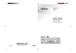
Service Manual
High-Fidelity AM/FM CD Player
Model
(PE-2628B-A / For U.S.A.)
(DRZ9255)
Model
(PE-2628K-A / For other countries)
PO
BA WER
TT
ER
SU
Y
PP
GR
LY
OU
ND
SPECIFICATIONS
FM tuner section
Frequency range:
87.9MHz to 107.9MHz(U.S.A.)
87.0MHz to 108.0MHz(OTHERS)
Usable sensitivity:
9dBf
50dB quieting sensitivity: 15dBf
Alternate channel selectivity:
70dB
Stereo separation:
35dB (1kHz)
Frequency response:
30Hz to 15kHz (+/-3dB)
8x oversampling digital filter
Blocked band attenuation:
-130 dB
Transmitted band attenuation:
+/-0.00001dB
Sampling rate converter
Input sampling rate:
fs32k, fs44.1k, fs48k,fs96k
Output sampling rate: fs48k, fs96k
DSP:
24-bit audio DSP, 34-bit arithmetic
operation (overflow margin 4-bit)
General
AM tuner section
Frequency range:
Usable sensitivity:
Power supply voltage:
530kHz to 1710kHz(U.S.A.)
531kHz to 1629kHz(OTHERS)
25uV
CD player section
System:
Usable discs:
Frequency response:
S/N ratio:
Dynamic range:
Distortion:
Compact disc digital audio system
Compact disc
5Hz to 20kHz (+/-1dB)
112dB (1kHz)
100dB (1kHz)
0.003%(20Hz to 20kHz)
+/-12dB (50Hz)
+/-12dB (10kHz)
Vol.0dB=4V
Vol.+6dB=8V(Max)
(CD 1kHz)
DSP/DAC
A/D conversion:
D/A conversion:
178(W)x50(H)x155(D)
163(W)x42(H)x98(D)
52(W)x125(H)x12(D)
1.8kg
700g
50g(including battery)
NOTES
Audio section
Bass control action:
Treble control action:
Line output level:
Current consumption:
Dimensions(mm)
Source unit:
DC-DC converter:
Remote control unit:
Weight
Source unit:
DC-DC converter:
Remote control unit:
14.4V DC(10.8V to 15.6V allowable) negative ground
Less than 5A
24-bit 64x oversampling
A/D converter
96kHz/24-bit advanced segment
D/A converter
-1-
* Use only compact discs bearing the
or
mark.Do
not play heart-shaped, octagonal, or other specially shaped
compact discs.
Some CDs recorded in CD-R/CD-RW mode may not be
usable.
* We cannot supply PWB with component parts in principle.
When a circuit on PWB has failure, please repair it by
component parts base. Parts which are not mentioned in
service manual are not supplied.
* Specifications and design are subject to change without
notice for further improvement.
DRZ9255
HX-D2
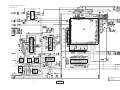
COMPONENTS
PE-2628B-A,PE-2628K-A
1.
2.
3.
4.
5.
6.
7.
8.
9.
Main unit
DC-DC converter
Rmote controller
Battery(CR2025)
Strap
Universal MTG-bracket
Outer escutcheon
16-Pin extension lead(1.5m)
(Fuse 3A
Memory B/U lead(YEL:3.5m)
(Fuse 10A
----------EE-1236B-A
RCB-169-600
----------300-4976-00
300-9035-01
370-6116-00
854-6428-00
120-0030-00
854-6423-01
060-0057-56
1
1
1
1
1
1
1
1
1 )
1
1 )
10.
11.
11-1.
11-2.
11-3.
11-4.
11-5.
12.
12-1.
12-2.
12-3.
Ground lead(BLK:1.5m)
854-6424-01
Parts bag for DC-DC converter ----------Mounting bracket
300-7362-02
Terminal cover
345-7403-00
Tapping screw
700-5016-89
Machine screw(M5x8)
714-4008-89
Plate nut
725-0216-00
Parts bag for source unit
----------Hook plate
330-8216-03
Lead holder
335-0833-03
Hexagonal screw(M5x8)
716-0496-01
1
1
2
1
4
4
4
1
2
1
1
CAUTIONS
Use of controls, adjustment or performance of procedures
other than those specified herein, may result in hazardous
radiation exposure.
The COMPACT DISC player should not be adjusted or repaired by anyone except properly qualified service personnel.
MODEL
12V
GROUND
AM 530 -1710kHz /FM 87.9 -107.9MHz
TH I S DEVICE COMPLIES WITH PART 15 OF THE FCC RULES.
OPERATION IS SUBJECT TO THE FOLLOWING TWO CONDITIONS:
(1) THIS DEVICE MAY NOT CAUSE HARMFUL INTERFERENCE, AND
(2) THIS DEVICE MUST ACCEPT ANY INTERFERENCE RECEIVED,
INCLUDING INTERFERENCE THAT MAY CAUSE UNDESIRED
OPERATION.
THIS PRODUCTION COMPLIES WITH DHHS RULES 21 CFR
SUBCHAPTER J APPLICABLE AT DATE OF MANUFACTURE.
CLARION CO.,LTD.
50 KAMITODA,TODA-SHI,SAITAMA-KEN,JAPAN
MANUFACTURED:
SERIAL No.
PE-
To engineers in charge of repair or inspection of our products.
Before repair or inspection, make sure to follow the
instructions so that customers and Engineers in
charge of repair or inspection can avoid suffering
any risk or injury.
1. Use specified parts.
The system uses parts with special safety features against
fire and voltage. Use only parts with equivalent characteristics when replacing them.
The use of unspecified parts shall be regarded as remodeling for which we shall not be liable. The onus of product
liability (PL) shall not be our responsibility in cases where
an accident or failure is as a result of unspecified parts
being used.
2. Place the parts and wiring back in their original positions
after replacement or re-wiring.
For proper circuit construction, use of insulation tubes,
bonding, gaps to PWB, etc, is involved. The wiring connection and routing to the PWB are specially planned using
clamps to keep away from heated and high voltage parts.
Ensure that they are placed back in their original positions
after repair or inspection.
If extended damage is caused due to negligence during
repair, the legal responsibility shall be with the repairing
company.
3. Check for safety after repair.
Check that the screws, parts and wires are put back securely in their original position after repair. Ensure for safety
reasons there is no possibility of secondary ploblems around
the repaired spots.
If extended damage is caused due to negligence of repair,
the legal responsibility shall be with the repairing company.
DRZ9255
HX-D2
Clarion Co.,Ltd.
MADE IN
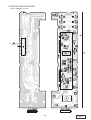
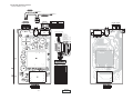
Bottom View of DRZ9255
4. Caution in removal and making wiring connection to the
parts for the automobile.
Disconnect the battery terminal after turning the ignition
key off. If wrong wiring connections are made with the
battery connected, a short circuit and/or fire may occur. If
extensive damage is caused due to negligence of repair,
the legal responsibility shall be with the repairing company.
5. Cautions regarding chips.
Do not reuse removed chips even when no abnormality is
observed in their appearance. Always replace them with
new ones. (The chip parts include resistors, capacitors,
diodes, transistors, etc). The negative pole of tantalum
capacitors is highly susceptible to heat, so use special care
when replacing them and check the operation afterwards.
6. Cautions in handling flexible PWB
Before working with a soldering iron, make sure that the
iron tip temperature is around 270 . Take care not to apply the iron tip repeatedly(more than three times)to the
same patterns. Also take care not to apply the tip with force.
7. Turn the unit OFF during disassembly and parts replacement. Recheck all work before you apply power to the unit.
8. Cautions in checking that the optical pickup lights up.
The laser is focused on the disc reflection surface through
the lens of the optical pickup. When checking that the laser optical diode lights up, keep your eyes more than 30cms
away from the lens. Prolonged viewing of the laser within
30cms may damage your eyesight.
9. Cautions in handling the optical pickup
The laser diode of the optical pickup can be damaged by
electrostatic charge caused by your clothes and body. Make
sure to avoid electrostatic charges on your clothes or body,
or discharge static electricity before handling the optical
pickup.
-2-
9-1. Laser diode
The laser diode terminals are shorted for transportation in order to prevent electrostatic damage. After
replacement, open the shorted circuit. When removing the pickup from the mechanism, short the
terminals by soldering them to prevent this damage.
9-2. Actuator
The actuator has a powerful magnetic circuit. If a
SYSTEM CHECK
magnetic material is put close to it. Its characteristics will change. Ensure that no foreign substances enter through the ventilation slots in the
cover.
9-3. Cleaning the lens
Dust on the optical lens affects performance. To
clean the lens, apply a small amount of isopropyl
alcohol to lens paper and wipe the lens gently.
Digital wiring
The first time this unit is turned on after the wire connections
are completed, it must be checked what equipment is connected. When the power is turned on, “SYSTEM CHK”
and “Push POWER”appear in the display alternately, so
press the [FUNC] button. The system check starts within
the unit. When the system check is complete, press the
[FUNC] button again.
When the optical digital cable is connected to or disconnected from this set later, press the function button while
holding down direct buttons [1] and [6] with the power OFF
to perform a system check.
Though pressing the reset button also performs a system
check, the contents of memory will be erased completely in
this case.
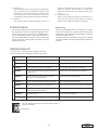
ERROR DISPLAYS
If an error occurs, one of the following displays is displayed.
Take the measures described below to eliminate the problem.
Error Display
Cause
Measure
A CD is caught inside the CD deck and is not ejected.
This is a failure of CD deck's mechanism.
ERROR 3
A CD cannot be played due to scratches,etc.
Replace with a non-scratched,non-warped-disc.
ERROR 2
A CD inside the CD changer is not loaded.
This is a failure of CD changer's mechanism.
ERROR 3
A CD inside the CD changer cannot be played due
to scratches, etc.
Replace with a non-scratched, non-warped disc.
ERROR 6
A CD inside the CD changer cannot be played
because it is loaded upside-down.
Eject the disc then reload it properly.
ERROR 2
A DISC inside the DVD changer cannot be played.
This is a failure of DVD mechanism.
ERROR 3
A DISC cannot be played due to scratches,etc.
Retry or replace with a non-scratched, non-warped-disc.
ERROR 6
A DISC inside the DVD changer cannot be played
because it is loaded upside-down.
Eject the disc then reload it properly.
ERROR P
Parental level error
Set the correct Parental level.
ERROR R
Region code error
Eject the disc and replace correct region code disc.
DVD changer
CD changer
CD
ERROR 2
If an error display other than the ones described above appears,
press the reset button.
Reset button
-3-
DRZ9255
HX-D2
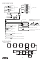
WIRE CONNECTIONS
Red
White
Red
AUX INPUT-1
Right
Red
White
AUX INPUT-1
Left
White
To external unit
Red
Red
AUX INPUT-2
Right
White
AUX INPUT-2
Left
Red
White
Black
White
Source unit
HIGH
Right
HIGH
Left
MID/FRONT
Right
MID/FRONT
Left
LOW/REAR
Right
LOW/REAR
Left
To external amplifier
Subwoofer
Right
Subwoofer
Left
Antenna input
Digital input/output
Optical digital cable
CeNET input
Black
CeNET cable
10-Pin Connector
16-Pin Connector Extension Lead 1.5m
Terminal Cover
Place the terminal cover on the terminals
to prevent a short circuit.
DC-DC Converter
Fuse(5A)
Terminal Cover
Brown wire(phone mute lead)
Connect to cellular
phone mute lead.
Black wire(Ground lead)1.5m
Connect to vehicle chassis ground.
Yellow wire(Bus power lead)
Connect directly to
battery.
Fuse(3A)
Fuse(10A)
Connect the terminal on the main power cord to
the car battery(+) terminal.
Yellow wire(Memory back-up lead)3.5m
Red wire(Power lead)
Accessory +12V
Blue/White wire(Amplifier turn-on lead)
Connect to remote turn-on lead of amplifier.
Orange/White wire(Illumination lead)
Connect to the car power supply terminal for illumination.
Blue wire(Auto antenna lead)
Connect it to the car supply terminal for the antenna.
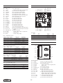
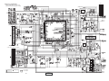
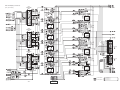
BLOCK DIAGRAM
Audio line sction
CD
Mechanism
IC903
DIGITAL
Digital
Interface
Receiver
IC915
DIGITAL
IC913
DIGITAL
Sampling
-rate
Converter
Digital
Signal
Processor
IC909
䌾IC911
DIGITAL
ANALOG
24bit
D/A
Converter
IC918
S-RAM
IC401
䌾IC406
ANALOG
IC407
䌾IC410
ANALOG
I/V
Converter
IC418
䌾IC421
Mid
ANALOG
Low-pass
Filter
8ch Line-out
Hi
High-quality
Electrical
Volume
Low
Sub-woofer
+
-15V
IC250
DC/DC
Converter
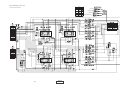
DRZ9255
HX-D2
-4-
-5-
DIGITAL IN
CD MECH
DRIVER
5V STB
ISOLAT
ISOLAT
SW PWB
EXPANDER
3.3V
STB
IC912
CLK IC
MASTER
U-COM
2.1V
DET
5V STB
IC200
POWER SUPPLY
ILL+B
DET
PHONE
INT
Q603
PHONE INT
DC/DC PWB
RCA LINEOUT
System section
KEY ILL
S718
VOL
DRZ9255
HX-D2
EXPLANATION OF IC
052-3393-00
M30622MEP-161GP
Terminal Description
pin 1: CD SBSY
System Controller
pin 60: VCC
pin 61: CD 5V
: - : Positive voltage supply.
: O : 5V power supply ON signal output for CD.
pin 62: VSS
: - : Negative voltage supply.
: IN : The sub Q data request command input
from the CD IC.
pin 63: REG CTRL
: O : Power supply IC control signal output.
pin 64: 5V REM
: O : 5V power supply ON signal output.
pin
2: TIME BASE
: IN : Time base pulse input.
pin 65: PLL SI
: IN : Serial data input from the PLL IC.
pin
3: DSP RDY
: IN : Ready signal input from the DSP IC.
pin
pin
4: NU
5: REMOCON
: - : Not in use.
: IN : Remote controller signal input terminal.
pin 66: PLL SO
pin 67: PLL SCK
: O : Serial data output to the PLL IC.
: O : The clock pulse output to the PLL IC.
pin 68: PLL CE
pin
6: BYTE
: IN : The data length selection(8bit/16bit).
pin
7: CN VSS
: IN : Connect to VSS.
pin
8: INIT 1
: IN : Destination setting input. Refer Table 1.
pin
9: INIT 2
: O : The chip enable signal output to the PLL
IC.
: IN : At receiving the FM station, this port detects the stereo signal. At seeking or scanning, this port detects the station detection
signal.
pin 10: RESET
pin 11: X out
pin 69: ST SD
: IN : Destination setting input. Refer Table 1.
: IN : Reset signal input.
: O : Crystal connection.
pin 70: VFD DD ON
: O : VFD DD converter ON signal output.
pin 71: ILL DET
: IN : Illumination ON signal input.
pin 12: VSS
: - : Negative voltage supply.
pin 72: DIR ERF
pin 13: X IN
: IN : Crystal connection.
: IN : Unlock & Parity error flag input from the
DIR IC.
: IN : The telephone interrupt signal input.
pin 14: VCC
: - : Positive voltage supply.
pin 73: PHONE INT
pin 15: NU
: - : Not in use.
pin 74: AUTO ANT
: O : Motor antenna control signal output.
pin 16: ACC DET
pin 17: BU DET
: IN : ACC detection signal input.
: IN : Backup detection signal input.
pin 75: AMP REM
: O : Standby signal output to Audio power amplifier.
pin 18: KEY INT
: IN : Key interrupting signal input.
pin 76: DIG In/Out sel
: O : Digital input/output selection.
pin 19: 27pinConnect
: IN : Connect to pin 27.
pin 77: SYS MUTE
: O : System muting signal output.
pin 20: VFD BLANK
: O : Blank pulse output to the VFD driver.
pin 21: BUS IN/out
: O : The audio signal control for Ce-NET.
pin 78: PRE MUTE
pin 79: SEL CLK
pin 22: BEEP
pin 23: E VOL CS
: O : Beep out.
: O : The chip select signal output to Electric
Volume IC.
: O : Pre-mute signal output.
: O : The serial clock output to the audio selector IC.
pin 80: SEL DATA
: O : The serial data output to the audio selector IC.
pin 24: E VOL SD
: O : The serial data output to Electric Volume
IC.
pin 81: KEY ILL REM
: O : Key illumination ON signal output.
pin 25: E VOL SCLK
: O : The serial clock output to Electric Volume
IC.
pin 82: DAC MC
pin 83: DAC MD
: O : Clock pulse output to the DAC.
: O : Serial command data output to the DAC.
pin 84: DAC MS
: O : Chip select output to the DAC.
pin 26: CLK REF
: O : Reference clock pulse output.
pin 85: DIR PDN
pin 27: IE BUS RX
: IN : IE Bus serial data input.
: O : The power down signal output to the DIR
IC.
pin 28: IE BUS TX
: O : IE Bus serial data output.
pin 29: EMULATOR TX : O : The serial data output to the emulator.
pin 86: PCM DET
: IN : Non-PCM detection signal input.
pin 87: DIR CDT O
: O : The control data output to the DIR IC.
pin 30: EMULATOR RX : IN : The serial data input from the emulator.
pin 88: DIR CCLK
: O : The control clock output to the DIR IC.
pin 31: CONNECT G
pin 89: DIR CSN
: O : The chip select output to the DIR IC.
pin 90: DSP INIT RST : O : The reset signal output to DSP IC.
: - : Connect to the ground.
pin 32: NU
: - : Not in use.
pin 33: VFD SO
pin 34: NU
: O : The serial data output to the VFD driver.
: - : Not in use.
pin 91: DSP RST
: O : Reset pulse output to the DSP IC.
pin 92: SYS ACC
: O : ACC detect signal output.
pin 35: VFD CLK
: O : The clock pulse output to the VFD driver.
pin 93: DSP REQ
: O : Request signal output to DSP IC.
: O : The latch strove signal output to the VFD
driver.
pin 94: A VSS
: - : Negative voltage supply for analog section.
pin 95: KEY AD
: IN : Input terminal of A/D converter for Key
judgment.
pin 36: VFD LAT
pin 37: JOG CW
: IN : Jog key signal input.
pin 38: JOG CCW
: IN : Jog key signal input.
pin 96: Vref
: - : Reference voltage.
pin 39: CONNECT G
: - : Connect to the ground.
pin 97: A VCC
pin 40: CATS LED
: O : CATS LED drive output.
: - : Positive voltage supply for the internal analog section.
pin 41: KEY Set
: O : Set signal output to the key scan IC.
pin 42: KEY CHIP SEL : O : The chip select signal output to the key
scan IC.
pin 98: DSP SI
: IN : Serial data input from the DSP IC.
pin 99: DSP SO
pin100: DSP SCK
: O : Serial data output to the DSP IC.
: O : The clock pulse output to DSP IC.
pin 43: KEY CLK
pin 44: CONNECT G
: O : The clock pulse output for the key scan IC.
: - : Connect to the ground.
pin 45: KEY DI
: IN : Key scan data input.
Japan
Noth America
pin 46: KEY DO
: O : The serial data output to the Key scan IC.
INIT 1 ( pin 8 )
H
H
L
pin 47: LD MUTE
: O : Muting signal output to the CD mechanism.
INIT 2 ( pin 9 )
H
L
L
pin 48: LD CONT
: O : The laser diode control signal output.
pin 49: CD TR A
: IN : The photo sensor signal input from the CD
mechanism.
pin 50: CD TR B
: IN : The photo sensor signal input from the CD
mechanism.
pin 51: CD CHK SW
: IN : CD disc chucking signal input.
pin 52: CD SSTOP
: IN : At loading, detects the chucking. And next,
detects the inside limit of the pick up position.
pin 53: CD RESET
: O : The reset pulse output to the CD IC.
pin 54: CD CCE
: O : The chip enable signal output to the CD
IC.
pin 55: CD BU CK
: O : CD IC clock pulse output.
pin 56: CD BUS 3
:I/O: The data bus.
pin 57: CD BUS 2
:I/O: The data bus.
pin 58: CD BUS 1
:I/O: The data bus.
pin 59: CD BUS 0
:I/O: The data bus.
DRZ9255
HX-D2
Table 1. Destination setting
-6-
Asia
051-6705-00
AK7720A
Terminal Description
pin 1: LFLT
Audio DSP with 2ch ADC and 6ch DAC
pin 61: I/O 3
pin 62: I/O 4
:I/O: Data input/output.
:I/O: Data input/output.
pin 63: I/O 5
:I/O: Data input/output.
: IN : The capacitor and the resistor connection
terminal for PLL.
pin 64: I/O 6
:I/O: Data input/output.
pin 65: I/O 7
:I/O: Data input/output.
pin
2: A VSS
: - : Analog ground.
pin 66: D VDD
pin
3: A VDD
: - : Positive supply voltage for the Analog section.
: - : Positive supply voltage for the digital section.
pin 67: D VSS
: - : Digital ground.
pin
4: INIT RESET
: IN : The initial reset input.
pin 68: TEST
: - : For the Test.
pin
5: CODEC RESET : IN : The CODEC reset input.
pin
6: DSP RESET
: IN : DSP reset input.
pin 69: TEST
pin 70: B VSS
: - : For the Test.
: - : Ground.
pin
pin
7: S MUTE
8: B VSS
: IN : The soft muting command input.
: - : Ground for the bus interface section.
pin 71: A OUT 3 R-
pin
9: PLL
: IN : Open or Connect to DVSS usually.
pin 72: A OUT 3 R+
: O : Inverted Right channel audio signal output
of DAC-3.
: O : Non-inverted Right channel audio signal
output of DAC-3.
pin 10: CKS
: IN : The clock pulse selection.
pin 11: S Data in A
: IN : DSP serial data input. Open or connect to
DVSS usually.
pin 12: S Data in 1
: IN : DSP serial data input.
pin 13: S Data in 2
: IN : DSP serial data input.
pin 14: S Data out 1
: O : DSP serial data output.
pin 73: NU
pin 74: A OUT 3 L-
: - : Not in use.
: O : Inverted Left channel audio signal output of
DAC-3.
pin 75: A OUT 3 L+
: O : Non-inverted Left channel audio signal output of DAC-3.
pin 76: A OUT 2 R-
: O : Inverted Right channel audio signal output
of DAC-2.
pin 77: A OUT 2 R+
: O : Non-inverted Right channel audio signal
output of DAC-2.
pin 78: NU
: - : Not in use.
pin 79: A OUT 2 L-
: O : Inverted Left channel audio signal output of
DAC-2.
pin 80: A OUT 2 L+
pin 20: S MODE
:I/O: SMODE(pin20) = L : 64fs clock input.
SMODE(pin20) = H : 64fs clock output.
: IN : Slave master selection.
: O : Non-inverted Left channel audio signal output of DAC-2.
pin 21: Clock Out
: O : Clock Out.
pin 81: NU
: - : Not in use.
pin 22: D VSS
: - : Digital ground.
pin 82: A OUT 1 R-
pin 23: D VDD
: - : Positive supply voltage for the digital section.
: O : Inverted Right channel audio signal output
of DAC-1.
pin 83: A OUT 1 R+
pin 24: XT I
: IN : Oscillation terminal.
pin 25: XT O
: O : Oscillation terminal.
: O : Non-inverted Right channel audio signal
output of DAC-1.
: - : Not in use.
pin 26: JX
: IN : External jumping signal input.
pin 27: RQ
: IN : The request signal input from the master
side.
pin 86: A OUT 1 L+
pin 28: S CLK
pin 29: SI
: IN : Sift clock input.
: IN : Serial data input.
pin 87: Vr DAC Low
: O : Inverted Left channel audio signal output of
DAC-1.
: O : Non-inverted Left channel audio signal output of DAC-1.
: IN : The reference voltage input.
pin 30: SO
: O : Serial data output.
pin 88: A VSS
: - : Analog ground.
pin 31: Write Ready
: O : Write ready flag output.
pin 15: S Data out 2
: O : DSP serial data output.
pin 16: S Data out 3/AD: O : DSP/ADC serial data output.
pin 17: S D OUT
: O : The serial data output.
pin 18: LR CK I/O
:I/O: SMODE(pin20) = L : 1fs clock input.
SMODE(pin20) = H : 1fs clock output.
pin 19: BIT CLK
pin 84: NU
pin 85: A OUT 1 L-
pin 32: Data Ready
: O : Data output ready flag output.
pin 33: CAS
: O : The column address strobe output to
DRAM.
pin 89: A VSS
: - : Analog ground.
pin 90: A VDD
: - : Positive supply voltage for the Analog section.
pin 91: Vr DAC High
: IN : The reference voltage input.
pin 92: NU
: - : Not in use.
pin 93: Vr ADC Low
: IN : The reference voltage input.
pin 94: A VSS
pin 95: A VDD
: - : Analog ground.
: - : Positive supply voltage for the Analog section.
pin 96: Vr ADC High
pin 97: A IN R-
: IN : The reference voltage input.
: IN : Inverted Right channel audio signal input.
pin 98: A IN R+
: IN : Non-inverted Right channel audio signal
input.
: IN : Inverted Left channel audio signal input.
pin 34: RAS
: O : The row address strobe output to DRAM.
pin 35: WRITE ENBL
: O : The write enable signal output.
pin 36: D VDD
: - : Positive supply voltage for the digital section.
pin 37: D VSS
: - : Digital ground.
pin 38: A 0
pin 39: A 1
: O : Address signal output.
: O : Address signal output.
pin 40: A 2
: O : Address signal output.
pin 41: A 3
: O : Address signal output.
pin 99: A IN L-
pin 42: A 4
: O : Address signal output.
pin100: A IN L+
pin 43: A 5
: O : Address signal output.
pin 44: A 6
pin 45: A 7
: O : Address signal output.
: O : Address signal output.
pin 46: A 8
: O : Address signal output.
pin 47: A 9
: O : Address signal output.
pin 48: A 10
: O : Address output to the external DRAM.
pin 49: A 11
: O : Address output to the external DRAM.
pin 50: A 12
pin 51: A 13
: O : Address signal output.
: O : Address signal output.
pin 52: A 14
: O : Address signal output.
pin 53: A 15
: O : Address signal output.
pin 54: A 16
: O : Address signal output.
pin 55: D VDD
: - : Positive supply voltage for the digital section.
pin 56: D VSS
: - : Digital ground.
pin 57: OUT ENABLE
: O : The output enable command output.
pin 58: I/O 0
pin 59: I/O 1
:I/O: Data input/output.
:I/O: Data input/output.
pin 60: I/O 2
:I/O: Data input/output.
-7-
: IN : Non-inverted Left channel audio signal input.
DRZ9255
HX-D2
051-6399-00
TC94A15F
Terminal Description
pin 1: IPF OUT
CD IC
pin 61: TRO
: O : Tracking equalizer output.
pin 62: Vref
: O : Reference voltage output.
pin 63: FMO
: O : Field equalizer output / Speed error output.
: O : IP flag output.
pin 64: DMO
: O : Disk equalizer output.
pin
pin
2: SB OK O
3: CLOCKIO
: O : Sub code Q data CRCC OK signal output.
:I/O: The clock pulse input/output for the sub
code reading.
pin 65: IO2A
:I/O: General input/output.
pin 66: IO3A
pin 67: MONIT
:I/O: General input/output.
: O : Internal DSP signal monitor.
pin
pin
4: VDD
5: VSS
: - : Positive supply voltage.
: - : Negative supply voltage.
pin 68: FG IN
: IN : FG input for the spindle CAV servo.
pin 69: VSS
: - : Negative supply voltage.
pin
6: DATA
: O : DATA
pin 70: VDD
: - : Positive supply voltage.
pin
7: SF SY O
: O : Playback frame synchronous signal output.
pin 71: TESIN
: IN : For test.
pin
8: SB SY O
: O : Sub code block synchronous signal output.
pin
pin 72: X VSS
pin 73: X IN
: - : Master clock analog ground.
: IN : Crystal connection.
: O : Crystal connection.
9: HSO
: O : The play speed flag output.
pin 10: UHSO
pin 11: AR SEL IN
: O : The play speed flag output.
: IN : Fix to the high level.
pin 74: X O
pin 75: X VDD
: - : Clock power supply.
pin 12: AWRC
: O : The control signal output for the active
wide range VCO.
: - : PLL positive supply voltage.
pin 76: D VSS
: - : Digital ground.
: O : Loop filter for VCO.
pin 21: VCO Ref
: IN : VCO reference voltage input.
pin 22: DTC N
pin 23: DTC P
: O : For the analog slicer.
: O : For the analog slicer.
pin 24: PLL VSS
: - : PLL ground.
pin 25: SLCO
: O : Output of internal DAC for data slice level
generation.
pin 26: RF IN
: IN : RF signal input.
pin 27: RF RP
: IN : RF ripple input.
pin 28: RF EQ OUT
: O : The output of the RF equalizer.
pin 29: A VDD
: - : Positive supply voltage for the Analog section.
pin 30: RES IN
: - : For reference current setting.
pin 31: Vref OUT
pin 32: VMDIR
: O : The reference voltage output.
: O : The reference voltage output.
pin 33: TESTR
pin 34: INVSEL
: O : The compensation terminal for RFEQO offset.
: IN : MDI polarity selection.
pin 35: AGCI
: IN : The input terminal of RF AGC amplifier.
pin 36: RF DCI
: IN : The input terminal for RF peak detection.
pin 37: RF OUT
: O : RF signal output.
pin 38: PN SEL
: IN : The transistor type selection input for laser
diode driver. L=NPN, H=PNP.
pin 39: EQ SET
: O : The equalizer setting terminal.
pin 40: RF VDD
: - : RF power supply.
pin 41: LDO
pin 42: MDI
: O : The laser diode drive output.
: IN : Monitor photo diode signal input.
pin 43: RF VSS
: - : RF ground.
pin 44: FNI 2
: IN : Main beam signal input.
pin 45: FNI 1
: IN : Main beam signal input.
pin 46: FPI 2
: IN : Main beam signal input.
pin 47: FPI 1
pin 48: TPI
: IN : Main beam signal input.
: IN : Sub beam signal input.
pin 49: TNI
: IN : Sub beam signal input.
pin 50: FTEO
: O : For test.
pin 51: RF ZI
: IN : RF ripple zero cross signal input.
pin 52: A VSS
: - : Analog ground.
pin 53: RF RP
pin 54: RF DC
: O : RF ripple signal output.
: O : RF peak detection signal output. (hologram
suitable)
pin 55: FEI
pin 56: SBAD
: O : Focus error signal output.
: O : Sub beam add signal output.
pin 57: TEI
: O : Tracking error signal output.
pin 58: TE Z IN
: IN : Tracking error signal inpur for zero cross.
pin 59: A VDD
: - : Positive supply voltage for the Analog section.
pin 60: FOO
: O : Focus equalizer output.
DRZ9255
HX-D2
: - : Negative supply voltage.
pin 84: BUS 0
:I/O: CD IC Data input / output.
pin 85: BUS 1
:I/O: CD IC Data input / output.
pin 86: BUS 2
pin 87: BUS 3
:I/O: CD IC Data input / output.
:I/O: CD IC Data input / output.
pin 88: BU CK IN
: IN : CD IC Data clock input.
pin 89: CCEI
: IN : Chip enable input.
pin 90: RSTI
: IN : Reset signal input.
pin 91: VDD
: - : Positive supply voltage.
pin 92: EMPHI/FAO
:I/O: Emphasis input for 1-bit DAC / Flag A
output.
pin 93: BCKI/FBO
:I/O: Bit clock input for 1-bit DAC / Flag B output.
pin 94: AIN/FCO
:I/O: Audio input for 1-bit DAC / Flag C output.
pin 95: LRCKI/FDO
:I/O: LR clock input for 1-bit DAC / Flag D output.
pin 96: EMPHO
: O : Emphasis flag output. H=Emphasis ON.
pin 97: B CK O
pin 98: A OUT
: O : Bit clock output.
: O : Audio signal output.
pin 99: LR CK O
: O : LR clock output.
pin100: D OUT
: O : Serial data output.
051-6643-90
M66010GP
24-bit I/O Expander
Parallel Data Input/Output
-8-
D 15 18
D 16 17
: - : PLL reference voltage.
pin 20: VCO FILTER
: O : 1bit DAC zero flag output.
pin 83: VSS
Parallel
Data
Input/Output
Ground
pin 19: P Vref
pin 82: Z DET O
D 10 23
D 11 22
D 12 21
D 13 20
D 14 19
: O : The output terminal for the Low Pass Filter.
10 D 22
11 D 21
12 D 20
13 D 19
14 D 18
15 D 17
16 GND
pin 18: LPF OUT
: O : Left channel data output for 1-bit DAC.
: - : Digital ground.
Ground
: IN : Inverted input of LPF for PLL.
: O : Digital reference voltage.
pin 80: LO
pin 81: D VSS
D 5 28
D 6 27
D 7 26
D 8 25
D 9 24
: O : T max judgment output.
pin 17: LPF N
pin 79: D Vref
5 VCC
6 SET
7 GND
8 D 24
9 D 23
pin 16: TMAX
: - : Positive supply voltage for the digital section.
Positive Supply
Set Signal input
pin 15: TMAX S
: O : Phase difference signal output of EFMPLCK.
: O : T max judgment output.
: O : Right channel data output for 1-bit DAC.
pin 78: D VDD
D 1 32
D 2 31
D 3 30
D 4 29
pin 14: PDO
pin 77: RO
Serial Data output 1 DO
Serial Data input
2 DI
Clock Pulse input 3 CLK
Chip Select input 4 CS
pin 13: P VDD
051-6373-18
AK4112BVF
Terminal Description
pin 1: D VDD
pin
2: D VSS
Digital Interface Receiver
: - : Positive voltage supply for the digital section.
: - : Digital ground.
Table 1. Audio data format
DIF 2
(pin 14)
DIF 1
(pin 13)
DIF 0
(pin 12)
D AUX
(pin 22)
SDT O
(pin 20)
LR CK
(pin 19)
0
16bit
Right
justified
64fs
0
24bit
Left
justified
H/L
0
Output
Output
24bit
Left
justified
18bit
Right
justified
H/L
64fs
1
Output
Output
20bit
Right
justified
H/L
64fs
0
24bit
Left
justified
Output
Output
24bit
Left
justified
24bit
Right
justified
H/L
64fs
Output
Output
24bit
Left
justified
24bit
Left
justified
H/L
64fs
Output
Output
24bit
24bit
L/H
64fs
0
0
BI CK
(pin 21)
pin
3: T VDD
: - : Positive voltage supply for output-buffer.
pin
4: VALIDITY
: TX
: O : Validity flag output in the parallel mode.
: O : Transmit channel (through data) output in
serial mode.
pin
pin
5: XT I
6: XT O
: IN : Oscillation terminal.
: O : Oscillation terminal.
0
pin
7: PDN
: IN : Power down & reset signal input.
1
pin
8: RESIST
: - : The resistor connection.
pin
9: A VDD
: - : Positive voltage supply for analog section.
pin 10: A VSS
: - : Negative voltage supply for analog section.
I2S
I2S
Output
Output
pin 11: RX 1
pin 12: DIF 0
: IN : The receiver channel 1 in serial mode.
: IN : The audio data format selection in parallel
mode, refer Table 1.
24bit
Left
justified
24bit
Left
justified
H/L
64-128fs
Intput
Input
24bit
24bit
H/L
64-128fs
I2S
I2S
Intput
Input
X'tal
fs(kHz)
: RX 2
pin 13: DIF 1
: IN : The receiver channel 2 in serial mode.
: IN : The audio data format selection in parallel
mode, refer Table 1.
: RX 3
pin 14: DIF 2
: IN : The receiver channel 3 in serial mode.
: IN : The audio data format selection in parallel
mode, refer Table 1.
: RX 4
pin 15: PCM DET
: IN : The receiver channel 4 in serial mode.
: O : Non-PCM detect. L = Non detect.
pin 16: PARA/SERI
: IN : Parallel("H")/Serial("L") mode select input.
pin 17: FS96
: O : 96kHz Sampling detect.
RX mode
H : fs = 88.2kHz or more
L : fs = 54kHz or less
Xtal mode
H : XFS96 = 1
L : XFS96 = 0
pin 18: ERF
: O : Unlock & Parity error output. L = No error.
pin 19: LR CK I/O
pin 20: SDT O
:I/O: Left/Right clock.
: O : The audio serial data output.
pin 21: BI CK
:I/O: Audio serial data clock.
0
1
1
1
1
1
0
0
1
1
1
0
1
0
1
Table 2. Master clock frequency select
OCK S 1 OCK S 0
(pin 26) (pin 25)
MCK O 1 MCK O 2
(pin 24) (pin 23)
32.0
44.1
48.0
96.0
0
0
256fs
256fs
256fs
0
1
256fs
128fs
256fs
1
0
512fs
256fs
512fs
32.0
44.1
48.0
1
1
-
-
Test Mode
-
-
PLL
X'tal
Clock
source
FS96
(pin 17)
SDT O
(pin 20)
32.0
44.1
48.0
96.0
Table 3. Clock operation mode select
CM 1
(pin 27)
CM 0
(pin 28)
UNLOCK
pin 22: D AUX
: IN : Auxiliary audio serial data input.
0
0
x
ON
OFF
PLL
RFS96
RX
pin 23: MCK O 2
: O : Master clock output, refer Table 2.
0
1
x
OFF
ON
X'tal
XFS96
D AUX
pin 24: MCK O 1
: O : Master clock output, refer Table 2.
1
0
0
ON
ON
PLL
RFS96
RX
pin 25: OCK Sel 0
: IN : Output clock select in parallel mode.
refer Table 2.
1
0
1
ON
ON
X'tal
XFS96
D AUX
1
1
x
ON
ON
X'tal
XFS96
D AUX
: CSN
pin 26: OCK Sel 1
: C CLK
pin 27: CM 1
: CDTI
pin 28: CM 0
: CDTO
: IN : Chip select input in serial mode.
: IN : Output clock select in parallel mode.
refer Table 2.
: IN : Control clock input in serial mode.
: IN : Master clock operation select input in parallel mode, refer Table 3.
: IN : Control data input in serial mode.
: IN : Master clock operation select input in parallel mode, refer Table 3.
: O : Control data output in serial mode.
-9-
DRZ9255
HX-D2
pin
4: S MUTE
: IN : The soft muting command input.
pin
5: DEM 0
: IN : De-emphasis Frequency Selection.
pin
6: DEM 1
: IN : De-emphasis Frequency Selection.
pin
7: I LR CK
: IN : Left/Right clock input for the input signal.
pin
pin
8: I BI CK
9: SDT I
: IN : Bit clock input for the input signal.
: IN : The serial data input.
Level
Shift
pin 12: I DIF 2
: IN : Input data format select.
pin 13: C MODE 0
: IN : The clock mode select.
pin 14: C MODE 1
pin 15: C MODE 2
: IN : The clock mode select.
: IN : The clock mode select.
pin 16: O DIF 0
: IN : Output data format select.
Level
Shift
Level
Shift
:I/O: Left/Right clock input/output for the output
signal.
pin 21: MASTER CLK
: IN : Master clock input.
pin 22: T VDD
pin 23: D VSS
: - : Positive voltage supply for output-buffer.
: - : Digital ground.
pin 24: VDD
: - : Positive voltage supply.
Truth Table
Table 1. Master/Slave control
Cmode 2 Cmode 1 Cmode 0
(pin 15) (pin 14) (pin 13)
Master CLK
(pin 21)
Master/Slave
(Output port)
L
L
L
256fso(fso to 96kHz)
Master
L
L
H
384fso(fso to 96kHz)
Master
L
H
L
512fso(fso to 48kHz)
Master
L
H
H
768fso(fso to 48kHz)
Master
H
L
L
Connect to DVSS
Slave
H
H
H
Connect to DVSS Master(bypass mode)
MUTE
(pin 9)
CNT
(pin 21)
CH1,2,3
output
CH4
output
H
H
MUTE OFF
LD ON
H
L
MUTE OFF
SL ON
L
H
MUTE ON
LD ON
L
L
MUTE ON
MUTE ON
051-5036-90
PGA2310UA
Stereo Volume Controller
ZCEN 1
Table 2. Input Audio data Formats
I DIF 2
(pin 12)
I DIF 1
(pin 11)
I DIF 0
(pin 10)
SDT I format
(pin 9)
I BI CK (slave)
(pin 8)
L
L
L
16bit LSB Justified
32 or less
L
L
H
20bit LSB Justified
40 or less
L
H
L
20bit MSB Justified
40 or less
L
H
H
20/16bit I2C compat.
32/40fs or less
H
L
L
24bit LSB Justified
48 or less
16 L IN
CS_ 2
S Data I 3
D VDD 4
15 L A GND
Logic
Control
D GND 5
SDT O format
(pin 18)
O BI CK
(Slave)
O BI CK
(Master)
L
L
16bit LSB Justified
64fs
64fs
L
H
20bit LSB Justified
64fs
64fs
H
L
20/16bit MSB Justif.
32/40fs or less
64fs
H
H
20/16bit I2C compat.
32/40fs or less
64fs
Table 4. De-emphasis filter control
DEM 1 (pin 6)
DEM 0 (pin 5)
De-emphasis filter
L
L
44.1kHz
13 A V-
11 R OUT
S Data O 7
10 R A GND
Mute In 8
Terminal Description
pin 1: ZCEN
14 L OUT
12 A V+
S CLK 6
Table 3. Output Audio data Formats
O DIF 0
(pin 16)
2-ch drive out- 13
2-ch drive out+ 14
:I/O: Bit clock input/output for the output signal.
pin 20: O LR CK
Power Vcc
10
1-ch drive out- 11
1-ch drive out+ 12
pin 19: O BI CK
8
9
: O : The audio serial data output.
Mute in
Power GND
: IN : Output data format select.
pin 18: SDT O
5
6
7
pin 17: O DIF 1
REG-Base
REG-FB
Pr-Ground
2.4V
3
4
: IN : Input data format select.
Level
Shift
1-ch OP in1-ch OP out
: IN : Input data format select.
pin 11: I DIF 1
2.4V
1
2
pin 10: I DIF 0
16 3-ch drive out15 3-ch drive out+
: - : Negative voltage supply for analog section.
: IN : Power down & reset signal input.
Quad Motor Drivers
19 Power Vcc
18 4-ch drive out17 4-ch drive out+
2: A VSS
3: PDN
28 Pre VCC
27 Bias
: O : PLL filter output.
pin
pin
O DIF 1
(pin 17)
BA5825FP-E2
21 Control in
20 Power Ground
051-6071-08
24 SL OP in23 SL OP out
22 Loading in-
Terminal Description
pin 1: FILT
Asynchronous Sample Rate Converter
26 3-ch OP in25 3-ch OP out
AK4121VF
2-ch OP in2-ch OP out
051-6708-90
9 R IN
: IN : Zero Cross Enable signal input.
pin
2: CS IN
: IN : The chip select command input.
pin
3: S DATA IN
: IN : The serial data input.
4: D VDD
5: D GND
: - : Positive voltage supply for digital section.
: - : Digital ground.
: IN : The serial clock input.
L
H
off
pin
pin
H
L
48.0kHz
pin
6: S CLK
L
H
32.0kHz
pin
7: S DATA OUT
: O : The serial data output.
pin
8: MUTE IN
: IN : Mute command input.
pin
9: R A IN
: IN : Right channel audio signal input.
pin 10: R A GND
pin 11: R A OUT
DRZ9255
HX-D2
: - : Right channel audio signal ground.
: O : Right channel audio signal output.
pin 12: A V+
: - : Positive voltage supply for analog section.
pin 13: A V-
: - : Negative voltage supply for analog section.
pin 14: L A OUT
: O : Left channel audio signal output.
pin 15: L A GND
: - : Left channel audio signal ground.
pin 16: L A IN
: IN : Left channel audio signal input.
- 10 -
051-9126-00
BS62LV1024STI-70
Terminal Description
pin 1: A 11
pin
pin
128 x 8 bit SRAM
PCM1792DBR
Terminal Description
pin 1: ZERO L
: IN : Address signal input.
2: A 9
3: A 8
051-6709-90
: IN : Address signal input.
: IN : Address signal input.
pin
pin
24bit 192kHz DA Converter
: O : ZERO flag output for Left channel.
2: ZERO R
3: M SEL
: O : ZERO flag output for Right channel.
: IN : I2C/SPI_ select.
pin
4: A 13
: IN : Address signal input.
pin
4: LR CK IN
: IN : Left/Right clock input.
pin
5: WE_
: IN : Write enable signal input.
pin
5: DATA IN
: IN : Serial data input.
pin
6: CE 2
: IN : The chip enable signal input.
pin
6: B CK IN
: IN : Bit clock input.
pin
7: A 15
: IN : Address signal input.
pin
7: SCK
: IN : The system clock pulse input.
pin
pin
8: VCC
9: NU
: - : Positive voltage supply.
: - : Not in use.
pin
pin
8: D GND
9: D VDD
: - : Digital ground.
: - : Positive voltage supply for the digital section.
pin 10: A 16
: IN : Address signal input.
pin 11: A 14
: IN : Address signal input.
pin 12: A 12
: IN : Address signal input.
pin 10: MS
pin 11: MDI
: IN : Chip select for mode control.
: IN : Mode control data input.
pin 13: A 7
: IN : Address signal input.
pin 12: MC
: IN : Mode control clock input.
pin 14: A 6
pin 15: A 5
: IN : Address signal input.
: IN : Address signal input.
pin 13: MD
: O : Mode control read back data output.
pin 14: RSTI
: IN : Reset signal input.
pin 16: A 4
: IN : Address signal input.
pin 15: A VCC
pin 17: A 3
: IN : Address signal input.
: - : Positive voltage supply for the internal analog section.
pin 18: A 2
: IN : Address signal input.
pin 19: A 1
: IN : Address signal input.
pin 20: A 0
pin 21: D 0
pin 16: A GND
: - : Analog ground.
pin 17: I out R+
: O : Right channel analog signal current output
+.
: IN : Address signal input.
:I/O: Data input/output.
pin 18: I out R-
: O : Right channel analog signal current output
-.
pin 22: D 1
:I/O: Data input/output.
pin 19: A GND
: - : Analog ground.
pin 23: D 2
:I/O: Data input/output.
pin 20: Iref
: - : Output current bias.
pin 24: GND
: - : Ground.
pin 21: V com R
: - : Right channel internal bias.
pin 25: D 3
:I/O: Data input/output.
pin 26: D 4
pin 27: D 5
:I/O: Data input/output.
:I/O: Data input/output.
pin 22: V com L
pin 23: A VCC
: - : Left channel internal bias.
: - : Positive voltage supply for the internal analog section.
pin 28: D 6
:I/O: Data input/output.
pin 29: D 7
:I/O: Data input/output.
pin 24: A GND
pin 25: I out L+
: - : Analog ground.
: O : Left channel analog signal current output +.
pin 30: CE 1_
: IN : The chip enable signal input.
pin 26: I out L-
pin 31: A 10
pin 32: OE_
: IN : Address signal input.
: IN : Output enable signal input.
pin 27: A GND
: O : Left channel analog signal current output .
: - : Analog ground.
pin 28: A VCC
: - : Positive voltage supply for the internal analog section.
Truth Table
WE_
(pin 5)
CE 1_
(pin 30)
CE 2
(pin 6)
OE_
(pin 32)
x
H
x
x
High Z
x
x
L
x
High Z
H
L
H
H
High Z
H
L
H
L
data out
L
L
H
x
data in
- 11 -
7
6
5
2
3
4 VEE
6
5
3
4 VEE
3: Output
7
2: Ground
pin
2
pin
Dual
VCC 8
Terminal Description
pin 1: Input(power source)
VCC 8
OP275GS
1
051-3012-90
Dual Operational Amplifier
1
11
6
3.3V Voltage Regulator
9
12
5
OPA2134UA
8 GND
NC 13
4
051-3042-90
10
14
3
uPD29M33T
Hex Buffer
7
15
1 VCC
051-3232-90
2
CD74HC4050PWR
NC 16
051-7285-08
I/O Operation
Operational
Amplifier
DRZ9255
HX-D2
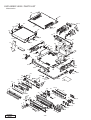
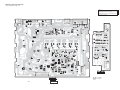
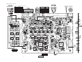
EXPLODED VIEW / PARTS LIST
Main section
40
E2
40
E1
E4
D2
74(x12)
38
82
79
39
40
E3
82
38
D1
42
D4
E2
60
86
38
47
41
40
82
D3
E2
E4
D2
87
38
51
64
63
62 61
71 72
85
E1
78
65
57
66
A1
73
92
83
77
91
69
E4
D1
D4
80
75
A1
E3 D3
82
58
53
40
59
A2
68
A2
92
82
76
46
91
84
45
55
30
67
36 37
70
52
43
81
46
31
35
34
32
27(x5)
10
48
9
33
26
54
11
44
31
25
32
24
88
4
8
90
23
22
21
12
18
20
89
56(x6)
19
7
6
29
49
5
17(x6)
16(x3)
28
50
2
3
13
14
1
15
DRZ9255
HX-D2
- 12 -
NO.
DESCRIPTION
Q'TY
NO.
378-0546-00 BADGE(PE2628BA:DRZ9255)
378-0547-00 BADGE(PE2628KA:HX-D2)
1
1
50
347-7379-00 SHADE FILM (PRESET)
6
2
371-5778-01 FACE PANEL(PE2628BA)
371-5778-00 FACE PANEL(PE2628KA)
1
1
51
816-4004-00 FLAT WIRE
1
52
347-7376-00 E-SHEET
1
3
373-1036-00 DIAL COVER
1
53
309-0798-00 FRONT PLATE
1
4
370-6112-01 ESCUTCHEON
1
54
714-2004-81 MACHINE SCREW (M2x4)
2
5
380-5591-00 KNOB CAP
1
55
716-0872-11 SCREW (M1.7x6)
2
6
345-5402-00 RUBBER RING
1
56
345-5140-00 RUBBER SPACER
6
1
PART NO.
PART NO.
DESCRIPTION
Q'TY
7
380-5592-00 INNER KNOB
1
57
305-0248-02 SIDE COVER (L)
1
8
335-7212-00 ILLUMI PLATE (L)
1
58
305-0249-02 SIDE COVER (R)
1
9
346-0163-00 LEATHER SHEET
1
59
313-1895-00 HEAT SINK
1
10
371-5779-00 TRIM PLATE
1
60
307-0702-00 REAR COVER
1
11
382-6997-00 BUTTON (L)
1
61
331-2946-00 SHIELD COVER (R)
1
12
335-7209-00 PACK ILLUMI
1
62
331-2945-00 SHIELD COVER (F)
1
13
382-6998-00 BUTTON (1-4)
1
63
347-7377-00 INSULATOR
1
14
382-6999-00 BUTTON (2-5)
1
64
313-1781-00 HEAT SINK
1
15
382-7000-00 BUTTON (3-6)
1
65
074-1023-16 OUTLET SOCKET (POWER)
1
16
335-7219-00 BUTTON ILLUMI
3
66
074-1194-00 OUTLET SOCKET (Ce NET)
1
17
335-7210-00 IND-ILLUMI
6
67
345-5796-00 CUSHION
1
18
335-7211-00 ILLUMI PLATE
1
68
074-1138-76 OUTLET SOCKET
1
19
335-7213-00 BUTTON HOLDER
1
69
075-0385-10 JACK (OPTICAL-IN)
1
20
382-6995-00 BUTTON (P/A)
1
70
347-7375-00 INSULATOR
1
21
382-6994-00 BUTTON (BAND)
1
71
076-6002-12 PLUG
1
22
382-6993-00 BUTTON (>>)
1
72
076-0515-08 PLUG (8P)
1
23
382-6992-00 BUTTON (ENT)
1
73
076-0515-12 PLUG (12P)
1
24
382-6991-00 BUTTON (<<)
1
74
345-3799-01 RUBBER PART
12
25
382-6990-00 BUTTON (FUNC)
1
75
076-0515-22 PLUG
1
26
382-6996-00 BUTTON (D)
1
76
304-0470-01 LOWER COVER
1
27
335-7215-00 BUTTON HOLDER
5
77
092-2214-00 ANT-RECEPT
1
28
335-7214-00 IR-FILTER
1
78
074-1106-08 OUTLET SOCKET
1
29
347-7383-00 DOUBLE FACE
2
79
303-0458-08 UPPER COVER
1
30
016-0025-00 VR W/SHAFT
1
80
074-1106-12 OUTLET SOCKET
1
31
347-7384-00 SHADE FILM(R/L)
2
81
32
347-7385-00 SHADE FILM(VFD)
2
286-6456-00 SETPLATE(PE2629BA)
286-6457-00 SETPLATE(PE2629KA)
1
1
33
347-7386-00 DOUBLE FACE(VFD)
1
82
714-3006-81 MACHINE SCREW (M3x6)
6
34
347-7387-00 DOUBLE FACE(ILLUMI)
2
83
覧覧
MAIN PWB
1
35
379-4053-28 VFD
1
84
345-5795-00 CUSHION
1
36
335-7216-00 VFD HOLDER
1
85
345-5797-00 HEAT RUBBER
1
37
335-7218-00 ILLUMI PLATE (C)
1
86
855-5500-00 RCA PIN CORD (4CH)
1
38
714-2603-81 MACHINE SCREW (M2.6x3)
4
87
880-2090B
1
39
345-5798-00 CUSHION
1
88
347-7415-00 FILM
1
40
716-0306-10 SCREW (M3x6)
7
89
347-7416-00 FILM
1
41
929-0291-80 CD MECH MODULE
1
90
347-7417-00 FILM
1
42
855-5505-00 RCA PIN CORD (8CH)
1
91
750-2796-02 SPRING
2
43
074-1105-22 OUTLET SOCKET
1
92
714-5008-41 MACHINE SCREW
2
44
347-7408-00 SHADE FILM
1
45
覧覧
46
716-0872-01 PAD SCREW (M1.7x5)
5
47
331-3775-00 MECH BRACKET
1
48
347-7380-00 SHADE FILM (L)
1
49
347-7382-00 SHADE FILM (R)
1
SWITCH PWB
TUNER PACK
1
- 13 -
DRZ9255
HX-D2
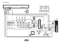
DC-DC converter(EE-1236B-A) section
NO.
11
10
18
11
10
9
12
8
PART NO.
DESCRIPTION
Q'TY
1
-----------
DC/DC PWB
2
073-0722-01 TERMINAL (BATT/GND)
1
3
077-0091-00 FUSE-RECEPT
1
4
074-0884-02 OUTLET SOCKET (10P)
1
5
060-0057-54 AUTO FUSE(5A)
1
6
331-3776-00 CONECTOR HOLDER
1
7
716-0821-02 IT SCREW
4
8
303-0487-00 UPPER COVER
1
9
383-0715-01 DECORATE PANEL
1
10
345-5443-00 O-RING
2
11
716-3521-00 LOCK SCREW (M3X4)
2
12
714-3006-89 MACHINE SCREW (M3X6)
4
13
311-1886-01 LOWER COVER
1
14
702-3008-89 TAP SCREW
2
15
702-2006-19 TAP SCREW
2
16
345-5444-00 SPACER
1
17
073-0731-01 TERMINAL
1
18
347-7378-00 PROTECT SHEET
1
1
6
7
12
7
4
1
13
16
7
5
3 2
17
15
14
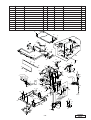
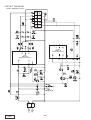
CD mechanism(929-0291-80) section
NO.
Q'TY
NO.
1
PART NO.
966-0595-25 DRIVE PLATE ASSY
DESCRIPTION
1
20
621-0603-25 LOCK ARM R
PART NO.
DESCRIPTION
Q'TY
1
2
969-0065-31 PICK UP UNIT
1
21
621-0724-21 GEAR BASE
1
3
-----------
LED PWB
1
22
621-0605-22 GEAR COVER
1
4
-----------
CD PWB
1
23
621-0723-20 IDLE CASE
1
5
SMA-182-100 MOTOR ASSY(SPINDLE)
1
24
816-2590-00 VINYL COAT WIRE(GRN)
1
6
SMA-183-100 MOTOR ASSY(SLED)
1
25
621-0608-21 SECOND GEAR
1
7
HBS-524-100 CLAMPER SUB ASSY
1
26
621-0609-20 BASE GEAR
1
7-1
620-1022-25 CLAMPER LINK
1
27
621-0610-20 IDLE GEAR A
1
7-2
620-1023-23 CLAMPER PLATE
1
28
621-0611-20 IDLE GEAR B
1
7-3
620-1024-23 SENSOR ARM
1
29
621-0612-21 ROLLER GEAR A
1
7-4
621-0708-20 CLAMPER RING
1
30
621-0719-20 ROLLER GEAR B
1
7-5
621-0626-21 STOPPER LINK
1
31
621-0720-20 ROLLER GEAR C
1
7-6
621-0627-21 DISC STOPPER
1
32
621-0721-20 ROLLER GEAR D
1
7-7
750-3471-20 SENSOR SPRING
1
33
621-0616-20 POWER GEAR A
1
8
803-4906-60 VINYL COAT WIRE(ORG)
1
34
621-0617-20 POWER GEAR B
1
9
816-2591-00 LEAD WIRE(YEL)
1
35
621-0618-20 POWER GEAR C
1
10
620-1025-22 ID-LOCK PLATE
1
36
621-0619-20 POWER GEAR D
1
11
620-1026-21 SPRING PLATE
1
37
621-0620-20 THREAD GEAR A
1
12
620-1027-27 LOWER CHASSIS
1
38
621-0621-20 THREAD GEAR B
1
13
620-1028-23 UPPER CHASSIS
1
39
621-0622-21 ROLLER SLEEVE
2
14
966-0638-20 SH-RACK ASSY
1
40
621-0623-23 LS-HOLDER
1
15
621-0598-27 UPPER GUIDE
1
41
621-0624-22 GUIDE RAIL
1
16
621-0599-26 ROLLER GUIDE
1
42
816-2593-00 LEAD WIRE(PUR)
1
17
621-0600-26 SHIFT LEVER
1
43
816-2542-01 FLAT WIRE(10P)
1
18
621-0601-21 RACK
1
44
716-3473-00 IT SCREW(M2 x 3)
2
19
621-0602-22 LOCK ARM L
1
45
621-0709-20 SH-BASE
1
DRZ9255
HX-D2
- 14 -
NO.
PART NO.
DESCRIPTION
Q'TY
NO.
PART NO.
DESCRIPTION
Q'TY
46
621-0629-20 LOADING ROLLER
2
57
750-3465-21 ROLLER SPRING L
1
47
345-8704-20 CUSHION RUBBER
1
58
750-3466-20 ROLLER SPRING R
1
48
622-1571-21 ROLLER SHAFT
1
59
750-3467-21 SHIFT SPRING
1
49
624-0018-01 LEAD SCREW
1
60
750-3468-20 RACK SPRING
1
50
629-0081-20 DAMPER F
2
61
750-3469-20 CLAMPER SPRING
1
51
629-0082-20 DAMPER R
1
62
750-3470-20 ID-LOCK SPRING
1
52
714-2003-81 MACHINE SCREW(M2 x 3)
2
63
816-2592-00 LEAD WIRE(BLU)
1
53
716-1507-00 SCREW(M2 x 3)
9
64
750-3472-21 DR-SPRING F
2
54
716-1733-00 SCREW(M1.7 x 2.3)
2
65
750-3473-20 DR-SPRING RA
1
55
716-3469-00 SCREW(φ3 x 4)
2
66
750-3474-20 DR-SPRING RB
1
56
716-3446-00 SCREW(M1.4 x 2.5)
2
67
750-3475-21 DR-SPRING C
1
A6
52
52
13
A4
A7
7-5
H3
H1
H2
19
F1
7-4
A5
3
44
E2
7-7
44
7-2
7-3
57
B2
15
D1
31
E1
G13
7-1
16
B1
7-6
M1
32
7
20
G12
D2
58
62
48
61
10
G5
17
46
G4
G1
G8
G14
54
39
G9
E2
G2
B2
G16 G15
1
40
B1
41
54
39
M1
G14 G5
G13
46
C5
G1
55
59
G3
G16
60
E1
18
G15
9 63 H3 8
H6
H1 42
24
H2 H4H5
A1
67
45
14
G4
G11 G10
G7
G8
G9
A3
G7 G10
A8
H7
G6
5
G6
I2
H8
G1
C2
H5
H4
3
A2
C6
H6
H7
C4
I1
53
C5
6
53
A6
65
C6
C7
21
56
A1
A3
50
G2
A4
2
C7
56
49
35
C1
11 L2 37 C3
29
36
53
51
25
34
38
30
G3
A7
A2
64
D1
50 47
C2
33
66
28
F1
A5
C4
C1
26
27
L1
A8
12
64
H8
22
C3
D2
I2
53
4
23
53
43
53
I1
- 15 -
DRZ9255
HX-D2
ELECTRICAL PARTS LIST
Main PWB(B1) section
REF No. PART No.
DESCRIPTION
REF No. PART No.
DESCRIPTION
REF No. PART No.
DESCRIPTION
BL1
C1
C2
C4
C5
C6
C7
C8
C9
C10
C11
C12
C13
C14
C16
C18
C20
C21
C22
C23
C24
C25
C26
C27
C28
C29
C55
C66
C67
C68
C200
C201
C203
C204
C205
C206
C207
C208
C210
C211
C212
C213
C214
C215
C216
C217
C218
C219
C220
C221
C222
C223
C224
C225
C226
C227
C228
C229
C230
880-2090B
168-2232-55
163-2263-35
163-1053-65
168-3332-78
168-3332-78
187-4763-35
168-2232-55
168-2232-55
168-6822-55
042-1631-50
042-1631-50
168-1032-55
168-1532-55
168-1032-55
163-3353-65
163-4763-15
166-1011-50
166-1011-50
166-1011-50
166-3311-50
166-1801-50
166-1501-50
163-2253-65
163-2253-65
168-2232-55
166-2201-50
166-2201-50
168-1032-55
168-1032-55
187-1073-35
187-1073-35
187-1063-35
042-9129-00
187-4763-35
042-1549-12
187-1063-35
042-1549-12
163-2263-35
187-4763-35
042-1631-50
042-1631-50
163-1063-35
168-1032-55
042-1631-50
163-2263-35
172-2231-15
168-1022-55
168-1042-78
187-1063-65
168-1022-55
043-0318-90
166-1011-50
168-1032-55
168-1032-55
168-1022-55
168-1022-55
168-1032-55
168-1022-55
C233
168-1022-55
C301
C302
C303
C304
C305
C306
C307
C308
C309
168-4732-78
168-4732-78
042-0654-52
042-0654-52
042-0654-52
042-0654-52
042-0654-52
042-0654-52
042-0654-52
16V 10uF
33pF CH
33pF CH
33pF CH
33pF CH
33pF CH
33pF CH
33pF CH
33pF CH
50V2.2uF
50V2.2uF
50V2.2uF
50V2.2uF
16V 100uF
16V 0.1uF
16V 10uF
16V 10uF
16V 10uF
16V 10uF
16V 10uF
16V 10uF
16V 10uF
16V 0.1uF
16V 10uF
16V 0.1uF
16V 0.1uF
50V1uF
50V1uF
50V1uF
50V1uF
16V22uF
0.47uF
16V10uF
16V 10uF
16V 10uF
16V 10uF
16V 10uF
33pF CH
33pF CH
33pF CH
33pF CH
16V 10uF
16V 10uF
16V 10uF
16V 10uF
0.01uF K
0.01uF K
0.01uF K
0.01uF K
1000pF K
100pF CH
2200pF
2200pF
2200pF
2200pF
2200pF
2200pF
2200pF
2200pF
2200pF
2200pF
2200pF
2200pF
560pF J
560pF J
560pF J
560pF J
560pF J
560pF J
560pF CH
560pF CH
220pF CH
220pF CH
166-2211-50
166-1211-50
166-2211-50
166-2211-50
166-2211-50
166-1211-50
166-2211-50
166-2211-50
166-2211-50
166-1211-50
166-2211-50
166-2211-50
166-2211-50
166-1211-50
168-1042-78
168-1022-55
168-1011-50
C310
C311
C312
C313
C314
C315
C316
C317
C318
C319
C320
C321
C322
C323
C324
C325
C326
C327
C328
C329
C330
C331
C332
C333
C334
C335
C336
C337
C338
C339
C340
C341
C342
C343
C344
C345
C346
C347
C348
C349
C350
C351
C352
C353
C354
C355
C356
C357
C358
C359
C360
C401
C402
C403
C404
C405
C406
C407
C408
C409
C410
C411
C412
C413
C414
C415
C416
C417
C418
C419
C420
C421
C422
C423
C424
C425
C426
C427
C428
C429
C430
C431
C432
C433
C434
C435
C436
C437
C439
C231
TUNER PACK
0.022uF K
16V22uF
50V1uF
0.033uF K
0.033uF K
16V47uF
0.022uF K
0.022uF K
6800pF K
10V100uF
10V100uF
0.01uF K
0.015uF K
0.01uF K
50V3.3uF
6.3V47uF
100pF CH
100pF CH
100pF CH
330pF CH
18pF CH
15pF CH
50V2.2uF
50V2.2uF
0.022uF K
22pF CH
22pF CH
0.01uF K
0.01uF K
16V 100uF
16V 100uF
16V 10uF
16V270uF
16V47uF
16V220uF
16V 10uF
16V220uF
16V22uF
16V47uF
10V100uF
10V100uF
16V10uF
0.01uF K
10V100uF
16V22uF
0.022uF
1000pF K
16V 0.1uF
50V10uF
1000pF K
5600pF
100pF CH
0.01uF K
0.01uF K
1000pF K
1000pF K
0.01uF K
1000pF K
(PE2628KA)
100pF CH
(PE2628KA)
1000pF K
(PE2628KA)
0.047uF K
0.047uF K
16V 10uF
16V 10uF
16V 10uF
16V 10uF
16V 10uF
16V 10uF
16V 10uF
C440
C441
C442
C443
C449
C450
C451
C452
C453
C454
C455
C456
C457
C458
C459
C460
C461
C462
C463
C464
C465
C466
C467
C468
C469
C470
C471
C472
C473
C474
C475
C476
C477
C478
C479
C480
C481
C482
C483
C484
C485
C486
C487
C488
C489
C491
C492
C493
C600
C601
C603
C605
C609
C612
C615
C900
042-0654-50
042-0654-50
042-0654-50
042-0654-50
168-1032-55
168-1032-55
168-1032-55
168-1032-55
168-1032-55
168-1032-55
168-1032-55
168-1032-55
168-1032-55
168-1032-55
168-1032-55
168-1032-55
168-1032-55
168-1032-55
168-1032-55
168-1032-55
042-1505-89
042-1505-89
042-1505-89
042-1505-89
168-1032-55
168-1032-55
168-1032-55
168-1032-55
168-1032-55
168-1032-55
042-1505-89
042-1505-89
042-1505-89
042-1505-89
168-1032-55
168-1032-55
042-1547-00
042-1547-00
042-1547-00
042-1547-00
042-1547-00
042-1547-00
042-1563-68
042-1563-68
168-1032-55
042-1547-00
042-1547-00
168-1032-55
168-1032-55
042-1576-01
168-1032-55
042-1577-00
168-4732-78
163-1063-35
168-1032-55
168-1032-55
220pF CH
12pF CH
220pF CH
220pF CH
220pF CH
12pF CH
220pF CH
220pF CH
220pF CH
12pF CH
220pF CH
220pF CH
220pF CH
12pF CH
16V 0.1uF
1000pF K
(PE2628KA)
6.3V 22uF
6.3V 22uF
6.3V 22uF
6.3V 22uF
0.01uF K
0.01uF K
0.01uF K
0.01uF K
0.01uF K
0.01uF K
0.01uF K
0.01uF K
0.01uF K
0.01uF K
0.01uF K
0.01uF K
0.01uF K
0.01uF K
0.01uF K
0.01uF K
10V10uF(OS)
10V10uF(OS)
10V10uF(OS)
10V10uF(OS)
0.01uF K
0.01uF K
0.01uF K
0.01uF K
0.01uF K
0.01uF K
10V10uF(OS)
10V10uF(OS)
10V10uF(OS)
10V10uF(OS)
0.01uF K
0.01uF K
16V22uF
16V22uF
16V22uF
16V22uF
16V22uF
16V22uF
16V22uF
16V22uF
0.01uF K
16V22uF
16V22uF
0.01uF K
0.01uF K
5.5V0.22uF
0.01uF K
6.3V100uF
0.047uF K
16V10uF
0.01uF K
0.01uF K
DRZ9255
HX-D2
042-0654-52
166-3301-50
166-3301-50
166-3301-50
166-3301-50
166-3301-50
166-3301-50
166-3301-50
166-3301-50
163-2253-65
163-2253-65
163-2253-65
163-2253-65
187-1073-35
168-1042-78
042-0654-52
042-0654-52
042-0654-52
042-0654-52
042-0654-52
042-0654-52
042-0654-52
168-1042-78
042-0654-52
168-1042-78
168-1042-78
163-1053-65
163-1053-65
163-1053-65
163-1053-65
163-2263-35
178-4742-78
042-0423-97
042-0654-52
042-0654-52
042-0654-52
042-0654-52
166-3301-50
166-3301-50
166-3301-50
166-3301-50
042-0654-52
042-0654-52
042-0654-52
042-0654-52
168-1032-55
168-1032-55
168-1032-55
168-1032-55
168-1022-55
166-1011-50
043-0264-51
043-0264-51
043-0264-51
043-0264-51
043-0264-51
043-0264-51
043-0264-51
043-0264-51
043-0264-51
043-0264-51
043-0264-51
043-0264-51
173-5611-18
173-5611-18
173-5611-18
173-5611-18
173-5611-18
173-5611-18
166-5611-50
166-5611-50
166-2211-50
166-2211-50
- 16 -
REF No.
C901
C902
C903
C904
C905
C906
C908
C909
C910
C911
C912
C913
C914
C915
C916
C917
C918
C919
C920
C921
C922
C923
C924
C925
C926
C927
C928
C929
C930
C931
C932
C933
C934
C935
C936
C937
C938
C939
C940
C941
C942
C943
C944
C945
C946
C947
C948
C949
C950
C951
C952
C953
C954
C955
C956
C957
C958
C959
C960
C961
C962
C963
C964
C965
C966
C967
C968
C969
C970
C975
PART No.
168-1042-78
042-0423-20
042-0423-20
168-1042-78
166-8096-50
166-8096-50
168-1042-78
168-1042-78
163-1063-35
168-1042-78
168-1042-78
168-1042-78
168-1022-55
042-0423-94
168-1042-78
163-1063-35
168-1042-78
042-0423-20
042-0423-97
042-0423-20
168-1042-78
168-1042-78
042-0423-20
168-1042-78
168-1042-78
168-1042-78
166-1011-50
168-6822-55
168-1042-78
042-0423-20
042-0423-20
168-1042-78
168-1042-78
042-0423-20
168-1032-55
168-1022-55
178-4742-78
168-1042-78
168-1022-55
042-0423-20
168-1042-78
168-1032-55
168-1032-55
042-0423-20
168-1042-78
168-1042-78
168-1042-78
042-0632-50
042-0632-50
042-0632-50
168-1042-78
168-1042-78
168-1042-78
168-1042-78
168-1042-78
168-1042-78
042-0632-50
042-0632-50
042-0632-50
168-1032-55
042-0592-58
042-0423-97
042-0592-58
042-0592-58
042-0423-97
042-0592-58
042-0592-58
042-0423-97
042-0592-58
166-1011-50
C977
C978
C979
C980
C981
C982
166-1011-50
168-1032-55
166-1011-50
168-1022-55
168-1022-55
168-1032-55
DESCRIPTION
16V 0.1uF
10V10uF
10V10uF
16V 0.1uF
8pF D CH
8pF D CH
16V 0.1uF
16V 0.1uF
16V10uF
16V 0.1uF
16V 0.1uF
16V 0.1uF
1000pF K
10V 4.7uF
16V 0.1uF
16V10uF
16V 0.1uF
10V10uF
16V10uF
10V10uF
16V 0.1uF
16V 0.1uF
10V10uF
16V 0.1uF
16V 0.1uF
16V 0.1uF
100pF CH
6800pF K
16V 0.1uF
10V10uF
10V10uF
16V 0.1uF
16V 0.1uF
10V10uF
0.01uF K
1000pF K
0.47uF
16V 0.1uF
1000pF K
10V10uF
16V 0.1uF
0.01uF K
0.01uF K
10V10uF
16V 0.1uF
16V 0.1uF
16V 0.1uF
6.3V47uF
6.3V47uF
6.3V47uF
16V 0.1uF
16V 0.1uF
16V 0.1uF
16V 0.1uF
16V 0.1uF
16V 0.1uF
6.3V47uF
6.3V47uF
6.3V47uF
0.01uF K
16V10uF
16V10uF
16V10uF
16V10uF
16V10uF
16V10uF
16V10uF
16V10uF
16V10uF
100pF CH
(PE2628BA)
100pF CH
0.01uF K
100pF CH
1000pF K
1000pF K
0.01uF K
REF No. PART No.
DESCRIPTION
C983
166-2211-50 220pF CH
(PE2628BA)
C984
168-1032-55 0.01uF K
C986
168-1022-55 1000pF K
C987
168-1032-55 0.01uF K
C988
168-1032-55 0.01uF K
C989
168-1032-55 0.01uF K
C9005 168-1032-55 0.01uF K
C9006 168-1032-55 0.01uF K
CCT901 010-3042-54 BLA3216A601
SG4T1
CCT902 010-3042-54 BLA3216A601
SG4T1
CCT903 010-3042-54 BLA3216A601
SG4T1
CCT904 010-3042-54 BLA3216A601
SG4T1
CCT905 010-3042-54 BLA3216A601
SG4T1
CCT906 010-3042-54 BLA3216A601
SG4T1
CCT907 010-3042-54 BLA3216A601
SG4T1
D201
001-0529-68 MA8180-L
D202
001-0516-90 MA111
D203
001-0516-90 MA111
D205
001-0516-90 MA111
D206
001-0516-90 MA111
D207
001-0516-90 MA111
D208
001-0516-90 MA111
D209
001-0466-91 S5688G
D210
001-0466-91 S5688G
D215
001-0529-32 MA8056-M
D219
001-0529-14 MA8030-L
D301
001-0516-90 MA111
D302
001-0516-90 MA111
D303
001-0516-90 MA111
D311
001-0529-44 MA8082-M
D350
001-0516-90 MA111
D351
001-0516-90 MA111
D352
001-0516-90 MA111
D353
001-0516-90 MA111
D450
001-0529-38 MA8068-M
D451
001-0516-90 MA111
D452
001-0529-38 MA8068-M
D453
001-0516-90 MA111
D454
001-0529-38 MA8068-M
D455
001-0516-90 MA111
D456
001-0529-38 MA8068-M
D600
001-0516-90 MA111
D601
001-0516-90 MA111
D602
001-0516-90 MA111
D603
001-0529-32 MA8056-M
D604
001-0529-32 MA8056-M
D901
001-0516-90 MA111
D902
001-0516-90 MA111
D903
001-0535-90 MA729
D904
001-0535-90 MA729
D905
001-0535-90 MA729
D906
001-0535-90 MA729
D907
001-0535-90 MA729
D908
001-0535-90 MA729
D909
001-0535-90 MA729
D910
001-0535-90 MA729
FIL901 060-3110-90 NFM4516P13C204
FBI
FIL902 060-3110-90 NFM4516P13C204
FBI
FIL903 060-3110-90 NFM4516P13C204
FBI
FIL904 060-3110-90 NFM4516P13C204
FBI
IC1
051-6212-08 LC72191JM-TLM
IC200
051-3297-10 BA4916-V2
IC301
051-3026-90 NJM4580V
IC302
051-3026-90 NJM4580V
IC303
051-5020-90 M61508FP
- 17 -
REF No.
IC304
IC305
IC306
IC307
IC401
IC402
IC403
IC404
IC405
IC406
IC407
IC408
IC409
IC410
IC418
IC419
IC420
IC421
IC600
IC601
PART No.
051-3034-90
051-7232-08
051-3026-90
051-3026-90
051-3042-90
051-3042-90
051-3042-90
051-3042-90
051-3042-90
051-3042-90
051-3042-90
051-3042-90
051-3042-90
051-3012-90
051-5036-90
051-5036-90
051-5036-90
051-5036-90
052-3393-00
051-5437-08
IC602
IC901
051-6600-58
051-7221-58
IC902
051-7243-48
IC903
IC905
051-6373-18
051-7221-58
IC906
051-7269-08
IC907
IC909
IC910
IC911
IC912
IC913
IC915
IC916
IC918
J200
J401
J402
J600
J602
J901
JW1
JW2
JW3
L1
L2
L3
L4
L5
L52
L230
051-7285-08
051-6709-90
051-6709-90
051-6709-90
051-6620-08
051-6705-00
051-6708-90
051-9126-00
051-3232-90
074-1023-16
074-1106-08
074-1106-12
074-1194-00
074-1138-76
075-0385-10
119-0000-05
119-0000-05
119-0000-05
010-2275-53
010-3103-64
010-3103-64
010-3406-54
010-3406-54
010-4046-00
119-0000-05
L230
010-3103-64
L301
L302
L310
L311
L490
L601
L902
L903
L904
L905
L906
L907
L908
L910
L911
L913
L914
L915
010-3406-66
010-3406-66
010-3103-64
010-3103-64
010-2326-00
010-3406-54
010-3103-64
010-3103-64
010-3103-64
010-3103-64
010-3103-64
010-3103-64
010-3103-64
010-3103-64
010-3406-62
010-3103-64
010-3103-64
010-3103-64
DESCRIPTION
NJM4558V
74VHC4066M
NJM4580V
NJM4580V
OPA2134UA
OPA2134UA
OPA2134UA
OPA2134UA
OPA2134UA
OPA2134UA
OPA2134UA
OPA2134UA
OPA2134UA
OP275GS
PGA2310UA
PGA2310UA
PGA2310UA
PGA2310UA
M30622MEP-161GP
S-80821ANMP-EDJE2
HA12187FP
SN74AHC1G04
HDCKR
SN74AHCT1G08
DCKR
AK4112BVF-E2
SN74AHC1G04
HDCKR
SN74AHC2G53
HDCTR
CD74HC4050PWR
PCM1792DBR
PCM1792DBR
PCM1792DBR
TC9246F
AK7720A
AK4121VF-E2
BS62LV1024STI-70
uPC29M33T
16P
8P
12P
13P CE-NET
26P
OPT JACK
1/10W 0 ohm JW
1/10W 0 ohm JW
1/10W 0 ohm JW
220uH
MMZ1608Y1
MMZ1608Y1
2.2uH
2.2uH
30uH
1/10W 0 ohm JW
(PE2629BA)
MMZ1608Y1
(PE2629KA)
22uH
22uH
MMZ1608Y1
MMZ1608Y1
BL02RN2-R62
2.2uH
MMZ1608Y1
MMZ1608Y1
MMZ1608Y1
MMZ1608Y1
MMZ1608Y1
MMZ1608Y1
MMZ1608Y1
MMZ1608Y1
10uH
MMZ1608Y1
MMZ1608Y1
MMZ1608Y1
DRZ9255
HX-D2
REF No.
L916
L917
L918
L919
L920
L921
L922
L923
L924
L925
L926
L927
L928
L929
L930
L931
L932
L933
L934
L935
L936
L937
L938
L939
L940
L941
L942
L946
L947
L948
L949
L950
L951
L952
L953
L954
L955
L956
L957
L958
L959
L960
L961
L962
L963
L964
L965
L966
P1
P401
P402
P501
Q1
Q2
Q3
Q4
Q5
Q6
Q7
Q201
Q202
Q203
Q204
Q205
Q207
Q215
Q216
Q217
Q218
Q219
Q220
Q230
Q234
Q235
Q236
Q238
Q239
PART No.
010-3406-66
010-2285-58
010-3103-64
010-3103-64
010-3103-64
010-3103-64
010-3103-64
010-3103-64
010-3103-64
010-3103-64
010-3103-64
010-3103-64
010-3103-64
010-3103-64
010-3103-64
010-3103-64
010-3103-64
010-3103-64
010-3103-64
010-3103-64
010-3103-64
010-3103-64
010-3103-64
010-3103-64
010-3103-64
010-3103-64
010-3103-64
010-3103-64
010-3103-64
010-3103-64
010-3103-64
010-3103-64
010-3103-64
010-3103-64
010-3103-64
010-3103-64
010-3103-64
010-3103-64
010-3103-64
010-3103-64
010-3103-64
010-3103-64
010-3103-64
010-3103-64
010-3103-64
010-3103-64
010-3103-64
010-3103-64
076-0515-22
076-0515-08
076-0515-12
076-6002-12
192-2712-51
192-2712-51
193-1858-00
125-2004-93
190-1162-00
190-1162-00
190-1162-00
125-2004-96
190-1298-00
192-2712-00
190-1162-00
190-1162-00
192-2712-00
103-2012-00
125-2004-93
191-1237-00
125-2004-93
191-1237-00
125-2004-93
191-1237-50
125-0002-92
193-1802-60
125-2004-92
125-0013-97
125-2004-92
DRZ9255
HX-D2
DESCRIPTION
22uH
BLM21A102FPB
MMZ1608Y1
MMZ1608Y1
MMZ1608Y1
MMZ1608Y1
MMZ1608Y1
MMZ1608Y1
MMZ1608Y1
MMZ1608Y1
MMZ1608Y1
MMZ1608Y1
MMZ1608Y1
MMZ1608Y1
MMZ1608Y1
MMZ1608Y1
MMZ1608Y1
MMZ1608Y1
MMZ1608Y1
MMZ1608Y1
MMZ1608Y1
MMZ1608Y1
MMZ1608Y1
MMZ1608Y1
MMZ1608Y1
MMZ1608Y1
MMZ1608Y1
MMZ1608Y1
MMZ1608Y1
MMZ1608Y1
MMZ1608Y1
MMZ1608Y1
MMZ1608Y1
MMZ1608Y1
MMZ1608Y1
MMZ1608Y1
MMZ1608Y1
MMZ1608Y1
MMZ1608Y1
MMZ1608Y1
MMZ1608Y1
MMZ1608Y1
MMZ1608Y1
MMZ1608Y1
MMZ1608Y1
MMZ1608Y1
MMZ1608Y1
MMZ1608Y1
22P
8P
12P
PLUG
2SC2712G,L
2SC2712G,L
2SD1858
RN1403
2SA1162
2SA1162
2SA1162
RN1406
2SA1298
2SC2712
2SA1162
2SA1162
2SC2712
2SD2012
RN1403
2SB1237
RN1403
2SB1237
RN1403
2SB1237QR
RN2402
2SD1802FA-R.S.T
RN1402
RN2427
RN1402
REF No.
Q240
Q300
Q301
Q302
Q303
Q413
Q414
Q415
Q416
Q417
Q418
Q419
Q420
Q421
Q422
Q600
Q601
Q602
Q603
Q604
Q605
Q606
Q901
Q902
Q903
Q904
R1
R2
R3
R4
R5
R6
R7
R9
R10
R14
R15
R16
R17
R18
R19
R20
R21
R24
R25
R27
R28
R29
R30
R83
R200
R201
R202
R203
R204
R205
R206
R207
R209
R210
R211
R212
R213
R216
R217
R224
R225
R226
R227
R228
R229
R230
R231
R233
R234
R235
R255
PART No.
125-2004-96
125-2004-93
125-2004-96
192-2712-00
125-2004-92
193-1328-00
193-1328-00
193-1328-00
193-1328-00
193-1328-00
125-0002-92
193-1328-00
125-0002-92
193-1328-00
193-1328-00
125-2004-92
125-2004-93
125-2004-93
190-1162-00
125-0002-92
125-2004-93
125-2004-93
125-2004-92
125-2004-93
125-2004-92
125-2004-92
119-1021-15
119-3311-15
119-4721-15
119-4721-15
119-1231-15
119-1231-15
119-1231-15
119-4741-15
119-2221-15
119-5631-15
119-1031-15
119-2221-15
119-1521-15
119-1031-15
119-1031-15
119-1031-15
119-1021-15
119-1521-15
119-1521-15
119-1021-15
119-1021-15
119-1021-15
119-1041-15
119-1021-15
119-1041-15
119-1041-15
119-5621-15
119-4731-15
119-5631-15
119-1031-15
119-1031-15
119-1021-15
119-1531-15
119-1031-15
119-4731-15
119-4721-15
119-2221-15
119-1021-15
119-2231-15
119-4701-15
119-1031-15
116-1221-15
119-1031-15
116-1221-15
116-1521-15
119-2221-15
116-2211-15
119-1031-15
119-1031-15
119-2221-15
116-4701-15
DESCRIPTION
RN1406
RN1403
RN1406
2SC2712
RN1402
2SD1328
2SD1328
2SD1328
2SD1328
2SD1328
RN2402
2SD1328
RN2402
2SD1328
2SD1328
RN1402
RN1403
RN1403
2SA1162
RN2402
RN1403
RN1403
RN1402
RN1403
RN1402
RN1402
1/10W 1k ohm
1/10W 330 ohm
1/10W 4.7k ohm
1/10W 4.7k ohm
1/10W 12k ohm
1/10W 12k ohm
1/10W 12k ohm
1/10W 470k ohm
1/10W 2.2k ohm
1/10W 56k ohm
1/10W 10k ohm
1/10W 2.2k ohm
1/10W 1.5k ohm
1/10W 10k ohm
1/10W 10k ohm
1/10W 10k ohm
1/10W 1k ohm
1/10W 1.5k ohm
1/10W 1.5k ohm
1/10W 1k ohm
1/10W 1k ohm
1/10W 1k ohm
1/10W 100k ohm
1/10W 1k ohm
1/10W 100k ohm
1/10W 100k ohm
1/10W 5.6k ohm
1/10W 47k ohm
1/10W 56k ohm
1/10W 10k ohm
1/10W 10k ohm
1/10W 1k ohm
1/10W 15k ohm
1/10W 10k ohm
1/10W 47k ohm
1/10W 4.7k ohm
1/10W 2.2k ohm
1/10W 1k ohm
1/10W 22k ohm
1/10W 47 ohm
1/10W 10k ohm
1/4W 1.2k ohm
1/10W 10k ohm
1/4W 1.2k ohm
1/4W 1.5k ohm
1/10W 2.2k ohm
1/4W 220 ohm
1/10W 10k ohm
1/10W 10k ohm
1/10W 2.2k ohm
1/4W 47 ohm
- 18 -
REF No.
R256
R257
R301
R302
R303
R304
R305
R306
R307
R308
R309
R310
R311
R312
R313
R314
R315
R316
R317
R318
R319
R320
R321
R322
R323
R324
R325
R326
R327
R328
R329
R330
R331
R332
R333
R334
R335
R336
R337
R338
R339
R340
R341
R342
R343
R344
R345
R346
R347
R348
R349
R350
R351
R352
R353
R354
R355
R356
R357
R358
R359
R360
R361
R362
R363
R364
R365
R366
R367
R368
R369
R370
R371
R372
R373
R401
R402
PART No.
116-4701-15
116-1221-15
119-1041-15
119-1041-15
119-1041-15
119-1041-15
119-1021-15
119-1021-15
032-0140-58
032-0140-58
032-0140-58
032-0140-58
032-0140-58
032-0140-58
032-0140-58
032-0140-58
119-1031-15
119-1031-15
119-1031-15
119-1031-15
119-1031-15
119-1031-15
119-1031-15
119-1031-15
032-0140-96
032-0140-96
032-0140-96
032-0140-96
119-4721-15
119-4721-15
119-1241-15
119-1041-15
119-1221-15
119-1021-15
119-3311-15
119-3311-15
119-3311-15
119-3311-15
032-0140-51
032-0140-51
032-0140-51
032-0140-51
119-1011-15
119-1011-15
119-1011-15
119-1011-15
119-4731-15
119-2731-15
119-2731-15
119-1031-15
119-1031-15
119-1031-15
119-1831-15
119-1021-15
119-1021-15
119-8221-15
119-1021-15
119-1021-15
119-2231-15
119-2731-15
119-2731-15
119-5631-15
119-1031-15
119-1031-15
119-1031-15
119-1031-15
119-1031-15
119-1041-15
119-1041-15
119-1041-15
119-1041-15
119-1041-15
119-1041-15
119-1041-15
119-1041-15
032-0165-50
032-0165-50
DESCRIPTION
1/4W 47 ohm
1/4W 1.2k ohm
1/10W 100k ohm
1/10W 100k ohm
1/10W 100k ohm
1/10W 100k ohm
1/10W 1k ohm
1/10W 1k ohm
1/10W 51k ohm F
1/10W 51k ohm F
1/10W 51k ohm F
1/10W 51k ohm F
1/10W 51k ohm F
1/10W 51k ohm F
1/10W 51k ohm F
1/10W 51k ohm F
1/10W 10k ohm
1/10W 10k ohm
1/10W 10k ohm
1/10W 10k ohm
1/10W 10k ohm
1/10W 10k ohm
1/10W 10k ohm
1/10W 10k ohm
1/10W 120k ohm F
1/10W 120k ohm F
1/10W 120k ohm F
1/10W 120k ohm F
1/10W 4.7k ohm
1/10W 4.7k ohm
1/10W 120k ohm
1/10W 100k ohm
1/10W 1.2k ohm
1/10W 1k ohm
1/10W 330 ohm
1/10W 330 ohm
1/10W 330 ohm
1/10W 330 ohm
1/10W 15k ohm F
1/10W 15k ohm F
1/10W 15k ohm F
1/10W 15k ohm F
1/10W 100 ohm
1/10W 100 ohm
1/10W 100 ohm
1/10W 100 ohm
1/10W 47k ohm
1/10W 27k ohm
1/10W 27k ohm
1/10W 10k ohm
1/10W 10k ohm
1/10W 10k ohm
1/10W 18k ohm
1/10W 1k ohm
1/10W 1k ohm
1/10W 8.2k ohm
1/10W 1k ohm
1/10W 1k ohm
1/10W 22k ohm
1/10W 27k ohm
1/10W 27k ohm
1/10W 56k ohm
1/10W 10k ohm
1/10W 10k ohm
1/10W 10k ohm
1/10W 10k ohm
1/10W 10k ohm
1/10W 100k ohm
1/10W 100k ohm
1/10W 100k ohm
1/10W 100k ohm
1/10W 100k ohm
1/10W 100k ohm
1/10W 100k ohm
1/10W 100k ohm
1/4W 750 ohm
1/4W 750 ohm
REF No.
R403
R404
R405
R406
R407
R408
R409
R410
R411
R412
R413
R414
R415
R416
R417
R418
R419
R420
R421
R422
R423
R424
R425
R426
R427
R428
R429
R430
R431
R432
R433
R434
R435
R436
R437
R438
R439
R440
R441
R442
R443
R444
R445
R446
R447
R448
R449
R450
R451
R452
R453
R454
R455
R456
R457
R458
R459
PART No.
032-0165-50
032-0165-50
032-0165-50
032-0165-50
032-0165-50
032-0165-50
032-0165-50
032-0165-50
032-0165-50
032-0165-50
032-0144-51
032-0144-51
032-0144-51
032-0144-51
032-0144-51
032-0144-51
032-0144-51
032-0144-51
032-0144-51
032-0144-51
032-0144-51
032-0144-51
117-5621-15
117-5621-15
117-5621-15
117-5621-15
032-0154-52
032-0144-51
032-0144-51
032-0154-52
032-0154-52
032-0144-51
032-0144-51
032-0154-52
032-0154-52
032-0144-51
032-0144-51
032-0154-52
032-0154-52
032-0144-51
032-0144-51
032-0154-52
032-0154-52
032-0144-51
032-0144-51
032-0154-52
032-0154-52
032-0144-51
032-0144-51
032-0154-52
032-0144-67
117-5621-15
117-5621-15
032-0144-67
032-0144-67
117-5621-15
117-5621-15
DESCRIPTION
1/4W 750 ohm
1/4W 750 ohm
1/4W 750 ohm
1/4W 750 ohm
1/4W 750 ohm
1/4W 750 ohm
1/4W 750 ohm
1/4W 750 ohm
1/4W 750 ohm
1/4W 750 ohm
1/8W 4.7k ohm J
1/8W 4.7k ohm J
1/8W 4.7k ohm J
1/8W 4.7k ohm J
1/8W 4.7k ohm J
1/8W 4.7k ohm J
1/8W 4.7k ohm J
1/8W 4.7k ohm J
1/8W 4.7k ohm J
1/8W 4.7k ohm J
1/8W 4.7k ohm J
1/8W 4.7k ohm J
1/8W 5.6k ohm
1/8W 5.6k ohm
1/8W 5.6k ohm
1/8W 5.6k ohm
1/4W 4.7k ohm
1/8W 4.7k ohm J
1/8W 4.7k ohm J
1/4W 4.7k ohm
1/4W 4.7k ohm
1/8W 4.7k ohm J
1/8W 4.7k ohm J
1/4W 4.7k ohm
1/4W 4.7k ohm
1/8W 4.7k ohm J
1/8W 4.7k ohm J
1/4W 4.7k ohm
1/4W 4.7k ohm
1/8W 4.7k ohm J
1/8W 4.7k ohm J
1/4W 4.7k ohm
1/4W 4.7k ohm
1/8W 4.7k ohm J
1/8W 4.7k ohm J
1/4W 4.7k ohm
1/4W 4.7k ohm
1/8W 4.7k ohm J
1/8W 4.7k ohm J
1/4W 4.7k ohm
1/8W 18k ohm J
1/8W 5.6k ohm
1/8W 5.6k ohm
1/8W 18k ohm J
1/8W 18k ohm J
1/8W 5.6k ohm
1/8W 5.6k ohm
REF No.
R460
R461
R509
R510
R511
R513
R514
R515
R516
R517
R518
R519
R520
R521
R522
R523
R524
R525
R526
R527
R528
R529
R530
R531
R532
R533
R534
R535
R536
R538
R539
R600
R601
R602
R603
R604
R605
R606
R607
R608
R609
R610
R611
R612
R613
R614
R615
R616
R617
R618
R622
R625
R626
R627
R628
R629
R633
PART No.
032-0144-67
119-1021-15
119-1041-15
119-1041-15
119-1041-15
032-0144-64
032-0144-68
119-1021-15
032-0144-68
119-1021-15
032-0144-64
032-0144-64
032-0144-68
119-1021-15
032-0144-68
119-1021-15
032-0144-64
032-0144-64
032-0144-68
119-1021-15
032-0144-68
119-1021-15
032-0144-64
032-0144-64
032-0144-68
119-1021-15
032-0144-68
119-1021-15
032-0144-64
119-1051-15
119-1051-15
119-3321-15
119-4731-15
119-4721-15
119-6801-15
119-1031-15
119-1031-15
119-5621-15
119-1031-15
116-1221-15
119-1021-15
119-1021-15
119-1021-15
119-1021-15
119-4721-15
119-3321-15
119-3321-15
119-3311-15
119-1031-15
119-1031-15
119-2231-15
119-1041-15
119-1041-15
119-4731-15
119-4731-15
119-4721-15
119-0000-05
DESCRIPTION
1/8W 18k ohm J
1/10W 1k ohm
1/10W 100k ohm
1/10W 100k ohm
1/10W 100k ohm
1/8W 330 ohm J
1/8W 22k ohm J
1/10W 1k ohm
1/8W 22k ohm J
1/10W 1k ohm
1/8W 330 ohm J
1/8W 330 ohm J
1/8W 22k ohm J
1/10W 1k ohm
1/8W 22k ohm J
1/10W 1k ohm
1/8W 330 ohm J
1/8W 330 ohm J
1/8W 22k ohm J
1/10W 1k ohm
1/8W 22k ohm J
1/10W 1k ohm
1/8W 330 ohm J
1/8W 330 ohm J
1/8W 22k ohm J
1/10W 1k ohm
1/8W 22k ohm J
1/10W 1k ohm
1/8W 330 ohm J
1/10W 1M ohm
1/10W 1M ohm
1/10W 3.3k ohm
1/10W 47k ohm
1/10W 4.7k ohm
1/10W 68 ohm
1/10W 10k ohm
1/10W 10k ohm
1/10W 5.6k ohm
1/10W 10k ohm
1/4W 1.2k ohm
1/10W 1k ohm
1/10W 1k ohm
1/10W 1k ohm
1/10W 1k ohm
1/10W 4.7k ohm
1/10W 3.3k ohm
1/10W 3.3k ohm
1/10W 330 ohm
1/10W 10k ohm
1/10W 10k ohm
1/10W 22k ohm
1/10W 100k ohm
1/10W 100k ohm
1/10W 47k ohm
1/10W 47k ohm
1/10W 4.7k ohm
1/10W 0 ohm JW
REF No. PART No.
DESCRIPTION
R634
119-0000-05 1/10W 0 ohm JW
(PE2629KA)
R638
119-1041-15 1/10W 100k ohm
R642
119-0000-05 1/10W 0 ohm JW
(PE2629BA)
R650
119-1021-15 1/10W 1k ohm
R651
119-1021-15 1/10W 1k ohm
R652
119-1021-15 1/10W 1k ohm
R901
119-8211-15 1/10W 820 ohm
R902
119-8211-15 1/10W 820 ohm
R903
119-8211-15 1/10W 820 ohm
R904
119-1031-15 1/10W 10k ohm
R905
119-3321-15 1/10W 3.3k ohm
R906
032-0140-80 1/10W 18k ohm F
R907
119-4711-15 1/10W 470 ohm
R908
119-4711-15 1/10W 470 ohm
R909
119-1011-15 1/10W 100 ohm
R910
119-2221-15 1/10W 2.2k ohm
R911
119-3311-15 1/10W 330 ohm
R912
119-1001-15 1/10W 10 ohm
R913
119-3311-15 1/10W 330 ohm
R914
119-1521-15 1/10W 1.5k ohm
R915
119-4711-15 1/10W 470 ohm
R916
119-1011-15 1/10W 100 ohm
R917
119-1021-15 1/10W 1k ohm
R918
119-1031-15 1/10W 10k ohm
R919
119-1031-15 1/10W 10k ohm
R920
119-1021-15 1/10W 1k ohm
R921
119-1021-15 1/10W 1k ohm
R922
119-1021-15 1/10W 1k ohm
R923
119-5611-15 1/10W 560 ohm
R924
119-1031-15 1/10W 10k ohm
R925
119-2711-15 1/10W 270 ohm
R926
119-3311-15 1/10W 330 ohm
R927
119-3311-15 1/10W 330 ohm
R928
119-3311-15 1/10W 330 ohm
R929
119-3311-15 1/10W 330 ohm
R930
119-5621-15 1/10W 5.6k ohm
R931
119-3311-15 1/10W 330 ohm
R932
119-1041-15 1/10W 100k ohm
R934
119-1041-15 1/10W 100k ohm
R935
119-1221-15 1/10W 1.2k ohm
R936
119-1521-15 1/10W 1.5k ohm
R937
119-1041-15 1/10W 100k ohm
R938
119-1041-15 1/10W 100k ohm
R945
119-1031-15 1/10W 10k ohm
R946
119-1031-15 1/10W 10k ohm
R947
119-1031-15 1/10W 10k ohm
SUP51 060-0122-20 DSP-141N-S00B
X1
061-1066-00 7.2MHz
X601
060-1505-50 10MHz
X602
060-0100-51 BUZZER
X901
061-3542-90 18.432MHz
PWB
039-2566-00 PWB(WITHOUT
COMPONENT)
Switch PWB(B2) section
REF No. PART No.
DESCRIPTION
REF No. PART No.
DESCRIPTION
REF No. PART No.
DESCRIPTION
C703
C706
C707
C709
C710
C711
D702
D703
D704
D705
D706
D707
D712
D714
D715
16V10uF
16V 0.1uF
16V10uF
0.01uF
0.01uF
16V 0.1uF
RFR1112H-22-TR
RFR1112H-22-TR
RFR1112H-22-TR
RFR1112H-22-TR
RFR1112H-22-TR
RFR1112H-22-TR
NSCW505T
NSCW505T
NSCW100-T
D716
D718
D719
D720
D721
D722
D723
D724
D725
D726
D727
D728
D729
D730
D751
NSCW100-T
MA8030-L
MA8036
MA8075
MA8075
MA8075
MA8075
NSCW100-T
NSCW100-T
MA8075
MA8075
MA8075
MA8075
MA8075
MA111
D752
D753
D754
FL701
IC701
IR701
J702
L701
Q207
R705
R706
R707
R708
R709
R710
MA111
MA111
MA111
VFD
M66010GP-201D
IR RECEIVER
SOCKET(22P)
22uH
2SC2873
1/10W 680 ohm
1/10W 680 ohm
1/10W 680 ohm
1/10W 680 ohm
1/10W 680 ohm
1/10W 680 ohm
042-0423-97
168-1042-78
042-0423-97
168-1032-55
168-1032-55
168-1042-78
001-7048-91
001-7048-91
001-7048-91
001-7048-91
001-7048-91
001-7048-91
001-7078-90
001-7078-90
001-7040-91
001-7040-91
001-0529-14
001-0584-15
001-0584-23
001-0584-23
001-0584-23
001-0584-23
001-7040-91
001-7040-91
001-0584-23
001-0584-23
001-0584-23
001-0584-23
001-0584-23
001-0516-90
- 19 -
001-0516-90
001-0516-90
001-0516-90
379-4053-28
051-6643-90
060-4017-90
074-1105-22
010-3406-66
192-2873-00
119-6811-15
119-6811-15
119-6811-15
119-6811-15
119-6811-15
119-6811-15
DRZ9255
HX-D2
REF No. PART No.
DESCRIPTION
REF No. PART No.
DESCRIPTION
REF No. PART No.
DESCRIPTION
R711
R714
R715
R716
R717
R718
R719
R720
R721
R722
R723
R724
R725
R726
R727
R728
1/10W
1/10W
1/10W
1/10W
1/10W
1/10W
1/10W
1/10W
1/10W
1/10W
1/10W
1/10W
1/10W
1/10W
1/10W
1/10W
R730
R760
R761
R762
R771
R772
R773
R774
R776
R777
R778
R779
S701
S702
S703
S704
1/10W 22 ohm
1/10W 3.9k ohm
1/10W 100k ohm
1/10W 100 ohm
1/10W 10k ohm
1/10W 10k ohm
1/10W 10k ohm
1/10W 10k ohm
1/10W 100k ohm
1/10W 100k ohm
1/10W 100k ohm
1/10W 100k ohm
SKRP-ABE-010
SKRP-ABE-010
SKRP-ABE-010
SKRP-ABE-010
S705
S706
S707
S708
S709
S710
S711
S712
S713
S714
S715
S716
S717
S718
PWB
SKRP-ABE-010
SKQMAH
SKQMAH
SKRP-ABE-010
SKQMAH
SKQMAH
SKRP-ABE-010
SKRP-ABE-010
SKQMAH
SKQMAH
SKRP-ABE-010
SKRP-ABE-010
SKRP-ABE-010
VR W/SHAFT
PWB(WITHOUT
COMPONENT)
119-4711-15
119-4721-15
119-4721-15
119-1031-15
119-4711-15
119-4711-15
119-4711-15
119-5611-15
119-4711-15
119-4711-15
119-4711-15
119-4711-15
119-4711-15
119-4711-15
119-4711-15
119-4711-15
470 ohm
4.7k ohm
4.7k ohm
10k ohm
470 ohm
470 ohm
470 ohm
560 ohm
470 ohm
470 ohm
470 ohm
470 ohm
470 ohm
470 ohm
470 ohm
470 ohm
119-2201-15
119-3921-15
119-1041-15
119-1011-15
119-1031-15
119-1031-15
119-1031-15
119-1031-15
119-1041-15
119-1041-15
119-1041-15
119-1041-15
013-6312-50
013-6312-50
013-6312-50
013-6312-50
013-6312-50
013-6305-50
013-6305-50
013-6312-50
013-6305-50
013-6305-50
013-6312-50
013-6312-50
013-6305-50
013-6305-50
013-6312-50
013-6312-50
013-6312-50
016-0025-00
039-2567-00
DC/DC PWB(B3) section
REF No. PART No.
DESCRIPTION
REF No. PART No.
DESCRIPTION
REF No. PART No.
DESCRIPTION
C202
C205
C206
C216
C250
C252
C254
C256
C258
C259
C260
C261
C262
C263
C264
35V100uF
63V47uF
63V47uF
0.01uF
16V470uF
0.1uF
35V1000uF
0.1uF
16V10uF
16V270uF
16V100uF
16V100uF
16V22uF
16V22uF
16V470uF
C265
D250
D251
D252
F201
FR251
IC202
IC250
J250
J251
L201
L202
L250
L251
L252
16V470uF
1S1885A
ZSA5A27
S5688G
FUSE 0.5A
FUSE 5A
DC-DC CONV
HMA-1570-2492
10P
OUTLET SOCKET
220uH
150uH
20uH
20uH
BL02RN2-R62
L253
L254
Q205
Q206
Q251
R213
R214
R215
R216
R217
R222
R253
R254
PWB
520uH
520uH
2SB1243
2SC2458
2SC2458
1/4W 2.2k ohm
1/4W 10k ohm
1/4W 1.5k ohm
1/4W 8.2k ohm
1W 330 ohm
1/4W 10k ohm
1/4W 10k ohm
1/4W 4.7k ohm
PWB(WITHOUT
COMPONENT)
042-1393-00
042-9134-00
042-9134-00
172-1031-15
042-1676-00
043-0251-10
042-1677-00
043-0251-10
187-1063-37
042-9129-00
042-1548-03
042-1548-03
042-1504-05
042-1504-05
042-1676-00
042-1676-00
001-0188-01
001-4003-00
001-0466-91
060-8049-01
060-0057-54
060-6026-00
060-6008-00
073-0722-01
074-0884-02
010-6009-88
010-2165-05
010-2303-00
010-2303-00
010-2326-00
010-8028-00
010-8028-00
191-1243-00
192-2458-00
192-2458-00
111-2221-94
111-1031-94
111-1521-94
111-8221-94
114-3311-11
111-1031-94
111-1031-94
111-4721-94
039-2568-00
CD PWB(B4) section
REF No. PART No.
DESCRIPTION
REF No. PART No.
DESCRIPTION
REF No. PART No.
DESCRIPTION
C1
C3
C4
C5
C6
C7
C9
C10
C11
C12
C13
C15
C16
C17
C18
C19
C21
C22
C24
C25
C26
C28
C29
C30
C31
C32
C33
C34
16V 0.1uF
4V220uF
16V 0.1uF
16V100uF
16V100uF
16V 0.1uF
1uF
6.3V100uF
470pF
1uF
470pF
16V 0.1uF
0.047uF
0.047uF
16V 0.1uF
16V 0.1uF
6800pF
0.033uF
1uF
16V 0.1uF
16V 0.1uF
16V 0.1uF
16V 0.1uF
68pF
16V 0.1uF
16V 0.1uF
0.015uF
16V 0.1uF
C35
C36
C37
C38
C39
C40
C41
C43
C45
C47
C48
C49
C50
C51
C52
C53
C54
C55
CCT2
D1
IC1
IC2
J101
J201
J301
Q1
Q2
R1
680pF
16V 0.1uF
16V 0.1uF
1500pF
4700pF
0.01uF
0.015uF
16V 0.1uF
6pF
47pF
16V 0.1uF
16V 0.1uF
12.5V 22uF
5600pF
1uF
10pF
10pF
1uF
1/32W 47k ohm x4J
1SS226
BA5825FP-E2
TC94A15F
26P
15P
10P
2SB1188PQR
2SB1188PQR
1/8W 680 ohm
R2
R9
R11
R12
R13
R14
R16
R17
R18
R19
R21
R22
R24
R26
R27
R28
R29
R30
R31
R32
R33
R34
R35
R36
R37
X2
PWB
1/8W 10 ohm
1/10W 220 ohm
1/10W 1M ohm
1/10W 2.2k ohm
1/10W 220 ohm
1/10W 220 ohm
1/10W 22k ohm
1/10W 100 ohm
1/10W 330k ohm
1/10W 5.6k ohm
1/10W 22k ohm
1/10W 47k ohm
1/10W 100k ohm
1/10W 15k ohm
1/10W 47k ohm
1/10W 18k ohm
1/10W 6.8k ohm
1/10W 82k ohm
1/10W 82k ohm
1/10W 10 ohm
1/10W 27k ohm
1/10W 27k ohm
1/10W 27k ohm
1/10W 27k ohm
1/10W 0.51 ohm
16.92MHz
PWB(WITHOUT
COMPONENT)
168-1042-78
163-2273-05
168-1042-78
163-1073-35
163-1073-35
168-1042-78
178-1052-78
042-0560-85
046-4712-58
178-1052-78
046-4712-58
168-1042-78
168-4732-78
168-4732-78
168-1042-78
168-1042-78
046-6822-58
046-3332-78
178-1052-78
168-1042-78
168-1042-78
168-1042-78
168-1042-78
045-6801-50
168-1042-78
168-1042-78
046-1532-78
168-1042-78
046-6812-58
168-1042-78
168-1042-78
046-1522-58
046-4722-58
046-1032-78
046-1532-78
168-1042-78
045-6097-50
045-4701-50
168-1042-78
168-1042-78
042-0666-00
046-5622-58
178-1052-78
045-1007-50
045-1007-50
178-1052-78
050-0140-63
001-0367-91
051-6071-08
051-6399-00
074-1228-76
074-1138-65
074-1138-60
131-1188-50
131-1188-50
117-6811-15
117-1001-15
033-2211-15
033-1051-15
119-2221-15
033-2211-15
033-2211-15
033-2231-15
033-1011-15
033-3341-15
033-5621-15
033-2231-15
033-4731-15
033-1041-15
033-1531-15
033-4731-15
033-1831-15
033-6821-15
033-8231-15
033-8231-15
119-1001-15
033-2731-15
033-2731-15
033-2731-15
033-2731-15
032-0162-50
061-3534-90
039-2435-20
LED PWB(B5)
REF No. PART No.
DESCRIPTION
D1
001-7058-90 AN1105W-RR
D2
001-7058-90 AN1105W-RR
J1
074-1138-60 10P
REF No. PART No.
DESCRIPTION
Q1
060-4015-90 PS1192H
Q2
060-4015-90 PS1192H
S1
013-7414-50 CHUCKING
REF No. PART No.
DESCRIPTION
S2
013-7413-50 LIMIT
PWB
039-1944-21 PWB(WITHOUT
COMPONENT)
CIRCUIT DIAGRAM
J600
Main PWB-A(B1) section 1/6
(System control,Power supply,CD I/F block)
NC
NC
(IE-BUS Driver)
IC602
HA12187FP
J600 13P DIN(Ce NET)
R602 4.7K
R634 0(KA)
Q603
2SA1162
R633 0
R642 0(BA)
To J101 of CD mech(page 32)
J602
5.0(FUNC SEL,P-OFF=RESET)
PHONE MUTE
5.0(ACC-OFF=RESET)
IC600
M30622MEP-161GP
(Master U-com )
B
(ILL-DET)
D600 R604
MA111 10K
PHONE-MUTE ON:5.0, OFF:0
(ACC 5V)
IC200 BA4916-V2
(Power supply)
(CD-5V)
IC601
S-80821
(2.1V Det.)
To J702 of Switch PWB J702へ(page 28)
P1
(BLK-LED)
(DAC 5V)
(B/U 5V)
2 : To Main PWB 2/6
3 : To Main PWB 3/6
4 : To Main PWB 4/6
5 : To Main PWB 5/6
: For PE-2628B-A
: For PE-2628K-A
- 20 -
DRZ9255
HX-D2
C233
1000p(KA)
(VFD-VCC)
L230
0 JW (BA)
MMZ1608Y1(KA)
C230 1000p
(KA)
R224
47
(ILL+B)
PHONE MUTE
A
L230
J200
16P ソケット
A
I
J
B
K
C
L
D
M
E
N
F
O
G
P
H
PHO
MUTE
NC
Main PWB-A(B1) section 2/6
(Tuner block)
BL1
(FM/AM Tuner)
R3 4.7K
R4 4.7K
C55 22p CH
IC1
LC72191JM
(PLL)
Q4 RN1403
1 : To Main PWB 1/6
2 : To Main PWB 2/6
3 : To Main PWB 3/6
- 21 -
DRZ9255
HX-D2
C6 0.033
C5 0.033
R7 12K
C14 0.015
(FM+B)
(AM+B)
Main PWB-A(B1) section 3/6
IC303
M61508FP
(SEL.)
DSP-A-GND
C359
100p
IC302
NJM4580V
IC301
NJM4580V
(AUX IN, Selector block)
IC306
NJM4580V
IC305
74HC4066M
(W)
R-ch
(R)
L-ch
(W)
R-ch
(R)
1 : To Main PWB 1/6
IC307
NJM4580V
IC304
NJM4558V
AUX IN2
AUX IN2
L-ch
AUX IN1
AUX IN1
4-ch RCA pin cord
5 : To Main PWB 5/6
2 : To Main PWB 2/6
4 : To Main PWB 4/6
- 22 -
DRZ9255
HX-D2
Main PWB-A(B1) section 4/6
(DSP, SRAM block)
IC913
AK7720A
(DSP)
3.3(ACC-OFF:RESRT)
3.3(FUNC SEL,PWR-OFF:RESRT)
IC907
CD74HC4050PWR
IC915 AK4121VF
(SRC)
IC903 AK4112BVF
(DIR)
IC916
BS62LV1024STI-70 (SRAM)
IC905 SN74AHC1G04
IC912
TC9246F
IC902
SN74AHCT1G08
IC901 SN74AHC1G04
IC906
SN74AHC2G53
(DIGITAL TERMINAL)
IC918
UPC29M33T
(3.3V STB)
1 : To Main PWB 1/6
3 : To Main PWB 3/6
5 : To Main PWB 5/6
- 23 -
DRZ9255
HX-D2
Main PWB-A(B1) section 5/6
IC911
PCM1792DBR
(DAC)
IC402
OPA2134UA
IC407
OPA2134UA
IC401
OPA2134UA
(DAC, I/V, LPF block)
IC404
OPA2134UA
IC403
OPA2134UA
IC408
OPA2134UA
IC910
PCM1792DBR
(DAC)
To P402(6/6)
IC405
OPA2134UA
IC909
PCM1792DBR
(DAC)
C439
1000p
IC409
OPA2134UA
C
To P401(6/6)
IC406
OPA2134UA
IC410
OP275GS
D
(OPEN)
C983
220p
C981
1000p
C975
100p
: For PE-2628B-A
: For PE-2628K-A
- 24 -
DRZ9255
HX-D2
1 : To Main PWB 1/6
3 : To Main PWB 3/6
4 : To Main PWB 4/6
Main PWB-B(B1) section 6/6
MODE
(E-VOL, RCA Line out block)
C
8-ch RCA pin cord
High
L-ch
R-ch
(W)
Mid/Front
L-ch
R-ch
(W)
(R)
(R)
Low/Rear
L-ch
R-ch
(W)
Sub-Woofer/Non-Fader
L-ch
R-ch
(W)
(R)
HIGH
MID/FRONT
LOW/REAR
SUB WOOFER
NON FADER
(R)
1
7
6
12
IC419
PGA2310UA
(E-VOL)
IC418
PGA2310UA
(E-VOL)
To J402(5/6)
D
To J401(5/6)
1
2
3
4
5
6
7
- 25 -
IC421
PGA2310UA
(E-VOL)
IC420
PGA2310UA
(E-VOL)
8
DRZ9255
HX-D2
PRINTED WIRING BOARD
Main PWB(B1) section 1/2
Caution:
COMPONENT SIDE: Parts on the component side seen
from the component side are indicated.
SOLDER SIDE: Parts on the solder side seen from the
solder side are indicated.
Main PWB-B (B1)
SOLDER SIDE
Main PWB-A (B1)
SOLDER SIDE
- 26 -
DRZ9255
HX-D2
: For PE-2628B-A
: For PE-2628K-A
Main PWB(B1) section 2/2
8-ch RCA pin cord
(855-5505-00)
R W
R W
I
BUS 14V
B A-ANT REMO
J PHONE MUTE
C AMP REMO
K ILLUMI
D B/U 14V
L GND
E DD +15V
M DD REMO
F DD GND
N DD GND
G DD -15V
O VFD REMO
H VFD +B
P VFD GND
13P DIN
(Ce NET)
16P Socket
2 13
P
O
N
M
L
K
J
I
6
10
H
G
F
E
D
C
B
A
1
4
5
9
3
8 7
12
11
1
GND
8
R-CH(-)
2
B/U 14V
9
SYS-ACC
3
L-CH(+)
10 BUS(-)
4
NC
11 L-CH(-)
5
NC
12 ILLUMI
6
BUS(+)
13 NC
7
R-CH(+)
R
W
AUX IN2
R
ANT Recept
(092-2214-00)
Digital terminal
W
AUX IN1
HIGH
13
P
O
N
M
L
H
G
F
E
D
K
C
7
8
6
10
12
I
A
3
1
66
3
9
12
1
1
9
1
8
1
8
16
9
16
9
1
8
1
8
1
1
1
1
1
16
19
9
18
16
1
1
1
36
1
1
1
12
1
1
14
2
1
6
1
1
1
1
1
7
8
8
1
7
4
1
1
12
2
11
2
D
J
B
1
13
MID/FRONT
LOW/REAR
14
15
1
14
9
16
16
1
9
8
1
28
15
1
14
75
25
1
51
75
51
76
26
26
28
50
11
1
28
15
1
14
2
Main PWB-B (B1)
COMPONENT SIDE
17
32
1
2
1
COMPONENT SIDE
- 27 -
DRZ9255
HX-D2
4
1
5
8
22
21
1
Main PWB-A (B1)
B
25
1
24
16
26
1
1
A
To J702 of Switch PWB(page 29)
Flat wire
(816-4004-00)
12
100
76
1
4
12
1
C
13
5
11
8
1
12
15
8
28
1
2
SUB WOOFER
NON FADER
1
2
24
R W
A ACC
1
R W
Refer to Printed wiring board of DC/DC PWB section(page 31).
Mid
Front High
R L R L
7
Sub-Woofer Low
Non-Fader Rear
R L
R L
4-ch RCA pin cord
(855-5500-00)
AUX IN2
AUX IN1
R
L
R
L
To J101 of
CD PWB
(page 32)
CIRCUIT DIAGRAM
Switch PWB(B2) section
FL701
(VFD)
A
IC701
M66010GP-201D
To P1 of Main PWB
(page 20)
J702
4.1(FUNC:0.7,EJ:0)
IR701
(IR)
- 28 -
DRZ9255
HX-D2
PRINTED WIRING BOARD
Switch PWB(B2) section
21
22
1
A
To P1 of Main PWB
(page 27)
1
17
32
1
2
16
45
Switch PWB(B2)
Switch PWB(B2)
COMPONENT SIDE
SOLDER SIDE
- 29 -
DRZ9255
HX-D2
CIRCUIT DIAGRAM
a
b
VFD DD
+B -15V
f
g
VFD VFD
GND REM
c
d
e
DD
DD B/U
GND +15V 14V
h
i
j
DD
DD
GND REM GND
DC/DC PWB(B3) section
J250
(10PSOCKET)
IC202
KR5000199
(VFD DC-DC Converter)
GND
BATT
DRZ9255
HX-D2
GND
BATT
10A
FUSE
J251
IC250
HMA157024
(Audio DC-DC Converter)
- 30 -
PRINTED WIRING BOARD
DC/DC PWB(B3) section
Ground lead
(854-6424-01)
GND (BLK)
*1.5m
BATT (YEL)
*3.5m
Back up lead
(854-6423-01)
Power terminal
10P Socket
10A Fuse
(060-0057-56)
GROUND BATTERRY
j
i
h
g
f
e
d
c
b
a
a
VFD +B
f
VFD GND
b
DD -15V
g
VFD REMO
c
DD GND
h
DD GND
d
DD +15V
i
DD REMO
e
B/U 14V
j
GND
BATTERRY GROUND
BATT
BATT
6
C
LOW NOISE
LOW NOISE
h
i
j
a
b
c
d
e
3A Fuse(120-0030-00)
7
g
ACC (RED)
a
f
A
b
BUS 14V (YEL)
c
A-ANT REMO (BLU)
d
I
e
f g h i j
a b c d e
PHONE MUTE (BRN)
f
J
g
B
h
K
i
*1.5m
j
AMP REMO (BLU/WHT)
ILLUMI (ORG/WHT)
To J250 of DC/DC converter
16-Pin extension lead
(854-6428-00)
GND
5
H
G
F
E
D
C
B
A
P
O
N
M
L
K
J
I
To J200 of source unit
1
2
1
3
4
3
A
- ACC
B
- A-ANT REMO
C
- AMP REMO
BLU/WHT
D
e B/U 14V
YEL/RED
E
d DD +15V
RED
F
c DD GND
BLK
G
b DD -15V
WHT
H
a VFD +B
RED
I
-
BUS 14V
YEL
J
-
PHONE MUTE
BRN
K
-
ILLUMI
ORG/WHT
L
j
GND
BLK/WHT
M
i
DD REMO
YEL/BLK
RED
BLU
N h DD GND
BLK
O g VFD REMO
WHT
P
f
VFD GND
BLK
DC/DC PWB(B3)
DC/DC PWB(B3)
COMPONENT SIDE
SOLDER SIDE
- 31 -
DRZ9255
HX-D2
GND
CIRCUIT DIAGRAM
PRINTED WIRING BOARD
CD PWB(B4), LED PWB(B5) section
CD PWB(B4), LED PWB(B5) section
B
CD PWB (B4)
To J602 of Main PWB(page 20)
COMPONENT SIDE
C45
C53 C54
C45
6p
X2
R17
R17 100
(V)
Pick up unit
(969-0065-31)
Spindle motor
(SMA-182-100)
LED PWB-B
G
N
R
G
G
R
N
C54 10p
R
E
BL D
U
R
C53 10p
O
R
BL G
K
X2
16.92M
K
ED
R
R
O
R12 2.2K
BL
Sled motor
(SMA-183-100)
YE
L
PU
LED PWB-A (B5)
SLED
MOTOR
LED PWB-A
SPNDLE
MOTOR
CD PWB (B4)
SOLDER SIDE
U
BL
L
YE
R
PU
To Pick up unit
LED PWB-B (B5)
- 32 -
DRZ9255
HX-D2
B
To J602 of
Main PWB
(page 27)