1
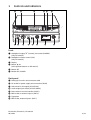
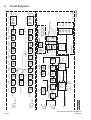
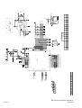
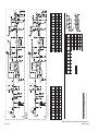
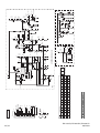
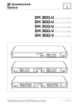
Service manual
EM 100 G2
EM 300 G2
EM 500 G2
SA 040818
POWER
EM 100 G2
SET
300
ON
SET
EM 300 G2
500
ON
SET
EM 500 G2
Short Description
The three stationary receivers EM 100 G2, EM 300 G2 and EM 500 G2
are ,True Diversity’ receivers and are equipped with the HDX noise reduction
system. Each receiver has a switching bandwidth of 36MHz in the UHF band.
Features
Subject to alterations
•
•
•
•
•
•
1440 UHF frequencies available for interference-free reception.
Direct channel selection via presets.
Scan function for finding free receive channels.
Low battery warning on transmitter and receiver.
Squelch pilot tone for interference-free operation.
Sound check mode for checking transmission conditions
(only EM 500 G2).
Sennheiser electronic GmbH & Co. KG • 30900 Wedemark
Phone: +49 (5130) 600 0 • Fax: +49 (5130) 600 300
1/32
Safety requirements
Observe safety regulations.
Observe ESD instructions while handling electrostatically endangered components.
Only skilled persons are allowed to alter and repair. For repairs and exchanges only
approved components according to the current spare parts list are allowed.
It is forbidden to alter the product unauthorised.
If not observed the adaptor is legally liable for possible results of damage.
repairs/exchanges
2/32
The following instructions for overhaul and testing must be followed. In case of
unusual problems please contact your Sennheiser distributor.
EM 500 G2, EM 300 G2, EM 100 G2
08/2004
Table of contents
1 Controls and indicators ................................................................................. 4
2 Technical data................................................................................................. 5
2.1
2.2
2.3
General.................................................................................................................... 5
RF part..................................................................................................................... 5
AF part .................................................................................................................... 6
3 Description ...................................................................................................... 7
3.1
3.2
3.3
3.4
Mainboard .............................................................................................................. 7
RF module............................................................................................................... 8
Display module...................................................................................................... 9
Monitor module (only EM 500 G2).................................................................... 9
4 Exploded view...............................................................................................10
4.1
4.2
Exploded view: EM 100 G2................................................................................ 10
Exploded view: EM 300 G2, EM 500 G2 .......................................................... 11
5 Test and alignment instructions................................................................13
5.1
5.2
5.3
5.4
Measuring and test equipment ....................................................................... 13
Measuring set-up................................................................................................ 13
Test table.............................................................................................................. 14
Reading out/changing unit data via the “DATA“ service interface ......... 17
6 Circuit diagrams ...........................................................................................19
Block diagram ...................................................................................................................19
Mainboard, circuit diagram, part 1/3........................................................................... 20
Mainboard, circuit diagram, part 2/3........................................................................... 21
Mainboard, circuit diagram, part 3/3........................................................................... 22
RF board, circuit diagram, part 1/3 .............................................................................. 23
RF board, circuit diagram, part 2/3 .............................................................................. 24
RF board, circuit diagram, part 3/3 .............................................................................. 25
Monitoring module MOD.A020, circuit diagram ........................................................26
Interconnector assignmet ..............................................................................................27
Mainboard, component side ..........................................................................................28
Mainboard, solder side....................................................................................................29
RF board, component side..............................................................................................30
RF board, solder side .......................................................................................................31
Monitoring module: MOD.A020, component side .....................................................32
Monitoring module: MOD.A020, solder side ...............................................................32
3/32
EM 500 G2, EM 300 G2, EM 100 G2
08/2004
1
Controls and indicators
�
�
�
� �
�
ON
SET
DATA
�
�
�
쐅
쐈
쐉
씈
씉
Front
쐃 Headphone output, ¼" (6.3mm) jack socket (PHONES)
(only EM 500 G2)
쐇 Headphone volume control (VOL)
(only EM 500 G2)
쐋 Display
쐏 Button / (two separate buttons on EM 100 G2)
쐄 Button SET
쐂 Button ON / POWER
Back panel
쐆
쐊
쐎
쐅
쐈
쐉
씈
씉
Cable grip for mains unit connector cable
DC socket for power supply unit connection (DC IN)
XLR socket for AF output (AF OUT BAL)
Audio output jack socket (AF OUT UNBAL)
RJ45 socket as service interface (DATA)
BNC socket as antenna input 2 (ANT II)
Type plate
BNC socket, antenna input 1 (ANT I)
EM 100 G2, EM 300 G2, EM 500 G2
08/2004
4/32
2
Technical data
2.1
General
Nominal output ______________________ +12VDC
Operating voltage ____________________ +10.5 ... +16V
Current consumption at nominal voltage ___ typ. 200mA
Quiescent current consumption (standby) __ typ. 50mA
Temperature range ___________________ -10°C ... +55°C
Dimensions (in mm)___________________ 212 x 145 x 38
Weight: ____________________________ approx. 1200g
Approval ___________________________ D801 488L RF
Max. audio output level (balanced/unbalanced)
3-pin XLR socket_________________ +19dBu
1/4 " (6.3 mm) jack socket _________ +13dBu
Headphone output (only EM 500 G2) _____¼" (6.3 mm) jack socket, stereo
THD (at nominal deviation, 1 kHz) __________ ≤ 0.9%
Control range (only EM 500 G2) _________ 40dB
2.2
RF part
Receiver principle _____________________ true diversity
Frequency ranges_____________________ 518 – 554MHz
626 – 662MHz
740 – 776MHz
786 – 822MHz
830 – 866MHz
Switching bandwidth __________________ 36MHz
Receive frequencies ___________________ 1440
Channel separation ___________________ > 400kHz
Channel grid_________________________ 25kHz
1. Oscillator frequency _________________ fOsc = fe + 241MHz
1. Intermediate frequency ______________ 241MHz
2. Oscillator frequency _________________ 230.3MHz
2. Intermediate frequency ______________ 10.7MHz
Modulation__________________________ wideband FM
Nominal/peak deviation________________ ±24kHz / ±48kHz
Frequency stability________________________ ≤ ±15ppm
Adjacent channel selection
EM 100 G2 _____________________ ≥ 65dB
EM 300 G2 __________________________ ≥ 68dB
EM 500 G2 __________________________ ≥ 70dB
Intermodulation attenuation
EM 100 G2 _____________________ ≥ 65dB
EM 300 G2 __________________________ ≥ 68dB
EM 500 G2 __________________________ ≥ 70dB
5
EM 100 G2, EM 300 G2, EM 500 G2
08/2004
Blocking
EM 100 G2, EM 300 G2 ______________ ≥ 70dB
EM 500 G2 _________________________ ≥ 75dB
Squelch _____________________________off, low: 5dBµV,
mid: 15dBµV
high: 25dBµV
Squelch pilot tone _____________________adjustable
S/N = 52 dBA (unweighted with HDX) _____< 2.5µV (typ. 1.4µV)
S/N = 80 dB (unweighted with HDX)_______< 10µV (typ. 6µV)
S/N max (peak deviation with HDX) _______> 120dB(A) (typ. 124dB(A)
Antenna inputs ______________________RF input: 2 BNC sockets, 50Ω
2.3
AF part
Compander system ____________________HDX
S/N (AF OUT)
EM 100 G2 _____________________ ≥ 110dB(A)
EM 300 G2 _____________________ ≥ 112dB(A)
EM 500 G2 _____________________ ≥ 115dB(A)
AF output voltage (nominal deviation)
Unbalanced _____________________1.25V = +4dBu
Balanced _______________________2.45V = +10dBu
AF output voltage (peak deviation)
Unbalanced
3.4V = +13dBu
Balanced
6.8V = +19dBu
AF frequency response _________________50Hz ... 18kHz; -3dB
Monitor output level/load _______________> 100mW/32Ω (only EM 500 G2)
AF outputs ______________________¼" (6.3mm) jack socket
Unbalanced
XLR-3M, balanced
Pilot tone
Pilot tone frequency ______________32.768kHz
Pilot tone deviation _______________≥ 1.5kHz
EM 100 G2, EM 300 G2, EM 500 G2
08/2004
6/32
3
Description
The receiver has a modular structure and comprises the following boards:
• Mainboard
• Display module
• RF module
• Monitor module (only EM 500 G2)
The display, RF and monitor modules are each connected to the mainboard via a
15-pin ribbon connection. The following sections explain the principal functions.
3.1
Mainboard
The mainboard is a single-sided PCB assembly. It is manually screwed to the side
walls, the front and the back panel wall and the RF module. The mainboard
performs the following functions:
• Conditioning of power supply
• Conditioning of AF signals
• Provision of power supply to additional modules
• Control of own functions and the RF and monitor module via the
microprocessor
3.1.1 Processing the diversity signal
The signal from the RF module with the highest field strength is switched by the
U50 or U51 diversity switches and reaches four signal conditioning blocks that are
connected in parallel.
3.1.2 U52 squelch switch with AF conditioning
If the squelch threshold you set is exceeded, U1 uses U52 to switch the AF signal
and activates the AF high pass filter with U75-1, the AF low pass filter with U75-2
and U76-1, the HDX expander with U100 and the AF stages U101-1, U101-2 and
U76-2.
With EM 500 G2 the AF stages U101-1 and U101-2 are used via analog switch U300
as LOW-CUT filters with a threshold frequency of 200Hz and with U301 as
HI-BOOST filters with an increase of approx. 5dB at 10kHz. Control is via U1,
Q300-1 and Q300-2.
The peak detector is connected to the level indicator behind U76-1 with U100 operational amplifiers (U100-2 and U100-1) whose output signal DEV_L is available to
microprocessor U1 for evaluation.
The two AF signals AF_0 (U76-2) and AF_180 (U101-2) both reach a divider
resistance chain at the inputs of analog switches U175 and U176, via which eight
AF signal switching stages are set by the user. The structure is strictly balanced and
is laid behind the active stages to guarantee full signal to noise ratio even if the
AF signal is weakened by approx. 40dB. From the two outputs, the AF signal then
reaches across various components to protect from ESD parasitic signals and
phantom voltage at AF sockets P175 and J175.
7
EM 100 G2, EM 300 G2, EM 500 G2
08/2004
3.1.3 Evaluation of the TX battery signal
The battery telegram sent by the transmitter reaches the U60-2 trigger stage, at
whose output appropriate square wave signals are available for evaluation by U1,
via the 4Hz low pass filter with U60-1.
3.1.4 Evaluation of the pilot signal
The 32.768kHz pilot signal sent by the transmitter is filtered from the signal mix
by the active crystal filter with Q95, Y95 and U95-1, rectified via the D95 diode and
made available for evaluation by U1 via trigger stage U96-1.
3.1.5 Functions of microprocessor U1
The receiver is controlled by the 8-bit U1 microprocessor, which contains in its flash
memory the control program and uses a sub-area as an EEPROM for saving data
even in the event of power failure. The microprocessor uses a 4MHz crystal to
generate both its own internal 8MHz cycle and the reference frequency for the
RF module PLL. It processes the signals already described in line with the program
specifications and the user specifications that can be set on an individual basis via
a menu.
3.1.6 Service interface (RJ45 socket)
The service interface “DATA“ with RS485 protocol, located on the back panel of the
unit, fulfills an important function. The RJ45 socket allows the relevant EEPROM parameters on the RF module and the simulated EEPROM to be read out and modified
in the microprocessor. This interface also enables a software update as part of the
hardware options. For example, the RJ45 socket enables you to read unit data and
write-in after replacing a board. The necessary service software is
available for download free of charge on our Internet homepage:
www.sennheiser.com > Service & Distributors > Service Documentation >
Download
3.2
RF module
The RF module is a single-sided PCB assembly that is fixed to the back panel via the
BNC input sockets and to the mainboard via a sheet metal brace. The RF module
performs RF conditioning until demodulation of the IF signal. The module is connected to the mainboard via a 15-pin ribbon connection; the following functions are
performed by the plug-in connection:
•
•
•
•
•
Incoming power supply of 5V DC from the mainboard.
Incoming system cycle (4MHz) from mainboard microprocessor.
2 x outgoing AF voltage to mainboard
2 x RSSI voltage to mainboard.
Communication between the mainboard microprocessor and
the EEPROM or the PLL for the RF module.
EM 100 G2, EM 300 G2, EM 500 G2
08/2004
8/32
3.2.1 RF module shielded compartments
The shielded compartments on the RF module perform the following functions:
• The two compartments between the BNC sockets contain the second mixer,
the 10.7MHz limiting amplifier and the FM demodulator.
• The compartment directly behind the BNC socket contains RF conditioning
up to an including the SAW filter for the first IF.
• The middle compartment performs frequency conditioning for the first
oscillator with VCO, buffer and PLL for both diversity channels.
The input filters are assembled outside the shielded compartments to ensure that
parasitic LO frequency currents cannot be coupled directly to the RF input. The input filters are relatively complex owing to the integrated IF and LO cases,
but nevertheless do not require alignment.
3.2.2 Alignment of the RF module
The only components still to be adjusted are
• C540 for alignment of VCO voltage at center frequency,
• C330 for setting the LO2 crystal oscillator,
• The L310 and L410 discriminator coils, and
• The two level adjusters for the AF outputs.
For communication with the processor on the mainboard, the RF module contains
the U700 EEPROM, in which the relevant frequency range data, the RSSI table and
other status data are stored. Communication is processed via the same bus used by
the microprocessor to communicate with the PLL U500 (frequency setting).
3.3
Display module
The display module for the status displays is connected to the mainboard via a
15-pin ribbon connection.
3.4
Monitor module (only EM 500 G2)
The monitor module (MOD.A020) is a single-sided PCB assembly and is connected
to the mainboard via a 15-pin plug-in connector. The monitor module PCB has a jack
socket for connecting headphones, and an appropriate volume control. The monitor
module also has a complete U1 and U2 amplifier for each AF phase; the volume can
be adjusted via R1.
The monitor module is primarily intended for stereo operation, but in phase configuration is possible for mono operation. If you want to minimize the volume differences in mono operation between the left and right channel (this may occur as a
result of the tolerances of R1), you must close the M1 solder bridge.
You must not close the M1 solder bridge if you are using the monitor
module in stereo mode.
9
EM 100 G2, EM 300 G2, EM 500 G2
08/2004
002
003
002
EM 100 G2, EM 300 G2, EM 500 G2
08/2004
004
005
019
012
013
013
003
018 017
018
018
incl.:
017
018
006* *
Pos. 006
Exploded view: EM 100 G2
009
020
007
4.1
004
011
016
016
020
Exploded view
005
008
001
4
10/32
002
11/32
003
002
004
005
012
008
010
004
005
016
001
016
013
020
020
009
019
011
012
013
007
014
003
018
015
017
incl.:
017
018
006* *
Pos. 006
4.2
Exploded view: EM 300 G2, EM 500 G2
EM 100 G2, EM 300 G2, EM 500 G2
08/2004
Pos
Bezeichnung
001
002
003
004
005
006
007
008
009
010
011
012
013
014
015
016
017
018
019
020
Casing
Lens screw
Holder
Lens screw
Spring washer
Front module with display
Rear panel
Label
PCB mainboard
PCB monitoring module (EM 500 G2 only)
PCB RF module
Lens screw
Flat cable, 15-pin
Flat cable, 30-pin
Knob (EM 500 G2 only)
Socket BNC 50R
Key cap ON/POWER
Key cap UP/DOWN/SET
Built-in plug XLR3M
Lens screw
EM 100 G2, EM 300 G2, EM 500 G2
08/2004
12/32
5
Test and alignment instructions
5.1
Measuring and test equipment
•
•
•
•
•
•
1 Spectrum analyzer up to at least 1.5GHz
1 RF signal generator
1 AF level measuring device
1 Oscilloscope
1 Multimeter
1 Laboratory power supply unit
5.2
Measuring set-up
+
DC IN
EM x00 G2
DATA
Laboratory
power supply unit
AF OUT
RF IN
230.00 MHz
Oscilloscope
AF level measuring device
RF signal generator
Other measuring equipment
Spectrum analyzer
13/32
Multimeter
EM 100 G2, EM 300 G2, EM 500 G2
08/2004
5.3
Test table
Sequence Type of measure- Signal input
ment/adjustment
Settings
Measuring
point/test
point
Required
value
Remarks
1
Visual inspection
1.1
Jack socket PHONES –
(only EM 500 G2)
–
–
–
Contacts are
not twisted, no
hairline cracks
at the solder
points, no
mechanical
damage
1.2
Volume control
(only EM 500 G2)
–
–
–
–
See 1.1
1.3
–
왖왔, SET,
POWER/ON buttons
–
–
–
See 1.1
1.4
DC socket, DC IN
–
–
–
–
See 1.1
1.5
XLR socket
–
–
–
–
See 1.1
1.6
Jack socket
–
–
–
–
See 1.1
1.7
RJ45 DATA socket
–
–
–
–
See 1.1
1.8
BNC sockets
–
–
–
–
See 1.1
1.9
Monitoring of all
display elements
+12VDC at DC socket
"POWER" = ON
–
–
Monitoring of
all display
segments
1.10
Monitoring of the il- See 1.9
luminated 왖왔, SET,
ON buttons
(not EM 100 G2)
See 1.9
–
–
–
2
Mainboard: current and voltage measurement
2.1
Standby
See 1.9
"POWER" = Off
"VOL" = min. (R1)
"AF level" = max.
–
50mA
Set laboratory
power supply
unit current
limiter to
ION = 1A
2.2
Current consumpti- See 1.9
on during operation
"POWER" = On
"VOL" = min. (R1)
"AF level" = max.
–
200mA
See 2.1
2.3
Commissioning
See 1.9
VOL = min. (R1)
AF LEVEL = max.
–
–
–
2.4
Operating voltage
(+12VDC)
See 1.9
POWER = On
Mainboard,
solder side:
+12VDC
–
TP209 (+)
TP208 (-)
2.5
Operating voltage
(+6VDD)
See 1.9
See 2.4
TP226/ GND
+5.8V to
+6.2V
–
2.6
Operating voltage
(+5VCC)
See 1.9
See 2.4
TP231/ GND
+4.8V to
+5.2V
–
2.7
Operating voltage
(+5VSW)
See 1.9
See 2.4
TP233/ GND
+4.8V to
+5.2V
–
2.8
Operating voltage
(+6VSW)
See 1.9
See 2.4
TP229/ GND
+5.8V to
+6.2V
–
EM 100 G2, EM 300 G2, EM 500 G2
08/2004
14/32
Sequence Type of measure- Signal input
ment/adjustment
3
Settings
Measuring
point/test
point
Required
value
Remarks
RF module
RF module removal:
1. Loosen the lens screw (RF board fastening, see Exploded view, Pos. 12).
2. Remove both BNC socket screws from the back panel of the unit.
3. Remove the RF module (the connection to the mainboard via the 15-pin flat cable remains).
Re-establishing the ground connection between the RF module and the mainboard:
Create an interference-free connection between MH3 on the RF board and 801 on the
mainboard. To do this, solder a wire approx. 10cm long between MH3 and 801.
+12VDC at the
DC socket
3.1
Operating voltage
(+5VSW)
Multimeter, DC
RF module
Component
side: L500
+4.9V to
+5.1V
3.2
Tuning voltage measurement
1. Open the center shielded compartment on the RF module.
2. On the track, solder a piece of wire approx. 2cm long to TP17 and one to TP4.
3. Guide the wires out of the receiver as measuring lines.
4. Set the C540 trimmer in the shielded compartment to precisely 2.4V; (use TP17 and TP4 for this).
3.2.1
Mid
range limit
See 3.1
Use TUNE to set the medium receiving frequency.
3.2.2
Lowest
range limit
See 3.1
3.2.3
Uppermost
range limit
3.3
Oscillator
3.3.1
+2.3V to
+2.5V
Alignment via
RF module,
component
side C540
Use TUNE to set the lowest TP 17
receiving frequency.
+0.8V to
+2.0V
–
See 3.1
Use TUNE to set the highest TP 17
receiving frequency.
+3.0V to
+4.2V
–
1. frequency
measurement
See 3.1
Use the "SET" and "DOWN" TP 1
buttons to switch to the
mid receiving frequency;
then spectrum analyzer
LO1=
fE +241MHz
–
3.3.2
1. Oscillator level
See 3.1
See 3.3.1
TP 102 /
TP 202
+4.3 V
Measurement
takes place indirectly via the
voltage at the
1st oscillator
3.3.3
2. frequency
measurement
See 3.1
See 3.3.1
TP 300
230.3MHz
± 11.5kHz
–
3.3.4
2. Oscillator level
See 3.1
See 3.3.1
TP 300
-20dBm to
-35dBm
–
3.4
Sensitivity,
channel 1
Center frequency;
Set the receiving frequency on the RF signal Squelch at "0";
AF level measuring device
generator:
ANT I RF: 2, 5µV; deviation: 24kHz mod: off
AF output
Better than
52dB(A)
–
3.5
Sensitivity,
channel 2
See 3.4 at ANT II
AF output
Better than
52dB(A)
–
3.6
THD, channel 1
RF signal generator at –
ANT I RF: 1mV; deviation: 24kHz mod: 1kHz
AF output
< 0.9%,
typ. 0,3%
–
3.7
THD, channel 2
See 3.4 at ANT II
–
AF output
< 0.9%,
typ. 0,3%
–
3.8
S/N max., channel 1 See 3.4 at ANT I
Mod: off
–
–
Better than
110dB(A)
–
3.9
S/N
max, channel 2
See 3.4 at ANT II
Mod: off
–
–
Better than
110dB(A)
–
3.10
AF output
voltage, tuner 1
See 3.1; Mod: on,
deviation: 48kHz
with AF meter
TP 6
+540mVeff to
+555mVeff
Alignment via
R360
3.11
AF output
voltage, tuner 2
See 3.1 Mod: on,
deviation: 48kHz
with AF meter
TP 8
+540mVeff to
+555mVeff
Alignment via
R460
15/32
See 3.4
RF module
Solder side:
TP 17
EM 100 G2, EM 300 G2, EM 500 G2
08/2004
Sequence Type of measure- Signal input
ment/adjustment
Settings
Measuring
point/test
point
Required
value
Remarks
3.12
Balanced RF output Feed in via XLR socket
voltage at 1kHz
peak deviation
–
–
+18dBu and
+6.1V
–
3.13
Unbalanced
RF output voltage
at 1kHz peak
deviation
Feed in via Jack socket
–
–
+12dBu and
+3.0V
–
4
Pilot tone
4.1
Pilot tone on
RF signal generator at
ANT I: RF level: 1mV
FM1
Deviation: 24kHz
Mod: 1kHz
FM2
Deviation: 2kHz
Mod: 32.768kHz
Pilot tone: “ON“
XLR socket
10dBu
–
4.2
Pilot tone off
RF signal generator at
ANT I: RF level: 1mV
FM1
Deviation: 24kHz
Mod: 1kHz
FM2
OFF
See 4.1
XLR socket
no signal
The display is
red illuminated
5
Monitor module (only EM 500 G2)
5.1
Monitor output
"PHONE"
Reduce deviation from –
24kHz to 6kHz.
–
–
AF segments
1 to 2 bars
5.2
Monitor output
"PHONE"
+12VDC at the
DC socket
oscilloscope at the relevant
PHONE connection:
Termination impedances,
32Ω in connector.
Gradually turn monitor control VOL to maximum, noting the sinus test signal. The signal
must increase cleanly and evenly, without distortion or drop-out, until it starts to clip.
5.3
Volume control
+12VDC at the
DC socket
"POWER" = On
–
6
Display module
- The EM 100 G2 exhibits a change in the form of individual segments.
- The EM 300 G2 and EM 500 G2 exhibit consistent changes in color display.
6.1
RF display
RF signal at ANT I
Mod: off
RF: 3µV
–
EM 100 G2
EM 300 G2,
EM 500 G2
RF signal at ANT II
Mod: off
RF: 3µV
EM 100 G2
EM 300 G2,
EM 500 G2
–
No "scratching"
is heard on
turning and
there is no tone
drop-out.
AF segment, no bar
RF segments 2 ± 1 bar
Diversity display I lights up
AF segment not visible
RF segments visible
Diversity display I lights up
AF segment, no bar
RF segments 2 ± 1 bar
Diversity display II lights up
AF segment not visible
RF segments visible
Diversity display II lights up
6.2
RF display
See 5.1
RF: 20µV
–
EM 100 G2
EM 300 G2,
EM 500 G2
RF segment: 4 bars
RF segment: 25dB
6.3
RF display
See 5.1
RF: 1mV
–
EM 100 G2
EM 300 G2,
EM 500 G2
RF segments:end-scale
deflection
RF segments:end-scale
deflection
6.4
AF display at
nominal deviation
24kHz
Mod: off
–
All
AF display "0"
6.5
AF display at
nominal deviation
48kHz
Mod: off
–
All
PEAK
EM 100 G2, EM 300 G2, EM 500 G2
08/2004
16/32
5.4
Reading out/changing unit data via the “DATA“ service interface
5.4.1 Overview
You can read out and change unit data via the integrated “DATA“ service interface.
For example, Sennheiser's service software helps you with the following functions:
•
•
•
•
Reading out the current software version and, if necessary, initiating a software update.
Commissioning the receiver following replacement of hardware (e.g. when a board is changed).
Changing the current frequency table.
Changing/resetting the receiver factory settings.
5.4.2 Required hardware
You need the Sennheiser service set for unit data read-in and read-out.
The service set contains for portable ew G2 units
• an infrared adapter for reading out/in data from portable units (e. g. SK 100),
for rack-mount ew G2 units
• an RS232/RS485 converter,
• an RS232 cable to connect the PC and the converter.
• an RS485 cable to connect the receiver and the converter.
You can order the service set directly from Sennheiser:
service set for software ew G2, ID no. 094739, price group 161
5.4.3 Required software
The service software is available for download free of charge on our Internet homepage:
www.sennheise.com > Service & Distributors > Service Documentation > Download
The minimum operating system requirement to run the software is Microsoft® Windows 95™ ,
and a free COM port (RS232) is also required.
5.4.4 Information about the service software
A user guide for the service software is available in PDF format. It contains information about how to
commission the service set, how to install the service software and how to read in/out unit data.
Please find more informations in the instructions for use of the ew G2 service software. Once the installation of
the software is complete you can find this help file in the Windows menu [Start].
17/32
EM 100 G2, EM 300 G2, EM 500 G2
08/2004
5.4.5 Commissioning after board replacement
After you have fitted a new board to the unit, you must use the service software to write the data to the unit
again (e.g. new frequency table).
Requirements
1. You have replaced a faulty board (e.g. receiver RF board),
2. You have connected the receiver via the DC IN an +12 V DC socket.
3. You have connected the unit to the COM port on the PC via the “DATA“ service interface.
4. You have installed the service software and launched it.
5. You have switched on the unit.
Writing unit data
Perform the following steps:
1. Click the button [Auto Detect].
Result: Your connected unit is detected.
2. Click the button [EXECUTE ALL] in the Info tab.
Result: All unit data is read out. If all the data are successfully read out, the message “Success“ appears.
Note: If you perform individual actions in the “Info“ or “Service“ tabs, you must subsequently return the
unit to operational status. Click on [Close Device] once the actions have been completed to do this.
3. Switch to the “Service“ tab.
4. Click the button [EXECUTE ALL].
Result: The new unit data will be written. If all the data are successfully written, the message "Success"
appears.
Result
You have successfully written the new data to the unit. These new data now correspond to the
new factory settings for your unit. Your can find these data in “D:\Sennheiser\ew G2 service package“ in the
files “Defaults.dat“ and “FreqTable.dat“ or alternatively “FreqTableIEM.dat“.
EM 100 G2, EM 300 G2, EM 500 G2
08/2004
18/32
Block diagram
BPF
MIXER
U100
U225
U210
U226
U227
SUPPLY
UNIT
MIXER
U300
30Hz
U75
+5V
+5Vsw
DATA
MAIN
uC
25KHz
U75 U76
U1
Q404
LIM.AMP
MCK
4MHz
HDX
EXP
U100
Y402
10.7MHz
10.7MHz
Y304
+
-
FRONTMODUL
LCD
+
-
+
-
U76
+AF
U101
LP_100KHz
U700
EE-EPROM
LP_100KHz
R460
R360
U175 U176
-22...+18dBu
+
ON/OFF
SELECT
DOWN
UP
AF-OUT BALANCED
-
MONITOR-MODUL
EM500 ONLY
+10dBu max
100mw max
U400
DISCR.
DISCR.
U300
AF-ON
U2
-AF
U400
LIM.AMP
LIM.AMP
Q300
LEVEL_MON
R1
Y404
10.7MHz
DATA/CLK
LIM.AMP
Q304
MCK = Main clock
10.7MHz
Y302
TX_BATT
DETECTOR
U60
U400
MIXER
MCK
4MHz
5Hz
U60
Y200
241MHz
PLL
230.3MHz
U500
241MHz
Y100
+10-15V/50mA
+8Vsw
R79
U200
MIXER
VCO
Q504 Q506
MUTE
U52
PILOT
DETECTOR
32.768kHz
U95 U96
DIVERSITY
U50 U51
10.5-16VDC IN
AF-2
AF-1
RF-2
(EM550
from Splitter 2)
f_IN 241MHz
RF-1
(EM550
from Splitter 1)
BPF
+6Vsw
-6Vsw
-7Vsw
19/32
230.3MHz
AF-2
AF-1
300903Prl1530
MAIN-BOARD
U402
U302
RF-BOARD
6
Circuit diagrams
EM 100 G2, EM 300 G2, EM 500 G2
08/2004
4
TOP
TP211
C242
220pK
R243
22KJ
R245
2.2KJ
C243
10nK
R242
10KJ
L225
10UK
TP240
C225
1.0uK
*
0.75
D210
SM4007
F210
C241
1.0uK
PWR_/ON
2
3
1
TP209
1
TP210
2
GND
OUT
3
OUT
L641
R247
1.0KJ
R248
1.0KJ
Q244
BC807W
2.2KJ
R249
Q243
BC817W
C227
47u16V
R211
47KJ
8
1.0uK
C245
TP241
2
GND
C228
10uM
IN
OUT
L226
TS102U226
78L05
1
C229
10uM
R226
33KJ
D240
BAV99
TP227
C214
C246
1.0uK
10UK
L240
1.0nK
C230
LCD_LIGHT
1
C247
1.0uK
IN
1.0uK
C631
1.0uK
1.0KJ
R252
Q248
BC857S
R251
100KJ
OUT
D630
1
1
Q213
BC847S
D631
2
10KJ
R254
*
0.0R
R637
TOP
TP230
TOP
TP232
TP234
2
R257
33.2KF
+5VSW
TOP
TP243
TP244
R256
43.2KF
47.5KF
*
R636
47.5KF
*
*
Q600
BC807W
R602
4.75KF
D632
BAV99W
R632
-6.5VSW
Q247
BCX54/16
Q248
BC857S
R631
100KF
2
Q632
BC857S
C233
10uM
PWR_ON
+6VSW
C232
47u16V
TOP
TP630
TP631
*
100KJ
R601
BAV99W BAV99W
1
33KJ
R229
TP229
TOP
TP228
+5VSW
Q630
BC817W
-6.5VEE
2
GND
C231
1.0uK
*
C630
8
U227
78L05
R228
100KJ
Q226
BC817W
C215
1.0uK
33KJ
R600
R700
33KJ
Q632
BC857S
R630
100KJ
TP242
Q225
BCX51/16
BAV70
D225
R220
10KJ
Q213
BC847S
R218
2.2KJ
4.75KF
R219
Q211
BC807W
R227
1.5KJ
R225
10KJ
1.0nK
27RJ
R214
1.0MJ
TP226
R215
33KJ
+6V_DD
D213
BAT54
PWR_/ON
+5VCC
TP225
R212
47KJ
10KJ
R230
C213
1.0uK
C212
2.2nK
Q210
BC807W
C211
47u16V
3
Q242
BC807W
C244
100nK
HS800T
4.7KJ
R246
Q241
BC817W
R244
4.7KJ
IN
2
GND
C226
1.0uK
IN
U225
MC78M08
C210
22u35V
1
U210
MC78M06
R210
10KJ
D211
D212
BAV99W BAV99W
Mainboard, circuit diagram, part 1/3
R240
220KJ
R241
1.0MJ
Q240
BC817W
C240
22u35V
TP208
*
J210
ROKA5202580
U_in
BAV99W
D214
TP212
27RJ
R217
*
R216
*
R213
10KJ
*
*
*
*
*
*
*
*
*
*
R604
+5VSW
TP231
EM100
EM300
EM500
P802
P801
P800
NC
1
2
3
4
5
6
7
8
9
10
11
12
13
14
15
16
17
18
19
20
21
22
23
24
25
26
27
28
29
30
R641
1.0KJ
LCD-MODUL_Graf .
*
J640
30FLZ-RSM1-TB
LCD_D2
LCD_D1
LCD_D3
TP652
TP653
TP654
TP655
TP656
TP657
TP658
TP651
TP650
TP280
TP266
TP265
R642
1.0KJ
TP9
1
2
3
4
5
6
7
8
9
10
11
12
13
14
15
LCD_D3
LCD_D4
LCD_D5
LCD_D6
LCD_D7
LCD_/CS2
LCD_RS
/RST
-6.5VEE
+6VSW
R261
**
0.0R
never
mounted
NC
+8VSW
NC
NC
/MUTE
/AF_ON
NC
NC
NC
NC
TP11 TP20
+6VSW
1
2
3
*
1
2
3
4
5
6
TS102
L640
TOP
*
C640
100nK
R644
R645
R646
R647
nm
m
m
R630
R631
R632
R633
R634
R635
R636
R637
nm
m
m
VOL_/LO W
R601
R602 R604
R605 R606
R609 R610
R607 R608
nm
m
m
+AF_OUT
-AF_OUT
U_in
+5VCC
+5VSW
EE_/WP
MCK
RSSI2_LEV
PLL_CS
RSSI1_LEV
BUS_CLK
BUS_DAT
+5VSW
AF_2
AF_1
C9
100nK
-DATA
+DATA
TP640 TP641
4
3
2
1
J5
WESTERN 4POL
TOP
TP271 TP276
TOP
TP270 TP275
TP278
TOP
TP274
TP269
TP277
TP268
TOP
TP273
TOP
TP272
TP267
RF-MODUL
P640
S6B-PH-SM3
AF_MON
4
5
6
7
8
9
10
11
12
13
14
15
J100
15FLZ-RSM1-TB
AF_MON
MONITOR-MODUL
LCD_/CS1
+5VCC
LCD_RW
/DOWN
LCD_E
/UP
LCD_D0
/SET
LCD_D1
/ON-OFF
LCD_D2
I_CONST_GN
I_CONST_RT
/ON-OFF
LCD_D0
TP281
I_CONST_GN
NC
NC
/SET
/UP
/DOWN
+5VSW
LCD-MODUL_Segment
1
2
3
4
5
6
7
8
9
10
11
12
13
14
*
J300
15FLZ-RSM1-TB
C630
D630 Q600
D631 Q601 Q630 L640 C631 C640 R221 R260 R641
P640 D210 D632
R642
Q602 Q632
nm
nm
m
nm
nm
nm
nm
nm
nm
nm
m
m
m
m
nm
m
nm
nm
m
nm
m
m
m
nm
m
m
nm
m
nm
m
m
nm
m
VARIANTEN
nm = not mounted
m = mounted
*
0.0R
*
R260
LCD_LIGHT
R261
R700
never
mounted
+6V_DD
TP606
**
R609
100KJ
33KJ
*
R610
J210 J300 J640 J700
nm
nm
m
m nm m
nm
m
nm
m nm m
m
m
nm
m nm m
P800
P801 P802
*
*
*
R606
100KJ
33KJ
R607
*
R608
4.75KF
2
*
*
I_CONST_GN
Q602
BC807W
Q601
BC847S
*
TP233
LCD_CONTRAST
R635
47.5KF
R634
22.6KF
+5VSW
+5VCC
*
+5VSW
100KJ
*
R605
Q601
BC847S
+8VSW
1
33KJ
R603
100KJ
R633
47.5KF
*
*
*
*
*
0.0R
*
*
Q212
BCX51/16
*
15
*
R221
R644
1.0KJ
*
R645
J700
15FLZ-RSM1-TB
*
R646
I_CONST_RT
*
TOP
TP602 TP605
1.0KJ
*
TOP
TP601 TP604
1.0KJ
R647
/PWR_MUTE
1.0KJ
*
EM 100 G2, EM 300 G2, EM 500 G2
08/2004
20/32
*
2
4
82.5KF
*
165KF
R997
R996
8
*
41.2KF
R998
TP642
TP16
R11
R11
R11
R11
3
4
1
2
Mainboard, circuit diagram, part 2/3
1
TP643
330KF
*
R995
LCD_RW
LCD_E
BUS_CLK
BUS_DAT
TP15
1
2
3
4
5
6
7
8
9
10
11
12
13
14
15
16
PTE1/FP12
PTE0/FP11
FP10
FP9
PTD7/KBI7/SDA
PTD6/KBI6/SCL
FP8
FP7
FP6
FP5
FP4
FP3
FP2
*
U1
MC68HC908LJ24
PTB4/T2CH0
TP24
10MJ
R38
OSC1
PTC3/FP22
OSC2
PTC2/FP21
LCD_CONTRAST
PTB5/T2CH1
BP0
PTE4/FP15
BP1
PTE3/FP14
BP2
PTE2/FP13
PTD4/KBI4/T1CLK
PTD3/SPSCK/CALOUT
R22
*
PTC5/FP24
PTC6/FP25
PTC7/FP26
PTA0/KBI0
PTA1/KBI1
PTA2/KBI2
PTA3/KBI3
PTA4/ADC0
PTA5/ADC1
PTA6/ADC2
PTA7/ADC3
PTB6/ADC4
PTB7/ADC5
VREFH
VREFL
C7
10uM
48
47
46
45
44
43
42
41
40
39
38
37
36
35
34
33
C8
10uM
10RJ
R35
R31
470RJ
R8
R8
R8
R7
R7
R7
R7
R6
R6
R6
R6
R5
R5
R5
VSS
VIN
EM100
EM300
EM500
R46
100KJ
VOUT
MC68HC908LJ24
MC68HC908LJ24
MC68HC908LJ24
1
R21
100KJ
U1(87224)
3
2
R45
100KJ
TP30
TP31
TP32
TP33
U2
AS440NM-4.5
3
2
1
4
3
2
1
4
3
2
1
4
2
3
TP25
+5VCC
TP4
TP5
TP6
TP7
TP13
C4
27pJ
C6
100pJ
L1
TS102
PTD0/SS/CALIN
+5VDD
TP12
*
+5VCC
C5
3-10p
*
Y1
4MHZ
*
Y2
4MHz
VDD
17 18 19 20 21 22 23 24 25 26 27 28 29 30 31 32
PTE6/FP17
FP1
PTB3/T1CH1
PTE7/FP18
PTD5/KBI5/T2CLK
PTB2/T1CH0
PTC0/FP19
BP3/FP0
33nK
C10
10KJ
PTB1/RxD
PTD2/MOSI
R12
TP23
R13
27pJ
C2
VSS
PTC4/FP23
0.0R
Y3
VDDA
IRQ
64 63 62 61 60 59 58 57 56 55 54 53 52 51 50 49
R999
47KJ
C20
1.0uK
10nK
C3
ANT_1
TXD_EN
C1
100pJ
RXD
TXD
PTB0/TxD
PTD1/MISO
/PWR_MUTE
TX_BATT
R10
*
*
/AF_ON
/MUTE
TP14 TP10
CGMXFC
PTC1/FP20
TP1
U620 R72
nm
nm
nm
nm
nm
nm
DI
C13
1.0nK
C12
R19
100KJ
R71
1.0MJ
4
DE
RE
2
3
RO
U3
5
nm
m
m
nm
nm
nm
nm
nm
nm
nm
m
m
nm
nm
nm
m
nm
m
C5
R72
10KJ
6
7
nm
m
m
C20
0.0R
*
R74
0.0R
R73
/SET
/UP
/DOWN
/ON-OFF
A
B
nm
nm
nm
+5VSW
/SET
1.0nK
C15
R23
100KJ
GND
VCC
8
+5VCC
R74 R995 R996 R997 R998 R999
1.0nK
C14
R20
100KJ
*
U3
SN75176
1
1.0nK
R18
100KJ
VARIANTEN
nm = not mounted
m = mounted
*
/RST
R47
100KJ
LCD_D7
LCD_D6
LCD_D5
VOL_0
RSSI1_LEV
DEV_L
PILOT
VOL_2
VOL_1
R69
0.0R
+5VCC
R70
1.0MJ
TP19
TP18
RSSI2_LEV
TXD
TXD_EN
RXD
TP17
*
EM100/300 = SN75176
EM500
= SP485
+5VCC
MCK
*
R15
R17
4
R9
3
R9
2
R9
1
R9
PTE5/FP16
LCD_LIGHT
LCD_RS
8
R94
22KJ
R127
47RJ
R93
47KJ
R126
47RJ
R92
22KJ
EE_/WP
VDD
RST
TP2
TP3
1
2
3
4
1
2
3
4
1
2
3
4
1
2
3
R1
R1
R1
R1
R2
R2
R2
R2
R3
R3
R3
R3
R4
R4
R4
LCD_/CS1
LCD_/CS2
HI_BOOST
LOW_CUT
VOL_/LOW
LCD_D0
PWR_ON
PLL_CS
LCD_D1
LCD_D2
LCD_D3
LCD_D4
/NOISE
/RST
U620
M24C64
Y1
72339
m
m
m
1
5
5
SDA
7
WP
A1
2
A0
1
6
SCL
*
A2
3
-DATA
+DATA
D40
BZA856A
TP22
2
TP21
BUS_CLK
BUS_DAT
3
4
Y2
87187
nm
nm
nm
GND
4
21/32
EM 100 G2, EM 300 G2, EM 500 G2
08/2004
Geh
R178
10RK
**
68RJ
R187
-6.5VSW
2
ANT_1
U51
NC7SZ66
B
1.0MF
C60
27nK
R60
22uM
C52
R54
47KJ
U175
MAX4581
TP175
R188
33RJ
R184
0.0R
3
D177
BZA856A
100pJ
TP176
C171
C172
22u63V
D176
BZA856A
TOP
R172
100KJ
TP177
(Line)
R189
15RJ
-
*
+
R118
100KF
**
R179
10RK
R190
6.8RJ
R191
3.32RF
2
D175
BAT74
10RK
R180
C174
10uM63V
TP184
TOP
TP178
TP179
SE
A
3
GND
Vcc
5
+6VSW
+
-
*
R192
3.32RF
7
R183
10KJ
*
R193
3.32RF
*
R194
3.32RF
*
R195
6.8RJ
TP180
TP181
TP182
TP183
TOP
R205
0.0R
/AF_ON
R113
100KJ
+5VCC
D115
BAS70-04W
C121
4.7nK
D95
BAS70-04W
C120
1.0nK
R105
4.7KJ
10nK
U95
NJM062V
+6VSW
*
4
8
R173
0.0R
BZA856A
D179
10RJ
R181
10KJ
v-
v+
+6VSW
+6VSW
10nK
TP185
*
R196
15RJ
3
+
3
R108
*
4
7
R123
1
+6VSW
3
v-
v+
+
4
8
3.3KJ
*
R198
68RJ
2
-
4
5
100RJ
C178
1.0uK
R1011
+
*
R200
270RJ
4
8
*
R199
120RJ
0.0R
R208
7
-
*
+
4
8
-6.5VSW
v-
v+
+6VSW
U75
NJM062V
AF_180
AF_MON
-AF_OUT
IN_AF550
6
5
C80
1.0nF
/NOISE
R207
1.0MJ
TP186
v-
v+
-6.5VSW
-
+6VSW
0.0R
R1012
TOP
TP116
PILOT
-6.5VSW
C177
1.0uK
6
U177
NJM4580V *
1
0.0R
C79
560pF
R91
TX_BATT
TP61
TP115
C179
1.0uK
4.7KJ
R125
R124
470KJ
+6VSW
+6VSW
TP95
R82
220KJ
16.2KF
TOP
TP96
TOP
TP60
R83
4.12KF
R84
+6VSW
-6.5VSW
v-
8
R67
47KJ
R68
100KJ
+6VSW
v+
R81
C78
1.0nF
8.06KF
R112
1.0MJ
U96
LM393D
7
2.2MJ
+6VSW
C122
2.2nK
-
4
8
R110
v-
v+
10MJ
R111
4.7MJ
*
+
R1010
R197
33RJ
v-
v+
8
C64
U60
1.0uK NJM062V
-
*
+
470KJ
+6VSW
1
TOP
TP8
TP75
10KJ
10K
R80
U177
NJM4580V *
6
4
8
-6.5VSW
R79
v-
v+
+6VSW
R66
-
R122
3.3MJ
5
-
*
+
6
5
U176
MAX4581
R121
390KJ
R120
180KJ
2
U96
LM393D
2.2MJ
100RJ
R65
R64
R78
4.7KJ
2
U75
NJM062V *
47KJ
R119
100KJ
22KJ
R107
220KJ
R109
1
4.7KJ
R182
6
5
4
C102
10nK
v-
v+
8
+6VSW
C100 C101 R106
-
*
+
R77
1.0MJ
R76
68KJ
C77
22nJ
AF_HI_PASS 30Hz
C76
22nJ
4
U95
1 NJM062V
2
3
U60
NJM062V
R75
180KJ
C75
22nJ
R104
10MJ
v-
v+
8
+6VSW
1.0MF
C63
1.8nK
1.0MF
C62
100nK
2
TP53
R63
B
TOP
TP52
R62
TX_BATT
max. 3.3 Veff
1.25 Veff
@ 24 kHz DEV
2 1
R117
8.25KF
C119
270pJ
C98
100nK
J175
HSJ1540_3010
R116
100KF
C118
270pJ
C96
12pJ
**
220KJ
2
3
1.0MF
C61
22nK
R61
R55
47KJ
R59
470KJ
R114
100KJ
4
1
U52
NC7SZ66
+6VSW /MUTE
TOP
TP54
TP51
C97
+6VSW
10pC
Y95
32.768kHz
R102
R97
61.9KF
150KJ
Q95
R100
BC817W
1.2pB
C99
R99
680KJ
R115
8.25KF
C117
270pJ
R98
33.2KF
+6VSW
R186
120RJ
R176
10KJ
R175
10RJ
R185
270RJ
10RK
R177
R58
3
GND
Vcc
33KJ
R57
100KJ
SE
A
C173
10uM63V
D175
BAT74
1
P175
NC3-MA-HR
1
2
-AF_OUT
+AF_OUT
R171
100KJ
max. 6.5 Veff
2.45 Veff
@ 24 kHz DEV
100pJ
C115
4
1
R95
470KJ
C116
270pJ
R96
180KJ
C95
1.0nK
Q50
BC817W
10KJ
+5VSW
R56
AF_1
7
8
VCC
VEE
GND
16
5
47KJ +6VSW 470KJ
R53
R51
X7
4
C51
10uM
47KJ
**
47KJ
3
GND
R52
SE
2
R50
4
X6
3
AF_0
B
12 X3
R101
100KJ
Vcc
15 X2
R103
A
13 X0
100KJ
1
X5
2
EN
AF_2
X4
1
EN
C175
3
X
5
6
9
10
C176
14 X1
**
VOL_0
VOL_1
VOL_2
11
C
B
A
6
9
10
11
C
B
A
TOP
TP50
13 X0
U50
NC7SZ66
14 X1
5
15 X2
7
EM100
EM300
EM500
C130
1.0uJ
9
6
1
R87
**
R136
m
m
m
R173
16
13
12
1.0uJ
15
G
5
G
R139
R170
nm
nm
nm
C131
R162
1K5
1K5
1K5
3.8k
10k
Vref
10
GND
U100 SA575DK
U110 SA575D
10k
VCC
20
10KF
R89
4
7
R200
270R
270R
270R
*
C84
1.0pC
1
11
14
R199 R198
120R 68R
120R 68R
120R 68R
-
*
+
C135
1.0uJ
C134
1.0uJ
R130
1.0MJ
2
3
4
8
1
**
2
3
-
*
+
R133
15KJ
v-
v+
4
8
+6VSW
HIBOOST
TP78
TP77
1
2.74KF
1.5KF
R132
R131
never mounted
R52 R302 R160
R184 C96
R304 U110
C173 C174
1.0uK
C150
+6VSW
U300
MAX4514
*
R501
0.0R
*
R300
2.2KJ
14.7KF
-6.5VSW
59KF
R135
10nJ
R134
U101
C137
NJM4580V
3.3nJ
-6.5VSW
R128
2.2KJ
C136
150pJ
C138
C103
220pK
C139
1.0uJ
-6.5VSW
v-
v+
TOP
TP76
IN_AF550
100KF
R151
22.1KF
R152
*
+
2
R154
10KF
4
8
TP155
R165
C155 0.0R
7
TOP
TP154
HI_BOOST
R312
220KJ
D150
BAV99W
R150
10KF
+5VSW
v-
v+
8
4
R158
22.1KF
22.1KF
R157
22.1KF
R156
1
*
3
**
22.1KF
C151
10uM
5
TOP
TP153 TP152
AF_180
AF_0
+AF_OUT
*
2
Mainboard, circuit diagram, part 3/3
C152
10uM
DEV_L
TOP
TP150
TP151
R161
100RJ
D151
BAV99W
*
Q300
BC857S
U101
NJM4580V
0.0R
R306
4
+6VSW
AF_DEV.
U100
R160
SA575DK 270KJ
1
2
+5VSW
R314
220KJ
7
IN
V+
R315
220KJ
R159
LOW_CUT
R313
470KJ
1
17
**
0.0R
+6VSW
0.0R
-6.5VSW
-
*
+
0.0R
6
5
R304
GND
NO
R302
3
2
COM
*
0.0R
R170
-6.5VSW
R138
**
R137
12.1KF
*
C301
100nJ
*
U301
MAX4514
1
LOWCUT
R311
470KJ
U100
SA575DK
100KF
R155
*
*
R301
4.75KF
R310
220KJ
*
R500
TP131 0.0R
C300
100nJ
*
TOP
TP130
Q300
BC857S
R153
100KF
19
18
v+
v-
+6VSW
100pJ
1.0uK
U76
TP166
NJM4580V -6.5VSW
5
*
-
C154
REVERS AF-PHASE
R163
2.2KJ
1.5KF
C153
R162 220pK
6
R164
1.5KF
R310
R311
R312
R313
U300
R197 R196 R195 R194 R193 R300 R301 R306 R314
R315 R500 R501 C300 C301 U301 Q300
nm
nm
nm
m
m
nm
nm
nm nm
33R 15R 6R8 3R32 3R32 nm
nm
nm
nm
m
m
nm
nm
nm nm
33R 15R 6R8 3R32 3R32 nm
m
m
m
m
m
nm m nm
m
m
33R 15R 6R8 3R32 3R32
VARIANTEN
nm = not mounted
m = mounted
C132
10uM
U76
NJM4580V +6VSW
U100 SA575DK
**
10k
3.8k
10k
Vref
U110 SA575D
8
C83
100pF
1.0KJ
R90
C82
3.3nF
EXPANDOR
13.3KF
R88
680KJ
+5VSW
C81
1.0nF
2.26KF
R86
8.06KF
R85
AF_LOWCUT 25kHz
*
C133
*
+6VSW
12 X3
1
5
22u4V
R139
0.0R
R136
0.0R
2
C50
10uM
X4
1
*
*
MUTE&DIV_SWITCH
X5
5
16
7
8
VCC
VEE
GND
3
X6
2
X
X7
4
V+
*
3
4
-6.5VSW
*
*
*
IN
+
NO
+
-
COM
-
EM 100 G2, EM 300 G2, EM 500 G2
08/2004
GND
22/32
2
*
2.7pB
C200
2.7pB
*
*
*
*
0.65-2.5p
*C202
47nJ
C206
2-6p
L204
0.65-2.5p
*C102
47nJ
C106
2-6p
*
L104
EM100-500
47nJ
L208
*
10pC
C212
*
47nJ
L108
*
10pC
0.5pB
*
C110
TP100
0.5pB
C210
8
5
6
7
Version Code
IFAMP
IFAMP
GND
IFAMP
C228
10nK
TS102
L224
TP202
*
EM100-500
C234
2-6p
C232
1.0nK
100RJ
1
in
in
8
6
in
in
1
3
5
GND
7
3
5
GND
7
out
out
4
2
4
2
5V
8mA
out
out
Y200
241.0MHz
TS102
L228
8
6
C238
12pJ
2mA
5V
C138
12pJ
m
040803Prl1415
EM100
-500
nm
nm
nm
R600 R601 R602 R603
68NJ
L230
nm
Range
2p2B n.m.
2p2B n.m.
2p2B n.m.
R206
470RJ
1
Q100
BFP405
1
Q200 4
BFP405
3
4
3
2
2
2.7pB
C117
C146
10nK
2.7pB
C217
C246
10nK
C248
m
m
m
m
m
nm
m
5
7
6
4
nm
nm
nm
nm
nm
nm
nm
nm
m
nm
3
m
nm
nm
m
m
nm
nm
nm
m
nm
m
1
2
*
1
330KF
R600
*
Version
1
330KF
R605
2
165KF
*
R601
2
165KF
R606
*
82.5KF
4
*
*
R602
4
82.5KF
R607
*
8
41.2KF
R603
8
41.2KF
*
R608
TP604
TP602
TP600
47nJ 4n7D 33nJ 2n7C 12nJ 18nJ
47nJ 4n7D 39nJ 2n7C 12nJ 18nJ
39nJ 4n7D 39nJ 2n7C 12nJ 18nJ
47nJ 5n6D 39nJ 4n7D 12nJ 27nJ
ZF1_1
1.0nK
C148
1.0nK
56nJ 6n8D 39nJ 10nJ 27nJ 33nJ
Range Code
n.m. n.m.
n.m. n.m.
n.m. n.m.
n.m. n.m.
R605 R606 R607 R608
Range Code
18pJ n.m.
18pJ n.m.
18pJ n.m.
10pC 3p3B 1p0B 18pJ 10pC 2p2B n.m. 0p5B n.m.
J100 J102
J200 J202
m
470RJ
R202
68NJ
L130
R106
470RJ
C108 C109 C110 C111 C112 C114 C116 C120 C134 L108 L110 L112
L118
C208 C209 C210 C211 C212 C214 C216 C220 C234 L208 L210 L212 L116 L216 L218
150nJ
L226
*
R200
150nJ
C134
2-6p
Y100
241.0MHz
R102
2mA 470RJ
5V
6p8C 3p3B 0p5B 18pJ 10pC 2p2B n.m.
LO
VDD
GND
1.0nK
5
6
L126
C132
1.0nK
8mA
5V
5 2p7B 2p2B n.m. 15pJ 12pJ 3p9B n.m. 18pJ 6n8D 6n8D 47nJ
4
3
2
1 RFin
U200
CMY213
100nJ
C222
IFAMP
IFAMP
8
7
TS102
L128
8p2C 3p3B n.m.
Version
18nJ
L218
*
LO
4
L220
VDD
3
GND
IFAMP
100RJ
R100
4 2p7B 2p7B n.m. 10pC 10pC 4p7B n.m. 15pJ 6n8D 6n8D 47nJ
*
18nJ
L118
GND
U100
CMY213
TS102
TP102
10pC 3p3B n.m.
12nJ
L216
C218
10nK
*
*
2
1 RFin
1.0nK
C128
10nK
L124
3 3p3B 3p3B n.m. 10pC 10pC 5p6B n.m. 18pJ 6n8D 6n8D 47nJ
10nJ 6n8D 47nJ
2.7nC
L116
C118
10nK
100nJ
C122
8p2C 3p3B n.m.
100pJ
39nJ
*
L212
LO = Local oscillator
LO1_2
*
TP201
C214
2.2pB
39nJ
L112
*
L114
LO = Local oscillator
LO1_1
*
L120
0.5pB
2 3p9B 4p7B n.m. 18pJ 18pJ 8p2C n.m. 22pJ 6n8D 6n8D 47nJ
1 3p9B 5p6B n.m. 15pJ 15pJ 10pC n.m.
*
TP200
C114
2.2pB
TP101
10nK
*
C100 C101 C102 C103
C105 C106 C107 L100 L102 L104
C200 C201 C202
C203 C205 C206 C207 L200 L202 L204
RF board, circuit diagram, part 1/3
Range
* Variable RF-Parts (Range4 EM100-500 is shown)
M2
2
J200
1 BNC-H
GND
J202
MM9329
M1
RF-IN-2
GND
J100
1 BNC-H
*
*
*
C112
*
*
C100
*
L100
*
L102
2.7pB
6.8nD
C103 C101
6.8nD
C203 C201
*
L200
*
*
*
*
C207 C205
6.8nD
6.8nD
10pC
*
L202
2.7pB
10pC
15pJ
4.7pB
*
C107 C105
*
*
J102
MM9329
L206
12nJ
12nJ
4.7pB
L106
15pJ
C220
TS102
TS102
*
C120
*
1.0pB
1.0pB
*
C108
*
C208
C104
33pJ
C204
33pJ
4.7nG
4.7nG
8.2pC
L110
*
8.2pC
L210
C116
*
C216
*
2.7pB
L214
2.7pB
C124
C224
L122
C126
L222
C226
100nK
100nK
68nJ
12pJ
68nJ
12pJ
C140
R110
C130
C230
C136
C236
C109
*
C111
*
C209
*
C211
*
10nK
100nK
3.3pB
18pJ
100nK
3.3pB
18pJ
C113
L134
C213
L234
100nK
100nK
C240
R210
68NJ
0.5pB
68NJ
1.8pB
4.7KJ
1.8pB
4.7KJ
C144
C244
R104
R204
10KJ
10KJ
RF IN 1
C215
22pJ C119
L132
L232
33nJ
R108
C115
33nJ
R208
270RJ
6.8pC
270RJ
6.8pC
C219
C121
22pJ
C221
68nJ
L101
ZF1_2
5.6pB
C125 C123
68nJ
L201
5.6pB
C225 C223
22pJ 2.2pB
22pJ 2.2pB
23/32
EM 100 G2, EM 300 G2, EM 500 G2
08/2004
10KJ
L304
R308
1.0KJ
Q300
BFR340F
47RJ
C306
1.0pB
R304
0.5pB
L302
**
C320
1
R301
390RJ
in
2
GND
4
Y302
10.7MHz
TP300
C316
8.2pC
120nJ
Y300
230.3MHz
R320
out
6
R316
390RJ
R324
10KJ
C314
10nK
10nK
C326
TP301
220pK
C318
1.0KJ
R318
C322
3.9pB
220RJ
C324
100nK
R310 TP303
220RJ
C328
1.0nK
R328
1.0KJ
R322
10KJ
2.7pB
5V
C330
2-6p
1mA
C332
RF board, circuit diagram, part 2/3
060104Lew1650
C304
10nK
10KJ
R300
M3
C300
10nK
89519
ZF1_1
R302
R332
C340
3
ON
100nK
C338
1
in
100nK
Q304
BFS17W
R330
390RJ
220RJ
2
DET.
14
13
12
C344
1.8pB
5
Gnd
2
GND
4
Y304
10.7MHz
6
7
8
Vcc
Vcc
9
L310
5.6uH
C339
1.0pB
C354
33pJ
5V
1.3mA
RSSI
10
**
6
IF
11
out
220RJ
R334
C342
100nK
4
U300 BH4127
15
Gnd
TP301
1
OSC
16
1.0KJ
1.8pB
C302
220pK
C346
2.2uM6V3
R346
6
**
1
3
R306
C350
10uM
330RJ
R336
C352
100nK
4.7KJ
C360
10nK
C362
33u6V3
47KJ
47KJ
+
-
470RJ
R412
3
10k
R360
4
TS102
6mA
R362
220RJ
RSSI_1
550mV
48kHz Hub
TP302
U302
NJM2730
L314
5V
2
5
0.35mA
5V
v+
v-
5V
R356
5.6KJ
R352
R305
R340
2.43KF
R350
27KJ
100KJ
C348
1.8KJ
L308
1
R344
3
TS102
1
R348
R307
2
R360
M2
1
R401
390RJ
in
2
GND
4
Y402
10.7MHz
out
6
ZF1_2
R416
390RJ
R424
10KJ
C414
10nK
10nK
C426
ZF1/ZF2_2
AF_OUT_1
C401
10nK
C432
R428
1.0KJ
R408
10KJ
C416
1.0nK
3
ON
100nK
C438
1
in
100nK
C440
Q404
BFS17W
R430
390RJ
220RJ
2
DET.
14
13
12
C442
5
Gnd
2
GND
4
Y404
10.7MHz
6
6
IF
11
out
220RJ
R434
100nK
4
U400 BH4127
15
Gnd
R432
1
OSC
16
C444
1.8pB
**
C402
1.8pB
220pK
C446
2.2uM6V3
C448
7
RSSI
8
Vcc
Vcc
9
1.8KJ
C439
2.7pB
C454
33pJ
5V
1.3mA
10
L410
5.6uH
1.0KJ
R426
**
1
3
C450
10uM
R402
330RJ
R436
4.7KJ
v+
v-
3
10k
R460
2
5
6mA
5V
TS102
L414 RSSI_2
TP402
220RJ
R462
R460
AF_OUT_2
C302
C402
C320
R348
R448
** not mounted
550mV
48kHz Hub
U402
NJM2730
4
0.35mA
5V
5V
C460
10nK
C462
33u6V3
47KJ
47KJ
+
-
R452
C452
100nK
C464
R456 22pJ
5.6KJ
R440
2.43KF
27KJ
R450
1.5KJ
R448
R403
R405
22pJ
1.0MJ
6
1
1
C364
L408
R444
3
TS102
ZF1/ZF2_1
120nJ
C301
10nK
1.0MJ
100KJ
2
R303
1.5KJ
R404
EM 100 G2, EM 300 G2, EM 500 G2
08/2004
24/32
2.7pB
M6
1
2
3
4
5
6
7
8
9
10
11
12
13
M5
MCK(4MHz)
R500
C504
3.3KJ
R504
TP3
0.22uM20V
100RJ
R510
100RJ
100RJ
R508
m
n.m.
1p0B 1p5B 2p7B 1p0B 1p5B 0p5B 1p0B n.m.
RF board, circuit diagram, part 3/3
m
m
1p8B 1p8B 2p7B 1p0B 1p5B 0p5B 0p75B n.m.
m
m
1p5B 1p5B 2p7B 1p0B 1p5B 0p5B 1p0B
n.m.
3 0.652.5p
4 0.652.5p
5 0.652.5p
n.m.
2 2-6p 1p8B 1p8B 3p9B 1p0B 2p7B 0p5B 0p75B
m
m
n.m.
m
m
m
n.m.
n.m.
n.m.
n.m.
220nJ
220nJ
220nJ
220nJ
220nJ
12n5 4n7G
12n5 4n7G
12n5 5n6D
12n5 4n7G
18n5 6n8D
100pJ
C520
R520
10KJ 7 6 5 4 3
TP17
TP2
m.
n.m.
R532
100nK
C538
C534
+EE
C532
100nK
15u6V3
4.7KJ
R528 4.7KJ
47pJ
C528
1.0nK
*
15KJ
12.5nH
BB565
*
D500
220nJ
R700
0.0R
*
Data
SCL 6
SDA 5
3 A2
4 GND
2 A1
VDD 8
WP 7
*
1 A0
10KJ
U700
24C01
R702
100RJ
C700
100RJ
DAT
CLK
/EE_WP
100nK
R708
R706
100KJ
L700
TS102
R704
+EE
D510
BB565
*
D508
BB565
D502
*
1.5pB
*
C544
R544
220nJ
11mA
5V
*
10RJ
C548
1.0pB
2.7pB
R540
*
C546
C554
100nK
C800
10uM
TS102
L800
L501
47uN
L512
220nJ
Q504
BFS520
C550
1.0nK
68RJ
C501
10nK
R552
C558
1.0nK
L516
47nJ
Q802
BC847S 1
TP800
R800
10KJ
Q800
BC807W
Q802
BC847S 2
R802
100KJ
2
4
4.7V
TP802
R806
10KJ
*
R810
22KJ
R808
1.0KJ
R812
22KJ
Q804
BC847PN
R816
2.2MJ
LO1_2
LO1_1
C806
15u6V3
D800
1SS355
LO =
Local oscillator
*
*
R814
100KJ
TP24
TP1
C568
0.5pB
C570
1.0pB
*
L518
4.7nG
100RJ
R550
L520
TS102
C572
10nK
C564
22pJ
4.7V
C562
1.5pB
22RJ
R560
C804
10uM
Q804
C802 BC847PN
470pK
R804
22KJ
1.5pB
C556
3
Q506
BFG520W/X
1
R558
47KJ
DC Filtering
33RJ
R546
4.7pB
C552
L514
TS102
4.7V
R548
68RJ
L510
2.2KJ
R542
1.0KJ
*
1
L506
220nJ
3
4
Q502
BC857S
47pJ
R538
5
BB565
L504
*
*
6
2
Q502
BC857S
1.5KJ
C502
R536
*
L508
C542
1.5pB
C540
0.65-2.5p
TP25
R534
47RJ
L502
TS102
SYNTHESIZER & VCO
C522
C530
1.0nK 0.22uM20V
4.7KJ
R524
C526
R526
22RJ
22RJ
C518
100nK
m. = mounted
n.m. = not mounted
R700
R702
**
C516
TP21
0.22uM20V
4.7KJ
R518
TP20
11 12 13 14 15
C524
10nK
R522
8 OSC
CPo 2
9 GND U500
FLo 1
10 CE LMX2316 Vp 16
100RJ TP22
R506 TP23
TP19
DAT
CLK
C503
22pJ
C508
1.0nK
C506
10nK
/PLL_EN
R512
330RJ
22RJ
R502
C540 C542 C544 C546 C548 C562 C568 C570 D500 D502 D508 D510 L506 L508 L518
* Variable Parts
5V
TP4
TP6
TP8
TP7
TP11
TP12
TP9
/PLL_EN
MCK(4MHz)
TP18
1 2-6p 1p8B 1p8B 4p7B 1p0B 3p3B 0p5B 0p75B
Range
L500
AF_OUT_1
TS102
5VSW
TP10
TP14
TP15
TP13
AF_OUT_2
5VSW
DAT
CLK
RSSI_1
RSSI_2
TP16
/EE_WP
Vcc1
Clock
TP5
fin
LE
+EE
fin
Data
14
C500
GND
Vcc2
15
10uM
1.0pB
C512
R516
GND
Fo/LD
J3
15FLZ-RSM1-TB
R501
C514
33RJ
050803Prl1430
15u6V3
3.3KJ
100nK
C560
25/32
EM 100 G2, EM 300 G2, EM 500 G2
08/2004
32
+8VSW
MUTE
R1
10k
R1
10k
*/*= not mounted
* = variable part
TP3
TP4
TP5
TP6
4
R7
1.0KJ
6
5
*/*
92938
R12
*/*
*/*
R13
C5
10u10V
*/*
part
-
1
+
v-
v+
R8
1
2.2KJ
4
8
+8VSW
R14
*/*
*/*
-
2
+
4
8
*/*
*/*
R16
R18
*/*
*/*
*
7
C15
4.7u10V
2.2KJ
R9
v-
v+
U1
+8VSW
NJM4580V
C4
10u10V
R5
1.0KJ
2
3
U1
NJM4580V
77640
85430
group
C3
10u10V
R3
100KJ
+8VSW
220nK
R6
100KJ
3
C2
R4
100KJ
220nK
C1
R2
100KJ
2
5
TP2
1
6
TP1
Monitoring module MOD.A020,
Circuit diagram
15
14
13
12
11
10
9
8
7
6
5
4
3
2
1
J1
15FLZ-RSM1-TB
*/*
*/*
R19
*/*
*/*
R20
*
4.7KJ
R11
R21
*/*
*/*
4.7KJ
R10
C16
100nK
C7
220nK
C6
220nK
C9
*/*
*/*
R22
*/*
*/*
C13
*
4
8
7
6
5
3
2
1
SVRR
*/*
*/*
C14
VP
VP
VP1
16
*/*
*/*
C15
*
1
-
+
-
+
R20
10KJ
MODE
MUTE
INV2
-INV2
INV1
-INV1
STANDBY
+8VSW
120KJ
R21
47KJ
*
R22
10u10V
M1
220nK
C8
220u10V
* C10
X
X
C16
4
v-
v+
8
13
GND
-
-
VP2
15
2
*
12
11
14
*/*
*/*
J3
*/*
*/*
U3
U3
LM358D
1
3
BUFFER
OUT2
OUT1
R17
2.2KJ
*/*
X
C10
1.0MJ
*
R13
*
R14
*220KJ
220u10V
220u10V
C12
C11
220KJ
R12
U2
TDA8559T
+8VSW
-
+
EM 100 G2, EM 300 G2, EM 500 G2
08/2004
26/32
291003Kra1234
1.0KJ
*
R18
R15
2.2KJ
TP8
*
*
*
1.0uK
*
C14
R19
470KJ
1.0uK
C13
R16
470KJ
1
2
3
TP7
1
2
3
TP9
J2
J3
*
EM 100 G2, EM 300 G2, EM 500 G2
08/2004
NC
2
14
NC
2
14
3
13
NC
11
J2
AF OUT
MONITOR
NC
4 5
12
11
PLL_CS
6
10
10
4 9 5 1 6
MCK
12
3
13
MONITOR MOD A020
1
15
1
+EE
EE_/WP
RSSI_2
RF-IN 1
BNC
J100
MCK
PLL_CS
AF_ON
15
+5VSW
EE_/WP
RSSI_2
RSSI_1
AF_EN
RSSI_1
7
NC
PLL_CLK
9
7
7
NC
10
6
+5VSW
1 0 1
PLL_DAT
+8VSW
PLL_DAT
6
(EM500 ONLY)
8
8
8
7
9
8
9
PLL_CLK
RF MODUL
NC
NC
NC
NC
NC
MUTE
NC
NC
+8VSW
+5VSW
NC
1
11
5
5
12
4
2
R1
LEVEL
13
3
13
3
AF_2
14
2
14
2
AF_1
4
AF_MON
-AF_R
AF_2
AF_MON
-AF_L
RF-IN 2
BNC
J200
NC
27/32
AF_1
15
1
15
1
J4
FLEXIBLE CONNECTOR
J300
J100
FLEXIBLE CONNECTOR
J3
MAINBOARD
1
15
2
14
J175
Phono Jack 6.3
LCD_CS
LCD_D3
3
13
+5VSW
+VCC
4 9 5
12
NC
LCD_/RD
LCD_D1
11
/DOWN
/DOWN
7
3
6
+AF
1 0
/SET
+AF
NC
2
1 1 12
5
/ON-OFF
4
NC
3
3
J210
DC-IN 12-16V
(EM300/500 ONLY)
8 1
8
-AF
LCD_D0
-AF
(EM100 ONLY)
7
9
GND
Grafikdisplay
1
LCD_D2
/UP
/SET
P175
XLR3PIN
BALANCED AF OUT
Segmentdisplay
6
10
LCD_/WR
UP
LCD_DATA
NC
/ON-OFF
NC
XXV
I_CONST_GN
14
2
NC
NC
15
1
X1
J700
30
1
29
LCD_/CS1
LCD_/CS1
2
28
+5VCC
+5VCC
3
27
LCD_/RW
LCD_/RW
4
26
/DOWN
/DOWN
5
25
LCD_WR-/EN
LCD_WR-/EN
6
24
/UP
/UP
7
23
LCD_D0
LCD_D0
8
22
/SET
/SET
9
21
LCD_D1
LCD_D1
10 1 11
20
/ON-OFF
/ON-OFF
19
LCD_D2
LCD_D2
12
18
BL_YEL
I_CONST_GN
13
17
BL_RED
I_CONST_RT
4
16
Interconnector assignmet
15
15
LCD_D3
LCD_D3
16
14
LCD_D4
LCD_D4
17
13
LCD_D5
LCD_D5
18
12
LCD_D6
LCD_D6
19
11
LCD_D7
LCD_D7
20
10
LCD_CS2
LCD_CS2
21
9
LCD_RS
LCD_RS
22
8
/RST
/RST
23
7
-6.5VEE
-6.5VEE
24
6
NC
+6VSW
25
5 3 4
+BACKLIGHT_UP
+BACKLIGHT_UP
26
27
011203kre1330
+BACKLIGHT_DOWN
+BACKLIGHT_DOWN
-BACKLIGHT_UP
-BACKLIGHT_UP
28
2
+BACKLIGHT_ON/OFF
+BACKLIGHT_ON/OFF
29
J640
1
30
X1
28/32
TP96
C301
R301
R304
R138
TP130
U101
C137
R123
C120
D115
R115
R117
C119
C121
U95
R109
R66
R64
R65
R61
R96
R95 R97 C6 0
C99 R100
R62
U60
C64
C63
R99
R104
R102 C9 7
Y9 5
C300
R315
R311
R312
Q300
C138
TP76
C83
C136
C103
U300
TP150
R128
C8 4
C8 1
R86
R85
R84
R106
R136
R306
TP152
C153
U76
C82
R87
R88
R89
C132
C134
R90
R135
R134
C155
R133
C139
R310
R313
R314
C135
R501
R300
R132
R131
C131
R83
R108
801
J300
TP154
R165
C154
R162
R164
R500
R137
U301
R302
R163
R121
R111
U96
510791B
Mainboard, component side
TP60
R122
R120
R124
TP116
R112
R110
R125
R119
C118
C117
C116
C122
D95
C101
C100
R105
R107
C102
C9 8 R103
Q95
R63 C62
R101 R118
C96
R60
R68
C6 1
R116
R98 C115
C9 5
R67
EM 100 G2, EM 300 G2, EM 500 G2
08/2004
R130
C133
R160
C152
C130
C78
C150
C8 0
R152R151
R81
D150
R79
U110
U100
D151
R91 R82
R159
R153
R150
R80
U75
R158
R77
C7 6
U52
TP52
TP50
C7 5
R75
R114
TP54
C79
R78
R76
C7 7
C151
R154
U50
U51
R50
TP8
C5 1
R59
1 24 8
R995
C9
R996
R69
TP272
R71
R70
TP268
R997
R998
R127
R126
R92
R54
C52
C50
R55
R51
R93
J5
TP181
TP274
TP270
J100
J700
C173
TP276
R72
R22
C6
C171
U175
R185
L640
TP180
U620
R73
R74
C2 0
Y1
Y2
Y3
C
R9
J640
2
C1
R35
C8
U1
R260
R1
R2
R3
R4
R607
R606R610
Q601
R609
R23
R20
R19
R18
C13
C12
R1011
R1010
R182
C176
D175
R183
P640
TP640
R198 R199 R200
U177
C179
R139
U226
TP232
P175
C228
L226
U227
C215
C227
Q211
C230
U210
R240
R241
TP243 D631
R251
L240
R252
R254
R257
C243
R245
D240
R246
C245
C246
Q247
C233
TP228
R602
L641
R210
C211
C231
C213 R227
R216
R217
R634
R633
R637
D632
R636
R215
C212
TP630
R630 D214
R632
R631
C178
C232
TP604
R601
D213
R213
R212
R230
R604
R603
C630
D630
C631
TP230
R647
Q602
R605
R1012
TP183
TP602
R641
R642
R261
R644
R645
R646
R221
Q213
Q630
Q632
R635
Q212
Q240
R256
C244
U225
F210
TP211
TP176
TP178
C225
L225
Q242 R244
R247
R700
R220 Q600
R600
R219
R214
U176
C172
C1 5
C1 4
R11
Q210
R211
D211 D212
C214
R229
R243
R242
Q241
Q243
R248 C242
R249
J210
C210
C240
C241
C247
R226
R218
D225
R228
Q226
R225
Q225
R608
C174
TP182
R7
R6
R21
U2
C229
C226
D210
Q248
R178
J175
C7
R38
R10
R8
R173
R184
R5
R195
R196
R12
R186
R172
C4
C5
R999
R15
R17
C10
R13
C3
R31
R113 R205
L1
R197
R194 R193
C177
R181
R171
R180
R179
D177
R157
R156
R155
R161
R53
R52
R57 R58
Q50
R56
D40
U3
R94
R47
R46
R45
R192
R191
R190 R189
R188
R187
R208
R207
D176 R177
R175
C175
C640
R176
R170
D179
Q244
TP61
TP115
510791L
TP95
TP166
TP155
TP153
TP131
TP77
TP78
TP151
TP53
TP51
TP75
TP643
TP18
TP267
TP21
TP17
TP273
TP19
TP22
TP269
TP642
TP271
TP278
TP14
TP10
TP175
TP281
TP186
TP16
TP15
TP23
TP658
TP13
TP654
TP656
TP12
TP657
TP653
TP275
TP24
TP25
TP652
TP655
TP185
TP651
TP30
TP4
TP641
TP265
TP31
TP32
TP5
TP650
TP7
TP6
TP33
TP1
TP266
TP3
TP280
TP231
TP2
TP184
TP20
TP9
TP233
TP601
TP277
TP177
TP11
TP229
TP605
TP234
TP179
TP212
TP226
TP225
TP631
TP210
TP227
TP208
TP240
TP242
TP209
TP244
TP241
29/32
Mainboard, solder side
TP606
EM 100 G2, EM 300 G2, EM 500 G2
08/2004
RF board, component side
L128
C136
C130
R100
86413 B
C104
L106
C107 C105
C106
L104
L100
J100
C101 C103
C102
C100
C110
L114
L118
L116
C124
C128
C111 C109
C132
C134
U100
L122
C108
L112
J102
C112
R356
R360
C122
C126
L126
R108
C144
V
21
84
R
C560
C213
L132
U302
R305
C362
R344 R340
R348
R352
R350
R346
R308
R334
L310
Y304
R330
C352
R336
C340
C338
C350
U300
Y300
C802
L302
C306
R300
R328
R324
C314
R322
C301
R316
Y302
C316
C318
C330
L304
C532
R526
C518
R522
R528
R532
R534
R502
C538
C534
R426
L410
Y404
C452
U400
C440
R430 C438
C450
R402
R436
R428
R424
L408
C446
C432
C416
C225
C223
C221
C248
R456
U402
C219
C401
C414
R408
R416
C462
R450 R452
R448
R444 R440
R403
L228
C244
L218
U200
C226
C236
C230
C222
L226
L224
L222
R700
L700
R704
C304
Q300
R302
C300
C508 R520
R500
C512
C516
L230
R460
Q200 C215
C217
R204
R206 R202
Y200
C218
L216
C216
C234
C211C209
L500
R708
R706
C700
C804
R812
Q804
C806
M5 R516
C524
R504
U500
C526
R550
C562
C504
C246
C238
L234
R210
C220 L214
M6
L314
L414
J200
L206
C204
C228
C500
U700
R306
R806
R802 Q802
L506
L508
R538
R542
L510
R552
C556
C570 R560
C119
C148
R800
C540
L504
C530
C542
C546
Q504
L514R544
R548
MH3
R501
R546
C501
L501
C550
C552
R558
Q506
C568
L308
C346
C332
D510 D502
D500 D508
R603
R602
R601
R600
R608
R607
R606
R605
C548 C528
R540 R524
L512
C544
L520
C506
C520
L518
C572
C564
C115
Q100
L130
C113
C138
L800
C502
C800
C240
L232
R208
R200
L220
L212
C214
L210
L200
C200
R510
C202
C522 L516
C554
C514 C558
R518
L502
L201
C208
C212
C210
L208
C206
C205 C207
C203 C201
L202
C232
C224
R462
L204
Q502
R536
C503
R404 C460
C402
R512
C324
R310
R320
C454
C439 C448
C444
Q800
R814
R804
R808
R810
R304
C320
C322
C464
R816 D800
R318
R412
C442
R405 R401
C116
Y100
L134
R110
R104
C140
C117
L101
C118
C120
R102
R106
C146
C121
C123
C348
C302
R307 C360
L124
L120
C114
L110
C125
C364
R303
R362
C354
C344
C342
C328
R301
C339
C326
R332
Q304
C426
R432
R434
Q404
Y402
30/32
R702
L108
L102
EM 100 G2, EM 300 G2, EM 500 G2
08/2004
J202
R508
R506
J3
86413 L
TP102
TP100
TP302
TP101
TP300
TP602
TP301
TP800
TP604
TP17
TP600
TP802
TP303
TP21
TP25
TP20
TP24
TP19
TP23
TP22
TP1
TP2
TP3
TP402
TP201
TP200
TP15
TP16
TP5
TP7
TP14
TP4
TP10
TP13
31/32
TP11
TP18
TP8
TP9
TP12
TP6
RF board, solder side
TP202
EM 100 G2, EM 300 G2, EM 500 G2
08/2004
C5
C3
C4
R9
J1
TP3
R7
TP4
C2
TP2
U1
R4
M1
R2
TP6
R5
C9
R11
R6
R3
C7
R8
R17
R10
TP1
C1
C6
TP5
R14
R15
TP9
R13
R12
R18
TP8
TP7
R19
R20
C14
C13
C15
R16
R22
C16 R21
77653B
U3
Monitoring module MOD.A020
Component side
C8
U2
C10
C11
J2
J3
77653L
EM 100 G2, EM 300 G2, EM 500 G2
08/2004
C12
Monitoring module: MOD.A020
Solder side
R1
32/32