1
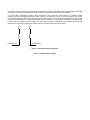
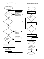
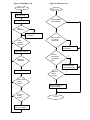
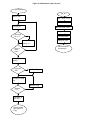
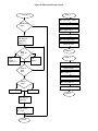
Designing a Dual-Interface Keyboard with the Cypress
Semiconductor CY7C63413 USB Microcontroller
Revision 1.3 02/13/99
Added 3D mouse documentation and endpoint 2 boot protocol description
Revision 1.2 11/09/98
Added power management documentation
Revision 1.1 10/29/98
Added slave mouse documentation
Introduction
The PS/2 auxiliary device interface is an established standard in the personal computer industry. It is used for the
attachment of peripherals to the computer such as a keyboard, mouse, joystick, etc. In recent years, the Universal Serial
Bus (USB) standard has been developed in an attempt to address the shortcomings of PS/2 and other common desktop
computer electrical interfaces, including limited bandwidth, data integrity and the limitation of a single slave device per port.
USB addresses bandwidth limitations by offering 1.5Mbit (low speed) and 12Mbit (full speed) serial data transfer rates. USB
provides several levels of data integrity validation, including cyclic redundancy code (CRC) checking, and defines procedures
for failed-transfer recovery. In addition, the USB architecture provides for the connection of up to 127 devices on a single
root hub. While the USB standard has been embraced by the computer industry, and is now included by default on most
desktop motherboards produced for sale, there remains a large installed base of computers and operating system software
which do not yet support USB. This application note address the design of a keyboard that supports both the USB and PS/2
interfaces using the Cypress Semiconductor single-chip CY7C63413 USB microcontroller.
This application note starts by addressing the basic requirements for key-scan and other interface-independent keyboard
functionality, followed by an introduction to the CY7C63413 USB controller. A schematic of the Dual-Interface keyboard and
its connection details can be found in the Hardware Implementation Section.
The software section describes the architecture of the firmware required to implement the keyboard function. The source
code of the demonstration keyboard firmware is available with the Cypress CY3651 Development Kit. Please contact your
local Cypress Sales Office for details.
This application note assumes that the reader is reasonably familiar with the CY7C63413 USB controller, the Universal
Serial Bus and the PS/2 device interface. The CY7C63413 data sheet is available from the Cypress web site at
http://www.cypress.com. USB documentation can be found at the USB Implementers Forum web site at http://www.usb.org/.
Information regarding the PS/2 keyboard interface can be found in IBM publication 84F9735, IBM Personal System/2
Hardware Technical Reference – Common Interfaces, which may be purchased directly from IBM.
Keyboard Basics
Key Switches and Scan Matrix
A computer keyboard typically has between 101 and 104 keys that are uniquely positioned in a scan matrix. The scan matrix
consists of M rows and N columns, all of which are electrically isolated from each other. The number of rows (M) is typically
no greater than 8, and the number of columns (N) is no greater than 20. Each key sits over two isolated contacts of its
corresponding row and column in the scan matrix. When a key is pressed, the two contacts are shorted together, and the
row and column of the key are electrically connected (Figure 1).
1Key Switch
Intelligent Controller
The typical computer keyboard keyboard contains an embedded controller that performs the necessary functions to scan the
key matrix and implement the communication interface to the host computer. The essential task of the controller is to
monitor the keys and report key presses and/or releases to the host computer. The basic key-matrix scanning approach is,
for the most part, independent of the host communications interface.
Basic Key Matrix Scanning
The controller continuously imposes a sequential scan pattern onto the column lines of the key matrix, such that a logic 0 is
imposed on one column line at a time, with all other column lines at logic 1. The controller reads the row lines each time a
new column pattern is applied. If a 0 is propagated to a row line, then the key at the intersection of that column and row has
been pressed. See Figure 2 and Figure 3.
1Scan Results For No Key Press
1Scan Results for Key 1, 1 Pressed
Host Interface Cable
A PS/2 keyboard is connected to the main computer through a shielded PS/2 cable that typically contains 4 wires carrying
signals Vcc, GND, Clock, and Data. A shield drain wire is typically also provided. The USB cable is also a shielded cable
containing four conductors: Vcc, GND, Data+ and Data-. For the purpose of implementing a dual-interface keyboard, the
electrical requirements of the USB interface are more stringent than those of PS/2. For that reason, the interface cable used
in the dual-interface implementation should meet all requirements for low-speed USB.
Introduction to CY7C63413
The CY7C63413 is a high performance 8-bit RISC microcontroller with an integrated USB Serial Interface Engine (SIE). The
architecture implements 37 commands that are optimized for USB applications. The CY7C63413 has a built-in clock
oscillator and timers, as well as general purpose I/O lines that can be configured as resistive with internal pull-ups, opendrain outputs, or traditional CMOS outputs. High performance, low-cost human-interface type computer peripherals such as
a keypad or keyboard can be implemented with minimum external components and firmware effort.
In addition, the CY7C63413’s microcontroller is capable of performing all functions necessary to implement a PS/2 interface
to a host computer. In this case, the USB functions of the chip are unused, and the RAM and I/O normally dedicated to USB
tasks are available for general use.
Clock Circuit
The CY7C63413 has a built-in clock oscillator and PLL-based frequency doubler. This circuit allows a cost effective 6 MHz
ceramic resonator to be used externally while the on-chip RISC core runs at 12 MHz.
USB Serial Interface Engine (SIE)
The operation of the SIE is totally transparent to the user. In receive mode, USB packet decode and data transfer to the
endpoint FIFO are automatically done by the SIE. The SIE then generates an interrupt to invoke the service routine after a
packet is unpacked.
In the transmit mode, data transfer from the endpoint and the assembly of the USB packet are handled automatically by the
SIE.
General Purpose I/O
The CY7C63413 has 32 general purpose I/O lines divided into 4 ports: Port 0 through Port 3. One such I/O circuit is shown
in Figure 4. Each port (8 bits) can be configured as resistive with internal pull-ups (7 KΩ ), open drain outputs (high
impedance inputs), or traditional CMOS outputs.The port configuration is determined according to Table 1 below.
Table 1. GPIO Configuration
Port
Pin
Driver Mode Interrupt
Configuration
Bits
11
10
Interrupt Bit
10
01
00
1
X
X
X
0
Polarity
Resistive
CMOS
Output
CMOS Input
Open Drain
Open Drain
disabled
disabled
+
Ports 0 to 2 offer low current drive with a typical current sink capability of 7 mA. Port 3 offers higher current drive, with a
typical current sink of 12 mA which can be used to drive LEDs.
Each General Purpose I/O (GPIO) is capable of generating an interrupt to the RISC core. Interrupt polarity is selectable on a
per port basis using the GPIO Configuration Register (see Table 1 above.) Selecting a negative polarity (“-”) will cause falling
edges to trigger an interrupt, while a positive polarity (“+”) selects rising edges as triggers. The interrupt triggered by a GPIO
line is individually enabled by a dedicated bit in the Interrupt Enable Register. All GPIO interrupts are further masked by the
Global GPIO Interrupt Enable Bit in the Global Interrupt Enable Register.
The GPIO Configuration Register is located at I/O address 0x08. The Data Registers are located at I/O addresses 0x00 to
0x03 for Port 0 to Port 3 respectively.
Power-up Mode
The CY7C63413 offers 2 modes of operation after a power-on-reset (POR) event: suspend-on-reset (typical for a USB
application) and run-on-reset (typical for a PS/2 application). The suspend-on-reset mode is selected by attaching a pull-up
resistor (100K to 470K Ω ) to Vcc on Bit 7 of GPIO Port 3. The run-on-reset mode is selected by attaching a pull-down resis-
tor (0 to 470K Ω ) to ground on Bit 7 of GPIO Port 3. See Figure 5 and Figure 6.
Figure 1. One General Purpose I/O Line
VCC
Port 3, Bit 7
Rpullup
100K to 470K OHM
Figure 1. Suspend-On-Reset Mode
Port 3, Bit 7
Rpulldown
0 to 470K OHM
Figure 1. Run-On-Reset Mode
Hardware Implementation
Figure 8 is the schematic for a dual-interface keyboard application. This design may be used to implement a USB-only
keyboard, a dual-interface (USB and PS/2) keyboard, or a USB keyboard with the capability to support a slave PS/2 mouse.
The latter design is the subject of Cypress Application Note XXXXX. The table in the lower left hand corner of the schematic
Main Drawing shows what components are to be installed for the desired implementation
Key Matrix and LEDs
Port 2 is configured as resistive (7 Kohm pull-ups to Vcc), and is connected to rows 0~7 of the scan matrix, providing
support for up to 8 rows. Port 0, 1, and 3 are also configured as resistive. Ports 0 and 1 provide connection to key matrix
columns 0 ~ 15, and coulmns 16 and 17 are serviced by Port 3 bits 4 and 5, providing support for up to 18 columns. For
scan matrices with less than 8 rows or 18 columns, the unused port bits may be left unconnected. The cathodes of the three
keyboard LEDs (Num Lock, Caps Lock, and Scroll Lock) are connected via current-limiting resistors R7, R8 and R9 to bits 0,
1 and 2 of Port 3, which can sink sufficient current to directly drive the LEDs. The LED anodes are connected directly to
VCC. An LED is turned ON by the firmware writing a 0 to its corresponding port bit.
When no row or column bits are set to 0 by the firmware, all bits will be pulled to a logic ‘1’ by their internal 7K-ohm
resistors. When, during key scanning, firmware drives any column bit to a logic ‘0’, the row bits corresponding to any closed
keys on that column in the matrix will also be read as logic 0’s by the firmware. If no keys are closed on the activated
column, all row bits will be read as logic 1’s by the firmware. See Figure 7. Each column in the matrix is scanned by writing
its associated port bit to logic 0, holding all other column bits at logic 1, then interrogating the row inputs on port 2. A
complete matrix scan consists of one scan for each column in the matrix.
Power-On Reset
Port 3, Bit 7 controls the POR mode of the CY7C63413 microcontroller. Depending upon the interface being implemented,
this bit will be pulled either to VCC, invoking suspend-mode POR, or to GND, invoking run-mode POR. Suspend mode POR
is used when the host interface is known to be USB. In this mode, the microcontroller goes immediately into a suspend state
after power-on, until a USB Reset condition is detected on the D+/D- lines. Upon detection of this condition, the
microcontroller institutes a 128uS delay, after which code execution begins.
In the case where the host interface is know to be or may be PS/2, and therefore in which a USB Reset condition may not
occur, run-mode POR is selected. In this mode, the microcontroller, upon detection of power, implements a 128mS delay for
power and oscillator stabilization, after which code execution begins.
Microcontroller Clock
The microcontroller clock in the refertence design is based on a 6 MHz ceramic resonator which is connected across the
XTALI and XTALO pins of the microcontroller. The CY7C63413 includes internal DC biasing and crystal element load
capacitance together with an inverting amplifier to implement an on-chip Colpitts-style inverting oscillator using the external
crystal or resonator. This circuit is intended to operate using no other external components with crystals or resonators
designed for a parallel-resonant load capacitance of 30pF. As the XTALI pin is a high-impedance node, the resonator or
crystal component should be placed as physically close to the microcontroller as possible, and care should be taken in
layout to avoid coupling of high-frequency signals onto this node. The 6MHz reference clock produced by the oscillator
circuit is frequency doubled, using an on-chip phase-locked loop (PLL), to yield the 12MHz CPU instruction clock.
Power
The 5V Vcc and GND come directly from the host interface cable. Shield ground is also provided on the host connector. A
4.7uF tantalum capcitor, C3, provides bulk power supply bypass, and additional high-frequency bypass is provided by 0.1uF
capacitor C2. Capacitor C4 provides an AC path between signal ground and shield ground, per the USB specification, and
10M-ohm resistor R10 is provided as a DC discharge path for C4 in the event that shield ground and signal ground become
separated at the host.
Host Interface Connection
In the event that the host interface is known to be USB, jumper JP1 will be installed, connecting resistor R2 between the
USB D- line and Vcc. The USB specification indicates that a 1.5K-ohm, 5% resistor be used between the D- line and a 3.0 ~
3.6V DC rail for termination of a low-speed device. The reference design employs a 1%, 7.5K-ohm resistor between D- and
the nominal 5VDC rail. Cypress recommends this termination method as an alternative to the method described in the USB
specification, as it yields compatible signal levels and does not require the use of a separate 3V regulator.
In the event that a dual-interface design is being implemented, JP1 is left open, and transistor Q1 is installed to allow
firmware control over the USB pullup resistor via Bit 3 of Port 3. On power-up, port pin 3.3 is high impedance, and resistor
R11 guarantees that Q1 is turned OFF, disconnecting pullup R2 from the rail. Once the firmware determines the type of host
interface to be implemented, it may enable the pullup, or leave it disabled, by controlling Q1 as necessary. In the event that
a PS/2 interface is selected, the device relies on the host’s pullup resistors to terminate the open-collector PS/2 clock and
data lines. No pullups are included in the reference design on the device side of the PS/2 interface.
VCC
Row port line
Row i
VCC
Column port line
Column j
Figure 1. Row/Column Port Configuration
Figure 1. Hardware Implementation
Firmware Implementation
The reference firmware supports both the USB and PS/2 interfaces. For each interface, the firmware can be conceptually
divided into the following sections: host command processing, scan code conversion, and keyboard matrix scanning. Of
these tasks, the keyboard matrix scanning is common to both interfaces and, as such, is organized as a set of callable
functions which scan the keyboard and return interface-independent information about the state of the keys. The information
regarding the key states must be uniquely converted to the proper format for each interface (scan code conversion) prior to
transmission to the host. In addition, both interfaces require support for interface-specific host commands that configure
the keyboard; for USB, this includes enumeration and setup, and for PS/2, this includes such commands as selecting the
scan set, selecting the key repeat rate and delay (typematic functionality), and enabling/disabling scanning.
Code Organization
The supplied reference firmware supports four variants: a usb keyboard, a ps2 keyboard, a usb/ps2 dual-interface keyboard,
and a usb with slave mouse/ps2 dual-interface keyboard (refer to the readme.txt in the reference firmware distribution for
detailed instructions on building each variant). Code for the usb-only and ps2-only implementations is less than 4k in size.
However, the code size for both dual-interface implementations is larger than 4K; this places a constraint on the
organization of the firmware due to the microcontroller’s restriction that code residing in the upper 4K of memory cannot call
routines residing in the lower 4K (the reverse, however, is possible). To effectively circumvent this limitation, the main
control loop and host command processing modules for both USB and PS/2 reside in the lower 4K of ROM, while the
subroutines that these modules invoke (keyboard scanning, scan code conversion) are placed in the upper 4K.
In addition, ISRs for both interfaces reside in the lower 4K in accordance with the hardware interrupt support provided by
the microcontroller.
Since the dual-interface firmware detects the type of interface (USB or PS/2) dynamically upon power-up (which commences
when the keyboard is plugged into the computer, or the computer itself is turned on), the USB-specific firmware and PS/2
specific firmware never run simultaneously. Thus, static variable assignment and other RAM usage for the two separate
host interface firmware modules can overlap, reducing overall RAM requirements. Since the keyboard martrix scanning
routines are utilized in both USB and PS/2 situations, the RAM associated with this task cannot be shared with other
functions and is statically allocated in its own area of RAM.
In normal operation, the control flow is roughly the same for both USB and PS/2 interfaces, although their modules remain
entirely distinct. After power-up housekeeping is performed and the keyboard scanning is enabled, the firmware enters a
loop, from which it periodically invokes the keyboard matrix scanning subroutine. The key-scan module converts
row/column key information to generic key numbers, which are in turn converted by scan-code conversion modules to the
required scan codes for the currently active host interface. A separate scan-code conversion module exists for each scan-set
required, and the key-scan module invokes the scan-code conversion module corresponding to the currently-selected host
scan set (e.g., USB, PS/2 Scan Set 1, PS/2 Scan Set 2 or PS/2 Scan Set 3). USB supports only one scan set, while PS/2
supports three separate host-selectable scan sets. When the keyboard matrix scanning subroutine returns, the converted
key press information just collected by the scan conversion code can be transmitted to the host from the main loop.
Auto-Interface Mode
The dual-interface keyboard determines upon power-up whether it is attached to a USB or PS/2 interface. This is
accomplished as follows.
Upon detecting power, the microcontroller implements a 128mS delay, after which code execution begins at the Reset
vector. The firmware sets the D+/D- lines to Hi-Z, leaves the USB pullup resistor disconnected from the D- lines, then
institutes an additional delay of 10mS. With the D+/D- lines in Hi-Z, the 15K-ohm pulldown resistors on a USB host will
cause both lines to be pulled to 0V (disconnected). If the interface is PS/2, the idle-state pullup resistors on the PS/2 host will
cause both lines to be pulled to Vcc.
The host determination is complicated somewhat by the fact that a PS/2 host will often times place the port in an inhibit state
by holding the PS/2 clock line low. Unless the host is attempting to transmit data, however, the data line will still be pulled
high. A host computer will not typically attempt to transmit data to the keyboard until it has received a power up status
indication from the keyboard.
The D+/D- lines are then polled approximately every 2uS for a duration of 1mS. If, on any four consecutive samples, either
or both of the D+ or D- lines are sampled as non-zero, the interface is determined to be PS/2. Otherwise (both D+ and Dremain low), the D- pullup is engaged by enabling Q1, causing a USB connect condition. The firmare then delays 10uS
longer, and examines the lines once again to verify that the connect condition (D+ low, D- high) persists on the lines. If so,
the interface is determined to be USB. If not, the connect resistor is disconnected from D-, and the host is assumed to be a
PS/2 interface which happens to be driving both Clock and Data. See Figure XX.
USB Interface
All USB Human Interface Device (HID) class applications such as a keyboard, follow the same USB start-up procedure. The
procedure is as follows (see Figure 9.)
Figure 2. USB Start-Up Procedure
Device Plug-in (Power On Reset)
The USB device is powered when it is connected to the bus. The pull-up resistor on D– notifies the hub that a low-speed (1.5
Mbps) device has just been connected. Program execution begins at address 0 (see Figure 10).
Figure 2. Power On Reset
Bus Reset
The host recognizes the presence of a new USB device and resets it (see Figure 11).
Figure 2. Bus Reset ISR
• Enable device address 0
• Enable 1ms Timer Interrupt
• Enable End Point 0 to respond to SETUP packets
Enumeration
The host sends a SETUP packet followed by IN packets to read the device description from default address 0. When the
description is received, the host assigns a new USB address to the device. The device begins responding to communication
with the newly assigned address. The host then asks for the device descriptor, configuration descriptor and HID report
descriptor. The descriptors hold the information about the device. They will be discussed in detail below. Using the information returned from the device, the host now knows the number of data endpoints supported by the device (in a USB
keyboard, there is only one data endpoint). The host will issue a Set Configuration with a value of 1. At this point, the
process of enumeration is completed. See Figures 12, 13, and 14.
•
Endpoint 0 ISR
• Responds to
SETUP packet
according to the parsing structure
Figure 2. USB Standard Request Parsing Structure
Figure 2. USB HID Class Request Parsing Structure
Data Acquisition/Transfer
The firmware periodically writes scan patterns to the scan matrix columns, and reads the row result to determine which keys
are pressed. The scan codes of the keys pressed are sent to the host using endpoint 1 (see Figure 15). When the host
issues IN packets to retrieve data from the device, the device returns eight bytes of data. These eight bytes hold the
keyboard control data (see Figure 16). Usage codes for each key can be found in Appendix A.3 of the Device Class Definition for Human Interface Devices (HID). When one of the LED buttons (i.e. Num Lock, Caps Lock, Scroll Lock) are pressed
or released, the host issues a SETUP packet with a Set_Report request through the control pipe to End Point 0, followed by
an OUT packet with 1 Data byte indicating which LED should be on or off (see Figure 17.)
Figure 2. Endpoint 1 Interrupt Service Routine
Byte 7 - Key 6
Byte 6 - Key 5
Byte 5 - Key 4
Byte 4 - Key 3
Byte 3 - Key 2
Byte 2 - Key 1
Byte 1 - Reserved
Bit 7
Right Right Right Right Left
GUI Alt
Shift Ctrl GUI
Bit 0
Left AltLeft Left Byte 0Shift Ctrl Modifier
Figure 2. IN Data Organization for USB Keyboard
Bit 7
Bit 0
Con Con Con Kana Com Scroll Caps Num Byte 0stant stant stant
pose Lock Lock Lock LED report
Figure 2. LED Report for USB Keyboard
The byte order and bit field positions are defined by the HID report descriptor (discussed below), and are also consistent with
the Boot Protocol requirements for legacy systems.
USB Descriptors
As stated earlier, the USB descriptors hold information about the device. There are several types of descriptors, which will be
discussed in detail below. All descriptors have certain characteristics in common. Byte 0 is always the descriptor length in
bytes and Byte 1 is always the descriptor type. Dis
cussion of these two bytes will be omitted from the following descriptions.
The rest of the descriptor structure is dependent on the descriptor type. An example of each descriptor will be given.
Descriptor types are device, configuration, interface, endpoint, string, report, and several different class descrip
tors.
Device Descriptor
This is the first descriptor the host requests from the device. It contains important information about the device. The size of
this descriptor is 18 bytes. A list follows:
•
•
•
•
•
•
•
•
•
•
•
•
USB Specification release number in binary-coded deci
mal (BCD) (2 bytes)
Device class (1 byte)
Device subclass (1 byte)
Device protocol (1 byte)
Max packet size for Endpoint 0 (1 byte)
Vendor ID (2 bytes)
Product ID (2 bytes)
Device release number in BCD (2 bytes)
Index of string describing Manufacturer (Optional) (1 byte)
Index of string describing Product (Optional) (1 byte)
Index of string containing serial number (Optional) (1 byte)
Number of configurations for the device (1 byte)
Example of a device descriptor
Descriptor Length (18 bytes)
Descriptor Type (Device)
Complies to USB Spec Release (1.00)
Class Code (insert code)
Subclass Code (0)
Protocol (No specific protocol)
Max Packet Size for endpt 0 (8 bytes)
Vendor ID (Cypress)
Product ID (USB Keyboard)
Device Release Number (1.03)
String Describing Vendor (None)
String Describing Product (None)
String for Serial Number (None)
Possible Configurations (1)
Configuration Descriptor
The configuration descriptor is 9 bytes in length and gives the configuration information for the device. It is possible to have
more than one configuration for each device. When the host requests a configuration descriptor, it will continue to read these
descriptors until all configurations have been received. A list of the structure follows:
•
•
•
•
•
•
Total length of the data returned for this configuration (2 bytes)
Number of interfaces for this configuration (1 byte)
Value used to address this configuration (1 byte)
Index of string describing this configuration (Optional) (1 byte)
Attributes bitmap describing configuration characteristics (1 byte)
Maximum power the device will consume from the bus (1 byte)
Example of configuration descriptor
Descriptor Length (9 bytes)
Descriptor Type (Configuration)
Total Data Length (34 bytes)
Interfaces Supported (1)
Configuration Value (1)
String Describing this Config (None)
Config Attributes (Bus powered)
Max Bus Power Consumption (100mA)
Interface Descriptor
The interface descriptor is 9 bytes long and describes the interface of each device. It is possible to have more than one
interface for each device. This descriptor is set up as follows:
• Number of this interface (1 byte)
• Value used to select alternate setting for this interface (1 byte)
• Number of endpoints used by this interface. If this number is zero, only endpoint 0 is used by this interface (1
byte)
• Class code (1 byte)
• Subclass code (1 byte)
• Protocol code (1 byte)
• Index of string describing this interface (1 byte)
Example of interface descriptor
Descriptor Length (9 bytes)
Descriptor Type (Interface)
Interface Number (0)
Alternate Setting (0)
Number of Endpoints (1)
Class Code (insert code)
Subclass Code (0)
Protocol (No specific protocol)
String Describing Interface (None)
HID (Class) Descriptor
The class descriptor tells the host about the class of the de
vice. In this case, the device falls in the human interface de
vice
(HID) class. This descriptor is 9 bytes in length and is set up as follows:
•
•
•
•
•
Class release number in BCD (2 bytes)
Localized country code (1 byte)
Number of HID class descriptor to follow (1 byte)
Report descriptor type (1 byte)
Total length of report descriptor in bytes (2 bytes)
Example of HID class descriptor
Descriptor Length (9 bytes)
Descriptor Type (HID Class)
HID Class Release Number (1.00)
Localized Country Code (USA)
Number of Descriptors (1)
Report Descriptor Type (HID)
Report Descriptor Length (63 bytes)
Endpoint Descriptor
The endpoint descriptor describes each endpoint, including the attributes and the address of each endpoint. It is possible to
have more than one endpoint for each interface. This de
scriptor is 7 bytes long and is set up as follows:
•
•
•
•
Endpoint address (1 byte)
Endpoint attributes. Describes transfer type (1 byte)
Maximum packet size this endpoint is capable of transfer
ring (2 bytes)
Time interval at which this endpoint will be polled for data (1 byte)
Example of endpoint descriptor
Descriptor Length (7 bytes)
Descriptor Type (Endpoint)
Endpoint Address (IN, Endpoint 1)
Attributes (Interrupt)
Maximum Packet Size (8 bytes)
Polling Interval (10 ms)
Report Descriptor
This is the most complicated descriptor in USB. There is no set structure. It is more like a computer language thatscribes
de
the format of the device’s data in detail. This descrip
tor is used to define the structure of the data returned to the host as well
as to tell the host what to do with that data. An example of a report descriptor can be found below.
A report descriptor must contain the following items: Input (or Output or Feature), Usage, Usage Page, Logical Minimum,
Logical Maximum, Report size, and Report Count. These are all necessary to describe the device’s data.
Example of report descriptor
Usage Page (Generic Desktop)
Usage (Keyboard)
Collection (Application)
Usage Page(key codes)
Usage Minimum (224)
Usage Maximum (231)
Logical Minimum (0)
Logical Maximum (1)
Report Size (1)
Report Count (8) ; modifier byte
Input (Data, Variable, Absolute)
Report Count (1)
Report Size (8)
Input (Constant) ; reserved byte
Report Count (5)
Report Size (1)
Usage Page (LEDs)
Usage Minimum (1)
Usage Maximum (5)
Output (Data, Variable,
Absolute); LED report
Report Count (1)
Report Size (3)
Output (Constant) ;padding
Report Count (6)
Report Size (8)
Logical Minimum (0)
Logical Maximum (101)
Usage Page (key codes)
Usage Minimum (0)
Usage Maximum (101)
Input (Data, Array) ;key array(6)
End Collection
Input items are used to tell the host what type of data will be returned as input to the host for interpretation. These items
describe attributes such as data vs. constant, variable vs. ar
ray, absolute vs. relative, etc.
Usages are the part of the descriptor that defines what should be done with the data that is returned to the host. From the
example descriptor, Usage (Keyboard) tells the host that this is a keyboard device. There is also another kind of Usage tag
found in the example called a Usage Page. The reason for the Usage Page is that it is necessary to allow for more than 256
possible Usage tags. Usage Page tags are used as a second byte which allows for up to 65536 Usages.
Logical Minimum and Logical Maximum are used to bound the values that a device will return. For example, a keyboard that
will return the values 0 to 101 for the scan code of each key press will have a Logical Minimum (0) and Logical Maxi
mum
(101). These are different from Physical Minimum and Physical Maximum. Physical boundaries give some meaning to the
Logical boundaries. For example, a thermometer may have Logical boundaries of 0 to 999, but the Physical bound
aries may
be 32 to 212. In other words, the boundaries on the thermometer are 32 to 212 degrees Fahrenheit, but there are one
thousand steps defined between the boundaries.
Report Size and Report Count define the structures that the data will be transferred in. Report Size gives the size of the
structure in bits. Report Count defines how many structures will be used. In the example descriptor above, the lines port
Re
Size (8) and Report Count (6) define a 6 byte key array for a keyboard.
Collection items are used to show a relationship between two or more sets of data. For example, a minimal keyboard can be
described as a collection of four data items (Modifier byte, Reserved byte, LED report, and Key Array). End Collection items
simply close the collection.
It is important to note that all examples given here are merely for clarification. They are not necessarily definitive solutions.
A more detailed description of all items discussed here as well as other descriptor issues can be found in the “Device Class
Definition for Human Interface Devices (HID)” revision 1.0 and in the “Universal Serial Bus Specification” revision 1.0,
chapter 9. Both of these documents can be found on the USB world wide web site at http://www.usb.org/.
Functionality
Main Loop
The main loop of the firmware (Figure 20) waits for the key
board Scan Task to be scheduled by the 1 ms ISR (Figure 21),
and then executes it. At the completion of the scan task, the main loop will check for global scanning errors, such as rollover
errors or phantom-key errors, and will format an error report if either of these conditions are present (this report consists of a
standard key report in which all 6 key array positions in the End Point 1 FIFO (bytes 2–7) will be loaded with usage code
01h). Reports, either key reports or error reports, are sent to the host via End Point 1 any time a report is requested. The
host side software will repeat the key press until the release of the key, so that the device does not require a continuous
report when no key status changes have occurred.
Scan Task
The USB Scan Task consists of a call tousb_scan_keys. This routine first calls the generic matrix scanning routine, which
maintains an image of the state of the key matrix since the last time the routine was invoked. The matrix scanning routine
compares the current state of the keys against the image by sequencing through the rows and columns of the matrix. As
successive key state changes are detected, they are saved as the “current” state in the image, and are also reported to the
USB scan-conversion code via a subroutine call, with a generic key-code and state-change (up or down) as arguments. The
scan-conversion code converts this generic key information into the appropriate USB usage codes, and places it in a USBformatted buffer (discussed above) for eventual transmission to the host.
Suspend/Resume/Remote Wakeup
According to the USB Specification 1.0, a device has to go intosuspend mode after 3 ms of no bus activity. The 1 ms ISR
determines when this condition occurs (by reading the Bus Activity bit, bit 3, of the USB Status and Control Register, 1Fh)
and sets the SUSPEND_FLAG accordingly. The main loop, upon detecting the assertion of this flag, suspends the
microcontroller by setting bit 0 (the Run bit) and bit 3 (Suspend bit) of the Pro
cessor Status and Control Register (FFh). The
microcontroller will resume operation if a GPIO interrupt occurs or bus activity resumes.
Prior to suspending the microcontroller, the firmware pulls down all the column port lines and enables a falling edge interrupt
on all Port 2 lines (Row port). If any key is pressed while in the suspended state, one of the row lines will be pulled low and
trigger a GPIO interrupt. The GPIO ISR causes the microcontroller to return from suspend mode, and send a resume signal
(force a K state where D+ is high and D- is low for 10ms) to wake up the host (remote wake up).
N-Key Rollover
In the case where multiple keys are pressed and held down, only the last key pressed should be repeated. To accomplish
this, the last key press is stored in theLastTx buffer and is sent again in a separate report to the host whenever a multi
ple
key report is sent. Once the same key is released, a report notifying it of the release is sent to the host (all 6 key array
positions are filled with 0’s).
Endpoint 2
The usb reference firmware supports the implementation of the power, sleep, and wake keys, as defined in the USB HID
specification and in Microsoft’s PC98 Keyboard Specification. These keys are reported to the host via an entirely separate
descriptor structure reserved for power management events. In addition, the reference firmware includes optional support for
a slave ps2 mouse, using another unique descriptor structure for mouse packets. Endpoint 2 is pressed into service to
report both power management events and mouse data packets. These packets are distinguished by a unique report ID
embedded in the packet itself, which identifies the content of the packet currently being transmitted. The structure of the
data inside the packet, and the value of the report ID for each type of transmission, is entirely defined by the report
descriptor for endpoint 2:
usage page (generic desktop)
usage (mouse)
collection (application)
report id (1)
usage (pointer)
collection (linked)
usage page (buttons)
usage minimum (1)
usage maximum (3)
logical minimum (0)
logical maximum (1)
report count (3 bytes)
report size (1)
input (3 button bits)
report count (1)
report size (5)
input (constant 5 bit padding)
usage page (generic desktop)
usage (X)
usage (Y)
usage (wheel)
logical minimum (-127)
logical maximum (127)
report size (8)
report count (3)
input (3 position bytes X & Y & wheel)
end collection
end collection
usage page(Generic Desktop)
usage (System Control)
collection(Application)
report id (2)
usage page(Generic Desktop)
usage minimum(System Power Down)
usage maximum(System Wake Up)
logical minumum(0)
logical maximum(1)
report count (3)
report size (1)
input(Data,Var,rel)
report count (1 byte)
report size (5 bits)
input (constant)
end collection
The above descriptor defines two types of packets that can be sent on endpoint 2: a 5-byte mouse packet consisting of a
report ID (= 0x1), a single byte of button information, and a byte each of X, Y, and wheel data; and a 2-byte power
management packet, consisting of a report ID (= 0x2) and a byte containing the current state of the power management
keys:
Bits 7-3
Bit 2
Bit 1
Bit 0
unused
1 = wake key pressed
1 = sleep key pressed
1 = power key pressed
The reference firmware enables endpoint 2 upon power-up. The power management keys are scanned every 4 msec along
with other keys in the matrix. If power management keys are pressed, a 2-byte power management packet as described
above will be transmitted to the host at that time. If no power events are recognized, the mouse (if one is connected, and if
the firmware includes support for the mouse) is polled and its data is transmitted instead.
Note that the endpoint 2 descriptor allows for a mouse packet that includes optional “wheel”, or Z-axis, When the firmware
detects the presence of a mouse, it interrogates the mouse to determine its type. If the mouse is not a 3D mouse, the
“wheel” data in the packet is set to zero; otherwize, wheel data is tranmsitted in the appropriate byte.
Finally, to support boot protocol, the firmware will not transmit power key status on endpoint 2 when the boot protocol is
selected via the host command; instead, it reverts to transmitting a standard 2-axis mouse packet without the packet id
header: i.e., a three-byte packet consisting of button data, X, and Y coordinates. When report protocol is re-selected, the
packet structure is as described above.
Slave Mouse Support
The usb portion of the reference firmware includes optional support for a slave ps2 mouse. The firmware uses 2 port pins to
implement the clock/data interface to the mouse, reports data to the host via USB data endpoint 2. Commands to the
mouse are initiated by the main loop of the reference firmware and are sequenced to completion by subsequent GPIO
interrupts, which are generated by edge transitions of the mouse’s clock line. During normal execution, the firmware places
the ps2 mouse in polling mode (in which the mouse only transmits data packets upon request); at 4msec intervals the
firmware solicits mouse data and places it in USB endpoint 2’s data buffer for transmission to the host.
Slave mouse support is optional. The usb reference firmware, by default, makes calls to subroutines that implement the
slave mouse interface. However, these calls can be “stubbed” and the slave mouse code removed. Two variants of the
reference firmware (usb.asm and usbps2.asm) are examples of code that disables mouse support; usbsmps2.asm is an
example of one that includes it.
To support the slave ps2 mouse, the usb reference firmware performs the following additional tasks, in addition to those
already described for normal usb operation :
• Support for mouse packet transmission on endpoint 2. The report descriptor for endpoint 2 includes a mouse collection,
so that the host will detect the presence of a mouse and poll for its data accordingly. This additional support is handled
in the report descriptor tables and in the firmware that transmits the report descriptors to the host on the control
endpoint (endpoint 0).
• Support for bit-level serial communications to/from the mouse. Serial communications are handled via a state machine
implemented in the functionmouse_int, which is invoked from the GPIO ISR each time the mouse clock line transitions
to clock in or out the next bit of a transaction.mouse_int communicates the successful result of a data transfer to the
main loop via a set of status flags and a 3-byte data buffer.
• Support for mouse plug ‘n play. To insure that the ps2 mouse can be plugged/unplugged during operation, the firmware
calls the function MouseConnectTask periodically from the main loop. This function maintains the connect state of the
ps2 mouse by periodically verifying its operation. If the mouse is determined to be unplugged as a result of lost
communication, this function issues reset commands to the mouse each time it is invoked, until it receives a valid
response from the re-connected mouse. MouseConnectTask relies on the helper function mouse_1ms_int , which is
called from the 1msec ISR to monitor the elapsed time between mouse transactions. If the mouse is unplugged in the
middle of a transaction, this routine will flag a timeout, thus resetting the bit-level state machinemouse_int
in
so that a
fresh command can be re-initiated.
• Support for periodic data collection from the mouse. The reference firmware calls the function
MouseTask at 4 msec
intervals, to solicit a data packet from the mouse. This received packet is placed the data in endpoint 2’s data buffer for
eventual transmission to the host.
• Support for remote wakeup. Any mouse movement or button press is required to wake up the keyboard from suspend
(in addition to a key press from the keyboard itself or from the resumption of USB bus activity). To accomplish this, the
firmware temporarily places the mouse in data mode by callingmouse_suspend prior to suspending the
microcontroller. In this mode the mouse will automatically report data if its position or buttons change state. This
unsolicited mouse activity will generate a GPIO interrupt, which in turn causes the microcontroller to wake up from
suspend mode and resume operation. The firmware callsmouse_resume to restore the mouse to data polling mode
after returning from a suspend.
PS/2 Interface Reference Firmware
The PS/2 reference firmware is conceptually simple: all tasks are handled sequentially from a main loop. The 1msec ISR
merely increments a count variable to generate gross delays and to time the period between successive keyboard scans.
Since the USB D+ and D- lines are pressed into service as the PS/2 Clock and Data lines, rather than using GPIO lines,
changing the drive state for bit transitions of the PS/2 clock and data must be accomplished by modifying the control bits in
the USB Status and Control register. Remembering that the PS/2 clock and data are open-collector lines, the idle state of
the PS/2 interface is a setting of ‘111’in Control Bits 2~0 of this register, placing both lines at Hi-Z. Neither the clock nor
data line are everdriven high. Each line is always either driven low or pulled high by the pullup resistors on the host. Driving
the clock line (corresponding to D+) low while floating the data line (corresponding to D-), for instance, would be
accomplished with a setting of ‘110’in Control Bits 2~0.
The PS/2 firmware can be be viewed as two layers: an interface layer and a command layer. The interface layer processes
the bit-level transaction management between the host and the keyboard, and the command layer deals with the higher-level
implementation of keyboard commands and responses. All PS/2 timing is generated from the keyboard, which is always the
source of the PS/2 clock signal. Interface-layer transaction timing is based on instruction timing.
Due to the high instructionprocessing rate of the CY7C63413, code loops are used to generate the short delays required at the PS/2 bit transaction
level, and an assembler macro ,DELAY, has been included to simplify the implementation of these delays. See Figures 24
and 25.
At the transaction level, a byte being received from or transmitted to the host computer is handled essentially without
interruption. This is necessary due to the relatively narrow timing requirements at the bit-level interface of the PS/2. While
the 1.28mS interrupt may be serviced within a PS/2 transaction, the ISR is kept sufficiently short that the overall interface
timing requirements can still be met.
The PS/2 host interface command processor is integrated into the main loop. That is, when the keyboard is not being
scanned, the firmware continually checks to see if the host is attempting to send a command. If so, it invokes the code that
accepts and processes the command, returns any required responses, and returns to the main loop. A complete description
of the PS/2 command set and functional requirements, including the parameter descriptions and the electrical timing
specifications for the PS/2 interface is provided in the IBM document referenced at the beginning of this Application Note.
Functionality
Main Loop
After power-up housekeeping is performed, the main loop of the PS/2 firmware is entered. This loop invokes the keyboard
scanning task at periodic (4msec) intervals and sends to the host any key presses that were detected, and also checks for
the presence of a host command request. Command requests are honored immediately: the firmware receives and parses
the command and invokes the proper subroutine to perform the command and return any required data to the host. See
Figures 22 and 23.
Scan Task
The reference firmware scans the key matrix approximately once every 4mS. This timing is generated from the 1mS interrupt
service routine, which increments a 1-msec count variable upon each invocation. On each pass through the Main Loop, the
1 msec count variable is checked and, if 4 ms has passed, a call to
ps2_scan_keys is made and the 1-msec count variable
is reinitialized to 0. Key presses and releases identifed by the key-scan code are reported back to the PS/2 interface
processing code by a call to the currently active scan-code conversion routine. The PS/2 scan conversion routine converts
the key information into the current scan (1, 2, or 3) code, and places the resultant key codes into a 16-element circular
buffer. Some key changes generate key codes up to 8 bytes in length. If there is not enough room in the buffer for the entire
code, the code for that key is discarded and a 1-byte overflow code is placed in the buffer instead. One element of the buffer
is always reserved for this potential error code. After the matrix scanning routine completes,
ps2_scan_keys will insert an
overflow code in the key buffer if global key errors such as phantom keys (discussed below) are detected.
PS/2 Command Processing
On each pass through the main loop, the firmware calls functionps2_get_byte to check for the initiation of a transaction
from the host. This is identified by astart condition, with the PS2 clock line high and the PS2 data line low. Upon recognition
of the host transmit request,ps2_get_byte proceeds to complete the byte transaction with the host, receiving the new data
byte, before returning to the main loop. The new byte is then passed off to the command processor,
ps2_do_command. Any
additional parameter bytes associated with the command are then handled directly from the command processor by calls to
ps2_get_byte.
Keyboard Scanning Details
Debounce
The mechanical switch properties of the key switches cause them to bounce after a key press. These bounces may be
mistaken for actual key events. SeeFigure 18.
Figure 2. Key Switch Bounce
To solve this problem, all keys that are pressed or released have their code stored in a Debounce FIFO (the reference
firmware uses a 6-element FIFO). This FIFO is transparently maintained within the generic key matrix scanning routine.
As the routine executes, keys whose state has changed are searched for in the FIFO. If the key’s code is not already in the
FIFO, it is placed there, indicating that this is the initial state change, either as the key was pressed or released. At the time
the key is entered in the FIFO, a counter is initialized which is counted down on subsequent calls to the key matrix scanning
routine and thus keeps track of how long the key has been in the FIFO. When the count is exhausted, the key is removed
from the FIFO. Thus, a key ‘s code is present in the FIFO from the time it is initially pressed, to some predetermined count
(the debounce interval) afterwards. During this interval, key state changes for keys in the FIFO are considered to be caused
by switch debounces, and are ignored.
The reference firmware uses a value of 3 for the debounce count when a key is initially depressed, and 1 when the key is
released. Since the key matrix scanning interval is called every 4 msec, the debounce interval for key press is thus 12 msec,
and for releases is 4 msec. In other words, any status change for 12 msec after a key is pressed, or 4msec after a key is
released, is considered to be caused by switch bounces, and is disregarded. Different keyboards will have varying key switch
sensitivity, and so these debounce times are declared as constants in the firmware to facilitate modification.
Phantom Keys
A phantom fourth key press (D) will be detected in a scan matrix if two keys (A and B) in the same column are pressed,
along with a third key (C) pressed in the same row as A or B (see
Figure 19). If this situation is detected, the global variable
phantom_flag is set to 1, indicating that the current key matrix scan could not accurately determine the state of the keys.
The interface-specific portions of the firmware use this flag to generate error condition information to the host.
Figure 2. Phantom Key Situation
Customizing the Key Matrix Lookup Table
The key matrix scanning routine converts the row and column intersection corresponding to a key location, into a unique and
interface-independent 8-bit code, which is forwarded to the USB and PS/2 scan-conversion portions of the firmware. These
codes closely follow the standard enumeration for a 101/104 key keyboard, with some extensions for newer keys such as
Power, Sleep, and Wake. The key matrix routine uses a lookup table in the file matrix.asm, which must be customized for
different matrix layouts. The lookup entries are organized to correspond to the key matrix positions from (row 0, col 0), (row
1, col 0),...(row 7,col 0),(row 0, col 1),( row 1, col 1),....(row 7, col 1),… .(row 0, col 15), (row 1, col 15),....(row 7, col 15).
For instance, if your key matrix layout places the “1” key at the intersection of row 0 and column 0, you would edit the
lookup table in the file matrix.asm and place the constant AT101KB_01 (predefined in the file at101.inc to represent the “1”
key) at the first position in the lookup, and so on for all the keys in your matrix.
The addition of an entirely new key to a matrix is more involved. For example, suppose you wanted to add a new function
key, F13, to an existing key matrix. The following steps are necessary:
• Edit the file at101.inc and assign a new enumeration to the new key. Currently, the enumerations 1-132 and 135 are
used, so add the line “ALT101KB_F13KEY EQU 133” to this file.
• Edit the file matrix.asm and add the newly defined mnemonic for the F13 key to the lookup, in the proper position as
defined by the row and column that the new key will occupy in the physical layout of your scan matrix;
• Edit the file usbkey.asm, and at position 133 of the USB usage code lookup table, add the new usage code for your key;
• Edit the file ps2key.asm, and at position 133 of the scan code lookup tables (there are 3 of them), insert the new scan
codes for your key. Note that some scan codes involve the generation of multibyte codes if additional keys are held
down at the time the key is depressed. If your scan codes require additional make/break key codes prepended or
appended to the base code (see scan codes for keys 75 to 90, for instance) you may have to add code to this module as
well to generate these additional key codes.
Figure 20. USB Main Loop
Figure 21. USB 1ms & GPIO ISRs
USB Main Loop
SUSPEND_
FLAG = 1?
1 ms ISR
Suspend;
Wait for GPIO ISR
(key press or
mouse activity*);
SUSPEND_FLAG
= 0;
Resume
y
n
Clear watchdog
timer
n
3 ms of
bus
inactivity?
n
SCAN_FLAG
= 1?
y
Set SUSPEND_FLAG
=1
y
Call usb_scan_keys
Has 4 ms
past?
Error in
scan?
Fill EP1 FIFO
with 1’s
(Rollover
Error);
Enable EP1
transmission
y
n
New key
found in
scan?
y
Set SCAN_FLAG = 1
y
Fill EP1 FIFO
with Key Buffer;
Enable EP1
transmission
Call mouse_1ms_int*
Return
n
Call mousetask;
Fill EP2 FIFO withMouse Buffer;
Enable EP2 Transmission*
SCAN_FLAG = 0
GPIO ISR
Call mouse_int*
Return
*optional for slave mouse support
n
Figure 22. PS/2 Main Loop
Main Loop
Figure 23. PS/2 Idle Loop
Idle Loop
Call idle_loop
Host Inhibiting
transmission?
Call ps2_get_byte
y
Byte
Received?
n
n
y
n
Process Host
Command
Scan
Interval
Expired?
y
Need to Send
A “resend”
command?
n
y
Transmit “Resend”
Command
Reset Scan Interval
n
Scanning
Enabled?
y
Call ps2_scan_keys
y
Scan Code
Buffer
Empty?
n
n
Transmit
Buffer
Empty?
y
n
Put Next Scan
Code in Transmit
Need to
resend last
transmitted
byte?
n
Transmit
Buffer
Empty?
n
Transmit contents of
Transmit Buffer
Return
y
Retransmit last
transmitted byte
y
Figure 24. PS2/Interface Layer: Receive
ps2-receive
get_bit
Wait 5 usec
D+ = 0; D- = HI-Z
Delay 35 usec
Call get_bit
D+ = HI-Z; D- = HI-Z
1
Delay 5 usec
Received
Bit = 1?
Get State of DDelay 25 usec
Parity +=1
Done 8
data
bits?
Return State of
D- (data bit)
n
Call get_bit
(parity)
Parity bit
OK?
Set Error Flag
Call get_bit (stop
bit)
Set Error Flag
Stop bit
= 1?
Call Send_0
(ack bit)
Return 8 Data
bits and Error
Flag
Figure 25. PS/2 Interface Layer: Send
ps2_send
Send_1
D+ = HI-Z; D- = HI-Z1
D+,D- both
high?
n
Delay 5 usec
D+ = 0; D- = HI-Z
y
Delay 35 usec
Wait 50 usec;
Call Send_0
(Start bit);
Parity = 1
Delay 30 usec
Return
Next
Data Bit
= 1?
y
D+ = HI-Z; D- = HI-Z
n
Call
Send_1;
Parity += 1
Call
Send_0
D+ = HI-Z; D- = 0
Done 8
data
bits?
Delay 5 usec
n
D+ = 0; D- = 0
y
Delay 35 usec
Parity =
Odd?
y
Send_0
n
D+ = HI-Z; D- = 0
Delay 30 usec
Call Send _1
Call Send_0
Return
Call Send_1
(stop bit)
Set D+ = HI-Z;
D- = HI-Z
Return
Figure 26. AutoConfigure
Set D+,D- to Hi-Z;
Disconnect USB
Pullup Resistor
Wait 10 ms
Wait 2 Usec
n
D+ and
D- Low?
y
1 ms
expired?
y
n
Wait 2 Usec
D+ and
D- Low?
Connect USB Pullup
Resistor
Wait 10 Usec
y
n
Wait 2 Usec
n
D- Hi and
D+ Lo?
y
D+ and
D- Low?
y
50 Msec
Expired?
n
Wait 2 Usec
y
Disconnect USB
Pullup Resistor
D+ and
D- Low?
y
n
Interface is PS2
Interface is USB
n
Conclusion
This Application Note, together with the hardware reference design and reference firmware (available from Cypress) provides
a superset of the functionality necessary for the implementation of a USB, PS/2 or dual-interface keyboard using the
Cypress CY7C63413 processor. The built-in USB functionality of the CY7C63413, combined with its fast instruction
execution time and flexible I/O configuration make it an unbeatable choice for low-speed USB and dual-interface
applications.