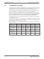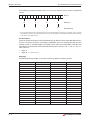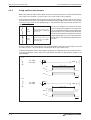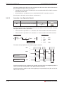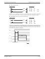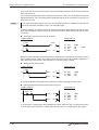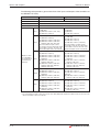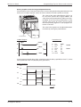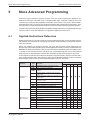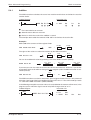
1
MITSUBISHI ELECTRIC
MELSEC FX Family
Programmable Logic Controllers
Beginners Manual
FX1S, FX1N,
FX2N, FX2NC,
FX3U
Art. no.: 166388
26042006
Version A
MITSUBISHI ELECTRIC
INDUSTRIAL AUTOMATION
The texts, illustration, diagrams and examples in this manual
are provided for information purposes only.
They are intended as aids to help explain the installation,
operation, programming and use of the programmable logic controllers
of the MELSEC FX1S, FX1N, FX2N,FX2NC and FX3U series.
If you have any questions about the installation and operation
of any of the products described in this manual please contact
your local sales office or distributor (see inside back cover).
You can find the latest information and answers to frequently asked
questions on our website at www.mitsubishi-automation.com.
MITSUBISHI ELECTRIC EUROPE BV reserves the right to make changes to this manual
or the technical specifications of its products at any time without notice.
© 04/2006
Beginner’s Manual for the programmable logic controllers of the MELSEC FX family
FX1S, FX1N, FX2N, FX2NC und FX3U
Art. no.: 166388
Version
A
04/2006
Revisions / Additions / Corrections
pdp-tr
First edition
Safety Guidelines
Safety Guidelines
For use by qualified staff only
This manual is only intended for use by properly trained and qualified electrical technicians
who are fully acquainted with the relevant automation technology safety standards. All work
with the hardware described, including system design, installation, configuration, maintenance, service and testing of the equipment, may only be performed by trained electrical technicians with approved qualifications who are fully acquainted with all the applicable automation
technology safety standards and regulations. Any operations or modifications to the hardware
and/or software of our products not specifically described in this manual may only be
performed by authorised Mitsubishi Electric staff.
Proper use of the products
The programmable logic controllers of the FX1S, FX1N, FX2N, FX2NC and FX3U series are only
intended for the specific applications explicitly described in this manual. All parameters and
settings specified in this manual must be observed. The products described have all been
designed, manufactured, tested and documented in strict compliance with the relevant safety
standards. Unqualified modification of the hardware or software or failure to observe the warnings on the products and in this manual may result in serious personal injury and/or damage
to property. Only peripherals and expansion equipment specifically recommended and approved by Mitsubishi Electric may be used with the programmable logic controllers of the FX1S,
FX1N, FX2N FX2NC and FX3U series.
All and any other uses or application of the products shall be deemed to be improper.
Relevant safety regulations
All safety and accident prevention regulations relevant to your specific application must be
observed in the system design, installation, configuration, maintenance, servicing and testing
of these products. The regulations listed below are particularly important in this regard. This
list does not claim to be complete, however; you are responsible for being familiar with and
conforming to the regulations applicable to you in your location.
쎲 VDE Standards
– VDE 0100
Regulations for the erection of power installations with rated voltages below 1000 V
– VDE 0105
Operation of power installations
– VDE 0113
Electrical installations with electronic equipment
– VDE 0160
Electronic equipment for use in power installations
– VDE 0550/0551
Regulations for transformers
– VDE 0700
Safety of electrical appliances for household use and similar applications
– VDE 0860
Safety regulations for mains-powered electronic appliances and their accessories for
household use and similar applications.
쎲 Fire safety regulations
FX Beginners Manual
I
Safety Guidelines
쎲 Accident prevention regulations
– VBG Nr.4
Electrical systems and equipment
Safety warnings in this manual
In this manual warnings that are relevant for safety are identified as follows:
P
DANGER:
Failure to observe the safety warnings identified with this symbol can result in health
and injury hazards for the user.
E
WARNING:
Failure to observe the safety warnings identified with this symbol can result in damage
to the equipment or other property.
II
MITSUBISHI ELECTRIC
Safety Guidelines
General safety information and precautions
The following safety precautions are intended as a general guideline for using PLC systems
together with other equipment. These precautions must always be observed in the design,
installation and operation of all control systems.
P
DANGER:
쎲 Observe all safety and accident prevention regulations applicable to your specific application. Always disconnect all power supplies before performing
installation and wiring work or opening any of the assemblies, components and
devices.
쎲 Assemblies, components and devices must always be installed in a shockproof
housing fitted with a proper cover and fuses or circuit breakers.
쎲 Devices with a permanent connection to the mains power supply must be integrated in the building installations with an all-pole disconnection switch and a
suitable fuse.
쎲 Check power cables and lines connected to the equipment regularly for breaks
and insulation damage. If cable damage is found immediately disconnect the
equipment and the cables from the power supply and replace the defective cabling.
쎲 Before using the equipment for the first time check that the power supply rating
matches that of the local mains power.
쎲 Take appropriate steps to ensure that cable damage or core breaks in the signal
lines cannot cause undefined states in the equipment.
쎲 You are responsible for taking the necessary precautions to ensure that programs interrupted by brownouts and power failures can be restarted properly
and safely. In particular, you must ensure that dangerous conditions cannot
occur under any circumstances, even for brief periods.
쎲 EMERGENCY OFF facilities conforming to EN 60204/IEC 204 and VDE 0113
must remain fully operative at all times and in all PLC operating modes. The
EMERGENCY OFF facility reset function must be designed so that it cannot
ever cause an uncontrolled or undefined restart.
쎲 You must implement both hardware and software safety precautions to prevent
the possibility of undefined control system states caused by signal line cable or
core breaks.
쎲 When using modules always ensure that all electrical and mechanical specifications and requirements are observed exactly.
FX Beginners Manual
III
Safety Guidelines
IV
MITSUBISHI ELECTRIC
Contents
Contents
1
Introduction
1.1
About this Manual . . . . . . . . . . . . . . . . . . . . . . . . . . . . . . . . . . . . . . . . . . . . . . . . .1-1
1.2
More Information . . . . . . . . . . . . . . . . . . . . . . . . . . . . . . . . . . . . . . . . . . . . . . . . . .1-1
2
Programmable Logic Controllers
2.1
What is a PLC? . . . . . . . . . . . . . . . . . . . . . . . . . . . . . . . . . . . . . . . . . . . . . . . . . . .2-1
2.2
How PLCs Process Programs . . . . . . . . . . . . . . . . . . . . . . . . . . . . . . . . . . . . . . . .2-2
2.3
The MELSEC FX Family . . . . . . . . . . . . . . . . . . . . . . . . . . . . . . . . . . . . . . . . . . . .2-4
2.4
Selecting the Right Controller . . . . . . . . . . . . . . . . . . . . . . . . . . . . . . . . . . . . . . . .2-5
2.5
Controller Design . . . . . . . . . . . . . . . . . . . . . . . . . . . . . . . . . . . . . . . . . . . . . . . . . .2-6
2.5.1 Input and output circuits . . . . . . . . . . . . . . . . . . . . . . . . . . . . . . . . . . . . . . .2-6
2.5.2 Layout of the MELSEC FX1S base units . . . . . . . . . . . . . . . . . . . . . . . . . . 2-6
2.5.3 Layout of the MELSEC FX1N base units . . . . . . . . . . . . . . . . . . . . . . . . . . 2-7
2.5.4 Layout of the MELSEC FX2N base units . . . . . . . . . . . . . . . . . . . . . . . . . . 2-7
2.5.5 Layout of the MELSEC FX2NC base units . . . . . . . . . . . . . . . . . . . . . . . . . 2-8
2.5.6 Layout of the MELSEC FX3U base units . . . . . . . . . . . . . . . . . . . . . . . . . . 2-8
2.5.7 PLC components glossary . . . . . . . . . . . . . . . . . . . . . . . . . . . . . . . . . . . . .2-9
3
An Introduction to Programming
3.1
Structure of a Program Instruction. . . . . . . . . . . . . . . . . . . . . . . . . . . . . . . . . . . . .3-1
3.2
Bits, Bytes and Words . . . . . . . . . . . . . . . . . . . . . . . . . . . . . . . . . . . . . . . . . . . . . .3-2
3.3
Number Systems . . . . . . . . . . . . . . . . . . . . . . . . . . . . . . . . . . . . . . . . . . . . . . . . . .3-2
3.4
The Basic Instruction Set. . . . . . . . . . . . . . . . . . . . . . . . . . . . . . . . . . . . . . . . . . . .3-5
3.4.1 Starting logic operations . . . . . . . . . . . . . . . . . . . . . . . . . . . . . . . . . . . . . . .3-6
3.4.2 Outputting the result of a logic operation . . . . . . . . . . . . . . . . . . . . . . . . . . 3-6
3.4.3 Using switches and sensors . . . . . . . . . . . . . . . . . . . . . . . . . . . . . . . . . . . .3-8
3.4.4 AND operations . . . . . . . . . . . . . . . . . . . . . . . . . . . . . . . . . . . . . . . . . . . . . .3-9
3.4.5 OR operations . . . . . . . . . . . . . . . . . . . . . . . . . . . . . . . . . . . . . . . . . . . . . .3-11
3.4.6 Instructions for connecting operation blocks . . . . . . . . . . . . . . . . . . . . . . 3-12
3.4.7 Pulse-triggered execution of operations . . . . . . . . . . . . . . . . . . . . . . . . . . 3-14
3.4.8 Setting and resetting devices . . . . . . . . . . . . . . . . . . . . . . . . . . . . . . . . . . 3-15
3.4.9 Storing, reading and deleting operation results . . . . . . . . . . . . . . . . . . . . 3-17
FX Beginners Manual
V
Contents
3.4.10Generating pulses . . . . . . . . . . . . . . . . . . . . . . . . . . . . . . . . . . . . . . . . . . .3-18
3.4.11Master control function (MC and MCR instructions) . . . . . . . . . . . . . . . . . 3-19
3.4.12Inversion of an Operation Result. . . . . . . . . . . . . . . . . . . . . . . . . . . . . . . . 3-20
3.5
Safety First! . . . . . . . . . . . . . . . . . . . . . . . . . . . . . . . . . . . . . . . . . . . . . . . . . . . . .3-21
3.6
Programming PLC Applications. . . . . . . . . . . . . . . . . . . . . . . . . . . . . . . . . . . . . .3-23
3.6.1 An alarm system . . . . . . . . . . . . . . . . . . . . . . . . . . . . . . . . . . . . . . . . . . . .3-23
3.6.2 A rolling shutter gate . . . . . . . . . . . . . . . . . . . . . . . . . . . . . . . . . . . . . . . . .3-28
4
Devices in Detail
4.1
Inputs and Outputs . . . . . . . . . . . . . . . . . . . . . . . . . . . . . . . . . . . . . . . . . . . . . . . .4-1
4.2
Relays . . . . . . . . . . . . . . . . . . . . . . . . . . . . . . . . . . . . . . . . . . . . . . . . . . . . . . . . . .4-3
4.2.1 Special relays . . . . . . . . . . . . . . . . . . . . . . . . . . . . . . . . . . . . . . . . . . . . . . .4-3
4.3
Timers . . . . . . . . . . . . . . . . . . . . . . . . . . . . . . . . . . . . . . . . . . . . . . . . . . . . . . . . . .4-4
4.4
Counters . . . . . . . . . . . . . . . . . . . . . . . . . . . . . . . . . . . . . . . . . . . . . . . . . . . . . . . .4-7
4.5
Registers . . . . . . . . . . . . . . . . . . . . . . . . . . . . . . . . . . . . . . . . . . . . . . . . . . . . . . . .4-9
4.5.1 Data registers . . . . . . . . . . . . . . . . . . . . . . . . . . . . . . . . . . . . . . . . . . . . . . .4-9
4.5.2 Special registers . . . . . . . . . . . . . . . . . . . . . . . . . . . . . . . . . . . . . . . . . . . .4-10
4.5.3 File registers . . . . . . . . . . . . . . . . . . . . . . . . . . . . . . . . . . . . . . . . . . . . . . .4-11
4.6
Programming Tips for Timers and Counters . . . . . . . . . . . . . . . . . . . . . . . . . . . . 4-11
4.6.1 Specifying timer and counter setpoints indirectly . . . . . . . . . . . . . . . . . . . 4-11
4.6.2 Switch-off delay . . . . . . . . . . . . . . . . . . . . . . . . . . . . . . . . . . . . . . . . . . . . .4-14
4.6.3 Delayed make and break. . . . . . . . . . . . . . . . . . . . . . . . . . . . . . . . . . . . . .4-15
4.6.4 Clock signal generators . . . . . . . . . . . . . . . . . . . . . . . . . . . . . . . . . . . . . .4-16
5
More Advanced Programming
5.1
Applied Instructions Reference . . . . . . . . . . . . . . . . . . . . . . . . . . . . . . . . . . . . . . .5-1
5.1.1 Entering applied instructions . . . . . . . . . . . . . . . . . . . . . . . . . . . . . . . . . . . .5-6
5.2
Instructions for Moving Data . . . . . . . . . . . . . . . . . . . . . . . . . . . . . . . . . . . . . . . . .5-7
5.2.1 Moving individual values with the MOV instruction . . . . . . . . . . . . . . . . . . . 5-7
5.2.2 Moving groups of bit devices . . . . . . . . . . . . . . . . . . . . . . . . . . . . . . . . . . . .5-9
5.2.3 Moving blocks of data with the BMOV instruction . . . . . . . . . . . . . . . . . . . 5-10
5.2.4 Copying source devices to multiple destinations (FMOV) . . . . . . . . . . . . 5-11
5.2.5 Exchanging data with special function modules . . . . . . . . . . . . . . . . . . . . 5-12
VI
MITSUBISHI ELECTRIC
Contents
5.3
Compare Instructions . . . . . . . . . . . . . . . . . . . . . . . . . . . . . . . . . . . . . . . . . . . . .5-15
5.3.1 The CMP instruction . . . . . . . . . . . . . . . . . . . . . . . . . . . . . . . . . . . . . . . . .5-15
5.3.2 Comparisons within logic operations. . . . . . . . . . . . . . . . . . . . . . . . . . . . . 5-17
5.4
Math Instructions . . . . . . . . . . . . . . . . . . . . . . . . . . . . . . . . . . . . . . . . . . . . . . . . .5-20
5.4.1 Addition . . . . . . . . . . . . . . . . . . . . . . . . . . . . . . . . . . . . . . . . . . . . . . . . . . .5-21
5.4.2 Subtraction . . . . . . . . . . . . . . . . . . . . . . . . . . . . . . . . . . . . . . . . . . . . . . . .5-22
5.4.3 Multiplication . . . . . . . . . . . . . . . . . . . . . . . . . . . . . . . . . . . . . . . . . . . . . . .5-23
5.4.4 Division . . . . . . . . . . . . . . . . . . . . . . . . . . . . . . . . . . . . . . . . . . . . . . . . . . .5-24
5.4.5 Combining math instructions. . . . . . . . . . . . . . . . . . . . . . . . . . . . . . . . . . . 5-25
6
Expansion Options
6.1
Introduction . . . . . . . . . . . . . . . . . . . . . . . . . . . . . . . . . . . . . . . . . . . . . . . . . . . . . .6-1
6.2
Available Modules . . . . . . . . . . . . . . . . . . . . . . . . . . . . . . . . . . . . . . . . . . . . . . . . .6-1
6.2.1 Modules for adding more digital inputs and outputs . . . . . . . . . . . . . . . . . . 6-1
6.2.2 Analog I/O modules. . . . . . . . . . . . . . . . . . . . . . . . . . . . . . . . . . . . . . . . . . .6-1
6.2.3 Communications modules . . . . . . . . . . . . . . . . . . . . . . . . . . . . . . . . . . . . . .6-2
6.2.4 Positioning modules . . . . . . . . . . . . . . . . . . . . . . . . . . . . . . . . . . . . . . . . . .6-2
6.2.5 HMI control and display panels . . . . . . . . . . . . . . . . . . . . . . . . . . . . . . . . . . 6-2
FX Beginners Manual
VII
Contents
VIII
MITSUBISHI ELECTRIC
Introduction
About this Manual
1
Introduction
1.1
About this Manual
This manual will help you to familiarise yourself with the use of the MELSEC FX family of programmable logic controllers. It is designed for users who do not yet have any experience with
programming programmable logic controllers (PLCs).
Programmers who already have experience with PLCs from other manufacturers can also use
this manual as a guide for making the transition to the MELSEC FX family.
The symbol „쏔“ is used as a placeholder to identify different controllers in the same range. For
example, the designation "FX1S-10쏔-쏔쏔" is used to refer to all controllers whose name
begins with FX1S-10, i.e. FX1S-10 MR-DS, FX1S-10 MR-ES/UL, FX1S-10 MT-DSS and
FX1S-10 MT-ESS/UL.
1.2
More Information
You can find more detailed information on the individual products in the series in the operating
and installation manuals of the individual modules.
See the MELSEC FX Family Catalogue, art. no. 167840, for a general overview of all the controllers in the MELSEC FX family. This catalogue also contains information on expansion
options and the available accessories.
For an introduction to using the programming software package see the GX Developer FX
Beginner’s Manual, art. no. 166391.
You can find detailed documentation of all programming instructions in the Programming
Manual for the MELSEC FX family, art. no. 132738 and in the Programming Manual for the
FX3U series, art. no. 168591.
The communications capabilities and options of the MELSEC FX controllers are documented
in detail in the Communications Manual, art. no. 070143.
All Mitsubishi manuals and catalogues can be downloaded free of charge from the Mitsubishi
website at www.mitsubishi-automation.com.
FX Beginners Manual
1–1
More Information
1–2
Introduction
MITSUBISHI ELECTRIC
Programmable Logic Controllers
What is a PLC?
2
Programmable Logic Controllers
2.1
What is a PLC?
In contrast to conventional controllers with functions determined by their physical wiring the
functions of programmable logic controllers or PLCs are defined by a program. PLCs also have
to be connected to the outside world with cables, but the contents of their program memory can
be changed at any time to adapt their programs to different control tasks.
Programmable logic controllers input data, process it and then output the results. This process
is performed in three stages:
쎲 an input stage,
쎲 a processing stage
and
쎲 an output stage
Programmable Logic Controller
Output
Input
Switch
Contactors
Input Stage
Processing Stage
Output Stage
The input stage
The input stage passes control signals from switches, buttons or sensors on to the processing
stage.
The signals from these components are generated as part of the control process and are fed to
the inputs as logical states. The input stage passes them on to the processing stage in a
pre-processed format.
The processing stage
In the processing stage the pre-processed signals from the input stage are processed and
combined with the help of logical operations and other functions. The program memory of the
processing stage is fully programmable. The processing sequence can be changed at any time
by modifying or replacing the stored program.
The output stage
The results of the processing of the input signals by the program are fed to the output stage
where they control connected switchable elements such as contactors, signal lamps, solenoid
valves and so on.
FX Beginners Manual
2–1
How PLCs Process Programs
2.2
Programmable Logic Controllers
How PLCs Process Programs
A PLC performs its tasks by executing a program that is usually developed outside the controller and then transferred to the controller’s program memory. Before you start programming it is
useful to have a basic understanding of how PLCs process these programs.
A PLC program consists of a sequence of instructions that control the functions of the controller. The PLC executes these control instructions sequentially, i.e. one after another. The entire
program sequence is cyclical, which means that it is repeated in a continuous loop. The time
required for one program repetition is referred to as the program cycle time or period.
Process image processing
The program in the PLC is not executed directly on the inputs and outputs, but on a “process
image” of the inputs and outputs:
Switch on PLC
Delete output memory
Input signals
Input terminals
Poll inputs and signal states
and save them in the process
image of the inputs
PLC program
Process image
of inputs
Instruction 1
Instruction 2
Instruction 3
....
....
....
Process image
of outputs
Instruction n
Output terminals
Transfer process image
to outputs
Output signals
Input process image
At the beginning of each program cycle the system polls the signal states of the inputs and
stores them in a buffer, creating a “process image” of the inputs.
2–2
MITSUBISHI ELECTRIC
Programmable Logic Controllers
How PLCs Process Programs
Program execution
After this the program is executed, during which the PLC accesses the stored states of the
inputs in the process image. This means that any subsequent changes in the input states will
not be registered until the next program cycle!
The program is executed from top to bottom, in the order in which the instructions were programmed. Results of individual programming steps are stored and can be used during the current program cycle.
Program execution
X000 X001
0
M0
Store result
M6
M1 M8013
4
Y000
M2
Control output
M0
Y001
9
Process stored result
Output process image
Results of logical operations that are relevant for the outputs are stored in an output buffer – the
output process image. The output process image is stored in the output buffer until the buffer is
rewritten. After the values have been written to the outputs the program cycle is repeated.
Differences between signal processing in the PLC and in hard-wired controllers
In hard-wired controllers the program is defined by the functional elements and their connections (the wiring). All control operations are performed simultaneously (parallel execution).
Every change in an input signal state causes an instantaneous change in the corresponding
output signal state.
In a PLC it is not possible to respond to changes in input signal states until the next program
cycle after the change. Nowadays this disadvantage is largely compensated by very short program cycle periods. The duration of the program cycle period depends on the number and type
of instructions executed.
FX Beginners Manual
2–3
The MELSEC FX Family
2.3
Programmable Logic Controllers
The MELSEC FX Family
The compact micro-controllers of the MELSEC FX series provide the foundation for building
economical solutions for small to medium-sized control and positioning tasks requiring 10 to
256 integrated inputs and outputs in applications in industry and building services.
With the exception of the FX1S all the controllers of the FX series can be expanded to keep
pace with the changes in the application and the user’s growing requirements.
Network connections are also supported. This makes it possible for the controllers of the FX
family to communicate with other PLCs and controller systems and HMIs (Human-Machine
Interfaces and control panels). The PLC systems can be integrated both in MITSUBISHI networks as local stations and as slave stations in open networks like PROFIBUS/DP.
In addition to this you can also build multi-drop and peer-to-peer networks with the controllers
of the MELSEC FX family.
The FX1N, FX2N and FX3U have modular expansion capabilities, making them the right
choice for complex applications and tasks requiring special functions like analog-digital and
digital-analog conversion and network capabilities.
All the controllers in the series are part of the larger MELSEC FX family and are fully compatible with one another.
Specifications
FX1S
FX1N
FX2N
FX2NC
FX3U
Max integrated
I/O points
30
60
128
96
80
Expansion capability
(max. possible I/Os)
34
132
256
256
384
2000
8000
16000
16000
64000
Cycle time per
log. instruction (µs)
0,55 – 0,7
0,55 – 0,7
0,08
0,08
0,065
No. of instructions
(standard / step ladder /
special function)
27 / 2 / 85
27 / 2 / 89
27 / 2 / 107
27 / 2 / 107
27 / 2 / 209
—
2
8
4
8 right
10 left
Program memory
(steps)
Max. special function
modules connectable
2–4
MITSUBISHI ELECTRIC
Programmable Logic Controllers
2.4
Selecting the Right Controller
Selecting the Right Controller
The base units of the MELSEC FX1S, FX1N and FX2N(C) series are available in a number of
different versions with different power supply options and output technologies. You can choose
between units designed for power supplies of 100–240 V AC, 24 V DC or 12–24 V DC, and
between relay and transistor outputs. The controllers of the FX3U series are currently only
available for AC power supply and with relay outputs.
Series
FX1S
FX1N
FX2N
FX2NC
FX3U
I/Os
Type
No. of
inputs
No. of
outputs
10
FX1S-10 M쏔-쏔쏔
6
8
14
FX1S-14 M쏔-쏔쏔
8
6
20
FX1S-20 M쏔-쏔쏔
12
8
30
FX1S-30 M쏔-쏔쏔
16
14
14
FX1N-14 M쏔-쏔쏔
8
6
24
FX1N-24 M쏔-쏔쏔
14
10
40
FX1N-40 M쏔-쏔쏔
24
16
60
FX1N-60 M쏔-쏔쏔
36
24
16
FX2N-16 M쏔-쏔쏔
8
8
32
FX2N-32 M쏔-쏔쏔
16
16
48
FX2N-48 M쏔-쏔쏔
24
24
64
FX2N-64 M쏔-쏔쏔
32
32
80
FX2N-80 M쏔-쏔쏔
40
40
128
FX2N-128 M쏔-쏔쏔
64
64
16
FX2NC-16 M쏔-쏔쏔
8
8
32
FX2NC-32 M쏔-쏔쏔
16
16
64
FX2NC-64 M쏔-쏔쏔
32
32
96
FX2NC-96 M쏔-쏔쏔
48
48
16
FX3U-16 MR/ES
8
8
32
FX3U-32 MR/ES
16
16
48
FX3U-48 MR/ES
24
24
64
FX3U-64 MR/ES
32
32
80
FX3U-80 MR/ES
40
40
Power supply
Output type
24 V DC
or
100 – 240 V AC
Transistor
or relay
12 – 24 V DC
or
100 – 240 V AC
Transistor
or relay
Wahlweise
24 V DC
oder
100 – 240 V AC
Transistor
or relay
24 V DC
Transistor
or relay
100 – 240 V AC
Relay only
To choose the right controller for your application you need to answer the following questions:
쎲 How many signals (external switch contacts, buttons and sensors) do you need to input?
쎲 What types of functions do you need to switch, and how many of them are there?
쎲 What power supply options are available?
쎲 How high are the loads that the outputs need to switch? Choose relay outputs for switching
high loads and transistor outputs for switching fast, trigger-free switching operations.
FX Beginners Manual
2–5
Controller Design
2.5
Programmable Logic Controllers
Controller Design
All the controllers in the series have the same basic design. The main functional elements and
assemblies are described in the glossary in section 2.5.7.
2.5.1
Input and output circuits
The input circuits use floating inputs. They are electrically isolated from the other circuits of
the PLC with optical couplers. The output circuits use either relay or transistor output technology. The transistor outputs are also electrically isolated from the other PLC circuits with optical
couplers.
The switching voltage at all the digital inputs must have a certain value (e.g. 24 V DC). This voltage can be taken from the PLC’s integrated power supply unit. If the switching voltage at the
inputs is less than the rated value (e.g. <24 V DC) then the input will not be processed.
The maximum output currents are 2 A on 250 V three-phase AC and non-reactive loads with
relay outputs and 0.5 A on 24 V DC and non-reactive loads.
2.5.2
Layout of the MELSEC FX1S base units
Protective cover
Terminal cover
Mounting hole
Power supply
connection
Interface for expansion
adapter boards
Cutout for adapters or
control panel
Terminals for
digital inputs
100-240
VAC
L
N
X7
X5
X3
X1
S/S
X6
X4
X2
X0
0 1 2 3
4 5 6 7
IN
RUN/STOP switch
2 analog potentiometers
POWER
RUN
ERROR
Connection for
programming units
Connection for the
service power supply
LEDs for indicating
the input status
FX1S-14MR
OUT
0 1 2 3
4 5
Y2
Y1
Y0
0V
COM2 Y3
24V COM0 COM1
Y4
Y5
14MR
-ES/UL
MITSUBISHI
LEDs for indicating
the operating status
LEDs for indicating
the output status
Protective cover
Terminals for
digital outputs
2–6
MITSUBISHI ELECTRIC
Programmable Logic Controllers
2.5.3
Controller Design
Layout of the MELSEC FX1N base units
Protective cover
Terminal cover
Terminals for
digital inputs
Mounting hole
Connection of the
power supply
Extension bus
RUN/STOP switch
Slot for memory cassettes,
adapters and displays
2 analog
potentiometers
Connection for
programming units
Connection for the
service power supply
100-240
VAC
L
X15
X7 X11 X13
X5
X3
X1
X14
S/S
X6 X10 X12
X4
X2
X0
N
0 1 2 3
4 5 6 7
8 9 10 11
12 13 14 15
IN
POWER
RUN
ERROR
LEDs for indicating
the operating status
FX1N-24MR
OUT
0 1 2 3
4 5 6 7
10 11
Y6 Y10
Y5
Y3
Y2
Y1
Y11
Y0
0V
COM4 Y7
COM2 COM3 Y4
24+ COM0 COM1
LEDs for indicating
the input status
24MR
-ES/UL
MITSUBISHI
Terminals for
digital outputs
LEDs for indicating
the output status
Housing cover
Lid
Terminal cover
Protective cover
2.5.4
Layout of the MELSEC FX2N base units
Connection for the
service power supply
Terminal cover
Mounting hole
Connection for
expansion adapter boards
Memory battery
Connection for
programming units
RUN/STOP switch
Removable terminal
strip for digital outputs
Slot for memory
cassettes
Terminals for
digital inputs
LEDs for indicating
the input status
LEDs for indicating
the operating status
Connection for
extensions
Protective cover des
Erweiterungsbusses
LEDs for indicating
the output status
Protective cover
Housing cover
FX Beginners Manual
2–7
Controller Design
2.5.5
Programmable Logic Controllers
Layout of the MELSEC FX2NC base units
Protective cover
Memory battery
Battery
compartment
Extension bus
(on side)
RUN/STOP switch
MITSUBISHI
POWER
RUN
BATT
ERROR
RUN
X0
STOP
5
6
3
5
6
7
X4
•
•
COM
LEDs for indicating
the output status
2
LEDs for indicating
the input status
Connector for
terminal strips
COM
Memory cassette slot
X7
X6
X5
Memory cassette
(optional)
X3
X2
X1
Cover
X0
7
1
Y4
Y0
X4
Protective cover
for expansion bus
Y0
Y1
3
Y2
2
COM1 Y3
1
2nd interface
for CNV adapter
MELSEC
FX2NC-16MR-T-DS
Y4
Operating status LEDs
Terminals for
digital inputs
Terminals for
digital outputs
2.5.6
Layout of the MELSEC FX3U base units
Battery cover
Protective cover
Terminal cover
Terminals for
digital inputs
Memory battery
Installation place for the
FX3U-7DM display
Blind cover for
expansion board
RUN/STOP switch
Connection for
programming unit
Top cover
(used if FX3U-7DM
is not installed)
2–8
LEDs for indicating
the input status
LEDs for indicating
the operating status
Protective cover for
expansion bus
LEDs for indicating
the output status
Output terminals
Terminal cover
Protective cover
MITSUBISHI ELECTRIC
Programmable Logic Controllers
2.5.7
Controller Design
PLC components glossary
The following table describes the meaning and functionality of the single components und
parts of a Mitsubishi PLC.
Component
Description
Connection for
expansion
adapter boards
Optional expansion adapter boards can be connected to this interface. A variety of different adapters are available for all FX lines (except the FX2NC). These adapters extend
the capabilities of the controllers with additional functions or communications interfaces.
The adapter boards are plugged directly into the slot.
Connection for programming units
This connection can be used for connecting the FX-20P-E hand-held programming unit or
an external PC or notebook with a programming software package (e.g. GX Developer/FX).
EEPROM
Read/write memory in which the PLC program can be stored and read with the programming software. This solid-state memory retains its contents without power, even in the
event of a power failure, and does not need a battery.
Slot for optional memory cassettes. Inserting a memory cassette disables the controller’s
Memory cassette slot internal memory – the controller will then only execute the program stored in the cassette.
Extension bus
Both additional I/O expansion modules and special function modules that add additional
capabilities to the PLC system can be connected here. See Chapter 6 for an overview of
the available modules.
Analog
potentiometers
The analog potentiometers are used for setting analog setpoint values. The setting can be
polled by the PLC program and used for timers, pulse outputs and other functions (see
Section 4.6.1).
Service power
supply
The service power supply (not for FX2NC) provides a regulated 24V DC power supply
source for the input signals and the sensors. The capacity of this power supply depends
on the controller model (e.g. FX1S and FX1N: 400mA; FX2N-16M쏔-쏔쏔 through
FX2N-32M쏔-쏔쏔: 250 mA, FX2N-48M쏔-쏔쏔 through FX2N-64M쏔-쏔쏔: 460 mA)
Digital inputs
The digital inputs are used for inputting control signals from the connected switches, buttons or sensors. These inputs can read the values ON (power signal on) and OFF (no
power signal).
Digital outputs
You can connect a variety of different actuators and other devices to these outputs,
depending on the nature of your application and the output type.
LEDs for indicating
the input status
These LEDs show which inputs are currently connected to a power signal, i.e. a defined
voltage. When a signal is applied to an input the corresponding LED lights up, indicating
that the state of the input is ON.
LEDs for indicating
the output status
These LEDs show the current ON/OFF states of the digital outputs. These outputs can
switch a variety of different voltages and currents depending on the model and output
type.
LEDs for indicating
the operating status
The LEDs RUN, POWER and ERROR show the current status of the controller. POWER
shows that the power is switched on, RUN lights up when the PLC program is being executed and ERROR lights up when an error or malfunction is registered.
Memory battery
The battery protects the contents of the MELSELC PLC’s volatile RAM memory in the
event of a power failure (FX2N, FX2NCand FX3U only). It protects the latched ranges for
timers, counters and relays. In addition to this it also provides power for the integrated
real-time clock when the PLC’s power supply is switched off.
RUN/STOP switch
MELSEC PLCs have two operating modes, RUN and STOP. The RUN/STOP switch
allows you to switch between these two modes manually. In RUN mode the PLC executes
the program stored in its memory. In STOP mode program execution is stopped and it is
possible to program the controller.
FX Beginners Manual
2–9
Controller Design
2 – 10
Programmable Logic Controllers
MITSUBISHI ELECTRIC
An Introduction to Programming
3
Structure of a Program Instruction
An Introduction to Programming
A program consists of a sequence of program instructions. These instructions determine the
functionality of the PLC and they are processed sequentially, in the order in which they were
entered by the programmer. To create a PLC program you thus need to analyse the process to
be controlled and break it up into steps that can be represented by instructions. A program
instruction, represented by a line or “rung” in ladder diagram format, is the smallest unit of a
PLC application program.
3.1
Structure of a Program Instruction
A program instruction consists of the instruction itself (sometimes referred to as a command)
and one or more (in the case of applied instructions) operands, which in a PLC are references
to devices. Some instructions are entered on their own without specifying any operands –
these are the instructions that control program execution in the PLC.
Every instruction you enter is automatically assigned a step number that uniquely identifies its
position in the program. This is important because it is quite possible to enter the same instruction referring to the same device in several places in the program.
The illustrations below show how program instructions are represented in the Ladder Diagram
(LD, left) and Instruction List (IL, right) programming language formats:
Device
X0
Device
AND X0
Instruction
Instruction
The instruction describes what is to be done, i.e. the function you want the controller to perform. The operand or device is what you want to perform the function on. Its designation consists of two parts, the device name and the device address:
X0
Device name
Device address
Examples of devices:
Device name
Type
Function
X
Input
Input terminal on the PLC (e.g. connected to a switch)
Y
Output
Output terminal on the PLC (e.g. for a contactor or lamp)
M
Relay
A buffer memory in the PLC that can have two states, ON or OFF
T
Timer
A “time relay” that can be used to program timed functions
C
Counter
A counter
D
Data register
Data storage in the PLC in which you can store things like measured
values and the results of calculations.
See Chapter 4 for a detailed description of the available devices.
The specific device is identified by its address. For example, since every controller has multiple
inputs you need to specify both the device name and the address in order to read a specific
input.
FX Beginners Manual
3–1
Bits, Bytes and Words
3.2
An Introduction to Programming
Bits, Bytes and Words
As in all digital technology, the smallest unit of information in a PLC is a “bit”. A bit can only have
two states: “0” (OFF or FALSE) and “1” (ON or TRUE). PLCs have a number of so-called bit
devices that can only have two states, including inputs, outputs and relays.
The next larger information units are the “byte”, which consists of 8 bits, and the “word”, which
consists of two bytes. In the PLCs of the MELSEC FX families the data registers are “word
devices”, which means that they can store 16-bit values.
Bit 15
0
Bit 0
0
0
0
0
0
0
0
0
1 Byte
0
0
0
0
0
0
0
1 Byte
1 Word
Since a data register is 16 bits wide it can store signed values between -32,768 and +32,767
(see Chapter 3.3). When larger values need to be stored two words are combined to form a
32-bit long word, which can store signed values between -2,147,483,648 and +2,147,483,647.
Counters make use of this capability, for example.
3.3
Number Systems
The PLCs of the MELSEC FX family use several different number systems for inputting and
displaying values and for specifying device addresses.
Decimal numbers
The decimal number system is the system we use most commonly in everyday life. It is a “positional base 10” system, in which each digit (position) in a numeral is ten times the value of the
digit to its right. After the count reaches 9 in each position the count in the current position is
returned to 0 and the next position is incremented by 1 to indicate the next decade (9 à 10, 99
à 100, 199 à 1,000 etc).
–
Base: 10
–
Digits: 0, 1, 2, 3, 4, 5, 6, 7, 8, 9
In the MELSEC FX family of PLCs decimal numbers are used for entering constants and the
setpoint values for timers and counters. Device addresses are also entered in decimal format,
with the exception of the addresses of inputs and outputs.
Binary numbers
Like all computers a PLC can only really distinguish between two states, ON/OFF or 0/1. These
“binary states” are stored in individual bits. When numbers need to be entered or displayed in
other formats the programming software automatically converts the binary numbers into the
other number systems.
3–2
–
Base: 2
–
Digits: 0 and 1
MITSUBISHI ELECTRIC
An Introduction to Programming
Number Systems
When binary numbers are stored in a word (see above) the value of each digit (position) in the
word is one power of 2 higher than that of the digit to its right. The principle is exactly the same
as in decimal representation, but with increments of 2 instead of 10 (see graphic):
215 214 213 212 211 210 29 28 27 26 25 24 23 22 21 20
0
0
0
0
0
0
0
0
0
0
0
0
0
0
0
Base 2 Notation
Decimal Value
Base 2 Notation
Decimal Valuet
20
1
28
256
1
2
2
9
22
4
210
1024
23
8
211
2048
12
4096
8192
2
512
4
16
2
25
32
213
64
2
14
16384
128
215
32768*
2
2
6
27
*
0
In binary values bit 15 is used to represent the sign (bit 15=0: positive value, bit 15=1: negative value)
To convert a binary value to a decimal value you just have to multiply each digit with a value of 1
by its corresponding power of 2 and calculate the sum of the results.
Example 쑴
00000010 00011001 (binary)
00000010 00011001 (binary) = 1 x 29 + 1 x 24 + 1 x 23 + 1 x 20
00000010 00011001 (binary) = 512 + 16 + 8 + 1
00000010 00011001 (binary) = 537 (decimal)
Hexadecimal numbers
Hexadecimal numbers are easier to handle than binary and it is very easy to convert binary
numbers to hexadecimal. This is why hexadecimal numbers are used so often in digital technology and programmable logic controllers. In the controllers of the MELSEC FX family hexadecimal numbers are used for the representation of constants. In the programming manual
and other manuals hexadecimal numbers are always identified with an H after the number to
avoid confusion with decimal numbers (e.g. 12345H).
–
Base: 16
–
Digits: 0, 1, 2, 3, 4, 5, 6, 7, 8, 9, A, B, C, D, E, F (the letters A, B, C, D, E and F represent the
decimal values 10, 11, 12, 13, 14 and 15)
The hexadecimal system works in the same way as the decimal system – you just count to FH
(15) instead of to 9 before resetting to 0 and incrementing the next digit (FH à 10H, 1FH à 20H,
2FH à 30H, FFH à 100H etc). The value of digit is a power of 16, rather than a power of 10:
1A7FH
0
16 = 1
1
16 = 16
2
16 = 256
3
16 = 4096
FX Beginners Manual
(in this example: 15 x 1
(in this example: 7 x 16
(in this example: 10 x 256
(in this example: 1 x 4096
=
=
=
=
15)
112)
2560)
4096)
6783 (decimal)
3–3
Number Systems
An Introduction to Programming
The following example illustrates why it is so easy to convert binary values hexadecimal
values:
1
*
1
1
1
0
1
1
0
1
0
1
1
1
0
0
1
Binary
15
5
11
9
Decimal*
F
5
B
9
Hexadecimal
Converting the 4-bit blocks to decimal values does not directly produce a value that corresponds to the complete
16-bit binary value! In contrast, the binary value can be converted directly to hexadecimal notation with exactly the
same value as the binary value.
Octal numbers
Inputs X8 and X9 and outputs Y8 and Y9 do not exist on the base units of the MELSEC FX family. This is because the inputs and outputs of MELSEC PLCs are numbered using the octal
number system, in which the digits 8 and 9 don’t exist. Here, the current digit is reset to 0 and
the digit in the next position is incremented after the count reaches 7 (0 – 7, 10 – 17, 70 – 77,
100 – 107 etc).
–
Base: 8
–
Digits: 0, 1, 2, 3, 4, 5, 6, 7
Summary
The following table provides an overview of the four different number systems:
3–4
Decimal notation
Octal notation
Hexadecimal notation
Binary notation
0
0
0
0000 0000 0000 0000
1
1
1
0000 0000 0000 0001
2
2
2
0000 0000 0000 0010
3
3
3
0000 0000 0000 0011
4
4
4
0000 0000 0000 0100
5
5
5
0000 0000 0000 0101
6
6
6
0000 0000 0000 0110
7
7
7
0000 0000 0000 0111
8
10
8
0000 0000 0000 1000
9
11
9
0000 0000 0000 1001
10
12
A
0000 0000 0000 1010
11
13
B
0000 0000 0000 1011
12
14
C
0000 0000 0000 1100
13
15
D
0000 0000 0000 1101
14
16
E
0000 0000 0000 1110
15
17
F
0000 0000 0000 1111
16
20
10
0000 0000 0001 0000
:
:
:
:
99
143
63
0000 0000 0110 0011
:
:
:
:
MITSUBISHI ELECTRIC
An Introduction to Programming
3.4
The Basic Instruction Set
The Basic Instruction Set
The instructions of the PLCs of the MELSEC FX family can be divided into two basic categories, basic instructions and applied instructions, which are sometimes referred to as “application instructions”.
The functions performed by the basic instructions are comparable to the functions achieved by
the physical wiring of a hard-wired controller. All controllers of the MELSEC FX family support
the instructions in the basic instruction set, but the applied instructions supported vary from
model to model (see Chapter 5).
Basic instruction set quick reference
Instruction
Function
Description
LD
Load
Initial logic operation, polls for signal state “1” (normally open)
LDI
Load invers
Initial logic operation, polls for signal state “0” (normally closed)
OUT
Output instruction
Assigns the result of a logic operation to a device
AND
Logical AND
Logical AND operation, polls for signal state “1”
ANI
AND NOT
Logical AND NOT operation, polls for signal state “0”
OR
Logical OR
Logical OR operation, polls for signal state “1”
ORI
OR NOT
Logical OR NOT operation, polls for signal state “0"
ANB
AND Block
Connects a parallel branch circuit block to the preceding parallel block, in
series.
ORB
OR Block
Connects a serial block of circuits to the preceding serial block, in parallel.
LDP
Load Pulse, load on detection of rising edge of device signal pulse
LDF
Load Falling Pulse, load on falling device signal pulse
ANDP
ANDF
Pulse signal
instructions
AND Pulse, logical AND on rising device signal pulse
AND Falling Pulse, logical AND on falling device signal pulse
ORP
OR Pulse, logical OR on rising device signal pulse
ORF
OR Falling Pulse, logical OR on falling device signal pulse
SET
Set device
RST
Reset device
MPS
MRD
MPP
Store, read and delete
intermediate operation
results
PLS
Pulse instructions
PLF
MC
MCR
INV
Master Control
Assigns a signal state that is retained even if after input condition is no
longer true
Reference
Chapter 3.4.1
Chapter 3.4.2
Chapter 3.4.4
Chapter 3.4.5
Chapter 3.4.6
Chapter 3.4.7
Chapter 3.4.8
Memory Point Store, store an operation result in the stack
Memory Read, read a stored operation result from the stack
Chapter 3.4.9
Memory POP, read a stored operation result and delete it from the stack
Pulse, sets a device for one operation cycle on the rising pulse of the input
condition (input turns ON)
Pulse Falling, sets a device* for one operation cycle on the falling pulse of
the input condition (input turns OFF)
Chapter
3.4.10
Master Control Reset
Instructions for activating or deactivating the execution of defined parts of
the program
Chapter
3.4.11
Invert
Inverts the result of an operation
Chapter
3.4.12
FX Beginners Manual
3–5
The Basic Instruction Set
3.4.1
An Introduction to Programming
Starting logic operations
Instruction
Function
Symbol
GX Developer FX
LD
Load instruction, starts a logic operation
and polls the specified device for signal
state “1”
F5
LDI
Load instruction, starts a logic operation
and polls the specified device for signal
state “0”
F6
A circuit in a program always begins with an LD- or LDI instruction. These instructions can be
performed on inputs, relays, timers and counters.
For examples of using these instructions see the description of the OUT instruction in the next
section.
3.4.2
Outputting the result of a logic operation
Instruction
OUT
Function
Symbol
GX Developer FX
Output instruction, assigns the result of
an operation to a device
F7
The OUT instruction can be used to terminate a circuit. You can also program circuits that use
multiple OUT instructions as their result. This is not necessarily the end of the program, however. The device set with the result of the operation using OUT can then be used as an input
signal state in subsequent steps of the program.
Example (LD and OUT instructions)
Instruction List
Ladder Diagram
X000
0
Y000
0
1
LD
OUT
X000
Y000
These two instructions result in the following signal sequence:
ON (1)
X0
OFF (0)
ON (1)
Y0
OFF (0)
The condition of the LD instruction (poll for signal state “1”) is true so the result of the
operation is also true (“1”) and the output is set.
3–6
t
MITSUBISHI ELECTRIC
An Introduction to Programming
The Basic Instruction Set
Example (LDI and OUT instructions)
Ladder Diagram
Instruction List
X000
0
0
1
Y000
LDI
OUT
X000
Y000
ON (1)
X0
OFF (0)
ON (1)
Y0
OFF (0)
The condition of the LDI instruction (poll for signal state “0”) is no
longer true so the output is reset.
t
Double assignment of relays or outputs
Never assign the result of an operation to the same device in more than one place in the
program!
The program is executed
sequentially from top to bottom, so in this example the
second assignment of M10
would simply overwrite the
result of the first assignment.
You can solve this problem
with modification shown on
the right. This takes all the
required input conditions
into account and sets the
result correctly.
FX Beginners Manual
X001
X003
M10
X004
X005
M10
X001
X003
M10
X004
X005
3–7
The Basic Instruction Set
3.4.3
An Introduction to Programming
Using switches and sensors
Before we continue with the description of the rest of the instructions we should first describe
how signals from switches, sensors and so on can be used in your programs.
PLC programs need to be able respond to signals from switches, buttons and sensors to perform the correct functions. It is important to understand that program instructions can only poll
the binary signal state of the specified input – irrespective of the type of input and how it is
controlled.
Make
contact
When a make contact is operated the input is set (ON, signal state “1”)
Break
contact
When a break contact is operated the input is reset (OFF,
signal state “0”)
As you can imagine, this means that when
you are writing your program you need to be
aware whether the element connected to the
input of your PLC is a make or a break device.
An input connected to a make device must be
treated differently to an input connected to a
break device. The following example illustrates this.
Usually, switches with make contacts are used. Sometimes, however, break contacts are used
for safety reasons – for example for switching off drives (see section 3.5).
The illustration below shows two program sequences in which the result is exactly the same,
even though different switch types are used: When the switch is operated the output is set
(switched on).
24 V
LD X000
OUT Y000
X000
0
Y000
X0
Switch operated
ON
X0
OFF
ON
Y0
OFF
t
24 V
LDI X000
OUT Y000
X000
0
Y000
X0
Switch operated
ON
X0
OFF
ON
Y0
OFF
t
3–8
MITSUBISHI ELECTRIC
An Introduction to Programming
3.4.4
The Basic Instruction Set
AND operations
Instruction
Function
Symbol
AND
Logical AND (AND operation with poll for
signal state “1” or ON)
ANI
Logical AND NOT (AND operation with
poll for signal state “0” or OFF)
GX Developer FX
F5
F6
An AND operation is logically the same as a
serial connection of two or more switches in
an electrical circuit. Current will only flow if all
the switches are closed. If one or more of the
switches are open no current flows – the AND
condition is false.
Note that the programming software uses the same icons and function keys for the AND and
ANI instructions as for the LD and LDI instructions. When you program in Ladder Diagram format the software automatically assigns the correct instructions on the basis of the insertion
position.
When you program in Instruction List format remember that you can’t use the AND and ANI
instructions at the beginning of circuit (a program line in ladder diagram format)! Circuits must
begin with an LD or LDI instruction (see Chapter 3.4.1).
Example of an AND instruction
Ladder Diagram
Instruction List
AND instruction
X000
X001
0
Y000
0
1
2
LD
AND
OUT
X000
X001
Y000
In the example output Y0 is only switched on when inputs X0 and X1 are both on:
ON (1)
X0
OFF (0)
ON (1)
X1
OFF (0)
ON (1)
Y0
OFF (0)
t
FX Beginners Manual
3–9
The Basic Instruction Set
An Introduction to Programming
Example of an ANI instruction
Instruction List
Ladder Diagram
ANI instruction
X000
X001
0
Y000
0
1
2
LD
ANI
OUT
X000
X001
Y000
In the example output Y0 is only switched on when input X0 is on and input X1 is off:
ON (1)
X0
OFF (0)
ON (1)
X1
OFF (0)
ON (1)
Y0
OFF (0)
t
3 – 10
MITSUBISHI ELECTRIC
An Introduction to Programming
3.4.5
The Basic Instruction Set
OR operations
Instruction
Function
Symbol
OR
Logical OR (OR operation with poll for
signal state “1” or ON)
ORI
Logical OR NOT (OR operation with poll
for signal state “0” or OFF)
GX Developer FX
F5
F6
An OR operation is logically the same as the
parallel connection of multiple switches in an
electrical circuit. As soon as any of the
switches is closed current will flow. Current will
only stop flowing when all the switches are
open.
Example of an OR instruction
Instruction List
Ladder Diagram
X000
0
Y000
0
1
2
LD
OR
OUT
X000
X001
Y000
X001
OR instruction
In the example output Y0 is switched on when either input X0 or input X1 is on:
ON (1)
X0
OFF (0)
ON (1)
X1
OFF (0)
ON (1)
Y0
OFF (0)
t
FX Beginners Manual
3 – 11
The Basic Instruction Set
An Introduction to Programming
Example of an ORI instruction
Ladder Diagram
Instruction List
X000
0
0
1
2
Y000
LD
ORI
OUT
X000
X001
Y000
X001
ORI instruction
In the example output Y0 is switched on when either input X0 is on or input X1 is off:
ON (1)
X0
OFF (0)
ON (1)
X1
OFF (0)
ON (1)
Y0
OFF (0)
t
3.4.6
Instructions for connecting operation blocks
Instruction
Function
ANB
AND Block (serial connection of blocks of
parallel operations/circuits)
ORB
OR Block (parallel connection of blocks
of serial operations/circuits)
Symbol
GX Developer FX
F9
uF9
Although ANB- and ORB are PLC instructions they are only displayed and entered as connecting lines in the Ladder Diagram display. They are only shown as instructions in Instruction List
format, where you must enter them with their acronyms ANB and ORB.
Both instructions are entered without devices and can be used as often as you like in a program. However, the maximum number of LD and LDI instructions is restricted to 8, which effectively also limits the number of ORB or ANB instructions you can use before an output instruction to 8 as well.
3 – 12
MITSUBISHI ELECTRIC
An Introduction to Programming
The Basic Instruction Set
Example of an ANB instruction
Ladder Diagram
ANB instruction
X000
X001
0
Y007
M2
M10
Instruction List
0
1
2
3
4
5
LD
ORI
LDI
OR
ANB
OUT
X000
M2
X001
M10
1st parallel connection (OR operation)
2nd parallel connection (OR operation)
ANB instruction connecting both OR operations
Y007
In this example output Y07 is switched on if input X00 is “1”, or if relay M2 is “0” and input X01 is
“0”, or if relay M10 is “1”.
Example of an ORB instruction
Ladder Diagram
X000
X001
0
Y007
M2
ORB instruction
M10
Instruction List
0
1
2
3
4
5
LD
ANI
LDI
AND
ORB
OUT
X000
X001
M2
M10
st
1 serial connection (AND operation)
2nd serial connection (AND operation)
ORB instruction connecting both AND operations
Y007
In this example output Y07 is switched on if input X00 is “1” and input X01 is “0”, or if relay M2 is
“0” and relay M10 is “1”.
FX Beginners Manual
3 – 13
The Basic Instruction Set
3.4.7
An Introduction to Programming
Pulse-triggered execution of operations
Instruction
Function
Symbol
LDP
Load Pulse, loads on the rising edge of
the device’s signal
LDF
Load Falling Pulse, loads on the falling
edge of the device’s signal
ANDP
AND Pulse, logical AND operation on the
rising edge of the device’s signal
ANDF
AND Falling Pulse, logical AND operation
on the falling edge of the device’s signal
ORP
OR Pulse, logical OR operation on the
rising edge of the device’s signal
ORF
OR Falling Pulse, logical OR operation
on the falling edge of the device’s signal
GX Developer FX
In PLC programs you will often need to detect and respond to the rising or falling edge of a bit
device’s switching signal. A rising edge indicates a switch of the device value from “0” to “1”, a
falling edge indicates a switch from “1” to “0”.
During program execution operations that respond to rising and falling pulses only deliver a
value of “1” when the signal state of the referenced device changes.
When do you need to use this? For example, suppose you have a conveyor belt with a sensor
switch that activates to increment a counter every time a package passes it on the belt. If you
don’t use a pulse-triggered function you will get incorrect results because the counter will
increment by 1 in every program cycle in which the switch registers as set. If you only register
the rising pulse of the switch signal the counter will be incremented correctly, increasing by 1
for each package.
Note
Most applied instructions can also be executed by pulse signals. For details see chapter . 5).
Evaluating a rising signal pulse
Instruction List
Ladder Diagram
X001
M0
0
0
1
LDP
OUT
X001
M0
ON (1)
X1
OFF (0)
1
M0
0
Relay M0 is only switched on for the duration of a single
program cycle
3 – 14
t
MITSUBISHI ELECTRIC
An Introduction to Programming
The Basic Instruction Set
Evaluating a falling signal pulse
Instruction List
Ladder Diagram
M235
X010
M374
0
0
1
2
LD
ANDF
OUT
M235
X010
M374
1
M235
0
ON (1)
X10
OFF (0)
1
M374
0
t
If X10 is off (0) and M235 is on (1) relay M374 is switched on for the
duration of a single program cycle.
With the exception of the pulse trigger characteristic the functions of the LDP, LDF, ANDP,
ANDF, ORP and ORF instructions are identical to those of the LD, AND and OR instructions.
This means that you can use pulse-trigger operations in your programs in exactly the same
way as the conventional versions.
3.4.8
Setting and resetting devices
Instruction
햲
햳
Function
Symbol
SET
Set a device�,
(assign signal state “1”)
SET 첸
RST
Reset a device�,
(assign signal state “0”)
RST 첸
GX Developer FX
F8
F8
The SET instruction can be used to set outputs (Y), relays (M) and state relays (S).
The RST instruction can be used to reset outputs (Y), relays (M), state relays (S), timers (T), counters (C) and registers (D, V, Z).
The signal state of an OUT instruction will normally only remain “1” as long as the result of the
operation connected to the OUT instruction evaluates to “1”. For example, if you connect a
pushbutton to an input and a lamp to the corresponding output and connect them with an LD
and an OUT instruction the lamp will only remain on while the button remains pressed.
The SET instruction can be used to use a brief switching pulse to switch an output or relay on
(set) and leave them on. The device will then remain on until you switch it off (reset) with a RST
instruction. This enables you to implement latched functions or switch drives on and off with
pushbuttons. (Outputs are generally also switched off when the PLC is stopped or the power
supply is turned off. However, some relays also retain their last signal state under these conditions – for example a set relay would then remain set.)
To enter a SET or RST instruction in Ladder Diagram format just click on the icon shown in the
table above in GX Developer, or press the F8 key. Then enter the instruction and the name of
the device you want to set or reset, for example SET Y1.
FX Beginners Manual
3 – 15
The Basic Instruction Set
An Introduction to Programming
Instruction List
Ladder Diagram
X001
0
SET
M0
RST
M0
0
1
2
3
X002
2
LD
SET
LD
RST
X001
M0
X002
M0
If the set and reset instructions for the same
device both evaluate to “1” the last operation
performed has priority. In this example that
is the RST instruction, and so M0 remains
off.
X1
X2
M0
t
This example is a program for controlling a pump to fill a container. The pump is controlled
manually with two pushbuttons, ON and OFF. For safety reasons a break contact is used for the
OFF function. When the container is full a level sensor automatically switches the pump off.
Instruction List
Ladder Diagram
X001
0
SET
Y000
Pump
RST
Y000
Pump
Pump
ON
0
1
2
3
4
LD
SET
LDI
OR
RST
X001
Y000
X002
X003
Y000
X002
2
Pump
OFF
X003
Level
sensor
3 – 16
MITSUBISHI ELECTRIC
An Introduction to Programming
3.4.9
The Basic Instruction Set
Storing, reading and deleting operation results
Instruction
Function
Symbol
GX Developer FX
MPS
Memory Point Store, stores the result of
an operation
—
—
MRD
Memory Read, reads a stored operation
result
—
—
MPP
Memory POP, reads a stored operation
result and deletes it
—
—
The MPS, MRD and MPP instructions are used to store the results of operations and intermediate values in a memory called the “stack”, and to read and delete the stored results. These
instructions make it possible to program multi-level operations, which makes programs easier
to read and manage.
When you enter programs in Ladder Diagram format these instructions are inserted automatically by the programming software. The MPS, MRD and MPP instructions are only actually
shown when you display your program in Instruction List format, and they must also be entered
manually when you program in this format.
Instruction List
Ladder Diagram
X000
X001
0
Y000
MPS
X002
Y001
MRD
X003
Y002
MPP
0
1
2
3
4
5
6
7
8
9
LD
MPS
AND
OUT
MRD
AND
OUT
MPP
AND
OUT
X000
X001
Y000
X002
Y001
X003
Y002
To make the advantage of these instructions clearer the example below shows the same program sequence programmed without MPS, MRD and MPP:
Ladder Diagram
X000
X001
0
Y000
X000
X002
3
Y001
X000
6
Instruction List
X003
Y002
0
1
2
3
4
5
6
7
8
LD
AND
OUT
LD
AND
OUT
LD
AND
OUT
X000
X001
Y000
X000
X002
Y001
X000
X003
Y002
When you use this approach you must program the devices (X0 in this example) repeatedly.
This results in more programming work, which can make quite a difference in longer programs
and complex circuit constructions.
In the last output instruction you must use MPP instead of MRD to delete the stack. You can use
multiple MPS instructions to create operations with up to 11 levels. For more examples of how
to use the MPS, MRD and MPP instructions see the Programming Manual for the FX Family.
FX Beginners Manual
3 – 17
The Basic Instruction Set
3.4.10
An Introduction to Programming
Generating pulses
Instruction
*
Function
Symbol
PLS
Pulse, sets an device* for the duration of
a single program cycle on the rising edge
of the switching pulse of the input condition / device
PLS 첸
PLF
Pulse Falling, sets a device* for the duration of a single program cycle on the falling edge of the switching pulse of the
input condition / device
PLF 첸
GX Developer FX
F8
F8
PLC and PLF instructions can be used to set outputs (Y) and relays (M).
These instructions effectively convert a static signal into a brief pulse, the duration of which
depends on the length of the program cycle. If you use PLS instead of an OUT instruction the
signal state of the specified device will only be set to “1” for a single program cycle, specifically
during the cycle in which the signal state of the device before the PLS instruction in the circuit
switches from “0” to “1” (rising edge pulse).
The PLF instruction responds to a falling edge pulse and sets the specified device to “1” for a
single program cycle, during the cycle in which the signal state of the device before the PLF
instruction in the circuit switches from “1” to “0” (falling edge pulse).
To enter a PLS or PLF instruction in Ladder Diagram format click in the GX Developer toolbar
on the tool icon shown above or press F8. Then enter the instruction and the corresponding
device to be set in the dialog, e.g. PLS Y2.
Instruction List
Ladder Diagram
X000
0
PLS
M0
SET
Y000
PLF
M1
RST
Y000
0
1
2
3
4
5
6
7
M0
2
X001
4
LD
PLS
LD
SET
LD
PLF
LD
RST
X000
M0
M0
Y000
X001
M1
M1
Y000
M1
6
X0
The rising edge of the device X0
signal triggers the function.
X1
In the case of device X1 the falling
edge of the signal is the trigger.
M0
Relays M0 and M1 are only
switched on for the duration of a
single program cycle.
M1
Y0
t
3 – 18
MITSUBISHI ELECTRIC
An Introduction to Programming
3.4.11
The Basic Instruction Set
Master control function (MC and MCR instructions)
Instruction
햲
햳
Function
Symbol
MC
Master Control, sets a master control
condition, marking the beginning of a
program block�
MC n 첸
MCR
Master Control Reset, resets a master
control condition, marking the end of a
program block�
MCR n
GX Developer FX
F8
F8
The MC instruction can be used on outputs (Y) and relays (M). n: N0 through N7
n: N0 through N7
The Master Control Set (MC) and Reset (MCR) instructions can be used to set conditions on
the basis of which individual program blocks can be activated or deactivated. In Ladder Diagram format a Master Control instruction functions like a switch in the left-hand bus bar that
must be closed for the following program block to be executed.
X001
Ladder Diagram
MC
0
N0
The “switch” does not have to
be programmed manually and
it is only actually displayed
during program execution in
Monitor mode.
N0
M10
M10
X002
4
Y003
X003
Y004
6
8
10
MCR
N0
X002 X004
M155
Instruction List
0
1
4
5
6
7
8
10
11
12
LD
MC
LD
OUT
LD
OUT
MCR
LD
AND
OUT
X001
N0
X002
Y003
X003
Y004
N0
X002
X004
M155
M10
In the example above the program lines between the MC and MCR instructions are only executed when input X001 is on.
The section of the program to be executed can be specified with the nesting address N0
through N7, which allows you to enter multiple MC instructions before the closing MCR instruction. (See the FX Programming Manual for an example of nesting.) Addressing a Y or M device
specifies a make contact. This contact activates the program section when the input condition
for the MC instruction evaluates true.
FX Beginners Manual
3 – 19
The Basic Instruction Set
An Introduction to Programming
If the input condition of the MC instruction evaluates false the states of the devices between the
MC and MCR instructions change as follows:
–
Latched timers and counters and devices that are controlled with SET an RST instructions
retain their current state.
–
Unlatched timers and devices that are controlled with OUT instructions are reset.
(See chapter 4 for details on these timers and counters.)
3.4.12
Inversion of an Operation Result
Instruction
INV
Function
Symbol
GX Developer FX
Invert, reverses the result of an operation
An INV instruction inverts the operation result up to just before the INV instruction, and does
not require device number specification.
–
If the result of an operation is "1", it becomes "0" after execution of the INV instruction.
–
If the result of an operation is "0", it becomes "1" after execution of the INV instruction.
Instruction List
Ladder Diagram
X001
X002
Y000
0
INV instruction
0
1
2
3
LD
AND
INV
OUT
X001
X002
Y000
The above example produces the following signal sequence:
1
X001
0
1
X002
0
1
Operation result before the
INV instruction
0
Operation result after the
INV instruction
1
Y000
0
t
The INV instruction can be used when you need to invert the result of a complex operation. It
can be used in the same position as the AND and ANI instructions.
The INV instruction cannot be used at the beginning of an operation (circuit) like an LD, LDI,
LDP or LDF instruction.
3 – 20
MITSUBISHI ELECTRIC
An Introduction to Programming
3.5
Safety First!
Safety First!
PLCs have many advantages over hard-wired controllers. However, when it comes to safety it
is important to understand that you cannot trust a PLC blindly.
Emergency OFF devices
It is essential to ensure that errors in the control system or program cannot cause hazards for
staff or machines. Emergency OFF devices must remain fully functional even when the PLC is
not working properly – for example to switch off the power to the PLC outputs if necessary.
Never implement an Emergency OFF switch solely as an input that is processed by the PLC,
with the PLC program activating the shutdown. This would be much too risky.
Safety precautions for cable breaks
You must also take steps to ensure safety in the event that the transmission of signals from the
switches to the PLC are interrupted by cable breaks. When switching equipment on and off via
the PLC always use switches or pushbuttons with make contacts for switching on and with
break contacts for switching off.
+24 V
ON
EMERG.
OFF
OFF
In this example the contactor for a drive system can also be switched off manually with
an Emergency OFF switch.
X000 X001 X002
COM Y000 Y001
0V
X001
0
SET
Y000
Motor ON
Motor ON
X002
2
RST
Motor OFF
Y000
Motor ON
In the program for this installation the make
contact of the ON switch is polled with an LD
instruction, the break contact of the OFF
switch with an LDI instruction. The output,
and thus also the drive, is switched off when
the input X002 has a signal state of “0”. This
is the case when the OFF switch is operated
or when the connection between the switch
and input X002 is interrupted.
This ensures that if there is a cable break the drive is switched off automatically and it is not
possible to activate the drive. In addition to this, switching off has priority because it is processed by the program after the switch on instruction.
Interlock contacts
If you have two outputs that should never both be switched on at the same time – for example
outputs for selecting forward or reverse operation for a motor – the interlock for the outputs
must also be implemented with physical contacts in the contactors controlled by the PLC. This
is necessary because only an internal interlock is possible in the program and an error in the
PLC could cause both outputs to be activated at the same time.
FX Beginners Manual
3 – 21
Safety First!
An Introduction to Programming
The example on the right shows such an interlock with contactor contacts. Here it is physically impossible for contactors K1 and K2 to be
switched on at the same time.
X000 X001 X002
COM Y000 Y001
K2
K1
K1
K2
Automatic shutdown
When a PLC is used to control motion sequences in which hazards can arise when components move past certain points additional limit switches must be installed to interrupt the movement automatically. These switches must function directly and independently of the PLC. See
Chapter 3.6.2. for an example of such an automatic shutdown facility.
Output signal feedback
Generally, the outputs of PLCs are not monitored. When an output is activated the program
assumes that the correct response has taken place outside the PLC. In most cases no additional facilities are required. However, in critical applications you should also monitor the output signals with the PLC – for example when errors in the output circuit (wire breaks, seized
contacts) could have serious consequences for safety or system functioning.
In the example on the right a make contact in
contactor K1 switches input X002 on when output Y000 is switched on. This allows the program to monitor whether the output and the
connected contactor are functioning properly.
Note that this simple solution does not check
whether the switched equipment is functioning
properly (for example if a motor is really turning). Additional functions would be necessary
to check this, for example a speed sensor or a
voltage load monitor.
3 – 22
X000 X001 X002
COM Y000 Y001
+24 V
K1
MITSUBISHI ELECTRIC
An Introduction to Programming
3.6
Programming PLC Applications
Programming PLC Applications
Programmable logic controllers provide an almost unlimited number of ways to link inputs with
outputs. Your task is to choose the right instructions from the many supported by the controllers of the MELSEC FX family to program a suitable solution for your application.
This chapter provides two simple examples that demonstrate the development of a PLC application from the definition of the task to the finished program,.
3.6.1
An alarm system
The first step is to have a clear concept of what you want to do. This means that you need to
take a “bottom-up” approach and write a clear description of what it is you want the PLC to do.
Task description
The objective is to create an alarm system with several alarm circuits and a delay function for
arming and disarming the system.
–
The system will be armed with a key switch, with a 20-second delay between turning the
switch and activation. This provides enough time for the user to leave the house without
tripping the alarm. During this delay period a display will show whether the alarm circuits
are closed.
–
An alarm will be triggered when one of the circuits is interrupted (closed-circuit system,
also triggers an alarm when a circuit is sabotaged). In addition to this we want to show
which circuit triggered the alarm.
–
When an alarm is triggered a siren and a blinking alarm lamp are activated after a delay of
10 seconds. (The acoustic and visual alarms are activated after a delay to make it possible
to disarm the system after entering the house. This is also why we want to use a special
lamp to show that the system is armed.)
–
The siren will only be sounded for 30 seconds, but the alarm lamp will remain activated
until the system is disarmed.
–
A key-operated switch will also be used to deactivate the alarm system.
Assignment of the input and output signals
The next step is to define the input and output signals we need to process. On the basis of the
specifications we know that we are going to need 1 key-operated switch and 4 alarm lamps. In
addition to this we need at least 3 inputs for the alarm circuits and 2 outputs for the siren and the
blinking alarm lamp. This makes a total of 4 inputs and 6 outputs. Then we assign these signals
to the inputs and outputs of the PLC:
Function
Name
S1
X1
Alarm circuit 1
S11, S12
X2
Alarm circuit 2
S21, S22
X3
Alarm circuit 3
S31, S32
X4
Arm system
Input
Output
FX Beginners Manual
Adress
Display “system armed”
H0
Y0
Acoustic alarm (siren)
E1
Y1
Optical alarm (rotating beacon)
H1
Y2
Alarm circuit 1 display
H2
Y3
Alarm circuit 2 display
H3
Y4
Alarm circuit 3 display
H4
Y5
Remarks
Make contact (key-operated switch)
Break contacts (an alarm is triggered
when the input has the signal state “0”)
The outputs functions are activated when
the corresponding outputs are switched
on (set). For example, if Y1 is set the
acoustic alarm will sound.
3 – 23
Programming PLC Applications
An Introduction to Programming
Programming
Now we can start writing the program. Whether relay devices are going to be needed and if so
how many usually only becomes clear once you actually start programming. What is certain in
this project is that we are going to need three timers for important functions. If we were using a
hard-wired controller we would use timer relays for this. In a PLC you have programmable electronic timers (see Chapter 4.3). These timers can also be defined before we start
programming:
Function
Timer
Adress
Remarks
Arming delay
T0
Time: 20 seconds
Alarm triggering delay
T1
Time: 10 seconds
Siren activation duration
T2
Time: 30 seconds
Next we can program the individual control tasks:
쎲 Delayed arming of the alarm system
Ladder Diagram
Instruction List
X001
K200
T0
0
T0
4
Y000
0
1
4
5
LD
OUT
LD
OUT
X001
T0
T0
Y000
K200
When the key-operated switch is turned to ON the delay implemented with timer T0 starts to
run. After 20 seconds (K200 = 200 x 0.1s = 20s) the indicator lamp connected to output Y000
lights up, indicating that the system is armed.
쎲 Monitor alarm circuits and trigger alarm signal
Ladder Diagram
Instruction List
X002 Y000
6
SET
M1
SET
Y003
SET
M1
SET
Y004
SET
M1
SET
Y005
X003 Y000
10
X004 Y000
14
6
7
8
9
10
11
12
13
14
15
16
17
LDI
AND
SET
SET
LDI
AND
SET
SET
LDI
AND
SET
SET
X002
Y000
M1
Y003
X003
Y000
M1
Y004
X004
Y000
M1
Y005
Output Y000 is polled in this routine to check whether the alarm system is armed. You could
also use a relay here that would then be set and reset together with Y000. An interruption of an
alarm circuit will only set relay M1 (indicating that an alarm has been triggered) if the alarm system is actually armed. In addition to this outputs Y003 through Y005 are used to indicate which
alarm circuit triggered the alarm. Relay M1 and the corresponding alarm circuit output will
remain set even when the alarm circuit is closed again.
3 – 24
MITSUBISHI ELECTRIC
An Introduction to Programming
Programming PLC Applications
쎲 Alarm activation delay
Ladder Diagram
Instruction List
K100
T1
M1
18
18
19
22
23
K300
T2
T1
22
LD
OUT
LD
OUT
M1
T1
T1
T2
K100
K300
When an alarm is triggered (M1 switches to “1”) the 10s delay timer starts. After the 10 seconds
T1 then starts timer T2, which is set to 30 seconds, and the siren activation time begins.
쎲 Alarm display (switch on siren and rotating beacon)
Ladder Diagram
T1
Instruction List
T2
26
27
28
29
30
Y001
26
T1
Y002
29
LD
ANI
OUT
LD
OUT
T1
T2
Y001
T1
Y002
The siren is activated after the 10s activation delay (T1) and remains on while timer T2 is running. After the end of the 30s activation period (T2) the siren deactivates. The rotating beacon
is also switched on after the 10s delay. The following illustration shows the signal sequence
generated by this section of the program:
1
M1
0
1
10 s
T1
0
1
30 s
T2
0
ON
Y1
OFF
ON
Y2
OFF
t
FX Beginners Manual
3 – 25
Programming PLC Applications
An Introduction to Programming
쎲 Resetting all outputs and the relay
Ladder Diagram
Instruction List
X001
31
RST
Y000
RST
Y001
RST
Y002
RST
Y003
RST
Y004
RST
Y005
RST
M1
31
32
33
34
35
36
37
38
LDI
RST
RST
RST
RST
RST
RST
RST
X001
Y000
Y001
Y002
Y003
Y004
Y005
M1
When the alarm system is switched off with the key-operated switch all the outputs used by the
program and the relay M1 are all reset. If an alarm was triggered the interrupted alarm circuit
which was released until the system was switched off is displayed.
3 – 26
MITSUBISHI ELECTRIC
An Introduction to Programming
Programming PLC Applications
Connection of the PLC
The sketch below shows how easy it is to implement this alarm system with a PLC of the FX
family. The example shows an FX1N-14MR.
S1
S11
S21
S31
S12
S22
S32
S/S 0 V
N
PE
L1
S/S
100-240
VAC
L
N
X1
X0
X3
X2
X5
X7
X4
X6
0 1 2 3
4 5 6 7
MITSUBISHI
IN
POWER
RUN
ERROR
FX1S-14MR
OUT
0 1 2 3
4 5
0V
24V
H0
FX Beginners Manual
E1
Y0
COM0
Y1
COM1
Y2
COM2
H1
Y4
Y3
Y5
H2
14MR
-ES/UL
H3
H4
3 – 27
Programming PLC Applications
3.6.2
An Introduction to Programming
A rolling shutter gate
Task description
We want to implement a control system for a warehouse’s rolling shutter gate that will enable
easy operation from both outside and inside. Safety facilities must also be integrated in the
system.
Warning lamp H1
S7
S3
S1
S5
STOP
S6
S0
S2
S4
쎲 Operation
– It must be possible to open the gate from outside with the key-operated switch S1 and to
close it with pushbutton S5. Inside the hall it should be possible to open the gate with
pushbutton S2 and to close it with S4.
– An additional time switch must close the gate automatically if it is open for longer than
20 s.
– The states “gate in motion” and “gate in undefined position” must be indicated by a blinking warning lamp.
쎲 Safety facilities
3 – 28
–
A Stop button (S0) must be installed that can halt the motion of the gate immediately at any
time, stopping the gate in its current position. This Stop switch is not an Emergency OFF
function, however! The switch signal is only processed by the PLC and does not switch any
external power connections.
–
A photoelectric barrier (S7) must be installed to identify obstacles in the gateway. If it registers an obstacle while the gate is closing the gate must open automatically.
–
Two limit switches must be installed to stop the gate motor when the gate reaches the fully
open (S3) and fully closed (S6) positions.
MITSUBISHI ELECTRIC
An Introduction to Programming
Programming PLC Applications
Assignment of the input and output signals
The task description clearly defines the number of inputs and outputs needed. The gate drive
motor is controlled with two outputs. The signals required are assigned to the PLC inputs and
outputs as follows:
Function
Inputs
Outputs
Timer
Name
Adress
Remarks
Break contact (when the switch is operated X0 = “0” and the gate stops)
STOP button
S0
X0
OPEN key-operated switch
(outside)
S1
X1
OPEN button (inside)
S2
X2
Upper limit switch (gate open)
S3
X3
CLOSE button (inside)
S4
X4
CLOSE button (outside)
S5
X5
Lower limit switch (gate closed)
S6
X6
Break contact (X6 = “0” when the gate is
down and S6 is activated)
Photoelectric barrier
S7
X7
X7 is set to “1” when an obstacle is registered
Warning lamp
H1
Y0
—
Motor contactor (motor reverse)
K1
Y1
Reverse = OPEN gate
Motor contactor (motor forward)
K2
Y2
Forward = CLOSE gate
Delay for automatic close
—
T0
Time: 20 seconds
Make contacts
Break contact (X2 =”0” when the gate is
up and S3 is activated)
Make contacts
The program components
쎲 Operation of the rolling shutter gate with the pushbuttons
The program must convert the input signals for the operation of the gate into two commands for
the drive motor: “Open Gate” and “Close Gate”. Since these are signals from pushbuttons that
are only available briefly at the inputs they need to be stored. To do this we use two relays to
represent the inputs in the program and set and reset them as required:
–
M1: open gate
–
M2: close gate
Ladder Diagram
Instruction List
X001
0
PLS
M100
SET
M1
PLS
M200
SET
M2
X002
M100
M2
4
X004
7
X005
M200
11
0
1
2
4
5
6
7
8
9
11
12
13
LD
OR
PLS
LD
ANI
SET
LD
OR
PLS
LD
ANI
SET
X001
X002
M100
M100
M2
M1
X004
X005
M200
M200
M1
M2
M1
The signals for opening the gate are processed first: When key-operated switch S1 or button
S2 are operated a signal is generated and M001 is set to a signal state of “1” for just one pro-
FX Beginners Manual
3 – 29
Programming PLC Applications
An Introduction to Programming
gram cycle. This ensures that the gate cannot be blocked if the button sticks or of the operator
does not release it.
It must be ensured that the drive can only be switched on when it is not already turning in the
opposite direction. This is implemented by programming the PLC so that M1 can only be set
when M2 is not set.
NOTE
The motor direction interlock must also be complemented by an additional interlock with
physical contactors outside the PLC (see wiring diagram).
A similar approach is used to process the signals from buttons S4 and S5 for closing the gate.
Here, M1 is polled for a signal state of “0” to ensure that M1 and M2 cannot both be set at the
same time.
쎲 Close gate automatically after 20 seconds
Ladder Diagram
Instruction List
X003
K200
T0
14
T0
18
SET
M2
14
15
18
19
LDI
OUT
LD
SET
X003
T0
T0
M2
K200
When the gate is open limit switch S3 activates and input X3 is switched off. (For safety reasons
S3 is a break contact.) When this happens timer T0 starts the 20s delay (K200 = 200 x 0.1s =
20s). When the timer reaches 20s relay M2 is set and the gate is closed.
쎲 Stop gate with STOP switch
Ladder Diagram
Instruction List
X000
20
RST
M1
RST
M2
20 LDI
21 RST
22 RST
X000
M1
M2
Pressing the STOP button (S0) resets relays M1 and M2, stopping the gate motor.
쎲 Identifying obstacles with the photoelectric barrier
Ladder Diagram
X007
23
Instruction List
M2
RST
M2
SET
M1
23
24
25
26
LD
AND
RST
SET
X007
M2
M2
M1
If an obstacle is registered by the photoelectric barrier while the gate is closing relay M2 is
reset and the close operation is halted. After this relay M1 is set, opening the gate again.
3 – 30
MITSUBISHI ELECTRIC
An Introduction to Programming
Programming PLC Applications
쎲 Switching the motor of with the limit switches
Ladder Diagram
Instruction List
X003
27
RST
M1
RST
M2
X006
29
27
28
29
30
LDI
RST
LDI
RST
X003
M1
X006
M2
When the gate is open limit switch S3 is activated and input X3 is switched off. This resets relay
M1, turning off the motor. When the gate is fully closed S6 is activated, X6 is switched off and
M2 is reset, turning off the motor. For safety reasons the limit switches are break contacts. This
ensures that the motor is also switched off automatically (or cannot be switched on) if the connection between the switch and the input is interrupted.
NOTE
The limit switches must be wired so that they also switch off the motor automatically without
support from the PLC (see wiring diagram).
쎲 Controlling the motor
Ladder Diagram
Instruction List
M1
31
Y001
M2
33
Y002
31
32
33
34
LD
OUT
LD
OUT
M1
Y001
M2
Y002
At the end of the program the signal states of relays M1 and M2 are transferred to outputs Y001
and Y002.
쎲 Warning lamp: “Gate in Motion” and “Gate in Undefined Position”
Ladder Diagram
Instruction List
X003 X006 M8013
35
Y000
35
36
37
38
LD
AND
AND
OUT
X003
X006
M8013
Y000
If neither of the limit switches is activated this means that the gate is being opened or closed or
has been stopped in an intermediate position. In all these situations the warning lamp blinks.
The blink speed is controlled with special relay M8013, which is automatically set and reset at
1s intervals (see Chapter 4.2).
FX Beginners Manual
3 – 31
Programming PLC Applications
An Introduction to Programming
Connection of the PLC
24 V
S1
S0
S2
S3
S4
S5
S6
Photoelectric barrier
Lower limit switch
Close gate (outside)
Close gate (inside)
Upper limit switch
Open gate (inside)
STOP
Open gate (outside)
The rolling shutter gate control system can be implemented with a controller like the
FX1N-14MR.
S7
L1
N
PE
S/S 0 V
S/S
100-240
VAC
L
N
X1
X3
X0
X5
X2
X4
X7
X6
0 1 2 3
4 5 6 7
MITSUBISHI
IN
POWER
RUN
ERROR
FX1S-14MR
OUT
0 1 2 3
4 5
0V
24V
Y0
COM0
Y1
COM1
Y2
COM2
Y4
Y3
Y5
14MR
-ES/UL
Interlock by contactor
3 – 32
S3
S6
K1
K2
Deactivation by limit switches
Close gate
K1
Open gate
Warning lamp
H1
K2
MITSUBISHI ELECTRIC
Devices in Detail
4
Inputs and Outputs
Devices in Detail
The devices in PLCs are used directly in control program instructions. Their signal states can
be both read and changed by the PLC program. A device reference has two parts:
–
the device name and
–
the device address.
Example of a device reference (e.g. input 0):
X0
Device name
4.1
Device address
Inputs and Outputs
The PLC’s inputs and outputs connect it to the process that it is controlling. When an input is
polled by the PLC program the voltage on the input terminal of the controller is measured.
Since these inputs are digital they can only have two signal states, ON or OFF. When the voltage at the input terminal reaches 24V the input is on (state “1”). If the voltage is lower than 24V
the input evaluates as off (signal state “0”).
In MELSEC PLCs the identifier “X” is used for inputs. The same input can be polled as often as
necessary in the same program.
NOTE
The PLC cannot change the state of inputs. For example, it is not possible to execute an OUT
instruction on an input device.
If an output instruction is executed on an output the result of the current operation (the signal
state) is applied to the output terminal of the PLC. If it is a relay output the relay closes (all relays
have make contacts). If it is a transistor output the transistor makes the connection and activates the connected circuit.
The illustration on the left shows an example
of how you can connect switches to the
inputs and lamps and contactors to the outputs of a MELSEC PLC.
X000 X001 X002
Y000 Y001 Y002
The identifier for output devices is “Y”. Outputs can be used in logic operation instructions as
well as with output instructions. However, it is important to remember that you can never use an
output instruction on the same output more than once (see also chapter 3.4.2).
FX Beginners Manual
4–1
Inputs and Outputs
Devices in Detail
The following table provides a general overview of the inputs and outputs of the controllers of
the MELSEC FX family.
Device
Inputs
Outputs
Device identifier
X
Y
Device type
Bit device
Possible values
0 or 1
Device address format
Octal
Number of devices and addresses (depends on
controller base
unit type)
*
4–2
FX1S
6 (X00–X05)
8 (X00–X07)
12 (X00–X07, X10, X11, X12, X13)
16 (X00–X07, X10–X17)
4 (Y00–Y03)
6 (Y00–Y05)
8 (Y00–Y07)
14 (Y00–Y07, Y10–Y15)
FX1N
8 (X00–X07)
14 (X00–X07, X10–X15)
24 (X00–X07, X10–X17, X20–X27)
36 (X00–X07, X10–X17, X20–X27,
X30–X37, X40, X41, X42, X43)
The total number of inputs can be
increased to max. 84 (X123) with expansion modules. However, the sum of all
inputs and outputs cannot exceed 128.
6 (Y00–Y05)
10 (Y00–Y07, Y10, Y11)
16 (Y00–Y07, Y10–Y17)
24 (Y00–Y07, Y10–Y17, Y20–Y27)
The total number of outputs can be
increased to max. 64 (Y77) with expansion modules. However, the sum of all
inputs and outputs cannot exceed 128.
FX2N
8 (X00–X07)
16 (X00–X07, X10–X17)
24 (X00–X07, X10–X17, X20–X27)
32 (X00–X07, X10–X17, X20–X27,
X30–X37)
40 (X00–X07, X10–X17, X20–X27,
X30–X37, X40–X47)
64 (X00–X07, X10–X17, X20–X27,
X30–X37, X40–X47, X50–X57,
X60–X67, X70–X77)
8 (Y00–Y07)
16 (Y00–Y07, Y10–Y17)
24 (Y00–Y07, Y10–Y17, Y20–Y27)
32 (Y00–Y07, Y10–Y17, Y20–Y27,
Y30–Y37)
40 (Y00–Y07, Y10–Y17, Y20–Y27,
Y30–Y37, Y40–Y47)
64 (Y00–Y07, Y10–Y17, Y20–Y27,
Y30–Y37, Y40–Y47, Y50–Y57,
Y60–Y67, Y70–Y77)
FX2NC
8 (X00–X07)
16 (X00–X07, X10–X17)
32 (X00–X07, X10–X17, X20–X27,
X30–X37)
48 (X00–X07, X10–X17, X20–X27,
X30–X37, X40–X47, X50–X57)
8 (Y00–Y07)
16 (Y00–Y07, Y10–Y17)
32 (Y00–Y07, Y10–Y17, Y20–Y27,
Y30–Y37)
48 (Y00–Y07, Y10–Y17, Y20–Y27,
Y30–Y37, Y40–Y47, X50–X57)
FX3U
8 (X00–X07)
16 (X00–X07, X10–X17)
24 (X00–X07, X10–X17, X20–X27)
32 (X00–X07, X10–X17, X20–X27,
X30–X37)
40 (X00–X07, X10–X17, X20–X27,
X30–X37, X40–X47)
8 (Y00–Y07)
16 (Y00–Y07, Y10–Y17)
24 (Y00–Y07, Y10–Y17, Y20–Y27)
32 (Y00–Y07, Y10–Y17, Y20–Y27,
Y30–Y37)
40 (Y00–Y07, Y10–Y17, Y20–Y27,
Y30–Y37, Y40–Y47)
The total number of inputs can be increased to max. 248 (X367) with expansion modules. However, the sum of all
inputs and outputs cannot exceed 256.
MITSUBISHI ELECTRIC
Devices in Detail
4.2
Relays
Relays
In your PLC programs you will often need to store intermediate binary results (a signal state of
“0” or “1”) temporarily for future reference. The PLC has special memory cells available for this
purpose known as “auxiliary relays”, or “relays” for short (device identifier: "M").
You can store the binary result of an operation in a relay, for example with an OUT instruction,
and then use the result in future operations. Relays help to make programs easier to read and
also reduce the number of program steps: You can store the results of operations that need to
be used more than once in a relay and then poll it is often as you like in the rest of the program.
M1
M1
Poll for signal state “1” (relay set)
M1
Poll for signal state “0” (has the relay been reset?)
In addition to normal relays the FX controllers also have retentive or “latched” relays. The normal unlatched relays are all reset to a signal state of “0” when the PLC power supply is switched
off, and this is also their standard state when the controller is switched on. In contrast to this,
latched relays retain their current states when the power is switched off and on again.
Relay types
Device
Unlatched relays
Device identifier
M
Device type
Bit device
Possible values für a device
0 or 1
Device address format
Number of devices and
addresses
햲
햳
4.2.1
Latched relays
Decimal
FX1S
384 (M0–M383)
128 (M384–M511)
FX1N
384 (M0–M383)
1152 (M384–M1535)
FX2N
FX2NC
500 (M0–M499)�
FX3U
500 (M0–M499)�
524 (M500–M1023)�
2048 (M1024–M3071)
524 (M500–M1023)�
6656 (M1024–M7679)
You can also configure these relays as latched relays with the PLC parameters.
You can also configure these relays as unlatched relays with the PLC parameters.
Special relays
In addition to the relays that you can switch on and off with the PLC program there is also
another class of relays known as special or diagnostic relays. These relays use the address
range starting with M8000. Some contain information on system status and others can be used
to influence program execution. The following table shows a few examples of the many special
relays available.
FX Beginners Manual
4–3
Timers
4.3
Devices in Detail
Special
relay
Function
Program processing
options
M8000
When the PLC is in RUN mode this relay is always set to “1”.
M8001
When the PLC is in Run mode this relay is always set to “0”.
M8002
Initialisation pulse (following activation of RUN mode this relay is set
to “1” for the duration of one program cycle.
M8004
PLC error
M8005
Low battery voltage
M8013
Clock signal pulse: 1 second
M8031
Clear all devices (except data registers D) that are not registered as
battery-latched.
M8034
Disable outputs – the PLC outputs remain off but program execution
continues.
Poll signal state
Poll signal state
Set signal state.
Timers
When you are controlling processes you will often want to program a specific delay before
starting and stopping certain operations. In hard-wired controllers this is achieved with timer
relays. In PLCs this is achieved with programmable internal timers.
Timers are really just counters that count the PLCs internal clock signals (e.g. 0.1s pulses).
When the counter value reaches the setpoint value the timer’s output is switched on.
All timers function as make delay switches and are activated with a “1” signal. To start and reset
timers you program them in the same way as outputs. You can poll the outputs of timers as
often as you like in your program.
Instruction List
Ladder Diagram
K123
T200
X0
0
T200
4
Y0
0
1
4
5
LD
OUT
LD
OUT
X0
T200
T200
Y0
K123
In the above example timer T200 is started when input X0 is switched on. The setpoint value is
123 x 10ms = 1.23 s, so T200 switches on output Y0 after a delay of 1.23 s. The signal
sequence generated by the following program example is as follows:
1,23 s
X0
T200
The timer continues to count the internal
10ms pulses as long as X0 remains on.
When the setpoint value is reached the
output of T200 is switched on.
If input X0 or the power supply of the PLC
are switched off the timer is reset and its
output is also switched off.
Y0
You can also specify the timer setpoint value indirectly with a decimal value stored in a data
register. See Chapter 4.6.1 for details.
4–4
MITSUBISHI ELECTRIC
Devices in Detail
Timers
Retentive timers
In addition to the normal timers described above the controllers of the FX1N, FX2N, FX2NC
and FX3U series also have retentive timers that retain their current time counter value even if
the device controlling them is switched off.
The current timer counter value is stored in a memory that is retained even in the event of a
power failure.
Example of a program using a retentive timer:
Instruction List
Ladder Diagram
X1
K345
T250
0
T250
Y1
4
0
1
4
5
6
7
LD
OUT
LD
OUT
LD
RST
X0
T250
T250
Y1
X2
T250
K345
X2
6
RST T250
Timer T250 is started when input X0 is switched on. The setpoint value is 345 x 0.1 s = 34.5s.
When the setpoint value is reached T250 switches output Y1 on. Input X2 resets the timer and
switches its output off..
t1
X1
t2
t1 + t2 = 34,5 s When X1 is on the timer counts the internal
100ms pulses. When X1 is switched off the
current time counter value is retained. The
timer’s output is switched on when the current value reaches the setpoint value of the
timer.
T250
Y1
A separate instruction must be programmed
to reset the timer since it is not reset by switching off input X1 or the PLC’s power. Input
X2 resets timer T250 and switches off its
output..
X2
FX Beginners Manual
4–5
Timers
Devices in Detail
Timers in the base units of the MELSEC FX family
Timer types
Device
Normal Timers
Device identifier
T
Device type (for setting and polling)
Bit device
Possible values (timer output)
0 or 1
Device address format
Decimal
Timer setpoint value entry
As a decimal integer constant. The setpoint can
be set either directly in the instruction or indirectly in a data register.
FX1S
FX1N
Number of devices
and addresses
FX2N
FX2NC
FX3U
*
4–6
Retentive Timers
100 ms
(Range 0.1 to 3276.7 s)
63 (T0–T62)
—
10 ms
(Range 0.01 to 327.67 s)
31 (T32–T62)*
—
1 ms
(Bereich 0.001 to 32.767 s)
1 (T63)
—
100 ms
(Range 0.1 to 3276.7 s)
200 (T0–T199)
6 (T250–T255)
10 ms
(Range 0.01 to 327.67 s)
46 (T200–T245)
—
1 ms
(Range 0.001 to 32.767 s)
4 (T246–T249)
—
100 ms
(Range 0.1 to 3276.7 s)
200 (T0–T199)
6 (T250–T255)
10 ms
(Range 0.01 to 327.67 s)
46 (T200–T245)
—
1 ms
(Range 0.001 to 32.767 s)
—
4 (T246–T249)
100 ms
(Range 0.1 to 3276.7 s)
200 (T0–T199)
6 (T250–T255)
10 ms
(Range 0.01 to 327.67 s)
46 (T200–T245)
1 ms
(Range 0.001 to 32.767 s)
256 (T256–T511)
4 (T246–T249)
These timers are only available when special relay M8028 is set. The total number of 100ms timers is then reduced
to 32 (T0 – T31).
MITSUBISHI ELECTRIC
Devices in Detail
4.4
Counters
Counters
The programmers of the FX family also have internal counters that you can use for programming counting operations.
Counters count signal pulses that are applied to their inputs by the program. The counter output is switched on when the current counter value reaches the setpoint value defined by the
program. Like timers, counter outputs can also be polled as often as you like in the program.
Example of a program using a counter:
Ladder Diagram
Instruction List
X0
RST C0
0
X1
K10
C0
3
0
1
3
4
7
8
LD
RST
LD
OUT
LD
OUT
X0
C0
X1
C0
C0
Y0
K10
C0
7
Y0
Whenever input X1 is switched on the value of counter C0 is incremented by 1. Output Y0 is set
when X1 has been switched on and off ten times (the counter setpoint is K10).
The signal sequence generated by this program is as follows:
First the counter is reset with input X0 and a
RST instruction. This resets the counter value
to 0 and switches off the counter output.
X0
X1
0
1
2
3
4
5
6
7
8
9
10
Once the counter value has reached the setpoint value any additional pulses on input X1
no longer have any effect on the counter.
Y0
There are two kinds of counters, 16-bit counters and 32-bit counters. As their names indicate,
they can count up to either 16-bit or 32-bit values and they use 16 bits and 32 bits, respectively,
to store their setpoint values. The following table shows the key features of these counters.
FX Beginners Manual
4–7
Counters
Devices in Detail
Feature
16 Bit Counters
32 Bit Counters
Count direction
Incrementing
Incrementing and decrementing (the direction is specified by switching a special relay
on or off)
Setpoint value
range
1 to 32767
-2 147 483 648 to 2 147 483 647
Setpoint value
entry
Directly as a decimal constant (K) in the
instruction, or indirectly in a data register
Directly as a decimal constant (K) in the
instruction or indirectly in a pair of data
registers
Counts to a maximum of 32,767, after which
the counter value no longer changes.
Ring counter: After reaching 2,147,483,647
the next incrementing value is
-2,147483,648. (When counting backwards
the jump is from -2,147483,648 to
2,147,483,647)
Counter output
Once the setpoint value has been reached
the output remains on.
When incrementing the output remains on
once the setpoint value has been reached.
When decrementing the output is reset
(switched off) once the value drops below
the setpoint value.
Resetting
An RST instruction is used to delete the current value of the counter and turn off its output.
Counter overflow
behaviour
In addition to normal counters the controllers of the MELSEC FX family also have high-speed
counters. These are 32-bit counters that can process high-speed external counter signals
read on inputs X0 to X7. In combination with some special instructions it is very easy to use
these counters to automate positioning tasks and other functions.
High-speed counters use an interrupt principle: The PLC program is interrupted and responds
immediately to the counter signal. For a detailed description of high-speed counters please
refer to the Programming Manual for the MELSEC FX family.
Counter overview
Counter types
Device
Normal counters
Device identifier
Device type (for setting and polling)
Bit device
Possible device values (counter output)
0 or 1
Device address format
Decimal
Counter setpoint value entry
As a decimal integer constant. The setpoint can
be set either directly in the instruction or indirectly in a data register (two data registers for
32-bit counters).
FX1S
FX1N
Number of devices
and addresses
FX2N
FX2NC
FX3U
16 bit counter
16 (C0–C15)
16 (C16–C31)
32 bit counter
—
—
32 bit high-speed counter
—
21 (C235–C255)
16 bit counter
16 (C0–C15)
184 (C16–C199)
32 bit counter
20 (C200–C219)
15 (C220–C234)
32 bit high-speed counter
—
21 (C235–C255)
16 bit counter
100 (C0–C99)�
100 (C100–C199)�
32 bit counter
20 (C200–C219)�
햲
햳
15 (C220–C234)�
�
32 bit high-speed counter
21 (C235–C255)
16 bit counter
100 (C0–C99)�
32 bit counter
20 (C200–C219)�
32 bit high-speed counter
4–8
Retentive counters
C
100 (C100–C199)�
15 (C220–C234)�
�
21 (C235–C255)
The current counter values of retentive counters are retained when the power supply is switched off.
You can set the PLC parameters to configure whether the current values of these counters should be retained
when the power supply is switched off.
MITSUBISHI ELECTRIC
Devices in Detail
4.5
Registers
Registers
The PLC’s relays are used to store the results of operations temporarily. However, relays can
only store values of On/Off or 1/0, which means that they are not suitable for storing measurements or the results of calculations. Values like this can be stored in the “registers” of the controllers of the FX family.
Registers are 16 bits or one word wide (see Chapter 3.2). You can create “double word” registers capable of storing 32-bit values by combining two consecutive data registers.
1 sign bit
15 data bits
Register:
16 bit
2 14 2 13 2 12 2 11 2 10 2 9 2
8
2
7
2
6
2
5
2
4
2
3
2
2
2
1
2
0
2
2
2
1
2
0
0: = positive value
1: = negative value
31 data bits
1 sign bit
Double word register:
32 bit
...
2
30
2
29
2
28
...
0: = positive value
1: = negative value
A normal register can store values from 0000H – FFFFH (-32,768 – 32,767). Double-word registers can store values from 00000000H – FFFFFFFFH (-2,147,483,648 – 2,147,483,647).
The controllers of the FX family have a large number of instructions for using and manipulating
registers. You can write and read values to and from registers, copy the contents of registers,
compare them and perform math functions on their contents (see chapter 5).
4.5.1
Data registers
Data registers can be used as memory in your PLC programs. A value that the program writes
to a data register remains stored there until the program overwrites it with another value.
When you use instructions for manipulating 32-bit data you only need to specify the address of
a 16-bit register. The more significant part of the 32-bit data is automatically written to the next
consecutive register. For example, if you specify register D0 to store a 32-bit value D0 will contain bits 0 through 15 and D1 will contain bits 16 through 31.
FX Beginners Manual
4–9
Registers
Devices in Detail
What happens when the PLC is switched off or stopped
In addition to the normal registers whose contents are lost when the PLC is stopped or the
power supply is turned off, the FX PLCs also have latched registers, whose contents are
retained in these situations.
NOTE
When special relay M8033 is set the contents of the unlatched data registers are also not
cleared when the PLC is stopped.
Data register overview
Data register types
Device
Normal registers
Device identifier
D
Device type (for setting and polling)
Word device (two registers can be combined to store double-word
values)
Possible device values
16 bit registers: 0000H to FFFFH (-32768 to 32767)
32 bit register: 00000000H to FFFFFFFFH (-2 147 483 648 to
2 147 483 647)
Device address format
Decimal
Number of devices and
addresses
햲
햳
4.5.2
Latched registers
FX1S
128 (D0–D127)
128 (D128–D255)
FX1N
128 (D0–D127)
7872 (D128–D7999)
FX2N
FX2NC
200 (D0–D199)�
FX3U
200 (D0–D199)�
312 (D200–D511)�
7488 (D512–D7999)
524 (M500–M1023)�
6656 (M1024–M7679)
You can also configure these registers as latched registers with the PLC parameters.
You can also configure these registers as unlatched registers with the PLC parameters.
Special registers
Just like the special relays (Chapter 4.2.1) starting at address M8000 the FX controllers also
have special or diagnostic registers, whose addresses start at D8000. Often there is also a
direct connection between the special relays and special registers. For example, special relay
M8005 shows that the voltage of the PLC’s battery is too low, and the corresponding voltage
value is stored in special register D8005. The following table shows a small selection of the
available special registers as examples.
Special
register
Function
D8004
Error relay address (shows which error relays are set)
D8005
Battery voltage (e.g. the value “36” means 3.6V)
D8010
Current program cycle time
D8013–D8019
Time and date of the integrated real-time clock
D8030
Value read from potentiometer VR1 (0 – 255)
D8031
Value read from potentiometer VR2 (0 – 255)
Program processing
optionsm
Read register contents
Read register contents
Change register contents
Read register contents (FX1S
and FX1N only)
Registers with externally modifiable contents
The controllers of the FX1S and FX1N series have two integrated potentiometers with which
you can adjust the contents of special registers D8030 and D8031 in the range from 0 to 255
(see Chapter 4.6.1). These potentiometers can be used for a variety of purposes – for example
to adjust setpoint values for timers and counters without having to connect a programming unit
to the controller.
4 – 10
MITSUBISHI ELECTRIC
Devices in Detail
4.5.3
Programming Tips for Timers and Counters
File registers
The contents of file registers are also not lost when the power supply is switched off. File registers can thus be used for storing values that you need to transfer to data registers when the
PLC is switched on, so that they can be used by the program for calculations, comparisons or
as setpoints for timers.
File registers have the same structure as data registers. In fact, they are data registers – they
consist of blocks of 500 addresses each in the range from D1000 to D7999.
Device
File registers
Device identifier
D
Device type (for setting and polling)
Word device (two registers can be combined to store double-word
values)
Possible device values
16 bit register: 0000H to FFFFH (-32768 to 32767)
32 bit register: 00000000H to FFFFFFFFH (-2 147 483 648 to
2 147 483 647)
Device address format
Decimal
FX1S
Number of devices and
addresses
1500 (D1000–D2499)
A maximum of 3 blocks of 500 file registers each can be defined in
the PLC parameters.
FX1N
FX2N
FX2NC
7000 (D1000–D7999)
A maximum of 14 blocks of 500 file registers each can be defined in
the PLC parameters.
FX3U
For a detailed description of the file registers see the Programming Manual for the MELSEC
FX family.
4.6
Programming Tips for Timers and Counters
4.6.1
Specifying timer and counter setpoints indirectly
The usual way to specify timer and counter setpoint values is directly, in an output instruction:
Ladder Diagram
X17
0
M50
4
Instruction List
K500
T31
K34
C0
0
1
4
5
LD
OUT
LD
OUT
X17
T31
M50
C0
K500
K34
In the example above T31 is a 100ms timer. The constant K500 sets the delay to 500 x 0.1s =
50s. The setpoint for counter C0 is also set directly, to a value of 34 with the constant K34.
The advantage of specifying setpoints like this is that you don’t have to concern yourself with
the setpoint value once you have set it. The values you use in the program are always valid,
even after power failures and directly after switching the controller on. However, there is also a
disadvantage: If you want to change the setpoint you need to edit the program. This applies
particularly for timer setpoint values, which are often adjusted during controller configuration
and program tests.
You can also store setpoint values for timers and counters in data registers and have the program read them from the registers. It is then possible to change the values quickly with a pro-
FX Beginners Manual
4 – 11
Programming Tips for Timers and Counters
Devices in Detail
gramming unit if necessary, or to specify setpoint values with switches on a control console or
a HMI control panel.
The following listing shows an example of how to specify setpoint values indirectly:
Instruction List
Ladder Diagram
M15
0
MOV D100 D131
X17
6
D131
T31
M8002
10
MOV K34 D5
M50
16
0
1
6
7
10
11
16
17
LD
MOV
LD
OUT
LD
MOV
LD
OUT
M15
D100
T31
M8002
K34
M50
C0
D131
X17
D131
D5
D5
D5
C0
–
When relay M15 is one the contents of data register D100 are copied to D131. This register
contains the setpoint value for T131. You could use a programming or control unit to adjust
the contents of D100.
–
The special relay M8002 is only set for a single program cycle directly after the PLC is switched on. This is used to copy the constant value of 34 to data register D5, which is then
used as the setpoint value for counter C0.
You don’t have to write program instructions to copy the setpoint values to the data registers.
You could also use a programming unit to set them before the program is started, for example.
E
WARNING:
If you use normal registers the setpoint values will be lost when the power supply is
switched off and when the RUN/STOP switch is set to the STOP position. If this happens
hazardous conditions may be created next time the power is switched on and/or when
the PLC is started again, because all the setpoints will have a value of “0”.
If you don’t configure your program to copy the values automatically you should always
use latched data registers for storing the setpoint values for timers and counters. Also,
remember that even the contents of these registers will also be lost when the PLC is
switched off if the backup battery is empty.
4 – 12
MITSUBISHI ELECTRIC
Devices in Detail
Programming Tips for Timers and Counters
Setting setpoints with the integrated potentiometers
The controllers of the FX1S and FX1N series have two integrated analog potentiometers with
which you can adjust setpoint values for timers and other functions quickly and easily.
100-240
VAC
L
N
The value of the upper potentiometer (VR1) can
be read from special data register D8031, the
value of the lower potentiometer (VR2) from register D8031. To use one of the potentiometers as the
setpoint value source for a timer you just specify
the corresponding register in your program instead of a constant.
X15
X7 X11 X13
X5
X3
X1
X14
S/S
X6 X10 X12
X4
X2
X0
0 1 2 3
4 5 6 7
8 9 10 11
12 13 14 15
IN
POWER
RUN
ERROR
The value in the register can be adjusted between
0 and 255 by turning the potentiometer.
FX1N-24MR
OUT
0 1 2 3
4 5 6 7
10 11
Y6 Y10
Y5
Y3
Y2
Y1
Y11
Y0
0V
COM4 Y7
COM2 COM3 Y4
24+ COM0 COM1
24MR
-ES/UL
MITSUBISHI
Potentiometer
Ladder Diagram
Instruction List
D8030
T1
X001
0
D8031
T2
T1
4
T1
0
1
4
5
8
8
10
T2
Y000
8
LD
OUT
LD
OUT
LD
ANI
OUT
X001
T1
T1
T2
T1
T2
Y000
D8030
D8031
In the program example above Y0 is switched on after the delay specified for timer T1, for the
time specified for timer T2 (delayed pulse generation).
Signal sequence
ON
X1
OFF
1
[D8030]
T1
0
1
[D8031]
T2
0
ON
Y0
OFF
t
FX Beginners Manual
4 – 13
Programming Tips for Timers and Counters
4.6.2
Devices in Detail
Switch-off delay
By default, all the timers in MELSEC PLCs are delayed make timers, i.e. the output is switched
ON after the defined delay period. However, you will often also want to program a delayed
break operation (switch OFF after a delay). A typical example of this is a ventilation fan in a
bathroom that needs to continue running for several minutes after the lights are switched off.
Program version 1 (latching)
Ladder Diagram
Instruction List
X001
Y000
0
Y000
0
1
2
3
4
5
6
T0
K300
T0
X001
5
LD
LD
ANI
ORB
OUT
LDI
OUT
X001
Y000
T0
Y000
X001
T0
K300
As long as input X1 (e.g. a light switch) is on output Y0 (fan) is also on. However, the latching
function ensures that Y0 also remains on after X1 has been switched off, because timer T0 is
still running. T0 is started when X1 is switched off. At the end of the delay period (300 x 0.1s =
30s in the example) T0 interrupts the Y0 latch and switches the output off.
Signal sequence
X1
30 s
T0
Y0
t
Program version 2 (set/reset)
Ladder Diagram
Instruction List
X001
SET
0
X001
2
Y000
K300
T0
T0
6
RST
0
1
2
3
6
7
LD
SET
LDI
OUT
LD
RST
X001
Y000
X001
T0
K300
T0
Y000
Y000
When X1 is switched on output Y0 is set (switched on). When X1 is switched off timer T0 is
started. After the delay period T0 then resets output Y0. The resulting signal sequence is identical with that produced by program version 1.
4 – 14
MITSUBISHI ELECTRIC
Devices in Detail
4.6.3
Programming Tips for Timers and Counters
Delayed make and break
Sometimes you will want to switch an output on after a delay and then switch it off again after
another delay. This is very easy to implement with the controller’s basic logical instructions.
Ladder Diagram
Instruction List
0
K25
T1
4
K50
T2
X000
X000
T1
0
1
4
5
8
9
10
11
T2
8
Y000
LD
OUT
LDI
OUT
LD
OR
ANI
OUT
X000
T1
X000
T2
T1
Y000
T2
Y000
K25
K50
Y000
Signal sequence
ON
X0
OFF
1
T1
0
1
T2
0
ON
Y0
OFF
t1
t2
t
Output Y000 is latched with the help of T1, keeping the output switched on until the end of the
break delay period.
FX Beginners Manual
4 – 15
Programming Tips for Timers and Counters
4.6.4
Devices in Detail
Clock signal generators
The controllers have special relays that make it very easy to program tasks requiring a regular
clock signal (for example for controlling a blinking error indicator light). Relay M8013 switches
on and off at 1-second intervals, for example. For full details on all special relays see the Programming Manual for the FX family.
If you need a different clock frequency or different on and off times you can program your own
clock signal generator with two timers, like this:
Ladder Diagram
X001
Instruction List
K10
T1
T2
0
T1
0
1
2
5
6
9
K20
T2
5
LD
ANI
OUT
LD
OUT
OUT
X001
T2
T1
T1
T2
Y000
K10
K20
Y000
Input X1 starts the clock generator. If you want, you can omit this input – then the clock generator is always on. In the program you could use the output of T1 to control a blinking warning
light. The on period is determined by T2, the off period by T1.
The output of timer T2 is only switched on for a single program cycle. This time is shown much
longer than it really is in the signal sequence illustration below. T2 switches T1 off and immediately after this T2 itself is also switched off. In effect this means that the duration of the on
period is increased by the time that it takes to execute a program cycle. However, since the
cycle is only a few milliseconds long it can usually be ignored.
Signal sequence
ON
X0
OFF
1
T1
0
t1
1
T2
t2
0
ON
Y1
OFF
t
4 – 16
MITSUBISHI ELECTRIC
More Advanced Programming
5
Applied Instructions Reference
More Advanced Programming
The basic logic instructions listed in Chapter 3 can be used to emulate the functions of a
hard-wired contactor controller with a programmable logic controller. However, this only
scratches the surface of the capabilities of modern PLCs. Since every PLC is built around a
microprocessor they can also easily perform operations like mathematical calculations, comparing numbers, converting from one number system to another or processing analog values.
Functions like these that go beyond the capabilities of logic operations are performed with special instructions, which are referred to as applied or application instructions.
5.1
Applied Instructions Reference
Applied instructions have short names that are based on the English names of their functions.
For example, the instruction for comparing two 16-bit or 32-bit numbers is called CMP, which is
short for compare.
When you program an applied instruction you enter the instruction name followed by the
device name. The following table shows all the applied instructions currently supported by the
MELSEC FX family of controllers. This list may look a little overwhelming at first, but don’t worry
– you don’t have to memorise them all! When you are programming you can use the powerful
Help functions of GX Developer and GX IEC Developer to find the instructions you need.
In this chapter we will only cover the more frequently-used instructions, which are shown with a
grey shaded background in the reference table. For full documentation of all the instructions
with examples please refer to the Programming Manual for the FX family.
Category
Instruction
CJ
Program flow
functions
FX Beginners Manual
Controller
FX1S
FX1N
FX2N FX2NC FX3U
쏹
쏹
쏹
쏹
쏹
Conditional Jump to a program position
CALL
Calls (executes) a subroutine
SRET
Subroutine Return, marks the end of a subroutine
IRET
Interrupt Return, marks the end of an interrupt routine
EI
Enable Interrupt, enables processing of interrupt routines
DI
Disable Interrupt, disables processing of
interrupt routines
FEND
First End, marks end of main program block
WDT
WatchDog Timer refresh
FOR
Marks beginning of a program loop
NEXT
Marks end of a program loop
CMP
Compare numerical values
쏹
쏹
쏹
쏹
쏹
ZCP
Zone Compare, compares numerical ranges
쏹
쏹
쏹
쏹
쏹
MOV
Move data from one storage area to another
쏹
쏹
쏹
쏹
쏹
Shift Move
쏹
쏹
쏹
Compliment, copies and inverts
쏹
쏹
쏹
SMOV
Move and compare functions
Function
CML
BMOV
Block Move
쏹
쏹
쏹
FMOV
Fill Move, copy to a range of devices
쏹
쏹
쏹
쏹
쏹
XCH
Exchange data in specified devices
쏹
쏹
쏹
BCD
BCD conversion
쏹
쏹
쏹
쏹
쏹
BIN
Binary conversion
쏹
쏹
쏹
쏹
쏹
5–1
Applied Instructions Reference
Category
More Advanced Programming
Instruction
ADD
Math and logic
instructions
쏹
FX2N FX2NC FX3U
쏹
쏹
쏹
쏹
쏹
쏹
쏹
쏹
쏹
쏹
쏹
쏹
쏹
DIV
Divide numerical values
쏹
쏹
쏹
쏹
쏹
INC
Increment
쏹
쏹
쏹
쏹
쏹
DEC
Decrement
쏹
쏹
쏹
쏹
쏹
AND
Logical AND
쏹
쏹
쏹
쏹
쏹
Logical OR
쏹
쏹
쏹
쏹
쏹
Logical exclusive OR
쏹
쏹
쏹
쏹
쏹
NEG
Negation, logical inversion of device contents
쏹
쏹
쏹
ROR
Rotate right
쏹
쏹
쏹
ROL
Rotate left
쏹
쏹
쏹
RCR
Rotate carry right, rotate right with carry
쏹
쏹
쏹
RCL
Rotate carry left, rotate left with carry
쏹
쏹
쏹
SFTR
Shift right, bitwise shift to the right
쏹
쏹
쏹
쏹
쏹
SFTL
Shift left, bitwise shift to the left
쏹
쏹
쏹
쏹
쏹
WSFR
Word shift right, shift word values to the right
쏹
쏹
쏹
WSFL
Word shift left, shift word values to the left
쏹
쏹
쏹
SFWR
Shift register write, writes to a FIFO stack
쏹
쏹
쏹
쏹
쏹
SFRD
Shift register read, reads from a FIFO stack
쏹
쏹
쏹
쏹
쏹
ZRST
Zone Reset, resets ranges of like devices
쏹
쏹
쏹
쏹
쏹
DECO
Decode data
쏹
쏹
쏹
쏹
쏹
ENCO
Encode data
쏹
쏹
쏹
쏹
쏹
SUM
Sum (number) of active bits
쏹
쏹
쏹
BON
Bit on, checks status of a bit
쏹
쏹
쏹
Calculates mean values
쏹
쏹
쏹
Timed annunciator set, starts a timer interval
쏹
쏹
쏹
Annunciator reset
쏹
쏹
쏹
SQR
Square root
쏹
쏹
쏹
FLT
Floating point, converts data
쏹
쏹
쏹
REF
Refresh inputs and outputs
쏹
쏹
쏹
MEAN
쏹
쏹
REFF
Refresh inputs and filter adjust
쏹
쏹
쏹
MTR
Input matrix, read a matrix (MTR)
쏹
쏹
쏹
DHSCS
High-speed counter set
쏹
쏹
쏹
쏹
쏹
DHSCR
High-speed counter reset
쏹
쏹
쏹
쏹
쏹
DHSZ
High speed zone compare
쏹
쏹
쏹
SPD
Speed detection
쏹
쏹
쏹
쏹
쏹
PLSY
Pulse Y output (frequency)
쏹
쏹
쏹
쏹
쏹
PWM
Pulse output with pulse width modulation
쏹
쏹
쏹
쏹
쏹
Pulse ramp (accelleration/deceleration setup)
쏹
쏹
쏹
쏹
쏹
Initial state, set up multi-mode STL system
쏹
쏹
쏹
쏹
쏹
PLSR
IST
쏹
쏹
쏹
ABSD
Absolute counter comparison
쏹
쏹
쏹
쏹
쏹
INCD
Incremental counter comparison
쏹
쏹
쏹
쏹
쏹
TTMR
Teaching timer
쏹
쏹
쏹
SER
STMR
ALT
RAMP
5–2
쏹
Subtract numerical values
ANR
Application
instructions
Add numerical values
Multiply numerical values
ANS
High-speed
instructions
FX1N
SUB
XOR
Data operation
functions
Controller
FX1S
MUL
OR
Rotate and shift
functions
Function
Search data stack
쏹
쏹
쏹
Alternate state, flip-flop function
쏹
쏹
쏹
쏹
쏹
Ramp function
쏹
쏹
쏹
쏹
쏹
쏹
쏹
쏹
쏹
Special timer
ROTC
Rotary table control
쏹
SORT
Sort table data on selected fields
쏹
MITSUBISHI ELECTRIC
More Advanced Programming
Category
Instructions for
external
I/O devices
Applied Instructions Reference
Instruction
TKY
Ten key input
HKY
Hexadecimal key input
DSW
Digital switch
SEGD
7-segment display decoder
SEGL
7-segment display with latch
ARWS
ASC
PR
FROM
Instructions for
external serial
devices
FX Beginners Manual
쏹
쏹
쏹
FX2N FX2NC FX3U
쏹
쏹
쏹
쏹
쏹
쏹
쏹
쏹
쏹
쏹
쏹
쏹
쏹
쏹
쏹
Arrow switch
쏹
쏹
쏹
ASCII conversion
쏹
쏹
쏹
Print, data output via the outputs
쏹
쏹
쏹
쏹
쏹
쏹
쏹
Read data from a special function module
Write data to a special function module
쏹
쏹
쏹
쏹
RS serial communications
쏹
쏹
쏹
쏹
쏹
PRUN
Parallel run (octal mode)
쏹
쏹
쏹
쏹
쏹
ASCI
Convert to an ASCII character
쏹
쏹
쏹
쏹
쏹
HEX
Convert to a hexadecimal character
쏹
쏹
쏹
쏹
쏹
CCD
Check Code, sum and parity check
쏹
쏹
쏹
쏹
쏹
VRRD
Read setpoint values from FX1N-8AV-BD
and FX2N-8AV-BD
쏹
쏹
쏹
쏹
쏹
VRSC
Read switch settings from FX1N-8AV-BD and
FX2N-8AV-BD
쏹
쏹
쏹
쏹
쏹
쏹
쏹
쏹
쏹
쏹
RS serial communications (2)
Program a PID control loop
ZPUSH
Zone push, store contents of index registers
ZPOP
Zone pop, restore contents of index registers
DECMP
Trigonometry
instructions for
floating point
numbers
쏹
FX1N
TO
PID
Floating point
operations
Controller
FX1S
RS
RS2
Store/restore
index registers
Function
쏹
쏹
Compare floating point values
쏹
쏹
쏹
쏹
쏹
쏹
DEZCP
Compare floating point values (range)
DEMOV
Move floating point values
쏹
DESTR
Convert floating point value to a string
쏹
DEVAL
Convert string to floating point value
쏹
DEBCD
Convert floating point value to scientific notation
쏹
쏹
쏹
DEBIN
Convert scientific notation to floating point
쏹
쏹
쏹
DEADD
Add floating point numbers
쏹
쏹
쏹
DESUB
Subtract floating point numbers
쏹
쏹
쏹
DEMUL
Multiply floating point numbers
쏹
쏹
쏹
DEDIV
Divide floating point numbers
쏹
쏹
DEXP
Floating point exponent
쏹
DLOGE
Calculate natural logarithm
쏹
DLOG10
Calculate decadic logarithm
DESQR
Square root of floating point numbers
DENEG
Reverse sign of floating point numbers
쏹
쏹
쏹
쏹
쏹
쏹
INT
Convert floating-point numbers to integers
쏹
쏹
쏹
SIN
Calculate the sine
쏹
쏹
쏹
COS
Calculate the cosine
쏹
쏹
쏹
TAN
Calculate the tangent
쏹
쏹
쏹
ASIN
Calculate the arc sine
쏹
ACOS
Calculate the arc cosine
쏹
ATAN
Calculate the arc tangent
쏹
RAD
Convert degrees to radians
쏹
DEG
Convert radians to degrees
쏹
5–3
Applied Instructions Reference
Category
Data operations
More Advanced Programming
Function
WSUM
Sum of the contents of word devices
쏹
WTOB
Word to byte, divide words into bytes
쏹
BTOW
Byte To Word, form words from individual
bytes
쏹
Combine groups of 4 bits to form words
쏹
UNI
DIS
Positioning
instructions
Operations with
the PLC’s integrated clock
Data exchange
with analog
modules
Instructions in
external memory
FX2N FX2NC FX3U
쏹
Divide words into groups of 4 bits
쏹
쏹
쏹
SORT
Sort the data in a table
쏹
DSZR
Return to zero home point (with proximity
switch)
쏹
DVIT
Positioning with interrupt
쏹
TBL
Positioning with data table
DABS
쏹
Read absolute current position
쏹
쏹
쏹
쏹
쏹
ZRN
Return to zero home point
쏹
쏹
쏹
PLSV
Output pulses with variable frequency
쏹
쏹
쏹
DRVI
Position to an incremental value
쏹
쏹
쏹
DRVA
Position to an absolute value
쏹
쏹
쏹
TCMP
Compare clock data
쏹
쏹
쏹
쏹
쏹
TZCP
Compare clock data with a zone (range)
쏹
쏹
쏹
쏹
쏹
TADD
Add clock data
쏹
쏹
쏹
쏹
쏹
TSUB
Subtract clock data
쏹
쏹
쏹
쏹
쏹
HTOS
Convert hours / minutes / seconds time value
to seconds
쏹
STOH
Convert seconds time value to hours / minutes / seconds
쏹
TRD
Read clock time and date
쏹
쏹
쏹
쏹
쏹
TWR
Write time and date to PLC clock
쏹
쏹
쏹
쏹
쏹
Operating hours counter
쏹
쏹
쏹
쏹
쏹
쏹
쏹
쏹
쏹
쏹
쏹
쏹
쏹
GRY
Convert Gray code to decimal
GBIN
Convert decimal number to Gray code
RD3A
Read analog input values
WR3A
Write analog output values
EXTR
Execute command stored in an external ROM
쏹
Read device comment
RND
Generate a random number
DUTY
Generate a pulse with a defined length
CRC
Check data (CRC check)
HCMOV
Instructions for
data stored in
consecutive devices (data blocks)
FX1N
Swap least and most significant bits
COMRD
Miscellaneous
instructions
FX1S
SWAP
HOUR
Gray code
conversion
Controller
Instruction
쏹
Move the current value of a high-speed counter
BK+
Add data in a data block
BK-
Subtract data in a data block
BKCMP=
BKCMP>
BKCMP<
BKCMP<>
쏹
Compare data in data blocks
BKCMP<=
BKCMP>=
5–4
MITSUBISHI ELECTRIC
More Advanced Programming
Category
Applied Instructions Reference
Instruction
STR
Convert binary data to a string
VAL
Convert a string to binary data
$+
LEN
String operations
Data table
operations
Function
RIGHT
Controller
FX1S
FX1N
FX2N FX2NC FX3U
Concatenate strings
Returns the length of a string
Extract substring from right
LEFT
Extract substring from left
MIDR
Select a character string
MIDW
Replace a character strings
INSTR
Search for a character string
$MOV
Move a character string
FDEL
Delete data from a table
FINS
Insert data in a table
POP
Read last data inserted in a table
SFR
Shift a 16-bit data word right
SFL
Shift a 16-bit data word left
쏹
쏹
LD=
LD>
LD<
LD<>
LD<=
LD>=
AND=
Comparison
operations
AND>
AND<
Compare data within operations
쏹
쏹
쏹
쏹
쏹
AND>=
OR=
OR>
OR<
OR<>
OR<=
OR>=
Data control
instructions
Instructions for
communication
with frequency
inverters
Data exchange
with special
function modules
High-speed counter instruction
FX Beginners Manual
LIMIT
Limits the output range of values
BAND
Define input offset
ZONE
Define output offset
SCL
Scale values
DABIN
Convert an ASCII number to a binary value
BINDA
Convert a binary value to ASCII code
SCL2
Scale values (different value table structure to
SCL)
IVCK
Check status of frequency inverter
IVDR
Control frequency inverter
IVRD
Read frequency inverter parameter
IVWR
Write parameter to frequency inverter
IVBWR
Write parameters to frequency inverter in
blocks
RBFM
Read from module buffer memory
WBFM
Write to module buffer memory
HSCT
Compare current value of a high-speed counter with data in data tables
쏹
쏹
쏹
쏹
5–5
Applied Instructions Reference
Category
Instructions for
extension file
registers
5.1.1
More Advanced Programming
Controller
Instruction
Function
LOADR
Read data from extension file registers
SAVER
Write data to extension file registers
FX1S
INITR
Initialise extension registers and extension
file registers
LOGR
Read values from devices in extension registers and extension file registers
RWER
Write data from extension registers to extension file registers
INITER
Initialise extension file registers
FX1N
FX2N FX2NC FX3U
쏹
Entering applied instructions
Programming applied instructions in GX Developer FX is simple. Just position the cursor in the
place in the program line where you want to insert the instruction and type the abbreviations for
the instruction and its operand(s). GX Developer will automatically register that you are entering an instruction and will open the input dialog (see below). Alternatively, you can also position
the cursor and then click on the insert instruction tool in the toolbar
.
You can also select the instruction from the
drop-down list, which you can display by
clicking on the „쑽“ icon.
Then enter the abbreviations for the instruction and its operand(s) in the input field, separating
them by spaces.
All numbers must be preceded by a letter character, which either identifies the device type or –
in the case of constants – specifies the number format. The letter “K” identifies decimal constants and “H” identifies hexadecimal constants.
In the example on the left a MOV instruction
is used to write the value 5 to data register
D12.
The Help button opens a dialog in which you can search for a suitable instruction for the function you want to perform. The help also contains information on how the functions work and the
type and number of devices that they take as operands.
Then you just click on OK to insert the
applied instruction into the program.
M457
MOV K5 D12
If you are programming in Instruction List format enter the instruction and its operand(s) in a
single line, separated by spaces.
5–6
MITSUBISHI ELECTRIC
More Advanced Programming
5.2
Instructions for Moving Data
Instructions for Moving Data
The PLC uses data registers for storing measurements, output values, intermediate results of
operations and table values. The controller’s math instructions can read their operands directly
from the data registers and can also write their results back to the registers if you want. However, these instructions are also supported by additional “move" instructions, with which you
can copy data from one register to another and write constant values to data registers.
5.2.1
Moving individual values with the MOV instruction
The MOV instruction “moves” data from the specified source to the specified destination.
NOTE
Note that despite its name this is actually a copy process – it does not delete the data from
the source location.
Ladder Diagram
0
Instruction List
MOV D10 D200
�
0 MOV
�
D10
D200
�
�
쐃 Data source (this can also be a constant)
쐇 Data destination
In the example the value in data register D10 will be copied to register D200 when input X1 is
on. This results in the following signal sequence:
X001
D200
2271
125
963
5384
D10
5384
963
t
The contents of the data source will be
copied to the data destination as long as the
input condition evaluates true. The copy operation does not change the contents of the
data source.
When the input condition is no longer true the instruction will no longer change the contents of the data
destination.
Pulse-triggered execution of the MOV instruction
In some applications it is better if the value is written to the destination in one program cycle
only. For example, you will want to do this if other instructions in the program also write to the
same destination or if the move operation must be performed at a defined time.
If you add a “P” to the MOV instruction (MOVP) it will only be executed once, on the rising edge
of the signal pulse generated by the input condition.
FX Beginners Manual
5–7
Instructions for Moving Data
More Advanced Programming
In the example below the contents of D20 are written to data register D387 when the state of
M110 changes from “0" to ”1".
Ladder Diagram
Instruction List
M110
0
0 LD
1 MOVP
MOVP D20 D387
D20
M110
D387
After this single operation has been performed copying to register D387 stops, even if the
M110 remains set. The signal sequence illustrates this:
M110
4700
D20
D387
6800
3300
4700
3300
t
The contents of the data source are only copied to the destination on the rising pulse of the input condition.
Moving 32-bit data
To move 32-bit data just prefix a D to the MOV instruction (DMOV):
Ladder Diagram
Instruction List
X010
0
DMOV C200 D40
0 LD
1 DMOV
X010
C200
D40
When input X010 is on the current value of 32-bit counter C200 is written to data registers D40
and D41. D40 contains the least significant bits.
As you might expect, there is also a pulse-triggered version of the 32-bit DMOV instruction:
Ladder Diagram
Instruction List
M10
0
DMOVP D10 D610
0 LD
1 DMOVP D10
M10
D610
When relay M10 is set the contents of registers D10 and D11 are written to registers D610 and
D611.
5–8
MITSUBISHI ELECTRIC
More Advanced Programming
5.2.2
Instructions for Moving Data
Moving groups of bit devices
The previous section showed how you can use the MOV instruction to write constants or the
contents of data registers to other data registers. Consecutive sequences of relays and other
bit devices can also be used to store numerical values, and you can copy them as groups with
applied instructions. To do this you prefixing a “K” factor to the address of the first bit device,
specifying the number of devices you want to copy with the operation.
Bit devices are counted in groups of 4, so the K factor specifies the number of these groups of
4. K1 = 4 devices, K2 = 8 devices, K3 = 12 devices and so on.
For example, K2M0 specifies the 8 relays from M0 through M7. The supported range is K1 (4
devices) to K8 (32 devices).
Examples for addressing groups of bit devices:
–
K1X0:
4 inputs, start at X0
(X0 to X3)
–
K2X4:
8 inputs, start at X4
(X4 to X13, octal notation)
–
K4M16: 16 relays, start at 16
(M16 to M31)
–
K3Y0:
12 outputs, start at Y0
(Y0 to X13, octal notation)
–
K8M0:
32 relays, start at M0
(M0 to M31)
Addressing multiple bit devices with a single instruction makes programming quicker and produces more compact programs. The following two examples both transfer the signal states of
relays M0 – M4 to outputs Y10 – Y14:
M0
Y010
M1
M8000
Y011
MOV K1M0 K1Y010
M2
Y012
M3
Y013
If the destination range is smaller than the source range the excess bits are simply ignored
(see the following illustration, top example). If the destination is larger than the source “0” is
written to the excess devices. Note that when this happens the result is always positive
because bit 15 is interpreted as the sign bit (lower example in the following illustration).
Bit 15
0
Bit 0
1
0
1
0
1
0
1
0
1
0
1
0
1
0
1
Sign bit (0: positive, 1: negative)
MOV D0 K2 M0
These relays will not be changed
M15 M14 M13 M12 M11 M10
M9
M8
0
1
0
1
0
1
0
1
M7
M6
M5
M4
M3
M2
M1
M0
1
0
1
0
MOV K2 M0 D1
Sign bit (0: positive, 1: negative)
0
Bit 15
FX Beginners Manual
0
0
0
0
0
0
0
0
1
0
1
Bit 0
5–9
Instructions for Moving Data
5.2.3
More Advanced Programming
Moving blocks of data with the BMOV instruction
The MOV instruction described in Chapter 5.2.1 can only write single 16 or 32 bit values to a
destination. If you want, you can program multiple sequences of MOV instructions to move
contiguous blocks of data. However, it is more efficient to use the BMOV (Block MOVe) instruction, which is provided specifically for this purpose.
Ladder Diagram
0
Instruction List
0 BMOV
BMOV D10 D200 K5
�
�
�
D10
D200
K5
�
�
�
쐃 Data source (16-bit device, first device in source range)
쐇 Data destination (16-bit device, first device in destination range)
쐋 Number of elements to be moved (max. 512)
The example above works as follows:
BMOV D10 D200 K5
D 10
D 11
D 12
D 13
D 14
1234
5678
-156
8765
4321
1234
5678
-156
8765
4321
D 200
D 201
D 202
D 203
D 204
5 data registers
BMOV also has a pulse-triggered version, BMOVP (see section 5.2.1 for details on pulse-triggered execution).
Blocks of bit devices: When you move blocks of bit devices with BMOV the K factors of the data
source and the data destination must always be identical.
Example
BMOV K1M0 K1Y0 K2
M0
M1
M2
M3
M4
M5
M6
M7
5 – 10
0
1
1
0
1
0
1
0
0
1
1
0
1
0
1
0
Y000
Y001
Y002
Y003
Y004
Y005
Y006
Y007
This copies 2 blocks with 4 bit
devices each.
MITSUBISHI ELECTRIC
More Advanced Programming
5.2.4
Instructions for Moving Data
Copying source devices to multiple destinations (FMOV)
The FMOV (Fill MOVe) instruction copies the contents of a word or double word device or a
constant to multiple consecutive word or double word devices. It is generally used to delete
data tables and to set data registered to a predefined starting value.
Ladder Diagram
0
Instruction List
0 FMOV
FMOV D4 D250 K20
�
�
�
D4
D250
K20
�
�
�
쐃 Data to be written to the target devices (constants can also be used here)
쐇 Data destination (first device of the destination range)
쐋 Number of elements to be written in the destination range (max. 512)
The following example writes the value “0” to 7 elements:
FMOV K0 D10 K7
0
0
0
0
0
0
0
0
D 10
D 11
D 12
D 13
D 14
D 15
D 16
7 data words
Here too, FMOV has a pulse-triggered version, FMOVP (see section 5.2.1 for details on
pulse-triggered execution).
You can also transfer 32-bit data by prefixing the instruction with “D” (DFMOV and DFMOVP).
FX Beginners Manual
5 – 11
Instructions for Moving Data
5.2.5
More Advanced Programming
Exchanging data with special function modules
You can add expansion modules to increase the number of inputs and outputs available to all
base units of the MELSEC FX series except the FX1S models. In addition to this you can also
supplement the controller’s functions by adding so-called “special function modules” – for
example for reading analog signals for currents and voltages, for controlling temperatures and
for communicating with external equipment.
The digital I/O expansion modules do not require special instructions; the additional inputs and
outputs are handled in exactly the same way as those in the base unit. Communication
between the base unit and special function modules is performed with two special applied
instructions: the FROM and TO instructions.
Each special function module has a memory range assigned as a buffer for temporary storage
of data, such as analog measurement values or received data. The base unit can access this
buffer and both read the stored values from it and write new values to it, which the module can
then process (settings for the module’s functions, data for transmission etc).
Base unit
Special function module
Device memory
Buffer memory
TO
FROM
The buffer memory can have up to 32,767 individual addressable memory cells, each of
which can store 16 bits of data. The functions of
the buffer memory cells depends on the individual special function module – see the module’s documentation for details.
Buffer memory address 0
Buffer memory address 1
Buffer memory address 2
:
:
Buffer memory address n-1
Buffer memory address n
The following information is required when you use the FROM and TO instructions:
5 – 12
–
The special function module to be read from or written to
–
The address of the first buffer memory cell to be read from or written to
–
The number of buffer memory cells to be read from or written to
–
The location in the base unit where the data from the module is to be stored or containing
the data to be written to the module
MITSUBISHI ELECTRIC
More Advanced Programming
Instructions for Moving Data
Special function module address
Since you can attach multiple special function modules to a single controller each module
needs to have a unique identifier so that you can address it to transfer data to and from it. Each
module is automatically assigned a numerical ID in the range from 0 – 7 (you can connect a
maximum of 8 special function modules). The numbers are assigned consecutively, in the
order in which the modules are connected to the PLC.
24- SLD
24+
24-
24+
L-
I+
VI-
VI-
V+
V+
L+
24-
24+
I+
L+
SLD
L-
I+
SLD
I+
VI-
VI-
V+
V+
FG
V+
FG
L+
V+
FX2N -4AD-PT
SLD
L+
I+
VI-
VI-
V+
L-
V+
FG
I+
FX2N-4AD-TC
L-
I+
FX2N-4DA
I+
VI-
VI-
FX2N -4DA
D/A
Special function
module 0
Module 1
Module 2
Starting address in the buffer memory
Every single one of the 32,767 buffer addresses can be addressed directly in decimal notation
in the range from 0 – 32,767 (FX1N: 0 – 31). When you access 32-bit data you need to know
that the memory cell with the lower address stores the less significant 16 bits and the cell with
the higher address stores the more significant bits.
Buffer address n+1
Buffer address n
More significant 16 bits
Less significant 16 bits
32-Bit-Wert
This means that the starting address for 32-bit data is always the address containing the less
significant 16 bits of the double word.
Number of data units to be transferred
The quantity of data is defined by the number of data units to be transferred. When you execute
a FROM or TO instruction as a 16-bit instruction this parameter is the number of words to be
transferred. In the case of the 32-bit versions DFROM and DTO the parameter specifies the
number of double words to be transferred.
16-bit instruction
Units of data: 5
32-bit instruction
Units of data: 2
D100
Adr. 5
D100
Adr. 5
D101
Adr. 6
D101
Adr. 6
D102
Adr. 7
D102
Adr. 7
D103
Adr. 8
D103
Adr. 8
D104
Adr. 9
D104
Adr. 9
FX Beginners Manual
5 – 13
Instructions for Moving Data
More Advanced Programming
The value you can enter for the number of data units depends on the PLC model you are using
and whether you are using the 16-bit or 32-bit version of the FROM instruction:
Valid range for no. of data units to be transferred
PLC Model
16-Bit Instruction (FROM, TO)
32-Bit Instruction (DFROM, DTO)
FX2N
1 bis 32
1 bis 16
FX2NC
1 bis 32
1 bis 16
FX3U
1 bis 32767
1 bis 16383
Data destination or source in the base unit
In most cases you will read data from registers and write it to a special function module, or copy
data from the module’s buffer to data registers in the base unit. However, you can also use outputs, relays and the current values of timers and counters as data sources and destinations.
Pulse-triggered execution of the instructions
If you add a P suffix to the instructions the data transfer is initiated by pulse trigger (for details
see the description of the MOV instruction in section 5.2.1).
How to use the FROM instruction
The FROM instruction is used to transfer data from the buffer of a special function module to
the controller base unit. Note that this is a copy operation – the contents of the data in the module buffer are not changed.
Ladder Diagram
0
Instruction List
FROM K0 K9 D0 K1
�
�
�
�
0 FROM
K0
K9
D0
K1
�
�
�
�
쐃 Special function module address (0 to 7)
쐇 Starting address in buffer (FX1N: 0 – 31, FX2N, FX2NC and FX3U: 0 – 32,766). You can
use a constant or a data register containing the value.
쐋 Data destination in the controller base unit
쐏 Number of data units to be transferred
The example above uses FROM to transfer data from an FX2N-4AD analog/digital converter
module with the address 0. The instruction reads the current value of channel 1 from buffer
address 9 and writes it to data register D0.
The next example shows how the 32-bit version of the instruction is used to read data from
address 2 in the special function module. The instruction reads 4 double words starting at
buffer address 8 and writes them to data registers D8 – D15.
0
DFROM K2 K8 D8 K4
The next example illustrates the use of the pulse triggered version, FROMP. Here the contents
of the four buffer addresses 0 – 3 are only transferred to data registers D10 – D13 when the signal state of the input condition changes from “0” to “1”.
0
5 – 14
FROMP K0 K0 D10 K4
MITSUBISHI ELECTRIC
More Advanced Programming
Compare Instructions
How to use the TO instruction
The TO instruction transfers data from the controller base unit to the buffer of a special function
module. Note that this is a copy operation, it does not change the data in the source location.
Ladder Diagram
0
Instruction List
TO K0 K1 D0 K1
0 TO
�
�
�
�
K0
K1
D0
K1
�
�
�
�
쐃 Special function module address (0 – 7)
쐇 Starting address in buffer (FX1N: 0 – 31, FX2N, FX2NC and FX3U: 0 – 32,766). You can
use a constant or a data register containing the value.
쐋 Data source in the controller base unit
쐏 Number of data units to be transferred
In the example above the contents of data register D0 are copied to the buffer address 1 of special function module number 0.
5.3
Compare Instructions
Checking the status of bit devices like inputs and relays can be achieved with basic logic
instructions because these devices can only have two states, “0” and “1”. However, you will
also often want to check the contents of word devices before doing something – for example
switching on a cooling fan when a specified setpoint temperature is exceeded. The controllers
of the MELSEC FX family provide a number of different ways to compare data.
5.3.1
The CMP instruction
CMP compares two numerical values, which can be constants or the contents of data registers. You can also compare the current values of timers and counters. Depending on the result
of the comparison (greater than, less than or equal) one of three bit devices is set.
Ladder Diagram
0
Instruction List
CMP D0 K100 M0
�
�
�
�
0 LD
1 CMP
�
....
D0
K100
M0
�
�
�
쐃 Input condition
쐇 First value to be compared
쐋 Second value to be compared
쐏 First of three consecutive relays or outputs, which are set (signal status “1”) depending on
the result of the comparison:
1. Device 1: ON if Value 1 > Value 2
2. Device 2: ON if Value 1 = Value 2
3. Device 3: ON if Value 1 < Value 2
In this example the CMP instruction controls relays M0, M1 and M2. M0 is “1” if the contents
of D0 is greater than 100; M1 is “1” if the contents of D0 is precisely 100 and M2 is “1” if D0 is
less than 100. The state of the three bit devices is maintained even after the input condition
has been switched off because their last state is stored.
FX Beginners Manual
5 – 15
Compare Instructions
More Advanced Programming
To compare 32-bit data you just use DCMP instead of CMP:
Ladder Diagram
0
Instruction List
DCMP D0 D2 M0
0 LD
1 DCMP
....
D0
D2
M0
In the example above the contents of D0 and D1 are compared with the contents of D2 and D3.
The handling of the three bit devices indicating the result of the comparison is exactly the same
as for the 16-bit version of the instruction.
Application example
It is easy to create a two-point control loop with the CMP instruction:
Ladder Diagram
Instruction List
M8000
0
CMP D20 K22 M20
M20
8
RST Y000
0 LD
1 CMP
8 LD
9 RST
10 LD
11 SET
M8000
D20
M20
Y000
M22
Y0001
K22
M20
M22
10
SET Y000
In this example the CMP instruction is executed cyclically. M8000 is always “1” when the PLC is
executing the program. Register D20 contains the value for the current room temperature.
Constant K22 contains the setpoint value of 22°C. Relays M20 and M22 show when the temperature goes higher or lower than the setpoint. If the room is too warm output Y0 is switched
off. If the temperature is too low M22 switches output Y0 on again. This output could be used to
control a pump for adding hot water, for example.
5 – 16
MITSUBISHI ELECTRIC
More Advanced Programming
5.3.2
Compare Instructions
Comparisons within logic operations
In the CMP instruction described in the last section the result of the comparison is stored in
three bit devices. Often, however, you only want to execute an output instruction or a logic operation on the basis of the result of a comparison, and you generally won’t want to have to use
three bit devices for this. You can achieve this with the “load compare” instructions and the AND
and OR bitwise logic comparisons.
Comparison at the beginning of a logic operation
Ladder Diagram
Instruction List
0
0 LD>=
>= D40 D50
�
�
�
D40
D50
�
�
�
쐃 Compare condition
쐇 First compare value
쐋 Second compare value
If the condition evaluates true the signal state after the comparison is set to “1”. A signal state of
“0” shows that the comparison evaluated as false. The following comparisons are possible:
–
Compare for "equals":
=
(value 1 = value 2)
The output of the instruction is only set to "1" if the values of both devices are identical.
–
Compare for "greater than":
>
(value 1 > value 2)
The output of the instruction is only set to "1" if the first value is greater than the second value.
–
Compare for "less than":
>
(value 1 < value 2)
The output of the instruction is only set to "1" if the first value is smaller than the second value.
–
Compare for "not equal":
<>
(value 1 <> value 2)
The output of the instruction is only set to "1" if the two values are not equal.
–
Compare for "less than or equal to":
(value 1 울 value 2)
<=
The output of the instruction is only set to "1" if the first value is less than or equal to the second value.
–
Compare for "greater than or equal to": >=
(value 1 욷 value 2)
The output of the instruction is only set to "1" if the first value is greater than or equal to the
second value.
To compare 32-bit data prefix a D (for double word) to the compare condition:
Ladder Diagram
Instruction List
0
0 LDD>
D> D10 D250
D10
D250
This "D" specifies 32-bit data
The example above checks whether the contents of data registers D10 and D11 are greater
than the contents of registers D250 and D251.
FX Beginners Manual
5 – 17
Compare Instructions
More Advanced Programming
More examples:
Ladder Diagram
0
Instruction List
>= C0 D20
0 LD>=
5 OUT
M12
C0
M12
D20
Relay M12 is set to "1" when the value of counter C0 is equal to or greater than the contents of D20.
Ladder Diagram
Instruction List
T52
0
> D10 K-2500
Y003
0 LD>
5 AND
6 OUT
D10
T52
Y003
K-2500
Output Y003 is switched on when the contents of D10 is greater than -2,500 and timer T52 has
finished running.
Ladder Diagram
0
Instruction List
D< C200 K182547
M53
0 LDD<
9 OR
10 OUT
C200
M110
M53
K182547
M110
Relay M53 is set to "1" if either the value of counter C200 is less than 182,547 or relay M110 is
set to "1".
Compare as a logical AND operation
Ladder Diagram
0
Instruction List
<= D40 D50
�
�
�
0 LD
1 AND<= D40
�
�
...
D50
�
쐃 Compare condition
쐇 First comparison value
쐋 Second comparison value
An AND comparison can be used just like a normal AND instruction (see chapter 3).
The comparison options are the same as those described above for a comparison at the beginning of an operation. Here too, you can also compare 32-bit values with an AND operation:
Ladder Diagram
0
Instruction List
D= D30 D400
0 ANDD= D30
D400
This "D" specifies 32-bit data
5 – 18
MITSUBISHI ELECTRIC
More Advanced Programming
Compare Instructions
Compare as a logical OR operation
Ladder Diagram
Instruction List
0
0 LD
1 OR>=
�
...
C20
K200
�
�
>= C20 K200
�
�
�
쐃 Compare condition
쐇 First comparison value
쐋 Second comparison value
An OR comparison can be used just like a normal AND instruction (see chapter 3).
The comparison options are the same as those described above for a comparison at the beginning of an operation. Here too, you can also compare 32-bit values with an OR operation:
Ladder Diagram
Instruction List
0
0 LD
1 ORD=
C200
...
D10
D= C200 D10
This "D" specifies 32-bit data
FX Beginners Manual
5 – 19
Math Instructions
5.4
More Advanced Programming
Math Instructions
All the controllers of the MELSEC FX family can perform all four basic arithmetical operations
and can add, subtract, multiply and divide integer numbers (i.e. non-floating-point numbers).
These instructions are described in this section.
The controller base units of the FX2N, FX2NC and FX3U series can also process floating-point numbers. This is done with special instructions that are documented in detail in the
Programming Manual of the MELSEC FX series.
After every addition or subtraction you should always program instructions to check the states
of the special relays listed below to see whether the result is 0 or has exceeded the permitted
value range.
쎲 M8020
This special relay is set to "1" if the result of an addition or subtraction is 0.
쎲 M8021
Special relay M8021 is set to "1" if the result of an addition or subtraction is smaller than
-32,767 (16-bit operations) or -2,147,483,648 (32-bit operations).
쎲 M8022
Special relay M8022 is set to "1" if the result of an addition or subtraction is greater than
+32,767 (16-bit operations) or +2,147,483,647 (32-bit operations).
These special relays can be used as enable flags for continuing with additional math operations. In the following example the result of the subtraction operation in D2 is used as a divisor.
Since dividing by 0 is impossible and causes an error the division is only executed if the divisor
is not 0.
Ladder Diagram
Instruction List
M8000
0
SUB D0 D1 D2
M8020
8
5 – 20
DIV D3 D2 D5
0
1
8
9
LD
SUB
LDI
DIV
M8000
D0
M8020
D3
D1
D2
D2
D5
MITSUBISHI ELECTRIC
More Advanced Programming
5.4.1
Math Instructions
Addition
The ADD instruction calculates the sum of two 16-bit or 32-bit values and writes the result to
another device.
Ladder Diagram
Instruction List
0
0 ADD
ADD D0 D1 D2
�
�
�
D0
D1
D2
�
�
�
쐃 First source device or constant
쐇 Second source device or constant
쐋 Device in which the result of the addition is stored
The example above adds the contents of D0 and D1 and writes the result to D2.
Examples
Add 1,000 to the contents of data register D100:
ADD K1000 D100 D102
1000
+
D 100
53
D 102
1053
The signs of the values are taken into account by the ADD instruction:
ADD D10 D11 D12
D 10
5
+
D 11
-8
D 12
-3
You can also add 32-bit values by prefixing a "D" to the ADD instruction (DADD):
DADD D0 D2 D4
D1 D0
65238
+
D3 D2
27643
D5 D4
92881
If you want you can also write the result to one of the source devices. However, if you do this
remember that the result will then change in every program cycle if the ADD instruction is executed cyclically!
D0
18
ADD D0 K25 D0
+
D0
43
25
The ADD instruction can also be executed in pulse-triggered mode. Then it is only executed
when the signal state of the input condition changes from "0" to "1". To use this mode just add a
"P" suffix to the ADD instructions (ADDP, DADDP).
In the following example the constant value 27 is only added to the contents of D47 once, in the
program cycle in which the signal state of relay M47 changes from "0" to "1":
Ladder Diagram
Instruction List
M47
0
FX Beginners Manual
ADDP D47 K27 D51
0 LD
1 ADDP
M47
D47
K27
D51
5 – 21
Math Instructions
5.4.2
More Advanced Programming
Subtraction
The SUB instruction calculates the difference between two numerical values (contents of
16-bit or 32-bit devices or constants). The result of the subtraction is written to a third device.
Ladder Diagram
Instruction List
0
0 SUB
SUB D0 D1 D2
�
�
�
D0
D1
D2
�
�
�
쐃 Minuend (the subtrahend is subtracted from this value)
쐇 Subtrahend (this value is subtracted from the minuend)
쐋 Difference (result of the subtraction)
In the example above the contents of D1 is subtracted from the contents of D0 and the difference is written to D2.
Examples
Subtract 100 from the contents of data register D11 and write the result to D101:
SUB D100 K100 D101
D 100
247
–
D 101
147
100
The signs of the values are taken into account by the SUB instruction:
SUB D10 D11 D12
D 10
5
–
D 11
-8
D 12
13
You can also subtract 32-bit values by prefixing a “D” to the SUB instruction (DSUB):
DSUB D0 D2 D4
D1 D0
65238
–
D5 D4
37595
D3 D2
27643
If you want you can also write the result to one of the source devices. However, if you do this
remember that the result will then change in every program cycle if the SUB instruction is executed cyclically!
SUB D0 K25 D0
D0
197
–
D0
172
25
The SUB instruction can also be executed in pulse-triggered mode. Then it is only executed
when the signal state of the input condition changes from "0" to "1". To use this mode just add a
"P" suffix to the SUB instructions (SUBP, DSUBP).
In the following example the contents of D394 is only subtracted from contents of D50 once, in
the program cycle in which the signal state of relay M50 changes from "0" to "1":
Ladder Diagram
Instruction List
M50
0
5 – 22
SUBP D50 D394 D51
0 LD
1 SUBP
M50
D50
D394
D51
MITSUBISHI ELECTRIC
More Advanced Programming
5.4.3
Math Instructions
Multiplication
The FX controllers’ MUL instruction multiplies two 16-bit or 32-bit values and writes the result
to a third device.
Ladder Diagram
0
Instruction List
0 MUL
MUL D0 D1 D2
�
�
�
D0
D1
D2
�
�
�
쐃 Multiplicand
쐇 Multiplier
쐋 Device in which the result of the addition is stored
The example above adds the contents of D0 and D1 and writes the result to D2.
NOTE
When you multiply two 16-bit values the result can quite easily exceed the range that can be
displayed with 16 bits. Because of this the product of multiplications is always written to two
consecutive 16-bit devices (i.e. a 32-bit double word).
When you multiply two 32-bit values the product is written to four consecutive 16-bit devices
(64 bits, two double words).
Always take the size of these device ranges into account when you are programming and
take care not to create range overlaps by using the devices in the ranges to which the products are written!
Examples
Multiply the contents of D0 and D1 and store the product in D3 and D2:
D0
1805
MUL D0 D1 D2
x
D1
481
D3 D2
868205
The signs of the values are taken into account by the MUL instruction. In this example the value
in D10 is multiplied by the constant value -5:
D 10
8
MUL D10 K-5 D20
x
D 21 D 20
-40
-5
You can also multiply 32-bit values by prefixing a "D" to the MUL instruction (DMUL):
DMUL D0 D2 D4
D1 D0
65238
x
D3 D2
27643
D7
D6
D5
1803374034
D4
The MUL instruction can also be executed in pulse-triggered mode by adding a "P" suffix to the
MUL instructions (MULP, DMULP). The following multiplication is only executed when input
X24 switches from "0" to "1":
Ladder Diagram
Instruction List
X24
0
FX Beginners Manual
MULP D25 D300 D26
0 LD
1 MULP
X24
D25
D300
D26
5 – 23
Math Instructions
5.4.4
More Advanced Programming
Division
The MELSEC FX family’s DIV instruction divides one number by another (contents of two
16-bit or 32-bit devices or constants). This is an integer operation and cannot process floating-point values. The result is always an integer and the remainder is stored separately.
Ladder Diagram
0
Instruction List
0 DIV
DIV D0 D1 D2
�
�
�
D0
D1
D2
�
�
�
쐃 Dividend
쐇 Divisor
쐋 Quotient (result of the division, dividend ÷ divisor = quotient)
NOTES
The divisor should never be 0. Division by 0 is not possible and will generate an error.
When two 16-bit values are divided the quotient is written to one 16-bit device and the remainder is written to the next device. This means that the result of a division always requires
two consecutive 16-bit devices (= 32 bits).
When you divide two 32-bit values the quotient is written to two 16-bit devices and the remainder is written to the next two 16-bit devices. This means that four consecutive 16-bit devices are always required for the result of a 32-bit division.
Always take the size of these device ranges into account when you are programming and
take care not to create range overlaps by using the devices in the ranges to which the results
of the calculations are written!
Examples
Divide the contents of D0 by the contents of D1 and write the result to D2 and D3:
DIV D0 D1 D2
D0
40
쐦
D1
6
D2
6
Quotient (6 x 6 = 36)
D3
4
Remainder (40 - 36 = 4)
The signs of the values are taken into account by the DIV instruction. In this example the counter value of C0 is divided by the value in D10:
DIV C0 D10 D200
5 – 24
C0
36
쐦
D 10
-5
D 200
-7
Quotient
D 201
1
Remainder
MITSUBISHI ELECTRIC
More Advanced Programming
Math Instructions
Division with 32-bit values:
DDIV D0 D2 D4
D0
D1
65238
D3
쐦
D2
27643
D5
D4
Quotient
2
D7
D6
9952
Remainder
Adding a “P” suffix to the DIV instructions executes the instructions in pulse-triggered mode
(DIV -> DIVP, DDIVPL -> DMULP). In the following example the counter value of C12 is only
divided by 4 in the program cycle in which input X30 is switched on:
Ladder Diagram
Instruction List
X30
0
5.4.5
DIVP C12 K4 D12
0 LD
1 DIVP
X30
C12
K4
D12
Combining math instructions
In real life one calculation is seldom all you want to perform. The FX controllers allow you to
combine math instructions to solve more complex calculations. Depending on the nature of the
calculation you may have to use additional devices to store intermediate results.
The following example shows how you could calculate the sum of the values in data registers
D101, D102 and D103 and then multiply the result by the factor 4:
Ladder Diagram
Instruction List
M101
0
ADD D101 D102 D200
M8022
ADD D200 D103 D200
M8021 M8022
MUL D200 K4 D104
0
1
8
9
10
17
18
19
20
LD
ADD
MPS
ANI
ADD
MPP
ANI
ANI
MUL
M101
D101
D102
D200
M8022
D200
D103
D200
M8021
M8022
D200
K4
D104
–
First the contents of D101 and D102 are added and the result is stored in D200.
–
If (and only if) the sum of D101 and D102 does not exceed the permitted range it is then
added to the value in D103.
–
If the sum of D101 through D103 does not exceed the permitted range it is multiplied by the
factor 4 and the result is written to D104 and D105.
FX Beginners Manual
5 – 25
Math Instructions
5 – 26
More Advanced Programming
MITSUBISHI ELECTRIC
Expansion Options
6
Expansion Options
6.1
Introduction
Introduction
You can expand the base units of the MELSEC FX series with expansion modules and special
function modules.
These modules are divided into three categories:
쎲 Modules that that occupy digital inputs and outputs (installed on the right of the controller).
These include the compact and modular digital expansion and special function modules.
쎲 Modules that do not occupy any digital inputs and outputs (installed on the left side of the
controller).
쎲 Interface and communications adapters that do not occupy any digital inputs and outputs
(installed directly in the controller unit).
6.2
Available Modules
6.2.1
Modules for adding more digital inputs and outputs
A variety of different modular and compact expansion modules are available for adding I/Os to
the MELSEC FX1N/FX2N/FX2NC and FX3U base units. In addition to this, digital I/Os can also
be added to the controllers of the FX1S, FX1N and FX3U series with special expansion adapters
that are installed directly in the controller itself. These adapters are a particularly good choice
when you only need a few additional I/Os and/or do not have enough space to install expansion
modules on the side of the controller.
The "modular" expansion units only contain the digital inputs and outputs, they do not have
their own power supplies. The "compact" expansion units have a larger number of I/Os and an
integrated power supply unit for the system bus and the digital inputs.
The available base units and expansion units can be mixed and matched in a huge variety of
different combinations, making it possible to configure your controller system very precisely to
the needs of your application.
6.2.2
Analog I/O modules
Analog I/O modules convert analog input signals to digital values or digital input signals to analog signals.
A number of modules are available for current/voltage signals and for temperature monitoring
with direct connections for Pt100 resistance thermometers or thermo elements.
FX Beginners Manual
6–1
Available Modules
6.2.3
Expansion Options
Communications modules
Mitsubishi Electric produces a range of interface modules and adapters with serial ports
(RS-232, RS-422 and RS-485) for connecting peripherals or other controllers.
A number of special communications modules are available for integrating the MELSEC FX1N,
FX2N, FX2NC and FX3U in a variety of different networks.
ENetwork interface modules are currently available for Profibus/DP, AS-interface, DeviceNet,
CANopen, CC-Link and Mitsubishi’s own proprietary networks.
6.2.4
Positioning modules
You can complement the internal high-speed counters of the MELSEC FX controllers with
additional external hardware high-speed counter modules, which you can use for connecting
devices like incremental rotary transducers and positioning modules for servo and stepping
drive systems.
You can program precise positioning applications with the MELSEC FX family with the help of
positioning modules for pulse train generation. These modules can be used to control both
stepping and servo drives.
6.2.5
HMI control and display panels
Mitsubishi Electric’s control and display panels provide an effective and user-friendly
human-machine interface (HMI) for working with the MELSEC FX series. HMI control units
make the functions of the controlled application transparent and comprehensible.
All the available units can monitor and edit all relevant PLC parameters, such as actual and
setpoint values for times, counters, data registers and sequential instructions.
HMI units are available with both text and graphics based displays. Fully-programmable function keys and touch-sensitive screens make them even easier to use. The units are pro®
grammed and configured with a Windows -based PC running user-friendly software.
The HMI units communicate with the FX PLCs via the programming interface, and they are
connected directly with their standard cable. No additional modules are required to connect
the units to the PLCs.
6–2
MITSUBISHI ELECTRIC
Index
Index
A
ADD instruction · · · · · · · · · · · · · · · · 5-21
ANB instruction · · · · · · · · · · · · · · · · 3-12
AND instruction · · · · · · · · · · · · · · · · · 3-9
ANDP/ANDF instruction · · · · · · · · · · · · 3-14
ANI instruction · · · · · · · · · · · · · · · · · 3-9
Automatic shutdown · · · · · · · · · · · · · · 3-22
B
Binary numbers · · · · · · · · · · · · · · · · · 3-2
BMOV instruction · · · · · · · · · · · · · · · 5-10
Buffer memory· · · · · · · · · · · · · · · · · 5-12
C
Counter
Functions · · · · · · · · · · · · · · · · · · 4-7
Specifying setpoints indirectly · · · · · · · 4-11
D
Data registers · · · · · · · · · · · · · · · · · · 4-9
Device
Address · · · · · · · · · · · · · · · · · · · 3-1
Counter overview · · · · · · · · · · · · · · 4-8
Data register overview · · · · · · · · · · · 4-10
File registers overview · · · · · · · · · · · 4-11
Inputs/outputs overview · · · · · · · · · · · 4-2
Name · · · · · · · · · · · · · · · · · · · · 3-1
Relay overview · · · · · · · · · · · · · · · 4-3
Timer overview · · · · · · · · · · · · · · · 4-6
DIV instruction · · · · · · · · · · · · · · · · · 5-24
E
EEPROM · · · · · · · · · · · · · · · · · · · · 2-9
Emergency OFF devices · · · · · · · · · · · 3-21
Example of programming
A rolling shutter gate · · · · · · · · · · · · 3-28
An alarm system · · · · · · · · · · · · · · 3-23
Clock signal generator · · · · · · · · · · · 4-16
Delay switches · · · · · · · · · · · · · · · 4-4
Specifying timer and counter setpoints · · 4-11
Switch-off delay · · · · · · · · · · · · · · 4-14
F
H
Hexadecimal numbers · · · · · · · · · · · · · 3-3
I
Instruction
ADD · · · · · · · · · · · · · · · · · · · · 5-21
ANB · · · · · · · · · · · · · · · · · · · · 3-12
AND · · · · · · · · · · · · · · · · · · · · · 3-9
ANDF· · · · · · · · · · · · · · · · · · · · 3-14
ANDP · · · · · · · · · · · · · · · · · · · 3-14
ANI · · · · · · · · · · · · · · · · · · · · · 3-9
BMOV · · · · · · · · · · · · · · · · · · · 5-10
CMP · · · · · · · · · · · · · · · · · · · · 5-15
DIV · · · · · · · · · · · · · · · · · · · · · 5-24
FMOV · · · · · · · · · · · · · · · · · · · 5-11
FROM · · · · · · · · · · · · · · · · · · · 5-14
INV · · · · · · · · · · · · · · · · · · · · · 3-20
LD · · · · · · · · · · · · · · · · · · · · · · 3-6
LDF· · · · · · · · · · · · · · · · · · · · · 3-14
LDI· · · · · · · · · · · · · · · · · · · · · · 3-6
LDP · · · · · · · · · · · · · · · · · · · · 3-14
MC · · · · · · · · · · · · · · · · · · · · · 3-19
MCR · · · · · · · · · · · · · · · · · · · · 3-19
MOV · · · · · · · · · · · · · · · · · · · · · 5-7
MPP · · · · · · · · · · · · · · · · · · · · 3-17
MPS · · · · · · · · · · · · · · · · · · · · 3-17
MRD · · · · · · · · · · · · · · · · · · · · 3-17
MUL · · · · · · · · · · · · · · · · · · · · 5-23
OR · · · · · · · · · · · · · · · · · · · · · 3-11
ORB · · · · · · · · · · · · · · · · · · · · 3-12
ORF · · · · · · · · · · · · · · · · · · · · 3-14
ORI · · · · · · · · · · · · · · · · · · · · · 3-11
ORP · · · · · · · · · · · · · · · · · · · · 3-14
OUT · · · · · · · · · · · · · · · · · · · · · 3-6
PLF· · · · · · · · · · · · · · · · · · · · · 3-18
PLS· · · · · · · · · · · · · · · · · · · · · 3-18
RST · · · · · · · · · · · · · · · · · · · · 3-15
SET · · · · · · · · · · · · · · · · · · · · 3-15
SUB · · · · · · · · · · · · · · · · · · · · 5-22
TO · · · · · · · · · · · · · · · · · · · · · 5-15
Interlock contacts · · · · · · · · · · · · · · · 3-21
INV instruction · · · · · · · · · · · · · · · · · 3-20
Falling edge · · · · · · · · · · · · · · · · · · 3-14
FMOV instruction · · · · · · · · · · · · · · · 5-11
FROM instruction · · · · · · · · · · · · · · · 5-14
Einsteigerhandbuch MELSEC FX-Familie
i
Index
L
LD instruction · · · · · · · · · · · · · · · · · · 3-6
LDI Instruction · · · · · · · · · · · · · · · · · 3-6
LDP/LDF instruction · · · · · · · · · · · · · · 3-14
M
Memory battery · · · · · · · · · · · · · · · · · 2-9
MOV instruction· · · · · · · · · · · · · · · · · 5-7
MPP instruction · · · · · · · · · · · · · · · · 3-17
MPS instruction · · · · · · · · · · · · · · · · 3-17
MRD instruction · · · · · · · · · · · · · · · · 3-17
MUL instruction · · · · · · · · · · · · · · · · 5-23
O
Octal numbers · · · · · · · · · · · · · · · · · 3-4
Optical couplers· · · · · · · · · · · · · · · · · 2-6
OR instruction · · · · · · · · · · · · · · · · · 3-11
ORB instruction · · · · · · · · · · · · · · · · 3-12
ORI instruction· · · · · · · · · · · · · · · · · 3-11
ORP/ORF instruction · · · · · · · · · · · · · 3-14
OUT Instruction · · · · · · · · · · · · · · · · · 3-6
S
Safety cable breaks · · · · · · · · · · · · · · 3-21
Service power supply · · · · · · · · · · · · · · 2-9
SET instruction · · · · · · · · · · · · · · · · 3-15
Signal feedback · · · · · · · · · · · · · · · · 3-22
Special function modules
Exchanging data with special function modules 5-12
Special registers· · · · · · · · · · · · · · · · 4-10
Special relays · · · · · · · · · · · · · · · · · · 4-3
SUB instruction · · · · · · · · · · · · · · · · 5-22
Switch-off delay · · · · · · · · · · · · · · · · 4-14
T
Timers · · · · · · · · · · · · · · · · · · · · · 4-4
TO instruction · · · · · · · · · · · · · · · · · 5-15
P
PLF instruction · · · · · · · · · · · · · · · · 3-18
PLS instruction · · · · · · · · · · · · · · · · 3-18
Process image processing · · · · · · · · · · · 2-2
Program instruction · · · · · · · · · · · · · · · 3-1
R
Retentive timers · · · · · · · · · · · · · · · · 4-5
Rising edge · · · · · · · · · · · · · · · · · · 3-14
RST instruction · · · · · · · · · · · · · · · · 3-15
RUN/STOP switch · · · · · · · · · · · · · · · 2-9
ii
MITSUBISHI ELECTRIC
MITSUBISHI ELECTRIC
HEADQUARTERS
EUROPÄISCHE VERTRETUNGEN
EUROPÄISCHE VERTRETUNGEN
VERTRETUNGEN EURASIEN
MITSUBISHI ELECTRIC
EUROPA
EUROPE B.V.
German Branch
Gothaer Straße 8
D-40880 Ratingen
Telefon: 02102 / 486-0
Telefax: 02102 / 486-1120
E-Mail: [email protected]
MITSUBISHI ELECTRIC
FRANKREICH
EUROPE B.V.
French Branch
25, Boulevard des Bouvets
F-92741 Nanterre Cedex
Telefon: +33 1 55 68 55 68
Telefax: +33 1 55 68 56 85
E-Mail: [email protected]
MITSUBISHI ELECTRIC
IRLAND
EUROPE B.V.
Irish Branch
Westgate Business Park, Ballymount
IRL-Dublin 24
Telefon: +353 (0) 1 / 419 88 00
Fax: +353 (0) 1 / 419 88 90
E-Mail: [email protected]
MITSUBISHI ELECTRIC
ITALIEN
EUROPE B.V.
Italian Branch
Via Paracelso 12
I-20041 Agrate Brianza (MI)
Telefon: +39 039 6053 1
Telefax: +39 039 6053 312
E-Mail: [email protected]
MITSUBISHI ELECTRIC
SPANIEN
EUROPE B.V.
Spanish Branch
Carretera de Rubí 76-80
E-08190 Sant Cugat del Vallés
Telefon: +34 9 3 / 565 3160
Telefax: +34 9 3 / 589 1579
E-Mail: [email protected]
MITSUBISHI ELECTRIC
UK
EUROPE B.V.
UK Branch
Travellers Lane
GB-Hatfield Herts. AL10 8 XB
Telefon: +44 (0) 1707 / 27 61 00
Telefax: +44 (0) 1707 / 27 86 95
E-Mail: [email protected]
MITSUBISHI ELECTRIC
JAPAN
CORPORATION
Office Tower “Z” 14 F
8-12,1 chome, Harumi Chuo-Ku
Tokyo 104-6212
Telefon: +81 3 6221 6060
Telefax: +81 3 6221 6075
MITSUBISHI ELECTRIC
USA
AUTOMATION
500 Corporate Woods Parkway
Vernon Hills, IL 60061
Telefon: +1 847 / 478 21 00
Telefax: +1 847 / 478 22 83
Koning & Hartman B.V.
BELGIEN
Researchpark Zellik, Pontbeeklaan 43
BE-1731 Brussels
Telefon: +32 (0)2 / 467 17 44
Telefax: +32 (0)2 / 467 17 48
E-Mail: [email protected]
TELECON CO.
BULGARIEN
Andrej Ljapchev Lbvd. Pb 21 4
BG-1756 Sofia
Telefon: +359 (0) 2 / 97 44 05 8
Telefax: +359 (0) 2 / 97 44 06 1
E-Mail: —
louis poulsen
DÄNEMARK
industri & automation
Geminivej 32
DK-2670 Greve
Telefon: +45 (0) 70 / 10 15 35
Telefax: +45 (0) 43 / 95 95 91
E-Mail: [email protected]
UTU Elektrotehnika AS
ESTLAND
Pärnu mnt.160i
EE-11317 Tallinn
Telefon: +372 (0) 6 / 51 72 80
Telefax: +372 (0) 6 / 51 72 88
E-Mail: [email protected]
Beijer Electronics OY
FINNLAND
Ansatie 6a
FI-01740 Vantaa
Telefon: +358 (0) 9 / 886 77 500
Telefax: +358 (0) 9 / 886 77 555
E-Mail: [email protected]
UTECO A.B.E.E.
GRIECHENLAND
5, Mavrogenous Str.
GR-18542 Piraeus
Telefon: +302 (0) 10 / 42 10 050
Telefax: +302 (0) 10 / 42 12 033
E-Mail: [email protected]
SIA POWEL
LETTLAND
Lienes iela 28
LV-1009 Riga
Telefon: +371 784 / 2280
Telefax: +371 784 / 2281
E-Mail: [email protected]
UAB UTU POWEL
LITAUEN
Savanoriu pr. 187
LT-2053 Vilnius
Telefon: +370 (0) 52323-101
Telefax: +370 (0) 52322-980
E-Mail: [email protected]
Intehsis srl
MOLDAWIEN
Cuza-Voda 36/1-81
MD-2061 Chisinau
Telefon: +373 (0)2 / 562263
Telefax: +373 (0)2 / 562263
E-Mail: [email protected]
Koning & Hartman B.V.
NIEDERLANDE
Donauweg 2 B
NL-1000 AK Amsterdam
Telefon: +31 (0)20 / 587 76 00
Telefax: +31 (0)20 / 587 76 05
E-Mail: [email protected]
Beijer Electronics A/S
NORWEGEN
Teglverksveien 1
N-3002 Drammen
Telefon: +47 (0) 32 / 24 30 00
Telefax: +47 (0) 32 / 84 85 77
E-Mail: [email protected]
GEVA
ÖSTERREICH
Wiener Straße 89
AT-2500 Baden
Telefon: +43 (0) 2252 / 85 55 20
Telefax: +43 (0) 2252 / 488 60
E-Mail: [email protected]
MPL Technology Sp. z o.o.
POLEN
ul. Sliczna 36
PL-31-444 Kraków
Telefon: +48 (0) 12 / 632 28 85
Telefax: +48 (0) 12 / 632 47 82
E-Mail: [email protected]
Sirius Trading & Services srl
RUMÄNIEN
Str. Biharia Nr. 67-77
RO-013981 Bucuresti 1
Telefon: +40 (0) 21 / 201 1146
Telefax: +40 (0) 21 / 201 1148
E-Mail: [email protected]
Beijer Electronics AB
SCHWEDEN
Box 426
S-20124 Malmö
Telefon: +46 (0) 40 / 35 86 00
Telefax: +46 (0) 40 / 35 86 02
E-Mail: [email protected]
ECONOTEC AG
SCHWEIZ
Postfach 282
CH-8309 Nürensdorf
Telefon: +41 (0) 1 / 838 48 11
Telefax: +41 (0) 1 / 838 48 12
E-Mail: [email protected]
AutoCont Control s.r.o.
SLOWAKEI
Radlinského 47
SK-02601 Dolný Kubín
Telefon: +421 435868 210
Telefax: +421 435868 210
E-Mail: [email protected]
INEA d.o.o.
SLOWENIEN
Stegne 11
SI-1000 Ljubljana
Telefon: +386 (0) 1-513 8100
Telefax: +386 (0) 1-513 8170
E-Mail: [email protected]
AutoCont
TSCHECHISCHE REPUBLIK
Control Systems s.r.o.
Nemocnicni 12
CZ-702 00 Ostrava 2
Telefon: +420 59 / 6152 111
Telefax: +420 59 / 6152 562
E-Mail: [email protected]
GTS
TÜRKEI
Darülaceze Cad. No. 43 Kat. 2
TR-80270 Okmeydani-Istanbul
Telefon: +90 (0) 212 / 320 1640
Telefax: +90 (0) 212 / 320 1649
E-Mail: [email protected]
CSC Automation Ltd.
UKRAINE
15, M. Raskova St., Fl. 10, Office 1010
UA-02002 Kiev
Telefon: +380 (0) 44 / 494 33 55
Telefax: +380 (0) 44 / 494 33 66
E-Mail: [email protected]
Meltrade Ltd.
UNGARN
Fertõ Utca 14.
HU-1107 Budapest
Telefon: +36 (0)1 / 431-9726
Telefax: +36 (0)1 / 431-9727
E-Mail: [email protected]
Tehnikon
WEISSRUSSLAND
Oktjabrskaya 16/5, Ap 704
BY-220030 Minsk
Telefon: +375 (0) 17 / 210 46 26
Telefax: +375 (0) 17 / 210 46 26
E-Mail: [email protected]
Kazpromautomatics Ltd. KASACHSTAN
2, Scladskaya Str.
KAZ-470046 Karaganda
Telefon: +7 3212 50 11 50
Telefax: +7 3212 50 11 50
E-Mail: [email protected]
Avtomatika Sever Ltd.
RUSSLAND
Lva Tolstogo Str. 7, Off. 311
RU-197376 St Petersburg
Telefon: +7 812 1183 238
Telefax: +7 812 1183 239
E-Mail: [email protected]
Consys
Promyshlennaya St. 42
RUSSLAND
RU-198099 St Petersburg
Telefon: +7 812 325 3653
Telefax: +7 812 147 2055
E-Mail: [email protected]
Electrotechnical
RUSSLAND
Systems Siberia
Shetinkina St. 33, Office 116
RU-630088 Novosibirsk
Telefon: +7 3832 / 119598
Telefax: +7 3832 / 119598
E-Mail: [email protected]
Elektrostyle
RUSSLAND
Poslannikov Per., 9, Str.1
RU-107005 Moscow
Telefon: +7 095 542 4323
Telefax: +7 095 956 7526
E-Mail: [email protected]
Elektrostyle
RUSSLAND
Krasnij Prospekt 220-1, Office No. 312
RU-630049 Novosibirsk
Telefon: +7 3832 / 106618
Telefax: +7 3832 / 106626
E-Mail: [email protected]
ICOS
RUSSLAND
Industrial Computer Systems Zao
Ryazanskij Prospekt, 8A, Off. 100
RU-109428 Moscow
Telefon: +7 095 232 0207
Telefax: +7 095 232 0327
E-Mail: [email protected]
NPP Uralelektra
RUSSLAND
Sverdlova 11A
RU-620027 Ekaterinburg
Telefon: +7 34 32 / 532745
Telefax: +7 34 32 / 532745
E-Mail: [email protected]
STC Drive Technique
RUSSLAND
Poslannikov Per., 9, Str.1
RU-107005 Moscow
Telefon: +7 095 790 7210
Telefax: +7 095 790 7212
E-Mail: [email protected]
KUNDEN-TECHNOLOGIE-CENTER
DEUTSCHLAND
MITSUBISHI ELECTRIC EUROPE B.V.
Kunden-Technologie-Center Nord
Revierstraße 5
D-44379 Dortmund
Telefon: (02 31) 96 70 41-0
Telefax: (02 31) 96 70 41-41
MITSUBISHI ELECTRIC EUROPE B.V.
Kunden-Technologie-Center Süd-West
Kurze Straße 40
D-70794 Filderstadt
Telefon: (07 11) 77 05 98-0
Telefax: (07 11) 77 05 98-79
MITSUBISHI ELECTRIC EUROPE B.V.
Kunden-Technologie-Center Süd-Ost
Am Söldnermoos 8
D-85399 Hallbergmoos
Telefon: (08 11) 99 87 40
Telefax: (08 11) 99 87 410
VERTRETUNGEN
MITTLERER OSTEN
Telefon: 02102 486-0
Hotline: 01805 000-7650
CBI Ltd.
SÜDAFRIKA
Private Bag 2016
ZA-1600 Isando
Telefon: +27 (0) 11/ 928 2000
Telefax: +27 (0) 11/ 392 2354
E-Mail: [email protected]
Ilan & Gavish Ltd.
ISRAEL
Automation Service
24 Shenkar St., Kiryat Arie
IL-49001 Petah-Tiqva
Telefon: +972 (0) 3 / 922 18 24
Telefax: +972 (0) 3 / 924 07 61
E-Mail: [email protected]
Texel Electronics Ltd.
ISRAEL
Box 6272
IL-42160 Netanya
Telefon: +972 (0) 9 / 863 08 91
Telefax: +972 (0) 9 / 885 24 30
E-Mail: [email protected]
MITSUBISHI ELECTRIC
Gothaer Straße 8
D-40880 Ratingen
VERTRETUNG AFRIKA
INDUSTRIAL AUTOMATION
Fax:
02102 486-7170
[email protected]
www.mitsubishi-automation.de
www.mitsubishi-automation.com