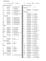
1
QT-CD161/141
SERVICE MANUAL
No. S5929QTCD161/
QT-CD161(S)
QT-CD141(BK)
• In the interests of user-safety the set should be restored to its
original condition and only parts identical to those specified should
be used.
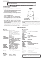
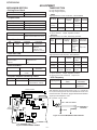
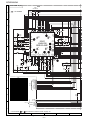
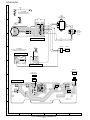
Illustration: QT-CD161
CONTENTS
Page
IMPORTANT SERVICE NOTES (FOR U.S.A. ONLY)....................................................................................................... 2
SPECIFICATIONS ............................................................................................................................................................. 2
NAMES OF PARTS ........................................................................................................................................................... 3
REMOTE CONTROL .......................................................................................................................................................... 3
DISASSEMBLY .................................................................................................................................................................. 4
REMOVING AND REINSTALLING THE MAIN PARTS ..................................................................................................... 5
ADJUSTMENT ................................................................................................................................................................... 6
NOTES ON SCHEMATIC DIAGRAM ................................................................................................................................ 9
TYPES OF TRANSISTOR ................................................................................................................................................. 9
WAVEFORMS OF CD CIRCUIT ...................................................................................................................................... 10
BLOCK DIAGRAM ........................................................................................................................................................... 11
SCHEMATIC DIAGRAM / WIRING SIDE OF P.W.BOARD ............................................................................................. 14
TROUBLESHOOTING (CD SECTION) ........................................................................................................................... 23
FUNCTION TABLE OF IC ................................................................................................................................................ 27
PARTS GUIDE/EXPLODED VIEW
PACKING OF THE SET (FOR U.S.A. ONLY)
DIFFERENCE BETWEEN QT-CD161 AND QT-CD141
SECTION
QT-CD161
QT-CD141
REMOTE CONTROL
HEADPHONE SOCKET
SHARP CORPORATION
–1–
This document has been published to be used
for after sales service only.
The contents are subject to change without notice.
QT-CD161/141
FOR A COMPLETE DESCRIPTION OF THE OPERATION OF THIS UNIT, PLEASE REFER
TO THE OPERATION MANUAL.
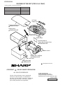
IMPORTANT SERVICE NOTES (FOR U.S.A. ONLY)
BEFORE RETURNING THE AUDIO PRODUCT
(Fire & Shock Hazard)
Before returning the audio product to the user, perform the
following safety checks.
1. Inspect all lead dress to make certain that leads are not
pinched or that hardware is not lodged between the chassis
and other metal parts in the audio product.
2. Inspect all protective devices such as insulating materials,
cabinet, terminal board, adjustment and compartment covers
or shields, mechanical insulators etc.
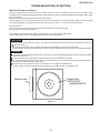
3. To be sure that no shock hazard exists, check for leakage
current in the following manner.
* Plug the AC line cord directly into a 120 volt AC outlet.
* Using two clip leads, connect a 1.5k ohm, 10 watt resistor
paralleled by a 0.15µF capacitor in series with all exposed
metal cabinet parts and a known earth ground, such as
conduit or electrical ground connected to earth ground.
* Use a VTVM or VOM with 1000 ohm per volt, or higher,
sensitivity to measure the AC voltage drop across the
resistor (See diagram).
* Connect the resistor connection to all exposed metal parts
having a return path to the chassis (antenna, metal cabinet,
screw heads, knobs and control shafts, escutcheon, etc.)
and measure the AC voltage drop across the resistor.
VTVM
AC SCALE
1.5k ohms
10W
0.15 µ F
TO EXPOSED
METAL PARTS
TEST PROBE
CONNECT TO
KNOWN EARTH
GROUND
All check must be repeated with the AC line cord plug connection
reversed.
Any reading of 0.3 volt RMS (this corresponds to 0.2 milliamp.
AC.) or more is excessive and indicates a potential shock
hazard which must be corrected before returning the audio
product to the owner.
SPECIFICATIONS
● Tape recorder
● General
Power source: AC 120 V, 60 Hz
DC 12 V [ "D" size (UM/SUM-1,
R20 or HP-2) battery × 8]
DC 3 V [ "AA" size (UM/SUM-3,
R6 or HP-7) battery × 2 for tuner
memory]
Power
Stand-by; 1.5 W
consumption: Power on; 20 W
Output power: FTC; 2.0 W min. RMS per channel
into 8 ohms from 150 Hz to 20
kHz, with no more than 10 % total
harmonic distortion.
RMS; 2.3 W/CH
(DC operation, 10 % T.H.D.)
Speakers:
4" (10 cm) full-range speaker x 2
Output
Headphones; 16-50 ohms
terminals:
(recommended; 32 ohms)
Dimensions: Width; 18-15/16" (480 mm)
Height; 6-1/16" (153 mm)
Depth; 10" (254 mm)
Weight:
7.1 lbs. (3.2 kg) without batteries
● Radio
Frequency
range:
Frequency
response:
Signal/noise
ratio:
Wow and
flutter:
Motor:
Bias system:
Erase
system:
50 - 14,000 Hz (Normal tape)
50 dB
0.25 % (WRMS)
DC 12 V electric governor
AC bias
Magnet erase
● Compact disc player
Type:
Signal
readout:
Audio
channels:
Quantization:
Filter:
D/A
converter:
Wow and
flutter:
FM; 87.5 - 108 MHz
AM; 530 - 1,720 kHz
Compact disc
Non-contact, 3-beam semi-conductor laser pickup
2
16-bit linear quantization
4-times oversampling digital filter
1-bit D/A converter
Unmeasurable
(less than 0.001% W. peak)
Specifications for this model are subject to change without
prior notice.
–2–
QT-CD161/141
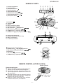
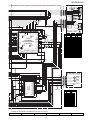
NAMES OF PARTS
3
1. Cassette Compartment
2. CD Compartment
3. (TAPE) Record Button:
4. (TAPE) Play Button:
5. (TAPE) Rewind Button:
6. (TAPE) Fast Forward Button:
7. (TAPE) Stop/Eject Button:
4
5
6
7
8
1
/
8. (TAPE) Pause Button:
2
9
10
9. Band/Pause:
10. Tuner Memory
11. Volume
12. Power, On/Function Switch
13. Extra Bass Button: X-BASS
14. (CD) Track Down: /Review Button:
15. (CD) Track Up: /Cue Button:
16. (TUNER)Tuning: /(CD) Stop Button:
17. (TUNER) Tuning: /(CD) Play/Repeat Button:
15
16
12
13
11
14
17
18
19
18. FM Telescopic Rod Aerial
19. Headphone Socket (QT-CD161 Only)
20. Battery Compartment
21. AC Power Input Socket
20
Remote control (QT-CD161 ONLY)
1. (TUNER) Tuning: /(CD) Play/Repeat Button:
2. (CD) Track Down: /Review Button:
3. Band/Pause:
4. (CD) Track Up: /Cue Button:
5. (TUNER)Tuning: /(CD) Stop Button:
21
1
2
4
3
5
REMOTE CONTROL (QT-CD161 ONLY)
Sensor Remote
Notes concerning use:
● Replace the batteries if the operating distance is
reduced or if the operation becomes erratic.
● Periodically clean the transmitter LED on the
remote control and the sensor on the main unit
with a soft cloth.
● Exposing the sensor on the main unit to strong
light may interfere with operation. Change the
lighting or the direction of the unit.
● Keep the remote control away from moisture,
excessive heat, shock, and vibrations.
15
15
–3–
8" - 20'
(0.2 m - 6 m)
0,2 m - 6 m
QT-CD161/141
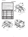
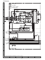
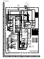
DISASSEMBLY
Caution on Disassembly
Follow the below-mentioned notes when disassembling the
unit and reassembling it, to keep it safe and ensure excellent
performance:
1. Take cassette tape and compact disc out of the unit.
2. Be sure to remove the power supply plug from the wall
outlet before starting to disassemble the unit.
3. Take off nylon bands or wire holders where they need to
be removed when disassembling the unit. After servicing
the unit, be sure to rearrange the leads where they were
before disassembling.
4. Take sufficient care on static electricity of integrated
circuits and other circuits when servicing.
STEP
REMOVAL
PROCEDURE
FIGURE
1
Rear Cabinet
1. Screw ................. (A1) x10
2. Socket .................. (A2) x1
4-1
4-2
2
Top Cabinet
1. Knob ..................... (B1) x1
(with CD Mechanism/ 2. Screw ................... (B2) x3
Tape Mechanism/ 3. Socket .................. (B3) x1
Main PWB)
4-2
3
Main PWB/
1. Screw ................... (C1) x9
Switch PWB/
2. Socket .................. (C2) x4
Headphones PWB 3. Soldering .............. (C3) x3
(QT-CD161 Only)
4-3,5-1
4-3,5-1
4-3
4
Tape Mechanism
1. Screw ................... (E1) x4
5-1
5
CD Mechanism
1. Screw ................... (F1) x3
5-1
6
Terminal PWB
1. Screw ................... (G1) x5
2. Hook ..................... (G2) x1
5-2
7
Battery PWB
1. Hook ..................... (H1) x2
5-3
(B2)x1
ø3x10mm
Top Cabinet
(B1)x1
(B2)x2
ø3x10mm
(A2)x1 (B3)x1
Front Cabinet
Main PWB
Figure 4-2
(C1)x6
ø3x10mm
(C1)x2
ø3x10mm
(C2)x1
Switch
PWB
Front Cabinet
Headphones
PWB
(C3)x3
(A1)x1
ø3x12mm
(A1)x6
ø3x20mm
Main PWB
(C2)x2
Rear Cabinet
(A1)x3
ø3x12mm
Top Cabinet
Figure 4-3
Figure 4-1
–4–
QT-CD161/141
(E1)x4
ø3x10mm
(G2)x1
Push
(F1)x3
ø2.5x10mm
Driver
Tape
Mechanism
(G1)x2
ø3x10mm
Rear Cabinet
(G1)x1
ø3x10mm
Top Cabinet
CD Mechanism
(C2)x1
(C1)x1
ø2.5x8mm
Terminal PWB
(G1)x2
ø3x10mm
Figure 5-1
Figure 5-2
Rear Cabinet
Pull
(H1)x1
(H1)x1
Pull
Battery PWB
Figure 5-3
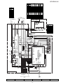
REMOVING AND REINSTALLING THE MAIN PARTS
CD MECHANISM SECTION
(A1) x2
ø2.6 x6mm
Perform steps 1, 2, 3 and 5 of the disassembly method to
remove the CD mechanism.
How to remove the pickup (See Fig. 5-4.)
Pickup
CD
Mechanism
1. Remove the screws (A1) x 2 pcs., to remove the shaft (A2)
x1 pcs.
2. Remove the stop washer (A3) x1 pcs., to remove the gear
(A4) x 1 pcs.
3. Remove the pickup.
Shaft
(A2) x1
Stop
Washer
(A3) x1
Gear
(A4) x1
Figure 5-4
–5–
QT-CD161/141
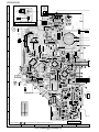
ADJUSTMENT
TUNER SECTION
MECHANISM SECTION
fL: Low-range frequency
fH: High-renge frequency
• Driving Force Check
Torque Meter
Specified Value
PLAY: TW-2412
• FM RF
Signal generator: 1 kHz, 75 kHz dev., FM modulated
Over 120 g
• Torque Check
Torque Meter
Test Stage Frequency
Frequency
Display
Specified Value
Play: TW-2111
25 to 65 g.cm
87.5 MHz
60 to 130 g.cm
Band
Coverage
—
Fast Forward: TW-2231
Rewind: TW-2231
60 to 130 g.cm
RF
90.0 MHz
(10~30 dB)
90.0 MHz
• Head Azimuth
Torque Meter
Output: Speaker Terminal
(CNP201 Load resistance: 8 ohms)
Test
Stage
• Tape Speed
Adjusting
Point
Test
Tape
MTT-111 In motor
Specified
Value
Instrument
Connection
3,000 ± 90 Hz
Output: Speaker
Teaminal
(CNP201 Load
resistance: 8 ohms)
IF
Position of each switch or control
Volume control
Function switch
X-BASS
Max
Tape/Power Off
On
• Bias Oscillation
Instrument
Connection
Specified Value
82 kHz ± 6 kHz
– 6 kHz
L301
Pin 2 of CNP201
Frequency
10.7 MHz
Frequency
Display
98.00 MHz
Test Tape
Specified Value
MTT-118
1.8 V ± 3 dB
T1(Turn
the core of
T1 fully
counterclockwise.
Input: Pin 1 of
IC1
Output: TP2
Frequency
Display
IF
450 kHz
1,720 kHz
Band
Coverage
—
530 kHz
(fL): L4
*3
1.4 ± 0.05 V
Tracking
600 kHz
1,400 kHz
600 kHz
1,400 kHz
(fL): L3
(fH):TC1
AM TRACKING
fL
fH
Adjusting Point
Speaker Terminal
(Load resistance: 8 ohms)
AM BAND
COVERAGE
MAIN PWB
G
FM DET.
21 19 17
D
FET : 2SK19 or 2SK54
VCO
TO FREQUENCY
COUNTER
S
1
10 kohm
R7
FM IF
Pin 13, pin 21 and
ground of IC2
Pin 21 of IC2
13
IC2
TP1
Instrument
Connection
Note:
After preparing the test circuit shown in Fig. 6-1, connect the
Pin 13, Pin 21 and ground of the IC2 with the test circuit, and
measure the value. At this time, apply a standard unmodulated
signal input and adjust the VCO.
VR1
L3
AM BAR
ANTENNA
Specified
Value
76 kHz ± 200 Hz
Pin 13 of IC2
TP2
TC1
*2
R26
T2
L4
Setting/ Instrument
Adjusting Connection
Parts
T3
*1
• VCO Frequency
Instrument Connection
FM ROD ANTENNA
L2
T3
L1
Figure 6-1 VCO FREQUENCY TEST CIRCUIT
AM IF
T1
IC1
Instrument
Connection
Test Stage Frequency
VR1
1
Setting/
Adjusting
Parts
*1. Input: Antenna, Output: Pin19 of IC2
*2. Input: Antenna, Output: Speaker Terminal
*3. Input: Input is not connected, Output: TP1
• Playback Amplifier Sensitivity Check
FM RF
*2
• AM IF/RF
Signal generator: 400 Hz, 30%, AM modulated
TAPE SECTION
Adjustment Point
L1
*1. Input: Antenna, Output: TP1
*2. Input: Antenna, Output: Speaker Terminal
• Detection
Signal generator: 10.7 MHz, FM sweep generator
Specified Value
MTT-114
Setting/ Instrument
Adjusting Connection
Parts
(fL): L2
*1
2.0 ± 0.1 V
FM BAND
COVERAGE
Figure 6-2 ADJUSTMENT POINTS
–6–
QT-CD161/141
TURNING ON THE TEST MODE
The types of test mode for this microcomputer and specific test mode turning-on procedure are as follows. Only the unit key is used.
The remote control key is not valid. The power must be turned on while two keys are held down.
(1) CD test mode function
The power is turned while the (PRESET
) and STOP (TUNING
) keys are held down.
(2) Tuner test mode function
) and PAUSE (BAND) keys are held down.
The power is turned on while the (PRESET
(3) LCD test mode function
The power is turned on while the (PRESET
) and MEMORY keys are held down.
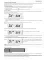
CD TEST MODE
When the CD test mode is turned on, the CD pickup is moved to the innermost periphery, and the following indication appears.
The operation of CD test mode is as follows.
Indication
(1) The CD pickup is moved with the unit UP key and DOWN key.
UP key: The pickup is slid to the outer periphery.
DOWN key: The pickup is slid to the inner periphery. However, when it reaches the innermost periphery, it does not move further
inward.
(2) When the PLAY key is pressed in stop state, the laser diode turns on if CD lid is closed.
Indication
(3) When the PLAY key is pressed in laser ON state, playback is started from the current position of pickup.
Indication
The current playback track No. and time are indicated.
(4) When the STOP key is pressed during playback, the laser goes out and playback is stopped, and the process returns to step
(1). (The pickup position does not change.)
(5) When the MEMORY key is pressed during playback, tracking servo ON/OFF is performed. (Even if the playback is stopped
in servo OFF state, the servo is turned on when the playback is restored.)
Indication
The current pickup position and time are indicated. (When the
pickup is moved with the UP/DOWN key, the time at that point
is indicated.)
Others
While the CD lid is open (LID-SW = "H"), the test mode is turned on but the operations of step (2) and subsequent steps are not
performed. The operation of step (1) is performed.
Contents of error display
Error display
Er 01
Er 02
Contents of an error
when TOC information cannot be read normally.
When a PU-IN SW detection error occurs.
TUNER TEST MODE
The tuner test mode is intended to store the measurement frequency for adjustment and inspection in the preset memory CH
without frequency adjustment in the case of tuner adjustment in the production line.
When the power is turned on while the PRESET
(DOWN) key and BAND (PAUSE) key are held down together, the frequency
for adjustment measurement of destination (specified according to AREA terminal) is preset-stored in the preset memory CH. (The
frequency to be preset-stored for specific destination is as shown in the next page.)
–7–
QT-CD161/141
In the tuner test mode the band is FM, and the mode is FM STEREO in case of start-up.
As with the ordinary mode, when the PRESET
key is pressed for 1ch of preset memory CH, maximum CH is set. When the
PRESET
key is pressed for maximum CH of preset memory CH, 1ch is set.
The BAND key is valid. As in the ordinary mode, the band/FM MONO/STEREO mode can be switched.
To exit from the tuner test mode, turn off the power to the microcomputer.
Indication
The indication is the same as that of ordinary operation. However,
when the test mode is turned on, the indication shown left lights
for one second.
Preset frequencies for various destinations (random preset memory)
BAND (CH)
1
2
3
4
5
6
7
8
9
10
11
12
13
14
15
16
17
18
19
20
21
22
23
24
25
26
27
28
29
30
U.S.A.
FM 87.5M
FM 108.0M
FM 98.0M
FM 90.0M
FM 106.0M
AM 530K
AM1720K
AM 990K
AM600K
AM 1400K
EUROPE
GENERAL 1
GENERAL 2
FM 87.50M
FM 108.00M
FM 98.00M
FM 90.00M
FM 106.00M
AM 522K
AM1620K
AM 990K
AM 603K
AM 1404K
FM 87.50M
FM 108.00M
FM 98.00M
FM 90.00M
FM 106.00M
AM 531K
AM1602K
AM 990K
AM 603K
AM 1404K
FM 87.5M
FM 108.0M
FM 98.0M
FM 90.0M
FM 106.0M
AM530K
AM1620K
AM 990K
AM 600K
AM 1404K
Note:
The unit shown in table is Hz. K is x1000. M is x1,000,000.
The slash indicates that data are not stored in the memory.
FM is stereo mode.
LCD TEST MODE
When the LCD test mode is turned on, all the segments of LCD light.
Indication
–8–
QT-CD161/141
NOTES ON SCHEMATIC DIAGRAM
• Resistor:
To differentiate the units of resistors, the symbol as K and M
are used: the symbol K means 1000 ohm and the symbol M
means 1000 kohm and the resistor without any symbol is an
ohm resistor. The resistor designated "Fusible" is a fuse type
resistor
• Capacitor:
To indicate the unit of capacitor, a symbol P is used: this
symbol P means micro-micro-farad and the unit of the capacitor
without such a symbol is microfarad. As to electrolytic capacitor,
the expression “capacitance/withstand voltage” is used.
(CH), (TH), (RH), (UJ): Temperature compensation
(ML): Mylar type
(P.P.): Polypropylene type
• The indicated voltage in each section is the one measured by
Digital Multimeter between such a section and the chassis
with no signal given.
REF. NO
DESCRIPTION
1. Tuner
( ): AM mode
Marking except for ( ): FM mode
2. CD
( ): Play mode
Marking except for ( ): Stop state
3. Deck section
( ): Record mode
Marking except for ( ): Playback mode
Display / Control section:
( ): Active state
Marking except for ( ): CD Function mode at stop state
• Schematic diagram and Wiring Side of P.W.Board for this
model are subject to change for improvement without prior
notice.
• Parts marked with “
”(
) are important for
maintaining the safety of the set. Be sure to replace these
parts with specified ones for maintaining the safety and
performance of the set.
POSITION
REF. NO
DESCRIPTION
POSITION
SW102
RECORD/PLAYBACK
PLAYBACK
SW504
MEMORY
OFF—ON
SW201
FUNCTION/POWER
TAPE—TUNER— CD/
OFF—ON
SW505
PRESET DOWN
OFF—ON
SW506
PRESET UP
OFF—ON
SW202
X-BASS
OFF—ON
SW507
CD LID OPEN/CLOSE
OFF—ON
SW501
TUNER UP
OFF—ON
SW601
TAPE MAIN
OFF—ON
SW502
TUNER DOWN
OFF—ON
SW702
PICKUP IN
OFF—ON
SW503
BAND
OFF—ON
FRONT
VIEW
E C B
(S)(G)(D)
(1) (2) (3)
KTA1266 GR
KTA1273 Y
KTC3194 Y
KTC3199 GR
KTC8050 D
KRA102 M
KRA109 M
KRC104 M
KRC107 M
Figure 9 TYPES OF TRANSISTOR
–9–
QT-CD161/141
WAVEFORMS OF CD CIRCUIT
1
2
5ms
0.50 V
IC801 20 F.E
5ms
5.0 V
IC801 54 DRF
STOP
FOCUS
PLAY
SERCH
50ms
10.0 V
JP+
7
50ms
10.0 V
JP-
8
50ms
0.50 V
JP
9
50ms
1.00 V
TE
6
0.5ms
10.0 V
JP+
7
0.5ms
10.0 V
JP-
8
0.5ms
0.50 V
JP
9
0.5ms
1.00 V
TE
10
20ms
1.00 V
SPO
11
20ms
2.00 V
CLV+
10
50ms
1.00 V
SPO
11
50ms
2.00 V
CLV+
3
1
3
6
CUE
0.5ms
1.00 V
HF
1
4
0.5ms
5.0 V
HFL
5
0.5ms
5.0 V
TES
3
0.5ms
1.00 V
H.F
4
0.5ms
5.0 V
HFL
5
0.5ms
5.0 V
TES
2
REVIEW
3
REVIEW
PLAY
NORMAL DISC
TN0=01
1
6
50ms
10.0 V
JP+
7
50ms
10.0 V
JP-
8
50ms
0.50 V
JP
9
50ms
1.00 V
TE
6
0.5ms
10.0 V
JP+
7
0.5ms
10.0 V
JP-
8
0.5ms
0.50 V
JP
9
0.5ms
1.00 V
TE
2
3
PLAY
TCD-712 (140mm)
TN0=01
CUE
PLAY
TCD-712
12
5s
100mV
SLD
1
12
0.5s
100mV
SLD
1
– 10 –
QT-CD161/141
TO
MAIN
SECTION
+7.4V
(CD)
45
XIN
44
XOUT
46 39 38 33 32
IC802
LC78622E
SERVO/SIGNAL
CONTROL
11
8
4
2
53
54
55
56
57
58
61
1
9 10 12 13 14 15 16 17 18 19 20
VCC1
Q801
DRF
CE
DAT
CL
CLK
DEF
JP–
SLI
SLC
CV+
64
54
53
52
51
50
49
SLD 29
SLEQ 28
SPO 27
FD 16
TO 15
+7.4V
1 30
CONSTANT
VOLTAGE Q804
REGULATOR
+5V
1 2 3 4
3
13
7 8 9 22 25 24
IC803
LA6541
FOCUS/TRACKING
/SPIN/SLIDE
DRIVER
29
28
18
SL–
SL+
FIN2
FIN1
E
F
30 31
25 26 20 21
5 6 10 11
M
M
PICKUP UNIT
M701
SPIN
MOTOR
TRACKING COIL
FOCUS COIL
LASER
DRIVER
LDD
32
IC801
LA9240M
SERVO AMP.
+5V
62
~
44 43 40
CL, DAT, SELIAL CONTROL
XL801
16.93MHz
+5V
XVDD
VDD
6 VVDD
43
23
37
EFMO
EFMIN
LCHO
CLV+
CLV–
V/P
HFL
TES
TOFF
TGL
JP+
JP– RES. CQCK. COIN
SQOUT. RWC. WRQ
64 63 62 51
TO MAIN
SECTION
Figure 11 BLOCK DIAGRAM (1/3)
– 11 –
M702
SLIDE
MOTOR
TO MAIN
SECTION
QT-CD161/141
SPEAKERS
SP502
SP501
R-CH
L-CH
12
10
T601
POWER
TRANSFORMER
8
IC202
LA4597
POWER AMP.
11
5
R
6
L
2
D651~D654
RECTIFIER
IC203
KIA7808P
SW202
A,B
BACK UP
+B
3
VOLTAGE
REGULATOR
X-BASS
TUNER
+B
AM / FM
SELECT
+B
FM +B
+B1
STANBY
VR201
A,B
SW201-C
POWER/
FUNCTION
Q201
Q202
Q251
VOLUME
BATTERY
DC12V
["D" SIZE (UM/SUM-1,
R20 or HP-2)BATTERYx8]
SO601
2
+B2
1
SW601
MAIN
SW201-D
POWER /
FUNCTION
M601
TAPE
MOTOR
REC
REC
TAPE
REC / PB
SW102
A,F
+B1
1
L
12
R
L
5
R
9
6
8
SW201-G
REC / PB
REC
POWER/
FUNCTION
SW201-A,B
P. B
IC101
EQULIZER
AMP.
BA331IL
RADIO
Q351 BIAS
L301 OSC.
REC
CD
FROM TUNER
SECTION
IC2-9,10PIN
SW102
REC / PB
B.D
P.B
P.B
REC / PB
SW102
C,E
SW102-H
REC / PB
P.B
FROM
CD/DISPLAY
SECTION
ERASE
R-CH HEAD
L-CH
REC / PB
HEAD
Figure 12 BLOCK DIAGRAM (2/3)
– 12 –
BATTERY
DC3V
["AA" SIZE (UM/SUM-3,
R6 or HP-7)BATTERYx2
FOR TUNER MEMORY]
AC INPUT
AC 120V
60Hz
QT-CD161/141
TUNER
+B
IC502
RESET
X501
27
24 32
SW702
PICKUP IN
MONO/ST
1 2 3 4 5 6 7 8 9 10 11 12 13 14 15 16 17 18 19 20 21
RESET
Q501
Q502
12
31 23
~
79
13
76
,
11
IC501
CD/TUNER CONTROL
MICROCOMPUTER
~
72
56
14
6
5
13
4
20
3
19
TO CD
SECTION
6
22 23 24
SW504
MEMORY
SW503
BAND
SW502
TUNER DOWN
SW501
TUNER UP
SW505
PRESET DOWN
SW506
PRESET UP
TO MAIN
SECTION
SW601
MAIN
AUDIO
+12V
VOLTAGE
REGULATOR
ZD1
15 MO/ST
9
TUNER +B
Q5
Q6
A-GND
FM+B
13 17 16 10 7
L-CH OUT
10 R-CH OUT
IC2
LA1805
FM /AM/IF APX.
16 MPX IN
FM RIPPLE
FILTER
+5V
13 MPX VCO
10 IF IN
VR1
VCO
+B
+B 21
11 AM IN
12 FM IN OF1 6
18 DET OUT
+B
20 FM DET
TUNER
STEREO 7
GND
T2
8
IC3
TC9216P
PLL
6
AM IF IN 5
AM IF IN
FM DET
PERIDO 5
CLOCK
4
DATA
3
CF2
22 AM RF IN
14 DOUT
13 VSS
T3
D GND
AM IF
VT
AM MIX OUT
VT CONTROL
24 AM OSC AM MIX OUT 2
FM IF IN 1
AM OSC OUT
1 X OUT X IN 2
X1
4.5MHz
Q3
Q4
CF1
FM+B
9
VD2
8
L2
7
VD3-1
FM IF
Q1
VD3-2
T1
6
5
TC1
VT
AM ANT.
L4
FM RF
L3
IC1
TA7358AP
FM FRONT END
RF AMP.
FM OSC
VT
AM OSC.
LCD DISPLAY
LCD501
RX501
4
VD1
3
L1
1
FM ROD
ANTENA
Figure 13 BLOCK DIAGRAM (3/3)
– 13 –
F1
B.P.F
QT-CD161/141
MAIN PWB-A1(1/4)
LASER
DRIVE
Q801
KTA1266 GR
CD SIGNAL
A
R842
22
C849
0.022
12 TD–
13 TD
14 JP
CL
CLK
DEF
DRF
CE
DAT
REFI
VCC2
FSS
SPD
SLEQ
SLD
SL–
SL+
JP–
C833
0.001
R833
5.6K
R832
56K
R836
47K
R837
47K
R8
1.2
C832 R834
1K
27P
C831
0.0027
R835
470
C822
220P
R821
56K
R822
6.8K
R827
220K
D802
1N4148
R810
82K
C851
0.022
C821
1/50
2
3
4
5
6
7
8
9
C846
PU IN
WRQ
SQOUT
DRF
SL–
SL+
RWC
CO IN
CQCK
RES
10
11
D-GND 1
+B 7.4V 45
P16 1-F
R838
33K
C834
0.033
C887
0.022
G
R85
680
+B
P19 8-H
F
IC802
PIN
VOLTAGE PIN
NO. VOLTAGE NO. VOLTAGE
23 5V
0V
45 2V
0V
24 0V
46 0V
1.5V
25 0V
47 0.1V
0V
26 0V
48 2.2V
2V
27 0V
49 0V
28 0V
5V
50 2.5V
0.3V
29 0V
51 0V
0V
30 5V
52 2.5V
2.5V
31 2.5V
53 0V
54 0V
2.5V
32 0V
55 0V
0V
33 0V
34 0V
0V
56 4.1V
35 5V
0V
57 4.1V
36 4.7V
5V
58 5V
37 2V
0V
59 0V
38 0V
60 2.7V
4.8V
39 0V
5V
61 2.4V
40 2V
5V
62 0V
41 4.7V
0V
63 0V
42 0V
0V
64 0V
43 5V
2.5V
44 2.3V
0V
34
33
R830 R824
1K
10K
C818
1/50
C819
R825
47/16
1.2K
R831
C820
1K
0.0033
R826
220K
VREF
C811
0.1
PIN
NO.
1
2
3
4
5
6
7
8
9
10
11
12
13
14
15
16
17
18
19
20
21
22
C835 0.1/50
C837 10/16
C838 0.01
SPG
SP–
R815 C814 R816
47K 0.01 1.5K
R840
22K
VR
30 31 32
SP
29
R820
10K
R814
10K
R812
15K
C813
0.1
27 28
R817
82K
C850
0.1
C816
0.001
C817
0.47/50
GND
E
R839
22K
21 22 23 24 25 26
C812
330P
R823
1.2K
17 18 19 20
R813
33K
R828
1K
R829
1K
LF2
TOFF 35
FE–
A GND
NC
15
16
34 TGL
33 JP+
15 TO
16 FD
C810
180P
C845
4.7/50
R849
100K
11 TA
R808
12K
PH1
BH1
10 TH
R811
3.3K
D
LDS
9 SCI
C809
0.047
FSC 46
GND 45
SLI 44
SLC 43
RFS– 42
C830
2.0P
RFSM 41
CV+ 40
CV– 39
SLOF 38
HFL 37
TES 36
IC801
LA9241M
SERVO AMP.
C815
0.0047
R806
100
48
7 TE
8 TESI
C808
0.068
R871
4.7K
47
48 NC
47 TBC
R819
39K
C806
0.033
R805
6.8K
R807
1K
R809
27K
R803
15K
C805
0.033
R804
2.2K
1 FIN2
2 FIN1
6 TE–
FA–
FE
C807
0.1/50
R802
100K
FD–
FA
C
61 60 59 58 57 56 55 54 53 52 51 50 49
2
3 E
4 F
5 TB
C803
0.1/50
C804
0.001
63 62
LDD
1
64
VCC1
B
C839 0.1
C840 0.33/50
C848
1/50
POWER GND
L-CH
AUDIO GND
R-CH
+B
13
14
15
16
H
• The numbers 1 to 12 are waveform numbers shown in page 10.
1
2
3
4
Figure 14 SCHEMATIC DIAGRAM (1/6)
– 14 –
5
6
5
4
3
2
1
F
E
B
A
K
TOFF
TGL
IC802
LA78623D
SERVO/SIGNAL
CONTROL
BI801
TR+
TR–
FO–
FO+
XL801
16.93MHz
44
43
42
41
40
C868 R874
10/16 100
C867
10/16
LVSS 38
LCHO 37
LVDD 36
MUTEL 35
C890
100/10
B
F
TR–
TR+
FO+
FO–
GND
PD
VR
LD
TR+
FO+
FO–
TR–
TR–
PICKUP UNIT
R873
100
PIN
NO.
1
2
3
4
5
6
7
8
9
10
11
12
13
14
15
16
17
18
19
20
21
22
C870
0.0022
C869
0.0022
34
33
R880
100
17 18 19 20 21 22 23 24 25 26 27 28 29 30 31 32
L801
0.82µH
K
E
A
B
F
47
RVSS 39
34 NC
33 TEST4
15 HFL
16 TES
1
2
3
4
5
6
7
8
1
2
3
4
5
6
7
8
R875 R876
10K 10K
SBCK
SFSY
PW
RWC
COIN
SQOUT
RES
CQCK
WRQ
FSX
XOUT
XVDD
MUTER
RVDD
RCHO
TEST3
11 TEST2
12 CLV+
13 CLV–
14 V/P
15
16
48 EFLG
47 SBSY
LD
M0N
K
E
A
48
XVSS 46
XIN 45
CONT1
CONT2
CONT3
CONT4
CONT5
EMPH
C2F
DOUT
EMFO
10 EMFIN
TEST5
4.2M
16M
TST11
CS
VVDD
FR
Vss
JP+
JPPCK
FSEQ
VDD
TEST1
R856
1.2K
R857
27K 6
7
8
9
1 DEFI
2 TAI
5
4
3
2
1
5
4
3
2
1
CNS801
C802
47/16
1
2
3
4
5
6
7
8
C801
0.01
64 63 62 61 60 5 9 58 57 56 55 54 53 52 51 50 49
R858 C841 1
680 0.047 2
3 PDO
C842
VVss
0.047 4
5 ISET
LD
PD
VR
C
R801
1K
R860
1K
C847
0.01
CNS802
BI802
QT-CD161/141
C843
100/10
IC801
VOLTAGE PIN
NO. VOLTAGE
23 2.5V
2.5V
2.5V
24 2.5V
2.5V
25 2.5V
2.5V
26 2.5V
2.5V
27 2.5V
28 2.5V
2.5V
29 2.5V
2.5V
2.5V
30 2.2V
2.5V
31 2.2V
2.5V
32 0V
2.5V
33 0V
2.5V
34 5V
2.5V
35 5V
2.5V
36 4.8V
2.5V
37 0V
38 5V
2.5V
2.5V
39 0V
40 0V
2.5V
41 1.5V
2.5V
42 2.4V
2.5V
43 2.5V
2.5V
44 2.5V
0V
PIN
NO.
45
46
47
48
49
50
51
52
53
54
55
56
57
58
59
60
61
62
63
64
VOLTAGE
0V
2.5V
2.5V
0V
0V
2.4V
4.1V
4.7V
0V
0V
5V
5V
2.5V
2.5V
0.9V
0.9V
2.1V
4.2V
0V
5V
C873
0.01
TR+
TR–
FO–
FO+
CD MOTOR PWB-B
SP+
6
5
5
Q802
KTA1273 Y
10
11
12
13
14
15
VCC
BIAS IN
VIN4
VIN4G
VO4+
VO4–
GND
GND
GND
VO3–
VO3+
VG3
VIN3
CD
RESET
30
29
28
27
26
25
24
23
22
21
20
19
18
17
16
SL+ 4
SL– 3
4
4
3
3
2
2
2
1
1
1
PU-IN
C888
0.022
VCC
MUTE
VIN1
VG1
VO1+
VO1–
GND
GND
GND
VO2–
VO2+
VG2
VIN2
REG OUT
REG-B
IC803
LA6541
C846
330/10
1
2
3
4
5
6
7
8
9
CNS803
6
5
M
M701
SPINDLE
MOTOR
M
M702
SLED
MOTOR
SW702
PICKUP IN
CNP803
+B
BI803
6
SP–
+B
TUNER GND
PIN
NO.
1
2
3
4
5
6
7
8
9
10
11
12
13
14
15
C844
330/10
L802
0.68µH
IC803
VOLTAGE PIN
NO. VOLTAGE
7.2V
16 0V
0V
17 0V
2.8V
18 2.5V
0V
19 2.6V
3.6V
20 3.5V
0V
21 2.9V
GND
22 GND
23 GND
GND
24 GND
GND
25 3.2V
3.2V
26 3.2V
3.2V
27 0V
0V
28 2.6V
2.6V
29 0.4V
5.1V
6.6V
30 7.2V
• NOTES ON SCHEMATIC DIAGRAM can be found on page 9.
7
8
9
10
Figure 15 SCHEMATIC DIAGRAM (2/6)
– 15 –
11
12
QT-CD161/141
FM SIGNAL
CD SIGNAL
A
PLAYBACK SIGNAL
RECORD SIGNAL
CNS101 CNP101
1
1
2
C
SW102-B
R
P
C107
R107
(B)820P
1K
2
3
3
4
4
R-CH
R
P
SW102-E
ERASE HEAD
R
NF2
11
4
C112
330P(B)
C108
820P(B)
R
P R108 C110
1K 270P(B)
SW102-D
R110
C106
0.0018(B) 120
P
SW102-H
R119
3.3K
BA3311L
C111
REC./P.B.
330P(B)
EQUALIZER
IN2
9
GND
6
7
C114
47/16
C116
0.018
(ML)
FILTER 10
ALC T 2
OUT2
12
C120
47/16
SW102-C
R
P
L-CH
R115 R117
3.9K 3.9K
C113
C117
47/16
10/16
C109
3
1
PRE AMP
270P(B) NF1
OUT1
8 C119
IC101
2.2/50
VCC
5 IN1
R109
120
R101
330
R102
330
C118
10/16
R116
3.9K
R114
8.2K
R106
15K
C354
0.022(ML)
BIAS OSC
L301
D
P18 3-A,4-A
E
R-CH
GND(A)
L-CH
TUNER +B
D GND
23
22
21
32
28
C352
220/10
ON OFF
SW202-A
X-BASS
C123
220/10
SW202-B
X-BASS
ON OFF
R125
680K
R122
2.7K
C152
0.039
(ML)
TAPE
TUNER
CD
SW201-B
R351
330
(1/4W)
R352
150
(1/4W)
C353
0.0056
(ML)
Q351
KTC8050 D
R354
10(1/4W)
+B
R458
1.2K
P19 7-A,11-H
F
P14 2-H,P19 11-HION
+B
R-CH
AUDIO GND
L-CH
CD +7.4V
DIGITAL GND
POWER GND
+7.4V
MUTE
FUNC(CD)
BACK UP
16
15
14
42
1
R154
2.2K
R
R353
47K(1/4W)
C351
0.0022
(ML)
R123
3.3K
R124
3.3K
SW102-G
R153
2.2K
D103
1N4148
SW102-F
P
C122 R
0.01(Z)
R118 R120
3.9K 3.3K
P
R121
2.7K
C121
0.01 SW102-A
R
P
D101
1N4148
B
C115
R113
0.018(ML) 8.2K
D102
1N4148
R105
15K(1/4W)
SW201-A
TAPE
TUNER
CD
C151
0.039(ML)
R103
12K
C105
0.0018(B)
R104
12K
D303
1N4004
R457
1.2K
R456
15K
R455
15K
+B
13
12
43
44
40
+B
C252
0.022
G
MAIN PWB-A1(2/4)
H
• NOTES ON SCHEMATIC DIAGRAM can be found on page 9.
1
2
3
4
Figure 16 SCHEMATIC DIAGRAM (3/6)
– 16 –
5
6
R
2
R
2
QT-CD161/141
C233
470/10
R222 C220
0.068
1K
C222
0.001(B)
–
+
6
1
D201
1SS133
8
CNS201
C234
470/10
1
2
3
C652
0.022(Z)
CNS602
CNP602
SW201-D
CD
TUNER
TAPE
1
2
3
C302
0.047(Z)
VOLTAGE
REGULATOR
OUT
IC203 1 IN
3 KIA7808P
2
2
2
3
3
SP501
L-CH
SP502
R-CH
WOOFER
8OHMS
T601
POWER TRANSFORMER
D653
1N4004
ACSO
AC INPUT
AC120V,60Hz
DC12V [ ''D'' SIZE(UM/SUM-1,
R20 OR HP-2)BATTERY x 8]
C301
1/50
DC 3V [ ''AA'' SIZE(UM/SUM-3
R6 OR HP-7)BATTERY x 2
FOR TUNER MEMORY]
D301
1N4148
BATTERY PWB-A4,5
R230
2.7(1/4W)
+B
1
QT-CD141
C653
0.022(Z)
SW201-C
1
C227
4700/25
R256
4.7K
TAPE
TUNER
CD
WOOFER
8OHMS
D652
1N4004
R255
2.2K
R254
10K
+B
SP502
R-CH
TERMINAL PWB-A3
R253
1.8K
D252
1N4148
R252
22K
SP501
L-CH
SPEAKER
WOOFER
8OHMS
C232
0.1
(ML)
Q251
KTA1266 GR
R251
10K
3
3
10
5
3
C231
0.1
(ML)
11
9
2
C651
C654
0.022(Z) 0.022(Z)
D251
1N4148
IC202
LA4597
POWER
AMP.
1
2
FW202
D651
IN4004
C218
0.0027(B)
13
1
3
1
CNP201
Q201
KTC3199 GR
1
C223
100/10
4
C224
Q202
100/10
KTC3199 GR
7
C225
220/25
R224
3
4.7K
12
+
–
C229
100/10
2
D654
1N4004
VR201-B
20K(B)
CNS201
CNP201
C226
0.022(Z)
R220
3.3K
C216
0.027(ML)
R152
22K
SPEAKER
WOOFER
8OHMS
R223
4.7K
R225
100K
C228
1/50
R219
3.3K
QT-CD161
R228
120(1/4W)
VR201-A
20K(B)
C215
0.027(ML)
R151
22K
R227
120(1/4W)
C230
100/10
C219
R221 0.068
C221
1K
(ML) 0.001(B)
C217
0.0027
(B)
HEADPHONES PWB-A2
IC202
PIN VOLTAGE
NO.
0.1V
1
0V
2
11.2V
3
0V
4
11.3V
5
0V
6
0.1V
7
12V
8
10.4V
9
10 5.8V
11 0V
12 5.8V
13 10.4V
IC101
PIN
VOLTAGE
NO.
1 <0V> [3.23V]
2 <0V> [0V]
3 <0.6V> [0.6V]
4 <0V> [0V]
5 <0V> [0V]
6 <0V> [0V]
7 <0V> [0V]
8 <7.43V> [7.43V]
9 <0V> [0V]
10 <7.37V> [7.37V]
11 <0.6V> [0.6V]
12 <3.3V> [3.3V]
< >: Recording
[
]: Play
D302
1N4148
SW601
TAPE
MAIN SW
+
–
7
8
9
10
Figure 17 SCHEMATIC DIAGRAM (4/6)
– 17 –
M
M601
TAPE MOTOR
11
12
SO601
QT-CD161/141
TUNED
MONO/STEREO
STEREO
GND(D)
21 22 23
24 25 26 28 29 30 31 32
P16 1-E
7 DTE OUT 17
ST IND
18
6 GND
C38 R25
C36
5 AM IF
0.018 33K 0.0022
(M)
19
R24
3.9K
FM DET 20
T2
+B
C31
0.022
C32
0.022
C12
0.022
FM +B 21
R5
10K
R12
4.7K
4
2
1
FB
B.P.F
1 2 3
F1
H
R71
6.8K
C10
24P
(UJ)
C14
0.022
R3
33K
R2
100K
C2
0.01
R9
100K
FM BAND
COVERAGE
AM TRACKING
fL
fH
AM ANT
VD3-1
KV1591A-2
5
D2
1SS133
C4
27P(CH)
6
+B
3
C20
470P
R11
56K
C18
0.022
C17
0.047
C28
2.2/50
IC2
PIN
NO.
1.6V
13
1.6V
14
6V (6.3V)
15
0.2V (0.7V) 16
1.6V
17
0V
18
0V
19
0V
20
2.5V
21
2.5V
22
5.1V (6.6V) 23
0.8V (1V)
24
VOLTAGE
C16
0.022(M)
R1
22(1/4W)
C59
0.022
C70
0.001
R10
L4 68K
L3
VOLTAGE
1.2V (0V)
1.9V (1.6V)
1V (1.3V)
1.7V
1.5V (1.7V)
1.5V (1.5V)
0.4V (0.4V)
6.1V (6.4V)
6.1V (6.4V)
1.6V
1.6V
1.6V
( ): AM
C71
0.022
C58
0.01
C19
12P(UJ)
Q6
KRC104 M
Q5,Q6:FM RIPPLE FILTER
IF-IN OT-2
I/O5(ST) OT-3
IC3
TC9216P @PPL
C30
15P(CH)
DO 1 X IN
R20
6.8K
1
Q1
KTC3194 Y
RE AMP.
T1
FM IF
C8
15P(CH)
C3
4.7P(CH)
C7
VD1
FM RF 0.001KV1360NT
R70
L1
22K
IC1
TA7358AP
FM FRONTEND
R4
10
7
3
G
FM OSC
L2
C9
33P(CH)
1
2
PIN
NO.
1
2
3
4
5
6
7
8
9
10
11
12
R8
47K
R13
390
VD2
KV1360NT
3
R18
47K
C25
0.001
R7
4.7K
C11
22P(CH)
2
Q3
KTC3199 GR
Q3,Q4:VT
CONTROL
CF1
2
R56
47
8
C24
2.2/50
TP1
9
F
R17
10K
AM +B 23
IN
1 FM IF AM
OSC 24
1
C13
47/16
R15
1.2K
+B
AM RF 22
3
E
C34 C35
220/10 0.022
9
C22
0.01(M)
R6
560
VD3-2
KV1591A-2
3 AM
MIX
2
R16
2.2K
C27
0.022
TC1
5P
T3
AMIF
4
16 15 14 13 12 11 10
C26
0.022
FM DET
C33
22/16
2
2 3 4 5 6 7 8
AM OSC
D
C72
0.001
1
DO 2
C40
470P
C21
0.022
+B
8 TUN IND
3
CF2
1
C29
12P(CH)
C41
3.3/50
C45
0.022(M)
0.9V
1.6V
6.8V
0V
0V
6.8V
1.4V
6.2V
6.8V
C56
0.01
VDD X OUT
MPZ 16
–IN
R35
2.2K
X1
4.5MHz
D4
1SS133
Q4
KTC3199 GR
9 L CH
R43
47K
R42
4.7K
C47
1/50
IC2
LA1805
FM/AM/IF MPX.
14
10 R CH FM
15
–M/ST
VOLTAGE
C57
100/10
VR1
C42
VCO
3.3/50 6.8K(B)
C46
0.022(M)
R36
2.2K
R37
6.8K
R30
15K
R29
1.2K
13
11 AM/FM
C48
1/50
R38
6.8K
C
12 NC VCO
2
C37
0.022
1
R51
1K
R47
56K
L5
CH 470µH
Q9
KRA109 M
R48
56K
D3
1SS133
TP2
3
C49
1/50
C43
0.0015
(STYROL)
PIN
NO.
1
2
3
4
5
6
7
8
9
R46
56K
+B
10K
R39
R50
1K
IC1
C50
0.022
GND DATA
CLOCK
FM-IN
PERIOD
AM-IN OT-1
B
ZD1
DZ5.1BSB
R52
1K
R44
180(1/4W)
+B
+B
C60
100P
+B
R45
220(1/4W)
R72
1K
Q5
KRA102 M
A
PLL(PERIOD)
PLL(DATA)
PLL(CLOCK)
TUNER +B
L-CH
GND(A)
R-CH
P19 8-A,P16 1-E
PIN
NO.
1
2
3
4
5
6
7
8
9
IC3
VOLTAGE PIN
NO. VOLTAGE
2.4V
10
––
2.3V
11
0V
6.8V
12
2.3V
0.1V
13
GND
4.9V
14
0V
3.0V
15
––
––
16
0.5V
––
––
AM BAND
COVERAGE fL
C52
0.022
C51
10/16
C6
0.01(M)
FM SIGNAL
AM SIGNAL
C5
0.01(M)
D1
1SS133
MAIN PWB-A1(3/4)
FM
ROD ANTENA
• NOTES ON SCHEMATIC DIAGRAM can be found on page 9.
1
2
3
4
Figure 18 SCHEMATIC DIAGRAM (5/6)
– 18 –
5
6
QT-CD161/141
IC202
PIN VOLTAGE
NO.
0.1V
1
0V
2
11.2V
3
0V
4
11.3V
5
0V
6
0.1V
7
12V
8
10.4V
9
10 5.8V
11 0V
12 5.8V
13 10.4V
PIN
NO.
1
2
3
4
5
6
7
8
9
10
11
12
13
14
15
16
17
18
19
20
21
22
P18 5-A
P16 1-F,P14 2-H
+7.4V
MONO/STEREO
TUNED
STEREO
PLL(CLOCK)
PLL(DATA)
PLL(PERIOD)
12
24 25
26
29 30 31
+B
1 2 3 4 5 6 7 8 9 10 11 12
R540
1K
XL501
4.19MHz
R543
6.8K
MAIN PWB-A1(4/4)
4
SL–
SL+
RWC
COIN
CQCK
RESET
DRF
PU IN
WRQ
SQ OUT
P14 3-F
7
8
R542
3.3K
43 42
FUNC(CD)
P-MUTE
3 2 5 11 10 9 8 7 6
13 14 15 16 17 18 19 20 21
R539
1K
R541
1K
R531
15K
R533 1K
R534 1K
R535 1K
R536 1K
R537 1K
R538 1K
R530
15K
63 62 61 60 59 58 57 56 55 54 53 52 51 50 49 48 47 46 45 44 43 42 41
QT-CD161
ONLY
R552
1K
SEG8
R532
1K
Q502
3 KRC107M
RESET
LCD501
40
39
38
37
36
35
34
33
32
31
30
29
28
27
26
25
1
C521
0.0047 2
SW504
MEMORY
R505 D506
5.6K 1SS133
SEG9
SEG10
SEG11
SEG12
SEG13
SEG14
SEG15
SEG16
SYNC IN
FUNC
P-MUTE2
P-MUTE1
VSS
XOUT
XIN
Q501
KTC3199 GR
RESET
D505
1SS133
IC501
IX0016SJ
CD/TUNER CONTROL
MICROCOMPUTER
C509 R504
0.1/50 100K
R521 1K
R522 1K
VL1
LID SW
CLOCK
DATA
PERIOD
T-MUTE
AREA
KEY1
KEY0
STEREO
MONO/ST
WRQ
SD
PU IN
DRF
RESET
CQCK
COIN
RWC
SL+
SL–
REMOCON
SYS
STOP
27 RESET
25 SQ OUT
R524
56K
65
66
67
68
69
70
71
72
73
74
75
76
77
78
79
80
C508 1
0.022
R506
2.7K
R519 560
R520 1K
1 2 3 4 5 6 7 8 9 10 11 12 13 14 15 16 17 18 19 20 21 22 23 24
R503
1.8K
R523
15K
IC502
PST9142
RESET
3
R528
10K
R518
10K
2
R527
10K
SEG7
SEG6
SEG5
SEG4
SEG3
SEG2
SEG1
SEG0
VCC
VREF
AVSS
COM3
COM2
COM1
COM0
VL3
R511 560
R512 560
R513 560
R517
10K
D504
1SS133
D503
1SS133
R526
10K
C512
0.022
R507 C513
1K 0.022
R509 1K
R510 1K
R508
56K
+B
SW503
BAND
R501
150 (1/4W)
D501
1SS133
D502
1SS133
C510 C511
0.1(M) 0.022
C504
0.022
R502
2.7K
2
RX501
REMOTE
SENSOR R548
47
L501
100µH
+B
R546
15K
IC101
PIN
VOLTAGE
NO.
1 <0V> [3.23V]
2 <0V> [0V]
3 <0.6V> [0.6V]
4 <0V> [0V]
5 <0V> [0V]
6 <0V> [0V]
7 <0V> [0V]
8 <7.43V> [7.43V]
9 <0V> [0V]
10 <7.37V> [7.37V]
11 <0.6V> [0.6V]
12 <3.3V> [3.3V]
< >: Recording
[
]: Play
QT-CD161 ONLY
C519
10/16
1
R549
15K
R545
5.6K
SW507
CD LID
OPEN/CLOS
R550
15K
ZD501
DZ5.6BSB
C505
0.022
R544
3.3K
2
1
C516
100P
SW502
TUNER
DOWN
1
3
C503
10/16
2.2V
2.2V
2.2V
2.2V
2.2V
2.2V
2.2V
2.2V
5.0V
––
––
––
––
––
––
––
SW506
PREST UP
SW501
TUNER
UP
FW501
3
1
C502
0.022
VOLTAGE
R547
3.3K
+B
C501
100/10
VOLTAGE PIN
NO.
––
65
––
66
––
67
––
68
––
69
––
70
––
71
––
72
––
73
––
74
––
75
2.2V
76
2.2V
77
2.2V
78
2.2V
79
2.2V
80
2.2V
2.2V
2.2V
2.2V
2.2V
2.2V
SWITCH PWB-A5
3
C506
2.2/50
IC501
VOLTAGE PIN
NO.
––
45
4.0V
46
0.5V
47
––V
48
5.0V
49
––
50
––
51
2.0V
52
2.3V
53
GND
54
––
55
5.0V
56
5.4V
57
––
58
––
59
––
60
––
61
––
62
––
63
––
64
63
––
––
64
SW505
PREST
DOWN
GND(D)
BACK UP +B
40 1
VOLTAGE PIN
NO.
23
3.0V
1.5V
24
––
25
––
26
––
27
28
––
––
29
––
30
5.0V
31
5.0V
32
5.0V
33
––
34
2.1V
35
5.0V
36
4.6V
37
38
4.9V
4.9V
39
40
3.9V
41
––
42
––
43
––
44
––
P16 1-F
9
10
Figure 19 SCHEMATIC DIAGRAM (6/6)
– 19 –
11
12
QT-CD161/141
CD-C161 ONLY
QT-CD141
ONLY
P21 10-B
FROM
SPEAKER
3
CNS201
J201
HEADPHONES
FW202
1
R227
A
1 2 3
R228
CNP101
1 2 3 4
C351
G
A
B
D
F
FW201
1 2 3
TO TERMINAL PWB
CNS602
C227
C229
C220
C226
C231
C232
C230
Q802
R842
16
15
20
B
C
E
25
5
C844
IC803
10
30
1
C849
R840
R819
C815
R820
R821
C816
R839
R830
R823
R822
R826
C808
C807
R806
R807
R809
R811
R808
C810
C806
R805
C804
C805
R804
R802
R803
C803
C801
R801
C802
13
10
15
CNS803
IC2
BR
GY
GY
GY
GY
GY
C40
20
5
CF2
C38
R25
C36
T2
FM DET
B
C
E
CF1
E
C
B
C52
L4
AM OSC
C34
C35
R24
24
1 C31
R17
3
2
1
C51
Q3
TC1
C13
C19
-1
R7
T1
FM IF
R70
C14
C20
R11
C17
R9
-2
R12
R5
VD3
L2
C18
R10
C11
D2
R56
C6
C4
C7
R3
VD1
C16
C5
F1
R2
D4
R30
12
T3
AM IF
R1
D1
2
1
H
C9
R71
L1
FM RF
3
R29
R36
C42
C41
VD2
C10
R4
C2
9 8 7 6 5 4 3 2 1
C3
C59
L3
AM BAR ANTENNA
MAIN PWB-A1
• The numbers 1 to 12 are waveform numbers shown in page 10.
3
R829
R828
R814 R812
R815
C814
R816
C812
R817
R810
R827
C822
D3
C58
C12
R13
C8
2
C817
C888
R16
PINK
C26
PK
C25
9
C43
3
2
1
BLACK
Q4
Q1
C71
IC1
WHITE
BK
R39
C37
1 2 3
C24
R15
C70
WH (W)
C45
C32
R6
R8
C29
B
C
E
GRAY
C49
C46
C47
R35
R37
C22
C60
C27
GY
8
C33
Q5
L5
VIOLET
C840
C21
BLUE
VL
C48
R42
R18
C28
R20
C72
GREEN
BL
Q9
3 2 1
1
2
3
IC3
GR
9 10 11 12 13 14 15 16
8 7 6 5 4 3 2 1
R46
R47
R48
YELLOW
6
BI803
4
Figure 20 WIRING OF P.W.BOARD (1/3)
– 20 –
5
1
2
3
4
5
MPX VCO CK
76kHz
VR1
C56
X1
ORANGE
C818
C839
C50
ZD1
C57
R45
Q6
C30
YL
CNS
BK
WH
WH
WH
WH
5
R38
COLOR TABLE
OR
R834
R519
3
1
R549
R50
R51
R52
RED
1
1 BI802
1
R72
R550
2
BROWN
C809
R44
BK
BK
R824
R825
C819
C830
C838
C837
R509
4
5
1
2
3
4
5
6
7
8
10
16
10
60
12
17
20
15
IC801
64
R43
F
C813
25
55
49
R510
R513
R512
R511
Q502
C516
CD LID
OPEN/CLOSE
BR
R831
C521
D802
3
2
1
C821
B
C
E
Q501
C509
1
2
1
R813
35 30
40
45
50
C835
R524
BK
WH
WH
WH
WH
WH
WH
WH
7
C811
33 32
48
C850
C845
R871
C851
R837
R835
C831
R522
R838
C834
R836
C833
R849
B C E
C846
R833
C832
R832
R856
R857
C842
C841
R858
R508
R530
R505
D506
R504
R517
C873
C843
R880
XL801
C847
CNS
6
8
1
64
R521
SW507
R D (R )
W601
IC203
C867
L802
R876
R507
C513
R528
R503
C508
1
C820
5
R552
IC502
C505
FW501
1
R518
16
10
60
Q801
1 BI801
17
20
15
IC802
55
C848
L801
25
R860
R520
D504
D503
4
45
50
R533
R534
R535
R536
R537
R538
R527
D303
32
40
49
C512
ZD501
C502
11
35 30
48
R531
R539
R526
D505
R502
QT-CD161
ONLY
C870
R523
15
1
W601
33
24
5
C506
R501
C501
1
2
3
C890
25
20
10
C511
L501
R506
C510
C503
J48
D501
D502
C887
30
70
R456
R458
50
IC501
60
XL501
35
55
64
R540
40
C504
E
C868
R874
41
45
R548
C519
D201
C225
R542
E
C
B
Q251
LCD501
R541
D251
RX501
1 REMOTE
SENSOR
2
R532
3
R873
R875
R543
80
FW501
E
C
B
R122
C122
R120
D103
R124
C119
C120
R125
P22 3-E
TO SWITCH PWB
R354
R353
R352
C117
CNP602
C302
C869
R253
5
P22 6-E
TO SENSOR PWB
R351
R114
R116
Q351
R230
R455
R457
R252
R254
D252
75
1
R106
C106
R118
IC101
C118
12
10
8
6
4
2
C224
IC202
C301
R255
R251
65
G
C116
C114
R110
C110
11
9
7
5
3
1
R117
C121
C228
R225
C222
R256
D302
D301
C252
(CD + 2-BAND)
21
20
19
18
17
16
15
14
13
12
11
10
9
8
7
6
5
4
3
2
1
D
4
C123
13
12
11
10
9
8
7
6
5
4
3
2
1
A
SW202
X-BASS
C221
C223
R223
B
D
C353
C233
C219
Q201
E C B
R152
R151
SW201
CD-TUNER-TAPE
ON
TUNER
CD
C
Q202
R153
R224
R-CH
R221
L-CH
OFF
TAPE
B
C151
C152
C354
D102
C234
E C B
R154
A
3
R222
SW201
FUNCTION
C
1
4 FW201
4
R102
R108
C108 C112
C107 C111
R107C109
R109
C113
C115
1
1
D101
R123
R119
FW202
B
L301
H
SW102
E
R101
R103
R115
R113
R121
HEADPHONES PWB-A2
R104
R105
P21 10-B
FROM
SPEAKER
C105
CNP201
1
2
3
CNS201
C
C352
CNP201
6
1
2
3
4
5
6
QT-CD161/141
SPEKERS
SP502
R-CH
P20 1-A
TO
HEADPHONES PWB
(QT-CD161)
SW601
TAPE MAIN
(233-7)
CNP602
1 2 3
TO TERMINAL PWB
M601
TAPE MOTOR
(233-6)
CNS602
CNP201
P20 3-A
TO
MAIN PWB
(QT-CD141)
SP501
L-CH
1 WH
2 BK
3 RD
CNS201
TAPE
ERASE HEAD
(233-5)
RECORD/PLAYBACK
HEAD(233-4)
RD
BK
WH
BR
BK
YL
CNS101
4
3
2
1
11
W601
BK
WH
RD
BK
BK
R842
PICK UP UNIT
C848
B
C
E
Q801
CNS801
6
1 BI801
R810
12
BK
WH
WH
WH
WH
WH
WH
WH
1
2
3
4
5
6
7
8
5 4 3 2 1
8 7 6 5 4 3 2 1
7
R
09
10
C807
R806
1
1 BI802
5
CD MOTOR PWB-B
CNS802
BK
WH
WH
WH
WH
1
2
3
4
5
-
8
+
MPX VCO CK
76kHz
VR1
SW702
SPENDLE MOTOR
M701
D4
F3895AF
R30
R29
9
CNP803
PICKUP IN
6
5
4
3
2
1
-
C42
C43
CNS803
C41
38
R25
C36
T2
FM DET
C35
R24
SLED MOTOR
M702
1
2
3
4
5
6
+
C52
L4
AM OSC
C34
C40
BR
GY
GY
GY
GY
GY
C19
-2
FM ROD ANTENNA( 210 )
-1
TC1
NTENNA
WB-A1
7
8
9
10
Figure 21 WIRING OF P.W.BOARD (2/3)
– 21 –
11
12
QT-CD161/141
(208)
BATTERIES
DC12V["D" size (UM/SUM-1,
R20 or HP2) battery x 8]
A
T601
POWER
TRANSFORMER
(230)
B
PT
YL
D653
PT
YL
D652
ACSO
OR
RD
BK
CNS602
C653
C652
+B
C654
GND
D654
G
D651
ACSO
C651
RD
RD
SO601
AC SOCKET
AC 120V
60Hz
BK
OR
TERMINAL PWB-A3
C
OR
OR
CNS602
BATTERIES
DC3V["AA" size (UM/SUM-3,R6 or HP-7)
battery x 2 for tuner memory]
3
2
1
P20 6-B
TO MAIN PWB
CNP602
(237)
D
BATTERY PWB-A4
BACK-UP
BATTERY PWB-A5
E
P20 1-E
TO MAIN PWB
P20 1-B
TO MAIN PWB
FW501
FW201
SWITCH PWB-A6
SW502
MEMORY
TUNER
DOWN
C520
R220
BAND
1
4
FW501
PRESET
DOWN
TUNER
UP
C217
R219
C215
SW506
PRESET
UP
C216
C218
R545
G
SW505
SW501
1
R546
SW503
VR201
FW201
4
R547
SW504
R544
F
H
1
2
3
4
Figure 22 WIRING OF P.W.BOARD (3/3)
– 22 –
5
6
QT-CD161/141
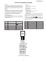
TROUBLESHOOTING (CD SECTION)
When the CD does not function
When the CD section does not operate when the objective lens of the optical pickup is dirty, this section may not operate. Clean
the objective lens, and check the playback operation. When this section does not operate even after the above step is taken, check
the following items.
Remove the cabinet and follow the troubleshooting instructions.
"Track skipping and/or no TOC (Table Of Contents) may be caused by build up of dust other foreign matter on the laser pickup
lens. Before attempting any adjustment make certain that the lens is clean. If not, clean it as mentioned below."
Turn the power off.
Gently clean the lens with a lens cleaning tissue and a small amount of isopropyl alcohol.
Do not touch the lens with the bare hand.
Dust gradually accumulates on the objective lens during use, and it may degrade performance.
To avoid this problem, use a cleaning disc designed for CD optical pickup lenses.
HOW TO USE
1. Using the brush in the cleaner cap, apply 1 or 2 drops of the cleaning fluid to the brush on the CD cleaner disc which has
the mark next to it.
2. Place the CD cleaner disc onto the CD disc tray with the brush side down, then press the play button.
3. You will hear music for about 20 seconds and the CD player will automatically stop. If it continues to turn, press the stop button.
CAUTION
The CD lens cleaner should be effective for 30 - 50 operations, however if the brushes become worn out earlier then please
replace the cleaner disc.
If the CD cleaner brushes become very wet then wipe off any excess fluid with a soft cloth.
Do not drink the cleaner fluid or allow it to come in contact with the eyes. In the event of this happening then drink and / or
rinse with clean water and seek medical advice.
The CD cleaner disc must not be used on car CD player or on computer CD ROM drives.
All rights reserved. Unauthorized duplicating, broadcasting and renting product is prohibited by law.
Cleaning Disc
PARTS CODE:
UDSKA0004AFZZ
Cleaner Liquid
Figure 23
– 23 –
QT-CD161/141
When the CD does not function
When the CD section does not operate When the objective lens of the optical pickup is dirty,this section may not operate.Clean
the objective lens,and check the playback operation.When this section does not operate even after the above step is taken,check
the following items.
Remove the cabinet and follow the troubleshooting instructions.
"Track skipping and/or no TOC(Table Of Contents) may be caused by build up of dust other foreign matter on the laser pickup lens.
Before attempting any adjustment make certain that the lens is clean. If not, clean it as mentioned below."
Turn the power off.
Gently clean the lens with a lens cleaning tissue and a small amount of isopropyl alcohol.
Do not touch the lens with the bare hand.
• The CD function will not work.
The CD operating keys don't work.
Yes
Check the CD, DPS microcomputer (IC501), power supply, 4.19
MHz and 16.93 MHz clock, and reset terminal.
Yes
Check the waveform of SCK, SO (DATA) and SI (COMM).
Yes
See if the pick-up is in the pick-up in SW702(pu-in switch) position.
Yes
If the items mentioned above are OK, check the main
microcomputer IC501.
• The CD operating keys work.
Check the Focus - HF system.
Playback can be performed without a disc.
Yes
Does the pick-up move up and down twice?
Focus search OK.
Yes
No
Does the output waveform of IC801(16)(FD) match that shown in
Fig. 24?
Check the area around IC803-BI801/CNS801.
Yes
No
Check the IC801(50)(CLK) line, 4MHz.
Check the microcomputer data on pins (51)(CL), (52)(DAT) and
(53)CE.
Focus search
is performed
two times
when play
operation is
done without
disc.
0.5s
0.50 V
IC801 16 FD
0.5s
0.50 V
IC801 15 TD
1
2
Figure 24
– 24 –
QT-CD161/141
• Playback can only be performed when a disc
is loaded.
No
Check the laser diode driver.
Check the area around IC801(16) - (21) (focus servo circuit).
No
If the disc is not turning, the DRF
should not change to "H".
Is the Focus servo active? (Can you hear it working?)
Yes
▼
Yes
Does the DRF signal change from "L" to "H"?
Check the spin
system.
Yes
Yes
No
Level is abnormal.
▼
Is HF waveform normal (see the Fig. 25-1, 2)?
Yes
Check the periphery
of IC801 pins 41 and
42.
Yes
Check the tracking system.
HF
0.1V/DIV
0.5µsec/DIV(DC)
IC801 41
(When playing
back the disc)
▼
Waveform is unstable.
Check the spin
system.
Waveform in case
of normal playback
0.5s
1.00 V
IC801 16 FD
0.5s
10.0 V
IC801 12 CLV+
2
1
3
0.5s
10.0 V
IC801 54 DRF
4
0.5s
2.00 V
IC801 7 TE
Figure 25-1
Figure 25-2
• Check the tracking system.
Check waveform of IC801 pin 7 (TE).
The waveform shown in Fig. 25-3
appears, and no-disc state appears
soon.
Play is possible in
TEST mode.
Yes
Tracking servo is inoperative.
Yes
The unit will be initialized in
Normal mode,but it will not Yes
playback.
Data cannot be read.
Yes
Check the periphery of IC801
pin 8 to pin 15, and IC803 to
BI801/CNS801.
Normal jump is impeded, and the
program top cannot be reached. Yes
Check the VCO-PLL system.
5ms
1.00 V
IC801 7 TE
4
5 ms
5.0 V
IC801 54 DRF
3
Figure 25-3
– 25 –
Yes
Check the periphery of
IC801 pin 14.
QT-CD161/141
• Checking the spin system.
Play operation is performed without disc.
Yes
The spin driver circuit is normal.
The turntable rotates a little.
Yes
No
The turntable fails to rotate or rotates at high speed.
Yes
Check the periphery of IC801 pins 23 to 27, pin 39 and pin 40,
IC802 pin 12 and pin 13, IC803 to BI803/CNS803.
• Checking the VCO-PLL system
Play operation is performed when disc exits.
Yes
Although HF waveform is normal, TOC data cannot be read.
Yes
Check PDO waveform (Fig. 26).
Error
Check the IC801 pins 43 and 44, IC802 pins 3, 5, 7, 9 and 10.
0.5s
1.00 V
IC802 3 PDO
2
0.5s
1.00 V
IC801 16 FD
Stop --> Play
As VCO frequency is locked at
4.32 M Hz,
voltage of PDO
rises and stabilizes.
3
Figure 26
•
Although HF waveform is normal and the time
indication is normal, no sound is emitted.
Check IC802 pin 48 (EFLG).
No
Yes
Check IC802 pins 37and 40.
Abnomal
Check the periphery of IC802 (OPAMP).
– 26 –
Usually, the number of pulses of flawless disc is 100 pulses/sec
or less.
QT-CD161/141
FUNCTION TABLE OF IC
IC501 RH-iX0016SJZZ (IX0016SJ): CD/Tuner Control Microcomputer (1/2)
Pin No.
Terminal
Name
Port Name
Input/
Output
Function
1,2
VL2
VL2
Input
LCD bias setting power input terminal.
3
P67/AN7
LID-SW (CD)
Input
CD cover position detection SW input terminal.
"L" = CD cover CLOSED, "H"= CD cover OPEN.
4
P66/AN6
CLOCK (TUNER)
5
P65/AN5
DATA (TUNER) Input/Output PLL IC serial data input/output terminal.
Address 8 bits, sending/receiving 24-bit data.
6
P64/AN4
PERIOD(TUNER)
Output
PLL IC serial data transmission start/stop pulse output terminal.
7*
P63/AN3
T-MUTE (TUNER)
Output
Tuner output mute output terminal.
"H" = Mute ON.
8*
P62/AN2
AREA (TUNER)
Input
Destination voltage detection input. Operates as an A/D input port, and when a reset is executed,
detects the DC voltage present at the destination.
9
P61/AN1
KEY1
Input
Operation key input. Max. 8 keys.
10
P60/AN0
KET0
Input
Operation key input. Max. 8 keys.
11
P57/ADT
STEREO
(TUNER)
Input
FM stereo broadcast detection input.
"L" = When receiving a stereo broadcast .
12
P56/TOUT
MONO/ST
(TUNER)
Output
13
P55/CNTR1
WRQ (CD)
Input
Detection input to standby with sub Q code output from LC78623D.
14
P54/CNTR0
SD (TUMNER)
Input
Tuner carrier wave detection input.
"L" = When a carrier wave is detected.
15
P53/RTP0
PU IN (CD)
Input
CD pickup position detection SW input terminal.
"L" = Innermost circumference.
Input
HF level detection input terminal from LA9241M.
Output
PLL IC serial data transmission timing CLOCK output terminal.
FM mode output terminal read by the tuner IF IC.
"H" = FM stereo mode ("L" = FM mono/AM band).
16
P52/RTP0
DRF (CD)
17
P51/INT3
CD-RESET (CD)
18
P50/INT2
CQCK (CD)
Output
Serial data synchronous clock for LA9241M/LC78623D interface.
19
P47/SRDY
COIN (CD)
Output
LA9241M/LC78623D control command output terminal.
20
P46/SCLK
RWC (CD)
Output
READ/WRITE control output terminal to LA9241M/LC78623D.
21
P45/TXD
SL+ (CD)
Output
Slide motor forward control output terminal to LA9241M.
22
P44/RXD
SL- (CD)
Output
23
P43/INT1
REMOCON
Input
Remote control signal input terminal
Detected on the falling edge.
24
P42/INT0
SYS-STOP
Input
Input terminal for detecting a power failure or dead battery.
"L" = The unit will enter the backup mode.
Input
Sub code Q data input terminal from LC78623D.
25
P41/Ø
SQOUT (CD)
26*
P40
N.C
Output
Input
LC78623D reset signal output.
Slide motor back control output terminal to LA9241M.
27
RESET
RESET
28*
P71/XCIN
N.C
No connect.
29*
P70/XCOUT
N.C
No connect.
Input
Microcomputer reset signal input.
30
XIN
XIN
31
XOUT
XOUT
Main clock oscillator connection terminal.
32
VSS
VSS
33*
P27
P-MUTE1
Output
Audio signal mute condition output terminal.
"H" = Mute ON.
34
P26
P-MUTE2
Output
Audio signal mute condition output terminal.
"L" = Mute ON.
35
P25
CD-FUNC
Input
CD function detection input terminal.
"H" = CD function.
36
P24
SYNC-IN
Input
Record SW detection input terminal.
"H" = Record SW ON.
37*
P23
N.C
No connect.
38*
P22
N.C
No connect.
39*
P21
N.C
No connect.
Output
––
Microcomputer power GND.
40
P20
N.C
No connect.
41*
P17/SEG31
N.C
No connect.
42*
P16/SEG30
N.C
No connect.
43*
P15/SEG29
N.C
No connect.
In this unit, the terminal with asterisk mark (*) is (open) terminal which is not connected to the outside.
– 27 –
QT-CD161/141
IC501 RH-iX0016SJZZ (IX0016SJ): CD/Tuner Control Microcomputer (2/2)
Pin No.
Terminal
Name
Port Name
Input/
Output
Function
44*
P14/SWG28
N.C
No connect.
45*
P13/SEG27
N.C
No connect.
46*
P12/SEG26
N.C
No connect.
47*
P11/SEG25
N.C
No connect.
48
P10/SEG24
N.C
No connect.
49
P07/SEG23
N.C
No connect.
50
P06/SEG22
N.C
No connect.
51
P05/SEG21
N.C
No connect.
52
P04/SEG20
N.C
No connect.
53
P03/SEG19
N.C
No connect.
54*
P02/SEG18
N.C
No connect.
55
P01/SEG17
N.C
56
P00/SEG16
SEG16
Output
LCD segment output.
57
P37/SEG15
SEG15
Output
LCD segment output.
58
P36/SEG14
SEG14
Output
LCD segment output.
59
P35/SEG13
SEG13
Output
LCD segment output.
60
P34/SEG12
SEG12
Output
LCD segment output.
61
SEG11
SEG11
Output
LCD segment output.
62
SEG10
SEG10
Output
LCD segment output.
63
SEG9
SEG9
Output
LCD segment output.
64
SEG8
SEG8
Output
LCD segment output.
65
SEG7
SEG7
Output
LCD segment output.
66
SEG6
SEG6
Output
LCD segment output.
67
SEG5
SEG5
Output
LCD segment output.
68
SEG4
SEG4
Output
LCD segment output.
69
SEG3
SEG3
Output
LCD segment output.
70
SEG2
SEG2
Output
LCD segment output.
71
SEG1
SEG1
Output
LCD segment output.
72
SEG0
SEG0
Output
73
VCC
VCC
Microcomputer power +5V.
74
VREF
VREF
A/D converter power +5V.
75
AVSS
AVSS
76
COM3
COM3
Output
LCD common output terminal.
77
COM2
COM2
Output
LCD common output terminal.
78
COM1
COM1
Output
LCD common output terminal.
76
COM0
COM0
Output
LCD common output terminal.
80
VL3
VL3
No connect.
LCD segment output.
A/D converter power GND.
Input
LCD bias setting power input terminal.
In this unit, the terminal with asterisk mark (*) is (open) terminal which is not connected to the outside.
– 28 –
QT-CD161/141
PARTS GUIDE
MODEL
QT-CD161(S)
QT-CD141(BK)
“HOW TO ORDER REPLACEMENT PARTS”
To have your order filled promptly and correctly, please furnish the
following information.
1. MODEL NUMBER
2. REF. No.
3. PART NO.
4. DESCRIPTION
For U.S.A. only
Contact your nearest SHARP Parts Distributor to order.
For location of SHARP Parts Distributor,
Please call Toll-Free;
1-800-BE-SHARP
MARK: SPARE PARTS-DELIVERY SECTION
Explanation of capacitors/resistors parts codes
Capacitors
Resistors
VCC ....................... Ceramic type
VCK ........................ Ceramic type
VCT ........................ Semiconductor type
VC • • MF ............... Cylindrical type (without lead wire)
VC • • MN ............... Cylindrical type (without lead wire)
VC • • TV ................ Square type (without lead wire)
VC • • TQ ............... Square type (without lead wire)
VC • • CY ............... Square type (without lead wire)
VC • • CZ ............... Square type (without lead wire)
VC • • • • • • • • • J .. The 13th character represents capacity difference.
("J" ±5%, "K" ±10%, "M" ±20%, "N" ±30%,
"C" ±0.25 pF, "D" ±0.5 pF, "Z" +80-20%.)
VRD ....................... Carbon-film type
VRS ........................ Carbon-film type
VRN ....................... Metal-film type
VR • • MF ............... Cylindrical type (without lead wire)
VR • • MN ............... Cylindrical type (without lead wire)
VR • • TV ................ Square type (without lead wire)
VR • • TQ ............... Square type (without lead wire)
VR • • CY ............... Square type (without lead wire)
VR • • CZ ............... Square type (without lead wire)
VR • • • • • • • • • J .. The 13th character represents error.
("J" ±5%, "F" ±1%, "D" ±0.5%.)
If there are no indications for the electrolytic capacitors, error is ±20%.
If there are no indications for other parts, the resistors are ±5%
carbon-film type.
NOTE:
Parts marked with “
” are important for maintaining the safety of the set.
Be sure to replace parts with specified ones for maintaining the safety and performance of the set.
– 29 –
QT-CD161/141
NO.
PRICE
RANK
PARTS CODE
DESCRIPTION
INTEGRATED CIRCUITS
VHITA7358AP-1
VHILA1805//-1
VHITC9216P/-1
VHIBA3311L/-1
J
J
J
J
AG
AM
AL
AK
FM Front End,TA7358AP
FM/AF IF MPX.,LA1805
PLL,TC9216P
REC./P.B.Equalizer
Amp.,BA3311L
Power Amp.,LA4597
Voltage Regulator,KIA7808P
CD/Tuner Control
Microcomputer,IX0016SJ
Reset,PST9142
Servo Amp.,LA9241M
Servo/Signal Control,LC78623D
Focus/Tracking/Spin/Slide
Driver,LA6541D
IC202
IC203
IC501
VHILA4597//-1
VHIKIA7808P-1
RH-IX0016SJZZ
J
J
J
AH
AH
BC
IC502
IC801
IC802
IC803
VHIPST9142/-1
VHILA9241M/-1
VHILC78623D-1
VHILA6541D/-1
J
J
J
J
AH
AS
AY
AW
VSKTC3194Y/-1
VSKTC3199GR-1
VSKRA102M//-1
VSKRC104M//-1
VSKRA109M//-1
VSKTC3199GR-1
VSKTA1266GR-1
VSKTC8050D/-1
VSKTC3199GR-1
VSKRC107M//-1
VSKTA1266GR-1
VSKTA1273Y/-1
J
J
J
J
J
J
J
J
J
J
J
J
AD
AB
AC
AC
AC
AB
AB
AD
AB
AC
AB
AE
D1~4
D101~103
D201
D251,252
D301,302
D303
D501~506
D651~654
D802
VD1,2
VD3
VHDDS1SS133-1
VHDDS1SS133-1
VHDDS1SS133-1
VHDDS1SS133-1
VHDDS1SS133-1
VHD1N4004//-1
VHDDS1SS133-1
VHD1N4004//-1
VHDDS1SS133-1
VHCKV1360NT-1
VHCKV1591A2-3
J
J
J
J
J
J
J
J
J
J
J
AB
AB
AB
AB
AB
AB
AB
AB
AB
AF
AU
ZD1
ZD501
VHEDZ5R1BSB-1
VHEDZ5R6BSB-1
J
J
Silicon,DS1SS133-1
Silicon,DS1SS133-1
Silicon,DS1SS133-1
Silicon,DS1SS133-1
Silicon,DS1SS133-1
Silicon,1N4004
Silicon,DS1SS133-1
Silicon,1N4004
Silicon,DS1SS133-1
Variable Capacitance,KV1360NT
Variable Capacitance,
KV1591A2
AC Zener,5.1V,DZ5.1BSB
AC Zener,5.6V,DZ5.6BSB
RFILF0001SJZZ
RFILA0002SJZZ
RFILR0001SJZZ
J
J
J
AD FM IF
AH AM IF
AD FM Band Pass Filter
RCILI0001SJZZ
RCILI0002SJZZ
RCILI0003SJZZ
RTRNP0001SJZZ
J
J
J
J
AD
AD
AD
AP
RCILR0004SJZZ
RCILB0011SJZZ
CCORF0002SJ09
RCILB0012SJZZ
VP-CH471K0000
RCILB0003SJZZ
VP-CH101K0000
VP-DHR82K0000
VP-DHR68K0000
J
J
J
J
J
J
J
J
J
AE FM RF
AF FM,OSC
AM Bar Antenna
AF AM,OSC
AB 470 µH,Choke
AD OSC,Bias
AB 100 µH,Choke
AE 0.82 µH,Choke
AC 0.68 µH
J
J
AC 6.8 kohms (B),Semi-VR [VCO]
AK 20 kohms (B),Semi-VR [Volume]
TRANSISTORS
Silicon,NPN,KTC3194 Y
Silicon,NPN,KTC3199 GR
Digital,PNP,KRA102 M
Digital,NPN,KRC104 M
Digital,PNP,KRA109 M
Silicon,NPN,KTC3199 GR
Silicon,PNP,KTA1266 GR
Silicon,NPN,KTC8050 D
Silicon,NPN,KTC3199 GR
Digital,NPN,KRC107 M
Silicon,PNP,KTA1266 GR
Silicon,PNP,KTA1273 Y
DIODES
!
FILTERS
CF1
CF2
F1
TRANSFORMERS
!
T1
T2
T3
T601
FM IF
FM Detection
AM IF
Power
COILS
L1
L2
L3
L4
L5
L301
L501
L801
L802
VARIABLE RESISTORS
VR1
VR201
RVR-M0001SJZZ
RVR-B0003SJZZ
PRICE
RANK
PARTS CODE
DESCRIPTION
VARIABLE CAPACITOR
IC1
IC2
IC3
IC101
Q1
Q3,4
Q5
Q6
Q9
Q201,202
Q251
Q351
Q501
Q502
Q801
Q802
NO.
TC1
RTO-H1003SJZZ
J
AG Trimmer
J
J
J
AN Crystal,4.5 MHz
AK Ceramic,4.19 MHz
AE Ceramic,16.93 MHz
J
J
J
J
J
J
J
J
J
J
J
J
J
J
J
J
J
J
J
J
J
J
J
J
J
J
J
J
J
J
J
J
J
J
J
J
J
J
J
J
J
J
J
J
J
J
J
J
J
J
J
J
J
J
J
J
J
J
J
J
J
J
J
J
J
J
J
J
J
J
AE
AA
AA
AE
AA
AA
AA
AB
AA
AB
AB
AB
AB
AB
AB
AA
AA
AB
AE
AB
AA
AB
AB
AA
AA
AB
AB
AB
AB
AA
AB
AC
AA
AB
AB
AB
AB
AB
AB
AB
AB
AB
AB
AB
AA
AA
AB
AA
AB
AA
AA
AA
AB
AB
AB
AB
AB
AB
AB
AB
AB
AA
AB
AA
AB
AB
AB
VIBRATORS
X1
XL501
XL801
RCRSB0001SJZZ
RCRM-0003SJZZ
RCRM-0002SJZZ
CAPACITORS
C2
C3
C4
C5,6
C7
C8
C9
C10
C11
C12
C13
C14
C16
C17
C18
C19
C20
C21
C22
C24
C25
C26,27
C28
C29
C30
C31,32
C33
C34
C35
C36
C37
C38
C40
C41,42
C43
C45,46
C47~49
C50
C51
C52
C56
C57
C58
C59
C60
C70
C71
C72
C105,106
C107,108
C109,110
C111,112
C113,114
C115,116
C117,118
C119
C120
C121,122
C123
C151,152
C215,216
C217,218
C219,220
C221,222
C223,224
C225
C226
C227
C228
C229,230
–1–
VCTYPA1CU103M
VCCCPA1HH4R7C
VCCCPA1HH270J
VCTYPA1CU103M
VCKYPA1HB102K
VCCCPA1HH150J
VCCCPA1HH330J
VCCUPA1HJ240J
VCCCPA1HH220J
VCKYPA1HF223Z
RC-GZA476AF1C
VCKYPA1HF223Z
VCTYPA1CU223M
VCKYPA1HF473Z
VCKYPA1HF223Z
VCCUPA1HJ120J
VCKYPA1HB471K
VCKYPA1HF223Z
VCTYPA1CU103M
RC-GZA225AF1H
VCKYPA1HB102K
VCKYPA1HF223Z
RC-GZA225AF1H
VCCCPA1HH120J
VCCCPA1HH150J
VCKYPA1HF223Z
RC-GZA226AF1C
RC-GZA227AF1A
VCKYPA1HF223Z
VCKYPA1HB222K
VCKYPA1HF223Z
VCTYPA1CU183M
VCKYPA1HB471K
RC-GZA335AF1H
VCQSMV1HS152J
VCTYPA1CU223M
RC-GZA105AF1H
VCKYPA1HF223Z
RC-GZA106AF1C
VCKYPA1HF223Z
VCKYPA1HF103Z
RC-GZA107AF1A
VCKYPA1HF103Z
VCKYPA1HF223Z
VCKYPA1HB101K
VCKYPA1HB102K
VCKYPA1HF223Z
VCKYPA1HB102K
VCKYPA1HB182K
VCKYPA1HB821K
VCKYPA1HB271K
VCKYPA1HB331K
RC-GZA476AF1C
VCQYKA1HM183K
RC-GZA106AF1C
RC-GZA225AF1H
RC-GZA476AF1C
VCKYPA1HF103Z
RC-GZA227AF1A
VCQYKA1HM393K
VCQYKA1HM273K
VCKYPA1HB272K
VCQYKA1HM683K
VCKYPA1HB102K
RC-GZA107AF1A
RC-GZA227AF1E
VCKYPA1HF223Z
RC-GZA478AF1E
RC-GZA105AF1H
RC-GZA107AF1A
0.01 µF,16V
4.7 pF (CH),50V
27 pF (CH),50V
0.01 µF,16V
0.001 µF,50V
15 pF (CH),50V
33 pF (CH),50V
24 pF (UJ),50V
22 pF (CH),50V
0.022 µF,50V
47 µF,16V,Electrolytic
0.022 µF,50V
0.022 µF,16V
0.047 µF,50V
0.022 µF,50V
12 pF (UJ),50V
470 pF,50V
0.022 µF,50V
0.01 µF,16V
2.2 µF,50V,Electrolytic
0.001 µF,50V
0.022 µF,50V
2.2 µF,50V,Electrolytic
12 pF (CH),50V
15 pF (CH),50V
0.022 µF,50V
22 µF,16V,Electrolytic
220 µF,10V,Electrolytic
0.022 µF,50V
0.0022 µF,50V
0.022 µF,50V
0.018 µF,16V
470 pF,50V
3.3 µF,50V,Electrolytic
0.0015 µF,50V,Styrol
0.022 µF,16V
1 µF,50V,Electrolytic
0.022 µF,50V
10 µF,16V,Electrolytic
0.022 µF,50V
0.01 µF,16V
100 µF,10V,Electrolytic
0.01 µF,16V
0.022 µF,50V
100 pF,50V
0.001 µF,50V
0.022 µF,50V
0.001 µF,50V
0.0018µF,50V
820 pF,50V
270 pF,50V
330 pF,50V
47 µF,16V,Electrolytic
0.018 µF,50V,Mylar
10 µF,16V,Electrolytic
2.2 µF,50V,Electrolytic
47 µF,16V,Electrolytic
0.01 µF,16V
220 µF,10V,Electrolytic
0.039 µF,50V,Mylar
0.027 µF,50V,Mylar
0.0027 µF,50V
0.068 µF,50V,Mylar
0.001 µF,50V
100 µF,10V,Electrolytic
220 µF,25V,Electrolytic
0.022 µF,50V
4700 µF,25V,Electrolytic
AB 1 µF,50V,Electrolytic
AB 100 µF,10V,Electrolytic
QTCD161/141
NO.
PRICE
RANK
PARTS CODE
DESCRIPTION
C231,232
C233,234
C252
C301
C302
C351
C352
C353
C354
C501
C502
C503
C504,505
C506
C508
C509
C510
C511~513
C516
C519
VCQYKA1HM104K
RC-GZA477AF1A
VCKYPA1HF223Z
RC-GZA105AF1H
VCKYPA1HF473Z
VCQYKA1HM222K
RC-GZA227AF1A
VCQYKA1HM562K
VCQYKA1HM223K
RC-GZA107AF1A
VCKYPA1HF223Z
RC-GZA106AF1C
VCKYPA1HF223Z
RC-GZA225AF1H
VCKYPA1HF223Z
RC-GZA104AF1H
VCTYPA1CU104M
VCKYPA1HF223Z
VCKYPA1HB101K
RC-GZA106AF1C
J
J
J
J
J
J
J
J
J
J
J
J
J
J
J
J
J
J
J
J
AB
AC
AB
AB
AB
AA
AB
AA
AB
AB
AB
AB
AB
AB
AB
AB
AB
AB
AA
AB
C520
C521
C651~654
C801
C802
C803
C804
C805,806
C807
C808
C809
C810
C811
C812
C813
C814
C815
C816
C817
C818
C819
C820
C821
C822
C830
C831
C832
C833
C834
C835
C837
C838
C839
C840
C841,842
C843
C844
C845
C846
C847
C848
C849
C850
C851
C867,868
C869,870
C873
C887
C888
C890
VCKYPA1HF103Z
VCKYPA1HB472K
VCKYPA1HF223Z
VCKYPA1HF103Z
RC-GZA476AF1C
RC-GZA104AF1H
VCKYPA1HB102K
VCTYPA1CU333M
RC-GZA104AF1H
VCTYPA1CU683M
VCTYPA1CU473M
VCKYPA1HB181K
VCTYPA1CU104M
VCKYPA1HB331K
VCTYPA1CU104M
VCTYPA1CU103M
VCKYPA1HB472K
VCKYPA1HB102K
RC-GZA474AF1H
RC-GZA105AF1H
RC-GZA476AF1C
VCKYPA1HB332K
RC-GZA105AF1H
VCKYPA1HB221K
VCCCPA1HH2R0C
VCKYPA1HB272K
VCCCPA1HH270J
VCKYPA1HB102K
VCTYPA1CU333M
RC-GZA104AF1H
RC-GZA106AF1C
VCTYPA1CU103M
VCTYPA1CU104M
RC-GZA334AF1H
VCTYPA1CU473M
RC-GZA107AF1A
RC-GZA337AF1A
RC-GZA475AF1H
RC-GZA337AF1A
VCTYPA1CU103M
RC-GZA105AF1H
VCKYPA1HF223Z
VCTYPA1CU104M
VCKYPA1HF223Z
RC-GZA106AF1C
VCKYPA1HB222K
VCKYPA1HF103Z
VCKYPA1HF223Z
VCKYPA1HF103Z
RC-GZA107AF1A
J
J
J
J
J
J
J
J
J
J
J
J
J
J
J
J
J
J
J
J
J
J
J
J
J
J
J
J
J
J
J
J
J
J
J
J
J
J
J
J
J
J
J
J
J
J
J
J
J
J
AB
AB
AB
AB
AB
AB
AA
AB
AB
AB
AB
AA
AB
AA
AB
AE
AB
AA
AA
AB
AB
AA
AB
AA
AA
AA
AA
AA
AB
AB
AB
AE
AB
AA
AB
AB
AB
AB
AB
AE
AB
AB
AB
AB
AB
AA
AB
AB
AB
AB
0.1 µF,50V,Mylar
470 µF,10V,Electrolytic
0.022 µF,50V
1 µF,50V,Electrolytic
0.047 µF,50V
0.0022 µF,50V,Mylar
220 µF,10V,Electrolytic
0.0056 µF,50V,Mylar
0.022 µF,50V,Mylar
100 µF,10V,Electrolytic
0.022 µF,50V
10 µF,16V,Electrolytic
0.022 µF,50V
2.2 µF,50V,Electrolytic
0.022 µF,50V
0.1 µF,50V,Electrolytic
0.1 µF,16V
0.022 µF,50V
100 pF,50V
10 µF,16V,Electrolytic
[QT-CD161 Only]
0.01 µF,16V
0.0047 µF,50V
0.022 µF,50V
0.01 µF,16V
47 µF,16V,Electrolytic
0.1 µF,50V,Electrolytic
0.001 µF,50V
0.033 µF,16V
0.1 µF,50V,Electrolytic
0.068 µF,16V
0.047 µF,16V
180 pF,50V
0.1 µF,16V
330 pF,50V
0.1 µF,16V
0.01 µF,16V
0.0047 µF,50V
0.001 µF,50V
0.47 µF,50V,Electrolytic
1 µF,50V,Electrolytic
47 µF,16V,Electrolytic
0.0033 µF,50V
1 µF,50V,Electrolytic
220 pF,50V
2 pF (CH),50V
0.0027 µF,50V
27 pF (CH),50V
0.001 µF,50V
0.033 µF,16V
0.1 µF,50V,Electrolytic
10 µF,16V,Electrolytic
0.01 µF,16V
0.1 µF,16V
0.33 µF,50V,Electrolytic
0.047 µF,16V
100 µF,10V,Electrolytic
330 µF,10V,Electrolytic
4.7 µF,50V,Electrolytic
330 µF,10V,Electrolytic
0.01 µF,16V
1 µF,50V,Electrolytic
0.022 µF,50V
0.1 µF,16V
0.022 µF,50V
10 µF,16V,Electrolytic
0.0022 µF,50V
0.01 µF,16V
0.022 µF,50V
0.01 µF,16V
100 µF,10V,Electrolytic
J
J
J
J
J
J
J
J
AA
AA
AA
AA
AA
AA
AA
AA
22 ohms,1/4W
100 kohm,1/6W
33 kohms,1/6W
10 ohm,1/6W
10 kohm,1/6W
560 ohms,1/6W
4.7 kohms,1/6W
47 kohms,1/6W
NO.
RESISTORS
R1
R2
R3
R4
R5
R6
R7
R8
VRD-ST2EE220J
VRD-ST2CD104J
VRD-ST2CD333J
VRD-ST2CD100J
VRD-ST2CD103J
VRD-ST2CD561J
VRD-ST2CD472J
VRD-ST2CD473J
–2–
PRICE
RANK
PARTS CODE
R9
R10
R11
R12
R13
R15
R16
R17
R18
R20
R24
R25
R29
R30
R35,36
R37,38
R39
R42
R43
R44
R45
R46~48
R50~52
R56
R70
R71
R72
R101,102
R103,104
R105,106
R107,108
R109,110
R113,114
R115~118
R119,120
R121,122
R123,124
R125
R151,152
R153,154
R219,220
R221,222
R223,224
R225
R227,228
VRD-ST2CD104J
VRD-ST2CD683J
VRD-ST2CD563J
VRD-ST2CD472J
VRD-ST2CD391J
VRD-ST2CD122J
VRD-ST2CD222J
VRD-ST2CD103J
VRD-ST2CD473J
VRD-ST2CD682J
VRD-ST2CD392J
VRD-ST2CD333J
VRD-ST2CD122J
VRD-ST2CD153J
VRD-ST2CD222J
VRD-ST2CD682J
VRD-ST2CD103J
VRD-ST2CD472J
VRD-ST2CD473J
VRD-ST2EE181J
VRD-ST2EE221J
VRD-ST2CD563J
VRD-ST2CD102J
VRD-ST2CD470J
VRD-ST2CD223J
VRD-ST2CD682J
VRD-ST2CD102J
VRD-ST2CD331J
VRD-ST2CD123J
VRD-ST2CD153J
VRD-ST2CD102J
VRD-ST2CD121J
VRD-ST2CD822J
VRD-ST2CD392J
VRD-ST2CD332J
VRD-ST2CD272J
VRD-ST2CD332J
VRD-ST2CD684J
VRD-ST2CD223J
VRD-ST2CD222J
VRD-ST2CD332J
VRD-ST2CD102J
VRD-ST2CD472J
VRD-ST2CD104J
VRD-ST2EE121J
J
J
J
J
J
J
J
J
J
J
J
J
J
J
J
J
J
J
J
J
J
J
J
J
J
J
J
J
J
J
J
J
J
J
J
J
J
J
J
J
J
J
J
J
J
AA
AA
AA
AA
AA
AA
AA
AA
AA
AA
AA
AA
AA
AA
AA
AA
AA
AA
AA
AA
AA
AA
AA
AA
AA
AA
AA
AA
AA
AA
AA
AA
AA
AA
AA
AA
AA
AA
AA
AA
AA
AA
AA
AA
AA
R230
R251
R252
R253
R254
R255
R256
R351
R352
R353
R354
R455,456
R457,458
R501
R502
R503
R504
R505
R506
R507
R508
R509,510
R511~513
R517,518
R519
R520~522
R523
R524
R526~528
R530,531
R532
R533~541
R542
R543
R544
R545
VRD-ST2EE2R7J
VRD-ST2CD103J
VRD-ST2CD223J
VRD-ST2CD182J
VRD-ST2CD103J
VRD-ST2CD222J
VRD-ST2CD472J
VRD-ST2EE331J
VRD-ST2EE151J
VRD-ST2EE473J
VRD-ST2EE100J
VRD-ST2CD153J
VRD-ST2CD122J
VRD-ST2EE151J
VRD-ST2CD272J
VRD-ST2CD182J
VRD-ST2CD104J
VRD-ST2CD562J
VRD-ST2CD272J
VRD-ST2CD102J
VRD-ST2CD563J
VRD-ST2CD102J
VRD-ST2CD561J
VRD-ST2CD103J
VRD-ST2CD561J
VRD-ST2CD102J
VRD-ST2CD153J
VRD-ST2CD563J
VRD-ST2CD103J
VRD-ST2CD153J
VRD-ST2CD102J
VRD-ST2CD102J
VRD-ST2CD332J
VRD-ST2CD682J
VRD-ST2CD332J
VRD-ST2CD562J
J
J
J
J
J
J
J
J
J
J
J
J
J
J
J
J
J
J
J
J
J
J
J
J
J
J
J
J
J
J
J
J
J
J
J
J
AA
AA
AA
AA
AA
AA
AA
AA
AA
AA
AA
AA
AA
AA
AA
AA
AA
AA
AA
AA
AA
AA
AA
AA
AA
AA
AA
AA
AA
AA
AA
AA
AA
AA
AA
AA
DESCRIPTION
100 kohm,1/6W
68 kohms,1/6W
56 kohms,1/6W
4.7 kohms,1/6W
390 ohms,1/6W
1.2 kohms,1/6W
2.2 kohms,1/6W
10 kohm,1/6W
47 kohms,1/6W
6.8 kohms,1/6W
3.9 kohms,1/6W
33 kohms,1/6W
1.2 kohms,1/6W
15 kohms,1/6W
2.2 kohms,1/6W
6.8 kohms,1/6W
10 kohm,1/6W
4.7 kohms,1/6W
47 kohms,1/6W
180 ohms,1/4W
220 ohms,1/4W
56 kohms,1/6W
1 kohm,1/6W
47 ohms,1/6W
22 kohms,1/6W
6.8 kohms,1/6W
1 kohm,1/6W
330 ohms,1/6W
12 kohms,1/6W
15 kohms,1/6W
1 kohm,1/6W
120 ohms,1/6W
8.2 kohms,1/6W
3.9 kohms,1/6W
3.3 kohms,1/6W
2.7 kohms,1/6W
3.3 kohms,1/6W
680 kohms,1/6W
22 kohms,1/6W
2.2 kohms,1/6W
3.3 kohms,1/6W
1 kohm,1/6W
4.7 kohms,1/6W
100 kohm,1/6W
120 ohms,1/4W
[QT-CD161 Only]
2.7 ohms,1/4W
10 kohm,1/6W
22 kohms,1/6W
1.8 kohms,1/6W
10 kohm,1/6W
2.2 kohms,1/6W
4.7 kohms,1/6W
330 ohms,1/4W
150 ohms,1/4W
47 kohms,1/4W
10 ohm,1/4W
15 kohms,1/6W
1.2 kohms,1/6W
150 ohms,1/4W
2.7 kohms,1/6W
1.8 kohms,1/6W
100 kohm,1/6W
5.6 kohms,1/6W
2.7 kohms,1/6W
1 kohm,1/6W
56 kohms,1/6W
1 kohm,1/6W
560 ohms,1/6W
10 kohm,1/6W
560 ohms,1/6W
1 kohm,1/6W
15 kohms,1/6W
56 kohms,1/6W
10 kohm,1/6W
15 kohms,1/6W
1 kohm,1/6W [QT-CD161 Only]
1 kohm,1/6W
3.3 kohms,1/6W
6.8 kohms,1/6W
3.3 kohms,1/6W
5.6 kohms,1/6W
QT-CD161/141
NO.
R546
R547
R548
R549,550
R552
R801
R802
R803
R804
R805
R806
R807
R808
R809
R810
R811
R812
R813
R814
R815
R816
R817
R819
R820
R821
R822
R823
R824
R825
R826,827
R828~831
R832
R833
R834
R835
R836,837
R838
R839,840
R842
R849
R856
R857
R858
R860
R871
R873,874
R875,876
R880
PRICE
RANK
PARTS CODE
VRD-ST2CD153J
VRD-ST2CD332J
VRD-ST2EE470J
VRD-ST2CD153J
VRD-ST2CD102J
VRD-ST2CD102J
VRD-ST2CD104J
VRD-ST2CD153J
VRD-ST2CD222J
VRD-ST2CD682J
VRD-ST2CD101J
VRD-ST2CD102J
VRD-ST2CD123J
VRD-ST2CD273J
VRD-ST2CD823J
VRD-ST2CD332J
VRD-ST2CD153J
VRD-ST2CD333J
VRD-ST2CD103J
VRD-ST2CD473J
VRD-ST2CD152J
VRD-ST2CD823J
VRD-ST2CD393J
VRD-ST2CD103J
VRD-ST2CD563J
VRD-ST2CD682J
VRD-ST2CD122J
VRD-ST2CD103J
VRD-ST2CD122J
VRD-ST2CD224J
VRD-ST2CD102J
VRD-ST2CD563J
VRD-ST2CD562J
VRD-ST2CD102J
VRD-ST2CD471J
VRD-ST2CD473J
VRD-ST2CD333J
VRD-ST2CD223J
VRD-ST2EE220J
VRD-ST2CD104J
VRD-ST2CD122J
VRD-ST2CD273J
VRD-ST2CD681J
VRD-ST2CD102J
VRD-ST2CD472J
VRD-ST2CD101J
VRD-ST2CD103J
VRD-ST2CD101J
J
J
J
J
J
J
J
J
J
J
J
J
J
J
J
J
J
J
J
J
J
J
J
J
J
J
J
J
J
J
J
J
J
J
J
J
J
J
J
J
J
J
J
J
J
J
J
J
DESCRIPTION
AA
AA
AA
AA
AA
AA
AA
AA
AA
AA
AA
AA
AA
AA
AA
AA
AA
AA
AA
AA
AA
AA
AA
AA
AA
AA
AA
AA
AA
AA
AA
AA
AA
AA
AA
AA
AA
AA
AA
AA
AA
AA
AA
AA
AA
AA
AA
AA
15 kohms,1/6W
3.3 kohms,1/6W
47 ohms,1/4W [QT-CD161 Only]
15 kohms,1/6W
1 kohm,1/6W
1 kohm,1/6W
100 kohm,1/6W
15 kohms,1/6W
2.2 kohms,1/6W
6.8 kohms,1/6W
100 ohm,1/6W
1 kohm,1/6W
12 kohms,1/6W
27 kohms,1/6W
82 kohms,1/6W
3.3 kohms,1/6W
15 kohms,1/6W
33 kohms,1/6W
10 kohm,1/6W
47 kohms,1/6W
1.5 kohms,1/6W
82 kohms,1/6W
39 kohms,1/6W
10 kohm,1/6W
56 kohms,1/6W
6.8 kohms,1/6W
1.2 kohms,1/6W
10 kohm,1/6W
1.2 kohms,1/6W
220 kohms,1/6W
1 kohm,1/6W
56 kohms,1/6W
5.6 kohms,1/6W
1 kohm,1/6W
470 ohms,1/6W
47 kohms,1/6W
33 kohms,1/6W
22 kohms,1/6W
22 ohms,1/4W
100 kohm,1/6W
1.2 kohms,1/6W
27 kohms,1/6W
680 ohms,1/6W
1 kohm,1/6W
4.7 kohms,1/6W
100 ohm,1/6W
10 kohm,1/6W
100 ohm,1/6W
Connector Ass’y,8Pin
Connector Ass’y,5Pin
Connector Ass’y,6Pin
Socket,4Pin
Socket,3Pin
Socket,3Pin
Connector Ass’y,4Pin
(Not Replacement Item)
Connector Ass’y,3Pin
Connector Ass’y,3Pin
Flat Wire,5Pin
Flat Wire,3Pin [QT-CD161 Only]
Flat Wire,8Pin
Flat Wire,3Pin
Flat Wire,2Pin
Core
Core
Jack,Headphones
[QT-CD161 Only]
LCD
Motor with Pulley [Tape]
Motor with Chassis [Spindle]
Motor with Gear [Sled]
Remote Sensor
[QT-CD161 Only]
AC Socket
Speaker,Woofer
Switch,Slide Type
[Record/Playback]
Switch,Slide Type
[Function/Power]
OTHER CIRCUITRY PARTS
!
BI801/CNS801
BI802/CNS802
BI803/CNS803
CNP101
CNP201
CNP602
CNS101
QCNWN0113SJZZ
QCNWN0114SJZZ
QCNWN0115SJZZ
QCNCW001DSJZZ
QCNCW001CSJZZ
QCNCW002CSJZZ
————
J
J
J
J
J
J
AF
AD
AE
AC
AC
AD
––
CNS201
CNS602
FW201
FW202
FW203
FW501
FW601
J39
J100
J201
QCNWN0001SJZZ
QCNWN0132SJZZ
QCNWN0133SJZZ
QCNWN0140SJZZ
QCNWN0144SJZZ
QCNWN0134SJZZ
QCNWN0089SJZZ
RCORF0001SJZZ
RCORF0001SJZZ
QJAKM0007AWZZ
J
J
J
J
J
J
J
J
J
J
AD
AE
AE
AE
AE
AG
AC
AC
AF
LCD501
M601
M701
M702
RX501
RV-LX0005SJZZ
9GD192112343W
RMOTV0408AFM3
RMOTV0409AFM1
VHLN61V380A-1
J
J
J
J
J
AU
AX
AN
AN
AN
SO601
SP501,502
SW102
QSOCA0001SJZZ
VSP0010PBT98S
QSW-S0001SJZZ
J
J
J
AE
AL
AD
SW201
QSW-S0008SJZZ
J
AG
NO.
PRICE
RANK
PARTS CODE
SW202
SW501
SW502
SW503
SW504
SW505
SW506
SW507
QSW-P0001SJZZ
QSW-K0001SJZZ
QSW-K0001SJZZ
QSW-K0001SJZZ
QSW-K0001SJZZ
QSW-K0001SJZZ
QSW-K0001SJZZ
QSW-F0001SJZZ
J
J
J
J
J
J
J
J
SW601
SW702
W601
9GD192112343W J
QSW-F9001AWZZ J
QCNWN0101SJZZ J
DESCRIPTION
AD
AC
AC
AC
AC
AC
AC
AD
Switch,Push Type [X-Bass]
Switch,Key Type [Tuner Up]
Switch,Key Type [Tuner Down]
Switch,Key Type [Band]
Switch,Key Type [Memory]
Switch,Key Type [Preset Down]
Switch,Key Type [Preset Up]
Switch,Leaf/Skeleton Type
[CD Lid Open/Close]
AX Switch,Push Type [Tape Main]
AE Switch,Push Type [Pickup In]
AC Flat,Wire,2Pin
CD MECHANISM PARTS
!
301
302
303
304
305
306
701
702
703
704
M701
M702
SW702
NGERH0586AFZZ
NGERH0587AFZZ
MLEVP1054AFZZ
NSFTM0291AFFW
PCUSG0613AFZZ
RCTRH8179AFZZ
XBSSD26P06000
XHBSD20P05000
XBBSD20P03000
LX-WZ1070AFZZ
RMOTV0408AFM3
RMOTV0409AFM1
QSW-F9001AWZZ
J
J
J
J
J
J
J
J
J
J
J
J
J
AC
AC
AC
AD
AC
BG
AA
AA
AA
AA
AN
AN
AE
Gear,Middle
Gear,Drive
Rail,Guide
Shaft,Guide
Cushion
Pickup Unit Ass’y
Screw,ø2.6×6mm
Screw,ø2×5mm
Screw,ø2×3mm
Washer,ø4.5×ø1.5×0.25mm
Motor with Chassis [Spindle]
Motor with Gear [Sled]
Switch,Push Type [Pickup In]
Front Cabinet Ass’y [QT-CD161]
Front Cabinet Ass’y [QT-CD141]
Top Cabinet [QT-CD161]
Top Cabinet [QT-CD141]
Rear Cabinet [QT-CD161]
Rear Cabinet [QT-CD141]
Panel,Control [QT-CD161]
Panel,Control [QT-CD141]
Decoration Plate [QT-CD161]
Decoration Plate [QT-CD141]
Knob,Volume
Nylon Band
Spring,Battery,+/Handle [QT-CD141]
Handle [QT-CD161]
Rod Antenna
Spring,Rod Antenna
Battery Compartment Lid
[QT-CD141]
Battery Compartment Lid
[QT-CD161]
Knob,X-BASS
Button,Unit [QT-CD161]
Button,Unit [QT-CD141]
Knob,Function [QT-CD161]
Knob,Function [QT-CD141]
Cassette Lid [QT-CD141]
Cassette Lid [QT-CD161]
Spring,Cassette Lid
Button,Pause [QT-CD141]
Button,Pause [QT-CD161]
Button,Stop [QT-CD141]
Button,Stop [QT-CD161]
Button,FF [QT-CD141]
Button,FF [QT-CD161]
Button,REW [QT-CD141]
Button,REW [QT-CD161]
Button,Play [QT-CD141]
Button,Play [QT-CD161]
Button,Rec [QT-CD141]
Button,Rec [QT-CD161]
Bracket,Button
Leg,Cushion
CD Lid [QT-CD141]
CD Lid [QT-CD161]
Stabilizer Ass’y
Stabilizer
(Not Replacement Item)
Magnet
Lever,Record
Spring,Battery,-
CABINET PARTS
201
201
202
202
203
203
204
204
205
205
206
207
208
209
209
210
211
212
GCABA1029SJM1
GCABA1032SJM1
GCABC1029SJSA
GCABC1029SJSB
GCABB1029SJSA
GCABB1032SJSA
HPNLC1032SJSA
HPNLC1036SJSA
HDECQ0022SJSA
HDECQ0022SJSB
JKNBK0016SJSA
LHLDW1001SJZZ
MSPRC0002SJFD
JHNDP1001SJSA
JHNDP1002SJSB
QANTR0003SJZZ
MSPRZ0001SJFD
GFTAB1001SJSA
J
J
J
J
J
J
J
J
J
J
J
J
J
J
J
J
J
J
BC
BA
AV
AR
AZ
AV
AS
AK
AF
AE
AE
AD
AC
AE
AM
AL
AC
AD
212
GFTAB1005SJSB
J
AH
213
214
214
215
215
216
216
217
218
218
219
219
220
220
221
221
222
222
223
223
224
225
226
226
227
227- 1
JKNBK0018SJSA
LHLDZ1015SJSA
LHLDZ1015SJSB
JKNBK0017SJSA
JKNBK0017SJSB
GFTAC1001SJSA
GFTAC1001SJSD
MSPRD0001SJFD
JBTN-0001SJSA
JBTN-0007SJSB
JBTN-0002SJSA
JBTN-0008SJSB
JBTN-0003SJSA
JBTN-0009SJSB
JBTN-0004SJSA
JBTN-0010SJSB
JBTN-0005SJSA
JBTN-0011SJSB
JBTN-0006SJSA
JBTN-0012SJSB
LANGK0001SJFW
PGUMS0001SJZZ
GFTAT1001SJSA
GFTAT1001SJSD
CHLDM1001SJ01
————
J
J
J
J
J
J
J
J
J
J
J
J
J
J
J
J
J
J
J
J
J
J
J
J
J
AC
AF
AF
AC
AC
AE
AM
AC
AC
AC
AC
AC
AC
AC
AC
AC
AC
AC
AC
AC
AC
AB
AE
AN
AG
––
227- 2
228
230
PMAGF0002AWZZ J
MSPRP0001SJFW J
MSPRC0001SJFN J
AE
AC
AC
–3–
QTCD161/141
NO.
PRICE
RANK
PARTS CODE
DESCRIPTION
NO.
231
232
233
233- 1
233- 2
233- 3
233- 4
233- 5
233- 6(M601)
233- 7(SW601)
234
234
PRDAR0001SJZZ
LHLDA1001SJZZ
CMECB0001SJ01
9GD192104309
9GD192107039
9GD192109389
9GD62070114
9GD62091010
9GD192112343W
9GD6401011499
TSPC-0079SJZZ
TSPC-0080SJZZ
J
J
J
J
J
J
J
J
J
J
J
J
AD
AC
AY
AR
AE
AE
AL
AM
AX
AE
AF
Heat Sink
Holder,Bar Antenna
Tape Mechanism Ass’y
Pinch Roller Arm Ass’y
Belt,RF
Belt,Main
Head,Playback/Record
Head,Erase
Motor With Pulley [Tape]
Switch,Leaf Type [Tape Main]
Label,Specifications [For U.S.A.]
Label,Specifications
[Except for U.S.A.]
Gear,Damper
Holder,LCD
Spring,Back Up
Spring,CD Lid
Screw,ø3×12mm
Screw,ø3×20mm
Screw,ø3×10mm
Screw,ø2.5×10mm
Washer,ø2.8×ø12×0.8mm
Screw,ø2.5×8mm
Screw,ø3×8mm
Screw,ø2×3mm
Screw,ø3×10mm
235
236
237
240
601
602
603
604
605
606
607
608
609
CGERH0001SJ01
LHLDZ1016SJZZ
MSPRC0003SJFE
MSPRD0002SJFD
XUBSD30P12000
XUBSD30P20000
XUBSD30P10000
XUBSD25P10000
XWHSD28-08120
XUPSD25P08000
XUBSD30P08000
XHBSD20P03000
XEBSF30P10000
J
J
J
J
J
J
J
J
J
J
J
J
J
AF
AE
AF
AC
AA
AA
AA
AB
AB
AB
AA
AA
AA
QACCU0001SJ00
TINSE0023SJZZ
J
J
TINSE0025SJZZ
J
TINSZ0037SJZZ
J
TINSZ0038SJZZ
J
TLABN0053SJZZ
TLABN0054SJZZ
TLABR1041SJZZ
TLABR1043SJZZ
TLABZ0026SJZZ
TLABZ0027SJZZ
RRMCG0015SJSA
J
J
J
J
J
J
J
HTR0211-720010
J
AR AC Power Supply Cord
AH Operation Manual
[For U.S.A./Central America]
[QT-CD161]
AP Operation Manual
[For U.S.A./Central America]
[QT-CD141]
Operation Manual [Except for
U.S.A/Central America]
[QT-CD161]
Operation Manual [Except for
U.S.A./Central America]
[QT-CD141]
AE Label,Serial No. [QT-CD161]
Label,Serial No. [QT-CD141]
AD Label,Bar Code [QT-CD141]
AE Label,Bar Code [QT-CD161]
AE Label,Feature [QT-CD161]
AG Label,Feature [QT-CD141]
AX Remote Control
[QT-CD161 Only]
Battery Lid,Remote Control
[QT-CD161 Only]
ACCESSORIES
!
P.W.B. ASSEMBLY (Not Replacement Item)
PWB-A1~7
DCEK-0004SJ03
J
––
PWB-A1~6
DCEK-0004SJ06
J
PWB-B
QPWBF3895AFZZ
J
Main/Headphones/Terminal/
Battery/Battery/Switch/Spacer
(Combined Ass'y)[QT-CD161]
–– Main/Terminal/Battery/Battery/
Switch/Spacer
(Combined Ass'y)[QT-CD141]
AC CD Motor (PWB Only)
J
AZ
OTHER SERVICE PART
UDSKA0004AFZZ
CD Pickup Lens Cleaner
–4–
PARTS CODE
PRICE
RANK
DESCRIPTION
QT-CD161/141
306
701
A
704
304
701
302
B
702
C
D
301
303
703x2
E
M701
F
305
M702
305x2
G
SW702
H
PWB-B
1
2
3
4
Figure 5 CD MECHANISM EXPLODED VIEW
–5–
5
6
QT-CD161/141
601x4
602x2
203
210
A
212
209
234
PWB-A3
230
B
237
T601
601x2
208
602x4
PWB-A4
216
PWB-A5
226
211
SO601
603
225x2
202
C
603
PWB-A7
603x2
PWB-A2
227-2
233 (233-1, 233-2
233-3, 233-4, 233-5,
233-6, 233-7)
227
603x2
607x2
D
227-1
217
223
222
221
220
224
240
235
218
PWB-A6
606
SW507
219
603x4
228
214
603
607x2
608
603x3
E
Silicon
Grease
CD
MECHANISM
603x4
605x3
607
IC203
PWB-A1
603
IC202
604x3
607
201
231
F
215
603x2
213
SP501
232
603x6
LCD501
236
607
206
L3
603x4
G
609
SP502 207
205
204
H
NOTE: The parts of cassette mechanism which are supplied are only the unit and consumable parts.
1
2
3
4
Figure 6 CABINET EXPLODED VIEW
–6–
5
6
QT-CD161/141
PACKING OF THE SET (FOR U.S.A. ONLY)
• Setting position of switches and knobs
Tape Mechanism Control
STOP STATE
TUNING
LOW
POWER/FUNCTION
OFF/TAPE
X-BASS
OFF
VOLUME
LOW
AC Power
Supply Cord
Polyethylene Bag, Unit
SSAKH0001SJZZ
Packing Case
SPAKC0063SJZZ
Energy Star Label
TLABZ0031SISC
Feature Label
FR
ON
T
Operation Manual
Energy Star Caustion Sheet
TCAUZ0006SJZZ
FR
ON
T
Remote Control
Packing Add., Left/Right
SPAKA0001SJZZ
Bar Code Label
Energy Star Label
TLABZ0032SJZZ
: Not Replacement Item
COPYRIGHT
©
1999 BY SHARP COPORATION
ALL RIGHTS RESERVED.
No part of this publication may be reproduced,
stored in a retrieval system, or transmitted in
any from or by any means, electronic, mechanical,
photocopying, recording, or otherwise, without
prior written permission of the publisher.
SHARP CORPORATION
Communication Systems Group
Quality & Reliability Control Center
Higashihiroshima, Hiroshima 739-0192, Japan
Printed in Japan
A9905-1922 NS•HA•C
SC • LAG