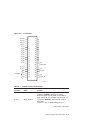
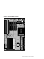
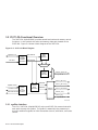
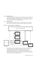
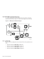
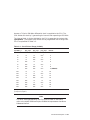
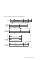
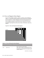
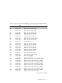
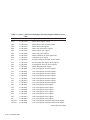
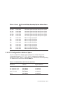
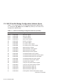
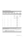
1
AlphaPC64 Evaluation Board
User’s Guide
Order Number: EC–QGY2C–TE
Revision/Update Information:
Digital Equipment Corporation
Maynard, Massachusetts
This document supersedes the AlphaPC64
Evaluation Board User’s Guide
(EC–QGY2B–TE).
July 1995
While Digital believes the information included in this document is correct as of the date of
publication, it is subject to change without notice.
Digital Equipment Corporation makes no representations that the use of its products in the
manner described in this publication will not infringe on existing or future patent rights, nor
do the descriptions contained in this publication imply granting of licenses to make, use, or sell
equipment or software in accordance with the description.
© Digital Equipment Corporation 1995.
Printed in U.S.A.
All rights reserved.
DEC, DECchip, DECladebug, OpenVMS, the AlphaGeneration design mark, and the DIGITAL
logo are trademarks of Digital Equipment Corporation.
Digital Semiconductor is a Digital Equipment Corporation business.
Digital UNIX Version 3.2 for Alpha is a UNIX 93 branded product.
ABT is a registered trademark of Applied Business Technologies, Inc.
AMD and MACH are registered trademarks of Advanced Micro Devices, Inc.
Intel is a trademark of Intel Corporation.
National is a registered trademark of National Semiconductor Corporation.
NEC is a registered trademark of NEC Corporation.
OSF/1 is a registered trademark of Open Software Foundation, Inc.
PHOENIX is a registered trademark of Phoenix Technologies, Ltd.
TriQuint is a trademark of TriQuint Semiconductor, Inc.
Windows NT is a trademark of Microsoft Corporation.
Xilinx is a trademark of Xilinx, Incorporated.
UNIX is a registered trademark in the United States and other countries licensed exclusively
through X/Open Limited.
All other trademarks and registered trademarks are the property of their respective owners.
This document was prepared using VAX DOCUMENT Version 2.1.
Contents
Preface . . . . . . . . . . . . . . . . . . . . . . . . . . . . . . . . . . . . . . . . . . . . . . . . . . . . .
xiii
1 AlphaPC64 Introduction
1.1
1.1.1
1.1.2
1.1.3
1.1.4
1.1.5
1.1.6
1.1.7
1.1.8
1.1.9
1.2
System Components and Features . . . . .
Memory Subsystem . . . . . . . . . . . . .
DECchip 21072 Support Chipset . . .
PAL Control Set . . . . . . . . . . . . . . . .
Level 2 Cache Subsystem Overview .
Clock Subsystem Overview . . . . . . .
PCI Interface Overview . . . . . . . . . .
ISA Interface Overview . . . . . . . . . .
Software Support . . . . . . . . . . . . . . .
Design Support . . . . . . . . . . . . . . . .
Evaluation Board Uses . . . . . . . . . . . . .
.
.
.
.
.
.
.
.
.
.
.
.
.
.
.
.
.
.
.
.
.
.
.
.
.
.
.
.
.
.
.
.
.
.
.
.
.
.
.
.
.
.
.
.
.
.
.
.
.
.
.
.
.
.
.
.
.
.
.
.
.
.
.
.
.
.
.
.
.
.
.
.
.
.
.
.
.
.
.
.
.
.
.
.
.
.
.
.
.
.
.
.
.
.
.
.
.
.
.
.
.
.
.
.
.
.
.
.
.
.
.
.
.
.
.
.
.
.
.
.
.
.
.
.
.
.
.
.
.
.
.
.
.
.
.
.
.
.
.
.
.
.
.
.
.
.
.
.
.
.
.
.
.
.
.
.
.
.
.
.
.
.
.
.
.
.
.
.
.
.
.
.
.
.
.
.
.
.
.
.
.
.
.
.
.
.
.
.
.
.
.
.
.
.
.
.
.
.
.
.
.
.
.
.
.
.
.
.
.
1–1
1–2
1–2
1–2
1–4
1–4
1–4
1–4
1–5
1–6
1–6
2 System Jumpers and Connectors
2.1
2.1.1
2.1.2
2.2
Configuration Jumpers . . . . . . . . . . . .
Software Configuration Jumpers .
Hardware Configuration Jumpers
AlphaPC64 Board Connectors . . . . . .
.
.
.
.
.
.
.
.
.
.
.
.
.
.
.
.
.
.
.
.
.
.
.
.
.
.
.
.
.
.
.
.
.
.
.
.
.
.
.
.
.
.
.
.
.
.
.
.
.
.
.
.
.
.
.
.
.
.
.
.
.
.
.
.
.
.
.
.
.
.
.
.
.
.
.
.
.
.
.
.
.
.
.
.
2–1
2–1
2–5
2–6
.
.
.
.
.
.
.
.
.
.
.
.
.
.
.
.
.
.
.
.
.
.
.
.
.
.
.
.
.
.
.
.
.
.
.
.
.
.
.
.
.
.
.
.
.
.
.
.
.
.
.
.
.
.
.
.
.
.
.
.
.
.
.
.
.
.
.
.
.
.
.
.
.
.
.
.
.
.
.
.
.
.
.
.
.
.
.
.
.
.
.
.
.
.
.
.
.
.
.
.
.
.
.
.
.
3–1
3–2
3–4
3–7
3–8
3 Functional Description
3.1
3.1.1
3.1.2
3.1.3
3.2
Chipset Introduction . . . . . . . .
21071-CA Introduction . . . .
21071-DA Introduction . . . .
21071-BA Introduction . . . .
21071-CA Functional Overview
.
.
.
.
.
.
.
.
.
.
.
.
.
.
.
.
.
.
.
.
.
.
.
.
.
iii
3.2.1
sysBus Interface . . . . . . . . . . . . . . . . . . . . . . .
3.2.1.1
sysBus Arbitration . . . . . . . . . . . . . . . . . .
3.2.1.2
L2 Cache Control . . . . . . . . . . . . . . . . . . .
3.2.1.3
sysBus Control . . . . . . . . . . . . . . . . . . . . .
3.2.1.4
Address Decoding . . . . . . . . . . . . . . . . . . .
3.2.1.5
Error Handling . . . . . . . . . . . . . . . . . . . .
3.2.2
Memory Controller . . . . . . . . . . . . . . . . . . . . .
3.2.2.1
Memory Organization . . . . . . . . . . . . . . .
3.2.2.2
Memory Address Generation . . . . . . . . . .
3.2.2.3
Memory Page Mode Support . . . . . . . . . .
3.2.2.4
Read Latency Minimization . . . . . . . . . . .
3.2.2.5
Transaction Scheduler . . . . . . . . . . . . . . .
3.2.2.6
Programmable Memory Timing . . . . . . . .
3.2.2.7
Presence Detect Logic . . . . . . . . . . . . . . .
3.3
21071-DA Functional Overview . . . . . . . . . . . . . .
3.3.1
sysBus Interface . . . . . . . . . . . . . . . . . . . . . . .
3.3.1.1
Address Decode . . . . . . . . . . . . . . . . . . . .
3.3.1.2
I/O Write Transaction Buffering . . . . . . . .
3.3.1.3
I/O Read Data Buffering . . . . . . . . . . . . .
3.3.1.4
Wrapping Mode . . . . . . . . . . . . . . . . . . . .
3.3.2
PCI Interface . . . . . . . . . . . . . . . . . . . . . . . . .
3.3.2.1
DMA Address Translation . . . . . . . . . . . .
3.3.2.2
DMA Write Buffer . . . . . . . . . . . . . . . . . .
3.3.2.3
DMA Read Buffer . . . . . . . . . . . . . . . . . .
3.3.2.4
PCI Burst Length and Prefetching . . . . . .
3.3.2.5
PCI Burst Order . . . . . . . . . . . . . . . . . . .
3.3.2.6
PCI Parity Support . . . . . . . . . . . . . . . . .
3.3.2.7
PCI Exclusive Access . . . . . . . . . . . . . . . .
3.3.2.8
PCI Bus Parking . . . . . . . . . . . . . . . . . . .
3.3.2.9
PCI Retry Timeout . . . . . . . . . . . . . . . . . .
3.3.2.10
PCI Master Timeout . . . . . . . . . . . . . . . .
3.3.2.11
Address Stepping in Configuration Cycles
3.3.2.12
Data Coherency . . . . . . . . . . . . . . . . . . . .
3.3.2.13
Deadlock Resolution . . . . . . . . . . . . . . . . .
3.3.2.14
Guaranteed Access-Time Mode . . . . . . . .
3.3.2.15
Interrupts . . . . . . . . . . . . . . . . . . . . . . . .
3.4
21071-BA Functional Overview . . . . . . . . . . . . . .
3.4.1
sysData Bus . . . . . . . . . . . . . . . . . . . . . . . . . .
3.4.2
memData Bus . . . . . . . . . . . . . . . . . . . . . . . .
3.4.3
epiData Bus . . . . . . . . . . . . . . . . . . . . . . . . . .
3.4.4
Memory Read Buffer . . . . . . . . . . . . . . . . . . .
3.4.5
I/O Read Buffer and Merge Buffer . . . . . . . . .
3.4.6
I/O Write Buffer and DMA Read Buffer . . . . .
iv
.
.
.
.
.
.
.
.
.
.
.
.
.
.
.
.
.
.
.
.
.
.
.
.
.
.
.
.
.
.
.
.
.
.
.
.
.
.
.
.
.
.
.
.
.
.
.
.
.
.
.
.
.
.
.
.
.
.
.
.
.
.
.
.
.
.
.
.
.
.
.
.
.
.
.
.
.
.
.
.
.
.
.
.
.
.
.
.
.
.
.
.
.
.
.
.
.
.
.
.
.
.
.
.
.
.
.
.
.
.
.
.
.
.
.
.
.
.
.
.
.
.
.
.
.
.
.
.
.
.
.
.
.
.
.
.
.
.
.
.
.
.
.
.
.
.
.
.
.
.
.
.
.
.
.
.
.
.
.
.
.
.
.
.
.
.
.
.
.
.
.
.
.
.
.
.
.
.
.
.
.
.
.
.
.
.
.
.
.
.
.
.
.
.
.
.
.
.
.
.
.
.
.
.
.
.
.
.
.
.
.
.
.
.
.
.
.
.
.
.
.
.
.
.
.
.
.
.
.
.
.
.
.
.
.
.
.
.
.
.
.
.
.
.
.
.
.
.
.
.
.
.
.
.
.
.
.
.
.
.
.
.
.
.
.
.
.
.
.
.
.
.
.
.
.
.
.
.
.
.
.
.
.
.
.
.
.
.
.
.
.
.
.
.
.
.
.
.
.
.
.
.
.
.
.
.
.
.
.
.
.
.
.
.
.
.
.
.
.
.
.
.
.
.
.
.
.
.
.
.
.
.
.
.
.
.
.
.
.
.
.
.
.
.
.
.
.
.
.
.
.
.
.
.
.
.
.
.
.
.
.
.
.
.
.
.
.
.
.
.
.
.
.
.
.
.
.
.
.
.
.
.
.
.
.
.
.
.
.
.
.
.
.
.
.
.
.
.
.
.
.
.
.
.
.
.
.
.
.
.
.
.
.
.
.
.
.
.
.
.
.
.
.
.
.
.
.
.
.
.
.
.
.
.
.
.
.
.
.
.
.
.
.
.
.
.
.
.
.
.
.
.
.
.
.
.
.
.
.
.
.
.
.
.
.
.
.
.
.
.
.
.
.
.
.
.
.
.
.
.
.
.
.
.
.
.
.
.
.
.
.
.
.
.
.
.
.
.
.
.
.
.
.
.
.
.
.
.
.
.
.
.
.
.
.
.
3–8
3–9
3–9
3–10
3–10
3–10
3–11
3–11
3–11
3–11
3–11
3–12
3–12
3–12
3–13
3–14
3–14
3–14
3–14
3–14
3–14
3–14
3–15
3–15
3–15
3–16
3–16
3–16
3–16
3–17
3–17
3–17
3–17
3–18
3–19
3–19
3–20
3–20
3–21
3–21
3–21
3–21
3–21
3.4.7
3.4.8
3.4.9
3.4.10
3.4.11
3.5
3.6
3.6.1
3.6.2
3.7
3.7.1
3.7.2
3.8
3.8.1
3.8.2
3.8.3
3.9
3.9.1
3.9.2
3.9.3
3.9.4
3.9.5
3.10
3.11
3.12
3.13
3.13.1
3.13.2
3.13.3
DMA Write Buffer . . . . . . . . . . .
Memory Write Buffer . . . . . . . . .
Error Checking . . . . . . . . . . . . .
epiBus Data Path . . . . . . . . . . . .
sysBus Output Selectors . . . . . .
Error Handling . . . . . . . . . . . . . . . .
Clock Subsystem . . . . . . . . . . . . . . .
TriQuint PLL Clock Oscillator . .
System Clock Distribution . . . . .
PCI Interrupts and Arbitration . . . .
System Interrupts . . . . . . . . . . .
PCI/ISA Arbitration . . . . . . . . . .
PCI Devices . . . . . . . . . . . . . . . . . . .
Intel Saturn IO Chip . . . . . . . . .
PCI Expansion Slots . . . . . . . . .
PCI Graphics Interface . . . . . . .
ISA Devices . . . . . . . . . . . . . . . . . . .
Keyboard and Mouse Controller .
Combination Controller . . . . . . .
Time-of-Year Clock . . . . . . . . . . .
Utility Bus Memory Devices . . .
ISA Expansion Slots . . . . . . . . .
Serial ROM . . . . . . . . . . . . . . . . . . .
dc Power Distribution . . . . . . . . . . .
Reset and Initialization . . . . . . . . . .
System Software . . . . . . . . . . . . . . .
Serial ROM Code . . . . . . . . . . . .
Flash ROM Code . . . . . . . . . . . .
Operating Systems . . . . . . . . . . .
.
.
.
.
.
.
.
.
.
.
.
.
.
.
.
.
.
.
.
.
.
.
.
.
.
.
.
.
.
.
.
.
.
.
.
.
.
.
.
.
.
.
.
.
.
.
.
.
.
.
.
.
.
.
.
.
.
.
.
.
.
.
.
.
.
.
.
.
.
.
.
.
.
.
.
.
.
.
.
.
.
.
.
.
.
.
.
.
.
.
.
.
.
.
.
.
.
.
.
.
.
.
.
.
.
.
.
.
.
.
.
.
.
.
.
.
.
.
.
.
.
.
.
.
.
.
.
.
.
.
.
.
.
.
.
.
.
.
.
.
.
.
.
.
.
.
.
.
.
.
.
.
.
.
.
.
.
.
.
.
.
.
.
.
.
.
.
.
.
.
.
.
.
.
.
.
.
.
.
.
.
.
.
.
.
.
.
.
.
.
.
.
.
.
.
.
.
.
.
.
.
.
.
.
.
.
.
.
.
.
.
.
.
.
.
.
.
.
.
.
.
.
.
.
.
.
.
.
.
.
.
.
.
.
.
.
.
.
.
.
.
.
.
.
.
.
.
.
.
.
.
.
.
.
.
.
.
.
.
.
.
.
.
.
.
.
.
.
.
.
.
.
.
.
.
.
.
.
.
.
.
.
.
.
.
.
.
.
.
.
.
.
.
.
.
.
.
.
.
.
.
.
.
.
.
.
.
.
.
.
.
.
.
.
.
.
.
.
.
.
.
.
.
.
.
.
.
.
.
.
.
.
.
.
.
.
.
.
.
.
.
.
.
.
.
.
.
.
.
.
.
.
.
.
.
.
.
.
.
.
.
.
.
.
.
.
.
.
.
.
.
.
.
.
.
.
.
.
.
.
.
.
.
.
.
.
.
.
.
.
.
.
.
.
.
.
.
.
.
.
.
.
.
.
.
.
.
.
.
.
.
.
.
.
.
.
.
.
.
.
.
.
.
.
.
.
.
.
.
.
.
.
.
.
.
.
.
.
.
.
.
.
.
.
.
.
.
.
.
.
.
.
.
.
.
.
.
.
.
.
.
.
.
.
.
.
.
.
.
.
.
.
.
.
.
.
.
.
.
.
.
.
.
.
.
.
.
.
.
.
.
.
.
.
.
.
.
.
.
.
.
.
.
.
.
.
.
.
.
.
.
.
.
.
.
.
.
.
.
.
.
.
.
.
.
.
.
.
.
.
.
.
.
.
.
.
.
.
.
.
.
.
.
.
.
.
.
.
.
.
.
.
.
.
.
.
.
.
.
.
.
.
.
.
.
.
.
.
.
.
.
.
.
.
.
.
.
.
.
.
.
.
.
.
.
.
.
.
.
.
.
.
.
.
.
.
.
.
.
.
.
.
.
.
.
.
.
.
.
.
.
.
.
.
.
.
.
.
.
.
.
.
.
.
.
.
.
.
.
.
.
.
.
.
.
.
.
.
3–22
3–22
3–22
3–22
3–22
3–23
3–24
3–24
3–26
3–30
3–30
3–33
3–34
3–34
3–34
3–34
3–35
3–35
3–36
3–37
3–37
3–38
3–38
3–39
3–41
3–41
3–41
3–43
3–43
...
...
4–1
4–4
...
4–4
...
4–5
...
4–7
...
...
4–8
4–9
4 System Address Mapping
4.1
4.1.1
4.1.2
4.1.3
4.1.4
4.1.5
4.1.6
CPU Address Mapping to PCI Space . . . . . . . . . . . . . . . . . . .
Cacheable Memory Space (0 0000 0000 to 0 FFFF FFFF)
Noncacheable Memory Space (1 0000 0000 to
1 7FFF FFFF) . . . . . . . . . . . . . . . . . . . . . . . . . . . . . . . . .
DECchip 21071-CA CSR Space (1 8000 0000 to
1 9FFF FFFF) . . . . . . . . . . . . . . . . . . . . . . . . . . . . . . . . .
DECchip 21071-DA CSR Space (1 A000 0000 to
1 AFFF FFFF) . . . . . . . . . . . . . . . . . . . . . . . . . . . . . . . . .
PCI Interrupt Acknowledge/Special Cycle Space
(1 B000 0000 to 1 BFFF FFFF) . . . . . . . . . . . . . . . . . . . .
PCI Sparse I/O Space (1 C000 0000 to 1 DFFF FFFF) . . .
v
4.1.7
4.1.7.1
4.1.7.2
4.1.8
4.1.9
4.2
PCI Configuration Space (1 E000 0000 to 1 FFFF FFFF) .
PCI Configuration Cycles to Primary Bus Targets . . . .
PCI Configuration Cycles to Secondary Bus Targets . .
PCI Sparse Memory Space (2 0000 0000 to
2 FFFF FFFF) . . . . . . . . . . . . . . . . . . . . . . . . . . . . . . . . . .
PCI Dense Memory Space (3 0000 0000 to 3 FFFF FFFF) .
PCI-to-Physical Memory Addressing . . . . . . . . . . . . . . . . . . . .
..
..
..
4–12
4–14
4–14
..
..
..
4–15
4–18
4–19
Power Requirements . . . . . . . . . . . . . . . . . . . . . . . . . . . . . . . . . .
Environmental Characteristics . . . . . . . . . . . . . . . . . . . . . . . . . . .
Physical Board Parameters . . . . . . . . . . . . . . . . . . . . . . . . . . . . .
5–1
5–2
5–2
5 Board Requirements and Parameters
5.1
5.2
5.3
A System Register Descriptions
A.1
DECchip 21071-CA CSR Descriptions . . . . . . . . . . . . . . . .
A.1.1
General Control Register . . . . . . . . . . . . . . . . . . . . . . .
A.1.2
Error and Diagnostic Status Register . . . . . . . . . . . . .
A.1.3
Tag Enable Register . . . . . . . . . . . . . . . . . . . . . . . . . . .
A.1.4
Error Low Address Register . . . . . . . . . . . . . . . . . . . . .
A.1.5
Error High Address Register . . . . . . . . . . . . . . . . . . . .
A.1.6
LDx_L Low Address Register . . . . . . . . . . . . . . . . . . . .
A.1.7
LDx_L High Address Register . . . . . . . . . . . . . . . . . . .
A.1.8
Memory Control Registers . . . . . . . . . . . . . . . . . . . . . .
A.1.8.1
Video Frame Pointer Register . . . . . . . . . . . . . . . .
A.1.8.2
Presence Detect Low-Data Register . . . . . . . . . . . .
A.1.8.3
Presence Detect High-Data Register . . . . . . . . . . .
A.1.8.4
Base Address Registers . . . . . . . . . . . . . . . . . . . . .
A.1.8.5
Configuration Registers . . . . . . . . . . . . . . . . . . . . .
A.1.8.6
Bank Set Timing Registers A and B . . . . . . . . . . .
A.1.8.7
Global Timing Register . . . . . . . . . . . . . . . . . . . . .
A.1.8.8
Refresh Timing Register . . . . . . . . . . . . . . . . . . . .
A.2
DECchip 21071-DA CSR Descriptions . . . . . . . . . . . . . . . .
A.2.1
Dummy Registers 1 Through 3 . . . . . . . . . . . . . . . . . .
A.2.2
Diagnostic Control and Status Register . . . . . . . . . . . .
A.2.3
sysBus Error Address Register . . . . . . . . . . . . . . . . . .
A.2.4
PCI Error Address Register . . . . . . . . . . . . . . . . . . . . .
A.2.5
Translated Base Registers 1 and 2 . . . . . . . . . . . . . . . .
A.2.6
PCI Base Registers 1 and 2 . . . . . . . . . . . . . . . . . . . . .
A.2.7
PCI Mask Registers 1 and 2 . . . . . . . . . . . . . . . . . . . .
A.2.8
Host Address Extension Register 0 . . . . . . . . . . . . . . .
A.2.9
Host Address Extension Register 1 . . . . . . . . . . . . . . .
vi
.
.
.
.
.
.
.
.
.
.
.
.
.
.
.
.
.
.
.
.
.
.
.
.
.
.
.
.
.
.
.
.
.
.
.
.
.
.
.
.
.
.
.
.
.
.
.
.
.
.
.
.
.
.
.
.
.
.
.
.
.
.
.
.
.
.
.
.
.
.
.
.
.
.
.
.
.
.
.
.
.
.
.
.
.
.
.
.
.
.
.
.
.
.
.
.
.
.
.
.
.
.
.
.
.
.
.
.
.
.
.
.
.
.
.
.
.
.
.
.
.
.
.
.
.
.
.
.
.
.
.
.
.
.
.
A–1
A–1
A–4
A–6
A–8
A–8
A–9
A–9
A–10
A–10
A–11
A–12
A–12
A–13
A–17
A–22
A–23
A–24
A–24
A–25
A–29
A–30
A–31
A–32
A–33
A–34
A–34
A.2.10
A.2.11
A.2.12
A.2.13
A.2.14
Host Address Extension Register 2 . . . . .
PCI Master Latency Timer Register . . . . .
TLB Tag Registers 0 Through 7 . . . . . . . .
TLB Data Registers 0 Through 7 . . . . . . .
Translation Buffer Invalidate All Register
.
.
.
.
.
.
.
.
.
.
.
.
.
.
.
.
.
.
.
.
.
.
.
.
.
.
.
.
.
.
.
.
.
.
.
.
.
.
.
.
.
.
.
.
.
.
.
.
.
.
.
.
.
.
.
.
.
.
.
.
.
.
.
.
.
.
.
.
.
.
.
.
.
.
.
A–35
A–36
A–37
A–38
A–38
.
.
.
.
.
.
.
.
.
.
.
.
.
.
.
.
.
.
.
.
.
.
.
.
.
.
.
.
.
.
.
.
.
.
.
.
.
.
.
.
.
.
.
.
.
.
.
.
.
.
.
.
.
.
.
.
.
.
.
.
.
.
.
.
.
.
.
.
.
.
.
.
.
.
.
.
.
.
.
.
.
.
.
.
.
.
.
.
.
.
.
.
.
.
.
.
.
.
.
.
.
.
.
.
.
.
.
.
.
.
.
.
.
.
.
.
.
.
.
.
.
.
.
.
.
.
.
.
.
.
.
.
.
.
.
.
.
.
.
.
.
.
.
.
.
.
.
.
.
.
.
.
.
.
.
.
.
.
.
.
.
.
.
.
.
.
.
.
.
.
.
.
.
.
.
.
.
.
.
.
.
.
.
.
.
.
.
.
.
.
.
.
.
.
.
B–1
B–2
B–4
B–4
B–6
B–8
B–9
B–10
B–10
B–12
B–15
B–16
B–16
PCI Interrupt Acknowledge/Special Cycle Address Space .
PCI Sparse I/O Address Space . . . . . . . . . . . . . . . . . . . . . .
SIO PCI-to-ISA Bridge Operating Register Address Space
PCI Configuration Address Space . . . . . . . . . . . . . . . . . . .
SIO PCI-to-ISA Bridge Configuration Address Space . . . . .
PCI Sparse Memory Address Space . . . . . . . . . . . . . . . . . .
PCI Dense Memory Address Space . . . . . . . . . . . . . . . . . .
PC87312 Combination Controller Register Address Space .
Utility Bus Device Address . . . . . . . . . . . . . . . . . . . . . . . .
Interrupt Control PLD Addresses . . . . . . . . . . . . . . . . . . .
8242PC Keyboard and Mouse Controller Addresses . . . . . .
Time-of-Year Clock Device Addresses . . . . . . . . . . . . . . . . .
Flash ROM . . . . . . . . . . . . . . . . . . . . . . . . . . . . . . . . . . . . .
Flash Memory Segment Select Register . . . . . . . . . . . .
Flash Memory Addresses . . . . . . . . . . . . . . . . . . . . . . .
Flash ROM Configuration Registers . . . . . . . . . . . . . . .
Flash ROM Memory Map . . . . . . . . . . . . . . . . . . . . . . .
.
.
.
.
.
.
.
.
.
.
.
.
.
.
.
.
.
.
.
.
.
.
.
.
.
.
.
.
.
.
.
.
.
.
...
...
...
...
...
...
...
...
...
...
...
...
...
...
...
...
...
C–1
C–1
C–1
C–5
C–6
C–7
C–7
C–7
C–10
C–12
C–12
C–12
C–13
C–14
C–14
C–14
C–15
B SROM Initialization
B.1
SROM Initialization . . . . . . . . . . . . . . . . . .
B.1.1
Firmware Interface . . . . . . . . . . . . . . .
B.1.2
Automatic CPU Speed Detection . . . . .
B.1.3
CPU Bus Interface Timing . . . . . . . . . .
B.1.4
L2 Cache Read and Write Calculations
B.1.5
Memory Initialization . . . . . . . . . . . . .
B.1.6
L2 Cache Initialization . . . . . . . . . . . . .
B.1.7
Flash ROM (System ROM) . . . . . . . . . .
B.1.7.1
Special Flash ROM Headers . . . . .
B.1.7.2
Flash ROM Structure . . . . . . . . . . .
B.1.7.3
Flash ROM Access . . . . . . . . . . . . .
B.1.8
Icache Flush Code . . . . . . . . . . . . . . . .
B.1.9
AlphaPC64 Configuration Jumpers . . .
.
.
.
.
.
.
.
.
.
.
.
.
.
.
.
.
.
.
.
.
.
.
.
.
.
.
C PCI Address Maps
C.1
C.2
C.3
C.4
C.5
C.6
C.7
C.8
C.9
C.10
C.11
C.12
C.13
C.13.1
C.13.2
C.13.3
C.13.4
vii
D Technical Support and Ordering Information
D.1
D.2
D.3
D.4
D.5
Technical Support . . . . . . . . . . . . . . . . . . . .
Ordering Alpha Microprocessor Sample Kits
Ordering Digital Semiconductor Products . .
Ordering Associated Literature . . . . . . . . . .
Ordering Third-Party Documentation . . . . .
.
.
.
.
.
.
.
.
.
.
.
.
.
.
.
.
.
.
.
.
.
.
.
.
.
.
.
.
.
.
.
.
.
.
.
.
.
.
.
.
.
.
.
.
.
.
.
.
.
.
.
.
.
.
.
.
.
.
.
.
.
.
.
.
.
.
.
.
.
.
.
.
.
.
.
.
.
.
.
.
D–1
D–1
D–2
D–3
D–4
AlphaPC64 Functional Block Diagram . . . . . . . . . . . . . .
AlphaPC64 Component Layout and Board Dimensions .
AlphaPC64 Board Jumpers . . . . . . . . . . . . . . . . . . . . . .
J3 Connector . . . . . . . . . . . . . . . . . . . . . . . . . . . . . . . . .
AlphaPC64 Board Connectors . . . . . . . . . . . . . . . . . . . .
Maximum and Minimum SIMM Bank Layouts . . . . . . .
Basic Cache and Memory Subsystem Address and Data
Paths . . . . . . . . . . . . . . . . . . . . . . . . . . . . . . . . . . . . . . .
Basic I/O Subsystem Address and Data Paths . . . . . . . .
21071-CA Block Diagram . . . . . . . . . . . . . . . . . . . . . . . .
Cache Subsystem for an 8MB Cache . . . . . . . . . . . . . . .
DECchip 21071-DA Block Diagram . . . . . . . . . . . . . . . .
DECchip 21071-BA Block Diagram . . . . . . . . . . . . . . . .
TriQuint Clock Generator . . . . . . . . . . . . . . . . . . . . . . .
Primary Clock Distribution Network . . . . . . . . . . . . . . .
Buffered Clock Distribution Network . . . . . . . . . . . . . . .
Interrupt Control and PCI Arbitration . . . . . . . . . . . . . .
Interrupt and Interrupt Mask Registers . . . . . . . . . . . .
ISA Devices . . . . . . . . . . . . . . . . . . . . . . . . . . . . . . . . . .
SROM Serial Port . . . . . . . . . . . . . . . . . . . . . . . . . . . . .
dc Power Distribution . . . . . . . . . . . . . . . . . . . . . . . . . .
System Reset and Initialization . . . . . . . . . . . . . . . . . . .
sysBus Address Map . . . . . . . . . . . . . . . . . . . . . . . . . . .
PCI Sparse I/O Space Address Translation . . . . . . . . . .
PCI Memory Space Address Translation . . . . . . . . . . . .
PCI Target Window Compare Scheme . . . . . . . . . . . . . .
.
.
.
.
.
.
.
.
.
.
.
.
.
.
.
.
.
.
.
.
.
.
.
.
1–3
1–7
2–2
2–3
2–7
3–3
.
.
.
.
.
.
.
.
.
.
.
.
.
.
.
.
.
.
.
.
.
.
.
.
.
.
.
.
.
.
.
.
.
.
.
.
.
.
.
.
.
.
.
.
.
.
.
.
.
.
.
.
.
.
.
.
.
.
.
.
.
.
.
.
.
.
.
.
.
.
.
.
.
.
.
.
3–4
3–5
3–8
3–9
3–13
3–20
3–24
3–27
3–29
3–31
3–33
3–35
3–39
3–40
3–42
4–2
4–10
4–16
4–21
Index
Figures
1–1
1–2
2–1
2–2
2–3
3–1
3–2
3–3
3–4
3–5
3–6
3–7
3–8
3–9
3–10
3–11
3–12
3–13
3–14
3–15
3–16
4–1
4–2
4–3
4–4
viii
4–5
4–6
5–1
A–1
A–2
A–3
A–4
A–5
A–6
A–7
A–8
A–9
A–10
A–11
A–12
A–13
A–14
A–15
A–16
A–17
A–18
A–19
A–20
A–21
A–22
A–23
A–24
A–25
A–26
A–27
A–28
A–29
B–1
B–2
B–3
SG Map Page Table Entry in Memory . . . . . . .
SG Map Translation of PCI to SysBus Address
Major Board Component Layout . . . . . . . . . . .
General Control Register . . . . . . . . . . . . . . . . .
Error and Diagnostic Status Register . . . . . . .
Tag Enable Register . . . . . . . . . . . . . . . . . . . . .
Error Low Address Register . . . . . . . . . . . . . . .
Error High Address Register . . . . . . . . . . . . . .
LDx_L Low Address Register . . . . . . . . . . . . . .
LDx_L High Address Register . . . . . . . . . . . . .
Video Frame Pointer Register . . . . . . . . . . . . .
Presence Detect Low-Data Register . . . . . . . . .
Presence Detect High-Data Register . . . . . . . .
Bank Set 0 Base Address Register . . . . . . . . . .
Bank Set 0 to 7 Configuration Register . . . . . .
Bank Set 8 Configuration Register . . . . . . . . . .
Bank Set Timing Register A . . . . . . . . . . . . . .
Bank Set Timing Register B . . . . . . . . . . . . . .
Global Timing Register . . . . . . . . . . . . . . . . . .
Refresh Timing Register . . . . . . . . . . . . . . . . .
Diagnostic Control and Status Register . . . . . .
sysBus Error Address Register . . . . . . . . . . . .
PCI Error Address Register . . . . . . . . . . . . . . .
Translated Base Registers 1 and 2 . . . . . . . . . .
PCI Base Registers 1 and 2 . . . . . . . . . . . . . . .
PCI Mask Registers 1 and 2 . . . . . . . . . . . . . .
Host Address Extension Register 0 . . . . . . . . .
Host Address Extension Register 1 . . . . . . . . .
Host Address Extension Register 2 . . . . . . . . .
PCI Master Latency Timer Register . . . . . . . . .
TLB Tag Registers 0 Through 7 . . . . . . . . . . . .
TLB Data Registers 0 Through 7 . . . . . . . . . . .
Write Cycle Timing . . . . . . . . . . . . . . . . . . . . .
Special Header Content . . . . . . . . . . . . . . . . . .
J3 Connector (Repeated) . . . . . . . . . . . . . . . . .
.
.
.
.
.
.
.
.
.
.
.
.
.
.
.
.
.
.
.
.
.
.
.
.
.
.
.
.
.
.
.
.
.
.
.
.
.
.
.
.
.
.
.
.
.
.
.
.
.
.
.
.
.
.
.
.
.
.
.
.
.
.
.
.
.
.
.
.
.
.
.
.
.
.
.
.
.
.
.
.
.
.
.
.
.
.
.
.
.
.
.
.
.
.
.
.
.
.
.
.
.
.
.
.
.
.
.
.
.
.
.
.
.
.
.
.
.
.
.
.
.
.
.
.
.
.
.
.
.
.
.
.
.
.
.
.
.
.
.
.
.
.
.
.
.
.
.
.
.
.
.
.
.
.
.
.
.
.
.
.
.
.
.
.
.
.
.
.
.
.
.
.
.
.
.
.
.
.
.
.
.
.
.
.
.
.
.
.
.
.
.
.
.
.
.
.
.
.
.
.
.
.
.
.
.
.
.
.
.
.
.
.
.
.
.
.
.
.
.
.
.
.
.
.
.
.
.
.
.
.
.
.
.
.
.
.
.
.
.
.
.
.
.
.
.
.
.
.
.
.
.
.
.
.
.
.
.
.
.
.
.
.
.
.
.
.
.
.
.
.
.
.
.
.
.
.
.
.
.
.
.
.
.
.
.
.
.
.
.
.
.
.
.
.
.
.
.
.
.
.
.
.
.
.
.
.
.
.
.
.
.
.
.
.
.
.
.
.
.
.
.
.
.
.
.
.
.
.
.
.
.
.
.
.
.
.
.
.
.
.
.
.
.
.
.
.
.
.
.
.
.
.
.
.
.
.
.
.
.
.
.
.
.
.
.
.
.
.
.
.
.
.
.
.
.
.
.
.
.
.
.
.
.
.
.
4–23
4–25
5–3
A–2
A–4
A–6
A–8
A–9
A–9
A–9
A–10
A–11
A–12
A–12
A–14
A–16
A–18
A–20
A–22
A–23
A–25
A–29
A–30
A–31
A–32
A–33
A–34
A–34
A–35
A–36
A–37
A–38
B–7
B–10
B–17
ix
Tables
1
2
3
4
1–1
2–1
2–2
2–3
3–1
3–2
3–3
3–4
3–5
3–6
4–1
4–2
4–3
4–4
4–5
4–6
4–7
4–8
4–9
4–10
5–1
5–2
A–1
A–2
A–3
A–4
A–5
A–6
A–7
A–8
x
Register Field Type Notation . . . . . . . . . . . . . . . . . . . .
Unnamed Register Field Notation . . . . . . . . . . . . . . . .
Data Units . . . . . . . . . . . . . . . . . . . . . . . . . . . . . . . . . .
Signal References . . . . . . . . . . . . . . . . . . . . . . . . . . . . .
L2 Cache SIMM Sizes . . . . . . . . . . . . . . . . . . . . . . . . .
Jumper Position Descriptions . . . . . . . . . . . . . . . . . . . .
AlphaPC64 Board Jumpers . . . . . . . . . . . . . . . . . . . . .
Module Connector Descriptions . . . . . . . . . . . . . . . . . .
TriQuint Operating Frequencies . . . . . . . . . . . . . . . . .
Clock Divisor Range (21064A) . . . . . . . . . . . . . . . . . . .
Distribution of 66-MHz Clock Signals . . . . . . . . . . . . .
Distribution of 33-MHz Shifted Clock Signals . . . . . . .
Distribution of 33-MHz Clock Signals . . . . . . . . . . . . .
CPU Interrupt Assignment . . . . . . . . . . . . . . . . . . . . .
sysBus Address Space Description . . . . . . . . . . . . . . . .
DECchip 21071-CA CSR Register Addresses . . . . . . . .
DECchip 21071-DA CSR Register Addresses . . . . . . . .
PCI Sparse I/O Space Byte Enable Generation . . . . . .
PCI Configuration Space Definition . . . . . . . . . . . . . . .
PCI Address Decoding for Primary Bus Configuration
Accesses . . . . . . . . . . . . . . . . . . . . . . . . . . . . . . . . . . . .
PCI Sparse Memory Space Byte Enable Generation . .
PCI Target Window Enables . . . . . . . . . . . . . . . . . . . .
PCI Target Address Translation—Direct Mapped . . . .
Scatter-Gather Map Address . . . . . . . . . . . . . . . . . . . .
Power Supply dc Current Requirements (275 MHz) . . .
Major Board Component Descriptions . . . . . . . . . . . . .
General Control Register . . . . . . . . . . . . . . . . . . . . . . .
Error and Diagnostic Status Register . . . . . . . . . . . . .
Cache Size Tag Enable Values . . . . . . . . . . . . . . . . . . .
Maximum Memory Tag Enable Values . . . . . . . . . . . . .
Video Frame Pointer Register . . . . . . . . . . . . . . . . . . .
Bank Set 0 to 7 Configuration Register . . . . . . . . . . . .
Bank Set 8 Configuration Register . . . . . . . . . . . . . . . .
Bank Set Timing Register A . . . . . . . . . . . . . . . . . . . .
.
.
.
.
.
.
.
.
.
.
.
.
.
.
.
.
.
.
.
.
.
.
.
.
.
.
.
.
.
.
.
.
.
.
.
.
.
.
.
.
.
.
.
.
.
.
.
.
.
.
.
.
.
.
.
.
.
.
.
.
.
.
.
.
.
.
.
.
.
.
.
.
.
.
.
.
.
.
.
.
.
.
.
.
.
.
.
.
.
.
.
.
.
.
.
xvi
xvii
xvii
xviii
1–4
2–3
2–5
2–8
3–24
3–25
3–28
3–28
3–29
3–30
4–3
4–5
4–7
4–11
4–12
.
.
.
.
.
.
.
.
.
.
.
.
.
.
.
.
.
.
.
.
.
.
.
.
.
.
.
.
.
.
.
.
.
.
.
.
.
.
.
.
.
.
.
.
.
.
.
.
.
.
.
.
.
.
.
.
.
.
.
.
.
.
.
.
.
.
.
.
.
.
.
.
.
.
.
4–13
4–17
4–20
4–22
4–24
5–1
5–4
A–2
A–4
A–7
A–7
A–10
A–14
A–16
A–18
A–9
A–10
A–11
A–12
A–13
A–14
A–15
A–16
A–17
A–18
A–19
A–20
A–21
A–22
A–23
B–1
B–2
B–3
B–4
B–5
B–6
B–7
B–8
C–1
C–2
C–3
C–4
C–5
C–6
C–7
C–8
C–9
C–10
C–11
Bank Set Timing Register B . . . . . . . . . . . . . . . . . . . . . . .
Global Timing Register . . . . . . . . . . . . . . . . . . . . . . . . . . .
Refresh Timing Register . . . . . . . . . . . . . . . . . . . . . . . . . .
Diagnostic Control and Status Register . . . . . . . . . . . . . . .
Diagnostic Control and Status Register Field
D_BYP<1:0> . . . . . . . . . . . . . . . . . . . . . . . . . . . . . . . . . . .
sysBus Error Address Register . . . . . . . . . . . . . . . . . . . . .
PCI Error Address Register . . . . . . . . . . . . . . . . . . . . . . . .
Translated Base Registers 1 and 2 . . . . . . . . . . . . . . . . . . .
PCI Base Registers 1 and 2 . . . . . . . . . . . . . . . . . . . . . . . .
PCI Mask Registers 1 and 2 . . . . . . . . . . . . . . . . . . . . . . .
Host Address Extension Register 1 . . . . . . . . . . . . . . . . . .
Host Address Extension Register 2 . . . . . . . . . . . . . . . . . .
PCI Master Latency Timer Register . . . . . . . . . . . . . . . . . .
TLB Tag Registers 0 Through 7 . . . . . . . . . . . . . . . . . . . . .
TLB Data Registers 0 Through 7 . . . . . . . . . . . . . . . . . . . .
Output Parameter Descriptions . . . . . . . . . . . . . . . . . . . . .
Cache Loop Delay Characteristics . . . . . . . . . . . . . . . . . . .
SRAM Timing Specification Definitions . . . . . . . . . . . . . . .
Worst-Case SRAM Timing Specifications . . . . . . . . . . . . . .
CPU Specifications . . . . . . . . . . . . . . . . . . . . . . . . . . . . . . .
Special Header Entry Descriptions . . . . . . . . . . . . . . . . . .
Higher 512KB Flash ROM Image Selection . . . . . . . . . . . .
Jumper Position Descriptions (Repeated) . . . . . . . . . . . . .
SIO PCI-to-ISA Bridge Operating Register Address Space
Map . . . . . . . . . . . . . . . . . . . . . . . . . . . . . . . . . . . . . . . . . .
Address Bits and PCI Device idsel Pins . . . . . . . . . . . . . . .
SIO PCI-to-ISA Bridge Configuration Address Space Map .
PC87312 Combination Controller Register Address Space
Map . . . . . . . . . . . . . . . . . . . . . . . . . . . . . . . . . . . . . . . . . .
Integrated Device Electronics (IDE) Register Addresses . .
Utility Bus Device Decode . . . . . . . . . . . . . . . . . . . . . . . . .
Interrupt Control PLD Addresses . . . . . . . . . . . . . . . . . . .
Keyboard and Mouse Controller Addresses . . . . . . . . . . . .
Time-of-Year Clock Device Addresses . . . . . . . . . . . . . . . . .
Flash Memory Segment Select Register . . . . . . . . . . . . . . .
Flash Memory Addresses (Within Segment) . . . . . . . . . . . .
.
.
.
.
.
.
.
.
A–21
A–22
A–23
A–26
.
.
.
.
.
.
.
.
.
.
.
.
.
.
.
.
.
.
.
.
.
.
.
.
.
.
.
.
.
.
.
.
.
.
.
.
.
.
A–28
A–29
A–30
A–31
A–32
A–33
A–34
A–35
A–36
A–37
A–38
B–2
B–5
B–5
B–6
B–6
B–11
B–13
B–17
..
..
..
C–1
C–5
C–6
.
.
.
.
.
.
.
.
.
.
.
.
.
.
.
.
C–8
C–10
C–11
C–12
C–12
C–13
C–14
C–14
xi
C–12
C–13
xii
Flash ROM Configuration Registers . . . . . . . . . . . . . . . . . . . .
Memory Map of Flash Memory . . . . . . . . . . . . . . . . . . . . . . .
C–15
C–16
Preface
This guide describes the AlphaPC64 Evaluation Board. The board is an
evaluation and development module for computing systems based on the
Alpha 21064A microprocessor.
Audience
This guide is written for system designers and others who use the AlphaPC64
to design or evaluate computer systems based on the Alpha 21064A
microprocessor.
Scope
This guide describes the features, configuration, functional operation, and
interfaces of the AlphaPC64. Additional information is available in the
AlphaPC64 schematics and program source files. Appendix D provides a list of
related documentation and technical support information.
Document Content
This guide contains the following chapters and appendixes:
•
Chapter 1, AlphaPC64 Introduction, introduces the AlphaPC64, including
its components, uses, and features.
•
Chapter 2, System Jumpers and Connectors, describes the user
environment configuration, board connectors and functions, jumper
functions and logic states; and identifies jumper and connector locations.
•
Chapter 3, Functional Description, provides a functional description of
the board, including the DECchip 21072 chipset, Level 2 (L2) cache and
memory subsystems, systems interrupts, clock and power subsystems, and
PCI and ISA devices.
•
Chapter 4, System Address Mapping, describes the mapping of the 34-bit
processor address space into memory and I/O space addresses.
xiii
•
Chapter 5, Board Requirements and Parameters, describes the board power
and environmental requirements, and identifies major board components.
•
Appendix A, System Register Descriptions, describes the control and status
registers of the DECchip 21071-CA and DECchip 21071-DA.
•
Appendix B, SROM Initialization, describes the general SROM, Level 2
(L2) cache, and memory initialization steps and associated parameters.
It also includes information about the firmware interface, timing
considerations, SROM header, and configuration jumpers.
•
Appendix C, PCI Address Maps, provides the AlphaPC64 operating register
address space maps.
•
Appendix D, Technical Support and Ordering Information, describes how
to obtain information and technical support, and how to order Digital
Semiconductor products and associated literature.
Document Conventions
This section describes the abbreviation and notation conventions used
throughout this guide.
Numbering
All numbers are decimal or hexadecimal unless otherwise specified. In cases
of ambiguity, a subscript indicates the radix of nondecimal numbers. For
example, 19 is decimal, but 1916 and 19A are hexadecimal.
UNPREDICTABLE and UNDEFINED Definitions
Results specified as UNPREDICTABLE may vary from moment to moment,
implementation to implementation, and instruction to instruction within
implementations. Software can never depend on results specified as
UNPREDICTABLE.
Operations specified as UNDEFINED may vary from moment to moment,
implementation to implementation, and instruction to instruction within
implementations. The operation may vary from nothing to stopping system
operation. UNDEFINED operations must not cause the processor to hang, that
is, reach a state from which there is no transition to a normal state where the
machine can execute instructions.
Note the distinction between results and operations. Nonprivileged software
cannot invoke UNDEFINED operations.
xiv
Ranges and Extents
Ranges are specified by a pair of numbers separated by two periods (..) and are
inclusive. For example, a range of integers 0..4 includes the integers 0, 1, 2, 3,
and 4.
Extents are specified by a pair of numbers in angle brackets (<>) separated
by a colon ( : ) and are inclusive. For example, bits <7:3> specifies an extent
including bits 7, 6, 5, 4, and 3.
Address Radix
All memory addresses, register addresses, and address offset values are in
hexadecimal notation unless specified otherwise.
Memory and Register Contents Radix
All data associated with read and write transactions to and from memory
locations and registers are in hexadecimal notation unless specified otherwise.
Must Be Zero
Fields specified as must be zero (MBZ) must never be filled by software with a
nonzero value. If the processor encounters a nonzero value in a field specified
as MBZ, a reserved operand exception occurs.
Should Be Zero
Fields specified as should be zero (SBZ) should be filled by software with a zero
value. These fields may be used at some future time. Nonzero values in SBZ
fields produce UNPREDICTABLE results.
Register and Memory Figures
Register figures have bit and field position numbering starting at the right
(low-order) and increasing to the left (high-order).
Memory figures have addresses starting at the top and increasing toward the
bottom.
xv
Register Field Notation
Register figures and tabulated descriptions have a mnemonic that indicates the
bit or field as described in Table 1.
Table 1 Register Field Type Notation
xvi
Notation
Description
RW
A read/write bit or field. The value may be read and written by
software, microcode, or hardware.
RO
A read-only bit or field. The value may be read by software, microcode,
or hardware. It is written by hardware; software or microcode write
transactions are ignored.
WO
A write-only bit or field. The value may be written by software and
microcode. It is read by hardware. Read transactions by software or
microcode return an UNPREDICTABLE result.
WZ
A write-only bit or field. The value may be written by software or
microcode. It is read by hardware, and read transactions by software or
microcode return a zero.
WC
A write-to-clear bit or field. The value may be read by software or
microcode. Software or microcode write transactions of a 1 cause the bit
to be cleared by hardware. Software or microcode write transactions of
a 0 do not modify the state of the bit.
RC
A read-to-clear bit or field. The value is written by hardware and
remains unchanged until read. The value may be read by software or
microcode, at which point hardware may write a new value into the
field.
RW1C
A read/write one-to-clear bit or field. The value may be read. Software,
microcode, or hardware writes a 1 to clear the bit or field.
Other register fields that are unnamed may be labeled as specified in Table 2.
Table 2 Unnamed Register Field Notation
Notation
Description
0
A 0 in a bit position indicates a register bit that is read as a 0 and is
ignored on a write transaction.
1
A 1 in a bit position indicates a register bit that is read as a 1 and is
ignored on a write transaction.
x
An x in a bit position indicates a register bit that does not exist in
hardware. The value is UNPREDICTABLE when read, and is ignored
on a write transaction.
Bit Notation
Multiple bit fields are shown as extents (see Ranges and Extents).
Cautions
Cautions indicate potential damage to equipment or data.
Data Units
Table 3 defines the data unit terminology used in this guide.
Table 3 Data Units
Term
Words
Bytes
Bits
Other
Word
1
2
16
—
Longword
2
4
32
—
Quadword
4
8
64
—
Octaword
8
16
128
Single read fill; that is, the cache space
that can be filled in a single read access.
It takes two read accesses to fill one L2
cache line (see Hexword).
Hexword
16
32
256
Cache block, cache line. The space
allocated to a single cache block.
xvii
Schematic References
Logic schematics are included in the AlphaPC64 design package. In this guide,
references to schematic pages are printed in italics. For example, the following
specifies schematic page 3:
‘‘. . . the 300-MHz oscillator (AlphaPC64.3) supplies . . .’’
In some cases, more than one schematic page is referenced. For example, the
following specifies schematic pages 17 through 20:
‘‘. . . the DRAM buffers (AlphaPC64.17–20) . . .’’
Signal Names
Signal names in text are printed in boldface lowercase type. As Table 4 shows,
mixed-case and uppercase signal naming conventions are ignored.
Table 4 Signal References
This Guide
Other Documentation
cwmask7
cWMask7, CWMASK7
In addition, where a group of signals are referenced, the signal names are
combined. For example, the following would be combined as b0_l<2:0>_we_l:
b0_l0_we_l
b0_l1_we_l
b0_l2_we_l
xviii
1
AlphaPC64 Introduction
The AlphaPC64 Evaluation Board (AlphaPC64) is an evaluation and
development module for computing systems based on the Alpha 21064A
microprocessor.
The AlphaPC64 provides a single-board hardware and software development
platform for the design, integration, and analysis of supporting logic and
subsystems. The board also provides a platform for peripheral component
interconnect (PCI) I/O device hardware and software development.
Note
If you are not familiar with the 21064A, please read the following
system and memory/cache design application notes:
•
Designing a System with the DECchip 21064 Microprocessor: An
Application Note
•
Designing a Memory/Cache Subsystem for the DECchip 21064
Microprocessor: An Application Note
Appendix D provides ordering information and a list of related
documentation.
1.1 System Components and Features
The AlphaPC64 is implemented in industry-standard parts and uses a 21064A
CPU running at 150 MHz to 275 MHz. The functional components are shown
in Figure 1–1 and are introduced in the following subsections.
AlphaPC64 Introduction 1–1
1.1.1 Memory Subsystem
The DRAM memory can provide 16MB to 512MB with a 128-bit data bus. The
memory is contained in two banks of four commodity single inline memory
modules (SIMMs). Each SIMM is 36 bits wide, with 32 data bits, 1 parity bit,
and 3 unused bits with 70-ns or less access. The following SIMM sizes are
supported:
1M x 36
2M x 36
4M x 36
8M x 36
16M x 36
1.1.2 DECchip 21072 Support Chipset
The 21064A is supported by a DECchip 21072 ASIC chipset (21072), with a
128-bit memory interface. The chipset consists of the following three chips:
•
DECchip 21071-CA (21071-CA) provides the interface from the CPU to
cache and main memory, and includes the cache and memory controller.
•
DECchip 21071-BA (21071-BA) provides a 32-bit data path from the CPU
to memory and I/O. Four chips provide the 128-bit interface.
•
DECchip 21071-DA (21071-DA) provides an interface from the CPU to the
PCI.
The chipset includes the majority of functions required to develop a highperformance PC or workstation, requiring minimum discrete logic on the
module. It provides flexible and generic functions to allow its use in a wide
range of systems.
1.1.3 PAL Control Set
The AlphaPC64 contains a 4-PAL control set and includes the following:
•
Two 16V8-5 PALs provide L2 cache output-enable and write-enable
functions.
•
One 22V10-25 PAL provides interrupt address decode functions and utility
bus (Ubus) control.
•
One MACH210-20 PAL provides the PCI and ISA interrupts.
1–2 AlphaPC64 Introduction
Figure 1–1 AlphaPC64 Functional Block Diagram
21064A Support
L2 Cache Interface
- L2 Cache PALs
- TriQuint PLL
Clock
- External Clock
Oscillator
- Serial Boot ROM
- Power Supply
- Supervisor
- System Clocking
L2 Cache
Control
L2 Cache SIMMs
buff_
address
- Address Buffers
Alpha 21064A
Microprocessor
Address
Running at
200 MHz to
275 MHz
- 512KB
oe and we
- 2MB
- 8MB
tag_adr
- Longword Parity
data<127:0>
21072 Chipset
Check Bits<21, 14, 7, 0>
Address
data<15:0>
PCI Devices *
PCI
Bus
DECchip 21071-DA
DECchip 21071-CA
DECchip 21071-BA
- PCI Bridge
- Cache/Memory
Control
- 208-Pin Package
- 128-Bit Data Path
- 208-Pin Package
- Requires Four
DECchip
21071-BA Chips
PCI Arbitration
ISA Interface
*Three PCI Expansion Slots with
One Shared Expansion Slot
ISA Bus
ISA Expansion
- 2 or 3 Expansion
Slots
- National 87312
- Intel 8242 Mouse
and Keyboard
- System Support
- IDE
Memory
Control
Address
Memory
data<127:0>
Memory Buffering
ABT162244
Buffers
Memory SIMMs
- 128-Bit Data Path
b_addr
- Longword Parity
b_mctl
- 16MB to 512MB
- 2 Banks
LJ04129A.AI5
AlphaPC64 Introduction 1–3
1.1.4 Level 2 Cache Subsystem Overview
The external Level 2 (L2) cache subsystem supports 512KB, 1MB, 2MB, 4MB,
or 8MB cache sizes by using a 128-bit data bus. The L2 cache size can be
reconfigured through onboard hardware and software jumpers.
The AlphaPC64 supports the L2 cache SIMM sizes shown in Table 1–1. Two
SIMMs are required per system. The AlphaPC64 comes with a 2MB, 12-ns L2
cache.
Table 1–1 L2 Cache SIMM Sizes
L2 Cache Size
Static RAM (SRAM) Access Times
512KB
6 ns, 8 ns, 10 ns, 12 ns, 15 ns
1
6 ns, 8 ns, 10 ns, 12 ns, 15 ns
1
6 ns, 8 ns, 10 ns, 12 ns, 15 ns
1MB , 2MB
4MB , 8MB
1 Cache
size can be reduced with jumpers.
1.1.5 Clock Subsystem Overview
The clock subsystem provides clocks to the 21072 chipset and PCI devices. Two
oscillators provide clocks for the ISA and combination chip functions.
1.1.6 PCI Interface Overview
The PCI interface provides a selectable PCI speed between 25 MHz and
33 MHz (based on 21064A clock divisors). An Intel 82378ZB Saturn IO (SIO)
chip provides a PCI-to-ISA bridge.
The PCI has three dedicated slots and one shared slot with the ISA.
1.1.7 ISA Interface Overview
The ISA provides an expansion bus and the following system support functions:
•
Mouse and keyboard controller functions provided through an Intel 8242
chip
•
National 87312 chip used as the combination chip providing a diskette
controller; two universal, asynchronous receiver/transmitters (UARTs); an
integrated device electronics (IDE) controller; a bidirectional parallel port;
and an interface to the utility bus (Ubus) for ISA interrupts and jumper
status
1–4 AlphaPC64 Introduction
•
Time-of-year (TOY) function provided by a Dallas DS1287 chip
•
1MB flash ROM memory using the Intel 28F008SA chip
The ISA has two dedicated expansion slots and one shared expansion slot with
the PCI.
1.1.8 Software Support
Software support includes an industry-standard, 1MB flash ROM containing
debug monitor code and a console interface. Source code listings for all
software (including boot code and diagnostic ROM monitor) are provided. The
debug monitor provides the ability to do the following:
•
Download files through serial port, I/O diskette, and optional Ethernet
port.
•
Load data from the flash ROM through the debug monitor.
•
Examine and deposit the AlphaPC64 system register, 21064A internal
processor registers (IPRs), and I/O mapped registers.
•
Examine and modify DRAM and I/O mapped memory.
•
Disassemble CPU instructions in memory.
•
Transfer control to programs in memory.
•
Perform native debugging, including breakpoints and single stepping.
•
Perform full source-level debugging by using DECladebug software running
on a host communicating through an Ethernet connection.
Development code can be generated on a host system and loaded into the
AlphaPC64 through the serial line, optional Ethernet port, diskette, or flash
ROM. Full design database and user documentation are provided.
A serial ROM (SROM) contains the 21064A initialization code. When reset
is deasserted, the contents of the SROM are read into the instruction cache
(Icache) and are executed to perform initialization. During initialization, code
is loaded from the flash ROM. Following initialization, control is transferred to
the code in the flash ROM.
AlphaPC64 Introduction 1–5
1.1.9 Design Support
The full database, including schematics and source files, is supplied. User
documentation is also included. The database allows designers with no
previous Alpha architecture experience to successfully develop a working Alpha
system with minimal help.
1.2 Evaluation Board Uses
The AlphaPC64 has a remote debug capability and a software debug monitor
for loading code into the system and for performing other software debug
functions such as memory read, memory write, and instruction breakpoint.
When combined with a hardware interface, the debug monitor can be used to
write and debug software (for example, device drivers) for workstation and PC
products. The monitor can also be used for embedded control products such
as laser printers, communications engines (such as bridges and routers), and
video products.
The AlphaPC64 has user-configurable flexibility in L2 cache size and DRAM
access time. Performance benchmarks can be run to determine the effects of
these characteristics on actual programs.
Different coding techniques can be tested and combined with the hardware
trade-offs available to optimize system performance.
The AlphaPC64 provides a basis for a high-performance, low-cost PC or
workstation.
Figure 1–2 shows the AlphaPC64 board component layout and dimensions.
1–6 AlphaPC64 Introduction
33.0 cm (13.0 in ± 0.0005 in)
Figure 1–2 AlphaPC64 Component Layout and Board Dimensions
22.1 cm (8.7 in ± 0.0005 in)
Scale = 90% LJ-04458.AI5
AlphaPC64 Introduction 1–7
2
System Jumpers and Connectors
The AlphaPC64 uses jumpers to implement variations in clock frequency and
L2 cache size and speed. These jumpers must be configured for the user’s
environment. Onboard connectors are provided for the I/O, memory SIMMs,
serial and parallel peripherals, integrated device electronics (IDE) devices, and
L2 cache SIMMs.
After the module is configured, you can apply power and run the debug
monitor. The debug monitor and its commands are described in the Alpha
Microprocessors Evaluation Board Debug Monitor User’s Guide. Appendix D
provides information about other software design tools.
2.1 Configuration Jumpers
The software and hardware configuration jumpers are identified in Figures 2–1
and 2–2, and are described in Tables 2–1 and 2–2.
2.1.1 Software Configuration Jumpers
The software configuration jumpers are completely programmable. Table 2–1
describes each jumper position.
The SROM code defines the software configuration jumpers sp_bit<7:0>, as
shown in Figure 2–2 (see Appendix B).
The board is shipped with the jumpers described in Tables 2–1 and 2–2 in the
default position.
System Jumpers and Connectors 2–1
Figure 2–1 AlphaPC64 Board Jumpers
J16
J15
J3
Scale = 90%
2–2 System Jumpers and Connectors
LJ-04459.AI5
Figure 2–2 J3 Connector
sysclkdiv
1
2
jmp_irq2
3
4
jmp_irq1
5
6
jmp_irq0
7
8
toy_clr
9
10
sp_bit0
11
12
sp_bit1
13
14
sp_bit2
15
16
sp_bit3
17
18
sp_bit4
19
20
sp_bit5
21
22
sp_bit6
23
24
sp_bit7
25
26
gnd
reset button
27
28
hd_act_l
29
30
hd_led_l
31
32
gnd
spkr
33
34
key_lock
vdd
35
36
gnd
37
38
gnd
vdd
39
40
power_led_l
To Speaker
LJ-04132.AI
Table 2–1 Jumper Position Descriptions
Select Bit
Register Bit
Name
sp_bit7
BOOT_OPTION
Jumper out—Boot first image in flash ROM.
Jumper in (default)—Boot one of several
alternate images in flash ROM as specified by
RAM location 3F in TOY RAM. See Section B.1.7.
sp_bit6
MINI_DEBUG
Jumper out (default)—Boot selected image in
flash ROM.
Jumper in—Trap to SROM debug port (J1).
Function
(continued on next page)
System Jumpers and Connectors 2–3
Table 2–1 (Cont.) Jumper Position Descriptions
Select Bit
Register Bit
Name
Function
sp_bit<5:3>
BC_SPEED<2:0>
L2 cache speed selection is shown here.
<2>
J3-21
1
In
sp_bit<2:0>
BC_SIZE<2:0>
BC_SPEED
<1>
<0>
J3-19
J3-17
In
In
Reserved
2
In
In
Out
In
Out
In
8 ns
In
Out
Out
10 ns
Out
In
In
12 ns (default)
Out
In
Out
15 ns
Out
Out
In
Reserved
Out
Out
Out
Reserved
1
In
in (logical 0)
2 Jumper
out (logical 1)
2–4 System Jumpers and Connectors
6 ns
L2 cache size selection is shown here.
BC_SIZE
<2> <1>
<0>
J3-15 J3-13
J3-11
1 Jumper
L2 Cache Period
In
In
L2 Cache Size
Disables L2 cache
2
In
In
Out
512KB
In
Out
In
1MB
In
Out
Out
2MB (default)
Out
In
In
4MB
Out
In
Out
8MB
Out
Out
In
Reserved
Out
Out
Out
Reserved
2.1.2 Hardware Configuration Jumpers
Hardware configuration jumpers are shown in Figure 2–1 and are described in
Table 2–2.
Table 2–2 AlphaPC64 Board Jumpers
Connector
Pins
Description
Note: All other combinations are reserved.
L2 Cache Address Lines
J15
4
Adr<22:19> L2 cache (AlphaPC64.8)
J15-1
Adr19
1
In
1 Jumper
in (logical 0)
2 Jumper
out (logical 1)
J15-2
Adr20
J15-3
Adr21
J15-4
Adr22
Size
In
In
In
8MB
2
In
In
In
Out
In
In
Out
Out
2MB (default)
4MB
In
Out
Out
Out
1MB
Out
Out
Out
Out
512KB
(continued on next page)
System Jumpers and Connectors 2–5
Table 2–2 (Cont.) AlphaPC64 Board Jumpers
Connector
Pins
Description
System Clock Functions
J3
4
21064A CPU clock divisor selection (AlphaPC64.4)
J3-1
sysclkdiv_h
J3-3
jmp_irq2
J3-5
jmp_irq1
J3-7
jmp_irq0
Divisor
In
In
In
In
2
In
In
In
Out
3
In
In
Out
In
4
In
In
Out
Out
5
In
Out
In
In
6
In
Out
In
Out
7
In
Out
Out
In
8
In
Out
Out
Out
Out
In
In
In
10
Out
In
In
Out
11
Out
In
Out
In
12
Out
In
Out
Out
13
Out
Out
In
In
14
Out
Out
In
Out
15
Out
Out
Out
In
16
Out
Out
Out
Out
17
9
(default)
Flash ROM
J16
3
Flash ROM update enable/disable connector (AlphaPC64.35)
Jumper from pin 1 to pin 2 disables flash ROM update.
Jumper from pin 2 to pin 3 enables flash ROM update (default).
2.2 AlphaPC64 Board Connectors
The module connectors are shown in Figure 2–3 and are described in
Table 2–3.
2–6 System Jumpers and Connectors
Figure 2–3 AlphaPC64 Board Connectors
J32
J33
J34
J31
J30
J28
J25
J27
J24
J29
J26
J17
J18
J19
J20
J21
J22
J23
J14
J3
J4
J5
J6
J7
J8
J9
J10
J11
J12
J13
J2
J1
Scale = 90%
LJ-04457.AI5
System Jumpers and Connectors 2–7
Table 2–3 Module Connector Descriptions
Connector
Pins
Description
PCI Connectors
J23
124
PCI expansion connector 3 (AlphaPC64.24)
J22
124
PCI expansion connector 2 (AlphaPC64.24)
J21
124
PCI expansion connector 1 (AlphaPC64.25)
J20
124
PCI expansion connector 0 (AlphaPC64.25)
ISA Connectors
J19
98
ISA expansion connector 2 (AlphaPC64.27)
J18
98
ISA expansion connector 1 (AlphaPC64.27)
J17
98
ISA expansion connector 0 (AlphaPC64.27)
L2 Cache SIMMs Connectors
J13
160
L2 cache SIMMs connector 1, data<127:64>
(AlphaPC64.10)
J12
160
L2 cache SIMMs connector 0, data<63:00>
(AlphaPC64.10)
Keyboard and Mouse Connectors
J33
6
Keyboard connector (AlphaPC64.31)
J34
6
Mouse connector (AlphaPC64.31)
(continued on next page)
2–8 System Jumpers and Connectors
Table 2–3 (Cont.) Module Connector Descriptions
Connector
Pins
Description
Memory SIMMs
J11
72
Bank 0, DRAM 0 SIMM (AlphaPC64.16)
J10
72
Bank 0, DRAM 1 SIMM (AlphaPC64.16)
J9
72
Bank 0, DRAM 2 SIMM (AlphaPC64.17)
J8
72
Bank 0, DRAM 3 SIMM (AlphaPC64.17)
J7
72
Bank 1, DRAM 0 SIMM (AlphaPC64.18)
J6
72
Bank 1, DRAM 1 SIMM (AlphaPC64.18)
J5
72
Bank 1, DRAM 2 SIMM (AlphaPC64.19)
J4
72
Bank 1, DRAM 3 SIMM (AlphaPC64.19)
J2
6
SROM test data serial port input connector
(AlphaPC64.3)
SROM Test
Note: This connector can be used as a terminal port for
the Mini-Debugger.
National 87312 Connectors
J25
26
Combination chip parallel port connector
(AlphaPC64.29)
J26
40
IDE supports two devices. (AlphaPC64.32)
J32
10
Combination chip serial communication port 1
connector (AlphaPC64.30)
Note: This connector can be used as a terminal port for
the Debug Monitor.
J30
10
Combination chip serial communication port 2
connector (AlphaPC64.30)
J24
34
Combination chip diskette drive connector
(AlphaPC64.30)
(continued on next page)
System Jumpers and Connectors 2–9
Table 2–3 (Cont.) Module Connector Descriptions
Connector
Pins
Description
J29
6
Module power connector (GND, –5 V, +5 V (Vdd))
(AlphaPC64.38)
J31
6
Module power connector (GND, +12 V, –12 V, +5 V
(Vdd), p_dcok) (AlphaPC64.38)
J28
6
Module power connector (+3.3 V, GND) (AlphaPC64.38)
J27
6
Power Connectors
Module power connector (GND, +3.3 V) (AlphaPC64.38)
Note: Power for the AlphaPC64 is provided by a usersupplied, standard PC power supply which includes
3.3 V dc. Digital does not provide this power supply.
J14
3
CPU fan power and sensor (AlphaPC64.38)
Caution: Fan sensor required
The fan must have a built-in sensor that drives a signal
if the airflow stops. The sensor is connected to J13. The
fan supplied with the AlphaPC64 includes an airflow
sensor.
J1
3
Enclosure fan connector (GND, +12 V, GND)
(AlphaPC64.38)
System Reset
J3 (Pins 28, 30)
2
System reset switch connector (AlphaPC64.4)
Speaker Connector
J3 (Pins 33, 35,
37, 39)
4
2–10 System Jumpers and Connectors
Speaker should be connected to pins 33, 35, 37, and 39.
(AlphaPC64.4)
3
Functional Description
This chapter describes the functional operation of the AlphaPC64.
The description introduces the ASIC support chipset and describes its
implementation with the 21064A microprocessor and its supporting memory
and I/O devices.
Information, such as bus timing and protocol, found in other specifications,
data sheets, and reference documentation is not duplicated. Appendix D
provides a list of supporting documents and order numbers.
Note
For detailed descriptions of chipset logic, operations, and transactions,
refer to the DECchip 21071 and DECchip 21072 Core Logic Chipsets
Data Sheet.
For details of the PCI interface, refer to the PCI System Design Guide
and the PCI Local Bus Specification.
3.1 Chipset Introduction
The DECchip 21072 chipset provides a cost-competitive solution for designers
developing uniprocessor systems using the 21064A microprocessor. The chipset
provides a 128-bit memory interface and includes the following three gate
arrays:
•
DECchip 21071-CA (21071-CA): cache and memory controller—208-pin
plastic quad flat pack (PQFP)
•
DECchip 21071-DA (21071-DA): PCI interface—208-pin PQFP
•
DECchip 21071-BA (21071-BA): data path—208-pin PQFP
Functional Description 3–1
3.1.1 21071-CA Introduction
The 21071-CA chip provides the interface between the 21064A and main
memory. It provides the system interface to the cache. The chip controls and
moves data to and from banks of main memory. It responds to commands from
the CPU and 21071-DA and arbitrates between them. It also supports control
of the L2 cache RAMs during a CPU cache miss and direct memory access
(DMA) transactions.
On the AlphaPC64, the 21071-CA controls two banks of DRAM SIMMs.
The SIMMs can range in size from 1M x 36 to 16M x 36. Each bank can
accommodate four 36-bit SIMMs to support a 128-bit data path with longword
parity. Figure 3–1 shows the maximum and minimum SIMM bank layouts.
The chip provides support for a single video bank of dual-port RAM (VRAM).
This bank may have 128K, 256K, 512K, or 1M locations. Each location consists
of octaword data for the 128-bit interface. VRAM capacity can vary from 1MB
to 16MB.
The components of the cache and memory subsystem are distributed between
the 21071-CA and the 21071-BA. Together, the chips serve as an interface
between the sysBus and memory subsystem (see Figure 3–2).
The CPU, 21071-DA, cache, and memory communicate with each other
through the sysBus. The sysBus is essentially the processor pin bus with
additional signals for DMA transaction control, arbitration, and cache control.
The 21071-CA chip controls the L2 cache and memory. The following list
summarizes the major features of the 21071-CA:
•
Provides control for filling the L2 cache and extracting victims on CPUinitiated transactions.
•
Provides control for probing the L2 cache on DMA transactions and
invalidating the L2 cache on DMA write hits.
•
Arbitrates between the CPU and the 21071-DA for control of the sysBus.
•
Stores addresses for the four-cache-line memory write buffer.
•
Controls the loading of the I/O write buffer and the DMA read buffer.
•
Uses fast-page mode on the DRAMs to improve performance on DMA burst
reads and memory write transactions.
3–2 Functional Description
Figure 3–1 Maximum and Minimum SIMM Bank Layouts
Maximum 512MB DRAM Layout - Populated with 16M x 36 SIMMs
DRAM 2 - 64MB SIMM
memData64 - 95 + Parity
J9
DRAM 3 - 64MB SIMM
memData96 - 127 + Parity
J8
DRAM 0 - 64MB SIMM
memData0 - 31 + Parity
J11
DRAM 1 - 64MB SIMM
memData32 - 63 + Parity
J10
Bank 0
256MB
512MB
DRAM 2 - 64MB SIMM
memData64 - 95 + Parity
J5
DRAM 0 - 64MB SIMM
memData0 - 31 + Parity
J7
Bank 1
256MB
DRAM 3 - 64MB SIMM
memData96 - 127 + Parity
J4
DRAM 1 - 64MB SIMM
memData32 - 63 + Parity
J6
Minimum 16MB DRAM Layout - Populated with 1M x 36 SIMMs
DRAM 2 - 4MB SIMM
memData64 - 95 + Parity
J9
DRAM 0 - 4MB SIMM
memData0 - 31 + Parity
J11
Bank 0
16MB
DRAM 3 - 4MB SIMM
memData96 - 127 + Parity
J8
DRAM 1 - 4MB SIMM
memData32 - 63 + Parity
J10
16MB
DRAM 2
Unpopulated
J5
DRAM 0
Unpopulated
J7
Bank 1
0MB
DRAM 3
Unpopulated
J4
DRAM 1
Unpopulated
J6
LJ04134A.AI
Functional Description 3–3
Figure 3–2 Basic Cache and Memory Subsystem Address and Data Paths
Tag Adr Ctrl
L2 Cache Ctrl
SysAdr
CPU
21071-CA
Memory Address and Control
Cache
Memory
DRAMs
sysData <127:0> Check <21, 14, 7, 0>
32 Bits
32 Bits
21071-BA0
21071-BA1
32 Bits
32 Bits
32 Bits
21071-BA2
32 Bits
32 Bits
21071-BA3
32 Bits
memData <127:0>
memPar <3:0>
21071-DA Data Path Bit Assignments
sysData Lines
memData Lines
21071-BA0 <31:0>
21071-BA1 <63:32>
21071-BA2 <95:64>
21071-BA3 <127:96>
memData <31:0>
memData <63:32>
memData <95:64>
memData <127:96>
LJ03944A.AI
3.1.2 21071-DA Introduction
The 21071-DA chip functions as the bridge between the PCI and the CPU
and its L2 cache and memory (see Figure 3–3). The chip interface protocol is
compliant with the PCI local bus. With the exception of a few pipeline registers
and the parity tree, all the data path functions required to support the PCI
reside in the chip.
3–4 Functional Description
The 21071-DA provides all controls and interfaces to the PCI and sysBus and
contains the following components and functions:
•
sysBus interface state machine
•
sysBus address decoder and translator
•
epiBus arbitration and control
•
PCI interface, state machines, and parity generation
•
PCI address decoder and translator
Figure 3–3 Basic I/O Subsystem Address and Data Paths
sysData <127:0> Check <21,14,7,0>
32 Bits
CPU
21071-BA0
32 Bits
32 Bits
21071-BA1
32 Bits
21071-BA2
32 Bits
32 Bits
32 Bits
21071-BA3
32 Bits
memData <127:0>
memPar <3:0>
Cache
32 Bits
32 Bits
32 Bits
32 Bits
Memory
DRAMs
epiData <31:0>
Buffer
Memory Address and Control
21071-CA
Request and Grant Control
sysAdr <33:5>
21071-DA
PCI Bus ad<31:0>
(Address and data
lines multiplexed)
LJ03945A.AI
Functional Description 3–5
The following list summarizes the major features of the 21071-DA:
•
Scatter-gather mapping from the 32-bit PCI address to the 34-bit physical
address, with an onchip, 8-entry translation lookaside buffer (TLB) for fast
address translations. To reduce cost, the scatter-gather tables are stored in
memory and are automatically read by the 21071-DA when a translation
misses in the TLB.
•
Supports a maximum PCI burst length of 16 longwords on PCI memory
read and write transactions.
•
Supports two types of addressing regions on CPU-initiated transactions to
PCI space.
Sparse space for accesses with byte and word granularities, and a
maximum burst length of two.
Dense space for burst lengths from one to eight write transactions and
a burst length of two on read transactions. This region can be used
for memory-like structures, such as frame buffers, which require high
bandwidth accesses.
•
Stores address information for the DMA write buffer and controls the
loading of the DMA write buffer and I/O read buffer.
•
Stores address information for the I/O write buffer and controls the
unloading of the I/O write buffer and DMA read buffer.
Note
The 21071-DA is not a PCI peripheral; it is a bridge between the
PCI peripherals and the CPU/system memory. The chip implements
functions of a host bridge that are not sufficient to interface the chip as
a PCI peripheral component.
3–6 Functional Description
3.1.3 21071-BA Introduction
The 21071-BA chip provides a 32-bit data path from the 21064A to main
memory and I/O. Four chips are required for the 128-bit interface.
The chip contains the cache and memory interface data path, which includes
buffers for victim, noncacheable write, and DMA write operations. It also
contains the I/O subsystem data path, which provides buffering for DMA read
and write data, and I/O read and write data.
The chip interfaces to the cache and CPU by using the CPU sysBus (pin bus).
It interfaces with the 21071-DA through the 32-bit epiBus (communications
path between the 21071-DA and 21071-BA). The 21071-BA functions as the
data path for the cache, memory, and I/O subsystem, and contains the following
data path functions:
Error Detection Logic—The 21071-BA supports longword parity on the
128-bit memory interface. Error checking and generation is performed only on
DMA-initiated transactions; error checking and generation on CPU-initiated
transactions is performed by the CPU.
Memory Write Buffer—The memory write buffer has four entries; each entry
is a cache line (32B). The buffer is distributed across the four 21071-BA chips
in the system. Data stored in this buffer has passed all cache coherency checks
and is written to memory in the order it was received on the sysBus.
Memory Read Buffer—The memory read buffer is a one-cache-line temporary
holding buffer used to store data written by the CPU on memory write
transactions, or to store data read from the PCI bus on CPU read transactions.
I/O Write Buffer—The I/O write buffer has two entries. One entry acts as a
write buffer for CPU I/O write transactions to the 21071-BA or PCI bus; the
other acts as a holding buffer.
DMA Read Buffer—The DMA read buffer stores data that is being read from
the memory by a device on the PCI bus. This buffer consists of two cache lines
and is distributed across the 21071-BA chips.
DMA Write Buffer—The DMA write buffer stores four cache lines of PCI
memory write data. Each entry is unloaded after the necessary cache
coherency checks have been performed.
Functional Description 3–7
3.2 21071-CA Functional Overview
The 21071-CA (AlphaPC64.6) provides second-level cache and memory control
functions. It also controls the cache and memory data path located on the
21071-BA. Figure 3–4 shows a block diagram of the 21071-CA.
Figure 3–4 21071-CA Block Diagram
tagadr<31:17>
adr<33:5>
Tag
Compare
Address
Generation
Write Address
Write
Buffer
Address
Read Address
AlphaPC64.6
Row and
Column
Generation
b0<3:0>_adr<11:0>
48 AlphaPC64.12-14
AlphaPC64.6
b<3:0>_ras<1:0>_l
SysBus Control
L2 Cache Control
Dath Path Control
SysBus
and
L2 Cache
Control
Write Bank
Memory
Bank
Generation Read Bank
8
b<3:0>_ras<1:0>b_l
8
Memory
Control
b<1:0>_cas<3:0>b_l
8
AlphaPC64.6
b0<3:0>_we_l
4
b<3:0>_we_l
AlphaPC64.7
4
AlphaPC64.15
AlphaPC64.6
LJ-04135.AI
3.2.1 sysBus Interface
The CPU, 21071-DA (AlphaPC64.26), cache, and 21071-CA communicate with
each other through the sysBus. The sysBus is essentially the processor pin
bus with additional signals for DMA transaction control, arbitration, and cache
control.
3–8 Functional Description
3.2.1.1 sysBus Arbitration
The 21071-CA arbitrates between the CPU and 21071-DA, which requests use
of the sysBus and the L2 cache when they have a transaction to perform. The
CPU has default ownership of the sysBus so that it can access the L2 cache
whenever the 21071-DA is not requesting the bus.
3.2.1.2 L2 Cache Control
Figure 3–5 shows the implementation of a cache subsystem with an 8MB
cache. Note that the 21071-CA supports a 128-bit secondary cache interface.
Figure 3–5 Cache Subsystem for an 8MB Cache
AlphaPC64 L2 Cache SIMMs (8MB)
AlphaPC64.10
FCT162244ET
21071-DA
AlphaPC64.7
Address
Tag, Tag V, D, P
CPU
CPU Cache Control
Cache/Memory
Control
21071-CA
System
Cache
Control
AlphaPC64.7
PAL
Arrays
128-Bit Data
AlphaPC64.20-21
Data Path
21071-BA
AlphaPC64.2
LJ-04136.AI
The L2 cache controller provides control for the secondary cache on CPUinitiated memory read and write transactions that miss, and on all CPUinitiated memory LDx_L and STx_C transactions (hits and misses).
On DMA-initiated transactions, the L2 cache controller provides control for
probing the cache and extracting or invalidating the cache line when required.
The 21071-CA supports a write-back cache.
Functional Description 3–9
3.2.1.3 sysBus Control
The sysBus controller consists of a sequencer that receives CPU and DMA
command fields for decode, results from the sysBus arbiter logic, and status
from the memory controller logic. The sequencer supplies machine state
signals that are used to generate L2 cache control and read requests to the
memory controller; to load data from the sysBus into the read, merge, and
write buffers; and to acknowledge cycles to the CPU and 21071-DA. The
sysBus controller supports wrapping on the sysBus.
3.2.1.4 Address Decoding
The 21071-CA sysBus interface logic decodes the sysBus address for both CPU
and DMA requests to determine the action to take. It supports cacheable and
noncacheable memory accesses, as well as accesses to its CSR space. (See
Chapter 4 for information about address space mapping.)
3.2.1.5 Error Handling
During CPU and DMA transactions, the 21071-CA detects the following errors:
•
L2 cache tag address parity error
•
L2 cache tag control parity error
•
Nonexistent memory error
When one or more errors are detected on a transaction, the 21071-CA signals
the errors to the CPU or the 21071-DA at the end of the transaction by
acknowledging a hard error condition on the cack<2:0> or iocack<1:0> signal
lines. The current sysadr<33:5> is logged in the error address register, and
error status logged in the CPU clears all the error status bits by writing the
control and status register (CSR).
If errors occur on a transaction while the error address and status are locked,
the transaction is acknowledged with a hard error condition on the cack<2:0>
or iocack<1:0> fields. The LOSTERR bit in the error and diagnostics status
register is set, and the lost error address and status are not recorded.
The hard error condition overrides STx_C transaction fail. The lock bit is
UNPREDICTABLE after LDx_L transactions with errors.
3–10 Functional Description
3.2.2 Memory Controller
This section summarizes memory organization and memory controller features.
3.2.2.1 Memory Organization
The 21071-CA supports up to:
•
Eight bank sets of DRAM (bank sets 0..7), where one bank set equals four
SIMMs
•
One bank set (bank set 8) of VRAM
Each bank set can be made up of one or two banks. A bank of memory refers
to one width of DRAMs, implemented with SIMMs. The SIMM implementation
requires more than one SIMM to form one memory bank. For example, four
33-bit SIMMs are required to form the 128-bit bank width. On the AlphaPC64,
the 21071-CA supports 16MB to 512MB of DRAM.
Memory is accessed at 128 bits. Because the AlphaPC64 uses longword parity,
132 bits are required.
3.2.2.2 Memory Address Generation
The programmable base address of a bank set must be aligned to the natural
size boundary. For example, an 8MB bank set must start on an 8MB boundary.
The hardware allows for holes in memory with badly programmed addresses.
Each bank set has a programmable base address and size. The incoming
physical address is compared in parallel with the memory ranges of all bank
sets present. Depending on the size of the bank set, a variable number of
physical address and base address bits from the CSR are compared.
3.2.2.3 Memory Page Mode Support
The 21071-CA supports page mode optimization on the memory banks within a
transaction. Page mode between transactions is supported on DMA read burst
transactions and on memory write transactions.
3.2.2.4 Read Latency Minimization
To minimize the read latency seen by devices on the sysBus, the memory
controller performs certain optimizations in the way transactions are selected.
In general, because write transactions can go into a deep write buffer, read
transactions are given priority over write transactions (that is, to the extent
that in some cases the memory controller waits for a read transaction to
execute even if there are write transactions queued in the write buffer).
Functional Description 3–11
3.2.2.5 Transaction Scheduler
The memory interface does memory refresh, cache-line read and write
transactions, and shift register loads to VRAM bank set 8. The memory
controller has a scheduler that prioritizes transactions and selects one to be
serviced. If the selected transaction is waiting for row address strobe (RAS)
precharge, and another higher priority transaction is initiated, the scheduler
deselects the previously chosen transaction and selects the higher priority
transaction.
3.2.2.6 Programmable Memory Timing
The memory control state machine performs its sequence of steps through
all memory transactions. On memory read and write transactions, it
communicates with the 21071-BA chips so that data may be latched from
the memData bus or driven onto the memData bus respectively.
The memory control state machine is actually two state machines (master,
and read and write). The master state machine performs the RAS and
column address strobe (CAS) assertions, and controls when the other state
machine starts. The read and write state machine performs the sequencing
for generating the memcmd to read or write memory data. The read and
write state machine is started by the master and runs through its sequence
independently.
3.2.2.7 Presence Detect Logic
The 21071-CA supports loading the status of 32 presence pins into a register
after reset. The 32 bits are loaded into a shift register on the module and then
are shifted 1 bit at a time into the 21071-CA.
3–12 Functional Description
3.3 21071-DA Functional Overview
The 21071-DA is a bridge between the PCI local bus and the 21064A
microprocessor and its L2 cache and memory. The 21071-DA contains all
control functions of the bridge and some data path functions. Other data path
functions reside in the 21071-BA.
The 21071-DA can be divided into two major sections: the sysBus (processor,
memory) interface and the PCI interface. The following sections describe the
sysBus and PCI interface features. Figure 3–6 shows a block diagram of the
21071-DA.
Figure 3–6 DECchip 21071-DA Block Diagram
adr<33:5>
Address
MUX and
Merge Logic
DMA Write
I/O Read Data
DMA Read
I/O Write Data
I/O
Address
8-Entry
TLB
cbe<3:0>
PCI Window
Hit Detection
Parity Check
Generation
par
epiErr<31:0>
CSRs and
Error Logging
DMA Read Address
Read
Bypass
MUX
DMA Write
Address
4-Entry
DMA Write
Address
FIFO
ad<31:0>
3 LW DMA
Read I/O
Write Buffer
epiData<31:0>
LJ03949A.AI
Functional Description 3–13
3.3.1 sysBus Interface
The sysBus interface includes the sysBus control state machine, the address
decode for CPU-initiated transactions, buffering for CPU-initiated transactions,
and the 21071-DA control and status registers.
3.3.1.1 Address Decode
The 21071-DA provides logic for translating and extending between the
21064A 34-bit physical address space and the 32-bit PCI address space. The
address decode in the 21071-DA uses the address mapping and translation
scheme described in Chapter 4 to generate PCI addresses on CPU-initiated
transactions. All systems using the 21071-DA are required to follow this
address mapping scheme.
3.3.1.2 I/O Write Transaction Buffering
The 21071-DA supports write-and-run I/O write transactions (see the PCI
Local Bus Specification) and implements a 1-entry write buffer. The address
and control mechanism is in the 21071-DA; the corresponding data is stored in
the 21071-BA.
3.3.1.3 I/O Read Data Buffering
The 21071-DA provides data buffering for one I/O read transaction initiated by
the CPU. The I/O read buffer resides in the 21071-BA, but is controlled by the
21071-DA. The I/O read buffer is a temporary holding buffer and is invalidated
at the end of each I/O read transaction.
3.3.1.4 Wrapping Mode
The 21071-DA supports wrapped mode only on transactions initiated by the
21064A. The requested quadword is the only one that is returned on I/O read
transactions. To function correctly, the CPU must be configured in wrap mode.
3.3.2 PCI Interface
The PCI interface of the 21071-DA is a fully compliant PCI host bridge. It
acts as a master on the PCI on CPU-initiated transactions and is a target on
memory space transactions initiated by PCI masters.
3.3.2.1 DMA Address Translation
The PCI interface supports direct and scatter-gather mapping from the 32-bit
PCI address to the 34-bit physical address space. It provides two windows
that can be mapped to regions within the PCI address space. Each address
region can be independently programmed to be direct mapped or scatter-gather
mapped.
3–14 Functional Description
3.3.2.2 DMA Write Buffer
The PCI interface has a write buffer for buffering DMA write data. The DMA
write buffer is made up of four entries. Each entry contains the cache-line
address, eight longwords of data, the byte enables corresponding to each
longword, and a valid bit for the entry. The untranslated PCI address is stored
in the DMA write buffer. Address translation is performed when the particular
entry is unloaded from the DMA write buffer. The address and valid bits are
stored in the 21071-DA, and corresponding data and byte enables are stored in
the 21071-BA.
3.3.2.3 DMA Read Buffer
The 21071-DA controls the DMA read buffer located in the 21071-BA. The
buffer stores up to 16 longwords of data organized as two cache lines. A
valid bit is implemented with each longword. Data received from the sysBus
(memory or cache) is loaded into the DMA read buffer by the sysBus interface,
and the corresponding valid bit is set. The data is unloaded by the PCI
interface.
3.3.2.4 PCI Burst Length and Prefetching
The PCI interface supports a maximum burst length of 16 longwords on
PCI write transactions directed toward main memory. If the PCI write
transaction starts on an even cache-line boundary with PCI (ad<5> = 0 and
PCI ad<4:2> = 0), a full burst of 16 longwords is supported. The transaction
will be terminated using a PCI disconnect after the sixteenth longword
has been received. In all other cases, the actual burst will be less than 16
longwords.
On DMA read transactions, a maximum burst length of eight longwords is
supported if DMA prefetching is not enabled in the 21071-DA and if a PCI
read multiple command was not used by the requesting device. A maximum
burst length of 16 longwords is supported if DMA prefetching is enabled in
the 21071-DA or if a PCI read multiple command was used by the requesting
device.
On CPU-initiated read transactions, when the 21071-DA is a master on the
PCI, a maximum burst length of two is supported.
On CPU-initiated write transactions, when the 21071-DA is a master on the
PCI, a maximum burst length of two is supported in sparse memory and I/O
spaces, and a maximum burst length of eight is supported in dense memory
space.
Functional Description 3–15
3.3.2.5 PCI Burst Order
PCI address bits ad<1:0> specify the burst ordering requested by the master
during memory transactions. When the 21071-DA is a master of the PCI, it
will always indicate a linear incrementing burst order (ad<1:0> = 0) on read
and write transactions.
On DMA transactions, the 21071-DA supports burst transfers only when a
linear-incrementing burst order is specified. If the master specifies a different
burst order (ad<1:0> is nonzero), the PCI interface disconnects the transaction
after one data transfer.
3.3.2.6 PCI Parity Support
The 21071-DA complies with the specification that all PCI devices generate
parity across PCI ad<31:0> (data and address lines) and cbe#<3:0> (command
and byte enables). When it is master of the PCI, it also checks the incoming
parity on I/O read transactions, interrupt vector read transactions, and
configuration read transactions during data phases. When the 21071-DA is
a target on the PCI, it checks parity during the address phase and during data
phases on memory write transactions.
3.3.2.7 PCI Exclusive Access
The 21071-DA supports the PCI Exclusive Access protocol, using the lock_l
signal. A locked transaction to main memory on the PCI causes the PCI
interface to lock out all nonexclusive main memory accesses initiated by PCI
masters. This is done by disconnecting the PCI transaction without completing
any data transfers. Until the lock is cleared on the PCI, only the PCI master
that locked main memory is allowed to complete transactions to main memory
(see the PCI Local Bus Specification).
On the sysBus side, the PCI lock causes the system lock flag to be cleared
by using the ioclrlock command encoded on the iocmd<2:0>. The system
lock flag is held cleared until all locked DMA read and write transactions to
memory have been completed on the sysBus and the lock is cleared on the PCI.
As a master on the PCI, the 21071-DA does not initiate locked transactions.
3.3.2.8 PCI Bus Parking
When no devices are requesting bus mastership, Digital recommends that the
system arbiter grant default bus ownership to the 21071-DA by asserting its
iogrant signal. This will reduce the latency for CPU-initiated transfers to the
PCI when the bus is idle. Granting the PCI to a device when no requests are
pending is referred to as bus parking in the PCI Local Bus Specification. If
the 21071-DA is granted the bus when it is not requesting the PCI, it will drive
the ad<31:0>, cbe_l<3:0>, and par signals.
3–16 Functional Description
The 21071-DA also supports PCI bus parking during reset. If the iogrant
signal is asserted by the PCI arbiter (req_l is always tristated by the 21071-DA
during reset), the 21071-DA will drive ad<31:0>, cbe<3:0>, and (one clock
cycle later) par. When iogrant is deasserted, the 21071-DA tristates these
signals.
3.3.2.9 PCI Retry Timeout
The 21071-DA implements a timeout mechanism to terminate CPU-initiated
transactions that do not complete on the PCI because of too many disconnects
or retries. When it initiates a CPU transaction on the PCI, the 21071-DA
counts the number of times it is retried or disconnected. If the number exceeds
224 , it flags an error to the CPU and aborts the transaction.
3.3.2.10 PCI Master Timeout
The PCI protocol specifies a mechanism to limit the duration of a master’s
burst sequence. The mechanism requires a PCI master to implement a latency
timer that counts the number of cycles since the assertion of frame#. If the
master latency timer has expired and the master’s grant has been taken away,
the master is required to surrender the bus.
This mechanism is intended to prevent masters from holding bus ownership for
extended periods of time, and selects low latency in instead of high throughput.
The 21071-DA implements a programmable master latency timer.
3.3.2.11 Address Stepping in Configuration Cycles
To provide flexibility and reduce design complexity when using the addressstepping feature, the 21071-DA performs address stepping on configuration
read and write transactions. For these transactions, the 21071-DA will drive
the PCI bus for two clock cycles during the address phase for the idsel# pins
of all PCI devices to reach a valid logic level. The 21071-DA does not perform
address or data stepping in any other case.
3.3.2.12 Data Coherency
There are generally two agents in the system where data transfer actions must
be synchronized: CPU and a remote PCI device. The 21071-DA maintains
data coherency and synchronization between the agents by using the following
mechanisms:
•
The 21071-DA preserves strict ordering of DMA write transactions initiated
on the PCI.
•
DMA read transactions can bypass write transactions that are not to the
same address (double cache line). Strict ordering is maintained between
read and write transactions to the same address.
Functional Description 3–17
•
I/O transfers from the CPU to the PCI or to 21071-DA CSRs are performed
in order. This policy guarantees a coherent view of PCI I/O space from the
CPU.
•
The 21071-DA flushes DMA write data to memory before acknowledging
a barrier command from the CPU. Because explicit ordering commands
are absent on the PCI, the MB instruction is used to order CPU and DMA
accesses.
•
The 21071-DA also flushes the I/O write buffer to the PCI before
acknowledging a barrier command. This preserves the order between
CPU I/O accesses and CPU memory accesses.
•
The 21071-DA clears the system lock flag on PCI exclusive read and write
transactions to system memory.
3.3.2.13 Deadlock Resolution
There are two major buses allocated for use during data transfers: the sysBus
and the PCI. Some data transfers require the use of both of these buses
to complete. In particular, CPU I/O transfers to or from the PCI require
ownership of the sysBus followed by ownership of the PCI. Similarly, PCI
DMA transfers to or from the memory subsystem require ownership of the PCI
followed by ownership of the sysBus.
Because of the nonpended nature of these buses, during read transfers (I/O or
DMA), both buses must be held at the same time for the transfer to complete.
Generally, because the 21071-DA features write-and-run style buffering, only
one bus must be held at a time during write transfers (I/O or DMA). However,
when a write buffer is full, both buses must be held at the same time so that
some data from the write buffer can be flushed before new data is accepted.
The 21071-DA resolves deadlock by forcing the CPU to relinquish ownership of
the sysBus, thereby giving priority to the PCI agent. By giving priority to the
PCI agent, the 21071-DA provides the system designer more flexibility in the
choice of PCI devices. That is, it supports devices that use the PCI disconnect
in handling deadlock situations. The 21071-DA forces the CPU to relinquish
the sysBus by using a preempt request while arbitrating for the sysBus.
3–18 Functional Description
3.3.2.14 Guaranteed Access-Time Mode
The Intel 82378ZB ISA bridge provides three sideband signals (flushreq_l,
memreq_l, and memack_l) to provide mechanisms for flushing system write
buffers and to allow a guaranteed access time of 2.1 s to a master on the
ISA bus. The flushreq_l and memreq_l signals are outputs from the bridge;
memack_l is an input to the bridge.
Note
Guaranteed access-time mode is not supported on the AlphaPC64.
3.3.2.15 Interrupts
The 21071-DA interrupts the CPU by using the int_hw0 signal when it has
errors to report. The 21071-DA does not distinguish between hard and soft
errors when asserting the interrupt signal.
The 21071-DA does not provide an interval timer interrupt. This functionality
should be provided to the CPU by some other device in the system. In addition,
interrupts from other PCI devices or from a PCI interrupt controller must be
sent directly to the CPU without intervention.
The 21071-DA participates in the interrupt acknowledge process. It responds
to CPU read block commands directly to the interrupt acknowledge address
space, which triggers the 21071-DA to perform an interrupt acknowledge
transaction on the PCI. The interrupt vector returned on the PCI is returned
to the CPU through the sysBus by the 21071-DA.
Functional Description 3–19
3.4 21071-BA Functional Overview
This section describes the data bus configurations and provides a functional
overview of the 21071-BA. Figure 3–7 shows a block diagram of the 21071-BA.
Figure 3–7 DECchip 21071-BA Block Diagram
Memory
Read
Buffer
sysData
<127:0>
Memory
Write
Buffer
Merge
I/O
Read
Buffer
memData
<127:0>
PAD
Latch
Parity
Check
DMA
Read
Buffer
DMA
Write
Buffer
I/O
Write
Buffer
Parity
Generator
epiData <31:0>
75%
LJ03948A.AI
3.4.1 sysData Bus
With the 21072-AA configuration, only the lower 32 bits of the sysData bus are
used:
•
21071-BA0 connects to data<31:0> (longword 0)
•
21071-BA1 connects to data<63:32> (longword 1)
•
21071-BA2 connects to data<95:64> (longword 2)
•
21071-BA3 connects to data<127:96> (longword 3)
3–20 Functional Description
3.4.2 memData Bus
With a memData bus of 128 bits, four 21071-BA chips are required, that is:
•
21071-BA0 connects to longword 0 (memdata<31:0>)
•
21071-BA1 connects to longword 1 (memdata<63:32>)
•
21071-BA2 connects to longword 2 (memdata<95:64>)
•
21071-BA3 connects to longword 3 (memdata<127:64>)
3.4.3 epiData Bus
Each 21071-BA has 32 epiData bus pins. The epiData pins of the 21071-BA
chips are tied together to form a 32-bit epiData bus.
3.4.4 Memory Read Buffer
The memory read buffer stores data that is read from memory before it is
returned to the CPU on the sysBus or to DMA in the DMA read buffer.
Each 21071-BA stores four longwords of data and corresponding parity bits
in the memory read buffer. The 4-chip system contains an additional eight
longwords of storage; however, the extra storage is not usable.
3.4.5 I/O Read Buffer and Merge Buffer
On CPU-initiated memory transactions, the buffer performs the merge buffer
functions. On CPU-initiated I/O read transactions addressed to or through
the 21071-DA, the buffer acts as the I/O read buffer. Loading of data into the
buffer is controlled by the 21071-CA and 21071-DA.
Each 21071-BA contains four longwords of data and corresponding parity
bits. The parity bits are meaningful only for merge data. The parity bits are
UNPREDICTABLE for I/O read data.
3.4.6 I/O Write Buffer and DMA Read Buffer
This buffer can store up to four entries of data, where each entry has four
longwords for each 21071-BA. Data from this buffer is sent out on the epiData
bus. In the 21072-AA implementation, two entries of this buffer are allocated
for I/O write data storage, and two entries are allocated for DMA read data
storage. The four 21071-BA system uses only two of the four longwords of each
entry. However, the extra storage is not accessible. Loading of each entry can
be controlled separately, allowing maximum flexibility in allocating the buffer
entries to the 21071-DA. Loading of the buffer is handled by the 21071-CA,
with the address provided by the 21071-DA on iolinesel<1:0>. The 21071-DA
controls unloading of the buffer.
Functional Description 3–21
3.4.7 DMA Write Buffer
The DMA write buffer has four entries. Each entry contains four longwords for
each 21071-BA and corresponding byte masks. However, only half the storage
for each entry is used. The extra storage is not accessible.
The DMA write buffer is loaded by the 21071-DA and is unloaded by the
21071-CA during a DMA write transaction on the sysBus. The byte masks are
used to merge the valid bytes of data written in the DMA write buffer with the
background data from the cache line, which may be obtained from the L2 cache
or memory.
3.4.8 Memory Write Buffer
The memory write buffer has four entries. Each entry contains four longwords
of data for each 21071-BA along with the corresponding parity bits. The
memory write buffer is loaded by the 21071-CA sysBus interface and is
unloaded by the 21071-CA memory controller.
3.4.9 Error Checking
The 21071-BA performs error checking on DMA transactions. When memory
or L2 cache data is read because of a DMA transaction (a DMA read or a
DMA-masked write transaction), the data is checked for parity errors.
If the data contains a parity error, the 21071-DA is notified (for a DMA read
transaction), or bad parity is written back into memory (for a DMA write
transaction).
In case of a DMA-masked write transaction, parity is generated for the merged
data going into the memory write buffer.
3.4.10 epiBus Data Path
The epiBus may be used to load the I/O read buffer or the DMA write buffer.
In addition to write data, byte masks are stored in the DMA write buffer.
The epiBus may also be used to unload the DMA read buffer (which also serves
as the I/O write buffer).
3.4.11 sysBus Output Selectors
Two levels of multiplexers select the output for the sysData bus. The first level
selects the source for each longword of data and parity bits. The second level
selects the two longwords to be driven on the sysData bus.
3–22 Functional Description
3.5 Error Handling
The first error causes CSR error bits and the associated error address register
to be set and locked. If another error occurs, only the lost error bit is set and
int_hw0 is asserted to interrupt the processor. The int_hw0 signal is held
asserted as long as the corresponding error bit is set.
The PCI error address register (PEAR) logs addresses sent out or received on
the PCI. The sysBus error address register (SEAR) logs the address that was
sent out or received on the sysBus.
The 21071-DA returns a hard error condition in the iocmd<2:0> field on I/O
read transactions with errors. No interrupt is asserted in this case because
the 21064A has been notified that the read transaction had an error. There
is no case where the 21071-DA returns a soft error condition on an I/O read
transaction.
I/O write transactions are acknowledged with OK (1002 on cack<2:0>) because
of the write-and-run feature for I/O write transactions in the 21071-DA. The
transaction is acknowledged on the sysBus before it is initiated on the PCI.
Interrupt int is asserted to notify the 21064A that an error has occurred on
the PCI during the I/O write transaction.
All DMA transaction errors are flagged by interrupting the processor with int
when the error occurs.
Functional Description 3–23
3.6 Clock Subsystem
The system clocks can be divided into three areas: the input clocks required
by the CPU, CPU clock distribution to the system logic, and miscellaneous
oscillators and clocks required for the peripheral interfaces and functions.
The 21064A CPU clock input is provided by a TriQuint phase-locked loop (PLL)
clock oscillator.
3.6.1 TriQuint PLL Clock Oscillator
As shown in Figure 3–8, the TriQuint PLL clock oscillator is composed of two
stages: oscillator and frequency multiplier, with the multiplier producing the
CPU clock input (clkin_h and clkin_h). Depending on the PLL clock part
selected (listed in Table 3–1), the oscillator stages can operate from 25 MHz to
50 MHz, with the multiplier stages producing output frequencies of 250 MHz
to 700 MHz.
Figure 3–8 TriQuint Clock Generator
TriQuint PLL Clock
clkin_h
TriQuint PLL Clock
Oscillator Stage
Oscillator
Frequency
Multiplier Stage
AlphaPC64.3
clkin_l
sysclkout1
21064A
AlphaPC64.2
LJ04137A.AI
Table 3–1 TriQuint Operating Frequencies
PLL Part
Operating Frequencies
TQ2059
Oscillator running from 25 MHz to 35 MHz, X10 multiplier output from
250 MHz to 350 MHz
TQ2060
Oscillator running from 35 MHz to 50 MHz, X10 multiplier output from
350 MHz to 500 MHz
TQ2061
Oscillator running from 25 MHz to 35 MHz, X20 multiplier output from
500 MHz to 700 MHz
3–24 Functional Description
Assume a TriQuint 500-MHz differential clock is supplied to the CPU. The
CPU divides the clock by 2, generating its internal clock operating at 250 MHz.
The internal clock is further divided by the CPU to generate the system clock
(sysclkout1). The system clock divisor can be programmed over a range from
2 to 17 as specified in Table 3–2.
Table 3–2 Clock Divisor Range (21064A)
J3-1
sysclkdiv_h
1
In
J3-3
jmp_irq2
In
J3-5
jmp_irq1
In
J3-7
jmp_irq0
In
Divisor
2
2
In
In
In
Out
3
In
In
Out
In
4
In
In
Out
Out
5
In
Out
In
In
6
In
Out
In
Out
7
In
Out
Out
In
8
In
Out
Out
Out
Out
In
In
In
10
Out
In
In
Out
11
Out
In
Out
In
12
Out
In
Out
Out
13
Out
Out
In
In
14
Out
Out
In
Out
15
Out
Out
Out
In
16
Out
Out
Out
Out
17
1 Jumper
in (logical 0)
2 Jumper
out (logical 1)
9 (default)
Note
For other clocks generated by the CPU and not used on the board,
refer to the Alpha 21064 and Alpha 21064A Microprocessors Hardware
Reference Manual.
Functional Description 3–25
3.6.2 System Clock Distribution
Figure 3–9 shows the primary clock distribution network for both phase-locked
loop (PLL) devices. The major module clock, sysclkout1, is developed by the
21064A. It is sent to U39, a PLL clock device (AMCC S4402).
3–26 Functional Description
Figure 3–9 Primary Clock Distribution Network
U39
21064A
sysclkout1
AMCC
S4402
sysclk_pll90
sysclk_pll0
sysclk_pll0_2x
U38
74FCT
805CT
pciclk_sio
sysclk_pll90
Buffer 1
33-MHz Clocks
(Shifted 90°)
pciclk_slot<3:0>
clk1x2_dec<1:4>
sysclk_pll0_2x
Buffer 2
66-MHz Clocks
clk1x2_com_epic
U37
74FCT
805CT
clk2xref_pal
clk2xref_dec1_dec2
Buffer 1
clk2xref_dec3_dec4
clk2xref_com_epic
33-MHz Clocks
(Shifted 90°)
pciclk_epic
clk1_pal
sysclk_pll0
Buffer 2
33-MHz Clock to L2 Cache PAL
clk1_fb
33-MHz Feedback Clock for S4402
LJ-04456.AI5
Functional Description 3–27
U40 generates six 66-MHz clock signals, which are distributed as shown in
Table 3–3.
Table 3–3 Distribution of 66-MHz Clock Signals
Clock Signal Name
Destination
clk1x2_dec1
21071-BA0 (AlphaPC64.20)
clk1x2_dec2
21071-BA1 (AlphaPC64.20)
clk1x2_dec3
21071-BA2 (AlphaPC64.21)
clk1x2_dec4
21071-BA3 (AlphaPC64.21)
clk1x2_com_epic
21071-DA (AlphaPC64.6, AlphaPC64.23)
U39 generates thirteen 33-MHz clock signals. These 33-MHz clock signals are
shifted 90 degrees. They are distributed as shown in Table 3–4.
Table 3–4 Distribution of 33-MHz Shifted Clock Signals
Clock Signal Name
Destination
pciclk_slot<3:2>
PCI slots 3 and 2 (AlphaPC64.24)
pciclk_slot<1:0>
PCI slots 1 and 0 (AlphaPC64.25)
pciclk_sio
Saturn IO chip (PCI-to-ISA bridge) (AlphaPC64.26)
pciclk_epic
21071-CA, (AlphaPC64.23)
clk2xref_dec1_dec2
21071-BA0 (AlphaPC64.20–21)
clk2xref_dec3_dec4
21071-BA2 (AlphaPC64.20–21)
clk2xref_com_epic
21071-DA (AlphaPC64.6, AlphaPC64.23)
clk2xref_pal
L2 cache PALs (AlphaPC64.7)
3–28 Functional Description
U40 also generates two 33-MHz clock signals, which are distributed as shown
in Table 3–5.
Table 3–5 Distribution of 33-MHz Clock Signals
Clock Signal Name
Destination
clk1_pal
U25 (L2 cache PAL) (AlphaPC64.7)
clk1_fb
U39 (provide feedback to S4402 PLL) (AlphaPC64.5)
There are two additional oscillators that provide 14.3-MHz and 24-MHz clocks
for the AlphaPC64, as shown in Figure 3–10.
Figure 3–10 Buffered Clock Distribution Network
clkb
pciclk_sio
AlphaPC64.5
14.3-MHz
Oscillator
osc
8242
Keyboard
and Mouse
kclk
mclk
AlphaPC64.31
82378ZB
PCI-to-ISA
Bridge
AlphaPC64.26
sysclk
ISA
ISA
ISA
AlphaPC64.36
LJ-04139.AI
A 14.3-MHz oscillator (69.9-ns period) (AlphaPC64.36) output is buffered and
produces osc, which is routed to the host PCI-to-ISA bridge (AlphaPC64.26)
and the three ISA slots (AlphaPC64.27). This is the standard 14.31818-MHz
ISA clock.
A 24-MHz oscillator (41.7-ns period) (AlphaPC64.36) produces osc24, which
provides clocking for the National 87312 combination chip (AlphaPC64.29).
Functional Description 3–29
3.7 PCI Interrupts and Arbitration
The following subsections describe the PCI interrupt and arbitration (arbiter)
logic.
3.7.1 System Interrupts
Figure 3–11 shows the AlphaPC64 interrupt logic. Interrupt logic is
implemented in two programmable logic devices (PLDs), MACH210–20
and AMD22V10–25, shown on AlphaPC64.34. The PLDs allow each PCI and
Saturn IO (SIO) chip interrupt to be individually masked. The PLDs also allow
the current state of the interrupt lines to be read.
The AlphaPC64 has 17 PCI interrupts: four from each of the four PCI slots
(16) and one from the SIO bridge.
All PCI interrupts are combined in the PLD and drive a single output signal,
pci_isa_irq. This signal drives CPU input cpu_irq0 through a multiplexer.
There is also a memory controller error interrupt and an I/O controller error
interrupt within the CPU.
The CPU interrupt assignment, during normal operation, is listed in
Table 3–6.
Table 3–6 CPU Interrupt Assignment
Interrupt
Source
CPU
Interrupt
Description
pci_isa_irq
cpu_irq0
Combined output of the interrupt PLD
rtc_irq_l
cpu_irq1
Real-time clock interrupt from DS1287
nmi
cpu_irq2
Nonmaskable interrupt from the SIO bridge
—
cpu_irq3,
cpu_irq4
Not used; tied to ground (AlphaPC64.2)
sys_irq0
cpu_irq5
Hardware interrupt from the PCI host bridge
(21071-CA) (AlphaPC64.23)
3–30 Functional Description
Figure 3–11 Interrupt Control and PCI Arbitration
sys_irq0
21071-DA
System
Interrupt
PLDs
pci_isa_irq<0>
AlphaPC64.34
pci_inta<3:0>
pci_intb<3:0>
pci_intc<3:0>
pci_intd<3:0>
rtc_irq_l<1>
nmi <2>
PCI Bus
AlphaPC64.4
sio_int
cpu_irq5,
<2:0>
pci_req_s0_l
MUX
pci_gnt_s0_l
PCI
Slot 0
pci_req_s1_l
PCI
Slot 1
pci_gnt_s1_l
CPU
irq_resetd_l
jmp_irq<2:0>
PCI-to-ISA
Bridge
pci_req_s2_l
PCI
Slot 2
pci_gnt_s2_l
Clock
Multiplier
Jumpers
pci_req_s3_l
PCI
Slot 3
pci_gnt_s3_l
AlphaPC64.4
drq<7:5,3:0>
ISA
Slots
Combination
Control
Keyboard/
Mouse
Control
AlphaPC64.29
AlphaPC64.31
<7:3>
<12, 1>
irq<15:3, 1>
AlphaPC64.2
AlphaPC64.26
AlphaPC64.27
LJ-04140.AI
Functional Description 3–31
Three jumpers (J14, J15, and J16) connect to one side of the multiplexer. The
jumper configuration sets the CPU clock multiplier value through the IRQ
inputs during reset.
The ISA bus interrupts (IRQ0 through IRQ8 and IRQ12 through IRQ14) are
all nested through the SIO and then into the CPU. The interrupt assignment
is configurable but is normally used as follows:
Interrupt Level
Interrupt Source
IRQ0
Interval timer
IRQ1
Keyboard
IRQ2
Chains interrupt from slave peripheral interrupt controller (PIC)
IRQ3
8-bit ISA from serial port COM2
IRQ4
8-bit ISA from serial port COM1
IRQ5
8-bit ISA from parallel port (or IRQ7)
IRQ6
8-bit ISA from floppy disk controller
IRQ7
8-bit ISA from parallel port (or IRQ5)
IRQ8
Unused (real-time clock internal to the SIO)
IRQ9,10,11
16-bit ISA
IRQ12
Mouse
IRQ13
16-bit ISA
IRQ14
IDE
IRQ15
16-bit ISA
The AlphaPC64 timer interrupt is generated by the real-time clock by means
of cpu_irq1, rather than by the timer within the SIO, which would route the
interrupt through the ISA bus interrupts.
Interrupt PLDs Function
The MACH210 PLD acts as 8-bit I/O slave on the ISA bus at addresses 804,
805, and 806. This is accomplished by a decode of the three ISA address bits
sa<2:0> and the three ecas_addr<2:0> bits.
3–32 Functional Description
Each interrupt can be individually masked by setting the appropriate bit in the
mask register. An interrupt is disabled by writing a 1 to the desired position
in the mask register. An interrupt is enabled by writing a 0. For example,
bit <7> set in interrupt mask register 1 indicates that the INTB2 interrupt is
disabled. There are three mask registers located at ISA addresses 804, 805,
and 806.
An I/O read at ISA addresses 804, 805, and 806 returns the state of the
17 PCI interrupts rather than the state of the masked interrupts. On read
transactions, a 1 means that the interrupt source shown in Figure 3–12 has
asserted its interrupt. The mask register can be updated by writing addresses
804, 805, or 806. The mask register is write-only.
Figure 3–12 Interrupt and Interrupt Mask Registers
Interrupt and Interrupt Mask Register 1 (ISA Address 804h)
7
6
5
4
3
2
intb2
intb1
intb0
sio
inta3
inta2
Interrupt and Interrupt Mask Register 2 (ISA Address 805h)
7
6
5
4
3
2
intd2
intd1
intd0
intc3
intc2
intc1
Interrupt and Interrupt Mask Register 3 (ISA Address 806h)
7
6
5
4
3
2
RAZ
RAZ
RAZ
RAZ
RAZ
RAZ
1
0
inta1
inta0
1
0
intc0
intb3
1
0
RAZ
intd3
Notes: RAZ = Read-as-Zero, Read-Only
Interrupt Mask Register Is Write-Only
LJ-04211.AI
3.7.2 PCI/ISA Arbitration
Arbitration logic is implemented in the Intel 82378ZB Saturn IO (SIO) chip.
The arbitration scheme is flexible and software programmable. Refer to
the Intel 82420/82430 PCIset ISA and EISA Bridges document for more
information about programmable arbitration.
Functional Description 3–33
3.8 PCI Devices
The AlphaPC64 uses the PCI bus as the main I/O bus for the majority of
peripheral functions. The board implements the ISA bus as an expansion bus
for system support functions and peripheral devices.
3.8.1 Intel Saturn IO Chip
The SIO chip provides the bridge between the PCI bus and the Industry
Standard Architecture (ISA) bus. The SIO chip incorporates the logic for the
following:
•
A PCI interface (master and slave)
•
An ISA interface (master and slave)
•
Enhanced 7-channel DMA controller that supports fast DMA transfers and
scatter gather, and data buffers to isolate the PCI bus from the ISA bus
•
PCI and ISA arbitration
•
A 14-level interrupt controller
•
A 16-bit BIOS timer
•
Three programmable timer counters
•
Nonmaskable interrupt (NMI) control logic
•
Decoding and control for utility bus peripheral devices
•
Speaker driver
Refer to the Intel 82420/82430 PCIset ISA and EISA Bridges document for
additional information.
3.8.2 PCI Expansion Slots
Four PCI bus expansion slots are available on the AlphaPC64, with one slot
shared with the ISA. The four slots use the standard 5-V PCI connector and
pinout for 32-bit implementation. This allows the system designer to add
additional PCI options.
3.8.3 PCI Graphics Interface
The DECchip 21030 8-bpp Evaluation Board (EB30-8) can be used as a
high-performance graphics processor. This optional add-on occupies one PCI
slot.
The microprocessor memory controller has the capability of performing simple
graphics-oriented data manipulations.
3–34 Functional Description
3.9 ISA Devices
Figure 3–13 shows the AlphaPC64 ISA bus implementation with peripheral
devices and connectors. Also shown is the utility bus with system support
devices.
Figure 3–13 ISA Devices
PCI Bus
la<23:17>
sd<15:0>
ubus<7:0>
sd<7:0>
Transceiver
AlphaPC64.33
PCI-to-ISA
Bridge
82378ZB
Diskette J24
AlphaPC64.30
Combination
Chip
87312
Parallel J25
AlphaPC64.29
Flash ROM
1M x 8
TOY
1287
COM1 J32
Keyboard
Mouse
8242
ISA
Slot
0
ISA
Slot
1
ISA
Slot
2
J17
J18
J19
AlphaPC64.30
COM2 J30
AlphaPC64.30
IDE J26
AlphaPC64.32
sa<9:0>
AlphaPC64.35
sa<18:0>
AlphaPC64.35
flash_adr19
AlphaPC64.31
sa<2>
sa<19:0>
AlphaPC64.26
AlphaPC64.27
86.5%
LJ04141B.AI
3.9.1 Keyboard and Mouse Controller
The Intel N8242 located on the ISA utility bus provides the keyboard and
mouse controller functions. It is packaged in a 44-pin plastic leadless chip
carrier (PLCC) configuration.
Functional Description 3–35
The 8242 is an Intel UPI-42AH universal peripheral interface. It is an 8-bit
slave microcontroller with 2KB of ROM and 256 bytes of RAM that has been
preprogrammed with a keyboard BIOS for standard scan codes.
Refer to either of the following Intel documents for additional information:
•
UPI™-41AH/42AH Universal Peripheral Interface 8-Bit Slave
Microcontroller
•
Peripheral Components
3.9.2 Combination Controller
The AlphaPC64 uses the National PC87312 as the combination controller chip
(see Figure 3–13). It is packaged in a 100-pin PQFP configuration. The chip
provides the following ISA peripheral functions:
•
Diskette controller—Software compatible to the Intel PC8477 (contains a
superset of the Intel DP8473 and NEC uPD765) and the Intel N82077 FDC
functions. The onchip analog data separator requires no external filter
components and supports the 4MB drive format and 5.25-inch and 3.5-inch
diskette drives. FDC data and control lines are brought out to a standard
34-pin connector. A ribbon cable interfaces the connector to one or two
diskette drives.
•
Serial ports—Two UARTs with modem control, compatible with NS16450
or PC16550, are brought out to separate onboard, 10-pin connectors. The
lines can be brought out through 9-pin female D-sub connectors on the
bulkhead of a standard PC enclosure.
•
Parallel port—The bidirectional (jumper-controlled) parallel port is brought
out to an onboard 26-pin connector. It can be brought out through a 25-pin
female D-sub connector on the bulkhead of a standard PC enclosure.
•
IDE interface control—The IDE control logic provides a complete IDE
interface, including external signal buffers.
An onboard 24-MHz oscillator supplies a reference clock for the diskette data
separator and serial ports.
Refer to National document PC87311/PC87312 (Super I/O™ II/III) Floppy
Disk Controller with Dual UARTs, Parallel Port, and IDE Interface for
additional information.
3–36 Functional Description
3.9.3 Time-of-Year Clock
The Dallas DS1287 chip, located on the ISA utility bus, provides the time-ofyear (TOY) function. It is contained in a plastic 24-pin dual inline package
(DIP). The DS1287 is designed with onchip RAM, a lithium energy source, a
quartz crystal, and write-protection circuitry (see Figure 3–13).
The functions available to the user include the following:
•
Nonvolatile time-of-day clock
•
Alarm
•
100-year calendar
•
Programmable interrupt
•
Square-wave generator
•
50 bytes of nonvolatile static RAM
The time of day and memory are maintained in the absence of power through
the lithium energy source.
The DS1287 includes three separate, fully automatic interrupt sources for a
processor. The alarm interrupt can be programmed to occur at rates from one
per second to one per day. The periodic interrupt can be selected for rates
from 122 µs to 500 ms. The update-ended interrupt can be used to indicate to
the program that an update cycle has completed. The device interrupt line is
presented to the system interrupt PLD.
3.9.4 Utility Bus Memory Devices
The AlphaPC64 utility bus drives the Intel 28F008SA flash ROM. This 1MB,
versatile flash ROM provides nonvolatile memory for operating system and
firmware support. The flash ROM is split into two 512KB segments. Selection
between the two segments is determined by the value of flash_adr19. This
signal is latched and driven by the interrupt PALs that reside on the ISA bus.
Writing a 0 to ISA location 80016 selects the lower 512KB; writing a 1 selects
the upper 512KB.
In order for the flash ROM to be written, 12 V dc must be present on the Vpp
pin of the flash ROM. Jumper J16 controls the voltage to this pin. With the
jumper across pins 2 and 3, the contents of the flash ROM can be modified.
With the jumper across pins 1 and 2, it is protected from write operations
(see Table 2–2).
Functional Description 3–37
Refer to the Intel Flash Memory document for additional information about
pin assignments and signal descriptions, register descriptions, and a functional
description (including timing, electrical characteristics, and mechanical data).
3.9.5 ISA Expansion Slots
Three ISA expansion slots are provided for plug-in ISA peripherals. One of the
slots is shared with the PCI and can be used for a PCI or ISA device.
3.10 Serial ROM
The 21064A uses a serial ROM (SROM) for its initialization code. When reset
is deasserted, the contents of the SROM are read into the Icache of the 21064A.
The code is then executed from the Icache. The general steps performed by the
SROM initialization are:
1. Initialize the CPU’s internal processor registers (IPRs).
2. Perform the minimum I/O subsystem initialization necessary to access the
real-time clock (RTC) and the system ROM (also called flash ROM).
3. Detect CPU speed by polling the periodic interrupt flag (PIF) in the RTC.
4. Set up memory and/or L2 cache parameters based on the speed of the CPU.
5. Wake up the DRAMs.
6. Initialize the L2 cache.
7. Copy the contents of the entire memory to itself to ensure good memory
data parity.
8. Scan system ROM for the special header that specifies where and how
system ROM firmware should be loaded.
9. Copy the contents of the system ROM to memory and begin code execution.
10. Pass parameters up to the next level of firmware to provide a predictable
firmware interface.
Figure 3–14 is a simplified block diagram of the SROM serial port logic.
The multiplex function for SROM signal real_srom_d and serial port signal
test_srom_d is performed by IRQ_T1_MACH210A (AlphaPC64.34) to gain an
SROM data input to the 21064A.
3–38 Functional Description
Figure 3–14 SROM Serial Port
srom_d
srom_oe_l
real_srom_d
SROM
21064A
srom_clk
AlphaPC64.2
AlphaPC64.3
srom_clk_l
srom_oe_l
J2
IRQMUX
AlphaPC64.34
gnd
test_srom_d_l
test_srom_d
AlphaPC64.3
LJ04142A.AI
After the SROM code has been read into the Icache, the 21064A SROM port
can be used as a software controlled serial port. The serial port can be used for
such things as diagnosing system problems when the only working devices are
the 21064A, the SROM, and the logic required for their direct support.
3.11 dc Power Distribution
The AlphaPC64 derives its system power from a user-supplied, industrystandard PC power supply. The power supply must provide +12 V dc, –12 V dc,
–5 V dc, Vdd (+5 V dc), and 3.3 V dc. The dc power is supplied through power
connectors J27, J28, J29, and J31 (AlphaPC64.38) (see Figure 3–15). Power
is distributed to the board logic through dedicated power planes within the
6-layer board structure.
As shown in Figure 3–15, the +12 V dc, –12 V dc, and –5 V dc are supplied to
ISA connectors J17, J18, and J19 (AlphaPC64.27).
The +12 V dc and –12 V dc are supplied to PCI connectors J20, J21, J22, and
J23 (AlphaPC64.24–25).
The +12 V dc is also supplied to the CPU fan connector J13 (AlphaPC64.38)
and enclosure fan connector J1 (AlphaPC64.38).
Vdd is supplied to ISA connectors J17, J18, and J19 and PCI connectors J20,
J21, J22, and J23.
Functional Description 3–39
Figure 3–15 dc Power Distribution
Power Connectors: AlphaPC64.38
J31
1
p_dcok
3
+12 V dc
4
-12 V dc
IC
Devices
Clocks
PCI
Slots
ISA
Slots
J29
3
4
-5 V dc
AlphaPC64.27
AlphaPC64.24-25
AlphaPC64.2
Vdd
5
6
3 V dc
Logic
Fan
J28
1
3 V dc
21064A
2
3
AlphaPC64.2
4
J31
5
2
Vdd
6
5
Ground
6
J27
1
Ground
2
J29
3
4
3 V dc
5
1
2
6
LJ04143B.AI
3–40 Functional Description
A TL7702B power monitor senses the +3-V dc input to ensure that it is stable
before the 21064A inputs and I/O pins are driven. Any device that drives the
21064A has a tristate output controlled by the power monitor output.
If the +3-V dc output fails, the power monitor enables sense_dis, which is
applied to the reset logic (AlphaPC64.36). The reset logic generates a group of
reset functions to the 21064A and the remainder of the system, including PCI
devices (see Section 3.12).
3.12 Reset and Initialization
An external switch can be connected to J3 (AlphaPC64.4) to control the reset
signal (see Figure 3–16). The external switch state is ORed with p_dcok,
from the external power supply and with fan_ok_l to assert pre_reset. The
pre_reset function initializes the 21064A and the system logic, but does not
send an initialization pulse to the ISA devices.
If either p_dcok or fan_ok_l is deasserted, it will cause pre_reset to be
asserted and b_dcok to be deasserted. Asserting b_dcok causes a full system
initialization, equivalent to a power-down and power-up cycle.
3.13 System Software
The AlphaPC64 software is divided into the following categories:
•
Serial ROM code
•
Flash ROM code
•
Operating systems
3.13.1 Serial ROM Code
The serial ROM code is contained in the Xilinx XC1765D serial configuration
ROM (AlphaPC64.3). The code is executed by the 21064A on power-up as
described in Section 3.10. The serial ROM code initializes the system, which
includes loading debug monitor or other code from the flash ROM. The serial
ROM code then transfers control to the code loaded from the flash ROM.
The mini-debugger is also resident in the SROM. A jumper can be set in J3
to trap to the mini-debugger. Connector J2 provides a terminal port for the
mini-debugger.
Functional Description 3–41
Figure 3–16 System Reset and Initialization
dc Power
J31
p_dcok
OR
Gate
b_dcok
Fan Sensor
J14
fan_ok_l
AlphaPC64.37
Reset
Switch
button_1
J3
OR
Gate
pre_reset
p_dcok
AlphaPC64.37
AlphaPC64.4
U29
pre_reset
+3 V dc Power
Sense
AlphaPC64.4
sense_dis
NOR
Gate
rst_l
74ACT244
sys_reset1_l
sys_reset2_l
sys_reset3_l
sys_reset4_l
AlphaPC64.37
Reset Functions:
- PCI-to-ISA Bridge
- PCI Interrupt
Controller
- 21071-DA
- 21071-CA
- 21071-BA
- 21064A
cpu_dcok
b_dcok
cpu_reset
AlphaPC64.36
LJ-04144.AI5
3–42 Functional Description
3.13.2 Flash ROM Code
The AlphaPC64 includes an industry-standard, 1MB flash ROM that is
programmed to include the debug monitor code (AlphaPC64.35) during
manufacture. The user can develop code on a host system and program it
into the ROM by loading it into the AlphaPC64 through the serial or optional
Ethernet ports.
The monitor provides functions such as the following:
•
File load
•
Read and write memory and registers
•
Memory image dump
•
Transfer control to program
•
Breakpoints
The user kit includes the full source code listing for all SROM and flash ROM
software.
3.13.3 Operating Systems
The AlphaPC64 is designed to run any of three operating systems:
Windows NT, Digital UNIX, or OpenVMS.
Functional Description 3–43
4
System Address Mapping
This chapter describes the mapping of the 34-bit processor physical address
space into memory and I/O space addresses. It also includes the translations of
the processor-initiated address into a PCI address, and PCI-initiated addresses
into physical memory addresses.
4.1 CPU Address Mapping to PCI Space
The 34-bit physical sysBus address space is composed of the following:
•
Memory address space
•
Local I/O space, for registers residing on the sysBus (that is, registers in
the 21071-CA and 21071-DA chips)
•
PCI space
Note
The sysBus represents the 21064A pin bus as well as control signals
between the 21071-CA and 21071-DA chips.
The PCI defines three physical address spaces: PCI memory space (for memory
residing on the PCI), PCI I/O space, and PCI configuration space. In addition
to these address spaces, the sysBus I/O space is also used to generate PCI
interrupt acknowledge cycles and PCI special cycles. Figure 4–1 shows the
address space. Table 4–1 provides a summary description of the spaces.
System Address Mapping 4–1
Figure 4–1 sysBus Address Map
0 0000 0000
Cacheable Memory Space
0 FFFF FFFF
1 0000 0000
Noncacheable Memory Space
1 7FFF FFFF
1 8000 0000
21071-CA CSR Space
1 9FFF FFFF
1 A000 0000
21071-DA CSR Space
1 AFFF FFFF
1 B000 0000
PCI Interrupt Acknowledge
Special Cycle Space
1 BFFF FFFF
1 C000 0000
PCI Sparse I/O Space
1 DFFF FFFF
1 E000 0000
PCI Configuration Space
1 FFFF FFFF
2 0000 0000
PCI Sparse Memory Space
2 7FFF FFFF
3 0000 0000
PCI Dense Memory Space
3 FFFF FFFF
LJ-03952.AI
4–2 System Address Mapping
Table 4–1 sysBus Address Space Description
sysAdr
<33:32>
sysAdr
<31:28>
00
xxxx
Address Space
Description
Cacheable memory
space
Accessed by the CPU instruction
stream (Istream) or data stream
(Dstream). Accessed by DMA.
The 21071-DA does not respond to
addresses in this space.
01
0xxx
Noncacheable
memory space
Accessed by the CPU (Istream or
Dstream). Accessed by DMA. Can be
used for a frame buffer on the DRAM
bus.
The 21071-DA does not respond to
addresses in this space.
01
100x
21071-CA CSRs
The 21071-CA responds to all
addresses in this space. Dstream
access only.
The 21071-DA does not respond to
addresses in this space.
01
1010
21071-DA CSRs
The 21071-DA responds to all
addresses in this space. Dstream
access only.
01
1011
PCI interrupt
acknowledge or
PCI special cycle
The 21071-CA expects the 21071-DA
to respond to all addresses in this
space.
A read transaction causes a PCI
interrupt acknowledge; a write
transaction causes a special cycle.
Dstream access only.
01
110x
PCI sparse I/O space
16MB of PCI space. The lower
256KB of this space must be used for
addressing the PCI and ISA devices.
The remainder of the space can be
used for other devices. Dstream
access only.
01
111x
PCI configuration
space
A read or write transaction to this
address space causes a configuration
read or write cycle on the PCI.
Dstream access only.
(continued on next page)
System Address Mapping 4–3
Table 4–1 (Cont.) sysBus Address Space Description
sysAdr
<33:32>
sysAdr
<31:28>
01
xxxx
Address Space
Description
PCI sparse memory
space
128MB addressable PCI space.
The lower address bits are used
to determine byte masks and
transaction length information. The
4GB space is reduced to a 128MB
sparse space. Use this space when
byte or word granularity is required.
Read or write length is no more
than a quadword. Reading other
than the requested data is harmful.
Prefetching read data is prohibited.
Dstream access only.
11
xxxx
PCI dense memory
space
4GB of PCI space. Used for devices
with access granularity greater than
one longword. Read transactions do
not have side effects; prefetching data
from PCI devices is allowed. Typically
used for data buffers. Dstream access
only.
4.1.1 Cacheable Memory Space (0 0000 0000 to 0 FFFF FFFF)
The 21071-CA recognizes the 4GB of quadrant 0 (corresponding to
sysBus<33:32> = 00) as cacheable memory space. The 21071-CA responds
to all read and write accesses in this space. Some or all of main memory can
be programmed to be in cacheable space.
4.1.2 Noncacheable Memory Space (1 0000 0000 to 1 7FFF FFFF)
The 21071-CA recognizes the lower 2GB of quadrant 1 (corresponding to
sysBus<33:32> = 01) as noncacheable memory space. The L2 cache is
bypassed by the 21071-CA on accesses to this space. Some or all of main
memory can be programmed to be in this space. If a frame buffer is supported
in system memory, it should be addressed in this space.
4–4 System Address Mapping
4.1.3 DECchip 21071-CA CSR Space (1 8000 0000 to 1 9FFF FFFF)
The DECchip 21071-CA responds to all CSR accesses in this space. Table 4–2
specifies the registers and associated register addresses. Appendix A contains
the register descriptions.
Table 4–2 DECchip 21071-CA CSR Register Addresses
Address16
Register Name
1 8000 0000
General control register
1 8000 0020
Reserved
1 8000 0040
Error and diagnostic status register
1 8000 0060
Tag enable register
1 8000 0080
Error low address register
1 8000 00A0
Error high address register
1 8000 00C0
LDx_L low address register
1 8000 00E0
LDx_L high address register
1 8000 0200
Global timing register
1 8000 0220
Refresh timing register
1 8000 0240
Video frame pointer register
1 8000 0260
Presence detect low-data register
1 8000 0280
Presence detect high-data register
1 8000 0800
Bank 0 base address register
1 8000 0820
Bank 1 base address register
1 8000 0840
Bank 2 base address register
1 8000 0860
Bank 3 base address register
1 8000 0880
Bank 4 base address register
1 8000 08A0
Bank 5 base address register
1 8000 08C0
Bank 6 base address register
1 8000 08E0
Bank 7 base address register
1 8000 0900
Bank 8 base address register
(continued on next page)
System Address Mapping 4–5
Table 4–2 (Cont.) DECchip 21071-CA CSR Register Addresses
Address16
Register Name
1 8000 0A00
Bank 0 configuration register
1 8000 0A20
Bank 1 configuration register
1 8000 0A40
Bank 2 configuration register
1 8000 0A60
Bank 3 configuration register
1 8000 0A80
Bank 4 configuration register
1 8000 0AA0
Bank 5 configuration register
1 8000 0AC0
Bank 6 configuration register
1 8000 0AE0
Bank 7 configuration register
1 8000 0B00
Bank 8 configuration register
1 8000 0C00
Bank 0 timing register A
1 8000 0C20
Bank 1 timing register A
1 8000 0C40
Bank 2 timing register A
1 8000 0C60
Bank 3 timing register A
1 8000 0C80
Bank 4 timing register A
1 8000 0AA0
Bank 5 timing register A
1 8000 0CC0
Bank 6 timing register A
1 8000 0CE0
Bank 7 timing register A
1 8000 0D00
Bank 8 timing register A
1 8000 0E00
Bank 0 timing register B
1 8000 0E20
Bank 1 timing register B
1 8000 0E40
Bank 2 timing register B
1 8000 0E60
Bank 3 timing register B
1 8000 0E80
Bank 4 timing register B
1 8000 0EA0
Bank 5 timing register B
1 8000 0EC0
Bank 6 timing register B
1 8000 0EE0
Bank 7 timing register B
1 8000 0F00
Bank 8 timing register B
4–6 System Address Mapping
4.1.4 DECchip 21071-DA CSR Space (1 A000 0000 to 1 AFFF FFFF)
The DECchip 21071-DA responds to all accesses in this space. Table 4–3
specifies the registers and associated register addresses. Appendix A contains
the register descriptions.
Table 4–3 DECchip 21071-DA CSR Register Addresses
Address16
Register Name
1 A000 0000
21071-DA control and status register (DCSR)
1 A000 0020
PCI error address register (PEAR)
1 A000 0040
sysBus error address register (SEAR)
1 A000 0060
Dummy register 1
1 A000 0080
Dummy register 2
1 A000 00A0
Dummy register 3
1 A000 00C0
Translated base 1 register
1 A000 00E0
Translated base 2 register
1 A000 0100
PCI base 1 register
1 A000 0120
PCI base 2 register
1 A000 0140
PCI mask 1 register
1 A000 0160
PCI mask 2 register
1 A000 0180
Host address extension register 0 (HAXR0)
1 A000 01A0
Host address extension register 1 (HAXR1)
1 A000 01C0
Host address extension register 2 (HAXR2)
1 A000 01E0
PCI master latency timer register
1 A000 0200
TLB tag 0 register
1 A000 0220
TLB tag 1 register
1 A000 0240
TLB tag 2 register
1 A000 0260
TLB tag 3 register
1 A000 0280
TLB tag 4 register
1 A000 02A0
TLB tag 5 register
1 A000 02C0
TLB tag 6 register
1 A000 02E0
TLB tag 7 register
(continued on next page)
System Address Mapping 4–7
Table 4–3 (Cont.) DECchip 21071-DA CSR Register Addresses
Address16
Register Name
1 A000 0300
TLB 0 data register
1 A000 0320
TLB 1 data register
1 A000 0340
TLB 2 data register
1 A000 0360
TLB 3 data register
1 A000 0380
TLB 4 data register
1 A000 03A0
TLB 5 data register
1 A000 03C0
TLB 6 data register
1 A000 03E0
TLB 7 data register
1 A000 0400
Translation buffer invalidate all register (TBIA)
4.1.5 PCI Interrupt Acknowledge/Special Cycle Space (1 B000 0000 to
1 BFFF FFFF)
A read access to this space causes an interrupt acknowledge cycle on the
PCI. Bits sysBus<6:3> are used to generate the byte enables on the PCI as
specified in Table 4–4. Bits sysBus<26:7> are in a don’t care state during this
transaction.
A write access to this space causes a special cycle on the PCI. The address and
byte enables are in a don’t care state during this transaction.
Note
Software must use an STL instruction to initiate these transactions.
An STQ instruction will result in a 2-longword burst on the PCI, which
is illegal.
4–8 System Address Mapping
4.1.6 PCI Sparse I/O Space (1 C000 0000 to 1 DFFF FFFF)
The PCI sparse I/O space is similar to the PCI sparse memory space. This
512MB sysBus address space maps to 16MB of PCI I/O address space. A
read or write transaction to this space causes a PCI I/O read or PCI I/O write
command respectively.
Bits sysBus<33:29> identify the various address spaces on the sysBus. Bits
sysBus<6:3> generate the length of the PCI transaction in bytes, the byte
enables, and ad<2:0> on the PCI (see Table 4–4).
Bits sysBus<28:8> correspond to the quadword PCI addresses and are sent
out on ad<23:3> during the address phase on the PCI. Bits ad<31:24>
are obtained from one of two host address extension registers (HAXR0
and HAXR2). The HAXR0 register (which is hardcoded as 0) is used for
sysBus addresses between 1 C000 0000 and 1 C07F FFFF (that is, when
sysBus<28:23> are 0).
The HAXR2 register maps sysBus addresses between 1 C080 0000 and
1 DFFF FFFF (that is, when sysBus<28:23> are nonzero anywhere in the
PCI address space). The HAXR2 register is a CSR in the 21071-DA chip and
is fully programmable. This allows ISA devices that require their I/O space
to be in the lower 256KB to coexist with other devices that do not have that
restriction. The lower 256KB of I/O space have fixed mapping (HAXR0 to
0), and the remaining I/O space (64MB minus 64KB) can be programmed
anywhere in PCI space.
Figure 4–2 shows the sysBus-to-PCI I/O address translation. Table 4–4 shows
how the byte enable bits and PCI ad<2:0> are generated from sysBus<6:3>.
System Address Mapping 4–9
Figure 4–2 PCI Sparse I/O Space Address Translation
33
29 28
23 22
08 07
05 04 03 02
00
sysBus Address
0 1 1 1 0 0 0 0 0 0 0
Length in Bytes
HAXR0
Byte Offset
31
24 23
03 02
00
PCI I/O Address
0 0 0 0 0 0 0 0
Address Translation for Lower 256KB of PCI I/O Space
33
29 28
0 1 1 1 0
31
24 23
23 22
08 07
05 04 03 02
00
sysBus Address
Nonzero
HAXR2
Length in Bytes
00
Byte Offset
31
24 23
03 02
00
PCI Memory Space
Address Translation for Remaining 64MB - 64KB of PCI Memory Space
LJ03953A.AI
4–10 System Address Mapping
Table 4–4 PCI Sparse I/O Space Byte Enable Generation
Length
CPU
Address
<6:5>
CPU
Address
<4:3>
PCI Byte
Enable1
PCI ad<2:0>
Byte
00
00
1110
CPU address<7>, 00
01
00
1101
CPU address<7>, 01
10
00
1011
CPU address<7>, 10
Word
Tribyte
Longword
Longword
11
00
0111
CPU address<7>, 11
00
01
1100
CPU address<7>, 00
01
01
1001
CPU address<7>, 01
10
01
0011
11
01
Illegal
00
10
1000
01
10
0001
—
CPU address<7>, 00
CPU address<7>, 01
2
—
10
10
Illegal
11
10
Illegal2
—
00
11
0000
CPU address<7>, 00
01
11
Illegal
2
—
2
—
Longword
10
11
Illegal
Quadword
11
11
0000
1 Byte
CPU address<7>, 10
2
000
enable set to 0 indicates that byte lane carries meaningful data.
2 These
combinations are architecturally illegal. If there is an access with this combination of
address<6:3>, the 21071-DA responds to the transactions but the results are UNPREDICTABLE.
Caution
Quadword accesses to this PCI sparse I/O space causes a 2-longword
burst on the PCI. PCI devices cannot support bursting in I/O space.
System Address Mapping 4–11
4.1.7 PCI Configuration Space (1 E000 0000 to 1 FFFF FFFF)
A read or write access to this space causes a configuration read or write cycle
on the PCI. There are two classes of targets: devices on the primary PCI bus
and devices on the secondary PCI buses that are accessed through PCI-to-PCI
bridge chips.
During PCI configuration cycles, the meanings of the address fields vary
depending on the intended target of the configuration cycle. Bits ad<1:0>,
which are supplied by the HAXR2 register, indicate the target bus:
Bits ad<1:0> equal to 00 indicate the primary PCI bus.
Bits ad<1:0> equal to 01 indicate a secondary PCI bus.
Table 4–5 defines the various fields of PCI ad<31:0> during the address phase
of a configuration read or write cycle.
Table 4–5 PCI Configuration Space Definition
Target Bus
ad Bits
Definition
<31:11>
Decoded from sysAdr<20:16> according to
Table 4–6.
Primary PCI Bus
Can be used for IDSEL# or don’t care states.
Typically, the IDSEL# pin of each device is
connected to a unique ad line.
<10:8>
Function select (1 of 8) from sysAdr<15:13>
<7:2>
Register select from sysAdr<12:7>
<1:0>
00 from HAXR2<1:0>
Secondary PCI Buses
(Must pass through a PCI-to-PCI bridge)
4–12 System Address Mapping
<31:24>
Forced to 0 by the 21071-DA chip
<23:16>
Secondary bus number from sysAdr<28:21>
<15:11>
Device number from sysAdr<20:16>
<10:8>
Function select (1 of 8) from sysAdr<15:13>
<7:2>
Register select from sysAdr<12:7>
<1:0>
01 from HAXR2<1:0>
Table 4–6 translates sysAdr<20:16> to PCI primary bus addresses.
Table 4–6 PCI Address Decoding for Primary Bus Configuration Accesses
Device Number (sysAdr<20:16>)
PCI ad<31:11>
00000
0000 0000 0000 0000 0000 1
00001
0000 0000 0000 0000 0001 0
00010
0000 0000 0000 0000 0010 0
00011
0000 0000 0000 0000 0100 0
00100
0000 0000 0000 0000 1000 0
00101
0000 0000 0000 0001 0000 0
00110
0000 0000 0000 0010 0000 0
00111
0000 0000 0000 0100 0000 0
01000
0000 0000 0000 1000 0000 0
01001
0000 0000 0001 0000 0000 0
01010
0000 0000 0010 0000 0000 0
01011
0000 0000 0100 0000 0000 0
01100
0000 0000 1000 0000 0000 0
01101
0000 0001 0000 0000 0000 0
01110
0000 0010 0000 0000 0000 0
01111
0000 0100 0000 0000 0000 0
10000
0000 1000 0000 0000 0000 0
10001
0001 0000 0000 0000 0000 0
10010
0010 0000 0000 0000 0000 0
10011
0100 0000 0000 0000 0000 0
10100
1000 0000 0000 0000 0000 0
10101 to 11111
0000 0000 0000 0000 0000 0
System Address Mapping 4–13
4.1.7.1 PCI Configuration Cycles to Primary Bus Targets
Primary PCI bus devices are selected during a PCI configuration cycle if their
IDSEL# pin is asserted, if the PCI bus command indicates a configuration
read or write transaction, and if ad<1:0> are 00. Bits ad<7:2>, which are
taken from sysAdr<12:7>, select a longword register in the device’s 256-byte
configuration address space. Configuration accesses can use byte masks, which
may be derived by following the method shown in Table 4–4.
Peripherals that integrate multiple functional units (for example, SCSI,
Ethernet, and so on) can provide configuration spaces for each function.
Bits ad<10:8>, which are taken from sysAdr<15:13>, can be decoded by
the peripheral to select one of eight functional units.
Bits <31:11> are used to generate the IDSEL signals. Typically, the IDSEL#
pin of each PCI peripheral is connected to a unique address line. Bits
ad<31:11>, are decoded from sysAdr<20:16> according to Table 4–6, ensuring
that only one bit of ad<31:11> is asserted for any given configuration space
transaction on the primary PCI bus. Bits sysAdr<28:21> are ignored.
4.1.7.2 PCI Configuration Cycles to Secondary Bus Targets
If the PCI cycle is a configuration read or write cycle but ad<1:0> are 01, a
device on a secondary PCI bus is being selected across a PCI-to-PCI bridge.
This cycle will be accepted by a PCI-to-PCI bridge for propagation to its
secondary PCI bus. During this cycle, sysAdr<28:7> generate PCI ad<23:2>,
which has four fields, as listed here:
•
ad<23:16>, taken from sysAdr<28:21>, select a unique bus number.
•
ad<15:11>, taken from sysAdr<20:16>, select a device on the PCI
(typically decoded by the target bridge to generate IDSEL# signals).
•
ad<10:8>, taken from sysAdr<15:13>, select one of eight functional units
per device.
•
ad<7:2>, taken from sysAdr<12:7>, select a longword in the device’s
configuration register space.
Each PCI-to-PCI bridge device can be configured using PCI configuration cycles
on its primary PCI interface. Configuration parameters in the PCI-to-PCI
bridge will identify the bus number for its secondary PCI interface and a range
of bus numbers that may exist hierarchically behind it.
4–14 System Address Mapping
If the bus number of the configuration cycle matches the bus number of the
bridge chip secondary PCI interface, it will intercept the configuration cycle,
decode it, and generate a PCI configuration cycle with ad<1:0> equal to 01
on its secondary PCI interface. If the bus number is within the range of bus
numbers that may exist hierarchically behind its secondary PCI interface, the
PCI configuration cycle passes, unmodified (leaving ad<1:0> = 01), through
the bridge. The configuration cycle will be intercepted and decoded by a
downstream bridge.
4.1.8 PCI Sparse Memory Space (2 0000 0000 to 2 FFFF FFFF)
Access to PCI sparse memory space can have byte, word, tribyte, longword, or
quadword granularity. The Alpha architecture does not provide byte, word, or
tribyte granularity, which the PCI requires. To provide this granularity, the
byte enable and byte length information is encoded in the lower address bits of
this space (ad<7:3>).
Bits sysBus<31:8> generate quadword addresses on the PCI, resulting in a
sparse 4GB space that maps to 128MB of PCI address space. An access to this
space causes a memory read or write access on the PCI.
Bits sysBus<33:32> identify the various address spaces on the sysBus. Bits
sysBus<7:3> generate the length of the PCI transaction in bytes, the byte
enables, and ad<2:0> (see Table 4–7). Bits sysBus<31:8> correspond to the
quadword PCI addresses and are sent out on ad<26:3> during the address
phase on the PCI.
Bits ad<31:27> are obtained from one of two host address extension registers
(HAXR0 and HAXR1). HAXR0 (which is hardcoded as 0) is used for sysBus
addresses from 2 0000 0000 to 2 1FFF FFFF (that is, when sysBus<31:29>
is 0). The HAXR1 register maps sysBus addresses from 2 2000 0000 to
2 FFFF FFFF (that is, when sysBus<31:29> is nonzero anywhere in the PCI
address space).
HAXR1 is a CSR in the 21071-DA and is fully programmable. This allows
ISA devices that require memory to be mapped in the lower 16MB to coexist
with other devices that do not have that restriction. The lower 16MB have a
fixed mapping (HAXR0) to 0, and the remaining 112MB can be programmed
anywhere in PCI space.
System Address Mapping 4–15
Figure 4–3 shows the sysBus to PCI memory address translation. Table 4–7
shows the generation of the byte enables and PCI address ad<2:0> from
sysBus<6:3>.
Figure 4–3 PCI Memory Space Address Translation
33 32 31
29 28
08 07 06 05 04 03 02
00
1 0 0 0 0
Length in Bytes
HAXR0
31
Longword Address
27 26
Byte Offset
03 02 01 00
0 0 0 0 0
0 0
Address Translation for Lower 16MB of PCI Memory Space
33 32 31
29 28
08 07 06 05 04 03 02
00
1 0 Nonzero
31
HAXR1
27 26
Length in Bytes
00
Byte Offset
Longword Address
31
27 26
03 02 01 00
0 0
Address Translation for Remaining 112MB of PCI Memory Space
LJ03938A.AI
Table 4–7 shows the generation of the byte enables and PCI address ad<2:0>
from sysBus<6:3>.
Bits sysBus<33:5> are directly available from the CPU. Bits sysBus<4:3> are
derived from the longword masks (cpucwmask<7:0>). On read transactions,
the CPU sends out sysBus<4:3> on cpucwmask<1:0>.
4–16 System Address Mapping
Table 4–7 PCI Sparse Memory Space Byte Enable Generation
Length
PCI Byte
CPU
CPU
Address<6:5> Address<4:3> Enable1
PCI ad<2:0>2
Byte
00
00
1110
CPU address<7>, 00
01
00
1101
CPU address<7>, 00
10
00
1011
CPU address<7>, 00
11
00
0111
CPU address<7>, 00
00
01
1100
CPU address<7>, 00
01
01
1001
CPU address<7>, 00
10
01
0011
CPU address<7>, 00
11
01
Illegal3
—
00
10
1000
CPU address<7>, 00
01
10
0001
Word
Tribyte
Longword
CPU address<7>, 00
3
10
10
Illegal
—
11
10
Illegal3
—
00
11
0000
CPU address<7>, 00
3
Longword
01
11
Illegal
—
Longword
10
11
Illegal3
—
Quadword
11
11
0000
000
1 Byte
2 In
enable set to 0 indicates that byte lane carries meaningful data.
PCI sparse memory space, PCI ad<1:0> are always 00.
3 These combinations are architecturally illegal. If there is an access with this combination
of address<6:3>, the 21071-DA will respond to the transactions but the results are
UNPREDICTABLE.
On write transactions, the relationship between cpucwmask<7:0> and
sysBus<4:3> is as follows:
If
If
If
If
cpucwmask<1:0>
cpucwmask<3:2>
cpucwmask<5:4>
cpucwmask<7:6>
is
is
is
is
nonzero,
nonzero,
nonzero,
nonzero,
sysBus<4:3>
sysBus<4:3>
sysBus<4:3>
sysBus<4:3>
is
is
is
is
00.
01.
10.
11.
System Address Mapping 4–17
Accesses in this space are no more than a quadword. Software must ensure
that the processor does not merge consecutive write transactions in its write
buffers by using memory barriers after each write transaction. Architecturally,
if a byte, word, tribyte, or longword is written on the PCI, an STL instruction
must be executed to the lower longword in the corresponding quadword
address. An STQ or STL instruction to the upper longword is not allowed.
One bit pair of cpucwmask<1:0>, <3:2>, <5:4>, and <7:6> must have a
value of 01 (binary). The other fields must be 00. The location of the 01
field indicates whether the data reference is byte, word, tribyte, or longword
(respectively).
Similarly, if a quadword is written to the PCI, software must execute an
STQ instruction to the corresponding address. The only legal value on
cpucwmask<7:6> in sparse space is 11000000.
If a byte, word, tribyte, or longword is read from the PCI, an LDL instruction
must be executed to the lower longword in the corresponding quadword
address. An LDL instruction to the upper longword or LDQ instruction returns
the wrong data. If a quadword is read from the PCI, software must use an
LDQ instruction. An LDL instruction returns wrong data.
4.1.9 PCI Dense Memory Space (3 0000 0000 to 3 FFFF FFFF)
PCI dense memory space is typically used for data buffers on the PCI and has
the following characteristics:
•
There is a one-to-one mapping between CPU addresses and PCI addresses.
A longword address from the CPU maps to a longword on the PCI (thus
the name dense space as opposed to PCI sparse memory space).
•
Byte or word accesses are not allowed in this space. Minimum access
granularity is a longword. The maximum transfer length implemented by
the 21072 chipset is a cache line (32 bytes) on write transactions, and a
quadword on read transactions.
•
Read prefetching is allowed in this space; additional read transactions
have no side effects. The 21064A does not specify a longword address
on read transactions; it only specifies a quadword address. Therefore,
read transactions in this space are always performed as a quadword read
transaction with a burst length of two on the PCI.
•
Write transactions to addresses in this space can be buffered in the
21064A. The 21072 chipset supports a maximum burst length of 8 on the
PCI corresponding to a cache line of data.
4–18 System Address Mapping
The address generation in dense space is as follows:
•
Bits sysBus<31:5> are sent out on ad<31:5>.
•
On read transactions, ad<4:3> is generated from cpucwmask<1:0>;
ad<2> is always 0.
•
On write transactions, ad<4:2> is generated from cpucwmask<7:0>. If
the lower longword is to be written, ad<2> is 0; if the lower longword
is masked out and the upper longword is to be written, ad<2> is 1.
The number of longwords written on the PCI is directly obtained from
cpucwmask<7:0>. Any combination of cpucwmask<7:0> is allowed by
the 21072 chipset.
Note
If the cache line written by the processor has holes, that is, if some
of the longwords are masked out, the corresponding transfer is still
performed on the PCI with disabled byte enables. Downstream bridges
must be able to deal with disabled byte enables on the PCI during
write transactions.
4.2 PCI-to-Physical Memory Addressing
Incoming 32-bit memory addresses are mapped to the 34-bit physical memory
addresses. The 21071-DA allows two regions in PCI memory space to be
mapped to system memory with two programmable address windows. The
mapping from the PCI address to the physical address can be direct (physical
mapping with an extension register) or scatter-gather mapped (virtual). These
two address windows are referred to as the PCI target windows.
Each window has three registers associated with it: PCI base register, PCI
mask register, and the translated base register. Appendix A contains the
register descriptions.
The PCI mask register provides a mask corresponding to ad<31:20> of an
incoming PCI address. The size of each window can be programmed from 1MB
to 4GB (in powers of 2) by masking bits of the incoming PCI address, using the
PCI mask register as specified in Table 4–8.
System Address Mapping 4–19
Table 4–8 PCI Target Window Enables
PCI_MASK<31:20>1
Window Size
Value of n2
0000 0000 0000
1MB
20
0000 0000 0001
2MB
21
0000 0000 0011
4MB
22
0000 0000 0111
8MB
23
0000 0000 1111
16MB
24
0000 0001 1111
32MB
25
0000 0011 1111
64MB
26
0000 0111 1111
128MB
27
0000 1111 1111
256MB
28
0001 1111 1111
512MB
29
0011 1111 1111
1GB
30
0111 1111 1111
2GB
31
1111 1111 1111
4GB3
32
1 Combinations
of bits not shown in PCI_MASK<31:20> are not supported.
2 Depending
on the target window size, only the incoming address bits <31:n> are compared with
bits <31:n> of the PCI base registers as shown in Figure 4–4. If n = 20 to 32, no comparison is
performed; n is also used in Figure 4–6.
3 When
this combination is chosen, the WENB bit in the other PCI base register must be cleared;
otherwise, the two windows will overlap.
Based on the value of the PCI mask register, the unmasked bits of the
incoming PCI address are compared with the corresponding bit of each
window’s PCI base register. If the base registers and the incoming PCI address
match, the incoming PCI address has hit that target window; otherwise, it
missed that window. A window enable bit (WENB) is provided in the PCI
base register of each window to allow them to be independently enabled and
disabled.
The PCI target windows must be programmed such that the PCI address
ranges do not overlap. The compare scheme between the incoming PCI address
and the PCI base register (together with the PCI mask register) is shown in
Figure 4–4.
4–20 System Address Mapping
Note
The window base addresses must be on naturally aligned address
boundaries, depending on the size of the window.
Figure 4–4 PCI Target Window Compare Scheme
n n -1
31
PCI Address
20 19
13 12
Peripheral Page Number
Compare
n n -1
31
PCI Base
Register
Offset
Hit
20
XXX
n n -1
31
PCI Mask
Register
00
0000000
20
111
(Determines n )
LJ-03955.AI
When an address match occurs with a PCI target window, the 21071-DA
translates the 32-bit PCI address ad<31:0> to a 34-bit processor byte address
(actually a 29-bit hexword address). The translated address is generated in
one of two ways as determined by the scatter-gather enable (SGEN) bit of the
PCI base register of the associated window.
System Address Mapping 4–21
If SGEN is cleared, the DMA address is direct mapped. The translated address
is generated by concatenating bits from the matching window translated base
register with bits from the incoming PCI address. The PCI mask register
determines which bits of the translated base register and PCI address are used
to generate the translated address as shown in Table 4–9.
Note that the unused bits of the translated base register must be cleared
for correct operation. Because system memory is located in the lower half of
the CPU address space, sysBus<33> is always zero. Bits sysBus<32:5> are
obtained from the translated base register.
Table 4–9 PCI Target Address Translation—Direct Mapped
PCI_MASK<31:20>
Translated Base <32:5>
0000 0000 0000
T_BASE<32:20>:PCI ad<19:5>
0000 0000 0001
T_BASE<32:21>:PCI ad<20:5>
0000 0000 0011
T_BASE<32:22>:PCI ad<21:5>
0000 0000 0111
T_BASE<32:23>:PCI ad<22:5>
0000 0000 1111
T_BASE<32:24>:PCI ad<23:5>
0000 0001 1111
T_BASE<32:25>:PCI ad<24:5>
0000 0011 1111
T_BASE<32:26>:PCI ad<25:5>
0000 0111 1111
T_BASE<32:27>:PCI ad<26:5>
0000 1111 1111
T_BASE<32:28>:PCI ad<27:5>
0001 1111 1111
T_BASE<32:29>:PCI ad<28:5>
0011 1111 1111
T_BASE<32:30>:PCI ad<29:5>
0111 1111 1111
T_BASE<32:31>:PCI ad<30:5>
1111 1111 1111
T_BASE<32>:PCI ad<31:5>
If the SGEN bit is set, the translated address is generated by a table lookup.
The incoming PCI address indexes a table stored in system memory. The
table is referred to as a scatter-gather (SG) map. The translated base register
specifies the starting address of the SG map. Bits of the incoming PCI address
are used as an offset from the base of the map. The map entry provides the
physical address of the page.
4–22 System Address Mapping
Each SG map entry maps an 8KB page of PCI address space into an 8KB page
of processor address space. Each SG map entry is a quadword. Each entry has
a valid bit in position 0. Address bit ad<13> is at bit position 1 of the map
entry. Because the 21072 implements only valid memory addresses up to 6GB,
bits ad<63:21> of the SG map entry must be programmed to 0. Bits ad<21:1>
of the SG entry generate the physical page address. This is appended to bits
ad<12:5> of the incoming PCI address to generate the memory address placed
on the sysBus. Figure 4–5 shows the SG map entry.
Figure 4–5 SG Map Page Table Entry in Memory
63
32
MBZ
31
21 20
MBZ
01
Page Address <32:13>
00
Valid
LJ03956A.AI
The size of the SG map table is determined by the size of the PCI target
window as defined by the PCI mask register (see Table 4–10). Because the
SG map is located in system memory, sysBus<33> is always zero. Bits
sysBus<32:2> are obtained from the translated base register and the PCI
address.
System Address Mapping 4–23
Table 4–10 Scatter-Gather Map Address
PCI_MASK<31:20>
SG Map
Table Size
SG Map Address<32:3>
0000 0000 0000
1KB
T_BASE<32:10>:PCI ad<19:13>
0000 0000 0001
2KB
T_BASE<32:11>:PCI ad<20:13>
0000 0000 0011
4KB
T_BASE<32:12>:PCI ad<21:13>
0000 0000 0111
8KB
T_BASE<32:13>:PCI ad<22:13>
0000 0000 1111
16KB
T_BASE<32:14>:PCI ad<23:13>
0000 0001 1111
32KB
T_BASE<32:15>:PCI ad<24:13>
0000 0011 1111
64KB
T_BASE<32:16>:PCI ad<25:13>
0000 0111 1111
128KB
T_BASE<32:17>:PCI ad<26:13>
0000 1111 1111
256KB
T_BASE<32:18>:PCI ad<27:13>
0001 1111 1111
512KB
T_BASE<32:19>:PCI ad<28:13>
0011 1111 1111
1MB
T_BASE<32:20>:PCI ad<29:13>
0111 1111 1111
2MB
T_BASE<32:21>:PCI ad<30:13>
1111 1111 1111
4MB
T_BASE<32:22>:PCI ad<31:13>
Figure 4–6 shows the entire translation process from the PCI address to the
physical address on a window implementing SG mapping. The following list
describes the translation operation:
1. Bits ad<12:5> of the PCI address directly generate the page offset.
2. The relevant bits of the PCI address (as specified by the window mask
register, depending on the size of the window) generate the offset into the
SG map.
3. The relevant bits of the translated base register indicate the base address
of the SG map.
4. The map base is appended to the map offset to generate the address of the
corresponding SG entry.
5. Bits <20:1> of the map are used to generate the physical page address,
which is appended to the page offset to generate the PCI address.
6. Bit <0> is the valid bit for the page table entry.
4–24 System Address Mapping
Figure 4–6 SG Map Translation of PCI to SysBus Address
n
31
PCI Address
13 12
Peripheral Page Number
05 04
00
Offset
Compare
sysBus Base
Address
(Translated
Base Register)
Scatter-Gather
Map Address
Driven on sysBus
n -10 n -11
33
07
T_BASE
0000
n -10 n -11
33
20
03
01
Scatter-Gather Entry
Scatter-Gather
Map in Main
Memory
Physical Memory
Location Driven
on sysBus
33 32
13 12
sysBus Page Number
05
Offset
LJ03957A.AI
System Address Mapping 4–25
5
Board Requirements and Parameters
This chapter describes the evaluation board power and environmental
requirements, and physical board parameters.
5.1 Power Requirements
The AlphaPC64 derives its main dc power from a user-supplied, industrystandard PC power supply. The board has a total power dissipation of 96.2 W,
excluding PCI and ISA devices. Table 5–1 lists the power requirements of each
dc supply voltage.
The power supply must supply signal p_dcok to the system reset logic. Refer
to Section 3.12 and schematic page AlphaPC64.38 for additional information.
Table 5–1 Power Supply dc Current Requirements (275 MHz)
Voltage
Current
+5 V dc
10 A (maximum)
+3.3 V dc
10 A (maximum)
–5 V dc
0A
+12 V dc
1 A (maximum)
–12 V dc
0.1 A (maximum)
Caution: Fan Sensor Required
The 21064A cooling fan must have a built-in sensor that drives a signal
if the airflow stops. The sensor is connected to J14.
When airflow is interrupted, the sensor signal fan_conn_l is asserted
causing the signal cpu_dcok to be asserted to the 21064A. This
protects the 21064A under fan-failure conditions because the 21064A
dissipates less heat when cpu_dcok is asserted.
Board Requirements and Parameters 5–1
5.2 Environmental Characteristics
The AlphaPC64 board environmental characteristics are:
•
Operating temperature range of 10°C to 40°C (50°F to 104°F)
•
Storage temperature range of –55°C to 125°C (–67°F to 257°F)
5.3 Physical Board Parameters
The AlphaPC64 board consists of a 6-layer printed-wiring board. The board
is populated with integrated circuit packages together with supporting active
and passive components. The AlphaPC64 is a baby-AT-size board with the
following dimensions:
•
Width: 22.1 cm (8.7 in ± 0.0005 in)
•
Length: 33.0 cm (13.0 in ± 0.0005 in)
The board can be used in certain desktop systems that have adequate
clearance for the 21064A heat sink. All ISA and PCI expansion slots are
usable in standard desktop or deskside enclosures.
Figure 5–1 shows the board and component outlines and identifies the major
components. The components are described in Table 5–2. Refer to Chapter 2
for jumper and connector locations.
5–2 Board Requirements and Parameters
Figure 5–1 Major Board Component Layout
41
39
37
38
43
40
42
44
45
46
51
47
48
50
49
36
6
28
27
30
24
1
35
34
29
7
33
8
23
2
26
25
22
31
32
17
16
9
4
10
21
15
11
20
14
19
13
3
12
5
18
Scale = 90%
LJ-04460.AI5
Board Requirements and Parameters 5–3
Table 5–2 Major Board Component Descriptions
Number
Device
Component Description
1
U36
Alpha 21064A–275 microprocessor—431 PGA,
DC290A, 275 MHz
2
U24
DECchip 21071–BA0, 208-pin PQFP, ASIC
3
U8
DECchip 21071–BA1, 208-pin PQFP, ASIC
4
U13
DECchip 21071–BA2, 208-pin PQFP, ASIC
5
U2
DECchip 21071–BA3, 208-pin PQFP, ASIC
6
U35
DECchip 21071–DA, 208-pin PQFP, ASIC
7
U31
DECchip 21071–CA, 208-pin PQFP, ASIC
8, 9
U25, 17
PALCE16V8–5, 5-ns, 125-mA, 20-pin PLCC
10, 11, 12
U14, U9, U5
74FCT162244ETPV—48 SSOP
13, 14, 15,
16, 17
U4, U7, U11,
U12, U16
74ABT162244 – 48-pin SSOP, 16-bit buffer/driver
18
U1
64K 2 1 CMOS OTP serial ROM (initialization
code)
19, 20
U3, U6
74F244 buffer/line driver
21
U10
Dallas DS1287—24-pin DIP, real-time clock and
50-byte RAM with crystal
22
U15
Intel N8242PC/PHOENIX/1991 mouse and
keyboard controller, 44-pin PLCC
23
U19
E28F008SA–120, 40-pin TSOP, 1MX8 CMOS flash
ROM, 120 ns
24
U28
74F245 transceiver
25
U18
LS05 inverter gate
26
U20
74F14 trigger, SOIC
27
U26
74F02D NOR gate
28
U32
74F257 data selector/mux
29
U27
PLD, MACH210–20, 20-ns, 180-mA, 44-pin PLCC,
interrupt controller
30
U33
14.3-MHz crystal oscillator, PCI-to-ISA bridge
(SIO) oscillator
31
U21
74F04 hex inverter
(continued on next page)
5–4 Board Requirements and Parameters
Table 5–2 (Cont.) Major Board Component Descriptions
Number
Device
Component Description
32, 33
U22, U23
74F08 AND gate
34
U30
PALCE22V10H–25JC, 28-pin PLCC, 25 ns
35
U29
74ACT244
36
U34
S82378ZB—208-pin PQFP, PCI-to-ISA bridge chip
37
U47
24-MHz crystal oscillator
38
U43
PC87312VF combination floppy disk controller
chip—100-pin PQFP
39, 41, 43
U48, U50, U52
SN75189 receiver
40, 42
U49, U51
SN75188 driver
44, 45
U44, U45
74F245 transceiver
46
U46
74F244 buffer/line driver
47, 48
U37, U38
IDC FCT805CT—20-pin SOIC
49
U39
AMCC S4402 PLL—28-pin PLCC
50
U40
TriQuint TQ2061—28-pin PLCC, PLL 500-MHz to
700-MHz output
51
U41
27.50-MHz crystal oscillator
Board Requirements and Parameters 5–5
A
System Register Descriptions
This appendix describes the control and status registers (CSRs) of the
DECchip 21071-CA (Sections A.1 and A.1.8) and DECchip 21071-DA
(Section A.2).
A.1 DECchip 21071-CA CSR Descriptions
The CSRs are 16 bits wide and are addressed on cache-line boundaries.
Write transactions to read-only registers could result in UNPREDICTABLE
behavior; read transactions are nondestructive. Only zeros should be written
to unspecified bits within a CSR. Only bits <15:0> of each register are defined.
Other bits are undefined. CSRs are initialized as shown in the type field of
register descriptions.
Register addresses are specified in Table 4–2.
A.1.1 General Control Register
The general control register is shown in Figure A–1 and is defined in
Table A–1. The register contains status information that affects the major
operational modes of the 21071-CA.
System Register Descriptions A–1
Figure A–1 General Control Register
15 14 13 12 11 10 09 08 07 06 05 04 03 02 01 00
MBZ
MBZ
BC_BADAP
BC_FRCP
BC_FRCV
BC_FRCD
BC_FRCTAG
BC_IGNTAG
BC_LONGWR
BC_NOALLOC
BC_EN
WIDEMEM
MBZ
SYSARB
MBZ
LJ-04178.AI
Table A–1 General Control Register
Field
Name
Type
<15:14>
Reserved
MBZ
Description
—
1
<13>
BC_BADAP
RW, 0
L2 cache force bad address parity. When set, the tag
address parity will be loaded as bad (independent of
the BC_FRCTAG bit).
<12>
BC_FRCP
RW, 0
L2 cache force parity. When set, the parity bit will be
set on the next cache fill.
<11>
BC_FRCV
RW, 0
L2 cache force valid. When set, the valid bit will be
set on the next cache fill.
<10>
BC_FRCD
RW, 0
L2 cache force dirty. When set, the dirty bit will be set
on the next cache fill.
1 Register
field content after reset
(continued on next page)
A–2 System Register Descriptions
Table A–1 (Cont.) General Control Register
Field
Name
Type
Description
<9>
BC_FRCTAG
RW, 0
L2 cache force tag. When set, the LE cache will be
probed for victims, and the line will be invalidated
using the values in the BC_FRCD, BC_FRCV, and
BC_FRCP fields. CSRs will be used as the tag
controls. Although the line is invalidated (assuming
BC_FRCV is reset), the data is loaded into the cache,
and will be returned to the CPU as cacheable.
Used for diagnostic testing of the cache RAM and
for flushing the cache by setting this bit, clearing
BC_FRCV, and cycling through the address range
present in the cache.
<8>
BC_IGNTAG
RW, 0
L2 cache ignore tag. When set, L2 cache probes will
act as if the valid bit was invalid. All tag results will
be ignored (and any victims will be lost). Tag and
address parity will be ignored. This field may be used
to fill the cache with valid data.
<7>
BC_LONGWR
RW, 0
L2 cache long write transactions. When set, two
sysBus cycles are required to write to the cache data
RAMs.
<6>
BC_NOALLOC
RW, 0
L2 cache no allocate mode. When set, CPU write
transactions to cacheable memory space will not be
allocated into the cache.
<5>
BC_EN
RW, 0
L2 cache enable. When clear, the L2 cache is disabled
and the cache state machine will not probe the cache.
<4>
WIDEMEM
RO
Wide memory size. Reads the status of the widemem
input pin. Returns 1 for the 128-bit memory interface.
<3>
Reserved
MBZ
—
<2:1>
SYSARB
RW, 0
DMA arbitration mode. Determines arbitration
scheme for sysBus transactions.
<0>
Reserved
MBZ
Value
Meaning
0X
CPU priority
10
DMA priority
11
DMA strong priority
—
System Register Descriptions A–3
A.1.2 Error and Diagnostic Status Register
The error and diagnostic register is shown in Figure A–2 and is defined in
Table A–2. The register contains read-only status information for diagnostics
and error analysis. The occurrence of an error sets one or more error bits
(BC_TAPERR, BC_TCPERR, NXMERR) and locks the address of the error.
After the address is locked, any additional error will set LOSTERR and
will not affect the address or other error bits (BC_TAPERR, BC_TCPERR,
NXMERR). Clearing all of the error bits (not the LOSTERR bit) unlocks the
address.
Figure A–2 Error and Diagnostic Status Register
15 14 13 12 11 10 09 08 07 06 05 04 03 02 01 00
WRPEND
LDXLLOCK
PASS 2
MBZ
CREQCAUSE
VICCAUSE
DMACAUSE
NXMERR
BC_TCPERR
BC_TAPERR
LOSTERR
LJ-04179.AI
Table A–2 Error and Diagnostic Status Register
Field
Name
Type
Description
<15>
WRPEND
RO, O
Write pending. When set, indicates that valid write
data is stored in the write buffer.
<14>
LDXLLOCK
—
LDx_L locked. When set, indicates that the lock
bit for LDx_L is set and that the next STx_C may
succeed. Writing to any CSR or I/O space location
clears this lock bit.
(continued on next page)
A–4 System Register Descriptions
Table A–2 (Cont.) Error and Diagnostic Status Register
Field
Name
Type
Description
<13>
PASS 2
RO
Chip version reads low on pass 1 and high on
pass 2.
<12:9>
Reserved
MBZ
—
<8:6>
CREQCAUSE
RO
Cycle request that caused error. Indicates
the DMA or CPU cycle request type that
caused the error. Contains a copy of either
the cpucreq or iocmd signal lines, depending
on DMACAUSE<4>. Locked with the error
address. Only valid when an error is indicated
on BC_TAPERR, BC_TCPERR, or MEMERR.
<5>
VICCAUSE
RO
Victim write caused error. When set, indicates
that an NXM error was caused by a victim write
transaction. Undefined for other types of errors.
Locked with the error address. Valid only when an
error is indicated on BC_TAPERR, BC_TCPERR,
or MEMERR.
<4>
DMACAUSE
RO
DMA transaction caused error. When set, indicates
that the BC_TAPERR, BC_TCPERR, or NXMERR
was caused by a DMA transaction. Locked with
the error address. Valid only when an error
is indicated on BC_TAPERR, BC_TCPERR, or
MEMERR.
<3>
NXMERR
RW1C, 0
Nonexistent memory error. When set, indicates
that a read or write transaction occurred to
an invalid address that does not map to any
memory bank, CSR, or I/O quadrant. Set only
when address is unlocked.
<2>
BC_TCPERR
RW1C, 0
L2 cache tag control parity. When set, indicates
that a tag probe encountered bad parity in the tag
control RAM. Set only when address is unlocked.
<1>
BC_TAPERR
RW1C, 0
L2 cache tag address parity. When set, indicates
that a tag probe encountered bad parity in the tag
address RAM. Set only when address is unlocked.
<0>
LOSTERR
RW1C, 0
Lost error, multiple errors. When set, indicates
that additional errors occurred after an error
address was locked. No address or cause
information is latched for the error.
System Register Descriptions A–5
A.1.3 Tag Enable Register
The tag enable register, shown in Figure A–3, indicates which bits of the cache
tag are to be compared with sysadr<33:5>. If a bit is 1, the corresponding
bits in sysadr<33:5> and systag<31:17> are compared. If a bit is 0, there
is no comparison for those bits, and the systag bit is assumed to be tied low
on the module (through a resistor). Bits <15:1> in the register represent
systag<31:17>. This register is not initialized.
Figure A–3 Tag Enable Register
15 14 13 12 11 10 09 08 07 06 05 04 03 02 01 00
TAGEN<31:17>
MBZ
LJ-04180.AI
There is no requirement that the upper bits of TAGEN<31:17> be set. An
implementation that does not allow the full 4GB cacheable memory to be
installed may choose to mask off upper bits of TAGEN<31:17> and save having
to store a bit of the tag address in the tag address RAM.
To construct TAGEN<31:17>, refer to Tables A–3 and A–4. The value shown
in Table A–3 (based on the cache size) is ANDed with the value in Table A–4
(based on the maximum cacheable system memory). For example, a system
with a 16MB cache, and a maximum of 1GB cacheable memory would program:
1111 1111 0000 000X ANDed with
0011 1111 1111 111X gives
0011 1111 0000 000X which is put into TAGEN.
A–6 System Register Descriptions
Table A–3 Cache Size Tag Enable Values
TAGEN<15:0>
Compared
Bits
0000 0000 0000 00001
None
Cache Size
4GB
1000 0000 0000 0000
<31>
2GB
1100 0000 0000 0000
<31:30>
1GB
1110 0000 0000 0000
<31:29>
512MB
1111 0000 0000 0000
<31:28>
256MB
1111 1000 0000 0000
<31:27>
128MB
1111 1100 0000 0000
<31:26>
64MB
1111 1110 0000 0000
<31:25>
32MB
1111 1111 0000 0000
<31:24>
16MB
1111 1111 1000 0000
<31:23>
8MB
1111 1111 1100 0000
<31:22>
4MB
1111 1111 1110 0000
<31:21>
2MB
1111 1111 1111 0000
<31:20>
1MB
1111 1111 1111 1000
<31:19>
512KB
1111 1111 1111 1100
<31:18>
256KB
1111 1111 1111 1110
<31:17>
128KB
1 TAGEN<0>
is reserved and must be zero.
Table A–4 Maximum Memory Tag Enable Values
Compared
Bits
TAGEN<15:0>
1111 1111 1111 1110
1
0111 1111 1111 1110
Memory Size
<31:17>
4GB
<30:17>
2GB
0011 1111 1111 1110
<29:17>
1GB
0001 1111 1111 1110
<28:17>
512MB
0000 1111 1111 1110
<27:17>
256MB
0000 0111 1111 1110
<26:17>
128MB
1 TAGEN<0>
is reserved and must be zero.
(continued on next page)
System Register Descriptions A–7
Table A–4 (Cont.) Maximum Memory Tag Enable Values
TAGEN<15:0>
Compared
Bits
0000 0011 1111 1110
<25:17>
64MB
0000 0001 1111 1110
<24:17>
32MB
0000 0000 1111 1110
<23:17>
16MB
0000 0000 0111 1110
<22:17>
8MB
0000 0000 0011 1110
<21:17>
4MB
0000 0000 0000 1110
<19:17>
1MB
0000 0000 0000 0110
<18:17>
512KB
0000 0000 0000 0010
<17>
256KB
0000 0000 0000 0000
None
128KB
Memory Size
A.1.4 Error Low Address Register
The error low address register is shown in Figure A–4. The register locks the
low order bits of the sysBus address (sysadr<20:5>) that caused the error
and set the BC_TAPERR, BC_TCPERR, or NXMERR bit in the error and
diagnostic status register. If a victim read caused the error, the victim address
is not latched; rather, the address of the transaction is latched. Bits <15:0>
represent sysadr<20:5>. This register is read-only. It is not initialized and is
valid only when an error is indicated.
Figure A–4 Error Low Address Register
15 14 13 12 11 10 09 08 07 06 05 04 03 02 01 00
ERR_LADR<20:5>
LJ-04181.AI
A.1.5 Error High Address Register
The error high address register is shown in Figure A–5. The register locks
the high order bits of the sysBus address (sysadr<33:21>) that caused the
error. Bits <12:0> represent sysadr<33:21>. This register is read-only. It is
not initialized and is only valid when an error is indicated. Bits <15:13> are
reserved and must be zero.
A–8 System Register Descriptions
Figure A–5 Error High Address Register
15 14 13 12 11 10 09 08 07 06 05 04 03 02 01 00
MBZ
ERR_HADR<33:21>
LJ-04182.AI
A.1.6 LDx_L Low Address Register
The LDx_L low address register is shown in Figure A–6. The register stores
the low-order bits of the last locked address. Bits <15:0> in the register
represent sysadr<20:5>. This register is read-only and is not initialized.
Figure A–6 LDx_L Low Address Register
15 14 13 12 11 10 09 08 07 06 05 04 03 02 01 00
LDXL_LARD<20:5>
LJ-04183.AI
A.1.7 LDx_L High Address Register
The LDx_L high address register is shown in Figure A–7. The register stores
the high-order bits of the locked address. Bits <12:0> in the register represent
sysadr<33:21>. This register is read-only and is not initialized.
Figure A–7 LDx_L High Address Register
15 14 13 12 11 10 09 08 07 06 05 04 03 02 01 00
MBZ
LDXL_HARD<33:21>
LJ-04184.AI
System Register Descriptions A–9
A.1.8 Memory Control Registers
This section describes and defines 21071-CA registers that control memory
configuration and timing. Each bank set of memory has one configuration
register and two timing registers. The global timing register and refresh
timing register apply to all bank sets. The video frame pointer is used for
video transactions to bank set 8.
A.1.8.1 Video Frame Pointer Register
The video frame pointer register is shown in Figure A–8 and is defined in
Table A–5. The register contains address information that points to the
beginning of the video frame buffer. The video frame pointer is loaded into
the video display pointer at the beginning of each full serial transfer to bank
set 8. This register is not initialized.
Figure A–8 Video Frame Pointer Register
15 14 13 12 11 10 09 08 07 06 05 04 03 02 01 00
MBZ
VFP_SUBBANK
VFP_ROWADR
VFP_COLADR
LJ-04185.AI
Table A–5 Video Frame Pointer Register
Field
Name
Type
Description
<15>
Reserved
MBZ
—
<14>
VFP_SUBBANK
RW
Video frame subbank pointer. Subbank for the start
of the frame buffer. If the subbank is enabled by
setting S8_SUBENA in the bank set 8 configuration
register, setting the VFP_SUBBANK bit causes
the 21071-CA to assert v<1:0>_rasb8_l instead
of v<1:0>_ras8_l on full serial register loads.
VFP_SUBBANK is ignored if S8_SUBENA is
cleared.
<13:5>
VFP_ROWADR
RW
Video frame row address pointer. Row address of the
start of the frame buffer.
(continued on next page)
A–10 System Register Descriptions
Table A–5 (Cont.) Video Frame Pointer Register
Field
Name
Type
Description
<4:0>
VFP_COLADR
RW
Video frame column address pointer. Used as column
address <6:2> for all serial register loads.
A.1.8.2 Presence Detect Low-Data Register
The presence detect low-data register is shown in Figure A–9. The register
stores the low-order bits of the presence detect data that was shifted in after
reset. Bits <15:0> in the register represent data bits <15:0> that were shifted
in.
Note
After deassertion of reset, it takes 148 system clock cycles for this data
to become valid.
Figure A–9 Presence Detect Low-Data Register
15 14 13 12 11 10 09 08 07 06 05 04 03 02 01 00
PRES_DET<15:0>
LJ-04186.AI
System Register Descriptions A–11
A.1.8.3 Presence Detect High-Data Register
The presence detect high-data register is shown in Figure A–10. The register
stores the high-order bits of the presence detect data that was shifted in after
reset. Bits <15:0> in the register represent data bits <31:16> that were shifted
in.
Note
After deassertion of reset, it takes 148 system clock cycles for this data
to become valid.
Figure A–10 Presence Detect High-Data Register
15 14 13 12 11 10 09 08 07 06 05 04 03 02 01 00
PRES_DET<31:16>
LJ-04187.AI
A.1.8.4 Base Address Registers
Each memory bank set has a corresponding base address register as shown in
Figure A–11.
Figure A–11 Bank Set 0 Base Address Register
15 14 13 12 11 10 09 08 07 06 05 04 03 02 01 00
S0_BASEADR<33:23>
MBZ
LJ-04188.AI
The bits in this register are compared with the incoming sysBus address
sysadr<33:23> to determine the bank set being addressed. The contents of
this register are validated by setting the valid bit in the configuration register
of that bank set.
A–12 System Register Descriptions
The number of bits that are compared depends on the size of the corresponding
bank set. Bank sets 7 to 0 have an 11-bit field, limiting the minimum DRAM
bank set size to 8MB. Bits <15:5> in the register correspond to sysadr<33:23>.
Bank set 8, which can contain video RAMs and has a minimum size of 1MB,
has the same 11-bit field, where bits <15:5> in the register correspond to
sysadr<33:23> while sysadr<22:20> are compared with zero.
The base address of each bank set must begin on a naturally aligned boundary
(so for a bank set with 2n addresses, the n least significant bits must be zero).
Bank set 8 must be placed on an aligned 8MB boundary for bank sizes less
than or equal to 8MB.
If bank set 8 has parity checking disabled (S8_CHECK is clear), then bank set
8 must be mapped into noncacheable space (S8_BASEADR<32> is set).
Register bits <4:0> are reserved and must be zero.
A.1.8.5 Configuration Registers
Each memory bank set has a corresponding configuration register that contains
mode bits, memory address generation bits, and bank set decoding bits. Bank
set 0 to 7 configuration registers differ from the bank set 8 configuration
register.
System Register Descriptions A–13
Bank Set 0 to 7 Configuration Registers
Bank set 0 to 7 configuration registers have the same format and also have the
same limits on bank set size and type of DRAMs used. With the exception of
the valid bit, these registers are not initialized. Bank set 0 to 7 registers are
shown in Figure A–12 and are defined in Table A–6.
Figure A–12 Bank Set 0 to 7 Configuration Register
15 14 13 12 11 10 09 08 07 06 05 04 03 02 01 00
MBZ
S0_COLSEL
S0_SUBENA
S0_SIZE
S0_VALID
LJ-04189.AI
Table A–6 Bank Set 0 to 7 Configuration Register
Field
Name
Type
Description
<15:9>
Reserved
MBZ
—
<8:6>
S0_COLSEL
RW
Column address selection. Indicates the number
of valid column bits expected at the DRAMs. Used
together with memory width information to generate
row or column addresses. Memory interface width
is set at 128 bits. S0_COLSEL<2:0> field codes are
listed here:
S0_COLSEL<2:0>
Row, Column Bits
000
12, 12
001
12, 10 or 11, 11
010
Reserved
011
10, 10
1XX
Reserved
(continued on next page)
A–14 System Register Descriptions
Table A–6 (Cont.) Bank Set 0 to 7 Configuration Register
Field
Name
Type
Description
<5>
S0_SUBENA
RW, 0
Enable subbanks. When set, subbanks are enabled
and are determined according to S0_SIZE. When
clear, subbanks are disabled, and the <3:0>_rasb0_l
pins will be asserted only during refreshes.
<4:1>
S0_SIZE
RW
Bank set 8 size in megabytes. Indicates the size
of the bank set to determine which bits are used
in comparing the bank set base address with
the physical address (PA) and for generating the
subset. Corresponds to the total size of the bank set,
including subbanks, if present. S0_SIZE<3> must be
set to 0. S0_SIZE<3:0> field codes are listed here:
<0>
S0_VALID
RW, 0
S0_SIZE
<3:0>
Compared
Subset
Set Size
0000
—
—
Reserved
0001
PA<33:29>
PA<28>
512MB
0010
PA<33:28>
PA<27>
256MB
0011
PA<33:27>
PA<26>
128MB
0100
PA<33:26>
PA<25>
64MB
0101
PA<33:25>
PA<24>
32MB
0110
PA<33:24>
PA<23>
16MB
0111
PA<33:23>
PA<22>
1XXX
—
—
8MB
Reserved
Bank set 0 valid. If set, all timing and configuration
parameters for bank set 0 are valid, and access to
bank set 0 is allowed. If cleared, access to bank set
0 is not allowed.
Bank Set 8 Configuration Register
Bank set 8 is the VRAM bank; it supports minimum DRAM sizes and
configurations that differ from bank set 0 to 7. The bank set 8 configuration
register is shown in Figure A–13 and is defined in Table A–7.
System Register Descriptions A–15
Figure A–13 Bank Set 8 Configuration Register
15 14 13 12 11 10 09 08 07 06 05 04 03 02 01 00
MBZ
S8_CHECK
S8_COLSEL
S8_SUBENA
S8_SIZE
S8_VALID
LJ-04190.AI
Table A–7 Bank Set 8 Configuration Register
Field
Name
Type
Description
<15:10>
Reserved
MBZ
—
<9>
S8_CHECK
RW, 0
Enable parity checking. When set, accesses to
bank set 8 will have their parity checked, as with
other bank sets. When clear, parity will not be
checked. When clear, bank set 8 must be mapped
into noncacheable space. Only bank set 8 has this
feature.
<8:6>
S8_COLSEL
—
Column address selection. Indicates the number
of valid column bits expected at the DRAMs. Used
along with memory width information to generate
column row or column addresses. Memory width is
determined by the widemem pin.
S8_COLSEL field codes are listed here:
S8_COLSEL
Row, Column Bits
0XX
Reserved
100
9, 9
101
9, 8
11X
Reserved
(continued on next page)
A–16 System Register Descriptions
Table A–7 (Cont.) Bank Set 8 Configuration Register
Field
Name
Type
Description
<5>
S8_SUBENA
RW, 0
Enable subbanks. When set, subbanks are enabled
and determined according to S8_SIZE. When clear,
subbanks are disabled, and the b<1:0>_rasb0_l pins
will be asserted only during refresh.
<4:1>
S8_SIZE
RW, 0
Bank set 8 size. Indicates the size of the bank set to
determine which bits are used in comparing the base
address with the physical address and for selecting
the subset (if S8_SUBENA is set). Corresponds to
the total size of bank set 8, including subbanks, if
present. The S8_SIZE field codes are listed here:
<0>
S8_VALID
RW, 0
S8_SIZE
<3:0>
Compared
Subbank
Bank Set
Size
0XXX
—
—
Reserved
1000
—
PA<23>
Reserved
1001
PA<33:23>
PA<22>
8MB
1010
PA<33:22>
PA<21>
4MB
1011
PA<33:21>
PA<20>
2MB
1100
PA<33:20>
PA<19>
1MB
1101
—
—
Reserved
1110
—
—
Reserved
1111
—
—
Reserved
Register valid bit. If set, all parameters are valid
and access to bank set 8 is allowed. If cleared, no
accesses to bank set 8 are allowed. DMA accesses
to this bank should not be performed when error
checking is disabled.
A.1.8.6 Bank Set Timing Registers A and B
Each bank set has two timing registers (A and B) associated with it. These
registers contain the timing parameters required to perform memory read and
write transactions. The format of the timing registers is identical for all bank
sets.
System Register Descriptions A–17
On reset, all the parameters are set to the maximum value. This may not
result in correct operation on the memory interface. Therefore, the timing
registers should be programmed by software before setting the corresponding
bank set valid bit in the configuration register.
All the timing parameters are in multiples of memclk cycles. Most of the
timing parameters in timing registers A and B have a minimum value that is
added to the programmed value. The programmer should be careful to subtract
this value from the desired value before programming it into the register.
The description of the parameters also indicates the corresponding DRAM
parameter.
Bank Set Timing Register A
Bank set timing register A is shown in Figure A–14 and is defined in
Table A–8.
Figure A–14 Bank Set Timing Register A
15 14 13 12 11 10 09 08 07 06 05 04 03 02 01 00
MBZ
S8_RDLYCOL
S8_RDLYROW
S8_COLHOLD
S8_COLSETUP
S8_ROWHOLD
S8_ROWSETUP
LJ-04191.AI
Table A–8 Bank Set Timing Register A
Field
Name
Type
Description
<15>
Reserved
MBZ
—
<14:12>
S8_RDLYCOL
RW, 1
Read delay from column address. Used only when
starting in page mode. Delay from column address
to latching first valid read data.
P rogrammed value = desired value 0 2.
(continued on next page)
A–18 System Register Descriptions
Table A–8 (Cont.) Bank Set Timing Register A
Field
Name
Type
Description
<11:9>
S8_RDLYROW
RW, 1
Read delay from row address. Delay from row
address to latching first valid read data.
<8:7>
S8_COLHOLD
RW, 1
P rogrammed value = desired value 0 4.
Column hold. Column hold (tCAH ) from b0_cas<1:0>_l
assertion. Used to determine when the current
column address can be changed to the next column
or row address.
P rogrammed value = desired value 0 1.
<6:4>
S8_COLSETUP
RW, 0
Column address setup. Column address setup
(tASC ) to first CAS assertion and write enable setup
(tCWL ) to CAS assertion. Used to determine first
b0_cas<1:0>_l assertion after column address and
b<1:0>_cas<1:0>_l assertion after b0_l<3:0>_we_l.
The maximum of the two setup values should be
programmed. A programmed value of 7 is illegal.
P rogrammed value = desired value 0 1.
<3:2>
S8_ROWHOLD
—
<1:0>
S8_ROWSETUP
RW, 1
Row address hold. Used to switch memadr from
row to column after b<1:0>_ras_l assertion.
P rogrammed value = desired value 0 1.
Row address setup. Used to generate b<1:0>_ras0_l
assertion from row address.
P rogrammed value = desired value 0 1.
Bank Set Timing Register B
Bank set timing register B is shown in Figure A–15 and is defined in
Table A–9.
System Register Descriptions A–19
Figure A–15 Bank Set Timing Register B
15 14 13 12 11 10 09 08 07 06 05 04 03 02 01 00
MBZ
S8_WHOLD0COL
S8_WHOLD0ROW
S8_TCP
S8_WTCAS
S8_RTCAS
LJ-04192.AI
A–20 System Register Descriptions
Table A–9 Bank Set Timing Register B
Field
Name
Type
Description
<15:14>
Reserved
MBZ
—
<13:11>
S8_WHOLD0COL
RW, 1
Write hold time from column address. Used only for
the first data when starting in page mode. Write
data is valid with the column address and is held
valid S8_WHOLD0COL + 2 cycles after the column
address.
P rogrammed value = desired value 0 2.
<10:8>
S8_WHOLD0ROW
RW, 1
Write hold time from row address. Hold time of
first write data from first row address. The first
write data is valid with the row address, and is held
valid S8_WHOLD0ROW + 2 cycles after the row
address. Used when not starting in page mode. A
programmed value of zero is illegal.
P rogrammed value = desired value 0 2.
<7:6>
S8_TCP
RW, 1
CAS precharge (tCP ). Delay from b0_cas<1:0>_l
deassertion to the next assertion of b0_cas<1:0>_l in
page mode.
P rogrammed value = desired value 0 1.
<5:3>
S8_WTCAS
RW, 1
<2:0>
S8_RTCAS
RW, 1
Write CAS width (tCAS ). Used on write transactions
to generate the b0_cas<1:0>_l deassertion from the
assertion of b0_cas<1:0>_l.
Note: S8_WTCAS and S8_TCP should be
programmed such that their sum is 5.
P rogrammed value = desired value 0 2.
Read CAS width (tCAS ). Used on read transactions
to generate the b0_cas<1:0>_l deassertion from the
assertion of b0_cas<1:0>_l.
Note: S8_RTCAS and S8_TCP should be
programmed such that their sum is 5.
P rogrammed value = desired value 0 2.
System Register Descriptions A–21
A.1.8.7 Global Timing Register
The global timing register contains parameters that are common to all memory
bank sets. Each parameter counts memclk cycles. All pins on the memory
interface are referenced to memclk rising. The global timing register is shown
in Figure A–16 and is defined in Table A–10.
Figure A–16 Global Timing Register
15 14 13 12 11 10 09 08 07 06 05 04 03 02 01 00
MBZ
GTR_MAX_RAS_WIDTH
GTR_RP
LJ-04193.AI
Table A–10 Global Timing Register
Field
Name
Type
Description
<15:6>
Reserved
MBZ
—
<5:3>
GTR_MAX_RAS_
WIDTH
—
Maximum RAS assertion width. Maximum RAS
assertion width as a multiple of 128 memclk
cycles. When this count is reached, the signal
b<3:0>_ras0_l is deasserted at the end of the
ongoing transaction. This value should be
programmed with sufficient margin to allow
for the timer overflowing during a transaction.
Corresponds to DRAM parameter tRAS .
When programmed to a 0, page mode between
transactions will be disabled.
<2:0>
GTR_RP
—
Minimum number of RAS precharge cycles.
Cycles extend from b<3:0>_cas0_l deassertion
to next assertion of the same b<3:0>_cas0_l pin.
Corresponds to DRAM parameter tRP .
P rogrammed value = desired value 0 2.
A–22 System Register Descriptions
A.1.8.8 Refresh Timing Register
The refresh timing register contains refresh timing information used to
simultaneously refresh all bank sets using CAS-RAS refresh. Therefore, these
parameters should be programmed to the most conservative values across all
sets.
All the timing parameters are in multiples of memclk cycles. The parameters
have a minimum value that is added to the programmed value. The
programmer should be careful to subtract this minimum value from the desired
value before writing the value to the register.
The refresh timing register is shown in Figure A–17 and is defined in
Table A–11.
Figure A–17 Refresh Timing Register
15 14 13 12 11 10 09 08 07 06 05 04 03 02 01 00
FORCE_REF
MBZ
REF_INTERVAL
REF_RASWIDTH
REF_CAS2RAS
DISREF
LJ-04194.AI
Table A–11 Refresh Timing Register
Field
Name
Type
Description
<15>
FORCE_REF
RW, 1
Force refresh. Writing a 1 to this bit
causes a single memory refresh. Reads
as 0. Resets the internal refresh interval
counter.
<14:13>
Reserved
MBZ
—
<12:7>
REF_INTERVAL
RW,
0000012
Refresh interval. Multiplied by 64 to
generate number of memclk cycles
between refresh requests. A programmed
value of zero is illegal.
(continued on next page)
System Register Descriptions A–23
Table A–11 (Cont.) Refresh Timing Register
Field
Name
Type
Description
<6:4>
REF_RASWIDTH
RW, 1
Refresh RAS width. Refresh RAS assertion
width from b<3:0>_ras0_l assertion to
b<3:0>_ras0_l deassertion. b<3:0>_cas0_l
is deasserted with b<3:0>_ras0_l for
refresh. Corresponds to DRAM parameter
tRAS .
<3:1>
REF_CAS2RAS
RW, 1
P rogrammed value = desired value 0 3.
Refresh CAS assertion to RAS assertion
cycles. Corresponds to DRAM parameter
tCSR .
P rogrammed value = desired value 0 2.
<0>
DISREF
RW, 0
Disable refresh. Refresh operations will
not be performed when DISREF is set.
The other timings in this register should
not be changed while this bit is set.
FORCE_REF overrides DISREF.
A.2 DECchip 21071-DA CSR Descriptions
All CSRs are addressed on cache line boundaries (that is, address bits <4:2>
must be zero). Register addresses are specified in Table 4–3.
Write transactions to read-only registers do not cause errors and are
acknowledged as normal. Only zeros should be written to unspecified bits
within a register. Registers are initialized as specified in the register field
descriptions.
In the implementation, address bits <27:11> are treated as a don’t care state.
Therefore, accesses to addresses in 21071-DA CSR space with nonzero address
bits <27:11> will map to the corresponding CSR address with address bits
<27:11> equal to zero.
A.2.1 Dummy Registers 1 Through 3
These three registers have no side effects on write transactions and they return
zero on read transactions. Write transactions to these registers can be used
to pack the 21064A write buffers to prevent merging of sparse space I/O write
transactions. Software will not be forced to use an MB instruction between
write transactions if this mechanism is used.
A–24 System Register Descriptions
A.2.2 Diagnostic Control and Status Register
The diagnostic control and status register (DCSR) provides control of
operational and diagnostic modes, and it reports status and error conditions.
The register is shown in Figure A–18 and is defined in Table A–12.
Figure A–18 Diagnostic Control and Status Register
31 30 29 28 27 26 25 24 23 22 21 20 19 18 17 16 15 14 13 12 11 10 09 08 07 06 05 04 03 02 01 00
PASS2
MBZ
PCMD
D_BYP<1:0>
MERR
IPTL
UMRD
CMRD
NDEV
TABT
IOPE
DDPE
MBZ
LOST
IORT
DPEC
DCEI
PENB
MBZ
TENB
LJ-04195.AI
System Register Descriptions A–25
Table A–12 Diagnostic Control and Status Register
Field
Name
Type
Description
<31>
PASS2
RO
Pass 2. Chip version reads low on pass 1 and high
on pass 2.
<30:22>
Reserved
MBZ
—
<21:18>
PCMD
RO
PCI command. This field indicates the PCI type
when a PCI-initiated error is logged in the DCSR.
The field is valid only when IPTL, NDEV, TABT, and
IOPE are set.
<17:16>
D_BYP<1:0>
RW, 0
Disable read bypass. This field is used to control the
order of PCI-initiated memory read transactions with
respect to PCI-initiated memory write transactions.
The three modes are described in Table A–13.
<15>
MERR
RW, 0
Memory error. This bit is set when the 21071-DA
receives an error code in the iocack<1:0> field in
response to a memory access. Bits sysadr<35:5> for
this transaction are logged in sysBus error address
register bits <31:4>. This bit is not logged if the
sysBus error address register is locked by a previous
error. In this case, the lost error bit is set.
<14>
IPTL
RWC, 0
Invalidate page table lookup. This bit is set when
the longword scatter-gather map entry being
accessed is invalid. Bits ad<31:0> are logged in
the PCI error address register, if it is not already
locked.
<13>
UMRD
RWC, 0
Uncorrectable memory read data. This bit is set
when an uncorrectable error is encountered by the
21071-DA in the data read from the DMA read
buffer in the 21071-BA to the 21071-DA on a DMA
read or a scatter-gather read transaction. Bits
sysadr<33:6> for this transaction are logged in
sysBus error address register bits <31:4> if it is not
locked.
<12>
CMRD
RWC, 0
Correctable memory read data. Not applicable.
Longword parity is implemented on the AlphaPC64.
<11>
NDEV
RWC, 0
No device. This bit is set when devsel# is not
asserted in response to an I/O read or write
transaction initiated on the PCI by the 21071-DA.
Bits ad<31:0> for this transaction are logged in the
PCI error address register.
(continued on next page)
A–26 System Register Descriptions
Table A–12 (Cont.) Diagnostic Control and Status Register
Field
Name
Type
Description
<10>
TABT
RWC, 0
Target abort. This bit is set when a PCI slave device
ends an I/O read or write transaction using the
PCI target abort protocol. Bits ad<31:0> for this
transaction are logged in the PCI error address
register.
<9>
IOPE
RWC, 0
I/O parity error. This bit is set when a parity error
occurs in the data phase of an I/O read or write
transaction. Bits ad<31:0> for this transaction are
logged in the PCI error address register.
<8>
DDPE
RWC, 0
DMA data parity error. This bit is set when a parity
error occurs in the data phase of a DMA transaction.
Bits ad<31:0> for this transaction are logged in the
PCI error address register.
<7>
Reserved
MBZ
—
<6>
LOST
RWC, 0
Lost error. This bit is set by a 21071-DA error
condition when the address register corresponding to
that error is locked because of a previous error. In
this case, error information for the second error
is lost. The logged address information in the
sysBus error address register or the PCI error
address register will remain valid for the initial
error condition.
<5>
IORT
RWC, 0
I/O retry timeout. This bit is set when a retry
timeout error occurs on CPU-initiated read or write
transactions on the PCI. Bits ad<31:0> are logged in
the PCI error address register.
<4>
DPEC
RW, 0
Disable parity error checking. When DPEC is set,
parity checking will not be performed on the PCI bus
(address and data cycles, DMA and I/O transactions).
Parity generation is not affected.
<3>
DCEI
RW, 0
Disable correctable error interrupt. Not applicable.
Longword parity is implemented on the AlphaPC64.
<2>
PENB
RWC, 0
Prefetch enable bit. If this bit is set, the sysBus
master state machine will enable prefetching on
DMA read transactions.
<1>
Reserved
MBZ
—
(continued on next page)
System Register Descriptions A–27
Table A–12 (Cont.) Diagnostic Control and Status Register
Field
Name
Type
Description
<0>
TENB
RW, 0
TLB enable. When this bit is set, the entire TLB
is enabled. When the bit is cleared, the TLB will
be turned off and subsequent scatter-gather read
transactions will not result in allocation of TLB
entries. Entries that were valid when the TENB bit
was cleared will remain valid. To invalidate entries,
software must write to the TBIA register.
Table A–13 Diagnostic Control and Status Register Field D_BYP<1:0>
Value
Mode
Description
00
Full bypass
PCI-initiated memory read transactions will bypass buffered DMA
write transactions if the double hexword address of the read
transaction does not match that of the buffered write transactions.
The address comparison is done across address bits <31:6>.
01
NA1
Reserved
10
Partial bypass
DMA read transactions will bypass buffered memory write
transactions, if the address within the page does not match that
of the buffered DMA write transactions. The address comparison is
done across bits <12:6>.
11
No bypass
DMA read bypassing is disabled. DMA read transactions will be
ordered with respect to DMA write transactions originating on the
PCI.
1 Not
applicable
A–28 System Register Descriptions
A.2.3 sysBus Error Address Register
The sysBus error address register holds the sysBus address that was being
used when an error happened. The register is shown in Figure A–19 and is
defined in Table A–14.
Figure A–19 sysBus Error Address Register
31 30 29 28 27 26 25 24 23 22 21 20 19 18 17 16 15 14 13 12 11 10 09 08 07 06 05 04 03 02 01 00
SYS_ERR<33:5>
MBZ
LJ-04196.AI
Table A–14 sysBus Error Address Register
Field
Name
Type
Description
<31:3>
SYS_ERR<33:5>
RO
sysBus error address. The address sent on sysBus
sysadr<33:5> as a result of a DMA transaction is
stored in this field. The field logs errors indicated by
the MERR, UMRD, or CMRD bits in the DCSR, and
is valid only when one of these bits is set. If an error
bit is set, a subsequent error of the same type will
not update the address logged in this register and
the LOST bit is set in the DCSR.
<2:0>
Reserved
MBZ
—
System Register Descriptions A–29
A.2.4 PCI Error Address Register
The PCI error address register holds the PCI address ad<31:0> that was being
used when an error happened. The register is shown in Figure A–20 and is
defined in Table A–15.
Figure A–20 PCI Error Address Register
31 30 29 28 27 26 25 24 23 22 21 20 19 18 17 16 15 14 13 12 11 10 09 08 07 06 05 04 03 02 01 00
PCI_ERR<31:0>
LJ-04197.AI
Table A–15 PCI Error Address Register
Field
Name
Type
Description
<31:0>
PCI_ERR<31:0>
RO
PCI error. The address sent out on the PCI bus
ad<1:0> as a result of an I/O transaction is stored in
this register. The field logs the address of the errors
indicated by the NDEV, TABT, IOPE, DDPE, IPTL,
and IORT bits in the DCSR. The register is valid
only when one of these error bits is set. If one of the
bits is set, a subsequent error of the same type will
not update the address logged in this register and
the LOST bit is set in DCSR.
A–30 System Register Descriptions
A.2.5 Translated Base Registers 1 and 2
The translated base registers 1 and 2 provide the base address when mapping
is enabled or disabled. The registers are shown in Figure A–21 and are defined
in Table A–16.
Figure A–21 Translated Base Registers 1 and 2
31 30 29 28 27 26 25 24 23 22 21 20 19 18 17 16 15 14 13 12 11 10 09 08 07 06 05 04 03 02 01 00
T_BASE<32:10>
MBZ
LJ-04198.AI
Table A–16 Translated Base Registers 1 and 2
Field
Name
Type
Description
<31:9>
T_BASE<32:10>
RW
Translated base. If scatter-gather mapping is disabled,
T_BASE specifies the base CPU address of the
translated PCI address for the PCI target window. If
scatter-gather mapping is enabled, T_BASE specifies
the base CPU address for the scatter-gather map table
for the PCI target window.
<8:0>
Reserved
MBZ
—
System Register Descriptions A–31
A.2.6 PCI Base Registers 1 and 2
PCI base registers 1 and 2 provide the base address of the target window. The
registers are shown in Figure A–22 and are defined in Table A–17.
Figure A–22 PCI Base Registers 1 and 2
31 30 29 28 27 26 25 24 23 22 21 20 19 18 17 16 15 14 13 12 11 10 09 08 07 06 05 04 03 02 01 00
PCI_BASE<31:20>
WENB
SGEN
MBZ
LJ-04199.AI
Table A–17 PCI Base Registers 1 and 2
Field
Name
Type
Description
<31:20>
PCI_BASE<31:20>
RW
PCI base. This field specifies the base address of the
PCI target window.
<19>
WENB
RW, 0
Window enable. When this bit is cleared, the PCI
target window is disabled and will not respond to
PCI-initiated transfers. When WENB is set, the
PCI target window is enabled and will respond to
PCI-initiated transfers that hit in the address range
of the target window. This bit should be disabled
by the processor (software) when modifying any of
the PCI target window registers (base, mask, or
translated base).
<18>
SGEN
RW, 0
Scatter-gather enable. When this bit is cleared, the
PCI target window uses direct mapping to translate
a PCI address to a CPU address. When the bit is set,
the PCI target window uses scatter-gather mapping
to translate a PCI address to a CPU address.
<17:0>
Reserved
MBZ
—
A–32 System Register Descriptions
A.2.7 PCI Mask Registers 1 and 2
PCI mask registers 1 and 2 define the size of the target window. The registers
are shown in Figure A–23 and are defined in Table A–18.
Figure A–23 PCI Mask Registers 1 and 2
31 30 29 28 27 26 25 24 23 22 21 20 19 18 17 16 15 14 13 12 11 10 09 08 07 06 05 04 03 02 01 00
PCI_MASK<31:20>
MBZ
LJ-04200.AI
Table A–18 PCI Mask Registers 1 and 2
Field
Name
Type
Description
<31:20>
PCI_MASK<31:20>
RW
PCI mask. This field specifies the size of the PCI
target window; it is also used in the PCI-to-CPU
address translation.
<19:0>
Reserved
MBZ
—
System Register Descriptions A–33
A.2.8 Host Address Extension Register 0
The host address extension register is hardcoded to zero. A read transaction
from this register returns zero; a write transaction has no effect. The register
is shown in Figure A–24.
Figure A–24 Host Address Extension Register 0
31 30 29 28 27 26 25 24 23 22 21 20 19 18 17 16 15 14 13 12 11 10 09 08 07 06 05 04 03 02 01 00
Hardcoded to Zero
LJ-04201.AI
A.2.9 Host Address Extension Register 1
The host address extension register 1 generates ad<31:27> on CPU-initiated
transactions addressing PCI memory space. The register is shown in
Figure A–25 and is defined in Table A–19.
Figure A–25 Host Address Extension Register 1
31 30 29 28 27 26 25 24 23 22 21 20 19 18 17 16 15 14 13 12 11 10 09 08 07 06 05 04 03 02 01 00
EADDR<4:0>
MBZ
LJ-04202.AI
Table A–19 Host Address Extension Register 1
Field
Name
Type
Description
<31:27>
EADDR<4:0>
RW, 0
Extension address. This field is used as the five
high-order PCI address bits (ad<31:27>) for CPUinitiated transactions to PCI memory.
<26:0>
Reserved
MBZ
—
A–34 System Register Descriptions
A.2.10 Host Address Extension Register 2
The host address extension register 2 generates ad<31:24> on CPU-initiated
transactions addressing PCI I/O space. It also generates ad<1:0> during
PCI configuration read and write transactions. The register is shown in
Figure A–26 and is defined in Table A–20.
Figure A–26 Host Address Extension Register 2
31 30 29 28 27 26 25 24 23 22 21 20 19 18 17 16 15 14 13 12 11 10 09 08 07 06 05 04 03 02 01 00
EADDR<7:0>
MBZ
CONF_ADDR<1:0>
LJ-04203.AI
Table A–20 Host Address Extension Register 2
Field
Name
Type
Description
<31:24>
EADDR<7:0>
RW, 0
Extended address. This field is used as the eight
high-order PCI address bits ad<31:24> for CPUinitiated transactions to PCI I/O space.
<23:2>
Reserved
MBZ
—
<1:0>
CONF_ADDR<1:0>
RW, 0
Configuration address. This field is used as the
two low-order PCI address bits ad<1:0> for CPUinitiated transactions to PCI configuration space.
System Register Descriptions A–35
A.2.11 PCI Master Latency Timer Register
The PCI master latency timer register contains a value that determines
the latency timer period. It should be programmed to be nonzero during
system configuration. The register is shown in Figure A–27 and is defined in
Table A–21.
Figure A–27 PCI Master Latency Timer Register
31 30 29 28 27 26 25 24 23 22 21 20 19 18 17 16 15 14 13 12 11 10 09 08 07 06 05 04 03 02 01 00
MBZ
PMLC<7:0>
LJ-04204.AI
Table A–21 PCI Master Latency Timer Register
Field
Name
Type
Description
<31:8>
Reserved
MBZ
—
<7:0>
PMLC<7:0>
—
PCI master latency time. This field is loaded into
the master latency timer register at the start of a
PCI master transaction initiated by the 21071-DA.
The register resets to zero.
A–36 System Register Descriptions
A.2.12 TLB Tag Registers 0 Through 7
The TLB tag registers contain the PCI page address associated with the
CPU page address in the TLB data registers. The registers are shown in
Figure A–28 and are defined in Table A–22.
Figure A–28 TLB Tag Registers 0 Through 7
31 30 29 28 27 26 25 24 23 22 21 20 19 18 17 16 15 14 13 12 11 10 09 08 07 06 05 04 03 02 01 00
PCI_PAGE<31:13>
EVAL
MBZ
LJ-04205.AI
Table A–22 TLB Tag Registers 0 Through 7
Field
Name
Type
Description
<31:13>
PCI_PAGE<31:13>
RO
PCI page. This field specifies the PCI page address
(tag) corresponding to the translated CPU page
address in the associated TLB data register.
<12>
EVAL
RO
Entry valid. The entry valid bit can be read and
written through this bit. Normally, the invalid bit
contains the value read during a page table entry
read transaction.
<11:0>
Reserved
MBZ
—
System Register Descriptions A–37
A.2.13 TLB Data Registers 0 Through 7
The TLB data registers contain the CPU page address associated with the PCI
page address in the TLB tag registers. The registers are shown in Figure A–29
and are defined in Table A–23.
Figure A–29 TLB Data Registers 0 Through 7
31 30 29 28 27 26 25 24 23 22 21 20 19 18 17 16 15 14 13 12 11 10 09 08 07 06 05 04 03 02 01 00
MBZ
CPU_PAGE<32:13>
MBZ
LJ-04206.AI
Table A–23 TLB Data Registers 0 Through 7
Field
Name
Type
Description
<31:21>
Reserved
MBZ
—
<20:1>
CPU_PAGE<32:13>
RO
CPU page. Bits <32:13> of the translated CPU
address can be read or written through this field.
<0>
Reserved
MBZ
—
A.2.14 Translation Buffer Invalidate All Register
The translation buffer invalidate all register (TBIA) is write-only. A write
transaction to this register invalidates all valid entries in the scatter-gather
map TLB.
A–38 System Register Descriptions
B
SROM Initialization
The Alpha 21064A microprocessor provides a mechanism for loading the initial
instruction stream (Istream) from a compact serial ROM (SROM) to start the
bootstrap procedure. The SROM executable image is limited to the size of the
CPU instruction cache (Icache).
Because the image is running only in the Icache, it is relatively difficult to
debug. Therefore, Digital suggests that the scope and purpose of this code be
limited to performing the system initialization necessary to boot the next level
of firmware contained in the larger flash ROM (system ROM).
Trade-offs between simplicity and convenience of SROM code were made to
support the AlphaPC64 in various configurations. The source code for the
AlphaPC64 SROM is available with free licensing for use and modification.
B.1 SROM Initialization
After reset, the contents of the SROM is loaded into the Icache. After loading
the Icache, the CPU begins execution at location zero. Execution is performed
in the CPU PALmode environment with privileged access to the computer
hardware. The general steps performed by the SROM initialization are as
follows:
1. Initialize the CPU’s internal processor registers (IPRs).
2. Perform the minimum I/O subsystem initialization necessary to access the
real-time clock (RTC) and the flash ROM.
3. Detect CPU speed by polling the periodic interrupt flag (PIF) in the RTC.
4. Set up memory and/or Level 2 (L2) cache parameters based on the speed of
the CPU.
5. Wake up the DRAMs.
6. Initialize the L2 cache.
7. Copy the contents of the entire memory to itself to ensure good memory
data parity.
SROM Initialization B–1
8. Scan the flash ROM for a special header that specifies where and how flash
ROM firmware should be loaded.
9. Copy the contents of the flash ROM to memory and begin code execution.
10. Pass parameters up to the next level of firmware to provide a predictable
firmware interface.
B.1.1 Firmware Interface
A firmware interface provides a mechanism for passing critical information
about the state of the system and CPU up to the next level of firmware.
This interface is achieved through the use of a set of defined SROM output
parameters, as described in Table B–1.
This particular firmware interface serves the Alpha 21064A microprocessor.
Other Alpha architecture implementations may require a different firmware
interface.
Table B–1 Output Parameter Descriptions
Output Parameter
Parameter Description
r1 (t0) - AboxCtl value
The AboxCtl value allows the next-level software to preserve
any system-specific Dcache configuration information.
This register also contains the superpage enables that
could be modified by both the next-level firmware and/or
operating system PALcodes. Report of machine checks is
enabled/disabled here.
r2 (t1) - BiuCtl value
The BiuCtl value controls the external bus interface unit,
including L2 cache size and timing.
Caution
BiuCtl <2>, output enable, must
be set to 1 or 21064A hardware
damage may occur.
(continued on next page)
B–2 SROM Initialization
Table B–1 (Cont.) Output Parameter Descriptions
Output Parameter
Parameter Description
r17 (a1) - Memory size
This value is an unsigned quadword count of the number
of contiguous bytes of good memory in the system starting
at physical address zero. This simple mechanism will
be sufficient for simple systems. Systems that need to
communicate more detailed memory configuration may do
so through the system context value (see last table entry).
r18 (a2) - Cycle count in
picoseconds
This value is the number of picoseconds that elapse for each
increment of the processor cycle count (as read by the RPCC
instruction). Note that this may be a multiple of the actual
internal cycle count of the microprocessor as specified in the
Alpha Architecture Reference Manual. (A microprocessor
will increment the processor cycle count a multiple of the
microprocessor clock where the multiple is a power of 2,
including 20 = 1.)
r19 (a3) - Signature and
system revision ID
This register includes a signature that specifies that the
transfer is following the standard protocol and that the
other values can be trusted. In addition, the signature can
identify which version of the protocol is being followed. The
system revision is a 16-bit field that communicates system
revisions that would be significant to operating system
software. The register has the following format:
<63..32> Don’t care
<31..16> Signature
<15..0> System revision
Valid signatures have the following values:
deca - V1 (previous version of this specification)
decb - V2 (current version of this specification)
(continued on next page)
SROM Initialization B–3
Table B–1 (Cont.) Output Parameter Descriptions
Output Parameter
Parameter Description
r20 (a4) - Active
processor mask
The processor mask identifies each processor that is present
on the current system. Each mask bit corresponds to a
processor number associated by the bit number (that is,
bit 0 corresponds to processor 0). A value of 1 in the mask
indicates that the processor is present; a value of 0
indicates that the processor is not present.
To qualify as present, a processor must be:
•
Physically present
•
Functioning normally
•
Capable of sending and receiving interprocessor
interrupt requests
Uniprocessor systems will pass a value of 1 to this register.
r21 (a5) - System context
value
The context value is interpreted in a system-specific manner.
If the system needs to pass more than one system-specific
parameter, it may pass a context value, which is a physical
address pointer to a data structure of many system-specific
values.
B.1.2 Automatic CPU Speed Detection
The AlphaPC64 real-time clock (RTC) detects the speed of the CPU. This
allows a somewhat generic SROM to support AlphaPC64 systems configured
for different CPU speeds. The speed is determined by counting CPU cycles
between RTC interrupts that are set to occur at known time intervals.
B.1.3 CPU Bus Interface Timing
The AlphaPC64 L2 cache timing is based on CPU speed in addition to fixed
delays associated with the L2 cache subsystem. The pertinent L2 cache delays
used in the calculations result from the logic devices used in the L2 cache
subsystem, SRAM specifications, and board etch delays. This data is used to
calculate the appropriate BIU_CTL register setting, which determines the CPU
pin bus timing.
Tables B–2, B–4, and B–5 describe the fixed delays for the AlphaPC64.
Table B–3 provides the SRAM timing specification definitions.
B–4 SROM Initialization
Table B–2 Cache Loop Delay Characteristics
Function
Minimum
Delay
Maximum
Delay
Description
Tadr1
1.0 ns
1.6 ns
Delay from CPU to input of address buffer
Tbuf
1.0 ns
4.8 ns
Buffer gate delay
Tadr2
1.2 ns
1.5 ns
Address delay from buffer to SRAM inputs
1
Tdat
NA
1.9 ns
Data return path from SRAM to CPU
input pins
Twe1
1.0 ns
1.0 ns
Delay from CPU to the NOR gate in the
WE path
Tnor
1.2 ns
5.0 ns
NOR gate delay
Twe2
1.0 ns
1.0 ns
Delay from the NOR gate to the SRAM
inputs
1 NA
= Not applicable
Table B–3 SRAM Timing Specification Definitions
Parameter
Definition
Tacc
Access from address valid to data valid
Twc
Write cycle time
Twp
Write pulse width
Tdw
Data setup to write pulse deassertion
Tdh
Data hold from write pulse deassertion
Taw
Address setup to write pulse deassertion
Twr
Address hold from write pulse deassertion
Tas
Address setup to write pulse assertion
SROM Initialization B–5
Table B–4 Worst-Case SRAM Timing Specifications
Typical SRAM Timing Specifications
6-ns
SRAM
8-ns
SRAM
10-ns
SRAM
12-ns
SRAM
15-ns
SRAM
Tacc
6 ns
8 ns
10 ns
12 ns
15 ns
Twc
6 ns
8 ns
10 ns
12 ns
15 ns
Twp
6 ns
8 ns
9 ns
10 ns
12 ns
Tdw
3 ns
4 ns
5 ns
6 ns
7 ns
Tdh
0 ns
0 ns
0 ns
0 ns
0 ns
Taw
6 ns
8 ns
9 ns
10 ns
12 ns
Twr
0 ns
0 ns
0 ns
0 ns
0 ns
Tas
0 ns
0 ns
0 ns
0 ns
0 ns
Parameter
Table B–5 CPU Specifications
Function
Specification
Description
Tsu
3.5 ns
Internal CPU setup time (21064A)
Tstable
2.9 ns
CPU data stable time
B.1.4 L2 Cache Read and Write Calculations
The methods and equations for calculating L2 cache read and write timing are
presented in this section.
Read Cycle Calculation
Read = T adr1 + T buf + T adr2 + T acc + T dat + T su
B–6 SROM Initialization
Write Cycle Calculations
WRsetup is the earliest from the beginning of a write cycle that the write pulse
can be asserted (see Figure B–1).
Figure B–1 Write Cycle Timing
WRsetup
WRpulse
WRhold
LJ-04207.AI
W Rsetup = T adr1 + T buf + T adr2 + skew
Taddress, based on the address path, and Tdata, based on the data path
determine the earliest from the beginning of a write cycle that the write pulse
can be deasserted. The larger of these two determine the more critical path on
which the write pulse is determined.
T address = W Rsetup + T aw
T data = T clock + T stable + T dat + T dw
Because WRsetup is the earliest that the write pulse can be asserted, and
Taddress and Tdata determine the earliest that the write pulse can be
deasserted, it follows that:
W Rpulse = maximum of the following:
T address 0 W Rsetup = T aw
T data 0 W Rsetup
T wp + skew
W Rhold = T we1 + T nor + T we2 + skew
The WRsetup requirement is offset by the write-enable path delay (WRhold),
and the WRhold requirement is offset by the address path delay (WRsetup).
The WRsetup and WRhold delays are then discounted by the fastest possible
delay through the other path. The minimum parameters estimate the absolute
fastest propagation through the address and write-enable paths.
Therefore:
W Rsetup = T adr1 + T buf + T adr2 + skew 0 W Rhold (minimum)
W Rhold = T we1 + T nor + T we2 + skew 0 W Rsetup (minimum)
SROM Initialization B–7
B.1.5 Memory Initialization
The memory banks must be configured such that they are naturally aligned.
For example, a bank configured with 32MB must have a base address of zero
or some multiple of 32MB. Therefore, to ensure that both banks are contiguous
(no gaps), the larger bank should be set to a base of zero, and the smaller bank
should be set to the address immediately following the last location in the
larger bank.
If the banks are the same size, this is still true. There is no requirement for
which bank must be the larger one. Therefore, the following algorithm is used
to determine the base addresses of the banks:
If bank_0_size
bank_1_size
then
bank_0_base = 0
bank_1_base = bank_0_max_addr + 1
else
bank_1_base = 0
bank_0_base = bank_1_max_addr + 1
Eight consecutive RAS cycles are performed for each memory bank to ‘‘wake
up’’ the DRAMs. This is done by reading from each bank eight times. The
caches are disabled at this point so the read transactions go directly to the
DRAMs.
Good data parity is ensured by writing all memory locations. This is done
by rewriting the full contents of memory with the same data. Reading before
writing memory lengthens the time to initialize data parity; however, it
conserves the memory state for debugging purposes.
B–8 SROM Initialization
B.1.6 L2 Cache Initialization
These steps initialize L2 cache:
1. Set the BIU_CTL register in the CPU to ignore the L2 cache.
2. Set the general control register in the memory controller to enable the L2
cache while ignoring tag parity.
3. Clear the tag enable register in the memory controller.
4. Sweep the L2 cache with read transactions at cache block increments.
5. Reset the tag enable register with the proper value based on the L2 cache
and memory size.
6. Reset the general control register in the memory controller to disable the
ignore tag parity bit.
7. Reset the BIU_CTL register in the CPU with the proper value to enable
the L2 cache based on CPU speed, and L2 cache size and speed.
When the system is powered up, the L2 cache will contain UNPREDICTABLE
data in the tag RAMs. As the L2 cache is swept for initialization, the old
blocks (referred to as dirty victim blocks) will be written back to main memory.
These victim write transactions will occur based on the tag address that stores
the upper part of the address location for the dirty blocks of memory.
Because the tags are UNPREDICTABLE, the victim write transactions could
occur to UNPREDICTABLE addresses. Therefore, write transactions to
nonexistent memory could be attempted. If this happens, the transaction does
not complete and the tag is not updated in the cache.
By clearing the tag enable register, victim write transactions to nonexistent
memory are ignored. When the tag enable register is cleared, zero is always
stored in the tags. Tags of zero correspond only to the block of memory
beginning at zero up to the end of cache. Therefore, to initialize the cache,
only that memory range is swept with read transactions. Reading beyond that
memory range results in an incorrect tag address being stored.
SROM Initialization B–9
B.1.7 Flash ROM (System ROM)
The flash ROM, sometimes called the system ROM, is a 1MB, nonvolatile,
writable ROM. After the SROM code initializes the AlphaPC64 system, flash
ROM code prepares the system for booting. The flash ROM headers, structure,
and access methods are described here.
B.1.7.1 Special Flash ROM Headers
The MAKEROM tool is used to place a special header on ROM image files. The
SROM allows the flash ROM to contain several different ROM images, each
with its own header. The header informs the SROM where to load the image,
and whether or not it has been compressed with the MAKEROM tool. The
header is optional for flash ROM containing a single image. If the header does
not exist, the 1MB flash ROM is loaded and executed at physical address zero.
Figure B–2 shows the header content.
Figure B–2 Special Header Content
31
00
Validation Pattern 5A5AC3C3
00
Inverse Validation Pattern A5A53C3C
04
Header Size (Bytes)
08
Image Checksum
0C
Image Size (Memory Footprint)
10
Decompression Flag
14
Destination Address Lower Longword
18
Destination Address Upper Longword
1C
Reserved<31:16>
Firmware ID<15:8>
Header Rev<7:0>
20
Flash ROM Image Size
24
Optional Firmware ID<31:0>
28
Optional Firmware ID<63:32>
2C
Header Checksum (excluding this field)
30
LJ04171A.AI5
B–10 SROM Initialization
Table B–6 describes each entry in the special header.
Table B–6 Special Header Entry Descriptions
Entry
Description
Validation and inverse
validation pattern
This quadword contains a special signature pattern used to
validate that the special ROM header has been located. The
pattern is 5A5AC3C3A5A53C3C.
Header size (bytes)
This longword contains the size of the header block, which
varies among versions of the header specification.
When the the header is located, SROM code determines
where the image begins based on the header size.
Additional data added to the header will be ignored by
older SROM code.
A header size of 32 bytes implies version 0 of the header
specifications.
Image checksum
This longword is used to verify the integrity of the ROM.
Image size
The image size is used by the SROM code to determine how
much of the flash ROM should be loaded.
Decompression flag
The decompression flag informs the SROM code whether
the MAKEROM tool was used to compress the ROM image
with a repeating byte algorithm. The SROM code contains
routines that execute the decompression algorithm. Other
compression and decompression schemes, which work
independently from this scheme, may be employed.
Destination address
This quadword contains the destination address for the
image. The SROM code will load the image at this address
and begin execution.
Header revision
The revision of the header specifications used in this header.
This is necessary to provide for changes to the header
specification. Version 0 headers are identified by the size of
the header (32 bytes).
Flash ROM image size
The flash ROM image size reflects the size of the image as
it is contained in the flash ROM.
(continued on next page)
SROM Initialization B–11
Table B–6 (Cont.) Special Header Entry Descriptions
Entry
Description
Firmware ID
The firmware ID is a byte that specifies the firmware type.
This information facilitates image boot options necessary to
boot different operating systems.
Firmware Name
Firmware
Type
Debug monitor
0
Alpha evaluation board
debug monitor
Windows NT
1
Windows NT firmware
Alpha SRM
2
Alpha System Reference
Manual console
Firmware Description
Optional firmware ID
This optional field can be used to provide additional
firmware information such as firmware revision or a
character descriptive string up to 8 characters.
Header checksum
The checksum of the header. This is used to validate the
presence of a header beyond the validation provided by the
validation pattern.
B.1.7.2 Flash ROM Structure
During the power-up and initialization sequence, the AlphaPC64 will always
load the first image if the jumper is not installed (BOOT_OPTION is 1).
If the jumper is installed, the AlphaPC64 will read the value at location 3F in
the TOY RAM. The AlphaPC64 uses that value found at TOY RAM location 3F
to determine which image is selected (see Table B–7). The selected image will
be loaded and executed.
B–12 SROM Initialization
Table B–7 Higher 512KB Flash ROM Image Selection
TOY RAM Value1
Firmware ID2
Image Description
00
0
Evaluation board debug monitor firmware
01
1
Windows NT firmware
02
2
Alpha SRM firmware (OpenVMS)3
03
2
Alpha SRM firmware (Digital UNIX)3
4
8n
NA
SROM code will load the nth image from
flash ROM.
If n=0, the SROM code loads the entire
flash ROM contents.
If n=1,2, . . . , the SROM code loads the
first image, second image, and so on.
1 Operating
2 Found
system type. Found at TOY RAM address 3F.
in image header.
3 The
flash ROM will contain only one of these images.
4 Not
applicable.
If an image is specified and not found, the AlphaPC64 will load the first image
in flash ROM with a valid header. If no valid header is found, the whole 1MB
is loaded at address 0000 0000.
The following sections describe how to change the value stored in TOY RAM
location 3F by using either the basic debug monitor commands or the bootopt
debug monitor command.
SROM Initialization B–13
Changing TOY RAM Location 3F—bootopt Debug Monitor Command
Use the bootopt debug monitor command to change the value in location 3F.
In the example shown here, the bootopt command is used to change the value
in location 3F from 0 to 1.
AlphaPC64> bootopt 1
Predefined bootoptions are...
"0" "Alpha Evaluation Board Debug Monitor" "DBM"
"1" "The Windows NT Operating System" "NT"
"2" "OpenVMS" "VMS"
"3" "DEC OSF/1" "OSF"
O/S type selected: "Alpha Evaluation Board Debug Monitor"
....Firmware type: "DBM Firmware"
AlphaPC64> bootopt nt 2
O/S type selected: "The Windows NT Operating System"
....Firmware type: "Windows NT Firmware"
AlphaPC64> bootopt 3
Predefined bootoptions are...
"0" "Alpha Evaluation Board Debug Monitor" "DBM"
"1" "The Windows NT Operating System" "NT"
"2" "OpenVMS" "VMS"
"3" "DEC OSF/1" "OSF"
O/S type selected: "The Windows NT Operating System"
....Firmware type: "Windows NT Firmware"
AlphaPC64>
Note
On some evaluation board systems, ‘‘DEC OSF/1’’ may appear as
‘‘Digital UNIX’’.
1
Use the debug monitor bootopt command to see the image choices and note
which image is selected.
2
Use the debug monitor bootopt nt command to change the selected image
from 0 to 1.
3
Use the debug monitor bootopt command to verify that the selected image
has changed from 0 to 1.
B–14 SROM Initialization
B.1.7.3 Flash ROM Access
The flash ROM can be viewed as two banks of 512KB each. At power-up
the lower 512KB bank is accessed using the address range 3 FFF8 0000 to
3 FFFF FFFF.
Setting address bit 19 will allow you to access the higher 512KB of flash ROM.
Write a 1 to the register at address 800 to set address bit 19. Manually deposit
a 1 to address 1 C001 0000 or enter the following command from the debug
monitor:
> wb 800 1
The address range for the higher bank is 3 FFF8 0000 to 3 FFFF FFFF, the
same as for the lower bank. Access is now to the higher bank and will continue
until the AlphaPC64 is reset or a 0 is written to the register at address 800.
Note
The update-enable jumper must be installed from pin J16-2 to pin
J16-3 to enable writing to the flash ROM. See connector J16 in
Table 2–3.
SROM Initialization B–15
B.1.8 Icache Flush Code
The following code is loaded into memory after the flash ROM image. It is then
executed to flush the SROM initialization code from the Icache. The SROM
initialization code is loaded into the Icache, and it maps to memory beginning
at address zero.
77FF0055 mt r31, flushIc
C0000001 br r0, +4
.long destination
6C008000 ldl_p r0, 0x0 (r0)
47FF041F bis r31, r31, r31
47FF041F bis r31, r31, r31
47FF041F bis r31, r31, r31
47FF041F bis r31, r31, r31
47FF041F bis r31, r31, r31
47FF041F bis r31, r31, r31
6BE00000 jmp r31, (r0)
In an attempt to transfer execution to the first page in memory, execution
would continue in the SROM initialization code at that address. Therefore,
execution must be transferred to some address that does not hit in the Icache
where other code can flush the Icache.
The NOPs following the Icache flush allow the instructions that were fetched
before the Icache was updated to be cleared from the pipeline. Execution will
ultimately continue at the address contained in r0. At this point r0 contains
the starting address where the flash ROM image was loaded into memory.
B.1.9 AlphaPC64 Configuration Jumpers
The memory controller provides presence detect registers that contain the state
of the presence detect pins at reset. These pins reflect the SIMM presence
detect signals and the software configuration jumpers. Refer to Appendix A.
The software configuration jumpers are completely programmable. The SROM
code defines the software configuration jumpers, sp_bit<7:0>, as shown in
Figure B–3 and defined in Table B–8.
B–16 SROM Initialization
Figure B–3 J3 Connector (Repeated)
sysclkdiv
1
2
jmp_irq2
3
4
jmp_irq1
5
6
jmp_irq0
7
8
toy_clr
9
10
sp_bit0
11
12
sp_bit1
13
14
sp_bit2
15
16
sp_bit3
17
18
sp_bit4
19
20
sp_bit5
21
22
sp_bit6
23
24
sp_bit7
25
26
gnd
reset button
27
28
hd_act_l
29
30
hd_led_l
31
32
gnd
spkr
33
34
key_lock
vdd
35
36
gnd
37
38
gnd
vdd
39
40
power_led_l
To Speaker
LJ-04132.AI
Table B–8 Jumper Position Descriptions (Repeated)
Select Bit
Register Bit
Name
sp_bit7
BOOT_OPTION
Function
Jumper out (default)—Boot first image in flash
ROM.
Jumper in—Boot one of several alternate images
in flash ROM as specified by RAM location 3F in
TOY RAM. See Section B.1.7.
(continued on next page)
SROM Initialization B–17
Table B–8 (Cont.) Jumper Position Descriptions (Repeated)
Select Bit
Register Bit
Name
sp_bit6
MINI_DEBUG
Jumper out (default)—Boot selected image in
flash ROM.
Jumper in—Trap to SROM debug port (J1).
sp_bit<5:3>
BC_SPEED<2:0>
L2 cache speed selection is shown here.
Function
<2>
J3-21
1
In
1 Jumper
in (logical 0)
2 Jumper
out (logical 1)
BC_SPEED
<1>
<0>
J3-19
J3-17
In
In
L2 Cache Period
Reserved
2
In
In
Out
In
Out
In
8 ns
In
Out
Out
10 ns
Out
In
In
12 ns (default)
Out
In
Out
15 ns
Out
Out
In
Reserved
Out
Out
Out
Reserved
6 ns
(continued on next page)
B–18 SROM Initialization
Table B–8 (Cont.) Jumper Position Descriptions (Repeated)
Select Bit
Register Bit
Name
Function
sp_bit<2:0>
BC_SIZE<2:0>
L2 cache size selection is shown here.
BC_SIZE
<2> <1>
<0>
J3-15 J3-13
J3-11
1
In
1 Jumper
in (logical 0)
2 Jumper
out (logical 1)
In
In
L2 Cache Size
Disables L2 cache
2
In
In
Out
In
Out
In
1MB
In
Out
Out
2MB (default)
Out
In
In
4MB
Out
In
Out
8MB
Out
Out
In
Reserved
Out
Out
Out
Reserved
512KB
SROM Initialization B–19
C
PCI Address Maps
This appendix provides the AlphaPC64 PCI operating register address space
maps.
C.1 PCI Interrupt Acknowledge/Special Cycle Address Space
The PCI interrupt acknowledge/special cycle address space comprises an
address range from 1 B000 0000 through 1 BFFF FFFF.
C.2 PCI Sparse I/O Address Space
The PCI sparse I/O address space ranges from 1 C000 0000 to 1 DFFF FFFF.
The PCI operating register set occupies this space.
C.3 SIO PCI-to-ISA Bridge Operating Register Address Space
Table C–1 is a map of the Saturn IO (SIO) chip PCI-to-ISA bridge operating
address space.
Table C–1 SIO PCI-to-ISA Bridge Operating Register Address Space Map
Offset
Address
Register
000
1 C000 0000
DMA1 CH0 base and current address register
001
1 C000 0020
DMA1 CH0 base and current count register
002
1 C000 0040
DMA1 CH1 base and current address register
003
1 C000 0060
DMA1 CH1 base and current count register
004
1 C000 0080
DMA1 CH2 base and current address register
005
1 C000 00A0
DMA1 CH2 base and current count register
006
1 C000 00C0
DMA1 CH3 base and current address register
(continued on next page)
PCI Address Maps C–1
Table C–1 (Cont.) SIO PCI-to-ISA Bridge Operating Register Address Space
Map
Offset
Address
Register
007
1 C000 00E0
DMA1 CH3 base and current count register
008
1 C000 0100
DMA1 status and command register
009
1 C000 0120
DMA1 write request register
00A
1 C000 0140
DMA1 write single mask bit register
00B
1 C000 0160
DMA1 write mode register
00C
1 C000 0180
DMA1 clear byte pointer register
00D
1 C000 01A0
DMA1 master clear register
00E
1 C000 01C0
DMA1 clear mask register
00F
1 C000 01E0
DMA1 read/write all mask register bits register
020
1 C000 0400
INT 1 control register
021
1 C000 0420
INT 1 mask register
040
1 C000 0800
Timer counter 1—counter 0 count register
041
1 C000 0820
Timer counter 1—counter 1 count register
042
1 C000 0840
Timer counter 1—counter 2 count register
043
1 C000 0860
Timer counter 1—command mode register
060
1 C000 0C00
Reset utility bus IRQ12 register
061
1 C000 0C20
NMI status and control register
070
1 C000 0E00
CMOS RAM address and NMI mask register
078–07B
1 C000 0F18
BIOS timer register
080
1 C000 1000
DMA page register reserved
081
1 C000 1020
DMA channel 2 page register
082
1 C000 1040
DMA channel 3 page register
083
1 C000 1060
DMA channel 1 page register
084
1 C000 1080
DMA page register reserved
085
1 C000 10A0
DMA page register reserved
086
1 C000 10C0
DMA page register reserved
087
1 C000 10E0
DMA channel 0 page register
088
1 C000 1100
DMA page register reserved
(continued on next page)
C–2 PCI Address Maps
Table C–1 (Cont.) SIO PCI-to-ISA Bridge Operating Register Address Space
Map
Offset
Address
Register
089
1 C000 1120
DMA channel 6 page register
08A
1 C000 1140
DMA channel 7 page register
08B
1 C000 1160
DMA channel 5 page register
08C
1 C000 1180
DMA page register reserved
08D
1 C000 11A0
DMA page register reserved
08E
1 C000 11C0
DMA page register reserved
08F
1 C000 11E0
DMA low page register refresh
090
1 C000 1200
DMA page register reserved
092
1 C000 1240
Port 92 register
094
1 C000 1280
DMA page register reserved
095
1 C000 12A0
DMA page register reserved
096
1 C000 12C0
DMA page register reserved
098
1 C000 1300
DMA page register reserved
09C
1 C000 1380
DMA page register reserved
09D
1 C000 13A0
DMA page register reserved
09E
1 C000 13C0
DMA page register reserved
09F
1 C000 13E0
DMA low page register refresh
0A0
1 C000 1400
INT2 control register
0A1
1 C000 1420
INT2 mask register
0C0
1 C000 1800
DMA2 CH0 base and current address register
0C2
1 C000 1840
DMA2 CH0 base and current count register
0C4
1 C000 1880
DMA2 CH1 base and current address register
0C6
1 C000 18C0
DMA2 CH1 base and current count register
0C8
1 C000 1900
DMA2 CH2 base and current address register
0CA
1 C000 1940
DMA2 CH2 base and current count register
0CC
1 C000 1980
DMA2 CH3 base and current address register
0CE
1 C000 19C0
DMA2 CH3 base and current count register
0D0
1 C000 1A00
DMA2 status and command register
(continued on next page)
PCI Address Maps C–3
Table C–1 (Cont.) SIO PCI-to-ISA Bridge Operating Register Address Space
Map
Offset
Address
Register
0D2
1 C000 1A40
DMA2 write request register
0D4
1 C000 1A80
DMA2 write single mask bit register
0D6
1 C000 1AC0
DMA2 write mode register
0D8
1 C000 1B00
DMA2 clear byte pointer register
0DA
1 C000 1B40
DMA2 master clear register
0DC
1 C000 1B80
DMA2 clear mask register
0DE
1 C000 1BC0
DMA2 read/write all mask register bits
0F0
1 C000 1E00
Coprocessor error register
372
1 C000 6E40
Secondary floppy disk digital output register
3F2
1 C000 7E40
Primary floppy disk digital output register
40A
1 C000 8140
Scatter-gather interrupt status register
40B
1 C000 8160
DMA1 extended mode register
410
1 C000 8200
CH0 scatter-gather command register
411
1 C000 8220
CH1 scatter-gather command register
412
1 C000 8240
CH2 scatter-gather command register
413
1 C000 8260
CH3 scatter-gather command register
415
1 C000 82A0
CH5 scatter-gather command register
416
1 C000 82C0
CH6 scatter-gather command register
417
1 C000 82E0
CH7 scatter-gather command register
418
1 C000 8300
CH0 scatter-gather status register
419
1 C000 8320
CH1 scatter-gather status register
41A
1 C000 8340
CH2 scatter-gather status register
41B
1 C000 8360
CH3 scatter-gather status register
41D
1 C000 83A0
CH5 scatter-gather status register
41E
1 C000 83C0
CH6 scatter-gather status register
41F
1 C000 83E0
CH7 scatter-gather status register
420–423
1 C000 8418
CH0 scatter-gather descriptor table pointer register
424–427
1 C000 8498
CH1 scatter-gather descriptor table pointer register
(continued on next page)
C–4 PCI Address Maps
Table C–1 (Cont.) SIO PCI-to-ISA Bridge Operating Register Address Space
Map
Offset
Address
Register
428–42B
1 C000 8518
CH2 scatter-gather descriptor table pointer register
42C–42F
1 C000 8598
CH3 scatter-gather descriptor table pointer register
434–437
1 C000 8698
CH5 scatter-gather descriptor table pointer register
438–43B
1 C000 8718
CH6 scatter-gather descriptor table pointer register
43C–43F
1 C000 8798
CH7 scatter-gather descriptor table pointer register
481
1 C000 9020
DMA CH2 high page register
482
1 C000 9040
DMA CH3 high page register
483
1 C000 9060
DMA CH1 high page register
487
1 C000 90E0
DMA CH0 high page register
489
1 C000 9120
DMA CH6 high page register
48A
1 C000 9140
DMA CH7 high page register
48B
1 C000 9160
DMA CH5 high page register
4D6
1 C000 9AC0
DMA2 extended mode register
C.4 PCI Configuration Address Space
The PCI configuration address space comprises an address range from
1 E000 0000 through 1 FFFF FFFF. The PCI configuration register set
occupies this space. Table C–2 identifies the PCI devices and the corresponding
PCI address bit that drives the device idsel pin.
Table C–2 Address Bits and PCI Device idsel Pins
PCI Device
PCI Address Bit Driving
idsel Pin
Physical Address
Slot 2
pci_ad<16>
1 E005 0000
PCI expansion slot 0
pci_ad<17>
1 E006 0000
PCI expansion slot 1
pci_ad<18>
1 E007 0000
Saturn IO (SIO)
pci_ad<19>
1 E008 0000
Slot 3
pci_ad<20>
1 E009 0000
PCI Address Maps C–5
C.5 SIO PCI-to-ISA Bridge Configuration Address Space
Table C–3 is a map of SIO PCI-to-ISA bridge configuration address space.
PCI address bit pci_ad19 drives the idsel chip select pin for access to the
configuration register space.
Table C–3 SIO PCI-to-ISA Bridge Configuration Address Space Map
Offset
Address
Register
00–01
1 E008 0008
Vendor ID register
02–03
1 E008 0048
Device ID register
04–05
1 E008 0088
Command register
06–07
1 E008 00C8
Device status register
08
1 E008 0100
Revision ID register
40
1 E008 0800
PCI control register
41
1 E008 0820
PCI arbiter control register
42
1 E008 0840
PCI arbiter priority control register
44
1 E008 0880
MEMCS# control register
45
1 E008 08A0
MEMCS# bottom of hole register
46
1 E008 08C0
MEMCS# top of hole register
47
1 E008 08E0
MEMCS# top of memory register
48
1 E008 0900
ISA address decoder control register
49
1 E008 0920
ISA address decoder ROM block enable register
4A
1 E008 0940
ISA address decoder bottom of hole register
4B
1 E008 0960
ISA address decoder top of hole register
4C
1 E008 0980
ISA controller recovery timer register
4D
1 E008 09A0
ISA clock divisor register
4E
1 E008 09C0
Utility bus chip select enable A register
4F
1 E008 09E0
Utility bus chip select enable B register
54
1 E008 0A80
MEMCS# attribute register #1
55
1 E008 0AA0
MEMCS# attribute register #2
56
1 E008 0AC0
MEMCS# attribute register #3
57
1 E008 0AE0
Scatter-gather relocation base address register
(continued on next page)
C–6 PCI Address Maps
Table C–3 (Cont.) SIO PCI-to-ISA Bridge Configuration Address Space Map
Offset
Address
Register
80–81
1 E008 1008
BIOS timer base address register
C.6 PCI Sparse Memory Address Space
The PCI sparse memory address space comprises an address range from
2 0000 0000 through 2 7FFF FFFF.
C.7 PCI Dense Memory Address Space
The PCI dense memory address space comprises an address range from
3 0000 0000 through 3 FFFF FFFF.
C.8 PC87312 Combination Controller Register Address
Space
Table C–4 lists the base address values for the PC87312 combination diskette,
serial port, and parallel port controller.
The general registers are located at addresses 398 (index address) and 399
(data address). For example, writing an index value of 1 to address 398
selects the function address register. If a read transaction from address 399
follows, the data associated with the function address register is returned. If a
write transaction to address 399 follows, the function address register will be
updated.
PCI Address Maps C–7
Table C–4 PC87312 Combination Controller Register Address Space Map
Address Offset
Read/Write
Physical
Address
Register
398
1 C000 7300
Index address register
399
1 C000 7320
Data address register
Index
Register
General Registers
0
Function enable register
1
Function address register
2
Power and test register
COM2 Serial Port Registers
2F8-R 0DLAB=0
1 C000 5F00
COM2 receiver buffer register
2F8-W 0DLAB=0
1 C000 5F00
COM2 transmitter holding register
2F8 0DLAB=1
1 C000 5F00
COM2 divisor latch register (LSB)
2F9 1DLAB=0
1 C000 5F20
COM2 interrupt enable register
2F9 1DLAB=1
1 C000 5F20
COM2 divisor latch register (MSB)
2FA-R
1 C000 5F40
COM2 interrupt identification register
2FA-W
1 C000 5F40
COM2 FIFO control register
2FB
1 C000 5F60
COM2 line control register
2FC
1 C000 5F80
COM2 modem control register
2FD
1 C000 5FA0
COM2 line status register
2FE
1 C000 5FC0
COM2 modem status register
2FF
1 C000 5FE0
COM2 scratch pad register
(continued on next page)
C–8 PCI Address Maps
Table C–4 (Cont.) PC87312 Combination Controller Register Address Space
Map
Address Offset
Read/Write
Physical
Address
Register
3F0-R
1 C000 7E00
Status A register
3F1-R
1 C000 7E20
Status B register
3F2-R/W
1 C000 7E40
Digital output register
3F3-R/W
1 C000 7E60
Tape drive register
3F4-R
1 C000 7E80
Main status register
3F4-W
1 C000 7E80
Data rate select register
3F5-R/W
1 C000 7EA0
Data (FIFO) register
3F6
1 C000 7EC0
None (tristate bus)
3F7-R
1 C000 7EE0
Digital input register
3F7-W
1 C000 7EE0
Configuration control register
Diskette Registers
COM1 Serial Port Registers
3F8-R 0DLAB=0
1 C000 7F00
COM1 receiver buffer register
3F8-W 0DLAB=0
1 C000 7F00
COM1 transmitter holding register
3F8 0DLAB=1
1 C000 7F00
COM1 divisor latch register (LSB)
3F9 1DLAB=0
1 C000 7F20
COM1 interrupt enable register
3F9 1DLAB=1
1 C000 7F20
COM1 divisor latch register (MSB)
3FA-R
1 C000 7F40
COM1 interrupt identification register
3FA-W
1 C000 7F40
COM1 FIFO control register
3FB
1 C000 7F60
COM1 line control register
3FC
1 C000 7F80
COM1 modem control register
3FD
1 C000 7FA0
COM1 line status register
3FE
1 C000 7FC0
COM1 modem status register
3FF
1 C000 7FE0
COM1 scratch pad register
(continued on next page)
PCI Address Maps C–9
Table C–4 (Cont.) PC87312 Combination Controller Register Address Space
Map
Address Offset
Read/Write
Physical
Address
Register
3BC-R/W
1 C000 7780
Data register
3BD-R
1 C000 77A0
Status register
3BE-R/W
1 C000 77C0
Control register
3BF
1 C000 77E0
None (tristate bus)
Parallel Port Registers
Table C–5 Integrated Device Electronics (IDE) Register Addresses
Address
Offset
Physical
Address
Read Function
Write Function
1F0
1 C000 3E00
Data
Data
1F1
1 C000 3E20
Error
Features (write precomp)
1F2
1 C000 3E40
Sector count
Sector count
1F3
1 C000 3E60
Sector number
Sector number
1F4
1 C000 3E80
Cylinder low
Cylinder low
1F5
1 C000 3EA0
Cylinder high
Cylinder high
1F6
1 C000 3EC0
Drive/head
Drive/head
1F7
1 C000 3EE0
Status
Command
3F6
1 C000 7EC0
Alternate status
Device control
3F7
1 C000 7EE0
Drive address
Not used
C.9 Utility Bus Device Address
Table C–6 shows the decoding for utility bus (Ubus) devices driven from the
SIO bridge.
C–10 PCI Address Maps
Table C–6 Utility Bus Device Decode
Device Address Select Bits
ecsen_l
ecasaddr_2
ecasaddr_1
ecasaddr_0
Device
Select
Signal
0
0
0
0
rtcale_l
TOY address
70, 72,
74, 76
0
0
0
1
rtccs_l
TOY data
71, 73,
75, 77
0
0
1
0
kbcs_l
Mouse/
Keyboard
enable
60, 62,
64, 66
0
0
1
1
flashcs_l
flash ROM
enable1
—
0
1
0
0
—
Unused
—
0
1
0
1
—
Unused
—
0
1
1
0
—
Unused
—
0
1
1
1
—
Unused
—
1
0
0
0
—
Unused
—
1
0
0
1
—
Unused
—
1
0
1
0
—
Unused
—
1
0
1
1
—
Unused
—
1
1
0
0
—
Unused
—
1
1
0
1
—
Unused
—
1
1
1
0
—
Unused
—
1
1
1
1
—
Unused
—
Device
Selected
Address
Decode
1 The
encoded chip select signal for flashcs_l will always be generated for accesses to the upper 64KB (at the
top of 1MB, F0000–FFFFF) and its aliases (at the top of the 4GB and 4GB–1MB).
Access to the lower 64KB (E0000–EFFFF) and its aliases (at the top of the 4GB and 4GB–1MB) can be
enabled or disabled through the SIO.
An additional 384KB of BIOS memory (at the top of 4GB, FFFD0000–FFFDFFFF) can be enabled for BIOS
use.
Only one half of the 1MB flash ROM may be accessed at one time. The signal flash_adr19 selects the half as
follows:
flash_adr19 = 0 selects the lower 512KB of flash ROM.
flash_adr19 = 1 selects the higher 512KB of flash ROM.
PCI Address Maps C–11
C.10 Interrupt Control PLD Addresses
Table C–7 lists the registers and memory addresses for the interrupt control
PLD.
Table C–7 Interrupt Control PLD Addresses
Offset
Physical Address
Register
804
1 C001 0080
Interrupt status/interrupt mask register 1
805
1 C001 00A0
Interrupt status/interrupt mask register 2
806
1 C001 00C0
Interrupt status/interrupt mask register 3
C.11 8242PC Keyboard and Mouse Controller Addresses
Table C–8 lists the register and memory addresses for the keyboard/mouse
controller.
Table C–8 Keyboard and Mouse Controller Addresses
Offset
Physical Address
Register
60-R
1 C000 0C00
Auxiliary/keyboard data
60-W
1 C000 0C00
Command data
64-R
1 C000 0C80
Read status
64-W
1 C000 0C80
Command
C.12 Time-of-Year Clock Device Addresses
Table C–9 lists the register and memory addresses for the time-of-year (TOY)
clock device. The TOY clock register is accessed by writing to address 70
with the latched index. Then, reading from or writing to address 71 reads
or writes the register. For example, writing an 8 to address 70 followed by a
read transaction from address 71 returns the value of the month. Writing a 4
to address 70 followed by a write transaction to address 71 updates the hour
register.
C–12 PCI Address Maps
Table C–9 Time-of-Year Clock Device Addresses
Offset
Index
Latched
Physical
Address
Register
70
0
1 C000 0E00
Seconds
70
1
1 C000 0E00
Seconds alarm
70
2
1 C000 0E00
Minutes
70
3
1 C000 0E00
Minutes alarm
70
4
1 C000 0E00
Hour
70
5
1 C000 0E00
Hour alarm
70
6
1 C000 0E00
Day of week
70
7
1 C000 0E00
Day of month
70
8
1 C000 0E00
Month
70
9
1 C000 0E00
Year
70
A
1 C000 0E00
Register A
70
B
1 C000 0E00
Register B
70
C
1 C000 0E00
Register C
70
D
1 C000 0E00
Register D
71
—
1 C000 0E20
TOY clock chip select
C.13 Flash ROM
This section describes the following flash ROM topics:
•
Segment selection
•
Address range
•
Configuration registers
•
Memory map
PCI Address Maps C–13
C.13.1 Flash Memory Segment Select Register
Table C–10 lists the register address for the flash ROM. The flash ROM is
partitioned into two 512KB segments. Write a value of 0 to ISA address 800
to select the lower 512KB. Write a value of 1 to ISA address 800 to select the
higher 512KB. This register is write-only.
Table C–10 Flash Memory Segment Select Register
Offset
Physical Address
Register
800
1 C001 0000
Flash segment select
C.13.2 Flash Memory Addresses
Table C–11 lists the address range for the flash ROM.
Table C–11 Flash Memory Addresses (Within Segment)
Offset
Physical Address
Capacity
0 0000—7 FFFF
3 FFF8 0000—3 FFFF FFFF
512KB
C.13.3 Flash ROM Configuration Registers
Table C–12 lists the configuration registers for the Intel 28F008SA 1MB flash
ROM. A read transaction is simple and is performed by reading from the
appropriate address; however, to write data, the flash ROM must first be
erased. The structure of the flash ROM allows only the flash ROM to be erased
in 64KB blocks. See Section C.13.4.
In order to change 1 byte, the following steps must be completed:
1. Read the whole 64KB block into memory.
2. Change the desired byte in memory.
3. Erase the 64KB block in flash ROM.
4. Write the whole 64KB block from memory to the flash ROM.
C–14 PCI Address Maps
Table C–12 Flash ROM Configuration Registers
Offset
Data Written
on First Access
Register
X1
FF
Read array/reset register
X
90
Intelligent identifier register
X
70
Read status register
50
Clear status register
20
Erase setup/confirm register
X
B0
Erase suspend/resume register
WA3
40
Byte write setup/write register
WA
10
Alternate byte write setup/write register
X
BA
1X
2
= Any byte within the flash ROM address range.
2 BA
= Target address within the block being erased.
3 WA
= Target address of write transaction to memory.
All accesses to flash ROM (except for read transactions) require two bus cycles.
During the first cycle, register data is written to set up the registers. During
the second cycle, the read or write transaction performs the operation desired.
For more information about reading, erasing, and writing the flash ROM, see
the Intel Flash Memory document.
Accessing the flash ROM registers requires byte access, which is only possible
through use of PCI sparse memory space. The AlphaPC64 flash ROM resides
in PCI memory address range FFF8 0000 to FFFF FFFF. See Section 4.1.8 for
information about accessing this address range through sparse memory space.
C.13.4 Flash ROM Memory Map
There are eight blocks in each bank of flash ROM memory. Table C–13 lists
the address ranges of the blocks.
PCI Address Maps C–15
Table C–13 Memory Map of Flash Memory
Offset
Physical Address
Block
Number1
Capacity
0 0000–
3 FFF8 0000–
0,8
64KB
0 FFFF
3 FFF8 FFFF
1 0000–
3 FFF9 0000–
1,9
64KB
1 FFFF
3 FFF9 FFFF
2 0000–
3 FFFA 0000–
2,10
64KB
2 FFFF
3 FFFA FFFF
3,11
64KB
4,12
64KB
5,13
64KB
6,14
64KB
7,15
64KB
3 0000–
3 FFFB 0000–
3 FFFF
3 FFFB FFFF
4 0000–
3 FFFC 0000–
4 FFFF
3 FFFC FFFF
5 0000–
3 FFFD 0000–
5 FFFF
3 FFFD FFFF
6 0000–
3 FFFE 0000–
6 FFFF
3 FFFE FFFF
7 0000–
3 FFFF 0000–
7 FFFF
3 FFFF FFFF
1 Block
is determined by the value in the flash memory segment select register. See Section C.13.1.
C–16 PCI Address Maps
D
Technical Support and Ordering
Information
D.1 Technical Support
If you need technical support or help deciding which literature best meets your
needs, call the Digital Semiconductor Information Line:
United States and Canada
Outside North America
1–800–332–2717
+1–508–628–4760
D.2 Ordering Alpha Microprocessor Sample Kits
To order an Alpha microprocessor Sample Kit, which contains one Alpha
microprocessor, one heat sink, and supporting documentation, call
1–800–DIGITAL. You will need a purchase order number or credit card
to order the following Alpha microprocessor products.
Product
Order Number
Alpha 21064A–233 Sample Kit
21064–SD
Alpha 21064A–275 Sample Kit
21064–SE
Technical Support and Ordering Information D–1
D.3 Ordering Digital Semiconductor Products
To order the AlphaPC64 evaluation board and related products, contact your
local distributor.
You can order the following semiconductor products from Digital:
Product
Order Number
Alpha 21064A–200 Microprocessor
21064–AB
Alpha 21064A–233 Microprocessor
21064–BB
Alpha 21064A–275 Microprocessor
21064–DB
Alpha PC064–275 Microprocessor for PC Products
21064–P1
Alpha 21064 Evaluation Board Design Package
QR–21A01–13
AlphaPC64 Evaluation Board Kit—275 MHz
(Supports Digital UNIX and Windows NT operating
systems.)
21A02–03
AlphaPC64 Evaluation Board Design Package
QR–21A02–13
AlphaPC64 P3 Motherboard
21A02–A3
AlphaPC64 P3 Board with 2MB, 12-ns L2 Cache
21A02–A4
AlphaPC64 P3 Board with 512KB, 15-ns L2 Cache
21A02–A5
512KB, 15-ns L2 Cache SIMM for AlphaPC64
21A02–M1
2MB, 12-ns L2 Cache SIMM for AlphaPC64
21A02–M2
Heat Sink Assembly
2106H–AA
Alpha 21064 Evaluation Board Kit—150 MHz
21A01–03
D–2 Technical Support and Ordering Information
D.4 Ordering Associated Literature
The following table lists some of the available Digital Semiconductor literature.
For a complete list, contact the Digital Semiconductor Information Line.
Title
Order Number
Alpha 21064A–233, –275 Microprocessor Data Sheet
EC–QFGKA–TE
Alpha 21064 and Alpha 21064A Microprocessors Hardware
Reference Manual
EC–Q9ZUB–TE
DECchip 21071 and DECchip 21072 Core Logic Chipsets Data
Sheet
EC–QAEMA–TE
PALcode for Alpha Microprocessors System Design Guide
EC–QFGLB–TE
Designing a Memory/Cache Subsystem for the
DECchip 21064 Microprocessor: An Application Note
EC–N0301-72
Designing a System with the DECchip 21064
Microprocessor: An Application Note
EC–N0107–72
Calculating a System I/O Address for the DECchip 21064
Evaluation Board: An Application Note
EC–N0567–72
Alpha Microprocessors Evaluation Board Debug Monitor User’s
Guide
EC–QHUVB–TE
Alpha Microprocessors Evaluation Board Software Design Tools
User’s Guide
EC–QHUWA–TE
Alpha Microprocessors SROM Mini-Debugger User’s Guide
EC–QHUXA–TE
Technical Support and Ordering Information D–3
D.5 Ordering Third-Party Documentation
You can order the following documentation directly from the vendor:
Documentation
Order Number
82420/82430 PCIset ISA and EISA Bridges (includes
82378ZB SIO)
Intel No 290483
PC87311/PC87312 (Super I/O™ II/III) Floppy Disk
Controller with Dual UARTs, Parallel Port, and IDE
Interface
National Semiconductor
No 11362
UPI-41AH/42AH Universal Peripheral Interface 8-Bit
Slave Microcontroller
Intel No 210393
Peripheral Components
Intel No 296467
Flash Memory
Intel No 210830
PCI Local Bus Specification
Contact PCI Special
Interest Group
PCI System Design Guide
Contact PCI Special
Interest Group
Vendor Addresses
Intel Corporation
2200 Mission College Boulevard
PO Box 58119
Santa Clara, CA 95052–8119
National Semiconductors
2900 Semiconductor Drive
PO Box 58090
Santa Clara, CA 95052–8090
PCI Special Interest Group
M/S HF3–15A
5200 NE Elam Young Parkway
Hillsboro, OR 97124–6497
(503) 696–2000
D–4 Technical Support and Ordering Information
Index
21071-BA
functional description, 3–20
BA error checking, 3–22
DMA write buffer, 3–22
epiData bus, 3–21
I/O read and merge buffer, 3–21
I/O write and DMA read buffer, 3–21
memData bus, 3–21
memory read buffer, 3–21
memory write buffer, 3–22
sysData bus, 3–20
overview, 3–7
21071-CA
CSR descriptions, A–1 to A–24
See also specific register entries
CSR space, 4–5
functional description, 3–8
address decoding, 3–10
CA error handling, 3–10
L2 cache control, 3–9
sysBus arbitration, 3–9
sysBus controller, 3–10
sysBus interface, 3–8
overview, 3–2
21071-DA
CSR descriptions, A–24 to A–38
See also specific register entries
CSR space, 4–7
functional description, 3–13
PCI interface, 3–14
sysBus interface, 3–14
overview, 3–4
A
Address decode, 3–14
Address decoding, 3–10
Address map
bridge
configuration registers, C–6
operating registers, C–1
IDE register, C–10
operating registers, C–1
PC87312 registers, C–7, C–8
physical, C–1
Saturn IO chip
configuration registers, C–6
operating registers, C–1
utility bus decode, C–10
Address radix, xv
Address space
PCI configuration, C–5
PCI dense memory, C–7
PCI I/O, C–1
PCI interrupt acknowledge/special cycle,
C–1
PCI sparse memory, C–7
Address stepping in configuration cycles,
3–17
Alpha documentation, D–3
AlphaPC64 introduction, 1–1
Arbitration
PCI, 3–30
scheme, 3–33
Associated literature, D–3
Index–1
B
BA error checking, 3–22
Bank set timing register A, A–17
Bank set timing register B, A–17
Base address registers, A–12
Bit notation, xvii
Board configuration, 2–1
Board connectors, 2–6
Board layout, 1–6
Board overview, 1–1
Board uses, 1–6
Bridge
See SIO PCI-to-ISA bridge
C
CA error handling, 3–10
Cacheable memory space, 4–4
Cautions, xvii
Chipset overview, 3–1
DECchip 21071-BA, 3–7
DECchip 21071-CA, 3–2
DECchip 21071-DA, 3–4
Chipset support, 1–2
Clock subsystem, 3–24
14.3-MHz and 24-MHz clocks, 3–29
clock distribution, 3–26
system clock, 3–25
TriQuint PLL clock frequencies, 3–24
TriQuint PLL clock oscillator, 3–24
Clock subsystem overview, 1–4
Combination controller, 3–36
Components, 1–1
Configuration registers, A–13
CPU-to-PCI address space, 4–1
D
Data coherency, 3–17
Data units, xvii
dc power distribution, 3–39
See also Power requirements
Index–2
Deadlock resolution, 3–18
Debug and monitor code
serial ROM code, 3–41
Debug and monitor ROM
system support, 1–5
DECchip 21071-BA chip
See 21071-BA
DECchip 21071-CA chip
See 21071-CA
DECchip 21071-DA chip
See 21071-DA
DECchip 21072 chipset
See Chipset overview
Design support, 1–6
Diagnostic control and status register, A–25
Digital Semiconductor Information Line,
D–1
DMA address translation, 3–14
DMA read buffer, 3–15
DMA write buffer, 3–15, 3–22
Document conventions, xiv
extents, xv
numbering, xiv
ranges, xv
Documentation, D–3
Dummy registers 1 through 3, A–24
E
Environmental characteristics, 5–2
epiBus data path, 3–22
epiData bus, 3–21
Error and diagnostic status register, A–4
Error handling, 3–23
Error high address register, A–8
Error low address register, A–8
Evaluation board uses, 1–6
Extents, xv
F
Features, 1–1
Flash ROM, 3–43, B–10
access, B–15
address bit 19, B–15
banks, B–12
enable/disable jumpers, 2–6
header content, B–10
higher bank image selection, B–12
MAKEROM tool, B–10
operating systems, 3–43
special headers, B–10
structure, B–12
TOY RAM location 3F, B–13
update-enable jumper, B–15
G
General control register, A–1
Global timing register, A–22
Graphics interface, 3–34
Guaranteed access-time mode, 3–19
H
Handling errors with error address register
locked, 3–23
Hardware configuration jumpers, 2–5
Host address extension register 0, A–34
Host address extension register 1, A–34
Host address extension register 2, A–35
I
I/O read and merge buffer, 3–21
I/O read data buffering, 3–14
I/O space address map, C–1
I/O write and DMA read buffer, 3–21
I/O write transaction buffering, 3–14
IDE register address map, C–10
idsel pin select, C–5
Initialization, 3–41
Intel Saturn IO chip
See SIO chip
Interrupt control, 3–30
Interrupt control and PCI arbitration logic,
3–30
Interrupt mask registers, 3–33
Interrupt scheme, 3–30
Interrupts, 3–19
ISA arbitration, 3–33
ISA devices, 3–35
combination controller, 3–35, 3–36
ISA expansion slots, 3–38
time-of-year clock, 3–37
utility bus memory devices, 3–37
ISA expansion slots, 3–38
ISA interface overview, 1–4
L
L2 cache
control, 3–9
subsystem, 1–4
LDx_L high address register, A–9
LDx_L low address register, A–9
Level 2 cache
See L2 cache
Literature, D–3
M
memData bus, 3–21
Memory address generation, 3–11
Memory and register contents radix, xv
Memory control registers, A–10 to A–24
bank set timing register A, A–17
bank set timing register B, A–17
base address registers, A–12
configuration registers, A–13
global timing register, A–22
presence detect high-data register, A–12
presence detect low-data register, A–11
refresh timing register, A–23
video frame pointer register, A–10
Index–3
Memory controller, 3–11
memory address generation, 3–11
memory organization, 3–11
memory page mode support, 3–11
presence detect logic, 3–12
programmable memory timing, 3–12
read latency minimization, 3–11
transaction scheduler, 3–12
Memory figures, xv
Memory organization, 3–11
Memory page mode support, 3–11
Memory read buffer, 3–21
Memory subsystem, 1–2
Memory write buffer, 3–22
Must be zero, xv
N
Noncacheable memory space, 4–4
Numbering, xiv
O
Operating systems, 3–43
debug and monitor code, 3–43
serial ROM code, 3–41
software support, 1–5
system software, 3–41
Ordering products, D–2
P
PAL control set, 1–2
Parts
ordering, D–2
PC87312 register address map, C–7, C–8
PCI
arbitration, 3–30, 3–33
configuration address space, C–5
dense memory address space, C–7
input/output address space, C–1
interrupt acknowledge/special cycle
address space, C–1
sparse memory address space, C–7
Index–4
PCI base register 1, A–32
PCI base register 2, A–32
PCI burst length and prefetching, 3–15
PCI burst order, 3–16
PCI bus parking, 3–16
PCI configuration space, 4–12
PCI dense memory space, 4–18
PCI devices, 3–34
Intel Saturn IO chip, 3–34
PCI expansion slots, 3–34
PCI graphics interface, 3–34
PCI error address register, A–30
PCI exclusive access, 3–16
PCI expansion slots, 3–34
PCI graphics interface, 3–34
PCI interface, 3–14
address stepping in configuration cycles,
3–17
DMA address translation, 3–14
DMA read buffer, 3–15
DMA write buffer, 3–15
PCI burst length and prefetching, 3–15
PCI burst order, 3–16
PCI bus parking, 3–16
PCI exclusive access, 3–16
PCI master timeout, 3–17
PCI parity support, 3–16
PCI retry timeout, 3–17
PCI interface overview, 1–4
PCI interrupt acknowledge/special cycle,
4–8
PCI interrupt logic, 3–30
PCI mask register 1, A–33
PCI mask register 2, A–33
PCI master latency timer register, A–36
PCI master timeout, 3–17
PCI parity support, 3–16
PCI retry timeout, 3–17
PCI sparse I/O space, 4–9
PCI sparse space, 4–15
PCI-to-physical memory addressing, 4–19
Peripheral component interconnect
See PCI
Physical board parameters, 5–2
Power distribution, 3–39
Power requirements, 5–1
See also Power distribution
Presence detect high-data register, A–12
Presence detect logic, 3–12
Presence detect low-data register, A–11
Processor interrupts, 3–19
Programmable array logic, 1–2
Programmable memory timing, 3–12
R
Ranges, xv
Read latency minimization, 3–11
References
See Schematic references
Refresh timing register, A–23
Register field notation, xvi
Register figures, xv
Registers, A–1 to A–38
See also specific register entries
Related documentation, D–3
Reset, 3–41
Round-robin arbiter interrupts, 3–19
S
Saturn IO chip
See SIO chip
Schematic references, xviii
Serial ROM
See SROM
Serial ROM code, 1–5, 3–41
Should be zero, xv
Signal names, xviii
SIO chip, 3–34
configuration register address map, C–6
interrupt logic, 3–30
operating register address map, C–1
SIO PCI-to-ISA bridge
configuration address map, C–6
operating register address map, C–1
Software configuration jumpers, 2–1
Software support, 1–5
debug and monitor code, 3–43
operating systems, 3–43
serial ROM code, 3–41
system software, 3–41
SROM, 3–38
Support chipset, 1–2
sysBus and PCI-initiated transactions
data coherency, 3–17
deadlock resolution, 3–18
guaranteed access-time mode, 3–19
sysBus arbitration, 3–9
sysBus controller, 3–10
sysBus error address register, A–29
sysBus interface, 3–8, 3–14
address decode, 3–14
I/O read data buffering, 3–14
I/O write transaction buffering, 3–14
wrapping mode, 3–14
sysBus output selectors, 3–22
sysData bus, 3–20
System address mapping
CPU-to-PCI address space, 4–1
System address space
21071-CA CSR space, 4–5
21071-DA CSR space, 4–7
cacheable memory space, 4–4
noncacheable memory space, 4–4
PCI configuration space, 4–12
PCI dense memory space, 4–18
PCI interrupt acknowledge/special cycle,
4–8
PCI sparse I/O space, 4–9
PCI sparse space, 4–15
PCI-to-physical memory addressing, 4–19
System components, 1–1
System features, 1–1
System interrupts, 3–30
System ROM
See Flash ROM
System software, 3–41
debug and monitor code, 3–43
operating systems, 3–43
serial ROM code, 3–41
Index–5
System software (cont’d)
software support, 1–5
Translation buffer invalidate all register,
A–38
T
U
Tag enable register, A–6
Technical support, D–1
Time-of-year clock
See TOY clock
TLB data registers 0 through 7, A–38
TLB tag registers 0 through 7, A–37
TOY clock, 3–37
Transaction scheduler, 3–12
Translated base register 1, A–31
Translated base register 2, A–31
Ubus, 1–4
address decode, C–10
memory devices, 3–37
UNDEFINED, xiv
UNPREDICTABLE, xiv
Utility bus
See Ubus
V
Video frame pointer register, A–10
W
Wrapping mode, 3–14
Index–6