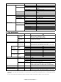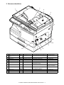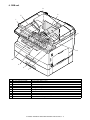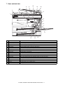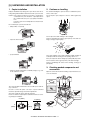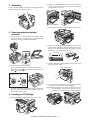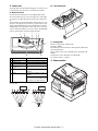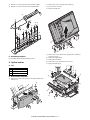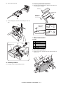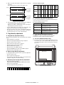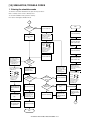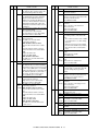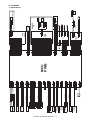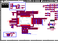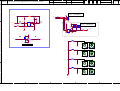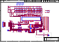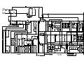
1
SERVICE MANUAL
CODE: 00ZAL2040CS1E
DIGITAL MULTIFUNCTIONAL
SYSTEM
(AL-2040CS)
MODEL
AL-2030
AL-2040CS
CONTENTS
[ 1 ] GENERAL . . . . . . . . . . . . . . . . . . . . . . . . . . . . . . . . . . . . . . . . . . . 1 - 1
[ 2 ] SPECIFICATIONS . . . . . . . . . . . . . . . . . . . . . . . . . . . . . . . . . . . . . 2 - 1
[ 3 ] CONSUMABLE PARTS . . . . . . . . . . . . . . . . . . . . . . . . . . . . . . . . . 3 - 1
[ 4 ] EXTERNAL VIEWS AND INTERNAL STRUCTURES . . . . . . . . . 4 - 1
[ 5 ] UNPACKING AND INSTALLATION . . . . . . . . . . . . . . . . . . . . . . . . 5 - 1
[ 6 ] COPY PROCESS . . . . . . . . . . . . . . . . . . . . . . . . . . . . . . . . . . . . . 6 - 1
[ 7 ] OPERATIONAL DESCRIPTIONS . . . . . . . . . . . . . . . . . . . . . . . . . 7 - 1
[ 8 ] DISASSEMBLY AND ASSEMBLY . . . . . . . . . . . . . . . . . . . . . . . . . 8 - 1
[ 9 ] ADJUSTMENTS . . . . . . . . . . . . . . . . . . . . . . . . . . . . . . . . . . . . . . 9 - 1
[10] SIMULATION, TROUBLE CODES . . . . . . . . . . . . . . . . . . . . . . . 10 - 1
[11] USER PROGRAMS. . . . . . . . . . . . . . . . . . . . . . . . . . . . . . . . . . . 11 - 1
[12] ELECTRICAL SECTION . . . . . . . . . . . . . . . . . . . . . . . . . . . . . . . 12 - 1
Parts marked with “ ” are important for maintaining the safety of the set. Be sure to replace these parts with
specified ones for maintaining the safety and performance of the set.
SHARP CORPORATION
This document has been published to be used
for after sales service only.
The contents are subject to change without notice.
CAUTION
This product is a class 1 laser product that complies with 21CFR 1040 of the CDRH standard and
IEC825. This means that this machine does not produce hazardous laser radiation. The use of controls,
adjustments or performance of procedures other than those specified herein may result in hazardous
radiation exposure.
This laser radiation is not a danger to the skin, but when an exact focusing of the laser beam is achieved
on the eye’s retina, there is the danger of spot damage to the retina.
The following cautions must be observed to avoid exposure of the laser beam to your eyes at the time of
servicing.
1) When a problem in the laser optical unit has occurred, the whole optical unit must be exchanged as a
unit, not as individual parts.
2) Do not look into the machine with the main switch turned on after removing the developer unit, toner
cartridge, and drum cartridge.
3) Do not look into the laser beam exposure slit of the laser optical unit with the connector connected
when removing and installing the optical system.
4) The middle frame contains the safety interlock switch.
Do not defeat the safety interlock by inserting wedges or other items into the switch slot.
CAUTION
INVISIBLE LASER RADIATION,
WHEN OPEN AND INTERLOCKS DEFEATED.
AVOID EXPOSURE TO BEAM.
VORSICHT
UNSICHTBARE LASERSTRAHLUNG,
WENN ABDECKUNG GEÖFFNET UND
SICHERHEITSVERRIEGELUNG ÜBERBRÜCKT.
NICHT DEM STRAHL AUSSETZEN.
LASER WAVE – LENGTH : 770 ~ 795nm
Pulse times : 12.88µs ± 12.88ns/7mm
Out put power : MAX 0.2mW
VARO !
AVATTAESSA JA SUOJALUKITUS
OHITETTAESSA OLET ALTTIINA
NÄKYMÄTTÖMÄLLE LASERSÄTEILYLLE ÄLÄ
KATSO SÄTEESEEN.
ADVARSEL
USYNLIG LASERSTRÅLNING VED ÅBNING, NÅR
SIKKERHEDSBRYDERE ER UDE AF
FUNKTION. UNDGÅ UDSAETTELSE FOR
STRÅLNING.
VARNING !
OSYNLIG LASERSTRÅLNING NÄR DENNA DEL
ÄR ÖPPNAD OCH SPÄRREN ÄR URKOPPLAD.
BETRAKTA EJ STRÅLEN. – STRÅLEN ÄR
FARLIG.
At the production line, the output power
of the scanner unit is adjusted to 0.57
MILLI-WATT PLUS 20 PCTS and is
maintained constant by the operation of
the Automatic Power Control (APC).
Even if the APC circuit fails in operation
for some reason, the maximum output
power will only be 15 MILLI-WATT 0.1
MICRO-SEC. Giving and accessible
emission level of 42 MICRO-WATT
which is still-less than the limit of
CLASS-1 laser product.
Caution
This product contains a low power laser
device. To ensure continued safety do not
remove any cover or attempt to gain access
to the inside of the product. Refer all
servicing to qualified personnel.
VAROITUS! LAITTEEN KÄYTTÄMINEN MUULLA
KUIN TÄSSÄ KÄYTTÖOHJEESSA MAINITULLA
TAVALLA SAATTAA ALTISTAA KÄYTTÄJÄN
TURVALLISUUSLUOKAN 1 YLITTÄVÄLLE
NÄKYMÄTTÖMÄLLE LASERSÄTEILYLLE.
VARNING - OM APPARATEN ANVÄNDS PÅ ANNAT
SÄTT ÄN I DENNA BRUKSANVISNING
SPECIFICERATS, KAN ANVÄNDAREN UTSÄTTAS
FÖR OSYNLIG LASERSTRÅLNING, SOM
ÖVERSKRIDER GRÄNSEN FÖR LASERKLASS 1.
The foregoing is applicable only to the 220V
model, 230V model and 240V model.
LUOKAN 1 LASERLAITE
KLASS 1 LASER APPARAT
CONTENTS
[1]
GENERAL
1. Major functions . . . . . . . . . . . . . . . . . . . . . . . . . . . . . . . . . . . . 1-1
[2]
SPECIFICATIONS
1. Basic Specifications. . . . . . . . . . . . . . . . . . . . . . . . . . . . . . . . .
2. Operation specifications . . . . . . . . . . . . . . . . . . . . . . . . . . . . .
3. Copy performance . . . . . . . . . . . . . . . . . . . . . . . . . . . . . . . . . .
4. GDI Printer. . . . . . . . . . . . . . . . . . . . . . . . . . . . . . . . . . . . . . . .
5. Scan function . . . . . . . . . . . . . . . . . . . . . . . . . . . . . . . . . . . . . .
6. SPF . . . . . . . . . . . . . . . . . . . . . . . . . . . . . . . . . . . . . . . . . . . . .
2-1
2-1
2-2
2-3
2-3
2-3
[3]
CONSUMABLE PARTS
1. Supply system table. . . . . . . . . . . . . . . . . . . . . . . . . . . . . . . . . 3-1
2. Environmental . . . . . . . . . . . . . . . . . . . . . . . . . . . . . . . . . . . . . 3-1
3. Production control number (lot No.) identification . . . . . . . . . . 3-2
[4]
EXTERNAL VIEWS AND INTERNAL STRUCTURES
1. Appearance . . . . . . . . . . . . . . . . . . . . . . . . . . . . . . . . . . . . . . .
2. Internal. . . . . . . . . . . . . . . . . . . . . . . . . . . . . . . . . . . . . . . . . . .
3. Operation panel . . . . . . . . . . . . . . . . . . . . . . . . . . . . . . . . . . . .
4. Motors and solenoids. . . . . . . . . . . . . . . . . . . . . . . . . . . . . . . .
5. Sensors and switches . . . . . . . . . . . . . . . . . . . . . . . . . . . . . . .
6. PWB unit . . . . . . . . . . . . . . . . . . . . . . . . . . . . . . . . . . . . . . . . .
7. Cross sectional view . . . . . . . . . . . . . . . . . . . . . . . . . . . . . . . .
4-1
4-1
4-2
4-4
4-5
4-6
4-7
UNPACKING AND INSTALLATION
1. Copier installation . . . . . . . . . . . . . . . . . . . . . . . . . . . . . . . . . .
2. Cautions on handling . . . . . . . . . . . . . . . . . . . . . . . . . . . . . . . .
3. Checking packed components and accessories . . . . . . . . . . .
4. Unpacking . . . . . . . . . . . . . . . . . . . . . . . . . . . . . . . . . . . . . . . .
5. Removing protective packing materials . . . . . . . . . . . . . . . . . .
6. Installing the TD cartridge . . . . . . . . . . . . . . . . . . . . . . . . . . . .
7. Loading paper . . . . . . . . . . . . . . . . . . . . . . . . . . . . . . . . . . . . .
8. Power to copier . . . . . . . . . . . . . . . . . . . . . . . . . . . . . . . . . . . .
9. Software. . . . . . . . . . . . . . . . . . . . . . . . . . . . . . . . . . . . . . . . . .
10. Connecting the interface cable . . . . . . . . . . . . . . . . . . . . . . . .
11. Interface. . . . . . . . . . . . . . . . . . . . . . . . . . . . . . . . . . . . . . . . . .
A. USB . . . . . . . . . . . . . . . . . . . . . . . . . . . . . . . . . . . . . . . . . .
B. RJ45 . . . . . . . . . . . . . . . . . . . . . . . . . . . . . . . . . . . . . . . . . .
12. Moving . . . . . . . . . . . . . . . . . . . . . . . . . . . . . . . . . . . . . . . . . . .
5-1
5-1
5-1
5-2
5-2
5-2
5-3
5-3
5-3
5-4
5-4
5-4
5-4
5-5
[5]
[6]
COPY PROCESS
1. Functional diagram . . . . . . . . . . . . . . . . . . . . . . . . . . . . . . . . . 6-1
2. Outline of print process . . . . . . . . . . . . . . . . . . . . . . . . . . . . . . 6-2
3. Actual print process . . . . . . . . . . . . . . . . . . . . . . . . . . . . . . . . . 6-2
[7]
OPERATIONAL DESCRIPTIONS
1. Outline of operation . . . . . . . . . . . . . . . . . . . . . . . . . . . . . . . . .
2. Scanner section . . . . . . . . . . . . . . . . . . . . . . . . . . . . . . . . . . . .
A. Scanner unit . . . . . . . . . . . . . . . . . . . . . . . . . . . . . . . . . . . .
B. Optical system . . . . . . . . . . . . . . . . . . . . . . . . . . . . . . . . . .
C. Drive system. . . . . . . . . . . . . . . . . . . . . . . . . . . . . . . . . . . .
3. Laser unit . . . . . . . . . . . . . . . . . . . . . . . . . . . . . . . . . . . . . . . . .
A. Basic structure . . . . . . . . . . . . . . . . . . . . . . . . . . . . . . . . . .
B. Laser beam path. . . . . . . . . . . . . . . . . . . . . . . . . . . . . . . . .
C. Composition . . . . . . . . . . . . . . . . . . . . . . . . . . . . . . . . . . . .
4. Fuser section . . . . . . . . . . . . . . . . . . . . . . . . . . . . . . . . . . . . . .
A. General description . . . . . . . . . . . . . . . . . . . . . . . . . . . . . .
5. Paper feed section and paper transport section . . . . . . . . . . .
A. Paper transport path and general operations . . . . . . . . . . .
6. Process unit new drum detection mechanism . . . . . . . . . . . . .
7. SPF section . . . . . . . . . . . . . . . . . . . . . . . . . . . . . . . . . . . . . . .
A. Outline . . . . . . . . . . . . . . . . . . . . . . . . . . . . . . . . . . . . . . . .
B. Document transport path and basic composition . . . . . . . .
C. Operational descriptions. . . . . . . . . . . . . . . . . . . . . . . . . . .
D. SPF open/close detection (book document detection) . . . .
7-1
7-2
7-2
7-2
7-2
7-3
7-3
7-3
7-3
7-3
7-4
7-4
7-4
7-7
7-7
7-7
7-7
7-8
7-8
DISASSEMBLY AND ASSEMBLY
1. High voltage section . . . . . . . . . . . . . . . . . . . . . . . . . . . . . . . .
A. List . . . . . . . . . . . . . . . . . . . . . . . . . . . . . . . . . . . . . . . . . . .
B. Disassembly procedure . . . . . . . . . . . . . . . . . . . . . . . . . . .
C. Assembly procedure. . . . . . . . . . . . . . . . . . . . . . . . . . . . . .
D. Charger wire cleaning. . . . . . . . . . . . . . . . . . . . . . . . . . . . .
E. Charger wire replacement . . . . . . . . . . . . . . . . . . . . . . . . .
2. Operation panel section. . . . . . . . . . . . . . . . . . . . . . . . . . . . . .
A. List . . . . . . . . . . . . . . . . . . . . . . . . . . . . . . . . . . . . . . . . . . .
B. Disassembly procedure . . . . . . . . . . . . . . . . . . . . . . . . . . .
C. Assembly procedure. . . . . . . . . . . . . . . . . . . . . . . . . . . . . .
3. Optical section . . . . . . . . . . . . . . . . . . . . . . . . . . . . . . . . . . . . .
A. List . . . . . . . . . . . . . . . . . . . . . . . . . . . . . . . . . . . . . . . . . . .
B. Disassembly procedure . . . . . . . . . . . . . . . . . . . . . . . . . . .
8-1
8-1
8-1
8-1
8-1
8-2
8-2
8-2
8-2
8-3
8-3
8-3
8-3
[8]
C. Assembly procedure . . . . . . . . . . . . . . . . . . . . . . . . . . . . . . 8-4
4. Fusing section . . . . . . . . . . . . . . . . . . . . . . . . . . . . . . . . . . . . . 8-5
A. List. . . . . . . . . . . . . . . . . . . . . . . . . . . . . . . . . . . . . . . . . . . . 8-5
B. Disassembly procedure. . . . . . . . . . . . . . . . . . . . . . . . . . . . 8-5
C. Assembly procedure . . . . . . . . . . . . . . . . . . . . . . . . . . . . . . 8-7
5. Tray paper feed/transport section . . . . . . . . . . . . . . . . . . . . . . 8-7
A. List. . . . . . . . . . . . . . . . . . . . . . . . . . . . . . . . . . . . . . . . . . . . 8-7
B. Disassembly procedure. . . . . . . . . . . . . . . . . . . . . . . . . . . . 8-7
C. Assembly procedure . . . . . . . . . . . . . . . . . . . . . . . . . . . . . 8-12
6. Manual paper feed section . . . . . . . . . . . . . . . . . . . . . . . . . . . 8-12
A. List. . . . . . . . . . . . . . . . . . . . . . . . . . . . . . . . . . . . . . . . . . . 8-12
B. Disassembly procedure. . . . . . . . . . . . . . . . . . . . . . . . . . . 8-12
C. Assembly procedure . . . . . . . . . . . . . . . . . . . . . . . . . . . . . 8-14
D. Pressure plate holder attachment . . . . . . . . . . . . . . . . . . . 8-14
7. Rear frame section . . . . . . . . . . . . . . . . . . . . . . . . . . . . . . . . . 8-14
A. List. . . . . . . . . . . . . . . . . . . . . . . . . . . . . . . . . . . . . . . . . . . 8-14
B. Disassembly procedure. . . . . . . . . . . . . . . . . . . . . . . . . . . 8-14
C. Assembly procedure . . . . . . . . . . . . . . . . . . . . . . . . . . . . . 8-15
8 Power section. . . . . . . . . . . . . . . . . . . . . . . . . . . . . . . . . . . . . 8-16
A. List. . . . . . . . . . . . . . . . . . . . . . . . . . . . . . . . . . . . . . . . . . . 8-16
B. Disassembly procedure. . . . . . . . . . . . . . . . . . . . . . . . . . . 8-16
C. Assembly procedure . . . . . . . . . . . . . . . . . . . . . . . . . . . . . 8-16
9. SPF section . . . . . . . . . . . . . . . . . . . . . . . . . . . . . . . . . . . . . . 8-16
A. SPF motor . . . . . . . . . . . . . . . . . . . . . . . . . . . . . . . . . . . . . 8-16
B. Pick-up roller, paper feed roller . . . . . . . . . . . . . . . . . . . . . 8-17
C. Paper exit roller . . . . . . . . . . . . . . . . . . . . . . . . . . . . . . . . . 8-17
D. Set sensor, scan front sensor . . . . . . . . . . . . . . . . . . . . . . 8-18
E. Transport roller . . . . . . . . . . . . . . . . . . . . . . . . . . . . . . . . . 8-18
10. 2nd cassette section. . . . . . . . . . . . . . . . . . . . . . . . . . . . . . . 8-18
A. Paper sensor. . . . . . . . . . . . . . . . . . . . . . . . . . . . . . . . . . . 8-19
B. Cassette detection switch . . . . . . . . . . . . . . . . . . . . . . . . . 8-19
C. Paper feed solenoid . . . . . . . . . . . . . . . . . . . . . . . . . . . . . 8-19
D. Transport roller . . . . . . . . . . . . . . . . . . . . . . . . . . . . . . . . . 8-19
E. Paper feed clutch . . . . . . . . . . . . . . . . . . . . . . . . . . . . . . . 8-20
F. 2nd paper feed roller . . . . . . . . . . . . . . . . . . . . . . . . . . . . . 8-20
[9]
ADJUSTMENTS
1. Optical section . . . . . . . . . . . . . . . . . . . . . . . . . . . . . . . . . . . . . 9-1
A. Copy magnification ratio adjustment . . . . . . . . . . . . . . . . . . 9-1
B. Image position adjustment . . . . . . . . . . . . . . . . . . . . . . . . . 9-2
2. Copy density adjustment . . . . . . . . . . . . . . . . . . . . . . . . . . . . . 9-4
A. Copy density adjustment timing . . . . . . . . . . . . . . . . . . . . . 9-4
B. Note for copy density adjustment . . . . . . . . . . . . . . . . . . . . 9-4
C. Necessary tool for copy density adjustment . . . . . . . . . . . . 9-4
D. Features of copy density adjustment . . . . . . . . . . . . . . . . . 9-4
E. Copy density adjustment procedure . . . . . . . . . . . . . . . . . . 9-4
3. High voltage adjustment. . . . . . . . . . . . . . . . . . . . . . . . . . . . . . 9-5
A. Main charger (Grid bias) . . . . . . . . . . . . . . . . . . . . . . . . . . . 9-5
B. DV bias check . . . . . . . . . . . . . . . . . . . . . . . . . . . . . . . . . . . 9-5
4. Duplex adjustment . . . . . . . . . . . . . . . . . . . . . . . . . . . . . . . . . . 9-6
A. Adjusting the paper reverse position in memory
for duplex copying . . . . . . . . . . . . . . . . . . . . . . . . . . . . . . . . 9-6
B. Adjusting trailing edge void in duplex copy mode . . . . . . . . 9-6
5. SPF scan position automatic adjustment . . . . . . . . . . . . . . . . . 9-7
6. SPF mode sub scanning direction magnification ratio
adjustment . . . . . . . . . . . . . . . . . . . . . . . . . . . . . . . . . . . . . . . . 9-7
7. Automatic black level correction. . . . . . . . . . . . . . . . . . . . . . . . 9-8
[10] SIMULATION, TROUBLE CODES
1. Entering the simulation mode. . . . . . . . . . . . . . . . . . . . . . . . . 10-1
2. List of simulations. . . . . . . . . . . . . . . . . . . . . . . . . . . . . . . . . . 10-2
3. Contents of simulations . . . . . . . . . . . . . . . . . . . . . . . . . . . . . 10-3
4. Trouble codes . . . . . . . . . . . . . . . . . . . . . . . . . . . . . . . . . . . 10-17
A. Trouble codes list . . . . . . . . . . . . . . . . . . . . . . . . . . . . . . 10-17
B. Details of trouble codes. . . . . . . . . . . . . . . . . . . . . . . . . . 10-17
[11] USER PROGRAM
1. Functions that can be set with user programs . . . . . . . . . . . . 11-1
2. Toner save mode . . . . . . . . . . . . . . . . . . . . . . . . . . . . . . . . . . 11-1
3. User programs . . . . . . . . . . . . . . . . . . . . . . . . . . . . . . . . . . . . 11-1
[12] ELECTRICAL SECTION
1. Block diagram. . . . . . . . . . . . . . . . . . . . . . . . . . . . . . . . . . . . . 12-1
A. Overall block diagram . . . . . . . . . . . . . . . . . . . . . . . . . . . . 12-1
2. Actual wiring diagram . . . . . . . . . . . . . . . . . . . . . . . . . . . . . . . 12-2
A. AL-2030. . . . . . . . . . . . . . . . . . . . . . . . . . . . . . . . . . . . . . . 12-2
B. AL-2040CS . . . . . . . . . . . . . . . . . . . . . . . . . . . . . . . . . . . . 12-4
3. Signal name list . . . . . . . . . . . . . . . . . . . . . . . . . . . . . . . . . . . 12-6
[1] GENERAL
1. Major functions
Configurations
Item
Model
AL-2030
AL-2040CS
CPM
PPM
SB/MB 2 Tray
(Letter) (Letter)
20CPM 16PPM
20CPM 16PPM
SPF
R-SPF
Color
GDI
PCL
EDuplex Shifter
Scanner printer printer SORT
RJ45
MB
MB
(print only)
Descriptions of items
CPM:
Copy speed (Copies Per Minute)
PPM:
Print speed (Print Per Minute)
SB/MB:
SB = Manual feed single bypass, MB = Manual feed multi-bypass
2 tray:
Second cassette unit.
SPF:
Original feed unit
R-SPF:
Duplex original feed unit
Color scanner:
Color scanner function
GDI printer:
GDI printer function with USB.
PCL printer:
PCL printer function with USB.
E-SORT:
Electronic sort function
Duplex:
Auto duplex copy/print function
Shifter:
Job separator function
FAX:
FAX function.
Descriptions of table
:
Standard provision
:
No function or no option available
Opt: Option
AL-2030
AL-2040CS GENERAL 1 - 1
AL-2040CS
FAX
[2] SPECIFICATIONS
1. Basic Specifications
Item
Type
Copy system
Segment (class)
Copier dimensions
Weight (Approximately)
AL-2030
AL-2040CS
AL-2030
AL-2040CS
Desktop
Dry, electrostatic
Digital personal copier
20-1/2" (W) x 17-5/8" (D) x 14-1/8" (H) (518mm (W) x 445mm (D) x 358mm (H))
20-1/2" (W) x 17-5/8" (D) x 17-5/8" (H) (518mm (W) x 445mm (D) x 445mm (H))
37.9 lbs. (17.2Kg)
TD cartridge not included
45.9 lbs. (20.8Kg)
2. Operation specifications
Paper feed
section
Section, item
Paper feed
system
Inch
system
Tray paper feed
section
Multi-bypass paper
feed section
Details
AL-2030
AL-2040CS
Paper size
Paper weight
Paper feed capacity
Kinds
Remark
Paper size
Paper weight
Paper feed capacity
Kinds
AB system
Tray paper feed
section
Multi-bypass paper
feed section
Remark
Paper size
Paper weight
Paper feed capacity
Kinds
Remark
Paper size
Paper weight
Paper feed capacity
Kinds
Remark
Paper exit section
Originals
Optical
section
Scanning
section
Exit way
Capacity of output tray
Original set
Max. original size
Original kinds
Original size detection
Scanning system
CCD sensor
Lighting lamp
Resolution
Type
Voltage
Power consumption
Output data
Writing
section
Writing system
Laser unit
Resolution
1 tray (250 sheet) + multi-bypass (50 sheet)
2 tray (500 sheet) + multi-bypass (50 sheet)
8-1/2" x 14", 8-1/2 x 11", 8-1/2" x 5-1/2" (Landscape)
15 - 21 lbs.
250 sheets
Standard paper, specified paper, recycled paper
User adjustment of paper guide available
8-1/2" x 14", 8-1/2 x 11", 8-1/2" x 5-1/2",
3-1/2" x 5-1/2" (Landscape)
15 - 34.5 lbs.
50 sheets
Standard paper, specified paper, recycled paper,
OHP, Label, Envelop (Single copy)
User adjustment of paper guide available
A4, B5, A5 (Landscape)
56 - 80g/m2 (15 - 21 lbs.)
250 sheets
Standard paper, specified paper, recycled paper
User adjustment of paper guide available
A4, B5, A5, B6, A6 (Landscape)
56 - 128g/m2 (15 - 34.5 lbs.)
50 sheets
Standard paper, specified paper, recycled paper,
OHP, Label, (Single copy)
User adjustment of paper guide available
Face down
100 sheets
Center Registration (left edge)
8-1/2" x 14" (A4)
sheet, book
None
3 CCDs (RGB) sensor scanning by lighting white
lamp
600 dpi
CCFL
560Vrms
2.8W
Output: R, G, B 1 or 8 bits/pixel / Input: A/D 16 bits
(12 bits actual)
Writing to OPC drum by the semiconductor laser
600 dpi
AL-2040CS SPECIFICATIONS 2 - 1
Image forming
Fusing section
Electrical section
Section, item
Photoconductor
Charger
Details
Type
Life
Charging system
Developing
Transfer system
Separation system
Developing system
Cleaning
Fusing system
Upper heat roller
Lower heat roller
Heater lamp
Cleaning system
Type
Type
Type
Voltage
Power consumption
Voltage
Frequency
Max.
Average (during copying)
Average (stand-by)
Pre-heat mode
Auto power shut-off mode
Power source
Power consumption
OPC (30ø)
18k
Saw-tooth charging with a grid, / (-) scorotron
discharge
(+) DC corotron system
(-) DC corotron system
Dry, 2-component magnetic brush development
system
Counter blade system (Counter to rotation)
Heat roller system
Teflon roller
Silicon rubber roller
Halogen lamp
120V
800W
120V
Common use for 50 and 60Hz
Less than 1000W
350Wh/H
80Wh/H
25Wh/H
8.8W or less
3. Copy performance
Section, item
Copy magnification
Fixed
magnification
ratios
Zooming
magnification
ratios
Manual steps (manual, photo)
Copy speed
First-copy time *1
(Approximately)
Inch system
8-1/2" x 11"
(Landscape)
Copy speed
(CPM)
AB system
A4 (Landscape)
Copy speed
(CPM)
AB system
B5 (Landscape)
Copy speed
(CPM)
Max. continuous copy quantity
Void
Void area
Image loss
Warm-up time
Power save mode reset time
Paper jam recovery time
Details
Same size
Enlargement
Reduction
Same size
Enlargement
Reduction
Same size
Enlargement
Reduction
Leading edge
Trailing edge
Side edge
void area
Leading edge
AL-2030
4 Reduction + 3 Enlargement
(AB system: 50, 70, 86, 100, 141, 200%)
(Inch system: 50, 64, 78, 100, 129, 200%)
25 - 400% (376 steps in 1% increments)
50 - 200% when using SPF
AL-2040CS
5 steps
8.0 seconds (When user program 24 is set to OFF)
10.7 seconds (When user program 24 is set to ON)
(paper: 8-1/2" x 11" (A4), exposure mode: AUTO, copy ratio: 100%)
20
20
20
20
20
20
20
20
20
20
20
20
20
20
20
20
20
20
99
1 - 4mm
4mm or less
0.5mm or more (per side)
4.5mm or less (total of both sides)
same size: 3.0mm or less (OC) / 4mm or less (SPF/Duplex)
Enlarge: 1 - 5mm or less (OC) / 3mm or less (SPF/Duplex)
Reduction (50%): 6.0mm or less (OC) / 8mm or less (SPF/Duplex)
0 sec. Immediately the ready lamp is lit.
0 sec. Immediately the ready lamp is lit.
0 sec.
∗ Jam recovery condition: Recovery time from 60 sec of door open.
*1: The first-copy time is measured after the power save indicator turns off following power on, using the document glass with the polygon
rotating in the copy ready state and "Selection of copy start state" set to ON in the user programs (8-1/2" x 11" (A4), paper fed from
paper tray).
The first-copy time may vary depending on machine operating conditions and ambient conditions such as temperature.
AL-2040CS SPECIFICATIONS 2 - 2
4. GDI Printer
Print speed
Duplex
Memory
Interface
Network
Emulation
Resolution
Supported OS
WHQL support
Max. 20ppm (excluding bypass tray, paper size A4, 8.5" x 11") (Variable depending on the PC
performance)
Yes (AL-2040CS only)
8MB (Duplex model: 16MB)
USB 2.0 (Full speed) / (RJ45 (10Base-T) AL-2040CS only)
Built-in NIC (AL-2040CS only)
GDI
600dpi *1
Win 98 / Me / 2000 / XP / Vista *2
Yes *2
*1: Engine Resolution
*2: By running change
5. Scan function
Type
Scanning system
Light source
Resolution
Originals
Output data
Scan range
Scan speed
Protocol
Interface
Scanner utility
Scan key/lamp
Duplex scan
Supported OS
Void area
WHQL supported
Flat Bed Color Scanner
Original table/SPF
3 CCDs (RGB) sensor scanning by lighting white lamp (2 pcs of CCFL)
Optical: 600 x 600dpi
Setting range: 50 - 9600dpi (Preview resolution is fixed at 75dpi)
Sheet type / Book type
R, G, B 1 or 8 bits/pixel
OC / SPF: 8.5" (H) x 14.0" (V)
Original position: Left Center
OC / SPF: Max. 2.88ms/line
TWAIN / WIA (Only XP) / STI
USB2.0 (Full speed support)
Button Manager / Sharpdesk / Composer
Yes
No
Win 98 / Me / 2000 / XP / Vista *1
No (User settable by PC)
Yes *1
*1: By running change
6. SPF
Original capacity
Original size
Original replacement speed
Original placement
Original weight
Mixed feeding (Paper size)
Original which cannot
50 sheets (14 to 23.9 lbs.) (56 to 90g/m2) Stacking Height: less than 6.5mm or 1/4"
8-1/2" x 14" to 5-1/2" x 8-1/2" / A4 to A5 (Landscape)
Max. 14 sheets (70%)
Face up
14 - 23.9lbs. (56 to 90g/m2)
No
Thermal papers, originals with punch holes for files, be used folded paper, transparent originals such as
OHP films, stapled or clip used originals with cover up liquid used, Originals with tape sealed, originals
with high level frictional coefficient such as photos or catalogs.
AL-2040CS SPECIFICATIONS 2 - 3
[3] CONSUMABLE PARTS
1. Supply system table
Common to all destinations
No.
1
Name
Develop cartridge (Black) x 1
2
Develop cartridge (Black) x 1
3
Drum cartridge
Content
Toner/developer cartridge x 1
(Toner: Net weight 213g) (Developer: Net weight 190g)
Toner/developer cartridge x 1
(Toner: Net weight 124g) (Developer: Net weight 190g)
Drum cartridge
Life
6K
(5% document)
4K
(5% document)
18K
Product name
AL-100TD
Package
5
AL-110TD
5
AL-100DR
5
2. Environmental
The environmental conditions for assuring the copy quality and the machine operations are as follows:
(4) Supply storage condition
(1) Normal operating condition
Temperature: 20 - 25°C
Humidity (RH)
90%
Humidity: 65 ± 5%RH
(2) Acceptable operating condition
Humidity (RH)
85%
60%
20%
–5˚C
20%
10˚C
30˚C
35˚C
30˚C
40˚C
(3) Transport condition
Humidity (RH)
90%
60%
15%
–25˚C
AL-2040CS CONSUMABLE PARTS 3 - 1
45˚C
3. Production control number (lot No.) identification
<Developing cartridge>
Production month
Production day
Destination code
(Dealer, distributor, OEM, etc.)
Production place
(SOCC: Fixed to B.)
End digit of year
Version No.
∗ Destination
Division
EX Destination
No.
G
H
P
Q
A same pack
B same pack
A
B
Option Destination
Production control
label attachment position
<Drum cartridge>
The label on the drum cartridge shows the date of production.
(SOCC production)
Production month
Production day
Destination code
(Dealer, distributor, OEM, etc.)
Production place
(SOCC: Fixed to B.)
End digit of year
Version No.
Production control
label attachment position(*1)
<JAPAN production>
Ver.A
9
1
1
0001
X
Production month
(1 - 9 = Jan. - Sep. 0 = Oct. X = Nov. Y = Dec.)
*1: The production control label is not attached to the cartridge of
a China product.
Serial number of month
Fixed to 1.
Pack division
(See table below)
End digit of year
Version No.
Division
Ex production
Option
Same pack
No.
1
2
3
AL-2040CS CONSUMABLE PARTS 3 - 2
[4] EXTERNAL VIEWS AND INTERNAL STRUCTURES
1. Appearance
SPF
Original guide
Document
feeder cover
Interface
Peep hole
Exit area
Interface
Document feeder tray
LAN connector
(AL-2040CS only)
USB connector
1
2
7
10
11
8
9
3
4
5
12
13
14
6
1
4
7
10
13
Document glass
Paper tray 1
Side cover
Paper output tray
Handle
2
5
8
11
14
Operation panel
Paper tray 2 (AL-2040CS only)
Side cover open button
Paper output tray extension
Power cord
3
6
9
12
Front cover
Multi-bypass tray
Bypass tray paper guides
Power switch
2. Internal
TD cartridge
Drum cartridge
2
3
4
1
5
1
4
Front cover
Transfer charger
2
5
Side cover
Charger cleaner
3
Fusing unit release lever
AL-2040CS EXTERNAL VIEWS AND INTERNAL STRUCTURES 4 - 1
3. Operation panel
1
2
3
4
5 6
7
8
14 15
1
3
5
7
Original to copy key and indicators (AL-2040CS only)
Two-sided copies from one-sided originals.
Turn on Long Edge or Turn on Short Edge
can be selected.
Light and dark keys and indicators
Use to adjust the MANUAL or PHOTO exposure level. Selected
exposure level is shown by a lit indicator. Use to start and
terminate user program setting.
SPF indicator
Copy ratio selector key and indicators
Use to sequentially select preset reduction/enlargement copy
ratios.
Selected copy ratio is shown by a lit indicator.
9
Display
Displays the specified copy quantity, zoom copy ratio, user
program code, and error code.
11 ONLINE key and indicator
Lights up when the unit is used as a printer and scanner (AL2040CS only). *3
13 Power save indicator
Lights up when the unit is in a power save mode.
15 Paper feed location indicators
Light up to show the selected paper feed station.
17 Copy quantity keys
• Use to select the desired copy quantity (1 to 99).
• Use to make user program entries.
*1: Drum cartridge replacement
The useful life of the drum cartridge is approximately 18,000
copies*. When the internal counter reaches approximately
17,000 copies, the drum replacement required (
) indicator
will light up indicating that replacement of the drum cartridge
will be needed soon. For more information on purchasing the
drum cartridge, please refer to the Operation Manual. When
the indicator begins to blink, the unit will stop operating until
the cartridge is replaced. Replace the drum cartridge at this
time.
16
2
9
10
17
11
12
13
18
Exposure mode selector key and indicators
Use to sequentially select the exposure modes: AUTO,
MANUAL or PHOTO.
Selected mode is shown by a lit indicator.
4
Alarm indicators
Drum replacement required indicator *1
Misfeed indicator
TD cartridge replacement required indicator *2
6 SPF misfeed indicator
8 Copy ratio display (%) key
• Use to verify a zoom setting without changing the zoom ratio.
• Use to check the number of originals that must be returned to
the document feeder tray if an original misfeed occurs while
using the SPF.
10 SCAN key and indicator (AL-2040CS only) *3, *4
12 Start key and indicator
• Copying is possible when the indicator is on.
• Press to start copying
• Use to set a user program.
14 Tray select key
Use to select a paper feed station (paper tray 1, paper tray 2
(AL-2040CS only) or multi-bypass tray).
16 ZOOM keys and indicator
Use to select any reduction or enlargement copy ratio from 25%
to 400% in 1% increments. (When the SPF is being used, the
zoom copy ratio range is 50% to 200%.)
18 Clear key
• Press to clear the display, or press during a copy run to
terminate copying.
• Press and hold down during standby to display the total
number of copies made to date.
*3: Indicators on the operation panel
The ONLINE indicator and the start (
state of the printer or scanner.
SCAN indicator
ONLINE indicator
) indicator indicate the
Start indicator
Power save indicator
*: Based on copying onto letter size paper at 5% toned area.
Start indicator
*2: TD cartridge replacement
The TD cartridge replacement required (
) indicator will light
up when toner is needed. For more information on purchasing
the TD cartridge. If copying is continued while the indicator is
lit, copies will gradually become lighter until the unit stops and
the indicator begins blinking.
On:
Indicates the unit is ready for copying or scanning is
being performed.
Blinking: The indicator blinks in the following situations:
• When a print job is interrupted.
• When reserving a copy job.
• When toner is being replenished during a copy or
print job.
Off:
The indicator is off in the following situations:
• During copying or scanning.
• The unit is in the auto power shut-off mode.
• When a misfeed or error has occurred.
AL-2040CS EXTERNAL VIEWS AND INTERNAL STRUCTURES 4 - 2
ONLINE indicator
The ONLINE key is pressed and on line and off line are
changed.
On:
Indicates the unit is ready for printing or scanning is
being performed. (On line)
Blinking: Printing or data is being received from a computer.
Off:
Copying is being performed. (Off line)
Power save indicator
On:
Indicates the unit is in a power save mode.
Blinking: Indicates that the unit is initializing (when the side
cover is opened and closed or the power turned off
and on).
SCAN indicator (AL-2040CS only)
On:
The SCAN (
) key has been pressed and the unit
is in scanner mode.
Blinking: A scan job is being executed from the computer, or
scan data is stored in the unit’s memory.
Off:
The unit is in the copy mode.
*4: Using the SCAN key to begin scanning
Note:
• Scanning is not possible during a copy job.
• If the SCAN (
) key is pressed during a print job, the scan
job will be stored.
• When scanning an original that has been placed in the SPF,
only one original can be placed unless you are using Sharpdesk.
1) Press the SCAN (
) key.
The unit enters scan mode.
2) Place the original you wish to scan on the document glass/
SPF.
3) Press the right copy quantity key to display the number of
the application that you wish to use for scanning.
The application numbers are initially as follows.
Application
number
SC1
SC2
SC3
SC4
SC5
SC6
Application launched
Sharpdesk (Full color) (if installed)
Sharpdesk (Monochrome) (if installed)
E-mail (your standard e-mail program in
the Windows OS you are using)
Fax (if a fax program is installed)
OCR (if an OCR program is installed)
Microsoft Word (if installed)
4) Press the start (
) key.
Scanning will start and the scanned data will be transferred
to the application.
AL-2040CS EXTERNAL VIEWS AND INTERNAL STRUCTURES 4 - 3
4. Motors and solenoids
9
2
8
4
1
5
7
6
10
3
No.
1
2
3
4
5
6
7
8
9
10
Part name
Main motor
Scanner motor
Toner motor
Cooling fan motor
Resist roller solenoid
Paper feed solenoid
Multi paper feed solenoid
SPF motor
Duplex motor
Paper feed solenoid
Control signal
MM
MRMT
TM
VFM
RRS
CPFS1
MPFS
SPFM
DMT
CPFS2
Function / Operation
Drives the copier.
Drives the optical mirror base (scanner unit).
Supplies toner.
Cools the optical, fusing section.
Resist roller rotation control solenoid
Cassette Paper feed solenoid 1
Multi manual pages feed solenoid
Drives the single pass feeder
Devices the duplex paper transport section
Cassette Paper feed solenoid 2
AL-2040CS EXTERNAL VIEWS AND INTERNAL STRUCTURES 4 - 4
5. Sensors and switches
2
1
8
9
3
4
10
5
7
No.
Name
1 Scanner unit home position
sensor
2 POD sensor
3 PPD2 sensor
4 Cassette detection switch
5 PPD1 sensor
6 Door switch
6
11
Signal
MHPS
Type
Transmission sensor
Function
Scanner unit home position detection
Output
"H" at home position
POD
PPD2
CED1
PPD1
DSW
Transmission sensor
Transmission sensor
Micro-switch
Transmission sensor
Micro-switch
Paper exit detection
Paper transport detection 2
Cassette installation detection
Paper transport detection 1
Door open/close detection
(safety switch for 24V)
New drum detection switch
"H" at paper pass
"L" at paper pass
"H" at cassette insertion
"L" at paper pass
1 or 0V of 24V at door open
7
Drum reset switch
DRST
Micro-switch
8
SPF sensor
Transmission sensor
9
10
11
SPPD sensor
2nd cassette
PPD3 sensor
SPID/
SD SW
SPPD
DSW
PPD3
Transmission sensor
Micro-switch
Transmission sensor
Paper entry detection
Cover open/close detection
Paper transport detection
2nd cassette door open detection
Paper transport detection 3
AL-2040CS EXTERNAL VIEWS AND INTERNAL STRUCTURES 4 - 5
Instantaneously "H" at
insertion of new drum
"L" at paper pass
"L" at paper pass
1 or 0V of 5V at door open
"L" at paper pass
6. PWB unit
9
2
5
1
8
6
10
4
3
7
No.
1
2
3
4
5
6
7
8
9
10
Name
Exposure lamp invertor PWB
Main PWB (MCU)
Operation PWB
High voltage PWB
CCD sensor PWB
LSU motor PWB
TCS PWB
LSU PWB
NIC PWB
Power PWB
Function
Exposure lamp (CCFL) control
Copier control
Operation input/display
High voltage control
For image scanning
For polygon motor drive
For toner sensor control
For laser control
Network print control (AL-2040CS only)
AC power input, DC voltage control
AL-2040CS EXTERNAL VIEWS AND INTERNAL STRUCTURES 4 - 6
7. Cross sectional view
3
2
18
5
15
16
4
17
1
6
7
8
9
10
11
14
No.
1
2
3
4
5
6
7
8
9
10
11
12
13
14
15
16
17
18
Part name
Scanner unit
Exposure lamp
LSU (Laser unit)
Paper exit roller
Main charger
Heat roller
Pressure roller
Drum
Transfer unit
Pickup roller
Manual paper feed tray
Manual paper feed roller
PS roller unit
Paper feed roller
Pickup roller
Separation roller
PS roller
Paper exit roller
13
12
Function and operation
Illuminates the original with the copy lamp and passes the reflected light to the lens unit(CCD).
Exposure lamp (CCFL) Illuminates original
Converts the original image signal into laser beams and writes onto the drum.
Roller for paper exit
Provides negative charges evenly to the drum surface.
Fuses toner on the paper. (Teflon roller)
Fuses toner on the paper. (Silicon rubber roller)
Forms images.
Transfers images onto the drum.
Picks up the manual feed paper. (In multi feed only)
Tray for manual feed paper
Transport the paper from the manual paper feed port.
Takes synchronization between the lead edge and the rear edge of the paper.
Picks up a sheet of paper from the cassette.
Picks up documents.
Separates documents to feed properly.
Feeds documents to the scanning section.
Discharges documents.
AL-2040CS EXTERNAL VIEWS AND INTERNAL STRUCTURES 4 - 7
[5] UNPACKING AND INSTALLATION
1. Copier installation
2. Cautions on handling
Improper installation may damage the copier. Please note the following during initial installation and whenever the copier is moved.
Be careful in handling the copier as follows to maintain the performance of this copier.
Caution: If the copier is moved from a cool place to a warm place,
condensation may form inside the copier. Operation in
this condition will cause poor copy quality and malfunctions.
Leave the copier at room temperature for at least 2 hours
before use.
Do not drop the copier, subject it to shock or strike it against any
object.
Do not install your copier in areas that are:
• damp, humid, or very dusty
Do not expose the drum cartridge to direct sunlight.
Doing so will damage the surface (green portion) of the drum cartridge, causing poor print quality.
• exposed to direct sunlight
• poorly ventilated
Store spare supplies such as drum cartridges and TD cartridges in
a dark place without removing from the package before use.
If they are exposed to direct sunlight, poor print quality may result.
Do not touch the surface (green portion) of the drum cartridge.
Doing so will damage the surface of the cartridge, causing poor
print quality.
• subject to extreme temperature or humidity changes, e.g., near
an air conditioner or heater.
3. Checking packed components and
accessories
Open the carton and check if the following components and accessories are included.
Operation manual
The copier should be installed near an accessible power outlet for
easy connection.
Be sure to connect the power cord only to a power outlet that
meets the specified voltage and current requirements.
Software CD-ROM
Also make certain the outlet is properly grounded.
Be sure to allow the required space around the machine for servicing and proper ventilation.
8" (20cm)
4"
(10cm)
Drum cartridge
(installed in unit)
8" (20cm)
4"
(10cm)
TD cartridge
AL-2040CS UNPACKING AND INSTALLATION 5 - 1
4. Unpacking
Be sure to hold the handles on both sides of the unit to unpack the
unit and carry it to the installation location.
2) Remove the CAUTION tape from the front cover and remove
the two protective pins from the fusing unit by pulling the
strings upward one at a time.
Protective pins
CAUTION tape
3) Push gently on both sides of the front cover to open the cover.
5. Removing protective packing
materials
1) Remove all pieces of tape shown in the illustration below.
Then open the SPF and remove protective materials. After
that, take out the bag containing the TD cartridge.
4) Remove the TD cartridge from the bag. Remove the protective
paper. Hold the cartridge on both sides and shake it horizontally four or five times. Hold the tab of the protective cover and
pull the tab to your side to remove the cover.
AL-2040CS
4 or 5 times
AL-2030
2) Release the scan head locking switch.
5) Gently insert the TD cartridge until it locks in place while pushing the lock release button.
Lock release button
The scan head locking switch is under the document glass.
If the switch is locked ( ), the unit will not operate. Unlock the
switch ( ) as shown below.
Grasp here and turn in
the direction of the arrow.
(A)
Lock
6) Close the front cover and then the side cover by pressing the
round projections near the side cover open button.
Unlock
To lock the scan head locking switch, hold up the catch in illustration (A) and turn the center knob counter-clockwise 90
degrees until you hear a click.
Caution: When closing the covers, be sure to close the front cover
securely and then close the side cover. If the covers are
closed in the wrong order, the covers may be damaged.
6. Installing the TD cartridge
1) Open the multi-bypass tray, and then open the side cover.
AL-2040CS UNPACKING AND INSTALLATION 5 - 2
7. Loading paper
8. Power to copier
1) Raise the handle of the paper tray and pull the paper tray out
until it stops.
Ensure that the power switch of the unit is in the OFF position.
Plug the other end of the power cord into the nearest outlet. Turn
the power switch on the left side of the unit to the "ON" position.
The start (
) indicator will light up and other indicators which
show the initial settings of the operation panel will also light up to
indicate the ready condition.
9. Software
2) Remove the pressure plate lock. Rotate the pressure plate
lock in the direction of the arrow to remove it while pressing
down the pressure plate of the paper tray.
The CD-ROM that accompanies the machine contains the following software:
Printer driver (AL-2030)
The printer driver enables you to use the printer function of the
machine.
The printer driver includes the Print Status Window. This is a utility
that monitors the machine and informs you of the printing status,
the name of the document currently being printed, and error messages.
Please note that the printing over a network connection is not possible.
3) Store the pressure plate lock which has been removed in step
2). To store the pressure plate lock, rotate the lock to fix it on
the relevant location.
Pressure plate lock
MFP driver (AL-2040CS)
Printer driver
The printer driver enables you to use the printer function of the
machine.
The printer driver includes the Print Status Window. This is a utility
that monitors the machine and informs you of the printing status,
the name of the document currently being printed, and error messages.
Please note that the Print Status Window does not operate when
the machine is used as a network printer.
Scanner driver*
4) Adjust the paper guides on the paper tray to the copy paper
width and length. Squeeze the lever of paper guide (A) and
slide the guide to match with the width of the paper. Move
paper guide (B) to the appropriate slot as marked on the tray.
The scanner driver allows you to use the scanning function of the
machine with TWAIN-compliant and WIA-compliant applications.
Sharpdesk* (AL-2040CS)
Sharpdesk is an integrated software environment that makes it
easy to manage documents and image files, and launch applications.
Button Manager* (AL-2040CS)
Button Manager allows you to use the scanner menus on the
machine to scan a document.
*: The scanning feature can only be used with computers that are
connected to the machine by a USB cable. If you are connected
to the machine by a LAN connection, only the printer function
can be used.
Paper guide (B)
Paper guide (A)
5) Fan the paper and insert it into the tray. Make sure the edges
go under the corner hooks.
Before installation
Note: Do not load paper above the maximum height line (
Exceeding the line will cause a paper misfeed.
Hardware and software requirements
).
Check the following hardware and software requirements in order
to install the software.
Computer
type
Operating
system*2 *3
Display
6) Gently push the paper tray back into the unit.
Hard disk
free space
Other
hardware
requirements
IBM PC/AT or compatible computer equipped
with a USB 2.0/1.1*1 or 10Base-T LAN interface
Windows 98, Windows Me, Windows 2000
Professional*4, Windows XP Professional*4,
Windows XP Home Edition*4
800 x 600 dots (SVGA) display with 256 colors
(or better)
150 MB or more
An environment on which any of the operating
systems listed above can fully operate
AL-2040CS UNPACKING AND INSTALLATION 5 - 3
*1: Compatible with Windows 98, Windows Me, Windows 2000
Professional, Windows XP Professional or Windows XP Home
Edition preinstalled model standardly equipped with a USB
port.
1) Insert the LAN cable into the LAN connector on the machine.
Use a network cable that is shielded.
*2: Printing is not available in MS-DOS mode.
*3: The machine does not support printing from a Macintosh environment.
*4: Administrator's rights are required to install the software using
the installer.
Installation environment and usable software
The following table shows the drivers and software that can be
installed for each version of Windows and interface connection
method.
Cable
USB
LAN
Operating
Printer Scanner Button
Sharpdesk
system
driver
driver Manager
Windows 98/ Available*1
Available
Me/2000/XP
Windows 98/
Not Available*2
Me/2000/XP
2) Turn on the machine.
3) Set up according to the Operation Manual.
11. Interface
A. USB
Connector
4-pin ACON UBR23-4K2200
Type-B connector
*1: The printer driver that is installed will vary depending on the
type of connection between the machine and your computer.
Cable
*2: Although it is possible to install Button Manager and Sharpdesk on Windows 98/Me/2000/XP, neither Button Manager nor
the scanner function of Sharpdesk can actually be used.
(2 m (6 feet) Max.: high-speed transmission equivalent)
Install the software according to the Operation Manual.
The pin numbers and signal names are listed in the following table.
Shielded twisted pair cable
Pin configuration
Pin No.
1
2
3
4
10. Connecting the interface cable
Connecting a USB cable
Follow the procedure below to connect the machine to your computer.
A USB cable for connecting the machine to your computer is not
included with the machine. Please purchase the appropriate cable
for your computer.
Signal name
+5V
-DATA
+DATA
GND
2
1
3
4
Caution:
• USB is available with a PC/AT compatible computer that was
originally equipped with USB and had Windows 98, Windows
Me, Windows 2000 Professional, Windows XP Professional or
Windows XP Home Edition preinstalled.
• Do not connect the USB cable before installing the printer driver.
The USB cable should be connected during installation of the
printer driver.
1) Insert the cable into the USB connector on the machine.
B. RJ45
RJ-45 connector pin arrangement
1
8
2) Insert the other end of the cable into your computer’s USB
port.
Using the machine as a network printer (AL-2040CS
only)
Note:
• Interface cables for connecting the machine to your computer
are not included with the machine. Please purchase the appropriate cable for your computer.
Pin No.
1
2
3
6
4, 5, 7, 8
Signal name
TD+
TD–
RD+
RD–
Not used.
• If you intend to use the machine as a scanner, it must be connected to your computer with a USB interface cable. The scanner function cannot be used if the machine is connected with a
LAN cable.
AL-2040CS UNPACKING AND INSTALLATION 5 - 4
LAN adapter RJ-45 connector
Send output +
Send output Receive input +
Receive input Not used.
12. Moving
Moving instructions
When moving the unit, follow the procedure below.
Note: When moving this unit, be sure to remove the TD cartridge
in advance.
1) Turn the power switch off and remove the power cord from the
outlet.
2) Open the side cover and front cover, in that order. Remove the
TD cartridge and close the front cover and side cover, in that
order.
To open and close the side cover and front cover, and to
remove the TD cartridge.
3) Raise the handle of the paper tray and pull the paper tray out
until it stops.
4) Push the center of the pressure plate down until it locks in
place and lock the plate using the pressure plate lock which
has been stored in the front of the paper tray.
5) Push the paper tray back into the unit.
6) Lock the scan head locking switch.
Note: When shipping the unit, the scan head locking switch must
be locked to prevent shipping damage.
7) Close the multi-bypass tray and the paper output tray extension, and attach the packing materials and tape which were
removed during installation of the unit.
8) Pack the unit into the carton.
AL-2040CS UNPACKING AND INSTALLATION 5 - 5
[6] COPY PROCESS
An OPC drum is used for the photoconductor.
(Structure of the OPC drum layers)
OPC layer
(20 microns thick)
Pigment layer (0.2
to 0.3 microns thick)
Aluminum drum
1. Functional diagram
Main charger
Laser beam
Cleaning blade
MG roller
Drum
Transfer unit
Resist roller
(Basic operation cycle)
Semiconductor laser
Focus correction lens
Main high voltage unit
Exposure
Charge
Saw tooth
Toner
Drum
Developing
Cleaning
Developer
Cleaning blade
PS roller
Waste toner box
To face
down tray
Paper release
Fusing
Separation
Transfer
Heat roller
Electrode
Transfer charger
Heater lamp
Transfer high
voltage unit
Synchronization
with drum
Manual feed
Cassette
paper feed
Print process
Paper transport route
AL-2040CS COPY PROCESS 6 - 1
2. Outline of print process
Step-2: Exposure (laser beam, lens)
This printer is a non-impact printer that uses a semiconductor
laser and electrostatic print process. This printer uses an OPC
(Organic Photo Conductor) for its photoconductive material.
First, voltage from the main corona unit charges the drum surface
and a latent image is formed on the drum surface using a laser
beam. This latent image forms a visible image on the drum surface
when toner is applied. The toner image is then transferred onto the
print paper by the transfer corona and fused on the print paper in
the fusing section with a combination of heat and pressure.
A Laser beam is generated from the semiconductor laser and controlled by the print pattern signal. The laser writes onto the OPC
drum surface through the polygon mirrors and lens. The resistance of the OPC layer decreases for an area exposed by the laser
beam (corresponding to the print pattern signal). The beam neutralizes the negative charge. An electrostatic latent image is
formed on the drum surface.
Semiconductor laser
Step-1: Charge
Step-2: Exposure
∗ Latent image is formed on the drum.
Step-3: Developing
Latent image formed on the drum is then changed into
visible image with toner.
Step-4: Transfer
The visible image (toner image) on the drum is transferred
onto the print paper.
Exposure
(semiconductor laser)
OPC layer
Pigment
layer
Aluminum
drum
Step-5: Cleaning
Residual toner on the drum surface is removed and collected by the cleaning blade.
Step-6: Optical discharge
Residual charge on the drum surface is removed, by
semiconductor laser beam.
Drum surface charge
after the exposure
3. Actual print process
Step-1: DC charge
A uniform negative charge is applied over the OPC drum surface
by the main charging unit. Stable potential is maintained by means
of the Scorotron charger.
Positive charges are generated in the aluminum layer.
About
DC5.5KV
( 580V/ 400V)
AL-2040CS COPY PROCESS 6 - 2
Non-image area
Image area
OPC layer
Pigment
layer
Aluminum
layer
Step-3: Developing (DC bias)
Step-4: Transfer
A bias potential is applied to the MG roller in the two component
magnetic brush developing method, and the toner is charged negative through friction with the carrier.
The visible image on the drum surface is transferred onto the print
paper by applying a positive charge from the transfer corona to the
backside of the print paper.
Non-image area of the drum surface charged with negative potential repel the toner, whereas the laser exposed portions where no
negative charges exist, attract the toner. As a result, a visible
image appears on the drum surface.
:Carrier (Magnetized particle)
:Toner (Charge negative by friction)
(N) (S) Permanent magnet
(provided in three locations)
N
S
N
About DC 5.2kV
DC
400V 8V
MG roller
Step-5: Separation
Since the print paper is charged positively by the transfer corona, it
is discharged by the separation corona. The separation corona is
connected to ground.
Step-6: Cleaning
Toner remaining on the drum is removed and collected by the
cleaning blade. It is transported to the waste toner collecting section in the cleaning unit by the waste toner transport roller.
Toner is attracted over the shadowed area because of the developing bias.
AL-2040CS COPY PROCESS 6 - 3
Step-7: Optical discharge (Semiconductor laser)
Start
Before the drum rotation is stopped, the semiconductor laser is
radiated onto the drum to reduce the electrical resistance in the
OPC layer and eliminate residual charge, providing a uniform state
to the drum surface for the next page to be printed.
1) Because the grid potential is at a low level, the drum potential
is at about -400V. (Carrier may not be attracted though the carrier is pulled towards the drum by the electrostatic force of 400V.
When the electrical resistance is reduced, positive charges on the
aluminum layer are moved and neutralized with negative charges
on the OPC layer.
2) Developing bias (-400V) is applied when the photoconductor
potential is switched from LOW to HIGH.
Semiconductor laser
3) Once developing bias (-400V) is applied and the photo conductor potential rises to HIGH, toner will not be attracted to the
drum.
Stop
The reverse sequence takes place.
Retaining developing bias at an abnormal occurrence
Function
The developing bias will be lost if the power supply was removed
during print process. In this event, the drum potential slightly
abates and the carrier makes deposits on the drum because of
strong static power. To prevent this, the machine incorporates a
function to retain the developing bias for a certain period and
decrease the voltage gradually against possible power loss.
Charge by the Scorotron charger
Function
The Scorotron charger functions to maintain uniform surface
potential on the drum at all times, It control the surface potential
regardless of the charge characteristics of the photoconductor.
Basic function
A screen grid is placed between the saw tooth and the photoconductor. A stable voltage is added to the screen grid to maintain the
corona current on the photoconductor.
Basic function
Normally, the developing bias voltage is retained for a certain time
before the drum comes to a complete stop if the machine should
stop before completing the normal print cycle. The developing bias
can be added before resuming the operation after an abnormal
interruption. Therefore, carrier will not make a deposit on the drum
surface.
As the photoconductor is charged by the saw tooth from the main
corona unit, the surface potential increases. This increases the
current flowing through the screen grid. When the photoconductor
potential nears the grid potential, the current turns to flow to the
grid so that the photoconductor potential can be maintained at a
stable level.
Process controlling
Function
The print pattern signal is converted into an invisible image by the
semiconductor laser using negative to positive (reversible) developing method. Therefore, if the developing bias is added before
the drum is charged, toner is attracted onto the drum. If the developing bias is not added when the drum is charged, the carrier is
attracted to the drum because of the strong electrostatic force of
the drum.
To avoid this, the process is controlled by adjusting the drum
potential and the grid potential of the Scorotron charger.
Basic function
Voltage added to the screen grid can be selected, high and low. To
make it easily understood, the figure below shows voltage transition at the developer unit.
0
START
STOP
Print potential
Toner attract
potential
Developing bias
2)
3)
1)
Low
4)
Drum potential
High
Time
AL-2040CS COPY PROCESS 6 - 4
[7] OPERATIONAL DESCRIPTIONS
1. Outline of operation
The outline of operation is described referring to the basic configuration.
(Basic configuration)
Scanner section
Operation
section
CCD
NIC PWB
Network
(print only)
PC
MCU (Main control/image process section)
USB
PC
LSU (Laser unit)
Laser diode, Polygon mirror lens
Laser beam
Paper exit
Process section
Fusing section
Printer section
Paper transport section
Cassette paper
feed section
Manual paper
feed section
(Outline of copy operation)
Printing
Setting conditions
7) Electrostatic latent images are formed on the OPC drum
according to the laser beams, and the latent images are developed to be visible images (toner images).
1) Set copy conditions such as the copy quantity and the copy
density with the operation section, and press the COPY button. The information on copy conditions is sent to the MCU.
Image scanning
8) Meanwhile the paper is fed to the image transfer section in
synchronization with the image lead edge.
2) When the COPY button is pressed, the scanner section starts
scanning of images.
The light from the copy lamp is reflected by the document and
passed through the lens to the CCD.
9) After the transfer of toner images onto the paper, the toner
images are fused to the paper by the fusing section. The copied paper is discharged onto the exit tray.
Photo signal/Electric signal conversion
3) The image is converted into electrical signals by the CCD circuit and passed to the MCU.
The print data sent from the PC are passed through the NIC PWB
(in case of network connection) and the MCU to the LSU. The procedures after that are the same as above 5) and later.
Image process
(Outline of scanner operation)
4) The document image signal sent from the CCD circuit is processed under the revised conditions and sent to the LSU
(laser unit) as print data.
The scan data are passed through the MCU to the PC according
to the conditions requested by the operations with the operation
panel.
(Outline of printer operation)
Electric signal/Photo signal (laser beam) conversion
5) The LSU emits laser beams according to the print data.
(Electrical signals are converted into photo signals.)
6) The laser beams are radiated through the polygon mirror and
various lenses to the OPC drum.
AL-2040CS OPERATIONAL DESCRIPTIONS 7 - 1
2. Scanner section
A. Scanner unit
Spectral sensitivity characteristics (Standard characteristics)
The scanner unit in the digital copier scans images.
Relative sensitivity
It is composed of the optical unit and the drive unit. The optical unit
performs scanning in the main scan direction with the light receiving elements (color CCD). The drive unit performs scanning in the
sub scanning direction by moving the optical unit.
B. Optical system
Two white lamps are used as the light source.
Light radiated from the light source is applied to the document on
the document table. The reflected light from the document is
reflected 4 times by No. 1 - No. 3 mirrors and passed through the
reduction lens to form images on the light-receiving surface of 3line CCD.
The light-receiving surface of the color CCD is provided with 3 line
scanning sections for RGB. Separate images scanned in each
color section are overlapped to complete color scanning. (When
PC scanning)
Wavelength [nm]
(Spectrum characteristics of the color CCD)
The resolution is 600dpi.
When copying, only the green component is used to print with the
printer.
1
9
10
8
8
9
The color component for printing can be switched to red or blue by
the service simulation.
Sensitivity
100
100.0
75
6
50.2
50
45.4
25
380
480
580
680
7
780
Wavelength [nm]
3
(Spectrum characteristics of the lamp)
4
5
2
(Optical unit)
1
4
7
10
Table glass
Mirror 1
CCD PWB
Original
2
5
8
Optical unit
Mirror 2
Lamp
3
6
9
Lens
Mirror 3
Reflector
C. Drive system
The drive system is composed of the scanner motor, the pulley
gear, the idle pulley, the idle gear, the belt 473, the belt 190, and
the shaft.
The motor rotation is converted into reciprocated movements of
the belt 473 through the idle gear, the pulley gear, the belt 190,
and the idle pulley to drive the optical unit.
9
7
3
1
4
7
4
Scanner motor
Belt 473
Shaft
6
1
2
2
5
8
Pulley gear
Belt 190
Idle gear
8
5
3
6
9
AL-2040CS OPERATIONAL DESCRIPTIONS 7 - 2
Idle pulley
Optical unit
Table glass
3
3. Laser unit
B. Laser beam path
The image data sent from the MCU (image process circuit) is sent
to the LSU (laser unit), where it is converted into laser beams.
A. Basic structure
The LSU unit is the writing section of the digital optical system.
The semiconductor laser is used as the light source, and images
are formed on the OPC drum by the polygon mirror and fθ lens,
etc.
The laser beams are passed through the collimator lens, the cylindrical lens, the polygon mirror, the fθ lens, and the mirror to form
images on the OPC drum in the main scanning direction. The laser
emitting PWB is provided with the APC (auto power control) in
order to eliminate fluctuations in the laser power. The BD PWB
works for measurement of the laser writing start point.
4
6
2
3
1
C. Composition
5
Effective scanning width: 216mm (max.)
Resolution: 600dpi
Beam diameter: 75um in the main scanning direction, 80um in the
sub scanning direction
Image surface power: 0.18 ± 0.01mW (Laser wavelength 770 795nm)
6
No
1
2
3
4
Component
Semiconductor laser
Collimator lens
Cylinder lens
Polygon mirror,
polygon motor
5 BD (Lens, PWB)
6 fθ lens
3
Polygon motor section: Brushless motor 20.787rpm
No. of mirror surfaces: 5 surfaces
Function
Generates laser beams.
Converges laser beams in parallel.
Takes the focus.
Reflects laser beams at a constant
rpm.
Detects start timing of laser
scanning.
Converges laser beams at a spot on
the drum.
Makes the laser scanning speeds at
both ends of the drum same as each
other. (Refer to the figure below.)
4. Fuser section
Makes the laser scanning speeds at both ends of the drum same
as each other.
a≠b≠c
a
b
d=e=f
c
d
e
f
f θ LENS
AL-2040CS OPERATIONAL DESCRIPTIONS 7 - 3
A. General description
2) The surface temperature of the upper heat roller is set to 160 200°C. The surface temperature during the power save mode
is set to 100°C.
General block diagram (cross section)
Thermal fuse
Separator pawl
PPD2
3) The self-check function comes active when one of the following malfunctions occurs, and an "H" is displayed on the multicopy window.
a. When the heat roller surface temperature rises above 240°C.
b. When the heat roller surface temperature drops below 100°C
during the copy cycle.
Separator pawl
c. Open thermistor
d. Open thermal fuse
e. When the heat roller temperature does not reach 190°C within
27 second after supplying the power.
Thermistor
Pressure roller
This model is provided with a fusing resistor in the fusing section
to improve transfer efficiency.
Heat roller
Paper guide
Top view
Heat roller
(4) Fusing resistor
Thermal fuse
Thermistor
Heater lamp
Since the upper heat roller is conductive, when using copy paper
that contains moisture and the distance between the transfer unit
and the fusing unit is short, the transfer current may find a path to
ground via the copy paper, the upper heat roller and the discharging brush.
5. Paper feed section and paper
transport section
A. Paper transport path and general operations
4
3
5
2
1
Separator pawl
6
7
8
9
10
(1) Heat roller
A Teflon roller is used for the heat roller and a silicone rubber roller
is used for the lower heat roller for better toner fusing performance
and paper separation.
(2) Separator pawl
Three separator pawls are used on the upper heat roller. The separator pawls are Teflon coated to reduce friction with the roller and
prevent a smear on the paper caused by the separator pawl.
(3) Thermal control
1) The heater lamp, thermistor, main PWB, DC power supply
PWB, and triac within the power supply unit are used to control
the temperature in the fuser unit.
To prevent against abnormally high temperature in the fuser
unit, a thermal breaker and thermal fuse are used for safety
purposes.
14
1
2
3
4
5
6
7
Scanner unit
Copy lamp
LSU (Laser unit)
Paper exit roller
Main charger
Heat roller
Pressure roller
13
8
9
10
11
12
13
14
12
11
Drum
Transfer unit
Pickup roller
Manual paper feed tray
Manual paper feed roller
PS roller unit
Paper feed roller
Paper feed is made in two ways; the tray paper feed and the manual paper feed. The tray is of universal-type, and has the capacity
of 250 sheets.
Heated by the heater
lamp. (950W)
Safety device
(thermal breaker, thermal
fuse)
Triac (in the
power supply unit)
The front loading system allows you to install or remove the tray
from the front cabinet.
The general descriptions on the tray paper feed and the manual
paper feed operation are given below.
The surface temperature
of the upper heat roller is
sensed by the thermistor.
Level of the thermistor is
controlled by the main PWB.
With the signal from the
main PWB, the triac is
controlled on and off.
(power supply PWB)
AL-2040CS OPERATIONAL DESCRIPTIONS 7 - 4
(1) Cassette paper feed operation
1) The figure below shows the positions of the pick-up roller, the
paper feed clutch sleeve, and the paper feed latch in the initial
state without pressing the COPY button after lighting the ready
lamp.
The paper feed latch is in contact with the projection of the
clutch sleeve.
2) When the COPY button is pressed, the main drive motor starts
rotating to drive each drive gear.
The pick-up drive gear also is driven at that time. Since, however, the paper feed latch is in contact with the projection of
the clutch sleeve, rotation of the drive gear is not transmitted to
the pick-up roller, which does not rotate therefore.
PFS
OFF
5) At this time, the paper is fed passed the paper entry detection
switch (PPD1), and detected by it. After about 0.15 sec from
detection of paper by PPD1, the tray paper feed solenoid
(PFS) turns on so that the clutch sleeve projection comes into
contact with the paper feed latch to stop the pick-up roller.
Then the pick-up roller rotates for about 0.15 sec so that the
lead edge of the paper is evenly pressed on the resist roller,
preventing against skew feeding.
PFS
ON
OFF
6) To release the resist roller, the tray paper feed solenoid and
the resist solenoid are turned on by the paper start signal to
disengage the resist start latch from the clutch sleeve, transmitting rotation of the resist drive gear to the resist roller shaft.
Thus the paper is transported by the resist roller.
7) After the resist roller starts rotating, the paper is passed
through the pre-transfer guide to the transfer section. Images
are transferred on the paper, which is separated from the OPC
drum by the drum curve and the separation section.
PFS
OFF
OFF
OFF
RRS
3) After about 0.1 sec from when the main motor start rotating,
the tray paper feed solenoid (PFS) turns on for a moment.
This disengages the paper feed latch from the projection of the
clutch sleeve, transmitting rotation of the pick-up drive gear to
the paper feed roller shaft, rotating the pick-up roller to feed
the paper.
PFS
RRS
RRS
ON
RRS
OFF
8) The paper separated from the drum is passed through the fusing paper guide, the heat roller (fusing section), POD (paper
out detector) to the copy tray.
4) After more than half rotation of the pick-up roller, the paper
feed latch is brought in contact with a notch on the clutch
sleeve, stopping rotation of the pick-up roller.
AL-2040CS OPERATIONAL DESCRIPTIONS 7 - 5
(2) Manual multi paper feed operation
1) Before paper feed operation, the manual paper feed solenoid
(MPFS) is turned OFF as shown in the figure below.
3) When pawl C of the manual paper feed clutch sleeve is
engaged with the manual feed latch, the manual feed stopper
falls and the manual take-up roller rises. At that time, the manual paper feed roller is rotating.
A
A
C
C
OFF
MPFS
ON
MPFS
2) When the PRINT button is pressed, the manual paper feed
solenoid (MPFS) turns on to disengage the manual paper feed
latch.
A from the manual paper feed clutch sleeve A, rotating the
manual paper feed roller and the manual take-up roller. At the
same time, the manual paper feed stopper opens and the
manual take-up roller is pressed to the surface of the paper to
start paper feeding.
4) The lead edge of the transported paper is pressed on the
resist roller by the transport roller. Then the paper is stopped
temporarily to allow synchronization with the lead edge of the
image on the OPC drum.
From this point, the operation is the same as the paper feed
operation from the tray. (Refer to 7-5 - 8.)
5) The solenoid turns off to close the gate and return to the initial
state.
C
A
A
C
ON
OFF
MPFS
MPFS
AL-2040CS OPERATIONAL DESCRIPTIONS 7 - 6
(3) Conditions of occurrence of paper misfeed
a. When the power is turned on:
PPD or POD is ON when the power is turned on.
2) When the detection gear 38T turns one rotation, there is no
gear any more and it stops.
The latch section of the 38T gear is latched and fixed with the
projection of the process cover.
b. Copy operation
a
PPD1 jam
b
PPD2 jam
c
POD jam
Gear notch
PPD1 does not turn off within 4 sec after
turning on the resist roller.
PPD2 is off immediately after turning on the
resist roller.
PPD2 does not turn off within 1.2 sec after
turning off the resist roller.
POD does not turn on within 2.9 sec after
turning on the resist roller.
POD does not turn off within 1.5 sec - 2.7 sec
after turning off PPD2.
6. Process unit new drum detection
mechanism
Gear pawl
1) When the power is turned on, the detection gear 38T is rotated
in the arrow direction by the detection gear 20T to push the
micro-switch (process detection switch) installed to the
machine sensor cover, making a judgement as a new drum.
Projection
Gear notch
Gear 20T
Gear 38T
Projection
Gear pawl
Process detection switch
7. SPF section
A. Outline
The SPF (Single Path Feeder) is installed to the AL-2030/2040CS
as a standard provision, and it automatically copies up to 50
sheets of documents of a same size. (Only one set of copies)
B. Document transport path and basic
composition
11
9
1 3 4
5
8
10
1
Pickup roller
2
3
5
7
9
11
Set detection ACT
Separation sheet
PS roller D
Paper exit roller
Document tray
4
6
8
10
AL-2040CS OPERATIONAL DESCRIPTIONS 7 - 7
2
6
7
Sheet of document for
paper feed
Document feed roller
Paper entry sensor
Transport follower roller
Paper exit follower roller
C. Operational descriptions
Document set
SPID ON
Document set sensor
Document feed unit lamp ON
PSW ON
MRMT rotation
(Copier side)
MM rotation
CPFS ON
Copy start
The scanner is shifted
to the exposure position.
(SPF side)
Main motor rotation
SPFM rotation
SPF motor rotation
Paper feed
PPD ON
RRC ON
Synchronization
Document transport sensor
SPPD ON
Document transport
Paper transport
(Transfer)
(Exposure)
(Fusing)
(Document exit)
POD ON
(Paper exit)
In the zooming mode, the magnification ratio in the sub
scanning direction (paper transport direction) is adjusted
by changing the document transport speed.
PSW
MRMT
SPF M
CL
SPPD
260ms
182ms
SCANST
MAIN M
CPFS1
RRS
PPD1
PPD2
POD
SPF JAM generation condition
1) When SPPD is ON (document remaining) in initializing
2) When SPPD is not turned ON within about 1.5 sec (at 100%
copy) after starting the document feed operation.
3) When SPPD is not turned OFF within about 4.7 sec (at 100%
copy) after turning on SPPD.
4) When the OC cover is opened during document transport
(during SPF motor rotation) (The SPF motor is stopped during
document transport, but the OC cover open error occurs
instead of the SPF JAM.)
D. SPF open/close detection (book document
detection)
SPF open/close detection (book document) detection is performed
by detecting the interval between the reference lines on the white
Mylar attached to the paper exit guide (document scanning section) by the scanner (CCD) and detecting the varied quantity.
B
A
(Floating)
(White Mylar)
Reference line
(CCD)
Reference line
B
A
AL-2040CS OPERATIONAL DESCRIPTIONS 7 - 8
A - B = Varied quantity of pixels
(pixel)
[8] DISASSEMBLY AND ASSEMBLY
2) Push up the lock pawls (2 positions) of the side cover, and
remove the transfer charger.
Lock pawl rear
Before disassembly, be sure to disconnect the power cord
for safety.
1. Do not disconnect or connect the connector and the
harness while the machine is powered. Especially be
careful not to disconnect or connect the harness
between the MCU PWB and the LSU (MCU PWB: CN42)
during the machine is powered. (If it is disconnected or
connected during the machine is powered, the IC inside
the LSU will be destroyed.)
2. To disconnect the harness after turning on the power, be
sure to turn off the power and wait for at least 10 sec
before disconnection. (Note that a voltage still remains
immediately after turning off the power.)
1)
The disassembly and assembly procedures are described for the
following sections:
1. High voltage section
2. Operation panel section
3. Optical section
4. Fusing section
5. Tray paper feed/transport section
2)
6. Manual paper feed section
7. Rear frame section
8. Power section
9. SPF section
10. 2nd cassette section
Transfer
charger
1)
1. High voltage section
A. List
No.
1
2
Part name Ref.
Transfer charger unit
Charger wire
B. Disassembly procedure
Lock pawl front
1) Press the side cover open/close button and open the side
cover.
C. Assembly procedure
For assembly, reverse the disassembly procedure.
D. Charger wire cleaning
1) Remove the charger cleaner from the manual paper feed unit.
1)
2)
1)
AL-2040CS DISASSEMBLY AND ASSEMBLY 8 - 1
2) Set the charger cleaner to the transfer unit, and move it reciprocally a few times in the direction of the arrow shown in the
figure below.
A. List
No.
1
2
4)
3)
2. Operation panel section
Part name Ref.
Operation panel unit
Operation PWB
B. Disassembly procedure
1) Open the side door, and Open the front cover.
2)
1)
1)
E. Charger wire replacement
2)
1) Remove the TC cover and remove the screw.
2) Remove the spring and remove the charger wire.
3) Install a new charger wire by reversing the procedures (1) and
(2).
At that time, be careful of the following items.
2) Remove the screws (4 pcs.), the harness, and the operation
panel unit.
1)
• The rest of the charger wire must be within 1.5mm. Refer to
Fig.1
• The spring hook section (charger wire winding section) must be
in the range of the projection section.
1)
• Be careful not to twist the charger wire.
3)
1)
2)
1)
Charger wire
1)
1)
2)
1mm
Protrusion
1.5mm
Fig.1
AL-2040CS DISASSEMBLY AND ASSEMBLY 8 - 2
3) Remove four screws, and remove the operation cabinet.
2) Remove two screws, and remove the earth wire.
4) Remove four screws, and remove the operation PWB.
3) Disconnect the connector.
4) Remove the SPF unit.
2)
1)
1)
1)
3) 3)
3)
1)
3)
3)
3)
4)
3)
3)
2)
3)
1)
1)
5) Remove five screws. Remove the operation unit, and disconnect the connector.
C. Assembly procedure
6) Remove the right cabinet.
For assembly, reverse the disassembly procedure
7) Remove the left cabinet.
8) Remove the screw, and remove the rear cover.
3. Optical section
9) Remove the table glass.
A. List
NO.
1
2
3
Part name Ref.
Copy lamp unit
Copy lamp
Lens unit
6)
1)
7)
1)
5)
B. Disassembly procedure
8)
1) Remove four screws, and remove the rear cabinet and the rear
cabinet cover.
1)
1)
3)
2)
2)
1)
1)
2)
1)
1)
AL-2040CS DISASSEMBLY AND ASSEMBLY 8 - 3
4)
10) Move the carriage to the position indicated on the figure.
C. Assembly procedure
11) Loosen the screw which is fixing the tension plate.
CCD core
12) Move the tension plate in the arrow direction to release the
tension, and remove the belt.
1) Pass the core through the CCD-MCU harness.
2) Insert the CCD-MCU harness into the CCD PWB connector of
the carriage unit.
3) Move the core which was passed through the CCD-MCU harness near the CCD PWB connector as shown in the figure
below, and fix it with a filament tape (19mm wide, 40mm long).
For the attachment reference, refer to the figure below. Clean
and remove oil from the attachment section.
3)
2)
4)
4) Attach the CCD-MCU harness to the duplex tape on the back
of the carriage unit.
5) Attach the PWB holder to the position specified in the figure
below.
6) Pass the core through the FFC and the PWB holder, and fix
the core.
1)
Note: Attach the FFC to the base
plate securely with duplex tape to
prevent against coming loose.
13) Remove the screw, and remove the rod stopper.
14) Remove the rod.
3)
2)
1)
Note: Attach the FFC
to fit with the marking line.
15) Lift the rear side of the carriage, remove the belt and the connector, and remove the carriage.
4)
1)
2)
3)
AL-2040CS DISASSEMBLY AND ASSEMBLY 8 - 4
Marking line
4. Fusing section
4) Remove the screw and remove the U-turn guide.
A. List
No.
1
2
3
4
5
1)
Part name Ref.
Thermistor
PPD2 sensor
Heater lamp
Pressure roller
Heat roller
2)
B. Disassembly procedure
1) Remove the connectors (3 pcs.) of the rear cabinet.
2) Open the side cover, remove two screws, and remove the fusing unit.
Pressure roller section disassembly
5) Remove the three screws, remove the fusing cover lower on
the right side, and open the heat roller section.
2)
3)
4)
6)
1)
5)
3)
1)
5)
2)
6)
6) Remove the screw and remove the PPD2 sensor.
1)
2)
3) Cut the binding band, remove the screw, and remove the thermistor.
2)
PPD2 sensor
1)
2)
Thermistor
3)
AL-2040CS DISASSEMBLY AND ASSEMBLY 8 - 5
7) Remove the plate spring on the right and remove the heater
lamp.
10) Remove the spring, and remove the lower separation pawls (4
pcs.).
2)
2)
2)
2)
1)
1)
2)
11) Remove the pressure release levers on the right and the left
sides.
1)
Heater lamp
8) Remove the spring, and remove the upper separation pawls (3
pcs.).
3)
1)
2)
12) Remove the pressure roller, the pressure bearing, and the
spring.
Note: Apply grease to the sections specified with an asterisk (*).
Pressure roller
1)
3)
1)
2)
1)
9) Remove the E-ring and remove the reverse gate.
3)
2)
3)
1)
2)
AL-2040CS DISASSEMBLY AND ASSEMBLY 8 - 6
Heat roller disassembly
(Continued from procedure (4).)
1)
5) Remove screws, remove the fusing cover, and open the heat
roller section.
3)
2)
1)
2)
2)
3)
6) Remove the C-ring and the fusing bearing, and remove the
heat roller.
3)
1)
2)
Heat roller
3)
C. Assembly procedure
For assembly, reverse the disassembly procedure.
5. Tray paper feed/transport section
A. List
No.
1
2
3
4
7) Remove the parts from the heat roller.
Note: Apply grease to the sections specified with ∗.
Part name Ref.
PPD1 sensor PWB
LSU unit
Intermediate frame unit
Paper feed roller
B. Disassembly procedure
1) Remove two screws, and remove the hinge guide R.
2) Disconnect the connector. (2 positions)
3) Remove five screws, and remove the scanner unit.
4) Remove the fan duct.
3)
2)
2
2)
3)
1)
2)
2)
2)
8) Remove two screws and remove the thermo unit.
Note: The set temperature of the thermostat differs from that of the
current model.
Current model
AL-2030/2040CS
2)
Temperature
210°C
230°C
1)
2)
AL-2040CS DISASSEMBLY AND ASSEMBLY 8 - 7
5) Remove each connector and four screws, and remove the
MCU PWB.
7) Remove two screws and remove the toner motor.
3)
2)
2)
1)
2)
1)
1)
1)
1)
1)
1)
2)
8) Remove two springs and open the intermediate frame unit.
6) Remove the PWB insulation mylar and remove the paper
transport detection sensor (PPD2).
1)
1)
2)
2)
AL-2040CS DISASSEMBLY AND ASSEMBLY 8 - 8
9) Remove the pulleys on the both sides and remove the paper
exit roller.
11) Release the belt pulley lock and remove the belt pulley bearing.
3)
2)
3)
1)
4)
2)
1)
12) Remove the paper exit roller.
10) Pull out the paper exit roller knob and remove the belt.
2)
1)
13) Remove the harness guide.
AL-2040CS DISASSEMBLY AND ASSEMBLY 8 - 9
14) Remove five screws and remove the main drive plate and the
belt.
2)
16) Remove four screws, and remove the paper guide unit.
1)
1)
1)
2)
1)
3)
1)
17) Remove four screws, and remove the LSU unit.
1)
1)
1)
2)
CAUTION:Attach the gears securely
15) Remove the parts as shown below, and remove the pressure
release solenoid and the paper feed solenoid.
3)
[Note for assembling the LSU]
When installing the LSU, turn the LSU clockwise and fix with
screws in order to provide an attachment backlash in the
proper direction.
4)
Observe the following sequence of fixing screws.
2)
1)
1)
4)
2)
3)
AL-2040CS DISASSEMBLY AND ASSEMBLY 8 - 10
18) Remove each pawl, and remove the paper exit tray.
21) Remove the screw and the E-ring, and remove the PS semicircular earth plate and the PS roller unit.
22) Remove the E-ring and remove the spring clutch from the PS
roller unit.
2)
5)
4)
PS roller unit
4)
3)
PS semi-circular
semi-circuler
earth plate
1)
1)
2)
19) Remove two screws and remove the fusing connector.
20) Remove five screws and the connector, and lift the intermediate frame unit to remove.
3)
3)
4)
23) Remove three screws and remove the TC front paper guide.
1)
2)
2)
2)
1)
AL-2040CS DISASSEMBLY AND ASSEMBLY 8 - 11
24) Remove the screw and the connector, and remove the PPD1
sensor PWB.
6. Manual paper feed section
A. List
No.
1
2
3
4
1)
Part name Ref.
Manual transport roller
Cassette detection switch
PPD1 sensor PWB
Side door detection unit
B. Disassembly procedure
Multi unit
2)
1) Remove the screw and remove the multi upper cover.
1)
25) Remove two E-rings and remove the paper feed roller.
26) Remove three E-rings and remove the clutch unit.
Back
5)
2)
Clutch unit
4)
Paper feed
roller
4)
3)
Front
1)
2)
C. Assembly procedure
For assembly, reverse the disassembly procedure.
AL-2040CS DISASSEMBLY AND ASSEMBLY 8 - 12
2) Remove the screw and remove the side door detection unit.
4) Remove two screws and remove the multi feed bracket unit
from the multi paper feed upper frame.
2)
2)
1)
1)
Back
1)
Wire treatment
2)
3) Remove three screws and remove the multi paper feed upper
frame.
1)
5)
1)
Remove three E-rings and remove the manual paper feed
roller B9.
1)
1)
1)
3)
L O CK
T O
K
2)
AL-2040CS DISASSEMBLY AND ASSEMBLY 8 - 13
2)
D. Pressure plate holder attachment
6) Remove the pick-up roller.
1) Attach the pressure plate holder so that the resin section is not
covered with the seal M1-N.
Seal M1-N
1)
Pressure plate
holder
Attachment
reference
2)
7) Cut the binding band and remove the multi paper feed solenoid.
1)
Attachment
reference
7. Rear frame section
A. List
Multi paper feed
solenoid
3)
2)
No.
1
2
3
4
5
Part name Ref.
Scanner motor
Main motor
Exhaust fan motor
NIC PWB
Main PWB
B. Disassembly procedure
1) Remove four screws, and remove the rear cabinet and the rear
cabinet cover.
1)
C. Assembly procedure
2)
For assembly, reverse the disassembly procedure.
2)
1)
AL-2040CS DISASSEMBLY AND ASSEMBLY 8 - 14
1)
2) Disconnect the connector.
6) Disconnect the connector.
3) Remove two screws, and remove the scanner motor.
7) Remove the two screws, and remove the NIC PWB.
1)
3)
2)
3)
1)
2)
2)
8) Disconnect the connector.
9) Remove the three screws, and remove the NIC PWB unit.
4) Remove two screws and one harness, and remove the main
motor.
2)
3)
3)
1)
2)
3)
10) Disconnect the connectors.
1)
11) Remove the five screws, and remove the MCU PWB.
2)
5) Remove two screws and one connector, and remove the
exhaust fan motor.
1)
1)
2)
3)
1)
2)
3)
1)
1)
1) 2)
1)
2)
2)
C. Assembly procedure
For assembly, reverse the disassembly procedure.
AL-2040CS DISASSEMBLY AND ASSEMBLY 8 - 15
8 Power section
A. SPF motor
1) Remove the screw.
A. List
No.
1
2) Disengage the pawl (3 positions).
Part name Ref.
Power PWB
3) Remove the rear cabinet.
3)
B. Disassembly procedure
1) Disconnect each connector.
2) Remove the screw, and remove the earth line.
3) Remove two screws, and remove the power PWB unit.
2)
4)
1)
1)
2)
1)
1)
2)
1)
1)
3)
1) Remove the screw, and remove the harness.
2) Remove three screws.
3) Disengage the pawl (4 positions).
5)
4) Remove the transport unit.
4)
C. Assembly procedure
For assembly, reverse the disassembly procedure.
4)
9. SPF section
No.
A
B
C
D
E
Part name Ref.
SPF motor
Pick-up roller, paper feed roller
Paper exit roller
Set sensor, scan front sensor
Transport roller
3)
(1) Rear cabinet disassembly
1) Remove four screws.
3)
2) Remove the rear cabinet.
(2) Remove the SPF.
1)
1) Remove two screws, and remove the earth wire.
2) Disconnect the connector.
3) Remove the SPF unit.
2)
2)
1) Remove two screws, and remove the earth wire.
2) Remove the SPF motor unit.
3) Disconnect the connector.
1)
1)
2)
2)
3)
1)
1)
1)
AL-2040CS DISASSEMBLY AND ASSEMBLY 8 - 16
3)
1) Remove two screws.
1) Remove the shaft.
2) Remove the SPF motor.
2) Remove the paper feed roller.
3) Remove the bearing and the spring.
1)
1)
2)
2)
B. Pick-up roller, paper feed roller
3)
1) Remove two gears.
1) Remove the pick-up roller.
2) Remove the gear.
1)
1)
2)
1)
1) Open the upper door.
C. Paper exit roller
2) Remove two E-rings, and remove the spring, the arm, and the
bearing.
1)
Remove four gears.
2)
Remove two screws.
3) Remove the pick-up roller unit.
3)
Remove the frame.
2)
1)
2)
2)
3)
2)
2)
2)
3)
1)
1)
1) Remove the E-ring.
2) Remove the bearing.
3) Remove the paper guide unit.
4) Remove the paper exit roller.
AL-2040CS DISASSEMBLY AND ASSEMBLY 8 - 17
10. 2nd cassette section
4)
1)
2)
3)
No.
A
B
C
D
E
F
Part name Ref.
Paper sensor
Cassette detection SW
Paper feed solenoid
Transport roller
Paper feed clutch
2nd paper feed roller
Paper feed unit removal
1)
2)
D. Set sensor, scan front sensor
1) Remove the set sensor.
1)
2)
2) Remove the scan front sensor.
3) Disconnect the connectors.
∗ When assembling, attach the blue harness to the marking B
side of the sensor, and attach the orange harness to the opposite side sensor.
1)
1) Remove the screw.
2) Remove the rear cover.
1)
∗ When installing, engage the pawl and install the unit.
B
2)
3)
3)
E. Transport roller
A
1) Remove the actuator.
2) Remove the transport roller.
3) Remove the gear and the bearing.
3)
2)
1)
AL-2040CS DISASSEMBLY AND ASSEMBLY 8 - 18
2
1
1) Open the right cabinet.
B. Cassette detection switch
2) Remove three screws.
1) Remove the pawl.
3) Remove one connector from MCU.
2) Remove the cassette detection switch.
4) While tilting down the 2nd connection arm A, pull and remove
the paper feed unit toward you.
3) Remove the harness.
C
D
D
1
3
2
4
3
2
B
C. Paper feed solenoid
1
1) Remove the screw.
A
2) Remove the connector.
3) Remove the paper feed solenoid.
2
2
3
∗ When installing, securely insert two bosses C on the machine
side and two bosses D on the paper feed unit side. Be sure to
secure the ground wire B.
∗ Insert the 2nd page feed.
A. Paper sensor
1) Remove the pawl.
2) Remove the paper sensor.
3) Remove the harness.
2
1
3
D. Transport roller
1) Remove two E-rings.
2) Remove the transport roller.
4
1
1
B
A
3
2
∗ Install so that the earth spring A is brought into contact over
bearing B.
AL-2040CS DISASSEMBLY AND ASSEMBLY 8 - 19
E. Paper feed clutch
1) Remove the E-ring.
2) Remove the paper feed clutch.
3) Remove the parts.
A
2
1
3
∗ When installing, fit the cut surface A.
F. 2nd paper feed roller
1) Remove the E-ring and the parts.
2) Remove the 2nd paper feed roller.
A
1
B
2
C
1
D
∗ When installing, hang the 2nd connection arm on the 2nd connection arm Spring B. Be sure to install so that the earth spring
C is in contact under the bearing D.
AL-2040CS DISASSEMBLY AND ASSEMBLY 8 - 20
[9] ADJUSTMENTS
5) Calculate the main scanning direction magnification ratio.
Main scanning direction magnification ratio
1. Optical section
=
A. Copy magnification ratio adjustment
Copy image dimensions
Original dimension
X 100 (%)
(When a 100mm scale is used as the original.)
Original (Scale)
The copy magnification ratio must be adjusted in the main scanning direction and in the sub scanning direction. To adjust, use
SIM 48-1.
mm
1/2mm
10
20
100
110
120
JAPAN
HARDENED
STAINLESS
130
140
150
Shizuoka
(1) Outline
The main scanning (front/rear) direction magnification ratio adjustment is made automatically or manually.
Paper feed
direction
mm
1/2mm
HARDENED
STAINLESS
JAPAN
10
20
100
110
120
130
140
150
Shizuoka
Automatic adjustment: The width of the reference line marked on
the shading correction plate is scanned to perform the main scanning (front/rear) direction magnification ratio adjustment automatically.
Manual adjustment: The adjustment is made by manual key operations. (In either of the automatic and manual adjustments, the
zoom data register set value is changed for adjustment.)
The magnification ratio in the sub scanning direction is adjusted by
changing the carriage (scanner) scanning speed.
(2) Main scanning direction magnification ratio
adjustment
Reference
Comparison point
Copy
110
6) Check that the copy magnification ratio is within the specified
range. If it is not within the specified range, perform the following procedures.
7) Execute SIM 48-1 to select the main scanning direction copy
magnification ratio adjustment mode.
To select the adjustment mode, use the copy mode select key.
a. Cases when the adjustment is required
1) When the main PWB is replaced.
2) When the EEPROM in the main PWB is replaced.
3) When "U2" trouble occurs.
4) When repairing or replacing the optical section.
In the case of the automatic adjustment, when the START switch is
pressed, the mirror base unit moves to the white plate for shading
to scan the width of the reference line, calculating the correction
value and displaying and storing this value.
After execution of the automatic adjustment, go out from the simulation mode and make a copy to check the magnification ratio.
b. Necessary tools
• Screwdriver (+)
If the magnification ratio is not in the specified range (100 ± 1.0%),
manually adjust as follows.
• Scale
c. Adjustment procedure
1) Set the scale vertically on the document table. (Use a long
scale for precise adjustment.)
Adjustment mode
Main scanning direction
magnification ratio adjustment
Sub scanning direction
magnification ratio adjustment
Lighting lamp
TEXT lamp ON
PHOTO lamp ON
Default
50
50
8) Enter the new set value of main scanning direction copy magnification ratio with the copy quantity set key, and press the
START button.
9) Change the set value and repeat the adjustment until the ratio
is within the specified range.
When the set value is changed by 1, the magnification ratio is
changed by 0.1%.
(3) Sub scanning direction copy magnification ratio
a. Cases when the adjustment is required
1) When the scanner unit drive section is disassembled or the
part is replaced.
2) When the main PWB is replaced.
3) When the EEPROM in the main PWB is replaced.
4) When "U2" trouble occurs.
b. Necessary tools
• Scale
2) Set the copy magnification ratio to 100%.
3) Make a copy on A4 or 81/2" x 11" paper.
4) Measure the length of the copied scale image.
AL-2040CS ADJUSTMENTS 9 - 1
c. Adjustment procedure
B. Image position adjustment
1) Set the scale on the document table as shown below. (Use a
long scale for precise adjustment.)
There are following five kinds of image position adjustments,
which are made by laser control except for the image scan start
position adjustment. For the adjustments, SIM 50-01, 50-06, 5010, 50-18 and SIM 50-19 are used.
No.
1
2
3
4
5
6
7
8
9
10
11
12
Adjustment item
Print start position (Main cassette)
Print start position (2nd cassette)
Print start position (Manual feed)
Image lead edge void amount
Image scan start position
Image rear edge void amount
SPF image scan start position
SPF rear edge void amount
Center offset
Memory reverse position adjustment in
duplex copy
Duplex copy rear edge void adjustment
Duplex back print start position
Simulation
50 - 01
50 - 01
50 - 01
50 - 01
50 - 01
50 - 01
50 - 06
50 - 06
50 - 10
50 - 18
50 - 19
50 - 19
To select the adjustment mode with SIM 50-01, use the copy mode
select key.
2) Set the copy magnification ratio to 100%.
The relationship between the adjustment modes and the lighting
lamps are as shown in the table below.
3) Make a copy on A4 or 81/2" x 11" paper.
4) Measure the length of the copied scale image.
5) Calculate the sub scanning direction copy magnification ratio
using the formula below.
=
Copy image dimensions
Original dimension
X 100 (%)
110
Original (Scale)
mm
1/2mm
10
20
100
110
120
130
140
150
10
20
100
110
120
JAPAN
HARDDENCD
STAINLESS
130
140
AE, 2nd cassette lamp
AE, manual feed lamp
TEXT lamp
PHOTO lamp
AE, TEXT, PHOTO lamp
To select the adjustment mode with SIM 50-10, use the copy mode
select key.
Shizuoka
mm
1/2mm
Lamp ON
AE, main cassette lamp
: Supported for the installing model and skipped for non-installing mode.
HARDDENCD
STAINLESS
JAPAN
Adjustment mode
Print start position (Main cassette
paper feed)
Print start position (2nd cassette
paper feed)
Print start position (Manual paper
feed)
Image lead edge void quantity
Image scan start position
Image rear edge void quantity
Paper feed
direction
150
The relationship between the adjustment modes and the lighting
lamps are as shown in the table below.
Shizuoka
Reference
Comparison point
Machine with the multi manual paper feed unit
Copy
6) Check that the actual copy magnification ratio is within the
specified range. (100 ± 1.0%).
If it is not within the specified range, perform the following procedures.
7) Execute SIM 48-1 to select the sub scanning direction copy
magnification ratio adjustment mode.
To select the adjustment mode, use the copy mode select key.
(PHOTO lamp ON)
8) Enter the new set value of sub scanning direction copy magnification ratio with the copy quantity set key, and press the
START button.
Adjustment mode
Print center offset (Main cassette
paper feed)
Print center offset (2nd cassette)
Print center offset (Manual paper
feed)
Second side center offset
Lamp ON
AE, main cassette lamp
AE, 2nd cassette lamp
AE, manual paper feed
lamp
TEXT lamp
: Supported for the installing model and skipped for non-installing mode.
Repeat procedures 1) - 8) until the sub scanning direction actual
copy magnification ratio in 100% copying is within the specified
range.
When the set value is changed by 1, the magnification ration is
changed by 0.1%.
AL-2040CS ADJUSTMENTS 9 - 2
(1) Lead edge adjustment
(2) Image rear edge void amount adjustment
1) Set a scale to the center of the paper lead edge guide as
shown below, and cover it with B4 or 8 1/2" x 14" paper.
1) Set a scale to the rear edge section of A4 or 11" x 8 1/2" paper
size as shown in the figure below, and cover it with B4 or 8 1/2"
x 14" paper.
B4 or 8 1/2″ × 14″ paper
A4 size rear edge
2) Execute SIM 50-01 to select the image rear edge void amount
adjustment mode.
The set adjustment value is displayed on the copy quantity display.
2) Execute SIM 50-01
3) Set the print start position (AE lamp ON) (A), the lead edge
void amount (TEXT lamp ON) (B), and the scan start position
(PHOTO lamp ON) (C) to 0, and make a copy of a scale at
100%.
4) Measure the image loss amount (R mm) of the scale image.
Set C = 10 X R (mm). (Example: Set the value of C to 30.)
When the value of C is increased by 10, the image loss is
decreased by 1mm. (Default: 50)
3) Make a copy and measure the void amount of image rear
edge.
Void amount (Standard value: 2 - 3mm)
Scale image
5) Measure the distance (H mm) between the paper lead edge
and the image print start position.
Set A = 10 X H (mm). (Example: Set the value of A to 50.)
When the value of A is increased by 10, the image lead edge
is shifted to the paper lead edge by 1mm. (Default: 50)
6) Set the lead edge void amount to B = 50 (2.5mm).
When the value of B is increased by 10, the void amount is
increased by about 1mm. For 25 or less, however, the void
amount becomes zero. (Default: 50)
(Example)
Distance between paper lead
edge and image: H = 5mm
Image loss:
R = 3mm
5mm
10mm
Paper rear edge
4) If the measurement value is out of the specified range, change
the set value and repeat the adjustment procedure.
The default value is 50.
Note: The rear edge void cannot be checked with the first sheet
after entering the simulation mode, the first sheet after turning off/on the power, or the first sheet after inserting the
cassette. Use the second or later sheet to check the rear
edge void.
(3) Center offset adjustment
1) Set the self-made test chart for the center position adjustment
so that its center line is aligned with the center mark of the
document guide.
• Test chart for the center position adjustment.
Draw a line at the center of A4 or 8 1/2" x 11" paper in the paper
transport direction.
Document guide
Center
Copy paper
(A4 or 8 1/2″ × 11″)
2) Execute SIM 50-10 to select the print center offset (cassette
paper feed) adjustment mode.
The set adjustment value is displayed on the copy quantity display.
AL-2040CS ADJUSTMENTS 9 - 3
3) Make a copy and check that the copied center line is properly
positioned.
The standard value is 0 ± 2mm from the paper center.
2.0mm or less
(Copy A)
Copy image
Copy paper
folding line
Shift
2.0mm or less
(Copy B)
Copy image
Copy paper
folding line
Shift
Test chart comparison table
UKOG0162FCZZ
1
DENSITY
No.
UKOG0089CSZZ
0.1
DENSITY
No.
KODAK
GRAY
SCALE
2
3
4
0.2
1
5
6
7
8
0.3
2
3
9
10
W
0.5 1.9
0
19
A
4
D. Features of copy density adjustment
For the copy density adjustment, the image data shift function provided in the image process LSI is used.
(Paper feed direction)
4) If the measured value is out of the specified range, change the
set value and repeat the adjustment procedure.
When the set value is increased by 1, the copy image is
shifted by 0.1mm toward the rear frame.
• For the manual paper feed, change the manual paper feed
adjustment mode and perform the similar procedures.
• Since the document center offset is automatically adjusted by
the CCD which scan the reference lines (F/R) on the back of
document guide, there is no need to adjust manually.
List of the adjustment modes
Auto Mode
Manual Mode
Photo Mode
Manual T/S mode
T/S Auto mode
Brightness 1 step only
Brightness 5 steps. Adjustment of only the
center brightness is made.
Brightness 5 steps. Adjustment of only the
center brightness is made.
Brightness 5 steps. Adjustment of only the
center brightness is made.
Brightness 1 step only
2. Copy density adjustment
E. Copy density adjustment procedure
A. Copy density adjustment timing
Use SIM 46-1 to set the copy density for each copy mode.
The copy density adjustment must be performed in the following
cases:
For selection of modes, use the copy mode select key.
• When maintenance is performed.
1) Place the test chart so that its edge is aligned with the A4 (Letter) reference line on the document table. Then place a A4
(14" x 8 1/2") white paper on the test chart and close the document cover.
• When the developing bias/grid bias voltage is adjusted.
• When the optical section is cleaned.
• When a part in the optical section is replaced.
(1) Test chart (UKOG-0162FCZZ) setting
• When the optical section is disassembled.
• When the OPC drum is replaced.
• When the main control PWB is replaced.
• When the EEPROM on the main control PWB is replaced.
• When the memory trouble (U2) occurs.
B. Note for copy density adjustment
White paper
1) Arrangement before execution of the copy density adjustment
• Clean the optical section.
• Clean or replace the charger wire.
• Check that the voltage at the high voltage section and the developing bias voltage are in the specified range.
C. Necessary tool for copy density adjustment
• One of the following test charts:
UKOG-0162FCZZ, UKOG-0089CSZZ, KODAK GRAY SCALE
• B4 (14" x 8 1/2") white paper
• The user program AE setting should be "3."
1
2
3
4
5
6
7
8
9
10
W
AL-2040CS ADJUSTMENTS 9 - 4
Test chart
3. High voltage adjustment
(2) Perform the adjustment in each mode.
1) Execute SIM 46-1.
2) Select the mode to be adjusted with the exposure mode select
key. Set the exposure level to 3 for all adjustment. (Except for
the auto mode.)
(1)
(2)
Note:
• Use a digital multi meter with internal resistance of 10MΩ or
more measurement.
• After adjusting the grid LOW output, adjust the HIGH output. Do
not reverse the sequence.
Procedures
(1) Mode select key/display lamp
(2) Exposure level select key/
display lamp
Adjustment
mode
Auto mode
Manual mode
Photo mode
Manual T/S
mode
Auto T/S mode
A. Main charger (Grid bias)
Exposure mode
display lamp
Auto lamp ON
Manual lamp ON
Photo lamp ON
Manual lamp/Photo lamp
ON
Auto lamp/Photo lamp ON
1) Set the digital multi meter range to DC700V.
2) Set the positive side of the test rod to the connector CN11-3
(GRID) of high voltage section of the power PWB and set the
negative side to the frame ground (power frame).
Sharp gray chart
adjustment level
"3" is slightly copied.
"3" is slightly copied.
"3" is slightly copied.
"3" is slightly copied.
3) Execute SIM 8-2. (The main charger output is supplied for 30
sec in the grid voltage HIGH output mode.)
4) Adjust the control volume (VRG1) so that the output voltage is
580 ±12V.
"3" is slightly copied.
3) Make a copy.
Check the adjustment level (shown in the above table) of the
exposure test chart (Sharp Gray Scale).
Sharp Gray Scale adjustment level
Non toner
save
mode
1
2
3
4
5
VRG1
6
7
8
9
10
W
6
7
8
9
10
W
Slightly copied.
Not copied.
Toner
save
mode
1
2
3
4
5
B. DV bias check
Note: • A digital multi meter with internal resistance of 1GΩ must
be use for correct check.
• The adjustment volume is locked, and no adjustment can
be made.
Slightly copied.
Not copied.
(When too bright): Decrease the value displayed on the copy
quantity display.
Procedures
(When too dark):
2) Set the positive side of the test rod to the connector CN-10-1
(DV BIAS) and set the negative side to the frame ground
(power frame).
Increase the value displayed on the copy quantity display.
∗ The value can be set in the range of 1 - 99.
1) Set the digital multi meter range to DC500V.
3) Execute SIM 8-1 to output the developing bias for 30sec, and
check that the output is –400 ± 8V.
VRDV
AL-2040CS ADJUSTMENTS 9 - 5
4. Duplex adjustment
A. Adjusting the paper reverse position in
memory for duplex copying
This step adjusts the front surface printing (odd-number pages of a
document set) in the S-D mode copying.
That is, it covers the adjustment of the second surface printing
mode (image loss at the front edge of an image) in which image
data is once stored in memory.
The image data is read, starting from its front end in the document
delivery direction (Reference direction of document setting in the
OC mode)and stored in memory.
This stored image data is printed starting at the printing start position, in the order of last-stored data to the first-stored data.
In other words, the front edge image loss of the image can be
adjusted by changing the document read end position.
(Adjustment procedure)
1) Preparing test chart (Draw a scale at the rear end of one side
of a sheet of A4 white paper or letter paper)
2nd printing surface where scale is printed (lower side)
B. Adjusting trailing edge void in duplex copy
mode
This is the adjustment of the first surface printing mode (rear end
void) in duplex copying.
In a duplex copying operation, the paper is delivered starting from
the rear end of the first printing surface. It is therefore necessary to
make a void area at the rear end on the first printing surface to
prevent paper jam at the fusing part.
There are two adjustment modes:
1) Paper trailing edge void quantity 50-19 (TEXT)
This adjustment is made when the cassette paper size is recognized. The trailing edge void quantity can be adjusted by
changing the trailing edge image laser OFF timing.
5 10
2) Set the test chart so that the scale is positioned as shown
below, in the S-D mode.
Scale (S-D mode)
2) Print start position (Duplex back surface) (SPF) 50-19 (PHOTO)
The size (length) of a document read from the SPF is
detected, the image at the trailing edge of the first printing surface is cut to make a void area. (The adjustment of void quantity at the time when the cassette paper size is not
recognized.)
The paper void quantity should be first adjusted before the image
cut trailing edge void quantity (SPF) is adjusted.
(Adjustment procedure)
(1) Paper trailing edge void quantity
3) Execute SIM 50-18 to make a copy and check the front edge
image loss at the area where the scale is printed.
Adjust the setting so that the front edge image loss is less than
4.0 mm in the SPF mode.
An increase of 1 in setting represents an increase of 0.1 mm in
image loss.
1) Preparing test chart (Draw a scale at the rear end of one side
of a sheet of A/4 white paper or letter paper)
2) Set the test chart on the document glass as shown below.
Document guide
The trailing edge has a scale
Front edge of paper
The front edge of the
scale on test chart
less than 4 mm
Void area
5 10
Table glass
3) Using the user simulation [18], set the paper size of the first
cassette.
• Letter paper: 4
• A4 paper: 3
AL-2040CS ADJUSTMENTS 9 - 6
4) Execute SIM 50-19 to turn on the TEXT lamp and make the
printing mode in OC-D mode.
Make a copy of the test chart to check the void area of the
scale on the image.
Void position to be check
The density select key is used to select the mode.
Mode
SPF scan position auto
adjustment
SPF scan position manual
adjustment
Default
50
50
LED
AE mode lamp
TEXT mode lamp
Operation
Paper
The operation is similar to SIM 46-01. (In MANUAL)
The trailing edge void on the first printing surface
is shown above.
Adjust the setting so that the void area is 4 - 5 mm. An increase in
1 of setting represents 0.1 mm in void area.
(2) Print start position (Duplex back surface)
1) Set the test chart so that the scale is positioned as shown
below.
6cm or more is required.
Scale (S-D mode)
6. SPF mode sub scanning direction
magnification ratio adjustment
2) Execute SIM 50-19 to turn on the PHOTO lamp (on the operation panel) and make the printing mode in the S-D mode.
Note: Before performing this adjustment, be sure to check that the
OC mode adjustment in copying has been completed.
3) Remove and reinsert the cassette.
1) Put a scale on the original table as shown below, and make a
normal copy (100%) on the front and the back surfaces to
make a test chart.
Note: Make sure to carry out this step before making a copy during this adjustment.
4) Make a copy and check the void area of the scale on the
image.
Adjust the setting so that the void area is 2 - 4 mm. An
increase of 1 in setting represents an increase of 0.1 mm in
void area.
Void position to be checked
5. SPF scan position automatic
adjustment
Fold two sheets of A4 paper (white chart) into two, and place them
so that they cover the SPF scan glass and the OC glass together,
and close the OC cover.
When SIM 53-08 is executed, the current adjustment value is displayed as the initial display.
∗ Default is 50. Adjustment range is 1 – 99. Adjustment unit 1 =
about 0.127mm
In the case of AUTO, when START key is pressed, the mirror unit
scans from the home position to the SPF scan position with the
current adjustment value displayed. Then the SPF glass cover
edge position is determined from the difference in the CCD output
levels of the SPF glass cover edge and the OC side document
glass.
If the adjustment is completed normally, the adjusted value is
displayed on the 7seg/LCD. If it is terminated abnormally, the
following lamp is turned ON.
"JAM lamp": When the operation is canceled by pressing C key
during execution, the mirror is returned and "- -" is displayed.
Note: Since the printed copy is used as a test chart, put the scale
in paralled with the edge lines.
2) Set the test chart on the SPF and make a copy in the normal
ratio (100%).
3) Compare the scale image and the actual image.
If necessary, perform the following adjustment procedures.
4) Execute SIM 48-05.
5) The current sub scanning direction magnification ratio correction value is displayed in two digits on the display section.
6) Enter the set value and press the START key.
Mode
Sub scan magnification
ratio adjustment on the
surface of SPF document
Display item
SIDE1
Default
50
∗ When there is no document in SPF, copy is inhibited.
AL-2040CS ADJUSTMENTS 9 - 7
LED
AE mode
lamp
<Adjustment specification>
Adjustment mode
Sub scanning
direction
magnification
ratio (SPF mode)
Spec
value
At normal:
±1.0%
SIM
Set value
48-5
Add 1:
0.1% increase
Reduce 1:
0.1% decrease
Setting
range
1 – 99
7. Automatic black level correction
a. Cases when the adjustment is required
1) When the main PWB is replaced.
2) When the EEPROM in the main PWB is replaced.
3) When "U2" trouble occurs.
4) When repairing or replacing the optical section.
b. Adjustment procedure
Used to acquire the black level target value used for the black level
adjustment of white balance.
When SIM 63-02 is executed, the current correction value is displayed in 3 digits of 12bit hexadecimal number.
Place the gray gradation chart (UKOG-0162FCZZ) used as the
correction document so that the density 10 (black side) comes on
the left side and that the chart is upside down at the center of the
plate left center.
10
Chart back surface
When START key is pressed, the mirror base unit scans the chart
and calculates the correction value.
After completion of correction, the corrected value is displayed on
the display section.
∗ Default: 0
∗ If the value is set to the default, operation is made with 0x60.
AL-2040CS ADJUSTMENTS 9 - 8
[10] SIMULATION, TROUBLE CODES
1. Entering the simulation mode
To enter the serviceman simulation mode, press the keys as follows:
Clear → Density select → Clear→ Density select
To cancel the simulation mode, press the clear key.
Flow chart of entering the simulation mode
1
Is there a sub
code ?
YES
Start
Press the COPY key.
NO
Press the clear key.
The COPY QUANTITY
display blinks to indicate
"00" and the machine
enters the ready
state for sub code input.
Press the COPY
key.
Within 1sec
Press the exposure
mode selector key.
Enter the sub code with
the COPY QUANTITY key.
10th digit
1st digit:
Within 1sec
Count up of values:
COPY QUANTITY key
Count down of values:
Zoom key + COPY
QUANTITY key
Press the clear key.
Within 1sec
Press the COPY key.
The current set adjustment
value and the counter
value are displayed on the
COPY QUANTITY
displayed Sensor check,
etc. are displayed by the
alarm lamps, etc.
Press the exposure
mode selector key.
Is it the
simulation for
operation
check?
YES
To change the current set
values, enter with the COPY
QUANTITY key.
The COPY QUANTITY
display blinks to indicate
the previously set sub
enters the ready 7 state for
sub code input.
code, and the machine
Perform the operation
according to the
simulation number.
10th digit:
Enter the main code with
the COPY QUANTITY key.
1st digit:
Count up of values:
COPY QUANTITY key
Count down of values:
Zoom key + COPY
QUANTITY key
10th digit:
Is another
simulation to be
performed ?
NO
The entered value
is displayed on the
COPY QUANTITY
display.
Press the COPY
key.
All displays on the
operation panel go off,
and the machine enters
he ready state for entering
he main code.
Press the clear key.
YES
Is the
main code the
same ?
YES
1st digit:
Press the clear key.
NO
Is the
sub code
displayed ?
NO
Enter the new main
code.
YES
All displays on the
operation panel go off,
and the machine enters
the ready state for
entering the main code.
Press the clear key.
Count up of values:
COPY QUANTITY key
Count down of values:
Zoom key + COPY
QUANTITY key
The main code is
displayed on the
COPY QUANTITY
display.
The main code is
displayed on the
COPY QUANTITY
display.
1
The entered value
is registered.
Press the clear key.
End
AL-2040CS SIMULATION, TROUBLE CODES 10 - 1
2. List of simulations
Sim
Kind of
No.
main code
01 Optical system
02 SPF Individual
load operation
05 Lamp ON
check
06 Machine
individual load
operation
07 Aging
08 High voltage
output check
09
Sub
Operation
code
01 Mirror scan operation
02 Mirror home position sensor (MHPS)
status display
06 Aging of mirror scanning
01 Single Paper Feeder (SPF) aging
operation
02 SPF sensor status display
03 Motor ON
06 Resist clutch ON (SPF)
08 SPF paper feed solenoid operation
check
01 Operation panel display check
02 Fusing lamp, cooling fan operation
check
03 Copy lamp ON
01 Paper feed solenoid ON
02 Resist solenoid ON
01
06
08
01
02
03
06
01
00
Warm-up display and aging with jam
Intermittent aging
Shift to copy with the warm-up display.
Developing bias
Main charger (Grid high)
Grid voltage (Low)
Transfer charger
Duplex motor normal rotation
operation check <Duplex model only>
Duplex motor reverse operation check
<Duplex model only>
Duplex motor rotation speed
adjustment <Duplex model only>
Toner motor aging
00
00
Cancel of troubles other than U2
Cancel of U2 trouble
04
05
08
12
14
16
JAM total counter display
Total counter display
SPF counter display
Drum counter display
ROM version display
Duplex counter display
<Duplex model only>
Copy counter display
Printer counter display
Scanner mode counter display
(AL-2040CS only)
Scanner counter display
SPF JAM counter display
JAM total counter clear
SPF counter clear
Duplex counter clear
<Duplex model only>
Drum counter clear
Copy counter clear
Printer counter clear
Scanner counter clear
SPF JAM total counter clear
Scanner mode counter clear
(AL-2040CS only)
Main motor operation check (Cooling
fan motor rotation check)
Polygon motor ON
SPF setup
Second cassette setup
Machine duplex setup
Destination setup
Machine conditions check
Rear edge void setup
02
04
10 Toner motor
operation check
14 Trouble reset
16 U2 trouble
reset
22 Counter display
17
18
19
24 Counter clear
21
22
01
04
05
07
08
09
13
14
15
25 Main motor ON
26 Various setup
01
10
02
03
04
06
07
20
Sim
Kind of
No.
main code
26 Various setup
30 Sensor
operation check
(Standard
provision)
41
Sub
code
30
38
39
40
42
43
62
01
06
07
43 Fusing
temperature
setup
01
04
05
09
11
14
15
46 Exposure
adjustment
48 Magnification
ratio correction
01
02
18
19
20
29
30
31
32
01
05
49
50 Lead edge
adjustment
01
01
06
10
12
18
19
51 Timing
adjustment
53
02
61 Laser system
operation
63 Shading
03
08
01
02
12
13
64 Self print
67
01
50
AL-2040CS SIMULATION, TROUBLE CODES 10 - 2
Operation
CE mark support control ON/OFF
Cancel of stop at drum life over
Memory capacity check
Polygon motor OFF time setup
(Time required for turning OFF after
completion of printing)
Transfer ON timing control setup
Side void setup
Energy-save mode copy lamp setup
Paper sensor status display
OC cover float detection level
adjustment
OC cover float detection margin
setting
Fusing temperature setting (Normal
copy)
Fusing temperature setting in multi
copy
Fusing temperature setup in duplex
copy
Fusing control setting for postcard-size
paper
Fusing temperature setting for
postcard-size paper
Fusing start temperature setting
Postcard size paper fusing control
cycle sync setting
Copy density adjustment (300dpi)
Copy density adjustment (600dpi)
Image contrast adjustment (300dpi)
Exposure mode setup
SPF exposure correction
Image contrast adjustment (600dpi)
AE limit adjustment
Image sharpness adjustment
Copier color reproduction setup
Front/rear (main scanning) direction
and scan (sub scanning) direction
magnification ratio adjustment
The current SPF mode sub scan
direction magnification ratio is
displayed on the LCD/7seg.
Flash ROM program writing mode
Lead edge image position
Copy lead edge position adjustment
(SPF)
Center offset adjustment
Document off-center adjustment
Memory reverse position adjustment in
duplex copy
Duplex copy rear edge void
adjustment
Resist quantity adjustment
SPF scan position automatic
adjustment
Polygon motor check (HSYNC output
check)
Shading check
Black level automatic correction
Light quantity stabilization wait time
setting
Light quantity stabilization band
setting
Self print
USB receive speed adjustment
(USB1.1)
3. Contents of simulations
Input method: Clear key → Exposure Select key → Clear key → Exposure Select key
Main Sub
Content
code code
01
01 Mirror scan operation
(Operation/Procedure)
1. When this simulation is executed, the mirror home position is detected.
Sensor name
Mirror home position sensor
02
06
02
01
02
2. When the START key is pressed, scanning is executed at the speed corresponding to the currently set copy magnification
ratio.
The copy magnification ratio can be arbitrarily set with the magnification ratio select key/zoom key.
Mirror home position sensor (MHPS) status display
The mirror home position sensor is monitored, and the sensor status is displayed as follows: (The lamp is lighted while the
sensor is ON.)
[Photoconductor drum cartridge replacement lamp]
Aging of mirror scanning
When the PRINT switch is pressed, the mirror base performs full scan at the speed of the set magnification ratio. After 3 sec,
the mirror case performs full scan again. These procedures are repeated until the clear key is pressed. (When the PRINT
switch is pressed once, the ready lamp keeps OFF.)
The status of the mirror home position sensor is displayed with the photoconductor cartridge lamp. (The lamp is ON when the
mirror is at the home position.)
During aging, the copy lamp keeps ON.
Single Paper Feeder (SPF) aging operation
When START key is pressed, the set magnification ratio is obtained. For the SPF, the single surface document transport
operation is performed. For the R-SPF, the duplex document transport operation is performed.
Since, however, there is no required operating condition, the operation is not stopped even when a JAM occurs.
The magnification ratio change and the operation status display are Similar to SIM 1-01.
SPF sensor status display
ON/OFF of the sensors in the SPF can be checked with the following lamps.
Display
Developer cartridge replacement lamp
Jam lamp
03
06
08
05
01
Display lamp
OPC drum cartridge replacement lamp
Sensor
Document set detection (SPID)
SPF document transport detection (SPPD)
Motor ON
(Operation/Procedure)
When the start key is pressed, the SPF motor rotates for 10 sec at the speed corresponding to the currently set magnification
ratio.
Resist clutch ON (SPF)
(Operation/Procedure)
When the start key is pressed, the RSPF resist clutch (SRRC) repeats ON (500 ms) and OFF (500 ms) 20 times.
SPF paper feed solenoid operation check
The SPF paper feed solenoid (SPUS) is turned ON for 500msec and OFF for 500msec. This procedure is repeated 20 times.
Operation panel display check
• When the PRINT switch is pressed, all LEDs (including 7-segment LEDs) on the operation panel are lighted. (LED check
mode)
• When 1Up key is pressed, the LEDs on the operation panel are lighted individually from the top left to the bottom right in
sequence. After completion of all individual lighting, all LEDs are lighted simultaneously. (The 7-segment LED lights the
three-digit sections at the same time.)
Individual lighting frequency ON: 300ms, OFF: 20ms
• When the CLEAR key is pressed, this simulation is terminated.
• When the PRINT switch is pressed in the LED check mode, the machine enters the Key input check mode.
02
“Key input check mode”
When the machine enters the Key input check mode, the value display section indicates “– – –.” Every time any key on the
operation panel is pressed, the entered value is added and displayed on the value display section. However, the keys that
were pressed once are not counted again.
• When the PRINT switch is pressed, the entered value is added and displayed for 3 sec and all the LEDs are lighted. (LED
lighting check mode)
(Note for Key input check mode)
• Press the PRINT switch at the end. (If it is pressed in the middle of the process, the entered value up to that moment is
displayed for 3 sec and the machine enters the LED lighting check mode. (ALL the LEDs are lighted.))
• Multiple key inputs are ignored.
Fusing lamp, cooling fan operation check
When the PRINT switch is pressed, the fusing lamp repeats operations of 500ms-ON and 500ms-OFF 5 times. During that
time, the cooling fan motor rotates.
AL-2040CS SIMULATION, TROUBLE CODES 10 - 3
Main Sub
Content
code code
05
03 Copy lamp ON
(Operation/Procedure)
When the START key is pressed, the copy lamp is lighted for 5 sec.
06
01 Paper feed solenoid ON
(Operation/Procedure)
When the START key is pressed, the paper feed solenoid selected by the tray select key repeats ON (500ms) and OFF
(500ms) 20 times.
02 Resist solenoid ON
(Operation/Procedure)
When the START key is pressed, the resist solenoid (RRS) repeats ON (500ms) and OFF (500ms) 20 times.
07
01 Warm-up display and aging with jam
(Operation/Procedure)
1. When the simulation is executed, warming up is started.
2. Warm-up time is counted and displayed every second on the copy quantity display.
3. After completion of warm-up, the time count is stopped and the ready lamp is lighted.
4. Press the clear key to clear the warm-up time display, set the copy quantity, and press the START key, and the machine will
copy the set quantity repeatedly.
This simulation is canceled by turning off the power or executing any simulation which performs hardware reset.
06 Intermittent aging
(Operation/Procedure)
1. When the simulation is executed, warming up is started.
2. After completion of warm-up, the ready lamp is lighted.
3. Set the copy quantity and press the START key, and the machine will copy the set quantity repeatedly.
4. After 3 sec of the interval time from completion of copying the set quantity, the machine will resume copying.
5. The above operation 4 is repeated.
This simulation is canceled by turning off the power or executing any simulation which performs hardware reset.
08 Shift to copy with the warm-up display.
When the simulation code is entered, warming-up is started. The warming-up time is counted from 0 in the increment of 1 sec.
The operation during count-up process is as stated below.
When C key is pressed, the operation is terminated. (The 7-seg display indicates the sub code.)
Warming-up operation is continued.
After completion of warming-up, counting is terminated. (This is similar to SIM 07-01 without the aging function.
08
01 Developing bias
(Operation/Procedure)
When the START key is pressed, the developing bias is outputted for 30 sec.
02 Main charger (Grid high)
(Operation/Procedure)
When the START key is pressed, the main charger output is supplied for 30 sec in the grid voltage HIGH mode.
03 Grid voltage (Low)
(Operation/Procedure)
When the START key is pressed, the main charger output is supplied for 30 sec in the grid voltage LOW mode.
06 Transfer charger
(Operation/Procedure)
When the START key is pressed, the transfer charger output is supplied for 30 sec.
09
01 Duplex motor normal rotation operation check <Duplex model only>
The duplex motor is rotated in the normal direction (paper exit direction) for 30 sec.
After completion of the process, the display returns to the sub code input standby state.
02 Duplex motor reverse operation check <Duplex model only>
The duplex motor is driven in the reverse direction for 30 sec.
After completion of the process, the display returns to the sub code input standby state.
04 Duplex motor rotation speed adjustment <Duplex model only>
When this simulation is executed, the current set value is displayed.
Enter the adjustment value with UP/UP key, and press START key to save the entered value. The display returns to the sub
code input standby mode. When the set value is increased, the speed is increased, When the set value is decreased, the
speed is decreased.
Setup range: 1 – 13
Default: 6
10
00 Toner motor aging
(Operation/Procedure)
When the START key is pressed, the toner motor output is supplied for 30 sec.
14
00 Cancel of troubles other than U2
(Operation/Procedure)
After canceling the trouble, the simulation is also automatically canceled.
16
00 Cancel of U2 trouble
(Operation/Procedure)
1. When the START key is pressed, the EEPROM total counter check sum is rewritten and the trouble is canceled.
2. After canceling the trouble, the simulation is also automatically canceled.
AL-2040CS SIMULATION, TROUBLE CODES 10 - 4
Main Sub
Content
code code
22
04 JAM total counter display
The display method is the same as the total count value display.
<Display example: 12345>
012 → Blank → 345 → Blank → 012
0.7s
0.3s
0.7s
1.0s
0.7s
05
08
12
14
16
17
18
19
21
22
24
01
04
05
07
08
09
13
14
15
25
01
10
26
02
Total counter display
The total count value is displayed in 3 digits X 2 times repeatedly.
SPF counter display
The display method is the same as the total count value display.
Drum counter display
The display method is the same as the total count value display.
ROM version display
The main code and the sub code of the ROM version is displayed on the value display section in 2 digits alternately.
The display method is the same as the total count value display.
Duplex counter display <Duplex model only>
The display method is the same as the total count value display.
Copy counter display
The display method is the same as the total count value display.
Printer counter display
The display method is the same as the total count value display.
Scanner mode counter display (AL-2040CS only)
The display method is the same as the total count value display.
Scanner counter display
The display method is the same as the total count value display.
SPF JAM counter display
The display method is the same as the total count value display.
JAM total counter clear
When the PRINT switch is pressed, the JAM total count value is reset to 0.
SPF counter clear
When the PRINT switch is pressed, the SPF count value is reset to 0.
Duplex counter clear <Duplex model only>
When START key is pressed, the duplex count value is set to 0.
Drum counter clear
When the PRINT switch is pressed, the drum count value is reset to 0.
Copy counter clear
When the PRINT switch is pressed, the copy count value is reset to 0.
Printer counter clear
When the PRINT switch is pressed, the printer count value is reset to 0.
Scanner counter clear
When the PRINT switch is pressed, the scanner count value is reset to 0.
SPF JAM total counter clear
When the PRINT switch is pressed, the SPF JAM total count value is reset to 0.
Scanner mode counter clear (AL-2040CS only)
When the PRINT switch is pressed, the scanner mode counter is reset to 0.
Main motor operation check (Cooling fan motor rotation check)
When the PRINT switch is pressed, the main motor (as well as the duplex motor in the duplex model) is operated for 30 sec. If
the developing unit is installed at that time, the developing bias, the main charger, and the grid are outputted together in order
to avoid toner consumption. Since, in this case, laser discharge is required when stopping the motor, the polygon motor is
rotated at the same time. If the developing unit is not installed, the above high voltage is not outputted and only the motor is
rotated.
: Do not execute this simulation by forcibly turning ON the door ON/OFF switch.
Polygon motor ON
(Operation/Procedure)
When the START key is pressed, the polygon motor is operated for 30 sec.
SPF setup
When this simulation is executed, the current setup of the SPF code number is displayed. Enter the code number
corresponding to the SPF and press the PRINT switch to enable the setup.
Code number
0
1
2
SPF
SPF not installed
SPF installed
RSPF installed
AL-2040CS SIMULATION, TROUBLE CODES 10 - 5
Main Sub
Content
code code
26
03 Second cassette setup
(Operation/Procedure)
1. When this simulation is executed, the currently set code number of the second cassette is displayed.
2. Enter the code number and press the start key. The setting is changed.
Code number
0
1
04
Machine duplex setup
(Operation/Procedure)
1. When this simulation is executed, the currently set duplex code number is displayed.
2. Enter the code number corresponding to the duplex and press the ENTER key, and the setup will be changed.
Code number
0
1
06
Copy quantity display
20
Rear edge void setup
When this simulation is executed, the current setup of the rear edge void code number is displayed. Enter the code number
corresponding to the rear edge void and press the PRINT switch to enable the setup.
Code number
0
1
30
Destination
Inch series
AB series
Machine conditions check
When this simulation is executed, the current machine setup is displayed.
CPM
20 cpm
20
Duplex
Without Duplex
With Duplex
Destination setup
When this simulation is executed, the current setup of the destination code number is displayed. Enter the code number
corresponding to the destination and press the PRINT switch to enable the setup.
Code number
0
1
07
Second cassette
Without second cassette
With second cassette
Rear edge void setup
Rear edge void not provided
Rear edge void provided * Default
CE mark support control ON/OFF
When this simulation is executed, the current setup of the CE mark support code number is displayed. Enter the code number
corresponding to the CE mark support setup and press the PRINT switch to enable the setup.
Code number
0
1
CE mark support setup
CE mark support control OFF * Default (100V series)
CE mark support control ON
The default for CE-support 200V series is “1.”
38
Cancel of stop at drum life over
When this simulation is executed, the current setup of the code number is displayed. Enter the code number and press the
PRINT switch to enable the setup.
Code number
0
1
39
Memory capacity check
When this simulation is executed, the current memory capacity is displayed.
Code number
8
16
40
Setup
Stop at drum life over * Default (AL model)
Cancel of stop at drum life over
Setup
8 Mbyte
16 Mbyte
Polygon motor OFF time setup (Time required for turning OFF after completion of printing)
When this simulation is executed, the current setup of the code number is displayed. Enter the code number and press the
PRINT switch to enable the setup.
Code number
0
1
2
3
Setup
0 sec
30 sec * Default
60 sec
90 sec
AL-2040CS SIMULATION, TROUBLE CODES 10 - 6
Main Sub
Content
code code
26
42 Transfer ON timing control setup
(Operation/Procedure)
1. When this simulation is executed, the currently set code number is displayed.
2. Enter the code number and press the START key, and the setting will be changed. (For any number different from the
following ones, the default time is automatically set.)
Code number
0
1
2
3
4
5
6
7
8
9
10
43
01
Setting
0 mm
0.5 mm
1.0 mm
1.5 mm
2.0 mm * Default
2.5 mm
3.0 mm
3.5 mm
4.0 mm
4.5 mm
5.0 mm
Setup
Copy lamp OFF
Copy lamp half-ON (50%) * Default
Paper sensor status display
Indicates the paper sensor status using the lamps on the operation panel.
Sensor name
Before-resist paper sensor (PPD1)
Fusing section paper sensor (PPD2)
Paper exit sensor (POD)
2nd CS paper sensor (PPD3)
New drum cartridge sensor (PUIS)
41
06
Setting
Default (236 msec)
+2 msec
+4 msec
+6 msec
+8 msec
+10 msec
+12 msec
+14 msec
+16 msec
+18 msec
+20 msec
Energy-save mode copy lamp setup
Used to set half-ON (50%)/OFF of the copy lamp in the pre-heat mode.
When this simulation is executed, the current setup of the code number is displayed. Enter the code number and press the
PRINT switch to enable the setup.
Code number
0
1
30
Code number
11
12
13
14
15
16
17
18
19
20
21
Side void setup
(Operation/Procedure)
1. When this simulation is executed, the currently set code number of the side void amount is displayed.
2. Enter the code number and press the start key. The setting is changed.
Code number
0
1
2
3
4
5
6
7
8
9
10
62
Setting
Default (236 msec)
–20 msec
–18 msec
–16 msec
–14 msec
–12 msec
–10 msec
–8 msec
–6 msec
–4 msec
–2 msec
Display lamp
Developer cartridge replacement lamp
JAM lamp
Photoconductor cartridge replacement lamp
2nd cassette lamp
Zoom lamp
OC cover float detection level adjustment
When this simulation is executed, the current set value is displayed.
When ENTER/START key is pressed, the mirror base unit moves to the SPF scanning position and the OC cover float
detection level (number of pixels between black lines) is acquired and displayed.
The value (0000) is displayed on the 7seg in 2 digits for each.
When the mirror base unit returns to the home position, the acquired value is displayed.
If the value is not acquired, an error is displayed as shown below. (Default: 0)
The status display is as shown below.
The JAM lamp is lighted. (The 7seg display remains to the original value.)
Note that the OC cover must be closed when executing this simulation.
∗ When the value is 0, float detection is not performed in a normal job.
When C key is pressed, the display returns to the sub code input standby state.
AL-2040CS SIMULATION, TROUBLE CODES 10 - 7
Main Sub
Content
code code
41
07 OC cover float detection margin setting
For the number of pixels between black markers on the SPF scanning position saved in SIM 41-06 (OC cover float detection
level adjustment), if the number of pixels between the markers when processing float detection is less than the number of
pixels set with this simulation, it is judged as the float error.
In addition, if the set value of this simulation is 0, no float error occurs.
When this simulation is executed, the current set value is displayed.
Enter the adjustment value with UP/UP key, and press START key to save the entered value. The display returns to the sub
code input standby mode.
Set range: 0 – 99
Default: 30 (30 pixels)
43
01 Fusing temperature setting (Normal copy)
Used to set the fusing temperature of 3rd or later sheet. (For 1st and 2dns sheets, SIM 43-14 is used.)
When this simulation is executed, the currently set code number is displayed.
Enter the code number with UP/UP key and press START key. The entered value is saved and the display returns to the sub
code input standby state.
The density select key is used to select the mode. The set value of the selected mode is displayed on the 7seg.
Code number
0
1
2
3
4
5
6
7
8
Set temperature (°C)
170
175
180
185
190
195 (* Default)
200
205
210
Mode
Main cassette paper feed & 2nd cassette paper feed
Manual paper feed
04
Lamp ON
AE mode lamp
TEXT mode lamp
∗ The cassette feed and the manual feed are controlled similarly.
Fusing temperature setting in multi copy
From the 20th sheet and later, the fusing temperature is changed over from the level set with SIM 43-1 to the level set with this
simulation.
When this simulation is executed, the currently set code number is displayed.
Enter the code number with UP/UP key and press START key. The entered value is saved and the display returns to the sub
code input standby state.
The density select key is used to select the mode. The set value of the selected mode is displayed on the 7seg.
Code number
0
1
2
3
4
5
Set temperature (°C)
165
170
175
180
185
190
Mode
Main cassette paper feed & 2nd cassette paper feed
Manual paper feed
Target temperature setting for small-size paper (A5/B5/INV)
05
Lamp ON
AE mode lamp
TEXT mode lamp
PHOTO mode lamp
Default
3
3
1
∗ The cassette feed and the manual feed are controlled similarly.
Fusing temperature setup in duplex copy
In duplex copy, this setup value is added to the fusing temperature of single copy. When this simulation is executed, the
current setup of the code number is displayed. Enter the code number and press the PRINT switch to enable the setup.
Code number
0
1
2
3
4
5
6
7
8
9
Temperature shift (°C)
±0°C * Default
–8°C
–6°C
–4°C
–2°C
±0°C
+2°C
+4°C
+6°C
+8°C
AL-2040CS SIMULATION, TROUBLE CODES 10 - 8
Main Sub
Content
code code
43
09 Fusing control setting for postcard-size paper
When this simulation is executed, the currently set code number is displayed.
Enter the code number and press START key to save the setting.
Code number
0
1
11
Fusing temperature setting for postcard-size paper
When this simulation is executed, the current set value is displayed.
Press UP/UP key to select the setting, and press START key to write into the EPROM. The display returns to the sub code
input standby mode.
Code number
0
1
2
3
4
5
6
7
8
14
Temperature shift (°C)
Cancel * Default
Setting
Temperature shift (°C)
160
165
170
175
180
185
190
195 * Default
200
Fusing start temperature setting
The fusing temperature when starting printing (first – second sheet) is set.
When this simulation is executed, the currently set code number is displayed.
When the code number is entered with UP/UP key and the START key is pressed, setting is changed over.
Code number
0
1
2
3
4
5
6
7
8
Set temperature (°C)
160
165
170
175
180
185
190
195 (* Default)
200
Mode
Main cassette paper feed & 2nd cassette paper feed
Manual paper feed
15
Lamp ON
AE mode lamp
TEXT mode lamp
∗ The cassette feed and the manual feed are controlled similarly.
Postcard size paper fusing control cycle sync setting
When this simulation is executed, the currently set code number is displayed.
Change the setting with UP/UP key, and press START key to write the setting to the EEPROM. (Setting range: 0 – 20, default:
0)
∗ When set to "0," the setting is canceled and the fusing temperature control and the paper pass timing are not synchronized.
The conventional control (control same as the other paper) is performed.
∗ When set to "1" – "20," the postcard pass is synchronized with the fusing temperature control cycle, providing stable fusing
performance. However, CPM is reduced.
Code number
0
1
:
6
:
20
Sync setting
Cancel
Setting
Fusing heater lamp OFF timing temperature
– (* Default)
+0.5°C
:
+3.0°C
:
+10.0°C
∗ When set to "1" – "20," if "Set value x 0.5°C + Temperature control level," the fusing heater lamp is turned OFF.
AL-2040CS SIMULATION, TROUBLE CODES 10 - 9
Main Sub
Content
code code
46
01 Copy density adjustment (300dpi)
Used to set the copy density in each mode.
(Operating procedure)
When this simulation is executed, warm-up and shading operations are performed and the current setup is displayed in two
digits (default: 50).
Change the setup value with the copy quantity keys. Press the PRINT switch and a copy is made according to the new setup.
The greater the setup value is, the darker the copy is. The smaller the setup value is, the brighter the copy is. Only EXP.3 copy
is made in this simulation. When set to a darker level, Exp.1 and Exp.5 copies also become darker. When set to a brighter
level, Exp.1 and Exp.5 copies also become brighter. Press the CLEAR key to save the setup and exit from the simulation
mode.
Use the copy mode select key to select a copy mode. The setup value of the selected copy mode is displayed on the copy
quantity display. (adjustment range: 1 – 99)
Copy mode
AE mode (300dpi)
TEXT mode (300dpi)
PHOTO mode
TS mode (TEXT) (300dpi)
TS mode (AE) (300dpi)
02
Copy density adjustment (600dpi)
Used to set the copy density in each mode.
(Operation/Procedure)
When this simulation is executed, the machine performs warm-up and shading, and the current setup value is displayed in two
digits. (Default: 50)
Use the copy quantity key to change the setup value, and press the PRINT switch to make a copy with the new setup.
The greater the setup value is, the darker the copy is, and vise versa. Only EXP.3 copy is made. If it is set to a darker density,
EXP.1 and EXP.5 copies also become darker. If it is set to a brighter density, they also become brighter.
When the CLEAR key is pressed, the entered setup value is saved and the simulation is terminated.
Any copy mode can be selected with the copy mode select key. The setup value of the selected copy mode is displayed on the
copy quantity display. (Setup range: 1 – 99)
Copy mode
AE mode (600dpi)
TEXT mode (600dpi)
PHOTO mode
TS mode (TEXT) (600dpi)
TS mode (AE) (600dpi)
18
Display lamp
AE mode lamp
TEXT mode lamp
PHOTO mode lamp
TEXT mode lamp & PHOTO mode lamp
AE mode lamp & PHOTO mode lamp
Display lamp
AE mode lamp
TEXT mode lamp
PHOTO mode lamp
TEXT mode lamp & PHOTO mode lamp
AE mode lamp & PHOTO mode lamp
Image contrast adjustment (300dpi)
Used to set the image contrast in each mode.
(Operating procedure)
When this simulation is executed, warm-up and shading operations are performed and the current setup value is displayed in
two digits. (Default: 50)
Change the setup value with the copy quantity keys. Press the PRINT switch and a copy is made according to the new setup.
The greater the setup value is, the higher the contrast is. The smaller the setup value is, the lower the contrast is. Though only
EXP.3 copy is made in this simulation, the contrast levels in EXP.1 and EXP.5 are also changed. Press the CLEAR key to save
the setup and exit from the simulation mode.
Use the copy mode select key to select a copy mode. The setup value of the selected copy mode is displayed on the copy
quantity display.
(adjustment range: 1 – 99)
Copy mode
AE mode (300dpi)
TEXT mode (300dpi)
PHOTO mode
TS mode (TEXT) (300dpi)
TS mode (AE) (300dpi)
Display lamp
AE mode lamp
TEXT mode lamp
PHOTO mode lamp
TEXT mode lamp & PHOTO mode lamp
AE mode lamp & PHOTO mode lamp
AL-2040CS SIMULATION, TROUBLE CODES 10 - 10
Main Sub
Content
code code
46
19 Exposure mode setup
<γ table setup or AE operation mode setup>
When this simulation is executed, the current setup of the gamma table code number is displayed. Enter the code number
corresponding to desired gamma table, and press the PRINT switch or the copy mode select key to enable the setup.
Code number
1
2
γ table
Image quality priority mode
Toner consumption priority mode * Default
When the copy mode select key is pressed during setup of the gamma table, the mode is switched to the AE operation setup
mode and the current setup of the AE operation mode code number is displayed. (Default: 0) Enter the code number
corresponding to your desired AE operation mode, and press the PRINT switch or the copy mode select key to switch the
setup. (When the copy mode select key is pressed, the mode is returned to the gamma table setup mode.)
Code number
0
1
AE operation mode
Fixed process * Default
Real time process
<PHOTO image process setting>
When the copy mode select key is pressed in the AE operation mode setting, the mode is changed to the PHOTO image
process setting and the currently set code number of the PHOTO image process setting is displayed. (Default: 0)
When the code number corresponding to the desired Photo image process setting is entered and the copy mode select key is
pressed, the mode is changed over.
Mode
γ
AE
PHOTO
20
Setting content
Image priority mode
Toner consumption priority mode * Default
Lead edge stop * Default
Real time process
Error diffusion process * Default
Dither process
Display lamp
OFF
AE ON
PHOTO ON
SPF exposure correction
Used to adjust the exposure correction quantity in the SPF mode by adjusting the differential of Vref voltage for the OC mode.
(Operating procedure)
When this simulation is executed, the current setup is displayed. Enter the adjustment value with the 10-key and press the
PRINT key to enable the setup and make a copy.
When the CLEAR key is pressed, the entered value is saved and the simulation mode is terminated.
∗ The greater the value is the darker the exposure is.
The smaller the value is, the brighter the exposure is.
Mode
SPF
29
Code number
1
2
0
1
1
2
Display lamp
TEXT mode lamp
Image contrast adjustment (600dpi)
Used to set the contrast in each mode.
(Operation/Procedure)
When this simulation is executed, the machine performs warm-up and shading, and the current setup value is displayed in two
digits. (Default: 50)
Use the copy quantity keys to change the setup value, and press the PRINT switch to make a copy with the new setup.
The greater the setup value is, the greater the contrast is, and vise versa. Only EXP.3 copy is made, however, EXP.1 contrast
and EXP.5 contrast are also changed accordingly.
When the CLEAR key is pressed, the entered setup value is saved and the simulation is terminated.
Any copy mode can be selected with the copy mode select key. The setup value of the selected copy mode is displayed on the
copy quantity display.
(Setup range: 1 – 99)
Copy mode
AE mode (600dpi)
TEXT mode (600dpi)
PHOTO mode
TS mode (TEXT) (600dpi)
TS mode (AE) (600dpi)
Display lamp
AE mode lamp
TEXT mode lamp
PHOTO mode lamp
TEXT mode lamp & PHOTO mode lamp
AE mode lamp & PHOTO mode lamp
AL-2040CS SIMULATION, TROUBLE CODES 10 - 11
Main Sub
Content
code code
46
30 AE limit adjustment
AE and the limit value of AE (toner save) are set.
Setting is changed. When START key is pressed, the set content is written into the EEPROM and the display returns to the
sub code input standby mode.
When UP key is pressed, the setting is changed over. (Set range: 0 – 31, Default: 0)
Each mode can be selected by pressing the density select key.
For UP keys, only 1UP key is valid. (10UP key is invalid.)
Mode
AE limit value
AE (toner save) limit value
31
Display lamp
AE mode lamp
TEXT mode lamp
<Remark>
When SIM 26-06 is changed or SIM 46-19 automatic exposure mode is changed, this setting is also changed to the default
value.
Image sharpness adjustment
Used to adjust the clear/shading-off of an image in each mode.
(Operating procedure)
When this simulation is executed, warm-up and shading operations are performed and the current setup value is displayed.
(Default: 1)
Change the setup value with the copy quantity keys. Press the PRINT switch and a copy is made according to the new setup.
When the clear key is pressed, the entered setup value is saved and the simulation is terminated.
Setup value
0
1
2
Image quality
Shading off
Standard * Default
Clear
Any desired copy mode can be selected with the copy mode select key. The code number of the selected copy mode is
displayed on the copy quantity display.
Copy mode
AE mode
TEXT mode
PHOTO mode
TS mode (TEXT)
TS mode (AE)
32
Display lamp
AE mode lamp
TEXT mode lamp
PHOTO mode lamp
TEXT mode lamp & PHOTO mode lamp
AE mode lamp & PHOTO mode lamp
Copier color reproduction setup
Used to set color reproduction for each mode. Colors which are easily copied or which are not easily copied are selected.
Setup value
0
1
2
Easy-to-copy colors
Purple/Blue/Red
Light blue/Green/Blue
Yellow/Red/Green
Difficult-to-copy colors
Yellow/Green/Light blue
Purple/Red/Yellow
Blue/Light blue/Purple
∗ This setup does not affect black-and-white copies.
(Operating procedure)
When this simulation is executed, the current setup of the code number for each copy mode is displayed. (Default: 0)
Change the setup value with the copy quantity keys and press the Print switch. A copy will be made according to the setup. At
that time, the color component used for copying is changed.
When the clear key is pressed, the entered code number is saved and the simulation mode is terminated.
Any desired copy mode can be selected with the copy mode select key. The selected copy mode is displayed on the copy
quantity display.
Code number
0
1
2
Component of use
Green * Default
Red
Blue
Copy mode
AE mode (including TS)
TEXT mode (including TS)
PHOTO mode
Display lamp
AE mode lamp
TEXT mode lamp
PHOTO mode lamp
AL-2040CS SIMULATION, TROUBLE CODES 10 - 12
Main Sub
Content
code code
48
01 Front/rear (main scanning) direction and scan (sub scanning) direction magnification ratio adjustment
The magnification ratios in the main scanning direction (front/rear) and in the sub scanning direction are adjusted.
Enter the adjustment value with 10-key, and press START key to save the entered value, and make a copy. (When the set
value is increased by 1, the magnification ratio is increased by 0.1%.)
The adjustment mode can be selected with the density select key. (Adjustment range: 1 – 99, Default: 50)
Mode
Main scanning direction magnification ratio
OC mode sub scanning direction magnification ratio
05
Mode
01
Default
50
50
The current SPF mode sub scan direction magnification ratio is displayed on the LCD/7seg.
When START key is pressed, the entered data are obtained and saved into the EEPROM, and a copy is made. (When the set
value is changed by 1, the ratio is increased by 0.1%.) (Set range: 1 – 99, Default: 50)
Each mode can be selected by pressing the density select key.
Sub scanning direction magnification ratio
adjustment on the SPF document front surface.
49
Display lamp
TEXT mode lamp
PHOTO mode lamp
Display lamp
COPY mode lamp
Lamp ON
AE mode lamp
Default
50
∗ When there is no document in the SPF, copy is inhibited.
Flash ROM program writing mode
(Operating procedure)
When this simulation is executed, “d” is displayed on the display and the machine enters the Flash ROM program writing
mode.
Use the writing tool to write the program from PC. During writing, the display indicates as shown below. After completion of
downloading, turn OFF/ON the power to reset.
Status
Download data reception
Data erase start
Data writing (Boot section)
Data writing (program section)
Sum check
Download complete
Error state
Display
“d” ON
“d” ON
“d” ON
“d” ON
“d” ON
“0FF” ON
“E *” ON
Pre-heat lamp
ON
OFF
Blink
Blink
ON
OFF
OFF
∗ “*” in an error display indicates the error position.
1
2
3
4
5
6
7
8
Data reception error
Loader function transfer
FLASH ROM delete
FLASH ROM writing (Boot section)
FLASH ROM writing (Program section)
Sum check (Loader section)
Sum check (Boot section)
Sum check (Program section)
AL-2040CS SIMULATION, TROUBLE CODES 10 - 13
Ready lamp
OFF
ON
OFF
Blink
ON
OFF
OFF
Main Sub
Content
code code
50
01 Lead edge image position
Used to adjust the copy image position and the lead edge void quantity on the copy paper. The adjustment is made by
adjusting the image scan start position and the print start position (resist roller ON timing) at 100%.
(Operating procedure)
When this simulation is executed, the current setup value is displayed the current setup value is displayed in two digits.
(Center value: 50) Press the copy mode select key to select your desired copy mode, and the display will change. Enter the
adjustment value with the 10-key and press the PRINT switch, and the setup value will be saved and a copy will be made.
Press the clear key to save the setup value and exit from the simulation mode. When the adjustment is made for the main
cassette feed, all the adjustment values at all the paper feed ports become the same. (Increasing the setup value by 1
corresponds to about 0.1mm shift.)
Adjustment mode
Print start position (Main cassette paper feed)
Print start position (2nd cassette paper feed)
Print start position (Manual paper feed)
Image lead edge void quantity
Image scan start position
Image rear edge void quantity
Lamp ON
AE, main cassette lamp
AE, 2nd cassette lamp
AE, manual feed lamp
TEXT, main cassette lamp
PHOTO, main cassette lamp
AE, TEXT, PHOTO, main cassette lamp
: Supported if the model is installed and skipped if it is not installed.
(Adjustment procedure)
06
AE ON
TEXT ON
PHOTO ON
↓
↓
↓
1. Set the print start position (A), the lead edge void quantity (B) and the scan start position (C) to 1 (Set range: 1 – 99), and
make a copy at 100%.
2. Measure the image loss quantity (R mm) of the scale.
(Example)
Set C = 10 × R (mm) (Example: Set 40.)
Distance from the paper lead edge
to the image lead edge: H = 5mm
When the value C is increased by 10, the image loss is decreased by 1mm.
(Default: 50)
Image loss:
3. Measure the distance (H mm) from the paper lead edge to the image print
R = 4mm
start position.
Set A = 10 × H (mm) (Example: set 50)
5mm
When the value A is increased by 1mm, the image lead edge is shifted to
the paper lead edge by 1mm. (Default: 50)
10mm
4. Set the lead edge void quantity to B = 50 (2.5mm). (Default: 50)
When the value B is increased by 10, the void is increased by about 1mm.
(When set to 25 or less, the void becomes zero.)
• The SPF adjustment is performed by adjusting the SPF image scan start position.
Copy lead edge position adjustment (SPF)
The SPF copy lead edge adjustment is performed.
When the document scan position adjustment value is increased by 1, the scan start timing is advanced by 0.1mm.
As the print result, it is shifted in the direction opposite to the scan start position.
Each mode can be selected by pressing the density select key.
Mode
Front surface document scan position adjustment
Rear edge void adjustment (SPF)
10
Lamp ON
AE mode lamp
PHOTO mode lamp
Default
50
∗ When there is no document in the SPF, copy is inhibited.
Center offset adjustment
Used to adjust the copy image position on the copy paper and the center offset position when scanning a document.
(Operating procedure)
When this simulation is executed, the current setup value is displayed. Enter the adjustment value with the 10-key and press
the PRINT switch, and the entered value will be saved and a copy will be made. When the clear key is pressed, the entered
value will be saved and the simulation will be terminated. (When the setup value is increased by 1, shift is increased by
0.1mm.)
Adjustment mode
Print center offset (Main cassette paper feed)
Print center offset (2nd cassette paper feed)
Print center offset (Manual paper feed)
Second side center offset (Main cassette paper feed)
Lamp ON
AE, main cassette lamp
AE, 2nd cassette lamp
AE, manual paper feed lamp
TEXT, main cassette lamp
: Supported only for installing models, and skipped for not-installing models.
∗ When the setup value is too great, outside of the shading area may be read, and black streaks may be produced on the
edges.
When the adjustment value is increased, the image is shifted to the left.
When the adjustment value is decreased, the image is shifted to the right.
AL-2040CS SIMULATION, TROUBLE CODES 10 - 14
Main Sub
Content
code code
50
12 Document off-center adjustment
The document scan off-center adjustment is performed.
The adjustment mode is changed over with the copy mode select key. (Adjustment range: 1 – 99, Default: 50)
When the adjustment value is increased, the print result is shifted to the left.
Mode
Platen document scanning
SPF document front surface scanning
18
Lamp ON
AE mode lamp
TEXT mode lamp
Default
50
Memory reverse position adjustment in duplex copy
When this simulation is executed, the current setup value of correction is displayed. Enter the correction value with the 10-key
and press the PRINT switch, and the entered value will be saved.
Front surface printing in the S-D mode and printing on even pages in the D-S mode are reverse memory copy operations from
the document rear edge section.
When, therefore, the output image print position adjustment is required, adjust as follows:
In the reverse memory copy operation, if the document scan direction is in the direction of the arrow in the figure, the scan rear
edge section of the image is printed first.
When, therefore, the print lead edge is shifted, set the reference chart so that the reference position is in the rear edge
section, and use this simulation to adjust so that the print image lead edge comes to the lead edge.
Since printing is performed by processing the scanned image from the scan end position to the scan lead edge, the print lead
edge position adjustment is performed by changing the end data position stored in memory with the simulation setup value.
Document transport direction
Paper transport direction
Scan lead edge
Print lead edge
Lead edge void (1)
Print start position
Scan end position
(Default: Scan cut by void (1))
Scan rear edge
Rear edge void
Print rear edge
Scan direction
19
Duplex copy rear edge void adjustment
Used to adjust the rear edge void quantity in duplex copy.
(Operating procedure)
When this simulation is executed, the current setup value is displayed the current setup value is displayed in two digits.
(Center value: 50 However, setup 50 = setup 0) When the correction value is set to 0, the correction value is written as 50.
Press the copy mode select key to select your desired copy mode, and the display will change. Enter the adjustment value
with the 10-key and press the PRINT switch, and the setup value will be saved and a copy will be made. (The paper
information is cleared for every copying.) Press the clear key to save the setup value and exit from the simulation mode.
(Increasing the setup value by 1 increases the void quantity by about 0.1mm.)
Adjustment mode
Paper rear edge void quantity
Print start position (Duplex back)
51
02
Lamp ON
TEXT lamp
PHOTO lamp
Resist quantity adjustment
Used to adjust the contact pressure of paper against the machine resist roller and the RSPF resist roller.
(Operating procedure)
When this simulation is executed, the current setup value is displayed.
Enter the adjustment value with the 10-key and press the PRINT switch, the entered set value will be saved and a copy will be
made. When the clear key is pressed, the entered value will be saved and the machine will exit from the simulation mode.
Adjustment mode
Main cassette paper feed
2nd cassette paper feed
Manual paper feed
duplex back
Lamp ON
AE, main cassette lamp
AE, 2nd cassette lamp
AE, manual paper feed lamp
TEXT, PHOTO, main cassette lamp
: Supported only for installing models, and skipped for not-installing models.
AL-2040CS SIMULATION, TROUBLE CODES 10 - 15
Main Sub
Content
code code
53
08 SPF scan position automatic adjustment
Place three sheets of white paper so that they cover the SPF scan glass and the OC glass, and execute the simulation with
the OC cover open, the mirror unit scans from the home position to the SPF scan position to identify the SPF glass cover edge
position by the difference in the CCD output levels of the SPF glass cover edge and the OC side document glass.
Default is 50. Adjustment range is 0 – 99. Adjustment increment: 1 = about 0.127mm
In the case of AUTO, when START key is pressed, the mirror unit scans from the home position to the SPF scan position with
the current adjustment value displayed. Then the SPF glass cover edge position is determined from the difference in the CCD
output levels of the SPF glass cover edge and the OC side document glass.
If the adjustment is completed normally, the adjusted value is displayed on the 7seg/LCD. If it is terminated abnormally, the
following lamp is turned ON.
"JAM lamp": When the operation is canceled by pressing C key during execution, the mirror is returned and "- -" is displayed.
The density select key is used to select the mode.
Mode
SPF scan position auto adjustment
SPF scan position manual adjustment
61
03
63
01
02
Lamp ON
AE mode lamp
TEXT mode lamp
Default
50
Polygon motor check (HSYNC output check)
(Operation/Procedure)
When the START key is pressed, HSYNC is performed and the polygon motor is rotated for 30 sec.
At that time, the Zoom lamp is lit for 100msec for every 3 times that the HSYNC is detected.
Shading check
Used to display the detection level of the white board for shading.
(Operating procedure)
When the PRINT switch is pressed, the mirror base unit moves to the white board for shading to light the copy lamp. Under
this state, the level of one pixel at the CCD center which is not corrected for 10sec in 1 sec, and the result is displayed on the
value display section.
Black level automatic correction
The black level target value for using in the black level adjustment of the white balance is obtained.
When this simulation is executed, the current correction value is displayed in 12bit hexadecimal number in 3 digits.
Place the gray gradation chart (UKOG-0162FCZZ) used as the correction document face-down at the center of the left edge of
the platen so that the density 10 side (black side) is on the left side of the OC.
10
1
Chart back surface
12
13
When START key is pressed, the mirror base unit scans the chart to calculate the correction value.
After completion of correction, the revised correction value is displayed on the LCD/7seg.
Default: 0
Light quantity stabilization wait time setting
In the light quantity stabilization process on white balance, the wait time before entering the light quantity level stabilization
process is set. (Note: The light quantity level of the previous light quantity stabilization is used as the target. When the light
quantity level reaches the level during the wait time, the wait time set with this simulation is ignored and the stabilization
process is started.
When this simulation is executed, the currently set value is displayed.
Enter the adjustment value with UP/UP key, and press START key to save the entered value.
Set range: 0 – 99 (Corresponding to the light quantity stabilization wait time 0 – 99 sec)
Default: 15 (15 sec)
Light quantity stabilization band setting
When the difference between the minimum value and the maximum value of the light quantity levels sampled for 3.2 sec in
100msec cycle in the light quantity stabilization process on white balance is smaller than the set value of this simulation, it is
judged that the light quantity is stabilized. (Note: The magnification ratio of the AFE gain setting is automatically reflected on
the stabilization band.)
When this simulation is executed, the currently set value is displayed.
Enter the adjustment value with UP/UP key, and press START key to save the entered value.
Set range: 1 – 99 (Light quantity stabilization band: Corresponds to 1 – 99 of 4,095 gradations)
Default: 16
AL-2040CS SIMULATION, TROUBLE CODES 10 - 16
Main Sub
Content
code code
64
01 Self print
Print of one page is made regardless of the status of the optical system.
(Operating procedure)
When this simulation is executed, warm-up is performed and the ready lamp is lighted. Enter the code number with the 10-key,
and select the cassette with the cassette select key and press the PRINT switch, and paper feed operation will be made from
the selected cassette and printing of the selected pattern will be made. Printing is in 1by2 mode, or grid pattern.
Code number
0
1
2
3
67
50
Pattern
1by2
Grid pattern
White paper
Black background
USB receive speed adjustment (USB1.1)
Used to set the limitation on the print data receive speed of USB2.0 (Full speed) port (USB port on the machine).
→ When print images from USB2.0 (Full speed) port are disturbed, change the setting and try again.
When this simulation is executed, the currently set code number is displayed.
Enter the code number corresponding to the adjustment value, and press START key to change the setting.
Code number
1
2
3
4
Setting
FAST
NORMAL1
NORMAL2
SLOW
Speed
↑ Fast
↓ Slow
4. Trouble codes
A. Trouble codes list
B. Details of trouble codes
Main Sub
Details of trouble
code code
E7
01 Duplex model memory setup error, memory notdetected error
02 LSU trouble
10 Shading trouble (Black correction)
11 Shading trouble (White correction)
16 Abnormal laser output
F5
02 Copy lamp lighting abnormality
H2
00 Thermistor open
H3
00 Heat roller high temperature detection
H4
00 Heat roller low temperature detection
L1
00 Feeding is not completed within the specified time
after starting feeding. (The scan head locking switch
is locked)
L3
00 Scanner return trouble
L4
01 Main motor lock detection
32 Exhaust fan motor lock detection trouble
L6
10 Polygon motor lock detection
U2
04 EEPROM read/write error (Serial communication
error)
11 Counter check sum error (EEPROM)
Main Sub
Details of trouble
code code
E7
01 Content Duplex model memory setup error, memory
not-detected error
Detail
The memory is not set properly or the
memory capacity is not set to the duplex
setup (6M).
Check Set SIM 26-39 code number to 2.
and
remedy
02 Content LSU trouble
Detail
The BD signal from the LSU cannot be
detected in a certain cycle. (Always OFF or
always ON)
Cause LSU connector or LSU harness defect or
disconnection
Polygon motor rotation abnormality
Laser beams are not generated.
MCU PWB abnormality.
Check Check connection of the LSU connector.
and
Execute SIM 61-03 to check the LSU
remedy operations.
Check that the polygon motor rotates
normally.
Check that the laser emitting diode
generates laser beams.
Replace the LSU unit.
Replace the MCU PWB.
10 Content Shading trouble (Black correction)
Detail
The CCD black scan level is abnormal
when the shading.
Cause Improper connection of the CCD unit flat
cable
CCD unit abnormality
MCU PWB abnormality
Check Check connection of the CCD unit flat
and
cable.
remedy Check the CCD unit.
AL-2040CS SIMULATION, TROUBLE CODES 10 - 17
Main Sub
Details of trouble
code code
E7
11 Content Shading trouble (White correction)
Detail
The CCD white scan level is abnormal
when the shading.
Cause Improper connection of the CCD unit flat
cable
Dirt on the mirror, the lens, and the
reference white plate
Copy lamp lighting abnormality
CCD unit abnormality
MCU PWB abnormality
(When occurred in the SPF scan position.)
Improper installation of the mirror unit
Check Clean the mirror, lens, and the reference
and
white plate.
remedy Check the light quantity and lighting status
of the copy lamp (SIM 05-03).
Check the MCU PWB.
16 Content Abnormal laser output
Detail
When the laser output is stopped, HSYNC
is detected.
Cause Laser abnormality
MCU PWB abnormality.
Check Check the laser emitting diode operation.
and
Replace the MCU PWB.
remedy
F5
02 Content Copy lamp lighting abnormality
Detail
The copy lamp does not turn on.
Cause Copy lamp abnormality
Copy lamp harness abnormality
CCD PWB harness abnormality.
Check Use SIM 5-3 to check the copy lamp
operations.
and
remedy When the copy lamp lights up.
Check the harness and the connector
between the CCD unit and the MCU PWB.
When the copy lamp does not light up.
Check the harness and the connector
between the copy lamp unit and the MCU
PWB.
Replace the copy lamp unit.
Replace the MCU PWB.
H2
00 Content Thermistor open
Detail
The thermistor is open.
The fusing unit is not installed.
Cause Thermistor abnormality
Control PWB abnormality
Fusing section connector disconnection
The fusing unit is not installed.
Check Check the harness and the connector
and
between the thermistor and the PWB.
remedy Use SIM 14 to clear the self diagnostic
display.
Main Sub
Details of trouble
code code
H3
00 Content Heat roller high temperature detection
Detail
The fusing temperature exceeds 240°C.
Cause Thermistor abnormality
Control PWB abnormality
Fusing section connector disconnection.
Check Use SIM 5-02 to check the heater lamp
and
blinking operation.
remedy When the lamp blinks normally.
Check the thermistor and its harness.
Check the thermistor input circuit on the
control PWB.
When the lamp keeps ON.
Check the power PWB and the lamp control
circuit on the MCU PWB.
Use SIM 14 to clear the self diagnostic
display.
H4
00 Content Heat roller low temperature detection
Detail
1) When the target temperature (165°C) is
not reached in 55 sec after starting
warming-up.
2) When the temperature below 100°C is
detected for 300ms under the ready
print state.
∗ "Starting warming-up" means not only
that in power supply but also reset that in
reset from shut-off and in side door
close. (The timing of generating H4 is not
limited to that in power supply.)
Cause Thermistor abnormality
Heater lamp abnormality
Thermostat abnormality
Control PWB abnormality
Check Use SIM 5-02 to check the heater lamp
and
blinking operation.
remedy When the lamp blinks normally.
Check the thermistor and its harness.
Check the thermistor input circuit on the
control PWB.
When the lamp does not light up.
Check for disconnection of the heater lamp
and the thermostat. Check the interlock
switch.
Check the power PWB and the lamp control
circuit on the MCU PWB.
Use SIM 14 to clear the self diagnostic
display.
AL-2040CS SIMULATION, TROUBLE CODES 10 - 18
Main Sub
Details of trouble
code code
L1
00 Content Feeding is not completed within the
specified time after starting feeding. (The
scan head locking switch is locked)
Detail
The white area and the black marking on
the shading plate are used to obtain the
difference in the CCD level values for
judgment of lock. When the difference in
the levels of which and black is small, it is
judged that the black mark could not be
scanned by lock and the trouble code “L1”
is displayed.
Cause The scan head is locked by the lock switch.
Mirror unit abnormality
The scanner wire is disconnected.
The origin detection sensor abnormality
Mirror motor harness abnormality
Check Check to confirm that the scan head lock
and
switch is released.
remedy Use SIM 1-1 to check the mirror
reciprocating operations.
When the mirror does not feed.
Check for disconnection of the scanner
wire.
Check the harness and the connector
between the mirror motor and the MCU
PWB.
Replace the mirror unit.
Replace the MCU PWB.
When the mirror does feed.
Use SIM 1-2 to check the mirror home
position sensor.
L3
00 Content Scanner return trouble
Detail
When the mirror base is returned for the
specified time (6 sec) in mirror initializing
after turning on the power, the mirror home
position sensor (MHPS) does not turn ON.
Or when the mirror base is returned for the
specified time (about 6 sec) after start of
copy return, the mirror home position
sensor (MHPS) does not turn ON.
Cause Mirror unit abnormality
Scanner wire disconnection
Origin detection sensor abnormality
Mirror motor harness abnormality
Check Use SIM 1-1 to check the mirror
and
reciprocating operations.
remedy When the mirror does not return.
Check for disconnection of the scanner
wire.
Check the harness and the connector
between the mirror motor and the MCU
PWB.
Replace the mirror unit.
Replace the MCU PWB.
When the mirror does feed.
Use SIM 1-2 to check the mirror home
position sensor.
Main Sub
Details of trouble
code code
L4
01 Content Main motor lock detection
Detail
When the main motor encoder pulse is not
detected for 100 msec.
Cause Main motor unit abnormality
Improper connection or disconnection the
main motor and the harness.
MCU PWB abnormality
Check Use SIM 25-01 to check the main motor
and
operations.
remedy Check connection of the main motor
harness/connector.
Replace the main motor.
Replace the MCU PWB.
32 Content Exhaust fan motor lock detection trouble
Detail
The error detection is started after 2 sec
from starting rotation of the exhaust fan
motor.
1) The continuous rotation state of 250ms
is not detected for 1 sec after starting
detection.
2) When the lock sensor (in the exhaust
fan) detects the HIGH level (unstable)
after detection the lock state (stable
state).
Cause Exhaust fan motor connector connection
trouble
Exhaust fan motor trouble
MCU PWB trouble
Check Exhaust fan motor connector connection
and
check
remedy Exhaust fan motor replacement
Replace the MCU PWB.
L6
10 Content Polygon motor lock detection
Detail
The lock signal (specified rpm signal) does
not return within a certain time (about 20
sec) from starting the polygon motor
rotation.
Cause Polygon motor unit abnormality
Improper connection or disconnection of
the polygon motor and the harness.
MCU PWB abnormality
Check Use SIM 61-1 to check the polygon motor
and
operations.
remedy Check connection of the polygon motor
harness/connector.
Replace the polygon motor.
Replace the MCU PWB.
U2
04 Content EEPROM read/write error (Serial
communication error)
Detail
EEPROM access process error
Cause EEPROM abnormality
Check Check that the EEPROM is properly set.
and
Use SIM 16 to cancel the trouble.
remedy Replace the MCU PWB.
11 Content Counter check sum error (EEPROM)
Detail
Check sum error of the counter area in the
EEPROM
Cause EEPROM abnormality
Check Check that the EEPROM is properly set.
and
Use SIM 16 to cancel the trouble.
remedy Replace the MCU PWB.
AL-2040CS SIMULATION, TROUBLE CODES 10 - 19
[11] USER PROGRAM
The conditions of factory setting can be changed according to the
use conditions.
3) To enter the toner save mode, press the light (
) key. The
light and dark indicator marked "1" will light up, indicating the
toner save mode is selected.
1. Functions that can be set with user
programs
Toner save mode
Reduces toner consumption by approximately 10%.
Power save modes
The unit has two power save modes of operation: preheat mode
and auto power shut-off mode.
Preheat mode
When the unit enters the preheat mode, the power save ( ) indicator will light up and other indicators will remain on or off as
before. In this condition, the fuser in the unit is maintained at a
lower heat level, thereby saving power. To copy from the preheat
mode, make desired copier selections and press the start (
)
key using the normal copying procedure.
Auto power shut-off mode
When the unit enters the auto power shut-off mode, the power
save ( ) indicator will light up and other indicators except the
ONLINE indicator will go out. The auto power shut-off mode saves
more power than the preheat mode but requires a longer time
before starting copying. To copy from the auto power shut-off
mode, press the start (
) key. Then make desired copier selections and press the start (
) key using the normal copying procedure.
Auto clear
The unit returns to the initial settings a preset amount of time after
the end of job.
This preset amount of time (auto clear time) can be changed.
Resolution of AUTO & MANUAL mode
You can set the copy resolution used for AUTO and MANUAL
(
) exposure mode.
2. Toner save mode
1) Press the exposure mode selector key to select the MANUAL
(
) mode.
4) Press the exposure mode selector key. The PHOTO (
)
indicator will stop blinking and light up steadily. The light and
dark indicator marked "3" will light up. The toner save mode is
now active.
Note: To return to the standard mode, repeat the procedure but
use the dark (
) key to select exposure level "5" in step
3).
3. User programs
The user programs allow the parameters of certain functions to be
set, changed, or canceled as desired.
Set the power save modes, auto clear time, preheat mode,
SPF automatic original discharge time, resolution of AUTO &
MANUAL mode and reset factory setting.
1) Press and hold down the light (
) key simultaneously for
more than 5 seconds until all the alarm indicators (
,
,
) blink and "
" appears in the display.
2) Use the left copy quantity (
) key to select a user program
number (1: Auto clear time, 2: Preheat mode, 3: Auto power
shut off mode, 4: Auto power shut off timer, 6: SPF automatic
original discharge time, 10: Resolution of AUTO & MANUAL
mode, 21: Reset factory, 24: Prevention of OC copies when
the SPF is up function, 25: Copy effective paper width setting
function (Bypass tray), 26: Copy effective paper width setting
function (Tray 1), 27: Copy effective paper width setting function (Tray 2) (AL-2040CS only), 28: Selection of copy start
state (Polygon rotation on/off), 29: Fusing temperature setting
when the bypass tray is used). The selected number will blink
in the left side of the display.
3) Press the start (
) key. The entered program number will be
steadily lit and the currently selected parameter number for the
program will blink on the right side of the display.
4) Select the desired parameter using the right copy quantity
(
) key. The entered parameter number will blink on the
right of the display.
Program
Mode
No.
1
Auto clear time
2) Press and hold down the exposure mode selector key for
approximately 5 seconds. The MANUAL (
) indicator will
go out and the PHOTO (
) indicator will begin to blink. The
light and dark indicator marked "5" will light up, indicating the
standard toner mode is active.
2
3
4
6
10
21
Parameters
1 → 10 sec., 2 → 30 sec.,
*3 → 60 sec., 4 → 90 sec.,
5 → 120 sec., 6 → OFF
Preheat mode
*1 → 30 sec., 2 → 60 sec.,
3 → 5 min., 4 → 30 min.,
5 → 60 min., 6 → 120 min.,
7 → 240 min.
Auto power shut off mode *1 → ON, 2 → OFF
Auto power shut off timer *1 → 5 min., 2 → 30min.,
3 → 60 min., 4 → 120 min.,
5 → 240 min.
SPF automatic original
1 → 5 min., *2 → 30 min.,
discharge time
3 → 60 min., 4 → 120 min.,
5 → 240 min., 6 → OFF
Resolution of AUTO &
*1 → 300dpi, 2 → 600dpi
MANUAL mode
Reset factory
1 → YES, *2 → NO
AL-2040CS USER PROGRAM 11 - 1
Program
Mode
No.
24
Prevention of OC copies
when the SPF is up
function
25
Copy effective paper width
setting function (Bypass
tray)
26
Copy effective paper width
setting function (Tray 1)
27
28
29
Parameters
*1 → ON, 2 → OFF
*1 → Large (LETTER/A4
width), 2 → Small
(INVOICE/B5R width)
*1 → Large (LETTER/A4
width), 2 → Small
(INVOICE/B5R width)
Copy effective paper width *1 → Large (LETTER/A4
setting function (Tray 2)
width), 2 → Small
(AL-2040CS only)
(INVOICE/B5R width)
Selection of copy start
*1 → ON, 2 → OFF
state (Polygon rotation on/
off)
Fusing temperature
*1 → Low, 2 → High
setting when the bypass
tray is used
∗ Factory default settings are indicated with an asterisk (*).
5) Press the start (
) key. The right-hand number in the display
will be steadily lit and the entered value will be stored.
Note: To change the setting or to set another mode, press the
clear key. The unit will return to step 2).
6) Press the light (
) key to return to the normal copy mode.
AL-2040CS USER PROGRAM 11 - 2
AL-2040CS ELECTRICAL SECTION 12 - 1
SRAM
256kbit
FlashROM
1Mbit
1284 I/F
AGC
USB I/F
MPX
Main Motor
Sensor/SW
PAPD,PPD3,
PD2,CED2
Mechanical load
CPFS2
Driver
12V
USB1T20
Scanner CLK(48MHz)
Printer CLK
(18.3856MHz)
Driver
24V
2nd Cassette
(AL2040 only)
Fan Motor
(2speed,Lock sensor)
Duplex Motor
AL2040 only
FPGA
Ether Chip
RTL8019AS
NIC PCBA
(AL2040 only)
CPU
uPD703100
RJ45
(N/W
connector)
MCU-PWB
CCD Driver
CDS
A5V
MMCLK
5V
R
G
B
NF
AFE (HT82V24)
/MMD
CCD
(ILX558X)
USB2.0
Full Speed
5V
/MMRDY
12V
Mirror Motor
Driver
(296pin)
LSU
LASER
SDRAM
A[19…1]
D[15…0]
HC151
MHPS
Driver
SPF Motor
POWER SUPPLY
AC Code
/POFF,HL,PR
FW
3.3V,5VEN,5V,12V,24V
TC, GRID, MC, BIAS
HVU
PSW
SELIN1,2,3
KEYIN1,2
PSL
ONL
OP-CLK
OP-LATCH
OP-DATA
I2C Bus
8Kbyte
EEPROM
CPU CLK(19.6608MHz)
SSCG
CPU
H8S/2321
(19.6608MHz)
System Reset
16Mbyte (AL2040)
or 8Mbyte (AL2030)
Reset IC
3.3V
Polygon
Motor
DC-DC
PWM
HOME
POSITION
SENSOR
SRAM
1Mbit
Flash ROM 16Mbit
Lamp Inverter
for CCFL
CCFL x 2
0 - 24V
8bits (MSB/LSB)
5V
KRONOS ASIC
Reg
Toner Motor
Driver
3.3V
AD
16bits
3.3V
PMD
CCD PWB
PMCLK
Carriage Unit
HC151 x 2
PSL LED
ONL LED
OPE PWB
16bit
LED Driver
START KEY
KEY Matrix
AL2030 13 pcs
AL2040 15 pcs
LED
AL2030 44 pcs
AL2040 48 pcs
CPU INTERRUPT
SPPD
PSW
FW
MHPS
CPU I/O
Interlock SW
Cassette detector X 2
Drum Initial detector
PPD1
POD
MFD
PPD2
SPOD
Sensor/SW
(Electorical detector/SW/Sensor)
(Counter) MCNT
MPFS,RRS,CPFS1
Mechanical Load
[12] ELECTRICAL SECTION
1. Block diagram
A. Overall block diagram
AL-2040CS ELECTRICAL SECTION 12 - 2
1
2
3
4
5
CASSETTE
PAPER
SOLENOID
MPFS
SOLENOID
PPD1
CED1
D-GND
RESIST ROLLER
SOLENOID
TONER MT
CED1
5
4
3
2
1
1
2
POLYGON MT
24V
P-GND
/PMD
PMRDY
PMCLK_A
LD
8
7
6
5
4
3
2
1
DHAI-0519QSPZ
-HSYNC
D-GND
+5V
D-GND
-LDEN
-VIDEO
-S/H
D-GND
MAIN MT
INT24V
PGND
/MMD
MMLD
/MMCLK
POD
Fan MT
Thermistor
PPD2
RTH_IN
D-GND
1
2
㪛㪪㪮
CN16
1 LEDPPD1
2 PPD1
3 D-GND
B3B-PH-K-R
DHAI-0289QSZZ
CN15
1 24V
2 24V1(DSWS)
B2P-VH-R
CN26
1 24V
2 /MPFS
3 5䌖
4 MFD
5 DGND
B5B-PH-K-R
CN7
1 CED1
2 D-GND
3 D-GND
B3B-PH-K-K
1
2
3
B3B-PH-K-S
CN10
24V
/CPFS1
1
2
3
B3B-PH-K-E
CN12
24V
/RRS
CN23
1 TMA_O
2 TMB_O
B2P-VH
CN6
1 INT24V
2 PGND
3 /MMD
4 MMLD
5 /MMCLK
B5B-PASK-1
DHAI-0269QSZZ
DHAI-0514QSPZ
1
2 PD1
3 D-GND
B3B-PH-K-M
CN25
CN41
1 24V
2 P-GND
3 /PMD
4 PMRDY
5 PMCLK_A
B05B-CZHK-B
CN19
1 LEDPOD
2 POD
3 D-GND
B3B-PH-K-S
CN13
1 24VDupMT
2 /DMT_0
3 /DMT_1
4 /DMT_2
5 /DMT_3
B05B-XASK-1
CN11
1 VFMOUT
2 FANLK
3 /VFMCNT
4 PGND
B4B-PH-K-S
CN22
1 LEDPPD2
2 PPD2
3 D-GND
4 RTH_IN
5 D-GND
B5B-PH-K-S
DHAI-0529QSPZ
DHAI-0272QSZZ
DHAI-0287QSZZ
CN42
1 /SYNC
2 D-GND
3 INT5V
4 D-GND
5 /LDEN
6 /VIDEO
7 SHOLD
8 D-GND
B08B-CZHK-B
1
2
1
2
3
DHAI-0530QSPZ
DHAI-0286QSZZ
LEDPPD2
PPD2
D-GND
1
2
3
MCU
PWB
CN1
D-GND
9
P-GND
10
D-GND
11
3.3VIN
12
EN5V
13
3.3VIN
14
5V
15
/POFF
16
12VIN
17
24V
18
FW
19
24V
20
/PR
21
HLOUT
22
P-GND
23
P-GND
24
B24B-PNDZS-1
1
2
3
4
/BIAS
5
/TC
6
/GRIDL
7
/MC
8
B24B-PNDZS-1
CN1
INT5V
INT24V
CN5
24V
1
TCS
2
DVSEL
3
D-GND
4
B4B-PH-K-R
CN3
P-GND
1
P-GND
2
VCL
3
VCL
4
12V
5
12V
6
EN5V
7
D-GND
8
(VSAMP)
9
CCD-TG
10
D-GND
11
CCD-RS
12
(BSAMP)
13
CCD-CP
14
(AFE_SDI)
15
CCD_PHI2
16
D-GND
17
CCD_PHI1
18
(AFE_SEN)
19
(ADCLK)
20
D-GND
21
(AFE_SCK)
22
(AFE_DB7)
23
mt_at_home
24
(AFE_DB5)
25
(AFE_DB6)
26
D-GND
27
(AFE_DB4)
28
(AFE_DB3)
29
(AFE_DB2)
30
(AFE_DB1)
31
(AFE_DB0)
32
FF4-32-S15D5
CN4
OUTA+
1
OUTB+
2
OUTA3
OUTB4
B4B-PH-K-R
CN2
D-GND
1
KEYIN1#
2
SELIN3
3
STROBE
4
SELIN1
5
OP-CLK
6
SELIN2
7
OP-LATCH
8
OP-DATA
9
EN5V
10
D-GND
11
PSL
12
ONL
13
PSW
14
KEYIN2#
15
5V
16
DRST
17
D-GND
18
IMSA-9619S-18A
DHAI-0525QSPZ
DHAI-0268QSZ3
DHAI-0513QSPZ
1
2
3
4
5
6
7
8
9
10
11
12
13
14
15
16
1
2
3
4
5
6
7
8
1
2
D-GND
P-GND
D-GND
3.3VIN
EN5V
3.3VIN
5V
/POFF
12VIN
24V
FW
24V
/PR
HLOUT
P-GND
P-GND
/BIAS
/TC
/GRIDL
/MC
INT5V
INT24V
BIAS
F-GND
POWER
SUPPLY
PWB
D-GND
CN303
DRST
L
N
HLN
HLL
BC
TC
MCFB
GRID
MC
CCD
PWB
VCL
P-GND
OPE
PWB
HVT PWB
P-GND
P-GND
VCL
VCL
12V
12V
EN5V
D-GND
(VSAMP)
CCD-TG
D-GND
CCD-RS
(BSAMP)
CCD-CP
(AFE_SDI)
CCD_PHI2
D-GND
CCD_PHI1
(AFE_SEN)
(ADCLK)
D-GND
(AFE_SCK)
(AFE_DB7)
MHPS
(AFE_DB5)
(AFE_DB6)
D-GND
(AFE_DB4)
(AFE_DB3)
(AFE_DB2)
(AFE_DB1)
(AFE_DB0)
CN304
D-GND
KIN1
SELIN3
OP-STB
SELIN1
OP-CLK
SELIN2
OP-LATCH
OP-DATA
5VEN
D-GND
PSL
ONL
PSW
KIN2
5V
DRST
D-GND
DHAI-0526QSPZ
1
2
3
4
5
6
7
8
9
10
11
12
13
14
15
16
17
18
19
20
21
22
23
24
25
26
27
28
29
30
31
32
1
2
3
4
5
6
7
8
9
10
11
12
13
14
15
16
17
18
1
2
1
2
3
1
1
1
4
1
1
2
1
2
24V
TCS
DVSEL
D-GND
BIAS
HLL
HLN
1
2
6
5
8
AC-CORD
1
2
DHAI-0267QSPZ
DHAI-0292QSZZ
DHAI-0273QSZZ
DHAI-0515QSPZ
1
2
6
5
8
INVERTER
PWB
1
2
DRST
D-GND
SCANNER
UN
SCANNER
MT
DHAI-0270QSZZ
DHAI-0510QSP1
1
2
3
DV
un
DHAI-0511QSP1
TCS
CL
CL
HL
THERMOSTAT
AL MODEL ONLY
DRST
2. Actual wiring diagram
A. AL-2030
(1) MCU PWB (1/2)
MCU
PWB
CN24
24VSPFMT
1
2
24VSPFMT
SPMT_0
3
SPMT_2
4
SPMT_1
5
SPMT_3
6
SPID
7
DGND
8
LEDSPID
9
SPPD
10
DGND
11
LEDSPPD
12
B12B-PH-K-S
DHAI-0532QSP1
SPF UNIT
COMA
COMB
A
/A
B
/B
SPID
DGND
LEDSPID
SPPD
DGND
LEDSPPD
5
2
4
6
3
1
1
2
3
1
2
3
SPPD
SPID
SPMT
(2) SPF unit (2/2)
AL-2040CS ELECTRICAL SECTION 12 - 3
1
2
RTH_IN
D-GND
1
2
Thermistor
24V
P-GND
/PMD
PMRDY
PMCLK_A
AL-2040CS ELECTRICAL SECTION 12 - 4
1
2
3
4
5
CASSETTE
PAPER
SOLENOID
MPFS
SOLENOID
PPD1
CED1
D-GND
RESIST ROLLER
SOLENOID
TONER MT
CED1
LD
-HSYNC
D-GND
+5V
D-GND
-LDEN
-VIDEO
-S/H
D-GND
5
4
3
2
1
1
2
POLYGON MT
MAIN MT
INT24V
PGND
/MMD
MMLD
/MMCLK
POD
DSW
CN16
1 LEDPPD1
2 PPD1
3 D-GND
B3B-PH-K-R
DHAI-0289QSZZ
CN15
1 24V
2 24V1(DSWS)
B2P-VH-R
CN26
1 24V
2 /MPFS
3 5䌖
4 MFD
5 DGND
B5B-PH-K-R
CN7
1 CED1
2 D-GND
3 D-GND
B3B-PH-K-K
1
2
3
B3B-PH-K-S
CN10
24V
/CPFS1
1
2
3
B3B-PH-K-E
CN12
24V
/RRS
CN23
1 TMA_O
2 TMB_O
B2P-VH
CN6
1 INT24V
2 PGND
3 /MMD
4 MMLD
5 /MMCLK
B5B-PASK-1
1
2 PD1
3 D-GND
B3B-PH-K-M
DHAI-0269QSZZ
DHAI-0514QSPZ
CN41
1 24V
2 P-GND
3 /PMD
4 PMRDY
5 PMCLK_A
B05B-CZHK-B
DHAI-0529QSPZ
CN25
CN42
1 /SYNC
2 D-GND
3 INT5V
4 D-GND
5 /LDEN
6 /VIDEO
7 SHOLD
8 D-GND
B08B-CZHK-B
CN19
1 LEDPOD
2 POD
3 D-GND
B3B-PH-K-S
DHAI-0530QSPZ
DHAI-0286QSZZ
CN13
1 24VDupMT
2 /DMT_0
3 /DMT_1
4 /DMT_2
5 /DMT_3
B05B-XASK-1
DUPLEX MT
CN22
1 LEDPPD2
2 PPD2
3 D-GND
4 RTH_IN
5 D-GND
B5B-PH-K-S
CN11
1 VFMOUT
2 FANLK
3 /VFMCNT
4 PGND
B4B-PH-K-S
DHAI-0272QSZZ
DHAI-0287QSZZ
Fan MT
8
7
6
5
4
3
2
1
1
2
3
LEDPPD2
PPD2
D-GND
1
2
3
DHAI-0519QSPZ
PPD2
MCU
PWB
CN1
D-GND
9
P-GND
10
D-GND
11
3.3VIN
12
EN5V
13
3.3VIN
14
5V
15
/POFF
16
12VIN
17
24V
18
FW
19
24V
20
/PR
21
HLOUT
22
P-GND
23
P-GND
24
B24B-PNDZS-1
1
2
3
4
/BIAS
5
/TC
6
/GRIDL
7
/MC
8
B24B-PNDZS-1
CN1
INT5V
INT24V
CN5
24V
1
TCS
2
DVSEL
3
D-GND
4
B4B-PH-K-R
CN3
P-GND
1
P-GND
2
VCL
3
VCL
4
12V
5
12V
6
EN5V
7
D-GND
8
(VSAMP)
9
CCD-TG
10
D-GND
11
CCD-RS
12
(BSAMP)
13
CCD-CP
14
(AFE_SDI)
15
CCD_PHI2
16
D-GND
17
CCD_PHI1
18
(AFE_SEN)
19
(ADCLK)
20
D-GND
21
(AFE_SCK)
22
(AFE_DB7)
23
mt_at_home
24
(AFE_DB5)
25
(AFE_DB6)
26
D-GND
27
(AFE_DB4)
28
(AFE_DB3)
29
(AFE_DB2)
30
(AFE_DB1)
31
(AFE_DB0)
32
FF4-32-S15D5
CN4
OUTA+
1
OUTB+
2
OUTA3
OUTB4
B4B-PH-K-R
CN2
D-GND
1
KEYIN1#
2
SELIN3
3
STROBE
4
SELIN1
5
OP-CLK
6
SELIN2
7
OP-LATCH
8
OP-DATA
9
EN5V
10
D-GND
11
PSL
12
ONL
13
PSW
14
KEYIN2#
15
5V
16
DRST
17
D-GND
18
IMSA-9619S-18A
DHAI-0525QSPZ
DHAI-0268QSZ3
DHAI-0513QSPZ
1
2
3
4
5
6
7
8
9
10
11
12
13
14
15
16
1
2
3
4
5
6
7
8
1
2
D-GND
P-GND
D-GND
3.3VIN
EN5V
3.3VIN
5V
/POFF
12VIN
24V
FW
24V
/PR
HLOUT
P-GND
P-GND
/BIAS
/TC
/GRIDL
/MC
INT5V
INT24V
BIAS
F-GND
POWER
SUPPLY
PWB
D-GND
CN303
DRST
L
N
HLN
HLL
BC
TC
MCFB
GRID
MC
CCD
PWB
VCL
P-GND
OPE
PWB
HVT PWB
P-GND
P-GND
VCL
VCL
12V
12V
EN5V
D-GND
(VSAMP)
CCD-TG
D-GND
CCD-RS
(BSAMP)
CCD-CP
(AFE_SDI)
CCD_PHI2
D-GND
CCD_PHI1
(AFE_SEN)
(ADCLK)
D-GND
(AFE_SCK)
(AFE_DB7)
MHPS
(AFE_DB5)
(AFE_DB6)
D-GND
(AFE_DB4)
(AFE_DB3)
(AFE_DB2)
(AFE_DB1)
(AFE_DB0)
CN304
D-GND
KIN1
SELIN3
OP-STB
SELIN1
OP-CLK
SELIN2
OP-LATCH
OP-DATA
5VEN
D-GND
PSL
ONL
PSW
KIN2
5V
DRST
D-GND
DHAI-0526QSPZ
1
2
3
4
5
6
7
8
9
10
11
12
13
14
15
16
17
18
19
20
21
22
23
24
25
26
27
28
29
30
31
32
1
2
3
4
5
6
7
8
9
10
11
12
13
14
15
16
17
18
1
2
1
2
3
1
1
1
4
1
1
2
1
2
24V
TCS
DVSEL
D-GND
BIAS
HLL
HLN
1
2
6
5
8
AC-CORD
120V/60Hz
1
2
DHAI-0267QSPZ
DHAI-0292QSZZ
DHAI-0273QSZZ
DHAI-0515QSPZ
1
2
6
5
8
INVERTER
PWB
SCANNER
UN
SCANNER
MT
DHAI-0270QSZZ
DHAI-0510QSP1
1
2
3
1
2
DRST
D-GND
DV
un
DHAI-0511QSP1
TCS
CL
CL
HL
THERMOSTAT
AL MODEL ONLY
DRST
B. AL-2040CS
(1) MCU PWB (1/4)
(2) SPF unit (2/4)
CN24
24VSPFMT
1
24VSPFMT
2
SPMT_0
3
SPMT_2
4
SPMT_1
5
SPMT_3
6
SPID
7
DGND
8
LEDSPID
9
SPPD
10
DGND
11
LEDSPPD
12
B12B-PH-K-S
MCU
PWB
DHAI-0532QSP1
5
2
4
6
3
1
COMA
COMB
A
/A
B
/B
1
2
3
SPID
DGND
LEDSPID
SPID
1
2
3
SPPD
DGND
LEDSPPD
SPPD
SPMT
SPF UNIT
(3) 2nd cassette unit (3/4)
DHAI-0306QSZZ
2
1
CPFS2
PPD3
5V
PPD3
D-GND
3
2
1
PD2
PD2
D-GND
1
2
/CPFS2
24V
2
1
14
13
11
8
7
6
4
2
1
9
3
5
9
10
/CPFS2
24V
5V
PPD3
D-GND
PD2
D-GND
CED2
D-GND
FG
1
2
4
7
8
9
11
13
14
6
3
5
9
10
1
2
4
7
8
11
12
13
14
3
5
6
9
10
CN18
/CPFS2
24V
5V
PPD3
D-GND
PD2
D-GND
CED2
D-GND
B14B-PHDSS-B
CED2
CED2
D-GND
MCU PWB
1
2
2nd CASSETTE UN
(4) NIC PWB (4/4)
TO
NETWORK
NIC
PWB
CN1
D-GND
DIR3
/IT3
/SELIN3
/AFFFD3
/STB
/FLT
SLCT
PFRR
PBSY
/PACK
P7
P6
P5
P4
P3
P2
P1
P0
/RESET
VCC3
5V
5V
D-GND
DHAI-0518QSPZ
1
2
3
4
5
6
7
8
9
10
11
12
13
14
15
16
17
18
19
20
21
22
23
24
CN39
24 D-GND
23 /REV
22 /INIT
21 /SLCTIN
20 /AUTOFD
19 /STB
18 /FAULT
17 SLCT
16 PE
15 BUSY
14 /ACK
13 PARAD7
12 PARAD6
11 PARAD5
10 PARAD4
9 PARAD3
8 PARAD2
7 PARAD1
6 PARAD0
5 /OA_RST
4 VCC3
3 EN5V
2 EN5V
1 D-GND
24FMN-BTK-A
AL-2040CS ELECTRICAL SECTION 12 - 5
MCU
PWB
3. Signal name list
Signal name
LEDPPD2
PPD2
RTH_IN
VFMOUT
FANLK
/VFMCNT
/DMT_0
/DMT_1
/DMT_2
/DMT_3
LEDPOD
POD
/SYNC
/LDEN
/VIDEO
SHOLD
/PMD
PMRDY
PMCLK_A
PD1
/MMD
MMLD
/MMCLK
TMA_O
TMB_O
/RRS
/CPFS1
CED1
LEDPPD1
PPD1
/MPFS
KEYIN1#
SELIN3
STROBE
SELIN1
OP-CLK
SELIN2
OP-LATCH
OP-DATA
PSL
ONL
PSW
KEYIN2#
OUTA+
OUTB+
OUTAOUTBVCL
(VSAMP)
CCD-TG
CCD-RS
(BSAMP)
CCD-CP
(AFE_SDI)
CCD_PHI2
CCD_PHI1
(AFE_SEN)
(ADCLK)
(AFE_SCK)
(AFE_DB7)
Name
PPD2 sensor power
PPD2 sensor
Thermistor
Fusing fan
Fusing fan
Fan speed signal
DUP motor
DUP motor
DUP motor
DUP motor
POD sensor power
POD sensor
Laser
Laser
Laser
Laser
Polygon motor
Polygon motor
Polygon motor
PD SW sensor
Main motor
Main motor
Main motor
Toner motor
Toner motor
1st transport solenoid
1st CS pickup solenoid
Machine cassette detection
PPD sensor power
PPD sensor
Multi bypass solenoid
Key scan input
Select signal 3
LED driver control
Select signal 1
LED driver control
Select signal 2
LED driver control
LED driver control
Power save LED
Online LED
Start button control
Key scan input
Scanner motor
Scanner motor
Scanner motor
Scanner motor
Copy lamp
AFE
CCD
CCD
AFE
CCD
AFE
CCD
CCD
AFE
AFE
AFE
AFE
Function/Operation
Paper transport detection
Fusing section thermistor temperature detection
Fan drive signal
Fan lock detection signal
Fan rotation speed control
DUP motor phase control
DUP motor phase control
DUP motor phase control
DUP motor phase control
Paper transport detection
Horizontal sync signal from the LSU
Laser circuit control signal
Laser drive signal
Laser APC signal
Polygon motor drive signal
Polygon motor ON/OFF detection signal
Clock signal to the polygon motor
1st CS paper width sensor
Polygon motor drive signal
Polygon motor ON/OFF detection signal
Clock signal to the polygon motor
Toner motor phase control
Toner motor phase control
Paper transport detection
Key detection control
HC151 select signal
HC151 select signal
HC151 select signal
Key detection control
Scanner motor phase control
Scanner motor phase control
Scanner motor phase control
Scanner motor phase control
Copy lamp control
AFE control signal
CCD control signal
CCD control signal
AFE control signal
CCD control signal
AFE serial data
CCD control signal
CCD control signal
AFE control signal
AFE control signal
AFE control signal
Image scan data
AL-2040CS ELECTRICAL SECTION 12 - 6
Section
Fusing section
Fusing section
Fusing section
Optical section
Optical section
Optical section
Duplex drive section
Duplex drive section
Duplex drive section
Duplex drive section
Paper exit section
Paper exit section
LSU
LSU
LSU
LSU
LSU
LSU
LSU
Not used
Main drive section
Main drive section
Main drive section
Toner motor drive section
Toner motor drive section
Paper transport section
Paper transport section
Paper transport section
Paper transport section
Paper transport section
Optical section
Operation section
Operation section
Operation section
Operation section
Operation section
Operation section
Operation section
Operation section
Operation section
Operation section
Operation section
Operation section
Optical drive section
Optical drive section
Optical drive section
Optical drive section
Scanner unit section
Scanner unit section
Scanner unit section
Scanner unit section
Scanner unit section
Scanner unit section
Scanner unit section
Scanner unit section
Scanner unit section
Scanner unit section
Scanner unit section
Scanner unit section
Scanner unit section
Signal name
MHPS
(AFE_DB5)
(AFE_DB6)
(AFE_DB4)
(AFE_DB3)
(AFE_DB2)
(AFE_DB1)
(AFE_DB0)
TCS
DVSEL
/BIAS
/TC
/GRIDL
/MC
/POFF
FW
/PR
HLOUT
SPMT_0
SPMT_2
SPMT_1
SPMT_3
SPID
LEDSPID
SPPD
LEDSPPD
/CPFS2
PPD3
PD2
CED2
/REV
/INIT
/SLCTIN
/AUTOFD
/STB
/FAULT
SLCT
PE
BUSY
/ACK
PARAD7
PARAD6
PARAD5
PARAD4
PARAD3
PARAD2
PARAD1
PARAD0
/OA_RST
Name
MHPS sensor
AFE
AFE
AFE
AFE
AFE
AFE
AFE
Toner sensor
Developing tank detection
HV bias signal
HV TC signal
HV grid signal
HV MC signal
Low voltage power
Low voltage power
Heater lamp
Heater lamp
SPF motor
SPF motor
SPF motor
SPF motor
SPID sensor
SPID sensor power
SPPD sensor
SPPD sensor power
2nd CS pickup solenoid
PPD3 sensor
PD2 SW sensor
2nd CS cassette detection
IEEE1284
IEEE1284
IEEE1284
IEEE1284
IEEE1284
IEEE1284
IEEE1284
IEEE1284
IEEE1284
IEEE1284
IEEE1284
IEEE1284
IEEE1284
IEEE1284
IEEE1284
IEEE1284
IEEE1284
IEEE1284
Option reset
Function/Operation
Carriage HP detection
Image scan data
Image scan data
Image scan data
Image scan data
Image scan data
Image scan data
Image scan data
Toner quantity detection
HV bias drive
Transfer charger grid control
Main charger grid control
Main charger control
Output power control
Zero cross detection
Power relay control
Heater lamp control
SPF motor phase control
SPF motor phase control
SPF motor phase control
SPF motor phase control
SPF UN paper entry sensor
SPF transport detection
2nd CS paper transport detection
2nd CS paper width detection
/REV signal
/INIT signal
/SLCTIN signal
/AUTOFD signal
/STB signal
/FAULT signal
SLCT signal
PE signal
BUSY signal
/ACK signal
Data bus
Data bus
Data bus
Data bus
Data bus
Data bus
Data bus
Data bus
Reset signal to the NIC PWB
AL-2040CS ELECTRICAL SECTION 12 - 7
Section
Optical section
Scanner unit section
Scanner unit section
Scanner unit section
Scanner unit section
Scanner unit section
Scanner unit section
Scanner unit section
Developing section
Developing section
Process section
Process section
Process section
Process section
Power section
Power section
Power section
Power section
SPF section
SPF section
SPF section
SPF section
SPF section
SPF section
SPF section
SPF section
2nd cassette section
2nd cassette section
2nd cassette section
2nd cassette section
Network section
Network section
Network section
Network section
Network section
Network section
Network section
Network section
Network section
Network section
Network section
Network section
Network section
Network section
Network section
Network section
Network section
Network section
Network section
5
TITLE
4
MCU PWB Circuit diagram(Ver 2.0) -CPU section-
D
NOT mounted
R7(*3)
OPEN
0J
R4(*1)
OPEN
680J
R8(*4)
22J
OPEN
C
H
K
D
DATE
D
W
N
P.
No
Thursday, March 01, 2007
1
/ 14 SHARP
VCC3
C1
*6
R1
R2
C2
N.M.
N.M.
0.1u
IC1
TP253
0J
MODEL AL2030/AL2040
1
C
H
K
D
Spreading Range : +/- 1.2%
mounted
R3(*2)
2
A
P
P
D
U.CODE CPWBX0205QS**
DWN No.
IC2の近傍に配置し、パターン幅太く(0.5mm程度)、最短に配線
VCC3
Δ1 C1,C5を22pFから27pFへ変更
When IC1 is,
3
ENG. Dept.4/DOCUMENT DIV
ISSD
TP254
OPEN
TP255
C5(*5)
27pF
15pF
C1(*6)
27pF
15pF
7
6
4
3
BR1
VDD
FRSEL
S0
S1
XIN/CLKIN
XOUT
SSCLK
VSS
TP257
1
8
5
2
/STBY
NMI
/WDTOVF
TP262
R3
*2
R4
XTAL
*1
X1
HC-49U/S
19.6608MHz
C3
BR2
1
2
3
4
D15
D14
D13
D12
8
7
6
5
1
2
3
4
*R3,R4,C1, and C5 are temtative
R6
10kJx4
100p
N.M.
0J
10kJx4
C6
C5
*5
TP256
R8
*4
MCNT
/CS5
CRUMSCL
/PRINTST
R245
R246
R247
R248
R Y / BY
/ESSR DY
(K EYIN2)
TP263
1
2
3
4
10kJ(open)
10kJ
10kJ
10kJ
D11
D10
D9
D8
1
2
3
4
D7
D6
D5
D4
1
2
3
4
D3
D2
D1
D0
1
2
3
4
・「2
12p
(2,4)
1
2
3
4
10kJx4
8
7
6
5
10kJx4
/RESET1
BR10
DMT0
DMT1
DMT2
DMT3
MMCLK
RESETOUT1
D_CONT (4)
STROBE (4)
CRUMSCL (12)
CRUMSDTA (12)
4
3
2
1
5
6
7
8
POFF
TxD
SDA
SCL
R249
R250
R251
R252
/CS5
MCNT
8
7
6
5
/TRANSST
/SCANST
/SCANSP#
TP267
1
2
3
4
8
7
6
5
10kJx4
Δ11
SPFMT3
4
SPFMT2/MIRCNT 3
SPFMT1
2
SPFMT0
1
MCNT (5)
CPU3.3
BR12
BR15
1
2
3
4
4
3
2
1
/CS3#
/CS2#
/CS1#
/CS0#
C13
N.M.
TP131
TP132
BR22
33Jx4
C15
N.M.
C12
22pF
TP6
TP8
TP9
TP10
1
2
3
4
8 BR17
7 33Jx4
6
5
TP194
TP193
TP192
TP191
D15
D14
D13
D12
TP24
TP25
TP30
TP31
TP32
TP33
TP125
TP126
1
2
3
4
1
2
3
4
8
7
6
5
8
7
6
5
BR18
33Jx4
TP190
TP189
TP188
TP187
TP186
TP185
TP184
TP183
D11
D10
D9
D8
D7
D6
D5
D4
TP127
TP128
TP129
TP130
1
2
3
4
8 BR20
7 33Jx4
6
5
TP182
TP181
TP180
TP179
D3
D2
D1
D0
BR19
33Jx4
BR25
33Jx4
TP160
TP161
TP162
TP163
TP164
TP165
TP166
TP167
TP168
TP169
TP170
TP171
TP172
TP173
TP174
TP175
TP176
A4
A5
A6
A7
A8
A9
A10
A11
A12
A13
A14
A15
A16
A17
A18
A19
A20
VCC3
4
3
2
1
/ES_PAGE
/MSU_ST1
R xD
CRUMSDTA
R17
R261
R262
R263
10kJ
10kJ
10kJ
10kJ
STROBE
R421
10kJ
5
6
7
8
R19
10kJ
Δ11
Reset Circ uit
VCC3
VCC3
R20
100kJ
IC3
2
VDD VOUT
4
1
GND
3
CT
TP260
/RESET0 (2,3,4)
TP259
C17
C18
N.M.
0.01uF
B
H8S/2321
IC3端子近傍に配置・オ、データバス(D0-D15)はできるだけ等長、最短で配線
ASIC ̲RESET
TP156
TP157
TP158
TP159
BLM18PGxxxSN1D
L1
N.M._ZJSR5101-223
BR16
(SIN1)
(SIN2)
(SIN3)
(K EYIN1)
10kJx4
・「3
D[15..0] (2,3)
TP252
TP249
TP251
TP250
TP261
TP178
TP177
A0
A1
A2
A3
1
2
3
4
8
7
6
5
1
2
3
4
8
7
6
5
C14
N.M.
L11
TP195
(USB_IN) (4)
SCL (3)
RxD (9)
SDA (3)
TxD (9)
POFF (2,5)
BU4212F
33Jx4
・「3
SCL
R xD
SDA
TxD
POFF
TP196
C16
0.1u
BR21
TP197
C10
1uF
5
TP248
6
TP154 7
8
TP155
64
63
62
61
60
59
58
57
56
55
54
53
52
51
50
49
48
47
46
45
44
43
42
41
40
39
ARB_INT
(FW)
CPU_SY NC
CCD_TG
(SPPD)
(PSW)
ARB_INT (2)
(FW) (4)
CPU_SYNC (2)
mt_at_home# (4)
CCD_TG (2,4)
(SPPD) (7)
(PSW) (7)
R21
RESETOUT1
R16
33J
TP2
(2) /CS2
(3) /CS1
(3) /CS0
TP247
TP246
BR24
8
7 33Jx4
6
5
TP245
HD6412321VF25(H8S/2321)
BR26
8
7 33Jx4
6
5
1
2
3
4
PSL
(8) PSL
B
TP240
TP241
TP242
TP243
TP244
SPFMT3
SPFMT2/MIRCNT
SPFMT1
SPFMT0
P35/SCK1
P34/SCK0
P33/RxD1
P32/RxD0
P31/TxD1
P30/TxD0
VCC
PD7/D15
PD6/D14
PD5/D13
PD4/D12
Vss
PD3/D11
PD2/D10
PD1/D9
PD0/D8
PE7/D7
PE6/D6
PE5/D5
PE4/D4
Vss
PE3/D3
PE2/D2
PE1/D1
PE0/D0
VCC
C
33J
TP258
R22
10kJ
/ASIC_RST (2,4,12)
C26
47p
1
2
3
4
/SCANST
/TRANSST
8 BR23
7 33Jx4
6
5
(2) /SCANSP
(2) /SCANST
(2) /TRANSST
(5) PMCLK
(4) SPFMT3
(4) SPFMT2/MIRCNT
(4) SPFMT1
(4) SPFMT0
R18 /SCANSP# TP239
33J
AVcc
Vref
P40/AN0
P41/AN1
P42/AN2
P43/AN3
P44/AN4
P45/AN5
P46/AN6/DA0
P47/AN7/DA1
AVss
Vss
P17/PO15/TIOCB2/TCLKD
P16/PO14/TIOCA2
P15/PO13/TIOCB1/TCLKC
P14/PO12/TIOCA1
P13/PO11/TIOCD0/TCLKB
P12/PO10/TIOCC0/TCLKA
P11/PO9/TIOCB0/DACK1
P10/PO8/TIOCA0/DACK0
MD0
MD1
MD2
PG0/CAS
PG1/CS3
PG2/CS2
1
2
3
4
/MSU_ST1
C11
N.M.
P53/ADTRG
P52/SCK2
Vss
Vss
P51/RxD2
P50/TxD2
PF0/BREQ
PF1/BACK
PF2/LCAS/ WAIT/BREQO
PF3/LWR
PF4/HWR
PF5/RD
PF6/AS
VCC
PF7/0
Vss
EXTAL
XTAL
VCC
STBY
NMI
RES
WDTOVF
P20/PO0/TIOCA3
P21/PO1/YICOB3
P22/PO2/TIOCC3
P23/PO3/TIOCD3
P24/PO4/TIOCA4
P25/PO5/TIOCB4
P26/PO6/TIOCA5
P27/PO7/TIOCB5
P63/TEND1
P62/DREQ1
P61/TEND0/CS5
Vss
Vss
P60/DREQ0/CS4
Vss
/ES_PAGE
(4) (KEYIN1)
103
104
105
106
107
108
109
110
111
112
113
114
115
116
117
118
119
120
121
122
123
124
125
126
127
128
PG3/CS1
PG4/CS0
Vss
NC
VCC
PC0/A0
PC1/A1
PC2/A2
PC3/A3
Vss
PC4/A4
PC5/A5
PC6/A6
PC7/A7
PB0/A8
PB1/A9
PB2/A10
PB3/A11
Vss
PB4/A12
PB5/A13
PB6/A14
PB7/A15
PA0/A16
PA1/A17
PA2/A18
PA3/A19
Vss
PA4/A20/IRQ4
PA5/A21/IRQ5
PA6/A22/IRQ6
PA7/A23/IRQ7
P67/CS7/IRQ3
P66/CS6/IRQ2
Vss
Vss
P65/IRQ1
P64/IRQ0
TP231
TP232
TP233
TP234
TP235
TP236
TP237
TP238
1
2
3
4
5
TP133 6
TP134 7
TP135 8
TP136 9
10
TP137 11
TP138 12
TP139 13
TP140 14
TP141 15
TP142 16
TP143 17
TP144 18
19
TP145 20
TP146 21
TP147 22
TP148 23
TP149 24
TP150 25
TP151 26
TP152 27
28
TP153 29
30
31
32
33
34
35
36
37
38
(5) RTH
(5) (TCS_AN)
(4) (SIN1)
(4) (SIN2)
(4) (SIN3)
8
7
6
5
10kJx4
102
101
100
99
98
97
96
95
94
93
92
91
90
89
88
87
86
85
84
83
82
81
80
79
78
77
76
75
74
73
72
71
70
69
68
67
66
65
10kJx4
IC2
N.M._10kJ
10kJ
2kJ
2kJ
・「2
BR14
C
5
6
7
8
10kJx4
10kJx4
DMT0
DMT1
DMT2
DMT3
BR11
CPUCLK(NC)
/ RD#
/HW R#
/LWR#
DMT0 (6)
DMT1 (6)
DMT2 (6)
DMT3 (6)
MMCLK (5)
STROBE
CRUMSCL
CRUMSDTA
8
7
6
5
BR8
8
7
6
5
10kJx4
TP209
TP208
TP207
TP206
TP205
TP204
TP203
TP202
TP201
TP200
TP199
TP198
/STBY
TP213
NMI
TP212
TP211
/WDTOVF
TP210
CPUCLK(NC)
EXTAL
XTAL
C78
100p
TP215
TP214
TP230
C9
TP228
TP227
TP225
TP223
TP221
TP219
TP7
TP216
33p
33p
33p
33J
33J
33J
ONL
(K EYIN2)
/ESSR DY
R Y / BY
(8) ONL
(4) (KEYIN2)
(3) RY/BY
C8
R12
R13
R14
TP229
TP222
TP224
TP226
(4) SELIN3
(4) SELIN2
(4) SELIN1
/PRINTST
/ RD#
/HW R#
/LWR#
33J
33J
100J
TP217
TP1
R9
TP218 R10
TP220 R11
BR6
ARB_INT
(FW)
CPU_SY NC
CCD_TG
8
7
6
5
10kJx4
BR7
(2) /PRINTST
(2,3) /RD
(3) /H W R
(2) /LWR
D
100p
EXTAL
*3
8
7
6
5
10kJx4
BR5
R7
C7
1
2
3
4
C4
CY25811SC
R5
BR3
/CS0#
/CS1#
/CS2#
/CS3#
8
7
6
5
・「3
CPU3.3
0.1u
0.1u
0.1u
0.1u
0.1u
0.1u
A[20..0] (2,3)
C19
C25
C24
C23
C22
C21
C20
+
A
IC3端子近傍に配置し、アドレスバス(A0-A20)はできるだけ等長、最短で配線
10u/16V
A
各パスコンはIC3の各電源端子(VCC,AVCC)近傍に配置し、パターン幅太く(0.5mm程度)、最短で配線
5
4
3
2
1
3
TP392
TP393
TP394
TP395
8
7
6
5
33Jx4
8
7
6
5
8
7
6
5
8
7
6
5
TP396
TP397
TP398
TP399
TP400
82Jx4
TP401
TP402
TP403
TP404
33Jx4
TP405
TP406
TP407
TP408
33Jx4
IC6の近傍に配置し最短で配線
33J SFCLK48
N.C.
GND
4
パターン・揩ヘ0.5mm以上
SG8002DC(18.3590MHz)
5
4
0.1u
0.1u
0.1u
0.1u
0.1u
0.1u
0.1u
0.1u
0.1u
0.1u
C27
C28
C29
C30
C31
C32
C33
C34
C35
C36
0.1u
0.1u
0.1u
C68
C69
C47
0.1u
0.1u
C67
C46
0.1u
0.1u
C66
C45
0.1u
0.1u
0.1u
C65
C44
0.1u
C64
C43
0.1u
0.1u
C63
C42
0.1u
C41
0.1u
0.1u
0.1u
C40
C39
C38
0.1u
TP106
TP107
TP108
TP109
TP110
TP111
C62
TP102
TP103
TP104
TP105
0.1u
TP99
TP100
TP101
0.1u
TP95
TP96
TP97
TP98
PIDATA0
PIDATA1
PIDATA2
TP92
TP93
TP94
PIDATA3
PIDATA4
PIDATA5
PIDATA6
PIDATA7
1
1 1
1 1
1 1 1 1 1 1 1 1
1
1
1
2
3
4
TP44
TP43
TP42
TP41
TP40
TP39
TP38
TP37
TP57
TP58
TP59
TP60
33Jx4
BR62
33Jx4
8
7
6
5
R404 33J
R403 33J
1
2
3
4
1
2
3
4
BR61
33Jx4
BR60
33Jx4
8
7
6
5
8
7
6
5
PARAD0
PARAD1
PARAD2
PARAD3
TP317
TP316
TP315
TP314
PARAD4
PARAD5
PARAD6
PARAD7
TP313
TP312
TP311
TP310
/REV
FAULT
TP309
TP308
/ACK
B USY
PE
SLCT
TP307
TP306
TP305
TP304
/I NIT
/S LCTIN
/AUTOFD
/STB
TP303
TP302
TP301
TP300
/REV (13)
/FAULT (13)
PARAD[7..0] (13)
/ACK (13)
B USY (13)
PE (13)
SLCT (13)
/INIT (13)
/SLCTIN (13)
/AUTOFD (13)
/STB (13)
VCC3
/SCANSP (1)
SUSPEND (11)
N.M.
8
7
6
5
N.M.
BR63
C70
1 1 1 1
1
2
3
4
/PRINTST (1)
/SCANST (1)
R CV (11)
VPIN (11)
VMIN (11)
VPOUT (11)
VMOUT (11)
OEN (11)
TP318
C73
33J
N.M.
R43
TP321
TP320
TP319
C72
33J
33J
33J
N.M.
R40
R41
R42
TP46
TP45
TP56
/TRANSST (1)
R CV
VP IN
VMIN
C71
TP67
TP54
TP53
TP52
TP51
TP55
10kJ
TP322
1 1 1
TP70
TP69
TP68
TP50
TP49
TP48
TP47
R39
1 1 1 1 1
TP75
TP74
TP73
TP72
TP71
1 1 1 1 1
TP76
VCC3
VCC3
・「2
MEM_INT
CLKSW
/POACK
/PIREQ
R253
R254
R255
R256
10kJ
10kJ
10kJ
10kJ
PODATA0
PODATA1
PODATA2
PODATA3
BR43
1
2
3
4
10kJx4
8
7
6
5
PODATA4
PODATA5
PODATA6
PODATA7
BR46
1
2
3
4
10kJx4
8
7
6
5
R CV
VP IN
VMIN
BR51
1
2
3
4
10kJx4
8
7
6
5
PARAD0
PARAD1
PARAD2
PARAD3
BR52
1
2
3
4
10kJx4
8
7
6
5
PARAD4
PARAD5
PARAD6
PARAD7
BR53
1
2
3
4
10kJx4
8
7
6
5
/I NIT
/S LCTIN
/AUTOFD
/STB
BR54
1
2
3
4
10kJx4
8
7
6
5
VCC3
VCC3
OP_LATCH (4)
OP_DATA (4)
TM (4)
TM_ (4)
R44
10kJ
TP5
TP34
TP35
TP36
TP61
TP62
TP63
TP64
TP65
TP66
B
VCC3
OP_CLK (4)
R45
N.M.
TP298
R48
N.M.
TP299
PFCLK
SPFON (4)
MIRON (4)
MPFS (5)
R50
N.M.
R49
10kJ
R51
10kJ
HL (5)
PR (5)
CPFS2 (5)
ミラーモータ回転方向設定用PIN
ASIC評価用のみ
TP276
TP294
TP295
TP296
TP297
TP292
TP293
TP286
TP288
TP289
TP290
TP291
TP287
TP4
R52
S YNC#
VCC3
R RS
(5) LDEN
(5) MRPS1
(5) MRPS2
(5) MRPS3
(5) CPFS1
(5)
VFM_24V
(5)PTPULSE
PFC LKIN
5
VFMCNT_12V
OUTPUT
C231
12p
CLK_CONT1
TP117
TP118
TP119
TP120
TP121
TP122
TP123
TP124
TP450
(/SYNC) (4)
C79
47p
R409
N.M._10KJ
TP451
(4) (/ASIC_RST)
R406 33J
PFCLKOUT
IC6の近傍に配置し最短で配線
R407 N.M.
(1,4) /RESET1
R408 N.M.
C256
N.M.
C257
47p
R375
N.M.
・「8
TP452 /OA_RST (13)
(1,5) POFF
R236
CLK_CONT
N.M.
Δ1
3
R374
N.M.
10J
(5)
VCC
33J
ARB_INT
0.1u
C230
8
R363
(1)
X3
PODATA0
PODATA1
PODATA2
PODATA3
PODATA4
PODATA5
PODATA6
PODATA7
A
(5)
/CS2
(1,3) A[20..0]
BLM18PGxxxSN1D
C232
22000p
L10
(1,3) D[15..0]
・「3
・「3
A9
A8
A7
A6
D15
D14
D13
D12
D11
D10
D9
D8
IC6の近傍に配置し最短で配線
VCC3
C
TP115
TP116
VCC3
TP279
TP280
TP281
TP282
TP283
TP284
TP3
TP285
パターン・揩ヘ0.5mm以上
(5) MMD
(5) PMD
(5) TC
(5)
GRIDL
(5) MC
(5) BIAS
SG8002DC(48.0000MHz)
IC6の近傍に配置し最短で配線
S YNC#
4
C77
12p
TP277
TP278
R53
(4) VIDEO#
(5) /LEND
GND
5
TP269
N.C.
OUTPUT
TP268
・「1
A
VCC
TP113
TP114
1
2
3
4
5
6
7
8
9
10
11
12
13
14
15
16
17
18
19
20
21
22
23
24
25
26
27
28
29
30
31
32
33
34
35
36
37
38
39
40
41
42
43
44
45
46
47
48
49
50
51
52
53
54
55
56
57
58
59
60
61
62
63
64
65
66
67
68
69
70
71
72
73
74
C75
22000p
8
D
222
221
220
219
218
217
216
215
214
213
212
211
210
209
208
207
206
205
204
203
202
201
200
199
198
197
196
195
194
193
192
191
190
189
188
187
186
185
184
183
182
181
180
179
178
177
176
175
174
173
172
171
170
169
168
167
166
165
164
163
162
161
160
159
158
157
156
155
154
153
152
151
150
149
X2
・「3
+
47u/16V
10kJx4
/POACK
/PIREQ
1
TP388
TP389
TP390
TP391
33Jx4
TP112
1
33Jx4
8
7
6
5
HG73C141HFV
148
147
146
145
144
143
142
141
140
139
138
137
136
135
134
133
132
131
130
129
128
127
126
125
124
123
122
121
120
119
118
117
116
115
114
113
112
111
110
109
108
107
106
105
104
103
102
101
100
99
98
97
96
95
94
93
92
91
90
89
88
87
86
85
84
83
82
81
80
79
78
77
76
75
1 1 1
TP384
TP385
TP386
TP387
8
7
6
5
(注)RAM̲CLK̲OUTのパターンは
最短で直線的に・z線し、パターン幅は1mmとする。
ASICのSDRAM̲CLK出力から
ASICのSDRAM̲CLK入力までを
最短距離でパターン設計
C76
0.1u
CLK_CONT1
C37
8
7
6
5
各パスコンはIC6の各電源端・q(VCC)近傍に配置し、パターン幅太く(0.5mm程度)、最短で配線
/POREQ
VCC(AC)
/PIWT
/PIACK
GND(AC)
/POACK
/PIREQ
GND(CORE)
PODATA0
PODATA1
PODATA2
PODATA3
PODATA4
PODATA5
PODATA6
PODATA7
VCC(CORE)
/TRANSST
/RECEPTST
/PRINTST
/SCANST
RCV
VPIN
VMIN
GND(CORE)
VPOUT
VMOUT
OEN
GND(AC)
SUSPEND
IE1284_PARAD0
IE1284_PARAD1
VCC(AC)
IE1284_PARAD2
IE1284_PARAD3
IE1284_PARAD4
IE1284_PARAD5
IE1284_PARAD6
IE1284_PARAD7
IE1284_REV
VCC(CORE)
IE1284_FAULT
IE1284_ACK
IE1284_BUSY
IE1284_PE
GND(CORE)
IE1284_SLCT
IE1284_INIT
IE1284_SLCTIN
VCC(CORE)
IE1284_AUTOFD
IE1284_STB
TSP_MODE
TSO0
/SCANSP
VCC(AC)
OPE_CLK
GND(AC)
OPE_LATCH
OPE_DATA
TM
/TM
VCC(CORE)
OUTP14B
OUTP13B
OUTP12B
OUTP11B
OUTP10B
OUTP09B
OUTP08B
GND(CORE)
OUTP07B
OUTP06B
OUTP05B
ASIC
TP274
TP275
33J
33Jx4
TP272
TP273
MAD7
MAD6
MAD5
MAD4
TP380
TP381
TP382
TP383
8
7
6
5
PFCLKOUT
P FCLKIN
MAD12
MAD11
MAD9
MAD8
TP376
TP377
TP378
TP379
PFCLK
CLKSW
(3) DQM1
(3) SDCKE
TP372
TP373
VCC3
・「9
VCC3
BLM18PGxxxSN1D
L2
ZJSR5101-102TA
G3.3V
10kJx4
BR71
1
8
7
6 TP374
5 TP375
33Jx4
8
7
6
5
33Jx4
TP449
BLM18PGxxxSN1D
L13
/ 14 SHARP
・「3
8
7
6
5
BR70
1 1
33Jx4
(1,4,12)
RAMDB11
RAMDB10
RAMDB9
RAMDB8
TP368
TP369
TP370
TP371
8
7
6
5
1
2
3
4
BR37
TP435
1
TP436
2
TP437
3
TP438
4
BR40
TP439
1
TP440
2
TP441
3
TP442
4
BR41
TP443
1
TP444
2
TP445
3
TP446
4
BR44
TP429
1
TP430
2
TP447
3
TP448
4
BR47
TP414
1
TP415
2
TP416
3
TP417
4
BR49
TP418
1
TP419
2
TP420
3
TP421
4
BR50
RAM_CLK_OUT
RAMDB15
RAMDB14
RAMDB13
RAMDB12
C74
N.M.
1 1 1 1 1 1
1
2
3
4
1
1
2
3
4
BR34
1
2
3
4
BR35
1
2
3
4
BR36
MEM_INT
R47
MM_AI0
MM_AI1
MM_AI2
(4)
MIRCNT
(1) CPU_SYNC
(3) SDCLK
MM_BI0
MM_BI1
MM_BI2
TP431
TP432
TP433
TP434
RAMDB3
RAMDB2
RAMDB1
RAMDB0
IC6-276pin近傍に配置し
GNDは275pinまたは277pin
と・ナ短で接続
TP360
TP361
TP362
TP363
TP364
TP365
TP366
TP367
D3
D2
D1
D0
10kJx4
8 RAMDB11
7 RAMDB10
6 RAMDB9
5 RAMDB8
1 1 1 1
(1) / LWR
(1,3) /RD
/ASIC_RST
RAMDB7
RAMDB6
RAMDB5
RAMDB4
BR48
1
2
3
4
1 1 1
PIDATA4
PIDATA5
PIDATA6
PIDATA7
1
TP425
TP426
TP427
TP428
/SDRAS
/SDCAS
/SDWDE
DQM0
VCC3
10kJx4
8 RAMDB15
7 RAMDB14
6 RAMDB13
5 RAMDB12
1 1 1 1
TP271
(3)
(3)
(3)
(3)
BR45
1
2
3
4
1 1 1
1
2
3
4
1
TP413
TP422
TP423
TP424
(3) BANK1
(3) BANK0
(3) /SDCS
B
1 1 1
2
L12
PIDATA0
PIDATA1
PIDATA2
PIDATA3
1 1 1 1
TP409
TP410
TP411
TP412
MAD10
10kJx4
8 RAMDB3
7 RAMDB2
6 RAMDB1
5 RAMDB0
1 1 1
SFCLK48
MAD3
MAD2
MAD1
MAD0
BR42
1
2
3
4
1 1 1
Thursday, March 01, 2007
VCC3
1 1 1
(6) MM_PH_B
(6) MM_BI0
(6) MM_BI1
(6) MM_PH_A
(6) MM_AI0
(6) MM_AI1
10kJx4
8 RAMDB7
7 RAMDB6
6 RAMDB5
5 RAMDB4
1 1 1 1 1 1
GND(CORE)
MM_Y3
MM_Y2
MM_Y1
VCC(CORE)
MM_PH_B
MM_BI0
MM_BI1
MM_BI2
MM_PH_A
MM_AI0
MM_AI1
MM_AI2
GND(AC)
RAM_MAD3
RAM_MAD2
GND(CORE)
RAM_MAD1
RAM_MAD0
RAM_MAD10
VCC(CORE)
RAM_BANKS1
RAM_BANKS0
RAM_CS
RAM_RAS
RAM_CAS
VCC(AC)
RAM_WDE
RAM_DQM0
GND(AC)
RAM_DATA7
RAM_DATA6
RAM_DATA5
RAM_DATA4
GND(CORE)
RAM_DATA3
RAM_DATA2
RAM_DATA1
RAM_DATA0
GND(AC)
RAM_DATA15
RAM_DATA14
VCC(CORE)
RAM_DATA13
RAM_DATA12
RAM_DATA11
RAM_DATA10
RAM_DATA9
RAM_DATA8
VCC(CORE)
RAM_DQM1
RAM_CKE
GND(AC)
RAM_CLK_OUT
GND(CORE)
RAM_MAD12
RAM_MAD11
RAM_MAD9
VCC(CORE)
RAM_MAD8
RAM_MAD7
VCC(AC)
RAM_MAD6
RAM_MAD5
RAM_MAD4
GND(AC)
CPUDATA15
CPUDATA14
CPUDATA13
CPUDATA12
CPUDATA11
CPUDATA10
CPUDATA9
CPUDATA8
(1)
MM_AI1
MM_AI2
223
224
225
226
227
228
229
230
231
232
233
234
235
236
237
238
239
240
241
242
243
244
245
246
247
248
249
250
251
252
253
254
255
256
257
258
259
260
261
262
263
264
265
266
267
268
269
270
271
272
273
274
275
276
277
278
279
280
281
282
283
284
285
286
287
288
289
290
291
292
293
294
295
296
RAM_CLK_OUT
A5
A4
A3
A2
A1
10kJ
10kJ
TP357
TP358
TP359
(5) MM_Y3
(5) MM_Y2
(5) MM_Y1
(3) MAD[12..0]
BR39
1
2
3
4
10kJx4
5
6
7
8
CLPWM
VCC(AC)
AFE_DB0
AFE_DB1
AFE_DB2
AFE_DB3
AFE_DB4
AFE_DB5
AFE_DB6
AFE_DB7
GND(AC)
AFESCK
VCC(CORE)
ADCLK
GND(CORE)
AFE_SEN
CCD_PH1
CCD_PH2
AFE_SDI
CCD_CP
BSAMP
CCD_RS
CCD_TG
VSAMP
GND(CORE)
TD0
TDI
TRSK
TMS
TCK
VCC(CORE)
/INREQ
/OUTCS
/OUTACK
/ESPRD
/FAXPRD
/PCLPRD
GND(AC)
MDAT15
MDAT14
MDAT13
VCC(CORE)
MDAT12
MDAT11
MDAT10
VCC(AC)
MDAT09
MDAT08
MDAT07
GND(CORE)
MDAT06
MDAT05
MDAT04
VCC(CORE)
MDAT03
MDAT02
MDAT01
MDAT00
GND(AC)
/INCS
/INACK
/OUTREQ
GND(CORE)
/HSYNC
PIDATA0
PIDATA1
PIDATA2
VCC(AC)
PIDATA3
PIDATA4
PIDATA5
PIDATA6
PIDATA7
/POCS
MM_BI0
MM_BI1
MM_BI2
MM_AI0
(3) RAMDB[15..0]
BR69
4
3
2
1
CPU_DATA7
CPU_DATA6
CPU_DATA5
CPU_DATA4
VCC(AC)
CPU_DATA3
CPU_DATA2
CPU_DATA1
CPU_DATA0
GND(AC)
MIRCNT
/CPUSYNC
MEM_INT
ARB_INT
VCC(CORE)
CPU_AD8
CPU_AD7
CPU_AD6
CPU_AD5
GND(CORE)
RAM_CLK_IN
CPU_AD4
CPU_AD3
CPU_AD2
CPU_AD1
CPU_AD0
/CPUCS
SFCLK48
GND(CORE)
/CPUWR
/CPURD
/RESET
VCC(CORE)
PFCLK
CLKSW
GND(CORE)
PFCLKOUT
PFCLKIN
GND(PLL)
VCC(PLL)
GND(PLL)
VCC(PLL)
TM2_15M
/SYNC
GND(AC)
/VIDEO
/LEND
VCC(AC)
OUTP00A
OUTP01A
OUTP02A
OUTP03A
OUTP04A
OUTP05A
OUTP06A
OUTP15A
VCC(CORE)
OUTP07A
OUTP08A
GND(CORE)
OUTP09A
OUTP10A
OUTP11A
OUTP12A
OUTP13A
VCC(CORE)
OUTP14A
OUTP00B
GND(AC)
OUTP01B
OUTP02B
OUTP03B
OUTP04B
VCC(AC)
10kJx4
8
7
6
5
D7
D6
D5
D4
R37
R38
TP352
TP353
TP354
TP355
MTAD12
MTAD13
MTAD14
MTAD15
P.
No
G3.3V
VCC3
C
8
7
6
5
10KJ
10kJx4
5
6
7
8
DATE
D
W
N
TP356
(10) CL
IC4
BR33
1
2
3
4
TP348
TP349
TP350
TP351
R34
BR68
4
3
2
1
MTAD3
MTAD2
MTAD1
MTAD0
8
7
6
5
8
7
6
5
/OUTCS
MTAD8
MTAD9
MTAD10
MTAD11
MTAD6
MTAD5
MTAD4
47p 47p 47p 47p 47p N.M.47p 47p N.M.47p N.M.
AFE_DB7
AFE_DB6
AFE_DB5
AFE_DB4
10kJx4
AFE_DB3
8
AFE_DB2
7
AFE_DB1
6
AFE_DB0
5
10kJx4
10kJ AFE_SDI
33J
BR29
AFE_DB7 0Jx4 1
AFE_DB6
2
AFE_DB5
3
AFE_DB4
4
BR31
AFE_DB3 0Jx4 1
AFE_DB2
2
AFE_DB1
3
AFE_DB0
4
C48 C49 C50 C51 C52 C53 C54 C55 C56 C57 C58
1
2
3
4
BR30
1
2
3
4
BR32
R36
33J
R35
10kJx4
5
6
7
8
TP89
TP90
TP91
VCC3
33J
R33
BR28
4
3
2
1
TP86
TP87
TP88
(4) AFE_DB[7..0]
R32
JTG_TCK
JTG_TMS
JTG_TDI
JTG_TDO
10kJx4
5
6
7
8
MTAD9
MTAD8
MTAD7
TP347
(4) AFE_SCK
33J
10KJ
BR66
4
3
2
1
MTAD12
MTAD11
MTAD10
TP346
(4) ADCLK
33J
R31
R28
MTAD4
MTAD5
MTAD6
MTAD7
TP83
TP84
TP85
TP345
(4) AFE_SEN
R30
/ INREQ
10kJx4
5
6
7
8
10kJx4
5
6
7
8
MTAD15
MTAD14
MTAD13
(4) CCD_PHI1
33J
(1,3,4)
TP344
33J
R29
/RESET0
TP343
(4) CCD_PHI2
R27
BR27
4
3
2
1
/PCLPRO
/FAXPRO
/ESPRD
/OUTACK
BR67
4
3
2
1
TP77
TP78
TP79
TP80
TP81
TP82
TP342
33J
TP324
TP323
AFE_SDI
(4) AFE_SDI
33J
R26
MTAD0
MTAD1
MTAD2
MTAD3
/I NREQ
/OUTCS
/OUTACK
/ESPRD
/FAXPRO
/PCLPRO
TP341
(4) CCD_CP
D
33J
R25
TP326
TP325
(4) BSAMP
R24
JTG_TDO
JTG_TDI
TP340
JTG_TMS
JTG_TCK
TP339
(4) CCD_RS
VCC3
TP335
TP334
TP333
TP332
TP331
TP330
TP329
TP328
TP327
(1,4) CCD_TG
33J
TP336
R23
VCC3
TP337
TP338
(4) VSAMP
C
H
K
D
0.1u
MODEL AL2030/AL2040
IC6近傍に配置し、最短で配線
1
C
H
K
D
C61
MCU PWB Circuit diagram(Ver 2.0) -Graphic_ASIC section-
A
P
P
D
U.CODE CPWBX0205QS**
DWN No.
1 1 1
TITLE
2
ENG. Dept.4/DOCUMENT DIV
ISSD
C60
4
C59
5
2
1
5
TITLE
4
3
MCU PWB Circuit diagram(Ver 2.0) -Memory section-
2
ENG. Dept.4/DOCUMENT DIV
ISSD
A
P
P
D
U.CODE CPWBX0205QS**
DWN No.
MODEL AL2030/AL2040
1
C
H
K
D
C
H
K
D
DATE
D
W
N
P.
No
Thursday, March 01, 2007
3
/ 14 SHARP
Flas hROM VPP Controll
VCC3
D
部品型番
J1;ヘッダー
J2;ソケット
Seria l EE-PROM
VCC3
VCC3
R58
8
7
6
5
1kJ
・「3
VCC
WC
SCL
SDA
E0
E1
E2
VSS
1
2
3
VPP
R56
10kJ
IC5
1
2
3
4
24C02/24WC04/24WC08
N.M.
(1) SCL
(1) SDA
J1,J2
・「3
C81
0.1u
R59
N.M.
R62
VCC3
D
RE-H032TD-1190
JM-2W-96
RAMDB[15..0] (2)
VCC3
VCC3
VCC3
R65
(1,2,4) /RESET0
VCC3 VCC3
VDD
VDD
GND
GND
A19
A18
A8
A7
A6
A5
A4
A3
A2
8
24
C83
C84
0.1u
0.1u
9
25
R68
(1) RY/BY
R69
0J
A17
A1
IS63LV1024L-12J-TR
B
/H W R
0J
TP454 VPP
A15
A14
A13
A12
A11
A10
A9
A8
A19
NC
WE
RP
VPP
WP
RY/BY
A18
A17
A7
A6
A5
A4
A3
A2
A1
A16
BYTE
GND
DQ15
DQ7
DQ14
DQ6
DQ13
DQ5
DQ12
DQ4
VCC
DQ11
DQ3
DQ10
DQ2
DQ9
DQ1
DQ8
DQ0
OE
GND
CE
A0
RAMDB7
D15
D7
D14
D6
D13
D5
D12
D4
D11
D3
D10
D2
D9
D1
D8
D0
VSS
DQ15
VSSQ
DQ14
DQ13
VCCQ
DQ12
DQ11
VSSQ
DQ10
DQ9
VCCQ
DQ8
VSS
NC
UDQM
CLK
CLKE
NC
A11
A9
A8
A7
A6
A5
A4
VSS
54
53
52
51
50
49
48
47
46
45
44
43
42
41
40
39 TP458
38
37
36
35
34
33
32
31
30
29
28
RAMDB15
RAMDB14
RAMDB13
RAMDB12
RAMDB11
RAMDB10
RAMDB9
RAMDB8
DQM1 (2)
SDCLK (2)
SDCKE (2)
C82
N.M.
SDRAM (16bit x 4bank)
R67
0J
MAD12
MAD11
MAD9
MAD8
MAD7
MAD6
MAD5
MAD4
IC6-38pin近傍に配置
GNDはIC6-41pinとスルーホールを
介さず接続
・「3
B
VCC3
C233
C234
0.1u
C86
C85
R70
C236
VCC
DQ0
VCCQ
DQ1
DQ2
VSSQ
DQ3
DQ4
VCCQ
DQ5
DQ6
VSSQ
DQ7
VCC
LDQM
WE
CAS
RAS
CS
BA0
BA1
A10
A0
A1
A2
A3
VCC
/CS0 (1)
A1
C87
C235
MAD10
MAD0
MAD1
MAD2
MAD3
(2) DQM0
(2) /SDWDE
(2) /SDCAS
(2) /SDRAS
(2) /SDCS
(2) BANK0
(2) BANK1
/R D
Flash ROM
・「3
RAMDB5
RAMDB6
A17
N.M.
R64
R63
D8
D9
D10
D11
D12
D13
D14
D15
48
47
46 TP457
45
44
43
42
41
40
39
38
37
36
35
34
33
32
31
30
29
28
27
26
25
N.M.
CS1
OE
WE
6
7
10
11
22
23
26
27
N.M.
5
28
12
I/O0
I/O1
I/O2
I/O3
I/O4
I/O5
I/O6
I/O7
N.M.
A0
A1
A2
A3
A4
A5
A6
A7
A8
A9
A10
A11
A12
A13
A14
A15
A16
0.1u
N.M.
/R D
/H W R
N.M.
(1) /CS1
(1,2) /RD
(1) /H W R
1
2
3
4
13
14
15
16
17
18
19
20
21
29
30
31
32
1
2
3
4
5
6
7
8
9
10
TP453 11
12
13
14
TP455 15
16
TP456 17
18
19
20
21
22
23
24
RAMDB3
RAMDB4
R66
10kJ
IC7
A16
A15
A14
A13
A12
A11
A10
A9
A20
IC8
A0
A1
A2
A3
A4
A5
A6
A7
A8
A9
A10
A11
A12
A13
A14
A15
A16
1
2
3
4
5
6
7
8
9
10
11
12
13
14
15
16
17
18
19
20
21
22
23
24
25
26
27
RAMDB0
RAMDB1
RAMDB2
SRAM
C
IC6
FLASH ROM
N.M.
N.M.
10kJ
(1,2) A[20..0]
VCC3
SDRAM
C
C88
0.1u
C89
0.1u
C90
0.1u
C91
0.1u
C92
0.1u
C93
0.1u
C94
0.1u
(1,2) D[15..0]
MAD[12..0] (2)
IC7
LH28F800BJE-PBTL90(LHF80JZP)
LH28F160BJE-BTL90(LHF16JT2)
OPEN
OPEN
OPEN
R86
(J1,J2がN.M.の時 : 0J)
0J
OPEN
R83
OPEN
10kJ
C86
0.1u
OPEN
C87
OPEN
22000p
R82
A
S29AL008D70TFI020#
S29GL016A90TFIR20#
10kJ
R81
IC6
Vendor/Type
128Mb(2Mx16bitx4bank)
A
64Mb(1Mx16bitx4bank)
5
4
K 4 S 2 8 1 6 3 2 I-UC60( Samsung )
3
2
K 4 S 6 4 1 6 3 2 K-UC75( Samsung )
1
5
TITLE
4
3
MCU PWB Circuit diagram(Ver 2.0) -Driver section 1-
2
ENG. Dept.4/DOCUMENT DIV
ISSD
A
P
P
D
U.CODE CPWBX0205QS**
DWN No.
MODEL AL2030/AL2040
1
C
H
K
D
C
H
K
D
D
W
N
DATE
P.
No
Thursday, March 01, 2007
4
/ 14 SHARP
VCC3
5 V/3.3V
(11) USB_IN
SIN1
SIN2
SIN3
(2) AFE_SDI
(2) AFE_SEN
(2) AFE_SCK
5V
IC10
(7) (PPD1)
(7) (POD)
(7) (MFD)
(7) (CED1)
(7) (TCS)
(7) (PMRDY)
(7) DVS1
(7) (DRST)
D
TP463
TP464
TP465
TP466
TP467
TP468
TP469
TP470
TP484
TP485
TP486
(8) (SELIN1)
(8) (SELIN2)
(8) (SELIN3)
4
3
2
1
15
14
13
12
D0
D1
D2
D3
D4
D5
D6
D7
11
10
9
7
A
B
C
G
VCC
16
R74
Y
W
GND
5
TP487
6
TP488
3.3V
TP496
AFE_SDI
R15
0J
2
4
6
8
11
13
15
17
1
19
10
TP18
TP493
SIN1
10J
C97
20
18
16
14
12
9
7
5
3
TP497
R71
TP498
R72
TP499
R73
TP19 R130
0J
0.1u
33p
(USB_IN) (1)
(SIN1) (1)
(SIN2) (1)
(SIN3) (1)
AFE_SDI# (10)
AFE_SEN# (10)
AFE_SCK# (10)
33J
33J
33J
AFE_SDI#
TP17
C95
0.1u
AFE_SDI R133
open
AFE_SDI#
C80
0.1u
VCC3
IC43
2
4
6
8
11
13
15
17
1
19
10
(2) VSAMP
(1,2) CCD_TG
(2) CCD_RS
(2) BSAMP
(2) CCD_CP
(2) CCD_PHI2
(2) CCD_PHI1
(2) ADCLK
20
18
16
14
12
9
7
5
3
VCC
1Y1
1Y2
1Y3
1Y4
2Y1
2Y2
2Y3
2Y4
1A1
1A2
1A3
1A4
2A1
2A2
2A3
2A4
1G
2G
GND
TP534
TP535
TP536
TP537
TP538
TP539
TP540
TP541
5 V/3.3V
3.3V
IC11
機種設定
H;AL2030/AL2040
L;AL2050
5V
(8) KEYIN1
(8) KEYIN2
(1,2,3) /RESET0
5V
・「7
(1) D_CONT
IC12
(7) (FANLK)
・「5
11
10
9
7
N.M.
D0
D1
D2
D3
D4
D5
D6
D7
A
B
C
G
VCC
16
W
GND
100J
TP502
(1,2,12) /ASIC_RST
R80
Y
R78
5
TP489
6
TP490
TP494
R81
4
3
2
1
15
14
13
12
/RESET#
TP503
SIN2
2
4
6
8
11
13
15
17
1
19
10
10J
1A1
1A2
1A3
1A4
2A1
2A2
2A3
2A4
1G
2G
GND
VCC
1Y1
1Y2
1Y3
1Y4
2Y1
2Y2
2Y3
2Y4
20
18
16
14
12
9
7
5
3
TP507
TP508
TP509
TP510
TP511
R75
R76
R77
R79
33J
33J
1kJ
33J
/RESET#
(KEYIN1) (1)
(KEYIN2) (1)
/RESET1 (1,2)
(D_CONT) (11)
TP11
(/ASIC_RST) (2)
TP12
C101
C98
0.1u
74LCX244
C102
0.01uF
N.M.
C100
0.1u
33p
VCC3
5V
IC13
(7) (PD1)
(7) (PD2)
TP482
TP483
11
10
9
7
A
B
C
G
R85
10kJ
16
R86
Y
W
5
TP491
6
TP492
TP495
SIN3
10J
C103
C104
0.1u
33p
(1) SPFMT0
(1) SPFMT1
(1) SPFMT2/MIRCNT
(1) SPFMT3
(2) MIRON
(2) SPFON
1A1
1A2
1A3
1A4
2A1
2A2
2A3
2A4
1G
2G
GND
VCC
1Y1
1Y2
1Y3
1Y4
2Y1
2Y2
2Y3
2Y4
20
18
16
14
12
9
7
5
3
CCD _PHI1#
CCD _PHI2#
CC D_CP#
CC D_RS#
CCD_TG#
TP516
TP517
TP518
TP519
5
6
7
8
BR55
4
3
2
1
AFE_DB[7..0] (2)
IC44
AFE_DB#0
AFE_DB#1
AFE_DB#2
AFE_DB#3
AFE_DB#4
AFE_DB#5
AFE_DB#6
AFE_DB#7
3.3V
TP513
TP514
TP515
(SPFMT0) (6)
(SPFMT1) (6)
(SPFMT2) (6)
(SPFMT3) (6)
2
4
6
8
11
13
15
17
1
19
10
1A1
1A2
1A3
1A4
2A1
2A2
2A3
2A4
1G
2G
GND
20
18
16
14
12
9
7
5
3
VCC
1Y1
1Y2
1Y3
1Y4
2Y1
2Y2
2Y3
2Y4
AFE_DB0
AFE_DB1
AFE_DB2
AFE_DB3
AFE_DB4
AFE_DB5
AFE_DB6
AFE_DB7
C
74LCX244(open)
33Jx4
C105
0.1u
74LCX244
GND
ADCLK#
VCC3
IC14
2
4
6
8
11
13
15
17
1
19
10
(2) MIRCNT
VCC
BSAMP#
C262
0.1u
5V
D0
D1
D2
D3
D4
D5
D6
D7
VSAMP#
N.M.
(10) AFE_DB#[7..0]
C
4
3
2
1
15
14
13
12
D
8
3.3V
TP480
VSAMP# (10)
CCD_TG# (10)
CCD_RS# (10)
BSAMP# (10)
CCD_CP# (10)
CCD_PHI2# (10)
CCD_PHI1# (10)
ADCLK# (10)
VCC3
C99
74HC151
(7) (SPID)
VSAMP#
CCD_TG#
CC D_RS#
BSAMP#
CC D_CP#
CCD _PHI2#
CCD _PHI1#
ADCLK#
C255
10kJ
(7) (PPD2)
(7) (PPD3)
(5) THOPEN
10kJ
(7) (CED2)
(7) DSWS
(7) (MMLD)
PROTECT
TP471
TP472
TP473
TP474
TP475
TP476
TP477
TP478
TP500
TP501
R46
33J
R55
33J
R60
33J
R82
33J
R54
33J
R57
33J
R61
33J
R83
33J
C108
N.M.
C124
N.M.
C125
N.M.
C126
N.M.
C129
N.M.
C130
N.M.
C132
N.M.
C133
N.M.
74LCX244
VCC3
8
・「3
R2050
1A1
1A2
1A3
1A4
2A1
2A2
2A3
2A4
1G
2G
GND
VCC
1Y1
1Y2
1Y3
1Y4
2Y1
2Y2
2Y3
2Y4
74LCX244
C96
74HC151
R2030
VCC3
IC9
Digital Input Multiprexer
BR64
8
74HC151
5V
3.3V
2
4
6
8
11
13
15
17
1
19
10
R96
10kJ
R97
10kJ
R128
10kJ
(1) SELIN1
(1) SELIN2
(1) SELIN3
(2) OP_CLK
(2) OP_DATA
(2) OP_LATCH
(2) TM
(2) TM_
1A1
1A2
1A3
1A4
2A1
2A2
2A3
2A4
1G
2G
GND
8
7
6
5
AFE_DB#4
AFE_DB#5
AFE_DB#6
AFE_DB#7
5
6
7
8
5V
20
18
16
14
12
9
7
5
3
TP520
TP521
TP522
TP523
TP524
TP525
TP526
TP527
1
2
3
4
AFE_DB0
AFE_DB1
AFE_DB2
AFE_DB3
4
3
2
1
AFE_DB4
AFE_DB5
AFE_DB6
AFE_DB7
0Jx4
IC15
VCC
1Y1
1Y2
1Y3
1Y4
2Y1
2Y2
2Y3
2Y4
AFE_DB#0
AFE_DB#1
AFE_DB#2
AFE_DB#3
R87
R88
R89
R90
R91
R92
R93
R94
33J
33J
33J
33J
33J
33J
33J
33J
TP528
TP529
TP530
(SELIN1) (8)
(SELIN2) (8)
(SELIN3) (8)
(OP_CLK) (8)
(OP_DATA) (8)
(OP_LATCH) (8)
(TM) (6)
(TM_) (6)
BR65
0Jx4
C107
0.1u
74VHCT244
B
B
5V
5V
VCC3
5 V/3.3V
3.3V
3.3V
R98
N.M.
5V
C106
IC18
(9) /SYNC
(10) mt_at_home
IC16
Vcc
5
TP505
1
A1
Y1
6
TP506
3
A2
Y2
4
0.1u
TP531 R100
33J
(/SYNC) (2)
5
1
4
(2) VIDEO#
TP542
2
3
mt_at_home# (1)
R95
/VIDEO (9)
100J
NC7ST08M5X
C109
GND
C110
2
47p
0.1u
NC7WZ17
IC20の1ピンの近傍に配置
5V
・「1
IC11の近傍に配置
VCC3
3.3V
3.3V
3.3V
IC45
R99
10kJ
(1) STROBE
IC35
A
(8) FW
1
A1
3
A2
Vcc
5
Y1
6
Y2
4
GND
2
TP533 R101
5V
C263
0.1u
VCC3
33J
5
1
4
2
3
TP543
R422
100J
TP270
C258
0.1u(open)
C221
0.1u
NC7WZ17
5
4
3
2
TP544
(STROBE) (8)
A
NC7ST08M5X
(FW) (1)
1
5
4
3
TITLE
MCU PWB Circuit diagram(Ver 2.0) -Driver section 2-
2
ENG. Dept.4/DOCUMENT DIV
ISSD
A
P
P
D
U.CODE CPWBX0205QS**
DWN No.
C
H
K
D
DATE
D
W
N
P.
No
Thursday, March 01, 2007
5
/ 14 SHARP
8
7
6
5
MODEL AL2030/AL2040
1
C
H
K
D
VCC3
BR72
10kJx4
VCC3
INT24V
12V
TP551
1B
2B
3B
4B
5B
6B
7B
E
1C
2C
3C
4C
5C
6C
7C
COM
16
15
14
13
12
11
10
9
Q18
KRC102S
TP265
Q20
KRA119S
R146
1.5kF
Q21
R195
PGND
3
TP266
R194
(2) PR
PR#
TP21
TP22
100J
/ PR
3
3
+
2
-
TP28
TP26
2
TP264
R144
47kJ
2
2
R193
10kJ
TP27
3
C134
TP29
(2) PTPULSE
R191
4.7kJ
R153
100J
1uF/16V
KID65001AF
R138
10kJ
R155
470kJ
D34
1SS355
/MC (8)
/BIAS (8)
/TC (8)
/GRIDL (8)
/MCNT (9)
D33
1SS355
C160
2.2uF/10V
(D)
IC17A
KIA393F
Q19
2SK3018
TP23
1
R192
10kJ
D
(G)
(S)
12V
C162
0.1u
/PR (8)
12V
100J
D35
1SS355
IC17B
KIA393F
1
KRC102S
8
TP549
1
2
3
4
5
6
7
8
8
TP545
TP546
TP547
TP548
R370 1.5kJ
(1) MCNT
PR#
IC19
1.5kJx4
8
7
6
5
4
D
BR56
1
2
3
4
1
(2) MC
(2) BIAS
(2) TC
(2) GRIDL
1
1
2
3
4
24V
+
6
-
7
TP479
4
PGND
5
24V
VCC3
5V
D49
MTZ J22B
R418
N.M._10kJ
BR57
1
2
3
4
(2) CPFS1
(2) CPFS2
(2) MPFS
(2) R RS
R379
R380
(2) VFM_24V
(2) VFMCNT_12V
1.5kJx4
8
7
6
5
VCC3
N.M._1.5kJ
N.M._1.5kJ
1
2
3
4
5
6
7
8
1B
2B
3B
4B
5B
6B
7B
E
16
15
14
13
12
11
10
9
1C
2C
3C
4C
5C
6C
7C
COM
VCC3
R108
/CPFS1 (9)
/CPFS2 (9)
/MPFS (9)
/RRS (9)
R102
1kF
N.M._47kJ
R103
1MF
R104
7.5kF
R105
1kJ
R109
TP561
/VFMCNT (9)
TP562
Q2
N.M._KTA1505S
TP618
TP617
N.M._4.7kJ 1/4W
3
+
2
-
D1
VFMOUT (9)
KID65001AF
MA700
D4
PGND
C
12V
24V
R413
N.M._10kJ
IC21
TP554
TP555
TP556
TP557
TP558
TP559
TP560
R106
10kF
1SS355
IC20A
KIA393F
R107
4.3kF
TP619
1
4
R419
N.M._10kJ
8
・「5
FTH
12V
C
C111
0.1u/50V
PGND
VCC3
VCC3
D2
D3
24V
R388
47kJ
1
3
CP16
TP606
1
12V
3
2
2
KDS226(open)
KDS226
TP605
4.7kJ 1/4W
8
Q12
2SB1132
B
D57
(9) RTH_IN
1
-
C112
22000p
TP607
R389
+
2
R110
300J
1
TP620
RTH (1)
TP621
0.1u
C114
TP609
12V
CP17
C113
12V
CRH01
47kJ
R111
100J
D55
RLS-73
KRC102S
3
IC22A
KIA358F
4
R386
TP603
3
2
C
Q16
E
0603FA1.5A/0603SFF150FM
0.1u/50V
E
0603FA1.5A/0603SFF150FM
Q17
R387
TP604
3
TP608
B
VCC3
C
4.7kJ 1/4W
2
Q13
2SB1132
R113
10kJ
TP610
B
RLS-73
TP622
CRH01
5
+
6
-
IC20B
KIA393F
B
7
1
KRC102S
5V
R112
1.2kF
D56
8
D58
12V
4
PGND
R114
10kF
INT5V
THOPEN (4)
C115
22000p
D5
R196
10kJ
Q3
KRA119S
1
1SS355
R84
10kJ
TP611
パターン幅太く。0.5mm以上。
IC24
Δ10
1B
2B
3B
4B
5B
6B
7B
G
16
15
14
13
12
11
10
9
1C
2C
3C
4C
5C
6C
7C
NC
/MMD (9)
MRPS_1 (6)
MRPS_2 (6)
MRPS_3 (6)
/POFF (8)
TP614
R405
TP613
2
Analog Ton ner Sensor Buffer
TP612
3
0J
5V
R414
N.M._10kJ
R115
100J 1/4W
1
Δ8
/MMCLK (9)
3
3
2
R129
N.M.
Q11
2SK3018(open)
2
2
KDS226(open)
(G)
R365
0J
HLOUT (8)
(S)
(12) TCS_AN
R142
10kJ(open)
5
+
6
-
TP624
5V
1
KDS226(open)
8
3
A
D47
1
(D)
Q14
KRC102S
VCC3
12V
D46
KID65503F
(1) MMCLK
5V
・「5
IC22B
KIA358F
R366
N.M.
7
(TCS_AN) (1)
TP623
A
IC25
1
2
3
4
5
6
7
8
(2) MM_Y1
(2) MM_Y2
(2) MM_Y3
(2) PMD
(1) PMCLK
(2) LDEN
(2) /LEND
1B
2B
3B
4B
5B
6B
7B
G
R364
1C
2C
3C
4C
5C
6C
7C
NC
16
15
14
13
12
11
10
9
MMref0 (6)
MMref1 (6)
MMref2 (6)
/PMD (9)
PMCLK_A (9)
/LDEN (9)
0J
R117
10kJ Q4
KRC102S
3
4
VCC3
1
2
3
4
5
6
7
8
(2) MMD
(2) MRPS1
(2) MRPS2
(2) MRPS3
(1,2) POFF
(2) HL
FTH
R367
C237
10kJ
N.M.
SHOLD (9)
2
TP615
KID65503F
パターン幅太く。0.5mm以上。
1
R116
10kJ
5
4
3
2
1
5
TITLE
4
3
MCU PWB Circuit diagram(Ver 2.0) -Driver section 3-
2
ENG. Dept.4/DOCUMENT DIV
ISSD
MODEL AL2030/AL2040
U.CODE CPWBX0205QS**
DWN No.
A
P
P
D
1
C
H
K
D
C
H
K
D
DATE
D
W
N
P.
No
Thursday, March 01, 2007
6
D
/ 14 SHARP
D
Duplex Motor Driver
Scanner Motor Driver
For AL2040 Model Only
パターン幅太く。0.5mm以上。
パターン幅太く。1.0mm以上。
(9)
(9)
(9)
(9)
OUT_AOUT_A+
OUT_B+
OUT_B-
パターン幅太く。0.5mm以上。
IC26
5V
24VSCMT
(1) DMT0
R118
R119
TP594
(1) DMT1
0.68J 1W
0.68J 1W
1
2
3
4
5
6
7
8
9
10
11
12
TP586
PGND
C117
820p
(2) MM_BI0
(2) MM_BI1
(2) MM_PH_B
5V
R122
1kJ
TP591
C118
820p
TP587
R125
2kJ
C
R126
1kJ
R127
510J
R120
1.5kJ
IC27
R121
1.5kJ
OUT 1A
OUT 2A
SENSE 2
COMP 2
OUT 2B
GND
GND
I02
I12
PHASE 2
VREF 2
RC 2
C120
0.1u
VS
SENSE 1
COMP 1
OUT 1B
I01
GND
GND
I11
PHASE 1
VREF 1
RC 1
VSS
24
23
22
21
20
19
18
17
16
15
14
13
(1) DMT3
TP593
MM_AI0 (2)
17
18
GND
GND
O1
2
/DMT0 (9)
O2
7
/DMT1 (9)
O3
9
/DMT2 (9)
O4
16
/DMT3 (9)
24VDupMT
COM
COM
D6
1
8
TD62064AF
MTZ J22B
PGND
パターン幅太く。1.0mm以上。
(※)放熱フィンのパターンは極力面積の広いベタPGNDとすること。
C119
820p
PGND
C
PGND
(5) MMref0
(5) MMref1
(5) MMref2
PGND
I1
NC
NC
I2
NC
I3
NC
NC
I4
NC
TP592
R124
30kJ
5V
PGND
C116
820p
MM_AI1 (2)
MM_PH_A (2)
L6219DS
R123
30kJ
(1) DMT2
3
4
5
6
10
11
12
13
14
15
PGND
TP588
TP589
TP590
パターン幅太く。1.0mm以上。
C121
0.1u
24V
PGND
CP1
0603FA1.5A/0603SFF150FM
PGND
24VSCMT
CP2
0603FA1.5A/0603SFF150FM
C122
47u/35V
+
C123
0.1u/50V
24VSPFMT
CP3
0603FA1.5A/0603SFF150FM
24VDupMT
PGND
SPF Motor Driver
・「1
B
B
Tonner Motor Driver
24VSPFMT
24V
IC28
4
3
2
1
(4) (SPFMT0)
(4) (SPFMT2)
(4) (SPFMT1)
(4) (SPFMT3)
BR59
5
6
7
8
10kJx4
8
7
11
12
IN A
IN A/
IN B
IN B/
Vs
13
9
REF
Sense A
OUT A
OUT A
OUT A/
OUT A/
OUT B
OUT B
OUT B/
OUT B/
1
2
3
4
17
18
15
16
6
Sync
5
14
Sense B
GND
10
SPMT_0 (9)
5V
SPMT_2 (9)
R244
4.7kJ
SPMT_1 (9)
SPMT_3 (9)
STA7100M
5V
+
C128
0.1u/50V
2
Vcc
(4) (TM)
9
IN1
Vref
8
(4) (TM_)
1
IN2
OUT1
7
TMA_O (9)
5
GND
OUT2
3
TMB_O (9)
N.C
4
C222
R132
1J 2W
C127
10u/35V
IC29
R141
1J 2W
0.1u
Vs
6
TA7291AS
R131
750J
PGND
R134
300J
R135
620J
R136
1.2kJ
R137
100J
パターン幅太く。1.0mm以上。
0.1u
(5) MRPS_1
(5) MRPS_2
(5) MRPS_3
A
TP595
TP596
TP597
A
PGND
5
パターン幅太く。0.5m・壕ネ上。ただし(TM),(TM̲)を除く。
C131
PGND
PGND
4
3
2
1
5
TITLE
4
3
MCU PWB Circuit diagram(Ver 2.0) -Noise filter/Pull-up section-
2
ENG. Dept.4/DOCUMENT DIV
ISSD
MODEL AL2030/AL2040
A
P
P
D
U.CODE CPWBX0205QS**
DWN No.
1
C
H
K
D
C
H
K
D
DATE
D
W
N
Thursday, March 01, 2007
P.
No
7
/ 14 SHARP
EMI対策用バイパスコンデンサ
パターン幅太く。1.0mm以上。
VCC3
INT24V
5V
D
D
R143
C135
C136
C137
C138
C139
C140
C141
C142
C143
0.1u
N.M.
0.1u
0.1u
N.M.
N.M.
N.M.
N.M.
N.M.
(9) 24V1(DSWS)
0.22J 2W
R152
1kJ 2W
D11
1SS355
D9
D10
1
1
3
C144
C145
C146
C147
C148
C149
C150
N.M.
N.M.
N.M.
N.M.
N.M.
0.1u
0.1u
C151
C152
C153
C154
C155
C156
C157
C158
C159
0.1u
0.1u
0.1u
0.1u
0.1u
0.1u
0.1u
0.1u
N.M.
3
2
PGND
PGND
R145
15kJ
2
KDS226
R147
4.7kJ
R148
10kJ
R149
10kJ
R150
15kJ
R151
10kJ
KDS226
(9) SPID
(9) PPD3
(9) PD1
(9) PD2
D12
1SS355
5V
(9) POD
(9) PMRDY
D13
TP585
1
R154
1kJ
R156
R157
R158
1kJ
1kJ
1kJ
R159
R160
1kJ
1kJ
(SPID) (4)
(PPD3) (4)
(PD1) (4)
(PD2) (4)
(POD) (4)
(PMRDY) (4)
5V
3
2
基板上に均等配置(基板分割ブロック毎に1個配置)
R161
20kJ
KDS226
R162
20kJ
D14
D15
1
D17
1
3
3
2
KDS226
C161
C163
C164
C165
C166
C167
1000p
1000p
1000p
1000p
1000p
1000p
1
3
2
KDS226
R163
2.7kJ
D16
1
3
2
DSWS (4)
2
KDS226
KDS226
C168
0.1u
・「1
VCC3
C
C
5V
R240
10J
R241
10J
TP13
1
R242
10J
TP14
1
R243
10J
TP15
1
TP16
D18
1
D19
1
C223
C224
C225
1
C226
3
2
1000p
1000p
1000p
3
R164
10kJ
2
1000p
KDS226
・「5
(12) DVSEL
(12) TCS
(9) MFD
(9) MMLD
(9) FANLK
R165
10kJ
R166
15kJ
R167
10kJ
R377
10kJ
KDS226
R168
R169
R170
R171
R378
5V
1kJ
1kJ
1kJ
1kJ
1kJ
DVS1 (4)
(TCS) (4)
(MFD) (4)
(MMLD) (4)
(FANLK) (4)
基板上に均等配置(基板端面エッジ゙部にC+Rを各端に均等配置)
・「実装
D21
D22
1
2
1
3
24V
C169
+
47u/35V
C170
0.1u/50V
C171
C172
C173
C248
1000p
1000p
1000p
1000p
3
2
KDS226
B
D50
1
3
2
KDS226
KDS226
D20
1SS355
INT24V
B
R394
100kJ
R172
100J 2W
IC30
1
IN
OUT
3
INT5V
GND
C175
+
2 KIA7805
47u/35V
PGND
5V
C176
VCC3
0.1u
D23
D24
1
・「3
L14
・「3
BLM18PGxxxSN1D
BLM18PGxxxSN1D
2
D26
1
1
3
2
KDS226
L4
ZJSR5101-223
D25
1
3
L15
3
KDS226
3
R173
15kJ
2
R174
15kJ
R175
7.5kJ
R176
7.5kJ
R177
7.5kJ
R178
12kJ
2
KDS226
R179
3.3kJ
KDS226
L5
ZJSR5101-223
(8) 12VIN
12V
C177
+
47u/25V
C179
0.1u
(8) 3.3VIN
VCC3
R396
C178
100kJ
+
22u/16V
C180
(9) PPD1
(9) PPD2
(9) SPPD
(8) PSW
R399
100kJ
0.1u
(9) CED1
(9) CED2
(8) DRST
5V
EN5V
D27
D28
1
+
C183
A
22u/16V
0.1u
R398
100kJ
C182
22u/16V
+
C184
0.1u
R397
100kJ
1kJ
1kJ
1kJ
1kJ
R184
R185
R186
1kJ
1kJ
1kJ
(PPD1) (4)
(PPD2) (4)
(SPPD) (1)
(PSW) (1)
(CED1) (4)
(CED2) (4)
(DRST) (4)
VCC3
5V
C181
R180
R181
R182
R183
1
3
2
C185
C186
C187
C188
1000p
1000p
1000p
1000p
KDS226
D29
1
3
C189
C190
1000p
1000p
3
2
A
2
KDS226
KDS226
各コネクタの近傍に配置すること。
電源ラインのパターンはすべてパターン幅極力太く。1.0mm以上。
CN1付近で構成
5
4
3
2
1
5
TITLE
4
3
ISSD
MCU PWB Circuit diagram(Ver 2.0) -Connector section 1-
2
ENG. Dept.4/DOCUMENT DIV
MODEL AL2030/AL2040
A
P
P
D
U.CODE CPWBX0205QS**
DWN No.
1
C
H
K
D
C
H
K
D
D
W
N
DATE
Thursday, March 01, 2007
P.
No
D
8
/ 14 SHARP
D
To Operational PWB
C N1
1
3
5
7
9
11
13
15
17
19
21
23
C194
C
0.1u/50V
C193
EN5V
5V
(7) 12VIN
(4) FW
(5) /PR
N.M._1608size
(5) /BIAS
(5) /GRIDL
2
4
6
8
10
12
14
16
18
20
22
24
/TC (5)
/MC (5)
(7) DRST
3.3VIN (7)
(7) PSW
C N2
CP8
KEY IN2#
/POFF (5)
24V
HLOUT (5)
(4) (OP_DATA)
(4) (OP_LATCH)
(4) (SELIN2)
(4) (OP_CLK)
(4) (SELIN1)
(4) (STROBE)
(4) (SELIN3)
B24B-PNDZS-1
PGND
0603FA1.5A/0603SFF150FM
INT24V
CP7
INT5V
5V
0603FA1.5A/0603SFF150FM
EN5V
To Power unit
Q6
KRC106S
PGND
C195
3
(1) ONL
KEY IN1#
Q5
KRC106S
2
1000p
3
(1) PSL
18
17
16
15
14
13
12
11
10
9
8
7
6
5
4
3
2
1
CN2
Pin#1
C
IMSA-9619S-18A
2
電源ラインのパターンはすべてパターン幅極力太く。最低でも1.0mm以上。
1
1
電源ライン : EN5V,5V,12VIN,3.3VIN,24V,INT5V,INT24V
R400 N.M._1608size
PGND
B
B
5V
DGNDとPGNDの接続・p。
CN1の近傍に1608サイズのチップ抵・Rを配置すること。
D30
D31
1
1
3
2
KDS226
(4) KEYIN2
(4) KEYIN1
R189
R190
3
2
KDS226
R187
10kJ
R188
10kJ
C191
C192
1000p
1000p
KEY IN2#
KEY IN1#
1kJ
1kJ
コネクタ・[子のできるだけ近傍に配置
A
A
5
4
3
2
1
5
4
3
ISSD
TITLE
MCU PWB Circuit diagram(Ver 2.0) -Connector section 2-
2
ENG. Dept.4/DOCUMENT DIV
U.CODE CPWBX0205QS**
DWN No.
MODEL AL2030/AL2040
A
P
P
D
1
C
H
K
D
C
H
K
D
DATE
D
W
N
Thursday, March 01, 2007
P.
No
9
/ 14 SHARP
To Mecha. COUNTER
INT24V
24V
D
C198
C199
1000p
1000p
C N7
To Main motor
1
2
3
4
5
(5) /MMD
(7) MMLD
(5) /MMCLK
D
CN28
C N6
(7) CED1
1
2
3
To Cassette detect
3
2
1
(5) /MCNT
N.M._B03B-PH-K-R
B3B-PH-K-K
・i黒)
B5B-PASK-1
・i赤)
パターン幅太く。0.5mm以上。
PGND
24V
パターン幅太く。0.5mm以上。
CN11
・「5
(5) VFMOUT
(7) FANLK
(5) /VFMCNT
CN10
1
2
3
4
To Fan motor
To Cassette paper solenoid
1
2
3
(5) /CPFS1
B3B-PH-K-S
B4B-PH-K-S
C200
C201
1000p
1000p
・i白)
・i白)
パターン幅太く。0.5mm以上。
24V
For AL2040 Model Only
CN12
24VDupMT
/DMT0
/DMT1
/DMT2
/DMT3
B3B-PH-K-E
To Duplex motor
5V
パターン幅太く。1.0mm以上。
R203
200J 1/4W
To Interlock switch
1
2
To 2nd. cassette
5V 24V
B05B-XASK-1
パターン幅太く。1.0mm以上。
(7) 24V1(DSWS)
For AL2040 Model Only
・i青)
パターン幅太く。0.5mm以上。
24V
CN15
C
24V 5V
・i赤)
1
2
3
(7) PPD1
To Paper pass detect
CN18
(5) /CPFS2
1
3
5
7
9
11
13
・i赤)
(7) PPD3
(For debug)
1
2
3
4
(1) RxD
(1) TxD
5V
INT5V
1000p
R204
200J 1/4W
CN17
1000p
VCC3
コネクタ端子のできるだけ近傍に配置
C204
5V
1000p
CPU Serial
PGND
C203
(7) PD2
(7) CED2
C202
C206
C205
B3B-PH-K-R
Not mounted
C246
0.1u/50V
0.1u/50V
CN16
B2P-VH-R
2
4
6
8
10
12
14
N.M._1608size
(6)
(6)
(6)
(6)
1
2
3
4
5
To Resist roller solenoid
1
2
3
(5) /RRS
CN13
N.M.
C
C247
PGND
PGND
コネクタ(CN14)端子のできるだけ近傍に配置
B14B-PHDSS-B
CN19
1
2
3
(7) POD
B
PGND
To Paper out detect
B
N.M._B4B-PH-K-S
D42
・i白)
B3B-PH-K-S
・i白)
1
3
2
KDS226
CN42
(5) /LDEN
(4) /VIDEO
(5) SHOLD
5V
1
2
3
4
5
6
7
8
To Mirror motor
CN22
1
2
3
4
5
C N4
(7) PPD2
(6)
(6)
(6)
(6)
B08B-CZHK-B
OUT_A+
OUT_B+
OUT_AOUT_B-
1
2
3
4
(5) RTH_IN
To HL unit
B5B-PH-K-S
CN41
1
2
3
4
5
(5) /PMD
(7) PMRDY
(5) PMCLK_A
・i赤)
・「9
パターン幅太く。0.5mm以上。
To Polygon motor
(6)
(6)
(6)
(6)
5V
R208
200J 1/4W
B05B-CZHK-B
PGND
CN25
A
(7) PD1
1
2
3
To Paper detect
(5) /MPFS
B3B-PH-K-M
・i緑)
To Toner motor
24V
SPMT_0
SPMT_2
SPMT_1
SPMT_3
(7) SPID
(7) SPPD
CN26
(7) MFD
1
2
3
4
5
5V
24VSPFMT
CN24
1
2
3
4
5
6
7
8
9
10
11
12
A
B12B-PH-K-S
To Multi unit
B5B-PH-K-R
・i赤)
パターン幅太く。0.5mm以上。
CN23
(6) TMA_O
(6) TMB_O
5V
パターン幅太く。1.0mm以上。
・i白)
B4B-PH-K-R
24V
To SPF unit
・「3
R205
200J 1/4W
200J 1/4W
1kJ
R140
To LD
R206
200J 1/4W
(4) /SYNC
R207
・「9
1
2
B2P-VH
パターン幅太く。1.0mm以上。
5
・i白)
4
3
2
1
5
TITLE
4
3
ISSD
MCU PWB Circuit diagram(Ver 2.0) -Scanner I/F section-
ENG. Dept.4/DOCUMENT DIV
MODEL AL2030/AL2040
2
U.CODE CPWBX0205QS**
DWN No.
A
P
P
D
1
C
H
K
D
C
H
K
D
DATE
D
W
N
Thursday, March 01, 2007
P.
No
D
/
10 14
SHARP
D
To Scanner unit
Copy Lamp Inverter
12V
EN5V
・「3
24V
Q9 2SJ537
L6
220uH
CP6
0603FA1.5A/0603SFF150FM
・「6
VCL
・「6
CP9
CP10
0603FA1.5A/0603SFF150FM
0603FA1.5A/0603SFF150FM
TWKA-221K
VCC3
R209
910J
・「9
D43
R212
+
C210 33p
5.6kJ 1/4W
C207
47u/35V
1
D44
11EQS06
+ C208
47u/35V
C209
R210
15kJ
R211
12kJ
C N3
3
AFE_DB#0
AFE_DB#2
AFE_DB#4
AFE_DB#6
2
0.1u/50V
R213
1kJ
KDS226
32
30
28
26
24
22
20
18
16
14
12
10
8
6
4
2
(4) mt_at_home
(2) CL
C211
R214
15kJ
R215
56kJ
Q8
KTC3198
1000p
(4) AFE_SCK#
(4) ADCLK#
(4) CCD_PHI1#
(4) CCD_PHI2#
(4) CCD_CP#
(4) CCD_RS#
(4) CCD_TG#
VCL
C
AFE_DB#1
AFE_DB#3
31
29
27
25
23
21
19
17
15
13
11
9
7
5
3
1
AFE_DB#5
AFE_DB#7
AFE_SEN# (4)
AFE_SDI# (4)
BSAMP# (4)
VSAMP# (4)
VCL
C
PGND
コネクタ端子のできるだけ近傍に配置
FF4-32-S15D5
パターン幅太く。0.5mm以上。
PGND
PGND
(4) AFE_DB#[7..0]
AFE_DB#0
AFE_DB#1
AFE_DB#2
AFE_DB#3
AFE_DB#4
AFE_DB#5
AFE_DB#6
AFE_DB#7
B
B
A
A
5
4
3
2
1
5
TITLE
4
3
ISSD
MCU PWB Circuit diagram(Ver 2.0) -USB2.0(FULL) I/F section-
2
ENG. Dept.4/DOCUMENT DIV
A
P
P
D
U.CODE CPWBX0205QS**
DWN No.
MODEL AL2030/AL2040
1
C
H
K
D
C
H
K
D
D
W
N
DATE
Thursday, March 01, 2007
P.
No
D
/
11 14
SHARP
D
R216
(4) USB_IN
24J
C
C
C212
R217
10kJ
100p
D45
ZENER_6.2V
(4) (D_CONT)
VCC3
VCC3
2
9
12
13
(2) OEN
(2) VPOUT
(2) VMOUT
R221
R223
R224
(2) R CV
(2) VPIN
(2) VMIN
33J
33J
33J
TP563
TP564
TP565
3
4
5
6
(2) SUSPEND
N.M.
N.M.
OE#
SPEED
VPO
VMO/FSEO
VCC
MODE
RCV
VP
VM
SUSPEND
USB1T20
C215 C216 C217
N.M.
R218
Δ11
IC31
14
R420
1 TP567
R219
D+
D-
11
10
NC
8
GND
7
1.5kJ
CN33
N.M.
N.M.
TP568
TP569
L7
R220
R222
24J
24J
TP570
TP571
1
2
3
4
BLM18BB121SN1D
BLM18BB121SN1D
L8
C213
C214
Shield
0.1u
TP566
・「1
0.1u
+5V
DD+
GND
UBS21-4K2J00(ACON)
パターンは平行に走ら・ケ、極力スルーホールは通さないこと。
二本のパターンの外側はDGNDでガードすること。
・pターン幅は0.3mmとする。
L9
N.M.
B
D32
HZM6.2Z4MWA(open)
B
F.G
A
A
5
4
3
2
1
5
TITLE
4
3
ISSD
MCU PWB Circuit diagram(Ver 2.0) -CRUM I/F section-
2
ENG. Dept.4/DOCUMENT DIV
A
P
P
D
U.CODE CPWBX0205QS**
DWN No.
MODEL AL2030/AL2040
1
C
H
K
D
C
H
K
D
D
W
N
DATE
Thursday, March 01, 2007
P.
No
D
/
12 14
SHARP
D
To DV Unit
(Analog Tonner Sensor)
24V
R376
・「3
N.M.
C N5
EN5V
VCC3
(5) TCS_AN
(7) TCS
(7) DVSEL
TP575
TP576
R368
R369
1
2
3
4
N.M.
0J
B4B-PH-K-R
R225
N.M.
R139
1kJ
(1) CRUMSDTA
R231
R226
10kJ
IC32
3.3V
1
A
Vcc
5
B
2
TP573
0J
TP572
(1,2,4) /ASIC_RST
4
OE
GND
・i赤)
5V
24V
(CRUMSDTA)
EN5V
D39
C218
0.1u
3
To DV Unit with CRUM
(Analog Tonner Sensor)
D40
1
1
3
TC7SBD385AFU(open)
2
R200
10J
R232
10kJ(open)
3
2
KDS226
KDS226
C N9
1
3
5
7
9
C
2
4
6
8
10
R201
N.M._300J
R202
N.M._300J
(CRUMSDTA)
(CRUMSCL)
C
N.M._B10B-PHDSS-B
・i白)
EN5V
3.3V
5V
C220
IC34
0.1u
(1) CRUMSCL
5
1
4
TP574
2
3
(CRUMSCL)
FB1
NC7ST08M5X(open)
0J or CHIP INDUCTER(NM) <1608>
F-GND 1
CR UM Controll
基板 ビス穴D部周辺
表面 裏面 とも接続
FB2
0J or CHIP INDUCTER(NM) <1608>
F-GND 2
B
B
基板 ビス穴D部周辺
表面 裏面 とも接続
FB3
0J or CHIP INDUCTER(NM) <1608>
F-GND 3
基板 ビス穴D部周辺
表面 裏面 とも接続
FB4
0J or CHIP INDUCTER(NM) <1608>
F-GND 4
A
A
PGND
5
4
3
基板 ビス穴E部周辺
表面 裏面 とも接続
2
1
A
TITLE
B
C
ISSD
MCU PWB Circuit diagram(Ver 2.0) -NIC Interface section-
ENG. Dept.4/DOCUMENT DIV
MODEL AL2030/AL2040
D
U.CODE CPWBX0205QS**
DWN No.
A
P
P
D
E
C
H
K
D
C
H
K
D
D
W
N
DATE
Thursday, March 01, 2007
P.
No
/
13 14
SHARP
For AL2040 Model Only
4
4
(2) /OA_RST
(2) /ACK
(2) B USY
(2) PE
(2) SLCT
(2) /FAULT
(2) /STB
(2) /AUTOFD
(2) /SLCTIN
(2) /IN IT
(2) /REV
(2) PARAD[7..0]
PARAD0
PARAD1
PARAD2
PARAD3
PARAD4
PARAD5
PARAD6
PARAD7
/ACK
B USY
PE
SLCT
/FAULT
/STB
/AUTOFD
/S LCTIN
/I NIT
/REV R402
0603FA1.5A/0603SFF150FM
CP11
R401
EN5V
0603FA1.5A/0603SFF150FM
CP12
VCC3
0J
N.M.
・「8
To NIC PWB
CN39
TP461
TP462
TP460
TP459
24
23
22
21
20
19
18
17
16
15
14
13
12
11
10
9
8
7
6
5
4
3
2
1
このパスコンはCN39の電源端子(21,22,23pin)近傍に配置
VCC3
EN5V
C251
C252
C253
C254
0.1u
0.1u
0.1u
0.1u
24FMN-BTK-A
3
3
2
2
1
1
A
B
C
D
E
A
B
C
OPE PWB (7SEG)
TITLE
a2
g2
g3
e2
c1
△1
/1
SHARP
c2
d2
d3
c3
4
LEDM
LTL-1LHG-002A
LTL-1LHG-002A
NM_LTL-1LHEE-002A
g3
TP1
1
b3
2
R424
10kJ
Thursday, March 15, 2007
P.
No
LEDM
Q305
2SB1197K
3
1
DATE
D
W
N
e3
d1
+5V
C
H
K
D
b2
f3
g1
e1
E
C
H
K
D
a3
b1
f2
f1
A
P
P
D
U.CODE CPWBF0208QS**(QPWBF0208QS2Z)
DWN No. PA845201 (PA845202)
MODEL Jaguar3
a1
4
D
ENG. Dept.4/DOCUMENT SYSTEM DIV
ISSD
f3
e3
d3
c3
b3
a3
R425
1kJ
△1
Q304
2SB1197K
3
R426
10kJ
TP2
MPL
LED60
QS31 N.M
LED75
LED69
NotMount
△1
PE
ME
LED71
ZPL
DU21
LED91
LED73
RPL
LED70
QS31 N.M
LED76
LTL-1LHEE-002A
LTL-1LHEE-002A
LTL-1LHG-002A
LTL-1LHG-002A
LTL-1LHG-002A
LTL-1LHG-002A
LTL-1LHG-002A
LTL-1LHG-002A
LTL-1LHG-002A
LTL-1LHG-002A
g2
f2
e2
d2
c2
b2
a2
SPFL
LED67
2
1
AE
LTL-1LHG-002A
LTL-1LHG-002A
LTL-1LHG-002A
LTL-1LHG-002A
LTL-1LHG-002A
△1'
DU22
R427
1kJ
JPL
CS1L
DPL
EXL
EXD
EXN
LED68
LED102
LED74
LED77
LED78
LED79
CS2L
DAA1
SCNL
LED80
QS31 N.M
LED81
NotMount
LED92
QS31 N.M
5VEN
△1
TP3
f1
e1
d1
c1
b1
a1
SJAL
BPL
R365
150J
R366
150J
R378
150J
R367
150J
R368
150J
R369
150J
1ENR
LED90
LED89
△1
2
1
R428
10kJ
g1
Q306
2SB1197K
3
R370
150J
LED93
R371
150J
R429
1kJ
R372
150J
TPL
3RE
2RE
1RE
NOR
LED94
LED95
LED96
LED97
LED98
R420
150J
R379
150J
R422
150J
R373
150J
DAA2
PML
LED72
2ENR
LED99
NotMount
R374
150J
LTL-1LHG-002A
LTL-1LHG-002A
△1
LTL-1LHG-002A
LTL-1LHEE-002A
LTL-1LHG-002A
LTL-1LHG-002A
LTL-1LHG-002A
LTL-1LHEE-002A
LTL-1LHG-002A
LTL-1LHG-002A
LTL-1LHG-002A
LTL-1LHG-002A
R375
150J
PSL
ONL
LED101
R376
150J
R364
470J
R363
470J
ONLL
LED61
R377
150J
TP16
TP12
TP13
TP15
TP17
TP11
TP18
TP19
TP14
TP10
TP9
TP8
TP20
TP21
TP7
3
TP22
3
TP6
47uF/16V
22000PF
△1
TP41
47
46
/Q14
/Q15
/Q16
/Q17
1
48
32
45
/Q13
2
/Q18
31
/Q2
/Q19
39
/Q8
/Q1
/Q20
/Q31
17
4
37
36
34
33
43
18
/Q32
/Q12
/Q6
/Q5
GND5
62
/Q4
GND4
44
41
/Q3
/Q10
GND3
GND2
14
3
TP31 TP30
DUPK
SW29
SKQNABD010
QS31 N.M
EXUPK
SW17
SKQNABD010
EXDWK
SW18
SKQNABD010
EXMODK
SW24
SKQNABD010
ZUPK
SW23
SKQNABD010
ZDWK
SW22
SKQNABD010
CRSK
SW19
SKQNABD010
TP29 TP28
TP40 C348
TP39
TP38 TP37 TP36
+5V
R416
R413
DRST
510J
R414
R417
1KJ
R415
510J
1KJ
1KJ
TP52
TP54
TP55
TP56
TP57
+5V
D-GND
PSW
SW16
SKQNABD010
D316
1SS133
D311
1SS133
D319
D312
D320
1SS133 1SS133 1SS133
C351 C353
C352
N.M.
N.M. C349
N.M.
74HC151
TP53 IC305
6 W
D0
D1
5 Y
D2
D3
D4
D5
D6
16 VCC
D7
4
3
2
1
15
14
13
12
A
B
C
G
11
10
9
7
8
0.1uF
11
10
9
7
GND
TP66
TP67
TP68
TP69
TP70
TP71
R396
4.7KJ
R397
4.7KJ
R399
4.7KJ
R383
R382
R381
R407
R380
R404
SW30
SKQNABD010
10UPK
SW25
SKQNABD010
MAGK
SW20
SKQNABD010
SCNK
SW21
SKQNABD010
QS31 N.M
2
+5V
100J
100J
100J
100J
100J
100J
OLK
SW26
SKQNABD010
CLK
SW27
SKQNABD010
1UPK
SW28
SKQNABD010
C337
1000p
D313
1SS133
CN303
N.M.
GND
A
B
C
G
0.1uF
8
D317
1SS133
C354
VCC
C350
BPK
C341
1000p
16
+5V
100J
100J
100J
100J
100J
100J
100J
100J
C335
1000p
Y
+5V
4 TP58 R390
TP59R389
3
TP60R388
2
TP61R387
1
15 TP62R386
14 TP63R402
13 TP64R385
12 TP65R384
C347
1000p
5
D0
D1
D2
D3
D4
D5
D6
D7
C334
1000p
C328
5VEN
PSL
ONL
TP49
TP50
W
R395
4.7KJ
IC306
TP51 6
R401
4.7KJ
R393
4.7KJ
R392
4.7KJ
R391
4.7KJ
R400
4.7KJ
R405
4.7KJ
1KJ
R403
4.7KJ
R419
C331
1000p
200PF 200PF 200PF
1KJ
C333
1000p
C344 C345
200PF
1KJ
R421
C340
1000p
C346
R418
C330
1000p
150J
1KJ
C339
1000p
R410
R339
R398
4.7KJ
150J
TP42
TP43
TP44
TP45
C338
1000p
150J
R409
R412
1.5KJ
R406
4.7KJ
R408
R423
1.5KJ
C336
1000p
TP46
TP47
TP48
CN304
S3B-PH-K-S
TP34 TP33 TP32
IC304
22000PF
R411
1.5KJ
D318
D315 1SS133 D314
1SS133
1SS133
1
2
3
35
38
40
/Q7
5
GND1
S OUT
19
8
42
/Q9
/Q11
CLOCK
64
S IN
30
12
10
/Q23
/Q25
/LATCH
BEO
49
50
11
/Q27
/Q26
7
VCC
/STROBE
51
/Q22
6
63
TP35
TP25 TP26 TP27
+5V
C332
1000p
D-GND
DRST
5V
PSW
KIN2
KIN1
OP-STB
OP-CLK
OP-LATCH
OP-DATA
SELIN1
SELIN2
SELIN3
D-GND
5VEN
PSL
ONL
D-GND
C343
R394
4.7KJ
D-GND
DRST
5V
KIN2
PSW
ONL
PSL
D-GND
5VEN
OP-DATA
OP-LATCH
SELIN2
OP-CLK
SELIN1
OP-STB
SELIN3
KIN1
D-GND
C342
C329
1000p
2
/Q24
+5V
18FMN-BMTTR-A-TB or IMSA-9619S-18C-TB
18
17
16
15
14
13
12
11
10
9
8
7
6
5
4
3
2
1
/Q21
/Q29
△2
16
15
+5V
/Q30
/Q28
IC304
LC7935AN
9
TP23 TP24
13
TP5
74HC151
C324はPSW付近に設置する事
R431
4.7KJ
+5V
CN305
CVOP
C355
100J
1
2
NM_1000p
R430
+5V
△2
1
2
3
1
NM_ S3B-PH-K-R (RED)
2007/3/9
Ver,1.5
CVOP検知信号を追加。 コネクタをロック付きに変更。
トランジスタ変更に伴う変更(Q304,305,306:KRA225S→2SB1197K,R424〜429追加)
OP-STB信号にプルアップ抵抗を追加(R423)
LED電流制限抵抗の定数変更(120J→150J)
1
2007/2/16
DATE
A
B
C
D
LEDマトリックスの変更(RPL⇔PML)
FFCコネクタ SMT品に変更
Ver,1.0
DRAWING
INFO
REVISE
E
PREPA
LEAD-FREE SOLDER
The PWB’s of this model employs lead-free solder. The “LF” marks indicated on the PWB’s and the Service Manual mean “Lead-Free” solder.
The alphabet following the LF mark shows the kind of lead-free solder.
Example:
<Solder composition code of lead-free solder>
Lead-Free
5mm
Solder composition
code (Refer to the
table at the right.)
a
Solder composition
Solder composition code
Sn-Ag-Cu
a
Sn-Ag-Bi
Sn-Ag-Bi-Cu
b
Sn-Zn-Bi
z
Sn-In-Ag-Bi
i
Sn-Cu-Ni
n
Sn-Ag-Sb
s
Bi-Sn-Ag-P
Bi-Sn-Ag
p
(1) NOTE FOR THE USE OF LEAD-FREE SOLDER THREAD
When repairing a lead-free solder PWB, use lead-free solder thread.
Never use conventional lead solder thread, which may cause a breakdown or an accident.
Since the melting point of lead-free solder thread is about 40°C higher than that of conventional lead solder thread, the use of the exclusive-use
soldering iron is recommendable.
(2) NOTE FOR SOLDERING WORK
Since the melting point of lead-free solder is about 220°C, which is about 40°C higher than that of conventional lead solder, and its soldering capacity is
inferior to conventional one, it is apt to keep the soldering iron in contact with the PWB for longer time. This may cause land separation or may exceed
the heat-resistive temperature of components. Use enough care to separate the soldering iron from the PWB when completion of soldering is
confirmed.
Since lead-free solder includes a greater quantity of tin, the iron tip may corrode easily. Turn ON/OFF the soldering iron power frequently.
If different-kind solder remains on the soldering iron tip, it is melted together with lead-free solder. To avoid this, clean the soldering iron tip after
completion of soldering work.
If the soldering iron tip is discolored black during soldering work, clean and file the tip with steel wool or a fine filer.
CAUTION FOR BATTERY REPLACEMENT
(Danish)
ADVARSEL !
Lithiumbatteri – Eksplosionsfare ved fejlagtig håndtering.
Udskiftning må kun ske med batteri
af samme fabrikat og type.
Levér det brugte batteri tilbage til leverandoren.
(English)
Caution !
Danger of explosion if battery is incorrectly replaced.
Replace only with the same or equivalent type
recommended by the manufacturer.
Dispose of used batteries according to manufacturer’s instructions.
(Finnish)
VAROITUS
Paristo voi räjähtää, jos se on virheellisesti asennettu.
Vaihda paristo ainoastaan laitevalmistajan suosittelemaan
tyyppiin. Hävitä käytetty paristo valmistajan ohjeiden
mukaisesti.
(French)
ATTENTION
Il y a danger d’explosion s’ il y a remplacement incorrect
de la batterie. Remplacer uniquement avec une batterie du
même type ou d’un type équivalent recommandé par
le constructeur.
Mettre au rebut les batteries usagées conformément aux
instructions du fabricant.
(Swedish)
VARNING
Explosionsfara vid felaktigt batteribyte.
Använd samma batterityp eller en ekvivalent
typ som rekommenderas av apparattillverkaren.
Kassera använt batteri enligt fabrikantens
instruktion.
(German)
Achtung
Explosionsgefahr bei Verwendung inkorrekter Batterien.
Als Ersatzbatterien dürfen nur Batterien vom gleichen Typ oder
vom Hersteller empfohlene Batterien verwendet werden.
Entsorgung der gebrauchten Batterien nur nach den vom
Hersteller angegebenen Anweisungen.
CAUTION FOR BATTERY DISPOSAL
(For USA, CANADA)
"BATTERY DISPOSAL"
THIS PRODUCT CONTAINS A LITHIUM PRIMARY
(MANGANESS DIOXIDE) MEMORY BACK-UP BATTERY
THAT MUST BE DISPOSED OF PROPERLY. REMOVE THE
BATTERY FROM THE PRODUCT AND CONTACT YOUR
LOCAL ENVIRONMENTAL AGENCIES FOR INFORMATION
ON RECYCLING AND DISPOSAL OPTIONS.
"TRAITEMENT DES PILES USAGÉES"
CE PRODUIT CONTIENT UNE PILE DE SAUVEGARDE DE
MÉMOIRE LITHIUM PRIMAIRE (DIOXYDE DE MANGANÈSE)
QUI DOIT ÊTRE TRAITÉE CORRECTEMENT. ENLEVEZ LA
PILE DU PRODUIT ET PRENEZ CONTACT AVEC VOTRE
AGENCE ENVIRONNEMENTALE LOCALE POUR DES
INFORMATIONS SUR LES MÉTHODES DE RECYCLAGE ET
DE TRAITEMENT.
COPYRIGHT © 2007 BY SHARP CORPORATION
All rights reserved.
Printed in Japan.
No part of this publication may be reproduced,
stored in a retrieval system, or transmitted,
in any form or by any means,
electronic; mechanical; photocopying; recording or otherwise
without prior written permission of the publisher.
Trademark acknowledgements
• Microsoft®, Windows®, Windows® 98, Windows® Me, Windows® 2000,
Windows® XP and Internet Explorer® are registered trademarks or trademarks of
Microsoft Corporation in the U.S.A. and other countries.
• Adobe®, the Adobe® logo, Acrobat®, the Adobe® PDF logo, and ReaderTM are
registered trademarks or trademarks of Adobe Systems Incorporated in the United
States and other countries.
• IBM, PC/AT, and PowerPC are trademarks of International Business Machines
Corporation.
• Sharpdesk is a trademark of Sharp Corporation.
• All other trademarks and copyrights are the property of their respective owners.
SHARP CORPORATION
Digital Document System Group
CS Promotion Center
Yamatokoriyama, Nara 639-1186, Japan
2007 May Printed in Japan