1
OPERATIONS MANUAL
EBC-BX
WinSystems reserves the right to make changes in the circuitry
and specifications at any time without notice.
Copyright 2003 by WinSystems. All Rights Reserved.
REVISION HISTORY
P/N 403-0307-000
ECO Number
Date Code
ORIGINATED
03-57
030124
030923
Rev Level
B
C
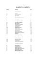
TABLE OF CONTENTS
Section
Number
Paragraph
Title
1
General Information
1.1
1.2
1.3
Features
General Description
Specifications
2
EBC-BX Technical Reference
2.1
2.2
2.3
2.4
2.5
2.6
2.7
2.8
2.9
2.10
2.11
2.12
2.13
2.14
2.15
2.16
2.17
2.18
2.19
2.20
2.21
2.22
2.23
2.24
2.25
2.26
Introduction
Intel FW82430BX Chipset
Memory Installation
Interrupt Routing
Power/Reset Connections
Mouse Interface
Real Time Clock/Calendar
Keyboard Interface
Serial Interface
Parallel Printer Port
Speaker/Sound Interface
PC/104 Interface
PC/104-Plus Bus Interface
Floppy Interface
IDE Hard Disk Interface
Watchdog Timer Configuration
Status LED
Battery Select Control
DiskOnChip Configuration
Parallel I/O
VGA Configuration
Ethernet Controller
Fan Power Connector
Multi-I/O Connector
USB Connector
Jumper/Connector Summary
3
Award BIOS Configuration
3.1
3.2
3.3
3.4
3.5
3.6
3.7
3.8
3.9
General Information
Entering Setup
Setup Main Menu
Standard CMOS Setup
Advanced BIOS Features Setup
Chipset Features Setup
Integrated Peripherals Setup
Power Management Setup
PnP/PCI Configuration
Page
Number
1-1
1-1
1-2
2-1
2-1
2-1
2-2
2-3
2-3
2-4
2-4
2-5
2-12
2-12
2-12
2-13
2-14
2-15
2-16
2-16
2-16
2-17
2-18
2-21
2-23
2-24
2-25
2-25
2-26
3-1
3-1
3-1
3-2
3-6
3-11
3-14
3-19
3-23
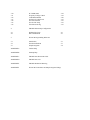
3.10
3.11
3.12
3.13
3.14
3.15
3.16
PC Health Status
Frequency/Voltage Control
Load BIOS Defaults
Set Supervisor Password
Set User Password
Save & Exit Setup
Exit without Saving
3-25
3-25
3-26
3-27
3-27
3-27
3-27
4
EBC-BX DiskOnChip Configuration
4.1
4.2
DiskOnChip Usage
DOC Initialization
5
WS16C48 Programming Reference
5.1
5.2
5.3
Introduction
Function Definitions
Sample Programs
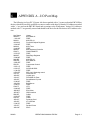
APPENDIX A
I/O Port Map
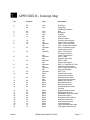
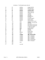
APPENDIX B
Interrupt Map
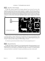
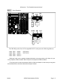
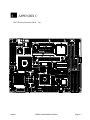
APPENDIX C
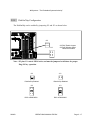
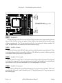
EBC-BX Parts Placement Guide
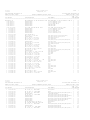
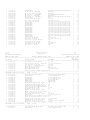
APPENDIX D
EBC-BX Parts List
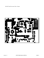
APPENDIX E
EBC-BX Mechanical Drawing
APPENDIX F
WS16C48 I/O Routines and Sample Program Listings
4-1
4-1
5-1
5-1
5-6
1
General Information
1.1
Features
n
n
n
n
n
n
n
n
n
n
n
n
n
n
n
n
1.2
Intel Low Power Celeron Processors and Low Power Pentium III processors
EBX-compliant board
256KB/128KB of pipeline burst L2 cache (Pentium III/Celeron)
Up to 256MB of SDRAM
Socket for bootable DiskOnChip or DIP socket for BIOS extension support of Flash
or ROM
PC Compatible uses Intel 443BX chip set
On board high resolution AGP 1X video controller
Flat panel video support
Supports resolutions up to 1280 x 1024
Simultaneous CRT and LCD operation
PC-104/Plus and PC/104 expansion buses
10/100 Mbps Ethernet using Intel 82559
4 RS-232 serial ports with FIFO, COM1 & COM2
supports optional RS-422/485/J1708 support
Bi-directional LPT port supports EPP/ECP
Dual IDE channels support UDMA-33 and UDMA-66 Drives
48 bi-directional TTL digital I/O lines
General Description
The EBC-BX is a small, high-performance, em beddable com puter sys tem on a sin gle board. It in tegrates a number of popu lar I/O op tions in clud ing AGP 1X VGA, Eth er net, Solid- State Disk, and HighDensity Par al lel I/O. Four PC com pati ble se rial ports are stan dard, as are the floppy, hard disk, and parallel printer interfaces. The EBC-BX is populated with either an Intel low power Celeron processor or
an Intel low power Pentium III processor at speeds from 300 to 700 MHz. Up to 256Mbytes of user
installable DIMM memory is supported. A 16-bit PC/104 expansion bus and the PC/104Plus bus is
provided for further expansion to an entire industry of add-on peripherals including sound and speech
modules, SCSI controllers, Analog I/O mod ules, and lit er ally hun dreds of other op tions available from
WinSystems and a variety of vendors supporting the PC/104 and PC/104-Plus standards. An onboard
32-pin sili con disk socket sup port s the M-Systems’ Disk On Chip Flash mod ules in sizes rang ing from 8
Megabytes to over 500 Megabytes.
030923
OPERATIONS MANUAL EBC-BX
Page 1 - 1
1.3
Specifications
1.3.1
Electrical
Bus Interface :
PC/104 8-Bit or 16-Bit expansion bus
PC/104-Plus 32-bit expansion bus
System Clock :
FSB 100MHz
Interrupts :
TTL Level input
VCC :
+5V +/- 5% at 2.75A typical with an Intel 400Mhz Celeron processor with
32MB SDRAM
+5V +/-5% at 3.4A typical with an Intel Pentium III processor at 700 Mhz with
32MB SDRAM
VCC1 :
+12V +/-5% (Not required. PC/104 Expansion, Flat Panel, use only)
VCC2 :
-12V +/-5% (Not required. PC/104 Expansion or Flat Panel use only)
VCC3:
3.3V (Not required. PC/104 Plus expansion use only)
Memory
Addressing :
256 Megabyte addressing
BIOS ROM :
256K Atmel Flash (reprogrammable on board)
Memory DIMM Socket : 168-pin 3.3V Dimm Module; PC-100 SDRAM Module
SSD Memory :
1.3.2
One 32-pin JEDEC standard socket supporting the M-Systems’ 32-Pin DOC
(DiskOnChip) module.
Mechanical
Dimensions :
5.75 X 8.0 X 0.60 inches (without PC/104 modules or cables)
PC-Board :
FR4 Epoxy Glass with 6 signal layers and 4 power planes with screened
component legend, and plated through holes
Jumpers :
0.025" square posts on 0.10" centers
Connectors :
Multi I/O :
50-pin RN type IDH-50LP
COM3/COM4 :
20-pin RN type IDH-20LP
Floppy Disk :
34-pin RN type IDH-34-LP
Page 1 - 2
OPERATIONS MANUAL EBC-BX
030923
1.3.3
CRT :
14-pin 2mm Molex Type 87331-1420
Flat Panel :
Two, 50-pin 2mm Molex type 87331-5020
Power/Reset :
9-pin in-line Molex type 26-60-7091
Fan Power :
3-pin in-line Molex type 22-11-2032
Mouse :
5-pin in-line latching Molex type 22-11-2052
USB :
4-pin in-line latching Molex type 22-11-2042
PC/104 Bus :
64-Pin SAMTEC type ESQ-132-12-G-D
40-Pin SAMTEC type ESQ-120-12-G-D
PC/104-Plus Bus :
120-Pin SAMTEC type TS-30-Q
IDE :
Two 40-pin 2mm Molex Type 70246-4021
Ethernet :
RJ-45
Environmental :
Operating Temperature :
-40° to +60° C
Non-condensing relative humidity :
5% to 95%
030923
OPERATIONS MANUAL EBC-BX
Page 1 - 3
2
EBC-BX Technical Reference
2.1
Introduction
This sec tion of the man ual is in tended to pro vide suf fi cient in for ma tion re gard ing the configuration
and usage of the EBC-BX board. WinSystems maintains a Technical Support group to help answer
questions regarding configuration, usage, or programming of the board. For answers to questions not
adequately addressed in this manual, contact Technical Support at (817) 274-7553 between 8AM and
5PM Central Time.
2.2
Intel FW82443BX / SMSC Victory-66 Chipset
The EBC-BX utilizes the Intel FW82443BX North bridge coupled with the SMSC Victory-66
South bridge. This com bined chipset pro vides a highly- integrated, high- performance back bone f or full
Pentium class com pati bil ity. The Chipset con tains the logic for DRAM and bus state con trol as well as
the standard complement of 'AT' class peripherals, including :
Two-82C37 DMA controllers
Two-82C59 Interrupt controllers
82C54 Timer/Counter
Real Time Clock
Enhanced Power Management
Full Plug and Play compatibility
These functional units are 100% PC/AT compatible and are supported by the Award BIOS and
setup. Us ers de sir ing to ac cess these in ter nal pe riph er als di rectly should ref er to any manu fac tur ers generic literature on the equivalent discrete component.
There are a number of internal registers within the BX chipset that are used by the BIOS for control
and con figu ra tion. Ref er to the I/O map in Ap pen dix A for port us age to avoid con flicts when add ing external I/O devices.
2.3
Memory Installation
The EBC- BX sup ports a sin gle user instal la ble 168- pin stan dard DIMM. DIMM mod ules should be
a minimum speed of PC-100 and x64 or x 72. Either ECC on non-ECC parts may be used. A single
DIMM socket is pro vided which can sup port SDRAM sizes from 32MB to 256MB. For a list of qualified DIMMs, go to http://www.winsystems.com/memory
Installation is accomplished with power off by inserting the DIMM module directly into the connector at M1. The DIMM module is keyed in 2 places and cannot be inserted backwards without ex-
030923
OPERATIONS MANUAL EBC-BX
Page 2 - 1
WinSystems - "The Embedded Systems Authority"
treme force. The module is inserted until the retaining clips snap into place. Removal is the reverse
process. Push down on the retaining clips, moving them outward. The DIMM module, once released,
will be forced up to an appropriate removal position.
2.4
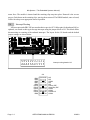
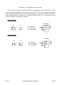
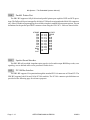
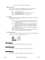
Interrupt Routing
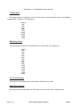
All in ter rupts on the EBC- BX are routed to their re spec tive PC/104 bus pins. On board non- PnP peripherals, are routed to their typical usage interrupts using the jumper block at J19. This block allows
disconnecting or rerouting of the onboard interrupts. The layout for the J19 header and the default
jumper settings are shown below.
21 19 17 15
o o o o
o o o o
22 20 18 16
13 11 9
o o o
o o o
14 12 10
7
o
o
8
5
o
o
6
3
o
o
4
1
o
o
2
Interrupt routing header J19
J19
IRQ3
IRQ4
IRQ5
IRQ7
IRQ6
IRQ14
IRQ15
IRQ12
IRQ11
IRQ10
IRQ9
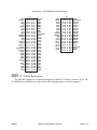
Page 2 - 2
1 o
3 o
5 o
7 o
9 o
11 o
13 o
15 o
17 o
19 o
21 o
o 2
o 4
o 6
o 8
o 10
o 12
o 14
o 16
o 18
o 20
o 22
N/C
N/C
COM3
N/C
N/C
Primary IDE
Secondary IDE
COM4
COM3
Parallel I/O
COM4
OPERATIONS MANUAL EBC-BX
030923
WinSystems - "The Embedded Systems Authority"
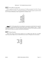
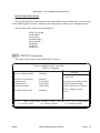
2.5
Power/Reset Connections
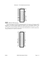
Power is applied to the EBC-BX via the connector at J3 (Molex part number 26-60-7091). The pin
definitions for J3 are given below. An optional push-button-reset (Normally Open) may also be routed
into J3 if desired. Momentary closure to ground forces a hardware reset.
J3
+5V
GND
GND
+12V
+3.3V
GND
+5V
-12V
PB Reset
o1
o2
o3
o4
o5
o6
o7
o8
o9
Note : The 3.3 Volt input pin does not provide power to any devices on the board. It is routed directly to the PC/104Plus Bus and is only re quired if there are PC/104Plus cards that re quire 3.3 Volts be
sup plied from the Bus. The +12 and -12 Volt pins are routed di rectly to the PC/104 con nec tors and flatpanel connectors and are not required for normal board operation.
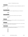
2.6
Mouse Interface
A PS/2 mouse may be attached via the connector at J1. An adapter cable, CBL-225-1 is available
from Win Sys tems to adapt to a con ven tional PS/2 mouse con nec tor. The pin out for J1 is shownhere.
J1
MSDAT
N/C
GND
+5V
MSCLK
030923
1o
2o
3o
4o
OPERATIONS MANUAL EBC-BX
Page 2 - 3
WinSystems - "The Embedded Systems Authority"
2.7
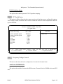
Real Time Clock/Calendar
The EBC-BX contains an onboard Clock/Calendar within the Victory-66 chip. This clock is fully
compatible with the MC146818A used in the original PC-AT computers. This clock has a number of
features including periodic and alarm interrupt capabilities. In addition to the time and date keeping
func tions, the sys tem con figu ra tion is kept within the CMOS RAM con tained in the clock sec tion. This
RAM holds all of the setup information regarding hard and floppy disk types, video type, shadowing,
wait states, etc. Refer to the section on the Award BIOS Setup for what is configured via the CMOS
RAM.
J27
1o
2o
3o
J27 Battery Select Jumper
It may be come nec es sary at some time to make the CMOS RAM for get its cur rent con figu ra tion and
to start fresh with fac tory de faults. This may be ac com plished by re mov ing power from the board . Then
remove the jumper from pins 2-3 on J27 and place on pins 1-2 for 10 seconds. Replace the jumper on
J27 pins 2-3, power-up, and reconfigure the CMOS settings as desired.
If is desired to operate the board without a battery J27 must be jumpered on pins 1-2.
2.8
Keyboard Interface
The EBC-BX contains an onboard PS/2 style keyboard controller. Keyboard connection is made
through the Multi-I/O con nec tor at J2. An adapter ca ble P/N CBL- 247-1 is avail able from Win Systems
to make ready access to all of the devices terminated at the Multi-I/O connector. Users desiring custom
connections should refer to the Multi-I/O connector pin definitions given later in this manual.
Page 2 - 4
OPERATIONS MANUAL EBC-BX
030923
WinSystems - "The Embedded Systems Authority"
2.9
Serial Interface
U9 U4 U5
1o
2o
3o
3 2 1
o o o
J15
J17
U10 U6 U7
1o
2o
3o
3 2 1
o o o
J16
J18
The EBC-BX provides four 16550 compatible RS-232 serial ports at the following addresses :
COM1
COM2
COM3
COM4
3F8H
2F8H
3E8H*
2E8H*
at IRQ 4
at IRQ 3
at IRQ 5**
at IRQ 9**
(PnP Device)
(PnP Device)
*COM ports 3 and 4 can be enabled or disabled individually via the jumper block at J24. When J24 pins
1-2 are jumpered, COM3 is enabled. When J24 pins 3-4 are jumpered, COM4 is enabled.
**The interrupts are not disconnected when COM3 or COM4 are disabled. Use the interrupt rout ing block
J19 described earlier to disconnect the default interrupts if desired.
030923
OPERATIONS MANUAL EBC-BX
Page 2 - 5
WinSystems - "The Embedded Systems Authority"
The two primary serial ports, COM1 and COM2 are configurable for RS-422, RS-485 or J1708,
with the ad di tion of op tional driver ICs (Win Sys tems P/N CK-75176-2). The con figu ra tion op tions for
each of the supported modes are shown on the following pages. Connection to COM1 and COM2 is
made through the Multi-I/O connector at J2. An adapter cable (P/N CBL- 247-1) is avail able from WinSystems to adapt to standard DB9 connectors.
COM1 - RS-232
COM1 DB9
J15
321
ooo
J17
123
ooo
U4 - Installed
U9 - Not Installed
U5 - Not Installed
CD
RX Data
TX Data
DTR
GND
1oo6
2oo7
3oo8
4oo9
5o
DSR
RTS
CTS
RI
COM2 - RS-232
COM2 DB9
J19
321
ooo
Page 2 - 6
J22
123
ooo
U6 - Installed
U10 - Not Installed
U7 - Not Installed
OPERATIONS MANUAL EBC-BX
CD
RX Data
TX Data
DTR
GND
1oo6
2oo7
3oo8
4oo9
5o
DSR
RTS
CTS
RI
030923
WinSystems - "The Embedded Systems Authority"
COM3/COM4 - RS-232
COM3 and COM4 are RS-232 only and are terminated at J4. An adapter cable is available from
WinSystems (P/N CBL-173-1), which adapts J4 to two stan dard DB9M con nec tors. The pin defi ni tions
for J4 are shown here :
J4
COM3 DCD
COM3 RX
COM3 TX
COM3 DTR
GND
COM4 DCD
COM4 RX
COM4 TX
COM4 DTR
GND
2.9.1
1oo2
3oo4
5oo6
7oo8
9 o o 10
11 o o 12
13 o o 14
15 o o 16
17 o o 18
19 o o 20
COM3 DSR
COM3 RTS
COM3 CTS
COM3 RI
N/C
COM4 DSR
COM4 RTS
COM4 CTS
COM4 RI
N/C
RS-422 Mode Configuration
RS-422 levels are supported on both COM1 and COM2 with the installation of the optional “Chip
Kit”, WinSystems part number CK-75176-2. This kit provides the driver ICs necessary for a single
channel of RS-422. If two channels of RS-422 are required then two kits will be needed. RS-422 is a
4-wire point- to- point full- duplex in ter face al low ing much longer ca ble runs than are pos si ble with RS232. The differentialtransmitter and receiver twisted pairs offer a high degree of noise im mu nity. RS422 usually requires the lines be terminated at both ends. This termination can be accomplished either
on the cable or by in stall ing re sist ers on the board in locations reserved for them. The method for de termining the correct resistor values is beyond the scope of this document but it is recommended that trial
values of 100 ohms be used in all three locations at the receiver end. The following illustration shows
the cor rect mode jump er ing, driver IC in stal la tion, I/O con nec tor pin defi ni tions, and ter mi na tion re sistor locations for each of the channels when used in RS-422 mode.
030923
OPERATIONS MANUAL EBC-BX
Page 2 - 7
WinSystems - "The Embedded Systems Authority"
COM1 - RS-422
COM1 DB9
J15
J17
123
ooo
321
ooo
U4 - Not Installed
U9 - Installed
U5 - Installed
N/C
TX+
TXN/C
GND
1
2
3
4
5
oo6
oo7
oo 8
oo 9
o
RX+
RXN/C
N/C
RS-422 NOTE : When used in RS-422 mode,
the transmitter must be enabled by setting the RTS
bit in the Modem Control Register (Bit1).
VCC
R116
RX+
R114
RXR112
* Im por tant Note: All se rial ter mi na tion com po nents are sur face mount 0805 pack ages on the
bot tom side of the board. These should only be in stalled by sur face mount quali fied in di viduals.
COM2 - RS-422
COM2 DB9
J16
J18
123
ooo
321
ooo
U6 - Not Installed
U10 - Installed
U7 - Installed
N/C
TX+
TXN/C
GND
1
2
3
4
5
oo6
oo7
oo8
oo9
o
RS-422 NOTE: When used in RS-422 mode,
the transmitter must be enabled by setting the RTS
bit in the Modem Control Register (Bit).
VCC
R117
RX+
R115
TXR113
Page 2 - 8
OPERATIONS MANUAL EBC-BX
030923
2.9.2
RS-485 Mode Configuration
The RS-485 Multi- drop in ter face is sup ported on both chan nels with the in stal la tion of the op tional
“Chip Kit”, WinSystems’ part number CK-75176-2. A single kit is sufficient to configure both channels for RS-485. RS-485 is a 2-wire multi-drop interface where only one station at a time talks (transmits) while all oth ers lis ten (re ceive). RS- 485 usu ally re quires the twisted pair be ter mi nated at each end
of the run. The required termination values are dependent upon a number of factors including: line impedance, line length, etc. A good trial value is 100 ohms in all three re sis tor lo ca tions. The fol low ing illustrations show the correct jumpering, driver IC installation, I/O connector pinout, and termination
resistor locations for each of the channels when used in RS-485 mode.
COM1 - RS-485
COM1 DB9
J15
J17
321
ooo
U4 - Not Installed
U9 - Installed
U5 - Not Installed
123
ooo
VCC
R106
TX/RX+
R109
TX/RXR108
N/C
TX/RX+
TX/RXN/C
GND
1oo6
2oo7
3oo8
4oo9
5o
N/C
N/C
N/C
N/C
RS-485 NOTE : Because RS-485 uses a single
twisted-pair, all transmitters are connected in parallel. Only one station at a time may transmit or have
its transmitter enabled. The transmitter Enable/Disable is controlled in software using bit 1 in the Modem Control Register (RTS). When RTS is set, the
trans mit ter is en abled, and when cleared (the nor mal
state) the transmitter is disabled and the receiver is
enabled. Note that it is necessary to allow some
minimal settling time after enabling the transmitter
bef ore trans mit ting the first char ac ter. Like wise, following a transmission, it is necessary to be sure that
all characters have been completely shifted out of
the UART (Check Bit 6 in the Line Status Register)
before disabling the transmitter to avoid chopping
off the last character.
Important Note: All serial termination components are surface mount 0805 packages on the
bottom of the board. These should only be installed by surface mount qualified individuals.
030923
OPERATIONS MANUAL EBC-BX
Page 2 - 9
WinSystems - "The Embedded Systems Authority"
COM2 - RS-485
COM2 DB9
J16
J18
123
ooo
321
ooo
VCC
R103
TX/RX+
R105
TX/RXR104
U6 - Not Installed
U10 - Installed
U7 - Not Installed
N/C
TX/RX+
TX/RXN/C
GND
1oo6
2oo7
3oo8
4oo9
5o
N/C
N/C
N/C
N/C
RS-485 NOTE : Because RS-485 uses a single
twisted-pair, all transmitters are connected in parallel. Only one station at a time may transmit or have
its transmitter enabled. The transmitter Enable/Disable is controlled in software using bit 1 in the Modem Control Register (RTS). When RTS is set, the
trans mit ter is en abled, and when cleared (the nor mal
state) the transmitter is disabled and the receiver is
enabled. Note that it is necessary to allow some
minimal settling time after enabling the transmitter
bef ore trans mit ting the first char ac ter. Like wise, following a transmission, it is necessary to be sure that
all characters have been completely shifted out of
the UART (Check Bit 6 in the Line Status Register)
before disabling the transmitter to avoid chopping
off the last character.
Important Note : All serial termination components are surface mount 0805 pack ages. These
should only be installed by surface mount qualified individuals.
2.9.3
SAE J1708 Configuration
The Society of Automotive Engineers (SAE) J1708 interface is a variation of the RS-485 interface
which is used for “Se rial Data Com mu ni ca tions be tween Mi cro com puter Sys tems in Heavy Duty Ve hicle Applications”. It is beyond the scope of this document to go into detail on the J1708 specification.
The EBC-BX may be user configured for J1708 by the addition of the CK-75176-2 “Chip Kit”. One
“Chip Kit” is suf fi cient to con fig ure both chan nels for J1708. The il lus tra tions that fol low show the correct jump er ing, driver IC in stal la tion, I/O con nec tor pin defi ni tions, and the ter mi na tion net work de tails
for each of the channels when used in J1708 mode.
Page 2 - 10
OPERATIONS MANUAL EBC-BX
030923
WinSystems - "The Embedded Systems Authority"
COM1 - J1708
COM1 DB9
J15
321
ooo
J17
U4 - Not Installed
U9 - Installed
U5 - Not Installed
123
ooo
1oo6
2oo7
3oo 8
4oo 9
5o
N/C
TX/RX+
TX/RXN/C
GND
N/C
N/C
N/C
N/C
VCC
R106
4.7K
R111 47 OHM
TX/RX+
C104 .0022 ufd
R109
Absent
C103 .0022 ufd TX/RX-
R108
4.7K
R110 47 OHM
Important Note : All serial termination components are surface mount 0805 packages on the
bottom of the board. These should only be installed by surface mount qualified individuals.
COM2 - J1708
COM2 DB9
J16
321
ooo
J18
U6 - Not Installed
U10 - Installed
U7 - Not Installed
123
ooo
N/C
TX/RX+
TX/RXN/C
GND
1
2
3
4
5
oo6
oo7
oo8
oo9
o
N/C
N/C
N/C
N/C
VCC
R103
4.7K
R100 47 OHM
TX/RX+
R1105
Absent
R104
4.7K
030923
C100 .0022 ufd
C101 .0022 ufd
TX/RX-
R101 47 OHM
OPERATIONS MANUAL EBC-BX
Page 2 - 11
WinSystems - "The Embedded Systems Authority"
2.10
Parallel Printer Port
The EBC-BX supports a fully bi-directional parallel printer port capable of EPP and ECP operations. The PnP par al lel port is mapped by de fault at 378H and is ter mi nated at the Multi-I/O connectors
at J3. Other I/O and in ter rupt map ping are avail able us ing the Award BIOS setup menu op tions. The pin
definitions for the parallel port DB25 connector when using the CBL-247-1 cable are shown below:
STROBE
PD0
PD1
PD2
PD3
PD4
PD5
PD6
PD7
ACK
BUSY
PE
SLCT
2.11
1o
2o
3o
4o
5o
6o
7o
8o
9o
10 o
11 o
12 o
13 o
o 14
o 15
o 16
o 17
o 18
o 19
o 20
o 21
o 22
o 23
o 24
o 25
AUTOFD
ERROR
INIT
SLIN
GND
GND
GND
GND
GND
GND
GND
GND
Speaker/Sound Interface
The EBC- BX util izes a high- impedance piezo type de vice for audio out put. BIOS beep codes, er ror
signaling, or user-defined tones can be presented via this device.
2.12
PC/104 Bus Interface
The EBC-BX supports I/O expansion through the standard PC/104 connectors at J20 and J23. The
EBC-BX supports both 8-bit and 16-bit PC/104 modules. The PC/104 connector pin definitions are
provided on the following page for reference purposes.
Page 2 - 12
OPERATIONS MANUAL EBC-BX
030923
WinSystems - "The Embedded Systems Authority"
GND
RESET
+5V
IRQ9
-5V
DRQ2
-12V
0WS
+12V
GND
MEMW
MEMR
IOW
IOR
DACK3
DRQ3
DACK1
DRQ1
REFRESH
SYSCLK
IRQ7
IRQ6
IRQ5
IRQ4
IRQ3
DACK2
TC
BALE
+5V
OSC
GND
GND
2.13
J23
B1 o o
B2 o o
B3 o o
B4 o o
B5 o o
B6 o o
B7 o o
B8 o o
B9 o o
B10 o o
B11 o o
B12 o o
B13 o o
B14 o o
B15 o o
B16 o o
B17 o o
B18 o o
B19 o o
B20 o o
B21 o o
B22 o o
B23 o o
B24 o o
B25 o o
B26 o o
B27 o o
B28 o o
B29 o o
B30 o o
B31 o o
B32 o o
A1
A2
A3
A4
A5
A6
A7
A8
A9
A10
A11
A12
A13
A14
A15
A16
A17
A18
A19
A20
A21
A22
A23
A24
A25
A26
A27
A28
A29
A30
A31
A32
IOCHK
BD7
BD6
BD5
BD4
BD3
BD2
BD1
BD0
IOCHRDY
AEN
SA19
SA18
SA17
SA16
SA15
SA14
SA13
SA12
SA11
SA10
SA9
SA8
SA7
SA6
SA5
SA4
SA3
SA2
SA1
SA0
GND
GND
SBHE
LA23
LA22
LA21
LA20
LA19
LA18
LA17
MEMR
MEMW
SD8
SD9
SD10
SD11
SD12
SD13
SD14
SD15
KEY
J20
C0 o o
C1 o o
C2 o o
C3 o o
C4 o o
C5 o o
C6 o o
C7 o o
C8 o o
C9 o o
C10 o o
C11 o o
C12 o o
C13 o o
C14 o o
C15 o o
C16 o o
C17 o o
C18 o o
C19 o o
D0
D1
D2
D3
D4
D5
D6
D7
D8
D9
D10
D11
D12
D13
D14
D15
D16
D17
D18
D19
GND
MEMCS16
IOCS16
IRQ10
IRQ11
IRQ12
IRQ15
IRQ14
DACK0
DRQ0
DACK5
DRQ5
DACK6
DRQ6
DACK7
DRQ7
VCC
MASTER
GND
GND
PC/104Plus Bus Interface
The EBC-BX supports I/O expansion through the standard PC/104Plus connector at J22. The
PC/104Plus Bus pin definitions are provided on the following page for reference purposes.
030923
OPERATIONS MANUAL EBC-BX
Page 2 - 13
WinSystems - "The Embedded Systems Authority"
J22
Pin
A
B
C
D
1
GND/5.0 KEY
Reserved
+5
AD00
2
VI/O
AD02
AD01
+5V
3
AD05
GND
AD04
AD03
4
C/BE0*
AD07
GND
AD06
5
GND
AD09
AD08
GND
6
AD11
VI/O
AD10
M66EN
7
AD14
AD13
GND
AD06
8
+3.3V
C/BE1*
AD15
+3.3V
9
SERR*
GND
SB0*
PAR
10
GND
PERR*
+3.3V
SDONE
11
STOP*
+3.3V
LOCK*
GND
12
+3.3V
TRDY*
GND
DEVSEL*
13
FRAME*
GND
IRDY*
+3.3V
14
GND
AD16
+3.3.V
C/BE3*
15
AD18
+3.3V
AD17
GND
16
AD21
AD20
GND
AD19
17
+3.3V
AD23
AD22
+3.3V
18
IDSEL0
GND
IDSEL1
IDSEL2
19
AD24
C/BE3*
VI/O
IDSEL3
20
GND
AD26
AD25
GND
21
AD29
+5V
AD28
AD27
22
+5V
AD30
GND
AD31
23
REQ0*
GND
REQ1*
VI/O
24
GND
REQ2*
+5V
GNT0*
25
GNT1*
VI/O
GNT2*
GND
26
+5V
CLK0
GND
CLK1
27
CLK2
+5V
CLK3
GND
28
GND
INTD*
+5V
RST*
29
+12V
INTA*
INTB*
INTC*
30
-12V
Reserved
Reserved
GND/3.3V KEY
2.14
Floppy Disk Interface
The EBC-BX supports up to 2 standard 3 1/2" or 5 1/4" PC compatible floppy disk drives. The
drives are con nected via the I/O con nec tor at J10. Note that the in ter con nect ca ble to the drives is a standard floppy I/O ca ble used on desk top PCs. The ca ble must have the twisted sec tion prior to the drive A
position. The pin definitions for the J10 connector are shown on the following page:
Page 2 - 14
OPERATIONS MANUAL EBC-BX
030923
WinSystems - "The Embedded Systems Authority"
J10
GND
GND
GND
GND
GND
GND
GND
GND
GND
GND
GND
GND
GND
GND
GND
GND
GND
2.15
1 o
3 o
5 o
7 o
9 o
11 o
13 o
15 o
17 o
19 o
21 o
23 o
25 o
27 o
29 o
31 o
33 o
o
o
o
o
o
o
o
o
o
o
o
o
o
o
o
o
o
2
4
6
8
10
12
14
16
18
20
22
24
26
28
30
32
34
RPM/LC
N/C
N/C
INDEX
MTR0
DRV1
DRV0
MTR1
DIR
STEP
WDATA
WGATE
TRK0
WPRT
RDATA
HDSEL
DSKCHG
IDE Hard Disk Interface
The EBC-BX supports standard IDE fixed disks through the I/O connectors at J5 (primary) and J8
(secondary). The EBC-BX supports multiple PIO modes as well as Ultra-DMA (UDMA)33 and
UDMA 66 drives when used with an UDMA 80-pin cable (WinSystems P/N CBL-126-10). A red activity LED is present at D3 and D2 for the primary and secondary hard drive controllers respectively.
The pin definitions for J5 and J8 are shown here:
RST
D7
D6
D5
D4
D3
D2
D1
D0
LED
DRQ
IOW
IOR
RDY
DACK
IRQ
A1
A0
CS1
VCC
030923
J5 and J8
1 o o 2
3 o o 4
5 o o 6
7 o o 8
9 o o 10
11 o o 12
13 o o 14
15 o o 16
17 o o 18
19 o o 20
21 o o 22
23 o o 24
25 o o 26
27 o o 28
29 o o 30
31 o o 32
33 o o 34
35 o o 36
37 o o 38
39 o o 40
GND
D8
D9
D10
D11
D12
D13
D14
D15
N/C
GND
GND
GND
NC
GND
NC
NC
A2
CS3
GND
OPERATIONS MANUAL EBC-BX
Page 2 - 15
WinSystems - "The Embedded Systems Authority"
2.16
Watchdog Timer Configuration
Watchdog Timer configuration jumper J21
J21
1o
2o
The EBC-BX board features a power-on voltage detect, and power-down/power brownout reset
circuit to protect memory and I/O from faulty CPU operation during periods of illegal voltage levels.
This supervisor circuitry also features a watchdog timer which can be used to guard against software
lock ups. An in ter nal timer with a pe ri od of 1.5 or 150 sec onds will, when en abled, re set the CPU if the
watchdog has not been serviced within the allotted time. The watchdog timer powers-up disabled and
must be enabled in software before timing will begin. Enabling is accomplished by writing a 1 to I/O
port 1EEH. Writ ing a 0 to I/O port 1EEH will disable the watch dog. Af ter ena bling, pet ting may be accomplished by writing any value to I/O port 1EFH at least every 1.5 if J21 is not jumpered or at least
every 150 sec onds if J21 is jumpered, or a reset will oc cur. This mode of op era tion can be used with the
BIOS or DOS provided that the watchdog is disabled bef ore mak ing any ex ten sive BIOS or DOS calls,
especially video or disk I/O calls which could exceed the time seconds allowed when the 1.5 second
mode is used.
2.17
Status LED
A green LED is populated on the board at D1 which can be used for any application specific pur pose. The LED can be turned on in soft ware by writ ing a 1 to I/O port 1EDH. The LED can be turned off
by writing a 0 to 1EDH.
2.18
Battery Select Control
An on board 350mAH nomi nal ca pac ity, lith ium bat tery is pro vided for the CMOS Clock/Cal en dar.
A master battery enable jumper is provided at J27. When J27 is jumpered pins 2-3, battery power is
supplied to the Clock/Calendar. When J27 is jumpered pins 1-2, the battery is to tally dis connected and
no current will be drawn from it. Battery life is highly dependent upon duty cycle as there is no current
drawn from the bat tery when +5 volts is ap plied to the board. Both stor age and op era tional temperatures
play a prominent factor in battery life. High temperatures will shorten battery life significantly. J27
must be jumpered 1-2 if a battery is not installed.
Page 2 - 16
OPERATIONS MANUAL EBC-BX
030923
WinSystems - "The Embedded Systems Authority"
2.19
DiskOnChip Configuration
The DiskOnChip can be enabled by jumpering J12 and J13 as shown below.
J12
2 1
o o
J12 DOC Enable Jumper
J13 DOC Window Select
BIOS Write Enable
J13
3
o
o
4
1
o
o
2
Note : J13 pins 1-2 control BIOS write, and must be jumpered at all times for proper
Plug-N-Play operation.
J12
J12
2 1
o o
2 1
o o
DiskOnChip Enabled
DiskOnChip Disabled
J13
J13
2
o
o
4
2
o
o
4
1
o
o
3
DOC at D800:0000
030923
1
o
o
3
DOC at D000:0000
OPERATIONS MANUAL EBC-BX
Page 2 - 17
WinSystems - "The Embedded Systems Authority"
J6
2 1
o o
J6 Parallel I/O Enable
J14 Parallel I/O +5V Supply Enable
J14
2 1
o o
2.20
Parallel I/O
The EBC- BX util izes the Win Sys tems WS16C48 ASIC high- density I/O chip mapped at a base address of 120H. The first 24 lines are capable of fully latched event sensing with sense polarity being
software programmable. Two, 50-pin connectors allow for easy mating with industry standard I/O
racks. The pinout for the two connectors are shown on the next page.
2.20.1
Parallel I/O Enable
The par al lel fea tures of the EBC- BX can be en abled or dis abled us ing the jumper block at J6. When
J6 is jumpered the par al lel I/O is en abled at I/O ad dress 120H. When J6 is open the 16 ad dresses start ing
at I/O address 120H are free for use by other devices.
2.20.2
Parallel I/O VCC Enable
The I/O con nec tors can pro vide +5 volts to an I/O rack or for mis cel la ne ous pur poses by jumpering
J14. When J14 is jumpered +5 volts is pro vided at pin 49 of both J7 and J9. It the user's re spon si bil ity to
limit current to a safe value (less than 400mA ) to avoid damaging the CPU board.
2.20.3
Parallel I/O Connectors
The 48 lines of parallel I/O are terminated through two 50- pin con nec tors at J7 and J9. The J7 connector handles I/O ports 0-2 while J9 handles ports 3-5. The pin definitions for J7 and J9 are shown on
the following page.
Page 2 - 18
OPERATIONS MANUAL EBC-BX
030923
WinSystems - "The Embedded Systems Authority"
J7
Port 2 Bit 7
Port 2 Bit 6
Port 2 Bit 5
Port 2 Bit 4
Port 2 Bit 3
Port 2 Bit 2
Port 2 Bit 1
Port 2 Bit 0
Port 1 Bit 7
Port 1 Bit 6
Port 1 Bit 5
Port 1 Bit 4
Port 1 Bit 3
Port 1 Bit 2
Port 1 Bit 1
Port 1 Bit 0
Port 0 Bit 7
Port 0 Bit 6
Port 0 Bit 5
Port 0 Bit 4
Port 0 Bit 3
Port 0 Bit 2
Port 0 Bit 1
Port 0 Bit 0
+5V
2.20.4
J9
1oo2
3oo4
5oo6
7oo8
9 o o 10
11 o o 12
13 o o 14
15 o o 16
17 o o 18
19 o o 20
21 o o 22
23 o o 24
25 o o 26
27 o o 28
29 o o 30
31 o o 32
33 o o 34
35 o o 36
37 o o 38
39 o o 40
41 o o 42
43 o o 44
45 o o 46
47 o o 48
49 o o 50
GND
GND
GND
GND
GND
GND
GND
GND
GND
GND
GND
GND
GND
GND
GND
GND
GND
GND
GND
GND
GND
GND
GND
GND
GND
Port 5 Bit 7
Port 5 Bit 6
Port 5 Bit 5
Port 5 Bit 4
Port 5 Bit 3
Port 5 Bit 2
Port 5 Bit 1
Port 5 Bit 0
Port 4 Bit 7
Port 4 Bit 6
Port 4 Bit 5
Port 4 Bit 4
Port 4 Bit 3
Port 4 Bit 2
Port 4 Bit 1
Port 4 Bit 0
Port 3 Bit 7
Port 3 Bit 6
Port 3 Bit 5
Port 3 Bit 4
Port 3 Bit 3
Port 3 Bit 2
Port 3 Bit 1
Port 3 Bit 0
+5V
1oo2
3oo4
5oo6
7oo8
9 o o 10
11 o o 12
13 o o 14
15 o o 16
17 o o 18
19 o o 20
21 o o 22
23 o o 24
25 o o 26
27 o o 28
29 o o 30
31 o o 32
33 o o 34
35 o o 36
37 o o 38
39 o o 40
41 o o 42
43 o o 44
45 o o 46
47 o o 48
49 o o 50
GND
GND
GND
GND
GND
GND
GND
GND
GND
GND
GND
GND
GND
GND
GND
GND
GND
GND
GND
GND
GND
GND
GND
GND
GND
WS16C48 Register Definitions
The EBC- BX uses the Win Sys tems ex clu sive ASIC de vice, the WS16C48. This de vice pro vides 48
lines of digital I/O. There are 17 unique registers within the WS16C48. The following table summarizes the registers and the text that follows provides details on each of the internal registers.
I/O Address
Offset
Page 0
Page 1
Page 2
Page 3
00H
Port 0 I/O
Port 0 I/O
Port 0 I/O
Port 0 I/O
01H
Port 1 I/O
Port 1 I/O
Port 1 I/O
Port 1 I/O
02H
Port 2 I/O
Port 2 I/O
Port 2 I/O
Port 2 I/O
03H
Port 3 I/O
Port 3 I/O
Port 3 I/O
Port 3 I/O
04H
Port 4 I/O
Port 4 I/O
Port 4 I/O
Port 4 I/O
05H
Port 5 I/O
Port 5 I/O
Port 5 I/O
Port 5 I/O
06H
Int_Pending
Int_Pending
Int_Pending
Int_Pending
07H
Page/Lock
Page/Lock
Page/Lock
Page/Lock
08H
N/A
Pol_0
Enab_0
Int_ID0
09H
N/A
Pol_1
Enab_1
Int_ID1
0AH
N/A
Pol_2
Enab_2
Int_ID2
030923
OPERATIONS MANUAL EBC-BX
Page 2 - 19
WinSystems - "The Embedded Systems Authority"
Register Details
Port 0-5 I/O - Each I/O bit in each of the 6 ports can be individually programmed for input or output. Writing a '0' to a bit position causes the corresponding output pin to go to a High-Impedance state
(pulled high by ex ter nal 10K ohm re sis tors). This al lows it to be used as an in put. When used in the in put
mode, a read reflects the inverted state of the I/O pin, such that a high on the pin will read as a '0' in the
register. Writing a '1' to a bit position causes the output pin to sink current (up to 12mA), effectively
pulling it low.
INT_PENDING - This read-only register reflects the combined state of the INT_ID0 through
INT_ID2 registers. When any of the lower 3 bits are set, it indicates that an interrupt is pending on the
I/O port corresponding to the bit po si tion(s) that are set. Read ing this reg is ter al lows an In ter rupt Service Routine to quickly determine if any interrupts are pending and which I/O port has a pending interrupt.
PAGE/LOCK - This reg is ter serves two pur poses. The up per two bits se lect the reg is ter page in use
as shown here:
D7 D6
0
0
1
1
0
1
0
1
Page
Page 0
Page 1
Page 2
Page 3
Bits 5-0 allow for locking the I/O ports. A '1' written to the I/O port position will prohibit further
writes to the corresponding I/O port.
POL0-POL2 - These reg is ters are ac ces si ble when page 1 is se lected. They al low in ter rupt po lar ity
se lec tion on a port- by- port and bit- by- bit ba sis. Writ ing a '1' to a bit po si tion se lects the rising edge detection interrupts while writing a '0' to a bit position selects falling edge detection interrupts.
ENAB0-ENAB2 - These registers are accessible when page 2 is selected. They allow for port-byport and bit-by-bit enabling of the edge detection interrupts. When set to a '1' the edge detection interrupt is en abled for the cor re spond ing port and bit. When cleared to a '0', the bit's edge de tec tion in ter rupt
is disabled. Note that this reg is ter can be used to in di vidu ally clear a pend ing in ter rupt by disabling and
reenabling the pending interrupt.
INT_ID0 - INT_ID2 - These registers are accessible when page 3 is selected. They are used to
identify currently pend ing edge in ter rupts. A bit when read as a '1' in di cates that an edgeof the polarity
programmed into the corresponding polarity register has been rec og nized. Note that a write to this register (value ignored) clears ALL of the pending interrupts in this register.
Page 2 - 20
OPERATIONS MANUAL EBC-BX
030923
WinSystems - "The Embedded Systems Authority"
2.21
VGA Configuration
The EBC-BX uses a fourth generation CRT/Flat panel Super VGA controller. It supports standard
VGA output as well as a variety of Flat Panel Displays using optional Flat Panel Adapter (FPA) kits.
The video on the EBC- BX uses the Asil iant 69000 se ries VGA con trol lers. The Asili ant con trol ler supports stan dard and super- VGA as well as Color and Mono chrome pan els with 8, 9, 12, 15, 16, 18,24 and
36-bit interfaces.
WinSystems provides flat panel support through a series of Flat Panel Adapter (FPA) kits. Contact
your WinSystems Applications Engineer for the most current list of available FPA’s and supported
panels.Details regarding interfacing to spe cific Flat Pan els is not pro vided in this manual but should be
ref er enced in the docu men ta tion ac com pa ny ing the FPA kit. At tempted con nec tion to any flat panel not
di rectly sup ported by a Win Sys tems FPA mod ule is at the us er’s risk and ex treme care should be exercised to avoid damaging or destroying the panel.
HAZARD WARNING: LCD panels can require a high voltage for the panel backlight. This highfrequency voltage can exceed 1000 volts and can present a shock hazard. Care should be taken when
wiring or handling the inverter output. To avoid dan ger of shock and to avoid dam ag ing frag ile and expensive panels, make all connection changes with power removed.
Note: J26 must be jumpered 1-2 for Sharp-type panels, and 2-3 for NEC-type panels.
2.21.1
CRT Output Connection
Video output to a standard VGA monitor is made via the connector at J32. An adapter cable part
number CBL-234-1 is available from WinSystems to adapt from J32 to the standard DB15 VGA connector. The pin definitions for the J32 connector are shown here :
J32
RED 1 o o 2
GREEN 3 o o 4
BLUE 5 o o 6
HSYNC 7 o o 8
VSYNC 9 o o 10
DDCDATA 11 o o 12
DDCCLK 13 o o 14
030923
GND
GND
GND
GND
GND
GND
VCC
OPERATIONS MANUAL EBC-BX
Page 2 - 21
WinSystems - "The Embedded Systems Authority"
2.21.2
Panel Backlight Connection
Panel Backlight connection is made via the connector at J25. The pinout for J25 is shown here for
reference.
J25
+12
+12
GND
GND
ENBKL
VCC
VCC
2.21.3
o1
o2
o3
o4
o5
o6
o7
Flat Panel Output Connection
Con nec tion to all flat pan els is made via the two 50- pin con nec tors at J31 and J32. These connectors
are ca bled to the ap pro pri ate FPA (Flat Panel Adapter) mod ule which then breaks out the nec es sary cabling for attachment to the panel itself. The FPA module also supplies any special controls that may be
needed for the panel. Refer to the FPA documentation for specific hookup instructions. The pin definitions for J30 and J33 are shown here :
FP12
FP13
FP14
FP15
FP16
FP17
FP18
FP19
FP20
FP21
FP22
FP23
FP24
FP25
FP26
FP27
FP28
FP29
FP30
FP31
FP32
FP33
FP34
FP35
SWVCC
Page 2 - 22
1 o
3 o
5 o
7 o
9 o
11 o
13 o
15 o
17 o
19 o
21 o
23 o
25 o
27 o
29 o
31 o
33 o
35 o
37 o
39 o
41 o
43 o
45 o
47 o
49 o
J30
o 2
o 4
o 6
o 8
o 10
o 12
o 14
o 16
o 18
o 20
o 22
o 24
o 26
o 28
o 30
o 32
o 34
o 36
o 38
o 40
o 42
o 44
o 46
o 48
o 50
GND
GND
GND
GND
GND
GND
GND
GND
GND
GND
GND
GND
GND
GND
GND
GND
GND
GND
GND
GND
GND
GND
GND
GND
SWVCC
SW0
SW2
FPO
FP1
FP2
FP3
FP4
FP5
FP6
FP7
FP8
FP9
FP10
FP11
PCSHCLK
PCFLM
PCLP
PCM
PHSYNC
PVSYNC
ENVCC
ENBKL
ENVEE
+12V
SWVCC
OPERATIONS MANUAL EBC-BX
J33
1 o o
3 o o
5 o o
7 o o
9 o o
11 o o
13 o o
15 o o
17 o o
19 o o
21 o o
23 o o
25 o o
27 o o
29 o o
31 o o
33 o o
35 o o
37 o o
39 o o
41 o o
43 o o
45 o o
47 o o
49 o o
2
4
6
8
10
12
14
16
18
20
22
24
26
28
30
32
34
36
38
40
42
44
46
48
50
SW1
SW3
GND
GND
GND
GND
GND
GND
GND
GND
GND
GND
GND
GND
GND
GND
GND
GND
GND
GND
GND
GND
-12V
+12V
SWVCC
030923
WinSystems - "The Embedded Systems Authority"
2.21.4
Video Mode Table
The EBC-BX video section supports a number of standard and extended VGA modes. The
following table extracted from the Asiliant 69000 databook shows the video modes supported.
Resolution
2.22
Color depth (bpp)
Refresh Rates
640 x 480
8
60, 75, 85
640 x 480
16
60, 75, 85
640 x 480
24
60, 75, 85
800 x 600
8
60, 75, 85
800 x 600
16
60, 75, 85
800 x 600
24
60, 75, 85
1024 x 768
8
60, 75, 85
1024 x 768
16
60, 75, 85
1280 x 1024
8
60
Ethernet Controller
The 82559 is part of Intel’s sec ond gen era tion fam ily of fully in te grated 10BASE-T/100BASE-TX
LAN so lu tions. The 82559 con sists of both the Me dia Ac cess Con trol ler (MAC) and the physi cal layer
(PHY) combined into a single component solution.
The 82559 is a 32-bit PCI controller that features enhanced scatter-gather bus mastering capabilities which en ables it to per form high- speed data trans fers over the PCI bus. The 82559 bus master ca pabilities enable the component to process high-level commands and perform multiple operations offloading com mu ni ca tion tasks from the system CPU. Two large trans mit and re ceive FI FOs of 3 Kbytes
each help prevent data un derruns and over runs, al low ing the 82559 to trans mit data with mini mum interframe spacing (IFS).
The 82559 can op er ate in ei ther full du plex or half du plex mode. In full du plex mode the 82559 adheres to the IEEE 802.3x Flow Control specification. Half duplex performance is enhanced by a proprietary collision reduction mechanism.
The 82559 includes a simple PHY interface to the wire transformer at rates of 10BASE-T and
100BASE- TX, and Auto- Negotiation ca pa bil ity for speed, du plex, and flow con trol. The 82559 also includes an interface to a serial (4-pin) EEPROM. The EEPROM provides power-on initialization for
hardware and software configuration parameters. The 82559 is also 100% PnP compatible and is configured through this interface. Ethernet connection to the EBC-BX is made through the connector at
J28.
There are Eth er net status LED’s at D6, D7, and D8. The color and func tion of each LED is listed below :
D6 = Ethernet 100BASE-TX (Red)
D7 = Ethernet activity LED (Green)
D8 = Ethernet link LED (Yellow)
For ethernet drivers go to:
http://developer.intel.com/design/network/drivers/
030923
OPERATIONS MANUAL EBC-BX
Page 2 - 23
WinSystems - "The Embedded Systems Authority"
J34
3o
2o
1o
Cooling fan connections J31 and J34
J31
3 2 1
o o o
J31 and J34
GND 1 o
FAN POWER 2 o
FAN TACH 3 o
2.23
Fan Power Connector
The EBC-BX has a connector located at J31 to supply power to the processor cooling fan. The pin
definitions are shown here for reference. There is also a connector at J34 for use with an auxiliary system cooling fan. The pin definitions for these connectors is shown here :
Both J31 and J34 provide +5V nominal at 250mA max.
Page 2 - 24
OPERATIONS MANUAL EBC-BX
030923
WinSystems - "The Embedded Systems Authority"
2.24
Multi I/O Connector
The I/O to the primary se rial chan nels, the printer port, and key board are all ter mi nated via the connector at J2. An adapter cable, part number CBL-247-1, is available from WinSystems to adapt to the
conventional I/O connectors. The pin definitions for J2 are shown here
COM1 - DCD
COM1 - RXD
COM1 - TXD
COM1 - DTR
COM1 - GND
COM2 - DSR
COM2 - RTS
COM2 - CTS
COM2 - RI
LPT - STROBE
LPT - PD0
LPT - PD1
LPT - PD2
LPT - PD3
LPT - PD4
LPT - PD5
LPT - PD6
LPT - PD7
LPT - ACK
LPT - BUSY
LPT - PE
LPT - SLCT
KEYBD - GND
KEYBD - KDATA
KEYBD - +5V
2.25
J2
1o o 2
3o o4
5o o6
7o o 8
9 o o 10
11 o o 12
13 o o 14
15 o o 16
17 o o 18
19 o o 20
21 o o 22
23 o o 24
25 o o 26
27 o o 28
29 o o 30
31 o o 32
33 o o 34
35 o o 36
37 o o 38
39 o o 40
41 o o 42
43 o o 44
45 o o 46
47 o o 48
49 o o 50
COM1 - DSR
COM1 - RTS
COM1 - CTS
COM1 - RI
COM2 - DCD
COM2 - RSX
COM2 - TXD
COM2 - DTR
COM2 - GND
LPT - AUTOFD
LPT - ERROR
LPT - INIT
LPT - SLCTIN
LPT - GND
LPT - GND
LPT - GND
LPT - GND
LPT - GND
LPT - GND
LPT - GND
LPT - GND
KEYBD - GND
KEYBD - GND
KEYBD - CLK
KEYBD - +5V
USB Connector
A USB cable may be attached via the connector at J11. An adapter cable, CBL-249-1 is available
from WinSystems to adapt to a conventional USB port. The pinout for J11 is shown here.
J11
1o
2o
3o
4o
030923
USBV0
D0D0+
USBG0
OPERATIONS MANUAL EBC-BX
Page 2 - 25
WinSystems - "The Embedded Systems Authority"
2.26
Jumper/Connector Summary
Connector/
Jumper
Description
Page Reference
J1
J2
J3
J4
J5
J6
J7
J8
J9
J10
J11
J12
J13
J14
J15
J16
J17
J18
J19
J20
J21
J22
J23
J24
J25
J26
J27
J28
J29
J30
J31
J32
J33
J34
Mouse connector
Multi-I/O connector
Power connector
COM3, COM4 connector
Primary IDE connector
Parallel I/O enable jumper
Parallel I/O connector
Secondary IDE connector
Parallel I/O connector
Floppy disk connector
USB connector
DOC Enable jumper
DOC configuration jumper
Parallel I/O VCC select jumper
COM1 RS-422/RS-485 configuration jumper
COM2 RS-422/RS-485 configuration jumper
COM1 RS-422/RS-485 configuration jumper
COM1 RS-422/RS-485 configuration jumper
IRQ routing jumper
PC/104 16-bit connector
Watchdog Timer configuration jumper
PC/104Plus connector
PC/104 8-bit connector
COM3/COM4 Enable jumper
Flat Panel backlight connector
Flat Panel backlight type select jumper
Master Battery select jumper
Ethernet connector
ITP Debug port
Flat Panel/FPA connector
CPU Fan/tachometer connector
VGA CRT output connector
Flat Panel/FPA connector
Auxiliary Fan/Tachometer connector
2-3
2-25
2-3
2-7
2-15
2-18
2-18
2-15
2-18
2-14
2-25
2-17
2-17
2-18
2-5
2-5
2-5
2-5
2-2
2-13
2-16
2-13
2-13
2-5
2-22
2-21
2-4
2-23
N/A
2-22
2-24
2-21
2-22
2-24
Page 2 - 26
OPERATIONS MANUAL EBC-BX
030923
3
Award BIOS Configuration
3.1
General Information
The EBC- BX comes equipped with a stan dard Award BIOS with Setup in ROM that al lows us ers to
modify the basic system configuration. This type of information is stored in battery-backed CMOS
RAM so that it retains Setup information when power is turned off.
3.2
Entering Setup
To en ter setup, power on the com puter and press the DEL key im me di ate ly af ter the mes sage “ Press
DEL to Enter Setup” appears on the lower left of the screen. If the message disappears before you respond and you still wish to en ter setup, re start the sys tem by turn ing it OFF and then ON or by pressing
the RE SET but ton, if so equipped, or by press ing the CTRL, ALT and DEL key si mul ta ne ously. Alternately, under certain error conditions of incorrect setup the message:
“Press F1 to continue or DEL to Enter Setup”
may ap pear. To En ter Setup at that time, press the DEL key. To at tempt to con tinue, ig nor ingthe error condition, press the F1 key.
3.3
Setup Main Menu
The main menu screen is displayed on the following page. Each of the options will be discussed in
this section. Use the arrow keys to highlight the desired selection and press ENTER to enter the submenu or to execute the function selected.
030923
OPERATIONS MANUAL EBC-BX
Page 3 - 1
WinSystems - "The Embedded Systems Authority"
Phoenix - AwardBIOS CMOS Setup Utility.
Standard CMOS Features
Advanced BIOS FEATURES
Advanced Chipset Features
Integrated Peripherals
Power Management Setup
PnP/PCI Configuration
PC Health Status
Frequency/Voltage Control
Load Bios Defaults
Set Supervisor Password
Set User Password
Save & Exit Setup
Exit Without Saving
Esc : Quit
F10 : Save & Exit Setup
↑↓→←
:Select Item
Time, Date. Hard Disk, Type...
3.4
Standard CMOS Features
The items in the Standard CMOS Setup menu are divided into several categories. Each category
may include one or more setup items. Use the arrow keys to highlight the item and then use the PgUp,
PgDn, +.-. keys to select the desired value for the item.
Date
The date format is <day>,< date>,< month>, <year>
Day = The day, from Sun to Sat, determined by the BIOS and is display only
Date = the date, from 1 to 31 (or the maximum for the current month)
Month = the month, JAN through DEC
Year = The year, from 1900 to 2099
Time
The time is hour, minute, second. The time is calculated on the 24-hour, military-time clock such
that 1:00PM is 13:00:00.
Page 3 - 2
OPERATIONS MANUAL EBC-BX
030923
WinSystems - "The Embedded Systems Authority"
Phoenix - AwardBIOS CMOS Setup Utility
Standard CMOS Features
Date (mm:dd:yy)
Time (hh:mm:ss)
Wed Dec 4 2002
13:57:21
Item Help
Menu Level
IDE Primary Master
IDE Primary Slave
IDE Secondary Master
IDE Secondary Slave
[MAXTOR 6L020J1]
[None]
[HL-DT-STDVD-ROM GR8]
[None]
Drive A
Drive B
[1.44M, 3.5 in.]
[None]
Video
Halt On
[EGA/VGA]
[No Errors]
Base Memory
Extended Memory
Total Memory
Press [Enter] to enter
next page for detail
hard drive settings.
640K
261120K
262144K
↑ ↓ → ← : Move Enter : Select PU/PD/+/- : Value F10 : Save ESC : Exit F1 : General Help
F5 : Previous Values
F6 : Fail-Safe Defaults
F7 : Optimized Defaults
IDE Primary Master
Pressing [Enter] brings up a sub-menu screen of choices regarding the Primary fixed disk.
IDE HDD Auto-Detection
Pressing [Enter] when this selection is highlighted will cause the system to
interrogate the attached hard disk and choose the parameters automatically
030923
OPERATIONS MANUAL EBC-BX
Page 3 - 3
WinSystems - "The Embedded Systems Authority"
IDE Primary Master
Pressing [Enter], when this item is highlighted, allows for selection of how
parameters for the hard drive will be determined. The choices are :
- No Hard Drive is installed
- Automatically detect the hard disk parameters at power-up
(Recommended Setting)
Manual - Use the parameters entered manually by the user
None
Auto
Access Mode
Pressing [Enter] when this option is highlighted allows selection of the hard disk
access mode. The choices are :
CHS - The drive will be accessed using direct Cylinder, Head, Sector mode.
No translation will take place. This can only be used when the “manual”
mode is selected above.
LBA - This selection allows the native mode of the drive to be translated to
Cylinder, head, and sector counts that are compatible with allowable
BIOS parameter restrictions. Drives up to 120GB can be used with
this mode.
LARGE - This is another translation scheme that is not commonly used but may
be required for some O/Ss.
AUTO - This mode chooses the appropriate translation mode (usually LBA) for
the actual drive attached. (Recommended Setting)
Drive Parameters/Size
The drive size in MB is displayed for all modes. When manual and CHS modes are
selected the user may enter values into these fields :
Cylinder
Head
Precomp
Landing Zone
Sector
- 0 to 65535
- 0 to 255
- 0 to 65535
- 0 to 65535
- 0 to 255
IDE Primary Slave
This selection is identical to the IDE Primary Master shown above.
IDE Secondary Master
This selection is identical to the IDE Primary Master shown above.
IDE Secondary Slave
This selection is identical to the IDE Primary Master shown above.
Page 3 - 4
OPERATIONS MANUAL EBC-BX
030923
WinSystems - "The Embedded Systems Authority"
Drive A type/Drive B type
This category identifies the type of floppy drives attached as Drive A: or Drive B:.
The choices are as follows :
NONE
360K, 5.25 in.
1.2M, 5.25 in.
720K, 3.5 in
1.44M, 3.5 in.
2.88M 3.5 in.
Video
This cate gory speci fies the type of video adapter used for the pri mary sys tem moni tor that matches
your video display board and monitor. The available choices are:
EGA/VGA
CGA40
CGA80
MONO
The EBC-BX has built-in VGA support so EGA/VGA should be selected.
Error Halt
This category determines whether the system will halt if a nonfatal error is detected during
the power-up self test. The choices are:
No Errors : The system will not be stopped for any error that may be detected.
All Errors : Whenever the BIOS detects a nonfatal error, the system will be
stopped and a prompt will appear.
All, but Keyboard : The system will not stop for a keyboard error, it will stop for all
other errors.
All, but diskette : The system will not stop for disk errors. All others will result in a
prompt.
All but Disk/Key : All errors except diskette or keyboard will result in a halt and a
prompt.
030923
OPERATIONS MANUAL EBC-BX
Page 3 - 5
WinSystems - "The Embedded Systems Authority"
Memory
This category is display only and is determined by the BIOS POST (Power-On Self Test).
Base Memory
The POST rou tines in the BIOS will de ter mine the amount of base (con ven tional) mem ory in stalled
in the sys tem. The value of the base mem ory is typi cally 640K for sys tems with a Mega byte of memory
or greater.
Extended Memory
The BIOS determines how much extended memory is present during the POST. This is the amount
of memory located above 1MB in the CPU's memory address space.
Total Memory
The BIOS dis plays the to tal of the Base mem ory and the Ex tended mem ory in stalled in the sys tem.
.
3.5
Advanced BIOS Features Setup
Virus Warning
This op tion when en abled, pro tects the boot sec tor and par ti tion ta ble of the hard disk against unauthor ized writes through the BIOS. Any at tempt to al ter these ar eas will re sult in an er ror message and a
prompt to authorize the activity.
CPU Internal Cache
This op tion, when en abled, pro vides maxi mum per form ance by cach ing in struc tions and data using
the on-chip cache of the Pentium processor.
External Cache
This option, when enabled, further enhances performance by caching recently used instructions
and data into fast SRAM.
Page 3 - 6
OPERATIONS MANUAL EBC-BX
030923
WinSystems - "The Embedded Systems Authority"
Phoenix - AwardBIOS CMOS Setup Utility
Advanced BIOS Features
Virus Warning
CPU Internal Cache
External Cache
CPU L2 Cache ECC Checking
Processor Number Feature
Quick Power On Self Test
First Boot Device
Second Boot Device
Third Boot Device
Boot Other Device
Swap Floppy Drives
Boot Up Floppy Seek
Boot Up Numlock Status
Gate A20 Options
Typematic Rate Setting
Typematic Rate (Chars/Sec)
Typematic Delay (Msec)
Security Option
OS Select for DRAM > 64MB
Report No FDD for WIN 95
Video BIOS Shadow
C8000-CBFFF Shadow
CC000-CFFFF Shadow
D0000-D3FFF Shadow
D4000-D7FFF Shadow
D8000-DBFFF Shadow
DC000-DFFFF Shadow
Small Logo (EPA) Show
[Disabled]
[Enabled]
[Enabled]
[Enabled]
[Disabled]
[Enabled]
[Floppy]
[HDD-0]
[CD-ROM]
[Enabled]
[Disabled]
[Disabled]
[On]
[Fast]
[Enabled]
[6]
[250]
[Setup]
[Non-OS2]
[No]
[Enabled]
[Disabled]
[Disabled]
[Disabled]
[Disabled]
[Disabled]
[Disabled]
[Disabled]
Item Help
Menu Level
Allows you to choose the
VIRUS warning feature for IDE
hard disk boot sector protection. If
this function is enabled and
someone attempt to write data
into this area , BIOS will show a
warning message on screen and
alarm beep
↑ ↓ → ← : Move Enter : Select PU/PD/+/- : Value F10 : Save ESC : Exit F1 : General Help
F5 : Previous Values
F6 : Fail-Safe Defaults
F7 : Optimized Defaults
CPU L2 Cache ECC Checking
This option when enable provides ECC validity checking to the L2 cache reads.
030923
OPERATIONS MANUAL EBC-BX
Page 3 - 7
WinSystems - "The Embedded Systems Authority"
Processor Number Feature
This feature when enabled allows software to read the unique Processor Serial number present on
the Intel processors.
Quick Power On Self Test (POST)
This option, when enabled, speeds up the POST during power up. The BIOS will shorten and/or
skip some items during POST.
First Boot Device
This options allows for selection of the primary or “First” boot device. The BIOS will attempt to
boot from this device first. The menu selection are :
Floppy
LS120
HDD-0
SCSI
CD-ROM
HDD-1
HDD-2
HDD-3
ZIP100
LAN
Disabled
Note : Not all of these devices will be available and selection of a nonexistent device may result in a
drastic increase in boot time.
Second Boot Device
This op tion al lows for se lec tion of the sec on dary choice for boot me dia us age. The op tions are identical to those given above for the “First Boot Device”.
Third Boot Device
This op tion al lows for se lec tion of a third choice of boot me dia. The op tions are the same as for the
previous two menu items.
Boot Other Device
The op tion when en abled al lows other de vices with self- contained boot firmware to be come the primary boot media.
Page 3 - 8
OPERATIONS MANUAL EBC-BX
030923
WinSystems - "The Embedded Systems Authority"
Swap Floppy Drive
This option allows for swapping of the A: and B: floppy drives without actually relocating the
drives on the cable.
Boot Up Floppy Seek
Dur ing POST, when this op tion is en abled, the BIOS will de ter mine if the floppy drive is 40 track or
80 tracks. If disabled, no seek test will be performed and no error can be reported.
Boot Up Numlock Status
This allows user selection of the Numlock state at boot time.
Gate A20 Option
This option allows for the selection of the source for the gate A20 signal. The choices are:
Normal - Sourced from the keyboard controller
Fast - Sourced from the Chipset
Typematic Rate Setting
This op tion en ables or dis ables the type matic rate pro gram ming at boot time. Type matic is the autorepeat function for the keyboard.
Typematic Rate
When the typematic rate setting is enabled, the typematic repeat speed is set via this option. The
supported rates are :
6 characters per second
8 characters per second
10 characters per second
12 characters per second
15 characters per second
20 characters per second
24 characters per second
30 characters per second
030923
OPERATIONS MANUAL EBC-BX
Page 3 - 9
WinSystems - "The Embedded Systems Authority"
Typematic Delay
When typematic rate setting is enabled, this option specifies the time in milliseconds before autorepeat begins. The supported values are:
250 mS
500 mS
750 mS
1000 mS
Security Option
This option allows you to limit access to the system and setup, or just to setup. The choices are:
System - The system will not boot and access will be denied if the correct password is not entered
at the prompt.
Setup - The system will boot, but access to Setup will be denied if the correct password is not entered
at the prompt.
NOTE: To dis able se cu rity, se lect “Pass word Set ting” at the Setup Main Menu and then you will be
asked to en ter a pass word. Do not type any thing, just hit EN TER. Once the se cu rity is dis abled, the system will boot and you can enter Setup freely.
OS Select for DRAM > 64MB
This option allows selection of an operating system for DRAM greater than 64MB.
The options are:
OS2
Non-OS2
Report No FDD for Win 95
This option, when enabled, signals Windows 95 if there is no floppy present.
The options are:
Yes
No
Page 3 - 10
OPERATIONS MANUAL EBC-BX
030923
WinSystems - "The Embedded Systems Authority"
Shadowing Options
When shadowing for a particular address range is enabled, it instructs the BIOS to copy the BIOS
located in ROM into DRAM. This shad ow ing from an 8- bit EPROM into fast 32- bit DRAM re sults in a
Multi-magnitude increase in performance. The main BIOS is shadowed automatically but there are
other areas that may be selected for shadowing as shown here:
Video BIOS Shadow - C000-C7FFF EGA/VGA BIOS ROM
C8000-CBFFF
CC000-CFFFF
D0000-D3FFF
D4000-D7FFF
D8000-DBFFF
DC000-DFFFF
Small Logo(EPA) Show
This op tion when en abled in structs the BIOS to dis play the EPA Energy- Star logo in the up per right
corner of the screen during the POST process.
3.6
Chipset Features Setup
The options in this section control the chipset programming at boot time. In most cases, the default
set tings should be used un less you have a clear un der stand ing of the sig nifi cance of the change. It is possible using these options to create a system that will either not boot or is very unstable or unreliable. If
this should occur, there are two methods to return the system to a stable configuration. If the system
works well enough to get into Setup, simply choose the “Load BIOS Defaults” option and then select
“Save and Exit Setup” to restore fac tory de faults. If the sys tem will not run well enough to run Setup, it
will be necessary to remove the battery source temporarily until the CMOS memory decays. Refer to
Section 2.7 for details on reinitializing the CMOS RAM.
Each of the options for the Chipset Features Menu will be briefly discussed in the sections that follow.
SDRAM RAS-to-CAS Delay
This option allows for selection of the number of clock to delay the RAS to CAS transition. The
available choices are :
3 Clocks
2 Clocks
030923
OPERATIONS MANUAL EBC-BX
Page 3 - 11
WinSystems - "The Embedded Systems Authority"
Phoenix - AwardBIOS CMOS Setup Utility
Advanced Chipset Features
SDRAM RAS-to-CAS Delay
SDRAM RAS Precharge Time
SDRAM CAS Latency Time
SDRAM Precharge Control
DRAM Data Integrity Mode
System BIOS Cacheable
Video BIOS Cacheable
Video RAM Cacheable
8 Bit I/O Recovery Time
16 Bit I/O Recovery Time
Memory Hole at 15M-16M
AGP Aperture Size (MB)
[3]
[3]
[3]
[Enabled]
[Non-ECC]
[Disabled]
[Disabled]
[Disabled]
[1]
[1]
[Disabled]
[64]
Item Help
Menu Level
↑ ↓ → ← : Move Enter : Select PU/PD/+/- : Value F10 : Save ESC : Exit F1 : General Help
F5 : Previous Values
F6 : Fail-Safe Defaults
F7 : Optimized Defaults
SDRAM RAS Precharge Time
This options allows for setting the SDRAM RAS precharge timing. The choices are :
3 clocks
2 clocks
SDRAM CAS Latency Time
This option allows control of the SDRAM CAS latency timing. The choices are :
3 clocks
2 clocks
Page 3 - 12
OPERATIONS MANUAL EBC-BX
030923
WinSystems - "The Embedded Systems Authority"
SDRAM Precharge Control
This option, when enabled, allow control of the SDRAM precharge timing.
System BIOS Cacheable
This option enables or disables cacheability of the system BIOS.
Video BIOS Cacheable
This option enables or disables cacheability of the video BIOS.
8 Bit I/O Recovery
Enables and defines 8-bit I/O recovery time in number of clocks.
16 Bit I/O Recovery
Enables and defines 16-bit I/O recovery time in number of clocks.
Memory Hole At 15M-16M
This option, when enabled, disables onboard memory between 15M and 16M.
AGP Aperture Size (MB)
This option specifies the amount of address space to allocate to the AGP video aperture. The
choices are :
4
8
16
32
64
128
256
030923
OPERATIONS MANUAL EBC-BX
Page 3 - 13
WinSystems - "The Embedded Systems Authority"
3.7
Integrated Peripherals Setup
The options in this section allow for control of the integrated peripherals, i.e. Floppy and IDE controllers, serial ports, and the parallel port.
Phoenix - Award BIOS CMOS Setup Utility
Integrated Peripherals
IDE 1st Channel Cable
IDE 2nd Channel Cable
IDE Primary Master PIO
IDE Primary Slave PIO
IDE Secondary Master PIO
IDE Secondary Slave PIO
IDE Primary Master UDMA
IDE Primary Slave UDMA
IDE Secondary Master UDMA
IDE Secondary Slave UDMA
On-Chip Primary PCI IDE
On-Chip Secondary PCI IDE
USB Keyboard Support
Init Display First
IDE HDD Block Mode
Onboard FDC Controller
Onboard Serial Port 1
Onboard Serial Port 2
Onboard Parallel Port
Parallel Port Mode
ECP Mode Use DMA
[40 Pins]
[40 Pins]
[Auto]
[Auto]
[Auto]
[Auto]
[Auto]
[Auto]
[Auto]
[Auto]
[Enabled]
[Enabled]
[Disabled]
[AGP]
[Enabled]
[Enabled]
[3F8/IRQ4]
[2F8/IRQ3]
[378/IRQ7]
[ECP+EPP1.9]
[3]
Item Help
Menu Level
↑ ↓ → ← : Move Enter : Select PU/PD/+/- : Value F10 : Save ESC : Exit F1 : General Help
F5 : Previous Values
F6 : Fail-Safe Defaults
F7 : Optimized Defaults
IDE 1st Channel Cable
This option allows for specification of the cable type attached to the Primary IDE channel. The
choices are :
40 Pins
80 Pins
Page 3 - 14
OPERATIONS MANUAL EBC-BX
030923
WinSystems - "The Embedded Systems Authority"
IDE 2nd Channel Cable
This op tion al lows the ca ble type to be speci fied for the sec on dary IDE chan nel. The choices are :
40 Pins
80 Pins
IDE Primary Master PIO
This option allows selection of the PIO mode to be used with the Primary Master IDE device. The
choices are :
Auto
Mode 0
Mode 1
Mode 2
Mode 3
Mode 4
IDE Primary Slave PIO
This option allows for selection of the PIO mode to be used with a Primary Slave IDE device. The
choices are :
Auto
Mode 0
Mode 1
Mode 2
Mode 3
Mode 4
IDE Secondary Master PIO
This op tion al lows se lec tion of the PIO mode to be used with the Secondary Mas ter IDE de vice. The
choices are :
Auto
Mode 0
Mode 1
Mode 2
Mode 3
Mode 4
030923
OPERATIONS MANUAL EBC-BX
Page 3 - 15
WinSystems - "The Embedded Systems Authority"
IDE Secondary Slave PIO
This option allows for selection of the PIO mode to be used with a Secondary Slave IDE device.
The choices are :
Auto
Mode 0
Mode 1
Mode 2
Mode 3
Mode 4
IDE Primary Master UDMA
This op tion al lows for se lect ing whether an UDMA mode will be used for disk trans fers on the Primary Master IDE device. The choices are :
Disabled
Auto
IDE Primary Slave UDMA
This op tion al lows for se lect ing whether an UDMA mode will be used for disk trans fers on the Primary Slave IDE device. The choices are :
Disabled
Auto
IDE Secondary Master UDMA
This option allows for selecting whether an UDMA mode will be used for disk transfers on the
Secondary Master IDE device. The choices are :
Disabled
Auto
IDE Secondary Slave UDMA
This op tion al lows for se lect ing whether an UDMA mode will be used for disk trans fers on the Secondary Slave IDE device. The choices are :
Disabled
Auto
Page 3 - 16
OPERATIONS MANUAL EBC-BX
030923
WinSystems - "The Embedded Systems Authority"
On-Chip Primary PCI IDE
This option enables or disables the onboard Primary IDE controller.
On-Chip Secondary PCI IDE
This option enables or disables the onboard Secondary IDE controller.
USB Keyboard Support
This option enables or disables BIOS support for USB keyboards.
Init Display First
This op tion al lows se lec tion of the source for the first, or pri mary, video con trol ler. The choices are :
PCI Slot
AGP
Note : The onboard video is im ple mented on the AGP bus. An al ter nate pri mary video dis play m ay
be used by installing a PC/104Plus video card and setting this option to PCI Slot.
IDE Block Mode
This option allows enabling of the IDE block mode for disk transfers.
Onboard FDC Controller
This option controls the onboard Floppy Disk controller. The options are :
Enabled
Disabled
Onboard Serial Port 1
This option allows for control of the first onboard serial port. The options are :
Disabled
3F8/IRQ4
2F8/IRQ3
3E8/IRQ4
2E8/IRQ3
Auto
030923
OPERATIONS MANUAL EBC-BX
Page 3 - 17
WinSystems - "The Embedded Systems Authority"
Onboard Serial Port 2
This option allows for control of the second onboard serial port. The options are :
Disabled
3F8/IRQ4
2F8/IRQ3
3E8/IRQ4
2E8/IRQ3
Auto
Onboard Parallel Port
This option allows for configuration of the onboard parallel printer port. The options are :
Disabled
3BC/IRQ7
378/IRQ7
278/IRQ5
Parallel Port Mode
This option controls the operating mode of the onboard parallel port. The options are :
SPP
EPP1.9+SPP
ECP
ECP+EPP1.9
Normal
EPP1.7+SPP
ECP+EPP1.7
ECP Mode Use DMA
This option controls which DMA channel will be used for ECP transfers. The choices are:
3
1
Page 3 - 18
OPERATIONS MANUAL EBC-BX
030923
WinSystems - "The Embedded Systems Authority"
3.8
Power Management Setup
The items in this menu control operation of the BIOS based power management functions.
ACPI function
This option allows for control of the BIOS level ACPI functionality.
Phoenix - Award BIOS CMOS Setup Utility
Power Management Setup
ACPI Function
[Enabled]
Power Management
[User Define]
PM Control by APM
[Yes]
Video Off Method
[V/H SYNC + Blank]
Video Off After
[Standby]
Modem Use IRQ
[3]
Doze Mode
[Disabled]
Standby Mode
[Disabled]
Suspend Mode
[Disabled]
HDD Power Down
[Disabled]
VGA Active Monitor
[Disabled]
IRQ 8 Break Suspend
[Disabled]
USB Keyboard Support
[Disabled]
** Reload Global Timer Events **
IRQ[3-7, 9-15],NMI
[Disabled]
Primary IDE 0
[Disabled]
Primary IDE 1
[Disabled]
Secondary IDE 0
[Disabled]
Secondary IDE 1
[Disabled]
Floppy Disk
[Disabled]
Serial Port
[Disabled]
Parallel Port
[Disabled]
Item Help
Menu Level
↑ ↓ → ← : Move Enter : Select PU/PD/+/- : Value F10 : Save ESC : Exit F1 : General Help
F5 : Previous Values
F6 : Fail-Safe Defaults
F7 : Optimized Defaults
030923
OPERATIONS MANUAL EBC-BX
Page 3 - 19
WinSystems - "The Embedded Systems Authority"
Power Management
This option allows for the specification for the type and extent of power management options. The
choices are :
User Define
Min Saving
Max Saving
PM Control by APM
This option, when enabled, allows an APM aware OS to control system power management. The
options are :
Yes
No
Video Off Method
This option specifies the method used for Video blanking or PM shutdown. The options are :
Blank Screen
V/H SYNC + Blank
DPMS
Video Off After
This op tion speci fies at what power- management stage the video off func tion will be exe cuted. The
options are :
NA
Suspend
Standby
Doze
Page 3 - 20
OPERATIONS MANUAL EBC-BX
030923
WinSystems - "The Embedded Systems Authority"
Modem Use IRQ
This option allows specification of the IRQ used by the modem for PM control functions. The options are :
NA
3
4
5
7
9
10
11
Doze Mode
This option allows for setting the time-out value before entering Doze mode or for disabling Doze
mode completely. The options are :
Disable
1 Min
2 Min
4 Min
8 Min
12 Min
20 Min
30 Min
40 Min
1 Hour
Standby Mode
This option allows for setting the time-out value before entering Standby mode or for disabling
Standby mode completely. The options are :
Disable
1 Min
2 Min
4 Min
8 Min
12 Min
20 Min
30 Min
40 Min
1 Hour
030923
OPERATIONS MANUAL EBC-BX
Page 3 - 21
WinSystems - "The Embedded Systems Authority"
Suspend Mode
This option allows for setting the time-out value before entering Suspend mode or for disabling
Suspend mode completely. The options are :
Disable
1 Min
2 Min
4 Min
8 Min
12 Min
20 Min
30 Min
40 Min
1 Hour
HDD Power Down
This option allows selection of a Hard disk power down timer. The options are :
Disable
1 Min
2 Min
3 Min
4 Min
5 Min
6 Min
7 Min
8 Min
9 Min
10 Min
11 Min
12 Min
13 Min
14 Min
15 Min
VGA Active Monitor
This option when enabled tracks video changes for PM activity status.
IRQ 8 Break Suspend
This option when enabled allows an RTC alarm event to awaken from a suspend event.
Page 3 - 22
OPERATIONS MANUAL EBC-BX
030923
WinSystems - "The Embedded Systems Authority"
Reload Global Timer Events
The 8 options that follow al low in di vid ual selection of IRQs or de vices to moni tor. Ac tivity on any
of the enabled options resets the countdown timers delaying any further power management steps.
The items that can be enabled for monitoring are :
IRQ[3-7, 9-15], NMI
Primary IDE 0
Primary IDE 1
Secondary IDE 0
Secondary IDE 1
Floppy Disk
Serial Port
Parallel Port
3.9
PNP/PCI Configuration
The options in this section control PNP and PCI resources.
Phoenix - AwardBIOS CMOS Setup Utility
PNP/PCI Configuration
PNP OS Installed
Reset Configuration Data
[No]
[Disabled]
Resources Controlled by
IRQ Resources
DMA Resources
Memory Resources
[Manual]
[Press Enter]
[Press Enter]
[Press Enter]
PCI/VGA Palette Snoop
[Disabled]
Item Help
Menu Level
Select yes if you are using a Plug
and Play capable operating
system. Select No if you need the
BIOS to configure non-boot
devices
↑ ↓ → ← : Move Enter : Select PU/PD/+/- : Value F10 : Save ESC : Exit F1 : General Help
F5 : Previous Values
F6 : Fail-Safe Defaults
F7 : Optimized Defaults
030923
OPERATIONS MANUAL EBC-BX
Page 3 - 23
WinSystems - "The Embedded Systems Authority"
PNP OS Installed
This op tion al lows the user to as sign whether the op er at ing sys tem is Plug and Play compatible. The
options are:
Yes
No
Reset Configuration Data
This option, when enabled, will reset the configuration data on power up. The options are:
Enabled
Disabled
Resources Controlled By
This option allows the user to select resource control of the system. The options are:
Auto (ESCD)
Manual
IRQ Resources
This op tion al lows for IRQs to be re served for Leg acy ISA de vices or to be used in the pool of available IRQs for PCI and ISA PnP devices.
DMA Resources
This option allows for DMA resources to be reserved for legacy ISA devices or to be used in the
pool of available DMA resources for PCI or ISA PnP devices.
Memory Resources
This option allows for reserving an upper memory block with a size between 8K and 64K Bytes.
The available starting segment addresses for this reserved block are :
C800
CC00
D000
D400
D800
DC00
Page 3 - 24
OPERATIONS MANUAL EBC-BX
030923
WinSystems - "The Embedded Systems Authority"
PCI/VGA Palette Snoop
This option when enabled permits PCI/VGA palette snooping.
3.10
PC Health Status
This option is different from the other setup menu items in that there are no configurable options.
This is simply a status screen that can be used to examine the status of various temperatures and voltages on the board.
Phoenix - AwardBIOS CMOS Setup Utility
PC Health Status
Current Systems Temp
Current CPU Temp
Current CPUFAN1 Speed
Current CPUFAN2 Speed
+2.5 Volts
Vcore
+3.3 Volts
+5.0 Volts
+12.0 Volts
VCCT
30°C / 86°F
39°C / 102°F
3740 RPM
0 RPM
2.51 V
1.36 V
3.36 V
4.97 V
11.97 V
1.48 V
Item Help
Menu Level
↑ ↓ → ← : Move Enter : Select PU/PD/+/- : Value F10 : Save ESC : Exit F1 : General Help
F5 : Previous Values
F6 : Fail-Safe Defaults
F7 : Optimized Defaults
3.11
Frequency/Voltage Control
The items in this menu allow for configuration of certain clock control items.
Auto Detect PCI/DIMM Clk
This option when enabled, instructs the BIOS to turn off unused clocks to DIMM sockets and PCI
slots.
030923
OPERATIONS MANUAL EBC-BX
Page 3 - 25
WinSystems - "The Embedded Systems Authority"
Phoenix - AwardBIOS CMOS Setup Utility
Frequency/Voltage Control
Auto Select PCI/DIMM Clk
Spread Spectrum
[Enabled]
[Disabled]
Item Help
Menu Level
↑ ↓ → ← : Move Enter : Select PU/PD/+/- : Value F10 : Save ESC : Exit F1 : General Help
F5 : Previous Values
F6 : Fail-Safe Defaults
F7 : Optimized Defaults
Spread Spectrum
This option enables the purposeful jittering of all of the primary Clock frequencies by the percentages given by the choices shown here.
Disabled
-0.5%
+/-0.5%
+/-0.25%
3.12
Load BIOS Defaults
This option when selected, reloads all of the CMOS settings with the factory specified settings.
Page 3 - 26
OPERATIONS MANUAL EBC-BX
030923
WinSystems - "The Embedded Systems Authority"
3.13
Set Supervisor Password
This op tion, when a pass word has been en tered, pro tects the Setup menus from un au thor ized alteration of the op tions. Hit ting “En ter” when prompted for the pass word, dis ables the pass word security.
3.14
Set User Password
This op tion pro vides a sec ond level of pass word se cu rity to the BIOS setup screens. When both the
Supervisor and the User passwords are enabled. The user will only be able to al ter fixed disk info. If no
Supervisor password is enabled, the user access password allows full access to the Setup screens. The
security option is disabled by hitting “Enter” at the password prompt.
3.15
Save & Exit Setup
This function writes all changes to CMOS RAM and restarts the system.
3.16
Exit without Saving
This option exits setup without saving any changes made and then restarts the system.
030923
OPERATIONS MANUAL EBC-BX
Page 3 - 27
4
EBC-BX DiskOnChip Configuration
4.1
DiskOnChip Usage
The EBC-BX supports the M-Systems’ DiskOnChip (DOC) flash device in sizes ranging from
8MB to over 500MB. The DOC de vice con tains a BIOS ex ten sion, the TFFS (True Flash File Sys tem),
and the Flash memory all in a single 32-pin device. The DOC emulates a hard disk and can be used as a
secondary hard disk to a physical IDE drive or it can be the only hard disk in the system.
The DOC is installed into the socket at U15. Refer to the section 2.19 for correct device jumpering
and enabling of the DOC.
4.2
DOC Initialization
The DOC is initialized in an identical fashion to a fixed disk. DOS is booted (from floppy or hard
disk), FDISK is run on the DOC drive (be sure to get the right drive), the sys tem is re booted and then the
DOC is formatted using the DOS format command.
If the /S switch was used during formatting and there is no other fixed disk device specified or attached to the system the DOC will become the boot device. If a hard disk is present, the DOC will become a secondary fixed disk.
030923
OPERATIONS MANUAL EBC-BX
Page 4 - 1
5
WS16C48 Programming Reference
5.1
Introduction
This section provides basic documentation for the included I/O routines. It is intended that the accompanying source code equip the programmer with a basic library of I/O functions for the WS16C48
or can serve as the basis from which application specific code can be derived.
5.2
Function Definitions
This section briefly describes each of the functions contained in the driver. Where necessary, short
ex am ples will be pro vided to il lus trate us age. Any ap pli ca tion mak ing use of any of the driver func tions
should include the header file “uio48.h”, which includes the function prototypes and the needed constant definitions.
Note that all of the func tions util ize the con cept of “bit_number”. The “bit_number” is a value from
1 to 48 (1 to 24 for in ter rupt re lated func tions) that cor re lates to a spe cific I/O pin. Bit_number 1 is port
0 bit 0 and continues through to bit_number 48 at port 5 bit 7.
INIT_IO - Initialize I/O, set all ports to input
Syntax
void init_io(unsigned io_address);
Description
This function takes a single argument:
io_address - The I/O address of the WS16C48 chip.
There is no re turn value. This func tion ini tial izes all I/O pins for in put (sets them high), dis ables all
interrupt settings, and sets the image values.
030923
OPERATIONS MANUAL EBC-BX
Page 5 - 1
WinSystems - "The Embedded Systems Authority"
READ_BIT - Reads an I/O port Bit
Syntax
int read_bit(int bit_number);
Description
This function takes a single argument:
bit_number - This is a value from 1 to 48 that indicates the I/O pin to read from.
This func tion re turns the state of the I/O pin. A '1' is re turned if the I/O pin is low and a '0' is returned
if the pin is high.
WRITE_BIT - Write a 1 or 0 to an I/O pin
Syntax
void write_bit(int bit_number, int value);
Description
This function takes two arguments:
bit_number - This is value from 1 to 48, which is the bit to be acted upon.
Value - is either 1 or 0.
This func tion al lows for writ ing of a sin gle bit to ei ther a '0' or a '1' as speci fied by the second argument. There is no return value and other bits in the I/O port are not affected.
Page 5 - 2
OPERATIONS MANUAL EBC-BX
030923
WinSystems - "The Embedded Systems Authority"
SET_BIT - Set the specified I/O Bit
Syntax
void set_bit(int bit_number);
Description
This function takes a single argument:
bit_number - a value between 1 and 48 specifying the port bit to be set.
This function sets the specified I/O port bit. Note that set ting a bit re sults in the I/O pin actually going low. There is no return value and other bits in the same I/O port are unaffected.
CLR_BIT - Clear the specified I/O Bit
Syntax
void clr_bit(int bit_number);
Description
This function takes a single argument:
bit_number - a value from 1 to 48 indicates the bit number to clear.
This function clears the specified I/O bit. Note that clearing the I/O bit results in the actual I/O pin
going high. This function does not affect any bits other than the one specified.
030923
OPERATIONS MANUAL EBC-BX
Page 5 - 3
WinSystems - "The Embedded Systems Authority"
ENAB_INT - Enable Edge Interrupt, Select Polarity
Syntax
void enab_int(int bit_number, int polarity);
Description
This function requires two arguments:
bit_number - A value from 1 to 24 specifying the appropriate bit
polarity - Specifies rising or falling edge polarity detect. The constants RISING and FALLING are defined
in “uio48.h”
This function enables the edge detection circuitry for the specified bit at the specified polarity. It
does not unmask the interrupt controller, install vectors, or handle interrupts when they occur. There is
no return value and only the specified bit is affected.
DISAB_INT - Disable Edge Detect Interrupt Detection
Syntax
void disab_int(int bit_number);
Description
This function requires a single argument:
bit_number - A value from 1 to 24 specifying the appropriate bit.
This func tion shuts down the edge de tec tion in ter rupts for the speci fied bit. There is no return value
and no harm is done by calling this function for a bit which did not have edge detection interrupts enabled. There is no affect on any other bits.
Page 5 - 4
OPERATIONS MANUAL EBC-BX
030923
WinSystems - "The Embedded Systems Authority"
CLR_INT - Clear the specified pending interrupt
Syntax
void clr_int(int bit_number);
Description
This function requires a single argument:
bit_number - The specified bit number from 1 to 24 to reset the interrupt.
This func tion clears a pend ing in ter rupt on the speci fied bit. It does this by dis abling andreenabling
the in ter rupt. The net re sult af ter the call is that the in ter rupt is no longer pend ing andis rearmed for the
next tran si tion of the same po lar ity. Call ing this func tion on a bit that has not been en abled for in ter rupts
will result in its interrupt being en abled with an un de fined po lar ity. Call ing this function with no interrupt pending will have no adverse affect. Only the specified bit is affected.
GET_INT - Retrieve bit number of pending interrupt
Syntax
int get_int(void);
Description
This function requires no arguments and returns either a '0' for no bit interrupts pending or a value
between 1 and 24 representing a bit number that has a pending edge detect interrupt. The function returns with the first interrupt found and begins its search at Port 0 Bit 0 proceeding through to Port 2 Bit
7. It is necessary to use either clr_int() or disab_int() to avoid returning the same bit continuously. This
func tion may ei ther be used in an ap pli ca tion's ISR or can be used in the fore ground to poll for bit tran sitions.
030923
OPERATIONS MANUAL EBC-BX
Page 5 - 5
WinSystems - "The Embedded Systems Authority"
5.3
Sample Programs
There are three sample programs in source code form included on the EBC-BX diskette in the
UIO48 directory. These programs are not useful by themselves but are provided to illustrate the usage
of the I/O functions provided in UIO48C.
FLASH.C
This program was compiled with Borland C/C++ version 3.1 on the command line with:
bcc flash.c uio48.c
This program illustrates the most basic usage of the WS16C48. It uses three functions from the
driver code. The io_init() function is used to initialize the I/O functions and the set_bit() and clr_bit()
functions are used to sequence through all 48 bits turning each on and then off in turn.
POLL.C
This program was compiled with Borland C/C++ version 3.1 on the command line with:
bcc poll.c uio48.c
This program illustrates additional features of the WS16C48 and the I/O library functions. It programs the first 24 bits for input, arms them for falling edge detection, and then polls using the library
routine get_int() to determine if any transitions have taken place.
INT.C
This program was compiled with Borland C/C++ version 3.1 on the command line with:
bcc int.c uio48.c
This pro gram is iden ti cal in func tion to the “poll.c” pro gram ex cept that in ter rupts are ac tive and all
updating of the transition counters is accomplished in the background during the interrupt service routine.
Summary
The source code for all three pro grams as well as the I/O rou tines are in cluded on the ac com panying
diskette. The source code is also provided in printed form in APPENDIX F. These I/O routines along
with the sam ple pro gram should pro vide for a good ba sis on which to build an ap pli ca tion using the features of the WS16C48.
Page 5 - 6
OPERATIONS MANUAL EBC-BX
030923
6
APPENDIX A - I/O Port Map
The following is a list of PC I/O ports. Ad dresses marked with a '-' are not used on the EBC-BX but
their use should be carefully qualified so as not to conflict with other I/O boards. I/O addresses marked
with a '+' are used on the EBC-BX board and are unique to the WinSystems’ design. I/O Addresses
marked with '**' are generally un used and should be the ba sis for the first choices in I/O address selection.
Hex Range
000-00F
**010-01F
020-021
+022-023
**024-03F
040-043
**044-05F
060-06F
070-071
**072-07F
080-08F
**090-09F
0A0-0BF
0C0-0DF
**0E0-0EF
0F0-0F1
**0F2-11F
+120-12F
**130-1DF
+1E0-1EF
1F0-1FF
-200-20F
-210-21F
-220-22F
**230-237
-238-23B
**240-277
278-27F
**280-2AF
-2B0-2DF
-2E0-2E7
2E8-2EF
**2F0-2F7
2F8-2FF
-300-31F
-320-32F
**330-377
-378-37F
-380-3AF
030923
Usage
8237 DMA #1
FREE
8259 PIC #1
Finali 486 Chipset Registers
FREE
8254 Timer
FREE
8042 Keyboard Controller
CMOS RAM/RTC
FREE
DMA Page Registers
FREE
8259 PIC #2
8237 DMA #2
FREE
Coprocessor Control
FREE
WS16C48 HDIO
FREE
SSD, Led, Watchdog control
Fixed Disk I/O
Joystick port
PCM SSD I/O Ports
Soundblaster I/O ports
FREE
BUS Mouse
FREE
LPT1
FREE
EGA Video
GPIB Interface
COM4
FREE
COM2
Prototype Card
XT Hard Disk
FREE
Parallel Printer
SDLC
OPERATIONS MANUAL EBC-BX
Page 6 - 1
WinSystems - "The Embedded Systems Authority"
-3B0-3BB
-3C0-3CF
3E8-3EF
3F0-3F6
3F8-3FF
Page 6 - 2
DMA
EGA
COM3
Floppy Disk
COM1
OPERATIONS MANUAL EBC-BX
030923
7
APPENDIX B - Interrupt Map
No.
Address
Type
Description
0
1
00
04
CPU
CPU
2
3
4
5
08
0C
10
14
6
7
8
18
1C
20
9
24
A
28
CPU
CPU
CPU
BIO
186
186
186
Hardware
286
Hardware
286
Hardware
B
2C
C
30
D
34
E
38
F
10
3C
40
11
44
12
13
14
15
48
4C
50
54
286
Hardware
286
Hardware
286
Hardware
286
Hardware
386
Hardware
BIOS
286
BIOS
486
BIOS
BIOS
BIOS
BIOS
16
17
18
19
1A
1B
1C
1D
1E
1F
58
5C
60
64
68
6C
70
74
78
7C
BIOS
BIOS
BIOS
BIOS
BIOS
BIOS
BIOS
BIOS
BIOS
BIOS
Divide by 0
Single Step
386 Debug Exception
NMI
Breakpoint
Overflow
Print Screen
Bound Exception
Invalid opcode exception
Coprocessor unavailable
IRQ0 - 18.2Hz heart beat
LIDT - Double fault exception
IRQ1 - Keyboard interrupt
Coprocessor segment
IRQ2 - XT Reserved,
AT-Slaved Controller
Invalid TSS exception
IRQ3 - COM2
Segment not present
IRQ4 - COM1
Stack fault exception
IRQ5 - XT Hard Disk, AT Free
Protection fault exception
IRQ6 - Floppy Disk Interrupt
Page fault exception
IRQ7 - LPT1
Video BIOS functions
Coprocessor exception
BIOS Equipment check
Alignment check exception
Memory Size function
BIOS Disk functions
BIOS serial functions
Cassette/protected mode
functions
Keyboard BIOS functions
BIOS printer functions
SROM Basic Entry point (IBM)
Boot loader function
BIOS time of day functions
Keyboard break vector
User chained timer tick
Video Initialization
Floppy Disk parameter table
CGA graphic character font
030923
OPERATIONS MANUAL EBC-BX
Page 7 - 1
WinSystems - "The Embedded Systems Authority"
20
21
22
23
24
25
26
27
28
29
2A
2F
30
33
3F
40
80
84
88
8C
90
94
98
9C
A0
A4
A8
BC
C0
CC
FC
100
MS-DOS
MS-DOS
MS-DOS
MS-DOS
MS-DOS
MS-DOS
MS-DOS
MS-DOS
MS-DOS
MS-DOS
MS-DOS
MS-DOS
MS-DOS
MS-DOS
MS-DOS
BIOS
41
42
43
44
4A
50
51
5A
5B
5C
67
6D
70
71
72
73
74
75
76
77
80
F0
F1
FF
104
108
10C
110
128
140
144
168
16C
170
19C
1B4
1C0
1C4
1C8
1CC
1D0
1D4
1D8
1DC
200
3C0
3C4
3FC
BIOS
BIOS
BIOS
BIOS
BIOS
BIOS
BIOS
NET
NET
NET
MS-DOS
VGA
Hardware
Hardware
Hardware
Hardware
Hardware
Hardware
Hardware
Hardware
Page 7 - 2
Program terminate
DOS function call
Terminate Address
Ctrl-Break Address
Fatal Error Vector
Absolute disk read
Absolute disk write
Terminate
Idle Signal
TTY output
MS-Net services
Print Spool
Long jump interface
Mouse functions
Overlay interrupt
Floppy I/O when fixed disk
is present
Fixed disk 1 parameter table
EGA Chain
EGA Parameter table pointer
EGA graphics character font
AT Alarm exit address
AT Alarm interrupt
Mouse functions
Functions
Boot chain
Net BIOS entry
EMS functions
VGA Service
IRQ8 - Real Time clock
IRQ9 - Redirected IRQ2
IRQ10 - Unassigned
IRQ11 - Unassigned
IRQ12 - Unassigned
IRQ13 - Unassigned
IRQ14 - IDE Fixed Disk
IRQ15 - Unassigned
Basic
Not Used
OPERATIONS MANUAL EBC-BX
030923
8
APPENDIX C
EBC-BX Parts Placement Guide - Top
030923
OPERATIONS MANUAL EBC-BX
Page 8 - 1
EBC-BX Parts Placement Guide - Bottom
Page 8 - 2
OPERATIONS MANUAL EBC-BX
030923
9
APPENDIX D
EBC-BX Parts List
10/13/03
Range on Parent Item
PAGE
1
11:19:08
WinSystems, Inc.
ASSM ITEM FROM: EBC-BXPLUS-700
ASSM ITEM THRU: EBC-BXPLUS-700
PARENT LOC FROM: <FIRST>
DEFAULT COMPONENT LOCATION: ARLIN
PARENT LOC THRU: <LAST>
===================================================================================================================================
ITEM
QTY
LVL ITEM KEY
ITEM DESCRIPTION
BOM COMMENT
TYPE REQUIRED
===================================================================================================================================
EBC-BXPLUS-700
EBX-COMPATIBLE 700 MHZ LP PENTIUM 3 OMB EBX-COMPATIBLE 700 MHZ LP PENTIUM 3 OMB SD F
1.0
1 999-9999-001
SPECIAL NOTES
07/24/03 MEB ECO 03-44
I
1.0
1 999-9999-001
SPECIAL NOTES
09/11/02 MEB ECO 02-42
I
1.0
1 999-9999-001
SPECIAL NOTES
05/21/02 MEB (REV A)
I
1.0
1 999-9999-001
SPECIAL NOTES
SPECIAL NOTES
I
1.0
1 999-9999-001
SPECIAL NOTES
SPECIAL NOTES
I
1.0
1 0307-001-0000C
ASSY CORE, BOT-SMT EBC-BX REV.C
ASSY CORE, BOT-SMT EBC-BX REV.C
F
1.0
2
999-9999-001
SPECIAL NOTES
07/24/03 MEB ECO 03-44 REVC
I
1.0
2
999-9999-001
SPECIAL NOTES
09/11/02 MEB ECO 02-42
I
1.0
2
999-9999-001
SPECIAL NOTES
05/02/02 MEB (REVA)
I
1.0
2
999-9999-001
SPECIAL NOTES
02-06-03 KMT ECO 03-09
I
1.0
2
999-9999-001
SPECIAL NOTES
05/08/03 KMT ECO# 03-36
I
1.0
2
400-0307-000C
PCB, EBC-BX REV.C
I
1.0
2
601-0000-503
RES 0 Ohm 5% 1/10w 0805
R100,R101,R110,R111,R118,R182,W100,
I
13.0
2
999-9999-001
SPECIAL NOTES
W105,W107,W109,W112,W113,W114
I
1.0
2
601-0100-503
RES 10 Ohm 5% 1/10w 0805
R149,R165,R166,R167
I
4.0
2
601-0101-503
RES 100 Ohm 5% 1/10w 0805
R127,R139,R183
I
3.0
2
601-0102-503
RES 1K Ohm 5% 1/10W 0805
R128,R130,R131,R137,R138,R140,R144,R151,
I
11.0
2
999-9999-001
SPECIAL NOTES
R154,R171,R180
I
1.0
2
601-0103-503
RES 10K Ohm 5% 1/10W 0805
R126,R129,R132,R134,R135,R146,R150,R155,
I
12.0
2
999-9999-001
SPECIAL NOTES
R187,R188,R191,R204
I
1.0
2
601-0203-503
RES 20K Ohms 5% 1/10W 0805
R156
I
1.0
2
601-0220-503
RES 22 Ohm 5% 1/10w 0805
R174,R177,R186
I
3.0
2
601-0271-503
RES 270 Ohm 5% 1/10w 0805
R175,R190,R196
I
3.0
2
601-0303-503
RES 30K OHM 5% 0805 1/10W SMT
R152,R160,R205
I
3.0
2
601-0331-503
RES 330 Oh, 5%, 0805
R121,R122,R123,R124,R141,R143,R145,R148,
I
12.0
2
999-9999-001
SPECIAL NOTES
R195,R197,R199,R202
I
1.0
2
601-0332-503
RES 3.3K Ohm, 5%, 0805 1/10W SMT
R158,R162,R176
I
3.0
2
601-0470-503
RES 47 Ohm 5% 1/10w 0805
R170,R194
I
2.0
2
601-0471-503
RES 470 Ohm 20% 1/10w 0805
R102,R107
I
2.0
2
601-0474-503
RES 470K Ohm 5% 1/10W 0805
R120
I
1.0
2
601-0564-503
RES 560K Ohm 5% 1/10W 0805
R119
I
1.0
2
601-0683-503
RESISTOR 68K 5% 0805 SMT
R153
I
1.0
2
601-0750-503
RES 75 Ohm 5% 1/10W 0805
R193
I
1.0
2
601-1000-303
RES 100 Ohm 1% 1/10w 0805
SMT
R161,R172,R181
I
3.0
2
601-1001-303
RES 1K OHM 1% 1/10W SMT 0805
R185,R201,R203
I
3.0
2
601-1100-303
RES 110 OHM 1% 0805 1/10W SMT
R168
I
1.0
2
601-1210-303
RES 121 Ohm 1% 1/10w 0805
R173
I
1.0
2
601-1432-303
RES 14.3K Ohm 1% 1/10w 0805
R163
I
1.0
2
601-1500-303
RES 150 Ohm 1% 1/10w 0805
R159,R178,R192
I
3.0
2
601-1501-303
RES 1.5K Ohm 1% 1/10w 0805
R125,R136,R184
I
3.0
2
601-3922-303
RES 39.2K Ohms 1% 1/10W 0805
R198
I
1.0
2
601-4532-303
RES 45.3K 1% 0805
R164,R200
I
2.0
2
601-5490-303
RES 549 Ohms 1% 0805
R142,R157
I
2.0
2
601-562A-303
RES 56.2 OHM 1% 0805 1/10W SMT
R169,R179,R189
I
3.0
2
601-6040-303
RES 604 Ohms 1% 1/10W 0805
R147
I
1.0
10/13/03
Range on Parent Item
PAGE
2
11:19:09
WinSystems, Inc.
ASSM ITEM FROM: EBC-BXPLUS-700
ASSM ITEM THRU: EBC-BXPLUS-700
PARENT LOC FROM: <FIRST>
DEFAULT COMPONENT LOCATION: ARLIN
PARENT LOC THRU: <LAST>
===================================================================================================================================
ITEM
QTY
LVL ITEM KEY
ITEM DESCRIPTION
BOM COMMENT
TYPE REQUIRED
===================================================================================================================================
2
602-0100-524
RN 10 Ohm, 5%, 4RES ARRAY
RP170,RP198
I
2.0
2
602-0101-524
RN 100 Ohm, 5%, 4RES ARRAY
RP150
I
1.0
2
602-0102-524
RN 1K Ohm, 5%, 4RES ARRAY
RP105,RP121,RP139,RP141,RP154,RP163,RP173, I
10.0
2
999-9999-001
SPECIAL NOTES
RP184,RP199,RP200
I
1.0
2
602-0103-524
RN 10K Ohm, 5%, 4RES ARRAY
RP100,RP101,RP102,RP103,RP104,RP113,
I
37.0
2
999-9999-001
SPECIAL NOTES
RP114,RP115,RP116,RP125,RP126,RP128,RP129, I
1.0
2
999-9999-001
SPECIAL NOTES
RP130,RP131,RP132,RP133,RP134,RP135,
I
1.0
2
999-9999-001
SPECIAL NOTES
RP136,RP137,RP138,RP143,RP144,RP145,RP146, I
1.0
2
999-9999-001
SPECIAL NOTES
RP147,RP149,RP157,RP159,RP160,RP161,
I
1.0
2
999-9999-001
SPECIAL NOTES
RP164,RP165,RP167,RP171,RP172
I
1.0
2
602-0151-524
RN 15O OHM 4 RES 8 PIN PKG 5%
RP182,RP183
I
2.0
2
602-0152-524
RN 1.5K OHM 4 RESISTOR 8 PIN PKG
RP174
I
1.0
2
602-0220-524
RN 22 Ohm, 5%, 4RES ARRAY
RP185,RP186,RP187,RP188,RP189,RP190,RP191
I
11.0
2
999-9999-001
SPECIAL NOTES
RP192,RP193,RP194,RP195
I
1.0
2
602-0272-524
RN 2.7K Ohm, 5%, 4RES ARRAY
RP142,RP155,RP158,RP162
I
4.0
2
602-0330-524
RN 33 Ohm, 5%, 4RES ARRAY
RP106,RP107,RP108,RP109,RP111,RP112,RP117, I
16.0
2
2
2
2
2
2
2
2
2
2
2
2
2
2
2
2
2
2
2
2
2
2
2
2
2
2
2
2
2
2
999-9999-001
602-0331-524
602-0471-524
602-0472-524
602-0750-524
602-0822-524
999-9999-001
603-1027-803
603-1037-803
603-1047-803
999-9999-001
999-9999-001
999-9999-001
999-9999-001
999-9999-001
999-9999-001
999-9999-001
999-9999-001
999-9999-001
999-9999-001
999-9999-001
999-9999-001
999-9999-001
603-1052-803
603-1055-807
603-1061-803
603-1527-803
603-2219-803
603-8217-803
603-3307-503
SPECIAL NOTES
RN 330 Ohm, 5%, 4RES ARRAY
RN 470 Ohm, 4 RES 8 PIN RPACK
RN 4.7K Ohm, 5%, 4RES ARRAY
RN 75 Ohm, 5%, 4RES ARRAY
RN 8.2K Ohm, 5%, 4RES ARRAY
SPECIAL NOTES
CAP 1000pF 50v 20% CER 0805
CAP .01uF 50v 20% CER 0805
CAP .1uF 50v 20% CER 0805
SPECIAL NOTES
SPECIAL NOTES
SPECIAL NOTES
SPECIAL NOTES
SPECIAL NOTES
SPECIAL NOTES
SPECIAL NOTES
SPECIAL NOTES
SPECIAL NOTES
SPECIAL NOTES
SPECIAL NOTES
SPECIAL NOTES
SPECIAL NOTES
CAP 1uF 10v 20% CER 0805
CAP 1uF 25v 20% CER 1812
CAP 10uF 6.3v 20% X5R SMT 0805
CAP .0015uF 50v 20% CER 0805
CAP 220pF 200v 20% CER 0805
CAP 820pF 50v 20% CER 0805
CAP 33pF 50v 2% CER 0805
RP118,RP119,RP120,RP122,RP123,RP124,RP127,
RP151,RP152
RP168,RP169
RP110,RP140,RP148,RP166,RP197
RP181,RP196
RP153,RP156,RP175,RP176,RP177,RP178,RP179,
RP180
C111,C272
C155,C168,C176,C209
C102,C105,C106,C107,C108,C109,C113,C114,
C115,C116,C117,C118,C119,C120,C121,C122,
C123,C124,C125,C126,C127,C128,C129,C130,
C131,C132,C133,C134,C135,C136,C137,C138,
C139,C140,C141,C142,C143,C144,C145,C146,
C147,C149,C151-C154,C156,C157,C158,C159,
C160,C161,C162,C163,C164,C165,C167,C170,
C172,C178,C179,C180,C183,C184,C185,C186,
C187,C188,C189,C190,C191,C192,C205,C210,
C214,C221,C223,C229,C231,C232,C233,C234,
C236,C237,C239,C240,C241,C242,C243,C247,
C250,C251,C252,C253,C255,C256,C257,C258,
C260,C261,C262,C263,C264,C267,C274,C284,
C285
C166,C182,C222
C171,C173,C174,C206,C273
C150
C230
C278,C282,C286
C181,C196
C283
I
I
I
I
I
I
I
I
I
I
I
I
I
I
I
I
I
I
I
I
I
I
I
I
I
I
I
I
I
I
1.0
2.0
2.0
5.0
2.0
8.0
1.0
2.0
4.0
109.0
1.0
1.0
1.0
1.0
1.0
1.0
1.0
1.0
1.0
1.0
1.0
1.0
1.0
3.0
5.0
1.0
1.0
3.0
2.0
1.0
10/13/03
Range on Parent Item
PAGE
3
11:19:10
WinSystems, Inc.
ASSM ITEM FROM: EBC-BXPLUS-700
ASSM ITEM THRU: EBC-BXPLUS-700
PARENT LOC FROM: <FIRST>
DEFAULT COMPONENT LOCATION: ARLIN
PARENT LOC THRU: <LAST>
===================================================================================================================================
ITEM
QTY
LVL ITEM KEY
ITEM DESCRIPTION
BOM COMMENT
TYPE REQUIRED
===================================================================================================================================
2
603-3317-803
CAP 330PF 20% 50V 0805 SMT X7R
C177,C197
I
2.0
2
603-4707-803
CAP 47pF 50v 20% CER 0805
4k per reel C110,C112,C265,C268,C271
I
5.0
2
603-4737-803
CAP .047uF 50v 20% CER 0805
C148,C169
I
2.0
2
603-56R7-303
CAP 5.6pF 50V +/-.5PF 0805 SMT NPO
C175,C193
I
2.0
2
603-82R7-303
CAP 8.2pF 50v .50pF CER 0805
C220
I
1.0
2
607-0008-000
DIODE SMT SCHOTTKY SOT-23
D100,D101,D102
I
3.0
2
660-0002-002
TRANS MMBT2222ALT1 SOT-23
Q100,Q101,Q103,Q104
I
4.0
2
665-0004-002
FAIRCHILD FDV301N NCHANNEL DIGITAL FET Q102
I
1.0
----------------------------------------------------------------------------------------------------------------------------------SUB-ASSEMBLY TOTAL: 0307-001-0000C
ARLIN - 93 Items
----------------------------------------------------------------------------------------------------------------------------------1 0307-002-0000C
ASSY CORE, TOP-TH EBC-BX REV.C
ASSY CORE, TOP-TH EBC-BX REV.C
F
1.0
2
999-9999-001
SPECIAL NOTES
07/24/03 MEB ECO 03-44
I
1.0
2
999-9999-001
SPECIAL NOTES
07-01-03 MEB ECO 03-36
I
1.0
2
999-9999-001
SPECIAL NOTES
09/11/02 MEB ECO 02-42
I
1.0
2
999-9999-001
SPECIAL NOTES
05/15/02 MEB (REVA)
I
1.0
2
999-9999-001
SPECIAL NOTES
SPECIAL NOTES
I
1.0
2
999-9999-001
SPECIAL NOTES
SPECIAL NOTES
I
1.0
2
200-0040-000
SOCKET 40 POS QPHFZ-40-B-1W (Aptos)
J20
I
1.0
2
200-0064-000
SOCKET 64 POS QPHFZ-64-B-1W (Aptos)
J23
I
1.0
2
200-0120-000
CONN PC104 PLUS Aptos PQECOK9.35/2.28
J22
I
1.0
2
200-0168-100
SOCKET 168 PIN 3.0V SDRAM DIMM,VERTICAL M1
I
1.0
2
201-0003-001
HDR 3 PIN MOLEX 22-11-2032
J31,J34
I
2.0
2
201-0004-003
HDR MOLEX 4 POS 22-11-2042
J11
I
1.0
2
201-0005-003
HEADER 5 PIN LATCH MOLEX 22-11-2052
J1
I
1.0
2
201-0009-003
HEADER 9 POS. RA .156" SP GOLD PLATING
J3
I
1.0
2
201-0034-021
HDR 34 ST IDH-34LP-S3-TR (720)
J10
I
1.0
2
201-0036-010
HDR 1X36 UN Aptos LHY-36S-E-060/030
J12,J21=1X2
I
.6
2
999-9999-001
SPECIAL NOTES
J15,J16,J17,J18,J27=1X3
I
1.0
2
201-0040-022
HDR 40 POS IDC W/PIN 20 REMOVED 80/tray J5,J8
I
2.0
2
201-0050-021
HDR 50 ST IDH-50LP-S3-TR (504) 60/tray: J2
I
1.0
2
201-0072-120
HDR 2X36 UN Aptos LHZ-72S-E-060/030
J13=2X2 J19=2X11
I
.4
2
250-0320-001
TERMINAL STRIP 316-93-132-41-006000
U15=2X16
I
1.0
2
250-0320-200
SKT STRP 32 POS SS-132-G-2 (SAM)
U4,U6=2X12 U5,U7,U9,U10=2X4
I
3.0
2
200-0243-100
SOCKET 24 P .3 ICO-243-S8A-T (1,496)
U17,U28
I
2.0
----------------------------------------------------------------------------------------------------------------------------------SUB-ASSEMBLY TOTAL: 0307-002-0000C
ARLIN - 23 Items
----------------------------------------------------------------------------------------------------------------------------------1 0307-004-0000C
ASSY CORE, TOP-SMT EBC-BX REV.C
ASSY CORE, TOP-SMT EBC-BX REV.C
F
1.0
2
999-9999-001
SPECIAL NOTES
07/24/03 MEB ECO 03-44
I
1.0
2
2
2
2
2
2
999-9999-001
999-9999-001
999-9999-001
999-9999-001
125-0008-000
601-0220-503
SPECIAL NOTES
SPECIAL NOTES
SPECIAL NOTES
SPECIAL NOTES
TRANSISTOR SI4947DY DUAL P-CHANNEL FET
RES 22 Ohm 5% 1/10w 0805
09/11/02 MEB ECO 02-42
05/15/02 MEB (REVA)
SPECIAL NOTES
SPECIAL NOTES
U29
R1,R2
I
I
I
I
I
I
1.0
1.0
0.0
1.0
1.0
2.0
10/13/03
Range on Parent Item
PAGE
4
11:19:11
WinSystems, Inc.
ASSM ITEM FROM: EBC-BXPLUS-700
ASSM ITEM THRU: EBC-BXPLUS-700
PARENT LOC FROM: <FIRST>
DEFAULT COMPONENT LOCATION: ARLIN
PARENT LOC THRU: <LAST>
===================================================================================================================================
ITEM
QTY
LVL ITEM KEY
ITEM DESCRIPTION
BOM COMMENT
TYPE REQUIRED
===================================================================================================================================
2
601-2508-304
RES .025 OHM 1/2WATT 1% 1206 SMT
R4
I
1.0
2
602-0330-524
RN 33 Ohm, 5%, 4RES ARRAY
RP1,RP2,RP3,RP4
I
4.0
2
603-1047-803
CAP .1uF 50v 20% CER 0805
C10,C15,C36,C42-C46,C48,C50,C56
I
11.0
2
603-1055-807
CAP 1uF 25v 20% CER 1812
C38,C53
I
2.0
2
603-1065-82D
CAP 10uF 25v 20% TAN 6032
C1,C2,C9,C11,C14,C19,C20,C24
I
8.0
2
603-107C-85F
CAP 100UF 8VOLT 20% POLYMER ALUM 7343H
C3,C21,C30,C31,C32,C33,C34
I
7.0
2
603-187B-85F
IC, CAP 180UF 4V 20% POLYMER ALUM 7343H C25,C26,C39,C40,C49,C60
I
6.0
2
603-2207-503
CAP 22PF 50v 2% NPO 0805
C12,C13,C16,C17
I
4.0
2
603-3365-82E
CAP 33UF 25V 20% 7343 TANT.SMT
C5,C59
I
2.0
2
603-4763-82E
CAP 47uF 16v 20% TAN 7343
C4,C18
I
2.0
2
603-68R7-203
CAP 6.8pF 50v +/-.5pf CER 0805 4k/reel C7,C8
I
2.0
2
605-1005-000
INDUCTOR 4.7uh 0805 SMT
L3
I
1.0
2
605-2001-000
FERRITE BEAD, SMT 3528
FB1,FB2
I
2.0
2
606-0006-000
IC, 5VH 4AMP TRANSFORMER
T2
I
1.0
2
606-0008-000
IC, SHIELDED INDUCTOR SMT
L1,L2
I
2.0
2
607-0005-005
LED, GREEN SMT
D1,D7
I
2.0
2
607-0006-005
LED, RED SMT
D2,D3,D6
I
3.0
2
607-0007-005
LED, YELLOW SMT
D8
I
1.0
2
607-0010-013
IC UPS5819 POWERMITE SCHOTTKY DIODE 1A
D4,D5
I
2.0
2
611-0004-001
IC, 74HC04M Philips 74HC04D-T 2500/reel U20
I
1.0
2
611-0125-001
IC, 74HC125 QUAD TRI-STATE BUFFER
U16
I
1.0
2
611-0245-002
IC, 74HC245DW-T
Philips 2k/reel
U22
I
1.0
2
612-0014-001
IC, 74HCT14 (SM)
U21
I
1.0
2
612-0688-002
IC, 74HCT688D-T (SM) Philips 2k/reel
U14
I
1.0
2
621-0025-024
IC, FDC37C672-MD SUPER I/O TQFP
U8
I
1.0
2
622-0002-019
IC, LTC1726EMS8-5 SUPERVISOR
U13
I
1.0
2
622-0020-021
IC, SYSTEM HARDWARE MONITOR
U26
I
1.0
2
622-0021-019
IC, FREQ. SYNTH CY28317ZC-2T TSSOP
U18
I
1.0
2
623-0011-025
IC, INTEL 82443BX HOST BRIDGE/CONTROLLER U32
I
1.0
2
623-0012-025
IC, SMSC SLC90E66 PCI SOUTH BRIDGE
U25
I
1.0
2
650-0032-002
SOCKET 32P AMP 822498-1 (28)
U27
I
1.0
2
665-0005-008
IC, N CHANNEL SMPS MOSFET S0-8 PKG
Q1,Q2,Q3,Q4,Q5,Q6
I
6.0
2
668-0001-008
IC, DUAL COMPLIMENTARY MOSFET S0-8 PKG U35
I
1.0
2
677-0006-029
IC, SWITCHING REGULATOR CONTROLLER
U36
I
1.0
2
677-0007-019
IC, DUAL SWITCHING CONT. W/150ma LD0
U37
I
1.0
2
681-0002-007
XTAL, 14.31818mhz 18pf SMT FA-365
Y2
I
1.0
2
681-0004-001
XTAL 32.768KHZ SMT 6pf load capacity
Y1
I
1.0
2
682-0003-006
OSC 1.8432MHZ CMOS SG-710 SERIES
U11
I
1.0
2
690-0001-000
TRANSDUCER, AUDIO STAR MQT-03D
SP1
I
1.0
----------------------------------------------------------------------------------------------------------------------------------SUB-ASSEMBLY TOTAL: 0307-004-0000C
ARLIN - 46 Items
----------------------------------------------------------------------------------------------------------------------------------1 0307-010-0000C
SUB ASSY CORE, EBC-BX REV.C
SUB ASSY CORE, EBC-BX REV.C
F
1.0
2
999-9999-001
SPECIAL NOTES
07/24/03 MEB ECO 03-44
I
1.0
2
999-9999-001
SPECIAL NOTES
09/11/02 MEB ECO 02-42
I
1.0
2
999-9999-001
SPECIAL NOTES
05/15/02 MEB (REVA)
I
1.0
10/13/03
Range on Parent Item
PAGE
5
11:19:12
WinSystems, Inc.
ASSM ITEM FROM: EBC-BXPLUS-700
ASSM ITEM THRU: EBC-BXPLUS-700
PARENT LOC FROM: <FIRST>
DEFAULT COMPONENT LOCATION: ARLIN
PARENT LOC THRU: <LAST>
===================================================================================================================================
ITEM
QTY
LVL ITEM KEY
ITEM DESCRIPTION
BOM COMMENT
TYPE REQUIRED
===================================================================================================================================
2
999-9999-001
SPECIAL NOTES
02-05-03 KMT ECO 0309
I
1.0
2
999-9999-001
SPECIAL NOTES
SPECIAL NOTES
I
1.0
2
999-9999-001
SPECIAL NOTES
SPECIAL NOTES
I
1.0
2
111-0047-000
BATTERY, LTC-3PN 3.5V (EAGLE PICHER)
BT1 *MUST HAND SOLDER AFTER ASSEMBLY
I
1.0
2
201-0002-000
PLUG JUMPER 999-19-310-00-000000
J12=1-2 J13=1-2 3-4
I
9.0
2
999-9999-001
SPECIAL NOTES
J19=5-6 11-12 13-14 19-20 21-22
I
1.0
2
999-9999-001
SPECIAL NOTES
J27=2-3
I
1.0
2
637-0008-015
FLASH, 256KX8 AT29C020-PLCC (32/TUBE)
U27 CS=4A9B \EBCBX\REL0416.BIN
I
1.0
2
730-0083-000
IC, SP208CP (SIPEX), MAX208CNG (15)
U4,U6
I
2.0
2
901-0011-000
IC, PALC22V10-35PC (15,TI) (17,CYP)
U17 CS=8503 \EBCBX\EBCBXU17.JED
I
2.0
2
999-9999-001
SPECIAL NOTES
U28 CS=2B84 \EBCBX\EBCBXU28.JED
I
1.0
2
999-9999-001
SPECIAL NOTES
NOTE: INST. FOR ASSY. OF FAN / HEAT SINK
I
1.0
2
403-0307-200
ASSY DRAWING, CPU COOLER
DRAWING, CPU COOLER INSTRUCTIONS.
I
1.0
2
502-0515-200
CPU COOLER, 54mm 5V W/TACH
10 wk LT
U34 * SEE 403-0307-200 INSTRUCTIONS
I
1.0
2
502-0009-000
HEAT SINK 1" X 1" MATERIAL/PART# RD-339C U34 * SEE 403-0307-200 INSTRUCTIONS
I
1.0
2
502-0018-000
HEAT 'SPREADER' 1.25"x 1.60" COPPER
U34 * SEE 403-0307-200 INSTRUCTIONS
I
1.0
2
502-0209-000
HEAT SINK .750"x.750" THERMAGAP .020"THK U34 * SEE 403-0307-200 INSTRUCTIONS
I
1.0
2
500-0200-033
SCREW PPH 4-40 X 1/4"
U34 * SEE 403-0307-200 INSTRUCTIONS
I
4.0
2
CBL-238-1
CABLE, CPU COOLING FAN
U34 * SEE 403-0307-200 INSTRUCTIONS
I
1.0
2
502-0016-000
HEAT SINK,BDN14-3CB 1.41"SQUARE x.355"HT U32 * INST. W/THERMAL ADHESIVE 502-0009-00 I
1.0
2
502-0009-000
HEAT SINK 1" X 1" MATERIAL/PART# RD-339C U32 * INST. ON 502-0016-000
I
1.0
----------------------------------------------------------------------------------------------------------------------------------SUB-ASSEMBLY TOTAL: 0307-010-0000C
ARLIN - 24 Items
----------------------------------------------------------------------------------------------------------------------------------1 0307-200-0000C
ASSY ENET, TOP-SMT, EBC-BX REV.C
ASSY ENET, TOP-SMT, EBC-BX REV.C
F
1.0
2
999-9999-001
SPECIAL NOTES
07/24/03 MEB ECO 03-44
I
1.0
2
999-9999-001
SPECIAL NOTES
09/11/02 MEB ECO 02-42
I
1.0
2
999-9999-001
SPECIAL NOTES
05/16/02 MEB (REVA)
I
1.0
2
999-9999-001
SPECIAL NOTES
12/06/02 KT ECO# 02-73
I
1.0
2
999-9999-001
SPECIAL NOTES
SPECIAL NOTES
I
1.0
2
999-9999-001
SPECIAL NOTES
SPECIAL NOTES
I
1.0
2
603-1065-82D
CAP 10uF 25v 20% TAN 6032
C22
I
1.0
2
606-0007-000
IC, 10/100 LAN MAGNETICS
T1
I
1.0
2
621-0038-025
IC, GD82551QM ETHERNET PCI CONTROLLER
U24
I
1.0
2
635-0001-001
IC, 24C02 SEEPROM S08 SERIAL 16X64
U19
I
1.0
2
681-0001-007
XTAL, 25.0000mhz 18pf SMT FA-365
Y3
I
1.0
----------------------------------------------------------------------------------------------------------------------------------SUB-ASSEMBLY TOTAL: 0307-200-0000C
ARLIN - 11 Items
----------------------------------------------------------------------------------------------------------------------------------1 0307-202-0000C
ASSY ENET, TOP-TH EBC-BX REV.C
ASSY ENET, TOP-TH EBC-BX REV.C
F
1.0
2
999-9999-001
SPECIAL NOTES
07/24/03 MEB ECO 03-44
I
1.0
2
999-9999-001
SPECIAL NOTES
09/11/02 MEB ECO 02-42
I
1.0
2
999-9999-001
SPECIAL NOTES
05/16/02 MEB (REVA)
I
1.0
2
999-9999-001
SPECIAL NOTES
SPECIAL NOTES
I
1.0
2
999-9999-001
SPECIAL NOTES
SPECIAL NOTES
I
1.0
2
201-0008-500
TEL JACK RJ45 MOLEX 950-01-2881
J28
I
1.0
----------------------------------------------------------------------------------------------------------------------------------SUB-ASSEMBLY TOTAL: 0307-202-0000C
ARLIN - 6 Items
-----------------------------------------------------------------------------------------------------------------------------------
10/13/03
Range on Parent Item
PAGE
6
11:19:13
WinSystems, Inc.
ASSM ITEM FROM: EBC-BXPLUS-700
ASSM ITEM THRU: EBC-BXPLUS-700
PARENT LOC FROM: <FIRST>
DEFAULT COMPONENT LOCATION: ARLIN
PARENT LOC THRU: <LAST>
===================================================================================================================================
ITEM
QTY
LVL ITEM KEY
ITEM DESCRIPTION
BOM COMMENT
TYPE REQUIRED
===================================================================================================================================
1 0307-300-0000C
ASSY VIDEO,TOP-SMT EBC-BX REV.C
ASSY VIDEO,TOP-SMT EBC-BX REV.C
F
1.0
2
999-9999-001
SPECIAL NOTES
07/24/03 MEB ECO 03-44
I
1.0
2
999-9999-001
SPECIAL NOTES
09/11/02 MEB ECO 02-42
I
1.0
2
999-9999-001
SPECIAL NOTES
05/16/02 MEB (REVA)
I
1.0
2
999-9999-001
SPECIAL NOTES
SPECIAL NOTES
I
1.0
2
999-9999-001
SPECIAL NOTES
SPECIAL NOTES
I
1.0
2
603-1065-82D
CAP 10uF 25v 20% TAN 6032
C23,C27,C28,C29,C47
I
5.0
2
650-0032-002
SOCKET 32P AMP 822498-1 (28)
U33
I
1.0
2
621-0026-025
IC, VIDEO CONTROLLER, 69K 256 PIN MBGA
U31
I
1.0
----------------------------------------------------------------------------------------------------------------------------------SUB-ASSEMBLY TOTAL: 0307-300-0000C
ARLIN - 8 Items
----------------------------------------------------------------------------------------------------------------------------------1 0307-302-0000C
ASSY VIDEO,TOP-THR EBC-BX REV.C
ASSY VIDEO,TOP-THR EBC-BX REV.C
F
1.0
2
999-9999-001
SPECIAL NOTES
07/24/03 MEB ECO 03-44
I
1.0
2
999-9999-001
SPECIAL NOTES
09/11/02 MEB ECO 02-42
I
1.0
2
999-9999-001
SPECIAL NOTES
05/16/02 MEB (REVA)
I
1.0
2
999-9999-001
SPECIAL NOTES
SPECIAL NOTES
I
1.0
2
999-9999-001
SPECIAL NOTES
SPECIAL NOTES
I
1.0
2
201-0007-003
HEADER 7 PIN
MOLEX 22-11-2072
J25
I
1.0
2
201-0014-420
HDR., 2X7 2MM SHROUDED
J32
I
1.0
2
201-0036-010
HDR 1X36 UN Aptos LHY-36S-E-060/030
J26=1X3
I
1.0
2
201-0050-420
HDR, Sam., STMM-125-02-S-D
J30,J33
I
2.0
----------------------------------------------------------------------------------------------------------------------------------SUB-ASSEMBLY TOTAL: 0307-302-0000C
ARLIN - 9 Items
----------------------------------------------------------------------------------------------------------------------------------1 0307-310-0000C
SUB ASSY VIDEO, EBC-BX REV.C
SUB ASSY VIDEO, EBC-BX REV.C
F
1.0
2
999-9999-001
SPECIAL NOTES
07/24/03 MEB ECO 03-44
I
1.0
2
999-9999-001
SPECIAL NOTES
03/21/03 MEB ECO 03-20
I
1.0
2
999-9999-001
SPECIAL NOTES
09/11/02 MEB ECO 02-42
I
1.0
2
999-9999-001
SPECIAL NOTES
05/16/02 MEB (REVA)
I
1.0
2
999-9999-001
SPECIAL NOTES
SPECIAL NOTES
I
1.0
2
999-9999-001
SPECIAL NOTES
SPECIAL NOTES
I
1.0
2
637-0003-015
IC, AT29C010A-12JC 128K X 8 FLASH ROM
U33 CS=3B00 EBCBX\PCIVID\REL0314.BIN
I
1.0
2
201-0002-000
PLUG JUMPER 999-19-310-00-000000
J12=1-2
I
2.0
2
999-9999-001
SPECIAL NOTES
J26=2-3
I
1.0
----------------------------------------------------------------------------------------------------------------------------------SUB-ASSEMBLY TOTAL: 0307-310-0000C
ARLIN - 9 Items
----------------------------------------------------------------------------------------------------------------------------------1 0307-400-0000C
ASSY SECOND SERIAL TOP-SMT,EBC-BX REVC ASSY SECOND SERIAL TOP-SMT,EBC-BX REVC
F
1.0
2
999-9999-001
SPECIAL NOTES
07/24/03 MEB ECO 03-44
I
1.0
2
999-9999-001
SPECIAL NOTES
09/11/02 MEB ECO 02-42
I
1.0
2
999-9999-001
SPECIAL NOTES
05/16/02 MEB (REVA)
I
1.0
2
999-9999-001
SPECIAL NOTES
SPECIAL NOTES
I
1.0
2
999-9999-001
SPECIAL NOTES
SPECIAL NOTES
I
1.0
2
621-0033-024
IC, ST16C2550CQ48 DUAL UART
U12
I
1.0
----------------------------------------------------------------------------------------------------------------------------------SUB-ASSEMBLY TOTAL: 0307-400-0000C
ARLIN - 6 Items
-----------------------------------------------------------------------------------------------------------------------------------
10/13/03
Range on Parent Item
PAGE
7
11:19:14
WinSystems, Inc.
ASSM ITEM FROM: EBC-BXPLUS-700
ASSM ITEM THRU: EBC-BXPLUS-700
PARENT LOC FROM: <FIRST>
DEFAULT COMPONENT LOCATION: ARLIN
PARENT LOC THRU: <LAST>
===================================================================================================================================
ITEM
QTY
LVL ITEM KEY
ITEM DESCRIPTION
BOM COMMENT
TYPE REQUIRED
===================================================================================================================================
1 0307-402-0000C
ASSY SECOND SERIAL TOP-TH,EBC-BX REV.C ASSY SECOND SERIAL TOP-TH,EBC-BX REV.C
F
1.0
2
999-9999-001
SPECIAL NOTES
07/24/03 MEB ECO 03-44
I
1.0
2
999-9999-001
SPECIAL NOTES
09/11/02 MEB ECO 02-42
I
1.0
2
999-9999-001
SPECIAL NOTES
05/16/02 MEB (REVA)
I
1.0
2
999-9999-001
SPECIAL NOTES
SPECIAL NOTES
I
1.0
2
999-9999-001
SPECIAL NOTES
SPECIAL NOTES
I
1.0
2
201-0020-021
HEADER 2x10 ST Aptos LPHS-20S3-B-032-SP J4
I
1.0
2
201-0072-120
HDR 2X36 UN Aptos LHZ-72S-E-060/030
J24=2X2
I
.1
2
250-0320-200
SKT STRP 32 POS SS-132-G-2 (SAM)
U2=2X12 U3=2X12
I
.7
----------------------------------------------------------------------------------------------------------------------------------SUB-ASSEMBLY TOTAL: 0307-402-0000C
ARLIN - 8 Items
----------------------------------------------------------------------------------------------------------------------------------1 0307-410-0000C
SUB ASSY SECOND SERIAL,EBC-BX REV.C
SUB ASSY SECOND SERIAL,EBC-BX REV.C
F
1.0
2
999-9999-001
SPECIAL NOTES
07/24/03 MEB ECO 03-44
I
1.0
2
999-9999-001
SPECIAL NOTES
09/11/02 MEB ECO 02-42
I
1.0
2
999-9999-001
SPECIAL NOTES
05/16/02 MEB (REVA)
I
1.0
2
999-9999-001
SPECIAL NOTES
SPECIAL NOTES
I
1.0
2
999-9999-001
SPECIAL NOTES
SPECIAL NOTES
I
1.0
2
730-0083-000
IC, SP208CP (SIPEX), MAX208CNG (15)
U2,U3
I
2.0
2
201-0002-000
PLUG JUMPER 999-19-310-00-000000
J24=1-2 3-4
I
2.0
----------------------------------------------------------------------------------------------------------------------------------SUB-ASSEMBLY TOTAL: 0307-410-0000C
ARLIN - 7 Items
----------------------------------------------------------------------------------------------------------------------------------1 0307-500-0000C
ASSY DIGITAL TOP SMT, EBC-BX REV.C
ASSY DIGITAL TOP SMT, EBC-BX REV.C
F
1.0
2
999-9999-001
SPECIAL NOTES
07/24/03 MEB ECO 03-44
I
1.0
2
999-9999-001
SPECIAL NOTES
09/11/02 MEB ECO 02-42
I
1.0
2
999-9999-001
SPECIAL NOTES
05/16/02 MEB (REVA)
I
1.0
2
999-9999-001
SPECIAL NOTES
SPECIAL NOTES
I
1.0
2
999-9999-001
SPECIAL NOTES
SPECIAL NOTES
I
1.0
2
603-1065-82D
CAP 10uF 25v 20% TAN 6032
C6
I
1.0
2
650-0084-002
SOCKET, 84 POSITION PLCC 213-084-602
U1
I
1.0
----------------------------------------------------------------------------------------------------------------------------------SUB-ASSEMBLY TOTAL: 0307-500-0000C
ARLIN - 7 Items
----------------------------------------------------------------------------------------------------------------------------------1 0307-502-0000C
ASSY DIGITAL TOP TH, EBC-BX REV.C
ASSY DIGITAL TOP TH, EBC-BX REV.C
F
1.0
2
999-9999-001
SPECIAL NOTES
07/24/03 MEB ECO 03-44
I
1.0
2
999-9999-001
SPECIAL NOTES
09/11/02 MEB ECO 02-42
I
1.0
2
999-9999-001
SPECIAL NOTES
05/16/02 MEB (REVA)
I
1.0
2
999-9999-001
SPECIAL NOTES
SPECIAL NOTES
I
1.0
2
999-9999-001
SPECIAL NOTES
SPECIAL NOTES
I
1.0
2
201-0036-010
HDR 1X36 UN Aptos LHY-36S-E-060/030
J6,J14=1X2
I
.1
2
201-0050-021
HDR 50 ST IDH-50LP-S3-TR (504) 60/tray: J7,J9
I
2.0
----------------------------------------------------------------------------------------------------------------------------------SUB-ASSEMBLY TOTAL: 0307-502-0000C
ARLIN - 7 Items
----------------------------------------------------------------------------------------------------------------------------------1 0307-510-0000C
SUB ASSY DIGITAL, EBC-BX REV.C
SUB ASSY DIGITAL, EBC-BX REV.C
F
1.0
10/13/03
Range on Parent Item
PAGE
8
11:19:15
WinSystems, Inc.
ASSM ITEM FROM: EBC-BXPLUS-700
ASSM ITEM THRU: EBC-BXPLUS-700
PARENT LOC FROM: <FIRST>
DEFAULT COMPONENT LOCATION: ARLIN
PARENT LOC THRU: <LAST>
===================================================================================================================================
ITEM
QTY
LVL ITEM KEY
ITEM DESCRIPTION
BOM COMMENT
TYPE REQUIRED
===================================================================================================================================
2
999-9999-001
SPECIAL NOTES
07/24/03 MEB ECO 03-44
I
1.0
2
999-9999-001
SPECIAL NOTES
09/11/02 MEB ECO 02-42
I
1.0
2
999-9999-001
SPECIAL NOTES
05/16/02 MEB (REVA)
I
1.0
2
999-9999-001
SPECIAL NOTES
SPECIAL NOTES
I
1.0
2
999-9999-001
SPECIAL NOTES
SPECIAL NOTES
I
1.0
2
201-0002-000
PLUG JUMPER 999-19-310-00-000000
J6=1-2
I
1.0
2
905-0030-000
IC, UD27-PL84-M3B:D
U1
I
1.0
----------------------------------------------------------------------------------------------------------------------------------SUB-ASSEMBLY TOTAL: 0307-510-0000C
ARLIN - 7 Items
----------------------------------------------------------------------------------------------------------------------------------1 0307-720-0000C
SUB ASSY BOT-SMT PROCESSOR 700MHZ REVC
SUB ASSY BOT-SMT PROCESSOR 700MHZ REVC
F
1.0
2
999-9999-001
SPECIAL NOTES
07/24/03 MEB ECO 03-44
I
1.0
2
999-9999-001
SPECIAL NOTES
09/11/02 MEB ECO 02-42
I
1.0
2
999-9999-001
SPECIAL NOTES
05/16/02 MEB (REVA)
I
1.0
2
999-9999-001
SPECIAL NOTES
SPECIAL NOTES
I
1.0
2
999-9999-001
SPECIAL NOTES
SPECIAL NOTES
I
1.0
2
603-2252-803
CAP 2.2uF X5R 10v 20% CER 0805
C194,C195,C198,C199,C201,C202,C207,C208,
I
35.0
2
999-9999-001
SPECIAL NOTES
C212,C213,C215,C216,C217,C218,C219,C224,
I
1.0
2
999-9999-001
SPECIAL NOTES
C225,C226,C227,C228,C235,C238,C244,C245,
I
1.0
2
999-9999-001
SPECIAL NOTES
C246,C254,C259,C266,C269,C270,C275,C276,
I
1.0
2
999-9999-001
SPECIAL NOTES
C277,C280,C281
I
1.0
2
601-0000-503
RES 0 Ohm 5% 1/10w 0805
W102,W106
I
2.0
----------------------------------------------------------------------------------------------------------------------------------SUB-ASSEMBLY TOTAL: 0307-720-0000C
ARLIN - 11 Items
----------------------------------------------------------------------------------------------------------------------------------1 0307-725-0000C
SUB ASSY TOP-SMT PROCESSOR 700MHZ REVC SUB ASSY TOP-SMT PROCESSOR 700MHZ REVC
F
1.0
2
999-9999-001
SPECIAL NOTES
07/24/03 MEB ECO 03-44
I
1.0
2
999-9999-001
SPECIAL NOTES
09/11/02 MEB ECO 02-42
I
1.0
2
999-9999-001
SPECIAL NOTES
05/16/02 MEB (REVA)
I
1.0
2
999-9999-001
SPECIAL NOTES
SPECIAL NOTES
I
1.0
2
999-9999-001
SPECIAL NOTES
SPECIAL NOTES
I
1.0
2
603-2252-803
CAP 2.2uF X5R 10v 20% CER 0805
C35,C37,C41,C51,C52,C54,C55,C57,C58
I
9.0
2
620-0017-025
IC, PROC. KC80526GY850256 850MHZ PIII
U34
I
1.0
----------------------------------------------------------------------------------------------------------------------------------SUB-ASSEMBLY TOTAL: 0307-725-0000C
ARLIN - 7 Items
----------------------------------------------------------------------------------------------------------------------------------1 950-0001-100
BAG STATIC BARRIER 07-0810 8X10
BAG STATIC BARRIER 07-0810 8X10
I
1.0
1 910-0024-000
LABEL, STATIC SENSITIVE 130-02
LABEL, STATIC SENSITIVE 130-02
I
1.0
1 910-0037-000
LABEL, AWARD BIOS, D686 Pentium
INSTALL BIOS LABEL ON PC104 CONNECTOR.
I
1.0
1 999-9999-001
SPECIAL NOTES
NOTE: JUMPER SETUP SUMMARY
I
1.0
1 999-9999-001
SPECIAL NOTES
J6=1-2
I
1.0
1 999-9999-001
SPECIAL NOTES
J12=1-2
I
1.0
1 999-9999-001
SPECIAL NOTES
J13=1-2, 3-4
I
1.0
1 999-9999-001
SPECIAL NOTES
J19=5-6, 11-12, 13-14, 19-20, 21-22
I
1.0
1 999-9999-001
SPECIAL NOTES
J24=1-2, 3-4
I
1.0
1 999-9999-001
SPECIAL NOTES
J26=2-3
I
1.0
10/13/03
Range on Parent Item
PAGE
9
11:19:15
WinSystems, Inc.
ASSM ITEM FROM: EBC-BXPLUS-700
ASSM ITEM THRU: EBC-BXPLUS-700
PARENT LOC FROM: <FIRST>
DEFAULT COMPONENT LOCATION: ARLIN
PARENT LOC THRU: <LAST>
===================================================================================================================================
ITEM
QTY
LVL ITEM KEY
ITEM DESCRIPTION
BOM COMMENT
TYPE REQUIRED
===================================================================================================================================
1 999-9999-001
SPECIAL NOTES
J27=2-3
I
1.0
===================================================================================================================================
TOP ASSEMBLY TOTAL: EBC-BXPLUS-700
ARLIN - 33 Items
===================================================================================================================================
REPORT RECAP
-----------0 WARNING(S)
PARAMETER RECAP
--------------PARAMETER KEY
REPORT TITLE
: 10 BOM for Manuals
: Range on Parent Item
ASSM ITEM RANGE
PARENT LOC RANGE
: EBC-BXPLUS-700
: <FIRST>
THRU EBC-BXPLUS-700
THRU <LAST>
COSTING METHOD
QUANTITY TO EXPLODE
: A
: 1
PRODUCT KEY RANGE
: <FIRST>
COMMODITY KEY RANGE : <FIRST>
DEFAULT COMP LOC
: ARLIN
BOM STATUS PRIORITY : A
THRU <LAST>
THRU <LAST>
USE SCRAP FACTOR (Y/N)
UPDATE INV STD COST
NO. LEVELS TO EXPLODE
COLUMNS OF DESC TEXT
SHORT OR LONG
(S/L)
PRINT ITEM DESC (Y/N)
:
:
:
:
:
:
N
N
999
42
S
Y
10
APPENDIX E
EBC-BX Mechanical Drawing
11 APPENDIX F
WS16C48 I/O Routines and Sample Program Listings
/* UIO48.H
Copyright 1996 by WinSystems Inc.
Permission is hereby granted to the purchaser of the WinSystems
UIO cards and CPU products incorporating the UIO device, to distribute
any binary file or files compiled using this source code directly or
in any work derived by the user from this file. In no case may the
source code, original or derived from this file, be distributed to any
third party except by explicit permission of WinSystems. This file is
distributed on an "As-is" basis and no warranty as to performance,
fitness of purposes, or any other warranty is expressed or implied.
In no case shall WinSystems be liable for any direct or indirect loss
or damage, real or consequential resulting from the usage of this
source code. It is the user's sole responsibility to determine
fitness for any considered purpose.
*/
/**************************************************************************
*
Name : uio48.h
*
*
Project
: PCM-UIO48 Software Samples/Examples
*
*
Date : October 30, 1996
*
*
Revision: 1.00
*
*
Author
: Steve Mottin
*
****************************************************************************
*
*
Changes :
*
*
Date
Revision
Description
*
________
________
______________________________________________
*
10/30/96
1.00
Created
*
*****************************************************************************
*/
#define RISING 1
#define FALLING 0
void init_io(unsigned io_address);
int read_bit(int bit_number);
void write_bit(int bit_number);
void set_bit(int bit_number);
void clr_bit(int bit_number);
void enab_int(int bit_number, int polarity);
void disab_int(int bit_number);
void clr_int(int bit_number);
int get_int(void);
/* UIO48.C
Copyright 1996 by WinSystems Inc.
Permission is hereby granted to the purchaser of the WinSystems
UIO cards and CPU products incorporating the UIO device, to distribute
any binary file or files compiled using this source code directly or
in any work derived by the user from this file. In no case may the
source code, original or derived from this file, be distributed to any
third party except by explicit permission of WinSystems. This file is
distributed on an "As-is" basis and no warranty as to performance,
fitness of purposes, or any other warranty is expressed or implied.
In no case shall WinSystems be liable for any direct or indirect loss
or damage, real or consequential resulting from the usage of this
source code. It is the user's sole responsibility to determine
fitness for any considered purpose.
*/
/**************************************************************************
*
Name : uio48.c
*
*
Project
: PCM-UIO48 Software Samples/Examples
*
*
Date : October 30, 1996
*
*
Revision: 1.00
*
*
Author
: Steve Mottin
*
****************************************************************************
*
*
Changes :
*
*
Date
Revision
Description
*
________
________
______________________________________________
*
10/30/96
1.00
Created
*
*****************************************************************************
*/
#include <dos.h>
/* This global holds the base address of the UIO chip */
unsigned base_port;
/* This global array holds the image values of the last write to each I/O
ports. This allows bit manipulation routines to work without having to
actually do a read-modify-write to the I/O port.
*/
unsigned port_images[6];
/*===========================================================================
*
INIT_IO
*
* This function take a single argument :
*
*
* io_address :
This is the base I/O address of the 16C48 UIO Chip
*
on the board.
*
*
* This function initializes all I/O pins for input, disables all interrupt
* sensing, and sets the image values.
*
*===========================================================================*/
void init_io(unsigned io_address)
{
int x;
/* Save the specified address for later use */
base_port = io_address;
/* Clear all of the I/O ports. This also makes them inputs */
for(x=0; x < 7; x++)
outportb(base_port+x, 0);
/* Clear our image values as well */
for(x=0; x < 6; x++)
port_images[x] = 0;
/* Set page 2 access, for interrupt enables */
outportb(base_port+7,0x80);
/* Clear all interrupt enables */
outportb(base_port+8,0);
outportb(base_port+9,0);
outportb(base_port+0x0a,0);
/* Restore normal page 0 register access */
outportb(base_port+7,0);
}
/*===========================================================================
*
*
READ_BIT
*
*
* This function takes a single argument :
*
*
* bit_number
: The integer argument specifies the bit number to read.
*
Valid arguments are from 1 to 48.
*
* return value : The current state of the specified bit, 1 or 0.
*
* This function returns the state of the current I/O pin specified by
* the argument bit_number.
*
*===========================================================================*/
int read_bit(int bit_number)
{
unsigned port;
int val;
/* Adjust the bit_number to 0 to 47 numbering */
--bit_number;
/* Calculate the I/O port address based on the updated bit_number */
port = (bit_number / 8) + base_port;
/* Get the current contents of the port */
val = inportb(port);
/* Get just the bit we specified */
val = val & (1 << (bit_number % 8));
/* Adjust the return for a 0 or 1 value */
if(val)
return 1;
return 0;
}
/*===========================================================================
*
*
WRITE_BIT
*
* This function takes two arguments :
*
*
* bit_number : The I/O pin to access is specified by bit_number 1 to 48.
*
* val :
The setting for the specified bit, either 1 or 0.
*
* This function sets the specified I/O pin to either high or low as dictated
* by the val argument. A non zero value for val sets the bit.
*
*===========================================================================*/
void write_bit(int bit_number, int val)
{
unsigned port;
unsigned temp;
unsigned mask;
/* Adjust bit_number for 0 based numbering */
--bit_number;
/* Calculate the I/O address of the port based on the bit number */
port = (bit_number / 8) + base_port;
/* Use the image value to avoid having to read the port first. */
temp = port_images[bit_number / 8]; /* Get current value */
/* Calculate a bit mask for the specified bit */
mask = (1 << (bit_number % 8));
/* Check whether the request was to set or clear and mask accordingly */
if(val)
/* If the bit is to be set */
temp = temp | mask;
else
temp = temp & ~mask;
/* Update the image value with the value we're about to write */
port_images[bit_number / 8] = temp;
/* Now actually update the port. Only the specified bit is affected */
outportb(port,temp);
}
/*===========================================================================
*
SET_BIT
*
*
* This function takes a single argument :
*
* bit_number : The bit number to set.
*
* This function sets the specified bit.
*
*===========================================================================*/
void set_bit(int bit_number)
{
write_bit(bit_number,1);
}
/*===========================================================================
*
CLR_BIT
*
*
* This function takes a single argument :
*
* bit_number : The bit number to clear.
*
* This function clears the specified bit.
*
*===========================================================================*/
void clr_bit(int bit_number)
{
write_bit(bit_number,0);
}
/*===========================================================================
*
*
ENAB_INT
*
* This function takes two arguments :
*
* bit_number : The bit number to enable intterups for. Range from 1 to 48.
*
* polarity
: This specifies the polarity of the interrupt. A non-zero
*
argument enables rising-edge interrupt. A zero argument
*
enables the interrupt on the flling edge.
*
* This function enables within the 16C48 an interrupt for the specified bit
* at the specified polarity. This function does not setup the interrupt
* controller, nor does it supply an interrupr handler.
*
*============================================================================*/
void enab_int(int bit_number, int polarity)
{
unsigned port;
unsigned temp;
unsigned mask;
/* Adjust for 0 based numbering */
--bit_number;
/* Calculate the I/O address based uppon the bit number */
port = (bit_number / 8) + base_port + 8;
/* Calculate a bit mask based on the specified bit number */
mask = (1 << (bit_number % 8));
/* Turn on page 2 access */
outportb(base_port+7,0x80);
/* Get the current state of the interrupt enable register */
temp = inportb(port);
/* Set the enable bit for our bit number */
temp = temp | mask;
/* Now update the interrupt enable register */
outportb(port,temp);
/* Turn on access to page 1 for polarity control */
outportb(base_port+7,0x40);
/* Get the current state of the polarity register */
temp = inportb(port);
/* Get current polarity settings */
/* Set the polarity according to the argument in the image value */
if(polarity)
/* If the bit is to be set */
temp = temp | mask;
else
temp = temp & ~mask;
/* Write out the new polarity value */
outportb(port,temp);
/* Set access back to Page 0 */
outportb(base_port+7,0x0);
}
/*===========================================================================
*
*
DISAB_INT
*
* This function takes a single argument :
*
* bit_number : Specifies the bit number to act upon. Range is from 1 to 48.
*
* This function shuts off the interrupt enabled for the specified bit.
*
*===========================================================================*/
void disab_int(int bit_number)
{
unsigned port;
unsigned temp;
unsigned mask;
/* Adjust the bit_number for 0 based numbering */
--bit_number;
/* Calculate the I/O Address for the enable port */
port = (bit_number / 8) + base_port + 8;
/* Calculate the proper bit mask for this bit number */
mask = (1 << (bit_number % 8));
/* Turn on access to page 2 registers */
outportb(base_port+7,0x80);
/* Get the current state of the enable register */
temp = inportb(port);
/* Clear the enable bit int the image for our bit number */
temp = temp & ~mask;
/* Update the enable register with the new information */
outportb(port,temp);
/* Set access back to page 0 */
outportb(base_port+7,0x0);
}
/*==========================================================================
*
*
CLR_INT
*
* This function takes a single argument :
*
* bit_number : This argument specifies the bit interrupt to clear. Range
*
is 1 to 24.
*
*
* This function is use to clear a bit interrupt once it has been recognized.
* The interrupt left enabled.
*
*===========================================================================*/
void clr_int(int bit_number)
{
unsigned port;
unsigned temp;
unsigned mask;
/* Adjust for 0 based numbering */
--bit_number;
/* Calculate the correct I/O address for our enable register */
port = (bit_number / 8) + base_port + 8;
/* Calculate a bit mask for this bit number */
mask = (1 << (bit_number % 8));
/* Set access to page 2 for the enable register */
outportb(base_port+7,0x80);
/* Get current state of the enable register */
temp = inportb(port);
/* Temporarily clear only OUR enable. This clears the interrupt */
temp = temp & ~mask;
/* clear the enable for this bit */
/* Write out the temporary value */
outportb(port,temp);
/* Re-enable our interrupt bit */
temp = temp | mask;
/* Write it out */
outportb(port,temp);
/* Set access back to page 0 */
outportb(base_port+7,0x0);
}
/*==========================================================================
*
*
GET_INT
*
* This function take no arguments.
*
* return value : The value returned is the highest level bit interrupt
*
currently pending. Range is 1 to 24.
*
* This function returns the highest level interrupt pending. If no interrupt
* is pending, a zero is returned. This function does NOT clear the interrupt.
*
*===========================================================================*/
int get_int(void)
{
int temp;
int x;
/* read the master interrupt pending register, mask off undefined bits */
temp = inportb(base_port+6) & 0x07;
/* If there are no interrupts pending, return a 0 */
if((temp & 7) == 0)
return(0);
/* There is something pending, now we need to identify what it is */
/* Set access to page 3 for interrupt id registers */
outportb(base_port+7,0xc0);
/* Read interrupt ID register for port 0 */
temp = inportb(base_port+8);
/* See if any bit set, if so return the bit number */
if(temp !=0)
{
for(x=0; x <=7; x++)
{
if(temp & (1 << x))
{
outportb(base_port+7,0);
/* Turn off access */
return(x+1);
/* Return bitnumber with active
int */
}
}
}
/* None in Port 0, read port 1 interrupt ID register */
temp = inportb(base_port+9);
/* See if any bit set, if so return the bit number */
if(temp !=0)
{
for(x=0; x <=7; x++)
{
if(temp & (1 << x))
{
outportb(base_port+7,0);
/* Turn off access */
return(x+9);
/* Return bitnumber with active
int */
}
}
}
/* Lastly, read status of port 2 int id */
temp = inportb(base_port+0x0a);
/* Read port 2 status */
/* If any pending, return the appropriate bit number */
if(temp !=0)
{
for(x=0; x <=7; x++)
{
if(temp & (1 << x))
{
outportb(base_port+7,0);
/* Turn off access */
return(x+17);
/* Return bitnumber with active
int */
}
}
}
/* We should never get here unless the hardware is misbehaving but just
to be sure. We'll turn the page access back to 0 and return a 0 for
no interrupt found.
*/
outportb(base_port+7,0);
return 0;
}
/* FLASH.C
Copyright 1996-2001 by WinSystems Inc.
Permission is hereby granted to the purchaser of the WinSystems
UIO cards and CPU products incorporating the UIO device, to distribute
any binary file or files compiled using this source code directly or
in any work derived by the user from this file. In no case may the
source code, original or derived from this file, be distributed to any
third party except by explicit permission of WinSystems. This file is
distributed on an "As-is" basis and no warranty as to performance,
fitness of purposes, or any other warranty is expressed or implied.
In no case shall WinSystems be liable for any direct or indirect loss
or damage, real or consequential resulting from the usage of this
source code. It is the user's sole responsibility to determine
fitness for any considered purpose.
*/
#include
#include
#include
#include
<stdio.h>
<conio.h>
<dos.h>
"uio48.h"
/* This is where we have our board jumpered to */
#define BASE_PORT 0x120
/* This is an utlra-simple demonstration program of some of the functions
available in the UIO48 source code library. This program simply sets and
clears each I/O line in succession. It was tested by hooking LEDs to all
of the I/O lines and wathching the lit one race through the bits.
*/
void main()
{
int x;
/* Initialize all I/O bits, and set then for input */
init_io(BASE_PORT);
/* We'll repeat our sequencing until a key is pressed */
while(!kbhit())
{
/* We will light the LED attached to each of the 48 lines */
for(x=1; x <=48; x++)
{
/* Setting the bit lights the LED */
set_bit(x);
/* The wait time is subjective. We liked 100mS */
delay(100);
/* Now turn off the LED */
clr_bit(x);
}
}
getch();
}
/* POLL.C
Copyright 1996-2001 by WinSystems Inc.
Permission is hereby granted to the purchaser of the WinSystems
UIO cards and CPU products incorporating the UIO device, to distribute
any binary file or files compiled using this source code directly or
in any work derived by the user from this file. In no case may the
source code, original or derived from this file, be distributed to any
third party except by explicit permission of WinSystems. This file is
distributed on an "As-is" basis and no warranty as to performance,
fitness of purposes, or any other warranty is expressed or implied.
In no case shall WinSystems be liable for any direct or indirect loss
or damage, real or consequential resulting from the usage of this
source code. It is the user's sole responsibility to determine
fitness for any considered purpose.
*/
#include <stdio.h>
#include <conio.h>
#include "uio48.h"
#define BASE_PORT 0x120
/* This program uses the edge detection interrupt capability of the
WS16C48 to count transitions on the first 24 lines. It does this
however, no by using true interrupts but by polling for transitions
using the get_int() function.
*/
/* Our transition totals are stored in this array */
unsigned int_counts[25];
/* Definitions for local functions */
void check_ints(void);
void main()
{
int x;
/* Initialize the I/O ports.
Set all I/O pins to input */
init_io(BASE_PORT);
/* Initialize our transition counts, and enable falling edge
transition interrupts.
*/
for(x=1; x<25; x++)
{
int_counts[x] = 0;
enab_int(x,FALLING);
/* Clear the counts */
/* Enable the falling edge interrupts */
}
/* Clean up the screen for our display. Nothing fancy */
clrscr();
for(x=1; x<25; x++)
{
gotoxy(1,x);
printf("Bit number %02d ",x);
}
/* We will continue to display until any key is pressed */
while(!kbhit())
{
/* Retrieve any pending transitions and update the counts */
check_ints();
/* Display the current count values */
for(x=1; x < 25; x++)
{
gotoxy(16,x);
printf("%05u",int_counts[x]);
}
}
getch();
}
void check_ints()
{
int current;
/* Get the bit number of a pending transition interrupt */
current = get_int();
/* If it's 0 there are none pending */
if(current == 0)
return;
/* Clear and rearm this one so we can get it again */
clr_int(current);
/* Tally a transition for this bit */
++int_counts[current];
}
/* INTS.C
Copyright 1996-2001 by WinSystems Inc.
Permission is hereby granted to the purchaser of the WinSystems
UIO cards and CPU products incorporating the UIO device, to distribute
any binary file or files compiled using this source code directly or
in any work derived by the user from this file. In no case may the
source code, original or derived from this file, be distributed to any
third party except by explicit permission of WinSystems. This file is
distributed on an "As-is" basis and no warranty as to performance,
fitness of purposes, or any other warranty is expressed or implied.
In no case shall WinSystems be liable for any direct or indirect loss
or damage, real or consequential resulting from the usage of this
source code. It is the user's sole responsibility to determine
fitness for any considered purpose.
*/
#include
#include
#include
#include
<stdio.h>
<dos.h>
<conio.h>
"uio48.h"
#define BASE_PORT 0x120
/* This program like the poll.c sample uses the edge detection interrupt
capability of the WS16C48 to count edge transitions. Unlike poll.c,
however this program actually uses interrupts and update all of the
transition counters in the background.
*/
/* Our transition totals are stored in this global array */
unsigned int_counts[25];
/* Function declarations for local functions */
void check_ints(void);
void interrupt int_handler(void);
void interrupt (*old_handler)(void);
void main()
{
int x;
/* Initialize the I/O ports. Set all I/O pins to input */
init_io(BASE_PORT);
/* Install an interrupt handler for the board */
/* We disable interrupts whenever we're changing the environment */
disable();
/* Disable interrupts during initialization */
/* Get the old handler and save it for later resoration */
old_handler = getvect(0x72);
/* Hardwired for IRQ10 */
/* Install out new interrupt handler */
setvect(0x72,int_handler);
/* Clear the transition count values and enable the falling edge
interrupts.
*/
for(x=1; x<25; x++)
{
int_counts[x] = 0;
enab_int(x,FALLING);
}
/* Clear the counts */
/* Enable the falling edge interrupts */
/* Unmask the interrupt controller */
outportb(0xa1,(inportb(0xa1) & 0xfb));
/* Unmask IRQ 10 */
/* Reenable interrupts */
enable();
/* Set up the display */
clrscr();
/* Clear the Text Screen */
for(x=1; x<25; x++)
{
gotoxy(1,x);
printf("Bit Number %02d
}
",x);
/* We will continuously print the transition totals until a
key is pressed */
/* All of the processing of the transition interrupts, including
updating the counts is done in the background when an interrupt
occurs.
*/
while(!kbhit())
{
for(x=1; x < 25; x++)
{
gotoxy(16,x);
printf("%05u",int_counts[x]);
}
}
getch();
/* Disable interrupts while we restore things */
disable();
/* Mask off the interrupt at the interrupt controller */
outportb(0xa1,inportb(0xa1) | 0x02);
/* Mask IRQ 10 */
/* Restore the old handler */
setvect(0x72,old_handler);
/* Put back the old interrupt handler */
/* Reenable interrupts. Things are back they way they were before we
started.
*/
enable();
}
/* This function is executed when an edge detection interrupt occurs */
void interrupt int_handler(void)
{
int current;
/* Get the current interrupt pending. There really should be one
here or we shouldn't even be executing this function.
*/
current = get_int();
/* We will continue processing pending edge detect interrupts until
there are no more present. In which case current == 0
*/
while(current)
{
/* Clear the current one so that it's ready for the next edge */
clr_int(current);
/* Tally up one for the current bit number */
++int_counts[current];
/* Get the next one, if any others pending */
current = get_int();
}
/* Issue a non-specific end of interrupt command (EOI) to the
interrupt controller. This rearms it for the next shot.
*/
outportb(0xa0,0x20);
outportb(0x20,0x20);
}
/* Do non-specific EOI */
Telephone: 817-274-7553 . . Fax: 817-548-1358
http://www.winsystems.com . . E-mail: [email protected]
WARRANTY
WinSystems warrants that for a period of two (2) years from the date of shipment any Products and Software
purchased or licensed hereunder which have been developed or manufactured by WinSystems shall be free of any
material defects and shall perform substantially in accordance with WinSystems' specifications therefore. With
respect to any Products or Software purchased or licensed hereunder which have been developed or manufactured
by others, WinSystems shall transfer and assign to Customer any warranty of such manufacturer or developer held
by WinSystems, provided that the warranty, if any, may be assigned. The sole obligation of WinSystems for any
breach of warranty contained herein shall be, at its option, either (i) to repair or replace at its expense any materially
defective Products or Software, or (ii) to take back such Products and Software and refund the Customer the
purchase price and any license fees paid for the same. Customer shall pay all freight, duty, broker's fees, insurance
changes and other fees and charges for the return of any Products or Software to WinSystems under this warranty.
WinSystems shall pay freight and insurance charges for any repaired or replaced Products or Software thereafter
delivered to Customer within the United States. All fees and costs for shipment outside of the United States shall be
paid by Customer. The foregoing warranty shall not apply to any Products or Software which have been subject to
abuse, misuse, vandalism, accidents, alteration, neglect, unauthorized repair or improper installations.
THERE ARE NO WARRANTIES BY WINSYSTEMS EXCEPT AS STATED HEREIN. THERE ARE NO
OTHER WARRANTIES EXPRESS OR IMPLIED INCLUDING, BUT NOT LIMITED TO, THE IMPLIED
WARRANTIES OF MERCHANTABILITY AND FITNESS FOR A PARTICULAR PURPOSE, IN NO
EVENT SHALL WINSYSTEMS BE LIABLE FOR CONSEQUENTIAL, INCIDENTAL, OR SPECIAL
DAMAGES INCLUDING, BUT NOT LIMITED TO, DAMAGES FOR LOSS OF DATA, PROFITS OR
GOODWILL. WINSYSTEMS' MAXIMUM LIABILITY FOR ANY BREACH OF THIS AGREEMENT OR
OTHER CLAIM RELATED TO ANY PRODUCTS, SOFTWARE, OR THE SUBJECT MATTER
HEREOF, SHALL NOT EXCEED THE PURCHASE PRICE OR LICENSE FEE PAID BY CUSTOMER
TO WINSYSTEMS FOR THE PRODUCTS OR SOFTWARE OR PORTION THEREOF TO WHICH
SUCH BREACH OR CLAIM PERTAINS.
WARRANTY SERVICE
All products returned to WinSystems must be assigned a Return Material Authorization (RMA) number. To obtain
this number, please call or FAX WinSystems' factory in Arlington, Texas and provide the following information:
1. Description and quantity of the product(s) to be returned including its serial number.
2. Reason for the return.
3. Invoice number and date of purchase (if available), and original purchase order number.
4. Name, address, telephone and FAX number of the person making the request.
5. Do not debit WinSystems for the repair. WinSystems does not authorize debits.
After the RMA number is issued, please return the products promptly. Make sure the RMA number is visible on the
outside of the shipping package.
The customer must send the product freight prepaid and insured. The product must be enclosed in an anti-static bag
to protect it from damage caused by static electricity. Each bag must be completely sealed. Packing material must
separate each unit returned and placed as a cushion between the unit(s) and the sides and top of the shipping
container. WinSystems is not responsible for any damage to the product due to inadequate packaging or static
electricity.