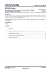
1
APPLICATION NOTE
RX62N Group
R01AN0629EJ0101
Rev.1.01
Mar 31, 2011
Ethernet Transmit and Receive Settings
Introduction
This application note presents a sample program that makes settings for transmitting and receiving
Ethernet/IEEE802.3 frames using the Ethernet controller (ETHERC) and Ethernet DMA controller (EDMAC).
Target Devices
• RX62N Group MCU (product number: R5F562N8BDBG)
• LAN8700i, manufactured by Standard Microsystems Corporation
Target Board
• Renesas Starter Kit +(product number: R0K5562N0C000BE)
Notes
• RX62N group's capacity of built-in ROM and built-in RAM is different in each product. Please correct the section
arrangement in Table 7.1 according to the product used.
• The sample program uses the auto-negotiation function to select the communication mode. If the amount of time
required for auto-negotiation by the RX62N and the connection partner of the RX62 differs considerably,
communication may fail even though auto-negotiation is successful.Please adjust it according to 4.6.1.
• Please note that the Renesas Starter Kit +(product number: R0K5562N0C000BE) supports the MII (Media
Independent Interface) only, and doesn't support RMII (Reduced Media Independent Interface).
Contents
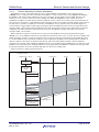
1.
Introduction........................................................................................................................................ 2
U
U
U
U
U
U
U
U
U
U
U
U
U
U
U
U
U
U
2.
U
Description of Initial Settings ............................................................................................................. 4
U
3.
4.
U
Description of Transmit/Receive Settings ....................................................................................... 18
U
5.
U
Endian Mode Selection in Sample Program ................................................................................... 49
U
6.
U
Interface (MII/RMII) Selection in Sample Program ......................................................................... 49
U
7.
U
Allocation of Sections in Sample Program ...................................................................................... 50
U
8.
U
Note on Use of Renesas Starter Kit + ............................................................................................. 50
U
9.
U
Description of Physical Layer Transceiver (PHY) Auto-Negotiation Settings ................................... 6
U
U
U
U
Reference Documents..................................................................................................................... 51
R01AN0629EJ0101 Rev.1.01
Mar 31, 2011
U
Page 1 of 52
RX62N Group
1.
Ethernet Transmit and Receive Settings
Introduction
0B
1.1
Specifications
9B
• The sample program supports the big endian and little endian operating modes of the RX62N.
• The sample program supports the Media Independent Interface (MII) and Reduced Media Independent Interface
(RMII).
• The sample program does not include any interrupt handling functionality. In order to use interrupts, it is necessary
for the customer to create the necessary program code separately.
• The sample program does not include routines for handling transmit of receive errors. If error handling functionality
is required, it is necessary for the customer to create the necessary program code separately.
• After a reset is canceled, the sample program makes settings for the clock generation circuit, module stop function,
and I/O registers.
• The LAN8700i from Standard Microsystems Corporation is used as the Ethernet physical layer transceiver (PHY).
• The auto-negotiation function is used for the link to the Ethernet physical layer transceiver (PHY).
• The sample program obtains the auto-negotiation result from the Ethernet physical layer transceiver (PHY)
connected to the RX62N and makes ETHERC settings to match the connection mode information (full-duplex mode
or half-duplex mode, transfer speed* of 10 Mbps or 100 Mbps) obtained.
• The sample program allows selection between the following two types of processing.
⎯ Transmission of 10 Ethernet frames
⎯ Reception of 10 Ethernet frames
Note: *
1.2
•
•
•
•
•
This setting is needed only when using the RMII. When the MII is used, the transfer speed is
detected automatically by the ETHERC from the clock frequency of the physical layer transceiver
(PHY), so there is no need to specify the transfer speed.
Functions Used
10B
Clock generation circuit
Module stop function
I/O ports
Ethernet controller (ETHERC)
Ethernet controller direct memory access controller (EDMAC)
R01AN0629EJ0101 Rev.1.01
Mar 31, 2011
Page 2 of 52
RX62N Group
1.3
Ethernet Transmit and Receive Settings
Applicable Conditions
1B
• MCU: RX62N Group
• Evaluation board: Renesas Starter Kit +(product number: R0K5562N0C000BE)
• Operating frequencies:
Input clock: 12 MHz
System clock (ICLK): 96 MHz
Peripheral module clock (PCLK): 48 MHz
External bus clock (BCLK) and SDRAM clock (SDCLK): 24 MHz
• Operating mode: Single-chip mode
• Integrated development environment: Renesas Electronics High-performance Embedded Workshop,
Ver. 4.07.00.007
• C compiler: Renesas Electronics RX Family C/C++ Compiler, Ver. 1.00.00.001
• Compile options:
⎯ Big endian operation
-cpu=rx600 -endian=big -patch=rx610 -include="$(WORKSPDIR)\src\bsp","$(WORKSPDIR)\src\driver"
-output=obj="$(CONFIGDIR)\$(FILELEAF).obj" -debug –nologo
⎯ Little endian operation
-cpu=rx600 -patch=rx610 -include="$(WORKSPDIR)\src\bsp","$(WORKSPDIR)\src\driver"
-output=obj="$(CONFIGDIR)\$(FILELEAF).obj" -debug –nologo
• Optimizing linkage editor: Renesas Electronics Optimizing Linkage Editor, Ver. 10.00.00.001
• Linker options:
-noprelink -rom=D=R,D_1=R_1,D_2=R_2 -nomessage -list="$(CONFIGDIR)\$(PROJECTNAME).map"
-show=all -nooptimize
-start=B_RX_DESC,B_TX_DESC,B_RX_BUFF_1,B_TX_BUFF_1,B_1,R_1,B_2,R_2, B,R,SU,SI, BETH_BUFF/
01000,PResetPRG/0FFFF8000,C_1,C_2,C,C$*,D*,P,PIntPRG,W*/0FFFF8100, FIXEDVECT/0FFFFFFD0 -nologo
-output="$(CONFIGDIR)\$(PROJECTNAME).abs" -end -input="$(CONFIGDIR)\ $(PROJECTNAME).abs"
-form=stype -output="$(CONFIGDIR)\$(PROJECTNAME).mot" -exit
R01AN0629EJ0101 Rev.1.01
Mar 31, 2011
Page 3 of 52
RX62N Group
2.
Ethernet Transmit and Receive Settings
Description of Initial Settings
1B
An initial settings program, which performs minimal hardware initialization processing such as memory initialization
after a power-on reset, is required in order to use the Ethernet driver of the sample program. Sample settings for the
initial settings program are described below.
2.1
Description of Initial Settings Program
12B
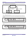
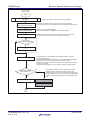
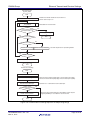
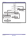
The initial settings program comprises multiple source files, including resetprg.c, which contains the main
PowerON_Reset_PC function, and hwsetup.c, which is called as a function. The main source files described below.
• resetprg.c
The file resetprg.c is generated automatically by High-performance Embedded Workshop and contains declarations
for the PowerON_Reset_PC function. PowerON_Reset_PC is the first function run after a reset is canceled. The
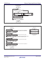
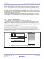
start address of this function is set in the reset vector defined in vecttbl.c. Figure 2.1 shows the processing sequence
of the PowerON_Reset_PC function.
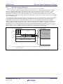
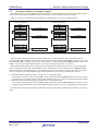
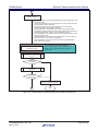
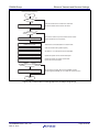
• hwsetup.c
The file hwsetup.c contains declarations for the HardwareSetup function called by the PowerON_Reset_PC
function. The HardwareSetup function in turn calls the functions that make settings for the clock generation circuit,
module stop function, and I/O ports. These are the minimum hardware settings for the system.
Figure 2.2 shows the processing sequence of the HardwareSetup function.
PowerON_Reset_PC function
Start
INTB setting
set_intb()
Set the start address of the variable vector table
in the interrupt table register (INTB).
FPSW setting
set_fpsw()
Initialize the floating-point status word (FPSW).
RAM area section initialization
_INITSCT()
Hardware initialization
HardwareSetup()
PSW setting
set_psw()
Processor mode setting
Change_PSW_PM_to_UserMode()
Call main function
main()
Initialize section B (uninitialized data section) to zero.
For section D (initialized data section), copy the initial value
of the ROM area to the RAM area. To change the sections,
modify the table in dbsct.c.
Initialize the operating mode, clock generation circuit,
power-down (low-power) function, I/O ports, and bus.
Defined in hwsetup.c.
Initialize the processor status word (PSW).
Change the processor mode from supervisor to user.
Call the main function.
Execute BRK instruction
brk()
End
Figure 2.1 Processing Sequence of Reset Program
R01AN0629EJ0101 Rev.1.01
Mar 31, 2011
Page 4 of 52
RX62N Group
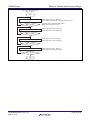
Ethernet Transmit and Receive Settings
HardwareSetup function
Start
Clock generation circuit settings
io_set_cpg()
I/O port settings
ConfigurePortPins()
Module stop function setting
EnablePeripheralModules()
Set the system clock (ICLK), peripheral module clock (PCLK),
external bus clock (BCLK), and SDRAM clock (SDCLK).
Set the I/O ports to be used for Ethernet communication.
Disable the module stop function for the Ethernet controller
DMA controller (EDMAC).
End
Figure 2.2 Processing Sequence of Hardware Initialization Function
2.2
Details of Initial Settings
13B
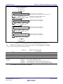
Table 2.1 lists the settings used in the sample program.
Table 2.1
Module
Operating mode
Clock generation circuit
Module stop function
I/O ports
2.3
Sample Program Settings
Settings
Single-chip mode
System clock: 96 MHz
Peripheral module clock: 48 MHz
External bus clock and SDRAM clock: 24 MHz
Disabled for Ethernet controller DMA controller (EDMAC)
Pin settings used for Ethernet communication
Notes on Initial Settings
14B
Do not access the static variable area before the _INIT_SCT function is executed.
The C language static variable area is initialized by executing the _INIT_SCT function. Note that accessing the area
before the function has been run will return undefined values.
R01AN0629EJ0101 Rev.1.01
Mar 31, 2011
Page 5 of 52
RX62N Group
3.
Ethernet Transmit and Receive Settings
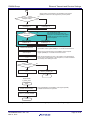
Description of Physical Layer Transceiver (PHY) Auto-Negotiation Settings
2B
The sample program uses the Ethernet physical layer transceiver (PHY) to perform auto-negotiation. The autonegotiation result is read via the PHY interface register (PIR) of the ETHERC.
3.1
Operation of Functions Used
15B
The actual physical layer link processing is performed using the functionality of the Ethernet physical layer
transceiver (PHY). This enables the RX62N to obtain the link result simply by reading it from the Ethernet physical
layer transceiver (PHY). The sample program enables the auto-negotiation function of the physical layer transceiver
(PHY). For details of the functions of the Ethernet physical layer transceiver (PHY), see the Ethernet physical layer
transceiver (PHY) datasheet.
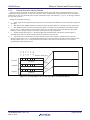
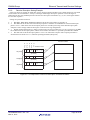
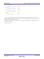
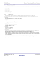
The interface between the ETHERC and the Ethernet physical layer transceiver (PHY) is standardized according to
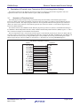
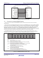
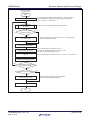
the IEEE802.3 Media Independent Interface (MII) or Reduced Media Independent Interface (RMII). Figures 3.1 and 3.2
show connection examples for the RX62N and LAN8700i.
The auto-negotiation result is stored in the internal registers of the Ethernet physical layer transceiver (PHY) and can
be read by using a serial interface (Serial Management Interface) employing the MDC and MDIO pins. The RX62N can
read from and write to these pins by using the PIR register. The procedure for accessing the internal registers of the
Ethernet physical layer transceiver (PHY) is described in 3.2, Procedure for Accessing MII/RMII Registers.
MII (Media Independent Interface)
RX62N
ET_TX_ER
ET_ETXD3
ET_ETXD2
ET_ETXD1
ET_ETXD0
ET_TX_EN
ET_TX_CLK
ET_MDC
ET_MDIO
ET_ERXD3
ET_ERXD2
ET_ERXD1
ET_ERXD0
ET_RX_CLK
ET_CRS
ET_COL
ET_RX_DV
ET_RX_ER
LAN8700i
TX_ER
TXD3
TXD2
TXD1
TXD0
TX_EN
TX_CLK
MDC
MDIO
RXD3
RXD2
RXD1
RXD0
RX_CLK
CRS
COL
RX_DV
RX_ER
Figure 3.1 LAN8700i Connection Example (MII)
R01AN0629EJ0101 Rev.1.01
Mar 31, 2011
Page 6 of 52
RX62N Group
Ethernet Transmit and Receive Settings
RMII (Reduced Media Independent Interface)
LAN8700i
RX62N
RMII_TXD1
RMII_TXD0
RMII_TXD_EN
TXD1
TXD0
TXD_EN
ET_MDC
ET_MDIO
RMII_RXD1
RMII_RXD0
REF50CK
RMII_CRS_DV
MDC
MDIO
RXD1
RXD0
RX_CLK
CRS_DV
RMII_RX_ER
RX_ER
Figure 3.2 LAN8700i Connection Example (RMII)
3.2
Procedure for Accessing MII/RMII Registers
16B
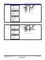
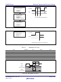
The procedure for accessing the internal MII/RMII registers of the Ethernet physical layer transceiver (PHY) is
described below.
The serial interface (Serial Management Interface) used to access the MII/RMII registers consists of MDC and MDIO
(both pin names used on the ETHERC side). MDC is the clock pin used for synchronization, and MDIO is the data I/O
pin. The states of the pins can be referenced or changed by means of the PHY interface register (PIR) of the ETHERC.
There are no control pins, so data must always be output in the format stipulated by the MII/RMII specification
(MII/RMII management frames). Figure 3.3 shows an MII/RMII management frame. The sample program executes Z0
output for one bit period in the IDLE state. The IEEE802.3 specification does not mention clock input, but it is provided
for safety because without it some physical layer transceiver (PHY) devices cannot connect properly.
The MII/RMII management frame I/O is performed in order in 1-bit units, starting from PRE. Figures 3.4 to 3.7
illustrate the I/O sequence for 1-bit units. Make sure that the MDC and MDIO I/O timing conform to the IEEE802.3
specification. Table 3.1 and figure 3.8 show the I/O timing as stipulated in the IEEE802.3 specification.
Access Type
Item
PRE
ST
OP
Number of bits
32
2
2
5
5
Read
1..1
01
10
00001
Write
1..1
01
01
00001
MII/RMII Management Frame
PHYAD
REGAD
TA
DATA
IDLE
2
16
⎯
RRRRR
Z0
D..D
⎯
RRRRR
10
D..D
X
[Legend]
PRE
: 32 consecutive 1s
ST
: Write 01 to indicate the start of the frame.
OP
: Write the code indicating the access type.
PHYAD : Write 0001 if the PHY address is 1 (sequential write starting with the MSB).
This value varies according to the PHY address.
REGAD : Write 0001 if the register address is 1 (sequential write starting with the MSB).
This value varies according to the PHY register address.
TA
: Time for switching data transmission source on MII/RMII interface
(a) For write: Write 10.
(b) For read: Perform bus release (notation: Z0).
DATA : 16 bits of data. Sequentially write or read from MSB.
(a) For write: Write 16 bits of data.
(b) For read: Read 16 bits of data.
IDLE
: Wait time until next MII management format input
(a) For write: Perform independent bus release (notation: X).
(b) For read: Bus already released during TA; control unnecessary.
Figure 3.3 MII/RMII Management Frame Format
R01AN0629EJ0101 Rev.1.01
Mar 31, 2011
Page 7 of 52
RX62N Group
Ethernet Transmit and Receive Settings
(1) Write to PHY
interface register
PIR.MMD = 1
PIR.MDO = write data
PIR.MDC = 0
ET_MDC
MDO
(2) Write to PHY
interface register
(1) (2)
(3)
1-bit data write timing relationship
PIR.MMD = 1
PIR.MDO = write data
PIR.MDC = 1
(3) Write to PHY
interface register
PIR.MMD = 1
PIR.MDO = write data
PIR.MDC = 0
Figure 3.4 1-Bit Data Write Sequence
(1) Write to PHY
interface register
ET_MDC
PIR.MMD = 0
PIR.MDC = 0
MDO
(2) Write to PHY
interface register
(1) (2)
PIR.MMD = 0
PIR.MDC = 1
(3)
Bus release timing relationship
(3) Write to PHY
interface register
PIR.MMD = 0
PIR.MDC = 0
Figure 3.5 Bus Release Sequence (TA During Read)
R01AN0629EJ0101 Rev.1.01
Mar 31, 2011
Page 8 of 52
RX62N Group
Ethernet Transmit and Receive Settings
(1) Write to PHY
interface register
ET_MDC
PIR.MMD = 0
PIR.MDC = 1
MDI
(2) Read from PHY
interface register
PIR.MMD = 0
PIR.MDC = 1
PIR.MDI is read data
(1)
(2)
(3)
1-bit data read timing relationship
(3) Write to PHY
interface register
PIR.MMD = 0
PIR.MDC = 0
Figure 3.6 1-Bit Data Read Sequence
(1) Write to PHY
interface register
ET_MDC
PIR.MMD = 0
PIR.MDC = 0
MDO
(1)
Independent bus release timing relationship
Figure 3.7 Independent Bus Release Sequence (IDLE During Write)
Table 3.1
Item
MDC high-level pulse width
MDC low-level pulse width
MDC cycle time
MDIO setup time
MDIO hold time
MDIO output delay time
MDC/MDIO I/O Timing
Symbol
t1
t2
t3
t4
t5
t6
Min.
Max.
160
160
400
10
10
0
300
Unit
ns
ns
ns
ns
ns
ns
t3
t1
t2
MDC
t4
t5
MDIO
(EtherC output)
t6
MDIO
(PHY output)
Figure 3.8 MDC/MDIO I/O Timing
R01AN0629EJ0101 Rev.1.01
Mar 31, 2011
Page 9 of 52
RX62N Group
3.3
Ethernet Transmit and Receive Settings
Description of Physical Layer Transceiver (PHY) Auto-Negotiation Settings
17B
• phy.c
This file contains declarations for the function that initializes the physical layer transceiver (PHY) (phy_init
function) and the function that obtains the auto-negotiation result (phy_set_autonegotiate function). Figure 3.9
shows the processing sequence of the phy_init function and figure 3.10 of the phy_set_autonegotiate function.
Figures 3.11 to 3.16 show the processing sequences of the MII/RMII register read function (_phy_read function)
and MII/RMII register write function (_phy_write function), which are executed within the phy_init function and
phy_set_autonegotiate function, and their lower level functions.
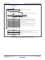
PHY initialization function
phy_init
Start
Write to MII/RMII register 0
_phy_write()
Read MII/RMII register 0
_phy_read()
Yes
Write 0x8000 to MII/RMII register 0 to reset the PHY.
Read MII/RMII register 0.
Check the following two points:
• Bit 15 in MII/RMII register 0, to determine if the reset completed
• Wait counter value does not exceed the maximum value
(PHY_RESET_WAIT), indicating that no timeout has occurred.
PHY reset not complete and
no timeout occurred?
No
PHY_RESET_WAIT is defined in phy.h.
No
Timeout occurred?
Yes
Return R_PHY_ERROR
Return R_PHY_OK
End
Figure 3.9 Processing Sequence of Physical Layer Transceiver (PHY) Initialization Function
R01AN0629EJ0101 Rev.1.01
Mar 31, 2011
Page 10 of 52
RX62N Group
Ethernet Transmit and Receive Settings
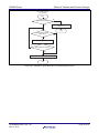
Auto-negotiation result acquisition function
phy_set_autonegotiate
Start
Yes
Write to MII/RMII register 4
_phy_write()
Write 0x01E1 to MII/RMII register 4 to enable the following PHY link conditions:
full-duplex, half-duplex, 10 Mbps, 100 Mbps.
Write to MII/RMII register 0
_phy_write()
Write 0x1200 to MII/RMII register 0 to start auto-negotiation.
Read MII/RMII register 1
_phy_read()
Read MII/RMII register 1.
Bit 5 in MII/RMII register 1 of the LAN8700i is read twice because the internal state is
reflected by a latch circuit.
Auto-negotiation not complete
and no timeout occurred?
Check the following two points:
• That bit 5 in the MII/RMII register is set to 1 (auto-negotiation completed)
• That the wait counter value does not exceed the maximum value
(PHY_AUTO_NEGOTIATION_WAIT) (timeout)
No
PHY_AUTO_NEGOTIATON_WAIT is defined in phy.h.
No
Timeout occurred?
Read MII/RMII register 5 and return the connection modes
supported by the link partner.
Yes
Return R_PHY_ERROR
Read MII/RMII register 5 and return result
_phy_read()
End
Figure 3.10 Auto-Negotiation Result Acquisition Function
MII/RMII register read function
_phy_read
MII/RMII register write function
_phy_write
Start
Start
Preamble output
_phy_preamble()
Preamble output
_phy_preamble()
Command output (read command)
_phy_reg_set()
Command output (write command)
_phy_reg_set()
Bus release (transmit source switch)
_phy_ta_z0()
Output 10
_phy_ta_10()
DATA input
_phy_reg_read()
DATA output
_phy_reg_write()
Bus release (transmit source switch)
_phy_ta_z0()
Bus release (transmit source switch)
_phy_ta_z0()
End
End
Figure 3.11 Processing Sequence of MII/RMII Register Access (1)
R01AN0629EJ0101 Rev.1.01
Mar 31, 2011
Page 11 of 52
RX62N Group
Ethernet Transmit and Receive Settings
Preamble output function
_phy_preamble
Command output function
_phy_reg_set
Start
Start
Set ST code (01) in
command bits 15 and 14
1-bit output
_phy_preamble()
Set OP code (10 or 01) in
command bits 13 and 12
No
Set PHYAD code (xxxxx) in
command bits 11 to 7
Output of 32 bits complete?
Yes
Set REGAD code (xxxxx) in
command bits 6 to 2
End
Highest command bit = 0?
No
Yes
Output 1 bit (value: 0)
_phy_mii_write_0()
Output 1 bit (value: 1)
_phy_mii_write_1()
Shift command 1 to left
No
Output of 14 bits complete?
Yes
End
Figure 3.12 Processing Sequence of MII/RMII Register Access (2)
R01AN0629EJ0101 Rev.1.01
Mar 31, 2011
Page 12 of 52
RX62N Group
Ethernet Transmit and Receive Settings
Data input function
_phy_reg_read
Start
Write 0x00000000 to PIR register
No
MDC wait OK?
Output low-level from ET_MDC pin.
Set ET_MDIO pin to read direction.
The MDC wait is defined as MDC_WAIT.
MDC_WAIT is defined in phy.h.
Yes
Write 0x00000001 to PIR register
Output high-level from ET_MDC.
No
MDC wait OK?
Yes
Read MDI bit in PIR register
Write 0x00000001 to PIR register
Output high-level from ET_MDC.
No
MDC wait OK?
Yes
Write 0x00000000 to PIR register
Output low-level from ET_MDC pin.
No
MDC wait OK?
Yes
No
Reading of 16 bits complete?
Yes
End
Figure 3.13 Processing Sequence of MII/RMII Register Access (3)
R01AN0629EJ0101 Rev.1.01
Mar 31, 2011
Page 13 of 52
RX62N Group
Ethernet Transmit and Receive Settings
Data output function
_phy_reg_write
Start
Highest data bit = 0?
No
Yes
Output 1 bit (value: 0)
_phy_mii_write_0()
Output 1 bit (value: 1)
_phy_mii_write_1()
Shift data 1 to left
No
Output of 16 bits complete?
Yes
End
Figure 3.14 Processing Sequence of MII/RMII Register Access (4)
Bus release function
_phy_ta_z0
TA during write function
_phy_ta_10
Start
Start
Write 0x00000000 to PIR register
Output low-level from ET_MDC pin.
Set ET_MDIO pin to read direction.
No
Output 1 bit (value: 1)
_phy_mii_write_1()
Output 1 bit (value: 0)
MDC wait OK?
_phy_mii_write_0()
Yes
Write 0x00000001 to PIR register
Output high-level from ET_MDC.
No
The MDC wait is defined as MDC_WAIT.
MDC_WAIT is defined in phy.h.
MDC wait OK?
End
Yes
Write 0x00000001 to PIR register
Output high-level from ET_MDC.
No
MDC wait OK?
Yes
Write 0x00000000 to PIR register
Output low-level from ET_MDC pin.
No
MDC wait OK?
Yes
End
Figure 3.15 Processing Sequence of MII/RMII Register Access (5)
R01AN0629EJ0101 Rev.1.01
Mar 31, 2011
Page 14 of 52
RX62N Group
Ethernet Transmit and Receive Settings
1-bit (value: 1) output function
_phy_mii_write_1
Start
Write 0x00000006 to PIR register
No
MDC wait OK?
Output low-level from ET_MDC pin.
Set ET_MDIO pin to write direction and output high-level.
The MDC wait is defined as MDC_WAIT.
MDC_WAIT is defined in phy.h.
Yes
Write 0x00000007 to PIR register
No
Output high-level from ET_MDC pin.
Output high-level from ET_MDIO pin.
MDC wait OK?
Yes
Write 0x00000007 to PIR register
No
Output high-level from ET_MDC pin.
Output high-level from ET_MDIO pin.
MDC wait OK?
Yes
Write 0x00000006 to PIR register
No
Output low-level from ET_MDC pin.
Output high-level from ET_MDIO pin.
MDC wait OK?
Yes
End
Figure 3.16 Processing Sequence of MII/RMII Register Access (6)
R01AN0629EJ0101 Rev.1.01
Mar 31, 2011
Page 15 of 52
RX62N Group
Ethernet Transmit and Receive Settings
1-bit (value: 0) output function
_phy_mii_write_0
Start
Write 0x00000002 to PIR register
No
MDC wait OK?
Output low-level from ET_MDC pin.
Set ET_MDIO pin to write direction and output low-level.
The MDC wait is defined as MDC_WAIT.
MDC_WAIT is defined in phy.h.
Yes
Write 0x00000003 to PIR register
No
Output high-level from ET_MDC pin.
Output low-level from ET_MDIO pin.
MDC wait OK?
Yes
Write 0x00000003 to PIR register
No
Output high-level from ET_MDC pin.
Output low-level from ET_MDIO pin.
MDC wait OK?
Yes
Write 0x00000002 to PIR register
No
Output low-level from ET_MDC pin.
Output low-level from ET_MDIO pin.
MDC wait OK?
Yes
End
Figure 3.17 Processing Sequence of MII/RMII Register Access (7)
3.4
Details of Physical Layer Transceiver (PHY) Auto-Negotiation Settings
18B
Table 3.2 lists the settings used in the sample program.
Table 3.2
Sample Program Settings
Item
PHY model
Link modes
Link determination method
PHY address
Setting target MII/RMII
registers
Description
LAN8700i from Standard Microsystems Corporation
100 Mbps (full-duplex, half-duplex) and 10 Mbps (full-duplex, half-duplex)
Auto-negotiation
0x1F*1
Register 0 — Basic Control (address: 0x00)
Register 1 — Basic Status (address: 0x01)
Register 4 — Auto Negotiation Advertisement (address: 0x04)
Register 5 — Auto Negotiation Link Partner Ability (address: 0x05)
Note: 1. The setting of the Renesas Starter Kit +(product number: R0K5562N0C000BE) is 0x1F. This must
be changed to match the actual PHY address.
R01AN0629EJ0101 Rev.1.01
Mar 31, 2011
Page 16 of 52
RX62N Group
3.5
Ethernet Transmit and Receive Settings
Notes on Physical Layer Transceiver (PHY) Auto-Negotiation Settings
19B
• The sample program assumes that auto-negotiation mode is used as the PHY link determination method.
• When the partner device is operating in auto-negotiation mode, the link mode is determined according to the priority
levels shown in table 3.3.
Table 3.3
Priority Level
High
1
2
3
4
Low
Link Mode Priority Levels
Link Mode
100 Mbps, full-duplex
100 Mbps, half-duplex
10 Mbps, full-duplex
10 Mbps, half-duplex
• The MII/RMII register access timing can be changed by using the following macro definition in the phy.h file. Use
a setting value of 1 or greater.
#define
MDC_WAIT
2
• The physical layer transceiver (PHY) reset completion wait duration used by the sample program can be changed by
using the following macro definition in the phy.h file.
#define PHY_RESET_WAIT
0x00020000L
• Auto-negotiation normally takes a few seconds to complete, but the physical layer transceiver (PHY) autonegotiation completion wait duration used by the sample program can be changed by using the following macro
definition in the phy.h file.
#define PHY_AUTO_NEGOTIATON_WAIT 0x00800000L
• On the Renesas Starter Kit +(product number: R0K5562N0C000BE) the PHY address is set to 0x1F. The PHY
address used by the sample program can be changed by using the following macro definition in the phy.h file.
#define
PHY_ADDR
0x1F
R01AN0629EJ0101 Rev.1.01
Mar 31, 2011
Page 17 of 52
RX62N Group
4.
Ethernet Transmit and Receive Settings
Description of Transmit/Receive Settings
3B
The sample program makes use of the Ethernet controller (ETHERC) and Ethernet controller direct memory access
controller (EDMAC).
4.1
Operation of Functions Used
20B
The RX62N Group always uses the ETHERC and EDMAC to perform Ethernet communication functions. The
ETHERC handles transmit and receive control. The EDMAC uses DMA transfer exclusively to move data between the
transmit and receive FIFOs and the user-specified data storage destinations (buffers).
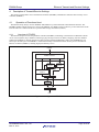
4.1.1
Overview of ETHERC
31B
The RX62N Group has an on-chip Ethernet controller (ETHERC) conforming to the Ethernet or IEEE802.3 Media
Access Control (MAC) layer standard. Connecting a physical layer transceiver (PHY) complying with this standard
enables the ETHERC to perform transmission and reception of Ethernet/IEEE802.3 frames. The ETHERC has one
MAC layer interface port. The ETHERC is connected internally to the Ethernet direct memory access controller for
Ethernet controller (EDMAC), enabling high-speed memory access.
EDMAC
ETHERC
EDMAC interface
MAC
Receive
controller
Transmit
controller
Command status
interface
MII
RMII
Port
PHY
Figure 4.1 Configuration of ETHERC
R01AN0629EJ0101 Rev.1.01
Mar 31, 2011
Page 18 of 52
RX62N Group
4.1.2
Ethernet Transmit and Receive Settings
Overview of ETHERC Transmitter
32B
The ETHERC transmitter assembles transmit data into a frame and outputs it to the MII/RMII when there is a
transmit request from the transmit EDMAC. The transmit data is sent to the lines via the MII/RMII by the physical layer
transceiver (PHY). Figure 4.2 shows the state transitions of the ETHERC transmitter.
• 1. When the transmit enable (ECMR.TE) bit is set to 1, the transmitter enters the transmit idle state.
• 2. When a transmit request is issued by the transmit EDMAC, the ETHERC sends the preamble to the MII/RMII
after carrier detection and a transmission delay equivalent to the frame interval time. If full-duplex transfer, which
does not require carrier detection, is selected, the preamble is sent as soon as a transmit request is issued by the
transmit EDMAC.
• 3. The transmitter sends the SFD, data, and CRC sequentially. At the end of transmission, the transmit EDMAC
generates a transmission complete interrupt (TC). If a collision or the carrier-not-detected state occurs during data
transmission, it is reported as an interrupt source.
• 4. After the frame interval time elapses, the transmitter enters the idle state, and if there is more transmit data,
continues transmission.
FDPX
TE set
Start of transmission
(preamble transmission)
Idle
Transmission
halted
Carrier
detected
HDPX
Carrier not
detected
TE reset
HDPX
Transmission
retry start
FDPX
Carrier detected
Collision
Reset
Carrier detected
Carrier not
detected
Transmission retry
processing*1
Carrier
detected
Collision
Failure of 15
transmission
retries or
collision after
512-bit duration
SFD transmission
Error
Collision*2
Error
Error
notification
Error detected
Data transmission
Collision*2
Error
Normal transmission
CRC transmission
[Legend]
FDPX: Full-duplex
HDPX: Half-duplex
SFD: Start frame delimiter
Notes: 1. Transmission retry processing includes both jam transmission accompanying collision detection and
adjustment of the transmission interval by the back-off algorithm.
2. Transmission is retried only when transmitting 512 or fewer bits of data (including the preamble and SFD).
When a collision is detected during transmission of more than 512 bits of data, only jam transmission occurs
and transmission retry using the back-off algorithm is not attempted.
Figure 4.2 ETHERC Transmitter State Transitions
R01AN0629EJ0101 Rev.1.01
Mar 31, 2011
Page 19 of 52
RX62N Group
4.1.3
Ethernet Transmit and Receive Settings
Overview of ETHERC Receiver
3B
The ETHERC receiver divides the frame from the MII/RMII into the preamble, SFD, data, and CRC, and the fields
from DA (destination address) to the CRC data are output to the receive EDMAC. Figure 4.3 shows the state transitions
of the ETHERC receiver.
• 1. When the receive enable (ECMR.RE) bit is set to 1, the receiver enters the receive idle state.
• 2. Upon detecting an SFD (start frame delimiter) after a receive packet preamble, the receiver starts receive
processing. It discards frames with an invalid pattern.
• 3. In normal mode, if the destination address of the frame matches the RX62N address, or if the broadcast or
multicast frame type is specified, the receiver starts data reception. In promiscuous mode, the receiver starts
reception for any type of frame.
• 4. After receiving data from the MII/RMII, the receiver performs a CRC check on the frame data field. The result
is indicated as a status bit in the descriptor after the frame data has been written to memory. The receiver reports an
error status in the case of an abnormality.
• 5. After one frame is received, the receiver prepares to receive the next frame if the receive enable bit in the
ETHERC mode register is set to 1 (ECMR.RE = 1).
Illegal carrier
detection
ET_RX-DV negation
Start of
frame reception
Idle
RE set
Reception
halted
Wait for
SFD reception
Preamble
detected
SFD received
RE reset
Promiscuous and other
station destination address
Destination address
received
Own destination address
or broadcast
or multicast
or promiscuous
Reset
Receive error
detected
Error detected
Data received
Error
notification*
End of reception
Receive error
detected
Normal reception
CRC received
[Legend]
SFD: Start frame delimiter
Note: * Data is transmitted to the buffer for error frames as well.
Figure 4.3 Receiver State Transitions
R01AN0629EJ0101 Rev.1.01
Mar 31, 2011
Page 20 of 52
RX62N Group
4.1.4
Ethernet Transmit and Receive Settings
Overview of EDMAC
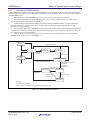
34B
The RX62N Group has an on-chip direct memory access controller (EDMAC) that is directly connected to the
Ethernet controller (ETHERC). Most buffer management is controlled by the EDMAC by using descriptors. This
reduces the load on the CPU, enabling efficient data transmission and reception.
The EDMAC is connected to the ETHERC, allowing efficient transfer of transmit and receive data to and from the
memory (buffers), bypassing the CPU. The EDMAC itself reads stored control information, such as buffer pointers
(called descriptors) that correspond to the individual buffers. Transmit data is read from the transmit buffers, and
receive data written to the receive buffers, according to the control information. By arranging multiple descriptors
consecutively (in a descriptor list), transmission and reception can be performed continuously.
Table 4.1 lists the EDMAC specifications, and figure 4.4 shows the configuration of the EDMAC and of the
descriptors and transmit/receive buffers in memory.
Table 4.1
Item
Data transmission and reception
Functions
•
•
•
•
•
Specifications of EDMAC
Description
Descriptor management system
Support for single-frame/multi-buffer operation
Efficient system bus utilization through use of DMA block transfer
(32-byte units)
Indication in descriptors of transmit/receive frame status information
Ability to insert padding in receive data
RX62N Group
Internal bus
Transmit buffers
EDMAC
Transmit
descriptors
Receive buffers
Receive
descriptors
External
bus
interface
Internal
bus
interface
Transmit FIFO
Descriptor
information
Transmit DMAC
Receive FIFO
ETHERC
Descriptor
information
Receive DMAC
External memory
Figure 4.4 Configuration of EDMAC, Descriptors, and Buffers
R01AN0629EJ0101 Rev.1.01
Mar 31, 2011
Page 21 of 52
RX62N Group
4.1.5
Ethernet Transmit and Receive Settings
Overview of Descriptors
35B
To perform a DMA transfer, the EDMAC requires a unit of data called a descriptor that contains information such as
the storage address of the transmit or receive data. There are two types of descriptors: transmit descriptors and receive
descriptors. The EDMAC automatically starts reading a transmit descriptor when the TR bit in the EDMAC transmit
request register (EDTRR) is set to 1, and when the RR bit in the EDMAC receive request register (EDRRR) is set to 1 it
automatically starts reading a receive descriptor. It is necessary for the user to declare beforehand in the transmit or
receive descriptor the appropriate information regarding the DMA transfer of the transmit or receive data. When
transmission or reception of an Ethernet frame completes, the EDMAC clears to 0 the descriptor’s active bit (TACT for
transmission and RACT for reception) and updates the status bits (TFS25 to TFS0 for transmission and RFS26 to RFS0
for reception) to reflect the transmit or receive result.
The descriptors are allocated to a readable memory space, and the address of the start descriptor (the first descriptor
read by the EDMAC) is specified in the transmit descriptor list start address register (TDLAR) or receive descriptor list
start address register (RDLAR). When preparing multiple descriptors in a descriptor list, allocate the descriptors to
consecutive addresses according to the descriptor length specified by the DL bits in the EDMAC mode register
(EDMR).
4.1.6
Overview of Transmit Descriptor
36B
Figure 4.5 shows the correspondence between a transmit descriptor and a transmit buffer.
A transmit descriptor comprises, beginning from the start of the data, 32-bit units designated TD0, TD1, and TD2,
followed by padding. TD0 contains a bit indicating whether the transmit descriptor is active or inactive as well as
descriptor configuration information and status information. TD1 indicates the data length (TBL) of the transmit buffer
containing the data to be transferred according to the designation of the descriptor. TD2 indicates the start address of the
transmit buffer containing the data to be transferred. The length of the padding is determined according to the descriptor
length specified by the DL bits in the EDMR register.
Depending on the transmit descriptor settings, one descriptor can specify a single frame of transmit data (singleframe/single-descriptor) or multiple descriptors can specify a single frame of transmit data (single-frame/multidescriptor). Single-frame/multi-descriptor operation can be used, for example, to set multiple descriptors to specify a
fixed portion of data that is transmitted in every Ethernet frame. Specifically, the data in each Ethernet frame specifying
the destination address and transmit source address could be shared in common by multiple descriptors and the
remaining data stored in its own buffer.
Transmit descriptor
TD0
Transmit buffer
31 30 29 28 27 26
T T T T T T
A D F F F W
C L P P E B
I
T E 1 0
31
TD1
0
TFS
Valid transmit data
16
TBL
31
0
TBA
TD2
Padding (4, 20, or 52 bytes)
Note: The padding is a redundant area whose size is adjusted according to the descriptor length
(16, 32, or 64 bytes).
Figure 4.5 Correspondence of Transmit Descriptor and Transmit Buffer
R01AN0629EJ0101 Rev.1.01
Mar 31, 2011
Page 22 of 52
RX62N Group
4.1.7
Ethernet Transmit and Receive Settings
Overview of Receive Descriptor
37B
Figure 4.6 shows the correspondence between a receive descriptor and a receive buffer.
A receive descriptor comprises, beginning from the start of the data, 32-bit units designated RD0, RD1, and RD2,
followed by padding. RD0 contains a bit indicating whether the receive descriptor is active or inactive as well as
descriptor configuration information and status information. RD1 indicates the size (RBL) of the receive buffer
referenced by the descriptor and the data length (RFL) of the received frame. RD2 indicates the start address of the
receive buffer. The length of the padding at the end is determined according to the descriptor length specified by the DL
bits in the EDMR register.
Depending on the receive descriptor settings, one descriptor can be used to store all the receive data in a single frame
in a receive buffer (single-frame/single-descriptor) or multiple descriptors can be used to store the receive data in a
single frame to multiple buffers (single-frame/multi-descriptor). To use single-frame/multi-descriptor operation,
multiple descriptors (a descriptor list) must be prepared beforehand. When the length of a received frame exceeds the
descriptor RBL, the EDMAC transfers the data it contains to consecutive receive buffers, continuing on to the next
descriptor as necessary. This would apply, for example, when the descriptor RBL is set to 500 bytes and a 1,514-byte
Ethernet frame is received. Beginning from the first descriptor, the data in the received Ethernet frame is saved 500
bytes at a time to successive buffers, with only the final 14 bytes transferred to the fourth buffer.
Receive descriptor
RD0
RD1
Receive buffer
31 30 29 28 27 26
R R R R R
A D F F F
C L P P E
T E 1 0
0
RFS
15
RBL
31
31
16
0
Valid receive data
RFL
0
RD2
RBA
Padding (4, 20, or 52 bytes)
Note: The padding is a redundant area whose size is adjusted according to the descriptor length
(16, 32, or 64 bytes).
Figure 4.6 Correspondence of Receive Descriptor and Receive Buffer
R01AN0629EJ0101 Rev.1.01
Mar 31, 2011
Page 23 of 52
RX62N Group
4.1.8
Ethernet Transmit and Receive Settings
Transmit Descriptor Setting Example
38B
Figure 4.7 shows an example in which three transmit descriptor planes and three transmit buffer planes are used
(single-frame/single-descriptor). In this case, one frame only is transmitted by a single transmit request. The figure is
abbreviated to show only the TD0 portion of each transmit descriptor. The numbers (1), (2), etc., in the figure indicate
the execution sequence.
Settings are performed as follows.
• 1. Since single-frame/single-descriptor operation is used, the TFP1 and TFP0 bits in all the descriptor planes are
set to B'11.
• 2. Bits TACT, TFE, TWBI, and TFS25 to TFS0 in all the descriptor planes are cleared to 0 as the initial value.
• 3. The TDLE bit in the first and second descriptor planes is cleared to 0. The TDLE bit in the third descriptor
plane is set to 1, which causes the first descriptor plane to be read after processing of the third descriptor plane
completes. These settings enable the descriptors to function in a ring configuration.
• 4. Though omitted from figure 4.7, the data length of the transmit buffer referenced by each descriptor is
specified by the TBL bits and the transmit buffer start address by the TBA bits.
• 5. One frame only is transmitted by a single transmit request in this example, so the TACT bit of the first
descriptor plane only is set to 1 for the initial transmission. For the next transmission, the TACT bit of the second
descriptor plane only is set to 1. The transmission procedure is described in more detail in 4.1.10, Function
Operating Procedure (Transmission).
Transmit descriptors
Transmit buffers
T
A
C
T
T
D
L
E
T
F
P
1
T
F
P
0
T
F
E
T
W
B
I TFS25 to TFS0 (1)(4)
0
0
1
1
0
0
1st plane
00..0
(Omitted)
(2)(5)
0
0
1
1
0
0
00..0
2nd plane
(Omitted)
0
0
1
1
0
0
00..0
(3)(6)
3rd plane
(Omitted)
Figure 4.7 Correspondence of Transmit Descriptors and Transmit Buffers
R01AN0629EJ0101 Rev.1.01
Mar 31, 2011
Page 24 of 52
RX62N Group
4.1.9
Ethernet Transmit and Receive Settings
Receive Descriptor Setting Example
39B
Figure 4.8 shows an example in which three receive descriptor planes and three receive buffer planes are used. Each
receive buffer can accommodate 1,536 bytes, and single-frame/single-descriptor operation is used. The figure is
abbreviated to show only the RD0 portion of each receive descriptor. The numbers (1), (2), etc., in the figure indicate
the execution sequence.
Settings are performed as follows.
• 1. Bits RFP1, RFP0, RFE, and RFS26 to RFS0 in all the descriptor planes are cleared to 0.
• 2. The RDLE bit in the first and second descriptor planes is cleared to 0. The RDLE bit in the third descriptor
plane is set to 1, which causes the first descriptor plane to be read after processing of the third descriptor plane
completes. These settings enable the descriptors to function in a ring configuration.
• 3. Though omitted from figure 4.8, before reception starts the receive buffer size is set to 1,536 bytes by the RBL
bits in RD1 of all the descriptor planes, and the receive buffer start address is specified by the RBA bits in RD2.
• 4. The RACT bit of all the descriptor planes is set to 1 for continuous reception. The reception procedure is
described in more detail in 4.1.11, Function Operating Procedure (Reception).
Receive descriptors
R
A
C
T
R
D
L
E
R
F
P
1
R
F
P
0
R
F
E
1
0
0
0
0
Receive buffers
RFS26 to RFS0
0 0 • •
0
1st plane
(4)
(1)
(Omitted)
1
0
0
0
0
0 0 • •
0
(2)
0
(3)
2nd plane
(5)
(Omitted)
1
1
0
0
0
0 0 • •
3rd plane
(6)
(Omitted)
Figure 4.8 Correspondence of Receive Descriptors and Receive Buffers
R01AN0629EJ0101 Rev.1.01
Mar 31, 2011
Page 25 of 52
RX62N Group
4.1.10
Ethernet Transmit and Receive Settings
Function Operating Procedure (Transmission)
40B
The EDMAC transmitter is activated when the transmit request (TR) bit in the EDMAC transmit request register
(EDTRR) is set to 1 while the value of the TE bit in the ETHERC mode register (ECMR) is 1. After a software reset of
the ETHERC and EDMAC, the EDMAC reads the descriptor indicated by the transmit descriptor list start address
register (TDLAR). If the TACT bit of the descriptor that was read is set to 1 (active), the EDMAC sequentially reads
transmit frame data from the transmit buffer start address specified by TD2 for transfer to the ETHERC. The ETHERC
creates a transmit frame and starts transmission to the MII/RMII. After DMA transfer of data equivalent to the buffer
length specified in the descriptor, the processing described below is carried out according to the value of TFP.
• TFP = B'00 or B'10 (frame continuation)
Descriptor write-back (writing 0 to the TACT bit) is performed after DMA transfer. Then the TACT bit of the next
descriptor is read.
• TFP = B'01 or B'11 (frame end)
Descriptor write-back (writing 0 to the TACT bit and status bits) is performed after completion of frame
transmission. Then the TACT bit of the next descriptor is read.
When the TACT bit of the descriptor that was read is set to 1 (active), frame transmission continues and the next
descriptor is read. When a descriptor with the TACT bit cleared to 0 (inactive) is read, the EDMAC clears the TR bit in
EDTRR to 0 and transmit processing completes. Setting the TR bit to 1 after it has been cleared to 0 reactivates the
EDMAC transmitter, and in this case the next descriptor after the descriptor from the last transmission is read. Figure
4.9 shows a sample transmission sequence.
Transmission sequence
EDMAC
RX62N Group + memory
Transmit FIFO
ETHERC
Ethernet
ETHERC/EDMAC
initialization
Descriptor and
transmit buffer
settings
Transmit instruction
Descriptor read
Transmit data transfer
Descriptor write-back
Descriptor read
Transmit data transfer
Frame transmission
Descriptor write-back
Transmission end
Figure 4.9 Sample Transmission Sequence
R01AN0629EJ0101 Rev.1.01
Mar 31, 2011
Page 26 of 52
RX62N Group
4.1.11
Ethernet Transmit and Receive Settings
Function Operating Procedure (Reception)
41B
The EDMAC receiver is activated when the receive request (RR) bit in the EDMAC receive request register
(EDRRR) is set to 1 while the value of the RE bit in ECMR is 1. After a software reset of the ETHERC and EDMAC,
the EDMAC reads the descriptor indicated by the receive descriptor list start address register (RDLAR) and, if the
RACT bit is set to 1 (active), enters the receive standby state. When the ETHERC receives a frame for a local
destination (an address for which local reception is enabled), it stores it in the receive FIFO. If the value of the RACT
bit in the receive descriptor is 1, the EDMAC transfers the frame to the receive buffer specified by RD2. (If the value of
the RACT bit is 0 (inactive), the RR bit is cleared to 0 and EDMAC receive operation stops.) If the data length of a
received frame is longer than the buffer length specified by RD1, the EDMAC performs a write-back operation to the
descriptor (RFP = B'10 or B'00) when the buffer becomes full, then reads the next descriptor. When frame reception is
completed, or if frame reception is aborted because of an error, the EDMAC performs write-back to the relevant
descriptor (RFP = B'11 or B'01).
When continuous reception is selected (receive request bit reset (RNR) bit in receiving method control register
(RMCR) set to 1), the EDMAC reads the next descriptor and, if the RACT bit is set to 1, enters the receive standby state.
When continuous reception is selected, setting the receive request bit non-reset mode (RNC) bit in the RMCR register
to 1 causes EDMAC receive operation to continue, with no clearing of the RR bit even if the RACT bit is cleared to 0
(inactive). (Receive descriptors are fetched consecutively, and receive frame DMA continues.) When continuous
reception is not selected (value of RNR bit in RMCR register is 0), the RR bit in the EDRRR register is cleared to 0 and
EDMAC receive operation ends. Setting the RR bit to 1 once again causes the EDMAC to read the next descriptor after
the descriptor from the last receive operation and then enter the receive standby state.
Figure 4.10 shows a sample reception sequence.
Reception sequence
RX62N Group + memory
EDMAC
Receive FIFO
ETHERC
Ethernet
ETHERC/EDMAC
initialization
Descriptor and
receive buffer
settings
Receive instruction
Descriptor read
Frame reception
Receive data transfer
Descriptor write-back
Descriptor read
Receive data transfer
Descriptor write-back
Reception end
Descriptor read
(preparation for receiving
next frame)
Figure 4.10 Sample Reception Sequence (Single-Frame/Single-Descriptor)
R01AN0629EJ0101 Rev.1.01
Mar 31, 2011
Page 27 of 52
RX62N Group
4.1.12
Ethernet Transmit and Receive Settings
Function Operating Procedure (Transmission/Reception)
42B
The basic settings needed for Ethernet transmission and reception are described below. Figures 4.11 to 4.13 show
sample Ethernet transmit/receive setting sequences.
Start
Reset ETHERC/EDMAC
Software reset of ETHERC/EDMAC
Write 1 to the SWR bit in the EDMAC mode register (EDMR).
Do not allow access to the registers of all Ethernet-related modules
during the software reset issue duration (64 cycles).
Descriptor settings
• Transmit/receive descriptor initial settings
• Clear transmit/receive buffer to 0
• Initial pointer setting in transmit/receive descriptor
• Transmit/receive descriptor initial settings
TD0: (TACT) Set for frame transmission.
(TDLE) Set to 1 in last plane (and to 0 in other planes).
(TFP) Set for frame transmission.
(TWBI) Set to 1 in plane triggering write-back end interrupt.
TD1: (TBL) Set for frame transmission.
TD2: (TBA) Set to start address of transmit buffer corresponding to each descriptor.
The transmit buffer must be aligned with a 32-byte boundary.
Padding area: The EDMAC does not use this area. It may be set to any user-defined value.
RD0: (RACT) Set to 1 (active).
(RDLE) Set to 1 in last plane (and to 0 in other planes).
(RFP) No need to set. Manipulated by write-back by EDMAC.
RD1: (RBL) Set to maximum transfer byte length of receive buffer.
(RFL) No need to set. Manipulated by write-back by EDMAC.
RD2: (RBA) Set to start address of transmit buffer corresponding to each descriptor.
The receive buffer must be aligned with a 32-byte boundary.
Padding area: The EDMAC does not use this area. It may be set to any user-defined value.
• Clear transmit/receive buffer to 0
Clear transmit/receive data buffer area in memory to 0.
• Transmit/receive descriptor initial pointer setting
Initialize the pointer variable for managing the current descriptor.
Set the start address of the transmit/receive descriptor list to the initial value.
ETHERC settings
• Clear status
• MAC address settings
• Transmit/receive settings
• Clear status
Write 1 to flag bits in ETHERC status register (ECSR) to clear them.
• MAC address settings
Set the upper 32 bits of the 48-bit MAC address in the MAC address high register (MAHR).
Set the lower 16 bits of the 48-bit MAC address in the MAC address low register (MALR).
• Transmit/receive settings
Set the following registers/bit according to the operation settings:
Bits other than transmit enable (TE) and receive enable (RE) in ETHERC mode register (ECMR)
Receive frame length register (RFLR)
IPG register (IPGR)
Automatic PAUSE frame register (APR)
Manual PAUSE frame register (MPR)
Automatic PAUSE frame retransmit count register (TPAUSER)
Random number generation counter upper limit setting register (RDMLR)
Broadcast frame receive count setting register (BCFRR)
1
Figure 4.11 Sample Ethernet Transmit/Receive Setting Sequence (1)
R01AN0629EJ0101 Rev.1.01
Mar 31, 2011
Page 28 of 52
RX62N Group
Ethernet Transmit and Receive Settings
1
EDMAC settings
• Clear status
• Transmit/receive settings
• Clear status
Write 1 to flag bits in ETHERC/EDMAC status register (EESR) to clear them.
• Transmit/receive settings
Set the following registers/bit according to the operation settings:
Bits other than software reset (SWR) in EDMAC mode register (EDMR)
Transmit descriptor list start address register (TDLAR)
Receive descriptor list start address register (RDLAR)
Transmit/receive status copy enable register (TRSCER)
Transmit FIFO threshold register (TFTR)
FIFO depth register (FDR)
Receiving method control register (RMCR)
Flow control start FIFO threshold setting register (FCFTR)
Receive data padding insert register (RPADIR)
Transmit interrupt setting register (TRIMD)
PHY initialization and link
• PHY initialization
• Auto-negotiation
No
Auto-negotiation
complete?
PHY initialization and link
• PHY initialization
Use the PIR register to reset the PHY.
• Auto-negotiation
Use the PIR register to start auto-negotiation by the PHY.
Wait for auto-negotiation to complete.
Yes
Set to connection mode supported
by link partner
Enable interrupts
Enable transmission/reception
Start reception
No
TACT = 0?
Yes
Set the duplex mode (DM) bit in the ETHERC mode register (ECMR)
to match the auto-negotiation result. For RMII,
set the transmission/reception rate (RTM) bit as well.
In the ETHERC interrupt permission register (ECSIPR) and
ETHERC/EDMAC status interrupt permission register (EESIPR)
set the bits for the interrupts to be used to 1 (enabled).
Set the IEN0 bit to 1 in interrupt request enable register 04 (IER04)
of the interrupt control unit (ICUa).
Set the priority level in interrupt priority register 08 (IPR08) of
the interrupt control unit (ICUa).
Set the transmit enable (TE) and receive enable (RE) bits
in the ETHERC mode register (ECMR) to 1 to enable transmission
and reception.
Set the receive request (RR) bit in the EDMAC receive request
register (EDRRR) to 1 to enable the receive function.
Confirmation that operation using current descriptor is not underway
Using the descriptor management pointer for transmission,
confirm that the TACT bit of the current descriptor is cleared to 0,
indicating that transmission has completed or been aborted.
2
Figure 4.12 Sample Ethernet Transmit/Receive Setting Sequence (2)
R01AN0629EJ0101 Rev.1.01
Mar 31, 2011
Page 29 of 52
RX62N Group
Ethernet Transmit and Receive Settings
2
Set transmit frame in transmit buffer
Transmit descriptor settings
Update transmit descriptor
management pointer
Start transmission
Set transmit data in the buffer specified by the current descriptor.
Set the current descriptor to the transmit-enabled state.
Set TFP to a position within the transmit frame.
Set TDL to the transmit data length.
Set the TACT bit to 1. (This bit is set last.)
Set the next descriptor as the current descriptor.
Set the transmit request (TR) bit in the EDMAC transmit request register (EDTRR)
to 1 to start the transmit function.
End
Figure 4.13 Sample Ethernet Transmit/Receive Setting Sequence (3)
4.2
Operation of Sample Program
21B
The sample program performs one of the two tasks listed below according to the test type selected in the main routine.
In both cases, the same settings are used for the Ethernet initial state.
• Transmission of 10 Ethernet frames
• Reception of 10 Ethernet frames
4.2.1
Operation of Sample Program (Transmission)
43B
When the transmission test is selected, the sample program uses the ETHERC and EDMAC to transmit 10 frames to
the partner host.
Eight transmit descriptor planes and eight 1,536-byte transmit buffer planes are prepared. The transmit descriptors are
put into a linked state for use.
After writing 10 frames worth of transmit data to the transmit buffer, the sample program uses the transmit request
(TR) bit in the EDMAC transmit request register (EDTRR) to determine when transmission of the 10 frames is
complete, then ends the transmission test.
4.2.2
Operation of Sample Program (Reception)
4B
When the reception test is selected, the sample program uses the ETHERC and EDMAC to receive 10 frames from
the partner host.
Eight receive descriptor planes and eight 1,536-byte receive buffer planes are prepared. The receive request bit reset
(RNR) bit in the receiving method control register (RMCR) is set to 1 to enable continuous reception.
The sample program checks the RFE bit in the receive descriptor (bit 27 in RD0) and, if there is no error (RFE = 0),
copies 1 frame of data from the receive buffer to the user buffer. Then it initializes the relevant descriptor to prepare for
the next transmission. If an error has occurred (RFE = 1), the sample program just initializes the relevant descriptor but
does not copy a frame to the user buffer. Note that the data transferred to the receive buffer consists of the portion of the
Ethernet frame other than the preamble, SFD, and CRC.
R01AN0629EJ0101 Rev.1.01
Mar 31, 2011
Page 30 of 52
RX62N Group
4.2.3
Ethernet Transmit and Receive Settings
Operating Environment of Sample Program
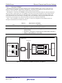
45B
Figure 4.14 shows the operating environment of the sample program. For points to be borne in mind with regard to
the operating environment, see 4.6.1, Notes on Operating Environment.
Figure 4.14 Operating Environment of Sample Program
4.2.4
Ethernet Frame Format
46B
The transmit data that must be prepared consists of the portion of the Ethernet frame other than the preamble, start
frame delimiter (SFD), and CRC. The destination MAC address and transmit source MAC address in the header must
be changed to match the MAC addresses of the devices used. Note that the ETHERC does not check the transmit source
MAC address.
Unit: byte
7
Preamble
1
6
6
Transmit
Destination
source
SFD
MAC address
MAC address
2
Type/
length
46 to 1,500
Data
4
CRC
Data stored in transmit buffer, 60 to 1,514 bytes
Figure 4.15 Ethernet Frame Format (Transmission)
The data transferred to the receive buffer consists of the portion of the Ethernet frame other than the preamble, SFD,
and CRC.
Unit: byte
7
Preamble
1
6
6
Transmit
Destination
source
SFD
MAC address
MAC address
2
Type/
length
46 to 1,500
Data
4
CRC
Data transferred to receive buffer, 60 to 1,514 bytes
Figure 4.16 Ethernet Frame Format (Reception)
R01AN0629EJ0101 Rev.1.01
Mar 31, 2011
Page 31 of 52
RX62N Group
4.3
Ethernet Transmit and Receive Settings
Descriptor Definition in Sample Program
2B
The EDMAC does not use the padding area of the descriptor. It can be used freely by the user. The sample program
uses this area to specify the start address of the next descriptor, creating a linked structure in software.
Figure 4.17 shows the transmit and receive descriptors, and the buffers, used by the sample program.
Receive Descriptors
Transmit Descriptors
status
bufsize
size
Char *buf_p
Discript *next
RX_BUFF
status
bufsize
size
Char *buf_p
Discript *next
RX_BUFF
status
bufsize
size
Char *buf_p
Discript *next
RX_BUFF
status
bufsize
size
Char *buf_p
Discript *next
status
bufsize
size
Char *buf_p
Discript *next
status
bufsize
size
Char *buf_p
Discript *next
TX_BUFF
TX_BUFF
TX_BUFF
Figure 4.17 Transmit and Receive Descriptors, and Buffers
The descriptors comprise the transmit descriptors TD0, TD1, and TD2, which are 32-bit units, and the receive
descriptors RD0, RD1, and RD2, which are also 32-bit units. The sample program defines RBL, the upper 16 bits of the
32-bit unit RD1 (TBL, the upper 16 bits of the 32-bit unit TD1), as the structure member bufsize, and the lower 16 bits
of RD1 as the structure member size. The other 32-bit units are defined as members of 32-bit size.
When allocated in the RAM, the descriptors operate according to the endian setting of the bus. (The on-chip RAM
uses the endian mode of the CPU.) The EDMAC accesses the descriptors in 32-bit units. Therefore, bufsize and size
must be allocated in the RAM according to the conditions below to ensure that their contents match when accessed in
32-bit or 16-bit units. No such conditions apply to the other members because they are defined as 32-bit size.
• When the RAM to which a descriptor is allocated is set to big-endian mode
Set the address allocation of the 32-bit unit RD1 (TD1) such that the member bufsize defined for the upper 16 bits is
assigned the low-order address and the member size defined for the lower 16 bits is assigned the high-order address.
• When the RAM to which a descriptor is allocated is set to little-endian mode
Set the address allocation of the 32-bit unit RD1 (TD1) such that the member bufsize defined for the upper 16 bits is
assigned the high-order address and the member size defined for the lower 16 bits is assigned the low-order address.
The descriptors of the sample program are defined as structures using macros defined by the compiler, as described
below.
R01AN0629EJ0101 Rev.1.01
Mar 31, 2011
Page 32 of 52
RX62N Group
Ethernet Transmit and Receive Settings
struct Descriptor
{
__evenaccess uint32_t
#if __LIT
__evenaccess uint16_t
__evenaccess uint16_t
#else
__evenaccess uint16_t
__evenaccess uint16_t
#endif
int8_t
struct Descriptor
};
status;
size;
bufsize;
bufsize;
size;
*buf_p;
*next;
It is possible to change the number of descriptors and the buffer size by changing the macros below, which are
defined in r_ether.h. BUFSIZE specifies the size of the receive buffers (RX_BUFF) and transmit buffers (TX_BUFF),
and ENTRY specifies the number of descriptors.
The buffers must align with a 32-byte boundary, so the value defined by BUFSIZE in the r_ether.h file assures a 32byte aligned value in RAM.
#define BUFSIZE
#define ENTRY
1536
8
R01AN0629EJ0101 Rev.1.01
Mar 31, 2011
Page 33 of 52
RX62N Group
4.4
Ethernet Transmit and Receive Settings
Ethernet Driver API
23B
The functions below are provided as TCP/IP stack driver interfaces. They compose the standard Renesas API (RAPI)
for Renesas Ethernet devices.
•
•
•
•
•
R_Ether_Open
R_Ether_Close
R_Ether_Read
R_Ether_Write
R_Ether_Write_Sync
4.4.1
R_Ether_Open
47B
The R_Ether_Open function initializes the ETHERC, EDMAC, physical layer transceiver (PHY), and
transmit/receive data buffers. The initialization of the ETHERC and EDMAC is separate from the power-on reset.
• Prototype
int32_t R_Ether_Open(uint32_t ch, uint8_t mac_addr[]);
• Arguments
⎯ ch
ETHERC channel number specification
⎯ mac_addr
ETHERC MAC address specification
• Return values
R_ETHER_OK(0): Normal completion
R_ETHER_ERROR(-1): Error
• Properties
Declared in r_ether.h file
Defined in r_ether.c file
• Description
The R_Ether_Open function initializes the ETHERC and EDMAC. It sets the EDMAC descriptors and buffers to
their initial state. The MAC address is used to initialize the MAC address register of the ETHERC.
The initial settings specify auto-negotiation mode for the physical layer transceiver (PHY).
The RX62N has only one Ethernet channel, so Ethernet driver processing does not branch according to the channel
number. The function will operate normally regardless of the channel number value, but setting the channel number
to 0 is recommended.
The Ethernet driver of the RX62N does not include code for processing when the MAC address is set to 0.
Therefore, make sure to input a value other than 0 as the MAC address, or add appropriate program code for
processing when the MAC address is set to 0.
R01AN0629EJ0101 Rev.1.01
Mar 31, 2011
Page 34 of 52
RX62N Group
4.4.2
Ethernet Transmit and Receive Settings
R_Ether_Close
48B
The R_Ether_Close function disables the transmit and receive functions of the ETHERC. This function does not
power-down the ETHERC and EDMAC.
• Prototype
int32_t R_Ether_Close(uint32_t ch);
• Arguments
⎯ ch
ETHERC channel number specification
• Return values
R_ETHER_OK(0): Normal completion
R_ETHER_ERROR(-1): Error
• Properties
Declared in r_ether.h file
Defined in r_ether.c file
• Description
The R_Ether_Close function disables the transmit and receive functions of the ETHERC.
The RX62N has only one Ethernet channel, so Ethernet driver processing does not branch according to the channel
number. The function will operate normally regardless of the channel number value, but setting the channel number
to 0 is recommended.
4.4.3
R_Ether_Read
49B
The R_Ether_Read function receives data to the application’s receive buffer.
• Prototype
int32_t R_Ether_Read(uint32_t ch, void *buf);
• Arguments
⎯ ch
ETHERC channel number specification
⎯ *buf
Receive data buffer pointer
• Return values
Value of 0 or greater: Number of bytes received. 0 indicates no receive data.
R_ETHER_ERROR(-1): Error (Covers both hardware and software errors.)
R_ETHER_HARD_ERROR(-3): Hardware error (Software reset required to recover.)
R_ETHER_RECOVERABLE(-4): Recoverable error (Software reset not required to recover.)
R_ETHER_NODATA(-5): No receive data
Note: The sample program does not use the R_ETHER_HARD_ERROR(-3), R_ETHER_RECOVERABLE(4), and R_ETHER_NODATA(-5) return values.
• Properties
Declared in r_ether.h file
Defined in r_ether.c file
• Description
The R_Ether_Read function reads data from the buffer designated by the receive descriptor. The receive descriptor
status is updated each time new data is processed. After reading the data, the function copies it to the receive data
buffer.
The RX62N has only one Ethernet channel, so Ethernet driver processing does not branch according to the channel
number. The function will operate normally regardless of the channel number value, but setting the channel number
to 0 is recommended.
The data associated with a descriptor that generates a receive frame error is discarded, the status is cleared, and read
operation continues.
R01AN0629EJ0101 Rev.1.01
Mar 31, 2011
Page 35 of 52
RX62N Group
4.4.4
Ethernet Transmit and Receive Settings
R_Ether_Write
50B
The R_Ether_Write function transmits data from the application’s transmit buffer.
• Prototype
int32_t R_Ether_Write(uint32_t ch, void *buf, uint32_t len);
• Arguments
⎯ ch
ETHERC channel number specification
⎯ *buf
Pointer to Ethernet data to be transmitted
⎯ len
Ethernet frame length
• Return values
R_ETHER_OK(0): Normal completion
R_ETHER_ERROR(-1): Error
• Properties
Declared in r_ether.h file
Defined in r_ether.c file
• Description
The R_Ether_Write function writes transmit data to the buffer designated by the transmit descriptor. The transmit
descriptor status is updated each time new data is processed. After the data is written, it is transmitted by the
ETHERC.
The R_Ether_Write function does not check transmit completion.
The RX62N has only one Ethernet channel, so Ethernet driver processing does not branch according to the channel
number. The function will operate normally regardless of the channel number value, but setting the channel number
to 0 is recommended.
The function does not check for transmit frame errors.
4.4.5
R_Ether_Write_Sync
51B
The Ether_Write_Sync function writes transmit data to the transmit buffer and waits for data transmission to
complete.
• Prototype
int32_t R_Ether_Write_Sync(uint32_t ch, void *buf, uint32_t len);
• Arguments
⎯ ch
ETHERC channel number specification
⎯ *buf
Pointer to Ethernet data to be transmitted
⎯ len
Ethernet frame length
• Return values
R_ETHER_OK(0): Normal completion
R_ETHER_ERROR(-1): Error
R_ETHER_TIMEOUT(-2): Timeout
R_ETHER_HARD_ERROR(-3): Hardware error (Software reset required to recover.)
R_ETHER_RECOVERABLE(-4): Recoverable error (Software reset not required to recover.)
• Properties
Declared in r_ether.h file
Defined in r_ether.c file
• Description
The R_Ether_Write function writes transmit data to the buffer designated by the transmit descriptor. In addition to
processing new data and waiting for transmission to complete, it updates the transmit descriptor status.
R01AN0629EJ0101 Rev.1.01
Mar 31, 2011
Page 36 of 52
RX62N Group
Ethernet Transmit and Receive Settings
Note: Do not use this function because it is not supported by the RX62N Ethernet driver. Use the
R_Ether_Write function to transmit data from the transmit buffer.
4.5
Processing Procedure of Sample Program
24B
Figures 4.18 and 4.19 show the processing sequence of the sample program, which uses the Ethernet driver API, and
figures 4.20 to 4.28 show the processing sequence of the Ethernet driver API and its subordinate functions.
Main function
main
Start
Select test type (i = 1 or 2)
No
i = 1?
Yes
i = 2?
No
Yes
Sample transmit program
Sample receive program
Figure 4.18 Main Processing Sequence of Sample Program (1)
R01AN0629EJ0101 Rev.1.01
Mar 31, 2011
Page 37 of 52
RX62N Group
Ethernet Transmit and Receive Settings
Sample transmit program
SampleEthernetTransmission
Sample receive program
SampleEthernetReception
Start
Start
R_Ether_Open
R_Ether_Open
No
No
Success?
Success?
Yes
Yes
R_Ether_Write
R_Ether_Read
No
No
Success?
Success?
Yes
Yes
No
10 frames
transmitted?
Yes
No
10 frames
received?
Yes
R_Ether_Close
No
Transmission complete?
(TR = 0 in EDTRR?)
End
Yes
R_Ether_Close
End
Figure 4.19 Main Processing Sequence of Sample Program (2)
R01AN0629EJ0101 Rev.1.01
Mar 31, 2011
Page 38 of 52
RX62N Group
Ethernet Transmit and Receive Settings
Open function
R_Ether_Open
Start
Transmit/receive descriptor initialization
_eth_fifoInit
Initial pointer setting for
transmit/receive descriptor
Reset ETHERC/EDMAC
Initialize the transmit descriptor and receive descriptor.
Initialization of pointer variable for managing the current descriptor
Set the initial value of the start address of the transmit/receive descriptor list.
Software reset of ETHERC/EDMAC
Write 1 to the SWR bit in the EDMAC mode register (EDMR).
Wait because access to the registers of all Ethernet-related modules is
prohibited during the software reset issue duration (64 cycles).
i=0
No
i < 0x00000100?
Yes
i+1
ETHERC settings
Check MAC address
MAC address = 0?
No
MAC address register setting
Write 0x00000037 to the ETHERC status register (ECSR) to clear the
ETHERC internal status.
Write 0x00000020 to the ETHERC interrupt permission register (ECSIPR) to
prohibit interrupt notification by reports from the ECSR register.
Set the receive frame length bits in the receive frame length register (RFLR)
to specify 1,518 bytes.
Set the inter packet gap bits in the IPG register (IPGR) to specify 96 bits.
Yes
Set the MAC address in the MAC address high register
(MAHR) and MAC address low register (MALR). The
sample program does not include code for processing when
the MAC address is set to 0. The user must add appropriate
program code for processing when the MAC address is set
to 0.
Read MAC address
Set MAC address register
1
Figure 4.20 Ethernet API Processing Sequence of Sample Program (1)
R01AN0629EJ0101 Rev.1.01
Mar 31, 2011
Page 39 of 52
RX62N Group
Ethernet Transmit and Receive Settings
1
EDMAC settings
Write 0x47FF0F9F to the ETHERC/EDMAC status register (EESR) to clear
the transmit status.
Set the start address of the receive descriptor list in the receive descriptor
list start address register (RDLAR).
Set the start address of the transmit descriptor list in the transmit
descriptor list start address register (TDLAR).
Write 0x00000000 to the transmit/receive status copy enable register
(TRSCER) to disable updating of transmit and receive status information in
the relevant descriptors, TFS25 to TFS0 and RFS26 to RFS0.
Write 0x00000000 to the transmit FIFO threshold register (TFTR) to select
store and forward mode.
Write 0x00000707 to the FIFO depth register (FDR) to set the capacity of
the transmit and receive FIFOs to 2,048 bytes.
Write 0x00000001 to the receiving method control register (RMCR) to
select continuous reception.
Only applicable for little endian operation
Write 1 to the big/little endian mode bit in the
EDMAC mode register (EDMR) to select little
endian mode.
Set transmit/receive data to
little endian mode
PHY initialization
phy_init
Initialization
successful?
No
Yes
Auto-negotiation result
acquisition
Auto-negotiation
successful?
No
Yes
Return R_ETHER_ERROR
2
End
Figure 4.21 Ethernet API Processing Sequence of Sample Program (2)
R01AN0629EJ0101 Rev.1.01
Mar 31, 2011
Page 40 of 52
RX62N Group
Ethernet Transmit and Receive Settings
2
Set the duplex mode (DM) bit in the ETHERC mode register
(ECMR) to match the mode supported by the link partner.
No
Link partner supports
full-duplex mode?
Yes
Set to half-duplex mode
ECMR.DM = 0
Set to full-duplex mode
ECMR.DM = 1
Link partner supports
100 Mbps?
No
Yes
Set to 100 Mbps
ECMR.RTM = 1
Set to 10 Mbps
ECMR.RTM = 0
Set the transmit enable (TE) or receive enable (RE) bit in
the ETHERC mode register (ECMR) to 1 to enable transmit/receive.
Enable transmit/receive
Set the receive request (RR) bit in the EDMAC receive request
register (EDRRR) to 1 to enable the receive function.
Start reception
Wait until the link partner is ready. The duration of the wait depends
on the system characteristics of the link partner, so careful evaluation
is necessary when setting the value.
i=0
i < 0x00000100?
Only applicable for RMII
Set the transmission/reception rate
(RTM) bit in the ETHERC mode register
(ECMR) to match the mode supported
by the link partner.
No
Yes
i+1
Return R_ETHER_OK
End
Close function
R_Ether_Close
Start
Disable transmit/receive
Write 0x00000000 to the ETHERC mode register (ECMR)
to disable transmit/receive operation.
Return R_ETHER_ERROR
End
Figure 4.22 Ethernet API Processing Sequence of Sample Program (3)
R01AN0629EJ0101 Rev.1.01
Mar 31, 2011
Page 41 of 52
RX62N Group
Ethernet Transmit and Receive Settings
Data write function
R_Ether_Write
Start
Initialize variable flag
The variable flags are used to write to bits TFP1, TFP0, and TACT in
receive descriptor 0 (TD0). Set the variable flag to correspond to
TACT = 0, TFP1 = 1, and TFP0 = 0.
Transmit data write
_eth_fifoWrite
Write data to the transmit descriptor and transmit buffer.
Can entire transmit size
be written to buffer?
No
Yes
Set the variable flag to correspond to TFP0 = 1. TACT and TFP1
retain their pre-setting values.
Set variable flag
Clear bits TFP1 and TFP0 in
transmit descriptor 0 (TD0)
Set bits TACT, TFP1, and TFP0 in
transmit descriptor 0 (TD0)
flag = 0
Set the variable flag to correspond to TACT = 1,
and write the variable flag values to bits TFP1, TFP0,
and TACT in transmit descriptor 0 (TD0).
Set the variable flag to correspond to TACT = 0, TFP1 = 0, and TFP0 = 0.
Update transmit descriptor pointer
No
Data equivalent to transmit
size written to buffers?
Yes
Transmit function enabled?
Yes
No
Enable transmit function
Set the transmit request (TR) bit in the EDMAC
transmit request register (EDTRR) to 1.
Return R_ETHER_OK
End
Figure 4.23 Ethernet API Processing Sequence of Sample Program (4)
R01AN0629EJ0101 Rev.1.01
Mar 31, 2011
Page 42 of 52
RX62N Group
Ethernet Transmit and Receive Settings
Data read function
R_Ether_Read
Start
Initialize the internal variable for receive size to 0
and for receive loop to on.
Internal variable initialization
Receive data read
_eth_fifoRead
Read data from receive buffer.
Yes
2 or more receive frames
and receive size = 0?
Return R_ETHER_OK
No
Yes
No receive data?
End
No
Receive error?
No
Yes
Receive error handling Normal receive processing
See other sequences for processing details.
Yes
Receive loop on?
No
Return receive size
End
Receive error handling
Start
Set receive size to 0
Clear the receive frame position (RFP), receive frame error (RFE),
and receive frame status (RFS) flags of receive descriptor 0 (RD0).
Clear receive flags
Activate receive descriptor
Receive function
enabled?
Set RACT to 1 to activate the receive descriptor.
Yes
No
Enable receive function
Set the receive request (RR) bit in the EDMAC receive request
register (EDRRR) to 1 to enable the receive function.
End
Figure 4.24 Ethernet API Processing Sequence of Sample Program (5)
R01AN0629EJ0101 Rev.1.01
Mar 31, 2011
Page 43 of 52
RX62N Group
Ethernet Transmit and Receive Settings
Normal receive processing
Start
No
RFP1 = 1?
Yes
Clear the receive size to 0 when the contents of
the receive buffer are the start of the frame.
Set receive size to 0
No
RFP0 = 1?
Yes
Turn off receive loop
Turn off the receive loop if the contents of the receive
buffer include the end of the frame.
Update receive size
Add the size of the read data to the receive size.
Clear RFP
Clear the receive frame position (RFP).
Activate receive descriptor
Set RACT to 1 to activate the receive descriptor.
Update the pointer to the relevant descriptor.
Update receive descriptor pointer
Update the pointer for writing receive data
by the size of the read data.
Update receive data pointer
Yes
Receive function enabled?
No
Enable receive function
Set the receive request (RR) bit in the EDMAC receive
request register (EDRRR) to 1 to enable the receive function.
End
Figure 4.25 Ethernet API Processing Sequence of Sample Program (6)
R01AN0629EJ0101 Rev.1.01
Mar 31, 2011
Page 44 of 52
RX62N Group
Ethernet Transmit and Receive Settings
descriptor initialization function
_eth_fifoInit
Start
Update pointer to descriptor to be initialized
Transmit descriptor?
Yes
Set transmit data buffer
Clear data buffer
No
Set the buffer address of the relevant descriptor.
Set receive data buffer
Clear the relevant data buffer to 0.
Set buffer size
Set the buffer size for a receive descriptor in RFL and the
buffer size for a transmit descriptor in the padding area.
Clear buffer internal size
For a receive descriptor clear RBL to 0 and for a transmit
descriptor clear TBL to 0.
Clear frame status
Set next descriptor address
No
Set pointer to descriptor to be initialized.
For a receive descriptor set RACT in RD0 to 1 (otherwise 0).
For a transmit descriptor clear all bits in TD0 to 0.
Set the address of the next descriptor to be referenced.
All descriptors initialized?
Yes
Set descriptor ring end
In the last descriptor in the descriptor list, set the bit that indicates the
end of the descriptor ring (TDLE or RDLE) to 1.
Set start of next descriptor ring
Also, set the address of the next descriptor to the address of the first
descriptor.
End
Figure 4.26 Sample Program Descriptor Processing Sequence (1)
R01AN0629EJ0101 Rev.1.01
Mar 31, 2011
Page 45 of 52
RX62N Group
Ethernet Transmit and Receive Settings
FIFO write function
_eth_fifoWrite
Start
No
Descriptor active?
Yes
Return –1
End
Written data exceeds
buffer size?
Yes
No
Write data to buffer
No
Entire data size written?
Yes
Return size written
End
Figure 4.27 Sample Program Descriptor Processing Sequence (2)
R01AN0629EJ0101 Rev.1.01
Mar 31, 2011
Page 46 of 52
RX62N Group
Ethernet Transmit and Receive Settings
FIFO read function
_eth_fifoRead
Start
Yes
Descriptor active?
No
Yes
Frame error?
No
Return –2
Return –1
No
Frame complete?
Yes
End
Set descriptor buffer data size
to read size
Set buffer size to read size
No
Read size exceeds buffer size?
Read data from buffer
Yes
Subtract buffer size
from read size
No
Entire read size was read?
Yes
Return read size
End
Figure 4.28 Sample Program Descriptor Processing Sequence (3)
R01AN0629EJ0101 Rev.1.01
Mar 31, 2011
Page 47 of 52
RX62N Group
4.6
Ethernet Transmit and Receive Settings
Notes on Transmit/Receive Settings
25B
4.6.1
Note on Operating Environment
52B
The sample program uses the auto-negotiation function to select the communication mode. If the amount of time
required for auto-negotiation by the RX62N and the connection partner of the RX62N (the hub in figure 4.14) differs
considerably, communication may fail even though auto-negotiation is successful.
If the connection partner of the RX62N cannot receive even after auto-negotiation completes successfully, insert a
wait period on the RX62N side to enable the connection partner to enter the ready-to-receive state. The amount of time
needed for the connection partner to enter the ready-to-receive state will differ depending on the system, so the user
should perform sufficient evaluation when determining the wait period.
To adjust the duration of the wait period, modify the following lines of code in the R_EtherOpen function (lines 278
to 280) in the r_ether.c file.
/* Delay to stabilize */
/* Set the count according to the system */
for( i = 0 ; i < 0x0000100 ; i++ );
4.6.2
Note on Interrupt Handling
53B
The sample program does not use interrupt functions. In order to use interrupts, the user must add appropriate
program code.
4.6.3
Note on Error Handling
54B
The sample program does not include routines for handling transmit or receive errors. If error handling is required,
the user must add appropriate program code.
4.6.4
Note on Transmit/Receive Buffer Size
5B
The buffers must align with a 32-byte boundary, so the value defined by BUFSIZE in the r_ether.h file assures a 32byte aligned value in RAM.
4.6.5
Note on Reception Mode
56B
When continuous reception is selected (receive request bit reset (RNR) bit in receiving method control register
(RMCR) set to 1), the EDMAC reads the next descriptor and enters the receive standby state if the value of the RACT
bit is 1.
In continuous reception mode, setting the receive request bit non-reset mode (RNC) bit in the RMCR register to 1
causes EDMAC receive operation to continue, with no clearing of the RR bit even if the RACT bit is cleared to 0
(inactive). (Receive descriptors are fetched consecutively, and receive frame DMA continues.)
This means that data may be overwritten before the receive data is passed to a higher layer. The setting that causes
DMA to continue even when the RACT bit is cleared to 0 (inactive) should not be used under conditions requiring
handshaking, such as TCP communication. This setting is recommended for use in conditions such as UDP
communication where real-time performance is essential and retransmission is not required.
R01AN0629EJ0101 Rev.1.01
Mar 31, 2011
Page 48 of 52
RX62N Group
5.
Ethernet Transmit and Receive Settings
Endian Mode Selection in Sample Program
4B
In the compile options of the RX compiler, big endian is defined as the predefined macro __BIG and little endian as
__LIT. The sample program uses these macros to absorb the difference due to the endian mode selection.
5.1
Big Endian Mode
26B
For big-endian operation, make the following settings, and set the Pin3 of SW4 on the Renesas Starter Kit +(product
number: R0K5562N0C000BE) to OFF (MDE=Hi).
• 1.
• 2.
• 3.
Launch RX Standard Toolchain by selecting Build → RX Standard Toolchain from the HEW toolbar.
On the CPU tab select Big under Endian, then click OK.
Build the file once again.
5.2
Little Endian Mode
27B
For little-endian operation, make the following settings, and set the Pin3 of SW4 on the Renesas Starter Kit
+(product number: R0K5562N0C000BE) to ON (MDE=Low).
• 1.
• 2.
• 3.
6.
Launch RX Standard Toolchain by selecting Build → RX Standard Toolchain from the HEW toolbar.
On the CPU tab select Little under Endian, then click OK.
Build the file once again.
Interface (MII/RMII) Selection in Sample Program
5B
MII/RMII selection can be accomplished by switching macros. Make the appropriate change to ETH_MODE_SEL,
which is defined in r_ether.h.
6.1
MII
28B
As shown below, set ETH_MODE_SEL to ETH_MII_MODE in the r_ether.h file.
#define ETH_MODE_SEL ETH_MII_MODE
6.2
RMII
29B
As shown below, set ETH_MODE_SEL to ETH_RMII_MODE in the r_ether.h file. Please note that the Renesas
Starter Kit +(product number: R0K5562N0C000BE) supports the MII (Media Independent Interface) only, and doesn't
support RMII (Reduced Media Independent Interface).
#define ETH_MODE_SEL ETH_RMII_MODE
R01AN0629EJ0101 Rev.1.01
Mar 31, 2011
Page 49 of 52
RX62N Group
7.
Ethernet Transmit and Receive Settings
Allocation of Sections in Sample Program
6B
Table 7.1 shows the allocation of sections by the sample program.
For details on the compiler, see section 5, Optimizing Linkage Editor Options, and 8.1, Program Structure, in RX
Family C/C++ Compiler, Assembler, Optimizing Linkage Editor: Compiler Package User’s Manual.
Table 7.1
Address
0x00001000
Device
On-chip RAM
0xFFF80000
On-chip ROM
0xFFF80100
0xFFFFFFD0
7.1
Allocation of Sections in Sample Program
Section
B_RX_DESC
B_TX_DESC
B_RX_BUFF_1
B_TX_BUFF_1
B_1
R_1
B_2
R_2
B
R
SU
SI
BETH_BUFF
PResetPRG
C_1
C_2
C
C$*
D*
P
PIntPRG
W*
FIXEDVECT
Description
Receive descriptor area
Transmit descriptor area
Receive buffer area
Transmit buffer area
Uninitialized data area with 1-byte alignment
Initialized data area (variable) with 1-byte alignment
Uninitialized data area with 2-byte alignment
Initialized data area (variable) with 2-byte alignment
Uninitialized data area with 4-byte alignment
Initialized data area (variable) with 4-byte alignment
User stack area
Interrupt stack area
Transmit/receive data buffer of main routine
Program area of ResetPRG section
(initial settings program)
Constant area with 1-byte alignment
Constant area with 2-byte alignment
Constant area with 4-byte alignment
Constant area of C$* sections
(C$DSEC, C$BSEC, C$VECT)
Initialized data area (initial value)
Program area with no section definition
Program area of IntPRG section (interrupt)
Switch statement branch table area
FIXEDVECT section area
Notes on Allocation of Sections
30B
• The sample program set the transmit/receive descriptor length (DL) bits in the EDMAC mode register (EDMR) to
specify 16 bytes, so the B_RX_DESC and B_TX_DESC sections should be allocated so that they are aligned with
16-byte boundaries.
• Allocate the B_RX_BUFF_1 and B_TX_BUFF_1 sections so that they are aligned with 32-byte boundaries.
8.
Note on Use of Renesas Starter Kit +
7B
Please note that the Renesas Starter Kit +(product number: R0K5562N0C000BE) supports the MII (Media
Independent Interface) only, and doesn't support RMII (Reduced Media Independent Interface). Must select MII from
the interface of the reference program (MII/RMII) according to 6.1.
R01AN0629EJ0101 Rev.1.01
Mar 31, 2011
Page 50 of 52
RX62N Group
9.
Ethernet Transmit and Receive Settings
Reference Documents
8B
• RX62N Group Hardware Manual
(The latest version can be downloaded from the Renesas Electronics Web site.)
• RX Family Software Manual
(The latest version can be downloaded from the Renesas Electronics Web site.)
• RX Family Compiler Package User’s Manual
(The latest version can be downloaded from the Renesas Electronics Web site.)
• Standard Microsystems Corporation LAN8700/LAN8700i Datasheet
(The latest version can be downloaded from the Standard Microsystems Corporation Web site.)
R01AN0629EJ0101 Rev.1.01
Mar 31, 2011
Page 51 of 52
RX62N Group
Ethernet Transmit and Receive Settings
Website and Support
• Renesas Electronics Website
http://www.renesas.com/
HU
U
• Inquiries
http://www.renesas.com/inquiry
HU
U
All trademarks and registered trademarks are the property of their respective owners.
R01AN0629EJ0101 Rev.1.01
Mar 31, 2011
Page 52 of 52
Revision Record
Rev.
1.00
1.01
A-1
Date
Dec.27.10
Mar.31.11
Page
—
1,3,16,17,
31,49,50
Description
Summary
First edition issued
Change target board to the Renesas Starter Kit +(product
number: R0K5562N0C000BE).
General Precautions in the Handling of MPU/MCU Products
The following usage notes are applicable to all MPU/MCU products from Renesas. For detailed usage notes
on the products covered by this manual, refer to the relevant sections of the manual. If the descriptions under
General Precautions in the Handling of MPU/MCU Products and in the body of the manual differ from each
other, the description in the body of the manual takes precedence.
1. Handling of Unused Pins
Handle unused pins in accord with the directions given under Handling of Unused Pins in the
manual.
The input pins of CMOS products are generally in the high-impedance state. In operation
with an unused pin in the open-circuit state, extra electromagnetic noise is induced in the
vicinity of LSI, an associated shoot-through current flows internally, and malfunctions occur
due to the false recognition of the pin state as an input signal become possible. Unused
pins should be handled as described under Handling of Unused Pins in the manual.
2. Processing at Power-on
The state of the product is undefined at the moment when power is supplied.
The states of internal circuits in the LSI are indeterminate and the states of register
settings and pins are undefined at the moment when power is supplied.
In a finished product where the reset signal is applied to the external reset pin, the states
of pins are not guaranteed from the moment when power is supplied until the reset
process is completed.
In a similar way, the states of pins in a product that is reset by an on-chip power-on reset
function are not guaranteed from the moment when power is supplied until the power
reaches the level at which resetting has been specified.
3. Prohibition of Access to Reserved Addresses
Access to reserved addresses is prohibited.
The reserved addresses are provided for the possible future expansion of functions. Do
not access these addresses; the correct operation of LSI is not guaranteed if they are
accessed.
4. Clock Signals
After applying a reset, only release the reset line after the operating clock signal has become
stable. When switching the clock signal during program execution, wait until the target clock
signal has stabilized.
When the clock signal is generated with an external resonator (or from an external
oscillator) during a reset, ensure that the reset line is only released after full stabilization of
the clock signal. Moreover, when switching to a clock signal produced with an external
resonator (or by an external oscillator) while program execution is in progress, wait until
the target clock signal is stable.
5. Differences between Products
Before changing from one product to another, i.e. to one with a different part number, confirm
that the change will not lead to problems.
The characteristics of MPU/MCU in the same group but having different part numbers may
differ because of the differences in internal memory capacity and layout pattern. When
changing to products of different part numbers, implement a system-evaluation test for
each of the products.
Notice
1.
All information included in this document is current as of the date this document is issued. Such information, however, is subject to change without any prior notice. Before purchasing or using any Renesas
Electronics products listed herein, please confirm the latest product information with a Renesas Electronics sales office. Also, please pay regular and careful attention to additional and different information to
be disclosed by Renesas Electronics such as that disclosed through our website.
2.
Renesas Electronics does not assume any liability for infringement of patents, copyrights, or other intellectual property rights of third parties by or arising from the use of Renesas Electronics products or
technical information described in this document. No license, express, implied or otherwise, is granted hereby under any patents, copyrights or other intellectual property rights of Renesas Electronics or
others.
3.
You should not alter, modify, copy, or otherwise misappropriate any Renesas Electronics product, whether in whole or in part.
4.
Descriptions of circuits, software and other related information in this document are provided only to illustrate the operation of semiconductor products and application examples. You are fully responsible for
the incorporation of these circuits, software, and information in the design of your equipment. Renesas Electronics assumes no responsibility for any losses incurred by you or third parties arising from the
use of these circuits, software, or information.
5.
When exporting the products or technology described in this document, you should comply with the applicable export control laws and regulations and follow the procedures required by such laws and
regulations. You should not use Renesas Electronics products or the technology described in this document for any purpose relating to military applications or use by the military, including but not limited to
the development of weapons of mass destruction. Renesas Electronics products and technology may not be used for or incorporated into any products or systems whose manufacture, use, or sale is
prohibited under any applicable domestic or foreign laws or regulations.
6.
Renesas Electronics has used reasonable care in preparing the information included in this document, but Renesas Electronics does not warrant that such information is error free. Renesas Electronics
7.
Renesas Electronics products are classified according to the following three quality grades: "Standard", "High Quality", and "Specific". The recommended applications for each Renesas Electronics product
assumes no liability whatsoever for any damages incurred by you resulting from errors in or omissions from the information included herein.
depends on the product's quality grade, as indicated below. You must check the quality grade of each Renesas Electronics product before using it in a particular application. You may not use any Renesas
Electronics product for any application categorized as "Specific" without the prior written consent of Renesas Electronics. Further, you may not use any Renesas Electronics product for any application for
which it is not intended without the prior written consent of Renesas Electronics. Renesas Electronics shall not be in any way liable for any damages or losses incurred by you or third parties arising from the
use of any Renesas Electronics product for an application categorized as "Specific" or for which the product is not intended where you have failed to obtain the prior written consent of Renesas Electronics.
The quality grade of each Renesas Electronics product is "Standard" unless otherwise expressly specified in a Renesas Electronics data sheets or data books, etc.
"Standard":
Computers; office equipment; communications equipment; test and measurement equipment; audio and visual equipment; home electronic appliances; machine tools;
personal electronic equipment; and industrial robots.
"High Quality": Transportation equipment (automobiles, trains, ships, etc.); traffic control systems; anti-disaster systems; anti-crime systems; safety equipment; and medical equipment not specifically
designed for life support.
"Specific":
Aircraft; aerospace equipment; submersible repeaters; nuclear reactor control systems; medical equipment or systems for life support (e.g. artificial life support devices or systems), surgical
implantations, or healthcare intervention (e.g. excision, etc.), and any other applications or purposes that pose a direct threat to human life.
8.
You should use the Renesas Electronics products described in this document within the range specified by Renesas Electronics, especially with respect to the maximum rating, operating supply voltage
range, movement power voltage range, heat radiation characteristics, installation and other product characteristics. Renesas Electronics shall have no liability for malfunctions or damages arising out of the
use of Renesas Electronics products beyond such specified ranges.
9.
Although Renesas Electronics endeavors to improve the quality and reliability of its products, semiconductor products have specific characteristics such as the occurrence of failure at a certain rate and
malfunctions under certain use conditions. Further, Renesas Electronics products are not subject to radiation resistance design. Please be sure to implement safety measures to guard them against the
possibility of physical injury, and injury or damage caused by fire in the event of the failure of a Renesas Electronics product, such as safety design for hardware and software including but not limited to
redundancy, fire control and malfunction prevention, appropriate treatment for aging degradation or any other appropriate measures. Because the evaluation of microcomputer software alone is very difficult,
please evaluate the safety of the final products or system manufactured by you.
10. Please contact a Renesas Electronics sales office for details as to environmental matters such as the environmental compatibility of each Renesas Electronics product. Please use Renesas Electronics
products in compliance with all applicable laws and regulations that regulate the inclusion or use of controlled substances, including without limitation, the EU RoHS Directive. Renesas Electronics assumes
no liability for damages or losses occurring as a result of your noncompliance with applicable laws and regulations.
11. This document may not be reproduced or duplicated, in any form, in whole or in part, without prior written consent of Renesas Electronics.
12. Please contact a Renesas Electronics sales office if you have any questions regarding the information contained in this document or Renesas Electronics products, or if you have any other inquiries.
(Note 1)
"Renesas Electronics" as used in this document means Renesas Electronics Corporation and also includes its majority-owned subsidiaries.
(Note 2)
"Renesas Electronics product(s)" means any product developed or manufactured by or for Renesas Electronics.
http://www.renesas.com
SALES OFFICES
Refer to "http://www.renesas.com/" for the latest and detailed information.
Renesas Electronics America Inc.
2880 Scott Boulevard Santa Clara, CA 95050-2554, U.S.A.
Tel: +1-408-588-6000, Fax: +1-408-588-6130
Renesas Electronics Canada Limited
1101 Nicholson Road, Newmarket, Ontario L3Y 9C3, Canada
Tel: +1-905-898-5441, Fax: +1-905-898-3220
Renesas Electronics Europe Limited
Dukes Meadow, Millboard Road, Bourne End, Buckinghamshire, SL8 5FH, U.K
Tel: +44-1628-585-100, Fax: +44-1628-585-900
Renesas Electronics Europe GmbH
Arcadiastrasse 10, 40472 Düsseldorf, Germany
Tel: +49-211-65030, Fax: +49-211-6503-1327
Renesas Electronics (China) Co., Ltd.
7th Floor, Quantum Plaza, No.27 ZhiChunLu Haidian District, Beijing 100083, P.R.China
Tel: +86-10-8235-1155, Fax: +86-10-8235-7679
Renesas Electronics (Shanghai) Co., Ltd.
Unit 204, 205, AZIA Center, No.1233 Lujiazui Ring Rd., Pudong District, Shanghai 200120, China
Tel: +86-21-5877-1818, Fax: +86-21-6887-7858 / -7898
Renesas Electronics Hong Kong Limited
Unit 1601-1613, 16/F., Tower 2, Grand Century Place, 193 Prince Edward Road West, Mongkok, Kowloon, Hong Kong
Tel: +852-2886-9318, Fax: +852 2886-9022/9044
Renesas Electronics Taiwan Co., Ltd.
13F, No. 363, Fu Shing North Road, Taipei, Taiwan
Tel: +886-2-8175-9600, Fax: +886 2-8175-9670
Renesas Electronics Singapore Pte. Ltd.
1 harbourFront Avenue, #06-10, keppel Bay Tower, Singapore 098632
Tel: +65-6213-0200, Fax: +65-6278-8001
Renesas Electronics Malaysia Sdn.Bhd.
Unit 906, Block B, Menara Amcorp, Amcorp Trade Centre, No. 18, Jln Persiaran Barat, 46050 Petaling Jaya, Selangor Darul Ehsan, Malaysia
Tel: +60-3-7955-9390, Fax: +60-3-7955-9510
Renesas Electronics Korea Co., Ltd.
11F., Samik Lavied' or Bldg., 720-2 Yeoksam-Dong, Kangnam-Ku, Seoul 135-080, Korea
Tel: +82-2-558-3737, Fax: +82-2-558-5141
© 2011 Renesas Electronics Corporation. All rights reserved.
Colophon 1.1