1
AN93
S i 2 4 9 3 / S i 2 4 5 7 / S i 2 4 3 4 / S i 2 4 1 5 / S i 2 4 0 4 M o d e m D e s i g n e r ’s G u i d e
1. Introduction
board layout files available separately. These include
double-sided and single-sided layouts with options for
through-hole isolation components. Additionally,
evaluation boards, useful for evaluating the modem
chipset or for initial prototyping work, are available.
Check with your Silicon Laboratories salesperson or
distributor for more details.
This application note is intended to supplement the
Si2493/Si2457/Si2434/Si2415 and Si2404 data sheets
and is divided into two main sections: "2. Hardware
Design Reference" and "3. Software Design
Reference". The Hardware Design Reference provides
functional descriptions and information necessary to
design ISOmodem® hardware. Chipset specifications
can be found in the respective data sheets. The
Software Design Reference includes information on
how to control the functionality of the modem with AT
commands and register settings. Particular topics of
interest in either design reference can be easily located
through the table of contents or the comprehensive
index located at the back of this document.
The Software Design Reference consists of sections
focused on the modem controller, memory, and digital
interface. The modem controller section includes a
complete description of AT commands, “fast connect”
options, transparent HDLC/V.80 mode, escape
methods, and default settings. The memory section
describes the EEPROM interface, S-Registers, and URegisters including bit-mapped registers used to
configure both the modem chip and the line-side DAA
chip. "3.4. Digital Interface" on page 98 provides details
about the serial and parallel interface capability of the
modem. Additionally, there are several programming
examples, a section on testing, and a comprehensive
section with configuration settings for most countries.
The Hardware Design Reference is divided into three
sections. The first section describes the modulations
and protocols supported by the chipset. The modem
and DAA chip operation are described, and a reference
design including a suggested bill of materials is
presented. Silicon Laboratories also has printed circuit
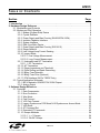
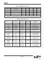
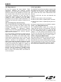
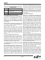
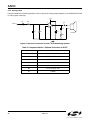
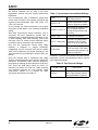
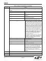
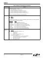
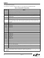
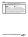
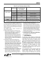
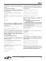
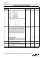
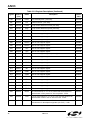
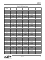
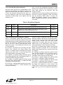
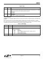
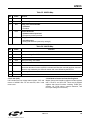
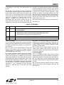
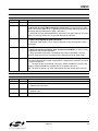
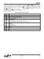
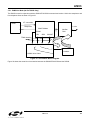
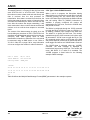
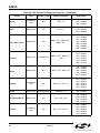
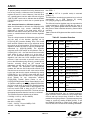
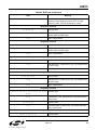
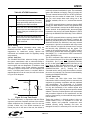
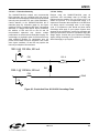
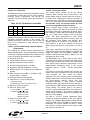
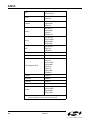
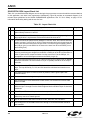
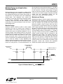
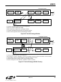
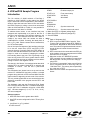
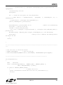
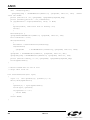
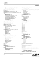
Isolation Barrier
CLKIN/XTALI
CLKOUT/EECS/A0
RXD
TXD
CTS
RTS
DCD
ESC
RI
PLL
Clocking
Si3018*
Data Bus
Microcontroller
DSP
Hybrid
and dc
Termination
TIP
Isolation
Interface
DAA
Interface
AOUT
Parallel
Interface
External
Circuitry
RAM/ROM
Serial
Interface
INT
CS
WR
RD
A0
D0-D7
Si2493/57/34/15/04
XTALO
ISOB
RING
Ring Detect
Off-Hook
RESET
*Si3010 with Si2404
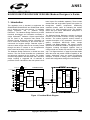
Figure 1. Functional Block Diagram
Rev. 0.9 2/06
Copyright © 2006 by Silicon Laboratories
AN93
AN93
2
Rev. 0.9
AN93
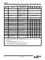
TA B L E O F C O N T E N TS
Section
Page
1. Introduction . . . . . . . . . . . . . . . . . . . . . . . . . . . . . . . . . . . . . . . . . . . . . . . . . . . . . . . . . . . . .1
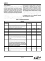
2. Hardware Design Reference . . . . . . . . . . . . . . . . . . . . . . . . . . . . . . . . . . . . . . . . . . . . . . . .7
2.1. Modulations and Protocols . . . . . . . . . . . . . . . . . . . . . . . . . . . . . . . . . . . . . . . . . . . . .7
2.2. Modem and DAA Operation . . . . . . . . . . . . . . . . . . . . . . . . . . . . . . . . . . . . . . . . . . . .9
2.2.1. Modem (System-Side) Device . . . . . . . . . . . . . . . . . . . . . . . . . . . . . . . . . . . . 9
2.2.2. Crystal Oscillator . . . . . . . . . . . . . . . . . . . . . . . . . . . . . . . . . . . . . . . . . . . . . . . 9
2.2.3. Power Supply and Bias Circuitry (Si2493/57/34/15/04) . . . . . . . . . . . . . . . . 11
2.2.4. Isolation Capacitor Interface . . . . . . . . . . . . . . . . . . . . . . . . . . . . . . . . . . . . . 11
2.2.5. System Interface . . . . . . . . . . . . . . . . . . . . . . . . . . . . . . . . . . . . . . . . . . . . . . 11
2.2.6. DAA (Line-Side) Device . . . . . . . . . . . . . . . . . . . . . . . . . . . . . . . . . . . . . . . . 11
2.2.7. Power Supply and Bias Circuitry (Si3018/10) . . . . . . . . . . . . . . . . . . . . . . . . 11
2.2.8. Ringer Network . . . . . . . . . . . . . . . . . . . . . . . . . . . . . . . . . . . . . . . . . . . . . . . 12
2.2.9. Line Voltage/Loop Current Sensing . . . . . . . . . . . . . . . . . . . . . . . . . . . . . . . 12
2.2.10. Legacy Mode. . . . . . . . . . . . . . . . . . . . . . . . . . . . . . . . . . . . . . . . . . . . . . . . 12
2.2.10.1. Line Voltage Measurement. . . . . . . . . . . . . . . . . . . . . . . . . . . . . . . . . 12
2.2.10.2. Loop Current Measurement . . . . . . . . . . . . . . . . . . . . . . . . . . . . . . . . 12
2.2.11. Hookswitch and DC Termination. . . . . . . . . . . . . . . . . . . . . . . . . . . . . . . . . 15
2.2.11.1. DC Termination. . . . . . . . . . . . . . . . . . . . . . . . . . . . . . . . . . . . . . . . . . 15
2.2.12. AC Termination . . . . . . . . . . . . . . . . . . . . . . . . . . . . . . . . . . . . . . . . . . . . . . 15
2.2.13. Ringer Impedance and Threshold. . . . . . . . . . . . . . . . . . . . . . . . . . . . . . . . 16
2.2.14. Pulse Dialing and Spark Quenching . . . . . . . . . . . . . . . . . . . . . . . . . . . . . . 16
2.2.15. Billing Tone Detection . . . . . . . . . . . . . . . . . . . . . . . . . . . . . . . . . . . . . . . . . 16
2.2.16. Billing Tone Filter (Optional) . . . . . . . . . . . . . . . . . . . . . . . . . . . . . . . . . . . . 17
2.2.17. PCM Interface (24-Pin TSSOP Only) . . . . . . . . . . . . . . . . . . . . . . . . . . . . . 17
2.3. Typical Application Schematic . . . . . . . . . . . . . . . . . . . . . . . . . . . . . . . . . . . . . . . . . 18
2.3.1. Bill of Materials: Si2493/57/34/15/04 Chipset . . . . . . . . . . . . . . . . . . . . . . . . 19
2.3.2. Analog Output . . . . . . . . . . . . . . . . . . . . . . . . . . . . . . . . . . . . . . . . . . . . . . . . 20
3. Software Design Reference . . . . . . . . . . . . . . . . . . . . . . . . . . . . . . . . . . . . . . . . . . . . . . . . 21
3.1. Controller . . . . . . . . . . . . . . . . . . . . . . . . . . . . . . . . . . . . . . . . . . . . . . . . . . . . . . . . . . 22
3.1.1. Data Compression . . . . . . . . . . . . . . . . . . . . . . . . . . . . . . . . . . . . . . . . . . . . 22
3.1.2. Error Correction. . . . . . . . . . . . . . . . . . . . . . . . . . . . . . . . . . . . . . . . . . . . . . . 23
3.1.3. Wire Mode. . . . . . . . . . . . . . . . . . . . . . . . . . . . . . . . . . . . . . . . . . . . . . . . . . . 23
3.1.4. Fast Connect. . . . . . . . . . . . . . . . . . . . . . . . . . . . . . . . . . . . . . . . . . . . . . . . . 23
3.1.5. V.29 Fast Connect . . . . . . . . . . . . . . . . . . . . . . . . . . . . . . . . . . . . . . . . . . . . 23
3.1.6. Legacy Synchronous DCE Mode/V.80 Synchronous Access Mode . . . . . . . 23
3.1.7. V.80 Mode. . . . . . . . . . . . . . . . . . . . . . . . . . . . . . . . . . . . . . . . . . . . . . . . . . . 23
3.1.8. AT Command Set . . . . . . . . . . . . . . . . . . . . . . . . . . . . . . . . . . . . . . . . . . . . . 27
3.1.9. Extended AT Commands . . . . . . . . . . . . . . . . . . . . . . . . . . . . . . . . . . . . . . . 42
3.1.10. Escape Methods . . . . . . . . . . . . . . . . . . . . . . . . . . . . . . . . . . . . . . . . . . . . . 54
3.1.10.1. “+++” Escape . . . . . . . . . . . . . . . . . . . . . . . . . . . . . . . . . . . . . . . . . . . 54
3.1.10.2. “9th Bit” Escape . . . . . . . . . . . . . . . . . . . . . . . . . . . . . . . . . . . . . . . . . 54
Rev. 0.9
3
AN93
3.1.10.3. “Escape Pin” Escape . . . . . . . . . . . . . . . . . . . . . . . . . . . . . . . . . . . . . 54
3.1.11. Sleep Mode . . . . . . . . . . . . . . . . . . . . . . . . . . . . . . . . . . . . . . . . . . . . . . . . . 56
3.1.12. Powerdown . . . . . . . . . . . . . . . . . . . . . . . . . . . . . . . . . . . . . . . . . . . . . . . . . 56
3.1.13. Reset/Default Settings . . . . . . . . . . . . . . . . . . . . . . . . . . . . . . . . . . . . . . . . 56
3.2. DSP . . . . . . . . . . . . . . . . . . . . . . . . . . . . . . . . . . . . . . . . . . . . . . . . . . . . . . . . . . . . . . 58
3.3. Memory . . . . . . . . . . . . . . . . . . . . . . . . . . . . . . . . . . . . . . . . . . . . . . . . . . . . . . . . . . . 58
3.3.1. Firmware Upgrades. . . . . . . . . . . . . . . . . . . . . . . . . . . . . . . . . . . . . . . . . . . . 58
3.3.1.1. Method 1 (The Fastest) . . . . . . . . . . . . . . . . . . . . . . . . . . . . . . . . . . . . 58
3.3.1.2. Method 2. . . . . . . . . . . . . . . . . . . . . . . . . . . . . . . . . . . . . . . . . . . . . . . . 58
3.3.1.3. Method 3. . . . . . . . . . . . . . . . . . . . . . . . . . . . . . . . . . . . . . . . . . . . . . . . 58
3.3.2. EEPROM Interface (24-Pin TSSOP Only) . . . . . . . . . . . . . . . . . . . . . . . . . . 59
3.3.3. Detailed EEPROM Examples . . . . . . . . . . . . . . . . . . . . . . . . . . . . . . . . . . . . 62
3.3.4. Boot Commands (custom defaults). . . . . . . . . . . . . . . . . . . . . . . . . . . . . . . . 62
3.3.5. AT Command Macros (customized AT commands) . . . . . . . . . . . . . . . . . . . 62
3.3.6. Firmware Upgrades. . . . . . . . . . . . . . . . . . . . . . . . . . . . . . . . . . . . . . . . . . . . 62
3.3.7. Boot Command Example . . . . . . . . . . . . . . . . . . . . . . . . . . . . . . . . . . . . . . . 63
3.3.8. AT Command Macro Example . . . . . . . . . . . . . . . . . . . . . . . . . . . . . . . . . . . 63
3.3.9. Autoloading Firmware Upgrade Example (24-Pin TSSOP Only) . . . . . . . . . 63
3.3.10. S-Registers . . . . . . . . . . . . . . . . . . . . . . . . . . . . . . . . . . . . . . . . . . . . . . . . . 66
3.3.11. U-Registers . . . . . . . . . . . . . . . . . . . . . . . . . . . . . . . . . . . . . . . . . . . . . . . . . 69
3.3.12. U-Register Detailed Description . . . . . . . . . . . . . . . . . . . . . . . . . . . . . . . . . 75
3.3.13. U00–U16 (Dial Tone Detect Filter Registers) . . . . . . . . . . . . . . . . . . . . . . . 75
3.3.14. U17–U30 (Busy Tone Detect Filter Registers) . . . . . . . . . . . . . . . . . . . . . . 76
3.3.15. U31–U33 (Ringback Cadence Registers) . . . . . . . . . . . . . . . . . . . . . . . . . . 79
3.3.16. U34–U35 (Dial Tone Timing) . . . . . . . . . . . . . . . . . . . . . . . . . . . . . . . . . . . 79
3.3.17. U37–U45 (Pulse Dial Registers) . . . . . . . . . . . . . . . . . . . . . . . . . . . . . . . . . 79
3.3.18. U46–U48 (DTMF Dial Registers) . . . . . . . . . . . . . . . . . . . . . . . . . . . . . . . . 80
3.3.19. U49–U4C (Ring Detect Registers) . . . . . . . . . . . . . . . . . . . . . . . . . . . . . . . 81
3.3.20. U4D (Modem Control Register 1—MOD1) . . . . . . . . . . . . . . . . . . . . . . . . . 81
3.3.21. U4E (Pre-dial Delay Time Register) . . . . . . . . . . . . . . . . . . . . . . . . . . . . . . 83
3.3.22. U4F (Flash Hook Time Register) . . . . . . . . . . . . . . . . . . . . . . . . . . . . . . . . 83
3.3.23. U50–U51 (Loop Current Debounce Registers) . . . . . . . . . . . . . . . . . . . . . . 83
3.3.24. U52 (Transmit Level Register) . . . . . . . . . . . . . . . . . . . . . . . . . . . . . . . . . . 83
3.3.25. U53 (Modem Control Register 2) . . . . . . . . . . . . . . . . . . . . . . . . . . . . . . . . 84
3.3.26. U54 (CALT) . . . . . . . . . . . . . . . . . . . . . . . . . . . . . . . . . . . . . . . . . . . . . . . . . 84
3.3.27. U62 (DAAC1) . . . . . . . . . . . . . . . . . . . . . . . . . . . . . . . . . . . . . . . . . . . . . . . 84
3.3.28. U63 (DAAC2) . . . . . . . . . . . . . . . . . . . . . . . . . . . . . . . . . . . . . . . . . . . . . . . 85
3.3.29. U65 (DAAC4) . . . . . . . . . . . . . . . . . . . . . . . . . . . . . . . . . . . . . . . . . . . . . . . 86
3.3.30. U66 (DAA Control Register 5, DAAC5). . . . . . . . . . . . . . . . . . . . . . . . . . . . 86
3.3.31. U67–U6A (International Configuration Registers). . . . . . . . . . . . . . . . . . . . 86
3.3.32. U67 (ITC1) . . . . . . . . . . . . . . . . . . . . . . . . . . . . . . . . . . . . . . . . . . . . . . . . . 86
3.3.33. U68 (ITC2) . . . . . . . . . . . . . . . . . . . . . . . . . . . . . . . . . . . . . . . . . . . . . . . . . 88
3.3.34. U6A (ITC4) . . . . . . . . . . . . . . . . . . . . . . . . . . . . . . . . . . . . . . . . . . . . . . . . . 88
3.3.35. U6C (LVS). . . . . . . . . . . . . . . . . . . . . . . . . . . . . . . . . . . . . . . . . . . . . . . . . . 89
3.3.36. Modem Control and Interface Registers . . . . . . . . . . . . . . . . . . . . . . . . . . . 89
3.3.37. U6E (CK1). . . . . . . . . . . . . . . . . . . . . . . . . . . . . . . . . . . . . . . . . . . . . . . . . . 90
4
Rev. 0.9
AN93
3.3.38. U6F (PTME) . . . . . . . . . . . . . . . . . . . . . . . . . . . . . . . . . . . . . . . . . . . . . . . . 90
3.3.39. U70 (IO0) . . . . . . . . . . . . . . . . . . . . . . . . . . . . . . . . . . . . . . . . . . . . . . . . . . 90
3.3.40. U76 (GEN1) . . . . . . . . . . . . . . . . . . . . . . . . . . . . . . . . . . . . . . . . . . . . . . . . 92
3.3.41. U77 (GEN2) . . . . . . . . . . . . . . . . . . . . . . . . . . . . . . . . . . . . . . . . . . . . . . . . 93
3.3.42. U78 (GEN3) . . . . . . . . . . . . . . . . . . . . . . . . . . . . . . . . . . . . . . . . . . . . . . . . 93
3.3.43. U79 (GEN4) . . . . . . . . . . . . . . . . . . . . . . . . . . . . . . . . . . . . . . . . . . . . . . . . 94
3.3.44. U7A (GENA) . . . . . . . . . . . . . . . . . . . . . . . . . . . . . . . . . . . . . . . . . . . . . . . . 95
3.3.45. U7C (GENC) . . . . . . . . . . . . . . . . . . . . . . . . . . . . . . . . . . . . . . . . . . . . . . . . 95
3.3.46. U7D (GEND) . . . . . . . . . . . . . . . . . . . . . . . . . . . . . . . . . . . . . . . . . . . . . . . . 96
3.4. Digital Interface . . . . . . . . . . . . . . . . . . . . . . . . . . . . . . . . . . . . . . . . . . . . . . . . . . . . . 98
3.4.1. Serial Interface/UART . . . . . . . . . . . . . . . . . . . . . . . . . . . . . . . . . . . . . . . . . . 98
3.4.2. Autobaud. . . . . . . . . . . . . . . . . . . . . . . . . . . . . . . . . . . . . . . . . . . . . . . . . . . . 98
3.4.3. Flow Control . . . . . . . . . . . . . . . . . . . . . . . . . . . . . . . . . . . . . . . . . . . . . . . . . 98
3.4.4. Parallel Interface (24-Pin TSSOP Only) . . . . . . . . . . . . . . . . . . . . . . . . . . . 101
3.4.5. Parallel Interface Register 0 . . . . . . . . . . . . . . . . . . . . . . . . . . . . . . . . . . . . 102
3.4.6. Parallel Interface Register 1 . . . . . . . . . . . . . . . . . . . . . . . . . . . . . . . . . . . . 102
3.5. Programming Examples . . . . . . . . . . . . . . . . . . . . . . . . . . . . . . . . . . . . . . . . . . . . . 105
3.5.1. PCM/Voice Mode (24-Pin TSSOP Only). . . . . . . . . . . . . . . . . . . . . . . . . . . 107
3.5.2. Voice Mode Example . . . . . . . . . . . . . . . . . . . . . . . . . . . . . . . . . . . . . . . . . 110
3.5.3. SMS Support. . . . . . . . . . . . . . . . . . . . . . . . . . . . . . . . . . . . . . . . . . . . . . . . 111
3.5.4. Type II Caller ID/SAS Detection . . . . . . . . . . . . . . . . . . . . . . . . . . . . . . . . . 112
3.5.5. Intrusion/Parallel Phone Detection Example. . . . . . . . . . . . . . . . . . . . . . . . 123
3.5.6. Intrusion Detection—On-Hook Condition . . . . . . . . . . . . . . . . . . . . . . . . . . 123
3.5.7. Line Not Present/in Use Indication (Method 1 - Fixed) . . . . . . . . . . . . . . . . 123
3.5.8. Line Not Present/In Use Indication (Method 2—Adaptive) . . . . . . . . . . . . . 123
3.5.9. Intrusion Detection—Off-Hook Condition . . . . . . . . . . . . . . . . . . . . . . . . . . 124
3.5.10. Overcurrent Detection Example . . . . . . . . . . . . . . . . . . . . . . . . . . . . . . . . 125
3.5.11. Pulse/Tone Dial Decision . . . . . . . . . . . . . . . . . . . . . . . . . . . . . . . . . . . . . 125
3.5.12. Method #3: Adaptive Dialing . . . . . . . . . . . . . . . . . . . . . . . . . . . . . . . . . . . 126
3.5.13. Automatic Phone Line Configuration Detection . . . . . . . . . . . . . . . . . . . . 126
3.5.14. Line Type Determination . . . . . . . . . . . . . . . . . . . . . . . . . . . . . . . . . . . . . . 126
3.5.15. Telephone Voting Mode . . . . . . . . . . . . . . . . . . . . . . . . . . . . . . . . . . . . . . 126
3.5.16. HDLC Example: Bit Errors on a Noisy Line. . . . . . . . . . . . . . . . . . . . . . . . 127
3.5.17. Modem-On-Hold . . . . . . . . . . . . . . . . . . . . . . . . . . . . . . . . . . . . . . . . . . . . 130
3.5.17.1. Initiating Modem-On-Hold. . . . . . . . . . . . . . . . . . . . . . . . . . . . . . . . . 130
3.5.17.2. Receiving Modem-On-Hold Requests . . . . . . . . . . . . . . . . . . . . . . . 132
3.5.18. V.92 Quick Connect . . . . . . . . . . . . . . . . . . . . . . . . . . . . . . . . . . . . . . . . . 132
3.5.19. Testing . . . . . . . . . . . . . . . . . . . . . . . . . . . . . . . . . . . . . . . . . . . . . . . . . . . 133
3.5.19.1. Self Test . . . . . . . . . . . . . . . . . . . . . . . . . . . . . . . . . . . . . . . . . . . . . . 133
3.5.19.2. Board Test . . . . . . . . . . . . . . . . . . . . . . . . . . . . . . . . . . . . . . . . . . . . 133
3.5.19.3. Compliance Testing . . . . . . . . . . . . . . . . . . . . . . . . . . . . . . . . . . . . . 134
3.5.19.3.1. Emissions/Immunity . . . . . . . . . . . . . . . . . . . . . . . . . . . . . . . . . 137
3.5.19.4. Safety . . . . . . . . . . . . . . . . . . . . . . . . . . . . . . . . . . . . . . . . . . . . . . . . 137
3.5.19.5. 8 kV Surge . . . . . . . . . . . . . . . . . . . . . . . . . . . . . . . . . . . . . . . . . . . . 138
3.5.20. Country Dependent Setup. . . . . . . . . . . . . . . . . . . . . . . . . . . . . . . . . . . . . 138
3.5.20.1. Blacklisting . . . . . . . . . . . . . . . . . . . . . . . . . . . . . . . . . . . . . . . . . . . . 138
Rev. 0.9
5
AN93
3.5.20.2. Special Country Requirements for India . . . . . . . . . . . . . . . . . . . . . . 138
3.5.20.3. Caller ID . . . . . . . . . . . . . . . . . . . . . . . . . . . . . . . . . . . . . . . . . . . . . . 139
3.5.20.3.1. US Bellcore Caller ID . . . . . . . . . . . . . . . . . . . . . . . . . . . . . . . . 139
3.5.20.3.2. Forced Caller ID . . . . . . . . . . . . . . . . . . . . . . . . . . . . . . . . . . . . 139
3.5.20.3.3. UK Caller ID . . . . . . . . . . . . . . . . . . . . . . . . . . . . . . . . . . . . . . . 139
3.5.20.3.4. Japan Caller ID. . . . . . . . . . . . . . . . . . . . . . . . . . . . . . . . . . . . . 139
3.5.20.4. DC Termination. . . . . . . . . . . . . . . . . . . . . . . . . . . . . . . . . . . . . . . . . 141
3.5.20.5. Serbia and Montenegro Special Network Requirements . . . . . . . . . 141
3.5.20.6. Country Parameters . . . . . . . . . . . . . . . . . . . . . . . . . . . . . . . . . . . . . 141
3.5.20.7. Country Parameters Table . . . . . . . . . . . . . . . . . . . . . . . . . . . . . . . . 142
Appendix A—ISOmodem® Layout Guidelines (Si3018/10) . . . . . . . . . . . . . . . . . . . . . . . . 151
Appendix B—Prototype Bring-Up Guide (Si3018/10) . . . . . . . . . . . . . . . . . . . . . . . . . . . . 157
Appendix C—Si3008 Supplement . . . . . . . . . . . . . . . . . . . . . . . . . . . . . . . . . . . . . . . . . . . . 165
Appendix D—EPOS Applications . . . . . . . . . . . . . . . . . . . . . . . . . . . . . . . . . . . . . . . . . . . . 186
Document Change List . . . . . . . . . . . . . . . . . . . . . . . . . . . . . . . . . . . . . . . . . . . . . . . . . . . . 228
Contact Information . . . . . . . . . . . . . . . . . . . . . . . . . . . . . . . . . . . . . . . . . . . . . . . . . . . . . . .230
6
Rev. 0.9
AN93
2. Hardware Design Reference
The Si2493/57/34/15/04 chipset family consists of a 24pin TSSOP or a 16-pin SOIC low-voltage modem device
(Si2493/57/34/15/04) and a 16-pin SOIC line-side DAA
device (Si3018/10) connecting directly with the
telephone local loop (TIP and RING). This modem
solution is a complete hardware (controller-based)
modem that connects to a host processor through a
serial or parallel interface (parallel, PCM, and EEProm
interfaces are only available on the 24-pin TSSOP
package option). Isolation is provided by Silicon
Laboratories’ isolation capacitor technology, which uses
high-voltage capacitors instead of a transformer. This
isolation
technology
complies
with
global
telecommunications standards including FCC, CTR21,
JATE, and all known country-specific requirements.
Country, EMI/EMC, and safety test reports are
available. Check with your Silicon Laboratories
salesperson or distributor for more details. Additional
features include programmable ac/dc termination and
ring impedance, on-hook and off-hook intrusion
detection, caller ID, loop voltage/loop current
monitoring, overcurrent detection, ring detection, and
the switch-hook function.
All required program and data memory is included in the
modem device. When the modem receives a software
or hardware reset, all register settings revert to the
default values stored in the on-chip program memory.
The host processor interacts with the modem controller
through AT commands used to change register settings
and control modem operation. Changing register
settings and controlling the modem is described in "3.
Software Design Reference" on page 21.
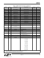
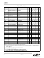
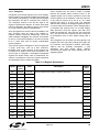
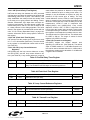
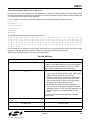
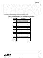
2.1. Modulations and Protocols
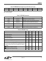
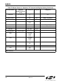
Tables 1 through 3 list the modulations, protocols,
carriers, and tones supported by the Si2493/57/34/15/
04 modem family. The Si2493 supports all modulations
and protocols from Bell 103 through V.92. The Si2457
supports all modulations and protocols from Bell 103
through V.90. The Si2434 supports all modulations and
protocols from Bell 103 through V.34. The Si2415
supports all modulations and protocols from Bell 103
through V.32bis. The Si2404 supports all modulations
and protocols from Bell 103 through V.22bis.
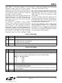
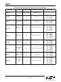
Table 1. Modulations and Protocols*
Specification
V.92*
Data Rate (bps)
48k, 40k, 32k, 24k
Modulation
PCM
V.90*
56k, 54.6k, 53.3k, 52k, 50.6k,
49.3k, 48k, 46.6k, 45.3k, 44k,
42.6k, 41.3k, 40k, 38.6k, 37.3k,
36k, 34.6k, 33.3k, 32k, 30.6k,
29.3k, 28k
33.6k, 31.2k, 28.8k, 26.4k, 24k,
21.6k, 19.2k, 16.8k, 14.4k, 12k,
9600, 7200, 4800, 2400
14.4k, 12k, 9600, 7200, 4800
V.29FC*
9600
9600, 4800
9600
TCM
QAM
QAM
V.23
1200
FSK
V.22bis
2400, 1200
QAM
V.22
1200
DPSK
Bell212A
1200
DPSK
V.21
300
FSK
Bell103
300
FSK
V.34*
V.32bis*
V.32*
Si2493 Si2457 Si2434 Si2415 Si2404
PCM
D
D
D
TCM
D
D
D
TCM
D
D
D
D
D
D
D
D
D
D
D
D
D
D
D
D
D
D
D
D
D
D
D
D
D
D
D
D
D
D
D
D
D
D
D
D
D*
D
D
D
D
D
D
*Note: With Si3018 DAA only.
Rev. 0.9
7
AN93
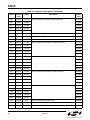
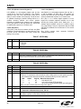
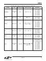
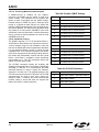
Table 2. Modulations and Protocols*
Protocol
Function
Si2493
Si2457
Si2434
Si2415
Si2404
V.44
Compression
V.42bis
Compression
V.42
Error Correction
D
D
D
D
D
D
D
D
D
D
D
MNP5
Compression
D
D
D
D
MNP2-4
Error Correction
D
D
D
D
D
*Note: While the Si2493/57/34/15/04 family allows any supported protocol with any modulation, some other
manufacturers’ modems may not permit some combinations. This is particularly common with 300 bps modulations.
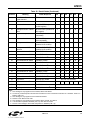
Table 3. Carriers and Tones
8
Specification
Transmit Carrier
(Hz)
Receive Carrier
(Hz)
Answer
Tone (Hz)
Carrier Detect (Acquire/
Release)
V.92
Variable
Variable
per ITU-T V.92
V.90
Variable
Variable
per ITU-T V.90
V.34
Variable
Variable
per ITU-T V.34
V.32bis
1800
1800
2100
per ITU-T V.32bis
V.32
1800
1800
2100
per ITU-T V.32
V.29
1700
1700
V.22bis, V.22
Originate
Answer
1200
2400
2400
1200
V.21
Originate (M/S)
Answer (M/S)
1180/980
1850/1650
1850/1650
1180/980
per ITU-T V.29
2100
–43 dBm/–48 dBm
–43 dBm/–48 dBm
2100
Bell212A
Originate
Answer
1200
2400
2400
1200
Bell103
Originate (M/S)
Answer (M/S)
1270/1070
2225/2025
2225/2025
1270/1070
–43 dBm/–48 dBm
–43 dBm/–48 dBm
2225
–43 dBm/–48 dBm
–43 dBm/–48 dBm
2225
Rev. 0.9
–43 dBm/–48 dBm
–43 dBm/–48 dBm
AN93
2.2. Modem and DAA Operation
2.2.2. Crystal Oscillator
This section describes hardware design requirements
for optimum Si2493/57/34/15/04 modem chipset
implementation.
There
are
three
important
considerations for any hardware design. First, the
reference design and components listed in the
associated bill of materials should be followed exactly.
These designs reflect field experience with millions of
deployed units throughout the world and are optimized
for cost and performance. Any deviation from the
reference design schematic and components will likely
have an adverse affect on performance. Second, circuit
board layouts must rigorously follow " Appendix A—
ISOmodem® Layout Guidelines (Si3018/10)" on page
151. Deviations from these layout techniques will likely
impact modem performance and regulatory compliance.
Finally, all reference designs use a standard component
numbering scheme. This simplifies documentation
references and communication with the Silicon
Laboratories technical support team. It is strongly
recommended that these same component reference
designators be used in all ISOmodem designs.
The crystal oscillator circuit requires a 4.9152 MHz
fundamental mode parallel-resonant crystal. Typical
crystals require a 20 pF load capacitance. This load is
calculated as the series combination of the capacitance
from each crystal terminal to ground including parasitic
capacitance due to package pins and PCB traces. The
parasitic capacitance is estimated as 7 pF per terminal.
This, in combination with the 33 pF capacitor, provides
40 pF per terminal, which, in series, yields the proper
20 pF load for the crystal.
The following sections describe the operation and
design considerations of the modem chip, DAA chip,
and associated circuitry.
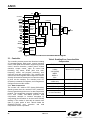
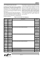
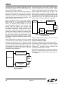
2.2.1. Modem (System-Side) Device
The Si2493/57/34/15/04 modem device contains a
controller, a DSP, program memory (ROM), data
memory (RAM), a serial and parallel interface, a crystal
oscillator, and an isolation capacitor interface.
Note: Parallel, PCM, and EEProm interfaces are only available on the 24-pin TSSOP package option.
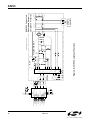
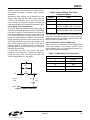
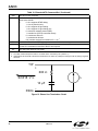
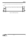
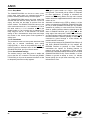
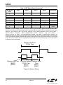
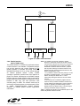
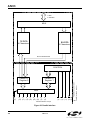
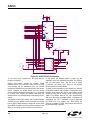
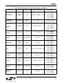
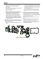
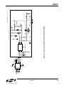
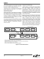
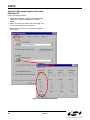
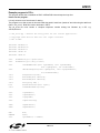
Figure 2 on page 10 clearly shows that in spite of the
significant internal complexity of the chip, the external
support circuitry is very simple. The following section
describes the function and use of the pins and some
important considerations for the selection and
placement of components.
Frequency stability and accuracy are critically important
to the performance of the modem. ITU-T specifications
require less than 200 ppm difference in the carrier
frequency of two modems. This value, split between the
two modems, requires the oscillator frequency of each
modem to be accurate and stable over all operating
conditions within ±100 ppm. This tolerance includes the
initial accuracy of the crystal, frequency drift over the
temperature range the crystal will experience, and five
year aging of the crystal. Other factors affecting the
oscillator frequency include the tolerance and
temperature drift of the load capacitor values. For
optimal V.92 performance, it is recommended to
increase the oscillator stability to ±25 ppm.
The CLKIN/XTALI pin (pin 1) can accept a 3.3 V
external 4.9152 MHz clock signal meeting the accuracy
and stability requirements described above. This is the
only input pin on the modem that is not 5 V tolerant. The
Si2493/57/34/04 will accept a 27 MHz clock that meets
the voltage and stability requirements described above.
Enabling this mode of operation is described in Table 24
on page 57.
The CLKOUT/A0 pin (pin 3) outputs a signal derived
from the 4.9152 clock. If the frequency of the output is
controlled via register U6E (CK1) using the Si2404 or
Si2415, this signal is programmable from 2.64 MHz to
40.96 MHz. If using the Si2434 or Si2457, this signal is
programmable from 3.17 MHz to 49.152 MHz. There
are two special cases for the value of R1. If
R1 = 00000b, CLKOUT is disabled. If R1 = 11111b
(default), CLKOUT = 2.048 MHz.
Rev. 0.9
9
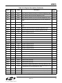
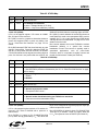
RESET_
RTS_/D7
RXD/RD_
TXD/WR_
CTS_/CS_/ALE_
CLKOUT/A0/EECS
INT_/D0
RI_/D1
EESD/D2
EECLK/D5/RXCLK
DCD_/D4
ESC/D3
AOUT/INT_
alt_RI_/D6/TXCLK
12
8
9
10
11
3
16
17
18
24
23
22
15
4
5
21
U3
RESET
RTS/D7
RXD/RD
TXD/WR
CTS/CS/ALE
CLKOUT/A0/EECS
13
14
2
1
C51
C53
Y1
C2
C1
R9
C5
Bias
C6
10
7
4
6
5
VREG2
VREG
IB
C2B
C1B
U2
8
9
1
12
13
16
14
2
3
Si3018
RNG1
RNG2
QE
QE2
QB
DCT2
DCT3
DCT
RX
C4
R1
Q5
R10
C7
Ring Detect/CID
R2
R11
DC Term
ACT
Q4
R4
R7
R8
R5
Q1
Z1
R3
Q2
Q3
C10
Hookswitch
Hookswitch/DCT
R6
No Ground Plane In DAA Section
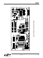
Figure 2. Si3018/10 Component Functions
Bypass
ISOcap
Emissions option
R13
R12
C41
C40
External crystal option
C52
Si2493/57/34/15/04
C2A
C1A
EECLK/D5/RXCLK
DCD/D4
CLKIN/XTALI
ESC/D3
AOUT/INT
alt_RI/D6/TXCLK
XTALO
INT/D0
RI/D1
EESD/D2
VD3.3
VD 3.3
GND
GND
VDA
VDB
6
20
7
19
1
2
C50
IGND
15
Rev. 0.9
SC
10
+
11
VDD
+
D1
C3
-
C9
C8
R15
R16
EMI/EMC
Capacitors
FB1
FB2
Emissions option
TIP
RV1
RING
EN55022 Conducted
Disturbance Surge
Compliance Protection
AN93
AN93
2.2.3. Power Supply and Bias Circuitry (Si2493/57/
34/15/04)
Power supply bypassing is important for the proper
operation of the Si2493/57/34/15/04, suppression of
unwanted radiation, and prevention of interfering
signals and noise from being coupled into the modem
via the power supply. C50 and C52 provide filtering of
the 3.3 V system power and must be located as close to
the Si2493/57/34/15/04 chip as possible to minimize
lead lengths. The best practice is to use surface mount
components connected between a power plane and a
ground plane. This technique minimizes the inductive
effects of component leads and PCB traces and
provides bypassing over the widest possible frequency
range.
Two bias voltages used inside the modem chip require
external bypassing and/or clamping. VDA (pin 7) is
bypassed by C51. VDB (pin 19) is bypassed by C53.
R12 and R13 are optional resistors that can, in some
cases, reduce radiated emissions due to signals
associated with the isolation capacitor. These
components must be located as close to the Si2493/57/
34/15/04 chip as possible to minimize lead lengths. The
best practice is to use surface mount components
connected to a ground plane. This technique minimizes
the inductive effects of component leads and PCB
traces, provides bypassing over the widest possible
frequency range, and minimizes loop areas that can
radiate radio frequency energy.
2.2.4. Isolation Capacitor Interface
The isolation capacitor is a proprietary high-speed
interface connecting the modem chip and the DAA chip
through a high-voltage isolation barrier provided by
capacitors C1 and C2. It serves three purposes. First, it
transfers control signals and transmit data from the
modem chip to the DAA chip. Second, it transfers
receive and status data from the DAA chip to the
modem chip. Finally, it provides power from the modem
chip to the DAA chip while the modem is in the on-hook
condition. The signaling on this interface is intended for
communication between the modem and the DAA chips
and cannot be used for any other purpose. It is
important to keep the length of the ISOcap path as short
and direct as possible. The layout guidelines for the pins
and components associated with this interface are
described in " Appendix A—ISOmodem® Layout
Guidelines (Si3018/10)" on page 151 and must be
carefully followed to ensure proper operation and avoid
unwanted emissions.
2.2.5. System Interface
There are two system interface options: serial and
parallel. The serial interface allows the host processor
to communicate with the modem controller through a
UART driver. In this mode, the modem is analogous to
an external “box” modem. The interface pins are 5 V
tolerant and communicate with TTL compatible lowvoltage CMOS levels. RS232 interface chips, such as
those used on the Si2457/34/15URT-EVB evaluation
board, can be used to make the serial interface directly
compatible with a PC or terminal serial port. The
operation of these pins is described in "3. Software
Design Reference" on page 21.
2.2.6. DAA (Line-Side) Device
The Si3018/10 DAA or line-side device, contains an
ADC, a DAC, control circuitry, and an isolation capacitor
interface. The Si3018/10 and surrounding circuitry
provide all functionality for telephone line interface
requirement compliance including a full-wave bridge,
hookswitch, dc termination, ac termination, ring detect,
loop voltage/current monitoring, and call progress
monitoring. A schematic of the Si3018/10 circuitry with
the component functions identified is shown in Figure 2.
Additionally, the Si3018/10 external circuitry is largely
responsible for EMI, EMC, safety, and surge
performance.
2.2.7. Power Supply and Bias Circuitry
(Si3018/10)
The Si3018/10 is powered by a small current passed
across the ISOcap™ in the on-hook mode and by the
loop current in the off-hook mode. Since there is no
system ground reference for the line-side chip due to
isolation requirements, a virtual ground, IGND, is used
as a reference point for the Si3018/10. Several bias
voltages and signal reference points used inside the
DAA chip require external bypassing, filtering, and/or
clamping. VREG2 (pin 10) is bypassed by C6. VREG
(pin 7) is bypassed by C5. These components must be
located as close to the Si3018/10 chip as possible to
minimize lead lengths. The best practice is to use
surface mount components and very short PCB trace
lengths to minimize the inductive effects of component
leads and PCB traces thereby bypassing over the
widest possible frequency range and minimizing loop
areas that can radiate radio-frequency energy.
Rev. 0.9
11
AN93
2.2.8. Ringer Network
2.2.10. Legacy Mode
R7 and R8 comprise the ringer network. These
components determine the modem’s on-hook
impedance at TIP and RING. These components are
selected to present a high impedance to the line, and
care must be taken to ensure the circuit board area
around these components is clean and free of
contaminants, such as solder flux and solder flakes.
Leakage on RNG1 (Si3018/10 pin 8) and RNG2
(Si3018/10 pin 9) can impair modem performance. R7
and R8 are also used by the modem to monitor the line
voltage.
The Si2493/57/34/15/04 has the ability to measure both
line voltage and loop current. The 8-bit LVCS register,
U79(LVCS) [7:0], reports line voltage measurements
when on-hook and loop current measurements when
off-hook.
2.2.9. Line Voltage/Loop Current Sensing
There are two methods for line voltage and loop current
sensing. The first method is the legacy mode using
U79(LVCS)[4:0]. The legacy mode is intended for
backward compatibility in applications originally
designed for the previous generation ISOmodem. This
mode is used in the intrusion detection algorithm
implemented on the device.
The second method of measuring line voltage and loop
current takes advantage of the improved resolution
available on the Si3018 and Si3010 DAA chips.
U63(LCS)[15:8] represents the value of off-hook loop
current as a non-polar binary number with 1.1 mA/bit
resolution. Accuracy is not guaranteed if the loop
current is less than the minimum required for normal
DAA operation. U6C(LVS)[15:8] represents the value of
on-hook and off-hook loop voltage as a signed, 2s
complement number with a resolution of 1 V/bit. Bit 15
represents the polarity of the TIP\RING voltage, and a
reversal of this bit represents a TIP\RING polarity
reversal. LVS = 0000h if the TIP\RING voltage is less
than 3.0 V and, in the on-hook state, can be taken as
“no line connected.”
12
Using the LVCS bits, the user can determine the
following:
When on-hook, detect if a line is connected.
When on-hook, detect if a parallel phone is off-hook.
When off-hook, detect if a parallel phone goes on or
off-hook.
Detect if enough loop current is available to operate.
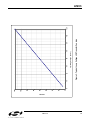
2.2.10.1. Line Voltage Measurement
The Si2493/57/34/15/04 reports the on-hook line
voltage with the LVS bits in 2s complement. LVS has a
full scale of 87 V with an LSB of 1 V. The first code
(0 → 1) is skewed such that a 0 indicates the line
voltage is < 3 V. The accuracy of the LVS bits is ±10%.
The user can read these bits directly through the LVS
register. A typical transfer function is shown in Figure 3.
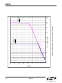
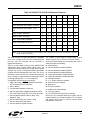
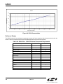
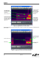
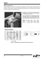
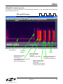
2.2.10.2. Loop Current Measurement
When the Si2493/57/34/15/04 is off-hook, the LCS bits
measure loop current in 1.1 mA/bit resolution. These
bits enable the user to detect another phone going offhook by monitoring the dc loop current. The line voltage
sense transfer function is shown in Figure 3, and the
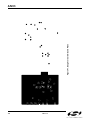
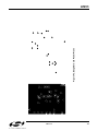
line current sense is detailed in Figure 4 and Table 4.
Rev. 0.9
LVS Bits
Rev. 0.9
0
16
32
48
64
80
96
112
128
0
16
64
Tip/Ring Voltage (Volts )
48
80
96
Figure 3. Typical Loop Voltage LVS Transfer Function
32
112
128
AN93
13
14
Rev. 0.9
0
32
64
96
128
160
192
224
256
0
16
48
64
80
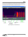
Loop Curre nt (m A)
96
112
Figure 4. Typical Loop Current LCS Transfer Function
32
ILIM = 1
128
144
ILIM = 0
AN93
LCS Bits
AN93
Table 4. Loop Current Transfer Function
LVCS[4:0]
Condition
00000
Insufficient line current for normal operation.
00001
Minimum line current for normal operation.
11111
Loop current is excessive (overload). Overload > 128 mA in all modes
except CTR21.
Overload > 56 mA in CTR21 mode.
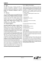
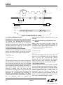
2.2.11. Hookswitch and DC Termination
TBR21 DCT Mode
The hookswitch and dc termination circuitry are shown
in Figure 2 on page 10. Q1, Q2, Q3, Q4, R5. R6, R7,
R8, R15, R16, R17, R19, and R24 perform the
hookswitch function. The on-hook/off-hook condition of
the modem is controlled by Si3018/10 pins 13 (QB) and
1 (QE).
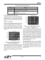
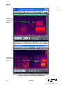
Voltage Across DAA (V)
45
2.2.11.1. DC Termination
The DAA has programmable settings for the dc
impedance, current limiting, minimum operational loop
current, and TIP/RING voltage. The dc impedance of
the DAA is normally represented with a 50 Ω slope as
shown in Figure 5, but can be changed to an 800 Ω
slope by setting the DCR bit. This higher dc termination
presents a higher resistance to the line as loop current
increases.
Voltage Across DAA (V)
12
FCC DCT Mode
11
10
9
8
7
6
.01 .02 .03 .04 .05 .06 .07 .08 .09 .1 .11
40
35
30
25
20
15
10
5
.015 .02 .025 .03 .035 .04 .045 .05 .055 .06
Loop Current (A)
Figure 6. TBR21 Mode I/V Characteristics
DCV[1:0] = 11, MINI[1:0] = 00
The MINI[1:0] bits select the minimum operational loop
current for the DAA, and the DCV[1:0] bits adjust the
DCT pin voltage, which affects the TIP/RING voltage of
the DAA. These bits allow important trade-offs to be
made between signal headroom and minimum
operational loop current. Increasing TIP/RING voltage
increases signal headroom, whereas decreasing the
TIP/RING voltage allows compliance to PTT standards
in low-voltage countries, such as Japan. Increasing the
minimum operational loop current above 10 mA also
increases signal headroom and prevents degradation of
the signal level in low-voltage countries.
2.2.12. AC Termination
Loop Current (A)
Figure 5. FCC Mode I/V Characteristics
DCV[1:0] = 11, MINI[1:0] = 00
For applications requiring current limiting per the legacy
TBR21 standard, the ILIM bit may be set to select this
mode. In this mode, the dc I/V curve is changed to a
2000 Ω slope above 40 mA, as shown in Figure 6. This
allows the DAA to operate with a 50 V, 230 Ω feed,
which is the maximum linefeed specified in the TBR21
standard.
The Si2493/57/34/15/04 has four ac termination
impedances when used with the Si3018 line-side
device. The ACT bits in Register U63 are used to select
the ac impedance setting on the Si3018. The four
available settings for the Si3018 are listed in Table 5. If
an ACT[3:0] setting other than the four listed in Table 5
is selected, the ac termination is forced to 600 Ω
(ACT[3:0] = 0000).
Rev. 0.9
15
AN93
Table 5. AC Termination Settings for the Si3018
Line-Side Device
ACT[3:0]
AC Termination
0000
600 Ω
0011
220 Ω + (820 Ω || 120 nF) and 220 Ω +
(820 Ω || 115 nF)
0100
370 Ω + (620 Ω || 310 nF)
1111
Global complex impedance
2.2.15. Billing Tone Detection
2.2.13. Ringer Impedance and Threshold
The ring detector in many DAAs is ac coupled to the line
with a large 1 µF, 250 V decoupling capacitor. The ring
detector on the Si2493/57/34/15/04 is resistively
coupled to the line. This produces a high ringer
impedance to the line of approximately 20 MΩ to meet
the majority of country PTT specifications, including
FCC and TBR21.
Several countries, including Poland, South Africa, and
Slovenia, require a maximum ringer impedance that can
be met with an internally synthesized impedance by
setting the RZ bit (Register 67, bit 1).
Some countries also specify ringer thresholds
differently. The RT bit (Register U67, bit 0) selects
between two different ringer thresholds: 15 V ±10% and
21.5 V ±10%. These two settings satisfy ringer
threshold requirements worldwide. The thresholds are
set so that a ring signal is guaranteed to be detected
above the maximum and not detected below the
minimum.
2.2.14. Pulse Dialing and Spark Quenching
Pulse dialing results from going off- and on-hook to
generate make and break pulses. The nominal rate is
10 pulses per second. Some countries have strict
specifications for pulse fidelity that include make and
break times, make resistance, and rise and fall times. In
a traditional, solid-state dc holding circuit, there are
many problems in meeting these requirements.
The Si2493/57/34/15/04 dc holding circuit actively
controls the on-hook and off-hook transients to maintain
pulse dialing fidelity.
Spark quenching requirements in countries, such as
Italy, the Netherlands, South Africa, and Australia, deal
with the on-hook transition during pulse dialing. These
tests provide an inductive dc feed resulting in a large
voltage spike. This spike is caused by the line
inductance and sudden decrease in current through the
loop when going on-hook. The traditional solution to the
problem is to put a parallel resistive capacitor (RC)
shunt across the hookswitch relay. However, the
capacitor required is large (~1 µF, 250 V) and relatively
16
expensive. In the Si2493/57/34/15/04, loop current can
be controlled to achieve three distinct on-hook speeds
to pass spark quenching tests without additional BOM
components. Through settings of two bits in two
registers, OHS (Register U67, bit 6) and OHS2
(Register U62, bit 8), a slow ramp-down of loop current,
which induces a delay between the time the OH bit is
cleared and the time the DAA actually goes on-hook,
can be achieved .
“Billing tones” or “metering pulses” generated by the
central office can cause modem connection difficulties.
The billing tone is typically a 12 kHz or 16 kHz signal
and is sometimes used in Germany, Switzerland, and
South Africa. Depending on line conditions, the billing
tone may be large enough to cause major modem
errors. The Si2493/57/34/15/04 chipset can provide
feedback when a billing tone occurs and when it ends.
Billing tone detection is enabled by setting the BTE bit
(U68, bit 2). Billing tones less than 1.1 VPK on the line
are filtered out by the low-pass digital filter on the
Si2493/57/34/15/04. The ROV bit (U68, bit 1) is set
when a line signal is greater than 1.1 VPK, indicating a
receive overload condition. The BTD bit is set when a
line signal (billing tone) is large enough to excessively
reduce the line-derived power supply of the line-side
device (Si3018/10). When the BTE bit is set, the dc
termination is changed to an 800 Ω dc impedance. This
ensures minimum line voltage levels even in the
presence of billing tones.
The OVL bit should be polled following billing tone
detection. When the OVL bit returns to 0, indicating that
the billing tone has passed, the BTE bit should be
written to 0 to return the dc termination to its original
state. It takes approximately 1 second to return to
normal dc operating conditions. The BTD and ROV bits
are sticky and must be written to 0 to be reset. After the
BTE, ROV, and BTD bits are cleared, the BTE bit can be
set to reenable billing tone detection.
Certain line events, such as an off-hook event on a
parallel phone or a polarity reversal, may trigger the
ROV or the BTD bits, after which the billing tone detector
must be reset. Look for multiple events before qualifying
whether billing tones are actually present.
Although the DAA remains off-hook during a billing tone
event, the received data from the line is corrupted (or a
modem disconnect or retrain may occur) in the presence
of large billing tones. To receive data through a billing
tone, an external LC filter must be added. A modem
manufacturer can provide this filter to users in the form
of a dongle that connects on the phone line before the
DAA. This keeps the manufacturer from having to
Rev. 0.9
AN93
include a costly LC filter internal to the modem when it
may only be necessary to support a few countries/
customers.
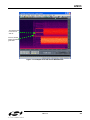
Table 6. Optional Billing Tone Filters
Component Values
Alternatively, when a billing tone is detected, the host
software may notify the user that a billing tone has
occurred. This notification can be used to prompt the
user to contact the telephone company and have the
billing tones disabled or to purchase an external LC filter.
Symbol
Value
C1,C2
0.027 µF, 50 V, ±10%
C3
0.01 µF, 250 V, ±10%
L3
3.3 mH, >120 mA, <10 Ω, ±10%
Coilcraft RFB0810-332 or equivalent
L4
10 mH, >40 mA, <10 Ω, ±10%
Coilcraft RFB0810-103 or equivalent
2.2.16. Billing Tone Filter (Optional)
To operate without degradation during billing tones in
Germany, Switzerland, and South Africa, an external LC
notch filter is required. (The Si3018/10 can remain offhook during a billing tone event, but modem data is lost
[or a modem disconnect or retrain may occur] in the
presence of large billing tone signals.) The notch filter
design requires two notches: one at 12 kHz and one at
16 kHz. Because these components are expensive and
few countries supply billing tone support, this filter is
typically placed in an external dongle or added as a
population option for these countries. Figure 7 shows an
example billing tone filter.
L3 must carry the entire loop current. The series
resistance of the inductors is important to achieve a
narrow and deep notch. This design has more than
25 dB of attenuation at 12 and 16 kHz.
The billing tone filter affects the ac termination and
return loss. The global complex ac termination passes
worldwide return loss specifications with and without the
billing tone filter by at least 3 dB.
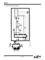
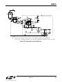
2.2.17. PCM Interface (24-Pin TSSOP Only)
Table 7 lists the pin connections for the Si2493/57/34/
15/04 PCM interface. This interface enables Voice
Mode operation. See "3.5. Programming Examples" on
page 105 for additional information.
C1
C2
Table 7. PCM Interface Pin Connection
Si24XX Pin
Si24XX Signal
3
CLKOUT
4
FSYNC
24
SDO
18
SDI
12
RESET*
L3
TIP
FROM
LINE
L4
To
DAA
C3
RING
Figure 7. Billing Tone Filter
Rev. 0.9
17
RESET_
RTS_/D7
RXD/RD_
TXD/WR_
CTS_/CS_/ALE_
CLKOUT/A0/EECS
INT_/D0
RI_/D1
EESD/D2
EECLK/D5/RXCLK
DCD_/D4
ESC/D3
AOUT/INT_
alt_RI_/D6/TXCLK
12
8
9
10
11
3
16
17
18
24
23
22
15
4
5
21
RESET
RTS/D7
RXD/RD
TXD/WR
CTS/CS/ALE
CLKOUT/A0/EECS
13
14
2
1
Y1
R13
R12
C41
C40
R9
C5
C2
C1
C6
10
7
4
6
5
VREG2
VREG
IB
C2B
C1B
U2
8
9
1
12
13
16
14
2
3
Si3018/10
RNG1
RNG2
QE
QE2
QB
DCT2
DCT3
DCT
RX
C4
R1
Q5
R2
R11
R10
C7
Q4
R4
R7
R8
R5
Q1
Z1
R3
Q2
Q3
C10
R6
No Ground Plane In DAA Section
+
D1
C3
-
Note: See Section "3.5.19.4. Safety" on page 137 for information regarding safety testing and the use of a
C51
Si2493/57/34/15/04
C2A
C1A
EECLK/D5/RXCLK
DCD/D4
CLKIN/XTALI
ESC/D3
AOUT/INT
alt_RI/D6/TXCLK
XTALO
INT/D0
RI/D1
EESD/D2
U3
1
2
VD3.3
VD 3.3
GND
GND
VDA
VDB
6
20
7
19
C52
IGND
C50
SC
Rev. 0.9
15
18
+
11
VDD
FB1
FB2
C9
C8
R15
R16
TIP
RV1
RING
AN93
2.3. Typical Application Schematic
AN93
2.3.1. Bill of Materials: Si2493/57/34/15/04 Chipset
Component
Value
Supplier(s)
C1, C2
33 pF, Y2, X7R, ±20%
Panasonic, Murata, Vishay
C3
10 nF, 250 V, X7R, ±10%
Venkel, SMEC
C4
1.0 µF, 50 V, Elec/Tant, ±20%
Panasonic
C5, C6, C50, C52
0.1 µF, 16 V, X7R, ±20%
Venkel, SMEC
C7
2.7 nF, 50 V, X7R, ±20%
Venkel, SMEC
C8, C9
680 pF, Y2, X7R, ±10%
Panasonic, Murata, Vishay
0.01 µF, 16 V, X7R, ±20%
Venkel, SMEC
C40, C41
33 pF, 16 V, X7R, ±20%
Venkel, SMEC
C51, C53
0.22 µF, 16 V, X7R, ±20%
Venkel, SMEC
Dual Diode, 225 mA, 300 V, CMPD2004S
Central Semiconductor
FB1, FB2
Ferrite Bead, BLM21AG601S
Murata
Q1, Q3
NPN, 300 V, MMBTA42
OnSemi, Fairchild
Q2
PNP, 300 V, MMBTA92
OnSemi, Fairchild
Q4, Q5
NPN, 80 V, 330 mW, MMBTA06
OnSemi, Fairchild
RV1
Sidactor, 275 V, 100 A
Teccor, Protek, ST Micro
R1
1.07 kΩ, 1/2 W, 1%
Venkel, SMEC, Panasonic
R2
150 Ω, 1/16 W, 5%
Venkel, SMEC, Panasonic
R3
3.65 kΩ, 1/2 W, 1%
Venkel, SMEC, Panasonic
R4
2.49 kΩ, 1/2 W, 1%
Venkel, SMEC, Panasonic
R5, R6
100 kΩ, 1/16 W, 5%
Venkel, SMEC, Panasonic
R7, R8
20 MΩ, 1/16 W, 5%
Venkel, SMEC, Panasonic
R9
1 MΩ, 1/16 W, 1%
Venkel, SMEC, Panasonic
R10
536 Ω, 1/4 W, 1%
Venkel, SMEC, Panasonic
R11
C10
1
D1, D2
2
73.2 Ω, 1/2 W, 1%
Venkel, SMEC, Panasonic
R133
0 Ω, 1/16 W
Venkel, SMEC, Panasonic
3
0 Ω, 1/16 W
Venkel, SMEC, Panasonic
U1
Si2493/57/34/15/04
Silicon Labs
U2
Si3018
Silicon Labs
4.9152 MHz, 20 pF, 100 ppm, 150 Ω ESR
ECS Inc., Siward
Zener Diode, 43 V, 1/2 W, BZX84C43
On Semi
R12,
R15, R16
1,4
Y1
Z1
Notes:
1. In STB applications, C40, C41, and Y1 can be removed by using the 27 MHz clock input feature.
2. Several diode bridge configurations are acceptable. For example, a single DF04S or four 1N4004 diodes may be used.
3. To decrease emissions, R15 and R16 may be populated with a BLM21AG601S or equivalent. R12 and R13 may be
populated with 5%, 1/16 W, 56 Ω resistors.
4. To ensure compliance with ITU specifications, frequency tolerance must be less than 100 ppm including initial
accuracy, 5-year aging, 0 to 70 °C, and capacitive loading. 50 ppm initial accuracy crystals typically satisfy this
requirement.
Rev. 0.9
19
AN93
2.3.2. Analog Output
Figure 8 illustrates an optional application circuit to support the analog output capability of the Si2493/57/34/15/04
for call progress monitoring.
+5 V
C2
R3
3
AOU T
2
6
+
–
4
C6
C4
+
5
U1
C5
R1
C3
Speaker
R2
Figure 8. Optional Connection to AOUT for a Monitoring Speaker
Table 8. Component Values—Optional Connection to AOUT
20
Symbol
Value
C2, C3, C5
0.1 µF, 16 V, ±20%
C4
100 µF, 16 V, Elec. ±20%
C6
820 pF, 16 V, ±20%
R1
10 kΩ, 1/10 W, ±5%
R2
10 Ω, 1/10 W, ±5%
R3
47 kΩ, 1/10 W, ±5%
U1
LM386
Rev. 0.9
AN93
3. Software Design Reference
This section provides information about the architecture
of the modem, functional blocks, registers, and their
interaction. The AT command set is presented, and
options are explained. The accessible memory
locations (S-Registers and U-Registers) and optional
external EEPROM are described. Instructions for writing
to and reading from them are discussed along with any
limitations or special considerations. A large number of
configuration and programming examples are offered as
illustrations of actual testable applications. These
examples can be used alone or in combination to create
the desired modem operation.
This section is organized into five major sections: "3.1.
Controller", "3.2. DSP" on page 58, "3.3. Memory" on
page 58, "3.4. Digital Interface" on page 98, and "3.5.
Programming Examples" on page 105. The “Controller”
section contains information about using controller
functions and features, such as the AT command set,
result codes, escape methods, power control, and
system reset information. The “DSP” section is brief
because the programmer has little control over the
operation of the DSP. The use of features that modify
DSP behavior is described in other sections. The
“Memory” section describes the use of S-Registers and
U-Registers to control the operation, features, and
configuration of the modem. The optional external SPI
EEPROM is useful for the non-volatile storage of
configuration settings, such as firmware upgrades or
country setup commands. The “Digital Interface” section
describes the serial interface and parallel interface.
Finally, the “Programming Examples” section illustrates
the implementation of modem functions and features
with the required AT commands and register values.
Configuration data is provided for most countries. These
examples can be used both to test modem operation
and as a programming aid.
The Si2493/57/34/15/04 modem chipset family is
controller-based. No modem drivers are required to run
on the system processor. This makes the Si2493/57/34/
15/04 modem family ideal for embedded systems
because a wide variety of processors and operating
systems can interface with the Si2493/57/34/15/04
through a simple UART (universal asynchronous
receiver transmitter) driver.
The modems in this family operate at maximum connect
rates of 48 kbps upstream/V.92 (Si2493), 56 kbps
downstream/V.90 (Si2457), 33.6 kbps/V.34 (Si2434),
14.4 kbps/V.32b (Si2415), and 2400 bps/ V.22b
(Si2404) and support all standard ITU-T fall-back
modes. These chipsets can be programmed to comply
with FCC, JATE, CTR21, and other country-specific
PTT requirements. They also support V.42 and MNP2–4
error correction and V.42b and MNP5 compression. A
“fast connect” and “transparent HDLC” are also
supported.
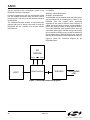
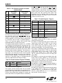
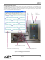
The Si2493/57/34/15/04 is highly integrated. The basic
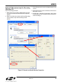
Si2493/57/34/15/04 functional blocks are shown in
Figure 9. The Si2493/57/34/15/04 includes a controller,
data pump (DSP), ROM, RAM, an oscillator, phaselocked loop (PLL), timer, serial interface, UART, a
parallel interface option, and a DAA interface. The
modem software is permanently stored in the on-chip
ROM. Only modem setup information (other than
defaults) and other software updates must be stored on
the host or optional external EEPROM and downloaded
to the on-chip RAM during initialization. There is no nonvolatile on-chip memory other than Program ROM. The
default user interface for the Si2493/57/34/15/04 is the
serial interface including the UART.
Rev. 0.9
21
AN93
XTI
XTO
PLL
Clocking
EESD
EECLK
EECS
RXD
TXD
CTS
RTS
DCD
ESC
RI
INT
CS
WR
RD
A0
D0-D7
EEPROM
Interface
C1
DAA
Interface
DSP
Controller
Serial
Interface/
UART
Data Bus
Si3018/10
CLKOUT
C2
To Phone
Line
Parallel
Interface
Program Bus
AOUT
ROM
RAM
RESET
FSYNC
SDO
SDI
MCLK
Si3000
Interface
Figure 9. Si2493/57/34/15/04 Functional Block Diagram
3.1. Controller
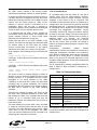
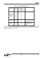
Table 9. Enabling Error Correction/Data
Compression
The controller provides several vital functions including
AT command parsing, DAA control, connect sequence
control, DCE (data communication equipment) protocol
control, intrusion detection, parallel phone off-hook
detection, escape control, caller ID control and
formatting, ring detect, DTMF (dual tone multifrequency) control, call progress monitoring, error
correction, and data compression. The controller also
writes to the control registers that configure the modem.
Virtually all interaction between the host and the modem
is done via the controller. The controller uses “AT”
(ATtention) commands, S-Registers, and U-Registers to
configure and control the modem.
To Enable
Use AT Commands
V.44*
V.42bis
V.42 (LAPM)
MNP5
MNP2–4
Wire
+DS44 (argument)
\N3 and %C1 (default)
V.42 and
V.42bis only
\N4 and %C1
V.42 only
\N4 and %C0
MNP2-4 only
\N2 and %C0
MNP2-5 only
\N2 and %C1
No data compression and
no error correction
\N0 and %C0
3.1.1. Data Compression
The modem can achieve DTE (host-to-ISOmodem)
speeds greater than the maximum DCE (modem-tomodem) speed through the use of a data compression
protocol. The compression protocols available are the
ITU-T V.44, V.42bis, and MNP5 protocols. Data
compression attempts to increase throughput by
compressing the information to be sent before actually
sending it. The modem is thus able to transmit more
data in a given period of time. Table 9 details the
Si2493/57/34/15/04 error correction and data
compression modes of operation.
22
*Note: V.44 is available only on Si2493.
Rev. 0.9
AN93
3.1.2. Error Correction
The Si2493/57/34/15/04 ISOmodem can employ error
correction (reliable) protocols to ensure error-free
delivery of data sent between two modems. The error
control methods are based on grouping data into frames
with checksums determined by the contents of each
frame. The receiving modem checks the frames and
sends acknowledgments to the transmitting modem.
When it detects a faulty frame, the receiving modem
requests a retransmission. Frame length varies
according to the amount of data transmitted or the
number of retransmissions requested from the opposite
end.
The Si2493/57/34/15/04 supports V.42 and MNP2–4
error correction protocols. V.42 (LAPM) is most
commonly used and is enabled in \N3 and \N4 modes.
In the default mode (\N3), the Si2493/57/34/15/04
attempts to connect with V.42 error correction and
V.42bis data compression (Si2457/34/15) and falls back
to either V.42 only, MNP 2–5, or no error correction
(wire mode) if necessary. In \N4 mode, the Si2493/57/
34/15/04 hangs up if a V.42 connection cannot be
established. If the ISOmodem hangs up in V.42 mode
after all data is successfully sent, the result code is
“OK”. If the modem hangs up before all data is
successfully sent, the result code is “No Carrier”. If the
modem connects without a protocol, “No Carrier” is
always sent.
The V.42 specification allows an alternate error
correction protocol, MNP2-4. MNP2-4 is enabled in \N2
mode. In \N2 mode, the Si2493/57/34/15/04 hangs up if
an MNP2, 3, or 4 connection cannot be established.
3.1.3. Wire Mode
Wire mode (\N0) is used to communicate with standard,
non-error-correcting modems. When optioned with \N3,
the Si2493/57/34/15/04 falls back to Wire mode if it fails
in an attempt to negotiate a V.42 or MNP2-4 link with the
remote modem. Error correction and data compression
are not active in Wire mode.
3.1.4. Fast Connect
The Si2493/57/34/15/04 supports several fast connect
modes of operation to reduce the time of a connect
sequence in originate mode.
3.1.5. V.29 Fast Connect
In addition to the low modulation speed fast connect
modes, the modem (only Si2493/57/34/15) also
supports a fast connect mode based on the 9600 bps
V.29 fax modulation standard. V.29 Fast Connect is
available as a patch for Rev C or greater. Please
contact Silicon Laboratories for additional details.
3.1.6. Legacy Synchronous DCE Mode/V.80
Synchronous Access Mode
The Si2493/57/34/15/04 supports two different DTE
interfaces to implement an Asynchronous DTE to
Synchronous DCE conversion.
Table 10 provides high-level options to choose between
the Legacy Synchronous DCE Mode and the newer
V.80 synchronous access mode.
Table 10. Synchronous Mode Overview
Mode
U-Register
AT+ES
Settings
Neither
U7A[2] = 0
+ES = D,,D
Legacy Synchronous
DCE Mode
U7A[2] = 1
+ES = D,,D
Synchronous Access
Mode
+ES = 6,,8
The synchronous access mode has more features than
the Legacy Synchronous DCE Mode. For new designs,
use the newer synchronous access mode interface.
Otherwise, if there is existing software written with the
Legacy Synchronous DCE Mode interface, no software
changes are required as long as the AT+ES command
settings are not changed from the default value.
3.1.7. V.80 Mode
As shown in Table 11, the synchronous access mode is
chosen by using the AT+ES=6,,8 command setting.
When using the synchronous access mode, it is
expected that the AT\N0 command be used to disable
all other error correction protocols that may interfere
with V.80 synchronous access mode operation.
The V.80 Mode has two distinct submodes. Switching
between these two submodes can be accomplished
within the confines of the same connection through the
use of In-Band commands.
Transparent Submode
Framed Submode
The Transparent Submode creates a direct bit-by-bit
translation from the DTE to and from the DCE. Any
application that requires a method of reconstructing a
serial bit-stream at the DCE can use the Transparent
Sub-mode.
The Framed Sub-mode represents data at the DCE in
HDLC/SDLC frames. This submode is typically used in
Point-of-Sale Terminal Applications. A common feature
used in conjunction with the Framed Submode is the
use of the 16-bit CRC. When used with the CRC option,
Rev. 0.9
23
AN93
the Framed Submode can be used in the same
applications currently using the Legacy Synchronous
DCE Mode.
Prior to sending the ATDT to establish a synchronous
access mode connection, the following commands and
registers require initialization: +MS, +ES, +ESA, +ITF,
+IFC, U87, and U7A.
As an example, the closest equivalent to the Legacy
Synchronous DCE Mode is the following initialization
setting.
With either Synchronous Access Submode, once a
connection has been established, payload data is
multiplexed with command/indicator information by use
of <EM> shielding. With <EM> shielding, either of the
two bytes <0x19> or <0x99> (used to represent <EM>)
precedes a special command or special indicator.
Note that the synchronous access mode <EM>
shielding is designed to support XON/XOFF
handshaking. As such, the bytes 0x13 and 0x11 (XON/
XOFF) are considered to be special characters in the
same way the 0x19 and 0x99 bytes, used for <EM>, are
special.
Since the payload data is multiplexed with <EM>
shielded command/indicator and possibly XON/XOFF
characters, Transparency <EM> codes are defined for
the purpose of allowing the host software to send 0x13,
0x11, 0x19 and 0x99 bytes to/from the DCE. For
example, if the desire is to send one <0x99> character
as a payload character, the host software sends
<EM><0x76> instead. For a complete list <EM>
commands and statuses, see Table 13.
24
Table 11. Synchronous Access Mode Settings
AT\N0
Required to disable MNP,V42
and other protocols
AT+ES = 6,,8
Enable synchronous access
mode on originate or answer
AT+ESA = 0,0,0,,1,0
Send Abort on underrun/overrun in Framed Submode.
Enable CRC generation and
checking.
AT+IFC = 2,2
CTS/RTS Flow Control
AT+ITF = 0383,0128
Controls CTS Flow Control
Threshold. CTS off at 383
bytes, CTS On at 128 bytes.
AT:U87,050A
Direct to Framed Sub-mode
upon connection. DCE starts
to transmit upon receipt of 10
bytes from the DTE.
In addition, a common Point-of-Sale V.22 Fast Connect
Handshake Protocol (with transparent HDLC) requires
these additional settings:
Table 12. Fast Connect Settings
AT+MS = V22
AT:U7A,3
Rev. 0.9
V22 Protocol
Set Fast Connect, Transmit
HDLC Flags instead of Marks
during handshake negotiation.
AN93
Table 13. EM In-band Commands and Statuses
Command /
Indicator pair
Hex Code
Transmit Direction
Receive Direction
Supported in
Transparent
Submode
Supported in
Framed Submode
<EM><t1>
0x5C
Transmit one 0x19 byte
Received one 0x19 byte
Yes1
Yes1
<EM><t2>
0x76
Transmit one 0x99 byte
Received one 0x99 byte
Yes1
Yes1
Yes1
Yes1
<EM><t3>
0xA0
Transmit one 0x11 byte
Received one 0x11 byte
Yes1
<EM><t4>
0xA1
Transmit one 0x13 byte
Received one 0x13 byte
Yes1
<EM><t5>
0x5D
Transmit two 0x19 bytes
Received two 0x19 bytes
Yes
Yes
<EM><t6>
0x77
Transmit two 0x99 bytes
Received two 0x99 bytes
Yes
Yes
<EM><t7>
0xA2
Transmit two 0x11 bytes
Received two 0x11 bytes
Yes
Yes
<EM><t8>
0xA3
Transmit two 0x13 bytes
Received two 0x13 bytes
Yes
Yes
<EM><t9>
0xA4
Transmit 0x19, 0x99
Received 0x19, 0x99
Yes
Yes
<EM><t10>
0xA5
Transmit 0x19, 0x11
Received 0x19, 0x11
Yes
Yes
<EM><t11>
0xA6
Transmit 0x19, 0x13
Received 0x19, 0x13
Yes
Yes
<EM><t12>
0xA7
Transmit 0x99, 0x19
Received 0x99, 0x19
Yes
Yes
<EM><t13>
0xA8
Transmit 0x99, 0x11
Received 0x99, 0x11
Yes
Yes
<EM><t14>
0xA9
Transmit 0x99, 0x13
Received 0x99, 0x13
Yes
Yes
<EM><t15>
0xAA
Transmit 0x11,0x19
Received 0x11,0x19
Yes
Yes
<EM><t16>
0xAB
Transmit 0x11,0x99
Received 0x11,0x99
Yes
Yes
<EM><t17>
0xAC
Transmit 0x11,0x13
Received 0x11,0x13
Yes
Yes
<EM><t18>
0xAD
Transmit 0x13,0x19
Received 0x13,0x19
Yes
Yes
<EM><t19>
0xAE
Transmit 0x13,0x99
Received 0x13,0x99
Yes
Yes
<EM><t20>
0xAF
Transmit 0x13,0x11
Received 0x13,0x11
Yes
Yes
<EM><mark>
0xB0
Begin Transparent Mode
Abort Detected in Framed Submode
Yes
Yes, Receive Only
<EM><flag>
0xB1
<EM><err>
0xB2
<EM><under>
0xB4
not applicable
Detected Transmit Data Underrun
Yes
Yes
<EM><tover>
0xB5
not applicable
Detected Transmit Data Overrun
Yes
Yes
<EM><rover>
0xB6
not applicable
Detected Receive Data Overrun
Yes
Yes
<EM><resume>
0xB7
Resume after a data underrun or overrun
(applicable if +ESA[C] = 1)
<EM><bnum>
0xB8
not applicable
<octnum0><octnum1> specifies number of octets in the transmit
data buffer if +ITF[C] is non-zero2.
<EM><unum>
0xB9
not applicable
<octnum0><octnum1> specifies number of discarded octets following a data overrun/underrun, after the <EM><resume> command. This is applicable if +ESA[C] = 12.
<EM><eot>
0xBA
Terminate carrier, return to command mode.
<EM><ecs>
0xBB
Escape to On-Line command mode
<EM><rrn>
0xBC
Request rate renegotiation
<EM><rate>
0xBE
not supported
Transmit a flag; enter Framed Submode if cur- Detected a non-flag to flag transition. Preceding data was a valid
rently in Transparent Submode. If +ESA[E]=1, frame. If +ESA[E]=1, sent FCS matches that of the calculated
append FCS to end of frame before sending CRC.
closing HDLC flag.
Transmit an Abort
Detected a non-flag to flag transition. Preceding data is not a
valid frame.
Yes
Yes
not applicable
Yes
Yes
Yes
Loss of carrier detected, return to command mode
Yes
Yes
Confirmation of Escape to On-Line command mode.
Yes
Yes
Indicate rate renegotiation
Yes
Yes
Retrain/Rate Reneg completed, following octets <tx><rx> indicate tx and rx rates.
Yes
Yes
0x20 - 1200 bps
0x21 - 2400 bps
0x22 - 4800 bps
0x23 - 7200 bps
0x24 - 9600 bps
0x25 - 12 kbps
0x26 14.4 kbps
0x27 - 16.8 kbps
0x28 - 19.2 kbps
0x29 - 21.6 kbps
0x2A - 24 kbps
0x2B - 26.4 kbps
0x2C - 28.8 kbps
0x2D - 31.2 kbps
0x2E - 33.6 kbps
Notes:
1.
2.
3.
U87[10] = 1 Can be used to limit the transparency characters in the receive direction, to these four cases only.
The actual value represented in <octnum0><octnum1> = (octnum0 / 2) + (octunum1 x 64)
<EM><0x45> indicates that an unrecognized <EM> command was sent to the modem.
Rev. 0.9
25
AN93
Given the example initialization settings shown in
Table 12, after an ATDT command has been sent to
establish a connection, the modem responds with the
following.
meets both the criteria of having 10 bytes received at
the DTE and receipt of an <EM> <flag> command. In
this example, the transmission at the DCE begins
approximately after the receipt of the <0xB1> byte.
ATDT12345
Once an HDLC frame begins transmitting at the DCE,
the host must ensure transmit overrun and underrun do
not occur. It is expected that the +ITF command be
used to adjust the transmit flow control thresholds so
that it is tuned to the system's ability to process the
interrupt.
CONNECT 1200
PROTOCOL: NONE
<0x19> <0xBE> <0x20> <0x20> <0x19> <0xB1>
The first <EM><rate> indicator shows that the modem
connected with a TX rate of 1200 bps and an RX rate of
1200 bps. The <EM><flag> that occurs immediately
after the <EM><rate> indicates that a non-flag to flag
transition has occurred and that the receiver has now
been synchronized. Note that an <EM> <flag> indicator
is applicable only to the first occurrence of a non-flag to
flag transition. Future occurrences of non-flag to flag
transitions are indicated with an <EM> <err> instead.
Also, this feature is unique to the U87[8]=1 option. Also
note that with U87[8]=1, the Framed Submode is
entered immediately upon connection. Otherwise, if
U87[8]=0, the Transparent Submode is entered instead,
and the host is expected to send an <EM> <flag> to
switch to the Framed Submode.
If a transmit underrun occurs, the <EM> <tunder>
indicator always appears in the receive path, regardless
of how +ESA[C] is programmed.
If +ESA[C] = 0, the modem transmits an abort character
at the DCE at the point of the transmit underrun.
Additional transmit frames can then be transmitted
normally.
If +ESA[C] = 1, the modem transmits an HDLC flag at
the point of the transmit underrun, and the DCE
continues to send only HDLC flags until the host sends
an <EM> <resume> command. The <EM> <resume> is
then followed by the <EM> <unum> command so that
the host software can correct this problem.
<0x10><0x19><0xA0><0x12><0x19><0xA1>
<0x14><0x15><0x19><0xB1>
A transmit overrun can occur if the host does not
properly implement transmit flow control. When a
transmit overflow occurs, the <EM> <tover> indicator
always appears in the receive path. A transmit overflow
is considered to be a catastrophic failure and results in
non-deterministic behavior at the DCE. It is
recommended that the session be terminated
immediately.
Note the bytes <0x11> and <0x13> are <EM> shielded
because these bytes could have been used for XON /
XOFF handshaking. In this example, CTS/RTS
hardware handshaking is used, so it is also possible for
the host to have sent this series of bytes instead:
It is expected that the <EM> <tover> and <EM>
<tunder> indicators be encountered during system
debug, and designing the system software properly to
avoid having these indicators occur should be the
design goal.
<0x10><0x11><0x12><0x13><0x14><0x15>
<0x19><0xB1>
In the receive direction, assuming that the remote
modem is another Si2457/34/15, this is the expected
sequence at the remote receiver DTE, representing the
frame sequence of:
<0x10><0x11><0x12><0x13><0x14> <0x15>
After a connection has been established, the modem is
ready to transmit and receive frames. For example, if it
is desired to send a frame whose contents are:
<0x10><0x11><0x12><0x13><0x14> <0x15>
The host software sends the following:
However, if the host does not <EM> shield the 0x11 and
0x13 characters, XON / XOFF software handshaking
can no longer be used.
In either of the above transmit frames, the <EM> <flag>
is used to indicate that a logical frame has completed.
The modem does not begin transmitting the frame at the
DCE until the <EM> <flag> is received or if the number
of bytes sent to the modem exceeds the number of
bytes programmed into U87[7:0].
In the above example, the following transmission:
<0x10><0x19><0xA0><0x12><0x19><0xA1>
<0x14><0x15><0x19><0xB1>
26
<0x10><0x19><0xA0><0x12><0x19><0xA1>
<0x14><0x15><0x19><0xB1>
In the receive direction, the <EM> <flag> indicates that
the CRC check is successful, and the preceding frame
was received correctly. If there had been an error in the
preceding frame, the <EM> <err> would have been sent
instead of the <EM> <flag>. The host is expected to
discard the entire frame based on whether or not the
frame is terminated with an <EM> <flag> or <EM>
<err>. The host should also expect to occasionally see
Rev. 0.9
AN93
the <EM> <mark> indicator if the sending modem
experienced a transmitter underrun or overrun problem.
In general, the RTS flow control is not used. However, if
it is used, and if RTS is negated for too long, the receive
buffers will eventually overflow. This is called a receiver
overrun, and the modem sends an <EM> <rover>
indicator. A receiver overrun is considered to be a
catastrophic failure, and the host is expected to
terminate the session. Host software must be designed
so that an <EM> <rover> indicator does not occur.
It is expected that the <EM> <rover> indicator be
encountered during system debug, and designing the
system software properly to avoid having these
indicators occur should be the design goal.
Please note that there is an option available in the
U87[10]. The reason for this option is to determine what
the modem sends to the DTE when the modem
receives back-to-back occurrences of the special
characters, 0x19, 0x99, 0x11, and 0x13, at the DCE.
As an example, if the following string is received at the
DCE:
<0x19> <0x19> <0x11> <0x11>
If U87[10] = 0, this is what the host software will receive
at the DTE:
<0x19> <0x5D> <0x19> <0xA2>
If U87[10] = 1, this is what the host software will receive
at the DTE:
<0x19> <0x5C> <0x19> <0x5C> <0x19> <0xA0>
<0x19> <0xA0>
The choice of how to program U87[10] is based on
whether or not it is desired to simplify the host receive
parsing algorithm or to guarantee that the receive
throughput is not overly affected by the <EM>
<shielding>. In the worst case, if there is a large frame
consisting only of special characters, the required
throughput at the DTE will have to be at least 2x that of
the DCE rate to account for the <EM> shielding
overhead.
3.1.8. AT Command Set
AT commands begin with the letters AT, end with a
carriage return, and are case-insensitive. However,
case cannot be mixed in a single command. The only
exception to this format is the A/ command. This
command is neither preceded by AT nor followed by a
carriage return but re-executes the previous command
immediately when the “/” character is typed. Generally,
AT commands can be divided into two groups: control
commands and configuration commands. Control
commands, such as ATD, cause the modem to perform
an action (in this case, dialing). The value of this type of
command is changed at a particular time to perform a
particular action. For example, the command
“ATDT1234<CR>” causes the modem to go off-hook
and dial the number 1234 via DTMF. No change is
made to the modem settings during the execution of an
action command.
Configuration
commands
change
modem
characteristics until they are modified or reversed by a
subsequent configuration command or the modem is
reset. Modem configuration status can be determined
with the use of ATY$, ATSn?, or AT:Rhh commands
where Y is a group of AT command arguments, n is an
S-register number (decimal), and hh is the hexadecimal
address of a U-Register.
The AT commands for reading configuration status are
listed in Table 14. Each command is followed by a
carriage return.
Table 14. Configuration Status
Command
ATY$ settings
Displays status of a group of
settings.
AT$
Basic AT command settings.
AT&$
AT& command settings.
AT%$
AT% command settings.
AT\$
There are two methods of ending a call. One is to use
the <EM> <eot> command followed by an ATH. Note
that sending the <EM> <eot> command will cause the
modem to go to command mode and stop the
transmitter; however, the modem does not go back on
hook until the ATH.
The other method is to use the <EM> <esc> command
to escape to command mode, and then issue an ATH
command. The main difference being that the <EM>
<esc> does not shut off the transmitter. The <EM>
<esc> can also be followed by an ATO command if it is
desired that the connection be resumed.
Action
AT\ command settings.
ATSn?
Displays contents of S-Register n
ATS$
Displays contents of all S-Registers
AT:Rhh
Displays contents of U-Register hh
AT:R
Displays the current contents of all
U-Registers.
AT+VCID?
Displays caller ID setting.
The examples in Table 15 assume the modem is reset
to its default condition. Each command is followed by a
carriage return.
Rev. 0.9
27
AN93
Command
Result
Comment
xxxx to Uhh, yyyy to Uhh+1, and zzzz to Uhh+2.
Additional consecutive values may be written up to the
48 character limit.
AT$
E = 001
Configuration status of basic
AT commands.
Table 17. Consecutive U-Register Writes on a
Single Line
Table 15. Command Examples
M = 000
Q = 000
Command
V = 001
AT:U00,0078,67EF,C4FA
X = 004
&D = 001
&G = 017
0xC4FA written to U02
Configuration of &AT
commands.
&H = 000
(Si2457)
&P = 000
ATS2?
043
S-Register 2 value—Escape
code character (+).
AT:R2C
00A0
Value stored in register U2C.
The modem has a 48-character buffer, which makes it
possible to enter multiple AT commands on a single
line. The multiple commands can be separated with
spaces or linefeed characters to improve readability.
Neither the AT nor the space (or linefeed characters)
are loaded into the buffer and are not included in the 48
characters. The command must end with a carriage
return character to instruct the modem to process the
command. The modem ignores command lines greater
than 48 characters and reports “ERROR”.
Table 16 shows examples of multiple AT commands on
a single line.
Caution: Some U-Register addresses are reserved for
internal use and are not available. Consequently, there
are gaps in the addresses of available U-Registers.
Writing to reserved registers can cause unpredictable
results. Be certain the U-Register addresses written
with a consecutive write command have consecutive
addresses. Only one :U or :R command is allowed per
AT command line.
If a command line has multiple commands, there can be
only one :U or :R command, and it must be the last
command
in
the
string.
For
example,
ATS0=3M1X1:U42,0022.
This restriction also applies to all commands beginning
with the “+” character (eg. +VCID).
For example, AT:U42,0022:U43,0010<CR> is an illegal
command and causes unpredictable behavior. Also, \Tn
commands may not be used on the same command line
as a :U or :R command.
Command
Result
The AT command execution time is approximately
300 ms. The host must wait for a response after each
command (e.g., “OK”) before issuing additional
commands. The reset recovery time (the time between
a hardware reset or the carriage return of an ATZ
command and the time the next AT command can be
executed) is approximately 300 ms.
ATS0=4M1X1<CR>
The modem auto-answers on
the fourth ring. The speaker
is on during dial and handshake only. Blind dialing is
enabled.
Characters must not be sent between the ATDT
command and the protocol message. During this time,
the modem is in a transition between command and
data modes. Any characters sent during this time will
cause the connection attempt to fail.
Table 16. Multiple AT Commands on a
Single Line
AT S0=4 M1 X1 <CR> Same as above (spaces do
not matter).
ATS0=4<CR>
Same as above.
ATM1<CR>
ATX1<CR>
Consecutive U-Registers can be written in a single
command as “AT:Uhh,xxxx,yyyy,zzzz” where hh is the
first U-Register address in the three register
consecutive series. This command writes a value of
28
0x0078 written to U00
0x67EF written to U01
Y = 000
AT&$
Result
Blind dialing (dialing without waiting for dial tone) is
enabled by ATX0, ATX1, and ATX3. Whether or not
blind dialing is enabled, use of the W dial modifier
causes the modem to look for a dial tone before dialing
the number string after the W. For example, an AT
command string, “ATX1 DT 9, W123456<CR>”, causes
the modem to dial 9 immediately without detecting a dial
tone but does not dial 123456 until a dial tone is
detected. AT commands and result codes are listed in
Tables 18–22. The default settings are shown in bold.
Rev. 0.9
AN93
Table 18. Basic AT Command Set
Command
Action
$
Display Basic AT command mode settings (see text for details).
A
Answer incoming call.
A/
Re-execute last command (executes immediately—not preceded by “AT” or followed by <CR>).
Rev. 0.9
29
AN93
Table 18. Basic AT Command Set (Continued)
Command
Dn
Action
Dial
The dial command, which may be followed by one or more dial command modifiers, dials a phone
number:
Modifier
Function
! or &
Flash hook-switch for U4F (FHT) ms (default: 500
ms)
, or <
Pause before continuing for S8 seconds (default: 2
seconds)
;
En
Local DTE echo.
E0
Disable.
E1
Enable.
30
Return to AT command mode after verifying dial
tone and dialing any digits.
@
Wait for silence. Returns “No Answer” when call is
terminated without a silent period after ringing.
G
Telephone voting mode. This modifier, intended for
use in Japan, enables a special dial-in voting mode
that may be used with certain automated voting
systems. When this modifier is placed anywhere in
the dial string (e.g, ATDG), the Si2493/57/34/15/04
dials the phone number and waits S7 seconds (60
by default) to detect a busy tone. When the busy
tone is detected, the Si2493/57/34/15/04 reports
whether a polarity reversal occurs between the
time the last digit is dialed and the detection of the
busy tone. If the S7 timeout occurs prior to a busy
tone detect, “NO CARRIER” will be reported.
Polarity reversal monitoring begins after the last
digit is dialed and ends when a busy tone is
detected or S7 times out.
The Si2493/57/34/15/04 reports either “POLARITY
REVERSAL” or “NO POLARITY REVERSAL”. It is
not possible to establish a modem connection
when using this command.
L
Radial Last Number
P
Pulse (rotary) dialing—pulse digits: 0, 1, 2, 3, 4, 5,
6, 7, 8, 9
T
Tone (DTMF) dialing—DTMF digits: *, #, A, B, C,
D, 0, 1, 2, 3, 4, 5, 6, 7, 8, 9
W
Wait for dial tone before continuing for S14 seconds (default: 12 seconds). Blind dialing modes
X0, X1, and X3 do not affect the W command.
If the DOP bit (U7A, bit 7) is set, the “ATDTW”
command causes the Si2457/34/15 to pause dialing and either report an “OK” if a dial tone is
detected or “NO DIALTONE” if a dial tone is not
detected.
Rev. 0.9
AN93
Table 18. Basic AT Command Set (Continued)
Command
Action
Hn
Hook-switch.
H0
Go on-hook (hang up modem).
H1
Go off-hook.
In
Identification and checksum.
I0
Display Si2493/57/34/15/04 revision code.
A = Revision A.
B = Revision B, etc.
I1
Display Si2493/57/34/15/04 firmware revision code (numeric).
No Patch
AT Command
Chip Revision
Response
ATI0
B
B
ATI1
B
00
ATI0
C
C
ATI1
C
00
Revision B Patch (rb_pX_YYYY)
AT Command
Chip Revision
Response
ATI0
B
B
ATI1
B
X
ATI0
C
B
ATI1
C
X
Revision C Patch (rc_pX_YYYY)
AT Command
Chip Revision
Response
ATI0
B (not allowed)
N/A
ATI1
B (not allowed)
N/A
ATI0
C
C
ATI1
C
X
Command
Action
I3
Display line-side revision code.
18(10)C = Si3018/10 revision C.
I6
Display the ISOmodem model number.
2404 = Si2404
2415 = Si2415
2434 = Si2434
2457 = Si2457
2493 = Si2493
Rev. 0.9
31
AN93
Table 18. Basic AT Command Set (Continued)
Command
I7
I8
Action
Diagnostic Results 1.
Format
RX <rx_rate>,TX <tx_rate>
PROTOCOL: <protocol>
LOCAL NAK <rre>
REMOTE NAK <rte>
RETRN/RR <rn>
DISC REASON <dr>
Description
Receive/transmit data rate in bps
Error correction/data compression protocol.
Number of V.42 receive errors
Number of V.42 transmit errors
Number of retrains/rate renegotiations
Disconnect reason code (see Table 23)
Diagnostic Results 2.
Format
RX LEVEL <rx_level>
TX LEVEL <tx_level>
EFFECTIVE S/N <esn>
RESIDUAL ECHO <re>
Description
Receive level power in dBm
Transmit level power in dBm.
Effective signal-to-noise ratio in dB
Ratio of residual echo to signal in dB
Ln
Speaker Volume
L1
Low
L2
Medium
L3
High
Mn
Speaker operation (via AOUT).
M0
Speaker is always off.
M1
Speaker is on while dialing and handshaking; off in data mode.
M2
Speaker is always on.
M3
Speaker is off while dialing; on during handshaking and retraining.
On
Return to data mode from command mode.
O0
Return to data mode.
O1
Return to data mode and perform a full retrain (at any speed except 300 bps).
O2
Return to data mode and perform rate renegotiation.
Qn
Response mode.
Q0
Enable result codes. (See Table 22.)
Q1
Disable result codes. (Enable quiet mode.)
R
Initiate V.23 Reversal (U53 bit 15 must be set.)
Sn
S-Register operations. (See Table 31.)
S$
List contents of all S-registers.
Sn?
Display contents of S-register n.
Sn=x
Set S-register n to value x. (n and x are decimal values.)
Vn
Result code type. (See Table 22.)
V0
Numeric result codes.
V1
Verbal result codes.
32
Rev. 0.9
AN93
Table 18. Basic AT Command Set (Continued)
Command
Action
Xn
Call Progress Monitor (CPM)—This command controls which CPM signals are monitored and
reported to the host from the Si2493/57/34/15/04. (See Table 22.)
X0
Basic results; disable CPM—Blind dial (does not wait for dial tone). CONNECT message does not
include speed.
X1
Extended results; disable CPM—Blind dial. CONNECT message includes speed.
X2
Extended results and detect dial tone only. X1 with dial tone detection.
X3
Extended results and detect busy only. X1 with busy tone detection.
X4
Extended results, full CPM. X1 with dial and busy tone detection.
X5
Extended results—Full CPM enabled including ringback detection. X4 with ring back detection.
Yn
Long space disconnect—Modem hangs up after 1.5 seconds or more of continuous space while
on-line.
Y0
Disable.
Y1
Enable.
Z
Hard Reset—This command is functionally-equivalent to pulsing the RESET pin low.
:E
Read from serial EEPROM. The format is AT:Ehhhh where hhhh = EEPROM address in hexadecimal.
:I
Interrupt Read—This command causes the ISOmodem to report the lower eight bits of the interrupt register U70 (IO0). The CID, OCD, PPD, and RI bits of this register are cleared, and the INT
pin (INT bit in parallel mode) is deactivated on this read.
:LPhh
Read Quick Connect data.
hh is a hex value. Data is read as follows:
:LP0
d1...d8
:LP8
d9...d16
:LP10
d17...d24
:LP18
d25...d32
:M
Write to serial EEPROM. The format is AT:Mhhhh,xxxx where hhhh = EEPROM address in hexadecimal, and xxxx = EEPROM data in hexadecimal.
:P
Program RAM Write—This command is used to upload firmware supplied by Silicon Labs to the
Si2493/57/34/15/04. The format for this command is AT:Phhhh,xxxx,yyyy,.... where hhhh is the
first address in hexadecimal, and xxxx,yyyy,.... is data in hexadecimal. Only one :P command is
allowed per AT command line. No other commands can be concatenated in the :P command line.
This command is only for use with special files provided by Silicon Laboratories. Do not attempt to
use this command for any other purpose. Use &T6 to display checksum for patch verification.
:R
U-Register Read—This command reads U-Register values in hexadecimal.
The format is AT:Rhh, where
hh = A particular U-Register address in hexadecimal.
The AT:R command displays all U- register values.
Only one :R command is allowed per AT command line.
Rev. 0.9
33
AN93
Table 18. Basic AT Command Set (Continued)
Command
Action
:U
U-Register Write—This command writes to the 16-bit U-Registers. The format is
AT:Uhh,xxxx,yyyy,zzzz,..., where
hh = user-access address in hexadecimal.
xxxx = data in hexadecimal to be written to location hh.
yyyy = data in hexadecimal to be written to location (hh + 1).
zzzz = data in hexadecimal to be written to location (hh + 2).
etc.
Only one :U command is allowed per AT command line.
+DR=X
Data compression reporting.
X
Mode
0
Disabled
1
Enabled
If enabled, the intermediate result code is transmitted at the point after error control negotiation.
The format of this result code is as follows:
Result code
Mode
+DR:NONE
Data compression is not in use
+DR:V42B
Rec. V.42bis is in use in both directions
+DR:V42B RD Rec. V.42bis is in use in receive direction only
+DR:V42B TD Rec. V.42bis is in use in transmit directions only
+DR:V44
Rec. V.44 is in use in both directions
+DR:V44 RD
Rec. V.44 is in use in receive direction only
+DR:V44 TD
Rec. V.44 is in use in transmit directions only
+DS=
A,B,C,D
Controls V.42bis data compression function.
A
Direction
0
No compression (V.42bis P0 = 0)
1
Transmit only
2
Receive only
3
Both Directions (V.42bis P0 = 11)
B
Compression_negotiation
0
Do not disconnect if Rec. V.42 is not negotiated.
1
Disconnect is Rec. V.42 is not negotiated.
C
Max_dict 512 to 65535
D
Max_string 6 to 250
34
Rev. 0.9
AN93
Table 18. Basic AT Command Set (Continued)
Command
Action
+DS44 =
Controls V.44 data compression function*.
A,B,C,D,E,F,G, A
Direction
H,I
0
No compression (V.42bis P0 = 0)
1
Transmit only
2
Receive only
3
Both Directions (V.42bis P0 = 11)
B
Compression_negotiation
0
Do not disconnect if Rec. V.42 is not negotiated
1
Disconnect is Rec. V.42 is not negotiated
C
Capability
0
Stream method
1
Packet method
2
Multi-packet method
D
Max_codewords_tx 256 to 65536
E
Max_codewords_rx 256 to 65536
F
Max_string_tx 32 to 255
G
Max_string_rx 32 to 255
H
Max_history_tx ≥ 512
I
Max_history_rx ≥ 512
*Note: Si2493 only
+ES = A, B, C Enable synchronous access mode
A – specifies the mode of operation when initiating a modem connection
D = Disable synchronous access mode
6 = Enable synchronous access mode when connection is completed and data state is
entered.
B – This parameter should not be used.
C – Specifies the mode of operation when answer a modem connection
D = Disable synchronous access mode
8 = Enable synchronous access mode when connection is completed and data state is
entered.
Rev. 0.9
35
AN93
Table 18. Basic AT Command Set (Continued)
Command
Action
+ESA =
Synchronous access mode control options
A,B,C,D,E,F,G A – Specifies action taken if an underrun condition occurs during transparent sub-mode
0 = Modem transmits 8-bit SYN sequences (see +ESA[G]) on idle.
B – Specifies action taken if an underrun condition occurs after a flag during framed submode
0 = Modem transmits 8-bit HDLC flags on idle.
C – Specifies action taken if an underrun or overrun condition occurs after a non-flag during
framed sub-mode
0 = Modem transmits abort on underrun in middle of frame.
1 = Modem transmits flag on underrun in middle of frame and notifies host of underrun or
overrun.
D – Specifies V.34 half duplex operation. This parameter should not be used.
E – Specifies CRC polynomial used while in framed sub-mode
0 = CRC generation checking disable
1 = 16-bit CRC generation and checking is performed by the modem
F – Specifies NRZI encoding and decoding
0 = NRZI encoding and decoding disabled
G – Defines 8-bit SYN
255 = Fixed at 255 (marks)
+FCLASS = X Class 1 Mode Enable.
X
Mode
0
Off
1
Enables support for V.29 Fast Connect mode.
256
SMS mode
+FRM = X
Class 1 Receive Carrier.
X
Mode
2
Detect V.21 (980 Hz) tone for longer than 100 ms, then send answer tone
(2100/2225 Hz) for 200 ms.
95
V.29 short synchronous.
96
V.29 full synchronous.
200
Returns to data mode prepared to receive an SMS message.
+FTM = X
Class 1 Transmit Carrier.
X
Mode
2
Transmit V.21 (980 Hz) tone and detect (2100/2225 Hz). Stop transmit 980 Hz when
(2100/2225 Hz is detected.
53
Same as &T4, but transmit V.29 7200 bps. Data pattern set by S40 register. AT +
FCLASS = 0 must be sent to restore the ISOmodem to normal operation after test.
54
Same as &T4, but transmit V.29 9600 bps. Data pattern set by S40 register. AT +
FCLASS = 0 must be sent to restore the ISOmodem to normal operation after test.
95
V.29 short synchronous.
96
V.29 full synchronous.
201
Returns to data mode prepared to transmit an SMS protocol 1 message.
202
Returns to data mode prepared to transmit an SMS protocol 2 message.
36
Rev. 0.9
AN93
Table 18. Basic AT Command Set (Continued)
Command
+GCI = X
Action
Country settings - Automatically configure all registers for a particular country.
X
Country
9
Australia
A
Austria
F
Belgium
16
Brazil
1B
Bulgaria
20
Canada
26
China
27
Columbia
2E
Czech Republic
31
Denmark
35
Ecuador
3C
Finland
3D
France
42
Germany
46
Greece
50
Hong Kong
51
Hungary
53
India
57
Ireland
58
Israel
59
Italy
0
Japan
61
South Korea
69
Luxembourg
6C
Malaysia
73
Mexico
7B
Netherlands
7E
New Zealand
82
Norway
87
Paraguay
89
Philippines
8A
Poland
8B
Portugal
9C
Singapore
9F
South Africa
A0
Spain
A5
Sweden
A6
Switzerland
B8
Russia
FE
Taiwan
B4
United Kingdom
B5
United States
Note: U-Registers are configured to Silicon Laboratories’ recommended values. Changes may be made by
writing individual registers after sending the AT+GCI command. The +GCI command resets U
registers through U86 and S6 (in Japan) to default values before setting country-specific values.
Refer to the chart and setup tables beginning with "3.5.20.7. Country Parameters Table" on page 142.
+GCI?
List current country code setting (response is: + GCI:<setting>)
+GCI = ?
List all possible country code settings.
Rev. 0.9
37
AN93
Table 18. Basic AT Command Set (Continued)
Command
Action
+IFC Options
+IFC = A
+IFC = A,B
Specifies the flow control to be implemented.
A
Specifies the flow control method used by the host to control data from the modem
0 None
1 Local XON/OFF flow control. Does not pass XON/XOFF character to the remote
modem.
2 Hardware flow control (RTS)
B
Specifies the flow control method used by the modem to control data from the host
0 None
1 Local XON/OFF flow control.
2 Hardware flow control (CTS).
+ITF Options
+ITF = A
+ITF = A,B
+ITF = A,B,C
Transmit flow control threshold.
A
Threshold above which the modem will generate a flow off signal
<0 to 511> bytes
B
Threshold below which the modem will generate a flow on signal
<0 to 511> bytes
C
Polling interval for <EM><BNUM> indicator
0 to 300 in 10 msec units.
+MR=X
Modulation reporting control.
X
Mode
0
Disabled
1
Enabled
If enabled, the intermediate result code is transmitted at the point during connect negotiation. The
format of this result code is as follows:
+MCR: <carrier> e.g. +MCR: V32B
+MRR: <rate>
e.g. +MRR: 14400
38
Rev. 0.9
AN93
Table 18. Basic AT Command Set (Continued)
Command
Action
+MS Options Modulation Selection.
A
Preferred modem carrier
+MS = A
V21
ITU-T V.21
+MS = A,B
V22
ITU-T V.22
+MS = A,B,C
V22B
ITU-T V.22bis (default for Si2404)
+MS = A,B,C,
V32
ITU-T
V.32
D
V32B ITU-T V.32bis (default for Si2415)
+MS = A,B,C,
V34
ITU-T V.34 (default for Si2434)
D,E
V90
ITU-T V.90 (default for Si2457)
+MS = A,B,C,
D,E,F
V92
ITU-T V.92 (default for Si2493)
B
Automatic modulation negotiation
0
Disabled
1
Enabled
C
Min Tx rate. Specifies minimum transmission rate.
0
Not configurable; always set to 0.
D
Max Tx rate. Specifies highest transmission rate. If not specified, they are determined by
the carrier and automode settings.
V21 300
V32 9600
V90 33600
V22 1200
V32B 14400 V92 48000
V22B 2400
V34 33600
E
Min Rx rate. Specifies minimum receive rate.
0
Not configurable; always set to 0.
F
Max Rx rate. Specifies maximum receive rate. If not specified (set to 0), they are determined by the carrier and automode settings.
V21 300
V32 9600
V90 54666
V22 1200
V32B 14400 V92 54666
V22B 2400
V34 33600
+PCW = X
Controls the action to be taken upon detection of call waiting.
X
Mode
0
Toggle RI and collect type II Caller ID if enabled by +VCID.
1
Hang up.
2
Ignore call waiting.
+PIG=X
Controls the use of PCM upstream in a V.92 DCE.
X
Mode
0
Enable PCM upstream.
1
Disable PCM upstream.
+PMH=X
Controls the modem-on-hold procedures.
X
Mode
0
Enables V.92 MOH.
1
Disables V.92 MOH.
+PMHF=X
V.92 MOH hook flash. This command causes the DCE to go on-hook and then return off-hook. If
this command is initiated and the modem is not On Hold, Error is returned.
Rev. 0.9
39
AN93
Table 18. Basic AT Command Set (Continued)
Command
Action
+PMHR=X
Initiate MOH. Requests the DCE to initiate or to confirm a MOH procedure. Valid only if MOH is
enabled.
X
Mode
0
V.92 MOH request denied or not available.
1
MOH with 10 s timeout granted.
2
MOH with 20 s timeout granted.
3
MOH with 30 s timeout granted.
4
MOH with 40 s timeout granted.
5
MOH with 1 min. timeout granted.
6
MOH with 2 min. timeout granted.
7
MOH with 3 min. timeout granted.
8
MOH with 4 min. timeout granted.
9
MOH with 6 min. timeout granted.
10 MOH with 8 min. timeout granted.
11 MOH with 12 min. timeout granted.
12 MOH with 16 min. timeout granted.
13 MOH with indefinite timeout granted.
14 MOH request denied. Future request will also be denied.
+PMHT=X
Controls access to MOH request and sets the timeout value.
X
Mode
0
Deny V.92 MOH request.
1
Grant MOH with 10 s timeout.
2
Grant MOH with 20 s timeout.
3
Grant MOH with 30 s timeout.
4
Grant MOH with 40 s timeout.
5
Grant MOH with 1 min. timeout.
6
Grant MOH with 2 min. timeout.
7
Grant MOH with 3 min. timeout.
8
Grant MOH with 4 min. timeout.
9
Grant MOH with 6 min. timeout.
10 Grant MOH with 8 min. timeout.
11 Grant MOH with 12 min. timeout.
12 Grant MOH with 16 min. timeout.
13 Grant MOH with indefinite timeout.
+PQC=X
V.92 Phase 1 and Phase 2 Control.
X
Mode
0
Enable Short Phase 1 and Short Phase 2.
1
Enable Short Phase 1.
2
Enable Short Phase 2.
3
Disable Short Phase 1 and Short Phase 2.
+PSS=X
Selection of full or short startup procedures.
X
Mode
0
The DCEs decide to use short startup procedures.
1
Forces the use of short startup procedures on next and subsequent connections.
2
Forces the use of full startup procedures on next and subsequent connections.
40
Rev. 0.9
AN93
Table 18. Basic AT Command Set (Continued)
Command
Action
+VCDT = n
Caller ID Type.
n Mode
0 = After ring only (Bellcore)
1 = Always on (Bellcore)
2 = UK
3 = Japan
+VCID = n
Caller ID Enable.
n
0 = Off
1 = Formatted caller ID enabled.
2 = Raw data caller ID enabled.
+VCIDR?
Type II caller ID information—”+VCIDR:” will be followed by raw caller ID information including
checksum. “No Data” will be displayed if no Type II data is available.
Rev. 0.9
41
AN93
3.1.9. Extended AT Commands
The extended AT commands, described in Tables 19–21, are supported by the Si2493/57/34/15/04.
Table 19. Extended AT& Command Set
Command
&$
Action
Display AT& current settings (see text for details).
&Dn
Escape Pin Function (Similar to DTR)
&D0
ESC (pin 22) is not used
&D1
ESC (pin 22) escapes to command mode from data mode if also enabled by HES U70, bit 15.
&D2
ESC (pin 22) assertion during a modem connection causes the modem to go on-hook and return to
command mode.
&D3
ESC (pin 22) assertion causes ATZ command (reset and return OK result code).
&Gn
Line connection rate limit—This command sets an upper limit on the line speed that the
Si2493/57/34/15/04 can connect. Note that the &Hn commands may limit the line speed as well
(&Gn not used for &H0 or &H1). Not all modulations support rates given by &G. Improper settings
are ignored.
&G3
1200 bps max
&G4
2400 bps max
&G5
4.8 kbps max.
&G6
7.2 kbps max.
&G7
9.6 kbps max.
&G8
12 kbps max.
&G9
14.4 kbps max (default for Si2415).
&G10
16.8 kbps max.
&G11
19.2 kbps max.
&G12
21.6 kbps max.
&G13
24 kbps max.
&G14
26.4 kbps max.
&G15
28.8 kbps max.
&G16
31.2 kbps max.
&G17
33.6 kbps max (default for Si2457 transmit and Si2434).
&Hn
Switched network handshake mode—&Hn commands must be on a separate command line from
ATD, ATA, or ATO commands.
&H0
V.90 with automatic fallback (56 kbps to 300 bps) (default for Si2457).
&H1
V.90 only (56 kbps to 28 kbps).
Notes:
1. The initial number attempted to test for an outside line is controlled by S51 (default = 1).
2. AT&$ reflects the last AT&P command issued but does not reflect any subsequent changes made by writing U-registers
with AT:U.
42
Rev. 0.9
AN93
Table 19. Extended AT& Command Set (Continued)
&H2
V.34 with automatic fallback (33.6 kbps to 300 bps) (default for Si2434).
&H3
V.34 only (33.6 kbps to 2400 bps).
&H4
ITU-T V.32bis with automatic fallback (14.4 kbps to 300 bps) (default for Si2415).
&H5
ITU-T V.32bis only (14.4 kbps to 4800 bps).
&H6
ITU-T V.22bis only (2400 bps or 1200 bps) (default for Si2404).
&H7
ITU-T V.22 only (1200 bps).
&H8
Bell 212 only (1200 bps).
&H9
Bell 103 only (300 bps).
&H10
ITU-T V.21 only (300 bps).
&H11
V.23 (1200/75 bps).
&H12
V.92 with automatic fallback (default for Si2493)
&Pn
Japan pulse dialing*
&P0
Configure Si2493/57/34/15/04 for 10 pulse-per-second pulse dialing. For Japan.
&P1
Configure Si2493/57/34/15/04 for 20 pulse-per-second pulse dialing. For Japan.
&Tn
Test mode.
&T0
Cancel Test Mode (Escape to Command mode to issue AT&T0). This command also reports the
number of bit errors encountered on the previous &T4 or &T5 test.
&T2
Initiate ITU-T V.54 (ANALOOP) test. Modem mode set by &H. Test loop is through the DSP and
DAA interface section of the Si2493/57/34/15/04 only. ISOmodem echoes data from TX pin
(Register 0 in parallel mode) back to RX pin (Register 0 in parallel mode). This test mode is typically
used during board-level debug.
&T3
Initiate ITU-T V.54 (ANALOOP) test. Modem mode set by &H. Test loop is through the DSP (Si2493/
57/34/15/04), DAA interface section (Si2493/57/34/15/04), ISOcap™ interface (Si3018/10), and
analog hybrid circuit (Si3018/10). ISOmodem echoes data from TX pin (Register 0 in parallel mode)
back to RX pin (Register 0 in parallel mode). Phone line termination required as in Figure 10. In
order to test only the ISOcap link operation, the hybrid and AFE codec can be removed from the test
loop by setting U62[1] (DL) = 1.
&T4
Initiate transmit as originating modem with automatic data generation. Modulation, data rate, and
symbol rate are set by &H, &G, and S41. Data pattern is set by the S40 register. Continues until the
ATH command is sent after an escape into command mode. Data is also demodulated as in
ANALOOP, and any bit errors are counted to be displayed after the test using &T0.
&T5
Initiate transmit as answering modem with automatic data generation. Modulation, data rate, and
symbol rate are set by &H, &G, and S41. Data pattern is set by the S40 register. Continues until the
ATH command is sent after an escape into command mode. Data is also demodulated as in
ANALOOP, and any bit errors are counted to be displayed after the test using &T0.
&T6
Compute checksum for firmware-upgradeable section of program memory. If no firmware upgrade
is installed, &T6 returns C:4474.
&Xn
Automatic determination of telephone line type.
Notes:
1. The initial number attempted to test for an outside line is controlled by S51 (default = 1).
2. AT&$ reflects the last AT&P command issued but does not reflect any subsequent changes made by writing U-registers
with AT:U.
Rev. 0.9
43
AN93
Table 19. Extended AT& Command Set (Continued)
&X0
Abort &x1 or &x2 command.
&X1
Automatic determination of telephone line type.
Result code: WXYZn
W:
0 = line supports DTMF dialing.
1 = line is pulse dial only.
X:
0 = line supports 20 pps dialing.
1 = line supports 10 pps dialing only.
Y:
0 = extension network present (PBX).
1 = outside line (PSTN) connected directly.
Z:
0 = continuous dial tone.
1 = make-break dial tone.
n:
0–9 (number required for outside line if Y = 0).1
&X2
Same as &X1, but Y result (PBX) is not tested.
Y2A
&Z
2
Produce a constant answer tone (ITU-T) and return to command mode. The answer tone continues
until the ATH command is received or the S7 timer expires.
Enter low-power wake-on-ring mode.
Notes:
1. The initial number attempted to test for an outside line is controlled by S51 (default = 1).
2. AT&$ reflects the last AT&P command issued but does not reflect any subsequent changes made by writing U-registers
with AT:U.
TIP
+
600 Ω
Si3018 V TR
IL
10 µF
RING
–
Figure 10. Phone Line Termination Circuit
44
Rev. 0.9
AN93
Table 20. Extended AT% Command Set
Command
Action
%$
Display AT% command settings (see text for details).
%B
Report blacklist. See also S42 register.
%Cn
Data compression.
%C0
Disable V.42bis and MNP5 data compression.
%C1
Enable V.42bis in transmit and receive paths.
If MNP is selected (\N2), %C1 enables MNP5 in transmit and receive paths.
%C2
Enable V.42bis in transmit path only.
%C3
Enable V.42bis in receive path only.
%On
Answer mode.
%O1
Si2493/57/34/15/04 answers a call in answer mode.
%O2
Si2493/57/34/15/04 answers a call in originate mode.
%Vn
Automatic Line Status Detection.
After the %V1 and %V2 commands are issued, the Si2493/57/34/15/04 automatically checks the
telephone connection for whether a line is present. If a line is present, the Si2493/57/34/15/04 automatically checks if the line is already in use. Finally, the Si2493/57/34/15/04 checks line status both
before going off-hook and again before dialing. %V1 uses the fixed method, and %V2 uses the
adaptive method. %V0 (default) disables this feature.
%V0
Disable automatic line-in-use detection.
%V1
Automatic Line Status Detection - Fixed Method.
Description: Before going off-hook with the ATD, ATO, or ATA commands, the Si2493/57/34/15/04
compares the line voltage (via LVCS) to registers NOLN (U83) and LIUS (U84):
Loop Voltage
0 ≤ LVCS ≤ NOLN
NOLN ≤ LVCS ≤ LIUS
LIUS ≤ LCVS
Action
Report “NO LINE” and remain on-hook.
Report “LINE IN USE” and remain on-hook.
Go off-hook and establish a modem connection.
Once the call has begun, the off-hook intrusion algorithm (described in "3.5.9. Intrusion Detection—
Off-Hook Condition" on page 124) operates normally. In addition, the Si2493/57/34/15/04 reports
“NO LINE” if the telephone line is completely disconnected. If the HOI bit (U77, bit 11) is set, “LINE
IN USE” is reported upon intrusion.
Rev. 0.9
45
AN93
Table 20. Extended AT% Command Set (Continued)
%V2
46
Automatic Line Status Detection - Adaptive Method.
Description: Before going off-hook with the ATD, ATO, or ATA commands, the Si2493/57/34/15/04
compares the line voltage (via LVCS) to the NLIU (U85) register:
Loop Voltage
Action
0 ≤ LVCS ≤ (0.0625 x NLIU)
Report “NO LINE” and remain on-hook.
(0.0625 x NLIU) < LVCS ≤ (0.85 x NLIU) Report “LINE IN USE” and remain on-hook.
(0.85 x NLIU) < LCVS
Go off-hook and establish a modem connection.
The NLIU register is updated every 1 ms with the minimum non-zero value of LVCS in the last
30 ms. This allows the Si2493/57/34/15/04 to eliminate errors due to 50/60 Hz interference and also
adapt to relatively slow changes in the on-hook dc reference value on the telephone line. This algorithm does not allow any non-zero values for NLIU below 0x0007. The host may also initialize NLIU
prior to issuing the %V2 command. Once the call has begun, the off-hook intrusion algorithm
(described in "3.5.9. Intrusion Detection—Off-Hook Condition" on page 124) operates normally. In
addition, the Si2493/57/34/15/04 reports “NO LINE” if the telephone line is completely disconnected.
If the HOI (U77, bit 11) bit is set, “LINE IN USE” is reported upon intrusion.
Rev. 0.9
AN93
The connect messages shown in Table 21 are sent when link negotiation is complete.
Table 21. Extended AT\ Command Set
Command
\$
Action
Display AT\ command settings (see text for details).
\Bn
Character length is automatically set in autobaud mode.
\B0
6N1—Six data bits, no parity, one stop bit, one start bit, eight bits total (\N0 only)
\B1
7N1—Seven data bits, no parity, one stop bit, one start bit, nine bits total (\N0 only)
\B2
7P1—Seven data bits, parity optioned by \P, one stop bit, one start bit, 10 bits total
\B3
8N1—eight data bits, no parity, one stop bit, one start bit, 10 bits total
\B5
8P1—Eight data bits, parity optioned by \P, one stop bit, one start bit, 11 bits total (\N0 only)
\B6
8X1—Eight data bits, one escape bit, one stop bit, one start bit, 11 bits total (enables ninth-bit
escape mode)
\Nn
Asynchronous protocol.
\N0
Wire mode (no error correction, no compression).
\N2
MNP reliable mode. The Si2493/57/34/15/04 attempts to connect with the MNP protocol. If unsuccessful, the call is dropped. Compression is controlled by %Cn.
\N3
V.42 auto-reliable—The Si2493/57/34/15/04 attempts to connect with the V.42 protocol. If
unsuccessful, the MNP protocol is attempted. If unsuccessful, wire mode is attempted. Compression is controlled by %Cn.
\N4
V.42 (LAPM) reliable mode (or drop call)—Same as \N3 except that the Si2493/57/34/15/04 drops
the call instead of connecting in MNP or wire mode. Compression is controlled by %Cn.
\N5
V.42 and MNP reliable mode - The Si2493/57/34/15/04 attempts to connect with V.42. If unsuccessful, MNP is attempted. If MNP is unsuccessful, the call is dropped. Wiremode is not attempted. Compression is controlled by %Cn.
\Pn
Parity type is automatically set in autobaud mode.
\P0
Even
\P1
Space1
\P2
Odd
Notes:
1. When in autobaud mode, \B0, \B1, and \P1 is not detected automatically. The combination of \B2 and \P3 is detected.
This is compatible with seven data bits, no parity, two stop bits. Seven data bits, no parity, one stop bit may be forced by
sending AT\T17\B1.
2. When changing rates, the result code “OK” is sent at the old DTE rate. Subsequent commands must be sent at the new
rate. When the Si2493/57/34/15/04 is configured in autobaud mode, \T0 through \T15 lock the new baud rate and
disable autobaud. To eliminate any possibility of a race condition between the receipt of the result code and the
changing of the UART speed, CTS is de-asserted while the result code is being sent until after the rate has been
successfully changed. The host should send the \T command and wait for the “OK” response. After the “OK” has been
received, the host may send data at the new rate as soon as CTS is asserted. The \T command should be the last
command sent in a multi-command line and may not be used on the same command line as :U or :R commands. If it is
not, the “OK” from the \T command is sent at the old DTE rate, and any other result codes are sent at the new DTE rate.
3. The autobaud feature does not detect this rate.
4. Default is \T16 (autobaud); otherwise, \T9 (19.2 kbps) if a pulldown is connected to pin 18 (24-pin device only).
Rev. 0.9
47
AN93
Table 21. Extended AT\ Command Set (Continued)
Command
Action
\P3
Mark.
\Qn
Modem-to-DTE flow control.
\Q0
Disable all flow control—This may only be used if the DTE speed and the line (DCE) speed are guaranteed to match throughout the call.
\Q2
Use CTS only.
\Q3
Use RTS/CTS.
\Q4
Enable XON/XOFF flow control for modem-to-DTE interface. Does not enable modem-to-modem
flow control.
\Tn
DTE rate2
\T0
300 bps
\T1
600 bps
\T2
1200 bps
\T3
2400 bps
\T4
4800 bps
\T5
7200 bps
\T6
9600 bps
\T7
12.0 kbps3
\T8
14.4 kbps.
\T9
19.2 kbps4
\T10
38.4 kbps
\T11
57.6 kbps
\T12
115.2 kbps
\T13
230.4 kbps
\T14
245.760 kbps3
Notes:
1. When in autobaud mode, \B0, \B1, and \P1 is not detected automatically. The combination of \B2 and \P3 is detected.
This is compatible with seven data bits, no parity, two stop bits. Seven data bits, no parity, one stop bit may be forced by
sending AT\T17\B1.
2. When changing rates, the result code “OK” is sent at the old DTE rate. Subsequent commands must be sent at the new
rate. When the Si2493/57/34/15/04 is configured in autobaud mode, \T0 through \T15 lock the new baud rate and
disable autobaud. To eliminate any possibility of a race condition between the receipt of the result code and the
changing of the UART speed, CTS is de-asserted while the result code is being sent until after the rate has been
successfully changed. The host should send the \T command and wait for the “OK” response. After the “OK” has been
received, the host may send data at the new rate as soon as CTS is asserted. The \T command should be the last
command sent in a multi-command line and may not be used on the same command line as :U or :R commands. If it is
not, the “OK” from the \T command is sent at the old DTE rate, and any other result codes are sent at the new DTE rate.
3. The autobaud feature does not detect this rate.
4. Default is \T16 (autobaud); otherwise, \T9 (19.2 kbps) if a pulldown is connected to pin 18 (24-pin device only).
48
Rev. 0.9
AN93
Table 21. Extended AT\ Command Set (Continued)
Command
Action
\T15
307.200 kbps
\T16
Autobaud On4
\T17
Autobaud Off. Lock at current baud rate.
\U
Serial mode—causes a low pulse (25 ms) on RI and DCD. INT to be the inverse of ESC. RTS to be
inverse of CTS.
Parallel mode—causes a low pulse (25 ms) on INT.
This command terminates with a RESET and does not generate an “OK” message.
\Vn
Connect message type.
\V0
Report connect and protocol message.
\V2
Report connect message only (exclude protocol message).
\V4
Report connect and protocol message with both upstream and downstream connect rates.
Notes:
1. When in autobaud mode, \B0, \B1, and \P1 is not detected automatically. The combination of \B2 and \P3 is detected.
This is compatible with seven data bits, no parity, two stop bits. Seven data bits, no parity, one stop bit may be forced by
sending AT\T17\B1.
2. When changing rates, the result code “OK” is sent at the old DTE rate. Subsequent commands must be sent at the new
rate. When the Si2493/57/34/15/04 is configured in autobaud mode, \T0 through \T15 lock the new baud rate and
disable autobaud. To eliminate any possibility of a race condition between the receipt of the result code and the
changing of the UART speed, CTS is de-asserted while the result code is being sent until after the rate has been
successfully changed. The host should send the \T command and wait for the “OK” response. After the “OK” has been
received, the host may send data at the new rate as soon as CTS is asserted. The \T command should be the last
command sent in a multi-command line and may not be used on the same command line as :U or :R commands. If it is
not, the “OK” from the \T command is sent at the old DTE rate, and any other result codes are sent at the new DTE rate.
3. The autobaud feature does not detect this rate.
4. Default is \T16 (autobaud); otherwise, \T9 (19.2 kbps) if a pulldown is connected to pin 18 (24-pin device only).
Rev. 0.9
49
AN93
Table 22. Result Codes
Meaning
Numeric4
Verbal Response
X0
X1
X2
X3
X4
X5
0
Command was successful
OK
X
X
X
X
X
X
1
Link established at 300 bps
or higher
CONNECT
X
X
X
X
X
X
2
Incoming ring detected
RING
X
X
X
X
X
X
3
Link dropped
NO CARRIER
X
X
X
X
X
X
4
Command failed
ERROR
X
X
X
X
X
X
5
Link establish at 1200
CONNECT 1200
X
X
X
X
X
6
Dial tone not present
NO DIALTONE
X
X
7
Line busy
BUSY
X
X
X
8
Remote not answering
NO ANSWER
X
X
X
9
Ringback detected
RINGING
10
Link established at 2400
CONNECT 2400
X
X
X
X
X
5
11
Link established at 4800
CONNECT 4800
12
Link established at 9600
CONNECT 96005
1
X
X
X
X
X
X
X
X
X
X
X
X
X
X
X
14
Link established at 19200
CONNECT 19200
X
X
X
X
X
15
Link established at 7200
CONNECT 72005
X
X
X
X
X
5
16
Link established at 12000
CONNECT 12000
X
X
X
X
X
17
Link established at 14400
CONNECT 144005
X
X
X
X
X
18
Link established at 16800
1
CONNECT 16800
X
X
X
X
X
19
Link established at 21600
CONNECT 216001
X
X
X
X
X
20
Link established at 24000
1
CONNECT 24000
X
X
X
X
X
21
Link established at 26400
CONNECT 264001
X
X
X
X
X
22
Link established at 28800
1
CONNECT 28800
X
X
X
X
X
23
Link established at 31200
CONNECT 312001
X
X
X
X
X
24
Link established at 33600
1
CONNECT 33600
X
X
X
X
X
30
Caller ID mark detected
CIDM
X
X
X
X
X
X
31
Hookswitch flash detected
FLASH
X
X
X
X
X
X
Notes:
1. This message is only supported on the Si2493, Si2457 and Si2434.
2. X is the only verbal response code that does not follow the <CR><LF>Result Code<CR><LF> standard. There is no
leading <CR><LF>.
3. This message is only supported on the Si2493 and Si2457.
4. Numeric mode: Result code <CR>.
5. This message is only supported on the Si2493, Si2457, Si2434, and Si2415.
6. V.44 with data compression disabled (+DS = 0) emits this result code.
7. Protocol :V42 message is sent if data compression is disabled (+DS = Q).
50
Rev. 0.9
AN93
Table 22. Result Codes (Continued)
Numeric4
Meaning
Verbal Response
X0
X1
X2
X3
X4
X5
32
UK CID State Tone Alert
Signal detected
STAS
X
X
X
X
X
X
33
Overcurrent condition
X2
X
X
X
X
X
X
40
Blacklist is full
BLACKLIST FULL (enabled
via S42 register)
X
X
X
X
X
X
41
Attempted number is blacklisted.
BLACKLISTED (enabled via
S42 register)
X
X
X
X
X
X
42
No phone line present
NO LINE (enabled via %Vn
commands)
X
X
X
X
X
X
43
Telephone line is in use
LINE IN USE (enabled via
%Vn commands)
X
X
X
X
X
X
44
Polarity reversal detected
POLARITY REVERSAL
(enabled via G modifier)
X
X
X
X
X
X
45
Polarity reversal NOT
detected
NO POLARITY REVERSAL
(enabled via G modifier)
X
X
X
X
X
X
52
Link established at 56000
CONNECT 560003
X
X
X
X
X
60
Link established at 32000
CONNECT
320003
X
X
X
X
X
61
Link established at 48000
CONNECT 480003
X
X
X
X
X
63
Link established at 28000
CONNECT
280003
X
X
X
X
X
64
Link established at 29333
CONNECT 293333
X
X
X
X
X
65
Link established at 30666
CONNECT
306663
X
X
X
X
X
66
Link established at 33333
CONNECT 333333
X
X
X
X
X
67
Link established at 34666
CONNECT
346663
X
X
X
X
X
68
Link established at 36000
CONNECT 360003
X
X
X
X
X
69
Link established at 37333
CONNECT
373333
X
X
X
X
X
70
No protocol
PROTOCOL: NONE
Set with \V0 command.
75
Link established at 75
CONNECT 75
X
77
V.42 protocol
PROTOCOL: V426
Set with \V0 command.
79
V.42bis protocol
PROTOCOL:
V42bis5
X
X
X
X
Set with \V0 command.
Notes:
1. This message is only supported on the Si2493, Si2457 and Si2434.
2. X is the only verbal response code that does not follow the <CR><LF>Result Code<CR><LF> standard. There is no
leading <CR><LF>.
3. This message is only supported on the Si2493 and Si2457.
4. Numeric mode: Result code <CR>.
5. This message is only supported on the Si2493, Si2457, Si2434, and Si2415.
6. V.44 with data compression disabled (+DS = 0) emits this result code.
7. Protocol :V42 message is sent if data compression is disabled (+DS = Q).
Rev. 0.9
51
AN93
Table 22. Result Codes (Continued)
Numeric4
Meaning
Verbal Response
X0
X1
X2
X3
X4
80
MNP2 protocol
PROTOCOL:
ALTERNATE, +CLASS 2
Set with \V command.
81
MNP3 protocol
PROTOCOL:
ALTERNATE, +CLASS 3
Set with \V command.
82
MNP4 protocol
PROTOCOL:
ALTERNATE, +CLASS 4
Set with \V command.
83
MNP5 protocol
PROTOCOL:
ALTERNATE, +CLASS 55
Set with \V command.
84
V.44 protocol
PROTOCOL: V.447
3
X5
Set with +DR command
90
Link established at 38666
CONNECT 38666
X
X
X
X
X
91
Link established at 40000
CONNECT 400003
X
X
X
X
X
92
Link established at 41333
3
CONNECT 41333
X
X
X
X
X
93
Link established at 42666
CONNECT 426663
X
X
X
X
X
94
Link established at 44000
CONNECT
440003
X
X
X
X
X
95
Link established at 45333
CONNECT 453333
X
X
X
X
X
96
Link established at 46666
CONNECT
466663
X
X
X
X
X
97
Link established at 49333
CONNECT 493333
X
X
X
X
X
98
Link established at 50666
CONNECT
506663
X
X
X
X
X
99
Link established at 52000
CONNECT 520003
X
X
X
X
X
100
Link established at 53333
CONNECT
533333
X
X
X
X
X
101
Link established at 54666
CONNECT 546663
X
X
X
X
X
102
DTMF dial attempted on a
pulse dial only line
UN-OBTAINABLE NUMBER
X
X
X
X
X
X
Notes:
1. This message is only supported on the Si2493, Si2457 and Si2434.
2. X is the only verbal response code that does not follow the <CR><LF>Result Code<CR><LF> standard. There is no
leading <CR><LF>.
3. This message is only supported on the Si2493 and Si2457.
4. Numeric mode: Result code <CR>.
5. This message is only supported on the Si2493, Si2457, Si2434, and Si2415.
6. V.44 with data compression disabled (+DS = 0) emits this result code.
7. Protocol :V42 message is sent if data compression is disabled (+DS = Q).
52
Rev. 0.9
AN93
Table 23. Disconnect Codes
Disconnect Code
8002
8
8008
9
8009
Reason
Handshake stalled.
No dial tone detected.
No line available.
No loop current detected.
Parallel phone pickup disconnect.
A
No ringback.
B
Busy signal detected.
D
V.42 requested disconnect.
E
MNP requested disconnect.
10
Drop dead timer disconnect.
8014
Loop current loss.
8017
Remote modem requested disconnect.
8018, 8019
Soft reset command received.
1a
V.42 Protocol error.
1b
MNP Protocol error.
801c
Loss-of-carrier disconnect.
801e
Long space disconnect.
801f
Character abort disconnect.
802a
Rate request failed.
802b
Answer modem energy not detected.
802c
V.8 negotiation failed.
2d
TX data timeout.
Rev. 0.9
53
AN93
3.1.10. Escape Methods
3.1.10.2. “9th Bit” Escape
There are four ways to escape from data mode and
return to command mode once a connection is
established. Three of these, “+++”, “9th Bit”, and the
“Escape Pin”, allow the connection to be maintained
while one or both modems are in the command mode.
These three escape methods can be concurrently
enabled, and any enabled escape method functions.
For example, if “+++” and the “Escape Pin” are both
enabled, either returns the modem to the command
mode from the data mode. The fourth escape method is
to terminate the connection.
The “9th Bit” escape mode feature is enabled by
sending the AT\B6 command through autobaud, which
detects a 9th bit space as “9th bit” escape mode. If this
escape method is selected, a 1 detected on the ninth bit
in a data word returns the modem to the command
mode. The 9th bit is ignored when the modem is in the
command mode. Timing for this escape sequence is
illustrated in Figure 12.
Always wait for the “OK” before entering the next
command after an escape. When making a new
connection, do not try to escape between the connect
message and the protocol message. An escape attempt
in this interval may fail because the modem is not in
data mode until after the protocol message.
3.1.10.1. “+++” Escape
The “+++” escape is enabled by default and is
controlled by U70[13] (TES). There are equal guard
time periods before (leading) and after (trailing) the
“+++” set by the S-Register, S12, during which there
must be no UART activity. If this UART inactivity
criterion is met, the Si2493/57/34/15/04 escapes to the
command mode at the end of the S12 time period
following the “+++”. Any activity in the UART during
either the leading or trailing time period causes the
ISOmodem to ignore the escape request and remain in
data mode. Timing for this escape sequence is
illustrated in Figure 11.
+++
Leading Guard
Tim e
Trailing Guard
Tim e
3.1.10.3. “Escape Pin” Escape
The “Escape Pin” is controlled by U70[15] (HES). This
bit is 0 by default, which disables the Escape pin, ESC,
(Si2493/57/34/15/04, pin 22). If HES is set to a 1, a high
level on Si2493/57/34/15/04, pin 22, causes the modem
to transition to the on-line command mode. The ESC pin
status is polled by the processor, and there is a latency
before the “OK” is received and the modem is in
command mode. Keep the “escape pin” active until the
“OK” is received. In parallel interface mode, the function
of the Escape pin is replaced by bit 2 in the Parallel
Interface Register 1. Setting bit 2 to a 1 causes the
modem to escape to the command mode.
While in data mode, an escape to command mode
occurs if ESC is sampled as negated for at least 60 ms,
then sampled asserted for at least 60 ms. The modem
is then prepared to accept AT commands, regardless of
whether the “OK” has been sent to the host. If the
modem is already in command mode, the modem does
not send the “OK”.
In practice, it is difficult to determine the exact boundary
between command mode and data mode. Time the
ESC 100 ms low and 100 ms high, and expect that the
modem has transitioned to command mode. Then,
dump the receive buffer after 100 ms, send “AT”, and
wait for “OK”. This way, you know the modem is in
command mode because the “OK” is caused by the
“AT” and not by the ESC toggling.
Guard Tim e = S12 (20 m sec units)
Default Guard Tim e S12 = 50 (1.0 sec)
Guard Tim e Range = 10–255 (0.2–5.1 sec)
Figure 11. “+++” Escape Timing
54
Rev. 0.9
AN93
UART Tim ing for Modem Transm it Path (9N1 Mode with 9th Bit Escape)
9-Bit Data
Mode
TX
Start
D0
D1
D2
D3
D4
D5
D6
t RTS
D7
ESC
Stop
t CTH
CTS
Figure 12. “9th Bit” Escape Timing
Rev. 0.9
55
AN93
3.1.11. Sleep Mode
The Si2493/57/34/15/04 can be set to enter a lowpower sleep mode when not connected and after a
period of inactivity determined by the S24 register.
The Si2493/57/34/15/04 enters the sleep mode S24
seconds after the last DTE activity, after the TX FIFO is
empty, and after the last data is received from the
remote modem. The Si2493/57/34/15/04 returns to the
active mode when there is a 1 to 0 transition on TXD in
the serial mode or a 1 to 0 transition on CS in the
parallel mode or if an incoming ring is detected. The
delay range for S24 is 1 to 255 seconds. The default
setting of S24 = 0 disables the sleep timer and keeps
the modem in the normal power mode regardless of
activity level.
3.1.12. Powerdown
The powerdown mode is a lower power state than sleep
mode but is entered immediately upon writing
U65[13] (PDN) = 1. Once in the powerdown mode, the
modem requires a hardware reset via the RESET pin
(Si2493/57/34/15/04, pin 12) to become active.
3.1.13. Reset/Default Settings
The modem must be reset after power is stable and
prior to the first “AT” command. The reset pin (Si2493/
57/34/15/04, pin 12) must be asserted at least 5 ms low
to adequately reset the on-chip registers.
56
CTS (pin 11) must remain at a Logic 1 (high state)
during Reset. The internal pull-up resistor is adequate
for most applications. If leakage or transients are
present on CTS during Reset, the high value internal
resistor should be supplemented with an external 10 kΩ
resistor to VCC.
Autobaud is enabled on the DTE by default. A 10 kΩ
resistor connected from EESD/D2 (Si2493/57/34/15/04
pin 18) to GND (Si2493/57/34/15/04 pin 20) disables
autobaud on powerup or reset and forces 19.2 kbps.
Serial or parallel interface selection depends upon the
state of Si2493/57/34/15/04, pin 15, AOUT/INT, at the
rising edge of the reset pulse. If AOUT/INT is left open,
an internal pullup resistor holds the pin at a logic 1, and
the serial interface is selected (default). If AOUT/INT is
connected to ground through a 10 kΩ resistor, the
parallel interface is selected.
A 10 kΩ resistor between D6 (Si2493/57/34/15/04 pin 4)
and GND (Si2493/57/34/15/04 pin 20) enables the
EEPROM interface on powerup or reset. Table 24
summarizes the options for enabling features on
powerup and reset by connecting a 10 kΩ resistor
between the indicated Si2493/57/34/15/04 pin and GND
(Si2493/57/34/15/04 Pin20). Zeroes indicate a <10 kΩ
pulldown to ground at startup or reset; “1”s indicate
internal pullup (do not pull down externally), and “X”s
indicate a don’t care.
Rev. 0.9
AN93
Table 24. Si2493/57/34/15/04 Pull-Downs and Features
Mode
Pin4
Pin9
Pin10
Pin11
Pin15
Pin18 Pin23*
Serial, EEPROM, 27 MHz, Autobaud
0
1
X
1
1
1
0
Serial, EEPROM, 27 MHz, 19.2K DTE
0
1
X
1
1
0
0
Serial, EEPROM, 4.9152 MHz, Autobaud
0
1
X
1
1
1
1
Serial, EEPROM, 4.9152 MHz, 19.2K
DTE
0
1
X
1
1
0
1
Serial, 27 MHz, Autobaud*
1
1
X
1
1
1
0
Serial, 27 MHz, 19.2K DTE
1
1
X
1
1
0
0
Serial, 4.9152 MHz, Autobaud*
1
1
X
1
1
1
1
Serial, 4.9152 MHz, 19.2K DTE
1
1
X
1
1
0
1
Parallel, 4.9152 MHz
X
1
1
1
0
X
X
Parallel, 27 MHz
X
1
1
0
0
X
X
*Note: 27 MHz is the only pulldown option available on the 16-pin devices and can be enabled with a pulldown
on pin 15 rather than pin 23.
The reset recovery time (the time between a hardware
reset or the carriage return of an ATZ command and the
time the next AT command can be executed) is
approximately 300 ms.
The modem is now ready to detect rings, answer
another modem, call, or dial out to a remote modem.
There is no non-volatile memory on the Si2493/57/34/
15/04 other than Program ROM. When reset, the
Si2493/57/34/15/04 reverts to the original factory default
settings. Any set-up or configuration data and software
updates must be reloaded after every reset. This is true
whether the reset occurs due to a power-down/powerup
cycle, a power-on reset through a manual reset switch,
by writing U6E[4] (RST) = 1, or executing ATZ.
Serial interface.
V.92 and fall-backs enabled (Si2493).
V.90 and fall-backs enabled (Si2457).
V.34 and fall-backs enabled (Si2434).
V.32bis and fall-backs enabled (Si2415).
V.22bis and fall-backs enabled (Si2404).
V.42/42bis enabled.
“+++” escape sequence enabled.
Answer-on-ring is disabled.
Speaker off.
DTE echo enabled.
Verbal result codes enabled.
CTS only enabled.
FCC (US) DAA and call progress settings.
Review the AT command tables and register lists for
complete details on all default settings. AT commands
and register writes must be used to modify factory
defaults after every reset.
A suggested reset sequence is as follows:
1. Apply reset pulse to RESET (Si2493/57/34/15/04,
pin 12); write RST bit or ATZ<CR>.
2. Wait > 300 ms.
3. Load firmware updates (if required).
4. Set non-default DAA interface parameters—DCV,
ACT, ILIM, OHS2, OHS, RZ, RT, (U67), LIM, (U68).
5. Set non-default cadence values—Busy Tone,
Ringback, Ring.
6. Set non-default frequency values—Ring.
7. Set non-default filter parameters.
Some key default settings for the modem after reset or
powerup include the following:
8. Set non-default S-register (values).
Rev. 0.9
57
AN93
3.2. DSP
3.3.1.1. Method 1 (The Fastest)
The DSP (data pump) is primarily responsible for
modulation, demodulation, equalization, and echo
cancellation. Because the ISOmodem is controllerbased, all interaction with the DSP is via the controller
through AT commands, S-Registers, and/or URegisters.
Send the entire file in quiet mode using a program that
waits for a precise amount of time after every line. This
can give load times as short as 0.7 seconds for a 6235
byte patch (at 115 kBaud). The file transfer should be
preceded by an ATZ or RESET followed by an ATE0
and an ATQ1. After the transfer, perform an ATE1 and/
or ATQ0 if needed.
3.3. Memory
1. Low pulse on RESET signal for at least 5.0 ms.
The user accessible memory in the Si2493/57/34/15/04
consists of the S-Registers accessed via the ATSn
command, and the U-Registers from 0x0000 to 0x0079
in the main memory space, accessed via the AT:Rhh
(register read) and the AT:Uhh (register write)
commands (where hh is the two digit hexadecimal
address of the register) and the external EEPROM.
These memory locations allow the modem to be
configured for a wide variety of functions and
applications and for global operation.
2. Wait 300 ms.
3.3.1. Firmware Upgrades
(n-5) Send AT:PIC0 (Last Line of Patch).
The Si2493/57/34/15/04 contains an on-chip Program
ROM that includes the firmware required for the
features listed in the data sheet. Additionally, the
Si2493/57/34/15/04 contains on-chip Program RAM to
accommodate minor changes to ROM firmware. This
allows Silicon Labs to provide future firmware updates
to optimize the characteristics of new modem designs
and those already deployed in the field.
(n-4) Wait 0.5 ms.
Firmware upgrades (patches) provided by Silicon Labs
are files loaded into the Si2493/57/34/15/04 Program
RAM after a reset using the AT:P command (see
Table 18). Once loaded, the upgrade status can be read
using the ATI1 command to verify the firmware revision
number. The entire firmware upgrade in RAM is always
cleared on a reset. To reload the file after a reset or
powerdown, the host processor rewrites the file using
the AT:P command during post-reset initialization.
Patch files may be more than 6000 characters in some
cases. They come in a .txt file containing multiple lines
that are sent serially to the ISOmodem. There are
several patch loading techniques that can be used in
different environments. See the description and
Table 25. Whichever technique is used, it is wise to do
an AT&T6 to verify the CRC of the loaded patch.
58
3. Send ATE0.
4. Wait for an OK.
5. Send ATQ1 to the modem.
6. Wait 0.5 ms.
7. Send AT:PIC (First line of the patch).
8. Wait 0.5 ms.
...
(n-3) Send ATQ0 to the modem.
(n-2) Wait for an OK.
(n-1) Send AT&T6 to the modem.
(n) Wait for an OK.
3.3.1.2. Method 2
Send the entire file using a program that waits for an OK
after every line. This will give 3.98 seconds for a 6235
byte patch (at 115 kBaud). Perhaps longer if the OS has
some latency issues.
3.3.1.3. Method 3
For development purposes, send the entire patch file
using a program that allows a timed preprogrammed
pause between lines, e.g. Hyper terminal or ProComm.
This will give times of around 16 seconds for a 6235
byte patch (at 115 kBaud). Due to the granularity of a
typical desktop operating system, be sure to set the
time delay between lines to 100 ms.
Rev. 0.9
AN93
Table 25. Load Technique and Speed Table*
Start Condition:
Delay
between lines
Load Time (sec)
for a 6235 byte patch
(at 115 kBaud)
Approach used with:
RESET then
0.5 ms
0.694
Embedded Systems
ATE0 & ATQ1
1.0 ms
0.771
Embedded Systems
2.0 ms
0.925
Embedded Systems
5.0 ms
1.385
Embedded Systems
10.0 ms
2.152
Embedded Systems
RESET
Wait for OK/
CR/LF
3.998
Windows or Embedded System where
time precision is poorer than 10 ms
RESET
100.0 ms
15.962
Windows without writing a patch loader
*Note: The delay times do not include the time to empty the UART's possibly long TX buffer. The time quoted is between the
end of transmission of the last character of a line and the start of transmission of the first character of the next line.
parenthesis. Example: U67[6](OHS) or
U67[3:2](DCT). Once the full register reference is
made, continuing discussion of the bits or bit range
refers to the bit or bit range name to simplify the text.
The bit or bit range inside the bracket represents the
actual bit or bit range within the register. The value of
a bit or bit range is presented in binary for clarity.
However, the address and value of a bit-mapped URegister is always read from or written to the Si2493/
57/34/15/04 in hexadecimal.
Si2493/57/34/15/04 S-Registers are identified with a
decimal address (e.g., S38), and the number stored
in an S-Register is also a decimal value.
A CRC can be run on the upgrade file loaded into onchip Program RAM with the AT&T6 command to verify
that the upgrade was correctly written to the on-chip
memory. The CRC value obtained from executing the
AT&T6 command should match the CRC value provided
with the upgrade code.
The following memory notation
followed in this document:
conventions
are
Single variable U-Registers are identified in this
document as the register type (i.e., U) followed by
the last two digits of the register’s hexadecimal
address and finally the register “name” in
parenthesis. Example: U4A(RGFD). Once the full
register reference is made, continuing discussion
refers to the register name to simplify the text. The
address and value of a single variable U-Register
are always read from or written to the Si2493/57/34/
15/04 in hexadecimal.
Bit-mapped U-Registers are identified in this
document at the top level as the register type (i.e.,
U) followed by the last two digits of the register’s
hexadecimal address and finally the register “name”
in parenthesis. Example: U67 (ITC1). Once the full
register reference is made, continuing discussion of
the register at the top level refers to the register
name to simplify the text. The address and value of a
bit-mapped U-Register is always read from or written
to the Si2493/57/34/15/04 in hexadecimal.
Bits within bit-mapped registers are identified in this
document as the register type (i.e., U) followed by
the last two digits of the register’s hexadecimal
address, the bit or bit range within the register in
brackets, and finally the bit or bit range “name” in
3.3.2. EEPROM Interface
(24-Pin TSSOP Only)
The ISOmodem chipset supports an optional serial
peripheral interface (SPI) bus EEPROM. The EEPROM
must support SPI mode 3 with a 16-bit (8 kbit – 64 kbit
range) address. Upon powerup, if a pulldown resistor
<10 kΩ is placed between D6 (Si2493/57/34/15/04, pin
4) and GND, the Si2493/57/34/15/04 attempts to detect
an EEPROM. The modem looks for a carriage return in
the first 10 memory locations. If none is found
(unprogrammed EEPROM), the modem stops reading
the EEPROM. An installed EEPROM may contain
custom default settings, firmware upgrades, and/or
user-defined AT command macros for use in custom AT
commands or country codes.
Once the EEPROM is detected, customer defaults that
are programmed into the EEPROM between the
optional heading "BOOT" and the "<CR><CR>"
delimiter execute immediately, and AT command
macros are loaded into on-chip RAM. The memory that
Rev. 0.9
59
AN93
may be allocated to the <commands> portion of the
EEPROM is limited to 1000 bytes.
For example:
Firmware upgrades may also be automatically loaded
into the Si2493/57/34/15/04 using the BOOT format.
Note that three <CR>’s must be the last three entries in
the EEPROM.
AT25080—AT25640 Atmel
The Si2493/57/34/15/04 includes a simple three-wire
interface that may be directly connected to serial SPI
EEPROMs that are available from several different
manufacturers.
25LC080—25LC640 Microchip
The EEPROM must be between 8192 and 65536 bits in
size and support the commands given in Table 27. The
EEPROM must also support 16-bit addressing
regardless of size, allow a minimum clock frequency of
1 MHz, and should assert its output on falling edges of
EECLK and latch input data on rising edges of EECLK.
A four-wire EEPROM (with separate serial input and
output data wires may be used with the input and output
pins connected to EESD so long as SDO is tristated on
the last falling edge of EECLK during a read cycle. All
data is sent to and from the EEPROM with the LSB first.
Figure 13 shows the connection diagram for the
EEPROM feature.
SPI
EEPROM
SO/SI
CS
SCLK
EESD EECS EECLK
HOST
Si2457/34/15/04
Si3018/10
Figure 13. EEPROM Connection Diagram
60
Rev. 0.9
TELEPHONE
LINE
AN93
Table 26. EEPROM Status Register (Any Other Bits are Unused)
7
6
5
4
3
2
1
0
—
—
—
—
—
—
WEL
WIP
WEL = write enable latch
WIP = write in progress
Table 27. EEPROM Commands
Instruction Name
Instruction Format
Description
READ
0000 0011
Read data from memory at address
WRITE
0000 0010
Write data to memory array beginning at address
WRDI
0000 0100
Clear write enable bit (disable write operation)
RDSR
0000 0101
Read status register
WRSR
0000 0001
Write status register
WREN
0000 0110
Set write enable bit (enable write operations)
Table 28. EEPROM Timing
Parameter
Symbol
Min.
Typ.
Max.
Unit
EECLK period
ECLK
1.0
—
—
µs
EESD input setup time
EISU
100
—
—
ns
EESD input hold time
EIH
100
—
—
ns
EESD output setup time*
EOSU
500
—
—
ns
EESD output hold time*
EOH
500
—
—
ns
EECS asserted to EECLK positive edge
ECSS
500
—
—
ns
EOZ
100
—
—
ns
EECS disable time between accesses
ECSW
500
—
—
ns
EECS asserted after final EECLK edge
ECSH
1
—
—
µs
EESD tristated before last falling EECLK edge during read
cycle. Last positive half of EECLK cycle is extended to provide
both 500 ns minimum EOH and 100 ns EESD before EECLK
falling edge.
*Note: EESD output at negative EECLK edge
Rev. 0.9
61
AN93
EOZ
ECLK
EOH
MSB
EISU
EOSU
LSB
EIH
EDH
ECSH
ECSS
ECSW
EEPROM Data Format
EESD
8-bit instruction
16-bit address
8-bit data
EECS
Figure 14. EEPROM Serial I/O Timing
3.3.3. Detailed EEPROM Examples
EEPROM Data is stored and read in hex ascii format in
eight address blocks beginning at a specified hex address.
For example, the AT:M0000,y0,y1,y2,y3,y4,y5,y6,y7
command writes the hex values y0…y7 at the hex
addresses from 0000 to 0007, respectively. The AT:E0000
command reads the hex values y0…y7 from the hex
addresses 0000 to 0007, respectively.
<CR><CR><CR> delimiter indicating the end of the
EEPROM.
3.3.5. AT Command Macros (customized AT commands)
Macros allow the creation of single custom AT
commands that execute combinations of default AT
commands including special register configurations. AT
command macros have the following format:
3.3.4. Boot Commands (custom defaults)
<command name><CR>
Commands to be executed upon boot-up are stored
between the heading “BOOT” and the first <CR><CR>
delimiter. The boot command has the following format:
<commands><CR>
<CR>
BOOT<CR>
<commands><CR>
<commands><CR>
<CR>
The commands end with a <CR>, which, in combination
with the final<CR>, provides the <CR><CR> delimiter.
Boot commands must be the first entry in the EEPROM
and are used to set the modem up with custom defaults,
such as settings for specific countries, auto answer, or
other special settings upon power-up or after a
hardware or software reset. This saves the host
processor from reloading special configuration strings at
power up or after a reset and allows the modem to be
customized by programming the EEPROM or
substituting preprogrammed EEPROMs. If the BOOT
command is the final entry in the EEPROM, it must end
with
an
additional
<CR>
to
provide
the
62
<commands><CR>
Each AT Command Macro ends with a <CR><CR>. The
final entry in the EEPROM ends with an additional
<CR> to provide the <CR><CR><CR> delimiter
indicating the end of the EEPROM. AT command
macros can have a name consisting of any string of
characters but must be the only command on a line.
3.3.6. Firmware Upgrades
Firmware upgrades (“patches”) are typically executed
upon boot-up and stored between the heading, “BOOT”,
and the first <CR><CR> delimiter. A firmware upgrade
has the format: BOOT<firmware upgrade><CR>. The
firmware upgrade ends with a <CR>, which, in
combination with the final<CR>, provides the
<CR><CR> delimiter. Firmware upgrades can also be
stored as an AT command macro if there are cases
when using the firmware upgrade is optional.
Rev. 0.9
AN93
The following are examples of Boot commands, AT
command macros, and automatically-loaded firmware
upgrades.
3.3.7. Boot Command Example
This must be written to the EEPROM as ASCII hex in
eight (8) address blocks. The actual AT commands to
store this boot command in the EEPROM starting at hex
address 0000 are:
On power-up or reset, it is desired to set the UART rate
to 115.2 kbps and limit the Si2493/57/34/15/04 to V.34
and lower operation.
AT:M0000,4E,0D,41,54,3A,55,32,43
The AT commands required to do this manually are:
AT:M0018,37,2C,30,30,30,43,2C,30
AT\T12<CR>
AT:M0020,30,31,30,2C,30,30,30,34
AT&H2<CR>
AT:M0028,0D,41,54,3A,55,34,44,2C
To implement this as a Boot Command, the commands
are:
AT:M0030,30,30,31,0D,0D,0D
BOOT<CR>
AT\T12<CR>
AT&H2<CR>
<CR>
This must be written to the EEPROM as ascii hex in
eight (8) address blocks. The actual AT commands to
store this boot command in the EEPROM starting at hex
address 0000 are:
AT:M0000,42,4F,4F,54,0D,41,54,5C
AT:M0008,54,31,32,0D,41,54,26,48
AT:M0008,2C,30,30,42,30,0D,0D,30
AT:M0010,38,30,0D,41,54,3A,55,36
With this macro installed in the EEPROM, the
ATN<CR> command configures the modem for
operation in Norway.
3.3.9. Autoloading Firmware Upgrade Example
(24-Pin TSSOP Only)
This example stores a firmware upgrade in EEPROM
that is automatically loaded into the modem after powerup or hardware/software reset with a pulldown on the
D6 pin (Si2493/57/34/15/04 pin 4).
The AT commands required to load the firmware
upgrade manually are:
AT*Y254:W0050,0000<CR>
AT:M0010,32,0D,0D,00,00,00
AT:PF800.08D5
Note that 41h corresponds to the display character A,
54h to T, 42 to B, 4F to O etc., and the value, 0D, for
carriage return corresponds to the decimal value, 13,
stored in S-Register 3 (S3). Table 30 shows the
relationship between the decimal values, hex values,
and display characters.
3.3.8. AT Command Macro Example
To implement this as a boot command macro, the
commands are:
BOOT<CR>
AT*Y254:W0050,0000<CR>
AT:PF800.08D5
This example creates an AT command macro,
ATN<CR>, to configure the Si2493/57/34/15/04 for
operation in Norway.
This must be written to the EEPROM as ascii hex in
eight (8) address blocks. The actual AT commands to
store this boot command in the EEPROM starting at hex
address 0000 are:
The AT commands required to do this manually are:
AT:M0000,42,4F,4F,54,0D,41,54,2A
AT:U2C,00B0,0080<CR>
AT:M0008,59,32,35,34,3A,57,30,30
AT:U67,000C,0010,0004<CR>
AT:M0010,35,30,2C,30,30,30,30,0D
AT:U4D,001<CR>
AT:M0018,41,54,3A,50,46,34,30,30
To implement this as an AT command macro, the
EEPROM contents should be:
AT:M0020,2C,30,38,44,35,0D,0D,0D
N<CR>
AT:U2C,00B0,0080<CR>
AT:U67,000C,0010,0004<CR>
Note that this firmware upgrade (patch) is only an
example meant to illustrate the procedure for loading a
patch into the EEPOROM. Loading this code into a
Si2493/57/34/15/04 causes undesirable behavior.
AT:U4D,001<CR>
<CR><CR>
Rev. 0.9
63
AN93
Table 29. Combination Example
Command
Function
Start of EEPROM contents
BOOT<CR>
<commands><CR>
<commands><CR>
<CR
End of BOOT string
Custom AT Command Name 1><CR>
Start of Custom AT Command 1
<commands><CR>
<commands><CR>
End of Custom AT Command 1
<CR>
Custom
AT
Command
<commands><CR>
Name
2><CR> Start of Custom AT Command 2
<commands><CR>
End of Custom AT Command 2
<CR>
< Custom AT Command
<commands><CR>
Name
3><CR> Start of Custom AT Command 3
<commands><CR>
64
<CR>
End of Custom AT Command 3
<CR>
End of EEPROM Contents
Rev. 0.9
AN93
Table 30. ASCII Chart
dec
hex Display dec
hex
Display
dec
hex Display dec
hex Display
0
00
<NUL>
32
20
<space>
64
40
@
96
60
`
1
01
<SOH>
33
21
!
65
41
A
97
61
a
2
02
<STX>
34
22
“
66
42
B
98
62
b
3
03
<ETX>
35
23
#
67
43
C
99
63
c
4
04
<EOT>
36
24
$
68
44
D
100
64
d
5
05
<ENQ>
37
25
%
69
45
E
101
65
e
6
06
<ACK>
38
26
&
70
46
F
102
66
f
7
07
<BEL>
39
27
'
71
47
G
103
67
g
8
08
<BS>
40
28
(
72
48
H
104
68
h
9
09
<HT>
41
29
)
73
49
I
105
69
i
10
0A
<LF>
42
2A
*
74
4A
J
106
6A
j
11
0B
<VT>
43
2B
+
75
4B
K
107
6B
k
12
0C
<FF>
44
2C
,
76
4C
L
108
6C
l
13
0D
<CR>
45
2D
-
77
4D
M
109
6D
m
14
0E
<SO>
46
2E
.
78
4E
N
110
6E
n
15
0F
<SI>
47
2F
/
79
4F
O
111
6F
o
16
10
<DLE>
48
30
0
80
50
P
112
70
p
17
11
<DC1>
49
31
1
81
51
Q
113
71
q
18
12
<DC2>
50
32
2
82
52
R
114
72
r
19
13
<DC3>
51
33
3
83
53
S
115
73
s
20
14
<DC4>
52
34
4
84
54
T
116
74
t
21
15
<NAK>
53
35
5
85
55
U
117
75
u
22
16
<SYN>
54
36
6
86
56
V
118
76
v
23
17
<ETB>
55
37
7
87
57
W
119
77
w
24
18
<CAN>
56
38
8
88
58
X
120
78
x
25
19
<EM>
57
39
9
89
59
Y
121
79
y
26
1A
<SUB>
58
3A
:
90
5A
Z
122
7A
z
27
1B
<ESC>
59
3B
;
91
5B
[
123
7B
{
28
1C
<FS>
60
3C
<
92
5C
\
124
7C
|
29
1D
<GS>
61
3D
=
93
5D
]
125
7D
}
30
1E
<RS>
62
3E
>
94
5E
^
126
7E
~
31
1F
<US>
63
3F
?
95
5F
_
127
7F
Rev. 0.9
65
AN93
3.3.10. S-Registers
S-Registers are typically used to set modem
configuration parameters during initialization and are
not usually changed during normal modem operation.
S-Register values other than defaults must be written
via the ATSn=x command after every reset event. SRegisters are specified as a decimal value (S01 for
example), and the contents of the register are always a
decimal number. Table 31 lists the S-Registers available
on the Si2493/57/34/15/04, their function, default value,
range of values, and units.
Many S-Registers are becoming industry standards,
such as S0 (number of rings for auto answer), S1 (ring
count), and S2 (escape character) among others.
However, there are usually variations in the function
(and availability) of S-Registers from one chipset to
another or from one chipset manufacturer to another.
These variations are due to a combination of feature
availability and choices made during the chip design.
Verify S-Register functions, defaults, ranges, and values
when adapting the Si2493/57/34/15/04 to an existing
design. This simple step can save time and help speed
product development. If a particular S-Register is not
available on the Si2493/57/34/15/04, the register may
not be necessary, or the function of the S-Register may
be available with the use of U-Registers (discussed
later) or through an AT command.
Table 31. S-Register Descriptions
Definition
S-Register
(Decimal)
Function
Default
(Decimal)
Range
Units
0
Automatic answer—This value represents the number
of rings the Si2493/57/34/15/04 must detect before
answering a call. 0 disables auto answer.
0
0–255
rings
1
Ring counter—Counts rings received on current call.
0
0–255
rings
2
ESC code character
43 (+)
0–255
ASCII
3
Carriage return character
13 (CR)
0–255
ASCII
4
Linefeed character
10 (LF)
0–255
ASCII
5
Backspace character
08 (BS)
0–255
ASCII
6
Dial tone wait timer—This timer sets the number of
seconds the Si2493/57/34/15/04 waits before blind
dialing and is only active if blind dialing is enabled (X0,
X1, X3).
02
0–255
seconds
7
Carrier wait timer—This timer starts when dialing is
completed. It sets the number of seconds the modem
waits without carrier before hanging up and the number of seconds the modem waits for ringback when
originating a call before hanging up. The register also
sets the number of seconds the answer tone continues
while using the AT*Y2A command.
80
0–255
seconds
8
Dial pause timer for “,” and “<” dial command modifiers
02
0–255
seconds
9
Carrier presence timer—Time the remote modem carrier must be detected before activating or reactivating
DCD (carrier loss debounce time).
06
1–255
0.1 second
66
Rev. 0.9
AN93
Table 31. S-Register Descriptions (Continued)
Definition
S-Register
(Decimal)
Function
Default
(Decimal)
Range
Units
10
Carrier loss timer—The time a remote modem carrier
must be lost before the Si2493/57/34/15/04 disconnects. Setting this timer to 255 disables the timer, and
the modem does not time out and disconnect. If S10 is
less than S9, even a momentary loss of carrier causes
a disconnect. Use for V.22bis and lower data rates.
14
1–255
0.1 second
12
Escape code guard timer—Minimum guard time
before and after “+++” to recognize a valid escape
sequence.
50
10–255
0.02 second
14
Wait for dial tone delay timer. This timer starts when
the “W” command is executed in the dial string.
12
0–255
seconds
24
Sleep Inactivity Time—This is the time the modem
operates in normal power mode with no activity on the
serial port, parallel port, or telephone line before entering the low-power sleep mode and waking on ring. The
modem remains in the normal power mode, regardless
of activity, if the timer is set to 0.
0
0–255
seconds
30
Disconnect Activity Timer—Sets the length of time that
the modem stays online before disconnecting with no
activity on the serial port, parallel port, or telephone
line (ring, hookswitch flash, or caller ID). This feature is
disabled if set to 0.
0
0–255
minutes
38
Hang Up Delay Time—Maximum delay between
receipt of the ATH0 command and hang up. If time out
occurs before all data can be sent, the NO CARRIER
(3) result code is sent. An OK response is sent if all
data is transmitted prior to time out. This register
applies to V.42 mode only. S38=255 disables time out,
and the modem only disconnects if data is successfully sent or carrier lost.
20
0–255
seconds
40
Data Pattern - Data pattern generated during &T4 and
&T5 transmit tests.
0 – All spaces (0s)
1 – All marks (1s)
2 – Random data
0
0–2
—
Rev. 0.9
67
AN93
Table 31. S-Register Descriptions (Continued)
Definition
S-Register
(Decimal)
Function
Default
(Decimal)
Range
Units
41
V.34 symbol rate - Symbol rate for V.34 when using
the &T4 and &T5 commands.
0 – 2400
symbols/second
1 – 2743
symbols/second
2 – 2800
symbols/second
3 – 3000
symbols/second
4 – 3200
symbols/second
5 – 3429
symbols/second
A valid combination of symbol rate (S41) and data rate
(&G) must be selected.
Symbol Rate
Allowable Data Rates
2400
2400 – 21600
2743
4800 – 26400
2800
4800 – 26400
3000
4800 – 28800
3200
4800 – 31200
3429
4800 – 33600
5
0–5
—
42
Blacklisting - The Si2493/57/34/15/04 does not dial the
same number more than two times in S44 seconds.
An attempt to dial a third time within S44 seconds
results in a “BLACKLISTED” result code. If the blacklist memory is full, any dial to a new number will result
in a “BLACKLIST FULL” result code. Numbers are
added to the blacklist only if the modem connection
fails. The %B command lists the numbers on the
blacklists.
0 – disabled
1 – enabled
0 (disabled)
0–1
—
43
Dial attempts to blacklist.
When blacklisting is enabled with S42, this value controls the number of dial attempts that result in a number being blacklisted.
4
0–4
—
44
Blacklist Timer
Period during which blacklisting is active
180
0–255
seconds
50
Minimum on-hook time – Modem remains on-hook for
S50 seconds. Any attempt to go off-hook is delayed
until this timer expires.
3
0–255
seconds
51
Number to start checking for an outsidePBX line.
1
0–9
—
68
Rev. 0.9
AN93
3.3.11. U-Registers
U-Registers (user-access registers) are 16-bit registers
directly written by the AT:Uhh command and read by the
AT:R (read all U-Registers) or AT:Rhh (read U-Register
hh) commands. See the AT command list in Table 18.
The U-Register number is the last two digits of the
register’s hexadecimal address. All values associated
with the U-Registers, the address, and the value written
to or read from the register are hexadecimal.
Some U-Registers are reserved and not available to the
user. Therefore, there are gaps in the available URegister address sequence. Additionally, some bits
within available U-Registers are reserved. Any attempt
to write to a non-listed U-Register or to write a reserved
bit to a value other than 0b causes unpredictable
modem operation.
There are two types of U-Registers. The first represents
a single 16-bit term, such as a filter coefficient,
threshold, delay, or other quantity. These registers can
be read from or written to as a single 16-bit value. The
second type of U-Register is bit-mapped. Bit-mapped
registers are written and/or read in hexadecimal, but
each bit or combination of bits in the register represents
an independent value or status information.
These individual bits are used to enable or disable
features and indicate states. Groups of bits in a bitmapped register can be used to represent a value. Bits
in these registers can be read/write, read only, reserved,
or they may be required to be set as a 1 or 0. Most
reserved bits return a 0 when read. Pay particular
attention when writing to bit-mapped registers to ensure
no reserved bits are overwritten. When changing bits in
a U-register with reserved bits, use a Read, Modify,
Write procedure. Read the register value with AT:R;
modify the desired bits, then write the new value with
AT:U. This will ensure the reserved bits are not altered.
All U-Registers revert to their default setting after a
reset.
The U-Registers can be broken into three groups: Call
Progress (U0–U33, U49–U4C), Dialing (U37–U48), and
Line Interface and Extended Functions (U4D–UA9).
Table 32 lists the available U-Registers, a brief
description, and their default values. Table 33
summarizes the signals and values available in the bitmapped registers.
Table 32. U-Register Descriptions
Register
Address
(Hex)
Name
Description
U00
0x0000
DT1A0
U01
0x0001
DT1B1
0x0000
U02
0x0002
DT1B2
0x0000
U03
0x0003
DT1A2
0x0000
U04
0x0004
DT1A1
0x0000
U05
0x0005
DT2A0
U06
0x0006
DT2B1
0x6EF1
U07
0x0007
DT2B2
0xC4F4
U08
0x0008
DT2A2
0xC000
U09
0x0009
DT2A1
0x0000
U0A
0x000A
DT3A0
U0B
0x000B
DT3B1
0x78B0
U0C
0x000C
DT3B2
0xC305
U0D
0x000D
DT3A2
0x4000
U0E
0x000E
DT3A1
0xB50A
Dial tone detect filters stage 1 biquad coefficients.
Dial tone detect filters stage 2 biquad coefficients.
Dial tone detect filters stage 3 biquad coefficients.
Rev. 0.9
Default
Value
0x0800
0x00A0
0x00A0
69
AN93
Table 32. U-Register Descriptions (Continued)
Register
Address
(Hex)
Name
U0F
0x000F
DT4A0
U10
0x0010
DT4B1
0x70D2
U11
0x0011
DT4B2
0xC830
U12
0x0012
DT4A2
0x4000
U13
0x0013
DT4A1
0x80E2
U14
0x0014
DTK
U15
0x0015
U16
70
Description
Dial tone detect filter stage 4 biquad coefficients.
Default
Value
0x0400
Dial tone detect filter output scaler.
0x0009
DTON
Dial tone detect ON threshold.
0x00A0
0x0016
DTOF
Dial tone detect OFF threshold.
0x0070
U17
0x0017
BT1A0
Busy Tone Detect filters stage 1 biquad coefficients.
0x0800
U18
0x0018
BT1B1
0x0000
U19
0x0019
BT1B2
0x0000
U1A
0x001A
BT1A2
0x0000
U1B
0x001B
BT1A1
0x0000
U1C
0x001C
BT2A0
U1D
0x001D
BT2B1
0x6EF1
U1E
0x001E
BT2B2
0xC4F4
U1F
0x001F
BT2A2
0xC000
U20
0x0020
BT2A1
0x0000
U21
0x0021
BT3A0
U22
0x0022
BT3B1
0x78B0
U23
0x0023
BT3B2
0xC305
U24
0x0024
BT3A2
0x4000
U25
0x0025
BT3A1
0xB50A
U26
0x0026
BT4A0
U27
0x0027
BT4B1
0x70D2
U28
0x0028
BT4B2
0xC830
U29
0x0029
BT4A2
0x4000
U2A
0x002A
BT4A1
0x80E2
U2B
0x002B
BTK
U2C
0x002C
U2D
0x002D
Busy tone detect filter stage 2 biquad coefficients.
Busy tone detect filter stage 3 biquad coefficients.
Busy tone detect filter stage 4 biquad coefficients.
0x00A0
0x00A0
0x0400
Busy tone detect filter output scaler.
0x0009
BTON
Busy tone detect ON threshold.
0x00A0
BTOF
Busy tone detect OFF threshold.
0x0070
Rev. 0.9
AN93
Table 32. U-Register Descriptions (Continued)
Register
Address
(Hex)
Name
Description
U2E
0x002E
BMTT
Busy cadence minimum total time in seconds multiplied by 7200.
0x0870
U2F
0x002F
BDLT
Busy cadence delta in seconds multiplied by 7200.
0x25F8
U30
0x0030
BMOT
Busy cadence minimum on time in seconds multiplied by 7200.
0x0438
U31
0x0031
RMTT
Ringback cadence minimum total time in seconds multiplied by
7200.
0x4650
U32
0x0032
RDLT
Ringback cadence delta in seconds multiplied by 7200.
0xEF10
U33
0x0033
RMOT
Ringback cadence minimum on time in seconds multiplied by
7200.
0x1200
U34
0x0034
DTWD
Window to look for dial tone in seconds multiplied by 1000.
0x1B58
U35
0x0035
DMOT
Minimum dial tone on time in seconds multiplied by 7200.
0x2D00
U37
0x0037
PD0
Number of pulses to dial 0.
0x000A
U38
0x0038
PD1
Number of pulses to dial 1.
0x0001
U39
0x0039
PD2
Number of pulses to dial 2.
0x0002
U3A
0x003A
PD3
Number of pulses to dial 3.
0x0003
U3B
0x003B
PD4
Number of pulses to dial 4.
0x0004
U3C
0x003C
PD5
Number of pulses to dial 5.
0x0005
U3D
0x003D
PD6
Number of pulses to dial 6.
0x0006
U3E
0x003E
PD7
Number of pulses to dial 7.
0x0007
U3F
0x003F
PD8
Number of pulses to dial 8.
0x0008
U40
0x0040
PD9
Number of pulses to dial 9.
0x0009
U42
0x0042
PDBT
Pulse dial break time (ms units).
0x003D
U43
0x0043
PDMT
Pulse dial make time (ms units).
0x0027
U45
0x0045
PDIT
Pulse dial interdigit time (ms units).
0x0320
U46
0x0046
DTPL
DTMF power level.
0x09B0
U47
0x0047
DTNT
DTMF on time (ms units).
0x0064
U48
0x0048
DTFT
DTMF off time (ms units).
0x0064
U49
0x0049
RGFH
Ring frequency high (2400/maximum valid ring frequency in Hz).
0x0022
U4A
0x004A
RGFD
Ring frequency delta = (2400/minimum valid ring frequency in Hz)
– (2400/maximum valid ring frequency in Hz)
0x007A
U4B
0x004B
RGMN
Ring cadence minimum ON time in seconds multiplied by 2400.
0x0258
U4C
0x004C
RGNX
Ring cadence maximum total time in seconds multiplied by 2400.
0x6720
U4D
0x004D
MOD1
This is a bit mapped register.
0x0000
Rev. 0.9
Default
Value
71
AN93
Table 32. U-Register Descriptions (Continued)
Register
Address
(Hex)
Name
U4E
0x004E
PRDD
U4F
0x004F
FHT
U50
0x0050
U51
72
Description
Default
Value
Pre-dial delay-time—(ms units).
0x0000
Flash hook time—(ms units).
0x01F4
LCDN
Loop current debounce on time (ms units).
0x015E
0x0051
LCDF
Loop current debounce off time (ms units).
0x00C8
U52
0x0052
XMTL
Transmit level adjust (1 dB units)
0x0000
U53
0x0053
MOD2
This is a bit-mapped register.
0x0000
U62
0x0062
DAAC1
This is a bit-mapped register.
0x0804
U63
0x0063
DAAC3
This is a bit-mapped register.
0x0003
U65
0x0065
DAAC4
This is a bit-mapped register.
0x00E0
U66
0x0066
DAAC5
This is a bit-mapped register.
0xXX40
U67
0x0067
ITC1
This is a bit-mapped register.
0x0008
U68
0x0068
ITC2
This is a bit-mapped register.
0x0000
U6A
0x006A
ITC4
This is a bit-mapped register (read only).
U6C
0x006C
LVS
This is a bit-mapped register.
0xXX00
U6E
0x006E
CK1
This is a bit-mapped register.
0x7F20
U6F
0x006F
PTME
This is a bit-mapped register.
0x00FF
U70
0x0070
IO0
This is a bit-mapped register.
0x2700
U71
0x0071
IO1
This is a bit-mapped register.
0x0000
U76
0x0076
GEN1
This is a bit-mapped register.
0x3240
U77
0x0077
GEN2
This is a bit-mapped register.
0x401E
U78
0x0078
GEN3
This is a bit-mapped register.
0x0000
U79
0x0079
GEN4
This is a bit-mapped register.
0x00XX
U7A
0x007A
GENA
This is a bit-mapped register.
0x0000
U7C
0x007C
GENC
This is a bit-mapped register.
0x0000
U7D
0x007D
GEND
This is a bit-mapped register.
0x0000
U83
0x0083
NOLN
No-Line threshold. If %V1 is set, NOLN sets the threshold for
determination of line present vs. line not present. 3 V/bit
0x0001
U84
0x0084
LIUS
Line-in-use threshold. If %V1 is set, LIUS sets the threshold for
determination of line in use vs. line not in use. 3 V/bit
0x0007
U85
0x0085
NLIU
Line-in-use/No line threshold. If %V2 is set, NLIU sets the threshold reference for the adaptive algorithm (see %V2). 3 V/bit
0x0000
Rev. 0.9
N/A
AN93
Table 32. U-Register Descriptions (Continued)
Register
Address
(Hex)
Name
Description
U86
0x0086
V9AGG
V.90 rate reduction in 1333 bps units. The V.90 connect rate is
reduced by this amount during negotiation.
0x0000
U87
0x0087
SAMCO
This is a bit-mapped register
0x0000
U9F1
0x009F
SASF
SAS frequency detection.
0x0000
UA02
0x00A0
SC0
SAS cadence 0. Sets the duration of the first SAS tone (ms).
0x01E0
UA12
0x00A1
SC1
SAS cadence 1. Sets the duration of the first SAS silence (ms).
0x0000
UA22
0x00A2
SC2
SAS cadence 2. Sets the duration of the second SAS tone (ms).
0x0000
UA32
0x00A3
SC3
SAS cadence 3. Sets the duration of the second SAS silence (ms).
0x0000
2
UA4
0x00A4
SC4
SAS cadence 4. Sets the duration of the third SAS tone (ms).
0x0000
UA52
0x00A5
SC5
SAS cadence 5. Sets the duration of the third SAS silence (ms).
0x0000
UA62
0x00A6
SC6
SAS cadence 6. Sets the duration of the fourth SAS tone (ms).
0x0000
UA72
0x00A7
SC7
SAS cadence 7. Sets the duration of the fourth SAS silence (ms).
0x0000
2
UA8
0x00A8
SC8
SAS cadence 8. Sets the duration of the fifth SAS tone (ms).
0x0000
UA92
0x00A9
SC9
SAS cadence 9. Sets the duration of the fifth SAS silence (ms).
0x0000
UAA2
0x00AA
V29 MODE This is a bit-mapped register.
Default
Value
0x0000
Notes:
1. See Table 81 for details.
2. See Table 82 for details.
Rev. 0.9
73
AN93
Table 33. Bit-Mapped U-Register Summary
Reg.
Name
U4D
MOD1
U53
MOD2
U54
CALT
U62
DAAC1
U63
DAAC3
U65
DAAC4
U66
DAAC5
U67
ITC1
U68
ITC2
U6A
ITC4
U6C
LVS
U6E
CK1
U6F
PTME
U70
IO0
U71
IO1
U76
GEN1
U77
GEN2
U78
GEN3
U79
GEN4
U7A
GENA
U7C
GENC
U7D
GEND
U87
SAM
Bit
15
Bit
14
Bit
13
TOCT
Bit
12
Bit
11
Bit
10
NHFP
NHFD
CLPD
Bit
9
Bit
8
Bit
7
FTP
SPDM
Bit
5
Bit
4
Bit
3
GT18
GT55
CTE
Bit
2
Bit
1
FOH
DL
Bit
0
REV
OHCT
OHS2
LCS
PWMG
ACT
PDN
PDL
FDT
MINI
ILIM
DCR
OHS
DCV
BTE
SQ1
SQ0
RZ
RT
ROV
BTD
RI
DCD
OVL
LVS
R1
PTMR
HES
TES
CIDM
OCDM PPDM
RIM
DCDM
CID
OCD
PPD
COMP
OHSR
IST
FACL
HOI
DCL
AOC
PRT
ACL
OHT
IB
IS
LVCS
DOP
ADD
HDLC
RIGPO
NLM
TCAL
ATZD
MINT
SERM
FSMS
XMTT
RUDE
Rev. 0.9
FAST
RIGPOEN
CALD
UAA V29MODE
74
Bit
6
V29
ENA
FDP
AN93
The thresholds are empirically found scalars and have
no units. These coefficients are programmed as 16-bit
2s complement values. All A0 values are in 3.12 format
where 1.0 = 0x1000. All other coefficients are in 1.14
format where 1.0 = 0xC000. Default settings meet FCC
requirements. Additionally, register U34 sets the time
window in which a dial tone can be detected. Register
U35 sets the minimum time within the U34 window that
the dial tone must be present for a valid detection. See
"3.3.16. U34–U35 (Dial Tone Timing)" on page 79 for
more information.
3.3.12. U-Register Detailed Description
U-Registers are identified with the letter “U” followed by
the last two digits of the register’s hexadecimal address.
Values written to or read from these registers are in
hexadecimal format. Country-specific register values
are presented in "3.5.20. Country Dependent Setup" on
page 138. All default settings are chosen to meet FCC
requirements.
3.3.13. U00–U16 (Dial Tone Detect Filter Registers)
U00–U13 set the biquad filter coefficients for stages 1–4
of the Dial Tone detect filter, and U14, U15, and U16 set
the Dial Tone detect output scaler, on threshold and off
threshold, respectively.
Table 34. U0–U16 (Dial Tone Registers)
Register
Name
Description
U00
DT1A0
U01
DT1B1
0x0000
U02
DT1B2
0x0000
U03
DT1A2
0x0000
U04
DT1A1
0x0000
U05
DT2A0
U06
DT2B1
0x6EF1
U07
DT2B2
0xC4F4
U08
DT2A2
0xC000
U09
DT2A1
0x0000
U0A
DT3A0
U0B
DT3B1
0x78B0
U0C
DT3B2
0xC305
U0D
DT3A2
0x4000
U0E
DT3A1
0xB50A
U0F
DT4A0
U10
DT4B1
0x70D2
U11
DT4B2
0xC830
U12
DT4A2
0x4000
U13
DT4A1
0x80E2
U14
DTK
U15
U16
Dial tone detect filters stage 1 biquad coefficients.
Dial tone detect filters stage 2 biquad coefficients.
Dial tone detect filters stage 3 biquad coefficients.
Dial tone detect filters stage 4 biquad coefficients.
Default
0x0800
0x00A0
0x00A0
0x0400
Dial tone detect filter output scaler.
0x0009
DTON
Dial tone detect ON threshold.
0x00A0
DTOF
Dial tone detect OFF threshold.
0x0070
Rev. 0.9
75
AN93
Settings for busy cadences are specified as a range for
ON time (minimum ON and maximum ON) and a range
for OFF time (minimum OFF and maximum OFF). The
three values represented by BMTT, BDLT, and BMOT
fully specify these ranges. BMTT (minimum total time) is
equal to the minimum ON time plus the minimum OFF
time. BDLT (allowable delta) is equal to the maximum
total time (maximum ON time plus the maximum OFF
time) minus the minimum total time (BMTT). BMOT is
the minimum ON time. The values stored in the
registers are the hexadecimal representation of the
times in seconds multiplied by 7200. Default values
meet FCC requirements (see Figure 15 on page 78).
3.3.14. U17–U30 (Busy Tone Detect Filter Registers)
U17–U2A set the biquad filter coefficients for stages 1–
4 of the Busy Tone detect filter, and U2B, U2C, and U2D
set the Busy Tone detect output scalar on threshold and
off threshold, respectively (see Table 35). The
thresholds are empirically found scalars and have no
units. These coefficients are programmed as 16-bit 2s
complement values. All A0 values are in 3.12 format
where 1.0 = 0x1000. All other coefficients are in 1.14
format where 1.0 = 0xC000. Default values meet FCC
requirements.
U2E, U2F, and U30 set the busy cadence minimum total
time (BMTT), busy cadence delta time (BDLT), and
busy cadence minimum on time (BMOT), respectively.
Table 35. U17–U30 (Busy Tone Detect Registers)
Register
Name
U17
BT1A0
U18
BT1B1
0x0000
U19
BT1B2
0x0000
U1A
BT1A2
0x0000
U1B
BT1A1
0x0000
U1C
BT2A0
U1D
BT2B1
0x6EF1
U1E
BT2B2
0xC4F4
U1F
BT2A2
0xC000
U20
BT2A1
0x0000
U21
BT3A0
U22
BT3B1
0x78B0
U23
BT3B2
0xC305
U24
BT3A2
0x4000
U25
BT3A1
0xB50A
U26
BT4A0
U27
BT4B1
0x70D2
U28
BT4B2
0xC830
U29
BT4A2
0x4000
U2A
BT4A1
0x80E2
U2B
BTK
U2C
76
Description
Busy tone detect filter stage 1 biquad coefficients.
Busy tone detect filter stage 2 biquad coefficients.
Busy tone detect filter stage 3 biquad coefficients.
Busy tone detect filter stage 4 biquad coefficients.
Default
0x0800
0x00A0
0x00A0
0x0400
Busy tone detect filter output scaler.
0x0009
BTON
Busy tone detect ON threshold.
0x00A0
U2D
BTOF
Busy tone detect OFF threshold.
0x0070
U2E
BMTT
Busy cadence minimum total time in seconds multiplied by 7200.
0x0870
U2F
BDLT
Busy cadence delta time in seconds multiplied by 7200.
0x25F8
U30
BMOT
Busy cadence minimum on time in seconds multiplied by 7200.
0x0438
Rev. 0.9
AN93
Table 36. BPF Biquad Values
BPF Biquad
Values
Stage 1
Stage 2
Stage 3
Stage 4
Output Scalar
310/510 (Default Busy and Dial Tone)
A0
0x0800
0x00A0
0x00A0
0x0400
—
B1
0x0000
0x6EF1
0x78B0
0x70D2
—
B2
0x0000
0xC4F4
0xC305
0xC830
—
A2
0x0000
0xC000
0x4000
0x4000
—
A1
0x0000
0x0000
0xB50A
0x80E2
—
K
—
—
—
—
0x0009
300/480
A0
0x0800
0x01A0
0x01A0
0x03A0
—
B1
0x0000
0x6E79
0x7905
0x7061
—
B2
0x0000
0xC548
0xC311
0xC8EF
—
A2
0x0000
0xC000
0x4000
0x4000
—
A1
0x0000
0x0000
0xA7BE
0x8128
—
K
—
—
—
—
0x0009
320/630
A0
0x0078
0x0210
0x0330
0x0330
—
B1
0x67EF
0x79E0
0x68C0
0x7235
—
B2
0xC4FA
0xC252
0xCB6C
0xC821
—
A2
0x4000
0x4000
0x4000
0x4000
—
A1
0x0214
0x8052
0xB1DC
0x815C
—
K
—
—
—
—
0x0008
325/550
A0
0x0100
0x0600
0x0600
0x0600
—
B1
0x71CC
0x78EF
0x69B9
0x68F7
—
B2
0xC777
0xC245
0xC9E4
0xC451
—
A2
0x4000
0x4000
0x4000
0x4000
—
A1
0x81C2
0x806E
0xAFE9
0xFCA6
—
K
—
—
—
—
0x0009
100/550
A0
0x0800
0x01C0
0x01C0
0x01C0
—
B1
0x7DAF
0x5629
0x7E3F
0x6151
—
B2
0xC1D5
0xCF51
0xC18A
0xDC9B
—
A2
0x4000
0xC000
0x4000
0x4000
—
A1
0x8000
0x0000
0xB96A
0x8019
—
Rev. 0.9
77
AN93
Table 36. BPF Biquad Values (Continued)
BPF Biquad
Values
Stage 1
Stage 2
Stage 3
Stage 4
Output Scalar
K
—
—
—
—
0x0005
400/440
A0
0x0020
0x0200
0x0400
0x0040
—
B1
0x7448
0x7802
0x73D5
0x75A7
—
B2
0xC0F6
0xC0CB
0xC2A4
0xC26B
—
A2
0x4000
0x4000
0x4000
0x4000
—
A1
0x96AB
0x8359
0x8D93
0x85C1
—
K
—
—
—
—
0x0008
Example: The United States specifies a busy tone with on time from 450 to 550 ms and off time from 450 to
550 ms. Thus, minimum ON time equals 0.450 s; maximum ON time equals 0.550 s; minimum OFF time equals
0.450 sec, and maximum OFF time equals 0.550 sec. Busy Cadence Minimum Total Time = 0.450 s +
0.450 s = 0.900 s.
Therefore,
BMTT = (0.900)(7200)d = 0x1950.
Maximum
total
time = 0.550 s
+
0.550 s = 1100 ms; so, BDLT = (1.10–0.900)(7200)d = 0x05A0, and BMOT = (0.450)(7200)d = 0x0CA8. The
hexadecimal values are stored in the appropriate registers using the AT:Uhh command where hh is the U-Register
number (hexadecimal address). Detection parameters can be wider than the minimum specifications. This is often
done in the modem defaults and other suggested settings so that one set of parameters can cover a large number
of different country requirements.
Maximum Cadence
TOTAL Time
Minimum ON Time
(BMOT)
(RMOT)
Minimum Cadence Cadence Delta
Time
TOTAL Time
(BDLT)
(BMTT)
(RDLT)
(RMTT)
Figure 15. Cadence Timing
78
Rev. 0.9
AN93
3.3.15. U31–U33 (Ringback Cadence Registers)
U31, U32, and U33 set the ringback cadence minimum
total time (RMTT), ringback cadence delta time (RDLT),
and ringback cadence minimum on time (RMOT) (see
Table 37). Country-specific settings for ringback
cadences are specified as a range for ON time
(minimum ON and maximum ON) and a range for OFF
time (minimum OFF and maximum OFF). The three
values represented by RMTT, RDLT, and RMOT fully
specify these ranges. RMTT, minimum total time, is
equal to the minimum ON time plus the minimum OFF
time. RDLT (allowable delta) is equal to the maximum
total time (maximum ON time plus the maximum OFF
time) minus the minimum total time (RMTT). RMOT is
the minimum ON time. The values stored in the
registers are the hexadecimal representation of the
times in seconds multiplied by 7200. Default values
meet FCC requirements.
Table 37. Ringback Cadence Registers
Register
Name
Description
U31
RMTT
Ringback cadence minimum total time in seconds multiplied by 7200.
0x4650
U32
RDLT
Ringback cadence delta in seconds multiplied by 7200.
0xEF10
U33
RMOT
Ringback cadence minimum on time in seconds multiplied by 7200.
0x1200
3.3.16. U34–U35 (Dial Tone Timing)
U34 determines the period of time the modem attempts
to detect a dial tone. U35 sets the time within this
window that the dial tone must be present in order to
return a valid dial tone detection. The value stored in
U35 is the hexadecimal representation of the time in
seconds multiplied by 7200.
Default
The value in U34 is the hexadecimal representation of
the time in seconds multiplied by 1000. The time
window represented in U34 must be larger than the dial
tone present time represented in register U35 (see
Table 38).
Table 38. Dial Tone Timing Register
Register
Name
Description
U34
DTWD
Window to look for dial tone in seconds multiplied by 1000
0x1B58
U35
DMOT
Minimum dial tone on time in seconds multiplied by 7200
0x2D00
3.3.17. U37–U45 (Pulse Dial Registers)
Registers U37–U40 set the number of pulses to dial
digits 0 through 9, respectively (see Table 39). The
values are entered in hexadecimal format with digit 0
having a default setting of 0x000A (10 decimal) pulses,
digit 1 having a default setting of one pulse, digit 2
having a default setting of two pulses, etc. This pulse
arrangement is used throughout most of the world.
There are, however, two exceptions—New Zealand and
Sweden. New Zealand requires 10 pulses for 0, nine
pulses for 1, eight pulses for 2, etc.
Default
Sweden, on the other hand, requires one pulse for 0,
two pulses for 1, etc. Complete information is provided
in "3.5.20. Country Dependent Setup" on page 138.
U42, U43, and U45 set the pulse dial break-time
(PDBT), make-time (PDMT), and inter-digit delay time
(PDIT), respectively. The values are entered in
hexadecimal format and represent ms units. The default
values meet FCC requirements. The default dialing
speed is 10 pps. See "3.5.20. Country Dependent
Setup" on page 138 for Japanese 20 pps dialing
configuration.
Rev. 0.9
79
AN93
Table 39. Pulse Dial Registers
Register
Name
Description
Default
U37
PD0
Number of pulses to dial 0.
0x000A
U38
PD1
Number of pulses to dial 1.
0x0001
U39
PD2
Number of pulses to dial 2.
0x0002
U3A
PD3
Number of pulses to dial 3.
0x0003
U3B
PD4
Number of pulses to dial 4.
0x0004
U3C
PD5
Number of pulses to dial 5.
0x0005
U3D
PD6
Number of pulses to dial 6.
0x0006
U3E
PD7
Number of pulses to dial 7.
0x0007
U3F
PD8
Number of pulses to dial 8.
0x0008
U40
PD9
Number of pulses to dial 9.
0x0009
U42
PDBT
Pulse dial break time (ms units).
0x003D
U43
PDMT
Pulse dial make time (ms units).
0x0027
U45
PDIT
Pulse dial interdigit time (ms units).
0x0320
3.3.18. U46–U48 (DTMF Dial Registers)
U46–U48 set the DTMF power level, DTMF on time, and DTMF off time, respectively (see Table 40). The DTMF
power level set in register U46 is a 16-bit hexadecimal value with the format 0x0(H)(L)0, where H is a hexadecimal
number (0–F) for the dBm level of the high-frequency DTMF tone, and L is a hexadecimal number (0–F) for the
dBm level of the low-frequency DTMF tone. The difference between the level of the high-frequency tone and the
low-frequency tone is called “twist” and can be set with the choice of the H and L values in –1 dBm steps. The
DTMF output level is 0 dBm for each tone if U46 = 0x0000 and –15 dBm if U46 = 0x0FF0. The default power level
is –9 dBm for the high tone and –11 dBm for the low tone.
U47 and U48 set the DTMF on time (DTNT) and DTMF off time (DTFT) respectively as a hexadecimal value with
ms units. The default value for both U47 and U48 is 100 ms, and the range of values is 0–1000 ms.
Table 40. DTMF Dial Registers
Register
Name
U46
DTPL
DTMF power level
0x09B0
U47
DTNT
DTMF on time (ms units).
0x0064
U48
DTFT
DTMF off time (ms units).
0x0064
80
Description
Rev. 0.9
Default
AN93
3.3.19. U49–U4C (Ring Detect Registers)
U49, U4A, U4B, and U4C set a representation of the
maximum ring frequency, the difference between the
highest and lowest valid ring frequency, minimum ring
on time, and maximum ring cadence time (time on +
time off), respectively. U49 is set as the hexadecimal
equivalent of 2400 divided by the highest valid ring
frequency in Hz.
U4A is set as the hexadecimal equivalent of 2400
divided by the minimum valid ring frequency in Hertz
minus 2400 divided by the maximum valid ring
frequency in Hertz.
U4B and U4C are set as the hexadecimal equivalents of
the times in seconds multiplied by 2400. The default
high ring frequency, RGFH (U49), is 70.6 Hz. The
default ring cadence minimum on time, RGMN, is
250 ms. The default ring cadence maximum total time is
11 seconds.
Table 41. Ring Detect Registers
Register
Name
Description
U49
RGFH
Ring frequency high (2400/maximum valid ring frequency in Hz).
0x0022
U4A
RGFD
Ring frequency delta (2400/minimum valid ring frequency in Hz)—
(2400/maximum valid ring frequency in Hz).
0x007A
U4B
RGMN
Ring cadence minimum ON time in seconds multiplied by 2400.
0x0258
U4C
RGNX
Ring cadence maximum total time in seconds multiplied by 2400.
0x6720
3.3.20. U4D (Modem Control Register 1—MOD1)
U4D is a bit-mapped register that controls various
telephony functions including the enabling of calling and
guard tones and loop current verification prior to dialing.
All bits in this register are read/write except the reserved
bits, 15, 13, 9, 6, 2, and 0. These bits must not be
written with a logic 1, and reading them returns a value
of 0 (see Table 42).
Bit 14 (TOCT) = 0 (default) turns off Calling Tone after
Answer Tone detection and allows Calling Tone
cadence to complete before proceeding with connect
sequence (per V.25). TOCT = 1 turns off Calling Tone
200 ms after Answer Tone detection begins.
Bit 12 (NHFP) = 0 (default) disables hook-flash during
pulse dialing (ignores & and ! dial modifiers). NHFP = 1
enables hook-flash during pulse dialing.
Bit 11 (NHFD) = 0 (default) disables hook-flash during
dial string (tone or pulse). NHFD = 1 enables hook-flash
during (tone or pulse) dial string.
Bit 10 (CLPD) = 0 (default) Modem ignores loop current
prior to dialing. If CLPD = 1, modem measures loop
current prior to dialing.
Default
This bit is used in conjunction with the loop current
debounce registers, U50 and U51 (LCDN and LCDF),
and U4D bit 1 (LLC). U50 provides a delay between the
modem going off-hook and the loop current
measurement. The delay allows the loop current to
stabilize prior to the measurement. Some countries
require the presence of loop current prior to dialing.
Bit 8 (FTP) = 0 (default) allows mixing tone and pulse
dialing in a single AT command. FTP = 1 forces the first
dialing mode encountered (tone or pulse) for the entire
AT command.
Bit 7 (SPDM) = 0 (default) causes the modem to pulse
dial if an ATDP command is given. If this bit is set to 1
the pulse dial modifier, P, is ignored, and the dial
command is carried out as a tone dial (ATDT).
Bit 5 (GT18) = 0 (default) disables the 1800 Hz Guard
tone. GT18 = 1 enables the 1800 Hz Guard tone.
Bit 4 (GT55) = 0 (default) disables the 550 Hz Guard
tone. GT55 = 1 enables the 550 Hz Guard tone.
Bit 3 (CTE) = 0 (default) disables and CTE = 1 enables
the Calling Tone referred to in bit 14 (TOCT). The
Calling Tone is a 1300 Hz tone in originate mode with a
0.5–0.7 sec on/1.5–2.0 sec off cadence as described in
V.25.
Rev. 0.9
81
AN93
Table 42. Register U4D Bit Map
82
Bit
Name
Function
15
Reserved
14
TOCT
13
Reserved
12
NHFP
No Hook-Flash Pulse.
0 = Disable.
1 = Enable.
11
NHFD
No Hook-Flash Dial.
0 = Disable.
1 = Enable.
10
CLPD
Check Loop Current Before Dialing.
0 = Ignore.
1 = Check.
9
Reserved
8
FTP
7
SPDM
6
Reserved
5
GT18
1800 Hz Guard Tone Enable. (UK Guard Tone)
0 = Disable.
1 = Enable.
4
GT55
550 Hz Guard Tone Enable.
0 = Disable.
1 = Enable.
3
CTE
Calling Tone Enable.
0 = Disable.
1 = Enable.
2
Reserved
Read returns zero.
1
Reserved
Read returns zero.
0
Reserved
Read returns zero.
Read returns zero.
Turn Off Calling Tone.
0 = Disable.
1 = Enable.
Read returns zero.
Read returns zero.
Force Tone or Pulse.
0 = Disable.
1 = Enable.
Skip Pulse Dial Modifier.
0 = No.
1 = Yes.
Read returns zero.
Rev. 0.9
AN93
3.3.21. U4E (Pre-dial Delay Time Register)
U4E sets the delay time between the ATD command
carriage return and when the modem goes off-hook and
starts dialing (either tone or pulse - see Table 43). This
delay establishes the minimum time the modem must
be on-hook prior to going off-hook and dialing. France,
Sweden, Switzerland, and Japan have minimum onhook time requirements. The value stored in U4E is the
desired delay minus 100 ms. The 100 ms offset is due
to a delay inherent in the dialing algorithm. The value
stored in the register is a hexadecimal number with ms
units. "3.5.20. Country Dependent Setup" on page 138,
contains information about country-specific values for
this register.
3.3.22. U4F (Flash Hook Time Register)
U4F sets the time the modem goes on-hook as a result
of a “!” or ”&” dial modifier (flash hook). The value stored
in the register is a hexadecimal number with ms units
(see Table 44).
3.3.23. U50–U51 (Loop Current Debounce
Registers)
U50 (LCDN) sets the loop current debounce on-time,
and U51 (LCDF) sets the loop current debounce offtime (see Table 45). Loop current debounce is used in
cases where the presence or absence of loop current
must be determined prior to taking some action. For
example, it may be desirable or required to verify the
presence of loop current prior to dialing. The loop
current debounce on-time, LCDN, is used to program a
delay in measuring loop current after the modem goes
off-hook to ensure the loop current is stable prior to the
measurement. LCDN is used in conjunction with
U4D[10] (CLPD) and U4D[0] (LCN). Loop current
debounce off-time, LCDF, is used in conjunction with
LCN to delay the modem going on-hook if loop current
is interrupted during a connection. The values stored in
the registers are hexadecimal numbers with ms units.
The default value for LCDN is 350 ms. The default value
for LCDF is 200 ms. The range of values for these
registers is 0–65535 in ms units.
3.3.24. U52 (Transmit Level Register)
U52 (XMTL) adjusts the modem transmit level
appearing on a 600 Ω line. (See Table 46.) The default
value of 0x0000 results in a –9.85 dBm transmit level.
U52 can be used to decrease this level in 1 dBm units to
the minimum modem receive threshold of –48 dBm with
a register value of 0x0026.
Table 43. Pre-Dial Delay Timer Register
Register
Name
U4E
PRDD
Description
Pre-dial delay-time after ATD command that modem waits to dial (ms
units). The Si2493/57/34/15/04 stays on-hook during this time.
Default
0x0000
Table 44. Flash Hook Time Register
Register
Name
U4F
FHT
Description
Flash Hook Time (ms units).
Default
0x01F4
Table 45. Loop Current Debounce Registers
Register
Name
Description
Default
U50
LCDN
Loop current debounce on time (ms units).
0x015E
U51
LCDF
Loop current debounce off time (ms units).
0x00C8
Table 46. Transmit Level Register
Register
Name
U52
XMTL
Description
Transmit level adjust (1 dB units).
Rev. 0.9
Default
0x0000
83
AN93
3.3.25. U53 (Modem Control Register 2)
3.3.27. U62 (DAAC1)
U53 (MOD2) is a bit-mapped register with all bits,
except bit 15, reserved (see Table 52). The AT&H11
command sets the V.23 1200/75 bps mode. Bit 15
(REV) is used to enable V.23 reversing. This bit is set to
0b (disable reversing) by default. Setting this bit to 1b
enables reversing transmit and receive speeds.
Reversing is initiated by the modem in the “origination
mode” (low speed TX and high speed RX). U53 resets
to 0x0000 with a power-on or manual reset.
U62 (DAAC1) is a bit-mapped register with only bits 1,
2, and 8 available. All other bits in this register are
reserved and must be set according to Table 49. U62
resets to 0x0804 with a power-on or manual reset.
3.3.26. U54 (CALT)
U54 (CALT) sets the time between off-hook and DAA
calibration if timed calibration is enabled with the TCAL
bit (U7D, bit 12). The OHCT bits (15:8) control this
timing in 32 ms units.
Bit 1 (DL) = 1 or 0 causes digital loopback to occur
beyond the isolation capacitor interface out to and
including the analog hybrid circuit. Setting bit 1 to 1
enables digital loopback across the isolation barrier
only. This setting is used in conjunction with the AT&H
and AT&T3 commands. DL must be set to “0” for normal
operation.
Bit 2 (FOH) controls
calibration takes place.
when
automatic
Si3018/10
Table 47. U53 Bit Map
Bit
15
Name
REV
14:0
Reserved
Function
V.23 Reversing.
0 = Disable.
1 = Enable.
Read returns zero.
Table 48. U54 Bit Map
Bit
15:8
Name
OHCT
7:0
Reserved
Function
Off-hook to calibration timing in 32 ms units. If enabled with TCAL (U7D bit 12), this value
controls the time between off-hook and DAA calibration.
Must be set to zero.
Table 49. U62 Bit Map
Bit
15:12
11
10:9
8
Name
Reserved
Reserved
Reserved
OHS2
7:3
2
Reserved
FOH
1
DL
0
Reserved
Function
Must be set to zero.
Must be set to one.
Must be set to zero.
On-Hook Speed 2.
This bit, in combination with the OHS bit and the SQ[1:0] bits on-hook speeds specified
are measured from the time the OH bit is cleared until loop current equals zero.
OHS
OHS2
SQ[1:0] Mean On-Hook Speed
0
0
00
Less than 0.5 ms
0
1
00
3 ms ±10% (meets ETSI standard)
1
X
11
26 ms ±10% (meets Australia spark quenching spec)
Note: The +GCI command does not modify OHS2, SQ[1:0].
84
Must be set to zero.
0 = Automatic calibration timer set to 426 ms.
1 = Automatic calibration timer set to 106 ms.
0 = Digital loopback beyond ISOcap™ interface.
1 = Digital loopback across ISOcap interface only.
Must be set to zero.
Rev. 0.9
AN93
Table 50. U62
Bit
Name
Function
10
Full 2
This bit is available on Si3019 Rev E and later only, and is reserved on all other revisions
and DAA chips. When enabled, allows +6 dBm max into 600 Ω and guarantees >+3.2 dBm
in all 16 ac terminations of the Si3019E and later revisions.
0 = Disable
1 = Enable.
7
Full 1
0 = Disable
1 = Enable. +3.2 dBm maximum into 600 Ω.
3.3.28. U63 (DAAC2)
U63(DAAC2) is a bit-mapped register with bits 3:0 reserved and should be modified through a read-modify-write
operation.
Bits 15:8 (LCS) function as an 8-bit unsigned measure of off-hook loop current with a resolution of 1.1 mA/bit.
Bits 7:4 (ACT) set the ac termination the Si3010/Si3018/Si3019 presents to tip and ring. The ac impedance setting
is dictated by the certification requirements for the country in which the modem is used.
Table 51. U63 Bit Map
Bit
Name
Function
15:8
LCS
Off-hook loop current (1.1 mA/bit).
7:4
ACT
AC Termination Select.
ACT AC Termination
0000
Real 600 Ω
0011
220 Ω + (820 Ω || 120 nF) and 220 Ω + (820 Ω || 115 nF)
0100
370 Ω + (620 Ω || 310 nF)
1111
Global complex impedance
3:0
Reserved
Read returns 0011b.
Rev. 0.9
85
AN93
3.3.29. U65 (DAAC4)
U65 (DAAC4) is a bit-mapped register with bits 3:0,
12:5, and 15 reserved. Bits 1:0 and 6:5 must not be
changed in a read-modify-write cycle.
Bit 14 (PWMG) = 0 (default) provides 0 dB gain to
AOUT. PWMG = 1 provides a 6 dB gain to AOUT.
Bit 13 (PDN) = 0 allows the device to operate at normal
power level. PDN = 1 completely powers down both the
Si3018/10 and the Si2493/57/34/15/04 chips.
The bit takes effect at the carriage return of the AT
command writing this bit to a 1. Once this bit is set, the
modem must be reset via the RESET pin (Si2493/57/
34/15/04, pin 12) to become active. When reset, the
modem reverts to the default settings.
Bit 4 (PDL) = 0 (default) allows the modem to operate at
normal power levels. PDL = 1 powers down the Si3018/
103018/10. This is a test mode typically used for boardlevel debugging, not normal modem operation.
U65 resets to 0x00E0 with a power-on or manual reset.
Table 52. U65 Bit Map
Bit
Name
Function
15
Reserved
14
PWMG
13
PDN
12:7
Reserved
Read returns zero.
6:5
Reserved
Must not change in a read-modify-write.
4
PDL
3:2
Reserved
Read returns zero.
1:0
Reserved
Must not change in a read-modify-write.
Read returns zero.
PWM Gain.
0 = No gain.
1 = 6 dB gain applied to AOUT.
Powerdown.
0 = Normal.
1 = Powerdown.
Powerdown Line-Side Chip.
0 = Normal operation.
1 = Places the Si3018/10 in powerdown mode.
3.3.30. U66 (DAA Control Register 5, DAAC5)
U66 (DAAC5) is a bit-mapped register with all bits
except bit 6 reserved (see Table 53).
Bit 6 (FDT) is a read-only bit that reports whether or not
an isolation capacitor frame lock is established. FDT is
typically used for board-level debugging and is not used
during normal modem operation.
U66 resets to 0xXX40 with a power-on or manual reset
assuming framelock is established. The upper byte is
variable.
3.3.31. U67–U6A (International Configuration Registers)
International Configuration Registers include U67
through U6A. These are bit-mapped registers that
control international configuration settings, such as dc
and ac termination, ringer impedance and detection,
current limit, and billing tone protection.
3.3.32. U67 (ITC1)
U67 is a bit-mapped register with bits 5:4, 8, 11:10, and
15:14 reserved (see Table 54). U67 resets to 0x0008
with a power-on or manual reset.
Bit 7 (DCR) is used to set the dc line termination of the
modem. DCR = 0b is the normal mode of operation with
dc impedance selected by U67[3:2] (DCV).
86
Rev. 0.9
AN93
When DCR = 1b, the device presents a dc line
impedance of 800 Ω, which can be used to enhance
operation with a parallel phone, for improved low line
voltage performance, and for overload. This bit must be
set to 0 when the modem is on-hook. See "3.5.20.4. DC
Termination" on page 141 for details.
Bit 6 (OHS) is used to control the speed with which the
modem drops the line. The default setting, OHS = 0b,
causes the modem to go from the off-hook state
(drawing loop current) to the on-hook state (not drawing
loop current) quickly.
This operation is acceptable in many countries.
However, some countries, such as Italy, South Africa,
and Australia, have spark quenching requirements.
Spark quenching can be accomplished by placing a
resistor and a capacitor across the hookswitch or by
controlling the off-hook to on-hook transition speed to
prevent excessive voltage buildup. Slowly reducing the
loop current to zero fulfills the spark quenching
requirement without the extra components. Setting
OHS = 1b causes the hookswitch to turn off the loop
current with a ramp instead of a step.
Bits 3:2 (DCV) select the dc termination for the modem.
DCV = 00b is the lowest voltage mode supported on the
Si2493/57/34/15/04. DCV = 01b is the next lowest
voltage mode. See "3.5.20.4. DC Termination" on page
141 for details.
Bit 1 (RZ) = 0 (default) allows ringer impedance to be
determined by external components. This impedance is
typically 800–900 kΩ. RZ = 1 enables on-chip synthesis
of a lower ringer impedance for countries, such as
Poland, South Africa, and South Korea.
Bit 0 (RT), Ring Threshold, is used to satisfy various
country ring detect requirements. RT = 0b (default) sets
the ring threshold for 11–22 VRMS. RT = 1b sets the ring
threshold for 17–33 VRMS. Signals below the lower level
of the range are not detected. Signals above the upper
level of the range are always detected.
Table 53. U66 Bit Map
Bit
Name
15:7
Reserved
6
FDT
5:0
Reserved
Function
Read returns zero.
Frame Detect.
0 = ISOcap frame lock not established
1 = ISOcap frame lock established
Read returns zero.
Table 54. U67 Bit Map
Bit
Name
Function
15:14 Reserved Read returns zero.
13:12 MINI[1:0] Minimum Operational Loop Current.
Adjusts the minimum loop current at which the DAA can operate. Increasing the minimum operational loop current can improve signal headroom at a lower TIP/RING voltage.
MINI[1:0] Min Loop Current
00
10 mA
01
12 mA
10
14 mA
11
16 mA
11:10 Reserved Read returns zero
9
ILIM
Current Limiting Enable.
0 = Current limiting mode disabled.
1 = Current limiting mode enabled. This mode limits loop current to a maximum of 60 mA per
the CTR21 standard.
8
Reserved Read returns zero.
Rev. 0.9
87
AN93
Table 54. U67 Bit Map (Continued)
Bit
7
6
5:4
3:2
1
0
Name
DCR
Function
DC Impedance Selection.
0 = 50 Ω dc termination slope is selected. This mode should be used for all standard
applications.
1 = 800 Ω dc termination is selected.
OHS
On-Hook Speed.
See OHS2.
Reserved Read returns zero.
DCV[1:0] TIP/RING Voltage Adjust.
These bits adjust the voltage on the DCT pin of the line-side device, which affects the TIP/RING
voltage on the line. Low-voltage countries should use a lower TIP/RING voltage. Raising the
TIP/RING voltage can improve signal headroom.
DCV[1:0] DCT Pin Voltage
00
3.1 V
01
3.2 V
10
3.35 V
11
3.5 V
RZ
Ringer Impedance.
0 = Maximum (high) ringer impedance.
1 = Synthesize ringer impedance. C15, R14, Z2, and Z3 must not be installed when setting this
bit. See the “Ringer Impedance” section in “AN93: Si2493/Si2457/Si2434/Si2415/Si2404
Modem Designer’s Guide”.
RT
Ringer Threshold Select.
Used to satisfy country requirements on ring detection. Signals below the lower level do not
generate a ring detection; signals above the upper level are guaranteed to generate a ring
detection.
0 = 11 to 22 Vrms.
1 = 17 to 33 Vrms.
3.3.33. U68 (ITC2)
3.3.34. U6A (ITC4)
U68 is a bit-mapped register with bits 15:3 reserved.
Reading these bits returns zero. Bits 4 and 2:0 are all
read/write (see Table 55).
U6A is a bit-mapped register with bits 15:3 and 1:0
reserved. Reading these bits returns zero. Bit 2 is readonly. (See Table 56.)
Bit 2 (BTE) = 0b (default) is disabled by default. When
BTE = 1b, the DAA automatically responds to a collapse
of the line-derived power supply during a billing tone
event. When off-hook, if BTE = 1b and BTD goes high,
the dc termination is increased to 800 Ω to reduce loop
current. If BTE and U70[9] (RIM) are set to 1b, an
interrupt from U70[1] (RI) also occurs when BTD goes
to 1b (high).
Bit 2 (OVL) is a read-only bit that detects a receive
overload. This bit is similar to U68[1] (ROV) except OVL
clears itself after the overload condition is removed.
Bit 1 (ROV) is normally 0b and is set to 1b to report an
excessive receive input level. ROV is cleared by writing
it to 0b.
Bit 0 (BTD) = 0b normally but is set to 1 if a billing tone
is detected. BTD is cleared by writing a 0b to BTD.
U68 resets to 0x0000 with a power-on or manual reset.
88
Rev. 0.9
AN93
Table 55. U68 Bit Map
Bit
Name
Function
15:8
Reserved
Read returns zero.
7:3
Reserved
Do not modify.
2
BTE
Billing Tone Protect Enable.
0 = Disabled.
1 = Enabled.
1
ROV
Receive Overload.
0 = Normal receive input level.
1 = Excessive receive input level.
0
BTD
Billing Tone Detected.
0 = No billing tone.
1 = Billing tone detected (cleared by writing 0).
Table 56. U6A Bit Map
Bit
Name
Function
15
Reserved
14
SQ1
13
Reserved
12
SQ0
11:3
Reserved
2
OVL
1
Reserved
Read only; value indeterminate.
0
Reserved
Read returns zero.
Read returns zero.
Spark quenching. See OHS2.
Read returns zero.
Spark quenching. See OHS2.
Read returns zero.
Overload Detected.
This bit has the same function as ROV, but clears itself after the overload has been removed.
This bit is only masked by the off-hook counter and is not affected by the BTE bit.
3.3.35. U6C (LVS)
3.3.36. Modem Control and Interface Registers
U6C contains the line voltage status register, LVS, and
resets to 0xXX00. Bits 7:0 are reserved, and a read
returns zero.
Modem Control and Interface registers include registers
U6E, U70–U73, and U76–U79. These are bit-mapped
registers that control functions including TX/RX gain,
clocking, I/O, PCM codecs, intrusion detection, and
LVCS (line voltage current sense).
Rev. 0.9
89
AN93
3.3.37. U6E (CK1)
3.3.38. U6F (PTME)
U6E controls the clockout divider. Bits 15:13 and 7:0 are
reserved. U6E resets to 0x7F20 with a power-on or
manual reset. (See Table 58.)
Bits[12:8] (R1) make up the R1 clockout divider. An
81.92 MHz (Si2404/15) or 98.304 MHz (Si2434/57)
clock signal passes through a ÷(R1+1) circuit to derive
the CLKOUT signal on pin 3 of the Si2493/57/34/15/04.
If R1 = 00000b, CLKOUT is disabled. R1 is set at a
default
value
of
11111b
resulting
in
CLKOUT = 2.048 MHz
(Si2434/57)
or
CLKOUT = 2.048 MHz (Si2404/15). The CLKOUT
adjustment range (1 < R1 < 30) is 2.64 MHz to
40.96 MHz for the Si2404/Si2415 and 3.17 MHz to
49.152 MHz for the Si2434/Si2457/Si2493.
U6F contains the parallel port receive FIFO interrupt
timer and resets to 0x00FF.
Bits [15:8] are reserved and should not be written to any
value other than 0b.
Bits[7:0] set the period of an internal timer that is reset
whenever the parallel port receive FIFO (Parallel
Interface 0 register) is read. If the internal timer expires
with data in the RX FIFO, an interrupt is generated
regardless of the state of RXF (Parallel Interface 1
register, bit 7). This ensures that the host always
removes all receive data from the parallel port receive
FIFO even if RXF is not set.
Table 57. U6C Bit Map
Bit
Name
15:8
LVS[7:0]
Line Voltage Status.
Eight bit signed 2s complement number representing the on-hook and off-hook tip-ring voltage. Each bit
represents 1 V. Polarity of the voltage is represented by the MSB (sign bit). 0000_0000 = Measured voltage is < 3 V.
Function
7:0
Reserved
Read returns zero.
Table 58. U6E Bit Map
Bit
Name
15:13
Reserved
12:8
R1
7:0
Reserved
Function
Do not modify.
R1 CLKOUT Divider.
Read returns zero. (bit 5 returns 1) Do not modify.
Table 59. U6F Bit Map
Bit
15:8
7:0
Name
Function
Reserved Do not modify
PTMR Parallel Port Receive FIFO Interrupt Timer. PTMR (msec units)
3.3.39. U70 (IO0)
U70 controls escape and several indicator and detector
masks and provides several read-only status bits. (See
Table 60.) Bits 5, 6, 7, and 14 are reserved.
Bits 4:0 are read only, and bits 15 and 13:8 are read/
write. U70 resets to 0x2700 with a power-on or manual
reset.
Bit 15 (HES) = 0b (default) disables the hardware
escape pin (Si2493/57/34/15/04, pin 22 [ESC]).
90
Setting HES = 1b enables ESC. When ESC is enabled,
escape from the data mode to the command mode
occurs at the rising edge of the ESC pin. Multiple
escape options can be enabled simultaneously.
For example, U70[13] (TES) = 1b by default, which
enables the “+++” escape. If HES is also set
(HES = 1b), either escape method works. Additionally,
the 9th bit escape can also be enabled with the AT\B6
command or through autobaud.
Rev. 0.9
AN93
Bit 13 (TES) = 1b (default) enables the traditional “+++”
escape sequence. To successfully escape from data
mode to command mode using “+++”, there must be no
UART activity for a guard period determined by register
S12, both before and after the “+++”. S12 can be set for
a period ranging from 200 ms to 5.1 seconds.
Bit 12 (CIDM) = 0b (default) prevents a change in
U70[4] (CID), caller ID, from triggering an interrupt. If
CIDM = 1b, an interrupt is triggered with a low-to-high
transition on CID.
Bit 11 (OCDM) = 0b (default), an interrupt is not
triggered with a change in OCD. If OCDM = 1b, a lowto-high transition on U70[3] (OCD), overcurrent detect,
triggers an interrupt. This bit must be set for Australia
and Brazil.
Bit 10 (PPDM) = 1b (default) causes a low-to-high
transition in U70[2] (PPD), parallel phone detect, to
trigger an interrupt. If PPDM = 0b, an interrupt is not
triggered with a change in PPD.
Bit 9 (RIM) = 1b (default) causes a low-to-high transition
in U70[1] (RI), ring indicator, to trigger an interrupt. If
RIM = 0b, an interrupt is not triggered with a change in
RI.
Bit 8 (DCDM) = 1b (default) causes a high-to-low
transition in U70[0] (DCD), data carrier detect, to trigger
an interrupt. If DCDM = 0b, an interrupt is not triggered
with a change in DCD.
Bits 4:0 are the event indicators described below. All are
“sticky” (i.e., remain set to 1b after the event) and clear
on an interrupt read (AT:I).
Table 60. U70 Bit Map
Bit
Name
Function
15
HES
14
Reserved
13
TES
12
CIDM
Caller ID Mask.
0 = Change in CID does not affect INT.
1 = CID low-to-high transition triggers INT.
11
OCDM
Overcurrent Detect Mask.
0 = Change in OCD does not affect INT.
(“X” result code is not generated in command mode.)
1 = OCD low-to-high transition triggers INT.
(“X” result code is generated in command mode.)
10
PPDM
Parallel Phone Detect Mask.
0 = Change in PPD does not affect INT.
1 = PPD low-to-high transition triggers INT.
9
RIM
8
DCDM
7:5
Reserved
4
CID
Enable Hardware Escape Pin.
0 = Disable.
1 = Enable.
Read returns zero.
Enable Escape (+++).
0 = Disable.
1 = Enable.
Ring Indicator Mask.
0 = Change in RI does not affect INT.
1 = RI low-to-high transition triggers INT.
Data Carrier Detect Mask.
0 = Change in DCD (U70, bit 0) does not affect INT.
1 = DCD high-to-low transition triggers INT.
Read returns zero.
Caller ID (sticky).
1 = Caller ID preamble detected; data to follow. Clears on :I read.
Rev. 0.9
91
AN93
Table 60. U70 Bit Map (Continued)
Bit
Name
Function
3
OCD
Overcurrent Detect (sticky).
1 = Overcurrent condition has occurred. Clears on :I read.
2
PPD
Parallel Phone Detect (sticky).
1 = Parallel phone detected since last off-hook event. Clears on :I read.
1
RI
0
DCD
Ring Indicator (sticky).
1 = Ring event has occurred (Si2493/57/34/15/04 on-hook). Clears on :I read.
Data Carrier Detect (status).
1 = carrier detected (inverse of DCD pin).
U71 IO1
Bit
D15
D14
D13
D12
D11
D10
D9
D8
D7
D6
D5
D4
D3
D2
D1
D0
Name
COMP
PRT
Type
R/W
R/W
Reset settings = 0x0000
Bit
Name
15:5
Reserved
4
COMP
3:1
Reserved
0
PRT
Function
Read returns zero.
0 – Disables compression (PCM mode).
1 – Enables linear compression.
0 – Disables PCM mode.
1 – Enables PCM mode.
3.3.40. U76 (GEN1)
U76 provides control for parallel phone detect (PPD)
intrusion parameters including the off-hook sample rate
(OHSR), absolute current level with modem off-hook
(ACL), ACL update from LVCS (FACL), and the
difference in current between ACL and LVCS that
triggers an off-hook intrusion detection (DCL). All bits in
U76 are read/write (see Table 61).
OHSR[15:9] sets the off-hook loop current sample rate
for intrusion algorithms in 40 ms units. The default value
is 25 (1 sec). The minimum recommended value is 5
(200 ms). The sample rate can be adjusted to much
lower values; however, the likelihood of false intrusion
detections increases sharply with sample rates less
than 520 ms.
Bit 8 (FACL). If FACL = 0b (default), the ACL register is
automatically updated to the LVCS value at the sample
rate determined by OHSR. This feature is used to
92
ensure the ACL value is continuously updated.
Updating ACL allows host software to determine the
loop current (value returned in ACL) provided the
modem is off-hook longer than the time defined by
U77(IST). Loop current on a particular line can vary
over time due to a variety of factors including
temperature and weather conditions. Updating ACL
reduces the probability of false intrusion detection by
ensuring the ACL reference reflects the most recent offhook conditions. If FACL = 1b, a value can be written
into ACL by the host. This value is not updated and
remains in the ACL register until overwritten by the host
or until FACL is returned to 0 and updates from LVCS
overwrite the stored value. Writing an initial value to
ACL eliminates the possibility of the modem going offhook for the first time simultaneously with an intrusion
and storing the intrusion loop current in ACL.
Bits 7:5 (DCL) set the differential level between ACL
and LVCS that triggers an off-hook PPD interrupt. DCL
Rev. 0.9
AN93
is adjustable in 3 mA units. The default value is 2
(6 mA).
Bits 4:0 (ACL): ACL provides a means of detecting a
parallel phone intrusion during the time between the
modem going off-hook and the U77[15:12] (IST) time
value. If ACL = 0, the ISOmodem has no reference and
must use the loop current sample from the first off-hook
event as a reference for parallel phone intrusion
detection. Typically, the host sets ACL to an
approximate value and FACL = 0 before the first offhook event after powerup or reset. This allows the
updated ACL value to be used for subsequent calls and
eliminates a potential detection problem if an intrusion
occurs simultaneously when the modem goes off-hook
for the first time after a powerup or reset. If ACL = 0b, it
is ignored by the off-hook intrusion algorithm. A PPD
interrupt is generated if U79[4:0] (LVCS) is DCL less
than ACL for two consecutive samples. The ISOmodem
writes ACL with the contents of LVCS after an intrusion
with the last LVCS value before the intrusion. The
default value for ACL is 0b.
U76 resets to 0x3240 with a power-on or manual reset.
(See Table 61.)
Table 61. U76 Bit Map
Bit
Name
Function
15:9
OHSR
Off-Hook Sample Rate for Intrusion Detection (40 ms units).
(1 second default)
8
FACL
Force ACL.
0 = While off-hook, ACL is automatically updated with LVCS value.
1 = While off-hook, ACL saves previously written value.
7:5
DCL
Differential Current Level (3 mA units). (6 mA default)
4:0
ACL
Absolute Current Level (3 mA units). (0 default)
U77 is a bit-mapped register that controls parameters
relating to intrusion detection and overcurrent detection.
U77 resets to 0x401E with a power-on or manual reset
(see Table 62).
Bit 9 (AOC) = 0b (default) disables AutoOvercurrent. If
enabled and an overcurrent condition is detected, the
dc termination switches to 800 Ω, thus, reducing the
current. If AOC = 0, the overcurrent condition is only
reported by U70[3] (OCD).
Bits 15:12 (IST) set the delay between the time the
modem goes off-hook and the intrusion detection
algorithm begins. This register has 250 ms increments,
and the default value is 4 (1 sec).
Bits 8:0 (OHT) set the delay between the time the
modem goes off-hook and LVCS is read for an
overcurrent condition. The default value for this register
is 30 ms (see Table 62).
Bit 11 (HOI) determines whether the host or modem
responds to an intrusion. HOI = 0b (default) prevents the
modem from hanging-up in response to an intrusion
without host intervention. In this case, the host monitors
U70[2] (PPD) and takes the appropriate action when
PPD is asserted indicating an intrusion. If HOI = 1b, the
modem hangs up immediately and will not go off-hook
and dial when an intrusion is detected without host
intervention. If %VN commands are set, HOI also
causes the “LINE IN USE” result code upon PPD
interrupt.
3.3.42. U78 (GEN3)
3.3.41. U77 (GEN2)
U78 is a bit-mapped register that controls intrusion
detection blocking and intrusion suspend. U78 resets to
0x0000 with a power-on or manual reset (see Table 63).
Bits 15:14 (IB) controls intrusion blocking after dialing
has begun. Table 63 defines the bit values and intrusion
blocking.
Bits 7:0 (IS) set the delay between the start of dialing
and the start of the intrusion algorithm when IB = 10b
(see Table 63).
Rev. 0.9
93
AN93
Table 62. U77 Bit Map
Bit
Name
Function
15:12
IST
Intrusion Settling Time (250 ms units) 1 second default.
11
HOI
Hang-Up On Intrusion.
0 = ISOmodem does not automatically hang up after an off-hook PPD interrupt.
1 = ISOmodem automatically hangs up after an off-hook PPD interrupt.
10
Reserved
Read returns zero.
9
AOC
AutoOvercurrent.
0 = Disable.
1 = Enable.
8:0
OHT[8:0]
Off-Hook Time (1 ms units) 30 ms default.
Table 63. U78 Bit Map
Bit
Name
15:14
IB
13:8
Reserved
7:0
IS
Function
Intrusion Blocking.
00 = No intrusion blocking.
01 = Intrusion disabled from start of dial to end of dial.
10 = Intrusion disabled from start of dial to IS register time-out.
11 = Intrusion disabled from start of dial to “CONNECT XXX”, “NO DIALTONE”, or “NO CARRIER”.
Read returns zero.
Intrusion Suspend (500 ms units) default = 0 ms.
3.3.43. U79 (GEN4)
U79 is a bit-mapped register. Bits 15:6 are reserved.
Bits 5:0 represent the line voltage, loop current, or onhook line monitor (see Table 64). While the modem is
on-hook, the value in the LVCS register measures loop
voltage (see Table 65). This value can be used to
determine if a line is connected or if a parallel phone or
other device goes off-hook or on-hook. The accuracy of
the LVCS bits is ±20%. When the modem goes off-hook,
the value in the LVCS register measures loop current.
LVCS can indicate when a parallel phone or other
device goes on-hook or off-hook and detect whether
enough loop current is available for the modem to
operate or if an overload condition exists.
The line voltage monitor full scale may be modified by
changing R5 as follows:
VMAX = VMIN + 4.2 (10M + R5 + 1.78k)/(R5 +1.78k)/5
See Table 65. LVCS is backward-compatible with older
ISOmodem® revisions. The value is absolute and does
not reflect loop polarity. See U6C (LVS) [15:8] for 1 V/bit
resolution and signed 2s complement format and
U63(LCS) [15:8] for 1.1 mA/bit loop current
measurement. The values for loop voltage and loop
current in U79 are calculated by the modem from the
values in U6C and U63 respectively.
Table 64. Monitor Mode Values
On-Hook Voltage Monitor Mode
Off-Hook Current Monitor Mode
00000 = No line connected.
00001 = Minimum line voltage (VMIN = 2.5 V ±0.5 V).
11111 = Maximum line voltage (87 V ±20%)
94
00000 = No loop current.
00001 = Minimum loop current.
11110 = Maximum loop current.
11111 = Loop current is excessive (overload). Overload
> 155 mA (60 mA in CTR21 mode).
Rev. 0.9
AN93
Table 65. U79 Bit Map
Bit
Name
15:6
Reserved
5:0
LVCS
Function
Read returns zero.
Line Voltage Current Sense.
On-Hook = Voltage Monitor (2.75 V/bit).
Off-Hook = Loop Current Monitor (3 mA/bit).
3.3.44. U7A (GENA)
Si2493/57/34/15/04 dials the remaining digits as DTMF.
U7A is a bit-mapped register. U7A resets to 0x0000.
Bits 15:8 and 5:3 are reserved.
Bit 1 (HDLC) controls whether the normal asynchronous
mode (default) is used or the transparent HDLC mode is
enabled. See "3.1.6. Legacy Synchronous DCE Mode/
V.80 Synchronous Access Mode" on page 23 for more
details on these modes.
Bit 7 (DOP) is used in a method to determine whether a
phone line supports DTMF or pulse only dialing. See
"3.5.11. Pulse/Tone Dial Decision" on page 125 for
details.
Bit 6 (ADD) attempts DTMF dial, then falls back to pulse
dialing if unsuccessful. First digit is dialed as DTMF. If a
dial tone is still present after two seconds, the Si2493/
57/34/15/04 redials the first digit and remaining digits as
pulse. If a dial tone is not present after two seconds, the
Bit 0 controls whether the normal ITU/Bellcore modem
handshake (default) or a special fast connect
handshake is used. Fast connect is typically used in
specialized applications, such as point-of-sale
terminals, where it is important to rapidly connect and
transfer a small amount of data (see Table 66).
Table 66. U7A Bit Map
Bit
Name
Function
15:8
Reserved
7
DOP
0 = Normal ATDTW operation.
1 = Use ATDTW for pulse/tone dial detection (see "3.5.11. Pulse/Tone Dial Decision" on page
125 for details).
6
ADD
Adaptive Dialing.
1 = Enable
0 = Disable
5:3
Reserved
Read returns zero.
2
Reserved
Read returns zero.
1
HDLC
Synchronous Mode.
0 = Normal asynchronous mode.
1 = Transparent HDLC mode.*
0
FAST
Fast Connect.
0 = Normal modem handshake timing per ITU/Bellcore standards.
1 = Fast connect modem handshake timing.*
Read returns zero.
*Note: When HDLC or FAST is set, the \N0 (Wire mode) setting must be used.
3.3.45. U7C (GENC)
U7C is a bit-mapped register with bits 15:5 and bits 3:1
reserved. U7C resets to 0x0000 with a power-on or
manual reset.
Bit 4 (RIGPO) is output on RI (Si2493/57/34/15/04
pin 15) when U7C[0] (RIGPOEN) = 1b. This allows the
RI pin to be configured as a general-purpose output pin
under host processor control.
Bit 0 (RIGPOEN)=0 (default) allows RI (Si2493/57/34/
15/04 pin 15) to indicate a valid ring signal. When Bit
0 = 1b, RI outputs the value of RIGPO. (See Table 67.)
Rev. 0.9
95
AN93
U7D is a bit-mapped register with bits 15,13:9, and bits
8:2 reserved. U7D resets to 0x0000 with a power-on or
manual reset.
Bit 11 (OHCT) = 0 (default) when set to 1 forces the
DAA to calibrate at the start of dialing. The first dial
character should be a delay (“,”) to prevent interference
with the first digit.
Bit 14 (NLM) = 0 (default) causes the modem to
automatically detect loop current absence or loss. When
bit 14 = 1b, this feature is disabled.
Bit 1 (ATZD) = 0 (default) allows the ATZ command to
be active. When Bit 1 = 1b, the ATZ command is
disabled.
Bit 12 (TCAL) = 0 (default) when set to 1 forces the DAA
to calibrate at a programmable time after going off-hook.
The time between going off-hook and the start of
calibration is programmed with U54[15:8] in 32 ms
units.
Bit 0 (FDP) = 0 (default). FSK data processing stops
when the carrier is lost. Unprocessed data is lost.
Setting Bit 0 = 1 causes FSK data processing to
continue for up to two bytes of data in the pipeline after
carrier is lost.
3.3.46. U7D (GEND)
Table 67. U7C Bit Map
Bit
Name
15:5
Reserved
4
RIGPO
3:1
Reserved
0
Function
Read returns zero.
RI (Si2493/57/34/15/04 pin 15).
Follow this bit when U7C[0] (RIGPIOEN) = 1b.
Read returns zero.
RIGPOEN 0 = RI (Si2493/57/34/15/04 pin 15) indicates valid ring signal.
1 = RI (Si2493/57/34/15/04 Pin 15) follows U7C[4] (RIGPO).
Table 68. U7D Bit Map
Bit
Name
15
Reserved
14
NLM
13
Reserved
12
TCAL
0 = Timed calibration disabled.
1 = Timed calibration. The time between off-hook and calibration is set in U54 (OHCT).
11
CALD
0 = No calibration during dial.
1 = Calibrate during dial. It is recommended that the dial string start with “,” to prevent first
digit loss.
10:2
Reserved
Read returns zero.
1
ATZD
0 = ATZ enabled.
1 = ATZ disabled.
0
FDP
0 = FSK data processing stops when carrier is lost.
1 = FSK data processing continues for two bytes after carrier is lost.
96
Function
Read returns zero.
0 = Enables “No Loop Current” Detect.
1 = Disables “No Loop Current” Detect.
Read returns zero.
Rev. 0.9
AN93
U87 SAM Synchronous Access Mode Configuration Options
Bit
Name
Function
15:11
Reserved
10
MINT
Minimal Transparency
0 = Generate two-byte <EM> transparency sequences. This option will use codes
<EM><T5> through <RM><T20> (if possible) for received data containing two back-toback bytes requiring transparency (Rev C and later).
1 = Generate one-byte <EM>transparency sequences. This option will only use codes
<EM><T1> through <EM><T4> for received data (Rev B and later).
9
SERM
Special Error Reporting Mode
0 = Ignore unrecognized in-band commands.
1 = Generate <EM><0x45> (“E” for error) in response to any unrecognized in-band
commands.
8
FSMS
Framed Sub-Mode Startup
0 = Upon successful connection, enter Transparent Sub-Mode. An <EM><FLAG>
is required to enter Framed Sub-Mode.
1 = Upon successful connection, immediately enter Framed Sub-Mode. The first
received <EM><err> (from a successful hunt) is transformed into an <EM><flag>.
7:0
XMTT
Transmitter Threshold
This value represents the number of bytes before a transmission is started. The following values are special:
0
The same as ten. Upon receipt of ten bytes, data is transferred. The DTE must
supply a closing flag within the required time or an underrun will occur.
255 The same as infinity, e.g. never start a packet until the closing flag is received.
Read returns zero.
UAA V.29 MODE
Bit
Name
Function
15:3
Reserved
2
RUDE
1
V29ENA
0 – Disables V.29.
1 – Enables V.29.
0
Reserved
Read returns zero.
Read returns zero.
0 = Disables rude disconnect.
1 = Enables rude disconnect.
Rev. 0.9
97
AN93
3.4. Digital Interface
The Si2493/57/34/15/04 can be connected to a host
processor through either a serial or parallel interface.
Direct connection to the chip requires low-voltage
CMOS signal levels from the host and any other
circuitry directly interfacing with the Si2493/57/34/15/04.
The following sections describe in detail the serial and
parallel digital interface options.
3.4.1. Serial Interface/UART
The DTE rate is set by the autobaud feature after reset.
On the 24-pin package, if a pulldown resistor ≤ 10 kΩ is
placed between EESD/D2 (Si2493/57/34/15/04, pin 18)
and GND (Si2493/57/34/15/04, pin 6), the UART is
configured to 19.2 kbps 8-bit data no parity and 1 stop
bit on reset. The UART data rate is programmable from
300 bps to 307 kbps with the AT\Tn command. After the
AT\Tn command is issued, the ISOmodem echoes the
result code at the old DTE rate. After the result code is
sent, all subsequent communication is at the new DTE
rate.
The DTE baud clock is within the modem crystal
tolerance (typically ±50 ppm), except for DTE rates that
are uneven multiples of the modem clock. All DTE rates
are within the +1%/–2.5% required by the V.14
specification. Table 69 shows the ideal DTE rate, the
actual DTE rate, and the approximate error.
Table 69. DTE Rates
Ideal DTE Rate
(bps)
Actual DTE
Rate (bps)
300
300
600
600
1200
1200
98
Approximate
Error(%)
2400
2400
7200
7202
9600
9600
12000
12003
14400
14400
19200
19200
38400
38400
57600
57488
0.2
0.01
0.02
115200
115651
0.4
230400
228613
0.8
245760
245760
307200
307200
The UART interface synchronizes on the start bits of
incoming characters and samples the data bit field and
stop bits. The interface is designed to accommodate
character lengths of 8, 9, 10, and 11 bits giving data
fields of 6, 7, 8, or 9 bits. Data width can be set to 6, 7,
or 8 bits with the AT\Bn command. Parity can be set to
odd, even, mark, or space by the AT\Pn command in
conjunction with AT\B2 or AT\B5. Other AT\Bn settings
have no parity.
3.4.2. Autobaud
The Si2493/57/34/15/04 includes an automatic baud
rate detection feature that allows the host to start
transmitting data at any standard DTE rate from
300 bps to 307.2 kbps. This feature is enabled by
default. When autobaud is enabled, it continually
adjusts the baud rate, and the Si2493/57/34/15/04
always echoes result codes at the same baud rate as
the most recently-received character from the host.
Autobaud can be turned off using the AT commands,
\T0 through \T15 and \T17. Autobaud can be turned on
again using the AT command, \T16.
Autobaud is off when dialing, answering, and in data
mode and set to the most recently-active baud rate prior
to entering one of these states. When in autobaud
mode, autoparity is performed when either an “at” or an
“AT” is detected. Autoparity detects the following
formats: 7N1, 7N2, 7O1, 7E1, 8N1, 8E1, 8O1, and 9N1.
Note: For 7N1, the modem is programmed to 7 data bits,
mark parity, and this may be changed with the AT\P
and AT\B commands. In autobaud mode, 7N1 is properly interpreted and echoed, but the AT\P and AT\B
commands must be sent prior to dialing in order to lock
the parity and format to 7N1. Otherwise, the Si2493/57/
34/15/04 locks to 7 bits, mark parity mode (7N2).
3.4.3. Flow Control
The Si2493/57/34/15/04 supports flow control through
RTS/CTS and XON/XOFF. RTS (request-to-send) is a
control signal from the terminal (DTE) to the modem
(DCE) indicating data may be sent from the modem to
the terminal. CTS (clear-to-send) is a control signal from
the modem (DCE) to the terminal (DTE) indicating data
may be sent from the terminal to the modem for
transmission to the remote modem. This arrangement is
typically referred to as hardware flow control. There is a
14-character FIFO and a 1024 character elastic transmit
buffer (see Figure 16). CTS goes inactive (high) when
the 1024 character buffer reaches 796 characters then
reasserts (low) when the buffer falls below 128
characters. There is no provision to compensate for
FIFO overflow. Data received on TXD when the FIFO is
full is lost.
Rev. 0.9
AN93
XON/XOFF is a software flow control in which the
modem and the terminal control data flow by sending
XON characters (^Q/11h) and XOFF characters (^S/
13h). XON/XOFF flow control is enabled on the Si2493/
57/34/15/04 with AT\Q4.
DCD does not de-assert during a retrain (see S9 for
carrier presence timer and S10 for carrier loss timer).
CTS always de-asserts during initial training, retrain,
and at disconnect regardless of the \Qn setting. For \Q0
CTS, flow control is disabled, and CTS is inactive during
data transfer. The modem remains in the data mode
during normal automatic retrains. The host can force a
retrain by escaping to the command mode and sending
ATO1 or ATO2.
1024 Character Elastic Tx Buffer
SRAM
CTS
CTS Deasserts
796 Characters
Tx Data
14-Character
Hardware
Buffer
Transmit
128 Characters
CTS Asserts
Figure 16. Transmit Data Buffers
1024 Character Elastic Rx Buffer
SRAM
796 Characters
Parallel RXF bit
Mode REM bit
Rx data
RTS
12-Character
Hardware
Buffer
Receive
128 Characters
Figure 17. Receive Data Buffers
Rev. 0.9
99
AN93
8-Bit Data
Mode
UART Tim e for Modem Receive Path (8N1 Mode)
RX
Start
t RTS
D0
D1
D2
D3
D4
D5
D6
D7
Stop
t RTH
RTS
9-Bit Data
Mode
TX
UART Tim ing for Modem Transm it Path (9N1 Mode with 9th Bit Escape)
Start
D0
D1
D2
D3
D4
D5
D6
D7
ESC
t RTS
Stop
t CTH
CTS
Figure 18. Asychronous UART Serial Interface Timing Diagram
The DCD and RI pins can be used as a hardware monitor of carrier detect and ring signals. Additionally, the INT pin
can be programmed to monitor the bits in register U70 listed in Table 70. The RI, PPD, OCD, CID, and RST bits are
sticky, and the AT:I command reads and clears these signals and deactivates the INT pin if INT is enabled. A block
diagram of the UART in the serial interface mode is shown in Figure 19.
Table 70. Register U70 Signals INT Can Monitor
100
Signal
U70 Bit
Function
DCD
0
Data Carrier Detect—active high (inverse of DCD).
RI
1
Ring Indicate—active high (inverse of RI).
PPD
2
Parallel Phone Detect.
OCD
3
Overcurrent Detect.
CID
4
Caller ID Preamble Detect.
Rev. 0.9
AN93
.
11 Bits
to Data Bus
MUX
RX FIFO
TX FIFO
TX Shift
Register
TXD
(10)
CONTROL
CTS
(11)
RTS
(8)
INT
(16)
RX Shift
Register
RXD
(9)
Figure 19. UART Serial Interface
3.4.4. Parallel Interface
(24-Pin TSSOP Only)
The parallel interface is intended for applications where
a serial interface is not available. The parallel interface
has an 8-bit data bus and a single address bit. The
parallel interface is selected by forcing AOUT/INT
(Si2493/57/34/15/04 Pin 15) to a logic 0 (low) through
an external pulldown resistor ≤ 10 kΩ. 27 MHz
operation is possible in parallel mode. See Table 24 on
page 57 for details. Several pins on the Si2457 change
function when the parallel interface mode is selected. In
parallel mode, the modem must be configured for a DTE
Interface or 8N1 only. The host processor must
calculate parity for MSB. The modem sends bits as
received by the host and does not calculate parity. Refer
to “AN60: Si2493/57/34/15/04 Parallel Interface
Software” for detailed parallel interface applications
information*.
*Note: The parallel port has been modified in Si2456
Revision H and Si2457 Revision B and later to allow
interrupt-driven operation and remove the requirement
of using CTS and RTS for flow control (see “AN60:
Si2456/33/14 Parallel Interface Software”). Updates
that may affect existing host software written for the
Si2456 family with revisions before Revision H or the
Si2457 family Revision A are:
1. It is possible to clear the RXF bit by writing “0” in this
bit position of parallel register 1. It is recommended
that this bit always be written with “1” unless
intentionally clearing the RXF bit to remove an RXF
interrupt.
2. An inactivity timer controlled by register U6F will
assert an interrupt if data is available in the RX FIFO
for U6F milliseconds (default 255). This is important to
note when upgrading a hardware design from the
Si2456 family to the Si2457 family. A small change to
existing host software may be necessary.
Table 71 shows the function of the affected pins in the
serial and parallel interface modes.
Rev. 0.9
101
AN93
Pin
Serial Mode
Function
Parallel Mode
Function
3
CLKOUT
A0
8
RTS
D7
the RTS and CTS bits and the RXF and TXE bits in
Parallel Register 1. The operation of RTS and CTS is
analogous to that in Serial mode. These bits control the
transfer of data to and from a 1024 byte software buffer.
Flow control with TXE prevents block writes from
overflowing the TX hardware FIFO. All bits in this
register are read/write. The register resets to 0x63 after
a manual or power-on reset.
9
RXD
RD
Table 73. Parallel Register 1 Signals
10
TXD
WR
Data Bit
Signal
Function
11
CTS
CS
D7
RXF
Receive FIFO Almost Full
15
AOUT
INT
D6
TXE
Transmit FIFO Almost Full
16
INT
D0
D5
REM
Receive FIFO Empty
17
RI
D1
D4
INTM
Interrupt Mask
22
ESC
D3
D3
INT
Interrupt
23
DCD
D4
D2
ESC
Escape
D1
RTS
Request-to-Send
D0
CTS
Clear-to-Send
Table 71. Pin Function Changes in Parallel
Interface Mode
The parallel interface uses the FIFOs to buffer data in
the same way as serial mode. The main difference is
the additional control pins, RD, WR, CS, and the
addition of Parallel Interface Register 0 and Parallel
Interface Register 1. Flow control must be implemented
by monitoring TXE and RXF in Parallel Register 1.
There is no protection against FIFO overflow. Data
transmitted when the TX FIFO is full is lost.
The register, Parallel Interface register 0 or 1, available
to the Si2493/57/34/15/04 data pins, depends upon the
state of address pin A0. When A0 is low (logic 0), the
data pins D7–D0 and the parallel mode control pins
provide an interface to the transmit and receive FIFOs
through Parallel Interface Register 0. The functions of
D7–0 when A0 = 0b are listed in Table 72. When A0 is
high (logic 1), the data pins, D7–D0, and the parallel
mode control pins provide an interface to the signals in
Parallel Interface Register 1. The functions of D7–D0
when A0 = 1b are listed in Table 73. The maximum burst
data rate is approximately 350 kbps (45 kBps).
Table 72. Parallel Interface Register 0 Bit Map
Bit
Name
7:0
TX/RX[7:0]
Function
This register controls the flow of data in the parallel
mode and is reset to 0x63.
Bit 7 (RXF) is a read/write bit that gives the status of the
12-byte deep receive FIFO. If RXF = 0b, the receive
FIFO contains less than 10 bytes. If RXF = 1b, the
receive FIFO contains more than 9 bytes and is full or
almost full. Writing RXF = 0b clears the interrupt.
Bit 6 (TXE) is a read/write bit that gives the status of the
14-byte deep transmit FIFO. If TXE = 0b, the transmit
FIFO contains three or more bytes. If TXE = 1b, the
transmit FIFO contains two or fewer bytes. Writing
TXE = 0b clears the interrupt but does not change the
state of TXE.
Bit 5 (REM) is a read-only bit that indicates when the
receive FIFO is empty. If REM = 0b, the receive FIFO
contains valid data. If REM = 1b, the receive FIFO is
empty. The timer interrupt set by U6F ensures that RX
FIFO contents ≤ 9 bytes are serviced properly.
Bit 4 (INTM) is a read/write bit that controls whether or
not INT (bit 3) triggers the INT pin (Si2493/57/34/15/04,
pin 15 in the parallel mode).
Transmit/Receive Data
3.4.5. Parallel Interface Register 0
This register receives transmit data from the parallel
port and provides received data to the parallel port. In
parallel mode, eight data bits are loaded into the TX
FIFO for every parallel write to Register 0. Transmit and
receive flow control in the parallel mode is controlled by
102
3.4.6. Parallel Interface Register 1
Bit 3 (INT) is a read-only bit that reports Interrupt status
in the parallel mode. If INT = 0b, no interrupt has
occurred. If INT = 1b, an interrupt due to CID, OCD,
PPD, RI, or DCD (U70 bits 4, 3, 2, 1, 0, respectively)
has occurred. This bit is reset by :I.
Rev. 0.9
AN93
Bit 2 (ESC) is a read/write bit that is functionally
equivalent to the ESC pin in the serial mode. The
operation of this bit, like the ESC pin, is enabled by
setting U70[15] (HES) = 1b.
Bit 1 (RTS) is a read/write bit that functions in the
parallel mode like the RTS pin (Si2493/57/34/15/04,
pin 8) in the serial mode.
The operation of RTS and CTS is analogous to that in
the serial mode and must be enabled with AT\Q3. Bit 0
(CTS) is a read-only bit that functions in the parallel
mode like the CTS pin (Si2493/57/34/15/04, pin 11) in
the serial mode.
Table 74. Parallel Interface Register 1
Bit
Name Function
7
RXF
Receive FIFO Almost Full (status).
6
TXE
Transmit FIFO Almost Empty (status).
5
REM
Receive FIFO Empty.
4
INTM
Interrupt Mask.
0 = INT pin triggered on rising edge of RXF or TXE only.
1 = INT pin triggered on rising edge of RXF, TXE or INT (bit 3 below).
3
INT
Interrupt.
0 = No interrupt.
1 = Interrupt triggered.
2
ESC
Escape.
1
RTS
Request-to-Send.
0
CTS
Clear-to-Send.
Rev. 0.9
103
AN93
11 Bits
to Data Bus
MUX
TX FIFO
14 Characters
RX FIFO
12 Characters
Shared-Serial/Parallel
CONTROL
MUX
A0
(3)
D0
(16)
D1
(17)
D2
(18)
D3
(22)
D4
(23)
D5
(24)
D6
(4)
D7
(8)
Parallel Interface Unique
Figure 20. Parallel Interface
104
Rev. 0.9
RD
(9)
WR
(10)
CS
(11)
INT
(15)
Parallel mode pin number
Parallel I/F
Register 1
Parallel mode pin function
Parallel I/F
Register 0
AN93
3.5. Programming Examples
The following programming examples are intended to facilitate the evaluation of various modem features and serve
as example command strings used in part or in combination to create the desired modem operation. Table 75
summarizes the modem function/feature and the associated hardware pins, AT commands, S-Registers, and URegisters. When a command string is created to enable a particular feature, Table 75 should be reviewed to make
sure all necessary pins, commands, and registers have been considered.
Table 75. Modem Feature vs. Hardware, AT Command and Register Setting
Function/Feature
Autobaud
Hardware
AT Commands S-Registers
(Si2493/57/34/15/04
pin #)
18
\T16, \T17
Blacklisting
%B
Caller ID T1
+VCID, +VCDT
Caller ID T2
+PCW
+VCID
+VCIDR
42, 43, 44
U70[12,4]
Country Dependent
Settings
DTE Interface
U0–U4C, U4D[10,1,0], U50–U52,
U62[8], U67[6, 3:2, 1, 0],
U68[2, 1, 0], U69[6, 5, 4]
18
DTMF Dialing
EEPROM
En, \Bn, \Pn,
\Qn, \Tn, \U
D
3,4,18,24
6, 8, 14
U70[15], Parallel Register 1[2]
22
\B6
Intrusion Detection
12
U70[13,15]
U6A[1], U69[2], U70[10, 2],
U76[15:9, 8, 7:5, 4:0], U77[15:12,
11], U78[15:14, 7:0], U79[4:0]
Line Rate
&Gn, &Hn
Modem-On-Hold
+PCW
+PMHF
+PMHR
+PMHT
+PMH
+ATO
Overcurrent Detection
Parallel Interface
U46–U48, U4E
:E, :M
Escape (Parallel)
Escape (Serial)
U-Registers
U67[7], U70[11, 3],
U77[10, 9, 8:0], U79[4:0]
16, 17, 18, 22, 23,
24, 4, 8, 3, 15, 9, 10,
11
Rev. 0.9
105
AN93
Table 75. Modem Feature vs. Hardware, AT Command and Register Setting (Continued)
Function/Feature
PCM/Voice
AT Commands S-Registers
Hardware
(Si2493/57/34/15/04
pin #)
3, 4, 24, 18, 12
:U
*Y
U71
Power Control
&Z
24
U6E[2, 1:0], U65[13]
Pulse Dialing
D
6, 8, 14
U37–U45, U4E
Quick connect
+PQC
+PSS
Reset
12
Z
U6E[4], U70[7,5]
SAS detect
U9F–UA9
Self Test
Serial Interface
&Tn, &Hn
10, 11, 8, 16, 9
SMS
+FCLASS
+FRM
+FTM
V.29
+FCLASS
+FTM
+FRM
V.42/V.42b
+DR, %Cn, \Nn,
+DS
V.44*
+DS44, +DR
V.92
+MS
+PIG
*Note: Si2493 only.
106
U-Registers
Rev. 0.9
40, 41
AN93
3.5.1. PCM/Voice Mode (24-Pin TSSOP Only)
The Si3000 is used in conjunction with the Si2493/57/34/15/04 to transmit and receive 16-bit voice samples to and
from telephone lines as shown in Figure 21.
HOST
AT commands
2- wire
Responses
Si2457 Modem
FSYNC
SDO
SDI
NexGen
DAA
CLKOUT
TDMA Interface
FSYNC
SDO
SDI
MCLK
Handset
Si3000 Voice Codec
Figure 21. Voice Mode Block Diagram
Figure 22 shows the actual circuit connection between the Si2493/57/34/15/04 and the Si3000.
Rev. 0.9
107
AN93
VDD
C52
5
21
C50
INTb
RIb
24
23
22
15
4
16
17
18
3
8
9
10
11
RESETb
12
CLKIN/XTALI
XTALO
1
XTALI
2
XTALO
INT/D0
RI/D1
EESD/D2
CLKOUT/EECS/A0
C1A
RTS/D7
RXD/RD
TXD/WR
CTS/CS
C2A
RESET
6
20
7
19
RTSb
RXD
TXD
CTSb
EECLK/D5
DCD/D4
ESC/D3
AOUT/INT
D6
14
C1A
13
C1B
GND
GND
VDA
VDB
DCDb
ESC
AOUT
U3
VD3.3
VD 3.3
N O T E : D6 (PIN 4) MUST NOT HAVE PULLDOWN RESISTOR
Si2457/34/15/04
C51
C53
VDD
C66
R61
0
C68
0.1 uF
SPKR_R
1
MIC_BIAS
2
HDST
3
SPKR_R
MIC_BIAS
HDST
4
VDD
R62
47 k
5
R63
47 k
6
GND
VA
SDO
VD
MCLK
8
LINEO
SDI
FSYNC
7
SPKR_L
SCLK
LINEI
MIC_IN
RESET
0 . 1 uF
16
SPKR_L
15
LINEO
14
13
12
11
LINEI
10
M I C _IN
9
Si3000
Figure 22. Si2457/Si3000 Connection
To use voice mode, registers U71 and U59 must be
properly configured.
Setting U59 = 0001h enables the Si24XX TDMA
interface. When U71 is set to the value, 0011h, a 16-bit
voice sample will be transmitted from the Si3000
through the Si2493/57/34/15/04 and DAA to the remote
device. Likewise, an analog signal from the remote
device will pass through the DAA where it is converted
to a 16-bit voice sample, the Si24XX, and finally the
Si3000, where it is converted back to the analog receive
signal.
The modem must be the master, and it outputs FSYNC
and MCLK to the Si3000. In this example, the Si3000
has its digital TDMA interface configured as the Slave
Serial Mode by adding a 50 kΩ pull-down resistor to the
SDO pin and a pull-up 50 kΩ resistor to the SCLK pin.
108
In this mode, the Si3000’s MCLK is driven by the
2048 kHz clock from Si2493/57/34/15/04. The FSYNC
has an 8 kHz pulse input. The bit clock is 2048/
8 = 256 bits per frame sync. Refer to the Si3000
documentation for further details.
To send control information to the Si3000, the Si2493/
57/34/15/04 modem chip provides a PCM control port,
0x004B, which allows the user to send control words
across by using the AT memory write command. See
Table 76 for details. Wait for the “OK” approximately
300 msec after each command. When a connection is
established, the “AT.T” command is used to generate
the DTMF tone of a number; e.g., ATDT3<CR> will
generate a number 3 DTMF tone without the need for
an external DTMF generator.
Rev. 0.9
AN93
Table 76. Voice Commands
AT Commands
AT:U71,11
Purposes
Tell modem send/receive data in linear mode to/from Si3000 interface.
AT*Y254:W0059,7785
Enable Si2457 modem TDMA’s interface by setting LSBit of memory
0x0059.
AT*Y254:W004B,011C
Write to Si3000 Control Reg1: Line Driver, Handset Driver, and Microphone Bias Normal Operations are enabled.
AT*Y254:W004B,0200
Write to Si3000 Control Reg2: HPF enabled, PLL divided by 5, Digital
Loopback Off.
AT*Y254:W004B,055A
Write to Si3000 Control Reg5: Line-In, Mic-In, Handset-In, FIR are activated.
AT*Y254:W004B,067F
Write to Si3000 Control Reg6: Line-Out, Handset-Out are activated.
AT*Y254:W004B,075F
Write to Si3000 Control Reg7: SPKR_L, SPLR_R are activated.
ATH1
Off-hook command for calling.
AT.1
Dial individual number 1.
AT.0
Dial individual number 0.
AT.4
Dial individual number 4 and wait for answer.
Rev. 0.9
109
AN93
3.5.2. Voice Mode Example
Perform the following steps:
1. Connect hardware as shown in Figure 22. If using the Si3000 SSI EVB evaluation board, note that the Si3000
Evaluation Board requires an external 12-volt supply and derives 5 V power from the Si24xx-EVB. The Si24xxEVB should be connected to the supplied power adapter or powered through USB.
2. Enter the following AT commands to initialize the modem:
ATZ
reset modem
ATE0
disable echo
AT:U0071,11
enable voice routing firmware
AT*Y254:W0059,7785
enable Si3000 Hardware Interface
In actual application, this line
must be implemented as a read-modifywrite consisting of the following:
n = AT*Y254:Q0059
n |= 1
AT*Y254:W0059,n
AT*Y254:W004B,011C
Si3000 Reg 01 = 1C
This applies power to SPKRx,HDST,LINEO
AT*Y254:W004B,0545
Si3000 Reg 05 = 45
Enable HDST into ADC mixer
MIC input disabled
LINEI input disabled
AT*Y254:W004B,065D
Si3000 Reg 06 = 5D
Activate HDST as output
Keep LINEO muted
0 db Receive Gain Setting
AT*Y254:W004B,075C
Si3000 Reg 07 = 5C
0 dB Transmit Gain
Keep SPKRx muted
AT*Y0
3. Type "ATDTnnn", where nnn represents the telephone number of the remote telephone.
4. The remote phone rings and should be picked up.
5. Also pick up the local phone connected to the Si3000 Evaluation Board.
6. At this point, a voice connection exists between the two telephones.
7. It is also possible to send a series of single digit DTMF tones to the remote phone using the "AT.N" command
(dot character is in-between "AT" and "N", where N is a DTMF digit 0-9,A-F). The main reason for using the
"AT.N" instead of ATDT is that usage of AT.N ensures that carrier loss detection is not enabled inadvertently.
Using ATDT may result in a connection hang-up if the ambient noise is too low. Example:
AT.1 sends DTMF digit 1, return to voice mode.
8. Voice mode does not support T2CID, %V2, or overlap dialing.
110
Rev. 0.9
AN93
3.5.3. SMS Support
Short Message Service (SMS) is a service that allows
text messages to be sent and received from one
telephone to another via an SMS service center. The
Si2493/57/34/15/04 provides an interface that offers a
great deal of flexibility in handling multiple SMS
standards. This flexibility is possible because most of
the differences between standards is handled by the
host in the data itself. The Si24xx performs the
necessary modulation of the data and provides two
options for message packet structure (Protocol 1 and
Protocol 2, as defined in ETSI ES 201 912). The rest of
the data link layer and transfer layer are defined by the
host system.
The Si24xx uses a V.23 half-duplex modulation to
transmit and receive the data over the PSTN.
Two packet structures are provided: Protocol 1 and
Protocol 2. Protocol 2 differs from Protocol 1 in that a
packet is preceded by 300 bits of channel seizure. ETSI
ES 201 912 describes the other differences between
Protocols 1 and 2, but the host processor handles these
when structuring the data within the packet.
Table 77. Protocol 1
80 bits of mark (constant 1s)
Message
Table 78. Protocol 2
300 bits of channel seizure 80 bits of mark Message
(alternating 1’s and 0’s)
(constant 1s)
There are four commands that control the behavior of
the SMS feature.
Table 79. SMS Commands
Command
SMS Feature Behavior
AT+FCLASS = 256
Prepares the modem for handling SMS calls.
ATDT;
Goes off-hook and returns to
command mode. If a phone
number is provided, it is dialed
prior to returning to command
mode.
AT+FRM = 200
Returns to data mode prepared
to receive an SMS message.
AT+FTM = 201
Returns to data mode prepared
to transmit an SMS protocol 1
message.
AT+FTM = 202
Returns to data mode prepared
to transmit an SMS protocol 2
message.
To enable the SMS features on the Si24xx, the host
must send “AT+FCLASS = 256” to the modem prior to
handling an SMS call. The host can then dial or answer
an SMS call using the “ATDTxxxx;” (where xxxx is the
number to be dialed) or “ATDT;” commands,
respectively. Note the semi-colon at the end of the
command, which places the modem immediately into
command mode after dialing and responds with “OK”.
The host can then prepare the modem for transmitting
or receiving SMS data.
To receive Protocol 1 or Protocol 2 data, the host must
send “AT+FRM = 200”. This causes the modem to
return to data mode silently, listening for data from the
remote SMS server. If the modem detects a valid
Protocol 1 or Protocol 2 packet, it responds with a
“CONNECT” message followed by the SMS message
(without channel seizure and mark). When the carrier
stops, the modem returns to command mode and
responds with “OK”.
Rev. 0.9
111
AN93
To transmit Protocol 1 or Protocol 2 data, the host must
send “AT+FTM = 201” or “AT+FTM = 202”. This causes
the modem to return to data mode and wait silently until
data is received from the host processor for
transmission. Once data is received from the host, the
modem transmits the proper number of channel seizure
and mark bits followed by the data it received from the
host. After the modem has begun transmitting, it will
send marks when it does not have data to send and will
continue to do so until the host escapes to command
mode.
The content of the data message is entirely up to the
host including any checksum or CRC. ETSI ES 201 912
describes two standard data and transfer layers that are
commonly used. SMS typically relies on caller
identification information to determine if the call should
be answered using an SMS device or not. Refer to
"3.5.20.3. Caller ID" on page 139 for more information
on how to configure the modem for caller ID detection.
Date & Time:
3.5.4. Type II Caller ID/SAS Detection
When a call is in progress, the Subscriber Alerting
Signal (SAS) tone is sent by the central office to indicate
a second incoming call. The central office may also
issue a CPE Alert Signal (CAS) after the SAS to indicate
that call waiting caller ID (CWCID) information is
available. If properly configured, the modem will
acknowledge the CAS tone, receive the CWCID data,
and perform a retrain.
The Si24xx is configured through the +PCW command
to toggle the RI pin (+PCW=0), hang up (+PCW=1), or
do nothing (+PCW=2) upon receipt of the SAS tone.
The default is to ignore the SAS tone. The modem,
enabled through the +VCID command, will collect caller
ID information if +PCW is set to toggle the RI pin. The
AT:I command can be used to verify receipt of the SAS
and CWCID data. Bit 9 will be set for SAS receipt due to
the RI toggle. Bit 4 will be set if CWCID data is received.
The CWCID data is collected using the +VCIDR?
command. The data message is displayed in
hexadecimal format using ASCII text. The modem will
return “NO DATA” if no caller ID is available. The
+VCIDR response is listed below for the following
example CWCID message:
09/11 16:21
ICLID Number: 512-555-1234
Calling Name: JOHN_DOE
+VCIDR:
80 20 01 08 30 39 31 31 31 36 32 31 02 0A 35 31
32 35 35 35 31 32 33 34 07 08 4A 4F 48 4E 5F 44
4F 45 40
OK
Table 80 defines the Multiple Data Message Format (MDMF) parameters in the example response.
112
Rev. 0.9
AN93
Table 80. MDMF Parameters
Character Description
Hex Value
Message Type (MDMF)
80
Message Length
20
Parameter Type (Date/Time)
01
Parameter Length
08
ASCII Value
Month
30 39
09
Day
31 31
11
Hour
31 36
16
Minutes
32 31
21
Parameter Type (Number)
02
Parameter Length
0A
Number
35 31 32 35 35 35 31 32 33 34
Parameter Type (Name)
07
Parameter Length
08
Name
5125551234
4A 4F 48 4E 5F 44 4F 45
Checksum
JOHN_DOE
40
The SAS tone varies between countries and requires
configuration of the user registers, U9F–UA9. The
SAS_FREQ (U9F) register sets the expected SAS tone
frequency as shown in Table 81. The default SAS
frequency is 440 Hz. The expected cadence is set in the
ten cadence registers, SAS_CADENCE0 (UA0) through
SAS_CADENCE9 (UA9).
The even-numbered registers, (UA0, UA2, etc.), control
the time that the tone is expected to be present, and the
odd numbered registers select the time that the tone
must not be present. The values are expressed in
10 millisecond units. For example, a cadence of on
500 ms, off 300 ms then on for 500 ms may be selected
by writing 0032h to UA0, 001Eh to UA1 and 0032h to
UA2. The unused registers should be written to 0. The
default cadence setting is UA0 equal to 001Eh, and the
remaining nine registers are set to zero.
Table 81. SAS Tone Frequency
SAS_FREQ (U9F)
SAS Frequency
0x0000
440 Hz (Default)
0x0001
400 Hz
0x0002
420 Hz
0x0003
425 Hz
0x0004
480 Hz
0x0005
450 Hz
0x0006
900 Hz
0x0007
950 Hz
0x0008
523 Hz
0x0009
1400 Hz
Rev. 0.9
113
AN93
Table 82 defines the SAS cadence for each supported country. The on-time is listed in bold. This data was obtained
from the ITU-T Recommendation E.180 Supplement 2 (04/98).
Table 82. SAS Cadence for Supported Countries*
Country
Angola
Tone
Frequency (Hz)
Cadence (seconds)
U Registers
Waiting Tone
400
1.0 – 5.0
U9F = 0x0001
UA0 = 0x0064
UA1 = 0x01F4
Anguilla
Waiting Tone
440
0.5 – 10.0 – 0.5
U9F = 0x0000
UA0 = 0x0032
UA1 = 0x03E8
UA2 = 0x0032
Antigua and
Barbuda
Call Waiting
Tone
480
0.6 – 10.0
U9F = 0x0004
UA0 = 0x003C
UA1 = 0x03E8
0.4 – 0.2 – 0.4 – 4.0
U9F = 0x0003
UA0 = 0x0028
UA1 = 0x0014
UA2 = 0x0028
UA3 = 0x0190
0.2 – 0.2 – 0.2 – 4.4
U9F = 0x0003
UA0 = 0x0014
UA1 = 0x0014
UA2 = 0x0014
UA3 = 0x01B8
Argentine Republic
Aruba
Waiting Tone
Call Waiting
Tone
425
425
Australia
Call Waiting
Tone
425
0.2 – 0.2 – 0.2 – 4.4
U9F = 0x0003
UA0 = 0x0014
UA1 = 0x0014
UA2 = 0x0014
UA3 = 0x01B8
Austria
Waiting Tone
420
0.04 – 1.95
U9F = 0x0002
UA0 = 0x0004
UA1 = 0x00C3
Bermuda
Waiting Tone
440
(Two bursts, ten seconds
apart)
Bhutan
Waiting Tone
400
0.5 – 0.25
U9F = 0x0001
UA0 = 0x0032
UA1 = 0x0019
Botswana
Waiting Tone
425
0.2 – 1.0
U9F = 0x0003
UA0 = 0x0014
UA1 = 0x0064
114
Rev. 0.9
U9F = 0x0000
AN93
Table 82. SAS Cadence for Supported Countries* (Continued)
Country
Brazil
Tone
Waiting Tone
Frequency (Hz)
425
Cadence (seconds)
U Registers
0.05 – 1.0
U9F = 0x0003
UA0 = 0x0005
UA1 = 0x0064
British Virgin
Islands
Waiting Tone
440
0.5 – 10.0 – 0.5
U9F = 0x0000
UA0 = 0x0032
UA1 = 0x03E8
UA2 = 0x0032
Brunei
Darussalam
Call Waiting
Tone
400×24
0.5 – 0.25
U9F = 0x0001
UA0 = 0x0032
UA1 = 0x0019
Channel Islands:
Jersey
Waiting Tone
400
0.1 – 2.5 – 0.1
U9F = 0x0000
UA0 = 0x000A
UA1 = 0x00FA
UA2 = 0x000A
Chile
Waiting Tone
900+1300
0.5 – 0.5
U9F = 0x0006
UA0 = 0x0032
UA1 = 0x0032
China
Waiting Tone
450
0.4 – 4.0
U9F = 0x0005
UA0 = 0x0028
UA1 = 0x0190
Croatia
Call Waiting
Tone
0.3 – 8.0
U9F = 0x0003
UA0 = 0x001E
UA1 = 0x0320
0.1 – 0.1 – 0.1 – 5.3
U9F = 0x0003
UA0 = 0x000A
UA1 = 0x000A
UA2 = 0x000A
UA3 = 0x0212
0.33 – 9.0
U9F = 0x0003
UA0 = 0x0021
UA1 = 0x0384
Cyprus
Call Waiting
Tone
Czech Republic
Call Waiting
Tone
425
425
425
Dominica
(Commonwealth of)
Call Waiting
Tone
440
10.5 – 10.0 – 0.5
U9F = 0x0000
UA0 = 0x0032
UA1 = 0x03E8
UA2 = 0x0032
Ecuador
Call Waiting
Tone
425
0.2 – 0.6
U9F = 0x0003
UA0 = 0x0014
UA1 = 0x003C
Rev. 0.9
115
AN93
Table 82. SAS Cadence for Supported Countries* (Continued)
Country
Tone
Frequency (Hz)
Cadence (seconds)
Estonia
Call Waiting
Tone
950/1400/1800
3×(0.33 – 0.3)
Ethiopia
Call Waiting
Tone
425
0.2 – 0.6
U9F = 0x0003
UA0 = 0x0014
UA1 = 0x003C
0.15 – 8.0
U9F = 0x0003
UA0 = 0x000F
UA1 = 0x0320
0.2 – 0.2 – 0.2 – 5.0
U9F = 0x0003
UA0 = 0x0014
UA1 = 0x0014
UA2 = 0x0014
UA3 = 0x01F4
Finland
Germany
Waiting Tone
Waiting Tone
425
425
U Registers
U9F = 0x0007
Ghana
Waiting Tone
400
0.8 – 0.2 – 0.3 – 3.2
U9F = 0x0001
UA0 = 0x0050
UA1 = 0x0014
UA2 = 0x001E
UA3 = 0x0140
Gibraltar
Waiting Tone
400
0.1 – 3.0
U9F = 0x0001
UA0 = 0x000A
UA1 = 0x012C
Greece
Call Waiting
Tone
425
0.3 – 10.0 – 0.3 – 10.0
U9F = 0x0003
UA0 = 0x001E
UA1 = 0x03E8
UA2 = 0x001E
UA3 = 0x03E8
Guyana
Waiting Tone
480
0.5 – 18.0
U9F = 0x0004
UA0 = 0x0032
UA1 = 0x0708
0.5 – 0.5 – 0.2 – 4.0
U9F = 0x0000
UA0 = 0x0032
UA1 = 0x0032
UA2 = 0x0014
UA3 = 0x0190
Honduras
116
Call Waiting
Tone
440
Rev. 0.9
AN93
Table 82. SAS Cadence for Supported Countries* (Continued)
Country
Tone
Frequency (Hz)
Cadence (seconds)
U Registers
Hong Kong
Call Waiting
Tone
440
3×(0.5 – 0.5) – 8.0)
U9F = 0x0000
UA0 = 0x0032
UA1 = 0x0032
UA2 = 0x0032
UA3 = 0x0032
UA4 = 0x0032
UA5 = 0x0352
Hungary
Waiting Tone
425
0.04 – 1.96
U9F = 0x0003
UA0 = 0x0004
UA1 = 0x00C4
4x (0.2 – 0.2 – 0.2 – 3.6 –
0.2 – 0.2 – 0.2)
U9F = 0x0003
UA0 = 0x0014
UA1 = 0x0014
UA2 = 0x0014
UA3 = 0x0168
UA4 = 0x0014
UA5 = 0x0014
UA6 = 0x0014
0.2 – 0.2 – 0.2 – 10.0
U9F = 0x0003
UA0 = 0x0014
UA1 = 0x0014
UA2 = 0x0014
UA3 = 0x03E8
1x(0.15 – 10.0 – 0.15)
U9F = 0x0001
UA0 = 0x000F
UA1 = 0x03E8
UA2 = 0x000F
0.5 – 0.0~4.0 – 0.05 – 0.45
– 0.05 – 3.45 – 0.05 – 0.45
– 0.05 – 3.45
U9F = 0x0001
UA0 = 0x0032
UA1 = 0x0000 to 0x0190
UA2 = 0x0005
UA3 = 0x002D
UA4 = 0x0005
UA5 = 0x0159
UA6 = 0x0005
UA7 = 0x002D
UA8 = 0x0005
UA9 = 0x0159
Iceland
Iran
Israel
Japan
Waiting Tone
Waiting Tone
Call Waiting
Tone
Call Waiting
Tone I
425
425
400
400x16/400
Rev. 0.9
117
AN93
Table 82. SAS Cadence for Supported Countries* (Continued)
Country
Tone
Call Waiting
Tone Ii
Call Waiting
Tone Iii
Call Waiting
Tone Iv
Frequency (Hz)
Cadence (seconds)
U Registers
0.1 – 0.1 – 0.1 – 3.0
U9F = 0x0001
UA0 = 0x000A
UA1 = 0x000A
UA2 = 0x000A
UA3 = 0x012C
0.064 – 0.436 – 0.064 –
3.436
U9F = 0x0001
UA0 = 0x0007
UA1 = 0x002C
UA2 = 0x0007
UA3 = 0x0158
0.25 – 0.25 – 0.25 – 3.25
U9F = 0x0001
UA0 = 0x0019
UA1 = 0x0019
UA2 = 0x0019
UA3 = 0x0145
U9F = 0x0001 or 0x0002
UA0 = 0x0032
UA1 = 0x001E
UA2 = 0x0014
UA3 = 0x001E
UA4 = 0x0014
UA5 = 0x012C
400×16/400
400×16/400
400×16/400
Jordan
Waiting Tone
420×40//
400+440
0.5 – 2×(0.3 – 0.2) – 3.0
Kenya
Call Waiting
Tone
425
CONTINUOUS
Kiribati
Waiting Tone
425
U9F = 0x0003
0.1 – 0.2 – 0.1 – 4.7
U9F = 0x0003
UA0 = 0x000A
UA1 = 0x0014
UA2 = 0x000A
UA3 = 0x01D6
Korea (Republic Of)
Waiting Tone
350+440
0.25 – 0.25 – 0.25 – 3.25
U9F = 0x000
UA0 = 0x0019
UA1 = 0x0019
UA2 = 0x0019
UA3 = 0x0145
Lao P.D.R.
Waiting Tone
425
0.4 – 0.4
U9F = 0x0003
UA0 = 0x0028
UA1 = 0x0028
Lithuania
Waiting Tone
950/1400/1800
3×(0.333 – 1.0)
U9F = 0x0007
118
Rev. 0.9
AN93
Table 82. SAS Cadence for Supported Countries* (Continued)
Country
Tone
Frequency (Hz)
Cadence (seconds)
U Registers
Macau
Call Waiting
Tone
425
0.2 – 0.6
U9F = 0x0001
UA0 = 0x0014
UA1 = 0x003C
Madagascar
Call Waiting
Tone
440
0.1 – 1.9
U9F = 0x0000
UA0 = 0x000A
UA1 = 0x00BE
Malaysia
Waiting Tone
425
1.0 – 10.0 – 0.5 – 0.25 – 0.5
– 10.0 – 0.5 – 0.25
U9F = 0x0003
UA0 = 0x0064
UA1 = 0x03E8
UA2 = 0x0032
UA3 = 0x0019
UA4 = 0x0032
UA5 = 0x03E8
UA6 = 0x0032
UA7 = 0x0019
Maldives
Call Waiting
Tone
400
1.0 – 10.0
U9F = 0x0001
UA0 = 0x0064
UA1 = 0x03E8
Montserrat
Waiting Tone
440
0.5 – 10.0 – 0.5
U9F = 0x0000
UA0 = 0x0032
UA1 = 0x03E8
UA2 = 0x0032
Netherlands
Waiting Tone
425
0.5 – 9.5
U9F = 0x0003
UA0 = 0x0032
UA1 = 0x03B6
New Zealand
Waiting Tone I
400+450
0.5
U9F = 0x0001
UA0 = 0x0032
0.25 – 0.25 – 0.25 – 3.25
U9F = 0x0001
UA0 = 0x0019
UA1 = 0x0019
UA2 = 0x0019
UA3 = 0x0145
3×(0.2 – 3.0) – 0.2
U9F = 0x0008
UA0 = 0x0014
UA1 = 0x012C
UA2 = 0x0014
UA3 = 0x012C
UA4 = 0x0014
UA5 = 0x012C
UA6 = 0x0014
Waiting Tone Ii
Waiting Tone
Iii
400
523/659
Rev. 0.9
119
AN93
Table 82. SAS Cadence for Supported Countries* (Continued)
Country
Tone
Frequency (Hz)
Cadence (seconds)
U Registers
Nigeria
Call Waiting
Tone
400
2.0 – 0.2
U9F = 0x0001
UA0 = 0x00C8
UA1 = 0x0014
Oman
Waiting Tone
425
0.3 – 1.0
U9F = 0x0003
UA0 = 0x001E
UA1 = 0x0064
0.04 – 10.0 – 0.04 – 20.0 –
0.04 – 20.0
U9F = 0x0003
UA0 = 0x0004
UA1 = 0x03E8
UA2 = 0x0004
UA3 = 0x07D0
UA4 = 0x0004
UA5 = 0x07D0
0.65 – 0.325 – 0.125 – 1.3
– 2.6
U9F = 0x0007
UA0 = 0x0041
UA1 = 0x0021
UA2 = 0x00D
UA3 = 0x0082
UA4 = 0x0104
0.15 – 0.15 – 0.15 – 4.0
U9F = 0x0003
UA0 = 0x000F
UA1 = 0x000F
UA2 = 0x000F
UA3 = 0x0190
Papua New Guinea
Paraguay
Poland
Waiting Tone
Waiting Tone
Waiting Tone
425
950/950/1400
425
Portugal
Call Waiting
Tone
425
0.2 – 0.2 – 0.2 – 5.0
U9F = 0x0003
UA0 = 0x0014
UA1 = 0x0014
UA2 = 0x0014
UA3 = 0x01F4
Russia
Waiting Tone
950/1400/1800
3×0.333 – 1.0
U9F = 0x0007
0.5 – 10.0 – 0.5
U9F = 0x0000
UA0 = 0x0032
UA1 = 0x03E8
UA2 = 0x0032
0.2 – 0.2 – 0.2 – 0.2
U9F = 0x0003
UA0 = 0x0014
UA1 = 0x0014
UA2 = 0x0014
UA3 = 0x0014
St.-Kitts-and-Nevis
St. Lucia
120
Waiting Tone
Call Waiting
Tone
440
425
Rev. 0.9
AN93
Table 82. SAS Cadence for Supported Countries* (Continued)
Country
Tone
Frequency (Hz)
Cadence (seconds)
U Registers
Saudi Arabia
Call Waiting
Tone
425
0.15 – 0.2 – 0.15 – 10.0
U9F = 0x0003
UA0 = 0x000F
UA1 = 0x0014
UA2 = 0x000F
UA3 = 0x03E8
Sierra Leone
Waiting Tone
425
1.0
U9F = 0x0003
UA0 = 0x0064
0.3 – 0.2 – 0.3 – 3.2
U9F = 0x0003
UA0 = 0x001E
UA1 = 0x0014
UA2 = 0x001E
UA3 = 0x0140
Singapore
Call Waiting
Tone
425
Slovenia
Waiting Tone
425
0.3 – 10.0
U9F = 0x0003
UA0 = 0x001E
UA1 = 0x03E8
Solomon
Waiting Tone
400+450/400
0.5 – 0.5
U9F = 0x0001
UA0 = 0x0032
UA1 = 0x0032
South Africa
Call Waiting
Tone
400×33
0.4 – 4.0
U9F = 0x0001
UA0 = 0x0028
UA1 = 0x0190
Spain
Call Waiting
Tone
425
0.175 – 0.175 – 0.175 – 3.5
U9F = 0x0003
UA0 = 0x0012
UA1 = 0x0012
UA2 = 0x0012
UA3 = 0x015E
Sri Lanka
Call Waiting
Tone
425
0.5 – 2.5
U9F = 0x0003
UA0 = 0x0032
UA1 = 0x00FA
Sweden
Call Waiting
Tone I
425
0.2 – 0.5 – 0.2
U9F = 0x0003
UA0 = 0x0014
UA1 = 0x0032
UA2 = 0x0014
Tajikistan
Call Waiting
Tone
950/1400/1800
0.8 – 3.2
U9F = 0x0007
UA0 = 0x0050
UA1 = 0x0140
0.3 – 10.0
U9F = 0x0000
UA0 = 0x001E
UA1 = 0x03E8
Trinidad and
Tobago
Waiting Tone
440
Rev. 0.9
121
AN93
Table 82. SAS Cadence for Supported Countries* (Continued)
Country
Call Waiting
Tone
Turkey
Turks and Caicos
Islands
United States
Tone
Waiting Tone
Call Waiting
Tone
Frequency (Hz)
450
440
440
Cadence (seconds)
U Registers
0.2 – 0.6 – 0.2 – 8.0
U9F = 0x0005
UA0 = 0x0014
UA1 = 0x003C
UA2 = 0x0014
UA3 = 0x0320
0.5 – 10.0 – 0.5
U9F = 0x0000
UA0 = 0x0032
UA1 = 0x03E8
UA2 = 0x0032
0.3
U9F = 0x0000
UA0 = 0x001E
UA1 = 0x03E8
UA2 = 0x001E
UA3 = 0x03E8
Uruguay
Waiting Tone
425
0.2 – 0.2 – 0.2 – 4.4
U9F = 0x0003
UA0 = 0x0014
UA1 = 0x0014
UA2 = 0x0014
UA3 = 0x01B8
Vanuatu
Call Waiting
Tone
425
0.3 – 10.0
U9F = 0x0003
UA0 = 0x001E
UA1 = 0x03E8
Zimbabwe
Call Waiting
Tone
523/659
1.5 – 1.5
U9F = 0x0003
UA0 = 0x0096
UA1 = 0x0096
*Note:
1×f2
f1+f2
f1/f2
f1//f2
122
Explanation of Symbols:
f1 is modulated by f2.
the juxtaposition of two frequencies, f1 and f2, without modulation.
f1 is followed by f2.
in some exchanges, frequency f1 is used, and in others, frequency f2 is used.
Rev. 0.9
AN93
3.5.5. Intrusion/Parallel Phone Detection
Example
Loop voltage
The modem may share a telephone line with a variety of
other devices, particularly telephones. In most cases,
the modem has a lower priority for access to the phone
line. Someone dialing 911 in an emergency, for
example, has a higher priority than a set-top box
updating billing information. If someone is using a
telephone, the modem should not go off-hook. If
someone picks up a phone while the modem is
connected or dialing, the modem should drop the
connection and allow the phone call to proceed. The
modem must monitor the phone line for intrusion in both
the on-hook and off-hook conditions.
3.5.6. Intrusion Detection—On-Hook Condition
When the ISOmodem is on-hook, the U79[4:0] (LVCS)
value represents TIP-RING voltage; the ISOmodem is
in the command mode, and the host can easily monitor
LVCS with the AT:R79 command. A typical local loop
has a TIP-to-RING voltage greater than 40 V if all
devices sharing the loop (telephones, FAX machines,
modems, etc.) are on-hook. The typical local loop has a
large dc impedance that causes the TIP-RING voltage
to drop below 25 V when a device goes off-hook. The
host can monitor LVCS to determine whether the TIPRING voltage is approximately 40 V or something less
than 25 V to determine if a parallel device is off-hook.
This type of monitoring may also be performed with the
%V1 command. Alternatively, the host could be
programmed to periodically monitor LVCS and store the
maximum value as the “all devices on-hook” line voltage
and establish the on-hook intrusion threshold as a
fraction (possibly 50%) of that value. This allows the
system to adapt to different or changing local loop
conditions. An on-chip adaptive monitoring algorithm
may be enabled with the %V2 command.
0 < LVCS < U83
Action
Report “NO LINE” remain on-hook
U83 < LVCS < U84 Report “LINE IN USE” remain onhook
(U-register)
U84 < LVCS
Go off-hook and establish connection
A debounce timer controlled by U-registers 50 and 51
prevents polarity reversals from being detected as a
loss of loop current. The intrusion detection algorithm
continues to operate if U77(HOI)[11] is set. In this case,
a parallel phone intrusion while off-hook gives a “LINE
IN USE” result code to indicate the Si2493/57/34/15/04
has gone on-hook due to a parallel phone intrusion.
Note: This method may not be as desireable as method 2,
particularly for low-voltage lines.
Pros:
Easy to understand and predict
Allows reference level control
Cons:
Chosen levels must work for all lines—Not adaptive
3.5.8. Line Not Present/In Use Indication
(Method 2—Adaptive)
This method is enabled through %V2. This feature
checks the line status before going off-hook and again
before dialing. While on-hook, the part monitors line
voltage and updates U85(NLIU)[15:0] with this value.
Before going off-hook with the ATD, ATO, or ATA
command, the Si2493/57/34/15/04 reads the line
voltage and compares it with the stored reference.
3.5.7. Line Not Present/in Use Indication
(Method 1 - Fixed)
Loop Voltage
If enabled with %V1, this feature checks the line status
before going off-hook and again before dialing. Before
going off-hook with the ATD, ATO, or ATA command, the
Si2493/57/34/15/04 reads the line voltage and
compares it to U83 (NOLN)[15:0] and U84 (LIUS)[15:0].
Action
0 < LVCS < 6.25% x U85
Report “NO LINE”
remain on-hook
6.25% U85. < LVCS < 85% x
U85
Report “LINE IN
USE” remain on-hook
85% U85. < LVCS
Go off-hook and
establish connection
Rev. 0.9
123
AN93
To prevent polarity reversals from being detected as a
loss of loop current, a debounce timer controlled by Uregisters 50 and 51 is used. However, if the HOI bit is
set, a parallel phone intrusion while off-hook will give a
“LINE IN USE” result code to indicate that the Si2493/
57/34/15/04 has gone on-hook due to a parallel phone
intrusion.
3.5.9. Intrusion Detection—Off-Hook Condition
When the ISOmodem is off-hook, the U79[4:0] (LVCS)
value represents loop current. Additionally, the
ISOmodem is typically in the data mode, and it is
difficult for the host to monitor the LVCS value. For this
reason, a controller-based off-hook intrusion algorithm
is used.
There is a delay between the ISOmodem going off-hook
and the start of the intrusion algorithm set by
U77[15:12] (IST) (Intrusion Settling Time). This avoids
false intrusion detection due to loop transients during
the on-hook to off-hook transition. The off-hook intrusion
algorithm monitors the value of LVCS at a sample rate
determined by U76[15:9] (OHSR). The algorithm
compares each LVCS sample to the reference value in
U76[4:0] (ACL). ACL = 0 at the first off-hook event after
reset unless a value is written to it by the host. If
ACL = 0, the ISOmodem does not begin the intrusion
algorithm until after two LVCS samples have been
received. If the host writes a non-zero value to ACL
prior to the ISOmodem going off-hook, a parallel phone
intrusion occurring during the IST interval and
maintained until the end of the IST interval triggers a
PPD interrupt. The ISOmodem also automatically
updates ACL with the LVCS value while off-hook if an
intrusion has not occurred. An ACL value can be written
by the host and forced to remain unchanged by setting
U76[8] (FACL) = 1b. If LVCS is lower than ACL by an
amount greater than the value set in U76[7:5] (DCL)
(6 mA default) for two consecutive samples,
U70[2] (PPD), Parallel Phone Detect is set. If
U70[10] (PPDM) (Parallel Phone Detect Mask) is set to
1b (default condition), the INT pin (Si2493/57/34/15/04,
pin 14) in serial mode or the INT bit (Parallel Interface
Register 1, bit 3) in parallel mode is also triggered. The
host can monitor PPD or issue an AT:I to verify the
cause of an interrupt and clear PPD. The host can take
the appropriate action when the intrusion is confirmed.
The Intrusion Detection Algorithm is as follows:
if LVCS(t) = LVCS (t – 40 ms x OHSR)
and ACL – LVCS(t) < DCL
then ACL = LVCS(t)
if (ACL – LVCS (t – 40 ms x OHSR) > DCL
then PPD = 1
and INT (or INT bit in parallel mode) is asserted
(PPDM = 1)
The ISOmodem can also be programmed to go on-hook
automatically on a PPD interrupt by setting
U77 (HOI)[11] (Hang-Up On Intrusion) to 1b.
The off-hook intrusion algorithm may be suspended for
a period defined by U78[15:14] (IB) after the start of
dialing. This guards against false PPD detects due to
dial pulses or other transients caused by Central Office
switching.
Table 83 lists the U-Registers and bits used for Intrusion
Detection.
Table 83. Intrusion Detection
Register Bit(s)
Function
U70
10
PPDM
Parallel Phone Detect
Mask
U70
2
PPD
Parallel Phone Detect
U76
15:9
OHSR
Off-Hook Sample Rate
U76
8
FACL
Force ACL
U76
7:5
DCL
Differential Current
Level
U76
4:0
ACL
Absolute Current Level
U77
15:12
IST
Intrusion Settling Time
U77
11
HOI
Hang-Up On Intrusion
U78
15:14
IB
Intrusion Blocking
U78
7:0
IS
Intrusion Suspend
U79
4:0
LVCS
Line Voltage/Current
Sense
U83
15:0
NOLN
No Line Threshold %V1
U84
15:0
LIUS
Line-in-use Threshold
%V1
U85
15:0
NLIU
Line-in-use/No Line
Threshold %V2
The Si2493/57/34/15/04 has an internal analog-todigital converter used to monitor the loop voltage when
on-hook and loop current when off-hook to check for
parallel devices going off-hook. The host measures loop
voltage or current by reading U79[4:0] (LVCS). To set
the Si2493/57/34/15/04 to monitor loop voltage in the
on-hook state, the host issues the following commands:
and ACL – LVCS(t) > DCL
124
Name
Rev. 0.9
AN93
Command
AT:R79<CR>
Table 84. Overcurrent Detection
Function
Host reads the loop voltage
from the LVCS Register U79
bits 4:0 while the modem is
on-hook.
Register
Bit
Value
Function
U67
7
DCR
DC Impedance Select
U70
11
OCDM
Overcurrent Detect
Mask
U70
3
OCD
Overcurrent Detect
U77
8:0
OHT
Off-Hook Time
U79
4:0
LVCS
Line Voltage Current
Sense
To set the Si2457 to monitor loop current in the off-hook
state, the host issues the following commands:
Command
ATH1
AT:R79
Function
To go off-hook
3.5.11. Pulse/Tone Dial Decision
Host reads loop current from
the LVCS Register U79 bits
4:0 while the modem is offhook.
There are three methods to detect whether a telephone
line supports DTMF dialing or pulse dialing only. The
first method, which is the simplest, may require the
modem to go off-hook more than once. The second
method is slightly more complicated but does not
require the modem to go off-hook multiple times.
3.5.10. Overcurrent Detection Example
The Si2493/57/34/15/04 has a built-in overcurrent
detection feature (disabled by default) that measures
loop current a programmable amount of time after going
off-hook. This allows the modem to detect an improper
line condition. The overcurrent detect feature is enabled
by setting U70[11] (OCDM) = 1b. During the time after
the modem goes off-hook, loop current is measured and
set by U77[8:0] (OHT). The default delay is 16 ms. After
the delay, current is sampled every 1 ms. An
overcurrent is detected if two consecutive samples
indicate an overcurrent condition. If this feature is
enabled and excessive current is detected, the Si2493/
57/34/15/04 sends the “X” result code and triggers an
interrupt by asserting the INT pin or by setting the INT
bit in the parallel mode. After an interrupt is received,
the host issues the AT:I command to verify the OCD
interrupt and clear the OCD bit. The delay between
modem off-hook and loop current measurement is set
by the OHT bits. OHT is a 9-bit register with 1 ms units.
The default delay is 16 ms. When the modem is offhook in an overload condition, LVCS = 11111 (full
scale—overload error condition), an X is sent to the
DTE, and the OCD bit is set.
The Overcurrent Detection feature is controlled by
changing U-Register settings. The registers and bits
that control these features are shown in Table 84.
Method #1: Multiple Off-Hook Transitions:
Use DTMF to dial the desired number with the ATDT
command. If the line accepts tone dialing, the call is
completed, and connection to the remote modem
proceeds as usual.
If the line only allows pulse dialing, the modem hangs
up and reports UN-OBTAINABLE NUMBER. This
indicates that the modem detected a dial tone after the
DTMF dial attempt. Dial the number again using the
ATDP command instead of ATDT to use pulse dialing.
Method #2: Single Off-Hook Transition:
Use this method if it is undesirable for the modem to go
off-hook more than once or to DTMF dial a single digit.
This method is somewhat more complicated and is best
illustrated with an example, dialing the number 1234
below. This method only works with Rev. F and later.
Set bit 7 of U-register 7A (U7A[7](DOP) = 1b) and send
ATDT1;<cr> (Dial the first digit using DTMF and wait for
a response). A response of “OK” indicates the DTMF
digit, 1, was sent, and you can continue. If a response of
“NO DIALTONE” is received, the command failed
because there was no dial tone (no line available), and
the call cannot be completed.
If a response of “OK” is received after sending
ATDT1;<cr>, continue by sending ATDTW;<cr> to
perform the second dial tone detection and wait for a
response. A response of “NO DIALTONE” “OK”
indicates that no dial tone was detected for two
seconds, and the line is DTMF capable. Complete the
dialing by sending ATDT2345<cr> (DTMF dial
beginning with the second number since the first
number was successfully sent initially).
Rev. 0.9
125
AN93
If an OK (dial tone present) was received after the
ATDTW;<cr>, the line requires pulse dialing. Pulse dial
the entire telephone number using ATDP12345<cr>.
3.5.12. Method #3: Adaptive Dialing
Adaptive dialing attempts to dial with DTMF, then falls
back to pulse dialing. It is enabled with bit 6 of U7A. If bit
6 is set, the first digit is dialed with DTMF, and the
Si2493/57/34/15/04 waits two seconds. If a dial tone is
still present, the first digit is resent with pulse dialing
followed by the other digits in the dial string. If a dial
tone is not present, the remaining digits are dialed with
DTMF. Adaptive dialing does not select 10 pps vs.
20 pps dialing. This must be configured beforehand.
This method always results in pulse dialing when used
with a PBX since a dial tone is sent after the first
number.
3.5.13. Automatic Phone Line Configuration Detection
The modem may automatically determine the following
characteristics of the telephone line:
DTMF or pulse dialing only
Determine if 20 pps is supported on a pulse dial only
line.
Identify it as an outside line or extension network
(PBX).
If connected to a PBX, determine if the dial tone is
constant or make/break.
If connected to a PBX, determine the number to dial
for an outside line.
The AT&X1 command automatically determines the
above parameters through a series of off-hooks and
dialed digits.
126
Table 85. Automatic Phone Line Configuration
AT
Command
&X1
Result Code
WXYZn
W = 0 line supports DTMF dialing
1 line is pulse dial only
X = 0 line supports 20 pps dialing
1 line supports 10 pps dialing only
Y = 0 extension network (PBX)
1 connected to outside line
Z = 0 continuous dial tone
1 make-break dial tone
n = 0–9, number for outside line
3.5.14. Line Type Determination
The digit dialed to determine 10 pps vs. 20 pps is
programmable through S51. The &X2 command works
as described above; however, only DTMF/20 pps/
10 pps determination is made (no PBX). The &X1 and
&X2 commands may be aborted by sending the
command, AT&X0. The result code will be “OK”.
3.5.15. Telephone Voting Mode
The telephone voting mode (TVM) of operation monitors
the line to detect polarity reversals after dialing. It waits
for a busy tone to be detected and reports “POLARITY
REVERSAL” or “NO POLARITY REVERSAL” followed
by “OK”.
To enable TVM, use the “G” character in the dial string
(eg. ATDTG1). The “G” character must be used for each
TVM call. The S7 timer operates during TVM and
indicates “NO CARRIER” if a timeout occurs before the
busy tone is detected. Polarity reversal monitoring
begins after the last digit is dialed and ends at the
detection of the busy tone. Any loss of line-side power
(drop out) is considered a polarity reversal if loop
current is restored within U51 milliseconds.
Rev. 0.9
AN93
3.5.16. HDLC Example: Bit Errors on a Noisy Line
Bit errors can occur on an impaired line. The problem lies in determining and ignoring the spurious data resulting
from poor line conditions and recovering valid data. This example illustrates a typical data corruption problem due
to a noisy line and the method used to analyze it.
For this example, the modem is a Si2404 configured with the following initialization string after reset.
AT+ES=6,,8
AT+ESA=0,0,0,,1,0
AT+ITF=0383,0128
AT:U87,010A
AT+MS=V22
AT:U7A,3
The following data stream was received over a noisy line.
0D
19
19
BE
29
49
0A
B1
B0
C6
19
45
43
19
19
07
B0
52
4F
B2
B2
EA
19
0D
4E
30
29
D8
B2
0A
4E
93
C6
31
05
45
19
19
C2
CB
43
B1
B0
05
14
54
19
19
3C
9F
20
B2
B2
FA
7C
31
30
FF
C8
2D
32
93
98
86
19
30
19
89
C4
B0
30
B1
18
40
19
0D
19
19
E6
B2
0A
B2
B0
19
19
19
30
19
A0
B2
BE
93
B2
CA
19
20
19
92
EA
BA
20
B1
6E
A8
0D
19
19
EF
F9
0A
B1
B2
14
19
4E
19
19
65
B2
4F
B0
B2
19
8D
20
19
B6
B0
00
43
B2
9E
19
57
41
30
F7
B2
A5
52
93
46
DA
43
52
First, the data will be analyzed to point out the occurrence of bit errors and spurious data. Secondly, a simple
algorithm to filter the data will be proposed. Finally, the resulting valid data will be presented.
Table 86 lists an initial analysis of some recurring data patterns.
Table 86. Bit Errors
Data
Meaning
19 B0
Is an indication the modem has detected a pattern with >
6 marks in a row. Once this occurs, the receiver begins
looking for HDLC flags. Until the occurrence of HDLC
flags, 19 B2 and subsequent data is discarded.
19 B2
This pattern has three meanings.
If the receiver is looking for HDLC flags, 19B2 means
that the receiver has found an HDLC flag.
If 19B2 is received after a packet has started (prior
data exists), the receiver assumes the CRC check
does not match the FCS bytes sent by the remote
transmitter and declares the packet bad.
An isolated 19 B2 pattern (no preceding data) is
normal. This can occur when the following example
data pattern is seen: 7E 7E XX 7E 7E (where XX can
be up to 2 bytes of non-FLAG bit patterns at the
DCE).
The data can be analyzed as follows with valid data
shown in bold.
0D 0A 43 4F 4E 4E 45 43 54 20 31 32 30 30
0D 0A
CONNECT 1200
19 BE 20 20
tx 1200 rx 1200
19 B1
Received first flag.
Rev. 0.9
127
AN93
Table 86. Bit Errors (Continued)
Data
Meaning
Beginning of Packet
19 B0
A spurious byte received with > 6 mark bits in a row, the
modem is looking for HDLC flags.
19 B2
HDLC flag detected.
Beginning of Packet
30 93
19 B1
Good Packet.
Beginning of Packet
19 B2
If a 1 bit error is received in an HDLC flag, the modem
assumes a new single-byte packet. Since a 1-byte
packet is invalid, 19 B2 is generated by modem.
Beginning of Packet
30 93
19 B1
Good Packet
Beginning of Packet
19 B2
A 1-bit error is received in an HDLC flag, the modem
assumes a new single-byte packet. Since a 1-byte
packet is invalid, 19 B2 is generated by modem.
Beginning of Packet
30 93
19 B1
Good Packet
Beginning of Packet
19 B2
A 1-bit error is received in an HDLC flag, the modem
assumes a new single-byte packet. Since a 1-byte
packet is invalid, 19 B2 is generated by modem.
Beginning of Packet
30 93
19 B1
Good Packet
Beginning of Packet
19 B2
A 1-bit error received in an HDLC flag, the modem
assumes a new single-byte packet. Since a 1-byte
packet is invalid, 19 B2 is generated by modem.
Beginning of Packet
128
Rev. 0.9
AN93
Table 86. Bit Errors (Continued)
Data
Meaning
A 1-bit error is received in an HDLC flag, the modem
assumes a new single-byte packet. Since a 1-byte
packet is invalid, 19 B2 is generated by modem.
19 B2
Beginning of Packet
Spurious data
B6 9E F7 46
19 B0
Followed by a data byte with > 6 mark bits in a row. The
modem looks for HDLC flags
19 B2
HDLC Flag detected
Beginning of Packet
29 C6
Spurious data
19 B0
Followed by a data byte with > 6 mark bits in a row. The
modem looks for HDLC flags
19 B2
HDLC Flag detected
Beginning of Packet
Spurious data
FF 98 89 18
19 B0
Data byte with > 6 mark bits in a row. The modem looks
for HDLC flags
19 B2
HDLC Flag detected
Beginning of Packet
Spurious data
92 6E EF 14 65
19 B0
Data byte with > 6 mark bits in a row. The modem looks
for HDLC flags.
19 B2
HDLC Flag detected
Beginning of Packet
DA BE C6 07 EA D8 31 C2 05 3C FA C8 86 C4
40 E6
19 A0
CA EA A8 F9
19 B2
Spurious data
Transparency code, represents 0x11 data byte found in
receive data.
Spurious data
Calculated CRC not equal FCS. The modem assumes
this is a bad Frame
Beginning of Packet
8D 00 57 A5 43 29
Spurious data
Rev. 0.9
129
AN93
Table 86. Bit Errors (Continued)
Data
Meaning
19 B0
Followed by a data byte with > 6 mark bits in a row. The
modem looks for HDLC flags.
19 B2
HDLC Flag detected
Beginning of Packet
Spurious data
05 CB 14 9F 7C 2D
19 B0
Followed by a data byte with > 6 mark bits in a row. The
modem looks for HDLC flags.
19 B2
HDLC Flag Detected
19 B2
If there is 1 bit error received in an HDLC flag, the
modem assumes a new single-byte packet. Since a 1byte packet is invalid, 19 B2 is generated by the modem.
19 BA
Loss of Carrier Detected
0D 0A 4E 4F 20 43 41 52 52 49 45 52 0D 0A NO CARRIER
The following steps will allow the spurious data and bit errors to be eliminated while preserving the valid data.
1. Ignore 19 B0.
2. Use 19 B2 to discard all collected receive data.
The filtered version of the HDLC frames, based on this algorithm, is shown below with the valid data in bold.
0D
19
19
BE
29
49
0A
B1
B0
C6
19
45
43
19
19
07
B0
52
4F
B2
B2
EA
19
0D
4E
30
29
D8
B2
0A
4E
93
C6
31
05
45
19
19
C2
CB
43
B1
B0
05
14
54
19
19
3C
9F
20
B2
B2
FA
7C
31
30
FF
C8
2D
32
93
98
86
19
30
19
89
C4
B0
30
B1
18
40
19
0D
19
19
E6
B2
0A
B2
B0
19
19
19
30
19
A0
B2
BE
93
B2
CA
19
20
19
92
EA
BA
20
B1
6E
A8
0D
19
19
EF
F9
0A
B1
B2
14
19
4E
19
19
65
B2
4F
B0
B2
19
8D
20
19
B6
B0
00
43
B2
9E
19
57
41
30
F7
B2
A5
52
93
46
DA
43
52
3.5.17. Modem-On-Hold
The Si2493 supports modem-on-hold as defined by the ITU-T V.92 specification. This feature allows a connected
Si2493 to place a server modem-on-hold while a second call, typically a voice call, uses the phone line. The
maximum time the modems will remain on-hold is controlled by the modem receiving the modem-on-hold request.
Once the second call has completed, the Si2493 will reinitiate the data connection if the time elapsed has not
exceeded the time negotiated by the two modems. The Si2493 can also be placed on hold itself by a remote
modem allowing a far-end user to make or receive a voice call. Modem-on-hold is only supported on the Si2493 for
V.34 (14400–33600 bps) and higher speed modulations. The AT+PMH command is used to enable (+PMH = 0) or
disable (+PMH = 1) modem-on-hold.
3.5.17.1. Initiating Modem-On-Hold
Modem-on-hold is typically initiated when a connected client modem receives a subscriber alert signal (SAS) tone
as described in "3.5.4. Type II Caller ID/SAS Detection" on page 112. However, it may be initiated any time the
modem is on-line in command mode. The AT+PMHR command is used to initiate a modem-on-hold request. After
this command is issued, the modem will place a modem-on-hold request to the server, and the +PMHR: command
response will indicate the server’s response to the request. The possible responses may be seen in Table 87.
130
Rev. 0.9
AN93
If the server refuses to grant a modem-on-hold request, the modem will use the +PMHT setting to determine what
to do. If +PMHT = 0, the modem will remain connected to the server. If +PMHT is set to a non-zero value, the
modems will disconnect. The Si2493 will indicate these conditions with the result code, “MHnack; Disconnecting…”
or “MHnack; Reconnecting…”.
Once modem-on-hold has been initiated, it may be necessary for the Si2493 to perform a hook-flash to indicate to
the central office the incoming call may be accepted. This is initiated with the AT+PMHF command. The Si2493 will
go on-hook for the time set in user register U4F and remain off-hook while on-hold. Usually, a second hook-flash
is necessary to reestablish a data connection with the remote modem.
The Si2493 will attempt to reestablish a data connection with the remote modem upon receipt of the ATO
command and will indicate the connection has been reestablished with the CONNECT message. If the modems fail
to renegotiate the connection, the Si2493 will send the NO CARRIER message.
Table 87. Possible Responses to PMHR Command from Remote Modem
<Value>
Description
0
V.92 Modem-On-Hold Request Denied or
not available. The modem may initiate
another Modem-on-hold request later.
1
MOH with 10 second timeout Granted
2
MOH with 20 second timeout Granted
3
MOH with 30 second timeout Granted
4
MOH with 40 second timeout Granted
5
MOH with 1 minute timeout Granted
6
MOH with 2 minute timeout Granted
7
MOH with 3 minute timeout Granted
8
MOH with 4 minute timeout Granted
9
MOH with 6 minute timeout Granted
10
MOH with 8 minute timeout Granted
11
MOH with 12 minute timeout Granted
12
MOH with 16 minute timeout Granted
13
MOH with indefinite timeout Granted
14
MOH Request denied. Future requests will
also be denied during this session.
Rev. 0.9
131
AN93
3.5.17.2. Receiving Modem-On-Hold Requests
If Modem-on-hold is enabled via the +PMH=1
command, the Si2493 may be placed on hold by a
remote modem. The maximum time the modem will
remain on hold is configured with the +PMHT setting.
Possible values of +PMHT are given in Table 88. Upon
receipt of a Modem-on-hold request, the Si2493 will
indicate +PMHR: followed by the code corresponding to
the timeout granted. The DCD pin will de-assert while
the modem is on hold, and the CONNECT result code
will indicate a return to data mode. A modem disconnect
due to a timeout or failed negotiation will result in a NO
CARRIER result code.
Table 88. Possible +PMHT Settings
<Value>
3.5.18. V.92 Quick Connect
The Si2493 supports ITU-T V.92 shortened Phase 1
and Phase 2 to decrease the time required to connect to
a server modem using the V.90 modulation. After the
first call, the Si2493 will retain line parameters that allow
it to use shortened Phase 1 and 2 to reduce the total
negotiation time. If line conditions change or the remote
server does not support the shortening of these phases,
the modem will automatically connect with the normal
Phase 1 and Phase 2 negotiation unless specifically
commanded not to. Two AT commands control this
feature: AT+PQC and AT+PSS.
The AT+PQC command controls the enabling and
disabling of shortened Phase 1 and Phase 2 individually
according to Table 89. It is recommended that both
shortened phases be used to realize the maximum
reduction in connect time. The possible settings of the
AT+PSS command are shown in Table 90. The AT+PSS
command may be used to force quick connect by
setting AT+PSS = 1; however, this is not recommended
because calling a server that does not support this
feature will result in a failed connection.
132
Description
0
Deny V.92 Modem-on-Hold Request
1
Grant MOH with 10 second timeout
2
Grant MOH with 20 second timeout
3
Grant MOH with 30 second timeout
4
Grant MOH with 40 second timeout
5
Grant MOH with 1 minute timeout
6
Grant MOH with 2 minute timeout
7
Grant MOH with 3 minute timeout
8
Grant MOH with 4 minute timeout
9
Grant MOH with 6 minute timeout
10
Grant MOH with 8 minute timeout
11
Grant MOH with 12 minute timeout
12
Grant MOH with 16 minute timeout
13
Grant MOH with indefinite timeout
Table 89. AT+PQC Parameters
<Value>
Description
0
Enable Short Phase 1 and Short Phase 2
1
Enable Short Phase 1
2
Enable Short Phase 2
3
Disable Short Phase 1 and Short Phase 2
Rev. 0.9
AN93
previously-selected modulation is used. The modulation
options and defaults are listed in Table 19 on page 42.
The test is started with an AT&T2 or AT&T3 command.
During the test, the modem is in data mode. To end the
test, you must escape data mode using one of the
“Escape” methods, such as “+++”, and end the test with
AT&T0.
Table 90. AT+PSS Parameters
<Value>
0
Description
The DCEs decide whether or not to use
the short startup procedures. The short
startup procedures shall only be used if
enabled by the +PQC command.
1
Forces the use of the short startup procedures on the next and subsequent connections if they are enabled by the +PQC
command.
2
Forces the use of the full startup procedures on the next and subsequent connections independent of the setting of the
+PQC command.
3.5.19. Testing
This section contains information about using the
Si2493/57/34/15/04 built-in self-test features and
suggestions for board-level testing. Special test
commands and methods useful for regulatory testing
are presented.
3.5.19.1. Self Test
The Si2493/57/34/15/04’s advanced design provides
the system manufacturer with an enhanced ability to
determine system functionality during production tests
and to support end-user diagnostics. In addition to local
echo, a loopback mode exists allowing increased
coverage of system components. For the loopback test
mode, a line-side power source is required. While a
standard phone line can be used, the test circuit shown
in Figure 23 is adequate.
The AT&T2 command initiates a test loop from the DSP
through the DAA interface circuit of the Si2493/57/34/
15/04. Transmit data is returned to the DSP through the
receive channel. In the parallel mode, the transmit data
is passed to the receiver via Parallel Register 0. AT&T2
tests only the Si2493/57/34/15/04 chip, not the Si3018/
10.
The AT&T3 command initiates a test loop from the DSP
through the DAA interface, the ISOcap™ interface, the
Si3018/10, and the hybrid circuit. This test exercises the
Si2493/57/34/15/04, the Si3018/10, and many external
components. A phone line termination with loop current
and no dial tone is required for this test since it involves
the line-side chip (Si3018/10) and the hybrid. The
modem is off-hook during this test. The AT&T3 mode is
useful during emitted and conducted radiation testing.
Set U62(DL) [1] = 1, and issue the AT&T3 command to
test the ISOcap link only.
The AT\U command is also useful as a production test.
This command places a 25 ms low pulse on RI (Si2493/
57/34/15/04, pin 17) and DCD (Si2493/57/34/15/04,
pin 23). It also makes INT (Si2493/57/34/15/04, pin 16)
the inverse of ESC (Si2493/57/34/15/04, pin 22) and
RTS (Si2493/57/34/15/04, pin 8) the inverse of CTS
(Si2493/57/34/15/04, pin 11). Sending the AT\U
command can be used to verify the connection of these
pins to the circuit board. This command is terminated by
resetting the Si2493/57/34/15/04.
3.5.19.2. Board Test
TIP
The modem and DAA chips come from Silicon
Laboratories 100% functionally-tested on automatic test
equipment to guarantee compliance with the published
chip specifications. The functionality of a finished
product containing an ISOmodem chipset depends on
not only the functionality of the modem chipset after
assembly but also on discrete parts and product-related
software. Therefore, finished product test requirements
and procedures depend on the manufacturer and the
product. Consequently, no universal final test procedure
can be defined.
+
600 Ω
Si3018
VTR
RING
IL
10 μF
>20 mA
–
Figure 23. Loop Test Circuit
The AT&Tn command, in conjunction with the AT&Hn
command, performs a loopback self test of the modem.
AT&Hn determines the modulation used for the test
(V.22bis, V.32bis, etc). If an AT&Hn command is not
issued just prior to the start of the test, the default or
Testing the modem in a finished product is done for
several reasons. First, it is important to be sure the
modem chipset and peripheral components were
installed correctly during assembly and were not
damaged. Second, it is necessary to be sure the correct
Rev. 0.9
133
AN93
component values were installed and that there are no
manufacturing problems, such as solder bridges, cold
solder joints, or missing components.
Functional testing can be used to test special features,
such as intrusion detection, caller ID, and overcurrent
detection. An intrusion can be simulated by placing a
1 kΩ resistor across TIP and RING through a relay.
Caller ID testing requires special test equipment, such
as the Rochelle 3500 or Advent AI-150.
Many manufacturers choose to use built-in self-test
features, such as the &T3 Loopback test described
above. Others do a complete functional test of the
modem by originating and answering a call and
successfully passing a data file in each direction. This
process tests the modem and line-side chip
functionality, the associated external components, and
the software controlling the modem. This test can be
done with a modem under test (MUT) and a knowngood reference modem or between two modems under
test. Testing two modems under test at once reduces
test and setup time. Modem operational testing is time
consuming and adds to product cost. It is up to the
manufacturer to determine whether operational testing
is warranted.
Analog modems (Bell 103 through V.34) can be tested
by connecting the modems through a telephone line
simulator, such as Teltone TLS-3. A call can be placed
or received in either direction at the speed set in the
modems. A test script must be written for a computer to
control the dialing, monitor the call progress, send a file,
and compare the received and sent file. Figure 24
illustrates this test configuration.
Reference Modem
V.90 modems must be tested with a digital modem,
such as the USR Courier I. If you do not use a digital
modem as illustrated in Figure 25, the highest connect
speed a V.90 modem will support is 33.6 kbps. A call
can be placed or received in either direction at the
speed set in the modems. A test script must be written
for a computer to control the dialing, monitor the call
progress, send a file, and compare the received and
sent file. Figure 25 illustrates this test configuration.
Teltone
ILS 2000
ISDN
ISDN
Terminal
Adaptor
Analog
Modem Under Test
Figure 25. V.90 Modem Functional
Test Connection
Table 91 compares the coverage of &T2, &T3, and full
bidirectional functional testing.
3.5.19.3. Compliance Testing
Regulatory compliance testing requires the modem to
be configured in specific ways and controlled to perform
specific operations necessary to make required
measurements. Compliance testing commands and
configuration information are provided.
Some helpful commands for conducting compliance
testing on the Si2493/57/34/15/04 are listed in Table 92.
The modem register defaults configure the modem for
FCC operation.
Modem Under
Test
Figure 24. Bell 103–V.34 Modem Functional
Test Connection
134
ISDN Modem
Test
Computer
Test
Computer
Teltone TLS 3
ISDN
Rev. 0.9
AN93
Table 91. Test Coverage
Circuit or Function
&T2
&T3
Functional Test
Si2493/57/34/15/04 chip
Yes
Yes
Yes
ISOcap™ Operation
Yes
Yes
Yes
Si3018/10 Operation
Yes
Yes
Hookswitch
Yes
Yes
dc Termination
Yes
Yes
Bridge
Yes
Yes
AC Termination
Yes
Yes
Line Voltage Monitor
Yes
Ringer Network
Yes
Intrusion Detection
Yes
Caller ID
Yes
Overcurrent Detection
Yes
Table 92. AT Commands for Compliance Testing
AT Command/Test Method
Desired Response
ATH1
Continuous off-hook
ATH0
Return on-hook
AT&Hn (see command description for n)
Set modulation
AT&T3 (requires load and loop current)
Turn on carrier (originate)
Set S10 = 255 to keep the modem under test from hanging up after the Turn on carrier (answer)
remote modem is unplugged. Connect with another modem (Si24xx in
answer mode); then, unplug the other modem.
AT&T4
Initiate transmit as originating modem
with automatic data generation
AT&T5
Initiate transmit as answering modem
with automatic data generation
ATX0
Blind dial (no dial tone)
AT*Y1D<digit> (example: AT*Y1D1 for DTMF1)
Send continuous DTMF digit
ATM2
Speaker on continuously
ATM0
Turn off speaker
AT:Uhh,xxxx (hh is U-Register and xxxx is the hex value to be written)
Write a U-Register
AT:Rhh (hh is U-Register)
Read a U-Register
AT:R
Read all U-Registers
ATA
Send Answer Tone for 3 seconds
AT:U4D,0008 ATX0 ATDT
Send Calling Tone
Connect test modem and remote modem through a telephone line sim- Transmit a specific modulation
ulator. Configure test modem without protocol. Set test modem
S10 = 255. Connect phone in parallel to remote modem. Set remote
modem to desired modulation. Dial remote modem and connect. Take
parallel phone off-hook. Remove power from remote modem. Test
modem transmits indefinitely.
Rev. 0.9
135
AN93
Homologation testing requires that the Si2493/57/34/15/
04 signal output be measured for each modulation and
data rate. The AT&T3 command establishes an analog
loopback connection to the phone line and places the
modem in data mode. The modulation is controlled by
the &H command. This command is insufficient for
homologation for several reasons:
It is not possible to configure the output tone to be as
if from the answering or originating modem.
It is not possible to configure the data rate used in an
analoop connection within a given modulation.
Three data patterns need to be sent during output
testing: all marks, all spaces, and random data.
Once transmission with automatic data generation is
initiated, the modem goes off-hook and begins to
transmit the data in the modulation selected by the
existing &H command. Transmission continues until the
ATH command is sent after escape.
The data sent during &T4 and &T5 transmission tests is
controlled by the S40 register.
The data rate for &T4 and &T5 commands is controlled
by the existing &G command. In V.34 cases, where a
data rate may use multiple symbol rates, the symbol
rate is controlled by the S41 register. If an invalid
combination of data/symbol rate is selected, the modem
chooses a valid symbol rate. It is the responsibility of
the operator to select valid combinations for testing.
Table 93. Symbol/Data Rate
S41
V.34 Symbol Rate
Allowable Data Rates
0 (default)
2400 symbols/second
2400–21600
1
2743 symbols/second
4800–26400
2
2800 symbols/second
4800–26400
3
3000 symbols/second
4800–28800
4
3200 symbols/second
4800–31200
5
3429 symbols/second
7200–33600
After the &T4 or &T5 command is issued and the
modulation output has begun, a result code stating
“CONNECT” followed by the data rate (as if the output
were an actual connection) is sent. The 300 bps rate
does not give the speed after “CONNECT.” The &G4
command allows V.34/2400bps operation, and &G3
allows V.22bis/1200 bps operation.
The answer tone output must also be measured during
homologation testing. A bit in memory allows a
continuous answer tone to be output in the same way
as a continuous DTMF tone through the AT*Y1
command. After issuing the commands, AT&H10 and
AT*Y2A (separate line required for each), a constant
answer tone is produced, and the modem is returned to
command mode. The tone continues until a character is
received or the S7 timer expires. After the command
has been terminated, the modem returns on-hook and
sends the “NO CARRIER” message.
136
For homologation testing, it may be necessary to output
the V.29 modulation with transmit data. The +FTM
command includes additional codes given in Table 94 to
initiate output with the transmit data specified in S40.
Table 94. V.29 Data Rate
+FTM=
Transmit Modulation
Data Rate
53
V.29
7200
55
V.29
9600
The AT+FCLASS=0 command must be sent before any
other analoop test or connection is made. The modem
must remain on-hook for a time programmed in Sregister 50. Any attempt to go off-hook is delayed by this
time in 1 s units. S-50 default is 3 seconds.
Rev. 0.9
AN93
3.5.19.3.1. Emissions/Immunity
3.5.19.4. Safety
The Si2493/57/34/15/04 chipset and recommended
DAA schematic are fully compliant with and pass all
international electromagnetic emissions and conducted
immunity tests (includes FCC part 15,68; EN50082-1).
Careful attention to the Si2493/57/34/15/04 bill of
materials (page 19), schematic (page 18), and layout
guidelines ensure compliance with these international
standards. In designs with difficult layout constraints,
the addition of R12 and R13 to the C8 and C9
recommended capacitors may improve modem
performance on emissions and conducted immunity. For
such designs, a population option for R12 and R13 may
allow additional flexibility for optimization after the
printed circuit board has been completed. Also, under
some layout conditions, C8 and C9 may improve the
immunity to telephone line transients.
Designs using the Si2493/57/34/15/04 pass all
overcurrent and overvoltage tests for UL1950 3rd
Editions given the addition of a 1.25 A Fuse or PTC, as
shown in Figure 26. In a cost-optimized design, it is
important to remember that compliance to UL1950 does
not always require overvoltage tests. In the design
cycle, it is important to plan ahead and know which
overvoltage tests apply to your system. System level
elements in the construction, such as fire enclosure and
spacing requirements, need to be considered during the
design stages. Consult with your Professional Testing
Agency during the design of your product to determine
which tests apply to your system.
1000 Ω @ 100 MHz, 200 mA
C8
1.25 A
FB1
TIP
Fuse/PTC
RV1
1000 Ω @ 100 MHz, 200 mA
FB2
RING
C9
Figure 26. Circuits that Pass All UL1950 Overvoltage Tests
Rev. 0.9
137
AN93
3.5.19.5. 8 kV Surge
3.5.20.1. Blacklisting
Use the reference design with through-hole Y1
capacitors for C1, C2, C8, and C9. Use spacing
between the capacitor leads, between any line-side
(high voltage) component or trace and system side (low
voltage) component or trace greater than 8 mm. Also,
the spacing between any line-side component or trace
(or through-hole lead extending through the PCB) and
the chassis (or anything connected to the chassis or low
voltage circuitry) must be greater than 8 mm or
protected with insulating material capable of
withstanding a voltage greater than 8 kV. Additionally,
slots cut through the PCB are recommended between
the leads of C1, C2, C8, and C9 for increased creepage.
It goes without saying that the PCB and components
should be clean and free of contamination, such as
solder flux or other residue. The design engineer must
verify the spacing indicated above meets or exceeds
any specifications with which they wish to comply.
Blacklisting in the Si2493/57/34/15/04 prevents dialing
the same phone number more than three times in three
minutes. An attempt to dial a fourth time within three
minutes results in a “BLACKLISTED” result code. If the
blacklisting memory is full, any dial to a new number
results in a “BLACKLIST FULL” result code. The
number of allowable calls may be adjusted in S43. If
S43 = 3, the third call in S44 seconds is blacklisted. The
blacklisting time may be adjusted with register S44
(second units). A number is added to the blacklist only if
the connection fails. The S42 register controls
blacklisting.
Any number that is currently blacklisted is reported with
the %B command.
S42
Blacklisting
0 (default)
Disabled
1
Enabled
AT Command
Function
The ISOmodem used with the components and
techniques described above offers the highest reliability
and lowest cost of any available solution. The use of
supplemental surge suppression components is not
recommended.
3.5.20. Country Dependent Setup
Configuring the Si2493/57/34/15/04 for operation in
different countries is done easily with AT commands. No
hardware changes are required. For this reason, the
Si2493/57/34/15/04 is truly a global modem solution.
The U-Register values for various countries are
presented in the country configuration table in "3.5.20.7.
Country Parameters Table" on page 142. All U-Register
values are in hexadecimal.
The settings for different countries can be broken into
three groups: Call Progress, Dialing, and Line Interface/
Control. Call Progress settings include filter coefficients,
cadence data, and threshold values. Dialing includes
DTMF levels, thresholds, and timing and pulse dialing
parameters. Line Interface settings include ac line
impedance, off-hook voltage and current characteristics,
ringer sensitivity, and transmit levels. CID (Caller ID)
settings are discussed in a separate section.
Tables 97–99 list the registers and bits used for global
configuration and the functions performed by each.
Many countries use all or at least some of the default
FCC settings.
%B
Report blacklisted number (if
any) followed by “OK”
Example: AT%B\r
5121234567
OK
3.5.20.2. Special Country Requirements for India
To output a 0 dBm sine wave, use the following
commands for Si2493/57/34/15/04 (Revision A only):
AT:PF800, C4DD, 7B5C, 595F
AT*Y254:W50, 0, 5B86,1
AT:U46,0
AT*Y1X1DT1
This command string turns off the high-frequency DTMF
tone, leaving you with a single (the DTMF lowfrequency) tone when an ATDT is sent. The tone is
output continuously until any key is pressed. To restart
the tone output, type AT*Y1DT1. To change the tone
power level, type ATU46,00X0 (where X is a hex value
0–F representing power in –dBm from 0 to –15 dBm).
See "3.1.8. AT Command Set" on page 27 for additional
information on the AT command set and writing and
reading U and S registers.
138
Rev. 0.9
AN93
3.5.20.3. Caller ID
The ISOmodem supports all major caller ID (CID) types.
CID is disabled (+VCID = 0) when the modem is in the
default state. Setting +VCID = 1 via the AT+VCID = 1
command enables decoded CID, while setting
+VCID = 2 causes raw caller ID data to be output. The
specific CID mode is selected by +VCDT, which is set to
the US Bellcore standard by default. The
“AT+VCDT = n” command is used to define the CID
mode according to the decimal values of “n” defined in
Table 95. U70[4] (CID) is a sticky bit that is set when a
CID preamble is received and cleared with an AT:I
(“Interrupt read”) command.
Table 95. Caller ID Modes
n
+VCDT Settings
0
After ring only (US Bellcore) default
1
Force CID monitor (always on)
2
UK
3
Japan
3.5.20.3.2. Forced Caller ID
In this mode, the ISOmodem continuously monitors TIP
and RING while on-hook for the CID mark sequence
and FSK data. This mode is useful in systems requiring
detection of CID data before the ring burst. It is also
useful for detecting voice mail indicator signals and for
supporting Type II Caller ID.
3.5.20.3.3. UK Caller ID
Table 96 shows the AT command string that configures
the ISOmodem for Japan caller ID.
Table 96. Japan Caller ID
Command
Next the CID algorithm looks for the start bit, assembles
the characters, and sends them to the host as they are
received. When the CID burst is finished, the carrier is
lost, and “NO CARRIER” is echoed to the host. The
ISOmodem continues to detect subsequent ring bursts,
echoes “RING” to the host, increments the ring counter,
S1, and automatically answers after the number of rings
specified in S0.
Function
AT+VCID = 1 Enables caller ID.
AT+VCDT = 3 Selects Japan CID mode.
The following sections describe each CID mode.
3.5.20.3.1. US Bellcore Caller ID
The ISOmodem detects the first ring burst, echoes
“RING” to the host, and prepares to detect the CID
preamble. If +VCID = 2, 50 continuous mark bits (1s)
are detected; the “CIDM” response is echoed to the host
(indicating the mark sequence was received and FSK
modulated CID data will follow), and INT is triggered if
enabled.
The ISOmodem first detects a line polarity reversal,
echoes “FLASH” to the host, and triggers the INT pin.
The ISOmodem then searches for the Idle State Tone
Alert signal and, when detected, echoes “STAS” to the
host. After the Idle State Tone Alert Signal is completed,
the ISOmodem goes off-hook then on-hook to apply the
15 ms wetting pulse to the local loop. Next, the
ISOmodem prepares to detect the CID preamble. After
50 continuous mark bits (1s) are detected, the “CIDM”
response is echoed to the host indicating that the mark
sequence was received and that FSK-modulated CID
data will follow, and INT is again triggered. Then, the
CID algorithm looks for the start bit, assembles the
characters, and sends them to the host as they are
received. When the CID burst is finished, the carrier is
lost, and “NO CARRIER” is echoed to the host. The
ISOmodem detects ring bursts, echos “RING” to the
host, increments the ring counter, S1, and automatically
answers after the number of rings specified in S0.
3.5.20.3.4. Japan Caller ID
The ISOmodem detects a line polarity reversal and a
brief ring burst, then goes off-hook and triggers the INT
pin. CID data is sent using the V.23 specification. After
detecting 40 mark bits (1s), the ISOmodem searches for
a start-bit. “CIDM” is echoed to the host when a start bit
is received. The modem then starts to assemble
characters and sends them to the host. When the CID
signal is lost, the ISOmodem hangs up and echoes “NO
CARRIER” to the host. The modem then waits for the
normal ring signal.
Rev. 0.9
139
AN93
Table 97. International Call Progress Registers
Register
Value
Table 98. Dial Registers
Register
Function
Value
Pulse Dial Control
Dial Tone Control
U0–U14
U37–U40
Dial Tone Detect Filter Coefficients
U15
DTON
Dial Tone On Threshold
U16
DTOF
Dial Tone Off Threshold
U34
DTWD
Dial Tone Detect Window
U35
DMOT
Dial Tone Minimum On Time
Busy Tone Detect Filter Coefficients
U2C
BTON
Busy Tone On Threshold
U2D
BTOF
Busy Tone Off Threshold
U2E
BMTT
Busy Tone Minimum Total Time
U2F
BDLT
Busy Tone Delta Time
U30
BMOT
Busy Tone Minimum On Time
RMTT
Ringback Tone Minimum Total
Time
U32
RDLT
Ringback Tone Delta Time
U33
RMOT
140
Ring Frequency High
U4A
RGFD
Ring Frequency Delta
U4B
RGMN
Ring Cadence Minimum On
Time
U4C
RGNX
Ring Cadence Maximum Total
Time
Pulse Dial Break Time
U43
PDMT
Pulse Dial Make Time
U45
PDIT
Pulse Dial Interdigit Time
U46
DTPL
DTMF Power Level (and
Twist)
U47
DTNT
DTMF On Time
U48
DTFT
DTMF Off Time
Bit
10
Value
CLPD
1
LLC
0
U50
LCN
LCDN
U51
LCDF
U52
U67:
13:12
MINI
9 ILIM
Ring Detect Control
RGFH
PDBT
Register
U4D
Ringback Tone Minimum On
Time
U49
U42
Table 99. Line Interface/Control Registers
Ringback Cadence Control
U31
Pulse per Digit Definition
DTMF Control
Busy Tone Control
U17–U2B
Function
U68
Rev. 0.9
7
6
3:2
1
0
2
1
0
XMTL
DCR
OHS
DCV
RZ
RT
BTE
ROV
BTD
Function
Check Loop Current Before
Dialing
Low Loop Current Detect
(set for CTR21)
Loop Current Needed
Loop Current Debounce
On Time
Loop Current Debounce
Off Time
Transmit Level
DC Impedance Select
On-Hook Speed
DC Termination Select
Ringer Impedance
Ringer Threshold Select
Billing Tone Protect Enable
Receive Overload
Billing Tone Detected
AN93
3.5.20.4. DC Termination
The ISOmodem offers a great deal of flexibility in setting
dc termination. Several bits can be used to adapt to
particular country requirements and unusual line
conditions. The dc termination control bits are shown in
Table 100.
Table 100. DC Termination Control Bits
Reg
Bit
U67
7
DCR DC Impedance Select
Val
Function
U67
3:2
DCV DC Termination Select
U7D
10
LLV
Special low-voltage mode
A detailed description of each bit is given in the relevant
U-Register description section of this manual. The
following discussion centers on the use of these bits
alone or in combination to meet particular country
requirements.
3.5.20.5. Serbia and Montenegro Special Network
Requirements
The following are special network requirements for
Serbia and Montenegro. These specifications are based
on the best information available and are believed to be
correct. A complete specification was not available.
DC Feed: 48 or 60 V
Feeding Bridge: 2x400 Ω or 2x500 Ω
Network Impedance: 600 Ω resistive
On-Hook (Idle State) Noise: <–60 dBm
On-Hook ac (Ringer) impedance: >2.5 kΩ
DTMF Transmit: –9/–11 dBm and –6/–8 dBm are
allowed.
Data Transmit Level: 0 dBm to –15 dBm in 1 dB
steps (average –13 dBmo)
Out-of-band energy: Not specified
Pulse Dial: 1.6/1 ±15% (Pulse/pause)
Rep Rate: 10 pps
Interdial Pause: 250 ms <x> 800 ms, ±10%
Ring Tone: 25 Hz 80–90 Veff
Dial Tone: 425 Hz ±15%
Level: –8 dBm > x > –12 dBm
Cadence: 200 ms ±10% ON
300 ms ±10% OFF
700 ms ±10% ON
800 ms ±10% OFF
Busy Tone: 425 Hz ±15%
Level: –8 dBm > x > –12 dBm
Cadence: 500 ms ±10% ON
500 ms ±10% OFF
3.5.20.6. Country Parameters
The modem default settings are for the US-like
countries. Many countries use at least some of the
default register settings. Default values do not have to
be written when configuring the modem to operate in a
particular country, assuming the modem was reset just
prior to the configuration process. To avoid confusion
and possible errors, the modem should be reset
prior to reconfiguration between countries.
Some countries have unusual requirements. For
example, registers U37–U40 set the number of pulses
to dial digits 0 through 9, respectively. By default, digit 1
has a setting of 1 pulse; digit 2 has a setting of 2 pulses,
and so on. Digit 0 has a setting of Ah (10 decimal)
pulses. This pulse arrangement is used nearly
universally throughout the world. However, there are
two exceptions: New Zealand and Sweden. New
Zealand requires ten pulses for 0, nine pulses for 1,
eight pulses for 2, and so on. Sweden, on the other
hand, requires one pulse for 0, two pulses for 1, and so
on.
Japan has a requirement for both the default 10 pps
pulse dialing and 20 pps pulse dialing. To configure the
modem for 20 pps, set U42 (PDBT) = 0x0022, U43
(PDMT) = 0x0010, and U45 (PDIT) = 0x0258. The %P
command may also be used.
The Netherlands has a unique dial tone filter. Other
countries, such as Japan, have special low-voltage loop
requirements. South Korea, Poland, and South Africa
have special ringer impedance requirements. Set all
country-specific parameters listed in the country
parameter table in "3.5.20.7. Country Parameters
Table".
If you want to use the +GCI command for a country and
modify one or more U-Registers, be sure to execute the
+GCI command first, then modify the desired
register(s). The +GCI command resets all U-Registers
through U86 and S7 to factory defaults before applying
the country-specific settings. Check with your
compliance laboratory to verify whether countries
accepting TBR21 still accept their previous settings. A
recent change to TBR21 drops the requirement for loop
current limiting. The settings listed in the table in
"3.5.20.7. Country Parameters Table" are configured to
enable current limiting. If you want to disable loop
current limiting, change the setting for U67(ILIM)[9] = 0b
after the +GCI command.
The table in "3.5.20.7. Country Parameters Table"
contains recommended updates to the +GCI register
settings. The U-Register writes must be loaded after the
+GCI command. Some CTR/TBR 21 countries require
blacklisting. This can be enabled with S42 = 1. Some
also require a minimum period of time between calls
that can be set with S50 = 6.
Rev. 0.9
141
AN93
3.5.20.7. Country Parameters Table
Algeria*
AT+GCI=2E
AT:U35,10E0
AT:U46,9B0
AT:U62,904
Argentina*
AT+GCI=51
AT:U46,680
AT:U52,1
ATS007=50
Armenia*
AT+GCI=73
ATS007=80
Australia
AT+GCI=9
AT:U42,55,F
AT:U4F,79
AT:U52,2
ATS006=3
Austria (EU)
AT+GCI=A
AT:U14,7
AT:U35,10E0
AT:U46,9B0
AT:U4F,64
AT:U52,2
AT:U62,904
ATS006=3
Bahamas
Defaults
Bahrain*
AT+GCI=2E
AT:U35,10E0
AT:U46,9B0
AT:U62,904
Belarus*
AT+GCI=73
Belgium (EU)
AT+GCI=F
AT:U14,7
AT:U35,10E0
AT:U46,9B0
AT:U4F,64
AT:U52,2
AT:U62,904
ATS006=3
Bermuda
Defaults
Brazil
AT+GCI=16
AT:U67,8
*Note: These countries do not have a built-in +GCI support but are
using the settings of other countries as a shortcut.
142
Rev. 0.9
AN93
Brunei*
AT+GCI=9C
Bulgaria
AT+GCI=1B
AT:U35,10E0
AT:U46,9B0
AT:U62,904
Canada
AT+GCI=20
Caribbean
Defaults
Chile*
AT+GCI=73
AT:U49,28,83
ATS007=180
China - People's Republic
AT+GCI=26
AT:U67,8
Colombia
AT+GCI=27
Costa Rica
Defaults
Croatia*
AT+GCI=2E
AT:U35,10E0
AT:U46,9B0
AT:U62,904
Cyprus(EU)*
AT+GCI=2E
AT:U35,10E0
AT:U46,9B0
AT:U62,904
Czech Republic(EU)
AT+GCI=2E
AT:U35,10E0
AT:U46,9B0
AT:U62,904
Denmark (EU)
AT+GCI=31
AT:U14,7
AT:U35,10E0
AT:U46,9B0
AT:U4F,64
AT:U52,2
AT:U62,904
ATS006=3
Dominican Republic
Defaults
Dubai
Defaults
*Note: These countries do not have a built-in +GCI support but are
using the settings of other countries as a shortcut.
Rev. 0.9
143
AN93
Egypt*
AT+GCI=6C
AT:U35,10E0
AT:U62,904,33
AT:U67,208
ATS006=3
El Salvador
Defaults
Ecuador
AT+GCI=35
Estonia(EU)*
AT+GCI=2E
AT:U35,10E0
AT:U46,9B0
AT:U62,904
Finland (EU)
AT+GCI=3C
AT:U14,7
AT:U35,10E0
AT:U46,9B0
AT:U4F,64
AT:U52,2
AT:U62,904
ATS006=3
France (EU)
AT+GCI=3D
AT:U14,7
AT:U35,10E0
AT:U46,9B0
AT:U4F,64
AT:U52,2
AT:U62,904
ATS006=3
Georgia*
AT+GCI=73
Germany (EU)
AT+GCI=42
AT:U14,7
AT:U35,10E0
AT:U46,9B0
AT:U4F,64
AT:U52,2
AT:U62,904
ATS006=3
Ghana*
AT+GCI=2E
AT:U35,10E0
AT:U46,9B0
AT:U62,904
*Note: These countries do not have a built-in +GCI support but are
using the settings of other countries as a shortcut.
144
Rev. 0.9
AN93
Greece (EU)
AT+GCI=46
AT:U14,7
AT:U35,10E0
AT:U46,9B0
AT:U4F,64
AT:U52,2
AT:U62,904
ATS006=3
Guadeloupe*
AT+GCI=1B
AT:U62,904
Guam
Defaults
Hong Kong
AT+GCI = 50
Hungary(EU)
AT+GCI=51
AT:U35,10E0
AT:U62,904,33
AT:U67,208
Iceland(CTR-21)*
AT+GCI=2E
AT:U62,904
India
AT+GCI=53
AT:U63,3
AT:U67,8
Indonesia
Defaults
Ireland (EU)
AT+GCI=57
AT:U14,7
AT:U35,10E0
AT:U46,9B0
AT:U4F,64
AT:U52,2
AT:U62,904
ATS006=3
Israel
AT+GCI=58
AT:U35,10E0
AT:U46,9B0
AT:U4F,64
AT:U52,1
AT:U62,904
AT:U67,1004
*Note: These countries do not have a built-in +GCI support but are
using the settings of other countries as a shortcut.
Rev. 0.9
145
AN93
Italy (EU)
AT+GCI=59
AT:U14,7
AT:U35,10E0
AT:U46,9B0
AT:U4F,64
AT:U52,2
AT:U62,904
ATS006=3
Japan
AT+GCI=0
Jordan*
AT+GCI=16
AT:U49,22,7A
Kazakhstan*
AT+GCI=73
Korea
AT+GCI=61
AT:U67,A
Kuwait
Defaults
Kyrgyzstan*
AT+GCI = 73
Latvia(EU)*
AT+GCI=1B
AT:U35,10E0
AT:U46,9B0
AT:U62,904
Lebanon*
AT+GCI=2E
AT:U35,10E0
AT:U46,9B0
AT:U62,904
Lesotho*
AT+GCI=9F
AT:U63,33
AT:U67,A
ATS006=3
Liechtenstein(CTR-21)*
AT+GCI=2E
AT:U62,904
Lithuania(EU)*
AT+GCI=73
AT:U45,344
AT:U62,904,33
AT:U67,208
*Note: These countries do not have a built-in +GCI support but are
using the settings of other countries as a shortcut.
146
Rev. 0.9
AN93
Luxembourg (EU)
AT+GCI=69
AT:U14,7
AT:U35,10E0
AT:U46,9B0
AT:U4F,64
AT:U52,2
AT:U62,904
ATS006=3
Macao
Defaults
Malaysia
AT+GCI=6C
AT:U46,A80
Malta(EU)*
AT+GCI=2E
AT:U35,10E0
AT:U46,9B0
AT:U62,904
Martinique*
AT+GCI=1B
AT:U62,904
ATS007=50
Mexico
AT+GCI=73
Moldova*
AT+GCI=73
Morocco*
AT+GCI=2E
AT:U35,10E0
AT:U46,9B0
AT:U62,904
Netherlands (EU)
AT+GCI=7B
AT:U14,7
AT:U35,10E0
AT:U46,9B0
AT:U4F,64
AT:U52,2
AT:U62,904
ATS006=3
New Zealand
AT+GCI=7E
AT:U38,9,8,7,6
AT:U3D,4,3,2,1
AT:U46,670
AT:U52,2
AT:U67,8
Nigeria*
AT+GCI=1B
AT:U62,904
*Note: These countries do not have a built-in +GCI support but are
using the settings of other countries as a shortcut.
Rev. 0.9
147
AN93
Norway (CTR-21)
AT+GCI=82
AT:U14,7
AT:U35,10E0
AT:U46,9B0
AT:U4F,64
AT:U52,2
AT:U62,904
ATS006=3
Oman*
AT+GCI=89
Pakistan*
AT+GCI=89
AT:U46,8A0
Paraguay
AT+GCI=87
Peru
Defaults
Philippines
AT+GCI=89
Poland(EU)
AT+GCI=8A
AT:U14,7
AT:U52,2
AT:U62,904
AT:U67,208
AT:U77,4410
ATS006=3
Polynesia (French)*
AT+GCI=1B
AT:U62,904
Portugal (EU)
AT+GCI=8B
AT:U35,10E0
AT:U42,41,21
AT:U46,9B0
AT:U4F,64
AT:U52,1
AT:U62,904
Puerto Rico
Defaults
Qatar*
AT+GCI=16
AT:U49,22,7A
Reunion*
AT+GCI=1B
AT:U62,904
Romania*
AT+GCI=73
AT:U62,904,33
AT:U67,208
Russia
AT+GCI=B8
AT:U67,4
*Note: These countries do not have a built-in +GCI support but are
using the settings of other countries as a shortcut.
148
Rev. 0.9
AN93
Saudi Arabia
Defaults
Singapore
AT+GCI=9C
Slovakia(EU)*
AT+GCI=73
AT:U35,10E0
AT:U47,5A,5A
AT:U62,904,33
AT:U67,208
Slovenia(EU)*
AT+GCI=2E
AT:U35,10E0
AT:U46,9B0
AT:U62,904
South Africa
AT+GCI=9F
AT:U63,33
AT:U67,A
ATS006=3
Spain (EU)
AT+GCI=A0
AT:U14,7
AT:U35,10E0
AT:U46,9B0
AT:U4F,64
AT:U52,2
AT:U62,904
ATS006=3
Sri Lanka*
AT+GCI=9C
Sweden (EU)
AT+GCI=A5
AT:U14,7
AT:U35,10E0
AT:U37,1,2,3,4,5,6,7,8,9,A
AT:U46,9B0
AT:U4F,64
AT:U52,2
AT:U62,904
ATS006=3
Switzerland(CTR-21)
AT+GCI=A6
AT:U14,7
AT:U35,10E0
AT:U46,9B0
AT:U4F,64
AT:U52,2
AT:U62,904
ATS006=3
*Note: These countries do not have a built-in +GCI support but are
using the settings of other countries as a shortcut.
Rev. 0.9
149
AN93
Syria*
AT+GCI=16
AT:U49,22,7A
Taiwan
AT+GCI=FE
AT:U67,8
Thailand*
AT+GCI=6C
AT:U46,240
AT:U67,4
Tunisia*
AT+GCI=51
AT:U46,680
AT:U52,1
ATS007=50
Turkey*
AT+GCI=1B
AT:U35,10E0
AT:U46,9B0
AT:U62,904
UAE*
AT+GCI=6C
AT:U67,8
ATS006=3
USA
AT+GCI=B5
Ukraine*
AT+GCI=73
United Kingdom (EU)
AT+GCI=B4
AT:U14,7
AT:U35,10E0
AT:U46,9B0
AT:U4F,64
AT:U52,2
AT:U62,904
ATS006=3
Uruguay
Defaults
Uzbekistan
Defaults
Venezuela
Defaults
Yemen
Defaults
Zambia*
AT+GCI=2E
AT:U35,10E0
AT:U46,9B0
AT:U62,904
*Note: These countries do not have a built-in +GCI support but are
using the settings of other countries as a shortcut.
150
Rev. 0.9
AN93
APPENDIX A—ISOMODEM® LAYOUT GUIDELINES (Si3018/10)
Layout Guidelines
The key to a good layout is proper placement of
components. It is best to copy the placement shown in
Figure 27. Alternatively, perform the following steps,
referring to the schematics and Figure 28. It is strongly
recommended to complete the checklist in Table 101 on
page 154 while reviewing the final layout.
4. Place and group the following components around
U2: C4, R9, C7, R2, C5, C6, R7, R8. These
components should form the critical “inner circle” of
components around U2.
a.Place C4 close to U2 pin 3. This is best achieved
by placing C4 northwest of U2.
b.Place R9 close to U2 pin 4. This is best achieved
by placing R9 horizontally, directly to the north of
U2.
1. All traces, open pad sites, and vias connected to the
following components are considered to be in the
DAA section and must be physically separated from
non-DAA circuits by 5 mm to achieve the best
possible surge performance: R1, R2, R3, R4, R5,
R6, R7, R8, R9, R10, R11, R15, R16, U2, Z1, D1,
FB1, FB2, RJ11, Q1, Q2, Q3, Q4, Q5, C3, C4, C5,
C6, C7, C8, C9, C10, RV1, C1 pin 2 only, C2 pin 2
only, C8 pin 2 only, and C9 pin 2 only.
2. The isolation capacitors, C1, C2, C8 and C9, are the
only components permitted to straddle between the
DAA section and non-DAA section components and
traces. This means that for each of these capacitors,
one of the terminals is on the DAA-side, and the
other is not. Maximize the spacing between the
terminals (between pin 1 to pin 2) of each of these
capacitors.
3. Place and group the following components: U1, U2,
R12*, R13*, C1, C2.
*Note: Do not use ferrite beads in place of R12 and
R13.
a.U1 and U2 are placed so that the right side of U1
faces the left side of U2.
b.C1 and C2 should be placed directly between U1
and U2.
c.Place C7 close to U2 pin 15. This is best
achieved by placing C7 next to R9.
d.Place R2 next to U2 pin 16. This is best achieved
by placing R2 northeast of U2.
e.Place C6 close to U2 pin 10. This is best
achieved by placing C6 southeast of U2.
f.Place R7 and R8 close to U2. This is best
achieved by placing these components to the
south of U2.
g.Place C5 close to U2 pin 7. This is best achieved
by placing C5 southwest of U2.
5. Place Q5 next to R2 so that the base of Q5 can be
connected to R2 directly.
6. Place Q4 such that the base of Q4 can be routed to
U2 pin 13 easily and so the emitter of Q4 can be
routed to U2 pin 12 easily. Route these two traces
next to each other so that the loop area formed by
these two traces is minimized.
7. Place and group the following components around
the RJ11 jack: FB1, FB2, RV1, R15, R16, C8, and
C9.
a.Use 20 mil width traces on this grouping to
minimize impedance.
c.Keep R12 and R13 close to U1.
b.Place C8 and C9 close to the RJ11 jack,
recognizing that a GND trace will be routed
between C8 and C9 back to the Si24xx GND pin,
through a 20-mil width trace. The GND trace from
C8 and C9 must be isolated from the rest of the
Si3018/10 traces.
d.Place U1, U2, C1, and C2 so that the
recommended minimum creepage spacing for
the target application is implemented.
e.Place C1 and C2 so that traces connected to U2
pin 5 (C1B) and U2 pin 6 (C2B) are physically
separated from traces connected to:
c.The trace from C8 to GND and the trace from C9
to GND must be short and equidistant.
i.C8, R15, FB1
ii.C9, R16, FB2
iii.U2 pin 8, R7
iv.U2 pin 9, R9
8. After the previous step, there should be some space
between the grouping around U2 and the grouping
of components around the RJ11 jack. Place the rest
of the components in this area, given the following
guidelines:
Rev. 0.9
151
AN93
b.The area underneath U2 should be ground-filled
and connected to IGND (U2 pin 15). Ground fill
both the solder side and the component side and
stitch together using vias.
a.Space U2, Q4, Q5, R1, R3, R4, R10 and R11
away from each other for best thermal
performance.
b.The tightest layout can be achieved by grouping
R6, C10, Q2, R3, R5, and Q1.
c.C5, C6, C7 IGND return path should be direct.
d.The IGND plane must not extend past Q4 and
Q5.
c.Place C3 next to D1.
d.Make the size of the Q3, Q4, and Q5 collector
pads each sufficiently large for the transistor to
safely dissipate 0.5 W under worst case
conditions. See the transistor data sheet for
thermal resistance and maximum operating
temperature information. Implement collector
pads on both the component and solder side, and
use vias between them to improve heat transfer
for best performance.
9. U2 pin 15 is also known as IGND. This is the ground
return path for many of the discrete components and
requires special mention:
a.Route traces associated with IGND using 20 mil
traces.
10.The traces from R7 to FB1 and from R8 to FB2
should be well matched. This can be achieved by
routing these traces next to each other as possible.
Ensure that these traces are not routed close to the
traces connected to C1 or C2.
11. Minimize all traces associated with Y1, C40, and
C41.
12.Decoupling capacitors (size 0.22 µF and 0.1 µF
capacitors connected to VDA, VDB, VDD) must be
placed next to those pins. Traces of these
decoupling capacitors back to the Si24xx GND pin
should be direct and short.
Figure 27. Reference Placement
152
Rev. 0.9
AN93
11
C27
C26
Y1
1
2
11
11
1
8D
U1 Si24HS
1
2
XTALI
XTALO
5
6
7
VDD3.3
VDD3.3 GND
GND
VDDB
VDDA
C50
12
3A
C52
C51
21
20
19
4B
C53
12
2
R12*
12
C1A
C1B
4C
12
C1
3B
4A
+
C4
14
13
3C
3E
4D
8D
R2
QE
DCT
RX
IB
C1B
C2B
VREG
RNG1
3E
C5
DCT2
IGND
DCT3
QB
QE2
SC
VREG2
RNG2
9B
R7
4G
Q5
9C
R9
3A
1
2
3
4
5
6
7
8
*Note: DoR13*NOT use C2ferrite
beads in place of R12 and
2
R13.
5
C7
U2
4F
Traces, pad sites and vias
enclosed in box are in the DAA
section, and must be separated
from all other circuits by 5 mm.
16
15
14
13
12
11
10
9
3E
Si3018
C6
R8
4F
4E
9C
9C
9A
Q4
6
C3
8C
3E
RING
10
3E
D1
-
FB2
R16
+
7A
RV1
10
TIP
FB1
R15
C9
7B 7C
7B
C8
7C 7B
2
2
Note: Encircled references are described in the numbered paragraphs in Appendix A.
This is not a complete schematic. Only critical component placement and nets are drawn.
Figure 28. Illustrated Layout Guidelines+
Rev. 0.9
153
AN93
Si2493/57/34/15/04 Layout Check List
Table 101 is a checklist that the designer can use during the layout process to ensure that all the recommendations
in this application note have been implemented. Additionally, Figure 28 provides an annotated diagram of all
relevant layout guidelines for the SI3054 CNR/AMR/ACR applications. See "3.5.19.4. Safety" on page 137 for
information about safety testing and the use of a fuse.
Table 101. Layout Check List
P
154
#
Layout Items
1
U1 and U2 are placed so that pins 9–16 of U1 are facing pins 1–8 of U2. C1 and C2 are
placed directly between U1 and U2.
2
Place U1, U2, C1, and C2 so that the recommended minimum creepage spacing for the
target application is implemented. R12 and R13 should be close to U1.
3
C1 and C2 should be placed directly between U1 and U2. Short, direct traces should be
used to connect C1 and C2 to U1 and U2. These traces should never be longer than two
inches and should be minimized in length. Place C2 such that its accompanying trace to
the C2B pin (pin 6) on the Si3018 is not close to the trace from R7 to the RNG1 pin on
the Si3018 (pin 8).
4
Place R7 and R8 as close as possible to the RNG1 and RNG2 pins (pins 8 and 9),
ensuring a minimum trace length from the RNG1 or RNG2 pin to the R7 or R8 resistor. In
order to space the R7 component further from the trace from C2 to the C2B pin, it is
acceptable to orient it 90 degrees relative to the RNG1 pin (pin 8).
5
The area of the loop from C50 to U1 pin 4 and from C51 to pin 13 back to pin 12 (DGND)
should be minimized. The return traces to U2 pin 12 (DGND) should be on the component side.
6
The loop formed by XTALI, Y1, and XTALO should be minimized and routed on one
layer. The loop formed by Y1, C40, and C41 should be minimized and routed on one
layer.
7
The digital ground plane is made as small as possible, and the ground plane has
rounded corners.
8
Series resistors on clock signals are placed near source.
9
Use a minimum of 15 mil width traces in DAA section, use a minimum of 20 mil width
traces for IGND.
10
C3 should be placed across the diode bridge, and the area of the loop formed from
Si3018/19 pin 11 through C3 to the diode bridge and back to Si3018/19 pin 15 should be
minimized.
11
FB1, FB2, and RV1 should be placed as close as possible to the RJ11.
12
C8 and C9 should be placed so that there is a minimal distance between the nodes
where they connect to chassis ground.
13
Use at least a 20 mil wide trace from RJ11 to FB1, FB2, RV1, C8, C9, and F1.
14
The routing from TIP and RING of the RJ11 through F1 to the ferrite beads should be
well-matched.
Rev. 0.9
Required
AN93
Table 101. Layout Check List (Continued)
P
#
Layout Items
15
The traces from the RJ11 through R7 and R8 to U2 pin 8 and pin 9 should be well
matched. These traces may be up to 10 cm long.
16
Distance from TIP and RING through EMC capacitors C8 and C9 to chassis ground is
short.
17
There should be no digital ground plane in the DAA Section.
18
Minimize the area of the loop from U2 pin 7 and pin 10 to C5 and C6 and from those
components to U2 pin 15 (IGND).
19
R2 should be placed next to the base of Q5, and the trace from R2 to U2 pin16 should be
less than 20 mm.
20
Place C4 close to U2 and connect C4 to U2 using a short, direct trace.
21
The area of the loop formed from U2 pin 13 to the base of Q4 and from U2 pin 12 to the
emitter of Q4 should be minimized.
22
The trace from C7 to U2 pin 15 should be short and direct.
23
The trace from C3 to the D1/D2 node should be short and direct.
24
Provide a minimum of 5 mm creepage (or use the capacitor terminal plating spacing as a
guideline for small form factor applications) from any TNV component, pad or trace, to
any SELV component, pad or trace.
25
Minimize the area of the loop formed from U2 pin 4 to R9 to U2 pin 15.
26
Cathode marking for Z1.
27
Pin 1 marking for U1 and U2.
28
Space and mounting holes to accommodate for fire enclosure if necessary.
29
IGND plane does not extend under C3, D1, FB1, FB2, R15, R16, C8, C9, or RV1.
30
Size Q3, Q4, and Q5 collector pads to safely dissipate 0.5 W (see text).
31
Submit layout to Silicon Laboratories for review.
Rev. 0.9
Required
155
AN93
Module Design and Application
Considerations
Modem modules are more susceptible to radiated fields
and ESD discharges than modems routed directly on
the motherboard because the module ground plane is
discontinuous and elevated above the motherboard
ground plane. This separation also creates the
possibility of loops that couple these interfering signals
to the modem. Additionally, system designers can
adversely impact the ESD and EMI immunity and
performance of a properly-designed module with a poor
motherboard layout.
Module Design
Particular attention should be paid to power supply
bypassing and reset line filtering when designing a
modem module. Trace routing is normally very short on
modules since they are generally designed to be as
small as possible. Care should be taken to use ground
and power planes in the low-voltage circuitry whenever
possible and to minimize the number of vias in the
ground and power traces. Ground and power should
each be connected to the motherboard through one pin
only to avoid the creation of loops. Bypassing and
filtering components should be placed as close to the
modem chip as possible with the shortest possible
traces to a solid ground. It is recommended that a pi
filter be placed in series with the module VCC pin with a
filter, such as the one shown in Figure 29, on the reset
line. This filter also provides a proper power-on reset to
the modem. Careful module design is critical since the
module designer frequently has little control over the
motherboard design and the environment in which the
module will be used.
Motherboard Design
Motherboard design is critical to proper modem module
performance and immunity to EMI and ESD events.
First and foremost, good design and layout practices
must be followed. Use ground and power planes
whenever possible. Keep all traces short and direct.
Use ground fill on the top and bottom layers. Use
adequate power supply bypassing, and use special
precautions with the power and reset lines to the
modem module. Bypass VCC right at the modem
module connector. Be sure the modem module is
connected to VCC through a single pin. Likewise, be
sure ground is connected to the modem module through
one pin connected to the motherboard ground plane.
The modem reset line is sensitive and must be kept
very short and routed well away from any circuitry or
components that could be subjected to an ESD event.
Finally, mount the modem module as close to the
motherboard as possible. Avoid high-profile sockets that
increase the separation between the modem module
and the motherboard.
Murata BLM 18A
G601 SN1
Motherboard
Connector
VCC
To Modem Chip VCC
(Si2493/57/34/15/04
pins 5, 21)
1.0 μF
.01 μF
.01 μF
1.0 μF
10 kΩ
To RESET
(Si2493/57/34/15/04 pin 12)
2.2 μF
GND
GND
RESET
Figure 29. Modem Module VCC and RESET Filter
156
Rev. 0.9
AN93
APPENDIX B—PROTOTYPE BRING-UP GUIDE (Si3018/10)
should read approximately 40–52 V with the phone
on-hook.
Reset Modem
Do a manual reset on the modem. Hold Si2493/57/
34/15/04 pin 12 (RESET) low for 300 ms; return to
VDD (3.3 V) in less than 5 ms, and wait for at least
300 ms before executing the first AT command.
Check DTE Setup
Be sure the DTE (Host) serial port is configured the
same as the modem. The default condition is eight
data bits, no parity-bit, one stop-bit, and a DTE rate
of 19.2 kbps.
Check DTE Connection
Check the DTE interface connection. Be sure the
RTS (Si2493/57/34/15/04 pin 8) and CTS (Si2493/
57/34/15/04 pin 11) signals are low.
Check pullup/pulldown configuration resistor.
Introduction
This appendix provides tips for the debugging of initial
prototypes. Although most ISOmodem® prototype
designs function as expected, there is the potential for
layout errors, omitted or incorrect components used in
the initial assembly run, and host software problems. If
the prototype modem does not function correctly, the
techniques outlined in this guide will help quickly isolate
the problem and get the prototype functioning correctly.
A functional Si2457/34/15URT-EVB and data sheet and
a computer with HyperTerm is required for some of the
troubleshooting steps. It is assumed that the designer
has read the data sheet, used the reference design and
recommended bill of materials, and has carefully
followed the layout guidelines presented in
" Appendix A—ISOmodem® Layout Guidelines
(Si3018/10)" on page 151. The troubleshooting steps
begin with system-level checks and proceed to the
component level.
Visual Inspection
Before troubleshooting, be certain that the circuit boards
and components are clean. Carefully wash the boards
to remove all solder flux and solder flakes. Inspect the
modem circuitry to ensure all components are installed,
and inspect all solder joints for incomplete connections,
cold solder joints, and solder bridges. Check all
polarized components, such as diodes, Zener diodes,
and capacitors for correct orientation. Thoroughly clean
the circuit board after replacing a component or
soldering any connections.
Reset the Modem
Be sure the modem is properly reset after power is
applied and stable.
Check modem configuration
Read back the modem register settings and correct any
inconsistencies. The ATS$ command lists the contents
of all S-Registers, and the AT:R command lists the
contents of all U-Registers.
If the problem was not located with these basic
troubleshooting steps, it is time to narrow the problem
down to the host system (hardware and software), the
Si2493/57/34/15/04 chip (and associated components),
or the Si3018/10 (and associated components).
AT OK?
The modem responds with an “OK” to the command
“AT<cr>.”
This indicates that the host processor/software is
communicating with the modem controller, and
problems are in one of the following areas:
Basic Troubleshooting Steps
Check Power
With power off, use an ohmmeter to verify that the
system ground is connected to Si2493/57/34/15/04
pin 6. Turn on system power and measure the
voltage between pin 5 and pin 6 and between pin 21
and pin 6 on the Si2457/34/15. In both cases, the
voltage should be 3.3 V. If this is not the case, check
the power routing. If power is present, go to the next
step.
Check Phone Line
Check the phone line with a manual telephone to be
sure that there is a dial tone and that dialing is
possible. The dc voltage across TIP and RING
Rev. 0.9
Inappropriate Commands
Verify that all AT commands used are supported by
the Si2493/57/34/15/04 and comply with the proper
format. Be sure the command and argument are
correct. Do not mix upper and lower case alpha
characters in an AT command. An AT command
string contains 48 or fewer characters followed by a
carriage return. Command strings greater than 48
characters are ignored.
Command Timing
The execution time for an AT command is
approximately 200 ms. Execution is complete when
the “OK” is received. Subsequent AT commands
should wait for the “OK” message, which appears
157
AN93
within 200 ms after the carriage return. The reset
recovery time (the time between a hardware reset or
the carriage return of an ATZ command and the time
the next AT command can be executed) is
approximately 300 ms. When a data connection is
being established, do not try to escape to the
command mode until after the protocol message.
Register Configurations
The ATS$ command lists the contents of all SRegisters, and the AT:R command lists the contents
of all U-Registers.
Si3018/10 and/or Associated Components
If the modem goes off-hook and draws loop current
as a result of giving the ATH1 command, go to the
Si3018/10 Troubleshooting section.
If the modem does not go off-hook and draw loop
current as a result of giving the ATH1 command and
receiving an “OK” message, begin troubleshooting
with the isolation capacitor at the Si2457/34/15.
First, check all solder joints on the isolation
capacitors, Si3018/10, and associated external
components. If no problems are found, proceed to
the following ISOcap Troubleshooting section to
verify whether the problem is on the Si2493/57/34/
15/04 or the Si3018/10 side of the isolation
capacitor. If the problem is found to be on the
Si2493/57/34/15/04 side, check C50, C51, C53, the
corresponding PCB traces, and the Si2493/57/34/
15/04 pins. Correct any problems. If no problems are
found with the external components, replace the
Si2457/34/15.
If the problem is found to be on the Si3018/10 side of
the isolation capacitor, go to the Si3018/10
Troubleshooting section.
The modem does NOT respond with an “OK” to the
command “AT<cr>”.
This indicates that the host processor/software is not
communicating with the modem controller, and the
problem can be isolated as follows.
Si2493/57/34/15/04 Clock is Oscillating
First, be sure the Si2493/57/34/15/04 is properly
reset and RESET, pin 12, is at 3.3 V. Next, check the
DTE connection with the host system. If this does
not isolate the problem, go to the Host Interface
Troubleshooting section.
Si2493/57/34/15/04 Clock is Not Oscillating
Check the voltage on the Si2493/57/34/15/04, pins 5
and 21, to be sure the chip is powered. Also, check
that pins 6 and 20 are grounded. Next, check the
solder joints and connections (PCB traces) on C40,
C41, Y1, and the Si2493/57/34/15/04 Pin 1 and Pin
2. Measure C26 and C27 (or replace them with
known good parts) to ensure that they are the
158
correct value. If these steps do not isolate the
problem, replace the Si2457/34/15.
Host Interface Troubleshooting
The methods described in this section are useful as a
starting point for debugging a prototype system or as a
continuation of the troubleshooting process described
previously. The procedures presented in this section
require a known good Si2457/34/15URT-EVB
evaluation board and data sheet. This section describes
how to substitute the evaluation board for the entire
modem circuitry in the prototype system. Substituting a
known operational modem can help to quickly isolate
problems. The first step is to substitute the evaluation
board for the complete modem solution in the prototype
system. This immediately demonstrates whether any
modem functionality problems are in the prototype
modem circuitry or in the host processor, interface, or
software.
Verify Si2457/34/15URT-EVB Functionality
Connect the evaluation board to a PC and a phone
line or telephone line simulator. Using a program,
such as HyperTerm, make a data connection
between the evaluation board and a remote modem.
Remove power and the RS232 cable from the
evaluation board and proceed to the next step.
Connect Evaluation Board to Prototype System
Completely disconnect the embedded modem from
the host interface in the prototype system. Connect
the Si2457/34/15URT-EVB to the host interface
using JP3 as described in the Si2457/34/15URTEVB data sheet section titled Direct Access
Interface. This connection is illustrated in Figure 30.
Be sure to connect the evaluation board ground to
the prototype system ground. Power up and
manually reset the evaluation board, then power up
the prototype system and send “AT<cr>.” If an “OK”
response is received, make a connection to the
remote modem as in the previous step. If no “OK”
response is received, debug host interface and/or
software. If a connection is successfull, go to the
next step to isolate the problem in the prototype
modem.
An alternative approach is to connect the prototype
modem to the Si2457/34/15URT-EVB motherboard
in place of the daughter card and use a PC and
HyperTerm to test the prototype modem. See Figure
Figure 31 for details.
Isolation Capacitor Troubleshooting
Connect the evaluation board isolation capacitor to
Prototype Modem Si3018/10. Remove C1 on the
evaluation board and on the prototype system. Solder
one end of the evaluation board, C1, to the Si2457/34/
Rev. 0.9
AN93
If any of the on-hook and off-hook Si3018/10 pin
voltages are grossly different than those in Figure 34
and nothing seems wrong with the external circuitry
after using the Component Troubleshooting techniques,
replace the Si3018/10.
15-side pad leaving the other end of C1 unconnected.
Next, solder a short jumper wire from the unconnected
side of C1 on the evaluation board to the Si3018/10side C1 pad on the prototype system. This connection is
illustrated in Figure 32. Connect the phone line to the
prototype system RJ-11 jack.
Component Troubleshooting
Power up and manually reset the evaluation board, then
power up the prototype system. Attempt to make a
connection using the host processor and software, the
evaluation board Si2493/57/34/15/04, and the prototype
system Si3018/10 and associated external components.
If this connection is successful, the problem lies with the
PCB layout, the external components associated with
the Si2493/57/34/15/04 or the Si2493/57/34/15/04
device itself.
A digital multimeter is a valuable tool for verifying
resistances across components, diode directions,
transistor polarities and node voltages. During this
phase of troubleshooting, it is very useful to have a
known, good Si2457/34/15URT-EVB to compare
against measurements taken from the prototype
system. The resistance values and voltages listed in
Tables 102, 103, and 104 will generally be sufficient to
troubleshoot all but the most unusual problems.
If the connection attempt is not successful, the problem
lies with the Si3018/10 and/or associated components.
Proceed to the next section, “Si3018/10 Troubleshooting”.
Start with power off and the phone line disconnected.
Measure the resistance of all Si3018/10 pins with
respect
to
pin 15
(IGND).
Compare
these
measurements with the values in Table 102. Next,
measure the resistance across the components listed in
Table 103 and compare the readings to the values listed
in the table. Finally, using the diode checker function on
the multimeter, check the polarities of the transistors
and diodes as described in Table 104. The combination
of these measurements should indicate the faulty
component or connection. If none of the measurements
appears unusual and the prototype modem is not
working, replace the Si3018/10.
This diagnosis can be validated by connecting the Host
ISOcap capacitors to the Si3018/10 on the evaluation
board as shown in Figure 33.
Si3018/10 Troubleshooting
Start by measuring the on-hook and off-hook voltages at
the Si3018/10 pins with respect to IGND (pin 15).
Compare these voltages to those in Figure 34. This may
indicate an area of circuitry to investigate further using
the Component Troubleshooting techniques. The
voltages you measure should be close to (although not
exactly the same as) those in the figure.
Prototype System
Host
Controller
Host
UART
RS232
Transceiver
Si24xx
Si3018
Discretes
Si24xx
Si3018
Discretes
EVB
To
Phone
Line
Connect prototype system ground to EVB ground
Disable RS232 transceiver outputs (check evaluation board data sheet)
Disconnect prototype modem interface
Connect the evaluation board to the target system
Figure 30. Test the Host Interface
Rev. 0.9
159
AN93
Prototype System
Host
Controller
PC
Host
UART
RS232
Transceiver
Si24xx
Si3018
Discretes
Si24xx
Si3018
Discretes
To
Phone
Line
EVB
Connect prototype system ground to EVB ground
Remove modem module from EVB
Disconnect host outputs from prototype modem
Connect EVB RS232 transceivers to prototype modem
Use PC with HyperTerminal to test prototype modem
Figure 31. Test the Prototype Modem
Prototype System
C1
Host
Controller
Host
UART
Si24xx
Si3018
Discretes
Si3018
Discretes
C2
To
Phone
Line
C1
PC
RS232
Transceiver
EVB
Si24xx
C2
Connect the prototype ground to the EVB ground.
Lift prototype C1 and C2 and EVB C1 and C2 so the Si3018 is disconnected from the Si24xx on both modems.
Connect EVB C1 and C2 to the Si3018 pad of prototype system C1 and C2.
Connect the phone line to the RJ11 jack on the prototype system.
Use PC and HyperTerm and attempt to establish a modem connection.
Figure 32. Test the Prototype Si3018/10 Circuitry
160
Rev. 0.9
AN93
Prototype System
C1
Host
Controller
Host
UART
Si24xx
Si3018
Discretes
Si3018
Discretes
C2
C1
RS232
Transceiver
Si24xx
To
Phone
Line
C2
EVB
Connect the prototype ground to the EVB ground
Lift prototype and EVB C1 and C2 to decouple the line side from the DSP side. Do same on evaluation board.
Connect prototype system C1 and C2 to the Si3018 pad of EVB C1 and C2
Connect the phone line to the RJ11 jack on the EVB
Run the prototype system software to attempt a modem connection
Figure 33. Verify Prototype Si3018/10 Failure
On-Hook
Off-Hook
0V
QE
DCT2
0V
DCT
IGND
0V
RX
DCT3
0V
IB
0.5 V
0.9 V
1.6 V
QE
DCT2
2.2 V
3.4 V
DCT
IGND
0V
2.5 V
RX
DCT3
1.6 V
QB
0V
0V
0V
FB
QB
2.8 V
C1B
QE2
0V
0.5 V
CIB
QE2
2.1 V
C2B
S2
0V
0.9 V
C2B
SC
0V
2.3 V
VREG
VREG2
1.8 V
~1.0 V
1.0 V
RNG1
RNG2
0.9 V
~2.3 V
VREG
VREG2
~1.0 V
RNG1
RNG2
0V
0V
Voltages measured with respect to IGND (Si3018 pin 15)
Figure 34. Si3018/10 Typical Voltages
Rev. 0.9
161
AN93
Table 102. Resistance to Si3018/10 Pin 15
162
Si3018/10
Resistance
Pin 1
>6 MΩ
Pin 2
>5 MΩ
Pin 3
>2 MΩ
Pin 4
1 MΩ
Pin 5
>5 MΩ
Pin 6
>5 MΩ
Pin 7
>1 MΩ
Pin 8
>2 MΩ
Pin 9
>2 MΩ
Pin 10
>1 MΩ
Pin 11
0Ω
Pin 12
>2 MΩ
Pin 13
>5 MΩ
Pin 14
>14 MΩ
Pin 16
>5 MΩ
Rev. 0.9
AN93
Table 103. Resistance across Components
Si3018/10
Resistance
FB1
<1
FB2
<1
RV1
>20 MΩ
R1
1.07 kΩ
R2
150
R3
3.65 kΩ
R4
2.49 kΩ
R5
100 kΩ
R6
100 kΩ
R7
4.5 or 16 MΩ
R8
4.5 or 16 MΩ
R9
>800 kΩ
R10
536
R11
73
R12
<1
R13
<1
R15
<1
R16
<1
C1
>20 MΩ
C2
>20 MΩ
C3
>3 MΩ
C4
3.5 MΩ or 9.7 MΩ
C7
2 MΩ or 5 MΩ
C8
>20 MΩ
C9
>20 MΩ
Note: If two values are given, the resistance measured is dependent on polarity.
Rev. 0.9
163
AN93
Table 104. Voltage across Components with Diode Checker
Component
Q1, Q3, Q4, Q5
Base to Emitter
Base to Collector
Verifies transistors are NPN
0.6 V
0.6 V
Q2
Emitter to Base
Collector to Base
Verifies transistor is PNP
0.6 V
0.6 V
Q2 collector to Si3018/10 pin 1
If test fails, Z1 is reversed
164
Voltage
Rev. 0.9
>1 V
AN93
APPENDIX C—Si3008 SUPPLEMENT
Si3008 Introduction
Table 105. Country Compatibility
The Si3008 is a small form factor line-side device with a
reduced peripheral component count. The Si3008
meets the telephone network compatibility requirements
for North America and many other countries. This
appendix describes the Si3008 and its use with the
Si2493/57/34/15/04 ISOmodem®. The Si3008 features
are described and compared to those of the Si3018/10,
and a reference design is presented. Si3008 layout
guidelines and a sample layout are also included.
Finally, a prototype bring-up guide is presented for
Si3008-based designs.
Si3008 Capabilities and Limitations
Supported Features
The Si3008 uses Silicon Laboratories' patented
isolation technology to communicate with the Si2401
ISOmodem and provide high-voltage isolation. The
Si3008 meets the telephone network interface
requirements of the countries listed in Table 105 and
provides up to 6 kV of surge performance with Y2
isolation capacitors. The Si2493/57/34/15/04/3008
chipset meets all global requirements for EMI, EMC,
and safety if proper layout guidelines are followed. The
information presented here is a summary. For complete
details, see the Si2493/57/34/15/04/Si3008 datasheet.
Argentina
Kuwait
Brazil
Macao
Canada
Malaysia2
Chile
Mexico
China
Oman
Colombia
Pakistan
Ecuador
Peru
Egypt
Romania
El Salvador
Russia
Guam
Saudi Arabia
Hong Kong
Singapore
Hungary
Slovakia
India
Syria
Indonesia
Taiwan
Japan1
UAE
Jordan
USA
Kazakhstan
Yemen
Notes:
1. Requires waiver for <300 Ω
2. Loop current >20 mA
Rev. 0.9
165
AN93
A feature comparison between the Si3018/10 and the Si3008 is presented in Table 106. This table is designed to
present a quick capability comparison to enable the selection of the best DAA chip for a particular design.
Table 106. Si3018/10/Si3008 Feature Comparison
Feature
Name
Si3018/10
Si3008
Type I Caller ID
3
3
Type II Caller ID Snoop
3
3
UK Caller ID
3
3
Parallel phone detection
3
3
On-hook intrusion
3
3
ICL
3
Loop current loss detection
LCLD
3
Minimum loop current
MINI
3
Loop voltage adjust
DCV
3
DC impedance selection
DCR
3
AC impedance selection
ACT
3
Ringer impedance
RZ
3
Billing tone enable
BTE
3
Billing tone detect
BTD
3
On-hook speed
OHS
3
Loop current limiting
The Si3008 supports parallel handset off-hook/on-hook detection in both the on and off-hook modes. Loop current
is measured with 3.3 mA/bit resolution by the LCS bits. The LCS bits V loop current response is shown in
Figure 35, and the LCS transfer function is explained in Table 107. The DC I/V characteristic is illustrated in
Figure 36 and meets the requirements of the countries listed in Table 105. The Si3008 provides a ringer
impedance of approximately 5 MΩ and has an on-hook line monitor mode that supports Type 1, Type 2, and UK
Caller ID.
166
Rev. 0.9
AN93
The Si3008 meets the DTMF and pulse dialing requirements for the countries in Table 105. Higher DTMF signal
levels than those required can be achieved.
Sufficiently high DTMF levels will clip due to the output signal level limitations of the Si3008. DTMF distortion
between 10–20% is generally acceptable.
Loop current limiting (previously required by CTR/TBR21 countries, such as France) is not supported by the
Si3008. Although current limiting is no longer required for certification, some customers require it for backward
compatibility.
256
224
192
LCS Bits
160
128
96
64
32
0
0
16
32
48
64
80
Loop Current (m A)
96
112
128
144
Figure 35. Typical LCS Transfer Function
Table 107. Loop Current Sense Transfer Function
LCS[4:0]
Condition
00000b – 00011 b
Insufficient line current for normal operation. Use the DODI bit
(Offset 0x34, bit 3) to determine if a line is still connected.
00100 b – 11110 b
Normal operation.
11111 b
Loop current is excessive (>160 mA).
Rev. 0.9
167
AN93
D C IV
25
Vtip-ring (Volts)
20
15
10
5
0
0
20
40
60
80
100
120
140
160
180
Lo o p Cu r r e n t (m A)
Figure 36. DC/IV Characteristics
Reference Design
The Si3008 requires fewer peripheral components (in particular, fewer expensive high-voltage transistors) than the
Si3010. Table 108 compares the Si3010 and Si3008 peripheral component requirements.
Table 108. Si3018/10 vs. Si3008 Peripheral Component Requirements
Component
168
Si3010
Si3008
Resistors 1/16 W
9
12
Resistors 3/4 W
3
2
Capacitors (NP)
11
9
Capacitors (polar)
1
0
Y2 capacitors
4
4
Diode bridge
1
1
Zener diodes
1
2
pnp transistors
1
1
npn transistors
4
2
Ferrite beads
4
4
SiDactor
1
1
Crystal
1
1
Total Components
41
39
Rev. 0.9
RESET_
RXD
TXD
CTS_
GPIO1/EOFR
GPIO2/CD_
GPIO3/ESC
GPIO4/AOUT/INT_
GPIO5/RI_
RESET
RXD
TXD
CTS
GPIO1
GPIO2
GPIO3
GPIO4
GPIO5
Si2493/57/34/15/04FS
8
5
6
7
16
15
14
11
3
VD 4
12 GND
C51
C2A
C1A
XTALO
XTALI/CLKIN
U1
C50
9
10
2
1
Y1
External
crystal
option
1
R13
R12
C41
C40
Emissions
option
2
Rev. 0.9
C5
R20
R21
CID
VREG
C2B
C1B
QE
QB
DCT
RX
8
C11
5
6
7
Note: Z1 can be replaced by an MOV or MLV.
4
3
2
1
U2
9 IGND epad
R18
R19
R7
R8
R1X
R1Y
R1Z
R2X
R2Y
R2Z
Z1
C3
R5
D1
R4
Q1
Figure 37. Schematic of Si2493/57/34/15/04FS with Si3008
C2
C1
C4
R10
No Ground Plane In DAA Section
-
VDD
+
13 VA
FB1
FB2
Q2
C8
Q3
R6
C9
R15
R16
RV1
RING
TIP
Ferrite beads are used for best EMI
performance. In some situations, R15/R16
can be replaced with 0 ohm resistors.
Please submit layout to Silicon Labs for review
prior to PCB fabrication.
AN93
169
AN93
Bill of Materials: Si24xx Daughter Card
Table 109. Bill of Materials: Si24xx Daughter Card
Item Qty
Reference
Value
Rating
Tolerance
Foot Print
Dielectric Manufacturer Number Manufacturer
33 pF
Y2
±20%
C1808-GF-Y2
X7R
1
2
C1,C2
GA342D1XGF330JY02L
Murata
2
1
C3
10 nF
250 V
±20%
CC0805
X7R
C0805X7R251-103MNE
Venkel
3
1
C4
1.0 µF
25 V
(50 V used)
±20%
CC1206
X7R
GRM31MR71H105KA88L
Murata
4
4
C5,C50,C55,C56
0.1 µF
16 V
±20%
CC0603
X7R
C0603X7R160-104MNE
Venkel
5
2
C8,C9
680 pF
Y3
±10%
C1808-GD-Y3
X7R
GA342QR7GD681KW01L
Murata
6
1
C11
330 pF
50 V
±20%
CC0603
X7R
C0603X7R500-331MNE
Venkel
7
2
C40,C41
33 pF
16 V
±5%
CC0603
NPO
C0603NPO160-330JNE
Venkel
8
1
C51
0.22 µF
16 V
±20%
CC0603
X7R
C0603X7R160-224MNE
Venkel
9
1
C54
1.0 µF
10 V
±10%
3216_EIAA
Tant
TA010TCM105-KAL
Venkel
10
1
D1
HD04
400 V
MINIDIP4
HD04-T
Diodes, Inc.
11
5
FB1,FB2,FB5,
R15,R16
Ferrite Bead
RC0603
BLM18AG601SN1B
Murata
12
1
JP1
HEADER
8X2
CONN2X8-100-SMT
TSM-108-01-T-DV
Samtec
13
1
JP2
4X1
Header_0
CONN1X4-100-SMT
68000-403
Berg
14
2
Q1,Q3
NPN
300 V
SOT-23
MMBTA42LT1
Motorola
15
1
Q2
PNP
300 V
SOT-23
MMBTA92LT1
Motorola
16
1
RV1
SiDactor
275 V
100 A
SOD6
P3100SB
Teccor
17
3
R1X,R1Y,R1Z
619 Ω
1/4 W
±1%
RC1206
CR1206-4W-6190FT
Venkel
18
3
R2X,R2Y,R2Z
732 Ω
1/4 W
±1%
RC1206
CR1206-4W-7320FT
Venkel
19
1
R4
3.9 kΩ
1/16 W
±5%
RC0603
CR0603-16W-392JT
Venkel
20
2
R5,R6
100 kΩ
1/16 W
±5%
RC0603
CR0603-16W-104JT
Venkel
21
2
R7,R8
10 MΩ
1/8 W
±5%
RC0805
CR0805-8W-106JT
Venkel
22
1
R10
1 kΩ
1/16 W
±5%
RC0603
CR0603-16W-102JT
Venkel
23
2
R12,R13
56 Ω
1/16 W
±5%
RC0603
CR0603-16W-560JT
Venkel
24
1
R18
1.5 MΩ
1/16 W
±5%
RC0603
CR0603-16W-155JT
Venkel
25
1
R19
180 kΩ
1/16 W
±5%
RC0603
CR0603-16W-184JT
Venkel
26
2
R20,R21
3 MΩ
1/16 W
±5%
RC0603
CR0603-16W-305JT
Venkel
27
1
U1
Si2493/57/
34/15/04
SO16
Si2493/57/34/15/04FS
Silicon Labs
28
1
U2
29
1
Y1
30
1
Z1
170
Si3008
4.9152 Mhz 20 pF load,
150 ESR
20 V Dual
Zener
1/4 W
50 ppm
SO8E
Si3008-FS
Silicon Labs
XTAL-ATS-SM
559-FOXSD049-20
CTS Reeves
SOT-23
AZ23C20
Vishay
Rev. 0.9
AN93
Layout Guidelines
b.Place C8 and C9 close to the RJ11 jack,
recognizing that a GND trace will be routed
between C8 and C9, back to the Si24xx GND pin,
through a minimum 20 mil wide trace. The GND
trace from C8 and C9 must be isolated from the
rest of the Si3008 traces.
The key to a good layout is the proper placement of
components. It is best to copy the placement shown on
our evaluation boards (see the reference layout
included in this appendix). Alternatively, perform the
following steps, referring to the schematics.
1. All traces, open pad sites, and vias connected to the
following components are considered to be in the
DAA section and must be physically separated from
non-DAA circuits by 5 mm to achieve the best
possible surge performance: R1, R2, R4, R5, R6,
R7, R8, R10, R15, R16, R18, R19, R20, R21, U3,
Z1, D1, FB1, FB2, RJ11, Q1, Q2, Q3, C3, C4, C5,
C8, C9, C11, RV1, C1 pin 2 only, C2 pin 2 only, C8
pin 2 only, and C9 pin 2 only.
c.The trace from C8 to GND and from C9 to GND
must be short and equidistant.
6. After the previous step, there should be some space
between the grouping around U3 and the grouping
of components around the RJ11 jack. Place the rest
of the components in this area, given the following
guidelines:
a.Space U2, Q1, Q2, Q3, R1, R2, and R10 away
from each other for optimal thermal performance.
R1 and R2 can each dissipate nearly 0.75 W
under worst-case conditions.
2. The isolation capacitors, C1, C2, C8, and C9, are the
only components permitted to straddle between the
DAA section and non-DAA section components and
traces. This means that for each of these capacitors,
one of the terminals is on the DAA-side, and the
other is not. Maximize the spacing between the
terminals (between pin 1 and pin 2) of each of these
capacitors.
b.Place C3 next to D1.
c.Make the size of the Q1, Q2, and Q3 collector
pads each sufficiently large to safely dissipate
0.15 W under worst-case conditions. See the
transistor data sheet for thermal resistance and
maximum operating temperature information.
Implement collector pads on both the compound
and solder side and use vias between them to
improve heat transfer for best performance.
3. Place and group the following components: U1, U3,
R12, R13, C1, and C2.
a.U1 and U3 are placed so that the right side of U1
faces the left side of U3.
b.C1 and C2 should be placed directly between U1
and U3.
7. The epad of U3 (pin 9) is also known as IGND. This
is the ground return path for many of the discrete
components and requires special mention.
a.Route traces associated with IGND using 20 mil
traces.
c.Keep R12 and R13 close to U1.
d.Place U1, U3, C1, and C2 to realize the
recommended minimum creepage spacing for
the target application.
b.The area underneath U3 should be ground-filled
and connected to IGND (U3 pin 9). Ground fill
both the solder side and the component side and
stitch together using vias.
e.Place C1 and C2 so that traces connected to U3
pin 1 (C1B) and U3 pin 2 (C2B) are physically
separated from traces connected to:
c.C5, IGND return path should be direct.
d.The IGND plane must not extend past the diode
bridge.
iC8, R15, FB1
ii.C9, R16, FB2
4. Place and group the following components around
U3: C4, R18, R19, R20, R21, C5, C11, R7, and R8.
These components should form the critical “inner
circle” of components around U2. Refer to Figure 38
on page 173 for a sample placement.
5. Place and group the following components around
the RJ11 jack: FB1, FB2, RV1, R15, R16, C8 and
C9.
a.Use 20 mil width traces on this grouping to
minimize impedance.
8. The traces from R7 to FB1 and from R8 to FB2
should be well matched. This can be achieved by
routing these traces next to each other if possible.
Ensure that these traces are not routed close to the
traces connected to C1 or C2.
9. Minimize all traces associated with Y1, C40, and
C41, and allow NO other traces to be routed through
this circuitry.
10.Decoupling capacitors (0.22 µF and 0.1 µF)
connected to VA, VD must be placed next to those
pins. Traces of these decoupling capacitors back to
the Si2401 GND pin should be direct and short.
Rev. 0.9
171
AN93
Table 110. Si2493/57/34/15/04/Si3008 Layout Checklist
3
172
#
Layout Requirement
1
Place U1 and U3 so pins 9-16 of U1 are facing pins 1-4 of U3
2
Place U1, U3, C1 and C2 to provide minimum required creepage distance
3
Place R12 and R13 close to U1
4
Place C1 and C2 directly between U1 and U3, connect with short direct traces
5
Place R7, R8, R18, and R19 and C11 close to U2, keeping away from U3 pins 1 and 2
6
Provide large collector pads for heat sinking Q2 and Q3.
7
Use >15 mil trace widths in DAA section and >20 mil IGND trace widths
8
Place C3 directly across D1 and minimize IGND trace length
9
Place FB1, FB2, R15, R16, and RV1 close to the RJ-11 jack
10
Place C8 and C9 to minimize trace length to chassis ground
11
The traces from the RJ-11 through C8 and C9 to chassis ground must be short
12
Keep C8 and C9 away from C1 and C2 or place at 90 degrees
13
Use >20mil trace widths between RJ-11, FB1-2, R15, R16, RV1 C8 and C9
14
Match the routing from the RJ-11 to FB1 and FB2
15
Match traces from FB1, R7, C11 to U3 to those from FB2, R8, R18 to U3
16
There must be no digital ground or power plane in DAA area
17
Place C4 close to U2 and connect with very short direct traces
18
>5 mm creepage between any TNV and SELV component, pad or trace
19
Mark U1 pin 1 and U3 pin1
20
Allow space and mounting holes for fire enclosure if required
21
IGND plane does NOT extend under C3, D1, FB1-2, R15-16, C8-9 or RV1
22
All traces connecting C50, C51, C52 and U1 must be short and direct
23
The XTALI, Y1, XTALO loop must be minimized and routed on one layer
24
The Y1, C40, C41 loop must be minimized and routed on one layer
25
No traces can be routed through the Y1, C40, C41 loop
26
Space U2, Q1, Q2, Q3, R1, R2, and R10 for best thermal performance.
27
Size Q1, Q2, and Q3 collector pads to safely dissipate 0.15 W (see text).
28
Submit layout to Silicon Laboratories for review
Rev. 0.9
Figure 38. Daughter Card Component Side
AN93
Rev. 0.9
173
Figure 39. Daughter Card Solder Side Silkscreen
AN93
174
Rev. 0.9
Figure 40. Daughter Card Component Side Layout
AN93
Rev. 0.9
175
Figure 41. Daughter Card Ground Plane
AN93
176
Rev. 0.9
Figure 42. Daughter Card Power Plane
AN93
Rev. 0.9
177
Figure 43. Daughter Card Solder Side Layout
AN93
178
Rev. 0.9
AN93
Module Design and Application
Considerations
Modem modules are more susceptible to radiated fields
and ESD discharges than modems routed directly on
the motherboard because the module ground plane is
discontinuous and elevated above the motherboard
ground plane. This separation also creates the
possibility of loops that couple these interfering signals
to the modem. Additionally, system designers can
adversely impact the ESD and EMI immunity and
performance of a properly-designed module with a poor
motherboard layout.
Module Design
Particular attention should be paid to power supply
bypassing and reset line filtering when designing a
modem module. Trace routing is normally very short on
modules since they are generally designed to be as
small as possible. Care should be taken to use ground
and power planes in the low-voltage circuitry whenever
possible and to minimize the number of vias in the
ground and power traces. Ground and power should
each be connected to the motherboard through one pin
only to avoid the creation of loops. Bypassing and
filtering components should be placed as close to the
modem chip as possible with the shortest possible
traces to a solid ground. It is recommended that a pi
filter be placed in series with the module VCC pin with a
filter (such as the one shown in Figure 29 on page 156)
on the reset line. This filter also provides a proper
power-on reset to the modem. Careful module design is
critical since the module designer frequently has little
control over the motherboard design and the
environment in which the module will be used.
Motherboard Design
Motherboard design is critical to proper modem module
performance and immunity to EMI and ESD events.
First and foremost, good design and layout practices
must be followed. Use ground and power planes
whenever possible. Keep all traces short and direct.
Use ground fill on top and bottom layers. Use adequate
power supply bypassing, and use special precautions
with the power and reset lines to the modem module.
Bypass VCC right at the modem module connector. Be
sure the modem module is connected to VCC through a
single pin. Likewise, be sure ground is connected to the
modem module through one pin connected to the
motherboard ground plane. The modem reset line is
sensitive and must be kept very short and routed well
away from any circuitry or components that could be
subjected to an ESD event. Finally, mount the modem
module as close to the motherboard as possible. Avoid
high-profile sockets that increase the separation
between the modem module and the motherboard.
Murata BLM 18A
G601 SN1
Motherboard
Connector
VCC
To Modem Chip V CC
(Si2401 pins 5, 21)
1.0 μF
.01 μF
.01 μF
1.0 μF
10 kΩ
To RESET
(Si2401 pin 12)
2.2 μF
GND
GND
RESET
Figure 44. Modem Module VCC and RESET Filter
Rev. 0.9
179
AN93
Si2493/57/34/15/04/Si3008
Prototype Bring-Up Guide*
Reset Modem
Do a manual reset on the modem. Hold Si24xx pin 8
(RESET) low for 300 ms; return to VDD (3.3 V) in
less than 5 ms, and wait for at least 300 ms before
executing the first AT command.
Check DTE Setup
Be sure the DTE (Host) serial port is configured the
same as the modem. The default condition is eight
data bits, no parity-bit, one stop-bit, and a DTE rate
of 2400 bps.
Check DTE Connection
Check the DTE interface connection. Be sure the
CTS (Si24xx pin 7) signal is low.
Check pullup/pulldown configuration resistor.
*Note: Pin numbers refer to FS package.
This section provides help with the debugging of initial
prototypes. Although most ISOmodem® prototype
designs function as expected, there is the potential for
layout errors, omitted or incorrect components used in
the initial assembly run, and host software problems. If
the prototype modem does not function correctly, the
techniques outlined in this guide will help to quickly
isolate the problem and get the prototype functioning
correctly. A functional Si24xxURT-EVB and data sheet
and a computer with HyperTerm is required for some of
the troubleshooting steps. It is assumed that the
designer has read the data sheet, used the reference
design and recommended bill-of-materials, and
carefully followed the layout guidelines. The
troubleshooting steps begin with system-level checks
and proceed to the component level.
Visual Inspection
Before troubleshooting, be certain that the circuit boards
and components are clean. Carefully wash the boards
to remove all solder flux and solder flakes. Inspect the
modem circuitry to ensure all components are installed,
and inspect all solder joints for incomplete connections,
cold solder joints, and solder bridges. Check all
polarized components, such as diodes, Zener diodes,
and capacitors for correct orientation. Thoroughly clean
the circuit board after replacing a component or
soldering any connections.
Check modem configuration
Read back the modem register settings and correct any
inconsistencies. Use the ATSR or ATr# commands to
list the contents of the S-Registers.
If the problem was not located with these basic
troubleshooting steps, it is time to narrow the problem
down to the host system (hardware and software), the
Si24xx chip (and associated components), or the
Si3008 (and associated components).
AT OK?
The modem responds with an “O” to the command
“AT<cr>.”
This indicates the host processor/software is
communicating with the modem controller and problems
are in one of the following areas:
Reset the Modem
Be sure the modem is properly reset after power is
applied and stable.
Basic Troubleshooting Steps
Check Power
With power off, use an Ohm meter to verify that
system ground is connected to Si24xx pin 12. Turn
on system power and measure the voltage between
pins 4 and 12 and between pins 12 and 13 on the
Si2401. In both cases, the voltage should be 3.3 V. If
this is not the case, check the power routing. If
power is present, go to the next step.
Check Phone Line
Check the phone line with a manual telephone to be
sure there is a dial tone and dialing is possible. The
dc voltage across TIP and RING should read
approximately 40–52 V with the phone on-hook.
180
Rev. 0.9
Inappropriate Commands
Verify that all AT commands used are supported by
the Si24xx and comply with the proper format. Be
sure the command and argument are correct. Do not
mix uppercase and lowercase alphabetic characters
in an AT command (except the “r”, “m”, “q”, and “w”
commands).
Command Timing
The execution time for an AT command is
approximately 200 ms. Execution is complete when
the “O” is received. Subsequent AT commands
should wait for the “O” message, which appears
within 100 ms after the carriage return. The reset
recovery time (the time between a hardware reset or
the carriage return of an ATZ command and the time
the next AT command can be executed) is
approximately 100 ms. When a data connection is
being established, do not try to escape to the
command mode until after the protocol message.
Si3008 and/or Associated Components
If the modem goes off-hook and draws loop current
as a result of giving the ATH1 command, go to the
AN93
Si3008 Troubleshooting section.
If the modem does not go off-hook and draw loop
current as a result of giving the ATH1 command and
receiving an “O” message, begin troubleshooting
with the isolation capacitor at the Si24xx. First, check
all solder joints on the isolation capacitors, Si3008,
and associated external components. If no problems
are found, proceed to the following Troubleshooting
section to verify whether the problem is on the
Si24xx or the Si3008 side of the isolation barrier. If
the problem is found to be on the Si24xx side, check
C50, C51, C53, the corresponding PCB traces, and
the Si24xx pins. Correct any problems. If no
problems are found with the external components,
replace the Si24xx.
If the problem is found to be on the Si3008 side of
the isolation barrier, go to the Si3008
Troubleshooting section.
If the modem does NOT respond with an “O” to the
command ”AT<cr>,”
this indicates the host processor/software is not
communicating with the modem controller, and the
problem can be isolated as follows.
Si24xx Clock is Oscillating
First, be sure the Si24xx is properly reset and
RESET, pin 8, is at 3.3 V. Next, check the DTE
connection with the host system. If this does not
isolate the problem, go to the Host Interface
Troubleshooting section.
Si24xx Clock is Not Oscillating
Check the voltage on the Si24xx, pin 4, to be sure
the chip is powered. Also, check that pin 12 is
grounded. Next, check the solder joints and
connections (PCB traces) on C40, C41, Y1, and the
Si24xx, pins 1 and 2. Measure C26 and C27 (or
replace them with known good parts) to ensure they
are the correct value. If these steps do not isolate the
problem, replace the Si24xx.
Host Interface Troubleshooting
The methods described in this section are useful as a
starting point for debugging a prototype system or as a
continuation of the troubleshooting process described
above. The procedures presented in this section require
a known, good, Si24xxURT-EVB evaluation board and
data sheet. This section describes how to substitute the
evaluation board for the entire modem circuitry in the
prototype system. Substituting a known operational
modem can help to quickly isolate problems. The first
step is to substitute the evaluation board for the
complete modem solution in the prototype system.
This immediately demonstrates whether any modem
functionality problems are in the prototype modem
circuitry or in the host processor, interface, or software.
Verify Si24xxURT-EVB Functionality
Connect the evaluation board to a PC and a phone
line or telephone line simulator. Using a program
such as HyperTerm, make a data connection
between the evaluation board and a remote modem.
Remove power and the RS232 cable from the
evaluation board and proceed to the next step.
Connect Evaluation Board to Prototype System
Completely disconnect the embedded modem from
the host interface in the prototype system. Connect
the Si24xxURT-EVB to the host interface using JP3
as described in the Si24xxURT-EVB data sheet
section titled Direct Access Interface. This
connection is illustrated in Figure 45. Be sure to
connect the evaluation board ground to the
prototype system ground. Power up and manually
reset the evaluation board; then, power up the
prototype system and send “AT<cr>.” If an “OK”
response is received, make a connection to the
remote modem as in the previous step. If no “OK”
response is received, debug host interface and/or
software. If a connection is successfully made, go to
the next step to isolate the problem in the prototype
modem.
An alternative approach is to connect the prototype
modem to the Si24xxURT-EVB motherboard in place
of the daughter card, and use a PC and HyperTerm
to test the prototype modem. See Figure Figure 46
for details.
Troubleshooting
Connect Evaluation Board isolation capacitors to
Prototype Modem Si3008. Remove C1 on the
evaluation board and on the prototype system. Solder
one end of the evaluation board, C1, to the Si24xx-side
pad leaving the other end of C1 unconnected. Next,
solder a short jumper wire from the unconnected side of
C1 on the evaluation board to the Si3008-side C1 pad
on the prototype system. This connection is illustrated in
Figure 47. Connect the phone line to the prototype
system RJ-11 jack.
Power up and manually reset the evaluation board;
then, power up the prototype system. Attempt to make a
connection using the host processor and software, the
evaluation board, Si24xx, and the prototype system
Si3008 and associated external components. If this
connection is successful, the problem lies with the PCB
layout, the external components associated with the
Si24xx, or the Si24xx device itself.
Rev. 0.9
181
AN93
If the connection attempt is not successful, the problem
lies with the Si3008 and/or associated components.
Proceed to " Si3008 Troubleshooting" below.
This diagnosis can be validated by connecting the Host
isolation capacitors to the Si3008 on the evaluation
board as shown in Figure 48.
Si3008 Troubleshooting
Start by measuring the on-hook and off-hook voltages at
the Si3008 pins with respect to IGND (pin 15). Compare
these voltages to those in Figure 49. This may indicate
an area of circuitry to investigate further using the
Component Troubleshooting techniques. The voltages
you measure should be close to (although not exactly
the same as) those in the figure.
If any of the on-hook and off-hook Si3008 pin voltages
are significantly different from those in Figure 49 and
nothing seems wrong with the external circuitry after
using the Component Troubleshooting techniques,
replace the Si3008.
Component Troubleshooting
A digital multimeter is a valuable tool to verify resistance
across components, diode direction, transistor polarity
and node voltages. During this phase of
troubleshooting, it is highly useful to have a known good
Si24xxURT-EVB to compare against measurements
taken from the prototype system. The resistance values
and voltages listed in Figure 50 and Tables 111 and 112
will generally be sufficient to troubleshoot all but the
most unusual problems.
Start with power off and the phone line disconnected.
Measure the resistance of all Si3008 pins with respect
to pin 9 (IGND). Compare these measurements with the
values in Figure 50. Next, measure the resistance
across the components listed in Table 111 and compare
the readings to the values listed in the table. Finally,
using the diode checker function on the multimeter,
check the polarities of the transistors as described in
Table 112. The combination of these measurements
should indicate the faulty component or connection. If
none of the measurements appears unusual and the
prototype modem is not working, replace the Si3008.
Prototype System
Host
Controller
Host
UART
Si24xx
Si3008
Discretes
RS232
Transceiver
Si24xx
Si3008
Discretes
To
Phone
Line
EVB
Connect prototype system ground to EVB ground
Disable RS232 transceiver outputs (check evaluation board data sheet)
Disconnect prototype modem interface
Connect the evaluation board to the target system
Figure 45. Test the Host Interface
182
Rev. 0.9
AN93
Prototype System
Host
Controller
PC
Host
UART
RS232
Transceiver
Si24xx
Si3008
Discretes
Si24xx
Si3008
Discretes
To
Phone
Line
EVB
Connect prototype system ground to EVB ground
Remove modem module from EVB
Disconnect host outputs from prototype modem
Connect EVB RS232 transceivers to prototype modem
Use PC with HyperTerminal to test prototype modem
Figure 46. Test the Prototype Modem
Prototype System
C1
Host
UART
Host
Controller
Si24xx
Si3008
Discretes
To
Phone
Line
C2
C1
PC
RS232
Transceiver
EVB
Si24xx
Si3008
Discretes
C2
Connect the prototype ground to the EVB ground.
Lift prototype C1 and C2 and EVB C1 and C2 so the Si3008 is disconnected from the Si24xx on both modems.
Connect EVB C1 and C2 to the Si3008 pad of prototype system C1 and C2.
Connect the phone line to the RJ11 jack on the prototype system.
Use PC and HyperTerm and attempt to establish a modem connection.
Figure 47. Test the Prototype Si3008 Circuitry
Rev. 0.9
183
AN93
Prototype System
C1
Host
Controller
Host
UART
Si24xx
Si3008
Discretes
Si3008
Discretes
C2
C1
RS232
Transceiver
Si24xx
To
Phone
Line
C2
EVB
Connect the prototype ground to the EVB ground
Lift prototype and EVB C1 and C2 to decouple the line side from the DSP side. Repeat this on the evaluation board.
Connect prototype system C1 and C2 to the Si3008 pad of EVB C1 and C2
Connect the phone line to the RJ11 jack on the EVB
Run the prototype system software to attempt a modem connection
Figure 48. Verify Prototype Si3008 Failure
On-Hook
Off-Hook
0.54 V
C1B
DCT2
0.04 V
N/A
C1B
Rx
1.1 V
0.88 V
C2B
DCT3
0.05 V
N/A
C2B
DCT
3.0 V
QE2
0.06 V
2.3 V
VREG
QB
2.3 V
VREG2
0.52 V
1.0 V
CID
QE
1.7 V
2.3 V
VREG
1.0 V
CID
Voltages measured with respect to IGND (Si3008 pin 9)
Figure 49. Si3008 Typical Voltages
2.7 MΩ C1B
Rx
2.6 MΩ
2.7 MΩ C2B
DCT
1.4 MΩ
480 kΩ VREG
QB
1.4 MΩ
1.6 MΩ
QE
180 kΩ
CID
Resistance measured with power and phone line removed
Figure 50. Si3008 In-Circuit Resistance to IGND (Si3008 Pin 9)
184
Rev. 0.9
AN93
Table 111. Resistance across Components
Si3008 Circuit Component
FB1
FB2
RV1
R1
R2
R4
R5
R6
R7
R8
R10
R12
R13
R15
R16
R18
R19
R20
R21
C1
C2
C3
C4
C5
C8
C9
C11
Resistance
<1 Ω
<1 Ω
>10 MΩ
206 Ω
243 Ω
3.8 kΩ
4.0 kΩ
100 kΩ
2.7 MΩ / 8.4 MΩ
2.7 MΩ / 8.7 MΩ
1.0 kΩ
56 Ω
56 Ω
<1 Ω
<1 Ω
1.3 MΩ / 1.6 MΩ
165 kΩ
1.6 MΩ
1.6 MΩ
>20 MΩ
>20 MΩ
2.8 MΩ / >20 MΩ
4.5 MΩ / 3.3 MΩ
440 kΩ
>20 MΩ
>20 MΩ
3.2 MΩ / 3.0 MΩ
Note: If two values are given, the measured resistance is dependent upon polarity.
Table 112. Voltage across Components with Diode Checker
Component
Voltage
Q1, Q3
Base to Emitter
Base to Collector
Verifies transistors are NPN
Q2
Emitter to Base
Collector to Base
Verifies transistor is PNP
0.6 V
0.6 V
0.6 V
0.6 V
Rev. 0.9
185
AN93
APPENDIX D—EPOS APPLICATIONS
In general, EPOS applications require nearly flawless call connection reliability and a very short overall transaction
time. The message length of a typical EPOS terminal is between 120 to 260 bytes of information. Due to the
relatively small message length and the need for reliable connections under all line conditions and short connect
times, the preferred modulations have traditionally been variations of V.22 (1200 bps) or Bell212 (1200 bps). EPOS
servers do not strictly follow ITU standards. There are no ITU "fast connect" standards in spite of the term "V.22
fast connect." De-facto standards with modifications of ITU standards, such as V.22 FastConnect, have been
adopted to reduce the transaction time. Some server manufacturers make changes to the modem with the intent of
making it difficult for competing terminals to connect. Many EPOS servers have "out-of-spec" clocks and use
reduced handshake timing. V.22bis (2400 bps) is occasionally used in EPOS terminals as well. The primary
method by which V.22bis terminals achieve a shorter connection time has been through the use of a shorter
answer tone. V.29 FastPOS is a Hypercom proprietary protocol based on the V.29 Fax standard. For these
reasons, EPOS applications sometimes require technical detective work and fine tuning of the ISOmodem
performance typically with a patch.
Recently, improvements to the overall user experience have necessitated the storage of transaction information
within the EPOS terminal based on some predefined criteria. These stored transactions are typically sent as part of
a larger transaction at a later time. This effectively increases the message length to over 2 kB, necessitating the
use of higher speed modulations, such as V.29 FastPOS or V.32bis.
The choice of either V.29 FastPOS vs. V.32bis is a trade-off between transaction message length and connection
times. It is common for a terminal to support both of these modulations.
Modulation
Typical Connect Time (Sec)*
V.90
25
V.34
10.7
V.32b
7.8
V.22b
5.0
V.22
3.0
V.22FastConnect
0.6
V.29FastPOS
0.5
*Note: Does not include dial delay.
VISA II (7E1)
Terminal
Host
Dials host
ENQ (0x05)
STX <data>ETX, LRC
ACK (0x06)
STX <data>ETX, LRC
ACK (0x06)
EOT (0x04)
Disconnects
186
Rev. 0.9
AN93
Another consideration for EPOS applications is the
method of error detection and error correction. Early
EPOS terminals adopted the use of the Zilog 85C30
Serial Communications Controller in conjunction with a
synchronous modem to implement an HDLC/SDLCbased data link layer. The complexities of the HDLC
handling is done by the Serial Communications
Controller, while the modem performs strict data pump
function.
However, given the ubiquity of the UART, HDLC
handling can be performed by the modem also. To
facilitate this system partitioning, the V.80 protocol is
used.
V.80 allows the multiplexing of data, control, and status
information so that the host processor can specifically
control what frames are sent to, or received from, the
modem across the asynchronous UART (DTE)
interface. The host performs much of the other layers of
the protocol stack beyond this Data Link Layer. A
discussion of host software is beyond the scope of this
document.
Recommendation V80
The goal of V.80 is the concept of "abstracting hardware
circuits". This is achieved by the addition of a control/
status channel alongside the main data channel.
The main data channel is effectively the information
transfer across the UART TX and RX lines. The control/
status channel that runs alongside the main data
channel is signaled by the use of EM-shielding. This
means a “special character” is chosen to signify the
beginning of the control/status channel. In its simplest
form, this “special character”, in conjunction with the
“next” character, is taken together as a single nugget of
information denoting a special control message or a
special status. This concept is called "EM Shielding".
V.80 uses <0x19> as a special control character. The
next question becomes how to send a character,
<0x19>, as data? This is accommodated by the concept
of "Transparency" in which the host is required to send a
special sequence to signify its desire to send this
<0x19> as data instead of a control character.
The concept could have been very simple, with the
exception of the following complications:
Desire to support 7 data bit and 1-bit parity
asynchronous protocols
Desire to support XON and XOFF handshaking
Desire to limit bandwidth usage
The desire to support 7 data bit, 1 parity bit creates the
possibility that the host would be sending <0x99> when
the intention is to be sending the <0x19> “special
character”. The <EM> character is a shortcut for saying
<0x19> or <0x99>. It would have been nice if the
complication stopped there.
Unfortunately, the XON and XOFF characters are
<0x11> and <0x13>, respectively. These characters are
treated in a special way by many UARTs, and,
therefore, V.80 must ensure that neither <0x11> or
<0x13> occur in the data stream so that a lower protocol
layer will not need to be rewritten. Hence, the final
"special character set" for V.80 includes:
<0x19> <0x99> <0x11> <0x13>
What happens if the data file being sent is a constant
stream of <0x19> bytes? By the single-transparency
rules, one would then argue that the number of bytes
sent across the DTE would effectively be doubled; so, to
ensure that the throughput is not significantly bloated by
the EM Shielding, provisions for all combinations of two
special character combinations are created. This adds
yet another sixteen EM Shielding cases since there are
4 x 4 matrix of combinations of these special characters.
At this point, the Transparency cases for EM Shielding
can thus guarantee the ability to 'send anything' over
the DTE with the special considerations of 7 vs 8 data
bits, XON and XOFF characters and throughput
considerations. However, once the data channel has
been architected, the rest of the unused EM codes can
be used for the primary purpose of V.80, which is the
concept of "hardware abstraction".
In EPOS applications, abstracting pins, such as RI or
RTS, have very little value. The value comes in
abstracting the TXCLK and RXCLK of the Synchronous
UART. The Synchronous UART is the primary method
of connecting to the Zilog 85C30 Serial Channel
Controller. V.80 allows the interface between the host
and the modem to be a simple asynchronous DTE,
while allowing for synchronous operation performed by
the modem itself.
The purpose of going through this explanation is to
allow the easier reading of the V.80 standard and to
provide the proper framing of the use of V.80 in an
EPOS application. It is important to note that the usage
of V.80 for HDLC function does not use much of the
other aspects of V.80.
For example, the data transferred across the UART is
assumed to be 8-bits, even though V.80 provides the
ability to transfer ASCII data in 7-bits only. Also, it is rare
for XON/XOFF handshaking to be used in an EPOS
application, but, again the transparency rules of EM
Shielding are burdened with these extra EM codes.
Rev. 0.9
187
AN93
In the end, the only thing that matters in an EPOS application is the ability to send and receive HDLC frames
across the DTE. For this, the ability of the host to tell the modem "end of transmit frame" and the ability for the
modem to tell the host "crc check successful" is, in essence, the kernel of V.80 use in an EPOS application.
One final note before showing an example… the V.80 standard refers to a "Transparent Sub-Mode" and a "Framed
Sub-Mode". The main idea behind the Transparent Sub-Mode is to allow the host to specifically decide what bits
are being sent across the DCE. In the Transparent Sub-Mode, nothing is left out, and the host is responsible for
every single bit that is transmitted to and from the modem. In the Framed Sub-mode, the HDLC handling is
performed by the modem, and, therefore, there are actions taken by the modem that the host assumes and does
not worry about. In EPOS applications, only the "Framed Sub-Mode" is of any importance.
Example: Let's take an example of sending an HDLC Frame containing the following bytes:
0xFF 0x11
The host will transmit the following byte stream. Note that the 0x11 is sent as an <EM><t3> or 0x19 0xA0. An
<EM><flag> or 0x19 0xB1 denotes the end of frame.
0xFF 0x19 0xA0 0x19 0xB1
At the UART interface at TXD, the bit-representation is:
strt
1
0xFF
0
stp stp
11111111 1
0x19
0
stp strt
10001001
1
0xA0
0
stp strt
00000101 1
0x19
0
stp strt
10001001
1
0
0xB1
10001101
The modem strips off the start and stop bits and reconstructs the original bytes:
0xFF 0x19 0xA0 0x19 0xB1
The transparency characters are resolved, and, since the <EM><flag> is present, the Frame Check Sequence is
calculated. Let us assume that the FCS is 0xC00F:
16-bit FCS
0xFF 0x11 0xC0 0x0F
Adding the HDLC flags and zero-stuffing, the bit stream is shown as follows. Note that the bit stream containing the
0xFF and 0x0F bytes have inserted zero bits. The algorithm is fairly simple in that whenever there are five ones in
a row, a bit is inserted. The inserted bits are shown in red. This bit stream is then modulated and transmitted out to
the DCE.
16-bit FCS
Flag
0xFF
0x11
0xC0
0x0F
Flag
01111110 111110111 10001000 00000011 111010000 01111110
The receive process reverses the above steps. The receiver hunts for HDLC flags and synchronizes to the HDLC
flag stream. It then extracts the frame between the HDLC Flags and performs zero-bit deletion on the payload. The
receiver also calculates the CRC and matches with the 16-bit FCS of the frame. Then, the <EM> transparency is
added, and finally, the <EM><flag> is sent as an indication that the calculated CRC of the frame matches the FCS.
188
Rev. 0.9
AN93
Isomodem with V.80
UART
Data
DataBlock
Data
Block
Block
V.80
Transparency
Encode
Transmit
Path
HDLC
FLAG
Insertion
TXD
CTS*
Insert V.80
EM<FLAG>
between blocks
V.80
Transparency
Decode
MODEM
UART
Zero-Bit
Stuffing
TX Bit
Clock
PLL
XTAL
Modulate
g
Frame Check
Sequence
Generate
DCE
V.80 Handler
Data
DataBlock
Data
Block
Block
EM<FLAG> if good
RX frame, EM<ERR>
if bad RX frame
RX Bit Clock
Recovery
HDLC
FLAG
Detection
V.80
Transparency
Decode
Receive
Path
RXD
MODEM
UART
V.80
Transparency
Encode
Zero-Bit
Deletion
Add EM<FLAG>
or EM <ERR>
nCRC
Check
Demodulate
Figure 51. ISOModem V80 Protocol HDLC Framing in Framed Sub-Mode
ISOmodems in EPOS Applications
Recording Audio
* AT:U87[10] must be set when using Rev B silicon.
Recording and examining the audio signals on the
phone line is one of the best debugging techniques for
PSTN modems. Virtually all of the relevant signals are
in the audio spectrum and are easy to acquire using
standard PC sound cards and accessory hardware and
software that is especially designed for music creation
and analysis.
* A V.80 interface to V29 Fast Connect is not supported
on Rev B silicon and can be accomplished only as a
patch on Rev C. Please contact Silicon Laboratories,
Inc. for latest patch. " A V29FastPOS Sample Program"
on page 210 outlines how to use this patch.
* When operating as V.22 Fast Connect (+MS=V22,
AT:U7A,3), the register U80 can be modified to account
for unusual server timings. The value in U80 should
reflect the expected answer tone duration of the NAC.
The units are in 1/600 sec. For example, if the answer
tone duration of the server is 500 ms, AT:U80,012C.
* When operating as V.22 Fast Connect (+MS=V22,
AT:U7A,3), a short answer tone of at least 300 ms is
required for proper operation. This answer tone can be
2100 Hz, 2225 Hz, or a V.22 Unscrambled Binary Ones
(USB1). If the server NAC does not have any of these
answer tones prior to scrambled data or HDLC flags, it
is possible to command the modem to operate without
these tones by setting bit 15 of U80. The modem then
begins transmitting scrambled data (or HDLC Flags)
some time after the end of dialing, based on the value in
U80[14:0]. The units are in 1/600 sec. For example, to
command the modem to begin transmitting 3 seconds
after the end of dialing, set AT:U80,8708.
The required hardware is a Radio Shack Catalog No.
43-228A "Recorder Control". It can be used with any
PC.
The resulting wave may be recorded in the field without
any special software, but, for analysis, a software
package capable of showing the Spectral contents as
they change over time is recommended. The two most
widely used ones are Adobe Audition, a commercial
product, and Wavesurfer, which is a free open-source
product that runs on both Windows and Linux.
The technique of recording the audio then does not
replace sophisticated test equipment but is quite useful
in showing up some faults in the line and in the
modem's (DUT) negotiation with the device on the
other side of the phone line.
Rev. 0.9
189
AN93
When to Use Audio Recording
cross product signals in the modem.
This technique is best used when the modem appears
to connect normally against some servers but does not
connect well when calling a specific server or modem.
This implies the hardware is functional and the issues
most likely involve the negotiations between the
modems during connect and retrain.
Some in-band signals cannot be easily monitored this
way because they are common mode signals. While
they may be less visible to the recording apparatus,
they can be received by the modems in some cases. An
example of this is a strong common mode 50 or 60 Hz
hum with its harmonics (a 50 or 60 Hz buzz).
One way to rule out the possibility of a hardware issue is
to call the server or modem where the connect issue is
found using the Silabs EVB module.
Hardware Setup
Times When Audio Recording May Not
Help
Some signals are exceptions and cannot be monitored
in this way due to the limits of the bandwidth examined.
Examples are the dc voltage and currents that exist
during both on- and off-hook conditions, precise details
of the pulse dialing waveforms, and most EMI signals.
These EMI signals, which are not visible during the
recordings, may produce in-band demodulated and
The Radio Shack Catalog No. 43-228A "Recorder
Control" contains a transformer that bridges the phone
line with a dc blocking capacitor, as well a voiceoperated switch output that starts and stops a recording
device. We only use one of the output connectors since
we are not interested in the VOX mechanism. Connect
the Audio output connector (a 3.5 mm O.D. connector)
to the microphone input socket at the back of the PC.
The RJ11 connector from the "Recorder Control" should
be connected to the tip and ring of the phone line being
monitored.
The larger of the
two jacks (3.5 mm)
carries audio to
the PC
Connect the R11
jack “in parallel”
with Tip/Ring of
modem
Figure 52. Hardware Setup
190
Rev. 0.9
AN93
Setting PC Microphone Input for Recording
(Windows NT)
Use the following procedure:
1. Click Start->Settings->Control Panel->Sounds and
Multimedia to open the "Sounds and Multimedia
Properties" window.
2. Click Audio Tab; click Volume to open the
"Recording Control" window.
3. Select Microphone as input; adjust balance and
volume.
Figure 53. Sounds and Multimedia Properties
Rev. 0.9
191
AN93
Setting PC Microphone Input for Recording
(Windows 98)
Use the following procedure:
1. Select Start->Settings->Control Panel->Multimedia
Properties to open the Multimedia Properties
window.
2. Select the "Audio" tab and then the "Recording" icon
to open the Recording Control window.
3. Select Microphone as input, and adjust the balance
and volume.
Figure 54. Multimedia Properties
192
Rev. 0.9
AN93
Setting PC Microphone Input for Recording
(Windows XP)
3. Select Microphone as input, and adjust balance and
volume.
Use the following procedure:
4. Select Advanced to open the Advanced Controls for
Microphone screen.
1. Select Start->Control Panel->Multimedia Properties
to open the Sounds and Audio Devices Properties
window.
2. Select the Audio tab and then the Sound Recording
volume button to open the Recording Control
window.
5. Deselect the "1 Mic Boost" radio button (Mic. Boost
is essentially an AGC mechanism that can spoil the
audio recordings.)
Figure 55. Sounds and Audio Devices Properties
Rev. 0.9
193
AN93
Making the Recording with Windows Sound Recorder (Windows XP, NT or Windows 98)
Use the following procedure:
1. Click Start->Programs->Accessories->Entertainment->Sound Recorder to open "Sound Recorder" window
2. Select the red record button to start recording, then File->Save when done.
Figure 56. Sound Recorder
Making the Recording with Adobe Acrobat or Wavesurfer
These applications provide more recording options than the Window Sound Recorder application. They should be
set up for monophonic recordings at a sample rate of about 11,000 samples per second in order to save recording
space while still retaining reasonable fidelity. The number of bits per word should be 16 bits to allow the full
dynamic range available in the sound card. The larger resolution size of 32 bits floating point would be a waste of
space and computing power.
Figure 57. Adobe Acrobat Example
194
Rev. 0.9
AN93
Audio Playback and Analysis
An analysis software package that is capable of
showing the spectral contents as they change over time
is recommended. The two most widely-used ones are
Adobe Audition, a commercial product, and Wavesurfer,
which is a free, open-source product. Below are two
displays showing the results of recording a good V.22
transaction. It is important to know that we need to
examine the signal both in the time domain and the
frequency domain, with the frequency domain being a
much more useful view. The graphs below show time on
the horizontal axis and either wave energy in dB or
Frequency in Hz on the vertical scale. In the case of the
frequency display, the color of the wave indicates the
energy at that combination of elapsed time and
frequency. The color scheme is programmable. It is
typical in the temporal view to see a dc offset until one
applies a high-pass filter (a step that is rarely
necessary).
Figure 58. Adobe Audition Temporal View of a Good V.22 Transaction
Rev. 0.9
195
AN93
Figure 59. Adobe Audition Spectral View of a Good V.22 Transaction
An important parameter that is not obvious at first
glance is the resolution in "bands" of the spectral
display. There is a tradeoff that must always be
considered. This is set up in the Options->Settings
Display tab in the Adobe Audition product.
This parameter allows for finer and coarser vertical
(frequency) resolution at the cost of time domain
uncertainty.
Figures 60 and 61 depict the same wave files but with
256 bands vs. 2048 bands. One can see better timing
details in one graph compared with the other.
The 256 band spectral display shown in Figure 60
shows the fine timing details of the protocol with poor
frequency resolution.
The 2048 Band spectral display shown in Figure 61
allows for precise frequency measurements and signal
separation but at the cost of fine time resolution.
196
Rev. 0.9
AN93
Figure 60. 256 Band Spectral Display
Figure 61. 2048 Band Spectral Display
Rev. 0.9
197
AN93
Poor Audio Recordings
If an audio recording is not done correctly, it will not help debug the communication protocol. The following are
some examples of how things can go wrong in the process. The technical issues are not difficult, but, many times,
these recordings are made in the field where there may not be the knowledge to do this correctly. To get good data
from the field, customers or support people need to be shown the correct method.
Figure 62. Recording Made at Excessive Level
The above recording was made at an excessively high level. One can see clipping in the time domain and
numerous distortion products in the frequency domain.
Figure 63. Recording Made with AGC “Noise Reduction”
The above recording was made with AGC "Noise Reduction" still enabled, as you can see from the gradual level
drop in the time domain graph at the start of V.22 negotiations. It also shows evidence of a microphone being used
instead of a Radio Shack adaptor. This is visible in the frequency domain graph due to the horizontal striations (an
undulating frequency response) during the scrambled portion of the V.22 communication. One can also see third
harmonic distortion.
198
Rev. 0.9
AN93
Details of Some Low Speed Protocols
The following annotated recordings are shown to give very fundamental views of what to expect the EPOS modem
transactions to look like. There are many possible variations of these examples, both in compliance with the
specifications and not, but supported by common use. There are also very unusual variations that Silabs has made
efforts to support in order to allow customers to connect to non-standard and essentially broken modems. Some of
these are described in a later section.
Answering modem’s
Scambled Binary
Ones and Scrambled
Data; visually indistinguishable from
each other.
Bell 212 (2225 Hz
Answer Tone)
Calling modem’s
Scrambled Binary
Ones and Scrambled
Data; visually indistinguishable from
each other.
DTMF dialing
Figure 64. Appearance of Bell 212 Protocol
Unscrambled Binary
Ones (USB1) signal.
Two tones at 2250 and
2850 Hz.
2100 Hz
Answer Tone
Scrambled Binary
Ones and Scrambled
Data; visually indistinguishable from each
other.
DTMF dialing
Calling modem’s
Scrambled Binary
Ones and Scrambled
Data; visually indistinguishable from
each other.
Figure 65. Appearance of V.22 Protocol
Rev. 0.9
199
AN93
Answering modem’s
scrambled binary
ones and scrambled
data; visually indistinguishable from
each other.
Unscrambled Binary
Ones (USB1) signal.
Two tones at 2250
and 2850 Hz.
2100 Hz Answer Tone.
The three short horizontal
lines are the S1 signal
that triggers V.22bis training. The S1 signal is an
unscrambled double
digit 00 – 01.
Calling modem’s
Scrambled Binary
Ones and Scrambled Data; visually
indistinguishable
from each other.
Figure 66. Appearance of V.22 bis Protocol
This looks the same as the V.22 bis protocol above except for S1 signal used for signaling V.22 bis(ness) and for
start of retrains.
Caller Responds with
SB1s and scrambled
data.
2100 Hz Answer Tone.
DTMF dialing.
Caller sends SB1s
immediately.
Figure 67. Appearance of V.22 Fast Connect Protocols
200
Rev. 0.9
AN93
As shown in Figure 68, the V29FastPOS protocol looks different than the older, slower, V.22-like protocols. It is
also half-duplex, and each participating modem uses the entire spectral space available in the telephone line.
A receiving modem recognizes that the calling modem is V29-capable by detecting the V29 Calling tone at 980 Hz.
Another example with some more SDLC oriented data is provided later in this document.
DTMF dialing.
V29 Calling
Tone (980 Hz).
Answer Tone
(2225 or 2100 Hz).
Answering modem
sends training patterns and packet(s).
Calling modem sends
training patterns and
packet(s).
Modem exchange packets.
Figure 68. Appearance of V29FastPOS Protocol
Rev. 0.9
201
AN93
A V22 bis server
with unpredictable
and undesirable
gaps during the
USB1 signal.
A V22 bis server
with a 2225 answer
tone instead of
2100 Hz.
Figure 69. Examples of EPOS Server Misbehavior
202
Rev. 0.9
AN93
The Answer Tone
is too short at
400 ms.
Innocent, answer
modem generated,
guard tone.
Figure 70. Example of EPOS Server Misbehavior
Rev. 0.9
203
AN93
Examples of Line Impairments
DTMF Distorted by Low Line Level
Figure 71. Defective DTMF
Figure 72. Normal DTMF
Solutions:
Fix phone line.
Lower DTMF level with AT:U46, 0BD0 or AT:U46, 0CF0
Check the line current level with AT:R79 and AT:R6C.
204
Rev. 0.9
AN93
Power Line Related Noise
Figure 73. Odd Harmonics of 50 Hz Manifest as Horizontal Lines Spaced at 100 Hz
Causes:
Unbalanced Phone Line
High AC Leakage supply
Poor CMR in Modem
Solutions:
Fix Phone Line.
Ground the system to earth or Float completely via battery.
Use analog supply with lower ac Leakage
Rev. 0.9
205
AN93
AM Band Interference
This is a situation that one cannot see in the audio recordings. In certain areas, the symptoms include poor
connectivity rates and error rates. A good EMI common-mode filter may be necessary in some situations. An
example of an off-the-shelf unit designed to plug directly into the phone line is the Coilcraft TRF-RJ11, which can
be used for debugging or fixing problem locations.
Figure 74. Published Coilcraft TRF-RJ11 Filter Performance
206
Rev. 0.9
AN93
Debugging the DTE interface
A hardware-based serial RS232 monitoring product, such as the "Parascope Plus", is an invaluable tool for
debugging the DTE/DCE Interface. It captures and records details of DTE - DCE interaction. Hex and bit-shifted
views are possible, and it timestamps every char exchanged with much higher accuracy than a software-based
monitor. It is sold by FETEST http://www.fetest.com.
To
DCE
To
Power
To PC
Printer Port
Silabs IsoModem eval. board
Timestamp of highlighted char.
Feline WinXL serial transaction log.
Figure 75. Debugging the DTE Interface
Rev. 0.9
207
AN93
Optimizing the Patch Loading Time
In some cases, patch files may consist of more than
6000 characters. They come in a .txt file containing
multiple lines that need to be sent serially to the
IsoModem. There are several techniques that can be
used in different environments. See the description and
Table 113. Whichever technique is used, it is wise to do
an AT&T6 to verify the CRC of the loaded patch.
Method 1 (The Fastest)
Send the entire file in quiet mode using a program that
waits for a precise amount of time after every line. This
can give load times as short as 0.7 seconds for a
6235 byte patch (at 115 kBaud). The file transfer should
be preceded by a RESET followed by an ATE0 and an
ATQ1. After the transfer, perform an ATE1 and/or ATQ0
if needed:
(1) Low pulse on RESET signal for at least 5.0 ms.
(2) Wait 300 ms
(3) Send ATE0
(4) Wait for an OK
Note that the 0.5 ms wait time is the minimum and may
be tricky in some systems. Also, note that this time
period starts when the last character of a line leaves the
UART TX buffer. Longer wait times, such as 2 ms, may
give adequate load times of 0.925 ms, as shown in
Table 113.
Method 2
Send the entire file using a program that waits for an OK
after every line. This will give 3.98 seconds for a 6235
byte patch (at 115 kBaud). Perhaps longer if the OS has
some latency issues.
Method 3
For development purposes, send the entire patch file
using a program that allows a timed pre-programmed
pause between lines, e.g. HyperTerminal or ProComm.
This will give times of around 16 seconds for a
6235 byte patch (at 115 kBaud).
Due to the time granularity of a typical desktop
operating system, be sure to set the time delay between
lines to 100 ms.
(5) Send ATQ1 to the modem
(6) Wait 0.5 ms
(7) Send AT:PIC (First line of the patch)
(8) Wait 0.5 ms
...
(n-5) Send AT:PIC0 (Last Line of Patch)
(n-4) Wait 0.5 ms
(n-3) Send ATQ0 to the modem
(n-2) Wait for an OK
(n-1) Send AT&T6 to the modem
( n ) Wait for an OK
208
Rev. 0.9
AN93
Table 113. Load Techniques and Speeds
Start
Condition:
RESET then
ATE0 &
ATQ1
RESET
Delay
Between
Lines
Load Time (sec)
for a 6235 Byte
Patch
(at 115 kBaud)
Approach Used With:
0.5 ms
0.694
Embedded Systems
1.0 ms
0.771
"
2.0 ms
0.925
"
5.0 ms
1.385
"
10.0 ms
2.152
"
Wait for
OK/CR/LF
3.998
Windows or Embedded System where time precision is
poorer than 10 ms.
15.962
Windows Hyper Terminal
App with a 100 ms line
delay..
100.0 ms
RESET
Note that the delay times shown may be very short and do not include the time to empty the UART's potentially
long TX buffer. The time quoted is between the end of transmission of the last char of a line and the start of
transmission of the first char of the next line.
Rev. 0.9
209
AN93
A V29FastPOS Sample Program
Introduction
The 0.8 revision of AN93 outlined a Fax-Class 1
interface to V.29 FastPOS. In this method, the HDLC
layer is assumed to be accomplished by host software.
Another issue that has been raised is the case where
the EPOS Terminal is calling a server that can answer
either as V.29 FastPOS or V.22bis; it is not possible for
the modem to “train down” to V.22bis.
To address these issues, a new interface has been
designed and implemented as a patch to the Rev C
revision of the Isomodem. This interface allows the call
to start as a V.29 FastPOS and can train down to
V.22bis if the server NAC can answer as either a
V.29FastPOS or V.22bis. Currently, the latest patch is
the rc_p71_bcd8. Please contact Silicon Laboratories,
Inc. for the latest patch.
AT&D2
Enables escape pin
AT+IFC=0,2
Flow control setup
AT:U87,050A
V80 Setup
AT\N0
Wire Mode
AT+FCLASS=1
AT:U7A,1
AT:UAA,8004
AT+ES=6,,8
Synch access mode
AT+ESA=0,0,0,,1
Synch access mode control
4. Make Sure RTS* is negated (voltage high)
5. Make Sure DTR* is asserted (voltage low)
6. Send ATDT###
Notes:
1. Patch is "Originate Only"
2. RTS* is used as DIRECTION of transfer. Think
One of the improved aspects of this interface technique
is to use two control lines: (RTS* and DTR*); RTS*
controls direction of transfer, while the DTR* hangs up
the line. Note that the tradeoff here is that RTS* can no
longer be used as a method of stopping the modem
from sending data to the host. This is generally not an
issue as long as the DTE rate is greater than the DCE
rate and the host can keep up with the receiver without
having to resort to the negation of RTS*.
The data is in V80 format. Just read and write data while
toggling RTS* as needed. Assert RTS* to transmit and
de-assert to receive. We call this a push-to-talk
paradigm.
The description here shows how to set up and use the
modem for V29FastPOS and also provides a sample
program along with both a DTE trace and WAV files that
capture what is happening at both ends of the modem.
The only critical signals that are not recorded below but
obviously controlled in the program are the RTS* and
DTR* lines.
The hardware used was the Engineering Eval. Board
Rev 3.2 and a 24xx2G-DC Rev 1.2 module containing a
24 pin 2457 Rev C IsoModem chip plus a 3018 DAA
chip. JP6 was strapped {1-2, 4-5, 7-8, 10-11, 13-14}.
JP5 was unstrapped.
Setup procedure:
1. Host DTE Rate must be greater than 19200.
2. Host DTE must be configured for 8N1 CTS-only flow
control
3. Load Patch "rc_p71_bcd8.txt"
AT+GCI=xxxxxxx
210
Rev. 0.9
3.
4.
5.
6.
"Push-to-Talk" paradigm. Assert RTS* PRIOR to
transmission. Negate RTS* after frame has been
sent. The modem will guarantee that the carrier is
turned off after all current frames have been
completed.
DTR* is assumed to be connected to the ESC pin
of the modem. It has been programmed to HANG
UP when DTR* is negated.
When the modem is in RECEIVE operation
(RTS* negated), it is not possible to communicate
with the modem. The only control is to hang up
using DTR*.
The modem "automatically" takes care of figuring
out if it is supposed to be in "V29 Long Train" vs.
"V29 Short Train". The primary host responsibility
is to take care of RTS*.
Data to/from the modem is expected to be in V.80
format.
AN93
Example program in C/C++
This program shows how to establish an SDLC V29FastPOS link and keep the loop alive.
How to use the program:
It is only meant to run a few minutes for testing.
The program is run after a reset is done and loads the patch it loads from "patch.txt" and calls using the atdt line it
finds in "tel_no.txt". Both files need to terminate in CR LF.
The tel_no.txt file must contain a complete telephone number dialing line followed by a CR, e.g.
ATDT8,5551212.
// V29_test.cpp : Defines the entry point for the console application.
// Copyright 2005 Silicon Labs Inc. All rights reserved.
// Rev 0.0602
#include "stdafx.h"
#include "windows.h"
#include "stdlib.h"
#include <stdio.h>
#include <time.h>
char
fnamePatch[]=".\\patch.txt";
char
fnameTelno[]=".\\Tel_no.txt";
char
*SendAndWaitFor(char *cpCommand, char *cpInBuffRd,
char *cpResponse, int iTimeoutMs);
char
*WaitForResponse(char *cpResponse, char *cpInputBuffer,
int iTimeOutInMs);
void
SetupSerPort(void);
void
AssertRTS(bool bAssert);
void
AssertDTR(bool bAssert);
void
Delay(long iMs) ;
bool
GetFileTextLine(char *cpIn);
void
LoadAndSendPatch(void);
char
*cpInBuffer;
char
*cpOutBuffer;
char
*cpInputWr;
char
*cpErrorString;
FILE
*hpPatchFile;
FILE
*hpTelNoFile;
DCB
dcb;
HANDLE
hCom;
char
*pcCommPort = "COM1";
Rev. 0.9
211
AN93
COMMTIMEOUTS
sCOMMTIMEOUTS;
int
iCharCount;
char
*cpInputRd, *cpInputRd_temp, cpInput_test[255];
char
(char)0
caUA_PKT_STR[]
};
= {(char)0x30, (char)0x73, (char)0x19, (char)0xb1,
char
caRR_PKT_STR[]
(char)0xb1, (char)0 };
= {(char)0x30, (char)0x19, (char)0xa0, (char)0x19,
char
(char)0
= {(char)0x30, (char)0x93, (char)0x19, (char)0xb1,
caSNRM_PKT_STR[]
};
char
};
caRX_PKT_STR[]
=
{(char)0x19,
(char)0xb1,
(char)0
void AlternateCall(void);
int main(int argc, char* argv[])
{
// Initialize these buffers.
cpInBuffer
= (char *)malloc(100000);
cpOutBuffer = (char *)malloc(100000);
cpErrorString = (char *)malloc(100000);
for (int i= 0; i< 10000; i++)
{
cpInBuffer[i]
= 0;
cpOutBuffer[i]
= 0;
cpErrorString[i] = 0;
}
cpInputRd = cpInBuffer;
cpInputWr = cpInBuffer;
unsigned long
ulNoOfbytes;
SetupSerPort();
LoadAndSendPatch();
AssertDTR(true);// Leave DTR asserted for calling
cpInputRd = SendAndWaitFor("atz\r", cpInputRd, "OK\r\n", 300); // A soft reset
Just in case
Delay(300); // Important, AN93 implies this delay must be done after an ATZ.
cpInputRd
= SendAndWaitFor("ATE0\r", cpInputRd, "OK\r\n", 300);
cpInputRd_temp = SendAndWaitFor("AT&T6\r", cpInputRd, "OK\r\n", 300);// Get the
212
Rev. 0.9
AN93
patch CRC
printf ("%s \n", cpInputRd); cpInputRd=cpInputRd_temp;
patch CRC
//
setup
county
of
operation
locality******************
//
// Display the
********************MODIFY
to
your
cpInputRd = SendAndWaitFor("at+gci=B5\r", cpInputRd, "OK\r\n", 300);
// &D2 enables escape pin,
// X4
// \V2 report connect message only
enable extended result codes
// %c0 disable data compression
// %V1 Auto line status detection mode is the fixed method
// +IFC=0,2
No data flow control, Hardware flow control
cpInputRd = SendAndWaitFor("AT&D2x4\\V2%c0%V1+IFC=0,2\r", cpInputRd, "OK\r\n",
300);
// \N0
wire mode,
// +FCLASS=1
HDLC mumbo jumbo
cpInputRd = SendAndWaitFor("AT\\N0+FCLASS=1\r", cpInputRd, "OK\r\n", 300);
cpInputRd = SendAndWaitFor("AT:UAA,8004\r", cpInputRd, "OK\r\n", 300);
// +ES=6,,8
enabled synch access, //
initiating a connect
//
,,8
6,,
enables synch access on
enables synch access on answering a connect
cpInputRd = SendAndWaitFor("AT+ES=6,,8\r", cpInputRd, "OK\r\n", 300);
//
AT+ESA=0,0,0,,1
synch access mode control
//
0,,,,
modem transmits SYN if underrun during transparent mode
//
,0...
modem tx's flags after underrun after flag happens in framed sub mode
//
,,0,,
modem tx's abort on underrun in frame middle during framed sub mode
//
,,,,1
enables CRC generation and checking
cpInputRd = SendAndWaitFor("AT+ESA=0,0,0,,1\r", cpInputRd, "OK\r\n", 300);
//
"AT:U87,010A
//
0x0400 bit 10
Synch access mode config
Minimal transparency <EM><T1 thru T4> during Rx
//
0x0100 bit 8
Upon connection immediately enter framed sub mode
//
0x000A bits 3:0
Wait for 10 bytes before starting xmission.
cpInputRd = SendAndWaitFor("AT:U87,050A\r", cpInputRd, "OK\r\n", 300);
//
:U7A,1
Fast connect
cpInputRd = SendAndWaitFor("AT:U7A,1\r", cpInputRd, "OK\r\n", 300);
AssertRTS(false);
if ((hpTelNoFile = fopen(fnameTelno, "rb")) == NULL)
{
fprintf(stderr, "The Tel. Number File is missing.\n");
Rev. 0.9
213
AN93
exit(1);
}
char caOutGoing[256];
bool bValidLine = GetFileTextLine(caOutGoing);
printf("Phone Number: %s\n",caOutGoing);
if(bValidLine)
cpInputRd
= SendAndWaitFor(caOutGoing, cpInputRd, "CONNECT\r\n", 120000);
else
{
fprintf(stderr, "The Tel. Number File is incorrect.\n");
exit(1);
}
int iLength;
iCharCount = 0;
//
//reset the total chars to 0 for data mode.
Skip waiting for the speed packet.
// cpInputRd = WaitForResponse("\0x19\0xbe\0x24\0x24\0x19\0xb1", cpInputRd, 6000);
// ???
// Long training happens now!
cpInputRd = WaitForResponse(caSNRM_PKT_STR, cpInputRd, 6000);
Delay(50);
//Delay to allow the line to turn around
AssertRTS(true);
//RTS=1 for transmitting
Delay(300);
to turn around
//Delay to allow the line
//
Alternatively use USE CTS
iLength = strlen(caUA_PKT_STR);
WriteFile(hCom, caUA_PKT_STR, iLength, &ulNoOfbytes, 0);
// Tx UA messge
Delay(100);
while(1)
// Short training happens now!
{
AssertRTS(false);
printf("RTS=0 Rx ");
//RTS=0 for receiving
cpInputRd=WaitForResponse(caRX_PKT_STR,cpInputRd,3000);//Rx RR message
iLength = strlen(cpInput_test);
for (int i=0; i<iLength; i++)
214
Rev. 0.9
AN93
printf("%02x
",
(unsigned
char)cpInput_test[i]);printf("**%d
",
*cpInputRd);
//Alternatively use CTS
Delay(150);
do{
// flush out the bytes for last RX packets.
BOOL bError = !ReadFile(hCom,
cpInputWr, 1, &ulNoOfbytes, 0); //
ulNoOfbytes=1
printf("%02x ", (unsigned char)cpInputWr[0]);
}while (ulNoOfbytes); printf("\n");
AssertRTS(true); printf("RTS=1 Tx ");
//RTS=1 for transmitting
Delay(50); // morrie 01/20/06
iLength = strlen(caRR_PKT_STR);
for (i=0; i<iLength; i++)printf("%02x ", (unsigned char)caRR_PKT_STR[i]);
printf("\n");
WriteFile(hCom, caRR_PKT_STR, iLength, &ulNoOfbytes,0); //Tx RR message
Delay(100);
set RTS=0 for RX
//Delay x ms to complete TX sending before
}
return;
}
// -----------------------------------------------------------------------------------// Use this call to check CTS status
// DWORD iEVentMAsk;
// wait for EV_CTS
// BOOL WaitCommEvent(HANDLE hFile, &iEVentMAsk, LPOVERLAPPED lpOverlapped);
// ---------------------------------------------------------------void SetupSerPort()
{
BOOL
bSuccess;
hCom = CreateFile(pcCommPort,
GENERIC_READ | GENERIC_WRITE, 0,
NULL, OPEN_EXISTING, 0, NULL);
if (hCom == INVALID_HANDLE_VALUE)
{
// Handle the error.
printf ("CreateFile failed with error %d.\n", GetLastError());
exit(1);
}
Rev. 0.9
215
AN93
// Build on the current configuration, and skip setting the size
// of the input and output buffers with SetupComm.
bSuccess = GetCommState(hCom, &dcb);
if (!bSuccess)
{
// Handle the error.
printf ("GetCommState failed with error %d.\n", GetLastError());
exit(1);
}
// Fill in DCB: 57,600 bps, 8 data bits, no parity, and 1 stop bit.
dcb.fBinary
= TRUE;
// Binary mode; no EOF check
dcb.fOutxCtsFlow
= FALSE;
// No CTS output flow control
dcb.fOutxDsrFlow
= FALSE;
// No DSR output flow control
dcb.fDtrControl
= DTR_CONTROL_ENABLE;
// DTR flow control type
dcb.fDsrSensitivity
= FALSE;
// DSR sensitivity
dcb.fTXContinueOnXoff= TRUE;
// XOFF continues Tx
dcb.fOutX
= FALSE;
// No XON/XOFF out flow control
dcb.fInX
= FALSE;
// No XON/XOFF in flow control
dcb.fErrorChar
= FALSE;
// Disable error replacement
dcb.fNull
= FALSE;
// Disable null stripping
dcb.fRtsControl
= RTS_CONTROL_ENABLE;
// assert RTS
= FALSE;
// Do not abort rds/wr on error
dcb.fAbortOnError
dcb.BaudRate
= CBR_115200;
// set the baud rate
dcb.ByteSize
= 8;
// data size, xmit, and rcv
dcb.Parity
= NOPARITY;
// no parity bit
dcb.StopBits
= ONESTOPBIT;
// one stop bit
bSuccess = SetCommState(hCom, &dcb);
if (!bSuccess)
{
// Handle the error.
printf ("SetCommState failed with error %d.\n", GetLastError());
exit(1);
}
printf ("Serial port %s successfully initialized.\n", pcCommPort);
return;
}
// ------------------------------------------------------------------------------char *SendAndWaitFor(char *cpCommand, char *cpInBuffRd,
char *cpResponse, int iTimeoutMs)
216
Rev. 0.9
AN93
{
unsigned long ulNoOfbytes;
strcpy(cpOutBuffer, cpCommand);
WriteFile(hCom, (long *)cpOutBuffer, strlen((char *)cpOutBuffer),
&ulNoOfbytes, 0);
if(iTimeoutMs)
cpInBuffRd = WaitForResponse(cpResponse, cpInBuffRd, iTimeoutMs);
if(!cpInBuffRd)
exit(0);
return cpInBuffRd;
}
// Check for a specific response in the input buffer, and return ptr to what
// follows. If this times out or ERRORs before the response is found then a
// NULL is returned; It keeps reading the ser channel while waiting
char *WaitForResponse(char *cpResponse, char *cpInputBuffer, int iTimeOutInMs)
{
unsigned long ulNoOfbytes;
clock_t
sStartTime
= clock();
clock_t
sCurrentTime;
// covert wait time in ms's to clock_t by mutiplying by CLOCKS_PER_SEC/1000
clock_t
int iPasses
sWaitTime = (clock_t)(iTimeOutInMs*CLOCKS_PER_SEC)/1000;
= 0;
int iCharCnt =0;
// set to 0
while(1)
{
char cTemp = *cpInputWr;
*cpInputWr = 0;
char *cpFound = strstr(cpInputBuffer, cpResponse);
*cpInputWr = cTemp;
if(cpFound)
{//copy the received bytes for late display
strncpy(cpInput_test, cpInputBuffer, iCharCnt);cpInput_test[iCharCnt]='\0';
return cpFound + strlen(cpResponse);
}
// Setup a 50 ms timeout for reads
sCOMMTIMEOUTS.ReadIntervalTimeout
= 0;
sCOMMTIMEOUTS.ReadTotalTimeoutMultiplier
= 0;
sCOMMTIMEOUTS.ReadTotalTimeoutConstant
= 50;
sCOMMTIMEOUTS.WriteTotalTimeoutMultiplier = 0;
sCOMMTIMEOUTS.WriteTotalTimeoutConstant
Rev. 0.9
= 0;
217
AN93
SetCommTimeouts(hCom,
&sCOMMTIMEOUTS);
// Read the serial port
BOOL bError = !ReadFile(hCom,
char from the port
iCharCount += ulNoOfbytes;
cpInputWr, 1, &ulNoOfbytes, 0); //cpInputWr has
iCharCnt+=ulNoOfbytes;
if(bError)
{
strcat(cpErrorString, "Read Error\r\n");
exit(10);
before exit(0)
// implement a write to file
}
cpInputWr += ulNoOfbytes;
// check for a timeout
sCurrentTime = clock();
iPasses++;
if( sCurrentTime > (sStartTime + sWaitTime) )
{
strcat(cpErrorString, "Timeout of ");
strcat(cpErrorString, cpResponse);
printf ("\n%s\n", cpErrorString);
strncpy(cpInput_test, cpInputBuffer, iCharCnt);
cpInput_test[iCharCnt]='\0'; //copy the received bytes for late display
return cpInputBuffer;
// we exit with the same input string we came in
with
// because we time out.
}
}
};
// ------------------------------------------------------------------------void AssertRTS(bool bAssert)
{
BOOL
bSuccess;
if(bAssert)
dcb.fRtsControl
= RTS_CONTROL_ENABLE;
// assert RTS
else
dcb.fRtsControl
= RTS_CONTROL_DISABLE;
bSuccess = SetCommState(hCom, &dcb);
218
Rev. 0.9
// dis-assert RTS
AN93
if (!bSuccess)
{
// Handle the error.
printf ("SetCommState failed with error %d.\n", GetLastError());
exit(1);
}
else
return;
}
void AssertDTR(bool bAssert)
{
BOOL
bSuccess;
if(bAssert)
dcb.fDtrControl
= RTS_CONTROL_ENABLE;
// assert RTS
= RTS_CONTROL_DISABLE;
// dis-assert RTS
else
dcb.fDtrControl
bSuccess = SetCommState(hCom, &dcb);
if (!bSuccess)
{
// Handle the error.
printf ("SetCommState failed with error %d.\n", GetLastError());
exit(1);
}
return;
}
void Delay(long iMs)
{
clock_t wait;
// covert ms's to clock_t by mutiplying by CLOCKS_PER_SEC/1000
wait = (clock_t)(iMs*CLOCKS_PER_SEC)/1000;
clock_t goal;
goal = wait + clock();
while( goal > clock() )
;
}
void LoadAndSendPatch(void)
{
Rev. 0.9
219
AN93
char
caOutGoing[256];
cpInputRd_temp = SendAndWaitFor("AT&T7\r", cpInputRd, "OK\r\n", 300); //AT&T7
reset the modem.
printf ("Current %s \n", cpInputRd); cpInputRd=cpInputRd_temp;
printf ("Loading patch:%s...\n", fnamePatch);
if ((hpPatchFile = fopen(fnamePatch, "rb")) == NULL)
{
fprintf(stderr, "The Patch File is missing.\n");
exit(1);
}
AssertRTS(true );
cpInputRd=SendAndWaitFor("ATE1\r", cpInputRd, "OK\r\n", 300);
bool bValidLine = true;
while(bValidLine)
{
bValidLine = GetFileTextLine(caOutGoing);
if(bValidLine)
cpInputRd
= SendAndWaitFor(caOutGoing, cpInputRd, "OK\r\n", 3000);
}
cpInputRd
= SendAndWaitFor("ATE1\r", cpInputRd, "OK\r\n", 300);
cpInputRd_temp = SendAndWaitFor("AT&T6\r", cpInputRd, "OK\r\n", 300);
printf ("Finish Loading, %s \n", cpInputRd); cpInputRd=cpInputRd_temp;
fclose(hpPatchFile);
}
// Returns FALSE when at end of file
// Stops after first LF.
bool GetFileTextLine(char *cpIn)
{
*cpIn = 0;
char cpInChar[8]; cpInChar[1] = 0;
while(!feof(hpPatchFile))
{
cpInChar[0] =
fgetc(hpPatchFile);
strcat(cpIn, cpInChar);
if(*cpInChar == '\n')
return TRUE;
}
return FALSE;
}
220
Rev. 0.9
AN93
V29FastPOS detailed wave files
The following is a wave files that show a V29FastPOS SDLC transaction. It was captured with the program listed
above with a keep-alive loop.
RTS (not RTS*) signal
V29 Calling Tone
Answer Tone
(2225 Hz)
Repeat
DTE sends the calling
modem a UA packet
to transmit:
<0x30>(0x73><EM><0xB1>
Calling modem is receiving
and sends to the DTE:
“Connect Packet” :
<EM><0xBE><0x24><0x24><EM><B1>
Then the SNRM Packet:
<0x30><0x93><EM><0xB1>
DTE sends the calling modem
an RR packet to transmit:
<30><EM><0xA0><EM><B1>
Calling modem is receiving.
Sends a Tx abort to DTE:
<EM><0xB2>
Then the received RR packet:
<30><EM><0xA0><EM><B1>
Rev. 0.9
221
AN93
V29FastPOS DTE trace
This is recorded while the program listed above is running. The patch load is left out for brevity.
DCE
DTE
DCE
DTE
DCE
DTE
CR LF CR LF O
K
CR LF
a
a
A
E
0
CR
b
c
d
8
T
E
0
t
z
CR CR LF O
CR LF CR LF O
K
t
K
&
T
y
0
CR
A
T
T
*
CR LF O
K
CR LF
+
g
c
i
=
B
5
CR
DCE
DTE
V
2
%
c
0
%
V
1
+
I
F
C
=
0
DCE
DTE
T
\
N
0
+
F
C
L
A
S
S
=
1
CR
DCE
DTE
CR LF O
K
CR LF
A
A
,
8
0
0
4
CR
DCE
DTE
CR LF O
K
CR LF
CR
,
2
LF O
K
6
A
T
CR LF C
:
CR
CR LF O
K
CR LF
&
4
D
2
x
CR LF O
K
CR LF
\
A
K
CR LF
A
T
:
U
8
A
T
+
E
S
=
6
,
,
,
0
,
,
1
CR
CR LF O
K
CR LF
CR
T
+
E
S
A
=
0
,
0
U
8
7
,
0
5
0
A
CR
CR LF O
K
CR LF
A
T
D
T
8
,
0
1
1
CR LF C
O
N
N
E
C
T
CR LF
0
EM A0
0
EM A0
CR LF
A
T
:
:
U
7
A
,
1
CR
DCE
DTE
5
1
1
5
8
5
3
2
EM BE $
$
EM B1 0
EM B2 0
CR LF
A
T
EM B1
K
CR
CR LF O
DCE
DTE
222
t
A
t
DCE
DTE
a
CR LF
a
DCE
DTE
CR CR LF O
CR LF
DCE
DTE
DCE
DTE
z
CR
5
0
7
CR LF
0
s
93 EM B1
EM B2 0
EM B2 0
EM A0 EM B1
Rev. 0.9
5
EM A0 EM B1
EM B1
EM A0 EM B1
0
A
EM A0 EM B1
AN93
INDEX
A
A/ 27, 29
Absolute Current Level 92–93, 124
ac Termination 11, 17, 86, 135
Analog Output 20
Answer 8, 29, 45, 53, 57, 66, 81, 135, 139
Tone 81
AOUT 20, 32, 56, 86, 101–102
assembly 133, 157, 180
Asynchronous
mode 95
protocol 47
AT 21, 27–29, 42, 57–58, 66, 81, 86, 98, 100, 105, 138,
139
command execution time 28
Command Set 47
AT% Command Set 45
AT& Command Set 42
Australia 87
Automatic answer 66
AutoOverCurrent 93–94
B
Backspace character 66
Basic Troubleshooting Steps 157, 180
Bias Circuitry 11
Bill of Materials 19
Billing Tone 16–17, 89, 140
Detected 89, 140
Detection 16
Filter 17
Filter (Optional) 17
Protect Enable 89, 140
Bit-mapped registers 1, 59, 69, 86, 89
Blind dialing 28, 66
Board Test 133
Busy 33, 50, 53, 57, 71, 78, 140
cadence delta 71, 76
cadence minimum on time 71, 76
Cadence Minimum Total Time 71, 76, 78
tone detect filter output scaler 70, 76
Tone Detect Filter Registers 76
Tone Detect filters 70
tone detect OFF threshold 70, 76
tone detect ON threshold 70, 76
Tone Detect Registers 76
Enable 41
Mask 91
Type 41
Calling Tone 81–82, 135
Carriage return character 28, 66
Carrier
Detect 8, 100
loss timer 67
presence timer 66
wait timer 66
Character length 47
CK1 90
Clear To Send 102–103
CLKOUT 9, 90, 102
Divider 90
Command
mode 32, 54, 90, 91, 123, 158
timing 157
complex ac termination 17
compliance 9, 133–134, 137
Testing 135
Component Troubleshooting 159
Connect 49
message type 49
Consecutive U-Registers 28, 49
Control
commands 27
Registers 22, 140
controller 1, 7, 9, 21–22, 58, 124, 157–158
Country
Configuration Tables 141
Dependent Setup 138
Parameter Annexes 142
Dependent Settings 105
CRC 59
Crystal Oscillator 9
CTS 48–49, 56–57, 98, 102–103
current limit 86
D
DAA
C
Cadence Timing 78
Call Progress Monitor (CPM) 11, 20, 22, 33
Caller ID 7, 22, 27, 50, 67, 91, 100, 105, 134–135, 138–
139
(Line-Side) Chip 11
Control Register 4 86
Control Register 5 86
DAAC1 84
Data Carrier Detect 91–92, 100
Mask 91
Data Compression 22– 23, 32, 45
DC
Impedance Select 125
line impedance 87
Rev. 0.9
223
AN93
INDEX
Termination 16, 87, 88, 93, 125, 135, 140
Termination Control Bits 141
DCD 49, 66, 91, 92, 100, 102, 133
DCE 22, 98
Default Settings 1, 28, 56– 57, 75, 86, 141
Dial 30, 33, 50, 52, 57, 69, 75, 79, 94–95, 125, 135, 140–
141
pause timer 66
Registers 79, 80, 140
tone detect filter output scaler 70, 75
Tone Detect Filter Registers 75
tone detect OFF threshold 70, 75
tone detect ON threshold 70, 75
Tone Timing 79
Tone Timing Register 79
tone wait timer 66
Differential Current Level 93, 124
Digital Interface 21, 98
Disconnect Activity Timer 67
DSP 9, 21, 43, 58, 133
DTE 22, 30, 56, 57, 98, 125, 157, 158
Connection 157, 180
I/F 105
Setup 157, 180
speed 48
DTMF 22, 27, 30, 80, 95, 125, 135, 138, 140
Dial Registers 80
Dialing 105
off time 71
on time 71, 80
power level 71, 80
E
EEPROM 1, 21, 33, 56, 57, 58, 63, 105
Commands 61
Connection Diagram 60
Examples 62
Interface 59
Serial I/O Timing 62
Status Register 61
Timing 61
EMC 7, 11
EMI 11
Emissions 11, 137
EN55022 137
and CISPR-22 Compliance 137
Enable
Hardware Escape Pin 91
result codes 32
Error Correction 21–23, 32, 47
protocol 23
224
ESC 49, 54, 90, 102, 103, 133
code character 66
Escape 1, 22, 54–55, 57, 67, 90–91, 102, 103, 133, 158
(+++) 91
(Parallel) 105
(Serial) 105
code guard timer 67
Methods 21, 54
Extended results, full CPM 33
F
firmware 33, 43, 57, 58
revision code 31
Upgrades 58
Flash hook 30
Time 72, 83
Flow Control 48, 98–99, 102
Force Tone or Pulse 82
full scale 94, 125
G
GEN1 92
GEN2 93
GEN3 93
GEN4 94
GENA 95
GENC 95
GEND 96
guard tones 81
H
Hang Up
Delay Time 67
On Intrusion 94, 124
Hardware
Design Reference 7
reset 7, 28, 56, 57, 158
HDLC 1, 21, 95
Hook
Flash 82
switch 31
switch 30
flash 81
Hookswitch and dc Termination 15
I
Identification and checksum 31
Immunity 137
India 138
INT 33, 49, 56, 91, 100, 101, 102, 103, 124, 125, 139
International
Call Progress Registers 140
Configuration Registers 86
interrupt 88, 91–94, 102– 103, 124, 125, 139
Rev. 0.9
AN93
INDEX
Mask 102, 103
Intrusion
Blocking 93–94, 124
Detection 22, 89, 92–93, 105, 123, 124, 134–135
blocking 93
Detection—On-Hook Condition 123
Settling Time 94, 124
Suspend 93–94, 124
/Parallel Phone Detection 123
IO0 90
isolation capacitor Interface 9, 11
ISOlink interface 11
ISOmodem™
model number 31
Layout Guidelines 151
ITC1 86
ITC2 88
ITC4 88
ITU/Bellcore 95
J
L
Layout Guidelines 11, 137, 151, 157
Line
feed character 66
Interface/Control Registers 140
Rate 105
Voltage Current Sense 89, 95, 124, 125
Voltage Measurement 12
Voltage/Loop Current Sensing 12
Local DTE echo 30
Loop 43, 53, 83
Current 7, 12, 81–83, 87, 88, 92–95, 124–125, 133,
135, 140, 158
current debounce 83
Current Debounce Off Time 72, 83, 140
Current Debounce On Time 72, 83, 140
Current Debounce Registers 83
Current Measurement 12, 125
Current Needed 140
voltage 7, 11, 94, 124
Low Loop Current Detect 140
low-power wake-on-ring mode 44
manual reset 57, 84, 86, 88, 90, 93, 96, 157, 180
memory 1, 7, 9, 21, 43, 58, 59
notation 59
Minimum dialtone on time 71
mixing tone and pulse dialing 81
N
New Zealand 79, 141
NUMBER 125
Number 27, 28, 71, 80, 83, 125, 139
of pulses to dial 71, 79–80
Japan 139, 141
Caller ID 139
M
MNP2 52
MNP2–4 22–23
MNP3 52
MNP4 52
MNP5 7, 21, 22, 45, 52
Modem 92–95, 98–99, 105, 123, 125, 133–135, 138,
139, 141, 157, 158, 159– 160
(System-Side) Chip 9
and DAA Operation 9
Control and Interface Registers 89
Control Register 81
Control Register 2 84
to-DTE flow control 48
Modulations 1
and Protocols 7
Monitoring Speaker 20
Multiple AT Commands 28
Multiple off-hook transitions 125
O
Off-hook 7, 11–12, 15–17, 22, 27, 31, 81, 83, 87–89, 92–
95, 123–125, 133, 135, 138–139, 158–159
Sample Rate for Intrusion Detection 93
Time 94, 125
On-Hook 7, 11, 12, 15, 31, 83, 87, 94– 95, 123, 124, 139
Speed 140
Oscillator 9, 21
OverCurrent
Detect 91–100, 125
Detect Mask 91, 125
Detection 93, 105
Overload
Detected 89
Detection/Protection 125
P
Parallel
I/F 105
Interface 1, 7, 21, 54, 56, 101–105, 124
Interface Register 0 102
Interface Register 1 102
Phone Detect 91–92, 100, 123, 124
Phone Detect Mask 91, 124
Register 102, 133
Register 1 102
Pause 30
PCM 89
Rev. 0.9
225
AN93
INDEX
PLL 21, 90
Power
Control 21, 106
Down 56, 86
Supply 11, 16, 88
Powerdown 56, 58, 86
Pre-dial
Delay Time Register 83
delay-time 72, 83
Program
RAM 58, 59
RAM Write 33
ROM 21, 57, 58
Programming Examples 21, 105
Prototype Bring-Up Guide 157
Pulse
(rotary) dialing 30
Dial Break Time 71, 140, 80
Dial Interdigit Time 71, 80, 140
Dial Make Time 71, 80, 140
Dialing 81, 106, 125, 138, 141
PWM Gain 86
Ring Indicator 91, 92
Mask 91
Ringback cadence
delta 71, 79
minimum on time 71, 79
minimum total time 71, 79
Registers 79
Ringer 12
Impedance 86, 87, 140–141
Network 12, 135
Threshold Select 140
ROM 21, 58
RTS 48, 49, 98, 102, 103, 133, 157
RXD 102
S
R
Receive
Carrier 8
FIFO Almost Full 102, 103
FIFO Empty 102, 103
Overload 16, 88–89, 140
Re-execute 27, 29
reference design 1, 9, 157
Request To Send 98, 102–103
Reset 7, 16, 21, 27, 28, 33, 57, 66, 69, 86, 98, 102, 106,
124, 141, 157–159, 180
Result code 32
result code 23, 57, 67, 91, 125
Result Codes 21, 28, 32, 47, 50, 98
Return
to AT command mode 30
to Data mode 32
Reversing 84
RI 33, 49, 88, 91, 92, 95, 96, 100, 102
RIGPO 95, 96
RIGPOEN 95, 96
Ring Cadence
Maximum Total Time 71, 81, 140
minimum ON 71, 81, 140
Ring counter 66, 139
ring frequency 81
Delta 71, 81, 140
High 71, 81, 140
226
Safety 11, 137
Sample Rate 92–93, 124
Self Test 106, 133
Serial I/F 106
Serial Interface 11, 21, 56–57, 100–101, 106
/UART 98
Serial Mode 49, 56, 102– 103, 124
Si3015 Compound Functions 10
Si3018/10 Troubleshooting 159
Single off-hook transition 125
Skip Pulse Dial Modifier 82
Sleep
Inactivity Time 67
Mode 56, 67
Software Design Reference 21
South Africa 16, 17, 87, 141
Speaker 20, 28, 32, 57, 135
Special Country Requirements for India 138
Specification 8
S-register operations 32
S-Registers 1, 21, 22, 32, 57–58, 66, 105, 157, 158, 180
surge 11
performance 11
Switched network handshake mode 42
switch-hook 7
System Interface 11
T
Termination 43–44, 86, 133
Test
circuit 133
mode 43, 86, 133
Testing 1, 133–134, 137
Tone (DTMF) dialing 30
Tone detection 16, 79, 81
Transmit Carrier 8
Rev. 0.9
AN93
INDEX
Transmit FIFO Almost Full 102, 103
Transmit level
adjust 72, 83
Register 83
Troubleshooting 157–159, 180–182
TXD 56, 98, 102
Typical Voltages 161, 184
U
U78 72, 93, 105, 124
U7A 72, 95, 125
U7C 95
U7D 96
UART 21, 54, 98, 100
UL1950 137
Upgrades 58
U-Register
address 28, 33, 69
Descriptions 69
Detailed Description 75
Read 33
Write 28, 34
U-Registers 1, 21, 22, 27, 28, 34, 58, 59, 69, 75, 105,
124, 135, 158
US Bellcore 139
User-Access Register Read 33
V
V.23 Reversing 84
V.42 21, 22, 23, 32, 53, 57, 67
V.42/V.42b 106
V.42bis 7, 22, 23, 45, 51
Verbal result codes 32, 57
VF connection rate limit 42
Visual Inspection 157, 180
W
W dial modifier 28
wait for dial tone 33
delay timer 67
wake-on-ring 44
Window to look for dialtone 71
Wire Mode 23, 47, 95
X
XON/XOFF 48, 98, 99
Rev. 0.9
227
AN93
DOCUMENT CHANGE LIST
Revision 0.8 to Revision 0.9
Revision 0.5 to Revision 0.6
Added Si2493 to title.
Added V.92 information.
Added V.44 information.
Added and expanded several “AT+” commands.
Added U71 and U9F-UAA registers.
Corrected CTS* trigger points.
Added note for U70 configuration for Australia and
Brazil
Expanded "3.1.6. Legacy Synchronous DCE Mode/
V.80 Synchronous Access Mode" on page 23.
Added "3.5.1. PCM/Voice Mode (24-Pin TSSOP
Only)" on page 107.
Added "3.5.3. SMS Support" on page 111.
Added "3.5.4. Type II Caller ID/SAS Detection" on
page 112.
Added "3.5.17. Modem-On-Hold" on page 130.
Added "3.5.18. V.92 Quick Connect" on page 132.
Revision 0.6 to Revision 0.7
Added V.29FC to Table 1.
Updated part numbers in Bill of Materials on page
19.
Updated EE section and example code.
Updated Table 32, “U-Register Descriptions,” on
page 69.
Updated U63 bit map.
Updated U7D bit map
Updated “22.1. Country Register Settings for CTR/
TBR21 ATAAB and CTR21 Type Countries” on page
138.
Corrected New Zealand Pulse dial settings in “22.20
Country Register Settings for New Zealand” on page
147.
Updated Table 83 on page 124.
Deleted references to U69 (now for internal use
only).
Revision 0.7 to Revision 0.8
Updates to Registers CALT and GEND.
228
Rev. 0.9
Document format changes.
Minor text edits.
Deleted Legacy-Synchronous mode.
Updated layout guidelines.
Updated country configuration tables.
Added “Appendix C—Si3008 Supplement”.
Added “Appendix D—EPOS Application”.
AN93
NOTES:
Rev. 0.9
229
AN93
CONTACT INFORMATION
Silicon Laboratories Inc.
4635 Boston Lane
Austin, TX 78735
Tel: 1+(512) 416-8500
Fax: 1+(512) 416-9669
Toll Free: 1+(877) 444-3032
Email: [email protected]
Internet: www.silabs.com
The information in this document is believed to be accurate in all respects at the time of publication but is subject to change without notice.
Silicon Laboratories assumes no responsibility for errors and omissions, and disclaims responsibility for any consequences resulting from
the use of information included herein. Additionally, Silicon Laboratories assumes no responsibility for the functioning of undescribed features
or parameters. Silicon Laboratories reserves the right to make changes without further notice. Silicon Laboratories makes no warranty, representation or guarantee regarding the suitability of its products for any particular purpose, nor does Silicon Laboratories assume any liability
arising out of the application or use of any product or circuit, and specifically disclaims any and all liability, including without limitation consequential or incidental damages. Silicon Laboratories products are not designed, intended, or authorized for use in applications intended to
support or sustain life, or for any other application in which the failure of the Silicon Laboratories product could create a situation where personal injury or death may occur. Should Buyer purchase or use Silicon Laboratories products for any such unintended or unauthorized application, Buyer shall indemnify and hold Silicon Laboratories harmless against all claims and damages.
Silicon Laboratories, Silicon Labs, and ISOmodem are trademarks of Silicon Laboratories Inc.
Other products or brandnames mentioned herein are trademarks or registered trademarks of their respective holders.
230
Rev. 0.9