1
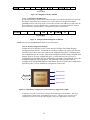
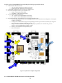
Standard Products
UT200SpW4RTR-EVB 4-Port SpaceWire
Router Evaluation Board Users Guide
User Manual
November, 2010
www.aeroflex.com/spacewire
1.0 INTRODUCTION
The UT200SpW4RTR-EVB is a 4-Port SpaceWire Router evaluation board designed to allow the system designer access to all
the features of the UT200SpW4RTR 4-Port router as defined in the datasheet (www.aeroflex.com/spacewire). The 4-Port
router is capable of operating at data rates from 10 to 200 Mbps. A parallel host interface is accessible through an onboard
FPGA. The Evaluation board can also be plugged into the Aeroflex Gaisler LEON 3-FT evaluation board, further expanding
functionality of the UT200SpW4RTR-EVB.
The UT200SpW4RTR router implements a non-blocking crosspoint switch and a "Round Robin" arbitration scheme allowing
all five receive ports access to all five transmit ports. Path and logical addressing are supported (Per ECSS-E-ST-50- 12C) and
lookup table storage is replicated five times giving each receive port a dedicated block of memory for logical addressing.
Configuration of lookup tables, as well as, access to internal registers may occur through any of the five ports using a simple
configuration protocol. A group adaptive function is also provided for two ports when implementing logical addressing.
Each of the four SpaceWire ports is capable of running at an independent speed. The clocking of the 4-port router is provided
by Aeroflex’s Clock Network Manager II. This allows the users systems to be configured with nodes/instruments running at
different speeds.
2.0 SCOPE
This document describes the features and necessary steps to set-up and operate the Aeroflex SpaceWire 4-port Router
Evaluation Board. It is recommended that the user be familiar with the UT200SpW4RTR 4-Port SpaceWire Router datasheet.
3.0 REFERENCE DOCUMENTS
ESA Publications Division, “SpaceWire Standard: ECSS-E-ST-50-12C”, http://www.ecss.nl/.
Aeroflex, “UT200SpW4RTR Datasheet”, www.aeroflex.com
Aeroflex, “UT7R2XLR816 Datasheet”, www.aeroflex.com
Aeroflex, “UT54LVDS031LV Datasheet”, www.aeroflex.com
Aeroflex, “UT54LVDS032LV Datasheet”, www.aeroflex.com
Aeroflex Gaisler GR-CPCI-UT699 LEON3-FT CPCI Development Board, www.gaisler.com
1
4.0 FUNCTIONAL DIAGRAM
PAGE 2
Clock Network
Manager II
4 LVCMOS Ports
SpW PORT
Powered from
3.3V
Powered from
3.3V
SpW PORT
2.5V
Regulator
4 LVDS SpW
UT200SpW4RTR
SpaceWire Router
HOST PORT
1.5V Linear
Regulator
SpW PORT
SpW PORT
SpW PORT
4 TX_CLK_IN
HOST CLK
LVDS
UT54LVDS031LV
UT54LVDS032LV
Xilinx
PROM
Xilinx V2
JTAG
PAGE 1
+3.3V
+5.0V
JTAG
Gaisler Board J9 Connector
PAGE 4
2.5V Power Plane
3.3V Power Plane
5.0V Power Plane
PAGE 6
1.5V Power Plane
SpW PORT
SpW PORT
PAGE 3
SpW PORT
+3.3
PIN
GND
BNC
2.5V
BNC
3.3V
BNC
5.0V
PAGE 5
Figure 1. Notional UT200SpW4RTR-EVB block diagram
2
5.0 FEATURES AND GENERAL OPERATION
The Aeroflex 4-Port SpaceWire Router evaluation board is designed to provide the user a flexible means to configure, control,
access, and route data through the UT200SpW4RTR device. Power to the board may be provided through the J9 connector on
the GR-UT699 CPCI Development Board or through the BNC connectors. Only one power source should be used at a time.
Clocking of the board is done via the UT7R2XLR816 Clock Network Manager. The UT7R2XLR816 can be configured using
the on board FPGA (Xilinx V2) or using the designated jumpers. The user is encouraged to download the UT7R2XLR816
Clock Network Manager Software GUI available at www.aeroflex.com/clocks and familiarize themselves with the
UT7R2XLR816 Clock Network Manager datasheet.
The 4-Port router device can be accessed using any of the four SpaceWire ports or through the V2 FPGA that is connected to
the Host port of the router. The FPGA on the board can be controlled and programmed by using either the JTAG connector or
using the LEON 3FT on the GR-UT699 Evaluation board. All of these features are detailed in the following sections.
3
5.1 Power
5.1.1 External Power
Power to the UT200SpW4RTR-EVB may be provided externally using the three BNC connectors. 5.0V,
3.3V and 2.5V must be provided to the board. In order to use external power provided by the BNC
connectors the user must jumper J57, J58, and J59. These jumpers ensure that external power is flowing to
the board. Ensure that Jumpers J64 and J65 are removed!
To avoid large surge currents in the UT200SpW4RTR device, VDD = 3.3V (J57) should be powered up
either before VDDC = 2.5V (J59) or synchronously with VDDC (VDD > VDDC). DO NOT power up the
core voltage supply VDDC before the I/O supply VDD; doing so causes a large in-rush current from
VDDC to VDD that stresses the power supplies and router components. If VDD and VDDC are being
powered up synchronously ensure that the voltage difference between VDDC and VDD does not exceed
0.4V (VDDC - VDD < 0.4V). See AC Electrical Characteristics in the UT200SpW4RTR datasheet for
specifics.
PE
UM
R
UT200SpW4RTR
4-Port Router
J
ER
UT54LVDS031LV
MP
JU
JUM
PER
Figure 2. External Power Jumper Configuration Settings
4
5.1.2
Aeroflex Gaisler Board Power
Power to the UT200SpW4RTR-EVB may also be provided from the J9 connector on the GR-CPCI-UT699 LEON3FT CPCI Development Board. Jumpers J64 and J65 must be set in order for the 120 pin J63 connector on the 4-Port
EVB to receive power from the LEON-3FT board. J63, the 120 pin connector, is located on the back side of the
UT200SpW4RTR-EVB. Use caution when mating the UT200SpW4RTR-EVB to the LEON-3FT evaluation board. If
the UT200SpW4RTR-EVB will be receiving power from the UT699 Evaluation board, jumpers J57, J58, and J59
should be removed.
UT54LVDS031LV
NOTE: Only connect jumpers required for the power source in use.
UT200SpW4RTR
4-Port Router
Figure 3. Aeroflex Gaisler LEON-3FT Power Jumper Settings
5
5.2 UT200SpW4RTR 4-Port Router
The 4-Port router can be easily configured using any of the four SpaceWire ports or the Host port connected to the V2.
If the user is going to use the XC18V04VQ44 Xilinx PROM (44-VTQFP) with the Virtex 2 - XC2V500
(FG256/FGG256) jumpers should be added to J6, J9, and J10 for proper access from the PROM to the FPGA.
Jumpers J6, J9 and J10 are located in the center on the top of the board.
5.2.1
LV_/CM Control Signal
The LV_/CM pin is the enable signal used to select between the LVDS or LVCMOS interfaces on the router. When
LV_CM is high the LVDS interface is active. When LV_CM is low, the LVCMOS interface is active.
5.2.1.1 Manual Jumper Control (J70 pin 2)
Control of this pin can be accomplished using the corresponding pin on J70 or through the V2
FPGA. For example, if LV_/CM signal is tied high, the LVDS I/O is active (TX1_D_LV[1:0],
TX1_S_LV[1:0], RX1_D_LV[1:0], and RX1_S_LV[1:0]), while the CMOS SpW I/O TX1_D,
TX1_S, RX1_D, and RX1_S is tri-stated. The row of pins closest to the LVCMOS SpaceWire
connectors is connected to VDD, the row closest to the middle of the board is connected to VSS.
5.2.1.2 V2 Control
The LV_/CM pin can also be controlled using the on board Virtex-2 device. LV_/CM on the
UT200SpW4RTR device is connected to pin B7 (IO_L94N_0/VREF_0) on the XC2V500 in the
Fine-Pitch BGA (FG256/FGG256) package. Control of the SpW I/O selection pin can be achieved
by writing code for the V2 device.
5.2.2
/OE Control Signal
This signal, used to control the outputs of the Receive FIFO, /OE , is active low. /OE supports the memory interface
timing of host controller that incorporates multiplexed address and data on the bus. If the user is not going to use the
parallel HOST interface, /OE can be held high.
5.2.2.1 Manual Jumper Control (J70 pin 3)
Control of this pin can be accomplished using the corresponding pin on J70 or through the V2
FPGA. Jumpering pin 3 on J70 to VDD disables the HOST port, tying pin 3 on J70 to VSS
activates the HOST port. The row of pins closest to the LVCMOS SpaceWire connectors is
connected to VDD; the row closest to the middle of the board is connected to VSS.
5.2.2.2 V2 Control
The /OE pin can also be controlled using the on board Virtex-2 device. /OE on the
UT200SpW4RTR device is connected to pin D7 (IO_L93N_0) on the XC2V500 in the Fine-Pitch
BGA (FG256/FGG256) package. Control of the SpW HOST interface can be achieved by writing
code for the V2 device.
5.2.3
/CSEL Control Signal
This allows the state of the control signals for the parallel HOST FIFOs to be connected to internal router logic. If
/CSEL is "High", the signals /TX_PUSH, /RX_POP, and any other backend inputs should not be allowed to be passed
on to internal logic. If the user is not going to use the parallel HOST interface, /CSEL should be help high.
5.2.3.1 Manual Jumper Control (J70 pin 1)
Control of this pin can be accomplished using the corresponding pin on J70 or through the V2
FPGA. Jumpering pin 1 on J70 to VDD disables the HOST FIFO interface. Tying pin 1 on J70 to
VSS activates the HOST port FIFOs. The row of pins closest to the LVCMOS SpaceWire
connectors is connected to VDD; the row closest to the middle of the board is connected to VSS.
5.2.3.2 V2 Control
The /CSEL pin can also be controlled using the on board Virtex-2 device. /CSEL on the
UT200SpW4RTR device is connected to pin A7 (IO_L94P_0) on the XC2V500 in the Fine-Pitch
BGA (FG256/FGG256) package. Control of the SpW HOST interface can be achieved by writing
code for the V2 device.
6
5.2.4
/RST Control Signal
The /RST pin is connected to push button switch SW1. /RST is active low. If the router needs to be reset the user can
push this switch and the router resets. After the router is reset the user should ensure that all the configuration and
status register are properly set to the desired configuration.
5.2.4.1 Manual Reset Control (SW1)
Control of this pin can be accomplished using switch SW1. pushing SW1 will reset the router
device. After the user pushes SW1 they should ensure that all the configuration and status register
are properly set to the desired configuration.
5.2.4.2 V2 Control
The /RST pin can also be controlled using the on board Virtex-2 device. /RST on the
UT200SpW4RTR device is connected to pin C7 (IO_L93P_0) on the XC2V500 in the Fine-Pitch
BGA (FG256/FGG256) package. Control of the SpW HOST interface can be achieved by writing
code for the V2 device. After the router is reset the user should ensure that all the configuration and
status register are properly set to the desired configuration.
Figure 4. UT200SpW4RTR Control Signal Locations
7
5.2.5
HOST Port Interface
Access to the 5th port of the HOST port of the UT200SpW4RTR can be accomplished by writing code targeted to the
Virtex 2 FPGA. Signals used to access the HOST port are listed below. Access to the HOST port can only be
achieved by using the V2. Be sure to jumper headers J6, J9, and J10 to ensure proper access from the PROM to the
V2 FPGA.
Table 1. UT200SpW4RTR Transmit HOST Port Connection Table
Virtex 2 – XC2V500 (FG256/FGG256)
Signal Description
Pin
IO_L01P_0
B4
IO_L01N_0
C4
IO_L02P_0
C5
IO_L02N_0
D5
IO_L03P_0/VRN_0
A5
IO_L03N_0/VRP_0
B5
IO_L04P_0
C6
IO_L04N_0/VREF_0
D6
IO_L05P_0
A6
IO_L05N_0
B6
IO_L92P_0
E7
IO_L92N_0
E6
UT200WSpW4RTR – 255 LGA
Signal Name
Pin
TXPORT0
C1
TXPORT1
D1
TXPORT2
F1
TXPORT3
G1
TXPORT4
C2
TXPORT5
D2
TXPORT6
E2
TXPORT7
F2
TXPORT8
G2
TX_PUSH
D3
TX_FULL
E3
TX_ALMOST_FULL
F3
Table 2. UT200SpW4RTR Receive HOST Port Connection Table
Virtex 2 – XC2V500 (FG256/FGG256)
Signal Description
Pin
IO_L01P_1
C13
IO_L01N_1
B13
IO_L02P_1
D12
IO_L02N_1
C12
IO_L03P_1/VRN_1
B12
IO_L03N_1/VRP_1
A12
IO_L04P_1/VREF_1
D11
IO_L04N_1
C11
IO_L05P_1
B11
IO_L05N_1
A11
IO_L92P_1
E11
IO_L92N_1
E10
UT200WSpW4RTR – 255 LGA
Signal Name
Pin
RXPORT0
A3
RXPORT1
A4
RXPORT2
A6
RXPORT3
A7
RXPORT4
B3
RXPORT5
B4
RXPORT6
B5
RXPORT7
B6
RXPORT8
B7
RX_POP
C4
RXEMPTY
C5
RX_ALMOST_EMPTY
C6
5.2.6
LEON-3FT HOST Port Access
The LEON-3FT evaluation board can also be used to control the FPGA and gain access to the HOST port of the
UT200SpW4RTR. The LEON-3FT device can access the UT200SpW4RTR by addressing the pins and signals listed
in the following table. This table shows the routing of the signal lines from the LEON-3FT to the Virtex 2 device.
The user can write code that will control the Virtex 2 such that the LEON has access to the HOST port of the SpW
router.
8
Table 3. LEON-3FT Evaluation Board Connector (J9) to V2 Connection Table
Virtex 2 - XC2V500 (FG256/FGG256)
Signal Description
Pin
IO_L05N_5/VRP_5
P6
IO_L93P_7/VREF_7
G1
IO_L93N_7
G2
IO_L94P_7
H3
IO_L94N_7
H4
IO_L96P_7
H1
IO_L96N_7
H2
IO_L94N_3
J14
IO_L05P_5/VRN_5
N6
IO_L94P_3
J13
IO_L04N_5
T5
IO_L43N_3
L16
IO_L04P_5/VREF_5
R5
IO_L45P_3
L12
IO_L03N_5/D4/ALT_VRP_5
P5
IO_L45N_3/VREF_3
K12
IO_L03P_5/D5/ALT_VRN_5
N5
IO_L06P_3
K13
IO_L02N_5/D6
R4
IO_L06N_3
L13
IO_L02P_5/D7
P4
IO_L01P_5/CS
T3
IO_L01N_5/RD/WR
T4
IO_L43P_3
L15
IO_L91P_5/VREF_5
R6
IO_L04P_3
M15
IO_L91N_5
T6
IO_L04N_3
M16
IO_L01P_7
D1
IO_L01N_7
C1
IO_L02P_7/VRN_7
D2
IO_L02N_7/VRP_7
D3
IO_L03P_7/VREF_7
E3
IO_L03N_7
E4
IO_L04P_7
E1
IO_L04N_7
E2
IO_L06P_7
F3
IO_L06N_7
F4
IO_L43P_7
F1
IO_L43N_7
F2
IO_L45P_7/VREF_7
G5
IO_L45N_7
F5
IO_L91P_7
G3
IO_L91N_7
G4
IO_L0N_3/VREF_3
M14
IO_L91P_3
K13
IO_L03P_3
M13
IO_L93P_3
K15
9
LEON-3FT Evaluation Board (J9)
Signal Name
A0
A1
A2
A3
A4
A5
A6
A7
A8
A9
A10
A11
A12
A13
A14
A15
A16
A17
A18
A19
A20
A21
A22
A23
A24
A25
A26
A27
D16
D17
D18
D19
D20
D21
D22
D23
D24
D25
D26
D27
D28
D29
D30
D31
RESETN (LEON-3FT)
BRDYN (LEON-3FT)
IOSN (LEON-3FT)
READ (LEON-3FT)
Pin
45
76
44
77
43
78
42
79
39
82
38
83
37
84
36
85
35
86
34
87
33
88
32
89
29
92
28
93
94
96
98
102
104
106
108
112
95
97
99
103
105
107
109
113
59
58
74
75
IO_L91N_3
IO_L93N_3/VREF_3
IO_L93P_5
IO_L93N_5
IO_L92P_5
IO_L92N_5
5.2.7
K14
K16
N7
P7
M6
M7
OEN (LEON-3FT)
WRITEN (LEON-3FT)
RAMOEN0
RAMOEN1
RAMSN0
RAMSN1
47
46
66
67
55
54
SpaceWire Interfaces
5.2.7.1 LVDS Interface
The LVDS SpaceWire ports on the UT200SpW4RTR are connected to SpaceWire connectors
located closest to the Router device.
Table 4. LVDS SpaceWire to UT200SpW4RTR port connection table
SpaceWire Port (LVDS)
1
2
3
4
Connector
P1
P4
P2
P3
Termination resistors are present on the receive signals of the LVDS SpW ports. The user is
cautioned to be sure to add 100Ω terminations resistors close to the router device when designing a
board. Termination resistors are not external and must be external to allow for proper operation of
the UT200SpW4RTR device.
5.2.7.2 LVCMOS Interface
The LVCMOS SpaceWire ports on the UT200SpW4RTR are connected to UT54LVDS031LV
LVDS Drivers. The UT54LVDS032LV LVDS receivers then run to the SpaceWire connectors
located furthest to the Router device. To enable the external LVDS Drivers and Receivers, the user
must use SW2 to enable or disable the UT54LVDS031LV and UT54LVDS032LV devices.
Table 5. LVCMOS SpaceWire to UT200SpW4RTR port connection table
SpaceWire Port (LVCMOS)
1
2
3
4
Connector
P5
P6
P7
P8
Table 6. LVDS Driver UT54LVDS031LV Enable configuration
Enable Signal
EN
/EN
L
H
All other
combinations of
ENABLE signals
Input
DIN
X
L
H
10
Output
DOUT+
DOUTZ
Z
L
H
H
L
Table 7. LVDS Receiver UT54LVDS032LV Enable Configuration
Enable Signal
EN
/EN
L
H
All other combinations
of ENABLE signals
Input
RIN+ - RINX
VID≥0.1V
VID≥-0.1V
Fail Safe Mode
Output
ROUT
Z
H
L
H
Table 8. Switch 2 LVDS Devices Connection Table
Switch 2 (SW2)
Position
1
2
3
4
5
6
7
8
Name
TX 1 ENABLE (EN)
TX 1 ENABLEB (/EN)
RX 1 ENABLE (EN)
RX1 ENABLEB (/EN)
TX 2 ENABLE (EN)
TX 2 ENABLEB (/EN)
RX 2 ENABLE (EN)
RX 2 ENABLEB (/EN)
Port Enabled
1 and 2
1 and 2
1 and 2
1 and 2
3 and 4
3 and 4
3 and 4
3 and 4
5.2.8
Time Code Interface
The UT200SpW4RTR time code interface is tied to the V2 FPGA. Time code signals can be monitored by writing a
user program that looks at these signals.
Table 9. Time code interface connection table
Virtex 2 - XC2V500 (FG256/FGG256)
Signal Description
Pin
IO_L01N_2
C16
IO_L01P_2
D16
IO_L02N_2/VRP_2
D14
IO_L02P_2/VRN_2
D15
IO_L03N_2
E13
IO_L03P_2/VREF_2
E14
IO_L04N_2
E15
IO_L04P_2
E16
IO_L06N_2
F13
IO_L06P_2
F14
UT200WSpW4RTR - 255 LGA
Signal Name
TIMECODE1
TIMECODE0
TIMECODE3
TIMECODE2
TIMECODE5
TIMECODE4
TIMECODE7
TIMECODE6
TICKOUT
TICKIN
Pin
T3
T2
R2
T4
R4
R3
R6
R5
T7
T6
5.2.9
Clock Interface
The Clock Network Manager (CNM) is used to provide the five clocks to the UT200SpW4RTR device. The clock
signals are HOST_CLK, TXCLK_IN_1, TXCLK_IN_2, TXCLK_IN_3, TXCLK_IN_4, and a clock to the V2 FPGA.
Please refer to the UT7R2XLR816 Clock Network Manager datasheet for further information.
The 43 pin headers on the board can be used for the configuration of the CNM. Each of the configuration signals are
3-level inputs. The middle row of headers is connected directly to the corresponding signal on the CNM device. The
surrounding rows of pins are connected to VDD = 3.3V and VSS = 0.0V.
The UT7R2XLR816 Clock Network Manager Software GUI should be downloaded from www.aeroflex.com/clocks
to assist in the proper configuration selection of the clocks that are provided to the SpaceWire router.
11
5.2.9.1 Manual Jumper Control (43 Pin header)
Control of the CNM can be accomplished using the corresponding pin on the 43 pin connector to set
the proper configuration as reported by the UT7R2XLR816 Clock Network Manager Software GUI.
The row of pins on the left or on the inside of the board are connected to 3.3V. The pins towards
the outside of the board are connected to VSS and the center row is connected to the pin of the
CNM. The silkscreen on the board indicates which signal is routed to which pin.
Table 10. UT7R2XLR816 CNM to 43 Pin Header Connection Table
UT7R2XLR816 - 168 LGA
Signal Name
Pin
/CM_LV
H10
FREQ_SEL
K11
TEST
B2
/OE
D9
REF_SEL
F3
/RST_DIV
F2
FB_PS0
J4
FB_PS1
K3
FB_PS2
K4
FB_DS0
L2
FB_DS2
J2
FB_DS1
K2
FB_DS3
H3
0Q_DS3
M6
0Q_DS2
M5
0Q_DS1
L5
0Q_DS0
M4
0Q_PS1
M2
0Q_PS0
L3
1Q_DS3
K6
1Q_DS2
L7
1Q_DS1
K8
1Q_DS0
L8
1Q_PS1
M2
1Q_PS0
L3
2Q_DS3
K10
2Q_DS2
L10
2Q_DS1
L11
2Q_DS0
M10
2Q_PS1
M9
2Q_PS0
L9
3Q_DS3
H11
3Q_DS2
F10
3Q_DS1
F11
3Q_DS0
G11
3Q_PS1
H12
3Q_PS0
J11
4Q_DS3
E11
4Q_DS2
C12
4Q_DS1
D11
4Q_DS0
F12
4Q_PS1
L12
4Q_PS0
J10
12
43 Pin Header
Pin
1
2
3
4
5
6
7
8
9
10
11
12
13
14
15
16
17
18
19
20
21
22
23
24
25
26
27
28
29
30
31
32
33
34
35
36
37
38
39
40
41
42
43
5.2.9.2 V2 Control
The CNN device can also be controlled using the on board Virtex-2 device. Control of the CNM
can be achieved by writing code for the V2 device that address the signals listed in the following
table.
Table 11. UT7R2XLR816 CMN to V2 connection table
Virtex 2 - XC2V500 (FG256/FGG256)
Signal Description
Pin
IO_L96N_1/GCLK3P
A9
IO_L05N_4/VRP_4
N11
IO_L95P_0/GCLK6S
C8
IO_L95N_0/GCLK7P
D8
IO_L96P_0/GCLK4S
A8
IO_L96N_0/GCLK5P
B8
IO_L94P_4
T10
IO_L94N_4/VREF_4
R10
IO_L95P_4/GCLK2P
P9
IO_L95N_4/GCLK3S
N9
IO_L96P_4/GCLK0P
T9
IO_L96N_4/GCLK1S
R9
IO_L96P_1/GCLK2S
B9
IO_L95N_1/GCLK1P
C9
IO_L94N_1
A10
IO_L94P_1/VREF_1
B10
IO_L93N_1
C10
IO_L93P_1
D10
IO_L96P_2
H16
IO_L96N_2
H15
IO_L45N_2
F12
IO_L45P_2/VREF_2
G12
IO_L43N_2
F15
IO_L43P_2
F16
IO_L91P_4
T11
IO_L91N_4/VREF_4
R11
IO_L92P_4
M10
IO_L92N_4
M11
IO_L93P_4
P10
IO_L93N_4
N10
IO_L01N_4/BUSY/DOUT(1)
T14
IO_L02P_4/D1
R13
IO_L03P_4/D3/ALT_VRN_4
P12
IO_L03N_4/D2/ALT_VRP_4
N12
IO_L04N_4/VREF_4
R12
IO_L04P_4
T12
IO_L05P_4/VRN_4
P11
IO_L91N_2
G13
IO_L91P_2
G14
IO_L93N_2
G15
IO_L93P_2/VREF_2
G16
IO_L94N_2
H13
IO_L94P_2
H14
UT7R2XLR816 - 168 LGA
Signal Name
4Q_PS0
4Q_PS1
4Q_DS0
4Q_DS1
4Q_DS2
4Q_DS3
3Q_PS0
3Q_PS1
3Q_DS0
3Q_DS1
3Q_DS2
3Q_DS3
2Q_PS0
2Q_PS1
2Q_DS0
2Q_DS1
2Q_DS2
2Q_DS3
1Q_PS0
1Q_PS1
1Q_DS0
1Q_DS1
1Q_DS2
1Q_DS3
0Q_PS0
0Q_PS1
0Q_DS0
0Q_DS1
0Q_DS2
0Q_DS3
FB_PS0
FB_PS1
FB_PS2
FB_DS0
FB_DS2
FB_DS1
FB_DS3
FREQ_SEL
/CM_LV
/OE
TEST
REF_SEL
/RST_DIV
13
Pin
J10
L12
F12
D11
C12
E11
J11
H12
G11
F11
F10
H11
L9
M9
M10
L11
L10
K10
L3
M2
L8
K8
L7
K6
L3
M2
M4
L5
M5
M6
J4
K3
K4
L2
J2
K2
H3
K11
H10
D9
B2
F3
F2
5.2.9.3 Initialization Divide Registers
All SpaceWire ports follow the initialization procedure as defined in
ECSS-E-ST-50-12C. Following are the key components of the initialization process. After a reset or
disconnect the link initiates operation at a signaling rate of 10 Mbps, ±1 Mbps. This provides the
system with a common data rate while the system is checked for proper operation. Once the
operation of the system is validated each of the four ports switches to the specified transmit data
rate. Each of the four ports must be capable of running at 10 ± 1 Mbps.
The initialization divide registers will all be loaded with the jumper settings value that pins
TX_DIV[4:0] on the UT200SpW4RTR are set to. These pins must be set to the proper settings in
order for the router to initialize at 10Mbps ± 1Mbps as defined in the SpaceWire Standard. The user
can use connector 73 or choose to use the V2 FPGA to configure the initialization divide registers.
If the user wishes to configure the router through port 3 and the transmit speed will be 100Mbps, the
user will need to set TX_DIV to 0x0A or 10 in decimal. Port 3 has the correct divider for the
10Mbps clock and can initialize the SpaceWire link. If the other ports are transmitting at different
data rates, the 10Mbps initialization data rate will not be correct. The user will then use Port 3 to set
the Transmit 10Mbps Register to the initialization data rate of 10Mbps. Once the router had
initialized and is in the run state, it will begin running at the specified TXCLK_IN rate.
NOTE: if TX_CLK is set to less than 10Mbps the Initialization Divide Register must be set to
0x01. The 4-Port Router will be able to initialize at these data rates. The user needs to be aware;
however, to be careful not to send any data until the links are in the run state. If the initialization
data rates are different, one side of the link could reach the run state before the other and, if that link
begins to send data, there is a good possibility the other side will disconnect because it received a
normal character before reaching the run state.
5.2.9.3.1
Manual Jumper Control (J73 header)
Configuration of the initialization divide registers can be accomplished using the
corresponding pin on the 5 pin J73 connector. The row of pins closest to the LVCMOS
SpW ports on the UT200SpW4RTR connected to 3.3V. The pins towards the LVDS SpW
ports are connected to VSS and the center row is connected to the initialization divide pin
as shown in the following table.
Table 12. J73 Initialization Divide Register pin assignments
UT200SpW4RTR – 255 LGA
Signal Name
Pin
TX_DIV[0]
M2
TX_DIV[1]
L2
TX_DIV[2]
K2
TX_DIV[3]
J3
TX_DIV[4]
H3
14
J73 Header
Pin
1
2
3
4
5
0
UT54LVDS031LV
TX
_D
IV
V4
TX_DI
UT200SpW4RTR
4-Port Router
UT54LVDS031LV
Figure 5. TX_DIV[4:0] Jumper Locations
5.2.9.3.2
V2 Control
The Initialization Divide Registers can also be controlled using the on board Virtex-2
device. Control of the TX_DIV[4:0] pins can be achieved by writing code for the V2
device that address the signals listed in the following table.
Table 13. UT200SpW4RTR TX_DIV[4:0] to V2 Connection Table
Virtex 2 - XC2V500 (FG256/FGG256)
Signal Description
Pin
IO_L91P_6
K4
IO_L91N_6
K3
IO_L93P_6
K2
IO_L93N_6/VREF_6
K1
IO_L94P_6
J4
UT200WSpW4RTR - 255 LGA
Signal Name
TX_DIV4
TX_DIV3
TX_DIV2
TX_DIV1
TX_DIV0
15
Pin
H3
J3
K2
L2
M2
5.2.9.4 Clock Network Manager Configuration
Each of the Divide Select banks contain output division selector and controller pins. There are four
ternary inputs used to control the 0Q[1:0], 1Q[1:0], 2Q[1:0], 3Q[1:0], 5Q[1:0], 7Q[1:0], and
FB_DS[1:0] output clock dividers, inverters, and enable controls. See Table 1 in the
UT7R2XLR816 Clock Network Manager Datasheet for output behavior resulting from each
combination of these pins.
The #Q_PS# pins are the bank output phase selectors. Depending on required skew these bits will
need to be set. These two ternary inputs are used to control the 0Q[1:0], 1Q[1:0], 2Q[1:0], 3Q[1:0],
5Q[1:0], 7Q[1:0], and FB_DS[1:0] output phase alignment. See Table 2 in the UT7R2XLR816
CNM Datasheet for output behavior output phase selections resulting from each combination of
these pins.
TXCLK_IN_1
Table 14. The Signal Highlighted in blue is the Signal Used to Clock TXCLK_IN_1
PIN#
N4
N3
M6
M5
L5
M4
M2
L3
CNM NAME
0Q0
0Q1
0Q_DS3
0Q_DS2
0Q_DS1
0Q_DS0
0Q_PS1
0Q_PS0
TXCLK_IN_2
Table 15. The Signal Highlighted in blue is the Signal Used to Clock TXCLK_IN_2
PIN#
N8
N7
K6
L7
K8
L8
L6
K5
CNM NAME
1Q0
1Q1
1Q_DS3
1Q_DS2
1Q_DS1
1Q_DS0
1Q_PS1
1Q_PS0
TXCLK_IN_3
Table 16. The Signal Highlighted in blue is the Signal Used to Clock TXCLK_IN_3
PIN#
N12
N11
K10
L10
L11
M10
M9
L9
CNM NAME
2Q0
2Q1
2Q_DS3
2Q_DS2
2Q_DS1
2Q_DS0
2Q_PS1
2Q_PS0
16
TXCLK_IN_4
Table 17. The Signal Highlighted in blue is the Signal Used to Clock TXCLK_IN_4
PIN#
J13
K13
H11
F10
F11
G11
H12
J11
CNM NAME
3Q0
3Q1
3Q_DS3
3Q_DS2
3Q_DS1
3Q_DS0
3Q_PS1
3Q_PS0
HOST_CLK and
V2_CLK
Table 18. The Signal Highlighted in blue is the Signal Used to Clock HOST_CLK and the purple Highlighted Signal is
Used to Clock the V2
PIN#
D13
E13
E11
C12
D11
F12
L12
J10
CNM NAME
4Q0
4Q1
4Q_DS3
4Q_DS2
4Q_DS1
4Q_DS0
4Q_PS1
4Q_PS0
FEEDBACK
Table 19. The feedback signals connects to the internal Phase- Frequency Detector
PIN#
H3
J2
K2
L2
K4
K3
J4
CNM NAME
FB_DS3
FB_DS2
FB_DS1
FB_DS0
FB_PS2
FB_PS1
FB_PS0
Tables 14-19 show the CMN banks that must be considered when using the CMN software to configure the desired
clocking of the 4-Port router. An example of how to determine the configuration settings of the CMN is provided
below.
5.2.9.5 CMN Configuration Example
Assume the user wanted to provide 200MHz clock to the TXCLK_IN_1, 16MHz clock to the
HADS3 Board, 16MHz clock to the HADS3 Board, and 12MHz to the HADS4 board. Given that
the Clock Network Manager II oscillator runs at 16MHz, the LCB FPGA will run at 16MHz, and
the LEON3FT can run at 16 or 32MHz.
Using the UTR2XLR816 Clock Network Manager II Frequency and Skew Calculator a schematic
detailing the output bank configuration requirements will be given. The output from the Frequency
and Skew Calculator will be used to configure the Clock Network Manager II register at location
0x00002000 to 0x00002018.
UTR2XLR816 Clock Network Manager II Frequency and Skew Calculator use the input the Input Frequency
Ref to 50MHz. There is a 50MHz oscillator that is used as the clock input reference.
17
Click [Configure] button
Bank 0
Bank 1
Bank 2
Bank 3
Bank 4
Bank 5
Bank 6
Bank 7
200
200
100
100
50 (HOST_CLK must be set to 0.25 times the fastest TXCLK_IN)
Don’t Care
Don’t Care
Don’t Care
Click [Calculate Configuration]
Select the configuration that best meets the systems needs.
Click [Return Selected Configuration]
Figure 6. UTR2XLR816 Clock Network Manager II Frequency and Skew Calculator results options
Click [Refresh Configuration]
Click [View Schematic]
18
Figure 7. Configuration Schematic
This is the configuration schematic that will be used to configure the Clock Network Manager for
the clocking of the UT200SpW4RTR and the V2 FPGA.
19
Table 20. Details the header pin configuration for the example of how to configure the CMN
VSS = connect the center pin to the VSS pin next to it
VDD = connect the center pin to the DD pin next to it
NC = Do not connect the center pin to anything
Header Pin
7
8
9
10
11
12
13
14
15
16
17
18
19
20
21
22
23
24
25
26
27
28
29
30
31
32
33
34
35
36
37
38
39
40
41
42
43
CNM Pin
FB_DS0
FB_DS1
FB_DS2
FB_DS3
FB_PS0
FB_PS1
FB_PS2
0Q_DS0
0Q_DS1
0Q_DS2
0Q_DS3
0Q_PS0
0Q_PS1
1Q_DS0
1Q_DS1
1Q_DS2
1Q_DS3
1Q_PS0
1Q_PS1
2Q_DS0
2Q_DS1
2Q_DS2
2Q_DS3
2Q_PS0
2Q_PS1
3Q_DS0
3Q_DS1
3Q_DS2
3Q_DS3
3Q_PS0
3Q_PS1
4Q_DS0
4Q_DS1
4Q_DS2
4Q_DS3
4Q_PS0
4Q_PS1
20
Value
VSS
NC
VSS
VSS
VDD
NC
VSS
VSS
VSS
VSS
VSS
NC
NC
VSS
VSS
VSS
VSS
NC
NC
NC
VSS
VSS
VSS
NC
NC
NC
VSS
VSS
VSS
NC
NC
VSS
NC
VSS
VSS
NC
NC
UT54LVDS031LV
UT200SpW4RTR
4-Port Router
Figure 8. Example CNM Jumper Setting
21
5.2.9 Router Configuration Protocol
The user may want to access to the configuration and status registers. Access to these registers can be accomplished
though any one of the four SpaceWire ports or the External Port. The default configuration is for all ports to be
configuration ports. If one or more ports are set up to be configuration ports, only one configuration command should
be sent at a time.
5.2.9.6 Configuration Ports
If multiple ports are set up as configuration ports and more than one configuration command is
being sent within the router, the configuration packets will be corrupted. The first byte of data with
value 0x00 received by any router port after reset or an EOP/EEP initiates a configuration
transaction. (ECSS-E-ST-50-12C). Configuration transactions allow access to the lookup tables,
configuration registers and status registers. The packet protocols for configuration reads and writes
are specified in the following sections.
5.2.9.7 Configuration Write
A configuration write packet loads a 16-bit data word to the specified 16-bit address location in the
configuration memory space. A configuration write packet begins with zero (0x00) or can contain
additional router address bytes, followed the final destination address byte set to zero. A
Configuration Write packet is shown below.
Figure 9. Configuration Write Command
Next, the router ID byte should be set to the value in the receiving router ID register. The Packet
Type byte should be set to Write (see table 6.), followed by the address least significant byte, the
address most significant byte, then the data least significant byte and the data most significant byte.
The last byte before the end of packet (EOP) will be the arithmetic Checksum value, which is an
arithmetic sum of the final destination address, the router ID, the Packet Type, the Address and Data
bytes. If the checksum value does not match, the command will not be executed. If the packet has
less than eight (8) bytes or the Checksum value is not the last byte, the command will not be
executed. (ECSS-E-ST-50-12C).
5.2.9.8 Configuration Read
The Read packet will read a number (Count) of 8-bit data values from consecutive 16-bit address
locations and transmit the data to the return location specified. This packet begins with zero or more
hardware or logical address bytes followed by the final destination address byte set to zero.
Next, the router ID byte should be set to the value in the router ID register, unless the router ID is
being read. The Packet Type byte should be set to Read, (0x01 or 0x02) followed by the address
least significant byte, the address most significant byte, the word count byte, and one or more return
path address byte(s). The order of the return path address bytes are to read in the order they are
received.
That is to say, the first return path address byte will be the path out of the first router with
subsequent bytes to be used for the next layers of routers. The last byte will be the checksum value,
which is an arithmetic sum of the destination address, router ID, packet type, address bytes, data
bytes and return path bytes. If the checksum received does not match the calculated value, an error
end of packet will be sent to the return address. The word count byte must be greater than zero. A
value of zero causes the command to not be executed. The return address path must contain one or
more bytes and the first header byte must not be zero; otherwise, the command will be considered
invalid and not be executed. The following figure shows the bytes required for a Read Packet
Command.
22
Figure 10. Configuration Read Command
5.2.9.9 Configuration Read Response
A read response will be sent back to the requesting address after a Read command is executed. The
Read packet command as shown in Figure 5 sets, up the address to read data from (Address
LSB/MSB) and how many 8-bit values to read (Count), and the return address bytes path. After the
Read command is executed a Read Response command will be issued and contains the data byte
pairs read from the specified address. A read response packet is shown below.
Figure 11. Configuration Read Response Command
NOTE: Please see UT200SpW4RTR Datasheet for more information
5.2.9.10 Router Configuration Example
Assume the user would like to write a value into the Configure Port Enable Register
residing at location 0x0102. Assume the user wants to configure the router such that only
the HOST port of the router can be used to send configuration packets. Configuring only
one configuration port on a router will prevent configuration packets being corrupted when
multiple ports are set up as configuration ports. If more than one port is set up as a
configuration port and more than one configuration command is sent within the router, the
configuration packets will be corrupted. The following example will show how to
configure the UT200SpW4RTR Router such that the System or HOST port is enabled and
SpaceWire ports 1 to 4 are disabled for configuration of the router.
SpaceWire Port 1
SpaceWire Port 2
HOST Port
SpaceWire Port 3
SpaceWire Port 4
Figure 12. 4-Port Router configuration for the following configuration example
Assume the user wants to write to the Configure Port Enable register in the Router. The user is
communication with the router via the HOST port or port 5. The first step is to use the write
configuration protocol to write the following packet into port 5 (HOST Port) of the router.
23
•
•
•
•
•
•
•
•
•
•
Use Write configuration protocol into port 5 of the router
Address Bytes: NONE Needed
0x00 for configuration
Router ID: 00 for router (default)
Protocol ID: 00 for no protocol used
Packet Type: 00 is Write
Set up Data Format
o Address LSB: 02 LSB
o Address MSB: 01 MSB of register location 0x0102
Write in Data
o Data LSB: 10 Bit15
87 4 0
o Data MSB: 00
00000000 00010000
Checksum: 13 this is the sum of the final destination address, router ID, protocol ID, packet type, and the
address and data bytes. 0x00+0x00+0x00+0x00+0x02+0x01+0x10+0x00 = 0x13
EOP: 100000000
5.2.10 Configuration and Status Registers
Please see UT200SpW4RTR datasheet available at www.aeroflex.com/Spacewire for detailed information on user
configurable registers. The router has a number of configuration and status registers which are used for initial setup of
the router and for monitoring the router's performance. These registers can be accessed using the configuration
protocol as explained in section 5.2.5.
5.2.11 Other Registers
All the other registers of the UT200SpW4RTR are not required to get the device up and running. The other registers
add important status and configuration capabilities, but are not required to start using the router. Please refer to
section 6.0 in the UT200SpW4RTR datasheet for a further description of the available registers.
24
6.0 PORT ADDRESSING
6.1 Path Addressing
Path Addressing is defined as a series of one or more characters at the start of the packet that define the route, or path,
that the packet should take across a SpaceWire network. The destination address is specified as a sequence of router
output port numbers used to route the packet across the network. The drawback is that the destination address can
become relatively large if several routing switches have to be traversed. Path Addressing is used for configuration of
the router. The routers look up tables does not have to be configured when path addressing is being used.
A packet with header 0x01 will be routed to Router port 1, a 0x02 header will be routed to port 2, 0x03 will be routed
to port 3, and so on. Please see the following table for a list of valid path addresses.
Table 21. Path Address Byte Memory Map
Address Byte (HEX)
0x01
0x02
0x03
0x04
0x05
Port
Path Address for Port 1
Path Address for Port 2
Path Address for Port 3
Path Address for Port 4
Path Address for HOST port
6.2 Logical Addressing
The router can be configured to use Logical addressing by using path addressing to configure the look up tables.
Logical Addressing contains a character at the start of a packet, which identifies a look up table location and then
selects the destination for the packet. Each destination address has a unique number or logical address associated with
it. These numbers can be assigned arbitrarily to nodes provided.
To access logical routing the user must configure the look-up tables. The looks up tables in the 4-Port router have
even parity. Valid look up table address locations are 0x0020 to 0x00F. If a portion of the look up table addressing
space is not going to be used, it is preferred if the user sets used addressed to 0x00.
6.3 Regional Logical Addressing
This addressing scheme is the same as Logical Addressing except for the fact that header delete is used. When using
Regional Logical Addressing the look up tables contains the information on which headers to keep and or delete.
6.4 Group Adaptive
The last SpaceWire addressing scheme is group adaptive. When Group adaptive routing is used, packets can be
routed to a requested destination through different network paths. Group adaptive routing can be set up for two paths.
To utilize group adaptive routing, the user must configure Group adaptive bits in look-up table. Bits 5 through 9 are
group adaptive address, and Bit 11 must be set to 0x01 to enable group adaptive routing. To use Logical or Group
Adaptive addressing the router must be configured to set up these functions
6.5 Look Up Table Data Format
The lookup tables on the router are organized into 16-bits and are organized as shown below.
Figure 13. Look-up Table Format
6.5.1 Primary Logical Address Bits
The five LSB bits [4:0] are the Primary Logical Address bits and are for selecting ports 1 through 4
regardless of whether Group Adaptive has been enabled or not. When Group Adaptive has been enabled, the
router looks at the port address specified by these bits first and if that port is busy, then looks at the port
specified by the Group Adaptive Address Bits.
25
6.5.2 Group Adaptive Address Bits
Bits [9:5] are used when Group Adaptive has been enabled and the port selected by the Primary Logical
Address Bits is busy. If group adaptive routing is not enabled and port selected by the Primary Logical
Address Bits is busy, the packet waits until the selected port is free.
6.5.3 Enable Header Delete Bit
Bit [10] is used to enable the header delete function for the port selected by either the Group Adaptive
Address bits or the Primary Logical Address Bits. Whenever this bit is set high, the router deletes the header
before sending the packet out of the requested transmit port.
6.5.4 Enable Group Adaptive Bit
Bit [11] is used to enable the Group Adaptive function on the router. Setting this bit high tells the router to
use bits [9:5] for the port select in the event the port select for the Primary Address Bits is busy.
6.5.5 Unused Bits
Look up table bits [14:12] needs to be set to 0x00. In order for the parity bit to be correct all three unused bits
need to contain 0’s. If these bits are set to something other than 0x00, the parity calculation will not be the
same as what the router is calculating.
6.5.6 Parity Bit
A Parity Bit is included for each lookup table location. The parity is even. When the header byte is decoded
and falls between address 0x20 and 0xFF, a lookup table address will be retrieved by the lookup table.
Again, parity will be calculated by adding the number of ones that are contained in the previous 8-bits data. If
the total number of 1's in bits added together is odd, the parity is odd parity. And if the number of 1's in bits
added is even, the parity is even parity. The current parity bit will then be compared to the calculated parity
and if they are not the same, the packet will be read out of the receive FIFO. This is commonly referred to as
"Spilling the Packet". Additionally, the Parity Error Register will be incremented.
Parity error register is different from the previously discussed SpaceWire parity. The parity error register is
based on the data in the lookup table. Please see ECSS-E-ST-50-12C for more information regarding parity.
6.5.7 Look up table configuration Example 1
Assume the user wants to write to the configure look up table address 0x0020 to contain addressing to send
out port 1. Meaning if a packet is received with logical address bytes 0x0020 it will be routed out port 1 of
the router. The user is in communication with the router via the HOST port or port 5.
The user will have to use the write configuration protocol into port 5 (HOST Port) of the Primary router to
set up look up tables.
SpaceWire Port 1
SpaceWire Port 2
HOST Port
SpaceWire Port 3
SpaceWire Port 4
Figure 14. 4-Port Router configuration for the look up table access and configuration example
26
•
•
•
•
•
•
•
Write directly into port 5 of the Router, no Address Bytes required
0x00 for configuration
Router ID: 00 for router ID (default)
Protocol ID: 00 for no protocol used
Packet Type: 00 is Write
Set up look-up table
o Address LSB: 20 sets up first address in look up table
o Address MSB: 00 the address MSB is always 00 because the address range of the Logical Addresses
is 0x0020 to 0x00FF
Write in Data
o Data LSB: 01 sets up port 1 of Router (this will set up logic such that is register 0x0020 is received
the data will go out of port 1 on Router )
o Data MSB: 04 Header Delete set
The write data for the look up table was calculated using the following look up table configuration. Primary Logical
Address Bits = 1 for the Logical address to be set to port 1. No group adaptive bits are used. Enable header delete
was turned on, and the parity was calculated as 0, because 1+1=2 = even number.
•
•
Checksum: 26 this is the sum of the final destination address, router ID, packet type, and the address and data
bytes. 0x00+0x01+0x00+0x20+0x00+0x01+0x04 = 0x26
EOP: 100000000
The data characters would look like:
27
6.5.8 Look up table configuration Example 2
Assume the user wants to confirm the configuration write just preformed on look up table address 0x0020
was completed correctly. The user can then use the read configuration command. The following example
details hope to accomplish this.
•
•
•
•
•
•
•
•
Address Bytes: 00, receive on port 5 (HOST port)
0x00 for configuration command
Router ID: 00 is router ID (default)
Protocol ID: 00 for no protocol used
Packet Type: is Read No Clear 0x01
Address LSB: 20
Address MSB: 00 sets up to read from address 0x0020
Count: 02 will read 2 Bytes of data. Count can only be an even number. To read one register you must enter
0x02, to read 2 registers you must enter 0x04, etc.
Return Address Bytes: 01 05 out port 1 of Router A, out port 5 Router P
Checksum: 28 this is the sum of the router ID, packet type, address bytes, count, an return address bytes.
0x00+0x00+0x00+0x01+0x20+0x00+0x02+0x05= 0x28
•
•
0
0 or More
Address Bytes
00
0x00
00
Router ID
00
Protocol ID
01
Packet Type
20
Address LSB
00
Address MSB
02
Count
05
1 or More
Return Address
Bytes
2
100000000
Check Sum
EOP
The Data Character would look like:
7.0 FPGA ACCESS
The V2 FPGA can be accessed using the V2 JTAG connection using a JTAG/USB Xilinx pod through the V2 PROM JTAG
connector or using the UT699 LEON-3FT on the Aeroflex Gaisler UT699 evaluation board.
Connector J8 is connected to the XC18V04VQ44 Xilinx PROM (44-VTQFP), connector J5 is connected to the JTAG interface
on the Virtex 2 - XC2V500 (FG256/FGG256). The user can determine which access route to the V2 is best suited to their
needs.
Be sure to jumper headers J6, J9, and J10 to ensure proper access from the PROM to the V2 FPGA.
8.0 QUICK START GUIDE
28
To quickly get the UT200SpW4RTR-EVB up and running the following steps should be followed
1. Connect headers J57, J59, and J58
a. This will enable external power supplies to be used
b. Ensure that headers J64 and J65 are not connected.
2. Connect BNC connectors to J54 3.3V, J56 2.5V , and J55 5.0V
3. Determine which SpW interface you would like to use
a. LVDS – Connect Pin 2 J70 to VDD
b. LVCMOS – Connect Pin 2 J70 to VSS
4. Are you going to use the HOST port?
a. Yes – Set Pin 1 J70 to VSS and Pin 3 J70 to VSS
b. No – Set Pin 1 J70 to VDD and Pin 3 J70 to VDD
5. Determine the data rate you would like to use to clock the SpaceWire ports
a. Use the UT7R2XLR816 Clock Network Manager Software GUI to determine the configuration of the signals
on the 43 pin connector
b. Configure the UT7R2XLR816 using the corresponding pin on the 43 pin connector such that you will get the
proper TXCLK_IN_#, HOST_CLK, and V2_CLK
c. Using J73 set the Initialization Divide Register TX_DIV[4:0] such that one of the TXCLK_IN rates
initializes the UT200SpW4RTR at 10Mbps ±1Mbps
d. Hook up your instruments to the SpaceWire ports
e. Power on the board
V
UT54LVDS031LV
5.0
V
3.3
?
DS S?
LV MO
C
LV
UT200SpW4RTR
4-Port Router
Figure 15. Quick Start example configuration
9.0 COMPATIBILITY WITH GR-UT699 EVALUATION BOARD
29
The UT200SpW4RTR-EVB can plug directly into the J9 connector on the LEON-3FT evaluation board. A ribbon cable can
also be used to easily use the SpaceWire evaluation board with the LEON-3FT board when the LEON board is plugged into a
cPCI chassis. Using the ribbon cable to connect the SpaceWire evaluation board to the LEON 3FT GR-UT699 evaluation
board allows for easier access to the SpW ports on the UT200SpW4RTR-EVB board.
The virtex-2 FPGA is connected to the HOST port of the UT200SpW4RTR device. J9 on the GR-UT699 evaluation board is
also connected to the V2 FPGA; control of the SpW router can be gained by accessing the connections listed in table 3 above.
For further information on interfacing the UT200SpW4RTR-EVB with the GR-UT699 Evaluation board please see the
Aeroflex Gaisler GR-UT699 Development Board User Manual.
30
10.0 BOARD SCHEMATICS
The schematics in Appendix A are for reference ONLY.
31
5
4
3
2
1
Change Block
Redesigned board for customer use
Board can plug into Aeroflex/Gaisler LEON-3FT Evaluation Board or be used as a table top board
UT200SpW4RTR-CUSTOMER-EVB Schematic
D
D
C
C
B
B
A
NOTICE TO ALL PERSONS RECEIVING THIS DRAWING:
THIS DOCUMENT IS PROPERTY OF AEROFLEX COLORADO SPRINGS
AND IS DELEVERED ON THE EXPRESS CONDITION THAT IT IS NOT TO BE
DISCLOSED, REPRODUCED IN WHOLE OR IN ANY PART, OR IS USED FOR
MANUFACTURE FOR ANYONE OTHER THAN AEROFLEX WITHOUT ITS
WRITTEN CONSENT; AND THAT NO RIGHT IS GRANTED TO DISCLOSE
OR SO USE ANY INFORMATION CONTAINED IN SAID DOCUMENT.
THIS RESTRICTION DOES NOT LIMIT THE RIGHT TO USE THE
INFORMATION OBTAINED FROM ANOTHER SOURCE.
A
Aeroflex Colorado Springs
4350 Centennial Blvd.
Colorado Springs
Colorado 80907
UT200SpW4RTR-CUST_EVB TITLE
Size
C
Tuesday, August 24, 2010
5
4
3
2
Scale
CAGE Code
Rev
DWG NO
ES4350222-001
65342
Sheet
Larsen
1
0
of
7
5
4
C1 C2 C3 C4 C5 C6
0.1uF0.1uF0.1uF0.01uF
0.01uF
0.01uF
B4
C4
C5
D5
A5
B5
C6
D6
A6
B6
IO_L01P_0
VCCO_0
IO_L01N_0
VCCO_0
IO_L02P_0
VCCO_0
IO_L02N_0
IO_L03P_0/VRN_0
IO_L92P_0
IO_L03N_0/VRP_0
IO_L92N_0
IO_L04P_0
IO_L93P_0
IO_L04N_0/VREF_0
IO_L93N_0
IO_L05P_0
IO_L94P_0
IO_L05N_0
IO_L94N_0/VREF_0
IO_L95P_0/GCLK6S
IO_L95N_0/GCLK7P
IO_L96P_0/GCLK4S
IO_L96N_0/GCLK5P
VDD3_3V
E7
E6
C7
D7
A7
B7
C8
D8
A8
B8
TXFULL
PAGE2
TXALMOSTFULL
PAGE2
RESET_N
OE_N
PAGE2
CSEL_N
PAGE2
LV_CM_N
PAGE2
4Q_DS0
PAGE3
4Q_DS1
PAGE3
4Q_DS2
PAGE3
4Q_DS3
PAGE3
D
XC2V500_256P
PAGE2
PAGE2,4
PAGE2,4
PAGE2,4
PAGE2,4
PAGE2,4
PAGE2,4
PAGE2,4
PAGE2,4
PAGE2,4
PAGE2,4
TX1D
TX1S
TX2D
TX2S
TX3D
TX3S
TX4D
TX4S
RX1D
RX1S
P1
N1
N3
N2
M4
M3
M2
M1
L4
L3
PAGE2,4
PAGE2,4
PAGE2,4
PAGE2,4
RX2D
RX2S
RX3D
RX3S
L2
L1
L5
K5
IO_L01P_6
VCCO_6
IO_L01N_6
VCCO_6
IO_L02P_6/VRN_6
VCCO_6
IO_L02N_6/VRP_6
IO_L03P_6
IO_L91P_6
IO_L03N_6/VREF_6
IO_L91N_6
IO_L04P_6
IO_L93P_6
IO_L04N_6
IO_L93N_6/VREF_6
IO_L06P_6
IO_L94P_6
IO_L06N_6
IO_L94N_6
IO_L96P_6
IO_L43P_6
IO_L96N_6
IO_L43N_6
IO_L45P_6
IO_L45N_6/VREF_6
J5
J6
K6
K4
K3
K2
K1
J4
J3
J2
J1
VDD3_3V
INITCLKDIV4
PAGE2
INITCLKDIV3
PAGE2
INITCLKDIV2
PAGE2
INITCLKDIV1
PAGE2
INITCLKDIV0
PAGE2
RST_DIV
PAGE3
RX4S
PAGE2,4
RX4D
PAGE2,4
C13 C14 C15 C16 C17 C18
0.1uF0.1uF0.1uF0.01uF
0.01uF
0.01uF
U1D
P16
N16
N14
N15
M13
M14
M15
M16
L13
L14
PAGE7
USB_RTS
PAGE7
USB_CTS
PAGE7
USB_DTR
PAGE7
USB_DSR
PAGE6
GR_IOSN
PAGE6,7
GR_RSTN
PAGE6
A25
PAGE6
A27
PAGE6
A17
PAGE6
A19
PAGE6
PAGE6
PAGE6
PAGE6
XC2V500_256P
L15
L16
L12
K12
A23
A11
A13
A15
J11
J12
K11
IO_L01P_3
VCCO_3
IO_L01N_3
VCCO_3
IO_L02P_3/VRN_3
VCCO_3
IO_L02N_3/VRP_3
IO_L03P_3
IO_L91P_3
IO_L03N_3/VREF_3
IO_L91N_3
IO_L04P_3
IO_L93P_3
IO_L04N_3
IO_L93N_3/VREF_3
IO_L06P_3
IO_L94P_3
IO_L06N_3
IO_L94N_3
IO_L96P_3
IO_L43P_3
IO_L96N_3
IO_L43N_3
IO_L45P_3
IO_L45N_3/VREF_3
VDD3_3V
K13
K14
K15
K16
J13
J14
J15
J16
GR_BRDYN
PAGE6
GR_OEN
PAGE6
GR_READ
PAGE6
GR_WR_EN
PAGE6
A9
PAGE6
A7
PAGE6
USBTXD
PAGE7
USBRXD
PAGE7
D16
D17
D18
D19
D20
D21
D22
D23
D24
D25
D1
C1
D2
D3
E3
E4
E1
E2
F3
F4
PAGE6
PAGE6
PAGE6
PAGE6
D26
D27
D28
D29
F1
F2
G5
F5
IO_L01P_7
VCCO_7
IO_L01N_7
VCCO_7
IO_L02P_7/VRN_7
VCCO_7
IO_L02N_7/VRP_7
IO_L03P_7/VREF_7
IO_L91P_7
IO_L03N_7
IO_L91N_7
IO_L04P_7
IO_L93P_7/VREF_7
IO_L04N_7
IO_L93N_7
IO_L06P_7
IO_L94P_7
IO_L06N_7
IO_L94N_7
IO_L96P_7
IO_L43P_7
IO_L96N_7
IO_L43N_7
IO_L45P_7/VREF_7
IO_L45N_7
C13
B13
D12
C12
B12
A12
D11
C11
B11
A11
G6
H5
H6
G3
G4
G1
G2
H3
H4
H1
H2
D30
D31
A1
A2
A3
A4
A5
A6
PAGE6
PAGE6
PAGE6
PAGE6
PAGE6
PAGE6
PAGE6
PAGE6
VDD3_3V
D
XC2V500_256P
VDD1_5V
C25 C26 C27 C28 C29 C30
0.1uF0.1uF0.1uF0.01uF
0.01uF
0.01uF
U1B
RXPORT0
RXPORT1
RXPORT2
RXPORT3
RXPORT4
RXPORT5
RXPORT6
RXPORT7
RXPORT8
RX_POP
C19 C20 C21 C22 C23 C24
0.1uF0.1uF0.1uF0.01uF
0.01uF
0.01uF
U1H
PAGE6
PAGE6
PAGE6
PAGE6
PAGE6
PAGE6
PAGE6
PAGE6
PAGE6
PAGE6
XC2V500_256P
PAGE2
PAGE2
PAGE2
PAGE2
PAGE2
PAGE2
PAGE2
PAGE2
PAGE2
PAGE2
1
C7
C8
C9 C10 C11
C12
0.1uF 0.1uF 0.1uF0.01uF
0.01uF 0.01uF
U1G
E8
F7
F8
D_ORV2 PAGE2
TXPORT0
TXPORT1
TXPORT2
TXPORT3
TXPORT4
TXPORT5
TXPORT6
TXPORT7
TXPORT8
TX_PUSH
2
IO_L01P_1
VCCO_1
IO_L01N_1
VCCO_1
IO_L02P_1
VCCO_1
IO_L02N_1
IO_L03P_1/VRN_1
IO_L92P_1
IO_L03N_1/VRP_1
IO_L92N_1
IO_L04P_1/VREF_1
IO_L93P_1
IO_L04N_1
IO_L93N_1
IO_L05P_1
IO_L94P_1/VREF_1
IO_L05N_1
IO_L94N_1
IO_L95P_1/GCLK0S
IO_L95N_1/GCLK1P
IO_L96P_1/GCLK2S
IO_L96N_1/GCLK3P
E9
F9
F10
+
VDD3_3V
E11
E10
D10
C10
B10
A10
D9
C9
B9
A9
33uF
RXEMPTY
PAGE2
RXALMEMPTY
PAGE2
2Q_DS3
PAGE3
2Q_DS2
PAGE3
2Q_DS1
PAGE3
2Q_DS0
PAGE3
V2CLK
PAGE3
2Q_PS1
PAGE3
2Q_PS0
PAGE3
4Q_PS0
PAGE3
C32 C33 C34 C35 C36 C37
0.1uF0.1uF0.1uF0.01uF
0.01uF
0.01uF
XC2V500_256P
U1F
SIGNAL IN MIDDLE OF VDD and VSS
LAYOUT TOGEATHER 10 PIN HEADERS
[+] [signal] [-]
J2
PAGE2
PAGE2
PAGE2
PAGE2
PAGE2
PAGE2
PAGE2
PAGE2
PAGE2
PAGE2
TIMECODE0
TIMECODE1
TIMECODE2
TIMECODE3
TIMECODE4
TIMECODE5
TIMECODE6
TIMECODE7
TICKIN
TICKOUT
PAGE3
PAGE3
PAGE3
PAGE3
1Q_DS3
1Q_DS2
1Q_DS1
1Q_DS0
D16
C16
D15
D14
E14
E13
E16
E15
F14
F13
F16
F15
G12
F12
Silkscreen
VSS
C38 C39 C40 C41 C42 C43
0.1uF0.1uF0.1uF0.01uF
0.01uF
0.01uF
U1C
C
IO_L01P_2
VCCO_2
IO_L01N_2
VCCO_2
IO_L02P_2/VRN_2
VCCO_2
IO_L02N_2/VRP_2
IO_L03P_2/VREF_2
IO_L91P_2
IO_L03N_2
IO_L91N_2
IO_L04P_2
IO_L93P_2/VREF_2
IO_L04N_2
IO_L93N_2
IO_L06P_2
IO_L94P_2
IO_L06N_2
IO_L94N_2
IO_L96P_2
IO_L43P_2
IO_L96N_2
IO_L43N_2
IO_L45P_2/VREF_2
IO_L45N_2
G11
H11
H12
G14
G13
G16
G15
H14
H13
H16
H15
C31
U1A
PAGE2
PAGE2
PAGE2
PAGE2
PAGE2
PAGE2
PAGE2
PAGE2
PAGE2
PAGE2
3
J3
1
2
3
4
5
6
7
8
9
10
VDD3_3V
CNM_LV_CM
PAGE3
CNM_FREQ_SEL
PAGE3
CNM_TEST
PAGE3
CNM_OE
PAGE3
RST_DIV
PAGE3
REF_SEL
PAGE3
1Q_PS0
PAGE3
1Q_PS1
PAGE3
PAGE6
PAGE6
PAGE6
PAGE6
PAGE6
PAGE6
PAGE6
PAGE6
PAGE6
PAGE6
J4
Silkscreen
3.3V
VDD3_3V
Silkscreen
1
2
3
4
5
6
7
8
9
10
T8
R8
P8
N8
T7
R7
VSS
VSS
VSS
VSS
1
2
3
4
5
6
7
8
9
10
T3
T4
P4
R4
N5
P5
R5
T5
N6
P6
A21
A22
A20
A18
A16
A14
A12
A10
A8
A0
IO_L01P_5/CS
IO_L01N_5/RD/WR
IO_L02P_5/D7
IO_L02N_5/D6
IO_L03P_5/D5/ALT_VRN_5
IO_L03N_5/D4/ALT_VRP_5
IO_L04P_5/VREF_5
IO_L04N_5
IO_L05P_5/VRN_5
IO_L05N_5/VRP_5
VCCO_5
VCCO_5
VCCO_5
IO_L91P_5/VREF_5
IO_L91N_5
IO_L92P_5
IO_L92N_5
IO_L93P_5
IO_L93N_5
IO_L94P_5/VREF_5
IO_L94N_5
IO_L95P_5/GCLK4P
IO_L95N_5/GCLK5S
IO_L96P_5/GCLK6P
IO_L96N_5/GCLK7S
L7
L8
M8
R6
T6
M6
M7
N7
P7
R7
T7
A24
PAGE6
A26
PAGE6
RAMSN0
PAGE1
RAMSN1
PAGE1
RAMOEN0
PAGE1
PAGE1
RAMOEN1
VDD3_3V
N8
P8
R8
T8
C
XC2V500_256P
HEADER 10
HEADER 10
HEADER 10
XC2V500_256P
C44 C45 C46 C47 C48 C49
0.1uF0.1uF0.1uF0.01uF
0.01uF
0.01uF
U1E
PAGE3
PAGE3
PAGE3
PAGE3
PAGE3
PAGE3
PAGE3
PAGE3
INITB
FB_PS0
FB_PS1
D_IN_0
FB_PS2
FB_DS0
FB_DS1
FB_DS2
FB_DS3
4Q_PS1
T13
T14
R13
P13
P12
N12
T12
R12
P11
N11
IO_L01P_4/INIT
IO_L01N_4/BUSY/DOUT
IO_L02P_4/D1
IO_L02N_4/D0/DIN
IO_L03P_4/D3/ALT_VRN_4
IO_L03N_4/D2/ALT_VRP_4
IO_L04P_4
IO_L04N_4/VREF_4
IO_L05P_4/VRN_4
IO_L05N_4/VRP_4
VCCO_4
VCCO_4
VCCO_4
IO_L91P_4
IO_L91N_4/VREF_4
IO_L92P_4
IO_L92N_4
IO_L93P_4
IO_L93N_4
IO_L94P_4
IO_L94N_4/VREF_4
IO_L95P_4/GCLK2P
IO_L95N_4/GCLK3S
IO_L96P_4/GCLK0P
IO_L96N_4/GCLK1S
L9
L10
M9
VDD3_3V
T11
R11
M10
M11
P10
N10
T10
R10
0Q_PS0
0Q_PS1
0Q_DS0
0Q_DS1
0Q_DS2
0Q_DS3
3Q_PS0
3Q_PS1
PAGE3
PAGE3
PAGE3
PAGE3
PAGE3
PAGE3
PAGE3
PAGE3
P9
N9
T9
R9
3Q_DS0
3Q_DS1
3Q_DS2
3Q_DS3
PAGE3
PAGE3
PAGE3
PAGE3
VDD3_3V
R1
4.7K
R2
4.7K
R3
4.7K
U1I
XC2V500_256P
C2
B
V2
Silkscreen
GND
J5
1
3
5
7
9
11
13
A14
VDD2_5V
2
4
6
8
10
12
14
A15
VREF
TMS
TCK
TDO
TDI
M0
M1
M2
PROGB
2MM Molex
T2
P2
R3
B3
A2
T15
B14
A3
A4
A13
TDI
VBATT
TDO
CCLK
DONE
C15
B
P15
R14
TCK
M0
M1
M2
HSWAP_EN
PROG
PWRDWN
TMS
RSVD_A3
RSVD_A4
RSVD_A13
VDD2_5V
XC2V500_256P
J7
R4
4.7K
J6
R5
4.7K
R6
4.7K
Silkscreen
1
2
M0
Silkscreen
HSWAP
1
2
PROM
J8
Silkscreen
M0
HEADER 2
GND
HEADER 2
J9
1
2
V2 Mode M1
1
3
5
7
9
11
13
VDD3_3V
2
4
6
8
10
12
14
VREF
TMS
TCK
TDO
TDI
U2
3
43
7
2MM Molex
M1
5
15
HEADER 2
13
INITB
J10
10
21
PROGB
M2
1
2
TDI
CLK
TCK
TMS
CE
OE/RST
CF
CEO
M2
VDD3_3V
A
HEADER 2
Layout headers together
17
35
38
8
16
26
36
6
18
28
41
VCC
VCC
VCC
VCCO
VCCO
VCCO
VCCO
GND
GND
GND
GND
TDO
D0
D1
D2
D3
D4
D5
D6
D7
NC1
NC2
NC3
NC4
NC5
NC6
NC7
NC8
NC9
NC10
NC11
NC12
NC13
NC14
NC15
NC16
31
40
29
42
27
9
25
14
19
D_IN_0
1
2
4
11
12
20
22
23
24
30
32
33
34
37
39
44
A
Aeroflex Colorado Springs
4350 Centennial Blvd.
Colorado Springs
Colorado 80907
XC18V04VQ44
UT200SpW4RTR-EVB FPGA - V2
Size
D
Tuesday, August 24, 2010
5
4
3
2
Scale
CAGE Code
Rev
DWG NO
ES4350222-001
65342
Larsen
1
Sheet
1
of
7
5
4
3
2
1
VDD3_3V
D
R14
DNI
C69
R13
DNI
C51
C52
C53 C54
C55
DNI 0.01uF
0.1uF0.01uF
0.1uF
0.01uF
0.1uF0.01uF
C56
C57
0.1uF
+
R8
VDD3_3V
DNI
DO NOT INSTALL
Silkscreen
TX_CLK4
R11
DNI
R12
DO NOT INSTALL
DNI
Silkscreen
TX_CLK3
C142 C50
DNI
C145
47uF
+
R10
DNI
DO NOT INSTALL
Silkscreen
TX_CLK2
C141
C146
47uF
C58
C59
0.01uF
C60
C61
C62 C63
C64
C65
C66
C67
0.1uF0.01uF 0.01uF 0.1uF 0.1uF 0.01uF 0.1uF 0.01uF 0.1uF
C139
DNI
C140
+
R7
DNI
DO NOT INSTALL
Silkscreen
TX_CLK1
VDD3_3V
VDD3_3V
DNI
C143
47uF
R9
DNI
C68
D
DNI
VDD2_5V
VDD3_3V
R15
100
C70
R16 R17 R18 R19
100 100 100 100
R20 R21 R22
100 100 100
DNI
T12
T15
R15
T13
P15
N15
T9
M14
L14
T10
K14
J14
A9
H14
G14
A10
F14
E14
A12
D15
C15
A13
B15
A15
TX1D
TX1_DTX1_D+
PAGE1,4
TX1S
TX1_STX1_S+
PAGE1,4
TX2D
PAGE1,4
TX2S
PAGE1,4
TX3D
TX2_DTX2_D+
TX2_STX2_S+
TX3_DTX3_D+
PAGE1,4
TX3S
TX3_STX3_S+
PAGE1,4
TX4D
PAGE1,4
TX4S
TX4_DTX4_D+
G10
H10
J10
K10
G9
H9
J9
K9
G8
H8
J8
nc1
nc2
nc3
nc4
nc5
nc6
nc7
nc8
nc9
nc10
nc11
D12
D11
E11
D10
D7
E6
D6
D5
E4
F4
G4
H2
K4
L4
N5
M4
N6
M6
R7
P6
TEST_SO9
TEST_SO8
TEST_SO7
TEST_SO6
TEST_SO5
TEST_SO4
TEST_SO3
TEST_SO2
TEST_SO1
TEST_SI9
TEST_SI8
TEST_SI7
TEST_SI6
TEST_SI5
TEST_SI4
TEST_SI3
TEST_SI2
TEST_SI1
TEST_SE
TEST_RSTN
A8
B1
C8
D4
E15
F11
F6
G12
G5
H1
K12
K5
L11
L6
M15
N4
P8
R1
T8
A11
D13
D9
A5
D8
C14
G15
C11
G13
E10
H13
E7
H4
G3
J13
K3
J4
M10
K15
M7
N13
P14
N9
P11
N8
T5
T11
TICK_OUT
TICK_IN
TX_PUSH
RX_POP
RX_EMPTY
RX_ALM_EMPTY
4_PORT_ROUTER_SKT
T1
M1
J1
E1
A2
P3
C3
M5
J5
H5
E5
K6
J6
H6
G6
L7
B
RX4S
TX1_STX1_S+
RX1_SRX1_S+
RX1_DRX1_D+
VDD3_3V
Silkscreen
VDD
Silkscreen
VSS
1
J69
2
3
1
J68
2
3
Silkscreen
LVDS PORT 4
Silkscreen
LVDS PORT 3
TX3_D+
Silkscreen
LVDS PORT 2
TX3_STX3_S+
P4
A
5
9
4
8
3
7
2
6
1
TX2_DTX2_D+
TX2_STX2_S+
RX2_SRX2_S+
RX2_DRX2_D+
RX3_SRX3_S+
RX3_DRX3_D+
TX4_STX4_S+
RX4_SRX4_S+
RX4_DRX4_D+
PAGE1,4
RX1S
PAGE1,4
RX1_D+
RX1_DRX1D
RXPORT8
RXPORT7
RXPORT6
RXPORT5
RXPORT4
RXPORT3
RXPORT2
RXPORT1
RXPORT0
TIMECODE7
TIMECODE6
TIMECODE5
TIMECODE4
TIMECODE3
TIMECODE2
TIMECODE1
TIMECODE0
PAGE1,4
C
PAGE1
PAGE1
PAGE1
PAGE1
PAGE1
PAGE1
PAGE1
PAGE1
PAGE1
PAGE1
PAGE1
PAGE1
PAGE1
PAGE1
PAGE1
PAGE1
PAGE1
T7
T6
TICKOUT
TICKIN
PAGE1
PAGE1
D3
C4
TX_PUSH
RX_POP
PAGE1
PAGE1
C5
C6
RXEMPTY
PAGE1
RXALMEMPTY
PAGE1
VDD3_3V
RESET_N PAGE1
OE_N
CSEL_N
LV_CM_N
HOSTCLK
PAGE1
PAGE1
PAGE1
PAGE3
R57
1K
D4
B
VDD3_3V
R23
10K
Silkscreen
/CSEL
LV_/CM
/OE
J70
BAT54AT
1
2
3
VDD3_3V
HEADER 3
U3
4
2
HEADER 3
HEADER 3
VCC OUT
IN GND
3
1
BOUNCLESS RST
MAX6816EUS-T
5
9
4
8
3
7
2
6
1
Silkscreen
ROUTER RESET
SW1
SW PUSHBUTTON-SPST
A
Aeroflex Colorado Springs
4350 Centennial Blvd.
Colorado Springs
Colorado 80907
UT200SpW4RTR-EVB Router
Size
C
Tuesday, August 24, 2010
5
RX2D
RX1_S+
RX1_S-
P3
TX4_DTX4_D+
PAGE1,4
PAGE1,4
RX2_D+
RX2_D-
P2
5
9
4
8
3
7
2
6
1
TX3_D-
RX3D
RX2S
D_ORV2 PAGE1
TX1_D+
PAGE1,4
RX2_S+
RX2_S-
P1
5
9
4
8
3
7
2
6
1
TX1_D-
PAGE1,4
RX3S
RX3_D+
RX3_D-
SIGNAL IN MIDDLE OF VDD and VSS
LAYOUT TOGEATHER 3 PIN HEADERS
[+] [signal] [-]
Silkscreen
LVDS PORT 1
RX4D
RX3_S+
RX3_S-
B14
B2
C13
K1
L1
J2
N1
RINGOUT
RESET_N
RINGEN
OE_N
CS_N
LV_CMN
HOST_CLK
PAGE1,4
RX4_D+
RX4_D-
R6
R5
R4
R3
R2
T4
T3
T2
TIME_CODE7
TIME_CODE6
TIME_CODE5
TIME_CODE4
TIME_CODE3
TIME_CODE2
TIME_CODE1
TIME_CODE0
VSS
VSS
VSS
VSS
VSS
VSS
VSS
VSS
VSS
VSS
VSS
VSS
VSS
VSS
VSS
VSS
TX4_STX4_S+
TX1_D
TX1_D_LVTX1_D_LV+
TX1_S
TX1_S_LVTX1_S_LV+
TX2_D
TX2_D_LVTX2_D_LV+
TX2_S
TX2_S_LVTX2_S_LV+
TX3_D
TX3_D_LVTX3_D_LV+
TX3_S
TX3_S_LVTX3_S_LV+
TX4_D
TX4_D_LVTX4_D_LV+
TX4_S
TX4_S_LVTX4_S_LV+
NANDTRO
PAGE1,4
RX4_S+
RX4_S-
C12
1
2
3
4
5
TX_PORT0
TX_PORT1
TX_PORT2
TX_PORT3
TX_PORT4
TX_PORT5
TX_PORT6
TX_PORT7
TX_PORT8
NC206
NC218
NC219
NC230
NC235
NC236
NC322
NC323
NC368
NC380
NC397
NC71
NC88
NC94
HEADER 5
HEADER 5
J72
1
2
3
4
5
2
3
4
5
C1
D1
F1
G1
C2
D2
E2
F2
G2
TXPORT0
TXPORT1
TXPORT2
TXPORT3
TXPORT4
TXPORT5
TXPORT6
TXPORT7
TXPORT8
P12
R14
P13
M13
L12
K13
F12
E13
C10
C9
C7
L3
M3
N2
VDD3_3V
J71
CLK_DiV1
CLK_DiV2
CLK_DiV3
CLK_DiV4
PAGE1
PAGE1
PAGE1
PAGE1
PAGE1
PAGE1
PAGE1
PAGE1
PAGE1
TX_INIT_DIV0
TX_INIT_DIV1
TX_INIT_DIV2
TX_INIT_DIV3
TX_INIT_DIV4
VSS
VSS
VSS
VSS
VSS
VSS
VSS
VSS
VSS
VSS
VSS
VSS
VSS
VSS
VSS
VSS
VSS
VSS
VSS
VSS
VSS
VSS
VSS
SIGNAL IN MIDDLE OF VDD Silkscreen
and VSS
LAYOUT TOGEATHER 3 PIN HEADERS J73
[+] [signal] [-]
1
CLK_DiV0
HEADER 5
C
M2
L2
K2
J3
H3
INITCLKDIV0
INITCLKDIV1
INITCLKDIV2
INITCLKDIV3
INITCLKDIV4
F10
R11
K11
J11
H11
G11
M12
J12
H12
E12
L13
F13
T14
N14
D14
L15
J15
H15
F15
A14
B11
F5
L5
PAGE1
PAGE1
PAGE1
PAGE1
PAGE1
VSS
VSS
VSS
PAGE3 TXCLK4
F9
E9
L10
PAGE3 TXCLK2
PAGE3 TXCLK3
TX_CLK_1_IN
TX_CLK_2_IN
TX_CLK_3_IN
TX_CLK_4_IN
VSS
VSS
VSS
VSS
VSS
P1
P2
P4
N3
PAGE3 TXCLK1
TTX21CLK
TTX22CLK
TTX23CLK
TTX24CLK
F8
E8
B8
M9
L9
P10
P9
N7
P7
P5
A16
B16
B13
C16
D16
B12
E16
F16
B10
G16
H16
B9
J16
K16
R10
L16
M16
R9
N16
P16
R13
R16
T16
R12
B7
B6
B5
B4
B3
A7
A6
A4
A3
TEST_MODE
RX4_S_LV+
RX4_S_LVRX4_S
RX4_D_LV+
RX4_D_LVRX4_D
RX3_S_LV+
RX3_S_LVRX3_S
RX3_D_LV+
RX3_D_LVRX3_D
RX2_S_LV+
RX2_S_LVRX2_S
RX2_D_LV+
RX2_D_LVRX2_D
RX1_S_LV+
RX1_S_LVRX1_S
RX1_D_LV+
RX1_D_LVRX1_D
RX_PORT8
RX_PORT7
RX_PORT6
RX_PORT5
RX_PORT4
RX_PORT3
RX_PORT2
RX_PORT1
RX_PORT0
TX_AL_FULL
TX_FULL
VSS
VSS
VSS
VSS
F3
E3
PAGE1 TXALMOSTFULL
PAGE1
TXFULL
TRX1CLK
TRX2CLK
TRX3CLK
TRX4CLK
F7
R8
M8
L8
N12
M11
N11
N10
VDD_C
VDD_C
VDD_C
VDD_C
VDD_C
VDD_C
VDD_C
VDD_C
VDD_C
VDD_C
VDD_C
VDD_C
VDD_C
VDD_C
VDD_C
VDD_C
VDD_C
VDD_C
VDD_C
VDD
VDD
VDD
VDD
VDD
VDD
VDD
VDD
VDD
VDD
VDD
VDD
VDD
VDD
VDD
VDD
VDD
VDD
VDD
VDD
VDD
VDD
VDD
VDD
VDD
VDD
VDD
SKT1
nc12
nc13
nc14
nc15
nc16
C71
DNI
K8
G7
H7
J7
K7
DNI
4
3
2
Scale
CAGE Code
Rev
DWG NO
ES4350222-001
65342
Sheet
Larsen
1
2
of
7
1
N7
N8
33
1
D4
RadClock II - Clocks
6Q0
6Q1
5Q0
5Q1
3Q1
3Q0
2Q1
2Q0
LOCK
LVD_INLVD_IN+
REF
FB_OUT
FB_IN
XTAL_IN
XTAL_OUT
1Q1
1Q0
N11
N12
7Q0
7Q1
UT7R2XLR816
K13
J13
TXCLK3
LOCK
J13
HEADER 1
A3
A4
A7
A8
A11
A12
4Q1
4Q0
TXCLK3
0Q1
0Q0
D
E13
D13
TXCLK2
PAGE2
Silkscreen
33
Silkscreen
R28
R29
33 HOST_CLK
33
Silkscreen
R27
33
TXCLK4
FB_PS0
FB_PS1
FB_PS2
FB_DS0
FB_DS1
FB_DS2
FB_DS3
CNM_LV_CM
PAGE1
CNM_FREQ_SEL
PAGE1
CNM_TEST
PAGE1
CNM_OE
PAGE1
RST_DIV
PAGE1
REF_SEL
PAGE1
U4C
J32 1
HEADER 1
J34 1
HEADER 1
J36 1
HEADER 1
R30
1K
H10
D9
K11
B2
D5
F2
F3
J4
K3
K4
L2
K2
J2
H3
J28 1
HEADER 1
J29 1
HEADER 1
J30 1
HEADER 1
1
1
1
1
1
1
1
K10
L10
L11
M10
M9
L9
1Q_DS3
1Q_DS2
1Q_DS1
1Q_DS0
1Q_PS1
1Q_PS0
2Q_DS3
2Q_DS2
2Q_DS1
2Q_DS0
2Q_PS1
2Q_PS0
UT7R2XLR816
CM#/LV
sOE#
FREQ_SEL
TEST
VSS_C
RST#_DIV
REF_SEL
RadClock II - Controls
4Q_DS3
4Q_DS2
4Q_DS1
4Q_DS0
4Q_PS1
4Q_PS0
K6
L7
K8
L8
L6
K5
0Q_DS3
0Q_DS2
0Q_DS1
0Q_DS0
0Q_PS1
0Q_PS0
VDD3_3V
7Q_DS3
7Q_DS2
7Q_DS1
7Q_DS0
7Q_PS1
7Q_PS0
6Q_DS3
6Q_DS2
6Q_DS1
6Q_DS0
6Q_PS1
6Q_PS0
5Q_DS3
5Q_DS2
5Q_DS1
5Q_DS0
5Q_PS1
5Q_PS0
C5
C3
D7
B5
B6
C6
R31
J37
X1
1
2
Silkscreen
RCV OSC EN
HEADER 2
B10
C7
B4
D6
C8
B8
4.7K
1
2
Tri_state
VDD
GND/Case OUT
4
3
50MHz
D8
C11
C9
B9
D10
C10
3Q_PS0
3Q_PS1
3Q_DS0
3Q_DS1
3Q_DS2
3Q_DS3
1
1
1
1
1
1
2Q_DS3 PAGE1
2Q_DS2 PAGE1
2Q_DS1 PAGE1
2Q_DS0 PAGE1
2Q_PS1 PAGE1
2Q_PS0 PAGE1
E11
C12
D11
F12
L12
J10
M6
M5
L5
M4
M2
L3
3Q_DS3
3Q_DS2
3Q_DS1
3Q_DS0
3Q_PS1
3Q_PS0
1Q_PS0
1Q_PS1
1Q_DS0
1Q_DS1
1Q_DS2
1Q_DS3
1
1
1
1
1
1
FB_PS0
FB_PS1
FB_PS2
FB_DS0
FB_DS1
FB_DS2
FB_DS3
C
H11
F10
F11
G11
H12
J11
J25
PAGE2
N3
N4
Silkscreen
R25
TXCLK2
R26
1
1
1
1
1
1
8 HEADER
J22
TXCLK1
33
0Q_PS0
0Q_PS1
0Q_DS0
0Q_DS1
0Q_DS2
0Q_DS3
8 HEADER
8 HEADER
8 HEADER
J19
8 HEADER
8 HEADER
8 HEADER
8 HEADER
J16
PAGE2
PAGE1
8 HEADER
8 HEADER
8 HEADER
8 HEADER
J12
V2CLK
8 HEADER
Silkscreen
TXCLK1
R24
HOSTCLK PAGE2
8 HEADER
U4A
Silkscreen
1
2
3
4
5
6
7
8
1
2
3
4
5
6
7
8
1
2
3
4
5
6
7
8
1
2
3
4
5
6
7
8
1
2
3
4
5
6
7
8
TXCLK4 PAGE2
J31 1
HEADER 1
J33 1
HEADER 1
J35 1
HEADER 1
J27
HOST_CLK
C
J24
TXCLK_IN4
J26
J21
TXCLK_IN3
J23
J18
TXCLK_IN2
J20
J15
1
2
3
4
5
6
7
8
1
2
3
4
5
6
7
8
1
2
3
4
5
6
7
8
1
2
3
4
5
6
7
8
1
2
3
4
5
6
7
8
TXCLK_IN1
J17
Silkscreen
VSS
FEEDBACK
J14
D
1
2
3
4
5
6
7
8
1
2
3
4
5
6
7
8
1
2
3
4
5
6
7
8
1
2
3
4
5
6
7
8
1
2
3
4
5
6
7
8
8 HEADER
Silkscreen
3.3V
CONFIG
VDD3_3V
/CM_LV
FREQ_SEL
TEST
sOE#
REF_SEL
/RST_DIV
FB_PS0
FB_PS1
FB_PS2
FB_DS0
FB_DS1
FB_DS2
FB_DS3
0Q_DS3
0Q_DS2
0Q_DS1
0Q_DS0
0Q_PS1
0Q_PS0
1Q_DS3
1Q_DS2
1Q_DS1
1Q_DS0
1Q_PS1
1Q_PS0
2Q_DS3
2Q_DS2
2Q_DS1
2Q_DS0
2Q_PS1
2Q_PS0
3Q_DS3
3Q_DS2
3Q_DS1
3Q_DS0
3Q_PS1
3Q_PS0
4Q_DS3
4Q_DS2
4Q_DS1
4Q_DS0
4Q_PS1
4Q_PS0
G1
2
D1
C1
3
J1
H1
4
M1
L1
5
SIGNAL IN MIDDLE OF VDD and VSS
LAYOUT TOGEATHER 43 PIN HEADER
[+] [signal] [-]
Silkscreen
B
4Q_PS0
4Q_PS1
4Q_DS0
4Q_DS1
4Q_DS2
4Q_DS3
1
1
1
1
1
1
B
A
A
Aeroflex Colorado Springs
4350 Centennial Blvd.
Colorado Springs
Colorado 80907
UT200SpW4RTR-EVB CLK Management
Size
C
Tuesday, August 24, 2010
5
4
3
2
Scale
CAGE Code
Rev
DWG NO
ES4350222-001
65342
Sheet
Larsen
1
3
of
7
5
4
3
C129
0.01uF
C128
0.1uF
2
1
16
VDD3_3V
EN
4
LVDSTX_EN1
EN
Silkscreen
TX1_D
R32
1
TX1D
Silkscreen
33
R33
TX1_S
7
TX1S
Silkscreen
33
TX2_D R34
PAGE1,2
TX2D
PAGE1,2
TX2S
P5
8
5
9
4
8
3
7
2
6
1
9
Silkscreen
33
R35
TX2_S
15
33
DIN1
DOUT1+
DOUT1-
DIN2
DOUT2+
DOUT2-
DIN3
DOUT3+
DOUT3-
DIN4
DOUT4+
DOUT4-
2
3
6
5
10
11
14
13
C131
PAGE1,2
RX1S
PAGE1,2
RX1D
PAGE1,2
RX2S
Silkscreen
RX1_S
8
0.01uF
VSS
EN
P6
12
LVDSRX_EN1B
4
5
9
4
8
3
7
2
6
1
LVDSRX_EN1
Quad LVDS Receiver
3
33 Silkscreen
R37
RX1_D
5
13
33
RIN1+
RIN1-
ROUT1
11
33 Silkscreen
R39
RX2_D
RX2D
U6
EN
R36
Silkscreen 33
R38
RX2_S
PAGE1,2
D
CONNECTOR MDM9-S
0.1uF
C130
Silkscreen
LVCMOS PORT1
VDD3_3V
UT54LVDS031LV-UPX
16
PAGE1,2
VSS
Quad LVDS Driver
VDD
PAGE1,2
D
VDD
U5
12
LVDSTX_EN1B
ROUT2
RIN2+
RIN2-
ROUT3
RIN3+
RIN3-
ROUT4
RIN4+
RIN4-
2
1
6
7
10
9
Silkscreen
LVCMOS PORT2
CONNECTOR MDM9-S
14
15
UT54LVDS032LV-UPX
R40
R41
Want these RX close to ROUTER
R42
100
Silkscreen
PORT1 SIN+
SIN-
C
16
VDD3_3V
12
LVDSTX_EN2B
4
LVDSTX_EN2
TX3_D
Silkscreen R44
33
R45
TX3S
PAGE1,2
TX4D
TX4_D
Silkscreen
7
TX3_S
33
R46
Silkscreen
33
R47
PAGE1,2
VSS
0.1uF
9
TX4_S
Silkscreen
15
TX4S
33
DIN1
DOUT1+
DOUT1-
DIN2
DOUT2+
DOUT2-
DIN3
DOUT3+
DOUT3-
DIN4
DOUT4+
DOUT4-
P7
5
9
4
8
3
7
2
6
1
2
3
6
5
10
11
14
13
0.1uF
C154
0.01uF
CONNECTOR MDM9-S
8
B
Silkscreen
RX3_S R48
PAGE1,2
RX3S
PAGE1,2
RX3D
PAGE1,2
RX4S
Want these RX close to ROUTER
Silkscreen
33
R49
RX3_D
5
11
33 Silkscreen
R51
RX4_D
LVDSTX_EN1
LVDSTX_EN1B
LVDSRX_EN1
LVDSRX_EN1B
LVDSTX_EN2
LVDSTX_EN2B
LVDSRX_EN2
LVDSRX_EN2B
PAGE1,2
13
RX4D
33
VSS
U8
EN
EN
P8
12
LVDSRX_EN2B
4
5
9
4
8
3
7
2
6
1
LVDSRX_EN2
Quad LVDS Receiver
3
Silkscreen33
R50
RX4_S
Silkscreen
LVCMOS PORT3
VDD3_3V
UT54LVDS031LV-UPX
C153
C
100
Silkscreen
PORT2 DIN+
DIN-
8
16
PAGE1,2
EN
0.01uF
C151
R43
Quad LVDS Driver
1
TX3D
EN
C152
VDD
PAGE1,2
VDD
U7
100
Silkscreen
PORT1 DIN+
DIN-
100
Silkscreen
PORT2 SIN+
SIN-
ROUT1
RIN1+
RIN1-
ROUT2
RIN2+
RIN2-
ROUT3
RIN3+
RIN3-
ROUT4
RIN4+
RIN4-
UT54LVDS032LV-UPX
2
1
6
7
10
9
B
Silkscreen
LVCMOS PORT4
CONNECTOR MDM9-S
14
15
R52
R54
100
Silkscreen
PORT3 DIN+
DIN-
100
Silkscreen
PORT4 SIN+
SIN-
R55
100
Silkscreen
PORT4 DIN+
DIN-
V-
ENABLE
ENABLE_B
ENABLE
ENABLE_B
ENABLE
ENABLE_B
ENABLE
ENABLE_B
UT200SpW4RTR-EVB LVDS
Size
C
1
1
1
1
2
2
2
2
Silkscreen
031 032 ENABLES
A
Aeroflex Colorado Springs
4350 Centennial Blvd.
Colorado Springs
Colorado 80907
TX
TX
RX
RX
TX
TX
RX
RX
VDD3_3V
1
A
SW2
TDS08
8
V+
- O +
S01
S02
S03
S04
S05
S06
S07
S08
16
15
14
13
12
11
10
9
100
Silkscreen
PORT3 SIN+
SIN-
R53
Tuesday, August 24, 2010
5
4
3
2
Scale
CAGE Code
Rev
DWG NO
ES4350222-001
65342
Sheet
Larsen
1
4
of
7
5
J55
BNC
Silkscreen
5.0V POWER
1
2
2
1
2
Silkscreen
2.5V POWER
VDD5_0V
1
2
1
VDD3_3V
J56
BNC
VDD2_5V
1
1
2
VDD3_3V
1
3
2
J54
BNC
C72
+
2
Silkscreen
3.3V POWER
4
10uF
J59
HEADER 2
J58
HEADER 2
U1J
A1
A16
B2
B15
C3
C14
F6
F11
G7
G8
G9
G10
H10
H7
H8
H9
J7
J8
J9
J10
K7
K8
K9
K10
L6
L11
P3
P14
R2
R15
T1
T16
D
VDD3_3V
C87
+
C86
+
33uF 33uF
+
33uF
+
33uF
C91
33uF
C85
+
C84
+
33uF
C136
33uF
C83
+
C82
VDD2_5V
+
33uF
C92
C93
0.01uF
0.1uF
GND
GND
GND
GND
GND
GND
GND
GND
GND
GND
GND
GND
GND
GND
GND
GND
GND
GND
GND
GND
GND
GND
GND
GND
GND
GND
GND
GND
GND
GND
GND
GND
VCCAUX
VCCAUX
VCCAUX
VCCAUX
VCCINT
VCCINT
VCCINT
VCCINT
VCCINT
VCCINT
VCCINT
VCCINT
B1
B16
R1
R16
0.1uF
0.1uF
0.1uF
0.1uF
C73
C74
C75
C76
D4
D13
E5
E12
M5
M12
N4
N13
0.1uF
0.1uF
0.1uF
0.1uF
0.1uF
0.1uF
0.1uF
0.1uF
C77
C78
C79
C80
C81
C88
C89
C90
10uF
C94
D
+
J57
HEADER 2
0.01uF C95
0.01uF C96
VDD1_5V
XC2V500_256P
Silkscreen
1.5V POWER
VDD3_3V
Silkscreen
ENABLE 2.5V reg
2
1
J75
B
2
1
HEADER 2
0.01uF
C119
0.1uF C122
Silkscreen
ENABLE CORE GR
0.01uF
C123
HEADER 2
0.1uF C124
0.1uF
C125
DNI
C138
VSS_4Q
VDD_3Q
VSS_3Q
VDD_2Q
VSS_2Q
VDD_1Q
VSS_1Q
VDD_0Q
1uH
C150
C149
D1
SSA33L
4.7uF
R68
1
12
6
R58
100
DNI
VSS_0Q
C137
82pF
UT7R2XLR816
6.65K
MIC2207
SW1
SW2
FB
10K
VIN1
VIN2
BIAS
PGOOD
EN
0.01uF
VDD_4Q
0.01uF
0.1uF
C103
C104
0.01uF
0.1uF
C110
0.1uF
C115
F13
C13
VDD3_3V
H13
L13
N10
B
N13
N9
VDD3_3V
N6
N5
N2
VDD3_3V
R67
C148
2
11
5
9
8
PGND
SGND
NC
PGND2
BELLY
R66
10
10K
10uF
3
4
7
10
13
R65
C147
10uF
L1
U12
RadClock II - Powers & Grounds
A10
A13
0.1uF
C117
0.1uF C118
VSS_5Q
VDD3_3V
A9
A6
C121
0.01uF
VDD2_5V
J74
VDD_5Q
A2
0.1uF
C113
0.1uF C116
VSS_6Q
E3
A5
C127
0.01uF
VDD3_3V
VSS_7Q
VDD_6Q
VDD3_3V
E2
0.1uF
C111
0.1uF C112
VSS_A
VDD_7Q
F1
E1
C133
0.01uF
VDD_A2
C105
15uF
C109
C107
0.1uF C108
VDD_C_1
VDD_C_2
VDD_C_3
VDD_C_4
VDD_C_5
VDD_C_6
VDD_C_7
VDD_C_8
VDD_C_9
VDD_C_10
VDD_C_11
VDD_C_12
VDD_C_13
VDD_C_14
VDD_C_15
VDD_C_16
VDD_C_17
VDD_C_18
VDD_C_19
VDD_C_20
VDD_C_21
VDD_C_22
VDD_C_23
VDD_C_24
VDD_C_25
VDD_C_26
VDD_C_27
VDD_C_28
VDD_C_29
VDD_C_30
VDD_C_31
VDD_C_32
+
0.01uF
0.01uF
VSS_C
B1
B3
B7
B12
B13
D2
D3
D12
E5
E6
E9
E10
F4
F5
F9
G4
G10
G12
H5
H9
J5
J6
J8
J9
K7
K12
M3
M7
M12
M13
N1
J3
G2
C114
0.1uF C106
VDD_A1
H2
K1
0.01uF
VDD_C
VDD3_3V
TPS76715QPWPR
1.5V LDO
C144
VSS_C
0.1uF
5
EN
VDD_C
C120
0.01uF
nc1
nc2
nc3
nc4
0.01uF
33uF
C102
C126
C101
0.01uF
+
C132
GND
16
4
8
15
17
18
NC1
NC2
NC3
NC4
NC5
VDD3_3V
VSS_C_13
VSS_C_12
VSS_C_11
VSS_C_10
VSS_C_9
VSS_C_8
VSS_C_7
VSS_C_6
VSS_C_5
VSS_C_4
VSS_C_3
VSS_C_2
VSS_C_1
RST
H7
H8
G7
G8
G6
G5
G3
F8
F7
F6
E12
E8
E7
E4
C4
C2
B11
3
GND/HSINK1
GND/HSINK2
GND/HSINK3
GND/HSINK4
GND/HSINK5
GND/HSINK6
GND/HSINK7
GND/HSINK8
C
U4B
VSS_C_19
VSS_C_18
VSS_C_17
VSS_C_16
1
2
9
10
11
12
19
20
13
14
H6
H4
G13
G9
33uF
OUT
OUT
VSS_C_27
VSS_C_26
VSS_C_25
VSS_C_24
VSS_C_23
VSS_C_22
+ C99
0.01uF 0.1uF
VDD1_5V
IN
IN
2.7K
C98
C100
6
7
C97
R56
U9
C
M11
M8
L4
K9
J12
J7
VDD3_3V
A
A
Aeroflex Colorado Springs
4350 Centennial Blvd.
Colorado Springs
Colorado 80907
UT200SpW4RTR-EVB POWER
Size
C
Tuesday, August 24, 2010
5
4
3
2
Scale
CAGE Code
Rev
DWG NO
ES4350222-001
65342
Sheet
Larsen
1
5
of
7
5
4
3
2
1
Change Block
D
D
J63
PAGE1 RAMOEN0
PAGE1 RAMOEN1
PAGE1 GR_IOSN
PAGE1 GR_READ
A1
PAGE1
PAGE1
A3
PAGE1
A5
PAGE1
A7
C
MEZ_33
J64
1
2
Silkscreen
GR 5.0V POWER
MEZ_5
PAGE1
PAGE1
PAGE1
PAGE1
PAGE1
PAGE1
PAGE1
PAGE1
A9
A11
A13
A15
A17
A19
A21
A23
PAGE1
PAGE1
PAGE1
PAGE1
PAGE1
PAGE1
PAGE1
PAGE1
A25
A27
D16
D24
D17
D25
D18
D26
PAGE1
PAGE1
PAGE1
PAGE1
PAGE1
PAGE1
PAGE1
PAGE1
HEADER 2
VDD5_0V
PAGE1
PAGE1
B
MEZ_5
J65
1
2
Silkscreen
GR 3.3V POWER
D19
D27
D20
D28
D21
D29
D22
D30
D23
D31
61
62
63
64
65
66
67
68
69
70
71
72
73
74
75
76
77
78
79
80
81
82
83
84
85
86
87
88
89
90
91
92
93
94
95
96
97
98
99
100
101
102
103
104
105
106
107
108
109
110
111
112
113
114
115
116
117
118
119
120
DGND
CLK
BEXCN
RWEN1
RWEN3
RAMOEN0
RAMOEN1
RAMOEN2
RAMOEN3
DGND
3.3V
RAMOEN4
ROMSN1
IOSN
READ
A1
A3
A5
A7
DGND
3.3V
A9
A11
A13
A15
A17
A19
A21
A23
DGND
3.3V
A25
A27
D16
D24
D17
D25
D18
D26
DGND
3.3V
D19
D27
D20
D28
D21
D29
D22
D30
DGND
3.3V
D23
D31
DGND
+12V
DGND
-12V
DGND
+5V
DGND
DGND
RESETN
BRDYN
RWEN0
RWEN2
RAMSN0
RAMSN1
RAMSN2
RAMSN3
DGND
3.3V
RAMSN4
ROMSN0
OEN
WRITEN
A0
A2
A4
A6
DGND
3.3V
A8
A10
A12
A14
A16
A18
A20
A22
DGND
3.3V
A24
A26
D0
D8
D1
D9
D2
D10
DGND
3.3V
D3
D11
D4
D12
D5
D13
D6
D14
DGND
3.3V
D7
D15
DGND
+12V
DGND
-12V
DGND
5V
DGND
60
59
58
57
56
55
54
53
52
51
50
49
48
47
46
45
44
43
42
41
40
39
38
37
36
35
34
33
32
31
30
29
28
27
26
25
24
23
22
21
20
19
18
17
16
15
14
13
12
11
10
9
8
7
6
5
4
3
2
1
GR_RSTN
GR_BRDYN
RAMSN0
RAMSN1
PAGE1,7
PAGE1
PAGE1
PAGE1
GR_OEN
PAGE1
PAGE1
GR_WR_EN
PAGE1
A0
PAGE1
A2
PAGE1
A4
PAGE1
A6
A8
A10
A12
A14
A16
A18
A20
A22
PAGE1
PAGE1
PAGE1
PAGE1
PAGE1
PAGE1
PAGE1
PAGE1
C
MEZ_33
A24 PAGE1
A26 PAGE1
B
MEZ_5
CONN_MEZ120
MEZ_33
HEADER 2
VDD3_3V
A
A
Aeroflex Colorado Springs
4350 Centennial Blvd.
Colorado Springs
Colorado 80907
UT200SpW4RTR-EVB GAISLER
Size
C
Tuesday, August 24, 2010
5
4
3
2
Scale
CAGE Code
Rev
DWG NO
ES4350222-001
65342
Sheet
Larsen
1
6
of
7
ORDERING INFORMATION
UT200SpW4RTR-EVB:
UT *****
Device Type:
200SpW4RTR-EVB = 4-port SpaceWire Evaluation Board
32
Aeroflex Colorado Springs - Datasheet Definition
Advanced Datasheet - Product In Development
Preliminary Datasheet - Shipping Prototype
Datasheet - Shipping QML & Reduced Hi – Rel
33