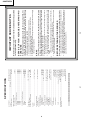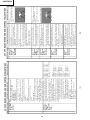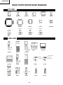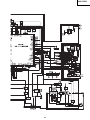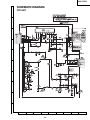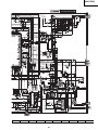
1
29H-FG5RU
SERVICE MANUAL
SY4C129HFG5RU
1-2
COLOUR TELEVISION
Chassis No.GB-4
MODEL
29H-FG5RU
In the interests of user-safety (Required by safety regulations in some countries) the set should be restored
to its original condition and only parts identical to those specified should be used.
FEATURES
Ë World Multi 28 System
Ë 100-CH Program Memory
Ë AV Mode (Standard / Dynamic /
Soft / Custom)
Ë CATV Hyper Band Ready
Ë 4 Line Digital Comb Filter
Ë Velocity Modulation
Ë Blue/Black Stretch Circuit
Ë Picture Noise Reduction
Ë White Temp. Select
Ë
Ë
Ë
Ë
Ë
Ë
Aperture Control
Gamma Correction
Multi (English / Russian)
On/Off/Reminder Timer
Comfy View
Rear AV-IN 1 & 2, S-Video In, AV Output
(Monitor Out), Headphone and Front AV-IN 3
Ë AFT
Ë Component Input Terminal
Ë Multi Language TELE TEXT
Ë
Ë
Ë
Ë
Ë
Ë
NICAM/A2
Child Lock
Dynamic Skin Tone
Graphic Equalizer
Clock
Sound Mode (Music / Movie /
News / Custom)
Ë Hotel Mode
Ë 16 : 9 Mode
CONTENTS
»
»
»
»
»
»
»
»
»
»
SPECIFICATIONS ........................................... 2
IMPORTANT SERVICE NOTES ...................... 2
ADJUSTMENT PRECAUTIONS ..................... 3
TROUBLE SHOOTING TABLE ..................... 18
SOLID STATE DEVICE BASE DIAGRAM ..... 22
WAVEFORMS ............................................... 23
CHASSIS LAYOUT ........................................ 25
BLOCK DIAGRAM ........................................ 26
DESCRIPTION OF SCHEMATIC DIAGRAM .. 28
SCHEMATIC DIAGRAM
■ CRT UNIT ................................................. 29
Page
■ MAIN UNIT ............................................... 30
■ FRONT UNIT ............................................ 32
» PRINTED WIRING BOARD ASSEMBLIES ... 34
» REPLACEMENT PARTS LIST
■ ELECTRICAL PARTS ............................... 40
■ MISCELLANEOUS PARTS ...................... 47
■ SUPPLIED ACCESSORIES ..................... 47
■ PACKING PARTS ..................................... 47
■ CABINET PARTS ..................................... 47
» PACKING OF THE SET ................................ 48
WARNING
The chassis in this receiver is partially hot. Use an isolation transformer between the line cord plug and power
receptacle, when servicing this chassis. To prevent electric shock, do not remove cover. No user – serviceable
parts inside. Refer servicing to qualified service personnel.
SHARP CORPORATION
1
1-1
Page
2
2-1
Specifications are subject to change without prior notice.
Aerial Input Impedance
VHF/UHF .......................................................................... 75 ohms Unbalanced
Receiving Channel
PAL-B/G, SECAM-B/G
VHF-Channels .............................................................................. E2 thru E12
UHF-Channels ............................................................................. E21thru E69
CATV ........................................................................ X thru Z +2, S1 thru S41
PAL-D/K, SECAM-D/K
VHF-Channels ........................................................ R1 thru R12, C1 thru C12
UHF-Channels ........................................................... 21thru 69, C21 thru C57
PAL-I, SECAM-I
VHF-Channels .................................................................. (IRELAND) B thru J
UHF-Channels ............................................................ (U.K. & H.K.) 21thru 69
NTSC-M
VHF-Channels ........................................................................... 2 thru 13 (US)
1 thru 12 (Japan)
UHF-Channels ......................................................................... 14 thru 69 (US)
13 thru 62 (Japan)
CATV .............................................................. A-6 thru A-1, A thru W+29 (US)
C13 thru C63 (Japan)
Receiving Frequency ................................................. 44.25 MHz thru 863.25 MHz
Dimensions ...................................................................................... Width: 722mm
Height: 582mm
Depth: 495mm
Weight(approx): 43.5 kg
Speaker
Size .................................................................................... 4.3 x 21.8 cm X 2pcs
Power Input ..................................................................... 220 ~ 240V AC 50/60 Hz
Power Consumption ...................................................................................... 135W
Audio Power Output Rating ....................................................... 10W X 2 (at Max.)
Intermediate Frequencies
Picture IF Carrier .................................................................................. 38.9MHz
Sound IF Carrier Frequency
6.5MHz .............................................................................................. 32.4MHz
6.0MHz .............................................................................................. 32.9MHz
5.5MHz .............................................................................................. 33.4MHz
4.5MHz .............................................................................................. 34.4MHz
Colour Sub-Carrier Frequency
PAL .................................................................................................. 34.47MHz
SECAM ................................................................................ 34.494/34.65MHz
NTSC ............................................................................................... 35.32MHz
Convergence ................................................................. Self Convergence System
Focus ......................................................... Bi-Potential, Uni-Potential Electrostatic
Sweep Deflection ...................................................................................... Magnetic
SPECIFICATIONS
Picture tube in this receiver employs integral implosion protection.
Replace with the same type number of picture tube for continued safety.
Do not lift picture tube by the neck.
Handle the picture tube only when wearing shatterproof goggles and after discharging
the high voltage completely.
2-2
1. Inspect all lead dress to make certain that leads are not pinched or that hardware is not
lodged between the chassis and other metal parts in the receiver.
2. Inspect all protective devices such as non-metal control knobs, insulating fishpapers,
cabinet backs, adjustment and compartment covers or shields, isolation resistor- capacity networks, mechanical insulators etc.
Before returning the receiver to the user, perform the following safety checks.
BEFORE RETURNING THE RECEIVER
1. When repairing the circuit, please make sure do not increase the high voltage of the set
to more than 34.0kV (at beam 0 µA).
2. To keep the set in a normal operation , please make sure it's function at 30.0kV ±1.5kV
(at beam 1,700 µA). The set has been factory - adjusted to the above-mentioned high
voltage.
∴ If there is a possibility that the high voltage fluctuates as a result of the repaires,
never forget to check for such high voltage after the work.
3. Do not substitute a picture tube with unauthorizerd types and/or brands which may
cause excessive X-ray radiation.
This receiver is designed so that any X-Ray radiation is kept to an absolute
minimum. Since certain malfunctions or servicing may produce potentially
hazardous radiation with prolonged exposure at close range, the followin
precautions should be observed:
X-RAY
1.
2.
3.
4.
When servicing the high voltage system, remove static charge from it by
connecting a 10K ohm resistor in series with an insulated wire (such as a
test probe) between picture tube dag and 2nd anode lead. (AC line cord
should be disconnected from AC outlet.)
SERVICE OF HIGH VOLTAGE SYSTEM AND PICTURE TUBE
Maintenance and repair of this receiver should be done by qualified
service personnel only.
IMPORTANT SERVICE NOTES
29H-FG5RU
3
3-1
Precaution: If haven't done this initialization, malfunction might be happen.
Note: Once the chassis has been assembly together and in ready condition, please make sure it's go
through initialize process (see sect 2-(1) above)
1 After enter into the SERVICE MODE, change data "INIT EEPROM" from 0 ---> 1
(which is under "CHECK MODE" section) and then switch off the main power, the
initial values are automatically preset (only when a new EEPROM is used).
2 The initial data are preset as listed in page 4 to 11.
3 Make sure whether the data need to modify or not (Initial data).
2. Factory Presetting.
1 Press and hold the local key "VOL DOWN" & "CH UP" when power on the main
switch,TV will enter into the SERVICE MODE.
2 Press the CH DOWN / UP key on the remote controller to get ready to select the
mode one by one.
3 Press the CH DOWN / UP key on the remote controller to select the modes
reversibly one by one.
4 Using the VOLUME UP/ DOWN key on the remote controller, the data can be modified.
5 Use the MENU Key on the remote controller to select the mode as shown in the
next page.
6 When press the local key "VOL DOWN" & "CH UP" at the same time, it will be
released from the service mode.
1. Setting the service mode by the microprocessor.
This model's setting are adjusted in two different ways: through the I2C bus control and
in the conventional analog manner. The adjustments via the I2C bus control include presetonly items and variable data.
ADJUSTMENT PRECAUTIONS
3-2
(1) In the Service Mode, Key is used to select the mode in the following order.
SERVICE MODE
29H-FG5RU
4-1
R/C CODE
TV-CH.
0
1
2
3
4
5
6
7
8
9
10
11
12
13
14
15
16
17
18
19
20
21
22
23
24
25
26
27
28
29
30
31
32
33
34
35
36
37
38
39
40
41
42
43
44
45
46
47
48
49
50
51
4
4-2
SREC/SRAC/SYI/STTM
MCL 1 (R/C CODE 117h)
CH-No.
Fv (MHz)
S-SYSTEM
SKIP OFF FREE
E-2
48.25
5.5
B/G
E-4/B-3
62.25
5.5
B/G
OIR-3
77.25
6.5
D/K
E-5
175.25
5.5
B/G
E-6/B-5
182.25
5.5
B/G
OIR-7
183.25
6.5
D/K
OIR-8
191.25
6.5
D/K
E-8/B-7
196.25
5.5
B/G
J-9
199.25
4.5
M
E-10/B-9
210.25
5.5
B/G
E-12/B-1
224.25
5.5
B/G
E-21
471.25
5.5
B/G
I-23
487.25
6.0
I
E-25
503.25
5.5
B/G
E-34
575.25
5.5
B/G
E-35
583.25
5.5
B/G
E-37
599.25
5.5
B/G
J-38
621.25
4.5
M
OIR-42
639.25
6.5
D/K
B-50
703.25
5.5
B/G
I-54
735.25
6.0
I
E-58
767.25
5.5
B/G
E-64
815.25
5.5
B/G
I-69
855.25
6.0
I
E-69
855.25
5.5
B/G
US-2
55.25
4.5
M
A-6
83.25
4.5
M
JA-6
183.25
4.5
M
JA-8
193.25
4.5
M
JA-12
217.25
4.5
M
US-14
471.25
4.5
M
JA-14
477.25
4.5
M
JA-50
693.25
4.5
M
US-83
885.25
4.5
M
S-2
112.25
5.5
B/G
S-10
168.25
5.5
B/G
SKIP OFF FREE
S-20
294.25
5.5
B/G
S-41
463.25
5.5
B/G
SKIP OFF FREE
B-43
647.25
5.5
B/G
B-45
663.25
5.5
B/G
B-47
679.25
5.5
B/G
E-5
174.95
5.5
B/G
E-5
175.55
5.5
B/G
SKIP OFF FREE
SKIP OFF FREE
SKIP OFF FREE
SKIP OFF FREE
SKIP OFF FREE
SKIP OFF FREE
SREC-SCA (SKD)
MCL 2 (R/C CODE 169h)
CH-No. Fv (MHz)
S-SYSTEM
590.25
5.5
B/G
AU-0
46.25
5.5
B/G
AU-2
64.25
5.5
B/G
AU-3
86.25
5.5
B/G
AU-4
95.25
5.5
B/G
AU-5A
138.25
5.5
B/G
AU-6
175.25
5.5
B/G
AU-7
182.25
5.5
B/G
AU-8
189.25
5.5
B/G
AU-9
196.25
5.5
B/G
AU-10
209.25
5.5
B/G
AU-11
216.25
5.5
B/G
SKIP OFF FREE
SKIP OFF FREE
SKIP OFF FREE
SKIP OFF FREE
SKIP OFF FREE
SKIP OFF FREE
SKIP OFF FREE
SKIP OFF FREE
SKIP OFF FREE
SKIP OFF FREE
SKIP OFF FREE
SKIP OFF FREE
SKIP OFF FREE
SKIP OFF FREE
SKIP OFF FREE
SKIP OFF FREE
WE-28
527.25
5.5
B/G
SKIP OFF FREE
SKIP OFF FREE
SKIP OFF FREE
SKIP OFF FREE
SKIP OFF FREE
SKIP OFF FREE
SKIP OFF FREE
SKIP OFF FREE
590.25
5.5
B/G
SKIP OFF FREE
SKIP OFF FREE
SKIP OFF FREE
E-2
48.25
5.5
B/G
WE-4
62.25
5.5
B/G
OI-3
77.25
6.5
D/K
E-5
175.25
5.5
B/G
OIR-7
183.25
6.5
D/K
OIR-8
191.25
6.5
D/K
E-10
210.25
5.5
B/G
E-12
224.25
5.5
B/G
I-23
487.25
6.0
I
WE-25
503.25
5.5
B/G
E-34
575.25
5.5
B/G
INITIAL SETTING
(1) Execute MCL 1/2 key to set the following data in EEPROM.
29H-FG5RU
SKIP OFF FREE
~
99
R/C CODE
TV-CH.
52
53
54
55
56
57
58
59
60
61
62
63
64
65
66
67
68
69
70
~
5-1
SREC-SCA (SKD)
MCL 2 (R/C CODE 169h)
CH-No. Fv (MHz)
S-SYSTEM
E-37
599.25
5.5
B/G
JPN-38
621.25
4.5
M
OI-42
639.25
6.5
D/K
I-54
735.25
6.0
I
E-58
767.25
5.5
B/G
WE-64
815.25
5.5
B/G
I-69
855.25
6.0
I
JA-1
91.25
4.5
M
JA-6
183.25
4.5
M
JA-8
193.25
4.5
M
JA-12
217.25
4.5
M
US-14
471.25
4.5
M
JA-50
693.25
4.5
M
S-2
112.25
5.5
B/G
S-10
168.25
5.5
B/G
S-20
294.25
5.5
B/G
S-41
463.25
5.5
B/G
E-5
174.95
5.5
B/G
E-5
175.55
5.5
B/G
SKIP OFF FREE
~
SREC/SRAC/SYI/STTM
MCL 1 (R/C CODE 117h)
CH-No.
Fv (MHz)
S-SYSTEM
SKIP OFF FREE
SKIP OFF FREE
SKIP OFF FREE
SKIP OFF FREE
SKIP OFF FREE
SKIP OFF FREE
SKIP OFF FREE
SKIP OFF FREE
SKIP OFF FREE
SKIP OFF FREE
SKIP OFF FREE
SKIP OFF FREE
SKIP OFF FREE
SKIP OFF FREE
SKIP OFF FREE
SKIP OFF FREE
SKIP OFF FREE
SKIP OFF FREE
SKIP OFF FREE
OSD LANGUAGE
Chinese
Chinese
English
Arabic
Russian
Malay
French
English
Thai
5
Refer to next page for setting of each destination.
5-2
Note : The CHILD LOCK PASSWORD and VIEW TIMER
PASSWORD are common use.
For model Set 8 processing only,
the respective EEPROM position is
updated again with MCL2 data (just like
MCL2 key has been pressed)
ITEMS
DEFAULT SETTINGS
EQUALIZER menu
MODE
MOVIE
INSET menu (for PIP model)
BRIGHTNESS
0
TINT
0
FEATURE menu
BLUE BACK
OFF
AUTO SELECT
ON
POWER SAVE *1
OFF
COMFY VIEW *2
OFF
SAFETY MODE *3
OFF
ROTATION
0
16:9 MODE
OFF
DEMO
OFF
CHILD LOCK menu
LOCK TV
OFF
LOCK STATUS
OFF
LOCK GAME *4
OFF
PASSWORD
0000
TIMER menu
CLOCK
_ _:_ _ AM
DAY
SUN
ON TIMER
_ _:_ _ AM
STATUS
ONCE
POSITION
__
VOLUME
__
OFF TIMER
_ _:_ _ AM
REMINDER
_ _:_ _
BEEP REMINDER
OFF
VIEW TIMER menu
VIEWING TIME
_ _:_ _
LOCK
OFF
PASSWORD
0000
CH SETTING menu
POSITION NAME
BLANK (For all position)
COLOUR
All Programs AUTO
SOUND
All Programs AUTO
SKIP
All Programs OFF
FM RADIO menu
SKIP
All Programs OFF
Refer to next page for *1 ~ *4.
SOUND SYSTEM
(AUTO)
(AUTO)
(AUTO)
(AUTO)
(AUTO)
(AUTO)
(AUTO)
*
(AUTO)
DEFAULT SETTINGS
GENERAL
Last power
ON
Last TV/AV mode
Program 1
Last position-TV
Program 1
Flashback Program-TV Program 1
Flashback Program-RADIO Program 1
Favorite Program A
Program 10
Favorite Program B
Program 20
Favorite Program C
Program 30
Favorite Program D
Program 40
1 / 2 digit entry
2 digit entry
Volume
0
GAME Volume
0
PIP
OFF
PIP location
Lower-Right
Last position-PIP
Program 1
AFT
All Programs ON
NICAM STEREO mode All Programs STEREO
NICAM BILINGUAL mode All Programs M1
NICAM MONO mode
All Programs MONO
A2 STEREO mode
All Programs STEREO
A2 BILINGUAL mode
All Programs MAIN
PICTURE menu
VIDEO MODE
DYNAMIC
CONTRAST
60
COLOUR
+6
BRIGHNESS
0
TINT
0
SHARPNESS
+6
PICTURE NR
OFF
WHITE TEMP
0 (CENTER)
SOUND menu
SURROUND
OFF
BBE
ON
BALANCE
0
AVL
ON
SUPER BASS/BASS+ ON
ITEMS
MODEL-SET KEY
1
2
3
4
5
6
7
8
9
Model-Set: The data in table below (1.1), Model set overview is updated to the respective EEPROM location
base on RC key input Model Set 1~9.
(1) The following default data has been factory-set for the E2PROM.
SHIPPING SETTING & CHECKING
29H-FG5RU
MAGNETIC FIELD (V.H) nT
20,000
40,000
-10,000
40,000
30,000
20,000
-50,000
20,000
45,000
20,000
BACKGROUND
17,000K
12,300K
18,000K
12.300K
7,500K
Table 2.1
DYNAMIC
60
+6
0
0
+6
OFF
0 (center)
STANDARD
60
+1
0
0
1
OFF
0 (center)
Table 2.2
6-1
(3) Refer to below note for *1 ~ *4.
(*1) : Only available for model with POWER SAVE function.
(*2) : Only available for model with COMFY VIEW function.
(*3) : Only available for model with SAFETY MODE function.
(*4) : Only available for model with GAME function.
MODE
CONTRAST
COLOR
BRIGHT
TINT
SHARPNESS
PEICTURE NR
WHITE TEMP
(2) Refer to below table (2-2) for NORMAL setting of each AV mode.
MODEL
HONG KONG
SINGAPORE
MIDDLE EAST
AUSTRALIA
RUSSIA
(1) Refer to below table (2-1) for setting of each destination.
S-SYS
AUTO
AUTO
AUTO
AUTO
AUTO
SOFT
50
-5
0
0
-4
OFF
0 (center)
LANGUAGE
CHINESE
ENGLISH
ARABIC
ENGLISH
RUSSIAN
FACTORY SET
SET 2
SET 3
SET 4
SET 8
SET 5
ITEM
1
2
3
4
5
6
7
8
9
10
11
12
13
14
15
16
17
18
19
20
21
22
23
24
25
26
27
28
29
30
31
32
33
34
35
36
37
38
39
40
41
42
43
44
45
46
47
48
49
50
51
52
53
54
55
56
57
58
59
60
61
62
63
64
SERVICE MODE
Option Mode
OPTION MODE MENU
6
OSD
DATA INITIAL DATA SETTING DATA
TUBE-TYPE
0/1
1
1
PIF
0..7
2
2
SND-M
0/1
0
1
SND-DK
0/1
1
1
SND-I
0/1
1
1
SND-BG
0/1
1
1
SECAM
0/1
1
1
NTSC358
0/1
0
1
NTSC443
0/1
1
1
GAME-IC
0/1
0
1
PIP
0/1
0
0
HEADPHONE
0/1
1
1
EQUALIZER
0/1
1
1
WOOFER
0/1
1
0
BBE
0/1
1
0
SRS
0/1
1
0
DOLBY
0/1
0
0
AUDIO-CFG
0..4
2
2
BILINGUAL
0/1
0
0
HOTEL
0/1
0
0
HTL-VOL
0..60
30
30
HTL-PRG
0..99
1
1
HTL-USE-LAST 0/1
1
1
OPC
0/1
0
1
ROTATION
0/1
0
0
CHILD
0/1
0
1
WSS
0/1
0
0
GLD-SCART
0/1
0
0
THAI
0/1
0
0
ARABIC
0/1
1
0
IRANIAN
0/1
0
0
MALAY
0/1
1
0
CHINESE
0/1
1
0
FRENCH
0/1
1
0
RUSSIAN
0..2
1
1
PW-LAST
0..2
1
1
BACK-GND
0/1
0
0
TUNER2
0/1
1
0
FM-RADIO
0/1
1
0
CURTAIN
0/1
1
1
CURT-COLOUR
0..7
7
7
AV1-IN
0/1
1
1
AV1S-IN
0/1
1
1
AV2-IN
0/1
1
1
DVD1-IN
0/1
1
1
AV3-IN
0/1
1
1
AV3S-IN
0/1
1
1
INCL-AV
0/1
1
1
TIM-REMINDER
0/1
1
1
TIM-VIEW
0/1
1
1
TIM-SWITCH
0/1
1
1
TIME-FORMAT
0/1
1
0
TIM-OFF
0/1
1
1
TIM-SKIP
0/1
1
0
TXT-EURO
0/1
1
1
TXT-WEST
0/1
1
1
TXT-ON
0/1
1
1
TXT-SPLIT
0/1
1
1
VIRGIN MODE
0/1
0
0
ERR-1-8-SUP
0/1
1
1
ERR-XRAY
0/1
1
1
ERR-SUPVOL
0/1
1
1
ERR-VERTG
0/1
1
1
LOGO
0/1
0
0
6-2
EEPROM ITEM
Picture Tube Used Type
PIF Frequency Setting
Sound M
Sound DK
Sound I
Sound BG
Colour System SECAM
Colour System NTSC358
Colour System NTSC443
Game IC
Picture In Picture
Headphone
Equalizer
Sub Woofer
BBE
SRS
DOLBY
Audio Configuration
Mono Bilingual
Hotel Mode
Hotel Volume
Hotel Program Number
HTL-USE-LAST
OPC
Rotation Functionality
Childlock
Wide Screen Signalling
Golden SCART
Thailand OSD Language
Arabic OSD Language
Iranian OSD Language
Malay OSD Language
Chinese OSD Language
French OSD Language
Russian OSD Language
Power On Last Status
Background
Tuner 2
FM Radio
Curtain Effect
Curtain Colour
AV1-IN
AV1S-IN
AV2-IN
Component Input
AV3-IN
AV3S-IN
INCL-AV
Reminder Timer
View Timer
Switch Timer
Time Format
Off Timer
Commercial Skip Timer
Teletext Pan-european
Teletext Western
Teletext On
Teletext Split
Virgin Mode
ERR-1-8-SUP
ERR-XRAY
ERR-SUPVOL
ERR-VERTG
LOGO
29H-FG5RU
ITEM EEPROM SETTING DATA RANGE
RF-AGC
0…63
A001
A002
RF AGC PIP
0…63
A003
V SLOPE
0…63
A004
VER-AMP-N50
0…63
A005
VER-SHI-N50
0…63
A006
HOR-SHI-N50
0…63
A007
EW-W-N50
0…63
A008
V-LIN
0…63
A009
S-COR
0…63
A010
V SCROLL
0…63
A011
VX-NORMAL
0…63
A012
H-PAR
0…63
A013
H-BOW
0…63
A014
E/W-PAR
0…63
A015
UPCOR-PAR
0…63
A016
LOCOR-PAR
0…63
A017
E/W-TRAP
0…63
A018
VER-AMP-N60
0…63
A019
VER-SHI-N60
0…63
A020
HOR-SHI-N60
0…63
A021
EW-W-N60
0…63
A022
VER-AMP-P50
0…63
A023
VER-SHI-P50
0…63
A024
HOR-SHI-P50
0…63
A025
EW-W-P50
0…63
A026 VX-43-COMPRESS
0…63
A027
VER-AMP-F50
0…63
A028
VER-SHI-F50
0…63
A029
HOR-SHI-F50
0…63
A030
EW-W-F50
0…63
A031
VER-AMP-S50
0…63
A032
VER-SHI-S50
0…63
A033
HOR-SHI-S50
0…63
A034
EW-W-S50
0…63
A035
SUB-SLOPE-S
0…63
A036
SUB-VX-S
0…63
A037
VER-AMP-C50
0…63
A038
VER-SHI-C50
0…63
A039
HOR-SHI-C50
0…63
A040
EW-W-C50
0…63
A041
SUB-SLOPE-C
0…63
A042
SUB-VX-C
0…63
A043
VER-AMP-P60
0…63
A044
VER-SHI-P60
0…63
A045
HOR-SHI-P60
0…63
A046
EW-W-P60
0…63
A047
VER-AMP-F60
0…63
A048
VER-SHI-F60
0…63
A049
HOR-SHI-F60
0…63
A050
EW-W-F60
0…63
A051
VER-AMP-S60
0…63
A052
VER-SHI-S60
0…63
A053
HOR-SHI-S60
0…63
A054
EW-W-S60
0…63
A055
VER-AMP-C60
0…63
A056
VER-SHI-C60
0…63
A057
HOR-SHI-C60
0…63
A058
EW-W-C60
0…63
A059
OF-ROTATE
0…127
Adjustment Mode Items
7
OSD
RF-AGC
RF AGC PIP
V SLOPE
VER-AMP-N50
VER-SHI-N50
HOR-SHI-N50
EW-W-N50
V-LIN
S-COR
V SCROLL
VX-NORMAL
H-PAR
H-BOW
E/W-PAR
UPCOR-PAR
LOCOR-PAR
E/W-TRAP
VER-AMP-N60
VER-SHI-N60
HOR-SHI-N60
EW-W-N60
VER-AMP-P50
VER-SHI-P50
HOR-SHI-P50
EW-W-P50
VX-43-COMPRESS
VER-AMP-F50
VER-SHI-F50
HOR-SHI-F50
EW-W-F50
VER-AMP-S50
VER-SHI-S50
HOR-SHI-S50
EW-W-S50
SUB-SLOPE-S
SUB-VX-S
VER-AMP-C50
VER-SHI-C50
HOR-SHI-C50
EW-W-C50
SUB-SLOPE-C
SUB-VX-C
VER-AMP-P60
VER-SHI-P60
HOR-SHI-P60
EW-W-P60
VER-AMP-F60
VER-SHI-F60
HOR-SHI-F60
EW-W-F60
VER-AMP-S60
VER-SHI-S60
HOR-SHI-S60
EW-W-S60
VER-AMP-C60
VER-SHI-C60
HOR-SHI-C60
EW-W-C60
OF-ROTATE
7-1
IC
UOC-TV
PIP-IF
UOC-TV
UOC-TV
UOC-TV
UOC-TV
UOC-TV
UOC-TV
UOC-TV
UOC-TV
UOC-TV
UOC-TV
UOC-TV
UOC-TV
UOC-TV
UOC-TV
UOC-TV
UOC-TV
UOC-TV
UOC-TV
UOC-TV
UOC-TV
UOC-TV
UOC-TV
UOC-TV
UOC-TV
UOC-TV
UOC-TV
UOC-TV
UOC-TV
UOC-TV
UOC-TV
UOC-TV
UOC-TV
UOC-TV
UOC-TV
UOC-TV
UOC-TV
UOC-TV
UOC-TV
UOC-TV
UOC-TV
UOC-TV
UOC-TV
UOC-TV
UOC-TV
UOC-TV
UOC-TV
UOC-TV
UOC-TV
UOC-TV
UOC-TV
UOC-TV
UOC-TV
UOC-TV
UOC-TV
UOC-TV
UOC-TV
UOC-TV
INITIAL DATA SETTING DATA
32
19
0
0
40
35
32
21
25
25
45
44
40
40
32
32
30
32
32
32
32
32
35
24
25
28
35
42
45
47
42
44
32
32
32
22
25
24
45
49
40
41
32
21
32
25
32
44
32
40
32
5
32
32
32
32
32
32
32
32
32
32
32
32
32
32
32
32
32
32
32
32
32
32
32
32
34
34
32
32
32
32
32
32
32
22
32
24
32
49
32
41
32
32
32
32
32
32
32
32
32
32
32
32
32
32
32
32
32
32
32
32
32
32
32
32
63
0
ITEM EEPROM SETTING DATA RANGE
A060
DRI-RS
0…63
A061
DRI-GS
0…63
A062
DRI-BS
0…63
A063
CUT-RS
0…63
A064
CUT-GS
0…63
A065
DRI-RC
0…63
A066
DRI-GC
0…63
A067
DRI-BC
0…63
A068
CUT-RC
0…63
A069
CUT-GC
0…63
A070
DRI-RW
0…63
A071
DRI-GW
0…63
A072
DRI-BW
0…63
A073
CUT-RW
0…63
A074
CUT-GW
0…63
A075
DRI-RS-DVD
0…63
A076
DRI-GS-DVD
0…63
A077
DRI-BS-DVD
0…63
A078
CUT-RS-DVD
0…63
A079
CUT-GS-DVD
0…63
A080
DRI-RC-DVD
0…63
A081
DRI-GC-DVD
0…63
A082
DRI-BC-DVD
0…63
A083
CUT-RC-DVD
0…63
A084
CUT-GC-DVD
0…63
A085
DRI-RW-DVD
0…63
A086
DRI-GW-DVD
0…63
A087
DRI-BW-DVD
0…63
A088
CUT-RW-DVD
0…63
A089
CUT-GW-DVD
0…63
A090
SUB-BRI
0…63
A091
SUB-BRI-DVD
0…63
A092
SUB-COL
0…63
A093
SUB-CON
0…63
A094
SUB-CON-DVD
0…63
A095
SUB-TINT-DVD
0…63
A096
SUB-TINT
0…63
A097
SUB-SHARP
0…63
A098
P-POSOFH-50
0…31
A099
P-POSOFV-50
0…7
A100
P-POSOFH-60
0…31
A101
P-POSOFV-60
0…7
A102
P-SUB-TINT
0…63
A103
P-CON-CTM
0…15
A104
P-CON-DYN
0…15
A105
P-CON-STD
0…15
A106
P-CON-SOFT
0…15
A107
P-SUB-BRI
0…15
A108
P-BKGD-R
0…15
A109
P-BKGD-G
0…15
A110
P-BKGD-B
0…15
A111
P-SUB-COL
0…15
A112
P-SUB-SHP
0…7
A113
VSD
0/1
A114
CUT OFF
0…63
A115
VG2
0/1
A116
DCXO
0…127
A117
DCXO-AUTO
0/1
7-2
IC
UOC-TV
UOC-TV
UOC-TV
UOC-TV
UOC-TV
UOC-TV
UOC-TV
UOC-TV
UOC-TV
UOC-TV
UOC-TV
UOC-TV
UOC-TV
UOC-TV
UOC-TV
UOC-TV
UOC-TV
UOC-TV
UOC-TV
UOC-TV
UOC-TV
UOC-TV
UOC-TV
UOC-TV
UOC-TV
UOC-TV
UOC-TV
UOC-TV
UOC-TV
UOC-TV
UOC-TV
UOC-TV
UOC-TV
UOC-TV
UOC-TV
UOC-TV
UOC-TV
UOC-TV
PIP
PIP
PIP
PIP
PIP
PIP
PIP
PIP
PIP
PIP
PIP
PIP
PIP
PIP
PIP
UOC-TV
UOC-TV
UOC-TV
UOC-TV
UOC-TV
OSD
DRI-RS
DRI-GS
DRI-BS
CUT-RS
CUT-GS
DRI-RC
DRI-GC
DRI-BC
CUT-RC
CUT-GC
DRI-RW
DRI-GW
DRI-BW
CUT-RW
CUT-GW
DRI-RS-DVD
DRI-GS-DVD
DRI-BS-DVD
CUT-RS-DVD
CUT-GS-DVD
DRI-RC-DVD
DRI-GC-DVD
DRI-BC-DVD
CUT-RC-DVD
CUT-GC-DVD
DRI-RW-DVD
DRI-GW-DVD
DRI-BW-DVD
CUT-RW-DVD
CUT-GW-DVD
SUB-BRI
SUB-BRI-DVD
SUB-COL
SUB-CON
SUB-CON-DVD
SUB-TINT-DVD
SUB-TINT
SUB-SHARP
P-POSOFH-50
P-POSOFV-50
P-POSOFH-60
P-POSOFV-60
P-SUB-TINT
P-CON-CTM
P-CON-DYN
P-CON-STD
P-CON-SOFT
P-SUB-BRI
P-BKGD-R
P-BKGD-G
P-BKGD-B
P-SUB-COL
P-SUB-SHP
VSD
CUT OFF
VG2
DCXO
DCXO-AUTO
INITIAL DATA SETTING DATA
32
32
32
32
32
32
32
32
32
32
32
32
32
32
32
32
32
32
32
32
32
32
32
32
32
32
32
32
32
32
32
32
32
32
32
32
32
32
32
32
32
32
32
32
32
32
32
32
32
32
32
32
32
32
32
32
32
32
32
32
32
39
32
38
32
34
32
48
32
49
32
34
32
34
32
12
0
16
0
3
0
16
0
3
0
32
0
4
0
4
0
4
0
4
0
4
0
4
0
4
0
4
0
7
0
3
0
0
6
6
0
1
79
69
0
0
29H-FG5RU
ITEM
S001
S002
S003
S004
S005
S006
S007
S008
S009
S010
S011
S012
S013
S014
S015
S016
S017
S018
S019
S020
S021
S022
S023
S024
S025
S026
S027
S028
S029
S030
S031
S032
S033
S034
S035
S036
S037
S038
S039
S040
S041
S042
S043
S044
S045
S046
S047
S048
S049
S050
S051
S052
S053
S054
S055
S056
S057
S058
S059
EEPROM SETTING DATA RANGE
V-LINCTRL
0…2
IFPLL
0…63
SOC1-0
0…3
WHITE LMT
0…15
GD
0/1
AGC0-1
0…3
FFI
0/1
CFA0
0/1
…
YD PAL
0 15
YD SECAM
0…15
YD N358
0…15
YD N443
0…15
YD AV-PAL
0…15
YD AV-SECAM
0…15
YD AV-N358
0…15
YD AV-N443
0…15
YD SAV-PAL
0…15
YD SAV-SECAM
0…15
YD SAV-N358
0…15
YD SAV-N443
0…15
YD COMP-PAL
0…15
YD COMP-SECAM
0…15
YD COMP-N358
0…15
YD COMP-N443
0…15
SBO1-0
0…3
CHSE1-0
0…3
FCO
0/1
OSO
0/1
DFL
0/1
EVG
0/1
HCO
0/1
SVMA
0/1
FBC
0/1
SLG1-0
0…3
CL3-0
0…15
GAM
0/1
TFR
0/1
CLD
0/1
BKS
0/1
BSD
0/1
AAS
0…3
DSK
0/1
BLS
0/1
LLB
0/1
DSA
0/1
RPA1-0
0…2
RPO1-0
0…3
COR1-0
0…3
CRA0
0/1
SPR2-0
0…6
SVM2-0
0…7
SMD1-0
0…3
PEAKFREQPAL443
0…3
PEAKFREQPALM
0…3
PEAKFREQPALN
0…3
PEAKFREQNTSC443
0…3
PEAKFREQNTSCM
0…3
PEAKFREQSECAM
0…3
PEAKFREQAV
0…3
Setting Mode 1-1
8
OSD
INITIAL DATA SETTING DATA
V-LINCTRL
0
0
IFPLL
32
32
SOC1-0
0
1
WHITE LMT
0
12
GD
1
1
AGC0-1
1
1
FFI
0
0
CFA0
0
0
YD PAL
7
11
YD SECAM
7
11
YD N358
7
9
YD N443
7
7
YD AV-PAL
7
7
YD AV-SECAM
7
7
YD AV-N358
7
7
YD AV-N443
7
7
YD SAV-PAL
7
7
YD SAV-SECAM
7
7
YD SAV-N358
7
7
YD SAV-N443
7
7
YD COMP-PAL
7
7
YD COMP-SECAM
7
7
YD COMP-N358
7
7
YD COMP-N443
7
7
SBO1-0
1
1
CHSE1-0
2
1
FCO
0
0
OSO
1
1
DFL
1
1
EVG
1
1
HCO
1
1
SVMA
1
1
FBC
0
0
SLG1-0
1
1
CL3-0
7
7
GAM
1
1
TFR
0
1
CLD
0
0
BKS
1
1
BSD
0
1
AAS
1
1
DSK
1
1
BLS
0
1
LLB
0
0
DSA
0
1
RPA1-0
0
2
RPO1-0
3
3
COR1-0
2
1
CRA0
0
0
SPR2-0
0
5
SVM2-0
5
3
SMD1-0
3
3
PEAKFREQPAL443
0
1
PEAKFREQPALM
0
0
PEAKFREQPALN
0
0
PEAKFREQNTSC443
0
1
PEAKFREQNTSCM
0
0
PEAKFREQSECAM
0
0
PEAKFREQAV
0
3
8-1
IC
UOC-TV
UOC-TV
UOC-TV
UOC-TV
UOC-TV
UOC-TV
UOC-TV
UOC-TV
UOC-TV
UOC-TV
UOC-TV
UOC-TV
UOC-TV
UOC-TV
UOC-TV
UOC-TV
UOC-TV
UOC-TV
UOC-TV
UOC-TV
UOC-TV
UOC-TV
UOC-TV
UOC-TV
UOC-TV
UOC-TV
UOC-TV
UOC-TV
UOC-TV
UOC-TV
UOC-TV
UOC-TV
UOC-TV
UOC-TV
UOC-TV
UOC-TV
UOC-TV
UOC-TV
UOC-TV
UOC-TV
UOC-TV
UOC-TV
UOC-TV
UOC-TV
UOC-TV
UOC-TV
UOC-TV
UOC-TV
UOC-TV
UOC-TV
UOC-TV
UOC-TV
UOC-TV
UOC-TV
UOC-TV
UOC-TV
UOC-TV
UOC-TV
UOC-TV
ITEM EEPROM SETTING DATA RANGE
S060
OF-COL-TV
0…31…62
S061
OF-COL-AV
0…31…62
S062
OF-COL-DVD
0…31…62
S063
OF-COL-P
0…31…62
S064
OF-COL-S
0…31…62
S065
OF-COL-N4
0…31…62
S066
OF-COL-N3
0…31…62
S067
OF-SHP-TV
0…31…62
S068
OF-SHP-AV
0…31…62
S069
OF-SHP-DVD
0…31…62
S070
OF-SHP-P
S071
OF-SHP-S
0…31…62
S072
OF-SHP-N4
0…31…62
S073
OF-SHP-N3
0…31…62
S074
OF-TINT-TV
0…31…62
S075
OF-TINT-AV
0…31…62
S076
OF-TINT-DVD
0…31…62
S077
OF-TINT-ADJ
0…31…62
S078
BB-TINT
0…63
S079
VMA-SOFT
0…3
S080
WS-SOFT
0…3
S081
VMA-STD
0…3
S082
WS-STD
0…3
S083
VMA-DYN
0…3
S084
WS-DYN
0…3
S085
VMA-CTM
0…3
S086
WS-CTM
0…3
S087
U-COL-SOFT
0…31…62
…
S088
U-COL-STD
0 31…62
S089
U-COL-DYN
0…31…62
S090
U-CON-SOFT
0…63
S091
U-CON-STD
0…63
S092
U-CON-DYN
0…63
S093
U-SHP-SOFT
0…31…62
S094
U-SHP-STD
0…31…62
S095
U-SHP-DYN
0…31…62
S096
VOL5-0
0…63
S097
HOP1-0
0…3
S098
TAS5-0-NORM
0…63
S099
TAS5-0-A
0…63
S100
BRI3-0
0…31
S101
HSD6-0
0…127
S102
VSD6-0
0…127
S103
HOPB1-0
0…3
S104
TASB5-0
0…63
S105
PGB5-0
0…127
S106
VOLB5-0
0…63
S107
SMTHB
0/1
S108
SMTH
0/1
S109
RANGE1-0
0…3
S110
RANGEB1-0
0…3
S111
PWR-SAVING
0/1
S112
PWR-TIME
0…3
S113
I-TIME
0…3
S114
GAME-HON
0…255
S115
GAME-VERT-1
0…255
S116
GAME-VERT-2
0…255
S117
GAME-ORIV
0…255
S118
GAME-MODE
0…255
Setting Mode 1-2
8-2
IC
UOC-TV
UOC-TV
UOC-TV
UOC-TV
UOC-TV
UOC-TV
UOC-TV
UOC-TV
UOC-TV
UOC-TV
UOC-TV
UOC-TV
UOC-TV
UOC-TV
UOC-TV
UOC-TV
UOC-TV
UOC-TV
UOC-TV
UOC-TV
UOC-TV
UOC-TV
UOC-TV
UOC-TV
UOC-TV
UOC-TV
UOC-TV
UOC-TV
UOC-TV
UOC-TV
UOC-TV
UOC-TV
UOC-TV
UOC-TV
UOC-TV
UOC-TV
UOC-TV
UOC-TV
UOC-TV
UOC-TV
UOC-TV
UOC-TV
UOC-TV
UOC-TV
UOC-TV
UOC-TV
UOC-TV
UOC-TV
UOC-TV
UOC-TV
UOC-TV
UOC-TV
UOC-TV
UOC-TV
GAME IC
GAME IC
GAME IC
GAME IC
GAME IC
OSD
OF-COL-TV
OF-COL-AV
OF-COL-DVD
OF-COL-P
OF-COL-S
OF-COL-N4
OF-COL-N3
OF-SHP-TV
OF-SHP-AV
OF-SHP-DVD
OF-SHP-P
OF-SHP-S
OF-SHP-N4
OF-SHP-N3
OF-TINT-TV
OF-TINT-AV
OF-TINT-DVD
OF-TINT-ADJ
BB-TINT
VMA-SOFT
WS-SOFT
VMA-STD
WS-STD
VMA-DYN
WS-DYN
VMA-CTM
WS-CTM
U-COL-SOFT
U-COL-STD
U-COL-DYN
U-CON-SOFT
U-CON-STD
U-CON-DYN
U-SHP-SOFT
U-SHP-STD
U-SHP-DYN
VOL5-0
HOP1-0
TAS5-0-NORM
TAS5-0-A
BRI3-0
HSD6-0
VSD6-0
HOPB1-0
TASB5-0
PGB5-0
VOLB5-0
SMTHB
SMTH
RANGE1-0
RANGEB1-0
PWR-SAVING
PWR-TIME
I-TIME
GAME-HON
GAME-VERT-1
GAME-VERT-2
GAME-ORIV
GAME-MODE
INITIAL DATA SETTING DATA
31
45
31
46
31
45
31
40
31
31
31
31
31
46
36
23
36
49
31
35
31
35
31
31
31
31
31
40
31
31
31
34
31
32
31
31
32
32
0
0
0
1
1
1
1
1
3
2
3
1
2
2
2
1
26
25
31
31
36
36
50
50
60
60
60
60
26
26
31
31
36
36
32
35
2
0
10
10
23
23
16
25
63
3
63
63
1
1
2
2
73
73
32
32
0
0
0
0
1
0
1
1
1
1
0
3
0
0
6
10
23
27
0
0
192
192
1
1
29H-FG5RU
ITEM EEPROM SETTING DATA RANGE
S119
PHI FORCE
0/1
S120
PHI
0…3
S121
BPD
0/1
S122
E2D
0/1
S123
ACL
0/1
S124
MUS
0/1
S125
CB
0/1
S126
SVM-OSD-PW
0…3
S127
SMD-OSD-TM
0…7
S128
XDT
0/1
S129
HBL
0/1
S130
WBF
0…15
S131
WBR
0…15
S132
FSL
0/1
S133
HP2
0/1
S134
CUR_VPOS
0..63
S135
OSVE
0/1
S136
GAIN-RED
0..127
S137
GAIN GREEN
0..127
S138
GAIN BLUE
0..127
Setting Mode 1-3
9-1
IC
UOC-TV
UOC-TV
UOC-TV
UOC-TV
UOC-TV
UOC-TV
UOC-TV
UOC-TV
UOC-TV
UOC-TV
UOC-TV
UOC-TV
UOC-TV
UOC-TV
UOC-TV
UOC-TV
UOC-TV
UOC-TV
UOC-TV
UOC-TV
OSD
PHI FORCE
PHI
BPD
E2D
ACL
MUS
CB
SVM-OSD-PW
SMD-OSD-TM
XDT
HBL
WBF
WBR
FSL
HP2
CUR_VPOS
OSVE
GAIN-RED
GAIN GREEN
GAIN BLUE
INITIAL DATA SETTING DATA
1
1
3
3
0
0
0
0
1
1
0
1
1
0
3
3
2
2
0
1
1
1
10
6
8
13
0
0
0
0
20
20
0
1
20
20
20
20
20
20
ITEM EEPROM SETTING DATA RANGE
S201
P-POSHOR
0…255
S202
P-POSVER-50
0…255
S203
P-POSVER-60
0…255
S204
P-HFP
0…15
S205
P-VFP
0…15
S206
P-VSPDEL-50
0…31
S207
P-VSPDEL-60
0…31
S208
P-VERBLK
0/1
S209
P-SELDEL
0…15
S210
P-CLPDEL
0…31
S211
P-AGCMD
0…3
S212
P-AGCVAL
0…15
S213
P-CLMPID
0…3
S214
P-BLKVCHYS
0/1
S215
P-BLKCVAL
0/1
S216
P-LMOFST
0…3
S217
P-PLLITC-TV
0…3
S218
P-PLLITC-AV
0…3
S219
P-BLKVCFIL
0/1
S220
P-YCD-TV-P
0…15
…
S221
P-YCD-TV-N3
0 15
S222
P-YCD-TV-N4
0…15
S223
P-YCD-TV-S
0…15
S224
P-YCD-AV-P
0…15
S225
P-YCD-AV-N3
0…15
S226
P-YCD-AV-N4
0…15
S227
P-YCD-AV-S
0…15
S228
P-LOCKSP
0/1
S229
P-CKILL
0…3
S230
P-BGPOS
0/1
S231
P-DEEMP
0…3
S232
P-COLON
0/1
S233
P-CHRBW
0…3
S234
P-IFCOMP
0…3
S235
P-SATNR
0/1
S236
P-SCADJ-P
0…31
S237
P-SCADJ-N3
0…31
S238
P-SCADJ-N4
0…31
S239
P-SCADJ-S
0…31
S240
P-PKLR
0…255
S241
P-PKLG
0…255
S242
P-PKLB
0…255
S243
P-YCOR
0/1
S244
P-PALIDL2
0/1
S245
P-PALIDL1
0…3
S246
P-PALIDL0
0/1
S247
P-PKBOOST
0/1
S248
P-CLPLEN
0…3
S249
P-SCMREL
0…3
S250
P-SCMIDL
0…7
S251
P-SECDIV
0/1
S252
P-BELLIIR
0/1
S253
P-PALINC1
0/1
S254
P-PALINC2
0/1
S255
P-LOCKSP
0…3
S256
P-SECACCL
0…7
S257
P-SECACC
0/1
S258
P-ADLCK
0/1
S259
P-ADLCKSEL
0/1
Setting Mode 2-1
9
9-2
IC
PIP
PIP
PIP
PIP
PIP
PIP
PIP
PIP
PIP
PIP
PIP
PIP
PIP
PIP
PIP
PIP
PIP
PIP
PIP
PIP
PIP
PIP
PIP
PIP
PIP
PIP
PIP
PIP
PIP
PIP
PIP
PIP
PIP
PIP
PIP
PIP
PIP
PIP
PIP
PIP
PIP
PIP
PIP
PIP
PIP
PIP
PIP
PIP
PIP
PIP
PIP
PIP
PIP
PIP
PIP
PIP
PIP
PIP
PIP
OSD
P-POSHOR
P-POSVER-50
P-POSVER-60
P-HFP
P-VFP
P-VSPDEL-50
P-VSPDEL-60
P-VERBLK
P-SELDEL
P-CLPDEL
P-AGCMD
P-AGCVAL
P-CLMPID
P-BLKVCHYS
P-BLKCVAL
P-LMOFST
P-PLLITC-TV
P-PLLITC-AV
P-BLKVCFIL
P-YCD-TV-P
P-YCD-TV-N3
P-YCD-TV-N4
P-YCD-TV-S
P-YCD-AV-P
P-YCD-AV-N3
P-YCD-AV-N4
P-YCD-AV-S
P-LOCKSP
P-CKILL
P-BGPOS
P-DEEMP
P-COLON
P-CHRBW
P-IFCOMP
P-SATNR
P-SCADJ-P
P-SCADJ-N3
P-SCADJ-N4
P-SCADJ-S
P-PKLR
P-PKLG
P-PKLB
P-YCOR
P-PALIDL2
P-PALIDL1
P-PALIDL0
P-PKBOOST
P-CLPLEN
P-SCMREL
P-SCMIDL
P-SECDIV
P-BELLIIR
P-PALINC1
P-PALINC2
P-LOCKSP
P-SECACCL
P-SECACC
P-ADLCK
P-ADLCKSEL
INITIAL DATA SETTING DATA
44
44
30
30
26
26
0
0
0
0
13
13
13
13
0
0
8
8
6
6
3
3
8
8
3
3
0
0
0
0
0
0
2
2
1
1
0
0
8
8
8
8
8
8
8
8
8
8
8
8
8
8
8
8
0
0
0
0
1
1
0
0
0
0
0
0
2
2
1
1
7
7
7
7
7
7
7
7
80
80
80
80
80
80
1
1
0
0
1
1
0
0
1
1
0
0
2
2
5
5
1
1
1
1
0
0
0
0
3
3
5
5
1
1
1
1
1
1
29H-FG5RU
ITEM EEPROM SETTING DATA RANGE
S260
P-ADLCKCC
0/1
S261
P-CLRANGE
0…3
S262
P-NADJ
0…7
S263
P-NSRED
0…7
S264
P-SLLTHD
0…3
S265
P-ISHFT
0…3
S266
P-ENLIM
0/1
S267
P-DTECT5060
0/1
S268
P-VTHRL50
0…127
S269
P-BCOROFF
0/1
S270
P-VTHRL60
0…127
S271
P-VTHRH50
0…15
S272
P-VTHRH60
0…15
S273
P-CLMSTGY
0/1
S274
P-SLLTHDV
0…7
S275
P-VFLYWHLM
0…3
S276
P-VFLYWHL
0/1
S277
P-CLMPCHRY
0…3
S278
P-VDETIFS
0/1
S279
P-VDETITC
0/1
S280
P-VLP
0…3
S281
P-LATENCY
0…3
S282
P-FILTBRST
0/1
S283
P-CLMPIST
0…31
S284
P-UVSEQ
0/1
S285
P-ABRTHD
0…15
S286
P-ABRSPD
0…7
S287
P-CZMEN
0/1
S288
P-CZMSP
0…3
S289
P-U-COL-DYN
-30…0…+30
S290
P-U-COL-STD
-30…0…+30
S291
P-U-COL-SOFT
-30…0…+30
S292
P-U-SHP-DYN
-30…0…+30
S293
P-U-SHP-STD
-30…0…+30
S294
P-U-SHP-SOFT
-30…0…+30
Setting Mode 2-2
IC
PIP
PIP
PIP
PIP
PIP
PIP
PIP
PIP
PIP
PIP
PIP
PIP
PIP
PIP
PIP
PIP
PIP
PIP
PIP
PIP
PIP
PIP
PIP
PIP
PIP
PIP
PIP
PIP
PIP
PIP
PIP
PIP
PIP
PIP
PIP
10-1
OSD
P-ADLCKCC
P-CLRANGE
P-NADJ
P-NSRED
P-SLLTHD
P-ISHFT
P-ENLIM
P-DTECT5060
P-VTHRL50
P-BCOROFF
P-VTHRL60
P-VTHRH50
P-VTHRH60
P-CLMSTGY
P-SLLTHDV
P-VFLYWHLM
P-VFLYWHL
P-CLMPCHRY
P-VDETIFS
P-VDETITC
P-VLP
P-LATENCY
P-FILTBRST
P-CLMPIST
P-UVSEQ
P-ABRTHD
P-ABRSPD
P-CZMEN
P-CZMSP
P-U-COL-DYN
P-U-COL-STD
P-U-COL-SOFT
P-U-SHP-DYN
P-U-SHP-STD
P-U-SHP-SOFT
INITIAL DATA SETTING DATA
1
1
1
1
3
3
6
6
0
0
3
3
1
1
1
1
41
41
0
0
60
60
8
8
13
13
0
0
0
0
1
1
1
1
0
0
1
1
0
0
1
1
3
3
1
1
26
26
0
0
0
0
0
0
0
0
0
0
0
0
0
0
0
0
0
0
0
0
0
0
S301
S302
S303
S304
S305
S306
S307
S308
S309
S310
S311
S312
S313
S314
S315
S316
S317
S318
S319
S320
S321
S322
S323
S324
S325
S326
S327
S328
S329
S330
S331
S332
S333
S334
S335
S336
S337
S338
S339
S340
S341
S342
S343
S344
S345
S346
S347
S348
S349
S350
S351
S352
S353
S354
S355
S356
S357
S358
FMI
BPB
BPB2
FILTBW-M
ID-BYBPF
ID-PGAIN
MPX-P-BW
FMSUB-BW
EIAJ-DEL
NDETPB
NICDEEM
NLOERLIM
NUPERLIM
FILTBW
OVMTHR
DECLEV
MONOLEV
NICLEV
SAPLEV
ADCLEV
IISLEV
BBEC-ON
BBEP-ON
BBEC-OFF
BBEP-OFF
MAINLOUD
MAINLONA
MAINLOCH
INSOEF
AVLMOD
AVLWGT
AVLLE
SRS3DCEN
SRS3DSP
SRS3DBYP
CLIPMANAGE
VDSMIXLEV
DBEADR
DBECOEF-LBS
DBECOEF-MBS
DUBADR
DUBCOEF-LSB
DUBCOEF-MSB
BAMAMO
BAMASUB
BAMAFC
BASS-MV
TREB-MV
EQ100-MV
EQ300-MV
EQ1K-MV
EQ3K-MV
EQ8K-MV
BASS-MS
TREB-MS
EQ100-MS
EQ300-MS
EQ1K-MS
0/1
0/1
0/1
0…3
0/1
0/1
0/1
0/1
0…3
0/1
0/1
0…255
0…255
0…3
0…3
0...31
0...31
0...31
0...31
0...31
0...31
0...15
0...15
0...15
0...15
0/1
0...7
0...3
0...7
0...7
0/1
0…15
0...15
0...15
0/1
0…4
0…5
0…63
0…255
0…15
0…255
0…255
0…15
0…3
0/1
0…15
0...31
0...31
0...31
0...31
0...31
0...31
0...31
0...31
0...31
0...31
0...31
0...31
ITEM EEPROM SETTING DATA RANGE
Setting Mode 3-1
DSP
DSP
DSP
DSP
DSP
DSP
DSP
DSP
DSP
DSP
DSP
DSP
DSP
DSP
DSP
DSP
DSP
DSP
DSP
DSP
DSP
DSP
DSP
DSP
DSP
DSP
DSP
DSP
DSP
DSP
DSP
DSP
DSP
DSP
DSP
DSP
DSP
DSP
DSP
DSP
DSP
DSP
DSP
DSP
DSP
DSP
DSP
DSP
DSP
DSP
DSP
DSP
DSP
DSP
DSP
DSP
DSP
DSP
IC
10
10-2
FMI
BPB
BPB2
FILTBW-M
ID-BYBPF
ID-PGAIN
MPX-P-BW
FMSUB-BW
EIAJ-DEL
NDETPB
NICDEEM
NLOERLIM
NUPERLIM
FILTBW
OVMTHR
DECLEV
MONOLEV
NICLEV
SAPLEV
ADCLEV
IISLEV
BBEC-ON
BBEC-OFF
BBEP-ON
BBEP-OFF
MAINLOUD
MAINLONA
MAINLOCH
INSOEF
AVLMOD
AVLWGT
AVLLE
SRS3DCEN
SRS3DSP
SRS3DBYP
CLIPMANAGE
VDSMIXLEV
DBEADR
DBECOEF-LBS
DBECOEF-MBS
DUBADR
DUBCOEF-LBS
DUBCOEF-MBS
BAMAMO
BAMASUB
BAMAFC
BASS-MV
TREB-MV
EQ100-MV
EQ300-MV
EQ1K-MV
EQ3K-MV
EQ8K-MV
BASS-MS
TREB-MS
EQ100-MS
EQ300-MS
EQ1K-MS
OSD
INITIAL
DATA
0
0
1
0
0
0
0
0
0
0
0
100
200
0
1
16
16
16
16
16
16
0
0
0
0
0
3
0
3
0
1
7
1
0
0
0
3
0
0
0
0
0
0
0
0
0
16
16
12
12
12
12
12
16
16
12
12
12
0
0
1
0
0
0
0
0
0
0
0
100
200
0
1
7
5
18
6
13
0
15
8
5
7
0
0
0
4
5
1
10
7
0
0
4
5
0
0
0
0
0
0
1
0
12
31
25
20
16
19
16
20
31
25
20
17
13
SETTING DATA
29H-FG5RU
S359
S360
S361
S362
S363
S364
S365
S366
S367
S368
S369
S370
S371
S372
S373
EQ3K-MS
EQ8K-MS
BASS-NW
TREB-NW
EQ100-NW
EQ300-NW
EQ1K-NW
EQ3K-NW
EQ8K-NW
BASS-CT
TREB-CT
IDMOD-SE
BPR-VOL
DEMUT-DLAY
AV-OUT LV
0...31
0...31
0...31
0...31
0...31
0...31
0...31
0...31
0...31
0...31
0...31
0…3
0…60
0…16
0…255
ITEM EEPROM SETTING DATA RANGE
Setting Mode 3-2
DSP
DSP
DSP
DSP
DSP
DSP
DSP
DSP
DSP
DSP
DSP
DSP
DSP
DSP
DSP
IC
11-1
EQ3K-MS
EQ8K-MS
BASS-NW
TREB-NW
EQ100-NW
EQ300-NW
EQ1K-NW
EQ3K-NW
EQ8K-NW
BASS-CT
TREB-CT
IDMOD-SE
BPR-VOL
DEMUT-DLAY
AV-OUT LV
OSD
INITIAL
DATA
12
12
16
16
12
12
12
12
12
16
16
0
20
8
16
17
20
31
25
13
16
19
16
13
31
25
0
30
8
18
SETTING DATA
1
RF-AGC
TAKE OVER
POINT ADJUSTMENT
(I2C BUS
CONTROL)
No. Adjustment point
11-2
3. Select "RF-AGC" item in the Adjustment Mode.
Adjust the "RF-AGC" bus data to obtain the Tuner
output pin drop 0.1V ~ 1.0V below maximum voltage.
4. Change the antenna input signal to 63 ~ 67dB_V,
and make sure there is no noise.
5. Set the RF AGC to 0 - 6 V with no saturation with
the waveform.
6. Turn up the input signal to 90 ~ 95 dB_B to be sure
that there is no cross modulation beat.
Fig. 3
1. Receive "PAL COLOR BAR" signal.
Signal Strength: 54 ± 1dB_V (75 ohm termination)
2. Connect the oscilloscope to TP53 (Tuner's AGC
Terminal) as shown in figure 3-1.
Adjustment condition/procedure
PIF ADJUSTMENT
Waveform or remarks
29H-FG5RU
11
1
PURITY ADJ.
No. Adjustment point
12
Monocolour
screen release
Monocolour
BLUE
screen
Monocolour
RED
screen
12-1
* Adjustment for uniformity is change to another
content. Please refer to the following page.
Monocolour
GREEN
screen
* Every push of the monocolour key changes the
screen as follows.
Note: Apply the adjustment after aging with
the beam current 1700 ± 50µA or more
for 30 minutes or more.
Note: Select the service mode, and press the
monocolor key of R/C for process, and
the monocolor screen (green) will be
selected.
1. Select the green monocolor screen with remote
contoller, and set the beam current of 1.7mA
with the contrast control.
2. Degauss the CRT enough with the degausing coil.
NOTE: Follow the job instruction manual to adjust the magnetic field.
3. The purity magnet must be previously set at the
0 magnetic field, and the convergence must be
adjusted to be rough.
With P-MAG, adjust it to the center - rank A.
4. Observe the points a,b, as shown in Fig.1-1
through the microscope.
Move DY fore and aft to set the landing at the
point (Rank A).
5. If the a/b balance is poor, compensate it to the
center "Rank AB".
6. Aline it to zero, keeping the raster rotation in the
east direction.
6. Tighten the deflection coil fastening screws.
» Tightening torque : 108N ± 20N (11Kgf ± 2Kgf)
8. Checking the CRT corner area, bond the magnetic sheet to set the landing at rank A for compensation.
Adjustment conditions/procedure
PURITY ADJUSTMENT
B
A
Fig.1-1
A=B
90mm
b
A=B
*Even with TEXT key or "R/G/B"
key, it can be directly switched to
each monocolor screen.
* Continuosly press the monocolour key 1 second or more,
and the monocolour mode will
be selected without the service
mode.
Fig. 1-3
Rank "A"
(on the left of the CRT)
B
A
Fig. 1-2
Rank "A"
(on the right of the CRT)
90mm
a
Waveform or remarks
2
Uniformity
adjustment (To
perform after
the purity and
convergence
adjustment.)
No. Adjustment point
12-2
* During the pasting of compensation magnet , use
the crosshatch pattern .
Make sure there is no blur or bendlines occur.
If the blur or bend are serious,adjust the location
of compensation magnet to make it better.
(The same method is applied for adjustment of
monocolor screen blue for blue uniformity ,and
changing both the magnetic field for north and south
direction.)
(South direction Red uniformity)
1. Horizontal mf = Set to monocolor screen red and
adjust to -0.25G.
2. Pay attention to the edge of CRT ,if the landing is
poor adjust by attaching the compensation magnet at the back of CRT.
(North direction Red uniformity)
1. Horizontal mf = Set to monocolor screen red and
adjust to +0.25G.
2. Pay attention to the edge of CRT,if the landing is
poor adjust by attaching the the compensation
magnet at the back of CRT.
(refer to Fig-1)
Before adjustment begin,Horizontal magnetic field
= 0G
Vertical magnetic field = Each destination's adjustment magnetic field.
Make sure to degauss it.
Adjustment conditions/procedure
PURITY ADJUSTMENT
(CRT back)
Fig. 1
Compensation magnet
Miss landing
(CRT surface)
Waveform or remarks
29H-FG5RU
1
CONVERGENC
ADJ.
( To be done
after the purity
adjustment.)
No. Adjustment point
13
VR2
VR1
13-1
Balance Coil
B
B
Purity Magnet
R
R
4-Pole Magnet
Lacquer
B
B
B
25mm ± 0.5mm
CRT NECK
Fig. 4
Adjust by Swing DY
Fig. 3
Adjust by Balance Coil
Fig. 2
Adjust by VR2
R
Fig. 1
Adjust by VR1
R
Y axis
X axis
Waveform or remarks
6-Pole Magnet.
Note:
In case of poor convergence adjustment on the
top and bottom and of the screen , adjust DY by
swing rightward and leftward.
(Refer to Fig-4)
( Dynamic convergence )
1. Fix the wedges in a position so that the deflection
york neck is at the center of top bottom and left
right. ( Straight line and without any blur horizontal / vertical line).
2. Adjust the Red, Blue, upper and lower of the centre y axis on the screen by using the Volume (VR2,
VR1)at the deflection york.
(Refer to fig.1 and fig.2)
3. If the Horizontal Red, Blue(XV) on the screen
centre X axisis shifted, correct the Red, Blue (XV)
by adjusting the balance coil on the deflection
york. (Refer to Fig. 3)
4. After confirm that there is no problems on the
entire screen ,bond each wedge on CRT and
glass tape on it. Fastening the screws of DY and
magnet unit (purity , 4 - pole and 6 pole ), then
coat the lacquer paint on DY fastening screw and
magnet unit fastening screw.
( Static convergence )
1. Overlap blue and red with the open-/closing angle and rotation of the 4 pole magnet.
2. Overlap green on blue and red with the open-/
closing angle and rotation of the 6 pole magnet.
1. Receive the " Crosshatch Pattern" signal.
2. Using the remote controller, call NORMAL mode.
Adjustment conditions/procedure
CONVERGENCE ADJUSTMENT
1
FOCUS
ADJUSTMENT
No. Adjustment point
13-2
1. Receive E-5CH (Monoscop pattern).
2. With the remote controller, make the image normal.
3. Adjust the focus VR to make the character"575"
on left bottom of monoscope as fine as possible.
Adjustment conditions/procedure
FOCUS ADJUSTMENT
Waveform or remarks
29H-FG5RU
2
1
WHITE BALANCE BACKGROUND
I2C BUS
ADJUSTMENT
(AV-IN
SIGNAL)
CRT CUTOFF
ADJUSTMENT
(I2C BUS
CONTROL)
No. Adjustment point
14
14-1
1. Receive the internal RF monoscope pattern.
2. Make the picture normal with the remote controller.
3. Connect the beam ammeter between terminal of
R623.
4. Coarsely confirm the beam current to approx. 1.7mA.
5. Receive the window pattern with AV input.
6. With the data of DRI-GS and DRI-BS, adjust the
color temperature of the 50% white.
7. Adjust the right dark area of the window to 12300K
with CUT-RS and CUT-GS.
8. Go back to 50% white area to check colour temperature, if out of range, please go back to step (6).
Note 1: Apply this adjustment after aging 30 min or
more with the beam current 1700 ± 50_A.
(On the white or green monocolor screen)
2:The colour temperature is based on the shipment destination as shown in Table 2.1 at
page 6-1.
3: Adjust DRI-GC/GW, DRI-BC/BW , CUT-RW/C
and CUT-GW/C as following DATA, after finishing DRI-BS and DRI-GS DATA adjustment.
CUT-RW/C = CUT-RS
CUT-GW/C = CUT-GS
DRI-RW = 32 (FIXED), DRI-RS = 32 (FIXED)
DRI-BC = "DRI-BS"
(For 7500_K, 12300_K, 17000_K and
18000_K Condition)
Note :
1. Before CRT cutoff adjustment, make sure following items are in INITIAL DATA.
a) A063 CUT-RS = 32
b) A064 CUT-GS = 32
c) A114 CUT OFF = 6
1. Switch TV to video mode , blue back off , with no
video signal and Press R/C to set picture into
normal condition.
2. Go to service mode at adjustment mode item A115
(VG2).
3. Adjust screen voltage until retrace line appear,
the following OSD will appear at bottom of screen.
UNSTABLE
OUT
ABOVE
4. Finally , slowly decrease the screen variable resistor until following OSD appear.
STABLE
IN
ABOVE / BELOW *
* The last OSD row is the indication of the screen
voltage value. If it show "BELOW", please increase the screen voltage and vice versa until
"STABLE" AND "IN" OSD appear.
Note :No matter the indication of last row's OSD is
indicate "ABOVE" or "BELOW", the important
thing is OSD change to "STABLE" and "IN".
Adjustment conditions/procedure
* 12300_K
DRI-GW = "DRI-GS" - 7
DRI-BW = "DRI-BS" - 7
DRI-GC = "DRI-GS" - 7
DRI-RC = 25
* 17000_K & 18000_K
DRI-GW = "DRI-GS" - 7
DRI-BW = "DRI-BS" - 7
DRI-GC = "DRI-GS" - 5
DRI-RC = 27
* 7500_K
DRI-GW = "DRI-GS" - 5
DRI-BW = "DRI-BS" - 5
DRI-GC = "DRI-GS" - 7
DRI-RC = 25
7500K X : 0.300 Y : 0.310
18000K X : 0.255 Y : 0.255
17000K X : 0.261 Y : 0.261
12300K X : 0.272 Y : 0.275
( With Monolta color thermometer
CA-100)
Waveform or remarks
CUT-OFF, BACKGROUND AND SUB-CONTRAST ADJUSTMENT
WHITE BALANCE BACKGROUND
I2C BUS
ADJUSTMENT
(DVD SIGNAL)
SUB-BRIGHTNESS
ADJUSMENT
(I2C BUS
CONTROL)
(AV-IN SIGNAL)
SUB-BRIGHTNESS
ADJUSMENT
(I2C BUS
CONTROL)
(DVD SIGNAL)
SUB-CONTRAST
I2C BUS
ADJUSMENT
(AV-IN SIGNAL)
SUB-CONTRAST
I2C BUS
ADJUSMENT
(DVD SIGNAL)
3
4
5
6
7
No. Adjustment point
14-2
1. Select the DVD mode.
2. Receive the signal of the DVD signal generator.
( Component signal) (Window Pattern)
3. Select the SUB-CONTRAST adjustment mode
(DVD) with the remote controller, and adjust 50%
white to 130 ± 10cd.
Note : Make sure the TV set already in the RF receiving state before changing to AV mode to continue with this adjustment.
(no POWER OFF from the previous adjustment.)
1. Receive the window pattern with AV input.
2. Make the image normal with the remote controller.
3. Select the SUB-CONTRAST adjustment mode
with the remote controller, and adjust 50% white
to 130 ± 10cd.
Note : Make sure the TV set already in the RF receiving state before changing to AV mode to continue with this adjustment.
(no POWER OFF from the previous adjustment.)
1. Select DVD mode.
2. Receive the signal of the DVD signal generator .
( Component signal) ( Window Pattern)
3. Make the image normal with the remote controller.
4. Select the SUB-BRIGHT adjustment mode (DVD)
, and adjust the right dark white area of the window pattern to 3.0 cd ± 0.5cd of the window pattern.
1. Receive the window pattern with AV input.
2. Make the image normal with the remote controller.
3. Select the sub- bright adjustment mode with the
remote controller, and adjust the right dark white
area of the window pattern to 3.0 cd ± 0.5cd.
1. The window pattern is received with DVD signal (
component signal).
2. Apply the adjustment in the same manners as 2
(AV-IN SIGNAL) and subsequence above.
(DRI-GS-DVD, DRI-BS-DVD, CUT-RS-DVD,
CUT-GS-DVD)
3. Select the SUB-CONTRAST adjustment mode
with the remote controller, and adjust 50% white
to 165 ± 10cd.
Apply the adjustment after the end of 2 (AV-IN SIGNAL).
Note: 1. All of the DRI-GW/C-DVD & DRI-BW/CDVD can be obtain by using same calculation as
white balance adjustment above (No.2). CUT-RW/
C-DVD and CUT-GW/C-DVD setting data are as
follow.
CUT-RW/C-DVD = CUT-RS-DVD
CUT-GW/C-DVD = CUT-GS-DVD
Adjustment conditions/procedure
Dark white
50% white
Dark white
generator SX-1006 for adjustment.
Note 1:
Use "Y" of Minolta color analyzer
CA-100 in adjustment.
Note 2:
Use the window pattern of the signal.
50% white
Note 1:
Use the window pattern of the signal generator SX-1006 for adjustment.
Waveform or remarks
CUT-OFF, BACKGROUND AND SUB-CONTRAST ADJUSTMENT
29H-FG5RU
1
15
Align the center of the screen to the geometric center
of CRT.
(monoscope)
(monoscope)
Adjust the overscan to 8.5%.
Adjust the linearity to the best.
Already preset.(Adjust this unless the linearity is
achieved.)
(monoscope)
Already preset..
Already preset .
Adjust the 2nd vertical line from the end of the
crosshatch pattern. Refer to Fig 1.6. (crosshatch)
Adjust the 2nd vertical line from the end of the
crosshatch pattern. Refer to Fig 1.7. (crosshatch)
Adjust the 2nd vertical line from the right end of the
crosshatch pattern so that the middle 4 blocks are
straight. Refer to Fig 1-2.
(crosshatch)
Adjust the 2nd upper vertical line from the right end
of the crosshatch pattern so that the upper line are
straight. Refer to Fig 1-3.
(crosshatch)
Adjust the 2nd lower vertical line from the right end
of the crosshatch pattern so that the bottom line are
straight. Refer to Fig 1-4.
(crosshatch)
Adjust the 2nd vertical line from the right end of the
crosshatch pattern so that the D1 (center area of the
second vertical line - edge of screen) and D2 (top
area of the second vertical line - edge of screen) are
same. Refer to Fig 1-5.
(crosshatch)
Adjust the overscan to 10%.
Align the center of the screen to the geometric center
of CRT.
(monoscope)
VER-SHI-N50
HOR-SHI-N50
EW-W-N50
V-LINE
V-S CORR
V-SCROLL
VX-NORMAL
H-PAR
H-BOW
E/W-PAR
UPCOR-PAR
LOCOR-PAR
EW-TRAP
VER-AMP-N60
VER-SHI-N60
15-1
Align the center of the screen to the geometric center
of CRT. (monoscope)
(monoscope)
Adjust the overscan to 8.5%.
VER-AMP-N50
(monoscope)
(monoscope)
Adjust V-Slope by Volume Up / Down Remote Control.
Refer to Fig. 1.1.
(monoscope)
V-SLOPE
A : Out of spec
B : OK
C : Out of spec
A
B
C
Fig. 1-7
H-BOW
Fig. 1-6
H-PAR
Fig. 1-5
Fig. 1-4
Fig. 1-3
Fig. 1-2
Waveform or remarks
D1
D2
SUB COLOUR
(I2C BUS
CONTROL)
1
SUB-TINT
( I2C BUS
CONTROL)
No. Adjustment point
1
No. Adjustment point
EW-W-N60
Waveform or remarks
75% W
G
100% W
15-2
W Y
Cy
G
Mg
R
Same Level
3. Select the "SUB-TINT" item in the ADJUSTMENT
MODE.. Adjust the "SUB-TINT" data to obtain the
waveform shown as Figure 1.1 (W and Mg same
level)
Waveform or remarks
Adjustment conditions/procedure
Mg
1.Receive the "NTSC 3.58 Colour Bar" signal
through AV IN.
2. Connect the oscilloscope to TP47B (P860 Pin6)
BLUE-OUT.
» Range : 100mV/Div. (AC)(Use Probe 10:1)
» Sweep time : 10 µsec/Div.
Fig. 1-1
Y
Cy
Waveform or remarks
NTSC CHROMA ADJUSTMENT
1. Receive the "PAL Color Bar" signal.
2. Make the image normal with the remote controller.
3. Connect the oscilloscope to TP48R (IC851 #9).
( Use Probe 10:1)
Range :
2 V/Div
Sweep Time : 20 µsec/Div
4. Set the sub color adjustment mode with the remote controller, and vary the sub color data to
make 100% W of the color bar and RED at the
same level for adjustment shown in Fig. 1-1.
Adjustment conditions/procedure
PAL CHROMA ADJUSTMENT
VER-AMP-P50 = VER-AMP-N50
VER-SHI-P50 = VER-SHI-N50
HOR-SHI-P50 = HOR-SHI-N50
EW-W-P50 = EW-W-N50
VER-AMP-P60 = VER-AMP-N60
VER-SHI-P60 = VER-SHI-N60
HOR-SHI-P60 = HOR-SHI-N60
EW-W-P60 = EW-W-N60
NOTE :
There are no separate adjustment for 16:9 mode
and Normal mode adjustment.
The 16:9 (Panorama mode 50/60Hz) data need to
follow the adjusted data for Normal mode (50/
60Hz). Please set the data as below.
Align the center of the screen to the geometric center
of CRT.
(monoscope)
VHOR-SHI-N60 Align the center of the screen to the geometric center
of CRT.
(monoscope)
Adjustment conditions/procedure
B
R
B
No. Adjustment point
Adjustment conditions/procedure
No. Adjustment point
MAIN SCREEN
ADJUSTMENT
HORIZONTAL AND VERTICAL DEFLECTION LOOP ADJUSTMENT
HORIZONTAL AND VERTICAL DEFLECTION LOOP ADJUSTMENT
29H-FG5RU
( For models
with GAME
only.)
16
1
( For models
with RADIO
only.)
No. Adjustment point
1
No. Adjustment point
Waveform or remarks
16-1
1. Use the signal generator to set carier frequncy of
89.5 MHz with sound modulation 400Hz.
2. Connect the signal to the FM radio tuner using
the RF coaxial cable with female adaptor.
3. Press the "FM RADIO" button of R/C to access
the FM RADIO menu.
4. Select the "FREQUENCY" in menu and press the
VOL+ key to search the frequency of 89.5 MHz.
5. Confirm the 400 Hz audio is clearly detected.
6. Press the "FM RADIO" button of R/C to exit.
Adjustment conditions/procedure
Waveform or remarks
FM RADIO OPERATION CHECK
3. If adjustment OK, then press the "GAME MODE"
key to exit to previously viewed channel from the
game mode.
Note : (A) For the HORIZONTAL position, enter
service mode and choose "Setting Mode
1". Key in the alphabic number 114 to
enter GAME-HON. Adjust to the proper
horizontal position.
(B) For the VERTICAL position, remain in
same "Setting Mode 1". Key in the
alphabic number 115 to enter GAMEVERT-1. Adjust to the proper vertical
position.
1. Use the "GAME" key (R/C) to enter the Game
Mode.
2. Press the TREBLE UP (code=46H) key (direct
key to enter "The Rock" game), and then confirm
the position and the function of the game.
Adjustment conditions/procedure
GAME OPERATION CHECK
7
WHITE TEMP
16-2
1. Receive "Monoscope Pattern" signal.
2. Set FUNCTION to select WHITE TEMP.
3. Press Volume Up/Down key to check WHITE
TEMP Option, STANDARD:
NORMAL SETTING, WARM for more REDDISH
direction changing, COOL for more BLUISH direction changing.
1. Once in PICTURE Mode, and the NORMAL key
is pressed, all the settings will be present to normal setting.
(Normal setting value for every mode, refer to
Table 2.2 on page 6-1).
NORMAL Key
6
1. Receive "Monoscope Pattern" signal.
2. Press to MENU mode, then Select Picture Mode
and set to select SHARPNESS.
3. Press Volume Up/Down key to check whether
the SHARPNESS effect is OK or not.
SHARPNESS
Key
1. Receive the "NTSC Colour Bar" signal thru AV in.
2. Press to MENU mode, then Select Picture Mode
and set to selectTINT.
3. Press Volume Up/Down key to check TINT, UP
for GREEN direction and DOWN for RED direction whether is OK or not.
1. Receive "Monoscope Pattern" signal.
2. Press to MENU mode, then Select Picture Mode
and set to select BRIGHTNESS.
3. Press Volume Up/Down key to check whether
the BRIGHTNESS effect is OK or not.
5
BRIGHTNESS
key
3
1. Receive "Color Bar" signal.
2. Press to MENU mode, then Select Picture Mode
and set to select COLOUR.
3. Press Volume Up/Down key to check whether
the COLOUR effect is OK or not.
TINT key
COLOUR key
2
Adjustment conditions/procedure
1. Receive "Monoscope Pattern" signal.
2. Press to MENU mode, then Select Picture Mode
and set to select CONTRAST.
3. Press Volume Up/Down key to check whether the
CONTRAST effect is OK or not.
4
CONTRAST
key
1
No. Adjustment point
Notes:If nothing is display
mean contrast, colour, bright,
tint, sharpness are all in normal setting.
Waveform or remarks
FUNCTION OPERATION CHECKING (VIDEO AND AUDIO)
29H-FG5RU
17
1. Receive PAL COLOUR BAR with SOUND 400Hz,
100% MODULATION (±50kHz Dev).
2. Maximum volume, and check the headphone
output with 400Hz sound and no sound out from
speaker.
SOUND
SYSTEM
HEADPHONE
OUTPUT
CHECKING
NOISE MUTE
CHECKING
10
11
12
17-1
1. Receive "PAL COLOUR BAR" signal.
2. Turn up the volume control to maximum, make
sure the sound is heard from the speakers. Then
put the unit in no signal state.
3. Check the sound mute is effective.
4. Finally turn sound level of CTV to minimum.
Ref : OUTPUT level of HEADPHONE is as
following.
Apx. 500mVp-p
1. Receive “PAL-D/K” signal, press the “SOUND
SYSTEM” to select B/G, I. Check the sound output is not working properly. Select D/K and check
the sound output to make sure it is working properly.
2. Receive “PAL-I” signal, press the “SOUND SYSTEM” to select B/G, D/K. Check the sound output
is not working properly. Select I and check the
sound output to make sure it is working properly.
3. Receive “PAL-B/G” signal, press the “SOUND
SYSTEM” to select I, D/K. Check the sound output is not working properly. Select B/G and check
the sound output to make sure it is working properly.
COLOUR
SYSTEM
1. Receive the "PAL COLOUR BAR" signal, press
the COLOUR SYSTEM key to select modes except PAL, check the COLOUR is not working properly. Then, select the "PAL" mode. Check again
its colour so that it is working properly.
2. Receive "SECAM COLOUR BAR" signal, press
COLOUR SYSTEM key to select modes except
SECAM, check the COLOUR is not working properly. Then, select the "SECAM" mode. Check
again its colour so that it is working properly.
3. Receive “NTSC 4.43” signal, press COLOUR
SYSTEM key to select modes except NTSC4.43,
check the COLOUR is not working properly. Then,
select the “NTSC 4.43” mode. Check again its
colour so that it is working properly.
4. Receive “NTSC 4.43/3.58 COLOUR BAR” signal
thru AV, press COLOUR SYSTEM key to select
modes except N4.43/3.58, check the COLOUR
is not working properly. Then, select the “NTSC
4.43/3.58” mode. Check again its colour so that it
is working properly.
Adjusting procedure/conditions
9
No. Adjusting point
(Continued)
Waveform and others
FUNCTION OPERATION CHECKING (VIDEO AND AUDIO)
H, V PROTECTOR
2
1
Waveform or remarks
Ref : Apx.13.3V.
#1
Music
OFF
OFF
0
OFF
OFF
-
#2
Music
OFF
0
OFF
ON
3. Connect the voltmeter to the speaker terminal and
make sure the reading is 9 ± 1 Vrms.
Setting item
Equalizer
Surround
BBE
Balance
AVL
Super Bass
Bass +
Music
OFF
OFF
0
OFF
ON
17-2
4. Connect the voltmeter to the dummy load and
make sure the reading is 15 ± 1 Vrms.
Equalizer
Surround
BBE
Balance
AVL
Super Bass
#2 : Sound setting for model without BBE and with Bass + in the
sound menu.
Waveform or remarks
#1 : Sound setting for model with
BBE and Super Bass in the
sound menu.
Adjustment conditions/procedure
1. Receive the E-10ch (PAL colour bar).
2. Set the volume to maximum and set the other
sound setting as follow.
SOUND OUTPUT CHECKING
1. Receive E-5ch(Monoscopepattern).
2. Connect the bias box to the cathode side (R607)
of D604.
3. Set the voltage of the bias box at 10V, and verify
that the protector does not operate.
4. Set the voltage of the bias box at 18V, and verify
that the protector operate.
Rear woofer
1. Receive the E-10ch (PAL colour bar).
ouput check2. Connect the woofer wire from P303 to a 16 ohm
ing (For model
dummy load.
with woofer
3. Set the volume to maximum and set the other
box only)
sound setting as follow.
Front speaker
output checking
No. Adjustment point
1
Adjustment conditions/procedure
PROTECTOR OPERATION CHECKING
No. Adjustment point
29H-FG5RU
Check protector
circuit and pin 106
& 107 (waveform
no.3 & 4) of IC
2100. Also check
the waveform no.7
of IC501 at pin 4
and its related
parts.
Yes
No
Check the power
circuit consisting of
IC701, IC702,
T701 and its
related parts. Also
check the
horizontal out
circuit Q604 and its
related parts.
Does horizontal circuit
momentary oscillate?
RED
Power on by R/C.
RED
LED COLOUR ?
NO RASTER
GREEN
GREEN
18-1
Check R,G,B
input and output
of IC 851.
Normal
Check the 14V,
120V and 210V
line from the
main PWB side.
Abnormal
Check CRT connector (KY), (H) bias
(14V,120 V, 210 V line).
TROUBLE SHOOTING TABLE
No
18
Check the power
circuit at the front
unit consisting of
IC4700, IC4702,
IC4701, D4707
and its related
parts.
No
18-2
Check 3V output
from pin 22 of IC
2001 and its
related parts.
Yes
Replace the Fuse.
Blown out
Check the power circuit
consisting of IC701, IC702,
T701 and its related parts.
Yes
Is the Fuse again blown out?
Does STBY+5V appear at pin 1 P1001
main unit ?
Normal
Check F4701.
F3700.
NO LED LIGHT
TROUBLE SHOOTING TABLE (Continued)
29H-FG5RU
Check sound
output signal from
pin 92 & 93 of IC
2100 and its
related circuit.
No sound comes
out at AV-out J905
19-1
Check output
signal at pin
68, 69 of IC
2100 and its
related circuit.
No
Check if there
is sound input
signal at pin 2
& 21 of IC 301.
No
Check
connection to
the speaker
Yes
Set volume to maximum. Is
there any sound output signal
at pin 10 & 14 of IC 301 ?
No sound from the
speaker
NO NORMAL SOUND
TROUBLE SHOOTING TABLE (Continued)
No
Check TU51.
Yes
19-2
Does 31V appear at pin 9 of TU 51 ? No
Yes
Does 5V appear at pin 7 of TU 51 ?
Snow noise increase.
Yes
Check +120V line at IC 753
and its related circuit.
Check the PC+5V line.
Does the snow noise appear
on the screen at maximum
contrast and brightness ?
NO PICTURE
No
A
TROUBLE SHOOTING TABLE (Continued)
29H-FG5RU
19
20
Check circuit between
AV-in terminal and pin
71, 74 & 78 of IC 2100.
No
Check pin 71, 74 & 78
Yes
of IC 2100. Does signal
or noise appear ?
No
Does AV input at AV1, Yes
AV 2 & AV 3 normal ?
Noise or signal
appear.
Normal
20-1
Check IC 2100 and its
related circuit.
Abnormal
No
Check the related
circuit of screen
heater (FBT) and
the CRT.
No
Does signal output at pin 7, 8
& 9 of IC 851 normal ?
Check IC 850 at
input pin 1, 2 & 3
and its related
circuit.
Yes
Check TU 51 (Tuner), SF
202 and its related circuit.
Check IC 2100 RGB out at
pin 42, 43 & 44. Is the output
normal ?
No
Check IC 2100 and its
related circuits.
Check pin 104 & 105 of IC2100.
No snow noise.
A
TROUBLE SHOOTING TABLE (Continued)
Set the
appropriate
colour system.
Set colour
control.
No
NO COLOUR
Check IC 851,
IC 2100 and its
related circuit.
20-2
Using a PAL colour bar signal,
check the RGB in & out line
between IC 2100 and IC 851.
Does the waveforms normal ?
No
Yes Go to CHANNEL SETTING at the
user MENU and change to the
appropriate colour system. Does
the colour appear ?
No
No
Yes Adjust the colour control at the
user MENU. Does colour appear ?
Check tuner TU 51,
SF201and its
related circuit.
Yes
Is only RF signal’s colour abnormal?
NO SPECIFIC COLOUR
B
COLOUR PRODUCED
TROUBLE SHOOTING TABLE (Continued)
29H-FG5RU
21-1
Yes
The picture
colour is
magenta.
Check pin 8
of IC 851
(G-out).
Check pin 9
of IC 851
(R-out).
Yes
Check pin 7
of IC 851
(B-out).
The picture
colour is
yellow.
Is the white balance properly
adjusted ?
The picture
colour is
cyan.
Check IC 2100 & IC 851 and its
related circuit including the RGB
input & output line.
No
Is some colours produced in the
B/W broadcast reception ?
B
No
Readjust the
white balance.
TROUBLE SHOOTING TABLE (Continued)
21-2
29H-FG5RU
21
29H-FG5RU
SOLID STATE DEVICE BASE DIAGRAM
TOP VIEW
8
4
1
8
5
20
5
2
3
5
1
7SET04F
128
1
4
BR24L32V
97
33
1
1
4
2
3
4
FXA003W
23
44
12
1
64
RH-IXxxxxWJ
4 5 6
1
8
4
5
IMZ1A
IMX1C
5
1
4
2883E331
8
5
8
5
1
4
1
4
11
IXA956WJ
C7W66U
IP0254
COLLECTOR
COLLECTOR
COLLECTOR
ZR
BR
JC
BASE EMITTER
BASE EMITTER
3 2 1
STV9380
8
24
34
65
33
10
1
PCF8563S
96
32
11
BASE EMITTER
B709AR
D601AR
BR24L04F
2SC2735
SIDE VIEW
D5SB 60 74
OUT
GND
VCC
1
1
BA005T
OUT
GND
VCC
7
RX6757
DX0477
23
TDA8922B
ST600C
ANODE (GREEN)
1
CATHODE
CATHODE
ANODE (RED)
OUT
GND
VCC
9
1
TDA6107A
ANODE
SC5511
5
A00BC0W
PX0036
PX0037
D6246
ANODE
CATHODE
E CB
SD2646
SK2161
DX0410
SC3198
22
E CB
PC1815
29H-FG5RU
WAVEFORMS
1 Horizontal Rate
Pin 1 Vp-p = 2.02 V
2 Horizontal Rate
Pin 2 Vp-p = 1.30 V
3 Vertical Rate
Pin 3 Vp-p = 2.26 V
4 Vertical Rate
Pin 4 Vp-p = 2.40 V
5 Vertical Rate
Pin 5 Vp-p = 4.16 V
6 Vertical Rate
Pin 6 Vp-p = 29.40 V
7 Vertical Rate
Pin 7 Vp-p = 60.00 V
8 Vertical Rate
Pin 8 Vp-p = 1.60 V
9 Horizontal Rate
Pin 9 Vp-p = 262.0 V
0 Horizontal Rate
Pin 10 Vp-p = 262.0 V
q Horizontal Rate
Pin 11 Vp-p = 176.0 V
w Horizontal Rate
Pin 12 Vp-p = 11.20 V
e Horizontal Rate
Pin 13 Vp-p = 1.024 kV
r Horizontal Rate
Pin 14 Vp-p = 248.0 V
t Horizontal Rate
Pin 15 Vp-p = 31.20 V
y Horizontal Rate
Pin 16 Vp-p = 1.84 V
u Horizontal Rate
Pin 17 Vp-p = 2.04 V
i Horizontal Rate
Pin 18 Vp-p = 2.10 V
o Horizontal Rate
Pin 19 Vp-p = 120.0 V
p Horizontal Rate
Pin 20 Vp-p = 106.0 V
a Horizontal Rate
Pin 21 Vp-p = 134.0 V
23
29H-FG5RU
-MEMO-
24
29H-FG5RU
CHASSIS LAYOUT
25
29H-FG5RU
BLOCK DIAGRAMS
26
29H-FG5RU
27
29H-FG5RU
DESCRIPTION OF SCHEMATIC DIAGRAM
SAFETY NOTES:
NOTES:
1. DISCONNECT THE AC PLUG FROM THE AC OUTLET BEFORE
REPLACING PARTS.
2. SEMICONDUCTOR HEAT SINKS SHOULD BE REGARDED AS
POTENTIAL SHOCK HAZARDS WHEN THE CHASSIS IS OPERATING.
1. The unit of resistance “ohm” is omitted.
(K = 1000 ohms, M = Meg ohm).
2. All resistors are 1/16 watt, unless otherwise noted.
3. All capacitors are µF, unless otherwise noted. (P = µµF).
VOLTAGE MEASUREMENT CONDITIONS:
IMPORTANT SAFETY NOTICE:
PARTS MARKED WITH “å” (
) ARE IMPORTANT FOR
MAINTAINING THE SAFETY OF THE SET. BE SURE TO REPLACE THESE PARTS WITH SPECIFIED ONES FOR MAINTAINING THE SAFETY AND PERFORMANCE OF THE SET.
1. Voltage in parenthesis measured with no Signal.
2. Voltages without parenthesis measured with PAL ColourSignal.
3. All the voltages in each point are measured high impedance
volt-meter.
SERVICE PRECAUTION:
WAVEFORM MEASUREMENT CONDITIONS:
THE AREA ENCLOSED BY THIS LINE (
) IS DIRECTLY
CONNECTED WITH AC MAINS VOLTAGE.
WHEN SERVICING THE AREA, CONNECT AN ISOLATING TRANSFORMER BETWEEN TV RECEIVER AND AC LINE TO ELIMINATE
HAZARD OF ELECTRIC SHOCK.
1. RF colour bar signal of 2.0V peak to peak applied at RF Tuner
TU51.
2. Approximately 4.0 V AGC bias (without signal).
28
29H-FG5RU
SCHEMATIC DIAGRAM
CRT UNIT
J
I
H
G
F
E
D
C
B
A
1
2
3
4
5
29
6
7
8
9
10
29H-FG5RU
MAIN UNIT
J
I
H
G
F
E
D
C
B
A
1
2
3
4
5
6
30
7
8
9
10
29H-FG5RU
10
11
12
13
14
31
15
16
17
18
19
29H-FG5RU
FRONT UNIT
J
I
H
G
F
E
D
C
B
A
1
2
3
4
5
6
32
7
8
9
10
29H-FG5RU
10
11
12
13
14
33
15
16
17
18
19
29H-FG5RU
PRINTED WIRING BOARD ASSEMBLIES
PWB-A: MAIN UNIT (COMPONENT SIDE)
J
I
H
G
F
E
D
C
B
A
1
2
3
4
5
6
34
7
8
9
10
29H-FG5RU
10
11
12
13
14
35
15
16
17
18
19
29H-FG5RU
PWB-A: MAIN UNIT (CHIP PARTS SIDE)
J
F DC4
Z4
I
H
R6 0 8
C5
C6 1 3
G
R6 5 2
R6 3 4
C6 2 8
R6 3 3
R6 3 5
RJ 6 0 1
RJ
C670015
C6 2 9
R6 2 7
R9 3 2
R9 3 1
R9 6 8
R6 3 0
R6 4 0
R6 3 8
F
Q6 0 5
R9 7 3
R9 7 4
R9 7 6
R9 6 9
Q6 0 7
R9 3 0
RJ 9 6 1
R9 7 5
C9 2 4
RJ 9 0 8
C9 2 6
R9 3 4
R9 0 2
R9 0 1
R9 2 1
R9 2 0
C9 1 0
C9 0 9
RLJ 990242
RJ 9 6 0
RJ
L 990231
RJ 2 0
R9 1 7
R9 1 8
E
RJ 1 1
R9 1 4
R9 1 3
RJ 3 2
R9 5 7
R9 6 0
R9 1 5
C9 1 2
RJ
L 990289
C9 1 1
R9 1 9
C9 6 8
R9 5 3
RJ 3 0
RJ 3 1
Q9 0 3
RJ 9 5 4
C9 6 2
R9 4 5
C9 6 1
R9 1 1
R9 1 0
C2 0 0 3
C2 0 0 2
C9 5 9
C2 0 0 6
C9 5 8
C9 0 5
R9 4 2
C9 5 6
R9 0 5
L 990263
RJ
C2 0 4 1
C2 0 0 7
C9 5 3
C2 2 3
RJ 2 8
RJ
L 990254
D
R9 0 6
R9 7 8
C9 2 2
C2 0 0 5
C2 0 4 8
R9 3 5
RJ 9 0 9
R2 0 0 4
RJ 1 5
RJ 1 3
RJ 2 7
Q9 0 4
R9 0 7
C9 5 7
C9 0 4
R9 1 6
C9 0 8
R9 5 0
Q9 0 7
C2 0 0 1
C9 6 0
R9 5 9
R9 4 8
R2 2 4
RJ 2 5
C9 4 3
R9 3 3
C9 6 7
Q9 0 6
R9 5 2
RJ
L 990278
C9 5 5
C2 1 0
C9 5 2
C9 5 4
C2 0 0 8
R9 7 9
R2 2 8
C2 0 1 2
C2 0 1 0
R9 3 6
C9 2 3
C2 0 1 5
R2 0 0 7
C2 0 1 7
C2 2 4
C2 0 2
RJ 3 3
R2 0 3
RJ 2 2
R9 4 9
R2 0 0 8
Q2 0 4
L2 0 0 4
C2 0 2 0
C2 2 2
C3 3 9
R2 0 0 9
D2 1 0 6
C2 1 1
C2 0 2 2
C2 0 2 6
R3 4 7
RJ 1 4
C3 9 9
RJ
C393256
R2 0 9
C2 0 3
R3 4 8
R6 3 7
C2 2 0
RJ 2 0 0
R992051
RJ
R2 3 0
R2 2 9
R2 0 1 0
D2 1 0 8
C3 9 7
C2 0 4
Z5
I C2 1 0 0
Z7
D2 1 0 7
RJ 9 6 4
RJ 9 6 5
R9 0 3
C6 4 4
C2 0 1
RJ 1 7
RJ 1 2
C3 9 8
RJ 9 6 6
R3 4 6
C2 2 1
C9 2 1
R9 2 6
R2 2 2
RJ 2 4
C2 0 2 8
R2 2 1
RJ 2 3
C2 2 6
R2 0 2 7
C2 0 3 0
C2 1 0 4
R6 0 0
C2 0 4 2
C
C9 6 5
R2 3 4
R2 3 3
Q2 0 5
D2 0 1
RJ 3 9
C2 1 9
R2 3 2
R2 1 6
R2 1 2
R2 0 2 3
RJ 9 3 8
C2 0 4 3
Q2 0 2
C2 2 5
R2 3 1
R2 0 2 2
R5 6
R2 1 8
C2 0 4 4
R2 0 1 6
R2 0 1 5
R2 1 4
C2 1 6
D2 0 0
C2 1 0 3
R2 0 1 7
R2 0 6
C2 0 1 8
C2 0 3 1
C2 0 3 6
C2 1 3
C2 1 4
R2 9
RJ
01
46
4
RJ 2 1
R2 0 8
R2 2 7
R5 2 1
R2 0 7
C2 0 4 5
C2 0 1 4
C5 2 3
R2 0 1
R2 0 5
RJ 4 0
R2 0 2 0
C2 0 1 3
C5 3 3
R2 0 4
C2 1 2
Q2 0 0
C5 4
RJ 5 0 1
C2 1 5
R5 5
R5 4
R5 7
C5 2
C5 2 1
C5 2 0
R2 0 2
RJ 5 1
C2 0 2 3
Q2 0 3
R2 0 1 4
R5 3
RJ 9 1 8
RJ 4 1
C2 0 2 5
R2 0 3 2
C2 0 2 9
RJ 3 5
R2 1 9
C2 0 3 7
R5 1
R2 1 0 8
C2 0 5 2
R2 0 5 2
C2 0 3 5
L2 0 1 1
L2 0 0 7
C2 1 8
B
C2 0 4 9
R2 0 1 2
L2 0 1 3
Q2 0 0 5
R2 0 3 3
R2 1 0 9
C5 2 9
RJ 9 4 0
R2 1 1 0
RJ 9 6 3
RJ 5 0 6
L2 0 0 6
RJ 9 5 3
L2 0 0 5
RJ 9 3 9
F DC2
RJ 3 8
RJ 3 6
RJ 3 7
C2 1 0 1
Z2
A
1
2
3
4
5
6
36
7
8
9
10
29H-FG5RU
F DC 1
Z1
R5 1 3
C5 1 6
C5 0 5
C5 0 7
C5 0 1
C5 0 6
C5 0 8
C6 4 5
RJ 2 6
R5 0 9
C9 4 8
RJ 9 2 7
RJ 7 0 1
RJ 3 4
R7 6 1
R7 6 0
RJ 2 9
R3 9 3
R3 9 7
R3 9 6
RJ 4 5 7
007
R3 1 7
R3 4 5
R3 2 0
RJ 9 0 4
RJ
R321336
C3 0 7
C3 1 0
C3 0 8
C3 0 5
C3 1 4
R3 0 9
R3 1 4
C3 1 1
C3 7 5
C3 1 3
R3 0 5
C3 2 1
C3 2 0
C3 7 4
C3 3 0
C3 2 8
C3 2 5
R3 2 2
C3 1 7
R3 0 4
R3 2 1
C3 2 3
R3 0 3
R3 2 3
C3 1 6
C3 1 8
C3 7 1
C3 6 6
C3 6 7
R2 0 5 2
C3 6 8
C2 0 4 7
I C2 1 0 1
RJ 2
RJ 1
R9 2 4
RJ 3
R2 0 4 0
R2 0 3 9
C3 7 0
C3 6 9
RJ 1 6
RJ 1 0
19
18
17
R3 9 4
Q3 9 1
R3 1 1
C3 3 7
C3 4 0
RJ 3 0 9
C3 4 7
C3 6 4
C3 6 5
R7 1 5
I C7 0 4
R3 9 5
Q3 9 0
R3 2 8
C3 4 3
C3 4 2
C3 5 0
C3 7 3
C3 4 6
C3 5 4
C3 5 3
C3 7 2
F DC 3
R2 0 3 8
Z3
R2 0 4 2
R2 0 1 2
37
C3 4 4
R3 0 2
R3 3 1
R3 3 2
R3 0 1
C3 5 8
C3 2 6
Q2 0 0 3
16
15
14
13
C3 5 6
C3 3 6
R3 5 1
RJ 1 8
C2 0 3 1
C3 0 6
C3 0 9
C3 3 8
R3 1 5
C3 1 2
C3 1 5
C3 1 9
C3 2 2
C3 4 5
C3 4 8
C3 5 2
C3 5 5
Q2 0 0 2
Q3 0 1
RJ 3 0 3
R3 3 3
R3 2 9
C3 8 6
R3 1 8
C3 5 9
C3 4 1
C3 6 0
R3 4 4
R3 1 9
D2 1 0 6
C7 6 8
C2 0 3 9
R9 2 3
R3 3 8
008
R3 5 5
C3 8 5
C3 0 4
RJ 2 4
RJ 3 0 7
009
C3 2 4
C3 2 9
C3 5 7
R2 0 4 3
D2 1 0 7
R2 0 4 1
RJ 9 3 6
R2 1 0 5
12
11
10
I C9 4 6
R9 6 8
R9 6 9
Q9 0 1
RJ 9 0 9
D2 1 0 8
R2 0 1 0
R6 3 5
RJ 6 0 1
R9 7 1
R5 0 2
R5 0 1
R5 0 5
C5 1 1
R5 0 6
C7 1 2
C5 0 9
Q2 0 0 1
C7 1 4
C7 6 7
R1 0 3 2
R3 9 2
C2 0 1 2
RJ 1 9
R3 1 6
R3 2 6
C3 0 3
C3 4 9
C3 5 1
C3 2 7
R2 1 0 4
29H-FG5RU
PWB-B: CRT UNIT
J
I
H
G
F
PWB-C: FRONT UNIT
E
D
C
B
A
1
2
3
4
5
6
38
7
8
9
10
29H-FG5RU
10
11
12
13
14
39
15
16
17
18
19
29H-FG5RU
10. REPLACEMENT
PARTS
Part No.
★
DescriptionLIST
Code
Ref. No.
Ref. No.
PARTS REPLACEMENT
Replacement parts which have these special safety characteristics
are identified in this manual; electrical components having such
features are identified by "å" in the Replacement Parts Lists.
The use of a substitute replacement part which does not have the
same safety characteristics as the factory recommended replacement parts shown in this service manual may create shock, fire or
other hazards.
"HOW TO ORDER REPLACEMENT PARTS"
To have your order filled promptly and correctly, please furnish the
following informations.
1. MODEL NUMBER
3. PART NO.
5. CODE
★
Part No.
Description
Code
PICTURE TUBE
å V101
å L703
å
VB68QCU185XFN
RCiLG0056PEZZ
QEARCA023WJZZ
PMAGFA009WJZZ
PMAGG3002CEZZ
R
R
R
R
R
Picture Tube
Degaussing Coil
Grounding Strap
Magnet
Magnet
å
CX
AS
AG
AK
AC
å
å
å
å
å
PRINTED WIRING BOARD ASSEMBLIES
(NOT REPLACEMENT ITEM)
PWB-A
PWB-B
PWB-C
DUNTKC516WEA3 - Main Unit
DUNTKC519WEA1 - CRT Unit
DUNTKC517WEA2 - Front Unit
—
—
—
å
PWB-A DUNTKC516WEA3
MAIN Unit
TUNER
NOTE:
THE PARTSHERE SHOWN ARE SUPPLIED ASAN
ASSEMBLY BUT NOT INDEPENDENTLY.
å TU51
RTUNQA021WJZZ R VHF Tuner
IC301
IC501
å IC701
IC704
IC751
å IC753
IC946
IC2031
IC2100
IC2101
IC2102
IC2104
VHiTDA8922B-1
VHiSTV9380+3ES
VHiSTRX6757-1S
VHiM2883E331EY
VHiBA005T//-1
VHiSE120N//-1
VHiPCF8563S-1Y
VHiPST600C/-1+
RH-iXA972WJZZQ
VHiBR24L32V-1Y
VHiBA00BC0W-1S
VHiBA00BC0W-1S
AW
INTEGRATED CIRCUITS
R
R
R
R
R
R
R
R
R
R
R
R
I.C.
STV9380A
STR-X6757LF
NJM2883E33
BA05T
SE120N
PCF8563TS/F4
PST600C-2
TDA12021H1/N1D
BR24L32FV-W
BA00BC0WT-V5
BA00BC0WT-V5
AP
AS
AF
AF
AG
AL
AD
BK
AG
AG
AG
TRANSISTORS
Q200
Q202
Q203
VS2SC2735//1EY
VS2PD601AR/-1Y
VS2PD601AR/-1Y
R 2SC2735
R 2PD601AR
R 2PD601AR
Q390
Q391
Q602
Q603
Q604
Q605
Q606
Q607
Q609
Q754
Q755
Q903
Q904
Q906
Q907
Q2002
VSiMX1C/C//-1Y
VSiMZ1A////-1Y
VS2SK2161++-1
VS2SC3198-Y-1+
VS2SD2646++1E
VS2PB709AR/-1Y
VS2SC2482//-1+
VSKRC103S//-1Y
VS2SC3198-Y-1+
VS2PC1815Y+-1+
VS2SC3198-G-1+
VSiMX1C/C//-1Y
VS2PB709AR/-1Y
VSiMZ1A////-1Y
VSKRC105S//-1Y
VS2PD601AR/-1Y
D52
D200
D201
D202
D203
D390
D391
D520
D521
D522
D601
D602
D603
D604
D605
D606
D607
D608
D609
D610
D611
D613
D614
D616
D617
D701
D702
D703
D704
D708
D709
D712
D713
D751
D752
D753
D754
D755
D758
D759
D760
D761
D762
D763
D764
D901
D903
D2101
D2102
D2103
D2104
D2106
D2107
D2108
JA206
IC702
R710
RH-EX0677GEZZY
VHD1SS390++-1Y
VHD1SS390++-1Y
VHD1SS133++-1Y
RH-EX0627GEZZY
VHD1SS133++-1Y
VHD1SS133++-1Y
RH-EX0609GEZZY
VHD1SS133++-1Y
RH-EX0609GEZZY
VHD1SS244//-1Y
VHD1SS133++-1Y
RH-DX0131CEZZY
RH-EX0641GEZZY
RH-DX0302CEZZY
VHD1SS133++-1Y
RH-DX0255CEZZ
RH-DXA006WJZZ
VHD1SS133++-1Y
RH-EX0611GEZZY
RH-DX0471CEZZY
VHD1SS133++-1Y
VHD1SS133++-1Y
RH-DX0321CEZZY
RH-EX0603GEZZY
RH-DX0131CEZZY
RH-DX0131CEZZY
RH-EX0656GEZZY
RH-DX0477CEZZ
RH-DX0131CEZZY
RH-EX0618GEZZY
RH-DX0066GEZZY
RH-DX0321CEZZY
RH-DXA006WJZZ
VHD1SS133++-1Y
RH-DX0407CEZZY
RH-DX0475CEZZ
RH-DX0410CEZZ
RH-DX0410CEZZ
RH-EX0650GEZZY
VHD1SS133++-1Y
VHD1SS133++-1Y
VHD1SS133++-1Y
VHD1SS133++-1Y
RH-EX0655GEZZY
RH-DX0475CEZZY
RH-DX0279CEZZY
VHD1SS133++-1Y
VHD1SS133++-1Y
VHD1SS133++-1Y
VHD1SS133++-1Y
RH-EX1394CEZZY
RH-EX1394CEZZY
RH-EX1394CEZZY
VHD1SS133++-1Y
RH-FXA003WJZZ
RH-HXA014WJZZ+
R
R
R
R
R
R
R
R
R
R
R
R
R
R
R
R
Description
iMX1C/C
iMZ1A
2SK2161
2SC3198
2SD2646
2PB709AR
2SC2482
KRC103S
2SC3198
2PC1815Y
2SC3198-G
iMX1C/C
2PB709AR
iMZ1A
KRC105S
2PD601AR
Code
AC
AC
AG
AA
AM
AB
AD
AA
AA
AC
AA
AC
AB
AC
AB
AB
DIODES
2. REF. NO.
4. DESCRIPTION
4. QUANTITY
MARK ★: SPARE PARTS-DELIVERY SECTION
Ref. No.
★
Part No.
AC
AB
AB
å
40
R
R
R
R
R
R
R
R
R
R
R
R
R
R
R
R
R
R
R
R
R
R
R
R
R
R
R
R
R
R
R
R
R
R
R
R
R
R
R
R
R
R
R
R
R
R
R
R
R
R
R
R
R
R
R
R
R
Zener Diode
1SS390
1SS390
1SS133
Zener Diode
1SS133
1SS133
Zener Diode
1SS133
Zener Diode
1SS244
1SS133
Diode
Zener Diode
Diode
1SS133
Diode
Diode
1SS133
Zener Diode
Diode
1SS133
1SS133
Diode
Zener Diode
Diode
Diode
Zener Diode
Diode
Diode
Zener Diode
Diode
Diode
Diode
1SS133
Diode
Diode
Diode
Diode
Zener Diode
1SS133
1SS133
1SS133
1SS133
Zener Diode
Diode
Diode
1SS133
1SS133
1SS133
1SS133
Zener Diode
Zener Diode
Zener Diode
1SS133
PC123Y82
Thermistor
AC
AB
AB
AA
AA
AA
AA
AA
AA
AA
AB
AA
AC
AA
AC
AA
AC
AD
AA
AA
AE
AA
AA
AC
AA
AC
AC
AB
AF
AC
AB
AC
AC
AD
AA
AD
AB
AG
AG
AB
AA
AA
AA
AA
AB
AB
AB
AA
AA
AA
AA
AB
AB
AB
AA
AD
AD
29H-FG5RU
Ref. No.
TH500
★
Part No.
Description
RH-HZ0004GEZZ+ R Thermistor
Code
Ref. No.
AE
C313
C314
C315
C316
C317
C318
C319
C320
C321
C322
C323
C324
C325
C326
C327
C328
C329
C330
C333
C366
C367
C370
C371
C374
C375
C376
C377
C378
C379
C380
C384
C390
C501
C502
C503
C504
C506
C508
C509
C510
C511
C512
C513
C514
C515
C516
C517
C518
C519
C520
C521
C522
C523
C524
C525
C526
C527
C528
C529
C530
C531
C532
C534
C600
C601
C602
C603
C605
C606
C607
C608
C609
C610
C611
C612
CRYSTALS
å PR701
X940
X2001
RMPTP0085CEZZ R Packaged Circuit
RCRSB0138GEZZ R Crystal
RCRSAA058WJZZ R Crystal
AL
AD
AD
FILTERS
SF201
SF202
RFiLCA021WJZZ
RFiLCA020WJZZ
R Filter
R Filter
L51
L202
L203
L301
L302
L503
L504
L601
L603
L701
L751
L2001
L2003
L2004
L2005
L2006
L2007
L2008
L2009
L2010
L2011
L2012
L2013
L2014
L2100
T601
T602
T701
VP-CF270K0000Y R
VP-DF100K0000Y R
VP-XF1R2K0000Y R
RCiLPA229WJZZ R
RCiLPA229WJZZ R
RCiLZA029WJZZ R
VP-XF220K0000Y R
RCiLZ1005CEZZ
R
RCiLZA053WJZZ R
RCiLFA125WJZZ R
RCiLP0179CEZZ+ R
VP-XF220K0000Y R
VP-MK560K0000+ R
VPCEM100MR70NYR
VPCEM100MR70NYR
VPCEM100MR70NYR
VPCEM100MR70NYR
VP-DF100K0000Y R
VP-DF100K0000Y R
VP-DF100K0000Y R
VPCEM100MR70NYR
VP-DF100K0000Y R
VPCEM100MR70NYR
VP-DF100K0000Y R
VP-DF100K0000Y R
RTRNZA050WJZZ R
RTRNFA100WJZZ R
RTRNWA134WJZZ R
C51
C53
C55
C201
C202
C205
C206
C207
C208
C209
C210
C211
C212
C213
C214
C215
C216
C217
C218
C219
C222
C223
C224
C301
C303
C305
C306
C307
C308
C309
C310
C312
VCEA9M1HW475M+R
VCEA0A0JW338M R
VCEA0A1HW105M+R
VCKYCY1HB103KY R
VCKYCY1HB104KY R
VCEA9M1HW106M+R
VCEA9M1HW106M+R
VCEA9M1CW106M+R
VCEA9M1HW225M+R
VCEA9M1HW225M+R
VCKYCY1HB104KY R
VCKYCY1HB332KY R
VCKYCY1HB103KY R
VCKYCY1HB103KY R
VCKYCY1HB103KY R
VCKYCY1HB103KY R
VCKYCY1AB105KY R
VCEA0A1CW107M+R
VCKYCY1HB103KY R
VCKYCY1HB103KY R
VCKYCY1HB104KY R
VCKYCY1HB104KY R
VCKYCY1HB103KY R
VCEA9M1CW476M+R
VCKYTV1HF224ZY R
VCKYCY1HB103KY R
VCKYCY1HB331KY R
VCKYCY1HB103KY R
VCKYCY1HB104KY R
VCKYTV1HF224ZY R
VCKYCY1HB104KY R
VCKYCY1HB104KY R
AK
AM
COILS AND TRANSFORMERS
å
å
å
å
Peaking, 27µH
Peaking, 10µH
Peaking, 1.2µH
Coil
Coil
Coil
Peaking, 22µH
Coil
Coil
Coil
Coil
Peaking, 22µH
Peaking, 56µH
Peaking, 10µH
Peaking, 10µH
Peaking, 10µH
Peaking, 10µH
Peaking, 10µH
Peaking, 10µH
Peaking, 10µH
Peaking, 10µH
Peaking, 10µH
Peaking, 10µH
Peaking, 10µH
Peaking, 10µH
Transformer
H-Volt Transformer
Transformer
AB
AB
AB
AF
AF
AM
AB
AH
AG
AK
AD
AB
AB
AC
AC
AC
AC
AB
AB
AB
AC
AB
AC
AB
AB
AF
AX
AR
CAPACITORS
4.7
50V
3300 6.3V
1
50V
0.01 50V
0.1
50V
10
50V
10
50V
10
16V
2.2
50V
2.2
50V
0.1
50V
3300P 50V
0.01 50V
0.01 50V
0.01 50V
0.01 50V
1
10V
100 16V
0.01 50V
0.01 50V
0.1
50V
0.1
50V
0.01 50V
47
16V
0.22 50V
0.01 50V
330P 50V
0.01 50V
0.1
50V
0.22 50V
0.1
50V
0.1
50V
Electrolytic
Electrolytic
Electrolytic
Ceramic
Ceramic
Electrolytic
Electrolytic
Electrolytic
Electrolytic
Electrolytic
Ceramic
Ceramic
Ceramic
Ceramic
Ceramic
Ceramic
Ceramic
Electrolytic
Ceramic
Ceramic
Ceramic
Ceramic
Ceramic
Electrolytic
Ceramic
Ceramic
Ceramic
Ceramic
Ceramic
Ceramic
Ceramic
Ceramic
AB
AD
AB
AA
AA
AB
AB
AB
AB
AB
AA
AA
AA
AA
AA
AA
AB
AC
AA
AA
AA
AA
AA
AB
AC
AA
AA
AA
AA
AC
AA
AA
å
å
å
å
å
41
Part No.
★
VCKYCY1HB153KY R
VCKYCY1HB221KY R
VCKYTV1HF224ZY R
VCKYCY1HB104KY R
VCKYTV1HF224ZY R
VCKYCY1HB104KY R
VCKYTV1HF224ZY R
VCKYCY1HB153KY R
VCKYCY1HB221KY R
VCKYCY1HB104KY R
VCKYCY1HB104KY R
VCKYTV1HF224ZY R
VCKYCY1HB104KY R
VCKYCY1HB104KY R
VCKYCY1HB104KY R
VCKYCY1HB103KY R
VCKYCY1HB331KY R
VCKYCY1HB103KY R
VCFYFA1HA394J+ R
VCKYTV1HF224ZY R
VCKYTV1HF224ZY R
VCKYCY1HB153KY R
VCKYCY1HB153KY R
VCKYCY1HB221KY R
VCKYCY1HB221KY R
VCFYFA1HA394J+ R
VCEA0A1EW477M+R
VCEA0A1EW477M+R
VCEA0A1HW226M+R
VCEA0A1EW477M+R
VCEA0A1EW477M+R
VCEA0A1CW477M+R
VCKYCY1HB102KY R
VCKYPA1HB102K+ R
VCKYPA1HB102K+ R
VCEA0A1EW108M R
VCKYCY1HB331KY R
VCKYTV1HF104ZY R
VCKYTV1HF104ZY R
VCEA0A1EW108M R
VCKYTV1HF104ZY R
VCEA0A1VW107M+R
VCFYFA1HA224J+ R
VCKYPA1HB471K+ R
VCKYPA1HB472K+ R
VCKYCY1HB104KY R
RC-FZ0272CEZZ+ R
VCEA0A1HW107M+R
VCEA9M1HW474M+R
VCCCCY1HH102JY R
VCCCCY1HH102JY R
VCEA9M1HW106M+R
VCKYCY1HB223KY R
VCEA0A1HW224M+R
VCEA9M1HW105M+R
VCQYTA1HM682K+R
VCQYTA1HM103J+ R
VCEA0A1AW107M+R
VCKYCY1HB103KY R
VCE9GA1CW106M+R
VCEA0A2AW225M+R
VCKYPA1HB102K+ R
RC-KZ1007CEZZ R
VCFPFA2EB154J R
VCKYCY1HB103KY R
VCFPVC3ZA223H R
VCQPPC2JB473J R
VCKYPA2HB102K+ R
VCKYPH3DB561K R
RC-KZ0106GEZZ R
VCEA4A2EN106M+ R
VCKYPA2HB102K+ R
VCEA0A1EW108M R
VCEA0A1VW476M+R
VCKYPA2HB151K+ R
Description
Code
0.015 50V Ceramic
220P 50V Ceramic
0.22 50V Ceramic
0.1
50V Ceramic
0.22 50V Ceramic
0.1
50V Ceramic
0.22 50V Ceramic
0.015 50V Ceramic
220P 50V Ceramic
0.1
50V Ceramic
0.1
50V Ceramic
0.22 50V Ceramic
0.1
50V Ceramic
0.1
50V Ceramic
0.1
50V Ceramic
0.01 50V Ceramic
330P 50V Ceramic
0.01 50V Ceramic
0.39 50V Mylar
0.22 50V Ceramic
0.22 50V Ceramic
0.015 50V Ceramic
0.015 50V Ceramic
220P 50V Ceramic
220P 50V Ceramic
0.39 50V Mylar
470 25V Electrolytic
470 25V Electrolytic
22
50V Electrolytic
470 25V Electrolytic
470 25V Electrolytic
470 16V Electrolytic
1000P 50V Ceramic
1000P 50V Ceramic
1000P 50V Ceramic
1000 25V Electrolytic
330P 50V Ceramic
0.1
50V Ceramic
0.1
50V Ceramic
1000 25V Electrolytic
0.1
50V Ceramic
100 35V Electrolytic
0.22 50V Mylar
470P 50V Ceramic
4700P 50V Ceramic
0.1
50V Ceramic
0.39P 100V M.Polypro
100 50V Electrolytic
0.47 50V Electrolytic
1000P 50V Ceramic
1000P 50V Ceramic
10
50V Electrolytic
0.022 50V Ceramic
0.22 50V Electrolytic
1
50V Electrolytic
6800P 50V Mylar
0.01 50V Mylar
100 10V Electrolytic
0.01 50V Ceramic
10
16V Elect, (N.P)
2.2
100V Electrolytic
1000P 50V Ceramic
Ceramic
0.15 250V M.Polypro
0.01 50V Ceramic
0.022 1.8kVM.Polypro
0.047 630V Mylar
1000P 500V Ceramic
560P 2kV Ceramic
3300P 250V Ceramic
10
250V Electrolytic
1000P 500V Ceramic
1000 25V Electrolytic
47
35V Electrolytic
150P 500V Ceramic
AA
AA
AC
AA
AC
AA
AC
AA
AA
AA
AA
AC
AA
AA
AA
AA
AA
AA
AC
AC
AC
AA
AA
AA
AA
AC
AD
AD
AB
AD
AD
AC
AA
AA
AA
AD
AA
AB
AB
AD
AB
AC
AB
AA
AB
AA
AD
AB
AB
AB
AB
AB
AA
AB
AB
AA
AB
AB
AA
AB
AB
AA
AC
AC
AA
AC
AA
AC
AG
AD
AA
AD
AB
AB
29H-FG5RU
Ref. No.
C613
å C614
C615
C616
C617
C618
C620
C621
C622
C623
C624
C625
C627
C635
C636
C644
C645
C701
C702
C703
å C704
C705
C706
C707
C708
C709
C711
C713
C714
C717
C751
C752
å C753
C754
C755
C756
C757
C758
C759
C761
C763
C764
C765
C766
C767
C768
C773
C904
C905
C907
C908
C911
C912
C922
C923
C928
C930
C931
C934
C935
C937
C938
C939
C942
C948
C949
C952
C953
C956
C957
C959
C960
C963
C965
C2004
Part No.
★
VCCCCY1HH101JY R
VCEA0A1VW336M+R
VCKYPA2HB102K+ R
VCEA0A1EW108M R
VCQYTA2AA104K+ R
RC-KZ0033CEZZ R
VCKYPA1HB472K+ R
VCEA0A1HW476M+R
VCKYPA2HB561K+ R
VCKYPA2HB272K+ R
VCEA9M1HW475M+R
VCKYPA1HB104K+ R
RC-FZA178WJZZ R
RC-FZ0363CEZZ R
RC-FZ0357CEZZ R
VCCCCY1HH102JY R
VCKYCY1HB104KY R
VCKYPA1HB102K+ R
RC-EZA192WJZZ R
RC-KZ018JCEZZ R
RC-KZ018JCEZZ R
VCFYFA1HA104J+ R
VCEA0A1VW106M+R
RC-KZ1007CEZZ R
VCEA9M1HW105M+R
VCKYPA1HB221K+ R
RC-FZA097WJZZ R
VCEA9M1CW106M+R
VCKYCY1HB103KY R
VCFYAA2JA103K+ R
VCEA0A1CW476M+R
VCEA0A1EW478M R
RC-KZ022SCEZZ R
RC-EZA065WJZZ R
RC-EZA065WJZZ R
RC-KZ0226CEZZ+ R
VCEA0A1CW476M+R
RC-KZ0120GEZZ R
VCEA0A1EW108M R
VCKYPA2HB101K+ R
VCEA0A1HW105M+R
VCKYPA2HB101K+ R
VCEA0A1EW108M R
VCKYPA2HB101K+ R
VCKYCY1HB153KY R
VCKYCY1HB104KY R
VCEA0A1HW106M+R
VCKYCY1HB104K R
VCKYCY1HB103KY R
VCEA0A1HW106M+R
VCKYYCY1HB104KYR
VCKYYCY1HB104KYR
VCKYYCY1HB103KYR
VCKYYCY1HB183KYR
VCKYYCY1HB183KYR
VCEA0A1CW106M+R
VCEA0A1CW106M+R
VCEA0A1CW477M+R
VCEA0A1HW105M+R
VCEA0A1HW105M+R
VCEA0A1HW106M+R
VCEA0A1HW106M+R
VCEA0A1CW227M+R
VCEA0A1HW106M+R
VCCCCY1HH180JY R
RC-EZ0380GEZZ R
VCCCCY1HH681JY R
VCCCCY1HH681JY R
VCCCCY1HH681JY R
VCCCCY1HH681JY R
VCCCCY1HH681JY R
VCCCCY1HH681JY R
VCEA0A1HW106M+R
VCKYCY1HB103KY R
VCEA0A1CW226M+R
Description
100P 50V Ceramic
33
35V Electrolytic
1000P 500V Ceramic
1000 25V Electrolytic
0.1
100V Mylar
150P 2kV Ceramic
4700P 50V Ceramic
47
50V Electrolytic
560P 500V Ceramic
2700P 500V Ceramic
4.7
50V Electrolytic
0.1
50V Ceramic
4.7
100V M.Polypro
0.56 250V M.Polypro
0.22 250V M.Polypro
1000P 50V Ceramic
0.1
50V Ceramic
1000P 50V Ceramic
330 400V Electrolytic
0.01 250V Ceramic
0.01 250V Ceramic
0.1
50V Mylar
10
35V Electrolytic
820P
Ceramic
1
50V Electrolytic
220P 50V Ceramic
820P
Mylar
10
16V Electrolytic
0.01 50V Ceramic
0.01 630V Mylar
47
16V Electrolytic
4700 25V Electrolytic
470P 4kV Ceramic
330 160V Ceramic
330 160V Ceramic
180P 2kV Ceramic
47
16V Electrolytic
150P 2kV Ceramic
1000 25V Electrolytic
100P 500V Ceramic
1
50V Electrolytic
100P 500V Ceramic
1000 25V Electrolytic
100P 500V Ceramic
0.015 50V Ceramic
0.1
50V Ceramic
10
50V Electrolytic
0.1
50V Ceramic
0.01 50V Ceramic
10
50V Electrolytic
0.1
50V Ceramic
0.1
50V Ceramic
0.01 50V Ceramic
0.018 50V Ceramic
0.018 50V Ceramic
10
16V Electrolytic
10
16V Electrolytic
470 16V Electrolytic
1
50V Electrolytic
1
50V Electrolytic
10
50V Electrolytic
10
50V Electrolytic
220 16V Electrolytic
10
50V Electrolytic
18P 50V Ceramic
Capacitor
680P 50V Ceramic
680P 50V Ceramic
680P 50V Ceramic
680P 50V Ceramic
680P 50V Ceramic
680P 50V Ceramic
10
50V Electrolytic
0.01 50V Ceramic
22
16V Electrolytic
Code
Ref. No.
AA
AA
AA
AD
AB
AB
AB
AB
AA
AB
AB
AG
AF
AE
AB
AA
AA
AQ
AC
AC
AA
AB
AC
AB
AA
AC
AB
AA
AC
AB
AG
AD
AK
AK
AC
AB
AC
AD
AB
AB
AB
AD
AB
AA
AA
AB
AA
AA
AB
AA
AA
AA
AA
AA
AB
AB
AC
AB
AB
AB
AB
AC
AB
AA
AM
AB
AB
AB
AB
AB
AB
AB
AA
AB
★
Part No.
C2005
C2006
C2007
C2008
C2009
C2010
C2012
C2013
C2014
C2017
C2018
C2019
C2020
C2021
C2022
C2023
C2025
C2026
C2027
C2028
C2029
C2030
C2032
C2034
C2035
C2036
C2038
C2039
C2040
C2041
C2042
C2044
C2045
C2046
C2047
C2048
C2100
C2101
VCKYYCY1HB104KYR
VCKYYCY1HB104KYR
VCKYYCY1HB104KYR
VCKYYCY1HB104KYR
VCEA9M1CW106M+R
VCKYCY1HB104KY R
VCKYCY1HB102KY R
VCCCCY1HH7R0DY R
VCCCCY1HH7R0DY R
VCKYCY1CF224ZY R
VCKYCY1HB104KY R
VCEA9M1CW107M+R
VCKYCY1HB104KY R
VCEA9M1CW107M+R
VCKYCY1CF224ZY R
VCKYCY1CF224ZY R
VCKYCY1CF224ZY R
VCKYCY1HB104KY R
VCEA9M1CW107M+R
VCKYCY1CF224ZY R
VCKYCY1CF224ZY R
VCKYCY1CF224ZY R
VCEA0A1JW227M+ R
VCFYFA1HA224J+ R
VCKYCY1HB104KY R
VCKYCY1CF224ZY R
VCEA9M1HW105M R
VCKYCY1CF334ZY R
VCEA9M1CW107M+R
VCKYYCY1HB104KYR
VCKYYCY1HB104KYR
VCKYYCY1HB104KYR
VCKYYCY1HB104KYR
VCEA0A1AW107M+R
VCKYYCY1HB104KYR
VCKYYCY1HB104KYR
VCEA0A1CW226M+R
VCKYCY1AB334KY R
JA38
RJ10
RJ11
RJ12
RJ15
RJ16
RJ18
RJ19
RJ20
RJ21
RJ22
RJ23
RJ24
RJ25
RJ27
RJ32
RJ33
RJ36
RJ37
RJ38
RJ40
RJ41
RJ51
RJ236
RJ307
RJ457
RJ501
RJ506
RJ701
RJ901
RJ904
RJ909
RJ921
RJ922
RJ923
VRD-RA2BE101JY
VRS-CY1JF000JY
VRS-CY1JF000JY
VRS-CY1JF000JY
VRS-CY1JF000JY
VRS-CY1JF000JY
VRS-CY1JF000JY
VRS-CY1JF000JY
VRS-CY1JF000JY
VRS-CY1JF000JY
VRS-CY1JF000JY
VRS-CY1JF000JY
VRS-CY1JF000JY
VRS-CY1JF000JY
VRS-CY1JF000JY
VRS-CY1JF000JY
VRS-CY1JF000JY
VRS-CY1JF000JY
VRS-CY1JF000JY
VRS-CY1JF000JY
VRS-CY1JF000JY
VRS-CY1JF000JY
VRS-CY1JF000JY
VRS-CY1JF000JY
VRS-CY1JF000JY
VRS-CY1JF000JY
VRS-CY1JF000JY
VRS-CY1JF000JY
VRS-CY1JF000JY
VRS-CY1JF000JY
VRS-CY1JF000JY
VRS-CY1JF000JY
VRS-CY1JF000JY
VRS-CY1JF000JY
VRS-CY1JF000JY
Description
0.1
50V
0.1
50V
0.1
50V
0.1
50V
10
16V
0.1
50V
1000P 50V
7P
50V
7P
50V
0.22 16V
0.1
50V
100 16V
0.1
50V
100 16V
0.22 16V
0.22 16V
0.22 16V
0.1
50V
100 16V
0.22 16V
0.22 16V
0.22 16V
220 63V
0.22 50V
0.1
50V
0.22 16V
1
50V
0.33 16V
100 16V
0.1
50V
0.1
50V
0.1
50V
0.1
50V
100 10V
0.1
50V
0.1
50V
22
16V
0.33 10V
Code
Ceramic
Ceramic
Ceramic
Ceramic
Electrolytic
Ceramic
Ceramic
Ceramic
Ceramic
Ceramic
Ceramic
Electrolytic
Ceramic
Electrolytic
Ceramic
Ceramic
Ceramic
Ceramic
Electrolytic
Ceramic
Ceramic
Ceramic
Electrolytic
Mylar
Ceramic
Ceramic
Electrolytic
Ceramic
Electrolytic
Ceramic
Ceramic
Ceramic
Ceramic
Electrolytic
Ceramic
Ceramic
Electrolytic
Ceramic
AA
AA
AA
AA
AB
AA
AA
AA
AA
AB
AA
AB
AA
AB
AB
AB
AB
AA
AB
AB
AB
AB
AC
AB
AA
AB
AB
AB
AB
AA
AA
AA
AA
AB
AA
AA
AB
AB
RESISTORS
42
R
R
R
R
R
R
R
R
R
R
R
R
R
R
R
R
R
R
R
R
R
R
R
R
R
R
R
R
R
R
R
R
R
R
R
100
0
0
0
0
0
0
0
0
0
0
0
0
0
0
0
0
0
0
0
0
0
0
0
0
0
0
0
0
0
0
0
0
0
0
1/8W Carbon
1/16W Metal Oxide
1/16W Metal Oxide
1/16W Metal Oxide
1/16W Metal Oxide
1/16W Metal Oxide
1/16W Metal Oxide
1/16W Metal Oxide
1/16W Metal Oxide
1/16W Metal Oxide
1/16W Metal Oxide
1/16W Metal Oxide
1/16W Metal Oxide
1/16W Metal Oxide
1/16W Metal Oxide
1/16W Metal Oxide
1/16W Metal Oxide
1/16W Metal Oxide
1/16W Metal Oxide
1/16W Metal Oxide
1/16W Metal Oxide
1/16W Metal Oxide
1/16W Metal Oxide
1/16W Metal Oxide
1/16W Metal Oxide
1/16W Metal Oxide
1/16W Metal Oxide
1/16W Metal Oxide
1/16W Metal Oxide
1/16W Metal Oxide
1/16W Metal Oxide
1/16W Metal Oxide
1/16W Metal Oxide
1/16W Metal Oxide
1/16W Metal Oxide
AA
AA
AA
AA
AA
AA
AA
AA
AA
AA
AA
AA
AA
AA
AA
AA
AA
AA
AA
AA
AA
AA
AA
AA
AA
AA
AA
AA
AA
AA
AA
AA
AA
AA
AA
29H-FG5RU
Ref. No.
RJ924
RJ926
RJ927
RJ928
RJ929
RJ938
RJ939
RJ940
RJ960
RJ961
RJ963
R51
R52
R53
R54
R55
R103
R201
R202
R204
R205
R206
R207
R208
R210
R212
R214
R216
R217
R218
R219
R220
R221
R222
R227
R228
R230
R303
R304
R305
R310
R311
R315
R317
R320
R321
R322
R323
R336
R337
R339
R340
R344
R347
R348
R355
R375
R376
R377
R378
R390
R391
R392
R393
R394
R395
R396
R397
R501
R502
R503
R504
R505
R507
R508
Part No.
VRS-CY1JF000JY
VRS-CY1JF000JY
VRS-CY1JF000JY
VRS-CY1JF000JY
VRS-CY1JF000JY
VRS-CY1JF000JY
VRS-CY1JF000JY
VRS-CY1JF000JY
VRS-CY1JF000JY
VRS-CY1JF000JY
VRS-CY1JF000JY
VRS-CY1JF000JY
VRD-RA2BE103JY
VRS-CY1JF563JY
VRS-CY1JF101JY
VRS-CY1JF101JY
VRS-VV3DB123J
VRS-CY1JF222JY
VRS-CY1JF682JY
VRS-CY1JF222JY
VRS-CY1JF471JY
VRS-CY1JF392JY
VRS-CY1JF272JY
VRS-CY1JF101JY
VRD-RA2BE122JY
VRS-CY1JF682JY
VRS-CY1JF222JY
VRS-CY1JF222JY
VRD-RA2BE223JY
VRS-CY1JF223JY
VRS-CY1JF223JY
VRD-RA2BE223JY
VRS-CY1JF181JY
VRS-CY1JF471JY
VRS-CY1JF680JY
VRS-CY1JF102JY
VRS-CY1JF391JY
VRS-CY1JF100JY
VRS-CY1JF100JY
VRS-CY1JF562JY
VRD-RA2BE562JY
VRS-CY1JF562JY
VRS-CY1JF273JY
VRS-CY1JF562JY
VRS-CY1JF562JY
VRS-CY1JF100JY
VRS-CY1JF100JY
VRS-CY1JF562JY
VRS-VV3AB220J
VRS-VV3AB220J
VRN-VV3AB4R7J
VRN-VV3AB4R7J
VRS-CY1JF822J
VRS-CY1JF101JY
VRS-CY1JF101JY
VRS-CY1JF822JY
VRD-RA2BE102JY
VRD-RA2BE102JY
VRD-RA2BE101JY
VRD-RA2BE101JY
VRN-VV3ABR22J
VRN-VV3ABR22J
VRS-CY1JF333JY
VRS-CY1JF103JY
VRS-CY1JF333JY
VRS-CY1JF103JY
VRS-CY1JF103JY
VRS-CY1JF333JY
VRS-CY1JF562JY
VRS-CY1JF123JY
VRD-RA2BE222JY
VRD-RA2BE822JY
VRS-CY1JF123JY
VRN-RA2BK272FY
VRD-RA2BE683JY
★
R
R
R
R
R
R
R
R
R
R
R
R
R
R
R
R
R
R
R
R
R
R
R
R
R
R
R
R
R
R
R
R
R
R
R
R
R
R
R
R
R
R
R
R
R
R
R
R
R
R
R
R
R
R
R
R
R
R
R
R
R
R
R
R
R
R
R
R
R
R
R
R
R
R
R
Description
0
0
0
0
0
0
0
0
0
0
0
0
10K
56K
100
100
12K
2.2K
6.8K
2.2K
470
3.9K
2.7K
100
1.2K
6.8K
2.2K
2.2K
22K
22K
22K
22K
180
470
68
1K
390
10
10
5.6K
5.6K
5.6K
27K
5.6K
5.6K
10
10
5.6K
22
22
4.7
4.7
8.2
100
100
8.2K
1K
1K
100
100
0.22
0.22
33K
10K
33K
10K
10K
33K
5.6K
12K
2.2K
8.2K
12K
2.7K
68K
Code
1/16W Metal Oxide
1/16W Metal Oxide
1/16W Metal Oxide
1/16W Metal Oxide
1/16W Metal Oxide
1/16W Metal Oxide
1/16W Metal Oxide
1/16W Metal Oxide
1/16W Metal Oxide
1/16W Metal Oxide
1/16W Metal Oxide
1/16W Metal Oxide
1/8W Carbon
1/16W Metal Oxide
1/16W Metal Oxide
1/16W Metal Oxide
2W
Metal Oxide
1/16W Metal Oxide
1/16W Metal Oxide
1/16W Metal Oxide
1/16W Metal Oxide
1/16W Metal Oxide
1/16W Metal Oxide
1/16W Metal Oxide
1/8W Carbon
1/16W Metal Oxide
1/16W Metal Oxide
1/16W Metal Oxide
1/8W Carbon
1/16W Metal Oxide
1/16W Metal Oxide
1/8W Carbon
1/16W Metal Oxide
1/16W Metal Oxide
1/16W Metal Oxide
1/16W Metal Oxide
1/16W Metal Oxide
1/16W Metal Oxide
1/16W Metal Oxide
1/16W Metal Oxide
1/8W Carbon
1/16W Metal Oxide
1/16W Metal Oxide
1/16W Metal Oxide
1/16W Metal Oxide
1/16W Metal Oxide
1/16W Metal Oxide
1/16W Metal Oxide
1W
Metal Oxide
1W
Metal Oxide
1W
Metal Film
1W
Metal Film
1/16W Metal Oxide
1/16W Metal Oxide
1/16W Metal Oxide
1/16W Metal Oxide
1/8W Carbon
1/8W Carbon
1/8W Carbon
1/8W Carbon
1W
Metal Film
1W
Metal Film
1/16W Metal Oxide
1/16W Metal Oxide
1/16W Metal Oxide
1/16W Metal Oxide
1/16W Metal Oxide
1/16W Metal Oxide
1/16W Metal Oxide
1/16W Metal Oxide
1/8W Carbon
1/8W Carbon
1/16W Metal Oxide
1/8W Metal Film
1/8W Carbon
Ref. No.
AA
AA
AA
AA
AA
AA
AA
AA
AA
AA
AA
AA
AA
AA
AA
AA
AA
AA
AA
AA
AA
AA
AA
AA
AA
AA
AA
AA
AA
AA
AA
AA
AA
AA
AA
AA
AA
AA
AA
AA
AA
AA
AA
AA
AA
AA
AA
AA
AA
AA
AA
AA
AA
AA
AA
AA
AA
AA
AA
AA
AA
AA
AA
AA
AA
AA
AA
AA
AA
AA
AA
AA
AA
AA
AA
å
å
å
å
å
å
å
å
å
å
43
R513
R514
R515
R516
R518
R519
R520
R521
R522
R523
R524
R525
R600
R602
R603
R604
R605
R606
R607
R608
R609
R610
R611
R612
R614
R615
R616
R617
R618
R619
R620
R621
R622
R623
R624
R625
R626
R627
R628
R631
R633
R634
R635
R636
R637
R638
R639
R640
R643
R645
R652
R654
R657
R669
R671
R701
R702
R703
R704
R705
R706
R707
R709
R712
R715
R716
R717
R751
R752
R753
R760
R761
R762
R763
R764
Part No.
VRS-CY1JF103JY
VRN-VV3ABR82J
VRS-VV3DB221J
VRS-VV3DB471J
VRD-RA2BE101JY
VRD-RA2BE101JY
VRD-RA2BE101JY
VRS-CY1JF123JY
VRD-RA2BE102JY
VRD-RM2HD680JY
VRD-RA2BE103JY
VRD-RA2BE102JY
VRS-CY1JF393FY
VRS-SV2HC270J
VRD-RA2BE101JY
VRN-VV3AB4R7J
VRD-RA2EE103GY
VRN-VV3ABR47J
VRD-RA2EE103JY
VRS-CY1JF393JY
VRN-VV3DB6R8J
VRN-VV3DBR15J
VRS-VV3DB332J
VRD-RA2BE101JY
VRD-RM2HD124JY
VRD-RM2HD154JY
VRD-RM2HD472JY
VRD-RA2BE102JY
VRN-VV3ABR47JY
VRS-SV2HC102JY
VRD-RA2BE152JY
VRD-RM2HD220JY
VRD-RA2BE394JY
VRS-VV3AB102J
VRD-RA2BE184JY
VRD-RA2BE394JY
VRS-VV3AB562J
VRS-CY1JF394JY
VRS-KA3NG1R2K
VRS-KA3NG122J
VRS-CY1JF331JY
VRS-CY1JF331JY
VRS-CY1JF102JY
VRS-VV3AB221J
VRS-CY1JF563JY
VRS-CY1JF473JY
VRS-KA3NG152J
VRS-CY1JF182JY
VRN-VV3LB3R3J
VRD-RA2BE473JY
VRS-CY1JF102JY
VRS-VV3DB103J
VRS-KA3HG681J
VRD-RA2BE101JY
VRD-RA2BE101JY
VRD-RM2HD100JY
VRD-RA2EE152JY
VRD-RA2EE473JY
VRD-RA2BE101JY
VRD-RA2BE102JY
VRD-RA2BE102JY
VRS-VV3DB104J
VRN-VV3DBR22J
RR-HZ0014GEZZY
VRS-CY1JF154JY
VRN-VV3DBR22J
VRS-VV3DB104J
VRD-RM2HD102JY
VRS-VV3AB330J
VRD-RA2EE471JY
VRS-CY1JF102JY
VRS-CY1JF103JY
VRS-VV3DB220J
VRD-RA2BE470JY
VRD-RA2BE102JY
★
Description
R
R
R
R
R
R
R
R
R
R
R
R
R
R
R
R
R
R
R
R
R
R
R
R
R
R
R
R
R
R
R
R
R
R
R
R
R
R
R
R
R
R
R
R
R
R
R
R
R
R
R
R
R
R
R
R
R
R
R
R
R
R
R
R
R
R
R
R
R
R
R
R
R
R
R
10K 1/16W Metal Oxide
0.82 1W
Metal Film
220 2W
Metal Oxide
470 2W Metal Oxide
100 1/8W Carbon
100 1/8W Carbon
100 1/8W Carbon
12K 1/16W Metal Oxide
1K 1/8W Carbon
68 1/2W Carbon
10K 1/8W Carbon
1K 1/8W Carbon
39K 1/16W Metal Oxide
27 1/2W Metal Oxide
100 1/8W Carbon
4.7 1W
Metal Film
10K 1/4W Carbon
0.47 1W
Metal Film
10K 1/4W Carbon
39K 1/16W Metal Oxide
6.8 2W
Metal Film
0.15 2W
Metal Film
3.3K 2W
Metal Oxide
100 1/8W Carbon
120K 1/2W Carbon
150K 1/2W Carbon
4.7K 1/2W Carbon
1K 1/8W Carbon
0.47 1W
Metal Film
1K 1/2W Metal Oxide
1.5K 1/8W Carbon
22
1/2W Carbon
390K 1/8W Carbon
1K 1W
Metal Oxide
180K 1/8W Carbon
390K 1/8W Carbon
5.6K 1W
Metal Oxide
390K 1/16W Metal Oxide
1.2 7W
Metal Oxide
1.2K 7W
Metal Oxide
330 1/16W Metal Oxide
330 1/16W Metal Oxide
1K 1/16W Metal Oxide
220 1W
Metal Oxide
56K 1/16W Metal Oxide
47K 1/16W Metal Oxide
1.5K 7W
Metal Oxide
1.8K 1/16W Metal Oxide
3.3 3W
Metal Film
47K 1/8W Carbon
1K 1/16W Metal Oxide
10K 2W
Metal Oxide
680 5W
Metal Oxide
100 1/8W Carbon
100 1/8W Carbon
10 1/2W Carbon
1.5K 1/4W Carbon
47K 1/4W Carbon
100 1/8W Carbon
1K 1/8W Carbon
1K 1/8W Carbon
100K 2W
Metal Oxide
0.22 2W
Metal Film
12M 1W
Resistor
150K 1/16W Metal Oxide
0.22 2W
Metal Film
100K 2W
Metal Oxide
1K 1/2W Carbon
33 1W
Metal Oxide
470 1/4W Carbon
1K 1/16W Metal Oxide
10K 1/16W Metal Oxide
22 2W
Metal Oxide
47 1/8W Carbon
1K 1/8W Carbon
Code
AA
AA
AA
AA
AA
AA
AA
AA
AA
AA
AA
AA
AA
AA
AA
AA
AA
AA
AA
AA
AB
AB
AA
AA
AA
AA
AA
AA
AA
AA
AA
AA
AA
AA
AA
AA
AA
AA
AD
AD
AA
AA
AA
AA
AA
AA
AD
AA
AB
AA
AA
AA
AD
AA
AA
AA
AA
AA
AA
AA
AA
AB
AB
AE
AA
AB
AB
AA
AA
AA
AA
AA
AA
AA
AA
29H-FG5RU
Ref. No.
R765
R767
R768
R769
R901
R902
R903
R905
R906
R907
R908
R909
R910
R911
R912
R913
R914
R915
R917
R918
R919
R920
R921
R926
R928
R930
R931
R932
R933
R934
R935
R936
R938
R942
R944
R945
R947
R948
R949
R950
R952
R956
R957
R959
R960
R963
R964
R967
R968
R969
R970
R971
R972
R977
R978
R979
R1032
R1034
R2001
R2002
R2004
R2005
R2006
R2007
R2008
R2009
R2010
R2011
R2012
R2013
R2015
R2016
R2017
R2018
R2019
Part No.
VRD-RA2BE102JY
VRS-VV3DB220J
VRD-RA2EE182JY
VRD-RA2BE821JY
VRS-CY1JF000JY
VRS-CY1JF103JY
VRS-CY1JF750JY
VRS-CY1JF101JY
VRS-CY1JF101JY
VRS-CY1JF101JY
VRD-RA2BE101JY
VRD-RA2BE101JY
VRS-CY1JF101JY
VRS-CY1JF101JY
VRD-RA2BE101JY
VRS-CY1JF101JY
VRS-CY1JF101JY
VRS-CY1JF000JY
VRS-CY1JF103JY
VRS-CY1JF103JY
VRS-CY1JF000JY
VRS-CY1JF103JY
VRS-CY1JF000JY
VRS-CY1JF151JY
VRD-RA2BE333JY
VRS-CY1JF750JY
VRS-CY1JF750JY
VRS-CY1JF750JY
VRS-CY1JF151JY
VRS-CY1JF750JY
VRS-CY1JF104JY
VRS-CY1JF222JY
VRD-RA2BE101JY
VRS-CY1JF222JY
VRD-RA2BE101JY
VRS-CY1JF473JY
VRD-RA2BE561JY
VRS-CY1JF473JY
VRS-CY1JF561JY
VRS-CY1JF102JY
VRS-CY1JF102JY
VRD-RA2BE560JY
VRS-CY1JF331JY
VRS-CY1JF223JY
VRS-CY1JF331JY
VRD-RA2BE101JY
VRD-RA2BE123JY
VRD-RA2BE333JY
VRS-CY1JF101JY
VRS-CY1JF101JY
VRD-RA2BE333JY
VRS-CY1JF562JY
VRD-RA2BE333JY
VRD-RA2BE101JY
VRS-CY1JF104JY
VRS-CY1JF104JY
VRS-CY1JF122JY
VRD-RA2BE122JY
VRD-RA2BE103JY
VRD-RA2BE101JY
VRS-CY1JF332JY
VRD-RA2BE101JY
VRD-RA2BE101JY
VRS-CY1JF222JY
VRS-CY1JF101JY
VRS-CY1JF101JY
VRS-CY1JF101JY
VRD-RA2BE101JY
VRS-CY1JF101JY
VRD-RA2BE101JY
VRS-CY1JF101JY
VRS-CY1JF101JY
VRS-CY1JF102JY
VRD-RA2BE101JY
VRD-RA2BE101JY
★
Description
R
R
R
R
R
R
R
R
R
R
R
R
R
R
R
R
R
R
R
R
R
R
R
R
R
R
R
R
R
R
R
R
R
R
R
R
R
R
R
R
R
R
R
R
R
R
R
R
R
R
R
R
R
R
R
R
R
R
R
R
R
R
R
R
R
R
R
R
R
R
R
R
R
R
R
1K 1/8W Carbon
22 2W
Metal Oxide
1.8K 1/4W Carbon
820 1/8W Carbon
0
1/16W Metal Oxide
10K 1/16W Metal Oxide
75 1/16W Metal Oxide
100 1/16W Metal Oxide
100 1/16W Metal Oxide
100 1/16W Metal Oxide
100 1/8W Carbon
100 1/8W Carbon
100 1/16W Metal Oxide
100 1/16W Metal Oxide
100 1/8W Carbon
100 1/16W Metal Oxide
100 1/16W Metal Oxide
0
1/16W Metal Oxide
10K 1/16W Metal Oxide
10K 1/16W Metal Oxide
0
1/16W Metal Oxide
10K 1/16W Metal Oxide
0
1/16W Metal Oxide
150 1/16W Metal Oxide
33K 1/8W Carbon
75 1/16W Metal Oxide
75 1/16W Metal Oxide
75 1/16W Metal Oxide
150 1/16W Metal Oxide
75 1/16W Metal Oxide
100K 1/16W Metal Oxide
2.2K 1/16W Metal Oxide
100 1/8W Carbon
2.2K 1/16W Metal Oxide
100 1/8W Carbon
47K 1/16W Metal Oxide
560 1/8W Carbon
47K 1/16W Metal Oxide
560 1/16W Metal Oxide
1K 1/16W Metal Oxide
1K 1/16W Metal Oxide
56 1/8W Carbon
330 1/16W Metal Oxide
22K 1/16W Metal Oxide
330 1/16W Metal Oxide
100 1/8W Carbon
12K 1/8W Carbon
33K 1/8W Carbon
100 1/16W Metal Oxide
100 1/16W Metal Oxide
33K 1/8W Carbon
5.6K 1/16W Metal Oxide
33K 1/8W Carbon
100 1/8W Carbon
100K 1/16W Metal Oxide
100K 1/16W Metal Oxide
1.2K 1/16W Metal Oxide
1.2K 1/8W Carbon
10K 1/8W Carbon
100 1/8W Carbon
3.3K 1/16W Metal Oxide
100 1/8W Carbon
100 1/8W Carbon
2.2K 1/16W Metal Oxide
100 1/16W Metal Oxide
100 1/16W Metal Oxide
100 1/16W Metal Oxide
100 1/8W Carbon
100 1/16W Metal Oxide
100 1/8W Carbon
100 1/16W Metal Oxide
100 1/16W Metal Oxide
1K 1/16W Metal Oxide
100 1/8W Carbon
100 1/8W Carbon
Code
Ref. No.
AA
AA
AA
AA
AA
AA
AA
AA
AA
AA
AA
AA
AA
AA
AA
AA
AA
AA
AA
AA
AA
AA
AA
AA
AA
AA
AA
AA
AA
AA
AA
AA
AA
AA
AA
AA
AA
AA
AA
AA
AA
AA
AA
AA
AA
AA
AA
AA
AA
AA
AA
AA
AA
AA
AA
AA
AA
AA
AA
AA
AA
AA
AA
AA
AA
AA
AA
AA
AA
AA
AA
AA
AA
AA
AA
Part No.
★
Description
R
R
R
R
R
R
R
R
R
R
R
R
R
R
R
R
R
R
R
R
R
R
R
R
R
R
R
R
R
100 1/16W Metal Oxide
10 1/8W Carbon
10 1/16W Metal Oxide
100 1/16W Metal Oxide
100 1/8W Carbon
100 1/8W Carbon
100 1/8W Carbon
100 1/8W Carbon
100 1/8W Carbon
10 1W
Metal Oxide
680K 1/16W Metal Oxide
10 1W Metal Oxide
100 1/8W Carbon
100 1/8W Carbon
33K 1/16W Metal Oxide
100 1/16W Metal Oxide
100 1/16W Metal Oxide
0
1/16W Metal Oxide
3.3K 1/16W Metal Oxide
3.3K 1/16W Metal Oxide
10K 1/16W Metal Oxide
3.3K 1/16W Metal Oxide
56K 1/8W Carbon
33K 1/8W Carbon
33K 1/8W Carbon
4.7K 1/16W Metal Oxide
4.7K 1/16W Metal Oxide
56K 1/8W Carbon
100 1/8W Carbon
R2020
R2021
R2022
R2023
R2024
R2025
R2028
R2029
R2030
R2031
R2033
R2034
R2035
R2036
R2038
R2039
R2040
R2041
R2042
R2043
R2044
R2052
R2101
R2102
R2103
R2104
R2105
R2106
R2107
VRS-CY1JF101JY
VRD-RA2BE100JY
VRS-CY1JF100JY
VRS-CY1JF101JY
VRD-RA2BE101JY
VRD-RA2BE101JY
VRD-RA2BE101JY
VRD-RA2BE101JY
VRD-RA2BE101JY
VRS-VV3AB100J
VRS-CY1JF684JY
VRS-VV3AB100J
VRD-RA2BE101JY
VRD-RA2BE101JY
VRS-CY1JF333JY
VRS-CY1JF101JY
VRS-CY1JF101JY
VRS-CY1JF000JY
VRS-CY1JF332JY
VRS-CY1JF332JY
VRS-CY1JF103JY
VRS-CY1JF332JY
VRD-RA2BE563GY
VRD-RA2BE333GY
VRD-RA2BE333GY
VRS-CY1JF472JY
VRS-CY1JF472JY
VRD-RA2BE563GY
VRD-RA2BE101JY
FB303
FB304
FB501
FB502
FB503
FB601
FB602
FB603
FB702
FB703
FB751
FB752
J905
J907
P301
P401
P601
P621
P701
P702
P1001
P1002
P1003
P1004
P2100
RDA602
RDA604
RDA701
RDA751
RY701
TP53
RBLN-0047CEZZ
RBLN-0047CEZZ
RBLN-0047CEZZ
RBLN-0047CEZZ
RBLN-0020CEZZ
RBLN-0047CEZZ
RBLN-0047CEZZ
RBLN-0020CEZZ
RBLN-0020CEZZ
RBLN-0020CEZZ
RBLN-0020CEZZ
RBLN-0020CEZZ
QTANJA056WJZZ
QSOCDA023WJZZ
QPLGN0461CEZZ
QPLGN0878GEZZ
QPLGN0160FJZZ
QPLGN0761CEZZ
QPLGN0260CEZZ
QPLGN0269GEZZ
QPLGN0761CEZZ
QPLGN0678GEZZ
QPLGN0778GEZZ
QPLGN0461CEZZ
QPLGN0661CEZZ
PRDARA123WJPW
PRDARA113WJPW
PRDARA140WJPW
PRDAR5072CEFW
RRLYJ0089CEZZ
QLUGP0102PEZZ
QCNW-D145WJPZ
Code
AA
AA
AA
AA
AA
AA
AA
AA
AA
AA
AA
AA
AA
AA
AA
AA
AA
AA
AA
AA
AA
AA
AA
AB
AB
AA
AA
AA
AA
MISCELLANEOUS PARTS
å
å
å
å
44
R
R
R
R
R
R
R
R
R
R
R
R
R
R
R
R
R
R
R
R
R
R
R
R
R
R
R
R
R
R
R
R
Balun
Balun
Balun
Balun
Balun
Balun
Balun
Balun
Balun
Balun
Balun
Balun
Terminal
Socket
Plug, 4pin
Plug, 8pin(KY)
Plug, 5pin(K)
Plug, 7pin(H)
Plug, 2pin
Plug, 2pin(AC)
Plug, 7pin(CC)
Plug, 6pin(CA)
Plug, 7pin(CD)
Plug, 4pin(CB)
Plug, 6pin
Heat Sink
Heat Sink
Heat Sink
Heat Sink
Relay
Lug
Connecting Cord
AB
AB
AB
AB
AB
AB
AB
AB
AB
AB
AB
AB
AH
AE
AB
AC
AD
AD
AC
AB
AD
AB
AC
AB
AD
AF
AF
AE
AC
AG
AA
29H-FG5RU
Ref. No.
★
Part No.
Description
Code
Ref. No.
R1511
R1512
R1513
å R1514
R1515
R1516
R1517
R1518
å R1519
R1520
R1521
R1522
R1523
R1524
R1525
R1526
R1527
R1528
R1529
R1530
R1531
R1532
R1534
PWB-B DUNTKC519WEA1
CRT Unit
INTEGRATED CIRCUIT
IC851
VHiTDA6107A-1
R TDA6107AJF/N1
Q1501
Q1502
Q1503
Q1504
Q1505
Q1506
Q1507
Q1508
VS2SC3198-Y-1+
VS2SA1266-Y-1+
VS2SA2005++1E
VS2SC5511++1E
VS2SC3198-Y-1+
VS2SC3198-Y-1+
VS2SC3198-Y-1+
VS2SC3198-Y-1+
D851
D852
D853
D854
D855
D856
D1501
D1506
D1507
D1508
D1509
RH-DX0220CEZZY
RH-DX0220CEZZY
RH-DX0220CEZZY
RH-DX0220CEZZY
RH-DX0220CEZZY
RH-DX0220CEZZY
VHD1SS133++-1Y
VHD1SS133++-1Y
VHD1SS133++-1Y
RH-DX0487CEZZY
RH-DX0487CEZZY
C851
C852
C853
C854
C855
C857
C858
C859
C1501
C1502
C1503
C1504
C1505
C1506
C1507
C1508
C1510
C1511
C1512
C1513
C1514
C1515
C1516
C1517
JB311
VCFYSB2EB823J R
VCEA0A2EW106M+R
VCKYPA2HB221K+ R
RC-KZ018JCEZZ R
VCKYPA2HB221K+ R
VCFYSB2EB823J R
VCQYTA1HM104J+ R
VCEA0A2AW106M+R
VCEA0A1EW476M+R
VCKYPA1HF103Z+ R
VCKYPA2HB472K+ R
VCKYPA2HB472K+ R
VCKYPA1HF103Z+ R
VCKYPA1HF103Z+ R
VCEA0A1EW476M+R
VCCSPA2HL560K+ R
VCEA4A2CN106M+ R
VCEA0A1EW476M+R
VCQYTA1HM822J+ R
VCQYTA1HM103J+ R
VCKYPA1HB391K+ R
VCQYTA1HM103J+ R
VCQYTA1HM104K+ R
VCKYPA2HB102K+ R
VCKYPA2HB102K+ R
AK
TRANSISTORS
R
R
R
R
R
R
R
R
2SC3198-Y
2SA1266-Y
2SA2005
2SC5511
2SC3198-Y
2SC3198-Y
2SC3198-Y
2SC3198-Y
AA
AA
AE
AE
AA
AA
AA
AA
DIODES
R
R
R
R
R
R
R
R
R
R
R
Diode
Diode
Diode
Diode
Diode
Diode
1SS133
1SS133
1SS133
Diode
Diode
AB
AB
AB
AB
AB
AB
AA
AA
AA
AC
AC
VRD-RM2HD101JY R
VRD-RM2HD101JY R
VRD-RM2HD101JY R
VRC-MA2HG152KY R
VRC-MA2HG152KY R
VRC-MA2HG152KY R
VRS-SV2HC100J R
VRD-RM2HD224JY R
VRD-RA2BE221JY R
VRD-RA2BE221JY R
VRD-RA2BE221JY R
VRD-RA2BE222JY R
VRD-RA2BE100JY R
VRD-RA2BE820JY R
VRD-RA2BE820JY R
VRD-RA2BE122JY R
VRD-RA2BE683JY R
100 1/2W
100 1/2W
100 1/2W
1.5K 1/2W
1.5K 1/2W
1.5K 1/2W
10 1/2W
220K 1/2W
220 1/8W
220 1/8W
220 1/8W
2.2K 1/8W
10 1/8W
82 1/8W
82 1/8W
1.2K 1/8W
68K 1/8W
Carbon
Carbon
Carbon
Solid
Solid
Solid
Metal Oxide
Carbon
Carbon
Carbon
Carbon
Carbon
Carbon
Carbon
Carbon
Carbon
Carbon
R
R
R
R
R
R
R
R
R
R
R
R
R
R
R
R
R
R
R
R
R
R
R
Description
68K
1.2K
12K
220
56
56
1.5
1
220
1K
22K
820
470
470
1.5K
39K
1.8K
330
27K
39K
1.5K
100
220
1/8W
1/8W
1/8W
2W
1/4W
1/4W
1/4W
1/4W
2W
1/8W
1/8W
1/8W
1/8W
1/8W
1/8W
1/8W
1/8W
1/8W
1/8W
1/8W
1/8W
1/8W
1/8W
Code
Carbon
Carbon
Carbon
Metal Oxide
Carbon
Carbon
Carbon
Carbon
Metal Oxide
Carbon
Carbon
Carbon
Carbon
Carbon
Carbon
Carbon
Carbon
Carbon
Carbon
Carbon
Carbon
Carbon
Carbon
AA
AA
AA
AA
AA
AA
AA
AA
AA
AA
AA
AA
AA
AA
AA
AA
AA
AA
AA
AA
AA
AA
AA
MISCELLANEOUS PARTS
AD
AD
AB
AC
AB
AD
AB
AC
AB
AA
AB
AB
AA
AA
AB
AA
AC
AB
AA
AB
AA
AB
AC
AA
AA
R
R
R
R
R
R
R
R
R
R
R
Balun
Balun
Tip, 1pin
Tip, 1pin
Plug, 2pin
Plug, 7pin(H)
Plug, 8pin(KY)
Heat Sink
Heat Sink
Heat Sink
Socket, 12pin
AB
AB
AB
AB
AB
AD
AC
AF
AD
AD
AE
PWB-C DUNTKC517WEA2
FRONT Unit
INTEGRATED CIRCUITS
IC4401
å IC4701
VHiKIA358P+-1
VHiMIP0254/-1
R KiA358P
R MiP0254SPSCF
AD
AL
TRANSISTORS
Q4001
Q4002
Q4003
Q4004
Q4005
Q4006
VS2SA1266-Y-1+
VS2SC3198-Y-1+
VS2SC3198-Y-1+
VS2SC3198-Y-1+
VS2SC3198-G-1+
VS2SC3198-G-1+
R
R
R
R
R
R
2SA1266-Y
2SC3198-Y
2SC3198-Y
2SC3198-Y
2SC3198-G
2SC3198-G
AA
AA
AA
AA
AA
AA
DIODES
D4001
D4002
D4003
D4301
D4401
D4402
D4701
D4706
å D4707
å IC4702
R4702
RESISTORS
R851
R852
R853
R854
R855
R856
R858
R861
R863
R864
R865
R1503
R1504
R1506
R1507
R1509
R1510
VRD-RA2BE683JY
VRD-RA2BE122JY
VRD-RA2BE123JY
VRS-VV3DB221J
VRD-RA2EE560JY
VRD-RA2EE560JY
VRD-RA2EE1R5JY
VRD-RA2EE1R0JY
VRS-VV3DB221J
VRD-RA2BE102JY
VRD-RA2BE223JY
VRD-RA2BE821JY
VRD-RA2BE471JY
VRD-RA2BE471JY
VRD-RA2BE152JY
VRD-RA2BE393JY
VRD-RA2BE182JY
VRD-RA2BE331JY
VRD-RA2BE273JY
VRD-RA2BE393JY
VRD-RA2BE152JY
VRD-RA2BE101JY
VRD-RA2BE221JY
FB852 RBLN-0091GEZZY
FB1501 RBLN-0020CEZZ+
P851
QTIPM0083CEZZ
P852
QTIPM0083CEZZ
P854
QPLGN0261CEZZ
P855
QPLGN0761CEZZ
P860
QPLGN0878GEZZ
RDA851 PRDAR0248PEFW
RDA1503PRDAR0083PEFW
RDA1504PRDAR0083PEFW
å SC851 QSOCVA005WJZZ
CAPACITORS
0.082 250V Mylar
10
250V Electrolytic
220P 500V Ceramic
0.01 AC250VCeramic
220P 500V Ceramic
0.082 250V Mylar
0.1
50V Mylar
10
100V Electrolytic
47
25V Electrolytic
0.01 50V Ceramic
4700P 500V Ceramic
4700P 500V Ceramic
0.01
50V Ceramic
0.01 50V Ceramic
47
25V Electrolytic
56P 500V Ceramic
10
160V Electrolytic
47
25V Electrolytic
8200P 50V Mylar
0.01 50V Mylar
390P 50V Ceramic
0.01 50V Mylar
0.1
50V Mylar
1000P 500V Ceramic
1000P 500V Ceramic
★
Part No.
AA
AA
AA
AA
AA
AA
AA
AA
AA
AA
AA
AA
AA
AA
AA
AA
AA
RH-PXA036WJZZ
RH-PXA036WJZZ
RH-PX0037PEZZ
VHD1SS133++-1Y
VHD1SS133++-1Y
VHD1SS133++-1Y
RH-DX0407CEZZY
RH-EX1329CEZZY
RH-DX0083GEZZ
RH-FXA003WJZZ
RH-HXA014WJZZ+
R
R
R
R
R
R
R
R
R
R
R
PhotoDiode
PhotoDiode
PhotoDiode
1SS133
1SS133
1SS133
Diode
Zener Diode
Diode
PC123Y82
Thermistor
AD
AD
AD
AA
AA
AA
AD
AD
AC
AD
AD
PACKAGED CIRCUIT
å VA4701 RH-VX0073CEZZ R Varistor
å ACC4701QACCZA019WJPZ R AC Cord
AD
AH
COIL & TRANSFORMER
å L4701
L4903
å T4701
45
RCiLFA106WJZZ R Coil
RCiLP0195CEZZ+ R Coil
RTRNZ0190PEZZ R Transformer
AE
AC
AH
29H-FG5RU
Ref. No.
Part No.
★
Description
Code
Ref. No.
å S4701
CAPACITORS
C4001
C4002
C4372
C4373
C4376
C4378
C4380
C4381
C4401
C4701
C4702
å C4703
å C4704
C4705
C4706
C4707
C4710
C4913
C4916
C4922
C4924
VCEA0A1HW476M+R
VCKYPA1HF103Z+ R
VCEA0A1CW106M+R
VCEA0A1CW106M+R
VCKYPA1HF103Z+ R
VCEA0A1CW106M+R
VCEA0A1HW105M+R
VCEA0A1HW105M+R
VCQYTA1HM104K+R
RC-FZA097WJZZ R
VCKYPA2HB221K+ R
VCEA0A2GW475M R
VCQYTA1HM104K+R
RC-KZ016SCEZZ R
RC-EZA160WJZZ R
RC-KZ0069GEZZ R
VCEA0A1CW476M+R
VCKYPA1HB102K+ R
VCKYPA1HB102K+ R
VCEA0A1HW106M+R
VCEA0A1HW106M+R
R4001
R4002
R4003
R4004
R4005
R4006
R4008
R4009
R4010
R4011
R4013
R4021
R4022
R4023
R4024
R4025
R4026
R4028
R4031
R4033
R4359
R4369
R4370
R4371
R4372
R4373
R4374
R4375
R4376
R4377
R4378
R4380
R4381
R4401
R4402
R4403
R4404
å R4701
å R4703
R4912
R4914
R4921
R4923
VRD-RA2BE221JY
VRD-RA2BE331JY
VRD-RA2BE681JY
VRD-RA2BE152JY
VRD-RA2BE472JY
VRD-RA2BE152JY
VRD-RA2BE223JY
VRD-RA2BE103JY
VRD-RA2BE470JY
VRD-RA2BE223JY
VRD-RA2BE103JY
VRD-RA2BE181JY
VRD-RA2BE223JY
VRD-RA2BE103JY
VRD-RA2BE473JY
VRD-RA2BE472JY
VRD-RA2BE331JY
VRD-RA2BE392JY
VRD-RA2BE392JY
VRD-RA2BE181JY
VRD-RA2BE102JY
VRD-RA2BE680JY
VRD-RA2BE680JY
VRD-RA2BE682JY
VRD-RA2BE682JY
VRD-RA2BE151JY
VRD-RA2BE151JY
VRD-RA2BE101JY
VRD-RA2BE273JY
VRD-RA2BE101JY
VRD-RA2BE273JY
VRD-RA2BE104JY
VRD-RA2BE104JY
VRD-RA2BE101JY
VRD-RA2BE224JY
VRD-RA2BE393JY
VRD-RA2BE105JY
VRC-UA2HG275KY
VRW-KP3HC330J
VRD-RA2BE103JY
VRD-RA2BE103JY
VRD-RA2BE750JY
VRD-RA2BE750JY
S4001
S4002
S4003
S4004
S4005
QSW-K0079GEZZ+
QSW-K0079GEZZ+
QSW-K0079GEZZ+
QSW-K0079GEZZ+
QSW-K0079GEZZ+
47
50V Electrolytic
0.01 50V Ceramic
10
16V Electrolytic
10
16V Electrolytic
0.01 50V Ceramic
10
16V Electrolytic
1
50V Electrolytic
1
50V Electrolytic
0.1
50V Mylar
0.22 AC250VM. Polypro
220P 500V Ceramic
4.7
400V Electrolytic
0.1
50V Mylar
470P 4kV Ceramic
470 16V Electrolytic
47P 2kV Ceramic
47
16V Electrolytic
1000P 50V Ceramic
1000P 50V Ceramic
10
50V Electrolytic
10
50V Electrolytic
AB
AA
AB
AB
AA
AB
AB
AB
AC
AC
AB
AE
AC
AD
AC
AC
AB
AA
AA
AB
AB
220 1/8W
330 1/8W
680 1/8W
1.5K 1/8W
4.7K 1/8W
1.5K 1/8W
22K 1/8W
10K 1/8W
47 1/8W
22K 1/8W
10K 1/8W
180 1/8W
22K 1/8W
10K 1/8W
47K 1/8W
4.7K 1/8W
330 1/8W
3.9K 1/8W
3.9K 1/8W
180 1/8W
1K 1/8W
68 1/8W
68 1/8W
6.8K 1/8W
6.8K 1/8W
150 1/8W
150 1/8W
100 1/8W
27K 1/8W
100 1/8W
27K 1/8W
100K 1/8W
100K 1/8W
100 1/8W
220K 1/8W
39K 1/8W
1M 1/8W
2.7M 1/2W
33 5W
10K 1/8W
10K 1/8W
75 1/8W
75 1/8W
Carbon
Carbon
Carbon
Carbon
Carbon
Carbon
Carbon
Carbon
Carbon
Carbon
Carbon
Carbon
Carbon
Carbon
Carbon
Carbon
Carbon
Carbon
Carbon
Carbon
Carbon
Carbon
Carbon
Carbon
Carbon
Carbon
Carbon
Carbon
Carbon
Carbon
Carbon
Carbon
Carbon
Carbon
Carbon
Carbon
Carbon
Solid
Cement
Carbon
Carbon
Carbon
Carbon
AA
AA
AA
AA
AA
AA
AA
AA
AA
AA
AA
AA
AA
AA
AA
AA
AA
AA
AA
AA
AA
AA
AA
AA
AA
AA
AA
AA
AA
AA
AA
AA
AA
AA
AA
AA
AA
AC
AD
AA
AA
AA
AA
å
å
å
å
å
Switch, MENU
Switch, VOL. UP
Switch, CH. DOWN
Switch, CH. UP
Switch, VOL. DOWN
AB
AB
AB
AB
AB
SWITCHES
R
R
R
R
R
★
QSW-P0612CEZZ
Description
R Switch
Code
AG
MISCELLANEOUS PARTS
RESISTORS
R
R
R
R
R
R
R
R
R
R
R
R
R
R
R
R
R
R
R
R
R
R
R
R
R
R
R
R
R
R
R
R
R
R
R
R
R
R
R
R
R
R
R
Part No.
46
FB4701
FB4702
FH4701
FH4702
F4701
J4301
J4901
J4902
P4001
P4002
P4003
P4004
P4701
P4702
RMC4001
RBLN-0094GEZZY
RBLN-0094GEZZY
QFSHD1013CEZZ+
QFSHD1014CEZZ+
QFS-CA003WJZZ
QJAKJ0101SEZZ
QJAKG0023WJZZ
QSOCDA023WJZZ
QPLGN0678GEZZ
QPLGN0461CEZZ
QPLGN0761CEZZ
QPLGN0778GEZZ
QPLGN0269GEZZ
QPLGN0269GEZZ
RRMCUA024WJZZ
R
R
R
R
R
R
R
R
R
R
R
R
R
R
R
Balun
Balun
Fuse Holder
Fuse Holder
Fuse, 5A 250V
Jack
Jack
Socket
Plug, 6pin(CA)
Plug, 4pin(CB)
Plug, 7pin(CC)
Plug, 7pin(CD)
Plug, 2pin
Plug, 2pin(AC)
Remote Receiver
AB
AB
AC
AC
AC
AE
AE
AE
AB
AB
AD
AC
AB
AB
AG
29H-FG5RU
Ref. No.
Part No.
★
Description
Code
Ref. No.
Part No.
MISCELLANEOUS PARTS
VSP2204PB048A
QCNW-C625WJPZ
QCNW-C627WJPZ
QCNW-C628WJPZ
QCNW-C629WJPZ
QCNW-C630WJPZ
QCNW-C631WJPZ
QCNW-C754WJPZ
QCNW-D348WJPZ
R
R
R
R
R
R
R
R
R
Speaker
Connecting Cord
Connecting Cord
Connecting Cord
Connecting Cord
Connecting Cord
Connecting Cord
Connecting Cord
Connecting Cord
★
Description
Code
CABINET PARTS
1
1-1
1-2
1-3
1-4
1-5
1-6
1-7
1-8
1-9
1-10
2
2-1
AT
AF
AG
AD
AE
AF
AG
AF
AM
CCABAA689WEV0
Not Available
HDECQA377WJSA
GDORFA083WJSB
HBDGB3141CESA
HiNDPA805WJSA
JBTN-A348WJKA
MSPRC0005PEFW
MSPRPA003WJFW
PSPAGA026WJZZ
GCOVHA045WJZZ
CCABBA438WEV0
Not Available
R
R
R
R
R
R
R
R
R
R
R
-
Front Cabinet Ass’y
Front Cabinet
LED & R/C Dec.
Door
SHARP Badge
Indication Plate (In door)
Power Button
Power Button Spring
Spring For Door
Door Spacer x2
Tweeter Cover x 2
Rear Cabinet Ass’y
Rear Cabinet
AC
—
AD
AH
AG
AD
AD
AB
AB
AB
AC
BL
—
SUPPLIED ACCESSORIES
ACCESSORIES
RRMCGA271WJSA R Infrared Remote Control
Unit
TiNS-B442WJZZ
R Opearation Manual
AR
AK
PACKING PARTS
SPAKCB585WJZZ
SPAKXA414WJZZ
SSAKA0031PEZZ
SSAKH0018PEZZ
TLABKA008WJZZ
-
Packing Case
Buffer Material
Polyethylene Bag
Wrapping Paper
Label
—
—
—
—
—
1
1-4
1-10
1-9
1-7 1-6
47
1-2
2
1-1
1-8
1-9
1-3 1-5
2-1
1-10
29H-FG5RU
PACKING OF THE SET
Operation Manual
FM Antenna
Wrrantty Card
Infra Red Remote
control unit
* Wrapping sack
*Buffer Material
* Packing Case
* Sensor label
USE 22 STAPLES
FIX THE PACKING CASE
MARK *: Non-replaceable items
48
29H-FG5RU
49
29H-FG5RU
COPYRIGHT © 2004 BY SHARP CORPORATION
ALL RIGHTS RESERVED.
No part of this publication may be reproduced,
stored in a retrieval system, or transmitted in
any form or by any means, electronic, mechanical,
photocopying, recording, or otherwise, without
prior written permission of the publisher.
TQ1830-S
Dec. 2004 Printed in Japan
In Japan gedruckt
Design and Production Information
Design
: SEM
Production : SREC
MY. KY
SHARP CORPORATION
AV Systems Group
Quality & Reliability Control Center
Yaita, Tochigi 329-2193, Japan