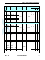
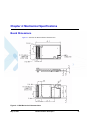
1
Technical Information
Motorola W24 Developer’s Guide
Module Hardware Description
MAY 31, 2008
6802984C95-A
SPECIFICATIONS SUBJECT TO CHANGE WITHOUT NOTICE
Notice
While reasonable efforts have been made to assure the accuracy of this document, Motorola, Inc. assumes no liability resulting
from any inaccuracies or omissions in this document, or from use of the information obtained herein. The information in this
document has been carefully checked and is believed to be entirely reliable. However, no responsibility is assumed for
inaccuracies or omissions. Motorola, Inc. reserves the right to make changes to any products described herein and reserves the
right to revise this document and to make changes from time to time in content hereof with no obligation to notify any person of
revisions or changes. Motorola, Inc. does not assume any liability arising out of the application or use of any product, software, or
circuit described herein; neither does it convey license under its patent rights or the rights of others.
It is possible that this publication may contain references to, or information about Motorola products (machines and programs),
programming, or services that are not announced in your country. Such references or information must not be construed to mean
that Motorola intends to announce such Motorola products, programming, or services in your country.
Copyrights
This instruction manual, and the Motorola products described in this instruction manual may be, include or describe copyrighted
Motorola material, such as computer programs stored in semiconductor memories or other media. Laws in the United States and
other countries preserve for Motorola and its licensors certain exclusive rights for copyrighted material, including the exclusive
right to copy, reproduce in any form, distribute and make derivative works of the copyrighted material. Accordingly, any
copyrighted material of Motorola and its licensors contained herein or in the Motorola products described in this instruction
manual may not be copied, reproduced, distributed, merged or modified in any manner without the express written permission of
Motorola. Furthermore, the purchase of Motorola products shall not be deemed to grant either directly or by implication, estoppel,
or otherwise, any license under the copyrights, patents or patent applications of Motorola, as arises by operation of law in the sale
of a product.
Computer Software Copyrights
The Motorola and 3rd Party supplied Software (SW) products described in this instruction manual may include copyrighted
Motorola and other 3rd Party supplied computer programs stored in semiconductor memories or other media. Laws in the United
States and other countries preserve for Motorola and other 3rd Party supplied SW certain exclusive rights for copyrighted
computer programs, including the exclusive right to copy or reproduce in any form the copyrighted computer program.
Accordingly, any copyrighted Motorola or other 3rd Party supplied SW computer programs contained in the Motorola products
described in this instruction manual may not be copied (reverse engineered) or reproduced in any manner without the express
written permission of Motorola or the 3rd Party SW supplier. Furthermore, the purchase of Motorola products shall not be deemed
to grant either directly or by implication, estoppel, or otherwise, any license under the copyrights, patents or patent applications of
Motorola or other 3rd Party supplied SW, except for the normal non-exclusive, royalty free license to use that arises by operation
of law in the sale of a product.
Usage and Disclosure Restrictions
License Agreements
The software described in this document is the property of Motorola, Inc. and its licensors. It is furnished by express license
agreement only and may be used only in accordance with the terms of such an agreement.
Copyrighted Materials
Software and documentation are copyrighted materials. Making unauthorized copies is prohibited by law. No part of the software
or documentation may be reproduced, transmitted, transcribed, stored in a retrieval system, or translated into any language or
computer language, in any form or by any means, without prior written permission of Motorola, Inc.
High Risk Materials
Components, units, or third-party products used in the product described herein are NOT fault-tolerant and are NOT designed,
manufactured, or intended for use as on-line control equipment in the following hazardous environments requiring fail-safe
controls: the operation of Nuclear Facilities, Aircraft Navigation or Aircraft Communication Systems, Air Traffic Control, Life
Support, or Weapons Systems (High Risk Activities). Motorola and its supplier(s) specifically disclaim any expressed or implied
warranty of fitness for such High Risk Activities.
Trademarks
MOTOROLA and the Stylized M Logo are registered in the US Patent & Trademark Office. All other product or service names are
the property of their respective owners.
© Copyright 2008 Motorola, Inc.
REV052604
Table of Contents
Manual Scope . . . . . . . . . . . . . . . . . . . . . . . . . . . . . . . . . . . . . . . . . . . . . . . . . . . . . . . . . . . . . . . . . . . vii
Target Audience . . . . . . . . . . . . . . . . . . . . . . . . . . . . . . . . . . . . . . . . . . . . . . . . . . . . . . . . . . . . . . . . . vii
Manual Organization . . . . . . . . . . . . . . . . . . . . . . . . . . . . . . . . . . . . . . . . . . . . . . . . . . . . . . . . . . . . . . vii
Applicable Documents . . . . . . . . . . . . . . . . . . . . . . . . . . . . . . . . . . . . . . . . . . . . . . . . . . . . . . . . . . . . vii
Regulatory Requirements . . . . . . . . . . . . . . . . . . . . . . . . . . . . . . . . . . . . . . . . . . . . . . . . . . . . . . . . . viii
Regulatory Statement (Safety). . . . . . . . . . . . . . . . . . . . . . . . . . . . . . . . . . . . . . . . . . . . . . . . . . . . . . viii
Antenna and Transmission Safety Precautions . . . . . . . . . . . . . . . . . . . . . . . . . . . . . . . . . . . . . . . . . . .ix
Standards . . . . . . . . . . . . . . . . . . . . . . . . . . . . . . . . . . . . . . . . . . . . . . . . . . . . . . . . . . . . . . . . . . . . . . . . x
Contact Us . . . . . . . . . . . . . . . . . . . . . . . . . . . . . . . . . . . . . . . . . . . . . . . . . . . . . . . . . . . . . . . . . . . . . . .xi
Text Conventions. . . . . . . . . . . . . . . . . . . . . . . . . . . . . . . . . . . . . . . . . . . . . . . . . . . . . . . . . . . . . . . . . .xi
Field Service . . . . . . . . . . . . . . . . . . . . . . . . . . . . . . . . . . . . . . . . . . . . . . . . . . . . . . . . . . . . . . . . . . . . xii
General Safety . . . . . . . . . . . . . . . . . . . . . . . . . . . . . . . . . . . . . . . . . . . . . . . . . . . . . . . . . . . . . . . . . . . xii
Caring for the Environment. . . . . . . . . . . . . . . . . . . . . . . . . . . . . . . . . . . . . . . . . . . . . . . . . . . . . . . . xiii
Limitation of Liability . . . . . . . . . . . . . . . . . . . . . . . . . . . . . . . . . . . . . . . . . . . . . . . . . . . . . . . . . . . . .xiv
Warranty Notification . . . . . . . . . . . . . . . . . . . . . . . . . . . . . . . . . . . . . . . . . . . . . . . . . . . . . . . . . . . . .xiv
How to Get Warranty Service? . . . . . . . . . . . . . . . . . . . . . . . . . . . . . . . . . . . . . . . . . . . . . . . . . . . . . . xv
Claiming . . . . . . . . . . . . . . . . . . . . . . . . . . . . . . . . . . . . . . . . . . . . . . . . . . . . . . . . . . . . . . . . . . . . . . . xv
Conditions . . . . . . . . . . . . . . . . . . . . . . . . . . . . . . . . . . . . . . . . . . . . . . . . . . . . . . . . . . . . . . . . . . . . . . xv
What is Not Covered by the Warranty . . . . . . . . . . . . . . . . . . . . . . . . . . . . . . . . . . . . . . . . . . . . . . . .xvi
Installed Data. . . . . . . . . . . . . . . . . . . . . . . . . . . . . . . . . . . . . . . . . . . . . . . . . . . . . . . . . . . . . . . . . . . xvii
Out of Warranty Repairs . . . . . . . . . . . . . . . . . . . . . . . . . . . . . . . . . . . . . . . . . . . . . . . . . . . . . . . . . . xvii
Revision History . . . . . . . . . . . . . . . . . . . . . . . . . . . . . . . . . . . . . . . . . . . . . . . . . . . . . . . . . . . . . . . xviii
Chapter 1:
Introduction . . . . . . . . . . . . . . . . . . . . . . . . . . . . . . . . . . . . . . . . . . . . . . . . . . . . . . . . . . . . . 1
Operation Setup . . . . . . . . . . . . . . . . . . . . . . . . . . . . . . . . . . . . . . . . . . . . . . . . . . . . . . . . . . . . . . . . . . . 1
Stand Alone Configuration . . . . . . . . . . . . . . . . . . . . . . . . . . . . . . . . . . . . . . . . . . . . . . . . . . . . . . . 1
Stacked Configuration . . . . . . . . . . . . . . . . . . . . . . . . . . . . . . . . . . . . . . . . . . . . . . . . . . . . . . . . . . . 1
Product Specifications . . . . . . . . . . . . . . . . . . . . . . . . . . . . . . . . . . . . . . . . . . . . . . . . . . . . . . . . . . . . . . 2
Regulatory Approvals . . . . . . . . . . . . . . . . . . . . . . . . . . . . . . . . . . . . . . . . . . . . . . . . . . . . . . . . . . . . . . 4
CFR 47 Part 15.19 specifies Label Requirements . . . . . . . . . . . . . . . . . . . . . . . . . . . . . . . . . . . . . . 4
CFR 47 Part 15.21 Information to user . . . . . . . . . . . . . . . . . . . . . . . . . . . . . . . . . . . . . . . . . . . . . . 4
CFR 47 Part 15.247 . . . . . . . . . . . . . . . . . . . . . . . . . . . . . . . . . . . . . . . . . . . . . . . . . . . . . . . . . . . . . 4
CRF 47 Part 15.247 & 15.205 & 15.209 . . . . . . . . . . . . . . . . . . . . . . . . . . . . . . . . . . . . . . . . . . . . . 4
CFR 47 Part 15.107 & part 15.109 . . . . . . . . . . . . . . . . . . . . . . . . . . . . . . . . . . . . . . . . . . . . . . . . . 4
European Union Directives Conformance Statement . . . . . . . . . . . . . . . . . . . . . . . . . . . . . . . . . . . 5
Chapter 2:
Hardware Interface Description . . . . . . . . . . . . . . . . . . . . . . . . . . . . . . . . . . . . . . . . . . . . . 7
Architecture Overview . . . . . . . . . . . . . . . . . . . . . . . . . . . . . . . . . . . . . . . . . . . . . . . . . . . . . . . . . . . . . 7
Digital Block . . . . . . . . . . . . . . . . . . . . . . . . . . . . . . . . . . . . . . . . . . . . . . . . . . . . . . . . . . . . . . . . . . 7
Power Management Block . . . . . . . . . . . . . . . . . . . . . . . . . . . . . . . . . . . . . . . . . . . . . . . . . . . . . . . . 8
RF Block . . . . . . . . . . . . . . . . . . . . . . . . . . . . . . . . . . . . . . . . . . . . . . . . . . . . . . . . . . . . . . . . . . . . . 8
Operating Modes . . . . . . . . . . . . . . . . . . . . . . . . . . . . . . . . . . . . . . . . . . . . . . . . . . . . . . . . . . . . . . . . . . 9
Power Supply. . . . . . . . . . . . . . . . . . . . . . . . . . . . . . . . . . . . . . . . . . . . . . . . . . . . . . . . . . . . . . . . . . . . 10
Power Supply Design . . . . . . . . . . . . . . . . . . . . . . . . . . . . . . . . . . . . . . . . . . . . . . . . . . . . . . . . . . . 10
Power Consumption . . . . . . . . . . . . . . . . . . . . . . . . . . . . . . . . . . . . . . . . . . . . . . . . . . . . . . . . . . . . 11
May 31, 2008
Module Hardware Description
i
Table of Contents
Power On/Off Operation . . . . . . . . . . . . . . . . . . . . . . . . . . . . . . . . . . . . . . . . . . . . . . . . . . . . . . . . . . . 12
Turning the W24 On . . . . . . . . . . . . . . . . . . . . . . . . . . . . . . . . . . . . . . . . . . . . . . . . . . . . . . . . . . . . 12
Turning the W24 On Using ON_N. . . . . . . . . . . . . . . . . . . . . . . . . . . . . . . . . . . . . . . . . . . . . . . 13
Turning the W24 On Using IGN . . . . . . . . . . . . . . . . . . . . . . . . . . . . . . . . . . . . . . . . . . . . . . . . 13
Turning the W24 Off . . . . . . . . . . . . . . . . . . . . . . . . . . . . . . . . . . . . . . . . . . . . . . . . . . . . . . . . . . . 14
Turning the W24 Off Using ON_N . . . . . . . . . . . . . . . . . . . . . . . . . . . . . . . . . . . . . . . . . . . . . . 14
Turning the W24 Off Using IGN . . . . . . . . . . . . . . . . . . . . . . . . . . . . . . . . . . . . . . . . . . . . . . . . 15
Power Loss shut down . . . . . . . . . . . . . . . . . . . . . . . . . . . . . . . . . . . . . . . . . . . . . . . . . . . . . . . . 16
Turning the W24 Off Using AT+iMRST . . . . . . . . . . . . . . . . . . . . . . . . . . . . . . . . . . . . . . . . . . 16
Low Power Mode. . . . . . . . . . . . . . . . . . . . . . . . . . . . . . . . . . . . . . . . . . . . . . . . . . . . . . . . . . . . . . . . . 17
Activating Low Power Mode . . . . . . . . . . . . . . . . . . . . . . . . . . . . . . . . . . . . . . . . . . . . . . . . . . . . . 17
Serial Interface During Low Power Mode . . . . . . . . . . . . . . . . . . . . . . . . . . . . . . . . . . . . . . . . . . . 18
Terminating Low Power Mode . . . . . . . . . . . . . . . . . . . . . . . . . . . . . . . . . . . . . . . . . . . . . . . . . . . 18
Temporary Termination of Low Power Mode . . . . . . . . . . . . . . . . . . . . . . . . . . . . . . . . . . . . . . 18
Permanent termination of Low Power Mode . . . . . . . . . . . . . . . . . . . . . . . . . . . . . . . . . . . . . . . 20
Deep Sleep Mode . . . . . . . . . . . . . . . . . . . . . . . . . . . . . . . . . . . . . . . . . . . . . . . . . . . . . . . . . . . . . . 20
Serial Interfaces . . . . . . . . . . . . . . . . . . . . . . . . . . . . . . . . . . . . . . . . . . . . . . . . . . . . . . . . . . . . . . . . . . 21
Primary UART (UART1) . . . . . . . . . . . . . . . . . . . . . . . . . . . . . . . . . . . . . . . . . . . . . . . . . . . . . . . . 21
Secondary UART (UART2) . . . . . . . . . . . . . . . . . . . . . . . . . . . . . . . . . . . . . . . . . . . . . . . . . . . . . . 22
USB Device Interface . . . . . . . . . . . . . . . . . . . . . . . . . . . . . . . . . . . . . . . . . . . . . . . . . . . . . . . . . . . 23
USB Host Interface (Stacked configuration only) . . . . . . . . . . . . . . . . . . . . . . . . . . . . . . . . . . . . . 23
SIM Interface . . . . . . . . . . . . . . . . . . . . . . . . . . . . . . . . . . . . . . . . . . . . . . . . . . . . . . . . . . . . . . . . . . . . 24
Audio Interface . . . . . . . . . . . . . . . . . . . . . . . . . . . . . . . . . . . . . . . . . . . . . . . . . . . . . . . . . . . . . . . . . . 25
A/D Converter Interface. . . . . . . . . . . . . . . . . . . . . . . . . . . . . . . . . . . . . . . . . . . . . . . . . . . . . . . . . . . . 26
Unused/Reserved Signals. . . . . . . . . . . . . . . . . . . . . . . . . . . . . . . . . . . . . . . . . . . . . . . . . . . . . . . . . . . 27
Controls and Indicators Interface. . . . . . . . . . . . . . . . . . . . . . . . . . . . . . . . . . . . . . . . . . . . . . . . . . . . . 28
Reset . . . . . . . . . . . . . . . . . . . . . . . . . . . . . . . . . . . . . . . . . . . . . . . . . . . . . . . . . . . . . . . . . . . . . . . . 28
VREF Reference Regulator . . . . . . . . . . . . . . . . . . . . . . . . . . . . . . . . . . . . . . . . . . . . . . . . . . . . . . 28
Wakeup . . . . . . . . . . . . . . . . . . . . . . . . . . . . . . . . . . . . . . . . . . . . . . . . . . . . . . . . . . . . . . . . . . . . . . 29
Antenna Detection . . . . . . . . . . . . . . . . . . . . . . . . . . . . . . . . . . . . . . . . . . . . . . . . . . . . . . . . . . . . . 29
GPRS/EGPRS Detection . . . . . . . . . . . . . . . . . . . . . . . . . . . . . . . . . . . . . . . . . . . . . . . . . . . . . . . . 29
Transmission Indicator . . . . . . . . . . . . . . . . . . . . . . . . . . . . . . . . . . . . . . . . . . . . . . . . . . . . . . . . . . 30
Wi-Fi LED Indicator . . . . . . . . . . . . . . . . . . . . . . . . . . . . . . . . . . . . . . . . . . . . . . . . . . . . . . . . . . . 30
Mode Select . . . . . . . . . . . . . . . . . . . . . . . . . . . . . . . . . . . . . . . . . . . . . . . . . . . . . . . . . . . . . . . . . . 30
General Purpose I/O. . . . . . . . . . . . . . . . . . . . . . . . . . . . . . . . . . . . . . . . . . . . . . . . . . . . . . . . . . . . . . . 31
Antenna Interface. . . . . . . . . . . . . . . . . . . . . . . . . . . . . . . . . . . . . . . . . . . . . . . . . . . . . . . . . . . . . . . . . 33
Chapter 3:
Electrical and Environmental Specifications. . . . . . . . . . . . . . . . . . . . . . . . . . . . . . . . . . 35
Absolute Maximum Ratings . . . . . . . . . . . . . . . . . . . . . . . . . . . . . . . . . . . . . . . . . . . . . . . . . . . . . . . . 35
Environmental Specifications . . . . . . . . . . . . . . . . . . . . . . . . . . . . . . . . . . . . . . . . . . . . . . . . . . . . . . . 36
Application Interface Specifications . . . . . . . . . . . . . . . . . . . . . . . . . . . . . . . . . . . . . . . . . . . . . . . . . . 36
Chapter 4:
Mechanical Specifications. . . . . . . . . . . . . . . . . . . . . . . . . . . . . . . . . . . . . . . . . . . . . . . . . 47
Board Dimensions . . . . . . . . . . . . . . . . . . . . . . . . . . . . . . . . . . . . . . . . . . . . . . . . . . . . . . . . . . . . . . . . 47
Interface Connector Specifications . . . . . . . . . . . . . . . . . . . . . . . . . . . . . . . . . . . . . . . . . . . . . . . . . . . 48
RF Connector Specifications . . . . . . . . . . . . . . . . . . . . . . . . . . . . . . . . . . . . . . . . . . . . . . . . . . . . . . . . 49
Mating Connector . . . . . . . . . . . . . . . . . . . . . . . . . . . . . . . . . . . . . . . . . . . . . . . . . . . . . . . . . . . . . . 49
W24 Mounting . . . . . . . . . . . . . . . . . . . . . . . . . . . . . . . . . . . . . . . . . . . . . . . . . . . . . . . . . . . . . . . . . . . 51
W24 Stand Alone Mounting . . . . . . . . . . . . . . . . . . . . . . . . . . . . . . . . . . . . . . . . . . . . . . . . . . . . . . 51
W24 + G24 Stacked Mounting . . . . . . . . . . . . . . . . . . . . . . . . . . . . . . . . . . . . . . . . . . . . . . . . . . . . 52
Chapter 5:
Support, Service and Troubleshooting . . . . . . . . . . . . . . . . . . . . . . . . . . . . . . . . . . . . . . 53
Support . . . . . . . . . . . . . . . . . . . . . . . . . . . . . . . . . . . . . . . . . . . . . . . . . . . . . . . . . . . . . . . . . . . . . . . . . 53
Who to Contact? . . . . . . . . . . . . . . . . . . . . . . . . . . . . . . . . . . . . . . . . . . . . . . . . . . . . . . . . . . . . . . . 53
ii
Module Hardware Description
May 31, 2008
Table of Contents
Required Query Information . . . . . . . . . . . . . . . . . . . . . . . . . . . . . . . . . . . . . . . . . . . . . . . . . . . . . 53
Service . . . . . . . . . . . . . . . . . . . . . . . . . . . . . . . . . . . . . . . . . . . . . . . . . . . . . . . . . . . . . . . . . . . . . . . . . 55
Who to Contact? . . . . . . . . . . . . . . . . . . . . . . . . . . . . . . . . . . . . . . . . . . . . . . . . . . . . . . . . . . . . . . 55
Required Query Information . . . . . . . . . . . . . . . . . . . . . . . . . . . . . . . . . . . . . . . . . . . . . . . . . . . . . 55
Testing a Standalone Unit . . . . . . . . . . . . . . . . . . . . . . . . . . . . . . . . . . . . . . . . . . . . . . . . . . . . . . . . . . 56
Acronyms and Abbreviations
Index
May 31, 2008
Module Hardware Description
iii
Table of Contents
iv
Module Hardware Description
May 31, 2008
List of Figures
1-1
1-2
W24 Stand Alone Configuration . . . . . . . . . . . . . . . . . . . . . . . . . . . . . . . . . . . . . . . . . . . . . . . . 1
W24 + G24 Stacked Configuration . . . . . . . . . . . . . . . . . . . . . . . . . . . . . . . . . . . . . . . . . . . . . . 2
2-1
2-2
2-3
2-4
2-5
2-6
2-7
2-8
2-9
2-10
2-11
W24 Block Diagram . . . . . . . . . . . . . . . . . . . . . . . . . . . . . . . . . . . . . . . . . . . . . . . . . . . . . . . . . . 7
Transmission Power Drops. . . . . . . . . . . . . . . . . . . . . . . . . . . . . . . . . . . . . . . . . . . . . . . . . . . . 11
ON_N Power On Timing . . . . . . . . . . . . . . . . . . . . . . . . . . . . . . . . . . . . . . . . . . . . . . . . . . . . . 13
IGN Power On Timing . . . . . . . . . . . . . . . . . . . . . . . . . . . . . . . . . . . . . . . . . . . . . . . . . . . . . . . 14
ON_N Power Off Timing . . . . . . . . . . . . . . . . . . . . . . . . . . . . . . . . . . . . . . . . . . . . . . . . . . . . . 15
IGN Power Off Timing. . . . . . . . . . . . . . . . . . . . . . . . . . . . . . . . . . . . . . . . . . . . . . . . . . . . . . . 15
WKUPI_N Signal Operation . . . . . . . . . . . . . . . . . . . . . . . . . . . . . . . . . . . . . . . . . . . . . . . . . . 18
WKUPO_N Signal Operation. . . . . . . . . . . . . . . . . . . . . . . . . . . . . . . . . . . . . . . . . . . . . . . . . . 19
Serial Interface Data . . . . . . . . . . . . . . . . . . . . . . . . . . . . . . . . . . . . . . . . . . . . . . . . . . . . . . . . . 20
Serial Interfaces Block Diagram. . . . . . . . . . . . . . . . . . . . . . . . . . . . . . . . . . . . . . . . . . . . . . . . 21
UART1 Interface Signals . . . . . . . . . . . . . . . . . . . . . . . . . . . . . . . . . . . . . . . . . . . . . . . . . . . . . 21
4-1
4-2
4-3
4-4
4-5
4-6
4-7
W24 Mechanical Characteristics . . . . . . . . . . . . . . . . . . . . . . . . . . . . . . . . . . . . . . . . . . . . . . .
W24 Stand Alone Model . . . . . . . . . . . . . . . . . . . . . . . . . . . . . . . . . . . . . . . . . . . . . . . . . . . . .
MMCX Connector Dimensions . . . . . . . . . . . . . . . . . . . . . . . . . . . . . . . . . . . . . . . . . . . . . . . .
Optional MMCX Cable Assembly . . . . . . . . . . . . . . . . . . . . . . . . . . . . . . . . . . . . . . . . . . . . . .
W24 Mounting Area . . . . . . . . . . . . . . . . . . . . . . . . . . . . . . . . . . . . . . . . . . . . . . . . . . . . . . . . .
W24 + G24 Stacked Mounting . . . . . . . . . . . . . . . . . . . . . . . . . . . . . . . . . . . . . . . . . . . . . . . . .
W24 + G24 Stacked Mounting Spacer Dimensions . . . . . . . . . . . . . . . . . . . . . . . . . . . . . . . . .
May 31, 2008
Module Hardware Description
47
48
49
50
51
52
52
v
List of Tables
1-1
Product Specifications . . . . . . . . . . . . . . . . . . . . . . . . . . . . . . . . . . . . . . . . . . . . . . . . . . . . . . . . 2
2-1
2-2
2-3
2-4
2-5
2-6
2-7
2-8
2-9
2-10
2-11
2-12
2-13
2-14
2-15
3-1
3-2
3-3
3-4
W24 Operating Modes . . . . . . . . . . . . . . . . . . . . . . . . . . . . . . . . . . . . . . . . . . . . . . . . . . . . . . . . 9
Power Supply Signals . . . . . . . . . . . . . . . . . . . . . . . . . . . . . . . . . . . . . . . . . . . . . . . . . . . . . . . . 10
W24 Current Ratings . . . . . . . . . . . . . . . . . . . . . . . . . . . . . . . . . . . . . . . . . . . . . . . . . . . . . . . . 11
Secondary UART Interface Signals . . . . . . . . . . . . . . . . . . . . . . . . . . . . . . . . . . . . . . . . . . . . . 22
USB Device Interface Signals (at Host connector) . . . . . . . . . . . . . . . . . . . . . . . . . . . . . . . . . 23
USB Host Interface Signals (at G24 connector). . . . . . . . . . . . . . . . . . . . . . . . . . . . . . . . . . . . 23
SIM Interface Signals . . . . . . . . . . . . . . . . . . . . . . . . . . . . . . . . . . . . . . . . . . . . . . . . . . . . . . . . 24
Analog Audio Interface Signals . . . . . . . . . . . . . . . . . . . . . . . . . . . . . . . . . . . . . . . . . . . . . . . . 25
Digital Audio Interface Signals . . . . . . . . . . . . . . . . . . . . . . . . . . . . . . . . . . . . . . . . . . . . . . . . 25
ADC Interface Signals . . . . . . . . . . . . . . . . . . . . . . . . . . . . . . . . . . . . . . . . . . . . . . . . . . . . . . . 26
Internal Interface Signals . . . . . . . . . . . . . . . . . . . . . . . . . . . . . . . . . . . . . . . . . . . . . . . . . . . . . 27
Controls and Indicators. . . . . . . . . . . . . . . . . . . . . . . . . . . . . . . . . . . . . . . . . . . . . . . . . . . . . . . 28
VREF Specifications . . . . . . . . . . . . . . . . . . . . . . . . . . . . . . . . . . . . . . . . . . . . . . . . . . . . . . . . 29
GPIO Interface Signals . . . . . . . . . . . . . . . . . . . . . . . . . . . . . . . . . . . . . . . . . . . . . . . . . . . . . . . 31
Antenna Interface Specifications . . . . . . . . . . . . . . . . . . . . . . . . . . . . . . . . . . . . . . . . . . . . . . . 33
Maximum Ratings . . . . . . . . . . . . . . . . . . . . . . . . . . . . . . . . . . . . . . . . . . . . . . . . . . . . . . . . . . 35
Environmental Ratings . . . . . . . . . . . . . . . . . . . . . . . . . . . . . . . . . . . . . . . . . . . . . . . . . . . . . . . 36
Host Interface Specifications . . . . . . . . . . . . . . . . . . . . . . . . . . . . . . . . . . . . . . . . . . . . . . . . . . 37
G24 Interface Specifications. . . . . . . . . . . . . . . . . . . . . . . . . . . . . . . . . . . . . . . . . . . . . . . . . . . 42
4-1
4-2
4-3
W24 host interface connector options . . . . . . . . . . . . . . . . . . . . . . . . . . . . . . . . . . . . . . . . . . . 48
W24 cellular interface connector options . . . . . . . . . . . . . . . . . . . . . . . . . . . . . . . . . . . . . . . . . 48
RF Connector Specifications . . . . . . . . . . . . . . . . . . . . . . . . . . . . . . . . . . . . . . . . . . . . . . . . . . 49
May 31, 2008
Module Hardware Description
vi
Preface
Manual Scope
This manual provides the electrical, mechanical and environmental requirements for properly
integrating the W24 module in a host application.
This manual gives a complete set of hardware features and functions that may be provided by
W24. The availability of any feature or function, which is described in this manual, depends on
the hardware revision and software version of a specific W24 model.
The parameters and values provided in this manual are defined under typical conditions. These
values may vary when subject to different conditions, such as SW version, network status,
application settings and environmental conditions.
Target Audience
This manual is intended for all members of the integration team who are responsible for
integrating the W24 into the host application, including representatives from hardware, software
and RF engineering disciplines.
Manual Organization
This manual contains the following chapters:
• Chapter 1 —introduces the W24 unit and provides important safety instructions.
• Chapter 2 —provides a detailed hardware description of the blocks and components
comprising the W24.
• Chapter 3 —describes the pin assignments for W24 connectors.
• Chapter 4 —describes W24 mechanical specifications and requirements.
• Chapter 5 —provides contact information for Motorola Service Support and Customer
Assistance.
Applicable Documents
•
•
•
•
May 31, 2008
Motorola W24 Developer’s Guide - Developer's Kit - 6802985C05
Motorola W24 Developer’s Guide - AT+i Commands - 6802985C10
Motorola G24 Developer’s Guide - Module Hardware Description - 68089192V27
Motorola G24 Developer’s Guide - AT Commands Reference Manual - 6889192V28
Module Hardware Description
vii
Regulatory Requirements
Regulatory Requirements
The Federal Communications Commission (FCC) requires application for certification of digital
devices in accordance with CFR Title 47, Part 15 Sub Part C ,section 15.247 and Part 15 Sub Part
B sections 15.107,15.109. This includes MPE calculation. As the W24 modem is not a standalone
transceiver but is an integrated module, the W24 cannot be tested by itself for EME certification.
It is, however, the integrator's responsibility to have the completed device tested for EME
certification.
Caution:
Unauthorized repairs or modifications could result in permanent damage to the
equipment and void your warranty and your authority to operate this device under
Part 15 of the FCC Rules.
Regulatory Statement (Safety)
The following safety precautions must be observed during all phases of the operation, usage,
service or repair of any cellular terminal or mobile incorporating the W24 module. Manufacturers
of the cellular terminal are advised to convey the following safety information to users and
operating personnel, and to incorporate these guidelines into all manuals supplied with the
product. Failure to comply with these precautions violates safety standards of design,
manufacture and intended use of the product. Motorola assumes no liability for customer failure
to comply with these precautions.
• The W24 must be operated at the voltages described in the technical documentation
• The W24 must not be mechanically or electrically changed. Use of connectors should follow
the guidance of the technical documentation
• The W24 is designed to meet the spectrum requirements of ETS 300328
• The W24 has been partially tested to EN301489-17, since compliance to ESD requirements
will depend critically on the integration into the host device
• When integrating the W24 into a system, Motorola recommends testing the system to
EN301489-17
• The W24 meets the safety requirements of EN60950
• Systems using the W24 are subject to mandatory EMC testing under directive 89/336/EEC
(see link below). Other directives, such as the LVD directive 73/23/EE, may also apply to a
system using the W24 module
http://ec.europa.eu/enterprise/newapproach/standardization/harmstds/reflist.html
Host Label Requirement
A readily visible label is required on the outside of the host that state i.e. “FCC ID:
IHDT56DB2/IC ID: 109O-DB2 is contained within”, provided the host is within the limits of the
module grant. You must not remove the label from embedded module.
FCC Notice to Users
Motorola has not approved any changes or modifications to this device by the user. Any changes
or modifications could void the user's authority to operate the equipment. See 47 CFR Sec. 15.21.
viii
Module Hardware Description
May 31, 2008
Preface
This device complies with part 15 of the FCC Rules. Operation is subject to the following two
conditions: (1) This device may not cause harmful interference, and (2) this device must accept
any interference received, including interference that may cause undesired operation. See 47 CFR
Sec. 15.19(3).
If your mobile device or accessory has a USB connector, or is otherwise considered a computer
peripheral device whereby it can be connected to a computer for purposes of transferring data,
then it is considered a Class B device and the following statement applies:
This equipment has been tested and found to comply with the limits for a Class B digital device,
pursuant to part 15 of the FCC Rules. These limits are designed to provide reasonable protection
against harmful interference in a residential installation. This equipment generates, uses and can
radiate radio frequency energy and, if not installed and used in accordance with the instructions,
may cause harmful interference to radio communications. However, there is no guarantee that
interference will not occur in a particular installation. If this equipment does cause harmful
interference to radio or television reception, which can be determined by turning the equipment
off and on, the user is encouraged to try to correct the interference by one or more of the
following measures:
• Reorient or relocate the receiving antenna.
• Increase the separation between the equipment and the receiver.
• Connect the equipment to an outlet on a circuit different from that to which the receiver is
connected.
• Consult the dealer or an experienced radio/TV technician for help.
This device complies with Part 15 of the FCC Rules. Operation is subject to the following two
conditions:
1. This device may not cause harmful interference.
2. This device must accept any interference received, including interference that may cause
undesired operation.
Precautions
Interface connector and some of the module circuits are not shielded. Be sure to take appropriate
precautionary measures in order to avoid ESD while handling the module. ESD can damage the
W24/G24 modules. Integrators need to design ESD protection on all external interfaces.
Antenna and Transmission Safety Precautions
User Operation
Do not operate your unit when a person is within eight inches (20 centimeters) of the antenna. A
person or object within 8 inches (20 centimeters) of the antenna could impair call quality and may
cause the unit to operate at a higher power level than necessary, as well as expose that person to
RF energy in excess of that established by the FCC RF Exposure Guidelines.
May 31, 2008
Module Hardware Description
ix
Standards
Important:
The unit must be installed in a manner that provides a minimum separation distance
of 8 inches (20 centimeters) or more between the antenna and persons and must not
be co-located or operate in conjunction with any other antenna or transmitter in
order to satisfy FCC RF exposure requirements for mobile transmitting devices.
Important:
To comply with the FCC RF exposure limits and to satisfy the categorical exclusion
requirements for mobile transmitters, the requirements described in the following
section, “Antenna Installation” , must be met.
Antenna Installation
• A minimum separation distance of 8 inches (20 centimeters) must be maintained between the
antenna and all persons.
• When using G24 module: The combined cable loss and antenna gain must not exceed +7.5
dBi (850MHz band). The combined cable loss and antenna gain must not exceed +2.5 dBi
and total system output must not exceed 2.0W EIRP in the PCS (1900) band in order to
comply with the EIRP limit of 24.232 (b). OEM installers must be provided with antenna
installation instruction and transmitter operating conditions for satisfying RF exposure
compliance.
• When using W24 module for meeting FCC - the combined cable loss and antenna gain must
not exceed 6 dBi (2400 MHz Band) and the total system output must not exceed 1.0W peak
output power 15.247(b) Or/and for meeting the EN 300 328 standard - Maximum EIRP
spectral density 10 dBm/MHz. The combined cable loss and antenna gain must not exceed
3 dBi.
Section 15.203 - Antenna Requirement
An intentional radiator shall be designed to ensure that no antenna other than that furnished by the
responsible party shall be used with the device. The use of a permanently attached antenna or of
an antenna that uses a unique coupling to the intentional radiator shall be considered sufficient to
comply with the provisions of this Section. The manufacturer may design the unit so that a
broken antenna can be replaced by the user, but the use of a standard antenna jack or electrical
connector is prohibited. This requirement does not apply to carrier current devices or to devices
operated under the provisions of Sections 15.211, 15.213, 15.217, 15.219, or 15.221. Further, this
requirement does not apply to intentional radiators that must be professionally installed, such as
perimeter protection systems and some field disturbance sensors, or to other intentional radiators
which, in accordance with Section 15.31(d), must be measured at the installation site. However,
the installer shall be responsible for ensuring that the proper antenna is employed so that the
limits in this Part are not exceeded.
Standards
•
•
•
•
•
x
FCC_47cfr15.247
FCC_47cfr15.209 & 15cfr15.205 (radiated spurious emission restricted band)
EN_300 328
IEEE Std 802.11b
IEEE Std 802.11g
Module Hardware Description
May 31, 2008
Preface
•
•
•
•
EN 60950 Safety
RSS-210 Issue 7 (IC Cannada)
EN 301 489-1
EN 301 489-17
Contact Us
We at Motorola want to make this guide as helpful as possible. Keep us informed of your
comments and suggestions for improvements.
For general contact, technical support, report documentation errors and to order manuals, use this
email address:
[email protected]
Motorola appreciates feedback from the users of our information.
Text Conventions
The following special paragraphs are used in this guide to point out information that must be read.
This information may be set-off from the surrounding text, but is always preceded by a bold title
in capital letters:
Note
Note: Presents additional, helpful, noncritical information that you can use.
Warning
Warning:
Presents information to warn you of a potentially hazardous situation in which there
is a possibility of personal injury.
Important
Important:
Presents information to help you avoid an undesirable situation
or provides additional information to help you understand a topic or concept.
Caution
Caution:
May 31, 2008
Presents information to identify a situation in which damage to software, stored
data, or equipment could occur, thus avoiding
the damage.
Module Hardware Description
xi
Field Service
Field Service
For Field Service requests, use this email address:
[email protected]
General Safety
Remember!. . . safety depends on you!
The following general safety precautions must be observed during all phases of operation,
service, and repair of the equipment described in this manual. Failure to comply with these
precautions or with specific warnings elsewhere in this manual violates safety standards of
design, manufacture, and intended use of the equipment. Motorola, Inc. assumes no liability for
the customer’s failure to comply with these requirements. The safety precautions listed below
represent warnings of certain dangers of which we are aware. You, as the user of this product,
should follow these warnings and all other safety precautions necessary for the safe operation of
the equipment in your operating environment.
Do not operate in an explosive atmosphere
Do not operate the equipment in the presence of flammable gases or fumes. Operation of any
electrical equipment in such an environment constitutes a definite safety hazard.
Do not service or adjust alone
Do not attempt internal service or adjustment unless another person, capable of rendering first aid
is present.
Keep away from live circuits
Operating personnel must:
• not remove equipment covers. Only Factory Authorized Service Personnel or other qualified
maintenance personnel may remove equipment covers for internal subassembly, or
component replacement, or any internal adjustment
• not replace components with power cable connected. Under certain conditions, dangerous
voltages may exist even with the power cable removed
• always disconnect power and discharge circuits before touching them
Do not substitute parts or modify equipment
Because of the danger of introducing additional hazards, do not install substitute parts or perform
any unauthorized modification of equipment. Contact Motorola Warranty and Repair for service
and repair to ensure that safety features are maintained.
xii
Module Hardware Description
May 31, 2008
Preface
Dangerous procedure warnings
Warnings, such as the example below, precede potentially dangerous procedures throughout this
manual. Instructions contained in the warnings must be followed. You should also employ all
other safety precautions that you deem necessary for the operation of the equipment in your
operating environment.
Warning example:
Warning:
Dangerous voltages, capable of causing death, are present in this equipment. Use
extreme caution when handling, testing,
and adjusting.
Caring for the Environment
The following information is provided to enable regulatory compliance with the European Union
(EU) Directive 2002/96/EC Waste Electrical and Electronic Equipment (WEEE) when using
Motorola equipment in EU countries.
Disposal of Motorola equipment in EU countries
Please do not dispose of Motorola equipment in landfill sites.
In the EU, Motorola in conjunction with a recycling partner will ensure that equipment is
collected and recycled according to the requirements of EU environmental law.
Please contact the Customer Network Resolution Center (CNRC) for assistance. The 24 hour
telephone numbers are listed at
http://mynetworksupport.motorola.com
Select Customer Network Resolution Center contact information.
Alternatively if you do not have access to CNRC or the internet, contact the Local Motorola
Office.
Disposal of Motorola equipment in non-EU countries
In non-EU countries, dispose of Motorola equipment in accordance with national and regional
regulations.
RoHS Compliance
The W24 product meets the European Union directive for RoHS compliance.
The RoHS compliance is subject to a declaration of conformity that may be viewed upon request.
May 31, 2008
Module Hardware Description
xiii
Limitation of Liability
Limitation of Liability
The Products are not designed, intended, or authorized for use as components in systems intended
for surgical implant into the body; in other applications intended to support or sustain life; for the
planning, construction, maintenance, operation or use of any nuclear facility; for the flight,
navigation, communication of aircraft or ground support equipment; or in any other application in
which the failure of the Product could create a situation where personal injury or death may occur.
If CUSTOMER should use any Product or provide any Product to a third party for any such use,
CUSTOMER hereby agrees that MOTOROLA is not liable, in whole or in part, for any claims or
damages arising from such use, and further agrees to indemnify and hold MOTOROLA harmless
from any claim, loss, cost or damage arising from such use.
EXCEPT AS SPECIFICALLY STATED ABOVE, THE PRODUCTS ARE PROVIDED "AS IS"
AND MOTOROLA MAKES NO OTHER WARRANTIES EXPRESS, IMPLIED,
STATUTORY, OR OTHERWISE REGARDING THE PRODUCTS. MOTOROLA
SPECIFICALLY DISCLAIMS ANY IMPLIED WARRANTIES OF MERCHANTABILITY
AND FITNESS FOR A PARTICULAR PURPOSE, OR ARISING FROM A COURSE OF
DEALING OR USAGE OF TRADE.
Under no circumstances shall MOTOROLA be liable to CUSTOMER or any other party for any
costs, lost revenue or profits or for any other special, incidental or consequential damages, even if
MOTOROLA has been informed of such potential loss or damage. And in no event shall
MOTOROLA's liability to CUSTOMER for damages of any nature exceed the total purchase
price CUSTOMER paid for the Product at issue in the dispute, except direct damages resulting
from patent and/or copyright infringement, which shall be governed by the "INDEMNITY"
Section of this Agreement.
The preceding states MOTOROLA's entire liability for MOTOROLA's breach or failure to
perform under any provision of this Agreement.
Warranty Notification
Motorola guarantees to you, the original purchaser, the OEM module and accessories which you
have purchased from an authorized Motorola dealer (the "Products"), to be in conformance with
the applicable Motorola specifications current at the time of manufacture for a term of [1] year
from date of purchase of the Product(s) (Warranty Term).
You must inform Motorola of the lack of conformity to the applicable specifications of any of the
Products within a period of two (2) months from the date on which you detect a defect in
material, workmanship or lack of conformity and in any event within a term not to exceed the
Warranty Term, and must immediately submit the Product for service to Motorola's Authorized
Repair or Service Center. Motorola shall not be bound by Product related statements not directly
made by Motorola nor any warranty obligations applicable to the seller.
A list of the Motorola Call Center numbers is enclosed with this Product.
During the Warranty term, Motorola will, at its discretion and without extra charge, as your
exclusive remedy, repair or replace your Product which does not comply with this warranty; or
failing this, to reimburse the price of the Product but reduced to take into account the use you
have had of the Product since it was delivered. This warranty will expire at the end of the
Warranty Term.
This is the complete and exclusive warranty for a Motorola OEM module and accessories and in
lieu of all other warranties, terms and conditions, whether express or implied.
xiv
Module Hardware Description
May 31, 2008
Preface
Where you purchase the product other than as a consumer, Motorola disclaims all other
warranties, terms and conditions express or implied, such as fitness for purpose and satisfactory
quality.
In no event shall Motorola be liable for damages nor loss of data in excess of the purchase price
nor for any incidental special or consequential damages* arising out of the use or inability to use
the Product, to the full extent such may be disclaimed by law.
This Warranty does not affect any statutory rights that you may have if you are a consumer, such
as a warranty of satisfactory quality and fit for the purpose for which products of the same type
are normally used under normal use and service, nor any rights against the seller of the Products
arising from your purchase and sales contract.
(*)including without limitation loss of use, loss of time, loss of data, inconvenience, commercial
loss, lost profits or savings.
How to Get Warranty Service?
In most cases the authorized Motorola dealer which sold and/or installed your Motorola OEM
module and original accessories will honor a warranty claim and/or provide warranty service.
Alternatively, for further information on how to get warranty service please contact the Motorola
M2M Data Module Customer Support Center.
Claiming
In order to claim the warranty service you must return the OEM module and/or accessories in
question to Motorola's Authorized Repair or Service Center in the original configuration and
packaging as supplied by Motorola. Please avoid leaving any supplementary items like SIM
cards. The Product should also be accompanied by a label with your name, address, and telephone
number; name of operator and a description of the problem.
In order to be eligible to receive warranty service, you must present your receipt of purchase or a
comparable substitute proof of purchase bearing the date of purchase. The module should also
clearly display the original Motorola Serial Number (MSN). Such information is contained with
the Product.
You must ensure that all and any repairs or servicing is handled at all times by a Motorola
Authorized Service Center in accordance with the Motorola Service requirements.
In some cases, you may be requested to provide additional information concerning the
maintenance of the Products by Motorola Authorized Service Centers only, therefore it is
important to keep a record of any previous repairs, and make them available if questions arise
concerning maintenance.
Conditions
This warranty will not apply if the type or serial numbers on the Product has been altered, deleted,
duplicated, removed, or made illegible. Motorola reserves the right to refuse free-of-charge
warranty service if the requested documentation can not be presented or if the information is
incomplete, illegible or incompatible with the factory records.
Repair, at Motorola's option, may include reflashing of software, the replacement of parts or
boards with functionally equivalent, reconditioned or new parts or boards. Replaced parts,
May 31, 2008
Module Hardware Description
xv
What is Not Covered by the Warranty
accessories, batteries, or boards are warranted for the balance of the original warranty time
period. The Warranty Term will not be extended. All original accessories, batteries, parts, and
OEM module equipment that have been replaced shall become the property of Motorola.
Motorola does not warrant the installation, maintenance or service of the products, accessories,
batteries or parts.
Motorola will not be responsible in any way for problems or damage caused by any ancillary
equipment not furnished by Motorola which is attached to or used in connection with the
Products, or for operation of Motorola equipment with any ancillary equipment and all such
equipment is expressly excluded from this warranty.
When the Product is used in conjunction with ancillary or peripheral equipment not supplied by
Motorola, Motorola does not warrant the operation of the Product/peripheral combination and
Motorola will not honor any warranty claim where the Product is used in such a combination and
it is determined by Motorola that there is no fault with the Product. Motorola specifically
disclaims any responsibility for any damage, whether or not to Motorola equipment, caused in
any way by the use of the OEM module, accessories, software applications and peripherals
(specific examples include, but are not limited to: batteries, chargers, adapters, and power
supplies) when such accessories, software applications and peripherals are not manufactured and
supplied by Motorola.
What is Not Covered by the Warranty
This warranty is not valid if the defects are due to damage, misuse, tampering, neglect or lack of
care and in case of alterations or repair carried out by unauthorized persons.
The following are examples of defects or damage not covered by this product warranty
1. Defects or damage resulting from use of the Product in other than its normal and customary
manner.
2. Defects or damage from misuse, access to incompatible sources, accident or neglect.
3. Defects or damage from improper testing, operation, maintenance, installation, adjustment,
unauthorized software applications or any alteration or modification of any kind.
4. Breakage or damage to antennas unless caused directly by defects in material or
workmanship.
5. Products disassembled or repaired other than by Motorola in such a manner as to adversely
affect performance or prevent adequate inspection and testing to verify any warranty claim.
6. Defects or damage due to range, coverage, availability, grade of service, or operation of the
Wi-Fi provider.
7. Defects or damage due to moist, liquid or spills of food.
8. Control unit coil cords in the Product that are stretched or have the modular tab broken.
9. All plastic surfaces and all other externally exposed parts that are scratched or damaged due
to customer normal use.
Depending on operating conditions and your usage habits, wear and tear might take place of
components including mechanical problems related to Product housing, paint, assembly,
sub-assemblies, displays and keyboards and any accessories which are not part of the Product's
in-box configuration. The rectification of faults generated through wear and tear and the use of
consumable items like batteries beyond their Optimum Performance Time as indicated in the
product manual is considered to be your responsibility and therefore Motorola will not provide
the free Warranty repair service for these items.
xvi
Module Hardware Description
May 31, 2008
Preface
Installed Data
Please make and retain a note of all data you have inserted into your Product for example names,
addresses, phone numbers, user and access codes, notes etc. before submitting your Product for a
Warranty service as such data may be deleted or erased as part of the repair or service process.
Please note if you have downloaded material onto your product, these may be deleted or erased as
part of the repair process or testing process. Motorola shall not be responsible for such matters.
The repair or testing process should not affect any such material that was installed by Motorola
on your Product as a standard feature.
Out of Warranty Repairs
Out of warranty HW repairs are not applicable for W24. Therefore, the defective unit shall be
scrapped.
May 31, 2008
Module Hardware Description
xvii
Revision History
Revision History
Manual Number
6802984C95-A
Manual Title
Module Hardware Description
Version Information
The following table lists the manual version, date of version, and remarks about
the version.
Revision History
Version
A
xviii
Date Issue
May 31, 2008
Remarks
Initial Release
Module Hardware Description
May 31, 2008
Chapter 1: Introduction
W24 is a self contained Wi-Fi module, supporting IEEE 802.11b/g systems in 2.4GHz band. W24
enables IP connectivity to any host device. It is ideal for enabling M2M applications to achieve
secure, high speed throughput and access to IP networks via 802.11b/g wireless LANs or even via
Cellular network when connected to G24 GSM/GPRS module family.
W24 integrates an operating system, drivers and communication stack, wide assortment of
proven security protocols, NATs for management purposes, built-in web server for managing the
device via web and inherent built-in device firewall.
Operation Setup
The W24 supports two operating setup configurations:
• Stand Alone configuration
• Stacked assembly configuration (with G24).
Stand Alone Configuration
Stand Alone configuration consists of a W24 as a stand alone Wi-Fi module that is controlled by
the host.
In this configuration, the W24 70 pin host connector (bottom connector) is used for interfacing
with the W24.
Figure 1-1 below illustrates the W24 Stand Alone configuration.
Figure 1-1: W24 Stand Alone Configuration
Stacked Configuration
Stacked configuration consists of a G24 that is mounted on top of the W24 in a piggy-back
configuration. In this configuration, the W24 70-pin host connector (bottom connector) is used
for interfacing with the host board, while the G24 is connected to the W24 cellular 70-pin
interface connector (top connector).
May 31, 2008
Module Hardware Description
1
Product Specifications
Figure 1-2 below illustrates the W24 & G24 stacked configuration.
G24
W24
Host PCB
Figure 1-2: W24 + G24 Stacked Configuration
Product Specifications
Important:
For safety regulations and requirements, see “Regulatory Requirements” on
page viii, “Regulatory Statement (Safety)” on page viii and “Antenna and
Transmission Safety Precautions” on page ix in “Preface” .
Note: Motorola reserves the right to change the specifications without prior notice.
Table 1-1: Product Specifications
Product Features
Adds Wi-Fi capability to G24 platforms
WLAN (802.11.b/g)
Operates in the 2.4GHz ISM band
Ad-Hoc WLAN Support
Local WEB server
Physical Characteristics
2
Size:
45.2 x 24.4 x 7.25 mm
45.2 x 24.4 x 5.5 mm (stand alone model)
Mounting:
Two Ø2.4 mm holes for M2 screws
Weight:
10 grams
Module Hardware Description
May 31, 2008
Table 1-1: Product Specifications (Cont.)
Environmental
Operational temperature:
-20°C to +60°C
Storage temperature:
-40°C to +85°C
Performance
Operating voltage:
3.3 - 4.2 V
Current consumption:
250mA
Maximum Tx peak output
power:
25 dBm according to 47 CFR 15.247 (b) (3) & RSS-210
Section A8.4
Interfaces
Connectors:
70-pin, board-to-board (host interface)
70-pin, board-to-board (G24 interface) not available on all
models
MMCX RF Connector
Serial Ports:
USB:
USB full-speed device port, Rev. 2.0
USB full-speed host port, Rev. 2.0
Host UART Interface:
BR from 2400 bps to 230.4 kbps
Extended bit rates, up to 3Mbps
Modem UART Interface:
BR from 2400 bps to 230.4 kbps
Extended bit rates, up to 3Mbps
Data Features
Data Throughput:
Via UART:
400 kbps upload / 1 Mbps download (security disabled)
100 kbps upload/ 300 kbps download (security enabled)
Via USB:
800 kbps upload /download (security disabled)
100 kbps upload/ 300 kbps download (security enabled)
Control/Status Indicators
Wakeup
Antenna Detect
Reset (Ready)
(Available only when coupled with G24)
TX enable
Features over RS232
Embedded TCP/IP stack
AT Command Set
AT+iTM commands (ConnectOne's AT+iTM) is an extension to the standard AT command set that allows programming, monitoring, communication activation and control.
W24 Does not support the standard AT Commands set.
Accessories
Developer Kit
May 31, 2008
Module Hardware Description
3
Regulatory Approvals
Regulatory Approvals
The W24 module has been tested and approved under the standards and regulations listed below:
• FCC
•
•
•
•
•
CE (DOC)
IC
EMC
Safety
R&TTE
Important:
The following paragraphs must be addressed by the integrator to ensure their host is
in compliance to the W24 FCC grant and/or the FCC grant of the host device and
the G24 (where applicable).
CFR 47 Part 15.19 specifies Label Requirements
The following text may be on the product, user's manual, or container.
This device complies with Part 15 of the FCC Rules. Operation is subject to the following two
conditions: (1) this device may not cause harmful interference, and (2) this device must accept
any interference received, including interference that may cause undesired operation.
CFR 47 Part 15.21 Information to user
The user's manual or instruction manual for an intentional or unintentional radiator shall caution
the user that changes or modifications not expressly approved by the party responsible for
compliance could void the user's authority to operate the equipment. In cases where the manual is
provided only in a form other than paper, such as on a computer disk or over the Internet, the
information required by this section may be included in the manual in that alternative form,
provided the user can reasonably be expected to have the capability to access information in that
form.
CFR 47 Part 15.247
Operation within the bands of 2400 to 2483.5 MHz.
CRF 47 Part 15.247 & 15.205 & 15.209
Spurious Radiated Emissions, Restricted Bands.
CFR 47 Part 15.107 & part 15.109
Note: This equipment has been tested and found to comply with the limits for a Class B digital
device, pursuant to Part 15 of the FCC Rules. These limits are designed to provide
4
Module Hardware Description
May 31, 2008
reasonable protection against harmful interference in a residential installation. This
equipment generates, uses and can radiate radio frequency energy and, if not installed and
used in accordance with the instructions, may cause harmful interference to radio
communications. However, there is no guarantee that interference will not occur in a
particular installation. If this equipment does cause harmful interference to radio or
television reception, which can be determined by turning the equipment off and on, the
user is encouraged to try to correct the interference by one or more of the following
measures:
• Reorient or relocate the receiving antenna.
• Increase the separation between the equipment and receiver.
• Connect the equipment into an outlet on a circuit different from that to which the
receiver is connected.
• Consult with your local dealer or with an experienced radio/TV technician for help.
European Union Directives Conformance Statement
Hereby, Motorola declares that this product is in compliance with
• The essential requirements and other relevant provisions of
Directive 1999/5/EC
• All other relevant EU Directives
0168
Product
Approval
Number
The above gives an example of a typical Product Approval Number.
You can view your product's Declaration of Conformity (DoC) to Directive 1999/5/EC (the
R&TTE Directive) at www.motorola.com/rtte - to find your DoC, enter the product Approval
Number from your product's label in the "Search" bar on the Web site.
May 31, 2008
Module Hardware Description
5
Regulatory Approvals
6
Module Hardware Description
May 31, 2008
Chapter 2: Hardware Interface Description
The following paragraphs describe in details the hardware requirements for properly interfacing
and operating the W24 module.
Architecture Overview
Figure 2-1 below illustrates the primary functional components of the W24.
Figure 2-1: W24 Block Diagram
The W24 consists of the following blocks:
Digital Block
•
•
•
•
•
May 31, 2008
Micro-controller Unit (MCU) for system and application code execution.
1MByte Flash.
Serial communications interfaces.
USB Device interface.
USB Host interface (available on cellular connector only).
Module Hardware Description
7
Architecture Overview
•
•
•
•
UART1.
UART2 (when stacked with G24).
General purpose IO signals.
12MHz crystal.
Power Management Block
• Power-up/down control circuit.
• Power Management IC (PMIC).
• 2 LDO regulators.
RF Block
• Wireless LAN Module which includes:
• Power Amplifier
• RF Transceiver
• RF switch
• Balun
• MAC Processor
• MAC EEPROM
• 26 MHz crystal.
• RF Antenna connector.
8
Module Hardware Description
May 31, 2008
Chapter 2: Hardware Interface Description
Operating Modes
W24 incorporates several operating modes. Each operating mode is different in the active
features and interfaces.
Table 2-1 summarizes the general characteristics of the W24 operating modes and provides
general guidelines for operation.
Table 2-1: W24 Operating Modes
Mode
Description
Features
Not Powered
VCC supply is disconnected.
The W24 is Off.
Any signals connected to the interface connector must be set low or tri-state.
Powered off
Valid VCC supply. All W24 voltage regulators are disabled.
The W24 Interfaces and circuits are powered
down. Only the power up/down control circuit is monitoring the IGN and ON_N signals. Any signals connected to the interface
connector must be set low or tri-stated.
Off-mode
Valid VCC supply. W24 powered down by
ON_N, while IGN set high. All W24 voltage
regulators are active.
The W24 Interfaces and circuits are powered
down. The CPU is running at 32kHz and
monitoring IGN and ON_N signals. Any signals connected to the interface connector
must be set low or tri-stated.
Sleep
RESET_N signal is high.
CTS_N signal is disabled.
The W24 is in low power mode.
The application interfaces are disabled, but,
W24 continues to monitor the Wi-Fi network.
Deep Sleep
RESET_N signal is high.
CTS_N signal is disabled.
The W24 enters deep sleep mode if it cannot
find an AP that it can register to. It wakes up
periodically to rescan and try to register. If
the AP is found, it exits the deep sleep mode.
If the AP cannot be found/registered to, it
goes back to deep sleep mode - during that
time it disables the RF section and does not
monitor the Wi-Fi network.
Idle
RESET_N signal is disabled (high).
CTS_N and DSR_N signals are enabled
(low).
The W24 is fully active, connected to the
Wi-Fi network and ready to communicate.
This is the default power-up mode.
Airplane
RF block disabled.
The W24 interfaces are fully active, but its
RF section is disabled.
Tx
RESET_N signal is high.
TXEN_N signal is toggling.
A Wi-Fi data transmission is in progress.
When data transmission terminates, W24
returns to the last operating state (Idle or
Sleep).
May 31, 2008
Module Hardware Description
9
Power Supply
Power Supply
The W24 power supply must be a single external DC voltage source of 3.3V to 4.2V. In order to
support the stacked configuration, i.e. when G24 cellular module is coupled on the W24 module,
the power supply must be able to sustain the required voltage level during a GSM transmit burst
current surge, which may reach 2.0A.
The W24 interface connector has 8 contacts for the main power supply, as described in Table 2-2.
All these contacts must be used for proper operation.
Table 2-2: Power Supply Signals
Pin #
Signal Name
Description
1-4
GND
Main ground connection for W24
module.
5-8
VCC
DC supply input for W24 module.
VIN = 3.3 V to 4.2 V
IRMS = 250 mA during transmission (Stand alone)
IRMS = 900 mA during multi-slot
transmission (with G24)
IMAX = 2.5 A during transmit
bursts
Power Supply Design
Note: The power design considerations show maximum requirements for stacked
configuration.
Special care must be taken when designing the power supply of the W24 in stacked configuration.
The single external DC power source indirectly supplies all the digital and analog interfaces, but
also directly supplies the G24 RF power amplifier (PA). Therefore, any degradation in the power
supply performance, due to losses, noises or transients, will directly affect the G24 performance.
The burst-mode operation of the GSM transmission and reception, draws instantaneous current
surges from the power supply, which causes temporary voltage drops of the power supply level.
The transmission bursts consume the most instantaneous current, and therefore cause the largest
voltage drop. If the voltage drops are not minimized, the frequent voltage fluctuations may
degrade the W24 and G24 performance.
10
Module Hardware Description
May 31, 2008
Chapter 2: Hardware Interface Description
Figure 2-2 illustrates the power supply behavior during GSM transmission (Stacked
configuration).
Figure 2-2: Transmission Power Drops
Power Consumption
Table 2-3 specifies typical W24 current consumption ratings in various operating modes. The
current ratings refer to the overall W24 current consumption over the VCC supply.
Table 2-3: W24 Current Ratings
Parameter
Description
Conditions
Min
Typ
Max
Unit
IOFF
Powered off
3.3V<Vcc<4.2V
10
100
µA
IOFF MODE
Powered off with
IGN high
3.3V<VCC<4.2V
IGN<0.8V
4
6
mA
3.3V<Vcc<4.2V
4
6
mA
IDEEPSLEEP
ISLEEP
Idle mode
3.3V<Vcc<4.2V
9
12
mA
IIDLE
Idle mode
3.3V<Vcc<4.2V
125
150
mA
IAIRPLANE
Airplane mode
3.3V<Vcc<4.2V
45
60
mA
3.3V<Vcc<4.2V
190
250
mA
ITX
May 31, 2008
Module Hardware Description
11
Power On/Off Operation
Power On/Off Operation
The W24 power on consists of two primary phases:
Initial power up is hardware controlled by the Power-up/down circuit which monitors two
power-up control signals: ON_N and IGN. If any of these two signals is asserted, the
Power-up/down circuit will enable Voltage regulators and the power management IC. They will
provide valid supply voltages to the processor which will start to boot.
The second phase is SW controlled. Processor checks the state of ON_N and IGN signals and if
any of them is asserted, the CPU takes control over the voltage regulators and power management
IC and holds them enabled.
Power down is controlled by SW - Once valid power-down condition occurs, CPU will release
the signal which keeps the regulators and power management enabled, thus causing the W24 to
power down. If this happened while IGN signal is still asserted, the regulators will remain active,
and the unit will enter "Off mode".
W24 state is indicated at the interface connector by the hardware output signals RESET_N. The
RESET_N signal indicates whether W24 is powered on or off. When the RESET_N is low, W24
is powered-off. When it is high, W24 is powered-on.
Note: As the power down process in W24 is SW controlled, if an unexpected reset occurs, the
module will power down if it is not being held by the IGN signal. Therefore, although
both ways of powering up/down are provided to user, we recommend using IGN as a sole
power up/down control signal. By using IGN as a control signal, user insures that in case
of an unexpected reset, the unit automatically turns on. If the IGN was not asserted, the
unit will remain "OFF" after a reset.
Important:
Do not operate the W24 out of its electrical or environmental limits. Refer to the
specifications chapter for details of these limits.
Turning the W24 On
When the W24 power supply is stable above the minimum operating level and W24 is powered
off, all of its circuits are disabled.
When W24 is turned on, by any of the methods described below, it will first perform an automatic
initialization. When the initialization has completed, W24 resumes normal operation (stand alone
mode), or turns on the G24 module (stacked modules) and resumes normal operation.
During the internal system-test process W24 may toggle several interface signals, which are
visible to the application. These signals do not represent any valid state or data, and should be
ignored by the customer application until the system-test has completed.
Valid Turn-on reasons are:
• ON_N asserted low for 0.5s
• IGNITION asserted
Note: During FW upgrades (reflashing) make sure to power-up the W24 by IGN.
12
Module Hardware Description
May 31, 2008
Chapter 2: Hardware Interface Description
Turning the W24 On Using ON_N
The ON_N input signal is set high by an internal pull-up resistor whenever a power supply is
applied to W24. Therefore, it is recommended to operate this signal using an open collector/drain
circuit connection.
Asserting the ON_N signal low for a minimum of 500 milliseconds (0.5 seconds) and a maximum
of 1.5 seconds will cause the W24 to turn-on.
Asserting the ON_N signal low for more than 1.5 seconds may cause the W24 to interpret the
signal as a power-off command, and turn off immediately after turning on.
Figure 2-3 illustrates the power-on process using the ON_N signal.
Figure 2-3: ON_N Power On Timing
Turning the W24 On Using IGN
The IGN input signal must be set low when not used. To turn on W24, this signal must be asserted
high. The IGN signal must remain high for the duration of the W24 operation. W24 powers down
when the IGN signal is returned to its low state.
Important:
May 31, 2008
It is recommended to place a pull-down resistor in the customer application, on the
IGN signal. A 100 kohm resistor, or less, is acceptable.
Module Hardware Description
13
Power On/Off Operation
Figure 2-4 illustrates the power-on process using the IGN signal.
Figure 2-4: IGN Power On Timing
Turning the W24 Off
There are several ways to turn the W24 off:
• Asserting the ON_N signal low for a minimum of 2 seconds.
• Setting the IGN signal low.
• Turning the W24 Off using AT+iMRST.
Note: If the unit was powered up by ON_N signal, W24 will ignore attempt to turn it off by
setting the IGNITION to low.
Attempts to power off the module within first 8 seconds from powerup must not be done.
The unit will ignore such attempts.
Turning the W24 Off Using ON_N
The ON_N signal is internally pulled-up when power is applied to W24.
Asserting the ON_N signal low for a minimum of 2 seconds will turn W24 off. This will initiate a
normal power-off process, which includes G24 power down (stacked configuration) and disabling
of all applications interfaces (UART, USB, etc.).
14
Module Hardware Description
May 31, 2008
Chapter 2: Hardware Interface Description
Figure 2-5 illustrates the power-off timings when using the ON_N signal.
Figure 2-5: ON_N Power Off Timing
Note: If the unit was powered up by IGN, and it's being turned off by ON_N, the unit will enter
"Off mode", and not power off.
Turning the W24 Off Using IGN
The IGN signal may be used to power off W24 if the unit was powered-up by the IGN signal.
When the IGN signal is set low, W24 will turn off. This will initiate a normal power-off process,
which includes G24 power down (stacked configuration) and disabling of all applications
interfaces (UART, USB, etc.).
The IGN signal will not power off W24 before 30 seconds have elapsed since W24 was
powered-on. This delay mechanism is implemented to protect W24 from unexpected transients
on the IGN line during power up, particularly when applying vehicle cranking waveforms.
Figure 2-6 illustrates the power-off timings when using the IGN signal.
Figure 2-6: IGN Power Off Timing
May 31, 2008
Module Hardware Description
15
Power On/Off Operation
Power Loss shut down
A low power shut down occurs when W24 senses that the external power supply is below the
minimal operating limit. The module will respond by powering down automatically without
notice.
This form of power-down is not recommended for regular use since the unexpected power loss
may result in loss of data.
Turning the W24 Off Using AT+iMRST
The AT+iMRST command initiates a W24 system reset operation, which powers off the W24.
This command emulates the ON_N signal operation for W24 power off.
Note: In Stacked configuration, AT+iMRST powers down W24 only. It does not power down
the G24 or any similar module.
16
Module Hardware Description
May 31, 2008
Chapter 2: Hardware Interface Description
Low Power Mode
The W24 supports optional low power modes, called Sleep Mode and Deep Sleep Mode, in
which it operates with minimum functionality, and therefore draws significantly less current.
During Sleep Mode the W24 network connection is not lost. W24 continues to monitor the
network constantly for any incoming data.
During low power mode, all of the W24 interface signals are inactive and are kept in their
previous state, prior to activating low power mode. To save power, all the W24 internal clocks
and circuits are shut down, and therefore serial communications are disabled.
In the cases where no Access Point can be found at W24 power-up, W24 will enter Deep Sleep
Mode. During Deep Sleep Mode, network connection does not exist. W24 will periodically come
out of Deep Sleep Mode, to attempt to locate APs. If the search is not successful, the module will
return to Deep Sleep Mode.
Activating Low Power Mode
By default, the W24 powers on in Idle mode. In this mode, all the W24 interfaces and features are
functional and the module is fully active. Sleep mode is activated by setting the AT+iPSE>0.
When the WAKEUP_N signal is disabled (high) and no data is present on the serial interface or
incoming from the Wi-Fi network, and no internal system task is running, W24 will enter Sleep
mode.
When in Sleep mode, the W24 disables all its serial interfaces (USB and UARTs), and the VBUS
output signal of the cellular connector (stacked configuration).
The W24 continues to respond to both external and internal interrupts.
The following conditions must be met for the W24 to enter Sleep mode:
• WKUPI_N signal is disabled (high).
• AT+ iPSE and AT+ iS102 parameter values are not 0.
• For example:
• AT+ iPSE = 1 activates low power mode after 1 second of inactivity.
• AT+ iPSE = 5 activates low power mode after 5 seconds of inactivity.
• AT+ iPSE = 0 disables low power mode (default).
• AT+ iWLPS parameter value is not 0, so the Wi-Fi chip is in automatic power save mode.
• No host command in currently being processed.
• No WPA process is currently active. For example, scanning or handshake.
• Carrier lost handling is not in process.
• No data is waiting to be transmitted over any of the active sockets.
• No data is waiting to be sent in SerialNET mode.
For more information about AT+ iS100 and AT+ iS102 parameters, see the following sections.
Important:
May 31, 2008
W24 will not enter Sleep mode in any case when data is present on the serial
interface or incoming from the Wi-Fi network, or an internal system task is running.
Only when processing of a pending external or internal system task has completed,
W24 will enter Sleep mode according to the AT+iPSE command settings.
Module Hardware Description
17
Low Power Mode
Serial Interface During Low Power Mode
During low power mode the W24 serial interfaces are disabled.
The W24 wakes up periodically from low power mode to monitor the network for data. After this
short paging is completed, W24 returns to low power mode. During this short awake period, the
serial interfaces are enabled and communications with the module is possible.
Terminating Low Power Mode
To bring W24 back from the sleep mode, WKUPI_N needs to be asserted (set low). The W24
Sleep mode is enabled or disabled by the AT+iPSE command. To permanently terminate the W24
Sleep mode, the AT+iPSE=0 command is used. W24 does not enter Sleep mode until an
AT+iPSE>0 command is sent.
Important:
During power save mode the W24 internal clocks and circuits are disabled, in order
to minimize power consumption. When terminating the power saving mode, and
switching to Idle mode, W24 requires a minimal delay time to reactivate and
stabilize its internal circuits before it can respond to application data. This delay is
typically 5 milliseconds. The delay guarantees that data on the serial interface is not
lost or misinterpreted.
Temporary Termination of Low Power Mode
Temporary termination of low power mode occurs when W24 switches from Sleep mode to Idle
mode for a defined period, and then returns automatically to Sleep mode.
Low power mode may be terminated temporarily by several sources, some of which are user
initiated and others are initiated by the system.
Using the WKUPI_N signal
The WKUPI_N signal is an active low input, that is set high by default. By asserting this signal
low the application can wake-up W24 from low power mode and switch to Idle mode.
W24 will remain in Idle mode, awake and fully active, as long as WKUPI_N signal remains low.
When this signal is disabled and set high again, W24 will return to Sleep mode automatically,
according to the AT+iPSE settings (see Figure 2-7).
Figure 2-7: WKUPI_N Signal Operation
18
Module Hardware Description
May 31, 2008
Chapter 2: Hardware Interface Description
The WKUPI_N signal is the recommended method to temporarily wake-up W24 from low power
mode. It provides the application full control of the W24 operating mode and guarantees that data
on the serial interface will not be lost or misinterpreted.
Using the WKUPO_N signal
The WKUPO_N signal is an active-low W24 output that is asserted high by default. By asserting
this signal low, the host can be waked up by W24. WKUPO_N alerts the host that W24 exits from
Sleep mode into Idle mode due to network activity (see Figure 2-8).
Figure 2-8: WKUPO_N Signal Operation
The AT+iS102 parameter defines the delay time, in milliseconds, that W24 waits when in
SerialNET mode, after asserting the WKUPO_N signal, and before sending data on the host
interface. This delay is required to allow the application enough time to re-activate from low
power mode and switch to normal mode. If S102=0, which is the default value, the WKUPO_N
signal and mechanism is disabled. In other words, W24 will never assert the WKUPO_N signal.
AT+iS100 defines the minimal time interval, in milliseconds, that W24 waits before asserting
WKUPO_N after de-asserting it. In other words, W24 will not assert the WKUPO_N signal if the
time that had passed from the previous de-assertion of this signal is not at least the duration
specified by the S100 parameter. This time interval is required to avoid frequent unnecessary
wakeup events and consequent S102 delays.
The S100 parameter is relevant only if S102>0, which enables the WKUPO_N signal operation.
Incoming Network Data
During low power mode, W24 continues monitoring the Wi-Fi network for any incoming data.
When W24 receives an indication from the network that data is available, it automatically wakes
up from low power mode to alert the application. When W24 has completed to process all the
tasks related to the incoming data, it will automatically return to low power mode according to the
AT+iEPS settings.
Depending on the type of network indication and the application settings, W24 may operate in
several methods, which are configurable by AT commands, to alert the application of the
incoming data:
• Enable the WKUPO_N signal to wake-up the application from low power.
• Send data to the application over the serial interface.
Data on the Serial interface
While W24 is temporarily awake in Idle mode, data may be transmitted on the serial interface. In
case data is being transmitted in any direction, W24 will not return to low power mode. This is
May 31, 2008
Module Hardware Description
19
Low Power Mode
regardless of the original wake-up reason or source. W24 will remain awake while data is
transferred.
Only when the serial interface transfer is completed and the data has been processed, W24 will
return to low power mode automatically, according to the AT+iPSE settings (see Figure 2-9).
Figure 2-9: Serial Interface Data
Permanent termination of Low Power Mode
The W24 low power mode is enabled and disabled by the AT+iPSE command.
To permanently terminate the W24 low power mode, the AT+iPSE = 0 command must be used.
Setting AT+iPSE = 0 disables the currently active low power mode and switches W24 to Idle
mode.
W24 will not return to low power mode until an AT+iPSE > 0 commands is set again.
This command can be sent only when the serial interface is active.
In case the serial interface is disabled, it must first be activated before sending this command. To
reactivate the serial interface, a temporary termination of the low power mode is required, as
described in “Temporary Termination of Low Power Mode” on page 18.
Following the temporary low power mode termination, the serial interface will activate and the
AT+iPSE = 0 command can be received by W24.
Deep Sleep Mode
In case that W24 cannot locate an active access point or cannot register to it, W24 will enter the
Deep Sleep Mode.
During Deep Sleep Mode, network connection does not exist. W24 will periodically come out of
the Deep Sleep Mode, to attempt to locate APs. If the search is not successful, the module will
return to the Deep Sleep Mode.
The time between consecutive attempts to locate an AP is set by the AT+iWLSI command.
20
Module Hardware Description
May 31, 2008
Chapter 2: Hardware Interface Description
Serial Interfaces
W24 includes three completely independent serial communications interfaces, which may be
used by the application for several purposes (see Figure 2-10).
Figure 2-10: Serial Interfaces Block Diagram
Primary UART (UART1)
The W24 primary UART is a standard 8-signal bus. The primary UART is used for all the
communications with W24 - AT+i commands interface, Wi-Fi data, and G24- AT command
Interface (stacked configuration), programming and software upgrades.
The UART signals are active low CMOS level signals. For standard RS232 communications with
a PC, an external transceiver is required.
W24 is defined as a DCE device, and the user application is defined as the DTE device. These
definitions apply for the UART signals naming conventions, and the direction of data flow, as
described in Figure 2-11.
Figure 2-11: UART1 Interface Signals
May 31, 2008
Module Hardware Description
21
Serial Interfaces
The W24 primary UART supports baud rates 2400, 4800, 9600, 19200, 38400, 57600, 115200,
230400, as well as the extended high speed rates: 1Mbps, 1.5Mbps and 3Mbps. Auto baud rate
detection is supported for baud rates up to 115200 bps. All flow control handshakes are
supported: hardware, software, or none. Parity bit and Stop bit definitions are also supported. The
UART default port configuration is 8 data bits, 1 stop bit and no parity, with hardware flow
control and auto baud rate detect enabled.
Primary UART is defined for 3 different HW models: standard, stand alone and JAVA models.
In the standard model, Primary UART is connected directly to W24 processor. 'AT+i' standard
command will be executed by the W24, while 'AT' commands that are for the G24 primary UART
(stacked configuration), will be diverted by the W24 processor to the G24 interface connector,
and will be executed by the G24.
In the JAVA model, where the G24 JAVA model function as W24 Host application, all UART
commands will be diverted to the G24 interface connector (by different HW wiring), and the G24
will execute them.
Important:
The W24 UART will not send data over the serial interface in case the DTR_N
and/or RTS_N input signals are disabled (set high). Therefore, regardless of the
handshake method, it is still required to enable these signals for proper operation, by
asserting them low.
Note: Add a pull-up resistors (22-100K) on all UART input signals that can be left in an
undefined state (Hi-Z). The resistors should pull to the VREF voltage level.
Secondary UART (UART2)
W24 incorporates Secondary UART interface intended to support G24 UART2 interface, in
stacked configuration. The interface consists of the following pins (see Table 2-4):
Table 2-4: Secondary UART Interface Signals
Pin #
Pin Name
Description
29
RXD2
Receive Data
31
TXD2
Transmit Data
33
RTS2
Request To Send
35
CTS2
Clear To Send
The above signals are routed from 70-pin host connector to G24 70-pin connector via W24. They
are not internally connected to W24 circuits. If the W24 will be used as stand alone only, the
above pins should be left open.
For more details on implementing a secondary interface for use with G24, please refer to the
"Motorola G24 Developer's Guide - Module Hardware Description", PN 6889192V27.
22
Module Hardware Description
May 31, 2008
Chapter 2: Hardware Interface Description
USB Device Interface
W24 incorporates a standard Universal Serial Bus (USB) interface.
The interface consists of the following pins (see Table 2-5):
Table 2-5: USB Device Interface Signals (at Host connector)
Pin #
Pin Name
Description
10
USB_VBUS
USB bus power
12
USB_DP
USB bus serial data
14
USB_DN
USB bus serial data
The W24 USB electrical interface and protocol conform to the USB 2.0 full-speed specifications.
W24 is defined as a USB device on the 70-pin Host Connector. This interface does not support
hub or host functionality.
USB may be used for standard communications with W24, as done through the UART interface.
USB Host Interface (Stacked configuration only)
W24 incorporates USB Host interface intended to support G24 USB interface, in stacked
configuration. The interface consists of the following pins (see Table 2-6):
Table 2-6: USB Host Interface Signals (at G24 connector)
Pin #
Pin Name
Description
10
USB_VBUS
USB bus power
12
USB_DP
USB bus serial data
14
USB_DN
USB bus serial data
The W24 USB Host electrical interface and protocol conform to the USB 2.0 full-speed
specifications.
USB may be only used for standard communications between W24 and G24 (stacked
configuration only), as done through the UART interface. Setting USB Host communication is
enabled by the AT+iHIF=5 command.
Important:
May 31, 2008
W24 relies on the host to provide the USB_VBUS voltage, for both USB device and
USB host interfaces. Therefore, if only USB host interface is to be used, or if host
interface is going to be used when the device USB interface is inactive, make sure
to provide the valid USB_VBUS voltage on the Host Connector.
Module Hardware Description
23
SIM Interface
For more details on setting a USB interface for use with G24, please refer to the "Motorola W24
Programmer's Guide - At+i Programmers Manual Description" PN 6802985C10.
Note: The maximum length of the W24 USB signals is 1m.
SIM Interface
W24 incorporates SIM interface intended to support G24 SIM interface, in stacked configuration.
The interface consists of the following pins (see Table 2-7):
Table 2-7: SIM Interface Signals
Pin #
Pin Name
Description
44
SIM_RST_N
Active low SIM reset signal
46
SIM_CLK
SIM Clock
48
SIM_VCC
SIM Voltage Supply
50
SIM_PD_N
Active low SIM card presence
detection
52
SIM_DIO
Serial input and output data
The above signals are routed from 70-pin host connector to G24 70-pin connector via W24. They
are not internally connected to W24 circuits. If the W24 will be used as stand alone only, the
above pins should be left open.
For more details on implementing a SIM interface for use with G24, please refer to the "Motorola
G24 Developer's Guide - Module Hardware Description" PN 6889192V27
24
Module Hardware Description
May 31, 2008
Chapter 2: Hardware Interface Description
Audio Interface
W24 incorporates Audio interface intended to support G24 Audio interface, in stacked
configuration. The interface consists of the following pins (see Table 2-8 for analog audio and
Table 2-9 for digital audio):
Table 2-8: Analog Audio Interface Signals
Pin #
Pin Name
Description
55
HDST_INT_N
Headset detect interrupt
57
HDST_MIC
Headset microphone input
59
AGND
Audio ground
61
MIC
Microphone input
63
ALRT_N
Alert speaker inverted
65
ALRT_P
Alert speaker
67
SPKR_N
Speaker inverted
69
SPKR_P
Speaker
Table 2-9: Digital Audio Interface Signals
Pin #
Pin Name
Description
18
PCM_DIN
Digital audio receive
20
PCM_DOUT
Digital audio transmit
22
PCM_CLK
Digital audio clock
24
PCM_FS
Digital audio clock
The above signals are routed from 70-pin host connector to G24 70-pin connector via W24. They
are not internally connected to W24 circuits. If the W24 will be used as stand alone only, the
above pins should be left open.
For more details on implementing a Audio interface for use with G24, please refer to the
"Motorola G24 Developer's Guide - Module Hardware Description" PN 6889192V27
May 31, 2008
Module Hardware Description
25
A/D Converter Interface
A/D Converter Interface
W24 incorporates Analog to Digital Converter interface intended to support G24 ADC interface,
in stacked configuration. The interface consists of the following pins (see Table 2-10):
Table 2-10: ADC Interface Signals
Pin #
Pin Name
Description
37
ADC1
General purpose A/D
43
ADC2
General purpose A/D
47
ADC3
General purpose A/D
The above signals are routed from 70-pin host connector to G24 70-pin connector via W24. They
are not internally connected to W24 circuits. If the W24 will be used as stand alone only, the
above pins should be left open.
For more details on implementing a ADC interface for use with G24, please refer to the
"Motorola G24 Developer's Guide - Module Hardware Description" PN 6889192V27
26
Module Hardware Description
May 31, 2008
Chapter 2: Hardware Interface Description
Unused/Reserved Signals
W24 provides an interface to unused and reserved G24 signals, to enable their usage in the future.
The signals are directly routed from 70-pin host connector to the 70-pin cellular connector. The
above pins should be left open. Here is the summary interface consists of the following pins (see
Table 2-11):
Table 2-11: Internal Interface Signals
Pin #
May 31, 2008
Pin Name
Description
54
LCD_CS
N.C
56
LCD_SD
N.C
58
LCD_CLK
N.C
70
SPI_CS
N.C
62
SPI_INT_N
N.C
64
SPI_DIN
N.C
68
SPI_DOUT
N.C
66
SPI_CLK
N.C
Module Hardware Description
27
Controls and Indicators Interface
Controls and Indicators Interface
The W24 incorporates several interface signals for controlling and monitoring the module's
operation. The following paragraphs describes these signals and their operation.
Table 2-12 gives a description of the controls and indicators signals.
Table 2-12: Controls and Indicators
Pin #
Pin Name
Description
25
RESET_N
W24 system readiness output
indicator. When high, W24 is
operating.
27
VREF
2.75V regulated output.
Supplies up to 100mA to the
external circuits.
26
WKUPO_N
Host application wake-up signal
indicator.
16
WKUPI_N
Device application wake-up signal control.
41
ANT_DET
Antenna physical connection
detect indicator.
39
TXEN_N
Transmission burst indication.
49
GPRS
GPRS/EGPRS coverage indicator.
60
WIFI_LED_LCD_RS
Wi-Fi Activity LED indicator.
45
MSEL_UID
Mode Select.
Reset
The RESET_N output signal indicates the W24's operating status. This signal is set high after
power up, when W24 is operating. It is set low when W24 is powered off.
When the RESET_N signal is low, the W24 interface signals are disabled and do not represent
any valid data or state. Furthermore, any input signals connected to the W24 interface must be
disabled (tri-state) or set low when RESET_N is low.
VREF Reference Regulator
The W24 incorporates a regulated voltage output, VREF. The regulator provides a 2.8V output
for use by the customer application. This regulator can source up to 100 mA of current to power
any external digital circuits. VREF voltage is present whenever the W24 is powered up,
regardless of it's mode of operation.
28
Module Hardware Description
May 31, 2008
Chapter 2: Hardware Interface Description
Important:
The VREF regulator is powered from the W24's main power supply, and therefore
any current sourced through this regulator originates from the W24 VCC supply.
The overall VCC current consumed by W24 is directly affected by the VREF
operation. The W24 current consumption rises with respect to the current drawn
from VREF.
Table 2-13 gives the VREF specifications.
Table 2-13: VREF Specifications
Parameter
Conditions
Min
Typ
Max
Unit
2.7
2.8
2.9
V
VOUT
IOUT = 150 mA
IOUT
Active mode
-
100
mA
Load regulation
IOUT = 1.0 mA to
100 mA
2
15
mV
Line regulation
Vin = Vcc
IOUT = 1.0 mA
1
10
mV
Wakeup
For a detailed description regarding Wake up signal interface, please refer to “Low Power Mode”
on page 17, paragraphs “Using the WKUPI_N signal” and “Using the WKUPO_N signal” .
Antenna Detection
The W24 incorporates an internal antenna detection circuit, which senses the physical connection
and removal of a Wi-Fi antenna, as well as the cellular antenna, in case that a cellular module like
G24 is stacked on the W24.
In case of stacked configuration (W24 + G24), a removal of a single or both of the modules
antennas, will cause the antenna detect indicator to be set Low.
The antenna detection state is reported to the application through the ANT_DET output signal,
and may also be queried by the AT+iRP19 command.
The detection circuit senses DC resistance to ground on the G24 antenna connector.
A DC resistance below 100kohm (+10%) is defined as a valid antenna connection, and the
ANT_DET output signal is set high.
GPRS/EGPRS Detection
This signal is routed from the 70-pin host connector to G24 70-pin connector via W24. It is not
internally connected to W24 circuits. If the W24 will be used as stand alone only, this signal pin
should be left open.
May 31, 2008
Module Hardware Description
29
Controls and Indicators Interface
For more details on implementing a GPRS/EGPRS signal for use with G24, please refer to the
"Motorola G24 Developer's Guide - Module Hardware Description" PN 6889192V27
Transmission Indicator
This signal is routed from the 70-pin host connector to G24 70-pin connector via W24. It is not
internally connected to W24 circuits. If the W24 will be used as stand alone only, the signal pin
should be left open.
For more details on implementing a GPRS/EGPRS signal for use with G24, please refer to the
"Motorola G24 Developer's Guide - Module Hardware Description" PN 6889192V27
Wi-Fi LED Indicator
Wi-Fi LED Indicator is an output which indicates the Wi-Fi activity. WIFI_LED_LCD_RS signal
is mapped on the pin 60 of the 70-pin Host Connector.
Mode Select
This signal sets the W24 mode of operation. It should be left open for normal operation. If pulled
to ground at power up for 3s, it forces a module in boot mode.
30
Module Hardware Description
May 31, 2008
Chapter 2: Hardware Interface Description
General Purpose I/O
W24 incorporates 8 General Purpose I/O interface. The interface consists of the following pins
(see Table 2-14):
Table 2-14: GPIO Interface Signals
Pin #
Pin Name
Description
28
GPIO1
General purpose I/O
30
GPIO2
General purpose I/O
32
GPIO3
General purpose I/O
34
GPIO4 / BT_PRIORITY
General purpose I/O / Bluetooth
coexistence indication
36
GPIO5 / BT_FREQ
General purpose I/O, Bluetooth
coexistence indication
38
GPIO6 / BT_STATE
General purpose I/O, Bluetooth
coexistence indication
40
GPIO7 / WL_ACTIVE
General purpose I/O, Bluetooth
coexistence indication
42
GPIO8
General purpose I/O
In Stand alone configuration, GPIO pins 1 to 3 act as general purpose inputs.
GPIO pins 4 to 7 function as Bluetooth coexistence control/indicators for the W24 to use with a
Bluetooth interface in order to avoid RF collision between Bluetooth and Wi-Fi transmission.
There are 2, 3 or 4-wires coexistence configurations possible. Below is the functionality
description of relevant signals:
Pin Name
May 31, 2008
Direction
Description
GPIO4 / BT_PRIORITY
I
In 2-Wires coexistence: When High, BT is transmitting or receiving high priority packets.
In 3-Wires coexistence: When High, BT PA is on or
BT is receiving data.
GPIO5 / BT_FREQ
I
This pin is not used for 2-wire and 3-wire Bluetooth
coexistence scheme. This pin can be used for
4-wire interface if needed.
This pin should either be left floating or be connected to ground.
Module Hardware Description
31
General Purpose I/O
Pin Name
Direction
Description
GPIO6 / BT_STATE
I
Used only in 3-Wires coexistence.
If Bluetooth is transmitting high priority data, the
Bluetooth device shall send a 20 s pulse on this line
right after BT_PRIORITY line has been asserted.
After this pulse, BT_STATE will go LOW to indicate RX Priority Bluetooth transmission or HIGH
to indicate TX Priority BT transmission.
GPIO7 / WL_ACTIVE
O
In 2-Wires coexistence: When High WLAN is
transmitting or receiving packets.
In 3-Wires coexistence: When Low, Bluetooth is
allowed to transmit. When High, Bluetooth is not
allowed to transmit. If Bluetooth is already transmitting packets when signal is asserted, then Bluetooth will shut off right after the current transaction
is completed.
GPIO8 is not used, and should be left open.
In stacked configuration, all GPIO signals are routed from G24 to host, and are used as GPIO
signals for G24 user application.
For more details on implementing a GPIO interface for use with G24, please refer to the
"Motorola G24 Developer's Guide - Module Hardware Description" PN 6889192V27
32
Module Hardware Description
May 31, 2008
Chapter 2: Hardware Interface Description
Antenna Interface
The W24 antenna connector is the RF interface to the WLAN network.
The antenna interface consist of an MMCX type connector, which has impedance matched to 50Ω
at the relevant WLAN 802.11 b/g frequencies.
The antenna or antenna application must be installed properly to achieve best performance.
Table 2-15 gives the antenna interface specifications.
Table 2-15: Antenna Interface Specifications
Parameter
Specifications
WLAN 802.11b/g band
2400 MHz - 2483.5MHz
Gain
0 dBi
Impedance
50Ω
VSWR
Less than: 2.5:1
It is the Integrator's responsibility to design the antenna or antenna assembly used with the W24.
This will highly affect the RF performance of the W24 (signal quality, current consumption etc.).
The following guidelines should be followed:
• Make sure that the antenna or antenna assembly matches the Antenna Interface
Specifications.
• Use low loss RF cable and connectors keeping cable runs to a minimum.
• In order to prevent mutual interference between the GSM and the WLAN antennas in stacked
configuration, a minimum distance that provides a 30dB isolation is required. To achieve the
required 30dB isolation between the antennas, a distance of about 7cm from each other
should be kept when using a monopole isotropic antenna with 0dBi and appropriate return
loss.
May 31, 2008
Module Hardware Description
33
Antenna Interface
34
Module Hardware Description
May 31, 2008
Chapter 3: Electrical and Environmental Specifications
Absolute Maximum Ratings
Table 3-1 gives the maximum electrical characteristics of the W24 interface signals.
Caution:
Exceeding the values may result in permanent damage to the module.
Table 3-1: Maximum Ratings
Parameter
Conditions
VCC Supply
May 31, 2008
Min
Max
Unit
-0.3
4.5
V
3.6
V
Digital Input Signals
(Except for IGN,
VBUS, USB_DP,
USB_DN)
W24 powered on
-0.3
Analog Input Signals
(Audio, A/D interfaces)
W24 powered on
-0.3
V
All Input Signals
(Except for IGN,
VBUS, USB_DP,
USB_DN)
W24 powered off
-0.3
V
IGN signal
-0.3
16
V
VBUS signal
-0.3
5.25
V
USB_DP, USB_DN
-0.3
3.6
V
Module Hardware Description
35
Environmental Specifications
Environmental Specifications
Table 3-2 gives the environmental operating conditions of the W24 module.
Caution:
Exceeding the values may result in permanent damage to the module.
Table 3-2: Environmental Ratings
Parameter
Min
Max
Unit
Ambient Operating
Temperature
-20
+60
°C
Storage Temperature
-40
+85
°C
-8
-15
+8
+15
ESD
Conditions
At antenna connector
Contact
Air
kV
Application Interface Specifications
Table 3-3 summarizes the DC electrical specifications of the host application interface connector
signals.
Table 3-4 summarizes the DC electrical specifications of the cellular modem (e.g. G24) interface
connector signals.
36
Important:
Interface signals that are not used by the customer application must be left
unconnected. W24 incorporates the necessary internal circuitry to keep unconnected
signal in their default state. Do not connect any components to, or apply any voltage
on, signals that are not used by the application.
Important:
It is recommended to place a pull-down resistor in the customer application, on the
IGN signal. A 100 kohm resistor, or less, is acceptable.
Important:
Signals that are defined as "Do Not Use", or DNU, must remain externally
unconnected in any case. These signals are reserved for future use.
Module Hardware Description
May 31, 2008
Chapter 3: Electrical and Environmental Specifications
Table 3-3: Host Interface Specifications
Level
Signal
Name
Pin #
Active Internal
H/L
PU/PD Parameter Conditions
Description I/O
Min
Typ
Max Units
3.3
3.6
4.2
V
190
250
mA
10
100
µA
2.8
2.9
V
3.15
V
Power:
1
2
GND
Ground
3
4
VIN
5
6
VCC
7
DC power
supply
I
IMAX
VCC = 3.6 V
IOFF
8
Control:
27
VREF
Reference
regulator output
O
16
WKUPI_N
W24 wakeup
input
I
WKUPO_
N
Host wakeup
output
O
RESET_N
W24 Ready
indication
output
O
26
25
53
ON_N
On/Off switch I
VOUT
L
L
L
L
15K PU
15K PU
15K PU
IOUT< 100mA
2.0
VIH
VIL
-0.3
VOH
VOL
IOUT < 8 mA
VOH
VOL
IOUT < 8 mA
100K
PU
VOH
VOL
80K PD
VIH
VIL
39
TXEN_N
Transmit indicator
O
L
15K PU
VOH
VOL
IOUT < 8 mA
Antenna presence indicator
O
VOH
VOL
IOUT < 8 mA
GPRS/
EGPRS coverage indicator
O
VOH
VOL
IOUT < 8 mA
GPRS
May 31, 2008
L
15K PU
2.75
V
V
V
H
49
V
0.4
I
15K PU
2.75
2
Ignition input
H
0.8
0.4
IGN
ANT_DET
0
0.4
51
41
2.7
2.75
V
0.4
2.75
V
0.4
Module Hardware Description
2.75
V
0.4
37
Application Interface Specifications
Table 3-3: Host Interface Specifications (Cont.)
Level
Pin #
Signal
Name
Active Internal
H/L
PU/PD Parameter Conditions
Description I/O
Min
Typ
Max Units
UART1:
21
TXD_N
UART1 TXD
I
L
11
RXD_N
UART1 RXD
O
L
9
RTS_N
UART1 RTS
I
L
15
CTS_N
UART1 CTS
O
L
19
DTR_N
UART1 DTR
I
L
15K PU
VIH
IOUT < 8 mA
2
-0.3
VIL
3.15
0
V
0.8
IOUT < 8 mA
V
13
DSR_N
UART1 DSR
O
L
VOL
17
DCD_N
UART1 DCD
O
L
VOH
2.575
23
RI_N
UART1 RI
O
L
29
RXD2
UART2 RXD
O
L
15K PU
31
TXD2
UART2 TXD
I
L
15K PU
VIH
2
33
RTS2
UART2 RTS
I
L
15K PU
35
CTS2
UART2 CTS
O
L
15K PU
0.4
UART2:
VIL
-0.3
3.15
0
0.8
IOUT < 8 mA
V
0.4
2.75
VOL
0
VOH
USB:
10
USB_VBUS
USB bus
power
I
H
5.0
5.25
V
12
USB_DP
USB bus
serial data
I/O
H
V
14
USB_DN
USB bus
serial data
I/O
L
V
SIM Card:
50
SIM_PD_N
SIM presence
detect
I
48
SIM_VCC
SIM supply
O
44
SIM_RST_
N
SIM reset
O
52
SIM_DIO
SIM serial
data
I/O
46
SIM_CLK
SIM clock
O
38
Refer to G24
Hardware
Description6889192V27
Stacked
Configuration
Module Hardware Description
May 31, 2008
Chapter 3: Electrical and Environmental Specifications
Table 3-3: Host Interface Specifications (Cont.)
Level
Pin #
Signal
Name
Active Internal
H/L
PU/PD Parameter Conditions
Description I/O
Min
Typ
Max Units
Digital Audio:
18
PCM_
DIN
Digital audio
receive
I
20
PCM_
DOUT
Digital audio
transmit
O
22
PCM_CLK
Digital audio
clock
O
24
PCM_FS
Digital audio
frame sync.
O
May 31, 2008
Refer to G24
Hardware
Description-
Stacked
Configuration
6889192V27
Module Hardware Description
39
Application Interface Specifications
Table 3-3: Host Interface Specifications (Cont.)
Level
Pin #
Signal
Name
Active Internal
H/L
PU/PD Parameter Conditions
Description I/O
Min
Typ
Max Units
GPIO:
28
GPIO1
General purpose I/O
I/O
30
GPIO2
General purpose I/O
I/O
32
GPIO3
General purpose I/O
I/O
34
GPIO4
General purpose I/O
I/O
36
GPIO5
General purpose I/O
I/O
38
GPIO6
General purpose I/O
I/O
40
GPIO7
General purpose I/O
I/O
42
GPIO8
General purpose I/O
I/O
67
SPKR_N
Speaker
inverted
O
69
SPKR_P
Speaker
O
63
ALRT_N
Alert speaker
inverted
O
65
ALRT_P
Alert speaker
O
61
MIC
Microphone
input
I
Audio:
Stacked
Configuration
6889192V27
59
AGND
Audio ground
57
HDST_
MIC
Headset
microphone
input
I
55
HDST_
INT_N
Headset
detect interrupt
I
40
Refer to G24
Hardware
Description-
Module Hardware Description
May 31, 2008
Chapter 3: Electrical and Environmental Specifications
Table 3-3: Host Interface Specifications (Cont.)
Level
Signal
Name
Pin #
Active Internal
H/L
PU/PD Parameter Conditions
Description I/O
Min
Typ
Max Units
A/D:
37
ADC1
General purpose A/D
I
43
ADC2
General purpose A/D
I
47
ADC3
General purpose A/D
I
45
MSEL_UI
D
Mode Select
Refer to G24
Hardware
Description-
Stacked
Configuration
6889192V27
VIH
VIL
2.0
-.03
VOL
VOH
2.75
3.6
0.8
V
0.4
V
Display:
54
CLI_CS
Do Not Use
60
WIFI_LE
D_LCD_R
S
Wi-Fi Activity Indicator
56
LCD_
DATA
Do Not Use
58
LCD_CLK
Do Not Use
O
3.15
Data Logger:
70
SPI_CS
Do Not Use
62
SPI_IRQ_
N
Do Not Use
64
SPI_DIN
Do Not Use
68
SPI_
DOUT
Do Not Use
66
SPI_CLK
Do Not Use
May 31, 2008
Module Hardware Description
41
Application Interface Specifications
Table 3-4: G24 Interface Specifications
Level
Signal
Name
Pin #
Active Internal
H/L
PU/PD Parameter Conditions
Description I/O
Min
Typ
Max Units
3.3
3.6
4.2
V
220
490
mA
10
100
µA
3.15
V
Power:
1
2
GND
Ground
3
4
VIN
5
6
VCC
DC power
IMAX
O
VCC = 3.6 V
IOFF
7
8
Control:
27
G24_VRE
F
Reference
regulator output
NC
N/A
16
G24_WK
UPI_N
W24 wakeup
input
O
L
G24_WK
UPO_N
Host wakeup
output
I
G24_RES
ET_N
Reset signal
output
I
G24_ON_
N
On/Off switch O
G24_IGN
Ignition input
26
25
53
51
39
41
49
42
TXEN_N
O
Transmit indicator
I
G24_ANT
_DET
Antenna presence indicator
I
GPRS
GPRS/
EGPRS coverage indicator
I
L
L
L
H
L
H
L
15K PU
15K PU
15K PU
15K PU
15K PU
15K PU
15K PU
15K PU
2
VIH
VIL
0
VOH
VOL
IOUT < 8 mA
VOH
VOL
IOUT < 8 mA
0.8
2.75
V
0.4
2.75
V
0.4
VOH
VOL
2.75
VIH
VIL
2
V
0.4
V
0.4
VOH
VOL
IOUT < 8 mA
VOH
VOL
IOUT < 8 mA
VOH
VOL
IOUT < 8 mA
2.75
V
0.4
2.75
V
0.4
Module Hardware Description
2.75
V
0.4
May 31, 2008
Chapter 3: Electrical and Environmental Specifications
Table 3-4: G24 Interface Specifications (Cont.)
Level
Pin #
Signal
Name
Active Internal
H/L
PU/PD Parameter Conditions
Description I/O
Min
Typ
Max Units
UART1:
21
TXD_N
UART1 TXD
O
L
11
RXD_N
UART1 RXD
I
L
9
RTS_N
UART1 RTS
O
L
15
CTS_N
UART1 CTS
I
L
19
DTR_N
UART1 DTR
O
L
13
DSR_N
UART1 DSR
I
L
17
DCD_N
UART1 DCD
I
L
23
RI_N
UART1 RI
I
L
29
RXD2
UART2 RXD
I
L
31
TXD2
UART2 TXD
O
L
33
RTS2
UART2 RTS
O
L
35
CTS2
UART2 CTS
I
L
VIH
2
VIL
-0.3
15K PU
3.15
0
0.8
IOUT < 8 mA
V
VOL
0.4
VOH
2.575
VIH
2
UART2:
15K PU
VIL
-0.3
3.15
0
0.8
IOUT < 8 mA
V
0.4
VOL
VOH
2.75
USB:
10
USB_VBUS
USB bus
power
O
H
12
USB_DP
USB bus
serial data
I/O
H
14
USB_DN
USB bus
serial data
I/O
L
SIM Card:
50
SIM_PD_N
SIM presence
detect
O
48
SIM_VCC
SIM supply
I
44
SIM_RST_
N
SIM reset
I
52
SIM_DIO
SIM serial
data
I/O
46
SIM_CLK
SIM clock
I
May 31, 2008
Refer to G24
Hardware
Description6889192V27
Stacked
Configuration
Module Hardware Description
43
Application Interface Specifications
Table 3-4: G24 Interface Specifications (Cont.)
Level
Pin #
Signal
Name
Active Internal
H/L
PU/PD Parameter Conditions
Description I/O
Min
Typ
Max Units
Digital Audio:
18
PCM_
DIN
Digital audio
receive
O
20
PCM_
DOUT
Digital audio
transmit
I
22
PCM_CLK
Digital audio
clock
I
24
PCM_FS
Digital audio
frame sync.
I
44
Refer to G24
Hardware
Description-
Stacked
Configuration
6889192V27
Module Hardware Description
May 31, 2008
Chapter 3: Electrical and Environmental Specifications
Table 3-4: G24 Interface Specifications (Cont.)
Level
Pin #
Signal
Name
Active Internal
H/L
PU/PD Parameter Conditions
Description I/O
Min
Typ
Max Units
GPIO:
28
GPIO1
General purpose I/O
I/O
30
GPIO2
General purpose I/O
I/O
32
GPIO3
General purpose I/O
I/O
34
GPIO4
General purpose I/O
I/O
36
GPIO5
General purpose I/O
I/O
38
GPIO6
General purpose I/O
I/O
40
GPIO7
General purpose I/O
I/O
42
GPIO8
General purpose I/O
I/O
67
SPKR_N
Speaker
inverted
I
69
SPKR_P
Speaker
I
63
ALRT_N
Alert speaker
inverted
I
65
ALRT_P
Alert speaker
I
61
MIC
Microphone
input
O
Audio:
Stacked
Configuration
6889192V27
59
AGND
Audio ground
57
HDST_
MIC
Headset
microphone
input
O
55
HDST_
INT_N
Headset
detect interrupt
O
May 31, 2008
Refer to G24
Hardware
Description-
Module Hardware Description
45
Application Interface Specifications
Table 3-4: G24 Interface Specifications (Cont.)
Level
Signal
Name
Pin #
Active Internal
H/L
PU/PD Parameter Conditions
Description I/O
Min
Typ
Max Units
A/D:
37
ADC1
General purpose A/D
O
43
ADC2
General purpose A/D
O
47
ADC3
General purpose A/D
O
45
UID
Do Not Use
Refer to G24
Hardware
Description-
Stacked
Configuration
6889192V27
Display:
54
CLI_CS
Do Not Use
60
LCD_RS
Do Not Use
56
LCD_
DATA
Do Not Use
58
LCD_CLK
Do Not Use
Data Logger:
70
SPI_CS
Do Not Use
62
SPI_IRQ_
N
Do Not Use
64
SPI_DIN
Do Not Use
68
SPI_
DOUT
Do Not Use
66
SPI_CLK
Do Not Use
46
Module Hardware Description
May 31, 2008
Chapter 4: Mechanical Specifications
Board Dimensions
Figure 4-1 describes the W24 mechanical characteristics.
Figure 4-1: W24 Mechanical Characteristics
May 31, 2008
Module Hardware Description
47
Interface Connector Specifications
A Stand Alone model of the W24 is shown in Figure 4-2.
Figure 4-2: W24 Stand Alone Model
Interface Connector Specifications
The W24 uses a single 70-pin, 0.5 mm pitch, board to board connector for the host interface, as
described in Table 4-1.
Table 4-1: W24 host interface connector options
W24 Connector
Molex 53748-0708
Mating Connector
Molex 52991-0708
Stacking Height
3.0 mm
Table 4-2 describes the cellular interface connector options.
Table 4-2: W24 cellular interface connector options
W24 Connector
Molex 52991-0708
48
Mating Connector
Molex 53748-0708
Module Hardware Description
Stacking Height
4.5 mm
May 31, 2008
Chapter 4: Mechanical Specifications
RF Connector Specifications
The W24 uses a standard MMCX receptacle connector for the radio interface. The connector is
manufactured by Amphenol, PN MMCX6251S5.
Figure 4-3 shows the MMCX connector dimensions.
Figure 4-3: MMCX Connector Dimensions
Table 4-3 describes the W24 RF connector characteristics.
Table 4-3: RF Connector Specifications
Parameter
Specifications
Impedance
50 Ω
Rated Voltage
335 VRMS
Contact Resistance
5 mΩ center contact
2.5 mΩ outer contact
Insulation
Resistance
1000 MΩ
Insertion Force
3.4 lbs maximum
Withdrawal Force
4.5 lbs maximum
Contact Retention
Force
4 lbs maximum
Durability
500 mated cycles minimum
Mating Connector
The RF mating connector should be a standard MMCX plug connector or cable assembly, which
corresponds to the W24 MMCX connector specifications.
Any standard MMCX connector or application from different manufacturers may be mated with
W24.
May 31, 2008
Module Hardware Description
49
RF Connector Specifications
Such a cable assembly example is the Huber-Suhner PN 11_MMCX-50-1-2/111_OH, which is
illustrated in Figure 4-4.
Figure 4-4: Optional MMCX Cable Assembly
50
Module Hardware Description
May 31, 2008
Chapter 4: Mechanical Specifications
W24 Mounting
The W24 incorporates 2 mechanical holes for installing the module onto the application board.
The holes are 2.4 millimeters in diameter, which accommodates several types of mechanical
elements.
Several mechanical approaches may be applied to mount and fasten W24 to the application board.
Using M2 screws with suitable washers to mount the module onto spacers, a bracket or chassis is
a recommended design.
Special attention must be paid to the area surrounding the W24 mounting holes. A grounding pad
of 4.4 millimeters in diameter surrounds these holes. The diameter and area of this pad must not
be exceeded by any mechanical or electrical element.
Several electrical components, which are not shielded, are located near the holes.
These components must not be in contact with the mounting elements or with other parts of the
application board, and care must be taken to avoid any damage.
Figure 4-5 depict the W24 mounting area.
Figure 4-5: W24 Mounting Area
W24 Stand Alone Mounting
The holes are used for mechanical mounting of W24 to the application board but also for
grounding support. Using conductive elements to install W24, significantly improves the overall
grounding of the module and therefore improves the W24 performance and stability.
It is required to use screws or other mechanical elements to fasten W24 to the application board,
but it is highly recommended to use conductive elements to improve the module's performance.
The preferred mounting screw head types are:
• "Allen" head with a champer - the best choice.
• "Torx" head - good.
• "Philips" head - may cause damage to nearby components.
Recommended screw type for static products: M2x4, PAN, SST
May 31, 2008
Module Hardware Description
51
W24 Mounting
For portable products it's recommended put also washer M2 (max. dia. 4.0mm)
Recommended screw tightening force - 2.5 Lb*In
W24 + G24 Stacked Mounting
When G24 module is stacked on W24 and mounted on the host PCB, it is required to use
hexagonal spacer (x2) between the two PCB's, see Figure 4-6.
Figure 4-6: W24 + G24 Stacked Mounting
Recommended spacer dimensions are described in Figure 4-7.
Recommended spacer tightening force - 3.0 Lb*In.
Figure 4-7: W24 + G24 Stacked Mounting Spacer Dimensions
52
Module Hardware Description
May 31, 2008
Chapter 5: Support, Service and Troubleshooting
Support
This section provides contact information for any possible queries that may arise, for example:
• Have questions?
•
•
•
•
•
Having trouble getting the Developer Board set up?
Technical questions?
Configuration questions/problems?
Technical operating problems?
Need documentation?
Who to Contact?
The M2M Data Module Customer Support Center is ready to assist you on integration issues.
Direct Customer. Use this following email address to contact customer assistance:
[email protected]
Note: The support services provided by Motorola are subject to the agreement between the
customer and Motorola and may be at an additional charge to the customer. Motorola will
inform the customer in advance of any such charge.
Indirect Customer. Send requests to your distributor and not to Motorola help desk.
Required Query Information
Every new call/problem report, directly from a Direct Customer or from a distributor, should be
directed to the help desk email address noted above in “Who to Contact?” . It is recommended to
report each individual issue in a separate email. The following information is required when
reporting a problem:
• Customer name and address
• Customer contact information for this request, including:
– Name
– Telephone
– Fax number
– Mobile number
– Email address
• Product name (W24)
May 31, 2008
Module Hardware Description
53
Support
•
•
•
•
Software version of the unit (AT+i3 command) or model number
PCB version (located on the PCB near the RF connector)
Severity of the problem
Problem description, including:
– Setup Configuration (such as Developer Board, handset, host, connections, and so on)
– Detailed scenario from startup
– Log of all the commands and the responses, beginning from startup
• Answers to the following questions:
– Was the same scenario tested on the Developer Board and the PC to reproduce the problem?
– How many units do you have, and how many of them have this problem?
– How often does the problem recur?
In addition to the information requested above, send the following AT commands and the
HyperTerminal log with the responses:
• AT+iRP10 // to get the signal strength (RX level)
•
•
54
AT+iUID // to read the unit MSN number
AT+i3 // to get the software version of the W24
Module Hardware Description
May 31, 2008
Chapter 5: Support, Service and Troubleshooting
Service
The M2M field service department is ready to support you in following cases:
1. To analyze the root cause of a special defect.
2. To replace defected units within the 12 months warranty period.
3. To perform a mass reflash of the W24.
Who to Contact?
Direct Customer. Use this following email address to contact customer assistance:
[email protected]
Indirect Customer. Contact your distributor and not Motorola field service department.
Required Query Information
To apply for analysis or replacement of modules within the warranty period, the following
information must be provided:
1. Model.
2. MSN (Motorola Serial Number).
3. Defect/Symptom for every unit (deeper details required for analysis).
4. Requester full information (Name, company, phone, email).
Populate all the above into an excel file and email it to the Field Service Department listed above.
If all the required data will be provided, an RMA will be issued to the customer within one
business day.
The RMA will specify exactly to what destination the customer should send the units to and other
references to be used for follow up.
May 31, 2008
Module Hardware Description
55
Testing a Standalone Unit
Testing a Standalone Unit
This section describes how to perform a W24 functionality test, whose purpose is to:
• Introduce the user to the W24
• Explain how to work with the W24 unit
• Describe how to evaluate basic W24 features
The test setup provides a wide platform through which a W24 unit can be evaluated. The specific
test procedure described below covers only a few of the W24’s many features. Using this setup,
you can perform several additional tests on the W24.
The test requires knowledge about the operation of the M2M Developer’s Kit, terminal
applications and AT and AT+i commands. Refer to relevant documentation for assistance.
To perform the test, you need the following:
• A W24 OEM cellular engine unit
• A W24 Developer's Kit
• A desktop or laptop computer, which includes:
– A free serial communications port (RS232)
– A connected and active line modem (internal or external)
– A terminal application (such as HyperTerminal)
For more information please refer to the W24 Service Document (1271488Y61).
56
Module Hardware Description
May 31, 2008
Acronyms and Abbreviations
Abbreviation
Full Name
A
A AMR
Adaptive Multi Rate
A AOC
Advice of Charge
B BR
Baud Rate
B bps
Bits Per Second
C CSD
Circuit Switched Data
C CTS
Clear to Send
D DCD
Data Carrier Detect
D DCE
Data Communication Equipment (such as modems)
D DCS
Digital Cellular System (GSM in the 1800MHz band)
D DOC
Department of Communications (Canada)
D DRX
Discontinuos Reception
D DSP
Digital Signal Processor
D DSR
Data Set Ready
D DTE
Data Terminal Equipment (such as terminals, PCs and so on)
D DTMF
Dual Tone MultiFrequency
D DTR
Data Terminal Ready
D DTX
Discontinuos Transmission
E EFR
Enhanced Full Rate
E EGPRS
Enhanced General Packet Radio Service
E EGSM
Extended Global System for Mobile Communications
E EIRP
Effective Isotropic Radiated Power
B
C
D
E
May 31, 2008
Module Hrdware Description
Acr & Abbr-1
Abbreviation
Full Name
E EMC
Electromagnetic Compatibility
E EOTD
Enhanced Observed Time Difference
E EPOS
Electronic Point of Sale
E ERP
Effective Radiated Power
E ESD
Electrostatic Discharge
E ETSI
European Telecommunication Standards Institute
F FCC
Federal Communications Commission (U.S.)
F FR
Full Rate
F FTA
Full Type Approval
G GCF
GSM Certification Forum
G GPIO
General Purpose Input/Output
G GPRS
General Packet Radio Service
G GSM
Global System for Mobile Communications
H HR
Half Rate
F
G
H
I
I
IC
Integrated Circuit
L
L LNA
Low-noise Amplifier
M MMCX
Miniature Micro Coax
M MO
Mobile Originated
M MT
Mobile Terminated
O OEM
Original Equipment Manufacturer
P PCB
Printed Circuit Board
P PCL
Power Class Level
P PCM
Pulse Code Modulation
P PCS
Personal Communication System (also known as GSM 1900)
P PD
Pull Down
P PDA
Personal Data Assistant
M
O
P
Acr & Abbr-2
Module Hrdware Description
May 31, 2008
Acronyms and Abbreviations
Abbreviation
Full Name
P PDU
Packet Data Unit
P PLL
Phase-locked Loop
P PTCRB
PCS-1900 Type Certification Review Board (GSM North America)
P PU
Pull Up
R R&TTE
Radio and Telecommunications Terminal Equipment
R RMS
Root Mean Square
R RI
Ring Indicator
R RTS
Request To Send
S SAR
Specific Absorption Rate
S SIM
Subscriber Identity Module
S SMS
Short Message Service
S SPI
Serial Peripheral Interface
T TDMA
Time Division Multiple Access
T TIS
Transmitter Isotropic Sensitivity
T TRP
Transmitter Radiated Power
R
S
T
May 31, 2008
Module Hrdware Description
Acr & Abbr-3
Abbreviation
Full Name
U
U UART
Universal Asynchronous Receiver Transmitter
U USB
Universal Serial Bus
U USSD
Unstructured Supplementary Services Data
V VCC
Voltage Common Collector
V VSWR
Voltage Standing Wave Ratio
V
Acr & Abbr-4
Module Hrdware Description
May 31, 2008
Index
A
Antenna Installation, x
Approvals
Regulatory, 4
B
Block Diagram Description, 7
E
Environmental
Specifications, 3
O
Organization of Manual, xviii
P
Physical Specifications, 2
Precautions, ix
Product Specifications, 3
R
Regulatory Approvals, 4
S
Specifications, 2
Environmental, 3
Physical, 2
Standards, x
Support Center, 53
T
Terms, 2
Testing, 56
U
User Operation, ix
W
W24
Abbreviations, 2
Antenna Installation, x
Block Diagram Description, 7
Product Specifications, 2
Regulatory Approvals, 4
Safety Precautions, ix
Standards, x
Terms and Abbreviations, 2
Testing, 56
User Operation, ix
Safety Precautions, ix
May 31, 2008
Module Hardware Description
Index-1
Index
Index-2
W-W
Module Hardware Description
May 31, 2008
MOTOROLA and the Stylized M Logo are registered in the US Patent & Trademark Office.
All other product or service names are the property of their respective owners.
?Copyright 2007 Motorola, Inc.
Java? Technology and/or J2ME? : Java and all other Java–based marks are trademarks or registered
trademarks of Sun Microsystems, Inc. in the U.S. and other countries.
UNIX? : UNIX is a registered trademark of The Open Group in the United States and other countries.
@6802984C95@
6802984C95