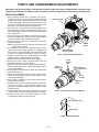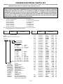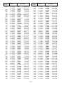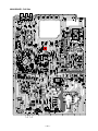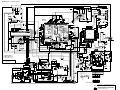
1
FILE NO.
SERVICE MANUAL
Remote Control Color
Television
DS20930
(U.S.A.)
(CANADA)
(MEXICO)
ORIGINAL VERSION
Chassis No. 20930-00
NOTE: Match the Chassis No. on
the unit’s back cover with
the Chassis No. in the
Service Manual.
MENU
CH
- VOL +
If the Original Version
Service Manual Chassis
No. does not match the
unit’s, additional Service
Literature is required. You
must refer to “Notices” to the
Original Service Manual
prior to servicing the unit.
POWER
Contents
Specifications
Safety Instructions . . . . . . . . . . . . . . . . . . . . . . . 2
Service Adjustments . . . . . . . . . . . . . . . . . . . 3 - 9
Purity and Convergence Adjustments. . . . 10 - 11
Service Hints . . . . . . . . . . . . . . . . . . . . . . . . . . 12
Mechanical Disassemblies . . . . . . . . . . . . . . . 13
Chassis Electrical Parts List . . . . . . . . . . . 14 - 21
Cabinet Parts List . . . . . . . . . . . . . . . . . . . . . . 22
Component and Test Point Locations. . . . 23 - 25
Block Diagram . . . . . . . . . . . . . . . . . . . . . . . . . 26
Power Rating . . . . . . . . . . . . . . . . . . . . . . 120V, 60Hz
Antenna Input Impedance . . . . . . . . . . . . . . . . . . 75Ω
UHF/VHF/CATV
Receiving Channel . . . . . . . . . . . . . . . . . . 2-13 (VHF),
14-69 (UHF),
01, 14-94, 95-125 (CATV)
Remote Ready . . . . . . . . . . . 26 Key Remote Control
Sound Output . . . . . . . . . . . . . . . . . . . . . . . . . 1 W/ch
Intermediate Frequency
Picture IF Carrier . . . . . . . . . . . . . . . . . . 45.75MHz
Sound IF Carrier . . . . . . . . . . . . . . . . . . . 41.25MHz
Color Sub Carrier . . . . . . . . . . . . . . . . . . 42.17MHz
Picture Tube . . . . . . . . . . . . . . . . . . . . . A51LVG896X
Semiconductors
Integrated Circuits. . . . . . . . . . . . . . . . . . . . . . . . . 9
Transistors . . . . . . . . . . . . . . . . . . . . . . . . . . . . . 23
Except within Tuner and RC Pre-Amp.
Cabinet Dimensions
Width. . . . . . . . . . . . . . . . . . . . . . . . . . . . . . 587mm
Height . . . . . . . . . . . . . . . . . . . . . . . . . . . . . 458mm
Depth . . . . . . . . . . . . . . . . . . . . . . . . . . . . . 486mm
DS20930, C3RK, PRODUCT CODE 111351429
REFERENCE No. SM780088
SAFETY INSTRUCTIONS
SAFETY PRECAUTIONS
READING SHOULD NOT EXCEED 1400 mV.
AC VOLTMETER
(5000 ohms per volt or more sensitivity)
WARNING: The chassis of this receiver has a floating ground
with the potential of one half the AC line voltage in respect to
earth ground. Service should not be attempted by anyone not
familiar with the precautions necessary when working on this
type of equipment.
The following precautions must be observed:
1. An isolation transformer must be connected in the power line
between the receiver and the AC line before any service is
performed on the receiver.
TELEVISION
RECEIVER
2. Comply with all caution and safety-related notes provided on
the side of the cabinet, inside the cabinet, on the chassis, and
the picture tube.
2000 ohm
10 watt
Good earth ground
such as a water pipe,
conduit, etc.
3. When replacing a chassis in the cabinet, always be certain
that all the protective devices are installed properly, such as
control knobs, adjustment covers, shields and barriers.
DO NOT OPERATE THIS TELEVISION RECEIVER
WITHOUT THE PROTECTIVE SHIELD IN POSITION AND
PROPERLY SECURED.
4. Before replacing the back cover of the set, thoroughly inspect
the inside of the cabinet to see that no stray parts or tools
have been left inside.
Before returning any television to the customer, the
service technician must perform the following safety checks
to be sure that the unit is completely safe to operate without
danger of electrical shock.
ANTENNA COLD CHECK
Remove AC plug from the 220 VAC outlet and place a jumper
across the two blades. Connect one lead of an ohmmeter to the
jumpered AC plug, and touch the other lead to each exposed
antenna terminal (UHF and VHF antenna terminals). The resistance must measure 10M ohm or over. Any resistance value
below this range indicates an abnormality which requires corrective action.
AC OUTLET
To be touched to all of exposed metal parts.
Voltmeter Hook-up for Leakage Current Check.
X-RADIATION PRECAUTION
The primary source of X-RADIATION in solid-state receivers is the
picture tube. The picture tube is specially constructed to limit X-Ray
emission. For continued X-RADIATION protection, the replacement
tube must be the same type as the original (including the suffix letter in the part numbers). Excessive high voltage may produce
potentially hazardous X-RADIATION. To avoid such hazards, the
high voltage must be maintained within specific limits. Refer to the XRADIATION WARNING NOTE on the CHASSIS SCHEMATIC in
this service manual for specific high voltage limits. If the high voltage exceeds specified limits, check the components specified on
the chassis schematic diagram and take the necessary corrective
action. Carefully follow the instructions for the +B Voltage Check
and the High Voltage Check to maintain the high voltage within the
specified limits.
LEAKAGE CURRENT CHECK
Plug the AC line cord directly into a 220 VAC outlet. (Do not use
an isolation transformer for this check.) Use an AC voltmeter,
that has 5000 ohms per volt or more sensitivity. Connect a 2000
ohm 10 watt resistor, between a known good earth ground
(water pipe, conduit, etc.) and all exposed metal parts of the
cabinet (antennas, earphone jack, screwheads, metal overlays,
control shafts, etc.). Measure the AC voltage across the 2000
ohm resistor.
The AC voltage should not exceed 1400 mV. A reading exceeding 1400 mV indicates that a dangerous potential exists. The
fault must be located and corrected. Repeat the above test with
the receiver power plug reversed.
PRODUCT SAFETY NOTICE
When replacing components in a receiver, always keep in mind
the necessary product safety precautions. Pay special attention
to the replacement of components marked with a star (★) in the
parts list and in the schematic diagrams. To ensure safe product
operation, it is necessary to replace those components with the
exact same PARTS.
NEVER RETURN A RECEIVER TO THE CUSTOMER
WITHOUT TAKING THE NECESSARY CORRECTIVE
ACTION.
—2—
SERVICE ADJUSTMENTS
GENERAL
This set has an On-screen Service Menu system included in the CPU that allows remote operation for most of the service adjustments.
IC802 (EEPROM) REPLACEMENT
When IC802 (EEPROM) is replaced, IC801 (CPU) will automatically write the initial reference data into IC802 for basic TV operation.
However, the bus data should be checked and some bus data should be set up before attempting the service adjustments. (See
pages 4 ~ 6 for detailed information.)
INITIAL BUS DATA SETUP
Note: When IC802 (EEPROM) is replaced, the Service Menu NO. 03 HP (H Phase), NO. 07 VLN (V Lin), NO. 28 PRE (Preshoot
Adj), NO. 37 AF (Auto Flesh), NO. 57 OPT (SA Option), and NO. 58 OP2 (SA Option 2) should be set up for proper TV operation before attempting the service adjustments.
1.
2.
3.
4.
5.
6.
7.
8.
9.
Disconnect the AC power cord (AC 120V line).
While pressing the MENU key, reconnect the AC power cord. The Service Menu display will now appear.
Select NO. 23 POS (Pre/Over SW) with ▲ or ▼ key. Adjust the data with + or – key for 1.
Select NO. 28 PRE (Preshoot Adj) with ▲ or ▼ key. Adjust the data with + or – key for 2.
Select NO. 37 AF (Auto Flesh) with ▲ or ▼ key. Adjust the data with + or – key for 1.
Select NO. 57 OPT (SA Option) with ▲ or ▼ key. Adjust the data with + or – key for 100.
Select NO. 58 OP2 (SA Option 2) with ▲ or ▼ key. Adjust the data with + or – key for 32.
Select NO. 63 SPO (Sub Bright Offset) with ▲ or ▼ key. Adjust the data with + or – key for 6.
Press the MENU key to turn off the Service Menu display.
ON-SCREEN SERVICE MENU SYSTEM
1. Enter the Service Menu:
NO.
DATA
XX OPT XXX XXXXXXXX
TITLE
ITEM NO.
BINARY DATA
(8 bit)
DECIMAL DATA
Figure 1. Service Menu Display
2. Service Adjustments:
• Press the ▲ or ▼ key to select the desired service menu you want to adjust. (See pages 4 for On-screen Service Menu.)
• Use the + or – key to adjust the data.
3. Exit from the Service Menu:
• Press the MENU key to turn off the Service Menu display.
—3—
Table 1. ON-SCREEN SERVICE MENU
When IC802 (EEPROM) is replaced, check the bus data to confirm they are the same as below. The shaded menu should be checked
and be set up or readjusted according to the procedures described in the following pages. Initial Setup Data marked with an * should
be changed from Initial Reference Data. (See page 3 for Initial Bus Data Setup.)
No.
TITLE
INITIAL REFFERENCE
DATA
INITIAL SETUP
DATA
RANGE OF DATA
01
HFR
29
29
0~63
02
AFC
0
0
0,1
03
HP
15
15
0~31
04
VS
64
64
0~127
Vertical Size
05
VPO
5
5
0~63
Vertical Position
06
VSP
0
0
0,1
07
VLN
18
18
0~31
Vertical Linearity
08
CRS
0
0
0~3
Cross B/W
09
GRY
1
1
0,1
Gray Mode
FUNCTION
Horizontal Frequency
AFC Gain & Gate
Horizontal Phase (Horizontal Centering)
Vertical Set Up (Sync. Sensitivity)
10
VSC
8
8
0~31
Vertical S Correction
11
HBR
3
3
0~7
H BLK R
12
HBL
4
4
0~7
H BLK L
13
CDM
0
0
0, 1
C D Mode
14
VC
7
7
0~7
Vertical Compression
15
RB
0
0
0~255
16
GB
0
0
0~255
Green Bias
17
BB
0
0
0~255
Blue Bias
18
RD
64
64
0~127
Red Drive
19
GD
8
8
0~15
Green Drive
20
BD
64
64
0~127
Blue Drive
21
SBI
48
48
0~127
Sub Bias
22
OSD
3
3
0~3
OSD Contrast
23
POS
0
1*
0,1
Pre/Over SW
Red Bias
24
FLS
1
1
0~7
Filter System
25
CKO
3
3
0~7
Color Killer Operation
26
GYA
0
0
0,1
G-Y Angle
27
CRG
2
2
0~3
Coring Gain
28
PRE
1
2*
0~3
Pre Shoot Adjust
29
WP
1
1
0,1
White Peak Limiter
30
FSW
0
0
0,1
FBP Blanking Switch
31
VBL
0
0
0,1
Vertical Blanking Switch
32
BSG
2
2
0~3
Black Stretch Gain
33
BSS
1
1
0~3
Black Stretch Start
34
DCR
1
1
0~3
DC Reset
35
YGM
1
1
0~3
Y Gamma
36
CBP
0
0
0,1
C Bypass
37
AF
0
1*
0,1
Auto Flesh
38
BAT
4
4
0~7
Brightness ABL Threshold
39
MSD
0
0
0,1
Mid Stop Def.
40
ABL
0
0
0,1
41
RYA
2
2
0~15
42
RAD
15
15
0~63
43
IAS
0
0
0,1
IF AGC
44
FMM
0
0
0,1
FM Mute
45
FL
15
15
0~31
FM Level
—4—
Auto Brightness Limit
R-Y/B-Y Angle
RF AGC Delay
Table 1. ON-SCREEN SERVICE MENU (Continued)
When IC802 (EEPROM) is replaced, check the bus data to confirm they are the same as below. The shaded menu should be checked
and be set up or readjusted according to the procedures described in the following pages. Initial Setup Data marked with an * should
be changed from Initial Reference Data. (See page 3 for Initial Bus Data Setup.)
No.
TITLE
INITIAL REFFERENCE
DATA
INITIAL SETUP
DATA
RANGE OF DATA
46
VL
4
4
0~7
47
EWD
39
39
0~63
EW DC.
48
EWA
30
30
0~63
EW Amp.
49
EWT
34
34
0~63
EW Tilt
50
EWP
7
7
0~7
EW Corner Top
51
EWB
8
8
0~7
EW Corner Bottom
52
HSC
7
7
0~7
Horizontal Size Comp.
53
SB
32
32
0~63
Sub Brightness
54
SCO
7
7
0~31
Sub Color
FUNCTION
Video Level
55
STI
20
20
0~31
Sub Tint
56
SSH
12
12
0~31
Sub Sharpness
57
OPT
0
100*
0~255
Option (See Note 1 page 6.)
58
OP2
0
32*
0~255
Option 2 (See Note 2 page 6.)
59
HR
27
27
0~63
OSD Horizontal Position
60
ATT
7
7
0~63
Input Level
61
WDB
32
32
0~63
Wideband
62
SPC
32
32
0~63
Spectral
63
SBO
5
6*
0~255
Sub Brighatness Offset
64
PCO
40
40
0~63
PIP Color
65
PTI
40
40
0~63
PIP Tint
66
PUV
24
24
0~63
PIP Top Position
67
PDV
147
147
0~255
PIP Bottom Position
68
PLH
40
40
0~63
PIP Left Position
69
PRH
101
101
0~255
PIP Right Position
70
PCN
52
52
0~63
PIP Y level
71
PBS
15
15
0~63
PIP BGP Phase
64
64
0~127
Red Drive Adjustment (See Note 3 page 6.)
72
73
DRV
64
64
0~127
Blue Drive Adjustment (See Note 3 page 6.)
–
0
0
0~255
Red Bias Adjustment (See Note 4 page 6.)
–
0
0
0~255
Green Bias Adjustment (See Note 4 page 6.)
–
0
0
0~255
Blue Bias Adjustment (See Note 4 page 6.)
—5—
SERVICE ADJUSTMENTS (Continued)
PROGRAM CODES
DRIVE / BIAS ADJUSTMENTS
The microprocessor used in this model is a multi-purpose type
and is used in several different models. To ensure proper
operation and the correct features for your particular model,
the Program Codes must be correct.
Note 3. Red/Blue Drive Adjustments in Service Menu No.
72 DRV: Adjust Red and Blue Drive Levels alternately with 1, 3,
7, and 9 keys on the remote control. (See Figure 2.) The Drive
Level adjustment data will be rewritten in the Service Menu No.
18 and 20 automatically.
Note 1. Option Data 1 (No. 57 OPT) should be decimal 100
(01100100 binary). See page 3 INITIAL DATA SETUP, step 6,
for set up procedure. If this program code is wrong, the TV will
not operate properly.
No. 57 OPT
BIT
0,1
DATA
FUNCTION
0
TV
1
10: MONITOR
CLOCK
5
STEREO/MONO
6,7
SURROUND
4
5
6
(N/A)
(N/A)
(N/A)
7
8
9
BD(-)
(N/A)
BD(+)
FOR RED DRIVE ADJUSTMENTS
FOR BLUE DRIVE ADJUSTMENTS
Note 4. Red/Green/Blue Bias Adjustments in Service Menu
No. 73: Adjust each Bias Level with 1, 3, 4, 6, 7, or 9 key on the
remote control. (See Figure 3.) The Bias Level adjustment data
will be rewritten in the Service Menu No. 15 ~ 17 automatically.
11: INHIBITED (=TV)
VIDEO INPUT
3
RD(+)
Figure 2.
01: HOTEL
MONITOR
3,4
2
(N/A)
00: TV
HOTEL
2
1
RD(-)
NONE
YES
NOT USED
MONO
STEREO
00: NONE
01: YES
10: NOT USED
11: NOT USED
Note 2. Option Data 2 (No. 58 OP2) should be decimal 32
(00100000 binary). See page 3 INITIAL DATA SETUP, step 7,
for set up procedure. If this program code is wrong, the TV will
not operate properly.
No. 58 OP2
BIT
FUNCTION
DATA
0
1
YES
NONE
0
V-GUIDE
1
COLOR ENHANCER
NOT USED
2
INITIAL CHANNEL
NOT USED
3
NOT USED
NOT USED
4
PIP
NOT USED
5
AV1/AV1, AV2
6
TONE/BASS, TREBLE
7
GAME KEY
AV1
AV1, AV2
NOT USED
NONE
YES
—6—
1
2
3
RB(-)
(N/A)
RB(+)
4
5
6
GB(-)
(N/A)
GB(+)
7
8
9
BB(-)
(N/A)
BB(+)
Figure 3.
FOR RED BIAS ADJUSTMENTS
FOR GREEN BIAS ADJUSTMENTS
FOR BLUE BIAS ADJUSTMENTS
ANTENNA CONNECTIONS
VCO ADJUSTMENT
This receiver is designed for UHF/VHF reception. A 75 ohm
terminal is provided for UHF and VHF receptions. When
connecting a CATV antenna system, connect the 75 ohm
coaxial cable directly to the 75 ohm terminal. For 300 ohm VHF
antenna, use the adapter (included with the TV set).
Note: VCO must be adjusted after IC101 (Signal Processor),
IC802 (EEPROM) or T151 (IF VCO Coil) is replaced.
CIRCUIT PROTECTION
Fuse F601 (4A) is included in the AC line. This fuse must be
replaced with the proper fuse. (See Parts List.)
CAUTION FOR CONTINUED PROTECTION AGAINST A
RISK OF FIRE, REPLACE ONLY WITH THE
SAME TYPE 4A, 125V FUSE.
4A 125V
ATTENTION: POUR MAINTENIR LA
PROTECTION CONTRE LES RISQUES D’
INCENDIE UTILISER UN FUSIBLE DE
RECHANGE DE MEME TYPE 4A, 125V.
+B VOLTAGE CHECK
Connect voltmeter + lead to TJ1 130V and – lead to ground
(TE7). Connect receiver to AC 120V line. Tune receiver to an
active channel. Reset the picture controls to the FACTORY
PRESET levels (press remote control RESET key twice).
Voltage must measure between +128.0V and +132.0V. If the
voltage is out of this range, the power circuit must be checked.
No +B adjustment is provided on this chassis.
HORIZONTAL CENTERING ADJUSTMENT
1. Tune receiver to an active channel.
2. Check that picture is in the horizontal center of TV screen.
If picture is too right or left, perform steps 3 ~ 6.
3. Turn off the receiver and disconnect the AC power cord.
4. While pressing the MENU key, reconnect the AC power cord.
The Service Menu display will now appear.
5. Select No. 03 HP (Horizontal Phase) with ▲ or ▼ key.
6. Adjust the data with + or – key for horizontal center.
To turn off the Service Menu display, press the MENU key.
1. Tune receiver to an active channel.
2. Set the picture controls to the Sports level.
3. Connect digital voltmeter + lead to pin 58 of IC101(TP10)
and – lead to ground (TE 7).
4. Confirm a reading of 3.6 ±0.6 VDC.
5. If voltage is out of specifications adjust T151 for 3.6 ±0.6
VDC.
RF-AGC ADJUSTMENT
1. Tune receiver to strongest VHF station in your area.
2. Set contrast and brightness controls for maximum.
3. Turn off the receiver and disconnect the AC power cord
(120V AC line).
4. While pressing the MENU key, reconnect the AC power
cord. The Service Menu display will now appear.
5. Select No. 42 RAD (RF AGC Delay) with ▲ or ▼ key.
6. Adjust the data with + or – key in the direction which causes
snow to appear, then in the opposite direction until the snow
just disappears.
VIDEO LEVEL
1. Connect color-bar generator to antenna terminal.
2. Turn off the receiver and disconnect the AC power cord
(120V AC line).
3. Connect oscilloscope to TP16(Q202 emitter) and ground.
4. While pressing the MENU key, reconnect the AC power
cord. The Service Menu display will now appear.
5. Select No. 46 VL (Video Level) with ▲ or ▼ key.
6. Adjust the + or – key for an oscilloscope reading of 1.0±0.1
Vp-p at TP16. Press the MENU key to turn off the Service
Menu display.
VERTICAL SIZE ADJUSTMENT
1. Tune receiver to an active channel.
2. Check the vertical size of the picture. If the vertical size is too
large or small, perform steps 3 ~ 6.
3. Turn off the receiver and disconnect the AC power cord.
4. While pressing the MENU key, reconnect the AC power cord.
The Service Menu display will now appear.
5. Select No. 04 VS (Vertical Size) with ▲ or ▼ key.
6. Adjust the data with + or –key for full scan. To turn off the
Service Menu display, press the MENU key.
VERTICAL CENTERING ADJUSTMENT
1. Tune receiver to an active channel.
2. Check that picture is in the vertical center of TV screen. If picture
center is too low, add a cutting wire to R513.
—7—
1.0 ±0.1 Vp-p
Figure 4.
SERVICE ADJUSTMENTS (Continued)
GRAYSCALE ADJUSTMENT
BRIGHTNESS LEVEL ADJUSTMENT
1. Set the picture controls to the Sports levels or Reset
(use MENU key and ▲ or ▼ key or RESET key).
2. Turn off the receiver and disconnect the AC power cord
(120V AC line).
3. While pressing the MENU key, reconnect the AC power
cord. The Service Menu display will now appear.
4. Select No. 15 RB (Red Bias), No. 16 GB (Green Bias), and
No. 17 BB (Blue Bias) with ▲ or ▼ key and set each data to
0 with + or – key.
5. Select No. 18 RD (Red Drive) and No. 20 BD (Blue Drive) with
▲ or ▼ key and set each data to 64 with + or – key.
6. Set No. 19 GD (Green Drive Reduction) data to 8, No. 53 SB
(Sub Brightness) data to 32, NO. 54 SCO (Sub Color ) data to
7, NO. 55 STI (Sub Tint) to 20, and NO. 56 SSH (Sub
Sharpness) data to 12 with ▲ or ▼, and + or – keys.
7. Turn Screen Control (T402) to minimum (fully counterclockwise).
8. Select the Service Menu No. 73 (Bias Adjustments) with ▲
or ▼ key.
9. Advance Screen Control (T402) clockwise to obtain just
visible one color line. If line does not appear, place this
control to maximum (fully clockwise).
10. Raise each Bias Level with 3, 6, and 9 keys to obtain just
visible white line. (See Figure 5 below.)
Note:Grayscale, RF AGC, Video Level, and High Voltage
Check must be adjusted before attempting Brightness
Level Adjustment.
1. Connect a color-bar generator to the antenna terminal.
2. Switch the generator to the crosshatch pattern.
3. Reset the picture controls to the Sports levels.
4. Connect voltmeter (high impedance) + lead to terminal
TP51 and – lead to terminal TP50 on main board. Set voltmeter for 1.5V~3.0V range.
5. Turn off the receiver and disconnect the AC power cord
(120V AC line).
6. While pressing the MENU key, reconnect the AC power
cord. The Service Menu display will now appear.
7. Select No. 53 SB (Sub Brightness) with ▲ or ▼ key.
8. Adjust the data with + or – key for 650mVDC.
9. Press the MENU key to turn off the Service Menu display.
10. Check brightness level on every active channels, readjust
(repeat steps 5~9), if necessary.
1
2
3
RB(-)
(N/A)
RB(+)
4
5
6
GB(-)
(N/A)
GB(+)
7
8
9
BB(-)
(N/A)
BB(+)
FOR RED BIAS ADJUSTMENTS
FOR GREEN BIAS ADJUSTMENTS
FOR BLUE BIAS ADJUSTMENTS
Figure 5. Remote Control Number keys’ functions
in Service Menu No. 73
11. Select the Service Menu No. 72 DRV (Drive Adjustments)
with ▲ or ▼ key.
12. Adjust Red and Blue Drive Levels alternately with 1, 3, 7, or
9 key to produce normal black and white picture in highlight
areas. (See Figure 6.)
1
2
3
RD(-)
(N/A)
RD(+)
4
5
6
(N/A)
(N/A)
(N/A)
7
8
9
BD(-)
(N/A)
BD(+)
Note: Do not set to excessive brightness level, otherwise the
contrast level will be suppressed.
HIGH VOLTAGE HOLD-DOWN TEST
Every time the receiver is serviced, the HIGH VOLTAGE
HOLD -DOWN circuit must be tested for proper operation by
following these steps;
1. Connect receiver to 120V AC line. Tune receiver to active
channel. Reset the picture controls to the Sports levels.
2. Check that the voltage measured between TP7 and TE7
(ground side) is within 16.5 VDC to 21 VDC. If the voltage is
out of this range, the Hold-Down Circuit must be checked.
3. Connect a DC Voltage supply to TP7 and TE7 through a 100
ohm 1/4W resistor. Adjust the DC voltage to 23VDC. The
receiver should shutdown, losing raster and sound. Then the
receiver should turn off automatically. This reaction indicates
that the Hold-Down circuit is functioning properly. If the
receiver goes not shutdown, a malfunction is indicated and
its cause must be found and corrected.
4. To obtain picture again, remove the DC Supply and wait a
few minutes. Now turn on the receiver.
FOR RED DRIVE ADJUSTMENTS
FOR BLUE DRIVE ADJUSTMENTS
Figure 6. Remote Control Number keys’ functions
in Service Menu No. 72 DRV
13. Check for proper grayscale at all brightness levels.
To turn off the Service Menu display, press the MENU key.
Note: If Grayscale Adjustment is made after picture tube
replacement, make Brightness Level Adjustment.
FOCUS ADJUSTMENT
Adjust focus control (T402) for well defined scanning lines.
—8—
SOUND ADJUSTMENT
SEPARATION ADJUSTMENT
1. Connect a color-bar generator to the antenna terminal with
audio signal of 1KHz at 100% modulated.
2. Set the picture controls to the Sports levels.
3. Connect oscilloscope + lead to TP21 (base Q135) and –
lead to ground.
4. Turn off the receiver and disconnect the AC power cord
(120V AC line).
5. While pressing the MENU key, reconnect the AC power
cord. The Service Menu display will now appear.
6. Select No. 45 FL (FM Level) with ▲ or ▼ key.
7. Adjust the data with + or – key for an oscilloscope reading
of 0.693 ±10% Vp-p at TP21.
8. Press the MENU key to turn off the Service Menu display
and disconnect the oscilloscope fromthe chassis.
7. Turn off the receiver and disconnect the AC power cord
(120V AC line).
8. Connect oscilloscope CH1 to TP317 and CH2 to TP318
and ground.
9. Connect an MTS TV/Stereo generator to antenna terminal.
10. While pressing the MENU key, reconnect the AC power
cord. The Service Menu display will now appear.
11. Select pilot , 300Hz audio frequency and Left modulating
signal.
12. Select NO. 61 WDB (Wideband) with ▲ or ▼ key.
13. Adjust the + or – key for minimum low frequencies at
TP317.(See Figure 8.)
14. Select 4K Hz audio frequency and Right modulating signal.
15. Select NO. 62 SPC (Spectral) with ▲ or ▼ key.
16. Adjust the + or – key for minimum high frequencies at
TP318.(See Figure 8.)
Repeat adjustment (steps 11-16) until no further decrease in
amplitude can be obtained. Press the MENU key to turn off the
Service Menu display.
0.693 ±10% Vp-p
Minimize L leakage
TP317 (R)
Figure 7.
300Hz
Minimize R leakage
MULTI-SOUND SECTION ADJUSTMENTS
TP318 (L)
Note: Multi-Sound Section must be adjusted after IC101
(Signal Processor), IC3401 (MTS Decoder) or IC802
(EEPROM) is replaced.
4KHz
Figure 8. Separation Adjustments
INPUT LEVEL ADJUSTMENT
1. Connect a signal to the antenna terminal with audio signal
of 1KHz at 100% modulated.
2. Turn off the receiver and disconnect the AC power cord
(120V AC line).
3. Connect voltmeter (RMS) to TP317 and ground.
4. While pressing the MENU key, reconnect the AC power
cord. The Service Menu display will now appear.
5. Select NO. 60 ATT (Attenuation) with ▲ or ▼ key.
6. Adjust the + or – key for a voltmeter reading of 400 ±20
mVrms at TP317.
—9—
PURITY AND CONVERGENCE ADJUSTMENTS
CAUTION: Purity and Convergence adjustments have been made at the factory. Readjustments should be made
only after the picture tube or deflection yoke is replaced. Follow the steps below for the necessary readjustments.
PURITY ADJUSTMENT
DEFLECTION YOKE
RUBBER
WEDGE
DEFLECTION YOKE
MOUNTING SCREW
Figure 1. Deflection Yoke Movement
PURITY
MAGNET
TABS
SIX-POLE
MAGNET TABS
34
FOUR-POLE
MAGNET TABS
12
1. When replacing picture tube or deflection yoke, mount
deflection yoke and purity-convergence magnets assembly
properly. See Figure 1. Position the picture tube facing east
or west. Demagnetize the picture tube and receiver using
an external degaussing coil. Set receiver to TV Service
Menu No. 73 (no vertical sweep) while degaussing.
2. Place the yoke on tube neck fully forward against glass.
Place the CPM on the tube neck aligning the center of the
purity magnet tabs (2 pole) over center of Focus Gap (G3 &
G4). See Figure 2.
3. Connect a color bar generator to the antenna terminal.
Switch the generator to a white field. Move yoke backward
on the neck until a uniform white field is obtained.
4. Allow 30 minutes warm up on a blank white field (high
intensity grayscale).
Note: If white field cannot be obtained, check Grayscale
Adjustments on page 6.
5. Set the picture controls to the Auto levels. Select a green
raster, either with the signal generator or by adjusting the
bias controls. If a signal generator is used for this step, Skip
to Step 10. If the bias controls will be used, go to step 6.
6. Adjust TV Service Menu No. 15 RB (R-Bias), No. 16 GB
(G-Bias), and No. 17 BB (B-Bias) data to 0 each.
7. Select TV Service Menu No. 73 (no vertical sweep).
8. Adjust the screen control counterclockwise until the
horizontal scan lines is no longer visible.
9. Select TV Service Menu No. 16 GB (G-Bias) and raise the
data to produce green raster. If retrace lines appear, reduce
screen control slightly.
10. Pull yoke back on the tube neck to obtain three-color raster
(blue, green and red).
11. Adjust the angle between the two purity magnet tabs to
center the vertical green belt in the picture tube. Do not
rotate tabs. See Figure 3.
12. Slowly slide the deflection yoke forward until a uniform
green screen is obtained.
13. Check the purity of the red and blue screens for uniformity.
Turn off other colors to check (use bias controls) or use
generator. If necessary, readjust the yoke position until all
screens are pure.
14. If bias controls and screen control were used to set purity,
reset Grayscale. Refer to Grayscale Adjustment on page 6.
15. Confirm that the yoke is not tilted. Tighten the yoke
mounting screw. Adjust convergence next.
ANGLE
OF TABS
FOCUS GAP
(G3-G4)
Figure 2. Purity and Convergence Magnets
ANGLE OF MAGNET TABS
MAGNET TABS
Figure 3. Adjusting Magnet
— 10 —
CONVERGENCE ADJUSTMENT
CENTER CONVERGENCE ADJUSTMENT
OUTER AREA CONVERGENCE ADJUSTMENT
1. Connect a crosshatch generator to antenna terminals.
2. Set Contrast control to low level to eliminate Blooming.
Reduce Brightness level to obtain black background if
necessary.
3. Adjust the angle between the four-pole magnet tabs 1 and 2
(Figure 2), and superimpose the red and blue vertical lines
in the center area of the picture screen. See Figure 4.
4. Keeping the tabs at the same angle, rotate them together to
superimpose the blue and red horizontal lines in the center
area of the picture screen. See Figure 4.
5. Adjust the six-pole magnet tabs 3 and 4 so the converged
red/blue line is superimposed on the green line. This is the
same procedure used in Steps 3 and 4. See Figure 5.
The outer area convergence is performed by positioning of the
yoke as follows:
1. Move the top of the yoke toward or away from the picture
tube. This movement will affect the vertical lines at the top
and bottom and the horizontal lines at the sides.
See Figure 6.
2. Check that splits at 12 O’Clock and 6 O’Clock positions are
minimized, adjust yoke for best compromise. Secure with
wedge at 12 O’Clock position. See Figure 1.
3. Move the side of the yoke toward or away from the picture
tube to converge the horizontal lines at the top and bottom
and the vertical lines at the sides. See Figure 7.
4. Check that splits at 12 O’Clock and 6 O’Clock are
minimized, adjust yoke for best compromise. Secure yoke
position with the side wedges. See Figure 1.
Note: When reusing the rubber wedges, apply a small
amount of silicone rubber adhesive or hot melt to each
of the wedges.
GREEN
BLUE
RED
BLUE
BLUE
GREEN
RED
RED
Adjust four-pole tabs angle to
superimpose blue and red vertical
line.
Adjust four-pole tabs together
to superimpose red and blue
horizontal line.
Line movement when adjusting
top of yoke in and out.
Figure 4. Blue an Red Line Movement
Figure 6. Top of Yoke Movement
BLUE
GREEN
RED
BLUE
GREEN
RED
BLUE / RED
BLUE
GREEN
RED
GREEN
Adjust six-pole tabs angle to
superimpose red / blue and
green vertical line.
Adjust six-pole tabs together
to superimpose red / blue and
green horizontal line.
Figure 5. Blue/Red and Green Line Movement
BLUE
GREEN
RED
Line movement when adjusting
side of yoke in and out.
Figure 7. Side of Yoke Movement
— 11 —
SERVICE HINTS
POWER FAILURE DETECTOR
This set is equipped with a Power Failure Detector function included in the CPU which checks for an abnormal condition in the
chassis power supplies, including the power supply derived from the Horizontal Output Transformer.
If, while the power is on, a failure is caused by any of the following that results in a low voltage supply, the CPU will turn the unit off in
1.5 seconds to prevent unnecessary damage:
• Failure within the power supply circuits.
• A short circuit in the load side from the supply.
• Stoppage of the Horizontal Output Oscillator caused by the X Radiation protection Hold-Down Circuit.
If, while the power is off, the power is switched on and any of these failures remains uncorrected, the CPU will shut off the power
within three seconds.
Check the following if the unit is turned off by the power failure detector.
1. Disconnect the AC power cord (120V AC line) for at least 10 seconds.
2. Connect a DC Voltmeter to the following TEST POINTS.
TJ6
D429 Cathode
5V
5V
3. Press the power key and check for the proper voltage supplies.
4. If any of these voltages is low, the power failure detector should turn the set off within three seconds.
5. Check all circuits listed above.
Note:This unit is equipped with a Power Surge Protection feature included in the CPU. If power Failure occurs three times within 15
minutes, the CPU will automatically stop functioning to help prevent secondary damage. (TV will not turn on by pressing the
power key.) To reset the operating programs within the CPU, disconnect the AC power cord for at least 10 seconds.
— 12 —
MECHANICAL DISASSEMBLIES
CABINET BACK REMOVAL
CHASSIS REMOVAL
1. Refer to Figure 1, remove 8 screws.
2. Pull off cabinet back and remove.
1. Remove cabinet back.
2. Discharge the picture tube anode (2nd anode lead) to the
dag coating (picture tube grounding lead).
3. Disconnect Degaussing coil socket (KD), Picture tube
socket, Deflection yoke connector (KDY), Speaker
connectors (KSP), and 2nd anode lead.
4. Remove chassis completely by sliding it straight back.
PICTURE TUBE REMOVAL
CAUTION: Do not disturb the deflection yoke or magnet
assembly on the picture tube neck. Care must be taken to
keep these assemblies intact, unless picture tube is being
replaced . Discharge the picture tube to the coating before
handling the tube.
1. Remove chassis, referring to Chassis Removal instructions.
2. Place cabinet’s front face down on the soft surface.
3. Remove the screw on each corner of the picture tube and
GENTLY lift the picture tube out of the cabinet.
4. Install a replacement picture tube in reverse order.
Properly install the degaussing coil and picture tube grounding lead on the picture tube. See Figure 2.
AV2 INPUT
R
AUDIO
L
S-VIDEO
(MONO)
UHF / VHF / CATV
75Ω
VIDEO
Figure 1. Cabinet Back Removal
Note: If the Picture Tube is being replaced, mount the
Degaussing Coil on the picture tube. See Figure 2.
DEGAUSSING
COIL
DEGAUSSING
COIL SOCKET
DEGAUSSING
COIL HOLDER
To CRT
unit ground
PICTURE TUBE
GROUND LEAD
Figure 2. Picture Tube Removal
— 13 —
CHASSIS ELECTRICAL PARTS LIST
CAUTION: To Protect against electrical shock and for continued product safety, refer to SAFETY PRECAUTIONS,
X-RADIATION PRECAUTION and PRODUCT SAFETY NOTICE on Page 2.
PRODUCT SAFETY NOTICE
PRODUCT SAFETY SHOULD BE CONSIDERED WHEN A REPLACEMENT IS MADE IN ANY AREA OF A RECEIVER.
COMPONENTS INDICATED BY A STAR (★) IN THIS PARTS LIST AND THE SCHEMATIC DIAGRAM DESIGNATE
COMPONENTS IN WHICH SAFETY CAN BE OF SPECIAL SIGNIFICANCE. IT IS PARTICULARLY RECOMMENDED
THAT ONLY PARTS DESIGNATED ON THE FOLLOWING PARTS LIST BE USED FOR COMPONENT REPLACEMENT
DESIGNATED BY A STAR. NO DEVIATIONS FROM RESISTANCE, WATTAGE, AND VOLTAGE RATINGS MAY BE
MADE FOR REPLACEMENT ITEMS DESIGNATED BY A STAR.
Notes: Parts having Location Number are located on the following boards.
Numbers under 700 Series . . . . . . . . . . . . . . . . . . . . . .On the Main Board.
Numbers 700 Series . . . . . . . . . . . . . . . . . . . . . . . . . . . .On the Picture Tube Socket Board.
Numbers 800 Series . . . . . . . . . . . . . . . . . . . . . . . . . . . .On the Main Board
Numbers 900 Series . . . . . . . . . . . . . . . . . . . . . . . . . . . .Out of Board.
Numbers 1000 Series . . . . . . . . . . . . . . . . . . . . . . . . . . .On the Main Board.
Numbers 1100 series . . . . . . . . . . . . . . . . . . . . . . . . . . .On the Main Board
Numbers 1900 series . . . . . . . . . . . . . . . . . . . . . . . . . . .On the Main Board
Note: Schematic part location numbers may not always match with the part descriptions.
The part descriptions are correct and should be used.
Schematic
Location
Part No.
Schematic
Location
Description
CAPACITORS
NOTES:
Read description of the Capacitor as follows:
(Example)
CERAMIC
100P
K
50V
Rated Voltage
Tolerance Symbols:
less than 10PF
A . .Not specified
B . .±0.1PF
C . .±0.25PF
D . .±0.5PF
F . .±1PF
G . .±2PF
R . .+0.25 - 0PF
S . .+0 - 0.25PF E . .+0 - 1PF
more than 10PF
A . .Not specified
B . .±0.1%
C . .±0.25%
D . .±0.5%
F . .±1%
G . .±2%
H . .±3%
J . .±5%
K . .±10%
L . .±15%
M . .±20%
N . .±30%
P . .+100 - 0%
Q . .+30 - 10% T . .+50 - 10%
U . .+75 - 10% V . .+20 - 10%
W .+100 - 10% X . .+40 - 20%
Y . .+150 - 10% Z . .+80 - 20%
Rated Value: P...Pico Farad U...Micro Farad
Material:
CERAMIC . . . . . .Ceramic
MT-PAPER . . . . .Metalized Paper
POLYESTER . . .Polyester
MT-POLYEST . . .Metalized Polyester
POLYPRO . . . . .Polypropylene
MT-POLYPRO . .Metalized Polypropylene
COMPO-FILM . .Composite Film
MT-COMPO . . . .Metalized Composite
STYRENE . . . . .Styrene
TA-SOLID . . . . . .Tantalum Solid
AL-SOLID . . . . . .Aluminum Solid
ELECT . . . . . . . .Electrolytic
NP-ELECT . . . . .Non-Polarized Electrolytic
OS-SOLID . . . . .Aluminum Solid with Organic
Semiconductive Electrolytic
C001
C002
C003
C004
C006
C010
C011
C012
C015
C101
C103
C106
C131
C133
C134
C136
C137
C141
C142
C143
C146
C147
C151
C153
C161
C211
C212
C221
C251
C252
C253
C256
C257
— 14 —
Part No.
403 048 1907
403 048 1907
403 155 2408
403 155 2408
403 215 2201
403 045 7803
403 045 7803
403 042 7707
403 043 6006
403 039 3507
403 215 2201
403 049 9803
403 049 0008
403 215 2201
403 113 3805
401 105 7909
403 166 9205
403 215 2201
403 284 4304
403 215 2201
403 215 2201
403 038 1603
403 048 6308
403 048 6308
403 305 3507
403 086 2300
403 049 9803
403 086 2300
401 105 7909
404 086 6602
403 062 0306
403 062 0504
403 179 0909
403 048 6308
403 049 0008
403 215 2201
Description
ELECT
ELECT
CERAMIC
CERAMIC
CERAMIC
ELECT
ELECT
ELECT
ELECT
ELECT
CERAMIC
ELECT
ELECT
CERAMIC
CERAMIC
MT-GLAZE
CERAMIC
CERAMIC
CERAMIC
CERAMIC
CERAMIC
ELECT
ELECT
ELECT
CERAMIC
NP-ELECT
ELECT
NP-ELECT
MT-GLAZE
POLYESTER
POLYESTER
POLYESTER
POLYESTER
ELECT
ELECT
CERAMIC
0.22U M
50V
0.22U M
50V
5600P K
50V
5600P K
50V
0.01U K
50V
220U M
25V
220U M
25V
22U M
16V
330U M
16V
470U M 6.3V
0.01U K
50V
2.2U M
50V
1U M
50V
0.01U K
50V
1000P K
50V
0.000 ZA 1/16W
10P J
50V
0.01U K
50V
0.022U K
50V
0.01U K
50V
0.01U K
50V
100U M 6.3V
0.47U M
50V
0.47U M
50V
0.1U Z
50V
1U M
50V
2.2U M
50V
1U M
50V
0.000 ZA 1/16W
0.047U K
63V
0.047U K
50V
0.047U K
50V
0.047U K
50V
0.47U M
50V
1U M
50V
0.01U K
50V
Schematic
Location
C258
C272
C274
C284
C285
C401
C402
C403
C404
C405
C406
C407
C408
★C411
★C416
C421
C427
C441
C471
C473
C482
C484
C487
C489
C493
C497
C502
C503
C504
C505
C506
C508
C509
C510
★C511
C516
★C601
C603
Part No.
403 044 1703
403 050 6600
403 041 8804
403 043 9106
403 215 2201
403 043 1902
403 215 2201
404 086 6800
403 063 0008
403 063 0206
403 179 0305
403 157 3601
403 086 2300
403 076 3607
403 075 9204
403 055 0504
404 077 4402
403 343 7901
404 081 2401
403 078 9805
403 346 6901
403 372 6609
403 038 6301
403 215 2201
403 215 2201
403 044 1703
404 084 5706
403 166 7706
403 067 7805
403 256 0808
403 115 0802
403 051 0607
403 052 8503
403 043 0202
404 056 5307
404 045 6605
403 038 1603
403 053 2104
403 049 9803
403 045 9807
404 084 5706
403 166 7706
403 067 7805
403 256 0808
403 062 5103
403 062 5301
403 179 0701
403 157 3106
404 084 5706
403 166 7706
403 067 7805
403 256 0808
403 215 2201
403 260 2300
403 041 8804
404 071 2404
404 066 2204
404 088 8802
403 075 7101
Schematic
Location
Description
ELEC
ELECT
ELECT
ELECT
CERAMIC
ELECT
CERAMIC
POLYESTER
POLYESTER
POLYESTER
POLYESTER
CERAMIC
NP-ELECT
CERAMIC
CERAMIC
ELECT
MT-POLYPRO
MT-POLYPRO
MT-POLYPRO
MT-POLYPRO
MT-POLYPRO
MT-POLYPRO
ELECT
CERAMIC
CERAMIC
ELECT
MT-POLYEST
MT-POLYEST
MT-COMPO
MT-COMPO
ELECT
ELECT
ELECT
ELECT
NP-ELECT
NP-ELECT
ELECT
ELECT
ELECT
ELECT
MT-POLYEST
MT-POLYEST
MT-COMPO
MT-COMPO
POLYESTER
POLYESTER
POLYESTER
CERAMIC
MT-POLYEST
MT-POLYEST
MT-COMPO
MT-COMPO
CERAMIC
MT-COMPO
ELECT
MT-POLYEST
MT-POLYEST
MT-POLYEST
CERAMIC
470U M
3.3U M
10U M
47U M
0.01U K
2200U M
0.01U K
6800P J
6800P K
6800P K
6800P K
100P J
1U M
470P K
1500P K
1U M
7200P H
7200P H
0.22U M
0.22U J
0.22U J
0.22U J
220U M
0.01U K
0.01U K
470U M
47U J
0.47U J
0.47U J
0.47U J
22U M
4.7U M
1000U M
220U M
2.2U M
2.2U M
100U M
220U M
2.2U M
2200U M
0.47U J
0.47U J
0.47U J
0.47U J
5600P K
5600P K
5600P K
56P J
0.47U J
0.47U J
0.47U J
0.47U J
0.01U K
0.15U J
10U M
0.22U K
0.22U M
0.22U M
1000P K
16V
50V
16V
16V
50V
16V
50V
63V
50V
50V
50V
50V
50V
500V
500V
160V
1.5K
1.5K
200V
200V
250V
250V
6.3V
50V
50V
16V
63V
63V
50V
50V
100V
50V
35V
16V
100V
50V
6.3V
35V
50V
25V
63V
63V
50V
50V
50V
50V
50V
50V
63V
63V
50V
50V
50V
50V
16V
250V
275V
275V
500V
C604
C606
C 608
C609
C612
C613
C614
★C625
C626
C628
C629
★C631
★C632
C634
C683
C689
C693
C701
C711
C721
★C742
C801
C806
C809
C810
C811
C822
C829
C835
C841
C842
C843
C853
C854
C856
C857
C858
C862
C1001
C1002
C1051
C1052
C1059
C1071
C1080
— 15 —
Part No.
403 075 7101
404 088 2909
404 088 7102
403 222 1907
403 263 6305
404 075 5005
404 089 3509
404 084 5102
403 057 2803
403 057 3107
403 181 8207
404 086 6503
403 062 0306
403 062 0504
403 179 0909
404 084 5003
403 057 0403
403 057 0601
403 179 3801
403 266 4902
403 042 4805
404 052 9309
403 043 0202
404 088 2909
404 088 7102
404 088 2909
404 088 7102
403 043 9106
403 043 0202
403 305 3507
403 047 8402
403 146 0505
403 113 3805
403 113 3805
403 077 2807
403 215 2201
403 039 3507
403 157 3601
403 157 3601
403 049 0008
403 042 7707
403 049 0008
403 215 2201
403 305 3507
403 305 3507
403 305 3507
403 047 8402
403 153 9300
403 049 0008
403 157 4202
403 113 3805
403 215 2201
403 041 8804
403 041 8804
403 042 7707
403 215 2201
403 041 8804
403 215 2201
403 305 3507
Description
CERAMIC
CERAMIC
CERAMIC
CERAMIC
CERAMIC
ELECT
ELECT
POLYESTER
POLYESTER
POLYESTER
POLYESTER
POLYESTER
POLYESTER
POLYESTER
POLYESTER
POLYESTER
POLYESTER
POLYESTER
POLYESTER
CERAMIC
ELECT
ELECT
ELECT
CERAMIC
CERAMIC
CERAMIC
CERAMIC
ELECT
ELECT
CERAMIC
ELECT
CERAMIC
CERAMIC
CERAMIC
CERAMIC
CERAMIC
ELECT
CERAMIC
CERAMIC
ELECT
ELECT
ELECT
CERAMIC
CERAMIC
CERAMIC
CERAMIC
ELECT
CERAMIC
ELECT
CERAMIC
CERAMIC
CERAMIC
ELECT
ELECT
ELECT
CERAMIC
ELECT
CERAMIC
CERAMIC
1000P K
1000P M
1000P M
2200P K
2200P K
470U M
470U M
0.1U K
0.1U K
0.1U K
0.1U K
0.047U J
0.047U K
0.047U K
0.047U K
0.01U J
0.01U K
0.01U K
0.01U K
1200P K
1000U M
220U M
220U M
1000P M
1000P M
1000P M
1000P M
47U M
220U M
0.1U Z
0.1U M
1200P K
1000P K
1000P K
1000P Z
0.01U K
470U M
100P J
100P J
1U M
22U M
1U M
0.01U K
0.1U Z
0.1U Z
0.1U Z
0.1U M
82P J
1U M
220P J
1000P K
0.01U K
10U M
10U M
22U M
0.01U K
10U M
0.01U K
0.1U Z
500V
250V
250V
1K
1K
200V
200V
63V
50V
50V
50V
63V
50V
50V
50V
63V
50V
50V
50V
1K
16V
160V
16V
250V
250V
250V
250V
16V
16V
50V
50V
50V
50V
50V
2K
50V
6.3V
50V
50V
50V
16V
50V
50V
50V
50V
50V
50V
50V
50V
50V
50V
50V
16V
16V
16V
50V
16V
50V
50V
Schematic
Location
C1081
C1902
C3401
C3404
C3406
C3407
C3408
C3411
C3412
C3413
C3414
C3416
C3417
C3418
C3421
C3422
C3423
C3424
C3426
C3427
C3431
C3432
C3433
C3434
C3436
C3439
C3441
C3442
C3447
C3448
Part No.
403 041 8804
403 041 8804
403 047 8402
403 086 0108
403 215 2300
403 155 2408
403 048 6308
403 048 6308
403 043 9106
403 051 0607
403 042 2405
403 086 0108
403 051 0607
403 086 0108
403 157 7104
403 356 5109
403 380 0002
403 086 0108
403 379 9900
403 049 0008
403 155 2309
403 047 8402
403 155 2309
403 284 4304
403 086 0108
403 086 0108
403 051 0607
403 051 0607
403 051 0607
403 051 0607
Schematic
Location
Description
ELECT
ELECT
ELECT
NP-ELECT
CERAMIC
CERAMIC
ELECT
ELECT
ELECT
ELECT
ELECT
NP-ELECT
ELECT
NP-ELECT
CERAMIC
CERAMIC
TA-SOLID
NP-ELECT
TA-SOLID
ELECT
CERAMIC
ELECT
CERAMIC
CERAMIC
NP-ELECT
NP-ELECT
ELECT
ELECT
ELECT
ELECT
10U M
10U M
0.1U M
4.7U M
0.012U K
5600P K
0.47U M
0.47U M
47U M
4.7U M
100U M
4.7U M
4.7U M
4.7U M
2700P K
0.047U K
3.3U K
4.7U M
10U K
1U M
4700P K
0.1U M
4700P K
0.022U K
4.7U M
4.7U M
4.7U M
4.7U M
4.7U M
4.7U M
16V
16V
50V
25V
50V
50V
50V
50V
16V
50V
16V
25V
50V
25V
50V
50V
10V
25V
10V
50V
50V
50V
50V
50V
25V
25V
50V
50V
50V
50V
D486
D487
D490
D501
D502
D503
★D601
★D602
★D603
★D604
DIODE
D001
D101
D351
D408
★D421
★D422
D428
D429
D471
D481
D482
D483
407 099 7000
407 054 5805
408 047 4706
407 100 0204
407 056 2307
408 047 6205
407 063 8606
407 056 7906
408 047 6502
407 222 4401
407 158 1307
407 158 1307
407 099 7109
407 054 5904
408 008 2406
407 013 4306
407 013 7109
407 006 4108
407 007 7603
407 124 6404
407 007 6606
407 124 5506
407 011 4407
407 124 6404
407 007 6606
407 124 5506
D611
ZENER DIODE MTZJ15B
ZENER DIODE RD15EB2
ZENER DIODE MTZJ15B
ZENER DIODE MTZJ36A
ZENER DIODE RD36EB1
ZENER DIODE MTZJ36A
ZENER DIODE MTZJ5.1A
ZENER DIODE RD5.1EB1
ZENER DIODE MTZJ5.1A
ZENER DIODE 1Z150
ZENER DIODE HZ11B2L
ZENER DIODE HZ11B2L
ZENER DIODE MTZJ15C
ZENER DIODE RD15EB3
DIODE 1N4148
DIODE 1S2076A
DIODE 1S2473
DIODE ERB44-04
DIODE EU2
DIODE ERA18-04
DIODE ES1
DIODE RMPG06G
DIODE TVR1G
DIODE ERA18-04
DIODE ES1
DIODE RMPG06G
★D612
D613
D614
★D624
★D625
D627
D629
D680
D683
D693
D801
— 16 —
Part No.
407 099 6102
407 054 0008
408 047 2306
407 005 7308
407 005 8602
407 088 6502
407 011 3004
408 009 9404
407 063 8903
407 057 0104
408 047 7707
407 005 7308
407 005 8602
407 088 6502
407 011 3004
408 009 9404
407 118 2207
407 100 0303
407 056 2406
408 047 6205
407 005 7605
408 008 8606
407 013 3200
407 005 7605
408 008 8606
407 013 3200
407 005 7605
408 008 8606
407 013 3200
407 005 7605
408 008 8606
407 013 3200
408 008 2406
407 013 4306
407 013 7109
407 147 5705
407 104 2402
407 106 6101
407 175 9904
407 063 9702
407 057 9800
407 006 0100
407 106 2806
407 211 5808
407 129 7000
408 008 2406
407 013 4306
407 013 7109
407 099 7208
407 054 7007
408 008 2406
407 013 4306
407 013 7109
408 008 2406
407 013 4306
407 013 7109
407 099 5501
407 057 2801
408 008 2406
Description
ZENER DIODE MTZJ10B
ZENER DIODE RD10EB2
ZENER DIODE MTZJ10B-52
DIODE EM01Z
DIODE ERA15-02
DIODE MPG06D
DIODE S5277B
DIODE 1N4002ID
ZENER DIODE MTZJ5.6C
ZENER DIODE RD5.6EB3
ZENER DIODE MTZJ5.6C
DIODE EM01Z
DIODE ERA15-02
DIODE MPG06D
DIODE S5277B
DIODE 1N4002ID
ZENER DIODE 1Z75
ZENER DIODE MTZJ36B
ZENER DIODE RD36EB2
ZENER DIODE MTZJ36A
DIODE EM2B
DIODE GP15G
DIODE 1S1887A
DIODE EM2B
DIODE GP15G
DIODE 1S1887A
DIODE EM2B
DIODE GP15G
DIODE 1S1887A
DIODE EM2B
DIODE GP15G
DIODE 1S1887A
DIODE 1N4148
DIODE 1S2076A
DIODE 1S2473
PHOTO COUPLE ON3131S
PHOTO COUPLE PC817C
PHOTO COUPLE PC817D
PHOTO COUPLE TLP621-1-BL
ZENER DIODE MTZJ9.1C
ZENER DIODE RD9.1EB3
DIODE ERA91-02
DIODE RU3YX
DIODE FE201-6L43
DIODE RU4AM LF-L1
DIODE 1N4148
DIODE 1S2076A
DIODE 1S2473
ZENER DIODE MTZJ16A
ZENER DIODE RD16EB1
DIODE 1N4148
DIODE 1S2076A
DIODE 1S2473
DIODE 1N4148
DIODE 1S2076A
DIODE 1S2473
ZENER DIODE MTZJ6.2C
ZENER DIODE RD6.2EB3
DIODE 1N4148
Schematic
Location
D831
D834
D836
D843
D1001
D1002
D1051
D1052
D1059
D1901
D1902
Part No.
407 013 4306
407 013 7109
407 222 5903
407 099 7109
407 054 5904
408 047 4706
408 008 2406
407 013 4306
407 013 7109
408 008 2406
407 013 4306
407 013 7109
07 099 6102
407 054 0008
408 047 2306
407 099 6102
407 054 0008
408 047 2306
407 099 6102
407 054 0008
408 047 2306
407 099 6102
407 054 0008
408 047 2306
407 206 5608
407 099 5600
407 057 4003
408 047 8605
407 099 6102
407 054 0008
408 047 2306
Description
Schematic
Location
DIODE 1S2076A
DIODE 1S2473
ZD UDZS3.6B-TE-17
ZENER DIODE MTZJ15C
ZENER DIODE RD15EB3
ZENER DIODE MTZJ15B
DIODE 1N4148
DIODE 1S2076A
DIODE 1S2473
DIODE 1N4148
DIODE 1S2076A
DIODE 1S2473
ZENER DIODE MTZJ10B
ZENER DIODE RD10EB2
ZENER DIODE MTZJ10B-52
ZENER DIODE MTZJ10B
ZENER DIODE RD10EB2
ZENER DIODE MTZJ10B-52
ZENER DIODE MTZJ10B
ZENER DIODE RD10EB2
ZENER DIODE MTZJ10B-52
ZENER DIODE MTZJ10B
ZENER DIODE RD10EB2
ZENER DIODE MTZJ10B-52
ZENER DIODE UDZS-TE-1710B
ZENER DIODE MTZJ6.8A
ZENER DIODE RD6.8EB1
ZENER DIODE MTZJ6.8A
ZENER DIODE MTZJ10B
ZENER DIODE RD10EB2
ZENER DIODE MTZJ10B-52
L602
L623
L625
L801
L811
L812
L821
L851
★L901
L1901
Q005
Q135
IC001
★IC501
★IC601
IC681
IC801
IC802
IC1081
IC3401
409 275 7903
409 491 4809
409 449 4103
409 172 8102
409 241 8309
409 066 7303
410 418 8602
409 495 6908
409 440 8902
409 376 1503
409 528 8404
409 497 0706
409 333 3700
409 051 3006
409 467 1108
IC LA4525
IC LA76834NM-TBM
IC LA78040
IC SE130NH
IC TA78L05S
IC UPC78L05J
IC M37272M6-542FP T4
IC CAT24WC02P
IC M24C02-BN6
IC ST24C02B6
IC S524A40X21-DCB0
IC S524C20D21-DCB0
IC 24LC02B/P
IC TC4053BP
IC CXA2134Q-T6
Q202
COIL
★LF601
L164
L401
L404
L413
645 012 0589
645 042 7510
645 052 6862
645 003 9713
645 016 2657
645 036 4198
645 003 9676
645 016 2565
645 036 7441
645 005 0763
652 000 1725
652 000 1725
645 008 2894
645 016 3098
645 006 2490
645 016 2404
645 006 2490
645 016 2404
645 008 2894
645 016 3098
645 008 2894
645 016 3098
645 059 7763
645 008 2894
645 016 3104
Description
CORE,PIPE
CORE PIPE
CORE PIPE
INDUCTOR,5.6U K
INDUCTOR,5.6U K
INDUCTOR,1U K
INDUCTOR,1U K
INDUCTOR,1U K
INDUCTOR,1U K
INDUCTOR,5.6U K
INDUCTOR,5.6U K
INDUCTOR,5.6U K
INDUCTOR,5.6U K
COIL,DEGAUSSING
INDUCTOR,5.6U K
INDUCTOR,5.6U K
TRANSISTOR
Q001
INTEGRATED CIRCUITS
★IC101
Part No.
LINE FILTER
LINE FILTER
LINE FILTER
INDUCTOR,15U K
INDUCTOR,15U K
INDUCTOR,1.0U,FILTER
INDUCTOR,100U K
INDUCTOR,100U K
COIL,LINEARITY
Q208
Q401
— 17 —
405 011 8401
405 011 8500
405 011 8609
405 012 2002
405 012 2101
405 012 2309
405 157 0505
405 151 8705
405 020 7501
405 020 7709
405 020 7907
405 008 4805
405 008 4904
405 011 8401
405 011 8500
405 011 8609
405 012 2002
405 012 2101
405 012 2309
405 157 0505
405 151 8705
405 020 7501
405 020 7709
405 020 7907
406 000 6804
405 001 7407
405 001 7605
405 004 3109
405 004 3208
405 151 3304
405 006 1707
05 006 1806
406 000 6804
405 001 7407
405 001 7605
405 004 3109
405 004 3208
405 151 3304
405 006 1707
405 006 1806
405 029 7106
TR 2SC1740S-Q
TR 2SC1740S-R
TR 2SC1740S-S
TR 2SC1815-GR
TR 2SC1815-O
TR 2SC1815-Y
TR 2SC536NF-NPA
TR 2SC536NG-NPA
TR 2SC945A-PA
TR 2SC945A-QA
TR 2SC945A-RA
TR 2SB764-E
TR 2SB764-F
TR 2SC1740S-Q
TR 2SC1740S-R
TR 2SC1740S-S
TR 2SC1815-GR
TR 2SC1815-O
TR 2SC1815-Y
TR 2SC536NF-NPA
TR 2SC536NG-NPA
TR 2SC945A-PA
TR 2SC945A-QA
TR 2SC945A-RA
TR 2SA1015-G(SAN)-TPE2
TR 2SA1015-O(SAN)
TR 2SA1015-Y(SAN)
TR 2SA564A-Q(CU)
TR 2SA564A-R(CU)
TR 2SA608NF-NPA
TR 2SA933S-Q
TR 2SA933S-R
TR 2SA1015-G(SAN)-TPE2
TR 2SA1015-O(SAN)
TR 2SA1015-Y(SAN)
TR 2SA564A-Q(CU)
TR 2SA564A-R(CU)
TR 2SA608NF-NPA
TR 2SA933S-Q
TR 2SA933S-R
TR 2SC2271-D
Schematic
Location
★Q402
Q486
Q490
★Q601
Q611
Q612
Q613
Q627
Q635
Q681
Q693
Q695
Q701
Part No.
405 013 6207
405 029 7205
405 013 6306
405 157 1304
405 023 5009
405 023 5306
405 023 5009
405 023 5306
405 166 7601
405 013 6801
405 013 7006
405 006 6504
405 006 6702
405 013 6801
405 013 7006
405 089 0000
405 089 0109
405 009 6907
405 009 7003
405 011 8401
405 011 8500
405 011 8609
405 012 2002
405 012 2101
405 012 2309
405 157 0505
405 151 8705
405 020 7501
405 020 7709
405 020 7907
405 011 8401
405 011 8500
405 011 8609
405 012 2002
405 012 2101
405 012 2309
405 157 0505
405 151 8705
405 020 7501
405 020 7709
405 020 7907
405 011 8401
405 011 8500
405 011 8609
405 012 2002
405 012 2101
405 012 2309
405 157 0505
405 151 8705
405 020 7501
405 020 7709
405 020 7907
406 000 6804
405 001 7605
405 004 3208
405 004 4809
405 151 3304
406 000 3605
405 066 4304
Description
Schematic
Location
TR 2SC2271-D-CTV
TR 2SC2271-E
TR 2SC2271-E-CTV
TR 2SD2634-YB
TR 2SD400-E-MP
TR 2SD400-F-MP
TR 2SD400-E-MP
TR 2SD400-F-MP
TR 2SK2872
TR 2SC2274-E
TR 2SC2274-F
TR 2SA984-E
TR 2SA984-F
TR 2SC2274-E
TR 2SC2274-F
TR 2SA1707-S
TR 2SA1707-T
TR 2SB985-S
TR 2SB985-T
TR 2SC1740S-Q
TR 2SC1740S-R
TR 2SC1740S-S
TR 2SC1815-GR
TR 2SC1815-O
TR 2SC1815-Y
TR 2SC536NF-NPA
TR 2SC536NG-NPA
TR 2SC945A-PA
TR 2SC945A-QA
TR 2SC945A-RA
TR 2SC1740S-Q
TR 2SC1740S-R
TR 2SC1740S-S
TR 2SC1815-GR
TR 2SC1815-O
TR 2SC1815-Y
TR 2SC536NF-NPA
TR 2SC536NG-NPA
TR 2SC945A-PA
TR 2SC945A-QA
TR 2SC945A-RA
TR 2SC1740S-Q
TR 2SC1740S-R
TR 2SC1740S-S
TR 2SC1815-GR
TR 2SC1815-O
TR 2SC1815-Y
TR 2SC536NF-NPA
TR 2SC536NG-NPA
TR 2SC945A-PA
TR 2SC945A-QA
TR 2SC945A-RA
TR 2SA1015-G(SAN)-TPE2
TR 2SA1015-Y(SAN)
TR 2SA564A-R(CU)
TR 2SA608-F-CTV-NP
TR 2SA608NF-NPA
TR 2SC3620(LB-SAN-1)
TR 2SC2621-C-RA
Q711
Q721
Q831
Q1071
— 18 —
Part No.
405 041 6507
405 041 6705
405 066 9903
405 067 0008
405 067 0107
406 000 3605
405 066 4304
405 041 6507
405 041 6705
405 066 9903
405 067 0008
405 067 0107
406 000 3605
405 066 4304
405 041 6507
405 041 6705
405 066 9903
405 067 0008
405 067 0107
405 134 5905
405 147 2205
405 002 0308
405 002 0407
405 002 6706
405 002 6904
405 163 1503
405 163 2708
405 173 9605
405 173 9704
406 000 6804
405 001 7407
405 001 7605
405 004 3109
405 004 3208
405 151 3304
405 006 1707
405 006 1806
Description
TR 2SC2621-D-RA
TR 2SC2621-E-RA
TR 2SC2688(1)-K
TR 2SC2688(1)-L
TR 2SC2688(1)-M
TR 2SC3620(LB-SAN-1)
TR 2SC2621-C-RA
TR 2SC2621-D-RA
TR 2SC2621-E-RA
TR 2SC2688(1)-K
TR 2SC2688(1)-L
TR 2SC2688(1)-M
TR 2SC3620(LB-SAN-1)
TR 2SC2621-C-RA
TR 2SC2621-D-RA
TR 2SC2621-E-RA
TR 2SC2688(1)-K
TR 2SC2688(1)-L
TR 2SC2688(1)-M
TR 2SA1037AK-T146-R
TR 2SA1037AK-S-T146
TR 2SA1037K T146 R
TR 2SA1037K T146 S
TR 2SA1179-M6-TB
TR 2SA1179-M7-TB
TR 2SA1179N-M6-TB
TR 2SA1179N-M7-TB
TR 2SA1235A1E
TR 2SA1235A1F
TR 2SA1015-G(SAN)-TPE2
TR 2SA1015-O(SAN)
TR 2SA1015-Y(SAN)
TR 2SA564A-Q(CU)
TR 2SA564A-R(CU)
TR 2SA608NF-NPA
TR 2SA933S-Q
TR 2SA933S-R
Schematic
Location
Description
Part No.
Schematic
Location
RESISTORS
R274
R276
R281
R284
R287
R288
R289
R321
R353
R400
★R401
★R402
R404
R405
R406
★R407
★R411A
NOTES:
Read description of the Resistor as follows:
(Example)
CARBON
4.7K J
A
1/4W
Rated Wattage
Performance Symbols:
A..General B...Non-flammable
Z...Low noise
Other...Temperature coefficient
Tolerance Symbols:
A...0.05%B...0.1% C...0.25%
D...0.5% F...1% G...2%
J...5%
K...10% M...20%
P...+5 -15%
Rated Value, ohms:
K...1,000
M...1,000,000
R413
R416
★R421
★R422
★R423
R426
R428
R430
R441
R442
R443
R444
R449
★R471
★R472
★R481
★R482
★R483
R485
★R486
R487
★R488
★R489
R491
R492
R493
R494
★R495
★R497
R499
R503
R504
R505
R506
R507
R508
R509
★R511
R517
R518
★R601
Material:
CARBON . . . . . . . .Carbon
MT-FILM . . . . . . . .Metal Film
OXIDE-MT . . . . . . .Oxide Metal Film
SOLID . . . . . . . . . .Composition
MT-GLAZE . . . . . .Metal Glaze
WIRE WOUND . . .Wire Wound
CERAMIC RES . . .Ceramic
FUSIBLE RES . . . .Fusible
R001
R002
R003
R004
R005
R006
R013
★R106
R107
R131
R133
R135
R137
R142
R143
R151
R161
R162
R163
R164
R166
R167
R201
R208
R209
R212
R251
R252
R272
R273
401 105 1105
401 105 1105
401 105 0504
401 105 0504
401 105 0603
401 014 4105
401 027 2600
401 008 2001
401 023 2802
401 105 4205
401 105 3703
401 105 7909
401 105 0504
401 105 4205
401 105 0504
401 105 4007
401 105 0702
401 105 0702
401 105 0900
401 105 0504
401 105 4502
401 105 1907
401 026 9600
401 105 0504
401 105 0405
401 105 6704
401 105 2904
401 025 8208
401 105 6605
401 105 0603
MT-GLAZE
MT-GLAZE
MT-GLAZE
MT-GLAZE
MT-GLAZE
CARBON
CARBON
CARBON
CARBON
MT-GLAZE
MT-GLAZE
MT-GLAZE
MT-GLAZE
MT-GLAZE
MT-GLAZE
MT-GLAZE
MT-GLAZE
MT-GLAZE
MT-GLAZE
MT-GLAZE
MT-GLAZE
MT-GLAZE
CARBON
MT-GLAZE
MT-GLAZE
MT-GLAZE
MT-GLAZE
CARBON
MT-GLAZE
MT-GLAZE
12K JA 1/16W
12K JA 1/16W
1K JA 1/16W
1K JA 1/16W
10K JA 1/16W
1.5K JA 1/4W
5.6K JA 1/6W
18K JA 1/2W
8.2K JA 1/4W
33K JA 1/16W
3K JA 1/16W
0.000 ZA 1/16W
1K JA 1/16W
33K JA 1/16W
1K JA 1/16W
330 JA 1/16W
100K JA 1/16W
100K JA 1/16W
120 JA 1/16W
1K JA 1/16W
390 JA 1/16W
180 JA 1/16W
470 JA 1/6W
1K JA 1/16W
100 JA 1/16W
680K JA 1/16W
22K JA 1/16W
22K JA 1/6W
6.8K JA 1/16W
10K JA 1/16W
— 19 —
Part No.
401 105 6001
401 024 9701
401 105 0603
401 026 9303
401 105 0405
401 105 0405
401 105 0405
401 105 0603
401 024 7400
401 024 6700
401 012 4503
401 013 4205
401 026 9303
401 105 6001
401 011 6102
401 069 8202
402 068 5001
402 076 0401
401 058 3706
401 026 3707
401 053 1202
401 052 6802
401 217 3905
401 105 6506
401 025 1902
401 024 7004
401 024 7004
401 105 0603
401 026 9907
401 025 4606
401 203 9904
401 006 7701
401 069 5607
401 010 2600
401 011 9004
401 006 7701
401 025 4606
401 069 5607
401 026 6609
401 059 1602
401 066 5204
401 012 5708
401 156 8504
401 019 4001
401 018 5801
401 061 1706
401 068 1501
401 026 6609
401 026 7002
401 027 2600
401 006 8104
401 027 8305
401 006 7602
401 024 9701
401 027 5502
401 065 2808
401 025 4606
401 105 2102
402 083 6106
Description
MT-GLAZE
CARBON
MT-GLAZE
CARBON
MT-GLAZE
MT-GLAZE
MT-GLAZE
MT-GLAZE
CARBON
CARBON
CARBON
CARBON
CARBON
MT-GLAZE
CARBON
OXIDE-MT
WIRE WOUND
WIRE WOUND
OXIDE-MT
CARBON
MT-FILM
MT-FILM
MT-GLAZE
MT-GLAZE
CARBON
CARBON
CARBON
MT-GLAZE
CARBON
CARBON
MT-GLAZE
CARBON
OXIDE-MT
CARBON
CARBON
CARBON
CARBON
OXIDE-MT
CARBON
OXIDE-MT
OXIDE-MT
CARBON
MT-FILM
CARBON
CARBON
OXIDE-MT
OXIDE-MT
CARBON
CARBON
CARBON
CARBON
CARBON
CARBON
CARBON
CARBON
OXIDE-MT
CARBON
MT-GLAZE
WIRE WOUND
5.6K JA 1/16W
12K JA 1/6W
10K JA 1/16W
47 JA 1/6W
100 JA 1/16W
100 JA 1/16W
100 JA 1/16W
10K JA 1/16W
10K JA 1/6W
100 JA 1/6W
100 JA 1/4W
120 JA 1/4W
47 JA 1/6W
5.6K JA 1/16W
8.2K JA 1/2W
8.2K JA 2W
6.8 KA 7W
6.8 KA 7W
1K JA 1W
33 JA 1/6W
2.2K FA 1/6W
10K FA 1/6W
3.3K FA 1/16W
680 JA 1/16W
15K JA 1/6W
1K JA 1/6W
1K JA 1/6W
10K JA 1/16W
4.7K JA 1/6W
18K JA 1/6W
4.7K FA 1/16W
1 JB 1/2W
8.2 JA 2W
47 JB 1/2W
1 JB 1/4W
1 JB 1/2W
18K JA 1/6W
8.2 JA 2W
390 JA 1/6W
15 JA 1W
22 JA 2W
1K JA 1/4W
33K FA 1/6W
390K JA 1/4W
330K JA 1/4W
33 JA 1W
4.7 JA 2W
390 JA 1/6W
3.9K JA 1/6W
5.6K JA 1/6W
1.2 JA 1/2W
820 JA 1/6W
1 JA 1/2W
12K JA 1/6W
6.8K JA 1/6W
120 JA 2W
18K JA 1/6W
18K JA 1/16W
1 KA 7W
Schematic
Location
★R602
R603
★R604
R606
R607
R608
R609
R611
★R612
★R613
R614
★R615
R616
R617
R618
R619
R627
R628
R629
★R630
R631
R632
R634
R683
R691
R692
R693
R694
R695
R701
R703
R704
R706
R707
R711
R713
R714
R716
★R717
R721
R723
R724
R726
★R727
R803
R804
R806
R807
R808
R809
R810
R813
R814
R816
R823
R829
R831
R833
Part No.
402 000 1603
402 088 1502
401 010 9203
401 066 3002
401 019 9709
401 016 1508
401 105 5509
401 105 2904
401 027 0309
402 001 8502
401 180 8402
401 020 0900
401 180 8402
401 105 0603
402 001 8106
401 012 5807
401 105 2904
401 105 0603
401 013 5301
401 105 0504
401 060 5002
401 022 3107
401 105 0504
401 027 0309
401 026 9907
401 105 0603
401 027 5908
401 105 6100
401 024 7400
401 105 2904
401 025 3807
401 105 7305
401 027 8107
401 009 1508
401 065 4604
401 025 3807
401 105 7305
401 105 7206
401 009 1508
401 065 4604
401 025 3807
401 105 7305
401 027 8107
401 009 1508
401 065 4604
401 024 6700
401 024 6700
401 105 5301
401 105 0603
401 105 0603
401 105 5301
401 105 2904
401 105 0603
401 105 0603
401 105 4007
401 024 6700
401 024 6700
401 105 0702
401 024 7400
Description
SOLID
RESISTER
CARBON
OXIDE-MT
CARBON
CARBON
MT-GLAZE
MT-GLAZE
CARBON
FUSIBLE RES
OXIDE-MT
CARBON
OXIDE-MT
MT-GLAZE
FUSIBLE RES
CARBON
MT-GLAZE
MT-GLAZE
CARBON
MT-GLAZE
OXIDE-MT
CARBON
MT-GLAZE
CARBON
CARBON
MT-GLAZE
CARBON
MT-GLAZE
CARBON
MT-GLAZE
CARBON
MT-GLAZE
CARBON
CARBON
OXIDE-MT
CARBON
MT-GLAZE
MT-GLAZE
CARBON
OXIDE-MT
CARBON
MT-GLAZE
CARBON
CARBON
OXIDE-MT
CARBON
ARBON
MT-GLAZE
MT-GLAZE
MT-GLAZE
MT-GLAZE
MT-GLAZE
MT-GLAZE
MT-GLAZE
MT-GLAZE
CARBON
CARBON
MT-GLAZE
CARBON
Schematic
Location
R835
R842
R843
R844
R846
R847
R848
R849
R851
R852
R853
R854
R856
R857
R858
R862
R864
R881
R882
R883
R884
R886
R1001
R1002
R1003
R1004
R1006
R1007
R1051
R1052
R1053
R1054
R1059
R1071
R1073
R1081
R1082
R1083
R1084
R1901
R1902
R1903
R1904
R1905
R1906
R1907
R1908
R1909
R1910
R3401
R3402
R3406
R3407
R3411
R3421
R3422
R3426
R3441
R3442
3.3M MA 1/2W
3.3M JA 1/2W
560K JA 1/2W
2.2 JA 2W
47 JB 1/4W
22 JA 1/4W
470K JA 1/16W
22K JA 1/16W
47K JA 1/6W
10 J- 1/2W
0.47 JA 2W
470 JB 1/4W
0.47 JA 2W
10K JA 1/16W
680 J- 1/4W
1K JB 1/4W
22K JA 1/16W
10K JA 1/16W
1.2K JA 1/4W
1K JA 1/16W
22K JA 1W
6.8K JA 1/4W
1K JA 1/16W
47K JA 1/6W
4.7K JA 1/6W
10K JA 1/16W
68K JA 1/6W
560K JA 1/16W
10K JA 1/6W
22K JA 1/16W
180 JA 1/6W
820 JA 1/16W
82 JA 1/6W
2.7K JA 1/2W
12K JA 2W
180 JA 1/6W
820 JA 1/16W
82 JA 1/16W
2.7K JA 1/2W
12K JA 2W
180 JA 1/6W
820 JA 1/16W
82 JA 1/6W
2.7K JA 1/2W
12K JA 2W
100 JA 1/6W
100 JA 1/6W
4.7K JA 1/16W
10K JA 1/16W
10K JA 1/16W
4.7K JA 1/16W
22K JA 1/16W
10K JA 1/16W
10K JA 1/16W
330 JA 1/16W
100 JA 1/6W
100 JA 1/6W
100K JA 1/16W
10K JA 1/6W
— 20 —
Part No.
401 105 3307
401 105 5905
401 105 5905
401 105 5905
401 024 7004
401 027 2600
401 027 2600
401 027 2600
401 105 0504
401 105 4700
401 105 8005
401 105 2805
401 024 6700
401 024 6700
401 105 2904
401 105 0405
401 105 1204
401 105 0405
401 105 0405
401 024 6700
401 024 6700
401 105 0603
401 113 4402
401 113 4402
401 105 0603
401 105 3406
401 105 0603
401 105 3406
401 113 4402
401 113 4402
401 024 7400
401 026 1307
401 024 7004
401 026 6609
401 024 6700
401 105 2904
401 105 2904
401 105 3406
401 105 0603
401 105 0603
401 105 0504
401 025 4200
401 105 7909
401 105 2805
401 105 4601
401 105 6001
401 105 1105
401 024 7004
401 024 7004
401 105 2706
401 105 2706
401 105 0702
401 105 8005
401 236 4303
401 105 4106
401 105 3703
401 105 4601
401 105 4304
401 105 0405
Description
MT-GLAZE
MT-GLAZE
MT-GLAZE
MT-GLAZE
CARBON
CARBON
CARBON
CARBON
MT-GLAZE
MT-GLAZE
MT-GLAZE
MT-GLAZE
CARBON
CARBON
MT-GLAZE
MT-GLAZE
MT-GLAZE
MT-GLAZE
MT-GLAZE
CARBON
CARBON
MT-GLAZE
MT-GLAZE
MT-GLAZE
MT-GLAZE
MT-GLAZE
MT-GLAZE
MT-GLAZE
MT-GLAZE
MT-GLAZE
CARBON
CARBON
CARBON
CARBON
CARBON
MT-GLAZE
MT-GLAZE
MT-GLAZE
MT-GLAZE
MT-GLAZE
MT-GLAZE
ARBON
MT-GLAZE
MT-GLAZE
MT-GLAZE
MT-GLAZE
MT-GLAZE
CARBON
CARBON
MT-GLAZE
MT-GLAZE
MT-GLAZE
MT-GLAZE
MT-GLAZE
MT-GLAZE
MT-GLAZE
MT-GLAZE
MT-GLAZE
MT-GLAZE
2.7K JA 1/16W
560 JA 1/16W
560 JA 1/16W
560 JA 1/16W
1K JA 1/6W
5.6K JA 1/6W
5.6K JA 1/6W
5.6K JA 1/6W
1K JA 1/16W
39K JA 1/16W
1M JA 1/16W
2.2K JA 1/16W
100 JA 1/6W
100 JA 1/6W
22K JA 1/16W
100 JA 1/16W
120K JA 1/16W
100 JA 1/16W
100 JA 1/16W
100 JA 1/6W
100 JA 1/6W
10K JA 1/16W
75 JA 1/16W
75 JA 1/16W
10K JA 1/16W
27K JA 1/16W
10K JA 1/16W
27K JA 1/16W
75 JA 1/16W
75 JA 1/16W
10K JA 1/6W
27K JA 1/6W
1K JA 1/6W
390 JA 1/6W
100 JA 1/6W
22K JA 1/16W
22K JA 1/16W
27K JA 1/16W
10K JA 1/16W
10K JA 1/16W
1K JA 1/16W
1.8K JA 1/6W
0.000 ZA 1/16W
2.2K JA 1/16W
3.9K JA 1/16W
5.6K JA 1/16W
12K JA 1/16W
1K JA 1/6W
1K JA 1/6W
220 JA 1/16W
220 JA 1/16W
100K JA 1/16W
1M JA 1/16W
62K FA 1/16W
3.3K JA 1/16W
3K JA 1/16W
3.9K JA 1/16W
330K JA 1/16W
100 JA 1/16W
Schematic
Location
R3443
R3444
R3445
R3446
R3447
R3448
Part No.
401 105 4304
401 105 0405
401 105 4304
401 105 0405
401 105 4304
401 105 0405
Description
MT-GLAZE
MT-GLAZE
MT-GLAZE
MT-GLAZE
MT-GLAZE
MT-GLAZE
Schematic
Location
330K JA 1/16W
100 JA 1/16W
330K JA 1/16W
100 JA 1/16W
330K JA 1/16W
100 JA 1/16W
F601B
★K701
K1001
K1011
K1051
★PS601
★Q901
Q901A
SWITCHES
SW1901
SW1903
SW1904
SW1905
SW1906
SW1907
645 003 4701
645 019 4887
645 027 7382
645 003 4701
645 019 4887
645 027 7382
645 003 4701
645 019 4887
645 027 7382
645 003 4701
645 019 4887
645 027 7382
645 003 4701
645 019 4887
645 027 7382
645 003 4701
645 019 4887
645 027 7382
SWITCH,PUSH 1P-1TX1
SWITCH,PUSH 1P-1TX1
SWITCH,PUSH 1P-1TX1
SWITCH,PUSH 1P-1TX1
SWITCH,PUSH 1P-1TX1
SWITCH,PUSH 1P-1TX1
SWITCH,PUSH 1P-1TX1
SWITCH,PUSH 1P-1TX1
SWITCH,PUSH 1P-1TX1
SWITCH,PUSH 1P-1TX1
SWITCH,PUSH 1P-1TX1
SWITCH,PUSH 1P-1TX1
SWITCH,PUSH 1P-1TX1
SWITCH,PUSH 1P-1TX1
SWITCH,PUSH 1P-1TX1
SWITCH,PUSH 1P-1TX1
SWITCH,PUSH 1P-1TX1
SWITCH,PUSH 1P-1TX1
Q901B1
Q901B2
Q901B3
★RL601
SP901
SP902
★W601
★W902
TRANSFORMER
T151
T401
★T402
★T601
645 049 3775
652 000 1442
645 060 1224
645 051 2384
645 051 4951
X141
X161
421 008 9008
610 015 2991
610 015 3059
645 041 1618
610 204 4195
610 245 9746
610 012 0655
645 050 4464
645 000 6692
645 021 5483
TRANS,OSC 45.75MHZ
TRANS,DRIVE
TRANS,FLYBACK
TRANS,POWER,PULSE
TRANS,POWER,PULSE
CRYSTAL/FILTERS
X251
X801
SAW F TSF5235P
TRAP,CERAMIC 4.5MHZ
TRAP,CERAMIC 4.5MHZ
TRAP CERAMIC 4.5 MHZ
CRYSTAL OSCILLATOR
CRYSTAL OSCILLATOR
CRYSTAL OSCILLATOR
OSC,CRYSTAL 3.58MHZ
OSC,CERAMIC 8.00MHZ
OSC,CERAMIC 8.00MHZ
MISCELLANEOUS
A100
★A101
A200
A700
A1901
★F601
F601A
610 306 8190
645 053 7936
645 052 6077
645 052 6084
610 306 8213
610 306 8206
645 047 6228
423 029 8008
423 018 8101
423 007 1601
423 007 1809
645 040 3576
ASSY,PWB,MAIN C3RK
TUNER,U/V
TUNER,U/V
TUNER,U/V
ASSY,PWB,CTV C3RK
ASSY,PWB,CRT C3RK
UNIT,REMOCON RECEIVER
FUSE 125V 4A
FUSE 125V 4A
FUSE 125V 4A
FUSE 125V 4A
HOLDER,FUSE
— 21 —
Part No.
645 040 3576
645 040 0056
645 006 3787
645 054 9885
645 007 1584
408 046 5209
414 012 1601
645 008 8674
610 003 1739
610 233 7891
610 290 4154
610 233 7891
610 290 4154
610 233 7891
610 290 4154
645 000 4155
645 011 2713
645 024 7828
645 015 8629
645 024 7767
645 052 5933
652 001 0888
652 001 0888
645 059 5370
610 305 3974
Description
HOLDER,FUSE
SOCKET,CRT 9P
JACK,RCA-3
JACK,RCA-3
SOCKET,DIN 4P
TH PTDAA1BF3R0Q100
CRT ASSY A51QDX992X003
MAGNET,CG.PR
CG PURITY MAGNET
DY SPACER E2HA
DY SPACER-F8LZ
DY SPACER E2HA
DY SPACER-F8LZ
DY SPACER E2HA
DY SPACER-F8LZ
RELAY
RELAY
RELAY
RELAY
RELAY
RELAY
SPEAKER,8
SPEAKER,8
CORD,POWER-2.0MK
ASSY,WIRE GND CONECTOR C3
CABINET PARTS LIST
8
AV2 INPUT
R
AUDIO
L
S-VIDEO
(MONO)
UHF / VHF / CATV
75Ω
VIDEO
7
9
10
MENU
CH
- VOL +
POWER
11
POWER
INPUT
RECALL DISPLAY CAPTION
4-a
4-b
5
MENU
3
2
1
1- -
CH
VOL
VOL
CH
V-GUIDE
SLEEP
RESET
MUTE
SURROUND
AV1 INPUT - VIDEO - L-AUDIO-R
JXMRF
12
6
ACCESSORY PARTS LIST
CABINET PARTS LIST
KEY NO.
PARTS NO.
DESCRIPTION
1
610 286 4977
610 286 7770
ASSY, BUTTON POWER-C2GA
SPRING COIL-C2GA
2
610 305 0447
DEC IND-C3RK
3
610 305 0188
ASSY, BUTTON UNIT-C3RK
4
610 305 0270
610 305 0348
610 305 7392
ASSY, CABINET FRONT-C3RK
CABINET FRONT-C3RK
DOOR-C3RK
5
610 284 7741
DOOR COVER-C2SA
6
610 305 0454
DEC SHEET DOOR-C3RK
7
645 041 7269
BADGE, SANYO
8
610 305 0393
CABINET BACK-C3RK
4-a
4-b
KEY NO.
— 22 —
PARTS NO.
DESCRIPTION
9
610 305 0652
LABEL RATING-C3RK
10
610 256 7670
HOLDER AC CORD-SGP-D4VA
11
645 059 0252
ASSY, RC TRANSMITTER-JXMRF
12
610 297 3723
RC-BATTERY COVER-JXMRA
610 305 0614
OWNER,S MANUAL-C3RK
R1903
A1901A
K001
R012
J013
C010
C011
JW08
J012
C3414
R011
C3411
C3412
J3403
IC001
4
J3402
5
C3416
1
8
C3417
C002
C3418
C3424
D001
C3427
KSP
C3448
C3442
J144
C3441
D472
J017
J3401
C3435
C3437
1 4
AUDIO OUT
C015
JW06
C001
J3471
C3447
L863
J812
JW07
E
J211
Q208
R823
R829
R402
D843
C802
C252
1
C629
C811
J855
J854
J481
L3401
JW02
J443
R401
C211
L256
J209
R252
J252
2
C505
D421
R441
R443
R444
J814
R1909
R1910
J808
J809
JW05
C822
3
Q695
R631
IC601
E
C253
C426
C421
D351
R883
JW04
L801
C829
E
X251
C212
J216
Q202
C403
X161
C509
L164
E
T151
J441
IC802
R884
E
C851
C625
Q486
C856
D486
R486
J624
R489
CPU
C405
C401
C256
C221
C258
R201
JP201
X801
C853
J802
D836
J811
R487
R489A
D625
L625
16
16
JW01
C153
5
R006
Q005
C489
C626
L136
J803
E
C131
C284
Q135
J131
1
R833
R832
C628
Q001
C151
R013
J852
J851
R847
R849
R848
R846
L812
L811
KS
E
C012
D624
L623
10
10
C624
J842
D422
JW13
D490
J449
J448
J447
R400
J453
R276
R804
R803
J142
J141
C274
L146
R284
J841
Q490
J843
C272
C147
J134
E
J1011
J1014
J1013
J401
J402
D408
JW03
L284
J445
R144
L141
R857
R856
J1081
J1082
J1083
J1006
J1004
E
J1007
R107
L401A
9
8
Q1071
J502
R517
Q402H7
R430
C406
L401
R406
R416
C408
C407
R106
D806
R503
D429
R421
J846
J276
J849
R422
J847
TP113
J848
J102
D801
J446
PB100B
R499
C497
J492
J493
JW14
C487
L402
R1071
R514
R1072
DIP
JW12
IC501H3
Q402H2
Q402
C1051
Q402H1
J501
1
C501
R1059
D1001
J1052
J1051
D1051
C1001
D1052
C1081
L1001
J508
R508
R506
R504
C504A
C504
C506
J412
J411
D409
D502
R1053
C412A
D501
7
C502
Q402H3
IC501
J503
JP1053
R1054
1
16
Q402H4
C412
J409
L501
J518
C516
R509
J1001
JP1003
IC1081
R1073
C473
R411AH2
Q401
C1059
IC501A
D482
C503
C411AH2
R511A
C411H2
Q402H6
C411H1
JW11
R497A
R497
V-ADJ.UP
R513
C102
A101
J113
J114
J3411
R505
R507
R512
IC501H2
R511
D101
C484
TP-E
L413AH1
L413H2
C101
R428
D428
V-ADJ.DOWN
J3410
J3409
J3408
J3407
J3406
J3405
TUNER
R482
R413
L413A
JP413
L413H1
J115
J117
C414
J014
R510
R413A
L413
KXH6
KXH3
KXH1
J118
C106
JW16
— 23 —
D834
C683
C634
R694
R634
Q635
JW15
C511
IC501H4
J3443
C3413
C3439
R683
L851
J816
J815
J817
Q681
C627
D629
E
J015
C511A
L821
E
D680
C693
D693
KB1
JW09
C3432
C806
IC681A
Q693
J407
KB
K1051
4
1
K1001
1
KX
IC681
R692
E
R411AH1
C416
C3404
C3436
Q627
R404
E
T402H10
J3404
C3408
C3401
E
R628
L404
D483
PB100A
C416A
TP7
D503
R483
R481
C417A
C1002
D1002
R686
1
C481
C482
R494
D481
C417
T402H1
J3442
D1902
B10S0150A
D683
2
R612
C608
R485
C411
T402B
T402H9
TP301
J601
D627
4
7
C608A
R353
D487
R491
C493
T402H6
C1901
JW10
L1901
D1901
3
T601A
R604
R492
R493
D471
C471
R471
T402H2
T402H8
R601H3
D601
1
T601
R611
C611
Q601H1
T402H7
E
IC501H1
IC501H5
AV
T402H11B
C
R411A
B
TP317
R601H2
L602
J602
Q611
R617
R606
D611
L611
TP50
C411A
T402H3
T402H12
R408
T402H4
T402H5
T402B
T402H11
R601A
C603
D614
E
L612
Q612
R614
C614
T402
KY
R411
H-OUT
R601
D602
R603
R607
R618
E
B10S01500
KY1P
R412
ACK
R488
TP132
KT3P
X141A
X141
1
4
TJ6
1
R495
8
5
C633
R495A
TP34
C633A
Q601H2
5
T601AH11
TJ3
KTP
R601H1
1B
60
PS
D603
C604
D613
C613
C612
R615
IVC
1
TJ5
V-OUT
KT5P
D604
E
Q613
KT4P
R407
STA
TUS
T601AH14
SW1907
SW1906
TE7
CLK
T601H7
TJ1
Q601
C632A
4
R613
C632
TJ2
R630
D612
POWER
C609H2
T601H2
NA8A CHASSIS
TP51
DATA
Q402H5
KT1P
LF601
A2
KD
TP318
C606A
C609H1
R472
PS601A
T401
KT2P
PS601
A1
C606
C609
JP608
C601
R602
4A 125V
C1902
C601C C601B
GND
KD1P
KD2P
MTS
LF601B
LF601A
J1907
SW1901
V
L
R
PRESET
CH-DN
CH-UP
VOL-DN
VOL-UP
SW1905
J1904
C631A
F601A
C601A
4A-125V
ATTENTION: POUR MAINTENIR LA PROTECTION CONTRE LES RISQUES D’
INCENDIE UTILISER UN FUSIBLE DE RECHANGE DE MEME TYPE 4A, 125V.
4A 125V
SW1904
SW1903
SW1902
J1903
C631
F601B
RL601
FOR CONTINUED PROTECTION AGAINST A RISK OF FIRE, REPLACE ONLY
WITH THE SAME TYPE 4A, 125V FUSE.
CAUTION
MAIN BOARD PARTS SIDE
K1011
F-AV
***
POWER
T402A
COMPONENT AND TESTPOINT LOCATIONS
K1011A
AUX2-L
D1059
J1050
1
KB
C511
C511A
AUX2-V
K1002
K1051
— 24 —
T402B
C411H2
C411H1
D482
J501
C501
IC501A
C510
Q402H6
D501
D409
J411
J412
C508
IC501
Q402H1
D502
J508
C506
J409
Q402H3
R508
R506
R504
L1001
C412A
Q402
L501
C502
JP1002
R518
C516
R509
C
J407
R1006
R1007
JP1003
IC1081
J518
J1001
R1084
R411
PB100A
L402
D881
Q402H2
C473
R411AH2
R514
R412
R411AH1
9
8
R416
R407
C884
1
2
3
T401
R411A
Q402H4
Q601H1
E
R609
Q612
C614
R608
L612
Q611
R617
R606
C625
J624
D486
E
C856
C857
T601A
R486
R604
R858
1
42 40
C852
JP005
Q486
T601
C489
Q005
R005
J881
C509
E
J811
J802
D836
10
X801
30
L625
D625
R619
Q613
R614
D614
R607
E
C613
R603
J850
Q695
1
2
C604
C603
D831
L3401
JW02
R631
R695
C629
D843
C811
R816
D603
D602
E
3
R694
E
R601H3
D604
D601
R634
C609H1
R602
C3441
L821
C627
C606A
Q693
C693
1B
60
PS
R601A
D627
E
IC681A
A2
R691
R601
D693
R692
C800
C3439
36
40
25
A1
48
C601C
JP608
J603
C003
01
C3417
C004
C3416
J3402
5
4
12
F601A
C689 D683
C3401
J601
C3404
10
13
C601A
C3413 JW09
20
J3403
R3421
R3422
R686
1
24
C3418
C3436
E R628
R601H1
34
8
1
IC
IC001
C002
Q627
37
30
C015
D001
C3424
C001
C3427
IC681
R693
C806
R601H2
D680
D629
J817
J815
J816
L851
JW06
C3432
C3447
R683
Q681 E
C006
R003
J3471
C3448
C3442
C822
C634
R629
L863
C606
Q635
R1909
R1910
J808
J809
C3435
R3433
KSP
J144
R001
R002
1 4
TP317
C3437
D834
C683
IC601
JW05
D421
J814
R444
R443
R814
J812
C505
R401
J017
J3401
R441
C252
J252
R252
L256
J481
J854
J855
R862
C802
C853
J602
C854
R801
JW04
C421
E
C427
J443
D351
C402
IC801
R618
1
16
16
D613
C612
R616
E
L602
R489A
R489
R853
C858
R487
22
20 21
C862
R813
R882
R881
C441
C426
Q208
C401
R402
R251
C253
R883
L801
R823
R829
C829
C405
R884
J813
R442
R321
C256
C282
R281
40
41
C251
C221R209
J209
D472
J018
KD2P
L611
R013
JW01
30
C403
50
R221
C258
JW07
KD
D884
C471
D611
77
10
L623
C626
Q001
R847
J852
J851
C807
C810
C851
J441
25
R212
X251
C212
C257
J216
C211
J211
LF601
R471
C608A
C608
C611
R612
10
D624
E
R006
24
60
R211
X161
R201
JP201
KD1P
R491
R492
C633A
D471
C633
R611
C624
R842
R843
R844
R810
5
20
R289
64
R165
E
TP16
T601H2
C493
R493
C628
C012
J804
J803
L812
L811
KS
TP36
1
10
10
IC
R287
R288
R835
T601H7
R494
R849
R848
R846
1
1
70
T601AH11
D481
C481
JW03
C131
80
65
C153
Q202
T601AH14
R485
Q402H5
C482
D408
J402
J401
J1013
R833
R832
D490
E
C285
J131
C284
C841
C843
R161
Q490
J842
J843
R284
J841
C161
R162
C147
E
L164
R164
4
R353
D483
D503
L404
C487
JW14
C404
R135
C142
R133 L136
R163
TP10
R854
D487
J1011
J1014
J493
R499
D801
C497
L284
J445
J449
J448
J447
R400
R273
R141
C141
J453
R276
C272
C804
R803
J142
L146
J141
JW13
C135
R137
R166
1
R481
C407
R106
C274
J492
J446
C803
R804
PB100B
R503
D429
R421
J1006
TP113
J848
R142
C151
B10S01500
3
R483
C408
R406
R404
E
R430
C406
L401
R517
D806
J1004
J1083
J1082
J846
J847
J276
J849
L141
J102
R495
Q401
L401A
J1081
R857
R856
J1007
J502
R1003
R1073
R1071
C1071
E
TE7
C412
J503
1
16
R1072
JP1071
R107
J134
TP21
R495A
2
J015
PB
A
L413
IC501H2
L413AH1
L413H2
C411AH2
C504A
C504
C503
R3435
R1083
E
L413H1
IC501H4
R511A
C1059
C1081
C1001
JP1053
R1054
B
JP413
R511
R497
R512
R513
R507
R505
R3437
R3436
J3411
R3434
R3448
R1059
J1052
D1001
J1051
D1052
R1053
Q1071
R144
D422
R488
TJ1
C632
JW15
4
TJ5
KXH1
KB1
R413
R497A
R482
J114
R3446
R3445
C102
C1052
TJ3
L413
R510
C484
J3410
J3409
J3408
J3407
J3406
C103
D1051
C1051
JW12
IC501H3
R413A
D428
R428
D101
J3405
C101
R103
J113
R422
C842
KXH3
R1052
J014
C813
C812
JW11
IC501H1
KXH6
R1051
JW16
AUX2-R
C414
C106
J117
TP-E
R1001
R3447
J414
J115
FIXED OUT-R
X
A101
EN
C416A
PB
R1081
C416
TJ6
X
SDA
C835
T402H10
SCL
IC501H5
R852
C417A
C1080
R886
C417
C809
X
K1001
R1004
5
T402
R1082
8
R630
C632A
T402H9
FIXED OUT-L
R272
T402H1
IF
IC802
R806
R809
C411A
R274
TP35
4
C411
R131
1
T402H2
C146
R405
T402H3
PB3
C808
R807
R808
R851
T402H6
PB2
R831
TJ2
T402H7
R134
R449
Q831
T402H8
R167
C801
R632
T402H12
TB
J217
R472
T402H11B
MB
C143
R143
R282
R864
R408
TP132
4
R426
C821
T402H4
5
TP318
T402H5
TP7
C132
R3432
T402H11
R423
C3433
R627
X
C3434
Q402H7
1
C3431
T402A
AGC
1
C3422
TP51
D883
C883
D882
KT2P
KT3P
KT4P
X
R3426
J3404
C3412
C601B
R3441
C601
F601B
C1902
D1901
B10S0150A
C631
C631A
C011
C010
R3442
R3444
R3443
J012
C3408
C3414
R3401
L1901
R011
TP301
R3411
C3411
R3402
JW10
D1902
C1901
J3442
J3443
C1002
D1002
JW08
J013
R012
K001
J1907
J1903
J1904
J1902
PB
R1903
R1901
A1901A
X
R1902
X
X141A
X141
C134
+
SW1902
X
R151
K1011A
K1011
X
T151
+
X
C3426
C3406
X
R208
C3402
SW1903
X
Q135
R004
C3423
C3407
SW1904
X
C152
C138
R136
C136
C133
C137
C3421
R3406
SW1905
X
PB
C3403
SW1906
R1905
VOL-DN
X
JP012
R1906
X
J021
R1002
SW1907
CH-UP
X
R1907
X
JP011
CH-DN
X
R1908
X
MENU
X
X
J118
MAIN BOARD - Foil Side
VOL-UP
R1904
J1901
POWER
SW1901
J1905
R3407
RL601
LF601A
LF601B
PS601
PS601A
D612
C609
C609H2
R613
Q601
R615
Q601H2
KT1P
TP50
KT5P
KY1P
T402B
KX
PB1
B10S0150B
***
Q721A
Q721
R724
R 1
R727A
R717A
R716
G
Q711A
E
E
K7U1
B
R707A
SCREEN
Q711
R726
(-)
5 (-)
K7S
R727
R721
R711
GND
R706
K7Y1
1
(-)
9V
K7B
HEATER +B
4
R707
R717
C742
K701
C702
R704
E
Q701A
Q701
R701
PICTURE TUBE SOCKET BOARD - Foil Side
Q721
R724
R716
R714
Q721A
R717A
R727A
Q711
1
R726
E
R
X
Q711A
R707A
K7U1
G
X
C742
K7B
H1
1
K7B
G1
SCREEN
G
R722
R723
R712
R713
B
K701
4
H2
R
R711
+B HEATER 9V (-)
C721
R721
R707
R717
5
R727
(-)
C712
X
E
K7S
B (-)
C711
C741
CAUTION
HIGH-VOLTAGE AT
FOCUS PIN
X
K7Y1
R706
R702
C701
R703
C702
R701
Q701A
E
B10S0150B
Q701
R704
— 25 —
ANT
IF
AGC
— 26 —
AC120V
60Hz
5
6
4A 125V
C601
LF601
LINE
FILTER
PS601
POSISTOR
Q613
ERR.
AMP.
2
IC801
CPU
WITH
CAPTION
DECODER
1
H-S
4A 125V
D612
PHOTO
COUPLER
D625
D624
T601
CONVERTER
TRANS.
20
19
9
10
31
33
32
34
28
Q611
Q612
OSC
Q601
SW.
X OUT
RL601
RELAY
X 801
X IN
KEY IN
RC IN
IIC SDA
IIC SCL
BUS SDA
BUS SCL
RF AGC
D601-D604
FULL WAVE
RECTIFIER
+12V
C808
C809
SW1901-1906
CONTROL KEYS
A1901
RC PRE-AMP
IC802
EEPROM
F601
AC
FUSE
L901
DEGAUSING
COIL
A101
UHF/VHF TUNER
WITH PLL
& BAND SW
BLOCK DIAGRAM
TJ1
Q693,
Q695
Q635
OVERLOAD
PROTECT.
D627
+130V
POWER
ON/OFF
POWER FAIL
AFT S-CURVE
RESET
Y CV IN
OSD (R)
OSD (G)
OSD (B)
OSD (BLK)
BEAM
VOLTAGE
DETECT.
ABL-IN
AV1/AV2 SW
S/COMP SW
S SW
MUTE
IC601
POWER
REG.
27
3
29
25
17
42
41
40
39
30
5
4
35
38
V-S
STANDBY MODE
ALWAYS +5V
CONTROL
Q627
12V SW.
+12V
Q681
12V SW
DRIVE
INT-V 5
S-C 3
V1/V2 2
L
H
L
L
H
V1 12
S-Y 1
H
V2 13
11
9/10
Q490
5V REG.
Q486
9V REG.
IC681
5V REG.
C 4
Y 15
V 14
IC1081
MODE SW
FOR CONTINUED PROTECTION AGAINST
A RISK OF FIRE, REPLACE ONLY WITH
THE SAME TYPE 4A, 125V FUSE.
ATTENTION: POUR MAINTENIR LA PROTECTION
CONTRE LES RISQUES D' INCENDIE UTILISER UN
FUSIBLE DE RECHANGE DE MEME TYPE 4A, 125V.
6
5
Q831
RESET
SCL 10
SDA 9
5V
B6
9V
TJ5
12V
5V
ALWAYS
Q1071
BUFF.
D801
8
15
35
RESET
RGB
OUT
19
18
14
OSD
SW.
40
30
HOLD DOWN
Q401
HORIZ.
DRIVE
H-PULSE
33
26
H-S
37
36
V-S
4.5MHz L164
SOUND X161
TRAP
Q202
BUFFER
IC3401
MTS DECODER
56 VIDEO
13
CONT
BRITE
13
75
17
COLOR
DEMOD
BPA
SHARP
BLACK
STRETCH
DELAY
LINE
H
HORIZ.
DRIVER
V
SYNC
SEP.
VIDEO
SW.
VIDEO
DET.
FM
DET.
BUS
INTERFACE
IC101
SIGNAL PROCESS
Q135
BUFFER
12
CAP
VIDEO
OUT
49
Y 54
X141 78/79
SAW
FILTER
RF AGC 77
11
ACL
Y 52
INT. VIDEO
SCL
SDL
EXT. VIDEO
CAUTION
B
G
R
15V
5
-B OUT
-G OUT
-R OUT
D429
+26V
AUDIO +B
+200V
Q701
Q711
Q721
Q402
HORIZ.
OUTPUT
VERT +B
D483
ABL
H.V.
FOCUS
SCREEN
HEATER
9
V +B
3
LOW +B
8
4
D492
D481
(7V)
Q005
AUDIO +B
SWITCH
DEFLECTION
YOKE
L902
5
1
6/7
T402
HORIZ.
OUTPUT
TRANS.
H
V
AUDIO +B
IC501
VERT.
OUTPUT
HOLD DOWN
DETECT.
T401
H-DRIVE
TRANS.
1
ABL
Q001
POWER OFF
NOISE
CANCEL
33 34 36 37
R428
D428
(13V)
D482
TV OUT-L
39
TV OUT-R
38
LS OUT-L
4
3 LS OUT-R
7
6
2
Q901
PIX TUBE
ANODE LEAK
DETECT.
R
L
Y
C
S-SW
1
IC001
AUDIO
AMP. 3
K1011
FRONT
AV IN
(AV 1)
K1001
REAR
AV IN
(AV2)
AND
FIXED
AUDIO
OUT
SP902
RIGHT
SPEAKER
SP901
LEFT
SPEAKER
VIDEO IN-1 (R)
AUDIO IN-1 (L)
VIDEO IN-1
FIXED
AUDIO OUT (R)
FIXED
AUDIO OUT (L)
VIDEO IN-2 (R)
AUDIO IN-2 (L)
VIDEO IN-2
K1051
S-VIDEO IN
(AV 2)
BLOCK DIAGRAM
— 27 —
For parts or service contact
SANYO Fisher Service Corporation
21605 Plummer Street
Chatsworth, CA 91311 (U.S.A.)
300 Applewood Crescent,
Concord, Ontario L4K 5C7 (CANADA)
February / 2003 SMC
Printed in U.S.A.
MODEL DS20930 Chassis No. 20930-00
SCHEMATIC DIAGRAMS
VOLTAGE CHARTS
Note: Voltages were measured with color-bar signal and controls set for normal picture.
NOTES ON SCHEMATIC DIAGRAM
1. All resistance values in ohms K=1,000 M=1,000,000.
2. Unless otherwise noted on schematic, all capacitor values less than 1 are expressed in µF (Micro Farad), and the
values more than 1 are in pF.
3. Unless otherwise noted on schematic, voltage reading taken with VOM from point indicated to chassis ground.
Voltage reading taken using color bar-signal on VHF channel 5, all controls at normal. Line voltage at 220 volts.
Some voltages may vary with signal strength.
4. Waveforms were taken with color-bar signal and controls set for normal picture. Waveforms marked with an ✽ may
vary with signal strength.
5. Symbol
indicates a fusible resistor, which protects the circuit from possible short circuits.
SERVICE NOTES:
1. When replacing parts on circuit boards, clamp the lead wires to terminals before soldering.
2. When replacing high wattage resistors on circuit board, keep the resistor body 10 mm (3/8”) from circuit board.
3. Keep wires away from high voltage and high temperature components.
PRODUCT SAFETY NOTICE
THE COMPONENTS DESIGNATED BY A STAR (★) ON THIS SCHEMATIC DIAGRAM DESIGNATE COMPONENTS
WHOSE VALUES ARE OF SPECIAL SIGNIFICANCE TO PRODUCT SAFETY. SHOULD ANY COMPONENT
DESIGNATED BY A STAR NEED TO BE REPLACED, USE ONLY THE PART DESIGNATED IN THE PARTS LIST. DO
NOT DEVIATE FROM THE RESISTANCE, WATTAGE AND VOLTAGE RATINGS SHOWN.
X-RADIATION WARNING NOTE
THIS TV CONTAINS CRITICAL PARTS TO PROTECT AGAINST X-RADIATION. NOMINAL 2ND ANODE VOLTAGE IS
26.5KV AT ZERO BEAM CURRENT AT 120 VOLTS AC LINE, AND MUST NOT EXCEED 28.0KV UNDER ANY
OPERATING CONDITION. SEE HIGH VOLTAGE CHECK ON PAGE 8.
INTEGRATED CIRCUITS
PHOTO COUPLERS
TOP VIEW
DIODES
TRANSISTORS
TOP VIEW
A
K
A
1
MARK
1
EC
B
EC
B
E
B
C
EC
B
E
B
K
C
A
1
COUNT TERMINALS IN
ARROW DIRECTION
A
K
K
A
SIDE VIEW
C
1
K
1
B
E
BC
E
B
EC
1
1
3
12
32
1
OUT
GND
IN (2) (3)
(1)
TOP VIEW
C
B ... BASE
C ... COLLECTOR
E ... EMITTER
B
A....ANODE
K....CATHODE
CHIP RESISTORS
TOP VIEW
12 x 10 3 = 12K ohm
123
E
CAPACITOR AND RESISTOR CODE CHART
CAPACITOR (Example)
500 C K 1500 B
Characteristics
Value code
Tolerance code
Material code
Voltage rating
D ...........................
T ............................
J ............................
K ...........................
M ...........................
N ...........................
P ...........................
Z ...........................
C ...........................
C ...........................
E ...........................
F ...........................
N ...........................
T ............................
K ...........................
H ...........................
P ...........................
M ...........................
±0.5pF
+50% –10%
±5%
±10%
±20%
±30%
+100% –0%
+80% –20%
±0.25pF
Ceramic
Electrolytic
Polyester
Polypropylene
Tantalum
Ceramic
MT-Composite
NP. Electrolytic
MT-Polypropylene
RESISTOR (Example)
6 Y K 4.7
Value code
Tolerance code
Material code
Wattage rating
D ...........................
F ...........................
G ...........................
J ............................
K ...........................
M ...........................
F ............................
N ...........................
S ...........................
Y ...........................
C ...........................
D ...........................
W ..........................
A
INFRARED EMITTING
B ... BASE
C ... COLLECTOR
E ... EMITTER
CHIP TRANSISTORS
1
K
E
B C
±0.5%
±1%
±2%
±5%
±10%
±20%
Fusible
Metalized Carbon
Oxide Metalized
Wire Wound
Solid
Carbon Film
Wire Wound
Device/Pin #
D612-1
D612-2
Volts/Mode
POWE ON:
POWER OFF
30.0
10.5
POWE ON:
POWER OFF
29.0
9.4
D612-3
POWE ON:
POWER OFF
0.7
0.4
D612-4
POWE ON:
POWER OFF
16.0
6.5
15.2
6.3
GND
N.C.
1.4
1.4
GND
GND
GND
GND
GND
GND
5.1
2.1
2.7
3.8
3.6
4.3
1.5
1.5
1.4
0.2
8.2
2.5
2.2
2.4
GND
GND
GND
GND
GND
N.C.
2.1
2.6
5.3
2.7
0.4
GND
N.C.
1.0
1.8
N.C.
5.0
4.3
1.7
IC001-1
IC001-2
IC001-3
IC001-4
IC001-5
IC001-6
IC001-7
IC001-8
IC101-1
IC101-2
IC101-3
IC101-4
IC101-5
IC101-6
IC101-7
IC101-8
IC101-9
IC101-10
IC101-11
IC101-12
IC101-13
IC101-14
IC101-15
IC101-16
IC101-17
IC101-18
IC101-19
IC101-20
IC101-21
IC101-22
IC101-23
IC101-24
IC101-25
IC101-26
IC101-27
IC101-28
IC101-29
IC101-30
IC101-31
IC101-32
IC101-33
IC101-34
IC101-35
IC101-36
IC101-37
IC101-38
IC101-39
IC101-40
IC101-41
IC101-42
IC101-43
IC101-44
4.7
GND
0
GND
GND
GND
2.3
Device/Pin #
POWER ON:
POWER OFF:
0.6
6.7
Q693-C
POWER ON:
POWER OFF:
28.9
7.8
Q693-E
POWER ON:
POWER OFF:
2.6
6.1
Q695-B
POWER ON:
POWER OFF:
28.9
GND
8.8
POWER ON:
POWER OFF:
28.9
9.2
Q695-E
Q701-B
Q701-C
Q701-E
Q711-B
Q711-C
Q711-E
Q721-B
Q721-C
Q721-E
Q831-B
Q831-C
Q831-E
Q1071-B
Q1071-C
Q1071-E
2.4
145.5
2.3
2.5
146.6
2.3
2.5
140.2
2.4
4.5
5.1
5.1
2.9
GND
3.6
Volts/Mode
Device/Pin #
IC101-45
IC101-46
IC101-47
IC101-48
IC101-49
IC101-50
IC101-51
IC101-52
IC101-53
IC101-54
IC101-55
IC101-56
IC101-57
IC101-58
IC101-59
IC101-60
IC101-61
IC101-62
IC101-63
IC101-64
IC101-65
IC101-66
IC101-67
IC101-68
IC101-69
IC101-70
IC101-71
IC101-72
IC101-73
IC101-74
IC101-75
IC101-76
IC101-77
IC101-78
IC101-79
IC101-80
IC501-1
IC501-2
IC501-3
IC501-4
IC501-5
IC501-6
IC501-7
IC601-1
IC601-2
IC601-3
IC681-1
IC681-2
IC681-3
IC801-1
IC801-2
IC801-3
IC801-4
IC801-5
IC801-6
IC801-7
IC801-8
IC801-9
IC801-10
3.6
2.1
3.1
GND
2.5
GND
GND
2.6
5.1
2.9
2.6
2.5
GND
3.6
4.4
4.4
GND
GND
GND
GND
2.4
2.2
2.2
0
3.2
GND
GND
GND
2.3
GND
2.2
2.6
2.2
2.9
2.9
GND
2.5
26.2
2.4
GND
12.8
26.6
2.5
130.0
29.2
GND
13.4
GND
5.0
4.0
3.9
4.9
0
0
0.3
0
0
0
4.9
IC801-11
IC801-12
IC801-13
IC801-14
IC801-15
IC801-16
IC801-17
IC801-18
IC801-19
IC801-20
IC801-21
IC801-22
IC801-23
IC801-24
IC801-25
IC801-26
IC801-27
Volts/Mode
Device/Pin #
GND
4.8
GND
4.9
1.9
0.2
2.1
GND
2.2
2.0
GND
4.9
GND
GND
4.8
0.3
POWE ON:
POWER OFF
4.9
0
IC801-28
IC801-29
IC801-30
IC801-31
IC801-32
IC801-33
IC801-34
IC801-35
IC801-36
IC801-37
IC801-38
IC801-39
IC801-40
IC801-41
IC801-42
IC802-1
IC802-2
IC802-3
IC802-4
IC802-5
IC802-6
IC802-7
IC802-8
IC1081-1
IC1081-2
IC1081-3
IC1081-4
IC1081-5
IC1081-6
IC1081-7
IC1081-8
IC1081-9
IC1081-10
IC1081-11
IC1081-12
IC1081-13
IC1081-14
IC1081-15
IC1081-16
3.9
2.6
0
4.9
3.6
4.9
3.7
4.8
4.9
4.9
4.8
0.2
0
0
0
GND
GND
GND
GND
4.9
4.9
GND
5.0
2.5
2.9
2.5
3.0
2.5
GND
GND
GND
0
0
0
2.9
2.5
2.9
2.9
9.3
Volts/Mode
IC3401-1
IC3401-2
IC3401-3
IC3401-4
IC3401-5
IC3401-6
IC3401-7
IC3401-8
IC3401-9
IC3401-10
IC3401-11
IC3401-12
IC3401-13
IC3401-14
IC3401-15
IC3401-16
IC3401-17
IC3401-18
IC3401-19
IC3401-20
IC3401-21
IC3401-22
IC3401-23
IC3401-24
IC3401-25
IC3401-26
IC3401-27
IC3401-28
IC3401-29
IC3401-30
IC3401-31
IC3401-32
IC34101-33
IC3401-34
IC3401-35
IC3401-36
IC3401-37
IC3401-38
IC3401-39
IC3401-40
IC3401-41
IC3401-42
IC3401-43
IC3401-44
IC3401-45
IC3401-46
IC3401-47
IC3401-48
4.1
4.1
4.1
4.1
3.6
3.7
GND
4.1
4.1
4.1
4.1
4.9
4.1
1.3
1.3
0
GND
3.2
9.1
0
4.1
4.1
3.7
3.9
4.1
4.1
4.1
1.9
4.1
4.1
2.0
4.1
4.1
4.1
0
4.1
4.1
4.1
4.1
4.1
4.1
GND
4.1
4.1
4.2
GND
4.1
4.1
Device/Pin #
Volts/Mode
Q202-B
Q202-C
Q202-E
Q208-B
Q208-C
Q208-E
Q401-B
Q401-C
Q401-E
Q402-B
Q402-C
Q402-E
Q486-B
Q486-C
Q486-E
Q490-B
Q490-C
Q490-E
2.3
GND
3.0
2.5
GND
3.1
0.3
39.4
GND
3.2
132.4
-0.2
9.9
11.6
9.2
5.9
7.3
5.2
Q601-G
POWER ON:
0.1
0
Q601-D
POWER ON:
POWER OFF:
163.5
170.0
Q601-S
POWER ON:
POWER OFF:
5.6
0.5
Q611-B
POWER ON:
POWER OFF:
4.6
0.8
Q611-C
POWER ON:
POWER OFF:
15.7
1.7
Q611-E
POWER ON:
POWER OFF:
5.7
0.4
Q612-B
POWER ON:
POWER OFF:
5.4
GND
0.8
Q612-E
POWER ON:
POWER OFF:
5.7
0.4
Q613-B
POWER ON:
POWER OFF:
0.2
0.1
Q613-C
POWER ON:
POWER OFF:
5.4
GND
0.9
Q627-B
POWER ON:
POWER OFF:
12.7
8.0
Q627-C
POWER ON:
POWER OFF:
13.2
0
Q627-E
POWER ON:
POWER OFF:
13.3
8.1
POWER OFF:
Q612-C
Q613-E
POWER OFF:
Q001-B
POWER ON:
POWER OFF:
Q635-B
POWER ON:
0.7
0
4.0
1.3
POWER OFF:
Q635-C
POWER ON:
POWER OFF:
Q001-C
POWER ON:
0
6.3
29.0
9.0
Q635-E
POWER ON:
POWER OFF:
4.0
1.3
Q681-B
POWER ON:
POWER OFF:
0.7
0
Q681-C
POWER ON:
POWER OFF:
0
GND
8.1
Q001-E
Q005-B
Q005-C
Q005-E
Q135-B
Q135-C
Q135-E
GND
15.0
15.7
15.8
2.7
5.2
2.0
WAVEFORMS
Volts/Mode
Q693-B
Q695-C
Device/Pin #
Note: Voltages were measured with color-bar signal and controls set for normal picture.
IC101 pin-17
(R-Output)
IC101 pin-18
(G-Output)
IC101 pin-19
(B-Output)
IC101 pin-52
(Video Input)
3.4Vp-p Horiz.
3.4Vp-p Horiz.
3.4Vp-p Horiz.
1.0Vp-p Horiz.
IC501 pin-5
(Vertical Output)
IC501 pin-1
(Inverting Input)
Q202-E (TP16)
(Inverting Video)
Q401-B
(Horizontal Drive)
50.4Vp-p Vert.
0.6Vp-p Vert.
1.0Vp-p Horiz.
1.0Vp-p Horiz.
Q402-B
(Horizontal Output)
Q601-G
(Power Switching)
T402 pin-9
(Heater)
18.2Vp-p Horiz.
15Vp-p 50KHz
29.6Vp-p Horiz.
Q681-E
Chassis No. 20930-00
R1003
1/16GJ
10KC
D1059
C1059
16EM
10
LBWA
UDZS10BG
C3435
X
R1006
1/16GJ
10KC
9
C3437
X
C284
16EM
47
LBWA
C161
KZ
0.1
LZF
G
20
21
22
23
18K
R443
4.7K
R495
1SJ33
47
J30A
00101
VCAIN
30
8
MAININ
VEOUT
29
9
MAINOUT
VETC
28
10
PCIN
15
16
17
18
19
C3414
16EM
100
LBWA
C002 LBWA
EM0.22
LBWA
C001
EM0.22
LBWA
X
DZXLB
ZA5.6C
J30A
00101
1/16GJ100C
1/16GJ100C
100
R881
R882
R883
R884
★
G
B
R713
1/16GJ
820C
R702
X
R703
1/16GJ
820C
B-OUT
Q701
X
R701
180
K7U1
L402
J
2400010
R411AH1
L401
L26B
2790N
SC
12
★
D483
ES1
:RMPG06G
:ERA18-04
F.B.T
T402
L40B1540
C406
500KK
470A
X
4
T402H6
2400010
K7Y1
Q401
2SC2271
(D:E:
D-C:E-C)
2400010
C487
35EM
1000
R483
1/2DJ
1B
★
2
★
KB
1
J11NA040N
KB1
X
D471
EU2:
ERB44-04
V+B
*
4
2400010
5
10
11
12
T402H11
2400010
T402H12
AFC
HEATER
R481
1/2DJ
47B
TP51
J30A
00101
X
C482
100EM
22
C493
100PM
2.2X
R494
DJ390K
<RGB>
<X-RAY>
R493
DJ390K
J30A
00101
2400010
L625
ZZ0122:
B4Z21B
0080N
R482
DJ1B
D482
TVR1G
1/16GJ10KC
1
2
R428
15K
D481
ES1
:ERA18-04
:RMPG06G
D428
RD15EB3
:MTZJ15C
R613
2SJ
0.47
POWER REG.
★ IC601
★ R421
1/6NF
2.2K
★
<V>
A
<L>
(M:MD:MDK:T)
A1
R609
1/16
GJ22KC
C613
63FJ
0.047
LBZA
R617
FJ680P
Q612
2SA984
(E:F)
2400010
Q601H1
Q601H2
4
D614
ERA9102
2400010
A2
C601
250GK0.22XD
:275GM0.22XB
KD
PS601
DHXAA
★EV0068
C612
63FJ0.1
LBZB
R607
DJ22
R614
DJ470B
D612
★ TLP621-1BL
★
500KK
1000A
R606
DJ47
R608
1/16GJ
470KC
L612
ZZ0
122
★
R615
2SJ
0.47
★
RL601
S20B00100:
S20B0170N:
S20B0171N:
S20B0230N:
S20B0390N:
S20B0680N
JP608
KD2P
J30B0250N:
J30B1380N
X
AT3
★
D613
RD9.1
EB3:
MTZJ
9.1C
R616
1/16
GJ
10KC
R602
C689
KZ0.1
LZF
D683
R
KD1P
1/2CM
3.3MXU:
1/2XJ
3.3MVA
★
★
C606
250KM1000
(VBW:VBBW)
R618
DJ1K
Q613
2SC2274
(E:F)
3
R619
1/16GJ
22KC
★C632
C614
63FJ0.01
LBZA
R686
12V
J
250KM1000
(VBW:VBBW)
RELAY DRI.
C632A
X
SE130NH
AT3
8. LIST OF REPLACEABLE DIODES.
TP35
M (7ED00025) 1SS176, 1SS133, GMA01
AND RESISTANCE VALUE ARE "1/4".
R (7DD00019) 1S2076, 1S2473, DS442, 1N4148
3. ALL CAPACITORS ARE 50WV RATING UNLESS OTHERWISE NOTED.
4. PARTS MARKED WITH
AA (7DD00192) 1S2076, 1S2473, DS442, 1N4148, 1SS133
ARE RELATED WITH X-RADIATION.
P (7DD00021) 1S2076A,1S2471, 1N4148
TP7
9. LIST OF REPLACEABLE TRANSISTORS.
2SC1740S
2SC945A
LETTER
SIDE
TOP VIEW
N
AD (7T200183)
ARW
ARW
AE (7QT00202)
1
EC
B
EC
B
E
BC
3
12S
GD
IN CASE
OF TR
IN CASE
OF IC
IN CASE
OF FET
Q,R,S
Q,P
2SC1815
Y,GR
Q,R,S
R,Q,P
O,Y,GR
2SA933S
2SA564A
2SA1015
AB (7T200181)
AC (7T200182)
R
R
Q,R
Q,R
2SA1037K
2SA1179
Y,GR
O,Y,GR
10. "J" : JUMPER WIRE.
"X" : PART NOT USED.
AT2
R423
★1/16GF
COLD SIDE
HOT SIDE
CHIP
3.3KC
C484
EM4.7
LBWA
★
F601
★4A125V
LF601
F35B0290N:
F35B1080N:
F35B0890N
★
C604
★ D603
Q611
2SC2274
(E:F)
L602
Z21B0140B
:PC817D
:PC817C
:ON3131S
C633A
X
C633
X
R612
1/2FJ
10
D611
R
2400010
3
3
D693
RD6.2EB3
:MTZJ6.2C
7. ISOLATION BORDER LINE.
2400010
C481
X
TE7
D429
R
11
2
★
2400010
R601A
X
D604
★
L611
ZZ0122
★
2
R694
10K
Q693
AE
1
16
R695
1/16
GJ22KC
6. VIEW OF TR & FET & IC.
R491
DJ1K
2400010
T402H9
9
TP50
X
2400010
T402H5
8
T402H10
X
★ R497
W902
GNDCONNECTOR
R471
★ 1/2DJ1B
TP36
X
2400010
3
LOW +B
C471
16EM
470
LBWA
Q635
AE
C608A
X
2400010
T601AH11
X
2400010
★D601
NOTES;
2400010
J30A
00101
14
C628
160EM
220XJ
R630
1SJ22K
47K
C693
EM0.1
LBWA
6
T402H8
2400010
TJ1
2. RESISTORS SPECIFIED WITH TYPE OF RESISTOR, TOLERANCE
T402H3
TJ3
R634
R693
1/16GJ
560KC
R430
1K
★
C625
1000KK
1200(CTB:
CRD)
D629
RD16EB1
:MTZJ16A
7
X
R601
7WK1VEA
R601H3
R601H1
2400010
R603
1/2DJ
560K
C608 C609H2
1000KK
2200
(NH:CRD:CTB)
Q601
2SK2872
-F82
R611
47K
C611
X
2400010
D625
RU4AMLF-L1:
FE201-6L43
130V
Q695
2SA1015Y
:2SA564ARCU
:2SA608FCNP
Q001
AE
C609H1
T601AH14
5. THICK LINES ARE 15WATTS SUPPLY LINE.
7
R013
5.6K
8
★
C603
500KK
1000A
★ D602
200EM
470VAA
2400010
6
1. RESISTORS SPECIFIED WITH RESISTANCE VALUE ARE "1/6DJ".
T402H2
2400010
R632
1/16
GJ1KC
160EM
1BE
R404
47
C407
500KK
1500A
7
2400010
★D624
RU3YX
C626
16EM
1000
D680
R
R692
68K
X
15V
J30B
(0250N:
1380N)
C634
16EM
47
LBWA
D408
1Z150
T402H4
T402H7
26V
D503
DZXLB
ZA36A
1
C627
X
Q681
AE
R005
1/16GJ
10KC
C012
16EM
22
LBWA
★C609
4
13
1
B1
R407
2SJ
5.6K
C408
R406
R416
33 1/2DJ8.2K
R412
X
★
T402H1
FO
13
★
<POWER FAIL>
OUT
IN
★R411
7SJ
6.8VC
<H-PULSE>
<H-DRIVE>
2400010
C411H2
14
R706
1/2DJ
2.7K
C741
X
2400010
2400010
HV
9V
CRT
Q901
BXXAVB278TDA-:(TOSHIBA)
A51LVG896X
BXXAVA011SDK-:(SAMSUNG)
A51QDX992X003
L401A
X
2400010
R505
1/2DJ
1.2
T401
B4L18
B0050N
1
R716
1/2DJ
2.7K
C701
KK
1200
LZB
2400010
C411H1
C473
63GJ
0.47
LBZA
R726
1/2DJ
2.7K
R711
180
C711
KK
1000
LZB
Q701A
J30B
(0250N:
1380N)
H-OUT
Q402
2SD2578YB
R507
R504
10K 1/2DJ1
R411AH2
C503
EK
2.2AE
K701
J11B3880N
X
X
R509
6.8K
★ SOCKET
Q711A
C712
R506
560
130V
★
C411
C412
★1500MH
X
0.012
(XK:AN)
R503
3.9K
R514
J
J30A
00101
5
C702
X
R704
82
R-OUT
Q711
*
1/16GJ100C
1/16GJ100C
1/16GJ100C
R
R723
1/16GJ
820C
R712
X
C416
200MM0.33UVB:
250MJ0.33
(UAP:AU)
L623
ZZ0122:
B4Z21B
0080N
C624
X
R627
1/16
GJ10KC
R628
DJ1.2K
R629
1/16
GJ1KC
R287
R288
R289
1
R714
1/16GJ
82C
★ C417
J30A
00101
2000KZ
1000HE
C721
KK
1000
LZB
X
C506
FK5600
(BF:D)
C508
CJ56CL
R508
18K
C504
25EM
2200
LBWA
★
R604
5
10
C683
16EM
220
LBWA
J30A
00101
K7S
J11NA
050N
★
KY1P
X
★C742
R721
180
JP413
J
R518
1/16
GJ18KC
D502
1Z75
R512
X
R413
X
4
★
12K
C516
16EM
10
LBWA
2400010
6
D601/.../D604
(800V-1.2A) X4
EM2B
(400V-1.2A) X4
:1S1887A
(400V-1.5A) X4
:ED0439
★
B1
L413H2
2400010
R727
2SJ
12K
Q721A
X
R722
X
R510
X
KX1P
K7B
J11NA040N
R707
★ 2SJ
2400010
L413AH1
15V
Q005
2SB764
(E:F)
C631A
R487
390
Q627
2SB985(S:T)
:2SA1707(S:T)
R631
DJ6.8K
C501
X
IC501H3
2400010
C502
35EM
220
R513
X
12K
7
R517
18K
L501
J
DY
L902
R717
★2SJ
6
5
R683
4.7K
★ R422 ★ D422 ★D421
1/6NF
10K
HZ11
B2L
HZ11
B2L
AJ (7T200221)
KS
J11NA050N
C421
6.3EM
220
<R>
<G>
<B>
R724
82
4
3
D501
★
2
S5277B:
ED0445:
MPG06D:
ERA15-02
KT2P
KT3P
KT4P
KT5P
KTP
KT1P
★
C511
R511
FK0.15D: 2SJ
FJ0.15D 120
1
KX4P
L70B16800 (TOSHIBA CRT)
SEMI ITC (SAMSUNG CRT)
Q701/Q711/Q721
2SC2621
(CRA:DRA:ERA):
2SC2688'1'(K:L:M):
QT0229Z
G-OUT
Q721
C800
X
X
C629
16EM
220
L404
L2B9101KN:
L2E1101KN
R485
18K
JP005
1
(VBW:VBBW)
IC681
UPC78L05J
:TA78L05S
L413
X
L413H1
L413A
X
2400010
KX3P
ASSY,PWB,CRT C3RK
1AA0B10S1130B
GND
VCC
KX
J10B0730N
KX5P
★
X
B1
2
1.0W 10%
R472
2SJ8.2
★ C631
250KM1000
2SJ2.2
TJ2
12V
R492
1/6NF
33K
D487
S5277B
:ED0445
:MPG06D
:ERA15-02
3
C006
KK0.01LZB
C414
X
X
R691
100
KT1P/.../KT5P
J30B0250N:
J30B1380N
ASSY PWB MAIN C3RK
1AA0B10S1130A
R408
X
C3418
25PM4.7D
D472
J
R006
DJ1.5K
T601
L51B4690N:
L51B4710N
<POWER FAIL>
130V
R
4
C015
16EM
330
LBWA
D001
DZXLB
ZA15B
SP901
A10B03600
SP901
A10B03600
X
9V-REG.
<ABL>
LA78040
L
4
5V
R276
12K
1
24
R489
2SJ22
R486
2SJ8.2
D409
KSP
J10EA040N
16EM
220
LBWA
★
Q486
2SD400
(E-MP:F-MP)
D486
RD10EB2
:MTZJ10B
IC681A
★ IC501
C3421
KK2700
LZB
C3416
25PM4.7D
X
TJ5
<SIF>
D806
X
R3422
1/16
GJ3KC
R3421
1/16
GJ3.3KC
C489
9V
D627
R
D881
X
D882
X
D883
X
C883
X
D884
X
C884
X
C3423
10TK3.3DR
C3422
KK0.047
LZB
25
JP012
1/16
GZ0C
C011
25EM
220
LBWA
C3424
25PM4.7D
5
J30A
00101
R497
200NM0.22UVB:
250MJ0.22UAP:
250MJ0.22AU
1SJ4.7
C010
25EM
220
LBWA
C3426
10TK
10DR
IC001
12
200MM0.22UVB:
250MJ0.22UAP:
250MJ0.22AU
2SJ2.2
23
R3426
1/16
GJ3.9KC
LA4525
<ALWAYS +5V>
C417
22
26
C3427
EM1
LBWA
C004
KK
5600
LZB
C003
KK
5600
LZB
R004
1/16GJ
1.8KC
R003
1/16GJ
1.8KC
TP34
<POWER ON/OFF>
1AA0B10B200AA
21
VE
SA
PIN
C3417
EM4.7
LBWA
C3413
EM4.7
R001
1/16GJ
8.2KC
R499
390
D490
C3412
16EM
47
LBWA
R495A
X
<ACL>
1AA0B10B2000A
20
27
R3411
1/16
GF62KC
X
<VERTICAL-OUT>
5V
14
GT
L3401
J
C3411
EM0.47
LBWA
TP301
L284
J
<9.0V B5>
VEW
T2
PCIN
T
IN
PL
12
<HS>
<AFT S-CURVE>
<L>
J30A
00101
DGND
R3407
1/16
GJ1MC
1/16GJ6.8KC
<VS>
7
R002
1/16GJ
8.2KC
R488
1SJ15
Q490
2SD400
(E-MP:
F-MP)
TJ6
C497
6.3EM
100
LBWA
5V
B6
31
<SIF>
X
R284
VCATC
C3408
EM0.47
LBWA
24
B
C285
KK
0.01
LZB
SCL
JP011
1/16
GZ0C
W601
C841
KZ
0.1
LZF
19
C3403
X
6
T1
K1011A
J31B010_NT
W10B14300
C842
KZ
0.1
LZF
R272
L146
J
18
32
J30A
00101
+8V
17
VCAWGT
IC3401
CXA2134QP
K1011
J12B3321N
R3441
1/16GJ
330KC
J30A
00101
C843
KZ
0.1
LZF
FRAME-GND
NC
16
<5V B6>
2Vp-p
V/C/Vert
GND
19mA
15
SDA
<P-FAIL>
C251
100mA
1VP-P
14
R444
<X-RAY>
C131
EM1
LBWA
C804
X
C274
16EM10
LBWA
4
13
5
C3404
25PM4.7D
C3407
KK
5600
LZB
34
C3402
X
13
<H-PULSE>
R211
X
12
<V-OUT>
C803
X
R162
1/16GJ
100KC
3
11
R3442
1/16GJ
100C
D801 R
25
E/W
C3441
EM4.7
LBWA
R3443
1/16GJ
330KC
L901
1AV0
L81B(2470:
2920)
2
L164
L2B9150KN:
L2E1150KN
C211
PM1
LBZA
R161
1/16GJ
100KC
TP113
10
63GJ
0.47
LBZA
<12V>
R823
100
X
R134
X
6.3EM
100LBWA
9
R
C147
X
DRIVE/CUT-OFF
CLAMP
C3406
KK
0.012
LZB
R401
DJ100
J30A
00101
KK0.01
LZB
8
VSS
R862
1/16GJ
100C
1
7
C146
L141
J
<SDA>
6
ABL
<RGB>
SDA
5
BUS
R803
100
J30A
00101
X141A
X
<5PIN>
J
L863
D831
UDZS3.6BG
R864
1/16GJ120KC
C811
R813
EM1 1/16GJ
LBWA 10KC
26
<B-IN>
J30A
00101
SCL
VDD
4
EEPROM
IC802
ST24C02B6:
24LC02B/P:
S524C20D21:
CAT24WC02P:
M24C02-BN6
C505
VER
RAMP
R3444
1/16GJ
100C
35
AUX1-L
UT
PO
R829
100
3
KK
0.01
LZB
C3442
EM4.7
LBWA
36
-R
X2
AU
NC
SA
5
2
TP20
K1001
J12B0530N
R1002
1/16GJ
75C
37
33
11
C401
16EM
470LBWA
38
ETC
NOIS
STIN
FRAME-GND
TP132
6
IF-GND
UT
-L
BAS
S-L
LSOU
T-R
39
NC
7
+5V
AFT
R832
X
X141
SF
5235P
<4PIN>
27mA 28 C402
HDR
VCC
27
1
R810
1/16GJ22KC
R809
1/16
GJ
4.7KC
VER
SEP
40
AUX1-R
R402
DJ120
63FJ6800
LBZA
41
SUBOUT
8
D834
DZXLB
ZA15B
R831
1/16GJ
100KC
OSD
SW
R3406
1/16
GJ
100KC
42
LSOUT-L
R400
100
C404
CJ100CL
43
VCC
R816
1/16
GJ
330C
C802
X
C801
KK
0.01
LZB
C862
KK
0.01
LZB
Q831
AJ
R808
1/16
GJ
10KC
R806
1/16
GJ
4.7KC
OSD
FIX GAIN
BRIGHT
1/16GJ
220C
44
SAPTC
R886
1/16GJ
10KC
L801
L2B95R6KN
:L2E15R6KN
29
VIF
VER
C/D
80
C405
PM1
LBZA
R405
1/16GJ
5.6KC
R3402
DZXLB
ZA5.1A
D351
H-GND 31
78
C143
KK0.01
LZB
R833
10K
R282
X
45
4
1/16GJ
220C
R3401
C282
X
C403
79
C829
EM1
LBWA
33
RGB
MATRIX
RF
AGC
77
R353
10K
CPU
RESET
C3434
KK
0.022
LZB
46
NC
R807
1/16
GJ
10KC
R814
1/16
GJ
10KC
R141
X
L812
L2E11R0KN:
L2B91R0KN
L811
L2E11R0KN:
L2B91R0KN
R281
1/16GJ10KC
47
TO
2
3
30
IF
AGC
1
34
32
76
X
48
C3436
25PM4.7D
C3401
EM0.1
LBWA
R449
1/16GF
4.7KC
TP12
KK
0.022
LZB
C141
KK0.01
LZB
R143
1/16GJ
1KC
R144
J
D836
R
PHASE
SHIFTER
C3433
KK
4700
LZB
C3439
25PM4.7D
GND
C821
X
AFC1
C3432
EM0.1
LBWA
IREF
C822
16EM
22
LBWA
C807
X
<RF AGC>
AFC2
IF-GND
C142
2
R3445
1/16GJ
330KC
D1002
DZXLB
ZA10B
R441
1K
<VS>
DC
REST
R142
1/16GJ
33KC
X
<HS>
35
HDR
C/D
75
C132
X
R3446
1/16GJ
100C
R1 IN
36
FBP
HDR
OUT
CONTRAST
BRIGHT
1
R2-IN
L1 IN
C3431
KK
4700
LZB
VG
CO R
MP
IN
C808
X
C809
CJ100
CL
COLOR
CLAMP
BLACK
STRETCH
74
R137
1/16GJ
1KC
TP11
C810
CJ100
CL
PEAKING
CORING
R3447
1/16GJ
330KC
C1002
16EM
10
LBWA
R426
1/16GJ680C
37
DC
VOL
73
<FB-IN>
42
72
<G-IN>
41
DEMO
<R-IN>
R
40
DELAY
LINE
FM
DET
X
R135
1/16
GZ0C
SYNC
SEP
<SCL>
G
39
<R>
SW
TP21
C272
EM3.3
LBWA
B
38
R843
1/16GJ
560C
Q135
AE
EXT C
C427
KK0.01
LZB
C441
R442
1/16GJ
KK0.01
10KC
LZB
38
NC
71
R844
1/16GJ
560C
R849
5.6K
37
<G>
C135
X
R1083
1/16GJ
27KC
R1084
1/16GJ
10KC
C426
X
40
H-GND 39
1/256
2ND AMP
BPF
TRAP
R273
1/16GJ
10KC
HS
VS
R848
5.6K
R842
1/16GJ
560C
LIM
AMP
C3447
EM4.7
LBWA
41
CW
KIL
ACC
KILLER
R274
1/16GJ
5.6KC
R847
5.6K
1
BLK
36
POWER
FAIL
35
S SELECT
34
2
ACK
33
3
42
BPF
R804
100
4
43
TINT
70
MUTE
32
D843
R
<ALWAYS 5V>
5
AV1/AV2
C806
6.3EM
470
LBWA
6
STATUS
BUS
SCL
31
L821
L2B9
5R6KN
:L2E1
5R6KN
7
S-SEL
30
IIC
SCL
29
BUS
SDA
28
27
IIC
DSA
ABL-IN
26
AFT
S-CURVE
POWER
25
8
KEY-IN
IC801
QXXAVB927P
RF-AGC
RES
VCC
24
9
RC
IN
AVCC
HLF
VHOLD
CVIN
CNVSS
XIN
XOUT
VSS
FS
23
10
1
<C022>
22
11
44
HDR
VCO
1ST AMP
BPF
J30A
00101
12
BPF
L136
X
<S SW>
13
45
SPLL
69
JP1071
X
<VS>
C137
CJ10CL
<BLK>
R3448
1/16GJ
100C
3
R1053
10K
A
U
X2L
TVO
UT-R
TVOUT-L
R846
1K
C134
KK1000
LZB
R1054
27K
EXT Y
SURRTC
14
68
46
FRAME-GND
APC1
4
L2 IN
C3448
EM4.7
LBWA
V1 IN
X-RAY
VIDEO
SW
D1001
DZXLB
ZA10B
X
8
TRE-R
15
47
VCO
VIDEO
DET
7
NC
16
CLMP
48
6
VOLIN-R
17
49
5
TOUT-R
18
50
4
X
TP318
NC
19
51
NC
5
C1001
16EM
10
LBWA
Q1071
AC
SW
C835
KK
0.01
LZB
R858
1/16
GJ
22KC
52
L
3
R1001
1/16GJ
75C
R3436
X
R3437
X
V2 IN
C SW
2
R3433
X
TP317
BASS-R
20
IC1081
TC4053BP
R1072
X
INT V
C1071
KK
0.01
LZB
R321
C256 1/16GJ10KC
EM1
LBWA
VIDEO
AMP
67
C133
KK0.01
LZB
R133
1/16GJ
3KC
53
A2C
PLL
66
R835
1/16GJ
2.7KC
54
CLMP
C138
X
R136
X
R851
1/16
GJ
1KC
NC
R1071
390
C509
63GJ
0.47
LBZA
C851
X
<B>
21
L
E-L
TR -L
LIN
C858
KK
1000
LZB
R801
X
59
8
9
VO
L851
L2B95R6KN:
L2E15R6KN
60
EM0.47
LBWA
C136
1/16
GZ0C
R852
1/16GJ39KC
61
65
1/16GJ
330C
C852
X
62
J30A
00101
C857
CJ220CL
R151
J30A
00101
C856
EM1
LBWA
63
C151
R131
1/16GJ33KC
C854
CJ82
CL
R1909
1K
X801
V11B00200:
V11B0780N
R853
1/16GJ
1MC
64
FRAME-GND
C853
EM0.1
LBWA
1/16
GJ100C
C252
63FK
0.047
LBZB
R251
1/16GJ
22KC
X251
EX0017
(XC:GC:DC)
:V10B5270J
R209
C221
PM1
LBZA
R221
X
V/C/Vert
VCC
C152
X
R854
1/16GJ
2.2KC
IF-VCC
60mA
SW1907 SW1906 SW1905 SW1904 SW1903 SW1902SW1901
X
C258
16EM
47
LBWA
R167
1/16GJ180C
R166
1/16GJ
390C
C153
C212
EM
0.47
EM2.2
LBWA
LBWA
58
57
56
55
<IF>
SW1901/.../SW1906
S10B3670J:
S10B0900J:
S10B5650J
POWER
VOL.+
10
C253
EM0.47
LBWA
R252
22K
C257
KK0.01
LZB
R163
1/16GJ
120C
R165
X
T151
L14B1840N
IF-GND
VOL.-
11
L
H
1
L256
J
R212
1/16GJ680KC
R1901
1/16GJ
10KC
<RF AGC>
CH +
H
H
R1073
100
5V
B6
1VP-P
★ IC101
LA76834NMP
Q202
AC
2VP-P
R1910
R164
1/16GJ
1KC
X161
F32B0190N:
F32B0290N
R1902
1/16GJ
1KC
R1903
1.8K
R1904
1/16GZ0C
R1905
1/16GJ
2.2KC
R1906
1/16GJ
3.9KC
C106
EM2.2
LBWA
1K
D1901
DZXLB
ZA6.8A
Q208
AC
X
3
PRESET CH -
JP201
<HS>
X
C1902
16EM
10
LBWA
L1901
L2B95R6KN:
L2E15R6KN
12
Y SW
R208
1/16GJ1KC
<H-DRIVE>
TP16
R1907
1/16GJ
5.6KC
1
R1908
1/16GJ
12KC
2
13
AV SW
R201
470
C1901
X
RC PRE AMP
14
VCC
<CV OUT>
J30A
00101
U20B40500
B1
15
<130V>
1/16GZ
0C
D1902
DZXLB
ZA10B
A1901A
D101
DZXLB
ZA36A
6
R OUT
V1 IN
V2 IN
16
R103
X
C103
KK
0.01
LZB
L OUT
R3435
X
<MODE SW>
C102
X
K1002
X
R3434
X
R3432
X
S SELECT
AV1/AV2
V1 IN
V2 IN
INT V/C OUT
R106
1/2DJ18K
S-GND
1K
S-SW
JP1002
X
C1080
KZ
0.1LZF
R107
DJ8.2K
R1007
1/16GJ
27KC
REAR AV IN
AV2
5V
B6
C101
6.3EM
470
LBWA
R857
100
R856
100
C1081
16EM
10
LBWA
R1004
1/16GJ
27KC
<V>
9V
C813
X
JP1053
J
C IN
R1052
1/16GJ
R1059 75C
FRONT AV IN
AV1
L1001
J
D1052
ZA10B
DZXLB
FIXED
AUDIO OUT
JP1003
X
C812
X
C1051
LBWA
22
16EM
C1052
KK0.01LZB
R1081
1/16GJ22KC
R1082
1/16GJ22KC
K1051
J11B0610N
Y IN
<R>
AV1/AV2 SW
GND
AGC
S/COMP SW
MB
IF
PB
TU+B
CLK
DATA
A101
F1BAM0246
:F1BAM0280
R1051
1/16GJ
75C
S IN(AV1)
D1051
ZA10B
DZXLB
<R>
MODEL DS20930
1
R,S
2SC2412K
5
AH (7T200220)
M6,M7
2SC2812
R,S
L6,L7
IMPORTANT:
SCHEMATIC PART LOCATION NUMBERS MAY NOT ALWAYS MATCH THE SCHEMATIC SYMBOLS.
THE SCHEMATIC SYMBOLS AND PART DESCRIPTIONS ARE CORRECT AND SHOULD BE USED.
THE PART DESCRIPTIONS WILL BE LISTED UNDER THE LOCATION NUMBER IN THE PARTS LIST.
CAUTION
FOR CONTINUED PROTECTION AGAINST A RISK OF FIRE,
REPLACE ONLY WITH THE SAME TYPE 4A, 125V FUSE.
4A 125V
ATTENTION: POUR MAINTENIR LA PROTECTION CONTRE
LES RISQUES D’ INCENDIE UTILISER UN FUSIBLE DE
RECHANGE DE MEME TYPE 4A, 125V.