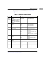
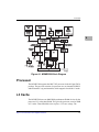
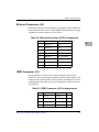
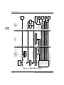
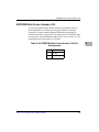
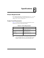
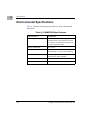
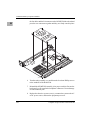
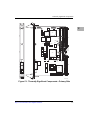
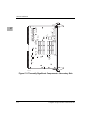
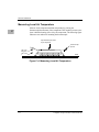
1
MVME5500
Single-Board Computer
Installation and Use
V5500A/IH2
October 2003 Edition
© Copyright 2003 Motorola Inc.
All rights reserved.
Printed in the United States of America.
Motorola and the stylized M logo are trademarks of Motorola, Inc., registered in the U.S.
Patent and Trademark Office.
All other product or service names mentioned in this document are the property of their
respective owners.
Safety Summary
The following general safety precautions must be observed during all phases of operation, service, and repair of
this equipment. Failure to comply with these precautions or with specific warnings elsewhere in this manual
could result in personal injury or damage to the equipment.
The safety precautions listed below represent warnings of certain dangers of which Motorola is aware. You, as
the user of the product, should follow these warnings and all other safety precautions necessary for the safe
operation of the equipment in your operating environment.
Ground the Instrument.
To minimize shock hazard, the equipment chassis and enclosure must be connected to an electrical ground. If the
equipment is supplied with a three-conductor AC power cable, the power cable must be plugged into an approved
three-contact electrical outlet, with the grounding wire (green/yellow) reliably connected to an electrical ground
(safety ground) at the power outlet. The power jack and mating plug of the power cable meet International
Electrotechnical Commission (IEC) safety standards and local electrical regulatory codes.
Do Not Operate in an Explosive Atmosphere.
Do not operate the equipment in any explosive atmosphere such as in the presence of flammable gases or fumes.
Operation of any electrical equipment in such an environment could result in an explosion and cause injury or
damage.
Keep Away From Live Circuits Inside the Equipment.
Operating personnel must not remove equipment covers. Only Factory Authorized Service Personnel or other
qualified service personnel may remove equipment covers for internal subassembly or component replacement
or any internal adjustment. Service personnel should not replace components with power cable connected. Under
certain conditions, dangerous voltages may exist even with the power cable removed. To avoid injuries, such
personnel should always disconnect power and discharge circuits before touching components.
Use Caution When Exposing or Handling a CRT.
Breakage of a Cathode-Ray Tube (CRT) causes a high-velocity scattering of glass fragments (implosion). To
prevent CRT implosion, do not handle the CRT and avoid rough handling or jarring of the equipment. Handling
of a CRT should be done only by qualified service personnel using approved safety mask and gloves.
Do Not Substitute Parts or Modify Equipment.
Do not install substitute parts or perform any unauthorized modification of the equipment. Contact your local
Motorola representative for service and repair to ensure that all safety features are maintained.
Observe Warnings in Manual.
Warnings, such as the example below, precede potentially dangerous procedures throughout this manual.
Instructions contained in the warnings must be followed. You should also employ all other safety precautions
which you deem necessary for the operation of the equipment in your operating environment.
Warning
Warning
To prevent serious injury or death from dangerous voltages, use extreme
caution when handling, testing, and adjusting this equipment and its
components.
Flammability
All Motorola PWBs (printed wiring boards) are manufactured with a flammability rating
of 94V-0 by UL-recognized manufacturers.
EMI Caution
Caution
!
Caution
This equipment generates, uses and can radiate electromagnetic energy. It
may cause or be susceptible to electromagnetic interference (EMI) if not
installed and used with adequate EMI protection.
Lithium Battery Caution
This product contains a lithium battery to power the clock and calendar circuitry.
Caution
!
Caution
Caution
!
Attention
Caution
!
Vorsicht
Danger of explosion if battery is replaced incorrectly. Replace battery only
with the same or equivalent type recommended by the equipment
manufacturer. Dispose of used batteries according to the manufacturer’s
instructions.
Il y a danger d’explosion s’il y a remplacement incorrect de la batterie.
Remplacer uniquement avec une batterie du même type ou d’un type
équivalent recommandé par le constructeur. Mettre au rebut les batteries
usagées conformément aux instructions du fabricant.
Explosionsgefahr bei unsachgemäßem Austausch der Batterie. Ersatz nur
durch denselben oder einen vom Hersteller empfohlenen Typ. Entsorgung
gebrauchter Batterien nach Angaben des Herstellers.
CE Notice (European Community)
Warning
!
Warning
This is a Class A product. In a domestic environment, this product may
cause radio interference, in which case the user may be required to take
adequate measures.
Motorola Computer Group products with the CE marking comply with the EMC Directive
(89/336/EEC). Compliance with this directive implies conformity to the following
European Norms:
EN55022 “Limits and Methods of Measurement of Radio Interference Characteristics
of Information Technology Equipment”; this product tested to Equipment Class A
EN55024 “Information technology equipment—Immunity characteristics—Limits and
methods of measurement”
Board products are tested in a representative system to show compliance with the above
mentioned requirements. A proper installation in a CE-marked system will maintain the
required EMC performance.
In accordance with European Community directives, a “Declaration of Conformity” has
been made and is available on request. Please contact your sales representative.
Notice
While reasonable efforts have been made to assure the accuracy of this document,
Motorola, Inc. assumes no liability resulting from any omissions in this document, or from
the use of the information obtained therein. Motorola reserves the right to revise this
document and to make changes from time to time in the content hereof without obligation
of Motorola to notify any person of such revision or changes.
Electronic versions of this material may be read online, downloaded for personal use, or
referenced in another document as a URL to the Motorola Computer Group Web site. The
text itself may not be published commercially in print or electronic form, edited, translated,
or otherwise altered without the permission of Motorola, Inc.
It is possible that this publication may contain reference to or information about Motorola
products (machines and programs), programming, or services that are not available in your
country. Such references or information must not be construed to mean that Motorola
intends to announce such Motorola products, programming, or services in your country.
Limited and Restricted Rights Legend
If the documentation contained herein is supplied, directly or indirectly, to the U.S.
Government, the following notice shall apply unless otherwise agreed to in writing by
Motorola, Inc.
Use, duplication, or disclosure by the Government is subject to restrictions as set forth in
subparagraph (b)(3) of the Rights in Technical Data clause at DFARS 252.227-7013 (Nov.
1995) and of the Rights in Noncommercial Computer Software and Documentation clause
at DFARS 252.227-7014 (Jun. 1995).
Motorola, Inc.
Computer Group
2900 South Diablo Way
Tempe, Arizona 85282
Contents
About This Manual
Summary of Changes ...............................................................................................xvii
Overview of Contents ............................................................................................ xviii
Comments and Suggestions ......................................................................................xix
Conventions Used in This Manual ............................................................................xix
CHAPTER 1
Hardware Preparation and Installation
Introduction .............................................................................................................. 1-1
Description ............................................................................................................... 1-1
Getting Started .......................................................................................................... 1-2
Overview of Startup Procedures ....................................................................... 1-2
Unpacking Guidelines ....................................................................................... 1-2
Hardware Configuration ........................................................................................... 1-3
MVME5500 Preparation ................................................................................... 1-4
Ethernet 2, PMC/SBC Mode, and P2 I/O Selection Headers
(J6, J7, J28, J32, J34, J97 – J110) ..................................................................... 1-8
Ethernet ...................................................................................................... 1-8
PMC/SBC Mode Selection ........................................................................ 1-8
P2 I/O Selection ......................................................................................... 1-9
Flash Boot Bank Select Header (J8) ................................................................1-11
Flash 0 Programming Enable Header (J9) .......................................................1-11
Safe Start ENV Header (J10) .......................................................................... 1-12
Flash 0 Block Write Protect Header (J15) ...................................................... 1-12
SROM Initialization Enable Header (J17) ...................................................... 1-13
PowerPC Bus Mode Select Header (J19) ....................................................... 1-13
CPU COP Enable Header (J20) ...................................................................... 1-14
PCI Bus 0.0 Speed Header (J25) ..................................................................... 1-14
VME SCON Select Header (J27) ................................................................... 1-15
PCI Bus 1.0 Speed Header (J29) ..................................................................... 1-15
EEPROM Write Protect Header (J30) ............................................................ 1-16
Setting the PMC Vio Keying Pin .................................................................... 1-16
Hardware Installation ............................................................................................. 1-17
Installing the MVME5500 into a Chassis ....................................................... 1-17
Connection to Peripherals ...................................................................................... 1-18
Completing the Installation .................................................................................... 1-19
vii
CHAPTER 2
Startup and Operation
Introduction .............................................................................................................. 2-1
Applying Power ........................................................................................................ 2-1
Switches and Indicators ............................................................................................ 2-1
CHAPTER 3
MOTLoad Firmware
Introduction .............................................................................................................. 3-1
Overview ........................................................................................................... 3-1
MOTLoad Implementation and Memory Requirements ................................... 3-1
MOTLoad Commands ....................................................................................... 3-2
MOTLoad Utility Applications ......................................................................... 3-2
MOTLoad Tests ................................................................................................. 3-2
Using MOTLoad ............................................................................................... 3-4
Command Line Interface ................................................................................... 3-4
Command Line Help ......................................................................................... 3-5
Command Line Rules ........................................................................................ 3-6
MOTLoad Command List ........................................................................................ 3-7
VME Settings ......................................................................................................... 3-12
CR/CSR Settings ............................................................................................. 3-16
Displaying VME Settings ................................................................................ 3-16
Editing VME Settings ..................................................................................... 3-17
Deleting VME Settings ................................................................................... 3-18
Restoring Default VME Settings ..................................................................... 3-18
Remote Start ........................................................................................................... 3-19
CHAPTER 4
Functional Description
Features ..................................................................................................................... 4-1
Block Diagram .......................................................................................................... 4-2
Processor ................................................................................................................... 4-3
L3 Cache ................................................................................................................... 4-3
System Controller ..................................................................................................... 4-4
CPU Bus Interface ............................................................................................. 4-4
Memory Controller Interface ............................................................................. 4-5
Interrupt Controller ............................................................................................ 4-5
I2C Serial Interface and Devices ....................................................................... 4-5
Direct Memory Access (DMA) ......................................................................... 4-6
Timers ................................................................................................................ 4-6
Flash Memory ........................................................................................................... 4-7
viii
System Memory ....................................................................................................... 4-7
PCI Local Buses and Devices .................................................................................. 4-8
Gigabit Ethernet Interface ................................................................................. 4-8
10/100Mb Ethernet Interface ............................................................................ 4-8
PCI-to-PCI Bridges ........................................................................................... 4-9
PMC Sites ......................................................................................................... 4-9
PCI IDSEL Definition ....................................................................................... 4-9
PCI Bus Arbitration .......................................................................................... 4-9
Asynchronous Serial Ports ..................................................................................... 4-10
Real Time Clock and NVRAM .............................................................................. 4-10
System Control and Status Registers ......................................................................4-11
Sources of Reset ......................................................................................................4-11
VME Interface .........................................................................................................4-11
PMC Expansion ..................................................................................................... 4-12
Debug Support ....................................................................................................... 4-12
CHAPTER 5
Pin Assignments
Introduction .............................................................................................................. 5-1
Connectors ................................................................................................................ 5-2
Asynchronous Serial Port Connector (J1) ......................................................... 5-2
Ethernet Connectors (J2) ................................................................................... 5-3
IPMC Connector (J3) ........................................................................................ 5-3
PCI/PMC Expansion Connector (J4) ................................................................ 5-5
CPU COP Connector (J5) ................................................................................. 5-8
PMC 1 Interface Connectors (J11, J12, J13, J14) ............................................. 5-8
Boundary Scan Connector (J18) ..................................................................... 5-15
PMC 2 Interface Connectors (J21, J22, J23, J24) ........................................... 5-16
Asynchronous Serial Port (COM2) Planar Connector (J33) ........................... 5-22
VMEbus Connectors (P1 & P2) (PMC Mode) ............................................... 5-22
VMEbus Connectors (P1 & P2) (SBC Mode) ................................................ 5-25
Memory Expansion Connector (P4) ............................................................... 5-29
Headers ................................................................................................................... 5-33
Ethernet 2, PMC/SBC Mode, and P2 I/O Selection Headers
(J6, J7, J28, J32, J34, J97 – J110) ................................................................... 5-33
Ethernet .................................................................................................... 5-33
PMC/SBC Mode Selection ...................................................................... 5-34
P2 I/O Selection ....................................................................................... 5-35
Flash Boot Bank Select Header (J8) ............................................................... 5-40
Flash 0 Programming Enable Header (J9) ...................................................... 5-40
Safe Start ENV Header (J10) .......................................................................... 5-41
ix
Flash 0 Block Write Protect Header (J15) ....................................................... 5-41
SROM Initialization Enable Header (J17) ...................................................... 5-42
Bus Mode Select Header (J19) ........................................................................ 5-42
COP Enable Header (J20) ............................................................................... 5-43
PCI Bus 0.0 Speed Header (J25) ..................................................................... 5-43
VME SCON Select Header (J27) .................................................................... 5-44
PCI Bus 1.0 Speed Header (J29) ..................................................................... 5-44
EEPROM Write Protect Header (J30) ............................................................. 5-45
APPENDIX A
Specifications
Power Requirements ................................................................................................ A-1
Supply Current Requirements .......................................................................... A-1
Environmental Specifications .................................................................................. A-2
APPENDIX B
RAM5500 Memory Expansion Module
Overview ................................................................................................................. B-1
Features .................................................................................................................... B-1
Functional Description ............................................................................................ B-1
RAM5500 Description ..................................................................................... B-1
SROM ............................................................................................................... B-3
Clocks ............................................................................................................... B-3
RAM5500 Module Installation ................................................................................ B-3
Memory Expansion Connector (P1) Pin Assignments ............................................ B-5
RAM5500 Programming Issues .............................................................................. B-8
Serial Presence Detect (SPD) Data .................................................................. B-8
APPENDIX C
Thermal Validation
Thermally Significant Components ......................................................................... C-1
Component Temperature Measurement ................................................................... C-5
Preparation ........................................................................................................ C-5
Measuring Junction Temperature ..................................................................... C-5
Measuring Case Temperature ........................................................................... C-5
Measuring Local Air Temperature ................................................................... C-8
x
APPENDIX D
Related Documentation
Motorola Computer Group Documents ...................................................................D-1
Manufacturers’ Documents ......................................................................................D-2
Related Specifications ..............................................................................................D-5
xi
List of Figures
Figure 1-1.
Figure 4-1.
Figure 4-2.
Figure 5-1.
Figure 5-2.
Figure 5-3.
Figure B-1.
Figure C-1.
Figure C-2.
Figure C-3.
Figure C-4.
MVME5500 Layout ............................................................................. 1-7
MVME5500 Block Diagram ................................................................ 4-3
COM1 Asynchronous Serial Port Connections (RJ-45) ..................... 4-10
SBC/IPMC712 Mode ......................................................................... 5-37
SBC/IPMC761 Mode ......................................................................... 5-38
PMC Mode ......................................................................................... 5-39
RAM5500 Block Diagram ...................................................................B-2
Thermally Significant Components—Primary Side ............................C-3
Thermally Significant Components—Secondary Side ........................C-4
Mounting a Thermocouple Under a Heatsink .....................................C-7
Measuring Local Air Temperature .......................................................C-8
xiii
List of Tables
Table 1-1. Startup Overview .................................................................................... 1-2
Table 1-2. MVME5500 Jumper Settings ................................................................. 1-5
Table 1-3. MVME5500 Connectors ...................................................................... 1-18
Table 2-1. Front-Panel LED Status Indicators ........................................................ 2-2
Table 3-1. MOTLoad Commands ........................................................................... 3-7
Table 4-1. MVME5500 Features Summary ............................................................ 4-1
Table 5-1. COM1 Connector (J1) Pin Assignments ................................................ 5-2
Table 5-2. Ethernet Connector (J2) Pin Assignments ............................................. 5-3
Table 5-3. IPMC Connector (J3) Pin Assignments ................................................. 5-3
Table 5-4. PCI/PMC Expansion Connector (J4) Pin Assignments ......................... 5-5
Table 5-5. CPU COP Connector (J5) Pin Assignments .......................................... 5-8
Table 5-6. PMC 1 Connector (J11) Pin Assignments ............................................. 5-9
Table 5-7. PMC 1 Connector (J12) Pin Assignments ........................................... 5-10
Table 5-8. PMC 1 Connector (J13) Pin Assignments ........................................... 5-12
Table 5-9. PMC 1 Connector (J14) Pin Assignments ........................................... 5-13
Table 5-10. Boundary Scan Connector (J18) Pin Assignments ............................ 5-15
Table 5-11. PMC 2 Connector (J21) Pin Assignments ......................................... 5-16
Table 5-12. PMC 2 Connector (J22) Pin Assignments ......................................... 5-17
Table 5-13. PMC 2 Connector (J23) Pin Assignments ......................................... 5-19
Table 5-14. PMC 2 Connector (J24) Pin Assignments ......................................... 5-20
Table 5-15. COM2 Planar Connector (J33) Pin Assignments .............................. 5-22
Table 5-16. VME Connector (P2) Pin Assignments (PMC Mode) ....................... 5-23
Table 5-17. VME Connector (P2) Pinout with IPMC712 ..................................... 5-26
Table 5-18. VME Connector (P2) Pinouts with IPMC761 ................................... 5-27
Table 5-19. Memory Expansion Connector (P4) Pin Assignments ...................... 5-29
Table 5-20. Ethernet 2 Selection Headers (J6, J7, J100, J101) Pin Assignments . 5-33
Table 5-21. Ethernet 2 Selection Headers (J34, J97, J98, J99) Pin Assignments . 5-34
Table 5-22. PMC/SBC Mode Selection Headers (J28, J32) Pin Assignments ..... 5-35
Table 5-23. P2 I/O Selection Headers (J102 – J110) Pin Assignments ................ 5-36
Table 5-24. Flash Boot Bank Select Header (J8) Pin Assignments ...................... 5-40
Table 5-25. Flash 0 Programming Enable Header (J9) Pin Assignments ............. 5-40
Table 5-26. Safe Start ENV Header (J10) Pin Assignments ................................. 5-41
Table 5-27. Flash 0 Write Protect Header (J15) Pin Assignments ........................ 5-41
Table 5-28. SROM Initialization Enable Header (J17) Pin Assignments ............. 5-42
xv
Table 5-29. Bus Mode Header (J19) Pin Assignments .......................................... 5-42
Table 5-30. COP Enable Header (J20) Pin Assignments ...................................... 5-43
Table 5-31. PCI Bus 0.0 Speed Header (J25) Pin Assignments ............................ 5-43
Table 5-32. VME SCON Select Header (J27) Pin Assignments ........................... 5-44
Table 5-33. PCI Bus 1.0 Speed Header (J25) Pin Assignments ............................ 5-44
Table 5-34. EEPROM Write Protect Header (J30) Pin Assignments .................... 5-45
Table A-1. Power Requirements ............................................................................. A-1
Table A-2. MVME5500 Specifications .................................................................. A-2
Table B-1. RAM5500 Feature Summary ................................................................ B-1
Table B-2. RAM5500 Connector (P1) Pin Assignments ........................................ B-5
Table C-1. Thermally Significant Components ...................................................... C-2
Table D-1. Motorola Computer Group Documents ................................................ D-1
Table D-2. Manufacturers’ Documents .................................................................. D-2
Table D-3. Related Specifications .......................................................................... D-5
xvi
About This Manual
The MVME5500 Single-Board Computer Installation and Use manual
provides the information you will need to install and configure your
MVME5500 single-board computer. It provides specific preparation and
installation information, and data applicable to the board.
As of the printing date of this manual, the MVME5500 supports the
models listed below.
Model Number
Description
MVME5500-0161
1 GHz MPC7455 processor, 512MB SDRAM,
Scanbe handles
MVME5500-0163
1 GHz MPC7455 processor, 512MB SDRAM,
IEEE handles
Summary of Changes
This is the second edition of the Installation and Use manual. It supersedes
the August 2003 edition and incorporates the following changes.
Date
October
2003
Changes
Added diagrams to Ethernet 2, PMC/SBC Mode, and P2 I/O
Selection Headers (J6, J7, J28, J32, J34, J97 – J110) on page
5-33 to better explain the PMC, SBC/IPMC761, and
SBC/IPMC712 modes in conjunction with the P2 adapter and
MVME761/712 transition modules. Added Appendix B,
RAM5500 Memory Expansion Module. Changed the default
configuration of the Flash Boot Bank Select Header (J8) to
Flash device 0. Added LFM specification to Table A-2 on page
A-2. Added more details to VME Settings on page 3-12. Other
changes were made to correct typographical errors.
xvii
Overview of Contents
This manual is divided into the following chapters and appendices:
Chapter 1, Hardware Preparation and Installation, provides MVME5500
board preparation and installation instructions, as well as ESD
precautionary notes.
Chapter 2, Startup and Operation, provides the power-up procedure and
identifies the switches and indicators on the MVMEM5500.
Chapter 3, MOTLoad Firmware, describes the basic features of the
MOTLoad firmware product.
Chapter 4, Functional Description, describes the MVME5500 on a block
diagram level.
Chapter 5, Pin Assignments, provides pin assignments for various headers
and connectors on the MMVE5500 single-board computer.
Appendix A, Specifications, provides power requirements and
environmental specifications.
Appendix B, RAM5500 Memory Expansion Module, provides a
description of the RAM5500 memory expansion module, as well as
installation instructions and connector pin assignments.
Appendix C, Thermal Validation, provides information to conduct thermal
evaluations and identifies thermally significant components along with
their maximum allowable operating temperatures.
Appendix D, Related Documentation, provides a listing of related
Motorola manuals, vendor documentation, and industry specifications.
xviii
Comments and Suggestions
Motorola welcomes and appreciates your comments on its documentation.
We want to know what you think about our manuals and how we can make
them better. Mail comments to:
Motorola Computer Group
Reader Comments DW164
2900 S. Diablo Way
Tempe, Arizona 85282
You can also submit comments to the following e-mail address:
[email protected]
In all your correspondence, please list your name, position, and company.
Be sure to include the title and part number of the manual and tell how you
used it. Then tell us your feelings about its strengths and weaknesses and
any recommendations for improvements.
Conventions Used in This Manual
The following typographical conventions are used in this document:
bold
is used for user input that you type just as it appears; it is also used for
commands, options and arguments to commands, and names of
programs, directories and files.
italic
is used for names of variables to which you assign values, for function
parameters, and for structure names and fields. Italic is also used for
comments in screen displays and examples, and to introduce new
terms.
courier
is used for system output (for example, screen displays, reports),
examples, and system prompts.
xix
<Enter>, <Return> or <CR>
represents the carriage return or Enter key.
Ctrl
represents the Control key. Execute control characters by pressing the
Ctrl key and the letter simultaneously, for example, Ctrl-d.
xx
1Hardware Preparation and
Installation
1
Introduction
This chapter contains the following information:
❏ Board preparation and installation instructions
❏ ESD precautionary notes
Description
The MVME5500 is a single-board computer based on the PowerPC
MPC7455 processor and the Marvell GT-64260B host bridge with a dual
PCI interface and memory controller. On-board payload includes two
PMC slots, two SDRAM banks, an expansion connector for two additional
banks of SDRAM, 8MB boot Flash ROM, one 10/100/1000 Ethernet port,
one 10/100 Ethernet port, 32MB expansion Flash ROM, two serial ports,
NVRAM and a real-time clock.
The MVME5500 interfaces to a VMEbus system via its P1 and P2
connectors and contains two IEEE 1386.1 PCI mezzanine card (PMC)
slots. The PMC slots are 64-bit and support both front and rear I/O.
Additionally, the MVME5500 is user-configurable by setting on-board
jumpers. Two I/O modes are possible: PMC mode or SBC mode (also
called 761 or IPMC mode). The SBC mode uses the IPMC712 I/O PMC
and the MVME712M transition module, or the IPMC761 I/O PMC and the
MVME761 transition module. The SBC mode is backwards compatible
with the MVME761 transition module and the P2 adapter card (excluding
PMC I/O routing) used on the MVME5100 product. This mode is
accomplished by configuring the on-board jumpers and by attaching an
IPMC761 PMC in PMC slot 1. Secondary Ethernet is configured to the
rear.
PMC mode is backwards compatible with the MVME5100 and is
accomplished by configuring the on-board jumpers.
1-1
1
Hardware Preparation and Installation
Getting Started
This section provides an overview of the steps necessary to install and
power up the MVME5500 and a brief section on unpacking and ESD
precautions.
Overview of Startup Procedures
The following table lists the things you will need to do before you can use
this board and tells where to find the information you need to perform each
step. Be sure to read this entire chapter, including all Caution and Warning
notes, before you begin.
Table 1-1. Startup Overview
What you need to do...
Refer to...
Unpack the hardware.
Unpacking Guidelines on page 1-2
Configure the hardware by
setting jumpers on the board.
MVME5500 Preparation on page 1-4
Install the MVME5500 board in
a chassis.
Installing the MVME5500 into a Chassis on
page 1-17
Connect any other equipment
you will be using
Connection to Peripherals on page 1-18
Verify the hardware is installed.
Completing the Installation on page 1-19
Unpacking Guidelines
Unpack the equipment from the shipping carton. Refer to the packing list
and verify that all items are present. Save the packing material for storing
and reshipping of equipment.
Note
1-2
If the shipping carton is damaged upon receipt, request that the
carrier’s agent be present during the unpacking and inspection of
the equipment.
Computer Group Literature Center Web Site
Hardware Configuration
Caution
!
Avoid touching areas of integrated circuitry; static discharge can damage
circuits.
Caution
ESD
Use ESD
Wrist Strap
Motorola strongly recommends that you use an antistatic wrist strap and a
conductive foam pad when installing or upgrading a system. Electronic
components, such as disk drives, computer boards, and memory modules
can be extremely sensitive to electrostatic discharge (ESD). After
removing the component from its protective wrapper or from the system,
place the component flat on a grounded, static-free surface (and, in the case
of a board, component side up). Do not slide the component over any
surface.
If an ESD station is not available, you can avoid damage resulting from
ESD by wearing an antistatic wrist strap (available at electronics stores)
that is attached to an active electrical ground. Note that a system chassis
may not be grounded if it is unplugged.
Caution
!
Inserting or removing modules with power applied may result in damage
to module components.
Caution
Warning
!
Dangerous voltages, capable of causing death, are present in this
equipment. Use extreme caution when handling, testing, and adjusting.
Warning
Hardware Configuration
This section discusses certain hardware and software tasks that may need
to be performed prior to installing the board in a chassis.
To produce the desired configuration and ensure proper operation of the
MVME5500, you may need to carry out certain hardware modifications
before installing the module.
http://www.motorola.com/computer/literature
1-3
1
1
Hardware Preparation and Installation
Most options on the MVME5500 are software configurable. Configuration
changes are made by setting bits in control registers after the board is
installed in a system.
Jumpers are used to control those options that are not software
configurable. These jumper settings are described further on in this
section. If you are resetting the board jumpers from their default settings,
it is important to verify that all settings are reset properly.
MVME5500 Preparation
Figure 1-1 illustrates the placement of the jumpers, headers, connectors,
and various other components on the MVME5500. There are several
manually configurable headers on the MVME5500 and their settings are
shown in Table 1-2. Each header’s default setting is enclosed in brackets.
1-4
Computer Group Literature Center Web Site
MVME5500 Preparation
For pin assignments on the MVME5500, refer to Chapter 5, Pin
Assignments.
Table 1-2. MVME5500 Jumper Settings
Jumper
Function
Settings
J6,
J100,
J7, J101
Ethernet 2 Selection
Headers
(see also J34, J97, J98, J99)
2-3 on all
[1-2 on all]
Rear P2 Ethernet (SBC mode)
Front-panel Ethernet
Note Refer to the note on
page 1-8 for a configuration
limitation.
J8
Flash Boot Bank Select
Header
No jumper installed
[1-2]
2-3
Boots from Flash 0
Boots from Flash 0
Boots from Flash 1
J9
Flash 0 Programming
Enable Header
No jumper installed
[1-2]
Disables Flash 0 writes
Enables Flash 0 writes
J10
Safe Start ENV Header
No jumper installed
Normal ENV settings used
during boot
Normal ENV settings used
during boot
Safe ENV settings used during
boot
[1-2]
2-3
J15
Flash 0 Block Write Protect
Header
No jumper installed
[1-2]
Disables Flash 0 K3 block
writes
Enables Flash 0 K3 block
writes
J16
Non-Standard Option
Header
For factory use only.
J17
SROM Initialization
Enable Header
No jumper installed
[1-2]
2-3
Enables SROM initialization
Enables SROM initialization
Disables SROM initialization
J19
PowerPC Bus Mode Select
Header
No jumper installed
[1-2]
2-3
60x bus mode
60x bus mode
MPX bus mode
http://www.motorola.com/computer/literature
1-5
1
1
Hardware Preparation and Installation
Table 1-2. MVME5500 Jumper Settings (continued)
Jumper
Function
Settings
J20
CPU COP Enable Header
No jumper installed
[1-2]
Enables boundary scan
Enables CPU COP
J25
PCI Bus 0.0 Speed Header
[No jumper installed]
PMC board controls whether
the bus runs at 33 MHz or
66 MHz
Forces PCI bus 0.0 to remain at
33 MHz
1-2
J27
VME SCON Select Header
No jumper installed
1-2
[2-3]
Always SCON
No SCON
Auto-SCON
J28, J32
PMC/SBC Mode Selection
Headers
(set both jumpers)
1-2 on both
2-3 on both
[2-3 on J32, 1-2 on
J28]
PMC mode
SBC/IPMC761 mode
SBC/IPMC712 mode
[No jumper installed]
PMC board controls whether
the bus runs at 33 MHz or 66
MHz
Forces PCI bus 1.0 to remain at
33 MHz
Warning: Refer to page
1-9 for a warning about
configuring for IPMC
mode.
J29
PCI Bus 1.0 Speed Header
1-2
J30
EEPROM Write Protect
Header
No jumper installed
[1-2]
J34,
J97,
J98, J99
J102 –
J110
1-6
Disables EEPROM
programming
Enables EEPROM
programming
Ethernet 2 Selection
Headers
(see also J6, J100, J7, J101)
1-2 on all
Rear P2 Ethernet
(set when in SBC/IPMC761
mode)
Note Refer to a note on
page 1-8 for a configuration
limitation.
[No jumpers
installed]
Front-panel Ethernet
P2 I/O Selection Headers
1-2
[2-3]
PMC 2 I/O connected to P2
IPMC I/O connected to P2
Computer Group Literature Center Web Site
MVME5500 Preparation
Note
Items in brackets are factory default settings.
The MVME5500 is factory tested and shipped with the configuration
described in the following section.
J18
U19
U7
J20
U6
U5
J8
J27
U28
U29
U30
J5
J21
J22
J23
J24
U25
U16
U4
PMC 2
XU2
XU1
P1
J102 - J110
J30
J17
J10
U18
U15
U17
U27
U23
J3
J11
U129
U14
J6 / J100
J99
J98
J34
J97
J101 / J7
P4
U13
U12
U3
U11
PMC 1
J12
U22
J13
U10
U2
J32
U26
U9
U20
U8
ABT/RST
J9
U125
J15 J16
J33
J14
U126
J19
J25
J29
U1
ENET 1
GigE
10/100
ENET 2
J2
P2
U123
U24
U31
BFL
COM1
CPU
J1
U124
J4
J28
4202 0703
Figure 1-1. MVME5500 Layout
http://www.motorola.com/computer/literature
1-7
1
1
Hardware Preparation and Installation
Ethernet 2, PMC/SBC Mode, and P2 I/O Selection Headers
(J6, J7, J28, J32, J34, J97 – J110)
All of the headers described below are used in conjunction with each other
to select various modes of operation for 10/100BaseT Ethernet, PMC/SBC
mode, and P2 I/O mode.
Ethernet
Four 3-pin planar headers (J6, J7, J100, J101) and four 2-pin planar
headers (J34, J97, J98, J99) are for 10/100/BaseT Ethernet 2 selection.
Ethernet 1 is the Gigabit Ethernet port and is front panel only.
For J6, J100, J7 and J101, install jumpers across pins 2-3 on all four
headers for rear P2 Ethernet. For front-panel Ethernet, install jumpers
across pins 1-2 on all four headers.
Note
If the rear P2 Ethernet is selected by jumpers J6, J7, J100, and
J101, the Ethernet signals also connect to PMC 1 user I/O
connector J14. If a PMC card is plugged into PMC slot 1, there
may be a conflict between the I/O from the PMC card and the
rear Ethernet signals. This conflict does not occur with the
IPMC761 or IPMC712 modules.
For J34, J97, J98 and J99, no jumpers are installed for front-panel Ethernet.
For rear P2 Ethernet, install jumpers across pins 1-2 on all four headers
when in SBC/IPMC761 mode.
PMC/SBC Mode Selection
The MVME5500 is set at the factory for SBC/IPMC712 mode. The
SBC/IPMC761 mode should only be selected when using the IPMC761
module in conjunction with the MVME761 transition module.The PMC
mode should be selected when using PMC modules with specific user I/O
in conjunction with the corresponding transition module. PMC mode
should also be selected when using PrPMC modules.
Two 3-pin planar headers (J28, J32) are for PMC/SBC mode selection. For
PMC mode, install jumpers across pins 1-2 on both headers. For
SBC/IPMC761 mode, install jumpers across pins 2-3 on both headers. For
1-8
Computer Group Literature Center Web Site
Ethernet 2, PMC/SBC Mode, and P2 I/O Selection Headers (J6, J7, J28, J32, J34, J97 – J110)
SBC/IPMC712 mode, install a jumper across pins 2-3 for J32 and install a
jumper across pins 1-2 for J28.
Warning
!
Warning
When J28 is configured for SBC/IPMC mode, –12V is supplied to P2 pin
A30. If there is an incompatible board plugged into this P2 slot, damage
may occur.
When J32 is configured for SBC/IPMC mode, +12V is supplied to P2 pin
C7. If there is an incompatible board plugged into this P2 slot, damage may
occur.
P2 I/O Selection
Nine 3-pin planar headers (J102 –J110) are for P2 I/O selection. Install
jumpers across pins 1-2 on all nine headers when in PMC mode. Install
jumpers across pins 2-3 on all nine headers when in SBC/IPMC761 or
SBC/IPMC712 mode to connect the extended SCSI signals to P2.
http://www.motorola.com/computer/literature
1-9
1
1
Hardware Preparation and Installation
(factory configuration)
Rear P2 Ethernet
Front-Panel Ethernet
J6
J6
3 2 1
3 2 1
J7
J7
1 2 3
1 2 3
J100
J100
3 2 1
3 2 1
J101
J101
1 2 3
1 2 3
J34
J34
1
2
1
2
1
2
1
2
J97
1
2
1
2
1
2
1
2
J97
J98
J98
J99
J99
(factory configuration)
PMC Mode
J28
SBC/IPMC761 Mode
J28
3 2 1
J32
SBC/IPMC712 Mode
J28
3 2 1
3 2 1
J32
J32
3 2 1
3 2 1
3 2 1
(factory configuration)
(extended SCSI)
P2 PMC 2 I/O
J102 –
J110
1-10
3 2 1
P2 IPMC I/O
J102 –
J110
3 2 1
Computer Group Literature Center Web Site
Flash Boot Bank Select Header (J8)
Flash Boot Bank Select Header (J8)
A 3-pin planar header selects the boot Flash bank. No jumper or a jumper
installed across pins 1-2 selects Flash 0 as the boot bank. A jumper
installed across pins 2-3 selects Flash 1 as the boot bank.
J8
J8
J8
1
1
1
2
2
2
3
3
3
Boots from Flash device 0
Boots from Flash device 1
Boots from Flash device 0
(factory configuration)
Flash 0 Programming Enable Header (J9)
A 2-pin planar header enables/disables programming of Flash 0 as a means
of protecting the contents from being corrupted. No jumper installed
disables all Flash 0 programming. The jumper must be installed in order to
erase array blocks, programming data, or configuring lock-bits.
J9
J9
1
1
2
2
Disables Flash 0 writes
http://www.motorola.com/computer/literature
Enables Flash 0 writes
(factory configuration)
1-11
1
1
Hardware Preparation and Installation
Safe Start ENV Header (J10)
A 3-pin planar header selects programmed or safe start ENV settings. No
jumper or a jumper across pins 1-2 indicates that the programmed ENV
settings should be used during boot. A jumper across pins 2-3 indicates
that the safe ENV settings should be used.
J10
J10
J10
1
1
1
2
2
2
3
3
3
Normal ENV settings used
during boot
Normal ENV settings used
during boot
(factory configuration)
Safe ENV settings used
during boot
Flash 0 Block Write Protect Header (J15)
A 2-pin planar header supports the Intel K3 Flash family write protect
feature. No jumper installed enables the lock-down mechanism. Blocks
locked down cannot be unlocked with the unlock command. The jumper
must be installed in order to override the lock-down function and enable
blocks to be erased or programmed through software. Refer to the Intel K3
Flash data sheet, listed in Appendix D, Related Documentation, for further
details.
J15
J15
1
1
2
2
Disable Flash 0 K3
block writes
1-12
Enable Flash 0 K3
block writes
(factory configuration)
Computer Group Literature Center Web Site
SROM Initialization Enable Header (J17)
SROM Initialization Enable Header (J17)
A 3-pin planar header enables/disables the GT-64260B SROM
initialization. No jumper or a jumper across pins 1-2 enables the
GT-64260B device initialization via I2C SROM while a jumper across
pins 2-3 disables this initialization sequence.
J17
J17
J17
1
1
1
2
2
2
3
3
3
Enable SROM initialization
Enable SROM initialization
(factory configuration)
Disable SROM initialization
PowerPC Bus Mode Select Header (J19)
A 3-pin planar header selects the processor bus operating mode. No jumper
or a jumper across pins 1-2 selects the 60x bus mode while a jumper across
pins 2-3 selects the MPX bus mode.
J19
J19
J19
1
1
1
2
2
2
3
3
3
60x bus mode
http://www.motorola.com/computer/literature
60x bus mode
(factory configuration)
MPX bus mode
1-13
1
1
Hardware Preparation and Installation
CPU COP Enable Header (J20)
A 2-pin planar header enables the Riscwatch capability. No jumper
installed disables COP and enables boundary scan. A jumper across pins
1-2 enables the COP emulator debug.
J20
J20
1
1
2
2
Disables COP;
enables boundary scan
Enables COP
emulator debug
(factory configuration)
PCI Bus 0.0 Speed Header (J25)
A 2-pin planar header that can force PCI bus 0.0 to run at 33 MHz rather
than the standard method of allowing the PMC board to control whether
the bus runs at 33 MHz or 66 MHz. No jumper installed allows the PMC
board to choose the PCI 0.0 bus speed. A jumper installed across pins 1-2
forces PCI bus 0.0 to run at 33 MHz.
J25
1
1
2
2
PMC board controls
PCI 0.0 bus speed
(factory configuration)
1-14
J25
Force PCI bus 0.0
to run at 33 MHz
Computer Group Literature Center Web Site
VME SCON Select Header (J27)
VME SCON Select Header (J27)
A 3-pin planar header allows the choice for auto/enable/disable SCON
VME configuration. A jumper installed across pins 1-2 configures for
SCON disabled. A jumper installed across pins 2-3 configures for auto
SCON. No jumper installed configures for SCON always enabled.
J27
J27
J27
1
1
1
2
2
2
3
3
3
Always SCON
No SCON
Auto-SCON
(factory configuration)
PCI Bus 1.0 Speed Header (J29)
A 2-pin planar header that can force PCI bus 1.0 to run at 33 MHz rather
than the standard method of allowing the PMC board to control whether
the bus runs at 33 MHz or 66 MHz. No jumper installed allows the PMC
board to choose the PCI 1.0 bus speed. A jumper installed across pins 1-2
forces PCI bus 1.0 to run at 33 MHz.
J29
J29
1
1
2
2
PMC board controls
PCI 1.0 bus speed
(factory configuration)
http://www.motorola.com/computer/literature
Force PCI bus 1.0
to run at 33 MHz
1-15
1
1
Hardware Preparation and Installation
EEPROM Write Protect Header (J30)
A 2-pin planar header enables/disables programming of the on-board
EEPROMs as a means of protecting the contents from being corrupted. No
jumper installed disables EEPROM programming by driving the WP pin
to a logic high. The jumper must be installed in order to program any of the
EEPROMs at addresses A0, A6, A8, and/or AA.
J30
J30
1
1
2
2
Disables EEPROM
programming
Enables EEPROM
programming
(factory configuration)
Setting the PMC Vio Keying Pin
Signalling voltage (Vio) is determined by the location of the PMC Vio
keying pin. Each site can be independently configured for either 5V or
3.3V signalling. The option selected can be determined by observing the
location of the Vio keying pin.
5V key option on a PMC board
1-16
3.3V key option on a PMC board
Computer Group Literature Center Web Site
Hardware Installation
Hardware Installation
Installing the MVME5500 into a Chassis
Use the following steps to install the MVME5500 into your computer
chassis.
1. Attach an ESD strap to your wrist. Attach the other end of the ESD
strap to an electrical ground (refer to Unpacking Guidelines). The ESD
strap must be secured to your wrist and to ground throughout the
procedure.
2. Remove any filler panel that might fill that slot.
3. Install the top and bottom edge of the MVME5500 into the guides of
the chassis.
Warning
!
Only use injector handles for board insertion to avoid
damage/deformation to the front panel and/or PCB.
Warning
4. Ensure that the levers of the two injector/ejectors are in the outward
position.
5. Slide the MVME5500 into the chassis until resistance is felt.
6. Simultaneously move the injector/ejector levers in an inward
direction.
7. Verify that the MVME5500 is properly seated and secure it to the
chassis using the two screws located adjacent to the injector/ejector
levers.
8. Connect the appropriate cables to the MVME5500.
http://www.motorola.com/computer/literature
1-17
1
1
Hardware Preparation and Installation
Connection to Peripherals
When the MVME5500 is installed in a chassis, you are ready to connect
peripherals and apply power to the board.
Figure 1-1 on page 1-7 shows the locations of the various connectors while
Table 1-3 lists them for you. Refer to Chapter 5, Pin Assignments for the
pin assignments of the connectors listed below.
Note
If a PMC module is plugged into PMC slot 1, the memory
mezzanine card cannot be used because the PMC module covers
the memory mezzanine connector.
Table 1-3. MVME5500 Connectors
1-18
Connector
Function
J1
COM1 front-panel connector
J2
Dual 1000/100/10BaseT front-panel connectors
J3
IPMC connector
J4
PCI/PMC expansion connector
J5
CPU COP connector
J11, J12, J13, J14
PMC 1 connectors
J18
Boundary scan connector
J21, J22, J23, J24
PMC 2 connectors
J33
COM2 planar connector
P1, P2
VME rear panel connectors
P4
Memory expansion connector
Computer Group Literature Center Web Site
Completing the Installation
Completing the Installation
Verify that hardware is installed and the power/peripheral cables
connected are appropriate for your system configuration.
Replace the chassis or system cover, reconnect the system to the AC or DC
power source, and turn the equipment power on.
http://www.motorola.com/computer/literature
1-19
1
2Startup and Operation
2
Introduction
This chapter gives you information about:
❏ the power-up procedure
❏ switches and indicators
Applying Power
After you verify that all necessary hardware preparation is complete and
all connections are made correctly, you can apply power to the system.
When you are ready to apply power to the MVME5500:
❏ Verify that the chassis power supply voltage setting matches the
voltage present in the country of use (if the power supply in your
system is not auto-sensing).
❏ On powering up, the MVME5500 brings up the MotLoad prompt,
MVME5500>.
Switches and Indicators
The MVME5500 board provides a single pushbutton switch that provides
both Abort and Reset (ABT/RST) functions. When the switch is depressed
for less than three seconds, an abort interrupt is generated to the processor.
If the switch is held for more than three seconds, a board hard reset is
generated.
2-1
Startup and Operation
The MVME5500 has two front-panel indicators:
2
❏ BFL, software controlled. Asserted by firmware (or other
software) to indicate a configuration problem (or other failure).
❏ CPU, connected to a CPU bus control signal to indicate bus
activity.
The following table describes these indicators:
Table 2-1. Front-Panel LED Status Indicators
2-2
Function
Label
Color
Description
CPU Bus
Activity
CPU
Green
CPU bus is
busy.
Board Fail
BFL
Yellow
Board has a
failure.
Computer Group Literature Center Web Site
3MOTLoad Firmware
3
Introduction
This chapter describes the basic features of the MOTLoad firmware
product, designed by Motorola as the next generation initialization,
debugger and diagnostic tool for high-performance embedded board
products using state-of-the-art system memory controllers and bridge
chips, such as the GT-64260B.
In addition to an overview of the product, this chapter includes a list of
standard MOTLoad commands and the default VME settings that are
changeable by the user, as allowed by the firmware.
Overview
The MOTLoad firmware package serves as a board power-up and
initialization package, as well as a vehicle from which user applications
can be booted. A secondary function of the MOTLoad firmware is to serve
in some respects as a test suite providing individual tests for certain
devices.
MOTLoad is controlled through an easy-to-use, UNIX-like, command line
interface. The MOTLoad software package is similar to many end-user
applications designed for the embedded market, such as the real time
operating systems currently available.
Refer to the MOTLoad Firmware Package User’s Manual, listed in
Appendix D, Related Documentation, for more details.
MOTLoad Implementation and Memory Requirements
The implementation of MOTLoad and its memory requirements are
product specific. The MVME5500 single-board computer (SBC) is offered
with a wide range of memory (for example, DRAM, external cache,
Flash). Typically, the smallest amount of on-board DRAM that a Motorola
SBC has is 32MB. Each supported Motorola product line has its own
3-1
MOTLoad Firmware
unique MOTLoad binary image(s). Currently the largest MOTLoad
compressed image is less than 1MB in size.
3
MOTLoad Commands
MOTLoad supports two types of commands (applications): utilities and
tests. Both types of commands are invoked from the MOTLoad command
line in a similar fashion. Beyond that, MOTLoad utilities and MOTLoad
tests are distinctly different.
MOTLoad Utility Applications
The definition of a MOTLoad utility application is very broad. Simply
stated, it is considered a MOTLoad command, if it is not a MOTLoad test.
Typically, MOTLoad utility applications are applications that aid the user
in some way (that is, they do something useful). From the perspective of
MOTLoad, examples of utility applications are: configuration, data/status
displays, data manipulation, help routines, data/status monitors, etc.
Operationally, MOTLoad utility applications differ from MOTLoad test
applications in several ways:
❏ Only one utility application operates at any given time (that is,
multiple utility applications can not be executing concurrently).
❏ Utility applications may interact with the user. Most test
applications do not.
MOTLoad Tests
A MOTLoad test application determines whether or not the hardware
meets a given standard. Test applications are validation tests. Validation is
conformance to a specification. Most MOTLoad tests are designed to
directly validate the functionality of a specific SBC subsystem or
component. These tests validate the operation of such SBC modules as:
dynamic memory, external cache, NVRAM, real time clock, etc.
All MOTLoad tests are designed to validate functionality with minimum
user interaction. Once launched, most MOTLoad tests operate
3-2
Computer Group Literature Center Web Site
MOTLoad Tests
automatically without any user interaction. There are a few tests where the
functionality being validated requires user interaction (that is, switch tests,
interactive plug-in hardware modules, etc.). Most MOTLoad test results
(error-data/status-data) are logged, not printed. All MOTLoad
tests/commands have complete and separate descriptions (refer to the
MOTLoad Firmware Package User’s Manual for this information).
All devices that are available to MOTLoad for validation/verification
testing are represented by a unique device path string. Most MOTLoad
tests require the operator to specify a test device at the MOTLoad
command line when invoking the test.
A listing of all device path strings can be displayed through the devShow
command. If an SBC device does not have a device path string, it is not
supported by MOTLoad and can not be directly tested. There are a few
exceptions to the device path string requirement, like testing RAM, which
is not considered a true device and can be directly tested without a device
path string. Refer to the devShow command description page in the
MOTLoad Firmware Package User’s Manual.
Most MOTLoad tests can be organized to execute as a group of related
tests (a testSuite) through the use of the testSuite command. The expert
operator can customize their testing by defining and creating a custom
testSuite(s). The list of built-in and user-defined MOTLoad testSuites, and
their test contents, can be obtained by entering testSuite -d at the
MOTLoad prompt. All testSuites that are included as part of a product
specific MOTLoad firmware package are product specific. For more
information, refer to the testSuite command description page in the
MOTLoad Firmware Package User’s Manual.
Test results and test status are obtained through the testStatus,
errorDisplay, and taskActive commands. Refer to the appropriate
command description page in the MOTLoad Firmware Package User’s
Manual for more information.
http://www.motorola.com/computer/literature
3-3
3
MOTLoad Firmware
Using MOTLoad
Interaction with MOTLoad is performed via a command line interface
through a serial port on the SBC, which is connected to an X-terminal or
other terminal emulator (for example, Window’s Hypercomm). The
default MOTLoad serial port settings are: 9600 baud, 8 bits, no parity.
3
Command Line Interface
The MOTLoad command line interface is similar to a UNIX command line
shell interface. Commands are initiated by entering a valid MOTLoad
command (a text string) at the MOTLoad command line prompt and
pressing the carriage-return key to signify the end of input. MOTLoad then
performs the specified action. An example of a MOTLoad command line
prompt is shown below. The MOTLoad prompt changes according to what
product it is used on (for example, MVME5500, MVME6100).
Example:
MVME5500>
If an invalid MOTLoad command is entered at the MOTLoad command
line prompt, MOTLoad displays a message that the command was not
found.
Example:
MVME5500> mytest
"mytest" not found
MVME5500>
If the user enters a partial MOTLoad command string that can be resolved
to a unique valid MOTLoad command and presses the carriage-return key,
the command will be executed as if the entire command string had been
entered. This feature is a user-input shortcut that minimizes the required
amount of command line input. MOTLoad is an ever changing firmware
package, so user-input shortcuts may change as command additions are
made.
3-4
Computer Group Literature Center Web Site
Command Line Help
Example:
MVME5500> version
Copyright: Motorola Inc.1999-2002, All Rights Reserved
MOTLoad RTOS Version 2.0
PAL Version 0.1 (Motorola MVME5500)
3
Example:
MVME5500> ver
Copyright: Motorola Inc. 1999-2002, All Rights Reserved
MOTLoad RTOS Version 2.0
PAL Version 0.1 (Motorola MVME5500)
If the partial command string cannot be resolved to a single unique
command, MOTLoad will inform the user that the command was
ambiguous.
Example:
MVME5500> te
"te" ambiguous
MVME5500>
Command Line Help
Each MOTLoad firmware package has an extensive, product-specific help
facility that can be accessed through the help command. The user can enter
help at the MOTLoad command line to display a complete listing of all
available tests and utilities.
Example
MVME5500>help
For help with a specific test or utility the user can enter the following at the
MOTLoad prompt:
help <command_name>
The help command also supports a limited form of pattern matching. Refer
to the help command page.
http://www.motorola.com/computer/literature
3-5
MOTLoad Firmware
Example
MVME5500>help testRam
Usage: testRam [-aPh] [-bPh] [-iPd] [-nPh] [-tPd] [-v]
Description: RAM Test [Directory]
Argument/Option Description
-a Ph: Address to Start (Default = Dynamic Allocation)
-b Ph: Block Size (Default = 16KB)
-i Pd: Iterations (Default = 1)
-n Ph: Number of Bytes (Default = 1MB)
-t Ph: Time Delay Between Blocks in OS Ticks (Default = 1)
-v O : Verbose Output
MVME5500>
3
Command Line Rules
There are a few things to remember when entering a MOTLoad command:
❏ Multiple commands are permitted on a single command line,
provided they are separated by a single semicolon(";").
❏ Spaces separate the various fields on the command line
(command/arguments/options).
❏ The argument/option identifier character is always preceded by a
hyphen (“-”) character
❏ Options are identified by a single character
❏ Option arguments immediately follow (no spaces) the option
❏ All commands, command options, device tree strings, etc., are
case sensitive
Example:
MVME5500> flashProgram -d/dev/flash0 -n00100000
For more information on MOTLoad operation and function, refer to the
MOTLoad Firmware Package User’s Manual.
3-6
Computer Group Literature Center Web Site
MOTLoad Command List
MOTLoad Command List
The following table provides a list of all current MOTLoad commands.
Products supported by MOTLoad may or may not employ the full
command set. Typing help at the MOTLoad command prompt will
display all commands supported by MOTLoad for a given product.
Table 3-1. MOTLoad Commands
Command
Description
as
One-Line Instruction Assembler
bcb bch bcw
Block Compare Byte/Halfword/Word
bdTempShow
Display Current Board Temperature
bfb bfh bfw
Block Fill Byte/Halfword/Word
blkCp
Block Copy
blkFmt
Block Format
blkRd
Block Read
blkShow
Block Show Device Configuration Data
blkVe
Block Verify
blkWr
Block Write
bmb bmh bmw
Block Move Byte/Halfword/Word
br
Assign/Delete/Display User-Program Break-Points
bsb bsh bsw
Block Search Byte/Halfword/Word
bvb bvh bvw
Block Verify Byte/Halfword/Word
cdDir
ISO9660 File System Directory Listing
cdGet
ISO9660 File System File Load
clear
Clear the Specified Status/History Table(s)
cm
Turns on Concurrent Mode
devShow
Display (Show) Device/Node Table
diskBoot
Disk Boot (Direct-Access Mass-Storage Device)
http://www.motorola.com/computer/literature
3-7
3
MOTLoad Firmware
Table 3-1. MOTLoad Commands (continued)
Command
3
3-8
Description
downLoad
Down Load S-Record from Host
ds
One-Line Instruction Disassembler
echo
Echo a Line of Text
elfLoader
ELF Object File Loader
errorDisplay
Display the Contents of the Test Error Status Table
eval
Evaluate Expression
execProgram
Execute Program
fatDir
FAT File System Directory Listing
fatGet
FAT File System File Load
fdShow
Display (Show) File Discriptor
flashProgram
Flash Memory Program
flashShow
Display Flash Memory Device Configuration Data
gd
Go Execute User-Program Direct (Ignore Break-Points)
gevDelete
Global Environment Variable Delete
gevDump
Global Environment Variable(s) Dump (NVRAM Header + Data)
gevEdit
Global Environment Variable Edit
gevInit
Global Environment Variable Area Initialize (NVRAM Header)
gevList
Global Environment Variable Labels (Names) Listing
gevShow
Global Environment Variable Show
gn
Go Execute User-Program to Next Instruction
go
Go Execute User-Program
gt
Go Execute User-Program to Temporary Break-Point
hbd
Display History Buffer
hbx
Execute History Buffer Entry
help
Display Command/Test Help Strings
Computer Group Literature Center Web Site
MOTLoad Command List
Table 3-1. MOTLoad Commands (continued)
Command
Description
l2CacheShow
Display state of L2 Cache and L2CR register contents
l3CacheShow
Display state of L3 Cache and L3CR register contents
mdb mdh mdw
Memory Display Bytes/Halfwords/Words
memShow
Display Memory Allocation
mmb mmh mmw
Memory Modify Bytes/Halfwords/Words
mpuFork
Execute program from idle processor
mpuShow
Display multi-processor control structure
mpuSwitch
Resets board switching master MPU
netBoot
Network Boot (BOOT/TFTP)
netShow
Display Network Interface Configuration Data
netShut
Disable (Shutdown) Network Interface
netStats
Display Network Interface Statistics Data
noCm
Turns off Concurrent Mode
pciDataRd
Read PCI Device Configuration Header Register
pciDataWr
Write PCI Device Configuration Header Register
pciDump
Dump PCI Device Configuration Header Register
pciShow
Display PCI Device Configuration Header Register
pciSpace
Display PCI Device Address Space Allocation
ping
Ping Network Host
portSet
Port Set
portShow
Display Port Device Configuration Data
rd
User Program Register Display
reset
Reset System
rs
User Program Register Set
set
Set Date and Time
http://www.motorola.com/computer/literature
3
3-9
MOTLoad Firmware
Table 3-1. MOTLoad Commands (continued)
Command
3
Description
sromRead
SROM Read
sromWrite
SROM Write
sta
Symbol Table Attach
stl
Symbol Table Lookup
stop
Stop Date and Time (Power-Save Mode)
taskActive
Display the Contents of the Active Task Table
tc
Trace (Single-Step) User Program
td
Trace (Single-Step) User Program to Address
testDisk
Test Disk
testEnetPtP
Ethernet Point-to-Point
testFlash
Flash Memory Erase/Write/Verify
testl2cRomRd
I2C ROM Read
testNvramRd
NVRAM Read
testNvramRdWr
NVRAM Read/Write (Destructive)
testRam
RAM Test (Directory)
testRamAddr
RAM Addressing
testRamAlt
RAM Alternating
testRamBitToggle
RAM Bit Toggle
testRamBounce
RAM Bounce
testRamCodeCopy
RAM Code Copy and Execute
testRamEccMonitor
Monitor for ECC Errors
testRamMarch
RAM March
testRamPatterns
RAM Patterns
testRamPerm
RAM Permutations
testRamQuick
RAM Quick
3-10
Computer Group Literature Center Web Site
MOTLoad Command List
Table 3-1. MOTLoad Commands (continued)
Command
Description
testRamRandom
RAM Random Data Patterns
testRtcAlarm
RTC Alarm
testRtcReset
RTC Reset
testRtcRollOver
RTC Rollover
testRtcTick
RTC Tick
testSerialExtLoop
Serial External Loopback
testSeriallntLoop
Serial Internal Loopback
testStatus
Display the Contents of the Test Status Table
testSuite
Execute Test Suite
testSuiteMake
Make (Create) Test Suite
testUsbOscillator
USB Oscillator
testUsbVok
USB Vok
testWatchdogTimer
Tests the accuracy of the watchdog timer device.
tftpGet
TFTP Get
tftpPut
TFTP Put
time
Display Date and Time
transparentMode
Transparent Mode (Connect to Host)
tsShow
Display Task Status
upLoad
Up Load Binary-Data from Target
version
Display Version String(s)
vmeCfg
Manages user specified VME configuration parameters
vpdDisplay
VPD Display
vpdEdit
VPD Edit
waitProbe
Wait for I/O Probe to Complete
http://www.motorola.com/computer/literature
3
3-11
MOTLoad Firmware
VME Settings
As shipped from the factory, the firmware on the MVME5500 will
program default values into the Universe II VME Interface chip. The
firmware allows certain VME settings to be changed in order for the user
to customize his/her environment. The following is a description of the
default VME settings that are changeable by the user. For more
information, refer to the MOTLoad User’s Manual and Tundra’s Universe
II User Manual, listed in Appendix D, Related Documentation.
3
❏
VME3PCI Master Enable = Y
N = Do not set up or enable the VMEbus Interface.
Y= Set up and enable the VMEbus Interface.
❏
PCI Slave Image 0
This image is set to zeroes and thus disabled.
❏
PCI Slave Image 1 Control = C0820000
Sets LSI1_CTL to indicate that this image is enabled, write
posting is enabled, VMEbus data width is 32 bits, VMEbus
address space is A32, data and non-supervisory AM encoding, no
BLT transfers to the VMEbus, and to accept addresses in PCI
memory space.
❏
PCI Slave Image 1 Base Address Register = 91000000
Sets LSI1_BS to indicate that the lower bound of PCI memory
addresses to be transferred to the VMEbus by this image is
0x91000000.
❏
PCI Slave Image 1 Bound Address Register = B0000000
Sets LSI1_BD to indicate that the upper bound of PCI memory
addresses to be transferred by this image is 0xB0000000.
❏
PCI Slave Image 1 Translation Offset = 70000000
Sets LSI1_TO to indicate that the PCI memory address is to be
translated by 0x70000000 before presentation on the VMEbus; the
result of the translation is: 0x91000000 + 0x70000000 =
0x101000000, thus 0x01000000 on the VMEbus.
3-12
Computer Group Literature Center Web Site
VME Settings
❏
PCI Slave Image 2 Control = C0410000
Sets LSI2_CTL to indicate that this image is enabled, write
posting is enabled, VMEbus data width is 16 bits, VMEbus
address space is A24, data and non-supervisory AM encoding, no
BLT transfers to the VMEbus, and to accept addresses in PCI
memory space.
❏
PCI Slave Image 2 Base Address Register = B0000000
Sets LSI2_BS to indicate that the lower bound of PCI memory
addresses to be transferred to the VMEbus by this image is
0xB0000000.
❏
PCI Slave Image 2 Bound Address Register = B1000000
Sets LSI2_BD to indicate that the upper bound of PCI memory
addresses to be transferred by this image is 0xB1000000.
❏
PCI Slave Image 2 Translation Offset = 400000000
Sets LSI2_TO to indicate that the PCI memory address is to be
translated by 0x40000000 before presentation on the VMEbus; the
result of the translation is: 0xB0000000 + 0x40000000 =
0xF0000000, thus 0xF0000000 on the VMEbus.
❏
PCI Slave Image 3 Control = C0400000
Sets LSI3_CTL to indicate that this image is enabled, write
posting is enabled, VMEbus data width is 16 bits, VMEbus
address space is A16, data and non-supervisory AM encoding, no
BLT transfers to the VMEbus, and to accept addresses in PCI
memory space.
❏
PCI Slave Image 3 Base Address Register = B3FF0000
Sets LSI3_BS to indicate that the lower bound of PCI memory
addresses to be transferred to the VMEbus by this image is
0xB3FF0000.
❏
PCI Slave Image 3 Bound Address Register = B4000000
Sets LSI3_BD to indicate that the upper bound of PCI memory
addresses to be transferred by this image is 0xB4000000.
http://www.motorola.com/computer/literature
3-13
3
MOTLoad Firmware
❏
PCI Slave Image 3 Translation Offset = 4C000000
Sets LSI3_TO to indicate that the PCI memory address is to be
translated by 0x4C000000 before presentation on the VMEbus;
the result of the translation is: 0xB3FF0000 + 0x4C000000 =
0xFFFF0000, thus 0xFFFF0000 on the VMEbus.
3
❏
PCI Slave Image 4 -7
These images are set to zeroes and thus disabled.
❏
VMEbus Slave Image 0 Control = E0F20000
Sets VSI0_CTL to indicate that this image is enabled, write and
read posting is enabled, program/data and supervisory AM
coding, data width is 32 bits, VMEbus A32 address space, 64-bit
PCI transfers are disabled, PCI Lock on RMW cycles are disabled,
and to transfer into PCI memory space.
❏
VMEbus Slave Image 0 Base Address Register = 00000000
Sets VSI0_BS to define the lower bound of VME addresses to be
transferred to the local PCI bus is 0x00000000.
❏
VMEbus Slave Image 0 Bound Address Register = (Local
DRAM Size)
Sets VSI0_BD to define that the upper bound of VME addresses
to be equal to the size of local DRAM.
❏
VMEbus Slave Image 0 Translation Offset = 00000000
Sets VSI0_TO to define that no translation of the VMEbus address
is to occur when transferred to the local PCI bus. According to the
CHRP map in use by MOTLoad, this will result in transfers to
local DRAM; that is, 0x00000000 on the VMEbus is 0x00000000
in local DRAM.
❏
VMEbus Slave Image 1 - 7
These images are set to zeroes and thus disabled.
❏
VMEbus Register Access Image Control Register =
00000000
The VRAI_CTL register is disabled.
3-14
Computer Group Literature Center Web Site
VME Settings
❏
VMEbus Register Access Image Base Address Register =
00000000
The contents of the VRAI_BS register are not applicable since the
image is disabled.
❏
PCI Miscellaneous Register = 10000000
The LMISC register is set for Universe I compatibility and the
coupled window timer is disabled.
❏
Special PCI Slave Image Register = 00000000
The SLSI register is disabled.
❏
Master Control Register = 00C00000
The MAST_CTL register is set to retry forever before the PCI
master signals error, transfer 128 bytes on posted writes before
release, use VMEbus request level 3, request mode = Demand,
Release When Done, align PCI transfers on 32 bytes, and use PCI
bus 0.
❏
Miscellaneous Control Register = 52040000
Sets MISC_CTL register to utilize 256 second VMEbus timeout,
round robin arbitration, 256 second arbitration timeout, do not use
BI-mode and assertion of VIRQ1 is to be ignored.
❏
User AM Codes = 40400000
Sets USER_AM to indicate a user AM code of 0.
The resulting map is therefore:
PCI addresses 0x91000000 - 0xB0000000: VMEbus A32/D32 space,
addresses 0x01000000 - 0x2000000.
PCI addresses 0xB0000000 - 0xB1000000: VMEbus A24/D16 space,
addresses 0xF0000000 - 0xF1000000.
PCI addresses 0xB3FF0000 - 0xB4000000: VMEbus A16/D16 space,
addresses 0xFFFF0000 - 0xFFFFFFFF.
VMEbus A32/D32 addresses from 0x00000000 to (local DRAM size)
address the local memory of the MVME5500.
http://www.motorola.com/computer/literature
3-15
3
MOTLoad Firmware
The following sections provide additional information pertaining to the
VME firmware settings of the MVME5500. A few VME settings are
controlled by hardware jumpers while the majority of the VME settings are
managed by the firmware command utility vmeCfg.
3
CR/CSR Settings
The firmware supports both Auto Slot ID and Geographical Addressing for
assigning the CR/CSR base address dependent on a hardware jumper
setting. See the VME64 Specification and the VME64 Extensions for
details. As a result, a 512K byte CR/CSR area can be accessed from the
VMEbus using the CR/CSR AM code.
Displaying VME Settings
To display the changeable VME setting, type the following at the firmware
prompt:
❏ vmeCfg -s -m
Displays Master Enable state
❏ vmeCfg -s -i(0 - 7)
Displays selected Inbound Window state
❏ vmeCfg -s -o(0 - 7)
Displays selected Outbound Window state
❏ vmeCfg -s -r184
Displays PCI Miscellaneous Register state
❏ vmeCfg -s -r188
Displays Special PCI Target Image Register state
❏ vmeCfg -s -r400
Displays Master Control Register state
❏ vmeCfg -s -r404
Displays Miscellaneous Control Register state
3-16
Computer Group Literature Center Web Site
Editing VME Settings
❏ vmeCfg -s -r40C
Displays User AM Codes Register state
❏ vmeCfg -s -rF70
Displays VMEbus Register Access Image Control Register state
Editing VME Settings
To edit the changeable VME setting, type the following at the firmware
prompt:
❏ vmeCfg -e -m
Edits Master Enable state
❏ vmeCfg -e -i(0 - 7)
Edits selected Inbound Window state
❏ vmeCfg -e -o(0 - 7)
Edits selected Outbound Window state
❏ vmeCfg -e -r184
Edits PCI Miscellaneous Register state
❏ vmeCfg -e -r188
Edits Special PCI Target Image Register state
❏ vmeCfg -e -r400
Edits Master Control Register state
❏ vmeCfg -e -r404
Edits Miscellaneous Control Register state
❏ vmeCfg -e -r40C
Edits User AM Codes Register state
❏ vmeCfg -e -rF70
Edits VMEbus Register Access Image Control Register state
http://www.motorola.com/computer/literature
3-17
3
MOTLoad Firmware
Deleting VME Settings
To delete the changeable VME setting (restore default value), type the
following at the firmware prompt:
3
❏ vmeCfg -d -m
Deletes Master Enable state
❏ vmeCfg -d -i(0 - 7)
Deletes selected Inbound Window state
❏ vmeCfg -d -o(0 - 7)
Deletes selected Outbound Window state
❏ vmeCfg -d -r184
Deletes PCI Miscellaneous Register state
❏ vmeCfg -d -r188
Deletes Special PCI Target Image Register state
❏ vmeCfg -d -r400
Deletes Master Control Register state
❏ vmeCfg -d -r404
Deletes Miscellaneous Control Register state
❏ vmeCfg -d -r40C
Deletes User AM Codes Register state
❏ vmeCfg -d -rF70
Deletes VMEbus Register Access Image Control Register state
Restoring Default VME Settings
To restore all of the changeable VME setting back to their default settings,
type the following at the firmware prompt:
vmeCfg -z
3-18
Computer Group Literature Center Web Site
Remote Start
Remote Start
As described in the MOTLoad Firmware Package User's Manual, listed in
Appendix D, Related Documentation, remote start allows the user to
obtain information about the target board, download code and/or data,
modify memory on the target, and execute a downloaded program. These
transactions occur across the VMEbus in the case of the MVME5500.
MOTLoad uses one of four mailboxes in the Universe II as the inter-board
communication address (IBCA) between the host and the target.
CR/CSR slave addresses configured by MOTLoad are assigned according
to the installation slot in the backplane, as indicated by the VME64
Specification. For reference, the following values are provided:
CR/CSR space for a board in the 1st slot will start at 0x0008.0000
CR/CSR space for a board in the 2nd slot will start at 0x0010.0000
CR/CSR space for a board in the 3rd slot will start at 0x0018.0000
CR/CSR space for a board in the 4th slot will start at 0x0020.0000
CR/CSR space for a board in the 5th slot will start at 0x0028.0000
CR/CSR space for a board in the 6th slot will start at 0x0030.0000
CR/CSR space for a board in the 7th slot will start at 0x0038.0000
CR/CSR space for a board in the 8th slot will start at 0x0040.0000
CR/CSR space for a board in the 9th slot will start at 0x0048.0000
CR/CSR space for a board in the ath slot will start at 0x0050.0000
CR/CSR space for a board in the bth slot will start at 0x0058.0000
CR/CSR space for a board in the cth slot will start at 0x0060.0000
For further details on CR/CSR space, please refer to the VME64
Specification, listed in Appendix D, Related Documentation.
The MVME5500 uses a Tundra Universe II for its VME bridge. The offsets
of the mailboxes in the Universe II are defined in the Universe II User
Manual, listed in Appendix D, Related Documentation, but are noted here
for reference:
Mailbox 0 is at offset 7f348 in the CR/CSR space
Mailbox 1 is at offset 7f34C in the CR/CSR space
Mailbox 2 is at offset 7f350 in the CR/CSR space
Mailbox 3 is at offset 7f354 in the CR/CSR space
http://www.motorola.com/computer/literature
3-19
3
MOTLoad Firmware
The selection of the mailbox used by remote start on an individual
MVME5500 is determined by the setting of a global environment variable
(GEV). The default mailbox is zero. Another GEV controls whether
remote start is enabled (default) or disabled. Refer to the Remote Start
chapter in the MOTLoad Firmware Package User's Manual for remote
start GEV definitions.
3
The MVME5500’s IBCA needs to be mapped appropriately through the
master’s VMEbus bridge. For example, to use remote start using mailbox
0 on an MVME5500 installed in slot 5, the master would need a mapping
to support reads and writes of address 0x002ff348 in VME CR/CSR space
(0x280000 + 0x7f348).
3-20
Computer Group Literature Center Web Site
4Functional Description
4
This chapter describes the MVME5500 on a block diagram level.
Features
The following table lists the features of the MVME5500.
Table 4-1. MVME5500 Features Summary
Feature
Description
Processor
– Single 1 GHz MPC7455 processor
– Bus clock frequency at 133 MHz
L3 Cache
– 2MB using DDR SRAM
– Bus clock frequency at 200 MHz
Flash
– 8MB Flash soldered on board
– 32MB expansion Flash soldered on board
System Memory
– Two banks on board for 512MB using 256Mb devices
– Expansion connector for a mezzanine board with two banks for
512MB using 256Mb devices
– Double-bit-error detect, single-bit-error correct across 72 bits
– Bus clock frequency at 133 MHz
Memory Controller
– Provided by GT-64260B
– Supports one to four banks of SDRAM for up to 1GB per bank
Processor Host Bridge
– Provided by GT-64260B
– Supports MPX mode or 60x mode
PCI Interfaces
– Provided by GT-64260B
– Two independent 64-bit interfaces, one compliant to PCI spec rev
2.1 (Bus 0.0) and the other compliant to PCI spec rev 2.2 (Bus 1.0)
– Bus clock frequency at 66 MHz
– Provided by the HiNT PCI 6154 secondary interface
– One 64-bit interface, compliant to PCI spec rev 2.1 (Bus 0.1)
– Bus clock frequency at 33 MHz
4-1
Functional Description
Table 4-1. MVME5500 Features Summary (continued)
Feature
Description
Interrupt Controller
– Provided by GT-64260B
– Interrupt sources internal to GT-64260B
– Up to 32 external interrupt inputs
– Up to seven interrupt outputs
Counters/Timers
– Eight 32-bit counters/timers in GT-64260B
I2C
– Provided by GT-64260B
– Master or slave capable
– On-board serial EEPROMs for VPD, SPD, GT-64260B init, and
user data storage
NVRAM
– 32KB provided by MK48T37
Real Time Clock
– Provided by MK48T37
Watchdog Timers
– One in GT-64260B
– One in MK48T37
– Each watchdog timer can generate interrupt or reset, software
selectable
On-board Peripheral
Support
– One 10/100/1000BaseT Ethernet interface, one 10/100BaseT
Ethernet interface
– Dual 16C550 compatible UARTs
PCI Mezzanine Cards
– Two PMC sites (one shared with the expansion memory and has
IPMC capability)
PCI Expansion
– One expansion connector for interface to PMCspan
Miscellaneous
– Reset/Abort switch
– Front-panel status indicators, Run and Board Fail
Form Factor
– Standard VME
4
Block Diagram
Table 4-1 shows a block diagram of the overall board architecture.
4-2
Computer Group Literature Center Web Site
Processor
4
Figure 4-1. MVME5500 Block Diagram
Processor
The MVME5500 supports the MPC7455 processor in the 483-pin CBGA
package. The processor consists of a processor core, an internal 256KB L2
and an internal L3 tag and controller, which supports a backside L3 cache.
L3 Cache
The MVME5500 uses two 8Mb DDR synchronous SRAM devices for the
processor’s L3 cache data SRAM. This gives the processor a total of 2MB
of L3 cache. These SRAM devices require a 2.5V core voltage. The
http://www.motorola.com/computer/literature
4-3
Functional Description
MVME5500 provides 1.5V as the SRAM I/O voltage. The L3 bus operates
at 200 MHz.
System Controller
The GT-64260B system controller for PowerPC architecture processors is
a single chip solution that provides the following features:
4
❏ A 64-bit interface to the CPU bus
❏ A 64-bit SDRAM interface
❏ A 32-bit generic device interface for Flash, etc.
❏ Two 64-bit, 66 MHz PCI bus interfaces
❏ Three 10/100Mb Ethernet MAC ports (two ports not used)
❏ A DMA engine for moving data between the buses
❏ An interrupt controller
❏ An I2C device controller
❏ PowerPC bus arbiter
❏ Counter/timers
❏ Watchdog timer
Each of the device buses are de-coupled from each other, enabling
concurrent operation of the CPU bus, PCI buses, and access to SDRAM.
Refer to the GT-64260B System Controller for PowerPC Processors Data
Sheet, listed in Appendix D, Related Documentation, for more details.
CPU Bus Interface
The GT-64260B supports MPX or 60x bus mode operation. The
MVME5500 board has jumper/build option resistors to select either
operating mode at power-up.
4-4
Computer Group Literature Center Web Site
Memory Controller Interface
Memory Controller Interface
The GT-64260B can access up to four banks of SDRAM for a total of 1GB
of SDRAM memory. The memory bus is capable of operating up to
133 MHz.
The MVME5500 board has two banks on board and a connector for an
expansion mezzanine board with two additional banks.
Interrupt Controller
The MVME5500 uses the interrupt controller integrated into GT-64260B
to manage the GT-64260B internal interrupts, as well as the external
interrupt requests. The external interrupt sources include the following:
❏ On-board PMC interrupts
❏ LAN interrupts
❏ VME interrupts
❏ RTC interrupt
❏ Watchdog timer interrupts
❏ Abort switch interrupt
❏ External UART interrupts
The interrupt controller provides up to seven interrupt output pins for
various interrupt functions. For additional details regarding the external
interrupt assignments, refer to the MVME5500 Single-Board Computer
Programmer’s Reference Guide.
I2C Serial Interface and Devices
A two-wire serial interface for the MVME5500 board is provided by a
master/slave capable I2C serial controller integrated into the GT-64260B
device. The I2C serial controller provides two basic functions. The first
function is to optionally provide GT-64260B register initialization
following a reset. The GT-64260B can be configured (by setting jumper
J17) to automatically read data out of a serial EEPROM following a reset
http://www.motorola.com/computer/literature
4-5
4
Functional Description
and initialize any number of internal registers. In the second function, the
controller is used by the system software to read the contents of the VPD
EEPROM contained on the MVME5500 board, along with the SPD
EEPROM(s), to further initialize the memory controller and other
interfaces.
The MVME5500 board contains the following I2C serial devices:
4
❏ 256 byte EEPROM for fixed GT-64260B initialization
❏ 8KB EEPROM for VPD
❏ 8KB EEPROM for user-defined VPD
❏ 256 byte EEPROM for SPD
❏ DS1621 temperature sensor
The 8KB EEPROM devices are implemented using Atmel AT24C64
devices. These devices use two byte addressing to address the 8KB of the
device.
Direct Memory Access (DMA)
The GT-64260B has an 8-channel DMA controller integrated in the device.
Each DMA channel is capable of moving data between any source and any
destination. This controller can be programmed to move up to 16MB of
data per transaction. The GT-64260B DMA channels also support chained
mode of operation. For additional details regarding the GT-64260B DMA
capability, refer to the GT-64260B System Controller for PowerPC
Processors Data Sheet, listed in Appendix D, Related Documentation.
Timers
The GT-64260B supplies eight 32-bit counters/timers, each of which can
be programmed to operate as a counter or a timer. The timing reference is
based on the GT-64260B Tclk input, which is set at 133 MHz. Each
counter/timer is capable of generating an interrupt.
The GT-64260B also has an internal 32-bit watchdog timer that can be
configured to generate an NMI or a board reset. After the watchdog timer
is enabled, it becomes a free running counter that must be serviced
4-6
Computer Group Literature Center Web Site
Flash Memory
periodically to keep it from expiring. Following reset, the watchdog timer
is disabled.
The watchdog timer has two output pins, WDNMI and WDE. The
WDNMI is asserted after the timer is enabled and the 24-bit NMI_VAL
count is reached. The WDNMI pin is connected to one of the GT-64260B
interrupt input pins so that an interrupt is generated when the NMI_VAL
count is reached. The WDE pin is asserted after the watchdog timer is
enabled and the 32-bit watchdog count expires. The WDE pin is connected
to the board reset logic so that a board reset is generated when WDE is
asserted. For additional details, refer to the GT-64260B System Controller
for PowerPC Processors Data Sheet, listed in Appendix D, Related
Documentation.
Flash Memory
The MVME5500 contains two banks of Flash memory accessed via the
device controller contained within the GT-64260B. The standard
MVME5500 product is built with the 128Mb devices.
System Memory
System memory for the MVME5500 is provided by one to four banks of
ECC synchronous DRAM in two banks. During system initialization, the
firmware determines the presence and configuration of each memory bank
installed by reading the contents of the serial presence detection (SPD)
EEPROM on the board, and another one on the expansion memory
module. The system firmware then initializes the GT-64260B memory
controller for proper operation based on the contents of the serial presence
detection EEPROM.
Note
If a PMC module is plugged into PMC slot 1, the memory
mezzanine card cannot be used because the PMC module covers
the memory mezzanine connector.
http://www.motorola.com/computer/literature
4-7
4
Functional Description
PCI Local Buses and Devices
The GT-64260B on the MVME5500 provides two independent 64-bit,
33/66 MHz PCI buses. The GT-64260B documentation refers to these
buses as PCI Bus 0 and PCI Bus 1.
The devices on Bus 1 are the GT-64260B PCI bridge 1, one 32/64-bit PMC
slot, and an 825544EI LAN device. The devices on Bus 0 are the
GT-64260B PCI bridge 0, one 32/64-bit PMC slot, and a HiNT PCI 6154
PCI-to-PCI bridge. For the purpose of this document, Bus 1 is also
identified as PCI Bus 1.0, and Bus 0 is also identified as PCI Bus 0.0.
4
Gigabit Ethernet Interface
The MVME5500 provides a Gigabit Ethernet transceiver interface
(1000BaseT) using an Intel 82544EI integrated Ethernet device
(Ethernet 1). It also supports 100BaseTX and 10BaseT modes of
operation. The Ethernet interface is accessed via an industry-standard,
front-panel mounted RJ-45 connector.
10/100Mb Ethernet Interface
The 10/100Mb Ethernet interface (Ethernet 2) comes from the GT-64260B,
and connects to an external PHY. This port can be routed to a front-panel
RJ-45 connector or to the P2 connector with user-configurable jumpers.
Each Ethernet interface is assigned an Ethernet Station Address. The
address is unique for each device. The Ethernet Station Address is
displayed on a label affixed to the board. The assembly policy is to assign
MAC addresses in such a manner that the higher value MAC address is
assigned to Ethernet port 1 and the lower to Ethernet port 2.
In addition, the Gigabit Ethernet address is stored in a configuration ROM
interfaced to the 82544EI device, while the 10/100Mb Ethernet address is
stored in the on-board VPD serial EEPROM.
4-8
Computer Group Literature Center Web Site
PCI-to-PCI Bridges
PCI-to-PCI Bridges
The MVME5500 uses a PCI 2.1 compliant, 66 MHz capable, HiNT
PCI 6154 PCI-to-PCI bridge. The primary side connects to PCI Bus 0.0 of
the GT-64260B and PMC/IPMC slot 1. The secondary side connects to
PCI Bus 0.1 on which a PMC expansion connector and the VME controller
resides.
PMC Sites
The MVME5500 board supports two PMC sites. Both sites support
processor PMC boards with two IDSELs and two arbitration request/grant
pairs. Slot 1 is connected to PCI Bus 0.0 of the GT-64260B and is 66 MHz
capable. Slot 2 is connected to PCI Bus 1.0 of the GT-64260B and is also
66 MHz capable.
Note
If a PMC module is plugged into PMC slot 1, the memory
mezzanine card cannot be used because the PMC module covers
the memory mezzanine connector.
PCI IDSEL Definition
PCI device configuration registers are accessed by using the IDSEL signal
of each PCI agent to an A/D signal as defined in the Peripheral Component
Interconnect (PCI) Local Bus Specification, Revision 2.2. IDSEL
definitions for the MVME5500 are shown in the MVME5500 Single-Board
Computer Programmer’s Reference Guide.
PCI Bus Arbitration
PCI arbitration for the MVME5500 PCI Buses 0.0 and 1.0 is provided by
an external arbiter PLD. The arbiter PLD implements a round-robin
priority algorithm. PCI arbitration for PCI Bus 0.1 is provided by the HiNT
PCI 6154 secondary internal arbiter.
http://www.motorola.com/computer/literature
4-9
4
Functional Description
Asynchronous Serial Ports
TL16C550C
4
DCD#
DCD
1
SIN
RXD
5
SOUT
TXD
4
DTR#
DTR
8
GND 3
DSR#
6
NC
RTS#
RTS
2
CTS#
CTS
7
RI#
RJ45 Connector
The MVME5500 board uses two TL16C550C universal asynchronous
receiver/transmitters (UARTs) interfaced to the GT-64260B device bus to
provide the asynchronous serial interfaces. EIA232 drivers and receivers
reside on board. COM1 signals are wired to an RS-232 transceiver that
interfaces to the front-panel RJ-45 connector. COM2 signals are also wired
to a transceiver that interfaces to an on-board 9-pin header (refer to
Chapter 5, Pin Assignments, for more details). An on-board 1.8432 MHz
oscillator provides the baud rate clock for the UARTs.
NC
Figure 4-2. COM1 Asynchronous Serial Port Connections (RJ-45)
Real Time Clock and NVRAM
The SGS-Thomson M48T37V is used by the MVME5500 board to
provide 32KB of non-volatile static RAM, real-time clock, and watchdog
timer. The watchdog timer, if enabled, can be programmed to generate
either an interrupt or system reset if it expires. Refer to the MK48T37V
Data Sheet for programming information.
4-10
Computer Group Literature Center Web Site
System Control and Status Registers
The M48T37V consists of two parts:
❏ A 44-pin 330mil SOIC device that contains the RTC, the
oscillator, 32KB of SRAM, and gold-plated sockets for the
SNAPHAT battery.
❏ A SNAPHAT battery that houses the crystal and the battery.
The SNAPHAT battery package is mounted on top of the SOIC
MT48T37V device after the completion of the surface mount process. The
battery housing is keyed to prevent reverse insertion.
System Control and Status Registers
The MVME5500 CPU board contains System Control and Status
Registers mapped into Bank 1 of the GT-64260B device bus interface.
Refer for the MMVE5500 Single-Board Computer Programmer’s
Reference Guide for details.
Sources of Reset
The sources of reset on the MVME5500 are the following:
❏ Power-up
❏ Abort/Reset Switch
❏ NVRAM Watchdog Timer
❏ GT-64260B Watchdog Timer
❏ System Control register bit
❏ VME Bus Reset
VME Interface
The MVME5500 provides a Universe II controller for the VMEbus
interface.
http://www.motorola.com/computer/literature
4-11
4
Functional Description
PMC Expansion
The MVME5500 provides a PMC expansion connector to add more PMC
interfaces than the two on the MVME5500 board. The connector is a
Mictor AMP 767096-3 connector.
4
Debug Support
The MVME5500 provides a boundary scan header (J18) and a COP
(Riscwatch) header for debug capability.
4-12
Computer Group Literature Center Web Site
5Pin Assignments
5
Introduction
This chapter provides pin assignments for various headers and connectors
on the MMVE5500 single-board computer.
❏ Asynchronous Serial Port Connector (J1) on page 5-2
❏ Ethernet Connectors (J2) on page 5-3
❏ IPMC Connector (J3) on page 5-3
❏ PCI/PMC Expansion Connector (J4) on page 5-5
❏ CPU COP Connector (J5) on page 5-8
❏ PMC 1 Interface Connectors (J11, J12, J13, J14) on page 5-8
❏ Boundary Scan Connector (J18) on page 5-15
❏ PMC 2 Interface Connectors (J21, J22, J23, J24) on page 5-16
❏ Asynchronous Serial Port (COM2) Planar Connector (J33) on
page 5-22
❏ VMEbus Connectors (P1 & P2) (PMC Mode) on page 5-22
❏ VMEbus Connectors (P1 & P2) (SBC Mode) on page 5-25
❏ Memory Expansion Connector (P4) on page 5-29
The following headers are described in this chapter:
❏ Ethernet 2, PMC/SBC Mode, and P2 I/O Selection Headers (J6,
J7, J28, J32, J34, J97 – J110) on page 5-33
❏ Flash Boot Bank Select Header (J8) on page 5-40
❏ Flash 0 Programming Enable Header (J9) on page 5-40
❏ Safe Start ENV Header (J10) on page 5-41
❏ Flash 0 Block Write Protect Header (J15) on page 5-41
❏ SROM Initialization Enable Header (J17) on page 5-42
5-1
Pin Assignments
❏ Bus Mode Select Header (J19) on page 5-42
❏ COP Enable Header (J20) on page 5-43
❏ PCI Bus 0.0 Speed Header (J25) on page 5-43
❏ VME SCON Select Header (J27) on page 5-44
❏ PCI Bus 1.0 Speed Header (J29) on page 5-44
❏ EEPROM Write Protect Header (J30) on page 5-45
5
Connectors
Asynchronous Serial Port Connector (J1)
An RJ-45 receptacle is located on the front panel of the MVME5500 board
to provide the interface to the COM1 serial port. The pin assignments for
this connector are as follows:
Table 5-1. COM1 Connector (J1) Pin Assignments
5-2
Pin
Signal
1
DCD
2
RTS
3
GNDC
4
TXD
5
RXD
6
GNDC
7
CTS
8
DTR
Computer Group Literature Center Web Site
Ethernet Connectors (J2)
Ethernet Connectors (J2)
Dual RJ-45 connectors are located on the front panel of the MVME5500
to provide the interface to the 10/100/1000BaseTX Ethernet ports. The pin
assignments for these connectors are as follows:
Table 5-2. Ethernet Connector (J2) Pin Assignments
Pin
1000BaseTX
10/100BaseT
1
MDIO0_P
TD+
2
MDIO0_N
TD–
3
MDIO1_P
RD+
4
MDIO2_P
AC Terminated
5
MDIO2_N
AC Terminated
6
MDIO1_N
RD–
7
MDIO3_P
AC Terminated
8
MDIO3_N
AC Terminated
5
IPMC Connector (J3)
One 40-pin Molex .635 mm (.025") pitch board-to-board receptacle
(52885) is used to provide a planar interface to IPMC module signals. This
receptacle mates with the Molex 53627 plug thus providing the 10.0 mm
stacking height of the PMC card. The pin assignments for this connector
are as follows:
Table 5-3. IPMC Connector (J3) Pin Assignments
Pin
Signal
Signal
Pin
1
I2CSCL
I2CSDA
2
3
GND
GND
4
5
DB8#
GND
6
7
GND
DB9#
8
http://www.motorola.com/computer/literature
5-3
Pin Assignments
Table 5-3. IPMC Connector (J3) Pin Assignments
5
5-4
Pin
Signal
Signal
Pin
9
DB10#
+3.3V
10
11
+3.3V
DB11#
12
13
DB12#
GND
14
15
GND
DB13#
16
17
DB14#
+3.3V
18
19
+3.3V
DB15#
20
21
DBP1#
GND
22
23
GND
No Connect
24
25
IPMC_INT
+3.3V
26
27
+3.3V
REQ#
28
29
GNT#
GND
30
31
GND
+3.3V
32
33
+5.0V
+5.0V
34
35
GND
GND
36
37
+5.0V
+5.0V
38
39
GND
GND
40
Computer Group Literature Center Web Site
PCI/PMC Expansion Connector (J4)
PCI/PMC Expansion Connector (J4)
One 114-pin Mictor connector with a center row of power and ground pins
is used to provide PCI/PMC expansion capability. The pin assignments for
this connector are as follows:
Table 5-4. PCI/PMC Expansion Connector (J4) Pin
Assignments
Pin
Signal
Signal
Pin
1
+3.3V
+3.3V
2
3
PCICLK
PMCINTA#
4
5
GND
PMCINTB#
6
7
PURST#
PMCINTC#
8
9
HRESET#
PMCINTD#
10
11
TDO
TDI
12
13
TMS
TCK
14
15
TRST#
PCIXP#
16
17
PCIXGNT#
PCIXREQ#
18
19
+12V
–12V
20
21
PERR#
SERR#
22
23
LOCK#
SDONE
24
25
DEVSEL#
SBO#
26
27
GND
GND
28
29
TRDY#
IRDY#
30
31
STOP#
FRAME#
32
33
GND
GND
34
35
ACK64#
Reserved
36
37
REQ64#
Reserved
38
http://www.motorola.com/computer/literature
GND
5
5-5
Pin Assignments
Table 5-4. PCI/PMC Expansion Connector (J4) Pin
Assignments (continued)
5
5-6
Pin
Signal
Signal
Pin
39
PAR
PCIRST#
40
41
C/BE1#
C/BE0#
42
43
C/BE3#
C/BE2#
44
45
AD1
AD0
46
47
AD3
AD2
48
49
AD5
AD4
50
51
AD7
AD6
52
53
AD9
AD8
54
55
AD11
AD10
56
57
AD13
AD12
58
59
AD15
AD14
60
61
AD17
AD16
62
63
AD19
AD18
64
65
AD21
AD20
66
67
AD23
AD22
68
69
AD25
AD24
70
71
AD27
AD26
72
73
AD29
AD28
74
75
AD31
AD30
76
+5V
Computer Group Literature Center Web Site
PCI/PMC Expansion Connector (J4)
Table 5-4. PCI/PMC Expansion Connector (J4) Pin
Assignments (continued)
Pin
Signal
Signal
Pin
77
PAR64
Reserved
78
79
C/BE5#
C/BE4#
80
81
C/BE7#
C/BE6#
82
83
AD33
AD32
84
85
AD35
AD34
86
87
AD37
AD36
88
89
AD39
AD38
90
91
AD41
AD40
92
93
AD43
AD42
94
95
AD45
AD44
96
97
AD47
AD46
98
99
AD49
AD48
100
101
AD51
AD50
102
103
AD53
AD52
104
105
AD55
AD54
106
107
AD57
AD56
108
109
AD59
AD58
110
111
AD61
AD60
112
113
AD63
AD62
114
http://www.motorola.com/computer/literature
GND
5
5-7
Pin Assignments
CPU COP Connector (J5)
The processor has a 0.100" COP header for use with the MPC7455 COP
controllers.
Table 5-5. CPU COP Connector (J5) Pin Assignments
5
Pin
Signal
Signal
Pin
1
CPUTDO
QACK_L
2
3
CPUTDI
CPUTRST_L
4
5
QREQ_L
2.5V_VIO
6
7
CPUTCK
OPTPU_2.5v
8
9
CPUTMS
NC
10
11
SRESET_L
NC
12
13
CPURST_L
KEY (no pin)
14
15
CHECKSTPO_L
GND
16
PMC 1 Interface Connectors (J11, J12, J13, J14)
There are four 64-pin SMT connectors for the PMC 1 slot on the
MVME5500 to provide a 32/64-bit PCI interface and optional I/O
interface.
5-8
Computer Group Literature Center Web Site
PMC 1 Interface Connectors (J11, J12, J13, J14)
Note
If a PMC module is plugged into PMC slot 1, the memory
mezzanine card cannot be used because the PMC module covers
the memory mezzanine connector.
Table 5-6. PMC 1 Connector (J11) Pin Assignments
Pin
Signal
Signal
Pin
1
TCK
–12V
2
3
GND
INTA#
4
5
INTB#
INTC#
6
7
PRESENT#
+5V
8
9
INTD#
PCI_RSVD
10
11
GND
+3.3Vaux
12
13
CLK
GND
14
15
GND
GNT#/XREQ0#
16
17
REQ#/XGNT0#
+5V
18
19
VIO
AD31
20
21
AD28
AD27
22
23
AD25
GND
24
25
GND
C/BE3#
26
27
AD22
AD21
28
29
AD19
+5V
30
31
VIO
AD17
32
33
FRAME#
GND
34
35
GND
IRDY#
36
37
DEVSEL#
+5V
38
39
GND
LOCK#
40
41
PCI_RSVD
PCI_RSVD
42
43
PAR
GND
44
http://www.motorola.com/computer/literature
5
5-9
Pin Assignments
Table 5-6. PMC 1 Connector (J11) Pin Assignments
5
Pin
Signal
Signal
Pin
45
VIO
AD15
46
47
AD12
AD11
48
49
AD09
+5V
50
51
GND
C/BE0#
52
53
AD06
AD05
54
55
AD04
GND
56
57
VIO
AD03
58
59
AD02
AD01
60
61
AD00
+5V
62
63
GND
REQ64#
64
Table 5-7. PMC 1 Connector (J12) Pin Assignments
5-10
Pin
Signal
Signal
Pin
1
+12V
TRST#
2
3
TMS
TDO
4
5
TDI
GND
6
7
GND
PCI_RSVD
8
9
PCI_RSVD
PCI_RSVD
10
11
MOT_RSVD
+3.3V
12
13
RST#
MOT_RSVD
14
15
+3.3V
MOT_RSVD
16
17
PME#
GND
18
19
AD30
AD29
20
21
GND
AD26
22
23
AD24
+3.3V
24
Computer Group Literature Center Web Site
PMC 1 Interface Connectors (J11, J12, J13, J14)
Table 5-7. PMC 1 Connector (J12) Pin Assignments
Pin
Signal
Signal
Pin
25
IDSEL
AD23
26
27
+3.3V
AD20
28
29
AD18
GND
30
31
AD16
C/BE2#
32
33
GND
IDSELB
34
35
TRDY#
+3.3V
36
37
GND
STOP#
38
39
PERR#
GND
40
41
+3.3V
SERR#
42
43
C/BE1#
GND
44
45
AD14
AD13
46
47
M66EN
AD10
48
49
AD08
+3.3V
50
51
AD07
REQB_L
52
53
+3.3V
GNTB_L
54
55
MOT_RSVD
GND
56
57
MOT_RSVD
EREADY
58
59
GND
NC (RESETOUT_L)
60
61
ACK64#
+3.3V
62
63
GND
NC (MONARCH#)
64
http://www.motorola.com/computer/literature
5
5-11
Pin Assignments
Table 5-8. PMC 1 Connector (J13) Pin Assignments
5
5-12
Pin
Signal
Signal
Pin
1
PCI_RSVD
GND
2
3
GND
C/BE7#
4
5
C/BE6#
C/BE5#
6
7
C/BE4#
GND
8
9
VIO
PAR64
10
11
AD63
AD62
12
13
AD61
GND
14
15
GND
AD60
16
17
AD59
AD58
18
19
AD57
GND
20
21
VIO
AD56
22
23
AD55
AD54
24
25
AD53
GND
26
27
GND
AD52
28
29
AD51
AD50
30
31
AD49
GND
32
33
GND
AD48
34
35
AD47
AD46
36
37
AD45
GND
38
39
VIO
AD44
40
41
AD43
AD42
42
43
AD41
GND
44
45
GND
AD40
46
47
AD39
AD38
48
49
AD37
GND
50
Computer Group Literature Center Web Site
PMC 1 Interface Connectors (J11, J12, J13, J14)
Table 5-8. PMC 1 Connector (J13) Pin Assignments
Pin
Signal
Signal
Pin
51
GND
AD36
52
53
AD35
AD34
54
55
AD33
GND
56
57
VIO
AD32
58
59
PCI_RSVD
PCI_RSVD
60
61
PCI_RSVD
GND
62
63
GND
PCI_RSVD
64
5
Table 5-9. PMC 1 Connector (J14) Pin Assignments
Pin
Signal
Signal
Pin
1
PMC1_1 (P2-C1)
PMC1_2 (P2-A1)
2
3
PMC1_3 (P2-C2)
PMC1_4 (P2-A2)
4
5
PMC1_5 (P2-C3)
PMC1_6 (P2-A3)
6
7
PMC1_7 (P2-C4)
PMC1_8 (P2-A4)
8
9
PMC1 _9 (P2-C5)
PMC1_10 (P2-A5)
10
11
PMC1_11 (P2-C6)
PMC1_12 (P2-A6)
12
13
PMC1_13 (P2-C7)
PMC1_14 (P2-A7)
14
15
PMC1_15 (P2-C8)
PMC1_16 (P2-A8)
16
17
PMC1_17 (P2-C9)
PMC1_18 (P2-A9)
18
19
PMC1_19 (P2-C10)
PMC1_20 (P2-A10)
20
21
PMC1_21 (P2-C11)
PMC1_22 (P2-A11)
22
23
PMC1_23 (P2-C12)
PMC1_24 (P2-A12)
24
25
PMC1_25 (P2-C13)
PMC1_26 (P2-A13)
26
27
PMC1_27 (P2-C14)
PMC1_28 (P2-A14)
28
29
PMC1_29 (P2-C15)
PMC1_30 (P2-A15)
30
http://www.motorola.com/computer/literature
5-13
Pin Assignments
Table 5-9. PMC 1 Connector (J14) Pin Assignments
5
5-14
Pin
Signal
Signal
Pin
31
PMC1_31 (P2-C16)
PMC1_32 (P2-A16)
32
33
PMC1_33 (P2-C17)
PMC1_34 (P2-A17)
34
35
PMC1_35 (P2-C18)
PMC1_36 (P2-A18)
36
37
PMC1_37 (P2-C19)
PMC1_38 (P2-A19)
38
39
PMC1_39 (P2-C20)
PMC1_40 (P2-A20)
40
41
PMC1_41 (P2-C21)
PMC1_42 (P2-A21)
42
43
PMC1_43 (P2-C22)
PMC1_44 (P2-A22)
44
45
PMC1_45 (P2-C23)
PMC1_46 (P2-A23)
46
47
PMC1_47 (P2-C24)
PMC1_48 (P2-A24)
48
49
PMC1_49 (P2-C25)
PMC1_50 (P2-A25)
50
51
PMC1_51 (P2-C26)
PMC1_52 (P2-A26)
52
53
PMC1_53 (P2-C27)
PMC1_54 (P2-A27)
54
55
PMC1_55 (P2-C28)
PMC1_56 (P2-A28)
56
57
PMC1_57 (P2-C29)
PMC1_58 (P2-A29)
58
59
PMC1_59 (P2-C30)
PMC1_60 (P2-A30)
60
61
PMC1_61 (P2-C31)
PMC1_62 (P2-A31)
62
63
PMC1_63 (P2-C32)
PMC1_64 (P2-A32)
64
Computer Group Literature Center Web Site
Boundary Scan Connector (J18)
Boundary Scan Connector (J18)
The boundary scan connector is used to provide boundary scan testing of
all on-board JTAG devices in a single scan chain.
Table 5-10. Boundary Scan Connector (J18) Pin
Assignments
Pin
Signal
Signal
Pin
1
TRST_L
GND
2
3
TDO
GND
4
5
TDI
GND
6
7
TMS
GND
8
9
TCK
GND
10
11
NC
GND
12
13
AW
GND
14
15
NC
GND
16
17
NC
GND
18
19
NC
NC
20
http://www.motorola.com/computer/literature
5
5-15
Pin Assignments
PMC 2 Interface Connectors (J21, J22, J23, J24)
There are four 64-pin SMT connectors for the PMC 2 slot on the
MVME5500 to provide a 32/64-bit PCI interface and optional I/O
interface.
Table 5-11. PMC 2 Connector (J21) Pin Assignments
5
5-16
Pin
Signal
Signal
Pin
1
TCK
–12V
2
3
GND
INTA#
4
5
INTB#
INTC#
6
7
PRESENT#
+5V
8
9
INTD#
PCI_RSVD
10
11
GND
+3.3Vaux
12
13
CLK
GND
14
15
GND
GNT#/XREQ0#
16
17
REQ#/XGNT0#
+5V
18
19
VIO
AD31
20
21
AD28
AD27
22
23
AD25
GND
24
25
GND
C/BE3#
26
27
AD22
AD21
28
29
AD19
+5V
30
31
VIO
AD17
32
33
FRAME#
GND
34
35
GND
IRDY#
36
37
DEVSEL#
+5V
38
39
GND
LOCK#
40
41
PCI_RSVD
PCI_RSVD
42
Computer Group Literature Center Web Site
PMC 2 Interface Connectors (J21, J22, J23, J24)
Table 5-11. PMC 2 Connector (J21) Pin Assignments
Pin
Signal
Signal
Pin
43
PAR
GND
44
45
VIO
AD15
46
47
AD12
AD11
48
49
AD09
+5V
50
51
GND
C/BE0#
52
53
AD06
AD05
54
55
AD04
GND
56
57
VIO
AD03
58
59
AD02
AD01
60
61
AD00
+5V
62
63
GND
REQ64#
64
5
Table 5-12. PMC 2 Connector (J22) Pin Assignments
Pin
Signal
Signal
Pin
1
+12V
TRST#
2
3
TMS
TDO
4
5
TDI
GND
6
7
GND
PCI_RSVD
8
9
PCI_RSVD
PCI_RSVD
10
11
MOT_RSVD
+3.3V
12
13
RST#
MOT_RSVD
14
15
+3.3V
MOT_RSVD
16
17
PME#
GND
18
19
AD30
AD29
20
21
GND
AD26
22
http://www.motorola.com/computer/literature
5-17
Pin Assignments
Table 5-12. PMC 2 Connector (J22) Pin Assignments
5
5-18
Pin
Signal
Signal
Pin
23
AD24
+3.3V
24
25
IDSEL
AD23
26
27
+3.3V
AD20
28
29
AD18
GND
30
31
AD16
C/BE2#
32
33
GND
IDSELB
34
35
TRDY#
+3.3V
36
37
GND
STOP#
38
39
PERR#
GND
40
41
+3.3V
SERR#
42
43
C/BE1#
GND
44
45
AD14
AD13
46
47
M66EN
AD10
48
49
AD08
+3.3V
50
51
AD07
REQB_L
52
53
+3.3V
GNTB_L
54
55
MOT_RSVD
GND
56
57
MOT_RSVD
EREADY
58
59
GND
NC (RESETOUT_L)
60
61
ACK64#
+3.3V
62
63
GND
NC (MONARCH#)
64
Computer Group Literature Center Web Site
PMC 2 Interface Connectors (J21, J22, J23, J24)
Table 5-13. PMC 2 Connector (J23) Pin Assignments
Pin
Signal
Signal
Pin
1
PCI_RSVD
GND
2
3
GND
C/BE7#
4
5
C/BE6#
C/BE5#
6
7
C/BE4#
GND
8
9
VIO
PAR64
10
11
AD63
AD62
12
13
AD61
GND
14
15
GND
AD60
16
17
AD59
AD58
18
19
AD57
GND
20
21
VIO
AD56
22
23
AD55
AD54
24
25
AD53
GND
26
27
GND
AD52
28
29
AD51
AD50
30
31
AD49
GND
32
33
GND
AD48
34
35
AD47
AD46
36
37
AD45
GND
38
39
VIO
AD44
40
41
AD43
AD42
42
43
AD41
GND
44
45
GND
AD40
46
47
AD39
AD38
48
49
AD37
GND
50
http://www.motorola.com/computer/literature
5
5-19
Pin Assignments
Table 5-13. PMC 2 Connector (J23) Pin Assignments
5
Pin
Signal
Signal
Pin
51
GND
AD36
52
53
AD35
AD34
54
55
AD33
GND
56
57
VIO
AD32
58
59
PCI_RSVD
PCI_RSVD
60
61
PCI_RSVD
GND
62
63
GND
PCI_RSVD
64
Table 5-14. PMC 2 Connector (J24) Pin Assignments
5-20
Pin
Signal
Signal
Pin
1
PMC2_1 (P2-D1)
PMC2_2 (P2-Z1)
2
3
PMC2_3 (P2-D2)
PMC2_4 (P2-D3)
4
5
PMC2_5 (P2-Z3)
PMC2_6 (P2-D4)
6
7
PMC2_7 (P2-D5)
PMC2_8 (P2-Z5)
8
9
PMC2_9 (P2-D6)
PMC2_10 (P2-D7)
10
11
PMC2_11 (P2-Z7)
PMC2_12 (P2-D8)
12
13
PMC2_13 (P2-D9)
PMC2_14 (P2-Z9)
14
15
PMC2_15 (P2-D10)
PMC2_16 (P2-D11)
16
17
PMC2_17 (P2-Z11)
PMC2_18 (P2-D12)
18
19
PMC2_19 (P2-D13)
PMC2_20 (P2-Z13)
20
21
PMC2_21 (P2-D14)
PMC2_22 (P2-D15)
22
23
PMC2_23 (P2-Z15)
PMC2_24 (P2-D16)
24
25
PMC2_25 (P2-D17)
PMC2_26 (P2-Z17)
26
27
PMC2_27 (P2-D18)
PMC2_28 (P2-D19)
28
29
PMC2_29 (P2-Z19)
PMC2_30 (P2-D20)
30
Computer Group Literature Center Web Site
PMC 2 Interface Connectors (J21, J22, J23, J24)
Table 5-14. PMC 2 Connector (J24) Pin Assignments
Pin
Signal
Signal
Pin
31
PMC2_31 (P2-D21)
PMC2_32 (P2-Z21)
32
33
PMC2_33 (P2-D22)
PMC2_34 (P2-D23)
34
35
PMC2_35 (P2-Z23)
PMC2_36 (P2-D24)
36
37
PMC2_37 (P2-D25)
PMC2_38 (P2-Z25)
38
39
PMC2_39 (P2-D26)
PMC2_40 (P2-D27)
40
41
PMC2_41 (P2-Z27)
PMC2_42 (P2-D28)
42
43
PMC2_43 (P2-D29)
PMC2_44 (P2-Z29)
44
45
PMC2_45 (P2-D30)
PMC2_46 (P2-Z31)
46
47
Not Used
Not Used
48
49
Not Used
Not Used
50
51
Not Used
Not Used
52
53
Not Used
Not Used
54
55
Not Used
Not Used
56
57
Not Used
Not Used
58
59
Not Used
Not Used
60
61
Not Used
Not Used
62
63
Not Used
Not Used
64
http://www.motorola.com/computer/literature
5
5-21
Pin Assignments
Asynchronous Serial Port (COM2) Planar Connector (J33)
A 10-pin 0.100" planar connector provides the interface to a second
asynchronous serial debug port. The pin assignments for this connector are
as follows:
Table 5-15. COM2 Planar Connector (J33) Pin
Assignments
5
Pin
Signal
Signal
Pin
1
COM2_DCD
COM2_DSR
2
3
COM2_RX
COM2_RTS
4
5
COM2_TX
COM2_CTS
6
7
COM2_DTR
COM2_RI
8
9
GND
KEY (no pin)
10
VMEbus Connectors (P1 & P2) (PMC Mode)
The VME P1 and P2 connectors are 160-pin DINs. The P1 connector
provides power and VME signals for 24-bit address and 16-bit data. The
pin assignments for the P1 connector are specified by the VME64
Extension Standard (refer to Appendix D, Related Documentation, for the
link to this specification).
Row B of the P2 connector provides power to the MVME5500 and to the
upper eight VMEbus address lines, and additional 16 VMEbus data lines.
The pin assignments for the P2 connector are as follows:
Warning
!
Warning
When J28 is configured for IPMC mode, –12V is supplied to P2 pin A30.
If there is an incompatible board plugged into this P2 slot, damage may
occur.
When J32 is configured for IPMC mode, +12V is supplied to P2 pin C7. If
there is an incompatible board plugged into this P2 slot, damage may
occur.
5-22
Computer Group Literature Center Web Site
VMEbus Connectors (P1 & P2) (PMC Mode)
J102 – J110 should be configured for PMC 2 I/O to connect PMC slot 2
user I/O from J24 to the P2 connector.
Table 5-16. VME Connector (P2) Pin Assignments (PMC Mode)
Pin
ROW Z
ROW A
ROW B
ROW C
ROW D
1
PMC2_2
(J24-2)
PMC1_2
(J14-2)
+5V
PMC1_1 (J14-1)
/P2_RX-
PMC2_1 (J24-1)
2
GND
PMC1_4
(J14-4)
GND
PMC1_3 (J14-3)
/P2_RX+
PMC2_3 (J24-3)
3
PMC2_5
(J24-5)
PMC1_6
(J14-6)
RETRY#
(No
connect)
PMC1_5 (J14-5)
/P2_TX-
PMC2_4 (J24-4)
4
GND
PMC1_8
(J14-8)
VA24
PMC1_7 (J14-7)
/P2_TX+
PMC2_6 (J24-6)
5
PMC2_8
(J24-8)
PMC1_10
(J14-10)
VA25
PMC1_9 (J14-9)
PMC2_7 (J24-7)
6
GND
PMC1_12
(J14-12)
VA26
PMC1_11 (J14-11)
PMC2_9 (J24-9)
7
PMC2_11
(J24-11)
PMC1_14
(J14-14)
VA27
PMC1_13 (J14-13)
PMC2_10 (J24-10)
8
GND
PMC1_16
(J14-16)
VA28
PMC1_15 (J14-15)
PMC2_12 (J24-12)
9
PMC2_14
(J24-14)
PMC1_18
(J14-18)
VA29
PMC1_17 (J14-17)
PMC2_13 (J24-13)
10
GND
PMC1_20
(J14-20)
VA30
PMC1_19 (J14-19)
PMC2_15 (J24-15)
11
PMC2_17
(J24-17)
PMC1_22
(J14-22)
VA31
PMC1_21 (J14-21)
PMC2_16 (J24-16)
12
GND
PMC1_24
(J14-24)
GND
PMC1_23 (J14-23)
PMC2_18 (J24-18)
13
PMC2_20
(J24-20)
PMC1_26
(J14-26)
+5V
PMC1_25 (J14-25)
PMC2_19 (J24-19)
http://www.motorola.com/computer/literature
5
5-23
Pin Assignments
Table 5-16. VME Connector (P2) Pin Assignments (PMC Mode)
Pin
ROW Z
ROW A
ROW B
ROW C
ROW D
14
GND
PMC1_28
(J14-28)
VD16
PMC1_27 (J14-27)
PMC2_21 (J24-21)
15
PMC2_23
(J24-23)
PMC1_30
(J14-30)
VD17
PMC1_29 (J14-29)
PMC2_22 (J24-22)
16
GND
PMC1_32
(J14-32)
VD18
PMC1_31 (J14-31)
PMC2_24 (J24-24)
17
PMC2_26
(J24-26)
PMC1_34
(J14-34)
VD19
PMC1_33 (J14-33)
PMC2_25 (J24-25)
18
GND
PMC1_36
(J14-36)
VD20
PMC1_35 (J14-35)
PMC2_27 (J24-27)
19
PMC2_29
(J24-29)
PMC1_38
(J14-38)
VD21
PMC1_37 (J14-37)
PMC2_28 (J24-28)
20
GND
PMC1_40
(J14-40)
VD22
PMC1_39 (J14-39)
PMC2_30 (J24-30)
21
PMC2_32
(J24-32)
PMC1_42
(J14-42)
VD23
PMC1_41 (J14-41)
PMC2_31 (J24-31)
22
GND
PMC1_44
(J14-44)
GND
PMC1_43 (J14-43)
PMC2_33 (J24-33)
23
PMC2_35
(J24-35)
PMC1_46
(J14-46)
VD24
PMC1_45 (J14-45)
PMC2_34 (J24-34)
24
GND
PMC1_48
(J14-48)
VD25
PMC1_47 (J14-47)
PMC2_36 (J24-36)
25
PMC2_38
(J24-38)
PMC1_50
(J14-50)
VD26
PMC1_49 (J14-49)
PMC2_37 (J24-37)
26
GND
PMC1_52
(J14-52)
VD27
PMC1_51 (J14-51)
PMC2_39 (J24-39)
27
PMC2_41
(J24-41)
PMC1_54
(J14-54)
VD28
PMC1_53 (J14-53)
PMC2_40 (J24-40)
28
GND
PMC1_56
(J14-56)
VD29
PMC1_55 (J14-55)
PMC2_42 (J24-42)
5
5-24
Computer Group Literature Center Web Site
VMEbus Connectors (P1 & P2) (SBC Mode)
Table 5-16. VME Connector (P2) Pin Assignments (PMC Mode)
Pin
ROW Z
ROW A
ROW B
ROW C
ROW D
29
PMC2_44
(J24-44)
PMC1_58
(J14-58)
VD30
PMC1_57 (J14-57)
PMC2_43 (J24-43)
30
GND
PMC1_60
(J14-60)
VD31
PMC1_59 (J14-59)
PMC2_45 (J24-45)
31
PMC2_46
(J24-46)
PMC1_62
(J14-62)
GND
PMC1_61 (J14-61)
GND
GND
PMC1_64
(J14-64)
+5V
32
5
PMC1_63 (J14-63)
+5V
VMEbus Connectors (P1 & P2) (SBC Mode)
The VME P1 and P2 connectors are 160-pin DINs. The P1 connector
provides power and VME signals for 24-bit address and 16-bit data. The
pin assignments for the P1 connector are specified by the VME64
Extension Standard (refer to Appendix D, Related Documentation, for the
link to this specification).
Row B of the P2 connector provides power to the MVME5500 and to the
upper eight VMEbus address lines, and additional 16 VMEbus data lines.
The pin assignments for the P2 connector are as follows:
Warning
!
Warning
When J28 is configured for IPMC mode, –12V is supplied to P2 pin A30.
If there is an incompatible board plugged into this P2 slot, damage may
occur.
When J32 is configured for IPMC mode, +12V is supplied to P2 pin C7. If
there is an incompatible board plugged into this P2 slot, damage may
occur.
http://www.motorola.com/computer/literature
5-25
Pin Assignments
J102 – J110 should be configured for IPMC I/O to connect the IPMC
extended SCSI signals from J3 to the P2 connector.
Table 5-17. VME Connector (P2) Pinout with IPMC712
5
Pin
Row Z
Row A
Row B
Row C
Row D
1
PMC2_2
DB0#
+5V
C- (10/100)
PMC2_1 (J24-1)
2
GND
DB1#
GND
C+ (10/100)
PMC2_3 (J24-3)
3
PMC2_5
DB2#
N/C
T- (10/100)
PMC2_4 (J24-4)
4
GND
DB3#
VA24
T+ (10/100)
PMC2_6 (J24-6)
5
PMC2_8
DB4#
VA25
R-
PMC2_7 (J24-7)
6
GND
DB5#
VA26
R+
PMC2_9 (J24-9)
7
PMC2_11
DB6#
VA27
+12V
(LAN)
PMC2_10 (J24-10)
8
GND
DB7#
VA28
PRSTB#
PMC2_12 (J24-12)
9
PMC2-14
DBP#
VA29
P DB0
PMC2_13 (J24-13)
10
GND
ATN#
VA30
P DB1
PMC2_15 (J24-15)
11
PMC2_17
BSY#
VA31
P DB2
PMC2_16 (J24-16)
12
GND
ACK#
GND
P DB3
PMC2_18 (J24-18)
13
PMC2_20
RST#
+5V
P DB4
PMC2_19 (J24-19)
14
GND
MSG#
VD16
P DB5
PMC2_21 (J24-21)
15
PMC2_23
SEL#
VD17
P DB6
PMC2_22 (J24-22)
16
GND
D/C#
VD18
P DB7
PMC2_24 (J24-24)
17
PMC2_26
REQ#
VD19
P ACK#
PMC2_25 (J24-25)
18
GND
I/O#
VD20
P BSY
PMC2_27 (J24-27)
19
PMC2_29 (J24-29)
TXD3
VD21
P PE
PMC2_28 (J24-28)
20
GND
RXD3
VD22
P SEL
PMC2_30 (J24-30)
21
PMC2_32 (J24-32)
RTS3
VD23
P IME
PMC2_31 (J24-31)
22
GND
CTS3
GND
P FAULT#
PMC2_33 (J24-33)
5-26
Computer Group Literature Center Web Site
VMEbus Connectors (P1 & P2) (SBC Mode)
Table 5-17. VME Connector (P2) Pinout with IPMC712 (continued)
Pin
Row Z
Row A
Row B
Row C
Row D
23
PMC2_35 (J24-35)
DTR3
VD24
TXD1_232
PMC2_34 (J24-34)
24
GND
DCD3
VD25
RXD1
PMC2_36 (J24-36)
25
PMC2_38 (J24-38)
TXD4
VD26
RTS1
PMC2_37 (J24-37)
26
GND
RXD4
VD27
CTS1
PMC2_39 (J24-39)
27
PMC2_41 (J24-41)
RTS4
VD28
TXD2
PMC2_40 (J24-40)
28
GND
TRXC4
VD29
RXD2
PMC2_42 (J24-42)
29
PMC2_44 (J24-44)
CTS4
VD30
RTS2
PMC2_43 (J24-43)
30
GND
DTR4
VD31
CTS2
PMC2_45 (J24-45)
31
PMC2_46 (J24-46)
DCD4
GND
DTR2
GND
32
GND
RTXC4
+5V
DCD2
VPC
5
Table 5-18. VME Connector (P2) Pinouts with IPMC761
Pin
Row Z
Row A
Row B
Row C
Row D
1
DB8#
DB0#
+5V
RD- (10/100)
PMC2_1 (J24-1)
2
GND
DB1#
GND
RD+ (10/100)
PMC2_3 (J24-3)
3
DB9#
DB2#
RETRY#
TD- (10/100)
PMC2_4 (J24-4)
4
GND
DB3#
VA24
TD+ (10/100)
PMC2_6 (J24-6)
5
DB10#
DB4#
VA25
Not Used
PMC2_7 (J24-7)
6
GND
DB5#
VA26
Not Used
PMC2_9 (J24-9)
7
DB11#
DB6#
VA27
+12VF
PMC2_10 (J24-10)
8
GND
DB7#
VA28
PRSTB#
PMC2_12 (J24-12)
9
DB12#
DBP#
VA29
PRD0
PMC2_13 (J24-13)
10
GND
ATN#
VA30
PRD1
PMC2_15 (J24-15)
11
DB13#
BSY#
VA31
PRD2
PMC2_16 (J24-16)
12
GND
ACK#
GND
PRD3
PMC2_18 (J24-18)
http://www.motorola.com/computer/literature
5-27
Pin Assignments
Table 5-18. VME Connector (P2) Pinouts with IPMC761 (continued)
5
Pin
Row Z
Row A
Row B
Row C
Row D
13
DB14#
RST#
+5V
PRD4
PMC2_19 (J24-19)
14
GND
MSG#
VD16
PRD5
PMC2_21 (J24-21)
15
DB15#
SEL#
VD17
PRD6
PMC2_22 (J24-22)
16
GND
D/C#
VD18
PRD7
PMC2_24 (J24-24)
17
DBP1#
REQ#
VD19
PRACK#
PMC2_25 (J24-25)
18
GND
O/I#
VD20
PRBSY
PMC2_27 (J24-27)
19
PMC2_29
(J24-29)
AFD#
VD21
PRPE
PMC2_28 (J24-28)
20
GND
SLIN#
VD22
PRSEL
PMC2_30 (J24-30)
21
PMC2_32
(J24-32)
TXD3
VD23
INIT#
PMC2_31 (J24-31)
22
GND
RXD3
GND
PRFLT#
PMC2_33 (J24-33)
23
PMC2_35
(J24-35)
RTXC3
VD24
TXD1_232
PMC2_34 (J24-34)
24
GND
TRXC3
VD25
RXD1_232
PMC2_36 (J24-36)
25
PMC2_38
(J24-38)
TXD4
VD26
RTS1_232
PMC2_37 (J24-37)
26
GND
RXD4
VD27
CTS1_232
PMC2_39 (J24-39)
27
PMC2_41
(J24-41)
RTXC4
VD28
TXD2_232
PMC2_40 (J24-40)
28
GND
TRXC4
VD29
RXD2_232
PMC2_42 (J24-42)
29
PMC2_44
(J24-44)
VD30
RTS2_232
PMC2_43 (J24-43)
30
GND
-12VF
VD31
CTS2_232
PMC2_45 (J24-45)
31
PMC2_46
(J24-46)
MSYNC#
GND
MDO
GND
32
GND
MCLK
+5V
MDI
VPC
5-28
Computer Group Literature Center Web Site
Memory Expansion Connector (P4)
Note
Rows A and C and Z’s (Z1, 3, 5, 7, 9, 11, 13, 15, and 17)
functionality is provided by the IPMC761 in slot 1 and the
MVME5500 Ethernet port 2.
Memory Expansion Connector (P4)
One 140-pin connector is used to provide memory expansion capability.
This connector interfaces to up to two additional banks of memory. The pin
assignments for this connector are as follows:
Note
If a PMC module is plugged into PMC slot 1, the memory
mezzanine card cannot be used because the PMC module covers
the memory mezzanine connector.
Table 5-19. Memory Expansion Connector (P4) Pin
Assignments
Pin
Signal
Signal
Pin
1
GND
GND
2
3
MD0
MD1
4
5
MD2
MD3
6
7
MD4
MD5
8
9
MD6
MD7
10
11
+3.3V
+3.3V
12
13
MD8
MD9
14
15
MD10
MD11
16
17
MD12
MD13
18
19
MD14
MD15
20
21
GND
GND
22
23
MD16
MD17
24
25
MD18
MD19
26
27
MD20
MD21
28
http://www.motorola.com/computer/literature
5-29
5
Pin Assignments
Table 5-19. Memory Expansion Connector (P4) Pin
Assignments (continued)
5
5-30
Pin
Signal
Signal
Pin
29
MD22
MD23
30
31
+3.3V
+3.3V
32
33
MD24
MD25
34
35
MD26
MD27
36
37
MD28
MD29
38
39
MD30
MD31
40
41
GND
GND
42
43
MD32
MD33
44
45
MD34
MD35
46
47
MD36
MD37
48
49
MD38
MD39
50
51
+3.3V
+3.3V
52
53
MD40
MD41
54
55
MD42
MD43
56
57
MD44
MD45
58
59
MD46
MD47
60
61
GND
GND
62
63
MD48
MD49
64
65
MD50
MD51
66
67
MD52
MD53
68
69
+3.3V
+3.3V
70
71
MD54
MD55
72
73
MD56
MD57
74
75
MD58
MD59
76
77
MD60
MD61
78
Computer Group Literature Center Web Site
Memory Expansion Connector (P4)
Table 5-19. Memory Expansion Connector (P4) Pin
Assignments (continued)
Pin
Signal
Signal
Pin
79
GND
GND
80
81
MD62
MD63
82
83
MPAR0
MPAR1
84
85
MPAR2
MPAR3
86
87
MPAR4
MPAR5
88
89
+3.3V
+3.3V
90
91
MPAR6
MPAR7
92
93
BA0#
BA1#
94
95
MA12
MA11
96
97
MA10
MA9
98
99
GND
GND
100
101
MA8
MA7
102
103
MA6
MA5
104
105
MA4
MA3
106
107
MA2
MA1
108
109
+3.3V
+3.3V
110
111
MA0
B2_CS#
112
113
B3_CS#
GND
114
115
DQM5
DQM7
116
117
SDWE#
SDRAS#
118
119
GND
GND
120
121
SDCAS#
+3.3V
122
123
+3.3V
DQM6
124
125
DQM5
I2CSCL
126
127
I2CSDA
A1_SPD (GND)
128
http://www.motorola.com/computer/literature
5
5-31
Pin Assignments
Table 5-19. Memory Expansion Connector (P4) Pin
Assignments (continued)
5
5-32
Pin
Signal
Signal
Pin
129
A0_SPD (NC)
DQM4
130
131
DQM3
DQM2
132
133
GND
CLK_MEZZ
134
135
GND
+3.3V
136
137
DQM1
DQM0
138
139
GND
GND
140
Computer Group Literature Center Web Site
Headers
Headers
Ethernet 2, PMC/SBC Mode, and P2 I/O Selection Headers
(J6, J7, J28, J32, J34, J97 – J110)
All of the headers described below are used in conjunction with each other
to select various modes of operation for 10/100BaseT Ethernet, PMC/SBC
mode, and P2 I/O mode.
Ethernet
Four 3-pin 2 mm planar headers and four 2-pin 2 mm planar headers are
for 10/100/BaseT Ethernet 2 selection. Ethernet 1 is the Gigabit Ethernet
port and is front panel only. The pin assignments for these headers are as
follows:
Table 5-20. Ethernet 2 Selection Headers (J6, J7, J100,
J101) Pin Assignments
10/100 Ethernet Receive Pairs
10/100 Ethernet Transmit Pairs
J6
J7
Pin
Signal
Signal
Pin
1
FP_RX–
FP_TX+
1
2
RX–
TX+
2
3
P2_RX–
P2_TX+
3
J100
J101
1
FP_RX+
FP_TX–
4
2
RX+
TX–
5
3
P2_RX+
P2_TX–
6
For rear P2 Ethernet, install jumpers across pins 2-3 on all four headers (J6,
J7, J100, and J101). For front-panel Ethernet, install jumpers across pins
1-2 on all four headers.
http://www.motorola.com/computer/literature
5-33
5
Pin Assignments
Note
If the rear P2 Ethernet is selected by jumpers J6, J7, J100, and
J101, the Ethernet signals also connect to PMC 1 user I/O
connector J14. If a PMC card is plugged into PMC 1, there may
be a conflict between the I/O from the PMC card and the rear
Ethernet signals. This conflict does not occur with the IPMC761
or IPMC712 modules.
Table 5-21. Ethernet 2 Selection Headers (J34, J97, J98,
J99) Pin Assignments
5
Pin
Signal
Pin
J34
Signal
J97
1
PMC1_IO(7)
1
PMC1_IO (5)
2
P2_TX+
2
P2_TX-
J98
J99
1
PMC1_IO(3)
1
PMC1_IO (1)
2
P2_RX+
2
P2_RX-
For rear P2 Ethernet, install jumpers on all four headers (J34, J97, J98, and
J99) when in SBC/IPMC761 mode. No jumpers are installed for frontpanel Ethernet.
PMC/SBC Mode Selection
Two 3-pin planar headers on the MVME5500 are for PMC/SBC mode
selection. For PMC mode, install jumpers across pins 1-2 on both headers.
For SBC/IPMC761 mode, install jumpers across pins 2-3 on both headers.
For SBC/IPMC712 mode, install a jumper across pins 2-3 for J32 and
5-34
Computer Group Literature Center Web Site
Ethernet 2, PMC/SBC Mode, and P2 I/O Selection Headers (J6, J7, J28, J32, J34, J97 – J110)
install a jumper across pins 1-2 for J28. The pin assignments for these
headers are as follows:
Table 5-22. PMC/SBC Mode Selection Headers (J28, J32)
Pin Assignments
J28
Warning
!
Warning
J32
Pin
Signal
Pin
Signal
1
Fused –12.0V
1
Fused +12.0V
2
P2_PMC1_IO
(60)
2
P2_PMC1_IO
(13)
3
PMC1_IO(60)
3
PMC1_IO(13)
5
When J28 is configured for SBC/IPMC mode, –12V is supplied to P2 pin
A30. If there is an incompatible board plugged into this P2 slot, damage
may occur.
When J32 is configured for SBC/IPMC mode, +12V is supplied to P2 pin
C7. If there is an incompatible board plugged into this P2 slot, damage may
occur.
Install jumpers across pins 1-2 on both headers to select PMC mode. Install
jumpers across pins 2-3 on both headers to select SBC/IPMC761 mode.
Install a jumper across pins 2-3 on J32 and install a jumper across pins 1-2
on J28 to select SBC/IPMC712 mode.
P2 I/O Selection
Nine 3-pin 2 mm planar headers are for P2 I/O selection. Install jumpers
across pins 1-2 on all nine headers to select PMC 2 I/O for P2 in PMC
mode. Install jumpers across pins 2-3 on all nine headers to select IPMC
http://www.motorola.com/computer/literature
5-35
Pin Assignments
I/O for P2 in SBC/IPMC761 or SBC/IPMC712 mode. The pin assignments
for these headers are as follows:
Table 5-23. P2 I/O Selection Headers (J102 – J110) Pin
Assignments
Pin
Signal
Pin
J102
5
Signal
J103
1
PMC2_IO (2)
1
PMC2_IO (5)
2
P2_PMC2_IO (2)
2
P2_PMC2_IO (5)
3
IPMC_DB8_L
3
IPMC_DB9_L
J104
J105
1
PMC2_IO (8)
1
PMC2_IO (11)
2
P2_PMC2_IO (8)
2
P2_PMC2_IO (11)
3
IPMC_DB10_L
3
IPMC_DB11_L
J106
J107
1
PMC2_IO (14)
1
PMC2_IO (17)
2
P2_PMC2_IO (14)
2
P2_PMC2_IO (17)
3
IPMC_DB12_L
3
IPMC_DB13_L
J108
J109
1
PMC2_IO (20)
1
PMC2_IO (23)
2
P2_PMC2_IO (20)
2
P2_PMC2_IO (23)
3
IPMC_DB14_L
3
IPMC_DB15_L
J110
5-36
1
PMC2_IO (26)
2
P2_PMC2_IO (26)
3
IPMC_DBP1_L
Computer Group Literature Center Web Site
http://www.motorola.com/computer/literature
P15 J3
J14
SCSI
P14
Parallel P14 J14
Port
J14
COM 1 P14
J14
COM 2 P14
J14
COM 3 P14
J14
COM 4 P14
IPMC712
J14-60
J28
-12v
J14-13
J32
+12v
Twisted
J6, J7, Pair
J100,
Ethernet
J101
J102J110
P2 C1
to
C4
P2 - P2 A30 A30
P2 - P2 C7 C7
P2 C1
to
C4
J2A1,
C1,
A2,
C2
J2-A29 to A31,C31,A32,C32
J2-A14 to A16,C16,A17,C17
J2-A14 to A16,C16,A17,C17
J2-A22 to A26,C26,A27,A28
P2-C27 to C32
P2-A19 to A24
P2-A25 to A32
P2-C27 to C32
P2-A19 to A24
P2-A25 to A32
COM 3
J9 - 2, 3,
4, 5, 20, 8
COM 2
J8 - 2, 3,
4, 5, 20, 8
COM 1
J7 - 2,
3, 4, 5
COM 4
J10-2, 3, 4, 17,
5, 20, 8, 15
J2-A22 to A26,C26,A27,A28
J2-C18 to C20, A21
J2-C18 to C20, A21
J2-A29 to A31,C31,A32,C32
P2-C23 to C26
P2-C23 to C26
Front
Panel
SCSI
conn
Printer Port
J5 - 1 to
13,31,32
J20
P2-C8 to C22
J2 - C4, C5,
A6, C6, A7,
C7, A8, C8,
A9 to A11,
C11, A12,
C12, A13
J3
J3-51
J4
50-pin SCSI
interconnect
P2-C8 to C22
J2 - C4, C5,
A6, C6, A7,
C7, A8, C8,
A9 to A11,
C11, A12,
C12, A13
J3
J3-51
J2 - J2 A4 A4
J2A1,
C1,
A2,
C2
MVME712M
Transition
Module
(3839)
P2-A1 to A18
+12VF
P2 Adapter
(3 row)
(3496 or 3216)
P2-A1 to A18
P2-Z1 to Z17
(odd pins)
J24-2,5,8,11,14,17,20,23,26
P2_PMC1_IO(60)
P2_PMC1_IO(13)
NC on IPMC712
J14-1,3,5,7
J97 to
J99,
J34 PMC1_IO (1,3,5,7)
Note: All PMC I/O nets are 0.010" wide for current
carrying capability on the MVME5500.
RJ-45
Panel
Front
GT-64260B
10/100
Ethernet
MVME5500
in SBC/IPMC712 Mode
(3829)
Ethernet 2, PMC/SBC Mode, and P2 I/O Selection Headers (J6, J7, J28, J32, J34, J97 – J110)
5
Figure 5-1. SBC/IPMC712 Mode
5-37
5-38
J14-1,3,5,7
P1 C1
to
C4
P2-A1 to A18
P2-Z1 to Z17
(odd pins)
-12VF
+12VF
C-, C+, T-, T+
J1-35
-45
J4-64,63,54,56
J4-44,46,48,50
P1-C31,C32,A31,A32
P2-A25 to A28
P1-A25 to A28
J4-32,31,34,33
P1-A21 to A24
P2-A21 to A24
P2-C31,C32,A31,A32
P2-A29 to A31,C31
J4-58,60,62,61
P1-C27 to C30
P2-C27 to C30
P2-A22 to A25
P2-C32,A32,A27,A28
P2-A16,C16,A17,C17
P2-C18 to C20,A21
J4-35,37,39,42
J9 - 6,
3, 2, 1
10/100
Ethernet
COM 4
J7 - 2
to 5
COM 3
J7 - 2
to 5
COM 2
J5 - 3,
2, 7, 8
COM 1
J5 - 3,
2, 7, 8
Printer Port
J4-15, 6 to 13, 3, 1,
5, 2, 14, 4, 17, 16
J12-35
-45
-12VF
P1-C23 to C26
P2 - C4, C5, A6,
C6, A7, C7, A8,
C8, A9 to A11,
C11, A12, C12,
A13 to A15
J4 - P2 51
C26
+12V
MVME761
Transition
Module
(3197)
P2-C23 to C26
P1-C8 to C22,A19,A20
P1-A1 to A18
P2 A1,
C1,
A2,
C2
J4 - P2 8
A4
J4
- 2,
1,
4,
3
J4-7,9,11 to 16,18,20
to 24,26,27,30
68 pin wide SCSI connector J1
P1-Z1 to Z17
(odd pins)
P2 - P1 A30 A30
P2 - P1 C7 C7
P2-C8 to C22, A19, A20
J102J110
J24-2,5,8,11,14,17,20,23,26
P2_PMC1_IO(60)
P2_PMC1_IO(13)
NC on IPMC761
Note: All PMC I/O nets are 0.010" wide for current
carrying capability on the MVME5500.
P15 J3
J14
SCSI
P14
J14
Parallel Port P14
J14
COM 1 P14
J14
COM 2 P14
J14
COM 3 P14
J14
Serial MUX P14
J14
COM 4 P14
IPMC761
J14-60
J28
-12v
J14-13
J32
+12v
J6, J7, Twisted
Pair
J100, Ethernet
J101
J97 to
J99,
J34 PMC1_IO (1,3,5,7)
P2 C1
to
C4
P2 Adapter
(5 row)
(3199)
5
Panel
RJ-45
Front
GT-64260B
10/100
Ethernet
MVME5500
in SBC/IPMC761 Mode
(Rear Ethernet)
(3829)
Pin Assignments
Figure 5-2. SBC/IPMC761 Mode
Computer Group Literature Center Web Site
http://www.motorola.com/computer/literature
J14-60
J28
-12v
J14-13
J32
+12v
Twisted
J6, J7, Pair
J100, Ethernet
J101
P2_PMC1_IO(60)
P2_PMC1_IO(13)
J14-1,3,5,7
J97 to
J99,
J34 PMC1_IO (1,3,5,7)
P2 A30
P2 C7
P2 C1
to
C4
PMC2_IO (46:1)
PMC1_IO (64:1)
P2
P2
P2-Z1 to Z17
(odd pins)
Note: All PMC I/O nets are 0.010" wide for current
carrying capability on the MVME5500.
J24
J14
J3
P2_PMC2_IO(2,5,8,11,14,17,20,23,26)
PMC2_IO(2,5,8,11,14,17,20,23,26)
J102J24-2,5,8,11,14,17,20,23,26
J110
Panel
RJ-45
Front
GT-64260B
10/100
Ethernet
MVME5500
in PMC Mode
(3829)
PMC1_IO(60)
PMC1_IO(13)
PMC1_IO (1,3,5,7)
P1 - D1 to
D30,
Z29,
Z31
PMC2_IO
PMC1_IO
P1 - A19 to
A32, C5, C6,
C8 to C32
P1-Z1 to Z17
(odd pins)
P1 A30
P1 C7
P1 C1
to
C4
PMC2_IO (1, 3, 4, 6, 7, 9, 10, 12, 13, 15,
16, 18, 19, 21, 22, 24, 25, 27, 28, 30, 31,
33, 34, 36, 37, 39, 40, 42, 43, 45, 44, 46)
PMC1_IO (3, 1, 7, 5, 11, 9, 15, 13, 17, 21,
19, 25, 24, 29, 27, 31, 33, 37, 35, 41, 39,
43, 38, 40, 44, 42, 48, 46, 45, 47, 49, 51,
50, 52, 54, 56, 60, 58, 62, 64, 53, 55, 59,
57, 63, 61)
P2 Adapter
(5 row)
(3199)
J3 - 2 to 64
(even pins)
J4 - 1 to 9,
11 to 16, 18,
20 to 24, 26,
28, 30 to 35,
37, 39, 42,
44, 46, 48,
50 to 52, 54,
56, 58, 60 to
64
Ethernet 2, PMC/SBC Mode, and P2 I/O Selection Headers (J6, J7, J28, J32, J34, J97 – J110)
5
Figure 5-3. PMC Mode
5-39
Pin Assignments
Flash Boot Bank Select Header (J8)
A 3-pin 2 mm planar header selects the boot Flash bank. No jumper or a
jumper installed across pins 1-2 selects Flash 0 as the boot bank. A jumper
installed across pins 2-3 selects Flash 1 as the boot bank. The pin
assignments for this header are as follows:
Table 5-24. Flash Boot Bank Select Header (J8) Pin
Assignments
5
Pin
Signal
1
GND
2
BANK_SEL
3
+3.3V
Flash 0 Programming Enable Header (J9)
A 2-pin 2 mm planar header enables/disables programming of Flash 0 as a
means of protecting the contents from being corrupted. No jumper
installed disables all Flash 0 programming. The jumper must be installed
in order to erase array blocks, programming data, or configuring lock-bits.
The pin assignments for this header are as follows:
Table 5-25. Flash 0 Programming Enable Header (J9) Pin
Assignments
5-40
Pin
Signal
1
+3.3V
2
VPEN
Computer Group Literature Center Web Site
Safe Start ENV Header (J10)
Safe Start ENV Header (J10)
A 3-pin 2 mm planar header selects programmed or safe start ENV
settings. No jumper or a jumper across pins 1-2 indicates that the
programmed ENV settings should be used during boot. A jumper across
pins 2-3 indicates that the safe ENV settings should be used. The pin
assignments for this header are as follows:
Table 5-26. Safe Start ENV Header (J10) Pin Assignments
Pin
Signal
1
GND
2
SAFE_START
3
+3.3V
Flash 0 Block Write Protect Header (J15)
A 2-pin 2 mm planar header supports the Intel K3 Flash family write
protect feature. No jumper installed enables the lock-down mechanism.
Blocks locked down cannot be unlocked with the unlock command. The
jumper must be installed in order to override the lock-down function and
enable blocks to be erased or programmed through software. Refer to the
Intel K3 Flash data sheet for further details. The pin assignments for this
header are as follows:
Table 5-27. Flash 0 Write Protect Header (J15) Pin
Assignments
http://www.motorola.com/computer/literature
Pin
Signal
1
+3.3V
2
WP_L
5-41
5
Pin Assignments
SROM Initialization Enable Header (J17)
A 3-pin 2 mm planar header enables/disables the GT-64260B SROM
initialization. No jumper or a jumper across pins 1-2 enables the
GT-64260B device initialization via I2C SROM while a jumper across
pins 2-3 disables this initialization sequence. The pin assignments for this
header are as follows:
Table 5-28. SROM Initialization Enable Header (J17) Pin
Assignments
5
Pin
Signal
1
+3.3V
2
SROM_INIT
3
GND
Bus Mode Select Header (J19)
A 3-pin 2 mm planar header selects the processor bus operating mode. No
jumper or a jumper across pins 1-2 selects the 60x bus mode while a
jumper across pins 2-3 selects the MPX bus mode. The pin assignments for
this header are as follows:
Table 5-29. Bus Mode Header (J19) Pin Assignments
5-42
Pin
Signal
1
GND
2
BUS_MODE
3
+3.3V
Computer Group Literature Center Web Site
COP Enable Header (J20)
COP Enable Header (J20)
A 2-pin 2 mm planar header enables the Riscwatch capability. A jumper
installed enables the Riscwatch. Remove the jumper to provide boundary
scan access for lab use. The pin assignments for this header are as follows:
Table 5-30. COP Enable Header (J20) Pin Assignments
Pin
Signal
1
COP_EN_L
2
GND
5
PCI Bus 0.0 Speed Header (J25)
A 2-pin 2 mm planar header provides the capability to force PCI Bus 0.0
to run at 33 MHz rather than allowing the PMC to control the bus to run at
33 or 66 MHz. No jumper installed allows the PMC to choose the PCI Bus
0.0 speed. A jumper installed across pins 1-2 forces PCI Bus 0.0 to run at
33 MHz. The pin assignments for this header are as follows:
Table 5-31. PCI Bus 0.0 Speed Header (J25) Pin
Assignments
http://www.motorola.com/computer/literature
Pin
Signal
1
P0_M66EN
2
GND
5-43
Pin Assignments
VME SCON Select Header (J27)
A 3-pin 2 mm planar header allows the choice for auto/enable/disable
SCON VME configuration. A jumper installed across pins 1-2 configures
for SCON disabled. A jumper installed across pins 2-3 configures for auto
SCON. No jumper installed configures for SCON always enabled. The pin
assignments for this header are as follows:
Table 5-32. VME SCON Select Header (J27) Pin
Assignments
5
Pin
Signal
1
No SCON
2
SCON
3
Auto-SCON
PCI Bus 1.0 Speed Header (J29)
A 2-pin 2 mm planar header provides the capability to force PCI Bus 1.0
to run at 33 MHz rather than allowing the PMC to control the bus to run at
33 or 66 MHz. No jumper installed allows the PMC to choose the PCI Bus
1.0 speed. A jumper installed across pins 1-2 forces PCI Bus 1.0 to run at
33 MHz.The pin assignments for this header are as follows:
Table 5-33. PCI Bus 1.0 Speed Header (J25) Pin
Assignments
5-44
Pin
Signal
1
P1_M66EN
2
GND
Computer Group Literature Center Web Site
EEPROM Write Protect Header (J30)
EEPROM Write Protect Header (J30)
A 2-pin 2 mm planar header enables/disables programming of the onboard EEPROMs as a means of protecting the contents from being
corrupted. No jumper installed disables EEPROM programming by
driving the WP pin to a logic high. The jumper must be installed in order
to program any of the EEPROMs at addresses A0, A6, A8, and/or AA. The
pin assignments for this header are as follows:
Table 5-34. EEPROM Write Protect Header (J30) Pin
Assignments
http://www.motorola.com/computer/literature
Pin
Signal
1
I2CWP
2
GND
5-45
5
ASpecifications
A
Power Requirements
In its standard configuration, the MVME5500 requires +5V, +12V, and
–12V for operation. On-board converters supply the processor core
voltage, +3.3V, +1.5V, +1.8V, and +2.5V.
Supply Current Requirements
Table A-1 provides an estimate of the typical and maximum current
required from each of the input supply voltages.
Table A-1. Power Requirements
Model
Power
MVME5500-0163
Typical: 6.62 A @ +5V
Maximum: 7.94 A @ +5V
MVME5500-0163 with memory
mezzanine
Typical: 7.46A @ +5V
Maximum: 8.96 A @ +5V
MVME5500-0163 with
IPMC712/761
Typical: 7.60 A @ +5V
Maximum: 9.12 A @ +5V
Note
In a 3-row chassis, PMC current should be limited to 19.8 watts
(total of both PMC slots). In a 5-row chassis, PMC current
should be limited to 46.2 watts (total of both PMC slots).
A-1
A
Specifications
Environmental Specifications
Table A-2 lists the environmental specifications, along with the board
dimensions.
Table A-2. MVME5500 Specifications
A-2
Characteristics
Specifications
Operating Temperature
0° to +55° C (forced air cooling required)
400 LFM (linear feet per minute) of forced
air cooling is recommended for operation in
the upper temperature range.
Storage Temperature
–40° to 70° C
Relative Humidity
Operating: 5% to 90% non-condensing
Non-operating: 5% to 95% non-condensing
Vibration
Non-operating: 1 G sine sweep, 5–100 Hz,
horizontal and vertical (NEBS1)
Physical Dimensions
6U, 4HP wide (233 mm x 160 mm x 20 mm)
MTBF
207,058 hours
Computer Group Literature Center Web Site
BRAM5500 Memory Expansion
Module
B
Overview
The RAM5500 memory expansion module can be used on the
MVME5500 as an option for additional memory capability. The expansion
module has two banks of SDRAM with up to 512MB of available ECC
memory. The RAM5500 incorporates a serial ROM (SROM) for system
memory serial presence detect (SPD) data.
Features
The following table lists the features of the RAM5500 memory expansion
module:
Table B-1. RAM5500 Feature Summary
Form Factor
Dual-sided mezzanine
SROM
Single 256 x 8 I2C SROM for SPD data
SDRAM
Double-bit error detect, single-bit error correct across 72
bits;
512MB mezzanine memory (two banks of 256MB
memory in each) at 133 MHz
Functional Description
The following sections describe the physical and electrical structure of the
RAM5500 memory expansion module.
RAM5500 Description
The RAM5500 is a memory expansion module that is used on the
MVME5500 single board computer. It is based on a single memory
B-1
RAM5500 Memory Expansion Module
mezzanine board design with two banks of memory. Each bank is 256MB
of ECC memory using 256Mb devices in 32MB x 8 device organization.
B
The RAM5500 provides a total added capacity of 512MB to the
MVME5500. The SDRAM memory is controlled by the GT-64260B,
which provides single-bit error correction and double-bit error detection.
ECC is calculated over 72-bits. The on-board I2C SROM contains SPD
data for the two banks, which is used by the memory controller for
configuration. Refer to the MVME5500 Single Board Computer
Programmer’s Reference Guide (V5500A/PG) for more information.
The RAM5500 memory expansion module is connected to the host board
with a 140-pin AMP 4mm Free Height plug connector. This memory
expansion module draws +3.3V through this connector.
The RAM5500 SPD uses the SPD JEDEC standard definition and is
accessed at address $A2. Refer to the following section on SROM for more
details.
CLK (0:8)
Bank of 9 (x8)
SDRAM
Registers
AVC16722
Registers
AVC16374
A,
BA,
WE_L,
RAS_L,
CAS_L,
CS_C_L,
CS_D_L
DQM
SROM
SPD
SCL
SDA
PLL
Clock
Driver
A1_SPD
A0_SPD
CLK1
MVME5500 Mezzanine Connector
Figure B-1. RAM5500 Block Diagram
B-2
Computer Group Literature Center Web Site
SROM
SROM
B
The RAM5500 memory expansion module contains a single 3.3V, 256 x 8,
serial EEPROM device (AT24C02). The serial EEPROM provides SPD
storage of the module memory subsystem configuration. The RAM5500
SPD is software addressable by a unique address.
Clocks
The host board provides one SDRAM clock to the memory expansion
connector. The frequency of the RAM5500 CLKS is the same as the host
board. This clock is used to generate the on-board SDRAM clocks using a
phase lock loop zero delay clock driver.
RAM5500 Module Installation
To upgrade or install a RAM5500 module, refer to and proceed as follows:
1. Attach an ESD strap to your wrist. Attach the other end of the ESD
strap to the chassis as a ground. The ESD strap must be secured to your
wrist and to ground throughout the procedure.
2. Perform an operating system shutdown. Turn the AC or DC power off
and remove the AC cord or DC power lines from the system. Remove
the chassis or system cover(s) as necessary for access to the VME
boards.
3. Carefully remove the MVME5500 from its VME card slot and lay it
flat, with connectors P1 and P2 facing you.
4. Inspect the RAM5500 module that is being installed on the
MVME5500 host board to ensure that standoffs are installed in the
four mounting holes on the module.
5. With standoffs installed in the four mounting holes on the RAM5500
module, align the standoffs and the P1 connector on the module with
http://www.motorola.com/computer/literature
B-3
RAM5500 Memory Expansion Module
the four holes and the P4 connector on the MVME5500 host board and
press the two connectors together until they are firmly seated in place.
B
4237 0903
6. Turn the entire assembly over and fasten the four short Phillips screws
to the standoffs of the RAM5500.
7. Reinstall the MVME5500 assembly in its proper card slot. Be sure the
host board is well seated in the backplane connectors. Do not damage
or bend connector pins.
8. Replace the chassis or system cover(s), reconnect the system to the AC
or DC power source, and turn the equipment power on.
B-4
Computer Group Literature Center Web Site
Memory Expansion Connector (P1) Pin Assignments
Memory Expansion Connector (P1) Pin
Assignments
B
The P1 connector on the RAM5500 is a 140-pin AMP 4mm Free Height
mating plug. This plug includes common ground contacts that mate with
standard AMP receptacle assemblies or AMP GIGA assemblies with
ground plates. Refer to Memory Expansion Connector (P4) on page 5-29
for the P4 pin assignments.
Table B-2. RAM5500 Connector (P1) Pin Assignments
1
GND*
GND*
2
3
DQ00
DQ01
4
5
DQ02
DQ03
6
7
DQ04
DQ05
8
9
DQ06
DQ07
10
11
+3.3V
+3.3V
12
13
DQ08
DQ09
14
15
DQ10
DQ11
16
17
DQ12
DQ13
18
19
DQ14
DQ15
20
21
GND*
GND*
22
23
DQ16
DQ17
24
25
DQ18
DQ19
26
27
DQ20
DQ21
28
29
DQ22
DQ23
30
31
+3.3V
+3.3V
32
33
DQ24
DQ25
34
35
DQ26
DQ27
36
37
DQ28
DQ29
38
http://www.motorola.com/computer/literature
B-5
RAM5500 Memory Expansion Module
Table B-2. RAM5500 Connector (P1) Pin Assignments
B
B-6
39
DQ30
DQ31
40
41
GND*
GND*
42
43
DQ32
DQ33
44
45
DQ34
DQ35
46
47
DQ36
DQ37
48
49
DQ38
DQ39
50
51
+3.3V
+3.3V
52
53
DQ40
DQ41
54
55
DQ42
DQ43
56
57
DQ44
DQ45
58
59
DQ46
DQ47
60
61
GND*
GND*
62
63
DQ48
DQ49
64
65
DQ50
DQ51
66
67
DQ52
DQ53
68
69
+3.3V
+3.3V
70
71
DQ54
DQ55
72
73
DQ56
DQ57
74
75
DQ58
DQ59
76
77
DQ60
DQ61
78
79
GND*
GND*
80
81
DQ62
DQ63
82
83
CKD00
CKD01
84
85
CKD02
CKD03
86
87
CKD04
CKD05
88
89
+3.3V
+3.3V
90
Computer Group Literature Center Web Site
Memory Expansion Connector (P1) Pin Assignments
Table B-2. RAM5500 Connector (P1) Pin Assignments
91
CKD06
CKD07
92
93
BA1
BA0
94
95
A12
A11
96
97
A10
A09
98
99
GND*
GND*
100
101
A08
A07
102
103
A06
A05
104
105
A04
A03
106
107
A02
A01
108
109
+3.3V
+3.3V
110
111
A00
CS_C_L
112
113
CS_D_L
GND*
114
115
DQM8
DQM7
116
117
WE_L
RAS_L
118
119
GND*
GND*
120
121
CAS_L
+3.3V
122
123
+3.3V
DQM6
124
125
DQM5
SCL
126
127
SDA
A1_SPD
128
129
A0_SPD
DQM4
130
131
DQM3
DQM2
132
133
GND
SDRAMCLK1
134
135
GND
+3.3V
136
137
DQM1
DQM0
138
139
GND*
GND*
140
http://www.motorola.com/computer/literature
B-7
B
RAM5500 Memory Expansion Module
Note
B
*Common GND pins mate to a GIGA assembly with a ground
plate. The GIGA assembly is an enhanced electrical performance
receptacle and plug from AMP that includes receptacles loaded
with contacts for grounding circuits at 9 or 10 signal circuits.
These ground contacts mate with grounding plates on both sides
of the plug assemblies.
RAM5500 Programming Issues
The RAM5500 contains no user programmable register, other than the
SPD data.
Serial Presence Detect (SPD) Data
This register is partially described for the RAM5500 within the
MVME5500 Single Board Computer Programmer’s Reference Guide. The
register is accessed through the I2C interface of the GT-64260B on the host
board (MVME5500). The RAM5500 SPD is software addressable by a
unique address.
B-8
Computer Group Literature Center Web Site
CThermal Validation
C
Board component temperatures are affected by ambient temperature, air
flow, board electrical operation, and software operation. In order to
evaluate the thermal performance of a circuit board assembly, it is
necessary to test the board under actual operating conditions. These
operating conditions vary depending on system design.
While Motorola Computer Group performs thermal analysis in a
representative system to verify operation within specified ranges, refer to
Appendix A, Specifications, you should evaluate the thermal performance
of the board in your application.
This appendix provides systems integrators with information which can be
used to conduct thermal evaluations of the board in their specific system
configuration. It identifies thermally significant components and lists the
corresponding maximum allowable component operating temperatures. It
also provides example procedures for component-level temperature
measurements.
Thermally Significant Components
The following table summarizes components that exhibit significant
temperature rises. These are the components that should be monitored in
order to assess thermal performance. The table also supplies the
component reference designator and the maximum allowable operating
temperature.
You can find components on the board by their reference designators as
shown in Figure C-1 and Figure C-2. Versions of the board that are not
fully populated may not contain some of these components.
The preferred measurement location for a component may be junction,
case, or air as specified in the table. Junction temperature refers to the
temperature measured by an on-chip thermal device. Case temperature
C-1
Thermal Validation
refers to the temperature at the top, center surface of the component. Air
temperature refers to the ambient temperature near the component.
C
Table C-1. Thermally Significant Components
Reference
Designator
Generic Description
Max. Allowable
Component
Temperature
(deg. C)
Measurement
Location
U2, U3
Flash, soldered
85
Ambient
U16
Gigabit Ethernet
119
Case
U22
System controller
110
Case
U24
MPC7455 processor
103
Case
U25
VME-to-PCI bridge
70
Ambient
U27
Clock buffer
95
Case
U31
PCI bridge
70
Ambient
U41-43,
U45-47,
U54-56,
U60-62,
U64-66,
U67-69
SDRAM
85
Case
U123-124
L3 Cache
115
Case
C-2
Computer Group Literature Center Web Site
Thermally Significant Components
J18
U19
U7
J20
U6
U5
J8
J27
C
U28
U29
U30
J5
J21
J22
J23
J24
U25
U16
U4
PMC 2
XU2
XU1
P1
J102 - J110
J30
J17
J10
U18
U15
U17
U27
U23
J3
J11
U129
U14
J6 / J100
J99
J98
J34
J97
J101 / J7
P4
U13
U12
U3
U11
PMC 1
J12
U22
J13
U10
U2
J32
U26
U9
U20
U8
ABT/RST
J9
U125
J15 J16
J33
J14
U126
J19
J25
J29
U1
ENET 1
GigE
10/100
ENET 2
J2
P2
U123
U24
U31
BFL
COM1
CPU
J1
U124
J4
J28
4202 0703
Figure C-1. Thermally Significant Components—Primary Side
http://www.motorola.com/computer/literature
C-3
Thermal Validation
U76
C
U85
U77
U86
U78
U87
U79
U88
U80
U70
U32
U33
U71
U38
U39
U52
U72
U58
U40
U59
U81
U89
U44
U73
U90
U34
U35
U36
U53
U82
U37
U67
U64
U60
U54
U45
U41
U68
U65
U61
U55
U46
U42
U69
U66
U62
U56
U47
U43
U74
U92
U83
U96
U57
U48
U97
U98
U75
U49
U50
U99
U100
U51
U63
4203 0203
Figure C-2. Thermally Significant Components—Secondary Side
C-4
Computer Group Literature Center Web Site
Component Temperature Measurement
Component Temperature Measurement
The following sections outline general temperature measurement methods.
For the specific types of measurements required for thermal evaluation of
this board, see Table C-1.
Preparation
We recommend 40 AWG (American wire gauge) thermocouples for all
thermal measurements. Larger gauge thermocouples can wick heat away
from the components and disturb air flowing past the board.
Allow the board to reach thermal equilibrium before taking measurements.
Most circuit boards will reach thermal equilibrium within 30 minutes.
After the warm up period, monitor a small number of components over
time to assure that equilibrium has been reached.
Measuring Junction Temperature
Some components have an on-chip thermal measuring device such as a
thermal diode. For instructions on measuring temperatures using the onboard device, refer to the component manufacturer’s documentation listed
in Appendix D, Related Documentation.
Measuring Case Temperature
Measure the case temperature at the center of the top of the component.
Make sure there is good thermal contact between the thermocouple
junction and the component. We recommend you use a thermally
conductive adhesive such as Loctite 384.
If components are covered by mechanical parts such as heatsinks, you will
need to machine these parts to route the thermocouple wire. Make sure that
the thermocouple junction contacts only the electrical component. Also
make sure that heatsinks lay flat on electrical components. The following
figure shows one method of machining a heatsink base to provide a
thermocouple routing path.
http://www.motorola.com/computer/literature
C-5
C
Thermal Validation
Note
C
C-6
Machining a heatsink base reduces the contact area between the
heatsink and the electrical component. You can partially
compensate for this effect by filling the machined areas with
thermal grease. The grease should not contact the thermocouple
junction.
Computer Group Literature Center Web Site
Measuring Case Temperature
C
Machined groove for
thermocouple wire
routing
Thermocouple
junction bonded
to component
ISOMETRIC VIEW
Machined groove for
thermocouple wire
routing
Through hole for thermocouple
junction clearance (may require
removal of fin material)
Also use for alignment guidance
during heatsink installation
Thermal pad
Heatsink base
HEATSINK BOTTOM VIEW
Figure C-3. Mounting a Thermocouple Under a Heatsink
http://www.motorola.com/computer/literature
C-7
Thermal Validation
Measuring Local Air Temperature
Measure local component ambient temperature by placing the
thermocouple downstream of the component. This method is conservative
since it includes heating of the air by the component. The following figure
illustrates one method of mounting the thermocouple.
C
Tape thermocouple wire to
top of component
Thermocouple
junction
Air flow
PWB
Figure C-4. Measuring Local Air Temperature
C-8
Computer Group Literature Center Web Site
DRelated Documentation
D
Motorola Computer Group Documents
The Motorola publications listed below are referenced in this manual. You
can obtain electronic copies of Motorola Computer Group publications by:
❏ Contacting your local Motorola sales office
❏ Visiting Motorola Computer Group’s World Wide Web literature
site, http://www.motorola.com/computer/literature
Table D-1. Motorola Computer Group Documents
Document Title
Motorola Publication
Number
MVME5500 Single-Board Computer
Programmer’s Reference Guide
V5500A/PG
MVME761 Transition Module Installation and Use
VME761A/IH
MVME712M Transition Module Installation and
Use
VME712MA/IH
MOTLoad Firmware Package User’s Manual
MOTLODA/UM
IPMC712/761 I/O Module Installation and Use
VIPMCA/IH
PMCspan PMC Adapter Carrier Board Installation
and Use
PMCSPANA/IH
To obtain the most up-to-date product information in PDF or HTML
format, visit http://www.motorola.com/computer/literature.
D-1
Related Documentation
Manufacturers’ Documents
For additional information, refer to the following table for manufacturers’
data sheets or user’s manuals. As an additional help, a source for the listed
document is provided. Please note that, while these sources have been
verified, the information is subject to change without notice.
D
Table D-2. Manufacturers’ Documents
Document Title and Source
Publication Number
MPC7450 RISC Microprocessor User’s Manual
Literature Distribution Center for Motorola
Telephone: 1-800- 441-2447
FAX: (602) 994-6430 or (303) 675-2150
MPC7450UM/D Rev 2
Web Site: http://ewww.motorola.com/webapp/sps/library/prod_lib.jsp
E-mail: [email protected]
MPC7450 RISC Microprocessor Hardware Specification
Literature Distribution Center for Motorola
Telephone: 1-800- 441-2447
FAX: (602) 994-6430 or (303) 675-2150
MPC7450EC/D Rev 3
Web Site: http://ewww.motorola.com/webapp/sps/library/prod_lib.jsp
E-mail: [email protected]
GT-64260B System Controller for PowerPC Processors Data Sheet
MV-S100414-00B
Marvell Technologies, Ltd.
Web Site: http://www.marvell.com/
Intel 82544EI Gigabit Ethernet Controller with Integrated PHY Data
Sheet
82544.pdf
Intel Corporation
Literature Center
19521 E. 32nd Parkway
Aurora CO 80011-8141
Web Site: http://www.intel.com/design/litcentr/index.htm
D-2
Computer Group Literature Center Web Site
Manufacturers’ Documents
Table D-2. Manufacturers’ Documents (continued)
Document Title and Source
Publication Number
LXT971A 10/100Mbit PHY
Intel Corporation
Literature Center
19521 E. 32nd Parkway
Aurora CO 80011-8141
Web Site: http://www.intel.com/design/litcentr/index.htm
3 Volt Synchronous Intel StrataFlash Memory 28F640K3,
28F640K18, 28F128K3, 28F128K18, 28F256K3,
D
290737-003
28F256K18 (x16)
Intel Corporation
Literature Center
19521 E. 32nd Parkway
Aurora CO 80011-8141
Web Site: http://www.intel.com/design/litcentr/index.htm
3 Volt Intel StrataFlash Memory
28F128J3A, 28F640J3A, 28F320J3A
290667-005
Intel Corporation
Literature Center
19521 E. 32nd Parkway
Aurora CO 80011-8141
Web Site: http://www.intel.com/design/litcentr/index.htm
PCI 6154 (HB2) PCI-to-PCI Bridge Data Book
PLX Technology, Inc.
870 Maude Avenue
Sunnyvale, California 94085
Web Site: http://www.hintcorp.com/products/hint/default.asp
http://www.motorola.com/computer/literature
6154_DataBook_v2.0.p
df
D-3
Related Documentation
Table D-2. Manufacturers’ Documents (continued)
D
Document Title and Source
Publication Number
TL16C550C Universal Asynchronous Receiver/Transmitter
SLLS177E
Texas Instruments
P. O. Box 655303
Dallas, Texas 75265
Web Site: http://www.ti.com
M48T37V
3.3V-5V 256Kbit (32Kx8) Timekeeper SRAM
ST Microelectronics
1000 East Bell Road
Phoenix, AZ 85022
Web Site: http://eu.st.com/stonline/index.shtml
AT24C02
AT24C04
AT24C64
AT24C256
AT24C512
2-Wire Serial CMOS EEPROM
Atmel Corporation
San Jose, CA
Web Site: http://www.atmel.com/atmel/support/
Universe II User Manual
Tundra Semiconductor Corporation
Web Site:
http://www.tundra.com/page.cfm?tree_id=100008#Universe II
(CA91C042)
D-4
8091142_MD300_01.p
df
Computer Group Literature Center Web Site
Related Specifications
Related Specifications
For additional information, refer to the following table for related
specifications. For your convenience, a source for the listed document is
also provided. It is important to note that in many cases, the information is
preliminary and the revision levels of the documents are subject to change
without notice.
Table D-3. Related Specifications
Document Title and Source
VITA
Publication Number
http://www.vita.com/
VME64 Specification
ANSI/VITA 1-1994
VME64 Extensions
ANSI/VITA 1.1-1997
2eSST Source Synchronous Transfer
VITA 1.5-199x
PCI Special Interest Group (PCI SIG) http://www.pcisig.com/
Peripheral Component Interconnect (PCI) Local Bus Specification,
Revision 2.0, 2.1, 2.2
PCI Local Bus
Specification
IEEE http://standards.ieee.org/catalog/
IEEE - Common Mezzanine Card Specification (CMC) Institute of
Electrical and Electronics Engineers, Inc.
P1386 Draft 2.0
IEEE - PCI Mezzanine Card Specification (PMC)
P1386.1 Draft 2.0
Institute of Electrical and Electronics Engineers, Inc.
http://www.motorola.com/computer/literature
D-5
D
Index
Numerics
10/100Mb Ethernet 4-8
A
abort/reset switch 2-1
air temperature range A-2
ambient temperature, measuring C-8
ambient temperatures C-2
applying power 2-1
asynchronous serial ports 4-10
B
block diagram 4-2
board
component temperatures C-1
connectors 1-18
description 1-1
dimensions A-2
installation 1-17
board fail LED 2-1
boundary scan header (J18) 4-12
C
clocks
RAM5500 B-3
command line rules
MOTLoad 3-6
comments, sending xix
completing the installation 1-19
connectors, list of 1-18
conventions used in the manual xix
CPU bus activity LED 2-1
CR/CSR settings 3-16
delete 3-18
display 3-16
edit 3-17
restore 3-18
delete VME settings 3-18
dimensions A-2
display VME settings 3-16
documentation, related D-1
E
edit VME settings 3-17
environmental specifications A-2
ESD precautions 1-3
Ethernet interface
10/100Mb 4-8
Gigabit 4-8
evaluating thermal performance C-1
expansion memory B-1
F
features, hardware 4-1
firmware command utility 3-16
Flash memory 4-7
G
Gigabit Ethernet 4-8
GT-64260B 4-4
CPU bus interface 4-4
DMA controller 4-6
I2C serial interface/devices 4-5
interrupt controller 4-5
memory controller interface 4-5, B-2
timers 4-6
D
H
debug 4-12
default VME settings 3-12
hardware features 4-1
hardware preparations 1-4
IN-1
headers, setting 1-5
heatsink, machining C-5
help command
MOTLoad 3-5
humidity A-2
I
indicators 2-1
install
MVME5500 1-17
RAM5500 B-3
installation, completing 1-19
N
NVRAM 4-10
O
J
operating temperatures, maximum C-1
jumper settings 1-5, 1-8 to 1-16
P
L
P1 connector B-5
PCI bus arbitration 4-9
PCI IDSEL signal 4-9
PCI local bus/devices 4-8
PCI-to-PCI bridge 4-9
physical dimensions A-2
PMC expansion connector 4-12
PMC sites 1-16, 4-9
power requirements A-1
power, apply 2-1
L3 cache 4-3
LEDs
board fail 2-1
CPU bus activity 2-1
LFM A-2
list of commands
MOTLoad 3-7
M
I
N
D
E
X
how employed 3-1
interface 3-4
list of commands 3-7
memory requirements 3-1
prompt explained 3-4
test suites 3-3
tests described 3-2
MPC7455 processor 4-3
manual conventions xix
manufacturers’ documents D-2
memory
Flash 4-7
system 4-7
memory expansion module B-1
features B-1
installation B-3
programming issues B-8
MOTLoad
command characteristics 3-4
command line help 3-5
command line rules 3-6
command types 3-2
command versus test 3-2
described 3-1
R
IN-2
Computer Group Literature Center Web Site
RAM5500 B-1
features B-1
installation B-3
P1connector B-5
programming issues B-8
real-time clock (RTC) 4-10
related documentation D-1
relative humidity A-2
reset, sources of 4-11
restore VME settings 3-18
S
serial ports 4-10
serial presence detect B-8
settings, VME 3-12
signalling voltage (Vio) 1-16
sources of reset 4-11
specifications A-2
SROM
RAM5500 B-3
startup overview 1-2
suggestions, submitting xix
switch, abort/reset 2-1
system controller 4-4
CPU bus interface 4-4
DMA controller 4-6
I2C serial interface/devices 4-5
interrupt controller 4-5
memory controller interface 4-5, B-2
timers 4-6
system memory 4-7
T
temperature measurement C-1, C-5
temperature range A-2
temperatures, component C-1
thermal performance C-1
thermocouple, mounting C-7
timer, watchdog 4-10
typeface, meaning of xix
U
Universe II controller 4-11
unpacking guidelines 1-2
V
vibration A-2
Vio keying pin 1-16
VME settings 3-12
delete 3-18
display 3-16
edit 3-17
restore 3-18
vmeCfg 3-16
W
watchdog timer 4-10
I
N
D
E
X
http://www.motorola.com/computer/literature
IN-3