1
INAUGURAL - DISSERTATION
zur
Erlangung der Doktorwürde
der
Naturwissenschaftlich-Mathematischen Gesamtfakultät
der
Ruprecht-Karls-Universität
Heidelberg
vorgelegt von
Diplom–Physiker Ralf Erich Panse
aus Mannheim
Tag der mündlichen Prüfung:
12. Oktober 2009
CHARM-Card: Hardware Based Cluster Control
And Management System
Gutachter:
Prof. Dr. Volker Lindenstruth
Prof. Dr. Thomas Ludwig
CHARM-Card: Hardwarebasiertes Computer-Cluster Kontroll- und
Managementsystem
Die Selektion und Analyse von Ereignisdaten des Schwerionen-Experiments ALICE am
CERN werden durch sogenannte Triggerstufen vorgenommen. Der High Level Trigger (HLT)
ist die letzte Triggerstufe des Experimentes. Er besteht aus einer Rechnerfarm von zur Zeit
über 120 Computer, die auf 300 Rechner ausgebaut werden soll. Die manuelle Installation, Konfiguration und Wartung einer Rechnerfarm dieser Größe sind dabei jedoch sehr
aufwändig und zeitintensiv.
Die vorliegende Arbeit beschreibt die Implementierung und Funktionsweise einer autonomen Steuereinheit, die in jedem Rechner des HLT Computer Clusters eingebaut wurde. Die
Hauptaufgaben der Steuereinheit sind die Fernsteuerung der Knoten und die automatische
Installation, Überwachung und Wartung derselben. Ein weiteres erreichtes Ziel ist die universelle Nutzung der Steuereinheit: Denn aufgrund der heterogenen Clusterstruktur durfte
es keine Einschränkungen für den Betrieb der Steuereinheit bezüglich des Rechnermodells
oder des Betriebssystems der Clusterknoten geben. Dadurch lassen sich auch kostengünstige COTS (commercial-off-the-shelf) Rechner als Knoten einsetzen, ohne dabei auf die
Fernwartungsfunktionen zu verzichten, wie sie in teuren Serverrechner zu finden sind.
Die Steuereinheit ist bereits im Einsatz und ermöglicht die Fernwartung aller Rechner des
HLT Clusters. Des Weiteren wurde die gesamte HLT Rechnerfarm mit Hilfe der Steuereinheit automatisch installiert, getestet und konfiguriert.
CHARM-Card: Hardware Based Computer Cluster Control And Management
System
The selection and analysis of detector events of the heavy ion collider experiment ALICE
at CERN are accomplished by the so-called trigger levels. The High Level Trigger (HLT) is
the last trigger level of this experiment. Currently, it consists of up to over 120 computers
and it is planned to upgrade the cluster to up to 300 computers. However, the manual
installation, configuration and maintenance of such a big computer farm require a large
amount of administrative effort.
This thesis describes the implementation and functionality of an autonomous control
unit, which was installed to every node of the HLT computing cluster. The main tasks of
the control unit are the remote control of the cluster nodes and the automatic installation,
monitoring and maintenance of the computers. By the reason of the heterogeneous layout
of the target cluster, the control unit was developed to be flexible in use independent of the
computer model or operating system of the cluster node. This characteristic enables remote
control of cost-efficient COTS (commercial-off-the-shelf) PCs, which do not have integrated
remote control capabilities as expensive server boards.
The HLT computing cluster is already remotely controlled by the help of the control
unit. Furthermore, this control unit was also used for the automatic setup, testing and
configuration of all cluster nodes.
5
Contents
1 Introduction
1.1 Outline . . . . . . . . . . . . . . .
1.2 ALICE Experiment . . . . . . . . .
1.3 HLT Computer Cluster . . . . . . .
1.4 Remote Management Tools . . . .
1.4.1 KVM . . . . . . . . . . . .
1.4.2 BIOS Console Redirection .
1.4.3 IPMI . . . . . . . . . . . . .
1.4.4 Remote Management Cards
1.5 CHARM Card . . . . . . . . . . .
1.5.1 Features of the CHARM . .
1.5.2 Usage of the CHARM . . .
.
.
.
.
.
.
.
.
.
.
.
.
.
.
.
.
.
.
.
.
.
.
.
.
.
.
.
.
.
.
.
.
.
.
.
.
.
.
.
.
.
.
.
.
.
.
.
.
.
.
.
.
.
.
.
.
.
.
.
.
.
.
.
.
.
.
.
.
.
.
.
.
.
.
.
.
.
.
.
.
.
.
.
.
.
.
.
.
.
.
.
.
.
.
.
.
.
.
.
.
.
.
.
.
.
.
.
.
.
.
.
.
.
.
.
.
.
.
.
.
.
.
.
.
.
.
.
.
.
.
.
.
.
.
.
.
.
.
.
.
.
.
.
.
.
.
.
.
.
.
.
.
.
.
.
.
.
.
.
.
.
.
.
.
.
.
.
.
.
.
.
.
.
.
.
.
.
.
.
.
.
.
.
.
.
.
.
.
.
.
.
.
.
.
.
.
.
.
.
.
.
.
.
.
.
.
.
.
.
.
.
.
.
.
.
.
.
.
.
.
.
.
.
.
.
.
.
.
.
.
.
.
.
.
.
.
.
.
.
.
.
.
.
.
.
.
.
.
.
.
.
.
.
17
18
18
18
20
20
21
21
21
23
23
24
2 CHARM Architecture
2.1 Overview of the CHARM Board .
2.2 Excalibur Chip . . . . . . . . . .
2.2.1 Embedded Stripe . . . . .
2.2.2 ARM922T CPU . . . . .
2.2.3 FPGA Device . . . . . . .
2.3 FPGA Design of the CHARM . .
.
.
.
.
.
.
.
.
.
.
.
.
.
.
.
.
.
.
.
.
.
.
.
.
.
.
.
.
.
.
.
.
.
.
.
.
.
.
.
.
.
.
.
.
.
.
.
.
.
.
.
.
.
.
.
.
.
.
.
.
.
.
.
.
.
.
.
.
.
.
.
.
.
.
.
.
.
.
.
.
.
.
.
.
.
.
.
.
.
.
.
.
.
.
.
.
.
.
.
.
.
.
.
.
.
.
.
.
.
.
.
.
.
.
.
.
.
.
.
.
.
.
.
.
.
.
.
.
.
.
.
.
.
.
.
.
.
.
.
.
.
.
.
.
27
27
29
29
30
31
31
3 Software of the CHARM
3.1 Boot Loader . . . . . . . . .
3.2 Operating System . . . . . .
3.2.1 Device Drivers . . .
3.3 File system of the CHARM
3.3.1 Directory Structure .
3.4 NFS-Directory . . . . . . .
.
.
.
.
.
.
.
.
.
.
.
.
.
.
.
.
.
.
.
.
.
.
.
.
.
.
.
.
.
.
.
.
.
.
.
.
.
.
.
.
.
.
.
.
.
.
.
.
.
.
.
.
.
.
.
.
.
.
.
.
.
.
.
.
.
.
.
.
.
.
.
.
.
.
.
.
.
.
.
.
.
.
.
.
.
.
.
.
.
.
.
.
.
.
.
.
.
.
.
.
.
.
.
.
.
.
.
.
.
.
.
.
.
.
.
.
.
.
.
.
.
.
.
.
.
.
.
.
.
.
.
.
.
.
.
.
.
.
.
.
.
.
.
.
35
35
35
35
37
37
38
4 Graphic Card Implementation
4.1 VGA Specification . . . . . . . . . . . . . . . . . . . . . . . .
4.1.1 VGA Components . . . . . . . . . . . . . . . . . . . .
4.1.2 Video Modes . . . . . . . . . . . . . . . . . . . . . . .
4.1.3 Access to the Video Memory and Register . . . . . . .
4.1.4 Addressing of the Video Planes . . . . . . . . . . . . .
4.2 Graphic Card Implementation Layout . . . . . . . . . . . . .
4.2.1 VGA address window . . . . . . . . . . . . . . . . . .
4.2.2 Hardware Implementation of the PCI Target Interface
.
.
.
.
.
.
.
.
.
.
.
.
.
.
.
.
.
.
.
.
.
.
.
.
.
.
.
.
.
.
.
.
.
.
.
.
.
.
.
.
.
.
.
.
.
.
.
.
.
.
.
.
.
.
.
.
.
.
.
.
.
.
.
.
41
41
42
43
45
46
46
47
50
.
.
.
.
.
.
.
.
.
.
.
.
.
.
.
.
.
.
7
Contents
.
.
.
.
.
.
.
.
.
.
.
.
.
.
.
.
.
.
.
.
.
.
.
.
.
.
.
.
.
.
.
.
.
.
.
.
.
.
.
.
.
.
.
.
.
.
.
.
.
.
.
.
.
.
.
.
.
.
.
.
.
.
.
.
.
.
.
.
.
.
.
.
.
.
.
.
.
.
.
.
.
.
.
.
.
.
.
.
.
.
.
.
.
.
.
.
.
.
.
.
.
.
.
.
.
.
.
.
.
.
.
.
.
.
.
.
.
.
.
.
.
.
.
.
.
.
55
60
60
62
64
64
5 Device Emulation
5.1 USB Device Emulation . . . . . . . . . .
5.1.1 USB Bus System . . . . . . . . .
5.1.2 Cypress EZ-Host USB Controller
5.1.3 Human Interface Device . . . . .
5.1.4 Mass Storage Device . . . . . . .
5.2 Legacy Device Emulation . . . . . . . .
5.2.1 Keyboard Controller . . . . . . .
5.2.2 BIOS Keyboard Buffer . . . . . .
5.3 Computer Power Control . . . . . . . . .
.
.
.
.
.
.
.
.
.
.
.
.
.
.
.
.
.
.
.
.
.
.
.
.
.
.
.
.
.
.
.
.
.
.
.
.
.
.
.
.
.
.
.
.
.
.
.
.
.
.
.
.
.
.
.
.
.
.
.
.
.
.
.
.
.
.
.
.
.
.
.
.
.
.
.
.
.
.
.
.
.
.
.
.
.
.
.
.
.
.
.
.
.
.
.
.
.
.
.
.
.
.
.
.
.
.
.
.
.
.
.
.
.
.
.
.
.
.
.
.
.
.
.
.
.
.
.
.
.
.
.
.
.
.
.
.
.
.
.
.
.
.
.
.
.
.
.
.
.
.
.
.
.
.
.
.
.
.
.
.
.
.
.
.
.
.
.
.
.
.
.
.
.
.
.
.
.
.
.
.
65
65
66
67
68
69
75
75
76
77
6 Hardware Monitor Functionality
6.1 Power On Self Test . . . . . . . . . . . . . . . . . . . . . . . .
6.2 Host System Inspector . . . . . . . . . . . . . . . . . . . . . .
6.2.1 PCI Master Control . . . . . . . . . . . . . . . . . . .
6.2.2 Computer Health Analyzer . . . . . . . . . . . . . . .
6.2.3 Analog Signal Measurement . . . . . . . . . . . . . . .
6.3 Display Screen Inspector . . . . . . . . . . . . . . . . . . . . .
6.3.1 Alphanumerical Representation of the Screen Content
6.3.2 Previous Content of the Screen . . . . . . . . . . . . .
6.3.3 Text Highlighting of the Screen . . . . . . . . . . . . .
6.4 Monitoring Software . . . . . . . . . . . . . . . . . . . . . . .
.
.
.
.
.
.
.
.
.
.
.
.
.
.
.
.
.
.
.
.
.
.
.
.
.
.
.
.
.
.
.
.
.
.
.
.
.
.
.
.
.
.
.
.
.
.
.
.
.
.
.
.
.
.
.
.
.
.
.
.
.
.
.
.
.
.
.
.
.
.
.
.
.
.
.
.
.
.
.
.
79
79
80
80
82
83
84
85
86
87
89
7 Automatic Cluster Management
7.1 Complex Tasks . . . . . . . . . . . . . . . . . . .
7.1.1 CHARM Remote Shell . . . . . . . . . . .
7.1.2 Setup of the BIOS CMOS Settings . . . .
7.1.3 Automatic Computer Tests . . . . . . . .
7.1.4 Automatic Network Setup . . . . . . . . .
7.1.5 Automatic Operating System Installation
7.1.6 Automatic Repair . . . . . . . . . . . . .
.
.
.
.
.
.
.
.
.
.
.
.
.
.
.
.
.
.
.
.
.
.
.
.
.
.
.
.
.
.
.
.
.
.
.
.
.
.
.
.
.
.
.
.
.
.
.
.
.
.
.
.
.
.
.
.
.
.
.
.
.
.
.
.
.
.
.
.
.
.
.
.
.
.
.
.
.
.
.
.
.
.
.
.
.
.
.
.
.
.
.
.
.
.
.
.
.
.
93
. 93
. 93
. 94
. 97
. 98
. 100
. 100
8 Special Implementations
8.1 PCI Bus Analyzer . . . . .
8.1.1 FPGA logic . . . . .
8.1.2 Controller Software .
8.1.3 GUI of the Analyzer
8.2 Network Card . . . . . . . .
.
.
.
.
.
.
.
.
.
.
.
.
.
.
.
.
.
.
.
.
.
.
.
.
.
.
.
.
.
.
.
.
.
.
.
.
.
.
.
.
.
.
.
.
.
.
.
.
.
.
.
.
.
.
.
.
.
.
.
.
.
.
.
.
.
.
.
.
.
.
.
.
.
.
.
4.3
8
4.2.3
VGA
4.3.1
4.3.2
4.3.3
4.3.4
Software VGA Processing . . .
BIOS . . . . . . . . . . . . . . .
BIOS Remote Procedure Call .
Host Interface of the RPC . . .
CHARM Interface of the RPC
Data Flow of the RPC . . . . .
.
.
.
.
.
.
.
.
.
.
.
.
.
.
.
.
.
.
.
.
.
.
.
.
.
.
.
.
.
.
.
.
.
.
.
.
.
.
.
.
.
.
.
.
.
.
.
.
.
.
.
.
.
.
.
.
.
.
.
.
103
103
104
105
105
107
Contents
8.2.1
8.2.2
CHARM-Host Network Bridge . . . . . . . . . . . . . . . . . . . . . 108
Network Masquerading . . . . . . . . . . . . . . . . . . . . . . . . . . 111
9 Benchmarks and Verification
9.1 VGA Function Performance . . . . . . . . . . . .
9.1.1 Estimation of the VGA Data Throughput
9.1.2 CHARM PCI Target Throughput . . . . .
9.1.3 CHARM VGA Processing Performance . .
9.1.4 CHARM Graphical Output Performance .
9.2 USB CD-ROM Performance . . . . . . . . . . . .
9.3 USB Compliance Test . . . . . . . . . . . . . . .
9.4 Power Consumption . . . . . . . . . . . . . . . .
.
.
.
.
.
.
.
.
.
.
.
.
.
.
.
.
.
.
.
.
.
.
.
.
.
.
.
.
.
.
.
.
.
.
.
.
.
.
.
.
.
.
.
.
.
.
.
.
.
.
.
.
.
.
.
.
.
.
.
.
.
.
.
.
.
.
.
.
.
.
.
.
.
.
.
.
.
.
.
.
.
.
.
.
.
.
.
.
.
.
.
.
.
.
.
.
.
.
.
.
.
.
.
.
.
.
.
.
.
.
.
.
.
.
.
.
.
.
.
.
113
113
114
116
116
121
124
126
127
10 Conclusion and Outlook
129
A Abbreviations
131
B Characteristics of the CHARM System
133
C Application of the CHARM
135
C.1 Third Party Application . . . . . . . . . . . . . . . . . . . . . . . . . . . . . 135
C.2 CHARM Specific Application . . . . . . . . . . . . . . . . . . . . . . . . . . 135
D CHARM Register Map
137
E CHARM Internal Address Map
139
F Device Emulation
143
G Test Setup
145
G.1 Supported Mainboards . . . . . . . . . . . . . . . . . . . . . . . . . . . . . . 146
H VGA
147
H.1 Video Modes . . . . . . . . . . . . . . . . . . . . . . . . . . . . . . . . . . . 147
H.2 VGA Register . . . . . . . . . . . . . . . . . . . . . . . . . . . . . . . . . . . 148
Bibliography
151
9
List of Figures
1.1
1.2
1.3
1.4
. .
. .
. .
of
. .
. .
19
20
22
1.5
Overview of the LHC ring at CERN. . . . . . . . . . . . . . . . . . .
The HLT cluster nodes. . . . . . . . . . . . . . . . . . . . . . . . . .
Remote management of computer systems. . . . . . . . . . . . . . . .
Screenshot of a VNC session while setup the BIOS settings with the
the CHARM. . . . . . . . . . . . . . . . . . . . . . . . . . . . . . . .
Screenshot of the web page provided by the CHARM. . . . . . . . .
2.1
2.2
2.3
Layout of the CHARM board. . . . . . . . . . . . . . . . . . . . . . . . . . . .
Structure of the Excalibur Embedded Processor Stripe [1]. . . . . . . . . . . . .
Structure of the CHARM PLD design. . . . . . . . . . . . . . . . . . . . . . . .
27
30
32
3.1
Boot process of the CHARM. First, the boot loader is executed from flash.
Afterwards, the boot code is copied to the SDRAM and is started from the
RAM. The console output of the CHARM is shown on the right side of the
picture. . . . . . . . . . . . . . . . . . . . . . . . . . . . . . . . . . . . . . .
CHARMs connects to the NFS-Server after boot up. . . . . . . . . . . . . .
36
39
3.2
4.1
4.2
4.3
4.4
4.5
4.6
4.7
4.8
4.9
4.10
4.11
4.12
4.13
4.14
4.15
4.16
4.17
4.18
. .
. .
. .
aid
. .
. .
Diagram of the VGA data processing. The arrows describes the data flow. .
Layout of the attribute byte. . . . . . . . . . . . . . . . . . . . . . . . . . . . .
Organization of the video planes in alphanumeric mode. . . . . . . . . . . . . . .
The screen is divided into odd and even columns. . . . . . . . . . . . . . . .
PCI Configuration Space of the CHARM. . . . . . . . . . . . . . . . . . . . . .
PCI Configuration Space hiding. . . . . . . . . . . . . . . . . . . . . . . . . . .
Layout of the PCI processing units. . . . . . . . . . . . . . . . . . . . . . . . .
Structure of the Request Buffer . . . . . . . . . . . . . . . . . . . . . . . . .
Two sample Request Buffer contents. The yellow frames mark the valid
content of the buffer. . . . . . . . . . . . . . . . . . . . . . . . . . . . . . . .
Timing of the access to the Request Buffer. . . . . . . . . . . . . . . . . . .
Timing of the access to the Request Buffer. . . . . . . . . . . . . . . . . . .
Request Buffer access synchronization. . . . . . . . . . . . . . . . . . . . . .
Processing of the Request Buffer. The BAR Switch driver reads out the
content and distribute the data to the processing drivers. . . . . . . . . . . .
Processing of read requests. . . . . . . . . . . . . . . . . . . . . . . . . . . .
Data format of a RPC message. . . . . . . . . . . . . . . . . . . . . . . . . .
Sending of an RPC message. . . . . . . . . . . . . . . . . . . . . . . . . . . .
Receiving of an RPC message. . . . . . . . . . . . . . . . . . . . . . . . . . .
Data flow of a host initiated RPC command. The dark boxes mark hardware
components and the white ones software units. . . . . . . . . . . . . . . . .
24
25
42
43
44
45
48
49
50
51
52
53
54
55
56
59
61
63
63
64
11
List of Figures
5.1
5.2
5.3
5.4
5.5
5.6
5.7
5.8
5.9
6.1
6.2
6.3
6.4
6.5
6.6
6.7
6.8
6.9
6.10
6.11
6.12
6.13
7.1
7.2
8.1
8.2
8.3
8.4
12
USB logical pipes. . . . . . . . . . . . . . . . . . . . . . . . . . . . . . . . .
HPI Bridge . . . . . . . . . . . . . . . . . . . . . . . . . . . . . . . . . . . .
USB keyboard implementation. The VNC server takes the user interaction
and converts it to USB keycodes. These keycodes are written into the keycode
buffer inside the USB controller. . . . . . . . . . . . . . . . . . . . . . . . .
Overview of the processing units while mass storage emulation. . . . . . . .
USB commands encapsulate SCSI commands. The CBW and CSW are the
USB wrapper. . . . . . . . . . . . . . . . . . . . . . . . . . . . . . . . . . . .
Processing of an MSBO message. The numbers represent the time flow of
the processing steps. . . . . . . . . . . . . . . . . . . . . . . . . . . . . . . .
Usage of the Transfer Buffer. The buffer contains the incoming USB requests.
The CHARM USB Mass Storage device provides data from a network location.
Organization of the keyboard buffer of the BIOS. . . . . . . . . . . . . . . .
The PCI bus provides the CHARM card access to the hardware units of the
host computer. . . . . . . . . . . . . . . . . . . . . . . . . . . . . . . . . . .
Communication flow of the PCI Master driver. . . . . . . . . . . . . . . . .
Example content of a video plane. . . . . . . . . . . . . . . . . . . . . . . . .
Look up table of a font set. . . . . . . . . . . . . . . . . . . . . . . . . . . .
Screenshot of the boot screen of an HLT cluster node. . . . . . . . . . . . .
Alphanumerical output of the screen content. . . . . . . . . . . . . . . . . .
Diagram of the viewable part of the video plane. Running an alphanumeric
mode, the CRTC Start Register defines the start pointer of the current screen
content. . . . . . . . . . . . . . . . . . . . . . . . . . . . . . . . . . . . . . .
Actual content of the screen. . . . . . . . . . . . . . . . . . . . . . . . . . . .
Previous content of the screen. . . . . . . . . . . . . . . . . . . . . . . . . .
Menu bar of the BIOS setup utility of an AMI BIOS. . . . . . . . . . . . . .
Screenshot of the Lemon GUI presenting the CHARM sensor information. .
Screenshot of the HLT SysMES GUI. . . . . . . . . . . . . . . . . . . . . . .
Screenshot of the HLT SysMES GUI. . . . . . . . . . . . . . . . . . . . . . .
66
69
70
70
71
73
74
75
77
81
82
85
85
86
86
87
88
88
88
91
92
92
Functional overview of the crsh.sh program. The red circles define the processing order of the function units. On the right hand of the picture, a shell
console calling the crsh.sh program is shown. The left side of the picture
shows the screen content of the host computer. . . . . . . . . . . . . . . . . 95
Functional overview of the system installation of the HLT cluster nodes. The
red circles define the process order of the system installation. . . . . . . . . 100
Layout of the PCI bus analyzer design [2]. . . . . . . . . . . . . . . . . . . .
GUI of the CHARM PCI bus analyzer. . . . . . . . . . . . . . . . . . . . . .
Data flow of Yapt and the PCI trace program. The Inet daemon builds
a bridge between the TCP stream of the Yapt software and the standard
console stream of the PCI trace program. . . . . . . . . . . . . . . . . . . .
Layout of a Network Interface Controller (NIC). . . . . . . . . . . . . . . . .
104
106
107
107
List of Figures
8.5
8.6
8.7
8.8
9.1
9.2
9.3
9.4
9.5
9.6
9.7
CHARM-Host network communication. In principle, there is no direct network connection between the host and the CHARM. But the PCI bus is used
to establish a network bridge between the CHARM and the host computer.
Block diagram of the network function of the CHARM. . . . . . . . . . . . .
Layout of the shared SRAM content [3]. The left side represents the lower
addresses. The right side marks the end of the SRAM content. . . . . . . .
Network connection of the host computer by the aid of the CHARM card.
The used IP addresses in the picture are one example of a possible network
configuration. . . . . . . . . . . . . . . . . . . . . . . . . . . . . . . . . . . .
VGA processing queue. . . . . . . . . . . . . . . . . . . . . . . . . . . . . . .
Processing time of the Request Buffer in relation to the running video mode.
Write throughput to the CHARM card in relation to the running video mode.
The color of the bars represents the number of provided video planes of the
dedicated video mode. The bars filled with a pattern define the throughput of
the CHARM card without screen generation. The solid-colored bars represent
the throughput with a running VNC server generating the screen content.
Additionally, the bars are labeled with the type of video mode: text or graphic
mode. . . . . . . . . . . . . . . . . . . . . . . . . . . . . . . . . . . . . . . .
Write throughput to the CHARM card in relation to the running video mode.
In this process, the processing VGA driver use the dirty-region function. The
color of the bars represents the number of provided video planes of the dedicated video mode. The bars filled with a pattern define the throughput of
the CHARM card without screen generation. The solid-colored bars represents the throughput with a running VNC server generating the screen
content. Additionally, the bars are labeled with the type of video mode: text
or graphic mode. . . . . . . . . . . . . . . . . . . . . . . . . . . . . . . . . .
Input frame rate of the CHARM card in relation to the running video mode.
The color of the bars represents the number of video planes used for the
dedicated video mode. The bars filled with a pattern define the input frame
rate of the CHARM card without screen generation. The solid-colored bars
represent the input frame rate with a running VNC server generating the
screen content. . . . . . . . . . . . . . . . . . . . . . . . . . . . . . . . . . .
Frame rate of the VNC server. The plain-colored boxes mark the frame rate
of the VNC server which does a full framebuffer generation and the boxes
which are filled with a pattern represent the frame rate of the VNC server,
when only 15% of the framebuffer has to be updated. The color of the bars
represent the number of used video planes for the dedicated video mode.
Additionally, the bars are labeled with the corresponding screen resolution
in pixels. The frame rate also includes the processing time which is spend to
transfer the VNC frame to the connected client. . . . . . . . . . . . . . . .
Read throughput to the CHARM USB CD-ROM device corresponding to
the block size of the transfer. The color of the bars defines one of the USB
packet sizes of the device: USB 1.1 (64 B) or USB 2.0 (512 B). . . . . . . .
108
109
110
111
113
118
120
122
123
125
126
13
List of Figures
B.1 CHARM card front view (model B). . . . . . . . . . . . . . . . . . . . . . . 134
B.2 CHARM card back view (model B). . . . . . . . . . . . . . . . . . . . . . . 134
E.1 SDRAM address map. . . . . . . . . . . . . . . . . . . . . . . . . . . . . . . 141
G.1 Test system #1 with an installed CHARM card. It is the topmost PCI card. 145
14
List of Tables
2.1
2.2
Features of the FPGA used in the EPXA1 chip where LE means Logic Element. 31
CHARM PCI Base Address Register. . . . . . . . . . . . . . . . . . . . . . . 33
3.1
3.2
3.3
3.4
3.5
3.6
Device driver of the CHARM. . . . . . . . . . .
MTD partitions of the CHARM’s flash memory.
Directory structure of the Root File System . .
Default settings of the NFS connection. . . . .
Directories of the NFS share /mnt/charmserver.
Content of the card specific subdirectory. . . . .
.
.
.
.
.
.
.
.
.
.
.
.
.
.
.
.
.
.
.
.
.
.
.
.
.
.
.
.
.
.
.
.
.
.
.
.
.
.
.
.
.
.
.
.
.
.
.
.
.
.
.
.
.
.
.
.
.
.
.
.
.
.
.
.
.
.
.
.
.
.
.
.
.
.
.
.
.
.
.
.
.
.
.
.
.
.
.
.
.
.
.
.
.
.
.
.
36
37
38
39
40
40
4.1
4.2
4.3
4.4
4.5
VGA address window to access the framebuffer.
VGA I/O ports controlling the video mode. . .
Device file system entry of the VGA driver. . .
Process file system entry of the VGA driver. . .
RPC Commands. . . . . . . . . . . . . . . . . .
.
.
.
.
.
.
.
.
.
.
.
.
.
.
.
.
.
.
.
.
.
.
.
.
.
.
.
.
.
.
.
.
.
.
.
.
.
.
.
.
.
.
.
.
.
.
.
.
.
.
.
.
.
.
.
.
.
.
.
.
.
.
.
.
.
.
.
.
.
.
.
.
.
.
.
.
.
.
.
.
45
46
57
58
62
5.1
5.2
5.3
5.4
Partitions of the SRAM of the USB controller. . .
Processing entities of the MSBO device. . . . . . .
I/O Ports of the ARM-EZ-Host message protocol.
Register of the 8042 keyboard controller. . . . . . .
.
.
.
.
.
.
.
.
.
.
.
.
.
.
.
.
.
.
.
.
.
.
.
.
.
.
.
.
.
.
.
.
.
.
.
.
.
.
.
.
.
.
.
.
.
.
.
.
.
.
.
.
.
.
.
.
68
71
72
76
6.1
Usage of the ADC ports. . . . . . . . . . . . . . . . . . . . . . . . . . . . . .
84
7.1
7.2
Principal tasks of the CHARM card while testing the HLT nodes. . . . . . . 97
System failures which are handled by the CHARM card. . . . . . . . . . . . 101
8.1
Features of the CHARM PCI bus analyzer. . . . . . . . . . . . . . . . . . . 104
9.1
Typical periodical VGA access sequence of the AMI BIOS running a graphic
mode. The first I/O write (to 0x3CE) is done once only. It sets up the
target register for the I/O writes to port 0x3CF. The next three accesses are
repeated periodically, whereas the memory addresses and values are changed.
The idle time is the period between two VGA accesses. . . . . . . . . . . . 114
VGA access sequence of a booting Linux kernel running a VGA text mode.
The idle time is the period between two VGA accesses. . . . . . . . . . . . . 115
VGA performance overview for the VGA requests shown in table 9.1 and
table 9.2. The access period is calculated on the time between two VGA
requests. . . . . . . . . . . . . . . . . . . . . . . . . . . . . . . . . . . . . . . 115
9.2
9.3
15
List of Tables
9.4
9.5
Performance of the CHARM VGA function. The transfer time is the period
of the successful PCI cycle. The CHARM cannot immediately accept data
after a data transfer. The dead time defines the period while the CHARM
rejects PCI accesses. . . . . . . . . . . . . . . . . . . . . . . . . . . . . . . . 116
Power consumption and power limitation of the CHARM card. . . . . . . . 127
B.1 Characteristics of the CHARM. . . . . . . . . . . . . . . . . . . . . . . . . . 133
E.1 AHB address map. . . . . . . . . . . . . . . . . . . . . . . . . . . . . . . . . 139
E.2 CHARM Register Map . . . . . . . . . . . . . . . . . . . . . . . . . . . . . . 140
F.1 USB controller firmware. . . . . . . . . . . . . . . . . . . . . . . . . . . . . . 143
F.2 USB controller firmware (continued). . . . . . . . . . . . . . . . . . . . . . . 144
G.1 Test system #1. . . . . . . . . . . . . . . . . . . . . . . . . . . . . . . . . . . 145
G.2 Test system #2. . . . . . . . . . . . . . . . . . . . . . . . . . . . . . . . . . . 145
G.3 Mainboards which support the CHARM. . . . . . . . . . . . . . . . . . . . . 146
H.1 VGA video modes. . . . . . . . . . . . . . . . . . . . . . . . . . . . . . . . . 147
H.2 VGA I/O Ports. . . . . . . . . . . . . . . . . . . . . . . . . . . . . . . . . . 148
16
1 Introduction
At present, computer clusters1 are the predominant construction type of supercomputer
installations. They are used in a wide range of applications like web search engines [4],
weather forecasts [5], simulation of financial markets [6] and high energy experiments. The
data analysis of future high energy experiments like CMS2 and ALICE3 are accomplished
by computer clusters, for example. A driving force for the usage of computer clusters is
the increased need of cheap computing power for computational science and commercial
application. The traditional supercomputing platforms cause high costs and have a low
availability, whereas clusters can be build up with cheap commodity-off-the-shelf (COTS)
components and are readily available.
Clusters can consist of several hundreds of computer nodes. For example, the data center
of a government agency in Sweden has a computer cluster of more than 2,000 nodes [9].
Hence, the management of those big computer farms requires a considerable amount of
administrative effort: installation, configuration and maintenance. For instance, installing
one node and cloning its hard disk provides a fast and easy way to setup the cluster nodes.
Afterwards, the files are copied from node to node. This can be done from a distance
using the remote boot function of the network card. But in case the booting fails, one
needs access to the console of the node to detect the source of the error and repeat the
installation. Furthermore, commodity PCs normally do not provide remote access to the
system without running an operating system [10]. This is the drawback using COTS instead
of expensive server computers, which provide a wide range of remote control functions.
There are a couple of remote management tools and devices which enable remote control
features on a single computer. The following sections will discuss functions of those and the
drawbacks of using them in a computer cluster. But either the existing remote management
functions are designed for a specific computer system or they provide only a subset of remote
control functions. This thesis describes a remote control and maintenance facility which
was developed for the HLT4 cluster of the ALICE experiment at CERN. The facility is
installed to every cluster node and allows the remote control of economic COTS cluster
nodes. Furthermore, it provides functions for the automation of the node administration.
In addition, this hardware device monitors the computer and takes action when a failure is
detected. A specific feature of this device is the possibility to access most of the hardware
units of the host computer. Therefore, malfunctioning of computer nodes can be inspected
more precisely.
1
Cluster is a collection of interconnected computers working together as a single system.
Compact Muon Solenoid [7].
3
A Large Ion Collider Experiment [8].
4
High Level Trigger.
2
17
1 Introduction
1.1 Outline
The following sections give an overview about the target system of this thesis. They also
discuss existing remote access tools for computer systems. The heart of the hardware based
remote control presented in this thesis is the CHARM5 PCI card which will be referenced
simply as CHARM in the rest of the text. The features of the card are summarized in
section 1.5.1. The architecture of the card is illustrated in chapter 2. The CHARM has its
own operating system which controls the hardware units of its board. Chapter 3 discusses
the operating system of the card. A central feature of the CHARM is the graphic card
function. The CHARM replaces the primary graphic card of the computer. The reason
of this approach and the implementation of the VGA function is explained in chapter 4.
Chapter 5 illustrates the device emulation of the CHARM. It is used for the interaction
with the host computer. Besides the remote access feature of the CHARM, the card also
monitors the host computer. The monitoring capability of the card is illustrated in chapter
6. The CHARM can also be used for other applications than the remote control of a computer. Chapter 8 explains the other functions which were implemented with the CHARM.
Experimental results and experiences with the CHARM are discussed in chapter 9. Chapter
10 summarizes the application of the CHARM and gives an outlook over the CHARM.
1.2 ALICE Experiment
ALICE is one of the four experiments at the Large Hadron Collider (LHC) [11, 12]. The LHC
is an accelerator ring which was built for the European Organization for Nuclear Research
(CERN). Figure 1.1 shows the LHC ring and the location of the main experiments: CMS,
ATLAS6 , ALICE, LHCb7 . The aim of ALICE is to study the physics of strongly interacting
matter at extreme energy densities, where the formation of a new phase of matter, the quarkgluon plasma, is expected. In the ALICE experiment lead ions collide at a total center of
mass energy of 1148.0 TeV [12]. The ALICE setup includes a variety of detectors focusing
on different particle properties. The biggest data source of ALICE is the time projection
chamber (TPC) which is being readout at a rate of up to 200 Hz [12]. Every such event
is about 82 MB in size. The most interesting events are selected by the so-called trigger
system. This approach optimizes the usage of the data bandwidth of the detector.
The ALICE trigger system is separated into four levels: Level-0, Level-1, Level-2 and the
High-Level Trigger(HLT) [12, 15]. They differ by the amount of data on which the decision
is based and by the complexity of the data analysis.
1.3 HLT Computer Cluster
The HLT is designed to analyze LHC events produced in the ALICE detector in an online
matter [16, 17]. The heart of the HLT consists of a computing cluster of several hundreds
of dual-processor nodes [18]. The nodes will be connected via Gigabit Ethernet [19]. Figure
5
Computer Health and Remote Management
A Toroidal LHC Apparatus [13].
7
Large Hadron Collider beauty [14].
6
18
1.3 HLT Computer Cluster
Figure 1.1: Overview of the LHC ring at CERN.
1.2 shows several HLT cluster nodes in the ALICE counting room. The current setup of the
cluster installed at CERN contains approximately a quarter of the foreseen nodes (>100).
The installation and administration of such a big computer farm is an extensive task.
Therefore, automatization of periodically task is highly recommended. Another issue to be
performed on the HLT cluster is the remote control of its nodes. The counting rooms of the
HLT are located near the ALICE detector. During beam time, the access to these rooms is
restricted and the computer cluster must be controlled remotely. The failed computers have
also to be fixed by remote control. Especially the front end processors (FEP) which get
the raw data from the detector have to run in any case. Normally, an FEP node cannot be
exchanged by a redundant node, because the node is directly connected with the detector
via an optical link. A broken FEP node has to be replaced completely with a new computer
at the same physical location.
At the beginning planning stage of the HLT, the model or type of PCs for the cluster was
not specified. To get a good price-performance ratio, the PCs should be purchase as late
as possible. An important aspect of the cluster node was to provided a good throughput
and compatibility for the Read Out Receiver Cards (RORC) [20]. These cards connect the
detector with the HLT. Unfortunately, the computers which are suited for the RORC do
not provide a built-in remote control which fulfills our requirements. To be as flexible as
possible the CHARM was developed to provided full remote control of the cluster nodes
independent of the final solution adopted for the computer components.
The following section summarizes common remote management facilities. The hardware
based remote control tools will be especially discussed whether it can be used for the HLT.
19
1 Introduction
Figure 1.2: The HLT cluster nodes.
1.4 Remote Management Tools
Remote management tools are used to remotely connect and manage a single or multiple
computers. There are a couple of software and hardware based remote management and
remote control tools on the market. Remote control software are widespread to any operating systems. SSH [21] and Telnet [22] are two of the best known remote access tools.
They provide console-based access to a remote computer, whereas graphical access can be
obtained with the Remote Desktop Protocol (RDP) [23] from Microsoft or the Remote
Framebuffer (RFB) protocol [24] maintained by RealVNC Ltd for example. Therefore, it is
not necessary to work in front of a server computer or a computing node in a cluster system.
However, if the operating system has failed, the software based remote access tools fail, too.
Furthermore, as a general rule the BIOS of a PC does not provide remote control software.
Hardware based remote maintenance closes the gap between the remote control software.
The following section describes common remote control techniques and components usually
used in cluster administration.
1.4.1 KVM
The most simple way to provide remote control of a computer system is the use of a KVM8
over IP9 devices. It replaces the local monitor and the local keyboard. The KVM device
has to be connected to the graphic card and to a serial port. The built-in Ethernet interface
8
Keyboard/Video/Mouse, a hardware device that allows a user to control multiple computers from a single
keyboard, video monitor and mouse.
9
Internet Protocol [25].
20
1.4 Remote Management Tools
of the device provides access to the serial port to emulate keystrokes or mouse movements.
The screen content is fetched from the graphic card and provided to remote computers.
1.4.2 BIOS Console Redirection
The main-board manufactures equip their products with hardware based remote maintenance units. The remote console is one of the widespread remote access tools for computer
systems. Thereby, one of the computer’s serial interfaces provides access to the screen of
the computer at boot time. However, the serial interface can only redirect text content but
cannot send graphical content. The main usage of the console redirection is the remote
configuration of the BIOS CMOS. But to use this feature a serial to Ethernet adapter has
to be plugged into the serial port of the host computer.
1.4.3 IPMI
The Intelligent Platform Management Interface (IPMI) specification defines a set of common interfaces to the platform management subsystem of a computer system [26, 27]. These
interfaces are used to monitor the health of a system and manage it. The first IPMI specification was announced in the year 1998 by Dell, HP, Intel Corporation and the NEC
Corporation [26]. The key characteristic of the IPMI is that the main control functions are
available independently of the main processor. Therefore, the IPMI operates independently
of the operating system (OS) and allows administrators to manage a system remotely even
in the absence of the OS. The heart of the IPMI architecture is the Baseboard Management
Controller (BMC) [27]. It provides the intelligence behind intelligent platform management. The BMC controls the interface between system management software and platform
management hardware. Additional management controllers can be connected to the BMC
using the IPMB which is a serial bus used for communication to and between management
controllers [26].
1.4.4 Remote Management Cards
KVM devices or the console redirection feature do not support the installation of an operating system in a remote way, because they do not provide boot device. As a general rule,
critical servers are equipped with a remote management card or an onboard remote management utility. They provide features beyond of KVM function. The most of the remote
management cards support a wide variety of management issues as for example a separate
network connectivity through a built-in network adapter, a browser (http and https) accessible management interface, hardware event logging, terminal access to system console,
providing a boot device, separate power source, restart, power up and power down features.
As a general rule, remote management cards are out-of-band management utilities which
use a dedicated management channel [28]. It provides remote control of a computer system
regardless of whether the machine is powered on. In contrast, an in-band management
utility is the use of regular data channels.
Figure 1.3 depicts a typical setup of a server managed remotely. The remote management
card could either share the same network environment as the host system or use a separate
21
1 Introduction
one. A separate network environment has the advantage to provide a secure remote interface
to the Internet, while the servers are only accessible via the local network.
Local Network Adapter
Connection
Internet
Management
Computer
Remote Management Card
Connection
Server
Figure 1.3: Remote management of computer systems.
Currently on the market there are several remote management cards as Peppercon eRIC
R
II [29], AMI MegaRAC
G4 [30] and TYAN SMDC M329 [31]. They differ in functionality
and functioning. The next paragraphs explain these cards more precisely.
Peppercon eRIC II The eRIC II is a KVM-over-IP PCI card that provides browser-based
remote access and control to any server [29]. It has an onboard VGA controller which
replace the primary graphic card of the host computer. The screen content is accessible
via an embedded web server running on the card. However, this card has no POST10
code analyzer. Furthermore, eRIC II does not provide own monitoring sensors to measure
temperature or fan speed.
R
AMI MegaRAC
G4 The MegaRAC G4 manufactured by American Megatrends Inc. is
a PCI card that can be installed onto regular server platforms or into blade servers [30]. It
implements KVM over LAN11 . The display screen is redirected from the VGA interface of
the host computer to a remote PC. The MegaRac G4 has similar features as the eRIC II
card, but it differs in that it does not have an onboard VGA chip. All monitoring features
of the card requires an IPMI12 connection to the motherboard.
TYAN SMDC M3291 In contrast to the MegaRAC and the eRIC express which serve
for a wide range of types of mainboards, the SMDC M3291 card was especially developed
for TYAN mainboards [31]. TYAN’s Server Management Daughter Card (SMDC) is no
peripheral card. The connections between the card and the mainboards are established by
ribbon cables instead of the card’s edge connector [32]. The card has no physical connection
to the graphic card. Instead it uses the console redirection feature of the BIOS to provide
remote console access. The SMDC provides remote system monitoring and controlling via
the IPMI over LAN interface.
10
Power On Self Test. It is explained in section 6.1.
Local Area Network.
12
Intelligent Platform Management Interface.
11
22
1.5 CHARM Card
1.5 CHARM Card
Common remote maintenance devices use existent management facilities of the main-board.
For the most part the devices access the BMC of the main-board via an IPMB. The absence
of an IPMB limits the features of the device or makes these devices unusable. Furthermore,
the most remote control devices provide solely a KVM function. In addition, monitoring
features or capabilities to inspect the computer are missing on the remote control cards.
The CHARM was developed to archive the required remote access, monitoring and diagnose
capabilities of a cluster of computers such as the HLT. The CHARM is a low profile PCI
expansion card and it is installed to every node in the cluster (figure B.1 and B.2 of the
appendix B shows an image of the card). Thereby, the card can be used independently of
the computer model or hardware architecture. The sole requirement for the CHARM is the
existence of a Conventional PCI bus. The card combines a number of features needed for
the remote control and remote diagnose of computer systems which are introduced in the
next paragraphs.
1.5.1 Features of the CHARM
The CHARM operates entirely independently of the PC and can remain powered while
the PC may even be powered down. In view of the fact that the CHARM runs with
its own operating system, it can offer a wide range of automatization features, including
automatic installation of the operating system, changing BIOS settings or booting a rescue
disk. There is no need for an administrator to process these tasks. Additionally, the card
provides monitoring and diagnostic features like temperature measurement and POST code
analysis [33]. The board of the CHARM contains several multipurpose interfaces which are
adjustable to later requirements. For example, the BIOS setting of the FEPs’ mainboards
have to be cleared via a jumper after a BIOS update. The mainboard manufacture does
not guarantee a runnable system after a BIOS update if the BIOS setting is solely cleared
by the BIOS update utility. A cable can be connected from the CHARM to the clear switch
in order to reset the BIOS setting by remote control.
The following list gives an overview of the features of the CHARM:
• KVM function.
• Inspecting of the screen content.
• Providing of a boot device via USB.
• Remote power control of the host computer.
• Temperature monitoring with own sensors.
• Fan speed measurement.
• PCI voltage measurement.
• Read out of the CMOS and DMI13 contents.
13
Desktop Management Interface.
23
1 Introduction
• Detection of the PCI devices via PCI bus scanning.
• PCI master capability to read out the host computer’s memory space.
• Reconfiguration to change the function of the card, if needed.
• Operating system Linux.
• Automatic installation and configuration of the host computer.
1.5.2 Usage of the CHARM
A couple of standard interfaces provide access to the CHARM and the usage of its functions.
The card can be used via SSH, VNC or HTTP. The SSH port provides access to the Linux
system of the CHARM. Most of the features of the CHARM can be accessed inside a console.
A list of the console applications of the CHARM can be found in the appendix C. The KVM
function of the card is established by a VNC server. It provides the screen content of the
host computer (see figure 1.4). The way the CHARM obtains the screen content of the host
is illustrated in chapter 4. Keyboard or mouse interactions inside a remote VNC session
are converted into keystrokes and mouse movements at the host computer system. Chapter
5 explains the method used for device emulation.
Figure 1.4: Screenshot of a VNC session while setup the BIOS settings with the aid of the
CHARM.
The main function of the CHARM can also be used via a web server which runs on the
card (see figure 1.5). It provides information about the CHARM like the MAC14 , the IP,
14
Media Access Control (MAC) is an identifier assigned to most network adapters.
24
1.5 CHARM Card
the host name and the revision date of the card. Additionally, the last ten POST codes
of the host computer (see section 6.1 to get more information about POST) are shown on
a web page. The CHARM can obtain real time information of the host computer like the
BIOS CMOS content or the PCI device list. This information is also provided by the web
server. Furthermore, an embedded Java VNC applet provides an interactive remote access
to the host computer. The sensor information of the CHARM like the PCI voltage, the
temperature and the fan speed are also shown on a web page.
Figure 1.5: Screenshot of the web page provided by the CHARM.
25
2 CHARM Architecture
This chapter explains the hardware units and their organization on the CHARM. Section 2.1
gives an overview of the board architecture. Afterwards, the hardware units are explained
through section 2.2 to section 2.3.
2.1 Overview of the CHARM Board
The different hardware components that form the CHARM system are mounted in a multi
chip module board which PCB1 consists of 8 layers. As control policy, controlling the
devices, an embedded system is running on the hard-core CPU [34] implemented on the
board. Thereby, an FPGA device [35] contains the control logic for the interfaces between
the processotar and the hardware of the board. The CPU and the FPGA a part of the
Excalibur chip from Altera [1] which is used on the CHARM. Figure 2.1 shows the layout of
the CHARM board and the different hardware units which are explained next in the text.
EZ-Host
USB controller
(on the backside)
RS232 serial
connector
Internal USB
connector
Connector to
JTAG
Reset connector
the Optocoupler
button
WOL Connector
Flash
memory
Voltage
regulator
External power
supply connector
USB mini
connector
}
General
IO pin
{
Ethernet
connector
Ethernet
chip
Sensor
connector
SDRAM SRAM
32bit PCI
dual voltage
connector
EPXA1
Chip
ADC
Floppy
Connector
Figure 2.1: Layout of the CHARM board.
1
Printed Circuit Board.
27
2 CHARM Architecture
RS232 connector The RS232 connector provides access to the operating system of the
card.
EZ-Host USB Controller The USB controller is used to emulated peripheral devices to
the host computer. It is explained with more detail in section 5.1.2.
Flash Memory The flash memory is the sole nonvolatile memory of the CHARM. It
contains the kernel of the embedded system, the root file system and a configuration file for
the FPGA.
Reset Button This button resets the board units and reboots the system.
JTAG Connector The card is programmed with the aid of the JTAG connector. It is
directly connected to the Excalibur chip which provides write access to the flash memory.
Therefore, the flash memory can be written via the JTAG interface.
Internal USB Connector To reduce cabling at the backside of the computer, the CHARM
contains onboard USB connectors. The USB cable connects the CHARM board directly
with the computer’s main-board (if the main-board supports internal USB connections).
Connectors to the Optocoupler Optocouplers are used for the galvanically separation
of electric circuits. The CHARM uses optocoupler for the power and reset switch of the
mainboard. The power control of the host system is explained in section 5.3.
WOL Connector Wake On LAN (WOL) connector provides a standard interface for a
standby power source. Some mainboards are equipped with a WOL connector which is
used by network cards. With the aid of the WOL connection, the network card remains
powered if the host system is going to be switched off. Additionally, the network card can
power on the computer via the WOL connection.
General I/O Pins These pins are not used for a special purpose. They can be used for later
requirements, like an input for the chassis power button or a connection to the mainboard
CMOS reset switch, for example.
ADC The onboard analog-digital converter measures the PCI voltage and the temperature.
The usage of the ADC is explained in section 6.2.3.
Floppy Connector Since the CHARM emulates an USB mass storage device, the floppy
connector for floppy drive emulation is not used.
Sensor Connector Temperature and additional voltage sensors are connected to the
sensor connector. The PCI voltage is measured onboard and does not require an external
sensor.
28
2.2 Excalibur Chip
SRAM The SRAM is used for fast data storage of the FPGA unit.
SDRAM The SDRAM is the main memory of the embedded system.
Excalibur EPXA1 Chip The EPXA1 contains the CPU and an FPGA unit. It is illustrated in section 2.2.
32 bit PCI Connector The card can be plugged into any PCI or PCI-X slot. Bus switches
allow to use the card with 5V and 3.3V PCI slots.
Ethernet Chip An 10/100 MBit Ethernet chip provides the network interface of the
CHARM.
USB Mini Connector The USB mini connectors provide an external USB connection from
the CHARM to the host computer. They are used if the host computer does not provide
an internal USB interface.
External Power Connector Besides PCI and WOL, the CHARM can be powered via a
separate power supply.
2.2 Excalibur Chip
The processing unit of the CHARM is the Excalibur chip [1] of the Altera Corporation [36].
The CHARM uses the EPXA1 chip of the Excalibur family. It contains a hard-core processor
and an FPGA unit. The embedded ARM processor operates with a frequency of up to 200
MHz. An AMBA2 AHB3 bus combines the processor with the FPGA. Additional you can
interconnect SDRAM and flash memories, an Ethernet chip or other external devices to the
internal bus system. The Excalibur chip is divided into the Embedded Stripe and the PLD
array (FPGA).
2.2.1 Embedded Stripe
The embedded stripe is the part of the Excalibur chip which contains the peripherals,
memory subsystem and the processor core. Figure 2.2 shows the structure and organization
of the design components which conform this submodule.
The main system bus of the Excalibur chip is the AHB bus and it is divided into two
parts: a fast bus system clocked with the frequency of the ARM processor named AHB1
bus and the AHB2 bus which is clocked with the half of the AHB1 frequency. The AHB
system is connected to other bus systems to access the hardware units of the CHARM.
The address mapping of the bus systems can be found in the appendix E. The SDRAM
module of 32 MB installed on the CHARM is directly connected to the Excalibur device.
2
3
Advanced Microprocessor Bus Architecture.
Advanced High-Performance Bus is a high-performance bus developed by ARM Ltd [37].
29
2 CHARM Architecture
Flash
Ethernet
SDRAM
Interrupt
Controller
Watchdog
Timer
ARM
Processor
AHB1
EBI
UART
Memory
Controller
AHB1-2
Bridge
Single-Port
SRAM
Single-Port
SRAM
Dual-Port
SRAM
Dual-Port
SRAM
AHB2
Timer
Stripe-to-PLD
Bridge
Configuration
Logic
PLD-to-Stripe
Bridge
Embedded Stripe
PLD Array
Figure 2.2: Structure of the Excalibur Embedded Processor Stripe [1].
The internal SDRAM controller is connected to the AHB bus system. The Ethernet chip
and the two 8 MB flash devices are accessible by the EBI4 bus. The EBI bus is independent
of the AHB bus and is synchronized internally with the AHB bus. The FPGA logic is
addressable via the AHB-PLD bridge. The internal SRAM entities of the Excalibur device
are not used by the CHARM. The FPGA logic is also synchronized with the AHB bus.
This is done by the PLD-Stripe-Bridge.
2.2.2 ARM922T CPU
The ARM CPU [34] is the second submodule of the Excalibur chip [1]. The core is a member
of the ARM9 family of processor cores designed by ARM Ltd.. The processor is a 32-bit
RISC5 CPU which includes an instruction and a data cache and a memory management
unit (MMU). The Harvard architecture is implemented using a five stage pipeline. An
AMBA bus interface provides the connection to the main memory and the peripherals of
the system.
4
5
Expansion Bus Interface.
Reduce Instruction Set Computing represents a CPU design strategy.
30
2.3 FPGA Design of the CHARM
2.2.3 FPGA Device
The embedded stripe of the Excalibur depicted in section 2.2 interfaces with a programmable
logic architecture similar to that of an APEX 20KE [35] device. Altera’s APEX20KE devices
are designed with MultiCore architecture, which combines LUT6 -based and product-termbased logic. Additionally, the device contains an enhanced memory structure to provide
a variety of memory functions, including CAM, RAM or dual-port RAM. The Excalibur
device EPXA1 contains the APEX20K-100E and is installed on the card. Table 2.1 lists
the features of this device.
Feature
Maximum system gates
Typical gates
LEs
Maximum RAM bits
Value
263.000
100.000
4.160
53.248
Table 2.1: Features of the FPGA used in the EPXA1 chip where LE means Logic Element.
2.3 FPGA Design of the CHARM
The communication and control of the hardware components of the CHARM is accomplished
by the FPGA logic. The figure 2.3 shows the layout of the FPGA design of the CHARM.
The FPGA design modules are connected to several bus systems. These bus systems are
accessible by the ARM processor through the Stripe-PLD-Bridge. Therefore the processor
can command the entities and control the hardware interfaces of the card, like PCI and
USB. Command and control utilities are centralized in a logic entity named the CHARM
Register. The content of the registers rules the control units of the hardware interfaces and
is partly directly connected to hardware components on the board. The CHARM Register
is explained subsequently to this section. The other logic modules will be discussed briefly.
The chapters which are related to this modules will illustrate its function more precisely.
Two bus systems are used to connect the entities, the AHB and the Avalon bus. The AHB
bus is a high performance bus from the ARM Ltd. and it is described in [37]. The Avalon
bus is a simple bus architecture designed for connecting on-chip peripherals together. The
Avalon bus is explained in [38].
CHARM Register The CHARM Register is the interface between the software running
on the ARM and the FPGA entities. It is accessible by the AHB bus system. Every register
inside the CHARM Register file relates to an FPGA unit. A C code include file contains
these address map. Appendix D shows the address mapping file. The kernel driver and
software application obtain the address to the related hardware units from this include file.
The PCI master, PCI target, POST code sniffer and the FAN speed module have more than
one configuration register inside the CHARM register file.
6
Look Up Table.
31
2 CHARM Architecture
AHB-Avalon
Bridge
ADC
SRAM
SPI
Tristate
Bridge
Avalon Bus
Stripe
PLD
Bridge
AHB
Master
PCI
Target
PCI
Core
PCI
Master
PCI
BARHide
FAN
Speed
AHB
HPI
Bridge
PLD
Stripe
Bridge
POST
Sniffer
CHARM
Register
AHB Bus
PCI
Bus
USB
Chip
AHB Bus
Stripe
PLD
PCI
Bus
LEDs, Optocoupler, FAN
Power Source Connectors
Figure 2.3: Structure of the CHARM PLD design.
Altera PCI Core The Altera PCI MegaCore is a soft IP7 core sold by the Altera Corporation. It provides an interface to the Conventional PCI bus. This includes the handle of
the PCI protocol and of the timing requirements. The front-end side of the core is directly
connected to the PCI bus signals. The back-end interface provides a PCI target port and
a PCI master port to connect user logic entities [39]. The core is available in four configurations: Master/Target 64bit, Target 64bit, Master/Target 32bit and Target 32bit. The
CHARM integrates the Master/Target 32bit core.
PCI BAR Functions The PCI core provides up to six PCI Base Address Registers (BAR)
[39]. The BAR defines address windows inside the host computer system [40]. The CHARM
uses four BARs for its PCI functions. Every address region is used by a dedicated CHARM
function. The main function is the VGA functionality. Table 2.2 depicts this relationship.
The first BAR is used for the graphic card implementation of the CHARM besides the
VGA protocol. The second BAR marks an I/O address window which provides a communi7
Intellectual Property.
32
2.3 FPGA Design of the CHARM
BAR No..
0
1
2
3
Type
Memory
I/O
Memory
I/O
Size
1 MB
64 KB
128 KB
32 KB
Function
Enhanced video function
BIOS RPC functions
VGA Memory Region
VGA I/O Region
Table 2.2: CHARM PCI Base Address Register.
cation port between the CHARM and the VGA BIOS running on the host computer. The
VGA BIOS is explained in section 4.3. The last two BARs implement the VGA address
windows. The VGA protocol and the related address window are explained in section 4.1.
PCI Target Control The PCI target control unit handles accesses to the BAR address of
the PCI core. The received data are commands for the CHARM and have to be processed.
The used FPGA does not provide enough space to process the data inside the FPGA.
Instead, software running on the ARM undertake this task. The target control unit buffers
the address, data and command of the PCI request to the SDRAM memory. Software reads
out the SDRAM and processes the data. Chapter 4 discusses this mechanism precisely.
The target control unit interfaces to the AHB Master module. The PCI target control does
not integrate an own bus master because the used bus system could be exchanged. The
bus master logic was separated from the PCI target logic. Previous FPGA designs use an
Avalon bus master to store the PCI data into the external SRAM. The released SDRAM
memory space could be used to increase the Linux main memory. However, if the CHARM
is not equipped with an external SRAM the card can be produced more cost efficiently.
PCI Master Control The PCI Master Control is connected to the master port of the
Altera PCI Core. It setups the PCI Core to initiated PCI bus cycles. The PCI Master
Control is explained in section 6.2.1 more precisely.
SPI The Serial Peripheral Interface (SPI) is a synchronous serial data link standard developed by Motorola. The SPI module interfaces to the Analog Digital Converter of the
CHARM. Additionally, the SPI module is addressable by the Avalon bus. The software
running on the ARM can command the ADC unit by the aid of the SPI module. The used
SPI module is an Altera SOPC8 Builder library component [41].
FAN Speed The FAN Speed module counts the impulses of the computer fans. They are
connected to the CHARM board and provide a digital signal which toggles proportional
with the fan frequency.
Avalon Bus System The Avalon Bus is a simple bus architecture. It is designed for
connecting on-chip processors and peripherals together to a system on a programmable chip
8
System On a Programmable Chip.
33
2 CHARM Architecture
(SOPC). Furthermore, the Avalon Bus architecture consists of logic and routing resources
inside a PLD. The principal design goals of the Avalon Bus are: simplicity, optimized
resource utilization and synchronous operation.
AHB Bus System The Advanced High-Performance Bus (AHB) is a high-performance
bus developed for AMBA. A typical AMBA-based system contains a microcontroller, highbandwidth on-chip RAM and a bridge interfacing low-bandwidth devices. The AHB Specification is part of the AMBA-Specification. It was developed from the Advanced RISC
Machines Ltd. (ARM). To archive best performance, AHB supports burst transactions and
pipelined operations.
HPI Bridge The HPI9 -Bridge is the interface between the AHB bus and the USB chip.
Generally, the Host Port Interface provides DMA access to the USB chip’s internal memory
by an external host [42].
9
Host Port Interface, an interface of the Cypress USB chip.
34
3 Software of the CHARM
The CHARM is an embedded system with a hard-core CPU, main memory and a non
volatile storage. The operating system of the card is Linux which is started by ARMboot,
the boot-loader of the CHARM. The following sections describe the booting procedure, the
Linux system and the file system of the card.
3.1 Boot Loader
ARMboot [43] is the boot-loader of the CHARM. It is available as free software under the
GNU Public License (GPL). The boot-loader is stored on the flash file system and activated
after power up. It is run directly from the flash memory by using the Altera Run-From-Flash
mode [44]. Thereby, ARMboot is started from the Altera boot loader which initializes the
Excalibur Stripe and the memory map [45]. Additionally, the Altera boot-loader configures
the FPGA logic via an integrated AHB slave peripheral [46]. The content of the FPGA
logic is stored in the flash memory. Afterwards, ARMboot copies the Linux kernel to the
RAM and starts the system. It supports three kinds of booting the system: boot from
memory, boot via tftp [47] and boot using the BOOTP [48] protocol. Figure 3.1 depicts
the boot sequence of the CHARM.
3.2 Operating System
The CHARM uses the standard Linux kernel 2.4.21 [49]. The kernel is compiled for the ARM
922T architecture. The related configuration files are located in the Linux kernel source
directory arch/arm/mach-epxa10db. The compiled kernel is stored in the flash memory in
a zlib1 compressed data format. It will decompress itself at boot time.
3.2.1 Device Drivers
Within the scope of this thesis, Linux device drivers were developed which gain access to
the CHARM hardware functions. Table 3.1 gives an overview of CHARM related device
drivers. The following paragraphs explain the usage of some of the device drivers.
adc The ADC driver communicates with the ADC via an SPI interface. Access to the
ADC device files triggers a readout to the ADC.
1
A software library used for data compression.
35
3 Software of the CHARM
SDRAM
FLASH
Executed from
Tasks
Configure Excalibur Chip:
! PLL
! Memory Map
! Embedded Strip I/O
! Cache
! SDRAM Controller
! PLD Logic
Console Output
ARMboot 1.0.2 (Jun 28 2006 - 17:14:16)
Altera Bootloader
! Setup CPU
! Disable MMU
! Reallocated ARMboot to SDRAM
! Init Serial Interface
! Init ARMboot Environment
! Init SDRAM
! Enable Exception Handling
! Set Ethernet MAC Address
! Copy Linux Image to SDRAM
! Verify Linux Image
! Start Linux Kernel
! Decompress Kernel to SDRAM
! Start Kernel
! Setup System
! Start Init Process
ARMboot code: 00000000 -> 00035e78
DRAM Configuration:
Bank #0: 00000000 64 MB
Flash: 8 MB
Hit any key to stop autoboot: 0
## Booting image at 40050000 ...
## Copy image from flash 40050000 to ram 00a00000 ...
Image Name: linux
Image Type: ARM Linux Kernel Image (uncompressed)
Data Size: 698120 Bytes = 681 kB = 0 MB
Load Address: 00a00000
Entry Point: 00a00000
Verifying Checksum ... OK
Loading Kernel Image ... OK
Starting kernel ...
ARMboot
Linux
Uncompressing Linux................................................ done, booting
the kernel.
Linux version 2.4.21-rmk1-dcs1 (rpanse@schlue) (gcc version
3.3.1) #1 Mi Jun 28 17:18:23 CEST 2006
CPU: Arm922Tid(wb) revision 0
Machine: KIP CHARM EPXA1
Ignoring unrecognised tag 0x00000000
On node 0 totalpages: 7680
zone(0): 7680 pages.
zone(1): 0 pages.
zone(2): 0 pages.
Kernel command line: root=/dev/mtdblock3 mem=30M
rootfstype=jffs2 console=ttyUA0,38400 charm_mac=40:0C:1A:
02:00:01 svn_version=1
Calibrating delay loop... 66.35 BogoMIPS
Memory: 30MB = 30MB total
Memory: 28776KB available (1254K code, 253K data, 64K init)
Dentry cache hash table entries: 4096 (order: 3, 32768 bytes)
...
Figure 3.1: Boot process of the CHARM. First, the boot loader is executed from flash.
Afterwards, the boot code is copied to the SDRAM and is started from the
RAM. The console output of the CHARM is shown on the right side of the
picture.
Name
adc.o
pcimaster.o
barSwitch.o
vga.o2
ptDriver.o
rpcDriver.o
System Files
/dev/cia/adc/port[0-10]
/dev/cia/pci/control
/dev/cia/pci/io
/dev/cia/pci/mem
/dev/cia/pci/config
/dev/cia/vga/plane[0-3]
/dev/cia/vga/registers
/dev/cia/vga/text
/dev/cia/vga/palette
/dev/cia/vga/control
/dev/cia/ptd
/dev/cia/rpc/control
Related Hardware Module
SPI.vhd
master_ctrl.vhd
register_file.vhd
target_ctrl_ARM.vhd
(barswitch.o)
Table 3.1: Device driver of the CHARM.
36
(barswitch.o)
(barswitch.o)
3.3 File system of the CHARM
pcimaster The pcimaster driver provides access to the PCI master functionality of the
card. For example, the programs "lspci" or "dmidecode" use this interface to inject PCI
cycles.
barSwitch It communicates with the PCI target control unit (see section 2.3) and distributes the PCI requests to the appropriate sub modules.
vga The VGA module undertakes processing of the IBM VGA specification. Section 4.2.3
illustrates the processing of the driver more precisely.
rpcDriver The communication interface between the VGA BIOS and the CHARM is
provided by the rpcDriver. With the aid of this connection, the CHARM obtains the
CMOS and the DMI content of the host computer.
3.3 File system of the CHARM
The root file system of the CHARM is based on the standard Linux directory structure. The
CHARM uses the Journalling Flash File System (JFFS2) version 2 which was developed by
Red Hat [50]. This file system is based on the Memory Technology Device (MTD) which is
a special device class accessing flash memories [51]. Table 3.2 depicts the MTD partitions of
the flash memory. The partitions of the MTD device are reflected in the Linux configuration
file drivers/mtd/maps/epxa-flash.c.
Minor Number
0
1
2
3
4
Address Window
0x000000 - 0x040000
0x040000 - 0x050000
0x050000 - 0x100000
0x100000 - 0x400000
0x400000 - 0x800000
Size
256 KB
64 KB
704 KB
3 MB
4 MB
Content
ARMboot
Boot Environment
Linux Kernel
Root File System
Extended File System
Table 3.2: MTD partitions of the CHARM’s flash memory.
3.3.1 Directory Structure
The directory structure of the root file system reflects the usage and source of the software.
The root file system is divided into two partitions to provide a separation of the CHARM
related functions and the Linux system. The first partition contains the Linux system with
common Linux utilities and the second partition contains only CHARM related software.
The common Linux utilities like fileutils or shellutils are stored in the /bin, /sbin, /usr/bin
and /usr/sbin directory. These utilities are provided by the software project BusyBox.
BusyBox [52] is a single executable which combines tiny versions of many common UNIX
37
3 Software of the CHARM
utilities. It replaces the most of the utilities usually found in GNU3 fileutils, shellutils, etc.
However, the utilities in BusyBox generally have fewer options than their full-featured GNU
counterparts. Third party software like ssh or the web server axhttpd are located in the
directory /usr/local/bin or /usr/local/sbin. By the reason of the limitation of write cycles to
the flash unit the permanently altered files like log files and temporary application data are
stored in a temporary file storage (tmpfs) facility using virtual memory [53]. The directory
/ext (extension) is mounted on the last MTD partition. It contains the CHARM specific
software like USB Firmware, VNC server and VGA BIOS content. But the CHARM related
drivers are the sole exception and are stored in /lib/modules on the third MTD partition.
Table 3.3 depicts the directory structure of the root file system of the CHARM.
Location
MTD 3
tmpfs
MTD 4
Directory
/bin/
/sbin/
/etc/
/lib/
/usr/www/
/usr/share/udhcpc/
/usr/lib/
/usr/local/bin/
/var/
/tmp/
/ext/bin/
/ext/etc/
/ext/usr/share/
/ext/lib/
Applications
BusyBox
BusyBox
Standard configuration files and boot scripts.
Libraries and modules.
Web pages.
Script for the DHCP client.
Contains sendmail.
Third party programs.
Log files and application storage
Directory for temporary content storage.
CHARM specific programs
CHARM specific configuration files and boot scripts.
USB Firmware, VGA BIOS ROM and other application data.
JPEG Library (used by the VNC server)
Table 3.3: Directory structure of the Root File System
3.4 NFS-Directory
The amount of software stored on the CHARM is limited to the size of the flash memory.
To obtain additional storage capabilities, the CHARMs connects to a central NFS4 server
in an automatic way. After receiving the initial DHCP5 response, the cards mount the NFS
share. Picture 3.2 illustrates this process. The DHCP response contains the host name of
the NFS server and the directory name of the NFS share. If the DHCP server does not
provide information about the NFS server, the CHARM uses the default settings to mount
the NFS directory. Table 3.4 lists the default settings of the NFS connection defined for
the CHARM.
3
GNU is a recursive acronym that stands for "GNU’s Not Unix".
Network File System [54].
5
Dynamic Host Configuration Protocol [55].
4
38
3.4 NFS-Directory
NFS-Share
NFS-Server
NFS
CHARM
DHCP-Server
Hostname
IP
NFS-Server Name
NFS-Share Directory
/mnt/charmserver
Figure 3.2: CHARMs connects to the NFS-Server after boot up.
Description
Default NFS server host name
Default NFS directory name
Mount point on the CHARM
Directory
charmserver
/mnt/charmserver
/mnt/charmserver
Table 3.4: Default settings of the NFS connection.
39
3 Software of the CHARM
The shared NFS directory is mount to /mnt/charmserver on the local file system. The
NFS share contains additional software, web pages and a boot script. Table 3.5 shows the
content of the NFS-Share.
Directory
./cards
./webpage
./temp
./tools
./Autostart
Description
Contains card specific settings and boot scripts
Contains project specific web pages of the internal web server.
Additional temporary directory
Directory for additional software for the CHARM.
Global boot scripts for all CHARMs.
Table 3.5: Directories of the NFS share /mnt/charmserver.
To manage several hundreds of CHARMs, the NFS directory contains also subdirectory
for specific cards. This avoids write access conflicts and enables individual configuration of
the CHARMs. For example, if new cluster nodes are inspected by the CHARM, the test
results are stored in the card specific directory. The CHARM gets its own subdirectory
located in the directory /mnt/charmserver/cards. The card specific directories are named
after the host name of the card. For example, the card related directory of the CHARM
"charm-123" is located in the subdirectory /mnt/charmserver/cards/charm-123/.
Directory
./Autostart
./webpage
./temp
Description
Contains a boot script which is executed after booting the local
system.
Directory of card specific web pages
Card specific temporary directory
Table 3.6: Content of the card specific subdirectory.
The boot script inside the Autostart directory is processed automatically by the cards.
The script can contain starting of additional CHARM programs or an instruction for OS
installation of the host computer. Starting of additional software from an NFS share is
necessary to improve and to adjust the standard CHARM software. Auxiliary software
for the CHARMs can be stored either in the card specific directory or in the global NFS
directory /mnt/charmserver/tools.
40
4 Graphic Card Implementation
The CHARM implements a VGA graphic card. It replaces the primary graphic card of the
host system to get the screen content of the host computer. But the CHARM is not installed
to a local monitor. Instead, the graphic data are processed on the CHARM and send it via
the network to an arbitrary remote computer. The card does not use a commercial graphic
processor chip because the raw graphic data can be better inspected than the video output
signal. For example, in a text mode (see section 4.1.2) the raw graphic data are ASCII
characters. Section 6.3 discusses the usage of scanning the screen content precisely. There
are tree major expansion bus types which are used to connect a graphic card: PCI, AGP1
and PCI Express. However, PCI Express drives AGP out of the market. The PCI bus is
widespread and almost the favored bus system for low bandwidth devices. The CHARM
implements a PCI graphic card to be operable in a variety of computer systems.
The first sections give an overview of the basic VGA protocol. Afterwards, the implementation of the VGA functions is illustrated precisely. The last section describes the software
which provides the screen content of the host computer.
4.1 VGA Specification
The Video Graphic Array (VGA) is an analog computer display specification developed by
IBM in the year 1987. The VGA specification has become one of the de facto standards
for PCs. It describes a video subsystem which includes a video buffer and a video digitalto-analog converter (DAC). Thereby, the DAC drives the analog output to the display
connector. The video memory consists of at least 256 KB and its use and mapping depend
on the mode selected. The VGA standard supports display resolution of up to 640x480 pixel
with a color depth of 4 bits. Older video standards like the Enhanced Graphics Adapter
(EGA) or the Monochrome Display Adapter (MDA) are integrated into the VGA standard.
Basically, there are two possibilities to draw the screen content:
• Usage of the BIOS’s video functions.
• Direct access to the VGA register and VGA planes.
The video functions of the BIOS hide the complexity of the VGA protocol. These functions
are explained in section 4.3. The direct access to a graphic card provides more flexibility
and optimization while building the screen content.
Nowadays, this standard is technologically outdated and the graphic cards support screen
resolution in excess of the VGA standard. Furthermore, the graphic cards provide digital
output to install an LCD or TFT monitor. But the basic video system of the most computers
1
Accelerated Graphics Port.
41
4 Graphic Card Implementation
today is based on the VGA standard and all VGA video modes are supported by the common
operating systems.
4.1.1 VGA Components
The VGA system has four main functional areas: the Cathode Ray Tube (CRT) controller,
the sequencer, the graphics controller, and the attribute controller. Figure 4.1 shows a
diagram of the VGA functional areas and the connections between the video memory and
the video Digital Analog Converter (DAC). The video DAC produces the analog video
signal for the monitor. Every VGA unit has its own configuration register set. They are
accessible via special I/O ports (see section 4.1.3). Appendix H.2 shows the register of the
VGA components.
Bus Interface
Video
RAM
CRT
Controller
Graphics
Controller
Sequencer
Attribute
Controller
Video
DAC
Analog Output
Figure 4.1: Diagram of the VGA data processing. The arrows describes the data flow.
The following paragraphs give a brief overview of the main VGA units.
CRT Controller The CRT controller generates vertical and horizontal synchronization
signal timings for the electronic beam. It also controls the addressing of the video memory,
the cursor and underline timings.
Sequencer The sequencer generates basic memory timings and the character clock. The
information from the framebuffer is read out and is converted into pixel color information
by the sequencer.
42
4.1 VGA Specification
Graphics Controller The graphics controller is the interface between the video memory
and the attribute controller during active display time. The graphics controller can perform
logical operations on the memory data.
Attribute Controller It contains the color look up table which determines what color will
be displayed for a given pixel value in the video memory.
Video Memory The VGA video memory is also called framebuffer and consists of 256KB
of memory organized as four planes of 64KB. The access to these video planes depends on
the video mode and is described in section 4.1.4. The pixel information inside the video
memory is not linear organized. Instead, the raw data of one pixel can be spread to several
planes and several locations inside a plane.
4.1.2 Video Modes
A video mode is a programmed VGA configuration that produces a graphics frame buffer
format and a screen image with specific characteristics. A VGA configuration is defined by
the register content of the Attribute, Graphics, CRT controller and the Sequencer. Basically,
a distinction is drawn between alphanumerical video modes and graphical video modes. In
alphanumerical video modes, the system writes the ASCII character code and attribute
data to the video memory. In the graphical video modes, the framebuffer contains pixel
information. A video mode is numbered from 1 to 19, but some numbers are omitted and
do not describe a valid video mode. Table H.1 in the appendix H shows all existing video
modes.
Alphanumerical video modes
The alphanumerical video modes are also called text modes. They differ among each other
in screen resolution, color depth and character font. Thereby, the first video memory plane
contains the ASCII character and the second plane stores the attribute value of the related
ASCII character.
7
6
5
4
3
2
1
0
character color
background color
blinking
Figure 4.2: Layout of the attribute byte.
Figure 4.2 depicts the layout of the attribute value. The first nibble defines the character
color, the following three bits define the background color and the most significant bit
activate the blinking of the character. Before a character can be drawn on the screen, the
43
4 Graphic Card Implementation
font of the character has to be loaded. The third video plane contains the fonts of the 256
ASCII characters.
Character
Plane 0
Attribute
Plane 1
Font
Font
Font
Font
Font
Font
Font
Font
Font
Plane 2
8
7
6
5
4
3
2
1
0
Unused
Plane 3
Figure 4.3: Organization of the video planes in alphanumeric mode.
Three default fonts are contained in the read-only memory (ROM) of the VGA card: an
8x8 font, an 8x14 font, and an 8x16 font. These font sizes are related to the running text
mode resolution. Up to eight fonts containing 256 characters can be loaded into the third
video plane. Thereby, two of these fonts can be active at one time.
Graphical Video Mode
The video memory contains the pixels of the screen whereas the organization of video
memory depends on the selected mode. There are three ways how the pixel are organized
in the video memory while using a graphic mode. It depends on the number of planes which
are used for the video mode. Video modes with high resolution uses more planes than low
resolution modes. A video plane can store a maximum of 64 KB, which is not sufficient to
store the pixel information of high resolution modes. The following paragraphs explain the
pixel organization inside the video memory related to the number of the used video planes.
One Plane Modes Modes using only one memory plane can organize the pixels in two
ways. The first one stores the pixels linear into the memory plane. The video memory
is sequential and the first byte contains the color information for the upper left picture
element of the screen. The second way to organize the pixels is to separate the pixel into
two parts. Every part has its own pixel area. Figure 4.4 illustrates this process. The screen
pixels are divided into odd and even pixels. The even pixels are stored in the first pixel
area and the odd in the second pixel area.
Two Plane Modes Some modes use two planes and a pixel is divided into two parts.
The first part is stored in the first plane and the second part in the second plane. It is
important not to confuse the classification of the pixel into two types explained in the one
plane mode with the fragmentation of a pixel into two parts. But there are combination of
44
4.1 VGA Specification
Odd Scan/Address
0x0
Pixel
Even Scans
Reserved
Odd Scans
Reserved
Even Scan/Address
0x8000
Video Memory
Display Screen
Figure 4.4: The screen is divided into odd and even columns.
both mechanism: classification of the pixel into two parts and fragmentation of the pixel
itself. These modes use two video planes with two separate pixel areas per plane.
Four Plane Modes Video modes using four video planes separate a pixel into four parts.
The first three planes represent one color at a time: blue, green and red. The last plane
contains the intensity of a pixel.
4.1.3 Access to the Video Memory and Register
A video card is one of the few hardware devices which has a fixed address range inside
the computer address space. Normally, there are configuration processes at the start up of
a computer which allocates the address of every hardware device. Thus, a new installed
device can be easily integrated into the computer system, because it will get automatically a
suitable address window inside the address space. But at the time when the VGA standard
was founded, the address window of hardware devices was fixed. Furthermore, the address
space of a computer was limited to 1 MB. Finally, the VGA video memory got the address
window from 0xA0000 to 0xBFFFF and this has been valid for every Personal Computer
since 1987. But the addresses of the I/O ports of a VGA card are fixed, too. With the
aid of the I/O ports one can setup the video mode or change the color palette of the pixel
color code. Table 4.1 and 4.2 show the memory and I/O address windows of a VGA card.
A detailed description of the VGA I/O ports and the related VGA register can be found in
the Appendix H.2.
Memory Address
0xA0000 - 0xAFFFF
0xB0000 - 0xB7FFF
0xB8000 - 0xBFFFF
Window Size
64 KB
32 KB
32 KB
Description
VGA graphic mode framebuffer
MDA framebuffer
VGA text/graphic mode framebuffer
Table 4.1: VGA address window to access the framebuffer.
45
4 Graphic Card Implementation
Port Address
0x3B0 - 0x3BB
0x3C0 - 0x3DF
Description
MDA register
VGA register
Table 4.2: VGA I/O ports controlling the video mode.
To be downward compatible with older display standards, the address window and I/O
ports of the MDA2 are part of the VGA standard but they are extremely rarely used in
modern computer systems. The address window of a VGA card is smaller than the size
of the video memory. There are several ways to access the video memory within the VGA
address window. The access mechanism depends on the running video mode. In principal,
there are five different access methods.
4.1.4 Addressing of the Video Planes
The video planes can be accessed within the framebuffer address window. The mapping
between the address window and the video memory depends on the video mode. The
problem is that the address window is smaller than the size of all four video planes. There
is no way for a direct linear mapping of the address window and all video planes. In
principal, the modes use two different kinds for the VGA address mapping.
Address Byte Selection The first kind of video plane selection is the usage of the last
bits of the address to select a video plane. However, the VGA graphic address window is
only 64 KB in size. Using the last bits for plane selection reduces the addressable memory
inside a video plane. For example, addressing all four video planes reduces the available
address bits by two.
Plane Select Register The second method to access the video planes is the usage of a
plane select register. The offset of the VGA address window is directly mapped to the VGA
planes. The whole 64 KB of a plane can be accessed. The plane select register is called Map
Mask Register and selects which one of the planes is mapped to the VGA address window.
But it is possible to select more than one plane. Thereby, it is possible to write data to all
planes simultaneously.
4.2 Graphic Card Implementation Layout
Basically, the VGA function of the CHARM is realized by a hardware-software co-design.
Normally, a graphic card processes the VGA data from the host in hardware. But by
the reason of the complicated VGA protocol and the limited resources of the used FPGA,
the CHARM handles the VGA requests by software. Hardware development of the VGA
function is more difficult than developing a software solution. The performance of the
2
Monochrome Display Adapter, a graphic card which can only display two different colors.
46
4.2 Graphic Card Implementation Layout
software based VGA processing is sufficient to display the screen content. The results of
the performance measurement is illustrated in chapter 9. However, there are hardware
units which provide the incoming VGA request to the VGA software. The part based on
hardware undertakes the low level PCI protocol and the software manages and processes
the data content. The hardware modules which receives the VGA requests are explained in
section 4.2.2. A detailed description of the software data processing is illustrated in section
4.2.3.
The development of the VGA function was time consuming, because of two major issues:
complexity and poor documentation. The VGA was designed to be compatible to its predecessors, MDA, CGA and EGA. As a result, the programming of the video modes are not
uniform. Furthermore, older and no longer existing video hardware units are still reflected
to the VGA register. To achieve fancy effects or to be suitable for special programs some
sub modes were added to the VGA video system which increases complexity. A further
problem is that the VGA specification is poorly and sometimes ambiguously documented.
The original IBM documentation was not sufficiently detailed [56]. This is also the cause
of the malfunction of early PCI VGA cards in certain computer systems. A way out of
this problem was the development of the VESA Video BIOS Extension [57]. This extension
provides higher screen resolutions and supports a linear framebuffer. However, the video
modes are supported by the most of the computer systems. In addition, there are also some
undocumented, hard to find or causal constrains implementing a PCI VGA card [58, 59].
The most of these constraints were found with trial and error while development and they
are briefly commented in section 4.2.1.
4.2.1 VGA address window
PCI cards get their address windows from the computer BIOS [59]. Before device initialization a PCI device does not respond to any memory or I/O cycle. The PCI Configuration
Space of the PCI cards defines the so-called Base Address Register which contains the address windows of the related PCI device. This approach is the central point of the Plug
and Play3 capability of the PCI bus [58]. But a PCI VGA card is some special type of
PCI card. Conflicting to the Plug and Play ability of the PCI bus, a VGA card has fixed
address windows inside the computer system. Furthermore, these windows should not be
implemented as PCI address windows inside the PCI configuration space. A VGA card has
to assume that these address windows are assigned to the card itself.
PCI BAR Hiding The problem is to find a suitable PCI core which provides the mentioned
above features. It is difficult to find a suitable PCI core answering to an address window
which had not been defined inside the PCI BARs. Hence, it is not surprising because this is
the specified behavior of a PCI device. A VGA card is the sole exception. The alternative
solution was developing an own PCI Core, but this idea was rejected due to the complexity
of this task. The small size of the FPGA increases the effort of this development. The PCI
core of the Altera Corporation was selected to provide the basic PCI functionality. But the
core does not provide the mentioned VGA features. However, the core supports hardwired
3
Plug and play is a computer feature that allows the addition of a new device without requiring reconfiguration of device drivers.
47
4 Graphic Card Implementation
BARs. This means that the base address register contains a fixed value or rather an address
window. This window is not changeable at runtime and cannot not be initialized by the
computer BIOS. Two PCI BARs of the Altera PCI core are setup with the VGA address
window 0xA0000-0xBFFFF and the I/O port range from 0x3C0-0x3DF. But these BARs
have to be hidden from the computer system. First, a VGA address window inside the
BAR conflicts to the reserved memory area of the first one megabyte of a computer system.
Second, a "hardwired" BAR does not meet the PCI Specification (except hardwired BARs
to zero) [40]. Therefore, a VHDL module was developed to hide these BARs against PCI
Configuration cycles.
31
16 15
0
Device ID
Vendor ID
00h
Status
Command
04h
Class Code
BIST
Header
Type
Latency
Timer
Revision ID
08h
Cache Line
Size
0Ch
10h
14h
Base Address Registers
(BARs)
BAR 0 Memory Region (1MB)
10h
BAR 1
IO Region (64KB)
14h
BAR 2
0xA0000 (128KB)
18h
BAR 3
0x3C0 (32KB)
1Ch
BAR 4
unused
20h
BAR 5
unused
24h
18h
1Ch
20h
24h
28h
Cardbus CIS Pointer
Subsystem ID
Subsystem Vendor ID
30h
Expansion ROM Base Address
Capabilities
Pointer
Reserved
Max_Lat
Min_Gnt
34h
38h
Reserved
Interrupt
Pin
2Ch
Interrupt
Line
3Ch
Figure 4.5: PCI Configuration Space of the CHARM.
Figure 4.5 depicts the content of the Base Address Register inside the PCI Configuration
Space of the PCI core. The first two BARs define a memory region and an I/O port region.
These regions are setup by the computer BIOS while startup. BAR2 and BAR3 contains
the hidden VGA address windows. But these BARs just contain the start address of the
address windows. The size of these hardwired windows is managed inside the PCI core.
Figure 4.6 illustrates the mechanism of the PCI BAR hiding. The PCI BAR Hide module
just answers to PCI Configuration Reads to address 0x18 and 0x1C. These are the locations
of BAR2 and BAR3 inside the PCI Configuration Space. By means of the IDSEL PCI signal,
the BAR Hide module can determine whether the PCI Configuration access belongs to the
48
4.2 Graphic Card Implementation Layout
Host does not see BAR2
Host Computer View
PCI Bus
PCI Signals
PCI Core
PCI Core View
PCI BAR
Hide
PCI BAR Hide View
Figure 4.6: PCI Configuration Space hiding.
CHARM. The module returns zero to the PCI AD (address/data) bus while the PCI data
phase. The reason is that unimplemented Base Address Registers have to be hardwired to
zero [40]. The signal of the PCI BAR Hide overwrites the signal of the PCI core returning
the hardwired VGA address.
VGA Vertical Retrace Register VGA is an analog display standard. Therefore, some
VGA registers control the output to a CRT Monitor (the CRTC register for example). The
electron beam of a CRT monitor has a vertical retrace. A vertical retrace is the returning
of the electron beam from the lower-right corner of the screen to the upper-left corner.
Operating systems use this time to write new graphic data to the video card. The VGA
input status register (I/O port 0x3DA) provides information about the vertical retrace of
the electron beam. Some operating systems do not work if the content of this register do
not periodically change. Furthermore, this applies also to graphic cards which have only
a digital output. The CHARM has to toggle the content of the status register to avoid
malfunction of the operating system of the host.
49
4 Graphic Card Implementation
4.2.2 Hardware Implementation of the PCI Target Interface
The VGA related interface between the host computer and the CHARM is the PCI bus. All
VGA requests of the host are sent over the PCI bus. Thereby, a VGA request is a screen
update or a video mode setting for example. The CHARM contains a PCI core which
interfaces with the PCI bus. It undertakes the low level PCI protocol. More information
about the PCI core can be found in chapter 2 or here [39]. The local side interface of the
PCI core is connected to the PCI target control unit. It processes the access to a PCI base
address of the CHARM. Figure 4.7 illustrates the data flow of the PCI write sent by the
host computer. The picture is a chart of the figure 2.3 of the PLD layout in chapter 2.
External
SDRAM
SDRAM
Controller
Data Flow of the
PCI Request
AHB
PLD
Stripe
Bridge
Stripe
AHB
Master
PCI
Target
Control
PCI
Core
PCI
Bus
PLD
Figure 4.7: Layout of the PCI processing units.
The PCI target control unit does neither process nor interpret the content of the PCI
access. Instead, the target control unit stores all information about the PCI request in
a dedicated buffer. After this, the host will receive the signal that the PCI transfer is
completed. But the data is not processed at this time. More precisely, the written VGA
data is currently not displayed in any way. Normally, the host writes VGA data to the
graphic card. Therefore, the CHARM does not have to return data and can process the
received data at a later time. But there are also VGA read request requiring data from the
CHARM. In this case, the CHARM has to return data as soon as possible to avoid slowing
down the system.
Request Buffer
The buffer storing the PCI requests is called "Request Buffer". It is located in the SDRAM,
the main memory of the CHARM. The buffer is organized like a list. Newly received PCI
requests append to the end of the list. Figure 4.8 depicts the structure of the Request
Buffer.
50
4.2 Graphic Card Implementation Layout
31
Request Buffer
0
0x0
11
PCI Request 1
8 7
PCI BAR Nr
4 3
PCI COMMAND
0
PCI BYTEENABLE
0x10
PCIRequest
Request 2 2
PCI
31
0
BAR NR., CMD,
BYTEENABLE.
0x20
0x20
PCI ADDRESS
PCI Request 3
0x30
PCI DATA
GAP
0x30
PCI Request N
Figure 4.8: Structure of the Request Buffer
An entry of the Request Buffer must contain all information about the PCI cycle. The
necessary information is: PCI address, PCI command, PCI byteenable and the PCI data.
The PCI information are saved in a structured way. Figure 4.8 illustrates the structure of
a Request Buffer entry. The PCI command is saved to associate the PCI address to one of
the two address spaces: I/O or memory. Sometimes not all bytes of the received PCI data
carry meaningful data. The PCI byteenable validates the bytes of the sent data. For this
reason the PCI byteenable must also be saved to separate the valid bytes inside a PCI data
packet. PCI devices have up to six BARs. Figure 4.5 depicts the PCI Configuration Header
containing the six Base Address Registers. The PCI BAR number stored in the Request
Buffer represents one of this BARs. The CHARM has additional PCI target functions
beyond the VGA standard. Every BAR is assigned to a dedicated function. An overview
of the PCI related functions is given in chapter 2. To assign the PCI requests to a function,
the BAR number is saved, too. By the reason of saving FPGA resources and to simplify
the Request Buffer management, there is a gap at the end of a buffer entry. The entries
are aligned to a 16 byte boundary. Due to performance-enhancing, the buffer is not cleared
after processing. The PCI target control unit marks the end of the buffer with a dedicated
value. The software processes the buffer until reading out the mark. Figure 4.9 shows a
Request Buffer at two different points in time.
The left side of the picture shows the first content of the Request Buffer. After the
data processing, the PCI target control unit writes to the Request Buffer again. The right
buffer contains the latest data content. The old data content was overwritten and the end
mark assigns the end of the valid content. The entries after the mark are old data from
the last buffer content. The Request Buffer on the right side also contains a PCI read
request. A read request has to be processed immediately and the PCI target control unit
51
4 Graphic Card Implementation
Address
Request Buffer
Request Buffer
PCI Write #1
PCI Write #8
PCI Write #2
PCI Write #9
PCI Write #3
PCI Write #10
PCI Write #4
PCI Read #1
PCI Write #5
MARK
PCI Write #6
PCI Write #6
PCI Write #7
PCI Write #7
MARK
MARK
Time = X
Time = X+1
Figure 4.9: Two sample Request Buffer contents. The yellow frames mark the valid content
of the buffer.
stops accepting further PCI requests from the host. Therefore, a read request is always the
last valid entry inside the buffer.
Hardware-Software Handshaking
The Request Buffer is also accessible by the processing software running on the ARM CPU.
To avoid raise conditions between the PCI target control unit and the processing software,
mutual access to the Request Buffer is not permitted. The target control unit is allowed to
write to the Request Buffer via a fixed period. PCI requests to the CHARM can be handled
during this time. After the expiration of this term, the processing software gets access to
the buffer. In the meantime, PCI access to the CHARM cannot be processed. The target
control unit terminates the PCI access with a "retry". According to the PCI specification,
the host has to repeat the same request [59]. After data processing the target control unit
gets access to the buffer again. Now, the repeated transaction can be processed. Figure
4.10 depicts this process. The host CPU writes data to the CHARM. The target control
unit takes the requests and saves them to the Request Buffer.
PCI Write #1 and PCI Write #2 are immediately stored. The related data are saved in
the buffer. But PCI Write #3 has to be repeated, because the software is processing the data
and the target control unit loses the access grant to the buffer. The target control unit is
waiting for the end of the data processing. The synchronization of the writing hardware and
the data processing software is time-consuming. For this reason, a single stored data packet
is not immediately processed by the software. Instead, the PCI requests to the CHARM
will be collected in the Request Buffer. However, the video screen has to be displayed in real
time. On this account, the Request Buffer is processed periodically within a fixed period.
Consequential, the buffer size is limited by the number of possible PCI requests within the
specified time interval. The software has no time limit for the buffer access. The buffer is
52
4.2 Graphic Card Implementation Layout
Host
CPU
PCI Core /
PCI Target Control
Time Window
Write #1
Request Buffer
write to
success
Write #2
write to
success
Write #3
retry
Processing
Write #3
Time Window
retry
Write #3
success
write to
Write #4
success
write to
Write #5
write to
success
Figure 4.10: Timing of the access to the Request Buffer.
released from the software after data processing. To avoid slow down the CHARM system,
there is no second buffer which stores the incoming PCI requests during data processing.
The time while the PCI target control unit stores the PCI requests to the buffer is used
by the CHARM system to convert the VGA data into a VNC framebuffer format (section
4.2.3 explains the VNC server). Figure 4.11 illustrates the synchronization of the access to
the Request Buffer.
The PCI target control unit informs the VGA processing software about the end of the
buffer writing. This is realized by one of the hardware interrupt ports of the ARM CPU.
The software acknowledges the interrupt and starts the read out of the Request Buffer.
The processing software consists of two parts: one for the PCI interface and one for the
VGA processing. The Base Address Register Switch driver (BAR Switch) handles the
Request Buffer and the VGA driver processes the VGA related PCI requests. The data are
read out and processed according to the FIFO (First in First out) principle. Meanwhile,
the PCI target state machine is not permitted to access the Request Buffer. Afterwards,
the BAR switch driver signals to the PCI target control unit about the end of the data
processing. Not till then, the target control unit starts writing to the Request Buffer again.
The acknowledge signal of the driver is realized by a control register. It is part of the
CHARM configuration and control registers, called "CHARM Register". Figure 2.3 shows
53
4 Graphic Card Implementation
PCI Target Control
BAR Switch
Driver
Request Buffer
VGA
Driver
Time Window
write to
write to
write to
wake up (interrupt)
acknowledge
read from
send to
Processing
signal end of processing
Figure 4.11: Timing of the access to the Request Buffer.
the location of the CHARM Register. It interfaces with the AHB Bus. The register entry
which is used to acknowledge the interrupt is called VGA_ACK_REGISTER. Table E lists
all entries of the CHARM Register.
VGA Interrupt and Acknowledge Dependency
The acknowledge and interrupt signals are used to synchronize the Request Buffer access.
Figure 4.12 illustrates the access rights to the Request Buffer. The state "PCI" symbolizes
that the PCI target control unit has exclusive access to the buffer. But the other two
states permits only the processing VGA software to access the buffer. The two values under
the state name represent the VGA interrupt line and the content of acknowledge register.
Furthermore, the edges are labeled with an "INT_REQ" and an "ACK" value. Thereby,
"INT_REQ" represents the wish of the PCI Target Control to activate the interrupt. The
"ACK" represents the content of the acknowledge register. The acknowledge register is set
by the BAR Switch driver. Hence, the VGA interrupt port is set or reset by the interrupt
signal of the target control unit and by the acknowledge register.
Summarily, the interrupt is set by the target control unit and reset by the BAR Switch
driver.
54
4.2 Graphic Card Implementation Layout
INT_REQ=0
ACK=X
INT_REQ=X
ACK=0
INT_REQ=X
ACK=1
P CI
00
SW1
01
ACCESS STATE
INT_REQ=1
ACK=X
SW0
10
(INT) (ACK)
INT_REQ=X
ACK=0
INT_REQ=X
ACK=1
Figure 4.12: Request Buffer access synchronization.
PCI Read Access
In principle, PCI read access to the CHARM is handled in the same manner like a PCI
write access. The Request Buffer is used to serve information about the incoming PCI Read
request. Thereby, the PCI data field of the Request Buffer entry has to be ignored, because
no data were sent. But unlike a PCI write request, a read access has to be processed in
time to provide the data. Thus, the target control unit sends immediately an interrupt to
inform the BAR Switch driver which contacts the VGA driver. The software processes the
Request Buffer and writes the requested value to a fixed and dedicated location inside the
main memory. This buffer is called Read Buffer. Besides the PCI read request, the Request
Buffer can also contain PCI write requests at the same time. But as a matter of fact, the
read request is the last request inside the Request Buffer, because after every read request
the target control unit looses the access right to the buffer. The PCI write requests inside
the buffer are processed before the single read request is handled by the software.
The location of the mentioned Read Buffer is shown in figure E.1. The Read Buffer was
planned to act as a cache. Consecutive read accesses could be answered quickly. But by the
reason of the VGA standard, read accesses to a VGA card have side effects. A read access
can affect the content of the next pending read request. Hence, the Read Buffer contains
only a single data word. Afterwards, the target control unit reads out the Read Buffer. The
host repeats the last read request and the PCI target control unit can provide the data.
The content is just valid for one successful data transaction. Further read accesses to the
same address starts the whole mechanism again. In the meantime, the target control unit
has to terminate all PCI requests with a "retry".
4.2.3 Software VGA Processing
The processing unit of the VGA data is the ARM CPU existing on the board. The VGA
instructions of the host are stored in the Request Buffer. But the instructions are present
55
4 Graphic Card Implementation
in form of PCI signals. These signals are processed according to the VGA protocol. Figure
4.13 illustrate the processing queue of the data inside the Request Buffer. The Request
Buffer does not solely contains VGA related PCI requests. The CHARM use the PCI
interface for features beyond the VGA function, too. The BAR Switch driver reads out the
Request Buffer according to the FIFO principle. It distributes every PCI request to the
related processing driver.
Request Buffer
Read Out
PCI Write #1
BAR Switch
Driver
PCI Write #2
PCI Write #3
Deliver
PCI Write #4
PCI Write #5
PCI Write #6
VGA
Driver
RPC
Driver
MARK
Figure 4.13: Processing of the Request Buffer. The BAR Switch driver reads out the content
and distribute the data to the processing drivers.
The BAR Switch Driver
VGA
The BAR Switch driver
is the central software component of the PCI target interface. The
VGA
Driver
acronym BAR relates Driver
toVGA
the PCI Base Address Register (BAR). The PCI Target Control
Video
Driver
unit and the BAR Switch
driver maintain and oversee the Request Buffer. The driver
Planes
installs an interrupt handler to the kernel. The interrupt handler is triggered by the VGA
interrupt which was activated by the PCI Target Control unit. By reason that the PCI
Target interface of the CHARM is mainly used for VGA accesses, the interrupt was called
VGA interrupt. The interrupt handler reads out the Request Buffer and distributes the
data to the related processing units step by step. The BAR Switch driver informs the PCI
Target Control unit when it has finished the data processing. Section 4.2.2 illustrates the
communication between the driver and the control unit. Based on the PCI BAR number, the
BAR switch driver selects the receiving driver for the PCI request. The PCI BAR number
is part of the stored PCI request (figure 4.8 depicts the format of a stored PCI request).
Preliminarily the processing drivers have to contact the BAR Switch driver and to register
a callback function for dedicated BAR numbers. For example, the VGA driver registers a
callback function for the BAR 2 and BAR 3. The RPC driver registers a callback function
56
4.2 Graphic Card Implementation Layout
for BAR 1 (RPC is explained in section 4.3.3). Following an example of the Request Buffer
content:
...
0000033d 000003d5 00003600 ffffffff
0000027c 000b806c 00007053 ffffffff
0000033e 000003d4 0000000e ffffffff
...
This example of a content of the Request Buffer is organized according to the data structure
illustrated in figure 4.8. The first double word contains the BAR number, byteenable and
the type of PCI request. With the aid of these information, the BAR Switch driver selects
the appropriate callback function. The second and third double word contain the address
and data of the PCI access which will transmit to the callback function. The BAR Switch
driver will also executes the callback function, if the host tries a read request to the PCI
target interface. The related driver has to write the requested value into the PCI read buffer.
After the execution of the callback function, the BAR Switch driver informs the PCI Target
Control unit about the valid entry inside the read buffer. Section 4.2.2 illustrates this
process.
The VGA Driver
The VGA driver undertakes the processing of the VGA protocol. According to the VGA
protocol, the driver administrates the four video planes [56]. These planes represent the
video screen content. They are located in the upper part of the 32 MB SDRAM memory.
Figure E.1 depicts the memory map of the SDRAM module. The content of the VGA
registers define the video mode. A mode defines how the video plane content has to be
processed to a picture. The registers are managed inside the driver. They are not directly
accessible with a user space program. Instead, the driver creates an entry inside the device
file system. The files in this file system represent an interface to a hardware device. Table
4.3 lists the directory tree of the VGA driver inside the device file system.
Device File
/dev/charm/vga/plane[0-3]
/dev/charm/vga/register
/dev/charm/vga/text
/dev/charm/vga/palette
/dev/charm/vga/control
Description
Contains the content of the video planes
Contains the content of the VGA register
Video memory in text mode
Actual color palette
Provides information about the video
mode and VGA settings
Table 4.3: Device file system entry of the VGA driver.
The content of the VGA planes is either provided by device files or for a fast access
directly accessible via memory-mapped file I/O. Thereby, the planes can be mapped from
the SDRAM to the user space. The start of the character content in a text mode is not fixed.
57
4 Graphic Card Implementation
As a reminder, the video plane contains ASCII characters while running an alphanumeric
(text) video mode (section 4.1.2 explains the alphanumeric mode). The host computer can
change the offset of the viewable part of the video plane. Changing the start of the actual
video content avoids the copy of the video content, if the cursor is located at the last line
and the text on the screen has to be scrolled to the top. The device file /dev/charm/vga/text
takes this into account and provides always the actual and valid content of the video plane.
Furthermore, this device file merges the plane 0 containing the ASCII characters and plane
1 containing the attribute values together. The least significant byte of a word provides the
character and the most significant byte provides the related attribute value while reading the
text mode device file. An ioctl request to the device file /dev/charm/vga/control provides
following information:
• Current video mode, screen resolution and color depth.
• A region which marks only the new content of the video plane. This information
reduces the CPU and bandwidth costs for a screen update.
• Sets the value for the VGA register of the beam retrace (section 4.2.1 gives more
information about the beam retrace).
• Provides a flag which gives information about the change of the video mode.
The device file /dev/charm/vga/control is mainly used by the VNC server. But the driver
also creates files in the process file system (/proc). It is a virtual file system that resides in
the kernel’s memory. The VGA process files provides information about the running video
mode. Table 4.4 shows a list of the system files inside the VGA driver subdirectory.
Device File
/proc/charm/vga/mode
/proc/charm/vga/stats
Description
Informs about the actual video mode
Returns statistical values
Table 4.4: Process file system entry of the VGA driver.
Basically, the video planes, the color palette and the video mode are used for the video
screen construction. In contrast, the other VGA system files mentioned above provides
debugging information.
Another import task of the VGA driver is the preparation of data for the requesting host
computer. A read access to a VGA card is not even a simple return of stored video data.
According to the VGA protocol the most of the requesting data have to be generate. Figure
4.14 illustrates the process of a read request against the CHARM. For data generation, the
video planes and the registers have to be taken into account. More information about the
VGA read process can be found at [56].
The Read Buffer is located in the SDRAM. The PCI target control unit reads out this
buffer and provides the data to the host computer. This process is discussed in section
4.2.2.
58
4.2 Graphic Card Implementation Layout
Request Buffer
PCI Read #1
MARK
Read Out
1
BAR Switch
Driver
2
Inform
5
PCI
Target Control
Execute Callback
Function
Read Buffer
VGA
Driver
3
Write To
Requested Data
4
Read Out
VGA
VGA
VGA
Driver
Video
Driver
Driver
Planes
Figure 4.14: Processing of read requests.
VNC Server
The video screen content is served via the VNC4 protocol [60]. A VNC server running on
the CHARM interfaces to the VGA kernel driver. Periodically the VNC server contacts
the VGA driver to generate the screen content. The VGA planes are converted to a VNC
related picture. In principal, the VNC server has the same task like the video output of a
generic VGA card.
First the VNC server determines the video mode. Therefore, the server sets the ioctl
request GET_SCREENINFO to the device file /dev/charm/vga/control. After that, the
server reads out the related video planes. A generic VNC client can contact the server
over the built-in Ethernet interface. There are a couple of free VNC clients for the most
operating systems. Hence, the host computer can be easily commanded by remote control.
A VNC server does not only provide an image of the screen. The client interacts with the
server. Commands like keystrokes and mouse movements are forwarded from the client to
the server. The server converts this commands to keystrokes and mouse movements on
the host computer. This is accomplished by several virtual devices provided to the host
computer. Device emulation realized by the USB interface is explained in section 5.1.
Terminal
Additionally, the video screen of the host computer can also be displayed directly on the
CHARM. The program "terminal" called on a CHARM command shell presents the screen
4
The Virtual Network Computing is a graphical desktop sharing system.
59
4 Graphic Card Implementation
of the host computer. Due to the missing of an X Server5 on the CHARM the program can
only display text mode graphic. In text mode, the video planes contain ASCII characters
instead of pixel data. The "terminal" program prints out these characters. The terminal
program reads out periodically the device file /proc/charm/vga/text to provide the screen
content.
4.3 VGA BIOS
The VGA BIOS is a library of functions providing a basic interface to a VGA adapter. A
PCI based graphic card initializes its BIOS functions while running the init routine of the
graphic card’s expansion ROM [40]. At startup, the computer BIOS executes the expansion
ROM init function of the PCI devices [59]. The following basic tasks are accomplished by
the expansion ROM of a VGA card:
• Initialize the hardware of the VGA card.
• Setup the interrupt function 0x10 of the host system’s interrupt vector table.
• Setup the video control part of the BIOS data area.
The main task of a VGA ROM is the deployment of the interrupt function of the interrupt
0x10. Interrupt 0x10 is also called VGA interrupt and provides basic function to setup the
video mode, color palette and video timing. The certain functions are selectable with the
aid of the AX, BX and DX register [61, 56]. The BIOS data area is a work area for the
system BIOS [56]. It contains information and settings of important system components
like memory, keyboard, hard discs and video subsystem. The VGA BIOS has to setup
the video control area of the BIOS data area. The base of the CHARM’s VGA BIOS is
the Plex86/Bochs LGPL VGABios [62]. The LGPL VGA BIOS is also used in several PC
R
virtualization and emulation software like QEMU [63] or VirtualBox
[64].
The VGA BIOS of the CHARM is extended with additional features beyond the VGA
functions. Section 4.3.1 illustrates the task and the usage of the mentioned functions.
4.3.1 BIOS Remote Procedure Call
There is information of the host computer which is not directly accessible by the CHARM.
For example, a few computer mainboards do not provide access to the DMI6 information
via the PCI expansion bus. The DMI data are located at a fixed address window inside the
host memory space [66]. But some computer systems do not allow or does not support read
out of the DMI address window from a subordinated hierarchical PCI bus. In this case, the
DMI information is only readable by the host CPU using the host bridge. For this reason,
a framework was developed to run programs on the host CPU and to send the results to
the CHARM. But the CHARM should be function independently of the host computer
architecture and operating system. Software which runs on the host computer depends on
its operating system. The CHARM has to provide the device driver and programs for the
5
6
X Window Server is a display server which provides windowing on bitmap displays.
Desktop Management Interface (DMI) provides hardware information of a computer system [65].
60
4.3 VGA BIOS
related operating system to obtain the information of the host computer. To be flexible as
possible, the CHARM uses another possibility to start a program on the host computer.
PCI expansion devices can provide a program to initialize itself and the related function
on the host system [59]. The code is stored at the expansion ROM of the device and is
read out by the computer BIOS during the POST7 phase. At PC-compatible systems the
expansion ROM init function has to be native Intel x86 code [59]. The CHARM expansion
ROM is appended with an additional code beyond the VGA BIOS functions (section 4.3
gives an overview of the VGA BIOS functions). It provides functions for the CHARM-host
communication. The communication mechanism of the CHARM and the software which
run on the host CPU was called BIOS Remote Procedure Call (BIOS-RPC). The following
tasks are processed by the init function of the CHARM expansion ROM:
• Initialize the VGA interrupt vector of the host system.
• Setup the BIOS video control area of the host computer.
• Ask the CHARM for RPC messages.
• Process the received and the built-in RPC messages.
RPC Message
An RPC message is either a command or a reply of a command. The RPC message consists
of a command ID, a command flag and an optional data field. Figure 4.15 shows the format
of a RPC message. The command flag is marked with an F in picture 4.15 and defines
whether a message is a command or a reply. If the RPC message is an RPC command, the
command flag has to be set. The Command ID assigns a message to a specific command.
For example, the display of a text message is one of the RPC commands. Table 4.5 lists
the RPC commands. The size of the data field defines the size in bytes of the Data Field.
Finally, the Data Field is an optional field which contains either a sub-command or the
requested data of an RPC command.
31 30
0x0
0x4
0x8
F
0
Command ID
Size of the Data Field
Data Field
(0 - 64kB)
0xFFFF
Figure 4.15: Data format of a RPC message.
The BIOS-RPC is bidirectional which allows also BIOS functions to execute commands on
the CHARM. An answer of an RPC message is again an RPC message. The communication
between CHARM and host is done via the PCI bus.
7
Power On Self Test.
61
4 Graphic Card Implementation
4.3.2 Host Interface of the RPC
The CHARM provides three 32-bit I/O ports for the RPC communication: command, data
and status port. The host computer can send or receive RPC commands with the aid of
these I/O ports. The I/O ports are defined by the PCI Base Address Register of the PCI
core.
RPC Command Port receives or provides RPC command IDs. An RPC command is a
task or an information for the receiver of the command. The command ID defines a
specific RPC command. The ID is written to the command port and setups a new
RPC command for the CHARM. Afterwards, the RPC data port is ready to accept
data. Writing to the command port again, executes the RPC command. Thereby, the
host can either start a new RPC command or reset the command port. The command
port can be reset by writing the RPC Reset command to the command port. Table
4.5 shows a list of all RPC commands.
RPC Data Port receives or provides data which relates to the RPC command. The RPC
data is part of the command and can specify a sub-command or data which has to
be processed by the receiver. Some RPC commands do not have a data field and the
data port is not used in this case.
RPC Status Port provides the state of the input or output FIFO of the RPC data port.
Data cannot be written if the status port returns a full input FIFO.
The diagram 4.16 illustrates the flow of sending an RPC command. First, the host writes
the RPC command ID to the RPC command port. Before the host can send data to the
CHARM, it has to check the state of the input FIFO. The input FIFO synchronizes the
data flow of the host to the CHARM. It is implemented in software and is part of the RPC
kernel driver (section 4.3.3 explains the RPC driver). After the transfer of the RPC data,
the host writes again to the RPC command port to signal the end of the RPC message.
Receiving an RPC command is quite similar to the sending of an RPC command. The
UML diagram 4.17 illustrates this process. The host reads out periodically the RPC command port until it receives an RPC command ID which is different to the ID of the RPC
Reset command. The RPC status port provides information whether the RPC command
contains additional data. After reading the RPC message, the host executes the command.
Afterwards, the host can read out the command and data port again until all pending RPC
commands are executed.
ID
0
1
2
3
Command
RPC_COMMAND_RESET
RPC_TEXT_MESSAGE
RPC_CMOS_DATA
RPC_DMI_DATA
Description
Marks the end of a command.
Sends a text message.
Contains the CMOS content of the host.
Contains the DMI content of the host.
Table 4.5: RPC Commands.
62
4.3 VGA BIOS
Write In
RPC Command Port
[ No Data To Send ]
[ Data To Send ]
Read Out
RPC Status Port
Write In
RPC Command Port
[ Status = FIFO Full ]
[ Status != FIFO Full ]
Write In
RPC Data Port
Figure 4.16: Sending of an RPC message.
Read Out
RPC Command Port
[ Command = 0 ]
[ Command != 0 ]
Read Out
RPC Status Port
Read Out
RPC Data Port
[ Status = Data Available ]
[ Status = Transfer End ]
Exceute
RPC Command
Figure 4.17: Receiving of an RPC message.
63
4 Graphic Card Implementation
4.3.3 CHARM Interface of the RPC
The CHARM sends or receives an RPC command with the aid of the RPC driver and
the RPC handler. The RPC driver is the RPC related interface between the host and the
CHARM. It handles the access to the RPC I/O ports from the host and provides a Linux
character device to the CHARM Linux system: /dev/charm/rpc/control. A program on
the CHARM can initiate an RPC command for the host by writing to the RPC device.
The following enumeration illustrates the order to transfer an RPC command to the host
computer:
1. Open a file handle to the RPC device.
2. Write the RPC message as one data packet to the RPC device.
3. Close the RPC device.
The RPC command is immediately added to the command queue. The RPC command
is delivered, if the host requests the CHARM for new RPC commands. There is no signal
like an interrupt to trigger the RPC request of the host. The host computer solely requests
for RPC commands while executing the expansion ROM of the CHARM. Section 4.3.4
illustrates the data flow from the CHARM to the host and vice versa of an RPC message.
In contrast, the receiving and the execution of an RPC message sent by the host is
accomplished by the RPC Handler. The RPC Handler do a blocking read to the RPC
device. The RPC device driver wake ups the RPC handler, if a new RPC command from
the host arrives. The RPC Handler immediately executes the RPC command.
4.3.4 Data Flow of the RPC
Figure 4.18 depicts the data flow of a host initiated RPC command. The host computer
sends the RPC message to the PCI I/O ports of the CHARM. The PCI Target Control
informs the BAR Switch driver about the I/O access. The BAR Switch driver reads out
the data and distributes them to the RPC driver. Section 4.2.3 illustrates the function of
the BAR switch driver precisely. The RPC driver wakes up the RPC Handler which reads
out and processes the RPC messages.
CHARM
VGA BIOS
Host
PCI
Core
PCI
Target Control
BAR Switch
Driver
RPC
Handler
RPC
Driver
CHARM
Figure 4.18: Data flow of a host initiated RPC command. The dark boxes mark hardware
components and the white ones software units.
64
5 Device Emulation
One of the most important feature of a remote management card is the interaction with
the host. Keyboard and mouse interactions from the commanding computer have to be
transmitted to the remote managed host. The CHARM card has USB interfaces to facilitate
these devices. Additionally, the CHARM card implements also a USB mass storage device.
For this reason, the card can provide a boot device to the host computer. The USB mass
storage implementation is separate in two parts: one for the high level USB protocol and
one for the SCSI1 commands inside the USB packets. By the reason of this approach, the
software, processing the SCSI commands can also used for the device emulation via PCI.
The next development step is the reduction of the USB interface. With the aid of the PCI
interface, the CHARM could implement a BEV2 or BCV3 device. BCV or BEV devices are
IPL4 devices that has the ability to load and execute an OS.
The host interaction can be accomplished by the PCI interface, too. At boot time, the
CHARM card can use the BIOS keyboard buffer to emulate keystrokes. Additionally, the
CHARM card can also access the PS/2 keyboard controller on the mainboard. The first
sections of this chapter discuss device emulation via USB. After a brief overview of the
USB protocol, the USB interface of the CHARM will be explained. Section 5.1.3 and 5.1.4
illustrate the USB device emulation done in the CHARM more in detail. At the end of the
chapter, the keyboard interaction using the PCI interface is presented.
5.1 USB Device Emulation
The onboard USB controller undertakes the low level USB protocol. It interfaces with the
onboard USB plugs and the Excalibur device. Section 5.1.2 discusses the interface and
feature of the USB chip. Basically, only one of the four existing USB connectors on the
CHARM is used. This is realized by the implementation of a USB composite device. Such
devices provide several independent functions at a single USB connection. The CHARM
card provides a keyboard, a mouse and a mass storage function. The usage of USB has
the advantage to emulated a variety of device. Hence, the CHARM function can easily
expand with new features. For example, the CHARM can provide a video device at its
USB interface on the card bracket. The host screen can be made available to this video
device and emulates a kind of VGA plug on a graphic card. Thereby, the host can be
commanded even if the network connection is down. But in this case, two USB connection
are used: one for the host and one for the inspecting computer obtaining the host screen
1
Small Computer System Interface
A Bootstrap Entry Vector is a pointer that points to code inside an option ROM [67].
3
A Boot Connection Vector is a pointer that points to code inside the option ROM that will perform
device initialization [67].
4
Initial Program Load
2
65
5 Device Emulation
content. In principle, every USB port on the CHARM can be used to provide devices for
the host, but the CHARM uses only one specific port.
5.1.1 USB Bus System
The Universal Serial Bus (USB) is a serial bus standard used to interface devices. USB can
connect computer peripherals such as mouse devices, keyboards, PDAs, joysticks, scanners,
digital cameras, printers and flash drives. Originally released in 1995, USB has a throughput
of 12 Mbps, but today USB operates at 480 Mbps. The USB system has an asymmetric
design. It consists of a host, a multitude of downstream USB ports, and multiple peripheral
devices connected within a tiered-star topology.
Communication
USB systems have only one host. All bus transfers are initiated by the host controller.
Thereby, the USB device communication is based on pipes (logical channels). Pipes are
connections from the host controller to an endpoint. An endpoint is a logical entity defined
on a device. Each USB device is composed of a collection of independent endpoints. Figure
5.1 depicts the host-device communication over the logical pipes.
Host Controller
Logical Pipes
Endpoints
Device
Figure 5.1: USB logical pipes.
A USB device can have up to 32 active pipes. The endpoint can transfer data in one
direction only, either for sending or for receiving. Hence, a pipe is uni-directional. There
are four groups of endpoints:
Control-Endpoint This type of endpoint is used to control the data communication between host and device. Furthermore, the addressing and configuration of the device is
processed by the control endpoint.
Interrupt-Endpoint Interrupt transfers are typically non-periodic communication. The
device "initiated" communication requiring bounded latency. But in a USB system, an
interrupt request is queued by the device until the host polls the USB device asking for
data.
66
5.1 USB Device Emulation
Bulk-Endpoint Used to transfer large bursty data. Bulk transfers provide error correction
and error re-transmission mechanisms.
Isochronous-Endpoint Isochronous transfers occur continuously and periodically. They
typically contain time sensitive information, such as an video or audio stream.
Descriptors
All USB devices have a hierarchy of descriptors which contain information about the type
and attributes of the device. Basically, a descriptor is a data structure with a defined
format. Each descriptor contains a byte-wide field that identifies the descriptor type. The
more common USB descriptor types are:
Device Descriptor Every USB device has only one device descriptor. The device descriptor contains information like the USB revision, the Product and Vendor IDs.
Configuration Descriptor The configuration descriptor specifies the possible device configurations. A USB device can provide selectable capabilities like low power mode or deactivation of certain functions.
Interface Descriptor The interface descriptor groups the endpoints into a functional
group performing a single feature of the device. For example, a multifunction USB device (so-called composite device) has more than one interface descriptor.
Endpoint Descriptor Endpoint descriptors are used to describe endpoints. Endpoint
describes a point where data enters or leaves a USB system.
String Descriptor String descriptors are optional and provide human-readable information.
Requests
All USB devices respond to requests from the host on the default Control Pipe. These
requests are used to control transfers. Thereby, there are three types of requests: Standard
Request, Class-specific Requests and Vendor-specific Requests. The Standard Requests are
defined for all USB devices. They control the addressing of the device and returns the
status of the device or the transfer. Class-specific requests are specified for a certain device
class, whereas vendor specific requests are defined by the device vendor to enable or control
vendor specific functions of the device.
5.1.2 Cypress EZ-Host USB Controller
The CHARM integrates the USB controller EZ-Host [42] which is manufactured by Cypress
Semiconductor Corporation [68]. Four USB ports provide host, peripheral or on-the-go
functionality. The chip is controlled by a 48 MHz 16-bit on-chip processor [42]. Programs
67
5 Device Emulation
running on the chip are stored in the on-chip 16 KB SRAM memory. Additionally, an 8
KB sized ROM provides a built-in BIOS. It supports boot control and a set of basic low
level USB functions. Therefore, the controller is powerful and flexible to implement USB
functions. But the drawback is the complexity of the programs and the difficult development
of the USB firmware. Figure 5.2 depicts the interfaces of the USB controller on the CHARM
card. The four USB ports are separated into internal and external USB ports. Two of them
are connected to Mini USB plugs5 at the card bracket. The other ports are connected to
onboard USB connectors. The internal SRAM of the USB controller is separated in three
sections: the firmware, the message control register and the HID control register. Table 5.1
depicts the partitions of the SRAM.
Address Window
0x0000 - 0x3000
0x3FC0 - 0x3FC3
0x3FD0 - 0x3FD3
0x3FD4 - 0x3FD7
0x3FE0 - 0x3FE3
0x3FE4 - 0x3FE7
0x3FE8 - 0x3FEB
0x3FF0 - 0x3FF1
0x3FF2 - 0x3FF3
0x3FF4 - 0x3FF5
0x3FF6 - 0x3FFB
Size
12 KB
32 B
32 B
32 B
32 B
32 B
32 B
16 B
16 B
16 B
32 B
Content
Firmware
Message Command Port
Message Data Pointer Port
Request Port
Message Interrupt Port
Message Size Port
Message Acknowledge Port
Keyboard Trigger Port
Keyboard Data Port
Mouse Trigger Port
Mouse Data Port
Table 5.1: Partitions of the SRAM of the USB controller.
The first 12 KB contain the firmware of the USB chip. Depending on the task of the
firmware, its size varies from eight till fourteen kilo bytes. The 16-bit HPI bus interface of
the USB controller provides access to the internal memory and has a throughput of up to
16 MB/s. It interfaces with the HPI -Bridge which connects the HPI port to the AHB bus
system [69]. Figure 5.2 depicts the interfaces of the HPI bridge to its components.
With the aid of the CHARM Register, the HPI Bridge and the USB controller can be
switched into reset state. The HPI address window is mapped to the AHB bus system.
Table E.1 shows the location of this window.
5.1.3 Human Interface Device
A human interface device or HID is a type of computer device that interacts directly with
humans. A keyboard, mouse or a joystick is a classical human interface device. The CHARM
emulates a keyboard and a mouse. While HID emulation, the USB controller undertakes
the whole HID protocol. The ARM CPU is not affected in this process. The keystroke
and the mouse movement values are directly written to a register inside the USB chip [70].
This register is periodically read out by a program running on the USB chip. Figure 5.3
5
Mini USB is a standardize USB plugs with a small form factor.
68
5.1 USB Device Emulation
Onboard
Internal
USB Plug #1
Internal
USB Plug #2
PLD
CHARM
Register
Stripe
PLD
Bridge
AHB
HPI
Bridge
16
USB
Chip
AHB Bus
External
USB Plug #1
External
USB Plug #2
Card Bracket
Figure 5.2: HPI Bridge
illustrate this process. The VNC server (explained in section 4.2.3) converts the keyboard
interaction inside a connected VNC client into USB keycodes. The USB mouse emulation
functions in the same way like the keyboard emulation. By default, an interrupt endpoint
provides the data of a USB keyboard or a USB mouse. However, an interrupt endpoint
or the related interrupt pipe does not sent a signal which informs the host. Instead, the
interrupt endpoint is read out periodically by the host.
5.1.4 Mass Storage Device
A mass storage is a storage of large amounts of information in a persisting and machinereadable fashion. The CHARM card emulates a USB storage device to provide a boot
device which can be used to install an operating system on the host system. Additionally,
a boot device can contain a program updating the BIOS of the system. Basically, the
CHARM card supports two types of mass storage devices: a CD-ROM or a flash memory
device. The emulated CD-ROM device provides an ISO image6 to the host system. The
most of the installation software for operating systems can be obtained as an ISO image.
In contrast, the flash memory device contains floppy disk images of an MS DOS file system.
BIOS update utilities are normally DOS programs which have to be stored on such a file
system. Modern mainboards support the "El Torito standard" [71]. It is an extension to
the ISO 9660 CD-ROM specification. This standard permits the booting of a floppy or hard
disk image from a CD-ROM. Thus, the CHARM card provides normally a USB CD-ROM
device which can provide ISO and floppy images.
6
An ISO image is a disk image of an ISO 9660 file system.
69
5 Device Emulation
CBW
SCSI
Command
USB
Firmware
Keycode
VNC
Server
Keycode
Interrupt Pipe
Host
Computer
USB Wrapper
Keycode
Buffer
...
ARM CPU
AHB-HPI
Bridge
USB Controller
Figure 5.3: USB keyboard implementation. The VNC server takes the user interaction and
converts it to USB keycodes. These keycodes are written into the keycode buffer
inside the USB controller.
Device Controlling
Unlike the HID emulation, the ARM CPU is affected while providing a mass storage device.
At one hand, the data of the disk image has to be transferred from the CHARM system
to the USB controller. On the other hand, the incoming read and write requests of the
host have to be proceeded. Basically, the control unit of the emulated mass storage device
is a program running on the USB controller. The ARM CPU is used as a coprocessor
in this process. Figure 5.4 depicts the processing entities while mass storage emulation is
performed. On the right hand side of the picture, the host computer interfaces with the
CHARM USB mass storage device. The mass storage device provides three transfer pipes.
The bulk out pipe receives the commands. And the bulk in pipe provides the requested
data. Handshaking and configuration requests are transferred over the control pipe. The
USB controller in the middle controls all incoming and outgoing data to the host computer.
The ARM CPU has direct memory access to the USB Controller. The high level protocol
commands are processed by the ARM CPU.
Control
ARM
CPU
DMA
AHB
USB Mass Storage
EZ-Host
USB
Controller
Bulk Out
Bulk in
Host
Computer
USB
Figure 5.4: Overview of the processing units while mass storage emulation.
Normally, USB mass storage devices are SCSI devices, like CD-ROMs, hard drives and
floppy disks. The USB protocol encapsulates the SCSI commands for the device. The SCSI
70
5.1 USB Device Emulation
command set is the basic unit of SCSI communication. It consists of a one byte operation
code followed by five or more bytes containing command-specific parameters. Figure 5.5
illustrates the process of encapsulating SCSI commands. The SCSI commands are sent
over the bulk out pipe. Every SCSI command is preceded by a Command Block Wrapper
(CBW) [72, 70]. It is a packet containing a command block and additional information. A
command block specifies a standardized command set. Possible command sets are: RBC7 ,
MMC-28 , UFI9 or SCSI transparent set for example.
CBW
SCSI
Command
USB
Controller
Bulk Out
Host
Computer
Bulk In
SCSI
Response
CSW
Figure 5.5: USB commands encapsulate SCSI commands. The CBW and CSW are the USB
wrapper.
The CHARM USB mass storage device uses the SCSI command set. This is the common
command set for new designs of mass storage devices. The response of a command is sent
over the bulk out pipe. It ends with a Command Status Wrapper (CSW) [70]. The CSW
indicates the success or failure of a command.
Table 5.2 gives a brief summary of the processing entities of the MSBO10 device. The
related pipes of the SCSI commands are the bulk pipes.
Tasks
ARM CPU
Processing of SCSI commands
Related Pipes
Bulk In/Out Pipe
USB Controller
Processing of:
USB Standard Requests
USB Class Requests
Control Pipe
Table 5.2: Processing entities of the MSBO device.
7
Reduced Block Commands, a subset of SCSI commands.
Multimedia Commands, a command set for CD and DVD device.
9
Command set, specialized for floppy disk devices.
10
Mass Storage Bulk Only [72].
8
71
5 Device Emulation
ARM-USB-Controller Communication
The software running on the USB controller is called Mass Storage Bulk Only (MSBO)
firmware. The program processing the high level protocol is named MSBO daemon. The
MSBO daemon runs on the ARM CPU. By the reason of the unidirectional connection
between the AHB bus and the USB Controller, the MSBO Firmware cannot contact the
ARM CPU. Instead, the MSBO daemon asks periodically the MSBO firmware for new
commands. To synchronize the communication between the daemon and the firmware, a
message based protocol is implemented. Table 5.3 lists the ports of the protocol.
Name
MESSAGE_COMMAND_PORT
MESSAGE_DATA_POINTER_PORT
REQUEST_MESSAGE
MESSAGE_INTERRUPT_PORT
MESSAGE_SIZE_PORT
MESSAGE_ACK_PORT
Address
0x3FC0
0x3FD0
0x3FD4
0x3FE0
0x3FE4
0x3FE8
Table 5.3: I/O Ports of the ARM-EZ-Host message protocol.
The ports are address locations inside the internal SRAM of the USB controller. The right
hand of the table displays the address of the message ports. A message contains a command
word, a pointer to a data location and a size information field. The size of the information
specifies the size of the data addressed by the data pointer. Following commands exist:
MESSAGE_CMD_DEBUG_MSG The message contains a debug message. Due to the
uncomfortable serial interface of the USB controller, debugging of the USB firmware is
difficult. With the aid of the Debug Message Command, the debug output is available on
the ARM CPU.
MESSAGE_CMD_SCSI_CMD If the USB Controller receives an SCSI command, then the
command is forwarded to the MSBO daemon. The daemon gets a pointer to the received
SCSI command. More information about the SCSI command processing can be found next
in this section.
MESSAGE_CMD_ERROR_MSG The firmware sends error messages with this command.
MESSAGE_CMD_CONFIGURATION_MSG The firmware sends information about its
internal configuration. This is the size and location of the transfer buffer. The transfer
buffer is discussed at the end of this section.
Handshaking
Every message is initiated by the MSBO firmware. The firmware informs the MSBO daemon
about a new message by activating the interrupt port MESSAGE_INTERRUPT_PORT.
72
5.1 USB Device Emulation
After the daemon detects an active interrupt, it acknowledges the request. Figure 5.6
illustrates the process of this protocol.
AHB
MSBO
Firmware
2. polling
Interrupt Port
MSBO
Daemon
3. set
6. reset
1. set
4. reset
Acknowledge Port
...
Command Port
5. read out
Data Pointer Port
Size Port
...
ARM CPU
AHB-HPI
Bridge
USB Controller
SRAM
Figure 5.6: Processing of an MSBO message. The numbers represent the time flow of the
processing steps.
To avoid raise conditions, the MESSAGE_ACK_PORT is written only by the daemon
and read out by the firmware. In opposite, the MESSAGE_INTERRUPT_PORT is written
by the firmware and read out by the daemon. The firmware resets the interrupt after the
detection of the acknowledgment. This is the same handshaking mechanism used for the
VGA processing entities (shown in section 4.2.2). At the time, the daemon reads out the
message. Afterwards, the daemon resets the acknowledgment.
SCSI Command Processing
The firmware generates a MESSAGE_CMD_SCSI_CMD message, when a SCSI command
from the host arrived. Afterwards the daemon processes the SCSI command. The daemon
does not acknowledge the MESSAGE_CMD_SCSI_CMD until the SCSI command is processed. Following steps are passed through while SCSI command processing:
• Host send an SCSI command to the CHARM.
• MSBO firmware sends a MESSAGE_CMD_SCSI_CMD message.
• MSBO daemon process the SCSI command.
• MSBO daemon acknowledges the MESSAGE_CMD_SCSI_CMD message.
• MSBO firmware sends a response to the host.
73
5 Device Emulation
Operation Code
0x12
0x25
0x28
0x2A
Meaning
Inquiry
Read Capacity
Read
Write
Description
Requests basic information like the vendor name.
Requests the data capacity information.
Read Request.
Write Request.
There are four basic SCSI commands for a mass storage device:
More information about the supporting SCSI commands can be found at [73]. The
MSBO firmware administrates a send and receive buffer for the incoming and outgoing
SCSI commands. This buffer is called Transfer Buffer. The USB Controller writes the
received SCSI requests to the Transfer Buffer (see figure 5.7).
CBW
MSBO
Firmware
MSBO
Daemon
DMA
Transfer
Buffer
SCSI
Command
Bulk out
Host
Computer
USB Wrapper
...
ARM CPU
AHB-HPI
Bridge
USB Controller
Figure 5.7: Usage of the Transfer Buffer. The buffer contains the incoming USB requests.
Otherwise, the data which has to be sent is also written to the Transfer Buffer. The USB
controller uses this buffer to provide bulk data to the host computer. The buffer is locked
until the data is sent to the host. The location of this buffer depends on the used USB
firmware. There are a different kinds of firmware which were developed for special cases.
Table F.2 lists the available USB firmware for the CHARM card. The firmware sends a
MESSAGE_CMD_CONFIGURATION message to tell the MSBO daemon the location of
the Transfer Buffer.
Data Source
The CHARM card has a small amount of non volatile memory. Large files like disk images
have to be stored outside the CHARM memory. There are two types of network storage
used by the CHARM: a file on a network file system or a file on a web server. Figure 5.8
illustrates the two types of data source for the MSBO daemon. The daemon transforms the
74
5.2 Legacy Device Emulation
USB read and write requests to HTTP or file system requests. Before, the daemon has to
get announced which data source has to be used.
NFS Source The Linux running on the ARM CPU mounts an NFS11 share. The image
files are stored on an NFS directory. The MSBO daemon has therefore direct access to the
file. But in principle, every network file system available for LINUX is usable to store large
files on the CHARM.
Web Server Source Another way to obtain a big data source is a web-server. Common
web servers, like Apache, provide partial content requests. Files can be loaded in arbitrary
ranges. This is very important for the CHARM card. It has only a small memory to buffer
the provided disk image. If the remote managed computer wants to read from the CHARM
mass storage device, the data is partly loaded from the web server.
NFS
Host
Computer
USB
USB
Mass
Storage
NFS
Server
Disk
Disk
Disk
Image
Image
Image
Ethernet
CHARM Card
HTTP
Web
Server
Disk
Disk
Disk
Image
Image
Image
Figure 5.8: The CHARM USB Mass Storage device provides data from a network location.
5.2 Legacy Device Emulation
The older PC motherboards do not have USB support at boot time. USB HID devices like a
keyboard does not function while running the BIOS. The CHARM emulates USB keyboard
does not work in this stage. To interact with such motherboards another interface has to
Webserver
be used providing the keyboard functionality.
Server
5.2.1 Keyboard Controller
The most of the current off-the-shelf motherboards contain a keyboard controller for legacy
serial ports. These keyboard controllers are backward compatible to the Intel keyboard
controller 8042. The software interface to the controller was not changed. Generally, there
are two I/O ports controlling this device: 0x60 and 0x64 [74, 75].
Table 5.4 lists the registers of the 8042 keyboard controller. The following steps detail
the procedure of keystroke processing:
11
Network File System (NFS) is a network file system protocol originally developed by Sun Microsystems.
75
5 Device Emulation
1.
2.
3.
4.
Keyboard sends one byte to the controller.
Controller stores the byte in the output buffer.
Controller activates the interrupt line.
Device driver reads out one byte at port 0x60.
Port
0x64
0x64
0x60
0x60
Mode
read
write
read
write
Description
Status Register
Command Register
Output Register
Data Register
Table 5.4: Register of the 8042 keyboard controller.
The CHARM card does not interface with the physical keyboard interface of the keyboard
controller. Instead, the CHARM card writes the keystrokes with the aid of the controller
ports to the output buffer. The following simplified C-code illustrates this process:
outb(0x64,0xD2);
outb(0x60,keycode);
First, the CHARM card setups the keyboard controller. The command 0xD2 tells the
controller that the next data byte written to port 0x60 is written to the output register as
if initiated by a device. Afterwards, the code of the pressed key is written to port 0x60.
By the way, the USB keyboard legacy driver of the computer BIOS uses a similar way
to forward keystrokes. The keyboard controller informs the host CPU that new data are
available. The host CPU reads out the keyboard controller output buffer and processes the
data.
5.2.2 BIOS Keyboard Buffer
Some computer BIOS does not process keystroke if no physical device is plugged into the
computer. The CHARM card cannot use the keyboard controller in such a case. But the
BIOS administrates a keyboard buffer to store the received keystrokes [61, 74]. The buffer
is located in the BIOS memory area. It starts at 0x41E and is 32 bytes in length. The
buffer is organized as a circular buffer. A start and an end pointers maintain the buffer.
The word (2 bytes) at 0x41A holds the current head, the start pointer of the BIOS keyboard
buffer. Furthermore, the word (2 bytes) at 0x41C holds the current tail, the end pointer of
the BIOS keyboard buffer.
Figure 5.9 depicts the keyboard buffer of the BIOS. A keystroke is stored into two bytes.
The first byte is the ASCII12 representation of the pressed key. The second byte is the scancode of the key. A scancode is the number or sequence of numbers assigned to each key on
the keyboard. Since every key is stored into two bytes, the standard BIOS keyboard buffer
12
American Standard Code for Information Interchange.
76
5.3 Computer Power Control
0x41E
0
0x43D
1
2
3
4
5
Scancode
ASCII
1 Byte
1 Byte
6
7
8
9
10 11 12 13 14 15
Start
Pointer
End
Pointer
0
{
Figure 5.9: Organization of the keyboard buffer of the BIOS.
can contain 16 characters. The BIOS keyboard buffer can be used to emulate keystrokes.
0x410 are
This technique is referred to as stuff keys by programmers. The emulated keystrokes
written into the keyboard buffer behind the tail of the buffer. Afterwards, the end
pointer
0x414
of the buffer is appropriately changed. The next call of the BIOS keyboard handler provides
0x418
the emulated keystrokes to the calling program. The BIOS recognizes the change of the
0x41C
end pointer and reads out the keycodes. However, the use of the BIOS keyboard to
emulate
keystrokes is restricted to the run of the computer BIOS Setup Utility and the boot
up of
0x420
the computer. The operating system uses their own keyboard buffer to handle keystrokes
0x424
and the BIOS keyboard buffer is not used by the running operating system.
5.3 Computer Power Control
Sometimes a computer has to be rebooted or powered down. The CHARM has an interface
to hook the power and the reset switch of the motherboard. The CHARM shares both, the
power and the reset switch, with the computer chassis. The computer can be switched on
either with the power button of the chassis or by the CHARM card by remote control. But
the CHARM has to be powered by a standby power source in this process. Otherwise, the
CHARM will be switched off while powering down the computer.
77
6 Hardware Monitor Functionality
Computer systems are in general not fail-safe with respect to availability and reliability.
Besides the errors produced by the software running on the system, the hardware is also
error-prone. Moving parts of the hardware are one of the first devices with the highest
potential to fail over a specified period of time. Specially, these are the fans and the hard
disks [76] of the computer system. But a computer system also produces heat which can
damage other parts of the system like the CPU. Therefore, the CHARM card was not only
developed to provide remote control functions, it also monitors the host computer system.
Additionally, the CHARM offers diagnose function to improve the search of the error source.
The following functions are used to detect a failure or to find the source of a failure:
• POST Code Analyzer.
• Host System Inspector.
• Measurement of temperature, voltage and the fan speed.
• Display Screen Inspector.
The following sections discuss the features more precisely. Furthermore, the CHARM
provides monitoring software which summarizes the results of the measurements of the
CHARM card or takes action in case a pending error is detected. Basically, there are two
monitor clients running on the CHARM card:
• Lemon - LHC Era Monitoring.
• SysMES - System Management for Networked Embedded Systems and Clusters.
Section 6.4 explains the Lemon software and the SysMES framework.
6.1 Power On Self Test
The Power-on self-test is a series of diagnostic routines performed when a computer system
is powered up [59]. The POST is handled by the BIOS of the computer. The principal duties
of the computer BIOS during POST are as follows: to verify the integrity of the BIOS code
itself, to test the operability of the CPU, to verify system and size main memory, to discover,
to initialize, and to catalog all system buses and devices, to identify and to select which
devices are available for booting. At the beginning of each POST task, the BIOS outputs
the test-point error code normally to I/O port 0x80 [77]. But on few computer systems the
I/O port 0x300 and 0x81 are used to output the error code [78]. The code written to port
0x80 does not ever mean a failure. Instead it represents a checkpoint to indicate the task
79
6 Hardware Monitor Functionality
that the system is currently executing [79]. The error or checkpoint code is either a byte
or a word value. The BIOS and mainboard manufactures provide tables assigning the code
value to a certain checkpoint or failure. Most of the POST code tables can be obtained
at the website www.bioscentral.com. As a general rule, the BIOS vendor provides a set of
basic POST codes and the motherboard manufactures extend the POST code set with their
own codes.
The CHARM takes the POST codes from the PCI bus and presents it to the user interface
of the card. Therefore, the CHARM snoops the PCI bus and waits for an I/O access to
port 80h. This is the task of the POST sniffer module. Figure 2.3 of chapter 2 shows the
module at the lower part of the picture. It acts passively and does not influence the PCI
bus. The module runs independently and does not need the PCI core of the CHARM.
It is improved for some computer systems which do not provide the POST code data in
a valid PCI data cycle, instead the POST code was transferred in a PCI retry cycle. In
this system there was no completed PCI data cycle to port 0x80. Hence, write accesses
to the POST code I/O address will never be successful. Additionally, the port address of
the POST sniffer is changeable by the Linux system running on the CHARM. This enables
POST code sniffing in computer systems using other ports than port 0x80 to transfer POST
codes. The CHARM uses the codes to control the boot process of the host system. For
example, the POST code 0x37 at the test system #1 (see appendix G) means the display
of the CPU information and the entry point of the BIOS setup utility [32]. And the POST
code 0x85 represents the display of an error message and the waiting of a user response.
Chapter 7 describes how the CHARM uses the POST code to perform automatic setup
tasks of a computer system.
6.2 Host System Inspector
The CHARM card analyzes the host computer with the aid of the PCI bus. The name
Host System Inspector combines all functions of the CHARM which inspects actively the
host computer. If a computer system does not start and the system is not operable, the
CHARM card undertakes the system control. Figure 6.1 shows a computer system with an
installed CHARM card. The CHARM card has PCI master capabilities and can access all
hardware units connected to the PCI bus. By the reason of the Linux system running on
the card, the CHARM can initialize and use the hardware devices as well as the operating
system of the host computer [80]. The system can be inspected with regards to which part
of the hardware avoids the booting of the computer. The hardware can be tested step by
step.
The base of the PCI master capability is the PCI Master Control unit which is explained
in the following section, and the related PCI master kernel driver.
6.2.1 PCI Master Control
The PCI Master Control unit interfaces with the master port of the Altera PCI core. It
initiates PCI cycles with the aid of the PCI core. The master control unit is commanded
via the CHARM Register file. Software running on the ARM CPU can access the CHARM
Register to command the PCI Master Control unit. A Linux kernel driver controls and
80
6.2 Host System Inspector
Processor
Cache
Bridge/
Memory
Controller
Audio
DRAM
PCI Local Bus #0
LAN
CHARM Card
PCI-to-PCI
Bridge
Other I/O
Functions
PCI Local Bus #1
Figure 6.1: The PCI bus provides the CHARM card access to the hardware units of the
host computer.
orchestrates the access to the PCI Master Control unit. This enables full PCI access of the
Linux system of the CHARM card. The PCI Master Control registers are:
PCI MASTER ADDRESS contains the PCI address for the next master access.
PCI MASTER COMMAND contains the PCI command for the next master access.
PCI MASTER BYTEENABLE N stores the PCI byteenable signal for the next PCI cycle.
PCI MASTER DATA OUT contains the return value of the PCI Master Control. Normally,
this is the read value of the last PCI read cycle.
PCI MASTER DATA IN contains the data which has to be transferred from the CHARM
to the target device.
PCI MASTER CONTROL is the register to control the state machine of the PCI Master
Control. The start or the stop of a PCI Master access is handled with this register.
PCI MASTER RESET resets the state machine of the PCI Master Control unit.
PCI MASTER STATE contains the state of the PCI Master Control unit.
Figure 6.2 illustrates the communication flow of the PCI Master driver. The signals for
the PCI Master Control are registered using one register for every clock domain. The start
signal activates the PCI Master Control. To save space inside the FPGA, only the start
and the done signal are synchronized to the clock domains using two FIFOs connected in
81
6 Hardware Monitor Functionality
series. The other signals like the address or the command are initialized before starting the
PCI Master Control unit and they do not have to be synchronized. The start signal locks
the input register of the PCI Master Control unit. Afterwards, the PCI Master Control
unit commands the PCI core to initiate the related PCI cycle [39]. The done signal informs
the PCI master driver about the end of the PCI transaction. The driver has to check this
register periodically. The error signal reports a failed PCI cycle. It is only valid if the done
signal is also asserted.
Address
PCI
Master
Driver
Command
AHB
Control
Data In
CHARM
Register
Data Out
Byteenable
Start
Done
Error
AHB Clock Domain
PCI Master
Control
Signals
PCI
Core
PCI Clock Domain
Figure 6.2: Communication flow of the PCI Master driver.
The PCI master driver creates Linux device files which provide access to the host computer PCI space. Programs like lspci1 or dmidecode2 use this interface to return information
about the host.
6.2.2 Computer Health Analyzer
Computer systems have a range of error sources. The most of them are detectable and
correctable by the running operating system. Thereby, software failures are easier to handle than hardware failures. Whilst software failures can be corrected by remote control,
hardware failures cannot. In a computer cluster environment it is necessary to detect and
correct the error by remote control. But if a failure crashes the system or the network
connection failed, a direct interaction with the computer is unavoidable. Sometimes a computer system does not restart after rebooting. The cause can be trivial failures like a bad
boot-loader configuration or a wrong BIOS CMOS setup. In this case the failure is easy to
repair if remote access to the boot console is possible. The CHARM card helps inspecting
failures and repairs automatically also such kind of errors.
Computer State Detector
Searching the source of an error can be very restricted if the nodes lost the remote access
capability. With the aid of the CHARM card a failed network setup can be repaired. The
VNC server of the CHARM provides access to the host computer. The network setup can
1
2
Lists the devices which are connected to the PCI bus.
Shows the DMI information of the host computer.
82
6.2 Host System Inspector
get repaired manually. But if the system of the node failed, the detection of the error source
is difficult. The CHARM card provides information which can identify the error source.
The following paragraphs list the status information which can be obtained by the CHARM
card while computer state detection is performed.
POST Code Provides information about hardware failures at boot time.
BIOS CMOS Content The CHARM card gets the BIOS CMOS content at boot time.
The CHARM VGA BIOS sends the CMOS content while running the init routine. The
CMOS content provides among others information about the system time, CMOS battery
status and the POST configuration status. Therefore, the CHARM can return the time
of the system start of the computer, the state of the CMOS configuration and provide
information whether the hardware of the system was changed since the last boot.
BIOS Interrupt Table The BIOS interrupt table contains the pointers to the interrupt
service routines. The interrupts are numbered and related to special tasks. For example,
the interrupt 0x10 is used to setup the active graphic card in the computer system. The
BIOS initializes the interrupt table at an early stage of the boot time. The CHARM
accesses the interrupt table with the aid of the PCI master interface. Therefore, it can
detect whether the CPU is workable at boot time. If the interrupt table is not initialized,
the BIOS is not executed - hence, the CPU is unworkable.
List PCI Devices The program lspci read out the configuration space of the PCI bus. The
CHARM card can detect all devices which are plugged into the same PCI bus segment like
itself with the aid of PCI Configuration cycles. Furthermore, the CHARM can recognized
whether the BIOS already initialized the PCI Configuration Space of the devices. If the
PCI BARs of a device are not initialized, the BIOS can crash before device initialization
or the device is disabled because of a malfunction. A Built-in Self Test (BIST) failure of a
device can cause the BIOS to deactivate it [40]. The BIST register is an optional capability
of PCI devices. It is part of the PCI Configuration space.
6.2.3 Analog Signal Measurement
Computer systems normally provide information about input voltage and temperature of
certain hardware units. Software tools read out these values and make them available to the
user. But if a system fails, there is no possibility to obtain this information. Some devices
like power supplies and expansion cards generally do not have a temperature sensor. The
CHARM integrates an ADC3 to measure voltage and temperature values. The temperature
sensors are either directly connected to the CHARM card or connected to an expansion
board. A Linux kernel driver running on the ARM CPU provides access to the ADC.
The ADC has eleven ports which usage is summarized in table 6.1. As a sensor, negative
temperature coefficient thermistors (NTCs) are used to measure the temperature of certain
computer devices. The specific resistor of an NTC depends on the temperature. The
3
Analog-to-digital converter.
83
6 Hardware Monitor Functionality
onboard ADC measures the related change of the voltage between the NTC and a constant
reference resistor. The temperature is calculated by two steps. First, the measured voltage is
converted into the related resistance of the NTC. Afterwards, the temperature is calculated
by the resistance of the NTC using the Steinhart & Hart equation [81, 82].
Port
1
2
3
4
5 - 10
11
12
Usage
Voltage measurement of 12V PCI pin.
Temperature measurement using an external NTC.
Temperature measurement using an external NTC.
Temperature measurement of the CHARM board.
Temperature measurement using an external NTC.
Voltage measurement of 3.3V PCI pin.
Voltage measurement of 5V PCI pin.
Table 6.1: Usage of the ADC ports.
FAN Speed Measurement
The CHARM card provides also the speed measurement of up to eight cooling fans. The
fans should be connected to the board of the card. The fan_speed VHDL module counts the
fan speed impulses in a fixed period of time. The results can be obtained by the CHARM
register file. The program fan_speed shows a list of all measured speed values. Following a
sample output of the program:
charm:/ $ fan_speed
Fan
Fan
Fan
Fan
Fan
Fan
Fan
Fan
1
2
3
4
5
6
7
8
rotation
rotation
rotation
rotation
rotation
rotation
rotation
rotation
speed
speed
speed
speed
speed
speed
speed
speed
=
=
=
=
=
=
=
=
3159 RPM
2344 RPM
738 RPM
745 RPM
0
0
0
0
6.3 Display Screen Inspector
One advantage of the CHARM is the integrated VGA function. With the aid of the VGA
driver, one has direct access to the VGA planes (see section 4.2.3). The VGA data can
be inspected before it will be generated to a video output signal. This approach permits
several powerful features of the CHARM: obtaining the textual representation of the screen
and inspecting previous screen contents. Section 6.3.1 explains the generation of the textual
representation of the screen content and section 6.3.2 illustrates how to get the previous
84
6.3 Display Screen Inspector
content of the screen. Generally, the alphanumeric content of the VGA data is used to
get status information of the host computer, for example, to detect error keywords or to
validate a keyboard entry which was sent by the CHARM. A windows blue screen, for
example, has a specific design [83] or a Linux kernel panic message is printed on the text
console. These events can be detected via their typical screen content. Another advantage
of the VGA plane representation of the screen content is the receipt of the cursor position
and the extraction of highlighting of text contents. For example, running the BIOS setup
utility the text of the actual or activated menu item is normally highlighted. The CHARM
can use this information to move inside the BIOS menu and to select the right settings
automatically. Section 6.3.3 illustrates this approach.
6.3.1 Alphanumerical Representation of the Screen Content
While running a VGA text mode, the content filtering of keywords is very simple. The
first VGA plane contains ASCII characters which can be browsed like normal text files.
Section 7.1.3 discusses an application of this approach. Instead, running a graphical video
mode, the textual or semantic representation of the VGA data has to be find out in another
way. In this case, the inspection of the screen content is more difficult than the inspection
while running an alphanumeric video mode. In principle, any ordinary optical character
recognition (OCR) software can be used to extract the text from the VGA data. But the
CHARM does not have neither the performance nor the memory to get the result of standard
OCR software in adequate time. Due to the special conditions of the VGA content, the
OCR is reduced to a simple pattern recognition software. First, the video data are present
in form of digital pixel values instead of a screenshot with aliasing and distortion effects.
Second, the fonts of the characters are known. The VGA planes are inspected from the
upper left to the lower right corner. Figure 6.3 depicts an example content of a video plane,
whereas dark pixels represent an activated bit and the white ones a deactivated bit. The
bitmap of a VGA plane is scanned for characters of a specific font. A look-up table provides
the characters of the related bitmap pattern (see picture 6.4).
=A
Figure 6.3: Example content of a video
plane.
=B
=C
Figure 6.4: Look up table of a font set.
The font look-up tables are related to the operating system which is currently running
on the system. Inspecting the boot up screen, for example, requires the font table of the
specific computer BIOS. With the aid of the DMI information, the CHARM determines the
BIOS version and selects the proper font set for the inspection of the boot screen. Following
the usage of the display screen inspection is described:
85
6 Hardware Monitor Functionality
• Validation of the automatic BIOS CMOS setup by the CHARM card.
• Inspection of the BIOS boot messages.
• Analysis of the screen content after a system crash.
The advantage of this approach is the possibility of the automatic validation and analysis of
the screen content. Figure 6.5 shows the boot screen of a computer running in a graphical
video mode. The program getscreen inspects the VGA content and returns the textual
representation of the screen content. Figure 6.6 shows the result of the character recognition.
The average processing time of the getscreen program for a video resolution of 640x480 pixels
and a color depth of 4 bits is approximately 2 seconds. Unknown character patterns can be
returned as an arbitrary but fixed character, e.g. a space or an "X".
Figure 6.5: Screenshot of the boot screen of
an HLT cluster node.
Figure 6.6: Alphanumerical output of the
screen content.
6.3.2 Previous Content of the Screen
After a system crash, the screen content can provide information about the cause of the
failure. As mentioned above, information about a current Linux kernel panic is print out
to the screen. However, the message of the kernel panic should not be the last text content
which is printed on the screen. The output buffer of the text console could contain other
pending messages. These messages can be print out after the kernel message and scroll the
previous text content out of view. In this case, there is no possibility to read the kernel
message if the system crashes. But a VGA card can still contain the message inside the
video plane. To reduce the data traffic, a VGA card provides a pointer which marks the
86
6.3 Display Screen Inspector
start of the valid screen content inside a video plane. Increasing this pointer will scroll the
screen content to the top. Figure 6.7 illustrates this process.
0x0
Video
Mode
CRTC
Start Address
Register
Viewable
Screen Content
non visible
0x2000
Video Plane
Figure 6.7: Diagram of the viewable part of the video plane. Running an alphanumeric
mode, the CRTC Start Register defines the start pointer of the current screen
content.
This approach has the advantage that the scrolling of a text does not cause a copy of the
existing data to the new position on the screen. Instead, the start position of the screen
inside the video plane is changed and the new content is written behind the end of the last
content. Figure 6.8 shows the output of the terminal program which prints out the screen
content. The parameter -bw enables the black-white mode of the program which ignores the
color information of the screen and prints the characters in cold print, the parameter -shot
activates the screenshot mode of the program which prints out the screen content one-time.
With the aid of the offset parameter (-o), the screen content at a dedicated location inside
the video plane can be print out. Thus, the previous content of the screen can be obtained
by the terminal program. A video plane can store up to 8 screen pages at the same time.
But the graphical video modes also have the possibility to provide hidden screen content.
To improve a fast change to new screen contents, the graphical video modes support hidden
screen pages. The hidden pages can be used for a fast built of the next screen content in
the background or to save the frame of an application running in the background.
6.3.3 Text Highlighting of the Screen
Another important function of the screen content interpretation is the extraction of positional parameters like cursor position or identification of the activation of a menu item. For
example, the BIOS setup utility marks an active menu item with the exchange of the font
and the background color. Figure 6.10 shows the menu bar of the BIOS setup utility of an
AMI BIOS. In this case, the "Main" menu item is activated.
87
6 Hardware Monitor Functionality
Figure 6.8: Actual content of the screen.
Figure 6.9: Previous content of the screen.
Figure 6.10: Menu bar of the BIOS setup utility of an AMI BIOS.
This information is used to validate and to control automated host interaction of the
CHARM like the setup of the BIOS settings. Running an alphanumeric video mode, the
detection of highlighted text content is very simple. The second video plane contains the
attribute byte of the corresponding character inside the first video plane (see section 4.1.2).
On the basis of the attribute byte, highlighted text can be detected. The following paragraph shows a dump of the device file /dev/charm/vga/text which provides the characters
and the corresponding attribute bytes of the current screen content. In this process, the
output represents the screen content of the running BIOS setup utility shown in figure 6.10.
Thereby, the even addresses contain the characters and the odd the related attribute byte.
The characters are print out in their ASCII representation, whereas the attribute byte are
shown as octal values.
charm-b03:/
0000000
*
0000030
0000040
I
0000050
P
0000060
Y
0000070
*
00000a0
00000b0
00000c0
c
00000d0
h
88
$ hexdump /dev/charm/vga/text -c
037
037
037
037
037
037
037
037
037
037
037
037
037
037
O 037
037
037
037
037
S 037
U 037
037
037
037
037
T 037
037
037
037
S 037
I 037
037
037
037
E 037
L 037
037
037
037
T 037
I 037
037
037
B 037
U 037
T 037
037
037
027
027
027
027
027
027
e 027
i 027
027
027
d 027
p 027
M 161
A 027
027
s 027
a 161
d 027
027
e 027
i 161
v 027
027
t 027
n 161
a 027
027
027
027
n 027
C 027
027
6.4 Monitoring Software
00000e0
00000f0
0000100
0000110
0000120
0000130
027
027
r 027
t 027
u 027
027
027
027
027
027
r 027
E 027
P 027
027
027
027
i 027
x 027
C 027
027
027
027
t 027
i 027
I 027
P 027
027
027
y 027
t 027
P
o
B
S
027
027
027
027
027
027
n
w
o
e
027
027
027
027
027
027
P
e
o
c
027
027
027
027
027
027
As shown above, the address "00000a0" contains the entry of the "Main" menu item.
The corresponding attributes have the value "161", which defines a blue letter and a white
background. In contrast, the other menu items like "Advanced" have an attribute byte with
the value "027" - white letters on a blue background.
But the detection of highlighted text can also be possible running a graphical video mode.
Video modes using four video planes separate the pixel information into three color bits and
one intensity bit, whereas every bit is related to a dedicated video plane. Thus, the OCR of
the video plane storing the intensity bits returns the highlighted text of the screen content.
6.4 Monitoring Software
The CHARM card has a couple of sensors to inspect the host computer. Every sensor has
its own program to setup the related hardware or to print out the measured value, e.g. the
program hostTemperature is used to get the data of the temperature sensors. Monitoring
software like Nagios [84] or Lemon [85] provide a global view of a range of sensor information.
Furthermore, the monitoring software informs the administrator about sensor information
which exceed a certain threshold. Pending errors can be recognized and the administrator
can take an appropriated action at an early stage. Two monitoring clients run on the
CHARM: a Lemon client and a SysMES client. Both client and framework are explained
in the following section.
Lemon Interface
The HLT at CERN uses up to 100 CHARM cards inspecting the cluster nodes [33]. As
described in section 6.2.3, the CHARM card provides a couple of sensor data per node:
temperature, voltage, POST codes and fan speed values. The HLT uses the monitoring
framework LHC Era Monitoring (Lemon) to monitor the sensor data of each the node of
the cluster [85]. Lemon is a server/client based monitoring system. A Lemon client is
running on the CHARM cards at the HLT which sends the sensor data to a central Lemon
server. In this case, the client has been adapted to run on each CHARM card at the
HLT. The server stores the data to a database and finally a web application provides the
collected sensor values. Figure 6.11 shows a screen-shot of the Lemon web front-end of the
HLT cluster.
SysMES Interface
The SysMES framework [86] is a scalable, decentralized, fault tolerant, dynamic, rule based
tool set for the monitoring of networks of target systems. SysMES is an acronym for
89
6 Hardware Monitor Functionality
System Management for Networked Embedded Systems and Clusters. It is used as the
central cluster management for the HLT computing cluster and some of its benefits are
also used for executing some tasks on the CHARM, too. SysMES does not only collects
sensor information from the computer, but also provides a rule based system management
framework. The framework consists of two basic elements: events and tasks.
Events are sensor values or system information like a change of a setting or the state of
an action. The events are sent by the SysMES clients running on the inspected system.
Tasks are the actions to be initiated by the management servers. The actions are executed
on the servers or on the clients.
The actions can be triggered automatically by a rule or manually by a web front-end.
Figure 6.12 shows the SysMES GUI of the HLT computer cluster. Two SysMES clients
are assigned to every node: one running on the node and one running on the CHARM
card. The green boxes represent a SysMES client and the color of the boxes represents the
state of the node system. The SysMES framework is also used to update the software of
the CHARM card or to start an installation script on the CHARM which setups the host
computer. The following list summarizes the usage of the SysMES on the CHARM:
• Starts software updates on the HLT CHARM cards.
• Powers on or switches off the HLT cluster.
• Executes administration scripts on the CHARM card which install the host computer.
• Starts a BIOS update on the host computer via the CHARM card.
The HLT SysMES GUI provides a front-end to define and execute the above mentioned
tasks. Figure 6.13 shows a screenshot of the task deployment web page of the SysMES GUI.
Simple tasks like a reset of the card can be easily sent to all CHARM cards of the HLT
cluster.
90
6.4 Monitoring Software
Figure 6.11: Screenshot of the Lemon GUI presenting the CHARM sensor information.
91
6 Hardware Monitor Functionality
Figure 6.12: Screenshot of the HLT SysMES GUI.
Figure 6.13: Screenshot of the HLT SysMES GUI.
92
7 Automatic Cluster Management
The maintenance of a computer cluster causes high administration efforts. Often, there are
periodical tasks like set up new cluster node or the inspection of certain hardware components which has to be done manually by human intervention. For example, the LDAP1
entry of the Ethernet MAC of a new cluster node or the inspection of the screen content
of a failed computer are performed by the administrator. The CHARM card undertakes
administration tasks of a computer cluster. It inspects periodically the node and takes an
action automatically if necessary. Additionally, the CHARM setups and installs new cluster
nodes. An important basement of the automatic function is the extraction of information
from the screen content of the host computer as describes in section 6.3. The following
sections describe the automatic functions of the CHARM and the way it performs these
tasks.
7.1 Complex Tasks
The CHARM is able to process complex tasks like set up the CMOS content or executing a
program on the host system. Several functional units provide specific features which are used
to process a complex task. Following programs are the base of the complex tasks: terminal,
keyb_cmd, msbod, crsh.sh, hostPowerOn, hostPowerOff, hostReset, hostPOSTcode. These
programs are explained in the appendix C. For its relevance, only the crsh.sh shell script will
be discussed in the following section. The building of shell scripts which perform complex
tasks is exemplified in detail with two automatic functions in section 7.1.2 and section 7.1.3.
7.1.1 CHARM Remote Shell
The CHARM remote shell (crsh.sh) provides the execution of programs on the host system
without using a network connection. Instead, it uses the screen content of the host computer
and the keyboard emulation to get a communication base to the host system. The crsh.sh
script encapsulates the interaction with the host. It takes the parameter command which
has to be executed on the host computer. The output of the command is printed out to the
calling CHARM console. Following is an example of usage of the crsh.sh to get the CPU
information of the host system:
CHARM$>crsh.sh more /proc/cpuinfo
processor
: 0
vendor_id
: AuthenticAMD
cpu family
: 6
model
: 6
1
Lightweight Directory Access Protocol is a protocol for querying and modifying directory services.
93
7 Automatic Cluster Management
model name
stepping
cpu MHz
cache size
fdiv_bug
hlt_bug
f00f_bug
coma_bug
fpu
fpu_exception
cpuid level
wp
flags
bogomips
:
:
:
:
:
:
:
:
:
:
:
:
:
:
AMD Athlon(tm) XP 1600+
2
1410.644
256 KB
no
no
no
no
yes
yes
1
yes
fpu vme de pse tsc msr pae mce cx8 apic sep ...
2823.16
CHARM$>_
The crsh.sh script is called on the CHARM but the command more /proc/cpuinfo is executed
on the host system. There is a limitation using the crsh.sh script. A KNOPPIX live
system has to be run on the host computer. But it is easy to adjust the script to use it
for other console based operating system like MS DOS or UNIX. It is important to run an
alphanumeric video mode. In that video mode, the video memory contains ASCII characters
which can be processed like text files. The script uses two CHARM applications to execute
programs on the host system:
• keyb_cmd to send keystrokes to the host.
• terminal to get a snapshot of the screen content.
Figure 7.1 depicts a functional overview of the crsh.sh program. The crsh.sh script is
executed on a CHARM console to start the command more /proc/cpuinfo on the host
system. The crsh.sh script sends the appropriate keystrokes of the shell command via the
keyb_cmd to the host computer. The output of the command is printed out to the video
card (in our case the CHARM card). The program terminal returns the content of the
screen which is analyzed by the crsh.sh script. It prints out the output of the command
to the calling shell console. The crsh.sh script is mainly used for the automatic setup of
the network connection on the host computer or to perform tests on an unconfigured host
system.
7.1.2 Setup of the BIOS CMOS Settings
An important issue of the initialization of a cluster node is to set up the BIOS CMOS
settings. The standard BIOS settings of a PC are adjustable via the I/O ports 0x70 and
0x71 [56]. Nowadays, the BIOS settings are not suited into the standard CMOS memory
which contains 128 bytes in size. Modern chipsets use a second memory bank to store the
BIOS settings. But mostly, the BIOS settings are stored at the same location which contains
the BIOS code. The interface to this memory depends on the chipset and the BIOS. There
94
USB
KNOPPIX ISO
Image
Primary VGA
of the host
shell command
7.1 Complex Tasks
Host Computer
USB
CPU
running
KNOPPIX
CHARM
3
Keystrokes
2
crsh.sh
keyb_cmd
4
7
PCI
VGA Output
5
Video
Memory
1
Shell
terminal
6
KNOPPIX$>more /proc/cpuinfo
processor :0
vendor_id :AuthenticAMD
cpufamily :6
cpuidlevel :1
CHARM$>crsh.sh more /proc/cpuinfo
processor :0
vendor_id :AuthenticAMD
cpufamily :6
cpuidlevel :1
...
...
KNOPPIX$>_
CHARM$>_
Host Console
CHARM Console
Figure 7.1: Functional overview of the crsh.sh program. The red circles define the processing
order of the function units. On the right hand of the picture, a shell console
calling the crsh.sh program is shown. The left side of the picture shows the
screen content of the host computer.
is no generic interface to access the BIOS settings of modern computer systems without
using the BIOS Setup Utility. The CHARM card has the capability to change the BIOS
settings without human intervention. Basically, the CHARM uses the BIOS Setup Utility
to change the settings. First, the administrator setups the desired settings via the BIOS
Setup Utility. The CHARM records the keystrokes during the setup. The CHARM card
can replay the key sequence to setup the BIOS. However, the key sequence of a specific
setting depends on the initial setting. For example, if the user enables the onboard VGA,
the replay of the same key sequence will disable the onboard VGA device and so on. Hence,
the key sequence must ever relate to the default BIOS settings, which can be loaded at
any BIOS Setup Utility. Additionally, one can use the data sheet of the motherboard
to determine the key sequence of a certain BIOS settings. A shell script running on the
CHARM reboots the computer, enters the BIOS Setup Utility and sends the desired key
sequence. The POST codes of the host system indicate the process of the booting host
system. They are also used by the CHARM for the detection of the entry point of the BIOS
Setup Utility or for the detection of boot interruptions of the running BIOS. If the BIOS
detects a wrong BIOS setting, absence of a device or a malfunctioning hardware, it will stop
the booting. Generally, the BIOS prints out an error or warn message and provides several
options indicating how to proceed. For example, the absence of a keyboard or outage of the
CMOS battery can cause the stop of the boot process and the need of human intervention.
Additionally to error messages the BIOS sends appropriated POST codes to the PCI bus.
Following several building blocks of the BIOS setup script are discussed in detail:
95
7 Automatic Cluster Management
# Power on the node
hostPowerOn
while (hostPOSTcode != 0x37);
# 0x37 = (Displaying sign-on message)
# Send/push "delete key" to enter setup
keyb_cmd -u --key 0x7e335b1b -s
The POST code 0x37 represents the display of the BIOS start-up screen with the sign-on
message [79]. This is the moment, to push the "delete" button to enter the BIOS setup
utility. With the aid of the program key_cmd single keystrokes can be emulated. The
parameter –key defines the ASCII representation of the pressed key. There are no ASCII
codes for special function keys like the "delete" or the "arrow" keys [87]. In this case, the
ANSI escape codes are used to select a function key [88]. The value 0x7e335b1b is the
escape sequence of the "delete" key. Next a code fragment is shown which waits for the
entering of the BIOS Setup Utility:
while (true)
do
case (hostPOSTcode) in
"0x87" ) break
# 0x87 = (Execute BIOS setup if requested.)
"0x85" ) analyseError # 0x85 = (Display errors to the user.)
esac
done
The infinite while loop is used to wait for the start of the BIOS setup utility. The original
shell script contains a timeout to avoid an infinite run of the script. The advantage of
detecting the boot stage with the POST codes is that it is independent of the motherboard
or BIOS vendor. Furthermore, the CHARM can analyze the screen content to detect the
state of the booting or to validate the setup of the BIOS setting. Unfortunately, most of
the BIOS run in a graphical video mode and the screen content contains pixel data instead
of ASCII characters. But with the aid of the Display Screen Inspector the pixel data can be
converted into ASCII characters (section 6.3 explains this approach). However, analyzing
the screen content to detect the boot state highly depends on the host system, whereas the
basic POST code set depends only on the BIOS vendor. Basically, two vendors provide the
most of the BIOS for computer systems: American Megatrends and Phoenix Technologies.
The CMOS setup script can easily be ported to other computer systems. After entering the
BIOS Setup Utility, the key sequence of the appropriated BIOS setup is sent to the host
computer:
# Send key sequence to load the default BIOS setting
for key in $ANSI_LEFT $ANSI_DOWN $ANSI_DOWN $ASCII_ENTER ...
do
keyb_cmd -u --key $key -s
done
# Send key sequence to setup and save the desired BIOS setting
96
7.1 Complex Tasks
for key in $ANSI_RIGHT $ANSI_RIGHT $ANSI_DOWN
do
keyb_cmd -u --key $key -s
done
$ANSI_DOWN
$ASCII_ENTER ...
# Switch off the PC
hostPowerOff
The setup of the BIOS settings is finally a sequence of arrow, escape and return keys
which are sent to the host system. But first, the BIOS setup has to be set into an initial
state. The key sequence of the BIOS setup depends on this initial state.
7.1.3 Automatic Computer Tests
Before a node is configured to run in the HLT cluster, the hardware of the node has to
be tested. Furthermore, the hardware configuration of the node like main memory size,
amount of hard discs and the CPU speed, have to be validated with the expected values.
These tests ought to run before the operating system is installed. Therefore, a live system
has to start the computer tests. The setup of the live system, starting of the computer tests
and validating the results of one hundred computer nodes, requires a significant amount of
time.
At the HLT at CERN the CHARM cards test and validate the computer nodes. A shell
script running on every card setups the node, starts the tests and validates the hardware
configurations. Table 7.1 lists the tasks which are processed by the CHARM card.
•
•
•
•
•
•
•
•
•
•
•
•
Power on the node.
Setup the CMOS to boot from USB CD-ROM.
Boot a KNOPPIX Live CD.
Validating the PCI devices with lspci [89].
Get network interface MAC with ifconfig [90].
Validating the mainboard hardware setup with dmidecode [91].
Validate the hard disc configuration with /proc/diskstat.
Test the main memory with memtest [92].
Check the hard discs with badblocks [93].
Stress test of the CPUs with cpuburn [94].
Restart node.
Start installing of the system image.
Table 7.1: Principal tasks of the CHARM card while testing the HLT nodes.
The programs which validate and test the node are running on the host CPU. A KNOPPIX live system provides the necessary tools. In principle, there are two possibilities to process the test of the node: a script running on the node or direct interaction with keystrokes
and the visual output. To be flexible as possible, the test programs are executed by but
97
7 Automatic Cluster Management
not on the CHARM card. The main building blocks of the test script are explained step by
step:
# Start CD-ROM emulation provides a KNOPPIX CD
msbod -i KNOPPIX.iso -t CDROM
The msbod daemon is the interface between the USB controller and the data source of
the provided image. A KNOPPIX live CD provides the operating system for the computer
tests.
# Setups the BIOS CMOS to boot from CD-ROM
sh setupCMOS.sh
# Power on the node
hostPowerOn
The script setupCMOS.sh was already explained in section 7.1.2. It sets up the BIOS
settings which are also called the BIOS CMOS.
# Wait for the KNOPPIX shell prompt
while (terminal --shot -bw | grep -v "root@tty" ) ;
The terminal program provides an alphanumeric representation of the actual screen content of the host. This content will be inspected for the existence of the shell prompt. If the
shell is available, the CHARM will start the execution of the test programs.
# Get Hardware Information
prgs = "lspci" "more /proc/diskstats" "more /proc/cpuinfo" ...
for program in $prgs
do
crsh.sh $program >> hardware_info.txt
done
With the aid of the CHARM remote shell (crsh.sh is explained in section 7.1.1) programs
are executed on the host system. First, the hardware information will be obtained for the
validation of the expected values. The results of the programs are stored on a file on the
CHARM card. The content of this file will be compared with the expected values. The
hardware test programs like badblocks, memtest or cpuburn are also started with the crsh.sh
script. Afterwards, the script checks the results of the test programs.
7.1.4 Automatic Network Setup
The layout of the HLT cluster was reasonably defined before the cluster nodes were delivered.
Every node has a specific physical location in the counting room. It has to be a mapping
between the logical node and the related computer hardware. A logical node describes
the tasks, the location and the host name. The computer hardware is identified by its
corresponding Ethernet MAC address. To setup the computer cluster, the MAC addresses
98
7.1 Complex Tasks
of the new cluster nodes have to be written to a mapping list. Hence, the node mapping
of hundreds of computer nodes is very time consuming. The situation will get worse if the
node has more than one Ethernet interface. The front end processor nodes of the HLT have
three Ethernet ports, for example.
To ease network setup, the HLT at CERN uses the CHARM to identify the node. Instead
of making a mapping between the host network interfaces and the logical node, the mapping
is made between the CHARM card and the logical node. This approach has a couple of
advantages, as for example:
• The MAC addresses of the CHARM differs only in the least two significant bytes.
This factor accelerates the assignment of the node.
• The MAC address is printed on the card bracket.
• The CHARM card has only one network interface and therefore there is only one entry
in the initial node name mapping list.
However, the MAC address of the nodes has to be added to the mapping list. This
process is also done automatically with the aid of the CHARM. A script running on the
CHARM starts a KNOPPIX live system on the host computer and with the aid of the
crsh.sh program, the ifconfig2 command is executed on the host computer (section 7.1.1
explains the crsh.sh program). Following the part of the shell script which enters the MAC
address of the host system to the LDAP server:
# Get the Ethernet MAC of the host system
crsh.sh "ifconfig -a | grep HWaddr" > hostmac.txt
# Extract MAC address from file
hwaddr=$(more hostmac.txt | sed -e "s/.*HWaddr \\([0-9A-F:]*\\)/\1/")
# Enter MAC to the LDAP server
param="hostname=$hostname&hwaddr=$hwaddr"
wget -O tempfile.txt ${LDAP-WEBURL}?$param
In this script, the Ethernet MAC addresses of the host system are obtained via the
ifconfig program. Next, the MAC address is extracted from the ifconfig output via sed3 .
The LDAP server computer provides a web server to perform LDAP queries. The wget4
program transmits the LDAP entry to the LDAP web server. The host name of the MAC
address is obtained by the name of the CHARM card. Thereby, the host name of a CHARM
card is the host name of the related node and an additionally suffix "-charm". The CHARM
installed in the node "feptpcao00" would be named, for example, "feptpcao00-charm".
2
ifconfig is used to configure network interface parameters on a Linux system.
sed is a non interactive stream orientated editor.
4
wget is a non-interactive network downloader.
3
99
7 Automatic Cluster Management
7.1.5 Automatic Operating System Installation
After the CHARM cards have tested the nodes, the operating system of the node has to
be installed. The installation of the cluster nodes is also done automatically. The software
tool SystemImager is used to install the nodes [95]. The main issue of the SystemImager
is that it clones a Linux system [96]. Thereby, a master node, called golden client contains
the prototype of the Linux system.
clone system
upload
autoinstall disc
NFS-Server
provide
autoinstall disc
2
3
USB
CHARM Card
1
Image-Server
5
Golden Client
(Master Node)
download
system image
provide
autoinstall disc
4
Cluster Node
Figure 7.2: Functional overview of the system installation of the HLT cluster nodes. The
red circles define the process order of the system installation.
The SystemImager makes an image of the golden client and saves it to a dedicated server
node. It also generates a bootable floppy image which has to run on the unconfigured client
nodes. The floppy image contains a small live system which download the master image
from the image server and installs it to the local system. Figure 7.2 illustrates the process
of the cluster OS installation. The CHARM cards provide the floppy image to the client
nodes with the aid of the emulated USB CD-ROM device. The ISO file of the floppy image
is stored on an NFS server, because the CHARM does not have enough memory to store
the image. After power up of the client node, the system loads the boot disc which starts
the download of the system image from the image server. However, the client node can
also be completely installed from the network. The SystemImager framework provides a
boot server for such a case. The BIOS of the nodes has to be configured to boot from the
network. The CHARM can adjust the BIOS settings of the cluster nodes to boot from
the network. In this case, the auto install disc is loaded from the network instead of the
emulated USB CD-ROM device.
7.1.6 Automatic Repair
In general, boot failures like wrong CMOS settings or a failed boot-loader configuration are
normally not the cause of a serious hardware failure. Therefore, this kind of errors can be
easily fixed, without a time consuming search of the error source. As a rule, the cause of
the boot failure is printed out to the screen, like "CMOS checksum error" or "Missing boot
device". The CHARM card can detect and correct such kind of errors automatically. The
100
7.1 Complex Tasks
video output of the host computer is periodically inspected by the CHARM card. If an
error keyword is detected, the CHARM card can take appropriated actions. The table 7.2
lists the failures which can be handled by the CHARM card.
Failure
BIOS CMOS checksum error
Reboot and Select
proper Boot device
Detection/Condition
Keyword "checksum error" detected.
Action
Setup CMOS
Ping to the host failed.
Host is in boot stage.
POST code 0x85
Keyword "Boot Device failure" detected
Setup CMOS
Ping to the host failed.
Host is in boot stage.
POST code 0x85
Table 7.2: System failures which are handled by the CHARM card.
101
8 Special Implementations
The main function of the CHARM is the remote management of the HLT cluster nodes.
However, the CHARM is used in other fields. Thereby, special firmware implementations
enable new functions of the card. The base system of the card (boot-loader, the Linux
kernel and the base root file system) is not changed in this process. The difference are the
FPGA logic and the related Linux device driver. Two further functions are used with the
CHARM card: a PCI Bus Analyzer and a network card. The CHARM has the advantage
that the function of the card can be changed at runtime due to the reconfigurable logic
inside.
FPGA Reconfiguration The FPGA unit of the Excalibur chip is programmable with the
aid of the embedded ARM CPU [97][46]. The ARM CPU can reconfigure the FPGA at
runtime. For this reason, the CHARM card can change its function without rebooting the
board. The PLD device driver provides access to the FPGA unit. The programming file
for the FPGA is generated by the Altera Quartus synthesis software. Quartus is a software
to synthesis and route FPGA logic for Altera PLD devices. The following shell command
illustrates the reconfiguration of the FPGA.
charm:/> dd if=new_fpga_design.sbi of=/dev/pld
The dd utility copies data from one file to another. The PLD device is implemented as a
character device. The used FPGA cannot be programmed in parts. Before the FPGA will
be programmed, the device drivers using the PLD interface has to be unloaded. Missing
hardware units of a device driver may crash the whole system. Furthermore, the devices
have to be reinitialized by the device driver.
8.1 PCI Bus Analyzer
One of the special implementation of the CHARM, is the usage on a PCI bus analyzer. A
PCI bus analyzer is a device which monitors the bus traffic and decodes and displays the
data. It can be used during development of hardware or device drivers, diagnosing bus or
device failures. In contrast to the FPGA logic of the remote management implementation,
the FPGA design of the CHARM PCI bus analyzer does not contain any PCI core. Instead,
all PCI bus signals connected to the FPGA are used as input signals. The signals are
inspected via a final state machine (FSM) to detect a valid PCI data cycle [2].
Table 8.1 shows the features of the CHARM as a PCI bus analyzer. They are not limited
by the reason of logic space, hardware constraints or difficulties of development. It rather
displays the state of work.
103
8 Special Implementations
Feature
Trigger Conditions
Traced PCI Signals
Memory (FIFO) Depth
Number of traced PCI cycles
Description
PCI address and a related bus command,
manual trigger
AD, CBE, FRAME, IRDY, TRDY,
STOP, PAR, PERR[40]
49152 bits
1024
Table 8.1: Features of the CHARM PCI bus analyzer.
8.1.1 FPGA logic
The FPGA logic of the PCI bus analyzer is divided into three parts: a PCI trace engine,
a FIFO and an interface to the AHB bus system of the card [2]. The PCI trace engine
contains the main state machine which registers the PCI signals and analyzes the bus data.
The FIFO stores the traced PCI signals. It is also used to synchronize the data exchange
between the different clock domains. The trace module is clocked with the PCI bus clock.
In contrast, the AHB interface is synchronized with the AHB clock.
Figure 8.1 depicts the layout of the FPGA logic. The AHB slave controls the trace
module, whereas the slave is commanded by a program running on the ARM CPU.
Figure 8.1: Layout of the PCI bus analyzer design [2].
Abbildung 1: Diagramm
104
Bus. Sind die Bedingungen erfüllt, geht die State Machine in den Zustand Trace
über.
• Trace: Das Write Enable des FIFO wird gesetzt. Die registrierten PCI Signale liegen am Dateneingang des FIFO an. Die Abbruchbedingungen des Trace
werden bei jedem Clock-Zyklus überprüft. Diese sind entweder das Write Full
Signal vom FIFO oder Frame und Initiator Ready high. Ist eine der Bedingungen
erfüllt, geht der Tracer in den Read Zustand über.
8.1 PCI Bus Analyzer
8.1.2 Controller Software
The PCI trace software is a Linux console program. The program initializes, starts and
stops the trace module via an address window on the AHB bus. After a successful trace,
the program reads out the FIFO containing the traced PCI signals and stores them to a
file. The data is formatted in a human readable way. Every line in the file represents one
PCI cycle. The following command calls the PCI trace program:
$ pci_trace -s -a <PCI address> -o <PCI command> -f <filename>
The option -s starts the trace module. The options -a and -o set up the trigger conditions.
With the aid of the option -f the traced PCI data can be written to a file. There is also
an interactive mode of the program in which it can be started without parameters. The
configuration of the trace module is made by typing commands to the console input stream.
$
>
>
>
<
>
<
>
>
pci_trace
CHARM-PCI-Tracer v1.0
READY
setaddress 0xA0000
OK, Trigger Address is set to 0xa0000
start
WAITING
WAITING
For example, the console output above shows an interactive mode of the trace program.
The user sets up the trigger address to 0xA0000 and starts the trace module. The Yapt
program uses the trace program in the interactive mode. It will be discussed in the next
section.
8.1.3 GUI of the Analyzer
The software Yapt is a GUI wrapper for the PCI trace program [98]. The program allows a
comfortable usage of the CHARM PCI bus analyzer while hiding the command set of the
trace console program.
Figure 8.2 shows a screen shot of the GUI. It is a JAVA application running on an
arbitrary remote computer. It connects to the CHARM trace program and enables remote
control of the CHARM PCI bus analyzer. The trace program does not support remote
control capability of its own. Therefore, the Internet daemon (Inet) is used to provide a
network interface for the trace program. The Inet daemon is the service which controls who
can connect to your computer and which services they can use.
The Inet daemon is a super-server daemon on many Unix systems which manages various
Internet services [99]. This daemon links the input/output stream of a network socket to
the console input/output port of an arbitrary program. Figure 8.3 shows the data flow
between the Yapt software and the PCI trace program. First, Yapt has to be initialized
with the IP address of the CHARM PCI bus analyzer. Subsequently, Yapt connects to the
TCP port 45000 of the CHARM card. The Inet daemon of the CHARM card starts the PCI
105
8 Special Implementations
Figure 8.2: GUI of the CHARM PCI bus analyzer.
trace program and provides a bridge for the socket connection of the Yapt software with
the standard input/output stream of the PCI trace program. The commands are sent to
the input stream of the trace program. The results are received with the aid of the output
stream of the trace program.
Following, the content of the configuration file /etc/services for the CHARM PCI bus
analyzer is shown:
# /etc/services:
#
pci_trace
45000/tcp
...
pci_trace
The file /etc/services binds the network ports to the network services: port 45000 is bound
to the pci_trace service. The configuration file /etc/inetd.conf tells the Inet daemon which
program is related to the system services. The following content shows the entry of the Inet
configuration file /etc/inetd.conf of the CHARM card:
# /etc/inetd.conf
#
pci_trace stream tcp nowait root /ext/bin/pci_trace pci_trace
...
Yapt also provides additional features like the PCI trace console program. The following
list summarizes the features of the Yapt software.
106
8.2 Network Card
TCP/IP
TCP/IP
Intranet
PORT
45000
TCP/IP
Inet
Daemon
Stream
TCP/IP
STDIN
Yapt
GUI
STDOUT
PCI Trace
Program
Remote Computer
CHARM
Figure 8.3: Data flow of Yapt and the PCI trace program. The Inet daemon builds a bridge
between the TCP stream of the Yapt software and the standard console stream
of the PCI trace program.
• Setup of the trigger conditions.
• Present the waveform output of the traced PCI signals.
• Allows signal filter of the traced PCI signals.
• Providing of time marker.
• Calculation of the period between the time markers.
• Save and load of the traced PCI signals to the hard disc.
8.2 Network Card
The CHARM card can also function as a network card. A network card or NIC (Network
Interface Controller) is the interface between the host computer and a network [100]. Figure
8.4 depicts a block diagram of an Ethernet card [101, 100].
Bus
Interface
FIFO
FIFO
Physical
Layer
Interface
Figure 8.4: Layout of a Network Interface Controller (NIC).
Generally, there are two interfaces of a NIC: a bus interface and a physical link interface.
The bus interface is used to transfer the network data between the host computer and the
NIC. The physical link interface forms the connection between the NIC and the network.
107
8 Special Implementations
The physical layer is part of the OSI model which is an abstract description for network
protocol design. Normally, the bus interface has a higher throughput as the physical link
interface. Therefore, FIFOs are used to optimize the data traffic. The CHARM provides
an additional network interface to the host computer. This interface is used to establish
a network connection between the CHARM and the host computer without using a network cable. The CHARM obtains additional information about the host computer via this
network connection the operating state or the CPU utilization of the host. Next section
illustrates the CHARM-Host network bridge. Additionally, the CHARM provides a fallback
network interface for the host computer. In case the network of the host computer fails, the
CHARM can provide a network route to the host computer. This approach is discussed at
the end of this chapter.
192.168.0.5
10.0.1.11
8.2.1 CHARM-Host Network Bridge
TCP/IP
CHN
192.168.0.4
10.0.1.7
In principle, there is no internal network connection between the CHARM card and the
host computer. However, the CHARM card can access to the host computer by the aid of
TCP/IP
the network interface of the CHARM
card and the one of the host computer. Therefore, a
network route between the host and the CHARM card is required. It can be established,
for example, by using the same network switch.
Management
Picture 8.5 illustrates a possible network connection from the CHARM to the host comComputer
puter. A direct network connection via the Ethernet interface from the CHARM card to
the host would not be appropriate. In the case of a direct Ethernet connection, you would
not be able to access the CHARM if the host computer fails.
CHARM
Host
PCI
NIC
NIC
Intranet /
Internet
Figure 8.5: CHARM-Host network communication. In principle, there is no direct network
connection between the host and the CHARM. But the PCI bus is used to
establish a network bridge between the CHARM and the host computer.
A framework was developed which enables a generic network interface from the CHARM
card to the host computer without using the Ethernet network interface [3]. In this case,
the PCI bus is the data link layer and the physical layer.
Figure 8.6 shows a block diagram of the implemented network function. The left part
of the picture shows the local system of the CHARM which is connected to the FPGA
108
8.2 Network Card
unit with the aid of the Stripe-PLD bridge. The middle box of the picture represents the
interface between the local I/O system and the physical layer which is the PCI bus in our
case. The SRAM is shared between the CHARM card and the host computer.
Onboard SRAM
Tristate
Bridge
ARM
CPU
Stripe
PLD
Bridge
IRQ
Controller
IRQ
Controller
Avalon Bus
AHB
Avalon
Bridge
Avalon
Master
PCI
Target
PCI
Core
CPU
CHARM
Register
Memory
AHB Bus
PCI
Bus
AHB Bus
Stripe
CHARM
PLD
Host
Figure 8.6: Block diagram of the network function of the CHARM.
A PCI BAR of the CHARM card maps the SRAM to the PCI bus system of the host
computer. The network data traffic flows through the shared SRAM memory which is
central unit of the CHARM-Host network bridge. The right part of the picture depicts
the PCI bus, the physical layer of the CHARM network function. The network interface
of the host side is quite similar. The PCI bus is part of the host computer and obviously
is accessible by the host system. The network packets from the host computer are copied
from the main memory of the host to the SRAM of the CHARM card. The IRQ-Controller
of the CHARM card and the host computer are used to inform the counterpart about the
existence of new data packets. Figure 8.7 shows the layout of the SRAM. The first entry
in the SRAM stores the status of the network connection. The next two double words
contain the jiffies1 of the system. Afterwards, two FIFOs are implemented in the SRAM.
The FIFOs are organized as circular buffers and store the received or sent network data.
Thereby, the RX buffer of one system is the TX buffer of the counterpart at the same time.
Transfer FIFOs
As mentioned above, the transfer FIFOs are circular buffers. The middle part of the picture
8.7 shows the layout of a transfer FIFO. The write pointer of the FIFO (marked as "in"
in figure 8.7) is stored at the beginning of the buffer. The read pointer is stored next to
the write pointer (marked as "out" in the figure 8.7). The read pointer is written by the
receiving system and the write pointer is only changed by the sending counterpart. This
1
The number of elapsed ticks since the system was started [49].
109
8 Special Implementations
Figure 8.7: LayoutAbbildung
of the shared2.2:
SRAM
contentShared-Memory
[3]. The left side represents the lower
Schema:
addresses. The right side marks the end of the SRAM content.
2.3.5
buffer.c
behavior avoids race conditions while accessing the buffer.
The buffer contains standard
Linux network packets: the sk_buf [102, 3]. The sk_buf structure is defined in the file
<linux/skbuff.h>
located
in the Linux kernel
source code.
contains
others a timesIn dieser Datei
befinden sich
ausschließlich
Routinen
umItmit
demamong
Kommunikationspuffer
zu
tamp, the device id, the destination id, the sender id, a checksum and the payload of the
arbeiten, z.B. Pakete in den Puffer abzulegen oder abzuholen und die Konsistenz des Puffers
network data. There is no data conversion of the network data which is sent from the
sicherzustellen.
stellen wir
einmal
vor,CHARM-Host
wie dieser Puffer
host Dazu
to the CHARM
card erst
or vise
versa. The
Network strukturiert
bridge operatesist:
like a
loopback device which simply copies the data of the TX buffer into the RX buffer.
struct c h n p a c k e t {
unsigned long l e n ;
Network Driver
unsigned long magic ;
Two Linux
kernel
char
data
[ 1 6drivers
0 0 ] ;provide access to the CHARM-Host network: one for the host and
one for the CHARM card. Both drivers map the shared SRAM to the kernel space. Thereby,
};
the driver of the host-side maps the first PCI BAR of the CHARM card to the kernel space.
In contrast, the network driver on the CHARM side gets access to the SRAM with the aid
struct c hofn the
b uAvalon
f f e r Bus
{ address window. The layout of the shared SRAM is represented by the
next three C-structures:
unsigned
long i n ;
unsigned
long { out ;
struct chn_packet
a c k e t p a c k e t [CHN BUFFER LENGTH ] ;
struct
n plen;
unsignedc hlong
unsigned long magic;
};
char data[1600];
};
struct chn sharedmem {
unsigned
long { s t a t u s ;
struct chn_buffer
unsigned longin;
unsigned
long j i f f i e s [ 2 ] ;
unsigned
longout;
struct c h n b u f f e r b u f f e r [ 2 ] ;
};
110 um einen geteilten Speicherbereich auf den beide Kommunikationspartner ZuEs handelt sich
griff haben. Es wird von den Kommunikationspartnern nie an dieselbe Speicheradresse geschrieben, außer in die Variable status des 3-Wege-Handshakes. Dies stellt die Konsistenz sicher und
verhindert Race Conditions. Die eigentlichen Pakete (chn packet) werden mit einem Magic
DWord versehen um eventuelle Speicherprobleme festzustellen. Die sk buf Struktur, die uns
8.2 Network Card
struct chn_packet packet[CHN_BUFFER_LENGTH];
};
struct chn_sharedmem {
unsigned long status;
unsigned long jiffies[2];
struct chn_buffer buffer[2];
};
The structure chn_sharedmem describes the shared SRAM content. The two transfer
FIFOs are represented by the structure chn_buffer. One FIFO contain 32 packets. A packet
is defined by the structure chn_packet. It contains a Linux network packet (sk_buf) with
a size of up to 1600 bytes.
The only difference between the host-side and the CHARM-side network driver is the
usage of the two transfer FIFOs. The CHARM driver uses the first FIFO for the incoming
data and the host side uses the second one to receive data. At the same time, the CHARM
sends the packet to the second FIFO and the host writes its packet to the first FIFO.
8.2.2 Network Masquerading
The host computer can use the CHARM-Host Network bridge to access the intranet or
Internet network. Therefore, the CHARM card has to forward the IP packets to its built-in
Ethernet interface. The CHARM has to support network address translation (NAT) to
route the network packets of the host computer to the Ethernet interface.
Figure 8.8 depicts the network masquerading of the CHARM card. Network packets sent
to the CHN network interface (IP 192.168.0.5) of the CHARM card are forwarded to the
Ethernet interface (IP 10.0.1.11). Thereby, the source address of the TCP/IP packet is
exchanged with the IP address of the Ethernet interface of the CHARM: 10.0.1.11 in this
case. If the host computer lost the network connection of its primary network interface, the
CHN interface can be used to access the network.
Intranet /
Internet
TCP/IP
Ethernet
192.168.0.5
ETH
10.0.1.11
CHARM
CHN
TCP/IP
PCI
CHN
192.168.0.4
ETH 10.0.1.7
Host
TCP/IP
Ethernet
Figure 8.8: Network connection of the host computer by the aid of the CHARM card. The
used IP addresses in the picture are one example of a possible network configuration.
The CHARM network function can also get used as a hardware based firewall for the host
computer. The network traffic is filtered on the CHARM card. Software firewalls running
on the host computer can be avoided by manipulating the network drivers or the firewall
programs.
111
9 Benchmarks and Verification
This chapter details the performance of the functional units of the CHARM card. Especially, the throughput and the frame rate of the VGA card implementation are presented.
Previously, two running operating systems are inspected for VGA accesses to get an estimation of the required performance of the CHARM card. Additionally, the throughput of
the emulated USB mass storage device is discussed and finally the power consumption of
the CHARM is examined.
9.1 VGA Function Performance
One of the most important issues of the usability of remote access tools is the frame rate
of the exported screen. The display content should be provided in realtime to interact with
the remote computer. Frame rates of 15 Hz should be sufficient to saturate the human
visual system [103]. The performance of VGA processing, PCI interface and VNC server
form the frame rate of the exported screen. Figure 9.1 shows the processing queue of the
VGA function of the CHARM and the relevant performance parameters of every specific
step. The PCI throughput and the VGA processing time are discussed in section 9.1.2 and
9.1.3. Section 9.1.4 examines the update rate of the VNC framebuffer and the resulting
frame rate.
Host
CPU
PCI
Interface
PCI
Throughput
VGA
Driver
VGA
Processing Time
VNC
Server
VNC
Update Rate
VNC
Client
VNC
Frame Rate
Figure 9.1: VGA processing queue.
In this process, the performance of the PCI interface limits the throughput of the incoming
and outgoing VGA data. Furthermore, the throughput of a VGA card can influence the
system performance of the computer. If the graphic card cannot achieve the data traffic, the
computer system has to stop the graphical output. Single-threaded software with graphical
output has to wait for the graphic card. To get a guideline value of the expected VGA data
traffic, the graphical output of two operating systems were inspected. The following section
discusses the performance requirements of a VGA card.
113
9 Benchmarks and Verification
9.1.1 Estimation of the VGA Data Throughput
A VGA card is not a simple device providing a linear framebuffer. Instead, a VGA screen
is a collection of several I/O and memory accesses to the VGA card. This section gives an
overview of VGA accesses on a running system. The test system #1 (see appendix G) was
equipped with an off-the-shelf VGA card. Additionally, a PCI Bus Analyzer was installed
on the system to scan the PCI bus for VGA accesses. Two states of the running system
were inspected: the BIOS Setup Utility and a booting Linux kernel.
VGA Requests of the BIOS Setup Utility
The PCI bus was analyzed while changing the BIOS menu item. Table 9.1 shows the result
of the PCI trace. The AMI BIOS setup utility runs in a graphic mode. The first two
accesses are I/O write requests to the Graphics Address and Graphics Data registers. The
write access to I/O port 0x3CF selects the Bit Mask Register. This register is used to mask
the bits inside one byte of data. Depending on the VGA write mode, a bit value of zero
means that the related bit of the VGA memory write request is not saved to the video
plane. The next access is a read of the VGA memory. This read request fills the four VGA
read latches which can be used to copy data from one location to another. After a time of
720 ns the BIOS writes to the same location inside the VGA memory. The BIOS repeats the
sequence of setting the Bit Mask Register, reading from and writing to the video memory
until the whole screen is updated.
Operation
I/O Write
I/O Write
Memory Read
Memory Write
Address
0x3CE
0x3CF
0xA0000
0xA0000
Data Size
1 byte
1 byte
1 byte
1 byte
Value
0x08
0xFF
0xFF
0x07
Idle Time
810 ns
810 ns
720 ns
120 ns
Table 9.1: Typical periodical VGA access sequence of the AMI BIOS running a graphic
mode. The first I/O write (to 0x3CE) is done once only. It sets up the target
register for the I/O writes to port 0x3CF. The next three accesses are repeated
periodically, whereas the memory addresses and values are changed. The idle
time is the period between two VGA accesses.
VGA Requests of a Booting Linux Kernel
Table 9.2 shows a VGA request queue of a booting Linux kernel. Common Linux kernels
switch the VGA card into a text mode. In text mode the video memory contains ASCII
characters instead of pixel data. The first VGA access shown in table 9.2 is a write of
one character to the address 0xB8000. The second byte transferred is the attribute of the
character. In this process, the ASCII character 0x20 represents the space character and
the attribute of 0x07 specifies a white font on a black background. Afterwards, the host
computer changes the position of the text cursor. The first I/O write selects the Cursor
114
9.1 VGA Function Performance
Location High Register (CRTC register 0xE). The write to port 0x3D5 sets the value of the
Cursor Location High Register. The next two I/O writes are similar to the last I/O writes.
First, the host selects the Cursor Location Low Register (CRTC register 0xF). Subsequently,
the content for this register is written to port 0x3D5.
Operation
Memory Write
I/O Write
I/O Write
I/O Write
I/O Write
Address
0xB8000
0x3D4
0x3D5
0x3D4
0x3D5
Data Size
2 byte
1 byte
1 byte
1 byte
1 byte
Value
0x0720
0x0E
0x01
0x0F
0x19
Idle Time
(1-2) µs
(1-2) µs
(1-2) µs
(1-2) µs
(1-2) µs
Table 9.2: VGA access sequence of a booting Linux kernel running a VGA text mode. The
idle time is the period between two VGA accesses.
VGA Performance Estimation
The inspection of the VGA accesses of the BIOS Setup Utility and the Linux kernel should
gives an overview of the type and frequency of PCI requests to a VGA card. Other operating
systems like Microsoft Windows use similar access patterns to set up the screen content. It
is important to know the time between two VGA accesses. Table 9.1 and table 9.2 show in
the corresponding last columns the idle time between the VGA requests. This time gives
an estimation of the required performance of the CHARM card. The CHARM card should
be ready to accept data after this period. If the CHARM cannot accept further data after
this time, the video screen refresh will be delayed. The time between the VGA requests of
the host depends on the video mode, the operating system and the screen content. Table
9.3 shows the measured periods of VGA accesses to the VGA card. Section 9.1.2 examines
the throughput of the PCI target interface of the CHARM card.
Operation
BIOS Setup Menu (graphic mode)
Booting Linux Kernel (text mode)
Mean Access Period
550 ns
1020 ns
Throughput
6,9 MB/s
3,7 MB/s
Table 9.3: VGA performance overview for the VGA requests shown in table 9.1 and table
9.2. The access period is calculated on the time between two VGA requests.
But the mean access time only defines the VGA request frequency during a screen update.
Normally, if the screen content is not changed, it will not be written to the VGA card again.
The estimated throughput defines the throughput for the worst case situation. However,
some BIOS setup utilities, for example, update the screen content periodically even if the
screen content was not changed.
115
9 Benchmarks and Verification
9.1.2 CHARM PCI Target Throughput
The PCI target interface is controlled by a Linux driver running on the ARM CPU (see
section 4.2.3). The throughput of the PCI interface depends on the processing time of the
VGA driver, the size of the Request Buffer and the flush period of the Request Buffer. Table
9.4 lists the throughputs of the PCI interface. The first entry depicts the write throughput
to the Request Buffer which buffers the PCI commands. However, this throughput can
only be achieved for data volume less than or equal to the Request Buffer size. Higher
data volumes have to processed in chunks. This decreases the throughput because no data
are accepted while processing the Request Buffer. Without data processing the CHARM
achieves a PCI throughput of nearly 3,2 MB/s.
Access Type
PCI write (to Request Buffer)
PCI read
Transfer
Time
120 ns
120 ns
Dead
Time
1085 ns
22 µs
Total
Time
1,2 µs
≈ 22 µs
Related
Bandwidth
3,2 MB/s
177 KB/s
Table 9.4: Performance of the CHARM VGA function. The transfer time is the period of
the successful PCI cycle. The CHARM cannot immediately accept data after a
data transfer. The dead time defines the period while the CHARM rejects PCI
accesses.
After a successful data transfer, the CHARM card requires on an average of 1085 ns to
be ready for the next data reception. The reason for this long period is that every PCI
access causes three memory writes to the Request Buffer. The written data contains the
address, the data and the PCI control bits of the PCI cycle. The mean period of a VGA
request is within a time range of 550 ns to 1020 ns. The PCI bandwidth of the CHARM
card is lower than the required bandwidth for the estimated VGA requests. But the host
computer does not write permanently to a VGA card. The impact of the low bandwidth
will become noticeable at the video modes with high resolutions. A typical single-cycle PCI
access takes 8 clock cycles [59]. Single-cycle PCI data transfers to the CHARM card take
4 clock cycles (120 ns) and are comparable to the transfer time of common VGA cards.
However, modern graphic cards have their own graphic protocol and the video drivers use
PCI bursts to transfer the video data. The CHARM card does not support PCI bursts at the
moment. The performance of the PCI interface is influenced by the VGA data processing.
The following section examines the processing time of the VGA data and the influence of
the PCI target throughput.
9.1.3 CHARM VGA Processing Performance
The received VGA data is processed by the ARM CPU. The VGA driver starts the processing after the Request Buffer is filled or at the latest after a fixed period. The PCI target
interface does not accept data until the VGA driver finished the data processing. The time
between the last accepted PCI access and the release of the Request Buffer is a good estimation for the VGA processing time. But the time where the PCI target interface rejects
116
9.1 VGA Function Performance
PCI accesses also contains the overhead of the interrupt handling. An interrupt handle
spends a large amount of processing time because it causes the processor to save its state
of execution via a context switch. However, the interrupt handle spends approximately
20 µs of processor time, which does not have a relevant impact while processing the whole
Request Buffer. To examine the VGA processing time of the CHARM card, a test bench
program which sets up a video mode and writes large amounts of data to the CHARM
card was developed. The test program runs on Microsoft DOS. This approach avoids the
impact of the screen handling from a modern operating system. Furthermore, the video
mode is set up by a BIOS real mode interrupt of which function is not available in modern
operating systems. The test program measures the throughput to the video card for all
VGA video modes. Additionally, the processing time of the VGA data was examined via
the synchronous trace of the PCI bus. The CHARM card rejects the PCI requests while
processing the received VGA data. The PCI trace is inspected for long periods of PCI retry
cycles which is an indicator of the VGA data processing. Following a part of the PCI trace
mentioned above is shown:
SAMPLE
ADDRESS
DATA
C/BE#
CYCLE
TIME (Relative)
-------------------------------------------------------------54148
000A6658
0111
MEM WR
120. ns
54149
11223344 0000
DATA
1.29 us
54150
0000
IDLE
60. ns
54151
000A6654
0111
MEM WR
120. ns
54152
11223344 0000
DATA
1.08 us
54153
0000
IDLE
60. ns
54154
000A6650
0111
MEM WR
120. ns
54155
11223344 0000
DATA
29.9343 ms
54156
0000
IDLE
60. ns
54157
000A664C
0111
MEM WR
120. ns
54158
11223344 0000
DATA
1.08 us
The first column shows the sample number of the PCI trace, which represents the chronology of the PCI requests. The second and the third column represent the PCI address and
the PCI data of the access. Furthermore, the column C/BE# contains the PCI command or
the PCI byteenable value. In this process, the CYCLE column presents the meaning of the
PCI command value. Finally, the last column shows the period between the specific PCI
cycles. Sample # 54155, for example, shows a large period of a PCI write access. During
this time the CHARM processes the Request Buffer and rejects all PCI requests (see figure
4.10 in section 4.2.2). Figure 9.2 shows a diagram of the processing time of the content of
the Request Buffer. By the reason, the amount of data inside the Request Buffer is not
fixed, the processing time is normalized corresponding to the processing of 1 MB of data.
Most processing time is spend by the graphical video modes 0x4-0x6 and 0xF-0x13. They
use one till four video planes. As a matter of fact, the number of video planes used does not
have a relevant impact on the processing time. However, a single write request to a VGA
card can cause several internal write accesses to the video memory, which is divided into
four video planes. One will expect that the number of video planes used by the mode has an
117
9 Benchmarks and Verification
effect on the processing time. The reason for the low impact of the number of video planes
used is the marking of the so-called dirty regions during the VGA processing that requires
significant amount of processing time. The dirty regions function is used to improve the
screen generation and is explained in the next section.
The next section discusses also the impact of the VGA processing on the PCI throughput.
Figure 9.2: Processing time of the Request Buffer in relation to the running video mode.
Impact of the VGA Processing to the PCI Throughput
Section 9.1.2 discusses the throughput of the PCI target interface without data processing.
This section examines the influence of video data processing to the PCI throughput. Video
data processing depends on two parameters: the video mode and the state of the VNC
server. However, the processing of the incoming VGA data runs independently from the
screen generation of the VNC server. But the VNC server requires I/O bandwidth and
CPU processing time which affects the processing of the VGA driver. Furthermore, the
VNC server only converts new VGA data into the VNC framebuffer. Hence, the number of
incoming VGA data increases the processing time of the VNC server.
118
9.1 VGA Function Performance
Figure 9.3 shows the PCI throughput of the CHARM card in relation to the running video
mode. The throughput decreases from 3.2 MB/s (see table 9.3) without data processing
to narrowly 400 KB/s with data processing. The colors of the bars specify the number of
provided video planes of a video mode and the type of the video mode is printed on the
bars. The throughput is measured with and without screen generation. In the first case,
the data is only stored in the video planes according to the VGA protocol. But the VGA
content inside the video planes is not converted into an image. In the second case, a VNC
server reads out the plane content and generates the screen content. Thereby, the VNC
server converts the VGA content into a VNC framebuffer format.
First, the throughput of the PCI interface is examined without running a VNC server.
As a general rule, the data processing of the incoming VGA content is independent from the
screen resolution. But there are three different rates for the throughput shown in figure 9.3.
This depends on the mode type (alphanumeric or graphical) and the number of video planes
used by the mode. The number of planes is in relation to the color depth of the video mode.
Especially, the video modes with a color depth of 4 bits (using all four video planes) provide
the opportunity to access all planes simultaneously. In this case, the test bench program
activates all video planes for writing and a single write access to the CHARM generates
four write requests of the VGA driver to the internal video memory: one for every video
plane. Hence, the four-plane video modes have the worst throughput except for the video
mode 0x13. This video mode stores the video data into all four video planes but does not
support the Map Mask Register which allows the write to all video planes simultaneously.
Instead, the last two address bits of the VGA access choose one of the video planes to
store the data (section 4.1.4 explains this process). The one-plane and the two-plane video
modes use also the address bits to select the video plane. To improve the data throughput,
the incoming video data of these video modes is stored only in the first video plane. In
this case, the last address bits are part of the address offset inside the first video plane,
which violates the VGA specification. However, the VGA specification was developed to be
compatible with the previous video standards and contains obsolete policies. Furthermore,
the video standard was defined for a hardware implementation and was not improved to
run on software. But the internal organization of the video planes is hidden for the host
computer. In this case, there is neither an impact nor a restriction of the usage of the VGA
function of the CHARM for the host computer.
The video modes which use only one or two video plane provides the best write performance to the CHARM. However, the alphanumeric (text) modes use two video planes, but
do not have the same performance than the two-plane graphic modes (as video mode 0x4 or
0xf). In contrast, the alphanumeric modes are not improved to store the video data linearly
at the first video plane. The reason for this is that the content of the planes has different
meanings which should be separated and stored in different locations. For example, the first
plane contains ASCII characters, which can be used and processed like a text file (section
6.3 explains the usage of this process) and the third video plane stores the font tables used
by the video card (in this case the CHARM) to print the characters on the screen, rather
used to build the VNC framebuffer.
119
9 Benchmarks and Verification
Figure 9.3: Write throughput to the CHARM card in relation to the running video mode.
The color of the bars represents the number of provided video planes of the
dedicated video mode. The bars filled with a pattern define the throughput of
the CHARM card without screen generation. The solid-colored bars represent
the throughput with a running VNC server generating the screen content. Additionally, the bars are labeled with the type of video mode: text or graphic
mode.
120
9.1 VGA Function Performance
Impact of the Dirty-Regions Function on the PCI Throughput
The build and the transfer of the VNC screen content is time consuming. To improve the
processing time of the VNC server and the transfer of the VNC data to the client, the VNC
server only rebuilds new VGA data content into a VNC framebuffer. On this account, the
VGA driver provides a map which marks the part of the screen that contains new data.
Thereby, the screen content is segmented into regions of a fixed size. In this process, the
driver inspects the incoming VGA requests and marks the corresponding regions as changed
or so-called dirty. But the dirty-region function has also drawbacks. The write throughput
to the CHARM decreases, because every write access is inspected to set up the dirty-region
map.
Figure 9.4 shows the throughput to the CHARM with the usage of the dirty-region feature.
In contrast to the graphical mode, the dirty-region map for the alphanumeric mode is
managed by the VNC server. The reason of this is that the VNC server should only cache
the characters (not the pixels) of the screen content and compare with the new ones. In
this process, the VNC server compares 80×25 (screen size) characters and 80×25 attribute
values instead of 720×400 pixels. The result of the comparison forms the dirty-region map.
Hence, the alphanumeric modes allow the highest throughput to the CHARM. The other
video modes provide nearly the same throughput. In this process, the generation of the
dirty-region map is the bottleneck of the write performance to the CHARM. The number of
used video planes does not have a relevant influence anymore to the throughput. However,
the dirty-region function improves the speed of the generation of the VNC framebuffer and
decreases the data size of the transfer of the screen content to the VNC client. Section 9.1.4
discusses the frame rate of the VNC server.
The throughput to the CHARM determines the maximum number of frames per second
of a full frame update which can be send by the host computer. Figure 9.5 shows the input
frame rate to the CHARM corresponding to the video modes. The frame rate is calculated
with the screen size in bytes and the throughput to the CHARM of the corresponding
video mode. As expected, those alphanumeric video modes (mode 0-3 and 7), which allow
the highest throughput, provide the best input frame rate. Furthermore, the screen of an
alphanumeric video mode contains 80x25x2 bytes (characters and attributes), whereas the
screen of a graphical mode has a size of at least 15 KB (video mode 4,5). The frame rates
decrease with the screen resolution till nearly 2 frames per second for a full screen update
using video mode 0x12.
9.1.4 CHARM Graphical Output Performance
The display of the host computer is provided by the VNC server and it is updated every
fixed 50 ms (equates to 20 Hz). The server reads out the VGA data and generates a
VNC framebuffer. In this process, the resolution of the framebuffer depends on the VGA
mode and the color depth of the framebuffer is set up by the VNC client. The underlying
121
9 Benchmarks and Verification
Figure 9.4: Write throughput to the CHARM card in relation to the running video mode. In
this process, the processing VGA driver use the dirty-region function. The color
of the bars represents the number of provided video planes of the dedicated video
mode. The bars filled with a pattern define the throughput of the CHARM card
without screen generation. The solid-colored bars represents the throughput
with a running VNC server generating the screen content. Additionally, the
bars are labeled with the type of video mode: text or graphic mode.
122
9.1 VGA Function Performance
Figure 9.5: Input frame rate of the CHARM card in relation to the running video mode. The
color of the bars represents the number of video planes used for the dedicated
video mode. The bars filled with a pattern define the input frame rate of the
CHARM card without screen generation. The solid-colored bars represent the
input frame rate with a running VNC server generating the screen content.
123
9 Benchmarks and Verification
protocol of the VNC framebuffer is the RFB1 protocol. It supports color depths of 8,16 and
32 bits. However, the VNC client normally chooses the highest color depth of 32 bits per
pixel. Figure 9.6 depicts the frame rate provided by the VNC server in relation to the VGA
mode. In this case, the frame rate is the maximum number of frames per time which can be
generated by the VNC server. The frame rate is measured for two cases: a full framebuffer
generation and a given framebuffer in which 15% of the content has to be changed. As a
result, the VNC server spends approximately one second to generate and provide the whole
framebuffer content. Thereby, the VNC server has to process following steps:
• Copying the video data from the video plane to the framebuffer.
• Conversion of the indexed color2 based VGA pixels into true-color3 pixels.
• Sending of the pixel data to the VNC client.
As a matter of fact, the video data of the screen mostly changes in parts and the corresponding VNC framebuffer does not have to be regenerated completely. The reduction of
the video data which has to be converted into a VNC framebuffer increases the frame rate
of the VNC server. The bars filled with a pattern shown in figure 9.6 depict the achieved
frame rate of the VNC server, if only 15% of the associated VGA data were changed. Except
for the video modes 0x10-0x12, the VNC server achieves frame rates of up to 10 frames per
second. These frame frequencies are sufficient to control the computer by remote. As expected, the frame rates decrease with the screen resolution, but the color depth do not have
a relevant impact on the frame rate. The reason for this is that the VNC server normally
uses a fixed color depth of 32 bits for the framebuffer independently of the running video
mode. In this process, the original color depth of the video mode is expanded to 32 bits.
9.2 USB CD-ROM Performance
The CHARM card emulates a USB CD-ROM or flash device. Basically, the CHARM USB
device is used to provide an install media to the host computer. The read performance
is an important characteristic of this USB device. The throughput can depend on several
parameters: block size and packet size.
Packet Size is the size of the logical buffer which is used by a USB device for sending
or receiving a single packet. The Transfer Buffer of the USB controller contains a
plurality of this packets. A pointer defines the start of the actual sending or receiving
packet. The USB defines the allowable maximum bulk data payload sizes to be only
8, 16, 32 or 64 bytes for full-speed endpoints (USB 1.1) and 512 bytes for highspeed endpoints (USB 2.0) [104]. But the used USB controller only supports low
or full-speed endpoints. However, the USB controller can deal with packet size of
1
Remote Framebuffer [24].
The pixel does not contain the full information to represent its color, but only its index into a color
palette.
3
Truecolor is a method of representing the image information in an RGB color space.
2
124
9.2 USB CD-ROM Performance
Figure 9.6: Frame rate of the VNC server. The plain-colored boxes mark the frame rate of
the VNC server which does a full framebuffer generation and the boxes which
are filled with a pattern represent the frame rate of the VNC server, when only
15% of the framebuffer has to be updated. The color of the bars represent the
number of used video planes for the dedicated video mode. Additionally, the
bars are labeled with the corresponding screen resolution in pixels. The frame
rate also includes the processing time which is spend to transfer the VNC frame
to the connected client.
125
9 Benchmarks and Verification
512 bytes. The endpoint descriptor of a transfer pipe defines the maximum packet
size (wMaxPacketSize) which is accepted by the particular endpoint. But the host
controller can use smaller data packets than the allowed maximum packet size for the
transfer.
Block Size of a data transfer defines the size of the data packet which is requested by the
initiator.
Figure 9.7 shows the read performance to the emulated CD-ROM device. The throughput
is measured with two different transfer packet size corresponding to the block size of the
transfer. In this process, the host computer copies 256 MB of data from the emulated CDROM device to the hard disc of the host. As expected, the throughput allowing 512 bytes
data packets is remarkably higher than the one which permits a maximum packet size of
64 bytes for the data transfers.
Figure 9.7: Read throughput to the CHARM USB CD-ROM device corresponding to the
block size of the transfer. The color of the bars defines one of the USB packet
sizes of the device: USB 1.1 (64 B) or USB 2.0 (512 B).
9.3 USB Compliance Test
The Universal Serial Bus (USB) specification [104] defines the product design targets at the
level of mechanisms and interfaces. To enable measurement of compliance in real products,
126
9.4 Power Consumption
the USB-IF4 has instituted a Compliance Program that provides reasonable measures of
acceptability [105]. The USB-IF provides a compliance test tool, the USB Command Verifier
(USBCV) which evaluates High, Full and Low-speed USB devices for conformance to the
USB Device Framework, Hub device class, HID class, and OTG specifications [105]. The
USB devices provided by the CHARM are test with the USB Command Verifier. The
CHARM successfully pass the the USB Device Framework, HID class and the mass storage
class verification test5 .
9.4 Power Consumption
By the reason, the CHARM is a PCI device, and it is subject to the PCI standard. The PCI
Conventional Specification limits the power consumption for any PCI boards to 25 watts
[40]. But many systems cannot provide the full 25 watts per connector. PCI boards which
consume more than 10 watts should be powered up in a power saving mode.
CHARM-B card
CHARM-C card
CHARM-C card
PCI power limit
PCI standby power limit
ATX standby power limit
Voltage
5V
5V
3,8V
5V
3,3V
5V
Current
0,62A
0,59A
0,56A
5A
0,374A
2,5A
Power
3,10W
2,95W
2,13W
25W
∼1,24W
12,5W
Table 9.5: Power consumption and power limitation of the CHARM card.
The CHARM consumes less than 10 watts and in addition, it has extra power sources.
The CHARM can be powered by an external power supply or by a Wake On LAN plug.
The interface for the external power supply is accessible at the card bracket. Wake On LAN
(WOL) is an industry standard of remote power management of computer systems. The
WOL plug soldered on motherboards provides a standby power source. It is served by the
power supply of the computer. By the matter of facts, the ATX standard specifies among
others things the form factors, connectors and voltage limits of power supplies for computer
systems. The maximum power consumption of the 5V standby power of ATX power supplies
is limited to 12,5W [106, 107]. Table 9.5 gives an overview of the power consumption
requirements. Additionally, the table lists the power consumption of the CHARM models
B and C. Since 1999 the standby power for expansion cards has been able to be obtained by
the PCI bus [59]. But the PCI standby power provides less power than it is consumed by
the CHARM. There are some opportunities to reduce power consumption of the CHARM.
It is powered by a 5V power source. But the main hardware units on the card need a
voltage equal or less than 3.3V. The 5V power source is used for both the PCI bus switch
and the USB host function. However, the PCI bus switch can obtain the voltage from the
4
5
Universal Serial Bus Implementers Forum [105].
The USBCV version 1.3 was used for the verification.
127
9 Benchmarks and Verification
PCI bus. And the USB host function is neither used at the moment nor necessary for the
remote control function. The third row in table 9.5 depicts the power consumption of the
CHARM after reducing the input voltage of the CHARM. Therefore, the input voltage is
adjusted to get the minimal dropout voltage6 of the power regulator of the CHARM. This
gives an estimation of how much power can be saved removing the 5V power source and
removing the related power regulator.
6
The dropout voltage of a power regulator determines the lowest usable supply voltage.
128
10 Conclusion and Outlook
This thesis has presented a powerful remote management device which is suitable for the
most of the IBM compatible computer systems. The basic concept of the system is to
provide an independent and reliable off-band remote management facility. The remote
device, called CHARM card, is usable in a heterogeneous computer cluster environment to
provide a generic and uniform remote management interface for the administrator. The
administrator can work on every node as if sitting in front of it. By the reason of the PCI
and USB interface, the CHARM is flexible while emulating human interface devices. For
example, if USB is not available on a system, the CHARM can use the PCI interface to
interact with the computer. The basic functions of the card are accessible with common
applications like a web browser or a VNC client without the need for a special client software.
Furthermore, the card assists the administrator and undertakes periodical administration
tasks like set up of a cluster node, reboot of a crashed system or search of the failure of a
malfunctioning computer. This feature is enabled by the novel method consists of exporting
the screen content. Common remote management cards or KVMs use present graphic cards
to get the screen content. The analog signal of the graphic card is digitalized and sent to
the management computer. Few remote devices integrate a graphic processor, but finally
use the output signal of the graphic processor to generate the screen image. In contrast, the
CHARM card does not convert the received VGA information into a video signal. Instead, it
uses the raw VGA data to generate an image of the screen. The advantage of this approach
is that the VGA data information can be more rapidly transformed into an image than the
digitalization of a video signal. Furthermore, the VGA video planes can be inspected to get
a textual content of the screen. Running an alphanumeric mode, the video planes already
contains ASCII characters. Graphical modes has to be inspected with an optical character
recognition (OCR) program. But at boot time, the computer BIOS uses mainly the font set
provided by the graphic card. In this case, the character recognition is very simple, because
the font set is already known. However, if the BIOS does not use the font table of the
graphic card, the font table of the related BIOS has to be find out one-time with common
OCR software. Subsequently, the CHARM can use this table on every computer using the
same computer BIOS. The textual representation of the screen provides the semantic of
the screen content. This enables the generation of scripts running on the CHARM and
undertake complex administration tasks on the host computers: for example, the setup of
the BIOS settings or the installation of a cluster node. The status of the program running on
the host can be obtained by the screen content. Thus, the inspection of the screen and the
interaction via an emulated keyboard enables the automation of a variety of administration
tasks independently of the running software or operating system.
The CHARM card achieves an acceptable frame rate presenting the host screen to control
the computer by remote. Although the VGA processing is done by software on an embedded
system, the usability of the CHARM is sufficient for the computer remote control. However,
129
10 Conclusion and Outlook
the CHARM has potential to improve the performance. With the aid of code optimization,
there will be place inside the FPGA to add functions to help the processing of the VGA
requests. Moreover, the VESA BIOS Extensions (VBE) provides a linear framebuffer format
[57]. The pixel data can be easily transformed into a VNC framebuffer using a linear frame
buffer instead of the several complex VGA frame buffer formats. The VBE is a display
standard to increase the limited screen resolution of VGA and to simplify the configuration
of the video frame buffer.
To improve the flexibility of the CHARM card, the cabling between the CHARM and
the host computer can be also reduced. The USB interface can be replaced by emulating
the same device with the PCI interface. The CHARM card can emulate a PCI host bridge
instead of a PCI VGA card. This approach has the advantage of the emulation of different
hardware devices behind the bridge. For example, the CHARM can act as a VGA and an
SCSI expansion card simultaneously. Thus, the boot device can be provided by emulating
an SCSI hard disc instead of a USB mass storage device. This approach reduces the need of
an USB connection. Another way to provide a boot device without using the USB interface
is to hook the boot interrupt 0x19 or implementing a BEV1 [67]. Interrupt 0x19 provides
the bootstrap loader of a computer system and will be called by the BIOS after the POST
phase. With the aid of the CHARM RPC function, the boot code can get loaded from the
CHARM to the host computer. A Bootstrap Entry Vector (BEV) is a pointer that points
to a code inside an option ROM that will directly load an O/S [67]. For this approach, the
CHARM VGA BIOS code has to be expanded to a resident function which provides the
bootstrap entry vector. The cable activating the power and reset switch on the computer
main board can also be replaced. With the aid of the PCI PME2 pin which is part of the
edge connector, the PCI device can request a change in the system power state [59]. The
PME pin provides the ability to wake computers.
The next generation of the CHARM card will be designed for PCI Express (PCIe). PCI
Express is a successor of the PCI Local bus [108]. Nowadays, PCI Express drives the PCI
Local Bus out of the market and it is the common interface for graphic cards. Using PCIe
for the CHARM card enables the usage of the CHARM for the future.
1
2
Bootstrap Entry Vector.
Power Management Event.
130
A Abbreviations
ADC
AGP
AHB
ALICE
AMBA
ASCII
ATLAS
BAR
BCV
BEV
BIST
BMC
CGA
CHARM
CHN
CMS
CIA
CERN
CMOS
COTS
CPLD
CPU
DMA
DMI
DPRAM
DRAM
EBI
FEP
FIFO
FPGA
HPI
IP
IPL
IPMI
Analog-to-Digital Converter
Accelerated Graphics Port
AMBA High Speed Bus
A Large Ion Collider Experiment
Advanced Microcontroller Bus Architecture
American Standard Code for Information Interchange
A Toroidal LHC Apparatus
Base Address Register
Boot Connection Vector
Bootstrap Entry Vector
Built-in Self Test
Baseboard Management Controller
Color Graphics Adapter
Computer Health and Remote Management
CHARM-Host Network
Compact Muon Solenoid
Cluster Interface Agent, the predecessor of the CHARM
Conseil Européen pour la Recherche Nucléaire
Complementary Metal Oxide Semiconductor
Commodity off-the-shelf
Complex Programmable Logic Device
Central Processing Unit
Direct Memory Access
Desktop Management Interface
Dual Port RAM
Dynamic RAM
Expansion Bus Interface
Front End Processor
First-In First-Out Memory
Field Programmable Gate Array
Host Port Interface
Internet Protocol
Initial Program Load
Intelligent Platform Management Interface
131
A Abbreviations
KVM
LAN
LHC
LHCb
LUT
MAC
MDA
MSBO
MTD
NFS
NTC
OCR
PCB
PCI
PCIe
PLD
POST
RGB
SCSI
SDRAM
SRAM
SOPC
USB
VGA
VHDL
VHSIC
WOL
132
Keyboard, Video, Mouse
Local Area Network
Large Hadron Collider
Large Hadron Collider beauty
Look-Up Table
Media Access Control
Monochrome Display Adapter
Mass Storage Bulk Only
Memory Technology Device
Network File System
Negative Temperature Coefficient Thermistor
Optical Character Recognition
Printed Circuit Board
Peripheral Component Interconnect
Peripheral Component Interconnect Express
Programmable Logic Device
Power On Self Test
Red Green Blue
Small Computer System Interface
Synchronous Dynamic Random Access Memory
Static Random Access Memory
System On a Programmable Chip
Universal Serial Bus
Video Graphics Array
VHSIC Hardware Description Language
Very High Speed Integrated Circuit
Wake On LAN
B Characteristics of the CHARM System
Description
Operating system
CPU frequency
SDRAM (main memory)
Flash memory (non-volatile memory)
Dhrystone1 2.1 VAX MIPS
Dhrystone 2.1 per Seconds
Whetstone2 1.2
PCI Target write performance
PCI Target read performance
PCI Master write performance
PCI Master read performance
USB CD-ROM Read Performance
Value
Linux 2.4.21
120 MHz
32 MB
8 MB
78.8
136798.9
497.5 KIPS
3.3 MB/s
177 KB/s
330 KB/s
330 KB/s
316 KB/s
Table B.1: Characteristics of the CHARM.
1
2
Dhrystone is a synthetic computing benchmark program [109].
Double Precision Benchmark [110].
133
B Characteristics of the CHARM System
Figure B.1: CHARM card front view (model B).
Figure B.2: CHARM card back view (model B).
134
C Application of the CHARM
The following descriptions list the most important programs of the CHARM card. They
are divided into third parts programs which were adapted to run on the CHARM and the
CHARM specific applications.
C.1 Third Party Application
Web server The CHARM card uses two web servers: boa and axTLS [111]. Boa is a small
embedded web server without access control features. It will be replaced by axTLS
in a newer revision of the CHARM card. AxTLS supports access control features and
encrypted connections. It has a very small footprint which is therefore particularly
suitable for embedded systems. Furthermore, it is actively maintained. The web pages
and CGI scripts are stored in the directory /usr/www.
DHCP Client The default IP address of a CHARM card is 192.168.1.10. However, the
CHARM card starts a DHCP client at boot time to get dynamically its IP address.
Therefore the DHCP client udhcpc is used which is part of the BusyBox function. Every DHCP response is forwarded to a script located in /usr/share/udhcpc/ directory.
Among other things, this script is responsible for mounting an NFS share at start-up
for additional storage space.
SSH Server The CHARM card uses the SSH server dropbear. It supports SSH1 and SSH2.
Dmidecode Prints out the DMI information of the host computer.
C.2 CHARM Specific Application
keyb_cmd This program emulates keystrokes to the host computer. There are two possibilities to sent keystrokes to the host computer: via USB or PCI. The key_cmd
can use both interfaces. In the case using the USB interface, the program sends the
keystrokes via the emulated HID keyboard. Section 5.1.3 describes the HID interface
of the CHARM card. But the key_cmd can also use the PCI interface. More information about emulating a keyboard via the PCI interface can be obtained in section
5.2.
terminal The terminal program provides the textual content of the host screen if the host
runs an alphanumeric video mode. Furthermore, the program generates either a
screenshot or it runs in an interactive mode which provides a console based access to
the host computer.
135
C Application of the CHARM
msbod The Mass Storage Bulk Only Daemon (msbod) is the central application of the
USB CD-ROM emulation. Section 5.1.4 explains the functioning of this program.
hostPOSTcode The program hostPOSTcode returns the last POST code of the host system.
hostPowerOn, hostPowerOff The power switch of the mainboard of the host computer is
connected to the CHARM. The program hostPowerOff and the program hostPowerOn
use this connection to switch off or power on the computer. In this case, the CHARM
has to be powered from a standby power source.
hostReboot The hostReboot functions in the same way as hostPowerOff or hostPowerOn.
Hence, the reset switch on the mainboard is connected to the CHARM board.
ADCprint The raw values of the ADC measurements can be obtained by the ADCprint
program.
hostTemperature Eight ports of the ADC are used for the temperature measurement.
The program hostTemperature returns these values.
v2v The VNC server v2v is used to display the screen content of the host computer.
cmosDisplayer The cmosDisplayer shows the content of the standard BIOS CMOS of the
host. The CMOS contains the settings of the BIOS.
pciRead The program pciRead initiates PCI read cycles to the host computer.
charmRegister It prints out the content of the CHARM Register File located inside the
FPGA.
uploadUSBFirmware.sh This script write the data of a file containing the USB controller
firmware to the USB controller chip.
vgaClear Clears the content of the VGA plane, the VGA ROM and the Request Buffer.
fan_speed Displays the measured fan speed values.
pciInfo Shows the status of the PCI core and the PCI bus. Additionally, the state of the
Final State Machine of the PCI master and target are print out.
hostStatus Returns the power status of the host computer.
charmInfo Prints out status information and memory mapping of the CHARM.
136
D CHARM Register Map
#ifndef __CIA_PORT_MAP__
#define __CIA_PORT_MAP__
//
//
//
//
AUTO-CREATED: Mi 11. Jun 15:58:51 CEST 2008
based on cia_controller.vhd SVN Revision: unknow
These are the offsets of the CHARM control register.
All offsets are double word addresses.
#define
#define
#define
#define
#define
#define
#define
#define
#define
#define
#define
#define
#define
#define
#define
#define
#define
#define
#define
#define
#define
#define
#define
#define
#define
#define
#define
#define
#define
#define
POST_CODE_ADDR (0x00/4)
POST_CODE_DATA (0x04/4)
PC_STATE_ACK (0x08/4)
AHB_BRIDGE_STATE (0x0c/4)
PCI_MASTER_DATA_OUT (0x10/4)
PCI_MASTER_DATA_IN (0x14/4)
PCI_MASTER_CONTROL (0x18/4)
PCI_MASTER_ADDRESS (0x1c/4)
PCI_MASTER_RESET (0x20/4)
PCI_MASTER_COMMAND (0x24/4)
VGA_INTERRUPT (0x28/4)
SNIFFER_REQUEST (0x2c/4)
CIA_CONTROLLER_VERSION (0x30/4)
USB_RESET (0x34/4)
ADC_INTERRUPT (0x38/4)
POWER_SOURCE (0x3C/4)
OPTOCOUPLER_1 (0x40/4)
OPTOCOUPLER_3 (0x44/4)
OPTOCOUPLER_5 (0x48/4)
OPTOCOUPLER_7 (0x4c/4)
CIA_CONTROLLER_DATE (0x50/4)
PCI_BUS_NRESET (0x58/4)
PCI_CORE_STATUS (0x60/4)
CHARM_IRQ (0x64/4)
FAN4_SPEED (0x70/4)
FAN5_SPEED (0x74/4)
FAN6_SPEED (0x78/4)
FAN7_SPEED (0x7c/4)
FAN8_SPEED (0x80/4)
RESET_SW_INPUT (0x90/4)
137
D CHARM Register Map
#define
#define
#define
#define
#define
#define
#define
#define
#define
#define
#define
#define
POWER_SW_INPUT (0x94/4)
EXTERN_LED (0x98/4)
BAR_HIDING (0x9c/4)
VGA_ENABLE (0xA0/4)
PCI_TARGET_STATE (0xA8/4)
PCI_IRQ (0xAC/4)
PCI_MASTER_BYTEENABLE_N (0xB4/4)
PCI_MASTER_STATE (0xBC/4)
FAN1_SPEED (0xC0/4)
FAN2_SPEED (0xC4/4)
FAN3_SPEED (0xC8/4)
VGA_ACK (0xCC/4)
#endif // __CIA_PORT_MAP__
138
E CHARM Internal Address Map
The system bus of the Excalibur Chip is the AHB bus. Every hardware module has an
address window inside the AHB bus. The address map is configured with the aid of the
Altera SOPC builder. Table E.1 depicts the address windows and the related hardware
modules.
Address Window
0x00000000 - 0x02000000
0x20000000 - 0x20004000
0x20040000 - 0x20044000
0x40000000 - 0x40080000
0x40c00000 - 0x40c40000
0x80000000 - 0x80000400
0x81000000 - 0x81100000
0x82000020 - 0x82000040
Size
32 MB
16 KB
16 KB
8 MB
256 B
1 KB
16 KB
32 B
Hardware Module
SDRAM Memory
Internal SRAM Memory 1
Internal SRAM Memory 2
Flash Memory
Ethernet Chip
CHARM Register File
USB Chip (HPI Window)
SPI interface (ADC)
Table E.1: AHB address map.
The partitioning of the SDRAM module is depicted in figure E.1. The internal SRAM
and the external SRAM are not used for the remote management design. However, the
external SRAM is used for the PCI Bus analyzer design. Furthermore, the external SRAM
was used for the PCI target command buffer in former designs (section 4.2.2 explains the
command buffer). The content of the flash memory is discussed in section 3.3.
Figure E.1 depicts the address map of the SDRAM. It is shared between the Linux system
and the VGA processing units.
139
E CHARM Internal Address Map
Register Name
POST_CODE_ADDR
POST_CODE_DATA
PC_STATE_ACK
AHB_BRIDGE_STATE
PCI_MASTER_DATA_OUT
PCI_MASTER_DATA_IN
PCI_MASTER_CONTROL
PCI_MASTER_RESET
VGA_INTERRUPT
SNIFFER_REQUEST
CIA_CONTROLLER_VERSION
USB_RESET
ADC_INTERRUPT
POWER_SOURCE
OPTOCOUPLER_1
OPTOCOUPLER_3
OPTOCOUPLER_6
OPTOCOUPLER_8
CIA_CONTROLLER_DATE
PCI_BUS_NRESET
Offset
0x00
0x04
0x08
0x0c
0x10
0x14
0x18
0x20
0x28
0x2c
0x30
0x34
0x38
0x3C
0x40
0x44
0x48
0x4c
0x50
0x58
Register Name
PCI_CORE_STATUS
CHARM_IRQ
FAN4_SPEED
FAN5_SPEED
FAN6_SPEED
FAN7_SPEED
FAN8_SPEED
RESET_SW_INPUT
POWER_SW_INPUT
EXTERN_LED
BAR_HIDING
VGA_ENABLE
PCI_TARGET_STATE
PCI_IRQ
PCI_MASTER_BYTEENABLE_N
PCI_MASTER_STATE
FAN1_SPEED
FAN2_SPEED
FAN3_SPEED
VGA_ACK
Table E.2: CHARM Register Map
140
Offset
0x60
0x64
0x70
0x74
0x78
0x7c
0x80
0x90
0x94
0x98
0x9c
0xA0
0xA8
0xAC
0xB4
0xBC
0xC0
0xC4
0xC8
0xCC
0x0000000
Linux
Main Memory
(30 MB)
0x1F00000
0x1F41000
0x1F50000
Request Buffer
(256 KB)
30MB
Read Buffer (16 B)
Expansion ROM Content
(32 KB)
0x1E00000
VGA Plane 0 (64 KB)
31MB
VGA Plane 1 (64 KB)
VGA Plane 2 (64 KB)
VGA Plane 3 (64 KB)
0x2000000
32MB
Figure E.1: SDRAM address map.
141
F Device Emulation
File: SIE1_keyb_mouse_msbo_intern.bin
USB Interface
Onboard USB plug of SIE1
Description
Composite Device
Interface 0: keyboard
Interface 1: mouse
Interface 2: mass storage
File: SIE1_msbo_SIE2_keyb_mouse_intern.bin
USB Interface
Description
Onboard USB plug of SIE1
Single Device
Interface 0: mass storage
Onboard USB plug of SIE2
Composite Device
Interface 0: keyboard
Interface 1: mouse
File: SIE1_keyb_mouse_msbo_extern.bin
USB Interface
Card bracket Mini USB plug of SIE1
Description
Composite Device
Interface 0: keyboard
Interface 1: mouse
Interface 2: mass storage
Table F.1: USB controller firmware.
143
F Device Emulation
File: SIE1_keyb_mouse_intern.bin
USB Interface
Onboard USB plug of SIE1
File: SIE1_keyb_mouse_extern.bin
USB Interface
Card bracket Mini USB plug of SIE1
Description
Composite Device
Interface 0: keyboard
Interface 1: mouse
Description
Composite Device
Interface 0: keyboard
Interface 1: mouse
Table F.2: USB controller firmware (continued).
144
G Test Setup
There are two basic test setups, which were used to verify and test the CHARM card and
its applications. Test system #1 (see figure G.1) is a server motherboard installed in a rack
mount chassis and test system #2 is a systemboard installed in a midi tower case. Table
G.1 and G.2 shows the parameters of the test systems.
Figure G.1: Test system #1 with an installed CHARM card. It is the topmost PCI card.
Machine
CPU
Memory
Tyan Thunder h2000M S3992
2x AMD Dual-Core Opteron 2 GHz
4 GB
Table G.1: Test system #1.
Machine
CPU
Memory
Tyan Tiger HEsl S2567
2x Pentium III 866 MHz
500 MB
Table G.2: Test system #2.
145
G Test Setup
G.1 Supported Mainboards
The initialization of the computer system depends on the BIOS of the motherboard. Table
G.1 lists the motherboards which are successfully tested for supporting the CHARM card.
Vendor
TYAN
ASRock
DELL
Siemens
Supermicro
Model
S3992 (h2000M)
TIGER HEsl S2567
S5397
Thunder K8S Pro (S2882)
K7S41GX
OptiPlex 210L
Celsius 600
H8DCi
BIOS
AMI BIOS V2..04 07/10/2008
AMI BIOS 09/28/2001
Phoenix Technologies LTD BIOS V1.03
AMI BIOS 8.0
AMI BIOS P2.70 08/02/2006
Phoenix BIOS
Award BIOS v6.00PG
AMI BIOS
Table G.3: Mainboards which support the CHARM.
146
H VGA
H.1 Video Modes
Mode
No.
0,1
2,3
4,5
6
7
D
E
F
10
11
12
13
Type
text
text
graphic
graphic
text
graphic
graphic
graphic
graphic
graphic
graphic
graphic
Number of
Planes
2
2
2
1
2
4
4
2
4
1
4
4
Resolution
[Pixel]
360 x 400 x 4
720 x 400 x 4
320 x 200 x 2
640 x 200 x 1
720 x 400 x 1
320 x 200 x 4
640 x 200 x 4
640 x 350 x 1
640 x 350 x 4
640 x 480 x 1
640 x 480 x 4
320 x 200 x 8
Screen Size
[KB]
70,31
140,62
15.62
15,62
35,15
31,25
62,50
27,34
109,37
37,50
150,00
62,50
Table H.1: VGA video modes.
147
H VGA
H.2 VGA Register
I/O Port
0x3C0
0x3C1
0x3C2h (Read)
0x3C2h (Write)
0x3C4h
0x3C5h
0x3C7h (Read)
0x3C7h (Write)
0x3C8h
0x3C9h
0x3CAh (Read)
0x3CCh (Read)
0x3CEh
0x3CFh
0x3D4h
0x3D5h
0x3DAh (Read)
0x3DAh (Write)
Register Name
Attribute Address/Data Register
Attribute Data Read Register
Input Status #0 Register
Miscellaneous Output Register
Sequencer Address Register
Sequencer Data Register
DAC State Register
DAC Address Read Mode Register
DAC Address Write Mode Register
DAC Data Register
Feature Control Register
Miscellaneous Output Register
Graphics Controller Address Register
Graphics Controller Data Register
CRTC Controller Address Register
CRTC Controller Data Register
Input Status #1 Register
Feature Control Register
Table H.2: VGA I/O Ports.
148
H.2 VGA Register
149
Bibliography
[1] Excalibur Devices. Hardware Reference Manual, Altera Coperation, November 2002.
URL http://www.altera.com/literature/
[2] Martin Le-Huu. CHARM PCI Tracer . Internship report, University of Heidelberg,
Kirchhoff Institute of Physics, Chair of Computer Science and Computer
Engineering, November 2007.
URL http://www.kip.uni-heidelberg.de/ti
[3] Christoph Straehle and Marcel Schuh. Kommunikationsplattform zwischen CHARM
und HOST . Internship report, University of Heidelberg, Kirchhoff Institute of
Physics, Chair of Computer Science and Computer Engineering, November 2005.
URL http://www.kip.uni-heidelberg.de/ti
[4] Web Search for a Planet: The Google Cluster Architecture. IEEE Micro, 23:22 – 28,
2003. ISSN 0272-1732.
URL http://www.computer.org/portal/site/micro/
[5] European Centre for Medium-Range Weather Forecasts Website, 2008.
URL http://www.ecmwf.int/
[6] SAS Users Group International (SUGI) 29. Financial COWs: Using SAS to Manage
Parallel Clusters for Simulating Financial Markets., May 2004.
[7] Compact Muon Solenoid Experiment Homepage, 2008.
URL http://cms.cern.ch
[8] A Large Ion Collider Experiment Homepage, 2008.
URL http://aliceinfo.cern.ch
R
[9] TOP 500
Supercomputer Sites, 2008.
URL http://www.top500.org
[10] Rajkumar Buyya. High Performance Cluster Computing - Architecture and Systems.
Prentice Hall PTR, 1999. ISBN 0-13-013784-7.
[11] ALICE Homepage.
URL http://aliceinfo.cern.ch/
[12] Marcus Gutfleisch. Local Signal Processing of the ALICE Transition Radiation
Detector at LHC (CERN). Ph.D. thesis, University of Heidelberg, Kirchhoff
Institute of Physics, 2006.
URL http://www.kip.uni-heidelberg.de/ti
151
Bibliography
[13] A Toroidal LHC Apparatus Experiment Homepage, 2008.
URL http://atlas.web.cern.ch
[14] Large Hadron Collider beauty Experiment Homepage, 2008.
URL http://lhcb.web.cern.ch
[15] H.Tilsner, Timm Steinbeck, and Volker Lindenstruth. The high-level trigger of
ALICE . The European Physical Journal C, 33:1041–1043, 2004.
[16] S. Bablok, Matthias Richter, Dieter Roehrich, and Kjetil Ullaland. ALICE HLT
interfaces and data organisation. In CHEP2006 . CERN, "Mumbai (India)", 2006.
URL http://indico.cern.ch
[17] T.M. Steinbeck, V. Lindenstruth, and H. Tilsner. New Experiences with the ALICE
High Level Trigger Data Transport Framework . In Computing in High Energy
Physics, CHEP’04 . Interlaken, Switzerland, September 2004.
[18] "M. Richter, K. Aamodt, T. Alt, and V. Lindenstruth". High Level Trigger
Applications for the ALICE Experiment. Nuclear Science, IEEE Transactions on,
55:133–138, February 2008.
URL http://ieeexplore.ieee.org
[19] IEEE Standard 802.3 - LAN/MAN CSMA/CD Access Method . December 2005.
URL http://www.ieee802.org
[20] T. Alt, V.Lindenstruth, T. Steinbeck, and T. Tilsner. Benchmarks and
implementation of the ALICE high level trigger . In Real Time Conference IEEE-NPSS . 2005.
URL http://ieeexplore.ieee.org/Xplore
[21] T. Ylonen and C. Lonvick. The Secure Shell (SSH) Protocol Architecture. January
2006. RFC 4251.
URL http://tools.ietf.org/html/rfc4251
[22] J. Postel and J. Reynolds. Telnet Protocol Specification. May 1983. RFC 854.
URL http://tools.ietf.org/html/rfc854
[23] Remote Desktop Protocol . Microsoft Developer Network.
URL http://msdn.microsoft.com
[24] Tristan Richardson. The RFB Protocol . 2007.
URL http://www.realvnc.com/docs/rfbproto.pdf
[25] Jon Postel. Internet Protocol Specification. September 1981. RFC 791.
URL http://tools.ietf.org/html/rfc791
[26] IPMI Specification. Technical report, Intel, Hewlett-Packard, NEC, Dell, February
2004. Version 2.0.
URL http://download.intel.com/design/servers/ipmi/IPMIv2_0rev1_0.pdf
152
Bibliography
[27] Remote Management with the Baseboard Management Controller in
Eighth-Generation Dell PowerEdge Servers. October 2004.
URL
http://www.dell.com/downloads/global/power/ps4q04-20040110-Zhuo.pdf
[28] Douglas E. Comer. Computer Networks and Internets with Internet Applications.
Prentice Hall, 4 edition, August 2003. ISBN 978-0131433519.
URL http://www.netbook.cs.purdue.edu/index.htm
[29] Raritan, Inc. Peppercon eRIC II , 2008.
URL http://www.raritan.com
R
[30] MegaRAC
G4 - Remote Management Controller , 2008.
URL http://www.ami.com
[31] Server Management Daughter Card & Tyan System Operator . 2006.
URL ftp://ftp.tyan.com/manuals/m_m3291_100.pdf
[32] User’s Manual, S3992 Thunder h2000M , 1.0 edition, 2006.
URL http://www.tyan.com
[33] R. Panse, T.Alt, V.Lindenstruth, L.Hess, and H.Tilsner. A Hardware Based Cluster
Control And Management System. In CHEP2004 . CERN, "Interlaken (Suisse)",
September 2004.
URL http://indico.cern.ch
[34] ARM922T - Technical Reference Manual , 2001.
URL http://www.arm.com
[35] APEX 20K Programmable Logic Device Family, 5.1 edition, 2004.
URL http://www.altera.com/literature/
[36] Altera Corporation..
URL http://www.altera.com
[37] AMBA Specification. Technical report, ARM Ltd., 1999.
URL http://www.arm.com
[38] Avalon Bus Specification. July 2003.
URL http://www.altera.com.cn/literature/manual/mnl_avalon_bus.pdf
[39] PCI Compiler . User guide, Altera Corporation, 2007. Version 7.2.
[40] Conventional PCI Specification. June 1995.
URL http://www.pcisig.com
[41] Nios SPI - Data Sheet. July 2003.
URL http://www.altera.com/literature/ds/ds_nios_spi.pdf
153
Bibliography
[42] EZ-HostTM Programmable Embedded USB Host/Peripheral Controller - data sheet.
Technical report, Cypress Semiconductor Corporation, 2008.
URL http://download.cypress.com.edgesuite.net/design_resources/
datasheets/contents/cy7c67300_8.pdf
[43] Marius Groeger. Open-Source firmware suite for ARM based platforms.
URL http://armboot.sourceforge.net/
[44] Altera Corporation. Using Run-From-Flash Mode with the Excalibur Bootloader .
Application note, Altera Corporation, September 2002. Version 1.0.
URL http://www.altera.com/literature/an/an244.pdf
[45] Altera Corporation. Booting Excalibur Devices. Application note, Altera
Corporation, 2003. Version 1.2.
URL http://www.altera.com/literature/an/an187.pdf
[46] Altera Corporation. Reconfiguring Excalibur Devices Under Processor Control .
Application note, Altera Corporation, February 2003. Version 1.0.
[47] K. Sollins. The TFTP Protocol . 1992. RFC 1350.
URL http://tools.ietf.org/html/rfc1350
[48] B. Croft and J. Gilmore. Bootstrap Protocol (BOOTP). Technical report, Stanford
Univ., Stanford, Calif., 1985.
URL ftp://ftp.rfc-editor.org/in-notes/rfc951.txt
[49] Daniel Bovet and Marco Cesati. Understanding the LINUX KERNEL. O’Reilly &
Associates, Inc., January 2001. ISBN 0-596-00002-2.
URL http://www.oreilly.com
[50] Linux Symposium. The Journalling Flash File System, 2001.
[51] David Woodhouse. Memory Technology Devices.
URL http://linux-mtd.infradead.org
[52] Denys Vlasenko. BusyBox, UNIX utilities into a single small executebale..
URL http://www.busybox.net
[53] Peter Snyder. tmpfs: A Virtual Memory File System.
URL http://www.solarisinternals.com/si/reading/tmpfs.pdf
[54] Hal Stern. Managing NFS and NIS . O’Reilly & Associates, Inc., April 1992. ISBN
0-937175-75-7.
[55] R. Droms. Dynamic Host Configuration Protocol . 1997. RFC 2131.
URL http://tools.ietf.org/html/rfc2131
[56] PS/2 Hardware Interface Technical Reference. October 1990.
URL http://www.ibm.com
154
Bibliography
[57] Video Electronics Standards Association. VESA BIOS EXTENSION Core
Functions Standard . Technical report, Video Electronics Standards Association,
September 1998. Version 3.0.
[58] Edward Solari and George Willse. PCI Hardware and Software Architecture and
Design. Annabooks, February 1998. ISBN 0-929392-59-0.
URL http://www.annabooks.com
[59] Conventional PCI Specification. December 1998.
URL http://www.pcisig.com
[60] RealVNC Ltd. The original cross-platform remote control solution., 2007.
URL {h}ttp://www.realvnc.com/what.html
[61] Hans-Peter Messmer. PC-Hardwarebuch. Addison-Wesley, 1997. ISBN
3-8273-1086-5.
[62] Christophe Bothamy. Plex86/Bochs LGPL VGABios, 2008.
URL http://savannah.nongnu.org/projects/vgabios
[63] Fabrice Bellard. QEMU, open source processor emulator , 2008.
URL http://savannah.nongnu.org/projects/qemu
R
[64] Sun Microsystems, Inc. VirtualBox
, 2008.
URL http://www.virtualbox.org/
[65] DMI Specification. Technical report, Desktop Management Task Force, 1998.
Version 2.0s.
URL http://www.dmtf.org/standards/documents/DMI/DSP0001.pdf
[66] System Management BIOS (SMBIOS) Reference Specification. Technical report,
Desktop Management Task Force, September 2006. Version 2.5.
URL http://www.dmtf.org
[67] BIOS Boot Specification, 1.01 edition, January 1996.
URL http://www.phoenix.com
[68] Cypress Semiconductor Corporation.
URL http://www.cypress.com
[69] Georg Klein. Entwicklung einer USB-Anbindung für einen autonomen
Steuerrechner . Diploma thesis, University of Heidelberg, Kirchhoff Institute of
Physics, Chair of Computer Science and Computer Engineering, 2005.
URL http://www.kip.uni-heidelberg.de/ti
[70] Fabian Knobbe. Emulation von USB-Endgeräten über ein Embedded System.
Diploma thesis, University of Heidelberg, Kirchhoff Institute of Physics, Chair of
Computer Science and Computer Engineering, 2006.
URL http://www.kip.uni-heidelberg.de/ti
155
Bibliography
[71] Curtis E. Stevens. El Torito Bootable CD-ROM Format Specification. January 1995.
URL http://www.phoenix.com
[72] USB Mass Storage Class Bulk-Only Transport. Technical report, USB Implementers
Forum, Inc., September 1999.
URL http://www.usb.org/developers/docs/
[73] SCSI Primary Commands - 4 . September 2005. (SPC-4).
URL http://www.t10.org
[74] PS/2 and PC BIOS Interface Technical Reference. September 1991.
URL http://www.ibm.com
[75] Michael Tischler. PC intern 4 - Systemprogrammierung. DATA BECKER GmbH &
Co.KG, 1994. ISBN 3-8158-1094-9.
[76] Arne Wiebalck. ClusterRAID: Architecture and Prototype of a Distributed
Fault-Tolerant Mass Storage System for Clusters. Ph.D. thesis, University of
Heidelberg, Kirchhoff Institute of Physics, 2005.
URL http://www.kip.uni-heidelberg.de/ti
[77] PhoenixBIOS 4.0 Release 6.0 - POST Tasks and Beep Codes. Technical report,
Phoenix Techologies Ltd., 1997.
URL http://www.phoenix.com
[78] AwardBIOSTM Version 4.51PG - Post Codes & Error Messages. Technical report,
Phoenix Techologies Ltd., 1999.
URL http://www.phoenix.com
[79] AMIBIOS8TM Check Point and Beep Code List. Technical report, American
Megatrends, Inc., 2005.
URL http://www.ami.com
[80] Florian Painke. Ermitteln der MAC Adresse des Host Rechners von einer CIA Karte
aus. Internship report, University of Heidelberg, Kirchhoff Institute of Physics,
Chair of Computer Science and Computer Engineering, October 2005.
URL http://www.kip.uni-heidelberg.de/ti
[81] J.S. Steinhart and S.R. Hart. Calibration curves for thermistors. Deep Sea
Research, 15:497–503, 1968.
[82] Thermistor Calibration and the Steinhart-Hart Equation. Technical report, ILX
Lightwave., September 2003.
URL http://www.ilxlightwave.com/appnotes/thermistor_calibration_
steinhart-hart_equation.pdf
[83] Microsoft Corporation. Interpreting Bug Check Codes., 2007. Microsoft Developer
Network.
URL http://msdn2.microsoft.com/en-us/library/ms789396.aspx
156
Bibliography
[84] Ethan Galstad. Nagios, 2008.
URL http://www.nagios.orgl
[85] Miroslav Siket. LEMON - LHC Era Monitoring, 2008.
URL http://lemon.web.cern.ch/lemon/index.shtml
[86] Camilo Lara. The SysMES Architecture: System Management for Networked
Embedded Systems and Clusters. Date 2007 PhD Forum, Nice, France, 2007.
[87] American Standard Code for Information Interchange. Technical report, American
Standards Association, 1963.
URL http://www.ansi.org
[88] Control Functions for Coded Character Sets. Technical report, ECMA, 1998.
URL http://www.ecma-international.org
[89] Martin Mares. PCI Utilities., 2008.
URL http://mj.ucw.cz/pciutils.html
[90] Alan Cox and Fred N. van Kempen. Net-Tools., 2008.
URL http://physics.nist.gov/cuu/Units/binary.html
[91] Alan Cox. Dmidecode, 2001.
URL http://www.nongnu.org/dmidecode/
[92] Charles Cazabon. Memtester - A userspace utility for testing the memory subsystem
for faults., 2008.
URL http://pyropus.ca/software/memtester/
[93] Remy Card. E2fsprogs: Ext2/3/4 Filesystem Utilities., 2008.
URL http://e2fsprogs.sourceforge.net./
[94] Robert Redelmeier. CPU burn., 2001.
URL http://pages.sbcglobal.net/redelm/
[95] SystemImager .
URL https://sourceforge.net/projects/systemimager/
[96] Charles Bookman. Linux Clustering: Building and Maintaining Linux Clusters.
O’Reilly & Associates, Inc., 2002. ISBN 1-57870-274-7.
URL http://safari.oreilly.com/1578702747
[97] Altera Corporation. Rebuilding the Excalibur Dynamic Reconfiguration with Linux
Demonstration. Application note, Altera Corporation, 2003. Version 1.0.
[98] Martin Siggel. Yapt - Yet another PCI-Tracer . Internship report, University of
Heidelberg, Kirchhoff Institute of Physics, Chair of Computer Science and
Computer Engineering, November 2005.
URL http://www.kip.uni-heidelberg.de/ti
157
Bibliography
[99] Aeleen Frisch. Essential System Administration. O’Reilly & Associates, Inc., 1993.
ISBN 0937175803.
[100] Mathias Hein. Ethernet. Internat. Thomson Publishing, 2 edition, 1998. ISBN
3-8266-4041-1.
TM
[101] Ethernet Media Access Controller AllianceCORE - Product Specification. January
2004.
URL http://www.xilinx.com/publications/3rd_party/products/CAST_MAC.pdf
[102] Alessandro Rubini and Jonathan Corbet. LINUX - Device Driver . O’Reilly &
Associates, Inc., June 2001. ISBN 0-596-00008-1.
URL http://www.oreilly.com/catalog/linuxdrive2/chapter/book
[103] J.Y.C. Chen and J.E. Thropp. Review of Low Frame Rate Effects on Human
Performance. (1971 - 1995) Systems, Man and Cybernetics, IEEE Transactions on,
37(6), November 2007.
URL http://ieeexplore.ieee.org
[104] Universal Serial Bus Specification. Technical report, USB Implementers Forum,
Inc., April 2000.
URL http://www.usb.org/developers/docs/
[105] USB-IF Compliance Program.
URL http://www.usb.org/developers/compliance/
[106] ATX12V Power Supply Design Guide. March 2005.
URL http://www.intel.com
[107] Intel Corporation. Power Supply Design Guide for Desktop Platform Form Factors.
March 2007.
URL http://www.formfactors.org
TM
[108] PCI Express
Base Specification. July 2002.
URL http://www.pcisig.com
[109] Reinhold Weicker. DHRYSTONE: A Synthetic Systems Programming Benchmark .
Commun. ACM, 27(10):1013–1030, 1984.
[110] Rich Painter. C Converted Whetstone Double Precision Benchmark , 1998.
URL http://www.netlib.org/benchmark/
[111] Cameron Rich. axTLS Embedded SSL., 2008.
URL http://axtls.cerocclub.com.au
158
Danksagung/Acknowledgements
Mein Dank geht an alle diejenigen, die zum Gelingen dieser Arbeit beigetragen haben. Ein
Projekt dieser Größe lässt sich kaum von einer Einzelperson bewältigen. Zuallererst möchte
ich mich bei Herrn Prof. Lindenstruth bedanken für die freundliche Aufnahme in seine
TI-Gruppe und die Möglichkeit an diesem spannenden Thema zu arbeiten. In diesem Zuge
möchte ich auch der gesamten Arbeitsgruppe der Technischen Informatik samt Sekretariat
- Béatrice Bähr - für die nette und freundschaftliche Zusammenarbeit bedanken.
Des Weiteren möchte ich Prof. Ludwig danken, der sich freundlicherweise bereit erklärt
hat, das Zweitgutachten dieser Arbeit zu übernehmen.
Heinz Tilsner stand immer für Rat und Tat zur Seite und hat durch seine interessanten
und kritischen Diskussionen einen positiven Einfluss auf meine Arbeit gehabt. Dafür meinen
aufrichtigen Dank.
Eine weitere Person, die auf jeden Fall hier erwähnt werden muss, ist Holger Höbbel. Er
war maßgeblich beim Erstellen der Board-Platine beteiligt und konnte mir oft mit seinem
technischen Wissen weiterhelfen.
Meinen Diplomanden Georg Klein und Fabian Knobbe, aber auch allen Praktikanten
möchte ich hier meinen Dank aussprechen.
Einen maßgeblichen Teil, die Funktionalität der CHARM Karte zu erweitern, hat Matthias
Guede beigetragen. Herzlichen Dank.
Die CHARM-Karte wird jetzt von Jörg Peschek weiterentwickelt. Er ist am Ende meiner
Arbeit in das "CHARM-Team" gekommen und hat tatkräftig am Projekt mitgearbeitet.
Vielen Dank.
Für das Korrekturlesen danke ich Gloria Torralba, Silvia Breul, Heinz Tilsner und Venelin
Angelov.
Es gibt noch zahlreiche weitere Personen, die direkt oder indirekt geholfen haben diese
Arbeit zu meistern. Dazu zählen Deyan Atanasov, Arne Wiebalck, Torsten Alt, Stefan
Philipp, Sebastian Kalcher, Lord Hess, Dirk Gottschalk, Volker Kiworra und Venelin Angelov.
159


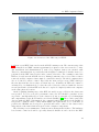
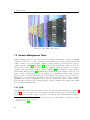


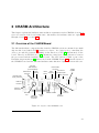


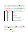

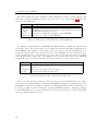
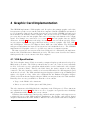
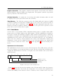
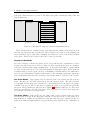
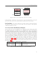


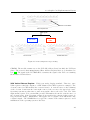
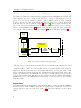

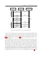
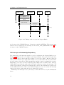
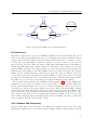

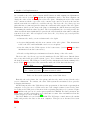
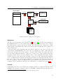
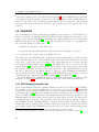
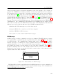
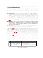

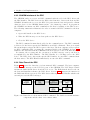

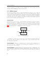


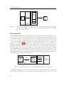

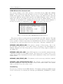
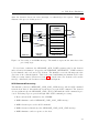
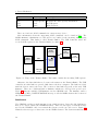
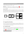


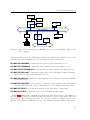

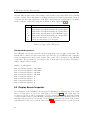
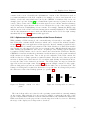

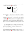

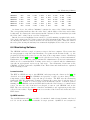
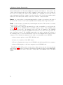

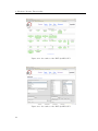


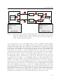
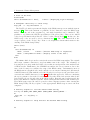
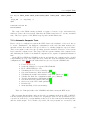


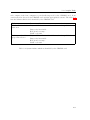


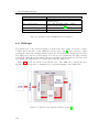

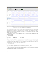
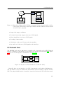
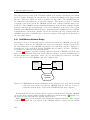
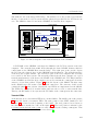
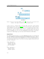
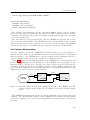


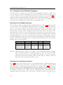


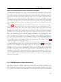
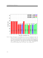
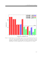
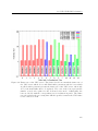
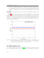
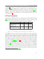


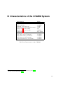
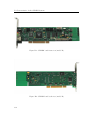

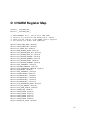

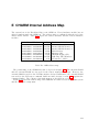

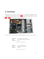


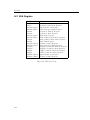


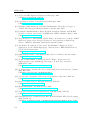
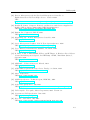
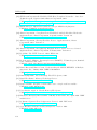

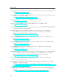
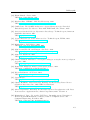
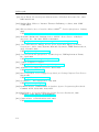


![[Product Monograph Template - Schedule D]](http://vs1.manualzilla.com/store/data/005793815_1-9ff4321a86e1483b72bfcf39a23d58ab-150x150.png)