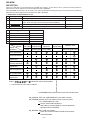
1
MD-M3/M1
SERVICE MANUAL
No.S6940MDM3M1//
MD-M3
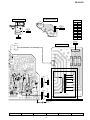
MD-M3 MD micro System consisting of
MD-M3(main unit) and CP-M3(speaker
system).
Illustration: MD-M3
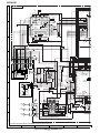
MD-M1
MD-M1 MD micro System consisting of
MD-M1(main unit) and CP-M1(speaker
system).
• In the interests of user-safety the set should be restored to its original
condition and only parts identical to those specified should be used.
Illustration: MD-M1
CONTENTS
Page
IMPORTANT SERVICE NOTES (FOR U.S.A. ONLY) ........................................................................................................ 2
SPECIFICATIONS .............................................................................................................................................................. 3
NAMES OF PARTS ........................................................................................................................................................... 4
OPERATION MANUAL ....................................................................................................................................................... 7
QUICK GUIDE .................................................................................................................................................................... 9
DISASSEMBLY ................................................................................................................................................................ 11
REMOVING AND REINSTALLING THE MAIN PARTS ................................................................................................... 13
TEST MODE .................................................................................................................................................................... 15
ADJUSTMENT ................................................................................................................................................................. 17
EEPROM WRITING PROCEDURE .................................................................................................................................. 23
EXPLANATION OF MECHANISM ERROR ...................................................................................................................... 24
EXPLANATION OF ERROR DISPLAY ............................................................................................................................. 25
NOTES ON SCHEMATIC DIAGRAM .............................................................................................................................. 26
TYPE OF TRANSISTOR AND LED ................................................................................................................................. 26
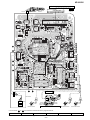
BLOCK DIAGRAM ........................................................................................................................................................... 27
SCHEMATIC DIAGRAM / WIRING SIDE OF P.W.BOARD ............................................................................................. 32
WAVEFORMS OF CD CIRCUIT ...................................................................................................................................... 54
WAVEFORMS OF MD CIRCUIT ..................................................................................................................................... 55
TROUBLE SHOOTING (CD SECTION) .......................................................................................................................... 57
TROUBLE SHOOTING (MD SECTION) ........................................................................................................................... 61
TROUBLE SHOOTING (POWER SUPPLY SECTION) ................................................................................................... 65
FUNCTION TABLE OF IC ................................................................................................................................................ 66
REPLACEMENT PARTS LIST/EXPLODED VIEW/PACKING OF THE SET (FOR U.S.A.)
SHARP CORPORATION
–1–
This document has been published to be used
for after sales service only.
The contents are subject to change without notice.
MD-M3/M1
FOR A COMPLETE DESCRIPTION OF THE OPERATION OF THIS UNIT, PLEASE REFER
TO THE OPERATION MANUAL.
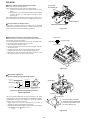
IMPORTANT SERVICE NOTES (For U.S.A.Only)
BEFORE RETURNING THE AUDIO PRODUCT
(Fire & Shock Hazard)
Before returning the audio product to the user, perform the
following safety checks.
1. Inspect all lead dress to make certain that leads are not
pinched or that hardware is not lodged between the chassis
and other metal parts in the audio product.
2. Inspect all protective devices such as insulating materials,
cabinet, terminal board, adjustment and compartment
covers or shields, mechanical insulators etc.
3. To be sure that no shock hazard exists, check for leakage
current in the following manner.
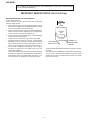
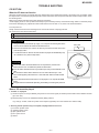
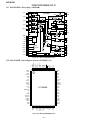
* Plug the AC line cord directly into a 120 volt AC outlet.
* Using two clip leads, connect a 1.5k ohm, 10 watt resistor
paralleled by a 0.15µF capacitor in series with all exposed
metal cabinet parts and a known earth ground, such as
conduit or electrical ground connected to earth ground.
* Use a VTVM or VOM with 1000 ohm per volt, or higher,
sensitivity to measure the AC voltage drop across the
resistor (See diagram).
* Connect the resistor connection to all exposed metal parts
having a return path to the chassis (antenna, metal cabinet,
screw heads, knobs and control shafts, escutcheon, etc.)
and measure the AC voltage drop across the resistor.
VTVM
AC SCALE
1.5k ohms
10W
0.15 µ F
TO EXPOSED
METAL PARTS
TEST PROBE
CONNECT TO
KNOWN EARTH
GROUND
All check must be repeated with the AC line cord plug connection
reversed.
Any reading of 0.3 volt RMS (this corresponds to 0.2 milliamp.
AC.) or more is excessive and indicates a potential shock
hazard which must be corrected before returning the audio
product to the owner.
–2–
MD-M3/M1
FOR A COMPLETE DESCRIPTION OF THE OPERATION OF THIS UNIT, PLEASE REFER
TO THE OPERATION MANUAL.
SPECIFICATIONS
MD-M3/M1
● General
Power source:
AC 120 V, 60 Hz
Power
consumption:
● Compact disc player section
Type:
Top open type compact disc
player
60 W
Signal readout:
Non-contact, 3-beam semiconductor laser pickup
Rotation speed:
200 - 500 rpm CLV, Approx.
Error correction:
CIRC (Cross Interleave ReedSolomon Code)
Quantization:
16-bit linear
Frequency
response:
20 - 20,000 Hz
D/A converter:
1-bit D/A converter
Dimensions:
Width; 6-5/16" (160 mm)
Height; 9-1/2" (240 mm)
Depth; 11-13/16" (300 mm)
Weight: 9.7 lbs. (4.4 kg)
● Amplifier section
Output power:
FTC 16 watts per channel
minimum RMS into 4 ohms
from 80 Hz to 20 kHz with no
more than 10% total
harmonic distortion
Output terminals: Speaker; 4 ohms
Headphones; 16 - 50 ohms
(recommended 32 ohms)
Input terminals:
AUX; 500 mV/47 k ohms
● MiniDisc recorder section
Type:
MiniDisc recorder
Signal readout:
Non-contact, 3-beam semiconductor laser pickup
Rotation speed:
400 - 900 rpm CLV, Approx.
Error correction:
ACIRC (Advanced Cross Interleave Reed-Solomon
Code)
Signal/noise ratio: 95 dB (1 kHz)
Dynamic range:
90 dB (1 kHz)
Wow and flutter:
Unmeasurable
(less than 0.001% W. peak)
● Tuner section
Frequency range: FM; 87.5 - 108.0 MHz
AM; 530 - 1,720 kHz
Sensitivity:
FM; 2.5 µV (75 ohms unbalanced)
AM; 650 µV/m
CP-M3/M1
Quantization:
20-bit linear (A/D converter)
Coding:
ATRAC (Adaptive TRansform
Acoustic Coding)
● Speaker section
2-way speaker system
Type (MD-M3):
4-3/4" (12cm) woofer,
3/4" (2cm) tweeter
44.1 kHz
Type (MD-M1):
Sampling
frequency:
Recording
method:
Magnetic modulation
overwrite method
Frequency
response:
20 - 20,000 Hz
D/A converter:
1-bit D/A converter
Wow and flutter:
Unmeasurable
(less than 0.001% W. peak)
Maximum input
power:
40 W
Rated input
power:
20 W
Impedance:
4 ohms
Dimensions:
(MD-M3)
Width; 6-5/16" (160 mm)
Height; 9-1/2" (240 mm)
Depth; 7-7/8" (198 mm)
Weight; 6.8 lbs. (3.1 kg)/each
Dimensions:
(MD-M1)
Width; 6-5/16" (160 mm)
Height; 9-1/2" (240 mm)
Depth; 7-1/4" (183 mm)
Weight; 4.0 lbs. (1.8 kg)/each
Signal/noise ratio: 95 dB (1 kHz)
Dynamic range:
90 dB (1 kHz)
Audio channel:
Stereo; 2 channels
Monaural; 1 channel
(playback only)
(long-time recording mode)
Full range speaker system
4" (10cm) full-range speaker
Specifications for this model are subject to change without
prior notice.
–3–
MD-M3/M1
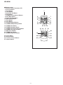
NAMES OF PARTS
■ Front panel
1. Power Button
2. (MD) Display Button
3. Timer Stand-by Indicator
4. (MD) Record Button
5. (CD/MD/TUNER) Memory Button
6. (CD/MD) Stop Button
(TUNER) Tuning Down Button
7. (CD/MD) Play/Pause Button
(TUNER) Tuning Up Button
8. Function Selector Buttons
9. CD Eject Button
10. MD Compartment
11. MD Eject Button
12. (CD/MD) Track Up/Cue Button
(TUNER) Preset Up Button
13. (CD/MD) Track Down/Review Button
(TUNER) Preset Down Button
14. CD MD Normal Speed Edit Button (MD-M3 ONLY)
14. CD MD Edit Button (MD-M1 ONLY)
15. CD MD High Speed Edit Button (MD-M3 ONLY)
16. Surround Button
17. Preset Equalizer Button
18. Extra Bass Button
19. Headphone Jack
20. Volume Control
9
1
2
3
4
5
6
7
10
11
12
13
14
15
16
17
18
19
20
8
▲ ▲▲
14
MD-M1
■ Rear panel
1. Speaker Terminals
2. FM 75 Ohms Antenna Terminal
3. Antenna Ground Terminal
4. AM Loop Antenna Terminal
5. Auxiliary Input (Analog) Level Control
6. Demo Switch
7. Auxiliary Input (Analog) Jacks
8. AC Power Input Jack
1
2
3
4
5
6
7
8
–4–
MD-M3/M1
■ Display window
1. Level Meters
2. Character Information Display
3. Surround Indicator
4. Extra Bass Indicator
5. FM Stereo Indicator
6. FM Stereo Mode Indicator
7. (CD/MD) Disc Indicator
8. (CD/MD) Track Indicator
9. (CD/MD/TUNER) Memory Indicator
10. (CD/MD) Repeat Indicator
11. (CD/MD) Play/Pause Indicator
12. (MD) TOC Indicator
13. (CD/MD) Random Play Indicator
14. (CD/MD) Total Indicator
15. (CD/MD) Remaining Time Indicator
16. Timer Record /Timer Play Indicator
17. CD Indicator
18. MD Indicator
19. (MD) Record Indicator
20. AM/PM Indicator
21. Sleep Indicator
1
SURROUND
X-BASS
ST
L
REC
PLAY
OVER
R
DISC TOC
TRACK
MEMORY
RANDOM
TOTAL
REMAIN
AM
PM
kHz REC
MHz SLEEP
2
3
4
5
6
7
8
9
10
11
12
13
14
15
SURROUND
X-BASS
ST
DISC TOC
TRACK
MEMORY
RANDOM
TOTAL
REMAIN
L
OVER
R
AM
16
17
18
19
REC
PLAY
PM
kHz REC
MHz SLEEP
20
21
CP-M3
■ Speaker section
1. Tweeter
2. Woofer
3. Bass Reflex Duct
4. Speaker Terminals
1
3
2
4
CP-M1
■ Speaker section
1. Full-Range Speaker
2. Bass Reflex Duct
3. Speaker Wire
1
2
3
–5–
MD-M3/M1
■ Remote control
1. Remote Control Transmitter LED
2. Surround Button
3. Clock Button
4. Timer Button
5. Name/TOC Edit Button
6. Sleep Button
7. (TUNER) Preset Up/Down Buttons
8. Extra Bass Button
9. Preset Equalizer Button
10. (MD) Display Button
11. Enter Button
12. Clear Button
13. Character Select Buttons
14. (CD/MD/TUNER) Memory Button
1
2
7
3
4
8
9
10
5
6
11
12 13 14
15. (CD/MD) Time Button
16. (CD/MD) Play Mode Button
17. (CD/MD) Track Down/Review Button
18. (CD/MD) Track Up/Cue Button
19. (MD) Record Button
20. (CD/MD) Stop Button
21. (CD/MD) Play/Pause Button
15
16
17
18
20
19
22. Power Button
23. Dimmer Button
24. Function Selector Buttons
25. Volume Buttons
–6–
21
22
24
23
25
3,5,7,9
kHz REC
MHz SLEEP
–7–
or
button to select the time
kHz REC
MHz SLEEP
kHz REC
MHz SLEEP
kHz REC
MHz SLEEP
or
button.
● When the button is pressed once, the time will
increase by 1 hour. When the button is pressed
once, the time will decrease by 1 hour.
● When the 12-hour display selected, “ AM ” will
change to “ PM ” automatically.
DISC TOC
TRACK
MEMORY
RANDOM
TOTAL
REMAIN
6 Adjust the hour by pressing the
DISC TOC
TRACK
MEMORY
RANDOM
TOTAL
REMAIN
5 Press the ENTER button.
The 24-hour display will appear.
(0:00 - 23:59)
"12:00 AM" The 12-hour display will appear.
(AM or PM 12:00 - 11:59)
"0:00 AM"
The 12-hour display will appear.
(AM or PM 0:00 - 11:59)
● Note that this can only be set when the unit is
first installed or it has been reset.
"0:00"
DISC TOC
TRACK
MEMORY
RANDOM
TOTAL
REMAIN
display mode.
4 Press the
DISC TOC
TRACK
MEMORY
RANDOM
TOTAL
REMAIN
3 Within 5 seconds, press the ENTER button.
DISC TOC
TRACK
MEMORY
RANDOM
TOTAL
REMAIN
1 Press the POWER button to turn the power on.
2 Press the CLOCK button.
1
2
4,6,8
In this example, the clock is set for the
24-hour (0:00) system.
SETTING THE CLOCK
kHz REC
MHz SLEEP
DISC TOC
TRACK
MEMORY
RANDOM
TOTAL
REMAIN
kHz REC
MHz SLEEP
or
kHz REC
MHz SLEEP
Perform steps 6 - 9 above.
Within 5 seconds, press the ENTER button.
Press the CLOCK button.
1
2
Perform steps 1 - 9 above.
Reset the microcomputer.
To change the time display mode:
1
2
3
To change the clock time:
Note:
● The clock display will flash on and off at the push
of the CLOCK button when the AC power supply
is restored after a power failure occurs or after
the AC power cord is disconnected.
If this happens, follow the procedure below to
change the clock time.
Press the CLOCK button.
● The time display will appear for about 5 seconds
even if stand-by mode.
To see the time display:
● The clock starts operating from "0" seconds.
(Seconds are not displayed.)
DISC TOC
TRACK
MEMORY
RANDOM
TOTAL
REMAIN
9 Press the ENTER button.
● When the button is pressed once , the time
will increase by 1 minute. When the button is
pressed once, the time will decrease by 1 minute.
● The hour setting will not advance even if minutes advance from "59" to "00".
button.
8 Adjust the minutes by pressing the
DISC TOC
TRACK
MEMORY
RANDOM
TOTAL
REMAIN
7 Press the ENTER button.
Illustration:MD-M3
2
Caution:
The operation explained above will erase all data
stored in memory including clock and timer
settings, and tuner, MD and CD presets.
the EQUALIZER button and the PLAY
button.
“ALL CLEAR” will appear.
2 Press the POWER button while holding down
mode.
1 Press the POWER button to enter the stand-by
If this product is subjected to strong external interference (mechanical shock, excessive static electricity, abnormal supply voltage due to lightning, etc.)
or if it is operated incorrectly, it may malfunction or
the display may not function correctly. If such a problem occurs, do the following:
1,2
RESETTING THE MICROCOMPUTER
YES
Correct
NO
Compact discs are fairly resistant to damage, however mistracking can occur due to an accumulation
of dirt on the disc surface.
Follow the guidelines below for maximum enjoyment from your CD collection and player.
Do not write on either side of the disc, particularly the non-label side.
Signals are read from the non-label side. Do not
mark this surface.
Keep your discs away from direct sunlight, heat,
and excessive moisture.
Always hold the CDs by the edges. Fingerprints,
dirt, or water on the CDs can cause noise or
mistracking. If a CD is dirty or does not play properly, clean it with a soft, dry cloth, wiping straight
out from the center, along the radius.
Care of compact discs
Periodically wipe the cabinet with a soft cloth and
a diluted soap solution, then wipe with a dry cloth.
Do not use chemically treated cleaning cloths or
other chemicals.
External care
Do not touch the Laser pickup lens. If fingerprints
or dust accumulate on the pickup, clean it gently
with a dry cotton swab.
Internal care
MAINTENANCE
MD-M3/M1
OPERATION MANUAL
When a radio or TV which uses an
indoor antenna is placed near the
unit, the picture on the TV screen
may be distorted or the radio may
not function properly .
Radios make unusual noise or the
picture on the TV screen is distorted.
–8–
The unit is placed near the TV or
computer .
The antenna direction is not placed
properly.
Did you erase the programmed station?
The preset channel cannot be recalled.
Possible cause
Is the MiniDisc protected against
accidental erasure?
Did you try to make recording on a
play-back only MiniDisc?
Can you see the “DISC FULL” or
“TOC FULL ” message in the display?
( :number or symbol)
The source has been encoded with
the SCMS signal (Serial Copy Management System).
The disc is very dirty.
Is the unit located near excessive
vibrations?
Has condensation formed inside the
unit?
Possible cause
The disc is very dirty.
The disc which does not satisfy the
standards.
Is the unit located near excessive
vibrations?
Has condensation formed inside the
unit?
The disc is loaded up-side down.
Radios make unusual noise consecutively .
Symptom
Radio reception
Even though a disc has been
loaded, “MD NO DISC” or “READ
ERR” is displayed.
Playback sounds are skipped.
A recording cannot be made.
Symptom
MD recording and playback
Even though a disc has been
loaded, “CD NO DISC” or “ERR”
is displayed.
Playback stops in the middle of a
track, or playback is not performed
properly.
Playback sounds are skipped.
Symptom
Possible cause
Is the volume level is set to “0”?
Are the headphones connected?
Are the speaker wires disconnected?
No sound is heard.
CD Playback
Did a power failure occur?
Possible cause
The clock is wrong.
When a button is pressed, the unit
does not respond.
Symptom
General
When the unit receives a radio
broadcast near a TV set, a computer or a word-processor ,it may
pick up noise. If this happens,try to move the unit from
the place where the noise is
picked up.
Correct the antenna direction.
Preset the channel again.
Redo programming.
Remedy
Clean the disc.
Place the unit on a firm, level
surface free from vibration.
Remove the disc and leave the
power turned on. The unit
should function properly in
about 1 hour.
Slide the accidental erase prevention tab back to its original
position.
Replace it with a recordable
disc.
Put in another recordable disc
with recording space on it.
Use another source.
Remedy
Load the disc with the correct
side up.
Clean the disc.
Load the correct disc.
Place the unit on a firm, level
surface free from vibration.
Remove the disc and leave the
power turned on. The unit
should function properly in
about 1 hour.
Remedy
It is recommended that you use
an external antenna.
Set this unit to the stand-by
mode and then turn it back on.
Then, retry the operation.
Increase the volume level.
Disconnect the headphones.
Connect the wires securely.
Try setting it again.
Remedy
If this unit functions abnormally during operation, first check the following items. If the unit continues to function
abnormally , or if an abnormality appears other than listed below, set this unit to the stand-by mode and disconnect the AC power plug, then consult your SHARP dealer or service personnel.
■ If a problem occurs
TROUBLESHOOTING
Meaning
? DISC
00:00
U TOC ERR*
(*:Number or
symbol)
U TOC ERR W
TOC FULL*
(*:Number or
symbol)
TOC W ERR
TOC ERR*
(*:Number or
symbol)
The disc is damaged.
TOC information cannot be read.
MD not specified.
There is no space left for recording character information (track names, disc names,
etc.).
● TOC information recorded on the MD does
not match the MD specifications or it cannot be read.
● The TOC information could not be created
properly due to a mechanical shock or to
scratches on the disc.
● The data contains an error .
● Music is not being recorded.
● Recording is impossible.
●
●
●
●
● The disc is damaged.
● A TOC is not written on the MD or there is
something wrong with data.
● The temperature is too high.
READ ERR
TEMP OVER
● You tried to record on a playback-only disc.
● The disc is write protected.
PLAY MD
PROTECTED
NOT AUDIO
MECHA ERR*
(*:Number or
symbol)
NAME FULL
● The number of characters for the disc name
or track name exceeds 40.
● The data recorded on this disc is not audio
data.
● A MiniDisc has not been loaded.
● The disc data cannot be read.
● There is a mechanical problem and the disc
is not working properly .
MD NO DISC
MD ERR
● A disc has not been loaded.
● The disc data cannot be read.
● Trouble is found.
● Recording cannot be performed correctly
due to vibration or shock in the unit.
● Timer recording is impossible or there is no
available space on the MD.
● A CD has not been loaded.
● The disc data cannot be read.
● The disc is out of recording space.
● Nothing is recorded.
● A track cannot be edited.
FOCUS ERR
DISC FULL
CD NO DISC
CAN’T REC
Error messages
BLANK MD
CAN’T EDIT
Remedy
Insert properly.
Replace the batteries.
Operate it within a range of
8" (0.2m) to 20' (6m) and within
an angle of 15 ° to either side of
center.
Connect the AC power cord.
Remedy
● Set this unit to the stand-by mode and try to
write the TOC again. (Remove any source
of shock or vibration while writing.)
● Replace it with another disc.
● Replace the disc with another recordable
disc.
● Contact the shop where you purchased the
unit.
● Replace it with another disc.
● Erase the disc and try recording again.
● Replace it with another recordable disc.
● Set this unit to the stand-by mode and wait
for a while.
● Replace it with another disc.
Select another track.
Replace the disc.
Replace it with another recordable disc.
Move the write protection tab back to its
original position.
● Reload the disc or replace it.
●
●
●
●
● Shorten the disc or track name.
● Contact the shop where you purchased the
unit.
● Load a MiniDisc.
● Reload the MiniDisc.
● Set this unit to the stand-by mode and press
the MD EJECT button.
● Load a CD.
● Reload the CD.
● Replace the disc with another recordable
disc.
● Reload the MiniDisc.
● Replace it with another disc.
● Change the stop position of the track and
then try editing it.
● Re-record or replace the MiniDisc.
● Replace it with another disc.
The batteries (polarity) are not inserted properly .
The batteries inside the remote control are dead.
The remote control is operated from
an incorrect distance or angle.
Is the AC power cord plugged in?
Possible cause
When an error message is displayed, proceed as follows:
ERROR MESSAGES
The power cannot be turned on
from the remote control.
The remote control does not function or does not operate properly.
Symptom
Remote control
(Continued)
MD-M3/M1
MD-M3/M1
3 Listening to a CD / Audición de discos CD
MD MICRO SYSTEM
Quick Guide/Guía rápida MD-M3
1
1 Check the supplied accessories / Compruebe los accesorios suministrados
● Remote control x 1
● Controlador remoto x 1
● AC power cord x 1
● Cable de alimentación de CA x 1
3
4
● Label side up
● Con el lado de la
etiqueta hacia arriba
CD EJECT
2
● AM loop antenna x 1
● Antena de cuadro de AM x 1
CD
5
PUSH CLOSE
To stop playback
Para detener la reproducción
● Speaker cushion x 8
● Almohadilla del altavos x 8
● Speaker wire x 2
● Cable del altavoz x 2
● FM antenna x 1
● Antena de FM x 1
POWER
6
2 Preparation for use / Preparación para su uso
■ Speaker connection
■ Conexión de los altavoces
■ Antenna connection
■ Conexión de las antenas
● AM Loop Antenna
● Antena de cuadro
de AM
Left speaker
Altavoz izquierdo
Right speaker
Altavoz derecho
4 Listening to an MD / Audición de discos MD
● FM Antenna
● Antena de FM
1
FM
75 OHMS
Black
Negro
POWER
GND
Red
Rojo
AM
LEFT
2
MD
4
RIGHT
Red
Rojo
RATESD SPEAKER
IMPEDANCE :
4 OHMS MIN.
To remove a MiniDisc
Para extraer un minidisco
Black
Negro
● AC 120 V, 60 Hz
● 120 V de CA, 60 Hz
■ Turning the power on and off
■ Conexión y desconexión de la alimentación
■ Remote control
■ Controlador remoto
3
Remote Sensor
Sensor remoto
● Label side facing up
● Con el lado de la etiqueta
orientado hacia arriba
POWER
● 2 “AA” size batteries
● 2 pilas del tamaño “AA”
To stop playback
Para detener la reproducción
8" - 20'
(0.2 m - 6 m)
0,2 m - 6 m
POWER
15
15
● Batteries are not included.
● Las pilas no están incluidas.
7 Recording
from a CD onto a MiniDisc (One-Touch Editing) /
Grabación de un disco CD a un minidisco (edición de un accionamiento)
5 Listening to the radio / Audición de la radio
1
POWER
1
2
2
3
Select “FM ST”,“FM”or“AM”
Seleccione “FM ST”,
“FM”o“AM”
POWER
3
Load a compact disc and a
recordable MiniDisc.
Inserte un disco compacto y un
minidisco grabable.
CD
Tune into the desired station.
Sintonizar la emisora deseada.
TUNER
To stop recording
Para detener la grabación
TUNING
4
HIGH
CD
8 Recording
from the built-in radio onto MiniDisc /
Grabación desde la radio incorporada a un minidisco
6 Sound control / Control del sonido
■ Volume
■ Volumen
NORMAL
MD EDIT
■ Pre-programmed equalizer
■ Ecualizador preprogramado
4
1
Tune into the desired station.
Sintonice la emisora deseada.
Check the recordable time.
Compruebe el tiempo que puede grabarse.
TUNER
DISPLAY
FLAT
SOFT
■ Extra bass (X-BASS)
■ Graves extra (X-BASS)
X-BASS
HEAVY
VOCAL
■ Surround
■ Sonido difuso
X-BASS
SURROUND
2
SURROUND
5
Load a recordable Minidisc.
Inserte un minidisco grabable.
To stop recording
Para detener la grabación
3
–9–
REC
MD-M3/M1
MD MICRO SYSTEM
Quick Guide/Guía rápida MD-M1
3 Listening to a CD / Audición de discos CD
1 Check the supplied accessories / Compruebe los accesorios suministrados
1
POWER
3
4
● Label side up
● Con el lado de la
etiqueta hacia arriba
CD EJECT
● Remote control x 1
● Controlador remoto x 1
● AC power cord x 1
● Cable de alimentación de CA x 1
2
CD
5
PUSH CLOSE
● AM loop antenna x 1
● Antena de cuadro de AM x 1
● FM antenna x 1
● Antena de FM x 1
To stop playback
Para detener la reproducción
2 Preparation for use / Preparación para su uso
■ Speaker connection
■ Conexión de los altavoces
■ Antenna connection
■ Conexión de las antenas
● AM Loop Antenna
● Antena de cuadro
de AM
Left speaker
Altavoz izquierdo
Right speaker
Altavoz derecho
● FM Antenna
● Antena de FM
4 Listening to an MD / Audición de discos MD
FM
75 OHMS
Black
Negro
1
GND
Red
Rojo
POWER
To remove a MiniDisc
Para extraer un minidisco
AM
LEFT
2
RIGHT
Red
Rojo
6
RATESD SPEAKER
IMPEDANCE :
4 OHMS MIN.
Black
Negro
MD
4
● AC 120 V, 60 Hz
● 120 V de CA, 60 Hz
■ Turning the power on and off
■ Conexión y desconexión de la alimentación
■ Remote control
■ Controlador remoto
Remote Sensor
Sensor remoto
3
POWER
● 2 “AA” size batteries
● 2 pilas del tamaño “AA”
● Label side facing up
● Con el lado de la etiqueta
orientado hacia arriba
8" - 20'
(0.2 m - 6 m)
0,2 m - 6 m
To stop playback
Para detener la reproducción
POWER
15
15
● Batteries are not included.
● Las pilas no están incluidas.
5 Listening to the radio / Audición de la radio
1
7 Recording
from a CD onto a MiniDisc (One-Touch Editing) /
Grabación de un disco CD a un minidisco (edición de un accionamiento)
POWER
1
2
2
3
Select “FM ST”,“FM”or“AM”
Seleccione “FM ST”,
“FM”o“AM”
POWER
3
Load a compact disc and a
recordable MiniDisc.
Inserte un disco compacto y un
minidisco grabable.
CD
Tune into the desired station.
Sintonizar la emisora deseada.
TUNER
To stop recording
Para detener la grabación
TUNING
CD
MD EDIT
8 Recording
from the built-in radio onto MiniDisc /
Grabación desde la radio incorporada a un minidisco
6 Sound control / Control del sonido
■ Volume
■ Volumen
4
■ Pre-programmed equalizer
■ Ecualizador preprogramado
4
1
Tune into the desired station.
Sintonice la emisora deseada.
Check the recordable time.
Compruebe el tiempo que puede grabarse.
TUNER
DISPLAY
FLAT
SOFT
■ Extra bass (X-BASS)
■ Graves extra (X-BASS)
X-BASS
HEAVY
VOCAL
■ Surround
■ Sonido difuso
X-BASS
SURROUND
SURROUND
2
5
Load a recordable Minidisc.
Inserte un minidisco grabable.
To stop recording
Para detener la grabación
3
– 10 –
REC
MD-M3/M1
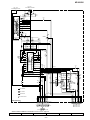
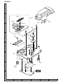
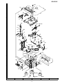
DISASSEMBLY
MAIN UNIT
Caution on Disassembly
The disassembling the machine or assembling it after
repair, observe the following instructions to ensure safety
and keep its performance.
1. Unload the compact disc, and mini-disc, cassette tape
from machine.
2. Be sure to unplug the power cable before starting
disassembly of the machine.
3. When disassembling each section, remove the nylon
band or wire arrangement.
After servicing the unit, be sure to rearrange the leads
where they were before disassembling.
If a screw of improper length is fit to the MD mechanism.
(A screw fit the part to the mechanism chassis of MD
section), it may contact the optical pickup, impeding
normal operation. Hence, due care must be taken.
4. While repairing, pay utmost attention to static electricity
on ICs.
(A2)x1
(A1)x1
ø3x10mm
REMOVAL
PROCEDURE
FIGURE
1
Top Cabinet
1. Screw ................ (A1) x4
2. Socket ............... (A2) x3
11-1
2
Side Panel (Right,Left) 1. Screw ................ (B1) x7
(Note 2)
11-1
3
Rear Panel
1. Screw ................ (C1) x4
11-1
4
Main PWB
(Note 2)
1. Flat Wire ............ (D1) x1
2. Lead Wire .......... (D2) x1
3. Screw ................ (D3) x6
4. Socket(MD-M3) .... (D4) x3
4. Socket(MD-M1) .... (D4) x2
5. Flat Cable .......... (D5) x4
11-2
Power/Tuner PWB 1. Screw ................ (E1) x4
2. Socket ............... (E2) x1
3. Flat Cable .......... (E3) x1
11-3
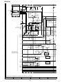
MD Unit and Holder 1. Screw ................ (F1) x4
(Note 1,2)
2. Screw ................ (F2) x5
12-1
5
6
Front Panel
Top Cabinet
Side Panel
(Right)
(B1)x3
ø3x10mm
(A1)x1
ø3x10mm
(B1)x2
ø3x10mm
Side Panel
(Left)
(A1)x2
ø3x10mm
MAIN UNIT MD-M3/M1
STEP
CD
Mechanism
(A2)x2
(C1)x4
ø3x10mm
(B1)x2
ø3x10mm
Rear Panel
Figure 11-1
(D5)x1 MD-M3 Only
(D4)x1
(D5)x2
Front Panel
(D3)x2
ø3x10mm
Main
PWB
Lug
(D3)x1
ø3x10mm
(D4)x1
(D5)x1
7
Power PWB
1. Screw ................ (G1) x4
12-1
8
Front Panel
1. Screw ................ (H1) x2
12-1
9
Jack PWB
1. Screw ................ (J1) x1
12-2
10
Display PWB
1. Knob .................. (K1) x1
2. Nut ..................... (K2) x1
3. Screw ................ (K3) x5
12-2
11
CD Mechanism
1. Screw ................ (L1) x3
12-3
(D3)x2
ø3x10mm
Jack
PWB
Main
PWB
(D4)x1
(D1)x1
(D3)x1
ø3x10mm
(D2)x1
Figure 11-2
Note 1: When removing or reinstalling the MD unit, avoid a
short circuit by being careful not to allow it to touch the
PWB.(Replacement with the PWB installed)
Note 2: After removing the connector for the optical pickup
from the connector wrap the conductive aluminium foil
around the front end of connector so as to protect the
optical pickup from electrostatic damage.
Cares after repairing
After completion of repair of product set the following shipping
mode to return.
1. Make sure that there is not a CD and MD disc in the tray.
Press and hold the PRESET EQUALIZER and STOP buttons,
and then press the POWER button to enter the TEST mode.
2. After the indication of FINISHED appears, unplug the power
cord. If this test mode is executed, the data stored by the
user in the preset memory are all cleared. It is necessary
tell and obtain the consent of user in advance.
– 11 –
Front Panel
(E3)x1
Power PWB
Power/Tuner
PWB
(E2)x1
Lug
(E1)x1
ø3x10mm
(E1)x1
ø3x10mm
(E1)x1
ø3x10mm
Figure 11-3
(E1)x1
ø3x10mm
MD-M3/M1
(F2)x1
ø3x10mm
Front Panel
(F1)x2
ø3x10mm
Front Panel
MD Unit
(F2)x4
ø3x12 mm
(K1)x1
MD Holder
(K3)x2
ø2.6x10mm
(G1)x4
ø4x8mm
Nut
(K2)x1
Washer
Jack PWB
(F1)x2
ø3x10mm
Power PWB
(H1)x2
ø3x10mm
Figure 12-2
Figure 12-1
(L1)x3
ø2.6x10mm
CD Mechanism
Display PWB
(J1)x1
ø2.6x10mm
(K3)x3
ø2.6x10mm
SPEAKER CP-M1
Top Cabinet
STEP
1
REMOVAL
Speaker
PROCEDURE
FIGURE
1. Net ..................... (A1) x1
2. Screw ................ (A2) x4
12-5
Woofer
Net
(A1) x1
Figure 12-3
(A2) x4
ø4 x12mm
SPEAKER CP-M3
REMOVAL
STEP
1
Speaker
(Woofer/Tweeter)
PROCEDURE
FIGURE
1. Net ..................... (A1) x1
2. Screw ................ (A2) x4
3. Cover Ring ........ (A3) x1
4. Screw ................ (A4) x4
5. Cover Ring ........ (A5) x1
6. Screw ................ (A6) x2
12-4
Screw Driver
Tweeter
Sheet
(A6) x2
ø4 x10mm
(A5) x1
(A1) x1
Figure 12-5
(A4) x4
ø4 x15mm
(A2) x4
ø4 x15mm
Net
Woofer
Figure 12-4
(A3) x1
– 12 –
MD-M3/M1
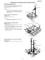
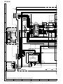
REMOVING AND REINSTALLING THE MAIN PARTS
MD MECHANISM SECTION
(A1)x1
ø1.7x5mm
For details about the procedure to remove the MD mechanism
from the main unit, refer to the Disassembly Procedure, Steps
1-6 in the main unit and also the MD section.
(Referring to p.11,12)
Magnetic Head
Caution:
After pulling out the optical pickup connector, wrap the
end of the connector in conductive aluminium foil to
prevent the optical pickup from being destroyed by
static electricity.
MD Mechanism
How to remove the magnetic head
(See Fig. 13-1)
1. Remove the screws (A1) x 1 pc.
Caution:
Take utmost care so that the magnetic head is not
damaged when it is mounted.
Figure 13-1
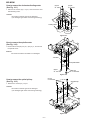
Slider Lever
How to remove the cartridge holder
(See Fig. 13-2)
Cartrdge Holder
1. Open the roller arm lever in the arrow direction, and lower
the clamp lever to the rear side.
2. Apply +5V to the red line side of blue connector of loading
motor, push the rack gear in the arrow direction to move the
cam plate lever unit tick is heard.
3. Remove the screw (B1) x 1 pc., and the spring (B2) x 1
pc.,fitted to the holder arm, and shift the cartridge holder to
the left side to remove it.
Roller Arm Lever
(B1) x1
ø1.7x5mm
Clamp Lever
Loading
Motor
Rack Gear
(B2) x1
Cam Plate Lever
Figure 13-2
(C1)x1
ø1.7x3mm
How to remove the mechanism switch PWB
(See Fig. 13-3)
(C1)x1
ø1.7x9.5mm
1. Remove the screws (C1) x 2 pcs., and remove the mechanism
switch PWB.
Mechanism Switch PWB
Figure 13-3
– 13 –
MD-M3/M1
(D1)x2
ø1.7x2mm
How to remove the sled motor/loading motor
(See Fig. 14-1)
(D1)x2
ø1.7x2mm
1. Remove the screws (D1) x 4 pcs., and remove the sled
motor/loading motor.
Caution:
Be careful so that the gear is not damaged.
(The damaged gear emits noise during searching.)
Loading Motor
Sled Motor
Figure 14-1
How to remove the spindle motor
(See Fig. 14-2)
1. Remove the screws (E1) x 2 pcs., (E2) x 1 pc., and remove
the spindle motor.
Caution:
Be careful so that the turntable is not damaged.
Turntable
Spindle Motor
(E2)x1
ø1.7x2.1mm
(E1)x2
ø1.7x2.5mm
Figure 14-2
(F1)x3
ø1.7x9.5mm
How to remove the optical pickup
(See Fig. 14-3)
Optical Picup
1. Remove the screws (F1) x 3 pcs.
Caution:
Be careful so that the gear is not damaged.
(The damaged gear emits noise during searching.)
Figure 14-3
– 14 –
MD-M3/M1
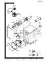
CD MECHANISM SECTION
CD Cover
For details about the procedure to remove the CD mechanism
from the main unit, refer to Disassembly Procedure, Steps 1
,11 in the main unit and also the CD section. (p.11,12).
( A2 ) x2
ø2.6 x6mm
How to remove the optical pickup
(See Fig. 15-1.)
CD Mechanism
1. Remove the mechanism cover, paying attention to the
pawls (A1)x 4 pcs.
2. Remove the screws (A2)x 2 pcs., to remove shaft (A3)x 1
pc.
3. Remove stop washer (A4)x 1 pc., to remove the gear (A5)x
1 pc.
4. Remove the optical pickup.
( A1 ) x4
Shaft
( A3 ) x1
Gear
( A5 ) x1
Stop Washer
( A4 ) x1
Note:
After disconnecting the optical pickup connector wrap the
front end of connector in conductive aluminium foil to prevent
damage to the optical pickup by static electricity.
Optical Pickup
Figure 15-1
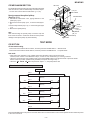
TEST MODE
CD SECTION
CD test mode setting
Press and hold the CD and PLAY buttons, and then press the POWER button. -> Normal mode
Press and hold the CD and STOP buttons, and then press the POWER button. -> Hi-speed mode
test mode
▲
▲
▲
▲
▲
▲
▲
▲
• Each step in the operation is only possible when the LID switch is ON in the CD test mode.
However, when a focus is not obtained in step 3, or when an error is detected, you cannot go forward.
• When the unit enters the error-handling mode, press the POWER button to end the test mode or press the STOP
button so that any further operations are prohibited, except for returning to step 1.
• When the
/
button is pressed in steps 2 - 5, the pickup will be slid.
• Flow chart in the CD test mode or less.
Entry
Step 1
Stop mode
Play
Memory
Stop
Step 2
Laser output ON
Play
Memory
Stop
Step 3
Play
Focus search
Memory
Stop
Step 4
Play
CLV ON
Memory
Step 5
Stop
Play
Manual play
Step 6
Normal play
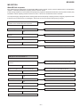
Stop
Press the POWER button at any time to cancel the test mode. The unit will return to the normal operation mode in which the power
to the unit is turned off.
– 15 –
MD-M3/M1
MD SECTION
Test mode setting method
1. Holding down the MD FUNCTION button and FF(
)button, press POWER button switch.
(State A is changed to state B .)
2. Insert the playback disc 1 (high reflection disc) or recording disc 2 (low reflection disc).(State C is set.)
Thus, the test mode state is set.
A tsm 13
e
: TEST MODE
STOP state
represents version of MD microcomputer.
(When the STOP button is pressed in the C state, the
indication A is restored. To restore C again, press the
PRESET EQUALIZER button.)
B EJECT
C AUT YOBI
Entering the specific mode
Whenever the SURROUND button is pressed, the mode is changed.
AUTO pre-adjustment
AUTO adjustment
EEPROM setting
MANUAL adjustment
RESULT Pre-adjustment
RESULT
MANUAL pre-adjustment
Cancel of test mode
To restore the usual state once reset.
*Before pressing the POWER button, be sure to perform the AUTO preliminary adjustment and the AUTO adjustment. Make
sure that they return a "COMPLETE" result.
*When the data of EEPROM was changed or the preliminary adjustment was performed again, be sure to press the POWER
button to write data in the EEPROM.
(Data is written in the EEPROM by pressing the POWER button.)
*When changing the EEPROM settings, write them into the EEPROM and then enter the test mode again. Perform the AUTO
preliminary adjustment and the AUTO adjustment. Then, write those into the EEPROM.
TUNER SECTION
• Test mode setting method
Holding down the TUNER button and PLAY/PAUSE button,
turn on POWER button switch. Frequency is set in the
memory (initial setting) as shown in Table 16.
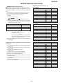
Preset No.
P01
P02
P03
P04
P05
Frequency
87.50 MHz
108.00 MHz
90.00 MHz
106.00 MHz
98.00 MHz
Preset No.
P06
P07
P08
P09
P10
Frequency
522 kHz
1,620 kHz
603 kHz
1,404 kHz
990 kHz
Table 16 Initial setting of memory
– 16 –
MD-M3/M1
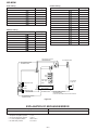
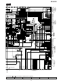
ADJUSTMENT
TUNER SECTION
• FM mute level adjustment
FM signal oscillator Frequency 1 kHz, 40 kHz
fL: Low-range frequency
fH: High-range frequency
• AM adjustment and confirmation
AM signal oscillator Frequency 400 Hz, 30%, AM modulation
Adjusting item
Adjusting
method
Adjusting object
IF
Adjust the indication of Set IF waveform
T351 set to 1,720 kHz. 450 kHz to maximum.
Frequency cover
(VT line voltage of
pin 20 of IC302)
fL: T306 (530 kHz)
Adjust the indication
of set to 530 kHz.
fH: (1,720 kHz)
fL: 1.1 ± 0.1 V
fH: 8.0 ± 1.3 V of
(Only confirmation)
fL: T302 (990 kHz)
Set the output of
speaker terminal
to maximum.
Tracking
Frequency
Adjusting
method
Adjusting
object
98 MHz
25 dB
VR351
Adjusting object
Input: SO301
Output: Speaker
Terminal
Electronic
voltmeter
Speaker
Terminal
SO301
FM signal oscillator
UNIT
Figure 17-2 FM Mute Level
AM Loop Antenna
IF : Speaker Terminal
Electronic
Freqency cover: IC302,Pin 20 voltmeter
POWER/TUNER PWB
AM IF
FM signal oscillator
UNIT
SO301
Antenna Terminal
IC302
GND
20
Loop Antenna
T351
VR351
Figure 17-1 AM IF
• Erasing the registered broadcast station
When the power is off, press and hold the TUNER button and
the STOP button, and then press the POWER button.
All the registered stations are erased.
FE301
T302
IC303
T306
AM Tracking
FM Mute Lebel
AM Band Coverge
Figure 17-3 ADJUSTMENT POINT
CD SECTION
• Adjustment
Since this CD system incorporates the following automatic
adjustment functions, readjustment is not needed when
replacing the pickup. Therefore, different PWBs and pickups
can be combined freely.
Each time a disc is changed, these adjustments are
performed automatically. Therefore, playback of each disc
can be performed under optimum conditions.
T
Stopped
CH1=500mV
DC 10:1
Items adjusted automatically
(1) Offset adjustment (The offset voltage between the head
amplifieroutput and the VREF reference voltage is
compensated inside the IC.)
* Focus offset adjustment
* Tracking offset adjustment
(2) Tracking balance adjustment (waveform drawing 17-4
EFBL)
(3) Gain adjustment (The gain is compensated inside the IC
sothat the loop gain at the gain crossover frequency will
be 0dB.)
* Focus gain adjustment
* Tracking gain adjustment
T
CH2=200mV
DC 10:1
CH3=1V
DC 10:1
FDO
1
TE
3
EFBL
2
CH2
v/DIV
200mV
=Filter=
Smoothing : ON
BW : FULL
=Offset=
CH1 :
0.000V
CH2 :
0.000V
CH3 :
0.00V
CH4 :
0.00V
=Record Length=
Main : 100K
Zoom :
2k
Figure 17-4
– 17 –
1999/04/05 20:26:47
500ms/div
(500ms/div)
NORM:20kS/s
=Trigger=
Mode : SINGLE
Type : EDGE CH1
Delay :
0.0ns
Hold off :
0.2us
MD-M3/M1
MD SECTION
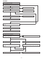
When the combination of mechanism/pickup and PWB was changed , set the TEST mode to perform the AUTO preliminary
adjustment and AUTO adjustment, write the adjustment data in EEPROM.
When EEPROM was replaced, set the TEST mode, write the EEPROM set data (p23,p24) and then perform the preliminary
adjustment and AUTO adjustment, write adjustment data in EEPROM.
1. Preparation for adjustment Test disc
Type
1
2
3
4
Part No.
Test disc
High reflection disc TGYS1 (SONY) [for Playback]
Low reflection disc Recording minidisc
SONY 80 minutes disk is recommended.(example:PRISM 80)
Head Adjusting transparent
Low reflection disc Pre-adjustment disc [TEAC Test MD]
RRCDT0101AFZZ
––––––––––––
RRCDT0103AFZZ
88GMMD-213A
Extension Cable (See Fig. 24)
1
2
3
4
5
Type
Part No.
Extension PWB for servicing
Extension Connector (2 Pin)
Extension Connector (6 Pin)
Extension Cable (5 Pin)
Extension Cable (28 Pin)
RUNTK0457AFZZ
QCNWK0059AFZZ
QCNWK0107AFZZ
QCNWK0109AFZZ
QCNWK0108AFZZ
Execution item
TEMP
Checking
required
EEPROM
setting
basic setting
Repair
TEMP
EEPROM_SET
operations
AUTO-YOBI
adjustment
Writing the
EEPROM setting
AUTO–YOBI
Operation check
TEST-PLAY TEST-REC
PICK replacement
HEAD replacement
MECHANISM
replacement
MAIN PWB
assembly replacement
MD microcomputer
replacement
MD LSI replacement
RF IC replacement
EEPROM IC
replacement
number
,
,
,
,
and
indicate the order of inplementation.
" – " is an item that you don't have to execute.
The EEPROM writing result is shown at the end of the test mode
OK_EEPROM: "SET" and "YOBI COMPLETE" were written normally
WR_EEPROM: Although "SET" was written normally, it was not written
in the "YOBI COMPLETE" state.
Peform "AUTO-YOBI" adjustment.
After making a normal adjustment, write the preliminary
adjustment into the EEPROM.
NG_EEPROM: "SET" could not be written.
Check the connection between the MD microcomputer
and the EEPROM.
– 18 –
MD-M3/M1
• Test Mode
1. EJECT mode
• TEMP setting (of EEPROM setting)
• CONTROL setting (of EEPROM setting)
• Setting of laser power (record/playback power)
2. AUTO pre-adjustment mode
• Automatic pre-adjustment is performed.
3. AUTO adjustment mode
• Automatic adjustment is performed. (After adjustment the grating adjustment mode is set.)
• RESULT sub-mode
• RESULT mode (final adjustment)
• MANUAL pre-adjustment mode
• MANUAL adjustment mode
• Therefore do not set this mode since it is not necessary for the service.
4. EEPROM setting mode
• Various coefficients of digital servo are changed manually.
5. TEST-PLAY mode
• Continuous playback from the specified address is performed.
• C1 error rate measurement, ADIP error rate measurement.
6. TEST-REC mode
• Continuous recording from the specified address is performed.
7. INNER mode
• The position where the INNER switch is turned on is measured.
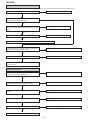
Above rank 4 bit HEX data
0
0
1
2
3
Below rank 4 bit HEX data
4
5
6
7
8
9
NUL
BLANK
00h
SOH
BLANK
01h
STX
BLANK
02h
ETX
BLANK
03h
EOT
BLANK
04h
ENQ
BLANK
05h
ACK
BLANK
06h
BEL
BLANK
07h
BS
BLANK
08h
HT
BLANK
09h
A
LF
10 BLANK0Ah
VT
B
BLANK
11
0Bh
FF
C
12 BLANK0Ch
CR
D
BLANK
13
0Dh
E
SO
14 BLANK0Eh
SI
F
BLANK
15
0Fh
1
DEL
BLANK
10h
DC1
BLANK
11h
DC2
BLANK
12h
DC3
BLANK
13h
DC4
BLANK
14h
NAK
BLANK
15h
SYN
BLANK
16h
ETB
BLANK
17h
CAN
BLANK
18h
EM
BLANK
19h
SUB
BLANK
1Ah
ESC
BLANK
1Bh
FS
BLANK
1Ch
GS
BLANK
1Dh
RS
BLANK
1Eh
US
BLANK
1Fh
2
3
SP
BLANK
20h
0
4
5
@
6
7
P
`
p
70h
30h
40h
50h
60h
!
1
A
Q
a
q
21h
31h
41h
51h
61h
71h
”
2
B
R
b
r
22h
32h
42h
52h
62h
72h
#
3
C
S
c
s
23h
33h
43h
53h
63h
73h
$
4
D
T
d
t
24h
34h
44h
54h
64h
74h
%
5
E
U
e
u
25h
35h
45h
55h
65h
75h
&
6
F
V
f
v
26h
36h
46h
56h
66h
76h
’
7
G
W
g
w
27h
37h
47h
57h
67h
77h
(
8
H
X
h
x
28h
38h
48h
58h
68h
78h
)
9
I
Y
i
y
29h
39h
49h
59h
69h
79h
:
J
Z
j
z
4Ah
5Ah
*
2Ah
+
2Bh
BLANK
3Ah
;
BLANK
3Bh
K
k
BLANK
4Bh
6Ah
5Bh
l
<
L
2Ch
3Ch
4Ch
=
M
2Dh
3Dh
4Dh
.
>
N
^
n
2Eh
3Eh
4Eh
5Eh
6Eh
/
?
O
_
o
2Fh
3Fh
4Fh
5Fh
6Fh
_
5Ch
BLANK
5Dh
Table 19 Character Table for MD Test Mode
– 19 –
BLANK
6Bh
,
BLANK
7Ah
7Bh
BLANK
6Ch
m
7Ch
BLANK
6Dh
7Dh
BLANK
7Eh
BLANK
7Fh
MD-M3/M1
1. EJECT mode
Step No.
Setting Method
Remarks
Display *
Step 1
Test mode EJECT state
Step 2
Press once the DISPLAY button. Max. power output state
[__EJECT___]
[XPW_______]
Step 3
Press once the DISPLAY button. Playback power output state
[PPW_______]
Step 4
Press once the DISPLAY button. Record power output state
[RPW_______]
Step 5
Press the NORMAL button.
TEMP setting of EEPROM setting
* Actual indicator character is shown on page 19 . ( See Table 19 )
Confirmation of pickup laser power
It is possible to confirm in the record/playback mode with the aid of laser power meter. However, since the laser power meter
measurement is characterized with dispersion, obtained data are used only for confirmation.
Reference data (at room temperature 25°C)
Playback: 0.72±0.1 mW
Record: 5.5±0.5 mW
Note: Never see directly the laser light. Otherwise your eyes are injured.
2. AUTO pre-adjustment mode (Low reflection disc only)
With the pre-adjustment disc (MMD-318)
Step No.
Remarks
Setting Method
Display *
Step 1
Test mode STOP state
[tsm13
Step 2
Press once the EQUALIZER button. AUTO pre-adjustment menu
[_AUT_YOBI_]
Step 3
Press the PLAY button.
End of adjustment
Step 4
Step 5
• During automatic adjustment
HAo→ • • • • • • • • • →LAO
If adjustment is OK, Step 4.
If adjustment is NG, Step 5.
changes as follows.
Grating adjustment,
adjustment value output
Press once the STOP button.
STEP 2 AUTO pre-adjustment menu
Adjustment value output
Press once the STOP button.
STEP 2 AUTO pre-adjustment menu
[
e
]
:______]
[_COMPLETE_]
[ Can't _ ADJ. ]
•
: Adjustment name
* Actual indicator character is shown on page 19 . ( See Table 19 )
3. AUTO adjustment mode
Step No.
Setting Method
Remarks
Test mode STOP state
Step 2
Press the EQUALIZER button two times. AUTO adjustment menu
[AUTO_AJST_]
Step 3
Press the PLAY button.
The slide moves to the innermost periphery, and automatic
adjustment is started.
• In case of high reflection disc
changes as follows.
PEG→HAG
•In case of low reflection disc
changes as follows.
PEG→LAG→GCG→GEG→LAG
If adjustment is OK, Step 4.
If adjustment is NG, Step 7.
[
For grating adjustment
STEP 5
STEP 2 AUTO adjustment
[_COMPLETE_]
End of adjustment
The AUTO preliminary adjustment should have been completed.
Display *
Step 1
[tsm13
e
]
:______]
Step 4
Adjustment value output
Press the PLAY button.
Press the STOP button.
Step 5
Continuous playback (pit section) Confirmation of CI error
Continuous playback (groove section)
[s
[a
c
c
]
]
Step 6
Press the DISPLAY button.
Press the STOP button.
Conformation of ADP error
STEP 2 AUTO adjustment menu
[a
a
]
Step 7
Adjustment value output
Press the STOP button.
STEP 2 AUTO adjustment menu
[ Can't _ ADJ. ]
•
: Adjustment name,
: Measurement value,
: Address
* Actual indicator character is shown on page 19 . ( See Table 19 )
– 20 –
MD-M3/M1
4. EEPROM setting mode
Shown in page 23,24.
5. TEST-PLAY mode
(For confirmation of the playback ability at the named address.)
Setting Method
Step No.
Remarks
Display *
Step 1
Test mode STOP state
The AUTO preliminary adjustment should have been completed.
[tsm1 3
Step 2
Press the NORMAL button.
TEST-PLAY menu
[TEST_PLAY_]
Step 3
Press once the DISPLAY button. ADDRESS setting (Target address initial value is indicated)
Press once the PLAY button.
[ADRES_0050]
Step 4
Continuous playback (pit section) (Address + C1 error indication)
Continuous playback (groove section) (Address + C1 error indication)
[s
[a
c
c
]
]
Step 5
Press once the DISPLAY button. (Address + ADIP error indication)
Continuous playback (groove section)
[a
a
]
Step 6
Press once the STOP button.
[TEST_PLAY_]
TEST-PLAY menu
e
]
* Actual indicator character is shown on page 19 . ( See Table 19 )
▲
▲
▲
▲
▲
▲
▲
▲
▲
▲
▲
▲
▲
▲
▲
▲
▲
▲
▲
▲
▲
▲
▲
▲
• If the STOP button is pressed while the TEST-PLAY menu is displayed, TEST mode STOP state is set.
• If the PLAY button is pressed while the TEST-PLAY menu is displayed, continuous playback is started from the current pickup position.
• Whenever the NORMAL button is pressed in the address setting mode, the address changes as follows.
0 0 5 0 → 0 3 C 0 → 0 7 0 0 → 0 8 A 0 → 0 0 5 0 → …………
• Whenever the DISPLAY button is pressed in the address setting mode, the digit which is changed with
/
changes
as follows.
0 0 5 0 → 0 0 5 0 → 0 0 5 0 → 0 0 5 0 → …………
• The digit of address which has been specified with
/
button in the address setting mode is set to +01H/-01H.(0~F)
* If the
/
button is held down, the setting changes continuously with 100 ms cycle.
6. TEST-REC mode
With recording mini disk (For confirmation of the playback ability at the named address.)
Setting Method
Step No.
Step 1
Test mode STOP state
Remarks
Display *
The AUTO preliminary adjustment should have been completed.
[tsm1 3
e
]
Step 2
Press twice the NORMAL button. TEST-REC menu
[TEST_REC__]
Step 3
Press once the DISPLAY button. ADDRESS setting (indication of address initial value)
[a0032_pw
]
Step 4
Press once the PLAY button.
While searching, set the search output to "H". To start continuous play,
return it to "L".
Continuous recording
[a
]
Step 5
Press once the STOP button.
TEST-REC menu
[TEST_REC__]
pw
* Actual indicator character is shown on page 19 . ( See Table 19 )
▲
▲
▲
▲
▲
▲
▲
▲
▲
▲
▲
▲
▲
▲
▲
▲
▲
▲
▲
▲
▲
▲
▲
▲
• If the STOP button is pressed while the TEST-PLAY menu is displayed, TEST mode STOP state is set.
• If the PLAY button is pressed while the TEST-REC menu is displayed, continuous record is started from the current pickup position.
• Whenever the NORMAL button is pressed in the address setting mode, the address changes as follows.
0 0 5 0 → 0 3 C 0 → 0 7 0 0 → 0 8 A 0 → 0 0 5 0 → …………
• Whenever the DISPLAY button is pressed in the address setting mode, the digit which is changed with
/
changes
as follows.
0 0 5 0 → 0 0 5 0 → 0 0 5 0 → 0 0 50 → …………
• The digit of address which has been specified with
/
button in the address setting mode is set to +01H/-01H.(0~F)
* If the
/
button is held down, the setting changes continuously with 100 ms cycle.
• Be sure to remove since excessive raising results in breakage of the pickup.
7. INNER mode
Step No.
•
Setting Method
Remarks
Display *
Step 1
Test mode STOP state
Step 2
Press the CD button.
INNER menu
[tsm1 3
[__INNER__]
Step 3
Press once the PLAY button.
INNER switch position measurement
(SUBQ address and C1 error are also indicated.)
[s
Step 4
Press once the STOP button.
: Address
INNER menu
[__INNER__]
* Actual indicator character is shown on page 19 . ( See Table 19 )
– 21 –
e
c
]
]
MD-M3/M1
Lead-in switch position measurement mode
Loosen the
two screws (A).
Insert High reflection test disk (TGYS1)
Note: Adjust the lead-in switch position to FF85 to FFDF.
1. Loosen the screw (A) x 2 pcs. which fix the mechanism switch
PWB.
2. Retighten the screw, pressing the mechanism switch PWB in
the arrow direction, and then measure the lead-in switch
position again.
After position adjustment fix with the two screws (A). (See Fig. 22-1.)
Note: After tightening the two screws on the PWB apply Screw Lock.
Lead In Switch
Forced rotation of loading motor
Mechanism Switch PWB
When STOP or EJECT appears in the display and the VOLUME
CONTROL knob is rotated (up or down), it allows the loading motor
to be forced to run (loading and unloading operations).
Figure 22-1
Adjustment of magnetic head mounting position
Magnetic head
When the magnetic head and optical pickup have been replaced, be
sure to adjust the mounting position.
For easier adjustment of mounting position move the optical pickup
to the center position, and then adjust the position.
1. Set the adjusting transparent disc 3.
2. Lower the magnetic head up-shift arm with your finger, and raise
the magnetic head.
3. Viewing the set from above, make an adjustment so that the
magnetic head aligns with the optical pickup objective lens.
4. Make sure that there is a clearance as shown in Figure 22-2 and
the magnetic head moves up and down smoothly.
Tangential direction
Objective lens
Radial direction
Push
Magnetic head
Figure 22-2
1
Mechanism Adjustment
1. Optical pickup grating inspecting method
43 Pin of IC1101
GND (TP1125)
26 Pin of IC1101
EOUT (TP1129)
a
OSILLOSCOPE
Spindle Motor
100K
470p
GND CH1
CH2
470p
25 Pin of IC1101
FOUT (TP1130)
3
2
X
100K
Y
b
LISSAJOUS'S WAVEFORM
Less than a:b = 4:1
Figure 22-3 Optical Pickup Grating Deviation
Measuring Method
Adjusting hole
3
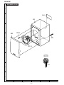
After the automatic adjustment has been performed in the AUTO
mode (test mode) using the low reflection test disk MMD212 (TEAC)
("COMPLETE" will have been displayed), adjust the Lissajous
waveform (x-y) using EOUT and FOUT.
1. Slightly loosen the 3 screws of spindle motor, and make an
adjustment, observing the Lissajous's waveform.
2. After the adjustments are complete, tighten the screws in numerical
order: 1 , 2 and then 3 . (See Fig. 22-4.)
Spindle motor
1
adjusting
hole
Check the Lissajou's waveform,
shifting the mounting position with
a screwdriver (to be fitted into the
disc motor adjusting hole).
2
Figure 22-4
– 22 –
MD-M3/M1
EEPROM WRITING PROCEDURE
EEPROM DATA LIST (Version : 01)
Focus setting
EEPROM (IC1402) writing procedure
1. Method for setting the reference temperature value
(This setting should be performed quickly at a room
temperature, between 21 C and 29 C when the PWB is not
hot.)
Item indication
(1) When replacing the EEPROM, wait until it has cooled down.
(2) Connect the main unit using the single MD main PWB.
(3) Enter the test mode as shown on page 20.
"EJECT"
(4) Press the NORMAL button.
"TEMP
"
:Measured temperature,
: Temperature setting
(5) Find the temperature correction value for the current ambient
temperature on the following table. Adjust the temperature
correction value using the jog dial.
Setting
FG
DA
H
FF1
70
H
FF2
E0
H
FZHLEV
ED
H
FOKLEVn
08
H
FOKLEVf
08
H
FOKLPFn
00
H
FOKLPFf
88
H
WAITf
90
H
Spin setting
Ambient temperature
correction
Item indication
Setting
+ 21.0 °C ~ + 23.2 °C
-1
SPG
20
H
+ 23.3 °C < + 26.8 °C
±0H
SPG—in
B8
H
+ 26.9 °C < + 29.0 °C
+1
SPG—mid
95
H
SPG—out
79
H
SP1
10
H
SP2
87
H
SP3
E3
H
SP4
E3
H
SP5
10
H
SPDLIM
7F
H
H
H
An example: When ambient temperature is 22°C and measured
temperature is 7AH
Temperature setting = 7A H - 01 H
= 79 H
* When the measured temperature fluctuates between
two values, take lower one (if temperature fluctuates
between 7AH and 79H, take 79H).
(6) Press the POWER button and write the temperature setting into
the EEPROM.
Tracking setting
Item indication
2. Method for making settings other than the reference
temperature
(1) Install the MD main PWB in the mechanism, and connect it to
the main unit.
(2) Enter the test mode as shown on page 20, and insert a disc.
"AUTO YOBI"
(3) Press the PLAY MODE button six times.
"EEPROM SET"
(4) Selection mode using the PLAY/PAUSE button.
(5) Selected using the PRESET EQUALIZER button.
(6) Determined by the PLAY/PAUSE button.
(7) Using the jog dial, adjust the settings as shown in the "List of the
EEPROM contents".
(8) Press the POWER button, and the settings will be written into
the EEPROM.
(9) Enter the test mode again, perform an "AUTO YOBI", and write
its results into the EEPROM.
– 23 –
Setting
TG
6B
H
TF1
6B
H
TF2
E0
H
SVCNT4
00
H
TRBLVo
50
H
TRBLVt
54
H
TRKLVo
50
H
TRKLVt
2E
H
TDPWo
89
H
TDPWt
1A
H
SLCTo
00
H
SLCTt
40
H
SLCTm
53
H
TCRSCIP
16
H
COTLVP
0A
H
COTLVr
1C
H
WAITm
FF
H
MD-M3/M1
Slide setting
Control setting
Setting
Item indication
Item indication
Setting
SLG
3B
H
CONTRL1
80
H
SL2
18
H
CONTRL2
02
H
SLDLIM
7F
H
SPKLEVm
26
H
SLDLEV
12
H
ADJTTM
14
H
SLKLVk
50
H
HDEQAD
92
H
SLKLVt
3A
H
LDEQAD
8F
H
SLKLVm
4C
H
GDEQAD
8D
H
HDEQBC
8C
H
LDEQBC
8F
H
GDEQBC
8D
H
HALSG
21
H
H
LALSG
21
H
H
ADJUST setting
Item indication
Setting
COK
A0
FAT
C0
H
GALSG
11
TAT
3E
H
HALSOFS
FE
H
00
H
00
H
CAT
20
H
LALSOFS
FAB
64
H
GALSOFS
STR
0A
H
SFS
0D
H
STC
0D
H
2Pin extension connector
QCNWK0059AFZZ
From Magnetic Head
5Pin extension flat cable
QCNWK0109AFZZ
CN1252
From
motor
From mechanism switch
PWB
CN1601(Bottom side)
From Optical
Pickup Unit
CN1602
CN1603
CN1101
CN1604(Bottom side)
MD MAIN PWB
28Pin extension
flat cable
QCNWK0108AFZZ
Extension PWB for service
(RUNTK0457AFZZ)
Fit the extension PWB for service to the mechanism
6P-2P extension connector
QCNWK0107AFZZ
Figure 24
EXPLANATION OF MECHANISM ERROR
Errors
Error display
MECHA _ * _ ERR
* = E Ejection completion position
* = M Horizontal midway position
* = L Load completed position
* = D Head-down position
None of the operations is completed properly.
HINF (IC1401 97 PIN)
< 1.3 V
> 3.06 V
1.853~2.48 V
1.3~1.853 V
– 24 –
MD-M3/M1
EXPLANATION OF ERROR DISPLAY
Error display
Errors
Corrective action
Can't REC
• Defect occurred successively 10 times during REC-PLAY.
• As a result of occurrence of defect during REC-PLAY the
recordable cluster became zero.
• Address is unreadable. REC state cannot be set for 20
seconds although retry is repeated.
• Check that the disc is free from flaw, dust
and fingerprint.
Check whether there is any black spot.
Check for disc disalignment and run-out.
Can't COPY
• The following judgement is made according to the channel
status of digital signal which was input from D-IN during RECPAUSE or REC-PLAY.
(1) Other than audio signal
(2) Other than signals of home-use appliances
(3) Copy NG due to inversion of copy bit in CD.
• Check whether CD is copy-inhibited one.
(An example: CD-R)
TOC FULL
• There were no areas to record music or character
information. (music name, disc name, etc.) during REC-PLAY.
• Replace the disc with a recording/
playback disc in which an area to register
UTOC remains.
UTOC R ERR
• FTNO > LTNO
• FTNO ≠ 0 or 1
• UTOC recorded on disc could not be read.
• UTOC data is not normal. Replace the
disc with other disc.
UTOC A ERR
• Start address > End address
• UTOC data is not normal. Replace the
disc with other disc.
UTOC L0~4 ERR
• Any data of UTOC 0 to 4 looped.
• UTOC data is not normal. Replace the
disc with other disc.
NOT AUDIO
• Nonaudio data was recorded in the track mode of currently
selected TNO.
• Select other TNO or replace the disc with
other disc.
? DISC
• Data "MINI" of system ID which has been written in TOC with
ASCII code is not correct.
• The disc type written in TOC does not correspond to pre/
mastered MD, recording MD and hybrid MD.
• The loaded disc is not applicable.
Replace the disc, and check.
DISC FULL
• When an attempt to set REC-PAUSE was made, there were no • Replace the disc with other recording disc
recordable areas.
in which recording area remains.
PLAY MD
• An attempt to set REC-PAUSE or to start editing was made on • The loaded disc is a playback-only disc.
the playback-only disc.
Replace the disc with a recording disc.
PROTECTED
• An attempt to record or edit was made on the record/playback
disc with its careless erase preventing tab being in erase
preventing state.
• An attempt was made to edit the track which was writeprotected by information written in UTOC.
• It is indicated when a tape is faulty operation prevention
condition. (tabs breaks.)
• Return the careless erase preventing tab
to its initial position, and redo.
• The track on which an attempt to edit was
made is a write-protected track. Redo on
another track.
• Cover the accidental erase prevention
holes with adhesive tape.
Can't EDIT
• Specific editing conditions were not satisfied.
• Cover the write-protect hole with a piece of cellophane tape.
• The applied operation procedure is not
proper. Redo, applying the correct
procedure.
TEMP OVER
• Owing to occurrence of some trouble internal temperature of
set (MD unit) rose excessively.
• Check by troubleshooting.
• Check whether the ambient temperature
is too high.
MD RD ERR
MD PA ERR
MD WR ERR
• Read data was not correct or data could not be read correctly.
• Trouble occurred during recording if music data, resulting in
record failure.
• Data of TOC or UTOC is not normal or
disc has flaw. Replace the disc with other
disc.
TOC S ERR
TOC R ERR
TOC T ERR
• TOC was read but data was not correct.
• TOC could not be read.
• The TOC information recorded on disc
does not conform to the MD standard.
Replace the disc with other disc.
• The disc has flaw. Replace the disc with
other disc.
UTOC W ERR
• Trouble occurred during rewriting of UTOC, resulting in UTOC
rewriting failure.
• The disc has flaw. Replace the disc with
other disc.
FOCUS ERR
• After the disc was loaded, focusing failure occurred.
• Check that the disc is free from flaw,
dust, fingerprint and black spot. Check for
disc disalignment and run-out.
BLANK MD
• UTOC was read but total TNO and the number of characters of • Perform recording to check that the disc
NAME was 0?
is recordable disc.
TOC W ERR
• Although UTOC can be read but UTOC cannot be rewritten.
• Check that the record head contact is
normal. Check that there is no broken
wire between PWB and the recording head.
MD ERR
• Data of EEPROOM is not correct.
• Perform adjustment
• Once reset, and redo. If error occurs
persistently, replace EEPROM.
– 25 –
MD-M3/M1
NOTES ON SCHEMATIC DIAGRAM
• Resistor:
To differentiate the units of resistors, such symbol as K and M are
used: the symbol K means 1000 ohm and the symbol M means 1000
kohm and the resistor without any symbol is ohm-type resistor.
Besides, the one with “Fusible” is a fuse type.
• Capacitor:
To indicate the unit of capacitor, a symbol P is used: this symbol P
means micro-micro-farad and the unit of the capacitor without such
a symbol is microfarad. As to electrolytic capacitor, the expression
“capacitance/withstand voltage” is used.
(CH), (TH), (RH), (UJ): Temperature compensation
(ML): Mylar type
(P.P.): Polypropylene type
• Schematic diagram and Wiring Side of P.W.Board for this model are
subject to change for improvement without prior notice.
REF.NO.
SW1
CD Lid
DESCRIPTION
SW2
SW1952
• The indicated voltage in each section is the one measured by Digital
Multimeter between such a section and the chassis with no signal
given.
1. In the tuner section,
( ) indicates AM
< > indicates FM stereo
2. In the CD section, the CD is stopped.
• Parts marked with “ ” (
) are important for maintaining
the safety of the set. Be sure to replace these parts with specified
ones for maintaining the safety and performance of the set.
POSITION
OFF
REF.NO.
SWD14
TUNER
DESCRIPTION
POSITION
OFF
Pickup In
OFF
SWD15
CD
OFF
Dirtect
OFF
SWD16
MD
OFF
SW1953
Lead In
OFF
SWD19
FF
OFF
SW1954
Play
OFF
SWD20
REV
OFF
SW1955
Rec
OFF
SWD21
PLAY
OFF
SW1956
Loading
OFF
SWD22
STOP
OFF
SWD01
POWER
OFF
SWD23
HIGH (MD-M3 ONLY)
OFF
SWD02
DISPLAY
OFF
SWD24
NORMAL (MD-M3 ONLY)
OFF
SWD08
MD EJECT
OFF
SWD24
CD MD EDIT (MD-M1 ONLY)
OFF
SWD10
SURROUND
OFF
SWD25
REC
OFF
SWD11
EQUALIZER
OFF
SWD26
MEMORY
OFF
SWD12
X-BASS
OFF
SWD28
VOLUME
OFF
SWD13
AUX
OFF
SWR11
DEMO
OFF
TYPE OF TRANSISTOR AND LED
(FRONT VIEW)
FRONT
VIEW
FRONT
VIEW
FRONT
VIEW
B
(D)
(3)
E
(S)
(1)
B C E
2SB1375
2SD2012
E
C
B
KTA1023 Y
E C B
(S) (G) (D)
(1) (2) (3)
HSC1815 GR
KRA107 M
KRC104 M
KRC107 M
KTC3199 GR
E C B
(S) (G) (D)
(1) (2) (3)
HSA1015 GR
KTA1266 GR
KTA1270 Y
KTA1271 Y
KTC3203 Y
2SC2878 A
2SC380 O
TOP
VIEW
C
(G)
(2)
RNC1404
RN1406
RN2404
RNC1407
2SA1162 G
2SC2412 KR
2SK2909
FRONT
VIEW
FRONT
VIEW
G D S
B C E
2SK1473
2SA1314 C
TOP VIEW
TOP VIEW
SB0209CP
SB007-03Q
FRONT VIEW
FRONT
VIEW
1N4004S 1SS133
SLI342UCB
KV1236Z23F
Figure 26 TYPES OF TRANSISTOR/DIODE AND LED
– 26 –
AC
AC
TS4B03GM
MD-M3/M1
3.2V
IC1300
TC74ACT02F
HEAD
DRIVER
6.5/4.75~5.25V
XL1201
33.8688MHz
RECORDING
HEAD
EXT.
PLL
1
2
3
4
MD
IC1201
LR376484
ATRAC ENCODER/DECODER
LRSY
GND
GND
DATA
CN1502
MD-M3 ONLY
M
M902
SLED
MOTOR
M901
SPINDLE
MOTOR
PICKUP UNIT
28P FFC
M
BACKUP
FOCUS
LIGHT
RECEIVING
SECTION
ERROR,
SIGNAL
LIGHT
RECEIVING
SECTION
RF
TRACKING
F
A
B
E
RF1
RF2
RF3
RF4
E-F SIGNAL A-B SIGNAL
RF1~RF4 SIGNAL
IC1101
IR3R55
RF
SIGNAL
PROCESSOR
IC1401
IX0290AW
MD SYSTEM
MICROCOMPUTER
3.2V
LASER DIODE
IC1402
S29294A
EEPROM
MONITOR DIODE
E-F
3.2V
3.2V
MECHANISM
6.5/4.75~5.25V
SW1952
WRITE PRO
DISC ID
IC1202
IX2474AF
4M BIT
D-RAM
LEAD IN SW1953
PLAY SW1954
3.2V
LOAD IN SW1956
IC1801
XC62EP32
REGULATOR
6.5/4.75~5.25V
IC1601
BA5984FP
MOTOR DRIVER
IC1702
NJM431U
REGULATOR
M903
M
3.2V
LOARDING MOTOR
BOTH HEAD UP
and DOWN
AUDIO INPUT
6.5/4.75~5.25V
A/D CONVERTER
IC1701
D/A CONVERTER UDA1344
Figure 27 BLOCK DIAGRAM (1/5)
– 27 –
DIGOUT
D.GND
DIGIN
BACKUP
PDOWN
RESET
MD-ST
DSCK
SERCH
KDATA
MDDATA
DSTB
D.GND
D.GND
D.GND
D.GND
DVDD
DVDD
PSWCK
LOADSW
AVCC
L.IN
AA.GND
R.IN
AD.GND
L.OUT
AA.GND
R.OUT
CN1501
REC SW1955
DIGITAL
3.2V
1
2
3
4
5
6
7
8
9
10
11
12
13
14
15
16
17
18
19
20
21
22
23
24
25
26
27
28
AUDIO OUT
MD-M3/M1
T302
AM
ANT
COIL
+
+B2
SO301
ANTENNA
+
+B3 -
+5V
–B2
FE301
IF OUT 1
FM FRONT END
8 ANT
3
4
7
FM +B
6
VT
2
FOUT
VCO 5
SWITCHING
+12V
IC901
XC61CN40
RESET
+B3
Q360
+5V(D)
FM/AM
+B9
2
VOLTAGE
REGULATOR
RESET
SY-STOP
1
3
+B3
3 4 5 6
BO1
B02
B03
B04
VT
20 19 18
16 15 12
22
1
FM MUTE LEVEL
4.5MHz
X352
VSS
VDD
11 IO1
13 IO2
XIN
IC302
LC72131
TUNER PLL COTROLLER
XOUT
7
NC 8
TUN MUTE
9
MO/ST
10
STEREO
FM IN
AM IN
IF IN
FM/AM
SD
Q904
Q371
DO
CE
DI
CL
+5V
AOUT
AIN
PD
21 17
+5V
VRR11
AUX INPUT
LEVEL
JR11
AUX INPUT
VR351
MPX IN
TUNER
MUTE
VDD
AUDIO
Function/Volume/Tone
10
16
+B3
MD/CD
2 A
AUX
ICP11
3
M62439SP
OUT
B
18
AUDIO PROCESSOR 8
VCC
19
Q351 AMP
TUNER 4
C
10
1
3
13
17
12 9
VSS
CF302
DI
CONT
REC TONE
11
OUT HL
1 20
6 15 7 14
5 D
16
SURROUND
+5V
Q353
Q354
CL
–B2
–2.7V
VOLTAGE REGULATOR
FM IF
QP
3 6
CNP14 26/28PIN
ICP81
NJM4565D
REC. AMP.
8
4
– 28 –
VSS
1 7
TO CD SECTION
Figure 28 BLOCK DIAGRAM (2/5)
VDD
CNP14
22/24PIN
CF352
14 LOUT
15 ROUT
VOLTAGE REGULATOR
+2.7V
+B3
GND
T351
AM IF
FM/AM OUT
SM
9
VCC
TUN MUTE
AM OSC OUT 24 10 IF OUT
IC303
6 SD
LA1832S
7 STEREO
FM IF DET./
13 MO/ST
FM MPX./AM IF
12 FM/AM
Q361
MPX
VCO
2
AM MIX OUT
4
8 17 1 20 18
AM IF IN
FM DET
CF351
456kHz
X351
FM IF IN
FM
75 OHMS
T306
AM
OSC
COIL
GND
GND
GND
AM
GND
TO DISPL
MD-M3/M1
T991
POWER TRANSFORMER (MAIN)
D951
+B1
VOLTAGE
REGULATOR
F995
4A/125V
+12V(D)
+B2
Q801
+12V(A)
+B3 -
VOLTAGE REGULATOR
+B4
D952
F997
3.15A/125V
VOLTAGE
REGULATOR
12V(A)
–30V
Q808
MDAVCC
–B2
F996
3.15A/125V
VOLTAGE
REGULATOR
Q802
Q803
Q951
–B1
VOLTAGE
REGULATOR
Q809
Q810
CD+7V
TO CD
+B5
VOLTAGE
REGULATOR
Q811
Q812
MDDVDD
+B4
TO MD
+B6
D953,D955
F998
800mA/125V
RELAY
DRIVER
FL ON
F999
1.6A/125V
Q911
V LOAD
RL990
+B10
Q813
+B2
AC INPUT
AC 120V
60Hz
+B10
+5V(D)
+B7
+B8
+B9
D991-D994
VOLTAGE
REGULATOR
IC902
3
AN75L05 1
+5V BACK UP
2
+5V(D)
SO990
T990
POWER TRANSFORMER (SUB)
+B1
7
MUTE
QX11
QX12
QX13
QX14
10
1
9
13
12
14
SY MUTE
11
VCC
AMP. HPSW
QP16
QP17
H.P MUTE
CONTROL
QR11
10
SY MUTE
1
3
SURROUND
QP15
ICP12
LA2610
SURROUND
4
2
5
JV91
1
7
+B2
4
8
VDD
+B3
–B2
SURROUND
SWITCHING
ICV11
NJM4565D
HEADPHONE
AMP.
3
5
11
12
5
6
AMP. MUTE
3
8
3
TMX11
SPEAKER
TERMINAL
ICX11
LA4451
POWER AMP.
AMP. HPSW
MUTE
VCC
VSS
SP LEVEL
FAN
MOTOR
MOX51
M
QX51
QX52
QX53
AMP. FAN
SURROUND
VDD
VSS
+B3
–B2
–B1
TO DISPLAY SECTION
TO DISPLAY SECTION
Figure 29 BLOCK DIAGRAM (3/5)
– 29 –
TO DISPLAY SECTION
MD-M3/M1
TO TRANS/PRE/TUNER
CNP14
1 DIGOUT
2
D.GND
3
DIGIN
BACKUP
PDOWN
MD RES
MD-ST
DSCK
SERCH
KDATA
10
MDDATA
4
5
6
7
8
9
11
ICP81 1/7PIN
ICP11 2/19PIN
TO PRE SECTION
(POWER)
Q92
MD DSTB
Q91
13
14
15
16
17
18
D.GND
MDDVDD
+B6
19 PSWCK
LOADSW
Q93
MDAVCC
LIN
22
AAGND
20
21
+B4
23
24
RIN
25
26
ADGND
LOUT
27
28
AAGND
ROUT
1
2
3
4
LRSY
DATACK
CDGND1
VOLTAGE
REGULATOR
CD+7V
+B5
DATA
+5V
+B12
CNP13
+B12
MD-M3 ONLY
VOLTAGE
REGULATOR
+5V
Q62
+B11
+3.3V
+B10
Q61
+B10
LID-SW
PICKUP-IN SW
SW2
PUIN
+5V
30 5 6 14 15
RF
28 27
FIN1
FIN2
RFSW 29
RFEV
TIN1
22
TIN2
FE
2120
TE
19 18
LDD
HFL
8
17
LDS
IC1
7
TES
LA9235M 16 LDOF
SERVO AMP. 10
NC 26
ODRV
11
NC 23
AGON
12
EFBL
Q51
Q52
PH
BH
1
2
3
4
9
25 24
13
VDD5V
+3.3V
VCC
+B10
REFL
VREF
TES0
TES1
PICKUP UNIT
5 18 36 49 50 44
73
EFMO
DEFECT
FSEQ
V/vP
DRF
RES
WRQ
INT
DO-CD SI
DI-CD SO
CL
CE
+B11
CD LID SW
SW1
VOLTAGE
REGULATOR
VVDD
ADAVDD
VDD
RVDD
XVDD
LVDD
CD
GND
80 79 78 77 72 71 70 69 68 67 66 65
10 EFMIN
9
14
15
16
7
LCHO 45
RCHO 48
MUTER
MUTEL 43
EMPH 42
SLCO
PH(RFENV)
FE
TE
HFL
41
28 LASER
30 CONT2
29 CONT1
22 TBLO
IC2
LC78640E
SERVO SIGNAL CONTROL
13 BH
17 VREF
IC3
LA6548 21
FOCUS/
16
17
TRACKING/
6 SPIN/SLED 23
5 DRIVER
25 SPDO
24 FDO
18
SPINDLE
M1
M
2
VCC
1 24
11
+B10
53 46 47 74 40 19 3
+B5
Figure 30 BLOCK DIAGRAM (4/5)
– 30 –
CONT6
CONT7
8
7
63
20 PHREF
21 BHREF
SBCK
PW
SBSY
62 SFSY
61 16M
64
TDO
CONT3
CONT4
CONT5
M
23
JITTV
JITTC
SLED
M2
39
DATA
59
DATACK 58
LRSY
57
XOUT
19
TRACKING
DOUT 37
FSX
38
EFLG
ASDFIN 56
ASDACK 55
ASLRCK 54
26 SLDO
4
9
20
31 52
11 12
31 32 33
75 76
XIN
FOCUS
XVSS
LVSS
RVSS
VSS
TEST
ADAVSS
VVSS
TO MD SECTION
12
16.9344MHz
60
MD-M3/M1
TO TRANS/POWER/PRE SECTION
/TUNER SECTION
TO TRANS SECTION
–B1
–B1
–30V
F1
F1
TIMER
LED
DEMO
SWR11
DEMO
SW
SWD28
JOG SW
VOLUME
VOL DOWN
VOL UP
DEMO
VOL DOWN
VOL UP
S1
S2
S3
S4
S5
S6
S7
S8
S9
S10
S11
S12
S13
S14
VP
VDD
–30V
S21/PC5
/PC4
S20
S22/PC6
S23/PC7
S24/PD0
S25/PD1
S26/PD2
S27/PD3
S28/PD4
S29/PD5
S30/PD6
S31/PD7
S32/PE0
S33/PE1
S34/PE2
S35/PE3
S36/PE4
S37/PE5
S38/PE6
VDD4
S39/PE7
S40/PF0
S41/PF1
S42/PF2
S43/PF3
S19/PC3
S1/T1
S2/T2
P72/INT2
/T0IN
MD DSTB
REMOCON
P71/INT1
TOHCP/AN9
P70/INT0
TOLCP/AN8
P86/AN6
P85/AN5
P84/AN4
P83/AN3
P82/AN2
P81/AN1
P80/AN0
VDD1
CF2
CF1
P87/AN7
/MICIN
SY-STOP
CL
CE
INT
WRQ
DRF
LID-SW
PUIN
PROGRAM
100
VSS1
98
XT2/AN11
97
XT1/AN10
96
RES
95
AMP HPSW
VSS
XT1
XT2
XD01
8.38MHz VDD
AMP TEMP
AMP LEVEL
SM
DEST
KEY1
KEY2
KEY3
94
P37
93
P36
92
P35
91
POWER
RESET
90
P34
89
P33
88
S18
VDD
VDD3 46
P00
S19
S15/T15 45
P01
S20
P02
S14/T14 44
S21
P03
S13/T13 43
G13
S12/T12 42
VSS2
ICD01
G12
IX0288AW
S11/T11 41
VDD2
G11
SYSTEM MICROCOMPUTER/
S10/T10 40
P04
G10
FL DRIVER
S9/T9 39
P05
G9
P06
S8/T8 38
G8
P07
S7/T7 37
G7
P10/SO0
S6/T6 36
S0/T0
G6
P11/SI0
S5/T5 35
/SB0
P73/INT3 /T0IN
G5
P16/T1PWML
S4/T4 34
P12/SCK0
G4
P17 /T1PWMH/BUZ
P13/
S3/T3 33
SO1
G3
QD02
32
G2
QD03
31
G1
QD04
1 2 3 4 5 6 7 8 9 10 11 12 13 14 15 16 17 18 19 20 21 22 23 24 25 26 27 28 29 30
P32
87
S15
S16/PC0 47
S48/PG0
86
50
S18 49 S16
/PC2
S17
S17/PC1 48
VP
P14/SI1/SB1
P15/SCK1
85
99
DI-CD SO
DO-CD SI
S44/PF4
/PG1
P31
VSS
VDD
MD RES
MD-ST
SERCH
V LOAD
KDATA
MDDATA
DSCK
82 S49
S47/PF7
83 S50/PG2
84 S51/PG3
P30
CL
DO
–B1
80 79 78 77 76 75 74 73 72 71 70 69 68 67 66 65 64 63 62 61 60 59 58 57 56 55 54 53 52 51
81
S46
/PF6
S45/PF5
LOADSW
CD RES
AMP FAN
AMP MUTE
CE
+B7
EQ VOCAL
SURROUND
(OPEN)
SY MUTE
DI
TIMER LED
FL ON
+B7
S1
S2
S3
S4
S5
S6
S7
S8
S9
S10
S11
S12
S13
S14
S15
S16
S17
S18
S19
S20
S21
G13
G12
G11
G10
G9
G8
G7
G6
G5
G4
G3
G2
G1
1
2
3
4
5
6
7
8
9
FLD01
FL DISPLAY
10
11
12
13
14
15
16
17
18
21
22
23
24
25
26
27
33
34
35
36
37
38
39
40
41
42
43
44
45
46
F2
F2
47
48
49
–30V
–B1
+B9
2
REMOCON
RXD01
REMOTE
SENSOR
1
3
KEY1
+B7
+5V(D)
+B9
KEY2
+5V(D)
+B8
+5V
BACK UP
KEY3
Figure 31 BLOCK DIAGRAM (5/5)
– 31 –
KEY MATRIX
SWD01-SWD08
SWD10-SWD16
SWD19-SWD26
(SWD23 MD-M3 ONLY)
MD-M3/M1
FLD01
A
–B
+B
CD17
0.022
RD60
47K
0V
RD14
1K
88 P03
SERCH
4.93V
VDD
0V
SURROUND
4.92V
0V
EQ VOCAL
4.93V
S39
VDD4
S40
S41
S42
S43
100 P15 4.84
P35 0V
P36 0V
1
2
3
4
5
6
7
8
9 10
POWER
P34 0V
1K
RD56
RD24 1K
P33 5.10V
99
P32 0V
98 P13 4.84V
100
P37 4.82V
97 P12 4.02V
CD20
0.001
RD23 1K
DD02
DS1SS133
CHASSIS
GND
99 P14 5.12
96 P11 4.00V
CL
RD22 1K
RD19 1K
RD20 1K
RD17 1K
RD18 1K
)
)
RD21 1K
BID01
DD01
DS1SS133
95 P10 0V
DSCK
CD SI(
FL ON
94 P07 4.78V
MDDATA
CD SO(
TIMER LED
93 P06 0V
KDATA
CD07
1/50
TU DI(
92 P05 0V
V LOAD
CD06
1/50
SYST
91 P04 0V
PROGRAM
MD-ST
90 VDD2 4.84V
1K
MD RES
1K
0V
89 VSS2 0V
RD31
CNPD01
1K
RD16
0V(4.8V) S44
87 P02
VDD
RD15
4.79V
86 P01
)
VSS
CD05
1/50
D
85 P00
0V
TU DO(
4.87V
)
0V
TU CL
RD30
1
TU CE
1K
81 PG0 4.2
82 PG1 4.9
84 PG3
P31 0V
GND(D)
RD11 1K
RD13
+B
83 PG2
1K LID-SW(DATA)
PUIN(CLK)
1K
2
4.91V
1K
CD04
0.022
CD03
100/10
CD02
0.022
0V
AMP MUTE
RD29
GND(D)
AMP FAN
RD10 1K
RD28
+B
+5V(D)
3
82
RD09 1K
P30 5.12V
+5V(D)
4
+B
WRQ
5
80 79 78 77 76 75 74 73 72 71
1K
RESET
LD01
+5V BACK UP 2.2µH (DH)
6
81
RD27
CD RES
P17 0V
LOADSW
RD08 1K
P16 0V
7
RD07 1K
SY-STOP
CE
8
4.11V S45
)
SPAN SEL
S47
4.93V
SY MUTE
S46
RD06 1K
TU SM
9
C
RD05 1K
TU CL
TU DO(
10
1
TU CE
INT
11
RD12 1K
)
1K
12
POWER/TUNER PWB
P46 1-E
RD04 1K
TU DI(
13
CFWR11
RD03 1K
FL ON
1K
14
RD02 1K
EQ VOCAL
RD25
15
RD01 1K
RD61
47K
SURROUND
16
B
+B
DEMO
17
DRF
17
RD26
FWD01
+B
28
28
27
26
25
24
23
22
21
20
19
11
5
4
G
3
2
1
1
FWD03
6
5
4
3
2
1
1
H
DRF
RD59
100K
WRQ
INT
)
)
SERCH
(OPEN)
MD-ST
MD RES
DSCK
KDATA
MD DSTB
LOADSW
AMP FAN
SY MUTE
AMP MUTE
CNPD02
6
CNP11
MAIN PWB
MD-M3:P39 12-A
MD-M1:P40 12-A
AMP LEVEL
CD RES
10
6
AMP TEMP
MDDATA
12
7
AMP HPSW
V LOAD
14
GND(D)
RESET
LID-SW(DATA)
PUIN (CLK)
PROGRAM
+5V(D)
CNPD03
• NOTES ON SCHEMATIC DIAGRAM can be found on page 26.
1
CD08
150P
CD09
150P
POWER
CD SI(
13
8
VF1
CD SO(
15
9
–B
CL
16
CNP12
MAIN PWB
MD-M3:P39 12-B
MD-M1:P40 12-B
–31(VP)
CE
18
17
F
VF2
(4.91V)
FWD02
E
2
3
4
Figure 32 SCHEMATIC DIAGRAM (1/14)
– 32 –
5
6
MD-M3/M1
28 29
30 31 32 33 34 35 36 37 38 39 40 41 42 43 44 45
F2
F2
NP
NP
G1
G2
G3
G4
G5
G6
G7
G8
G10
G9
G11
G12
G13
NC
NC
22 23 24 25 26 27
NC
21
NC
19 20
NC
S21
S20
S19
S18
S16
S17
S15
9 10 11 12 13 14 15 16 17 18
NP
8
NP
S12
S14
S11
S10
7
S9
S5
6
S8
S4
5
S6
S3
4
S7
S2
3
S1
F1
2
NP
F1
NP
1
S13
FL DISPLAY
FLD01
46 47 48 49
–B
+B
–29.6V
VP
RF77 100K
S14
S20
S11 41
RF76 100K
–20.4V
S13
S21
S22
S12 42
RF75 100K
–17.7V
S12
S23
S13 43
RF74 100K
–17.9V
S11
S14 44
RF73 100K
–20.2V
S10
ICD01
IX0288AW
SYSTEM MICROCOMPUTER/
FL DRIVER
RF72 100K
–14.6V
S9
S24
S25
S15 45
VDD
TIMER
–29.6V
47
VDD3 46
RF71 100K
–26.4V
S8
S26
S27
RD58
47K
RD53
1.2K
S16
S17
S17 48
S18
S16
50 S19
49 S18
CF53 100P
–29.6V
S7
S28
S15
RD55
1K
–29.6V
S6
S29
50
–26.3V 49
RD54
1K
–17.8V
S5
RED
–29.6V
S30
S31
S32
S33
S34
S35
S36
S37
S38
S39
VDD4
S40
S41
–29(VP)
74 73 72 71 70 69 68 67 66 65 64 63 62 61 60 59 58 57 56 55 54 53 52 51
–19.2V
81 PG0 4.29V
82 PG1 4.92V
LEDD01
SLI342UCB
–29.6V
S4
–30.04V
–29.6V
S3
CF52 100P
RF52
100K
–29.7V
RF51
100K
–29.7V
S2
VOL-UP
4.78V
S1
DEMO
VOL-DOWN
4.13V
4.78V
0V
0V
0V
VDD
4.93V
SURROUND
0V
4.92V
CF51
100P
+B
4.93V
S19 –15.4V
S20 –24.5V
S21 –22.8V
G13 –27.4V
G12 –27.4V
S10 40 G11 –27.4V
G10 –27.4V
S9
39
S8 38 G9 –27.4V
G8 –27.5V
S7
37
QD04
KTC3199 GR
RD63
100K
4.93V
–B
+B
RD48
8.2K
4.93V
CD15
0.022
RD50
39
CD16
220/6.3
4.89V
2
1
3
2
0V
3
CD18
0.001
CD14
150P
RD32
1K
RD49
100K
CD13
0.001
3.95V
RD52
10K
SPAN SEL
+B
RD51
10K
+B
CD09
150P
4.93V
–27.7V
RD47
68K
CD08
150P
–27.6V
–27.6V
4.93V
S0
G2 –27.5V
RD64
100K
REMOCON
RD46 1K
G1
MD DSTB
RD45 1K
QD03
KTC3199 GR
–27.6V
SY-STOP
RD43 1K
KEY3
1K
RD42
KEY2
1K
RD41
AN2
AN3
KEY1
1K
RD40
DEST
TU SM
1K
RD38
RD37 1K
AN0
AN1
AMP LEVEL
RD36 1K
AMP TEMP
RD35 1K
CF1
CF2
VDD
XD01
8.3886MHz
CD11
15P(CH)
CD12
18P(CH)
1K AMP HPSW
RD33
VSS
POWER
1K
RD56
RESET
PROGRAM
1K
31
G3 –27.4V
RD62
100K
INT3 4.00V
INT2 3.9V
INT1 0V
INT0 4.84V
AN7 0V
AN6 4.92V
AN5 4.92V
AN4 4.92V
3.81V
0.46V
0V
0V
VDD1 4.84V
2.48V
2.61V
VSS1 0V
0V
0V
9 10 11 12 13 14 15 16 17 18 19 20 21 22 23 24 25 26 27 28 29 30
P75
8
P74
P36 0V
32
7
RD31
QD02
KTC3199 GR
33
P35 0V
RES 4.81V
35
S4 34 G5 –27.8V
G4 –27.7V
S3
P34 0V
P37 4.82V
S6 36 G7 –27.7V
G6 –27.7V
S5
32 S2
31 S1
99 P14 5.12V
100 P15 4.84V
RXD01
REMOTE SENSOR
CD19
0.001
1
SWD28
VOLUME
RF25 8.2K
+B
RF26 8.2K
RD59
100K
RF27 8.2K
CD10
0.01
RF01
1K
RF02
2.2K
RF03
1.8K
RF04
2.2K
RF05
3.9K
RF06
5.6K
RF07
12K
SWD01
SWD02
SWD08
POWER
DISPLAY
MD
EJECT
RF10
1.2K
RF09
1K
SWD10
SWD11
SURROUND
SWD19
FF
SWD12
PRESET
EQUALIZER
RF17
1K
RF11
1.8K
X-BASS
RF18
1.2K
SWD20
REVIEW
RF12
2.2K
SWD21
RF14
5.6K
SWD13
SWD14
SWD15
SWD16
AUX
TUNER
CD
MD
RF19
1.8K
PLAY/
PAUSE
RF13
3.9K
SWD22
STOP
RF22
5.6K
RF21
3.9K
RF20
2.2K
SWD23
SWD24
HIGH
MD-M3 ONLY
CD
RF23
12K
SWD25
NORMAL
REC
SWD26
MEMORY
MD EDIT
DISPLAY PWB-B1
7
8
9
10
Figure 33 SCHEMATIC DIAGRAM (2/14)
– 33 –
11
12
MD-M3/M1
MAIN PWB
CNP11
MD-M3:P42 3-B
MD-M1:P41 3-B
FWD03
A
1
MAIN PWB
MD-M3:P42 4-B
MD-M1:P41 4-B
FWD02
CNP12
6
DISPLAY PWB-B1
1
28
RD56
RD15
RD21
RD19
18 17 16 15 14 13 12 11 10 9 8 7 6 5
RF01
45 44 43 42 41 40 39 38 37 36 35 34 33 32 31 30 29 28 27 26 25 24 23 22 21
C
SWD02
DISPLAY
RD58
RD12
RD54
RD55
RD01
RF52
RF51
SWD01
POWER
RD05
RD10
RD18
80 81
RD20
RD17
RD16
RD09
10
0
95
90
55
RD13
RD11
50
51
RF75
RF74
RF73
RF72
45
60
40
65
70
75
85
15
20
ICD01
IX0288
35 25
CD03
CD04
RD06
1
5
10
CD12
RF77
RF76
RD45
CD20
RD14
RD25
RD42
RD43
49 48
RD23
RD26
RD24
RD22
RD32
RD27
RD28
RD33
RD35
27 25 23 21 19 17 15 13 11 9 7 5 3 1
31 30
RF05 RF04
RD41
CD13
RF02
RD40
RD07
28 26 24 22 20 18 16 14 12 10 8 6 4 2
CD11 XD01
CD10
RD37
RD38
RF03
RD36
CD09
RD29
RD30
RD31
CD08
RD59
B
CNPD02
CD06
RD08
CD05
CD07
CNPD03
1 3 5
2 4 6
2 1
RF06
RF07
CD17
CF51
CF53
RD63
RD62
LEDD01
FLD01
CF52
RF71
RD53
RD64
COLOR TABLE
SWD21
PLAY
E
C
B
SWD22
STOP
RED
CD15
OR
ORANGE
YL
YELLOW
GR
GREEN
2
3
1
RXD01
REMOTE
SENSOR
RD49
SWD25
REC
SWD24
NORMAL
RF20
RF19
RF25
RD46
SWD23
HIGH
SWD24
NORMAL
RD47
RF26
RD60
BLUE
VL
VIOLET
GY
GRAY
WH(W)
WHITE
BK
BLACK
PK
PINK
RF21
ONLY M3
LD01
SWD10
SURROUND
RF23
ONLY M1
RD48
E
RF22
SWD26
MEMORY
BL
RD02
RD03
RD04
RF17
RF18
BROWN
RD(R)
CD14
E
C
B
RD50
SWD20
REV
QD03
SWD19
FF
QD02
D
RF27
E
C
B
SWD08
MD EJECT
QD04
BR
CD16
CD MD EDIT
CD02
RD51
SWD16
MD
RD52
CD18
RF14
CD19
F
CFWR11 POWER/TUNER PWB
P49 8-F
RF09
RD61
SWD15
CD
2
SWD28
VOLUME
3
BID01
G
CNPD01
1
SWD12
X-BASS
RF13
17
16
15
14
13
12
11
10
9
8
7
6
5
4
3
2
1
17
SWD14
TUNER
RF12
RF10
SWD11
PRESET
EQUALIZER
FWD01
1
DD01
DD02
RF11
SWD13
AUX
A
POWER/TUNER PWB
P49 9-G
H
1
2
3
4
Figure 34 WIRING SIDE OF P.W.BOARD (1/8)
– 34 –
5
6
MD-M3/M1
P36 2-C
TO POWER SECTION
P37 12-E
TO POWER SECTION
CP31
10/35
5.95V
0V
RP32
18K CP27
1/50
RP62
1K
QP15
KRC104 M
RP61
1K
CP25
10/35
CP41
0.001
RP29
3.3K
ZDP12
DZ2.7A
–B
CP42
0.001
CP21
0.022
RP21
10K
CP17
0.15(M3)
0.12(M1)
RP19
2.7K
12 VSS
OUT2 13
CP15
0.18(M3)
0.15(M1)
CP13
0.022
(ML)
TONEL2 14
0V
IND2
0V
INC2
0V
INB2
0V
INA2
AUX_L
0V
0V
RP22
10K
OUT1
CP18
0.15(M3)
TONEL10.12(M1)
0V
7 0V
0V
TONEH2
0V
8
0V
TUN_L
RP26
10K
VDD 10 21.2V
RP24
2.2K
GND
9
6
15
RP20
2.7K
CP16
0.18(M3)
0.15(M1)
TONEH1
0V
CP14
IND1 0.022(ML)
5 0V
16
4
17
18
3
19
2
20
1
INC1
0V
AUX_R
0.60V
–2.66V
11 CONT
–B
RP27
680
CP20
10/35
RP23
2.2K
0V
RP57
1K
+B
CP19
10/35
CP23
0.022
4.77V
RP28
680
RP30
3.3K
ZDP11
DZ2.7A
CP22
100/10
1
3
CP26
10/35
CP24
100/10
RP55
5.6K
2 0V
INB1
0V
INA1
RP16
1K
CP04
1/50
CD/MD_R
0V
RP04
1.5K
REC_R
REC OUT1
0V
REC OUT2
REC_L
ICP11
M62439SP
AUDIO PROCESSOR
RP15
1K
CP03
1/50
CD/MD_L
RP12
1K
CP12
1/50
CP11
1/50
CP83
0.022
CP84
0.022
8
4
FM SIGNAL
RP85 RP86 CP88
2.7K 2.7K 150P
CP02
1/50
RP01
3.9K
RP02
3.9K
2 0V 3 0V
7
1
0V
0V
CP91
2.2/50
RP89
100K
CP82
10/35
CP01
1/50
RP84
1K
6
5
–11.46V
RP82
220
CP86
2.2/50
RP92
100K
RP03
1.5K
0V
0V
11.42V
–B
RP91
100K
RP83
1K
CP87
150P
CP81
10/35
RP81
220
RP13
1K
RP14
1K
RP11
1K
–12V(A)
TUN_R
CP85
2.2/50
(2/2)
5.93V
CP93
330P
CP90
100P
RP88
18K
5.93V
(1/2)
1
ICP12
LA2610
SURROUND
5.93V
CP89
100P
RP87
18K
2
RP31
18K
5.94V
+12V(A)
GND REF
ANALOG
SURROUND
BASS
LEVEL
5
3
0.022
4.7/50
0V
6
4
CP29
CP37
5.95V
5.94V
47/16
0.022
0.022
RP25
2.7K
VCC
A
SW
B
B SW
A
ON/OFF
5.93V
7
CP32
10/35
RP51
220
CP36
CP35
CP30
11.64V
10
8
RP44
2.2K
RP41
3.3K
5.95V
11
9
RP43
2.2K
RP42
3.3K
RP50
1K
DP11
DS1SS133
12
R-CH
L-CH
27 26 25
RP49
1K
AGND
Z
ICP81
NJM4565D
REC. AMP.
CP92
2.2/50
RP90
100K
CP96
2.2/50
CP94
330P
CP95
2.2/50
CD SIGNAL
+B
MD SIGNAL
GND(D)
+12V(D)
TUN R
GND(A)
TUN L
GND(A)
AUX R
GND(A)
AUX L
+12V(A)
CONT
SURROUND
EQ VOCAL
MAIN PWB-A(1/3)
1
2 3
4
5 6 7 8 9 10 11 12 13
1
–12V(A)
+12V(A)
REC L
GND(A)
REC R
+B
CFWP12
M N O P Q
CD/MD L
GND(A)
CD/MD R
+12V(D)
GND(D)
RECORD SIGNAL
R S T U V
TO CD SECTION
MD-M3:P39 12-G
MD-M1:P40 12-G
13
FWP12
CFWR12
TO POWER/TUNER PWB
P46 1-G
• NOTES ON SCHEMATIC DIAGRAM can be found on page 26.
7
8
9
10
Figure 35 SCHEMATIC DIAGRAM (3/14)
– 35 –
11
12
MD-M3/M1
RV16
100K
2
QX12
2
HSC1815 GR 1
3.05V
RX15
47K
RX61
1K
RP58
47K
AMP HPSW 24
SY MUTE 23
AMP MUTE 22
D
RX36
2.2K
3.01V
QR11
0V KRA107 M
DX17
DS1SS133
CX16
10/35
1
3
2.62V
2
0V
1 0V
2
3
CX20
1/50
RX22
1K
11
MUTE:OPEN
RX16
220K
RP60
47K
Q801
2SD2012
12.29V
+12V(D) 18 +B
R805
2.2
18.10V
GND(D) 17
+12V(A)
–12V(A)
+B
V LOAD 7
D801
DS1SS133-1
R851
2.2
Q803
HSC1815 GR
13.81V
ZD802
DZ13C
ZD804
DZ13A
–13.15V
R816
150
Q808
2SB1375
C816
0.022
CD GND(D)
Q813
KRC107 M
3
0V
ZD807
DZ6.2C
5.43V
R852
5.6
(Fusible 1/4W)
+16V
C815
47/25
F998
800mA/125V
R817
560
ZD805
DZ8.2B
Q811
2SD2012
Q812
HSC1815 GR
+V(MD)
2
4.39V
8.16V
D810
DS1SS133
+B
R813
560
18.25V
7.62V
D806
DS1SS133
R807
560
–19.79V
Q810
HSC1815 GR
CDGND1 11
MDDVDD 10
MDAVCC 9
ADGND 8
Q809
2SD2012
7.01V
+6V(CD)
C817
10/35
CD+6V 12
–12.59V
ZD801
DZ13A
13.22V
C812
47/25
–B
C820
10/35
C819
0.022
–12V(A) 14
F
G
C808
0.022
C814
10/35
R803
680
C803
1/50
+16V
17.90V
R810
150
D802
DS1SS133
GND(A) 15
Q802
2SD2012
C807
47/25
C813
0.022
C810
0.047
C809
10/35
5.32V
ZD803
DZ5.1B
MDAVCC
TO CD SECTION
MD-M3:P39 8~12-H
MD-M1:P40 8~12-H
12.57V
R822 R811
330 330
C804
0.022
C805
47/25
12.87V
E
+16V
18.26V
F999
1.6A/125V
6.07V
6.63V
6.63V
1 0V
MDDGND1 6
MDDGND2 5
CDGND2 4
R820
330
C818
47/25
R819
560
ZD806
DZ8.2A
VF1 3
–31(VP) 2
VF2 1
H
• NOTES ON SCHEMATIC DIAGRAM can be found on page 26.
1
2
3
1.19V
0V
RX17
10K ON:H
AMP LEVEL 21
AMP FAN 20
+12V(A) 16 +B
8
9
10
CX23
100/50
DX11
DS1SS133
0V
RP59
47K
12
RX23
270
QP17
KRC107 M
QP16
KRC104 M
RX21
1K
4
Figure 36 SCHEMATIC DIAGRAM (4/14)
– 36 –
5
6
7
CX32
0.7V
0V
13
CX19
1/50
31.97V
14
0V
3
0V
DX18
DS1SS133
CX55
0.001
CX21
0.001
0V
0V
0.7V
QX14
HSC1815 GR
0.71V
CX12
10/35
CX14 CX13
RX13 0.001 0.001
5.6K
RX11
8.2K
0V
RX14
5.6K
P35 8-A
PRE SECTION
ICX11
LA4451
POWER AMP.
CV17
10/35
25.09V
11.43V
RX35
2.2K
0.71V
RX12
8.2K
C
CV18
10/35
QX13
HSC1815 GR
0V
L-CH 27
AGND 26
R-CH 25
RX54
100K
RV22
1K
RV26
220
QX11
HSC1815 GR
CX11
10/35
CHASSIS
GND
0V
–11.45V
RV25
220
LUG901
(352)
3
0V
CX22
100/50
CX24 RX24
100/50 270
(2/2)
1
RV12 CV24 0.29V 8
4
100 10/35
(1/2W)
B
RV24
100K
CV16
0.033
(ML)
0V
RV18
10K
JACK PWB-B2
2.29V
FWV11
RV23
100K
1.19V
5
4
3
2
1
RV19
270
ICV11
NJM4565D
HEADPHONE
AMP.
RX19
33K
CX17
560P
5
4
3
2
1
WTV91
CV92 CV91
100P 100P
RV15
100K
HP-RCH
GND(A)
HP-LCH
GND(M)
H/P SW
RV20
270
100(1/2W)
100
(1/2W)
FM
CV14
150P
HEADPHONE
RV91
RV92
LV91
2.2µH
(XH)
6 0V
RV17
10K
CHASSIS
GND
JV91
(1/2)
0.27V
CV15
0.033(ML)
RV21
1K
0V
CX18
560P
7
DP23
DS1SS133
A
5
0V
RV11
100 CV23
(1/2W) 10/35
CX56
RX37 0.001
DX19
DS1SS133 RX20 5.6K
33K
DP22
DS1SS133
CV13
150P
BIP01
RX38
5.6K
KV91
MD-M3/M1
MAIN PWB-A(2/3)
QX51
HSC1815 GR RX57
RX56
11.78V 3.9K
4.7K 0V
+12V(D)
CX51
10/35
RX53
27K
12.30V
(7.89V)
DX56
1 0V
DS1SS133
3
0V
(4.02V)
1
2
3
NC
1
2
1
2
M
MOX51
FAN MOTOR
QX52 0V
KTA1270 Y
RX59
22K 0V
DGND
AMP FAN
FWX51
1
2
3
CNSX51
CX53
47/25
ZDX52
DZ6.2B
12.30V(10.96V)
11.86V
RX58
47
CNPX51
FM SIGNAL
RX60
270
2
12.30V(0.51V)
QX53
KRC107 M
CX28
100/50
:H
TE:OPEN
1
RX51
3.9K
+
LEFT
RX29
270
(1/2W)
CX36
0.1
CX38
0.1
DX13
1N4004S
RX28
4.7
(1/2W)
CX37 CX35
0.1
0.1
TMX11
SPEAKER
CX34
2200/25
DX16
1N4004S
DX14
1N4004S
CX26
0.1
DX51
DS1SS133
DX52
DS1SS133
23.22V
2
CX31
47/50
CX33
2200/25
CX25
0.1
CX22
100/50
CX24 RX24
100/50 270
13.21V
3
13.16V
4
RX30
270(1/2W)
5
0V
6
CX32
47/50 23.23V
7
0V
1.19V
8
9
31.97V
10
0V
25.09V
11
CX21
0.001
12
0V
2.29V
RX52
3.9K
ICX11
LA4451
WER AMP.
–
RX27
4.7
(1/2W)
DX15
1N4004S
–
RIGHT
+
RX25
6.8K
Q801
2SD2012
9V
R805
2.2
18.10V
0.022
D951
TS4B03GM
~
CX30
2200/50
12.87V
R803
680
C803
1/50
31.98V
ZD801
DZ13A
+26V +
+16V
18.28V
~
C801
4700/25
7
C951
0.047
(ML)
C952
0.047
(ML)
–
Z TO PRE SECTION
P35 7-A
D952
TS4B03GM
~
C953
0.047
(ML)
–
+
C802
1000/25
3
C954
0.047
(ML)
~
–18V
–19.85V
+16V
C961
100/35
–30.6V
R956
100
R957
4.7K
–30.6V
C955
100/50
BI991
–24.43V
R954
220
ZD952
DZ5.6B
R953
220
–54.1V
Q951
KTA1023 Y
–30.05V
R951
1.8(1/2W)
–31V
CNS991
1
1
S1 A
2
2
S1 B
3
3
S2 A
4
4
S2 C
5
5
S2 B
6
6
S3 A
7
7
S3 B
R952
1.8(1/2W)
7
8
9
10
Figure 37 SCHEMATIC DIAGRAM (5/14)
– 37 –
11
12
TO TRANS SECTION
P46,47 6,7-G
R955
12K
D955
1N4004S
C959
47/50
C960
47/50
C958
47/63
+16V
ZD951
DZ30C
D953
1N4004S
5V
MD-M3/M1
A
CD LID
SW1
7
6
R51
5
R52
4
R53
3
2 R54
68K
1
BI2
C54
47/10
C23 R12
0.047 680
R79
1.5M
3.99V
+5V
C
PICKUP UNIT(307)
Q52
R58
3.3
C51
47/6.3
3.37V
Q51
KTA1266 GR
1.49V
C53
0.001
C52
0.01
1.66V
REFI 1.65V
5
VREF 1.65V 6
LDS 0V
7
LDD 2.73V 8
GND 0V
9
LDOF 0V
10
ODRV 0V
11
AGON 0V
12
EFBL 1.81V
13
TESO 1.66V
14
TESI 1.65V
LPF
ODRV 30
1.65V
29
1.65V
28
0.85V
27
PH
0V
26
0V
25
BH
1.48V
24
0V
ODRV
23
1.62V
PH/BH
22
1.65V
21
LPF
1.66V
20
1.65V
19
LPF
1.64V
18
0V
17
0V
16
RFSW
RF–
RF
NC
PH
BH
R5
39K
R6
27K
C13
0.01
T–
T+
F+
F–
GND
PD
VR
LD
TR+
FO+
FO–
TR–
ACTUATOR
R11
12K
C21
0.1
C25
0.1
R10
27K
C20
0.1
R80
1M
R15
10K
C42
68P
5
C26
0.047
C22
100P
C17
R8
0.0027 330
C
0
1
NC
C14
RFEV 0.33
FE– R3
FE 100K
TE– R4
TE 10K
HFL
TES
4
15
R43
220K
CORE1
CNP1A
D
7
6
5
4
3
2
1
K
E
B
A
F
C
C8
0.1
2.73V
LT0H41M1
K
E
B
A
F
C
LD
MON
C7
10/35
3.37V KTC3199 GR
1
2
3
1/66V
4
1.64V
8
C24 R13
2.2/50 680
C28
47/10
5.05V
3.27V VCC
C18
1P
C16 6P
C41
3.3
R60
100
+B
1.64V
C12
0.1
D93
DS1SS133
C82
0.022
FIN1
FIN2
TIN1
TIN2
IC1
LA9235M
SERVO AMP.
R7
6.8K
C6
100/10
C5
100/10
D60
DS1SS133
C11
100/10
C19
100/6.3
C55
0.01
R50
330
C29
0.1
R55
68K
R56
68K
R42
120K
B
68K
68K
68K
APC
7
K
6
E
5
B
4
A
3
F
2
C
1
CNS2
13
1
2
3
4
5
6
7
8
+B
R36
15K
R35
R38
R39
R40
C57
0.022
E
+B
18 17 16 15 14 13
M1
SPINDLE
M2
SLED
G
+
M
–
+
M
7 8 9 10 11 12
R59
100K
CNP3
1 2 3 4 5 6
3.11V
3.11V
1.65V
1.65V
3.28V
6.35V
BI1
0V
IC3
LA6548
FOCUS/TRACKING/
SPIN/SLED DRIVER
C56
330/6.3
0V
24 23 22 21 20 19
3.06V
3.06V
1.65V
1.64V
3.91V
3.27V
1
2
3
4
5
6
7
8
7.02V
0V
1.65V
1.65V
3.09V
3.09V
F
1
2
3
4
5
6
7
8
CNS1
7.02V
1.65V
1.65V
1.65V
3.10V
3.10V
TR–
TR+
FO+
FO–
GND
PD
VR
LD
–
SW2
PICKUP-IN
6
5
4
3
2
1
6
5
4
3
2
1
CNS3
SP+
SP–
SL+
SL–
PU-IN
6
5
4
3
2
1
BI3
CD SIGNAL
MAIN PWB-A(3/3)
CD MOTOR PWB-F
MD SIGNAL
H
• NOTES ON SCHEMATIC DIAGRAM can be found on page 26.
1
2
3
4
Figure 38 SCHEMATIC DIAGRAM (6/14)
– 38 –
5
6
MD-M3/M1
R19
10
R17
100K
6
R87
DOUT 120
9
C30
0.1
0V
L62
2.2µH
0V
0V 3
R90
4.7K
+5V
5.04V
5.65V
ZD61
DZ5.6B
Q61
KTA1271 Y
L61
0.82µH
C83
0.001
R63
150
C64
47/10
+7V
+B
7.02V
3.28V
R91
4.7K
R64
100
+B
7.02V
DIGOUT
D.GND
DIGIN
BACKUP
PDOWN
RESET
MD-ST
DSCK
SERCH
KDATA
MDDATA
DSTB
D.GND
D.GND
D.GND
D.GND
DVDD
DVDD
PSWCK
LOADSW
AVCC
L.IN
AA.GND
R.IN
AD.GND
L.OUT
AA.GND
R.OUT
2 4.38V
+B
+3.3V
6.39V
R65
470
11
12
5
6
9
10
7
+B
24 23 22 21 20 3 2 1
8
15
13
12
11
10
9
8
7
6
5
4
3
2
1
1
4
3
2
1
1
1
2
3
4
5
6
7
8
9
17 18
CNW2002
10
11
12
13
14
15
16
17
18
19
20
21
22
23
24
25
26
27
28
28
GND(D)
+12V(D)
CD/MD R
GND(A)
CD/MD L
GND(A)
REC R
REC L
N +12V(A)
M –12V(A)
+12V(A)
GND(A)
–12V(A)
GND(D)
+12V(D)
ADGND
–B
VF2
AMP HPSW
SY MUTE
AMP MUTE
AMP LEVEL
AMP FAN
VF1
–30(VP)
V LOAD
MDAVCC
MDDVDD
MDDGND1
MDDGND2
CD+6V
CD+7V
4
CDGND1
CDGND2
RECORD SIGNAL
CNPD02
16
14
V
U
T
S
R
Q
P
O
+B
16 15 14
TO POWER SECTION
P36 2-D~H
• The numbers 1 to 13
12 are waveform numbers shown in page 54.
7
8
9
10
Figure 39 SCHEMATIC DIAGRAM (7/14)
– 39 –
11
CNPD03
DISPLAY PWB
P32 1-H
18
17
CNP14
C62
100/6.3
GNAL
21
20
19
DISPLAY PWB
P32 1-F
R94
47K
R96
47K
R95
47K
3.5V
0V
1
C90
3.3
Q62
KTC3203 Y
24
23
22
CNP13
DSCK
KDATA
SERCH
MD-ST
PDOWN
V LOAD
MD RES
EMPH
26
25
D.GND
DATACK
LRSY
4.00V
0V
27
CNP12
3.27V MUTEL
FWD02
28
DATA
C38
0.022
3.27V MUTER
28 29 30 31 32 33 34 35 36 37 38 39 40
C31
100/6.3
1.11V
3.22V LVDD
3
Q92
KTC3199 GR
41
1.70V LCHO
LOADSW
Q93
KRC107 M
0V
42
0V
0V
0V
43
LVSS
0V
2
1
0V
Q91
KRC107 M
C36
8.2P(CH)
46
44
AUDIO
OUT
VDD
3.27V
DOUT 1.47V
FSX 1.17V
EFLG
TEST
27
LASER 0V
CONT1
CONT2
CONT3
CONT4
CONT5
PCK
C2F
25 26
0V
0V
24
0V
GENERAL
0V
3.27V
ERROR
CORRECT
S/H
23
R16
100K
15K
8.2K
15K
1K
47
45
22
CNS15
MDDATA
21
+B
MD DSTB
20
10
R88
6.8K
19
0V
R84 2.2K
+
–
0V
2.2K
R85 2.2K
17
18
11
SBCK
PW
SBSY
62
3.26V SFSY
61
0V
16M
R81
60
120
0V
DATA
59
R82
1.42V DATACK
58
120
1.58V LRSY
57
ASDFIN
R83
0V
56
120
0V
ASDACK
55
0V
ASLRCK
54
XVSS R18
C35
0V
53
1.48V XOUT 1M 8.2P(CH)
52
R20 C34
220 0.022
XIN
XL1
51 1.47V
16.934MHz
XVDD
50
3.22V RVDD
C37
49
1.71V RCHO
C39 47/10
48
0.022
0V
RVSS
63
1
28
VF2
–31(VP)
VF1
POWER ON
AMP HPSW
AMP TEMP
AMP LEVEL
DRF
WRQ
INT
CE
CL
CD SO
V LOAD
CD SI
CD RES
MDDATA
SERCH
PDOWN
MD-ST
MD RES
DSCK
KDATA
MD DSTB
LOADSW
AMP FAN
SY MUTE
AMP MUTE
12
64
6
5
4
3
2
1
CNP11
0V
SUBCODE
DECODE
CRC
1BIT DIGITAL
DAC FILTER
16
CLOCK
GENERATOR
SW
SW
AUTO
ADJUST
14
15
R92
47K
R93
10K
R86
JITER
1.65V DEFECT
CONTROL
0V
4.85V
0V
SERIAL
OUT
EXTERNAL
AUDIO IN
1.6V
1.6V
4.85V
5.14V
5.14V
CLV
CONTROL
INTERPOLATION
MUTE
ATTENUATION
DEEMPHASIS
1.6V
+B
6 FWD03
+5V(D)
PROGRAM
PUIN (CLK)
LID SW(DATA)
RESET
GND(D)
CNS13
MD MAIN PWB
P51 11-B
C44
0.1
0V
4.83V
5.14V
0V
0V
0V
3.26V
0V
PLL
VCEC
0V
12
13
FRAME SYNC
DETECT,PROTECT
INSERT
EFM DECODE
3.27V
3.27V
1.1V
PU-IN
CD_CHACK
VDD5V
DGND
DRF
RES
WRQ
INT
DO
DI
CL
CE
0V
LPF
0V
3.27V
SERVO
PROCESSEROR
11
0V
SLICE
LEVEL
CONTROL
10
0V
1
R36
15K
R35
R38
R39
R40
1.65V
FDO
2
1
2
3
4
5
6
7
8
9
A/D
VVSS
PCKIST
VVDD
C26
0.047
FR
HFL
R14
R80
1.2K SLCIST
1M
SLCO
EFMIN
JITTV
C27
0.1
JITTC
BH
1.62V PH(RFENV)
1.66V
FE
TE
1.64V
VREF
1.65V
3.27V ADAVDD
0V ADAVSS
1.59V PHREF
1.65V BHREF
1.81V TBLO
1.65V TDO
R44
1K
C29
0.1
R15
0K
C81 PDO1
0.022 PDO2
D/A
22
00P
COMMAND
INTERFACE
GENERAL
SPDO 1.64V
SLDO 1.64V
C24 R13
2/50 680
3.26V
8
1K
1K
1K
1K
1K
1K
1K
1K
C85
0.001
R98
47K
80 79 78 77 76 75 74 73 72 71 70 69 68 67 66 65
FG 0V
C23 R12
0.047 680
IC2
LC78640E
SERVO SIGNAL
CONTROL
1.51V
7
R71
R72
R73
R74
R75
R76
R77
R78
EFMO
DEFECT
FSEQ
V/P
CONT7
CONT6
VSS
VDD5V
DRF
RES
WRQ
INT
DO
DI
CL
CE
ZD60
DZ5.1A
C45
100/10
+B
+B
MD MAIN PWB CN1501
P51 12-C
C71
100P
C78
100P
3
R97
47K
12
TO PRE SECTION
P35 12-H
C72
0.01
C73
100P
C74
100P
C75
100P
C76
100P
C77
100P
MD-M3
MD-M3/M1
3.22V LVDD
R19
10
0V
R87
DOUT 120
9
0V
C30
0.1
5.65V
ZD61
DZ5.6B
Q61
KTA1271 Y
2 4.38V
1
L62
2.2µH
0V 3
L61
0.82µH
R91
4.7K
C83
0.001
R63
150
C64
47/10
+7V
+B
7.02V
3.28V
DIGOUT
D.GND
DIGIN
BACKUP
PDOWN
RESET
MD-ST
DSCK
SERCH
KDATA
MDDATA
DSTB
D.GND
D.GND
D.GND
D.GND
DVDD
DVDD
PSWCK
LOADSW
AVCC
L.IN
AA.GND
R.IN
AD.GND
L.OUT
AA.GND
R.OUT
0V
R64
100
+B
7.02V
24
23
22
21
20
19
18
17
16
15
14
13
12
11
10
9
8
7
6
5
4
3
2
1
6.39V
R65
470
1
1
2
3
4
5
6
7
8
9
10
11
13
14
15
16
17
18
19
20
21
22
23
24
25
26
27
28
28
V
U
T
S
R
Q
P
O
CD+7V
+B
4
11
12
5
6
9
10
7
+B
24 23 22 21 20 3 2 1
8
17 18
GND(D)
+12V(D)
CD/MD R
GND(A)
CD/MD L
GND(A)
REC R
REC L
N +12V(A)
M –12V(A)
+12V(A)
GND(A)
–12V(A)
GND(D)
+12V(D)
ADGND
–B
VF2
V LOAD
MDAVCC
MDDVDD
MDDGND1
MDDGND2
CD+6V
RECORD SIGNAL
CDGND1
CDGND2
CD SIGNAL
AMP HPSW
SY MUTE
AMP MUTE
AMP LEVEL
AMP FAN
VF1
–30(VP)
G
CNW2002
12
CNP14
C62
100/6.3
MD SIGNAL
1
MD MAIN PWB CN1501
P51 12-C
EMPH
R90
4.7K
+5V
5.04V
26
25
CNP12
DSCK
KDATA
SERCH
MD-ST
PDOWN
V LOAD
MD RES
0V
28 29 30 31 32 33 34 35 36 37 38 39 40
Q62
KTC3203 Y
27
3.27V MUTEL
+B
+3.3V
3
16 15 14
TO POWER SECTION
P36 2-D~H
H
• The numbers 1
1 to 13
12 are waveform numbers shown in page 54.
1
2
FWD02
28
C38
0.022
3.27V MUTER
C90
3.3
F
R94
47K
R96
47K
R95
47K
3.5V
1.11V
1.70V LCHO
4.00V
41
LVSS
0V
2
1
0V
Q91
KRC107 M
C36
8.2P(CH)
42
0V
0V
0V
43
C31
100/6.3
CNS15
Q92
KTC3199 GR
27
6
E
46
44
AUDIO
OUT
+B
LOADSW
Q93
KRC107 M
25 26
0V
0V
24
0V
GENERAL
0V
23
0V
3.27V
ERROR
CORRECT
S/H
D/A
22
10
47
45
R16
100K
15K
8.2K
15K
1K
0V
MD DSTB
21
0V
MDDATA
20
LPF
1BIT DIGITAL
DAC FILTER
+
–
11
SBCK
PW
SBSY
62
3.26V SFSY
61
0V
16M
60
0V
DATA
59
1.42V DATACK
58
1.58V LRSY
57
ASDFIN
0V
56
0V
ASDACK
55
0V
ASLRCK
54
XVSS R18
C35
0V
53
1.48V XOUT 1M 8.2P(CH)
52
R20 C34
220 0.022
XIN
XL1
51 1.47V
16.934MHz
XVDD
50
3.22V RVDD
C37
49
1.71V RCHO
C39 47/10
48
0.022
0V
RVSS
63
1
28
VF2
–31(VP)
VF1
POWER ON
AMP HPSW
AMP TEMP
AMP LEVEL
DRF
WRQ
INT
CE
CL
CD SO
V LOAD
CD SI
CD RES
MDDATA
SERCH
PDOWN
MD-ST
MD RES
DSCK
KDATA
MD DSTB
LOADSW
AMP FAN
SY MUTE
AMP MUTE
12
64
6
5
4
3
2
1
CNP11
R88
6.8K
A/D
17
19
CLOCK
GENERATOR
SERVO
PROCESSEROR
AUTO
ADJUST
14
INTERPOLATION
MUTE
ATTENUATION
DEEMPHASIS
SW
16
18
R92
47K
R93
10K
0V
EXTERNAL
AUDIO IN
1.6V
10
1.6V
11
JITER
1.65V DEFECT
12
CONTROL
0V
13
15
4.85V
0V
SERIAL
OUT
CLV
CONTROL
SLICE
LEVEL
CONTROL
1.6V
4.85V
5.14V
5.14V
4.83V
SUBCODE
DECODE
CRC
PLL
VCEC
0V
1.1V
+B
6 FWD03
+5V(D)
PROGRAM
PUIN (CLK)
LID SW(DATA)
RESET
GND(D)
3
4
Figure 40 SCHEMATIC DIAGRAM (8/14)
– 40 –
5
6
TO PRE SECTION
P35 12-H
C44
0.1
0V
5.14V
0V
0V
0V
0V
FRAME SYNC
DETECT,PROTECT
INSERT
EFM DECODE
3.27V
3.27V
1
6
K
35
38
39
40
0V
0V
3.27V
PU-IN
CD_CHACK
VDD5V
DGND
DRF
RES
WRQ
INT
DO
DI
CL
CE
0V
VDD
3.27V
DOUT 1.47V
FSX 1.17V
EFLG
TEST
2
0V
R17
100K
D
1
2
3
4
5
6
7
8
9
LASER 0V
CONT1
CONT2
CONT3
CONT4
CONT5
PCK
C2F
FDO
VVSS
PCKIST
VVDD
26
047
FR
HFL
R14
R80
1.2K SLCIST
1M
SLCO
EFMIN
JITTV
C27
0.1
JITTC
BH
1.62V PH(RFENV)
1.66V
FE
TE
1.64V
VREF
1.65V
3.27V ADAVDD
0V ADAVSS
1.59V PHREF
1.65V BHREF
1.81V TBLO
1.65V TDO
R44
1K
SW
C81 PDO1
0.022 PDO2
1.65V
C
COMMAND
INTERFACE
GENERAL
SPDO 1.64V
SLDO 1.64V
13
80
3.26V
8
1K
1K
1K
1K
1K
1K
1K
1K
C85
0.001
R98
47K
80 79 78 77 76 75 74 73 72 71 70 69 68 67 66 65
3.26V
R12
680
FG 0V
B
IC2
LC78640E
SERVO SIGNAL
CONTROL
1.51V
7
R71
R72
R73
R74
R75
R76
R77
R78
EFMO
DEFECT
FSEQ
V/P
CONT7
CONT6
VSS
VDD5V
DRF
RES
WRQ
INT
DO
DI
CL
CE
ZD60
DZ5.1A
C45
100/10
+B
+B
CNPD03
DISPLAY PWB
P32 1-H
R97
47K
CNPD02
3
C78
100P
C71
100P
A
DISPLAY PWB
P32 1-F
C72
0.01
C73
100P
C74
100P
C75
100P
C76
100P
C77
100P
MD-M1
MD-M3/M1
MD-M1
DISPLAY PWB CNPD03
P34 2-B
CNPD02 DISPLAY PWB
P34 4-B
FWD03
CNP3
CD MOTOR PWB
P49 11-B
6 5 4 3 2 1
28
8 7 6
WH
GY
WH
61
WH
GY
WH
GY
WH
RD
1
CNS3
FWD02
R98
CNP11
CNP12
1 3 5 7 9 11 13 15 17 19 21 23 25 27
2 4 6 8 10 12 14 16 18 20 22 24 26 28
3 2 1
CP81
CP13
RP21
RP19
RP55
8
9
10
Figure 41 WIRING SIDE OF P.W.BOARD (2/8)
– 41 –
D60
C54
RP31 RP5
1 2 3 4 5 6 7 8 9 10 11
RP62
CP19
CP25
11
CP35
ZDP11
• The numbers 1 to 13
12 are waveform numbers shown in page 54.
7
C51
Q51
R50
Bi2
R51
R53
R52
C8
CP27
RP32
RP61
RP29
1 2 3 4 5 6 7 8 9 10
DP11
CHASSIS
GND
CP37
CP83
R9
R10
CP82
CP86
CP14
CP29
CP30
R14
C22
C81
C19
RP57
RP30
CP26
RP24
CP20
RP20
ICP11
QP15
R56
R55
C29
CP90
20 19 18 17 16 1513413 12 11
KV91
JACK PWB-B2
RP86
12
RP28
BIP01
RP88
RP27
DP23
RP16
RP82 CP42
ZDP12
5
ICP81
CP22
1 2 3
CP92
RP15
CP24
RV92
DP22
RP87
5 6 7 8
4 3 2 1
2 4 6 8 10 12
1 3 5 7 9 11 13
CP91
RP23
RV91
1
CP89
CP87
RP22
RP13
C11
C18
CP23 CP41
CV91
WTV91
1
2
3
4
5
CFWP12
C12
R7
R6
CP21
RP14
C13
C16
R42
C17
CP88
LV91
30
R5
CP18
13
C53
C28
FWX51
25
R8
RP85
RP91
RP83
CP11
C55
C14
RP25
RP26
3
1
R43
R39
R38
R35
R44
24 25
30
RX57
B
B
C
C
E
E
QX52 QX51
CP12
RX58
20
16
R3
CP17
CFWR12
POWER/TUNER PWB
P49 9-G
CV92
20
QX53
3 2 1
GY
WH
GY
WH
GY
WH
RD
1
C
C6
IC1
CP16
45
15
10
R79
ZDX52
RX60
1
RX53
JV91
PHONES
35
50
55
C73
C74
C75
CX53
FWP12
5
75
C72
1
E
C
B
CP36
R88
R87
41
40
R20
60
64
5
C77
C78
C7
5
R4
CP85
PINK
C76
C44
RP92
PK
ZD60
RX59
BLACK
4
C71
RP12
WHITE
BK
R71
CX51
WH(W)
3
R80
RP11
GRAY
R54
10
15
C27
RX56
RX54
VIOLET
R15
C26
C45
R11
VL
GY
7
C41
C21
BLUE
E
C
B
C82
C24
C25
GREEN
BL
R58
Q5
7
R16
R17
D93
80
1
GR
8
IC2
R12
R13
YELLOW
8
CORE1
C23
ORANGE
YL
R78
R77
R76
R75
R74
R73
R72
R97
70
OR
2
13
65
RED
1 Bi1
C52
C38
C39
DX56
RD(R)
24
C30
R18
R93
R92
BROWN
1
20
13
CP15
C34
5
IC3
15
R36
Bi3
6
1
10
C37 C31
6
1
COLOR TABLE
12
E
C
B
R19
C90
C56
R59
L61
R40
L62
C35
C36
XL1
Q93
Q61
R65
C62
R64
BR
1 2 3
Q91
P53 12-A
MD MAIN PWB
CN1501
C57
CNW2002
9
RP01
C83
DIG OUT
28
RP02
CNP14
C5
1
R90
1 3 5 7 9 11 13 15 17 19 21 23 25 27
2 4 6 8 10 12 14 16 18 20 22 24 26 28
C20
12
Q92
B C E
R60
R95
R96
R94 R91
CP84
CNS15
11
RP84
10
SW1
CD LID
C85
1 3 5
2 4 6
MD-M3/M1
MD-M3
CNPD02 DISPLAY PWB
P34 4-B
FWD03
CNP12
1 3 5 7 9 11 13 15 17 19 21 23 25 27
2 4 6 8 10 12 14 16 18 20 22 24 26 28
5
BIP01
RP55
CHASSIS
GND
RP19
CP81
R50
Bi2
R51
R53
R52
R56
R55
3
4
D60
RP62
CP19
CP25
• The numbers 1 to 13
12 are waveform numbers shown in page 54.
Figure 42 WIRING SIDE OF P.W.BOARD (3/8)
– 42 –
5
CP36
CP27
RP31 RP5
1 2 3 4 5 6 7 8 9 10 11
H
2
C54
CP37
CP83
RP24
CP20
RP32
RP61
CP35
ZDP11
CP86
CP13
RP21
CP29
CP30
R14
C22
R9
R10
1 2 3 4 5 6 7 8 9 10
ICP11
RP57
RP30
CP26
RP29
20 19 18 17 16 1513413 12 11
QP15
C8
C29
RP20
CP14
DP11
1
C51
Q51
C53
R43
24 25
CP90
RP22
KV91
JACK PWB-B2
RP86
CP22
DP23
RP88
2 4 6 8 10 12
1 3 5 7 9 11 13
1 2 3
RP16
RP82 CP42
CP23 CP41
DP22
ICP81
4 3 2 1
ZDP12
CV92
1
CP92
RP15
CP24
RV92
CFWP12
RP87
RP23
RV91
WTV91
1
2
3
4
5
CP91
5 6 7 8
CP88
RP13
C11
C18
CP89
CP87
GY
WH
GY
WH
GY
WH
RD
C12
R6
CP21
CV91
G
RP14
C17
RP85
LV91
C13
C16
R42
R7
RP25
RP26
FWX51
30
R5
CP18
CP11
R8
E
C
B
C14
25
CP17
1
20
16
CP15
3
1
C55
IC1
CP16
RX57
B
B
C
C
E
E
QX52 QX51
CP12
RX58
13
JV91
PHONES
C28
3 2 1
1
C6
R3
CP82
QX53
CX51
RX53
C81
R79
ZDX52
RX60
1
CFWR12
POWER/TUNER PWB
P49 9-G
30
10
C75
CX53
FWP12
20
15
60
C73
C74
5
R4
CP85
C72
C19
C77
C78
C44
RP92
5
F
35
45
50
55
C76
BLACK
PINK
C83
41
40
R20
ZD60
DX56
PK
4
C71
RP91
RP83
WHITE
R71
RX59
WH(W)
3
RP12
GRAY
C7
R80
RP11
VIOLET
C45
E
C
B
R54
10
15
C27
R11
VL
GY
BK
7
BLUE
R15
C26
C21
BL
C41
D93
C24
C25
GREEN
R58
Q5
7
R16
R17
RX56
RX54
GR
8
8
C82
5
YELLOW
80
1
YL
IC2
R12
R13
ORANGE
R78
R77
R76
R75
R74
R73
R72
R97
1 Bi1
CORE1
C23
OR
2
13
70
RED
75
RD(R)
64
BROWN
65
BR
24
C52
R18
R93
R92
D
1
20
13
C30
C38
C39
6
1
5
IC3
15
R36
Bi3
6
1
10
C37 C31
C34
9
E
C
B
R19
C90
C56
12
6
RP28
R64
R84
Q93
R59
C57
C62
L62
C35
C36
XL1
28
1 2 3
Q91
R81
C
E
3 2 1
R86
P53 12-A
MD MAIN PWB
CN1501
RP01
C5
R82
CNW2002
RP02
CNP14
RP84
1
R90
1 3 5 7 9 11 13 15 17 19 21 23 25 27
2 4 6 8 10 12 14 16 18 20 22 24 26 28
C20
2 1
Q61
R65
3
4
CNP13
DIG OUT
CNS15
Q92
B C E
R60
R95
R96
R94 R91
CP84
P53 7-H
MD MAIN PWB
CNS13
COLOR TABLE
WH
GY
WH
SW1
CD LID
L61
R40
12
CNP11
R39
R38
R35
R44
11
8 7 6
R98
1 3 5
2 4 6
R88
R87
10
B
6 5 4 3 2 1
28
WH
GY
WH
GY
WH
RD
61
R83
R85
1
CNS3
FWD02
C85
A
CNP3
CD MOTOR PWB
P49 11-B
RP27
DISPLAY PWB CNPD03
P34 2-B
MD-M3/M1
CNS2
CNSX51
1
2
R810
C815
D810
ZD805
B
C
E
Q803
Q809
Q802
B
C
E
B
C
E
D801
C809 C807
Q801
C804
C54
~
~
C952
CX30
CNS991
TMX11
SPEAKER
R852
C953
LEFT
+
C951
ZD804
CX33
C812
R816
C814
D952
Bi991
1
C805
7
6
5
4
3
2
1
C954
D951
B
C
E
C955
R852
C803
D955
WH
WH
WH
WH
WH
WH
RD
RX25
RIGHT
~
~
E C B
RX16
RV17
RV19
DX15
12
RX21
RX23
8
9
DX16
ICX11
11
RX28
CX38
RX30
DX52
RX52
CX34
13
14
LUG901
(352)
CHASSIS
GND
7
10
CX32
DX14
CX25
CX22
CX21
DX13
CX26
CX28
CX24
CX20
CX23
RX20
RX24
1
2
3
4
5
6
7
8
9
CX19
RX19
CX18
CX17
QX13
B
C
E
CX36
RX22
RX36
RV21
CV13
CV23
CV15 RX35
RX38 CX13
ICV11
DX11
CX56
CX55
RX17
CV14
1 2 3 4
B C E
RX37
QX11
QX14
QR11
RV18 RV22
8 7 6 5
RV25
RP28
RX15
RV20
CX31
RV23
1
CV17
CV24
RV16
3
2
1
B
C
E
DX17
CV16
RP58
RV12
RV15
ZDP11
RX61
FWV11
5
CP35
3 2 1
CX16
ICP12
RV11
RP62
19
CP25
RV26
DX18
2 3 4 5 6 7 8 9 10 11 12
RX14
QP16 RX13
RX27
CX37
B C E
3 2 1
RP41
RP31 RP51
QX12
RP43
RP59
RP32
DX19
QP17
CP31
CP36
CP29
CP30
CP37
RP42
RX29
CX35
DX51
RX12
RX11
CX14
CV18
CP32
CX11
RP49
RV24
C813
RP60
D802
CP91
RX51
Q808
RP50
CX12
RP44
10
Figure 43 WIRING SIDE OF P.W.BOARD (4/8)
– 43 –
MAIN PWB-A
11
12
POWER PWB
P49 12-C
C818
Q812
R820
ZD806
Q811
D806
C801
C958
R803
ZD801
RP89
CP93
WH
WH
WH
WH
WH
WH
RD
7
R805
D953
3
RP81
RP27
B
C
E
ZD802
C11
ZDP12
R817
R807
R952
R951
FWX51
RP90
C12
F998
800mA/125V
F999
1.6A/125V
R822
R956
R957
R953
R954
RP04
1
C14
C13
R819
Q810
C808
R813
C55
B
C
E
+
1 2
D60
6
C959
R811
ZD951
Q62
CP96 CP03
CP95
GY
WH
GY
WH
GY
WH
RD
1
CP94
C816
C817
C802
CNPX51
CP04
R60
C51
Q51
R56
R55
C8
7
R53
R52
R51
R50
Bi2
7
E
C
B
RP03
R58
Q52
C52
E
C
B
CP01
8
B
C
E
R851
CP02
R63
B
C
E
ZD807
ZD803
C960
ZD952
C961
C64
R955
1
FAN MOTOR
MOX51
C810
Q951
E C B
ZD61
BR
C820
C819
Q813
3 2 1
RD
CNP991
GY
WH
GY
WH
GY
WH
RD
7 6 5 4 3 2 1
WH
GY
WH
GY
WH
GY
WH
RD
8 7 6 5 4 3 2 1
WH
RD
2 1
CNS1
CNS3
CD PICKUP UNIT(307)
P49 7,8-B
MD-M3/M1
A
VR351 FM MUTE
10K(B) LEVEL
C302
0.001
C366
0 001
C364
10/35
2 44V
AM LOW CUT
SD
6
4.90V
R352
1K
4 90V
4 5
GND
3
CF352
AM IF
1
C350
0.047
K
C352
10/35
C351
0.022
D304
DS1SS133
3
T351
C354
C337
0.022
C353
0.022
D303
DS1SS133
0V
0.49V
VSM
2.54V
AM IF IN
2
AM RF IN
2.54V
1
IC303
LA1832S
FM IF DET./FM MPX./AM IF
R336
4.7K
P46 1-C
TO TRANS SECTION
D
2.16V
C
19
0V
C336
470P
20
2.15V
C335
18P
(CH)
R351
5.6K
21
2.16V
C334
18P
(UJ)
AM OSC
R324
100K
AM MIX OUT
R323
68K
22
5.06V
D302
DS1SS133
AM OSC IN
VD301-2
KV1236Z23F
T306
FM IF IN
D301
DS1SS133
MAIN RADIATOR
CHASSIS GND
AM OSC OUT
24 23
FM AFC
C301
0.001
REG
CHASSIS GND
5.06V
3.50V
AUTO-STOP
B
BI301
C365
0.022
C343
33P
C363
0.022
R358
8.2K
L353
1mH
C361
0.022
C332
0.022
C362
3.3/50
C330
10P
(UJ)
AM ANT.
C342
0.022
C331
0.047
VD301-1 R319
KV1236Z23F 100K
T302
2
C340
0.001
AM IF
AM
1
CF302
FM IF
C394
47/16
C397
0.022
R382
150
3
E
R380
1.5K
VT
0.99V
0.98V
2.13V
CL
DO
4
5
6
IC302
LC72131
PLL CONTROLLER
R372
1K 0.81V
DI
3
2.67V
0V
CE
AIN
PD
6V
1 2
0V
C382
15P (CH)
18
R373
1K
IF OUT
FE301
FM FRONT END
F
R374
1K 0.34V
GND
X352
4.5MHz
AOUT
1
19
R379
2.2K
NC
2
X OUT
VSS
3
22 21 20
X IN
4
GND
5
ANT.
8 7 6
F OUT
0V
0V
C381
12P(CH)
VT
2.6V
6.0V
2.1V
C321
100/10
C341
0.022
VCC
0V
0V
R369
82
2.68V
GND
0V
C393
1/50
L342
2.2mH
C387
0.022
C380
10/35
C392
0.001
R381
10K
5 16V
2
R371
4.7K 4.79V
R344
470
C347
0.022
FM
75 OHMS
SO301
ANTENNA
R345
4.7K
C346
0.022
C345
0.022
GND
FM SIGNAL
AM SIGNAL
G
4.79V
Q37
KTA1015
H
• NOTES ON SCHEMATIC DIAGRAM can be found on page 26.
1
2
3
4
Figure 44 SCHEMATIC DIAGRAM (9/14)
– 44 –
5
6
C373
0.022
4.00V
3.87V
3.89V
3.43V
MO/ST
1.36V
L-CH OUT
1.35V
MPX IN
2.15V
R-CH OUT
R355
3.3K
R354
4.7K
C356
0.001
C355
22P
AM IF
R370
1K
R388
3.9K
C370
1/50
C398
100/10
C399
0.022
2
14 13
12
C358
1/50
C357
2.2/50
CF351
FM IF
C354
0.022
T351
C372 R362
1/50 2.2K
10 11
5.06V
4.90V
R353
270
L352
100µH
C394
47/16
R381
10K
0V
0V
5.15V
C385
MO/ST
5.15V
R392
390
Q360
KTA1266 GR
C386
330P
12.58V
R383
5.6K
R378
82K
R384
5.6K
R376
1K
D352
DS1SS133
12.39V
11.8V
R385
5.6K
C391
47/16
R360
4.7K
0V
4.79V
Q371
KTA1015 GR
D351
DS1SS133
IC302
LC72131
PLL CONTROLLER
10 11
4.00V
FM
MW
CH)
R373
1K
R374
1K 0.34V
2.67V
0V
3.74V
DO
7 8 9
0.30V
CL
6
R371
4.7K 4.79V
DI
5
R372
1K 0.81V
CE
4
0V
NC
3
0V
1 2
SW
STEREO IF IN
MUTE AM IN
NC
0V 0.01
VDD
2.59V
PD
5.16V
15 14 13 12
FM IN
17 16
AIN
0.99V
0.98V
18
R387
22K
ZD352
DZ3.9B
3
0V
2 3.85V
Q361
KRC107 M
1
0V
3.95V
TUN L
GND(A)
TUN R
+12V(A)
GND(A)
A B C D E F G H I
J
TU DO
TU DI
TU CL
TU CE
TU SM
X OUT
VSS
19
AOUT
6V
R379
2.2K
22 21 20
X IN
Hz
2.13V
C393
1/50
2.68V
R391
390
L351
100µH
R380
1.5K
VT
CH)
R377
47K
R393
1K
C387
0.022
C380
10/35
C392
0.001
C395
0.022
R359
1.8K
R382
50
ZD351
DZ5.1B
C396
100/10
R395
47K
C397
0.022
3
PHASE
(AM/FM)
9
15
PHASE
8
16
IF OUT
VCC
3.12V
MPX VCO
FM DET
7
2.91V
6
C353
0.022
C350
0.047
3
4.5V
Q351
KRC104 M
C369
27P
R356
1K
C368
1/50
X351
456kHz
C367 R350
1/50 2.7K
2.44V
STEREO
FM/AM OUT
17
CF352
AM IF
1
0V
1
0V 2
SD
18
AM LOW CUT
0V
R352
1K
19
4.90V
0V
2.16V
GND
AM IF IN
4 5
2.15V
3
5.06V
REG
AM MIX OUT
IC303
LA1832S
FM IF DET./FM MPX./AM IF
2
C374
0.022
R357
470K
C366
0.001
C365
0.022
C364
10/35
0.49V
20
VSM
2.54V
21
AM RF IN
2.54V
22
FM AFC
5.06V
AM OSC IN
23
R363
2.2K
R364
2.2K
C371 R361
1/50 2.2K
C363
0.022
C362
3.3/50
C361
0.022
MD-M3/M1
TO TRANS SECTION
P46 2-D
7
8
9
10
Figure 45 SCHEMATIC DIAGRAM (10/14)
– 45 –
11
12
MD-M3/M1
SWR11
DEMO SW
ON
A
FM SIGNAL
OFF
VRR11
AUX INPUT LEVEL
3
2
1,4
5
6
RR13
470
RR14
470
RR16
2.2K
RR15
2.2K
B
RR11
12K
TP910
1 2 3
+12V(D)
+B
+B
RR12
12K
K
A
B
C
D
E
) F
) G
H
I
J
17
16
15
13
12
11
10
9
8
7
6
5
4
3
2
1
12
11
P35 9-H
TO PRE SECTION
DR20
RR20
DS1SS133 4.7K
FLON
RR23
4.7K
R914
4.7K
C912
0.022
POWER
PWB
C913
100/10
C914
0.022
DEMO
SURROUND
EQ VOCAL
FL ON
TU DO
TU CE
TU CL
TU DI
TU SM
SPAN SEL
SY-STOP
RESET
+5V BACK UP
+5V(D)
+5V(D)
GND(D)
GND(D)
C915
10/35
C916
0.022
+B
+B
+B
10
9
8
7
6
5
4
3
2
1
EQ VOCAL
SURROUND
CONT
+12V(A)
AUX L
GND(A)
AUX R
GND(A)
TUN L
GND(A)
TUN R
+12V(D)
GND(D)
+B
CNP991
1
+B
D915
DS1SS133
CFWR12
H
• NOTES ON SCHEMATIC DIAGRAM can be found on page 26.
2
3
4
Figure 46 SCHEMATIC DIAGRAM (11/14)
– 46 –
5
2
3
4
CNS99
TO MAIN
P37 12-
CHASSIS
GND
1
4.95
C910
470/10
SY-STOP
+B
C909
0.01
S2 C
13
FWP12
RESET
POINT
0V
1
0V
CFWR11
FWD01
G
RR52
1K
CR55
0.01
(ML)
CR56
0.01
(ML)
4.83V
S2 A
F
RESET
S1 B
P32 1-B
TO DISP SECTION
14
E
4.95V
Q904
KRC107 M C908
4.7/50
2
3
S1 A
TUN L
GND(A)
TUN R
+12V(A)
GND(A)
TU DO(
TU DI(
TU CL
TU CE
TU SM
4.87V
+5V(D)
RR51
1K
DR21
DS1SS133
D
P45 11,12-H
TO TUNER SECTION
CHASSIS
GND
+B
4.95V
+5V BACK UP
D916
DS1SS133
C
DR12
DS1SS133
DR11
DS1SS133
P44 1-B
TO TUNER
SECTION
CR10
0.001
+B
12.21V
+5V(D)
C907
0.01
R-CH
D905
DS1SS133
AUX
INPUT
R909
100K
CR11
330P
CR12
330P
R912 R911
150 150
JR11
L-CH
6
MD-M3/M1
POWER/TUNER PWB-C1(2/2)
IC902
AN78L05
CONSTANT
VOLTAGE REGULATOR
D902
1N4004S
5.64V
3
1
11.46V
D901
1N4004S
D991-D994
1N4004S
D991
12.10V
R907
4.7K
D992
2
C901
2200/25
C902
0.47/50
C903
0.047(ML)
D907
IN4004S
0V
IC901
XC61CN40
RESET
C905
10/35
2
3
D993
0.59V
C906
0.022
1
0.01
4.95V
C993
0.047
(ML)
D994
C994
0.047(ML)
D906
DS1SS133
D903
DS1SS133
D904
DS1SS133
T990
POWER TRANSFORMER (SUB)
R991
4.7M
(1/2W)
R922
47K
0V
0.81V
4.17V
R921
4.7K
Q911
HSC1815GR
0.48V
(0.23V)
D911
DS1SS133
PWB-C2
RL990
RELAY
T991
POWER TRANSFORMER (MAIN)
3
3
BI990
CNS990
CNP990
3
F995
4A/125V
C990
0.0047
F996
3.15A/125V
2
2
2
SO990
AC INPUT
SOCKET
L990
F997
3.15A/125V
1
1
1
6
S2 B
S3 A
LINE FILTER
7
S3 B
5
S2 C
TF991
4
AC POWER
SUPPLY CORD
AC120V 60Hz
CNS991
MAIN PWB
37 12-G
7
8
9
10
Figure 47 SCHEMATIC DIAGRAM (12/14)
– 47 –
11
12
MD-M3/M1
A
Bi301
MAIN RADIATOR
CHASSIS GND
POWER/TUNER PWB-C1
JR11
AUX INPUT
DR12
R351
C350
L353
R324
IC303
C366
R350
R392
C395
BK
DR11 VRR11
AUX INPUT LEVEL
R361
R362
RD
CHASSIS
GND
L-ch
R370
C365
R357
RR13
RR15
R-ch
E
3
2
1
1
R356
RR14
6
3
CR11 5
2
RR11 4
1
3
X351
C353
C362
R358
C361
C343
C367
RR16
CR12
CNS990
RD
24 23 22 21 20 19 18 17 16 15 14 13
C336
R323
C332
VD301-1
R319
C330
C331
D303
D304
C337
C357
C372
OFF
C334
C358
R355
CF351
C399
1 2 3 4 5 6 7 8 9 10 11 12
C335
T306
RR12
VD301-2
C356
R353
CF302
1 2 3 C351
C363
C364
ON
C341
C321
T302
CNS1
MAIN PW
P43 7-A
C354
C398
R352
C352
D302
C340
CR10
SWR11
DEMO
R388
C342
AM
D
CF352
1
2
3
C346
L342
D301
C396
Q361
T351
R354
VR351
FE301
1
C371
2
R363
3
C373
4
R344
C374
C
1 2 3 4 5 6
R364
5
1 2 3 4 5 6 7
Q351
6
R369
R383
ZD352
R377
C369
C368
7
R384
R345
C347
8
R380
C345
R381
GND
R382
R336
R379
E
C
B
C355
C380
C397
C394
FM
75OHMS
C385
L351
C393
C370
R376
R393
22 21 20 19 18 17 16 15 14 13 12
X352 C381
C392
1
2
3
R359
C386
R395
IC302
R387
C387
C382
Q360
Bi301
R378
SO301
ANTENNA
ZD351
D351
1 2 3 4 5 6 7 8 9 10 11
B
C391
B C E
R360
R391
D352
Q371
R371
CD PICKU
L352
C301
R372
R374
R373
C302
R385
CHASSIS
GND
3
BK
1
Bi990
SO990
AC INPUT SOCKET
C902
D991
D994
D901
C993
C908
D902
L990
D992
C994
C901
G
D907
1
2
3
D906
IC902
T990
POWER TRANSFORMER (SUB)
R991
H
1
2
3
4
Figure 48 WIRING SIDE OF P.W.BOARD (5/8)
– 48 –
5
R912
Q904
C903
D993
6
1
R907
C907
3
2
D904
R921
C990
3
2
1
C905
C906
B
C
E
3
2
1
R909
CR55
CR56
R922
Q911
D911
RL990
D903 TP910
F
AC POWER CORD
AC120V
60Hz
D905
RR51
RR52
MD-M3/M1
CD PICKUP UNIT
CD MOTOR PWB-F
COLOR TABLE
BR
-
M1
SPINDLE MOTOR
CNP3
+
P43 8-A
MAIN PWB
CNS2
1 2 3 4 5 6 7
SW2
PICKUP IN
1 2 3 4 5 6 7 8
P43 6-A
MAIN PWB
CNS3
6
5
4
3
2
1
RED
OR
ORANGE
YL
YELLOW
GR
GREEN
M2
SLED MOTOR
+
BLUE
VL
VIOLET
GY
GRAY
WHITE
BK
BLACK
PK
PINK
MAIN PWB
P43 12-C
CNS991
CNS990
POWER PWB-C2
3
BK
BL
WH(W)
CNS1
MAIN PWB
P43 7-A
RD
BROWN
RD(R)
1
1 2 3 4 5 6 7
361
F997
3.15A/125V
3
F996
3.15A/125V
F995
4A/125V
C371
R370
CNP991
1
9
11
9
7
5
3
1
RR23
1
C912
13
1
FWP12
R914
D906
D915
IC902
CNPD01 P34 4-G
DISPLAY PWB
11
DR20
C916
2
13
CHASSIS
GND
CFWP12 P42 4-G
MAIN PWB
7
4
FWD01
15
DR21
C909
5
6
C913
12
3
8
C915
8
1
17
17
RR20
C910
R911
12
D916
D907
6
10
D902
1
2
3
14
C914
C902
C905
C906
4
C903
16
10
2
D901
CFWR11
CFWR12
R907
C907
1
IC901
C908
R912
SYS-RESET
SHORT
3
2
D904
3
2
1
Q904
3
2
1
R909
D903 TP910
D905
CNP990
T991
POWER TRANSFORMER (MAIN)
13
A
7
8
9
DISPLAY PWB
P34 5-H
10
Figure 49 WIRING SIDE OF P.W.BOARD (6/8)
– 49 –
11
12
MD-M3/M1
MD MAIN PWB-D
29 1.6V
28 1.36V
DATA
DVCC
24
25
R1200 120K
R1201 120K
R1202 150K
R1203 150K
R1204 62K
R1205 62K
R1206 33K
R1207 33K
3.16V
SYRDX
SYWRX
TEST2
X176KO
FODRF
FODRR
TRDRF
TRDRR
SLDRF
SLDRR
SPDRF
SPDRR
RAA3
26 27 28
11
NC
10
TP1136
A3
A2
A1
NC
TEST1
C1119
1
C1106
1
NC
0V 15
0V 16
1.45V
17
1.56V
18
1.62V
19
1.7V
20
1.5V
21
1.63V
22
1.53V
23
1.8V
24
1.4V
25
R1223
100
1.2V
0V
DATA
TP1130 R1112
22K
1.78V
0V 14 TEST0
TP1200
FODRF
FODRR
TRDRF
TRDRR
SLDRF
SLDRR
SPDRF
SPDRR
VBAT
1.6V 11
WBI
3.17V 12 VDD1
0V 13 DGND
C1200
1
3.2V
CLOCK
23
0V
22
CLOCK
LATCH
21
3.2V
20
LATCH
DGND
DTEMP
FOUT
19
1.45V
SGAIN
0V
0V
18
DTEMP
DISC
17
26
0V
STBY
16
TP1126 R1108
22K
TP1127 R1109
22K
1.25V 10
WBO-I
TP1128 R1110
22K
BOUT
27 1.35V
TP1129 R1111
22K
EOUT
1.78V
Low reflection : 0V
High reflection : 3.2V
AGND
AVCC
15
Group : 3.2V
Bit : 0V
BIAS
14
3.2V
13
TP1116
3.15V
TCGO
AOUT
LOGIC
3.2V
RF2
RF1
FIN
EIN
RF3
RF4
AIN
BIN
1.6V
0V
30 1.6V
HPF
TP1135
R1107
560
1.6V 3
EFMI
0V
4 AGND
5 AIN
1.77V
6 EIN
1.6V
7 TCG
1.36V
8 BIN
1.77V 9 FIN
1.36V
RAA1
LPF
1.6V
WBO
BIN
12 FIN
4
C1114
C1115 270P(CH)
C1116 270P(CH)
270P(CH)
C1117
270P(CH)
22KI 31
BIAS
EIN
5
AGC
8 TCGI
11
1.6V
32
C1201
10
1 EFMMON
2 AVCC
RAA2
EFMO
22KO
1.48V
3.2V
AOUT-IN
EOUT-IN
TCG
BOUT-IN
FOUT-IN
TP1134
ADIP
TP1201
1
EFMO-I
TP1133
C1112
330P
(CH)
34 0V
ADLPFO 1.6V
33
IC1101
IR3R55
RF SERVO/SIGNAL
PROCESSOR
1.6V
1.6V
1.6V
ADIPO
DIFF
10
TP1132
ADIPI
35
R1103 1.6V
390K
AIN
9
1.6V
R1106
56K
1.6V
36
AGC
REFI
100 99 98
SYRS
37
0.8V
1.6V
0.3V
ADAGI
38
2.5V
1.6V
39
RF2-1
40
EFMI
AVCC
1.6V
1.6V
C1109
1
0V
3.2V
1V
1.6V
0.7V
1.6V
EFMAGC
41
NC
5
C1103
0.027
42
DIFF
6
REFO
0.7V RFADD
7
B
43
EFM
&
C1102
1.6V
1
TO CHASSIS GND
44
R
SW
RF3
4
C1101
1
1.6V
45
TP1202
C1111
0.47
C1113
270P
(CH)
RF4
3
46
TP1131
TP1125
C1110
0.0047
ADAGC
RF1
2
0.7V
)
EFMAGI
0.7V
POUT
47
RF2
1
0.7V
0.7V
C1120
0.01
48
GOUT
0.7V
(
AGND
C1105
0.0033
C1104
0.033
ATTR
A
C1108
0.47
TP1124
C
C1107
0.033
FN
TP
FP
TN
R1105
1.2K
TP1113
TP1115
TP1117
TP1118
TP1119
TP1120
TP1121
TP1122
TP1123
8 7
6 5 4
3
3
12
2
CN1101
2 1
F+
T-
LVVIN
FT+
DGND
APCIN
VCC
AGND
RF2
RF4
MP/R
E
RF3
F
COM
RF1
LDVAR
A
DGND
DGND
LDON
APCOUT
LDVCC
SW
+2.8V
FLEXIBLE
PWB
LDVAR
LDON
TP1107
TP1108
TP1109
TP1110
TP1111
TP1112
R1102
10K
TP1104
TP1105
TP1106
TP1103
TP1100
TP1101
TP1102
28 27 26 25 24 23 22 21 20 19 18 1 7 16 15 1 4 13 12 11 10 9
B
LVVOUT
R/P
R/P
R1101
1
C1100
4.7
D
C1118
1
L1101
10µH
R1100
27
L1100
0.47µH
(
5 4 3 2 1
2
2
CN1604
+
3
2
1
LD+
LD-
1.6V
C1615
0.0015
SLDRR
SLDRF
Q1403
RN2404
TP1607
3
2
NC
NC
0V
NC
R1421
10K
R1423
10K
1.8V
1.8V
10K
EMPH
3.2V DOUTMT
MUTE
3.2V
3.2V DAMUT
TP1407 3.2V TEST0
TP1408 3.2V TEST1
TP1409 3.2V TEST2
AVCK3
SYSD5
SYSD6
SYSD7
SYWR
SYRS
SYRD
0V
0V
0V
3.15V
0V
0V
0V
3.2V
R/P
0V
0V
)
3 2.3V
0V
3
2
3.15V
3
2.1V
1 0V
Q1400
RNC1404
Q1402
RN2404
1 0V
1.6V
0V
R1618
15K
TRY-
L1600
1µH
4
Figure 50 SCHEMATIC DIAGRAM (13/14)
– 50 –
5
6
R1422
10K
0V
2
R1420
10K
R1424
10K EEPD
3.2V
1
2
C1411
330P
(CH)
Q1401
RNC1404
PRO
3.18V
3.2V
1
(
STID
R1616
6.8K
1.6V
1.6V
LD+
LD-
R1617
6.8K
1.6V
SPDRR
SPDRF
C1603
820P
3
S2
S1
FOK
PLL SEL
4M/16M
KDATA
DSCK
0V
2.3V
R1417
10K
0V
DATA
31 32 33 34 35 36 37 38 39 40 41 42 43 44 45 46 47 48 49
• NOTES ON SCHEMATIC DIAGRAM can be found on page 26.
2
AVCK2
DTEMP
AVCK1
TP1406
TP1404 3.2V TEST-K
TP1405 3.2V TESTK1
3.2V
R/P
PLAY : 3.15V
REC : 0V
CIN
INNER
H
1
1.7V R1419
R1415
10K
R1416
10K
1.4V MINF
3.2V
3.2V
HINF
GND
SBO
VREF
AVCC
HDON
27
28
0V
29
2V
30
3.2V
C1408
0.022
5
4
1.6V
VARI-P SW
P-DOWN 3.2V
26
MDDATA
R1411
1K
C1405
680P
R/P
6
VREF
R1406
100K
+
C1611
0.0082
C1612
0.0082
-
VCC
28
C1610
4.7
+
-
-
-
-
+
-
+
-
+
C1601
820P
MUTE
+
-
25
5V
C1616
100/10
27
0V
7
+
ST-ID
SERCH
MDRSW 3.15V
FSW NC 3.2V
0V
0V
R1620
15K
1.6V 25
1.6V
26
1.6V
8
C1613
0.0015
TRY+
24
DSENSE
VREF
1
23
1.6V
3.2V
3.2V
3.1V
DINT
2.1V SPP
2.1V SPN
29
-
VSS
DSTB
R/P
C1403
R1407
0.047
100K
0V
24
NC
SLP
TP1605
C1600
1 SPN
SPP
SLP
SLN
M
1
-
RVS
FWD RVS
FODRR
FODRF
9
1.6V
22
1.6V
R1601
6.8K
R1605
10K
SPTP1603
TP1604
+
–
R1600
6.8K
TRDRR
TRDRF
30
23
0V
C1406
R1412 0.022
10K
TT+
F+
F2
SP+
21
3.2V
C1602
820P
R1606
10K
2
C1607
1
C1604
820P
1
16
+
1
CN1603
M903
LOADING
MOTOR
)
A/B
97A : 0V
97B : 3.2V
IC1401
IX0290AW
MD SYSTEM
MICROCOMPUTER
3.18V
1.44V
MCCK
VCC
NC D
2.1V SLN
11
10
1.6V
+
M
+
–
20
SLD+
SLDTP1601
TP1602
+
+
19
+
CN1602
12
+
+
2
+
1
2
18
+
1
17
13
-
+
–
2.2V
0V
CNVSS
STID OUT
R/P
2.3V
14
+
-
M
C1619
330P
(CH)
+
+
-
TP1600
15
16
18
MINF
Low reflection : 2.2V
High reflection : 0.1V
SEACH OUT
RESET
NC
17
R1410
3.3K
LD+
LD-
IC1601
BA5984FP
MOTOR DRIVER
2.2V
2.2V
2.2V
16
19
0V
20
0V
21
0V
22
R1409
1K
FP F+
FN FTP T+
TNT-
0V
0V
R1403
1K
R1401
1.5K
R1400
2.7K
C1608
100/10
-
15
M901
SPINDLE
MOTOR
0V 14
1.5V
15
INNSW
MD MECHANISM SWITCH PWB-E
G
13
(
C1606
10
2V
R1402
1K
MINF
HINF
TP1303
C1303
IC1300
4.7
74ACT02F
HEAD DRIVER
LOADING
5.2V
2.6V 1
VCC 14
2.6V
2.6V 2
13
0.1V 3
0.1V
12
2.6V
4
11 1.56V
2.6V
2.6V5
10
0.1V
0.1V
6
9
0V
7 GND
8
1.56V
MINF
L1301
47µH
SW1956
LOADING
M902
SLED
MOTOR
12
LOADIN
C1401
0.022
R1904
820
SW1955
RECORD
C1304
10
TP1606
CN1401
C1400
0.022
0V 10
0V
11
C1404
0.022
CLOCK
5
LOAD IN
ERROR 3.1V
BYTE
LATCH
SW1954
PLAY
5
TP1402
TP1403
0V 5
0V 6
7
0V 8
0V 9
LEAD IN
HINF
NC
TO CHASSIS GND
SBCK
LDVAR
ADJS NC 3.2V
SFSY
4
R1408
3.3K
R1404
1K
HDON
Q1303
2SK1473
TP1400
TP1401
100 99 98 97 96 95 94 93 92 91 90 89 88 87 86 85 84 83 82
NC
0V 1
0V
2
0.2V
3
R1405
3.3K
R1903
820
F
3
4
CN1901
R1901
470
SW1953
LEAD IN
2
TP1302
EFMO
C1402
680P
DISC
MEDIA
1
2
0V
2SK1473
LEAD IN
HINF
3 GND
LOADING
4
MINF
1
D
C1407
0.047
HDON
R1902
1.8K
LEAD IN
HINF
GND
LOADING
MINF
S
S Q1301
CW1901
SW1952
1.5V
D
C1302
10
G
2.6V
0V
2.6V
MD PICKUP UNIT
S
G 2.6V
D1301 1.4V
SB0209CP
5V
5V
1.4V S
R1304
680
Q1302
2SK2909
R1413
1K
3.2V
0V
C1301
0.027
R1301
10
TP1300
C1300
120P
(CH)
2.6V
G
G
WRITE
PRO
D
D1300
SB0209CP
5
Q1300
2SK2909 D
1.5V
7
6
CN1300
TP1301
CW1903
1
2
F+ F- T+ T-
1/V
1/V
1/V
1/V
E
8
L1300
47µH
)
1
2
LDOUT VCC
DGND
EXTC
LDON
APC
LDVAR
LW
R1614
100K
R1612
200K
MAGNET HEAD
(RECORD)
1
2
3
4
)
R1414
1K
0.8V
2.2V
0.2V
7 6
T.COOL
F.COOL
8
(
28 27 26 25 24 23 22 21 20 19 18 17 16 15 14 13 12 11 10 9
0V
0V
IC140
S29294
EEPRO
5 DI
S
6 DATA C
0V 7 GND VC
0V
8 PRTCT N
MD-M3/M1
Circuitry parts in ( ) are not mounted.
TP1215
TP1218
TP1217
TP1216
R1215
1M
C1208
12P
(CH)
XL1201
33.8688MHz
)
22
C1210
22P
(CH)
P39 12-D
MAIN PWB
CNP13
TP1900
R1214
10K
TP1901
CNS13
R1221
10K
TP1211
(
)
NC
NC
NC
Vcc 5
1
R1219
10K
TP1214
Vcc 5
1
1 2 3 4
2
2
3 GND
3 GND
4
4
MD-M1 ONLY
10
6
9
7 GND
8
TP1209
GR
TP1703
TP1705
PK
WH
1.5V
3.17V
3.17V
C1715
0.1
3.2V
0V
YL
L3DATA
WS
BCK
L3MODE
L3CLK
TEST3
DATAI
DATAO
VDDD
VSSD
SYSCLK
TEST2
TEST1
OVERFL
0V
BK
L3DATA
3.17V
3.17V
1.55V
0V
C1713
0.01
1
5.4V
Q1702
2SA1162 G
0V
0.7V
2
1
R1708
27K
LOADIN
PDOWN
(
Q1805
2SA1314 C
C1804
2.2
P.GND
1
(
)
)
R1525 3.3K
R1526 1K
R1527 8.2K
R1528 8.2K
R1529 8.2K
R1530 220
R1531 220
0V
C1503
0.33
)
Q1806
RN1406
(
D.GND
TP1511
TP1512
TP1513
TP1520
TP1506
TP1521
TP1507
TP1522
TP1523
TP1524
TP1525
L1503
4.7µH
R1516 1.8K
)
C1500
330P(CH)
C1511
22P
(CH)
C1505
100P(CH)
CN1501
(
R1511
8.2K
( )
R1510
8.2K
(
)
( )
(
R1537
Z2134SC
R1513 47
)
)
)
R1538
Z2134SC
R1512 47
(
(
TP1508
TP1509
TP1510
L1501
1µH
R1532
1K
R1536
Z2134SC
R1515 1.8K
3
1
0V
2
0V
R1534
56
C1513
22P
5.4V R1711 R1712
12
4.8V 12
TP1500
TP1501
TP1502
TP1503
TP1504
TP1505
STID
DSCK
SERCH
KDATA
MDDATA
DSTB
)
R1707
1K
R1521
6.8K
)
(
2
(
TP1702
DOUT
DIN
R1522
220
BACK UP
3.18V
RESET
5V
R1808
1.8K
4.3V
C1803
100/10
Q1500
RNC1407
3 0.1V
3.2V
0V
TP1514
TP1515
TP1516
TP1517
TP1518
TP1519
)
5V
R1805
270
2
0V
(
)
0V
PCNT0
C1802
10
3.1V 3
R1514
1K
C1501
1
0.1V
(
5V
Q1803
RN1406 1
)
C1512
270P
(CH)
(
2
TP1801
PCNT0
)
MD-M1 ONLY
R1517
10K
R1518
10K
R1520
10K
) C1509
0.047
3
Q1701
RNC1404
C1409
0.1
(
ADDATA (
C1714
1
4
IC1801
XC62EP32
REGURATOR
R1802
220K
)
DFCK
0V 5
R1803
100K
(
C1508
0.047
0.15V
R1804
390
0V
R1807
27K
C1801
10
C1800
220/4
)
DADATA
3.3V
C1805
1
3.08V
TP1800
2
0V
1
3.1V
Q1800
RNC1407
(
BCLK
)
1.57V
1.57V
TP1704
TP1706
0V
0V
3.2V
C1712
10/16
R1811
1
3.2V
R1809
1
R1806
1
VREF3.2V
LRCK
3
3.1V
EPCS
0V
0V
1V
VADCP
VADCN
VINL
1.5V
C1710
10/16
R1700
39K
R1704
C1707 820
1
(
3.2V
Q1804
2SA1314 C
4.8V
R1801
270
3
EEPK
PRO
R1424
10K EEPD
C1711
47/4
)
R1430
10K
PCNT0
3.18V
0V
0V
0V
0V
3.15V
)
Q1801
2SA1162 G
R1420
10K
10K
R1535
Z2134SC
TP1415
(
1K
0V
SYSD5
SYSD6
SYSD7
SYWR
S2
S1
SYRS
SYRD
0V
0V
0V
3.2V
AA.GND
CN1502
LRSY
1
DATACK
2
GND
3
DATA 4
R1545
56
BACK UP
TP1410
R1425
100K
R1533
56
C1716
47/4
R1519 120
3
3.2V
5 DI
SK 4
3.2V
6 DATA CS 3
0V 7 GND VCC 2 3.2V
0V
8 PRTCT NC 1
0V
R1710
680K
IC1702
NJM431U 3.2V 5.4V
R1702 REGULATOR
1K 2.46V
3
1
3.85V
R1703
2
3.3K
R1701
30K
C1702
0.001
0V 1
0V
MD-M3 ONLY
Q1700
2SC2412 KR
TP1701
Q1802
RNC1407 2
IC1402
S29294A
EEPROM
1 2 3 4
L3CLK
L3MODE
R1709
39K
R1706
1M
0V
55 0V
SYSD0 54 0V
0V
SYSD1 53
SYSD2 52 0V
SYSD3 51 0V
SYSD4
42 43 44 45 46 47 48 49 50
R1705
39K
L1701
10µH
AA.GND
NC
5V
C1706
0.01
C1700
47/4
L1700
10µH
AA.GND
D1401
SB00703Q
2.4V
EEPRO
NC 57 0V
NC 56 0V
3.2V
1.4V
0V
VREF3.2V
3.15V
EMPH
ADMUT
3.2V DOUTMT
MUTE
3.2V
3.2V DAMUT
EEPK
EEPD
EPCS
VDDA
VSSA
NC
NC
NC
0V
0V
R1421
10K
R1423
10K
NC
10K
1.7V R1419
AVCK3
TP1407 3.2V TEST0
TP1408 3.2V TEST1
TP1409 3.2V TEST2
VCC
63
3.2V
62
3.2V R1426 1K
61
0V R1427 1K
60
3.2V
59
0V
R1428
58
C1705
0.1
C1701
47/4
100
NC 68 0V
TP1412
3.2V
L3CLK 67
3.2V TP1413
L3MODE 66
TP1414
3.2V
L3DATA 65
C1410
0V
GND 64
1
0V
NC
1 2 3 4 5 6 7 8 9 10 11 12 13 14
C1708
0.01
)
)
A/B
97A : 0V
97B : 3.2V
01
0AW
STEM
MPUTER
0V
IC1701
UDA1344
AD/DA CONVERTER
TP1700
(
(
XRST 80
0V
0V
DIGEX 78
0V
(
)
DFS1 77
3.2V (
)
DFS0 76
3.2V
NC DAPON 75
0V
SBSY 74
0V
73
A/B
3.1V LDON
LDON 72
TP1411
NC PCNT1 71 0V
3.1V
PCNT0 70
R1444
NC 69 0V
DIGCD 79
AVDD
AVSS
VSSO
)
C1750
820P
2V
.1V
3.2V
0V
3.2V
0V
1.6V
VREFD
C1704
47/4
(
C1703
0.1
28 27 26 25 24 23 22 21 20 19 18 17 16 15
VREF3.2V
R1429
47K
R1713
100K
R1540
22P
TOTMON
SBCK
L1200
4.7µH
24
C1709
0.01
89 88 87 86 85 84 83 82 81
CNP14
11
5
MAIN PWB
MD-M3 P39 12-F
MD-M1 P40 12-F
12
4
DFCK
13
3
DADATA
ADDATA
LRCK
BCLK
Vcc 14
2
VOUTL
I/O4
GND
1.2V
1.1V
0V
CAS
I/O3
OE
A9
RAS
WE
I/O2
A8
2.2V
2.4V
1.7V
1.3V
A7
20
A6
17 18 19
A5
16
1
VDDO
VOUTR
A1
1
VREFA
VINR
A2
2
1.4V
A3
3
L1201
0.47µH
VCC
4
11 12 13 14 15
A4
TP1206
TP1208
TP1205
5
1.1V
6
I/O1
1.8V
1.5V A9
7
2V
3V
1.1V
0.8V A0
8
A0
3.2V A3
1.2V A2
2.4V A1
9
1.2V
A4
A5
A6
A7
A8
8
R1210
220
10
2.5V
1.3V
IC1202
IX2474AF
4M BIT D-RAM
3V
1.56V
0V
3V
1.1V
1.1V
1.1V
1.5V
A9 2V
1.2V
2.4V
2.2V
0V
1.3V
1.3V
1.7V
C1203
1
TP1203
CNW2002
VDD 16
LOCK 15
2 PD
S2 14
3 VDDA
S1 13
4 AMPI
M2 12
5 AMPO
M1 11
6 VSSA
CKO 10
7 XI
VSS 9
8 NC
1 REF
TP1210
A4
A5
A6
A7
A8
2.5V
1.4V
NC 3.2V
1.2V
1.8V
0.8V
A3
A2
A1
A0 C1202
1
10
2.5V
1.2V
EFMO
RAA3
26 27 28 29 30 31 32 33 34 35 36 37 38 39 40 41 42 43 44 45 46 47 48 49 50
PLAY:0V
REC:1.5V
(
RAWEX
RARASX
RAA9
RACASX
RAD2
DGND
RAA7
RAA8
RAOEX
RAA6
RAA5
VDD2
RAA4
RAA10
RAA0
RAA1
SPDRR
RAA2
SLDRR
SPDRF
RAD3
SLDRF
C1207
1
R1212
47
YL
TRDRF
TRDRR
23
BK
FODRR
C1206
0.0012
RECORD SIGNAL
PK
X176KO
FODRF
DADATA
ADDATA
DFCK
BCLK
LRCK
R1211
220
WH
TEST2
RAD0
TCRS
0V 14 TEST0
0V 15 TEST1
0V 16
1.45V
17
1.56V
18
1.62V
19
1.7V
20
1.5V
21
1.63V
22
1.53V
23
1.8V
24
1.4V
25
XI 641.3V
DGND 63 0V
3.17V
VDD1 62
DIN
0V
DIC IN : 1.58V
VPD 61
OTHER : 0V
3.17V NC
VXI 60
3.2V
CDBCLK 59
3.2V
CDLRCK 58
3.2V
CDDATA 57
TEST4 56 0V
TEST3 55 0V
TESO1 54 58V
EXPORT1 53 0V
EXPORT0 52 0V
X700KO 51 58V
IC1201
LR376484
ATRAC ENCODER/DECODER
RAD1
WBI
3.17V 12 VDD1
0V 13 DGND
18
(
1.6V 11
CD SIGNAL
MD SIGNAL
R1222
13K
VBAT
270P
9
TP1212
R1217
C1209
12P(CH) 150
FIN
Connect an oscilloscope
)
EIN
TCG
BIN
should be measured by inserting the circuit,
as shown in the figre.
100K
1.55V
75
1V
DADATA 74
ADDATA 73 0V
DFCK 721.5V
1.55V
BCLK 71
1.5V
LRCK 70
0V
DGND 69
3.17V
VDD3 68
1.58V
DOUT 67
DIN
66
1.3V
XO 65
19
21
20
17
9
TP1213
PLCK
AGND
AIN
TEMON
SFSY
13 14
SBSY
SBO
FOK
MCCK
COUT
SENSE
VDD1
DINTX
DGND
SYD0
RSTX
SYD1
SYD2
SYD3
SYD4
SYD6
SYD5
SYD7
AVCC
EFMI
ACRCER
1.25V 10
EFMMON
SYRDX
1.48V
1
3.2V
2
1.6V 3
0V
4
1.36V
5
1.77V
6
1.6V
7
1.36V
8
1.77V 9
1
SYWRX
100 99 98 97 96 95 94 93 92 91 90 89 88 87 86 85 84 83 82 81 80 79 78 77 76
SYRS
6
7
(
3.16V
0V
0V
0V
0V
1.5V R1209
0V 100
3.17V
0.5V
0V
0.4V
0.6V
0.4V
0.4V
3.17V
3.15V
3.16V
0.9V
0.7V
0V
0.8V
3.1V C1205
1.5V 1
TP1204
TP1202
1.56V TP1207
1.8V
6
FEMON
C1204
0.047 R1208
220
Waveforms
C1506
100P(CH)
• The numbers 1 to 24 are waveform numbers shown in page 55 and 56.
7
8
9
10
Figure 51 SCHEMATIC DIAGRAM (14/14)
– 51 –
11
12
1
2
3
4
5
6
7
8
9
10
11
12
13
14
15
16
17
18
19
20
21
22
23
24
25
26
27
28
DIGOUT
GND
DIGIN
BACKUP
PDOWN
RESET
MD-ST
DSCK
SERCH
KDATA
MDDATA
DSTB
D.GND
D.GND
D.GND
D.GND
DVDD
DVDD
PSWCK
LOAD SW
AVCC
L IN
AA.GND
R IN
AD.GND
L OUT
AA.GND
R OUT
MD-M3/M1
MD MAIN PWB-D (TOP VIEW)
A
R1808
R1805
C1804
C1302
C1303
8
14
10
C1304
Q1801
R1801
Q1802
D1401
R1701
R1704
IC1701
R1702
Q1402
L1700
20
Q1403
Q1401
R1708
C1707
15
25
R1408
28
R1304
C1408
Q1700
R1713
Q1702
R1703
C
Q1800
Q1400
R1711
C1703
1
IC1300
L1301
R1612
R1712
5
L1300
R1802
C1509
C1501
R1520
R1518
C1802
Q1500
R1614
R1517
C1511
C1714
R1532
C1704
Q1806
R1514
C1500
R1519
R1803
C1503
R1537
R1538
R1536
Q1805
B
7
C1606
Q1803
L1501
R1406
C1805
3
C1702
R1400
L1701
14
8
1
R1426
R1425
IC1402
R1428
R1444
R1423
4
5
R1427
C1410
C1201
R1208
R1209
L1101
MD-M3 ONLY
C1118
R1421
R1811
R1420
R1430
C1705
R1706
R1419
R1710
C1411
R1422
C1409
R1709
R1424
R1402
5
R1806
R1416
R1413
C1715
IC1801
R1807
R1415
R1705
4
C1801
C1750
10
C1706
C1708
5
R1804
1
D
1
Q1804
R1403
C1204
L1201
R1212
C1210
E
1
C1206
C1200
R1200
C1207
10
R1201
R1202
R1223
15
R1102
L1100
20
R1101
C1100
R1205
R1204
R1206
R1207
R1203
R1600
C1601
F
R1617
L1600
C1612
R1210
CN1101
R1219
5
MD-M1 ONLY
25
C1202
28
L1200
R1100
C1203
R1620
C1615
C1616
G
MD PICKUP UNIT
FLEXIBLE
PWB
H
: Through-hole where the top and bottom patterns are connected.
1
2
3
4
Figure 52 WIRING SIDE OF P.W.BOARD (7/8)
– 52 –
5
6
MD-M3/M1
MD MAIN PWB-D (BOTTOM VIEW)
BK
BK
CW1903
CNP14
MAIN PWB
P42 2-C
CNW2002
MAGNET HEAD(32)
RECORD
2 1
TP1511
TP1411
TP1513
D1300
TP1519
TP1520
R1526
R1527
TP1509
28
C1505
TP1507
S
TP1504
TP1510
C1506
R1535
R1515
C1608
TP1502
R1512
TP1523
L1503 R1510
TP1508
TP1501 TP1503
TP1505
TP1700
TP1703
Q1701
TP1705
C1403
R1411
C1402
R1405
R1412
C1405
R1410
R1407
C1406
CHASSIS GND
C1404
R1409
R1404
1
R1401
20
15
10
100
5
TP1415
R1417
TP1204
35
R1105
R1809
TP1405
C1711
TP1278
TP1414
90
45
R1533
C1716
C1701
95
IC1401
40
C1710
TP1701
TP1404
R1414
C1107
14
C1700
R1700
1
TP1215
25
C1712
3
IC1702
C1407
30
31
2
TP1217
TP1218
TP1800
C1709
C1713
TP1702
TP1410
TP1303
C1800
13
TP1525
R1516
R1707
TP1302
TP1521
TP1524
TP1512
TP1500
TP1514
D1301
G
25
R1511
S
R1525
TP1517
R1521
D
TP1516
C1508
TP1606
Q1302
D
S
1
20
R1531
C1300
G
TP1515
C1301
TP1300
15
R1522
TP1301
Q1303
10
R1528
R1529
1
R1301
2
Q1301
D
TP1506
TP1522
TP1518
5
Q1300
G
CN1501
R1513
C1803
R1530
CN1300
TP1407
TP1704
TP1706
TP1408
85
2
1
C1513
R1545
2
CN1502
60
55
50
65
70
75
81
R1429
3
51
4
TP1601
TP1409
CN1602
TP1413
1
TP1412
15
6
7
9
TP1600
80
R1540
R1534
C1205
C1750
C1120
TP1209
TP1207
TP1901
TP1201
1
TP1214
C1602
TP1202
10
1
TP1112
10
R1103
C1101
13
TP1107
TP1111
TP1137
TP1120
TP1100
TP1104
TP1102
TP1110
5
TP1119
TP1101
TP1103
IC1202
TP1109
C1103
C1102
6
TP1136
12 TP1108
R1606
5
C1105 48
2
TP1121
R1616
R1601 22
28
11
15
16
TP1801
TP1605
3
2
CN1604
2
1
TP1604
20
CN1603
C1613
TP1122
C1604
TP1116
TP1105
1
7
R1618
TP1210
TP1206
17
23
22
12
29
C1611
TP1208
TP1205
TP1117
30
C1600
TP1900
TP1203
21
R1222
MD-M1 ONLY
51
50
TP1118
15
XL1201
TP1602
C1610
8
IC1601
45
TP1603
R1605
40
1
C1400
TP1400
14
TP1607
C1607
35
TP1401
C1619
15
C1603
R1112
C1119
30
26
C1106
C1109
1
TP1123
TP1106
8
11
10
CW1901
GY
R1904
MD-M3 ONLY
2
4
YL
BK
PK
WH
1 2
RD
4 3 2 1 CNS13
CNP13
M902
MD SLED MOTOR
MAIN PWB
P42 3-B
1
3
5
CN1901
C1108
45
C1104
YL
BK
PK
WH
TP1130
20
TP1124
4
3
2
1
TP1200
25
24
IC1101
5
C1401
R1214
55
TP1129
TP1127
30
1
TP1115
60
20
25
40
R1215
TP1213
R1110
35
R1217
65
15
R1111
R1109
R1107
R1106
C1111
C1110
37
TP1403
R1211
IC1201
TP1406
R1108
C1112
36
70
10
TP1128
C1114
TP1134
TP1126
TP1133
TP1131
75
5
C1116
C1115
C1117
C1113
TP1132
4
80
TP1402
TP1125
TP1135
TP1113
85
C1208 C1209
5
90
R1221
CHASSIS GND
95
TP1211
TP1212
76
CN1401
1
TP1216
100
18
19
21
20
16
SW1953
LEAD IN
SW1954
PLAY
R1903
1 2
SW1955
RECORD
R1902
BK
SW1952
DISC MEDIA
WRITE PRO
RD
1 2
BK
RD
SW1956
LOADING
R1901
MD MECHANISM SWITCH PWB-E
M901
MD SPINDLE MOTOR
M903
MD LOADING MOTOR
• The numbers 1 to 24 are waveform numbers shown in page 55 and 56.
7
8
9
10
Figure 53 WIRING SIDE OF P.W.BOARD (8/8)
– 53 –
11
12
BK
MD-M3/M1
WAVEFORMS OF CD CIRCUIT
Stopped
CH1=500mV
DC 10:1
CH3=500mV
DC 10:1
T
Stopped
CH1=500mV
DC 10:1
500ms/div
(500ms/div)
NORM:20kS/s
CH3=1V
DC 10:1
1999/04/05 17:33:17
CH4=1V
500ms/div
(500ms/div)
DC 10:1
NORM:20kS/s
PDO1
1
IC2 24
7
FDO
1
IC2 1
3
4
8
2
IC2 23
T
3
1
CH1
v/DIV
500mV
=Filter=
Smoothing : ON
BW : FULL
=Offset=
CH1 :
0.000V
CH2 :
0.0V
CH3 :
0.000V
CH4 :
0.00V
Stopped
CH1=500mV
DC 10:1
1
IC2 24
3
IC2 72
4
PDO2
IC2 2
TDO
CH2=10V
DC 10:1
=Record Length=
Main :
100K
Zoom :
2K
CH3=1V
DC 10:1
IC2 24
CH1
v/DIV
500mV
=Trigger=
Mode : AUTO
Type : EDGE CH1
Delay :
0.0ns
Hold off :
0.2us
=Filter=
Smoothing : ON
BW : FULL
Stopped
CH1=2V
DC 10:1
500ms/div
(500ms/div)
NORM:20kS/s
FDO
IC1 18 ,
=Offset=
CH1 :
0.000V
CH2 :
0.0V
CH3 :
0.00V
CH4 :
0.00V
=Record Length=
Main :
100K
Zoom :
2K
T
=Trigger=
Mode : AUTO
Type : EDGE CH2
Delay :
0.0ns
Hold off :
0.2us
1999/04/07 09:25:28
500ns/div
(500ns/div)
NORM:200MS/s
T
1
T
2
FDO
1
DRF
9
R87,88
1
DOUT
TE
3
IC2 16
CH Position To
-3div
-1div
0div
+1div
+3div
=Filter=
=Offset=
=Record Length=
Smoothing : ON CH1 :
0.000V
Main :
100K
BW : FULL
CH2 :
0.0V
Zoom :
2K
CH3 :
0.00V
CH4 :
0.00V
CH2
Position
0.20div
=Trigger=
Mode : AUTO
Type : EDGE CH1
Delay :
0.0ns
Hold off :
0.2us
=Filter=
Smoothing : ON
BW : FULL
Stopped
CH1=2V
DC 10:1
10
=Offset=
CH1 :
0.00V
CH2 :
0.00V
CH3 :
0.00V
CH4 :
0.00V
=Record Length=
Main :
1K
Zoom :
100
T
CH2=2V
DC 10:1
CH3=2V
DC 10:1
=Trigger=
Mode : NORMAL
Type : EDGE CH1
Delay :
2.887ms
Hold off :
0.2us
1999/04/05 20:50:17
5us/div
(5us/div)
NORM:100kS/s
CNP13 1
(For MD-M3)
IC2 57
(For MD-M1)
5
11
IC1 27
1
LRSY
CNP13 2
(For MD-M3)
IC2 58
2
DATACK
(For MD-M1)
12
CNP13 4
T
(For MD-M3)
3
DATA
CH3
v/DIV
2V
IC2 59
(For MD-M1)
Vp-p=1.0V~1.3V
0.5mV/div,0.5µsec/div
CH2=1V
DC 10:1
100ms/div
(100ms/div)
NORM:100kS/s
1
IC2 24
T
CH2=200mV
DC 10:1
=Record Length=
Main :
5K
Zoom : 100
CH3=1V
DC 10:1
=Trigger=
Mode : AUTO
Type : EDGE CH3
Delay :
0.0ns
Hold off :
0.2us
1999/04/05 20:26:47
500ms/div
(500ms/div)
NORM:20kS/s
FDO
1
TE
IC1 18 ,
2
IC2 16
4
3
=Offset=
CH1 :
0.00V
CH2 :
0.00V
CH3 :
0.00V
CH4 :
0.00V
T
Stopped
CH1=500mV
DC 10:1
T
Stopped
CH1=10V
DC 10:1
4
=Filter=
Smoothing : ON
BW : FULL
IC2 72
T
1
DRF
13
IC1 18 ,
TE
3
IC2 16
IC1 13 ,
EFBL
2
IC2 22
CH2
v/DIV
200mV
=Filter=
Smoothing : ON
BW : FULL
=Offset=
CH1 :
0.0V
CH2 :
0.00V
CH3 :
0.00V
CH4 :
0.00V
Stopped
CH1=200mV
DC 10:1
=Record Length=
Main :
100K
Zoom :
2K
T
=Filter=
Smoothing : ON
BW : FULL
=Trigger=
Mode : NORMAL
Type : EDGE CH1
Delay :
2.924ms
Hold off :
0.2us
1999/04/07 09:51:15
500ms/div
(500ms/div)
NORM:20kS/s
CH2=500mV
DC 10:1
T
FDO
1
IC2 24
2
6
IC2 25
1
SPDO
=Filter=
Smoothing : ON
BW : FULL
=Offset=
CH1 :
0.000V
CH2 :
0.000V
CH3 :
0.00V
CH4 :
0.00V
=Record Length=
Main :
100K
Zoom :
2K
=Trigger=
Mode : NORMAL
Type : EDGE CH2
Delay :
2.924ms
Hold off :
0.2us
– 54 –
=Offset=
CH1 :
0.000V
CH2 :
0.000V
CH3 :
0.00V
CH4 :
0.00V
=Record Length=
Main : 100K
Zoom :
2k
=Trigger=
Mode : SINGLE
Type : EDGE CH1
Delay :
0.0ns
Hold off :
0.2us
MD-M3/M1
WAVEFORMS OF MD CIRCUIT
PLAY STATE
Stopped
NORM: 100M S/s
CH1 500mV
AC 10:1
CH1 2V
DC 10:1
500ns/div
1
Offset
TP1201
(EFMMON)
CH1
CH2
CH3
CH4
T
--0.000V
0.000V
0.000V
CH2 2V
DC 10:1
CH3 200mV
AC 10:1
CH4 5V
DC 10:1
1ms/div
Filter
SMOOTH OFF
BW FULL
TP1201
1
TP1207
(TEMON)
6
Record Len
Main
500
Zoom
10
1
1997 / 08 / 04 13:35:24
T
Filter
SMOOTH OFF
BW FULL
1
PIT PLAY
Stopped
NORM: 1M S/s
1997 / 08 / 04 09:30:15
T
T
Record Len
Main
10K
Zoom
100
2
Detay
0.000 000 000s
Detay
0.000 00s
Hold Off
7
MIN
TP1209
(TOTMON)
Hold Off
MIN
3
Trigger
NORMAL
EDGE
CH1
TP1205
(TCRS)
8
Stopped
NORM: 2M S/s
CH1 500mV
AC 10:1
CH2 500mV
AC 10:1
CH1 2V
DC 10:1
CH1
CH2
CH3
CH4
1
1994 / 08 / 04 13:37:11
T
500us/div
T
GROOVE PLAY
Stopped
NORM: 1M S/s
1
Offset
2
4
1997 / 08 / 04 11:43:05
Filter
SMOOTH OFF
BW FULL
TP1121
(T+)
Trigger
AUTO
EDGE
CH2
GROOVE PLAY
T
----0.000V
0.000V
CH2 2V
DC 10:1
CH3 200mV
AC 10:1
CH4 5V
DC 10:1
1ms/div
Filter
SMOOTH OFF
BW FULL
TP1201
1
6
TP1207
CH1
CH2
CH3
CH4
T
Record Len
Main
10K
Zoom
100
3
Detay
0.000 00s
7
Hold Off
MIN
2
Trigger
NORMAL
EDGE
CH1
Hold Off
TP1209
MIN
3
8
Trigger
AUTO
EDGE
CH2
TP1205
4
PIT PLAY
Stopped
NORM: 50M S/s
CH1 1V
DC 10:1
4
TP1134
(ADLPFO)
Stopped
NORM: 500 S/s
1997 / 08 / 04 11:56:15
T
CH2 2V
DC 10:1
CH1 2V
DC 10:1
Filter
SMOOTH OFF
BW FULL
CH1
CH2
CH3
CH4
9
Offset
0.000V
0.000V
0.000V
0.000V
6
TP1212
(FEMON)
STAND-BY
1997 / 08 / 04 12:58:01
CH2 2V
DC 10:1
CH3 2V
DC 10:1
CH4 2V
DC 10:1
2s/div
Filter
SMOOTH OFF
BW FULL
T
1
Record Len
Main
10K
Zoom
100
2
Detay
0.000 000 0s
5
Detay
0.00s
10
Hold Off
TP1135
(WBO)
MIN
2
Offset
0.000V
0.000V
0.000V
0.000V
CH1
CH2
CH3
CH4
TP1207
Record Len
Main
10K
Zoom
100
1
POWER OFF
T
20us/div
T
Offset
0.000V
0.000V
--0.000V
Record Len
Main
10K
Zoom
100
2
Detay
0.000 000s
TP1123
(T-)
Offset
0.000V
0.000V
--0.000V
CH1
CH2
CH3
CH4
Hold Off
SPDRR
MIN
3
Trigger
NORMAL
EDGE
CH1
11
Trigger
AUTO
EDGE
CH1
SPDRF
4
POWER ON
Stopped
NORM: 50M S/s
GROOVE PLAY
CH1 1V
DC 10:1
4
TP1134
T
Stopped
NORM: 1k S/s
1997 / 08 / 04 11:55:38
T
CH2 2V
DC 10:1
CH1 2V
AC 10:1
20us/div
Filter
SMOOTH OFF
BW FULL
CH1
CH2
CH3
CH4
1
9
Offset
0.000V
0.000V
0.000V
0.000V
1997 / 08 / 04 13:57:22
12
CH2 2V
AC 10:1
CH3 5V
AC 10:1
CH4 5V
DC 10:1
1s/div
1
TP1122
(F+)
Record Len
Main
10K
Zoom
100
Offset
CH1
CH2
CH3
CH4
T
------0.000V
Record Len
Main
10K
Zoom
100
2
Detay
0.00s
13
Hold Off
TP1135
2
STAND-BY
Filter
SMOOTH OFF
BW FULL
TP1212
Detay
0.000 000 0s
5
POWER OFF
T
Hold Off
SENSE
MIN
MIN
3
Trigger
NORMAL
EDGE
CH1
14
Trigger
AUTO
EDGE
CH2
FOK
4
POWER ON
– 55 –
MD-M3/M1
Stopped
NORM: 1k S/s
CH1 2V
DC 10:1
9
CH2 2V
DC 10:1
CH3 5V
DC 10:1
CH4 5V
DC 10:1
1997 / 08 / 04 11:23:12
T
CH1 5V
DC 10:1
1s/div
CH2 5V
DC 10:1
CH3 52V
DC 10:1
2us/div
Filter
SMOOTH OFF
BW FULL
TP1212
1
6
PLAY
Stopped
NORM: 100M S/s
1997 / 08 / 04 14:19:52
T
Offset
0.000V
0.000V
0.000V
0.000V
CH1
CH2
CH3
CH4
TP1207
T
Filter
SMOOTH OFF
BW FULL
T
18 DADATA
Record Len
Main
10K
Zoom
100
2
20
Detay
Record Len
Main
2K
Zoom
20
BCLK
Detay
0.000 000 00s
2
0.00s
15
16
TP1600
(SLD+)
TP1601
(SLD-)
Hold Off
MIN
Trigger
AUTO
EDGE
CH2
17
Trigger
NORMAL
EDGE
CH1
LRCK
3
4
Stopped
NORM: 200 S/s
CH2 1V
DC 10:1
T
CH3 200mV
AC 10:1
CH4 200mV
DC 10:1
PLAY
Stopped
NORM: 100M S/s
1997 / 08 / 04 14:44:01
T
6
Hold Off
MIN
3
1997 / 08 / 04 10:35:14
T
CH1 2V
DC 10:1
5s/div
CH2 2V
DC 10:1
500ns/div
Filter
SMOOTH ON
BW FULL
TP1207
Filter
SMOOTH OFF
BW FULL
T
Offset
0.000V
0.000V
--25.000V
CH1
CH2
CH3
CH4
2
21
CH1
CH2
CH3
CH4
DFCK
1
Record Len
Main
10K
Zoom
20
15
Detay
TP1600
3
Detay
0.000 000 000s
0.00s
Hold Off
MIN
20
Trigger
AUTO
EDGE
CH2
TP1601
Offset
0.000V
0.000V
0.000V
0.000V
Record Len
Main
500
Zoom
10
Hold Off
16
Offset
0.000V
0.000V
0.000V
0.000V
CH1
CH2
CH3
CH4
1
MIN
BCLK
Trigger
NORMAL
EDGE
CH1
2
4
Stopped
NORM: 100M S/s
D/A CONVERSION
CH1 2V
DC 10:1
DIGITAL REC
PLAY
Stopped
NORM: 100M S/s
1997 / 08 / 04 10:03:45
T
CH2 2V
DC 10:1
1997 / 08 / 04 16:59:39
T
CH1 2V
DC 10:1
5us/div
CH2 2V
DC 10:1
500ns/div
Filter
SMOOTH OFF
BW FULL
Filter
SMOOTH OFF
BW FULL
17
LRCK
T
CH1
CH2
CH3
CH4
1
Offset
0.000V
0.000V
0.000V
0.000V
22
DiN
Record Len
Main
5K
Zoom
50
CH1
CH2
CH3
CH4
T
Record Len
Main
500
Zoom
50
1
Detay
0.000 000 000s
Detay
0.000 000 00s
Hold Off
Hold Off
18 DADATA
MIN
23
Trigger
NORMAL
EDGE
CH1
2
MIN
DOUT
Trigger
NORMAL
EDGE
CH1
2
PLAYBACK (1 kHz
A/D CONVERSION ANALOG REC (NO SIGNAL)
Stopped
NORM: 100M S/s
CH1 2V
DC 10:1
Stopped
NORM: 5M S/s
1997 / 08 / 04 10:12:30
T
CH2 2V
DC 10:1
T
CH1 500mV
DC 10:1
5us/div
LRCK
T
1
CH1
CH2
CH3
CH4
0dB)
1997 / 08 / 04 09:47:21
200us/div
Filter
SMOOTH OFF
BW FULL
Filter
SMOOTH OFF
BW FULL
17
Offset
0.000V
0.000V
0.000V
0.000V
T
24
Record Len
Main
5K
Zoom
50
VOUTL
VOUTR
CH1
CH2
CH3
CH4
Detay
0.000 000 s
Hold Off
Hold Off
MIN
MIN
2
Offset
0.0000V
0.000V
0.000V
0.000V
Record Len
Main
10k
Zoom
100
Detay
0.000 000 00s
19 ADDATA
Offset
0.000V
0.000V
0.000V
0.000V
Trigger
NORMAL
EDGE
CH1
1
– 56 –
Trigger
NORMAL
EDGE
CH1
MD-M3/M1
TROUBLE SHOOTING
CD SECTION
When the CD does not function
When the CD section does not operate when the objective lens of the optical pickup is dirty, this section may not operate. Clean
the objective lens, and check the playback operation. When this section does not operate even after the above step is taken, check
the following items.
Remove the cabinet and follow the trouble shooting instructions.
"Track skipping and/or no TOC (Table Of Contents) may be caused by build up of dust other foreign matter on the laser pickup
lens. Before attempting any adjustment make certain that the lens is clean. If not, clean it as mentioned below."
Turn the power off.
Gently clean the lens with a lens cleaning tissue and a small amount of isopropyl alcohol.
Do not touch the lens with the bare hand.
1.
Parts code
UDSKA0004AFZZ
CD optical pickup Lens cleaner disc
HOW TO USE
1. Using the brush in the cleaner cap, apply 1 or 2 drops of the cleaning fluid to the
brush on the CD cleaner disc which has the mark next to it.
2. Place the CD cleaner disc onto the CD disc tray with the brush side down,then
press the play button.
3. You will hear music for about 20 seconds and the CD player will automatically stop.
If it continuse to tum, press the stop button.
Cleaner Fluid
CAUTION
The CD lens cleaner should be effective for 30-50 operations, however if the
brushes become worn out earlier then please the cleaner disc.
If the CD cleaner brushes become very wet then wipe off any excess fluid with a soft
cloth.
Do not drink the cleaner fluid or allow it to come in contact with the eyes. In the
event of this happening then drink and / or rines with clean water and seek medical
advice.
The CD cleaner disk must not be used on car CD players or on computer CD ROM
drives.
All rights reserved.Unauthorized duplicating, broadcasting and renting this product is
Cleaner disc
When a CD cannot be played
1. "E-CD01" is displayed.
(1) Check the power to IC2 (LC78640E), the presence of the clock signal (16.93 MHz) and the status of the RESET terminal
(pin 70 on IC2).
(2) Did the pickup move to the PICKUP-IN Switch (SW2) position?
If (1) and (2) are OK, check the system microcomputer (especially the communication line with the DSP).
2. Pressing the CD operation key is accepted, but playback does not occur.
(1) Focus-HF system check
(2) Tracking system check
(3) Spin system check
(4) PLL system check
(5) Others
– 57 –
MD-M3/M1
(1) Focus-HF system check
Stopped
CH1=500mV
DC 10:1
Although a CD is inserted and the cover is closed, "NO
DISC" is displayed.
CH3=500mV
DC 10:1
T
500ms/div
(500ms/div)
NORM:20kS/s
FDO
1
Press the LID switch (SW1) without inserting a disc, and try
starting the playback operation.
TDO
3
CH1
v/DIV
500mV
=Filter=
Smoothing : ON
BW : FULL
=Offset=
CH1 :
0.000V
CH2 :
0.0V
CH3 :
0.000V
CH4 :
0.00V
=Record Length=
Main :
100K
Zoom :
2K
=Trigger=
Mode : AUTO
Type : EDGE CH1
Delay :
0.0ns
Hold off :
0.2us
Figure 58-1
1. Did the pickup move to the PICKUP-IN Switch (SW2)
position?
No
Sled motor (M2)
Yes
No
2. Does the focus (lens) move up and down?
(Waveform drawing 58-1).
Check the focus peripheral circuit.
Yes
No
3. Is the laser lit?
Check the laser diode driver Q51 peripheral circuit.
Yes
No
4. Is the turntable rotating?
Spindle motor (M1).
When a disc is loaded, start playback operation.
1. Is focus servo activated? (Waveform drawing 58-2)
No
Yes
2. Does DRF change from "L" to "H"?
No
Is the disc rotating?
3. Is the HF waveform normal? (Waveform drawing 58-3)
CH2=10V
DC 10:1
CH3=1V
DC 10:1
No
Check the spin system.
If the disc is spinning and a HF waveform is generated,
DRF will go H.
Yes
Stopped
CH1=500mV
DC 10:1
Pins 1~11 on IC1
Check the laser diode driver Q51 peripheral circuit.
Focus error circuit (pins 20 and 21 on IC1)
No
If the level is not normal, check around pins 27~29 on IC1.
500ms/div
(500ms/div)
NORM:20kS/s
FDO
1
T
2
DRF
TE
3
CH Position To
-3div
-1div
0div
+1div
+3div
=Filter=
=Offset=
=Record Length=
Smoothing : ON CH1 :
0.000V
Main :
100K
BW : FULL
CH2 :
0.0V
Zoom :
2K
CH3 :
0.00V
CH4 :
0.00V
CH2
Position
0.20div
=Trigger=
Mode : AUTO
Type : EDGE CH1
Delay :
0.0ns
Hold off :
0.2us
Vp-p=1.0V~1.3V
0.5mV/div,0.5µsec/div
Figure 58-2
Figure 58-3
– 58 –
MD-M3/M1
(2) Tracking system check
Check the TE waveform at pin 18 on IC1.
If the waveform shown in Figure 59-1 appears and soon after
NO DISC appears.
The tracking servo is not activated.
Check the peripheral circuits at pins 18 and 19 on IC1, pin 23 on
IC2, and CNS2.
"IL" is possible, but play is not possible.
A normal jump operation cannot be completed or the beginning of
the track cannot be found.
Check the around pin 23 on IC2.
"IL" is not possible.
Data cannot be read. Check the VCO-PLL system.
T
Stopped
CH1=10V
DC 10:1
CH2=1V
DC 10:1
100ms/div
(100ms/div)
NORM:100kS/s
TE
2
T
1
DRF
=Filter=
Smoothing : ON
BW : FULL
=Offset=
CH1 :
0.0V
CH2 :
0.00V
CH3 :
0.00V
CH4 :
0.00V
=Record Length=
Main :
100K
Zoom :
2K
=Trigger=
Mode : NORMAL
Type : EDGE CH1
Delay :
2.924ms
Hold off :
0.2us
Figure 59-1
(3) Spin system check
Press the LID switch without inserting a disc, and then try
starting the play operation.
1. The turntable rotates a little. (Waveform drawing 59-2)
The spin driver circuit is OK.
2. The turntable doesn't rotate.
Check around pin 25 on IC2, pins 7 and 8 on IC3, and CNS3.
Stopped
CH1=200mV
DC 10:1
T
1999/04/07 09:51:15
500ms/div
(500ms/div)
NORM:20kS/s
CH2=500mV
DC 10:1
T
FDO
2
1
SPDO
=Filter=
Smoothing : ON
BW : FULL
=Offset=
CH1 :
0.000V
CH2 :
0.000V
CH3 :
0.00V
CH4 :
0.00V
=Record Length=
Main :
100K
Zoom :
2K
Figure 59-2
– 59 –
=Trigger=
Mode : NORMAL
Type : EDGE CH2
Delay :
2.924ms
Hold off :
0.2us
MD-M3/M1
(4) PLL system check
Stopped
CH1=500mV
DC 10:1
CH3=1V
DC 10:1
1999/04/05 17:33:17
CH4=1V
500ms/div
(500ms/div)
DC 10:1
NORM:20kS/s
PDO1
When a disc is loaded, start play operation.
3
4
The HF waveform is normal, but the TOC data cannot be
read.
PDO2
T
FDO
1
CH1
v/DIV
500mV
Check the PDO waveform. (Figure 60-1)
=Filter=
Smoothing : ON
BW : FULL
=Offset=
CH1 :
0.000V
CH2 :
0.0V
CH3 :
0.00V
CH4 :
0.00V
=Record Length=
Main :
100K
Zoom :
2K
=Trigger=
Mode : AUTO
Type : EDGE CH2
Delay :
0.0ns
Hold off :
0.2us
Check around pins 1~6 on IC2.
Figure 60-1
(5) Others
The HF waveform is normal and the time is displayed
normally, but no sound is produced. Or the sound has
dropouts.
No
Is pin 35 (C2F) on IC2 "L"?
There are too many error flags on a damaged disc which
makes error correction impossible.
Yes
1. When playing at normal speed
Check the peripheral circuit at pin 37 (DOUT) on IC2 and
the waveform (Figure 60-2).
Check again using a known good disc.
2. When recording at double speed
Check the peripheral circuit at pins 57~59 (DATA, DATACK,
LRSY) on IC2 and the waveform (Figure 60-3).
If both 1. and 2. are OK, check the MD unit.
Stopped
CH1=2V
DC 10:1
T
1999/04/07 09:25:28
500ns/div
(500ns/div)
NORM:200MS/s
Stopped
CH1=2V
DC 10:1
T
CH2=2V
DC 10:1
CH3=2V
DC 10:1
1999/04/05 20:50:17
5us/div
(5us/div)
NORM:100kS/s
T
1
LRSY
1
DOUT
2
DATACK
T
3
DATA
=Filter=
Smoothing : ON
BW : FULL
=Offset=
CH1 :
0.00V
CH2 :
0.00V
CH3 :
0.00V
CH4 :
0.00V
=Record Length=
Main :
1K
Zoom :
100
=Trigger=
Mode : NORMAL
Type : EDGE CH1
Delay :
2.887ms
Hold off :
0.2us
=Filter=
Smoothing : ON
BW : FULL
Figure 60-2
CH3
v/DIV
2V
=Offset=
CH1 :
0.00V
CH2 :
0.00V
CH3 :
0.00V
CH4 :
0.00V
=Record Length=
Main :
5K
Zoom : 100
Figure 60-3
– 60 –
=Trigger=
Mode : AUTO
Type : EDGE CH3
Delay :
0.0ns
Hold off :
0.2us
MD-M3/M1
MD SECTION
When MD fails to operate
If the objective lens of optical pickup is contaminated, MD may fail to operate. At first, clean the objective lens to check playback
operation. If MD fails persistently to operate, perform checks as follows.
If dust or foreign substance is accumulated on the pickup lens, playback is disturbed and indication of TOC (content of tracks) may
be disabled. Before adjusting check that the lens is clean. If the lens is contaminated, treat it as follows.
Turn off power supply, impregnate the lens cleaning paper with a small quantity of isopropyl alcohol, and gently wipe the lens with
it with due care so that the lens is not damaged. At this time do not touch the lens directly with your finger.
Is power turned on in the MD position when the remote
controller or main unit MD STOP button is pressed?
Check as stated in item "MD power cannot be turned on".
No
Yes
Is disc loading normal?
No
Check as stated in "Disc Loading is not normal".
Yes
Is playback state set when the MD PLAY/PAUSE button is
pressed?
No
Check as stated in item "Playback state cannot be set".
Yes
Is audio output normal?
No
Check as stated in item "Audio playback circuit".
Yes
Is record and playback operations normal?
No
Check as stated in item "Record playback operations".
• MD power cannot be turned on.
Is normal operation performed when the main unit MD STOP
is pressed?
Yes
Check the remote controller, main unit and display PWB.
No
Is +5V to +6V applied to the pins 15 and 16 of CN1902?
No
Check the power PWB, system PWB and CN1902.
Yes
Is pulse given to the pin 5 of CN1902?
Check the system PWB, CN1902.
No
Yes
Check the periphery of IC1401.
Is +3.2V applied to the pin 62 of IC1401?
No
Yes
Is 8.4672 MHz pulse applied to the pin 15 of IC1401?
No
Check IC1201.
Yes
Is pulse output from the pin 34 of IC1401?
No
Yes
Check CN1902 and system PWB.
– 61 –
Check IC1401.
MD-M3/M1
• Disc loading is not normal.
Yes
Is disc loaded when it is inserted?
No
Check CN1601 and SW1956.
Is the pin 4 of CN1601 set to L state?
No
Yes
Check IC1401.
Is change observed on the pin 23 or 24 of IC1601?
No
No
Yes
Is change observed on the pin 30 or 31 of IC1601?
Check CN1604 and IC1601.
No
Yes
Check CN1604 and CN1604
Yes
Is ejection performed when the MD taking-out button is
pressed?
No
Yes
Disc retracts soon after completion of disc ejection.
Yes
Check CN1601 and SW1956.
• Playback state cannot be set.
Is it impossible to set both high reflection disc and low
reflection disc to playback state?
Check as stated in item "TEST mode check".
No
No
Yes
Only the high reflection disc cannot be played back.
Only the low reflection disc cannot be played back.
Yes
Yes
Is 1.02V±0.3V (high reflection disc) applied to the pin 93 of IC1401
in the TEST mode where the high reflection disc has been
inserted?
Yes
Is 3.2V±0.3V(record enabled) or 2.06V± 0.3V (record disabled)
applied to the IC1401 pin 93 after the low reflection disc has been set?
No
Yes
After adjustment check as stated in item "Normal playback".
No
Check SW1951A/B, mechanism switch PWB, and CN1601.
– 62 –
MD-M3/M1
• Normal playback
When it has been confirmed that EEPROM value is normal in the TEST mode
Is initialization performed normally when high reflection disc is
played back?
Does the playback time display advance?
No
No
Check IC1201
Does disc rotate normally?
No
Is lead-in switch turned on in the TEST mode when the pickup is on
the innermost periphery (Is the pin 6 of IC1401 on L level?)
No
Yes
Is an attempt to read repeatedly the TOC section of low reflection
disc made?
Check SW1953, mechanism switch PWB soldering joint, and CN1601
pin 1 periphery.
No
Since the TOC section has not been recorded on the new disc,
replace it with recorded low reflection disc.
Yes
Check the position as stated in item "lead-in switch position
measurement mode" (high reflection disc adjustment).
• Audio playback circuit
When sound is not output although the playback time display advances during playback in the normal mode.
Is audio output waveform observed on the pins 24 to 26 of
IC1701?
No
Check the pins 70, 71, 72 and 74 of IC1201, and the pins
12, 16, 17, and 19 of IC1701.
Yes
Is audio output waveform observed on the pins 22 and 24 of
CN1901?
Check connection between IC1701 and CN1901.
No
Yes
Check the system PWB and power PWB.
– 63 –
MD-M3/M1
• Record and playback operation
Insert the low reflection disc, and after verifying the audio output in the normal mode playback set the record/playback TEST mode
Recording from start address cannot be performed.
Yes
Is RF waveform output to the pin 1 IC1201 or TP1274 when
playback is performed after recording?
Check whether the disc is record-prohibited.
No
Yes
No
Does the level of pins 3 and 26,39 of IC1401 and the pins 9
and 19 of CN1101 in record state differ from that in playback
state?
Check periphery of IC1401 and CN1101.
No
Yes
Check for IC1201 soldering failure.
Does RF pattern appear on the pin 50 of IC1201?
No
Yes
Check the IC1251, Q1251 to 1254 and CN1252.
Is input waveform given to the pins 18 and 20 of CN1902 in
AUX input record in the NORMAL mode?
Check the system PWB.
No
No
Check connection between IC1701 and CN1902.
Is input waveform given to the pins 3 to 5 of IC1701?
No
Yes
Check the periphery of IC1701, check the pins 70, 71, 72,
and 73 of IC1201.
• Focus servo failure
Is waveform on the pins 27 and 28 of IC1101 normal in the TEST
mode focus gain coarse adjustment step?
No
Check waveform on the pins 9 and 10 of IC1101 and soldering joint.
Yes
Is level of pin 81 of IC1201 changed from H to L?
Is pulse waveform output to the pin 82 of IC1201?
No
Check waveform on the pins 8 and 9 of IC1201 and soldering joint.
Yes
Does the pulse waveform duty of pins 18 and 19 of IC1201
change?
No
Check soldering joint and part of IC1201.
Yes
Does waveform change on the pins 12 to 15 of IC1601?
Check soldering joint and part of IC1601.
No
Yes
Does waveform change on the pins 2 and 4 of CN1101?
Check CN1101 and pickup.
No
Yes
OK
– 64 –
MD-M3/M1
• Disc motor fails to run
Does waveform appear on the pins 24 and 25 of IC1201 in the
TEST mode focus gain coarse adjustment step?
No
Check soldering joint and parts of pins 24 and 25 of IC1201, and
peripheral circuit.
No
Check soldering joint of PWB of completed IC1601 and CN1601 disc
motor.
No
Check the soldering joint of pins 20 and 21 of IC1201, IC1601,
CN1101.
Yes
Check the waveform on the pins 22 and 23 of IC1201, check the
peripheral parts and soldering joint.
No
Check the waveform on the pins 22 and 23 of IC1201, check the
peripheral parts and soldering joint.
Yes
Does waveform appear on the pins 34 and 35 of IC1601, pins
1 and 2 of CN1603?
Yes
Replace the completed disc motor.
• Tracking servo failure
Does waveform appear on the pins 8 and 9 of IC1601, and pins
1 and 3 of CN1101 in the TEST mode focus gain adjustment
step?
Yes
Replace the optical pickup.
• Slide servo failure
Does the pickup move to external and internal periphery when
the
or
button is pressed in the TEST mode?
No
Is there any change on the pins 22 and 23 of IC1201 when the
or
button is pressed?
Yes
Is there any change on the pins 28 and 29 of IC1601, and the
pins 1 and 2 of CNP1602 when the
or
button is
pressed?
No
Check the soldering joint of IC1601 and CN1602.
Yes
Does voltage on the positive and negative terminals of slide
motor change when the
or
button is pressed?
No
Check the soldering joint connected to the sled motor to see whether
there is wire breakage.
Yes
Replace the sled motor.
POWER SUPPLY SECTION
• Although the power is turned on, the device does
not turn on.
Pin 76 on ICD01 changes from L to H.
No
When the POWER button is pressed,
pin 22 of ICD01 will change from 5V to
0V.
No
Check between pin 76 on ICD01 and
Q911.
No
Check the power circuit (F999, Q811,
Q812,ZD806 etc)
Yes
Power relay RL990 turns on.
Yes
The 5V MDVDD line is powered up. (ZD806
cathode)
– 65 –
No
Check between POWER button and pin
22 on ICD01.
MD-M3/M1
FUNCTION TABLE OF IC
IC1 VHiLA9235M/-1:Servo Amp. (LA9235M)
ODRV
FIN1 1
LA9235M
REF
FIN2 2
30 VCC
29 RFSW
REF
AGCON
REF
28 RF-
FIN3 3
REF
REF
PH
FIN4 4
27 RF
26 N/C
REF
25 PH
BH
24 BH
REF1 5
ODRV
REF
23 N/C
PH/BH
22 RFEV
REF
VREF 6
LDS 7
21 FE-
LPF
APC
LDD 8
20 FE
REF
REF
VEE 9
LDOF 10
ODRV
AGON 12
AGCON
EFBL 13
TESO 14
18 TE
REF
REF
REF
REF
REF
LPF
TESI 15
19 TE-
LPF
ODRV 11
17 HFL
16 TES
Figure 66-1 BLOCK DIAGRAM OF IC
80
79
78
77
76
75
74
73
72
71
70
69
68
67
66
65
EFMO
DEFECT
FSEQ
V/P
CONT7
CONT6
VSS
VDD
DRF
RES
WRQ
INT
DO
DI
CL
CE
IC2 VHiLC78640E-1:Servo/Signal Control (LC78640E) (1/3)
LC78640E
64
63
62
61
61
59
58
57
56
55
54
53
52
51
50
49
48
47
46
45
44
43
42
41
25
26
27
28
29
30
31
32
33
34
35
36
37
38
39
40
1
2
3
4
5
6
7
8
9
10
11
12
13
14
15
16
17
18
19
20
21
22
23
24
SPDO
SLDO
FG
LASER
CONT1
CONT2
CONT3
CONT4
CONT5
PCK
C2F
VDD
DOUT
FSX
EFLG
TEST
PDO1
PDO2
VVSS
PCKIST
VVDD
FR
HFL
SLCIST
SLCO
EFMIN
JITTV
JITTC
BH
PH(RFENV)
FE
TE
VREF
ADAVDD
ADAVSS
PHREF
BHREF
TBLO
TDO
FDO
Figure 66-2 BLOCK DIAGRAM OF IC
– 66 –
SBCK
PW
SBSY
SFSY
16M
DATA
DATACK
LRSY
ASDFIN
ASDACK
ASLRCK
XVSS
XOUT
XIN
XVDD
RVDD
RCHO
RVSS
LVSS
LCHO
LVDD
MUTER
MUTEL
EMPH
MD-M3/D1
IC2 VHiLC78640E-1:Servo/Signal Control (LC78640E) (2/3)
Pin No.
Terminal Name Input/Output Setting in Reset
1
PDO1
Output
–
2
PDO2
Output
–
Phase-comparison output terminal for built-in VOC control.
Rough servo : OFF, phase servo : ON.
3
VVSS
–
–
Ground terminal for built-in VCO.
4
PCKIST
AI
–
Resistor terminal for setting the PDO output current.
5
VVDD
–
–
Power terminal for built-in VCO.
6
FR
AI
–
Resistor terminal for setting the VCO frequency range.
7
HFL
Input
–
Mirror detection signal input terminal.
8
SLCIST
AI
–
For slice level control
Function
For PULL
Phase-comparison output terminal for built-in VOC control.
Resistance connection terminal for current adjustment of
SLCO output.
9
SLCO
Output
–
10
EFMIN
Input
–
Control output.
11*
JITTV
Output
Unfixed
12
JITTC
Output
–
Jitter detection/adjustment terminal.
13
BH
Input
–
BH signal input terminal. A/D input.
14
PH(RFENV)
Input
–
PH signal or RFENV signal input terminal. A/D input.
15
FE
Input
–
FE signal input terminal. A/D input.
16
TE
Input
–
TE signal input terminal. A/D input.
17
VREF
Input
–
VREF signal input terminal. A/D input.
18
ADAVDD
–
–
AD for servo, D/A power terminal.
19
ADAVSS
–
–
AD for servo, D/A ground terminal.
20*
PHREF
Output
(1/2VDD)
PH reference output terminal. D/A output.
21*
BHREF
Output
(1/2VDD)
BH reference output terminal. D/A output.
22
TBLO
Output
(1/2VDD)
Output terminal for tracking balance. D/A output.
23
TDO
Output
(1/2VDD)
Output terminal for tracking control. D/A output.
24
FDO
Output
(1/2VDD)
Output terminal for focus control. D/A output.
25
SPDO
Output
(1/2VDD)
Output terminal for spindle control. D/A output.
26
SLDO
Output
(1/2VDD)
Output terminal for sled control. D/A output.
27
FG
Input
–
28
LASER
Output
L
29
CONT1
In/Output
Input mode
General purpose input/output terminal 1.
Controlled with serial data command
30
CONT2
In/Output
Input mode
General purpose input/output terminal 2.
from microcomputer. When not used,
31
CONT3
In/Output
Input mode
General purpose input/output terminal 3.
set it as the input terminal and
32*
CONT4
In/Output
Input mode
General purpose input/output terminal 4.
open it by connecting to 0V, or set it
33*
CONT5
In/Output
Input mode
General purpose input/output terminal 5.
as the output terminal and open it.
34*
PCK
Output
H
35*
C2F
Output
H
C2 flag output terminal.
36
VDD
–
–
Power terminal of digital system.
37
DOUT
Output
L
Output terminal of digital OUT. (EIAJ format)
38*
FSX
Output
L
Output terminal of synchronous signal of 7.35kHz divided from quartz oscillation.
39*
EFLG
Output
L
C1,C2 correct monitor terminal.
40
TEST
Input
–
Input terminal for test. Surely connected to 0V.
41*
EMPH
In/Output
Input mode
42*
MUTEL
Output
H
Mute output terminal for L channel.
43*
MUTER
Output
H
Mute output terminal for R channel.
EFM signal input terminal.
Jitter detection/monitor terminal.
FG signal input terminal. (When not used,connect to 0V)
LASER ON/OFF control terminal.
Clock monitor terminal for EFM data replay. 4.3218MHz as phase clock.
Emphasis terminal. After resetting, it is configured as an input terminal. It can be controlled
from the outside. It is also becomes a emphasis monitor terminal under command control.
In this unit, the terminal with asterisk mark (*) is (open) terminal which is not connected to the outside.
– 67 –
MD-M3/M1
IC2 VHiLC78640E-1:Servo/Signal Control (LC78640E) (3/3)
Pin No.
Terminal Name Input/Output Setting in Reset
44
LVDD
–
–
45
LCHO
Output
1/2VDD
46
LVSS
–
–
47
RVSS
–
–
48
RCHO
OUTPUT
1/2VDD
49
RVDD
–
–
50*
XVDD
–
–
For quartz
Power terminal for quartz oscillation.
51*
XIN
Input
Oscillation
oscillation
Ground terminal of 16.9344MHz quartz oscillation.
52*
XOUT
Output
Oscillation
53*
XVSS
–
–
54
ASLRCK
Input
–
For anti
55
ASDACK
Input
–
shock mode
56
ASDFIN
Input
–
57
LRSY
Output
L
For digital
58
DATACK
Output
L
data output
59
DATA
Output
L
60
16M
Output
Clock output
61
SFSY
Output
L
Output terminal of synchronous signal of subcode frame.
It drops when subcode stand by.
62
SBSY
Output
L
Output terminal of synchronous signal of subcode block.
63
PW
Output
L
Output terminal of subcodes P,A,R,S,T,U and W.
64
SBCK
Input
–
Clock input terminal to read subcode. (When not used,connect to 0V)
65
CE
Input
–
For
66
CL
Input
–
microcomputer
67
DI
Input
–
interface
68
DO
Output
L
Data output terminal.
69
INT
Output
H
Interruption signal output terminal.
70
WRQ
Output
H
71
RES
Input
–
Reset input terminal of LC78640. When turning on power, set it at "L".
72
DRF
Output
L
Focus ON detection terminal.
73
VDD5V
–
–
Power terminal for microcomputer interface.
74
VSS
–
–
75*
CONT6
In/Output
Input mode
General purpose input/output terminal 6.
Controlled with serial data command
from microcomputer. When not used,
76*
CONT7
In/Output
Input mode
General purpose input/output terminal 7.
set it as the input terminal and
open it by connecting to 0V, or set it
as the output terminal and open it.
77*
V/ *P
Output
H
Monitor output terminal for automatic switch of rough servo/phase control.
"H" for rough servo, and "L" for phase servo.
78*
FSEQ
Output
L
Output terminal synchronous signal detection. "H" is output when synchronous signal
detected by EFM signal matches synchronous signal internally generated.
79
DEFECT
In/Output
Input mode
Defect terminal. After resetting, it is configured as an input terminal. It can be controlled
from the outside. It also becomes a defect monitor terminal under command control
80*
EFMO
Output
Unfixed
Function
L channel
Power terminal for L channel.
D/A converter L channel output terminal.
Ground terminal for L channel. Surely connected to 0V.
R channel
Ground terminal for R channel. Surely connected to 0V.
D/A converter R channel output terminal.
Power terminal for R channel.
Ground terminal for quartz oscillation. Surely connected to 0V.
L/R clock input terminal. (When not used,connect to 0V)
Bit clock input terminal. (When not used,connect to 0V)
L/R channel data input terminal. (When not used,connect to 0V)
L/R clock output terminal.
Bit clock output terminal.
L/R channel data output terminal.
16.9344MHz output terminal.
Chip enable signal input terminal.
Data transmission clock input terminal.
Data input terminal.
Interruption signal output terminal.
Ground terminal of digital system. Surely connected to 0V.
EFM signal output terminal.
In this unit, the terminal with asterisk mark (*) is (open) terminal which is not connected to the outside.
Be sure to supply the same potential to each power terminal. (VVDD,ADAVDD,VDD,LVDD,RVDD,XVDD)
Terminal witch is controlled by the power terminal (VDD5V) for a microcomputer interface :
CE (65pin), CL (66pin), DI (67pin), DO (68pin), INT (69pin), WRQ (70pin), RES (71pin), DRF (72pin),
CONT6 (75pin), CONT7 (76pin)
– 68 –
MD-M3/D1
IC3 VHiLA6548//-1: Focus/Tracking/Spin/Sled Driver (LA6548)
Pin No.
1
Function
Terminal Name
VCC
Power supply. (pin24 and short)
2
MUTE
ON/OFF for all CH output.
3*
VIN1
Channel 1 input terminal.
4
VG1
Channel 1 input terminal. (gain control)
5
VO1+
Channel 1 output terminal. (non-inverted)
6
VO1–
Channel 1 output terminal. (inverted)
7
VO2–
Channel 2 output terminal. (inverted)
8
VO2+
Channel 2 output terminal. (non-inverted)
9
VG2
Channel 2 input terminal. (gain control)
10*
VIN2
Channel 2 input terminal.
11
REG-OUT
Connect the external PNP transistor collector here. 3.3 VREG output.
12
REG-IN
Connect the external PNP transistor base here.
13*
RESET
Reset output.
14*
CD
Reset output delay time setting. (externally installed capacitor)
15*
VIN3
Channel 3 input terminal.
16
VG3
Channel 3 input terminal. (gain control)
17
VO3+
Channel 3 output terminal. (non-inverted)
18
VO3–
Channel 3 output terminal. (inverted)
19
VO4–
Channel 4 output terminal. (inverted)
20
VO4+
Channel 4 output terminal. (non-inverted)
21
VG4
Channel 4 input terminal. (gain control)
22*
VIN4
Channel 4 input terminal.
23
VREF
Apply the reference voltage.
24
VCC
Power supply. (pin1 and short)
In this unit, the terminal with asterisk mark (*) is (open) terminal which is not connected to the outside.
Set the ground (minimum potential) at the center frame.
AMP
MUTE
1
2
24
MUTE
(Output ON/OFF)
15.4k
11k
Focus
Input
Focus
Output
Tracking
Output
Tracking
Input
AMP 3.3V
23
15.4k
11k
3
22
4
21
5
6
7
8
9
Level
shift
Level
shift
Level
shift
Level
shift
15.4k
20
19
18
17
16
15.4k
11k
11k
10
15
11
14
12
AMP 3.3V
RESET
Vcc
Figure 69 BLOCK DIAGRAM OF IC
– 69 –
VREF
Input
13
Spindle
Input
Spindle
M Output
Sled
M Output
Sled
Input
MD-M3/M1
ICD01 RH-iX0288AWZZ: System Microcomputer/FL Driver (iX0288AW) (1/2)
Port Name
Function
Input/Output
Pin No.
Terminal Name
1
CD_CE
P16
Output
Serial control chip enable for CD DSP.
2
CD_INT
P17
Input
Serial control interruption for CD DSP.
3
CD_WRQ
P30
Input
Serial control write request for CD DSP.
4
CD_DRF
P31
Input
RF detection.
5
CD_LID_SW
P32
Input
CD lid open/close detection. "L" : CLOSE "H" : OPEN.
6
CD_PUIN
P33
Input
Pick position detection. "L" : INNER RADIUS.
7
PROGRAM
P34
Input
Program switch. "L" : PROGRAM MODE.
8
NC
P35
Input
Connection GND.
9
NC
P36
Input
Connection GND.
10
POWER
P37
Output
11
RESET
RES
Input
System reset input.
12
NC
AN10
Input
Connection GND.
13
AMP_HPSW
AN11
Input
Headphone switch input. "L" : HEADPHONE ON.
14
VSS
VSS1
–
15
CF_IN
CF1
Input
16
CF_OUT
CF2
Output
17
VDD
VDD1
18
AMP_TEMP
AN0
Input
AMP. temperature detection input.
19
AMP_LEVEL
AN1
Input
AMP. signal level detection input.
20
TU_SM
AN2
Input
TUNER signal meter input.
21
SY_DEST
AN3
Input
TUNER destination setting.
22
KEY1
AN4
Input
Operation key input 0 ~ 9.
23
KEY2
AN5
Input
Operation key input 10 ~ 18.
24
KEY3
AN6
Input
Operation key input 19 ~ 27.
25*
NC
P87
Input
Connection GND.
26
SYS_STOP
INT0
Input
System power failure detection input.
27
NC
P71
Input
Connection GND.
28
MD_DSTB
INT2
Input
Data strobe for serial data.
29
REM_IN
INT3
Input
Remote control input.
30
GI
T0
Output
Fluorescent grid drive.
31
G2
T1
Output
Fluorescent grid drive.
32
G3
T2
Output
Fluorescent grid drive.
33
G4
T3
Output
Fluorescent grid drive.
34
G5
T4
Output
Fluorescent grid drive.
35
G6
T5
Output
Fluorescent grid drive.
36
G7
T6
Output
Fluorescent grid drive.
37
G8
T7
Output
Fluorescent grid drive.
38
G9
T8
Output
Fluorescent grid drive.
39
G10
T9
Output
Fluorescent grid drive.
40
G11
T10
Output
Fluorescent grid drive.
41
G12
T11
Output
Fluorescent grid drive.
42
G13
T12
Output
Fluorescent grid drive.
43
S21
S13
Output
Fluorescent segment drive.
44
S20
S14
Output
Fluorescent segment drive.
45
S19
S15
Output
46
VDD-F
VDD3
47
S18
S16
Output
Fluorescent segment drive.
48
S17
S17
Output
Fluorescent segment drive.
49
S16
S18
Output
Fluorescent segment drive.
50
S15
S19
Output
Fluorescent segment drive.
–
–
Power for set switch output "H" : ON.
GND.
Main clock quarts 8.38MHz.
Main clock quarts 8.38MHz.
+ Power.
Fluorescent segment drive.
+Power for fluorescent drive.
In this unit, the terminal with asterisk mark (*) is (open) terminal which is not connected to the outside.
– 70 –
MD-M3/D1
ICD01 RH-iX0288AWZZ: System Microcomputer/FL Driver (iX0288AW) (2/2)
Port Name
Input/Output
Function
Pin No.
Terminal Name
51
VP
VP
–
52
S14
S20
Output
Fluorescent segment drive.
53
S13
S21
Output
Fluorescent segment drive.
54
S12
S22
Output
Fluorescent segment drive.
55
S11
S23
Output
Fluorescent segment drive.
56
S10
S24
Output
Fluorescent segment drive.
57
S9
S25
Output
Fluorescent segment drive.
58
S8
S26
Output
Fluorescent segment drive.
59
S7
S27
Output
Fluorescent segment drive.
60
S6
S28
Output
Fluorescent segment drive.
61
S5
S29
Output
Fluorescent segment drive.
62
S4
S30
Output
Fluorescent segment drive.
63
S3
S31
Output
Fluorescent segment drive.
64
S2
S32
Output
Fluorescent segment drive.
65
S1
S33
Output
Fluorescent segment drive.
66
VOL_UP
PE2
Input
Volume jog UP input .
67
VOL_DWN
PE3
Input
Volume jog DOWN input .
68
DEMO
PE4
Input
DEMO setting input. "L" : DEMO.
69
NC
PE5
Input
Connection GND.
70
NC
PE6
Input
Connection GND.
71
NC
PE7
Input
Connection GND.
72
VDD-F
VDD4
73
NC
PF0
Input
74
SURROUND
PF1
Output
Surround mode output. "H" : SURROUND ON.
75
EQ_VOCAL
PF2
Output
Equalizer gain control. "L" : VOCAL.
76
FL_POWER
PF3
Output
Power for display output. "H" : POWER ON.
77
TIMER_LED
PF4
Output
Timer stand by LED output. "H" : ON.
78
TU_DI
PF5
Input
79
SYS_MUTE
PF6
Output
System mute output. "H" : MUTE ON.
80
–
PF7
Output
Power failure back up output.
81
MD_LOADSW
PG0
Input
Loading switch detection input.
82
CD_RESET
PG1
Output
DSP reset output. "L" : RESET.
83
AMP_FAN
PG2
Output
Cooling fan output. "H" : MOTOR ON.
84
AMP_MUTE
PG3
Output
Speaker AMP. stand by. "L" : STAND BY.
85
TU_CE
PO0
Output
Chip enable for CCB serial control.
86*
NC
PO1
Input
87
TU_CL
PO2
Output
Clock output terminal for CCB/APRO serial control.
88
TU_DO
PO3
Output
Data output terminal for CCB/APRO serial control.
89
VSS
VSS2
–
GND.
90
VDD
VDD2
–
+Power.
91
MD_RESET
PO4
Output
Unit reset output. "H" : RESET.
92
MD_ST
PO5
Output
On ·synchronize output.
93
MD_SERCH
PO6
Output
MD search output.
94
MD_VLOAD
PO7
Output
Loading power switch.
95
MD_KDAT
SO0
Output
KEY DATA output terminal for serial control.
96
MD_MDDAT
SI0
Input
MD DATA input terminal for serial control.
97
MD_DSCK
SCK0
Output
CLOCK output terminal for serial control.
98
CD_SO
SO1
Output
DATA output terminal for serial control.
99
CD_SI
SI1
Input
100
CD_CL
SCK1
–
Output
– Power for fluorescent drive. –30V
Power for Fluorescent drive.
Connection GND.
Data input terminal for CCB serial control.
Connection GND.
DATA input terminal for serial control.
DATA output terminal for serial control.
In this unit, the terminal with asterisk mark (*) is (open) terminal which is not connected to the outside.
– 71 –
MD-M3/M1
ICP11 VHiM62439SP-1: Audio Processor (M62439SP)
Pin No.
1
Function
Terminal Name
REC OUT
Channel 1 REC OUT terminal. Useable for spare input terminal.
2
IN A1
3
IN B1
4
IN C1
5
IN D1
6
TONEH1
7
TONEL1
Channel 1 bass frequency , gain control terminal.
8
OUT1
Channel 1 output terminal.
Channel 1 input terminal.
Channel 1 treble frequency control terminal.
9
GND
GND.
10
VDD
+ Power.
11
CONT
Microcomputer data input terminal.
12
VSS
– Power.
13
OUT1
Channel 2 output terminal.
14
TONEL2
Channel 2 bass frequency , gain control terminal.
15
TONEH2
Channel 2 treble frequency control terminal.
16
IN A2
17
IN B2
18
IN C2
Channel 2 input terminal.
19
IN D2
20
REC OUT
Channel 1 REC OUT terminal. Useable for spare input terminal.
REC OUT 1
1
Rec out SW
20
REC OUT 2
INA1
2
Input SW
19
INA2
INB1
3
18
INB2
17
INC2
16
IND2
15
TONEH2
14
TONEL2
13
OUT2
12
VSS
11
CONT
Monophonic SW
INC1
4
MUTE
5K
IND1
5K
5
30K
TONEH1
6
21.6K
TONEL1
7
Volume
30K
2.4K 2.4K
Treble
boost
46K
OUT1
8
GND
9
VDD
10
21.6K
46K
Bass
boost
Control Logic
Figure 72 BLOCK DIAGRAM OF IC
– 72 –
MD-M3/D1
ICP12 VHiLA2610//-1: Surround (LA2610)
A SW
B
LEVEL
ANALOG
SURROUND
ON/OFF
BASS
B
A SW
Vcc
4
5
6
1u
0.1u 18K
L-IN
REF
4.7u
2200P
1u
3
R-IN
7
0.01u
FS-R
2
FS-L
1
REF
LEVEL-ADJ
VREF
LB-ADJ
8
0.01u
9
10
4.7u
11
1u
12
1u
GND=OFF
OPEN=ON
R-OUT L-OUT
Vcc
4.5~12V
REF
Figure 73-1 BLOCK DIAGRAM OF IC
FLD01 VVKBJ695GNK-1: FL Display
SURROUND
X-BASS
ST
DISC TOC
TRACK
MEMORY
RANDOM
TOTAL
REMAIN
L
OVER
R
RDS
TP
TA
EON
TI
PTY
PTYI
AM
REC
PLAY
PM
kHz REC
MHz SLEEP
Figure 73-2 FL DISPLAY
– 73 –
MD-M3/M1
– MEMO –
– 74 –
MD-M3/D1
PARTS GUIDE
MODEL
MD-M3
MD-M3 MD micro System consisting of
MD-M3(main unit) and CP-M3(speaker
system).
MODEL
MD-M1
MD-M1 MD micro System consisting of
MD-M1(main unit) and CP-M1(speaker
system).
“HOW TO ORDER REPLACEMENT PARTS”
To have your order filled promptly and correctly, please furnish the
following information.
1. MODEL NUMBER
2. REF. No.
3. PART NO.
4. DESCRIPTION
For U.S.A. only
Contact your nearest SHARP Parts Distributor to order.
For location of SHARP Parts Distributor,
Please call Toll-Free;
1-800-BE-SHARP
MARK: SPARE PARTS-DELIVERY SECTION
Explanation of capacitors/resistors parts codes
Capacitors
Resistors
VCC ....................... Ceramic type
VCK ........................ Ceramic type
VCT ........................ Semiconductor type
VC • • MF ............... Cylindrical type (without lead wire)
VC • • MN ............... Cylindrical type (without lead wire)
VC • • TV ................ Square type (without lead wire)
VC • • TQ ............... Square type (without lead wire)
VC • • CY ............... Square type (without lead wire)
VC • • CZ ............... Square type (without lead wire)
VC • • • • • • • • • J .. The 13th character represents capacity difference.
("J" ±5%, "K" ±10%, "M" ±20%, "N" ±30%,
"C" ±0.25 pF, "D" ±0.5 pF, "Z" +80-20%.)
VRD ....................... Carbon-film type
VRS ........................ Carbon-film type
VRN ....................... Metal-film type
VR • • MF ............... Cylindrical type (without lead wire)
VR • • MN ............... Cylindrical type (without lead wire)
VR • • TV ................ Square type (without lead wire)
VR • • TQ ............... Square type (without lead wire)
VR • • CY ............... Square type (without lead wire)
VR • • CZ ............... Square type (without lead wire)
VR • • • • • • • • • J .. The 13th character represents error.
("J" ±5%, "F" ±1%, "D" ±0.5%.)
If there are no indications for the electrolytic capacitors, error is ±20%.
If there are no indications for other parts, the resistors are ±5%
carbon-film type.
"CAUTION: For continued protection against risk of fire, replace only with same type F995:4A/125V, F996, F997:3.15A/125V,
F998:800mA/125V, F999:1.6A/125V fuse."
NOTE:
Parts marked with “
” are important for maintaining the safety of the set.
Be sure to replace parts with specified ones for maintaining the safety and performance of the set.
– 75 –
MD-M3/M1
NO.
PRICE
RANK
PARTS CODE
DESCRIPTION
NO.
INTEGRATED CIRCUITS
VHILA9235M/-1
VHILC78640E-1
VHILA6548//-1
J
J
J
IC302
IC303
VHILC72131/-1
VHILA1832S/-1
J
J
IC901
IC902
VHIXC61CN40-1
VHIAN78L05/-1
J
J
IC1101
IC1201
VHIIR3R55//-1
VHILR376484-1
J
J
IC1202
IC1300
IC1401
RH-IX2474AFZZ
VHI74ACT02F-1
RH-IX0290AWZZ
J
J
J
IC1402
IC1601
IC1701
IC1702
IC1801
ICD01
VHIS29294A/-1
VHIBA5984FP-1
VHIUDA1344/-1
VHINJM431U/-1
VHIXC62EP32-1
RH-IX0288AWZZ
J
J
J
J
J
J
ICP11
ICP12
ICP81
ICV11
ICX11
VHIM62439SP-1
VHILA2610//-1
VHINJM4565D-1
VHINJM4565D-1
VHILA4451//-1
J
J
J
J
J
AQ Servo Amp.,LA9235M
AW Servo/Signal Control,LC78640E
AN Focus/Tracking/Spin/Sled
Driver,LA6548
AP PLL Controller,LC72131
AN FM IF Det./FM Mpx./ AM IF,
LA1832S
AE Reset,XC61CN40
AE Constant Voltage Regulator,
AN78L05
AQ RF Signal,Processor,IR3R55
BC ATRAC Encoder/Decoder,
LR376484
BF 4Mbit D-RAM,IX2474AF
AF Head Driver,74ACT02F
BB MD System Microcomputer,
IX0290AW
AH EEPROM,S29294A
AR Motor Driver,BA5984FP
AY AD/DA Converter,UDA1344
AE Regulator,NJM431U
AE Regulator,XC62EP32
AP System Microcomputer/FL
Driver,IX0288AW
AG Audio Processor,M62439SP
AM Surround,LA2610
AC Rec.Amp.,NJM4565D
AC Headphone Amp.,NJM4565D
AN Power Amp.,LA4451
J
J
J
J
J
J
J
J
J
J
J
J
J
J
J
J
J
J
J
J
J
J
J
J
J
J
J
J
J
J
J
J
J
J
J
J
J
J
J
J
J
J
J
J
J
J
J
J
AB
AB
AC
AC
AC
AB
AC
AC
AB
AC
AC
AD
AC
AF
AD
AC
AD
AC
AC
AC
AC
AE
AE
AF
AE
AF
AB
AB
AC
AC
AC
AB
AB
AB
AC
AB
AC
AB
AD
AB
AB
AC
AC
AE
AC
AC
AD
AC
!
!
TRANSISTORS
VSKTA1266GR-1
VSKTC3199GR-1
VSKTA1271Y/-1
VSKTC3203Y/-1
VSKRC107M//-1
VSKTC3199GR-1
VSKRC107M//-1
VSKRC104M//-1
VSKTA1266GR-1
VSKRC107M//-1
VSHSA1015GR-1
VS2SD2012//-1
VSHSC1815GR-1
VS2SB1375//-1
VS2SD2012//-1
VSHSC1815GR-1
VS2SD2012//-1
VSHSC1815GR-1
VSKRC107M//-1
VSKRC107M//-1
VSHSC1815GR-1
VSKTA1023Y/-1
VS2SK2909//-1
VS2SK1473//-1
VS2SK2909//-1
VS2SK1473//-1
VSRNC1404//-1
VSRNC1404//-1
VSRN2404///-1
VSRN2404///-1
VSRNC1407//-1
VS2SC2412KR-1
VSRNC1404//-1
VS2SA1162G/-1
VSRNC1407//-1
VS2SA1162G/-1
VSRNC1407//-1
VSRN1406///-1
VS2SA1314C/-1
VSRN1406///-1
VSKTC3199GR-1
VSKRC104M//-1
VSKRC107M//-1
VSKRA107M//-1
VSHSC1815GR-1
VSHSC1815GR-1
VSKTA1270Y/-1
VSKRC107M//-1
DESCRIPTION
DIODES
IC1
IC2
IC3
Q51
Q52
Q61
Q62
Q91
Q92
Q93
Q351
Q360
Q361
Q371
Q801,802
Q803
Q808
Q809
Q810
Q811
Q812
Q813
Q904
Q911
Q951
Q1300
Q1301
Q1302
Q1303
Q1400
Q1401
Q1402
Q1403
Q1500
Q1700
Q1701
Q1702
Q1800
Q1801
Q1802
Q1803
Q1804,1805
Q1806
QD02~04
QP15,16
QP17
QR11
QX11~14
QX51
QX52
QX53
PRICE
RANK
PARTS CODE
Silicon,PNP,KTA1266 GR
Silicon,NPN,KTC3199 GR
Silicon,PNP,KTA1271 Y
Silicon,NPN,KTC3203 Y
Digital,NPN,KRC107 M
Silicon,NPN,KTC3199 GR
Digital,NPN,KRC107 M
Digital,NPN,KRC104 M
Silicon,PNP,KTA1266 GR
Digital,NPN,KRC107 M
Silicon,NPN,HSA1015 GR
Silicon,NPN,2SD2012
Silicon,NPN,HSC1815 GR
Silicon,PNP,2SB1375
Silicon,NPN,2SD2012
Silicon,NPN,HSC1815 GR
Silicon,NPN,2SD2012
Silicon,NPN,HSC1815 GR
Digital,NPN,KRC107 M
Digital,NPN,KRC107 M
Silicon,NPN,HSC1815 GR
Silicon,PNP,KTA1023 Y
FET,2SK2909
FET,2SK1473
FET,2SK2909
FET,2SK1473
Digital,NPN,RNC1404
Digital,NPN,RNC1404
Digital,PNP,RN2404
Digital,PNP,RN2404
Digital,NPN,RNC1407
Silicon,NPN,2SC2412 KR
Digital,NPN,RNC1404
Silicon,PNP,2SA1162 G
Digital,NPN,RNC1407
Silicon,PNP,2SA1162 G
Silicon,NPN,RNC1407
Digital,NPN,RN1406
Silicon,PNP,2SA1314 C
Digital,NPN,RN1406
Silicon,NPN,KTC3199 GR
Digital,NPN,KRC104 M
Digital,NPN,KRC107 M
Digital,PNP,KRA107 M
Silicon,NPN,HSC1815 GR
Silicon,NPN,HSC1815 GR
Silicon,PNP,KTA1270 Y
Digital,NPN,KRC107 M
D60
D93
D301~304
D351,352
D801,802
D806
D810
D901,902
D903~906
D907
D911
D915,916
D951,952
D953
D955
D991~994
D1300,1301
D1401
DD01,02
DP11
DP22,23
DR11,12
DR20,21
DX11
DX13~16
DX17~19
DX51,52
DX56
LEDD01
VD301
VHDDS1SS133-1
VHDDS1SS133-1
VHDDS1SS133-1
VHDDS1SS133-1
VHDDS1SS133-1
VHDDS1SS133-1
VHDDS1SS133-1
VHD1N4004S/-1
VHDDS1SS133-1
VHD1N4004S/-1
VHDDS1SS133-1
VHDDS1SS133-1
VHDTS4B03GM-1
VHD1N4004S/-1
VHD1N4004S/-1
VHD1N4004S/-1
VHDSB0209CP-1
VHDSB00703Q-1
VHDDS1SS133-1
VHDDS1SS133-1
VHDDS1SS133-1
VHDDS1SS133-1
VHDDS1SS133-1
VHDDS1SS133-1
VHD1N4004S/-1
VHDDS1SS133-1
VHDDS1SS133-1
VHDDS1SS133-1
VHPSLI342UCB1
VHCKV1236Z23F
J
J
J
J
J
J
J
J
J
J
J
J
J
J
J
J
J
J
J
J
J
J
J
J
J
J
J
J
J
J
AB
AB
AB
AB
AB
AB
AB
AB
AB
AB
AB
AB
AK
AB
AB
AB
AC
AB
AB
AB
AB
AB
AB
AB
AB
AB
AB
AB
AC
AS
ZD60
ZD61
ZD351
ZD352
ZD801
ZD802
ZD803
ZD804
ZD805
ZD806
ZD807
ZD951
ZD952
ZDP11,12
ZDX52
VHEDZ5R1BSA-1
VHEDZ5R6BSB-1
VHEDZ5R1BSB-1
VHEDZ3R9BSB-1
VHEDZ130BSA-1
VHEDZ130BSC-1
VHEDZ5R1BSB-1
VHEDZ130BSA-1
VHEDZ8R2BSB-1
VHEDZ8R2BSA-1
VHEDZ6R2BSC-1
VHEDZ300BSC-1
VHEDZ5R6BSB-1
VHEDZ2R7BSA-1
VHEDZ6R2BSB-1
J
J
J
J
J
J
J
J
J
J
J
J
J
J
J
AB
AC
AC
AC
AC
AB
AC
AC
AB
AB
AB
AB
AC
AB
AC
Silicon,DS1SS133
Silicon,DS1SS133
Silicon,DS1SS133
Silicon,DS1SS133
Silicon,DS1SS133
Silicon,DS1SS133
Silicon,DS1SS133
Silicon,1N4004S
Silicon,DS1SS133
Silicon,1N4004S
Silicon,DS1SS133
Silicon,DS1SS133
Silicon,TS4B03GM
Silicon,1N4004S
Silicon,1N4004S
Silicon,1N4004S
Silicon,SB0209CP
Silicon,SB00703Q
Silicon,DS1SS133
Silicon,DS1SS133
Silicon,DS1SS133
Silicon,DS1SS133
Silicon,DS1SS133
Silicon,DS1SS133
Silicon,1N4004S
Silicon,DS1SS133
Silicon,DS1SS133
Silicon,DS1SS133
LED,Red,SLI342UCB
Variable Capacitance,
KV1236Z23F
Zener,5.1V,DZ5.1A
Zener,5.6V,DZ5.6B
Zener,5.1V,DZ5.1B
Zener,3.9V,DZ3.9B
Zener,13V,DZ13A
Zener,13V,DZ13C
Zener,5.1V,DZ5.1B
Zener,13V,DZ13A
Zener,8.2V,DZ8.2B
Zener,8.2V,DZ8.2A
Zener,6.2V,DZ6.2C
Zener,30V,DZ30C
Zener,5.6V,DZ5.6B
Zener,2.7V,DZ2.7A
Zener,6.2V,DZ6.2B
VCKYBT1HB101K
RFILF0124AFZZ
RFILF0003AWZZ
RFILA0009AWZZ
J
J
J
J
AA
AD
AK
AE
100 pF,50V
FM IF
FM IF
AM IF
RCILA1064AFZZ
RCILB1074AFZZ
RCILI0011AWZZ
RTRNP0266AWZZ
RTRNP0263AWZZ
J
J
J
J
J
AD
AC
AD
AQ
BC
AM Antenna
OSC,AM
AM IF
Power Transformer,Sub
Power Transformer,MAIN
VP-XHR82K0000
VP-XH2R2K0000
VP-DH2R2K0000
VP-DH101K0000
VP-DH102K0000
RCILZ0019AWZZ
VPBNNR47K0000
VPBNN100K0000
VPBNN4R7K0000
VPBNNR47K0000
VP-NM470K0000
RCILZ0016AWZZ
VPBNN4R7K0000
RCILZ0016AWZZ
VPBNN100K0000
VP-DH2R2K0000
J
J
J
J
J
J
J
J
J
J
J
J
J
J
J
J
AC
AB
AB
AB
AB
AE
AC
AC
AC
AC
AC
AD
AC
AD
AC
AB
0.82 µH
2.2 µH,Choke
2.2 mmH,Peaking
100 µH,Choke
1 mH,Choke
Line Filter
0.47 µH
10 µH
4.7 µH
0.47 µH
47 µH
1 µH
4.7 µH
1 µH
10 µH
2.2 mmH,Peaking
FILTERS
CF51~53
CF302
CF351
CF352
TRANSFORMERS
!
!
T302
T306
T351
T990
T991
COILS
!
L61
L62
L342
L351,352
L353
L990
L1100
L1101
L1200
L1201
L1300,1301
L1501
L1503
L1600
L1700,1701
LD1
–1–
MD-M3/M1
NO.
LV91
R1535~1538
PRICE
RANK
PARTS CODE
VP-XH2R2K0000
RCILZ2134SCZZ
DESCRIPTION
J
J
AB 2.2 µH,Choke
Impeder,Z2134SC
J
J
AC 10 kohm (B),Semi-VR
AG Volume,AUX Input Level
J
J
J
J
J
AF
AH
AK
AF
AL
Crystal,456 kHz
Crystal,4.5 MHz
Crystal,8.3886 MHz
Crystal,16.934 MHz
Crystal,33.8688 MHz
J
J
J
J
J
J
J
J
J
J
J
J
J
J
J
J
J
J
J
J
J
J
J
J
J
J
J
J
J
J
J
J
J
J
J
J
J
J
J
J
J
J
J
J
J
J
J
J
J
J
J
J
J
J
J
J
J
J
J
J
J
J
J
J
AB
AB
AB
AB
AB
AA
AC
AA
AA
AA
AC
AB
AA
AB
AB
AB
AB
AB
AB
AB
AC
AA
AA
AB
AA
AD
AA
AB
AB
AB
AA
AA
AB
AA
AD
AA
AC
AB
AA
AA
AA
AB
AA
AA
AA
AD
AA
AB
AA
AB
AA
AA
AA
AA
AA
AA
AA
AA
AA
AB
AA
AB
AA
AA
100 µF,10V,Electrolytic
10 µF,35V,Electrolytic
0.1 µF,50V,Thin Film
100 µF,10V,Electrolytic
0.1 µF,50V,Thin Film
0.01 µF,16V
0.33 µF,50V,Thin Film
6 pF,50V
0.0027 µF,16V
1 pF,50V
100 µF,6.3V,Electrolytic
0.1 µF,50V,Thin Film
100 pF,50V
0.047 µF,50V,Thin Film
2.2 µF,50V,Electrolytic
0.1 µF,50V,Thin Film
0.047 µF,50V,Thin Film
0.1 µF,50V,Thin Film
47 µF,10V,Electrolytic
0.1 µF,50V,Thin Film
100 µF,6.3V,Electrolytic
0.022 µF,25V
8.2 pF (CH),50V
47 µF,10V,Electrolytic
0.022 µF,25V
3.3 µF,16V
68 pF,50V
0.1 µF,50V,Thin Film
100 µF,10V,Electrolytic
47 µF,6.3V,Electrolytic
0.01 µF,16V
0.001 µF,50V
47 µF,10V,Electrolytic
0.01 µF,16V
330 µF,6.3V,Electrolytic
0.022 µF,25V
100 µF,6.3V,Electrolytic
47 µF,10V,Electrolytic
100 pF,50V
0.01 µF,16V
100 pF,50V
0.022 µF,50V
0.022 µF,25V
0.001 µF,50V
0.001 µF,50V
3.3 µF,16V
0.001 µF,50V
100 µF,10V,Electrolytic
10 pF (UJ),50V
0.047 µF,50V
0.022 µF,25V
18 pF (UJ),50V
18 pF (CH),50V
470 pF,50V
0.022 µF,25V
0.001 µF,50V
0.022 µF,25V
33 pF,50V
0.022 µF,25V
0.047 µF,50V
0.022 µF,25V
10 µF,35V,Electrolytic
0.022 µF,25V
22 pF,50V
NO.
VARIABLE RESISTORS
VR351
VRR11
RVR-M0026AWZZ
RVR-B0020AWZZ
VIBRATORS
X351
X352
XD01
XL1
XL1201
92LCRSTL1425A
RCRSP0002AWZZ
RCRSP0009AWZZ
RCRSP0005AWZZ
RCRSC0001AWZZ
CAPACITORS
C5,6
C7
C8
C11
C12
C13
C14
C16
C17
C18
C19
C20,21
C22
C23
C24
C25
C26
C27
C28
C29,30
C31
C34
C35,36
C37
C38,39
C41
C42
C44
C45
C51
C52
C53
C54
C55
C56
C57
C62
C64
C71
C72
C73~78
C81
C82
C83
C85
C90
C301,302
C321
C330
C331
C332
C334
C335
C336
C337
C340
C341,342
C343
C345~347
C350
C351
C352
C353,354
C355
VCEAZA1AW107M
VCEAEA1VW106M
VCFYHA1HA104J
VCEAZA1AW107M
VCFYHA1HA104J
VCTYPA1CX103K
VCFYHA1HA334J
VCCSPA1HL6R0D
VCTYBT1CX272M
VCCSPA1HL1R0C
VCEAEA0JW107M
VCFYHA1HA104J
VCKYBT1HB101K
VCFYHA1HA473J
VCEAEA1HW225M
VCFYHA1HA104J
VCFYHA1HA473J
VCFYHA1HA104J
VCEAZA1AW476M
VCFYHA1HA104J
VCEAEA0JW107M
VCTYBT1EF223Z
VCCCBT1HH8R2K
VCEAEA1AW476M
VCTYBT1EF223Z
RC-EZ0004AWZZ
VCCSPU1HL680J
VCFYHA1HA104J
VCEAZA1AW107M
VCEAEA0JW476M
VCTYBT1CY103M
VCKYBT1HB102K
VCEAZA1AW476M
VCTYBT1CY103M
VCEAEA0JW337M
VCTYBT1EF223Z
VCEAEA0JW107M
VCEAZA1AW476M
VCKYBT1HB101K
VCTYBT1CY103M
VCKYBT1HB101K
VCKYPA1HF223Z
VCTYBT1EF223Z
VCKYBT1HB102K
VCKYBT1HB102K
RC-EZ0004AWZZ
VCKYBT1HB102K
VCEAZA1AW107M
VCCUMN1HJ100J
VCKYPA1HF473Z
VCTYMN1EF223Z
VCCUMN1HJ180J
VCCCMN1HH180J
VCKYMN1HB471K
VCTYMN1EF223Z
VCKYBT1HB102K
VCTYMN1EF223Z
VCCSMN1HL330J
VCTYMN1EF223Z
VCKYPA1HF473Z
VCTYMN1EF223Z
VCEAEA1VW106M
VCTYMN1EF223Z
VCCSMN1HL220J
!
!
–2–
C356
C357
C358
C361
C362
C363
C364
C365
C366
C367,368
C369
C370~372
C373,374
C380
C381
C382
C385
C386
C387
C391
C392
C393
C394
C395
C396
C397
C398
C399
C801
C802
C803
C804
C805
C807
C808
C809
C810
C812
C813
C814
C815
C816
C817
C818
C819
C820
C901
C902
C903
C905
C906
C907
C908
C909
C910
C912
C913
C914
C915
C916
C951~954
C955
C958
C959
C960
C961
C990
C993,994
C1100
C1101
C1102
C1103
C1104
C1105
C1106
C1107
C1108
C1109
C1110
C1111
C1112
C1113~1117
PRICE
RANK
PARTS CODE
VCKYMN1HB102K
VCEAEA1HW225M
VCEAEA1HW105M
VCTYMN1EF223Z
VCEAEA1HW335M
VCTYMN1EF223Z
VCEAEA1VW106M
VCTYPA1CX223K
VCKYMN1HB102K
VCEAEA1HW105M
VCCSBT1HL270J
VCEAEA1HW105M
VCTYPA1CX223K
VCEAEA1VW106M
VCCCMN1HH120J
VCCCMN1HH150J
VCTYMN1CY103K
VCKYMN1HB331K
VCTYMN1EF223Z
VCEAZA1CW476M
VCKYMN1HB102K
VCEAZA1HW105M
VCEAZA1CW476M
VCTYMN1EF223Z
VCEAZA1AW107M
VCTYMN1EF223Z
VCEAZA1AW107M
VCTYMN1EF223Z
VCEAZW1EW478M
VCEAZV1EW108M
VCEAEA1HW105M
VCKYPA1HF223Z
VCEAZA1EW476M
VCEAZA1EW476M
VCKYPA1HF223Z
VCEAEA1VW106M
VCKYPA1HF473Z
VCEAZA1EW476M
VCKYPA1HF223Z
VCEAEA1VW106M
VCEAZA1EW476M
VCTYBT1EF223Z
VCEAEA1VW106M
VCEAZA1EW476M
VCTYBT1EF223Z
VCEAEA1VW106M
VCEAZV1EW228M
VCEAEA1HW474M
VCQYKA1HM473K
VCEAEA1VW106M
VCTYMN1EF223Z
VCTYMN1CY103K
VCEAEA1HW475M
VCTYMN1CY103K
VCEAZA1AW477M
VCTYMN1EF223Z
VCEAEA1AW107M
VCTYMN1EF223Z
VCEAEA1VW106M
VCTYMN1EF223Z
VCQYKA1HM473K
VCEAZA1HW107M
VCEAZA1JW476M
VCEAZA1HW476M
VCEAZA1HW476M
VCEAZA1VW107M
RC-KZ0093GEZZ
VCQYKA1HM473K
RC-KZ0003AWZZ
VCKYTV0JB105K
VCKYTV1CF105Z
VCKYTV1HB273K
VCKYTV1HB333K
VCKYCY1HB332K
VCKYTV0JB105K
VCKYCY1CB333K
VCKYTV1CB474K
VCKYTV0JB105K
VCKYTV1HB472K
VCKYTV1CB474K
VCCCCY1HH331J
VCCCCY1HH271J
J
J
J
J
J
J
J
J
J
J
J
J
J
J
J
J
J
J
J
J
J
J
J
J
J
J
J
J
J
J
J
J
J
J
J
J
J
J
J
J
J
J
J
J
J
J
J
J
J
J
J
J
J
J
J
J
J
J
J
J
J
J
J
J
J
J
J
J
J
J
J
J
J
J
J
J
J
J
J
J
J
J
AA
AB
AB
AA
AB
AA
AB
AA
AA
AB
AA
AB
AA
AB
AA
AA
AA
AA
AA
AB
AA
AB
AB
AA
AB
AA
AB
AA
AK
AE
AB
AB
AB
AB
AB
AB
AB
AB
AB
AB
AB
AA
AB
AB
AA
AB
AG
AB
AB
AB
AA
AA
AB
AA
AC
AA
AA
AB
AA
AB
AC
AC
AB
AB
AC
AG
AB
AE
AD
AB
AA
AA
AA
AD
AA
AC
AD
AA
AC
AA
AA
DESCRIPTION
0.001 µF,50V
2.2 µF,50V,Electrolytic
1 µF,50V,Electrolytic
0.022 µF,25V
3.3 µF,50V,Electrolytic
0.022 µF,25V
10 µF,35V,Electrolytic
0.022 µF,16V
0.001 µF,50V
1 µF,50V,Electrolytic
27 pF,50V
1 µF,50V,Electrolytic
0.022 µF,16V
10 µF,35V,Electrolytic
12 pF (CH),50V
15 pF (CH),50V
0.01 µF,16V
330 pF,50V
0.022 µF,25V
47 µF,16V,Electrolytic
0.001 µF,50V
1 µF,50V,Electrolytic
47 µF,16V,Electrolytic
0.022 µF,25V
100 µF,10V,Electrolytic
0.022 µF,25V
100 µF,10V,Electrolytic
0.022 µF,25V
4700 µF,25V,Electrolytic
1000 µF,25V,Electrolytic
1 µF,50V,Electrolytic
0.022 µF,50V
47 µF,25V,Electrolytic
47 µF,25V,Electrolytic
0.022 µF,50V
10 µF,35V,Electrolytic
0.047 µF,50V
47 µF,25V,Electrolytic
0.022 µF,50V
10 µF,35V,Electrolytic
47 µF,25V,Electrolytic
0.022 µF,25V
10 µF,35V,Electrolytic
47 µF,25V,Electrolytic
0.022 µF,25V
10 µF,35V,Electrolytic
2200 µF,25V,Electrolytic
0.47 µF,50V,Electrolytic
0.047 µF,50V,Mylar
10 µF,35V,Electrolytic
0.022 µF,25V
0.01 µF,16V
4.7 µF,50V,Electrolytic
0.01 µF,16V
470 µF,10V,Electrolytic
0.022 µF,25V
100 µF,10V,Electrolytic
0.022 µF,25V
10 µF,35V,Electrolytic
0.022 µF,25V
0.047 µF,50V,Mylar
100 µF,50V,Electrolytic
47 µF,63V,Electrolytic
47 µF,50V,Electrolytic
47 µF,50V,Electrolytic
100 µF,35V,Electrolytic
0.0047 µF,250V
0.047 µF,50V,Mylar
4.7 µF,10V
1 µF,6.3V
1 µF,16V
0.027 µF,50V
0.033 µF,50V
0.0033 µF,50V
1 µF,6.3V
0.033 µF,16V
0.47 µF,16V
1 µF,6.3V
0.0047 µF,50V
0.47 µF,16V
330 pF (CH),50V
270 pF (CH),50V
MD-M3/M1
NO.
PARTS CODE
C1118
C1119
C1120
C1200
C1201
C1202,1203
C1204
C1205
C1206
C1207
C1208,1209
C1210
C1300
C1301
C1302
C1303
C1304
C1400,1401
C1402
C1403
C1404
C1405
C1406
C1407
C1408
C1409
C1410
C1411
C1500
C1501
C1503
C1505,1506
C1508
C1509
C1511
C1512
C1513
C1600
C1601
C1602~1604
C1606
C1607
C1608
C1610
C1611,1612
C1613
C1615
C1616
C1619
C1700,1701
C1702
C1703
C1704
C1705
C1706
C1707
C1708,1709
C1710
C1711
C1712
C1713
C1714
C1715
C1716
C1750
C1800
C1801
C1802
C1803
C1804
C1805
CD2
CD3
CD4
CD5~7
CD8,9
CD10
CD11
CD12
CD13
CD14
CD15
VCKYTV1CF105Z
VCKYTV0JB105K
VCKYTV1HF103Z
VCKYTV1CF105Z
RC-KZ0002AWZZ
VCKYTV1CF105Z
VCKYCY1CB473K
VCKYTV1CF105Z
VCKYTV1HB122K
VCKYTV1CF105Z
VCCCCY1HH120J
VCCCCY1HH220J
VCCCTV1HH121J
VCKYCY1CB273K
RC-KZ0002AWZZ
RC-KZ0003AWZZ
RC-KZ0002AWZZ
VCKYCY1CB223K
VCKYCY1HB681K
VCKYCY1CB473K
VCKYCY1CB223K
VCKYCY1HB681K
VCKYCY1CB223K
VCKYCY1CB473K
VCKYCY1CB223K
VCKYCY1EF104Z
VCKYTV1CF105Z
VCCCCY1HH331J
VCCCTV1HH331J
VCKYTV1CF105Z
VCKYTQ1CB334K
VCCCCY1HH101J
VCKYCY1CB473K
VCKYCY1CB473K
VCCCCY1HH220J
VCCCCY1HH271J
VCCCCY1HH220J
VCKYTQ1CF105Z
VCCSCY1HL821J
VCCSCY1HL821J
RC-KZ0002AWZZ
VCKYTV1CF105Z
VCEAPS107AF1A
RC-KZ0003AWZZ
VCKYCY1HB822K
VCKYCY1HB152K
VCKYCY1HB152K
VCEAPS107AF1A
VCCCCY1HH331J
VCEAPS476AF0G
VCKYCY1HB102K
VCKYCY1EF104Z
VCEAPS476AF0G
VCKYCY1EF104Z
VCKYTV1HF103Z
VCKYTV1CF105Z
VCKYTV1HF103Z
RC-EZ1620AFZZ
VCEAPS476AF0G
RC-EZ1620AFZZ
VCKYTV1HF103Z
VCKYTV1CF105Z
VCKYTV1CB104K
VCEAPS476AF0G
VCCSCY1HL821J
VCEAPS227AF0G
RC-KZ0002AWZZ
RC-KZ0002AWZZ
VCEAPS107AF1A
VCKYTQ1CF225Z
VCKYTV1CF105Z
VCTYBT1EF223Z
VCEAZA1AW107M
VCTYMN1EF223Z
VCEAZA1HW105M
VCKYMN1HB151K
VCTYMN1CY103K
VCCCMN1HH150J
VCCCMN1HH180J
VCKYMN1HB102K
VCKYBT1HB151K
VCTYBT1EF223Z
J
J
J
J
J
J
J
J
J
J
J
J
J
J
J
J
J
J
J
J
J
J
J
J
J
J
J
J
J
J
J
J
J
J
J
J
J
J
J
J
J
J
J
J
J
J
J
J
J
J
J
J
J
J
J
J
J
J
J
J
J
J
J
J
J
J
J
J
J
J
J
J
J
J
J
J
J
J
J
J
J
J
PRICE
RANK
DESCRIPTION
AB
AD
AA
AB
AE
AB
AA
AB
AA
AB
AA
AA
AA
AA
AE
AE
AE
AA
AA
AA
AA
AA
AA
AA
AA
AA
AB
AA
AA
AB
AC
AA
AA
AA
AA
AA
AA
AC
AA
AA
AE
AB
AD
AE
AA
AA
AA
AD
AA
AC
AA
AA
AC
AA
AA
AB
AA
AC
AC
AC
AA
AB
AA
AC
AA
AC
AE
AE
AD
AB
AB
AA
AB
AA
AB
AA
AA
AA
AA
AA
AA
AA
1 µF,16V
1 µF,6.3V
0.01 µF,50V
1 µF,16V
10 µF,10V
1 µF,16V
0.047 µF,16V
1 µF,16V
0.0012 µF,50V
1 µF,16V
12 pF (CH),50V
22 pF (CH),50V
120 pF (CH),50V
0.027 µF,16V
10 µF,10V
4.7 µF,10V
10 µF,10V
0.022 µF,16V
680 pF,50V
0.047 µF,16V
0.022 µF,16V
680 pF,50V
0.022 µF,16V
0.047 µF,16V
0.022 µF,16V
0.1 µF,25V
1 µF,16V
330 pF (CH),50V
330 pF (CH),50V
1 µF,16V
0.33 µF,16V
100 pF (CH),50V
0.047 µF,16V
0.047 µF,16V
22 pF (CH),50V
270 pF (CH),50V (MD-M1 Only)
22 pF (CH),50V (MD-M3 Only)
1 µF,16V
820 pF,50V
820 pF,50V
10 µF,10V
1 µF,16V
100 µF,10V,Electrolytic
4.7 µF,10V
0.0082 µF,16V
0.0015 µF,50V
0.0015 µF,50V
100 µF,10V,Electrolytic
330 pF (CH),50V
47 µF,4V,Electrolytic
1000 pF,50V
0.1 µF,25V
47 µF,4V,Electrolytic
0.1 µF,25V
0.01 µF,50V
1 µF,16V
0.01 µF,50V
10 µF,16V,Electrolytic
47 µF,4V,Electrolytic
10 µF,16V,Electrolytic
0.01 µF,50V
1 µF,16V
0.1 µF,16V
47 µF,4V,Electrolytic
820 pF,50V
220 µF,4V,Electrolytic
10 µF,10V
10 µF,10V
100 µF,10V,Electrolytic
2.2 µF,16V
1 µF,16V
0.022 µF,25V
100 µF,10V,Electrolytic
0.022 µF,25V
1 µF,50V,Electrolytic
150 pF,50V
0.01 µF,16V
15 pF (CH),50V
18 pF (CH),50V
0.001 µF,50V
150 pF,50V
0.022 µF,25V
NO.
PRICE
RANK
PARTS CODE
DESCRIPTION
CD16
CD17
CD18~20
CP1~4
CP11,12
CP13,14
CP15,16
VCEAZA0JW227M
VCTYBT1EF223Z
VCKYBT1HB102K
VCEAEA1HW105M
VCEAEA1HW105M
VCQYKA1HM223J
VCFYHA1HA154J
J
J
J
J
J
J
J
AC
AA
AA
AB
AB
AB
AC
CP15,16
VCFYHA1HA184J
J
AC
CP17,18
VCFYHA1HA124J
J
AB
CP17,18
VCFYHA1HA154J
J
AC
CP19,20
CP21
CP22
CP23
CP24
CP25,26
CP27
CP29,30
CP31,32
CP35
CP36
CP37
CP41,42
CP81,82
CP83,84
CP85,86
CP87,88
CP89,90
CP91,92
CP93,94
CP95,96
CR10
CR11,12
CR55,56
CV13,14
CV15,16
CV17,18
CV23,24
CV91,92
CX11,12
CX13,14
CX16
CX17,18
CX19,20
CX21
CX22~24
CX25,26
CX28
CX30
CX31,32
CX33,34
CX35~38
CX51
CX53
CX55,56
R1540
VCEAEA1VW106M
VCTYBT1EF223Z
VCEAZA1AW107M
VCTYBT1EF223Z
VCEAZA1AW107M
VCEAEA1VW106M
VCEAEA1HW105M
VCTYBT1EF223Z
VCEAEA1VW106M
VCTYBT1EF223Z
VCEAEA1CW476M
VCEAEA1HW475M
VCKYBT1HB102K
VCEAEA1VW106M
VCTYBT1EF223Z
VCEAEA1HW225M
VCKYBT1HB151K
VCKYBT1HB101K
VCEAEA1HW225M
VCKYBT1HB331K
VCEAEA1HW225M
VCKYBT1HB102K
VCKYMN1HB331K
VCQYKA1HM103J
VCKYBT1HB151K
VCQYKA1HM333K
VCEAEA1VW106M
VCEAEA1VW106M
VCKYBT1HB101K
VCEAEA1VW106M
VCKYBT1HB102K
VCEAEA1VW106M
VCCSPA1HL561J
VCEAEA1HW105M
VCKYBT1HB102K
VCEAZA1HW107M
VCFYHA1HA104J
VCEAZA1HW107M
VCEAZW1HW228M
VCEAZA1HW476M
RC-EZ1567AFZZ
VCFYHA1HA104J
VCEAEA1VW106M
VCEAZA1EW476M
VCKYBT1HB102K
VCCCCY1HH220J
J
J
J
J
J
J
J
J
J
J
J
J
J
J
J
J
J
J
J
J
J
J
J
J
J
J
J
J
J
J
J
J
J
J
J
J
J
J
J
J
J
J
J
J
J
J
AB
AA
AB
AA
AB
AB
AB
AA
AB
AA
AB
AB
AA
AB
AA
AB
AA
AA
AB
AA
AB
AA
AA
AB
AA
AB
AB
AB
AA
AB
AA
AB
AA
AB
AA
AC
AB
AC
AH
AB
AE
AB
AB
AB
AA
AA
220 µF,6.3V,Electrolytic
0.022 µF,25V
0.001 µF,50V
1 µF,50V,Electrolytic
1 µF,50V,Electrolytic
0.022 µF,50V,Mylar
0.15 µF,50V,Thin Film
(For MD-M1)
0.18 µF,50V,Thin Film
(For MD-M3)
0.12 µF,50V,Thin Film
(For MD-M1)
0.15 µF,50V,Thin Film
(For MD-M3)
10 µF,35V,Electrolytic
0.022 µF,25V
100 µF,10V,Electrolytic
0.022 µF,25V
100 µF,10V,Electrolytic
10 µF,35V,Electrolytic
1 µF,50V,Electrolytic
0.022 µF,25V
10 µF,35V,Electrolytic
0.022 µF,25V
47 µF,16V,Electrolytic
4.7 µF,50V,Electrolytic
0.001 µF,50V
10 µF,35V,Electrolytic
0.022 µF,25V
2.2 µF,50V,Electrolytic
150 pF,50V
100 pF,50V
2.2 µF,50V,Electrolytic
330 pF,50V
2.2 µF,50V,Electrolytic
0.001 µF,50V
330 pF,50V
0.01 µF,50V,Mylar
150 pF,50V
0.033 µF,50V,Mylar
10 µF,35V,Electrolytic
10 µF,35V,Electrolytic
100 pF,50V
10 µF,35V,Electrolytic
0.001 µF,50V
10 µF,35V,Electrolytic
560 pF,50V
1 µF,50V,Electrolytic
0.001 µF,50V
100 µF,50V,Electrolytic
0.1 µF,50V,Thin Film
100 µF,50V,Electrolytic
2200 µF,50V,Electrolytic
47 µF,50V,Electrolytic
2200 F,25V,Electrolytic
0.1 µF,50V,Thin Film
10 µF,35V,Electrolytic
47 µF,25V,Electrolytic
0.001 µF,50V
22 pF (CH),50V (MD-M3 Only)
J
J
J
J
J
J
J
J
J
J
J
J
J
J
J
J
J
J
J
AA
AA
AA
AA
AA
AA
AA
AA
AA
AA
AA
AA
AA
AA
AA
AA
AA
AA
AA
0 ohm,Jumper,ø1.4×3.5mm,Ivory
100 kohm,1/6W
10 kohm,1/6W
39 kohms,1/6W
27 kohms,1/6W
6.8 kohms,1/6W
330 ohms,1/6W
27 kohms,1/6W
12 kohms,1/6W
680 ohms,1/6W
1.2 kohms,1/6W
10 kohm,1/6W
100 kohm,1/6W
1 Mohm,1/6W
10 ohm,1/6W
220 ohms,1/6W
15 kohms,1/6W
8.2 kohms,1/6W
15 kohms,1/6W
RESISTORS
R3
R4
R5
R6
R7
R8
R10
R11
R12,13
R14
R15
R16,17
R18
R19
R20
R35,36
R38
R39
–3–
VRD-MN2BD000C
VRD-ST2CD104J
VRD-ST2CD103J
VRD-ST2CD393J
VRD-ST2CD273J
VRD-ST2CD682J
VRD-ST2CD331J
VRD-ST2CD273J
VRD-ST2CD123J
VRD-ST2CD681J
VRD-ST2CD122J
VRD-ST2CD103J
VRD-ST2CD104J
VRD-ST2CD105J
VRD-ST2CD100J
VRD-ST2CD221J
VRD-ST2CD153J
VRD-ST2CD822J
VRD-ST2CD153J
MD-M3/M1
NO.
!
R40
R42
R43
R44
R50
R51~56
R58
R59
R60
R63
R64
R65
R71~78
R79
R80
R81~83
R84~86
R87
R88
R90,91
R92
R93
R94~98
R319
R323
R324
R336
R344
R345
R350
R351
R352
R353
R354
R355
R356
R357
R358
R359
R360
R361~364
R369
R370
R371
R372~374
R376
R377
R378
R379
R380
R381
R382
R383~385
R387
R388
R391,392
R393
R395
R803
R805
R807
R810
R811
R813
R816
R817
R819
R820
R822
R851
R852
R907
R909
R911,912
R914
R921
R922
R951,952
R953,954
R955
R956
R957
PARTS CODE
VRD-ST2CD102J
VRD-ST2CD124J
VRD-ST2CD224J
VRD-ST2CD102J
VRD-ST2CD331J
VRD-ST2CD683J
VRD-ST2EE3R3J
VRD-ST2CD104J
VRD-ST2CD101J
VRD-ST2CD151J
VRD-ST2EE101J
VRD-ST2CD471J
VRD-ST2CD102J
VRD-ST2CD155J
VRD-ST2CD105J
VRD-ST2CD121J
VRD-ST2CD222J
VRD-ST2CD121J
VRD-ST2CD682J
VRD-ST2CD472J
VRD-ST2CD473J
VRD-ST2CD103J
VRD-ST2CD473J
VRD-MN2BD104J
VRD-MN2BD683J
VRD-MN2BD104J
VRD-ST2CD472J
VRD-MN2BD471J
VRD-MN2BD472J
VRD-ST2CD272J
VRD-MN2BD562J
VRD-MN2BD102J
VRD-MN2BD271J
VRD-ST2CD472J
VRD-MN2BD332J
VRD-MN2BD102J
VRD-ST2CD474J
VRD-MN2BD822J
VRD-ST2CD182J
VRD-MN2BD472J
VRD-ST2CD222J
VRD-MN2BD820J
VRD-ST2CD102J
VRD-MN2BD472J
VRD-MN2BD102J
VRD-MN2BD102J
VRD-ST2CD473J
VRD-MN2BD823J
VRD-MN2BD222J
VRD-MN2BD152J
VRD-MN2BD103J
VRD-ST2EE151J
VRD-MN2BD562J
VRD-MN2BD223J
VRD-ST2CD392J
VRD-ST2EE391J
VRD-ST2CD102J
VRD-ST2CD473J
VRD-ST2EE681J
VRD-ST2EE2R2J
VRD-ST2EE561J
VRD-ST2CD151J
VRD-ST2EE331J
VRD-ST2EE561J
VRD-ST2CD151J
VRD-ST2EE561J
VRD-ST2EE561J
VRD-ST2CD331J
VRD-ST2EE331J
VRD-ST2EE2R2J
VRG-ST2EH5R6J
VRD-MN2BD472J
VRD-ST2CD104J
VRD-ST2CD151J
VRD-ST2CD472J
VRD-ST2CD472J
VRD-ST2CD473J
VRD-RT2HD1R8J
VRD-ST2EE221J
VRD-ST2CD123J
VRD-ST2CD101J
VRD-ST2CD472J
J
J
J
J
J
J
J
J
J
J
J
J
J
J
J
J
J
J
J
J
J
J
J
J
J
J
J
J
J
J
J
J
J
J
J
J
J
J
J
J
J
J
J
J
J
J
J
J
J
J
J
J
J
J
J
J
J
J
J
J
J
J
J
J
J
J
J
J
J
J
J
J
J
J
J
J
J
J
J
J
J
J
PRICE
RANK
DESCRIPTION
NO.
PARTS CODE
AA
AA
AA
AA
AA
AA
AA
AA
AA
AA
AA
AA
AA
AA
AA
AA
AA
AA
AA
AA
AA
AA
AA
AA
AA
AA
AA
AA
AA
AA
AA
AA
AA
AA
AA
AA
AA
AA
AA
AA
AA
AA
AA
AA
AA
AA
AA
AA
AA
AA
AA
AA
AA
AA
AA
AA
AA
AA
AA
AA
AA
AA
AA
AA
AA
AA
AA
AA
AA
AA
AA
AA
AA
AA
AA
AA
AA
AA
AA
AA
AA
AA
1 kohm,1/6W
120 kohms,1/6W
220 kohms,1/6W
1 kohm,1/6W
330 ohms,1/6W
68 kohms,1/6W
3.3 ohms,1/4W
100 kohm,1/6W
100 ohm,1/6W
150 ohms,1/6W
100 ohm,1/4W
470 ohms,1/6W
1 kohm,1/6W
1.5 Mohms,1/6W
1 Mohm,1/6W
120 ohms,1/6W (MD-M3 Only)
2.2 kohms,1/6W (MD-M3 Only)
120 ohms,1/6W
6.8 kohms,1/6W
4.7 kohms,1/6W
47 kohms,1/6W
10 kohm,1/6W
47 kohms,1/6W
100 kohm,1/8W
68 kohms,1/8W
100 kohm,1/8W
4.7 kohms,1/6W
470 ohms,1/8W
4.7 kohms,1/8W
2.7 kohms,1/6W
5.6 kohms,1/8W
1 kohm,1/8W
270 ohms,1/8W
4.7 kohms,1/6W
3.3 kohms,1/8W
1 kohm,1/8W
470 kohms,1/6W
8.2 kohms,1/8W
1.8 kohms,1/6W
4.7 kohms,1/8W
2.2 kohms,1/6W
82 ohms,1/8W
1 kohm,1/6W
4.7 kohms,1/8W
1 kohm,1/8W
1 kohm,1/8W
47 kohms,1/6W
82 kohms,1/8W
2.2 kohms,1/8W
1.5 kohms,1/8W
10 kohm,1/8W
150 ohms,1/4W
5.6 kohms,1/8W
22 kohms,1/8W
3.9 kohms,1/6W
390 ohms,1/4W
1 kohm,1/6W
47 kohms,1/6W
680 ohms,1/4W
2.2 ohms,1/4W
560 ohms,1/4W
150 ohms,1/6W
330 ohms,1/4W
560 ohms,1/4W
150 ohms,1/6W
560 ohms,1/4W
560 ohms,1/4W
330 ohms,1/6W
330 ohms,1/4W
2.2 ohms,1/4W
5.6 ohms,1/4W,Fusible
4.7 kohms,1/8W
100 kohm,1/6W
150 ohms,1/6W
4.7 kohms,1/6W
4.7 kohms,1/6W
47 kohms,1/6W
1.8 ohms,1/2W
220 ohms,1/4W
12 kohms,1/6W
100 ohm,1/6W
4.7 kohms,1/6W
R991
R1100
R1101
R1102
R1103
R1105
R1106
R1107
R1108~1112
R1200,1201
R1202,1203
R1204,1205
R1206,1207
R1208
R1209
R1210,1211
R1212
R1214
R1215
R1217
R1219
R1221
R1222
R1223
R1301
R1304
R1400
R1401
R1402,1403
R1404
R1405
R1406
R1407
R1408
R1409
R1410
R1411
R1412
R1413
R1414
R1415,1416
R1417
R1419~1424
R1425
R1426~1428
R1429
R1430
R1444
R1510,1511
R1512,1513
R1514
R1515,1516
R1517,1518
R1519
R1520
R1521
R1522
R1525
R1526
R1527~1529
R1530,1531
R1532
R1533,1534
R1545
R1600,1601
R1605,1606
R1612
R1614
R1616,1617
R1618
R1620
R1700
R1701
R1702
R1703
R1704
R1705
R1706
R1707
R1708
R1709
R1710
RR-HZ0001AWZZ
VRS-TQ2BB270J
VRS-CY1JB1R0J
VRS-CY1JB103J
VRS-CY1JB394J
VRS-CY1JB122J
VRS-CY1JB563J
VRS-CY1JB561J
VRS-CY1JB223J
VRS-CY1JB124J
VRS-CY1JB154D
VRS-CY1JB623J
VRS-CY1JB333J
VRS-CY1JB221J
VRS-CY1JB101J
VRS-CY1JB221J
VRS-CY1JB470J
VRS-CY1JB103J
VRS-CY1JB105J
VRS-CY1JB151J
VRS-CY1JB103J
VRS-CY1JB103J
VRS-CY1JB103J
VRS-CY1JB101J
VRS-CY1JB100J
VRS-TV2AB681J
VRS-CY1JB272J
VRS-CY1JB152J
VRS-CY1JB102J
VRS-CY1JB102J
VRS-CY1JB332J
VRS-CY1JB104J
VRS-CY1JB104J
VRS-CY1JB332J
VRS-CY1JB102J
VRS-CY1JB332J
VRS-CY1JB102J
VRS-CY1JB103J
VRS-CY1JB102J
VRS-CY1JB102J
VRS-CY1JB103J
VRS-CY1JB103J
VRS-CY1JB103J
VRS-CY1JB104J
VRS-CY1JB102J
VRS-CY1JB473J
VRS-CY1JB103J
VRS-CY1JB101J
VRS-CY1JB822J
VRS-CY1JB470J
VRS-CY1JB102J
VRS-CY1JB182J
VRS-CY1JB103J
VRS-CY1JB121J
VRS-CY1JB103J
VRS-CY1JB682J
VRS-CY1JB221J
VRS-CY1JB332J
VRS-CY1JB102J
VRS-CY1JB822J
VRS-CY1JB221J
VRS-CY1JB102J
VRS-CY1JB560J
VRS-CY1JB560J
VRS-CY1JB682D
VRS-CY1JB103J
VRS-CY1JB204D
VRS-CY1JB104D
VRS-CY1JB682J
VRS-CY1JB153J
VRS-CY1JB153J
VRS-CY1JB393J
VRS-CY1JB303J
VRS-CY1JB102D
VRS-CY1JB332D
VRS-CY1JB821J
VRS-CY1JB393J
VRS-CY1JB105J
VRS-CY1JB102J
VRS-CY1JB273J
VRS-CY1JB393J
VRS-CY1JB684J
–4–
J
J
J
J
J
J
J
J
J
J
J
J
J
J
J
J
J
J
J
J
J
J
J
J
J
J
J
J
J
J
J
J
J
J
J
J
J
J
J
J
J
J
J
J
J
J
J
J
J
J
J
J
J
J
J
J
J
J
J
J
J
J
J
J
J
J
J
J
J
J
J
J
J
J
J
J
J
J
J
J
J
J
PRICE
RANK
DESCRIPTION
AE
AA
AA
AA
AA
AA
AA
AA
AA
AA
AA
AA
AA
AA
AA
AA
AA
AA
AA
AA
AA
AA
AA
AA
AA
AA
AA
AA
AA
AA
AA
AA
AA
AA
AA
AA
AA
AA
AA
AA
AA
AA
AA
AA
AA
AA
AA
AA
AA
AA
AA
AA
AA
AA
AA
AA
AA
AA
AA
AA
AA
AA
AA
AA
AA
AA
AA
AA
AA
AA
AA
AA
AA
AA
AA
AA
AA
AA
AA
AA
AA
AA
4.7 Mohms,1/2W
27 ohms,1/8W
1 ohm,1/16W
10 kohm,1/16W
390 kohms,1/16W
1.2 kohms,1/16W
56 kohms,1/16W
560 ohms,1/16W
22 kohms,1/16W
120 kohms,1/16W
150 kohms,1/16W
62 kohms,1/16W
33 kohms,1/16W
220 ohms,1/16W
100 ohm,1/16W
220 ohms,1/16W
47 ohms,1/16W
10 kohm,1/16W
1 Mohm,1/16W
150 ohms,1/16W
10 kohm,1/16W (MD-M1 Only)
10 kohm,1/16W
10 kohm,1/16W (MD-M1 Only)
100 ohm,1/16W
10 ohm,1/16W
680 ohms,1/10W
2.7 kohms,1/16W
1.5 kohms,1/16W
1 kohm,1/16W
1 kohm,1/16W
3.3 kohms,1/16W
100 kohm,1/16W
100 kohm,1/16W
3.3 kohms,1/16W
1 kohm,1/16W
3.3 kohms,1/16W
1 kohm,1/16W
10 kohm,1/16W
1 kohm,1/16W
1 kohm,1/16W
10 kohm,1/16W
10 kohm,1/16W
10 kohm,1/16W
100 kohm,1/16W
1 kohm,1/16W
47 kohms,1/16W
10 kohm,1/16W
100 ohm,1/16W
8.2 kohms,1/16W
47 ohms,1/16W
1 kohm,1/16W
1.8 kohms,1/16W
10 kohm,1/16W
120 ohms,1/16W
10 kohm,1/16W
6.8 kohms,1/16W
220 ohms,1/16W
3.3 kohms,1/16W
1 kohm,1/16W
8.2 kohms,1/16W
1.8 kohms,1/16W
1 kohm,1/16W
56 ohms,1/16W (MD-M3 Only)
56 ohms,1/16W (MD-M3 Only)
6.8 kohms,1/16W
10 kohm,1/16W
200 kohms,1/16W
100 kohm,1/16W
6.8 kohms,1/16W
15 kohms,1/16W
15 kohms,1/16W
39 kohms,1/16W
30 kohms,1/16W
1 kohm,1/16W
3.3 kohms,1/16W
820 ohms,1/16W
39 kohms,1/16W
1 Mohm,1/16W
1 kohm,1/16W
27 kohms,1/16W
39 kohms,1/16W
680 kohms,1/16W
MD-M3/M1
NO.
R1711,1712
R1713
R1801
R1802
R1803
R1804
R1805
R1806
R1807
R1808
R1809
R1811
R1901
R1902
R1903,1904
RD1
RD2~4
RD5
RD6
RD7
RD8,9
RD10
RD11
RD12
RD13,14
RD15,16
RD17,18
RD19~32
RD33
RD35,36
RD37,38
RD40~43
RD45,46
RD47
RD48
RD49
RD50
RD51,52
RD53
RD54,55
RD56
RD58
RD59
RD60,61
RD62~64
RF01
RF02
RF03
RF04
RF05
RF06
RF07
RF09
RF10
RF11
RF12
RF13
RF14
RF17
RF18
RF19
RF20
RF21
RF22
RF23
RF25~27
RF51,52
RF71
RF72~77
RP1,2
RP3,4
RP11~16
RP19,20
RP21,22
RP23,24
RP25
RP26
RP27,28
RP29,30
RP31,32
RP41,42
RP43,44
PRICE
RANK
PARTS CODE
VRS-TV2AB120J
VRS-CY1JB104J
VRS-CY1JB271J
VRS-CY1JB224D
VRS-CY1JB104D
VRS-CY1JB391J
VRS-CY1JB271J
VRS-TV2AB1R0J
VRS-CY1JB273J
VRS-CY1JB182J
VRS-TQ2BB1R0J
VRS-TQ2BB1R0J
VRS-TV2AB471J
VRS-TV2AB182J
VRS-TV2AB821J
VRD-MN2BD102J
VRD-ST2CD102J
VRD-MN2BD102J
VRD-ST2CD102J
VRD-MN2BD102J
VRD-ST2CD102J
VRD-MN2BD102J
VRD-ST2CD102J
VRD-MN2BD102J
VRD-ST2CD102J
VRD-MN2BD102J
VRD-ST2CD102J
VRD-MN2BD102J
VRD-ST2CD102J
VRD-ST2CD102J
VRD-MN2BD102J
VRD-MN2BD102J
VRD-ST2CD102J
VRD-ST2CD683J
VRD-ST2CD822J
VRD-ST2CD104J
VRD-ST2EE390J
VRD-ST2CD103J
VRD-ST2CD122J
VRD-MN2BD102J
VRD-ST2CD102J
VRD-MN2BD473J
VRD-MN2BD104J
VRD-ST2CD473J
VRD-ST2CD104J
VRD-MN2BD102J
VRD-MN2BD222J
VRD-MN2BD182J
VRD-MN2BD222J
VRD-MN2BD392J
VRD-MN2BD562J
VRD-MN2BD123J
VRD-MN2BD102J
VRD-MN2BD122J
VRD-MN2BD182J
VRD-MN2BD222J
VRD-MN2BD392J
VRD-MN2BD562J
VRD-ST2CD102J
VRD-ST2CD122J
VRD-ST2CD182J
VRD-ST2CD222J
VRD-ST2CD392J
VRD-ST2CD562J
VRD-ST2CD123J
VRD-ST2CD822J
VRD-MN2BD104J
VRD-ST2CD104J
VRD-MN2BD104J
VRD-ST2CD392J
VRD-ST2CD152J
VRD-ST2CD102J
VRD-ST2CD272J
VRD-ST2CD103J
VRD-ST2CD222J
VRD-ST2CD272J
VRD-ST2CD103J
VRD-ST2EE681J
VRD-ST2CD332J
VRD-ST2CD183J
VRD-ST2CD332J
VRD-ST2CD222J
J
J
J
J
J
J
J
J
J
J
J
J
J
J
J
J
J
J
J
J
J
J
J
J
J
J
J
J
J
J
J
J
J
J
J
J
J
J
J
J
J
J
J
J
J
J
J
J
J
J
J
J
J
J
J
J
J
J
J
J
J
J
J
J
J
J
J
J
J
J
J
J
J
J
J
J
J
J
J
J
J
J
AA
AA
AA
AA
AA
AA
AA
AA
AA
AA
AA
AA
AA
AA
AA
AA
AA
AA
AA
AA
AA
AA
AA
AA
AA
AA
AA
AA
AA
AA
AA
AA
AA
AA
AA
AA
AA
AA
AA
AA
AA
AA
AA
AA
AA
AA
AA
AA
AA
AA
AA
AA
AA
AA
AA
AA
AA
AA
AA
AA
AA
AA
AA
AA
AA
AA
AA
AA
AA
AA
AA
AA
AA
AA
AA
AA
AA
AA
AA
AA
AA
AA
DESCRIPTION
12 ohms,1/10W
100 kohm,1/16W
270 ohms,1/16W
220 kohms,1/16W
100 kohm,1/16W
390 ohms,1/16W
270 ohms,1/16W
1 ohm,1/10W
27 kohms,1/16W
1.8 kohms,1/16W
1 ohm,1/8W
1 ohm,1/8W
470 ohms,1/10W
1.8 kohms,1/10W
820 ohms,1/10W
1 kohm,1/8W
1 kohm,1/6W
1 kohm,1/8W
1 kohm,1/6W
1 kohm,1/8W
1 kohm,1/6W
1 kohm,1/8W
1 kohm,1/6W
1 kohm,1/8W
1 kohm,1/6W
1 kohm,1/8W
1 kohm,1/6W
1 kohm,1/8W
1 kohm,1/6W
1 kohm,1/6W
1 kohm,1/8W
1 kohm,1/8W
1 kohm,1/6W
68 kohms,1/6W
8.2 kohms,1/6W
100 kohm,1/6W
39 ohms,1/4W
10 kohm,1/6W
1.2 kohms,1/6W
1 kohm,1/8W
1 kohm,1/6W
47 kohms,1/8W
100 kohm,1/8W
47 kohms,1/6W
100 kohm,1/6W
1 kohm,1/8W
2.2 kohms,1/8W
1.8 kohms,1/8W
2.2 kohms,1/8W
3.9 kohms,1/8W
5.6 kohms,1/8W
12 kohms,1/8W
1 kohm,1/8W
1.2 kohms,1/8W
1.8 kohms,1/8W
2.2 kohms,1/8W
3.9 kohms,1/8W
5.6 kohms,1/8W
1 kohm,1/6W
1.2 kohms,1/6W
1.8 kohms,1/6W
2.2 kohms,1/6W
3.9 kohms,1/6W
5.6 kohms,1/6W
12 kohms,1/6W
8.2 kohms,1/6W
100 kohm,1/8W
100 kohm,1/6W
100 kohm,1/8W
3.9 kohms,1/6W
1.5 kohms,1/6W
1 kohm,1/6W
2.7 kohms,1/6W
10 kohm,1/6W
2.2 kohms,1/6W
2.7 kohms,1/6W
10 kohm,1/6W
680 ohms,1/4W
3.3 kohms,1/6W
18 kohms,1/6W
3.3 kohms,1/6W
2.2 kohms,1/6W
NO.
PARTS CODE
RP49,50
RP51
RP55
RP57
RP58~60
RP61,62
RP81,82
RP83,84
RP85,86
RP87,88
RP89~92
RR11,12
RR13,14
RR15,16
RR20
RR23
RR51,52
RV11,12
RV15,16
RV17,18
RV19,20
RV21,22
RV23,24
RV25,26
RV91,92
RX11,12
RX13,14
RX15
RX16
RX17
RX19,20
RX21,22
RX23,24
RX25
RX27,28
RX29,30
RX35,36
RX37,38
RX51,52
RX53
RX54
RX56
RX57
RX58
RX59
RX60
RX61
VRD-ST2CD102J
VRD-ST2EE221J
VRD-ST2CD562J
VRD-ST2CD102J
VRD-ST2CD473J
VRD-ST2CD102J
VRD-ST2EE221J
VRD-ST2CD102J
VRD-ST2CD272J
VRD-ST2CD183J
VRD-ST2CD104J
VRD-MN2BD123J
VRD-MN2BD471J
VRD-MN2BD222J
VRD-ST2CD472J
VRD-ST2CD472J
VRD-MN2BD102J
VRD-RT2HD101J
VRD-ST2CD104J
VRD-ST2CD103J
VRD-ST2CD271J
VRD-ST2CD102J
VRD-ST2CD104J
VRD-ST2EE221J
VRD-RT2HD101J
VRD-ST2CD822J
VRD-ST2CD562J
VRD-ST2CD473J
VRD-ST2CD224J
VRD-ST2CD103J
VRD-ST2CD333J
VRD-ST2CD102J
VRD-ST2CD271J
VRD-RT2HD682J
VRD-RT2HD4R7J
VRD-RT2HD271J
VRD-ST2CD222J
VRD-ST2CD562J
VRD-ST2CD392J
VRD-ST2CD273J
VRD-ST2CD104J
VRD-ST2CD472J
VRD-ST2CD392J
VRD-ST2EE470J
VRD-ST2CD223J
VRD-ST2EE271J
VRD-ST2CD102J
PRICE
RANK
J
J
J
J
J
J
J
J
J
J
J
J
J
J
J
J
J
J
J
J
J
J
J
J
J
J
J
J
J
J
J
J
J
J
J
J
J
J
J
J
J
J
J
J
J
J
J
AA
AA
AA
AA
AA
AA
AA
AA
AA
AA
AA
AA
AA
AA
AA
AA
AA
AA
AA
AA
AA
AA
AA
AA
AA
AA
AA
AA
AA
AA
AA
AA
AA
AN
AA
AA
AA
AA
AA
AA
AA
AA
AA
AA
AA
AA
AA
DESCRIPTION
1 kohm,1/6W
220 ohms,1/4W
5.6 kohms,1/6W
1 kohm,1/6W
47 kohms,1/6W
1 kohm,1/6W
220 ohms,1/4W
1 kohm,1/6W
2.7 kohms,1/6W
18 kohms,1/6W
100 kohm,1/6W
12 kohms,1/8W
470 ohms,1/8W
2.2 kohms,1/8W
4.7 kohms,1/6W
4.7 kohms,1/6W
1 kohm,1/8W
100 ohm,1/2W
100 kohm,1/6W
10 kohm,1/6W
270 ohms,1/6W
1 kohm,1/6W
100 kohm,1/6W
220 ohms,1/4W
100 ohm,1/2W
8.2 kohms,1/6W
5.6 kohms,1/6W
47 kohms,1/6W
220 kohms,1/6W
10 kohm,1/6W
33 kohms,1/6W
1 kohm,1/6W
270 ohms,1/6W
6.8 kohms,1/2W
4.7 ohms,1/2W
270 ohms,1/2W
2.2 kohms,1/6W
5.6 kohms,1/6W
3.9 kohms,1/6W
27 kohms,1/6W
100 kohm,1/6W
4.7 kohms,1/6W
3.9 kohms,1/6W
47 ohms,1/4W
22 kohms,1/6W
270 ohms,1/4W
1 kohm,1/6W
OTHER CIRCUITRY PARTS
!
!
BI1/CNS1
BI2/CNS2
BI3/CNS3
BI301
BI990/CNS990
BI991/CNS991
BID01
BIP01
CFWP12
CFWR11
CFWR12
CN1101
CN1300
CN1401
CN1501
CN1502
CN1602
CN1603
CN1604
CN1901
CNP3
CNP11
CNP12
CNP13
CNP14
CNP990
CNP991
CNPD01
CNPD02
CNPD03
CNPX51
–5–
QCNWN0975AWZZ J
QCNWN0976AWZZ J
QCNWN1438AWZZ J
QCNWN1445AWZZ J
QCNWN1442AWZZ J
QNCWN1443AWZZ J
QCNWN0308AWZZ J
QCNWN1444AWZZ J
QCNCWZG13AWZZ J
QCNCWZG17AWZZ J
QCNCWZG13AWZZ J
QCNCWY028AFZZ J
QCNCM891BAFZZ J
QCNCWXC05AFZZ J
QCNCWXC28AFZZ J
QCNCM891DAFZZ J
QCNCM890BAF02 J
QCNCM890BAFZZ J
QCNCM890BAF06 J
QCNCW037EAWZZ J
92LCONE6P53254 J
QCNCWZG06AWZZ J
QCNCWZG28AWZZ J
92LCONE4P53253 J
QCNCWYW28AWZZJ
QCNCM042BAWZZ J
QCNCM698GAFZZ J
QCNCWZG17AWZZ J
QCNCWZG28AWZZ J
QCNCWZG06AWZZ J
92LCONE2P53253 J
AH Connector Ass’y,8-8Pin
AF Connector Ass’y,7-7Pin
AG Connector Ass’y,6-6Pin
Read Wire Ass’y with Lug
AF Connector Ass’y,2-2Pin
Connector Ass’y.,7-7Pin
AC Read Wire Ass’y with Lug
AC Read Wire Ass’y
AD Socket,13Pin
AD Socket,13Pin
AD Socket,17Pin
AE Plug,28Pin
AC Plug,2Pin
AC Plug,5Pin
AG Socket
AD Plug,4Pin (MD-M3 Only)
AD Plug,2Pin
AC Plug,2Pin
AD Plug,2Pin
AH Socket,5Pin
AC Plug,6Pin
AC Socket,6Pin
AE Socket,28Pin
AB Plug,4Pin (MD-M3 Only)
AK Socket,28Pin
AC Plug,2Pin
AB Plug,7Pin
AD Socket,17Pin
AE Socket,28Pin
AC Socket,6Pin
AB Plug,2Pin
MD-M3/M1
NO.
!
!
!
!
!
!
PRICE
RANK
PARTS CODE
CNS13
QCNWN6616AFZZ J
CNS15
CNSX51
CNW2002
CORE1
CW1901
CW1903
F995
F996,997
F998
F999
FE301
FLD01
FWD01
FWD02
FWD03
FWP12
FWV11
FWX51
JR11
JV91
JV91
KV91
M1
M2
M901
M902
M903
MOX51
RL990
RXD1
SO301
SO990
SW1
SW2
SW1952
SW1953
SW1954
SW1955
SW1956
SWD01
SWD02
SWD08
SWD10
SWD11
QCNWN1440AWZZ
QCNWN1123AWZZ
QCNWN6763AFM1
RCORF0015AWZZ
QCNWN1042AWZZ
QCNWN1044AWZZ
QFS-D402BSJNI
QFS-D322BSJNI
QFS-D801BSJNI
QFS-D162BSJNI
RTUNS0013AWZZ
VVKBJ695GNK-1
QCNWN1431AWZZ
QCNWN1432AWZZ
QCNWN1433AWZZ
QCNWN1434AWZZ
QCNWN0816AWZZ
QCNWN0423AWZZ
QSOCJ0218AWZZ
QJAKH0001AWZZ
92LJACKH1759A
QLUGP0002AWZZ
92LMTR3025CASY
92LMTR1854BASY
RMOTV0023AWZZ
RMOTV0013AWM2
RMOTV0014AWM1
92LMTR1810A
RRLYD0001SJZZ
VHLN64H380A-1
QTANC0301AWZZ
QSOCA0209AWZZ
QSW-P0920AFZZ
QSW-F9001AW01
QSW-P0006AWZZ
QSW-M0157AFZZ
QSW-M0002AWZZ
QSW-M0002AWZZ
QSW-M0156AFZZ
92LSWICHT1663T
92LSWICHT1663T
92LSWICHT1663T
92LSWICHT1663T
92LSWICHT1663T
J
J
J
J
J
J
J
J
J
J
J
J
J
J
J
J
J
J
J
J
J
J
J
J
J
J
J
J
J
J
J
J
J
J
J
J
J
J
J
J
J
J
J
J
SWD12
SWD13
SWD14
SWD15
SWD16
SWD19
SWD20
SWD21
SWD22
SWD23
92LSWICHT1663T
92LSWICHT1663T
92LSWICHT1663T
92LSWICHT1663T
92LSWICHT1663T
92LSWICHT1663T
92LSWICHT1663T
92LSWICHT1663T
92LSWICHT1663T
92LSWICHT1663T
J
J
J
J
J
J
J
J
J
J
SWD24
92LSWICHT1663T
J
SWD24
92LSWICHT1663T
J
SWD25
SWD26
SWD28
SWR11
TMX11
TP910
WTV91
92LSWICHT1663T
92LSWICHT1663T
QSW-Z0005AWZZ
QSW-S0028AWZZ
QTANA0401AWZZ
QCNCW679CAFZZ
92LCONE5P52287
J
J
J
J
J
J
J
DESCRIPTION
NO.
AK Connector Ass’y,4-4Pin
(MD-M3 Only)
Read Wire Ass’y,
AC Connector Ass’y,2Pin
AN Flat Cable,28Pin
AB Core
AD Flat Cable,5Pin
AG Connector Ass’y,2Pin
AB Fuse,4A/125V
Fuse,3.15A/125V
AG Fuse,800mA/125V
AE Fuse,1.6A/125V
AT FM Front End
BB FL Display
AE Flat Cable,17Pin
AG Flat Cable,28Pin
AD Flat Cable,6Pin
AE Flat Cable,13Pin
AD Flat Wire,5Pin
AD Flat Wire,3Pin
AF Jack,AUX Input
AH Jack,Headphones (For MD-M3)
AF Jack,Headphones (For MD-M1)
AB Lug,Pin
BE Spindle Motor with Chassis
AP Sled Motor with Gear
AU MD Spindle Motor Ass’y
AR MD Sled Motor Ass’y
AQ MD Loading Motor Ass’y
AK Motor,Air Cooling Fan
AQ Relay
AK Remote Sensor,N64H380A
AH Terminal,FM Antenna
AH Socket,AC Input
AC Switch,Push Type [CD Lid]
AD Switch,Leaf Type [Pickup In]
AG Switch,Push Type [Direct]
AD Switch,Push Type [Lead In]
AD Switch,Push Type [Play]
AD Switch,Push Type [Rec]
AC Switch,Push Type [Loading]
AC Switch,Push Type [POWER]
AC Switch,Push Type [DISPLAY]
AC Switch,Push Type [MD EJECT]
AC Switch,Push Type [SURROUND]
AC Switch,Push Type
[PRESET EQUALIZER]
AC Switch,Push Type [X-BASS]
AC Switch,Push Type [AUX]
AC Switch,Push Type [TUNER]
AC Switch,Push Type [CD]
AC Switch,Push Type [MD]
AC Switch,Push Type [FF]
AC Switch,Push Type [REV]
AC Switch,Push Type [PLAY]
AC Switch,Push Type [STOP]
AC Switch,Push Type [HIGH]
(MD-M3 Only)
AC Switch,Push Type [NORMAL]
(For MD-M3)
AC Switch,Push Type
[CD MD EDIT] (For MD-M1)
AC Switch,Push Type [REC]
AC Switch,Push Type [MEMORY]
AM Jog Switch [VOLUME]
AG Switch,Slide Type [DEMO]
AG Terminal,Speaker
AC Plug,3Pin
AC Socket,5Pin
LANGF0033AWZZ
LANGF0034AWZZ
LCHSM0080AWM1
LHLDX3004AW01
MLEVF0036AWM1
MLEVF0025AWM1
MLEVF0025AWZZ
PSHEP0026AWZZ
MLEVF0037AWM2
————
PSHEP0024AWZZ
MLEVF0030AWM1
MLEVP0075AWZZ
MLEVP0076AWZZ
MLEVP0077AWZZ
MSPRD0103AWFJ
MSPRD0116AWFJ
MSPRD1318AFFJ
MSPRD1319AFFJ
MSPRD0104AWFJ
MSPRP0015AWFJ
MSPRP0017AWFJ
MSPRT0018AWFJ
MSPRT1566AFFJ
NGERH0066AWZZ
NGERH0067AWZZ
NGERH0068AWZZ
NGERH0084AWZZ
NGERR0002AWZZ
NROLP0010AWZZ
NROLR0001AWZZ
NSFTD0005AWFT
NSFTM0017AWFW
NSFTM0277AFFW
NSFTM0278AFFW
RCILH0108AFZZ
RCTRH8190AFZZ
LX-BZ0030AWZZ
LX-BZ0031AWZZ
LX-BZ0032AWZZ
LX-BZ0804AFFF
LX-BZ0846AFZZ
LX-BZ0851AFZZ
LX-BZ0883AFZZ
LX-WZ9268AFZZ
LX-WZ9269AFZZ
LX-BZ0036AWZZ
QCNWN1042AWZZ
QCNWN1044AWZZ
RMOTV0023AWZZ
RMOTV0013AWM2
RMOTV0014AWM1
QSW-P0006AWZZ
QSW-M0157AFZZ
QSW-M0002AWZZ
QSW-M0002AWZZ
QSW-M0156AFZZ
DESCRIPTION
J
J
J
J
J
J
J
J
J
J
J
J
J
J
J
J
J
J
J
J
J
J
J
J
J
J
J
J
J
J
J
J
J
J
J
J
J
J
J
J
J
J
J
J
J
J
J
AC
AF
AD
AC
AC
AB
AB
AB
AB
AB
AB
AB
AB
AB
AC
AC
AC
AC
AC
AC
AC
AF
AC
AC
AC
AP
BL
AB
AB
AB
AA
AB
AB
AB
AA
AA
AC
AD
AG
AU
AR
AQ
AG
AD
AD
AD
AC
Sheet,Head
Lever,Roller Arm Sub Ass’y
Lever,Clamp
Lever,Catch
Lever,Slider
Spring,Roller Holder
Spring,Spindle
Spring,Shift Arm
Spring,Holder Arm
Spring,Catch
Spring,Plate (A)
Spring,Drive Shaft
Spring,Lack
Spring,Roller Arm
Gear,Loading (B)
Gear,Drive
Gear,Loading (A)
Gear,Roller
Gear,Rack
Holder,Roller
Transfer Roller
Shaft,Drive
Shaft,Loading Gear
Shaft,Pickup Slide
Shaft,Pickup Guide
Magnetic Head
Pickup Unit
Screw,ø1.7×9.5mm
Screw,ø1.7×7.5mm
Screw,ø1.7×2mm
Screw,ø1.4×2.2mm
Screw,ø1.7×3mm
Screw,ø1.7×2.5mm
Screw,ø1.7×5mm
Washer,ø1.5×ø3.2×0.5mm
Washer,ø1.2×ø3×0.25mm
Screw,ø1.7×2.1mm
Flat Cable,5Pin
Connector Ass’y,2Pin
MD Spindle Motor Ass’y
MD Sled Motor Ass’y
MD Loading Motor Ass’y
Switch,Push Type [Direct]
Switch,Push Type [Lead In]
Switch,Push Type [Play]
Switch,Push Type [Rec]
Switch,Push Type [Loading]
CD MECHANISM PARTS
!
301
302
303
304
305
306
307
307- 1
MLEVP0080AWZZ
NGERH0011AWZZ
NGERH0012AWZZ
NSFTM0002AWFW
PCOVP1001AWSA
PCUSG0427AFSC
RCTRH8164AFZZ
————
J
J
J
J
J
J
J
AC
AC
AC
AE
AE
AC
BF
—
307- 2
307- 3
701
702
703
704
M1
M2
SW2
MSPRC0961AFZZ
NGERR0043AFZZ
LX-WZ1070AFZZ
XBBSD20P03000
XBSSD26P06000
XHBSD20P05000
92LMTR3025CASY
92LMTR1854BASY
QSW-F9001AW01
J
J
J
J
J
J
J
J
J
AA
AC
AA
AA
AA
AA
BE
AP
AD
Rail,Guide
Gear,Middle
Gear,Drive
Shaft,Guide
Cover,CD Mechanism
Cushion,Keep off Vibration
Pickup Unit Ass’y
Pickup Unit
(Not Replacement Item)
Spring,Rack
Gear,Rack
Washer,ø1.5×ø3.8×0.25mm
Screw,ø2×3mm
Screw,ø2.6×6mm
Screw,ø2×5mm
Spindle Motor with Chassis
Sled Motor with Gear
Switch,Push Type [PICKUP IN]
J
J
J
J
J
J
J
J
AL
AL
AL
AC
AF
AF
AQ
AQ
—
AH
AH
Cabinet,Top (For MD-M3)
Cabinet,Top (For MD-M1)
Panel,Rear
Cover,Remote Sensor
Door,MD (For MD-M3)
Door,MD (For MD-M1)
Lid Ass’y,CD (For MD-M3)
Lid Ass’y,CD (For MD-M1)
Lid,CD (Not Replacement Item)
Plate,CD Window (For MD-M3)
Plate,CD Window (For MD-M1)
CABINET PARTS
MD MECHANISM PARTS
1
2
3
4
5
6
6- 1
6- 2
7
7- 1
!
7- 2
8
9
10
11
12
13
14
15
16
17
18
19
20
21
22
23
24
25
26
27
28
29
30
31
32
33
601
602
603
604
605
606
607
608
609
610
CW1901
CW1903
M901
M902
M903
SW1952
SW1953
SW1954
SW1955
SW1956
PRICE
RANK
PARTS CODE
J
J
J
J
J
J
J
J
J
AD
AD
AE
AK
AF
AF
AD
AC
AG
—
301
301
302
303
304
304
305
305
305- 1
305- 2
305- 2
Bracket,MD Guide (A)
Bracket,MD Guide (B)
Chassis,Drive
Holder,Cartridge Ass’y
Lever,Cam Plate Ass’y
Arm Ass’y.,H/A Shift
Lever,H/A Shift
Sheet,H/A Shift Arm
Arm Ass’y,Holder
Lever,Holder Arm Sub Ass’y
(Not Replacement Item)
–6–
GCAB-1053AWSA
GCAB-1053AWSB
GCABB1186AWSA
GCOVH1014AWSA
GDORF0064AWSD
GDORF0064AWSE
92LCOV3025AS1
92LCOV3031AS1
————
HDECQ0454AWSA
HDECQ0454AWSB
J
J
MD-M3/M1
NO.
PRICE
RANK
PARTS CODE
306
306
307
307
308
309
310
310
312
313
314
314
315
315
316
317
317
318
318
319
319
321
GITAS0058AWSA
GITAS0058AWSB
GITAS0059AWSA
GITAS0059AWSB
HDECQ0449AWSA
HDECQ0473AWSA
HDECQ0452AWSA
HDECQ0452AWSB
HDECQ0471AWSA
HDECQ0472AWSA
HPNLC1222AWSA
HPNLC1223AWSA
HPNLC1207AWSA
HPNLC1207AWSB
JKNBK0045AWSD
JKNBK0067AWSA
JKNBK0067AWSB
JKNBZ0592AWSA
JKNBZ0592AWSB
JKNBZ0593AWSA
JKNBZ0593AWSB
JKNBZ0596AWSA
J
J
J
J
J
J
J
J
J
J
J
J
J
J
J
J
J
J
J
J
J
J
AP
AP
AP
AP
AE
AM
AK
AH
AC
AC
AU
AU
AL
AL
AD
AF
AF
AE
AE
AE
AE
AE
321
JKNBZ0596AWSB
J
AE
322
JKNBZ0597AWSA
J
AF
322
JKNBZ0620AWSB
J
AF
323
323
324
324
325
326
327
328
329
330
331
332
333
334
335
336
337
338
339
340
341
342
343
344
JKNBZ0598AWSA J
JKNBZ0598AWSB J
JKNBZ0599AWSA J
JKNBZ0599AWSB J
LANGK0092AWFW1 J
LANGK0107AWFW1 J
LANGK0108AWFW1 J
LANGK0159AWFW J
LANGK0160AWFW J
LANGK0176AWFW J
LCHSM0084AWFW J
LHLDZ3008AWSA J
LHLDZ1222AWZZ J
MLEVP0092AWSA J
MLEVP0093AWSA J
MLIFP0006AWZZ J
MSPRD0098AWFJ J
MSPRD0108AWFJ J
MSPRT0022AWZZ J
NBRGC0003AWZZ J
NFANP0001AWZZ J
PCOVS3021AWFW1J
PCOVS3022AWFW1J
PCOVW1011AWZZ J
AG
AD
AG
AG
AM
AG
AF
AE
AE
AC
AL
AG
AE
AC
AC
AE
AD
AC
AB
AC
AD
AL
AK
AF
344
PCOVW1012AWZZ J
AE
345
PCUSG0008AWZZ J
AB
346
347
348
349
350
351
352
353
355
PCUSG0022AWZZ
PCUSG0672AFSA
PCUSG0672AFSB
PMAGF0001AWZZ
PRDAR0132AWFW
PSPAS0003AWZZ
QFSHD0001AWZZ
QLUGP0001AWZZ
TSPC-0561AWZZ
J
J
J
J
J
J
J
J
J
AB
AD
AD
AF
AR
AC
AB
AC
AC
355
TSPC-0564AWZZ
J
AC
358
359
360
361
362
363
364
601
602
92LCSPR1431C
92LCUSN1651A
92LHOLD1524A1
92LN-BAND1318A
92LRDAT-1468B
TCAUS0037AWZZ
TLABS0231AWZZ1
LX-BZ0852AFFD
LX-BZ0880AFZZ
J
J
J
J
J
J
J
J
J
AA
AC
AD
AA
AE
AB
AB
AC
AC
DESCRIPTION
Side Panel,Left (For MD-M3)
Side Panel,Left (For MD-M1)
Side Panel,Right (For MD-M3)
Side Panel,Right (For MD-M1)
Plate,FL Filter
Plate,Front Window
Plate,Volume Nob (For MD-M3)
Plate,Volume Nob (For MD-M1)
Indicator Plate,STAND-BY
Decoration Plate,EDIT
Panel,Front (For MD-M3)
Panel,Front (For MD-M1)
Panel,MD Window (For MD-M3)
Panel,MD Window (For MD-M1)
Knob,AUX Input Level
Knob,Volume (For MD-M3)
Knob,Volume (For MD-M1)
Button [POWER] (For MD-M3)
Button [POWER] (For MD-M1)
Button [Function] (For MD-M3)
Button [Function] (For MD-M1)
Button
[SURROUND/EQ/X-BASS]
(For MD-M3)
Button
[SURROUND/EQ/X-BASS]
(For MD-M1)
Button [CD MD EDIT]
(For MD-M3)
Button [CD MD EDIT]
(For MD-M1)
Button [Operation] (For MD-M3)
Button [Operation] (For MD-M1)
Button [CD Eject] (For MD-M3)
Button [CD Eject] (For MD-M1)
MD Base Frame
Bracket,Fan (A)
Bracket,Fan (B)
Bracket,MD Holder Support
Bracket,Terminal
Bracket,CD Eject Lever
Chassis
Holder,MD Unit
Holder,FL Display
Lever,CD Eject
Lever,Switch
Damper,CD Lid
Spring,CD Lid
Spring,Fan Motor
Spring,MD Lid
Bearing Metal
Rotary Fan
MD Shield Case,Top
MD Shield Case,Bottom
Cover,POWER PWB
[Serial
No.905×××××~907×××××]
Cover,POWER PWB
[Serial No.908×××××~]
Cushion,Keep off Vibration,Fan
Motor
Cushion,Leg
Cushion,Keep off Vibration (A)
Cushion,Keep off Vibration (B)
Magnet
Heat Sink
Spacer,Fan Support
Holder,Fuse
Lug (LUG901)
Label,Specifications
(For MD-M3)
Label,Specifications
(For MD-M1)
Spring,Ring
Cushion,Stabilizer
Weight Holder
Nylon Band,80mm
Sub Radiator
UL Caution Label (Only Pre-pro)
UL Caution Label (From 1st.)
Screw,ø1.7×8.9mm
Screw,ø2×2.2mm
NO.
PRICE
RANK
PARTS CODE
603
604
605
606
607
608
609
610
611
612
613
614
615
LX-EZ0005AWFD
LX-EZ0025AWFN
LX-HZ0082AFZZ
LX-JZ0010AFFD
LX-TZ0019AFZZ
XBPSD20P04K00
XBPSD30P10KS0
XEBSD26P10000
XEBSD30P12000
XJBSD30P10000
XJBSD30P14000
XJBSF30P10000
XJBSF30P10000
J
J
J
J
J
J
J
J
J
J
J
J
J
AA
AC
AA
AA
AB
AA
AA
AA
AA
AA
AA
AA
AA
615
XJBSN30P10000
J
AA
616
617
CNW2002
FWD01
FWD02
FWD03
FWP12
XSPSN17P03K00
XWHSD32-10130
QCNWN6763AFM1
QCNWN1431AWZZ
QCNWN1432AWZZ
QCNWN1433AWZZ
QCNWN1434AWZZ
J
J
J
J
J
J
J
AB
AA
AN
AE
AG
AD
AE
DESCRIPTION
Screw,Special
Screw,ø3×10mm
Screw,ø4×8mm
Screw,ø3×10mm
Screw,Special
Screw,ø2×4mm with Washer
Screw,ø3×10mm
Screw,ø2.6×10mm
Screw,ø3×12mm
Screw,ø3×10mm
Screw,ø3×14mm
Screw,ø3×10mm,Black
Screw,ø3×10mm,Black
(For MD-M1)
Screw,ø3×10mm,Nickel
(For MD-M3)
Screw,ø1.7×3mm
Washer,ø3.2×ø13×1.0mm
MD Flat Cable,28Pin
Flat Cable,17Pin
Flat Cable,28Pin
Flat Cable,6Pin
Flat Cable,13Pin
SPEAKER BOX PARTS [CP-M3]
901
902
903
904
905
906
907
908
909
910
911
912
913
914
915
SP1,2
SP3,4
92L10003PM3H10
92L20100PM3H10
92L20500PM3H00
92L21600PM3H10
92L21610PM3H10
HDECQ0466AWSA
92L3141CPM3H10
92L332LY104B50
411-B840100P1
411-N74015AB1
92L419F7PM3H00
92L436T3248000
92L44210112000
92L44210112200
92L60000CPM300
VSP0012WBF44A
VSP0020TBA44A
J
J
J
J
J
J
J
J
J
J
J
J
J
J
J
J
J
BP
AN
AG
AK
AL
AH
AK
AC
AD
AE
AD
BB
AX
Speaker Box Ass’y
Net Frame Ass’y
Port Tube
Panel,Tweeter Ring
Panel,Woofer Ring
Tweeter Ring
Speaker Cord Ass’y
Terminal
Screw,ø4×10mm
Screw,ø4×15mm
Net Pin
Double Side Tape
Cushion,Tweeter Ring
Cushion,Tweeter
Label,Specification
Speaker,Woofer
Speaker,Tweeter
SPEAKER BOX PARTS [CP-M1]
901
902
903
904
905
SP1,2
92L051-0077
92L121-0175
92L291-0086
92L351-0340
92L372-0049
VSP0010PBX74A
J
J
J
J
J
J
AW Speaker Box Ass’y
AS Net Frame Ass’y
AG Speaker Cord
Label,Specification
AB Screw,ø4×12mm
AY Speaker,Full-range
QACCD0025AWZZ
QANTL0009AWZZ
TINSE0258AWZZ
TINSE0259AWZZ
TINSZ0437AWZZ
TINSZ0439AWZZ
92LBAG1460C1
J
J
J
J
J
J
J
AN
AH
AG
AG
AB
AT
AB
92LBAG1658B
J
ACCESSORIES
!
92LF-ANT1746A
J
RRMCG0190AWSA J
GFTAB1024AWSA J
AC Power Supply Cord
AM Loop Antenna
Operation Manual (For MD-M3)
Operation Manual (For MD-M1)
Quick Guide (For MD-M3)
Quick Guide (For MD-M1)
Polyethylene Bag,Operation
Manual
AA Polyethylene Bag,AC Power
Cord
AD FM Antenna
AS Remote Control
Lid,Remote Control
P.W.B. ASSEMBLY (Not Replacement Item)
PWB-A
PWB-A
PWB-B1/B2
PWB-B1/2
PWB-C1/C2
92LPWB3026MANS
92LPWB3032MANS
92LPWB3026DPLS
92LPWB3032DPLS
92LPWB3026TUNS
PWB-C1/2
92LPWB3032TUNS J
PWB-D
PWB-E
92LPWB2983MDSS J
QPWBF0400AWZZ J
PWB-F
QPWBF0027AWZZ J
–7–
J
J
J
J
J
—
—
—
—
—
Main (For MD-M3)
Main (For MD-M1)
Display/Jack (For MD-M3)
Display/Jack (For MD-M1)
Power/Tuner/Power
(For MD-M3)
— Power/Tuner/Power
(For MD-M1)
— MD Main
AC MD Mechanism Switch
(PWB Only)
AD CD Motor (PWB Only)
MD-M3/M1
NO.
PRICE
RANK
PARTS CODE
DESCRIPTION
NO.
OTHER SERVICE PARTS
88GMMD-213A
J
QCNWK0059AFZZ
QCNWK0107AFZZ
QCNWK0108AFZZ
QCNWK0109AFZZ
RRCDT0101AFZZ
RRCDT0103AFZZ
J
J
J
J
J
J
AF
AH
AL
AH
CB
BK
RUNTK0457AFZZ
UDSKA0004AFZZ
UDSKM0001AFZZ
J
J
J
BE
AZ
AZ
Pre Adjustment Disc Test MD
[TEAC]
Extension Cable (2Pin)
Extension Cable (6Pin)
Extension Flat Cable (28Pin)
Extension Flat Cable (5Pin)
Test Disc,Low Reflection
Head Adjusting Transparend
Disc
Extension PWB
CD Pickup Lens Cleaner Disc
Recording Mini Disc
–8–
PARTS CODE
PRICE
RANK
DESCRIPTION
MD-M3/M1
A
307-3
307
B
307-1
305
703
307-2
304
C
703
701
303
704
D
302
301
E
702x2
M1
F
306
M2
G
306x2
SW2
PWB-F
H
1
2
3
4
Figure 9 CD MECHANISM EXPLODED VIEW
–9–
5
6
MD-M3/M1
607
15
A
7-2
7-1
11
7
9
4
B
10
16
608
607 CW1903
26
C
27
32
608
12
33
24
8
30
A
21
20
D
17
609
601
601
22
609
604
18
28
25
601
SW1956
19
601
E
605
1
PWB-E
5
SW
1952
SW1955
603x2
CW1901
F
SW1953
SW1954
14
29
13
603x2
23
602
6-1
31
6-2
6
602
3
G
A
2
M901
H
M903
1
2
610
3
606x2
M902
4
Figure 10 MD MECHANISM EXPLODED VIEW
– 10 –
5
6
MD-M3/M1
614x2
355
363
364
606
A
305-2
POWER/TUNER
PWB-C1
305-1
305
316
614
302
612
614x2
615
329
349
B
306
337
346x2
360
606
359
608
LUG
324
615x2
342
FWP12
608
C
615x2
CNW2002
301
615
MD
MECHANISM
325
MD PWB-D
334
D
615
336
330
612
333
FLD01
601x2
611x2
609x2
FWD02
FWD03
615x2
612
611x2
610x5
307
615x2
304
318
312
303
DISPLAY
PWB-B1
332
607
339
328
605x4
609x2
612x3
352x6
344
327
607x2
315
323
351
340
322
[MD-M3] FWD01
345
617
321
MOX51
313
351
613
319
602
345
603 362x4
606
617
326
LUG
613
338
358
602
JACK
341
PWB-B2
612x7
352x4
314
F
It is contained
in the volume
Washer
Nat
317
601x2
308
E
G
347x2
608
608
603x3
604x2
343
335
CD MECHANISM
309
348x2
616x4
358
310
346x2
POWER PWB-C2
612
606x2
612x2
331
612x4
322
[MD-M1]
361
350
353
612
614x2
MAIN PWB-A
H
612x2
606x2
1
2
3
4
Figure 11 CABINET EXPLODED VIEW
– 11 –
5
6
MD-M3/M1
SPEAKER CP-M3
Tweeter
SP3 (L-CH)
SP4 (R-CH)
A
Capacitor
1.5 µF/100V
Black
B
Red
Woofer
SP1 (L-CH)
SP2 (R-CH)
909
903
914
913
904
C
SP3,4
910x4
908
901
902
D
912
906
907
915
911x2
E
F
910x4
911x2
SP1,2
G
905
Tweeter
SP3 (L-CH)
SP4 (R-CH)
Capacitor
1.5 µF/100V
Woofer
SP1 (L-CH)
SP2 (R-CH)
H
1
2
3
4
Figure 12 SPEAKER EXPLODED VIEW
– 12 –
5
6
MD-M3/M1
SPEAKER CP-M1
A
904
B
901
C
902
905x4
903
D
SP1,2
E
Full-Range
SP1 (L-CH)
SP2 (R-CH)
F
Black
G
H
1
2
3
4
Figure 13 SPEAKER EXPLODED VIEW
– 13 –
5
6
MD-M3/M1
PACKING METHOD (FOR U.S.A. ONLY)
Setting position of switches and knobs
AUX INPUT LEVEL
DEMO
MAX
ON
TLABZ0595AWZZ
Label, Energy Star(Set)
SPAKA0205AWZZ AC Power Supply Cord
Packing Add., Top
TLABZ0565AWSA
Label, Pop (MD-M1 Only)
SSAKH0024AWZZ
Polyethylene Bag,Unit
Polyethylene Bag,
AC Power Cord
50
20
TLABZ0570AWSA
Label,Pop
(DIGITAL)
(MD-M3 Only)
Fro
nt
SPAKZ0520AWZZ
Carton Sleeve
02
06
Front
ck
SPAKZ0461AWZZ
Bottom Pad,Unit
SPAKA0206AWZZ
Packing Add., Bottom,Unit
50
20
Ba
Fro
50
20
02
06
nt
60
Fro
Fnrot
n
04
60
04
02
06
t
SPAKC0804AWZZ
(For MD-M3)
SPAKC0806AWZZ
(For MD-M1)
Packing Case
nt
Fro
Speakers
SPAKZ0460AWZZ
Side Pad,Unit
DFZKN0002AW01
(MD-M3 Only)
Label,VM/Serial No.
DFZKN0001AW01
Label,VM No.
TLABZ0594AWZZ
Label, Energy Star
(P-case)
TLABR1035AWZZ
(For MD-M3)
TLABR1036AWZZ
(For MD-M1)
Label,Bar Code
Not Replacement Item
– 14 –
MD-M3/M1
SPAKZ0464AWZZ (For CP-M3)
SPAKZ0510AWZZ (For CP-M1)
Center Pad,Speaker
nt
Fro
SPAKP0058AWZZ
Polyethylene Bag,
Speaker
t
ron
F
5120A
5120A
SPAKA0215AWZZ
(For CP-M3)
SPAKA0218AWZZ
(For CP-M1)
Packing Add., Speaker
CP-M1
CP-M3
5120A
nt
t
ron
Fro
1
F
5
73
C0
SPAKZ0463AWZZ (For CP-M3)
SPAKZ0509AWZZ (For CP-M1)
Bottom Pad,Speaker
SPAKC0839AWZZ (For CP-M3)
SPAKC0830AWZZ (For CP-M1)
Packing Case,Speaker
5
73
3
FM Antenna
C
70
53
AM Loop Antenna
Caution Sheet
Energy Star
Quick Guide
Operation Manual
C
70
53
Polyethylene Bag,
Operation Manual
CP-M3 Only
Remote Control with Lid
Leg Cushion,Speaker
1
92L3191PC49210
Speaker Cord
92L60000CPM300(For CP-M3)
92L351-0340(For CP-M1)
Label, specfication
(Speaker)
2
2
3
3
t
ron
F
Not Replacement Item
– 15 –
C0
2
2
MD-M3/M1
Packing Add.,Top
Packing Add.,Bottom
Packing Pad.,Bottom
61
04
05
02
20
6
0
1
61
04
1
2
1
1
61
05
04
02
06
02
1
04
61
2
2
2
2
FINISH
05
02
2
06
02
2
5
3
4
7
4
3
5
3
06
05
05
02
02
06
02
4
4
02
3
3
3
6
4
02
05
06
02
05
02
4
5
FINISH
06
5
02
6
FINISH
– 16 –
MD-M3/M1
COPYRIGHT
© 1999 BY SHARP COPORATION
ALL RIGHTS RESERVED.
No part of this publication may be reproduced,
stored in a retrieval system, or transmitted in
any from or by any means, electronic, mechanical,
photocopying, recording, or otherwise, without
prior written permission of the publisher.
SHARP CORPORATION
Communication Systems Group
Quality & Reliability Control Center
Higashihiroshima, Hiroshima 739-0192, Japan
Printed in Germany
A9906-2329SS•HA•M
SC•LAG