1
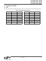
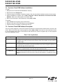
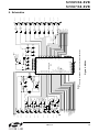
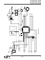
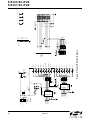
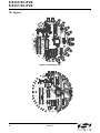
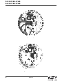
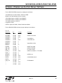
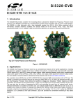
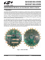
S i 5 3 6 5 / 6 6 - E VB S i 5 3 6 7 / 6 8 - E VB Si5365/66/67/68 E VALUATION B OA RD U SER ’ S G UIDE 1. Introduction The Si5365/66-EVB and Si5367/68-EVB provide platforms for evaluating Silicon Laboratories' Si5365/Si5366 and Si5367/Si5368 Any-Rate Precision Clocks. The Si5365 and Si5366 are controlled directly using configuration pins on the devices, while the Si5367 and Si5368 are controlled by a microprocessor or MCU (microcontroller unit) via an I2C or SPI interface. The Si5365 and Si5367 are low jitter clock multipliers with a loop bandwidth ranging from 30 kHz to 1.3 MHz. The Si5366 and Si5368 are jitter-attenuating clock multipliers, with a loop bandwidth ranging from 60 Hz to 8.4 kHz. The Si5366 device can optionally be configured to operate as a Si5365, so a single evaluation board is available to evaluate both devices. Likewise, the Si5368 can be configured to operate as a Si5367, so the two devices share a single evaluation board. The Si5365/66/67/68 Any-Rate Precision Clocks are based on Silicon Laboratories' 3rd-generation DSPLL® technology, which provides any-rate frequency synthesis in a highly integrated PLL solution that eliminates the need for external VCXO and loop filter components. The devices have excellent phase noise and jitter performance. The Si5366 and Si5368 jitter attenuating clock multipliers support jitter generation of 0.3 ps RMS (typ) across the 12 kHz–20 MHz and 50 kHz–80 MHz jitter filter bandwidths. The Si5365 and SI5367 support jitter generation of 0.6 ps RMS (typ) across the 12 kHz–20 MHz and 50 kHz–80 MHz jitter filter bandwidths. For all devices, the DSPLL loop bandwidth is digitally programmable, providing jitter performance optimization at the application level. These devices are ideal for providing clock multiplication/clock division, jitter attenuation, and clock distribution in mid-range and high performance timing applications. Top Bottom Figure 1. Si536x TQFP EVB Rev. 0.4 5/08 Copyright © 2008 by Silicon Laboratories Si5365/66-EVB Si5367/68-EVB Si5365/66-EVB Si5367/68-EVB Alarms 0.6 ps rms typ 30 kHz–1.3 MHz Y N LOS, FOS 14 x 14 100-QFN Si5367 4 5 I2C or SPI 10 to 710 10 to 1400 0.6 ps rms typ 30 kHz–1.3 MHz Y N LOS, FOS 14 x 14 100-QFN Input Freq (MHz) Control Package Hitless Switching 19 to 1050 Prog. Loop BW 15 to 707 Jitter Generation (12 kHz–20 MHz) Pin Output Freq (MHz) 5 # Clock Outputs 4 # Clock Inputs Si5365 Device PN Clock Mult. Table 1. Features by Part Number Any-Rate Precision Clock Multipliers Any-Rate Precision Clock Multipliers with Jitter Attenuation Si5366 4 5 Pin .008 to 707 .008 to 1050 0.3 ps rms typ 60 Hz–8.4 kHz Y Y LOL, LOS, 14 x 14 FOS 100-QFN Si5368 4 5 I2C or SPI .002 to 710 .002 to 1400 0.3 ps rms typ 60 Hz–8.4 kHz Y Y LOL, LOS, 14 x 14 FOS 100-QFN 2. Applications The Si5365/66/67/68 Any-Rate Precision Clocks have a comprehensive feature set, including any-rate frequency synthesis, multiple clock inputs, multiple clock outputs, alarm and status outputs, hitless switching between input clocks, programmable output clock signal format (LVPECL, LVDS, CML, CMOS), output phase adjustment between output clocks, and output phase adjustment between all output clocks and the selected reference input clock (phase increment/decrement). For more details, consult the Silicon Laboratories timing products website at www.silabs.com/timing. Both evaluation boards (EVBs) have a Silicon Laboratories MCU (C8051F340) that supports USB communications with a PC host. For the pin controlled parts (Si5365 and Si5366), the pin settings of the devices are determined by the MCU and the PC resident software that is provided with the EVB. For the MCU controlled parts (Si5367 and Si5368), the devices are controlled and monitored through the serial port (either SPI or I2C). A CPLD sits between the MCU and the Any-Rate Precision Clock device that performs voltage level translation and stores the pin configuration data for the pin controlled devices. Jumper plugs are provided so that the user can bypass the MCU/ CPLD to manually control the pin controlled devices. Ribbon headers and SMA connectors are included so that external clock in, clock out and status pins can be easily accessed by the user. For the MCU controlled devices (Si5367 and Si5368), the user also has the option of bypassing the MCU and controlling the parts from an external serial device. On-board termination is included so that the user can evaluate either single-ended or differential as well as ac or dc coupled clock inputs and outputs. A separate DUT (device under test) power supply connector is included so that the Any-Rate Precision Clocks can be run at either 1.8 or 2.5 V, while the USB MCU remains at 3.3 V. LEDs are provided for convenient monitoring of key status signals. For more detailed information about these devices, refer to the Any-Rate Precision Clock Family Reference Manual. 3. Features The Si5365/66-EVB and Si5367/68-EVBs each include the following: CD with documentation and EVB software including the DSPLLsim configuration software utility USB cable EVB circuit board including a Si5366 (Si5365/66-EVB) or a Si5368 (Si5367/68-EVB) User's Guide (this document) 2 Rev. 0.4 Si5365/66-EVB Si5367/68-EVB 4. Si5365/66-EVB and Si5367/68-EVB Quick Start 1. Install the Precision Clock EVB Driver. (This must be installed before the EVB is connected to the PC via the USB cable.) For details, see Section "7.EVB Software Installation" on page 11. 2. Install the Precision Clock EVB Software. (Assumes that Microsoft .NET Framework 1.1 is already installed.) 3. Connect the two power supplies to the EVB. One is 3.3 V and the other is either 1.8 or 2.5 V. The DUT is powered by the 1.8/2.5 V supply. 4. Turn on the power supplies. 5. Connect a USB cable from the EVB to the PC where the software was installed. 6. Install USB driver. 7. Launch software by clicking on Start→Programs→Silicon Laboratories→Precision Clock EVB Software and selecting one of the programs. 5. Functional Description The Si5365/66-EVB, Si5367/68-EVB, and software allow for a complete and simple evaluation of the functions, features, and performance of the Si5365, Si5366, Si5367 and Si5368 Any-Rate Precision Clocks. 5.1. Narrowband versus Wideband Operation This document describes two evaluation boards: one for the Si5365 and Si5366 and the other for the Si5367 and Si5368. The former evaluation board is for pin controlled clock parts and the latter is for clock parts that are to be controlled by an MCU over a serial port. Each of the two boards supports two parts: one that is wideband (the Si5365 and the Si5367) and the one that is narrowband (the Si5366 and the Si5368). The narrowband parts are both capable of operating in the wideband mode, so evaluation of the wideband parts can be done by using a narrowband part in wideband mode. As such, these evaluation boards are only populated with narrowband parts. To evaluate Si5365 device operation using the Si5365/66-EVB, the RATE[1:0] pins must be set to LL using the jumper provided. To evaluate Si5367 device operation using the Si536768-EVB, the Precision Clock EVB Software should be configured for wideband mode. For details, see the Precision Clock EVB Software documentation that can be found on the enclosed distribution CD. When operating in wideband mode (Si5365 and Si5367), the reference oscillator should be disabled because it could add to the phase noise of the output. Removing R28 will disable the reference oscillator. Installing R50 and C39 will guarantee that the oscillator will not amplify stray signals. 5.2. Block Diagram Figure 2 is a block diagram of the evaluation board and it is helpful to refer to this diagram. The MCU communicates to the host PC over a USB connection. The MCU controls and monitors the Si536x through the CPLD. The CPLD, among other tasks, translates the signals at the MCU voltage level of 3.3 V to the Si536x's voltage level, which is nominally 2.5 or 1.8 V. The user has access to all of the Si536x's pins using the various jumper settings as well as through the host PC via the MCU and CPLD. Rev. 0.4 3 Si5365/66-EVB Si5367/68-EVB Ext RefClk SPI bus CKOUT1 USB MCU Terminate Input SMAs Reset switch CKOUT2 Si536x CKOUT3 Output SMAs CKOUT4 LEDs FSOUT +3.3 V 1.8 to 3.3 V DUT PWR +1.8 V Vreg ss CPLD SPI, I2C signals reg addr SPI bus Jumper status signals Headers Control signals Figure 2. Si536x TQFP Block Diagram 5.3. Si536x Input and Output Clocks The Si536x has four differential inputs that are ac terminated to 50 Ω and then ac coupled to the part. Single ended operation can be implemented by simply not connecting to one of the two of the differential pairs. The four clock outputs are all differential, ac coupled and configured for driving 50 Ω transmission lines. When using single ended outputs, it is important that the unused half of the output be terminated. Given that the Frame Sync signal can have a duty cycle that is far from 50%, the Frame Sync outputs are dc coupled. If the Frame Sync signal is configured for CMOS output, then the two outputs are not complements of one another and should be wired in parallel so that the output drive current is doubled. To evaluate CMOS level Frame Sync outputs, a 0 Ω resistor should be installed at R19. Note that for the MCU controlled parts (Si5367 and Si5368), the Frame Sync output signal format can be configured independently of the other four outputs. Two jumpers are provided to assist in monitoring the Si536x power. When R36 is removed, J25 can be used to measure the device current. J18 can be used at any time to monitor the supply voltage at the device. The Si5366 and Si5368 require that an external reference clock be provided to enable the devices to operate as narrowband jitter attenuators with loop bandwidths as low as 60 Hz. The external reference clock can be either a crystal, a stand-alone oscillator or some other clock source. The range of acceptable reference frequencies is described in the Any-Rate Precision Clocks Family Reference Manual (Si53xx-RM). The EVB's are shipped with a 3rd overtone 114.285 MHz crystal that is used in the majority of applications. J1 and J2 are used when the Si536x is to be configured in narrowband mode with an external reference oscillator (i.e. without using the 114.285 MHz crystal). When operating in wideband mode, the reference oscillator should be disabled and so that it cannot add to the output phase noise. The RATE pins should also be configured for the desired mode, either through DSPLLsim or using the jumper plugs at J17 (see Table 7). Table 2 shows how the various components should be configured for the three modes of operation: 4 Rev. 0.4 Si5365/66-EVB Si5367/68-EVB Table 2. Reference Input Mode Mode Xtal1 38.88 MHz Ext Ref2 Wide Band Input 1 NC3 J1 NC Input 2 NC J2 NC C39 NOPOP4 install install C22 NOPOP install NOPOP R50 NOPOP NOPOP install R28 install NOPOP NOPOP RATE0 M — H RATE1 M — H Notes: 1. Xtal is 114.285 MHz 3rd overtone. 2. For external reference frequencies and RATE pin settings, see the Any-Rate Precision Clock Family Reference Manual. 3. NC—no connect. 4. NOPOP—do not install this component. For a differential external reference, connect the balanced input signals to J1 and J2. For single-ended operation, connect the input signal to J1 and disconnect J2. R51 is provided so that a different termination scheme can be used. If R51 is populated, then remove R52 and R24. 5.4. CPLD This CPLD is required for the MCU to control the Si536x over a flexible 1.8 or 2.5 V VDD. The CPLD provides two main functions: it translates the voltage level from 3.3 V (the MCU voltage) to the Si536x voltage (either 1.8 or 2.5 V). The MCU communicates to the CPLD with the SPI signals SS_CPLD_B (slave select), MISO (master in, slave out), MOSI (master out, slave in) and SCLK. The MCU can talk to CPLD-resident registers that are connected to pins that control the Si536x's pins, mainly for pin control mode. When the MCU wishes to access a Si536x register, the SPI signals are passed through the CPLD, while being level translated, to the Si536x. The CPLD is an EE device that is retains its code that is loaded through the JTAG port (J32). The core of the CPLD runs at 1.8 V, which is provided by voltage regulator U4. The CPLD also logically connects many of the LEDs to the appropriate Si536x pins. DUT_PWR +3.3 V MCU SS_CPLD_B SS_B SCLK SCLK MOSI CPLD SDI Si5367, Si5368 SDO MISO Figure 3. SPI Mode Serial Data Flow Rev. 0.4 5 Si5365/66-EVB Si5367/68-EVB 5.5. MCU The MCU communicates with the PC over USB so that PC resident software can be used to control and monitor the Si536x. The USB connector is J6 and the debug port, by which the MCU is flashed, is J31. The reset switch, SW1, resets the MCU, but not the CPLD. The MCU is a self-contained USB master and runs all of the code required to control and monitor the Si536x, both in the MCU mode and in the pin-controlled modes. U3 contains a unique serial number for each board and U5 is an EEPROM that is used to store configuration information for the board. The board powers up in free run mode with a configuration that is outlined in "Appendix— Powerup and Factory Default Settings" on page 25. For the pin controlled parts (Si5365/66-EVB), the contents of U5 configure the board on power up so that jumper plugs may be used. If DSPLLsim is subsequently run, the jumper plugs should be removed before DSPLLsim downloads the configuration to the EVB so that the jumpers do not conflict with the CPLD outputs. For microprocessor parts, U5 configures the EVB for a specific frequency plan as described in "Appendix—Powerup and Factory Default Settings" on page 25. The Evaluation board has a serial port connector (J22) that supports the following: Control by the MCU/CPLD of an Any-Rate part on an external target board. Control of the Any-Rate part that is on the Evaluation board through an external SPI or I2C port. For details, see J22 (Table 6). Though they are not needed on this Evaluation Board because the CPLD has low output leakage current, some applications will require the use of external pullup and pulldown resistors when three level pins are being driven by external logic drivers. This is particularly true for the pin-controlled parts: the Si5365 and Si5367. Consult the Si53xx-RM Any-Rate Precision Clock Family Reference Manual for details. LVPECL outputs will not function at 1.8 V. If the Si536x part is to be operated at 1.8 V, the output format needs to be changed by altering either the SFOUT pins (Si5365/66) or the SFOUT register bits (Si5367/68). 5.6. Power and 2L Signals This evaluation board requires two power inputs +3.3 V for the MCU and either 1.8 or 2.5 V for the Any-Rate Precision Clock part. The power connector is J40. The grounds for the two supplies are tied together on the EVB. There are sixteen LEDs, as described in Table 3. J14 is a three by 10 pin male header by which the user can manually set the values of the two-level inputs using jumper plugs connected to either ground (silkscreen labeled L) or the power supply (labeled H). J8 is a twenty pin ribbon header that brings out all of the status outputs from the Si536x. Note that some pins are shared and serve as both inputs and outputs, depending on how the device is configured. For users that wish to remotely access the input and output pins settings with external hardware, J14 and J8 can be connected to ribbon cables. 5.7. 3L Pins The three-level inputs can all be manually configured by installing jumper plugs at J17, either H or L. The M level is achieved by not installing a jumper plug at a given location. J17 can also be used as a connection to an external circuit that controls these pins. J22 is a ten pin ribbon header that is provided so that an external processor can control the Si536x over either the SPI or I2C bus. 6 Rev. 0.4 Si5365/66-EVB Si5367/68-EVB 6. Connectors and LEDs 6.1. LEDs There are sixteen LEDs on the board which provide a quick and convenient means of determining board status. Table 3. LED Status and Description LED Color Label LED Color Label D1 green 3.3 V D2 red LOL D3 green DUT_PWR D4 red C1B D5 red ALRMOUT D6 red C2B D7 yellow CPLD_2 D8 red C3B D9 yellow CPLD_1 D10 green C1A D11 red MCU_3 D12 green C2A D13 red MCU_2 D14 green C3A D15 red MCU_1 D16 green C4A Rev. 0.4 7 Si5365/66-EVB Si5367/68-EVB 6.2. User Jumpers and Headers. Use Figure 4 to locate the jumpers described in Tables 4, 5, 6, and 7: Ext Ref, J1, J2 J8 J14 C22 R24, R28, C22 on top; R50, R51, R52, C39 on bot J18 J17 J25, R36 J22 Figure 4. Connectors, Jumper Header Locations J25 assists in measuring the Any-Rate Precision Clock current draw. If J25 is to be used, R36 should be removed. 8 Rev. 0.4 Si5365/66-EVB Si5367/68-EVB J14 is a three-pin by ten header that is used to establish input levels for the pin controlled two-level inputs using jumper plugs. It also provides a means of externally driving the two-level input signals: Table 4. Two-Level Input Jumper Header, J14 J36 Pin Comment J14.1B CS0_C3A CS0 J14.2B CS1_C4A CS1 J14.3B INC J14.4B DEC J14.5B — not used J14.6B — not used J14.7B DSBL34 J14.8B FS_ALIGN J14.9B FS_SW J14.10B CK_CONF J8 is a 20 pin ribbon header that provides an external path to monitor the status pins. Table 5. External Status Connector, J8 J37 Pin Comment J8.1 LOL J8.3 C1B J8.5 C2B J8.7 C3B J8.9 C1A J8.11 C2A J8.13 CS0_C3A C3A J8.15 CS1_C4A C4A J8.17 INT_ALRM J8.19 DUT_PWR J22 is a 10 pin ribbon header that provides an external path to serially communicate with the Any-Rate Precision Clock. To control the Any-Rate part that is on the Evaluation Board from an external serial port, open the Register Programmer, connect to the Evaluation Board, go to Options in the top toolbar and select "Switch To External Control Mode". To control an Any-Rate part that is on an external target board from the Evaluation Board using its serial port, tie pin 9 of J22 low so that the on-board Any-Rate part is constantly being held in reset. This will force it to disable its SDA_SDO output buffer. This will work only for Evaluation Boards that have Rev C or higher Any-Rate parts. Rev. 0.4 9 Si5365/66-EVB Si5367/68-EVB Table 6. External Serial Port Connector, J22 J38 Pin J22.1 SDA_SDO J22.3 SCL_SCLK J22.5 SDI J22.7 A2_SS J22.9 DUT_RST_B Comment reset J17 is a three-pin by twenty header that is used to establish input levels for the pin controlled three-level inputs using jumper plugs. It also provides a means of externally driving the three-level input signals. Table 7. Three-Level Input Jumper Headers, J17 J39 Pin Comment J17.1B CMODE J17.2B AUTOSEL J17.3B A0_FRQSEL0 J17.4B A1_FRQSEL1 J17.5B A2_SS_FRQSEL2 J17.6B SDI_FRQSEL3 J17.7B SCL_SCLK_BWSEL0 J17.8B SDA_SDO_BWSEL1 J17.9B FRQTBL J17.10B DBL2_BY J17.11B BDBL_FS J17.12B DIV34_0 J17.13B DIV34_1 J17.14B SFOUT0 J17.15B SFOUT1 J17.16B RATE0 J17.17B RATE1 J17.18B FOS_CTL J17.19B — not used J17.20B — not used J18 is used to monitor the Any-Rate Precision Clock voltage. J1 and J2 are edge mount SMA connectors that are used, if so configured, to supply an external single-ended or differential 38.88 MHz reference oscillator. 10 Rev. 0.4 Si5365/66-EVB Si5367/68-EVB 7. EVB Software Installation The following sections describe how to install the EVB software. Note: These programs can control any of the Any-Rate Precision Clock devices including the Si5316, Si532x, and Si536x devices. This software can be installed once per PC and used for all available Precision Clock EVBs. 7.1. PC System Requirements Microsoft Windows 2000 or Windows XP USB 1.1 or USB 2.0 3 MB of hard drive space 1024 x 768 screen resolution or greater (1280 x 1024 recommended) Microsoft .NET Framework 1.1 Precision Clock EVB Driver (Note: The Precision Clock EVB driver is provided with the installation files.) 7.2. Microsoft .NET Framework Installation The Microsoft .NET Framework is required before installing and running the Precision Clock EVB software. Details and installation information about the .NET Framework are available via a shortcut in the NETFramework directory on the installation CD or at the following web site: http://www.microsoft.com/downloads/details.aspx?FamilyId=262D25E3-F589-4842-8157034D1E7CF3A3&displaylang=en Contact your system administrator for more details. 7.3. Precision Clock EVB Driver The EVB requires a driver to be controlled by the software. The following section lists the steps for installing and uninstalling the driver. 7.3.1. Install The driver files must be installed before the EVB is connected to the PC via the USB cable. This installation usually only needs to be completed once per PC. 1. Navigate to the "EVBDriver" directory on the CD. 2. Double-click on the PreInstaller.exe file to run the installation program for the driver. 3. Click Install in the dialog box. Be sure to select a location on the PC's hard drive for the files, if necessary. 4. If the PC is running Windows XP, click Continue Anyway when the wizard warns that the driver does not pass the Windows Logo verification for XP. After the above files are installed, the operating system will be able to identify the EVB's USB controller when the EVB is connected to the PC. The following steps occur when the EVB is connected to the PC for the first time. For Windows 2000, when the EVB is connected to the PC, the operating system will display a dialog box indicating that it found new hardware. No other action is required. The driver installation can be verified in the Device Manager under the USB section; look for "Precision Clock EVB" in the list. For Windows XP: 1. When the EVB is connected to the PC, the Found New Hardware wizard will appear. Use the default settings that will tell the PC to look for the driver. 2. Again, ignore the warning about the driver not passing verification by clicking Continue Anyway. 3. Click Finish to complete the install. 7.3.2. Uninstall In the Control Panel, select Add/Remove Programs. Then select "Precision Clock EVB Driver Set" and click Change/ Remove. The wizard will remove the associated files. Rev. 0.4 11 Si5365/66-EVB Si5367/68-EVB 7.4. Precision Clock EVB Software Installation To install: 1. Navigate to the "PrecisionClockEVBSoftware" directory. 2. Double-click on the Setup.exe file 3. Follow the steps in the wizard to install the program. Note: Use the default installation location for best results. 4. After the installation is complete, click on Start→Programs→Silicon Laboratories→Precision Clock EVB Software. Select one of the programs to control the EVB. 5. Refer to the online help in each program by clicking Help→Help. To uninstall: 1. Open Add/Remove Programs in the Control Panel. 2. Select the Precision Clock EVB Software, and click Remove. 3. Follow the steps in the wizard to complete the removal. 7.5. Precision Clock EVB Software Description There are several programs to control the Precision Clock device. Each provides a different kind of access to the device. Refer to the online help in each program by clicking Help→Help in the menu for more information on how to use the software. Note: Some of the Precision Clock devices do not have a register map, so some programs may not be applicable to them. Table 8. User Applications Program Description Register Viewer The Register Viewer displays the current register map data in a table format sorted by register address to provide an overview of the device’s state. This program can save and print the register map. Register Programmer The Register Programmer provides low-level register control of the device. Single and batch operations are provided to read from and write to the device. Register map files can be saved and opened in the batch mode. Setting Utility DSPLLsim 12 This application allows for quick access to each control on the Precision Clock device (either pin- or register-based). It can save and open text files as well. The DSPLLsim provides high-level control of the Precision Clock device. It has the frequency planning wizard as well as control of the pins and registers in a organized, intuitive manner. Rev. 0.4 49.9 R61 J30 J33 SMA_EDGE 1 CKIN4- SMA_EDGE 1 J38 SMA_EDGE 1 DBL2_BY SDA_SDO_BWSEL1 SCL_SCLK_BWSEL0 SDI_FRQSEL3 A2_SS_FRQSEL2 A1_FRQSEL1 A0_FRQSEL0 CK_CONF FRQTBL CMODE DUT_RST_B FS_SW FS_ALIGN FOS_CTL AUTOSEL INC DEC DIV34_1 DIV34_0 49.9 C42 100N R54 100N R53 R59 49.9 49.9 C55 C53 49.9 49.9 C50 C47 100N 100N J37 R57 R56 100N 100N R55 49.9 C61 C58 100N 100N R60 49.9 SMA_EDGE 1 CKIN4+ CKIN3- CKIN3+ J36 SMA_EDGE 1 3 3 3 CKIN2- CKIN2+ J35 SMA_EDGE 1 J41 SMA_EDGE 1 J39 SMA_EDGE 1 2 CKIN1- CKIN1+ ExtRefIn- J2 SMA_EDGE 1 J1 SMA_EDGE 1 ExtRefIn+ RATE1 2 2 3 3 3 3 3 2 10NF 10NF C59 10NF 10NF C39 10NF NOPOP See note 1 C46 10NF 10NF C45 C43 C56 C54 10NF C51 C48 C62 10NF R52 4 2 R24 0 ohm R28 NOPOP 0 ohm R50 C24 10NF 49.9 3 47 48 90 51 4 71 70 69 68 61 60 37 20 21 56 22 55 54 67 66 29 30 39 40 34 35 44 45 16 17 C22 10NF NOPOP C27 100N R36 0 ohm C25 100N Si536x U6 RSTB NC13 NC12 CMODE CK_CONF FRQTBL FRQSEL3_SDI FRQSEL2_A2_SS FRQSEL1_A1 FRQSEL0_A0 SDA_SDO_BWSEL1 SCL_SCLK_BWSWL0 DBL2_BY FS_SW FS_ALIGN FOS_CTL AUTOSEL INC DEC DIV34_1 DIV34_0 CKIN4+ CKIN4- CKIN3+ CKIN3- CKIN2+ CKIN2- CKIN1+ CKIN1- XA XB DUT_PWR C26 100N 1 2 NC11 NC10 NC9 NC8 NC7 NC6 NC5 NC4 NC3 NC2 NC1 LOL C1A C2A CS0_C3A CS1_C4A ALRMOUT C1B C2B C3B SFOUT1 SFOUT0 DBL_FS FS_OUT+ FS_OUT- DSBL34 CKOUT4+ CKOUT4- CKOUT3+ CKOUT3- CKOUT2+ CKOUT2- CKOUT1+ CKOUT1- 75 74 73 72 53 52 25 24 23 2 1 49 58 59 13 57 12 9 10 11 80 95 Figure 5. Si536x 0 ohm R30 NOPOP 0 ohm J7 SMA_EDGE 1 100N 100N C2 C33 100N J29 SMA_EDGE 1 C32 C17 0 ohm DBL_FS SFOUT1 SFOUT0 C1B C2B C3B INT_ALRM C1A C2A CS0_C3A CS1_C4A LOL DSBL34 R31 R29 C3 for CMOS output 100N 100N J10 SMA_EDGE 1 C19 50 C52 1UF C60 100N 100N C29 J23 SMA_EDGE 1 100N 100N C49 100N C57 100N to power plane J21 SMA_EDGE 1 C28 88 87 85 98 97 77 78 92 93 83 82 C44 100N Locate next to U1 C40 100N J18 to measure DUT current NOPOP J25 L2 Ferrite 2 Notes: 1. Change for Si5365, Si5367, and External Reference. 114.285 MHz 3 GND X1 R51 NOPOP 1 C41 10NF 49.9 100 1 2 1 2 2 J3 SMA_EDGE 1 J5 SMA_EDGE 1 J13 SMA_EDGE 1 J15 SMA_EDGE 1 FS_OUT- FS_OUT+ CKOUT4- CKOUT4+ CKOUT3+ CKOUT2- CKOUT2+ CKOUT1- CKOUT1+ CKOUT3- J28 SMA_EDGE 1 2 2 2 2 2 2 3 3 42 32 RATE1 RATE0 Gnd1 Gnd2 Gnd3 Gnd4 Gnd5 Gnd6 Gnd7 Gnd8 Gnd9 Gnd10 Gnd11 Gnd12 Gnd13 Gnd14 Gnd15 Gnd16 Gnd_Slug 2 5 6 15 27 62 63 76 79 81 84 86 89 91 94 96 99 100 7 8 14 18 19 26 28 31 33 36 38 41 43 46 64 65 101 3 3 3 3 Vdd1 Vdd2 Vdd3 Vdd4 Vdd5 Vdd6 Vdd7 Vdd8 Vdd9 Vdd10 Vdd11 Vdd12 Vdd13 Vdd14 Vdd15 Vdd16 Vdd17 2 2 3 3 3 3 3 2 2 2 2 2 Rev. 0.4 3 RATE0 Si5365/66-EVB Si5367/68-EVB 8. Schematics 13 14 Rev. 0.4 DUT_PWR 10 R15 0 ohm R10 R19 0 ohm R14 10 C8 1UF VCCAUX TMS TDI TDO TCK V3P3 C23 1UF 1 2 3 4 5 6 SMT J32 JTAG connector V3P3 1 2 3 5 83 47 48 45 FB Vreg Out C21 100N TPS76201 Gnd EN In U4 XC2C128 VCCAUX TDO TMS TCK TDI U10B 4 5 C20 10NF C14 1UF R16 66.5 R45 113 V1P8 + C12 100N C7 33UF 1.8V C16 10NF C9 1UF 100N C10 C13 10NF C15 10NF C11 10NF R21 88 98 20 38 51 26 57 R23 XC2C128 VCCIO2-1 VCCIO2-2 VCCIO1-1 VCCIO1-2 VCCIO1-3 VCC1 VCC2 GND1 GND2 GND3 GND4 GND5 GND6 GND7 GND8 FN12_M11 FN12_M13 FN12_M14 FN12_M15 FN11_M11 FN11_M12 FN11_M13 FN11_M14 FN10_M1 FN10_M2 FN10_M3 FN10_M4 FN10_M5 FN10_M6 FN10_M12 FN9_M1 FN9_M2 FN9_M4 FN9_M6 FN9_M12 FN4_M1 FN4_M2 FN4_M3 FN4_M5 FN4_M6 FN4_M13 FN3_M5 FN3_M12 FN3_M14 FN3_M16 FN2_M1_GTS2 FN2_M3_GTS3 FN2_M5_GTS0 FN2_M12_GTS1 FN2_M14 FN2_M15 FN1_M3_GSR FN1_M6 FN1_M12 FN1_M13 FN1_M14 Bank 2 U10A 68 67 66 65 85 86 87 89 77 76 74 73 72 71 70 78 79 80 81 82 8 9 10 11 12 13 93 92 91 90 1 2 3 4 6 7 99 97 96 95 94 Figure 6. CPLD C18 10NF DEC C1B C2B C3B FS_ALIGN FS_SW DBL_FS INC SFOUT1 C1A C2A CS0_C3A CS1_C4A DIV34_0 DIV34_1 DBL2_BY DSBL34 AUTOSEL FRQTBL SFOUT0 CMODE INT_ALRM RATE0 RATE1 CK_CONF FOS_CTL SDI_FRQSEL3 SCL_SCLK_BWSEL0 SDA_SDO_BWSEL1 DUT_RST_B LOL A0_FRQSEL0 A1_FRQSEL1 A2_SS_FRQSEL2 10k 10k DUT_PWR U10C 21 25 31 62 69 75 84 100 XC2C128 FN16_M5 FN16_M6 FN16_M11 FN16_M12 FN16_M13 FN15_M11 FN15_M12 FN15_M13 FN15_M14 FN15_M15 FN15_M16 FN14_M1 FN14_M3 FN14_M5 FN14_M14 FN14_M15 FN13_M2 FN13_M4 FN13_M6 FN13_M13 FN8_M6 FN8_M11 FN8_M12 FN8_M13 FN8_M14 FN8_M15 FN7_M5 FN7_M6 FN7_M11 FN7_M12 FN7_M13 FN7_M14 FN6_M2_CDRST FN6_M4_GCK2 FN6_M12_DGE FN6_M14 FN6_M16 FN5_M4_GCK1 FN5_M6_GCK0 Bank 1 43 42 41 40 39 58 59 60 61 63 64 52 50 49 46 44 53 54 55 56 32 33 34 35 36 37 19 18 17 16 15 14 24 27 28 29 30 23 22 +3.3V R20 0 ohm NOPOP R18 0 ohm NOPOP CPLD_SPARE16 CPLD_SPARE15 REG_ADR0 REG_ADR1 REG_ADR2 REG_ADR3 REG_ADR4 SS_CPLD_B MOSI MISO SCLK CPLD_IRQ CPLD_SPARE2 CPLD_SPARE1 CPLD_SPARE4 CPLD_LED10 CPLD_SPARE10 CPLD_SPARE9 CPLD_SPARE8 CPLD_SPARE7 CPLD_SPARE6 CPLD_SPARE5 CPLD_RST_B CPLD_SPARE14 CPLD_SPARE13 CPLD_SPARE12 CPLD_SPARE11 MCU_SPARE1 CPLD_LED2 CPLD_LED1 CPLD_LED0 CPLD_LED6 CPLD_LED5 CPLD_LED4 CPLD_LED3 MCU_SPARE2 CPLD_LED9 CPLD_LED8 CPLD_LED7 Si5365/66-EVB Si5367/68-EVB MISO SCLK CPLD_SPARE10 CPLD_SPARE9 CPLD_SPARE8 CPLD_SPARE7 CPLD_SPARE6 CPLD_SPARE5 CPLD_SPARE4 CPLD_SPARE2 CPLD_SPARE1 SS_CPLD_B W CS D Clk U5 7 3 1 5 6 49.9 49.9 49.9 M95040 HOLD EEPROM Q MOSI CPLD_IRQ MCU_SPARE1 MCU_SPARE2 2 8 Vcc Vss 4 C38 100N R17 R41 R11 R42 49.9 R46 10k 10k R4 J34 10_M_Header_SMT Spares C4 1UF C1 100N 46 45 44 43 42 41 40 39 6 5 4 3 2 1 48 47 P1.0 P1.1 P1.2 P1.3 P1.4 P1.5 P1.6 P1.7 P0.0 P0.1 P0.2 P0.3 P0.4 P0.5 P0.6 P0.7 U9 Si8051F340 C8051F340 P3.7 P3.6 P3.5 P3.4 P3.3 P3.2 P3.1 P3.0 P4.7 P4.6 P4.5 P4.4 P4.3 P4.2 P4.1 P4.0 23 24 25 26 27 28 29 30 15 16 17 18 19 20 21 22 Install 1.5K pullups for I2C operation. On MCU: P0.0 = SDA P0.1 = SCL NOPOP R13 1.5K Figure 7. MCU BOM = NOPOP V3P3 R9 10k GND 7 27.4 27.4 R1 R2 10k 1K R3 R43 1K NOPOP R5 J31 10_M_Header_SMT 2 1 4 3 6 5 8 7 10 9 MCU debug VBUS U1 SN65220 C6 1UF R40 C36 100N USB Clamp R37 1K EVB_SER_NUM U2 3 2 R39 10 C5 100N 10 CPLD_SPARE11 CPLD_SPARE12 CPLD_SPARE13 CPLD_SPARE14 CPLD_SPARE15 R8 USB Clamp D- J6 V USB 1 4 C37 NC3 3 4 5 100N NC1 U3 V3P3 SW1 4 3 USB SN65220 Ser No. NC2 I/O NO CPLD_RST_B reset 1 2 DS2411 2 R44 1K Gnd D+ serial number R7 CPLD_SPARE16 49.9 MCU_LED1 MCU_LED3 MCU_LED2 REG_ADR4 REG_ADR3 REG_ADR2 REG_ADR1 REG_ADR0 1K R38 0 ohm 1 NC1 A R12 10k 10 11 Vdd REGIN 2 Gnd1 V3P3 13 14 RST/C2CK C2D 3 6 1 NC1 A 6 NC2 B 4 3 6 Gnd2 5 2 Gnd1 Gnd2 NC2 B 4 S2 5 S1 5 V3P3 1 3 5 7 9 2 4 6 8 10 12 8 9 VBUS D+ D- P2.0 P2.1 P2.2 P2.3 P2.4 P2.5 P2.6 P2.7 38 37 36 35 34 33 32 31 6 Vcc GND Rev. 0.4 1 V3P3 Si5365/66-EVB Si5367/68-EVB 15 1 2 3 MCU_LED1 MCU_LED2 MCU_LED3 CPLD_LED0 CPLD_LED1 CPLD_LED2 R69 1K EVB main power Phoenix_4_screw 3.3V 3.3Vreturn DUT_PWRreturn J27 OE1 OE2 IN0 IN1 IN2 IN3 IN4 IN5 IN6 IN7 Ferrite L1 2 R71 1K 1 19 2 3 4 5 6 7 8 9 U8 18 17 16 15 14 13 12 11 + 0 ohm C34 330UF O0 O1 O2 Q3 O4 O5 O6 O7 Buffer 74LCX541 1 CPLD_LED3 CPLD_LED4 CPLD_LED5 CPLD_LED6 CPLD_LED7 CPLD_LED8 CPLD_LED9 CPLD_LED10 1 19 2 3 4 5 6 7 8 9 U7 1 2 BOM = NOPOP 20 Vcc 4 GND 10 * * * * OE1 OE2 IN0 IN1 IN2 IN3 IN4 IN5 IN6 IN7 + O0 O1 O2 Q3 O4 O5 O6 O7 Buffer 74LCX541 18 17 16 15 14 13 12 11 10k R150x4 + V3P3_LED C35 330UF Red D11 2C 2C 2C D16 D14 D12 D10 A A A A Grn Grn Grn Grn Red 2C A D8 Red 2 C A D6 Red D4 2 C A 2 C Red Grn A A Grn D2 D1 D3 A 2 C 2C 2C Red D5 Yel A A C D7 2 C 2 Yel A A 2 C C D9 Red D13 2 A Red 2 C A D15 C31 33UF 2 C + 1 1 1 1 1 1 1 1 1 1 1 1 1 1 1 1 C4A C3A C2A C1A C3B C2B C1B LOL +3.3V DUT_PWR INT_ALRM CPLD_2 CPLD_1 MCU_3 MCU_2 MCU_1 19 17 15 13 11 9 7 5 3 1 R48 R82x4 1 2 3 4 4 3 2 1 R82x4 R63 1 1 J4 C2A C1A C3B C2B C1B LOL J12 J16 J11 1 J26 J24 J19 J20 DUT_PWR 1 #4 H4 #4 H3 100 R66 10k J14 1C 2C 3C 4C 5C 6C 7C 8C 9C 10x3_M_HDR_SMT 10A 10B 9A 9B 8A 8B 7A 7B 6A 6B 5A 5B 4A 4B 3A 3B 2A 2B 1A 1B 10C #4 mounting holes R65 10k R27 H1 1 J9 1 1 1 1 1 1 1 INT_ALRM 10k status R6 8 7 6 5 5 6 7 8 R47 R49 ground pins 82.5 CS0_C3A CS1_C4A INC DEC DSBL34 FS_ALIGN FS_SW CK_CONF 20_M_Header_SMT 20 18 16 14 12 10 8 6 4 2 J8 DUT_PWR 0 ohm two level inputs Figure 8. Power, LEDs and 2L Inputs R35 R34 4 3 2 1 4 3 2 1 R32 1 2 3 4 1 2 3 4 R33 DUT_PWR R150x4 8 7 6 5 8 7 6 5 R150x4 R150x4 5 6 7 8 5 6 7 8 BSS138 R68 1 Q1 V3P3 C30 33UF +3.3V R73 3 2 DUT_PWR 20 Vcc Rev. 0.4 GND DUT_PWR H2 1 16 10 J40 #4 Si5365/66-EVB Si5367/68-EVB J22 9 7 5 3 1 Rev. 0.4 R64 NOPOP 0 ohm R62 R82x4 10 R26 R22 1.5K NOPOP DUT_PWR install for I2C R25 1.5K NOPOP R72 10k J17 R70 10k 1C 2C 3C 4C 5C 6C 7C 8C 9C 10C 11C 12C 13C 14C 15C 16C 17C 18C 19C 20C 20x3_M_HDR_SMT 20A 20B 19A 19B 18A 18B 17A 17B 16A 16B 15A 15B 14A 14B 13A 13B 12A 12B 11A 11B 10A 10B 9A 9B 8A 8B 7A 7B 6A 6B 5A 5B 4A 4B 3A 3B 2A 2B 1A 1B R58 100 DUT_PWR Figure 9. Serial Port, 3L Inputs Notes: 2. NOPOP for Si5365 and Si55366. NOPOP DUT_PWR 0 ohm CMODE AUTOSEL A0_FRQSEL0 A1_FRQSEL1 A2_SS_FRQSEL2 SDI_FRQSEL3 SCL_SCLK_BWSEL0 SDA_SDO_BWSEL1 FRQTBL DBL2_BY DBL_FS DIV34_0 DIV34_1 SFOUT0 SFOUT1 RATE0 RATE1 FOS_CTL SPI, I2C R67 port 10_M_Header_SMT 10 8 6 4 2 1 2 3 4 8 7 6 5 see note 2 DUT_RST_B three level inputs Si5365/66-EVB Si5367/68-EVB 17 Si5365/66-EVB Si5367/68-EVB 9. Bill of Materials Table 9. Si536x Bill of Materials Item Qty Reference Part Mfgr MfgrPartNum 1 32 C1,C2,C3,C5,C10,C12,C17,C19,C21, C25,C26,C27,C28,C29,C32,C33,C36, C37,C38,C40,C42,C44,C45,C47,C49, C50,C53,C55,C57,C58,C60,C61 100 N Venkel C0603X7R160-104KNE 2 7 C4,C6,C8,C9,C14,C23,C52 1 UF Venkel C0603X7R6R3105KNE 3 3 C7,C30,C31 33 UF Venkel TA0006TCM336MBR 4 16 C11,C13,C15,C16,C18,C20,C24,C41, C43,C46,C48,C51,C54,C56,C59,C62 10 NF Venkel C0603X7R160-103KNE 6 2 C34,C35 330 UF Panasonic EEE-HA0J331XP 7 6 D1,D3,D10,D12,D14,D16 Grn Lumex SML-LXT0805GW-TR 8 8 D2,D4,D5,D6,D8,D11,D13,D15 Red Lumex SML-LXT0805SRW-TR 9 2 D7,D9 Yel Lumex SML-LXT0805YW-TR 10 4 H1,H2,H3,H4 #4 mounting hole 11 20 J1,J2,J3,J5,J7,J10,J13,J15,J21,J23, J28,J29,J30,J33,J35,J36,J37,J38,J39, J41 SMA_EDGE Johnson 142-0701-801 12 9 J4,J9,J11,J12,J16,J19,J20,J24,J26 Jmpr_1pin 13 1 J6 USB FCI 61729-0010BLF 14 1 J8 20_M_Header_SMT Samtec HTST-110-01-lm-dv-a 15 1 J14 10x3_M_HDR_SMT Samtec TSM-110-01-L-TV 16 1 J17 20x3_M_HDR_SMT Samtec TSM-120-01-L-TV 17 1 J18 Jmpr_2pin 18 1 J22 10_M_Header_SMT Samtec HTST-105-01-lm-dv-a 20 1 J31 10_M_Header_SMT Samtec HTST-105-01-lm-dv-a 21 1 J32 SMT Sullins GZC36SABN-M30 23 1 J40 Phoenix_4_screw Phoenix MKDSN 1.5/4-5.08 24 2 L1,L2 Ferrite Venkel FBC1206-471H 25 1 Q1 BSS138 On Semi BSS138LT1G 26 2 R1,R2 27.4 Venkel CR0603-16W-27R4FT 27 13 R3,R4,R9,R12,R21,R23,R46,R63, R65,R66,R68,R70,R72 10 k Venkel CR603-16W-1002FT 28 6 R5,R37,R40,R44,R69,R71 1K Venkel CR0603-16W-1001FT 29 3 R6,R47,R67 R82x4 Panasonic EXB-38V820JV 30 15 R7,R11,R17,R24,R41,R42,R52,R53, R54,R55,R56,R57,R59,R60,R61 49.9 Venkel CR0603-16W-49R9FT 18 Rev. 0.4 Si5365/66-EVB Si5367/68-EVB Table 9. Si536x Bill of Materials (Continued) Item Qty Reference Part Mfgr MfgrPartNum 31 5 R8,R10,R14,R26,R39 10 Venkel CR0603-16W-10R0FT 33 9 R15,R19,R28,R29,R31,R36,R38, R48,R73 0 ohm Venkel CR0603-16W-000T 34 1 R16 66.5 Venkel CR0603-16W-66R5FT 36 2 R27,R58 100 Venkel CR0603-16W-1000FT 37 4 R32,R33,R34,R35 R150x4 Panasonic EXB-38V151JV 39 1 R45 113 Venkel CR0603-16W-1130FT 40 1 R49 82.5 Venkel CR0603-16W-82R5FT 42 1 SW1 NO Mountain Switch 101-0161-EV 43 2 U1,U2 SN65220 TI SN65220DBVT 44 1 U3 DS2411 Maxim/Dallas DS2411P 45 1 U4 TPS76201 TI TPS76201DBVT 46 1 U5 M95040 ST Micro M95040-WMN6P 47 1 U6 Si5368A-X-GQ* Silicon Labs Si5368A-X-GQ 48 2 U7,U8 74LCX541 Fairchild 74LCX541MTC_NL 49 1 U9 Si8051F340 Silicon Labs C8051F340-GQ 50 1 U10 XC2C128 Xilinx XC2C128-7VQG100I 51 1 X1 114.285 MHz TXC 7MA1400014 Venkel C0603X7R160-103KNE Not Populated 5 2 C22,C39 10 NF 19 2 J25,J27 Jmpr_2pin 22 1 J34 10_M_Header_SMT Samtec HTST-105-01-lm-dv-a 32 3 R13,R22,R25 1.5 K Venkel CR0603-16W-1501FT 35 6 R18,R20,R30,R50,R62,R64 0 ohm Venkel CR0603-16W-000T 38 1 R43 1K Venkel CR0603-16W-1001FT 41 1 R51 100 Venkel CR0603-16W-1000FT *Note: X denotes the product revision. Consult the ordering guide in the Si5368 Data Sheet for the latest product revision. For the Si5365/66-EVB, substitute Si5366-X-GQ. Rev. 0.4 19 Si5365/66-EVB Si5367/68-EVB 10. Layout Figure 10. Silkscreen Top Figure 11. Layer 1 20 Rev. 0.4 Si5365/66-EVB Si5367/68-EVB Figure 12. Layer 2, Ground Plane Figure 13. Layer 3 Rev. 0.4 21 Si5365/66-EVB Si5367/68-EVB Figure 14. Layer 4, 3.3 V Power Figure 15. Layer 5 22 Rev. 0.4 Si5365/66-EVB Si5367/68-EVB Figure 16. Layer 6, DUT Power Figure 17. Layer 7, Ground Plane Rev. 0.4 23 Si5365/66-EVB Si5367/68-EVB Figure 18. Layer 8 Figure 19. Silkscreen Bottom 24 Rev. 0.4 Si5365/66-EVB Si5367/68-EVB APPENDIX—POWERUP AND FACTORY DEFAULT SETTINGS For the Si5367/68-EVB, the power up settings are as follows: 19.44 MHz input on either CKIN1, CKIN3 or CKIN4 CKIN2 is not used because of free run mode 155.52 MHz output on CKOUT1 and CKOUT2 622.08 MHz output on CKOUT3 and CKOUT4 311.04 MHz output on CKOUT5 Loop BW of 70 Hz LVEPCL outputs for CKIN1, CKIN2, CKIN3 and CKIN4 For the Si5365/66-EVB, the factory jumper settings are as follows: For J17: Silkscreen Pin Jumper — J17.1B none AUTOSEL J17.2B none FRQSEL0 J17.3B none FRQSEL1 J17.4B L 19.44 MHz in, FRQSEL2 J17.5B none 155.52 MHz out FRQSEL3 J17.6B L BWSEL0 J17.7B L BWSEL1 J17.8B H FRQTBL J17.9B L SONET freq table DBL2_BY J17.10B L CK2OUT enabled DBL_FS J17.11B L FS_OUT normal DIV34_0 J17.12B none CKOUT3, CKOUT4 = 77.76 MHz DIV43_1 J17.13B L SFOUT0 J17.14B H SFOUT1 J17.15B none RATE0 J17.16B none RATE1 J17.17B none FOS_CTL J17.18B L — J17.19B none — J17.20B none Comment Autosel, non-revert lowest BW, 110 Hz LVPECL out 114.285 MHz xtal ref FOS disabled Rev. 0.4 25 Si5365/66-EVB Si5367/68-EVB For J14: Pin Pin Jumper CS0_C3A J14.1B none CS1_C4A J14.2B none INC J14.3B none DEC J14.4B none — J14.5B none — J14.6B none DBL34 J14.7B none CKOUT3, CKOUT 4 enabled FS_ALIGN J14.8B none no FS alignment FS_SW J14.9B none CKIN3, CKIN 4 not LOS inputs CK_CONF J14.10B none no FS out alignment 26 Comment Rev. 0.4 Si5365/66-EVB Si5367/68-EVB DOCUMENT CHANGE LIST Revision 0.2 to Revision 0.3 Updated "5.3.Si536x Input and Output Clocks" on page 4. Updated "5.5.MCU" on page 6. Added "Appendix—Powerup and Factory Default Settings" on page 25. Revision 0.3 to Revision 0.4 Updated for free run mode. Rev. 0.4 27 Si5365/66-EVB Si5367/68-EVB CONTACT INFORMATION Silicon Laboratories Inc. 400 West Cesar Chavez Austin, TX 78701 Tel: 1+(512) 416-8500 Fax: 1+(512) 416-9669 Toll Free: 1+(877) 444-3032 Email: [email protected] Internet: www.silabs.com The information in this document is believed to be accurate in all respects at the time of publication but is subject to change without notice. Silicon Laboratories assumes no responsibility for errors and omissions, and disclaims responsibility for any consequences resulting from the use of information included herein. Additionally, Silicon Laboratories assumes no responsibility for the functioning of undescribed features or parameters. Silicon Laboratories reserves the right to make changes without further notice. Silicon Laboratories makes no warranty, representation or guarantee regarding the suitability of its products for any particular purpose, nor does Silicon Laboratories assume any liability arising out of the application or use of any product or circuit, and specifically disclaims any and all liability, including without limitation consequential or incidental damages. Silicon Laboratories products are not designed, intended, or authorized for use in applications intended to support or sustain life, or for any other application in which the failure of the Silicon Laboratories product could create a situation where personal injury or death may occur. Should Buyer purchase or use Silicon Laboratories products for any such unintended or unauthorized application, Buyer shall indemnify and hold Silicon Laboratories harmless against all claims and damages. Silicon Laboratories, Silicon Labs, and DSPLL are trademarks of Silicon Laboratories Inc. Other products or brandnames mentioned herein are trademarks or registered trademarks of their respective holders. 28 Rev. 0.4