1
CD-PC1881V
SERVICE MANUAL
No. S0961CDPC1881
CD-PC1881V
CD-PC1881V Video CD Mini System consisting of CD-PC1881V
(main unit), CP-C881 (front speakers), CP-SW881 (sub woofer),
GBOXS0026AWM1 (center speaker) and GBOXS0027AWM1
(surround speakers).
NTSC/PAL
Manufactured under license from Dolby Laboratories Licensing
Corporation.
DOLBY, the double-D symbol
and “PRO LOGIC” are
trademarks of Dolby Laboratories Licensing Corporation.
• In the interests of user-safety the set should be restored to its
original condition and only parts identical to those specified be
used.
CONTENTS
Page
SAFETY PRECAUTION FOR SERVICE MANUAL ........................................................................................................... 2
VOLTAGE SELECTION ..................................................................................................................................................... 2
AC POWER SUPPLY CORD AND AC PLUG ADAPTOR ................................................................................................. 2
SPECIFICATIONS .............................................................................................................................................................. 3
NAMES OF PARTS ........................................................................................................................................................... 4
OPERATION MANUAL ...................................................................................................................................................... 7
DISASSEMBLY .................................................................................................................................................................. 8
REMOVING AND REINSTALLING THE MAIN PARTS ................................................................................................... 11
ADJUSTMENT ................................................................................................................................................................. 12
BLOCK DIAGRAM ........................................................................................................................................................... 15
SCHEMATIC DIAGRAM .................................................................................................................................................. 18
VOLTAGE ........................................................................................................................................................................ 30
WIRING SIDE OF P.W.BOARD ....................................................................................................................................... 31
NOTES ON SCHEMATIC DIAGRAM .............................................................................................................................. 38
TYPES OF TRANSISTOR AND LED ............................................................................................................................... 38
WAVEFORMS OF CD CIRCUIT ...................................................................................................................................... 39
TROUBLESHOOTING (CD SECTION) ........................................................................................................................... 40
FUNCTION TABLE OF IC ................................................................................................................................................ 44
FL SEGMENT ................................................................................................................................................................... 56
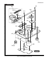
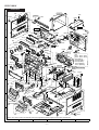
PARTS GUIDE/EXPLODED VIEW
SHARP CORPORATION
–1–
This document has been published to be used
for after sales service only.
The contents are subject to change without notice.
CD-PC1881V
SAFETY PRECAUTION FOR SERVICE MANUAL
Precaution to be taken when replacing and servicing the Laser Pickup.
The AEL (Accessible Emission Level) of Laser Power Output for this model is specified to be lower than Class I Requirements.
However, the following precautions must be observed during servicing to protect your eyes against exposure to the Laser beam.
(1) When the cabinet has been removed, the power is turned on without a compact disc, and the Pickup is on a position outer than
the lead-in position, the Laser will light for several seconds to detect a disc. Do not look into the Pickup Lens.
(2) The Laser Power Output of the Pickup inside the unit and replacement service parts have already been adjusted prior to shipping.
(3) No adjustment to the Laser Power should be attempted when replacing or servicing the Pickup.
(4) Under no circumstances look directly into the Pickup Lens at any time.
(5) CAUTION - Use of controls or adjustments, or performance of procedures other than those specified herein may result in
hazardous radiation exposure.
CAUTION
Laser Diode Properties
Material: GaAIAs
Wavelength: 780 nm
Emission Duration: continuous
Laser Output: max. 0.6 mW
This Video CD Mini System is classified as a CLASS 1
LASER product.
The CLASS 1 LASER PRODUCT label is located on the
rear cover.
Use of controls, adjustments or performance of procedures
other than those specified herein may result in hazardous
radiation exposure.
As the laser beam used in this compact disc player is
harmful to the eyes, do not attempt to disassemble the
cabinet. Refer servicing to qualified personnel only.
CAUTION-INVISIBLE LASER RADIATION WHEN OPEN. DO NOT STARE INTO
BEAM OR VIEW DIRECTLY WITH OPTICAL INSTRUMENTS.
VARNING-OSYNLIG LASERSTRALNING NAR DENNA DEL AR OPPNAD. STIRRA
EJ IN I STRALEN OCH BETRAKTA EJ STRALEN MED OPTISKA INSTRUMENT.
ADVERSEL-USYNLIG LASERSTRALING VED ABNING. SE IKKE IND I
STRALEN-HELLER IKKE MED OPTISKE INSTRUMENTER.
VARO! AVATTAESSA OLET ALTTIINA NAKYMATON LASERSATEILYLLE.
ALA TUIJOTA SATEESEEN ALAKA KATSO SITA OPTISEN LAITTEEN LAPI.
VARNING-OSYNLIG LASERSTRALNING NAR DENNA DEL AR OPPNAD.
STIRRA EJ IN I STRALEN OCH BETRAKTA EJ STRALEN GENOM OPTISKT
INSTRUMENT.
ADVERSEL-USYNLIG LASERSTRALING NAR DEKSEL APNES. STIRR IKKE
INN I STRALEN ELLER SE DIREKTE MED OPTISKE INSTRUMENTER.
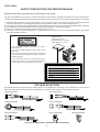
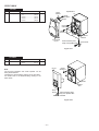
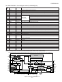
VOLTAGE SELECTION
The voltage selector is located on the AC voltage selector box. If adjustment is necessary, use a screwdriver in order to turn the
selector in either direction unitil the correct voltage figure is displayed in the window next the adjustment screw.
QACCA0001AW00
QACCJ0003AW00
QACCB0006AW00
QACCL0005AW00
QACCE0008AW00
QPLGA0003AWZZ
Figure 2 AC POWER SUPPLY CORD AND AC PLUG ADAPTOR
–2–
QPLGA0004AWZZ
CD-PC1881V
FOR A COMPLETE DESCRIPTION OF THE OPERATION OF THIS UNIT, PLEASE REFER
TO THE OPERATION MANUAL.
SPECIFICATIONS
CD-PC1881V
General
Power source:
Power consumption:
Dimensions:
Weight:
Tuner section
AC 110/127/220/230-240 V, 50/60 Hz
140 W
Width; 270 mm (10-5/8")
Height; 300 mm (11-13/16")
Depth; 362 mm (14-1/4")
8.1 kg (17.7 lbs.)
Frequency range:
Front speakers;
MPO; 176 W(88 W + 88 W)
(10 % T.H.D.)
RMS; 80 W (40 W + 40 W)
(10 % T.H.D.)
RMS; 72 W (36 W + 36 W)
(0.9 % T.H.D.)
Center speaker;
MPO; 32 W (10 % T.H.D.)
RMS; 20 W (10 % T.H.D)
RMS; 14 W (0.9 % T.H.D)
Surround speakers;
MPO; 32 W (16 W + 16 W)
(10 % T.H.D.)
RMS; 20 W (10 W + 10 W)
(10 % T.H.D.)
RMS; 14 W (7 W + 7 W)
(0.9 % T.H.D.)
Sub woofer;
MPO; 72 W (10 % T.H.D.)
RMS; 40 W (10 % T.H.D)
RMS; 32 W (0.9 % T.H.D)
Front speakers; 6 ohms
Centre speaker; 4 ohms
Surround speakers; 8 ohms
Sub woofer; 6 ohms
Headphones; 16-50 ohms
(recommended; 32 ohms)
Video out; 1 Vp-p (75 ohms)
Video/Auxiliary (audio signal) x 2;
500 mV/47 kohms
Wow and flutter:
Cassette deck section
Frequency response:
Signal/noise ratio:
Amplifier section
Output power:
Output terminals:
Input terminals:
D/A converter:
Frequency
response:
Dynamic range:
Front speaker section
Type:
3-way type [13 cm (5-1/4") woofer,
5 cm (2") tweeter and super tweeter]
Maximum input power: 80 W
Rated input power:
40 W
Impedance:
6 ohms
Dimensions:
Width; 200 mm (7-7/8")
Height; 300 mm (11-13/16")
Depth; 254 mm (10")
Weight:
2.9 kg (6.3 lbs.)/each
GBOXS0026AWM1
Center speaker section
Type:
Maximum input power:
Rated input power:
Impedance:
Dimensions:
Weight:
10 cm (4") full-range speaker
40 W
20 W
4 ohms
Width; 260 mm (10-1/4")
Height; 140 mm (5-1/2")
Depth; 155 mm (6-1/8")
0.9 kg (2.0 lbs.)
GBOXS0027AWM1
Surround speaker section
Type:
Maximum input power:
Rated input power:
Impedance:
Dimensions:
3-disc multi-play compact disc player
Non-contact, 3-beam semi-conductor
laser pickup
1-bit D/A converter Frequency
Weight:
10 cm (4") full-range speaker
20 W
10 W
8 ohms
Width; 170 mm (6-3/4")
Height; 88 mm (3-1/2")
Depth; 170 mm (6-3/4")
0.5 kg (1.0 lbs.)/each
CP-SW881
Sub woofer section
20 - 20,000 Hz
90 dB (1 kHz)
Video CD section
Video output format:
50-14,000 Hz (Normal tape)
55 dB (TAPE 1, playback)
50 dB (TAPE 2, recording/
playback)
0.15 % (WRMS)
CP-C881
Compact disc player section
Type:
Signal readout:
FM; 88-108 MHz
AM; 531-1,602 kHz
PAL/PAL60/NTSC
Type:
Maximum input power:
Rated input power:
Impedance:
Dimensions:
Weight:
13 cm (5-1/4") full-range speaker
80 W
40 W
6 ohms
Width; 200 mm (7-7/8")
Height; 300 mm (11-13/16")
Depth; 310 mm (12-3/8")
3.4 kg (7.5 lbs.)
Specifications for this model are subject to change without
prior notice.
–3–
CD-PC1881V
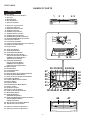
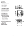
NAMES OF PARTS
CD-PC1881V
■ Front panel
1
1. Disc Number Selector Buttons
2. Disc Tray
3. Multi Indicator
4. Disc Skip Button
5. Open/Close Button
6. Dolby Pro Logic Indicator
7. Extra Bass Indicator
8. FM Stereo Mode Indicator
9. FM Stereo Indicator
10. (VCD/CD) Play Indicator
11. (VCD/CD) Pause Indicator
12. (VCD/CD) Repeat Indicator
13. (VCD/CD) Disc Number Indicators
14. (VCD/CD/TUNER) Memory Indicator
15. Timer Play Indicator
16. Timer Record Indicator
17. Spectrum Analyzer/Volume Level Indicator
18. (TAPE 2) Record Indicator
19. Sleep Indicator
22
3
45
6
7
8
9
12
Timer Set Indicator
(VCD) Digest Button
(VCD) Book Mark Button
(VCD) Skip Previous Button
(CD) Track Down/Review Button
(TUNER) Preset Down Button
(TAPE 2) Rewind Button
24. (VCD) Skip Next Button
(CD) Track Up/Cue Button
(TUNER) Preset Up Button
(TAPE 2) Fast Forward Button
25. Bypass Button
26. Normal Button
27. Timer/Sleep Button
28. Clock Button
29. (VCD) Playback Control Auto/Off Button
30. (VCD/CD) Audio Mode Button
31. (VCD) On Screen Display On/Off Button
32. On/Stand-by Button
33. Equalizer Mode Selector Button
34. Dimmer Button
35. Phantom Button
36. Extra Bass/Demo Mode Button
37. Volume Control
38. Headphone Socket
39. Function Selector Button
40. (TAPE 2) Record Pause Button
41. Memory/Set Button
42. (VCD) Stop/Return
(CD/TAPE) Stop Button
43. (VCD) Play/Repeat/Select/Resume Button
(CD) Play/Repeat Button
(TAPE) Play Button
44. Tuning and Time Up/Down Buttons
45. Sub Woofer Volume Control
10
11
13
14
15
16
20.
21.
22.
23.
17
20 2122 23
18 19
24 25 26
27
28
29
30
31
32
33
34
35
36
37
38 39 40 41 42 43 44
46
46. (TAPE 1) Cassette Compartment
47. (TAPE 2) Cassette Compartment
–4–
47
45
CD-PC1881V
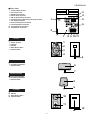
■ Rear panel
1. Video Output Socket
2. AC Power Lead
3. AM Aerial Terminal
4. Aerial Earth Terminal
5. FM 75 Ohms Aerial Terminal
6. Video/Auxiliary (Audio Signal) Input Sockets
7. AC Voltage Selector
8. Surround Speaker Terminals
9. Centre Speaker Terminals
10. Front Speaker Terminals
11. Sub Woofer Terminals
3
4
1
5
6
2
7
8 9 10 11
CP-C881
■ Front speaker
1
2
1. Super Tweeter
2. Tweeter
3. Woofer
4. Bass Reflex Duct
5. Speaker Wire
3
4
5
GBOXS0026AWM1
■ Center speaker
6. Full-Range Speaker
7. Speaker Wire
6
7
GBOXS0027AWM1
■ Surround speaker
8. Full-Range Speaker
9. Speaker Wire
8
9
CP-SW881
■ Sub woofer
10. Woofer
11. Bass Reflex Duct
12. Speaker Wire
10
11
12
–5–
CD-PC1881V
■ Remote control
1. Remote Control Transmitter LED
1
2. On/Stand-by Button
3. Surround Level Buttons
4. Centre Level Buttons
5. Dolby Pro Logic Button
6. Centre Mode Button
7. Test Tone Button
3
4
5
6
8. (VCD/CD) Direct Search Buttons
9. (VCD) On Screen Display On/Off Button
10. (VCD) PAL/NTSC Select Button
11. (VCD) Book Mark Button
12. (VCD) Digest/Time Search Button
13. (VCD/CD) Audio Mode Button
14. (VCD) VCD Auto/On Button
15. (VCD) Playback Control Auto/Off Button
16. (VCD/CD) Clear Button
17. (VCD/CD) Memory Button
18. (VCD/CD) Disc Skip Button
19. (VCD/CD) Random Button
20. (VCD/CD) Pause Button
21. (TAPE 2) Record Pause Button
22. (VCD) Skip/Previous Button
(CD) Track Down/Review Button
(TUNER) Preset Down Button
(TAPE 2) Rewind Button
23. (VCD) Skip/Next Button
(CD) Track Up/Cue Button
(TUNER) Preset Up Button
(TAPE 2) Fast Forward Button
24. (VCD) Stop/Return Button
(CD/TAPE) Stop Button
25. (VCD) Play/Repeat/Select/Resume Button
(CD) Play/Repeat Button
(TAPE) Play Button
26. Function Selector Buttons
27. Extra Bass Button
28. Equalizer Mode Button
29. Balance Control Buttons
30. Volume Up/Down Buttons
2
7
8
13
14
15
16
17
9
10
11
12
21 20 19 18
22 23 24 25
26
27
28
29
–6–
30
15
15
Replace the batteries if the operating distance is reduced or
if the operation becomes erratic.
Periodically clean the transmitter LED on the remote control
and the sensor on the main unit with a soft cloth.
Exposing the sensor on the main unit to strong light may
interfere with operation. Change the lighting or the direction
of the unit.
Keep the remote control away from moisture, excessive heat,
shock, and vibrations.
Notes concerning use:
0.2 m - 6 m
(8" - 20')
■ Remote control
Caution:
The operation explained above will erase all data stored in
memory including clock and timer settings, and tuner, video
CD and CD presets.
hold down the ON/STAND-BY button for at least 1 second.
1 Press the ON/STAND-BY button to enter the stand-by mode.
2 Whilst pressing down the button and the button,
To erase all of the stored memory contents (clock and timer
settings, and tuner and CD presets).
If the display is not correct.
If the operation is not correct.
Reset the microcomputer under the following conditions:
ON/
STAND-BY
RESETTING THE MICROCOMPUTER
TUNING/
TIME
(
)
–7–
AM 0:00
or
AM 12:00
) button to select the time
or
) button to adjust the hour.
Press the TUNING/TIME ( or ) button once to advance
the time by 1 hour. Hold it down to advance continuously.
When the 12-hour display is selected, “AM” will change automatically to “PM”.
6 Press the TUNING/TIME (
5 Press the MEMORY/SET button.
The 24-hour display will appear.
(0:00 - 23:59)
“AM 0:00” → The 12-hour display will appear.
(AM or PM 0:00 - 11:59)
“AM 12:00” → The 12-hour display will appear.
(AM or PM 12:00 - 11:59)
Note that this can only be set when the unit is first installed
or it has been reset.
“0:00” →
0:00
display mode.
4 Press the TUNING/TIME (
3 Within 5 seconds, press the MEMORY/SET button.
1 Press the ON/STAND-BY button to enter the stand-by mode.
2 Press the CLOCK button.
In this example, the clock is set for the 24-hour (0:00) system.
MEMORY/
SET
ON/
STAND-BY
CLOCK
(Main unit operation)
SETTING THE CLOCK
or
) button to adjust the
➁ Perform steps 1 - 9 above.
CROCOMPUTER”, .
① Perform steps 1 - 2 in the section “RESETTING THE MI-
To change the time display mode:
① Press the CLOCK button.
➁ Within 5 seconds, press the MEMORY/SET button.
➂ Perform steps 6 - 9 above.
To change the clock time:
Note:
The clock display will flash on and off at the push of the
CLOCK button when the AC power supply is restored after
a power failure occurs or after the AC power lead is disconnected.
If this happens, follow the procedure below to change the
clock time.
Press the CLOCK button.
The time display will appear for about 5 seconds.
To see the time display:
The clock starts operating from “0” seconds.
(Seconds are not displayed.)
And then the clock display will disappear a few seconds.
9 Press the MEMORY/SET button.
Press the TUNING/TIME ( or ) button once to advance
the time by 1 minute. Hold it down to change the time in 5
minute intervals.
The hour setting will not advance even if minutes advance
from “59” to “00”.
minutes.
8 Press the TUNING/TIME (
7 Press the MEMORY/SET button.
CD-PC1881V
OPERATION MANUAL
CD-PC1881V
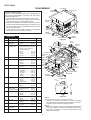
DISASSEMBLY
Top Cabinet
Front Panel
(A1)x2
ø3x12mm
Caution on Disassembly
Follow the below-mentioned notes when disassembling
the unit and reassembling it, to keep it safe and ensure
excellent performance:
1. Take cassette tape and compact disc out of the unit.
2. Be sure to remove the power supply plug from the wall
outlet before starting to disassemble the unit.
3. Take off nylon bands or wire holders where they need to
be removed when disassembling the unit. After servicing
the unit, be sure to rearrange the leads where they were
before disassembling.
4. Take sufficient care on static electricity of integrated
circuits and other circuits when servicing.
Side Panel
(Right)
(B1)x2
ø3x8mm
(A1)x2
ø3x12mm
(B2)x2
ø3x10mm
Rear Panel
CD-PC1881V
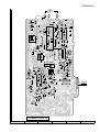
STEP
R EMOVAL
PROCEDURE
FIGURE
1
Top Cabinet
1. Screw ..................... (A1) x4
8-1
2
Side Panel
(Left/Right)
1. Screw ..................... (B1) x4
2. Screw ..................... (B2) x2
8-1
CD Tray Cover/
CD Player Unit
1. Turn on the power supply,
open the disc tray, take out
the CD cover, and close.
(Note 1) (Note 2)
2. Hook ....................... (C1) x5
3. Hook ....................... (C2) x2
4. Socket .................... (C3) x4
5. Screw ..................... (C4) x2
8-2
3
Side Panel (Left)
Figure 8-1
(C3) x4
DiscTray
1
Pull
CD Video PWB
Jack PWB
1. Screw ..................... (D1) x1
8-2
Rear Panel
1. Screw .....................
2. Screw .....................
3. Screw .....................
4. Socket ....................
(E1) x2
(E2) x8
(E3) x2
(E4) x1
8-2
6
Tuner PWB
1. Screw ..................... (F1) x1
2. Socket .................... (F2) x1
8-2
(C4) x1
ø3x10mm
7
Main PWB
1. Socket ....................
2. Flat Cable ..............
3. Flat Wire .................
4. Tip Wire ..................
5. Screw .....................
6. Socket ....................
(G1) x2
(G2) x1
(G3) x1
(G4) x1
(G5) x1
(G6) x1
9-1
(E4)x1
1. Screw .....................
2. Screw .....................
3. Socket ....................
4. PWB Holder ...........
(H1) x4
(H2) x2
(H3) x4
(H4) x4
9-1
1. Screw ..................... (J1) x1
2. Screw ..................... (J2) x2
9-2
2
(C2) x1
Front Panel
(C4) x1
ø3x10mm
Jack PWB
Rear Panel
(D1) x1
ø3x10mm
CD Tray
Cover
1
CD Player
Unit
5
Power PWB
Hook
(C1) x5
(C2) x1
4
8
(B1)x2
ø3x8mm
(E3)x2
ø3x10mm
(F1) x1
ø3x10mm
(F2)x1 Main PWB
(E2)x8
ø3x10mm
Tuner PWB
(E1)x2
ø3x10mm
Figure 8-2
LOCK
LEVER
9
Front Panel
10
Display PWB/
1. Screw ..................... (K1) x13
Switch PWB
2. Bracket Support ..... (K2) x1
Headphones PWB 3. Knob ....................... (K3) x1
9-2
11
Tape Mechanism 1. Open the cassette holder.
2. Screw...................... (L1) x6
3. Socket .................... (L2) x1
9-2
12
Turntable
1. Screw ..................... (M1) x1
2. Cover ..................... (M2) x1
9-3
13
Disc Tray
1. Screw ..................... (N1) x2
2. Guide ..................... (N2) x2
9-3
14
CD Video PWB
1. Screw ..................... (P1) x1
2. Socket .................... (P2) x4
9-4
15
CD Changer
Mechanism
1. Screw ..................... (Q1) x4
9-5
16
CD Mechanism
1. Screw ..................... (R1) x1
9-5
Figure 8-3
Note 1:
How to open the changer manually. (Fig. 8-3)
1. Change, turn fully the lock lever in the arrow direction
through the hole on the loading chassis bottom in this state.
After that, push forward the CD player base.
Note 2:
1. After removing the connector for the optical pickup from the
connector, wrap the conductive aluminium foil around the
front end of connector to protect the optical pickup from
electrostatic damage.
–8–
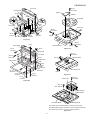
CD-PC1881V
(M1) x1
ø3 x10mm
Front Panel
Display PWB
(M2) x1
(G1)x2
Washer
(H3)x2
(H4)x4
1
Push
1
Push
2 Pull
POWER
PWB
Turntable
(G2)x1
(H3)x2
(G3)x1
Headphoens
PWB
Power PWB
Disc Tray
(G4)x1
(N1) x1
ø3 x10mm
(H1)x4
ø3x10mm
(G6)x1
(G5)x1
(H2)x2
ø3x10mm
ø3x6mm
Main PWB
(N2) x1
Figure 9-1
(N1) x1
ø3 x10mm
(L2)x1
Switch PWB
CD Player Unit
Figure 9-3
(K3)x1
(K1)x2
ø3x10mm
(N2) x1
Display PWB
(P1) x1
ø3 x10mm
Front Panel
(K1)x10
ø3x10mm
(K2)x1
CD Video PWB
(P2) x2
Headphones
PWB
Main Chassis
Open
Cassette
Holder
(Left/Right)
Tape
Mechanism
(K1)x1
ø3x10mm
(L1)x6
ø3x10mm
CD Player Unit
(P2) x2
(J2)x2
ø3x8mm
Figure 9-4
(J1)x1
ø3x10mm
Shift Lever
(Q1) x4
ø3 x12mm
Figure 9-2
(R1) x1
ø2.6 x10mm
CD Changer
Mechanism
CD Player Base
CD Mechanism
Be careful when installing the CD changer mechanism.
Install the CD changer mechanism on the CD player base after
the shift lever has been set in the highest position.
Figure 9-5
–9–
CD-PC1881V
CP-C881
STEP
1
REMOVAL
PROCEDURE
Front Speaker
1. Front Panel ............
2. Tip ..........................
3. Screw .....................
4. Screw .....................
5. Screw .....................
FIGURE
(A1) x1
(A2) x2
(A3) x2
(A4) x2
(A5) x4
Speaker Box
Super
Tweeter
10-1
(A3)x2
ø3x10mm
(A2)x2
(A4)x2
ø3x10mm
(A5)x4
ø4x14mm
Tweeter
Woofer
Front Panel
(A1)x1
Drive should be pried
away from Speaker Box.
Screw Driver
Figure 10-1
CP-SW881
STEP
1
REMOVAL
Sub woofer
PROCEDURE
FIGURE
1. Net .......................... (A1) x1
2. Screw ..................... (A2) x4
10-2
(A1)x1
Note:
The surround speakers and center speaker can be
easily disassembled.
Therefore the disassembling method is not described.
For details refer to the disassembling drawing in the
Parts Guide.
(A2)x4
ø4x14mm
Woofer
Speaker
Box
Screw
driver
Drive should be pried
away from Speaker Box.
Direction of handle
Figure 10-2
– 10 –
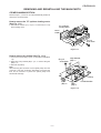
CD-PC1881V
REMOVING AND REINSTALLING THE MAIN PARTS
CD MECHANISM SECTION
Perform steps 1, 2, 3 and 14-16 of the disassembly method to
remove the CD mechanism.
How to remove the T/T up/down loading motor
(See Fig. 11-1)
1. Remove the screws (A1) x 2 pcs., to remove the T/T up/
down loading motor.
T/T Up/Down
Loading Motor
Motor
PWB
(A1) x2
ø2.6 x5mm
Figure 11-1
How to remove the pickup (See Fig. 11-2)
1. Remove the screws (B1) x 2 pcs., to remove the shaft (B2)x
1 pc.
2. Remove the stop washer (B3) x 1 pc., to remove the gear
(B4)x 1 pc.
3. Remove the pickup.
Stop Washer
(B1) x2
(B3) x1
ø2.6 x6mm
Note
After removing the connector for the optical pickup from the
connector, wrap the conductive aluminium foil around the
front end of connector to protect the optical pickup from
electrostatic damage.
Pickup
Shaft
(B2) x1
CD Mechanism
Gear
(B4) x1
Figure 11-2
– 11 –
CD-PC1881V
ADJUSTMENT
MECHANISM SECTION
TUNER SECTION
• Driving Force Check
fL: Low-range frequency
fH: High-renge frequency
• AM IF/RF
Signal generator: 400 Hz, 30%, AM modulated
Torque Meter
Specified Value
Play: TW-2412
Tape 1: Over 80 g
Tape 2: Over 80 g
• Torque Check
Torque Meter
Specified Value
Tape 1
Tape 2
Play: TW-2111
30 to 60 g. cm
Fast forward: TW-2231
—
30 to 60 g.cm
60 to 120 g.cm
Rewind: TW-2231
—
60 to 120 g.cm
Test Stage Frequency
Frequency
Display
AM IF
450 kHz
1,602 kHz
T351
AM Band
Coverage
—
531 kHz
(fL): T306 *2
1.1 ± 0.1 V
990 kHz
(fH): T302
AM Tracking 990 kHz
*1. Input: Antenna,
*2. Input: Antenna,
Setting/ Instrument
Adjusting Connection
Parts
*1
*1
Output: TP302
Output: TP301
• Tape Speed
Normal
speed
Test Tape
Adjusting
Point
Specified
Value
MTT-111
Variable
Resistor in
motor.
(MM1)
3,000 ±
30 Hz
TAPE MECHANISM
Instrument
Connection
Speaker
terminal
(Load
resistance:
8 ohms)
• FM
Notes:
1: Description of the "FM IF Adjustment" is not carried on this
Manual. It is because the IF coil in the FM front end section
has been best adjusted in the factory so that its further
adjustment is not needed at the field. When replacing the
FM front end assembly, no adjustment is needed either.
2: The parts in the FM front end section are prepared in a
complete unit, so you can't obtain each part individually.
• FM Mute Level
Signal generator: 1 kHz, 40 kHz dev., FM modulated
Frequency
MM 1
Motor
98.00 MHz
(25 dBµV)
Adjusting
Parts
Frequency
Display
98.00 MHz
VR351
Instrument
Connection
Input: Antenna
Output: Speaker
Terminal
Variable Resistor in motor
Figure 12-1
TUNER PWB
FM MUTE
LEVEL
AM IF
TP302
R357
IC303
TP301
R336
VR351
T351
T306
AM BAND
COVERAGE fL
SO301
ANTENNA
TERMINAL
FE301
AM
TRACKING fH
T302
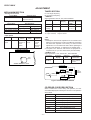
Figure 12-2 ADJUSTMENT POINTS
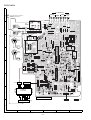
CD ERROR CODE DESCRIPTION
When a malfunction occurs during CD operation, an error
code will be displayed to identify the function in CD operation
which failed.
– 12 –
Error
0001
0101
0105
0201
0203
0304
0305
State Code
Cannot detect pickup-in SW
Tray close operation error
Tray close operation error
Tray open operation error
Tray open operation error
Disc skip operation error
Disc skip operation error
0307
Disc skip operation error
CD-PC1881V
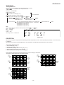
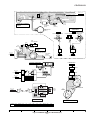
TEST MODE
• Setting the test mode
Any one of test mode can be set by pressing several keys as follows.
<CD> + <
> + <POWER> TEST: CD operation test
• TEST mode
Function — CD test mode
Setting of TEST mode
Indication of CD TST mode (Fig. 13-1)
IL is not performed.
OPEN/CLOSE operation is manual operation.
The pickup can be moved by using the (
<MEMORY>
LASER ON
<MEMORY>
Tracking on the spot.
SERVO OFF PLAY
<PLAY> key input
) or (
) key.
<MEMORY>
Tracking on the spot.
SERVO ON PLAY
<STOP>
STOP
TOC. IL is performed, and the ordinary PLAY is performed.
If the following key is pressed during PLAY, it is possible
to specify directly any Track No.
<Disc Number 1> key: Track 4
<Disc Number 2> key: Track 9
<Disc Number 3> key: Track 15
Note:
Only in STOP state it is possible to slide the pickup with the (
VOL. --- Last memory
BAL. --- CENTER
R.GEQ. --- FLAT
X-BAS --- OFF
1
2
) or (
Press <STOP> key.
Stop
) key.
3
Canceling method - POWER OFF
Figure 13-1
CD SECTION
Since this CD system incorporates the following automatic adjustment function, when the pickup is replaced, it is not necessary
to readjust it.
Since this CD unit does not need adjustment, the combination of PWB and laser pickup unit is not restricted.
• Automatic adjustment item
1. Focus offset (Fig. 13-2)
2. Tracking offset (Fig. 13-3)
3. E/F balance (tracking error balance) (Fig. 13-4)
4. RF level AGC function (HF level: constant)
5. RF level automatic follow-up of the tracking gain
This automatic adjustment is performed each time a disc is changed. Therefore,
each disc is played back using the optimal settings.
Enlarged
View
10ms
0.50 V
IC1 20 FE
0.1s
0.50 V
IC1 20 FE
FOCUS
OFF-SET
ADJUST
10ms
0.50 V
IC1 7 TE
0.1s
0.50 V
IC1 7 TE
TRACKING
OFF-SET
1 ADJUST
TRACKING
OFF-SET
1 ADJUST
2
2
Figure 13-3
Figure 13-2
TRACKING/
ERROR
BARANCE
1 ADJUST
200 ms
1V/diV
IC 1 15
TO
200 ms
1V/diV
IC 1 7
TE
2
Figure 13-4
– 13 –
CD-PC1881V
EXPLANATION OF DOLBY SURROUND PRO LOGIC AND EVALUATION METHOD
Outline
• In the normal mode of Pro Logic ON mode the amplifiers for
C-ch and S-ch are in operative state, so that the SP output
appears.
• In the Phantom mode of Pro Logic ON mode the amplifier for
C-ch is in MUTE state, so that the SP output is cut. The
amplifier for S-ch (surround) is in operative state, so that the
SP output appears
• Namely, two speakers are connected in parallel to one
amplifier.
• In the Pro Logic BYPASS mode the amplifier for C-ch (center
channel) and the amplifier for S-ch (surround channel) are in
MUTE state. The SP output is cut.
• State of element output and terminal output in specific mode
State of set
Output point
IC501 12 pin L-out
11 pin R-out
IC501
9pin C-out
IC501 10pin S-out
SP OUT
L-ch
(SO901)
R-ch
SP OUT C-ch
(SO901)
SP OUT S-ch
(SO901)
Dolby Pro Logic
Bypass mode
Output enabled state
Output enabled state
No output
No output
Output enabled state
Output enabled state
No output in MUTE (Q404) state
Dolby Pro Logic On mode
Normal mode
Output enabled state
Output enabled state
Output enabled state
Output enabled state
Output enabled state
Output enabled state
Output enabled state
Phantom mode
Output enabled state
Output enabled state
No output
Output enabled state
Output enabled state
Output enabled state
No output in MUTE (Q404) state
No output in MUTE (Q403) state
Output enabled state
Output enabled state
Test tone output
• Pro Logic ON Normal mode
Press the remote control TEST TONE button.
→Output of only L-ch →Output of only C-ch
↑
↓
Output of only S-ch ← Output of only R-ch
The test tone (noise) is repeatedly output for output period
(2 sec).
In this case the following indication appears repeatedly.
→TEST →L-ch →C-ch
↑
↓
S-ch ← R-ch
• Pro Logic ON Phantom mode
Press the remote control TEST TONE button.
→Output of only L-ch →Output of only R-ch
↑
↓
← Output of only S-ch
The test tone (noise) is repeatedly output for output period
(2 sec).
Output point
SP out
(SO901)
(SO901) SP out S-ch
SP out
(SO901)
L-ch
R-ch
Almost no output (only omitting component)
Almost no output (only omitting component)
Almost no output (only omitting component)
(2) L-ch/R-ch reverse phase input into VIDEO IN input jack in
VIDEO Function mode
(Reverse phase: Phase difference between L and R is 180°)
Output point
SP out
(SO901)
L-ch
R-ch
Normal mode
Almost no output (only omitting component)
Almost no output (only omitting component)
(SO901) SP out C-ch Almost no output (only omitting component)
(SO901) SP out S-ch
Output point
SP out
(SO901)
L-ch
R-ch
Input signal is output.
Phantom mode
Almost no output (only omitting component)
Almost no output (only omitting component)
(SO901) SP out C-ch SP cut, no output
(SO901) SP out S-ch
Relation between VIDEO IN input and output in Pro Logic
ON state
(1) L-ch/R-ch same phase input into VIDEO IN input jack in
VIDEO Function mode
Normal mode
Phantom mode
Input signal is output.
Input signal is output.
(SO901) SP out C-ch SP cut, no output
In this case the following indication appears repeatedly.
→TEST → L-ch → R-ch
↑
↓
← S-ch←
Output point
L-ch
R-ch
Input signal is output.
• Accordingly, if you want to output signal waveform to C-ch SP
out, give the same phase input into L-ch/R-ch INPUT in the
Pro Logic Normal mode.
If one of channels receives input, C-ch does not output. Only
L-ch or R-ch outputs.
• If you want to output signal waveform to S-ch SP out, you can
use either Normal mode or Phantom mode. However, 180°
reverse phase input must be given to L-ch/R-ch INPUT.
(SO901) SP out C-ch Input signal is output.
(SO901) SP out S-ch Almost no output (only omitting component)
– 14 –
SOLM2
SOLENOID
SW1
OPEN/CLOSE
M3
T/T UP/DOWN
LOADING MOTOR
SW3
DISC NUMBER
SW2
MECHA UP
CD-PC1881V
M
TO MAIN
SECTION
TO MAIN SECTION
87654321
+B1
GND (D)
MECHA UP
GND (D)
DISK NO.
OPEN/CLOSE
GND (D)
M–
M+
SOLSOL+
CNS10 10 9
1 2 3 4 5 6 CNP11
+B1
+B5
CNP10 10 9
QV4
JKV1
VIDEO OUT
87654321
R L
1 6 20
VDD
36 DQ12
1
DQ8
UCAS 28
LCAS 29
A8
A3
A4
DQ0
39 DQ15
WE
RAS
A0
~
ICV4
VIDEO
OPERATION
AMP.
NJM2267M
5 3
R L
21
27
35
40
ICV3
DRAM
SDM4260C
DQ7
6
DQ4
Q51
DQ3
IC4
4 BA4558F
OPE AMP.
DQ11
7 1
2 ~ 5 7 ~ 10 13 14 16 ~ 19 22 ~ 26 31 ~ 34
~
72
14 X2
MD8
MCAS
ICV2
MPEG DECOEDER
D61012GC
13 X1
35 AUDO
32 AUBCK
HD7
HD4
HD3
~
67
6 57
11 64
12 69
18 74
26 76
30 91
37 94
43 96
50 100
2
~
33 AULRCK
95 CDC2PO
97 CDLRCK
~
RES. CQCK. COIN
SQOUT. RWC. WRQ
V/P
HFL
TES
TOFF
TGL
JP+
JP–
XIN
EFMO
EFMI
CLV+
XOUT
53
AVSS
VSS
TEST1
TEST2
X1
16.93MHz
52
IC2
LC78631E
SERVO/SIGNAL
CONTROL
MD0
MD11
65 MD15
XV2
27MHz
41
6 AVDD
MD4
~
P0/DFCK 39
P1/DFIN 38
45
47 LVDD
27 VDD
MD5
68 MD12
5
7
~
RCHN
LCHN
TEST3
TEST4
LVSS
XVSS
56 49
54 XVDD
+5V
MA0
MRAS
MWE
MCAS
17 26 50 51
MA4
MA3
MA8
38 ~ 42 45 ~ 48 49 52 54 ~ 56 58 ~ 62 70 ~ 73 53
86 VOUT1
VDD,CKSEL,HSELX,
HD0 10
99 CDI
HSELAAVDD,
1 15 ~ 17 23 ~ 25 36 44 51 63 75 83 84 92
80
78
77
64
4 10 12 16 9 11 13 15 19 20 23 24 28 29
62 LDO
1234
SLD
SP
SPO
FD
TO
29
23
27
16
15
+B1
SL+. SL–. DRF
QV2
42 41 20 40 24 18 28 39 38 37 36
IC3
M63001FP
FOCUS/
TRACKING/
SPIN/SLED
DRIVER
25
20
17
2
1
QV3
XV1
4.19MHz
35
29
6745
CNPV2 1 2 3 4
M1
SPINDLE
MOTOR
M
TO MAIN SECTION
M2
SLED
MOTOR
M
PICKUP IN
SW4
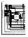
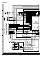
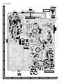
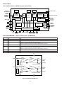
Figure 15 BLOCK DIAGRAM (1/3)
– 15 –
HD0
MDI
MDO
MCK
MBUSY
6
15 16 26 27
PICKUP UNIT
ICV1
MPEG CONTROLLER
IX0313AW
41 X1
CD SOL
8
23
15 PWR_MPEG
40 X2
18
19
20
22
22
21
14
64 ~ 57
HD7
MO SPEED
+B5
CD-LD M–
CD-LD M+
PU-IN SW
+B1
~
IC1
LA9241M
SERVO AMP.
DRF 54
SL+ 31
SL– 30
13 12 11
QV1
~
CV+
SLC
SL1
JP–
CE 53
DAT 52
CL 51
TRACKING COIL
Q1
40 4344
FIN2
FIN1
E
F
LASER
DRIVER
64 VCC1
32
FOCUS COIL
+5V
22
AGND
~
Q52
CL, DAT, SELIAL CONTROL/CE
~
+B1
7 ~ 9 14 16 17 25 ~ 33 39 42 45 ~ 50
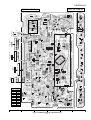
CD-PC1881V
SO301
ANTENNA
TERMINAL
FM IF
FE301
FM FRONT END
1
1
+B4
CF302
3
AM IF
2
3
1
VT
AM
CF352
+B4
2
OUT
4 5
8
9
IN GND
VCC
IC303
LA1832
FM/AM IF MPX.
VR351
FM MUTE LEVEL
AM OSC
23
IN
OUT
FMOSC
7
21
22
AFC
24
6
13
18
16
FM/AM
OUT
MPX
IN
MM1
TAPE MOTOR
IF
OUT
10
11
14 15
12
L
R
VOLUME
JOG
VR702
MUTING
Q361
MPX
PHASE
AM RF
AM ANTENNA
17
Q
Q
M
SWM5
CAM
4
SD
7
STEREO
6
F OUT
OSC
2
T351
FM IF IN
5
GND
MONO/ST
8
AM RF IN
FM
75 ohms
SWM3
FOOL PROOF
SWM4
F.A.S
SOLM1
SOLENOID
X351
456kHz
FM DET
CF351
MPX
VCO
CUT
Q353
Q354
TUNER MUTE
AM OSC.
T306
VD301
FM +B
20
+B4
Q360
FM
1
X IN
22
15
FM IN
AM IN
X352
4.5MHz
16
11
10
IF IN
VD301
VOLTAGE
REGURATER
+B4
FM MONO/ST
T302
13
+5V
12
17
IC302
LC72131
PLL (TUNER)
X OUT
7
VOLTAGE
REGULATOR
3 4 5 6
CE
DI
CL
DO
21
Q371
+B4
JK401
VIDEO IN
VIDEO1
L-CH
VIDEO2
R-CH
L-CH
VIDEO1
R-CH
TAPE
CNS11
FROM CD VIDEO
SECTION CNP11
TUNER
1
2
3
CD
IC101
AN7345K
PLAYBACK AND RECORD/
PLAYBACK AMP.
TAPE 1
PLAYBACK
HEAD
L-CH
R-CH
L(T1) 1
R(T1) 24
REC
P.B
L-CH
R-CH
TAPE 2
RECORD/
PLAYBACK
HEAD
P.B.
SWITCHING
Q103~Q106
L NF 3
R NF 4
POP REDUCE 6
L REC 9
R REC 16
12
IC401
LC75396N
AUDIO PROCESSOR
20
28
17 R
31 L
30
18
26
63 49
PB
Q121
Q122
REC
MUTING
5
20
T1/T2
REC
H/N
NOR/
HIGH
L REC
R
8 L NF
17 R NF
10 ALC
7
18
REF 14
AC BIAS
51
61
52
60
53
59
54
58
55
57
+B4
13
4 L
21 R
L(T2) 2
R(T2) 23
L
R
L
R
L
R
L
R
L
R
56
CL
DI
CE
VIDEO2
23 24 25
L 44 45 R
34
38
35
T1/T2
15
37
19
36
Q405
IC501
LV1035M
DOLBY PRO LOGIC
DECORD
33
22
9
ZD801
32
T1/T2
SWITCHING
Q109
SWITCHING
BIAS
OCS
ERASE
HEAD
X501
8MHz
Q111
Q110
Q903
SWITCHING
Q128
L104
Q124
REAR IN
Q107
Q108
CENTER IN
SWITCHING
13 9
Q126
BAIS
IC951
12
LA4451
POWER AM
11 4
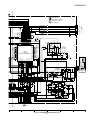
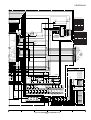
Figure 16 BLOCK DIAGRAM (2/3)
– 16 –
7
BAIS
CD-PC1881V
FL701
FL DISPLAY
Q702
Q703
M
1 2 3 4 ~ 15 16 ~ 25 26 ~ 28
29 ~ 36
37 38 39
MM1
APE MOTOR
Q705
Q706
Q707
TO CD VIDEO
SECTION
S22/DIST4
S21/DIST3
S20/DIST2
S19/DIST1
S18/DIST0
S17
S16
S15
S14
S13
S12
S11
VLOAD
S10
SPRLY
MBUSY
POWER
81
82
83
84
S5 85
S4 86
S3 87
S2 88
S1 89
G11 90
G10 91
G9 92
G8 93
G7 94
G6 95
G5 96
G4 97
G3 98
99
100
UNSWITCH
+B7
MEMORY +B4
BACK UP
M
30 29 28 27 26 25 24 23 22 21 20 19 18 17 16 15 14 13 12 11 10 9 8 7 6 5 4 3 2 1
+B5
PHM1
KEY
SW701~SW721
SW722~SW725
SW728~SW733
XL701
4.19MHz
Q704
M
Q905
1
RESET
IC704 KIA7042AP
3
2
M902
FAN MOTOR
+B4
TO CD VIDEO
SECTION
+B7
IC650
IC651
KIA4558P
OPE AMP.
15
14
13
12
11
10
+B
VDD
AC RLY CON
REC/PLAY
T BIAS
T T1T2
99 G2
100 G1
CLK
CE
DI
DO
+B7
REMOTE
SENSOR
33 KEY IN1
32 KET IN2
31 KEY IN3
RESET
CD DSP RWC
T2 RUN
1
RX701 3
2
IC701
IX0340AW
SYSTEM CONTROL
MICROCOMPUTER
SLDSLD+
FRF
CD DSPRES
CD DSP CQCK
SQOUT
CD DSP COIN
SBUSY
VDD
CD DSP WRQ
+B7
81 S9
82 S8
83 S7
84 S6
51 52 53 54
SPEANA1
SPEANA2
SPEANA3
+B7
MOD
KEY JOG A
KEY JOG B
SMUTE
CMUTE
SRMUTE
51 52 53 54 55 56 57 58 59 60 61 62 63 64 65 66 67 68 69 70 71 72 73 74 75 76 77 78 79 80
50 H/P
49 FPA
48 T1 FAS
47 CAM SW
46 VDD
45 T MOT
44 T SOL
43
42 U/D SW
41 DNO SW
40
39 REMOCON
38 SYS STOP
37 O/C SW
36 PUIN SW
35
34 AVDD
33
32
31
IC702
BU2092F
INPUT/OUTPUT
EXPANDER
18
2
3
4
5
6
7
M901
FAN MOTOR
+B5
IC601
3 NJM4560D
5 OPE AMP.
Q601,Q602
Q603, Q604
JK601
HEADPHONES
1
7
4
SUB WOOFER
VOLUME
VR701
7 IC471
4
KIA4558P
OPE. AMP.
3
SO901
SPEAKER
TERMINALS
RL901
Q904
F903
T3.15A
L 250V
Q907
SUB
WOOFER
18
L-IN 12
R-IN 16
Q401
Q402
IC902
POWER AMP.
STK40724
Q403
Q404
–B
1
7
4 10
5 3
FRONT
9 L-OUT
8 R-OUT
RL902
F902
T3.15A L 250V
FRONT
SPEAKER
20
F802
T5A L 250V
D801
PT801
MAIN POWER
TRANSFORMER
Q906
F901
T3.15A L 250V
CENTER
SPEAKER
+B1
230-240V
VOLTAGE
REGULATOR
+B3
+B4
+B5
+B8
+B2
+12V(ANALOG)
+12V(MOTOR)
+7V(CD)
+5.6V
ZD801
F803
T5A L 250V
D802
SURROUND
SPEAKER
SW801
VOLTAGE
SELECTOR
220V
VOLTAGE
REGULATOR
KIA7812P
3 IC804 1
VOLTAGE
2
REGULATOR
KIA7806P
3 IC805 1
2
F804
T3.15A
L 250V
D803~D806
127V
110V
T.F
3 IC806 1
AN78L05
2 CONSTANT VOLTAGE
REGULATOR
Q801
VOLTAGE
REGULATOR
F805
T1.6A L 250V
D807
~D809
RL801
AC POWER
SUPPLY CORD
REAR IN
CENTER IN
AC 110/127/220/230-240V
50/60Hz
13 9
+B6
Q802
VOLTAGE
REGULATOR
7
1
IC951
6
LA4451
POWER AMP.
11 4
+5V
+B7
CENTER OUT
REAR OUT
UNSWITCH
AN78L05
CONSTANT VOLTAGE
REGULATOR
3 IC803 1
2
D811~D814
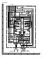
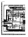
Figure 17 BLOCK DIAGRAM (3/3)
– 17 –
PT802
SUB POWER
TRANSFORMER
CD-PC1881V
TO CD VIDEO PWB
P27 12-C
CNP11
TO TUNER PWB
P21 12-A
CNP303
TO DECK SECTION
P20 2-A
CNS303
1 2 3 4 5 6 CNS11
1 2 3 4 5 6
R-CH
A_GND
L-CH
D_GND
7.3V
+B M_12V
BI401
R372
1K
D_GND
A_GND
REC_R
REC_L
TAPE_R
TAPE_L
A_12V
11 12 13 14 15 16 17 18 19 20 21
M_GND
TUN_R
TUN_L
A_GND
A_12V
DI
CE
DO
CL
D_GND
9 8 7 6 5 4 3 2 1
T1/T2
BIAS
REC_MUTE
A
R371
1K
FFC701
1
CNP502
14
100P
C551
100P
R520
22K
C550
100P
X501
8MHz
49
21
C510
C512
C511
C513
C516
C518
C520
C522
C525
C526
C528
C529
C530
C533
22
23
24
25
25
CNP701
TO DISPLAY PWB
P22 1-E
0.47/50
4.7/50
0.47/50
4.7/50
0.15/50
3.3/50
0.15/50
0.15/50
3.3/50
0.15/50
4.7/50
0.47/50
4.7/50
0.47/50
50 DC_OUT3
51 R_RECT
52 DC_OUT4
49 L_BPF3
53 L_RECT
54 VLR_TH
56
57
58
59
OSC
VDD
A/D
NS
D/A
DC_OUT
DC_OUT
IC501
LV1035M
VLR_2
VCS_2 DOLBY PRO LOGIC
VCS_1
DECORDER
VCS_TH
55 VLR_1
60 L+R_RECT
64 R_BPF3
61 DC_OUT2
L_OUT
R_OUT
S_OUT
D_GND
IREF
62 L-R_RECT
63 DC_OUT1
64
R503
1K
OSC 32
R504
1M
C541
C547
220/16
0.022
30
C514 0.082(ML)
29
C515 0.0033(ML)
31
28
27
26
C517 0.082(ML)
C519 0.47/50
25 C521
24 C523
23C524
22 C527
21
20
DET 19
VCC 18
NC 17
R508
C531
0.33/50
10/50
10/50
10/50
39K
2.2/50
C4
0.22
C
0.18(
C4
0.068(M
C
0.2
C
0.027(M
D516
1N4004S
20
D515
1N4004S
48 47 46 45 44 43 42 41 40 39 38 37 36 35 34 33
DATA
ENABLE
DATA
CLK
VSS
19
C549
VREF
VCC
C_OUT
S_OUT
R_OUT
L_OUT
AC_GND
L_IN
R_IN
S_IN
18
R522 1K
R521 1K
C509
0.1(ML)
17
C501
0.1
(ML)
+B
16
C503 1/50
C504 47/25
C505 0.47/50
13
15
1K
R501
100K
R502 100K
C502 1/50
SPEANA3
SPEANA2
SPEANA1
M_+12V
CLK
CE
DI
DO
Q11
ENA
A_GND
SUB_VOL_IN
SUB_VOL_OUT
1K
L_BPF2
L_BPF1
RT_IN
LT_IN
DC_OUT
C_MODE
GND
NS_BPF1
NS_BPF2
OSC
CLK
C
1K
1K
1K
R518
R519
C507 0.047
C508 680P
R516
R523
R517
TUN SM 10
D_GND 11
D_GND 12
C506 0.022
1
2
3
4
5
6
7
8
9
R_BPF2
R_BPF1
S_DC_OUT
C_DC_OUT
R_DC_OUT
L_DC_OUT
POWER
SR_MUTE
C MUTE
S_MUTE
T1/T2
TAPE BIAS
REC/PLAY
H/PSW
D
+B
+B
+B
B
R505
R506
R507
R509
R512
C532
4.7K
4.7K
1K
4.7K
4.7K
220/16
C563
0.022
0
C
0.0
0.004
C4
1/
C540
10/50
10/50
10/50
10/50
10/50
C539
220/16
C544
220/16
E
C535
C536
C537
C538
C543
0.1(ML)
C534 0.1(ML)
1 2 3 4 5 6 7 8 9 10 11 12 13 14 15 16
C546
0.022
C542
220/16
R510
18K
R511
1K
+B
+B
C545
220P
R513
3.3K
R515
3.3K
R514
330
+B
22K
22K
R443
R442
22/25
22/25
C436
+B
C437
F
D40
DS1SS
0V
0V
2
3
4V 1 Q405
KRC104
G
MAIN PWB-A1(1/2)
H
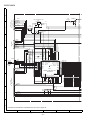
• NOTES ON SCHEMATIC DIAGRAM can be found on page 38.
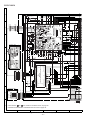
1
2
3
4
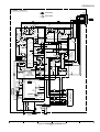
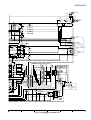
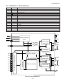
Figure 18 SCHEMATIC DIAGRAM (1/12)
– 18 –
5
6
CD-PC1881V
WB
CNS11
BI401
FM SIGNAL
C448
2.2/50
R401
27K
R404
1.8K
C462
390P
R402
27K
C463
390P
C464
390P
R-CH
C465
0.001
+B
+B
C460
0.022
+B
R483
100K
5
6
C477
100P
C478
0.082
(ML)
4
R480
1.5K
C479
10/50
R627
100
R424
220K
C609
100P
8
R611
560
C603
47/25
C604
47/25
R612
560
C606
100P
2
3
1
5
6
7
R617 C611 R621
1K 10/50 2.7K
R616
1K
4
C657
270P
R654
68K
C659
0.0027
R653
12K
C653
0.0027
D651
DS1SS133
R655
56K
C655
0.0068
R656
470K
CNP501
OPE AMP.
8
7
5
R664 6
220K
C666
2.2/50
D653
DS1SS133
R672
100K
SPEANA2
KIA4558P
2
C656
3
0.0068
C661 0.022 R668
R661 270K 2.2M
5
6
C662
R659
0.022
560K
–B
SPEANA3
R665
100K
C665
2.2/50
IC651
+B
–B
D652
DS1SS133
4
1
2
3
4
1
D654
DS1SS133
8
7
R663
R670
330
330
SPEANA1
R674
100K
C664
2.2/50
OPE AMP.
ZD651
DZ6.2BSC
–15V
FRONT_Lch
A_GND
REAR_OUT
FRONT_Rch
POWER
SUB_WOOF
CENTER_OUT
M_GND
+12V (M)
+12V (A)
D_GND
(CD) 7.3V
CD_GND
A_GND
R657
15K
R662
220K
C667
0.022
+B
+B
R652
33K
C663
0.022
D402
D403
DS1SS133 DS1SS133
0V
0V
2
3
R444
+B
10K
4V 1 Q405
KRC104 M
IC650
KIA4558P
R658
390K
C612 R626
10/50 22
C610
100P
R660
390K
C441
0.001
R651
10K
R437
2.2K
R446
330
R440
2.2K
C440 C439
0.001 0.001
0V Q403
KTC3199 GR
0.7V
0V
C651
270P
R666
2.2M
0V
0V
0V
+B
0V
0V
C627
22/50
R447
330
Q404
KTC3199 GR
R439
2.2K
R445
330
R448
330
R438 0.7V
2.2K
C442
0.001
22K
R441
22/25
22K
R442
C438
22/25
22K
R443
C436
C437
22/25
R618
12K
Q402
Q401
KTC3199 GR KTC3199 GR
R625
22
C605
100P
1
R622
2.7K
R613
100K
C607
47/25
C601
0.047 R601
R623
R605
Q601
(ML) 2.2K
22K
KTC3199 GR 22K
R607
R603
R609
2.2K
2.2K
100K
Q603
C617
C615
KTC3199 GR
0.001
0.001
C616
C618
C602
0.001
0.001
0.047
R608
R604
(ML)
2.2K
2.2K
Q602
R606
R624
R602
Q604
22K KTC3199 GR 22K KTC3199 GR 2.2K
R433
10K
R435
22K
R614
100K
R615
12K
IC601
NJM4560D
OPE AMP.
5
4
3
2
1
CNP601
FW601
5
C613
220/16
C614
0.022
R431 47K
R434 2.2K
+B
R423
220K
+B
IC601
R429 47K
R432 47K
C484
0.001
C481
0.022
R610
100K
R430 47K
R482
100K
C480
47/25
LFIN 33
C421
1/50
C482
2.2/50
R481
1K
7
1 2 3 4 5 6 7 8 9 10 11 12 13 14 15
CNP803
TO POWER PWB
P24 1-E
7
8
9
10
Figure 19 SCHEMATIC DIAGRAM (2/12)
– 19 –
11
12
JK601
HEADPHONES
C621
0.001
L601
100µH
R619
27
R620
27
L
R
R477
27K R478 6.8K
C423
10/50
C427 0.047(ML)
C433 2.2/50
C425 10/50
C476
0.15
(ML)
IC471
KIA4558P
OPE AMP.
1
H/P SW
GND
VSS
LVREF
COUT
LRCOM
CIN
LFOUT
LFCOM
1K
R428
R476
27K
2
3
R475
3.9K
R479
12K
C473
47/25
C429
2.2/50
C431
C432
47/25
C474
0.15
(ML)
8
C472
100P
R425
220K
47/25
1K
1K
R426
R427
C435
47/25
C428
0.047(ML)
C426
10/50
C430
2.2/50
R436
22K
R472
220K
C471
0.047
(ML)
HEADPHONES PWB-A4
LTIN 48
C403
LF1C1 47
0.082(ML)
LF1C2 46
C405
LF1C3 45
0.22/50
C407
LF2C1 44
0.18(ML)
LF2C2 43
C409
LF2C3 42
0.068(ML)
C411
LF3C1 41
0.22/50
LF3C2 40
C415
LF3C3 39
0.015
C413
LF4C1 38
0.027(ML)
LF4C2 37
C417
LF4C3 36
0.0022(ML)
LF5 35
LTOUT 34 C419 0.0047(ML)
17 18 19 20 21 22 23 24 25 26 27 28 29 30 31 32
C434
2.2/50
R471
220K
R474
15K
R484
100K
RTIN
C401
0.047(ML)
R473
100K
R417
R415
R413
R411
R409
C459
100/16
RINVIN1
R5
R4
R3
R2
R1
VDD
L1
L2
L3
L4
L5
LINVIN1
LSELO
RFOUT
RRIN
RRCOM
RROUT
RVREF
VREF
CL
DI
CE
C424
10/50
VIDEO_2
IN
R406
27K
D401
DS1SS133
IC401
LC75396N
AUDIO PROCESSOR
JK401
VIDEO IN
L-CH
R405
27K
64 63 62 61 60 59 58 57 56 55 54 53 52 51 50 49
RF1C1
RF1C2
RF1C3
RF2C1
RF2C2
RF2C3
RF3C1
RF3C2
RF3C3
RF4C1
RF4C2
RF4C3
RF5
14 RTOUT
15 RFIN
16 RFCOM
VIDEO_1
IN
IC471
C445
100P
0.047(ML)
0.047(ML)
0.047(ML)
0.047(ML)
R407
1.8K
R408
1.8K
C475
47/25
C402
0.047(ML)
C404
0.082(ML)
1
2
C406
3
0.22/50
C408
4
0.18(ML)
5
C410
0.068(ML)
6
C412
7
0.22/50
8
C414
0.027(ML)
9
C416
10
0.015
11
C418
0.0022
12
C420
13
0.0047(ML)
L-CH
R419
33K
C455
C453
C451
C449
C457 0.047(ML)
C447
2.2/50
R421
2.7K
1K
1K
1K
1K
1K
C456 0.047(ML)
C458 0.047(ML)
C450 0.047(ML)
C452 0.047(ML)
C454 0.047(ML)
1K
1K
1K
1K
R410 1K
C443
1/50
R412
R414
R416
R418
R420 C446
33K 100P
C444
1/50
+B
C461
390P
R-CH
R422
2.7K
C422
1/50
R403
1.8K
GND
R450
330
R449
330
PLAYBACK SIGNAL
RECORD SIGNAL
CD SIGNAL
CD-PC1881V
TO MAIN SECTION
P18 3-A
16
MAIN PWB-A1(2/2)
C652
0.01
M_GND
A_12V
D_GND
15
14 17
MECHANISM
CHASSIS
BOTTOM
CHASSIS
+B
TAPE_L
BIAS
21 12
A_GND
19
REC_L
REC_R
T1/T2
TAPE_R
A
REC_MUTE
11 13 18
20
+B
+B
R164
4.7K
D101
DS1SS133
R181
220K
D102
DS1SS133
B
C152
47/25
Q126
KRC104 M 0V 1
2
3
0V
11.6V
R162
47K
11.6V
R168
12
0V Q128
KTC3203 Y
R166
47K
0V
11.7V
R158
220
R167
100K
R160
150
(1/2W)
L104
330µH
0V
0V
C151
0.027
(ML)
C150
0.0039(ML)
SWITCHING
Q124
KTA1266 GR
C146
220/16
R123
3.9K
C113 C115 R121
330P 47/25 100K
R119
56
2
C111
330P
R117
1K
IC101
AN7345K
PLAYBACK AND
RECORD/
PLAYBACK AMP.
1
0V
C107
0V
R104
2.2K
0V
0V
CNP101
CNS101
TAPE1
PLAYBACK HEAD R-CH
0V
0V
0V
0.7V
R105
3.3K
0V
CNP102
R107
47K
0V
0V
Q103
2SC2389 SE
C105
180P
M_GND
ERASE
TAPE2_R2
A_GND
TAPE2_R1
TAPE2_L1
TAPE2_L2
1 2 3
PLAYBACK SIGNAL
RECORD SIGNAL
1 2 3 4 5 6 7
CNS102 1 2 3 4 5 6 7
1
2
3
Q103-Q111:SWITCHING
0V
0.001
Q105
2SC2389 SE
C106
180P
TAPE1_R
A_GND
TAPE1_L
C101
0.001
R109
4.7K
R110
4.7K
Q104
2SC2389 SE
R111
10K
Q107
KTC3199 GR
0V
R106
3.3K
C137
0.001
R131
18K
C121 R125
1/50 5.6K
4
3
0.7V
R102
1K
9.3V
8.6V
9.3V
R113
10K
C109
0.047
5 NC
R108
47K
C102
0.001
H
6
C117 C119
0.033 560P
C122 NC 20
R126
1/50
5.6K
21
R124
3.9K
R122
100K C114
22
330P
C116
47/25
23
C112
330P
24
R118
1K
Q109
KTA1266 GR
C135
C127
0.022
R114
10K
G
7
C108
Q108
0.001 KTC3199 GR
R112
10K
F
3.4V 3
1
0V
0V 2
0V 2
R115
4.7K
3 3.4V
1
C139
0.0033
R139 0.068
560
C131
0.001 R135
2.7K
R137
6.8K
C128
3.3/50
8
19
Q111
KRC104 M
Q110
KRC104 M
C153
100/16
C133 R141
22/25 56
Q106
2SC2389 SE
E
9
0.7V
R120
56
18
R145
10K
C141
1/50
R103
2.2K
+B
R174
150
(1/2W)
17
R134
68K
R132
18K
C120
560P
C118
0.033
C134
22/25
112K
+
–
D
16
56K
+
–
C140
0.0033
R142
C136
0.068
56
R140
560
C132
0.001
R136
R138
6.8K
2.7K
–
+
56K
C142
1/50
HICH=CHROME
0V
RIPPLE
ALC 11
Nor/CrO2
15
ALC 10 NC
–
+
112K
0V
R146
10K
14
HICH=T1
0.7V
13 Vcc GND 12
C147
0.022
C145
22/25
R101
1K
R182
220K
R154
10K
Q122
KTC3199 GR
C
0V
0.7V
R153
10K
0.7V
Q121
KTC3199 GR
0V
L-CH
TAPE2
RECORD/
ERASE
HEAD R-CH L-CH PLAYBACK HEAD
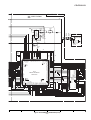
• NOTES ON SCHEMATIC DIAGRAM can be found on page 38.
1
2
3
4
Figure 20 SCHEMATIC DIAGRAM (3/12)
– 20 –
5
6
CD-PC1881V
TUNER PWB-G
FM SIGNAL
CNP303
D GND
1
DO
2
CLK
3
CE
4
DI
5
A+12V
6
A GND
7
L
8
R
9
AM SIGNAL
+B
C396
100/10
R358
8.2K
24
C350
AM OSC OUT
FM IF IN 1
R351
5.6K
VR351
10K(B)
C342
0.022
IC303
LA1832
FM IF DET./
FM MPX./AM IF
Q371
KTA1266 GR
R387
22K
ZD352
DZ3.9BSB
D351
DS1SS133
D352
DS1SS133
C391
47/16
R383
5.6K
R391
Q360 390
KTA1266 GR
0.022
C352
10/16
C351
0.022
3
C385
0.01
R378
82K
IC302
LC72131
PLL(TUNER)
R377
47K
L351
100µH
ST IND 11
12 IF IN
13 SD MO/ST 10
14
TUN_MUTE 9
15 AM IN
8
16
FM IN
17 VDD
R380
1.5K
18 PD
R379
2.2K 19 AIN
B01 7
DO 6
CL 5
DI 4
CE 3
20 AOUT
2
21 VSS
22 X OUT X IN 1
R381
10K
+B
FM MUTE
LEVEL
R392
390
CF351
FM DET.
10.7MHz
C387
0.022
T351
AM MIX OUT 2
23 AM OSC IN
L353
1mH
C343
33P
R393
1K
R352
1
1K
REG 3
22 FM AFC
C354
0.022
CF352 AM IF
2
3
4
21 AM RF IN
0.022
C362
3.3/50
R395 R360
47K 4.7K
AM IF
C363 0.022
GND 5
AM IF IN
18 FM/AM OUT
19 AM LOW CUT
20 VSM
C365 0.022
C364 10/16
C398
100/10
C353
0.022
SD 6
R350
2.7K
C366 0.001
R371
1K
R376
1K
CF351
STEREO 7
C367
1/50
1
2
C399
0.022
R353
270
FM DET 8
3
R398
1.2K
C386
330P
17 MPX VCO
C395
0.022
C355
22P
C356
0.001
VCC 9
X351
456KHz
R384
VOLTAGE 5.6K
REGULATOR
R359
1.8K
C394
47/16 C392
0.001
C393 C380
10/16
1/50
16 MPX IN
R385
5.6K
Q361
KRC107 M
R355
3.3K
PHASE 11
IF OUT 10
R356
1K
C361
L352
100µH
C397
0.022
C368
1/50
+B
C370
1/50
C357
2.2/50
C374
0.033
TP302
ZD351
DZ5.1BSB
R366
10K
15 R-CH OUT
R357
470K
Q354
KTC3199 GR
MUTING
C375
3.3/50
R368
33K
C358
1/50
C372
1/50
C373
0.033
13 MO/ST PHASE 12
(FM/AM)
14 L-CH OUT
+B
+B
R354
3.9K
R362
1.2K
C371 R361
1/50 1.2K
R364
47K
R367
1K
R363
47K
R365
10K
MUTING
Q353
KTC3199 GR
D353
DS1SS133
R382
150
X352
4.5MHz
C381
12P(CH)
CF302
2
C382
15P
(CH)
R372
1K
R373
1K
R374
1K
C384
0.001
+B
1
+B
FM IF
10.7MHz
R375
68
C330 C331
0.047
27P
(UJ)
C332
0.022
R336
1K
C335
560P
C334
27P(UJ)
R344
C347
C341
0.022
0.022
2 GND
T306
AM BAND
COVERAGE fL
AM OSC.
3 F OUT
C337
0.022
C338
0.001
D301
DS1SS133
D302
DS1SS133
+B
4 VT
R345
4.7K
C345
0.022
L342
2.2mH
C321
100/16
R369
C346
0.022
1.2K
5 VCC
6 GND
7 GND
8
GND
D304
DS1SS133
D303
DS1SS133
8 ANT
SO301 AM
ANTENNA
TERMINAL
7
1 IF OUT
470
FE301
FM FRONTEND
AM ANTENNA
R323
68K
C323
0.022
AM
TRACKING fH
T302
VD301
SVC348S
C301
0.001
FM
75 ohms
9
10
Figure 21 SCHEMATIC DIAGRAM (4/12)
– 21 –
11
12
CNS303
P18 12 - A
TO MAIN PWB
CD-PC1881V
+B
A
F
F
F
S22
S21
S20
S19
S18
S17
S16
S15
S14
S13
S12
S11
S10
S09
S08
S07
S06
S05
S04
S03
S02
S01
G11
G10
G09
G08
G07
G06
G05
FL701
FL DISPLAY
TO POWER PWB
P24 1-F
CNP806
R701
100K
R702
100K
Q707
KTC3199 GR
R703
100K
C702
1/50
R789
1K
R728
1K
R729
1K
81 82 83 84 85 86 87 88 89 90 91 92 93 94 95 96
80 S10
1
+B
D722
DS1SS133
+B
R790
D721 33
DS1SS133
C721
47/50
S8
S7
S6
S5
S4
S3
S2
S1
G11
G10
G9
G8
G7
G6
G5
4
Q706
KTC3199 GR
MDCK 3
MBUSY 4
CNS806
UN SW_5V 1
C
Q705
KTC3199 GR
MDO 2
BI703
B
TO CD VIDEOPWB
P28 1-E
CNPV2
1 2 3 4 5 6 7 8 9 10 11 12 13 14 15 16 17 18 19 20 21 22 23 24 25 26 27 28 29 30 31 32
CNSV2
1
MD1 1
79 VLOAD
78 S11
1 VDD
81 S9
77 S12
SW_5V 2
2
AC.RLY-CON 3
3
SP_RLY 4
4
74 S15
VF2 5
5
73 S16
VF1 6
6
72 S17
VLOAD 7
7
76 S13
+B
75 S14
CD
71 S18/DIST0
70 S19/DIST1
69 S20/DIST2
68 S21/DIST3
IC701
IX0340AW
C
SYSTEM CONTROL
MICROCOMPUTER C
67 S22/DIST4
24
25
25
52
51
C703
0.001
R746
8.2K
R725
390
+B
1K
10K
1K
1K
R738
R739
R740
R741
+B
+B
R760
10K
DISPLAY PWB-A2
12V
12V
2+
–
2
1
4 PHM1
PHOTO
INTERRUPTER
3
SWM3
FOOL PROOF
CNPM2
SWM4
F.A.S
SOLM1
SOLENOID
SWM5
CAM
FWM2
Q702
KTA1273 Y
0V
Q703
KTA1271 Y
12V
CNSM1
M
MM1
TAPE MOTOR
TAPE MECHANISM
PWB-F
CNPM1
FWM1
1
2
3
4
5
6
7
8
9
1
2
3
4
5
6
7
8
9
10
11
12
10
11
12
R758
1.2K
BI701
0V
R759 12V
10K
C705
47/25
D716
DS1SS133
MOTOR
1
GND
2
+12V +B
3
T2 RUN
4
FPA
5
T1FAS
6
SOLENOIDO
7
CAM SW
8
H
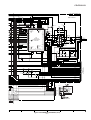
• NOTES ON SCHEMATIC DIAGRAM can be found on page 38.
1
2
3
R755
10K
R756
10K
R757
10K
R752
8.2K
R753
8.2K
R754
8.2K
M_GND
G
1K
1K
C704
0.001
+B
UNSW_5V
+B
50 49 48 47 46 45 44 43 42 41 40 39 38 37 36 35
R716
1K
LED724
SLI342YCJ
LED723
SLI342YCJ
SW_5V
TIMER LED
U/D SW
DNO SW
VSS
REMOCON
SYS STOP
O/C SW
PUIN SW
AVREF
53 T-BIAS
2.2K
1.8K
R713
1K
R715
1K
VR702
VOLUME JOG
A
B
30 T2 RUN
54 T_T1T2
R714
1K
VR701
20K(B)
SUB WOOFER
VOLUME
F
29 TUN SM
4
Figure 22 SCHEMATIC DIAGRAM (5/12)
– 22 –
5
6
R750
10K
23
28 SPEANA
51 AC RLY-CON
55 MDO
R748
10K
22
52 REC/PLAY
56 KEY JOG A
R749
10K
21
57 KEY JOG B
R736
R737
20
58 S MUTE
R747
10K
19
R708
1K
CD
C
59 C MUTE
2.2K
18
E
60 SR MUTE
R734
R735
17
61 HI-CUT
R733
16
62 POWER
LED722
SLI342UCJ
TIMER
15
63 SPRLY
H/P
FPA
T1FAS
CAM SW
VDD
T_MOT
T_SOL
14
64 SP-DET
1K
1K
1K
13
65 MBUSY
R706
1K
R710
1K
R712
22K
R726
8.2K
12
R705
1K
R709
1K
R719
10K
11
R723
10K
R707
1K
R700
10K
TO MAIN PWB
P18 1-D
CNP502
10
R704
1K
R711
1K
POWER
SR.MUTE
C.MUTE
S.MUTE
T_T1/T2
T_BIAS
REC/PLAY
H/PSW
TUN_SM
D_GND
D_GND
SPEANA3
SPEANA2
SPEANA1
M_12V
CLK
CE
DI
DO
Q11
ENA
A_GND
SUB_VOL_OUT
SUB_VOL_IN
D
1
2
3
4
5
6
7
8
9
R730
R731
R732
CNP701
1
R727
8.2K
FFC701
66 DISTOUT
D704
DS1SS133
CD-PC1881V
+B
R788
1K
IC702 LED DRIVER OUTPUT
R781
10K
REMARK FUNCTION COLOUR
F
F
G08
G07
G06
G05
G04
G03
G02
G01
F
C716
47/16
C717
0.022
KEYIN3
KEYIN2
SYS STOP
O/C SW
PUIN SW
AVREF
AVDD
KEYIN1
SQOUT
CD DSP CQCK
CD DSP RES
FRF(DRF)
SLD+
SLD–
8 SPEANA1
AVSS
9 TUN SM
0 T2 RUN SPEANA3
SPEANA2
10
11
12
13
1K
1K
1K
1K
1K
1K
1K
1K
1K
R780
10K
IC702
BU2092F
INPUT/OUTPUT
EXPANDER
R770
R769
17
R768
18
R767
19
R766
20
R765
21
R764
22
R763
23
R762
16
24
LED721 VIDEO
YELLOW
1K
1K
1K
1K
1K
1K
LED721
LED720
LED719
LED718
IC703 LED DRIVER OUTPUT
REMARK
LED717
LED716
LED716,LED717,LED721:SLI342YCJ
LED719,LED720:SLI342YCE
LED718:SLI325YC
+B
C708
18P
+B
1K
1K
1K
1K
1K
1K
1K
1K
1K
1
2
3
4
5
6
7
8
9
25
10
26
11
27
12
28
13
29
14
30
15
FUNCTION
COLOUR
LED701 NIGHT RIDER 1
GREEN
LED702 NIGHT RIDER 2
YELLOW
LED703 NIGHT RIDER 3
ORANGE
LED704 NIGHT RIDER 4
RED
LED705 NIGHT RIDER 5
ORANGE
LED706 NIGHT RIDER 6
YELLOW
LED707 NIGHT RIDER 7
GREEN
LED708 NIGHT RIDER 8
GREEN
LED709 NIGHT RIDER 9
GREEN
LED710 NIGHT RIDER 1 0
GREEN
CNS12
1 RWC(DSP)
2 WRQ(DSP)
3 CO IN(DSP)
4 SQ OUT(DSP)
5 CQ CK(DSP)
6 RES(DSP)
7 DRF(ASP)
8 D_GND
9 SLD+
10 SLD11 PUIN SW
12 OPEN/CLOSE
13 DISC NO
14 UP/DOWN
15 SBUSY
+B
R745
1K
R742 1K
R743 1K
R744 1K
1K
1K
YELLOW
YELLOW
+B
8 37 36 35 34 33 32 31
R740
R741
LED719 TUNER
LED720 TAPE
14
15
YELLOW
OE 17
Q11 16
R782
Q10 15
R783
Q9 14
Q8 13 R784
Q7 12 R785
R786
Q6 11
R787
Q5 10
C707
15P(CH)
4.19MHz
YELLOW
LED718 CD
VDD 18
+B
XL701
YELLOW
LED717 PLAY
CNP12
TO CD VIDEO PWB
P26 7-H
TROL
TER
C709
0.022
C710
1000/6.3
+B
VSS
DATA
CLOCK
LCK
Q0
Q1
Q2
Q3
Q4
BI702
G8
G7
G6
G5
G4
G3
G2
G1
3 94 95 96 97 98 99 100
R779
R778
R777
R776
R775
R774
R773
R772
R771
YELLOW
LED716 STOP
1
2
3
4
R793 1K
LED711
5
R792 1K
LED712
6
LED713
R791 1K
7
LED711~LED713
8
:SLI342YCJ
9
C706
1/50
ENA
DO
VDD
DI
CE
CLK
LCK1
LCK2
CD DSP RWC
RESET
X2
X1
VPP
XT2
CD DSP WRQ
VDD
SBUSY
CD DSP COIN
YELLOW
LED712 NORMAL
LED713 PHANTOM YELLOW
9 30 31 32 33 34 35 36 37 38 39
1
2
3
4
5
6
7
8
9
LED711 BYPASS
SWITCH PWB-A3
RD12
RD13
RD14
RD15
RD16
RD17
RD18
RD19
RD20
820
1.2K
1.5K
1.8K
2.2K
3.3K
3.9K
6.8K
12K
22K
68K
RD02
1.2K
SW701
ON-STAND-BY SW702
BOOK
MARK
RD03
1.5K
SW721
DIGEST
RD04
12K
SW704
SW703 TIMER/
CLOCK SLEEP
6
6
1
1
RD05
6.8K
RD06
12K
RD07
22K
SW705 SW706 SW707
DISC 1 DISC 2 DISC 3
RD09
68K
SW709
OPEN/
CLOSE
SW708
DISC
SKIP
+B
9
10
Figure 23 SCHEMATIC DIAGRAM (6/12)
– 23 –
LED706 SLI342YCB
RS706 470
LED708 L1154GT4
LED707 L1154GT4
18 17 16 15 14 13 12 11 10
IC703
1 2 3 4 5 6 7 8 9
SW714 SW715 SW716 SW717 SW718 SW719 SW720
CD AUDIO PLAYBACK ON SCREEN
SW713 TUNER/ VIDEO TAPE
MODE CONTROL DISPLAY
STOP BAND
FW701
RD01
820
8
RD31
68K
RD11
KEYIN1
7
RD30
22K
SW728 SW729 SW730
SW733
X-BASS/ EQUALI DIMMER SW731 SW732
PHANTOM NORMAL BY PASS
ZER
DEMO
RD10
SW710 SW711 SW712
REWIND RECORD/ MEMORY/
PAUSE
SET
+B
C714
0.022
RD28 +B RD29
6.8K
12K
RS705 470
RD32 MJ705 RD27
RD23 RD24 D718
3.9K
1.5K 1.8K DS1SS133 3.3K 2.2K
RS711
1.5K
RS708 470
RS707 470
C713 C722
0.022 10/50
SW722 SW723 SW724 SW725
FAST TUNING TUNING
FORWARD
DOWN PLAY
UP
KEYIN2
RX701
REMOTE
1 2 3 SENSOR
RS701 470
RS702 470
RS703 470
RS704 470
1
UNSW_5V
3
2
RS710 470
RS709 470
R797
100K
1
LED701
LED702
LED703
LED704
LED705
RD22
1.2K
C712
3.3/50
C719
0.022
C723
0.1/50
Q704
KRC102 M
3
VSS VDD
DATA OE
CLOCK Q11
LCK Q10
Q0
Q9
Q1
Q8
Q2
Q7
Q3
Q6
Q4
Q5
C711
0.01
2
D720
DS1SS133
+B
C718
47/16
R795
47K
IC704
KIA7042AP
RESET
RS712
1.2K
L702
100µH
D717
DS1SS133
RD21
820
KEYIN3
D715
DS1SS133
C715
47/16
+B
R755
10K
R756
10K
R757
10K
R798
D719
100 DS1SS133
SW_5V
L1154GT4
SLI342YCB
SLI342DCB
SLI342UCB
SLI342UCB
R751
3.3K
R750
10K
10K
R799
4.7K
LED710 L1154GT4
LED709 L1154GT4
IC703
BU2092F
INPUT/OUTPUT EXPANDER
+B
11
12
CD-PC1881V
A
IC902
STK40724 POWER AMP.
Q904
KTC3199 GR
R908 68K
C905 220P
R906
10K
R904 68K
C906
1/50
+
C912
100/50
R916
1K
R917 R918
56K 470
C917
47/50
15
16
17
18
C923
47P
C918
47/50
Ch3
Out
19
C926
47P
20
R964
4.7K
14
C915
47P
C916
15P
R965
4.7K
C929
15P
R927 R930 R931
470 56K 1K
R961
39K
C925
47/50
13
C924
15P
12
R924
1K
11
R922 R921
470 22K
10
R923
56K
Ch2
Out
9
C911
100/50
R913
100 Fusible
C934
0.1(ML)
C935
0.1(ML)
R909
1K
C908
0.001
C936
0.1(ML)
C937
0.1(ML)
R937
4.7
R934
4.7
D901
1SS133
R957
1K
C
8
R905
C903 1K
1/50
R907 1K
R903 100K
R901 100K
R902 68K
C902 220P
C901
1/50
7
R912
100
Fusible
C904
10/50
B
NC
NC
6
Ch1
Out
+Vcc
–Vcc
–Vcc
GND
5
Ch1
–
4
C907
10/50
–
3
Ch3
–
2
+
1
Ch2
+
NC
3 Ch
FM SIGNAL
R960
100K
R959
3.9K
C976
22/25
Q908
KTC3199 GR
R980
1K
R979
1K
A_GND
C981
22/25
1
C920
560
CENTER
R981
47K
REAR
C928
47/35
C922
1/50
R926
1K
R928
220
C921 R925
1/50 1K
R929
220
C919
0.0015
–B
D
2 Q903
KRC107 M
3
D902
1SS133
R919 R920
33K 100K
R955
10K
R956
5.6K
14
13
R933
10K
12
11
10
C933
220/35
C927
47/35
R932
18K
H:ON
L:OFF
L
POW
9
8
ZD803
DZ130BSB
-B
D802
TS6B04GM
C801
2200/50
G
R812
Q801
10 KTA1274 Y
VF1
VF2
VLOAD
POWER PWB-C
H
• NOTES ON SCHEMATIC DIAGRAM can be found on page 38.
1
2
3
4
Figure 24 SCHEMATIC DIAGRAM (7/12)
– 24 –
5
6
C812
220/50
R806
2.2K ZD802
C827
0.1
(ML)
47/50
IC805
KIA7806P
VOLTAGE
REGULATOR
47K
C804
47/50
1
2
R804
3
C803
D822
1SS133
1
2
C819
0.1
(ML)
100/35
3
D821
1SS133
CNP806
D804
1N4004S
2
C820
0.1
(ML)
C805
D806
0.047
1N4004S (ML)
C806
D805
0.047
1N4004S
(ML)
D803
1N4004S
ZD801
DZ6.2BSA
IC806
AN78L05
CONSTANT
VOLTAGE
REGULATOR
+B2
1
R801
12K
C802
3
C825
3300/25
VLOAD
VF1
VF2
SP_RLY
AC_RELAY_CORL
SW_5V
UN_SW_5V
C811 DZ300BSB
IC804
KIA7812P
VOLTAGE REGULATOR
C821
47/16
7
6
5
4
3
2
1
+B1
2 1 BI801
POWER
A_GND
CD_GND
CD_+B
D_GND(micom)
A_12V
+B
M_12V
+B
M_GND
D819
1SS133
F
FROM DISPLAY PWB
P22 1-C
CNS806
9
8
7
6
5
4
3
2
CNP803 1
C817
4.7/50
D801
TS6B04GM
R911
22K
R809
10K
10
2 1 BI801
C910
2200/50
C823
0.022
C822
10/50
D818
1SS133
FROM MAIN PWB
P19 8-H
CNP501
E
FRONT_R
REAR
CENTER
SUB_WOOFER
R910
22K
R810 10K
12
11
C909
2200/50
D824
1SS133
13
A_GND
FRONT_L
D823
1SS133
14
C824
1/50
15
–B
C828
0.022
–15V
C829
220/25
R963
820(2W)
1N
CD-PC1881V
R969
120(1/2W)
2 Q907
KRC107 M
1
3
C979
10/50
R966
15K
2
1
1
2
2
M
M901
FAN
MOTOR
R968
1K
R967
68K
R964
4.7K
D909
1SS133
RL901
2
1
C978
47/50
D903
1SS133
65
K
1
CNP804
CNS800
CNP800
CNS804
M902
FAN MOTOR
M
Q905
KTC3199 GR
F903
T3.15A L 250V
RL902
F901
T3.15A L 250V
C936
0.1(ML)
C937
0.1(ML)
F902
T3.15A L 250V
C987
0.1(ML)
C940
0.1(ML)
D908
1SS133
R940
4.7
R937
4.7
3
2
1
–
4
3
1
2
+
IC951
LA4451
POWER AMP.
C942
47/50
+
9
8
D904
1N4004S
3
4
D905
1N4004S
5
6
7
–
C938
47/50
C817
4.7/50
01
6B04GM
R982
270K
R949
4.7
D907
1N4004S
C960
0.1(ML)
C941
0.022
C950
0.1
(ML)
L-CH FRONT
SPEAKER
6 OHMS MIN.
R-CH
SO901
SPEAKER
TERMINALS
CENTER SPEAKER
4 OHMS
L-CH
R-CH
SURROUND
SPEAKER
8 OHMS MIN.
C813
100/50
D809
1N4004S
T.F.
133 C
(251)
PT801
MAIN POWER TRANSFORMER
(251)
CNS802
Q802
KRC107 M
1
3
IC803
AN78L05
CONSTANT
VOLTAGE REGULATOR
3
7
C818
1000/6.3
8
C816
10/16
D811
1N4004S
D810
1SS133
9
AC POWER
SUPPLY CORD(249)
AC 110/127/220/230-240V
50/60Hz
D814
1N4004S
1
2
Q801,Q802: VOLTAGE
REGULATOR
C826
0.0047
1
2
3
4
5
6
7
RL801
1
2
3
4
5
6
7
CNP802
1
2
3
4
5
SW801
VOLTAGE SELECTOR
230-240V
220V
127V
110V
D825
1SS133
CNP805
1
2
3
2
1
2
3
4
5
C815
470/35
D813
1N4004S
D812
1N4004S
C814
0.047
220/50
D808
1N4004S
C812
100/50
D807
1N4004S
F805
T1.6A L 250V
1
2
3
CNP801
CNS801
F803
T5A L 250V
R808
220
C808 C807
0.047 0.047
(ML) (ML)
F802
R807
10K T5A L 250V
C805
0.047
(ML)
C806
0.047
(ML)
2.2K ZD802
SUB WOOFER
6 OHMS
D817
1SS133
C809
F804
0.047
(ML) T3.15A L 250V
C810
0.047
(ML)
C811 DZ300BSB
+
–
R944
4.7
C949
0.1
(ML)
C944
1000/25
D906
1N4004S
802
04GM
1
74 Y
+
–
+
–
C959
0.1(ML)
CNS805
2
1
0
H:ON
L:OFF
C945
2200/25
R942
270
(1/2W)
C943
47/50
+
–
+
–
R941
270
(1/2W)
7M
–
+
Q906
KRC107 M
PT802
SUB POWER
TRANSFORMER
10
Figure 25 SCHEMATIC DIAGRAM (8/12)
– 25 –
11
12
CD-PC1881V
C2
0.01
C32
0.01
C31
220/4
C30
0.1
+B
C1
LASER
47/10
DRIVER
Q1
KTA1504 GR R1
12
R2
1K
C34
0.33/50
C15
0.01
C33
0.47/50
+B
A
C3
1/50
R46
560
R20
1K
2200P
R22
820
R21
1.5K
+
SLOF
S.Q.R
+
-
-
39
38
R27
39K
VREF
12
C17
0.001
R30
6.8K
R33
1.2K
R32
10K
R34
1K
35
34
33
5
6
2 9 3 0 3 1 32
R36
220K
7
R35
220K
C12
0.1
1
TR+
FO+
R37
82K
C35
1/50
4
D1
KDS193
5
FOTR-
8
ACTUATOR
1
2
3
4
5
6
7
8
F
CNS2A
TRTR+
FO+
FOGND
PD
VR
LD
CNP2
1
TR-
2
TR+
2
3
FO+
3
TR-
1
TR+
TO
LD_M+ 4 2
2
FD
LD_M- 4 1
3
FO (GAIN)
4
FO+
5
FO-
6
TR+
7
TR-
8
FO+
9
FO-
C76
0.022
4
FO-
5
GND
5
6
PD
6
12
7
VR
7
13
8
LD
8
14
4
10
1 1 GND
15 SL16 SL+
C36
100/10
1 7 SLD
1 8 VCC1
1 9 STANDBY
C55
100/16
2 0 Vref
21 MUTE
VCC4 40
M- 3 9
M+ 3 8
SOL- 37
SOL+ 3 6
35
34
33
C82
100/10
GND 32
31
C77
100/16
+B
30
29
VCC3 2 8
+B
SP+ 2 7
SP- 2 6
SPO 2 5
(SPN)VCC2 24
SOLD 2 3
SOL- 2 2
3
3
3
3
SW4
PICKUP
IN
2
2
2
2
1
1
1
1
SLIDE
PU-IN
R47
10K
SPSL_+
RWC(DSP)
M
R5
1K
4
SL_CD_PUIN
1
2
3
4
CQ CK(DSP)
4
5
DRF (ASP)
4
RES(DSP)
4
R4
1K
+
SP+
SQ OUT(DSP)
5
CO IN(DSP)
6
5
R3
1K
6
5
SPIN
WRQ(DSP)
CNS3A
6
5
+
CNP3
CNS3B
M
M2
SLED
MOTOR
6
-
CNP3A
G
M1
SPINDLE
MOTOR
+B
+B
C37
0.022
R56
6.8K
CD MOTOR PWB-D
6
7
8
9 1 0 11 1
CNP12
CNS12
P23 12 - D
FROM DISPLAY PWB
H
• The numbers 1 to 12 are waveform numbers shown in page 39.
• NOTES ON SCHEMATIC DIAGRAM can be found on page 38.
1
2
3
4
Figure 26 SCHEMATIC DIAGRAM (9/12)
– 26 –
5
6
OP/CLOS
CNS2B
1
PUIN SW
7
+B
+B
IC3
M63001FP
FOCUS/TRACKING/SPIN/SLED DRIVER
6
SLD-
3
SLD+
2
E
Q55
KRC102 S
3
37
TGL
C21
0.0033
R38
C23
0.0027 470
36
JP+
JP-
SL+
SL-
SLD
SLEO
SP-
R31
1.2K
REF
+
C16
0.0047
R25
1.5K
SPO
REF
R26
82K
27 2 8
-
1
3
40
CV-
TES
R54
10K
R43
56K
41
SLOF
HFL
1
3
2
Q57
KRC102 S
CL
CLK
CE
FSS
DRF
VCC2
REF1
DAT
SLOF
SLOF
4
OR
-
24 2 5 2 6
C14
0.01
R24
47K
-
FE1
REF
SP
AGND
2 0 21 2 2 2 3
C13
330P
R23
10K
10
TOFF
18 19
1
R6
15K
R19
1K
CV+
JP+
C25
27P(CH)
R39
1K
42
JP-
+
REF
REF
+
-
17
R40
5.6K
2
D_GND
1
+
R42
47K
43
HF
TP1
C19
1/50
F
GEN
REF
RFSM
RF
C20
47/10
2
REF+
-
C11
0.1
R18
15K
REF
JP
CV+
C18
0.47/50
B
R17
33K
FSTA
56K
3
Q56
KTC3876 Y
4
A
1M
E
1M
D
5
2200P
K
TO +
1 6 FD
GL
REF
+
JPCLO
FSC
FOSTA
GEN
+
- REF
FE-
15
SLC
SLOF
JP
+ REF
TO
FE
14
C26
0.033
8/12CM
REF CV-
THD
+
JP
REF
THDL
GEN
44
R44
33K
RFS-
+
TGL1
SPI
11
12 TDC10
180P
TD
13
45
VCC
+
-
TA
8
1/16
PHI
9 SCI
C8
1 0 TH
0.068
R16
3.3K
SLI
+
C7
0.1
R15
12K
FSTA
+
!
-
+
R14
27K
REF
REF
R12
100
C9
0.047
+
-+
8 TESI
C6
0.033
R11
6.8K
R13
1K
TE
REF
C5
0.033
R29
7
R10
2.2K
REF
CL
LASER
IC1
LA9241M
SERVO AMP.
VCR
-
DRF
VCR
SPG
C54
0.001
C
REF
DGND
TOSTA
2FREQ
C28
0.1
46
FSC
FOSTA
+
-
TB
TE-
HFL
CE
+
6
DEF
+
48
47
C29
4.7/25
EFBAL
VCR
-
REF
+
R9
100K
VCR
10K
5
R8
15K
REF
R28
C4
0.1
PICKUP UNIT
-
REF
+
-
NC
TBC
LATOH
F
+
E
4
+
F
CNP1
BHI
+
3
E
FA-
5
5
FE1
-
R45
4.7K
2
+
REF
FA
4
RF
+
+
3
4
1
2
FIN1
-
3
2
F
FIN2
REF
REF
3
B
B
1
-
A
9
A
FD-
2
-
1
2
-
1
4
VR
5 5 5 4 5 3 52 5 1 5 0 4 9
56
57
58
LF2
-
K
5
E
59
-
B
CNS1A
K
61 6 0
62
LDS LDO
-
DEF
CNS1B
VCC1
64 63
CD-PC1881V
CD VIDEO PWB-B (1/2)
+B
R41
47K
R57 1K
R58 1K
R59 1K
3
14 CLV1 5 V/P
11
IC2
LC78631E
SERVO/SIGNAL
CONTROL
1 7 TEST3
1 8 P4
19 HFL
20 TES
21 PCK
RV64
8.2K
RV66
8.2K
RVSS 5 5
XVDD 5 4
XOUT 52
XVSS 5 1
RV65
8.2K
LVSS 5 0
LCHN 4 9
LCHP 4 8
38 P0/DFCK
39 P1/DFIN
CV27
560P
LVDD 4 7
MUTEL 4 6
C2F 4 5
CONT1
DACKO
DFLRO
LRCKO
P5
SLDEMPH_B
JPSLD+
JP+
VDD
CV34 RV76
10/16 2.2K
RV72
10K
5
CV28
180P
CV29
180P
3
RV69
6.8K
RV73
10K
2
R68
1K
+
8
IC4
CV32
0.1
+
4
-
1
R-CH
A_GND
RV78
47K
CV36
47P(CH)
L-CH
D-GND
CV37
47P
(CH)
CV35
10/16
+B +7V
RV79
47K
+12V
+B
1
2
P18 6 - A
3
4
CNS11
5
FROM
MAIN PWB
6
CNP11
RV71
6.8K
RV75
10K
IC4
BA4558F
OPE AMP.
CV31
180P
1K
+B
1K
Q52
KTC3265Y
1K
C50
0.022
R69
1K
Q53
KTC3265 Y
R66
220
R64
22
L61
0.82µH
+B
+B
7
RV77
2.2K
+B
R67
1K
-
6
RV67
8.2K
23 TOFF
TEST4
THLD
RV74
10K
CV26
560P
RV70
6.8K +B
R78
ROMXA 44
40 P2
R77
CK2 4 3
2 2 FSEQ 24 TGL
R76
LRSY 4 2
23
P3/DFLR 41 R75
24
1K
25 26 27 28 29 30 31 32 3 3 34 35 36 37 38 39 40
C24
220P
CV30
180P
RV68
6.8K
XIN 5 3
1 6 TEST2
C22
220P
X1
16.93MHz
RVDD 5 8
RCHP 5 7
RCHN 5 6
1 0 VSS
1 1 EFMI
CV38
100/10
RV82
27K
PW 6 2
EFLG 6 1
SBSY 6 0
MUTER 59
8 TAI
9 EFMO
12 TEST1
1 3 CLV+
WRQ
SQOUT
RWC
RES
COIN
CQCK
16M
FAST
CONT2
65 DOUT
66 FSX
5 FR
6 AVDD
7 ISET
C27
0.0039
C40
0.1
1
79 DEFI
80 VCOC
3
SBCK 6 4
SFSY 6 3
+B
+B
+B
R70
100
C59
100/10
ZD61
Z02W5.6Y
+B
C75
0.001
R53
470
2 PD02
3 PDO1
4 AVSS
+5V
R52
68K
R54
10K
RV81
47K
C51
100/10
3
2
R50
680
1 VPDO
CS
1
8 0 7 9 7 8 77 7 6 7 5 74 7 3 7 2 7 1 7 0 6 9 6 8 6 7 6 6 6 5
R51
3.3M
C39
0.01
2
RV83
100
Q54
KTC3876 Y
1
TEST5
4.2M
C41
4.7/25
2
R49
100
CV33
330/6.3
C58
220P
R48
3.3M
+B
+B
C52
100/10
R60
1K
C48
100P
C46
100P
+B
C38
0.01
C49
100P
R61 1K
R62 1K
R63 1K
+B
C44
100P
C45
100P
C47
100P
CD SIGNAL
+B
+B
+B
C56
0.022
+B
+B
+7V
+12V(A)
+B
6
AUDO
+B
7
AUBCK
8
GND(D)
9
C2PO
10
DATAD
R82
1.5K
R80
2.2K
D92
KDS193
D93
KDS193
3
2
Q51
KRC102S
11
BCLK
12
LRCK
R81
2.2K
R83
1.5K
13
LD_M+
14
LD_M-
R91
1K
15
MO_SPEED
16
SOL
1
R84
2.2K
R90
220
17
+5V
+B
18
GND(A)
19
RESET
20
AUCLK
21
SBUSY
22
D91
KDS193
SOLM2
SOLENOID
LOCK
C37
0.022
CNP10
M+
M-
SOL+
SOLM+
MGND(D)
OPEN CLOSE
DISC NO.
GND(D)
MECHA UP
GND(D)
CNS10
BIM5
1
2
3
4
5
6
7
8
9
10
SBUSY
UP/DOWN
DISC NO.
OP/CLOS
PUIN SW
SLD-
SLD+
D_GND
DRF (ASP)
CD_D_NO
1
2
3
4
5
6
7
8
9
10
1
2
3
4
5
6
7
8
M
M3
T/T
UP/DOWN
LOADING
SW1
OPEN
CLOSE
SW2
MECHA UP
1
2
9 1 0 1 1 12 1 3 14 1 5
+
CD TRAY PWB -E
CNS5
6
-
1
2
SW3
DISC NUMBER
CNS12
P23 12 - D
M DISPLAY PWB
7
8
9
10
Figure 27 SCHEMATIC DIAGRAM (10/12)
– 27 –
11
4
5
AULRCK
12
P28 1 - B, 1 - F
TO VIDEO SECTION
+B
CD-PC1881V
B
P27 12 - E
TO CD SECTION
A
10
13
12
11
4
9
5
19
C2PO
LRCK
BCLK
DATAD
+7V
VOLTAGE REGULATOR
QV1
UPC29M33 T
+12V(A)
+B
QV4
KTA1298 Y
RV84
4.7K
+B
CV1
47/6.3
CV3
0.22
+B
GND(D)
DV5
KDS193
RV85
10K
QV2
KTA1298 Y
+B
RV1
10K
GND(A)
RV2
4.7K
DV4
KDS193 2
QV3
KRC104 S
3
1
+12V(A)
C
RV16 1.2K
RV17 1.2K
RV6 1K
CV4
47/6.3
GND(D)
AUDSW
SDATA
SCK
STROBE
KEYCON
RV10 1K
RV9 1K
RV8 1K
RV7 1K
TEST POINT
GND(A)
RV18 1K
18
CV2
0.022
LD_MLD_M+
SOL
MO_SPEED
20
22
RESET
SBUSY
RV36
RV35
RV34
RV33
RV32
RV31
RV30
RV29
RV28
RV27
RV26
RV25
RV24
270
270
270
270
270
270
270
270
270
270
270
270
270
RV23
270
RV22 1K
RV21 270
RV20
1K
F
P27 12 - E
TO CD SECTION
AVREF
AVDD
RESET
XT2
XT1
IC
X2
X1
VSS1
INT
SBUSY
15
14
17
16
+5V
16 15 14 13 12 11 10 9 8 7 6 5 4 3 2 1
HD7 64
17
MDI
HD6 63
18
HD5 62
19 MDO
HD4 61
20 MCK
HD3 60
21
1 VOCAL CANCEL HD2
59
22 MBUSY
HD1 58
23
VDD1
HD0
24
57
ICV1
HA 56
25 AVSS
26
MPEG CONTROLLER HDAK 55
HWR 54
27
IX0313AW
HRD 53
28
HCS 52
29
MPEG RESET 51
30
31
50
32
49
33 3435 36 37 38 3940 41 42 43 44 45 46 47 48
3.9K
3.9K
3.9K
3.9K
3.9K
3.9K
3.9K
3.9K
3.9K
3.9K
3.9K
3.9K
3.9K
3.9K
E
1K
1K
1K
10K
1K
10K
RV37
RV38
RV39
RV40
RV41
RV42
RV43
RV44
RV45
RV46
RV47
RV48
RV49
RV50
RV12
RV13
RV14
RV93
RV15
RV94
CD-SOL
KEY CONT.
K_C_STRB
K_C_CLK
K_C_DATA
MDI
MDO
MDCK
MBUSY
MO_SPEED
CD-LD MCD-LD M+
VDD0
VSS0
FROM
DISPLAY
PWB
1
2
3
4
RV86
4.7K
PWR_MPEG
CNPV2
P22 1 - B
CNSV2
RV11
1K
RV87
2.2K RV89
2.2K RV88
2.2K
D
CV5 0.022
RV19 1K
XV1
4.19MHz
CV
47
21
8
6
7
G
RV58
3.9K
AUCLK
AUBCK
AULRCK
AUDO
RV57
3.9K
RV56
3.9K
RV59
3.9K
H
• NOTES ON SCHEMATIC DIAGRAM can be found on page 38.
1
2
3
4
Figure 28 SCHEMATIC DIAGRAM (11/12)
– 28 –
5
6
CD-PC1881V
CD VIDEO PWB-B (2/2)
VIDEO SIGNAL
+B
+B
1
CV17
0.01
CV40
22/6.3
CV41
4.7/25
7
8
RV63
150
1
2
RV96
33K
CNSV3B
2
5
6
1
2
1
2
CNPV4
3
RV62
150
CNSV3A
4
CV39
100/10
CNPV3
ICV4
VIDEO OPERATION AMP.
NJM2267M
RV95
6.8K
JKV1
VIDEO OUT
1
2
CV18
100/10
DV1
1SS133
RV61
100K
CV15
4.7/25
JACK PWB-G
DV2
1SS133
CHASIS
GND
RV60
100
+B
HSYNC
NSYNC
CSYNC
VCLK
CV24
0.022
CV21
0.022
CV20
0.022
CV10
47/6.3
+B
+B
CV12
0.022
CV23
47/6.3
7
8
9
10
Figure 29 SCHEMATIC DIAGRAM (12/12)
– 29 –
11
1 VDD
2 DQ0
3 DQ1
4 DQ2
5 DQ3
6 VDD
7 DQ4
8 DQ5
9 DQ6
10 DQ7
11
12
13 WE
14 RAS
15
16 A0
17 A1
18 A2
19 A3
20 VDD
40
39
38
37
36
35
34
33
32
31
30
LCAS 29
UCAS 28
OE 27
A8 26
A7 25
A6 24
A5 23
A4 22
VSS 21
VSS
DQ15
DQ14
DQ13
DQ12
VSS
DQ11
DQ10
DQ9
DQ8
ICV3 DRAM
SDM4260C
VDD
AGND
VOUT3
CBP3
VOUT2
CBP2
VOUT1
CBP1
AVDD
VDD
HDAK
INT
GND
AUCLK
AUBCK
AULRCK
AUEMPH
AUDO
VDD
GND
MA8
MA7
MA6
MA5
MA4
GND
VDD
MA3
MA2
MA1
MA0
RV49 3.9K
RV50 3.9K
CDBCK
CDLRCK
CDEMPH
CDC2PO
GND
100 99 98 97 96 95 94 93 92 91 90 89 88 87 86 85 84 83 82 81 80 79 78 77 76
VDD 75
1 VDD
GND 74
HD7
2
MD8 73
3 HD6
MD9 72
4 HD5
GND
7
6
MD10
71
5 HD4
MD11 70
6 GND 99 CDI
GND 69
7 HD3 100 GND
MD12 68
8 HD2
MD13 67
HD1
9
CV6
MD14 66
HD0
27P(CH) 10
MD15 65
11 GND
GND 64
GND
12
XV2
VDD 63
ICV2
13 X1
27MHz
MD0 62
14 X2
MPEG DECODER
CV7
MD1 61
VDD
15
D61012GC
27P
MD2 60
16 CKSEL
(CH)
MD3
59
17 VDD
MD4 58
18 GND
GND 57
19 HCS
MD5 56
26 GND
20 HRD
49 MRAS
MD6 55
21 HWR 27 RESET
50 GND
MD7 54
22 HA
MCAS 53
23 HSELX
MWE
52
24 HSELA
VDD 51
25 VDD
CV9
0.022
26 27 28 29 30 31 32 33 3435 36 37 38 3940 41 42 43 44 45 46 47 48 49 50
CV22
47/6.3
CV19
0.022
CV13
0.1
CV14
0.1
CV11
0.022
CV16
0.1
+B
CV25
0.022
12
CD-PC1881V
VOLTAGE
IC1
PIN
NO.
1
2
3
4
5
6
7
8
9
10
11
12
13
14
15
16
17
18
19
20
21
22
23
24
25
26
27
28
29
30
31
32
33
34
35
36
37
38
39
40
41
42
43
44
45
46
47
48
49
50
51
52
53
54
55
56
57
58
59
60
61
62
63
64
VOLTAGE
2.5V
2.5V
2.5V
2.5V
2.5V
2.5V
2.5V
2.5V
2.5V
2.5V
2.5V
2.5V
2.5V
2.5V
2.5V
2.5V
2.5V
2.5V
2.5V
2.5V
2.5V
0V
2.5V
2.5V
2.5V
2.5V
2.5V
2.5V
2.5V
2.3V
2.3V
0V
0V
5.0V
5.0V
0V
0V
5.0V
0V
0V
1.6V
2.4V
2.4V
2.4V
0V
2.5V
2.5V
0V
0V
2.4V
4.6V
4.6V
0V
0V
5.0V
5.0V
2.5V
2.5V
1.0V
1.0V
2.2V
4.2V
0V
5.0V
VOLTAGE
PIN
NO.
1
2
3
4
5
6
7
8
VOLTAGE
IC902
PIN
NO.
1
2
3
4
5
6
7
8
9
10
11
12
13
14
15
16
17
18
19
20
VOLTAGE
0V
0V
-27.5V
-27.5V
-27.5V
0V
0V
0V
0V
-25.8V
26.0V
-0.15V
-0.15V
-24.6V
-0.1V
-0.1V
-0.1V
-0.1V
-27.5V
0V
0V
0V
0V
0V
1.9V
5.0V
0V
0V
2.5V
2.4V
0V
0V
0V
5.0V
0V
0V
5.0V
5.0V
0V
0V
2.5V
0V
5.0V
0V
0V
0V
0V
0V
0V
5.0V
2.5V
0V
0V
0V
5.0V
4.6V
1.9V
0V
0V
1.9V
4.6V
5.0V
5.0V
2.1V
2.1V
0V
0.1V
2.3V
0V
2.5V
0V
2.5V
0V
0V
0V
4.6V
4.6V
4.7V
0V
2.3V
2.3V
0V
0V
0V
IC4
2.6V
2.6V
2.6V
0V
2.4V
2.4V
2.6V
5.0V
FE301
PIN
NO.
1
2
3
4
5
6
7
8
VOLTAGE
0V (0V)
0V (0V)
2.6V (0V)
2V (1.1V)
8.5V (0V)
0V (0V)
0V (0V)
0V (0V)
PIN
NO.
1
2
3
4
5
6
7
8
9
10
11
12
13
14
15
16
17
18
19
20
21
22
23
24
25
26
27
28
29
30
31
32
33
34
35
36
37
38
39
40
41
42
VOLTAGE
2.5V
2.6V
2.9V
3.3V
3.3V
3.3V
3.3V
0V
0V
0V
0V
0V
0V
0V
3.3V
3.3V
3.0V
7.2V
5.0V
2.5V
0V
0V
0V
7.2V
2.5V
3.3V
3.3V
11.2V
0V
0V
0V
0V
0V
0V
0V
5.3V
5.3V
3.3V
3.3V
7.2V
0.1V
0.1V
IC101
PIN
NO.
1
2
3
4
5
6
7
8
9
10
11
12
13
14
15
16
17
18
19
20
21
22
23
24
VOLTAGE
0V (0V)
0V (0V)
0.5V (0.5V)
4.3V (4.3V)
0.2V (0.3V)
1.3V (1.3V)
0V (0V)
0.6V (0.6V)
4.1V (4.1V)
4.0V (4.0V)
0V (0V)
0V (0V)
8.1V (8.1V)
4.8V (4.8V)
0V (0V)
4.1V (4.1V)
0.6V (0.6V)
0V (0V)
2.5V (2.6V)
0.2V (0.3V)
4.3V (4.3V)
0.5V (0.5V)
0V (0V)
0V (0V)
IC471
PIN
NO.
1
2
3
4
5
6
7
8
VOLTAGE
5.6V
5.6V
5.5V
0V
5.6V
5.6V
5.6V
11.1V
IC601
PIN
NO.
1
2
3
4
5
6
7
8
VOLTAGE
5.6V
5.6V
5.5V
0V
5.5V
5.6V
5.6V
11.1V
IC302
IC301
IC3
IC2
PIN
NO.
1
2
3
4
5
6
7
8
9
10
11
12
13
14
15
16
17
18
19
20
21
22
23
24
25
26
27
28
29
30
31
32
33
34
35
36
37
38
39
40
41
42
43
44
45
46
47
48
49
50
51
52
53
54
55
56
57
58
59
60
61
62
63
64
PIN
NO.
1
2
3
4
5
6
7
8
9
VOLTAGE
0.9V (0V)
1.6V (0V)
6.0V (0.4V)
1.6V (0V)
0V (0V)
6.0V (0.3V)
5.2V (0.2V)
5.9V (0.3V)
6.0V (0.3V)
IC650
PIN
NO.
1
2
3
4
5
6
7
8
VOLTAGE
0.12V
0.1V
0.13V
–11.2V
0.1V
0.1V
0.1V
6.2V
PIN
NO.
1
2
3
4
5
6
7
8
9
10
11
12
13
14
15
16
17
18
19
20
21
22
IC303
VOLTAGE
2.5V (2.5V)
0V (0V)
0V (0V)
0V (0V)
4.5V (4.5V)
4.5V (4.5V)
0.2V (11.9V)
0V (0V)
0V (0V)
0V (0V)
5.1V (5.1V)
0V (0V)
0V (0V)
0V (0V)
0V (2.5V)
2.5V (0V)
5.1V (5.1V)
0.9V (0.9V)
0.9V (0.9V)
1.3V (1.1V)
0V (0V)
2.5V (2.5V)
IC651
PIN
NO.
1
2
3
4
5
6
7
8
IC702
PIN
NO.
1
2
3
4
5
6
7
8
9
10
11
12
13
14
15
16
17
18
VOLTAGE
0V
0V
0.2V
0V
9.8V
9.8V
9.8V
9.9V
9.8V
9.8V
9.8V
0.5V
0.5V
0.5V
9.8V
9.8V
0V
5.0V
IC703
PIN
NO.
1
2
3
4
5
6
7
8
9
10
11
12
13
14
15
16
17
18
VOLTAGE
0V
0V
0.2V
0V
9.8V
9.8V
9.8V
9.9V
9.8V
9.8V
9.8V
0.5V
0.5V
0.5V
9.8V
9.8V
0V
5.0V
VOLTAGE
1.6V (1.6V)
1.6V (1.6V)
7.1V (8.1V)
0.2V (0.6V)
1.6V (1.6V)
0V (0V)
5.1V (5.1V)
0V (0V)
2.3V (2.3V)
2.3V (2.3V)
6.4V (8.1V)
0.9V (0.9V)
1.1V (2.1V)
1.8V (1.6V)
2.2V (1.3V)
1.7V (1.7V)
1.6V (1.7V)
1.6V (1.6V)
0.4V (0.5V)
7.1V (8.1V)
7.1V (8.1V)
1.7V (1.7V)
1.7V (1.7V)
1.7V (1.7V)
IC401
VOLTAGE
0.2V
0.2V
0.2V
–9.8V
0.2V
0.2V
0.2V
6.2V
PIN
NO.
1
2
3
4
5
6
7
8
9
10
11
12
13
14
15
16
17
18
19
20
21
22
23
24
PIN
NO.
1
2
3
4
5
6
7
8
9
10
11
12
13
14
15
16
17
18
19
20
21
22
23
24
25
26
27
28
29
30
31
32
33
34
35
36
37
38
39
40
41
42
43
44
45
46
47
48
49
50
51
52
53
54
55
56
57
58
59
60
61
62
63
64
VOLTAGE
5.0V
5.0V
4.9V
4.8V
5.0V
4.9V
4.8V
5.0V
4.8V
4.8V
5.0V
4.9V
4.8V
5.0V
4.9V
5.0V
5.0V
4.9V
5.0V
5.0V
5.0V
5.0V
4.0V
-0.1V
-0.1V
0V
5.0V
5.0V
5.0V
4.9V
5.0V
5.0V
4.9V
5.0V
4.8V
4.9V
5.0V
4.8V
4.9V
5.0V
4.8V
4.9V
5.0V
4.8V
4.9V
5.0V
5.0V
4.9V
5.0V
5.0V
5.0V
5.0V
5.0V
5.0V
5.0V
10.0V
5.0V
5.0V
5.0V
5.0V
5.0V
5.0V
5.0V
4.9V
IC501
PIN
NO.
1
2
3
4
5
6
7
8
9
10
11
12
13
14
15
16
17
18
19
20
21
22
23
24
25
26
27
28
29
30
31
32
33
34
35
36
37
38
39
40
41
42
43
44
45
46
47
48
49
50
51
52
53
54
55
56
57
58
59
60
61
62
63
64
– 30 –
VOLTAGE
4.7V
4.7V
4.7V
4.7V
4.7V
4.7V
4.7V
9.4V
4.7V
4.7V
4.7V
4.7V
4.7V
4.7V
4.7V
4.7V
0V
9.4V
2.5V
0.6V
-0.1V
4.7V
4.7V
4.7V
4.7V
4.7V
4.7V
4.7V
4.7V
4.7V
5.0V
2.3V
-0.1V
4.0V
-0.1V
3.6V
-0.1V
4.0V
0V
4.7V
4.8V
0V
4.7V
4.7V
4.7V
4.7V
4.7V
4.7V
4.7V
4.7V
5.4V
4.7V
5.4V
4.6V
4.6V
4.6V
3.7V
3.5V
3.4V
5.4V
4.8V
5.4V
4.7V
4.7V
PIN
NO.
1
2
3
4
5
6
7
8
9
10
11
12
13
14
15
16
17
18
19
20
21
22
23
24
25
26
27
28
29
30
31
32
33
34
35
36
37
38
39
40
41
42
43
44
45
46
47
48
49
50
IC701
PIN
NO.
51
52
53
54
55
56
57
58
59
60
61
62
63
64
65
66
67
68
69
70
71
72
73
74
75
76
77
78
79
80
81
82
83
84
85
86
87
88
89
90
91
92
93
94
95
96
97
98
99
100
VOLTAGE
4.7V
4.7V
4.6V
0V
0V
0V
0V
0V
0V
4.7V
2.2V
2.0V
0V
4.6V
0V
4.7V
0V
4.7V
0V
4.7V
4.7V
0V
0V
0V
0V
0V
0V
0V
0V
0.9V
4.9V
4.9V
4.9V
4.7V
4.9V
4.6V
4.6V
4.9V
4.9V
0V
0V
4.6V
3.5V
11.9V
11.9V
4.4V
4.6V
0V
4.6V
0V
VOLTAGE
5.0V
0V
0V
0V
0V
5.0V
0V
0V
0V
0.5V
0V
0V
3.3V
2.6V
0V
0.5V
0.5V
1.0V
2.7V
5.0V
0V
1.5V
1.5V
1.5V
1.5V
1.5V
0V
2.5V
2.5V
0V
0V
0V
0V
0V
0V
0V
0V
0V
0.5V
0V
4.7V
0V
0V
4.7V
0V
0V
4.6V
4.6V
4.6V
4.6V
0V
4.7V
4.7V
5.0V
4.9V
–27.0V
–27.0V
–27.0V
–27.0V
–27.0V
–27.0V
–27.0V
0V
0V
-26.0V
–22.0V
–24.0V
0V
–27.0V
–24.0V
–24.0V
–24.0V
0V
0V
–21.0V
0V
0V
0V
0V
–24.0V
0V
–24.0V
0V
–24.0V
0V
–24.0V
–24.0V
–24.0V
–24.0V
–24.0V
QV1
ICV3
PIN
NO.
1
2
3
4
5
6
7
8
9
10
11
12
13
14
15
16
17
18
19
20
21
22
23
24
25
26
27
28
29
30
31
32
33
34
35
36
37
38
39
40
VOLTAGE
PIN
NO.
1
2
3
VOLTAGE
6.8V
0V
3.3V
ICV4
PIN
NO.
1
2
3
4
5
6
7
8
VOLTAGE
2.0V
0V
2.0V
2.0V
2.2V
2.2V
5.0V
2.2V
IC803
PIN
NO.
1
2
3
VOLTAGE
7.1V
0.6V
5.5V
IC804
PIN
NO.
1
2
3
VOLTAGE
17.0V
0V
12.0V
VOLTAGE
PIN
NO.
1
2
3
4
5
6
7
8
9
10
11
12
13
14
15
16
17
18
19
20
21
22
23
24
25
26
27
28
29
30
31
32
33
34
35
36
37
38
39
40
41
42
43
44
45
46
47
48
49
50
VOLTAGE
IC805
PIN
NO.
1
2
3
VOLTAGE
17.0V
1.3V
7.3V
ICV1
PIN
NO.
33
34
35
36
37
38
39
40
41
42
43
44
45
46
47
48
49
50
51
52
53
54
55
56
57
58
59
60
61
62
63
64
PIN
NO.
1
2
3
4
5
6
7
8
9
10
11
12
13
14
15
16
17
18
19
20
21
22
23
24
25
26
27
28
29
30
31
32
0V
0V
5.0V
0V
5.0V
1.5V
0V
0V
0V
5.0V
0.1V
0V
0.1V
0V
5.0V
0V
0V
0V
0V
0.5V
0V
0V
0V
5.0V
0V
0V
0V
0V
0V
0V
0V
0V
3.3V
3.3V
3.3V
3.3V
3.3V
0V
3.3V
3.3V
3.3V
3.3V
0V
0V
1.5V
1.5V
3.3V
3.3V
3.3V
0V
0.5V
5.0V
5.0V
1.5V
3.3V
3.3V
3.3V
0V
5.0V
1.0V
0V
0V
2.5V
2.0V
2.5V
0V
0V
3.3V
0V
1.5V
1.5V
1.5V
1.5V
1.5V
0V
3.3V
2.5V
1.0V
0.5V
0.5V
2.6V
0V
ICV2
PIN
NO.
51
52
53
54
55
56
57
58
59
60
61
62
63
64
65
66
67
68
69
70
71
72
73
74
75
76
77
78
79
80
81
82
83
84
85
86
87
88
89
90
91
92
93
94
95
96
97
98
99
100
IC806
PIN
NO.
1
2
3
VOLTAGE
12.0V
1.3V
4.9V
VOLTAGE
0V
5.0V
5.0V
5.0V
0V
5.0V
0V
0V
3.0V
0V
0V
5.0V
0V
0V
0V
0V
0V
0V
5.0V
0V
5.0V
5.0V
0.1V
1.2V
3.3V
3.3V
3.3V
3.3V
3.3V
0V
3.3V
2.8V
VOLTAGE
3.3V
3.3V
2.5V
0.5V
0V
0V
0V
0V
0V
0V
0V
0V
3.3V
0V
3.3V
0V
0V
0V
0V
0V
0V
0V
0V
0V
3.3V
0V
1.5V
0V
0V
0V
3.3V
3.3V
3.3V
3.3V
1.0V
1.5V
0V
0V
0V
0V
0V
3.3V
0V
0V
5.0V
0V
2.5V
2.5V
1.5V
0V
CD-PC1881V
SO301
ANTENNA
TERMINAL
FM 75 Ohms
GND
AM
A
D304
X352
C381
C392
R372
IC302
R371
C387
C380
R376
VD301
C385
C386
R336
R344
C341
R398
B
C
E
C331
C335
C337
C384
Q360
R323
L353
R358
R385
C351 CF302
C342
CF352
C352
T351
B C E
C395
ZD351
TO MAIN PWB
CNS303
P32 1 - E
R367
1
2
3
4
5
6
7
8
9
C375
R368
D353
R363
CNP303
C355
R354
R353
C399
R364
C396
R365
G
R362
Q353
Q354
R392
C354
C356 C370
CF351
R361
B C E
Q361
R393
C372
C371
L352
R352 C398
X351
C373
2 1
R391
3 2 1
C368
C374
3
C391
R359
F
IC303
C353 C366
R356
R357
R395
R355
C358
C367
R350
C365
C350
24
1
23 R351 2
22
3
4
21
20
5
19
6
18
7
17
8
16
9
15
10
14
11
13
12
1
2
3
C357
C343
C361
C363
C364
R387
R384
R383
FM MUTE
LEVEL
ZD352
B C E
VR351
C362
D351
C334
R382
D
R377
R375
T306
C332
D352
C
4
R345
3
2
1
R360
C345
C330
C382
22
1
21
2
20
3
19
4
18
5
17
6
16 R378 7
15
8
14
9
10
13
12
11
C393
R379
L351
FE301
C347
R380
C321
T302
R381
8
7
6
5
R369
L342
B
C346
C323
C397
R373
C394
D302
D301
E
R374
C338
Q371
D303
C301
R366
H
TUNER PWB-G
1
2
3
4
Figure 31 WIRING SIDE OF P.W.BOARD (1/7)
– 31 –
5
6
CD-PC1881V
JK601
HEADPHONES
TO DISPLAY PWB
P33 7-E
C621
CNP701
TO TAPE
MECHANISM PWB
P35 10-C
TO TAPE
MECHANISM PWB
P35 11-C
A
CNS101
CNS102
HEADPHONES
PWB-A4
FFC701
1
25
R620
R619
R442
R441
C437
R443
C438
C503
C519
R428
R427
R426
R434
C428
R622
R616
C612
R674
C656
D652
R652
R658
R651
C651
B
C
E
E
C
B
R623
R607
Q601
E
C
B
C615
B
C
E Q602
WH
BK
WH
BK
WH
RD
MAIN PWB-A1
CNS11
R-CH L-CH R-CH L-CH
VIDEO
VIDEO
2 IN
1 IN
JK401
CNP11
TO CD VIDEO PWB
P37 7-E
1
2
3
4
Figure 32 WIRING SIDE OF P.W.BOARD (2/7)
– 32 –
5
C616 R608
C610
C666
R672
C665
R664 IC650
8 7 6 5
C657
D651
R605
C607
R603
R604
R614
C601
IC601
R610
C603
C627
R601
1
2
3
4
R662
R655
R653
8
7
6
5
R609
R613
R611
1 2 3 4
C655
R666
R654
C663
ZD651
1
2
3
R665
4
C617
C618
C667
R657
R663
C609 R621
C605
R625
R615
C611
C613
R617
R660
C653
C659
C404
R627
C614
C482
R482
C484
R668
R618
C606
R612
C604
Q604
C448
8
7
6
IC651
5
R656
D653
C408
C477
C434
C430
C432
C435
C412
C476
R478
R481
C478
C463
R408
R405
C464
R403
C461
C473 C481
R406
R407
R477
IC471
5
6
7
8
C480
R482
C474
R480
R479
R484
D401
C479
R473
R475
C475
R476
C472
R474
C471
R402
C462
R404
R401
4
3
2
1
R659
C662
R661
C661
C406
D654
C664
R670
C410
C444
C402
5
FW601
C414
R422
C446
R420
R410
R416
C450
R414
C465
G
R412
C459
C460
R418
R483
C452
R411
C449 C456 R409
C451
F
R415
C455
64 1
C484 R626
R417
R471
R472
1
C424
40
25
20
45
17
15 16
IC401
50
55
10
60 5
48
49
C416
C418 C420
C447
C445
R419
R421
C422
35 30
R424
C426
C425
32
33
C403
R445
R435
R431
C427
R425
C423
C417
C415
C413
C405
C443
E
C411
R450
C458
1
R446
R436
R429
C429
C419
R413
H
R430
R433
R506
R512
C421
C409
C453
6 5 4 3 2 1
C439
C440
B C E Q402
R440
C433
R449
C457
6
CNP803
TO POWER PWB
P34 6-H
D403
R444
D402
C541
C514
C547
C517
B C E Q401
R439
C431
R511
R509
BI401
R505
6
R423
Q405
R437
R438
C505 C504
C508
C523
E C B Q404
R448
R432
C407
R372
R371
R518
R519
C454
E C B Q403
C441
C442
X501
R507
CNS303
R447
R520
R503
R504
C515
C531
C532
C563
C542
R516
R523
R517
C524
C540
D516
16 17
R510
C538
R513
R154
C537
C544
R514
R515
C536
33
32
R508 C521
1
C527
C534
D515
C135
40
60
35
IC501
30
5
25
10 20
15
64
C546
C535
C137
C550
C551
R602
C602
50 45
55
C543
CNP501
1
2
3
4
5
6
7
8
9
10
11
12
13
14
15
C549
C507
C533
R153
9
8
7
6
5
4
3
2
1
C506
C501
C509
49 48
C121
1
2
3
Q603
R501
R502
C502
R521
R522
C511
C518
C520
C539
C142
C145
C516
C522
C530
R131
E
C
B
C512
C525
C528
C529
Q121
13 12
C545
R121
C119
R123
R125
R139
C133
C139
C147 C141
C436
Q111
Q107
R110
R109
CNP101
C513
C128
C131 R135
R137
R181
15 10
C510
C526
C146
R158
CNP303
TO TUNER PWB
P31 6-F
C102
5
R145
R146
R140
R142
E C B
Q122
20
D102
D101
C140
C136
C113
C111
R141
R134
C132
R138
R136
C134
R132
1
IC101
C122
R182
R101
5
FW601
C652
C117
R102
R119
1
C101
3
2
1
C127
C116
R126
25 23 21 19 17 15 13 11 9 7 5 3 1
24 22 20 18 16 14 12 10 8 6 4 2
CNP502
C401
C118
C112
C114 24
C120 R122
D
C109
R120
3
2
1
C115
B C E
B
C
E
B
C
E
R118
C105
B C E
R107
Q108
C108
R111
CNP102
B C E
R124
C
1
2
3
4
5
6
7
C106
B C E
R108
C152
3
2
1
R115
C153
Q106
R166
R106
R112
Q104
R104
Q103
R103
Q105
R105
CNP601
1 2 3 4 5
R174
Q110
R117 C107
C151 Q109
R168
L104
C150
R160
Q128
R167
B
E
C
B
B
C
E
R114
R162
R606
R624
R113
1 2 3
Q124
B C E
L601
Q126
R164
CD-PC1881V
SWITCH PWB-A3
SW728
X-BASS/
DEMO
LED712
RD31
R781
SW733
BY PASS
R773
R716
SW712
MEMORY/
SET
RD11
R754
R714
R713
R712
R710
R709
R727
R726
SW710
REWIND
RD10
R704
R711
R707
R706
R747
R753
R752
RD13
D722
R734
R733
R705
R746
R715
R708
50 51
RS705
LED704
RS703
60
LED703
65
R748
R735
80
25
24
23
22
21
20
19
18
17
16
15
14
13
12
11
10
9
8
7
6
5
4
45 55
R732
R731
R730
R737
R736
81
70
35
40
R755
R738
85
75
RS702
25
30
R739
IC701
RD07
6
FW701
20
31
D721
7
FL701
R779
R777
15
R744
R743
R742
SW713
STOP
LED705
R789
R729
R728
R780
R778
R776
R775
C708
C707
90
R741
R740
C705
SW725
R758 PLAY
R759
R760
LED716
RS711
RS704
R770
R771
R772
RD21
R762
R763
R764
R765
R766
R767
R768
XL701
95
10
R757
R756
D716
100
1
5
D704
SW711
RECORD/
PAUSE
R719
SW714
TUNER/
BAND
1
L702
R700
R723
CNS806
R745
Q702 E C B
BI703
TO MAIN PWB
P32 3-A
CNP502
GY
WH
GY
WH
GY
WH
RD
R751
LED717
1
CNP701
25
24
23
22
21
20
19
18
17
16
15
14
13
12
11
10
9
8
7
6
5
4
3
2
1
C710
Q703
B
C
E
BI701
7
6 WH
5 GY
4 WH
3
2
1 RD
CNSM1
CNP806
R769
R749
R750
CNP12
BI702
15
36
35
34
33
32
31
30
29
28
27
26
R774
C709
1
1
3
2
1
PINK
7
SW716
TAPE
8
C714
RS708
9
1
6
10
Figure 33 WIRING SIDE OF P.W.BOARD (3/7)
– 33 –
SW703
CLOCK
11
RD06
LED709
R798
RD20
RX701
SW705
DISC 1
FW701
SW701
ON-STAND-BY
LED708
PK
RD05
BLACK
C711
C723
BK
R795
RD04
RD03
WHITE
R797
SW718
AUDIO
MODE
D718
WH(W)
LED720
3
2
1
SW706
DISC 2
D717
Q704
C712
GRAY
RD02
VIOLET
C702
D715
VL
GY
SW707
DISC 3
LED722
SW719
PLAYBACK
CONTROL
RD18
BLUE
RS709
C715
C713
RD19
BL
1
2
3
SW721
ON SCREEN
DISPLAY
C722
SW717
CD
RD17
GREEN
R785
SW721
DIGEST
RD01
GR
SW715
VIDEO
LED718
YELLOW
RD16
YL
RD15
ORANGE
RD14
OR
R784
RED
R783
BROWN
D720
D719
LED721
BR
RD(R)
SW702
R799 BOOK
MARK
LED719
COLOR TABLE
LED710
RS710
IC704
1 2 3
R782
TO POWER PWB
P34 5-H
SW722
FAST
FORWARD
9
5
39
38
37
RD23
8
IC703
1
SW723
TUNING UP
RD22
1
10
R702
R703
R790
VR701
SW724
SUB WOOFER TUNING
VOLUME
DOWN
15
18
B C E
Q707
R701
BK
FFC701
25
C721
B C E Q706
R786
R787
R725
WH
12 WH
11 GY
10 WH
9
8 GY
7
6
5
4
3
2
1
RD24
BR
RD12
CNPV2
1
2
3
4
BL
CNS12
RD
1
2 BL
3 BL
4 BL
BL
5
BL
6
BL
7
BL
8
BL
9
BL
10
BL
11
BL
12
BL
13
BL
14
BL
15
CNPM1
TO TAPE MECHANISM PWB
P35 12-A
TO CD VIDEO PWB
P37 7-B
TO CD VIDEO PWB
P37 7-E
LED723
CNSV2
C719
Q705
B C E
LED711
C706
C717
LED707
15
RS707
SW732
NORMAL
18
10
C704
C703
SW708
DISC
SKIP
RD30
IC702
VR702
VOLUME
JOG
LED706 RS706
RD29
1
RS712
C718
RS701 LED702
5
9
SW729
EQUALIZER
RD09
C716
R788
LED724
SW730
DIMMER
SW709
OPEN/
CLOSE
LED701
SW731
PHANTOM
R791
R792
R793
RD32
LED713
MJ705
RD28
RD27
DISPLAY PWB-A2
SW704
TIMER/
SLEEP
12
CD-PC1881V
AC POWER SUPPLY CORD (249)
AC 110/127/220/230-240V
50/60Hz
127V
230-240V
110V
CNP804
1
2
CNP800
B
R969
220V
SW801
VOLTAGE
SELECTOR
(251)
A
SO901
SPEAKER TERMINALS
SURROUND
SUB
FRONT
8oHms
WOOFER
6 oHms
CENTER
R-Ch
4 oHms L-Ch
L-Ch
R-Ch 6 oHms
2 1
C978
CNP801
4
3
2
1
(251)
5
R964
F902
T3.15A L 250V
R932
R933
Q907
Q904
R960
C976
C925
1
BI801
C829
R919 C906
ZD803
R956
R906
R955
C828
B C E Q908
R979
CNP803
3
2
1
1
2
3
C824
IC806
D823
D822
R809
D824
C920
Q903
R920
C922
C933
C821
C820
B
C
E
C819
WH
D809
OR
D802
C823
BI801
D818
D819
C809
C827
Q801
R810
BCE
CNP806
R806
C802
RD
3
C825
R801
ZD802
R812
R804
ZD801
BR
BL
1 2
IC805
IC804
C810
C806
C812
D803
G
C813
C804
D805
F804
T3.15A L 250V
C811
1
D804
D807
D806
PT801
MAIN POWER
TRANSFORMER
R969
3
C822
D808
BR
OR
OR
RB
YL
BL
YL
F805
T1.6A L 250V
4
3
2
7 6 5 4 3 2 1 CNS802
2 1
1 2
C805
3 2 1
RD
BL
RD
CNS805
Q906
D909
R903
R918
R930
R926
C921
R929
C919
R928
R925
C941
C927
1
2
3
CNP802
7
6
5
R940
C940
D908
C934
C937
C936
R912
C915
C923
R908
R931
C942
D906
C801
F
C938
1
2
3
4
5
6
7
8
9
10
11
12
13
14
1
2
3
2
C928
D907
C944
D817
C807
R807
C817
CNP805
IC951
1
R941
D904
C950
R944
RL901
R957
R942
F802
T5A L 250V
2
R980
C949
3
R922
R907
R909
R916
C943
C808
C987
R934
R937
C945
D801
R981
C981
R949
F803
T5A L 250V
E
R921
C815
D905
C816
D810
C960
R961
C959
3 2 1
R963
R905
C908
IC803
D902
R982
R911
R923
C924
R917
C916
R913
C818
CNS800
RD
2
1
BR
R924
3
2
1
R808
Q802
C910
C814
D811
D812
D813
D814
D
C912
RL902
C935
C926
C907
C904
1
2
3
4
5
6
7
8
9
10
11
12
13
14
15
16
17
18
19
20
C911
M902
FAN
MOTOR
F901
T3.15A L 250V
D903
C979
IC902
R910
BR
CNS804
2
1
C909
RD
PT802
SUB POWER TRANSFORMER
M901
FAN
MOTOR
C
R966
R967
Q905
RL801
D825
R968
B
C
E
C929
C917
R927
C918
C902
D901
C905
R902
R959
R904
C901
C903
R901
C826
F903
T3.15A L 250V
R965
7 6 5 4 3 2 1
C803
D821
POWER PWB-C
CNS806
5
4
3
2
1
FROM DISPLAY PWB
P33 7-F
CNS801
CNP501
TO MAIN PWB
P32 5-C
H
1
2
3
4
Figure 34 WIRING SIDE OF P.W.BOARD (4/7)
– 34 –
5
6
15
14
13
12
11
10
9
8
7
6
5
4
3
2
1
CD-PC1881V
SWM3
FOOL PROFF
(260-9)
2 1
FWM2
FWM1
PHM1
4
3
BK
CNPM2
WH
1
2
P33 7 - D
CNSM1
TO DISPLAY PWB
R
12 11 10 9 8 7 6 5 4 3 2 1
CNPM1
1 2
BK
WH
TAPE MECHANISM
PWB-F
SOLM1
SOLENOID
(260-8)
SWM4
F. A. S
(260-10)
SWM5
CAM
(260-11)
-
TAPE MECHANISM
ASSEMBLY
MM1
TAPE MOTOR
(260-7)
TAPE 2
RECORD/PLAYBACK
HEAD(260-6)
+
TAPE 1
PLAYBACK HEAD(260-6)
ERASE HEAD(260-5)
PK
SW3
DISC NUMBER
CNS5
2
1
WH
BK
WH
YL WH BL
BK
PK
BK
GY
GY
GY
2
1
P37 8 - H
CNP10
TO CD VIDEO
PWB
M3
T/T UP/DOWN
LOADING MOTOR
1
-
321
SOLENOID
SOLM2
BK
BK
WH
TRAY MOTOR
PWB-E
WH
PK
BK
WH
YL
BL
CNS102
OR
BR
WH
GY
WH
GY
WH
GY
WH
RD
BIM5
CNS10
10
9
8
7
6
5
4
3
2
1
CNS101
SW1
OPEN/CLOSE
PK
SW2
MECHA UP
1234567
CNP101
P32 3 - A
TO MAIN PWB
CNP102
P32 2 - A
TO MAIN PWB
+
6
P37 11 - H
TO CD VIDEO PEB
CNP3
PICKUP UNIT(306)
CNS3A
654321
CNS1A
GY
RD
WH
GY
WH
GY
WH
GY
WH
P37 10 - H
CNP2
TO CD VIDEO PWB
CNS2A
1
2
3
4
5
654321
1
2
3
4
5
6
7
8
CNP3A
654321
CNS3B
-
1
2
3
4
5
6
7
8
BL
PK
WH
YL
BK
WH
GY
WH
GY
WH
BK
WH
PK
YL
BL
RD
1
2
3
4
5
P37 12 - H
CNP1
TO CD VIDEO PWB
CNS1B
CNS2B
+
SW4
PICK UP IN
CNPV4
WH 1
BK
2
2
TO CD VIDEO
PWB
2
CNSV3B
-
DV1
CNSV3A
1
JACK PWB-H
COLOR
TABLE
BR
RD(R)
BROWN
RED
7
M2
SLED MOTOR
+
1 WH
BK
CNPV3
M1
SPINDLE
MOTOR
DV2
P37 7 - G
JKV1
VIDEO
OUT
OR
YL
GR
ORANGE YELLOW GREEN
8
CD MOTOR PWB-D
BL
VL
GY
W H(W )
BK
PK
BLUE
VIOLET
GRAY
WHITE
BLACK
PINK
9
10
Figure 35 WIRING SIDE OF P.W.BOARD (5/7)
– 35 –
11
12
CD-PC1881V
CD VIDEO PWB-B (TOP VIEW)
A
RV70
CV26
CV34
RV66
RV76
RV64
RV74
4
RV71
1
RV19
RV81
CV29
RV82
CV38
17
16
20
10
RV89
CV5
40
ICV1
5
45
CV35
RV21
1
60
50
55
64
RV50
RV6
C33
RV49
C51
RV37
RV31
RV33
RV41
RV26
RV24
RV32
RV35
RV22
RV42
RV7
RV30
RV25
RV36
RV8
RV29
RV9
C1
RV59
48
49
RV34
RV18
C24
C22
RV10
C30
RV20
35
RV17
CV4
C34
RV94
32
33
30
25
15
RV83
C
RV15
RV93
RV14
RV13
CV2
RV23
C41
RV88
CV31
RV73
RV16
RV75
RV27
RV79
RV12
RV67
CV27
IC4
CV37
RV11
RV65
8
XV1
RV77
5
RV86
CV33
RV69
RV87
CV32
CV28
RV68
CV36
B
CV30
RV72
RV78
RV28
RV40
C29
C52
1
25
10 15
5
CV13
RV57
30
90
CV15
C31
RV56
26
20
95
Q1
CV10
35
CV12
100
C12
R46
CV11
C3
CV9
D
ICV2
CV14
40
85
RV58
80
E
60
65
55
75
CV19
C59
50
51
C19
C7
C6
C54
R11
C5
45
70
76
R10
CV22
CV20
CV16
R8
R9
C4
RV60
RV61
CV21
CV1
C20
CV23
R12
CV24
R18
20
1
C11
R6
5
10
15
C18
CV25
R22
R16
ICV3
Q56
R20
R21
F
CV39
R17
35
25
30
40
R19
21
C55
D92
R90
CV18
CV41
R82
CV40
R80
R84
R37
C82
C35
C36
R83
C77
G
R81
R91
D93
Q51
H
: Through-hole where the top and bottom patterns are connected.
1
2
3
4
Figure 36 WIRING SIDE OF P.W.BOARD (6/7)
– 36 –
5
6
CD-PC1881V
C45
C47
C48
R61
CD VIDEO PWB-B (BOTTOM VIEW)
R59
R63
C49
R57
C44
R3
1
R62
R58
Q54
2
64
3
C38
R49
X1
R60
65
R4
C46
4
R5
CNS12
8
55
CNP12
C58
R77
R47
7
P33 7 - C
75
R78
IC2
R76
C37
9
R75
10
Q55
1
5
45
41
C39
80
50
R48
10
R69
40
11
35
12
R50
6
R41
R51
FROM
DISPLAY
PWB
70
60
5
Q57
15
R68
30
13
20
11
R53
C56
R44
R42
D1
R45
R39
C25
R38
R54
24
R67
C40
25
R52
15
C27
14
RV46
C75
RV43
L61
C50
C26
5
4
C28
RV47
XV2
CV7
RV38
R40
RV48
R43
C23
RV45
RV39
48
C32
49
CV6
50
2
1
10
RV1
9
20
C21
15
R31
R32
QV1
DV4
R29
C17
C13
R30
CNP1 5
DV5
CV17
2
P35 7 - G
C8
20
C76
4
1
40
RV96
6
5
35
30
4
3
2
2
3
4
5
6
7
8
25
42
CNP10
7
CNP2
IC3
1
D91
8
R14
21
15
10
5
RV95
9
7
R13
RV84
1
RV62
10
1
8
ICV4
1
2
R56
RV85
5
RV63
CNPV3
CNSV3A
3
R24
R25
R23
C14
4
C16
R28
P33 7 - B
FROM
JACK PWB
4
QV4
3
R27
2
8
1
10
12
17 16
R26
CV3
1
CNSV2
R33
RV2
QV3
64
5
25
R70
CNPV2
C2
QV2
R66
Q53
FROM
DISPLAY
PWB
R1
32
IC1
C9
6
35
30
R15
5
R36
C10
P32 3 - H
R35
R34
4
CNP11
CNS11
60
33
RV44
Q52
2
3
40
R64
1
FROM
MAIN PWB
R2
55
C15
45
ZD61
22
1
CNP3
6
5
4
3
2
1
CNS10
CNS2A
CNS3A
CNS1A
P35 7 - D
FROM TRAY MOTOR PWB
P35 7 - F
FROM PICKUP UNIT
P35 11 - E
FROM CD MOTOR PWB
P35 7 - E
FROM PICKUP UNIT
• The numbers 1 to 12 are waveform numbers shown in page 39.
7
6
3
8
9
10
Figure 37 WIRING SIDE OF P.W.BOARD (7/7)
– 37 –
11
12
CD-PC1881V
NOTES ON SCHEMATIC DIAGRAM
• Resistor:
To differentiate the units of resistors, such symbol as K and
M are used: the symbol K means 1000 ohm and the symbol
M means 1000 kohm and the resistor without any symbol is
ohm-type resistor. Besides, the one with “Fusible” is a fuse
type.
• Capacitor:
To indicate the unit of capacitor, a symbol P is used: this
symbol P means micro-micro-farad and the unit of the
capacitor without such a symbol is microfarad. As to
electrolytic capacitor, the expression “capacitance/withstand
voltage” is used.
(CH), (TH), (RH), (UJ): Temperature compensation
(ML): Mylar type
(P.P.): Polypropylene type
• Schematic diagram and Wiring Side of P.W.Board for this
model are subject to change for improvement without prior
notice.
REF. NO
DESCRIPTION
• The indicated voltage in each section is the one measured
by Digital Multimeter between such a section and the chassis with no signal given.
1. In the tuner section,
( ) indicates AM
< > indicates FM stereo
2. In the main section, a tape is being played back.
3. In the deck section, a tape is being played back.
( ) indicates the record state.
4. In the power section, a tape is being played back.
5. In the CD section, the CD is stopped.
• Parts marked with “
”(
) are important for
maintaining the safety of the set. Be sure to replace these
parts with specified ones for maintaining the safety and
performance of the set.
POSITION
REF. NO
SW1
OPEN/CLOSE
ON—OFF
SW718
AUDIO MODE
DESCRIPTION
ON—OFF
POSITION
SW2
MECHA UP
ON—OFF
SW719
PLAYBACK CONTROL
ON—OFF
SW3
DISC NUMBER
ON—OFF
SW720
ON SCREEN DISPLAY
ON—OFF
SW4
PICKUP IN
ON—OFF
SW721
DIGEST
ON—OFF
SW701
ON/STAND-BY
ON—OFF
SW722
FAST FORWARD
ON—OFF
SW702
BOOK MARK
ON—OFF
SW723
TUNING UP
ON—OFF
SW703
CLOCK
ON—OFF
SW724
TUNING DOWN
ON—OFF
SW704
TIMER/SLEEP
ON—OFF
SW725
PLAY
ON—OFF
SW705
DISC 1
ON—OFF
SW728
X-BASS/DEMO
ON—OFF
SW706
DISC 2
ON—OFF
SW729
EQUALIZER
ON—OFF
SW707
DISC 3
ON—OFF
SW730
DIMMER
ON—OFF
SW708
DISC SKIP
ON—OFF
SW731
PHANTOM
ON—OFF
SW709
OPEN/CLOSE
ON—OFF
SW732
NORMAL
ON—OFF
SW710
REWIND
ON—OFF
SW733
BYPASS
ON—OFF
SW801
VOLTAGE SELECTOR
110—127—
220—230-240
SW711
RECORD/PAUSE
ON—OFF
SW712
MEMORY/SET
ON—OFF
SW713
STOP
ON—OFF
SWM 3
FOOL PROOF
ON—OFF
SW714
TUNER/BAND
ON—OFF
SWM 4
F.A.S.
ON—OFF
ON—OFF
SWM 5
CAM
ON—OFF
VR702
VOLUME JOG
ON—OFF
SW715
VIDEO
SW716
TAPE
ON—OFF
SW717
CD
ON—OFF
FRONT
VIEW
E C B
(S)(G)(D)
(1) (2) (3)
2SC2389 SE
KRC102 M
KRC102 S
KRC104 M
KRC104 S
KRC107 M
KTA1266 GR
KTA1271 Y
KTA1273 Y
KTA1274 Y
KTC3199 GR
KTC3203 Y
L1154GT4
SLI325YC
SLI342DCB
SLI342UCB
FRONT SLI342UCJ
VIEW
SLI342YCB
SLI342YCE
SLI342YCJ
1
2 3
SVC348S
Figure 38 TYPES OF TRANSISTOR AND LED
– 38 –
3
2
1
KTA1298 Y
KTA1504 GR
KTC3265 Y
KTC3876 Y
CD-PC1881V
WAVEFORMS OF CD CIRCUIT
STOP
FOCUS
1
2
PLAY
SERCH
5ms
0.50 V
IC1 20 F.E
5ms
5.0 V
IC1 54 DRF
0.5ms
10.0 V
JP+
7
0.5ms
10.0 V
JP-
8
0.5ms
0.50 V
JP
9
0.5ms
1.00 V
TE
3
1
3
6
PLAY
CUE
0.5ms
1.00 V
HF
4
0.5ms
5.0 V
HFL
1
5
0.5ms
5.0 V
TES
3
3
0.5ms
1.00 V
HF
NORMAL DISC
TN0=01
10
20ms
1.00 V
SPO
11
20ms
2.00 V
CLV+
2
REVIEW
PLAY
TCD-712 (140mm)
TN0=01
4
5
0.5ms
5.0 V
HFL
1
0.5ms
5.0 V
TES
3
6
50ms
10.0 V
JP+
7
50ms
10.0 V
JP-
8
50ms
0.50 V
JP
9
2
0.5ms
10.0 V
JP+
7
0.5ms
10.0 V
JP-
8
0.5ms
0.50 V
JP
9
0.5ms
1.00 V
TE
6
50ms
10.0 V
JP+
7
50ms
10.0 V
JP-
8
50ms
0.50 V
JP
9
50ms
1.00 V
TE
50ms
1.00 V
SPO
11
50ms
2.00 V
CLV+
CUE
PLAY
TCD-712
12
50ms
1.00 V
TE
6
10
5s
100mV
SLD
1
12
0.5s
100mV
SLD
REVIEW
1
– 39 –
CD-PC1881V
TROUBLESHOOTING (CD SECTION)
When the CD does not function
When the CD section does not operate when the objective lens of the optical pickup is dirty, this section may not operate. Clean
the objective lens, and check the playback operation. When this section does not operate even after the above step is taken,check
the following items.
Remove the cabinet and follow the troubleshooting instructions.
"Track skipping and/or no TOC (Table Of Contents) may be caused by build up of dust other foreign matter on the laser pickup
lens. Before attempting any adjustment make certain that the lens is clean. If not, clean it as mentioned below."
Turn the power off.
Gently clean the lens with a lens cleaning tissue and a small amount of isopropyl alcohol.
Do not touch the lens with the bare hand.
Dust gradually accumulates on the objective lens during use, and it may degrade performance.
To avoid this problem, use a cleaning disc designed for CD optical pickup lenses.
HOW TO USE
1. Using the brush in the cleaner cap, apply 1 or 2 drops of the cleaning fluid to the brush on the CD cleaner disc which has
the mark next to it.
2. Place the CD cleaner disc onto the CD disc tray with the brush side down, then press the play button.
3. You will hear music for about 20 seconds and the CD player will automatically stop. If it continues to turn, press the stop button.
CAUTION
The CD lens cleaner should be effective for 30 - 50 operations, however if the brushes become worn out earlier then please
replace the cleaner disc.
If the CD cleaner brushes become very wet then wipe off any excess fluid with a soft cloth.
Do not drink the cleaner fluid or allow it to come in contact with the eyes. In the event of this happening then drink and / or
rinse with clean water and seek medical advice.
The CD cleaner disc must not be used on car CD player or on computer CD ROM drives.
All rights reserved. Unauthorized duplicating, broadcasting and renting product is prohibited by law.
Cleaning Disc
PARTS CODE:
UDSKA0004AFZZ
Cleaner Liquid
Figure 38
• When the turntable fails to stop.
5V
Is from 2.5V
5 V till 2.5V down pulse (approx. 300 ms)
0V
No
input into the IC701 pin 21 when the turntable is rotating?
Check the SWM3 and the wiring from the IC701 pin 21 to the
SWM3.
Yes
Is there following voltage input on the IC701 pin 21 in the
specific state?
When the CD mechanism is moved up: 0V
In other states: 4.3V
No
Yes
Check IC2 pin26 the periphery.
Yes
IC701 defective.
– 40 –
Check the MECHA UP SW and the wiring from the IC701 pin
21 to the MECHA UP SW.
CD-PC1881V
• When turntable fails to move.
Is there following voltage input on the IC701 pin 21 in the
specific state?
When the CD mechanism is moved up: 0V
In other states: 4.3V
No
Check the MECHA UP SW and the wiring from the IC701 pin
21 to the MECHA UP SW.
Yes
Is L output from the IC2 pin 26 during SEC when the disc skip
switch is pressed?
Check the wiring of IC2 pin 26.
No
OK
Yes
IC2 defective.
Check turntable motor and turntable mechanism.
• When the CD tray fails to open or close.
Is there following voltage input in specific state of IC701 pin 19?
Open state: 0V
Close state: 0V
Intermediate state between open state and close state: 4.3V
No
Check the OPEN CLOSE SW and the wiring from the IC701
pin 19 to the OPEN CLOSE SW.
Yes
Is H output to IC2 pin 24 or 25 for 7 seconds when the OPEN/
CLOSE key is pressed?IC91 is defective. Replace it.
Check the wiring of the IC2 pins 24 and 25.
No
OK
Yes
IC2 defective.
Check the loading motor (M1) and the loading mechanism.
• The CD function will not work.
The CD operating keys don't work.
Yes
Check the CD, DSP, power supply, and 16.93 MHz clock, and
reset terminal.
Yes
Check the waveform of SCK, SO (DATA) and SI (COMM).
Yes
See if the pick-up is in the PICKUP IN SW position.
Yes
If the items mentioned above are OK, check the main
microcomputer IC701.
– 41 –
CD-PC1881V
• The CD operating keys work.
Check the Focus - HF system.
Playback can be performed without a disc.
Yes
Does the pick-up move up and down twice?
Yes
Focus search OK
No
Does the output waveform of IC1(16)(FD) match that shown in
Fig. 42-1?
No
Check the IC1(50)(CLK) line, 4MHz.
Check the microcomputer data on pins (51)(CL), (52)(DAT)
and (53)CE.
Check the area around IC3-CNP2.
Yes
Focus search is
performed two
times when play
operation is done
without disc.
0.5s
0.50 V
IC1 16 FD
0.5s
0.50 V
IC1 7 TE
1
2
Figure 42-1
• Playback can only be performed when a disc is
loaded.
Is the Focus servo active? (Can you hear it working?)
No
Check the laser diode driver.
Check the area around IC1(16) - (21) (focus servo circuit).
No
If the disc is not turning, the DRF
should not change to "H".
Yes
Yes
Does the DRF signal change from "L" to "H"?
Check the spin system.
Yes
Yes
Is HF waveform normal (see the Fig. 42-2, 3)?
No
Yes
Yes
Check the spin system.
Waveform is unstable.
Check the tracking system.
HF
1.0V/DIV
0.5µsec/DIV(DC)
IC1 41
(When playing
back the disc)
Check the periphery of
IC1 pins 41 and 42.
Level is abnormal.
Waveform in case of
normal play-back
0.5s
1.00 V
IC1 16 FD
0.5s
10.0 V
IC2 13 CLV+
2
1
3
0.5s
10.0 V
IC1 54 DRF
4
0.5s
2.00 V
IC1 7 TE
Figure 42-2
Figure 42-3
– 42 –
CD-PC1881V
• Check the tracking system.
Check waveform of IC1 pin 7 (TE).
The waveform shown in
Fig. 43-1 appears, and nodisc state appears soon.
Play is possible in
TEST mode.
Yes
Yes
Tracking servo is
inoperative.
Yes
The unit will be initialized in
Normal mode,but it will not Yes
playback.
Data cannot be read.
Yes
Check the periphery of IC 1
pin 8 to pin 15, and IC 3 to
CNP2.
Normal jump is impeded,
and the program top
Yes
cannot be reached.
Check the periphery
of IC 1 pin 14.
Check the VCO-PLL system.
5ms
1.00 V
IC1 7 TE
4
5 ms
5.0 V
IC1 54 DRF
3
• Checking the spin system.
Play operation is performed without disc.
Figure 43-1
Yes
Yes
The turntable rotates a little.
The spin driver circuit is normal.
No
The turntable fails to rotate or rotates at high speed.
Yes
Check the periphery of IC1 pins 23 to 27, pin 39, and pin 40, IC2
pin 12 and pin 13, IC3 to CNP3.
• Checking the VCO-PLL system
Play operation is performed when disc exits.
Yes
Although HF waveform is normal, TOC data cannot be read.
Yes
Check PDO waveform (Fig. 43-2).
Abnormal
Check the IC1 pins 43 and 44, IC2 pins 3, 5, 7, 10, and 11.
Stop --> Play
As VCO frequency is locked at
4.32 M Hz, voltage
of PDO rises and
stabilizes.
0.5s
1.00 V
IC2 3 PDO
2
0.5s
1.00 V
IC2 16 FD
3
• Although HF waveform is normal and the time
indication is normal, no sound is emitted.
Figure 43-2
No
Check IC 2 pin 48 (EFLG).
Yes
Check IC2 pins 37, 40.
– 43 –
Usually, the number of pulses of flawless disc is 100 pulses/sec
or less.
CD-PC1881V
FUNCTION TABLE OF IC
IC1 VHiLA9241M/-1: Servo Amp. (LA9241M) (1/2)
Pin No.
Function
Port Name
1
FIN2
Connection pin for photodiode of pickup.
RF signal is generated through addition with FIN pin, and FE signal is generated through subtraction.
2
FIN1
Connection pin for photodiode of pickup.
3
E
Connection pin for photodiode of pickup. TE signal is generated through subtraction with F pin.
4
F
Connection pin for photodiode of pickup.
5
TB
Pin for input of DC component of TE signal.
6
TE-
Pin to connect gain setting resistor of TE signal to TE signal.
7
TE
TE signal output pin.
8
TESI
TES (Track error sense) comparator input pin. TE signal is band-passed and input.
9
SCI
Input pin for shock detection.
10
TH
Pin to set time constant of tracking gain.
11*
TA
TA amplifier output pin.
12
TD-
Pin to compose tracking phase compensation constant between TD and VR pins.
13
TD
Pin to set tracking phase compensation.
14
JP
Pin to set amplitude of tracking jump signal (kick pulse).
15
TO
Tracking control signal output pin.
16
FD
Focusing control signal output pin.
17
FD-
Pin to compose focusing phase compensation constant between FD and FA pins.
18
FA
Pin to compose focusing phase compensation constant between FD-/FA-pins.
19
FA-
Pin to compose focusing phase compensation constant between FA and FE pins.
20
FE
Output pin of FE signal.
21
FE-
Pin to connect gain setting resistor of FE signal across TE pin.
22
AGND
GND for analog signal.
23
SP
No connect.
24
SPI
Spindle amplifier input.
25
SPG
Pin to connect gain setting resistor in the 12cm mode of spindle.
26
SP-
Pin to connect spindle phase compensation constant together with SPD pin.
27
SPO
Spindle control signal output pin.
28
SLEO
Pin to connect thread phase compensation constant.
29
SLD
Thread control signal output pin.
30
SL-
Input pin of thread feed signal from micro computer.
31
SL+
Input pin of thread feed signal from micro computer.
32
JP-
Input pin of tracking jump signal from DSP.
33
JP+
Input pin of tracking jump signal from DSP.
34
TGL
Input pin of tracking gain control signal from DSP. TGL = Gain low at "H"
35
TOFF
Input pin of tracking off control signal from DSP. TOFF = Off at "H"
36
TES
Output pin of TES signal to DSP.
37
HFL
(HIGH FREQUENCY LEVEL) is used to judge whether main beam is positioned on the bit or on the mirror.
38
SLOF
Thread servo off control input pin.
39
CV-
Pin to input CLV error signal from DSP.
40
CV+
Pin to input CLV error signal from DSP.
41
RFSM
RF output pin.
42
RFS-
Pin to set gain of RF and set 3T compensation constant together with RFSM pin.
43
SLC
(SLICE LEVEL CONTROL) is the output pin to control of the level of the data slice with RF waveform DSP.
44
SLI
Input pin to control the level of data slice with DSP.
45
DGND
GND pin in the digital system.
46
FSC
Output pin for focus search smoothening capacitor.
47
TBC
(Tracking Balance Control) Pin to set EF balance variable range.
48*
NC
No connect.
49
DEF
Defect detection output pin of disk.
50
CLK
Reference clock input pin. 4.23MHz of DSP is input.
In this unit, the terminal with asterisk mark (*) is (open) terminal which is not connected to the outside.
– 44 –
CD-PC1881V
IC1 VHiLA9241M/-1:Servo Amp.(LA9241M) (2/2)
Pin No.
Function
Port Name
51
CL
Micro computer command clock input pin.
52
DAT
Micro computer command data input pin.
53
CE
Micro computer command chip enable input pin.
54
DRF
(DETECT RF) RF level detection output.
55
FSS
(Focus Serch Select) Pin to switch focus search mode. (± search/+ search for reference voltage)
56
VCC2
VCC pin for servo system and digital system.
57
REF1
Pin to connect pass control for reference voltage.
58
VR
Reference voltage output pin.
59
LF2
Pin to set defect detection time constant of disk.
60
PHI
Pin to connect capacitor for peak hold of RF signal.
61
BHI
Pin to connect capacitor for bottom hold of RF signal.
62
LDO
APC circuit output pin.
63
LDS
APC circuit output pin.
64
VCC1
RF system VCC pin.
VCC1
64
LDO
62
LDS
63
BHI
61
LF2
59
PHI
60
APC
VR REF1 VCC2 FSS DRF CE DAT CL
56 55 54 53 52
51
58 57
CLK DEF
50 49
REF
RF DET
48 NC
FIN2 1
47 TBC
FIN1 2
VCA
I/V
46 FSC
E 3
F 4
BAL
µ-COM
VCA
45 DGND
SLC
INTER FACE
44 SLI
43 SLC
TB 5
42 RFS-
TE- 6
TE 7
TE
41 RFSM
TESI 8
RF AMP
40 CV+
SCI 9
39 CV-
T.SERVO & T.LOGIC
38 SLOF
TH 10
37 HFL
36 TES
35 TOFF
34 TGL
TA 11
TD- 12
F.SERVO & F.LOGIC
SPINDLE SERVO
33 JP+
SLED SERVO
TD 13
JP 14
TO 15
FD 16
AGND
17
FD-
18
FA
19
FA-
20 21 22 23 24
25 26
FE FESP SPI SPG SP-
Figure 45 BLOCK DIAGRAM OF IC
– 45 –
27 28
SPO SLEO
30 31
29
SLO SL- SL+
32
JP-
CD-PC1881V
IC2 VHiLC78631E-1: Servo/Signal Control (LC78631E) (1/2)
Pin
No.
Terminal Name Input/Output
Function
1*
VPDO
Output
Variable pitch PLL charge pump output.
2
PD02
Output
Double-speed and mode playback PLL charge pump output.
3
PDO1
Output
Normal-speed mode playback PLL charge pump output.
4
AVSS
—
Analog system ground. Normally 0V.
5
FR
—
Built-in VCO frequency range setting resistor connection.
6
AVDD
—
Analog system power supply.
7
ISET
8
TAI
—
Input
Output
PDO1 and PDO2 output current setting resistor connection.
Test input. A pull-down resistor is built in.
9
EFMO
10
VSS
—
11
EFMI
Input
12
TEST1
Input
13,14
CLV+, CLV-
Output
Spindle servo control output. CLV+ outputs a high level for acceleration, and CLV-outputs a high
level for deceleration.
15
V/P
Output
Rough servo/phase control automatic switching monitor output. A high-level output indicates
rough servo, and a low-level output indicates phase control.
16,17
TEST2, TEST3
18*
P4
19
HFL
Input
Track detection signal input. This is a Schmitt input.
20
TES
Input
Tracking error signal input. This is a Schmitt input.
21*
PCK
Output
EFM data playback bit clock monitor. Outputs 4.3218 MHz when the phasw is locked.
22*
FSEQ
Output
Synchronization signal detection output. Output a high level when the synchronization signal
detected from EFM signal matches the internally generated synchronization signal.
23
TOFF
Output
Tracking off output.
24
TGL
Output
Tracking gain switching output. Increase the gain when this pin outputs a low level.
25*
THLD
Output
Tracking hold output.
26
TEST4
Input
27
VDD
28,29
JP+, JP-
Input
Input/Output
—
EFM signal output.
Digital system ground. Normally 0V.
EFM signal input.
Test input. A pull-down resistor is built in.
Test input. A pull-down resistor in built in.
I/O port.
Test input. A pull-down resistor is built in.
Digital system power supply.
Output
Track jump output. JP+ outputs a high level both for acceleration during outward direction jumps
and for deceleration during inward direction jumps. JP- outputs a high level both for acceleration
during inward direction jumps and for deceleration during outward direction jumps.
30*,31* SLD+, SLD-
Output
Slide output. This pin can be set to 1 of 4 levels by commands sent from the system control
microprocessor.
32
EMPH_B
Output
De-emphasis monitor. A high level indicates that disc requlring de-emphasis is being played.
33*
P5
34*
LRCKO
Output
35*
DFLRO
Output
36*
DACKO
Output
Input/Output
Output
I/O port.
LR clock output.
Digital filter outputs
LR data output. The digital filters can be turned off with the DFOFF command.
Bit clock output.
37*
CONT1
38
P0/DFCK
Input/Output
I/O port or digital filter bit clock input.
Output port.
39
P1/DFIN
Input/Output
I/O port or digital filter data input.
40
P2
Input/Output
I/O port. Used as the de-emphasis filter on/off switching pin in anti shock mode.
41
P3/DFLR
Input/Output
Port output or digital fllter LR clock input.
42
LRSY
Output
LR clock output.
43
CK2
Output
Bit clock output. The polarity can be inverted with the CK2CON command.
44
ROMXA
Output
45
C2F
Output
C2 flag output.
46
MUTEL
Output
Left channel mute output.
47
LVDD
—
48
LCHP
Output
49
LCHN
Output
50
LVSS
—
ROMXA pins
Interpolated data output. Data that has been interporated can be output by
issuing the ROMXA command.
Left channel power supply.
One-bit D/A
converter pins
Left channel P output.
Left channel N output.
Left channel ground. Normally 0V.
In this unit, the terminal with asterisk mark (*) is (open) terminal which is not connected to the outside.
Note: The same potential must be to the power terminals (VDD, VVDD, LVDD, RVDD, XVDD).
Unused input ports of general-purpose input/output ports (I/O) must be connected to 0V or set output port.
– 46 –
CD-PC1881V
IC2 VHiLC78631E-1: Servo/Signal Control (LC78631E) (2/2)
Pin
No.
Terminal Name Input/Output
Function
51
XVSS
—
Crystal osccillator garound. Normaly 0v.
52
XOUT
Output
53
XIN
54
XVDD
55
RVSS
—
56
RCHN
Output
57
RCHP
Output
58*
RVDD
59*
MUTER
Output
60*
SBSY
Output
Subcode block synchronization signal output.
61*
EFLG
Output
C1 and C2 error correction state monitor.
62*
PW
Output
Subcode P,Q,R,S,T,U and W output.
63*
SFSY
Output
Subcode frame synchronization signal output. Falls when the subcode output goes to the standby state.
64
SBCK
Input
65*
DOUT
Output
66*
FSX
Output
Outputs a 7.35 kHz synchronization signal generated by dividing the crystal oscillator frequency.
67
WRQ
Output
Subcode Q outputstandby output.
68
RWC
69
SQOUT
70
COIN
Input
Input for commands from the control microprocessor.
71
CQCK
Input
Command input acousition clock. Also used as the SQOUT subcode readout clock input.
This is a Schmitt input.
72
RES
Input
Chip reset input. This pin must be set low temporary when power is first applled.
73*
FAST
Output
Not used
74*
CONT2
Output
Output port.
75
16M
Output
16.9344 MHz output. 33.8688 MHz output in 4x playback mode.
76
4.2M
Output
4.2336 MHz output.
77
TEST5
Input
Test input. A pull-down resistor built in.
78
CS
Input
Chip select input. A pull-down resistor is built in.
79
DEFI
Input
Defect detection signal input.
80
VCOC
Input
Variable pitch VCO control input.
16.9344 MHz crystal oscillator connections. Use a 33.8688 MHz Crystal oscillator for quadspeed playback.
Input
16.9344 MHz crystal oscillator connections. Use a 33.8688 MHz Crystal oscillator for quadspeed playback.
—
Crystal oscillator power supply.
Right channel ground. Normaly 0V.
Right channel N output.
One-bit D/A
converter pins
Right channel P output.
—
Right channel power supply.
Right channel mute output.
Subcode readout clock input. This is a Schmitt input.
Digital output.
Input
Read/write control input.
Output
Subcode Q output.
In this unit, the terminal with asterisk mark (*) is (open) terminal which is not connected to the outside.
Note: The same potential must be to the power terminals (VDD, VVDD, LVDD, RVDD, XVDD).
Unused input ports of general-purpose input/output ports (I/O) must be connected to 0V or set output port.
V/P 15
ADDRESS
GENERATOR
CLV+, 13
CLV- 14
CLV
FSEQ 22
FRAME
SYNCHRONOUB
PROTECTION
DRAM
66, FSX,
61 EFLG
PCK 21
DEFI 79
PD02, 2,
PD01 3
FR, 5,
ISET 7
FAST 73
SUB CODE
DEMODULATION
ANTI-SHOCK I/F
D-ATT
PQRT
DE EMPHASIS
DF
DAC
65 32
34,35,36
LRCKO,
DFLRO,
DACKO
DOUT
SBCK
SBSY,
PW,
SFSY,
WRQ,
SQOUT
CS,
RWC
TOFF,
TGL,
THLD
SLD+,
SLD-
XIN
42,
43,
44,
45
LRSY,
CK2,
ROMXA,
C2F
33, P5,
38 PO/DFCK
59
56,
57
48,
49
MUTER
RCHP,
RCHN
LCHP,
LCHN
46 MUTEL
53 19,20 28,29 30,31 23,24,25 78,68 70,71 64 60,62,63,67,69
HFL,
TES
JP+,
JP-
52
DOUT
TJ
COMMAND
I/F
DATA
COMPENSATION
MUTE
EMPH_B
VARIABLE
PITCHRO
PKK
XOUT
VPDO 1
VCOC 80
CIRC
(ECC)
EFM
DEMODULATION
FAST
DETECT
PLL
COIN,
CQCK
EFMO 9
EFMI 11
Figure 47 BLOCK DIAGRAM OF IC
– 47 –
CD-PC1881V
IC3 VHiM63001FP-1: Focus/Tracking/Spin/Sled Driver (M63001FP)
1
2
3
4
5
6
7
8-14
15
16
17
18
19
20
21
22
23
24
25
26
27
28
29-35
36
37
38
39
40
41
42
Terminal
Name
IN2IN1AIN1BOUT1OUT1+
OUT2OUT2+
GND
OUT3+
OUT3IN3VCC1
STANDBY
VRFE
MUTE
IN5IN5+
VCC2
IN4OUT4OUT4+
VCC3
GND
OUT5+
OUT5OUT6+
OUT6VCC4
IN6IN6+
Function
CH2 inverted input.
CH1 inverted input.
CH1 output offset control.
CH1 inverted output.
CH1 non-inverted output.
CH2 inverted output.
CH2 non-inverted output.
GND
CH3 non-inverted output.
CH3 inverted output.
CH3 inverted input.
Power supply 1 (CH1, CH2, CH3)
STANDBY signal input.
CH1-CH4 Reference voltage input.
Mute signal input (CH6).
CH5 inverted input.
CH5 non-inverted input.
Power supply 2 (CH4).
CH4 inverted input.
CH4 inverted output.
CH4 non-inverted output.
Power supply 3 (CH5).
GND
CH5 non-inverted output.
CH5 inverted output.
CH6 non-inverted output.
CH6 inverted output.
Power supply 4 (CH6).
CH6 inverted input.
CH6 non-inverted input.
IN2–
1
42
IN6+
IN1A–
2
41
IN6–
IN1B–
3
40
VCC4
OUT1–
4
39
OUT6–
OUT1+
5
38
OUT6+
OUT2–
6
37
OUT5–
OUT2+
7
36
OUT5+
8
35
9
34
M63001FP
Pin No.
10
11
GND
12
1
–IN A
2
+IN A
3
VEE
4
A
–
30
14
29
OUT3+
15
28
VCC3
OUT3–
16
27
OUT4+
IN3–
17
26
OUT4–
VCC1
18
25
IN4–
STANDBY
19
24
VCC2
VREF
20
23
IN5+
MUTE
21
22
IN5–
+
+
B
–
8
VCC
7
OUT E
6
–IN B
5
+IN B
Figure 48 BLOCK DIAGRAM OF IC
– 48 –
GND
31
13
IC471,650,651 VHiKiA4558P-1: Ope Amp. (KIA4558P)
OUT A
33
32
CD-PC1881V
IC701 RH-iX0340AWZZ:System Control Microcomputer (IX0340AW) (1/2)
Pin No.
Port Name
1
VDD
VDD
—
2
P37
ENA
Output
3
P36
DO
Input
4
P35
DI
Output
Dara output
5
P34
CE
Output
CE output
6
P33
CLK
Output
Clock output
7,8
P32, P31
LCK1, LCK2
Output
C Clock output
Output
Terminal Name
Input/Output
9
P30
CD DSP RWC
10
RESET
RESET
11
X2
X2
Output
12
X1
X1
Input
13
Vpp
VPP
Input
—
—
Function
(+) Power supply
Dolby prologic enable terminal
Data input
CD DSP read write control
Reset
Main clock
Main clock
Power supply terminal
14*
XT2
XT2
15
P04
CD DSP WRQ
16
VDD
VDD
17
P27
SBUSY
Output
Comunicate to MPEG controller SBUSY
18
P26
CD DSP COIN
Outout
CD DSP comand
Input
—
Input
Open
CD DSP write request
(+) Power supply
19
P25
SQOUT
20
P24
CD DSP CQCK
Output
CD DSP clock
21
P23
CD DSP RES
Output
CD DSP reset
22
P22
FRF (DRF)
23
P21
SLD+
Output
CD sled motor +
24
P20
SLD-
Output
CD sled motor -
25
AVss
AVSS
26
ANI7
SPEANA3
Input
SPEANA data input 16 KHz
27
ANI6
SPEANA2
Input
SPEANA data input 1 KHz
28
ANI5
SPEANA1
Input
SPEANA data input 63 Hz
29
ANI4
TUN SM
Input
Tuner signal mater input
30
ANI3
T2 RUN
Input
Tape 2 ran pulse input
31-33
ANI2-ANI0
KEYIN3-KEYIN1
Input
Key input
34
AVDD
AVDD
—
Analog VDD
35
AVREF
AVREF
—
Analog REF voltage
36
P03
PUIN SW
Input
CD PUIN switch
37
P02
O/C SW
Input
CD open/close switch
38
INTP1
SYS STOP
Input
System stop input
39
INTP0
REMOCON
Input
Remocon input
40
Vss
VSS
41
P74
DNO SW
Input
CD disc No. switch
42
P73
U/D SW
Input
CD up/down switch
43
P72
TIMER LED
Output
Timer LED control
44
P71
T_SOL
Output
Tape solenoid control
45
P70
T_MOT
Output
Tape motor control
46
VDD
VDD
47
P127
48
P126
49
Input
—
—
CD DSP code q out
CD RF level detection
Analog ground
Ground voltage
—
(+) Power supply
CAM SW
Input
Tape cam switch
T1FAS
Input
Tape full autostop pulse input
P125
FPA
Input
Tape 2 A-side full proof
50
P124
H/P
Input
Headphone input
51
P123
AC RLY_CON
Output
AC relay control
52
P122
REC/PLAY
Output
Tape REC/PLAY change
53
P121
T_BIAS
Output
Tape Record bias control
54
P120
T_T1T2
Output
Tape T1/T2 change
55
P117
MDO
Input
MPEG microcomputer data input
In this unit, the terminal with asterisk mark (*) is (open) terminal which is not connected to the outside.
– 49 –
CD-PC1881V
IC701 RH-iX0340AWZZ:System Control Microcomputer (IX0340AW) (2/2)
Pin No.
Port Name
56
P116
KEY JOG A
57
P115
KEY JOG B
58
P114
S MUTE
Output
System mute
59
P113
C MUTE
Output
Center mute
60
P112
SR MUTE
Output
Surround mute
61*
P111
HI-CUT
Output
HI-CUT output
62
P110
POWER
Output
Power output
63
P107
SPRLY
Output
Speaker output relay control
64
P106
SP_DET
Input
Speaker output detection
65
P105
MBUSY
Input
Comunicate to MPEG controller MBUSY
66
P104
DISTOUT
Output
67
P103/FIP32
S22/DIST4
Input/Output
FL display segment driver distination input
68
P102/FIP31
S21/DIST3
Input/Output
FL display segment driver distination input
69
P101/FIP30
S20/DIST2
Input/Output
FL display segment driver distination input
70
P100/FIP29
S19/DIST1
Input/Output
FL display segment driver distination input
71
FIP28
S18/DIST0
Output
FL display segment driver
72-78
FIP27-FIP21 S17-S11
Output
FL display segment driver
79
VLOAD
80-89
FIP20-FIP11 S10-S1
Output
FL display segment driver
90-100
FIP10-FIP0
Output
FL display segment driver
Terminal Name
VLOAD
G11-G1
Input/Output
Input
Input
—
Function
Key jog input A
Key jog input B
Distination output
FL driver (–) power supply, –30V
In this unit, the terminal with asterisk mark (*) is (open) terminal which is not connected to the outside.
– 50 –
CD-PC1881V
ICV1 RH-iX0313AWZZ: MPEG Controller (IX0313AW)
Pin No.
Port Name
Terminal Name
Function
Input/Output
1
P50
VOCAL CANCEL
Output
Vocal cancel
2
P51
K_C_DATA
Output
Key control IC data
3
P52
K_C_CLK
Output
Key control IC clock
4
P53
K_C_STRB
Output
Key control IC strobe
5
P54
KEY CONT.
Output
Key control
6
P55
CD-SOL
Output
CD changer solenoid control
7,8
P56, P57
NO USE
Output
9
VSS0
VSS0
—
Ground voltage
10
VDD0
VDD0
—
VDD
11
P30
CD-LD M+
Output
CD changer motor control
12
P31
CD-LD M-
Output
CD changer motor control
13
P32
MO_SPEED
Output
CD changer motor speed control
14
P33
NO USE
Output
Goint 10 kohm to GND
15
P34
PWR_MPEG
Output
MPEG power supply control
16,17
P35, P36
NO USE
Output
Goint 10 kohm to GND
18
P20
MDI
Input
19
P21
MDO
Output
Comunicate to system µcom DO
20
P22
MCK
Input
Comunicate to system µcom CLK
21
P23
NO USE
Output
22
P24
MBUSY
Output
Comunicate to ststem µcom MBUSY
23
P25/ASCK0
NO USE
Output
Goint 10 kohm to GND
24
VDD1
VDD1
—
VDD
25
AVSS
AVSS
—
Ground
26-33
P17-P10
NO USE
Output
34
AVREF
AVREF
—
Goint 10 kohm to GND
Comunicate to system µcon DI
Joint 10 kohm to GND
Goint 10 kohm to GND
Conect to VDD
35
AVDD
AVDD
—
36
RESET
RESET
Input
37
XT2
XT2
38
XT1
XT1
—
Conect to VDD
39
IC
IC
—
Conect to ground
40
X2
X2
Output
41
X1
X1
Input
42
VSS1
VSS1
43
INTP0
INT
44
INTP1
SBUSY
Input
45,46
P02, P03
NO USE
Output
Goint 10 kohm to GND
47-50
P70-P73
NO USE
Output
Goint 10 kohm to GND
51
P74
MPEG RESET
Output
MPEG decoder reset
52
BUZ
HCS
Output
Chip select
53
P64/RD
HRD
Output
Reas strobe
54
WR
HWR
Output
Write strobe
55
WAIT
HDAK
56
ASTB
HA
57-64
AD0-AD7
HD0-HD7
—
Conect to VDD
Common use DSP_RESET
Open
Main clock
Main clock
—
Ground voltage
Output
Interrupt requset
Input
Output
Input/Output
Comunicate to system µcom SBUSY
Bus cycle acknowledge
Adress strobe
Host parallel intertface
– 51 –
CD-PC1881V
ICV2 VHiD61012GC-1: MPEG Decoder (D61012GC) (1/2)
Pin No.
Terminal Name Input/Output
1
VDD
2-5
HD7-HD4
6
GND
7-10
HD3-HD0
—
Input/Output
—
Input/Output
—
Function
Digital supply.
Host data bus.
HD7 = MSB, HDO = LSB.
Internally pulled down. Pull down resistance = approx. 42 kohms.
Can quit this pull down with the HD_PD_OFF register (74H, bo).
Ground
Host data bus.
HD7 = MSB, HD0 = LSB
Internally pulled down. Pull down resistance is approx. 42 kohms.
Can quit this pull down with the HD_PD_OFF register (74H, bo).
11,12
GND
13
X1
Input
To connect a 27 MHz oscillator.
Open when not using.
14
X2
Input
To connect a 27 MHz oscillator or input 27 MHz clock.
Set the clock at CKSEL terminal.
Signal input at 3.3 Vp-p.
15
VDD
16
CKSEL
17
VDD
—
Digital supply.
18
GND
—
Ground
19
HCS
Input
Chip select signal.
20
HRD
Input
Read strobe signal.
21
HWR
Input
Write strobe signal.
22
HA
Input
Address / address strobe signal.
23
HSELA
Input
Host interface select signal.
Select a serial interface or an 8-bit parallel interface.
HSELX = High: parallel interface.
HSELX = Low: serial interface.
24
HSELA
Input
Host interface mode select signal.
Select multiplex mode or separate mode.
HSELA = High: multiplex mode.
HSELA = Low: separate mode.
Fixed low when using serial interface.
25
VDD
—
Digital supply.
26
GND
—
Ground
27
RESET
Input
28
HDAK
Output
Host bus acknowledge signal.
29
INT
Output
Interrupt signal.
—
Input
Digital supply.
Select a clock to be input to X2 terminal.
Use CKSEL = High: oscillator.
CKSEL = Low : 27 MHz clock input.
Reset terminal.
30
GND
31
AUCLK
Input
32
AUBCK
Output
Audio bit clock.
33
AULRCK
Output
Audio L/R clock.
34*
AUEMPH
Output
Audio emphasis signal.
35
AUDO
Output
Audio data output.
36
VDD
37
GND
38-42
MA8-MA4
—
Ground
Ground
Audio clock (16.9344 MHz).
—
Digital supply.
—
Ground
Output
DRAM address bus.
MA8 = MSB, MAO = LSB.
43
GND
—
Ground
44
VDD
—
Digital supply.
45-48
MA3-MA0
Output
DRAM address bus.
MA8 = MSB, MA0 = LSB.
49
MRAS
Output
DRAM low address strobe signal.
50
GND
—
Ground
51
VDD
—
Digital supply.
In this unit, the terminal with asterisk mark (*) is (open) terminal which is not connected to the outside.
– 52 –
CD-PC1881V
ICV2 VHiD61012GC-1: MPEG Decoder (D61012GC) (2/2)
Pin No.
Terminal Name Input/Output
Function
52
MWE
Output
DRAM write enable signal.
53
MCAS
Output
DRAM column address strobe signal.
54-56
MD7-MD5
57
GND
58-62
MD4-MD0
63
VDD
64
GND
65-68
MD15-MD12
69
GND
70-73
MD11-MD8
Input/Output
—
Input/Output
—
—
Input/Output
—
Input/Output
DRAM data bus.
MD15 = MSB, MD0 = LSB.
Internally pulled down. Pull down resistance is approx. 42 kohms.
Can quit this pull down with the MD_PD_OFF register (74H, b1).
Ground
TDRAM data bus.
MD15 = MSB, MD0 = LSB.
Internally pulled down. Pull down resistance is approx. 42 kohms.
Can quit this pull down with the MD_PD_OFF register (74H, b1).
Digital supply.
Ground
DRAM data bus.
MD15 = MSB, MD0 = LSB.
Internally pulled down. Pull down resistance is approx. 42 kohms.
Can quit this pull down with the MD_PD_OFF register (74H, b1).
Ground
DRAM data bus.
MD15 = MSB, MD0 = LSB.
Internally pulled down. Pull down resistance is approx. 42 kohms.
Can quit this pull down with the MD_PD_OFF register (74H, b1).
74
GND
—
Ground
75
VDD
—
Digital supply.
76
GND
—
Ground
77*
VCLK
—
Not used
78*
CSYNC
Output
Synchronized signal generating signal
79*
NSYNC
Output
Synchronized signal generating signal
80*
HSYNC
Output
81*,82*
—
—
Not used
83
VDD
—
Digital supply.
84
AVDD
—
Analog power supply
85
CBP1
Output
3CH Video D/A signal
86
VOUT1
Output
3CH Video D/A signal
87
CBP2
Output
3CH Video D/A signal
88*
VOUT2
Output
3CH Video D/A signal
89
CBP3
Output
3CH Video D/A signal
90*
VOUT3
Output
3CH Video D/A signal
91
AGND
—
Analog power supply
92
VDD
—
Digital supply.
Synchronized signal generating signal
93*
—
—
Not used
94
GND
—
Ground
95
CDC2PO
Input
CD data input
96
CDEMPH
Input
CD data input
97
CDLRCK
Input
CD data input
98
CDBCK
Input
CD data input
99
CDI
Input
CD data input
100
GND
—
Ground
In this unit, the terminal with asterisk mark (*) is (open) terminal which is not connected to the outside.
– 53 –
CD-PC1881V
ICV2 VHiD61012GC-1: MPEG Decoder (D61012GC)
SRAM
CD-DSP
INTERFACE
CDD
CDBCK
CDLRCK
CDEMPH
CDC2P0
CBP3-CBP1
A/V
separation
CD-ROM
DECODER
NTSC/PAL
encoder
Interlace
Video
decoder
3ch
VIDEO
DAC
Synchronized signal
generating circuit
System
control
Audio
decoder
DRAM interface
Audio
interface
HDAK
HSELX
HSELA
OSD
Video interface
Host interface
HD7-HD0
HA
HCS
HRD
HWR
SRAM
VOUT3-VOUT1
VCLK
HSYNC
VSYNC
CSYNC
AUDO
AUBCK
AULRCK
AUEMPH
AUCLK
Arbiter
INT RESET X1,X2 MD15-0 MA8-0 MRAS MCAS MWE
ICV4 VHiNJM2267M-1: Video operation amp. (NJM2267M)
Function
Terminal Name
Pin No.
1
Clamp input terminal
Input of 1.9 V clamp, 1 Vp-p composite or Y-signal
2
GND
Ground
3
Sag correction terminal
Able to obtain an output without any sag by feeding back the sag, generated from output
coupling C, using the external C (see block diagram).
When not using the sag correction terminal, connect directly to the pin 4.
4,5
Output terminal
6 dB amplifier output. Able to drive 75? line.
6
Sag correction terminal
Able to obtain an output without any sag by feeding back the sag, generated from output
coupling C, using the external C (see block diagram).
When not using the sag correction terminal, connect directly to the pin 5.
7
V+
Power source
8
Clamp input terminal
Input of 1.9 V clamp, 1 Vp-p composite or Y-signal.
V+
7
VIN2 8
75Ω
Driver
6dB
Amp
Clamp
75Ω
2.0kΩ
VIN1 1
Vout2
75Ω
Driver
6dB
Amp
Clamp
2.0kΩ
V5AG2
Correction terminal
2.2Ω
Vout1
75Ω
V5AG1
Correction terminal
2.2kΩ
2
GND
Figure 54 BLOCK DIAGRAM OF IC
– 54 –
5 VOUT2
(6dB)
6 VOUT2
4 VOUT1
(6dB)
3 VOUT1
CD-PC1881V
ICV3 VHiSDM4260C-1: DRAM (SDM4260C)
Pin No.
Function
Port Name
1
VDD
Power supply
2-10
DQ0-DQ7
Data input/output
11*,12*
NC
Not used
13
WE
Read/write enable
14
RAS
Row address strobe
15*
NC
Not used
16-19
A0-A3
Address input (row/refresh: A0 to A3) (Column: A0 to A3)
20
VDD
Power supply
21
VSS
Ground
22-26
A4-A8
Address input (row/refresh: A4 to A8) (Column: A4 to A8)
27
OE
Output enable
28,29
UCAS, LCAS
Column address strobe
30*
NC
Not used
31-34
DQ8-DQ11
Data input/output
35
VSS
Ground
36-39
DQ12-DQ15
Data input/output
40
VSS
Ground
In this unit, the terminal with asterisk mark (*) is (open) terminal which is not connected to the outside.
1
20 VDD
RAS 14
Clock generating
LCAS 29
circuit
UCAS 28
Lower data
Lowar
Input buffer
Upper
40
35 VSS
21
2 DQ0
3 DQ1
WE 13
Lower data
10 DQ7
Output buffer
A0 16
A3 19
A4 22
A5 23
A6 24
A7 25
A8 26
Upper data
I/O control circuit
Input buffer
31 DQ8
32 DQ9
A0-A8
Roe decoder
A2 18
Row and column address buffer
A1 17
Coidmn decoder
A0-A8
Memory cell array
Upper data
39 DQ15
Output buffer
27 OE
Figure 55 BLOCK DIAGRAM OF IC
– 55 –
CD-PC1881V
FL701 VVKBJ685GNK-1: FL Display
11G
9G
10G
SI
S1
S5 S4
S3
S2
CO
Dp
B7 B6 B5
B4
B3
B1
B1
B2
1G
2G
3G
4G
5G
6G
7G
8G
a
h
B7
B8
B9
B10
B11
B12
B13
B14
B21
B20
B19
B18
B17
B16
B15
j
f
B6
B5
b
k
g
m
n
r
B4
B3
B2
e
p
c
d
B1
[ 1G~8G ]
[ 10G ]
ANODE CONNECTION
1G
2G~6G
7G
8G
9G
10G
11G
P1
Dp
Dp
Dp
Dp
S1
S1
S1
P2
d
d
d
d
B1
B1
B1
P3
c
c
c
c
B2
B2
B2
P4
n
n
n
n
B3
B3
B3
P5
p
p
p
p
B4
B4
B4
P6
r
r
r
r
B5
B5
B5
P7
e
e
e
e
B6
B6
B6
P8
m
m
m
m
B7
B7
B7
P9
g
g
g
g
B8
co
P10
B9
P11
b
b
b
b
B10
P12
k
k
k
k
B11
P13
j
j
j
j
B12
P14
h
h
h
h
B13
P15
f
f
f
f
P16
a
a
a
a
B15
P17
S2
S2
S2
S2
B16
P18
S3
S3
S3
S3
B17
P19
S4
S4
S4
S4
B18
P20
S5
S5
S5
S5
B19
(LOWER)
B14
P21
B20
P22
B21
Figure 56 FL SEGMENT
– 56 –
B2
B3
B4
B5 B6 B7
CD-PC1881V
PARTS GUIDE
MODEL
CD-PC1881V
CD-PC1881V Video CD Mini System consisting of CDPC1881V (main unit), CP-C881 (front speakers), CP-SW881
(sub woofer), GBOXS0026AWM1 (centre speaker) and
GBOXS0027AWM1 (surround speakers).
“HOW TO ORDER REPLACEMENT PARTS”
To have your order filled promptly and correctly, please furnish the
following information.
1. MODEL NUMBER
2. REF. No.
3. PART NO.
4. DESCRIPTION
For U.S.A. only
Contact your nearest SHARP Parts Distributor to order.
For location of SHARP Parts Distributor,
Please call Toll-Free;
1-800-BE-SHARP
MARK: SPARE PARTS-DELIVERY SECTION
Explanation of capacitors/resistors parts codes
Capacitors
Resistors
VCC ....................... Ceramic type
VCK ........................ Ceramic type
VCT ........................ Semiconductor type
VC • • MF ............... Cylindrical type (without lead wire)
VC • • MN ............... Cylindrical type (without lead wire)
VC • • TV ................ Square type (without lead wire)
VC • • TQ ............... Square type (without lead wire)
VC • • CY ............... Square type (without lead wire)
VC • • CZ ............... Square type (without lead wire)
VC • • • • • • • • • J .. The 13th character represents capacity difference.
("J" ±5%, "K" ±10%, "M" ±20%, "N" ±30%,
"C" ±0.25 pF, "D" ±0.5 pF, "Z" +80-20%.)
VRD ....................... Carbon-film type
VRS ........................ Carbon-film type
VRN ....................... Metal-film type
VR • • MF ............... Cylindrical type (without lead wire)
VR • • MN ............... Cylindrical type (without lead wire)
VR • • TV ................ Square type (without lead wire)
VR • • TQ ............... Square type (without lead wire)
VR • • CY ............... Square type (without lead wire)
VR • • CZ ............... Square type (without lead wire)
VR • • • • • • • • • J .. The 13th character represents error.
("J" ±5%, "F" ±1%, "D" ±0.5%.)
If there are no indications for the electrolytic capacitors, error is ±20%.
If there are no indications for other parts, the resistors are ±5%
carbon-film type.
NOTE:
Parts marked with “
” are important for maintaining the safety of the set.
Be sure to replace parts with specified ones for maintaining the safety and performance of the set.
CD-PC1881V
NO.
PRICE
RANK
PARTS CODE
DESCRIPTION
NO.
INTEGRATED CIRCUITS
IC1
IC2
IC3
VHILA9241M/-1
VHILC78631E-1
VHIM63001FP-1
J
J
J
IC4
IC101
VHIBA4558F/-1
VHIAN7345K/-1
J
J
IC302
IC303
VHILC72131/-1
VHILA1832//-1
J
J
IC401
IC471
IC501
VHILC75396N-1
VHIKIA4558P-1
VHILV1035M/-1
J
J
J
IC601
IC650,651
IC701
VHINJM4560D-1
VHIKIA4558P-1
RH-IX0340AWZZ
J
J
J
IC702,703
IC704
IC803
VHIBU2092F/-1
VHIKIA7042AP1
VHIAN78L05/-1
J
J
J
IC804
IC805
IC806
VHIKIA7812P-1
VHIKIA7806P-1
VHIAN78L05/-1
J
J
J
IC902
IC951
ICV1
ICV2
ICV3
ICV4
VHISTK40724-1
VHILA4451//-1
RH-IX0313AWZZ
VHID61012GC-1
VHISDM4260C-1
VHINJM2267M-1
J
J
J
J
J
J
AS Servo Amp.,LA9241M
BB Servo/Signal Control,LC78631E
AX Focus/Tracking/Spin/Sled Driver,
M63001FP
AD Ope Amp.,BA4558F
AM Playback and Record/
Playback Amp.,AN7345K
AP PLL (Tuner),LC72131
AR FM IF DET./FM MPX./AM IF.,
LA1832
AX Audio Processor,LC75396N
AC Ope Amp.,KIA4558P
BC Dolby Pro Logic Decorder,
LV1035M
AH Ope Amp.,NJM4560D
AC Ope Amp.,KIA4558P
System Control
Microcomputer,IX0340AW
AM Input/Output Expander,BU2092F
AC Reset,KIA7042AP
AE Constant Voltage Regulator,
AN78L05
AE Voltage Regulator,KIA7812P
AG Voltage Regulator,KIA7806P
AE Constant Voltage Regulator,
AN78L05
BD Power Amp.,STK40724
AN Power Amp.,LA4451
MPEG Controller,IX0313AW
MPEG Decoder,D61012GC
DRAM,SDM4260C
Video Operation Amp.,
NJM2267M
!
TRANSISTORS
VSKTA1504GR-1
VSKRC102S//-1
VSKTC3265Y/-1
VSKTC3876Y/-1
VSKRC102S//-1
VSKTC3876Y/-1
VSKRC102S//-1
VS2SC2389SE-1
VSKTC3199GR-1
VSKTA1266GR-1
VSKRC104M//-1
VSKTC3199GR-1
VSKTA1266GR-1
VSKRC104M//-1
VSKTC3203Y/-1
VSKTC3199GR-1
VSKTA1266GR-1
VSKRC107M//-1
VSKTA1266GR-1
VSKTC3199GR-1
VSKRC104M//-1
VSKTC3199GR-1
VSKTA1273Y/-1
VSKTA1271Y/-1
VSKRC102M//-1
VSKTC3199GR-1
VSKTA1274Y/-1
VSKRC107M//-1
VSKRC107M//-1
VSKTC3199GR-1
VSKRC107M//-1
VSKTC3199GR-1
VSUPC29M33T-1
VSKTA1298Y/-1
VSKRC104S//-1
VSKTA1298Y/-1
DESCRIPTION
DIODES
CD-PC1881V
Q1
Q51
Q52,53
Q54
Q55
Q56
Q57
Q103~106
Q107,108
Q109
Q110,111
Q121,122
Q124
Q126
Q128
Q353,354
Q360
Q361
Q371
Q401~404
Q405
Q601~604
Q702
Q703
Q704
Q705~707
Q801
Q802
Q903
Q904,905
Q906,907
Q908
QV1
QV2
QV3
QV4
PRICE
RANK
PARTS CODE
J
J
J
J
J
J
J
J
J
J
J
J
J
J
J
J
J
J
J
J
J
J
J
J
J
J
J
J
J
J
J
J
J
J
J
J
Silicon,PNP,KTA1504 GR
AB Digital,NPN,KRC102 S
Silicon,NPN,KTC3265 Y
AB Silicon,NPN,KTC3876 Y
AB Digital,NPN,KRC102 S
AB Silicon,NPN,KTC3876 Y
AB Digital,NPN,KRC102 S
AD Silicon,NPN,2SC2389 SE
AB Silicon,NPN,KTC3199 GR
AB Silicon,PNP,KTA1266 GR
AC Digital,NPN,KRC104 M
AB Silicon,NPN,KTC3199 GR
AB Silicon,PNP,KTA1266 GR
AC Digital,NPN,KRC104 M
AC Silicon,NPN,KTC3203 Y
AB Silicon,NPN,KTC3199 GR
AB Silicon,PNP,KTA1266 GR
AC Digital,NPN,KRC107 M
AB Silicon,PNP,KTA1266 GR
AB Silicon,NPN,KTC3199 GR
AC Digital,NPN,KRC104 M
AB Silicon,NPN,KTC3199 GR
AE Silicon,PNP,KTA1273 Y
AC Silicon,PNP,KTA1271 Y
AC Digital,NPN,KRC102 M
AB Silicon,NPN,KTC3199 GR
AE Silicon,PNP,KTA1274 Y
AC Digital,NPN,KRC107 M
AC Digital,NPN,KRC107 M
AB Silicon,NPN,KTC3199 GR
AC Digital,NPN,KRC107 M
AB Silicon,NPN,KTC3199 GR
Voltage Regulator,UPC29M33 T
AC Silicon,PNP,KTA1298 Y
AC Digital,NPN,KRC104 S
AC Silicon,PNP,KTA1298 Y
D1
D91~93
D101,102
D301~304
D351~353
D401~403
D515,516
D651~654
D704
D715~722
D801,802
D803~809
D810
D811~814
D817~819
D821~825
D901~903
D904~907
D908,909
DV1,2
DV4,5
LED701
LED702
LED703
LED704
LED705
LED706
LED707~710
LED711~713
LED716,717
LED718
LED719,720
LED721
LED722
LED723,724
VD301
ZD61
ZD351
ZD352
ZD651
ZD801
ZD802
ZD803
VHDKDS193//-1
VHDKDS193//-1
VHDDS1SS133-1
VHDDS1SS133-1
VHDDS1SS133-1
VHDDS1SS133-1
VHD1N4004S/-1
VHDDS1SS133-1
VHDDS1SS133-1
VHDDS1SS133-1
VHDTS6B04GM-1
VHD1N4004S/-1
VHD1SS133//-1
VHD1N4004S/-1
VHD1SS133//-1
VHD1SS133//-1
VHD1SS133//-1
VHD1N4004S/-1
VHD1SS133//-1
VHD1SS133//-1
VHDKDS193//-1
VHPL1154GT4-1
VHPSLI342YCB1
VHPSLI342DCB1
VHPSLI342UCB1
VHPSLI342DCB1
VHPSLI342YCB1
VHPL1154GT4-1
VHPSLI342YCJ1
VHPSLI342YCJ1
VHPSLI325YC-1
VHPSLI342YCE1
VHPSLI342YCJ1
VHPSLI342UCJ1
VHPSLI342YCJ1
VHCSVC348S/-1
VHEZ02W5R6Y-1
VHEDZ5R1BSB-1
VHEDZ3R9BSB-1
VHEDZ6R2BSC-1
VHEDZ6R2BSA-1
VHEDZ300BSB-1
VHEDZ130BSB-1
J
J
J
J
J
J
J
J
J
J
J
J
J
J
J
J
J
J
J
J
J
J
J
J
J
J
J
J
J
J
J
J
J
J
J
J
J
J
J
J
J
J
J
RFILF0124AFZZ
RFILF0003AWZZ
RFILA0009AWZZ
J
J
J
AD FM IF,10.7 MHz
AK FM Detector,10.7 MHz
AE AM IF
RTRNP0250AWZZ
RTRNP0239AWZZ
RCILA1064AFZZ
RCILB1074AFZZ
RCILI0011AWZZ
J
J
J
J
J
BH
AP
AD
AC
AD
Power,Main]
Power,Sub
AM Tracking
AM Oscillation
AM IF
VPBNNR82J0000
VP-MK331K0000
VP-DH2R2K0000
VP-DH101K0000
VP-DH101K0000
VP-DH102K0000
VP-DH101K0000
VP-DH101K0000
J
J
J
J
J
J
J
J
AB
AB
AB
AB
AB
AB
AB
0.82 µH
330 µH,Choke
2.2 mmH,Peaking
100 µH,Choke
100 µH,Choke
1 mH,Choke
100 µH,Choke
100 µH,Choke
AB
AB
AB
AB
AB
AB
AB
AB
AP
AB
AA
AB
AA
AA
AA
AB
AA
AA
AB
AC
AC
AC
AC
AC
AB
AC
AC
AB
AC
AC
AC
AC
AK
AC
AC
AB
AB
AB
AB
Silicon,KDS193
Silicon,KDS193
Silicon,DS1SS133
Silicon,DS1SS133
Silicon,DS1SS133
Silicon,DS1SS133
Silicon,1N4004S
Silicon,DS1SS133
Silicon,DS1SS133
Silicon,DS1SS133
Silicon,TS6B04GM
Silicon,1N4004S
Silicon,1SS133
Silicon,1N4004S
Silicon,1SS133
Silicon,1SS133
Silicon,1SS133
Silicon,1N4004S
Silicon,1SS133
Silicon,1SS133
Silicon,KDS193
LED,Green,L1154GT4
LED,Orange,SLI342YCB
LED,Yellow,SLI342DCB
LED,Red,SLI342UCB
LED,Orange,SLI342UCB
LED,Yellow,SLI342YCB
LED,Green,L1154GT4
LED,Yellow,SLI342YCJ
LED,Yellow,SLI342YCJ
LED,Yellow,SLI325YC
LED,Yellow,SLI342YCE
LED,Yellow,SLI342YCJ
LED,Red,SLI342UCJ
LED,Yellow,SLI342YCJ
Variable Capacitance,SVC348S
Zener,5.6V,Z02W5.6Y
Zener,5.1V,DZ5.1BSB
Zener,3.9V,DZ3.9BSB
Zener,6.2V,DZ6.2BSC
Zener,6.2V,DZ6.2BSA
Zener,30V,DZ300BSB
Zener,13V,DZ130BSB
FILTERS
CF302
CF351
CF352
TRANSFORMERS
!
!
PT801
PT802
T302
T306
T351
COILS
L61
L104
L342
L351
L352
L353
L601
L702
VARIABLE RESISTORS
VR351
RVR-M0026AWZZ
J
VR701
RVR-B0017AWZZ
J
–1–
AC 10 kohm (B),Semi-VR
[FM Mute Level]
AE 20 kohms (B)
[SUB Woofer Volume]
CD-PC1881V
NO.
PRICE
RANK
PARTS CODE
DESCRIPTION
NO.
C147
C150
C151
C152
C153
C301
C321
C323
C330
C331
C332
C334
C335
C337
C338
C341
C342
C343
C345~347
C350
C351
C352
C353
C354
C355
C356
C357
C358
C361
C362
C363
C364
C365
C366
C367
C368
C370~372
C373,374
C375
C380
C381
C382
C384
C385
C386
C387
C391
C392
C393
C394
C395
C396
C397
C398
C399
C401,402
C403,404
C405,406
C407,408
C409,410
C411,412
C413,414
C415,416
C417
C418
C419,420
C421
C422
C423~426
C427,428
C429,430
C431,432
C433,434
C435
C436~438
C439~442
C443
C444
C445,446
C447,448
C449~458
C459
VIBRATORS
X1
X351
X352
X501
XL701
XV1
XV2
92LCRSTL1746AT
92LCRSTL1425A
RCRSP0002AWZZ
RCRM-0173AFZZ
RCRSP0003AWZZ
RCRM-0201AFZZ
RCRSP0013AWZZ
J
J
J
J
J
J
J
AH
AF
AH
AE
AH
AD
Crystal,16.93 MHz
Crystal,456 kHz
Crystal,4.5 MHz
Ceramic,8 MHz
Crystal,4.19 MHz
Ceramic,4.19 MHz
Crystal,27 MHz
J
J
J
J
J
J
J
J
J
J
J
J
J
J
J
J
J
J
J
J
J
J
J
J
J
J
J
J
J
J
J
J
J
J
J
J
J
J
J
J
J
J
J
J
J
J
J
J
J
J
J
J
J
J
J
J
J
J
J
J
J
J
J
J
J
J
J
J
J
AD
AA
AB
AA
AA
AA
AB
AA
AA
AA
AA
AA
AA
AA
AB
AB
AD
AA
AA
AA
AA
AA
AA
AA
AA
AB
AA
AC
AA
AB
47 µF,10V,Electrolytic
0.01 µF,50V
1 µF,50V,Electrolytic
0.1 µF,25V
0.033 µF,50V
0.1 µF,25V
0.068 µF,16V
0.047 µF,50V
180 pF,50V
0.1 µF,25V
330 pF,50V
0.01 µF,50V
0.0047 µF,50V
0.001 µF,50V
0.47 µF,50V,Electrolytic
1 µF,50V,Electrolytic
47 µF,10V,Electrolytic
0.0033 µF,50V
220 pF,50V
0.0027 µF,50V
220 pF,50V
27 pF (CH),50V
0.033 µF,50V
0.0039 µF,50V
0.1 µF,25V
4.7 µF,25V,Electrolytic
0.1 µF,25V
220 µF,4V,Electrolytic
0.01 µF,50V
0.47 µF,50V,Electrolytic
0.33 µF,50V,Electrolytic
1 µF,50V,Electrolytic
100 µF,10V,Electrolytic
0.022 µF,50V
0.01 µF,50V
0.1 µF,25V
4.7 µF,25V,Electrolytic
100 pF,50V
0.022 µF,50V
100 µF,10V,Electrolytic
0.001 µF,50V
100 µF,16V,Electrolytic
0.022 µF,50V
220 pF,50V
100 µF,10V,Electrolytic
0.001 µF,50V
0.022 µF,50V
100 µF,16V,Electrolytic
100 µF,10V,Electrolytic
0.001 µF,50V
180 pF,50V
0.001 µF,50V
0.047 µF,50V
330 pF,50V
47 µF,25V,Electrolytic
0.033 µF,25V
560 pF,50V
1 µF,50V,Electrolytic
1 µF,50V,Electrolytic
0.022 µF,25V
3.3 µF,50V,Electrolytic
0.001 µF,50V
22 µF,25V,Electrolytic
0.068 µF,16V
0.001 µF,50V
0.0033 µF,16V
1 µF,50V,Electrolytic
22 µF,25V,Electrolytic
220 µF,16V,Electrolytic
CAPACITORS
C1
C2
C3
C4
C5,6
C7
C8
C9
C10
C11,12
C13
C14,15
C16
C17
C18
C19
C20
C21
C22
C23
C24
C25
C26
C27
C28
C29
C30
C31
C32
C33
C34
C35
C36
C37
C38,39
C40
C41
C44~49
C50
C51,52
C54
C55
C56
C58
C59
C75
C76
C77
C82
C101,102
C105,106
C107,108
C109
C111~114
C115,116
C117,118
C119,120
C121
C122
C127
C128
C131,132
C133,134
C135,136
C137
C139,140
C141,142
C145
C146
VCEAPS476AF1A
VCKYTV1HB103K
VCEAPS105AF1H
VCKYTV1EB104K
VCKYTV1HB333K
VCKYTV1EB104K
VCKYTV1CB683K
VCKYTV1HB473K
VCCSTV1HL181J
VCKYTV1EB104K
VCKYTV1HB331K
VCKYTV1HB103K
VCKYTV1HB472K
VCKYTV1HB102K
VCEAPS474AF1H
VCEAPS105AF1H
VCEAPS476AF1A
VCKYTV1HB332K
VCKYTV1HB221K
VCKYTV1HB272K
VCKYTV1HB221K
VCCCTV1HH270J
VCKYTV1HB333K
VCKYTV1HB392K
VCKYTV1EB104K
VCEAPS475AF1E
VCKYTV1EB104K
VCEAPS227AF0G
VCKYTV1HB103K
VCEAPS474AF1H
VCEAPS334AF1H
VCEAPS105AF1H
VCEAPS107AF1A
VCKYTV1HF223Z
VCKYTV1HB103K
VCKYTV1EB104K
VCEAPS475AF1E
VCKYTV1HB101K
VCKYTV1HF223Z
VCEAPS107AF1A
VCKYTV1HB102K
VCEAPS107AF1C
VCKYTV1HF223Z
VCKYTV1HB221K
VCEAPS107AF1A
VCKYTV1HB102K
VCKYTV1HF223Z
VCEAPS107AF1C
VCEAPS107AF1A
VCKYMN1HB102K
VCKYMN1HB181K
VCKYMN1HB102K
VCKZPA1HF473Z
VCKYMN1HB331K
VCEAZA1EW476M
VCTYPA1EX333K
VCKYMN1HB561K
RC-EZD105AF1H
VCEAZA1HW105M
VCTYMN1EF223Z
RC-EZD335AF1H
VCKYMN1HB102K
VCEAZA1EW226M
VCTYPA1CX683K
VCKYBT1HB102K
VCTYMN1CX332K
RC-EZD105AF1H
VCEAZA1EW226M
VCEAZA1CW227M
AB
AD
AA
AA
AA
AB
AA
AA
AD
AA
AC
AA
AA
AD
AA
AA
AC
AD
AA
AA
AA
AA
AA
AB
AA
AA
AB
AB
AA
AB
AA
AB
AA
AA
AA
AB
AB
AC
–2–
PRICE
RANK
PARTS CODE
VCTYMN1EF223Z
VCQYKA1HM392K
VCQYKA1HM273K
VCEAZA1EW476M
VCEAZA1CW107M
VCKYMN1HB102K
VCEAZA1CW107M
VCTYMN1EF223Z
VCCUMN1HJ270J
VCKYPA1HF473Z
VCTYMN1EF223Z
VCCUMN1HJ270J
VCCSPA1HL561J
VCTYMN1EF223Z
VCKYMN1HB102K
VCTYMN1EF223Z
VCTYMN1EF223Z
VCCSMN1HL330J
VCTYMN1EF223Z
VCTYMN1EF223Z
VCTYMN1EF223Z
VCEAZA1CW106M
VCTYMN1EF223Z
VCTYMN1EF223Z
VCCSMN1HL220J
VCKYMN1HB102K
VCEAZA1HW225M
VCEAZA1HW105M
VCTYMN1EF223Z
VCEAZA1HW335M
VCTYMN1EF223Z
VCEAZA1CW106M
VCTYPA1CX223K
VCKYMN1HB102K
VCEAZA1HW105M
VCEAZA1HW105M
VCEAZA1HW105M
VCTYPA1CX333K
VCEAZA1HW335M
VCEAZA1CW106M
VCCCMN1HH120J
VCCCMN1HH150J
VCKYMN1HB102K
VCTYMN1CY103K
VCKYMN1HB331K
VCTYMN1EF223Z
VCEAZA1CW476M
VCKYMN1HB102K
VCEAZA1HW105M
VCEAZA1CW476M
VCTYMN1EF223Z
VCEAZA1AW107M
VCTYMN1EF223Z
VCEAZA1AW107M
VCTYMN1EF223Z
VCQYKA1HM473K
VCQYKA1HM823K
VCEAEA1HW224M
VCQYKA1HM184K
VCQYKA1HM683K
VCEAEA1HW224M
VCQYKA1HM273K
VCTYMN0JY153M
VCQYKA1HM222K
VCTYMN1CX222K
VCQYKA1HM472K
RC-EZD105AF1H
VCEAZA1HW105M
VCEAZA1HW106M
VCQYKA1HM473K
VCEAZA1HW225M
VCEAZA1EW476M
VCEAZA1HW225M
VCEAZA1EW476M
VCEAZA1EW226M
VCKYMN1HB102K
VCEAZA1HW105M
RC-EZD105AF1H
VCKYMN1HB101K
VCEAZA1HW225M
VCQYKA1HM473K
VCEAZA1CW107M
J
J
J
J
J
J
J
J
J
J
J
J
J
J
J
J
J
J
J
J
J
J
J
J
J
J
J
J
J
J
J
J
J
J
J
J
J
J
J
J
J
J
J
J
J
J
J
J
J
J
J
J
J
J
J
J
J
J
J
J
J
J
J
J
J
J
J
J
J
J
J
J
J
J
J
J
J
J
J
J
J
J
AA
AA
AB
AB
AC
AA
AC
AA
AA
AB
AA
AA
AA
AA
AA
AA
AA
AA
AA
AA
AA
AC
AA
AA
AA
AA
AB
AB
AA
AB
AA
AC
AA
AA
AB
AB
AB
AA
AB
AC
AA
AA
AA
AA
AA
AA
AB
AA
AB
AB
AA
AB
AA
AB
AA
AB
AC
AB
AC
AB
AB
AB
AA
AA
AA
AB
AB
AB
AB
AB
AB
AB
AB
AB
AB
AA
AB
AB
AA
AB
AB
AC
DESCRIPTION
0.022 µF,25V
0.0039 µF,50V,Mylar
0.027 µF,50V,Mylar
47 µF,25V,Electrolytic
100 µF,16V,Electrolytic
0.001 µF,50V
100 µF,16V,Electrolytic
0.022 µF,25V
27 pF (UJ),50V
0.047 µF,50V
0.022 µF,25V
27 pF (UJ),50V
560 pF,50V
0.022 µF,25V
0.001 µF,50V
0.022 µF,25V
0.022 µF,25V
33 pF,50V
0.022 µF,25V
0.022 µF,25V
0.022 µF,25V
10 µF,16V,Electrolytic
0.022 µF,25V
0.022 µF,25V
22 pF,50V
0.001 µF,50V
2.2 µF,50V,Electrolytic
1 µF,50V,Electrolytic
0.022 µF,25V
3.3 µF,50V,Electrolytic
0.022 µF,25V
10 µF,16V,Electrolytic
0.022 µF,16V
0.001 µF,50V
1 µF,50V,Electrolytic
1 µF,50V,Electrolytic
1 µF,50V,Electrolytic
0.033 µF,16V
3.3 µF,50V,Electrolytic
10 µF,16V,Electrolytic
12 pF (CH),50V
15 pF (CH),50V
0.001 µF,50V
0.01 µF,16V
330 pF,50V
0.022 µF,25V
47 µF,16V,Electrolytic
0.001 µF,50V
1 µF,50V,Electrolytic
47 µF,16V,Electrolytic
0.022 µF,25V
100 µF,10V,Electrolytic
0.022 µF,25V
100 µF,10V,Electrolytic
0.022 µF,25V
0.047 µF,50V,Mylar
0.082 µF,50V,Mylar
0.22 µF,50V,Electrolytic
0.18 µF,50V,Mylar
0.068 µF,50V,Mylar
0.22 µF,50V,Electrolytic
0.027 µF,50V,Mylar
0.015 µF,6.3V
0.0022 µF,50V,Mylar
0.0022 µF,16V
0.0047 µF,50V,Mylar
1 µF,50V,Electrolytic
1 µF,50V,Electrolytic
10 µF,50V,Electrolytic
0.047 µF,50V,Mylar
2.2 µF,50V,Electrolytic
47 µF,25V,Electrolytic
2.2 µF,50V,Electrolytic
47 µF,25V,Electrolytic
22 µF,25V,Electrolytic
0.001 µF,50V
1 µF,50V,Electrolytic
1 µF,50V,Electrolytic
100 pF,50V
2.2 µF,50V,Electrolytic
0.047 µF,50V,Mylar
100 µF,16V,Electrolytic
CD-PC1881V
NO.
C460
C461~464
C465
C471
C472
C473
C474
C475
C476
C477
C478
C479
C480
C481
C482
C484
C501
C502,503
C504
C505
C506
C507
C508
C509
C510,511
C512,513
C514
C515
C516
C517
C518
C519
C520
C521
C522
C523,524
C525
C526
C527
C528
C529
C530
C531
C532
C533
C534
C535~538
C539
C540
C541,542
C543
C544
C546
C547
C549~551
C563
C601,602
C603,604
C605,606
C607
C609,610
C611,612
C613
C614
C615~618
C621
C627
C651
C652
C653
C655,656
C657
C659
C661~663
C664~666
C667
C702
C703,704
C705
C706
C707
C708
PRICE
RANK
PARTS CODE
VCTYMN1EF223Z
VCKYMN1HB391K
VCKYPA1HB102K
VCQYKA1HM473K
VCCSPA1HL101J
VCEAZA1EW476M
VCQYKA1HM154K
VCEAZA1EW476M
VCQYKA1HM154K
VCCSPA1HL101J
VCQYKA1HM823K
VCEAZA1HW106M
VCEAZA1EW476M
VCKZPA1HF223Z
VCEAZA1HW225M
VCKYMN1HB102K
VCQYKA1HM104K
VCEAZA1HW105M
VCEAZA1EW476M
VCEAEA1HW474M
VCTYMN1EF223Z
VCKZPA1HF473Z
VCKYMN1HB681K
VCQYKA1HM104K
VCEAEA1HW474M
VCEAEA1HW475M
VCQYKA1HM823K
VCQYKA1HM332K
VCEAZA1HW154M
VCQYKA1HM823K
RC-EZD335AF1H
VCEAEA1HW474M
VCEAZA1HW154M
VCEAEA1HW334M
VCEAZA1HW154M
VCEAZA1HW106M
RC-EZD335AF1H
VCEAZA1HW154M
VCEAZA1HW106M
VCEAEA1HW475M
VCEAEA1HW474M
VCEAEA1HW475M
VCEAZA1HW225M
VCEAZA1CW227M
VCEAEA1HW474M
VCQYKA1HM104K
VCEAZA1HW106M
VCEAZA1CW227M
VCEAZA1HW106M
VCEAZA1CW227M
VCQYKA1HM104K
VCEAZA1CW227M
VCTYMN1EF223Z
VCKZPA1HF223Z
VCKYMN1HB101K
VCTYMN1EF223Z
VCQYKA1HM473K
VCEAZA1EW476M
VCCSPA1HL101J
VCEAZA1EW476M
VCCSPA1HL101J
VCEAZA1HW106M
VCEAZA1CW227M
VCKZPA1HF223Z
VCKYMN1HB102K
VCKYMN1HB102K
VCEAZA1EW226M
VCKYMN1HB271K
VCKYPA1HB103K
VCTYMN1CX272K
VCTYMN1CX682K
VCKYMN1HB271K
VCTYMN1CX272K
VCTYMN1EF223Z
VCEAZA1HW225M
VCTYMN1EF223Z
RC-EZD105AF1H
VCKYMN1HB102K
VCEAZA1EW476M
RC-EZD105AF1H
VCCCMN1HH150J
VCCSMN1HL180J
J
J
J
J
J
J
J
J
J
J
J
J
J
J
J
J
J
J
J
J
J
J
J
J
J
J
J
J
J
J
J
J
J
J
J
J
J
J
J
J
J
J
J
J
J
J
J
J
J
J
J
J
J
J
J
J
J
J
J
J
J
J
J
J
J
J
J
J
J
J
J
J
J
J
J
J
J
J
J
J
J
J
AA
AA
AA
AB
AA
AB
AB
AB
AB
AA
AC
AB
AB
AA
AB
AA
AB
AB
AB
AB
AA
AA
AA
AB
AB
AB
AC
AA
AB
AC
AB
AB
AB
AB
AB
AB
AB
AB
AB
AB
AB
AB
AB
AC
AB
AB
AB
AC
AB
AC
AB
AC
AA
AA
AA
AA
AB
AB
AA
AB
AA
AB
AC
AA
AA
AA
AB
AA
AA
AA
AA
AA
AA
AA
AB
AA
AB
AA
AB
AB
AA
AA
DESCRIPTION
0.022 µF,25V
390 pF,50V
0.001 µF,50V
0.047 µF,50V,Mylar
100 pF,50V
47 µF,25V,Electrolytic
0.15 µF,50V,Mylar
47 µF,25V,Electrolytic
0.15 µF,50V,Mylar
100 pF,50V
0.082 µF,50V,Mylar
10 µF,50V,Electrolytic
47 µF,25V,Electrolytic
0.022 µF,50V
2.2 µF,50V,Electrolytic
0.001 µF,50V
0.1 µF,50V,Mylar
1 µF,50V,Electrolytic
47 µF,25V,Electrolytic
0.47 µF,50V,Electrolytic
0.022 µF,25V
0.047 µF,50V
680 pF,50V
0.1 µF,50V,Mylar
0.47 µF,50V,Electrolytic
4.7 µF,50V,Electrolytic
0.082 µF,50V,Mylar
0.0033 µF,50V,Mylar
0.15 µF,50V,Electrolytic
0.082 µF,50V,Mylar
3.3 µF,50V,Electrolytic
0.47 µF,50V,Electrolytic
0.15 µF,50V,Electrolytic
0.33 µF,50V,Electrolytic
0.15 µF,50V,Electrolytic
10 µF,50V,Electrolytic
3.3 µF,50V,Electrolytic
0.15 µF,50V,Electrolytic
10 µF,50V,Electrolytic
4.7 µF,50V,Electrolytic
0.47 µF,50V,Electrolytic
4.7 µF,50V,Electrolytic
2.2 µF,50V,Electrolytic
220 µF,16V,Electrolytic
0.47 µF,50V,Electrolytic
0.1 µF,50V,Mylar
10 µF,50V,Electrolytic
220 µF,16V,Electrolytic
10 µF,50V,Electrolytic
220 µF,16V,Electrolytic
0.1 µF,50V,Mylar
220 µF,16V,Electrolytic
0.022 µF,25V
0.022 µF,50V
100 pF,50V
0.022 µF,25V
0.047 µF,50V,Mylar
47 µF,25V,Electrolytic
100 pF,50V
47 µF,25V,Electrolytic
100 pF,50V
10 µF,50V,Electrolytic
220 µF,16V,Electrolytic
0.022 µF,50V
0.001 µF,50V
0.001 µF,50V
22 µF,25V,Electrolytic
270 pF,50V
0.01 µF,50V
0.0027 µF,16V
0.0068 µF,16V
270 pF,50V
0.0027 µF,16V
0.022 µF,25V
2.2 µF,50V,Electrolytic
0.022 µF,25V
1 µF,50V,Electrolytic
0.001 µF,50V
47 µF,25V,Electrolytic
1 µF,50V,Electrolytic
15 pF (CH),50V
18 pF,50V
NO.
!
C709
C710
C711
C712
C713,714
C715,716
C717
C718
C719
C721
C722
C723
C801
C802
C803,804
C805,806
C807~810
C811
C812,813
C814
C815
C816
C817
C818
C819,820
C821
C822
C823
C824
C825
C826
C827
C828
C829
C901
C902
C903
C904
C905
C906
C907
C908
C909,910
C911,912
C915
C916
C917,918
C919
C920
C921,922
C923
C924
C925
C926
C927,928
C929
C933
C934~937
C938
C940
C941
C942,943
C944
C945
C949,950
C959,960
C976
C978
C979
C981
C987
CV1
CV2
CV3
CV4
CV5
CV6,7
CV9
CV10
CV11,12
CV13,14
CV15
–3–
PRICE
RANK
PARTS CODE
VCKZPA1HF223Z
VCEAZA0JW108M
VCTYMN1CY103N
RC-EZD335AF1H
VCTYMN1EF223Z
RC-EZD476AF1C
VCTYMN1EF223Z
RC-EZD476AF1C
VCTYMN1EF223Z
VCEAZA1HW476M
VCEAZA1HW106M
RC-EZD104AF1H
VCEAZW1HW228M
VCEAZA1VW107M
VCEAZA1HW476M
VCQYKA1HM473K
VCQYKA1HM473K
VCEAZV1HW227M
VCEAZA1HW107M
VCKZPA1HF473Z
VCEAZV1VW477M
VCEAZA1CW106M
VCEAEA1HW475M
VCEAZA0JW108M
VCQYKA1HM104K
VCEAZA1CW476M
VCEAZA1HW106M
VCKZPA1HF223Z
VCEAEA1HW105M
VCEAZW1EW338M
RC-KZ001LAWZZ
VCQYKA1HM104K
VCKZPA1HF223Z
VCEAZA1EW227M
VCEAEA1HW105M
VCCSPA1HL221J
VCEAEA1HW105M
VCEAZA1HW106M
VCCSPA1HL221J
VCEAEA1HW105M
VCEAZA1HW106M
VCKYPA1HB102K
VCEAZW1HW228M
VCEAZA1HW107M
VCCSPA1HL470J
VCCSPA1HL150J
VCEAZA1HW476M
VCTYPA1EX152K
VCKYPA1HB561K
VCEAEA1HW105M
VCCSPA1HL470J
VCCSPA1HL150J
VCEAZA1HW476M
VCCSPA1HL470J
VCEAZA1VW476M
VCCSPA1HL150J
VCEAZA1VW227M
VCQYKA1HM104K
VCEAZA1HW476M
VCQYKA1HM104K
VCKZPA1HF223Z
VCEAZA1HW476M
VCEAZV1EW108M
VCEAZV1EW228M
VCQYKA1HM104K
VCQYKA1HM104K
VCEAZA1EW226M
VCEAZA1HW476M
VCEAZA1HW106M
VCEAZA1EW226M
VCQYKA1HM104K
VCEAPS476AF0J
VCKYTV1HF223Z
VCKYTV1CF224Z
VCEAPS476AF0J
VCKYTV1HF223Z
VCCCTV1HH270J
VCKYTV1HF223Z
VCEAPS476AF0J
VCKYTV1HF223Z
VCKYTV1EB104K
VCEAPS475AF1E
J
J
J
J
J
J
J
J
J
J
J
J
J
J
J
J
J
J
J
J
J
J
J
J
J
J
J
J
J
J
J
J
J
J
J
J
J
J
J
J
J
J
J
J
J
J
J
J
J
J
J
J
J
J
J
J
J
J
J
J
J
J
J
J
J
J
J
J
J
J
J
J
J
J
J
J
J
J
J
J
J
J
AA
AC
AA
AB
AA
AC
AA
AC
AA
AB
AB
AB
AH
AC
AB
AB
AB
AD
AC
AA
AC
AB
AC
AB
AB
AB
AA
AB
AG
AB
AB
AA
AC
AB
AA
AB
AB
AA
AB
AB
AA
AH
AC
AA
AA
AB
AA
AA
AB
AA
AA
AB
AA
AC
AA
AC
AB
AB
AB
AA
AB
AE
AG
AB
AB
AB
AB
AB
AB
AB
AC
AA
AB
AC
AA
AA
AA
AC
AA
AA
AB
DESCRIPTION
0.022 µF,50V
1000 µF,6.3V,Electrolytic
0.01 µF,16V
3.3 µF,50V,Electrolytic
0.022 µF,25V
47 µF,16V,Electrolytic
0.022 µF,25V
47 µF,16V,Electrolytic
0.022 µF,25V
47 µF,50V,Electrolytic
10 µF,50V,Electrolytic
0.1 µF,50V,Electrolytic
2200 µF,50V,Electrolytic
100 µF,35V,Electrolytic
47 µF,50V,Electrolytic
0.047 µF,50V,Mylar
0.047 µF,50V,Mylar
220 µF,50V,Electrolytic
100 µF,50V,Electrolytic
0.047 µF,50V
470 µF,35V,Electrolytic
10 µF,16V,Electrolytic
4.7 µF,50V,Electrolytic
1000 µF,6.3V,Electrolytic
0.1 µF,50V,Mylar
47 µF,16V,Electrolytic
10 µF,50V,Electrolytic
0.022 µF,50V
1 µF,50V,Electrolytic
3300 µF,25V,Electrolytic
0.0047 µF,250VAC,Ceramic
0.1 µF,50V,Mylar
0.022 µF,50V
220 µF,25V,Electrolytic
1 µF,50V,Electrolytic
220 pF,50V
1 µF,50V,Electrolytic
10 µF,50V,Electrolytic
220 pF,50V
1 µF,50V,Electrolytic
10 µF,50V,Electrolytic
0.001 µF,50V
2200 µF,50V,Electrolytic
100 µF,50V,Electrolytic
47 pF,50V
15 pF,50V
47 µF,50V,Electrolytic
0.0015 µF,25V
560 pF,50V
1 µF,50V,Electrolytic
47 pF,50V
15 pF,50V
47 µF,50V,Electrolytic
47 pF,50V
47 µF,35V,Electrolytic
15 pF,50V
220 µF,35V,Electrolytic
0.1 µF,50V,Mylar
47 µF,50V,Electrolytic
0.1 µF,50V,Mylar
0.022 µF,50V
47 µF,50V,Electrolytic
1000 µF,25V,Electrolytic
2200 µF,25V,Electrolytic
0.1 µF,50V,Mylar
0.1 µF,50V,Mylar
22 µF,25V,Electrolytic
47 µF,50V,Electrolytic
10 µF,50V,Electrolytic
22 µF,25V,Electrolytic
0.1 µF,50V,Mylar
47 µF,6.3V,Electrolytic
0.022 µF,50V
0.22 µF,16V
47 µF,6.3V,Electrolytic
0.022 µF,50V
27 pF (CH),50V
0.022 µF,50V
47 µF,6.3V,Electrolytic
0.022 µF,50V
0.1 µF,25V
4.7 µF,25V,Electrolytic
CD-PC1881V
NO.
PARTS CODE
CV16
CV17
CV18
CV19~21
CV22,23
CV24,25
CV26,27
CV28~31
CV32
CV33
CV34,35
CV36,37
CV38,39
CV40
CV41
VCKYTV1EB104K
VCKYTV1HB103K
VCEAPS107AF1A
VCKYTV1HF223Z
VCEAPS476AF0J
VCKYTV1HF223Z
VCKYTV1HB561K
VCCSTV1HL181J
VCKYTV1EF104Z
VCEAPS337AF0J
VCEAPS106AF1C
VCCCTV1HH470J
VCEAPS107AF1A
VCEAPS226AF0J
VCEAPS475AF1E
PRICE
RANK
DESCRIPTION
NO.
J
J
J
J
J
J
J
J
J
J
J
J
J
J
J
AA
AA
AD
AA
AC
AA
AA
AA
AA
AC
AB
AA
AD
AB
AB
0.1 µF,25V
0.01 µF,50V
100 µF,10V,Electrolytic
0.022 µF,50V
47 µF,6.3V,Electrolytic
0.022 µF,50V
560 pF,50V
180 pF,50V
0.1 µF,25V
330 µF,6.3V,Electrolytic
10 µF,16V,Electrolytic
47 pF (CH),50V
100 µF,10V,Electrolytic
22 µF,6.3V,Electrolytic
4.7 µF,25V,Electrolytic
J
J
J
J
J
J
J
J
J
J
J
J
J
J
J
J
J
J
J
J
J
J
J
J
J
J
J
J
J
J
J
J
J
J
J
J
J
J
J
J
J
J
J
J
J
J
J
J
J
J
J
J
J
J
J
J
J
J
J
J
J
J
J
AA
AA
AA
AA
AA
AA
AA
AA
AA
AA
AA
AA
AA
AA
AA
AA
AA
AA
AA
AA
AA
AA
AA
AA
AA
AA
AA
AA
AA
AA
AA
AA
AA
AA
AA
AA
AA
AA
AA
AA
AA
AA
AA
AA
AA
AA
AA
AA
AA
AA
AA
AA
AA
AA
AA
AA
AA
AA
AA
AA
AA
AA
AA
0 ohm,Jumper,ø1.4×3.5mm,Ivory
2.2 kohms,1/8W
12 ohms,1/10W
1 kohm,1/10W
15 kohms,1/10W
15 kohms,1/10W
100 kohm,1/10W
2.2 kohms,1/10W
6.8 kohms,1/10W
100 ohm,1/10W
1 kohm,1/10W
27 kohms,1/10W
12 kohms,1/10W
3.3 kohms,1/10W
33 kohms,1/10W
15 kohms,1/16W
1 kohm,1/10W
1.5 kohms,1/10W
820 ohms,1/10W
10 kohm,1/10W
47 kohms,1/10W
1.5 kohms,1/10W
82 kohms,1/10W
39 kohms,1/10W
10 kohm,1/10W
56 kohms,1/10W
6.8 kohms,1/10W
1.2 kohms,1/10W
10 kohm,1/10W
1.2 kohms,1/10W
1 kohm,1/10W
220 kohms,1/10W
82 kohms,1/10W
470 ohms,1/10W
1 kohm,1/10W
5.6 kohms,1/10W
47 kohms,1/10W
56 kohms,1/10W
33 kohms,1/10W
4.7 kohms,1/10W
560 ohms,1/10W
10 kohm,1/10W
3.3 Mohms,1/10W
100 ohm,1/10W
680 ohms,1/10W
3.3 Mohms,1/10W
68 kohms,1/10W
470 ohms,1/10W
10 kohm,1/10W
6.8 kohms,1/10W
1 kohm,1/10W
22 ohms,1/10W
220 ohms,1/10W
1 kohm,1/10W
100 ohm,1/10W
1 kohm,1/10W
2.2 kohms,1/10W
1.5 kohms,1/10W
2.2 kohms,1/10W
220 ohms,1/10W
1 kohm,1/10W
1 kohm,1/8W
2.2 kohms,1/8W
RESISTORS
MJ705
R1
R2~5
R6
R8
R9
R10
R11
R12
R13
R14
R15
R16
R17
R18
R19,20
R21
R22
R23
R24
R25
R26
R27
R28
R29
R30
R31
R32
R33
R34
R35,36
R37
R38
R39
R40
R41,42
R43
R44
R45
R46
R47
R48
R49
R50
R51
R52
R53
R54
R56
R57~63
R64
R66
R67~69
R70
R75~78
R80,81
R82,83
R84
R90
R91
R101,102
R103,104
VRD-MN2BD000C
VRD-MN2BD222J
VRS-TV2AB120J
VRS-TV2AB102J
VRS-TV2AB153J
VRS-TV2AB153J
VRS-TV2AB104J
VRS-TV2AB222J
VRS-TV2AB682J
VRS-TV2AB101J
VRS-TV2AB102J
VRS-TV2AB273J
VRS-TV2AB123J
VRS-TV2AB332J
VRS-TV2AB333J
VRS-CY1JB153J
VRS-TV2AB102J
VRS-TV2AB152J
VRS-TV2AB821J
VRS-TV2AB103J
VRS-TV2AB473J
VRS-TV2AB152J
VRS-TV2AB823J
VRS-TV2AB393J
VRS-TV2AB103J
VRS-TV2AB563J
VRS-TV2AB682J
VRS-TV2AB122J
VRS-TV2AB103J
VRS-TV2AB122J
VRS-TV2AB102J
VRS-TV2AB224J
VRS-TV2AB823J
VRS-TV2AB471J
VRS-TV2AB102J
VRS-TV2AB562J
VRS-TV2AB473J
VRS-TV2AB563J
VRS-TV2AB333J
VRS-TV2AB472J
VRS-TV2AB561J
VRS-TV2AB103J
VRS-TV2AB335J
VRS-TV2AB101J
VRS-TV2AB681J
VRS-TV2AB335J
VRS-TV2AB683J
VRS-TV2AB471J
VRS-TV2AB103J
VRS-TV2AB682J
VRS-TV2AB102J
VRS-TV2AB220J
VRS-TV2AB221J
VRS-TV2AB102J
VRS-TV2AB101J
VRS-TV2AB102J
VRS-TV2AB222J
VRS-TV2AB152J
VRS-TV2AB222J
VRS-TV2AB221J
VRS-TV2AB102J
VRD-MN2BD102J
VRD-MN2BD222J
–4–
R105,106
R107,108
R109,110
R111
R112~114
R115
R117,118
R119,120
R121,122
R123,124
R125,126
R131
R132
R134
R135,136
R137,138
R139,140
R141,142
R145,146
R153
R154
R158
R160
R162
R164
R166
R167
R168
R174
R181,182
R323
R336
R344
R345
R350
R351
R352
R353
R354
R355
R356
R357
R358
R359
R360
R361,362
R363,364
R365,366
R367
R368
R369
R371~374
R375
R376
R377
R378
R379
R380
R381
R382
R383~385
R387
R391,392
R393
R395
R398
R401,402
R403,404
R405,406
R407,408
R409
R410
R411~413
R414
R415
R416
R417
R418
R419,420
R421,422
R423
R424
PRICE
RANK
PARTS CODE
VRD-MN2BD332J
VRD-MN2BD473J
VRD-MN2BD472J
VRD-ST2CD103J
VRD-MN2BD103J
VRD-MN2BD472J
VRD-ST2CD102J
VRD-ST2CD560J
VRD-MN2BD104J
VRD-MN2BD392J
VRD-MN2BD562J
VRD-MN2BD183J
VRD-ST2CD183J
VRD-MN2BD683J
VRD-MN2BD272J
VRD-MN2BD682J
VRD-MN2BD561J
VRD-MN2BD560J
VRD-MN2BD103J
VRD-MN2BD103J
VRD-ST2CD103J
VRD-ST2EE331J
VRD-RT2HD151J
VRD-MN2BD473J
VRD-MN2BD472J
VRD-MN2BD473J
VRD-MN2BD104J
VRD-MN2BD120J
VRD-RT2HD151J
VRD-ST2CD224J
VRD-MN2BD683J
VRD-ST2CD102J
VRD-MN2BD471J
VRD-MN2BD472J
VRD-ST2CD272J
VRD-MN2BD562J
VRD-MN2BD102J
VRD-MN2BD271J
VRD-ST2CD392J
VRD-MN2BD332J
VRD-MN2BD102J
VRD-ST2CD474J
VRD-MN2BD822J
VRD-MN2BD182J
VRD-MN2BD472J
VRD-MN2BD122J
VRD-MN2BD473J
VRD-MN2BD103J
VRD-MN2BD102J
VRD-ST2CD333J
VRD-MN2BD122J
VRD-MN2BD102J
VRD-ST2EE680J
VRD-MN2BD102J
VRD-ST2CD473J
VRD-MN2BD823J
VRD-MN2BD222J
VRD-MN2BD152J
VRD-MN2BD103J
VRD-ST2EE151J
VRD-MN2BD562J
VRD-MN2BD223J
VRD-ST2EE391J
VRD-ST2CD102J
VRD-ST2CD473J
VRD-ST2CD122J
VRD-MN2BD273J
VRD-MN2BD182J
VRD-MN2BD273J
VRD-MN2BD182J
VRD-ST2CD102J
VRD-MN2BD102J
VRD-ST2CD102J
VRD-MN2BD102J
VRD-ST2CD102J
VRD-MN2BD102J
VRD-ST2CD102J
VRD-MN2BD102J
VRD-MN2BD333J
VRD-MN2BD272J
VRD-MN2BD224J
VRD-ST2CD224J
J
J
J
J
J
J
J
J
J
J
J
J
J
J
J
J
J
J
J
J
J
J
J
J
J
J
J
J
J
J
J
J
J
J
J
J
J
J
J
J
J
J
J
J
J
J
J
J
J
J
J
J
J
J
J
J
J
J
J
J
J
J
J
J
J
J
J
J
J
J
J
J
J
J
J
J
J
J
J
J
J
J
AA
AA
AA
AA
AA
AA
AA
AA
AA
AA
AA
AA
AA
AA
AA
AA
AA
AA
AA
AA
AA
AA
AA
AA
AA
AA
AA
AA
AA
AA
AA
AA
AA
AA
AA
AA
AA
AA
AA
AA
AA
AA
AA
AA
AA
AA
AA
AA
AA
AA
AA
AA
AA
AA
AA
AA
AA
AA
AA
AA
AA
AA
AA
AA
AA
AA
AA
AA
AA
AA
AA
AA
AA
AA
AA
AA
AA
AA
AA
AA
AA
AA
DESCRIPTION
3.3 kohms,1/8W
47 kohms,1/8W
4.7 kohms,1/8W
10 kohm,1/6W
10 kohm,1/8W
4.7 kohms,1/8W
1 kohm,1/6W
56 ohms,1/6W
100 kohm,1/8W
3.9 kohms,1/8W
5.6 kohms,1/8W
18 kohms,1/8W
18 kohms,1/6W
68 kohms,1/8W
2.7 kohms,1/8W
6.8 kohms,1/8W
560 ohms,1/8W
56 ohms,1/8W
10 kohm,1/8W
10 kohm,1/8W
10 kohm,1/6W
330 ohms,1/4W
150 ohms,1/2W
47 kohms,1/8W
4.7 kohms,1/8W
47 kohms,1/8W
100 kohm,1/8W
12 ohms,1/8W
150 ohms,1/2W
220 kohms,1/6W
68 kohms,1/8W
1 kohm,1/6W
470 ohms,1/8W
4.7 kohms,1/8W
2.7 kohms,1/6W
5.6 kohms,1/8W
1 kohm,1/8W
270 ohms,1/8W
3.9 kohms,1/6W
3.3 kohms,1/8W
1 kohm,1/8W
470 kohms,1/6W
8.2 kohms,1/8W
1.8 kohms,1/8W
4.7 kohms,1/8W
1.2 kohms,1/8W
47 kohms,1/8W
10 kohm,1/8W
1 kohm,1/8W
33 kohms,1/6W
1.2 kohms,1/8W
1 kohm,1/8W
68 ohms,1/4W
1 kohm,1/8W
47 kohms,1/6W
82 kohms,1/8W
2.2 kohms,1/8W
1.5 kohms,1/8W
10 kohm,1/8W
150 ohms,1/4W
5.6 kohms,1/8W
22 kohms,1/8W
390 ohms,1/4W
1 kohm,1/6W
47 kohms,1/6W
1.2 kohms,1/6W
27 kohms,1/8W
1.8 kohms,1/8W
27 kohms,1/8W
1.8 kohms,1/8W
1 kohm,1/6W
1 kohm,1/8W
1 kohm,1/6W
1 kohm,1/8W
1 kohm,1/6W
1 kohm,1/8W
1 kohm,1/6W
1 kohm,1/8W
33 kohms,1/8W
2.7 kohms,1/8W
220 kohms,1/8W
220 kohms,1/6W
CD-PC1881V
NO.
R425
R426~428
R429~432
R433
R434
R435,436
R437~440
R441~443
R444
R445~448
R449,450
R471,472
R473
R474
R475
R476
R477
R478
R479
R480
R481
R482
R483
R484
R501,502
R503
R504
R505,506
R507
R508
R509
R510
R511
R512
R513
R514
R515
R516~518
R519
R520
R521~523
R601~604
R605,606
R607,608
R609
R610
R611,612
R613
R614
R615
R616,617
R618
R619
R620
R621,622
R623
R624
R625
R626
R627
R651
R652
R653
R654
R655
R656
R657
R658
R659
R660
R661
R662
R663
R664
R665
R666
R668
R670
R672
R674
R700
R701~703
PRICE
RANK
PARTS CODE
VRD-MN2BD224J
VRD-ST2CD102J
VRD-MN2BD473J
VRD-MN2BD103J
VRD-MN2BD222J
VRD-ST2CD223J
VRD-ST2CD222J
VRD-ST2CD223J
VRD-ST2CD103J
VRD-ST2CD331J
VRD-MN2BD331J
VRD-MN2BD224J
VRD-MN2BD104J
VRD-MN2BD153J
VRD-MN2BD392J
VRD-ST2CD273J
VRD-MN2BD273J
VRD-MN2BD682J
VRD-MN2BD123J
VRD-MN2BD152J
VRD-MN2BD102J
VRD-MN2BD104J
VRD-ST2CD104J
VRD-MN2BD104J
VRD-MN2BD104J
VRD-MN2BD102J
VRD-MN2BD105J
VRD-ST2CD472J
VRD-ST2CD102J
VRD-MN2BD393J
VRD-ST2CD472J
VRD-MN2BD183J
VRD-ST2CD102J
VRD-ST2CD472J
VRD-MN2BD332J
VRD-MN2BD331J
VRD-MN2BD332J
VRD-ST2CD102J
VRD-MN2BD102J
VRD-MN2BD223J
VRD-ST2CD102J
VRD-MN2BD222J
VRD-MN2BD223J
VRD-MN2BD222J
VRD-MN2BD104J
VRD-ST2CD104J
VRD-MN2BD561J
VRD-ST2CD104J
VRD-MN2BD104J
VRD-MN2BD123J
VRD-MN2BD102J
VRD-MN2BD123J
VRD-MN2BD270J
VRD-ST2CD270J
VRD-MN2BD272J
VRD-ST2CD223J
VRD-MN2BD223J
VRD-MN2BD220J
VRD-ST2CD220J
VRD-ST2CD101J
VRD-MN2BD103J
VRD-MN2BD333J
VRD-ST2CD123J
VRD-ST2CD683J
VRD-MN2BD563J
VRD-ST2CD474J
VRD-ST2CD153J
VRD-MN2BD394J
VRD-MN2BD564J
VRD-MN2BD394J
VRD-MN2BD274J
VRD-MN2BD224J
VRD-ST2EE331J
VRD-MN2BD224J
VRD-MN2BD104J
VRD-MN2BD225J
VRD-ST2CD225J
VRD-ST2EE331J
VRD-MN2BD104J
VRD-MN2BD104J
VRD-ST2CD103J
VRD-MN2BD104J
J
J
J
J
J
J
J
J
J
J
J
J
J
J
J
J
J
J
J
J
J
J
J
J
J
J
J
J
J
J
J
J
J
J
J
J
J
J
J
J
J
J
J
J
J
J
J
J
J
J
J
J
J
J
J
J
J
J
J
J
J
J
J
J
J
J
J
J
J
J
J
J
J
J
J
J
J
J
J
J
J
J
AA
AA
AA
AA
AA
AA
AA
AA
AA
AA
AA
AA
AA
AA
AA
AA
AA
AA
AA
AA
AA
AA
AA
AA
AA
AA
AA
AA
AA
AA
AA
AA
AA
AA
AA
AA
AA
AA
AA
AA
AA
AA
AA
AA
AA
AA
AA
AA
AA
AA
AA
AA
AA
AA
AA
AA
AA
AA
AA
AA
AA
AA
AA
AA
AA
AA
AA
AA
AA
AA
AA
AA
AA
AA
AA
AA
AA
AA
AA
AA
AA
AA
DESCRIPTION
220 kohms,1/8W
1 kohm,1/6W
47 kohms,1/8W
10 kohm,1/8W
2.2 kohms,1/8W
22 kohms,1/6W
2.2 kohms,1/6W
22 kohms,1/6W
10 kohm,1/6W
330 ohms,1/6W
330 ohms,1/8W
220 kohms,1/8W
100 kohm,1/8W
15 kohms,1/8W
3.9 kohms,1/8W
27 kohms,1/6W
27 kohms,1/8W
6.8 kohms,1/8W
12 kohms,1/8W
1.5 kohms,1/8W
1 kohm,1/8W
100 kohm,1/8W
100 kohm,1/6W
100 kohm,1/8W
100 kohm,1/8W
1 kohm,1/8W
1 Mohm,1/8W
4.7 kohms,1/6W
1 kohm,1/6W
39 kohms,1/8W
4.7 kohms,1/6W
18 kohms,1/8W
1 kohm,1/6W
4.7 kohms,1/6W
3.3 kohms,1/8W
330 ohms,1/8W
3.3 kohms,1/8W
1 kohm,1/6W
1 kohm,1/8W
22 kohms,1/8W
1 kohm,1/6W
2.2 kohms,1/8W
22 kohms,1/8W
2.2 kohms,1/8W
100 kohm,1/8W
100 kohm,1/6W
560 ohms,1/8W
100 kohm,1/6W
100 kohm,1/8W
12 kohms,1/8W
1 kohm,1/8W
12 kohms,1/8W
27 ohms,1/8W
27 ohms,1/6W
2.7 kohms,1/8W
22 kohms,1/6W
22 kohms,1/8W
22 ohms,1/8W
22 ohms,1/6W
100 ohm,1/6W
10 kohm,1/8W
33 kohms,1/8W
12 kohms,1/6W
68 kohms,1/6W
56 kohms,1/8W
470 kohms,1/6W
15 kohms,1/6W
390 kohms,1/8W
560 kohms,1/8W
390 kohms,1/8W
270 kohms,1/8W
220 kohms,1/8W
330 ohms,1/4W
220 kohms,1/8W
100 kohm,1/8W
2.2 Mohms,1/8W
2.2 Mohms,1/6W
330 ohms,1/4W
100 kohm,1/8W
100 kohm,1/8W
10 kohm,1/6W
100 kohm,1/8W
NO.
!
R704~708
R709~711
R712
R713,714
R715
R716
R719
R723
R725
R726,727
R728,729
R730~732
R733,734
R735
R736,737
R738
R739
R740~744
R745
R746
R747
R748~750
R751
R752~754
R755~757
R758
R759,760
R762~768
R769
R770~772
R773,774
R775~779
R780,781
R782,783
R784~789
R790
R791~793
R795
R797
R798
R799
R801
R804
R806
R807
R808
R809,810
R812
R901
R902
R903
R904
R905
R906
R907
R908
R909
R910,911
R912,913
R916
R917
R918
R919
R920
R921
R922
R923
R924~926
R927
R928,929
R930
R931
R932
R933
R934
R937
R940
R941,942
R944
R949
R955
R956
–5–
PRICE
RANK
PARTS CODE
VRD-MN2BD102J
VRD-ST2CD102J
VRD-ST2CD223J
VRD-ST2CD102J
VRD-MN2BD102J
VRD-ST2CD102J
VRD-ST2CD103J
VRD-MN2BD103J
VRD-ST2EE391J
VRD-ST2CD822J
VRD-ST2CD102J
VRD-MN2BD102J
VRD-ST2CD222J
VRD-ST2CD182J
VRD-MN2BD102J
VRD-ST2CD102J
VRD-ST2CD103J
VRD-MN2BD102J
VRD-ST2CD102J
VRD-MN2BD822J
VRD-MN2BD103J
VRD-ST2CD103J
VRD-MN2BD332J
VRD-MN2BD822J
VRD-MN2BD103J
VRD-MN2BD122J
VRD-MN2BD103J
VRD-MN2BD102J
VRD-ST2CD102J
VRD-MN2BD102J
VRD-ST2CD102J
VRD-MN2BD102J
VRD-MN2BD103J
VRD-MN2BD102J
VRD-ST2CD102J
VRD-ST2CD330J
VRD-MN2BD102J
VRD-MN2BD473J
VRD-MN2BD104J
VRD-ST2EE101J
VRD-MN2BD472J
VRD-ST2CD123J
VRD-ST2CD473J
VRD-ST2CD222J
VRD-ST2CD103J
VRD-ST2EE221J
VRD-ST2CD103J
VRD-ST2CD100J
VRD-ST2CD104J
VRD-ST2CD683J
VRD-ST2CD104J
VRD-ST2CD683J
VRD-ST2CD102J
VRD-ST2CD103J
VRD-ST2CD102J
VRD-ST2CD683J
VRD-ST2CD102J
VRD-ST2EE223J
VRG-ST2EC101J
VRD-ST2CD102J
VRD-ST2CD563J
VRD-ST2CD471J
VRD-ST2CD333J
VRD-ST2CD104J
VRD-ST2CD223J
VRD-ST2CD471J
VRD-ST2CD563J
VRD-ST2CD102J
VRD-ST2CD471J
VRD-ST2CD221J
VRD-ST2CD563J
VRD-ST2CD102J
VRD-ST2CD183J
VRD-ST2CD103J
VRD-ST2EE4R7J
VRD-ST2EE4R7J
VRD-ST2EE4R7J
VRD-RT2HD271J
VRD-ST2EE4R7J
VRD-ST2EE4R7J
VRD-ST2CD103J
VRD-ST2CD562J
J
J
J
J
J
J
J
J
J
J
J
J
J
J
J
J
J
J
J
J
J
J
J
J
J
J
J
J
J
J
J
J
J
J
J
J
J
J
J
J
J
J
J
J
J
J
J
J
J
J
J
J
J
J
J
J
J
J
J
J
J
J
J
J
J
J
J
J
J
J
J
J
J
J
J
J
J
J
J
J
J
J
AA
AA
AA
AA
AA
AA
AA
AA
AA
AA
AA
AA
AA
AA
AA
AA
AA
AA
AA
AA
AA
AA
AA
AA
AA
AA
AA
AA
AA
AA
AA
AA
AA
AA
AA
AA
AA
AA
AA
AA
AA
AA
AA
AA
AA
AA
AA
AA
AA
AA
AA
AA
AA
AA
AA
AA
AA
AA
AB
AA
AA
AA
AA
AA
AA
AA
AA
AA
AA
AA
AA
AA
AA
AA
AA
AA
AA
AA
AA
AA
AA
AA
DESCRIPTION
1 kohm,1/8W
1 kohm,1/6W
22 kohms,1/6W
1 kohm,1/6W
1 kohm,1/8W
1 kohm,1/6W
10 kohm,1/6W
10 kohm,1/8W
390 ohms,1/4W
8.2 kohms,1/6W
1 kohm,1/6W
1 kohm,1/8W
2.2 kohms,1/6W
1.8 kohms,1/6W
1 kohm,1/8W
1 kohm,1/6W
10 kohm,1/6W
1 kohm,1/8W
1 kohm,1/6W
8.2 kohms,1/8W
10 kohm,1/8W
10 kohm,1/6W
3.3 kohms,1/8W
8.2 kohms,1/8W
10 kohm,1/8W
1.2 kohms,1/8W
10 kohm,1/8W
1 kohm,1/8W
1 kohm,1/6W
1 kohm,1/8W
1 kohm,1/6W
1 kohm,1/8W
10 kohm,1/8W
1 kohm,1/8W
1 kohm,1/6W
33 ohms,1/6W
1 kohm,1/8W
47 kohms,1/8W
100 kohm,1/8W
100 ohm,1/4W
4.7 kohms,1/8W
12 kohms,1/6W
47 kohms,1/6W
2.2 kohms,1/6W
10 kohm,1/6W
220 ohms,1/4W
10 kohm,1/6W
10 ohm,1/6W
100 kohm,1/6W
68 kohms,1/6W
100 kohm,1/6W
68 kohms,1/6W
1 kohm,1/6W
10 kohm,1/6W
1 kohm,1/6W
68 kohms,1/6W
1 kohm,1/6W
22 kohms,1/4W
100 ohm,1/4W,Fusible
1 kohm,1/6W
56 kohms,1/6W
470 ohms,1/6W
33 kohms,1/6W
100 kohm,1/6W
22 kohms,1/6W
470 ohms,1/6W
56 kohms,1/6W
1 kohm,1/6W
470 ohms,1/6W
220 ohms,1/6W
56 kohms,1/6W
1 kohm,1/6W
18 kohms,1/6W
10 kohm,1/6W
4.7 ohms,1/4W
4.7 ohms,1/4W
4.7 ohms,1/4W
270 ohms,1/2W
4.7 ohms,1/4W
4.7 ohms,1/4W
10 kohm,1/6W
5.6 kohms,1/6W
CD-PC1881V
NO.
R957
R959
R960
R961
R963
R964,965
R966
R967
R968
R969
R979,980
R981
R982
RD01
RD02
RD03
RD04
RD05
RD06
RD07
RD09
RD10
RD11
RD12
RD13
RD14
RD15
RD16
RD17
RD18
RD19
RD20
RD21
RD22
RD23
RD24
RD27
RD28
RD29
RD30
RD31
RD32
RS701~706
RS707
RS708~710
RS711
RS712
RV1
RV2
RV6~15
RV16,17
RV18~20
RV21
RV22
RV23~36
RV37~50
RV56~59
RV60
RV61
RV62,63
RV64~67
RV68~71
RV72~75
RV76,77
RV78,79
RV81
RV82
RV83
RV84
RV85
RV86
RV87~89
RV93,94
RV95
RV96
PRICE
RANK
PARTS CODE
VRD-ST2CD102J
VRD-ST2CD392J
VRD-ST2CD104J
VRD-ST2CD393J
VRS-VV3DA821J
VRD-ST2CD472J
VRD-ST2CD153J
VRD-ST2CD683J
VRD-ST2CD102J
VRD-RT2HD121J
VRD-ST2CD102J
VRD-ST2CD473J
VRD-ST2CD274J
VRD-MN2BD821J
VRD-ST2CD122J
VRD-MN2BD152J
VRD-MN2BD123J
VRD-MN2BD682J
VRD-MN2BD123J
VRD-ST2CD223J
VRD-MN2BD683J
VRD-MN2BD821J
VRD-MN2BD122J
VRD-ST2CD152J
VRD-ST2CD182J
VRD-ST2CD222J
VRD-MN2BD332J
VRD-MN2BD392J
VRD-MN2BD682J
VRD-MN2BD123J
VRD-MN2BD223J
VRD-MN2BD683J
VRD-MN2BD821J
VRD-MN2BD122J
VRD-MN2BD152J
VRD-ST2CD182J
VRD-MN2BD392J
VRD-MN2BD682J
VRD-ST2CD123J
VRD-MN2BD223J
VRD-MN2BD683J
VRD-ST2CD332J
VRD-MN2BD471J
VRD-ST2CD471J
VRD-MN2BD471J
VRD-ST2CD152J
VRD-MN2BD122J
VRS-TV2AB103J
VRS-TV2AB472J
VRS-TV2AB102J
VRS-TV2AB122J
VRS-TV2AB102J
VRS-TV2AB271J
VRS-TV2AB102J
VRS-TV2AB271J
VRS-TV2AB392J
VRS-TV2AB392J
VRS-TV2AB101J
VRS-TV2AB104J
VRS-TV2AB151J
VRS-TV2AB822J
VRS-TV2AB682J
VRS-TV2AB103J
VRS-TV2AB222J
VRS-TV2AB473J
VRS-TV2AB473J
VRS-TV2AB273J
VRS-TV2AB101J
VRS-TV2AB472J
VRS-TV2AB103J
VRS-TV2AB472J
VRS-TV2AB222J
VRS-TV2AB103J
VRS-TV2AB682J
VRS-TV2AB333J
J
J
J
J
J
J
J
J
J
J
J
J
J
J
J
J
J
J
J
J
J
J
J
J
J
J
J
J
J
J
J
J
J
J
J
J
J
J
J
J
J
J
J
J
J
J
J
J
J
J
J
J
J
J
J
J
J
J
J
J
J
J
J
J
J
J
J
J
J
J
J
J
J
J
J
AA
AA
AA
AA
AC
AA
AA
AA
AA
AA
AA
AA
AA
AA
AA
AA
AA
AA
AA
AA
AA
AA
AA
AA
AA
AA
AA
AA
AA
AA
AA
AA
AA
AA
AA
AA
AA
AA
AA
AA
AA
AA
AA
AA
AA
AA
AA
AA
AA
AA
AA
AA
AA
AA
AA
AA
AA
AA
AA
AA
AA
AA
AA
AA
AA
AA
AA
AA
AA
AA
AA
AA
AA
AA
AA
DESCRIPTION
NO.
1 kohm,1/6W
3.9 kohms,1/6W
100 kohm,1/6W
39 kohms,1/6W
820 ohms,2W
4.7 kohms,1/6W
15 kohms,1/6W
68 kohms,1/6W
1 kohm,1/6W
120 ohms,1/2W
1 kohm,1/6W
47 kohms,1/6W
270 kohms,1/6W
820 ohms,1/8W
1.2 kohms,1/6W
1.5 kohms,1/8W
12 kohms,1/8W
6.8 kohms,1/8W
12 kohms,1/8W
22 kohms,1/6W
68 kohms,1/8W
820 ohms,1/8W
1.2 kohms,1/8W
1.5 kohms,1/6W
1.8 kohms,1/6W
2.2 kohms,1/6W
3.3 kohms,1/8W
3.9 kohms,1/8W
6.8 kohms,1/8W
12 kohms,1/8W
22 kohms,1/8W
68 kohms,1/8W
820 ohms,1/8W
1.2 kohms,1/8W
1.5 kohms,1/8W
1.8 kohms,1/6W
3.9 kohms,1/8W
6.8 kohms,1/8W
12 kohms,1/6W
22 kohms,1/8W
68 kohms,1/8W
3.3 kohms,1/6W
470 ohms,1/8W
470 ohms,1/6W
470 ohms,1/8W
1.5 kohms,1/6W
1.2 kohms,1/8W
10 kohm,1/10W
4.7 kohms,1/10W
1 kohm,1/10W
1.2 kohms,1/10W
1 kohm,1/10W
270 ohms,1/10W
1 kohm,1/10W
270 ohms,1/10W
3.9 kohms,1/10W
3.9 kohms,1/10W
100 ohm,1/10W
100 kohm,1/10W
150 ohms,1/10W
8.2 kohms,1/10W
6.8 kohms,1/10W
10 kohm,1/10W
2.2 kohms,1/10W
47 kohms,1/10W
47 kohms,1/10W
27 kohms,1/10W
100 ohm,1/10W
4.7 kohms,1/10W
10 kohm,1/10W
4.7 kohms,1/10W
2.2 kohms,1/10W
10 kohm,1/10W
6.8 kohms,1/10W
33 kohms,1/10W
!
!
!
!
!
!
OTHER CIRCUITRY PARTS
BI401/CNS11 QCNWN1462AWZZ J
BI701/CNSM1 QCNWN0907AWZZ J
BI702/CNS12 QCNWN1381AWZZ J
AH Connector Ass’y,6/6Pin
AC Connector Ass’y,8/12Pin
AL Connector Ass’y,15/15Pin
–6–
PRICE
RANK
PARTS CODE
BI703/CNS806 QCNWN1475AWZZ J
BI801
QCNWN1480AWZZ J
BIM5/CNS10/CNS5 QCNWN1184AWZZ J
CNP1
92LCONE5P53253 J
CNP2
QCNCM705HAFZZ J
CNP3
92LCONE6P53253 J
CNP3A
92LCONE6P53254 J
CNP10
QCNCM705KAWZZ J
CNP11
QCNCM704FAWZZ J
CNP12
QCNCM704QAWZZ J
CNP101
92LCONE3P53253 J
CNP102
92LCONE7P53253 J
CNP303
QCNCW010JAWZZ J
CNP501
QCNCW010QAWZZ J
CNP502
QCNCWZG25AWZZ J
CNP601
92LCONE5P52287 J
CNP701
QCNCWZF25AWZZ J
CNP800
92LCONE2P5267 J
CNP801
QCNCM036EAWZZ J
CNP802
QCNCM035GAWZZ J
CNP803
QCNCM010QAWZZ J
CNP804
92LCONE2P5267 J
CNP805
QCNCM046CAWZZ J
CNP806
92LCONE7P53253 J
CNPM1
QCNCM932MAFZZ J
CNPM2
QCNCM030BAWZZ J
CNPV2
QCNCM704DAWZZ J
CNPV3
QCNCM704BAFZZ J
CNPV4
92LCONE2P53253 J
CNS1A/B
QCNWN1181AWZZ J
CNS2A/B
QCNWN1182AWZZ J
CNS3A/B
QCNWN1183AWZZ J
CNS101
QCNWN1187AWZZ J
CNS102
QCNWN1188AWZZ J
CNS303
QCNCM010JAWZZ J
CNS800
QCNWN1517AWZZ J
CNS801
QCNCM036BAWZZ J
CNS804
QCNWN1463AWZZ J
CNSV2
QCNWN1519AWZZ J
CNSV3A/B
QCNWN1524AWZZ J
F802,803
92LFUSET502E
J
F804
92LFUSET312E
J
F805
92LFUSET162E
J
F901~903
92LFUSET312E
J
FE301
RTUNS0008AWZZ J
FFC701
QCNWN1461AWZZ J
FL701
VVKBJ685GNK-1
J
FW601
QCNWN1477AWZZ J
FW701
QCNWN1092AWZZ J
FWM1
QCNWN1274AWZZ J
FWM2
QCNWN0338AWZZ J
JK401
QSOCJ0409AWZZ J
JK601
QJAKM0004AWZZ J
JKV1
QSOCJ0110AWZZ J
M1
92LMTR2790CASY J
M2
92LMTR1854BASY J
M3
RMOTV0373AFZZ J
AF
AD
AL
AB
AB
AC
AC
AC
AC
AG
AB
AC
AC
AE
AE
AC
AE
AF
AC
AD
AD
AC
AE
AB
AA
AB
AK
AH
AG
AG
AM
AC
AC
AC
AD
AD
AN
AG
AV
AD
AE
AC
AD
AK
BB
AP
AL
M901,902
MM1(260-7)
PHM1
RL801
RL901,902
RX701
SO301
SO901
SOLM1(260-8)
SOLM2
SW1
SW2
92LMTR1810A
RMOTV0006AWM1
VHPI31535CD-1
RRLYD0011AWZZ
RRLYD0004AWZZ
VHLN63H380A-1
QTANC0301AWZZ
QTANA1201AWZZ
RPLU-0002AWZZ
RPLU-0002AWZZ
QSW-P0004AWZZ
QSW-F0001AWZZ
J
J
J
J
J
J
J
J
J
J
J
J
AK
AR
AG
AE
AP
AK
AH
AM
AH
AH
AE
AD
SW3
SW4
SW701
SW702
SW703
SW704
SW705
SW706
SW707
SW708
SW709
QSW-P0005AWZZ
QSW-F9001AW01
92LSWICH1401AT
92LSWICH1401AT
92LSWICH1401AT
92LSWICH1401AT
92LSWICH1401AT
92LSWICH1401AT
92LSWICH1401AT
92LSWICH1401AT
92LSWICH1401AT
J
J
J
J
J
J
J
J
J
J
J
AD
AD
AC
AC
AC
AC
AC
AC
AC
AC
AC
DESCRIPTION
Connector Ass’y,7/7Pin
Connector Ass’y,2Pin
Connector Ass’y,6/10/2Pin
Plug,5Pin
Plug,8Pin
Plug,6Pin
Plug,6Pin
Plug,10Pin
Plug,6Pin
Plug,15Pin
Plug,3Pin
Plug,7Pin
Plug,9Pin
Socket,15Pin
Socket,25Pin
Socket,5Pin
Socket,25Pin
Plug,2Pin
Plug,5Pin
Plug,7Pin
Plug,15Pin
Plug,2Pin
Plug,3Pin
Plug,7Pin
Plug,12Pin
Pin Header,2Pin
Plug,4Pin
Plug,2Pin
Plug,2Pin
Connector Ass’y,5/5Pin
Connector Ass’y,8/8Pin
Connector Ass’y,6/6Pin
Connector Ass’y,3Pin
Connector Ass’y,7Pin
Socket,9Pin
Connector Ass’y,2Pin
Connector Ass’y,5Pin
Connector Ass’y,2Pin
Connector Ass’y,4Pin
Connector Ass’y,2/2Pin
Fuse,T5A L 250V
Fuse,T3.15A L 250V
Fuse,T1.6A L 250V
Fuse,T3.15A L 250V
FM Front End
Flat Cable,25Pin
FL Display
Flat Wire,5Pin
Flat Wire,6Pin
Flat Wire,2Pin
Flat Wire,2Pin
Jack,Video In
Jack,Headphones
Jack,Video Out
Motor with Chassis [Spindle]
Motor with Gear [Sled]
Motor with Worm Pulley
[T/T Up/Down Loading]
Motor,Air Cooling Fan
Motor with Pulley [Tape]
Photo Interrupter
Relay
Relay
Remote Sensor,N63H380A
Terminal,Antenna
Terminal,Speaker
Solenoid Ass’y [Tape]
Solenoid Ass’y [CD]
Switch,Push Type [Open/Close]
Switch,Leaf/Skeleton Type
[Mecha Up]
Switch,Push Type [Disc Number]
Switch,Leaf Type [Pickup In]
Switch,Key Type [ON/Stand-by]
Switch,Key Type [Book Mark]
Switch,Key Type [Clock]
Switch,Key Type [Timer/Sleep]
Switch,Key Type [Disc 1]
Switch,Key Type [Disc 2]
Switch,Key Type [Disc 3]
Switch,Key Type [Disc Skip]
Switch,Key Type [Open/Close]
CD-PC1881V
NO.
!
PRICE
RANK
PARTS CODE
SW710
SW711
SW712
SW713
SW714
SW715
SW716
SW717
SW718
SW719
92LSWICH1401AT
92LSWICH1401AT
92LSWICH1401AT
92LSWICH1401AT
92LSWICH1401AT
92LSWICH1401AT
92LSWICH1401AT
92LSWICH1401AT
92LSWICH1401AT
92LSWICH1401AT
J
J
J
J
J
J
J
J
J
J
AC
AC
AC
AC
AC
AC
AC
AC
AC
AC
SW720
92LSWICH1401AT J
AC
SW721
SW722
SW723
SW724
SW725
SW728
SW729
SW730
SW731
SW732
SW733
SW801
92LSWICH1401AT
92LSWICH1401AT
92LSWICH1401AT
92LSWICH1401AT
92LSWICH1401AT
92LSWICH1401AT
92LSWICH1401AT
92LSWICH1401AT
92LSWICH1401AT
92LSWICH1401AT
92LSWICH1401AT
QSOCE0008AWZZ
J
J
J
J
J
J
J
J
J
J
J
J
AC
AC
AC
AC
AC
AC
AC
AC
AC
AC
AC
AH
SWM3(260-9)
SWM4(260-10)
SWM5(260-11)
VR702
92LMSW1676A
QSW-F9003AWZZ
92LMSW1658A
QSW-Z0007AWZZ
J
J
J
J
AG
AG
DESCRIPTION
NO.
Switch,Key Type [Rewind]
Switch,Key Type [Record/Pause]
Switch,Key Type [Memory/Set]
Switch,Key Type [Stop]
Switch,Key Type [Tuner/Band]
Switch,Key Type [Video]
Switch,Key Type [Tape]
Switch,Key Type [CD]
Switch,Key Type [Audio Mode]
Switch,Key Type
[Playback Control]
Switch,Key Type
[On Screen Display]
Switch,Key Type [Digest]
Switch,Key Type [Fast Forward]
Switch,Key Type [Tuning Up]
Switch,Key Type [Tuning Down]
Switch,Key Type [Play]
Switch,Key Type [X-Bass/Demo]
Switch,Key Type [Equalizer]
Switch,Key Type [Dimmer]
Switch,Key Type [Phantom]
Switch,Key Type [Normal]
Switch,Key Type [Bypass]
Switch,Slide Type
[Voltage Selector]
Switch,Leaf Type [Fool Proof]
Switch,Leaf Type [F.A.S.]
Switch,Leaf Type [CAM]
Switch,Push Type [Volume Jog]
203
203- 1
92LMEC3052CTS1 J
————
AL
—
203- 2
203- 3
204
204- 1
GCOVA1221AWSC J
HDECQ0408AWSA J
92LMEC3052CTS2 J
————
AH
AD
AL
—
204- 2
204- 3
205
205- 1
GCOVA1222AWSC J
HDECQ0409AWSA J
KNOB3051BASY1 J
————
AH
AD
AG
—
205- 2
205- 3
206
207
208
208- 1
92LCSPR1431C
GCOVA1233AWZZ
MSPRD0092AWFJ
MSPRD0093AWFJ
92LHOLD3022AS1
————
J
J
J
J
J
AA
AD
AB
AB
AB
—
208- 2
208- 3
209
210
211
212
213
214
215
216
217
218
219
220
221
222
223
224
225
226
227
228
229
230
231
232
233
233- 1
PMAGF0001AWZZ
92LSUPT1749D
MLEVP0067AWZZ
LCHSZ0011AWZZ
LHLDZ1141AWZZ
MLEVP0066AWZZ
MLEVP0068AWZZ
MSPRC0024AWFW
NBLTK0033AWZZ
NGERH0064AWZZ
NGERH0065AWZZ
NGERK0003AWZZ
NGERK0004AWZZ
NGERK0005AWZZ
NGERW0006AWZZ
NPLYD0002AWZZ
LANGF0032AWZZ
LCHSZ0010AWZZ
LHLDZ1140AWZZ
MLEVP0070AWZZ
MSPRC0020AWFJ
MSPRD0044AWFJ
NROLP0009AWZZ
NTNT-0018AWSA
PCOVZ1013AWZZ
PCUSG0022AWZZ
92LCOV3159AS1
————
J
J
J
J
J
J
J
J
J
J
J
J
J
J
J
J
J
J
J
J
J
J
J
J
J
J
J
AF
AA
AC
AG
AB
AE
AB
AB
AC
AD
AB
AC
AB
AB
AC
AC
AC
AM
AB
AB
AB
AB
AB
AK
AB
AB
233- 2
233- 3
233- 4
234
235
236
237
238
239
240
240- 1
92LBADGE1671A
GCOVA1224AWSA
GCOVA1225AWSA
GCAB-1052AWSA
GCOVA1232AWZZ
92LN-BAND1318A
JKNBK0069AWSA
LANGK0168AWFW
PCUSG0022AWZZ
92LCAB3051BS1
————
J
J
J
J
J
J
J
J
J
J
AC
AE
AE
AP
AC
AA
AE
AD
AB
AL
—
240- 2
241
241- 1
PCUSG0022AWZZ J
92LCAB3051CS1
J
————
AB
AL
—
PCUSG0022AWZZ
LANGK0180AWFW
LBSHC0002AWZZ
LCHSM0085AWFW
NFANP0001AWZZ
GITAR0511AWSA
QFSHD0001AWZZ
QACCA0001AW00
J
J
J
J
J
J
J
J
AB
!
241- 2
242
243
245
246
247
248
249
AB
AM
!
249
QACCB0006AW00 J
AU
!
249
QACCE0008AW00 J
AG
!
249
QACCJ0003AW00
J
AK
!
249
QACCL0005AW00
J
AN
CD MECHANISM PARTS
!
301
302
303
304
305
306
306- 1
NGERH0011AWZZ
NGERH0012AWZZ
MLEVP0080AWZZ
NSFTM0002AWFW
92LMCUSN1524A
92LHPC1MASY
————
J
J
J
J
J
J
AC
AC
AC
AE
AD
BG
—
306- 2
306- 3
701
702
703
704
M1
M2
SW4
NGERR0043AFZZ
MSPRC0961AFZZ
XBSSD26P06000
XHBSD20P05000
XBBSD20P03000
LX-WZ1070AFZZ
92LMTR2790CASY
92LMTR1854BASY
QSW-F9001AW01
J
J
J
J
J
J
J
J
J
AC
AA
AA
AA
AA
AA
BB
AP
AD
Gear,Middle
Gear,Drive
Rail,Guide
Shaft,Guide
Cushion
Pickup Unit Ass’y
Pickup Unit
(Not Replacement Item)
Gear,Rack
Spring,Rack
Screw,ø2.6×6mm
Screw,ø2×5mm
Screw,ø2×3mm
Washer,ø1.5×ø3.8×0.25mm
Motor with Chassis [Spindle]
Motor with Gear [Sled]
Switch,Leaf Type [Pickup In]
AM CD Player Base
Front Panel Ass’y
— Front Panel
(Not Replacement Item)
AD Button,Disc No.
AE Button,Open/Close/Disc Skip
AE Button,ON/Stand-by
AE Button,X-BASS/Demo
AG Button,FF/REW/Tuning
AD Button,Timer/Sleep/Clock
AD Button,Dimmer/Equalizer
AE Button,Dolby Pro Logic
Function Button Ass’y
AC Operation Ring A
AB Operation Ring B
AD Cap,Operation Center
AD Cover,LED Top A
AE Panel,Center Cap
AH Cap,Decoration Panel
AF Decoration,Play Button
AE Decoration,Stop Button
Panel,AMP.
AC Panel,Play Button Decoration
AC Panel,Stop Button Decoration
AE Damper,Cassette Holder
AC Sheet,Reflector
AE Button,RDS
AC Reflector
CABINET PARTS
201
202
202- 1
GCAB-1044AWSA
92LCAB3157AS1
————
J
J
202- 2
202- 3
202- 4
202- 5
202- 6
202- 7
202- 8
202- 9
202-10
202-11
202-12
202-13
202-14
202-15
202-16
202-17
202-18
202-19
202-20
202-21
202-22
202-23
202-24
202-26
JKNBZ0557AWSB
JKNBZ0558AWSA
JKNBZ0628AWSA
JKNBZ0560AWSA
JKNBZ0563AWSB
JKNBZ0565AWSA
JKNBZ0570AWSA
JKNBZ0601AWSA
KNOB3157AASY1
HDECQ0412AWSA
HDECQ0413AWSB
HDECQ0414AWSA
HDECQ0415AWSA
HDECQ0417AWSA
HDECQ0418AWSB
HDECQ0419AWSA
HDECQ0420AWSA
HDECQ0511AWSA
HDECQ0457AWSA
HDECQ0458AWSA
MLIFP0006AWZZ
PSHEP0031AWZZ
JKNBZ0614AWSA
GCOVA1240AWZZ
J
J
J
J
J
J
J
J
J
J
J
J
J
J
J
J
J
J
J
J
J
J
J
J
PRICE
RANK
PARTS CODE
!
–7–
—
AD
AR
AD
DESCRIPTION
Cassette,Holder Ass’y,Tape 1
Cassette Holder,Tape 1
(Not Replacement Item)
Cassette Cover,Tape 1
Panel,Cassette Cover,Tape 1
Cassette,Holder Ass’y,Tape 1
Cassette Holder,Tape 2
(Not Replacement Item)
Cassette Cover,Tape 2
Panel,Cassette Cover,Tape 2
Volume Button Ass’y
Button,Volume
(Not Replacement Item)
Spring Ring,Volume Button
Refelector B
Spring,Cassette Up,Tape 1
Spring,Cassette Up,Tape 2
Stabilizer Ass’y
Stabilizer
(Not Replacement Item)
Magnet,Stabilizer
Support,Stabilizer Magnet
Lever,Lock
Chassis,CD Mechanism
Support,Pitch
Lever,Shift
Lever,Change
Spring,Solenoid
Belt,Drive
Gear,Cam
Gear,Turntable
Gear,Drive
Gear,Bevel
Gear,Loading
Gear,Worm Wheel
Pulley
Support,T/T Lock Lever
Chassis,Loading
Guide
Lever,T/T Lock
Spring,T/T Lock Lever
Spring,Lock Lever
Roller
Turntable
Cover,Wire
Cushion,Loading Chassis
CD Tray Cover Ass’y
Cover,CD Tray
(Not Replacement Item)
Badge,SHARP
Cover,CD Tray Panel,Left
Cover,CD Tray Panel,Right
Top Cabinet
Cover,Volume Refector A
Nylon Band,80mm
Knob,Sub Woofer
Bracket,Main PWB Support
Cushion,Leg
Side Panel Ass’y,Left
Side Panel,Left
(Not Replacement Item)
Cushion,Leg
Side Panel Ass’y,Right
Side Panel,Right
(Not Replacement Item)
Cushion,Leg
Bracket,Fan Motor Support
Bushing,AC Power Supply Cord
Main Chassis
Rotary Fan
Rear Panel
Holder,Fuse
AC Power Supply Cord
[For Saudi Arabia]
AC Power Supply Cord
[For Hong Kong]
AC Power Supply Cord [Asia/
Middle and Near East/Africa]
AC Power Supply Cord
[For Taiwan]
AC Power Supply Cord
[For Australia/New Zealand]
CD-PC1881V
NO.
!
!
PRICE
RANK
PARTS CODE
250
251
252
253
254
255
256
257
258
259
260
260- 1
260- 2
260- 3
260- 4
260- 5
260- 6
260- 7(MM1)
260- 8(SOLM1)
260- 9(SWM3)
260-10(SWM4)
260-11(SWM5)
261
262
PRDAR0145AWFW
92LLUG1746A
PRDAR0136AWFW
92LCSPR1431C
LHLDZ1225AWZZ
LHLDZ1227AWZZ
LHLDZ1228AWZZ
LHLDZ1226AWZZ
LHLDZ1213AWZZ
LHLDZ1204AWSA
92LMECHA3051A
NBLTK0011AWZZ
NBLTK0012AWZZ
NBLTK0030AWZZ
NROLY0002AWZZ
RHEDA0001AWZZ
RHEDH0003AWZZ
RMOTV0006AWM1
RPLU-0002AWZZ
92LMSW1676A
QSW-F9003AWZZ
92LMSW1658A
LX-LZ0006AWZZ
LANGK0185AWFW
J
J
J
J
J
J
J
J
J
J
J
J
J
J
J
J
J
J
J
J
J
J
J
J
263
264
266
267
268
269
269
QCNWN1481AWZZ
LHLDZ1229AWZZ
LANGT0047AWFW
LANGT0048AWFW
LHLDZ1235AWZZ
TSPC-0612AWZZ
TSPC-0613AWZZ
J
J
J
J
J
J
J
AD
AC
AE
AD
270
271
273
274
275
276
277
601
602
603
604
605
606
607
608
610
611
612
613
614
615
616
617
618
619
620
621
622
623
625
92LCAUT1706A1
92LCAUT1706B
LANGK0114AWFW
PSPAI0015AWZZ
TLABZ0641AWZZ
PCUSG0049AWZZ
QLUGP0001AWZZ
XEBSF30P12000
XJBSF30P08000
XJBSD30P08000
XJBSD30P10000
LX-HZ0082AFZZ
LX-JZ0010AFFD
XBBSD20P04000
XJBSF30P10000
XESSD30P10000
XJSSF30P10000
XWHJZ62-09510
XEBSD30P10000
LX-JZ0002AWFD
LX-EZ0005AWFD
XEBSD30P12000
XBPSD26P05JSO
LX-TZ0019AFZZ
XEBSD26P12000
XJBSD30P12000
XJSSD30P10000
XJBSD30P14000
XHBSD30P06000
XEBSD26P08000
J
J
J
J
J
J
J
J
J
J
J
J
J
J
J
J
J
J
J
J
J
J
J
J
J
J
J
J
J
J
AC
AA
AF
AA
AR
AA
AC
AC
AC
AC
AE
AD
BL
AC
AB
AC
AF
AG
AT
AR
AH
AG
AC
AC
AA
AA
AA
AA
AA
AA
AA
AA
AA
AA
AB
AA
AA
AA
AA
AB
AB
AA
AA
AA
AA
AA
AA
DESCRIPTION
NO.
Heat Sink,Main
Lug Terminal
Heat Sink,Sub
Ring Spring,Rotary Fan
Holder,Dolby
Holder,Volume
Holder,Play/Stop LED
Holder,Function
Holder,FL Display
Bracket,Stabilizer
Tape Mechanism Ass’y
Belt,Main
Belt,Main
Belt,Sub
Pinch Roller Ass’y
Head,Erase
Head,Record/Playback
Motor with Pulley [Tape]
Solenoid Ass’y
Switch,Leaf Type [Fool Proof]
Switch,Leaf Type [F.A.S.]
Switch,Leaf Type [CAM]
Snap,Main Chassis/Power PWB
Bracket,Headphone Jack
Support
Lug Wire
Holder,Multi Indicator
Bracket,Tuner PWB/Main PWB
Bracket,Tuner PWB/Rear Panel
Holder,Disc Number.Knob
Label,Specifications [For Taiwan]
Label,Specifications
[For Thailand]
Label,Class 3A Laser
Label,Laser
Bracket,Fan Motor Support
Spacer
Spacer
Cushion
Lug
Screw,ø3×12mm
Screw,ø3×8mm
Screw,ø3×8mm
Screw,ø3×10mm
Screw,ø4×8mm
Screw,ø3×10mm
Screw,ø2×4mm
Screw,ø3×10mm
Screw,ø3×10mm
Screw,ø3×10mm
Washer,ø6.2×ø10×0.9mm
Screw,ø3×10mm
Screw,ø3×10mm
Screw,Special
Screw,ø3×12mm
Screw,ø2.6×5mm
Screw,Special
Screw,ø2.6×12mm
Screw,ø3×12mm
Screw,ø3×10mm
Screw,ø3×14mm
Screw,ø3×6mm
Screw,ø2.6×8mm
ACCESSORIES/PACKING PARTS
!
!
QANTL0009AWZZ
QCNWG0022AWZZ
QPLGA0003AWZZ
QPLGA0004AWZZ
J
J
J
J
SPAKA0210AWZZ
SPAKC0856AWZZ
SPAKP0013AWZZ
SPAKZ0507AWZZ
TCAUA0037AWZZ
TCAUZ0035AWZZ
TGANE0011AW23
TGANZ0028AW31
TINST0061AWZZ
TINSZ0477AWZZ
J
J
J
J
J
J
J
J
J
J
AH AM Loop Antenna
AM Video Cable
Adaptor,AC Plug [Saudi Arabia]
Adaptor,AC Plug
[Central & South America]
AM Packing Add.,Left/Right,Unit
Packing Case
AC Polyethylene Bag,Unit
AB Mira Mat,AMP.Panel
Caution Tag [Taiwan Only]
AB Sheet,Caution
Warranty Card [For Philippines]
Warranty Card [For Taiwan]
Operation Manual [For Thailand]
Operation Manual
[Except for Thailand]
–8–
PRICE
RANK
PARTS CODE
TLABB0001AWZZ
J
TLABE0330AWZZ
J
TLABE0331AWZZ
J
TLABG0002AWZZ
J
TLABH0056AWSA
J
TLABH0057AWSA
J
TLABH0058AWSA
J
TLABJ0003AWZZ
J
TLABS0238AWZZ
J
TLABZ0610AWZZ
TLABZ0613AWZZ
TLABZ0620AWZZ
TLABZ0631AWZZ
TLABZ0668AWZZ
TLSTS0014AWZZ
TMAPC0162AWZZ
92LBAG1460C1
92LBAG1770A
J
J
J
J
J
J
J
J
J
92LBAG760C
J
92LFANT1746A
92LLABEL372C
J
J
92LPANEL713A
J
RRMCG0197AWSA J
GFTAB1022AWSA J
DESCRIPTION
AB Label,Japan
[Union of Arab Emirates/Syria]
Label,Bar Code [For Thailand/
Taiwan/Union of Arab Emirates]
Label,Bar Code
[For Asia/Middle and Near East/
Africa/Singapore]
AB Label,Hong Kong
[For Hong Kong Only]
E/C Comparision Sheet
[Taiwan Only]
E/C Comparision Sheet
[Taiwan Only]
E/C Comparision Sheet
[Taiwan Only]
AB Label,SHARP Corporation
JAPAN
Label,Safety
[For Hong Kong Only]
Label,Feature Tape 1
Label,Feature Tape 2
AB Label,Saving Energy
Label,Packing Case [For Taiwan]
Label,Sirm [Singapore]
SS List [Taiwan Only]
Map A [Egypt Only]
AB Polyethylene Bag,Accessories
AB Polyethylene Bag,AC Power
Suppy Cord [Hong Kong Only]
AA Polyethylene Bag,
AC Plug Adaptor [Saudi Arabia]
AD FM Antenna
Label,Serial No.
[Taiwan/Thailand]
AB Panel,Made in Malaysia [Jordan
Reunion/Kuwait Bahrain
Cyprus/Egypt/Saudi Arabia]
Remote Control
AK Battery Lid,Remote Control
P.W.B. ASSEMBLY (Not Replacement Item)
PWB-A1~4
92LPWB3157MANS J
PWB-B
PWB-C
PWB-D
PWB-E
PWB-F
PWB-G
PWB-H
92LPWB3159VCDS J
92LPWB3157PWRS J
QPWBF0027AWZZ J
QPWBF0341AWZZ J
QPWBF0106AWZZ J
92LPWB3073TUNS J
QPWBF0568AWZZ J
—
Main/Display/Switch/
Headphones (Combined Ass’y)
— CD Video
— Power
AD CD Motor (PWB Only)
AB Tray Motor (PWB Only)
AF Tape Mechanism (PWB Only)
— Tuner
Jack (PWB Only)
OTHER SERVICE PART
UDSKA0004AFZZ
J
AZ
CD Pickup Lens Cleaner
CD-PC1881V
NO.
PRICE
RANK
PARTS CODE
DESCRIPTION
NO.
CP-C881
SPEAKER BOX PARTS (Front Speaker)
901
902
903
904
905
906
92L10002671H10
92L200L0290010
92L200R0290010
92L201L0290010
92L201R0290010
92L3141PC46210
J
J
J
J
J
J
BB
AU
AU
AR
AR
AL
907
908
909
910
911
912
SP1,2
SP3,4
SP5,6
92L44210310100
92L23056121010
92L44010213300
411-B930100P1
411-B840140B1
92L6000C881W00
VSP0013WBK96F
VSP0050TBM76F
92L303R0300710
J
J
J
J
J
J
J
J
J
AD
AH
AC
AC
BG
AC
AM
Cabinet Ass’y
Front Panel,Left
Front Panel,Right
Net Frame Ass’y,Left
Net Frame Ass’y,Right
Speaker Cord Ass’y
(With Capacitor C1,2)
Cushion,Wire
Catching Holder
Port Cushion
Screw,ø3×10mm
Screw,ø4×14mm
Label,Specifications
Woofer
Tweeter
Super Tweeter
GBOXS0026AWM1
SPEAKER BOX PARTS (Center Speaker)
901
902
903
904
905
906
SP1
92L60-00-0760
92L32-01-0390
92L37-03-0120
92L35-02-0320
92L33-01-0970
92L39-01-0020
VSP0010PBY04A
J
J
J
J
J
J
J
AR
AW
AG
AB
Net Frame Ass’y
Rear Cabinet
Speaker Cord
Screw,ø3×14mm
Label,Parts Code
Cushion,Leg
AW Speaker
GBOXS0027AWM1
SPEAKER BOX PARTS (Surround Speaker)
901
902
903
904
905
SP1,2
92L60-00-0770
92L32-01-0400
92L37-03-0110
92L35-02-0320
92L33-01-0940
VSP0010PBY78A
J
J
J
J
J
J
AT
AQ
AK
AB
AC
AR
Net Frame Ass’y
Bottom Cabinet
Speaker Cord
Screw,ø3×14mm
Label,Parts Code
Speaker
CP-SW881
SPEAKER BOX PARTS (Sub Woofer)
901
902
903
904
905
906
907
908
909
SP1
92L121-0171
92L132-0001
92L316-0075
92L394-0050
92L051-0078
92L372-0107
92L372-0026
92L351-0338
92L291-0081
VSP0013WB416A
J
J
J
J
J
J
J
J
J
J
AV Net Frame Ass’y
AN Duct Panel Ass’y
Paper Pipe
AC Port Cushion
AY Cabinet Ass’y
AB Screw,ø4×14mm
AB Screw,ø3×10mm
Label,Specifications
AH Speaker Cord Ass’y
BA Speaker
PACKING PARTS
92L41-05-0300
J
92L41-08-0350
J
92L41-08-0350
J
92L411-0101
92L412-0129
J
J
AD
92L414-0023
92L416-0060
92L70032001600
92L71525003200
92L720CPC46200
J
J
J
J
J
AC
AC
AC
AL
Packing Add.,Top/Bottom,Center
Speaker/Surround Speaker
Polyethylene Bag,
Center Speaker
Polyethylene Bag,
Surround Speaker
Polyethylene Bag,Sub Woofer
Packing Add.,Left/Right,
Sub Woofer
Miramat Sheet,Sub Woofer
Center Pad,Front Speaker
Polyethylene Bag,Front Speaker
Miramat Sheet,Front Speaker
Packing Add.,Top/Bottom,
Front Speaker
–9–
PARTS CODE
PRICE
RANK
DESCRIPTION
CD-PC1881V
CD-PC1881V
701
306
A
304
306-2
701
306-1
B
704
306-3
302
C
301
702
303
D
703x4
E
M1
F
305
M2
305x2
G
SW4
PWB-D
H
1
2
3
4
Figure 10 CD MECHANISM EXPLODED VIEW
– 10 –
5
6
CD-PC1881V
CD-PC1881V
PWB-A1
240
A
PWB-A3
602x2
240-1
606
606x3
610x2
606x2
268
604
264
PWB-G
PWB-A2
257 275
B
266
606
240-2
610x10
258
M901
607x2
256 610
246
PWB-A4
202-14
202-15
202-13
202-12
608x14
276x2
202
C
202-26
202-10
202-2
254
255
237
262
247
610x6
202-11
625
202-22
202-7
202-4
202-9
202-16
243
PWB-F
263
260
(260-1, 260-2, 260-3,
260-4, 260-5, 260-6,
260-7(MM1),
260-8(SOLM1),
260-9(SWM3),
260-10(SWM4),
260-11(SWM5))
202-3
D
202-8
202-6
202-5
IC902
622x2
Silicon
grease
620x2
620x3
202-18
202-20
202-17
606
IC805
IC804
252
606
IC951 x2
202-19
202-1
202-22
250
248x6
239 603
239
235 621
274
205-2
603
205-3
205-1
603
203-2
206
205
G
277
251x2
PWB-C
M902
PT801
623x2
277
241-1
248x8
608x2
607x2
253
246 242
204-1
605x4
606
625
202-23
F
TAPE MECHANISM
620x2
E
203-1
249
PWB-H
202-24
202-21
269
273
253
FL701
267
203-3
241
204-2
203
241-2
204-3
H
236
207
245
204
261x4
602x2
Note: Only the unit and consumale parts are supplied as parts supply for the Tape mechanism.
1
2
3
4
Figure 11 CABINET EXPLODED VIEW (1/2)
– 11 –
5
6
CD-PC1881V
CD-PC1881V
259
611
208
A
208-3
208-2
208-1
601x2
234
612
B
230
226
270
SW3
271
229
C
229
227
229
601x2
233-3
233-2
D
233-1
233-4
233
201
614
CD
MECHANISM
228
603
618
217
619
211
232
E
225
613
223
209
229x2
618
215
218
219
229
615
F
222
219
216
231
221
212
213
SW2
225
617x2
229
G
220
613
224
238
M3
210
214
616x4
PWB-B
604
613
H
1
PWB-E
229
2
3
4
Figure 12 CABINET EXPLODED VIEW (2/2)
– 12 –
SOLM2
5
6
CD-PC1881V
CP-C881
TWEETER
SP3(L-CH)
SP4(R-CH)
Front Speaker Section
SUPER
TWEETER
SP5(L-CH)
SP6(R-CH)
A
Yellow
C1,2
Capacitor
(N.P.)
B
Black with Yellow Line
RED
Black with Red Line
BK
RED
C
SUPER
TWEETER
SP5(L-CH)
SP6(R-CH)
WOOFER
SP1(L-CH)
SP2(R-CH)
TWEETER
SP3(L-CH)
SP4(R-CH)
D
BK
C1,2
Capacitor
2.2µF,50V,
Electrolytic (N.P.)
912
WOOFER
SP1(L-CH)
SP2(R-CH)
SP3(L-CH)
SP4(R-CH)
SP5(L-CH)
SP6(R-CH)
E
910x2
902(Left)
903(Right)
SP1(L-CH)
SP2(R-CH)
910x2
F
907
904(Left)
905(Right)
911x4
901
909
906 (with Capacitor C1,2)
G
C1,2
908x4
H
1
2
3
4
Figure 13 SPEAKER EXPLODED VIEW (1/2)
– 13 –
5
6
CD-PC1881V
904x4
GBOXS0026AWM1
905
902
Center Speaker Section
A
904x4
901
903
SP1
B
SP1
906x4
C
BK
GBOXS0027AWM1
904x6
Surround Speaker Section
SP1(L-CH)
SP2(R-CH)
RD
905
SP1(L-CH)
SP2(R-CH)
901
D
903
BK
RD
902
E
908
CP-SW881
Sub Woofer Section
905
SP1
F
906x4
907x4
G
903
904
SP1
909
H
BK
901
RD
902
1
2
3
4
Figure 14 SPEAKER EXPLODED VIEW (2/2)
– 14 –
5
6
CD-PC1881V
COPYRIGHT © 1999 BY SHARP CORPORATION
ALL RIGHTS RESERVED.
No part of this publication may be reproduced,
stored in a retrieval system, or transmitted in
any form or by any means, electronic, mechanical,
photocopying, recording, or otherwise, without
prior written permission of the publisher.
SHARP CORPORATION
Communication Systems Group
Quality & Reliability Control Center
Higashihiroshima, Hiroshima 739-0192, Japan
Printed in Japan
A9910-2235NS•HA•M
EX