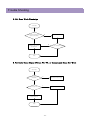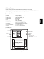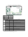
1
S/M NO. : DSP220PEF0
Service Manual
42" PLASMA PDP TV
CHASSIS : SP-220P
Model : DPP-42A1LASB
Caution
: In this Manual, some parts can be changed for improving. their
performance without notice in the parts list. So, if you need the
latest parts information, please refer to PPL(Parts Price List)in
Service Information Center.
Contents
I. Parts with exception of MODULE
1. Safety Precaution
2. Product Specification
2-1. SPECIFICATION
2-2. Available Input Signal
2-3. Remote Control Setup Code
3. The Features of Inside
4. DPP-42A1LASB Block Diagram
5. Default Setting in User Menu OSD
5-1. Picture Mode
5-2. Sound
5-3. Screen
5-4. Features
6. Service Mode
7. Power PCB
7-1. Input and Environmental Requirement
7-2. Output Characteristics
7-3. Function of Protection
7-4. Connector Specification
8. Power Adjustment
8-1. Vs (Sustain Voltage)
8-2. Vs (Adress Voltage)
8-3. 5Vcntl
9. Noticeable Points While Assembling
10. Software Upgrade Method
11. Trouble Shooting
12. Assembly List
13. STRUCTURE OF PDP SET
14. EXPLODED VIEW
2
3
3
5
6
27
28
29
29
29
30
30
31
33
33
33
33
34
35
35
36
37
38
41
44
59
61
66
II. Parts of MODULE
1. Confirmation Manual
2. Repair Manual
-1-
I. Parts with the exception of MODULE
1. Safety Precautions
1. Safety Precautions
(1) When moving or laying down a PDP Set, at least two people must work together. Avoid
any impact towards the PDP Set.
(2) Do not leave a broken PDP Set on for a long time. To prevent any further damages, after
checking the condition of the broken Set, make sure to turn the power (AC) off.
(3) When opening the BACK COVER, you must turn off power (AC) to prevent any electric
shock. When PDP is operating, high voltage and high current inside the Set can cause
electric shocks.
(4) When loosening screws, check the position and type of the screw. Sort out the screws and
store them separately for reassembling. Because screws holding PCBs are working as
electric circuit GROUNDING, make sure to check if any screw is missing when
assembling/reassembling. Do not leave any screws inside the set.
(5) If you open the BACK COVER, you will see a
Panel Gas Exhaust Tube (Picture. 1-1) inside
the bracket. If this part is damaged, the entire
PDP PANEL must be replaced. Therefore,
when working with the set, be careful not to
damage this part.
Picture 1-1. Panel Gas Exhaust Tube
(6) A PDP Set contains different kinds of
connector cables. When connecting or disconnecting cables, check the direction and
position of the cable beforehand.
(7) Connect/disconnect the connectors slowly with care especially FFC (film) cables and FPC
cables. Do not connect or disconnect connectors instantaneously with force, and handle
them carefully for reassembling.
(8) Connectors are designed so that if the number of pins or the direction does not match,
connectors will not fit. When having problem in plugging the connectors, check their kind,
position, and direction.
-2-
2. Product Specification
2-1. SPECIFICATION
ITEM
1. GENERAL
1-1. MODEL NO
1-2. CHASSIS NO
1-3. SCREEN SIZE
1-4. COUNTRY
1-5. RESOLUTION
1-6. REMOCON TYPE
1-7. SAFETY STANDARD
1-8 .TUNIG METHOD
1-9. MEMORY CHANNEL
2. MECHANICAL
2-1. APPEARANCE
1) WITHOUT STAND
2) WITH STAND
2-2. WEIGHT
1) WITHOUT STAND
2) WITH STAND
3. ELECTRICAL
3-1. VIDEO INPUT
3-2. DTV/DVD INPUT
3-3. SCART INPUT
3-4. PC INPUT
3-5. DVI INPUT
3-6. TV INPUT
1) COLOR STANDARD
2) ANTENNA IN
3) RECEPTION CHANNEL
4) IF & SUBCARRIER
3-7. SOUND INPUT
3-8. SPEAKER OUTPUT
3-9. POWER REQUIREMENT
SPECIFICATION
DPP-42A1LASB
SP-220P
42” (16:9)
Europe
852(H) x 480(V)
R-53J17
CE(CLASS B), CB
VS
99CH
W x H x D =1260 x 653 x 91 mm
W x H x D =1260 x 748.5 x 300 mm
33 Kg
38.75 Kg
COMPOSITE(NTSC, PAL, SECAM, PAL-M/N, NTSC4.43) &
S-VHS(50/60Hz Y/C) 1 Port
1080i, 720P, 480P , 480i, 576P, 576i
(Y, Pb/Cb, Pr/Cr COMPONENT SIGNAL) 2 Ports
SCART(COMPOSITE, R,G,B, SOUND R/L) 2 Ports
VGA ~ SXGA(Dot clock : 110MHz), 15 PIN D-SUB 1 Port
DVI-D INPUT (DVI Jack) 1 Port
PAL B/G+I/I+D/K, L-SECAM, L’--SECAM
ONE INPUT 75 Unbalanced (DIN Standard)
VHF LOW : E2 ~ S6 Ch.
VHF HIGH : S7 ~ S36 Ch.
UHF
: S37 ~ E69 Ch.
L’-SECOM : FB, FC1, FC
PIF : 38.90MHz (PAL, L-SECAM)
33.9 MHz (L’-SECAM)
SIF : 33.40MHz (B/G), 32.90MHz (I/I),
32.4MHz (D/K, L-SECAM), 40.4MHz (L’-SECAM)
VIDEO 1 Port, DTV/DVD 2 Ports, PC 1 Port, DVI 1 Port
10W(R) + 10W(L)
AC 100V~240V, 50/60Hz
-3-
REMARK
Product Specification
ITEM
3-10. POWER CONSUMPTION
3-11. RS-232 CONTROL
3-12. AV OUTPUT
3-13. FUNCTION
1) SCALING
SPECIFICATION
270W
RS-232 Communication (EXTERNAL UPGRADE)
SCART(CVBS, SOUND R/L) 2 Ports
DVI : Screen Mode (16:9, 4:3, Panorama)
PC : Screen Mode (16:9, 4:3, Panorama), H/V Position, Auto
TV / VIDEO / DVD (480, 576 i/p) : Screen Mode (16:9, 4:3,
Panorama, LB (16:9), LBS (16:9), 14:9, LB (14:9), LBS (14:9)
Auto)
2) OSD
18 Languages (English, Greek, Dutch, German, Russian, Rumanian,
Swedish, Danish, Finnish, Norwegian, Spanish, Italian, Franch,
Polish, Portuguese, Czech, Hungarian, Slovakian)
3) PIP / POP
TV, Video, S-Video / TV, Video, S-Video
4) OTHERS
Still, Sleep Mode, Sound Mode, Timer, Screen Mode, Teletext
(Level 1.5), WSS
4. OPTICAL
4-1. SCREEN SIZE
4-2. ASPECT RATIO
4-3. NUMBER OF PIXELS
4-4. DISPLAY COLOR
4-5. CELL PITCH
4-6. PEAK LUMINANCE
4-7. CONTRAST RATIO
4-8. VIEWING ANGLE
5. USERCONTROL & ACCESSORIES
5-1 CONTROL BUTTON(SET)
5-2. REMOTE CONTROL
(R-52M17)
5-3. ACCESSORIES
5-4. OPTIONAL PARTS
42”(106 cm) DIAGONAL
16 : 9
852(H)X480(V)
1,073,000,000 Colors ( 10bits for each RGB)
1.08(H) x 1.08(V)mm (1 Pixel = a Set of RGB Cells )
1500cd/m2(WITH FILTER GLASS)
10000:1 (Dark Room)
160 degree(VERTICAL/HORIZONTAL)
PUSH-PULL S/W : AC POWER BUTTON
SOFT S/W: MOVE/CH(UP, DOWN), VOLUME(LEFT, RIGHT),
MENU, INPUT SELECT
Power, Universal Selection (TV, VIDEO/DVD, CATV/SAT),
10 KEYS(0~10), Recall, VCR /DVD KEY
(F.R/SLOW, Play, F.F/SLOW, Stop, PAUSE, OPEN/CLOSE,
PREV, NEXT ), MENU, TV, AV, Component, PC/DVI, STILL,
PREV PR, MUTE, PR (UP/DOWN), VOL(UP/DOWN), SCREEN
MODE / MIX, Screen Size, Sleep Timer, I-II / CYAN, Sound Mode /
Index, Red, Green, Yellow, TXT, Reveal, Update, Expand, Subpage,
Hold, PIP, SWAP, PR+, PR-, Position, Sourse
REMOTE CONTROL, INSTRUCTION MANUAL, POWER CORD
STAND, WALL HANGER
-4-
REMARK
Product Specification
2-2 Available Input Signal
(1) PC & DVI
Resolution
640 X 480
720 X 400
800 X 600
1024 X 768
H Freq. (KHz)
V Freq. (Hz)
Remark
DVI
PC
31.469
59.940
DOS
O
O
37.861
72.809
VESA
O
O
37.500
75.000
VESA
O
O
31.469
70.087
IBM
O
O
35.156
56.250
VESA
O
O
37.879
60.317
VESA
O
O
48.363
60.004
VESA
O
O
(2) Component
z
z
z
z
1080i – 50 / 60Hz
720p – 50 / 60Hz
576p - 50 / 60Hz
480p - 50 / 60Hz
(3) Video
z PAL, PAL – M, PAL – N
z NTSC, NTSC 4.43
z SECAM
-5-
Product Specification
2-3. Remote Control Setup Code
-6-
Product Specification
VCR
Maker (BRAND) NAME
CANON
CAPEHART
CARENA
CARREFOUR
CASIO
CATHAY
CATRON
CGE
CIHAN CLARIVOX
CIMLINE
CLATRONIC
COMBITECH
CONDOR
CONTINENTAL EDISON
CORVUS
CRAIG
CROSLEY
CROWN
CROWN/ ONWA
CURTISMATHES
CYRUS
DAEWOO
DANSAI
DAWA
DAYTRON
DE GRAAF
DECCA
DECCA(UK)
DEGRAAF
DEITRON
DENKO
DENON
DESMET
DIAMANT
DIXI
DOMOH
DORIC
DUAL
DUMONT
DYNATECH
ELBE
ELCATECH
ELIN
ELSAY
ELTA
EMERSON
ESC
ESSELTE
ETZUKO
EUROMAN
EUROPHON
FENNER
FERGUSON
FIDELITY
FINLANDIA
CODE NUMBER (3DIGIT) LIST
147
061
065
009
039
021
061
039
155
029
029
033
021
044
148
008
160
009
148
060
175
001
021
155
021
113
039
054
015
021
029
113
155
055
078
155
160
021
015
039
021
029
056
029
021
009
021
148
029
155
061
061
016
029
015
148
171
044
090 133 148 155
061
171
061
090
155 171
056
021
029 061 064 171
009
029
021 033 061 064 155 171
055
061
177
044
047 065 090 148 155 166 175
039
049 054 065 113 148
039
039
148
036
044 065 090 112 148 155
054 065 148 155 175 189
148
113
155
029
011
056
148
029 032 039 060 073 127 148 155
057 061 064
155
021
039
039
023 039 044 090 094 100 104 108 112 130 131 165
056 148 162
049 054 065 113 175
-7-
Product Specification
-8-
Product Specification
-9-
Product Specification
-10-
Product Specification
-11-
Product Specification
-12-
Product Specification
-13-
Product Specification
-14-
Product Specification
-15-
Product Specification
-16-
Product Specification
-17-
Product Specification
-18-
Product Specification
-19-
Product Specification
-20-
Product Specification
-21-
Product Specification
-22-
Product Specification
-23-
Product Specification
-24-
Product Specification
-25-
Product Specification
-26-
DPP-42A1LASB Inside Features
3. The Features of Inside
-27-
4. DPP-42A1LASB Block Diagram
4850710S22
DVI Audio
Key PCB
DVI
PC Audio
PC (D-SUB)
LVDS
4859004460
Component1,2
12V,5V,STB
4850710S21
3.3V
4850708S16
AV1
4850705N31
LED PCB
AV2
33V,17V
4850706S35
4859004060
FFC Cable
Main Tuner
Speaker L Speaker R
S-VHS
RS-232
Upgrade
AV3
Sub Tuner
4850712S03
SUB B/D
AV3 PCB
-28-
5. Default Setting in User Menu OSD
1. Picture Mode
1) Mode
z
Normal
Dynamic
Cinema
User
Brightness
50
40
55
Undefined
Contrast
50
80
35
Undefined
Sharpness
8
10
6
Undefined
Colour
50
55
45
Undefined
Tint
50
50
50
Undefined
DVI & PC Input - Only brihgtness and contrast are available.
2) Default value of other functions in picture mode
Function
Default Value
Colour Temp
Normal
N.R.
NR1
CTI
On
z
N.R. means the noise reduction
z
DVI & PC don't support N.R. and CTI functions
2. Sound
1) Mode
Normal
Movie
Music
News
User
120 Hz
32
50
48
15
Undefined
500 Hz
32
38
38
32
Undefined
1.5 kHz
32
28
15
50
Undefined
5 kHz
32
40
42
32
Undefined
10 kHz
32
48
56
15
Undefined
2) Default value of other functions in sound mode
Function
Default Value
Balance
0
Effect
Off
AVC
Off
-29-
Default Setting in User Menu OSD
3. Screen
16 : 9 4 : 3
Panorama
LB (16:9)
LBS (16:9)
14 : 9
LB (14:9)
LBS (14:9)
Auto
Component
O
O
O
X
X
X
X
X
X
TV
O
O
O
O
O
O
O
O
O
AV
O
O
O
O
O
O
O
O
O
PC
O
O
O
X
X
X
X
X
X
DVI
O
O
O
X
X
X
X
X
X
z
H. Position, V. Position, and Auto screen size is available only in PC mode.
4. Features
1) Mode
Function
Background
Language
Child Lock
MGDI
Auto Power
Default Value
10
English
Off
On
Off
z
DVI & PC don't support MGDI function.
2) Time Setting
Function
Clock
Auto Clock Off Timer Off Time Wake Timer Wake Time Wake Prog. Wake Vol.
Default Value Undefined
On
Off
PM 12:00
Off
PM 12:00
3) ISM
Function
Pixel Shift
Low Bright
Image Invert
Default Value
Off
Off
Off
-30-
1
20
6. Service Mode
To enter SERVICE MODE,
A. Press “ ◀VOL ” -> “ MUTE ” -> “ RECALL ” -> “ MUTE ” button of remote
controller (R-53J17)
or
B. Press “ S9 ” button of SERVICE REMOTE CONTROLLER.
[Note] In the first line, there is the model name and the version of the upgraded
program on the PDP set.
1. Default Value of Pw318B_1 and Pw318B_2
Sub Bias Sub Gain
Pw318B_1
32
12
Pw318B_2
32
12
Bias R
Bias G
Bias B
Gain R
Gain G
Gain B
25
23
38
12
16
20
1) Pw318B_1
z
Sub Bias : For BRIGHTNESS adjustment (All inputs)
z
Sub Gain : For CONTRAST adjustment (All inputs)
z
Bias R : For R BRIGHTNESS adjustment (All inputs)
z
Bias G : For G BRIGHTNESS adjustment (All inputs)
z
Bias B : For B BRIGHTNESS adjustment (All inputs)
z
Gain R : For R CONTRAST adjustment (All inputs)
z
Gain G : For G CONTRAST adjustment (All inputs)
z
Gain B : For B CONTRAST adjustment (All inputs)
2) Pw318B_2
z
Sub Bias : For DVI BRIGHTNESS adjustment
z
Sub Gain : For DVI CONTRAST adjustment
2. Pw3300_1
Function
R Offset
G Offset
B Offset
R Gain
G Gain
B Gain
Default Value
100
100
100
94
97
94
Function
Y Offset
Pb Offset
Pr Offset
Y Gain
Pb Gain
Pr Gain
Default Value
105
125
125
90
203
196
z
RGB offset values will be set by executing ‘RGB Auto Cal’ in service mode.
z
YPbPr offset values will be set by executing ‘YPbPr Auto Cal’ in service mode.
-31-
Service Mode
z
The automatically set offset values may different from the default value depend
on B/D. However, the main B/D should be replaced or contact Kunpo R&D
center in Korea if the OFFSET values differ more than ±20 from default value.
3. Pw3300_2 & Pw2250
4. Msp34X0
AV Brt
AV Cont
Function
Sc pScale
Pw3300_2
127
75
Default Value
21
Pw2250
127
75
Fm pScale Nic pScale
25
51
z
In Msp34X0,
-
Sc pScale : Prescale adjustment for external input (AV, Component, PC, DVI
etc.)
-
Fm pScale : FM/AM prescale adjustment
-
Nic pScale : NICAM prescale adjustment
5. Misc
z
Function
TV Auto Off
TXT Lang
TXT T/F
Default Value
On
Auto
TOP
Tst Ptrn AT shows five cycled patterns (white, black, red, green, blue) every 1
minute automatically
z
Tst Ptrn MA shows five cycled patterns manually by pressing volume up key.
6. Panel
Function
Sync Mode
Bright Mode
Default Value
AUTO
100%
z
Power Mode Gamma Mode Panel Temp
100%
2.2N
**.*
Panel Temp indicates the current temperature of the panel.
7. Reset
z
Level 1 – Resets all data in E2PROM other than HDCP key, EDID, RGB offset
and YPbPr offset of Pw3300_1.
z
Level 2 – Resets all data in E2PROM other than the exception of Level 1 and
Pw318B_1.
z
Factory – Resets the data of auto search, language setting, time setting, and the
user menu values that could be reset by ‘Initialize’ function in
Feature mode.
-32-
7. Power PCB
1. Input and Environmental Requirement
Input Requirement
Description
Environment Requirement
Description
Norminal Input Voltage
AC100V to AC240V
Operating Temperature Range
-10 to 50 deg.
Input Voltage Variation Range
AC85V to AC276V
Operating Humidity Range
10 to 90 %
Nominal Frequency
50 / 60 Hz
Storage Temperature Range
-20 to 60 deg.
Frequency Variation Range
45Hz to 65Hz
Storage Humidity Range
10 to 90 %
Phase
Single
Cooling Condition
Free Air
30A zero-pk max. at cold start
Inrush Current
and any specified line, load and
temperature conditions
2. Output Characteristics
Output
Circuit
Norminal
Voltage
Load
Ripple
Voltage [V] Adjustment [V] Variation [A] Noise [mV p-p]
Vs
175
160 - 190
0.4 - 1.5
500 / 500
Vd
60
55 - 65
0.01 - 2.5
300 / 300
5V (ctrl)
5.1
4.75 - 5.25
1.2 - 4.0
30 / 200
5V
5.1
4.75 - 5.25
0.5 - 4.5
50 / 200
DTV3.4V
3.4
--
0.5 - 2.0
50 / 200
DTV2.5V
2.5
--
0.2 - 2.0
50 / 200
33VT
33.0
--
0 - 0.05
100 / 400
12V
12.0
--
0 - 2.0
100 / 400
17V (Audio)
17.0
--
0 - 0.7
100 / 400
-17V (Audio)
-17.0
--
0 - 0.7
100 / 400
5V (STBY)
5.0
--
0.03 - 1.0
50 / 200
3. Function of Protection
Protection
Output Circuit
Trip Point
Notes
Over Current
Vs
1.7A or more
Shut down by Under Voltage
Vd
3.0A or more
Shut down by Under Voltage
5V (ctrl)
13.0 - 25.5A
5V
(Total Current)
12V
1.76A or more
Shut down by Under Voltage
-33-
Shut down by Under Voltage
Power PCB
33V
0.08A or more
Shut down by Under Voltage
17V
1.0A or more
Shut down by Under Voltage
-17V
1.0A or more
Shut down by Under Voltage
Vs
220V or less
Shut down
Vd
86V or less
Shut down
5.5 - 7.0
Shut down
12V
13 - 17V
Shut down
33V
36 - 44V
Shut down
17V
19 - 24V
Shut down
-17V
-19 - -24V
Shut down
5V (ctrl)
5V
Over Voltage
4. Connector Specification
Connector
CN803 (PV)
Type
CN806
CN804 (PM)
CN801 (PA)
CN805
CN01
YMW025-10R B10P-VH YMW025-08R YMW025-06R B4P-VH YFW800-02
Maker
YEONHO
JST
YEONHO
YEONHO
JST
YEONHO
The number of pins
10
10
8
6
4
2
1
5V Stand_by
LVP
3.4V
33VT
5Vctrl
AC(L)
2
POWER
GND
3.4V
GND
5Vctrl
AC(N)
3
GND
GND
GND
+17
GND
4
GND
GND
GND
GND
GND
5
5V
GND
2.5V
GND
6
GND
Vd
2.5V
-17V
7
GND
Vd
GND
8
12V
NC
GND
9
12V
Vs
10
GND
Vs
Pin No.
-34-
8. Power Adjustment
z
Power Adjustment – Adjusting to standard power voltages, which are written in
the upper right side of PDP module. These values were already adjusted by
PDP module makers while producing.
Therefore, if there are some problems in
picture after adjusting, you should classify that PDP module as a fault and
contact to PDP module maker.
z
Input Video Pattern – 100 IRE Full White Pattern
Figure 3. Voltage Adjustment Label
1. Vs (Sustain Voltage) : Discharge Sustain Voltage
z
Measurement Equipment : Digital Volt Meter (DC volt mode)
z
Adjusting TP : TP204
z
Adjusting Location : RV203
z
Optimum Adjusting Voltage : The voltage which is written in the label located in
upper right side of the PDP module. (Typical Voltage : 187V)
-35-
Power Adjustment
2. Va (Address Voltage) : Data Input Voltage
z
Measurement Equipment : Digital Volt Meter (DC volt mode)
z
Adjusting TP : TP206 (Vd)
z
Adjusting Location : RV204 (Vd ADJ)
z
Optimum Adjusting Voltage : The voltage which is written in the label located in
upper right side of the PDP module. (Typical Voltage : 65V)
-36-
Power Adjustment
3. 5Vcntl (5V control)
z
Measurement Equipment : Digital Volt Meter (DC volt mode)
z
Adjusting TP : TP203
z
Adjusting Location : RV201
z
Optimum Adjusting Voltage : The voltage which is written in the label located in
upper right side of the PDP module. (Typical Voltage : 5.2V)
-37-
9. Noticeable Points While Assembling
1. Insertion of Ring Core (EMI Filter) to Speaker Cable (L,R), AV3
Cable and their position
-
Coil the Ring Core (Filter EMI, S/N: 5PZCA2009A) 2 turns with Speaker Cable
(L,R) as shown in the figure below.
-
Coil the Ring Core (Filter EMI, S/N: 5PZCAT3035) 1 Turn with AV3 Cable as
shown in the figure below.
Speaker
Cable
2 Turn
AV3
Cable
1 Turn
Speaker & AV3
Cable Allocation
(Separate with
Power Cable)
Speaker Cable
2 Turn
(No Ring Core
in Key Cable)
Speaker & KEY
Cable Allocation
2. Insertion of Ring Core to the Power Cable
-
Insert a Ring Core(Filter EMI, S/N : 5PZCA2009A) to 8 pin and 6 pin Power
Cable
-38-
Noticeable Points While Assembling
3. LVDS Cable Connection
ÆCABLE LVDS, S/N : 4856818800
a. DIGITAL B/D part
Æ CLAMP WIRE, S/N : 4856818800
Æ CLAMP WIRE, S/N : 4856815900
(Place these CLAMP WIRES as shown in the figure below)
* Make LVDS Cable not to touch on the Terminal Plate while connecting.
b. VIDEO B/D part
-39-
Noticeable Points While Assembling
4. Shieldron Tape on SCART Input
Æ Tape EMI, S/N : 485A100071
(Position: From top of Scart to Terminal Channel Gasket)
5. Shieldron Tape on DVI Input
Æ Tape EMI, S/N : 485A100571
(attach vertically, 3 X 4.2 Cm)
(Position: From top of DVI to Terminal Channel Gasket)
-40-
10. Software Upgrade Method
1. Check whether MAIN PCB is connected to SUB PCB (PA901 to P901).
2. Connect 9-PIN serial cable to the serial port of the computer.
3. Connect the opposite end of the serial cable to RS-232C port of SUB PCB.
4. Run Flashupgrader.exe in the PC to excute the program as shown below.
5. Select current Upgrade file
- Click “Choose...” button to select the file you want to upgrade.
- Select the file (pwSDK.inf) that you want to upgrade.
-41-
SOFTWARE UPGRADE Method
6. Select correct COM Port and Baud Rate(115200) as shown below. Then press Flash button to finish
setup.
7. Turn on the ac power and then upgrade program will start the download as shown below.
-42-
SOFTWARE UPGRADE Method
8. When the upgrading is complete, a window (below) will be opened. Press “Finish” button to complete
the process.
-43-
11. Trouble Shooting
Before starting Trouble Shooting
z
Trouble diagnosing and repairing of set mean find out which PCBs or blocks are
not working and replace them with new PCBs. Repairing the broken PCBs are
not necessary.
Keep the broken PCBs and return them to service center or
R&D center.
z
This Trouble Shooting list only contains representative and simple PCB trouble
diagnosis and Module Exchange method. Therefore, if you find sets that are
difficult to diagnose or to repair, contact R&D center.
z
Basic Trouble Diagnosis procedure
1) Check problem Symptoms
2) Open Back Cover
3) Trouble Diagnosis & Replace broken PCB
4) Adjust new PCB module
5) HEATRUN for at least 30 minutes, inputting Full White test pattern
6) Full Function test
7) Repair Complete
z
Required Equipment for trouble diagnosis
1) Digital Multimeter (User Mode : measure DC Voltage, measure Diode
Voltage, Short-open test)
2) Screwdriver (or electric screwdriver), Plastic adjusting tool
3) Oscilloscope (for detailed examination only)
z
Before replacing PCBs, you MUST turn the AC switch “OFF”.
z
After replacing High Voltage Board (Power PCB, Y-SUS, Z-SUS, Data B/D,
Scan B/D), and Main & Sub PCB, extra adjustment might be needed. (Refer to
Power Adjustment)
z
Dust or extraneous materials may cause bad connections. Therefore, try to
apply soft brush, air fresher, or breath to clean the dust or extraneous materials.
z
While assembling the set in factory, it could have bad connection.
Try to
reassemble the necessary connectors and also check the state of the
connectors.
z
After the set is repaired, leave Back Cover open for followings.
Run HEAT
RUN for at least 30 minutes by displaying Full White test pattern of Service
Mode (Refer to Service Manual I. ‘Service Mode’ part).
Check the screen
conditions and basic functions (remote control operation etc.)
z
After Back Cover is closed, redo HEAT RUN for at least one hour with Full
-44-
Trouble Shooting
White input using Test Pattern of Service Mode. Check the screen conditions
and basic functions.
z
Caution 1 !!
When disconnecting / connecting connectors, you MUST turn “OFF” the AC
power and check the direction and position of the connectors before
working.
z
Caution 2 !!
Whenever you reassemble connectors connecting High Voltage Board and
POWER PCB (CN805, CN806), remaining voltage still exists in the POWER
PCB could cause electric shock and damage the set.
Therefore always
reassemble the connectors several minutes after AC power is off.
To be
more careful, using a Multimeter you should check to see if Vs is less than
10V and then connect connectors.
Definition
z
Red LED – Stand by state (ready for operating)
z
Green LED – The set is turned on and operating
z
Shut Down – While green LED, power PCB does not make any operating sound
or noise (i.e. Power relay does not operate normally)
z
Weak Discharge – The screen looks like BLACK, but there are little discharged
cells on the screen
z
Abnormal Discharge – Shows unexpected discharged cells on the image
z
No Signal – OSD is working but no images are displaying
z
No Raster – Not even OSD is displaying
-45-
Trouble Shooting
1. No Signal or No Raster
Check Start
Does “No Signal”
screen appear?
N
Is a weak discharge
detected in the screen?
Y
Is the signal input Jack
properly connected?
N
Check AC connection
Check CN805, CN806
connectors
Check Power S/W ON
Y
N
Check the connection of
Jack (PDP and AV device)
Is LVDS connection
correctly connected?
Y
N
Check LVDS connection
between Digital B/D and
Main B/D
Y
Does input source (AV
device) work?
N
Check AV device
Check other connections
in all Boards. Are they OK?
Y
Y
Is input selection in
the correct mode?
N
Replace Main B/D
and/or Sub B/D
Correct the input mode
Y
Replace Main B/D
and/or Sub B/D
Done
-46-
N
Connect correctly
Trouble Shooting
2. No Sound
Check Start
N
Is an image
displaying on
screen?
Go to the section
of ‘No Image’
Y
N
Is the sound jack of external
device properly connected?
Connect the jack and
check the sound
again
Y
Y
Is mute key
pressed?
Cancel the mute and
check the sound
again
N
N
Is speaker cable
correctly connected?
(check P603, P604)
Connect the cable
and check the sound
again
Y
N
Is input source
TV?
Replace Main B/D
Y
N
Connect the cable
Y
Is the connection
between PA901 and
P901 OK?
N
Is sound OK?
Replace Sub B/D
Y
N
Is sound OK?
Y
DONE
-47-
Replace speakers
Trouble Shooting
3. Shut Down
Check Start
Turn AC power OFF
Open BACK COVER
Disconnect CN806 of Power PCB
Set Power PCB’s voltage switch to LOW
Turn AC power ON (Stand By)
Turn on the set (Green LED)
N
Y
Is ‘SHUT DOWN’ occured?
Connect CN806 back and disconnect
CN801, CN803,CN804, CN805
Go to ‘Low Voltage
Shut Down’ part in this
trouble shooting
Set Power PCB’s voltage switch to HIGH
Go to ‘High Voltage
Shut Down’ part in this
trouble shooting
-48-
Trouble Shooting
A) Low Voltage Shut Down
Check Start
Turn AC power off
Disconnect CN805 of Power PCB
Turn on the set after AC power on
N
Y
Is ‘SHUT DOWN’ occured?
Turn AC power off
Turn AC power off
Connect CN805 back and disconnect
CN 801, CN803, CN804 of Power PCB
Replace Main B/D
Disconnect P6 of Y-SUS B/D
Connect all connectors and set Power
PCB’s voltage switch to High
Turn on the set after AC power on
Done
N
Y
Is ‘SHUT DOWN’ occured?
Turn AC power off
Turn AC power off
Disconnect P2, P3 of Z-SUS
Go to ‘Z-SUS, Digital
B/D, Data B/D Shut
Down’ part
Connect P6 back and disconnect
P1 of Z-SUS B/D
Go to ‘Y-SUS, Scan B/
D Shut Down’ part
-49-
Trouble Shooting
B) Z-SUS, Digital B/D, Data B/D Shut Down
Check Start
Turn on the set after AC power on
N
Y
Is ‘SHUT DOWN’ occured?
Turn AC power off
Turn AC power off
Connect P2 of Z-SUS B/D
Replace Z-SUS B/D
Connect P2, P3 back and turn on the
set after AC power on
Turn on the set after AC power on
N
Y
Y
Is ‘SHUT DOWN’ occured?
N
Is ‘SHUT DOWN’ occured?
Replace Digital B/D
Replace Data B/D
Connect all cables and set
voltage switch to High
Connect all cables and set
voltage switch to High
Go back to ‘Low Voltage Shut
Down’ part again
Connect all cables and set
voltage switch to High
Done
Done
Done
-50-
Trouble Shooting
C) Y-SUS, Scan B/D Shut Down
Check Start
Disconnect P3, P4 of Y-SUS
Turn on the set after AC power on
N
Is ‘SHUT DOWN’ occured?
Y
Turn AC power off
Turn AC power off
Replace Scan B/D
Replace Y-SUS B/D
Connect all cables and set
voltage switch to High
Connect all cables and set
voltage switch to High
Done
Done
-51-
Trouble Shooting
D) High Voltage Shut Down
Check Start
Disconnect P1 of Z-SUS
Turn the set on after AC power on
N
Y
Is ‘Shut Down’ occured?
Turn AC power off
Turn AC power off
Disconnect three metal plates
between Y-SUS and Scan B/D
Connect P1 of Z-SUS back
Turn the set on after AC power on
Disconnect P5 of Y-SUS and
P3 of Z-SUS
N
Y
Is ‘Shut Down’ occured?
Turn AC power off
Turn the set on after AC power on
Turn AC power off
N
Y
Is ‘Shut Down’ occured?
Replace Y-SUS B/D
Replace SCAN B/D
Turn AC power off
Turn AC power off
Connect all cables
and assemble the set
Connect all cables
and assemble the set
Replace Z-SUS B/D
Replace Data B/D
Done
Done
Connect all cables
and assemble the set
Connect all cables
and assemble the set
Done
Done
-52-
Trouble Shooting
4. No Key Operation
Check Start
Turn on the Power S/W (AC ON)
N
Does LED turn on to red light?
Check the AC connection
Check the Power S/W on
Y
Turn on the set using remote control
N
Dees LED turn on to green
light?
Replace the Main B/D
Y
Check the connector of Key PCB
Replace the Key PCB
Check if the Key is working
N
Replace the Main B/D
Y
Done
-53-
Trouble Shooting
5. No Remote Control Operation
Check Start
Turn on the Power S/W (AC ON)
Does LED turn on to red light?
N
Check the AC connection
Check the Power S/W on
Y
Turn on the set using remote control
Y
Dees LED turn on to green light?
Check the other buttons of
remote control
N
Are all buttons
working properly?
Check the battery of remote control
N
N
Put the battery
Is there battery?
Y
Replace the Main B/D
Try to turn on the set using Key button
Y
Dees LED turn on to green light?
Replace the LED PCB
N
Replace the Main B/D
Done
-54-
Y
Done
Trouble Shooting
6. No Key and Remote Control Operation
Check Start
Check the battery of remote control
Replace the LED PCB
Turn the AC Power ON
Try to turn on the set using
remote control
Is the remote control
working?
Y
Replace the Key PCB
N
Replace the Main B/D
Done
-55-
Trouble Shooting
7. Weak Discharge or Abnormal Discharge
Check Start
Check the Vs and Va of Power PCB
N
Are they normal?
Set the values to typical voltages
Y
Y
Replace the Y-SUS
Do you still see the weak
discharge or abnormal discharge
on the screen?
N
Do you still see the weak
discharge or abnormal discharge
on the screen?
N
Done
Y
Replace the Z-SUS
Do you still see the weak
discharge or abnormal discharge
on the screen?
N
Y
Replace the Scan B/D
Done
-56-
Trouble Shooting
8. Not Even Weak Discharge
Check Start
N
Is Power B/D working? Does it
make normal sound?
Replace the Power B/D
Y
N
Replace Y-SUS, Z-SUS,
and Scan B/D
Is the set correctly working?
Y
Done
9. Particular Input Signal (Video, PC, TV, or Component) Does Not Work
Check Start
Is the input Jack correctly
connected?
N
Connect the input correctly
Y
Is the input TV?
Y
Replace Main and Sub B/Ds
N
Replace Main B/D
Done
-57-
Trouble Shooting
10. Others
A) Set Is Making Unusual Noise
Î Check the connection of Power PCB and Module. If they are OK,
replace the Power PCB and check the symptom again.
B) Occasionally, the set does not operate normally. Turning off and on the AC power
make the set to operate normal again
Î Upgrade the software first. If you still see the same symptom, replace
the Main and Sub B/D.
C) Images are abnormal
Î Check the default values of service mode and user mode. If they are
OK, replace the Main and Sub B/D.
If they are not OK, upgrade the
software and check the symptom again.
-58-
12. Assembly List
* Ass’y of module is listed on the next page.
No. PCB ASS'Y CODE
ASS'Y NAME
ASS'Y DESCRIPTION
1
4851413800
BACK COVER ASSY
21728+26162
2
4853293700
BRKT DR
ALDCS 8
3
4853220100
BRKT POWER MODULE
SECC T1.0
4
4854962100
BUTTON CH
ABS GY
5
4859004060
CABLE FFC
1.0-K-30P-50MM
6
4859004460
CABLE LVDS
1001-31FC+1001-31FC+42A1LASB=560
7
4859003750
CABLE PHONE PLUG
PLUG+CABLE 1365AWG26=150B
8
4856815900
CLAMP WIRE
EGI T0.4+TUBE+PIE 3.2
9
4856818800
CLAMP WIRE
AKKL-3140-A-RT
10 4850705N31
CONNECTOR
12505HS-05+12505TS+ULW=650
11 4850710S22
CONNECTOR
12505HS-10+12505HS-10+USW=600
12 4850706S35
CONNECTOR
YMH025-06R+YMH025-06R+ULW=200
13 4850710S21
CONNECTOR
YMH025-10+YMH025-10R+ULW=300
14 4850708S16
CONNECTOR
YMH025-08R+YMH025-08R+ULW=300
15 4850710S23
CONNECTOR
YH396-10V+YH396-10V+ULW=700
16 4850708S23
CONNECTOR
YH396-08V+YH396-08V+ULW=250
17 4850704S63
CONNECTOR
YH396-04V+YH396-04V+ULW=700
18 4850703N40
CONNECTOR
25045HP-03+25048HS-03+ULW=150
19 4850704N35
CONNECTOR
YH396-04V+YH396-05V+ULW=700
20 4850710N24
CONNECTOR
YH396-10V+YH396-09V+ULW=700
21 4850712S03
CONNECTOR
12505HS-12+12505HS-12+USW=850
22 48599DM001
CORD POWER AS
EU LP-33+LS-60=2.0M(LF)
23 485AS11290
CTRL BOARD AS
Digital BOARD
24 4855553900
DECO SENSOR
PC
25 5PZCAT3035
FILTER EMI
ZCAT3035-1330
26 5PZCA2009A
FILTER EMI
ZCAT2035-0930A
27 PTFEPWG089
FILTER EMI AS
DPP-42A1LASB
28 4853823100
FRAME HORIZENTAL
SECC T1.6
29 4851C02800
FRAME SUPPORT L AS
38232+38234
30 4851C02900
FRAME SUPPORT R AS
38233+38234
31 485A102280
GLASS FILTER
M4203-JW1245
32 4957000800
HEAT SINK
AL ANODIZHG+TAPE
-59-
Assembly List
33 4852090701
MASK FRONT
ABS GY
34 4850M10410
MODULE PDP
PDP42V7
35 4850M10110
MODULE POWER
1H217WA
36 PTMPMSG089
PCB MAIN MANUAL AS
DPP-42A1LASB
37 PTSBMSG089
PCB SUB MANUAL AS
DPP-42A1LASB
38 485A106070
SHIELDRON
(5 AND 3)X85X1T(ANGLE)
39 485A106270
SHIELDRON
41X53X18T
40 48A8310000
SPEAKER SYSTEM
SS-63A01
41 485A100071
TAPE EMI
CU+NI T0.13 VER1
42 485A100571
TAPE EMI
CU+NI 30X42XT0.2
43 4853633300
TERMINAL COVER
A5052 T1.0
44 4853635200
TERMINAL PLATE
A5052 T1.0
45 48B5353J17
TRANSMITTER REMOCON
R-53J17 (AAA)
46 485AS11590
X-LEFT BOARD AS
Data LEFT BOARD
47 485AS11690
X-RIGHT BOARD AS
Data RIGHT BOARD
48 485AS11490
Y-DRV BTM BOARD AS
Scan BTM BOARD
49 485AS11390
Y-DRV TOP BOARD AS
Scan TOP BOARD
50 485AS11090
Y-SUS BOARD AS
Y-SUS BOARD
51 485AS11190
Z-SUS BOARD AS
Z-SUS BOARD
-60-
13. STRUCTURE OF PDP SET
-61-
STRUCTURE OF PDP SET
COMPONENT
PICTURE
1). PDP MODULE
(With F/SUPPORT)
1a). Y-SUS B/D
1b). Z-SUS B/D
-62-
REMARK
STRUCTURE OF PDP SET
COMPONENTS
1d) Data
Relay
PKG(L)
PICTURE
1e) Data
Relay
PKG(R)
1f) Scan
Relay
PKG-T
1g) Scan
Relay
PKG-B
-63-
REMARK
STRUCTURE OF PDP SET
COMPONENT
PICTURE
1h) Digital
PKG
2) MAIN BOARD
3) SUB BOARD
4) POWER BOARD
-64-
REMARK
STRUCTURE OF PDP SET
COMPONENTS
5) FRONT MASK
PICTURE
6) FILTER GLASS
7) BACK COVER
-65-
REMARK
66
DAEWOO ELECTRONICS CORP.
686, AHYEON-DONG, MAPO-GU,
SEOUL, KOREA.
C.P.O. BOX 8003 SEOUL KOREA
PRINTED DATE : Nov. 2005
MODEL : PDP42V7####
CAUTION
1. BEFORE SERVICING THE PDP MODULE,
READ THE SAFETY PRECAUTIONS IN THIS MANUAL.
2. WHEN REPLACEMENT PARTS ARE REQUIRED, BE SURE TO USE
REPLACEMENT PARTS SPECIFIED BY THE MANUFACTURER.
English
PDP MODULE
SERVICE MANUAL
[PDP42V7#### Module]
CONTENTS
Ⅰ.
Ⅱ.
Ⅲ.
Ⅳ.
Safety Precautions/Technical Feature
Formation and Specification of Module
Adjustment
Trouble Shooting
1. Checking for No Picture
2. Hitch Diagnosis Following Display Condition
2-1. All or 1/2 of the screen doesn’t be shown
2-2. Screen doesn’t be shown as Data TCP
2-3. It is generated unusual pattern of Data TCP IC unit
2-4. Regular Stripe is generated about the quantity of one Data TCP IC or more
2-5. Screen doesn’t be shown at all as Scan FPC
2-6. Regular stripe is generated at regular internal on the whole screen
2-7. Data copy is generated to stripe direction
2-8. One or more stripe is generated on the screen
2-9. One or more horizontal line is generated on screen
2-10. Lightness of screen is wholly darken though there is input-signal-pattern
2-11. Different color is shown partially during full-white-screen or electric discharge is generated
during full-black-screen
2-12. Some lightness of some color doesn’t not generated well
3. Checking for component damage
3-1. Y IPM(IC15) or Z IPM(IC2) damage
3-2. Pass Top FET(Y B/D: HS2) damage
3-3. FET Ass’y(Y B/D: HS1) damage
3-4. SCAN IC(Y DRV B/D: IC1~8) damage
3-5. TCP damage
3-6. Crystal(CTRL B/D: X1) damage
4. Shift breakdown component compatibility consideration
4-1. Scan IC follows in application, compatibility of Y DRV Top, Bottom B/D
Ⅴ. Block Diagram
Ⅵ. Safety Components List
Ⅶ. Records of Revision for Boards, Components and ROM DATA
* Annexing : Schematic Diagram
- 2 -
Ⅰ. Safety Precautions/Technical Feature
(9) If the power cable is damaged, or if the connector is loose,
do not use the product: otherwise, this can lead to fire or
electric shock.
1. Safety Precautions
When servicing of PDP Module, it should be not enforced into
another way aside next rule, or a unaccustomed person
should not repairing.
When using/handling this PDP Module, pay attention to the
below warning and cautions.
(10) If the power connector or the connector of the power
cable becomes dirty or dusty, wipe it with a dry cloth.
Otherwise, this can lead to fire.
Indicates a hazard that may lead to death or injury if the
warning is ignored and the product is handled incorrectly.
Caution
Indicates a hazard that can lead to injury or damage to
property if the caution is ignored and the product is handled
incorrectly.
2) CAUTIONS
1) WARNING
(1) Do not touch Signal and Power Connnector while this
product operates.
Do not touch EMI ground part and Heat Sink of Film Filter.
(2) Do not supply a voltage higher than that specified to this
product. This may damage the product and may cause a
fire.
(3) Do not use this product in locations where the humidity is
extremely high, where it may be splashed with water, or
where flammable materials surround it.
Do not install or use the product in a location that does no
satisfy the specified environmental conditions. This may
damage the product and may cause a fire.
(4) If a foreign substance (such as water, metal, or liquid) gets
inside the product, immediately turn off the power.
Continuing to use the product, it is may cause fire or
electric shock.
(5) If the product emits smoke, and abnormal smell, or makes
an abnormal sound, immediately turn off the power.
Continuing to use the product, it may cause fire or electric
shock.
(6) Do not disconnect or connect the connector while power to
the product is on. It takes some time for the voltage to drop
to a sufficiently low level after the power has been turned
off.
Confirm that the voltage has dropped to a safe level before
disconnecting or connecting the connector.
(7) Do not pull out or insert the power cable from/to an outlet
with wet hands. It may cause electric shock.
(8) Do not damage or modify the power cable. It may cause
fire or electric shock.
- 3 -
(1) Do not place this product in a location that is subject to
heavy vibration, or on an unstable surface such as an
inclined surface. The product may fall off or fall over,
causing injuries.
(2) Before disconnecting cable from the product, be sure to
turn off the power. Be sure to hold the connector when
disconnecting cables. Pulling a cable with excessive force
may cause the core of the cable to be exposed or break
the cable, and this can lead to fire or electric shock.
(3) This product should be moved by two or more persons. If
one person attempts to carry this product alone, he/she
may be injured.
(4) This product contains glass. The glass may break, causing
injuries, if shock, vibration, heat, or distortion is applied to
the product.
(5) The temperature of the glass of the display may rise to
80°C or more depending on the conditions of use.
If you touch the glass inadvertently, you may be burned.
(6) If glass surface of the display breaks or is scratched, do
not touch the broken pieces or the scratches with bare
hands. You may be injured.
(7) PDP Module requires to be handled with care not to be
touched with metal or hard materials, and must not be
stressed by heat or mechanical impact.
(8) There are some exposed components on the rear panel of
this product. Touching these components may cause an
electric shock.
(9) When moving the product, be sure to turn off the power
and disconnect all the cables. While moving the product,
watch your step. The product may be dropped or all,
leading to injuries of electric shock.
English
(11) PDP Module uses a high voltage (Max.450V dc). Keep
the cautions concerning electric shock and do not touch
the Device circuitry when handling the PDP Unit. And
because the capacitor of the Device circuitry may remain
charged at the moment of Power OFF, standing by for 1
minute is required in order to touch the Device circuitry.
Warning
(10) In order to protect static electricity due to C-MOS circuitry of
the Drive part, wear a wrist band to protect static electricity
when handling.
(11) If cleaning the Panel, wipe it with a soft cloth moistened with
water or a neutral detergent and squeezed, being careful not
to touch the connector part of the Panel. And don’t use
chemical materials like thinner or benzene.
(12) If this product is used as a display board to display a static
image, “image sticking” occurs. This means that the luminance
of areas of the display that remain lit for a long time drops
compared with luminance of areas that are lit for a shorter
time, causing uneven luminance across the display.
The degree to which this occurs is in proportion to the
luminance at which the display is used. To prevent this
phenomenon, therefore, avoid static images as much as
possible and design your system so that it is used at a low
luminance, by reducing signal level difference between bright
area and less bright area through signal processing.
(13) Because PDP Module emits heat from the Glass Panel part
and the Drive circuitry, the environmental temperature must
not be over 40°C.
The temperature of the Glass Panel part is especially high
owing to heat from internal Drive circuitry. And because the
PDP Module is driven by high voltage, it must avoid
conductive materials.
(14) If inserting components or circuit board in order to repair, be
sure to fix a lead line to the connector before soldering.
(15) If inserting high-power resistor(metal-oxide film resistor or
metal film resistor) in order to repair, insert it as 10mm away
as from a board.
(16) During repairs, high voltage or high temperature components
must be put away from a lead line.
(17) This is a Cold Chassis but you had better use a cold
transformer for safety during repairs. If repairing electricity
source part, you must use the cold transformer.
(18) Do not place an object on the glass surface of the display.
The glass may break or be scratched.
(19) This product may be damaged if it is subject to excessive
stresses (such as excessive voltage, current, or temperature).
The absolute maximum ratings specify the limits of these
stresses.
(21) This product has a glass display surface. Design your
system so that excessive shock and load are not applied to
the glass. Exercise care that the vent at the corner of the glass
panel is not damaged.
If the glass panel or vent is damaged, the product is
inoperable.
(22) Do not cover or wrap the product with a cloth or other
covering while power is supplied to the product.
(23) Before turning on power to the product, check the wiring of
the product and confirm that the supply voltage is within the
rated voltage range. If the wiring is wrong or if a voltage
outside the rated range is applied, the product may
malfunction or be damaged.
(24) Do not store this product in a location where temperature
and humidity are high. This may cause the product to
malfunction. Because this product uses a discharge
phenomenon, it may take time to light (operation may be
delayed) when the product is used after it has been stored for
a long time. In this case, it is recommended to light all cells for
about 2 hours (aging).
(25) This product is made from various materials such as glass,
metal, and plastic. When discarding it, be sure to contact a
professional waste disposal operator.
(26) If faults occur due to arbitrary modification or disassembly,
LG Electronics is not responsible for function, quality or other
items.
(27) Use of the product with a combination of parameters,
conditions, or logic not specified in the specifications of this
product is not guaranteed. If intending to use the product in
such a way, be sure to consult LGE in advance.
(28) Within the warranty period, general faults that occur due to
defects in components such as ICs will be rectified by LGE
without charge. However, IMAGE STICKING due to
misapplying the above (12) provision is not included in the
warranty. Repairs due to the other faults may be charged for
depending on responsibility for the faults.
(29) In assembling Module into SET, in case Film Filter and as a
protective film is bared, static electricity of exfoliated protective
film which is bared from beginning X-Board down ward getting
TCP to no getting TCP should not influence on TCP.
Also Filter after protective film is bared or in the storage can
be charged with electricity, so the EMI ground part of Film
Filter should be used after Grounding.
(20) The recommended operating conditions are conditions in
which the normal operation of this product is guaranteed. All
the rated values of the electrical specifications are guaranteed
within these conditions.
Always use the product within the range of the recommended
operating conditions. Otherwise, the reliability of the product
may be degraded.
- 4 -
2. Technical Feature
PDP Module is a display device to be divided into a Panel part and a Drive part. The Panel part consists of
Electrodes, Phosphor, various dielectrics and gas, and the Drive part includes electronic circuitry and PCB.
PDP42V7#### model produced in the LG electronic is 42inches color Plasma display module of WVGA(852(H)x480(V)), and it is a
display device giving concrete to bright image by using AC Plasma technology of LG electronic.
1) General Specification
(10) Aspect Ratio
(11) Peak Brightness
(12) Contrast Ratio
(13) POWER CONSUMPTION
(14) Lifetime
:
:
:
:
:
:
:
:
:
:
:
:
:
:
PDP42V7####
852(H) x 480(V) (1pixel=3 RGB cells)
1080μ
m(H) x 1080μm(V)
320μ
m(H) x 1080μm(V) (Base: Green Cell)
920.1(H) x 518.4(V)±0.5mm
1005(H) x 597(V)x 60.6(D)±1mm
RGB Closed type
(R)1024 x (G)1024 x (B)1024
14.7Kg±0.5Kg
100Kg±5Kg(5EA/1BOX)
16:9
Typical 1500dc/㎡(1/10 White Window)
Avergae 100:1(Light room 100 Lx at center)
Typical 10000:1(Dark room 1/10 White Window)
(White Window Pattern at Center)
: Typical 200 W(Full White) * Note 1)
: Over 60,000 Hrs (Initial brightness 1/2)
English
(1) Model Name
(2) Number of Pixel
(3) Pixel Pitch
(4) Cell Pitch
(5) Display area
(6) Outline dimension
(7) Color arrangement
(8) Number of COLRO
(9) Weight
2) Block Diagram
LVDS Input
Controller Signal
Mentioned voltage follows
a standard of each Board input voltage
Full White standard
* Note 1) It can be changed maximum 300W according to input image.
- 5 -
Ⅱ. Formation and Specification of Module
No
Connector
Input Voltage & Signal
1
P1[Z SUS B/D]
5V, Va, Vs
2
P5[Y SUS B/D]
Vs
3
P6[Y SUS B/D]
5V
4
P9[CTRL B/D]
Control Signal
No
1
2
3
4
5
6
7
Part No.
Description
6871QCH053A
PWB(PCB) ASS’Y
LVDS CTRL B/D ASS’Y
6871QCH073A
PWB(PCB) ASS’Y
HITACHI COPPER LVDS CTRL B/D ASS’Y
6871QCH053B
PWB(PCB) ASS’Y
LVDS OUTER SIDE CTRL B/D ASS’Y
6871QCH053C
PWB(PCB) ASS’Y
PB-FREE FFC & CON LVDS OUTER SIDE CTRL B/D ASS’Y
6871QDH084A
PWB(PCB) ASS’Y
YDRV TOP B/D ASS’Y
6871QDH105A
PWB(PCB) ASS’Y
HITACHI COPPER YDRV TOP B/D ASS’Y
6871QDH085A
PWB(PCB) ASS’Y
YDRV BTM B/D ASS’Y
6871QDH106A
PWB(PCB) ASS’Y
HITACHI COPPER YDRV BTM B/D ASS’Y
6871QRH055A
PWB(PCB) ASS’Y
XR B/D ASS’Y
6871QRH055B
PWB(PCB) ASS’Y
PB-FREE FFC & CON XR B/D ASS’Y
6871QRH066A
PWB(PCB) ASS’Y
HITACHI COPPER XR B/D ASS’Y
6871QLH047A
PWB(PCB) ASS’Y
XL B/D ASS’Y
6871QLH047B
PWB(PCB) ASS’Y
PB-FREE FFC & CON XL B/D ASS’Y
6871QLH056A
PWB(PCB) ASS’Y
HITACHI COPPER XL B/D ASS’Y
6871QYH036A
PWB(PCB) ASS’Y
YSUS B/D ASS’Y
6871QYH036B
PWB(PCB) ASS’Y
PB-FREE FFC & CON YSUS B/D ASS’Y
6871QYH050A
PWB(PCB) ASS’Y
HITACHI COPPER YSUS B/D ASS’Y
6871QZH041A
PWB(PCB) ASS’Y
ZSUS B/D ASS’Y
6871QZH052A
PWB(PCB) ASS’Y
HITACHI COPPER ZSUS B/D ASS’Y
※ The composition and specification of Initial production module
Revision information refers to ‘Ⅶ Revision for Boards, Components and ROM DATA’
- 6 -
Ⅲ. Adjustment
1. Application Object
This standard is applied to the PDP42V7#### PDP Module
which is manufactured by the manufacturing team of PDP
promotion department or elsewhere.
3-2. Connection diagram of measuring
instrument and setting up the initial
voltage
(1) For connection diagram of measuring instrument,
refer to Fig. 1.(Connection diagram of measuring
instrument that adjusting the voltage wave form)
2. Notes
(2) Setting up the initial voltage(Voltage Label)
Vcc: 5V, Va: 65V, Vs: 187V
But, Initially setting up voltage can be changed by the set
up range according to the Module’s characteristic.
3-3. How to Adjust
(2) Module should get the Aging for the equilibrium after finish
the assembling. Aging condition is shown below.
- Service signal: 100% Full White, Red, Green, Blue pattern
signal(Service time of each pattern : within 5minutes/cycle)
- Service DC voltage : Match the voltage with the set up
voltage in the first adjustment.
- Aging time : More than 30 minutes
- Aging environment : Temp (25!2°C), Relative humidityLess than 65%
(1) Adjusting Vset-up Voltage Wave form
① Connect the measuring instrument to be (Fig. 1).
② Turn on the measuring instrument with Caution of (Fig. 1).
③ Connect the oscilloscope probe to B39(Bead) of Y B/D
bottom and GND.
④ Turn the VR1 of Y B/D and make the “A“ waveform Fig.
2 to be 10!2µs.
(2) Adjusting Vset-down Voltage Wave form
① Turn the VR2 of YSUS B/D and make the “B“ waveform
Fig. 2 to be 100!2µs.
(3) Module adjustment should be followed by below sequence.
- Setting up the Vsc/-Vy voltage(Vsc=115V, -Vy=-85V)
- Adjusting the voltage wave form(Refer to adjustment)
- 25!5°C, 65!10%
(4) Without any special specification, you should adjust the
Module in the environment of Temp (25!5°C) and Relative
humidity (65!10%)
Caution) If you let the still image more than 10 minutes(especially
The Digital pattern or Cross Hatch Pattern which has
clear gradation), after image can be presented in the
black level part of screen.
3. Adjustment after Assembling
3-1. Using Tools
(Fig. 2) Y, Z set-up Waveform
(1) Digital oscilloscope : More than 200MHz
(2) DVM(Digital Multimeter) : Fluke 87 or similar one
(3) Signal generator : VG-825 or similar one
(4) DC power supply or PSU
- DC power supply for Vs (1) : Should be changeable
between 0V to 200V/ more than 10A
- DC power supply for Va (1) : Should be changeable
between 0V to 100V/ more than 5A
- DC power supply for 5V (1) :Should be changeable
between 0V to 10V/ more than 10A
- DC-DC Converter Jig (1) : The Jig which has equivalent
voltage output of PDP42V7#### Module after taking the
Vs, Va, 5V voltage
- Voltage stability of power supply : Within !1% for Vs/Va,
within !3% for 5V
- 7 -
(3) Checking the DC/DC pack voltage
① Convert the signal of signal generator to the 100% Full
White signal.
② Connect the GND terminal of DVM to the right leg of R53
on the Y B/D and set the Plus terminal to the left leg of
R53 to check the Vsc voltage(115!1V) and when there is
abnormality in voltage turn the variable resistor(VR3) of
DC/DC Pack(Vsc) PS1 on Y B/D to adjust.
③ Connect the GND terminal of DVM to the right leg of
R78 on the Y B/D and set the Plus terminal to the left
leg of R78 to check the -Vy voltage(-85!1V) and when
there is abnormality in voltage turn the variable
resistor(VR4) of DC/DC Pack(-Vy) PS1 on Y B/D to
adjust.
English
(1) Without any special specification, the Module should be at
the condition of preliminaries more than 10minutes before
adjusting.
- Service signal : 100% Full White signal
- Service DC voltage : Vcc: 5V, Va: 65V, Vs: 187V
- DC/DC Pack voltage : Vsc=115V
-Vy: -85V
- Preliminaries environment : Temp (25!5°C), Relative
humidity (65!10%)
DC Power Supply for 5V
DC Power Supply for Va
Power
DC Power Supply for Vs
Signal Generator(VG-825)
<Caution>
(1) The power of the signal generator should be turned on before turning on the power of DC power supply.
(2) The voltage of DC power supply , in standard of Module input voltage, should be preset as below.
Vcc: 5V, Va: 65V, Vs: 187V
(3) The power of power supply must turned on by this sequence. Reverse direction When turning off.
* Module on : 5V ( Va ( Vs, Module off: Vs ( Va ( 5V
(4) Signal generator should be selected with 852)480(WVGA) mode.
※ Also the PSU(Power Supply Unit) use is possible
(Fig. 1) Connection diagram of measuring instrument
- 8 -
Ⅳ. Trouble Shooting
1. Checking for no Picture
A screen doesn’t display at all and condition of black pattern or power off.
English
(1) Check whether the CTRL B/D LED(D1, D2, D3, D4, D5) is turned on or not.
(2) Check the power and signal cable of CTRL B/D.
(3) X B/D, Y B/D, Z B/D is well plugged in.
(4) Check the connection of X B/D, Y B/D and Z B/D to CTRL B/D.
(5) Measure the output wave of X, Y, Z B/D with oscilloscope(more than 200MHz)
and find the trouble of B/D by comparing the output wave with below figure.
- Measure Point fo Y B/D : Bead B39
- Measure Point fo Z B/D : Bead B28
- Measure Point fo X B/D : P3
(6) Check the SCAN(Y side) IC
(7) Check the DATA(X side) TCP IC
(8) Replace the CTRL B/D.
(9) Check the Fuse of Y, Z B/D is open and replace when open.
(10) Check the input voltage. (Vcc=5V/Va=65V/Vs=187V)
Y B/D Output wave (1frame)
Z B/D Output wave (1frame)
- 9 -
Y B/D Output wave(1SF)
Z B/D Output wave(1SF)
X B/D Output wave(1frame): Va measurement
- 10 -
2. Hitch Diagnosis Following
Display Condition
2-2. The screen doesn’t be shown as Data
TCP
(1) In case of all of the screen doesn’t be shown, Confirm the
8pin connection of X B/D to Z B/D is well plugged in which
is correspond
(Include not be shown part of DataTCP quantity or a part)
(1) The problem between Data TCP and X B/D is more
possible that the screen is not be shown as data TCP.
(2) Confirm the connector of Data TCP is well connected to X
B/D. Correspond to the part that screen is not showing
(3) Confirm whether the Data TCP is failed.
(Inclusion examination with the naked eye(IC Burnt and
others)
① IC is Fail: Replace the Module
② In case of shorting the X B/D by foreign or PCB pattern
is open: When TCP IC is not Fail, replace the X B/D.
(2) In case of 1/2 of the screen doesn’t be shown
① XR B/D
- Confirm the 60pin connection of CTRL B/D to XR B/D
is well plugged in which is correspond
② XL B/D
- Confirm the 5pin connection of XR B/D to XL B/D is
well plugged in which is correspond
- Confirm the 60pin connection of CTRL B/D to XL B/D
is well plugged in which is correspond
(3) Replace relevant X B/D.
[ Example of the screen display form
(Anything of the 14 Data TCP can be shown beside below
pictures)
[ Relationship between screen and X B/D
Screen
X B/D
Left of the Screen 1/2 <--> Right X B/D
Right of the Screen 1/2 <--> Left X B/D
: All
: Partial
: not at all
[ Screen Display Form
[ How to examine Data TCP IC
Left of the Screen(1/2)
Right of the Screen(1/2)
Display
Not display
[ 1/4 of the screen doesn’t be shown
● Change ‘①(Va Power)‘ into CATHOD, ‘②(GND)‘ into
ANODE and then examine the Diode to the forward
or reverse direction.
● Burnt of ‘③(IC)’ and others examine with the naked
eye.
Equality with 2-1
- 11 -
English
2-1. All or 1/2 of the screen doesn’t be shown
2-3. It Generates Unusual Pattern of Data
TCP IC unit
2-4. Regular Stripe is Generated about the
Quantity of one Data TCP IC or more
(1) In case of generating unusual pattern of Data TCP IC unit
as below picture, there is problem in the Signal(CLK, data,
STB) or connector that is input into Data TCP IC
(1) In case of generating regular stripe about the quantity of one
Data TCP IC or more, check the connection of connector or
foreign.
(2) Confirm the connection connector/foreign of XB/D or CTRL
B/D to X B/D correspond to unusual screen.
(3) Replace relevant XB/D or CTRL B/D.
(2) In case of <case 1>
- Confirm the connection of Data TCP connector and IC
Fail.
- Replace the relevant X B/D.
(3) In case of <case 2>, <case 3>
- Confirm the connection of Data TCP connector and
connector that is connected from CTRL to X B/D.
- Check the foreign on the CTRL B/D and X B/D.
- Replace the relevant X B/D or CTRL B/D.
[ Screen Display Form
(4) In case of <case 4>, <case 5>
- Confirm the connector that is connected from CTRL to X B/D
- Replace relevant X B/D or CTRL B/D
- Confirm the connection of Z B/D and XR B/D(8pin), XR
B/D and XL B/D(5pin) power connector.
[ Screen Display Form
<Case 1>
<Case 2>
<Case 3>
<Case 4>
<Case 5>
Unusual screen comes
out about one TCP IC
quantity or more
Unusual screen comes
out about 1/2 of screen
or equal distances of
all screen
Unusual screen comes
out about 4/14 quantity
of screen or 3/14
Unusual screen comes
out about 1/2 quantity
of screen
Unusual screen comes
out about all screen
- 12 -
It comes out partial field about
the quantity of one IC or more
or It may come out together
at other field of screen.
2-5. The screen display has a problem for
Scan FPC.
(1) It’s may be a problem between Scan FPC and Y DRV B/D.
(2) Check the connection of Y DRV B/D and Scan FPC.
(3) If the Scan IC is failed, replace the Y DRV B/D.
[ Screen Display Form
2-6. The screen has a vertical line with
regular gap.
(A vertical stripe flash at especial color)
(1) This is a problem about CTRL B/D.
(2) Replace the CTRL B/D.
[ Screen Display Form
one eighth
of screen
English
The screen display is very good
The screen display is poor
The screen has a vertical line
with regular gap
[ Check a method of SCAN IC
2-7. A data copy is happened into vertical
direction
(1) In this case, it’s due to incorrect marking of scan wave.
(2) Replace the Y DRV B/D or Y B/D.
[ Screen Display Form
Change the Vpp Pin into ANODE and GND Pin into CATHOD
and then test the Diode with forward or reverse direction.
<Display Pattern>
<Case 1 : Entire Copy>
<Case 2 : Top Copy> <Case 3 : Bottom Copy> <Case 4 : Entire Copy>
- 13 -
2-8. The screen has one or several vertical
line
(1) In this case, It isn’t a problem about CTRL B/D or X B/D.
(2) It may cause followings.
- It’s out of order a panel
- Open or short of DATA TCP FPC attached panel
- It’s out of order a DATA TCP attached panel
2-11. The screen displays other color
partially on full white screen or happens
discharge partially on full black screen.
(1) Check the declination of Y B/D set up, set down wave.
(2) Measure each output wave with oscilloscope(more than
200MHz) and compare the data with below figure data.
Adjust the Y B/D Set_up(A) and Set_down(B) declination
by changing VR1 and VR2 as same writing on the
adjustment label.
- Measuring Point of Y B/D : B39
(3) Replace Module.
[ Screen Display Form
It may show several vertical
lines in a quarter or other
division part of screen
including left case.
2- 9. The screen has one or several
horizontal line
(1) In this case, it isn’t a problem about CTRL B/D or Y B/D.
(2) It may cause followings.
- It’s out of order a panel
- Open or short of SCAN FPC attached panel
- It’s out of order a SCAN IC attached panel
Y Output Voltage Wave form
2-12. It doesn’t display a specified
brightness at specified color
(3) Replace Y DRV B/D
(1) Check the connector of CTRL B/D input signal.
(2) Replace the CTRL B/D.
[ Screen Display Form
It may show several horizontal
lines including left case.
2-10. The screen displays input signal
pattern but the brightness is dark
(1) In this case, Z B/D operation isn’t complete.
(2) Check the power cord of Z B/D.
(3) Check the connector of Z B/D and CTRL B/D.
(4) Replace the CTRL B/D or Z B/D.
- 14 -
3. Checking for Component Damage
3-3. FET Ass’y(Y B/D: HS1) Damage
(1) When the internal Sustain_IGBT or ER_FET of Y IPM(IC
15) or Z IPM(IC 2) is damaged, VS FUSE is open and
screen doesn’t be shown.
O Test Point: B32~GND(Y B/D), B28~GND(Z B/D)
O Wave format: B32(Y B/D) or B28(Z B/D) has no output
wave.
(1) When Set_Up FET is damaged, screen doesn’t be shown
O Test Point: Enlarge the after measuring GND~B32(Y B/D)
O Wave format: Set_up waveform does not come out.
Set_up waveform
does not come out
<When the Set_Up FET is damaged>
(2) When Set_Down FET is damaged, electric discharge of
entire screen is generated.
O Test Point: Enlarge the after measuring GND~B32(Y B/D)
O Wave format: Set_down waveform does not come out.
<IPM Normal Output Wave>
O
Measurance position: Sustain section enlarge the after
measuring B32 wave of Y B/D and B28 wave of Z B/D.
(Full White Pattern)
3-2. Pass Top FET(Y B/D: HS2) Damage
Set_down waveform
does not come out
(1) When Pass Top FET is damaged, electric discharge of
entire screen is generated.
O Test Point: Enlarge the after measuring GND~B32(Y B/D)
O Wave format: When the Set_dn does not descend until
-Vy.
<When the Set_Down FET is damaged>
It does not descend until -Vy
<Reset section normal output wave>
<When the Pass Top FET is damaged>
O
- 15 -
Measurance position: Reset section enlargement wave of
B32(Y B/D) (Full White Pattern)
English
3-1. Y IPM(IC 15) or Z IPM(IC 2) Damage
3-4. SCAN IC(Y DRV B/D: IC1~8) Damage
(1) In case of SCAN IC poor, one horizontal line may open at
screen.
O Test Point: ICT measurance of GND~Y DRV B/D output
O Wave format: As shown below figure.
(4) In case of shorting the SCAN IC output by a dust, foreign
substance, it may overlap two horizontal lines on screen.
O Test Point: ICT measurance of GND~Y DRV B/D output
O Wave format: As shown below figure.
<When SCAN IC output is short>
<When SCAN IC is poor>
(2) Screen may not shown when SCAN IC is damaged by
SCAN IC poor, external electricity or spark.
O Test Point: ICT measurance of GND~Y DRV B/D output
O Wave format: Output wave format isn’t output (You can
see the damage for Y DRV B/D Top or Bottom’s SCAN
IC)
Section
(3) Screen shaked horizontally when Y DRV B/D Top and
Bottom cable is poor
O Test Point: ICT measurance of GND~Y DRV B/D output
O Wave format: As shown below figure.
<When Y DRV B/D Top and Bottom cable is poor>
<SCAN IC Normal Output Wave >
O
- 16 -
Measurance position: SCAN section enlarge the after
measuring output ICT of Y DRV B/D.
(Full White Pattern)
3-5. TCP Damage
3-6. Crystal(CTRL B/D: X1) Damage
(1) When Crystal is damage, the screen doesn’t be shown.
O Test Point: Measuring 3pin of GND~Crystal(CTRL B/D:
X1)
O Wave format: Output wave doesn’t come out
(2) In case of unusual launch of the Crystal, it may blink the
screen.
O Wave format: As shown below figure
English
(1) In case of shorting or opening the IC output of TCP, it may
show one or several vertical lines.
O Test Point: Enlarge the after measuring output TP of
GND~TCP
O Wave format: As shown output below figure.
In case of normal wave output, when STB signal is
generated, maintain High output. And when STB signal
is generated again must be fall Low.
But when IC of TCP is poor, STB signal is not generated
Output falls with Low.
<When IC output of COF is poor>
(2) In case of being damage IC of TCP or power resistance, the
screen doesn’t be shown or happens discharge partially.
O Test Point: Enlarge the after measuring output TP of
GND~TCP
O Wave format: Output wave doesn’t come out
<When Crystal is poor>
<Crystal Normal Output Wave >
O
<TCP Normal Output Wave >
O
Measurance position: Enlarge the after measuring output
TP of TCP (Full White Pattern)
- 17 -
Measurance position: Measuring output 3pin of
Crystal(X1: 100MHz) on CTRL B/D (Full White Pattern)
4. Shift breakdown component
compatibility consideration
4-1. Scan IC follows in application,
compatibility of Y DRV Top, Bottom B/D
(1) When B/D applicated FD3284F is breakdown, you must
mutually only replace Top B/D and Bottom B/D applicated
FD3284F.
(2) When IC of B/D applicated FD3284F IC is breakdown, you
must only replace FD3284F IC.
Different IC application being not right
B/D applicated FD3284F
When B/D is breakdown
Only use B/D applicated FD3284F
TOP: 6871QDH084A
TOP: 6871QDH084A
BTM: 6871QDH085A
BTM: 6871QDH085A
B/D applicated FD3284F
When IC is breakdown
TOP: 6871QDH084A
Only use FD3284F IC
IC: 0ILNRFE001A
BTM: 6871QDH085A
[ When replacing the IC, notice
To prevent dust, fix the same IC after removing the silicon
and then it again stick the IC.
Silicon Part No.: 7254Q00002A(Tube Type)
7254Q00002B(Can Type)
- 18 -
English
Ⅴ. Block Diagram
DC Power Supply for 5V
DC Power Supply for Va
DC Power Supply for Vs
- 19 -
Ⅵ. Safety Components List
(1) The safety components list of PDP42V7#### Model is as below.
(2) A component of
S
mark is important to keep product’s security. Therefore in exchanging a component, appointed component is
necessary used.
(3)
S
is an abbreviated word which is instead of <Safety>mark.
- 20 -
- 21 -
English
Ⅶ. Records of Revision for Boards, components and ROM DATA
1. Boards
Board
Part Number
Note
LVDS CTRL B/D ASS’Y
6871QCH053A
Initial Product
2005.03.04
HITACHI COPPER LVDS CTRL B/D ASS’Y
6871QCH073A
Initial Product
3
2005.03.04
LVDS OUTER SIDE CTRL B/D ASS’Y
6871QCH053B
Initial Product
4
2005.03.04
PB-FREE FFC & CON LVDS OUTER SIDE
6871QCH053C
Initial Product
No.
Date
1
2005.03.04
2
CTRL B/D ASS’Y
5
2005.03.04
YDRV TOP B/D ASS’Y
6871QDH084A
Initial Product
6
2005.03.04
HITACHI COPPER YDRV TOP B/D ASS’Y
6871QDH105A
Initial Product
7
2005.03.04
YDRV BTM B/D ASS’Y
6871QDH085A
Initial Product
8
2005.03.04
HITACHI COPPER YDRV BTM B/D ASS’Y
6871QDH106A
Initial Product
9
2005.03.04
XR B/D ASS’Y
6871QRH055A
Initial Product
10
2005.03.04
PB-FREE FFC & CON XR B/D ASS’Y
6871QRH055B
Initial Product
11
2005.03.04
HITACHI COPPER XR B/D ASS’Y
6871QRH066A
Initial Product
12
2005.03.04
XL B/D ASS’Y
6871QLH047A
Initial Product
13
2005.03.04
PB-FREE FFC & CON XL B/D ASS’Y
6871QLH047B
Initial Product
14
2005.03.04
HITACHI COPPER XL B/D ASS’Y
6871QLH056A
Initial Product
15
2005.03.04
YSUS B/D ASS’Y
6871QYH036A
Initial Product
16
2005.03.04
PB-FREE FFC & CON YSUS B/D ASS’Y
6871QYH036B
Initial Product
17
2005.03.04
HITACHI COPPER YSUS B/D ASS’Y
6871QYH050A
Initial Product
18
2005.03.04
ZSUS B/D ASS’Y
6871QZH041A
Initial Product
19
2005.03.04
HITACHI COPPER ZSUS B/D ASS’Y
6871QZH052A
Initial Product
- 22 -
2. COMPONENTS
No.
Date
COMPONENT
Part Number
Remark
1
2005.03.04
Y IPM(YSUS B/D: IC15)
4921QP1031A
Initial Product
2
2005.03.04
Z IPM(ZSUS B/D: IC2)
4921QP1031A
Initial Product
3
2005.03.04
SCAN IC(YDRV B/D: IC1~8)
0ILNRFE001A
Initial Product
4
2005.03.04
TCP
0ILNRD1002A
Initial Product
5
2005.03.04
FET(Y B/D: HS1)
4921QF2007A
Initial Product
English
(Set_up/Set_dn FET Ass’y)
- 23 -
3. ROM DATA
No.
Date
ROM Data Version
Contents
1
2005.03.04
42V73DN03
Inner Type LVDS Initial ROM Data
2
2005.03.04
42V73LV03
External Type LVDS Initial ROM Data
- 24 -
3828VD0143R
March, 2005
Printed in Korea