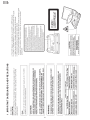
1
DV-L70S
DV-L70BL
DV-L70W
SERVICE MANUAL
SY9S7DV-L70S/
SERVICE MANUAL
PORTABLE DVD VIDEO PLAYER
MODELS
DV-L70S
DV-L70BL
DV-L70W
PORTABLE DVD VIDEO PLAYER
In the interests of user-safety (Required by safety regulations in some countries) the set should be restored to its
original condition and only parts identical to those specified
be used.
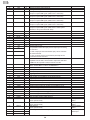
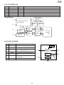
CONTENTS
MODELS DV-L70S/BL/W
Page
1. IMPORTANT SAFEGUARDS AND PRECAUTIONS ......................................................................... 2
2. FEATURES ........................................................................................................................................ 4
3. SPECIFICATIONS ............................................................................................................................. 4
4. PART NAMES .................................................................................................................................... 6
5. DISASSEMBLY METHOD ................................................................................................................. 7
6. ADJUSTMENT METHOD ................................................................................................................... 8
7. TEST MODE .................................................................................................................................... 13
8. TROUBLESHOOTING ..................................................................................................................... 16
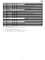
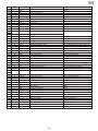
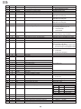
9. IC FUNCTION LIST .......................................................................................................................... 20
10. SEMICONDUCTOR LEAD IDENTIFICATION ................................................................................. 52
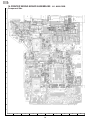
11. WIRING DIAGRAM .......................................................................................................................... 53
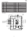
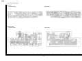
12. BLOCK DIAGRAMS ......................................................................................................................... 54
13. SCHEMATIC DIAGRAMS ................................................................................................................ 62
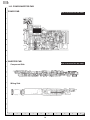
14. PRINTED WIRING BOARD ASSEMBLIES ...................................................................................... 74
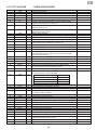
15. REPLACEMENT PARTS LIST ......................................................................................................... 79
16. PACKING OF THE SET ................................................................................................................... 92
SHARP CORPORATION
1
1. IMPORTANT SAFEGUARDS AND PRECAUTIONS
DV-L70S
DV-L70BL
DV-L70W
2
DV-L70S
DV-L70BL
DV-L70W
åCAUTION
BEFORE BATTERY DESTROY
Ë NICKEL-CADMIUM BATTERY
The following program is available in the United States. Please consult local environmental authorities concerning the
availability of this or other programs in your area.
The RBRCTM Seal
SHARP participates in the RBRCTM* Nickel-Cadmium Battery Recycling Program in the United States. The RBRCTM
Seal on our battery pack contained in our product indicates that SHARP is voluntarily participating in an industry
program to collect and recycle these batteries. The RBRCTM program provides you with a convenient alternative
to placing spent Nickel-Cadmium battery packs into the trash or municipal waste stream, which is illegal in some
areas. At the end of their useful life, the Nickel-Cadmium battery can be dropped off at the nearest collection center
for recycling. For information on the nearest collection center, call 1-800-8-BATTERY or your local recycling
center. If you are located outside the United States, contact your local authorities for information concerning proper
disposal and/or recycling of this battery. SHARP's involvement in this program is part of our commitent to protecting
our environment and conserving natural resources.
[Footnote] *RBRCTM is a trademark of the Rechargeable Battery Recycling Corporation.
Ë NICKEL-METAL HYDRIDE BATTERY
Ë LITHIUM or LITHIUM-ION BATTERY
Ë SEALED LEAD BATTERY
Battery disposal
Contains the above Rechargeable Battery. must be recycled or disposed of properly.
Remove the Battery from the products and contact Federal or State Environmental Agencies for information on
recycling and disposal options.
3
DV-L70S
DV-L70BL
DV-L70W
2. FEATURES
7" LCD Screen and Stereo Speakers
• A big 7" LCD screen and built-in stereo speakers provide exciting DVD viewing, even without connecting to a TV.
• Dolby Virtual provides high-quality surround sound.
2-WAY Power Supply (Battery pack is sold separately.)
• A 2-way power supply allows operation using the supplied AC adapter for indoor play, or the battery pack sold
separately for outdoor play.
Compact, Lightweight Design
• About the size of a movie DVD case, your DVD player is designed to go along just about anywhere.
High-Resolution Images, High-Quality Sound
• A high-resolution 336,960-pixel LCD screen produces images of outstanding quality.
• Digital gamma correction and digital super picture provide more realistic image detail.
• Dolby Virtual ensures richer sound from two built-in speakers.
AV input/output, optical digital output jack equipped as standard
• An optical digital output jack (which doubles as the audio input/output jack) can be used to output a stream of *1Dolby
Digital 5.1 channel audio, *2DTS digital audio and Audio MPEG. Connecting a Dolby Digital/DTS/Audio MPEG digital
surround processor or amplifier to this jack creates an environment of amazingly powerful surround sound.
• The AV input/output jack can be used to connect a video deck or camcorder to your DVD player. Or you can use these
jacks to connect to a TV for big-screen viewing. (Output only is supported for S-video. An S-video signal cannot be
input to your DVD player.)
*1 Manufactured under license from Dolby Laboratories. "Dolby", "Pro Logic" and the double-D symbol are trademarks
of Dolby Laboratories.
Confidential Unpulished Works. C 1992-1997 Dolby Laboratories, Inc. All rights reserved.
*2 "DTS" and "DTS Digital Surround" are trademarks of Digital Theater Systems, Inc.
3. SPECIFICATIONS
Product:
Model:
Signal System:
Supported Disc Types:
Video Input/Output:
S-Video Output:
Audio Input/Output:
Digital Audio Interface:
Audio Output:
Headphones Output:
Display:
Speakers:
Light Source:
Video Signal:
Portable DVD Video Player
DV-L70S/BL/W
NTSC/PAL
DVD (Region Number 2, ALL), Video CD, Audio CD (DV-L70S/BL)
DVD (Southeast Asia: Region Number 3, ALL/Australia and New Zealand:
Region Number 4, ALL), Video CD Audio CD (DV-L70W)
Input/Output Jack: Mini jack × 1 (accepts supplied S-video/video cord)
Input/Output Levels: 1Vp-p (75Ω)
Y Output Level: 1Vp-p (75Ω)
C Output Level: 0.286Vp-p (75Ω)
Output Jack: Mini jack (shared with Video In/Out) × 1
(accepts supplied S-video/video cord)
Input /Output Jack: Mini jack × 1 (accepts supplied audio cord)
Input/Output Levels: 2Vrms (1kHz, 0dB)
Optical digital output: Mini jack (shared with audio In/Out)
0.8W + 0.8W
Output Jack: Mini jack (stereo)
Screen Size: 7 inches (87.8 (315/32") (H) × 155.5 (61/8") (W) mm)
Type: Transmissive TN liquid crystal panel
Drive: TFT (thin transistor) active matrix
Pixels: 336,960 (234 (H) × 480 (W) × 3),
Effective Pixel Rate:99.99% minimum
Two 28mm round speakers
Internal (fluorescent)
Horizontal Resolution: 480 lines (DVD)
S/N Ratio: 60 dB minimum
4
DV-L70S
DV-L70BL
DV-L70W
Audio Signals: Frequency Characteristics:
Linear PCM DVD: 4Hz to 22kHz (48kHz sampling)/
4Hz to 44kHz (96kHz sampling)
CD: 4Hz to 20kHz (EIAJ)
(Audio MPEG Version 2.0)
S/N Ratio: CD: 95 dB 1kHz (EIAJ)
Dynamic Range: Linear PCM DVD: 94dB (EIAJ)
CD: 94dB (EIAJ)
Total Harmonic Distortion Ratio: 0.006% maximum (EIAJ)
Power Requirements: AC Adapter: 9V DC
Power Consumption: Main Power On: 11W average (15.5W maximum)
(AC Adapter) Standby: 0.5W (Power/standby lamp lit red)
Main Power Off:0W
Dimensions: 188 (W) × 141 (D) × 25.4 (H) mm (713/32" × 59/16" × 1")
(except for projections)
Weight: 620g (1.37 lbs)
Operating Temperature: 5°C to 35°C (41°F to 95°F)
Operating Humidity: 80% RH maximum
Storage Temperature: -20°C to 40°C (-4°F to 104°F)
AC Adapter Specifications
Power Requirements: 110 to 240V AC, 50/60Hz
Rated Input Capacity: DVD Operation: 30VA
Charging (110V): 30VA
Rated Output: DVD Operation: 9V DC
Charging: 9V DC
Dimensions: 58 (W) × 104 (D) × 275 (H) mm
(219/64" × 47/64" × 1053/64")
Weight: 170g (0.38 lbs)
Battery Pack Specifications
Type:
DC output:
Capacity:
Operating temperature:
Max. Dimensions:
Lithium-ion type
7.4V
4200mAh
0°C to +40°C (32°F to 104°F) (charging: 10°C to 30°C (50°F to 86°F))
184 (W) × 134.5 (D) × 14.5 (H) mm
(71/4" × 519/64" × 37/64") without protruding parts
Weight: 430g (0.95 lbs)
Specifications are subject to change without notice.
Weight and dimensions are approximate.
Digital Output (linear PCM)
· The digital output format used in this DVD video player is linear PCM audio sampling at 44.1 kHz or 48 kHz.
Linear PCM sound for DVD video discs sampled at 96 kHz cannot be output digitally.
Check the disc jacket for information on the audio sampling used.
3-1. ACCESSORIES
Accessories:
Audio Cord x 1, S-Video/Video cord x 1, AC Power Cord x 1, UM/SUM-3 battery x 2,
Remote Control Unit x 1, Earphones x 1, AC Adapter x 1, Operation Manual x 1
5
DV-L70S
DV-L70BL
DV-L70W
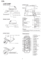
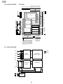
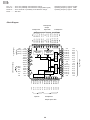
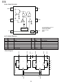
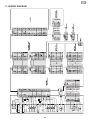
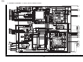
4. PART NAMES
For details on the use of each control.
6
DV-L70S
DV-L70BL
DV-L70W
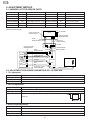
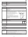
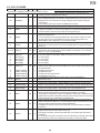
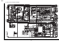
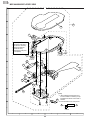
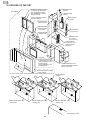
5. DISASSEMBLY METHOD
1
5-1. DISASSEMBLY METHOD
1. Remove the nine screws 1.
2. Loosen the two screws 2.
3. After opening the LCD unit, remove the hinge claw of cabinet A to detach it from
cabinet B.
Note: The power SW button is also removed. Be careful not to forget it when
assembling the unit.
4. Remove the FFC A from the main PWB.
2
A
Power SW Button
5. Remove the screws 3.
Note: Check the screws before assembling because they are different
depending on the right and left hinges.
6. Remove the connector 4 from the main PWB.
7. Remove the pickup FPC/sled lead connector 5.
8. Remove the screws 6 fixing the DC jack PWB.
9. Remove the four LCD rubber caps 7.
10. Remove the four screws 8.
Note: Be careful not to forget to put space washers when assembling because
they are tightened with the above screws.
11. Remove the cabinet D. At this time, remove engagement claws (two on the
upper LCD panel, two on the right and left sides, two on the lower LCD panel).
Note: Do not break the claws on the right and left sides by opening cabinet C
a little.
12. Remove the right and left speaker connectors 9.
5
6
5
4
3
7
Space Washer
8
7
8
Space Washer
9
10
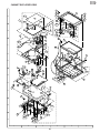
13. Remove the screw 0.
14. Remove the FPC q from the connector.
15. Remove the screw w.
16. Remove the FPC e from the connector.
17. Remove the screw r.
18. Remove the connector t.
12
11
13
14
11
15
19. Remove the four screws y.
20. Remove the three claws on the control panel (front: 2 pcs., rear: 1 pc.).
21. Open the disc cover u 180˚ to remove it from cabinet A.
17
16
7
DV-L70S
DV-L70BL
DV-L70W
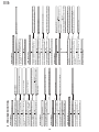
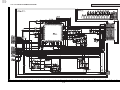
6. ADJUSTMENT METHOD
6-1. HARNESS LIST FOR SERVICE PARTS
Parts Code
Price Code
QCNW-8145GEZZ
AQ
QCNW-8146GEZZ
QCNW-8147GEZZ
Remarks
Parts Code
Price Code
Remarks
P.U. extension, 30-pin
QCNW-8151GEZZ
AQ
Inverter extension, 6-pin
AQ
Spindle extension, 13-pin
QCNW-8152GEZZ
AQ
LCD panel extension, 32-pin
AN
Sled extension, 2-pin
QCNW-8154GEZZ
AQ
Operation PWB extension, 12-pin
QCNW-8148GEZZ
AM
Power supply extension, 14-pin QCNW-1766TAZZ
BF
Inverter junction PWB
QCNW-8149GEZZ
AQ
Main LCD extension, 14-pin
QPWBF5002GEZZ
BF
LCD junction PWB
QCNW-8150GEZZ
AQ
Main LCD extension, 14-pin
QPWBF5003GEZZ
BF
Pickup junction PWB
Drawing for service jigs
Inverter PWB
Inverter junction PWB
QCNW-1766TAZZ
Panel
LCD junction PWB
QPWBF5002GEZZ
Inverter
QCNW-8151GEZZ
F
F
C
F
F
C
LB
PA
Power
supply PWB
LCD
QCNW-8150GEZZ
Lead wire
Pickup
QCNW-8145GEZZ
FFC
MA
LCD PWB
LC
Pickup junction PWB
QPWBF5003GEZZ
Mechanism
LA
LCD junction
QCNW-8152GEZZ
QCNW-8149GEZZ
AB
CN301
AA
QCNW-8146GEZZ
FFC spindle
AC
Operation cabinet
Main PWB
Lead wire
QCNW-8147GEZZ
Sled
CN302
FFC
Power supply, 14-pole
QCNW-8148GEZZ
AE
AD
QCNW-8154GEZZ
6-2. ADJUSTMENT PROCEDURE AND METHOD OF LCD PWB SIDE
1. 7.5V adjustment
Adjustment VR
Adjustment Point
Input Signal/Setting
Adjustment Method
R1102
Put a voltmeter between 6PIN (+7.5V) and 4PIN (GND) of TP1191.
No input
Adjust it to 7.50±0.02V.
2. Free run adjustment
Adjustment VR
Adjustment Point
Input Signal/Setting
Adjustment Method
R1104
Observe the 3PIN of TP1191 with a frequency counter.
No input, external input mode
Adjust it so as to get the HSY frequency of 15.625±0.01KHz
(64.0µS).
HSY
15.625KHz
(64.0µS)
3. Screen center adjustment
Adjustment VR
Adjustment Point
Input Signal/Setting
Adjustment Method
R1103
Visual observation of the panel
Monoscope full screen
Adjust the screen so that it is located in the center.
8
DV-L70S
DV-L70BL
DV-L70W
6-3. CHECK ITEMS OF LCD PWB SIDE
1. Power supply voltage check
Adjustment Point
Input Signal/Setting
Adjustment Method
Put voltmeters in 4PIN (GND), 5PIN (-16V) and 7PIN (13V) of TP1191.
Check in the DVD mode.
Check that each voltage indicates -16±1V and 13±0.5V respectively.
2. Free run check
Adjustment Point
Input Signal/Setting
Adjustment Method
Check the panel visually by connecting to the checker.
External input
Check that the horizontal movement of ODS is 1 mm or less when
inputting a signal in the external input mode with no signal input.
Input
6-4. ADJUSTMENT PROCEDURE AND METHOD OF MAIN PWB SIDE
1. Press the UP+DOWN key is pushed at the same time, and made power source on.
2. It moves to the special mode(SP MODE), and a BACKLIGHT(HI/LOW/OFF) key is pushed and turned off.
3. After setting is completed, a power source is turned off.
4. Again, a UP+DOWN key is pushed at the same time, and a power source is turned on and made special mode.
5. An INPUT/ DVD key is pushed, and it becomes adjustment mode.
6. Each operation in the adjustment mode changes as follows:
(1) Switch the adjustment block with the TILT key input.
DAC adjustment
OPT adjustment
BAT adjustment
(2) Perform paging of each adjustment block with the RETARN key.
TV1
TV2
TV3
(3) Switch each adjustment item with the menu key input.
TV1 adjustment
GAM0
SBRI
GPOS
CONT
TV2 adjustment
WB-R
WB-B
SCOL
STIN
TV3 adjustment
COM
OSDH
BBRI
GAM2
(4) Change each adjustment value with the left or right cursor key.
9
DV-L70S
DV-L70BL
DV-L70W
1. DAC adjustment
(1) TV1 adjustment
Adjustment VR
GAM0
Initial value "44" adjustment is unnecessary.
Adjustment VR
Adjustment Point
Input Signal/Setting
SBRI
————
It is set in "56".
Adjustment VR
Adjustment Point
Input Signal/Setting
Adjustment Method
GPOS
Connect the oscilloscope to COM output (6PIN of TP1901) and GND.
Black-and-white 10STEP
Adjust the common amplitude to 8.0±0.1Vp-p.
8.0±0.1Vp-p
Adjustment VR
Adjustment Point
Input Signal/Setting
Adjustment Method
GAM2
Connect the oscilloscope to 3PIN (VG) and GND of TP1901.
Black-and-white 10STEP
Adjust the Vpp of VG to 4.3±0.1Vp-p.
4.3±0.1Vp-p
Adjustment VR
Adjustment Point
Input Signal/Setting
Adjustment Method
CONT
Connect the oscilloscope to 3PIN (VG) and GND of TP1901.
Black-and-white 10STEP
Adjust the Vpp of VG to 3.3Vp-p.
White level
3.3±0.1Vp-p
Sync.
Black level
(2) TV2 adjustment
Adjustment VR
Adjustment Point
Input Signal/Setting
Adjustment Method
WB-R
Connect the oscilloscope to 3PIN (VG) and 4PIN (VR) of TP1901.
Black-and-white 10STEP
Adjust the white balance (red) so that peak-peak the equal of green and red output become equal.
Adjustment VR
Adjustment Point
Input Signal/Setting
Adjustment Method
WB-B
Dual the oscilloscope to 3PIN (VG) and 5PIN (VB) and GND of TP1901.
Black-and-white 10STEP
Adjust the white balance (blue) so that peak-peak the equal of green and blue output become equal.
Adjustment VR
Adjustment Point
Input Signal/Setting
Adjustment Method
SCOL
Connect the oscilloscope to 5PIN (VB) and GND of TP1901.
100% color bar
Adjust the blue amplitude of the color bar (black level to peak level) to 3.8±0.1Vpp.
10
DV-L70S
DV-L70BL
DV-L70W
Adjustment VR
Adjustment Point
Input Signal/Setting
Adjustment Method
STIN
Connect the oscilloscope to 5PIN (VB) and GND of TP1901.
100% color bar
It is adjusted so that shakes of the waveform of the blue signal of the color bar may become the
smallest.
(3) TV3 adjustment
Adjustment VR
Adjustment Point
Input Signal/Setting
Adjustment Method
COM
Specified adjustment jig (illuminometer) or visual observation
No input state
Brightness: Center
Perform it in a combination of PWB and the liquid crystal panel which will be supplied as
products finally.
• When using the specified adjustment jig
(Type drawing)
Optimal point
Connect the output of jig to the oscilloscope and
adjust the waveform to the minimum point.
At this time, perform the adjustment several times
to fix the optimal point because the measuring value
hardly changes around the optimal point.
• In case of visual adjustment
Stand or tilt the panel as shown in the figure and check
by shaking your head and seeing whether stripes appear.
If the adjustment is improper, you will see stripes in the
longitudinal direction. Perform the adjustment so that they
do not appear.
Adjust within the above
range to fix the optimal point
Direction of stripe
Adjustment VR
Adjustment Point
Adjustment method
OSDH
Visual observation
Adjust the OSDH of TV3 to 27 mm from the right of screen.
27mm
B brightness
Adjustment VR
Adjustment method
B BRI
Set the B brightness to “76”.
2. OPT adjustment
Adjustment VR
Initialization
OPT adjustment
It is set respectively in WIDE "03", OSDV"00", BL"01", PAL"00".
3. BAR adjustment
Adjustment VR
Initialization
Adjustment Method
BAT adjustment
Stabilized power supply, in the body, connection.
It is made DVD start rise state, and a BACKLIGHT(HI/LOW/OFF) key is pushed and made "HI".
The voltage of the stabilized power supply is adjusted to become 6.4±0.05V in the stabilized
power supply connection part (at DC JACK).
It is set so that the numerical value of the BAT display may become "00"
11
DV-L70S
DV-L70BL
DV-L70W
6-5. CHECK AND READJUSTMENT
1. Free run check
Adjustment VR
Adjustment Point
Input Signal/Setting
Check and
Readjustment
R1104
Visual observation
External input
Check that the horizontal movement of OSD position is 1 mm or less
when inputting a signal in the external input mode with no signal input.
If it is more than 1 mm, adjust it so as to get 1 mm or less.
Input
2. Screen position check
Adjustment VR
Adjustment Point
Input Signal/Setting
Check and
Readjustment
R1103
Visual observation of panel
Monoscope full screen
Check whether the screen is located in the center. If it is not located in the center, adjust it to the
center.
3. Luminance/gradation check
Adjustment VR
Adjustment Point
Input Signal/Setting
Check and
GPOS
Comparison with the standard set
10STEP signal
Check whether the luminance and gradation of 10STEP signal are not different in comparison
with the standard set. If they are different, adjust them so as to get equal to the standard set.
4. Depth check
Adjustment VR
Adjustment Point
Check and
Readjustment
S depth
Comparison with the standard set
Check whether the depth of color is not different in comparison with the standard set. If it is
different, adjust it so as to get equal to the standard set.
5. Tint check
Adjustment VR
Adjustment Point
Check and
Readjustment
S tint
Comparison with the standard set
Check whether the tone is not different in comparison with the standard set. If it is different, adjust
it so as to get equal to the standard set.
12
DV-L70S
DV-L70BL
DV-L70W
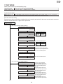
7. TEST MODE
When a power source is put with pushing a key.
Adjustment Mode
ROM renewal mode
A power source is put with pushing and .
It is put with pushing a playback key and a still key.
A power source is put.
When there is a disc Error rate display mode (There are a DVD and CD mode of it, and a disc is put, and a key manipulates.)
When there is
Test mode (Version display mode, color bar pattern display mode, mecha test mode.)
[The flow of the test mode]
A power source is put, and closing, a playback key and a stop key are pushed for about two seconds at the same time
without a disk the disk cover. It goes into the (test mode.
Test mode initial image plane
F0000000 00000000
<The "1" key of the remote controller is pushed.>
The preparation date display of the program
10000000 ∗∗∗∗∗∗∗∗
(Last updata)
The "playback" key of the remote controller is pushed.
Model number display
10000001 ∗∗∗∗∗∗∗∗
(Model number)
Model name Model number
DVL70S
00000702
DV-L70BL
00000702
DV-L70W
00000703
The "playback" key of the remote controller is pushed.
The preparation date display of the program
10000002 ∗∗∗∗∗∗∗∗
(Program ver.)
Region code display
10000003 ∗∗∗∗∗∗∗∗
The "playback" key of the remote controller is pushed.
Region No.
Region cord
4
00000008
3
00000004
2
00000002
(Region code)
The "reactivation" key of the remote controller is pushed.
Microcord version display
Micro-code is the thing of the process
program of the system integrated circuit.
10000004 ∗∗∗∗∗∗∗∗
(Microcode ver.)
The "playback" key of the remote controller is pushed.
The preparation date display of the servo program
10000005 ∗∗∗∗∗∗∗∗
(Servo ver.)
The "playback" key of the remote controller is pushed.
It is returned to the test mode initial image plane.
<The "2" key of the remote controller is pushed.>
There is no copy guard signal.
As for the symptom when it was
dubbed in the video tape recorder?
Color bar display
20000001 00000000
The "playback" key of the remote controller is pushed.
AGC only
As for the symptom when it was
dubbed in the video tape recorder?
Color bar display
20000002 00000000
Color bar display
20000003 00000000
The "playback" key of the remote controller is pushed.
AGC+Color stripe1
As for the symptom when it was
dubbed in the video tape recorder?
The "playback" key of the remote controller is pushed.
AGC+Color stripe2
As for the symptom when it was
dubbed in the video tape recorder?
Color bar display
20000003 00000000
To (1)
13
DV-L70S
DV-L70BL
DV-L70W
From (1)
<The "3" key of the remote controller is pushed.>
Mecah test mode display
30000000 00000000
When it failed in servo initialization.
It is returned to the test mode initial image plane
by pushing "the playback" of the remote
controller and a "stop" key at the same time.
Mecah test mode display
3000E000 EEEEEEEE
<The "1" key of the remote controller is pushed.>
A playback key and a stop key are pushed at
the same time, and it is returned to the test mode
initial image plane.
Laser test mode display
0D000100 00000000
The "playback" key of the remote controller is pushed.
The emission of the laser can be confirmed when
a disk cover is opened and a cap switch is
pushed with the thin bar and so on.
Note:Not to face the light of the laser squarely,
caution!
The "playback" key of the remote controller is pushed.
DVD mode (Light is sent out by DVD laser,
and a pickup is moved to the circumference.)
DD000100 00000000
CD mode (Light is sent out by CD laser,
and a pickup is moved to the circumference.)
Slead motor is rotated, and it moves a pickup to
the circumference.
CD000100 00000000
The "playback" key of the remote controller is pushed.
It is returned to the cause in power source off.
How to distinguish a difference in the DVD laser
and the CD laser.
DVD laser is lighter in comparison with the CD laser.
Note:Not to face the light of the laser squarely,
caution!
The "playback" key of the remote controller is pushed.
Laser off mode (Light isn't sent out by laser,
and a pickup is moved to the circumference.)
FD000100 00000000
<Disk is put, and the "2" key of the remote controller is pushed.>
*It is usually returned in power source off for the state.
DDT mode
0D00E201 000000EE
DDT mode
0D000100 00000000
When a disk is not in.
The "playback" key of the remote controller is pushed.
DDT step 1
DD000201 ∗∗++--00
It is executed to focus on of DDT.
Focus offset value(∗∗)
Track offset value(++)
0 layer focus balance value(--)
The "playback" key of the remote controller is pushed.
DDT step 2
DD000202 ∗∗++0000
A track, slead on are done after RF gain outline adjustment and track balance adjustment are done.
0 layer RF gain value(∗∗)
Track balance value(++)
0 layer focus balance value
The "playback" key of the remote controller is pushed.
DDT step 3
DD000203 ∗∗++0000
Just focus adjustment is done.
RF gain adjustment is done again after the completion.
0 layer focus balance value(∗∗)
Track RF gain value(++)
The "playback" key of the remote controller is pushed.
Focus gain adjustment is done.
0 layer focus gain value(∗∗)
DDT step 4
DD000204 ∗∗000000
The "playback" key of the remote controller is pushed.
Track gain adjustment is done.
Track gain value(∗∗)
DDT step 5
DD000205 ∗∗000000
The "playback" key of the remote controller is pushed.
DDT step 6
DD000206 ∗∗++0000 (DVD)
DD000206 00000000 (CD)
A two-layer disk does just focus of layer 1 and focus gain adjustment.
A CD does reading of TOC.
1 layer focus gain value(∗∗)
1 layer focus balance value(++)
To (2)
14
DV-L70S
DV-L70BL
DV-L70W
From (2)
The "playback" key of the remote controller is pushed.
Servo version display
F1000001 99071400
The "playback" key of the remote controller is pushed.
Focus offset value display
F1000002 ∗∗∗∗∗∗∗∗
The "playback" key of the remote controller is pushed.
Track offset value display
F1000003 ∗∗∗∗∗∗∗∗
The "playback" key of the remote controller is pushed.
0 layer focus balance value display
F1000004 ∗∗∗∗∗∗∗∗
The "playback" key of the remote controller is pushed.
1 layer focus balance value display
F1000005 ∗∗∗∗∗∗∗∗
The "playback" key of the remote controller is pushed.
Track balance value display
F1000006 ∗∗∗∗∗∗∗∗
The "playback" key of the remote controller is pushed.
0 layer focus gain value display
F1000007 ∗∗∗∗∗∗∗∗
The "playback" key of the remote controller is pushed.
1 layer focus gain value display
F1000008 ∗∗∗∗∗∗∗∗
The "playback" key of the remote controller is pushed.
Track gaine value display
F1000009 ∗∗∗∗∗∗∗∗
The "playback" key of the remote controller is pushed.
RF swing value display
F100000A ∗∗∗∗∗∗∗∗
The "playback" key of the remote controller is pushed.
RF gain value display
F100000B ∗∗∗∗∗∗∗∗
The "playback" key of the remote controller is pushed.
The inside switch ID value display
F100000C ∗∗∗∗∗∗∗∗
The "playback" key of the remote controller is pushed.
15
16
Check the switch SW9001.
Check the FET-TrQ9006.
Are the connector CN9002 and FFC wire normal?
NO
NO
NO
YES
NO
Check the DC jack and fuse F9001.
NO
Is key switch contact and installation state?
YES
Is the control voltage normally into the pins 95
and 96 of IC504? (95pin-key1, 96pin-key2)
YES
Check the peripheral circuit or replace IC504.
NO
Key manipulation on the DVD function side doesn't function.
FLOW CHART NO.4
Replace key switch.
Check the IC9001 and FET-TrQ9002.
Check the fuse F9002.
Check the FET-TrQ9003, D9003 and L9003.
Check the IC9001 and FET-TrQ9004.
YES
Check the IC3200 and IC3205 on the main PWB.
(Power-H line.)
Flow Chart NO.2
Flow Chart NO.3
NO
NO
Is almost the same voltage as the input voltage being
applied to the source pins 1 - 3 of FET-TrQ9001?
YES
NO
Is the pulse being applied to the gate pin 4 of
FET-TrQ9001? Or, is the voltage 1.5V or less?
YES
Check the FET-TrQ9001, D9002 and L9002.
3.2V is not being output.
FLOW CHART NO.3
Is the pulse being applied to the gate pin 4 of
FET-TrQ9006? Or, is the voltage 1.5V or less?
4.95V is not being output.
FLOW CHART NO.2
3.2V and 4.95V are not output to the pins 2 - 3
and pins 6 - 8 of connector CN9002, respectively.
YES
Is almost the same voltage as the input voltage being
applied to the source pins 1 - 3 of FET-TrQ9006?
YES
Is the voltage of gate pin 4 of FET-TrQ9006 1.5V
or less?
YES
Is almost the same voltage as the input voltage
being output to the drain pins 5 - 8 of Q9006?
YES
Is the "H" voltage being applied to the pin 1 of
connector CN9002?
YES
Check the IC9001, Q9005, D9004 and D9005.
The power is not turned on.
FLOW CHART NO.1
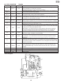
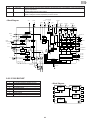
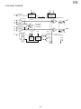
8. TROUBLESHOOTING
NO
YES
YES
Check IC701 their periphery.
YES
Is 4.8V being applied to the pins 16 and 17 of
IC701?
Does the pickup move in the direction of inner
periphery?
YES
After moving in the direction of inner periphery,
does the pickup move in the direction of outer
periphery?
Is the tray lid open?
The disc does not rotate.
FLOW CHART NO.7
YES
Check IC504, IC3200, IC3205 and their periphery.
Operation is possible from the DVD, but no
operation is possible from the infrared remote
control.
YES
Is 4.8V voltage supplied to the pin 2 terminal of
remote control receiver?
YES
Is the "L" pulse sent out pin 3 terminal of receiver
when the infrared remote control is activated?
YES
Is pulse signal supplied to the pin 32 of IC504
and the pin 40 of IC3200?
NO
NO
NO
NO
NO
NO
NO
NO
No operation is possible from the infrared remote control.
FLOW CHART NO.6
Is key switch contact and installation state?
YES
The key matrix circuit of IC3200 is checked.
30~27pins(S0~S3), 26, 25,20pins(K0~K3), D3102,
D3103~3108
YES
Check the main PWB unit of IC3200 and IC3205.
Key manipulation on the LCD function side doesn't function.
FLOW CHART NO.5
Check the M_4.8V line.
Check the cable connecting to the CN702.
(Check the line of pins 1 and 2 of CN702.)
Check the cable connecting to the CN302.
(Check the CN302 and line of pins 2 and 3 of IC702.)
NO
When S1001 is pressed, are the pins 1 and 2
short-circuited?
YES
Check the connection between pins 2 or 4 of S1001
and pins 27 of IC504.
Replace the S1001.
Check the line between the remote control receiver
and the pin 32 of IC504 and the pin 40 of IC3200.
Replace the remote control receiver.
Check 5V line. (IC3205)
Replace the remote control receiver or replace the
remote control transmitter is necessary.
Replace key switch.
DV-L70S
DV-L70BL
DV-L70W
NO
NO
17
Is the focus control drive voltage being applied to
the pins 4 and 2 of CN301?
YES
Check the connection of optical pickup cable.
If it is normal, replace the pickup.
YES
Is the focus control voltage being output from the
pins 24 and 25 of IC702?
NO
NO
Is the FE signal being input to the pin 38 of IC707? NO
(Check item for the symptom)
YES
Is the focus control signal being output to the pin NO
43 of IC707?
YES
The disc is not recognized.
(When the focus servo does not function)
FLOW CHART NO.9
YES
Is the FE signal output to the pin 21 of IC303?
When the playback button is pressed while both
tray switch(S1001) and LD switch(S502) are held
down with a disc loaded, the disc rotates but stops
immediately.
The disc is not recognized.
(In case of focus error)
FLOW CHART NO.8
Check the line between IC702 and connector CN301.
Replace the IC702.
Check the line between IC707 and IC702.
NO
Is the focus control voltage being input to the pin
17 of IC702?
NO
YES Is the voltage of 4.8V being applied to the pins 5
and 20 of IC702?
NO
Check the M_4.8V line.
Check the power supply peripheral circuit.
If it is normal, replace the IC707.
Check the line between pin 21 of IC303 and pin
38 of IC707.
Check the connection of optical pickup cable.
If it is normal, replace the optical pickup cable.
In case of DVD:Is the input signal supplied to the
pins (58, 63), (59, 64), (60, 3) and (61, 2)of IC303?
In case of CD: Is the input signal supplied to the pins
(49, 55), (50, 54), (52, 53), 46 and 47 of IC303?
NO
Refer to "The disc is not recognized. (When the
focus servo does not function)".
YES
YES
NO
YES
Does a signal come out in the following, each
output terminal of the integrated circuit?
Picture signal
IC201 4pin Y-SIG.
IC201 7pin C-SIG.
Sound signal
IC801 16pin AUDIO(L-CH)-SIG.
IC801 13pin AUDIO(R-CH)-SIG.
YES
Replace the main pwb unit.
Is the level of RF signal which is output from the
pin 28 of IC303, normal?
Set the disc on the disc tray.
YES
Is it possible to hold normally the disc with the
check?
YES
Both picture and sound do not operate normally.
FLOW CHART NO.12
NO
NO
NO
Is the drive signal (LDO2) of Q308 (LD POWER
CTL) being output to the pin 4 of IC303?
When S502 is pressed, is the base of Q309 0.8V?
YES
NO
Is the voltage of 3.4V being applied to the emitter
of Q308?
YES
NO
Is the voltage of 2.3V being applied to the pin 9
of CN301?
YES
Check the connection of optical pickup cable.
If it is normal, replace the pickup
The CD disc is not recognized.
(When the laser beam does not go on)
FLOW CHART NO.11
YES
Check the connection of optical pickup cable.
If it is normal, replace the pickup.
YES
Is the voltage of 3.1V and 2.3V being applied to
the pins 14 and 23 of CN301, respectively?
NO
Is the drive signal (SEL) of Q301 (LD POWER
ON) being output from the pin 52 of IC707?
NO
Is the drive signal (LDO1) of Q307 (LD POWER
CTL) being output to the pin 45 of IC303?
NO
When S502 is pressed, is the base of Q309 0.8V?
YES
NO
Is the voltage of 3.1V being applied to the emitter
of Q301? And, is the voltage of 3.4V being applied
to the emitter of Q307?
The DVD disc is not recognized.
(When the laser beam does not go on)
FLOW CHART NO.10
Replace the optical pickup unit.
NO
Check for contamination of objective lens of optical
pickup.
YES
It is laundered by the disk cleaner.
Check the loading switch (S502).
Check the line between Q308 and CN301.
Check the A_4.8V line. (Q309)
Check the line between the pin 4 of IC303 and
base of Q308.
Check the line between S502 and R397.
Check the Q301 and line between Q307 and
CN301.
Check the D_3.1V line and A_4.8V line. (Q309)
Check the line from the pin 52 of IC707, through
Q304, to the base of Q301.
Check the line between the pin 45 of IC303 and
base of Q307.
Check the line between S502 and R397.
DV-L70S
DV-L70BL
DV-L70W
NO
IC1801 5pin C-SIG.
18
NO
NO
Is TFT LCD CONTROL PROCESSOR (IC1101)
normal?
YES
LCD panel peripheral circuit and the existence of
the failure place of the appearance are confirmed.
Is the COM2 bias level of the LCD panel normal?
YES
YES
YES
NO
Do 19 of IC1801, 21, 24 pin (VR, VG, VB) output
appear?
YES
Is a power source being supplied to the LCD panel NO
normally?
VGH(+13V), VSS(-16V), VCC(-10.9V), VSH(4.8V),
VGL(-10V)
NO
NO
NO
A disk is set on the tray, and played back.
It confirms that there is no problem by flowchart
NO.12.
YES
Are the video signals inputted to the pins of LCD
DECODER IC1801.
IC1801 3pin Y-SIG.
Picture do not operate normally.
FLOW CHART NO.14
Check the peripheral circuit of IC2102, Q1805,
Q2102, D2301, D2303.
Does a signal come out in the following, each
output terminal of the integrated circuit?
Picture signal
IC2102 12pin Y-SIG.
IC2102 8pin C-SIG.
IC2102 10pin CVBS-SIG.
NO
A video signal doesn't come out in the outside
projected image output terminal (J6002).
FLOW CHART NO.13
Check the peripheral circuit of IC1101.
Doesn't the voltage adjustment of the line come off
+7.5V? If it deviates, it is readjusted with R1102.
YES
COMMON AMP., CURRENT DET. circuit are
examined. (Q1102~1103, IC1103, etc.)
YES
COMMON Doesn't AMP. adjustment come off?
If it deviates, it is readjusted based on the GPOS
adjustment.
A LCD panel power circuit and rogic circuit are
examined. (IC1000, Q1100, T1100, etc.)
Check the peripheral circuit of IC1801.
Check the line between the pin 4 of IC201 and
pin 3 of IC1801. (Q203~204, IC2101, Q1801,
Q1807, Q1808)
Check the line between the pin 7 of IC201 and
pin 5 of IC1801. (Q201~202)
The outside output terminal (J6002) peripheral is
checked from pins 12 and 8 of IC2102.
The VIDEO DRIVER circuit composed of Q2201,
Q2206 is examined.
YES
NO
NO
YES
NO
NO
NO
Check the LCD panel unit.
NO
Is (the 14,16 pin of IC1801) doing oscillation
(4.43MHz) with VCO of the chroma circuit
normally?
YES
Is the outside horizontal synchronizing of 34 pin of NO
IC1801 normal?
YES
NO
Does 6 pin of IC1801 gain the control voltage
(about 3.0V) of COLOUR?
NO
NO
Are 19 of IC1801, 21, 24 pin (VR, VG, VB) output
normal?
NO
A colour doesn't have it about the picture image.
FLOW CHART NO.17
Check the LCD panel unit.
Are 19 of IC1801, 21, 24 pin (VR, VG, VB) output
normal?
YES
Is white balance normal?
Does 7 pin of IC1801 gain the control voltage
(about 3.1V) of TINT?
YES
Colour of the picture image is abnormal.
FLOW CHART NO.16
Is the voltage of pins 5, 6, 7, and 8 of TP1191
normal?
YES
NO
Is TFT LCD CONTROL PROCESSOR (IC1101)
normal?
YES
LCD panel peripheral circuit and the existence of
the failure place of the appearance are confirmed.
Is the backlight going on?
No picture
FLOW CHART NO.15
Check the chroma periphery circuit of IC1801.
Check the peripheral circuit 6 pins of IC1801.
Check the pins 38, 44, 43 of IC1101 and L1109,
D1105, IC1102, Q1101, etc.
Check the periphery circuit of X1801 and pins 14,
16 of IC1801.
Check the chroma periphery circuit of IC1801.
The readjustment of white balance is done.
Check the periphery circuit 7 pin of IC1801.
Check the periphery of IC1101.
Check the periphery of IC1000, Q1100 and T1100.
Replace the inverter unit.
Check the pin 49 of IC3200 and pin 9 of IC3201.
NO
Is each voltage of CN1105 normal?
YES
NO Is the oscillation of inverter normal?
YES
Replace the backlight.
DV-L70S
DV-L70BL
DV-L70W
19
Is a signal being inputted to the following, each
output terminal of the integrated circuit?
IC6203 12pin AUDIO(L-CH)-SIG.
IC6202 12pin AUDIO(R-CH)-SIG.
YES
Is a signal being inputted to the following, each
output terminal of the integrated circuit?
IC6002 2pin AUDIO(L-CH)-SIG.
IC6002 6pin AUDIO(R-CH)-SIG.
YES
Does a signal come out in the following, each
output terminal of the integrated circuit?
IC6203 2, 5pin AUDIO(L-CH)-SIG.
IC6202 4pin
AUDIO(R-CH)-SIG.
YES
Set the disc on the disc tray.
It confirms that there is no problem by flowchart
NO.12.
YES
Is a signal being inputted to the following, each
output terminal of the integrated circuit?
IC6000 3pin AUDIO(L-CH)-SIG.
IC6000 5pin AUDIO(R-CH)-SIG.
YES
Is a signal being inputted to the following, each
output terminal of the integrated circuit?
IC6203 2, 5pin AUDIO(L-CH)-SIG.
IC6202 5pin
AUDIO(R-CH)-SIG.
YES
Sound do not operate normally.
FLOW CHART NO.19
Is the horizontal position of the picture image
normal?
YES
Check the LCD panel unit.
Is the PDP signal of 38 pin of IC1101 normal?
YES
Is the synchronizing signal of 7 pin of IC1101
normal?
YES
The synchronism of the picture image can't be taken.
FLOW CHART NO.18
Check the line between the pins 1, 7 of IC6000 and
pins 2, 5 of IC6203 and IC6202.
NO
Is the control signal of IN_H added to each of 9 of
IC6203 and IC6202, the 10 pin?
YES
The control peripheral circuit of IN_H is examined
in each of 9 of IC6203 and IC6202, the 10 pin.
The line of the space to 12 pin of IC6203, IC6202 is
checked through sound volume (R6010) from 4 pin
of IC6203, IC6202.
The actuation of the audio mute circuit of Q2004,
Q2005, Q6615, Q6616 is checked.
YES
The control signal line of SMUT is checked.
NO
NO
NO
The control signal line of IN_H is checked.
NO
Check the line between the pins 16, 13 of IC801
and pins 3, 5 of IC6000.
Check the peripheral circuit pins 71, 70 of IC1101,
C1122 and R1103 (image plane center position).
YES
The readjustment of R1103 (SCREEN. CENTER
POS.) is done.
Check the pins 38, 44, 43 of IC1101 and pins
L1109, D1105, IC1102, Q1101, etc.
Replace the IC1900.
NO
NO
NO
NO
Check the betweenthe emmiter and pin 36 of IC1801.
NO
Is a synchronizing signal being inputted to 36 pin of
IC1801?
YES
Is a synchronizing signal being outputted to 3 pin
of IC1900?
YES
SYNC SEPA. (IC1900), Q1900 and MONO MULTI
(IC1901), IC1902, IC1801 are checked.
Does a signal come out in the following, each
output terminal of the integrated circuit?
IC6602 1pin AUDIO(L-CH)-SIG.
IC6602 7pin AUDIO(R-CH)-SIG.
YES
The actuation of the audio mute circuit of Q2004,
Q2005, Q6012, Q6013 is checked.
YES
Check the headphone output terminal (J6001).
The headphone audio output is not emitted.
FLOW CHART NO.21
The actuation of the audio mute circuit of Q2004,
Q2005, Q6615, Q6616 is checked.
YES
Check the outside output terminal (J6000).
Does a signal come out in the following, each
output terminal of the integrated circuit?
IC6203 3, 15pin AUDIO(L-CH)-SIG.
IC6202 3, 15pin AUDIO(R-CH)-SIG.
YES
The outside output audio doesn't come out.
(Speaker audio comes out.)
FLOW CHART NO.20
Does a signal come out in the following, each
output terminal of the integrated circuit?
IC6002 16, 13pin AUDIO(L-CH)-SIG.
IC6002 12, 9pin AUDIO(R-CH)-SIG.
YES
Check or replace speaker.
NO
NO
NO
NO
NO
The control signal line of SMUT is checked.
Check the periphery circuit of IC6602.
The control signal line of SMUT is checked.
Is the control signal of IN_H added to each of 9 of
IC6203 and IC6202, the 10 pin?
YES
The control peripheral circuit of IN_H is examined
in each of 9 of IC6203 and IC6202, the 10 pin.
The control signal line of IN_H is checked.
NO
Check or replace IC6002 (AUDIO POWER OUT)
and IC6601 (POWER REG.)
DV-L70S
DV-L70BL
DV-L70W
DV-L70S
DV-L70BL
DV-L70W
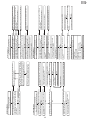
9. IC FUNCTION LIST
DIGITAL VIDEO ENCORDER
I/O
O
O
33
34
35
36
37
TVIN
EXT
F/Vsync
Hsync
TP9
I
I/O
I/O
I/O
I/O
38-41
TP8-5
I/O
42
43
44-47
DVss
DVdd
TP4-1
I/O
48
TP0
I/O
O
O
O
O
O
I
z(O)
I/O(I)
I
(I)
I
I
I
I
Operation function
Analog composite video signal output or Cb signal output current drive (positive)
Analog composite video signal output or Cb signal output current drive (negative)
Power Supply for CVBS / Cb DAC circuit
Analog luminance signal output current drive (positive)
Analog luminance signal output current drive (negative)
Power Supply for Y DAC circuit
Analog chrominance signal output or Cr signal output current drive (positive)
Analog chrominance signal output or Cr signal output current drive (negative)
Power Supply for C/Cr DAC circuit
Ground for DAC circuit
Reference current for the 3 DACs
Power Supply for DAC circuit
Reference full scale voltage for the 3 DACs
I2C chip address select {0 : 42(hex)/43(hex) 1 : 1C(hex)/1D(hex)}
TEST pin (Ground)
If SPI mode, serial data output / If I2C mode, connect to ground
Serial data input, Open drain output / If SPI mode, serial data input
Serial clock
Connect to Ground / If SPI mode, this pin is chip select
Ground for Digital circuit
27MHz clock input
Power Supply for Digital circuit
Reset signal, active LOW
NTSC/PAL select. This pin active only Reset time.(NTSC : Low PAL : High)
8-bit Multiplexd Y/Cr/Cb 4:2:2 data (ITU Rec656) input (1) or Multiplexd Y data
(ITU-Rec656/601) input in 16-bit input mode (DVIN7 : MSB)
TEST data input
Csync/Frame sync output or external VBI information input
Frame sync or Vertical sync input/output
Horizontal sync input/output
MUX switch in 8-bit X 2 Multiplexed Y/Cr/Cb 4:2:2 data (ITU-Rec656) input mode,
or Test data input/output
8-bit Multiplexed 4:2:2 data (ITU-Rec656/601) input (2), or Multiplexed Cr/Cb data
(ITU-Rec656/601) input in 16-bit input mode (MSB : TP8), or Test data input/output
Ground for Digital circuit
Power Supply for Digital circuit
8-bit Multiplexed 4:2:2 data (ITU-Rec656/601) input (2), or Multiplexed Cr/Cb data
(ITU-Rec656/601) input in 16-bit input mode (LSB : TP1), or Test data input/output
For test (should be ground)
ChipA
14
DVdd
43
DVdd
22
DVss
20
F/Vsync
Hsync
35
36
copy
protection
Sync_generator
BG
CGM5_gen
DVIN
48~44 41~38
TVIN
33
TP9
37
clock
21
0
H, V
Y
CC_gen
0
off_set
+
+
demux
Cb
0
Cr
0
Modulator
YVdd
3
CVBS/CbVDD
9
CVdd
4
YOUT
5
YOUT
0
1
CVBSOUT/Cb
2
CVBSOUT/Cb
7
COUT/Cr
8
COUT/Cr
13
VReff
11
Ibias
12
DAVdd
10
DAVss
0
0
BIAS
DVIN0~7
32~25
6
bus
42
TP0~8
23
12C/SPI
PAL/NTSC 24
TEST
17
18
19
SO
SDA/SI
SCL/SCK
SEL
MC44722/3
16
15
20
TP0~9
Reset
34
TEST
DVss
EXT
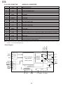
• Block Diagram
DAC
Terminal name
CVBS/Cb
CVBS/Cb
CVBS/Cb Vdd
Y
Y
YVdd
C/Cr
C/Cr
CVdd
DA Vss
Ibias
DA Vdd
VReff
ChipA
TEST
SO
SDA/SI
SCL/SCK
SEL
DVss
CLOCK
DVdd
Reset
PAL/NTSC
DVIN7-0
DAC
Pin No.
1
2
3
4
5
6
7
8
9
10
11
12
13
14
15
16
17
18
19
20
21
22
23
24
25-32
DAC
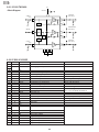
9-1. IC201 MC44722A
DV-L70S
DV-L70BL
DV-L70W
9-2. IC303 IX1517GE
Pin No.
1
2
3
4
5
6
7
8
9
10
11
12
13
14
15
16
Terminal name
GND
P2TP
P2TN
LDO2
MDI2
VrA
VrD
Vdd
DPAC
DPBD
DPD1
DPD2
SCB
SCL
SCD
VRCK
I/O
–
I
I
O
I
O
O
I
–
–
–
–
I
I
I
I
17
18
19
20
21
22
23
24
25
26
27
28
29
30
31
32
VCKF
VccP
LVL
TEO
FEO
DFTN
VccS
RPZ
RPO
RPB
RPP
RFO
NC
NC
VccR
DPDB
–
–
O
O
O
I
–
O
O
O
O
O
–
–
–
I
33
TEB
I
34
FEB
I
35
36
37
PSC
Vcc2
NC
I
–
–
38
EQD
I
39
40
41
42
43
GND2
RFDC
RFA
EQB
EQF
–
–
O
I
I
44
45
46
47
48
49
50
51
MDI1
LDO1
P1TN
P1TP
NC
P1FN
P1FP
LDP1
I
O
I
I
–
I
I
I
52
P1DI
I
RF SIGNAL PROCESSOR
Operation function
GND terminal.
TE+input (CD)
TE–input (CD)
Drive ouput
Monitor input
Analog VREF
Digital VREF
Power terminal
DPD AC combination capacity 1
DPD AC combination capacity 2
DPD integral capacity 1
DPD integral capacity 2
Control line (Bit clock)
Control line (Latch signal)
Control line (Sirial Data)
Reference clock input
Terminal DC Voltage(TYP.)
Remarks
–
VrA
VrA
–
–
2.1[V]
–
Vdd 1/2
4.2V (3.3V)
–
–
–
–
2.2[V]
2.2[V]
2.2[V]
2.3[V]
When frequency is increased, the
filters excepting the servo LPF are
shifted to high frequency side.
Capacity for time constant adjustment
–
Power terminal
–
Servo addition output
Vrd x (1/2)
TE output
VrD
FE output
VrD
DPD difect
–
Low DPD output: Mute
Power terminal (servo)
–
RF ripple center voltage
VrD
RF ripple output
VrD
RF ripple bottom
–
RF ripple peak
–
Equalizing RF output
2.3[V]
NC terminal
–
To be connected to GND
NC terminal
–
To be connected to GND
Power terminal (RF)
–
Pit depth adjustment
VrD
When D PDB is raised, the A/B
side delay increases.
TE balance
VrD
When TEB is raised, the TP side
gain increases and the A+C side
delay increases.
FE balance
VrD
When FEB is raised, the A+C (FP)
side gain increases.
VRCK frequency division ON/OFF
–
High: Frequency division OFF
Power terminal
–
NC terminal
VrD
To be connected to VrD, or to GND
through C
Group delay correction
VrD
When EQD is raised, the group
delay increases at the right side.
GND terminal.
–
DC feedback capacity
–
RF total addition output
2.2[V]
Boost adjustment
VrD
When EQB is raised, the boost increases.
Frequency adjustment
VrD
When EQF is raised, shift to the
high frequency side occurs.
Monitor input
–
Drive output
–
TE–input (DVD)
VrA
TE+input (DVD)
VrA
NC terminal
–
To be connected to GND
FE–input (DVD)
VrA
FE+input (DVD)
VrA
APC polarity 1
–
Positive polarity when this terminal
is connected to Vcc.
D input (DVD)
21
DV-L70S
DV-L70BL
DV-L70W
Pin No.
53
54
55
56
57
58
59
60
61
62
63
64
Terminal name
P1CI
P1BI
P1AI
GNDR
LDP2
I/O
I
I
I
–
I
Operation function
C input (DVD)
B input (DVD)
A input (DVD)
GND terminal (RF)
APC polarity 2
P2AI
P2BI
P2CI
P2DI
GNDS
P2FP
P2FN
I
I
I
I
–
I
I
A input (CD)
B input (CD)
C input (CD)
D input (CD)
GND terminal (Servo)
FE+input (CD)
FE–input (CD)
Terminal DC Voltage(TYP.)
Remarks
VrA
VrA
VrA
–
–
Positive polarity when this terminal
is connected to Vcc.
VrA
VrA
VrA
VrA
–
VrA
VrA
TEB
FEB
PSC
Vcc2
NC
EQD
GND2
RFDC
RFA
EQB
EQF
MDI1
LDO1
P1TN
P1TP
NC
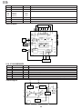
• Block Diagram
48 47 46 45 44 43 42 41 40 39 38 37 36 35 34 33
32 DPDB
P1FN
49
P1FP
50
31 VccR
LDP1
51
30 NC
P1DI
52
APC1
29 NC
sel-RF
57
P2DI
61
GNDS
62
P2FP
63
TE-gain
Adjust
sel-LVL
mode-TE
sel-PD
T-gain
Adjust
Time
constant
adjustment
18 VccP
3
4
5
6
7
8
Vdd
17 VCKF
VrD
GND
Terminal name
A0~A8,A9R
2
20 TEO
19 LVL
BUS
VrA
64
21 FEO
Level detect
3BTE creation
APC2
9-3. IC401 IX1484GE
Terminal
22 DFTN
DPDTE
creation
9 10 11 12 13 14 15 16
4M DRAM
Function
Address input
8
RAS
Row address strobe
23
CAS
Column address strobe
1~5,24~27
DQ1~DQ8
22
OE
Output enable
7
WE
Light enable
Data input/Data output
1, 14
Vcc
Power (5V)
15, 28
Vss
Ground (0V)
6, 21
NC
Not connected
22
VRCK
60
sel-DPD
1
10~13,16~20,9
23 VccS
sel-TE
59
P2CI
P2FN
sel-PD
SCD
58
24 RPZ
FE-gain
Adjust
FE creation
F-gain
Adjust
MDI2
P2BI
25 RPO
LDO2
P2AI
26 RPB
RF Ripple
creation
sel-FE
P2TN
LDP2
sel-IC
F-gain
Adjust
56
P2TP
GNDR
sel-PD
SCL
55
SCB
P1AI
27 RPP
DPD2
54
DPD1
P1BI
28 RFO
EQ
DPBD
53
DPAC
P1CI
R-gain
Adjust
DV-L70S
DV-L70BL
DV-L70W
9-4. IC402 IX1474GE
DEM/ECC (DVD)
Pin No.
1
Terminal name
DPCK1
I/O
I
Operation function
Signal processing reference clock input.
2
3
4
5
6
7
8
9
10
11
12
13
14
15
16
17
18
19
20
21
22
23
24
25
26
27
28
29
30
31
32
33
34
35
36
37
38
39
40
41
42
43
DVDD3
SVCK1
SVCK0
DVSS
DVDD2
N.C.
HDWR
HDRD
ECCCS
D8
D9
D10
D11
D12
D13
D14
D15
DVSS
DVDD5
HINT
HA0
HA1
PLCK
ED0
ED1
ED2
ED3
ED4
ED5
ED6
ED7
TEST
PDON
PDOP
RLLD
LPFN
LPFO
VCOF
SLCO
AVSS
AVR
VRC
–
I
O
–
–
–
I
I
I
I/O
I/O
I/O
I/O
I/O
I/O
I/O
I/O
–
–
O
I
I
I/O
–
–
–
–
–
–
–
–
I
O
O
O
I
O
O
O
–
O
–
Digital power. (3.3V)
Servo reference clock input. (Oscillation circuit input terminal)
Servo reference clock output. (Oscillation circuit input terminal)
Digital power. (0V)
Digital power. (3.3V)
User use prohibited.
MPU write signal.
MPU read signal.
MPU chip selection.
MPU data bus.
MPU data bus.
MPU data bus.
MPU data bus.
MPU data bus.
MPU data bus.
MPU data bus.
MPU data bus.
Digital power. (0V)
Digital power. (5V)
MPU interruption signal. (Occurrence of interruption = “L”)
MPU address bus.
MPU address bus.
Read channel clock input/output terminal.
User use is prohibited (N.C.) since it is for shipping adjustment.
44
45
46
47
48
49
50
51
52
53
54
PVR
AVDD
RVR2
RVDD
RFIN
RVSS
RVR1
DVR
DMO
RASN
CASN
O
–
–
–
I
–
–
I
O
O
O
For shipping adjustment.
PLL phase error signal output. (Negative polarity)
PLL phase error signal output. (Positive polarity)
RLL detection result output.
PLL loop filter amp. reverse input.
PLL loop filter amp. output.
VCO filter terminal.
Built-in comparator reference voltage output terminal.
Analog power. (0V)
Non-PLL system analog reference potential. (1.65V)
Resistance division point potential. (For analog reference
potential generation: 1.65)
PLL system analog reference potential. (1.65V)
Analog power. (3.3V)
2nd reference voltage. (For capacitor connection)
Exclusive-use power terminal. (3.3V)
RF signal input.
Exclusive-use power terminal. (0V)
1nd reference voltage. (For capacitor connection)
DMO reference potential. (1.65V recommended)
Disc equalizer output for DVD. (Triple value PWM + HiZ)
External RAM row address selection. (Negative logic)
External RAM row address selection. (Negative logic)
23
Remarks
0.5-3.3Vp-p Feedback
resistor built in.
For logic cell
3.3V-I/F Feedback
resistor built in.
For logic cell
For logic cell
Open
TTL level
TTL level
TTL level
TTL level
TTL level
TTL level
TTL level
TTL level
TTL level
TTL level
TTL level
For I/O cell
For I/O cell
OPEN DRAIN
TTL level
TTL level
Open
Set to “L”
DV-L70S
DV-L70BL
DV-L70W
Pin No.
55
56
57
58
59
60
61
62
63
64
65
66
67
68
69
70
71
72
73
74
75
76
77
78
79
80
81
82
83
84
85
86
87
88
89
90
91
92
93
94
95
96
97
Terminal name
MOEN
MWEN
DVSS
DVDD3
MA9
MA8
MA7
MA6
MA5
MA4
MA3
MA2
MA1
MA0
DVSS
DVDD5
MD7
MD6
MD5
MD4
MD3
MD2
MD1
MD0
SD7
SD6
SD5
SD4
DVSS
DVDD3
SD3
SD2
SD1
SD0
SERR
SOSO
SVAL
SDCK
DVSS
SREQ
RSTN
DVDD3
STDA
I/O
O
O
–
–
O
O
O
O
O
O
O
O
O
O
–
–
I/O
I/O
I/O
I/O
I/O
I/O
I/O
I/O
O
O
O
O
–
–
O
O
O
O
O
O
O
O
–
I
I
–
O
98
99
100
STCK
UPWM
DVSS
O
O
–
Operation function
External RAM output permission signal.
External RAM read/write selection.
Digital power. (0V)
Digital power. (3.3V)
External RAM address bus.
External RAM address bus.
External RAM address bus.
External RAM address bus.
External RAM address bus.
External RAM address bus.
External RAM address bus.
External RAM address bus.
External RAM address bus.
External RAM address bus.
Digital power. (0V)
Digital power. (5V)
External RAM data bus.
External RAM data bus.
External RAM data bus.
External RAM data bus.
External RAM data bus.
External RAM data bus.
External RAM data bus.
External RAM data bus.
MPEG data output.
MPEG data output.
MPEG data output.
MPEG data output.
Digital power. (0V)
Digital power. (3.3V)
MPEG data output.
MPEG data output.
MPEG data output.
MPEG data output.
MPEG data reliability flag. (Data error: “L”)
MPEG output sector sync signal. (Sector top: “L”)
MPEG data effective flag. (Effective state: “L”)
MPEG data transfer clock.
Digital power. (0V)
MPEG data request flag. (Request state: “L”)
Hard reset input. (Reset state: “L”)
Digital power. (3.3V)
Operation state monitor data.
(Output synchronizing with SDCK fall)
Operation state monitor sync signal. (Data top bit: “L”)
General-use PWM output.
Digital power. (0V)
24
Remarks
For logic cell
For logic cell
For I/O cell
For I/O cell
TTL level
TTL level
TTL level
TTL level
TTL level
TTL level
TTL level
TTL level
For logic cell
For logic cell
For logic cell
TTL level
For logic cell
Common with PWM.
Common with PWM.
4mA, 5V-I/F
For logic cell
DV-L70S
DV-L70BL
DV-L70W
FLASH
Input
A0-A12
Input
A13-A17
Input
25, 24~18,
8~4
3~15,
48, 17
29, 31, 33,
35, 38, 40,
42, 44
30, 32, 34, 36,
39, 41, 43, 45
DQ0-DQ7
Input/Output
DQ8-DQ15
Input/Output
26
CE#
Input
12
RP#
Input
28
OE#
Input
11
WE#
Input
15
RY/BY#
Output
47
BYTE#
Input
13
37
27, 46
9, 10, 14, 16
Vpp
Vcc
GND
NC
• Block Diagram
DQ8-15
DQ0-7
Output
Buffer
Output
Buffer
Input
Buffer
Input
Buffer
I/O Logic
BYTE#
OUTPUT MULTIPLEXER
DATA
ID
Register
QUEUE
REGISTER
CSR
Register
CE#
ESRs
A-1.0~17
OE#
CUI
DQ15/A-1
Data
Comparator
WE#
RP#
Input
Buffer
Y-DECODER
Y GATING/SENSING
RY/BY#
ADDRESS
QUEUE
LATCHES
X-DECODER
WSM
45
Name and function
Byte selection address: When the device is in the x8 mode, the low or high order
byte is selected. It is not used in the x16 mode.
(If BYTE# is high, DQ15/A-1 input circuit does not operate.)
Word selection address: Selection of one word of 16k byte block. These addresses
are latched during data wiring operation.
Block selection address: Selection of 1/32 erase block. These addresses are latched
during data writing, erasing and lock block operation.
Low order byte data input/output: Command user interface writing cycle data and
commandinput. Various data read memory identifier and status data output Chip
nonselection or output disable: Float state
High order byte data input/output: The function is the same as that of low order byte
data input/output. Operative only in x16 mode. x8 mode: Float state DQ15/A-1 is address.
Chip enable: Device control logic, input buffer, decoder and sense amp. are activated.
Chip becomes active only when CE# is “Low”.
Reset/Power down: If RP# is set to “Low”, the control circuit is initialized when power is turned
on. Hence, the RP#pin is set to “Low”. When power is turned on or off or in case of fluctuation
it is kept at “Low” so as to protect data from noise.
When RP# is in “Low” state, the device is in deep power down state. 480 ns is required to
recover from the deep power down state. If the RP# pin becomes “Low”, the whole chip
operation is interrupted and reset. After recovery the device is set to array read state.
Output enable: When OE# is set to “Low”, data is output from the DQ pin. When
OE# is set to “High”, the DQ pin is set to float state.
Write enable: Command user interface, data Q register and address Q latch access
is controlled. In “Low” state WE# becomes active. At rise edge the address and data
are fetched.
Ready/busy: The state of internal write state machine is output. In “Low” state it is
indicated that the write state machine is in operation. If the write state machine waits for
next operation instruction, erase is suspended or it is in deep power down state, the RY/
BY# pin is in float state.
Byte enable: When BYTE# is set to “Low”, the device is set to the x8 mode. At this
time the DQ8-DQ15 pin becomes float state. Address A-1 selects high order/low order
byte. When BYTE# is “High”, the device is set to the x16 mode. The A-1 input circuit is
disabled.
Write/erase power supply: 5.0 ± 0.5V is applied during writing/erasing.
Device power supply: 5.0 ± 0.5V
Ground
Nonconnection
16-KBYTE
Block 31
Type
16-KBYTE
Block 30
Symbol
16-KBYTE
Block 1
Pin No.
16-KBYTE
Block 0
9-5. IC501 IX1697GE
Program Erase
Voltage Switch
VPP
VCC
GND
ADDRESS
COUNTER
25
DV-L70S
DV-L70BL
DV-L70W
PD7/D15
PD6/D14
PD5/D13
PD4/D12
PD3/D11
PD2/D10
PD1/D9
PD0/D8
PE7/D7
PE6/D6
PE5/D5
PE4/D4
PE3/D3
PE2/D2
PE1/D1
PE0/D0
SYSCON
Vcc
Vcc
Vcc
Vcc
Vcc
Vss
Vss
Vss
Vss
Vss
Vss
Vss
Vss
Clock oscillator
Port G
A/D converter
PPG
P35/SCK1
P34/SCK0
P33/RxD1
P32/RxD0
P31/TxD1
P30/TxD0
P50
P51
P52
P53/ADTRG
P47/AN7/DA1
P46/AN6/DA0
P45/AN5
P44/AN4
P43/AN3
P42/AN2
P41/AN1
P40/AN0
Vref
AVcc
AVss
Port 4
P10/PO8/TIOCA0/DACK0
P11/PO9/TIOCB0/DACK1
P12/PO10/TIOCC0/TCLKA
P13/PO11/TIOCD0/TCLKB
P14/PO12/TIOCA1
P15/PO13/TIOCB1/TCLKC
P16/PO14/TIOCA2
P17/PO15/TIOCB2/TCLKD
P20/PO0/TIOCA3
P21/PO1/TIOCB3
P22/PO2/TIOCC3
P23/PO3/TIOCD3
P24/PO4/TIOCA4
P25/PO5/TIOCB4
P26/PO6/TIOCA5
P27/PO7/TIOCB5
Port 2
Port 3
D/A converter
PA7/A23/IRQ7
PA6/A22/IRQ6
PA5/A21/IRQ5
PA4/A20/IRQ4
PA3/A19
PA2/A18
PA1/A17
PA0/A16
PB7/A15
PB6/A14
PB5/A13
PB4/A12
PB3/A11
PB2/A10
PB1/A9
PB0/A8
PC7/A7
PC6/A6
PC5/A5
PC4/A4
PC3/A3
PC2/A2
PC1/A1
PC0/A0
Port 5
TPU
Port 1
9-7. IC506 IX1618GE
Port B
WDT
SCI
Port 6
P67/CS7/IRQ3
P66/CS6/IRQ2
P65/IRQ1
P64/IRQ0
P63/TEND1
P62/DREQ1
P61/TEND0/CS5
P60/DREQ0/CS4
Peripheral address bus
DMAC
RAM
PG4/CS0
PG3/CS1
PG2/CS2
PG1/CS3
PG0/CAS
Peripheral data bus
DTC
ROM *
Port F
PF7/ø
PF6/AS
PF5/RD
PF4/HWR
PF3/LWR
PF2/LCAS/WAIT/BFEQO
PF1/BACK
PF0/BREQ
Port C
Interruption
controller
Internal data bus
H8S/2000 CPU
Internal address bus
MD2
MD1
MD0
EXTAL
XTAL
STBY
RES
WDTOVF
NMI
Port E
Port A
Port D
Bass Controller
9-6. IC504 IX1478GE
SYSCON
A0
VCC
GND
A14
ROW
DECODER
512 x 2048
MEMORY ARRAY
INPUT DATA
CIRCUIT
COLUMN I/O
A15
A16
I/O0
I/O8
CE2
CE1
OE
WE
CONTROL
CIRCUIT
26
DV-L70S
DV-L70BL
DV-L70W
9-8. IC512 IX1535GE
Terminal
1
2
3
4
5
6
7
8
9
10
11
12
13
14
15
16
17
18
19
20
21
22
23
24
25
26
27
28
29
30
31
32
33
34
35
36
37
38
39
40
41
42
43
44
45
46
47
48
49
50
51
52
53
54
55
56
57
58
59
60
61
62
63
64
Terminal name
VDD
HADR0
HADR1
HADR2
HCS
HWR
HRD
HDAT0
HDAT1
HDAT2
HDAT3
HDAT4
HDAT5
HDAT6
HDAT7
VSS
VDD
EXPAL (0)
EXPAL (1)
EXPAL (2)
EXPAL (3)
EXPAU (0)
EXPAU (1)
VSS
VDD
EXPAU (2)
EXPAU (3)
EXPBL (0)
EXPBL (1)
EXPBL (2)
EXPBL (3)
VSS
VDD
EXPBU (0)
EXPBU (1)
EXPBU (2)
EXPBU (3)
EXPC (0)
EXPC (1)
EXPC (2)
VSS
EXPC (3)
EXPC (4)
EXPC (5)
EXPD (0)
EXPD (1)
EXPD (2)
VSS
VDD
EXPD (3)
EXPD (4)
EXPD (5)
BUFDO
BUFDI
SBUFBO
SBUFBI
SBUFAO
SBUFAI
MRST
MODE
BUFCO
TEST
BUFCI
VSS
HOST I/F
In/Output
–
Input
Input
Input
Input
Input
Input
In/Output
In/Output
In/Output
In/Output
In/Output
In/Output
In/Output
In/Output
–
–
In/Output
In/Output
In/Output
In/Output
In/Output
In/Output
–
–
In/Output
In/Output
In/Output
In/Output
In/Output
In/Output
–
–
In/Output
In/Output
In/Output
In/Output
In/Output
In/Output
In/Output
–
In/Output
In/Output
In/Output
In/Output
In/Output
In/Output
–
–
In/Output
In/Output
In/Output
Output
Input
Output
Input
Output
Input
Input
Input
In/Output
Input
Input
–
Function
Power +3.3V
CPU Address bus
CPU Address bus
CPU Address bus
CPU Tip select
CPU Write signal
CPU Read signal
CPU Data bus
CPU Data bus
CPU Data bus
CPU Data bus
CPU Data bus
CPU Data bus
CPU Data bus
CPU Data bus
Digital GND
Power +3.3V
General-use input/output terminal Gr.A
General-use input/output terminal Gr.A
General-use input/output terminal Gr.A
General-use input/output terminal Gr.A
General-use input/output terminal Gr.A
General-use input/output terminal Gr.A
Digital GND
Power +3.3V
General-use input/output terminal Gr.A
General-use input/output terminal Gr.A
General-use input/output terminal Gr.B
General-use input/output terminal Gr.B
General-use input/output terminal Gr.B
General-use input/output terminal Gr.B
Digital GND
Power +3.3V
General-use input/output terminal Gr.B
General-use input/output terminal Gr.B
General-use input/output terminal Gr.B
General-use input/output terminal Gr.B
General-use input/output terminal Gr.C
General-use input/output terminal Gr.C
General-use input/output terminal Gr.C
Digital GND
General-use input/output terminal Gr.C
General-use input/output terminal Gr.C
General-use input/output terminal Gr.C
General-use input/output terminal Gr.D
General-use input/output terminal Gr.D
General-use input/output terminal Gr.D
Digital GND
Power +3.3V
General-use input/output terminal Gr.D
General-use input/output terminal Gr.D
General-use input/output terminal Gr.D
Buffer output D
Buffer input D
Schmidt buffer output B
Schmidt buffer input B
Schmidt buffer output A
Schmidt buffer input A
Reset terminal
Mode selection terminal
Buffer output C
Test terminal (for Epson)
Buffer input C
Digital GND
27
DV-L70S
DV-L70BL
DV-L70W
Pin1~15 ........ There is a possibility of simultaneous change.
Pin18~47 ..... There is a possibility of simultaneous change.(Static signal)
Pin50~57 ..... There is almost no possibility of simultaneous change.
Pin63 ............ Not used
Operating frequency: Approx. 10 MHz
Operating frequency: Approx. 1 MHz
Operating frequency: Approx. 1 MHz
• Block Diagram
In/Output Pin
S2(0)
Q2(7)
Q2(6)
Q2(5)
Q2(4)
VDD
EXPBU(3)
EXPBU(2)
EXPBU(1)
EXPBU(0)
VDD
S2(1)
S2(3)
EXPC(3)
In/Output Pin
EXPC(0)
S2(4)
EXPC(4)
EXPC(1)
S2(5)
EXPC(5)
VSS
SOUT(0)
EXPD(0)
S2(2)
SOUT(1)
EXPD(1)
VSS
VSS
SOUT(2)
VSS
EXPD(2)
EXPC(2)
Output:
Open drain
In/Output Pin
48 47 46 45 44 43 42 41 40 39 38 37 36 35 34 33
VDD
32
VSS
VSS
31
EXPBL(3)
Q2(3)
SOUT(4)
EXPD(4) 51
Q2(2)
EXPD(5) 52
30
29
28
27
26
EXPBL(2)
SOUT(5)
EXPBL(1)
Q2(1)
EXPBL(0)
Q2(0)
EXPAU(3)
Q1(7)
EXPAU(2)
Q1(6)
VDD
VDD
BUFDO
Data Buffer
Latch D
Data Buffer
Latch C
53
54
SBUFBO 55
BUFDI
SBUFBI 56
SBUFAI 58
59
60
BUFCO 61
HDAT3
HDAT4
HDAT5
HDAT6
HDAT7
VSS
S1(2)
S1(3)
S1(4)
S1(5)
VSS
HDAT0
D(6)
HDAT2
HRD
D(5)
S1(1)
HWR
D(4)
Input Pin
S1(0)
4 5 6 7 8 9 10 11 12 13 14 15 16
HDAT1
2 3
D(7)
1
HCS
R/W CTL
D(3)
64
HADR2
VSS
HADR1
VSS
Data Buffer
D(2)
BUFCI
D(1)
CK
62
63
VDD
TEST
HADR0
TEST
D(0)
SEL
MRST
MODE
VDD
MRST
MODE
Data Buffer
Latch A
Exclusive-use pin
SBUFAO 57
In/Output Pin
Output: Open drain
28
25
24
23
VSS
VSS
EXPAU(1)
Q1(5)
22
EXPAU(0)
Q1(4)
21
EXPAL(3)
Q1(3)
20
EXPAL(2)
Q1(2)
19
18
17
EXPAL(1)
Q1(1)
EXPAL(0)
Q1(0)
VDD
VDD
In/Output Pin
49
EXPD(3) 50
Data Buffer
Latch B
In/Output Pin
VDD
SOUT(3)
DV-L70S
DV-L70BL
DV-L70W
9-9. IC601 IX1608GE
Pin No.
Pin name
Type I/O
Function
Host interface, CD-DSP interface, subcode interface (32-pin)
Reset input (active low). When deassert is applied in the asserted state, the
141
RESET#
I
I
initializing process of MD36710X is started.
Stand-by input (active low). When it is asserted together with RESET#, all output
pins and bidirectional pins are floated to separate MD36710X electrically from the
130
STNDBY#
I
I
peripherals. The inner operation is wholly stopped to also minimize the power
consumption.
In the stand-by mode, the contents of SDRAM are not held.
142
IDLE
3-S
O
Idle, init or reset state display output (active high)
The data bus width of the host interface is determined. Only during reset,
35
HWID
I
I
change is possible. For the low level (GND), the host interface of MD36710X
is set to 8 bits but set to the 16-bit width for the high level (VDD).
In the 16-bit width mode (HWIS is VDD), the byte order of the data bus of the host
interface is determined.
36
HORD
I
I
It can be changed only during reset. MD36710X is set to input or output m.s. bytes
at HD [15:8] for the low level (GND) and at HD [7:0] for the high level (VDD).
When HWID is at the GND level, it is connected to GND.
The protocol of the host bus is determined. It can be changed only during reset.
47
HTYPE
I
I
MD36710X is set to the type A for the low level (GND) and to the type B for the high
level (VDD).
8 l.s. of the host data bus. When HWID input is connected to GND, only the 8 l.s. signal
12, 14~21 HD[7:0]
3-S
I/O
is defined as the host data signal. When HWID is connected to VDD, it is defined
as the 8 l.s. line of 16-bit data bus.
When HWID is connected to VDD, it becomes the data line 11:8 of the 16-bit host data
7, 9~11
HD[11:8]
3-S
I/O
bus. When HWID is connected to GND, it becomes NC pin as specified below.
7
NC (HD[11])
O
O
For test (output)
9
NC (HD[10])
I
I
For test (input)
10
NC (HD[9])
I
I
For test (input)
11
NC (HD[8])
I
I
For test (input)
When HWID is connected to VDD, it becomes the data line 15:12 of the 16-bit host
3~6
HD[15:12]
3-S
I/O
data bus. When HWID is connected to GND, it becomes CD-DSP serial input port pin
as specified below.
6
CDDAT (HD[12])
I
I
CD-DSP bit clock input
5
CDDAT (HD[13])
I
I
CD-DSP data input
4
CDFRM (HD[14])
I
I
CD-DSP LR clock (frame) input
3
CDERR (HD[15])
I
I
CD-DSP data error input
22,
Host address input. The address signal to specify the physical address in
HA[3:0]
I
I
24~26
MD36710X is input.
29
HCS#
I
I
Host chip select input. Active low
Host protocol A type (HTYPE = GND): HR/W#. Input to determine the host access
27
HWR# (HR/W#)
I
I
direction. Host protocol B type (HTYPE = VDD): HWR#. Host write input (active low).
Host protocol A type (HTYPE = GND): HDS#. Data strobe input (active low).
30
HRD# (HDS#)
I
I
Host protocol B type (HTYPE = VDD): HRD#. Host read input (active low).
Host ready output (active high). To transfer the stream via the host bus using this
signal, use this signal. Moreover, the external pull-up resistor is necessary.
31
HRDY
3-S
O
It is possible to check that the transfer of CodBurstLen byte length is regarded as one
packet and the signal is active before start of transfer of each packet and continuously
write the bit stream up to CodBurstLen into MD36710X.
Interrupt request (Active low). It is deasserted as the host leads the interrupt status
register of MD36710X. Moreover, it is also deasserted after the host masks or resets
32
HIRQ#
3-S
O
the interrupt with the interrupt mask register of MD36710X.
If HIRQ# is not asserted, it enters the 3-state state. (The external pull-up resistor is
necessary.)
Host acknowledge output (active low). For the protocol of type A, MD36710X asserts the
output to inform the end of the read or write cycle.
If the signal is not active, it enters the 3-state state. (The external pull-up resistor is
33
HACK#
3-S
O
necessary.)
For the protocol of type B, it functions as the wait output signal. If the high-speed host
(microcomputer) is used, it is sometimes unnecessary to connect the signal.
29
DV-L70S
DV-L70BL
DV-L70W
Pin No.
Pin name
GPI/O signal (4-pin)
Type
I/O
122,123
3-S
I/O
I
O
I
O
I
I
GPAI/O [1:0]
2
GPSI
159
GPSO
PLL signal (6-pin)
129
GCLK
126
GCLK1
I
I
128
XO
O
O
136
PLLCA
I
I
137,135
PLLCFG [1:0]
Function
General purpose bidirectional pin for monitor and control with ADP microcode.
After resetting, this pin is defined as the input. If ADP command is used, setting is possible.
General purpose input for monitor with DVP microcode.
General purpose output for control with DVP microcode.
27,000MHz clock or crystal input for main processor
27,000MHz master clock input for audio. It must be connected to GCLK during ordinary
operation.
Output to crystal connected to GCLK. If crystal is not used in GCLK, XO is not connected.
Capacitor connection pin for PLL. Connect 47nF capacitor. Connect the other terminal
of the capacitor to PLLGND.
PLL configuration input. Change is possible during reset only. In the normal use, both pins
must be connected to (digital) GND.
Digital video port (24-pin)
92, 94~97,
Y [7:0]
99~101
3-S
O
102,
104~107,
109~111
C [7:0]
3-S
I/O
124
OSDPEL[3:0]
(C[3:0])
OSDPLT (C[4])
VCLKX2
3-S
I/O
84
VCLK
3-S
I/O
90
89
91
88
HSYNC
VSYNC
FI
CBLANK
3-S
3-S
3-S
O
I/O
I/O
I/O
O
85
VMASTER
I
I
87
VDEN#
I
I
3-S
O
In the 16-bit video mode (Video8 = 0), the line becomes the luminance output.
In the 8-bit mode (Video8 = 1), it becomes the luminance/color difference output
which is timely multiple-processed according to ITU-R656 standard (regardless
whether SAV, EAV sync code is present or not).
In the 16-bit video mode (Video8 = 0), the line becomes the color difference output.
In the 8-bit mode (Video8 = 1), the pin 3 (C[7:5]) of m.s. line is not used, and 1.s.5 pin
(C[4:0]) is specified as the input which is received from the external OSD device.
OSD pixel input. The four signals are used as the entry to on-chip OSD pallet.
On-chip OSD pallet selector. OSDPallete0 is selected for the low level, and
OSDpallete1 is selected for the high level.
Main video clock input or output. 27,000MHz
VCLKx2 signal is divided into two parts. The signal is used as the qualifier of the data
and sync signal.
Horizontally sync bidirection signal pin. The polarity and length are programmable.
Vertically sync bidirectional signal pin. The polarity and length are programmable.
Field identification bidirectional signal pin. The polarity is programmable.
Composite blank output. The waveform including the polarity is programmable.
Video master/slave selection input. For the high level, the video synchronization of
MD36710X goes into the master mode. (Accordingly, the video SYNC signal and
clock are output.)
For the low level, the video synchronization goes into the slave mode. (Accordingly,
the video SYNC signal and clock are input.)
Only in the reset mode, the setting of the terminal can be changed.
Video enable input (active low). When it is active, MD36710X outputs the video data.
When it is deasserted, the pixel output goes into the 3-state. (However, the sync
signal and clock are kept to be active.)
Though this input can be changed at any time, it is valid at the following VCKx2 time.
Digital audio port (8-pin)
132
AMCLK
117
S/PDIF(AOUT[3])
O
O
AOUT [2:0]
O
O
112
AIN
I
I
118
ALRCLK
O
O
119
ABCLK
O
O
116~114
Audio master clock input/output. The sampling frequencies of 384fs, 256fs, 192fs
and 128fs can be selected (programmable).
S/DDIF transmitter output. Moreover, it can be connected to DAC as the 4th audio
output (AOUT[3]). After resetting, the pin outputs the low level.
Serial output of PCM stereo audio for DAC. After resetting, the pin outputs the low
level. Only for AOUT[0], the sample width of 24 bits is supported.
Serial input of PCM stereo audio for ADC.
LR clock output of AOUT[3.0] and ATN. For the sampling frequency, it is a rectangular
wave.
The polarity of LR is programmable.
Bit clock output of AOUT[3.0] and AIN. AOUT is output at the rise/fall edges of the
clock (programmable), and AIN is latched.
30
DV-L70S
DV-L70BL
DV-L70W
Pin No.
Pin name
DVD-DSP interface (13-pin)
148
DVDREQ
146
DVDVALID
144
DVDSOS
*1
DVDDAT [7:0]
147
DVDSTRB
143
DVDERR
SDRAM interface (35-pin)
*2
RAMDAT [15:0]
*3
RAMADD [11:0]
56
RAMRAS#
59
RAMCAS#
57
PCLK
61
RAMDQM
54
RAMCS0#
55
RAMCS1#
60
RAMWE#
TEST signal (3-pin)
127
SCNENBL
83
TESTMODE
139
ICEMODE
Power signal (35-pin)
*4
GND
*5
VDD
134
PLLGND (GNDA)
138
PLLVDD (VDDA)
*1
*2
*3
*4
*5
Type
I/O
O
I
I
I
I
I
O
I
I
I
I
I
DVD-DSP data request output (polarity programmable)
DVD-DSP data valid input (polarity programmable)
DVD-DSP data selector start input (polarity programmable)
DVD-DSP data input bus
DVD-DSP data bit strobe (clock) input. Polarity programmable.
DVD-DSP error input. Polarity programmable.
3-S
O
O
O
O
O
O
O
O
I/O
O
O
O
O
O
O
O
O
SDRAM bidirectional data bus
SDRAM address bus output
SDRAM row selection (active low) output
SDRAM column selection (active low) output
SDRAM clock output (similar to the inner process clock)
SDRAM data masking (active high) output
SDRAM chip select (active low) output. For lower order of 2Mbyte device.
SDRAM chip select (active low) output. For higher order of 2Mbyte device.
SDRAM write enable (active low) output.
I
I
I
I
I
I
ground
power
ground
power
Function
Test pin. Usually connected to GNG.
Test pin. Usually connected to VDD.
Test pin. Usually connected to VDD.
Digital GND
Digital power supply (3.3V)
GND of inner PLL circuit
Power supply of inner PLL circuit (3.3V)
158~156, 154~151, 149
79, 77, 75, 72, 70, 67, 65, 62, 64, 66, 69, 71, 74, 76, 78, 82
52, 50, 51, 49, 46, 44, 42, 38, 39, 43, 45, 47
1, 13, 23, 40, 41, 53, 68, 80, 81, 108, 120, 121, 125, 131, 145, 160
8, 18, 28, 33, 48, 58, 63, 73, 103, 113, 133, 140, 150, 155
31
DV-L70S
DV-L70BL
DV-L70W
9-10. IC602 IX0750TA
Terminal
35
18
34
Terminal Name
Name
CLK
System Clock
CS
Chip Select
Input Function
Active on the positive going edge to sample all inputs.
Disables or enables device operation by masking or enabling all inputs
except CLK. CKE and L(U)DQM
Masks system clock to freeze operation from the next clock cycle.
CKE should be enabled at least one cycle prior to new command.
Disable input buffers for power down in stanby.
Row/column address are multiplexed on the same pins.
Row address: RA0~RA10, column address: CA0~CA7
CKE
Clock Enable
A0~A10/AP
Address
BA
Bank Select Address
17
RAS
Row Address Strobe
16
CAS
Column Address Strobe
15
WE
Write Enable
DOML(U)
Data Input/Output Mask
21~24
27~32
20
19
14, 36
2, 3, 5,
DQ0~15
6, 8, 9, 11, 12, 39, 40,
42, 43, 45, 46, 48, 49
Vcc/Vss
25, 1/26, 50
Vcc/VssO
44, 38, 13, 7/4, 10, 41, 47
33, 37
NC/RFU
Data Input/Output
Selects bank to be activated during row address latch time.
Selects bank for read/write during clumn address latch time.
Latches row address on the positive going edge of the CLK with RAS low.
Enables row access & precharge.
Latches addresses on the positive going edge of the CLK with CAS low.
Enables row access.
Enable write operation and row precharge.
Latches data in starting from CAS, WE active.
Makes data output Hi-Z, tsHZ after the clock and masks the output.
Blocks data input when L(U)DQM active.
Data inputs/outputs are multiplexed on the same pins.
Power Supply/Ground
Power and ground for the input buffers and the core logic.
Data Output Power/Ground Isolated power supply and ground for the output buffers to provide
improved noise immunity.
No Connection/
This pin is recommanded to be left No Connection on the device
Reserved for Future Use
• Block Diagram
Row Decoder
Ref. Addr.[0:11]
Address[0:10]
Refresh
Counter
Auto/Self Refresh
Refresh
Interval Timer
Row Addr. Latch/Predecode
Self Refresh Counter
512K x 16
Bank 0
Sense AMP & I/O gates
Column Decoder
Precharge
CKE
Address
Register
Row Active
CS
RAS
CAS
State Machine
BA(A11)
Column Active
Column Addr.
Latch & Counter
Overflow
Burst Length
Counter
WE
Data Input/Output Buffers
CLK
UDQM
Column Decoder
Sense AMP & I/O gates
Row Addr. Latch/Predecode
LDQM
512K x 16
Bank 1
Mode Register
Test Mode
32
I/O Control
DQ0
DQ1
DQ2
DQ3
DQ4
DQ5
DQ6
DQ7
DQ8
DQ9
DQ10
DQ11
DQ12
DQ13
DQ14
DQ15
DV-L70S
DV-L70BL
DV-L70W
9-11. IC701 AN8473NS-1
Pin No.
1
2
3
4
5
6
7
8
9
10
11
12
13
14
15
16
Terminal name
VH
H3L
H3H
H2L
H2H
H1L
H1H
EC
ECR
FG
START
VPUMP
BC1
BC2
GND
VDD
Operation function
Hole bias terminal
Hole element 3 negative input terminal
Hole element 3 positive input terminal
Hole element 2 negative input terminal
Hole element 2 positive input terminal
Hole element 1 negative input terminal
Hole element 1 positive input terminal
Torque command input terminal
Torque command reference input terminal
FG signal output terminal
Start/stop selection terminal
Booster terminal
Booster capacitor connection terminal
Booster capacitor connection terminal
GND terminal
Power terminal
Pin No.
17
18
19
20
21
22
23
24
25
26
27
28
29
30
31
32
Terminal name
VM21
VM22
CS
NC
A31
A32
PG2
A21
A22
PG1
A11
A12
NC
PWMSW
VM12
VM11
Operation function
Motor power terminal 2
Motor power terminal 2
Current detection terminal
N. C.
Drive output 3
Drive output 3
Power current detection terminal 2
Drive output 2
Drive output 2
Power current detection terminal 1
Drive output 1
Drive output 1
N. C.
PWM frequency selection terminal
Motor power terminal 1
Motor power terminal 1
• Block Diagram
5V
0.1µF
0.1µF
100µF
VDD
BC2 BC1 VPUMP
16
START 11
14
Start/stop
13
12
Thermal
protection
Booster circuit
18
2200pF
10
FG
100Ω
17
OSC
32
Amplification
31
H1H 7
H1H
6
5
H2L
4
H3H
Distribution
circuit
2
1
100Ω VH
EC
8
ECR
9
Output
circuit
PWMOUTU
3
H3L
Spindle speed
control signal
Hole
amplifier
matrix
21
22
23
PWMOUTL
Hole
bias
26
Absolute
value
FF
X5
VM22
VM11
VM12
27 A11
A12
28
A21
24
25
Amplification
H2H
(After checking the tolerance
of the electrical characteristics,
the customer determines the
resistance value.)
VM21
A22
A31
A32
PG2
PG1
19
CS
SRESET
VT
PWMSW
HIGH:40kHZ
LOW:80kHZ
30
PWM frequency
connection circuit
Vc1
SSET
33
15
GND
Rcs=0.33Ω
DV-L70S
DV-L70BL
DV-L70W
9-12. IC702 BA5933FP-1
Pin No.
1
2
3
4
5
6
7
8
9
10
11
12
Terminal name
STBY
OUT+
OUTGND
VCC
MUTE
GND
REG_OUT
REG_B
BIAS
IN1'
IN1
Operation function
Stand-by mode selector switch
CH1 positive output terminal
CH1 negative output terminal
GND
VCC
Mute terminal
Substrate GND
Constant voltage output
(collector of external Tr)
Connected to the base of external Tr
Bias input terminal
CH1 gain adjustment input terminal
CH1 gain fixed input terminal
Pin No.
13
14
15
16
17
18
19
20
21
22
23
24
25
Terminal name
OP_OUT
OP_IN(-)
OP_IN(+)
IN2'
IN2
IN3'
IN3
VCC
GND
OUT3OUT3+
OUT2OUT2+
Operation function
Operation amplifier output
Operation amplifier negative input
Operation amplifier positive input
CH2 gain adjustment input terminal
CH2 gain fixed input terminal
CH3 gain adjustment input terminal
CH3 gain fixed input terminal
VCC
GND
CH3 negative output terminal
CH3 positive output terminal
CH2 negative output terminal
CH2 positive output terminal
* The negative/positive pole of the output terminal is the polarity against the input.
• Block Diagram
23
22
x2
x2
x2
x2
21
20
19
18
17
16
8.3KΩ
24
8.3KΩ
25
15
14
+ -
+ -
LEVEL SHIFT
OP-AMP
+ -
8.3KΩ
LEVEL SHIFT
T.S.D.
8.3KΩ
LEVEL SHIFT
1
2
MUTE
x2
3
4
5
6
7
34
8.3KΩ 8.3KΩ
STBY x2
10KΩ 10KΩ
REGULATOR
+ + -
8
9
10
11
12
13
T.S.D ; Thermal shutdown
Unit of resistance is [Ω].
DV-L70S
DV-L70BL
DV-L70W
9-13. IC707 IX1473GE
SERVO PROCCESSOR
Pin No.
1
2
3
4
5
6
Terminal name
VSS
BCK
AOUT
DOUT
MBOB
IPF
I/O
–
O
O
O
O
O
7
SBOK
O
8
CLCK
I/O
9
10
11
12
13
VDD
VSS
DATA
SFSY
SBSY
–
–
O
O
O
14
15
16
17
SPCK
SPDA
COFS
MONIT
O
O
O
O
18
19
20
21
22
VDD
TESIO0
P2VREF
SPDO
PDOS
–
I
–
O
O
23
24
PDO
XMAXS
O
O
25
TMAX
O
26
27
28
29
LPFN
LPFO
PVREF
VCOREF
I
O
–
I
30
31
32
33
34
35
36
37
38
39
40
41
VCOF
AVSS
SLCO
RFIN
AVDD
RFCT
RFZI
RFRP
FEIN
SBAD
TSIN
TEIN
O
–
O
I
–
I
I
I
I
I
I
I
42
43
TEZI
FOO
I
O
Operation function
Digital ground terminal.
Bit clock (1.4122MHz) output terminal.
Audio data output terminal.
Digital out output terminal.
Buffer memory over signal output terminal. Over: “H”
Correction flag output terminal. When correction disable symbol
is given if AOUT output is C2 correction: “H”.
Sub-code Q data CRCC judgment result output terminal.
Judgment result OK: “H”.
Sub-code P to W data read clock output/input terminal.
Selectable with command bit.
Digital + power terminal
Digital ground terminal
Sub code P-W data output terminal.
Playback system frame sync signal output terminal.
Subcode block sync output terminal.
When subcode sync is detected, S1 position: “H”.
Processor status signal read clock (176.4 kHz) output terminal.
Processor status signal output terminal.
Correction system frame clock (7.35 kHz) output terminal.
LSI internal signal monitor terminal.
DSP internal flag and PLL system clock can be monitored with
microcomputer command.
Digital + power terminal.
Test input/output terminal. Usually fixed to “L”.
PLL system 2VREF terminal.
VCO center frequency shift terminal.
EFM and PLCK signal phase error signal output terminal.
(To be used when x8 speed operation is used)
EFM and PLCK signal phase error signal output terminal.
TMAX detection result output terminal.
To be selected with command bit TMPS.
TMAX detection result
Longer than specific period
Shorter than specific period
Within specified period
TMAXoutput
“P2VREFF”
“VSS”
“HiZ”
Reverse input terminal for low pass filter amplifier.
Output terminal for low pass filter amplifier.
PLL system VREF terminal.
VCO center frequency reference level terminal.
To be fixed usually to “PVREF”.
Filter terminal for VCO.
Analog system ground terminal.
Data slice level generation DAC output terminal.
RF signal input terminal.
Analog system power terminal.
RFRP signal center level input terminal.
RFRP zero cross input terminal.
RF ripple signal input terminal.
Focus error signal input terminal.
Sub-beam addition signal input terminal.
Test input terminal. To be fixed usually to “Vref”
Tracking error signal input terminal.
(Fetching when tracking servo is ON)
Tracking error zero cross input terminal.
Focus equalizer output terminal.
35
Remarks
DV-L70S
DV-L70BL
DV-L70W
Pin No.
44
45
46
Terminal name
TRO
VREF
RFGC
I/O
O
–
O
47
TEBC
O
48
FMO
O
49
FVO
O
50
DMO
O
51
52
53
54
55
56
57
58
59
60
2VREF
SEL
FOON
DFCT
SRCH
SHC
VDD
VSS
IO0
IO1
–
O
O
O
O
O
–
–
I/O
61
IO2
62
IO3
63
/DMOUT
64
/CKSE
65
66
67
68
69
70
71
72
73
74
75
76
77
78
79
80
81
82
/DACT
TESIN
TESIO1
VSS
PXI
PXO
VDD
XVSS
XI
XO
XVDD
DVDD
RO
DVSS
DVR
LO
DVDD
TEST1
–
O
–
–
O
–
I
83
TEST2
I
84
TEST3
I
85
86
87
BUS0
BUS1
BUS2
I/O
I/O
I/O
Operation function
Tracking equalizer output terminal.
Analog reference power terminal.
RF amplitude adjustment control signal output terminal.
Output of 3-pole PWM signal. (PWM carrier = 88.2 kHz)
Tracking balance control signal output terminal.
Output of 3-pole PWM signal. (PWM carrier = 88.2 kHz)
Feed equalizer output terminal.
Output of 3-pole PWM signal. (PWM carrier = 88.2 kHz)
Speed error signal or feed search EQ output terminal.
Output of 3-pole PWM signal. (PWM carrier = 88.2 kHz)
Disc equalizer output terminal.
Output of 3-pole PWM signal. (PWM carrier = DSP system
88.2kHz, to be synchronized with PXO)
General use I/O port.
It is possible to select the input port and output port according
to command.
In case of input port the terminal state (H/L) can be read with
the read command.
In case of output port the terminal state (H/L/HiZ) can be
controlled with the command.
Terminal to set the mode to output dual value PWM of feed
equalizer from the IO0,1 terminal and to output the dual value
PWM from disc equalizer of IO2,3 terminal “L” Active.
X’tal selection terminal.
When 16.9344 MHz: “H” When 33.8688 MHz: “L”
Test terminal.
Test input terminal.
Test input/output terminal.
Digital ground terminal.
DSP system clock oscillation circuit input terminal.
DSP system clock oscillation circuit output terminal.
Digital + power terminal.
Ground terminal for system clock oscillation circuit.
System clock oscillation circuit input terminal.
System clock oscillation circuit output terminal.
Positive power terminal for system clock oscillation circuit.
D/A converting section power terminal.
R channel data forward rotation output terminal.
D/A converting section analog ground terminal.
D/A converting section reference voltage terminal.
L channel data forward rotation output terminal.
D/A converting section power terminal.
Test terminal.
To be opened usually.
Test terminal.
To be opened usually.
Test terminal.
To be opened usually.
Microcomputer interface data input/output terminal.
36
Remarks
Pull-up resistor
built in.
Pull-up resistor
built in.
Pull-up resistor
built in.
Schmidt input
CMOS port
DV-L70S
DV-L70BL
DV-L70W
Pin No.
88
89
90
91
92
Terminal name
BUS3
VDD
VSS
BUCK
/CCE
I/O
I/O
–
–
I
I
93
TEST4
I
94
/TEMOD
I
95
/RST
I
96
TEST0
I
97
98
/HSO
/UHSO
O
O
99
EMPH
O
100
LRCK
O
Operation function
Remarks
Digital + power terminal.
Digital ground terminal.
Microcomputer interface clock input terminal.
Microcomputer interface chip enable signal input terminal.
BUS0 to 3 is active in “L” state.
Test terminal.
To be opened usually.
Local test mode selection terminal.
Schmidt input
Schmidt input
Pull-up resistor
built in.
Pull-up resistor
built in.
Pull-up resistor
built in.
Pull-up resistor
built in.
Reset signal input terminal.
Reset state: “L”
Test terminal.
To be opened usually.
Playback speed mode flag output terminal.
/UHSO
H
H
L
L
/HSO
H
L
H
L
Playback speed
x1 speed playback
x2 speed playback
x4 speed playback
x8 speed playback
2VREF
SEL
FOON
DFCT
SRCH
SHC
VDD
VSS
IO0
IO1
IO2
IO3
/DMOUT
/CKSE
/DACT
TESIN
VSS
PXI
PXO
VDD
XVSS
XI
XO
XVDD
• Block Diagram
TESIO1
Subcode Q data emphasis flag output terminal.
Emphasis ON: “H” OFF: “L”
Output polarity can be inverted by the command.
Channel clock (44.1 kHz) output terminal.
L channel “L” R channel: “H”
Output polarity can be inverted by the command.
75 74 73 72 71 70 69 68 67 66 65 64 63 62 61 60 59 58 57 56 55 54 53 52 51
DVDD 76
50 DMO
RO 77
49 FVO
DVSS 78
DVR 79
48 FMO
PWM
1Bit
LPF
47 TEBC
DAC
LO 80
Servo control
Clock
genelator
DVDD 81
46 RFGC
45 VREF
TEST1 82
D/A
44 TRO
TEST2 83
43 FOO
TEST3 84
BUS0 85
Micon
inter
face
BUS1 86
BUS2 87
BUS3 88
42 TEZI
+
–
Digital
ROM
equalizer
41 TEIN
40 TSIN
Address circuit
Automatic
RAM
adjusting circuit
A/D
39 SBAD
38 FEIN
+
–
VDD 89
37 RFRP
VSS 90
CLV servo
1Gk RAM
BUCK 91
Correction
circuit
/CCE 92
TEST4 93
35 RFCT
34 AVDD
Sync signal
protection
EFM
demodulation
/TEMOD 94
36 RFZI
+
–
33 RFIN
Data slicer
32 SLCO
PWM
/RST 95
31 AVSS
TEST0 96
Digital out
/HSO 97
/UHSO 98
EMPH 99
29 VCOREF
28 PVREF
+
–
PLL TMAX
Status
LRCK 100
30 VCOF
VCO
Subcode
demodulation
circuit
Audio output
circuit
27 LPFO
VDD
TMAX
CLCK
XMAXS
SBOK
PDO
IPF
PDOS
MBOB
SPDO
DOUT
P2VREF
AOUT
TESIO0
VSS
37
VDD
9 10 11 12 13 14 15 16 17 18 19 20 21 22 23 24 25
MONIT
8
COFS
7
SPDA
6
SPCK
5
SBSY
4
SFSY
3
DATA
2
VSS
1
BCK
26 LPFN
DV-L70S
DV-L70BL
DV-L70W
9-14. IC801 PCM1716E
Pin No.
1
2
3
4
5
6
7
8
9
10
11
12
13
14
15
16
17
18
19
20
21
22
23
24
25
26
27
28
Terminal name
LRCIN
DIN
BCKI
CLKO
XTI
XTO
DGND
VDD
VCC2R
AGND2R
EXTR
NC
VOUTR
AGND1
VCC1
VOUTL
NC
EXTL
AGND2L
VCC2L
ZERO
RSTB
CS/IWO
MODE
MUTE
MD/DM0
MC/DM1
ML/IIS
AUDIO D/A CONVERTER
I/O
I
I
I
O
I
O
–
–
–
–
O
–
O
–
–
O
–
O
–
–
O
I
I
I
I
I
I
I
Operation function
LRCK clock input (fs) (3)
Data input (3)
Bit clock input for data.
System clock buffered output.
Connection of crystal oscillator or external clock input.
Connection of crystal oscillator
Digital GND
Digital power +5V
Analog power +5V
Analog GND
Rch Analog output amp. • common
Not connected.
Rch Analog voltage output
Analog GND
Analog power +5V
Lch Analog voltage output
Not connected.
Lch Analog output amp. • common
Analog GND
Analog power +5V
Zero data • flug
Resetting. While this pin is in "L" state, the DF and delta -sigma modulator is in reset state. (1)
Chip selection/input format selection (2)
Mode control selection (H: Software, L: Hardware) (1)
Mute control (1)
Mode control data/deemphasis selection 1 (1)
Mode control BCK/deemphasis selection 2 (2)
Mode control latch/input format selection (1)
Note: (1) Pins 22, 24, 25, 26, 27, and 28: With Schmidt trigger input pull-up resistor (2) Pin 23: With Schmidt trigger input pull-down resistor
(3) Pins 1, 2, and 3: Schmidt trigger input
20 19
BCKI
9
10
3
LRCIN
1
DIN
2
ML/IIS
MC/DM1
MD/DM0
CS/IWO
MODE
MUTE
RSTB
VCC2R
AGND2R
VCC2L
AGND2L
• Block Diagram
Sirial
Input
I/F
8-time oversampling
digital filter with
Multilevel
delta/sigma
modulator
Mode
Control
I/F
Low-pass
filter
BPZ-Cont.
Open Drain
Crystal OSC
5
6
XTI XTO
Power
4
CLKO
38
15
14
16
18
DAC
function controller
28
27
26
23
24
25
22
Low-pass
filter
DAC
8
7
VCC1 AGND1 VDD DGND
VOUTL
EXTL
13
VOUTR
11
EXTR
21
ZERO
DV-L70S
DV-L70BL
DV-L70W
9-15. IC901 IX1516GE
Terminal name
Terminal
1
VDD
GAMMA S-P-TONE
In/Output
–
Input
Input
Input
Input
Input
Input
Function
Digitan power +3.3V
2
3
4
5
6
7
HADR (0)
HADR (1)
HADR (2)
HADR (3)
HADR (4)
HADR (5)
CPU Address bus
CPU Address bus
CPU Address bus
CPU Address bus
CPU Address bus
CPU Address bus
8
VSS
–
Digital GND
9
VDD
–
Digitan power +3.3V
10
11
HADR (6)
HADR (7)
Input
Input
CPU Address bus
CPU Address bus
12
13
14
15
HADAT (0)
HADAT (1)
HADAT (2)
HADAT (3)
Input
Input
Input
Input
CPU Data bus
CPU Data bus
CPU Data bus
CPU Data bus
16
VSS
17
VDD
18
19
20
21
HADAT (4)
HADAT (5)
HADAT (6)
HADAT (7)
Input
Input
Input
Input
CPU Data bus
CPU Data bus
CPU Data bus
CPU Data bus
22
INT
Input
CPU Data bus
23
WAIT
Input
24
VSS
–
25
VDD
–
26
27
HRD
HWR
Input
Input
CPU read signal
CPU write signal
28
HAS
Input
CPU address strobe signal
29
HCS
Input
CPU tip select signal
30
HIM
Input
CPU bus control selection signal (I/M mode = H/L)
31
MRST
Input
Reset signal
32
VSS
–
Digital GND
33
VDD
–
Digital power +3.3V
34
35
36
37
38
39
PXDO (0)
PXDO (1)
PXDO (2)
PXDO (3)
PXDO (4)
PXDO (5)
40
VSS
41
VDD
42
43
PXDO (6)
PXDO (7)
Output
Output
44
45
PXCLKO
VSYNCO
Output
Output
Reference clock output for pixel data. 27 MHz
Vertical sync signal output
46
HSYNCO
Output
Horizontal sync signal output
47
VSYNCI
Input
48
VSS
–
Digital GND
49
VDD
–
Digital power +3.3V
50
HSYNCI
Input
51
PXCLKI
Input
Reference clock output for pixel data. 27 MHz
52
53
54
55
PXDI (0)
PXDI (1)
PXDI (2)
PXDI (3)
Input
Input
Input
Input
Pixel data output
8-bit parallel video data conforming to ITU-R BT.601 and BT.656 standard (Cb/Y/Cr/Y)
MSB=PXDI(7), LSB=PXDI(0)
–
Digital GND
–
Digitan power +3.3V
Output
Output
Output
Output
Output
Output
CPU Data bus
Digital GND
Digitan power +3.3V
Pixel data output
8-bit parallel video data conforming to ITU-R BT.601 and BT.656 standard (Cb/Y/Cr/Y)
MSB=PXDO(7), LSB=PXDO(0)
–
Digital GND
–
Digital power +3.3V
Vertical sync signal output
Horizontal sync signal output
39
DV-L70S
DV-L70BL
DV-L70W
Terminal name
Terminal
56
VSS
In/Output
–
Function
Digital GND
57
VDD
–
Digital power +3.3V
58
59
60
61
PXDI (4)
PXDI (5)
PXDI (6)
PXDI (7)
Input
Input
Input
Input
62
63
TEST0
TEST1
Input
Input
Test terminal
Test terminal
64
VSS
–
Digital GND
• Block Diagram
CPU
12 15
2
7
18 21 10 11
HADAT
29
HADR
8
8
Edge
creation
SPT circuit
Source
Dec.
52 58 PXDI
8
55 61
28
27
26
30
31
HCS HAS HWR HRD
HIM MRST
1
1
1
1
1
1 9
Host interface
17 25
VDD
Digital
dinamic
r circuit
ITU-R
601/656
interface
8 16
24 32
Clock
Gen.
VSS
Digital color correction
1
VSYNCI
47
White
correction
1
TEST0 62
ITU-R
601/656
formatter
Timing
PXCLKO generation
1
44
40 48
56 64
Color
offset
correction
PXCLKI
51
33 41
49 57
DR-SPT
circuit
HSYNCI
50
1
1
1
1
46
45
HSYNCO
64pin LQFP
8
TEST1 63
INT 22
WAIT 23
VSYNCO PXDO
34 39
42 43
NTSC Enc.
(3ch D/A built in)
9-16. IC1000 MB3800PV
Pin No.
1
2
3
4
5
6
7
8
Terminal name
-IN
SCP
VCC
BR/CTL
OUT
GND
OSC
FB
I/O
I
–
–
I
O
–
–
O
Operation function
Error amplifier inversion input terminal
Capacitor connection terminal for soft start/SCP setting
Power terminal
Output current setting/control terminal
Totem pole type output terminal
Ground terminal
Capacitor/resistor connection terminal for oscillation frequency setting
Error amplifier output terminal
• Block Diagram
Vcc
OSC
3
7
Sawtooth
oscillator
0.6V
A source of
reference voltage
OUT
0.1V
1.25V
-IN
1
-
Error Amp.
30k
Output drive
control circuit
500
0.5V
FB
PWM
- Comp.
+
+
+
36k
+
5
0.1V
0.3V
DTC0.6V
8
Soft start
S. C. P
6
2
GND
4
SCP
BR/CTL
40
DV-L70S
DV-L70BL
DV-L70W
9-17. IC1101 LZ9GJ19+-1
Pin No.
1
2
3
4
5
6
7
8
9
10
11
12
13
14
15
16
17
18
19
20
21
22
23
24
25
26
27
28
29
30
31
32
33
34
35
36
Terminal name
VIN
CVOP
MON_E
HSY
VDD
FRPT
SYNI
FRPV
GND
VCS
NTPC
VSY
HRVC
VRVC
CLKC
MDS
GND
EXCL
GND
MDW
MDN
PWM
MON_F
VSWC
VCSWI
VSWO
VDD
SPOI
GND
PCP
CLOC
MOD2
HR
IHR
PS
CTR
Operation function
Pin No.
Vertical sync signal input (positive polarity)
37
Vertical sync separation signal output
38
Test setting output
39
Horizontal sync signal input/output (negative polarity)
40
Power terminal
41
Polarity inversion signal output for opposed polarity
42
Composite sync signal input
43
Polarity inversion signal output for video signal 44
Ground power terminal
45
Mask signal output for normal mode
46
Input for NTSC/PAL setting
47
Vertical sync signal input/output
48
Input for horizontal scanning direction setting
49
Input for vertical scanning direction setting
50
Input for clock/sync signal input/output setting
51
Input for display mode setting
52
Ground power terminal
53
Clock input/output
54
Ground power terminal
55
Input for display mode setting
56
Input for display mode setting
57
Backlight luminance control signal output
58
Test setting output
59
VSWO output control input
60
Video system selection input
61
Video system selection output
62
Power terminal
63
Start signal input/output for source driver
64
Ground power terminal
65
Test setting output
66
EXCL terminal output mode selection input
67
Control signal output for gate driver
68
Horizontal scan setting output for source driver
69
Horizontal scan setting output for source driver
70
Control signal output for source driver
71
Control signal output for source driver
72
Terminal name
SPIO
PDP
GND
MON
GND
GND
OSCO
OSCI
VDD
GND
CLD
TST1
RESH
RESV
TST2
TEST
MON_A
MON_B
MON_C
MON_D
CLS
SPS
VR
MOD1
TCLK
GND
GND
GPS
LOWI
ABC
VDD
GND
DVTC
BLKI
BLKO
SYNO
Operation function
Start signal input/output for source driver
Phase comparison output
Ground power terminal
Test setting output
Ground power terminal
Ground power terminal
Clock oscillation circuit output
Clock oscillation circuit input/output
Power terminal
Ground power terminal
Clock signal output for source driver
Test setting input
Horizontal counter reset input
Vertical counter reset input
Test setting input
Test setting input
Test setting output
Test setting output
Test setting output
Test setting output
Clock signal output for gate driver
Reset signal output for gate driver
Scan setting input for gate driver
Control signal for gate driver
Test setting input
Ground power terminal
Ground power terminal
Signal output for gate power supply
Control signal input for gate driver
Input for output setting
Power terminal
Ground power terminal
Test setting input
Both sides position adjustment input
Both sides position adjustment output
Composite sync signal output
9-18. IC1102 NJM2107F
V+
-INPUT
OUTPUT
+INPUT
V+
V-
41
+INPUT V-
OUTPUT
-INPUT
DV-L70S
DV-L70BL
DV-L70W
9-19. IC1801 IR3Y29BM
Pin No.
1
2
3
4
5
Terminal name
TRAP
CONTRAST
VIDEO IN
IDENT FILTER
C IN
6
7
8
9
10
11
12
13
COLOR
BURST OUT
KILLER FILTER
R-Y
B-Y
ACC FILTER
CHROMA OUT
TINT
14
15
16
17,18
VCO IN
APC FILTER
VCO OUT
GND1,2
20
22
25
19
21
24
23
26
R DC DET
G DC DET
B DC DET
R OUT
G OUT
B OUT
Vcc2
GAMMA 2
28
27
RGB AMPLITUDE
ADJUST
GAMMA 0
29
30
31
32
33
BRIGHT
SUB BRIGHT B
SUB BRIGHT R
COMMON FRP
FRP
34
SYNC IN
35
SYNC OUT
36
37
38
39
SYNC SEP
COMMON
AMPLITUDE
ADJUST
COMMON OUT
SW
40
41
42
43
44
B IN
G IN
R IN
Vcc
F ADJ
45
CLAMP
46
AGC FILTER
Operation function
It is a trap connection terminal. Output impedance is 1kΩ.
Adjustment can be done the signal contrast from the video input (Y/C input).
It is the input terminal of the composite video signal (in the case of the Y/C input, Y signal).
It is a filter connection terminal for ident detection.
It is the input terminal of the chroma signal at the time of the y/c input.
It comes to deal with composite video input when this terminal is articulated in GND again.
It is a color adjustment terminal.
A burst cleaning coil is articulated at the time of the PAL preference.
It is the connection terminal of the filter for killer detection.
It is the input terminal of the color difference demodulation circuit.
It is the connection terminal of the filter for the ACC detection.
A collar is adjusted, and it is the output terminal of the chroma signal which went ahead of the burst.
It is a terminal for the hue adjustment.
The transfer switch of NTSC/PAL is included, and it comes to deal with PAL by articulating it in GND.
It is the input terminal of VCO.
It is the connection terminal of the filter for the APC detection.
It is the output terminal of VCO.
GND1, GND2 aren't articulated inside the integrated circuit.
Give me these terminals as the surely same electric potential.
It is the smoothing capacitor connection terminal of the feedback circuit for the RGB output DC level
control.
Employ the condenser which leakage is rare in for the high impedance.
It is the output terminal of the RGB primary colors signal.
It is a power source connection terminal for the RGB Hara output.
Adjustment can be done the point of the gamma 2.
This terminal is preset inside.
Adjustment can be done between black-black of the RGB output signal the swing and the dynamic range.
This terminal is preset inside.
Adjustment can be done the point of the gamma 0.
This terminal is preset inside.
A gamma compensation curve and the adjustment of the swing of common output can be done.
It interlocks with the gamma compensation curve, and R and the slight adjustment of bright of B can be done.
This terminal is preset inside.
It is the input terminal of the timing pulse for level switching of the COMMON output.
It is the input terminal of the timing pulse for the RGB output inversion.
It is inverted with L, and it becomes non-inverting with H.
It is the input terminal of low active horizontal synchronizing.
A flip-flop is inverted at the time of PAL at the start of this synchronizing signal.
High active, and the composite synchronizing signal isolated in the synchronous separation circuit is
outputted.
An output form is open collector.
It is a synchronous separation circuit input terminal.
The adjustment of the COMMON signal amplitude can be done.
This terminal is preset inside.
It is the output terminal of the COMMON signal.
It is a SW signal input terminal whether to display either RGB input or video input.
'H' Or, it is open, and video input (Y/C input) is chosen in the RGB input, 'L'.
It is the input terminal of the RGB signal.
Input a signal by the capacitive coupling.
It is a power source connection terminal.
The characteristics of the built-in filter can do adjustment by the value of the backlash articulated in this
terminal.18kΩ is recommended with both NTSC and PAL.
Give me articulated backlash as the resistance value tolerance ± 2%, temperature characteristic
±200ppm/°C.
It is the connection terminal of the capacity for the pedestal clamp of the luminance signal.
Employ the condenser which leakage is rare in for the high impedance.
It is the connection terminal of the filter for the automatic gain control detection of the luminance signal.
42
DV-L70S
DV-L70BL
DV-L70W
Pin No.
47
Terminal name
AGC OUT
48
PICTURE
Operation function
It is the terminal which the voltage detected in the automatic gain control detector circuit of the luminance
signal is outputted in.
Output voltage rises the output voltage.
The frequency characteristic of the luminance signal can do adjustment.
When a voltage is lowered, emphasis is put on the contour.
• Block Diagram
TRAP
SYNC SEP
SYNC
OUT
COLOR
CLAMP
1
COM AMP
ADJ
AGC FIL
SYNC
IN
AGC
OUT
45 47
6
46
36
R DC DET
COM
OUT
34
38
35
37
20
G DC DET
R OUT
19
22
B DC DET
G OUT
21
25
B OUT
24
VREF
COMP
SYNCSEP
TRAP
3
VIDEO IN
N
F ADI
44
REG1
REG2
RGB AMP ADJ
Y/C
P
AGCDET
REG3
33
COMP
CIN
AGCAMP
5
ACC
7
BURST
CLEANING
COLOR
INV
INV
CLAMP
PAL ON
COM FRP
APC
N
ϒ
AMP
Window
Pulse GEN
P
VCO
ϒ
AMP
ϒ
AMP
39
PHASE
SHIFT
TINT
40
BGP
DEMOD
41
42
INT/EXT SW
PAL SW
4
SYNC IN
F/F
GND GND Vcc1
17
18
43
P
N
PICTURE
8
Y
12
R-Y
B-Y
R-Y
10
9
2
MATRIX
CHROMA
OUT
Vcc2
23
SUB BRIGHT R
SW
EXT B IN
EXT G IN
EXT R IN
N P N P
IDENT
IDENT FIL
SUB BRIGHT B
30
31
BGP GEN
13
BRIGHT
29
KILLER
14
16
ϒ2
26
F/F
15
ϒ0
27
ACC DET
ACC FIL
Vcc
FRP
32
Y/C
11
APC FIL
HPF
INV
G-Y
CONTRAST
B-Y
48
KILLER FIL
PICTURE
9-20. IC1900 BA7046F
Function
A horizontal oscillation backlash terminal
HD output terminal
SYNC output terminal (Open Collector)
VD output terminal
GND terminal
Video input terminal
Power terminal
Phase comparator output terminal
V. SEPA
6
5
SYNC
SEPA
3
43
8
PHASE
COMP
7
H. OSC
2
1
• Block Diagram
4
Pin No.
1
2
3
4
5
6
7
8
DV-L70S
DV-L70BL
DV-L70W
9-21. IC2102 TK15400
Vcc
• Block Diagram
+
Vcc=5.0V
33µF
1
Y-OUTPUT
Vout 2.0Vp-p
+
75Ω
8dB
75Ω
DRIVER
Y-INPUT
4.7µF
2
+
12
33µF
75Ω
1.5kΩ
Clamp
1.25V
11
5kΩ
75Ω
+
33µF
5kΩ
CVBS-OUTPUT
Vout 2.0Vp-p
Standby
Reference
&
Standby
Logic
8dB
75Ω
DRIVER
5
+
10
33µF
75Ω
1.5kΩ
Clamp
1.25V
BIAS
2.0V
C-Input
4.7µF
5kΩ
33µF
C-OUTPUT
Vout 1.3Vp-p
100kΩ
8dB
75Ω
DRIVER
+
9
5kΩ
75Ω
+
6
75Ω
3
4
+
8
33µF
75Ω
75Ω
7
GND
9-22. IC3200 IX1625GE
Pin No.
1
2
3
4
5
6
7
8
9
10
11
12
13
14
15
16
17
18
19
20
21
22
23
24
25
26
27
28
29
30
I/O
–
O
Terminal name
NC
BLK
–
I
I
I
O
I
I
I
O
O
O
I
O
O
O
I
O
–
O
NC
HSYNC
VSYNC
SCLK
SOUT
SIN
SYNC
PLLD
PLCS
PCLK
POUT
SAFE
RGB
MRDY
POW
PIN
K3
NC
K2
O
I
I
I
I
I
I
NC
K1
K0
S3
S2
S1
S0
Operation function
Remarks
Blanking signal output
To LCD decoder IC
Horizontal sync signal input
Vertical sync signal input
Serial clock input
Serial data output
Serial data input
Composite sync signal input
TVPLL lock signal input
TVPLL load EN output
Clock output for inner communication
Data output for inner communication
Not used. "H"
Not used. "L"
READY output
Power on/off control output
Data input for inner communication
Not used.
From LCD decoder ICFrom LCD decoder IC
From LCD decoder IC
From DVD system computer
To DVD system computer
From DVD system computer
From LCD decoder IC
From TV tuner
To TV tuner
To TV tuner, E2PROM, and DAC IC
To TV tuner, E2PROM, and DAC IC
Key matrix output2
From DVD system computer
To DCDC converter
From E2PROM
To operation panel
Key matrix output1
Key matrix output0
Key matrix input3
Key matrix input2
Key matrix input1
Key matrix input0
44
DV-L70S
DV-L70BL
DV-L70W
Pin No.
31
32
33
34
35
36
37
38
39
40
41
42
43
44
45
46
47
48
49
50
51
52
53
54
55
56
57
58
59
60
61
62
63
64
65
66
67
68
69
70
71
72
73
74
75
76
77
78
79
80
I/O
I
–
–
O
I
O
I
I
I
I
–
O
Terminal name
ST/MT
GND
NC
MONO
AFT
PDET
AGC
VOL
POW IN
IREM
NC
MODW
Operation function
Input for destination setting
Panel selection output (1)
To LCD control IC
O
O
O
I
O
–
–
O
O
O
O
O
O
O
O
O
I
O
MODN
VSW
MIRST
DVD P
LCD SW
LCD H
NC
NC
LED1
AV-S
LED2
AV-P
DEF
EPCS
DACS
FLOF
IN H
PSW
SMUTE
Panel selection output (2)
Not used.
DVD microcomputer reset output
DVD circuit power control
Liquid crystal panel open/close interrupt
Backlight ON/OFF control
To DVD system computer interface IC
To DVD power switch circuit
From liquid crystal open/close detection switch
From E2PROMTo liquid crystal inverter unit
–
O
I
–
–
–
–
–
–
–
–
NC
PMUTE
ACL
CLI
CLO
T1
T2
GND
GND
VDD
OSCI
OSCO
B
G
R
FMCS
NC.
Not used. (Pull-up)
Not used.
AFT voltage inputFrom LCD decoder IC
Battery monitor AD input
AGC voltage input
Not used.
Power button input
Remote control input
LED control (green)
TD/DVD video/audio selection output
LED control (red)
TD/DVD video/audio selection output
Defeat output
E2PROM chip select
DAC chip select
PAL/NTSC switching terminal
External input control
Not used.
Audio mute output
Video mute output
ACL input
System clock input
System clock output
Test input1
Test input2
Reference potential
Reference potential
Power supply
Sign clock input
Sign clock output
Blue sign output
Green sign output
Red sign output
Not used.
Remarks
L: Japan
GND
From TV tuner
From TV tuner
From remote control light receiving unit
To LED lighting circuit
To video SW IC/audio SW IC
To LED lighting circuit
To video SW IC/audio SW IC
To E2PROM
To adjustment DAC IC
To video SW IC/audio SW IC
To audio output circuit
To LCD decoder circuit
From 2VREG/reset generation IC
Oscillator
Oscillator
GND
GND
GND
GND
4.5~5.5V
To OSD oscillation coil
To OSD oscillation coil
To LCD decoder IC
To LCD decoder IC
To LCD decoder IC
45
DV-L70S
DV-L70BL
DV-L70W
Pin No.
2
3
5
6
7
I/O
O
Terminal name
BLK
Operation function
Blanking signal output
I
I
I
HSYNC
VSYNC
SCLK
Horizontal synch signal input
Vertical sync signal inputNegative polarity input
Serial clock input/output
8
O
SOUT
Serial data output
9
I
SIN
Serial data input
10
11
I
I
SYNC
PLLD
Composite sync signal input
TVPLL lock signal input*
12
O
PLCS
TVPLL load EN output*
13
14
15
16
17
O
O
I
O
O
PCLK
POUT
SAFE
RGB
MRDY
Clock output for inner communication
Data output for inner communication
READY output
18
O
POW
Power on/off control
19
20
22
23
25
26
27
28
29
30
31
34
36
39
I
O
O
PIN
K3
K2
Data output for inner communication
Not used.
Key matrix output2
O
O
I
I
I
I
I
O
O
O
K1
K0
S3
S2
S1
S0
ST/MT
MONO
S
M
Key matrix output1
Key matrix output0
Key matrix input3
Key matrix input2
Key matrix input1
Key matrix input0
Input for US setting
Not used.
AD input for battery monitor
Power button input
35
37
38
40
42
43
44
I
I
I
I
O
AFT
AGC
VOL
R/C
MODW
AFT voltage input*
AGC voltage input*
Sound volume AD input
Remote control input
Panel selection input(1)
MODN
Panel selection input(2)
45
46
47
48
49
O
O
O
O
O
VSW
MIRST
DVD P
LCDSW
LCDH
Not used.
DVD microcomputer reset output
DVD circuit power control
Liquid crystal panel open/close interrupt
Liquid crystal system circuit power control
Remarks
H ... OSD display
L ... Blank (television image)
Negative polarity input
Clock input during serial communication
with DVD microcomputer
Data output during serial communication
with DVD microcomputer
Data input during serial communication
with DVD microcomputer
Used for sync judgment in the search mode.
Used to judge whether TVPLL is locked in
the receiving frequency or not.
H ... Unlocked state
L ... Locked state
H ... During data transmission to TVPLL
L ... When data is not transmitted.
Serial clock output to E2PROM/TVPLL*/DAC
Serial data output to E2PROM/TVPLL*/DAC
Fixed at “H”.
Fixed at “L”.
READY signal output during serial
communication with DVD
H ... Command reception disable (BUSY state)
L ... Command reception enable (READY state)
DC/DC power control
H ... Power ON
L ... Power OFF (stand-by)
Serial data input to E2PROM
Key matrix input
H ... US, L ... Japan
H ... Po wer ON
L ... Power OFF
Tuner AFT voltage input
Tuner AGC voltage input
Sound VOL input
Infrared remote control input
MODW
H
H
L
L
46
MODN
H
L
H
L
Display mode
Full-screen mode
Wide mode
Normal mode
Cinema mode
H ... Normal, L ... Reset
H ... ON, L ... OFF
H ... OPEN, L ... CLOSE
H ... ON, L ... OFF
DV-L70S
DV-L70BL
DV-L70W
Pin No.
52
53
54
55
I/O
O
O
O
O
56
Terminal name
LED1
AV S
LED2
AV P
Operation function
LED control (green)
DVD/TV control
LED control (red)
DVD/TV control
DEF
Defeat output
57
O
EPCS
EPROM chip select
58
O
DACS
DAC chip select
59
O
FLOF
DVD video mute
60
61
62
63
65
O
I
O
IN H
PSW
SMUTE
External input control
Not used.
Audio mute output
O
PMUTE
Video mute output
79
O
FMCS
Not used.
Remarks
LED control
“H” is output during TV tuner reception.
LED control
“H” is output during TV tuner reception
and external input.
H ... External synchronization (normal)
L ... Internal synchronization (in the auto
preset mode/during OSC adjustment)
H ... During data transmission/reception
with E2PROM
L ... When data is not transmitted.
H ... During data transmission to DAC
L ... When data is not transmitted.
H ... Normal
L ... DVD video mute
H ... External input, L ... DVD/TV mode
L ... Speaker sound mute
H ... Normal
L ... Video mute
H ... Normal
75 OSC0
74 OSC1
77 P61/G
CGROM
OSD CONTROL
CGRAM
DATA BUS
ADDRESS BUS
It is
interrupted.
Timer
ROM
(32Kbyte)
RAM
(512byte)
47
76 P62/B
2 P64/BLK
5
79 P63/I
78 P60/R
VSVNC
HSYNC
6
SIO
31
P57
P56
34
A/D
P55
D/A(PWM)
P54
35
P47
52
36
40
P40
P50
P37
7
P32
P33
65
11
42
P30
61
PORT I/O
P20
P27
P17
60
30
20
P10
P00
P07
CL0
19
53
CL1
68
67
12
T1
T2
70
69
CPU
(SM83 core)
VDD
33
GND
32
CLOCK
GENERATOR
SYSTEM
CONTROL
66
ACL
• Block Diagram
DV-L70S
DV-L70BL
DV-L70W
11-23. IC3201 MB8346BV
Pin No.
17
14
16
I/O
I
O
I
Terminal name
Data input terminal
Data output terminal
Shift clock input terminal
15
I
18,
19,
2,
3,
4,
5,
6,
7,
8,
9,
12,
13
11
20
10
1
O
Remarks
The 12-bit serial data is input.
The bit data of MSB of 12-bit shift register is output.
The input signal form the DI terminal is input into 12-bit shift register when the shift
clock reises.
Load signal input terminal When “H” level is input, the data of the 12-bit shift register is loaded to the decoder
and register for D/A output.
D/A output teminal
Analog data of 8-bit D/A converter with OP amplifier is output.
–
–
–
–
Power terminal
GND terminal
Power terminal
GND terminal
Power terminal of MCU interface/OP amplifier
Ground terminal of MCU interface/OP amplifier
Power terminal of D/A converter
Ground terminal of D/A converter
• Block Diagram
GND
Vcc
DI
CLK
12 bits shift register
D1
D0
D2
D3
D4
D5
D6 D7
D8
DO
D9 D10 D11
Address decoder
8
LD
1 2 3 4
12
DO
DO
DI
12
8 bits latch
8 bits
R-2R
D/A Converter
Vcc
GND
12
DI
8 bits latch
8 bits
R-2R
D/A Converter
+
+
-
-
AO12 VDD Vss
AO1
48
DV-L70S
DV-L70BL
DV-L70W
9-24. IC3202 BR93L46F EEPROM
Terminal name
Terminal
2
VCC
In/Output
–
7
GND
–
3
CS
Input
4
CLK
Input
5
6
DIN
OCNT
Input
Output
Function
Power
All input/output reference voltage, 0V
Tip select input
Sirial clock input
Start bit, operation code, address and serial data input
Serial data output, READY/BUSY internal status indication output
• Block Diagram
Wave voltage
detection
C S
Instruction decode control
clock generation
Write
inhibition
S K
Instruction
register
D I
D O
Dummy bit
Address
buffer
6bit
High voltage
generation
Address
Decoder
6bit
1,024
bit
Data
resistor
16bit
EEPROM
R/W
Amp.
16bit
Aray
9-25. IC3205 S875045B
Pin No. Terminal name
Remarks
1
VOUT
Output terminal of voltage regulator
2
3
Vss
CD
VPF
SENSE
4
5
VOR
VIN
Phase fault
protection circuit
GND terminal
External capacitor connection terminal for
delay of voltage detection circuit
Power-off circuit input terminal
Voltage monitor terminal of voltage detection
circuit
Output terminal of voltage detection circuit,
Nch open drain
Positive power input terminal
VIN
5
Voltage
regulator
Voltage detection
circuit
VSS
2
Delay circuit
3
CD
49
1
VOUT
4
VOR
DV-L70S
DV-L70BL
DV-L70W
9-26. IC3601 TK11835
BASE
1
Is
2
+
-
-
6
VCC
5
GND
+
Thermal S.D
VFB
3
4
VREF
VREF
1.Power amplification Tr base drive
2.Electric current limitation
3.Output voltage feedback
4.Reference voltage
5.GND
6.Input
9-27. IC6002 TDA7053
GND2
10
12(-)
9(+)
5
+
IN2
SGND2
6
7
+
50
15
n.c.
11
n.c.
8
n.c.
4
n.c.
3
n.c.
l-i
l+i
2
l-i
l+i
1
TDA7053
Operation function
Output2 (Positive)
Power ground2
Not connected
Output2 (Negative)
CH2 gain fixed input terminal
CH3 gain adjustment input terminal
Not connected
VCC
OUT2A
OUT2B
Terminal name
OUT2A
GND2
n.c.
OUT2B
OUT1B
GND1
n.c.
OUT1A
Vp
GND1
13(-)
16(+)
14
OUT1A
• Block Diagram
Pin No.
9
10
11
12
13
14
15
16
OUT1B
Operation function
Signal ground1
Input1
Not connected
Not connected
Supply voltage
Input2
Signal ground2
Not connected
2
1
Terminal name
SGND1
IN1
n.c.
n.c.
Vp
IN2
SGND2
n.c.
IN1
SGND1
Pin No.
1
2
3
4
5
6
7
8
DV-L70S
DV-L70BL
DV-L70W
9-28. IC9001 TL1451AC
(9)
(16)
Vref=2.5V
Error Amp1
(3)
(4)
(5)
+
VCC
Reference
Voltage
2.0V
+2.5V
(2)
Trlangle
Oscillator
PWM Comprator1
1.4V
(7)
-
Error Amp2
(12)
(14)
(13)
(1)
+
Output1
Short Circuit
Protection
Comparator
+
+
Vref/2
(10)
Vref
Vref
R
R
Vref
Output2
(15)
PWM Comprator2
S
Latch
GND
U.V.L.O.
(6) (11)
51
(8)
DV-L70S
DV-L70BL
DV-L70W
10. SEMICONDUCTOR LEAD IDENTIFICATION
IC6002
VHiTDA7053/-1
IC701
VHiAN8473NS-1
1
SHARP
IC702
VHiBA5933FP-1
IC1901
VHiYTHC221AF-1
IC9001
VHiTL1451AC-1
IC801
VHiPCM1716E-1
IC707
RH-iX1473GEZZ
IC401
RH-iX1484GEZZ
IC201
VHiMC44722A-1
1
X601
RCRSC0031GEZZ
1
1
IC501
RH-iX1697GEZZ
IC303
RH-iX1517GEZZ
IC2102
VHiTK15400/-1
X702
RCRSC0035GEZZ
X1801
RCRSC0096TAZZ
1
IC6202, IC6203
VHiTC4053BF-1
IC704
RH-iX1531CEZZ
IC402
RH-iX1474GEZZ
IC3201
VHiMB8346BV-1
IC601
RH-iX1608GEZZ
1
IC2101
VHiNJM2535V-1
IC1000
VHiMB3800PV-1
IC504
RH-iX1478GEZZ
IC703
VHi10324AFV-1
IC3301
VHiTC7W14U/-1
1
IC901
RH-iX1516GEZZ
IC512
RH-iX1535GEZZ
IC506
RH-iX1618GEZZ
IC6602, IC1103,
IC6000
VHiNJM4560M-1
1
IC3202
VHiBR93L46F-1
IC1900
VHiBA7046F/-1
LZ9GJ18
SHARP
JAPAN
Y Y WW XXX
IC1101
VHiLZ9GJ19+-1
IC602
RH-iX0750TAZZ
IR3Y298
SHARP
JAPAN
Y Y WW X
IC3200
RH-iX1625GEN2
IC1801
VHiiR3Y29BM-1
1
IC1902
VHiTC4S81F/-1
IC1102
VHiNJM2107F-1
IC2103
VHiTC4S66F/-1
IC3601
VHiTK11835/-1
52
IC6601
VHiPQ20WZ11-1
IC3205
VHiS875045B-1
DV-L70S
DV-L70BL
DV-L70W
11. WIRING DIAGRAM
53
DV-L70S
DV-L70BL
DV-L70W
DV-L70S
DV-L70BL
DV-L70W
12. BLOCK DIAGRAMS
12-1. MAIN BLOCK DIAGRAM
J
I
H
G
F
E
D
C
B
A
1
2
3
4
5
6
7
8
9
10
11
54~55
12
13
14
15
16
17
18
19
20
DV-L70S
DV-L70BL
DV-L70W
DV-L70S
DV-L70BL
DV-L70W
12-2. LCD BLOCK DIAGRAM
J
I
H
G
F
E
D
C
B
A
1
2
3
4
5
6
7
8
9
10
11
56~57
12
13
14
15
16
17
18
19
20
DV-L70S
DV-L70BL
DV-L70W
DV-L70S
DV-L70BL
DV-L70W
12-3. POWER BLOCK DIAGRAM
J
I
H
G
F
E
D
C
B
A
1
2
3
4
5
6
7
8
9
10
11
58~59
12
13
14
15
16
17
18
19
20
DV-L70S
DV-L70BL
DV-L70W
DV-L70S
DV-L70BL
DV-L70W
12-4. INVERTER BLOCK DIAGRAM
J
I
H
G
F
E
D
C
B
A
1
2
3
4
5
6
7
8
9
10
11
60~61
12
13
14
15
16
17
18
19
20
DV-L70S
DV-L70BL
DV-L70W
DV-L70S
DV-L70BL
DV-L70W
13. SCHEMATIC DIAGRAMS 13-1. MAIN (1) CIRCUIT SCHEMATIC DIAGRAM
J
I
H
G
F
E
D
C
B
A
1
2
3
4
5
6
7
8
9
10
11
62~63
12
13
14
15
16
17
18
19
20
DV-L70S
DV-L70BL
DV-L70W
DV-L70S
DV-L70BL
DV-L70W
13-2. MAIN (2) CIRCUIT SCHEMATIC DIAGRAM
J
I
H
G
F
E
D
C
B
A
1
2
3
4
5
6
7
8
9
10
11
64~65
12
13
14
15
16
17
18
19
20
DV-L70S
DV-L70BL
DV-L70W
DV-L70S
DV-L70BL
DV-L70W
13-3. MAIN (3) CIRCUIT SCHEMATIC DIAGRAM
J
I
H
G
F
E
D
C
B
A
1
2
3
4
5
6
7
8
9
10
11
66~67
12
13
14
15
16
17
18
19
20
DV-L70S
DV-L70BL
DV-L70W
DV-L70S
DV-L70BL
DV-L70W
13-4. LCD CIRCUIT SCHEMATIC DIAGRAM
å AND SHADED COMPONENTS=SAFETY RELATED PARTS
J
I
H
G
F
E
D
C
å
B
A
1
2
3
4
5
6
7
8
9
10
11
68~69
12
13
14
15
16
17
18
19
20
DV-L70S
DV-L70BL
DV-L70W
DV-L70S
DV-L70BL
DV-L70W
13-5. POWER CIRCUIT SCHEMATIC DIAGRAM
å AND SHADED COMPONENTS=SAFETY RELATED PARTS
Note: It becomes Ref. NO. 90XX.
J
I
å
å
H
G
F
E
å
D
C
B
A
1
2
3
4
5
6
7
8
9
10
11
70~71
12
13
14
15
16
17
18
19
20
DV-L70S
DV-L70BL
DV-L70W
14. PRINTED WIRING BOARD ASSEMBLIES 14-1. MAIN PWB
Component Side
J
I
H
G
F
E
D
C
B
A
1
2
3
4
5
6
74
7
8
9
10
DV-L70S
DV-L70BL
DV-L70W
DV-L70S
DV-L70BL
DV-L70W
14-2. LCD/OPERATE PWB
J
LCD PWB
Component Side
Wiring Side
OPERATE PWB
Component Side
Wiring Side
I
H
G
F
E
D
C
B
A
1
2
3
4
5
6
7
8
9
10
11
76~77
12
13
14
15
16
17
18
19
20
DV-L70S
DV-L70BL
DV-L70W
14-3. POWER/INVERTER PWB
J
POWER PWB
Note: It becomes Ref. NO. 90XX.
I
H
G
F
INVERTER PWB
Component Side
Note: It becomes Ref. NO. 99XX.
E
D
Wiring Side
C
B
A
1
2
3
4
5
6
78
7
8
9
10
DV-L70S
DV-L70BL
DV-L70W
Part No.
★
Description
15. REPLACEMENT
PARTS
LIST/ Code
EXPLODED VIEWS
Ref. No.
Ref. No.
ELECTRICAL PARTS LIST
" HOW TO ORDER REPLACEMENT PARTS"
★MARK : SPARE PARTS-DELIVERY SECTION : ALL JAPAN
To have your order filled promptly and correctly, please furnish
the following informations.
2. REF. NO.
4. DESCRIPTION
å MARK: SAFETY RELATED PARTS
PWB ASSEMBLY IS NOT REPLACEMENT ITEM
Ref. No.
Part No.
★
Description
Code
PRINTED WIRING BOARD ASSEMBLIES
(NOT REPLACEMENT ITEM)
DUNTK5869KE50
DUNTK5870KE50
DUNTK5755XJ6D
Main PWB Unit
LCD PWB Unit
Operate PWB Unit
—
—
—
DUNTK5869KE50
MAIN PWB UNIT
INTEGRATED CIRCUITS
IC201
IC303
IC401
IC402
IC501
IC504
IC506
IC512
IC601
IC602
IC701
IC702
IC703
IC704
IC707
IC801
IC901
IC1801
IC1900
IC1901
IC1902
IC2101
VHiMC44722A-1
RH-iX1517GEZZ
RH-iX1484GEZZ
RH-iX1474GEZZ
RH-iX1697GEZZ
RH-iX1478GEZZ
RH-iX1618GEZZ
RH-iX1535GEZZ
RH-iX1608GEZZ
RH-iX0750TAZZ
VHiAN8473NS-1
VHiBA5933FP-1
VHi10324AFV-1
RH-iX1531CEZZ
RH-iX1473GEZZ
VHiPCM1716E-1
RH-iX1516GEZZ
VHiiR3Y29BM-1
VHiBA7046F/-1
VHiTHC221AF-1
VHiTC4S81F/-1
VHiNJM2535V-1
IC2102
IC2103
IC3200
IC3201
IC3202
IC3205
IC3301
IC3601
IC6000
IC6002
VHiTK15400/-1
VHiTC4S66F/-1
RH-iX1625GEN2
VHiMB8346BV-1
VHiBR93L46F-1
VHiS875045B-1
VHiTC7W14U/-1
VHiTK11835/-1
VHiNJM4560M-1
VHiTDA7053/-1
IC6202
IC6203
IC6601
IC6602
VHiTC4053BF-1
VHiTC4053BF-1
VHiPQ20WZ11-1
VHiNJM4560M-1
Q112
Q115
Q118
Q121
Q122
Q123
Q201
Q202
Q203
Q204
Q211
Q301
Q304
Q307
Q308
Q309
Q701
Q702
Q705
Q1801
Q1803
Q1804
Q1805
Q1806
Q1807
Q1808
Q1900
Q2004
Q2005
Q2102
Q2103
Q2104
Q2201
Q2202
Q2203
Q2204
Q2205
Q2206
Q2311
Q2312
Q3102
Q3103
Q3201
Q3202
Q3203
Q3204
Q3601
Q6000
Q6001
Q6002
Q6612
Q6613
Q6615
Q6616
VS2SA1774F/-1
VSFMMT717//-1
VSFMMT717//-1
VSDTA114EE/-1
VSFMMT717//-1
VSFMMT717//-1
VS2SC4738Y/-1
VS2SA1576//-1
VS2SC4738Y/-1
VS2SA1576//-1
VSDTC124EE/-1
VS2SA1576//-1
VSDTC144EE/-1
VS2SA1298Y/-1
VS2SA1298Y/-1
VS2SA1298Y/-1
VSDTA144EE/-1
VSDTC144EE/-1
VSDTC144EE/-1
VS2SC4738Y/-1
VSDTC144EE/-1
VSDTA144EE/-1
VSDTA144EE/-1
VSDTA144EE/-1
VS2SA1576//-1
VS2SA1774F/-1
VSDTA114YE/-1
VSDTA114EE/-1
VSDTA114EE/-1
VSDTC114EE/-1
VSDTA144EE/-1
VSDTC114EE/-1
VSDTA144EE/-1
VSDTC144EE/-1
VSDTC144EE/-1
VS2SC4738Y/-1
VS2SC4738Y/-1
VS2SA1576//-1
VSDTC114EE/-1
VSDTC114EE/-1
VSDTA144EE/-1
VS2SC4738Y/-1
VS2SC4738Y/-1
VS2SC4738Y/-1
VSDTA144EE/-1
VSDTA144EE/-1
VS2SA1362GR-1
VS2SD1306-E1E
VS2SD1306-E1E
VSDTA114EE/-1
VS2SC4213B/-1
VS2SC4213B/-1
VS2SC4213B/-1
VS2SC4213B/-1
D112
D301
D501
D502
D1802
D1803
D1807
D2000
D2002
D2101
D2102
D2301
D2302
VHDDAN222//-1
VHDDAP222//-1
VHDMA132K//-1
VHDMA132K//-1
VHDDAN222//-1
VHDHVU17TRF-1
VHDMA132K//-1
VHDMA132K//-1
VHDMA132K//-1
VHDMA716///-1
VHDMA716///-1
VHDDAP222//-1
VHDMA132K//-1
Description
TC4053BF, Multiplexer
TC4053BF, Multiplexer
PQ20WZ11, Batt Reg
NJM4560M, Audio Amp
Code
AG
AG
AG
AG
TRANSISTORS
Parts marked with " å " are important for maintaining the safety of the
set. Be sure to replace these parts with specified ones for maintaining
the safety and performance of the set.
1. MODEL NUMBER
3. PART NO.
5. PRICE CODE
★
Part No.
MC44722A, Video Enc.
AX
IX1517GE, RF Processor AX
IX1484GE, 4M DRAM
AU
IX1474GE, DEM/ECC
BG
IX1697GE, Flash Memory AX
IX1478GE, Micro Com.
BA
IX1618GE, 1M SRAM
AR
IX1535GE, Host I/F
AN
IX1608GE, Source Decoder BM
IX0750TA, 16 SDRAM
AX
AN8473NS, Spin Driver
AN
BA5933FP
AM
10324AFV
AF
IX1531CE, Multiplexer
AF
IX1473GE, Servo Processor BA
PCM1716E
AV
IX1516GE, Gamma S-P Tone AV
IR3Y29BM, LCD Decoder AT
BA7046F
AF
THC221AF
AG
TC4S81F
AC
NJM2535V,
AE
Input Video Selector
TK15400
AK
TC4S66F, SW
AD
IX1625GE
AT
MB8346BV
AN
BR93L46F
AG
S875045B
AH
TC7W14U
AG
TK11835
AH
NJM4560M, Audio Amp
AG
TDA7053
AL
2SA1774F
FMMT717
FMMT717
DTA114EE
FMMT717
FMMT717
2SC4738Y
2SA1576
2SC4738Y
2SA1576
DTC124EE
2SA1576
DTC144EE
2SA1298Y
2SA1298Y
2SA1298Y
DTA144EE
DTC144EE
DTC144EE
2SC4738Y
DTC144EE
DTA144EE
DTA144EE
DTA144EE
2SA1576
2SA1774F
DTA114YE
DTA114EE
DTA114EE
DTC114EE
DTA144EE
DTC114EE
DTA144EE
DTC144EE
DTC144EE
2SC4738Y
2SC4738Y
2SA1576
DTC114EE
DTC114EE
DTA144EE
2SC4738Y
2SC4738Y
2SC4738Y
DTA144EE
DTA144EE
2SA1362GR
2SD1306-E
2SD1306-E
DTA114EE
2SC4213B
2SC4213B
2SC4213B
2SC4213B
AA
AE
AE
AB
AE
AE
AA
AB
AA
AB
AA
AB
AA
AB
AB
AB
AA
AA
AA
AA
AA
AA
AA
AA
AB
AA
AB
AB
AB
AB
AA
AB
AA
AA
AA
AA
AA
AB
AB
AB
AA
AA
AA
AA
AA
AA
AC
AD
AD
AB
AC
AC
AC
AC
DIODES
79
DAN222
DAP222
MA132K
MA132K
DAN222
HVU17TRF
MA132K
MA132K
MA132K
MA716
MA716
DAP222
MA132K
AA
AA
AA
AA
AA
AE
AA
AA
AA
AC
AC
AA
AA
DV-L70S
DV-L70BL
DV-L70W
Ref. No.
★
Part No.
Description
Code
DUNTK5869KE50
MAIN PWB UNIT(Continued)
D2303
D3100
D3101
D3102
D3103
D3106
D3107
D3108
D3109
D3113
D3151
D3152
D3155
D3159
D3202
D3301
D3601
D3602
D6001
TH3100
J6000
VHDMA132K//-1
VHDDAN222//-1
VHDDA227///-1
VHDDA227///-1
VHDDAN222//-1
VHDDA221///-1
VHDDA221///-1
VHDDA221///-1
VHDHVU17TRF-1
VHDMA132K//-1
VHDMA132K//-1
VHDDAN222//-1
VHDDAP222//-1
VHDMA132K//-1
RH-PX0421CEZZ
VHDMA132K//-1
VHDMA132K//-1
VHDDA227///-1
VHDDAN222//-1
RH-HZ0025CEZZ
VHPGP1F562T-1
MA132K
DAN222
DA227
DA227
DAN222
DA221
DA221
DA221
HVU17TRF
MA132K
MA132K
DAN222
DAP222
MA132K
PhotoDiode
MA132K
MA132K
DA227
DAN222
Thermistor
PhotoDiode
X601
X702
X1801
RCRSC0031GEZZ
RCRSC0035GEZZ
RCRSC0096TAZZ
FL501
X3100
RFiLC0196GEZZ
RFiLC0201GEZZ
L201
L203
L204
L205
L206
L209
L301
L303
L304
L351
L401
L403
L501
L502
L511
L512
L701
L801
L1802
L1803
L1804
L2001
L2002
L2202
L3001
L3002
L3100
L3203
L3204
L3601
L3602
L3603
L3604
L6001
L6002
VPAWM100J2R6N
VPAWM270J3R9N
VPAWM270J3R9N
VPAWM270J3R9N
VPAWM270J3R9N
VPAWM470J6R4N
VPAWM100J2R6N
VPAWM100J2R6N
VPAWM100J2R6N
VPAWM100J2R6N
VPAWM470J6R4N
VPAWM470J6R4N
VPAWM470J6R4N
VPAWM1R0JR70N
VPAWM470J6R4N
VPAWM470J6R4N
VPAWM100J2R6N
VPAWM470J6R4N
VPAWM330J4R4N
VPAWM470J6R4N
VPAWM470J6R4N
VPAWM470J6R4N
VPAWM470J6R4N
VPAWM100J2R6N
RCiLF0391TAZZ
RCiLF0391TAZZ
VPAWM470J6R4N
VPAWM470J6R4N
VPAWM470J6R4N
VPAWM470J6R4N
RCiLP0158GEZZ
VPAWM100J2R6N
VPAWM470J6R4N
RCiLF0391TAZZ
RCiLF0391TAZZ
R6010
RVR-A4015GEZZ
AA
AA
AB
AB
AA
AB
AB
AB
AE
AA
AA
AA
AA
AA
AD
AA
AA
AB
AA
AC
AQ
AK
AG
AL
FILTERS
Filter, FiLC0196GE
Filter, FiLC0201GE
AE
AD
COILS
Peaking, 10µH
Peaking, 27µH
Peaking, 27µH
Peaking, 27µH
Peaking, 27µH
Peaking, 47µH
Peaking, 10µH
Peaking, 10µH
Peaking, 10µH
Peaking, 10µH
Peaking, 47µH
Peaking, 47µH
Peaking, 47µH
Peaking, 1µH
Peaking, 47µH
Peaking, 47µH
Peaking, 10µH
Peaking, 47µH
Peaking, 33µH
Peaking, 47µH
Peaking, 47µH
Peaking, 47µH
Peaking, 47µH
Peaking, 10µH
Coil, CiLF0391TA
Coil, CiLF0391TA
Peaking, 47µH
Peaking, 47µH
Peaking, 47µH
Peaking, 47µH
Coil, 150µH
Peaking, 10µH
Peaking, 47µH
Coil, CiLF0391TA
Coil, CiLF0391TA
AC
AC
AC
AC
AC
AC
AC
AC
AC
AC
AC
AC
AC
AC
AC
AC
AC
AC
AC
AC
AC
AC
AC
AC
AG
AG
AC
AC
AC
AC
AE
AC
AC
AG
AG
CONTROL
Variable Resistor
Part No.
C111
C112
C114
C115
C116
C117
C118
C201
C202
C203
C204
C205
C206
C207
C208
C210
C211
C212
C213
C214
C216
C219
C220
C226
C228
C229
C230
C237
C238
C301
C302
C303
C304
C305
C306
C308
C310
C312
C315
C331
C332
C333
C334
C335
C336
C337
C340
C341
C342
C343
C344
C345
C346
C351
C353
C354
C355
C362
C363
C371
C372
C373
C374
C401
C402
C404
C405
C406
C407
C408
C409
C410
C411
C412
VCEAPF0GW227M
VCEAPF0JW107M
VCKYCY1CF104Z
VCKYCY1CF104Z
VCKYCY1CF104Z
VCKYCY1CF104Z
VCKYCY1CF104Z
VCSATE0JJ476M
VCKYCY1EB103K
VCSATE0JJ476M
VCCCCY1HH270J
VCCCCY1HH560J
VCCCCY1HH390J
VCCCCY1HH150J
VCKYCY1EB103K
VCKYCY1EB103K
VCCCCY1HH270J
VCCCCY1HH560J
VCCCCY1HH390J
VCCCCY1HH150J
VCKYCY1EB103K
VCSATE1AJ476M
VCKYCY1HF103Z
VCSATE1AJ476M
VCKYCY1HF103Z
VCSATA0JJ106M
VCKYCY1HF103Z
VCEA0A0JW477M
VCEA0A0JW477M
VCKYCY1AF105Z
VCKYCY1AF105Z
VCKYCY1AF105Z
VCKYCY1AF105Z
VCKYCY1CB104K
VCKYCY1CB104K
VCKYCY1EB103K
VCKYCY1AF105Z
VCKYCY1EB103K
VCSATE1AJ476M
VCKYCY1EB103K
VCKYCY1AF105Z
VCKYCY1CB104K
VCKYCY1CB104K
VCKYCY1HB472K
VCKYCY1HB472K
VCKYCY1CB104K
VCSATE1AJ226M
VCKYCY1CB104K
VCKYCY1CB104K
VCKYCY1CB104K
VCKYCY1HB102K
VCKYCY1HB102K
VCKYCY1AF105Z
VCKYCY1EB103K
VCSATE1AJ476M
VCKYCY1CB104K
VCSATE1AJ476M
VCSATE1AJ476M
VCKYCY1EB103K
VCKYCY1CB104K
VCSAPD0JJ225M
VCSATE1AJ476M
VCKYCY1CB104K
VCKYCY1HB471K
VCSATE1AJ476M
VCKYCY1CB104K
VCSATE1AJ476M
VCCCCY1HH331J
VCCCCY1HH331J
VCKYCY1CB333K
VCKYCY1EB103K
VCCCCY1HH220J
VCKYCY1AF105Z
VCKYCY1EB103K
Description
Code
CAPACITORS
PACKAGED CIRCUITS
Crystal, CRSC0031GE
Crystal, CRSC0035GE
Crystal, CRSC0096TA
★
Ref. No.
AF
80
220
100
0.1
0.1
0.1
0.1
0.1
47
0.01
47
27p
56p
39p
15p
0.01
0.01
27p
56p
39p
15p
0.01
47
0.01
47
0.01
10
0.01
470
470
1
1
1
1
0.1
0.1
0.01
1
0.01
47
0.01
1
0.1
0.1
4700p
4700p
0.1
22
0.1
0.1
0.1
1000p
1000p
1
0.01
47
0.1
47
47
0.01
0.1
2.2
47
0.1
470p
47
0.1
47
330p
330p
0.033
0.01
22p
1
0.01
4V
6.3V
16V
16V
16V
16V
16V
6.3V
25V
6.3V
50V
50V
50V
50V
25V
25V
50V
50V
50V
50V
25V
10V
50V
10V
50V
6.3V
50V
6.3V
6.3V
10V
10V
10V
10V
16V
16V
25V
10V
25V
10V
25V
10V
16V
16V
50V
50V
16V
10V
16V
16V
16V
50V
50V
10V
25V
10V
16V
10V
10V
25V
16V
6.3V
10V
16V
50V
10V
16V
10V
50V
50V
16V
25V
50V
10V
25V
Electrolytic
Electrolytic
Ceramic
Ceramic
Ceramic
Ceramic
Ceramic
Tantalum
Ceramic
Tantalum
Ceramic
Ceramic
Ceramic
Ceramic
Ceramic
Ceramic
Ceramic
Ceramic
Ceramic
Ceramic
Ceramic
Tantalum
Ceramic
Tantalum
Ceramic
Tantalum
Ceramic
Electrolytic
Electrolytic
Ceramic
Ceramic
Ceramic
Ceramic
Ceramic
Ceramic
Ceramic
Ceramic
Ceramic
Tantalum
Ceramic
Ceramic
Ceramic
Ceramic
Ceramic
Ceramic
Ceramic
Tantalum
Ceramic
Ceramic
Ceramic
Ceramic
Ceramic
Ceramic
Ceramic
Tantalum
Ceramic
Tantalum
Tantalum
Ceramic
Ceramic
Tantalum
Tantalum
Ceramic
Ceramic
Tantalum
Ceramic
Tantalum
Ceramic
Ceramic
Ceramic
Ceramic
Ceramic
Ceramic
Ceramic
AB
AC
AA
AA
AA
AA
AA
AF
AA
AF
AA
AA
AA
AA
AA
AA
AA
AA
AA
AA
AA
AD
AA
AD
AA
AD
AA
AC
AC
AC
AC
AC
AC
AB
AB
AA
AC
AA
AD
AA
AC
AB
AB
AA
AA
AB
AD
AB
AB
AB
AA
AA
AC
AA
AD
AB
AD
AD
AA
AB
AD
AD
AB
AA
AD
AB
AD
AA
AA
AA
AA
AA
AC
AA
DV-L70S
DV-L70BL
DV-L70W
Ref. No.
Part No.
★
Description
Code
Ref. No.
DUNTK5869KE50
MAIN PWB UNIT(Continued)
C413
C414
C415
C416
C417
C418
C419
C420
C421
C424
C426
C427
C428
C429
C430
C431
C432
C440
C441
C451
C452
C453
C454
C455
C502
C503
C505
C506
C507
C511
C512
C513
C517
C519
C520
C521
C522
C524
C530
C531
C532
C550
C551
C552
C553
C561
C601
C602
C603
C604
C605
C606
C607
C608
C609
C610
C611
C612
C613
C614
C615
C616
C617
C618
C619
C620
C621
C622
C623
C625
C626
C627
VCKYCY1AF105Z
VCKYCY1EB103K
VCKYCY1HB471K
VCKYCY1EB103K
VCKYCY1CB104K
VCKYCY1EB103K
VCKYCY1EB103K
VCKYCY1EB103K
VCKYCY1EB103K
VCCCCY1HH101J
VCKYCY1CB104K
VCKYCY1EB103K
VCKYCY1EB103K
VCSATE1AJ476M
VCKYCY1EB103K
VCKYCY1EB103K
VCKYCY1EB103K
VCKYCY1CB104K
VCKYCY1CB104K
VCSATE1AJ476M
VCSATE1AJ476M
VCSATE1AJ476M
VCSATE1AJ476M
VCKYCY1CB104K
VCKYCY1EB103K
VCKYCY1EB103K
VCSATE0JJ476M
VCKYCY1CB104K
VCKYCY1EB103K
VCKYCY1EB103K
VCKYCY1EB103K
VCKYCY1CB104K
VCKYCY1EB103K
VCSATA0JJ226M
VCKYCY1EB103K
VCKYCY1EB103K
VCSATA1AJ106M
VCKYCY1EB103K
VCKYCY1EB103K
VCKYCY1EB103K
VCKYCY1EB103K
VCKYCY1EB103K
VCKYCY1EB103K
VCKYCY1EB103K
VCKYCY1EB103K
VCKYCY1EB822K
VCEAPF0GW227M
VCKYCY1EB103K
VCKYCY1CB104K
VCKYCY1HB102K
VCKYCY1CB104K
VCKYCY1EB103K
VCKYCY1EB103K
VCKYCY1CB104K
VCKYCY1CB104K
VCKYCY1AF105Z
VCSATE0JJ476M
VCKYCY1EB103K
VCKYCY1CB104K
VCKYCY1HB102K
VCKYCY1CB104K
VCKYCY1HB102K
VCSATE0JJ476M
VCKYCY1HB102K
VCKYCY1HB102K
VCCCCY1HH1R0C
VCKYCY1EB103K
VCCCCY1HH6R0D
VCKYCY1AF105Z
VCKYCY1EB103K
VCKYCY1HB102K
VCKYCY1EB103K
1
0.01
470p
0.01
0.1
0.01
0.01
0.01
0.01
100p
0.1
0.01
0.01
47
0.01
0.01
0.01
0.1
0.1
47
47
47
47
0.1
0.01
0.01
47
0.1
0.01
0.01
0.01
0.1
0.01
22
0.01
0.01
10
0.01
0.01
0.01
0.01
0.01
0.01
0.01
0.01
8200p
220
0.01
0.1
1000p
0.1
0.01
0.01
0.1
0.1
1
47
0.01
0.1
1000p
0.1
1000p
47
1000p
1000p
1p
0.01
6p
1
0.01
1000p
0.01
10V
25V
50V
25V
16V
25V
25V
25V
25V
50V
16V
25V
25V
10V
25V
25V
25V
16V
16V
10V
10V
10V
10V
16V
25V
25V
6.3V
16V
25V
25V
25V
16V
25V
6.3V
25V
25V
10V
25V
25V
25V
25V
25V
25V
25V
25V
25V
4V
25V
16V
50V
16V
25V
25V
16V
16V
10V
6.3V
25V
16V
50V
16V
50V
6.3V
50V
50V
50V
25V
50V
10V
25V
50V
25V
Ceramic
Ceramic
Ceramic
Ceramic
Ceramic
Ceramic
Ceramic
Ceramic
Ceramic
Ceramic
Ceramic
Ceramic
Ceramic
Tantalum
Ceramic
Ceramic
Ceramic
Ceramic
Ceramic
Tantalum
Tantalum
Tantalum
Tantalum
Ceramic
Ceramic
Ceramic
Tantalum
Ceramic
Ceramic
Ceramic
Ceramic
Ceramic
Ceramic
Tantalum
Ceramic
Ceramic
Tantalum
Ceramic
Ceramic
Ceramic
Ceramic
Ceramic
Ceramic
Ceramic
Ceramic
Ceramic
Electrolytic
Ceramic
Ceramic
Ceramic
Ceramic
Ceramic
Ceramic
Ceramic
Ceramic
Ceramic
Tantalum
Ceramic
Ceramic
Ceramic
Ceramic
Ceramic
Tantalum
Ceramic
Ceramic
Ceramic
Ceramic
Ceramic
Ceramic
Ceramic
Ceramic
Ceramic
C628
C631
C702
C703
C704
C705
C713
C716
C718
C719
C720
C721
C724
C725
C727
C728
C729
C730
C731
C733
C734
C735
C736
C737
C738
C739
C740
C741
C742
C743
C744
C745
C746
C747
C748
C749
C751
C752
C753
C754
C755
C758
C762
C763
C764
C766
C767
C770
C774
C775
C776
C801
C802
C803
C804
C805
C806
C829
C901
C902
C903
C904
C905
C906
C1802
C1803
C1804
C1805
C1806
C1807
C1808
C1809
C1810
C1811
C1812
AC
AA
AA
AA
AB
AA
AA
AA
AA
AA
AB
AA
AA
AD
AA
AA
AA
AB
AB
AD
AD
AD
AD
AB
AA
AA
AF
AB
AA
AA
AA
AB
AA
AD
AA
AA
AC
AA
AA
AA
AA
AA
AA
AA
AA
AA
AB
AA
AB
AA
AB
AA
AA
AB
AB
AC
AF
AA
AB
AA
AB
AA
AF
AA
AA
AA
AA
AA
AC
AA
AA
AA
81
Part No.
VCKYCY1CB104K
VCCCCY1HH0R5C
VCKYCY1EB103K
VCKYCY1EB103K
VCKYCY1CF104Z
VCKYCY1CF104Z
VCKYCY1HB332K
VCKYCY1EB103K
VCKYCY1HB222K
VCKYCY1HB332K
VCKYCY1EB103K
VCKYCY1CB473K
VCCCCY1HH100D
VCCCCY1HH9R0D
VCKYCY1EB103K
VCKYCY1EB103K
VCCCCY1HH101J
VCKYCY1CB104K
VCKYCY1HB472K
VCKYCY1HB472K
VCKYCY1EB103K
VCKYCY1CB473K
VCKYCY1CB104K
VCCCCY1HH221J
VCKYCY1EB103K
VCKYCY1HB471K
VCCCCY1HH221J
VCKYCY1EB103K
VCKYCY1EB103K
VCKYCY1HB272K
VCKYCY1EB103K
VCKYCY1EB103K
VCKYCY1EB103K
VCKYCY1EB153K
VCKYCY1EB103K
VCCCCY1HH470J
VCKYCY1EB103K
VCKYCY1EB103K
VCSATE0JJ476M
VCSATE1AJ476M
VCSATE1AJ476M
VCSATE1DJ106M
VCKYCY1CB104K
VCSATE1AJ476M
VCKYCY1CB104K
VCKYCY1CB104K
VCSATE1AJ476M
VCKYCY1HB222K
VCKYCY1HF103Z
VCKYCY1HF103Z
VCKYCY1HF103Z
VCSATA1AJ106M
VCKYCY1CB104K
VCSATA1AJ106M
VCSATD1AJ107M
RC-KZ0162GEZZ
RC-KZ0162GEZZ
VCKYCY1CB104K
VCKYCY1HF103Z
VCKYCY1HF103Z
VCKYCY1HF103Z
VCKYCY1HF103Z
VCKYCY1CF104Z
VCSATE1AJ476M
VCEAPF1AW476M
RC-KZ0082TAZZ
VCKYCY1HF103Z
VCKYCY1HF103Z
VCCCCY1EH821J
VCKYCY1AF105Z
VCKYCY1AF105Z
VCKYCY1HF103Z
VCKYCY1HF103Z
VCKYCY1AF105Z
VCKYCY1CF104Z
★
Description
0.1
0.5p
0.01
0.01
0.1
0.1
3300p
0.01
2200p
3300p
0.01
0.047
10p
9p
0.01
0.01
100p
0.1
4700p
4700p
0.01
0.047
0.1
220p
0.01
470p
220p
0.01
0.01
2700p
0.01
0.01
0.01
0.015
0.01
47p
0.01
0.01
47
47
47
10
0.1
47
0.1
0.1
47
2200p
0.01
0.01
0.01
10
0.1
10
100
4700p
4700p
0.1
0.01
0.01
0.01
0.01
0.1
47
47
1
0.01
0.01
820p
1
1
0.01
0.01
1
0.1
16V
50V
25V
25V
16V
16V
50V
25V
50V
50V
25V
16V
50V
50V
25V
25V
50V
16V
50V
50V
25V
16V
16V
50V
25V
50V
50V
25V
25V
50V
25V
25V
25V
25V
25V
50V
25V
25V
6.3V
10V
10V
20V
16V
10V
16V
16V
10V
50V
50V
50V
50V
10V
16V
10V
10V
Ceramic
Ceramic
Ceramic
Ceramic
Ceramic
Ceramic
Ceramic
Ceramic
Ceramic
Ceramic
Ceramic
Ceramic
Ceramic
Ceramic
Ceramic
Ceramic
Ceramic
Ceramic
Ceramic
Ceramic
Ceramic
Ceramic
Ceramic
Ceramic
Ceramic
Ceramic
Ceramic
Ceramic
Ceramic
Ceramic
Ceramic
Ceramic
Ceramic
Ceramic
Ceramic
Ceramic
Ceramic
Ceramic
Tantalum
Tantalum
Tantalum
Tantalum
Ceramic
Tantalum
Ceramic
Ceramic
Tantalum
Ceramic
Ceramic
Ceramic
Ceramic
Tantalum
Ceramic
Tantalum
Tantalum
16V
50V
50V
50V
50V
16V
10V
10V
10V
50V
50V
25V
10V
10V
50V
50V
10V
16V
Ceramic
Ceramic
Ceramic
Ceramic
Ceramic
Ceramic
Tantalum
Electrolytic
Ceramic
Ceramic
Ceramic
Ceramic
Ceramic
Ceramic
Ceramic
Ceramic
Ceramic
Code
AB
AA
AA
AA
AA
AA
AA
AA
AA
AA
AA
AA
AA
AA
AA
AA
AA
AB
AA
AA
AA
AA
AB
AA
AA
AA
AA
AA
AA
AA
AA
AA
AA
AA
AA
AA
AA
AA
AF
AD
AD
AD
AB
AD
AB
AB
AD
AA
AA
AA
AA
AC
AB
AC
AF
AB
AB
AB
AA
AA
AA
AA
AA
AD
AB
AC
AA
AA
AB
AC
AC
AA
AA
AC
AA
DV-L70S
DV-L70BL
DV-L70W
Ref. No.
Part No.
★
Description
Code
Ref. No.
DUNTK5869KE50
MAIN PWB UNIT(Continued)
C1813
C1814
C1815
C1816
C1817
C1818
C1819
C1820
C1821
C1822
C1823
C1824
C1825
C1826
C1827
C1828
C1829
C1830
C1831
C1832
C1833
C1834
C1836
C1837
C1838
C1839
C1840
C1841
C1842
C1843
C1844
C1845
C1847
C1900
C1901
C1902
C1903
C1904
C1905
C1906
C1907
C1908
C1909
C2002
C2012
C2013
C2014
C2104
C2108
C2109
C2110
C2111
C2112
C2113
C2201
C2202
C2205
C2206
C2207
C3028
C3029
C3030
C3037
C3042
C3101
C3102
C3103
C3104
C3107
C3108
C3109
C3110
VCKYCY1AF105Z
VCKYCY1CF104Z
VCKYCY1CF104Z
VCKYCY1HF103Z
VCCCCY1HH5R0C
VCKYCY1CF104Z
VCKYCY1AF105Z
VCSATN1AJ225M
VCKYCY1CF474Z
VCKYCY1HF103Z
VCKYCY1HF103Z
VCKYCY1HF103Z
VCKYCY1HF103Z
VCCCCY1HH390J
VCKYCY1HF103Z
VCSATA1AJ106M
VCCCCY1HH270J
VCCCCY1HH270J
VCKYCY1CF104Z
VCKYCY1HB681K
VCKYCY1HF103Z
VCKYCY1HF103Z
VCKYCY1CF104Z
VCKYCY1HF473Z
VCKYCY1HF103Z
VCKYCY1CF104Z
VCSATA1AJ106M
VCSATD1AJ107M
VCKYCY1AF105Z
VCKYCY1CF104Z
VCEAPF0JW107M
VCSATE1AJ476M
VCSATD1AJ107M
VCKYTV1CF105Z
VCKYCY1HB222K
VCCCCY1HH101J
VCKYTV1CF105Z
VCCCCY1HH331J
VCCCCY1HH221J
VCKYTV1CF105Z
VCCCCY1HH121J
VCCCCY1HH121J
VCCCCY1HH391J
VCKYCY1AF105Z
VCEAPF0JW107M
VCSATA1AJ106M
VCEAPF0JW107M
RC-KZ0082TAZZ
VCSATE0JJ107M
VCSATE1AJ336M
RC-KZ0082TAZZ
VCKYCY1CF104Z
VCKYCY1CF473Z
RC-KZ0082TAZZ
VCKYCY1CF104Z
VCSATA0JJ106M
VCSATE1AJ476M
VCSATE1AJ476M
VCSATE1AJ476M
VCKYCY1CF104Z
VCKYCY1AF105Z
VCSATA0JJ226M
VCKYCY1EB223K
VCKYTV1EB104K
VCCCCY1HH471J
VCCCCY1HH471J
VCCCCY1HH471J
VCCCCY1HH221J
VCCCCY1HH101J
VCCCCY1HH101J
VCCCCY1HH471J
VCCCCY1HH471J
1
0.1
0.1
0.01
5p
0.1
1
2.2
0.47
0.01
0.01
0.01
0.01
39p
0.01
10
27p
27p
0.1
680p
0.01
0.01
0.1
0.047
0.01
0.1
10
100
1
0.1
100
47
100
1
2200p
100p
1
330p
220p
1
120p
120p
390p
1
100
10
100
1
100
33
1
0.1
0.047
1
0.1
10
47
47
47
0.1
1
22
0.022
0.1
470p
470p
470p
220p
100p
100p
470p
470p
10V
16V
16V
50V
50V
16V
10V
10V
16V
50V
50V
50V
50V
50V
50V
10V
50V
50V
16V
50V
50V
50V
16V
50V
50V
16V
10V
10V
10V
16V
6.3V
10V
10V
16V
50V
50V
16V
50V
50V
16V
50V
50V
50V
10V
6.3V
10V
6.3V
10V
6.3V
10V
10V
16V
16V
10V
16V
6.3V
10V
10V
10V
16V
10V
6.3V
25V
25V
50V
50V
50V
50V
50V
50V
50V
50V
Ceramic
Ceramic
Ceramic
Ceramic
Ceramic
Ceramic
Ceramic
Tantalum
Ceramic
Ceramic
Ceramic
Ceramic
Ceramic
Ceramic
Ceramic
Tantalum
Ceramic
Ceramic
Ceramic
Ceramic
Ceramic
Ceramic
Ceramic
Ceramic
Ceramic
Ceramic
Tantalum
Tantalum
Ceramic
Ceramic
Electrolytic
Tantalum
Tantalum
Ceramic
Ceramic
Ceramic
Ceramic
Ceramic
Ceramic
Ceramic
Ceramic
Ceramic
Ceramic
Ceramic
Electrolytic
Tantalum
Electrolytic
Tantalum
Tantalum
Ceramic
Ceramic
Ceramic
Tantalum
Tantalum
Tantalum
Tantalum
Ceramic
Ceramic
Tantalum
Ceramic
Ceramic
Ceramic
Ceramic
Ceramic
Ceramic
Ceramic
Ceramic
Ceramic
Ceramic
C3111
C3112
C3113
C3114
C3115
C3116
C3117
C3118
C3119
C3120
C3121
C3122
C3123
C3124
C3125
C3126
C3129
C3130
C3131
C3132
C3133
C3134
C3135
C3136
C3137
C3138
C3139
C3140
C3142
C3143
C3144
C3145
C3361
C3362
C3601
C3602
C3603
C3604
C6000
C6001
C6003
C6004
C6005
C6006
C6007
C6008
C6009
C6010
C6011
C6012
C6013
C6014
C6021
C6022
C6051
C6052
C6055
C6056
C6202
C6203
C6300
C6630
C6631
C6632
C6633
C6634
C6635
C6638
C6639
C6640
C6641
C6642
C6643
C7001
AC
AA
AA
AA
AA
AA
AC
AC
AB
AA
AA
AA
AA
AA
AA
AC
AA
AA
AA
AA
AA
AA
AA
AA
AA
AA
AC
AF
AC
AA
AC
AD
AF
AB
AA
AA
AB
AA
AA
AB
AA
AA
AA
AC
AC
AC
AC
AC
AE
AG
AC
AA
AA
AC
AA
AD
AD
AD
AD
AA
AC
AD
AA
AB
AA
AA
AA
AA
AA
AA
AA
AA
82
Part No.
VCCCCY1HH221J
VCCCCY1HH471J
VCCCCY1HH221J
VCCCCY1HH221J
VCCCCY1HH471J
VCCCCY1HH471J
VCCCCY1HH471J
VCCCCY1HH471J
VCCCCY1HH220J
VCCCCY1HH471J
VCKYCY1HF103Z
VCKYCY1HF103Z
VCKYCY1HF103Z
VCSATE1AJ476M
VCKYCY1AF105Z
VCCCCY1HH470J
VCCCCY1HH471J
VCKYCY1HF103Z
VCKYCY1CF104Z
VCCCCY1HH471J
VCCCCY1HH471J
VCCCCY1HH471J
VCCCCY1HH471J
VCCCCY1HH471J
VCCCCY1HH471J
VCCCCY1HH471J
VCCCCY1HH471J
VCCCCY1HH471J
VCCCCY1HH471J
VCCCCY1HH471J
VCCCCY1HH471J
VCSATA1AJ106M
VCKYCY1CF104Z
VCSATE1AJ476M
VCSATE1AJ476M
VCKYCY1HB102K
VCSATE1AJ476M
VCKYCY1CF104Z
VCSATA1AJ106M
VCSATA1AJ106M
VCSATA1AJ106M
VCSATA1AJ106M
RC-KZ0161GEZZ
RC-KZ0161GEZZ
VCKYCY1AF105Z
VCKYCY1CB104K
VCEAPF1CW106M
VCKYCY1CB104K
VCKYCY1AF105Z
VCKYCY1AF105Z
VCEAPF1CW106M
VCEAPF1CW106M
VCSATJ0JJ107M
VCKYCY1EB103K
VCKYCY1AF105Z
VCKYCY1AF105Z
VCKYCY1EB223K
VCKYCY1EB223K
VCKYCY1CF104Z
VCKYCY1CF104Z
VCKYCY1CF104Z
VCKYCY1EB103K
VCEAPF1CW106M
VCKYCY1CB104K
VCKYCY1CB104K
VCEAPF1CW106M
VCEAPF1CW106M
VCKYCY1CB683K
VCKYCY1CB683K
VCKYCY1CB104K
VCKYCY1CB104K
VCKYCY1HF103Z
VCKYCY1HF103Z
VCKYCY1HB102K
★
Description
220p
470p
220p
220p
470p
470p
470p
470p
22p
470p
0.01
0.01
0.01
47
1
47p
470p
0.01
0.1
470p
470p
470p
470p
470p
470p
470p
470p
470p
470p
470p
470p
10
0.1
47
47
1000p
47
0.1
10
10
10
10
3900p
3900p
1
0.1
10
0.1
1
1
10
10
100
0.01
1
1
0.022
0.022
0.1
0.1
0.1
0.01
10
0.1
0.1
10
10
0.068
0.068
0.1
0.1
0.01
0.01
1000p
50V
50V
50V
50V
50V
50V
50V
50V
50V
50V
50V
50V
50V
10V
10V
50V
50V
50V
16V
50V
50V
50V
50V
50V
50V
50V
50V
50V
50V
50V
50V
10V
16V
10V
10V
50V
10V
16V
10V
10V
10V
10V
Ceramic
Ceramic
Ceramic
Ceramic
Ceramic
Ceramic
Ceramic
Ceramic
Ceramic
Ceramic
Ceramic
Ceramic
Ceramic
Tantalum
Ceramic
Ceramic
Ceramic
Ceramic
Ceramic
Ceramic
Ceramic
Ceramic
Ceramic
Ceramic
Ceramic
Ceramic
Ceramic
Ceramic
Ceramic
Ceramic
Ceramic
Tantalum
Ceramic
Tantalum
Tantalum
Ceramic
Tantalum
Ceramic
Tantalum
Tantalum
Tantalum
Tantalum
10V
16V
16V
16V
10V
10V
16V
16V
6.3V
25V
10V
10V
25V
25V
16V
16V
16V
25V
16V
16V
16V
16V
16V
16V
16V
16V
16V
50V
50V
50V
Ceramic
Ceramic
Electrolytic
Ceramic
Ceramic
Ceramic
Electrolytic
Electrolytic
Tantalum
Ceramic
Ceramic
Ceramic
Ceramic
Ceramic
Ceramic
Ceramic
Ceramic
Ceramic
Electrolytic
Ceramic
Ceramic
Electrolytic
Electrolytic
Ceramic
Ceramic
Ceramic
Ceramic
Ceramic
Ceramic
Ceramic
Code
AA
AA
AA
AA
AA
AA
AA
AA
AA
AA
AA
AA
AA
AD
AC
AA
AA
AA
AA
AA
AA
AA
AA
AA
AA
AA
AA
AA
AA
AA
AA
AC
AA
AD
AD
AA
AD
AA
AC
AC
AC
AC
AB
AB
AC
AB
AB
AB
AC
AC
AB
AB
AE
AA
AC
AC
AA
AA
AA
AA
AA
AA
AB
AB
AB
AB
AB
AC
AC
AB
AB
AA
AA
AA
DV-L70S
DV-L70BL
DV-L70W
Ref. No.
★
Part No.
Description
Code
Ref. No.
DUNTK5869KE50
MAIN PWB UNIT(Continued)
R423
R424
R428
R440
R441
R450
R500
R501
R502
R504
R505
R506
R507
R508
R509
R511
R512
R513
R514
R517
R518
R519
R520
R521
R522
R523
R524
R525
R527
R528
R529
R530
R531
R532
R533
R534
R535
R551
R552
R553
R563
R564
R565
R566
R567
R568
R569
R571
R572
R573
R581
R582
R583
R589
R590
R591
R592
R595
R596
R597
R598
R599
R603
R630
R632
R634
R635
R636
R638
R641
R642
R643
R644
R645
R647
RESISTORS
R113
R114
R119
R120
R123
R124
R125
R126
R201
R204
R205
R207
R208
R211
R212
R215
R217
R218
R219
R221
R222
R224
R225
R226
R228
R233
R269
R270
R271
R272
R273
R274
R275
R290
R302
R304
R307
R308
R312
R329
R330
R331
R332
R350
R352
R353
R354
R355
R369
R391
R392
R393
R394
R395
R396
R397
R401
R402
R403
R404
R405
R406
R409
R412
R413
R414
R416
R417
R418
R419
R422
VRS-CY1JF102J
VRS-CY1JF222J
VRS-TW2ED820J
VRS-CY1JF681J
VRS-CY1JF153J
VRS-CY1JF561J
VRS-CY1JF122J
VRS-CY1JF561J
VRS-CY1JF181J
VRS-CY1JF681J
VRS-CY1JF392J
VRS-CY1JF681J
VRS-CY1JF391J
VRS-CY1JF391J
VRS-CY1JF103J
VRS-CY1JF271F
VRS-CY1JF000J
VRS-CY1JF681J
VRS-CY1JF392J
VRS-CY1JF681J
VRS-CY1JF391J
VRS-CY1JF201F
VRS-CY1JF391J
VRS-CY1JF181J
VRS-CY1JF181J
VRS-CY1JF181J
VRS-CY1JF182F
VRS-CY1JF152F
VRS-CY1JF152F
VRS-CY1JF472J
VRS-CY1JF472J
VRS-CY1JF472J
VRS-CY1JF000J
VRS-CY1JF220J
VRS-CY1JF222J
VRS-CY1JF472J
VRS-TW2ED470J
VRS-TW2ED470J
VRS-CY1JF471J
VRS-CY1JF123J
VRS-CY1JF822J
VRS-CY1JF103J
VRS-CY1JF391J
VRS-CY1JF103J
VRS-CY1JF102J
VRS-CY1JF151J
VRS-CY1JF103F
VRS-CY1JF683F
VRS-CY1JF335J
VRS-TW2ED470J
VRS-TW2ED470J
VRS-CY1JF471J
VRS-CY1JF335J
VRS-CY1JF102J
VRS-CY1JF222J
VRS-CY1JF471J
VRS-CY1JF103J
VRS-CY1JF562J
VRS-CY1JF103F
VRS-CY1JF153F
VRS-CY1JF471J
VRS-CY1JF471J
VRS-CY1JF562J
VRS-CY1JF101J
VRS-CY1JF101J
VRS-CY1JF101J
VRS-CY1JF101J
VRS-CY1JF224J
VRS-CY1JF274J
VRS-CY1JF221J
VRS-CY1JF102J
1k
2.2k
82
680
15k
560
1.2k
560
180
680
3.9k
680
390
390
10k
270
0
680
3.9k
680
390
200
390
180
180
180
1.8k
1.5k
1.5k
4.7k
4.7k
4.7k
0
22
2.2k
4.7k
47
47
470
12k
8.2k
10k
390
10k
1k
150
10k
68k
3.3M
47
47
470
3.3M
1k
2.2k
470
10k
5.6k
10k
15k
470
470
5.6k
100
100
100
100
220k
270k
220
1k
1/16W
1/16W
1/4W
1/16W
1/16W
1/16W
1/16W
1/16W
1/16W
1/16W
1/16W
1/16W
1/16W
1/16W
1/16W
1/16W
1/16W
1/16W
1/16W
1/16W
1/16W
1/16W
1/16W
1/16W
1/16W
1/16W
1/16W
1/16W
1/16W
1/16W
1/16W
1/16W
1/16W
1/16W
1/16W
1/16W
1/4W
1/4W
1/16W
1/16W
1/16W
1/16W
1/16W
1/16W
1/16W
1/16W
1/16W
1/16W
1/16W
1/4W
1/4W
1/16W
1/16W
1/16W
1/16W
1/16W
1/16W
1/16W
1/16W
1/16W
1/16W
1/16W
1/16W
1/16W
1/16W
1/16W
1/16W
1/16W
1/16W
1/16W
1/16W
Metal Oxide
Metal Oxide
Metal Oxide
Metal Oxide
Metal Oxide
Metal Oxide
Metal Oxide
Metal Oxide
Metal Oxide
Metal Oxide
Metal Oxide
Metal Oxide
Metal Oxide
Metal Oxide
Metal Oxide
Metal Oxide
Metal Oxide
Metal Oxide
Metal Oxide
Metal Oxide
Metal Oxide
Metal Oxide
Metal Oxide
Metal Oxide
Metal Oxide
Metal Oxide
Metal Oxide
Metal Oxide
Metal Oxide
Metal Oxide
Metal Oxide
Metal Oxide
Metal Oxide
Metal Oxide
Metal Oxide
Metal Oxide
Metal Oxide
Metal Oxide
Metal Oxide
Metal Oxide
Metal Oxide
Metal Oxide
Metal Oxide
Metal Oxide
Metal Oxide
Metal Oxide
Metal Oxide
Metal Oxide
Metal Oxide
Metal Oxide
Metal Oxide
Metal Oxide
Metal Oxide
Metal Oxide
Metal Oxide
Metal Oxide
Metal Oxide
Metal Oxide
Metal Oxide
Metal Oxide
Metal Oxide
Metal Oxide
Metal Oxide
Metal Oxide
Metal Oxide
Metal Oxide
Metal Oxide
Metal Oxide
Metal Oxide
Metal Oxide
Metal Oxide
AA
AA
AB
AA
AA
AA
AA
AA
AA
AA
AA
AA
AA
AA
AA
AA
AA
AA
AA
AA
AA
AA
AA
AA
AA
AA
AA
AA
AA
AA
AA
AA
AA
AA
AA
AA
AA
AA
AA
AA
AA
AA
AA
AA
AA
AA
AA
AA
AA
AA
AA
AA
AA
AA
AA
AA
AA
AA
AA
AA
AA
AA
AA
AA
AA
AA
AA
AA
AA
AA
AA
83
Part No.
VRS-CY1JF103J
VRS-CY1JF103J
VRS-CY1JF103J
VRS-CY1JF102J
VRS-CY1JF102J
VRS-CY1JF000J
VRS-CY1JF472J
VRS-CY1JF103J
VRS-CY1JF103J
VRS-CY1JF332J
VRS-CY1JF332J
VRS-CY1JF332J
VRS-CY1JF103J
VRS-CY1JF103J
VRS-CY1JF103J
VRS-CY1JF103J
VRS-CY1JF103J
VRS-CY1JF103J
VRS-CY1JF103J
VRS-CY1JF103J
VRS-CY1JF473J
VRS-CY1JF103J
VRS-CY1JF102J
VRS-CY1JF103J
VRS-CY1JF102J
VRS-CY1JF102J
VRS-CY1JF102J
VRS-CY1JF103J
VRS-CY1JF100J
VRS-CY1JF103J
VRS-CY1JF103J
VRS-CY1JF103J
VRS-CY1JF103J
VRS-CY1JF472J
VRS-CY1JF472J
VRS-CY1JF472J
VRS-CY1JF103J
VRS-CY1JF560J
VRS-CY1JF560J
VRS-CY1JF560J
VRS-CY1JF151J
VRS-CY1JF151J
VRS-CY1JF151J
VRS-CY1JF151J
VRS-CY1JF151J
VRS-CY1JF151J
VRS-CY1JF151J
VRS-CY1JF103J
VRS-CY1JF102J
VRS-CY1JF102J
VRS-CY1JF102J
VRS-CY1JF100J
VRS-CY1JF000J
VRS-CY1JF472J
VRS-CY1JF472J
VRS-CY1JF472J
VRS-CY1JF472J
VRS-CY1JF472J
VRS-CY1JF472J
VRS-CY1JF472J
VRS-CY1JF472J
VRS-CY1JF101J
VRS-CY1JF102J
VRS-CY1JF000J
VRS-CY1JF000J
VRS-CY1JF102J
VRS-CY1JF000J
VRS-CY1JF560J
VRS-CY1JF560J
VRS-CY1JF102J
VRS-CY1JF102J
VRS-CY1JF102J
VRS-CY1JF102J
VRS-CY1JF102J
VRS-CY1JF560J
★
Description
10k
10k
10k
1k
1k
0
4.7k
10k
10k
3.3k
3.3k
3.3k
10k
10k
10k
10k
10k
10k
10k
10k
47k
10k
1k
10k
1k
1k
1k
10k
10
10k
10k
10k
10k
4.7k
4.7k
4.7k
10k
56
56
56
150
150
150
150
150
150
150
10k
1k
1k
1k
10
0
4.7k
4.7k
4.7k
4.7k
4.7k
4.7k
4.7k
4.7k
100
1k
0
0
1k
0
56
56
1k
1k
1k
1k
1k
56
1/16W
1/16W
1/16W
1/16W
1/16W
1/16W
1/16W
1/16W
1/16W
1/16W
1/16W
1/16W
1/16W
1/16W
1/16W
1/16W
1/16W
1/16W
1/16W
1/16W
1/16W
1/16W
1/16W
1/16W
1/16W
1/16W
1/16W
1/16W
1/16W
1/16W
1/16W
1/16W
1/16W
1/16W
1/16W
1/16W
1/16W
1/16W
1/16W
1/16W
1/16W
1/16W
1/16W
1/16W
1/16W
1/16W
1/16W
1/16W
1/16W
1/16W
1/16W
1/16W
1/16W
1/16W
1/16W
1/16W
1/16W
1/16W
1/16W
1/16W
1/16W
1/16W
1/16W
1/16W
1/16W
1/16W
1/16W
1/16W
1/16W
1/16W
1/16W
1/16W
1/16W
1/16W
1/16W
Metal Oxide
Metal Oxide
Metal Oxide
Metal Oxide
Metal Oxide
Metal Oxide
Metal Oxide
Metal Oxide
Metal Oxide
Metal Oxide
Metal Oxide
Metal Oxide
Metal Oxide
Metal Oxide
Metal Oxide
Metal Oxide
Metal Oxide
Metal Oxide
Metal Oxide
Metal Oxide
Metal Oxide
Metal Oxide
Metal Oxide
Metal Oxide
Metal Oxide
Metal Oxide
Metal Oxide
Metal Oxide
Metal Oxide
Metal Oxide
Metal Oxide
Metal Oxide
Metal Oxide
Metal Oxide
Metal Oxide
Metal Oxide
Metal Oxide
Metal Oxide
Metal Oxide
Metal Oxide
Metal Oxide
Metal Oxide
Metal Oxide
Metal Oxide
Metal Oxide
Metal Oxide
Metal Oxide
Metal Oxide
Metal Oxide
Metal Oxide
Metal Oxide
Metal Oxide
Metal Oxide
Metal Oxide
Metal Oxide
Metal Oxide
Metal Oxide
Metal Oxide
Metal Oxide
Metal Oxide
Metal Oxide
Metal Oxide
Metal Oxide
Metal Oxide
Metal Oxide
Metal Oxide
Metal Oxide
Metal Oxide
Metal Oxide
Metal Oxide
Metal Oxide
Metal Oxide
Metal Oxide
Metal Oxide
Metal Oxide
Code
AA
AA
AA
AA
AA
AA
AA
AA
AA
AA
AA
AA
AA
AA
AA
AA
AA
AA
AA
AA
AA
AA
AA
AA
AA
AA
AA
AA
AA
AA
AA
AA
AA
AA
AA
AA
AA
AA
AA
AA
AA
AA
AA
AA
AA
AA
AA
AA
AA
AA
AA
AA
AA
AA
AA
AA
AA
AA
AA
AA
AA
AA
AA
AA
AA
AA
AA
AA
AA
AA
AA
AA
AA
AA
AA
DV-L70S
DV-L70BL
DV-L70W
Ref. No.
Part No.
★
Description
Code
Ref. No.
DUNTK5869KE50
MAIN PWB UNIT(Continued)
R648
R649
R652
R653
R654
R657
R658
R670
R701
R702
R703
R704
R709
R717
R718
R720
R721
R724
R725
R728
R729
R733
R737
R738
R740
R741
R742
R744
R756
R758
R760
R761
R768
R769
R771
R772
R774
R778
R779
R781
R782
R786
R789
R790
R791
R793
R794
R795
R796
R797
R801
R802
R811
R819
R820
R821
R822
R831
R851
R852
R871
R891
R894
R895
R898
R901
R902
R903
R904
R905
R906
R907
VRS-CY1JF560J
VRS-CY1JF560J
VRS-CY1JF560J
VRS-CY1JF564J
VRS-CY1JF101J
VRS-CY1JF4R7J
VRS-CY1JF472J
VRS-TV1JD100J
VRS-TW2ED1R0J
VRS-TW2ED1R0J
VRS-CY1JF151J
VRS-CY1JF151J
VRS-TW2ED1R0J
VRS-CY1JF472J
VRS-CY1JF822J
VRS-CY1JF123J
VRS-CY1JF821J
VRS-CY1JF000J
VRS-CY1JF222J
VRS-CY1JF103J
VRS-CY1JF273J
VRS-CY1JF222J
VRS-CY1JF103J
VRS-CY1JF822J
VRS-CY1JF473J
VRS-CY1JF472J
VRS-CY1JF101J
VRS-CY1JF472J
VRS-CY1JF103J
VRS-CY1JF103J
VRS-CY1JF103J
VRS-CY1JF103J
VRS-CY1JF331J
VRS-CY1JF331J
VRS-CY1JF123J
VRS-CY1JF123J
VRS-CY1JF123J
VRS-CY1JF103J
VRS-CY1JF103J
VRS-CY1JF103J
VRS-CY1JF103J
VRS-CY1JF103J
VRS-CY1JF335J
VRS-CY1JF333J
VRS-CY1JF124J
VRS-CY1JF222J
VRS-CY1JF103J
VRS-CY1JF473J
VRS-CY1JF103J
VRS-CY1JF102J
VRS-CY1JF102J
VRS-CY1JF102J
VRS-CY1JF000J
VRS-CY1JF101J
VRS-CY1JF101J
VRS-CY1JF101J
VRS-CY1JF101J
VRS-CY1JF8R2J
VRS-CY1JF100J
VRS-CY1JF100J
VRS-CY1JF000J
VRS-CY1JF472J
VRS-CY1JF472J
VRS-CY1JF472J
VRS-CY1JF824J
VRS-CY1JF820J
VRS-CY1JF220J
VRS-CY1JF820J
VRS-CY1JF820J
VRS-CY1JF820J
VRS-CY1JF820J
VRS-CY1JF820J
56
56
56
560k
100
4.7
4.7k
10
1
1
150
150
1
4.7k
8.2k
12k
820
0
2.2k
10k
27k
2.2k
10k
8.2k
47k
4.7k
100
4.7k
10k
10k
10k
10k
330
330
12k
12k
12k
10k
10k
10k
10k
10k
3.3M
33k
120k
2.2k
10k
47k
10k
1k
1k
1k
0
100
100
100
100
8.2
10
10
0
4.7k
4.7k
4.7k
820k
82
22
82
82
82
82
82
1/16W
1/16W
1/16W
1/16W
1/16W
1/16W
1/16W
1/16W
1/4W
1/4W
1/16W
1/16W
1/4W
1/16W
1/16W
1/16W
1/16W
1/16W
1/16W
1/16W
1/16W
1/16W
1/16W
1/16W
1/16W
1/16W
1/16W
1/16W
1/16W
1/16W
1/16W
1/16W
1/16W
1/16W
1/16W
1/16W
1/16W
1/16W
1/16W
1/16W
1/16W
1/16W
1/16W
1/16W
1/16W
1/16W
1/16W
1/16W
1/16W
1/16W
1/16W
1/16W
1/16W
1/16W
1/16W
1/16W
1/16W
1/16W
1/16W
1/16W
1/16W
1/16W
1/16W
1/16W
1/16W
1/16W
1/16W
1/16W
1/16W
1/16W
1/16W
1/16W
Metal Oxide
Metal Oxide
Metal Oxide
Metal Oxide
Metal Oxide
Metal Oxide
Metal Oxide
Metal Oxide
Metal Oxide
Metal Oxide
Metal Oxide
Metal Oxide
Metal Oxide
Metal Oxide
Metal Oxide
Metal Oxide
Metal Oxide
Metal Oxide
Metal Oxide
Metal Oxide
Metal Oxide
Metal Oxide
Metal Oxide
Metal Oxide
Metal Oxide
Metal Oxide
Metal Oxide
Metal Oxide
Metal Oxide
Metal Oxide
Metal Oxide
Metal Oxide
Metal Oxide
Metal Oxide
Metal Oxide
Metal Oxide
Metal Oxide
Metal Oxide
Metal Oxide
Metal Oxide
Metal Oxide
Metal Oxide
Metal Oxide
Metal Oxide
Metal Oxide
Metal Oxide
Metal Oxide
Metal Oxide
Metal Oxide
Metal Oxide
Metal Oxide
Metal Oxide
Metal Oxide
Metal Oxide
Metal Oxide
Metal Oxide
Metal Oxide
Metal Oxide
Metal Oxide
Metal Oxide
Metal Oxide
Metal Oxide
Metal Oxide
Metal Oxide
Metal Oxide
Metal Oxide
Metal Oxide
Metal Oxide
Metal Oxide
Metal Oxide
Metal Oxide
Metal Oxide
R908
R909
R910
R911
R912
R918
R922
R932
R1801
R1802
R1803
R1805
R1806
R1807
R1809
R1810
R1811
R1812
R1813
R1814
R1815
R1817
R1818
R1820
R1822
R1823
R1824
R1825
R1826
R1827
R1828
R1829
R1830
R1831
R1832
R1833
R1834
R1835
R1837
R1838
R1839
R1840
R1841
R1842
R1843
R1844
R1847
R1848
R1850
R1851
R1854
R1856
R1858
R1859
R1860
R1863
R1864
R1865
R1868
R1871
R1873
R1900
R1901
R1902
R1903
R1904
R1905
R1906
R1907
R2011
R2012
R2104
R2105
R2106
R2107
AA
AA
AA
AA
AA
AA
AA
AA
AB
AB
AA
AA
AB
AA
AA
AA
AA
AA
AA
AA
AA
AA
AA
AA
AA
AA
AA
AA
AA
AA
AA
AA
AA
AA
AA
AA
AA
AA
AA
AA
AA
AA
AA
AA
AA
AA
AA
AA
AA
AA
AA
AA
AA
AA
AA
AA
AA
AA
AA
AA
AA
AA
AA
AA
AA
AA
AA
AA
AA
AA
AA
AA
84
Part No.
VRS-CY1JF820J
VRS-CY1JF820J
VRS-CY1JF820J
VRS-CY1JF820J
VRS-CY1JF820J
VRS-CY1JF820J
VRS-CY1JF101J
VRS-CY1JF102J
VRS-CY1JF181J
VRS-CY1JF151J
VRS-CY1JF102J
VRS-CY1JF102J
VRS-CY1JF391J
VRS-CY1JF333J
VRS-CY1JF104J
VRS-CY1JF183J
VRS-CY1JF333J
VRS-CY1JF683J
VRS-CY1JF472F
VRS-CY1JF272F
VRS-CY1JF105J
VRS-CY1JF822J
VRS-CY1JF562J
VRS-CY1JF101J
VRS-CY1JF101J
VRS-CY1JF392J
VRS-CY1JF472J
VRS-CY1JF101J
VRS-CY1JF472J
VRS-CY1JF183J
VRS-CY1JF122J
VRS-CY1JF562J
VRS-CY1JF101J
VRS-CY1JF561J
VRS-CY1JF562J
VRS-CY1JF334J
VRS-CY1JF334J
VRS-CY1JF822J
VRS-CY1JF562F
VRS-CY1JF183J
VRS-CY1JF223J
VRS-CY1JF223F
VRS-CY1JF000J
VRS-CY1JF106J
VRS-CY1JF474J
VRS-CY1JF685J
VRS-CY1JF103J
VRS-CY1JF273J
VRS-CY1JF101J
VRS-CY1JF153J
VRS-CY1JF103J
VRS-CY1JF224J
VRS-CY1JF683J
VRS-CY1JF393J
VRS-CY1JF223J
VRS-CY1JF152J
VRS-CY1JF152J
VRS-CY1JF152J
VRS-CY1JF102J
VRS-CY1JF153J
VRS-CY1JF000J
VRS-CY1JF103J
VRS-CY1JF474F
VRS-CY1JF134F
VRS-CY1JF331J
VRS-CY1JF474J
VRS-CY1JF223F
VRS-CY1JF222J
VRS-CY1JF104F
VRS-CY1JF101J
VRS-CY1JF222J
VRS-CY1JF750J
VRS-CY1JF750J
VRS-CY1JF103J
VRS-CY1JF391J
★
Description
82
82
82
82
82
82
100
1k
180
150
1k
1k
390
33k
100k
18k
33k
68k
4.7k
2.7k
1M
8.2k
5.6k
100
100
3.9k
4.7k
100
4.7k
18k
1.2k
5.6k
100
560
5.6k
330k
330k
8.2k
5.6k
18k
22k
22k
0
10M
470k
6.8M
10k
27k
100
15k
10k
220k
68k
39k
22k
1.5k
1.5k
1.5k
1k
15k
0
10k
470k
130k
330
470k
22k
2.2k
100k
100
2.2k
75
75
10k
390
1/16W
1/16W
1/16W
1/16W
1/16W
1/16W
1/16W
1/16W
1/16W
1/16W
1/16W
1/16W
1/16W
1/16W
1/16W
1/16W
1/16W
1/16W
1/16W
1/16W
1/16W
1/16W
1/16W
1/16W
1/16W
1/16W
1/16W
1/16W
1/16W
1/16W
1/16W
1/16W
1/16W
1/16W
1/16W
1/16W
1/16W
1/16W
1/16W
1/16W
1/16W
1/16W
1/16W
1/16W
1/16W
1/16W
1/16W
1/16W
1/16W
1/16W
1/16W
1/16W
1/16W
1/16W
1/16W
1/16W
1/16W
1/16W
1/16W
1/16W
1/16W
1/16W
1/16W
1/16W
1/16W
1/16W
1/16W
1/16W
1/16W
1/16W
1/16W
1/16W
1/16W
1/16W
1/16W
Metal Oxide
Metal Oxide
Metal Oxide
Metal Oxide
Metal Oxide
Metal Oxide
Metal Oxide
Metal Oxide
Metal Oxide
Metal Oxide
Metal Oxide
Metal Oxide
Metal Oxide
Metal Oxide
Metal Oxide
Metal Oxide
Metal Oxide
Metal Oxide
Metal Oxide
Metal Oxide
Metal Oxide
Metal Oxide
Metal Oxide
Metal Oxide
Metal Oxide
Metal Oxide
Metal Oxide
Metal Oxide
Metal Oxide
Metal Oxide
Metal Oxide
Metal Oxide
Metal Oxide
Metal Oxide
Metal Oxide
Metal Oxide
Metal Oxide
Metal Oxide
Metal Oxide
Metal Oxide
Metal Oxide
Metal Oxide
Metal Oxide
Metal Oxide
Metal Oxide
Metal Oxide
Metal Oxide
Metal Oxide
Metal Oxide
Metal Oxide
Metal Oxide
Metal Oxide
Metal Oxide
Metal Oxide
Metal Oxide
Metal Oxide
Metal Oxide
Metal Oxide
Metal Oxide
Metal Oxide
Metal Oxide
Metal Oxide
Metal Oxide
Metal Oxide
Metal Oxide
Metal Oxide
Metal Oxide
Metal Oxide
Metal Oxide
Metal Oxide
Metal Oxide
Metal Oxide
Metal Oxide
Metal Oxide
Metal Oxide
Code
AA
AA
AA
AA
AA
AA
AA
AA
AA
AA
AA
AA
AA
AA
AA
AA
AA
AA
AA
AA
AA
AA
AA
AA
AA
AA
AA
AA
AA
AA
AA
AA
AA
AA
AA
AA
AA
AA
AA
AA
AA
AA
AA
AA
AA
AA
AA
AA
AA
AA
AA
AA
AA
AA
AA
AA
AA
AA
AA
AA
AA
AA
AA
AA
AA
AA
AA
AA
AA
AA
AA
AA
AA
AA
AA
DV-L70S
DV-L70BL
DV-L70W
Ref. No.
Part No.
★
Description
Code
Ref. No.
DUNTK5869KE50
MAIN PWB UNIT(Continued)
R2111
R2113
R2201
R2202
R2203
R2204
R2205
R2208
R2209
R2210
R2301
R3100
R3102
R3112
R3113
R3114
R3115
R3116
R3117
R3118
R3119
R3121
R3122
R3123
R3124
R3125
R3126
R3129
R3130
R3131
R3132
R3133
R3137
R3138
R3139
R3140
R3141
R3142
R3145
R3146
R3149
R3150
R3151
R3152
R3153
R3154
R3155
R3156
R3157
R3158
R3159
R3160
R3161
R3162
R3163
R3164
R3165
R3166
R3167
R3168
R3170
R3171
R3172
R3173
R3181
R3182
R3183
R3185
R3186
R3187
R3190
R3192
VRS-CY1JF221J
VRS-CY1JF221J
VRS-CY1JF332J
VRS-CY1JF472J
VRS-CY1JF471J
VRS-CY1JF682J
VRS-CY1JF562J
VRS-CY1JF181J
VRS-CY1JF750J
VRS-CY1JF561J
VRS-CY1JF103J
VRS-CY1JF223J
VRS-CY1JF000J
VRS-CY1JF821J
VRS-CY1JF000J
VRS-CY1JF000J
VRS-CY1JF000J
VRS-CY1JF101J
VRS-CY1JF101J
VRS-CY1JF101J
VRS-CY1JF223J
VRS-CY1JF102J
VRS-CY1JF332J
VRS-CY1JF102J
VRS-CY1JF102J
VRS-CY1JF182J
VRS-CY1JF102J
VRS-CY1JF223J
VRS-CY1JF223J
VRS-CY1JF223J
VRS-CY1JF223J
VRS-CY1JF103J
VRS-CY1JF223J
VRS-CY1JF105J
VRS-CY1JF272J
VRS-CY1JF272J
VRS-CY1JF103J
VRS-CY1JF105J
VRS-CY1JF101J
VRS-CY1JF472J
VRS-CY1JF101J
VRS-CY1JF101J
VRS-CY1JF101J
VRS-CY1JF101J
VRS-CY1JF101J
VRS-CY1JF101J
VRS-CY1JF101J
VRS-CY1JF101J
VRS-CY1JF101J
VRS-CY1JF103J
VRS-CY1JF223J
VRS-CY1JF223J
VRS-CY1JF103J
VRS-CY1JF223J
VRS-CY1JF472J
VRS-CY1JF472J
VRS-CY1JF472J
VRS-CY1JF472J
VRS-CY1JF472J
VRS-CY1JF472J
VRS-CY1JF153J
VRS-CY1JF223J
VRS-CY1JF223J
VRS-CY1JF472J
VRS-CY1JF101J
VRS-CY1JF103J
VRS-CY1JF154J
VRS-CY1JF000J
VRS-CY1JF683J
VRS-CY1JF101J
VRS-CY1JF223J
VRS-CY1JF102J
220
220
3.3k
4.7k
470
6.8k
5.6k
180
75
560
10k
22k
0
820
0
0
0
100
100
100
22k
1k
3.3k
1k
1k
1.8k
1k
22k
22k
22k
22k
10k
22k
1M
2.7k
2.7k
10k
1M
100
4.7k
100
100
100
100
100
100
100
100
100
10k
22k
22k
10k
22k
4.7k
4.7k
4.7k
4.7k
4.7k
4.7k
15k
22k
22k
4.7k
100
10k
150k
0
68k
100
22k
1k
1/16W
1/16W
1/16W
1/16W
1/16W
1/16W
1/16W
1/16W
1/16W
1/16W
1/16W
1/16W
1/16W
1/16W
1/16W
1/16W
1/16W
1/16W
1/16W
1/16W
1/16W
1/16W
1/16W
1/16W
1/16W
1/16W
1/16W
1/16W
1/16W
1/16W
1/16W
1/16W
1/16W
1/16W
1/16W
1/16W
1/16W
1/16W
1/16W
1/16W
1/16W
1/16W
1/16W
1/16W
1/16W
1/16W
1/16W
1/16W
1/16W
1/16W
1/16W
1/16W
1/16W
1/16W
1/16W
1/16W
1/16W
1/16W
1/16W
1/16W
1/16W
1/16W
1/16W
1/16W
1/16W
1/16W
1/16W
1/16W
1/16W
1/16W
1/16W
1/16W
Metal Oxide
Metal Oxide
Metal Oxide
Metal Oxide
Metal Oxide
Metal Oxide
Metal Oxide
Metal Oxide
Metal Oxide
Metal Oxide
Metal Oxide
Metal Oxide
Metal Oxide
Metal Oxide
Metal Oxide
Metal Oxide
Metal Oxide
Metal Oxide
Metal Oxide
Metal Oxide
Metal Oxide
Metal Oxide
Metal Oxide
Metal Oxide
Metal Oxide
Metal Oxide
Metal Oxide
Metal Oxide
Metal Oxide
Metal Oxide
Metal Oxide
Metal Oxide
Metal Oxide
Metal Oxide
Metal Oxide
Metal Oxide
Metal Oxide
Metal Oxide
Metal Oxide
Metal Oxide
Metal Oxide
Metal Oxide
Metal Oxide
Metal Oxide
Metal Oxide
Metal Oxide
Metal Oxide
Metal Oxide
Metal Oxide
Metal Oxide
Metal Oxide
Metal Oxide
Metal Oxide
Metal Oxide
Metal Oxide
Metal Oxide
Metal Oxide
Metal Oxide
Metal Oxide
Metal Oxide
Metal Oxide
Metal Oxide
Metal Oxide
Metal Oxide
Metal Oxide
Metal Oxide
Metal Oxide
Metal Oxide
Metal Oxide
Metal Oxide
Metal Oxide
Metal Oxide
R3194
R3195
R3196
R3197
R3198
R3203
R3204
R3207
R3208
R3209
R3217
R3218
R3219
R3220
R3221
R3222
R3223
R3231
R3232
R3233
R3234
R3235
R3236
R3301
R3601
R3602
R3603
R3604
R3605
R3606
R6000
R6001
R6002
R6003
R6004
R6005
R6006
R6007
R6008
R6009
R6012
R6013
R6015
R6016
R6051
R6052
R6053
R6054
R6055
R6056
R6057
R6058
R6060
R6061
R6062
R6063
R6064
R6066
R6070
R6071
R6090
R6091
R6210
R6212
R6213
R6214
R6617
R6621
R6622
R6623
R6660
R6661
R6662
R6663
R6664
AA
AA
AA
AA
AA
AA
AA
AA
AA
AA
AA
AA
AA
AA
AA
AA
AA
AA
AA
AA
AA
AA
AA
AA
AA
AA
AA
AA
AA
AA
AA
AA
AA
AA
AA
AA
AA
AA
AA
AA
AA
AA
AA
AA
AA
AA
AA
AA
AA
AA
AA
AA
AA
AA
AA
AA
AA
AA
AA
AA
AA
AA
AA
AA
AA
AA
AA
AA
AA
AA
AA
AA
85
Part No.
VRS-CY1JF102J
VRS-CY1JF223J
VRS-CY1JF223J
VRS-CY1JF101J
VRS-CY1JF223J
VRS-TV1JF000J
VRS-CY1JF000J
VRS-CY1JF473J
VRS-CY1JF473J
VRS-CY1JF102J
VRS-CY1JF243F
VRS-CY1JF153F
VRS-CY1JF104J
VRS-CY1JF473J
VRS-CY1JF473J
VRS-CY1JF561J
VRS-CY1JF102J
VRS-CY1JF103J
VRS-CY1JF103J
VRS-CY1JF103J
VRS-CY1JF103J
VRS-CY1JF103J
VRS-CY1JF103J
VRS-CY1JF750J
VRS-TW2ED1R5J
VRS-CY1JF151J
VRS-CY1JF221J
VRS-CY1JF154J
VRS-CY1JF433J
VRS-TW2ED1R5J
VRS-CY1JF183J
VRS-CY1JF183J
VRS-CY1JF474J
VRS-CY1JF474J
VRS-CY1JF183J
VRS-CY1JF183J
VRS-CY1JF821J
VRS-CY1JF821J
VRS-CY1JF473J
VRS-CY1JF473J
VRS-CY1JF272J
VRS-CY1JF272J
VRS-CY1JF101J
VRS-CY1JF101J
VRS-CY1JF182J
VRS-CY1JF104J
VRS-CY1JF152J
VRS-CY1JF222J
VRS-CY1JF182J
VRS-CY1JF104J
VRS-CY1JF152J
VRS-CY1JF222J
VRS-CY1JF151J
VRS-CY1JF151J
VRS-CY1JF562J
VRS-CY1JF103J
VRS-CY1JF103J
VRS-CY1JF101J
VRS-CY1JF000J
VRS-CY1JF000J
VRS-CY1JF104J
VRS-CY1JF104J
VRS-CY1JF104J
VRS-CY1JF104J
VRS-CY1JF104J
VRS-CY1JF104J
VRS-CY1JF102J
VRS-CY1JF102J
VRS-CY1JF000J
VRS-CY1JF000J
VRS-CY1JF151J
VRS-CY1JF151J
VRS-CY1JF472J
VRS-CY1JF472J
VRS-CY1JF102J
★
Description
1k
22k
22k
100
22k
0
0
47k
47k
1k
24k
15k
100k
47k
47k
560
1k
10k
10k
10k
10k
10k
10k
75
1.5
150
220
150k
43k
1.5
18k
18k
470k
470k
18k
18k
820
820
47k
47k
2.7k
2.7k
100
100
1.8k
100k
1.5k
2.2k
1.8k
100k
1.5k
2.2k
150
150
5.6k
10k
10k
100
0
0
100k
100k
100k
100k
100k
100k
1k
1k
0
0
150
150
4.7k
4.7k
1k
1/16W
1/16W
1/16W
1/16W
1/16W
1/16W
1/16W
1/16W
1/16W
1/16W
1/16W
1/16W
1/16W
1/16W
1/16W
1/16W
1/16W
1/16W
1/16W
1/16W
1/16W
1/16W
1/16W
1/16W
1/4W
1/16W
1/16W
1/16W
1/16W
1/4W
1/16W
1/16W
1/16W
1/16W
1/16W
1/16W
1/16W
1/16W
1/16W
1/16W
1/16W
1/16W
1/16W
1/16W
1/16W
1/16W
1/16W
1/16W
1/16W
1/16W
1/16W
1/16W
1/16W
1/16W
1/16W
1/16W
1/16W
1/16W
1/16W
1/16W
1/16W
1/16W
1/16W
1/16W
1/16W
1/16W
1/16W
1/16W
1/16W
1/16W
1/16W
1/16W
1/16W
1/16W
1/16W
Metal Oxide
Metal Oxide
Metal Oxide
Metal Oxide
Metal Oxide
Metal Oxide
Metal Oxide
Metal Oxide
Metal Oxide
Metal Oxide
Metal Oxide
Metal Oxide
Metal Oxide
Metal Oxide
Metal Oxide
Metal Oxide
Metal Oxide
Metal Oxide
Metal Oxide
Metal Oxide
Metal Oxide
Metal Oxide
Metal Oxide
Metal Oxide
Metal Oxide
Metal Oxide
Metal Oxide
Metal Oxide
Metal Oxide
Metal Oxide
Metal Oxide
Metal Oxide
Metal Oxide
Metal Oxide
Metal Oxide
Metal Oxide
Metal Oxide
Metal Oxide
Metal Oxide
Metal Oxide
Metal Oxide
Metal Oxide
Metal Oxide
Metal Oxide
Metal Oxide
Metal Oxide
Metal Oxide
Metal Oxide
Metal Oxide
Metal Oxide
Metal Oxide
Metal Oxide
Metal Oxide
Metal Oxide
Metal Oxide
Metal Oxide
Metal Oxide
Metal Oxide
Metal Oxide
Metal Oxide
Metal Oxide
Metal Oxide
Metal Oxide
Metal Oxide
Metal Oxide
Metal Oxide
Metal Oxide
Metal Oxide
Metal Oxide
Metal Oxide
Metal Oxide
Metal Oxide
Metal Oxide
Metal Oxide
Metal Oxide
Code
AA
AA
AA
AA
AA
AA
AA
AA
AA
AA
AA
AA
AA
AA
AA
AA
AA
AA
AA
AA
AA
AA
AA
AA
AB
AA
AA
AA
AA
AB
AA
AA
AA
AA
AA
AA
AA
AA
AA
AA
AA
AA
AA
AA
AA
AA
AA
AA
AA
AA
AA
AA
AA
AA
AA
AA
AA
AA
AA
AA
AA
AA
AA
AA
AA
AA
AA
AA
AA
AA
AA
AA
AA
AA
AA
DV-L70S
DV-L70BL
DV-L70W
Ref. No.
Part No.
★
Description
Code
Ref. No.
DUNTK5869KE50
MAIN PWB UNIT(Continued)
R6665
R6683
R6684
R6685
R6686
R6687
R6688
R6689
R6691
R6692
R6694
R6695
R7001
R7007
R7019
R7020
R7021
R7022
R7023
R7024
R7026
R7042
R7050
R7754
R9193
VRS-CY1JF102J
VRS-CY1JF822J
VRS-CY1JF822J
VRS-CY1JF102J
VRS-CY1JF102J
VRS-CY1JF102J
VRS-CY1JF102J
VRS-CY1JF104J
VRS-CY1JF122J
VRS-CY1JF222J
VRS-CY1JF474J
VRS-CY1JF000J
VRS-CY1JF103J
VRS-CY1JF471J
VRS-CY1JF103J
VRS-CY1JF473J
VRS-CY1JF682J
VRS-CY1JF103J
VRS-CY1JF103J
VRS-CY1JF103J
VRS-CY1JF223J
VRS-CY1JF103J
VRS-CY1JF103J
VRS-CY1JF000J
VRS-CY1JF223J
CN301
CN302
CN702
CN802
CN1801
CN1802
CN5000
FB101
FB102
FB103
FB114
FB201
FB302
FB402
FB404
FB551
FB601
FB603
FB701
FB702
FB802
FB804
FB815
FB816
FB3100
FB3101
FB3201
FB3202
FB3206
FB3207
FB3208
FB3209
FB3210
FB3212
FB6001
FB6002
J6001
J6002
R624
R872
S501
S502
S1001
TP401
TP1901
QSOCN3087TAZZ
QPLGN0276TAZZ
QSOCN1372TAZZ
QSOCN1436TAZZ
QPLGN1476TAZZ
QPLGN1476TAZZ
QSOCN1286TAZZ
RBLN-0055TAZZ
RBLN-0055TAZZ
RBLN-0055TAZZ
RBLN-0052TAZZ
RBLN-0071TAZZ
RBLN-0052TAZZ
RBLN-0052TAZZ
RBLN-0052TAZZ
RBLN-0052TAZZ
RBLN-0052TAZZ
RBLN-0071TAZZ
RBLN-0052TAZZ
RBLN-0071TAZZ
RBLN-0052TAZZ
RBLN-0056TAZZ
RBLN-0056TAZZ
RBLN-0056TAZZ
RBLN-0052TAZZ
RBLN-0052TAZZ
RBLN-0052TAZZ
RBLN-0071TAZZ
RBLN-0056TAZZ
RBLN-0056TAZZ
RBLN-0056TAZZ
RBLN-0056TAZZ
RBLN-0056TAZZ
RBLN-0056TAZZ
RBLN-0056TAZZ
RBLN-0056TAZZ
QJAKE0263GEZZ
QJAKE0062TAZZ
RBLN-0006TAZZ
RBLN-0071TAZZ
QSW-M0024TAZZ
QSW-M0024TAZZ
QSW-M0024TAZZ
QPLGN0876TAZZ
QPLGN0676TAZZ
1k
8.2k
8.2k
1k
1k
1k
1k
100k
1.2k
2.2k
470k
0
10k
470
10k
47k
6.8k
10k
10k
10k
22k
10k
10k
0
22k
1/16W
1/16W
1/16W
1/16W
1/16W
1/16W
1/16W
1/16W
1/16W
1/16W
1/16W
1/16W
1/16W
1/16W
1/16W
1/16W
1/16W
1/16W
1/16W
1/16W
1/16W
1/16W
1/16W
1/16W
1/16W
Metal Oxide
Metal Oxide
Metal Oxide
Metal Oxide
Metal Oxide
Metal Oxide
Metal Oxide
Metal Oxide
Metal Oxide
Metal Oxide
Metal Oxide
Metal Oxide
Metal Oxide
Metal Oxide
Metal Oxide
Metal Oxide
Metal Oxide
Metal Oxide
Metal Oxide
Metal Oxide
Metal Oxide
Metal Oxide
Metal Oxide
Metal Oxide
Metal Oxide
W3361
AA
AA
AA
AA
AA
AA
AA
AA
AA
AA
AA
AA
AA
AA
AA
AA
AA
AA
AA
AA
AA
AA
AA
AA
AA
RRMCU0012TAZZ
Description
Remote Receiver
Code
AL
DUNTK5870KE50
LCD PWB UNIT
INTEGRATED CIRCUITS
IC1000
IC1101
IC1102
IC1103
VHiMB3800PV-1
VHiLZ9GJ19+-1
VHiNJM2107F-1
VHiNJM4560M-1
Q1100
Q1101
Q1102
Q1103
VS2SD999LK/-1
VS2SC4738Y/-1
VS2SC2411KR-1
VS2SA1036KR-1
MB3800PV
LZ9GJ19
NJM2107F
NJM4560M
D1103
D1104
D1105
D1106
D1107
D1108
D1109
D1110
VHDMA132K//-1
VHDMA716///-1
VHDHVU200A/-1
RH-EX0852CEZZ
RH-EX0852CEZZ
VHDMA132K//-1
VHDMA132K//-1
VHDMA132K//-1
AL
AQ
AE
AG
TRANSISTORS
2SD999LK
2SC4738Y
2SC2411KR
2SA1036KR
AC
AA
AC
AC
DIODES
MISCELLANEOUS PARTS
Socket, 30Pin
Plug, 2Pin
Socket, 13Pin
Socket, 14Pin
Plug, 14Pin
Plug, 14Pin
Socket, 12Pin
Balun, BLN-0055TA
Balun, BLN-0055TA
Balun, BLN-0055TA
Balun, BLN-0052TA
Balun, BLN-0071TA
Balun, BLN-0052TA
Balun, BLN-0052TA
Balun, BLN-0052TA
Balun, BLN-0052TA
Balun, BLN-0052TA
Balun, BLN-0071TA
Balun, BLN-0052TA
Balun, BLN-0071TA
Balun, BLN-0052TA
Balun, BLN-0056TA
Balun, BLN-0056TA
Balun, BLN-0056TA
Balun, BLN-0052TA
Balun, BLN-0052TA
Balun, BLN-0052TA
Balun, BLN-0071TA
Balun, BLN-0056TA
Balun, BLN-0056TA
Balun, BLN-0056TA
Balun, BLN-0056TA
Balun, BLN-0056TA
Balun, BLN-0056TA
Balun, BLN-0056TA
Balun, BLN-0056TA
Jack
Jack
Balun, BLN-0006TA
Balun, BLN-0071TA
Switch, LCD
Switch, LD
Switch, Tray
Plug, 8Pin
Plug, 6Pin
★
Part No.
MA132K
MA716
HVU200A
Zener, EX0852CE
Zener, EX0852CE
MA132K
MA132K
MA132K
AA
AC
AC
AC
AC
AA
AA
AA
COILS AND TRANSFORMER
AF
AD
AD
AE
AG
AG
AD
AB
AB
AB
AC
AB
AC
AC
AC
AC
AC
AB
AC
AB
AC
AC
AC
AC
AC
AC
AC
AB
AC
AC
AC
AC
AC
AC
AC
AC
AE
AF
AB
AB
AE
AE
AE
AE
AE
L1101
L1102
L1103
L1104
L1105
L1106
L1107
L1108
L1109
å T1100
VPAWM2R7J1R2N
VPAWM2R7J1R2N
VPAWM4R7J1R7N
VPAWM470J6R4N
VPAWM470J6R4N
VPAWM470J6R4N
VPAWM470J6R4N
VPAWM150J3R2N
VPAWM2R7J1R2N
RTRNZ0127GEZZ
Peaking, 2.7µH
Peaking, 2.7µH
Peaking, 4.7µH
Peaking, 47µH
Peaking, 47µH
Peaking, 47µH
Peaking, 47µH
Peaking, 15µH
Peaking, 2.7µH
Transformer
AC
AC
AC
AC
AC
AC
AC
AC
AC
AF
CONTROLS
R1102
R1103
R1104
RVR-M7951TAZZ
RVR-M7959TAZZ
RVR-M7949TAZZ
C1100
C1101
C1102
C1103
C1104
C1105
C1107
C1108
C1111
C1112
C1114
C1115
C1116
C1117
C1118
C1119
C1120
C1121
C1122
C1123
C1124
C1125
C1126
C1127
C1128
C1129
C1130
VCCCCY1HH101J
VCSATE1AJ476M
VCKYCY1CF104Z
VCKYCY1CF104Z
VCKYCY1CB104K
VCKYCY1CF104Z
VCKYCY1HB103K
VCKYCY1HB103K
VCKYCY1HB561K
VCKYCY1HB561K
VCSATA1AJ106M
VCSATA1AJ106M
VCKYCY1CF224Z
VCKYCY1CF104Z
VCKYCY1HB102K
VCKYCY1CF104Z
VCKYCY1CF104Z
VCKYCY1CF104Z
VCCCCY1HH820J
VCKYCY1CF104Z
VCKYCY1CF104Z
VCKYCY1CF224Z
VCKYCY1CF104Z
RC-KZ0052TAZZ
RC-KZ0046TAZZ
VCKYCY1CF104Z
VCKYCY1CF104Z
Variable Resistor
Variable Resistor
Variable Resistor
AC
AC
AC
CAPACITORS
86
100p
47
0.1
0.1
0.1
0.1
0.01
0.01
560p
560p
10
10
0.22
0.1
1000p
0.1
0.1
0.1
82p
0.1
0.1
0.22
0.1
4.7
4.7
0.1
0.1
50V
10V
16V
16V
16V
16V
50V
50V
50V
50V
10V
10V
16V
16V
50V
16V
16V
16V
50V
16V
16V
16V
16V
16V
35V
16V
16V
Ceramic
Tantalum
Ceramic
Ceramic
Ceramic
Ceramic
Ceramic
Ceramic
Ceramic
Ceramic
Tantalum
Tantalum
Ceramic
Ceramic
Ceramic
Ceramic
Ceramic
Ceramic
Ceramic
Ceramic
Ceramic
Ceramic
Ceramic
Ceramic
Ceramic
AA
AD
AA
AA
AB
AA
AA
AA
AA
AA
AC
AC
AA
AA
AA
AA
AA
AA
AA
AA
AA
AA
AA
AC
AD
AA
AA
DV-L70S
DV-L70BL
DV-L70W
Ref. No.
★
Part No.
Description
Code
Ref. No.
DUNTK5870KE50
LCD PWB UNIT(Continued)
C1131
C1132
C1133
C1134
C1135
C1136
C1137
C1138
C1139
C1140
C1141
C1142
C1143
C1144
C1145
C1146
C1147
C1148
C1149
C1150
C1151
C1152
C1153
C1154
C1155
C1156
C1157
C1158
C1159
C1160
C1161
C1162
C1163
C1164
C1165
C1166
C1167
C1169
C1170
C1171
C1174
C1175
C1176
C1177
C1178
C1179
C1180
C1181
C1182
C1183
C1184
C1185
C1186
C1187
C1188
C1189
C1191
C1192
VCCCCY1HH330J
RC-KZ0052TAZZ
RC-KZ0052TAZZ
RC-KZ0052TAZZ
RC-KZ0046TAZZ
VCKYCY1CF104Z
VCKYCY1CF104Z
VCKYCY1CF104Z
VCKYCY1CF104Z
VCKYCY1CF104Z
VCKYCY1CF104Z
VCKYCY1AF105Z
VCCCCY1HH330J
VCCCCY1HH330J
VCKYCY1HB102K
VCKYCY1CF104Z
VCKYCY1HB561K
VCKYCY1CF104Z
VCKYCY1CF104Z
VCKYCY1CF104Z
VCCCCY1HH101J
VCKYCY1HB102K
VCKYCY1CF104Z
VCKYCY1AF105Z
VCCCCY1HH221J
VCCCCY1HH271J
VCKYCY1CF104Z
VCKYCY1EF104Z
VCKYCY1CF104Z
VCKYCY1EF104Z
VCKYCY1CF474Z
VCKYCY1EF104Z
RC-KZ0084TAZZ
RC-KZ0084TAZZ
VCCCCY1HH330J
VCKYCY1AF105Z
VCKYCY1AF105Z
VCSATA1EJ105M
VCKYCY1CF104Z
VCKYCY1CF104Z
VCCCCY1HH101J
VCCCCY1HH101J
VCCCCY1HH101J
VCCCCY1HH101J
VCCCCY1HH101J
VCCCCY1HH101J
VCCCCY1HH101J
VCSATE1AJ476M
VCCCCY1HH101J
VCCCCY1HH101J
VCCCCY1HH101J
VCCCCY1HH101J
VCKYCY1CF334Z
VCKYCY1CF334Z
VCKYCY1CB104K
VCCCCY1HH100D
VCSATE1AJ476M
VCSATE1CJ226M
R1101
R1111
R1112
R1113
R1114
R1115
R1116
R1117
R1118
R1119
R1120
R1121
VRS-CY1JF000J
VRS-CY1JF561J
VRS-CY1JF561J
VRS-CY1JF561J
VRS-CY1JF561J
VRS-CY1JF561J
VRS-CY1JF561J
VRS-CY1JF273J
VRS-CY1JF222J
VRS-CY1JF561J
VRS-CY1JF561J
VRS-CY1JF222J
33p
4.7
4.7
4.7
4.7
0.1
0.1
0.1
0.1
0.1
0.1
1
33p
33p
1000p
0.1
560p
0.1
0.1
0.1
100p
1000p
0.1
1
220p
270p
0.1
0.1
0.1
0.1
0.47
0.1
1
1
33p
1
1
1
0.1
0.1
100p
100p
100p
100p
100p
100p
100p
47
100p
100p
100p
100p
0.33
0.33
0.1
10p
47
22
50V
16V
16V
16V
35V
16V
16V
16V
16V
16V
16V
10V
50V
50V
50V
16V
50V
16V
16V
16V
50V
50V
16V
10V
50V
50V
16V
25V
16V
25V
16V
25V
25V
25V
50V
10V
10V
25V
16V
16V
50V
50V
50V
50V
50V
50V
50V
10V
50V
50V
50V
50V
16V
16V
16V
50V
10V
16V
Ceramic
Ceramic
Ceramic
Ceramic
Ceramic
Ceramic
Ceramic
Ceramic
Ceramic
Ceramic
Ceramic
Ceramic
Ceramic
Ceramic
Ceramic
Ceramic
Ceramic
Ceramic
Ceramic
Ceramic
Ceramic
Ceramic
Ceramic
Ceramic
Ceramic
Ceramic
Ceramic
Ceramic
Ceramic
Ceramic
Ceramic
Tantalum
Ceramic
Ceramic
Ceramic
Ceramic
Ceramic
Ceramic
Ceramic
Ceramic
Ceramic
Tantalum
Ceramic
Ceramic
Ceramic
Ceramic
Ceramic
Ceramic
Ceramic
Ceramic
Tantalum
Tantalum
AA
AC
AC
AC
AD
AA
AA
AA
AA
AA
AA
AC
AA
AA
AA
AA
AA
AA
AA
AA
AA
AA
AA
AC
AA
AA
AA
AA
AA
AA
AB
AA
AC
AC
AA
AC
AC
AC
AA
AA
AA
AA
AA
AA
AA
AA
AA
AD
AA
AA
AA
AA
AA
AA
AB
AA
AD
AE
R1122
R1123
R1124
R1125
R1126
R1135
R1142
R1143
R1144
R1145
R1146
R1147
R1148
R1149
R1150
R1151
R1152
R1154
R1155
R1159
R1161
R1163
R1164
R1166
R1167
R1169
R1170
R1171
R1173
R1174
R1175
R1176
R1178
R1179
R1181
R1182
R1183
R1187
R1188
R1189
R1190
R1191
VRS-CY1JF561J
VRS-CY1JF561J
VRS-CY1JF561J
VRS-CY1JF561J
VRS-CY1JF221J
VRS-CY1JF224J
VRS-CY1JF105J
VRS-CY1JF391J
VRS-CY1JF562F
VRS-CY1JF473J
VRS-CY1JF392J
VRS-CY1JF683J
VRS-CY1JF273J
VRS-CY1JF564J
VRS-CY1JF564J
VRS-CY1JF683J
VRS-CY1JF105J
VRS-CY1JF000J
VRS-CY1JF103J
VRS-CY1JF102J
VRS-CY1JF222J
VRS-CY1JF272J
VRS-CY1JF332J
VRS-CY1JF101J
VRS-CY1JF331J
VRS-CY1JF100J
VRS-CY1JF101J
VRS-CY1JF101J
VRS-TQ2BD100J
VRS-CY1JF221F
VRS-CY1JF221F
VRS-TW2ED220J
VRS-CY1JF221F
VRS-CY1JF103J
VRS-CY1JF100J
VRS-CY1JF273J
VRS-CY1JF333J
VRS-CY1JF000J
VRS-CY1JF000J
VRS-CY1JF000J
VRS-CY1JF000J
VRS-CY1JF561J
CN1100
CN1101
CN1102
CN1103
CN1104
CN1105
FB1101
FB1102
FB1121
FB1122
FB1123
FB1124
TP1191
QPLGN1476TAZZ
QPLGN1476TAZZ
QPLGN0263TAZZ
QPLGN0263TAZZ
QSOCN3272TAZZ
QSOCN0686TAZZ
RBLN-0053TAZZ
RBLN-0053TAZZ
RBLN-0052TAZZ
RBLN-0052TAZZ
RBLN-0052TAZZ
RBLN-0052TAZZ
QPLGN0876TAZZ
1/16W
1/16W
1/16W
1/16W
1/16W
1/16W
1/16W
1/16W
1/16W
1/16W
1/16W
1/16W
Metal Oxide
Metal Oxide
Metal Oxide
Metal Oxide
Metal Oxide
Metal Oxide
Metal Oxide
Metal Oxide
Metal Oxide
Metal Oxide
Metal Oxide
Metal Oxide
Description
560
560
560
560
220
220k
1M
390
5.6k
47k
3.9k
68k
27k
560k
560k
68k
1M
0
10k
1k
2.2k
2.7k
3.3k
100
330
10
100
100
10
220
220
22
220
10k
10
27k
33k
0
0
0
0
560
1/16W
1/16W
1/16W
1/16W
1/16W
1/16W
1/16W
1/16W
1/16W
1/16W
1/16W
1/16W
1/16W
1/16W
1/16W
1/16W
1/16W
1/16W
1/16W
1/16W
1/16W
1/16W
1/16W
1/16W
1/16W
1/16W
1/16W
1/16W
1/8W
1/16W
1/16W
1/4W
1/16W
1/16W
1/16W
1/16W
1/16W
1/16W
1/16W
1/16W
1/16W
1/16W
Metal Oxide
Metal Oxide
Metal Oxide
Metal Oxide
Metal Oxide
Metal Oxide
Metal Oxide
Metal Oxide
Metal Oxide
Metal Oxide
Metal Oxide
Metal Oxide
Metal Oxide
Metal Oxide
Metal Oxide
Metal Oxide
Metal Oxide
Metal Oxide
Metal Oxide
Metal Oxide
Metal Oxide
Metal Oxide
Metal Oxide
Metal Oxide
Metal Oxide
Metal Oxide
Metal Oxide
Metal Oxide
Metal Oxide
Metal Oxide
Metal Oxide
Metal Oxide
Metal Oxide
Metal Oxide
Metal Oxide
Metal Oxide
Metal Oxide
Metal Oxide
Metal Oxide
Metal Oxide
Metal Oxide
Metal Oxide
Code
AA
AA
AA
AA
AA
AA
AA
AA
AA
AA
AA
AA
AA
AA
AA
AA
AA
AA
AA
AA
AA
AA
AA
AA
AA
AA
AA
AA
AA
AA
AA
AB
AA
AA
AA
AA
AA
AA
AA
AA
AA
AA
MISCELLANEOUS PARTS
Plug, 14Pin
Plug, 14Pin
Plug, 2Pin
Plug, 2Pin
Socket, 32Pin
Socket, 6Pin
Balun, BLN-0053TA
Balun, BLN-0053TA
Balun, BLN-0052TA
Balun, BLN-0052TA
Balun, BLN-0052TA
Balun, BLN-0052TA
Plug, 8Pin
AG
AG
AB
AB
AF
AC
AB
AB
AC
AC
AC
AC
AE
DUNTK5755XJ6D
OPERATE PWB UNIT
RESISTORS
0
560
560
560
560
560
560
27k
2.2k
560
560
2.2k
★
Part No.
AA
AA
AA
AA
AA
AA
AA
AA
AA
AA
AA
AA
DIODES
D5001
D5002
D5003
D5004
VHDDA221///-1
VHDDA221///-1
VHDDA221///-1
VHDDA221///-1
R5010
R5011
R5012
R5013
VRS-CY1JF122J
VRS-CY1JF821J
VRS-CY1JF681J
VRS-CY1JF471J
DA221
DA221
DA221
DA221
AB
AB
AB
AB
RESISTORS
87
1.2k
820
680
470
1/16W
1/16W
1/16W
1/16W
Metal Oxide
Metal Oxide
Metal Oxide
Metal Oxide
AA
AA
AA
AA
DV-L70S
DV-L70BL
DV-L70W
Ref. No.
Part No.
★
Description
Code
Ref. No.
DUNTK5755XJ6D
OPERATE PWB UNIT(Continued)
QSOCN1286TAZZ
QSW-K0096TAZZ
QSW-K0096TAZZ
QSW-K0096TAZZ
QSW-K0096TAZZ
QSW-K0096TAZZ
QSW-K0096TAZZ
QSW-K0096TAZZ
QSW-K0096TAZZ
QSW-K0096TAZZ
QSW-K0096TAZZ
QSW-K0096TAZZ
QSW-K0096TAZZ
QSW-K0096TAZZ
QSW-K0096TAZZ
QSW-K0096TAZZ
QSW-K0096TAZZ
Socket, 12Pin
Switch, LCD Size
Switch, LCD Light
Switch, DVD/TV
Switch, Retarn
Switch, Enter
Switch, Left
Switch, Play
Switch, Right
Switch, Stop
Switch, Down
Switch, Still/Pause
Switch, Up
Switch, Skip/Forward
Switch, Top Menu
Switch, Skip Back
Switch, Menu
★
Description
Code
SUPPLIED ACCESSORIES
å
å
MISCELLANEOUS PARTS
CN5001
S5001
S5002
S5003
S5004
S5005
S5006
S5007
S5008
S5009
S5010
S5011
S5012
S5013
S5014
S5015
S5016
Part No.
AD
AC
AC
AC
AC
AC
AC
AC
AC
AC
AC
AC
AC
AC
AC
AC
AC
QACCB0016TAZZ
QACCK0002TAZZ
QCNW-8340GEZZ
QCNW-8341GEZZ
RPHOH0001GEZZ
RRMCG1225GESA
RRMCG1225GESB
TiNS-3709GEZZ
TiNS-3710GEZZ
TiNS-3713GEZZ
TiNS-3766GEZZ
UADP-0195GEZZ
UBATU0243GEZZ
93GHR22172002
93GHR22172004
å
AC Power Cord(L70S/W) AV
AC Power Cord
AM
S-Video/Video Cord
AS
Audio Cord
AP
Earphone
AP
Remote Control Unit(L70S) AT
Remote Control Unit
AV
(L70BL/W)
Operation Manual(L70S/BL) AY
Operation Manual(L70S/BL) AY
Operation Manual(L70W) BA
Operation Manual
AF
AC Adapter
BK
Battery
AE
Battery Cover(L70S)
Battery Cover(L70BL/W)
PACKING PARTS
(NOT REPLACEMENT ITEM)
SPAKC4296GEZZ
SPAKC4297GEZZ
SPAKC4298GEZZ
SPAKF0195GEZZ
SPAKF0202GEZZ
SPAKL0047CEZZ
SPAKP0186GEZZ
SPAKX1065GEZZ
SPAKX1066GEZZ
SSAKA0100TAZZ
SSAKA0170CEZZ
Packing Case(L70BL)
Packing Case(L70S)
Packing Case(L70W)
Packing Material
Packing Material
(L70S/BL)
Stopper
Wrapping Paper
Packing Add.
Packing Add.
Polystylene Bag,
Accessories(L70W)
Polystylene Bag,
Accessories(L70S/BL)
—
—
—
—
—
—
—
—
—
—
—
MECHANISM PARTS
1
3
4
5
6
7
8
9
10
11
12
13
15
16
17
18
88
DMECD0004GE01
LHLDZ2070GEZZ
NGERH1328GEZZ
RMOTV1037GEZZ
MSPRP0199GEZZ
PCUSG0004GEZZ
PCOVP3021GEZZ
LX-WZ1053GE00
QCNW-8097GEZZ
XAPSF17P03000
XAPSN17P06000
LX-BZ3220GEFF
NGERH1329GEZZ
QCNW-8081GEZZ
MSPRP1217GEZZ
NSFTD0063GEZZ
Mechanism Ass'y
—
Sled Unit
AD
Intermediate Gear
AC
Sled Motor
AN
Grip Spring
AC
Insulator
AC
PU Cover
AF
Cut Washer
AA
Spindle Motor FFC
AE
Screw M1.7 X L3
AA
Screw M1.7 X L6 Ni Plating AB
Screw M1.2 X L2.7
AB
Motor Pinion
AC
Sled Lead Wire
AE
Earth Spring
AD
Main Guide Ass'y
DV-L70S
DV-L70BL
DV-L70W
Ref. No.
Part No.
★
Description
Code
Ref. No.
36
37
38
39
40
41
CABINET PARTS
1
CCABA1113GE01
1
CCABA1113GE02
1-4
1-5
2
3
4
5
6
HDECQ2105GESA
TLABS0421GEZZ
JBTN-2989GESA
CPNLC2696GE01
JBTN-2990GESA
MSPRD0198GEZZ
CCABB1226GE01
6
CCABB1226GE02
6-2
6-3
6-4
6-5
PZETK0012GEZZ
GLEGM9055CESC
LHLDZ1718CEZZ
LX-HZ3111CEFN
6-5
LX-HZ3090CEFF
6-6
7
7-2
7-3
7-4
7-5
7-6
7-7
8
11
PGUMM0059GEZZ
CFTAT1031GE02
HDECP0263GESA
HDECP0262GESA
HBDGS3017GESA
PGiDM0183GEZZ
LSTPP0012GEZZ
MSPRC0227GEZZ
MSPRC0245GEZZ
CCABC1003GE01
11
CCABC1003GE02
11-2
11-2
HBDGB3032GESE
HBDGB3032GESD
12
12-2
12-3
12-4
12-5
12-6
12-7
13
14
16
17
20
21
21
22
22
23
CCABD1002GE01
PCOVP0102GEZZ
PCOVP0103GEZZ
PSPAH0102GEZZ
PSPAH0103GEZZ
LX-HZ3094CEFD
PCOVP0106GEZZ
JBTN-2994GESA
MHNG-3021GEZZ
JBTN-2993GESA
PCAPH0102GEZZ
XiPSF20P04000
XiPSN20P08000
XiPSF20P08000
XiPSN20P06000
XiPSF20P06000
LX-HZ0018TAFN
23
LX-HZ0018TAFF
24
25
26
27
28
29
30
31
33
33-1
33-2
33-3
34
LX-HZ0030TAFF
RDENC0579GEZZ
DUNTK5869XJ6A
DUNTK5870XJ6A
RiNV-0003GEZZ
DUNTK5755XJ6D
QCNW-8100GEZZ
QCNW-8099GEZZ
CCNW-8096GE01
QCNW-8096GEZZ
QCNW-8098GEZZ
MHNG-1071GEZZ
QCNW-8161GEZZ
35
QCNW-8097GEZZ
Cabinet A Ass'y
BA
(Main Unit, Upper)(L70S)
Cabinet A Ass'y
BB
(Main Unit, Upper)(L70BL/W)
Disc Decoration Panel
AN
Laser Caution Label
AD
Key Tree
AP
Operation Panel Ass'y
AR
Open Button
AE
Lock Release SPR
AC
Cabinet B Ass'y
AZ
(Main Unit, Lower)(L70S)
Cabinet B Ass'y
AZ
(Main Unit, Lower)(L70BL/W)
Main PWB Isolating Sheet AL
Stand
AF
Stand Holder
AC
M1.7-4B Tight Screw
AB
(L70S)
M1.7-4B Tight Screw
AA
(L70BL/W)
Stopper Rubber
AB
Disc Cover Ass'y
AY
Decoration Plate
AM
Disc Window
AD
DVD Badge
AG
Ratchet Housing
AE
Ratchet Stopper
AE
Ratchet SPR
AB
Spring
AC
Cabinet C Ass'y(LCD, Rear) AX
(L70S)
Cabinet C Ass'y(LCD, Rear) AY
(L70BL/W)
SHARP Logo Badge(L70S) AF
SHARP Logo Badge
AF
(L70BL/W)
Cabinet D Ass'y(LCD Panel) AX
Speaker Cover R
AC
Speaker Cover L
AC
Speaker Spacer R
AD
Speaker Spacer L
AD
Collar B Tight Screw
AA
Speaker Cover M
AE
LCD Lock Button
AE
Hinge L
AN
Power SW Knob
AE
LCD Rubber Cap
AB
Screw(M2 X 4)
AA
Screw(M2 X 6)(L70S)
AA
Screw(M2 X 6)(L70BL/W) AA
Screw(M2 X 8)(L70S)
AA
Screw(M2 X 6)(L70BL/W) AA
P Tight Screw(M2 X 6)
AA
(L70S)
P Tight Screw(M2 X 6)
AA
(L70BL/W)
B Tight Screw(M2 X 4)
AA
Power Unit
BD
Main PWB Unit
—
LCD PWB Unit
—
Inverter Unit
BB
Operate PWB Unit
—
Power FFC
AE
Operation FFC
AF
LCD-MAIN Harness
AQ
Connecting Cord
AK
Connecting Cord
AK
Hinge R
AG
Harness for LCD Frame
AC
Earth
Spindle Motor FFC
AE
89
Part No.
QCNW-8117GEZZ
RSP-Z0005GEZZ
RLCDT0001GEZZ
XWHJZ21-02040
XWHSD32-05080
QCNW-8162GEZZ
★
Description
Inverter FFC
Speaker
LCD Panel
Washer
Speaker Washer
Harness for LCD PWB
Earth
Code
AF
AP
CS
AA
AA
AC
DV-L70S
DV-L70BL
DV-L70W
MECHANISM EXPLODED VIEW
Ref. No.
★
Part No.
Description
Code
Ref. No.
★
Part No.
Description
Code
H
1
8
G
7
F
When replacement or a
djustment of the parts in
this frame is necessary,
replace or adjust the
mechanism ass'y
(adjustment of the parts
is completed).
E
7
7
*2
5
15
11
*2
6
16
D
*1
3
13
4
9
C
17
12
18
[Notes]
*1. When soldering the sled lead wire y,
it must be made in a soldering iron tip
temperature of 290±20˚C and within 3
10
seconds.
*2. Press-fit dimension of motor pinion t.
B
15
5
A
5.8±0.1
1
2
3
4
90
5
6
DV-L70S
DV-L70BL
DV-L70W
CABINET EXPLODED VIEW
Ref. No.
★
Part No.
Description
Code
Ref. No.
Part No.
★
Description
Code
17
20
H
12
17
39
7-2
20
39
7
40
7-3
7-4
7-6
12-3
7-7
7-5
40
12-4
12-5
G
12-7 12-2
37
37
12-6
1
12-6
3
20
38
2
1-4
4
29
F
34
1-5
20
27
20
41
E
36
20
5
13
28
14
20
24
31
35
11-2
20
26
D
33-1
11
33-3
33-2
33
25
30
8
6
6-2
C
6-4
16
22
23
B
6-3
21
21
6-5
21
6-6
21
21
21
A
6-6
1
2
3
4
91
5
6
DV-L70S
DV-L70BL
DV-L70W
16.
OF THE
SET
Ref. PACKING
No.
Part No.
★
Description
DV-L70S/BL
Code
Ref. No.
★SSAKA0170CEZZ(DV-L70S/BL)
(Polystylene Bag, Accessories)
TiNS-3709GEZZ(DV-L70S/BL)
TiNS-3766GEZZ(DV-L70S/BL)
(Operation Manual)
Part No.
★
Description
RPHOH0001GEZZ
(EarPhone)
UBATU0243GEZZ
(Battery)
å
UADP-0195GEZZ
(AC Adapter)
TiNS-3710GEZZ(DV-L70S/BL)
(Operation Manual)
★SPAKF0195GEZZ
(Packing Meterial)
★SPAKX1065GEZZ
★SPAKX1066GEZZ
(Packing Add.)
å
QACCK0002TAZZ
(AC Power Cord)
★SPAKP0186GEZZ
(Wrapping Paper)
å
QACCB0016TAZZ
(DV-L70S/W)
(AC Power Cord)
QCNW-8340GEZZ
(S-Video/Video Cord)
QCNW-8341GEZZ
(Audio Cord)
DV-L70W
★SSAKA0100TAZZ(DV-L70W)
(Polystylene Bag, Accessories)
TiNS-3713GEZZ(DV-L70W)
(Operation Manual)
TiNS-3766GEZZ(DV-L70W)
(Operation Manual)
RRMCG1225GESA(DV-L70S)
RRMCG1225GESB(DV-L70BL/W)
(Remote Control Unit)
★SPAKF0202GEZZ(DV-L70S/BL)
(Packing Meterial)
★SPAKL0047CEZZ
(Stopper)
★SPAKC4297GEZZ(DV-L70S)
(Packing Case)
★SPAKC4296GEZZ(DV-L70BL)
(Packing Case)
★SPAKC4298GEZZ(DV-L70W)
(Packing Case)
★ Not Replacement Items
92
Code
DV-L70S
DV-L70BL
DV-L70W
Ref. No.
Part No.
★
Description
-Code
M E MRef.
O No.
-
93
Part No.
★
Description
Code
DV-L70S
DV-L70BL
DV-L70W
Ref. No.
Part No.
★
Description
- M E MRef.
O No.
-
Code
94
Part No.
★
Description
Code
DV-L70S
DV-L70BL
DV-L70W
Ref. No.
Part No.
★
Description
Code
Ref. No.
95
Part No.
★
Description
Code
DV-L70S
DV-L70S
DV-L70BL
DV-L70BL
DV-L70W
DV-L70W
Ref. No.
Part No.
★
Description
Code
Ref. No.
★
Part No.
Description
Code
COPYRIGHT C 1999 BY SHARP CORPORATION
ALL RIGHTS RESERVED.
No part of this publication may be reproduced,
stored in a retrieval system, or transmitted in
any form or by any means, electronic, mechanical,
photocopying, recording, or otherwise, without
prior written permission of the publisher.
SHARP CORPORATION
AV Systems Group
Quality & Reliability Control Center
Yaita, Tochigi 329-2193, Japan
TQ0791-S
Dec. 1999 Printed in JAPAN
SA. NS
96