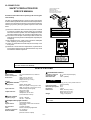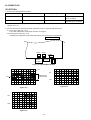
1
XL-520W/CP-520
SERVICE MANUAL
No. S0780XL520W//
XL-520W
CP-520
XL-520W and CP-520 constitute XL-520W.
• In the interests of user-safety the set should be restored to its original
condition and only parts identical to those specified should be used.
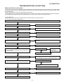
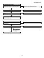
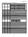
CONTENTS
Page
SAFETY PRECAUTION FOR SERVICE MANUAL ........................................................................................................... 2
SPECIFICATIONS ............................................................................................................................................................. 2
NAMES OF PARTS ........................................................................................................................................................... 3
OPERATION MANUAL ...................................................................................................................................................... 5
DISASSEMBLY .................................................................................................................................................................. 7
REMOVING AND REINSTALLING THE MAIN PARTS ..................................................................................................... 8
ADJUSTMENT ................................................................................................................................................................... 9
BLOCK DIAGRAM ........................................................................................................................................................... 16
SCHEMATIC DIAGRAM / WIRING SIDE OF P.W.BOARD ............................................................................................. 20
VOLTAGE ........................................................................................................................................................................ 28
NOTES ON SCHEMATIC DIAGRAM .............................................................................................................................. 29
TYPE OF TRANSISTOR AND LED ................................................................................................................................. 29
WAVEFORMS OF CD CIRCUIT ...................................................................................................................................... 30
TROUBLESHOOTING (CD SECTION) ........................................................................................................................... 31
FUNCTION TABLE OF IC ................................................................................................................................................ 36
REPLACEMENT PARTS LIST/EXPLODED VIEW
SHARP CORPORATION
–1–
This document has been published to be used
for after sales service only.
The contents are subject to change without notice.
XL-520W/CP-520
SAFETY PRECAUTION FOR
SERVICE MANUAL
Laeser Diode Properties
Material: GaAlAs
Wavelength: 780 nm
Emission Duration:continuous
Laser Output: max. 0.6 mW
Precaution to be taken when replacing and servicing the
Laser Pickup.
The AEL (Accessible Emission Level) of Laser Power Output
for this model is specified to be lower than Class I Requirements.
However, the following precautions must be observed during
servicing to protect your eyes against exposure to the Laser
beam
CAUTION-INVISIBLE LASER RADIATION WHEN OPEN. DO NOT STARE INTO
BEAM OR VIEW DIRECTLY WITH OPTICAL INSTRUMENTS.
(1) When the cabinet has been removed, the power is turned
on without a compact disc, and the Pickup is on a position
outer than the lead-in position, the Laser will light for several
seconds to detect a disc. Do not look into the Pickup Lens.
(2) The Laser Power Output of the Pickup inside the unit and
replacement service parts have already been adjusted prior
to shipping.
(3) No adjustment to the Laser Power should be attempted
when replacing or servicing the Pickup.
(4) Under no circumstances look directly into the Pickup Lens
at any time.
(5) CAUTION - Use of controls or adjustments, or performance
of procedures other than those specified herein may result
in hazardous radiation exposure.
VARNING-OSYNLIG LASERSTRALNING NAR DENNA DEL AR OPPNAD. STIRRA
EJ IN I STRALEN OCH BETRAKTA EJ STRALEN MED OPTISKA INSTRUMENT.
ADVERSEL-USYNLIG LASERSTRALING VED ABNING. SE IKKE IND I
STRALEN-HELLER IKKE MED OPTISKE INSTRUMENTER.
VARO! AVATTAESSA OLET ALTTIINA NAKYMATON LASERSATEILYLLE.
ALA TUIJOTA SATEESEEN ALAKA KATSO SITA OPTISEN LAITTEEN LAPI.
VARNING-OSYNLIG LASERSTRALNING NAR DENNA DEL AR OPPNAD.
STIRRA EJ IN I STRALEN OCH BETRAKTA EJ STRALEN GENOM OPTISKT
INSTRUMENT.
ADVERSEL-USYNLIG LASERSTRALING NAR DEKSEL APNES. STIRR IKKE
INN I STRALEN ELLER SE DIREKTE MED OPTISKE INSTRUMENTER.
FOR A COMPLETE DESCRIPTION OF THE OPERATION OF THIS UNIT, PLEASE REFER
TO THE OPERATION MANUAL.
SPECIFICATIONS
XL-520W
General
Power source:
Power consumption:
Dimensions:
Weight:
Cassette deck section
Frequency response:
Signal/noise ratio:
Wow and flutter:
AC110/127/220/230-240 V, 50/60 Hz
98 W
Width; 160 mm (6-5/16")
Height; 240 mm (9-1/2")
Depth; 300 mm (11-13/16")
3.7 kg (8.2 lbs.)
CP-520
Amplifier section
Output power:
Input terminals:
Output terminals:
50 - 14,000 Hz (Normal tape)
50 dB
0.25 % (WRMS)
Type:
2-way [12 cm (4-3/4") woofer and 2 cm
(13/16") tweeter]
Rated input power:
20 W
Maximum input power: 40 W
Impedance:
4 ohms
Dimensions:
Width; 160 mm (6-5/16")
Height; 240 mm (9-1/2")
Depth; 183 mm (7-1/4")
Weight:
1.8 kg (4.0 lbs.)/each
PMPO; 320 W (total)
MPO; 56 W (28 W + 28 W) (10% T.H.D)
RMS; 40 W (20 W + 20 W) (10% T.H.D)
Video/Auxiliary (audio signal);
500 mV/47 kohms
Speakers; 4 ohms
Headphones; 16-50 ohms
(recommended; 32 ohms)
Tuner section
Frequency range:
FM; 88 - 108 MHz
AM; 531 - 1,602 kHz
Specifications for this model are subject to change without
prior notice.
Compact disc player section
Type:
Signal readout:
D/A Converter:
Filter:
Frequency response:
Wow and flutter:
Compact disc player
Non-contact, 3-beam semi-conductor
laser pickup
1-bit D/A converter
8-times oversampling digital filter
20 - 20,000 Hz
Unmeasurable
(less than 0.001% W.peak)
–2–
XL-520W/CP-520
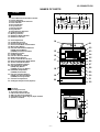
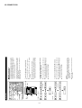
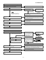
NAMES OF PARTS
XL-520W
1
Front Panel
1. Functin/Band/Track Number Indicator
2. Volume Indicator
3. Extra Bass/Equalizar Indicator
4. Timer Indicator
5. Record Indicator
6. Sleep Indicator
7. Repeat Indicator
8. Play Indicator
9. Video/Auxiliary Indicator
10. Random Indicator
11. Memory Indicator
12. FM Stereo Mode Indicator
13. FM Stereo Indicator
2
3
4 5
VOL
REC SLEEP
EQ
kHz
MHz
AUX RANDOM MEMORY
7
14. CD Compartment
15. On/Stand-by Switch
16. Remote Control Sensor
17. Record Pause/Beat Cancel Button
18. Memory/Set Button
19. (CD) Track Down/Review Button
(TAPE) Rewind Button
(TUNER) Preset Down Button
20. Headphone Socket
21. CD Eject Button
22. Function Selector Button
23. Band Selector Button
24. 3D Surround Mode Indicators
25. Extra Bass/Equalizer Mode Button
26. 3D Surround Mode Button
27. Volume Up/Down Buttons
28. (CD) Play/Pause Button
(TAPE) Play Button
(TUNER) Tuning Up Button
29. (CD/TAPE) Stop Button
(TUNER) Clear Button
30. (CD) Track Up/Cue Button
(TAPE) Fast Forward Button
(TUNER) Preset Up Button
31. Cassette Compartment
32. CD Digital Output Socket (Optical)
8
6
9
10
11
ST
12 13
14
21
22
15
23
24
16
25
17
26
27
28
18
29
30
19
31
20
32
Rear Panel
1. AC Voltage Selector
2. AC Power Input Socket
3. FM 75 ohms Aerial Socket
4. AM Loop Aerial Input Socket
5. Video/Auxiliary (Audio Signal) Input Sockets
6. Speaker Terminals
3
4
5
1
2
–3–
6
XL-520W/CP-520
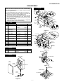
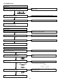
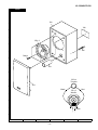
CP-520
Speaker Section
1
1. Tweeter
2. Woofer
3. Bass Reflex Duct
4. Speaker Wire
2
3
4
1
XL-520W
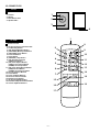
Remote Control
8
1. Remote Control Transmitter LED
2. On/Stand-by Button
3. (CD) Repeat/Random Button
4. (CD/TUNER) Memory/Set Button
5. (CD/TUNER) Clear Button
6. Timer/Set Button
7. Sleep Button
8. (CD/TAPE) Stop Button
9. (CD) Play/Pause Button
(TAPE) Play Button
10. (CD) Track Up/Cue Button
(TAPE) Fast Forward Button
(TUNER) Preset Up Button
11. (CD) Track Down/Review Button
(TAPE) Rewind Button
(TUNER) Preset Down Button
12. Tuning Up/Down Buttons
13. Timer Button
14. Timer Up/Down Buttons
15. Function Selector Button
16. Band Selector Button
17. 3D Surround Mode button
18. Extra Bass/Equalizer Mode Button
19. Volume Up/Down Buttons
2
9
ON/
STAND-BY
3
/RANDOM
4
MEMORY/
SET
5
CLEAR
SLEEP
PRESET
TUNING
TIMER/
SET
TIMER
TIMER
6
7
10
11
12
13
14
FUNCTION
BAND
X-BASS/
EQUALIZER
18
15
3D
SURROUND
16
17
–4–
VOLUME
19
–5–
8
7
6
5
4
3
2
MEMORY/
SET
0:00
MEMORY/
SET
ON/
STAND-BY
ON/
STAND-BY
AM 12:00
PRESET
(
/
)
PRESET
(
/
)
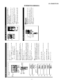
In this example, the clock is set for the 24-hour
(0:00) system.
SETTING THE CLOCK
Press the PRESET ( or ) button to select the time display
mode.
"0:00"
→ The 24-hour display will appear.
(0:00 - 23:59)
"AM 12:00" → The 12-hour display will appear.
(AM 12:00 - PM 11:59)
Press the MEMORY/SET button.
Press the ON/STAND-BY button to enter the stand-by mode.
Press the PRESET (
or
) button to adjust the hour.
Press the MEMORY/SET button.
Press the PRESET (
or
) button to adjust the minutes.
Press the MEMORY/SET button.
Press the MEMORY/SET button.
Perform steps 4 - 8 above.
Press the ON/STAND-BY button to enter the stand-by mode.
2
1
Perform steps 1 - 8 above.
Perform steps 1 - 3 in the section "RESETTING THE MICROCOMPUTER", on page 6.
To change the time display mode:
1
2
To change the clock time:
Note:
● In the event of a power failure or when the AC power lead is
disconnected, the clock display will go out.
When the AC power supply is restored, the clock display will
flash on and off to indicate the time when the power failure
occurred or when the AC power lead was disconnected.
If this happens, follow the procedure below to change the clock
time.
● The clock starts operating from "0" seconds. (Seconds are not
displayed.)
8
● Press the PRESET button once to advance the time by 1
minute. Hold it down to change the time in 5 minute intervals.
● The hour setting will not advance even if minutes advance from
"59" to "00".
6
7
● Press the PRESET button once to advance the time by 1 hour.
Hold it down to advance continuously.
● When the 12-hour display is selected, "AM" will change automatically to "PM".
4
5
● Note that this can only be set when the unit is first installed
or it has been reset (see page 6).
1
2
3
3
0.2 m - 6 m
(8" - 20')
15
15
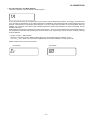
PREPARATION FOR USE
3
1
2,3
RESETTING THE MICROCOMPUTER
Whilst pressing down the MEMORY/SET button and the XBASS/EQUALIZER button, plug the AC power lead into the
AC INPUT socket on this unit.
Unplug the AC power lead from the AC INPUT socket on this
unit.
Press the ON/STAND-BY button to enter the stand-by mode.
● Keep the remote control away from moisture, excessive heat,
shock, and vibrations.
Notes concerning use:
● Replace the batteries if control distance decreases or operation
becomes erratic.
● Periodically clean the transmitter LED on the remote control
and the sensor on the main unit with a soft cloth.
● Exposing the sensor on the main unit to strong light may interfere with operation. Change the lighting or the direction of
the unit.
■ Remote control
Caution:
● The operation explained above will erase all data stored in
memory, such as clock and timer settings, tuner and CD presets.
3
1
2
Reset the microcomputer under the following conditions:
● To erase all of the stored memory contents (clock and timer
settings, tuner and CD presets).
● If the display is not correct.
● If the operation is not correct.
XL-520W/CP-520
OPERATION MANUAL
–6–
kHz
kHz
[10 kHz → 9 kHz]
kHz
kHz
[9 kHz → 10 kHz]
ON/
STAND-BY
(Continued)
(4 seconds)
(4 seconds)
BAND
kHz
kHz
kHz
kHz
FUNCTION
Press the BAND button to select the AM band.
Press the FUNCTION button until "FM" or "AM" appears in
the display.
Press the ON/STAND-BY button to turn the power on.
Hold down the BAND button and the ■ button for at least 4
seconds. Release the buttons when "AM SP 10 kHz" and "FM
SP 100 kHz" are displayed alternately.
Press the ON/STAND-BY button to enter the stand-by mode.
Hold down the BAND button and the ■ button for at least 4
seconds. Release the buttons when "AM SP 9 kHz" and "FM
SP 50 kHz" are displayed alternately.
Press the ON/STAND-BY button to enter the stand-by mode.
Cautions:
● When the unit is left for approximately 14 hours after the span
has been switched and AC power lead disconnected, it will be
automatically returned to a 9 kHz span. If this happens, set
the span again.
● When the span is switched, any stations that are memorised
will be cancelled.
● The unit will return to the clock display.
1
2
To return to a 9 kHz AM (50 kHz FM) interval:
● The unit will return to the clock display.
1
2
To change from a 9 kHz AM (50 kHz FM) interval to a
10 kHz AM (100 kHz FM) interval:
● If "AM 531 kHz" is displayed, it means that the radio has been
adjusted for a 9 kHz span. If "AM 530 kHz" is displayed, it
means that the radio has been adjusted for a 10 kHz span.
3
1
2
To check the tuning span currently selected:
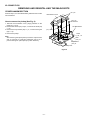
This product is not equipped with a span selector. However, it
will be adjusted to 9 kHz AM interval (50 kHz FM interval) when
shipped from the factory.
Before using the unit, be sure to set it for the AM tuning interval
(span) used in your area.
The International Telecommunication Union (ITU) has established
that member countries should maintain either a 10 kHz or a 9
kHz interval between broadcasting frequencies of any AM station.
The illustration shows the 9 kHz interval zones (regions 1 and
3), and the 10 kHz interval zone (region 2).
■ AM/FM interval (span)
XL-520W/CP-520
XL-520W/CP-520
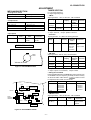
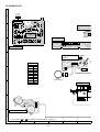
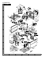
DISASSEMBLY
XL-520W
Caution on Disassembly
Follow the below-mentioned notes when disassembling
the unit and reassembling it, to keep it safe and ensure
excellent performance:
1. Take cassette tape and compact disc out of the unit.
2. Be sure to remove the power supply plug from the wall
outlet before starting to disassemble the unit.
3. Take off nylon bands or wire holders where they need be
removed when disassembling the unit. After servicing
the unit, be sure to rearrange the leads where they were
before disassembling.
4. Take suffcient care on static electricity of integrated
circuits and other circuits when servicing.
(A3)x1
ø3x10mm
Top
Cabinet
1
PROCEDURE
FIGURE
1. Screw .................. (A1) x4
2. Socket ................. (A2) x3
3. Screw .................. (A3) x1
7-1
REMOVAL
Top Cabinet
Side Panel
(Left/Right)
1. Screw .................. (B1) x7
7-1
3
Back Board
(With Power
Amp. PWB)
1. Screw .................. (C1) x4
2. Socket ................. (C2) x2
3. Flat Wire .............. (C3) x1
7-1
Main PWB
1. Screw .................. (D1) x3
2. Socket ................. (D2) x2
7-2
Front
Panel
(B1)x3
ø3x10mm
(C1)x2
ø3x10mm
Side Panel
(Right)
(C2)x2
Rear
Panel
Back
Board
(c3)x1
(C1)x2
ø3x10mm
Power Amp PWB
(F1)x6
ø3x10mm
7-2
6
Display PWB/
CD Servo PWB
1. Screw .................. (F1) x6
2. Socket ................. (F2) x2
7-2
7
Power Supply PWB 1. Screw .................. (G1) x5
7-2
8
Jack PWB
1. Screw .................. (H1) x1
7-3
9
Tape Mechanism
1. Screw .................. (J1) x4
7-3
10
CD Mechanism
1. Screw .................. (K1) x3
7-4
(D1)x1
ø3x10mm
CD Servo PWB
(D2)x1
(D1)x1
ø3x10mm
(F2)x1
CP-520
PROCEDURE
FIGURE
1. Net ........................... (A1) x1
3. Screw ...................... (A2) x4
7-5
CD Servo
PWB
(D2)x2
(F2)x1
(D2)x1
(E1)x2
ø3x10mm
REMOVAL
Main
PWB
Main PWB
(D1)x1
ø3x10mm
Display PWB
1. Screw .................. (E1) x2
Woofer
(A1)x2
ø3x10mm
Side Panel
(Left)
(B1)x2
ø3x10mm
(A1)x1
ø3x12mm
Front Panel
Front Panel
1
(A2)x1
Figure 7-1
5
STEP
CD
Mechanism
(A2)x2
(B1)x2
ø3x10mm
2
4
(A1)x1
ø3x12mm
Swicth
PWB
XL-520W
STEP
Top Cabinet
(G1)x4
ø4x6mm
Power Supply (G1)x1
PWB
ø3x10mm
Figure 7-2
Front Panel
CP-520
Speaker Box
Open
Tape Mechanism
(J1)x4
ø3x10mm
Net
(A1)x1
(A2)x4
ø4x12mm
(H1)x1
ø3x10mm
Woofer
Figure 7-3
(K1)x3
ø2.6x10mm
CD Mechanism
Screw
driver
Top Cabinet
Direction of handle
Figure 7-5
Figure 7-4
–7–
XL-520W/CP-520
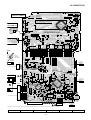
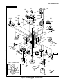
REMOVING AND REINSTALLING THE MAIN PARTS
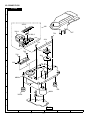
CD MECHANISM SECTION
( A1 ) x2
Perform steps 1,to 5 of the disassembly method to remove the
CD mechanism.
Mechanism Cover
( A2 ) x2
ø2.6 x6mm
How to remove the pickup (See Fig. 8)
1. Remove the mechanism cover, paying attention to the
pawls (A1) x 4 pcs.
2. Remove the screws (A2) x 2 pcs., to remove the shaft (A3)
x 1 pc.
3. Remove the stop washer (A4) x 1 pc., to remove the gear
(A5) x 1 pc.
4. Remove the pickup.
CD Mechanism
( A1 ) x2
Shaft
( A3 ) x1
Note:
After removing the optical pickup connector wrap the front
end of connector in conductive aluminium foil so as to
prevent damage of optical pickup by static electricity.
Gear
( A5 ) x1
StopWasher
( A4 ) x1
Pickup Unit
Figure 8
–8–
XL-520W/CP-520
ADJUSTMENT
MECHANISM SECTION
TUNER SECTION
• Driving Force Check
fL: Low-range frequency
fH: High-renge frequency
Torque Meter
Specified Value
Play: TW-2412
• FM RF
Signal generator: 1 kHz, 75 kHz dev., FM modulated
Over 80 g
• Torque Check
Torque Meter
Specified Value
Test Stage Frequency
Frequency
Display
Play: TW-2111
30 to 70 g. cm
Band
Coverage
—
87.50 MHz
Fast forward: TW-2231
50 to 140 g.cm
RF
50 to 140 g.cm
98.00 MHz
(10-30 dB)
98.00 MHz
Rewind: TW-2231
*1. Input: Antenna,
*2. Input: Antenna,
• Tape Speed
Test Tape
MTT-111
Specified
Value
Adjusting
Point
L302
*2
Output: TP301
Output: Speaker Terminal
• Detection
Signal generator: 10.7 MHz, FM sweep generator
Instrument
Connection
3,000 ±
90 Hz
Motor
Setting/ Instrument
Adjusting Connection
Parts
(fL): L303 *1
3.4 ± 0.1 V
Test
Stage
Headphone
Socket
IF
Frequency
10.7 MHz
Frequency
Display
98.00 MHz
TAPE MECHANISM
Setting/
Adjusting
Parts
Instrument
Connection
T304(Turn
the core of
T304 fully
counterclockwise.
Input: Pin 1 of
IC301
Output: TP302
• AM IF/RF
Signal generator: 400 Hz, 30%, AM modulated
M901
Motor
Volume in motor
Figure 9-1 ADJUSTMENT POINT
Test Stage Frequency
Frequency
Display
Setting/ Instrument
Adjusting Connection
Parts
IF
450 kHz
1,602 kHz
T351
Band
Coverage
—
531 kHz
(fL): T306 *2
1.1 ± 0.1 V
*1
Tracking
990 kHz
990 kHz
(fL): T302
*1
*1. Input: Antenna, Output: Speaker Terminal
*2. Input: Input is not connected, Output: TP301
• Setting the Test Mode
Keeping the BAND button and MEMORY button pressed, turn
on POWER. Then, the frequency is initially set in the memory
as shown in Table. Call it with the
,
button to use it
for adjustment and check of tuner circuit.
Preset No.
1
2
3
4
5
11~40
T302
AM
TRACKING fL
T306 AM BAND
COVERAGE fL
TP302
CNP301
L302
FM BAND
COVERAGE fL
1
TP301
FM MUTE
LEVEL
T304
FM IF
SO301
ANTENNA
TERMINAL
T351
L303 FM RF
87.50 MHz
108.00 MHz
98.00 MHz
90.00 MHz
106.00 MHz
Preset No.
6
7
8
9
10
AM
531 kHz
1,602 kHz
990 kHz
603 kHz
1,404 kHz
• FM Mute Level
Signal generator: 1 kHz, 40 kHz dev., FM modulated
Frequency
VR351
IC301
FM
AM IF
98.00 MHz
(25 dBµV)
MAIN PWB
Display
98.00 MHz
Adjusting
Parts
VR351*
*Adjust so that an output signal appears.
Figure 9-2 ADJUSTMENT POINTS
–9–
Instrument
Connection
Input: SO301
Output: Speaker
Terminal
XL-520W/CP-520
CD SECTION
1. This CD unit need adjustment as follow.
CD Test Mode
Value/Adjusting Method
Adjustment Part
Instrument Connection
Step 1
VR803 (Focus Offset)
DC + 40 mV (FEI>VRO)
FEI (R826) and VRO
(1-Pin of TP801)
Step 4
VR802 (Tracking Error Balance)
*1 (See Fig. 9-2)
TSO (3-Pin of TP801)
and VRO (1 Pin of TP801)
*1: Adjust to obtaiin vertically symmetrical waveform (Fig. 10-2) with respect toreference DC level. The reference level is VRO
(Approx DC 2.1V).
2. This CD unit have the following automatic adjustment function. Automatic adjustment item.
2-1: Focus Servo Gain (Fig. 10-3)
Focus Gain Adjustment is performed when disc is changed.
2-2: Tracking Servo Gain (Fig. 10-4)
Tracking Gain Adjustment is performed when disc is changed and disc is playbacked.
CD SERVO PWB
VR802
VR803
321
321
TP801
TRACKING
ERROR
BALANCE
FOCUS
OFFSET
T N V
S C R
O
O
Figure 10-1 ADJUSTMENT POINTS
TSO
1
FEI
SYMMETRICAL
UP AND DOWN
1
VRO
2
FSO
Figure 10-3
Figure 10-2
TSO
1
TS2O
2
Figure 10-4
– 10 –
XL-520W/CP-520
TEST MODE
The Test Mode for this microcomputer has two variations, namely "regular Test Mode" for adjustment and measurement and "selfdiagnosis Test Mode" for self-judgment in final inspection of products.
1. Entering the Test Mode
To enter the each Test Mode, press the POWER key, holding down the following two keys in the regular standby mode (power
off state). In this case only the main unit keys are valid. The Test Mode is not set even when the remote controller POWER
key is turned on.
[Regular Test Mode]
[Holding Down Keys]
1. CD Test Mode (TEST 1)………………………… Stop + Play
2. Tuner Test Mode (TEST 3)……………………… Memory/Set + Band Selector
3. Electronic volume Test Mode (TEST 4)………… Stop + Extra Bass/Equalizer Mode
4. Timer Test Mode (TEST 5)……………………… Fast Forward + Function Selector
5. LCD Test Mode (TEST 6)………………………… Memory/Set + Function Selector
[Self-diagnosis Test Mode]
1. Key input diagnosis TEST Mode (TESTA)………Play + Record Pause
2. CD Test Mode (TEST 1)
1. Step 1 Mode
When the CD Test Mode is set, the following display lights, and the CD pickup slides to the innermost periphery.
After lighting for 1.5 sec
When the following operation key is pressed in this state, the following operation is performed.
"POWER" ................ The Test Mode is set to off, power is turned off, and the mode is changed to the regular standby mode.
"FF/FWD" ................ After the pickup returns once to the innermost periphery, the pickup slides to the external periphery while
................................. this key is held down.
"REW/REV" ............. After the pickup returns once to the innermost periphery, the pickup slides to the internal periphery while
................................. this key is held down. However, input is invalid if PU-IN is on.
"PLAY" ..................... Shift to Step 2
"STOP" .................... Invalid
* In case of mode entry the pickup is moved to the internal periphery. At this time entry of any key other than POWER key is
disabled until shift of pickup to the internal periphery is completed. If PU-IN SW ON cannot be detected while waiting for 10
seconds, the slide motor is stopped, the following error is displayed, and entry of any key other than POWER key is disabled.
2. Step 2 Mode
When the PLAY key is pressed in the mode above, the laser lighting is turned on. In this state the laser is only turned on,
and other operations are not performed.
– 11 –
XL-520W/CP-520
When the following operation key is pressed in this state, the following operation is performed.
"POWER" ................ The Test Mode is set to off, power is turned off, and the mode is changed to the regular standby mode.
"FF/FWD" ................ While this key is held down, the pickup slides to the external periphery.
"REW/REV" ............. While this key is held down, the pickup slides to the internal periphery. However, if PU-IN is on, entry is
................................. invalid.
"PLAY" ..................... Shift to Step 3
"STOP" .................... Return to Step 1
3. Step 3 Mode
While the laser is lighting, the focus servo is turned on, and focus search is performed. If focusing failure occurs, focus search
is repeated until focusing is attained.
When the following operation keys are pressed in this state, the following operations are performed.
"POWER" ................ The Test Mode is set to off, power is turned off, and the mode is changed to the regular standby mode.
"FF/FWD" ................ While this key is held down, the pickup slides to the external periphery.
"REW/REV" ............. While this key is held down, the pickup slides to the internal periphery. However, if PU-IN is on, entry is
................................. invalid.
"PLAY" ..................... If focusing has been attained, the process proceeds to Step 4. Unless focusing has been attained,
................................. reception is inhibited.
"STOP" .................... Return to Step 1
4. Step 4 Mode
The disc is rotated and CLV is locked while the tracking servo is off.
The time display indicates always "0:00".
When the following operation keys are pressed in this state, thefollowing operations are performed.
"POWER" ................ The Test Mode is set to off, power is turned off, and the mode is changed to the regular standby mode.
"FF/FWD" ................ While this key is held down, the pickup slides to the external periphery.
"REW/REV" ............. While this key is pressed, the pickup slides to the internal periphery. However, if PU-IN is on, entry is
................................. invalid.
"PLAY" ..................... Shift to Step 5
"STOP" .................... Return to Step 1
5. Step 5 Mode
The tracking servo is turned on, groove is traced, mute is set to off, and playback is started. Even when the outermost
periphery of disc is reached in playback mode, it does not stop. The LCD display indicates playback lapse time as in case
of regular CD playback.
– 12 –
XL-520W/CP-520
When the following operation keys are pressed in this state, the following operations are performed.
"POWER" ................ The Test Mode is set to off, power is turned off, and the mode is changed to the regular standby mode.
"FF/FWD" ................ While this key is held down, the pickup slides to the external periphery.
"REW/REV" ............. While this key is held down, the pickup slides to the internal periphery. However, if PU-IN is on, entry is
................................. invalid.
"PLAY" ..................... Invalid
"STOP" .................... Return to Step 1
Other cautions
• While the CD lid OPEN is detected, entry into any step later than Step 2 is disabled. If CD lid OPEN is detected in any step
higher than Step 2, return to Step 1 is done.
• TOC IL is not performed in the Test Mode.
• The key operation, excepting that specified above, is the same as that of regular operation (CD). Only the FUNCTION key
is input-inhibited.
• Syncro REC with REC key input is also invalid in this mode.
3. Tuner Test Mode (TEST 3)
1. Outline of tuner (radio) Test Mode
The tuner Test Mode is intended to store adjustment/measurement frequency in the preset memory CH without frequency
adjustment by the adjusting personnel when the tuner is adjusted in the production line.
2. Details of tuner Test Mode
When power is turned on with the POWER key while the MEMORY/SET key and BAND key are held down together in
POWER OFF state, the frequency for adjustment/measurement of specific destination specified by the AREA terminal is
preset-stored in the preset memory CH (the frequency to be preset-stored for specific destination is explained in the Item
C). When the tuner Test Mode is started up, it is started with FM. FM is FM STEREO only.
When the REW key is pressed while the preset memory CH is 1CH, the highest CH is found as in case of regular mode. When
the FF key is pressed while the preset memory CH is highest CH, 1CH is found.
The RADIO (TUNER) BAND key (or TUNER/BAND key on the remote controller) is valid.
As in case of regular mode, selection of band, FM MONO/STEREO mode is enabled by pressing the RADIO (TUNER) BAND
(or TUNER/BAND ) key.
Exiting the tuner Test Mode, When the destruction data is stored in the memory in the tuner Test Mode, AC supply is
interrupted in the Test Mode and the AC supply is recovered, all the memory is cleared with the destruction data in case of
start-up.
(Countermeasures so that the Test Mode memory does not remain when AC supply is restored after power supply failure
occurred once in the Test Mode.) The memory is not cleared when AC supply is turned off after POWER OFF.
FUNCTIONkey is not accepted in the tuner test mode. In case of exit from the tuner Test Mode through the backup mode
upon occurrence of power failure the frequency data stored in the preset memory for adjustment/measurement is erased.
(As a result the preset memory CH becomes empty.)
The display indication is the same as that in case of regular operation.
The following display lights for one second when the tuner TEST mode is turned on
B
– 13 –
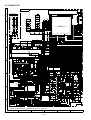
XL-520W/CP-520
Test Mode operation specification
3. Preset frequencies for various destinations (random preset memory)
BAND (CH)
1
2
3
4
5
FM 87.5MHz
FM 108.0MHz
FM 98.0MHz
FM 90.0MHz
FM 106.0MHz
BAND (CH)
6
7
8
9
10
10 kHz SPAN
9 kHz SPAN
AM
531 kHz
AM 1,602 kHz
AM
990 kHz
AM
603 kHz
AM 1,404 kHz
100 kHz SPAN
BAND (CH)
1
2
3
4
5
FM 87.5MHz
FM 108.0MHz
FM 98.0MHz
FM 90.0MHz
FM 106.0MHz
10 kHz SPAN
BAND (CH)
6
7
8
9
10
AM
530 kHz
AM 1,620 kHz
AM
990 kHz
AM
600 kHz
AM 1,400 kHz
• The unit used in the table above is Hz. K represents 1,000 times, and M represents 1,000,000 times.
• The hatched data shown in the table are not stored in the memory.
• FM is stereo mode.
Note: Keys which are effective in Test Mode
• Main unit keys:
VOLUME UP/DOWN, BAND, TUNING UP, POWER, MEMORY, CLEAR,
PRESET UP/DOWN
• Remote controller keys: VOL UP/DOWN, BAND, TUNING UP/DOWN, POWER, MEMORY, CLEAR, PRESET UP/DOWN
4. Electronic volume Test Mode (TEST 4)
After the Test Mode is set, the following display lights for one second.
When this mode has been set, -14dB (STEP17) is set, the preset equalizer is set to FLAT (EQ-3), the SRS mode is set to OFF,
and the start-up function is set to Tape.
1. The display is the same as that indicated in case of regular operation excepting when Test Mode is set.
2. The volume control with the Volume UP/DOWN key is only the following 3 steps, differing from the volume control in the regular
operation mode.
Volume — ∞ (STEP 0)
Volume — 14dB (STEP 17)
Volume — 0 (STEP 24)
3. The preset equalizer and SRS are switched if key operation is performed.
5. Timer Test Mode (TEST 5)
When the Test Mode is set, the following display lights for one second.
The current time and timer time are set in the following procedure, and timer playback is performed.
1. The present time is set to 1:00, the timer is set to ON time 1:02, OFF time 1:12, Function is set to Tape, Volume is set to STEP8.
One minute is counted in increments of second, and timer playback is performed. One step of Fade-in/out in this mode is
performed for 0.5 sec.
The display is the same as that appears in the regular timer operation.
2. After completion of timer playback test "TEST-5" indication (which appears when the mode is set) appears again and Standby
state is set. PLAY key entry is waited. If an entry is detected, the SLEEP timer is set to 2 minutes, and Function is set to
Tape, so that playback is started at once. Volume is set to STEP8, and 10 seconds are counted down in decrements of
second. One step of Fade-out is 0.5 sec.
The display is the same as that appears in the regular sleep playback mode.
3. After completion of SLEEP test, the Test Mode is turned off, and regular standby mode is set, so that the Test Mode ends.
6. LCD Test Mode (TEST 6)
When the LCD Test Mode is set, all the LCD segments light.
– 14 –
XL-520W/CP-520
7. Key input diagnosis Test Mode (TEST A)
When the Test Mode is set, the following display appears.
In this Test Mode checking as to whether all the main unit keys can be detected is performed. Accordingly, when this mode
is set, checking is performed so as to examine whether the POWER key was pressed last after all the following keys were
pressed. If the result is OK, the following OK is displayed. If any one of keys was not pressed, an error is indicated. When the
POWER key is pressed, exit from the mode is made irrespective of whether the termination is normal or abnormal, and the
standby mode is set.
All the models using this microcomputer do not have the same keys. The entry of the following keys is detected depending on
the combination of simultaneously pressed keys when this mode is set. Key pressing order is not fixed. Pressing of all keys
must be detected.
<
<
1. In case of "SRS" + "REC PAUSE"
Since the model does not have RDS and SRS, all the keys to be detected are the following 12 keys.
PLAY, VOL , VOL , BAND, G-EQ, FUNCTION, MEMORY/SET, REC PAUSE, REW/REV, FF/FWD, STOP, SRS
OK/NG indication of test result must be as follows.
OK indication
NG indication
– 15 –
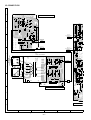
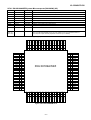
XL-520W/CP-520
~
~
74
SEG26
~
93
~
1 COM3
SEG7
FW702
LCD
LCD701
4 COM0
5 VLC3
9 OSC2
OSC1
VSS
12 XI
13 XO
14 MMOD
15 VREF
IC701
IX0189AW
10
~
~
POWER
VSM
F.P
57
LID-SW
BIAS
B-CAN
REC
MOT
SOL
56
~
25
~
31
32
34 35 36
38 39
41 42 40 44 45 46 47 48
CAM SW
LED704 - LED712
63
PU-IN
STEREO
SD
CLE
DATA
CD RES
CEE
BUCK
R-MUTE
23
62
KEY1
SYS STOP
REMOCON
~
21
BUS3
P-MUTE
P-CONT
CD+B
20
64
RESET
~
19
SRS1
SRS2
CE
17
~
KEY
SW702-SW708
SW710-SW714
SW718
~
X702
32.768kHz
11
DI
X701
8MHz
55
54
53
52
51
FW701
SYS STOP
REMOCON
RESET
SWITCHING
Q702
Q703
Q701
M+12V
Q704
Q705
RX701
SWTCHING
RESET
2 3 1
µ-CON +5V
A 12V
LED+B
Q707
SWITCHING
Q706
P CONT
SWITCHING
(S+6.2VLINE)
TR+
TR–
SL–
SL+
FMSO
GAIN1
NC
+– –+
LEVEL
SHIFT
+– –+
LEVEL
SHIFT
LEVEL
SHIFT
+ – –+
LEVEL
SHIFT
+– –+
IC804
–+
–
+
GND
NC
VCC
9 8 7 6 5 4 3 2 1
+
–
+
–
Reg5V
18 17 16 15 14 13 12 11 10
TS2O
CD STB
C3A
1
2
3
4
5
6
7
FSO
FSN
OSCI
CD+5V
VCC
SEL
DMEP
28
11
TS2O
29
10
30
9 FEN
TS2N
TS2P
31
8 FEP
32
TS1N
7 DFIN
33
TS1P
6
34
5
TR–
TR+
FO+
FO–
GND
PD
VR
LD
TSO
TEL1
35
4
36
3
TEL2
SWTCHING
37
2 RFI
Q801
+5V
TSN
1
38
39
TPO
40
41
42
TRACKING
ERROR
BLANCE
VR802
LDO
PD
1/2VCC
+5V
43
44
45
46
47
48
RFT
1
2
3
4
5
6
7
FOCUS
FEL1 OFFSET
VR803
SL–
PU-IN
GND
FEL2
FEI
FEO
SBAD
RFRP
2VRO
VRO
RFO
IC801
VRO
C2A
C
1
F
2
B 3
A
4
E
5
1/2V
6
+5V
7
15
RFN
C
F
B
A
E
GND
MON
LD
VCC
VR1A
THLD
16
FHLD
MDI
C4A
1/2VCC
1
2
3
4
5
6
7
8
FMSP
SP+
SP–
SL+
17
12
LDO
ACTUATOR
BI801
TR–
1
2
3
4
5
6
7
8
BI802
FO–
1
2
3
4
5
6
7
8
6
5
4
3
2
1
CNS802
TR–
TR+
FO+
FO–
GND
PD
VR
LD
TR+
FO+
6
5
4
3
2
1
CNS801
CNP803
SW801
PU-IN
–
6
5
4
3
2
1
18
27
FPI
+
SP+
SP–
SL+
SL–
PU-IN
GND
19
13
TNI
M
–
20
14
TNO
M802
SPINDLE
+
21
26
TPI
M
BI803
M801
SLED
CNS803
FMSM
22
25
TSO
FMSO
23
COSC
SP+
SP–
24
DFCT
DMEN
DMEO
FO–
FO+
DMEO
FSO
19 20 21 22 23 24 25 26 27 28 29 30 31 32 33 34 35 36
GND
GAIN4
VCC
GND
STAND
-BY
FNI
+
–
–
+
T.S.D
+–
3 2 1
TEST POI
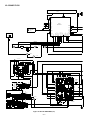
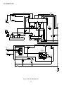
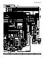
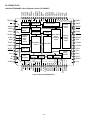
Figure 16 BLOCK DIAGRAM (1/4)
– 16 –
FW702
XL-520W/CP-520
CNS603
SW701
CD EJECT
M 12V
D GND
TO MAIN PWB
1
2
3
4
5
6
7
8
9
VCL
VCE
VDI
CL
DO
CE
DI
10
M GND
S+6.2V
A GND
20
19
18
R-CH
L-CH
P MUTE
A 12V
17
16
15
14
P CONT
CD+B
R-MUTE
FM ST
SD
REC
B-CAN
BIAS
SRS1
12
11
10
9
8
7
6
5
4
3
2
1
CNS602
SRS2
13
(S+6.2V)
µ-CON5V
5V
Q861
Q906
RUN PLS
MOT
SOL
REGULATOR
SWTCHING
TAPE MOTOR
SWTCHING
DRIVER
PU IN
Q905
Q904
M-12V
SWTCHING
Q903
CD+5V
Q902
SOLENOID
DRIVER
Q901
SWTCHING
49
50
N
51
52
P
53
54
GNDD
VDDD
16K RAM
CORRECT
58
59
VDDA
PDCNT
STATUS
CD+5V
RP
TMAX DET
CLV SERVO
N
AD
PLL
65
67
21
19
18
17
16
15
14
13
7 6 5 4 3 2 1 CNP901
RESET
BUCK
CCE
BUS3
BUS2
BUS1
BUS0
SW902
CAM
G-GND
FW901
12
PH901
AUDIO OUT
75
77 78 79 80
GNDA 7
LO 6
CD L-CH
CD R-CH
RO 2
GNDA 1
A-GND
IC802
3
2
1
X801
VRO
J801
DIGITAL
OUT TO
MD/DAT
TSO
STATUS
TESTX
GNDD
O
RST
BUCK
CCE
BUS3
BUS2
BUS1
BUS0
GNDD
VDDD
SW901
RECORD
PREVENTION
+
RO
O
P.F
CAM SW
TGUL
TEL1
TEL2
SERVO
STATUS
CD BUS
INTERFACE
FEI
TESH
TEOF
SBAD
RFRP
VREF
RFI
GNDA
Q DATA
RAM
48
A/D CONVERTOR
47
O
7 6 5 4 3 2 1 CNS901
SUB
CODE
44
LD
7 6 5 4 3 2 1 BI901
TIMING
GENERATOR
FOCUS
TRACKING
SERVO
CONTROL
CLOCK
43
26 25
DIGITAL
VDDX
OUT
XI
XO
DA CONV
GNDX
42
30 28 27
FMFB
FOCUS
L1 OFFSET
VR803
2VREF
SEL
FCSI
FKIC
34 33 32
ADRESS
41
36
EFM
L2
DMPC
DMFC
40 37
FMON
TKIC
TGUH1
D-GND
3 2 1 TP801
TEST POINT
Figure 17 BLOCK DIAGRAM (2/4)
– 17 –
M901
TAPE
–
M
SOL901
SOLENOID
XL-520W/CP-520
SWITCHING
Q351
R-MUTE
FM MUTE LEVEL
VR351
T302
AM ANT.
X351
R-CH OUT
L-CH OUT
IF OUT
PHASE
PHASE
(AM/FM)
MO/ST
14 13
VCC
SD
15
STEREO
GND
6
16
MPX IN
MPX VCO
17
FM/AM OUT
AM IF
T351
4 5
AM IF IN
2
18
FM DET
AM RF IN
1
20
AM IF IN
21
AM OSC
IN
AM OSC
OUT
23
AM MIX OUT
T306
24
AM MIX
OUT
AM OSC.
AM
LOOP
ANTENNA
CNP301
1
2
FM IF
IN
FM IF DET./
FM MPX./AM IF
IC303
LA1832
AM OSC OUT
7
8
9
10
12
VCC
+5V
CF351
CF352
VOLTAGE
REGULATOR
ZD351
+5V
AUDIO
+12V
A-GND
SO301
ANTENNA
TERMINAL
CF302
VT
L302
VD303
1 2 3
D GND
L303
VD302
FM IF
Vcc
+5V
T304
IF IN
AM IN
Q360
AUDIO +12V
FM RIPPLE
FiLTER
IF REQ
4
FM
3
MO/ST
1
FM
FM IN
AOUT
X OUT
X352
4.5MHz
9
CL
8
7
IC301
TA7358AP FM FRONT END
FM+B
12
15
DO
6
DI
3
16
CE
1
17
X IN
FM +B
VSS
22 21 20
BF301
5
6
7
9
10 11
IC302
LC72131
PLL CONTROLLER
CE DI
REC
CL
REC L
R
TAPE L
TA
SWITCHING
1
RECORD/PLAYBAK
HEAD
L-CH
R-CH
Q101-Q104
REC SW
Q105
REC MUTE Q106
REC
P/B SW
CONT
NF
5
6
AUDIO +12V
7
ERASE HEAD
3
P/B SW
L-IN
8
9
5
–
+
REC SW
8
AUDIO
+12V
150K
A-12V
BIAS OSC.
Q154 BEAT CANCEL
Q155 SWITCHING
B-CAN
11
NF
Q152
2
+
–
R-IN 9
Q151
L151
L-CH
ALC
MUTE
SWITCHING
Q172
1
150K
10
IC101
BA3126N
HEAD SELECTOR
Q171 SWITCHING
REC./P.B.
EQUALIZER
IC102
BA3311L
ALC
SWITCHING
Q107
R-CH
6
7
12
R-OUT
3
4
L-OUT
2
Q153 SWITCHING
REC BIAS
CONT
REC
SRS2
SRS1
SWITCHING
CNP602
Figure 18 BLOCK DIAGRAM (3/4)
– 18 –
1 2
XL-520W/CP-520
MODE
MODE
LIPPLE
FILTER
26 25 24 23 22 21 20 19 18 17 16 15
1
2
3
4 5
6
IC201
SRS5250S
Q208
8
7
9 10 11 12 13 14
IN R
IN L
OUT L OUT R
A 12V
28 27
PN OUT
MODE
NC
C OUT
NC
C IN
NC
CL4
NC
CL3
NC
CL2
NC
CL1
S IN
Vref
SOUT L OUT
CR4
R OUT
CR3
CR1
CR2
GND
Q201
R IN
L IN
Q205
Q203
VCC
PN IN
Q202
SRS1
SRS2
R-CH X-BASS/GRAPHIC EQUALIZER
TAPE
TAPE R
16 33
CD L
21
R1
L1
25
CE
24
23
31
29
27
26
R-MUTE
22
20
AUDIO +12V
18
L-CH
RVref
Vref
LVref
IC401
LC75394E
AUDIO PROCESSOR
D1
CL
NC
NC
AVSS
VSS
VSS
NC
NC
FUNCTION CONTROL
VOL CONTROL
G-EQ CONTROL
SO401
VIDEO/
AUX
R-CH
14 35
13
50
56
63
LTEST
54
RTEST
59
VDD
57
LVROUT
RVROUT
58
55
LINVIN2
LTOUT
19
28
CD R
9 8 7 6 5 4
62 61 60
AUDIO +12V
LVRIN
TUN L
CD
R2
L2
LF2C1
LF2C2
LF2C3
LF3C1
LF3C2
LF3C3
TUN R
LSELO
RSELO
TUNER
RF2C1
RF2C2
RF2C3
RF3C1
RF3C2
RF3C3
40 41 42 43 44 45 51 52 53
L3
R3
17 32
30
RINVIN2
RTOUT
RVRIN
TAPE L
L-CH X-BASS/GRAPHIC EQUALIZER
STEREO
SD
CE DI
CL DO
REC L
REC R
TAPE L
TAPE R
SO601
2
L-IN
9 R-IN
13
+
–
IC601
LA4450
POWER AMP.
5 R-CH OUT
STAND-BY
VCC
Q601
MUTE Q602
L-CH OUT
12
7
3
GND
P-CONT
J601
HEADPHONES
VOLTAGE
REGULATOR
CD+6.2V
D651 - D654
Q607
F651
T2.5A
L 250V
POWER
TRANSFORMER
T651
Q606
Q608
Q609
VOLTAGE
REGULATOR
MECH +12V
Q605
AUDIO +12V
Q604
CD+B
D656 - D659
F652
T1.25A
L 250V
230240V
220V
127V
110V
SW651
VOLTAGE
SELECTOR
T.F
CNP602
1 2 3 4 5 6 7 8 9
10 11 12 13 14 15 16 17 18 19 20
M 12V
D-GND
PRE CL
PRE CE
PRE DI
CL CQCK
TUN DO
TUN CE
DI COIN
BIAS
B-CAN
REC
SD
FM ST
R-MUTE
CD+B
P CONT
A 12V
P MUTE
CD L
CD R
A-GND
CD+6.2V
M-GND
SRS2
SRS1
TUNER
1 2 3 4 5 6 7 8 9
VOLTAGE
REGULATOR
Q603
10
AC SOCKET
110/127/220/230-240V
50/60 Hz
CNP603
TO CD SERVO PWB
Figure 19 BLOCK DIAGRAM (4/4)
– 19 –
XL-520W/CP-520
VD301-1 R319
AM TRACKING fL KV1236Z23F 100K
C374
0.018
R357
470K
C369
56P
R356
1K
12
C358
1/50
C357
2.2/50
R355
3.3K
R376
10K
C355 C356
22P 0.001
C398
100/10
CF351
C399
0.022
C370
1/50
ZD351
MTZJ5.1B
L352
100µH
C387
0.022
7 8 9
C384
0.001
AM SIGNAL
MW +B
R395
47K
R387
5.6K
C383
0.022
SW
Q360
KTA1266GR
R365
10K
+B
R383
5.6K
10 11
R385
5.6K
R384
12K
FM+B
6
MO/ST
MW
FM
5
FM
DO
4
C391
47/16
R371
1K
R372
1K
3
IF REQ IF IN
NC
AM IN
FM IN
VDD
IC302
LC72131 PLL CONTROLLER
1 2
R359
1.8K
FM SIGNAL
R392
390
C386
330P
15 14 13 12
17 16
PD
AIN
18
CL
C382
15P(CH)
C380
1/50
C392
0.001
X352
4.5MHz
19
R374
1K
BF301
22 21 20
R391
390
C385
0.01
R379
2.2K
DI
9
FM FRONT END
IC301
TA7358AP
C393
1/50
R373
1K
8
R309
820
Vr
TP301
C396
100/10
C395
0.022
R377
5.6K
L351
100µH
R380
1.5K
AOUT
C381
12P(CH)
R307
47
R381
10K
VSS
C317
0.022
R308
10K
C314
R386
330
CE
7
R382
330
CF302
VD302
KDV147C
L303
(CH)
22P
3.3P
C313(UJ)
5 6
C312
33P
R306
10
C311
15P(CH)
VD303
KDV147C
R303 33K
4
3
X OUT
2 3
T304
1
R393
1K
NC
1
C318
4.7P
FM IF
X IN
1 2 3
C319
18P
(CH)
C316
10/16
C315
100P
C310
0.022
C308
0.022
C307
0.0047
C309
0.001
R302
100K
FMRF
C305
0.0047
C303
0.001
R305
680
C394
47/16
C397
0.022
2
R362
15K
PHASE
(AM/FM)
L-CH OUT
R-CH OUT
PHASE
IF OUT
R361
15K
+B
R304
47K
R301
22
L302
C306
6.8P(UJ)
C304
0.01
D305
1SS133
FM 75OHMS
3
Q351
KRC104M
SWITCHING
14 13
Q305
2SC535C
SO301
1
MO/ST
X351
MPX VCO
VCC
FM DET
10 11
T351
AM IF
R310
4.7K
15
9
R363
3.3K
2
R364
3.3K
C371
1/50
C368
1/50
R350
2.7K
C367
1/50
FM/AM OUT
8
C354
0.022
C344
33P
C351
0.022
16
R353
270
2
FM BAND
COVERAGE fL
D
7
CF352
1 3
C350
0.022
C349
0.022
C
6
R352
1K
C337
0.022
ANTENNA
TERMINAL
C366
0.001
AM LOW CUT
4 5
C373
0.018
C372
1/50
FM IF DET./
FM MPX./AM IF
STEREO
3
IC303
LA1832
17
SD
2
18
VSM
FM AFC
1
19
R336
4.7K
1
2
20
GND
C336
470P
21
C353
0.022
C335
18P
(CH)
REG
C334
18P
(UJ)
AM BAND
COVERAGE fL
AM OSC OUT
R351
5.6K
C352
10/16
B
CNP301
AM LOOP
ANTENNA
R324
100K
R323
68K
AM MIX OUT
VD301-2
KV1236Z23F
T306
FM IF IN
D301
1SS133
D302
1SS133
22
AM OSC IN
24 23
AM IF IN
TP302
R321
22
AM RF IN
C360
0.022
C301
0.001
C365
0.022
VR351
10K(B)
FM MUTE
LEVEL
C364
10/16
C343
33P
MPX IN
R358
8.2K
L353
1mH
C333
0.022
C363
0.022
C332
0.022
C361
0.022
T302
C342
0.022
C331
0.047
C362
3.3/50
A
C330
8.2P
(UJ)
R360
4.7K
PLAYBACK SIGNAL
RECORD SIGNAL
CD SIGNAL
P/B SW
8
9
R138
330
REC SW
R118
22K
R122
4.7K
C117
10/16
R124
4.7K
R120
56
C105
270P
C130
4.7/25
C116
0.0022
REC./P.B. EQUALI ZER
3
–
+
C103
330P
2
3
BEAT CANCEL
SWITCHING
Q155
KTC3199GR
G
R159
5.6K
R160
5.6K
R152
100K
C153
0.0039
(P.P)
Q151
2SC2001-K
BIAS OSC.
C154
0.027
(ML)
C156
0.022
8
10
Q152
KTA1266GR
C155
47/16
BEAT CANCEL
SWITCHING
Q154
KTC3199GR
R151
47K
Q171
KRA102M
SWITCHING
IC102
BA3311L
R125
100K
R116
15K
1
150K
ALC
MUTE
C151
180P
C152
0.001
C104
330P
R104
120
C124
47/16
150K
6
11
R106
150K
R155
56
C125
100/25
12
D102
1SS133
C112
10/16
R110
3.9K
R128
3.9K
R130
3.3K
2
R113
3.9K
R133
1K
R137
4.7K
+B
D105
1SS133
3
1
Q107
KRC104M
SWITCHING R112
1K
Q106
KTC3199GR
REC MUTE
R157
150
1
Q153
KRC104M
SWITCHING
7
C110
0.015(ML)
C108
47/16
R108
10K
3
2
R134
100K
+B
2
+
–
9
C106
270P
+B
R154
10K
R153
10K
L151
330µH
R141
330
D101
1SS133
1
5
R102
1K
C122
82P
R131
4.7K
Q105
KTC3199GR
REC MUTE
R136
10K
7
C102
470P
C111
10/16
R111
1K
R132
4.7K
D106
1SS13
R114
3.9K
6
C107
47/16
R119
56
SWITCHING
Q104
KTC3199GR
R129
3.3K
C119
0.01
R123
4.7K
C109
0.015
(ML)
C126
22/16
R126
5.6K
R121
4.7K
SWITCHING
Q102
KTC3199GR
C129
4.7/25
R135
680K
P/B SW
CONT
5
R139
2.7K
C115
0.0022
C113
4.7/25
R127
3.9K
R109
3.9K
R107
10K
C118
0.022
4
R103
120
R117
22K
C120
0.01
3
R140
10K
C121
82P
ERASE HEAD
F
2
+B
R105
150K
SWITCHING
Q103
KTC3199GR
C123
2.2/50
1
2
3
4
5
6
7
8
1
C101
470P
SWITCHING
Q101
KTC3199GR
REC SW
C114
4.7/25
R-CH
1
2
3
4
5
6
7
8
CNP101
RECORD/PLAYBACK
HEAD
L-CH
CNS101
E
REC L
REC R
TAPE
TAPE
R115
15K
HEAD SELECTOR
IC101 R101
BA3126N 1K
D104
1SS133
R156
150
2
+B
Q172
KRC102M
SWITCHING
3
1
+B
+B
MAIN PWB-A1
CNP60
H
• NOTES ON SCHEMATIC DIAGRAM can be found on page 29.
1
2
3
4
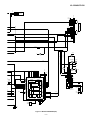
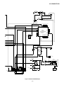
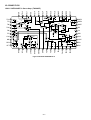
Figure 20 SCHEMATIC DIAGRAM (1/4)
– 20 –
5
6
XL-520W/CP-520
R219
10K
KRC107M
Q205 3
2
R233
CNP201
TUN R
C404 R418
1K
1/50
CD R
C402 R416
1/50
1K
25 CE
1K
1K
RF3C3
RF3C2
RF3C1
RF2C3
RF2C2
RF2C1
RF1C3
RTIN
RF1C2
RVRIN 53
Vref
VDD 57
LVROUT 58
LF4C3
LF4C2
LF3C3
LF3C1
LF2C3
LF2C2
LF2C1
LF1C3
LF1C2
LF1C1
LTIN
LVRIN 60
C437
100P
C205
OUT L
C441
10/16
C435
100/10
LVref 63
LFS 64
9 8 7 6 5 4 3 2 1
C444
100/25
C433 R479
0.0033 100K
C421
0.22
(ML)
C445
0.022
C427
0.01
C423
0.082
C425
0.033
R413
3.3K
R411
15K
LF3C2
LF4C1
C411
22/16
C415 R421
1K
1/50
STEREO
LSELO
FM+B
LINVIN2 62
16 15 14 13 12 11 10
A GND
SD
A 12V
3 2 1
18 NC
C405 R419
1/50
1K
+B
LTOUT 61
19 L2
+B
C439
10/16
LTEST 59
20 NC
17 L3
C442
10/16
C443
100/10
56
23 CL
L4
LINVIN1
R417
1K
C436
100/10
RVROUT 55
24 D1
C413
100P
TAPE L
R415
1K
C403
1/50
R480
100K
RTEST 54
IC401
LC75394E
AUDIO PROCESSOR
21 L1
C401
1/50
C440
10/16
RTOUT 52
22 VSS
CD L
C438
100P
RINVIN2 51
RF4C3
RF4C2
RF4C1
26 VSS
+B
C391
47/16
RF1C1
28 R1
27 AVSS
R385
5.6K
C434
0.0033
RFS 49
RVref 50
46 47 48
29 NC
R403
1K
R402
R401
RSELO
R3
31 NC
30 R2
TUN L
C428
0.01
C422
0.22
(ML)
33 34 35 36 37 38 39 40 41 42 43 44 45 46 47 48
32
VSM
R-MUTE
1 2 3 4 5 6 7 8
D401
D402
1SS133 1SS133
TAPE R
C406 R420
1/50 1K
C424
0.082
C426
0.033
R412
15K
R414
3.3K
C416 R422 C412
22/16
1/50 1K
1 2 3 4 5 6 7 8
C414
100P
C408
330P
C407
330P
R408
3.3K
R407
3.3K
R405
39K
R4
L-CH
R406
39K
RINVTIN1
R-CH
VIDEO/AUX
2.2/50
C204
2.2/50
100/16
SRS2
SRS1
A 12V
1SS133
CNP201
SO401
R214
1K
R213
1K
CR3
CR2
GND
CR1
Vre
A GND
IN R
IN L
D202
1SS133
D201
R OUT
R207
4.7K
R206
3.9K
C202
0.47/50
CR4
CL1
G IN
R209
1.2K
L OUT
NC
C210
0.33/50
C203
0.0047
(ML)
G OUT
NC
9 10 11 12 13 14
CL2
NC
8
CL3
NC
7
C220
R204
1.5K
6
OUT R
R202
100K
R205
47K
5
R201
33K
C240
0.022(ML)
R203
22K
4
C OUT
MODE
PN OUT
3
VCC
1 2
NC
L IN
R IN
26 25 24 23 22 21 20 19 18 17 16 15
IC201
C201
C221
100/16
C206
100/16
1K
4.7K
R215
4.7K
NC
C214
2.2/50
C215
2.2/50
R211
1K
R224
R223
10
R210
1K
C225
10/16
Q208
KTC3203Y
28 27
SRS5250S
N IN
R362
15K
0.022(ML)
R361
15K
R212 10K
R220 10K
C226
4.7/25
SRS PWB-B3
Q201
2SK246GR
100
R216
D203
1 1SS133
Q203
1 KRC107M 1
CL4
R217 10K
3
2
2
C IN
KRC107M
Q202
3
+B
+B
D GND
L-CH
5
STAND-BY
12
7 VCC
A_GND
R608 D601
1K 1SS133
C626
47/16
A_12V
8
D603
1SS133
Q603
KTC3199GR
R620
47
R617
33K
CNP603
R621
22K
C623
10/16
M 12V
D-GND
PRE CL
PRE CE
PRE DI
CL CQCK
TUN DO
TUN CE
DI COIN
10
CNS603
TO CD SERVO PWB
P23 12-A
CNS602
TO CD SERVO PWB
P23 12-C
7
1 2 3 4 5 6 7 8 9
C621
100/25
10 11 12 13 14 15 16 17 18 19 20
CNP602
C622
0.022
1 2 3 4 5 6 7 8 9
CD R
A-GND
D+5V
M-GND
BIAS
B-CAN
REC
SD
FM ST
R-MUTE
CD+B
P CONT
A 12V
P MUTE
CD L
SRS2
SRS1
+B
C630
4700/25
F652
T1.25A
L 250V
D651
D653
D654
R651
680(3W)
C651,C654: 0.1
D651-D654: 1N5402M
T.F
C654
T651
POWER
TRANSFORMER
R619
47
VOLTAGE
REGULATOR
Q604
2SD2012Y
+B
ZD601
MTZJ13A
!
1
2
R629
820
R628
100
C620
470/25
C657
C656
1
2
1
2
D657
D658
D656
D659
C658
C659
C656-C659: 0.1
D656-D659: IN4004S
POWER SUPPLY PWB-B2
9
SW651
VOLTAGE
SELECTOR
230240
C651
D652
+B
Q605
2SD2012Y
VOLTAGE
REGULATOR
F651
T3.15A
L 250V
BI651
1 2
BI652
R623
22K
C624
0.022
C625
10/16
+B
R625
10K
D602
1SS133
C627
0.022
D604
1SS133
R627
10K
R114
3.9K
C628
10/16
ZD602
MTZJ7.5C
M_12V
CNP651
1 2 CNS651
R624
1K
1
2
3
2
Q608
1
KRA102M
Q609
KRC107M
3
R661
330
5
L-CH
L-CH
A_GND
R-CH
R-CH
1
1 2
Q606
KTC3199GR
HEADPHONES
J601
R662
330
R-CH
VOLTAGE
Q607
REGULATOR 2SD2012Y
+B
C614
1000/35
C616
2200/50
CNP604
SP_L-CH
SP_L-CH_GND
SP_R-CH_GND
SP_R-CH
HEADPHONES
PWB-A5
IC601: POWER AMP.
C615
0.022
8
04
33
R613
270(1/2W)
R605
220
R606
220
9
C644
0.22
(ML)
6
R610
3.3
Q601
KTC3199GR
MUTE
C603
0.001
0V
C606
4.7/25
+
–
–
+
0V
4
10
C629
100/50
R609
3.3
FW601
R634
1K
C602
0.022
3
0V
8
C608
100/50
C611
0.22
(ML)
C643
0.22
(ML)
1
SPEAKER
TERMINAL
SO601
C613
1000/35
CNP652
1
2
3
4
5
6
7
8
+B
D106
1SS133
R607
6.8K
0V
R602
3.3K
2
14
11
0V
0V
FW604
1
+B
R604
1K
C607
100/50
IC601
LA4450
13
C610
47/50
3
R137
4.7K
R616
22K
CNP605
FW605
4
K
1
2
3
0V
0V
Q602
KTC3199GR
MUTE
C604
0.001
C601
33/16
R113
3.9K
1
R136
10K
R615
22K R603 0V
1K
0V
GR
E
C609
47/50
C605
4.7/25
R601
3.3K
C612
0.22(ML) R614
270(1/2W)
POWER AMP.PWB-B1
+B
CNS652
REC L
REC R
TAPE R
TAPE L
10
Figure 21 SCHEMATIC DIAGRAM (2/4)
– 21 –
11
SO651
AC SOCKET
110/127/220/230-240V
50/60Hz
12
XL-520W/CP-520
C
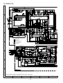
FW702
DISPLAY PWB-A3
LCD
LCD701
VOL
DOWN
SW702
R720
1.8K
L701
100µH
R711
1.8K
R712
1.8K
PLAY/
CD PAUSE/
TUNING UP
REC/
PAUSE
SW718
R727
15K
ON/
STAND-BY
N.C 65
SRS1 64
13 XO
SRS2 63
IC701
IX0189AW
SYSYTEM MICROCOMPUTER
BUS3 62
BUS2 61
BUS1 60
17 KEY1
BUS0 59
18 KEY2
CD STB 58
PU-IN 57
19 POWER
LID-SW 56
BIAS 55
R-MUTE
BUCK
CEE
CD RES
DATA
ID
STEREO
SD
B-CAN 54
CLE
SYS STOP
FUNC
CD+B
P-MUTE
N.C
RESET
CE
VCL
CL
25
VDI
24 VREF+
VCE
23 CAM SW
P-CONT
22 RUN PLS
REMOCON
21 F.P
+B
REC 53
MOT 52
SOL 51
DI
26 27 28 29 30 31 32 33 34 35 36 37 38 39 40 41 42 43 44 45 46 47 48 49 50
C712
0.01
R70J
10K
2 3 1
R70L
1K
Q703
KTC3199GR
SWITCHING
D721
1SS133
R70E
100K
R70F
82
C714
470P
C716
47/16
R70R
100
3
+B
R734
47K
D723
1SS133
C715
100/10
R70N
Q704
2SD468C 10(Fusible)
SWITCHING
Q706
KRC102M
R799 2
2.2K
1
+B
P CONT
+B
C704 +B
0.022
3
R764 1K
R760 1K
R761 1K
R753 1K
R754 1K
R755 1K
R756 1K
R757 1K
R759 1K
R789 47K
R735
47K
R736
47K
R739
47K
LED+B
M 12V
µ-CON+5V
GND
+B
+B
+B
GAIN1
R872
R871
+B
C2A
C
F
B
A
E
1/2V
+5V
1
2
3
4
5
6
7
1
2
3
4
5
6
7
1
2
3
4
5
6
7
R801
22
C802
100/10
R80E
82K
TSO
C R80A 82K
TEL2
R803
22K
+5V
F
B
A
E
R80B 82K
R80C 82K
R80F 82K
R80G 82K
TSN
C813
0.0022
TRACKING
ERROR
BALANCE
+B
+B
1/2VCC
H
TS1P
R809
100K
C804
47/16
FSN
COSC
OSCI
SEL
GND
C820
0.0068
DMEP
FSO
11
IC801
TA2065F
SERVO
AMP.
29
30
10
9
8
7
32
R811
27K
+B
28
F
B
A
E
LDO
PD
33
6
34
5
35
4
36
3
37
2
38
1
39
TPO
R804
120K
VR802
100K(B)
40
41
42
43
44
45
46
47
VR803
100K(B)
R825
470K
FHLD
C826
1/50
FEI
C827
470P
R827
FEO 150K
FEN
R828
2.7K
FEP
R837
2.7K
DFIN
SBAD
RFRP
2VRO
C831
0.056
(ML)
+B
VRO
RFI
C828
0.056
RFO (ML)
C829
3.9P
48
RFT
SWITCHING
Q801
2SA1015GR
12
TS1N
TEL1
R818
18
27
C809
0.015 TS2P
R812
18K
C807
0.22(ML)
FEL2
RFN
TR–
TR+
FO+
FO–
GND
PD
VR
LD
15
FEL1
LDO
1
2
3
4
5
6
7
8
16
31
R813
2.2K
R810
2.2K
17
2
4
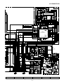
Figure 22 SCHEMATIC DIAGRAM (3/4)
– 22 –
C833
220/10
+B
C834
0.056(ML)
R838
12K
TP801
+B
3
C832
47/16
C830
47P
R829
470
• NOTES ON SCHEMATIC DIAGRAM can be found on page 29.
1
+B
5
6
3 2
VRO
MON
LD
VCC
C3A
GND
R814
1M
18
13
FPI
VR1A
SL–
PU-IN
GND
THLD
TS2O
19
14
FNI
1/2VCC
C
F
B
A
E
FMSP
+B
20
26
TNO
C4A
ACTUATOR
1
2
3
4
5
6
7
8
1
2
3
4
5
6
7
8
CNS802
G
TR–
TR+
FO+
FO–
GND
PD
VR
LD
SP+
SP–
SL+
21
R805
180K
TR+
FO+
FO–
TR–
CNS801
PICKUP UNIT
6
5
4
3
2
1
TS2N
6
5
4
3
2
1
C808
0.33
–
6
5
4
3
2
1
CNP803
SW801
PU-IN
SP+
SP–
SL+
SL–
PU-IN
GND
BI803
M
+
BI801
M802
SPINDLE
–
BI802
M
CNS803
M801
SLED
22
25
TSO
FMSM
R819
4.7K
+
23
R822
330
C825
0.039
(ML)
R826
220K
FMSO
R816
47K
F
24
R821
18K
C824
0.056
(ML)
FOCUS
OFFSET
R817
15K
TNI
+B
C811
22/16
C810
0.1(ML)
CD MOTOR
PWB-D
C822
47/16
C823
10/16
DMEO
R874
10K
TPI
GAIN4
DMEN
R875
10K
R873
4.7K
R823
100K
R820
33K
C821
VCC 0.022
C812
10/16
+B
FMSO
TS2O
DMEO
FSO
DFCT
SP+
SP–
FO–
FO+
CD STB
MDI
GND
STAND
-BY
19 20 21 22 23 24 25 26 27 28 29 30 31 32 33 34 35 36
+B
+B
T.S.D
LEVEL
SHIFT
++ – – +
–
–
+
VCC
+
–
LEVEL
SHIFT
+ – –+
+–
+B
10K
10K
IC804
M56748FP
NC
–+
–
+
+– –+
LEVEL
SHIFT
+– –+
LEVEL
SHIFT
+
–
+
–
+B
9 8 7 6 5 4 3 2 1
GND
NC
18 17 16 15 14 13 12 11 10
Reg5V
+B
TR+
TR–
SL–
SL+
IC804: FOCUS/TRACKING/
SPIN/SLIDE DRIVER
VCC
C871
330/10
E
1K
1K
2
R738
47K
R798
47K
R766
R765
R737
47K
SWITCHING
Q707
KTA1266GR
+B
1K
1K
1K
1K
1K
1K
10K
1K
1K
1K
1K
1K
1K
1K
220
220
R767 1K
1
ZD702
MTZJ6.2C
+B
R783
R782
R781
R780
R779
R778
R777
R776
R775
R774
R773
R772
R771
R770
R769
R768
SWITCHING
Q705
KRA102M
!
D722
1SS133
R70P
330
R70G
1K
C710
0.01
R70M
100
RX701
21043TE2
ZD701
+B MTZJ3.3B
R70H
10K
R70K
120
C717
0.022
SWITCHING
C711 Q702
3.3/50 KTC3199GR
C713
10/16
D720
1SS133
+B
R70C
3.3K
2
3
R70A R70B
1K
1K
1
Q701
KRC102M
RESET
D
+B
R741 1K
R742 1K
R743 1K
R744 1K
R745 1K
R746 1K
R747 1K
R748 1K
R749 1K
R750 1K
R751 1K
µ-COM VDD
µ-CON+5V
SYS STOP
REMOCON
RESET
+B
+B
R733 47K
FW701
C
SLR342MG2
N.C 66
12 XI
16 AREA
+B
R788 47K
N.C 67
15 VREF
+B
47K
N.C 68
OSC2
14 MMOD
R729
10K
SEG25
SEG26
SEG31 69
VDD
20 VSM
R713
10K
R722
10K
R721
10K
SEG24
SEG22
SEG30 70
VLC1
11 VSS
1K
1K
1K
1K
SEG23
SEG20
SEG18
SEG21
SEG19
SEG16
SEG17
SEG14
SEG15
SEG12
SEG13
SEG9
SEG8
SEG11
SEG10
SEG5
SEG6
SEG3
SEG1
SEG4
SEG2
SEG29 71
VLC2
10 OSC1
X701
8MHz
X702
32.768kHz
C702
22P(CH)
R728
R730
R731
R732
VLC3
SLR342MG2
R726
1K
SEG28 72
DO
R702B
120
VOL
UP
SW703
+B
74
SEG27 73
COM0
LED717
R719
1.8K
+B
R710
2.7K
75
COM1
LED716
PRESET
DOWN
SW711
R709
3.9K
SW705
X-BASS/
EQUALIZER
SW704
10 11 12 13 14 15 16 17 18 19 20 21 22 23 24
R787
R718
2.7K
R725
47K
C703
0.022
R717
3.9K
PRESET
UP
SW712
BAND
R724
47K
R723
47K
LED704
204GDTR4
R702A
120
LED707
204GDTR4
R703A
120
LED705
204GDTR4
STOP/
CLEAR
SW713
1
2
3
4
5
6
7
8
9
R708
5.6K
SW706
MEMORY/
SET
SW710
LED706
204GDTR4
LED712
204GDTR4
LED709
204GDTR4
R704B
120
B
R703B
120
LED710
204GDTR4
R704A
120
LED711
204GDTR4
LED708
204GDTR4
FUNCTION
5 6 7 8 9
99 98 97 96 95 94 93 92 91 90 89 88 87 86 85 84 83 82 81 80 79 78 77 76
100
SEG0
R707
10K
SW707
SW714
COM2
COM3
1 2 3 4
3D SURROUND
C701
22P(CH)
LED PWB-A4
A
SEG7
SW708
XL-520W/CP-520
CD SIGNAL
SW701
CD EJECT
M 12V
D GND
VCL
VCE
VDI
CL
DO
CE
DI
VSM
R793 47K
R794 47K
R790 47K
R789 47K
SLR342MG2
LED717
R788 47K
SLR342MG2
LED716
R787
47K
SEG26
4
+B
CNS603
M 12V
D GND
+B
1
2
3
4
5
6
7
8
9
VCL
VCE
VDI
CL
DO
CE
DI
CNP603
TO MAIN PWB
P21 8-H
FW702
CD LID SWITCH PWB-A7
10
+B
1K
1K
1K
1K
1K
1K
10K
1K
1K
1K
1K
1K
1K
1K
220
220
R767 1K
R766
R765
1K
1K
M GND
S+6.2V
A GND
R-CH
L-CH
P MUTE
A 12V
P CONT
CD+B
R-MUTE
FM ST
SD
REC
B-CAN
BIAS
+B
+B
+B
20
19
18
17
16
15
14
13
12
11
10
9
8
7
6
5
4
3
2
1
SRS1
SRS2
SD
STEREO
CNS602
+B
+B
+B
+B
µ-CON5V
D801
IN4004S
REGULATOR
Q861
2SD468C
D901
1SS133
TSO
R838
12K
TP801
VRO
C834
0.056(ML)
3 2 1
1
2
3
DFCT
VDDD
GNDD
TEL2
TEL1
TGUL
TGUH2
TGUH1
TKIC
FMON
TIMING
GENERATOR
CD BUS
INTERFACE
TEST1
TEST
FMFB
DMON
BUS0 14
CLOCK
EFM
SBOK 11
R881
220
TEST5 10
TEST4
TEST3
GNDA
LO
DA CONV
RO
RO
GNDA
9
8
7
6
5
4
3
2
1
PH901
SW901
RECORD
PREVENTION
FW901
+
TAPE MECHANISM
PWB-C
L802
0.82µH
M901
+B
C850
0.022
C852
0.0022
(ML)
3
2
1
3
2
1
3
2
1
R852
1K
+B
X801
16.9344MHz
C854
18P
(CH)
IC802: SERVO/
SIGNAL CONTROL
C865
0.022
(ML)
C855
15P(CH)
CD SERVO PWB-A2
• The numbers 1 to 17 are waveform numbers shown in page 30.
7
8
9
–
M
GNDX
XI
XO
DIGITAL
OUT
TEST2
DOUT
EMPH
AOUT
+B
C859
100/10
VDDD 12
C881
100/10
Q DATA
RAM
BUS1 15
65 66 67 68 69 70 71 72 73 74 75 76 77 78 79 80
JACK PWB-B4
+B
SW902
CAM
CCE 18
IC802
TC9284BF
C853
0.056(ML)
C849
0.01
C830
47P
TMAX DET
CLV SERVO
64 VCOF
C848 R846
0.01 33K
C833
220/10
AUDIO OUT
BCK
C832
47/16
63 LPFO
CNP901
BUS3 17
VDA
61 TMAX
62 LPFN
7 6 5 4 3 2 1
BUCK 19
LO
VDDX
R844
220K
R843
47K
R845
2.2M
BI901
PFCK 20
60 PDO
R851
1K
C829
3.9P
59 PDCNT
CORRECT
CHCK
C828
0.056
RFO (ML)
58 VDDA
WDCK
RFI
56 MONIT
57 DTSC1
R842
10K
C847
100P
+B
C843
0.0033
CNP805
C831
0.056
(ML)
+B
55 DTSC2
R841
1K
RFRP
16K RAM
STATUS
+B
54 GNDA
COFS
SBAD
53 RFI
Q904
KRC102M
SWITCHING
C901
0.001
C856
270P
C858
0.056(ML)
C842
0.0033
3
C902
3.3/25
7 6 5 4 3 2 1 CNW901
GNDD 13
SUB CODE
52 VREF
ADRESS
51 RFRP
2
1
3
R903
3.3K
Q903
KRC107M
SWITCHING
RESET
BUCK
CCE
BUS3
BUS2
BUS1
BUS0
C860
0.056(ML)
C857
47/16
R834
680K
R831
47K
R830
220K
DMPC
50 SBAD
C841
0.0047
+B
DFIN
R829
470
A/D CONVERTOR
FEP
R837
2.7K
STATUS
R828
2.7K
8
R886
4.7K
R901
1.5K
BUS2 16
CNS805
1
49 TEOF
FEN
VRO
R885
4.7K
R904
390
RST 21
SERVO
STATUS
SPDA
2
48 TESH
GNDD
3
C884
10/16
1
7 6 5 4 3 2 1
SUBD 23
47 FEI
PLL
4
C883
10/16
2
SUBSYC 22
46 FEL1
C827
470P
R827
FEO 150K
2VRO
R888
1.8K
CLCK 24
45 FEL2
TESTX
5
44 FKIC
HS
6
43 FCSI
BI805
7
C826
1/50
FEI
C844
0.022
8
+B
FOCUS
TRACKING
SERVO
CONTROL
42 SEL
R833
8.2K
C851
100/10
9
R832
15K
C845
47/16
10
R825
470K
C846
220/10
11
FEL1
FHLD
41 2VREF
DIGITAL OUT
TO MD/DAT
J801
12
VR803
100K(B)
R826
220K
13
FEL2
R887
1.8K
3
R902
56K
40 39 38 37 36 35 34 33 32 31 30 29 28 27 26 25
DMFC
C825
0.039
(ML)
14
C886
0.0022
2
1
+B
R822
330
FOCUS
OFFSET
5
C885
0.0022
R906
1.5K
C903
100/25
SOLENOID
DRIVER
Q902
2SB562C
R905
10K
R821
18K
C824
0.056
(ML)
Q905
2SB562C
D902
1SS133
C904
0.022
M 12V
RUN PLS
MOT
CAM SW
SOL
P.F
R907
10K
C887
0.022
+B
D903
1SS133
3
C905
0.022
+B
PU IN
+B
1
Q906
KRA102M
TAPE
MOTOR
DRIVER
C864
0.022(ML)
SWITCHING
2
+B
C861
10/16
CD R-CH
C863
0.022
C862
330/10
+B
ZD801
MTZJ5.6B
+B
R908
47K
R866
82
R867
10
A GND
D718
IN4004S
CD L-CH
+B
Q901
KRC102M
SWITCHING
CD+B
P CONT
A 12V
P MUTE
+B
CNP602
TO MAIN PWB
P21 8-H
R783
R782
R781
R780
R779
R778
R777
R776
R775
R774
R773
R772
R771
R770
R769
R768
CD STB
SRS1
SRS2
BUS3
BUS2
BUS1
BUS0
µ-CON5V
PU IN
BIAS
B-CAN
REC
MOT
SOL
P.F
RUN PLS
CAM-SW
R-MUTE
BUCK
CCE
CD RES
DATA
10
Figure 23 SCHEMATIC DIAGRAM (4/4)
– 23 –
11
12
SOL901
SOLENOID
XL-520W/CP-520
A
POWER AMP PWB-B1
R615
R601
R603
Q601
R607
B C E
R605
C605
C607
R604
C606 C629
B C E
R616
R602
Q602
R606 C608
C615
C616
2
1
C610
C644
C611
C643
R609
1 2 3
CNP605
P27 12-E
TO CD SERVO PWB
R11
R103
R127
C111
R135
R129
C119
D101
D102
C120
C118
R130
R141
R128
P25 12-G
TO MAIN PWB
C125
C123
Q106
FW605
C613
C112
R106
C110
R110 R133
B C E
D
R125
R132
C126
R112
C1
R131
R114
P25 12-G
TO MAIN PWB
Q105
R113
R111
C379
C378
CNS602
CNP652
C657
D657
C396
C395
CNS652
TO MAIN PWB
P25 12-D
C656
D656
C659
C658
D659
D658
SO651
T.F.
1
2
C376
C377
AC SOCKET
AC110/127/220/230-240V
50/60Hz
T651
POWER TRANSFORMER
C384
R391
R377
R392
ZD351
R395
110V
R360
F652
T1.25A L 250V
127V
127V
C
C394
R379
R381
BI651
D654
C651
D652
D651
L351
C380
R38
C
C382
CNS651
F651
T2.5A L 250V
C381
RD
1
2
12
13
14
15
16
17
18
19
20
21
22
X352
BR
C392
R651
F
C387
230-240V
E
R384
C383 11
10
9
8
7
6
5
4
3
2
1
230-240V
SW651
VOLTAGE SELECTOR
Q360
R359
IC302
110V
R387
R373
C654
220V
C391
R374
R371
R372
D653
220V
R365
E
R119
B C E
P27 12-F
TO CD SERVO PWB
FW604
D
2
4
6
8
10
12
C124
CNS603
C609
1 2 3 4 5 6 7 8
CNP604
R614
R613
C
3
R107
C109
R109
R134
R108
C614
R610
C612
D105
R137
R105
14
13
12
11
10
9
8
7
6
5
4
3
2
1
C604
B
CNP651
IC601
D601
R608
C603
C601
C397
R386
R309
POWER SUPPLY PWB-B2
C310
C315
G
Q305
R304
E
C
B
R305
MAIN PWB-A1
H
1
2
3
4
Figure 24 WIRING SIDE OF P.W.BOARD (1/4)
– 24 –
5
6
XL-520W/CP-520
RECORD/PLAYBACK
HEAD(137)
ERASE HEAD(138)
CNS101
PK
1
IC101
C425
R413
C423
C421
C427
R411
C413
Q152
C439
C437
C411
C415
C406
C402
C435
C433
C445
C444
R364
3
2
1
2
BI652
BR
C436
R480
C434
C441
R624
Q608
ZD601
R628
R629
C424
C422
1
2
3
1
TO POWER
SUPPLY PWB
1
CNP652
2
RD
CNS652
P24 5-E
5
1
Q603
C621
HEADPHONES
PWB-A5
C428
FW601
C622
J801
DIGITAL OUT
TO MD/DAT
B C E
C630
R620
D602
D603
R621
R619
Q604
C623
E
C
B
C367
1 2 3
Q605
C852
8
BI805
3
C602
1
WH
BK
PK
B
C
E
Q606
E
C
B
D604
C337
R627 C628
C334
Q607
C627
C336
1
FW604
FW605
R623
C625
C624
E
C
B
L802
R363
C426
C414
C440
50
C443
48
55
R479
C416
64
60
49
C442
D402
R661
C156
1
IC401
33
D401
R662
R153
R160
R159
5
R422
R362
CNS805
3 2 1
P27 11-H
JACK PWB-B4
C301
T302
IC301
C319
C318
C304
TO CD
SERVO PWB
CNP805
C331
C307
C305
1
R625
C332
R319
VD301-1
C626
T306
ZD602
C303
VD303
T304
R3
C310
TO POWER AMP PWB
CNP604
P24 4-D
C330
TO POWER AMP PWB
CNP605
C408
R408
C407
R407
C349
CNP301
R406
D302
BF301
D301
3
2
1
R405
C311
5
10
C335
C333
L302
C317
R416
R418
R420
R336
D305
8 7 6 5 4 3 2
15
30
32
35
C412
40
R414
45
R412
Q609
R617
C374
R357
R356
C369
VD301-2
R303
C309
C308 R302
R310
R307
R306
L303
R309
C313
C312
VD302
C314
R308
C381
C316
P24 4-C
SO301
2 1
FM ANTENNA
TERMINAL
7
C154
C152
C372
R324
R323
R321
R301
9
16
17
25
C404
C620
C366
C365
IC303
VR351
CF302
C351
C342
C306
1
C438
C373
C358
C399
R355 R353
CF351
C357
C398
R379
R381
C394
C361
R358
C343
L353
PWB-A1
R421
R419
R417
R415
R634
R361
C371
R393
X351
C354
2
1
C393
R305
C405
8 7 6 5 4 3 2 1
CNP201
CNP602
Q351
3
2
1
C353
R380
R386
R152
CNP603
Q172
1
2
3
4
5
6
7
8
9
10
11
12
13
14
15
16
17
18
19
20
12
13
R385
11
14
R383
15
10
16
9
E C B
8
17
C355
7
18
CF352
6
19
C386
5
20
1 2 3
R350
4 R351 21 C364
R352 3
22
C363
C352 2
C385
23
C360 R320
24
1
C350
C362
C344
T351
3
C397
R157
R155
20
C368
R382
L351
C380
12
13
14
15
16
17
18
19
20
21
22
R156
R154
C403
R376
C370
R384
R151
C153
C151
D106
R104
R134
R108
Q360
R359
B
C
E
R401
C129
C356
C391
C155
R118
L352
387
TO SRS PWB
P26 1-A
CNS201
C401
R395
R360
1
2
3
R403
C396
R377
E
C
B
R402
Q105
1
E
C
B
J601
HEADPHONES
C116
C115
R117
R119
Q154 Q155 Q153
C130
R120
C117
1
2
3
4
5
6
7
8
9
10
B
C
E
Q103
R123
D104
R125
R124
C126
E
C
B
B C E
C121
CNP101
B C E
R126
R122
R121
1
2
3
Q171
Q104
C108
Q151
1
2
3
E
C
B
C113
Q101
R116
C112
R106
C110
R110 R133
C122
C123
C102
C114
R138 Q102
C125
18
41
IC102
2
4
6
8
10
12
C124
1
3
5
7
9
11
R139
C107
C111
R135
BK
1
2
3
4
5
6
7
8
L151
R115
R103
8
C851
R107
1
2
R101
3
C105 4
C103 5
6
R140
7
C104
8
C106
9
R102
Q107
FW601
R136
3 2 1
C101
D105
AM LOOP
ANTENNA
8
SO401
VIDEO/AUX
9
L-CH
SO601
R-CH
SPEAKER
TERMINAL
10
Figure 25 WIRING SIDE OF P.W.BOARD (2/4)
– 25 –
11
12
XL-520W/CP-520
P25 10-B
TO MAIN PWB
CNP201
DISPL
R224
C206
C201
C
E
10
Q208
LED PWB -A4
LED704
LED706
R702A
LED705
R703A
LED707
R702B
R703B
LED708
LED710
SRS PWB -B3
LED709
LED712
R704B
C
LED711
R704A
FW701
R207
R209
R201
C210
R202
R203
14
R205
FW702
1
SW701
CD EJECT
C240
C202
R217
Q202 Q203
IC201
1
R206
1
B
20
5
R204
1
C221
2
C203
C226
3
R213
15
25
2
R223
S
C204
D
28
3
CD LID
SWITCH PWB-A6
G
C205
R215
R216
R233
C214
Q201
2
1
R214
R219
R210
R211
D202
3
C215
B
D203
Q205
C225
R212
D201
R220
8 7 6 5 4 3 2 1 CNS201
C220
A
SW902
CAM
TAPE MECHANISM
PWB-C
D
CNP901
COLOR TABLE
BR
RED
OR
ORANGE
YL
YELLOW
GR
GREEN
E
FW901
1
2
BROWN
RD(R)
BL
BLUE
VL
VIOLET
GY
GRAY
WH(W)
WHITE
BK
BLACK
PK
PINK
PH901
1
2
SW
RE
PR
76 54 321
SOL901
SOLENOID
4
3
M901
TAPE MOTOR
PICKUP UNIT
F
7
8
SLED
MOTOR
M801
CNP803
G
PICK IN
SW801
1
1
6
5
4
3
2
1
CD MOTOR PWB-D
SPINDLE
MOTOR
M802
H
• The numbers 1 to 17 are waveform numbers shown in page 30.
1
2
3
4
Figure 26 WIRING SIDE OF P.W.BOARD (3/4)
– 26 –
5
6
R70K R70J
R70H
R70F
Q702
C716
C713
R70R
C704
R720
R70P
E
C
B
R70N
C717
Q704
R749
R721
SW711
MEMORY
SET
RX701
R70M
ZD702
R731
SW712
<<
SW713
>>
Q701
D723
R759
C703
R737
R719
R718
STOP
SW714
R750
R745
R746
R747
R748
R744
R789
R790
R730
PLAY
SW702
R712
VOL –
SW703
R738
R735
R736
R729
R788
R713
R798
R717
Q707
3 2 1
C714
R727
R799
E
C
B
R723
R728
SW708
3D
SURROUND
SW704
VOL+
D718
X702
R724
R725
LED716
R722
R739
R710
SW705
G-EQ/X-BASS
FW701
D721
C710
D720
L701
R782
R783
R743
R742
R741
R775
R770
R771
R772
R773
R774
R776
R777
R778
R779
R780
R781
R734
Q705
FW702
LED717
1
2
3
R726
24 23 22 21 20 19 18 17 16 15 14 13 12 11 10 9 8 7 6 5 4 3 2 1
R711
Q706
X701
5
1
100
R707
C702
C701
10
95
SW706
BAND
R70L
R732
20
15
90
ZD701
SW718
STAND-BY
26
30
25
IC701
80
SW701
CD EJECT
FW701
D722
70
75
76
Q703 E
C
B
C715
40
35
E
C
B
R70G
55 45
60
65
85
R709
2
FW702
1
R733
SW707
FUNCTION
R708
R787
LID
TCH PWB-A6
51 50
1
2
3
R70B
R70C
LCD701
R753
3
2
1
R70E
C712
C711
R70A
R757
R764
R765
R766
R767
R768
R769
R754
R755
R756
DISPLAY PWB-A3
R760
R761
R751
XL-520W/CP-520
SW710
REC.PAUSE
SW902
CAM
SOL901
SOLENOID
R794
R793
R795
SW901
RECORD
PREVENTION
R908
C901
C903
C905
B C E
Q902
9
R881
C857
C883
C850
C885
R887
C884
C886
R851
C855
R846
C849
R844
R852
X801
R885
70
C854
R830
R841
R842
C827
C842
C843
C844
C845
C832
60
CNP805
9 4 3 6 11 2
12 1
BI803
C861
R867
C862
1
R888
C887
CNP602
16
17
ZD801
R871
6
E
C
B
R866
10 15 18
D801
5
C864
IC804
Q861
C863
R843
R845
C848
C846
C847
C853
P24 5-D
TO MAIN PWB
WH
GY
WH
GY
WH
RD
CD SERVO PWB-A2
8
25 20
1
1
5
30
C871
C834
1
80
75
64 65
19
35
R872
GY
WH
RD
C829
IC802
55
36
R875
R873
R874
C804
50
1
2
3
4
5
6
7
8
9
10
11
12
13
14
15
16
17
18
19
20
3 2 1
C830
R838
R801
R831
C826
C825
R828
39
R80G
R805
R80F
C802
R80E
48 1
R80C
C828
Q801
R80B
R80A
R829
B C E
5
10
45
14
C881
15
35
R833
C833
20 15
IC80110 14
40
R827
45 5
C841
R819
C820
C823
C821
C824
C808
R809
C809
R814
R816
R812
R811
R813
C807
C810
BI802
8
WH
GY
WH
GY
WH
CNS801
7
C811
C813
R804
1
30
20
30
40
R832 41
CNP603
CNS602
C859
25 24
C822
R818
8
7
6
5
4
3
2
1
C812
24
35
38
GY
WH
GY
WH
GY
WH
RD
C858
R834 R820
P24 5-C
TO MAIN PWB
15
R810
25 R823
7
BI801
1
R803
VR802
CNS802
1
R837
R817
8
7
7
6
5
4
3
2
1
R826
TP801
13 10
VR803
UP UNIT
3
2
1
R886
3
2
1
Q905
1
2
3
C865
B C E
BI901
1
2
3
4
5
6
7
8
9
10
C860
C856
1
C904
R906
Q901
7
R822
GY
CNS901
CNS603
R901
C831
1
2
3
7
D902
D901
C902
R825
D903
Q903
Q904
R904
R821
R903
R902
BK
R907
1
Q906
R905
3
2
1
6 5 4 3 2 1
10
Figure 27 WIRING SIDE OF P.W.BOARD (4/4)
– 27 –
CNS803
P25 12-G
TO JACK PWB
CNS805
11
12
XL-520W/CP-520
VOLTAGE
IC101
PIN
NO.
1
2
3
4
5
6
7
8
9
VOLTAGE
0V
0V
0V
0.3V(8V)
0V
2.8V
0V
0V
0V
IC102
PIN
NO.
1
2
3
4
5
6
7
8
9
10
11
12
VOLTAGE
4.6V
0V
0.6V
–
0V
0V
0V
10.2V
0V
0V(10.1V)
0.6V
4.6V
IC201
PIN
NO.
1
2
3
4
5
6
7
8
9
10
11
12
13
14
15
16
17
18
19
20
21
22
23
24
25
26
27
28
VOLTAGE
11.13V
5.57V
5.57V
5.57V
5.57V
5.57V
5.57V
5.57V
5.57V
5.57V
5.57V
5.57V
5.57V
5.57V
0V
5.56V
5.56V
5.56V
5.56V
5.56V
5.56V
5.56V
5.56V
5.56V
5.56V
1.367V
5.56V
5.55V
IC302
PIN
NO.
1
2
3
4
5
6
7
8
9
10
11
12
13
14
15
16
17
18
19
20
21
22
VOLTAGE
2.6V
0V
0.1V
0.1V
4.8V
5.1V
1.7V(11.4V)
3.7V(0V)
3.9V
0V
0V
0V
3.5V
0V
0V(2.6V)
2.6V(0V)
5.2V
0.9V
0.9V
–
–
2.6V
IC303
PIN
NO.
1
2
3
4
5
6
7
8
9
10
11
12
13
14
15
16
17
18
19
20
21
22
23
24
VOLTAGE
2.1V
5V
2.1V
2.1V
0V
5V
5V
2.9V(4.3V)
5V
0V
3.8V(1.9V)
3.8V(1.2V)
4V(2.2V)
–
1.3V
2.1V
2.3V(0V)
2.3V
0V(0.9V)
0.6V
2.1V(2.7V)
2.1V(2.7V)
5V
3.5V
IC401
PIN
NO.
1
2
3
4
5
6
7
8
9
10
11
12
13
14
15
16
17
18
19
20
21
22
23
24
25
26
27
28
29
30
31
32
33
34
35
36
37
38
39
40
41
42
43
44
45
46
47
48
49
50
51
52
53
54
55
56
57
58
59
60
61
62
63
64
VOLTAGE
4.7V
4.7V
4.7V
4.7V
4.7V
4.7V
4.7V
4.7V
4.7V
4.7V
4.7V
4.7V
4.7V
4.7V
4.7V
4.2V
4.3V
–
4.3V
–
4.3V
–
0V
0V
0V
–
–
4.3V
–
4.3V
–
4.3V
4.2V
4.7V
4.7V
4.7V
4.7V
4.7V
4.7V
4.7V
4.7V
4.7V
4.7V
4.7V
4.7V
4.7V
4.7V
4.7V
4.7V
4.7V
4.7V
4.7V
4.7V
4.7V
4.7V
4.7V
9.4V
4.7V
4.7V
4.7V
4.7V
4.7V
4.7V
4.7V
PIN
NO.
1
2
3
4
5
6
7
8
9
10
11
12
13
14
15
16
17
18
19
20
21
22
23
24
25
26
27
28
29
30
31
32
33
34
35
36
37
38
39
40
41
42
43
44
45
46
47
48
49
50
IC701
VOLTAGE PIN
NO. VOLTAGE
2.5V
51 0V
2.5V
52 0V
2.5V
53 0V
2.5V
54 0V
0V
55 0V
1.7V
56 0V
3.3V
57 5V
4.9V
58 0V
2.6V
59 4.1V
2.6V
60 4.1V
0V
61 3.9V
2.1V
62 3.9V
2.1V
63 0V
0V
64 4.9V
0V
65 0V
0V
66 0V
5V
67 2.5V
5V
68 2.5V
5V
69 2.5V
5V
70 2.5V
0V
71 2.5V
5V
72 2.5V
73 2.5V
5V
74 2.5V
5V
0V
75 2.5V
5V
76 2.5V
0V
77 2.5V
0V
78 2.5V
0V
79 2.5V
0V
80 2.5V
0V
81 2.5V
4.9V
82 2.5V
0V
83 2.5V
4.9V
84 2.5V
4.5V
85 2.5V
4.8V
86 2.5V
0V
87 2.5V
5V
88 2.5V
4.8V
89 2.5V
0.4V
90 2.5V
5.1V
91 2.5V
5.2V
92 2.5V
0.4V
93 2.5V
0V
94 2.5V
4.9V
95 2.5V
3.7V
96 2.5V
4.3V
97 2.5V
0V
98 2.5V
4.9V
99 2.5V
0V
100 2.5V
IC601
IC521
PIN
NO.
1
2
3
4
5
6
7
8
9
10
11
12
13
14
15
16
17
18
19
20
21
22
23
24
VOLTAGE
1.5V
1.5V
0.4V
1.43V
2.3V
2.6V
2.8V
1.3V
1.5V
0V
0.7V
0V
0.15V
0.2V
0.2V
0.03V
2.75V
2.5V
2.4V
1.1V
2.13V
2.13V
5.15V
3.65V
– 28 –
PIN
NO.
1
2
3
4
5
6
7
8
9
10
11
12
13
14
VOLTAGE
25.7V
14.7V
0V
0V
14.6V
25.8V
28.7V
1.22V
0V
27.7V
0V
2.07V
0V
1.22V
IC801
PIN
NO.
1
2
3
4
5
6
7
8
9
10
11
12
13
14
15
16
17
18
19
20
21
22
23
24
25
26
27
28
29
30
31
32
33
34
35
36
37
38
39
40
41
42
43
44
45
46
47
48
VOLTAGE
2.4V
2.1V
2.1V
4.2V
2.2V
2.2V
2.2V
0V
2V
2.1V
2.2V
2V
2.2V
2.2V
2.2V
2.3V
2.3V
2.5V
0V
5V
5V
2.2V
2.1V
2.2V
2V
2.1V
2.1V
2.1V
0V
2.1V
2.1V
2.1V
0V
2.1V
2.1V
2.3V
2.1V
2.2V
1.8V
2.1V
2.1V
1.9V
2.1V
2.2V
2.6V
0.3V
2.2V
1.9V
PIN
NO.
1
2
3
4
5
6
7
8
9
10
11
12
13
14
15
16
17
18
19
20
21
22
23
24
25
26
27
28
29
30
31
32
33
34
35
36
37
38
39
40
IC802
VOLTAGE PIN
NO. VOLTAGE
0V
41 4.2V
2.3V
42 5V
2.6V
43 –
5V
44 –
2.6V
45 –
2.3V
46 –
0V
47 2.2V
5V
48 2.1V
5V
49 2.1V
5V
50 2.2V
5V
51 2.2V
5V
52 2.1V
0V
53 –
4.2V
54 0V
4.1V
55 –
4.2V
56 –
4V
57 –
3.8V
58 5V
59 5V
4.3V
60 0V
2.3V
61 –
5V
62 –
0.1V
63 –
5V
64 –
0.4V
5V
65 0V
0V
66 5V
0.2V
67 0V
2.1V
68 1.3V
2.1V
69 1.7V
2.1V
70 2.5V
2.4V
71 2.5V
2.1V
72 0.3V
1.9V
73 2.5V
2.1V
74 0V
5V
75 2.4V
2V
76 5V
5V
77 5V
2.1V
78 2.2V
2.1V
79 2.2V
2.2V
80 0V
IC804
PIN
NO.
1
2
3
4
5
6
7
8
9
10
11
12
13
14
15
16
17
18
19
20
21
22
23
24
25
26
27
28
29
30
31
32
33
34
35
36
VOLTAGE
2.1V
2.1V
–
2.1V
2.1V
2.3V
2.3V
0V
0V
0V
0V
0V
2.3V
2.1V
2.6V
0V
5.4V
0V
–
5.4V
2.1V
2.1V
2V
2.7V
0V
0V
0V
0V
0V
1.8V
2.7V
–
0V
–
0V
0V
XL-520W/CP-520
NOTES ON SCHEMATIC DIAGRAM
• The indicated voltage in each section is the one measured
by Digital Multimeter between such a section and the chassis with no signal given.
1. In the tuner section,
( ) indicates AM
< > indicates FM stereo
2. In the main section, a tape is being played back.
3. In the deck section, a tape is being played back.
( ) indicates the record state.
4. In the power section, a tape is being played back.
5. In the CD section, the CD is stopped.
• Parts marked with “
”(
) are important for
maintaining the safety of the set. Be sure to replace these
parts with specified ones for maintaining the safety and
performance of the set.
• Resistor:
To differentiate the units of resistors, such symbol as K and
M are used: the symbol K means 1000 ohm and the symbol
M means 1000 kohm and the resistor without any symbol is
ohm-type resistor. Besides, the one with “Fusible” is a fuse
type.
• Capacitor:
To indicate the unit of capacitor, a symbol P is used: this
symbol P means micro-micro-farad and the unit of the
capacitor without such a symbol is microfarad. As to
electrolytic capacitor, the expression “capacitance/withstand
voltage” is used.
(CH), (TH), (RH), (UJ): Temperature compensation
(ML): Mylar type
(P.P.): Polypropylene type
• Schematic diagram and Wiring Side of P.W.Board for this
model are subject to change for improvement without prior
notice.
REF. NO
SW651
DESCRIPTION
VOLTAGE SELECTOR
POSITION
REF. NO
110/127/
220/230-240V
DESCRIPTION
POSITION
SW710
REC PAUSE
ON—OFF
SW711
MEMORY SET
ON—OFF
SW701
CD EJECT
ON—OFF
SW712
PRESET DOWN
ON—OFF
SW702
PLAY
ON—OFF
SW713
PRESET UP
ON—OFF
SW703
VOLUME DOWN
ON—OFF
SW714
STOP
ON—OFF
SW704
VOLUME UP
ON—OFF
SW718
ON/STAND-BY
ON—OFF
SW705
X-BASS/EQUALIZER
ON—OFF
SW801
PICKUP IN
ON—OFF
SW706
BAND
ON—OFF
SW901
RECORD PREVENTION
ON—OFF
SW707
FUNCTION
ON—OFF
SW902
CAM
ON—OFF
SW708
3D SURROUND
ON—OFF
FRONT
VIEW
E C B
(S) (G) (D)
(1) (2) (3)
2SA1015 GR
2SB562 C
2SC2001 K
2SD468 C
KRA102 M
KRC102 M
KRC104 M
KRC107 M
KTA1266 GR
KTC3199 GR
2SC535 C
204GDTR4
SLR342MG2F
2SD2012 Y
FRONT
VIEW
FRONT
VIEW
B C E
Figure 29 TYPES OF TRANSISTOR AND LED
– 29 –
XL-520W/CP-520
WAVEFORMS OF CD CIRCUIT
STOP
NO DISC FOCUS SEARCH
PLAY
1
FKIC
1
10
DMEO
1
2
FCSI
2
11
DMFC
2
3
FSO
3
12
DMPC
3
FOCUS SEARCH
IL
STOP
1
FKIC
1
2
FCSI
2
3
FSO
3
STOP
7
13
PLAY
TSO
1
FMSO
2
PLAY
CUE
4
FEI
1
7
TSO
1
3
FSO
2
14
TKIC
2
5
RFO
3
15
FMFB
3
STOP
4
FEI
5
RFO
6
SBAD
PLAY
REVIEW
1
2
3
STOP
7
TSO
1
14
TKIC
2
15
FMFB
3
PLAY
TCD-782 TUO-02 PLAYBACK
7
TSO
1
8
TS2O
2
9
RFRP
3
– 30 –
16
RO
1
17
R-CH
2
XL-520W/CP-520
TROUBLESHOOTING (CD SECTION)
When the CD does not function
When the CD section does not operate When the objective lens of the optical pickup is dirty,this section may not operate.Clean
the objective lens,and check the playback operation.When this section does not operate even after the above step is taken,check
the following items.
Remove the cabinet and follow the troubleshooting instructions.
"Track skipping and/or no TOC(Table Of Contents) may be caused by build up of dust other foreign matter on the laser pickup lens.
Before attempting any adjustment make certain that the lens is clean. If not, clean it as mentioned below."
Turn the power off.
Gently clean the lens with a lens cleaning tissue and a small amount of isopropyl alcohol.
Do not touch the lens with the bare hand.
Make sure that the disc is normal, and then set the FUNCTION switch to CD. Check the voltage on pins 14 of CNS 602.
Is the measured voltage as specified in circuit diagram?
No
Check the main unit power supply circuit.
Yes
Does the LCD work?
No
Check the procedure in "LCD DISPLAY ERROR".
Yes
Does the laser come on in CD test mode "STEP 2"?
No
Check the procedure in "LASER FAILURE".
Yes
Does the CD test mode advance from "STEP3" to "STEP4".
No
Check the procedure in "FOCUS FAILURE".
Yes
Does the spindle motor rotate normally when the CD test mode
changes from "STEP 3" to "STEP 4"?
No
Check the procedure in "SPINDLE MOTOR CLV SERVO
FAILURE"
Yes
Is the (HF) output on pin 1 of IC 801 flat in CD test mode "S5"?
No
Check the procedure in "HF ERROR"
Yes
Is a sound heard when the optical pickup moves to the selected
place in the FF/REW mode after the servo test mode "STEP 5"
has been selected?
No
Does the sled motor move?
Yes
No
Check the procedure in
"SLED MOTOR
OPERATION FAILURE".
Check the procedure in "NO SOUND".
Yes
Does LCD track number indicator work properly?
No
Check the pattern between pins 46, 47, 59, 60, 61 and 62 of
IC 701 and the pins 14, 15, 16, 17, 18 and 19 of IC 802.
Yes
Turn the power off and then back on. Does the unit initialize
properly and start playback when the PLAY key is pressed?
No
Yes
Check the pattern between pin 57 (PUIN) of IC 701 and
CNW 803.
Yes
Arc the 1st and 2nd selections played in order in the FF mode?
Is "Er" displayed?
No
Check the procedure in "TACK SERACH FAILURE".
Yes
Does playback continue for 30 seconds after the start of playback?
No
Yes
Normal
– 31 –
Check the procedure in "SLIDE SERVO OPERATION FAILURE".
XL-520W/CP-520
• LCD indication error.
Is +5V applied to the pin 8 (VDD) of IC701?
No
Is +5.6V applied to the
emitter of Q704?
No
Check the pattern between
Q704 and CNS603.
Yes
Check the pattern between Q704 and IC704.
Yes
Is +5V applied to the pin 38 (SYS STOP) of IC701?
Check the PWB pattern between the collector of Q702 and Q701.
No
Yes
Check the peripheral parts of IC701 and LCD701.
• Laser lighting failure.
Is +2.5V applied to the pin 42 of IC802?
No
Does the laser come on when pattern cut between pin 21 of IC801
and pin 42 of IC802.
Yes
No
Yes
Check the PWB pattern between IC701 and IC802 (BUCK/CCE/
BUS0~3)
Is approx. 2V applied to the collector of Q801.
No
Check the peripheral parts of IC801 and Q801. If it is normal, the
optical pickup is faulty.
No
Check as stated in item "FOCUS SERVO SAWTOOTH WAVE
FAILURE".
Yes
Check CNW802. If it is normal, the optical pickup is faulty.
• Focus failure.
Does the optical pickup move up and down when the disc is
removed?
Yes
Is the following waveform ouput at the pin 11 (FEI) of IC801
when the disc is set?
Check the periphery of IC801 and CNW802. is it normal?
No
Yes
Yes
Pin11
(FEI)
The optical pickup is faulty.
Pin16
(FSO)
Yes
The periphery of IC801 or
CNW802 is faulty.
Pin6
(SBAD)
Is the waveform shown above input at the pin 50 (SBAD) of
IC802?
Check the pattern between pin 6 of IC801 and pin 50 of IC802.
No
Yes
IC801 is faulty.
– 32 –
XL-520W/CP-520
• Focus servo sawtooth wave is not ouput.
Is +5V applied to the pin 20 (VCC) of IC801?
No
Check the pattern between pin 20 of IC801 and Q861.
Yes
Is sawtooth wave output to the pin 16 (FSO) of IC801?
No
Is the following waveform
shown below obtained?
No
Check R823 and R833 of
pins 43 and 44 of IC802.
If OK, IC801 is faulty.
Yes (the sawtooth wave
fluctuates once to a side).
1~2sec
Check the periphery of pin 17 (COSC) of IC801.
If OK, IC801 is faulty.
Yes
Is sawtooth wave obtained at the pin 33 of IC804 (as shown
above)?
No
Check pattern between pin 58 (CD STB) of IC701 and pin 36 of
IC804. If OK, signal line connection failure between pin 16 (FSO)
of IC801 and pin 33 of IC804.
No
Check the peripheral parts of IC804 and power line.
If OK, IC804 is faulty.
Yes
Is sawtooth wave obtained between pins 30 and 31 of IC804
(as shown above)?
Yes
Is sawtooth wave obtained between pins 3 and 4 of CNW801
(as shown above)?
Check the pattern between IC804 and CNW801.
No
Yes
CNW801 connection failure or optical pickup failure.
• Spindle motor clv servo failure.
Does the spindle motor rotate?
No
Yes (excessively high speed rotation)
No
Is the waveform shown above at the pin
24 of IC801.
No
Yes
Check the pattern between IC801 and
IC804.
Is voltage oobtained for spprox
0.3 to 1.5 sec between the pins
24 and 25 of IC804 when the
CD test mode "STEP3" is
changed to "STEP4"
Check whether the pins 39 and
40 of IC802 is set to HIGH for
approx. 0.3 to 1.5 sec and then
pulse is obtained when the CD
test mode STEP3 is changed
to "STEP4"?
Yes
Spindle motor failure or
wire breakage.
0.3~1sec
No
IC802 is faulty.
2V
VRO level
0.3~1sec
Yes
Check the periphery IC801. If OK, IC801 is faulty.
Yes
Does the eye pattern appear at the pin 1 (RFO) of IC 801?
(Although the waveform is not clear.)
No
Check again that the objective lens of optical pickup is not
contaminated. If it is contaminated, clean. Check the periphery of
IC801 and CNW802. If OK, the optical pickup is faulty.
Yes
Is eye pattern Vp-p1.4V output at the pin 53 (RFI) of IC802?
Check the PWB pattern and C841.
No
Yes
Check the periphery pins 55~64 to IC802. If OK, IC802 is
faulty.
– 33 –
XL-520W/CP-520
• HF error.
Is output (tracking error signal) obtained at the pin 35 (TSO) of
IC801 when the CD test mode "STEP4" is set?
No
Check IC801 and the periphery of CNW802. If OK, the optical
pickup is faulty.
VRO
Yes
Is tracking output obtained at the pin 30 (TS20) of IC801 when
the CD test mode "STEP5" is set?
No
Check the peripheral parts of IC801. If OK, IC801 is faulty.
Yes
Is output obtained between the pins 6 and 7 of IC804?
No
Check the peripheral parts of IC804. If OK, IC804 is faulty,
Yes
Check the connection between IC804 and CNW801.
If OK, the optical pickup is faulty.
• No sound.
No sound from both L and R-ch?
No
Check the interval between the pins 11 and 12 CNS602 as well as
between the pins 2 and 6 of IC602.
Yes
Is power supply voltage of IC802 normal?
Check power supply line.
No
Yes
Is signal of pins 2 and 6 of IC802 output?
No
Check the peripheral parts of IC802. If OK, IC802 is faulty.
Yes
The main PWB is faulty.
• Track search failure
Does the sled motor run in FF/REW state when the servo
test mode "STEP1" is set?
No
Check as stated in item "SLED MOTOR OPERATION FAILURE".
Yes
Is the following waveform output at the pin 35 (TSO) of IC801
during track search in normal playback?
No
Check the pattern between pins 34, 35 of IC801 and pins 48,49 of
IC802.
Yes
TSO
Is the following waveform output at the pin 5 (RFRP) of IC801
during track jump?
No
Yes
Pin5
(RFRP)
Check the C828. If OK, IC801 is faulty.
* The state where the waveform shown left is output at the pin 33 (TKIC) of
IC802 is referred to as track jump state.
Kick Pulse
or
Pin35
(TSO)
Is the following waveform output at the pin 30 (TS20) and pin
35 (TSO) of IC801 during track jump?
Yes
No
Pin35
(TSO)
Pin30
(TS20)
Check the pariphery of pin 30 (TS20) and pin 26 (FUSO) of
IC801.
– 34 –
Check pattern between pin 33 of IC802 and pin 31 of IC801.
If OK, IC801 is faulty.
XL-520W/CP-520
• Sled motor operation failure.
Is slide feed signal output between the pin 26 (FUSO), 27
(FMSM) of IC801 and the pin 15 of IC804 when FF/REW is
pressed after the servo test mode "STEP1" is SET?
No
Check the pattern between pin 27 of IC801 and pin 36 of IC802.
Check the connection of peripheral parts of IC801.
If OK, IC801 is faulty.
Yes
Is slide feed signal output between the pins 12 and 13 of IC804?
No
Check the peripheral parts of IC804. If OK, IC804 is faulty.
Yes
Is slide feed voltage applied between both terminals of sled
motor?
No
Check CNW803.
Yes
Check the CD mechanism (periphery of Slide mechanism).
If the sled motor does not run when DC2.0V is applied at both
ends, the sled motor is faulty.
• Slide servo operation failure.
Is the following waveform input to the pin 28 (FMSD) of IC801
during playback?
Check the periphery of pin 28 (FMSP) and pin 30 (TS20) of IC801.
No
Yes
Is the following waveform output at the pin 26 (FMSO) of IC801?
Yes
No
Rotation cycle of spin moter
Voltage differs according to
disc eccentricity.
The slide servo system is not faulty. Redo check.
– 35 –
IC801 is faulty.
XL-520W/CP-520
FUNCTION TABLE OF IC
IC701 RH-iX0189AWZZ:System Microcomputer(iX0189AW) (1/2)
Pin No.
Terminal Name Input/Output
1-4
COM3-COM0
5-7
VLC3-VLC1
8
VDD
9
OSC2
Output
Main clock oscillator connection terminal f=8MHz
10
OSC1
Input
Main clock oscillator connection terminal f=8MHz
11
VSS
12
XI
Input
Sub-clock oscillator connection terminal f=32.768kHz
13
XO
Output
Sub-clock oscillator connection terminal f=32.768kHz
14
MMOD
Input
15
VREF-
—
16
AREA
Input
Destination detection input this terminal serves as an A/D input port.
When resetting is performed, the destination setting is detected based on the DC voltage.
17
KEY1 AN0/PA1
Input
Operation key input, max. 8 keys
18
KEY2 AN0/PA2
Input
Operation key input, max. 8 keys
19
POWER
Input
POWER key input detection
20*
VSM
Input
Tuner signal meter (S meter) voltage input terminal
IX0189AW: Unused terminal (regular input port)
21
F.P
Input
Cassette tape erroneous erasing preventing lug detection input
H: Record inhibited
L: Record enable
22
RUN PLS
Input
Tape run/END detection input If pulse input is detected, it is judged that the tape is running.
23
CAM SW
Input
Cassette mechanism operation status detection input
H: Mechanism stop
L: Mechanism in operation
24
VREF+
25
DI
26
DO
Input
27
CL
Output
TUNER PLL IC sync clock output
28
VDI
Output
Terminal to output data to VOL IC
29
VCE
Output
VOL IC chip enable output
30
VCL
Output
VOL IC sync clock output
31
CE
Output
TUNER PLL IC enable output
32
RESET
33*
—
34
P-MUTE
Output
Power mute output
35
P-CONT
Output
Power amplifier operation control output
H: Amplifier operation ON
L: Amplifier operation OFF
36
CD+B
Output
CD servo power circuit control output
37
FUNC
Input
Function setting input
38
SYS STOP
Input
Power failure detection input L: Change to HALT mode
39
REMOCON
Input
Remote controller signal input
Output
—
—
—
—
Output
Input
—
Function
LCD COMMON output terminal
LCD power terminal
Microcomputer power supply +5V.
Microcomputer power supply GND
Memory mode selection terminal
Power supply for AD converter GND
A/D converter power supply +5V
Terminal to output data to TUNER PLL IC
Data input from TUNER PLL IC
"L"=OFF
"H"=ON
"L"=OFF
"H"=ON
RESET signal input
No Connect
"H"=MUTE OFF
"L"=MUTE ON
H: CD power ON
Reset mode: H: 4-step selection
L: CD power OFF
L: 3-step selection
40*
CLE
Input
RDS IC sync clock input
41
STEREO
Input
Radio stereo broadcast reception detection input
42
SD
Input
Broadcast reception status detection input
43*
ID
Input
RDS signal reception status detection
44*
DATA
Input
Data input from RDS IC
45
CD RES
Output
LC78623E RESET signal output
46
CEE
Output
TC9284F chip enable terminal
47
BUCK
Output
TC9284F data sync clock output
48
R-MUTE
Output
TUNER mute output
49
LED2
Output
IND LED control output (when SRS2 is on)
H: LED goes out
L: LED lights
H: LED goes out
L: LED lights
L: Stereo broadcast reception
L: Broadcast wave reception
H: RDS not received
L: RDS received
L: BUS terminal active
"H"=MUTE ON
"L"=MUTE OFF
50
LED3
Output
IND LED control output (when SRS1 is on)
51
SOL
Output
Cassette mechanism solenoid drive control output
52
MOT
Output
Cassette mechanism motor drive control output
In this unit, the terminal with asterisk mark (*) is (open) terminal which is not connected to the outside.
– 36 –
XL-520W/CP-520
IC701 RH-iX0189AWZZ:System Microcomputer(iX0189AW) (2/2)
Pin No.
Terminal Name Input/Output
Function
53
REC
Output
Tape circuit record/playback selection output
H:Record Mode
54
B-CAN
Output
Record bias oscillation frequency selection control output
55
BIAS
Output
56
LID-SW
57
PU-IN
58
CD STB
In/Output
CD servo control IC ON/OFF output terminal
59-62
BUS 0-3
In/Output
TC9284F control data input/output terminal
63,64
SRS2,1
Output
Record bias oscillation circuit control output
Input
Input
L:Playback Mode
H: Bias oscillation
CD lid status detection input
L: Lid closed
CD pickup position detection SW input
L: Innermost periphery
L: Oscillation stop
H: Lid opened
L: Servo On
H: Servo Stand-by
SRS control output
65*-68*
—
No connect
69-100*
SEG31-0
(69*-73*,
94*-100*)
—
LCD SEGMENT output
Note: Since RH-IX0189AWZZ is a 24-pin LCD, SEG0 of LCD is connected to SEG7 of
microcomputer output terminal (sequential connection up to SEG26).
SEG24
S
76
SEG23
S
77
SEG22
S
78
SEG21
S
79
SEG20
S
80
SEG19
S
81
SEG18
S
82
SEG17
S
83
SEG16
S
84
SEG15
S
85
SEG14
S
86
SEG13
S
87
SEG12
S
SEG11
S
88
90
89
SEG9
SEG10
SEG8
S
S
S
92
91
S
93
SEG7
S
94
SEG6
S
95
SEG5
S
96
SEG4
S
97
SEG3
S
98
SEG2
S
99
SEG1
S
100
SEG0
In this unit, the terminal with asterisk mark (*) is (open) terminal which is not connected to the outside.
COM3
O
1
75
S
SEG25
COM2
O
2
74
S
SEG26
COM1
O
3
73
S
SEG27
COM0
O
4
72
S
SEG28
VLC3
5
71
S
SEG29
VLC2
6
70
S
SEG30
VLC1
7
69
S
SEG31
VDD
8
68
S
67
S
OSC2
O
9
OSC1
I
10
VSS
RH-IX0189AWZZ
11
66
65
XI
I
12
64
O
SRS1
XO
O
13
63
O
SRS2
MMOD
I
14
62
I/O
BUS3
15
61
I/O
BUS2
BUS1
VREFAREA
I
16
60
I/O
KEY1
I
17
59
I/O
BUS0
KEY2
I
18
58
O
CD_STB
POWER
I
19
57
I
PU-IN
VSM
I
20
56
I
LID-SW
36
37
38
39
40
41
42
43
44
45
46
47
48
49
50
I
I
I
I
I
I
I
I
O
O
O
O
O
O
FUNC
SYS STOP
RENOCON
CLE
STEREO
SD
ID
DATA
CD RES
CEE
BUCK
R-MUTE
LED2
LED1
CD+B
35
P-CONT
32
31
30
29
28
27
26
34
SOL
O
O
O
O
P-MUTE
51
O
33
25
DI
I
MOT
RESET
REC
O
O
O
52
CE
53
24
O
23
VCL
I
VREF+
O
CAM-SW
VCE
B-CAN
O
BIAS
O
VDI
O
54
I
55
22
O
21
I
CL
I
DO
F.P
RUN PLS
Figure 37 BLOCK DIAGRAM OF IC
– 37 –
XL-520W/CP-520
IC802 VHiTC9284BF-1:Servo/Signal Control (TC9284BF) (1/2)
Pin No.
Port Name
Function
Input/Output
1
GNDA
2
RO
Output
—
R channel data forward output terminal.
3*
RO
Output
R channel data reverse output terminal.
—
Analog grand terminal fo DA vonverter (R channel)
4
VDA
5*
LO
Output
Analog power supply terminal for DA converter.
L channel data reverse output terminal.
6
LO
Output
L channel data forward output terminal.
7
GNDA
8*-10*
TEST3-TEST5
—
Analog grand terminal for DA converter (L channel)
Input
11*
SBOK
Test terminal. Normally, keep at "H" level or open.
12
VDD
—
Digital supply voltage terminal. (+5V)
13
GND
—
Digital ground terminal.
Output
In/Output
Subcode Q data CRC check adjusting result output terminal.
The adjusting result is OK at "H" level.
14-17
BUS0-BUS3
18
CCE
Command and data sending/receiving input/output terminals.
19
20*
21
RST
22*
SUBSYC
Output
23*
SUBD
Output
24*
CLCK
Input
25
VDD
—
Digital supply voltage terminal.
26
GND
—
Digital ground terminal.
27*
DFCT
Output
Input
Command and data sending/receiving chip enable signal input terminal.
The bus line becomes active at "L" level.
BUCK
Input
Command and data sending/receiving clock input terminal.
PFCK
Output
Input
Regeneration system frame periodic signal output terminal. 7.35 kHz
Reset input terminal. The internal system is reset at "L" level.
Subcode sync signal output terminals.
Subcode P~W output terminals.
Subcode P~W data readout clock input terminal.
Defect detection signal output terminal. VREF when defect is detected. Normally, HiZ.
28,29
TEL2,1
Output
Tracking gain adjusting analog switch output terminals VREF or Hiz.
30
TGUL
Output
Tracking servo loop low frequency phase compensator change-over analog switch output
terminal. HiZ (gain up) when detecting shock. Normally, VREF.
31*,32
TGUH2,1
Output
Tracking servo loop middle/high frequecy phase compensator change-over analog switch
output terminals. HiZ (gain up) when detecting shock. Normally, VREF. TGUH1 is used at
normal regeneration and TGUH2 is used at double speed regeneration.
33
TKIC
Output
Tracking actuator kick signal output terminal. Kicks in the outer circumferential direction ar "H"
level and in the inner circumferential direction at "L" level.
34
FMON
Output
Feed servo ON/OFF analog switch output terminals.
Servo on at "Hiz".
Servo off at "VREF".
35*
TEST1
Input
36
FMFB
Output
Test terminal. Normally, keep at "H" level or open.
Feed motor FWD/BWD feeding control signal output terminal. Feed in the outer circumferential
direction at "H" level and in the inner circumferential direction at "L" level.
37*
TEST
Input
38
DMON
Output
Disc motor driving circuit gain change-over analog switch output terminal.
Test terminal. Normally, keep at "H" level or open.
39
DMFC
Output
Disc motor CLV servo AFC signal output terminal.
COMMAND
H
DMSV
PWM
DMBK
DMPC
Output
41
2VREF
Input
42
SEL
Output
Motor acceleration
CLV servo ON
L
DMOFF
40
OPERATION
DMFC OUTPUT
DMFK
Motor deceleration
VREF
CLV servo OFF
Disc motor CLV servo APC signal output terminal.
Double times reference voltage input terminal. (VREF x2)
Servo mode indicating signal output terminal.
FOCUS SERVO
SEL
LD ON/OFF
L
OFF
OFF
LD OFF
OPERATION
HiZ
ON
OFF
Focus Search
H
ON
ON
Normal play, etc.
Focus Servo ON : FOK
In this unit, the terminal with asterisk mark (*) is (open) terminal which is not connected to the outside.
– 38 –
XL-520W/CP-520
IC802 VHiTC9284BF-1:Servo/Signal Control (TC9284BF) (2/2)
Pin No.
43
Port Name
FCSI
Function
Input/Output
Output
Focus actuator driving signal output terminal in the focus search mode.
FCSI OUTPUT
COMMAND
FORST
44
FKIC
Output
Lens gets for away from disc
FOSET
L
Lens gets near disc
Others
HiZ
Other than focus search
Focus actuator driving signal output terminal in the focus gain adjusting mide.
COMMAND
OPERATION
FKIC OUTPUT
FGASR
Output
OPERATION
H
H
Lens gets for away from disc
FGASS
L
Lens gets near disc
Others
HiZ
Other than focus adjustment
45*,46*
FEL2,1
47
FEI
Input
Focus error signal input terminal.
48
TESH
Input
Tracking error signal input sample holding analog switch input terminal.
49
TEOF
Output
50
SBAD
Input
51
RFRP
Input
RF ripple signal input terminal.
52
VREF
Input
Reference voltage input terminal. (+2.1V)
53
RFI
Input
RF signal input terminal.
54
GNDA
—
Analog ground terminal.
55
DTSC2
Output
56*
MONIT
Output
Internal signal (EFMO, PLCK, LOCK and MBOV) output terminal. Slected by command.
57
DTSC1
Output
Data slice control EFM signal nagative output terminal.
58
VDDA
59
PDCNT
60
PDO
Output
Phase error signal output terminal between EFM signal and PLCK.
61
TMAX
Output
TMAX signal output terminal, HiZ at time of system clock.
TMAX OUTPUT
TMAX PERIOD
—
Input
Focus again adjusting analog switch output terminals.
Tracking servo operation ON/OFF analog switch output terminal.
VREF when the tracking servo is OFF.
Sub beam adding signal input terminal.
Data slice control EFM signal passive output terminal.
Analog supply voltage terminal. (+5V)
PDO output control terminal.
At "L" level, PDO output is made to HiZ by force.
Longer than specified period
L
Shorter than specified period
H (2VREF)
Specified period
HiZ
62
LPFN
Input
63
LPFO
Output
64
VCOF
Input
VCO filter terminal.
65
TESTX
Input
Test terminal.
66*
HS
67
GNDD
—
68*
SPDA
Output
69*
COFS
Output
Correction system frame periodic signal output terminal. 7.35 kHz.
70*
WDCK
Output
Word clock output terminal. Normally, 88.2kHz.
71*
CHCK
Output
Channel clock output terminal. Normally, 44.1 kHz.
72*
BCK
Output
Bit clock output terminal. Normally, 1.4112MHz
73*
AOUT
Output
Audio data output terminal.
74*
EMPH
Output
Emphasis ON/OFF indication signal output terminal. Emphasis ON at "H" level.
75
DOUT
Output
Digital out output terminal.
76*
TEST2
Input
77
VDDX
Output
78,79
XI,XO
In/Output
80
GNDX
Output
Output
LPF amplifier inverting input terminal for PLL.
LPF amplifier output terminal for PLL.
Double speed monitor output terminal. Double speed operation at "L" level.
Digital ground terminal.
Processor status signal output terminal.
Correction process judging result, memory buffer capacity, etc.
Test terminal. Normally, keep at "H" level or open.
Oscillator supply voltage terminal.
Crystal oscillator connecting teminal.
Oscillator grand terminal.
In this unit, the terminal with asterisk mark (*) is (open) terminal which is not connected to the outside.
– 39 –
XL-520W/CP-520
VCOF
LPFO
LPFN
TMAX
PDO
PDCNT
VDDA
DTSC1
MONIT
DTSC2
GNDA
RFI
VREF
RFRP
SBAD
TEOF
TESH
FEI
FEL1
FEL2
FKIC
FCSI
SEL
2VREF
IC802 VHiTC9284BF-1:Servo/Signal Control (TC9284BF)
64 63 62 61 60 59 58 57 56 55 54 53 52 51 50 49 48 47 46 45 44 43 42 41
TESTX 65
40
DMPC
39
DMFC
38
DMON
37
TEST
36
FMFB
35
TEST1
34
FMON
33
TKIC
32
TGUH1
31
TGUH2
30
TGUL
29
TEL1
28
TEL2
27
DFCT
XO 79
26
GNDD
GNDX 80
25
VDDD
HS 66
PLL circuit
Data slicer
AD converter
GNDD 67
SPDA 68
Internal
status
TMAX detection circuit
CLV servo circuit
COFS 69
Address
circuit
Sync separating circuit
EFM demodulation circuit
WDCK 70
CHCK 71
BCK 72
AOUT 73
Servo status
signal
generating
circuit
Correcting
output
circuit
audio
output
Correcting
circuit
EMPH 74
DOUT 75
Tracking
search
control
circuit
16K RAM
Digital Out
Correcting
system
timing
generator
TEST2 76
VDDX 77
DA
converter
1
2
3 4
Clock
generator
5
6
7
8
Sub-code
demodulation
circuit
Q data
RAM
CD bus
interface
9 10 11 12 13 14 15 16 17 18 19 20 21 22 23 24
GNDA
RO
RO
VDA
LO
LO
GNDA
TEST3
TEST4
TEST5
SBOK
VDDD
GNDD
BUS0
BUS1
BUS2
BUS3
CCE
BUCK
PFCK
RST
SUBSYC
SUBD
CLCK
XI 78
Focus/
tracking
servo
Figure 40 BLOCK DIAGRAM OF IC
– 40 –
XL-520W/CP-520
IC801 VHiTA2065F/-1:Servo Amp. (TA2065F)
Pin No.
Terminal Name
Function
Input/Output
1
RFO
Output
RF amp (RF AMP) output terminal.
2
RFI
Input
3
VRO
Output
VR amp output terminal.
4
2VRO
Output
2VR amp output terminal.
5
RFRP
Output
RF ripple signal output terminal.
6
SBAD
Output
Defects detection signal output terminal.
7
DFIN
Input
8
FEP
Input
Focus error balance adjusting input terminal.
9
FEN
Input
Focus error amp (FE AMP) negative phase input terminal.
10
FEO
Output
11
FEI
Input
Focus output amp (FS AMP) positive phase input terminal.
12
FHLD
Input
Hold switch terminal for defect.
13*,14*
FEL1,2
Input
Focus gain adjusting terminal.
15
FSN
Input
Focus output amp (FS AMP) nagative phase input terminal.
16
FSO
Output
Focus output amp (FS AMP) output terminal.
17
COSC
Output
Focus search signal generating capacitor connecting terminal.
18
OSCI
Input
19
GND
—
Ground terminal.
20
VCC
—
Power source terminal.
21
SEL
Input
22
DMEP
Input
Disc motor amp (DM AMP) positive phase input terminal.
23
DMEN
Input
Disc motor amp (DM AMP) negative phase input terminal.
24
DMEO
Output
25
DFCT
Input
26
FMSO
Output
27
FMSN
Input
Feed motor output amp (FMS AMP) negative phase input terminal.
28
FMSP
Input
Feed motor output amp (FMS AMP) positive phase input terminal.
29*
THLD
Input
30
TS2O
Output
31
TS2N
Input
Tracking servo amp 2 (TS2 AMP) negative phase input terminal.
32
TS2P
Input
Tracking servo amp 2 (TS2 AMP) positive phase input terminal.
33*
TS1N
Input
Tracking servo amp 1 (TS1 AMP) negative phase input terminal.
34
TS1P
Input
Tracking servo amp 1 (TS1 AMP) positive phase input terminal.
35
TSO
Ouput
Tracking output amp (TS AMP) output terminal.
36,37
TEL1,2
Input
Tracking gain adjusting terminal.
38
TSN
Input
Tracking output amp (TS AMP) negative phase input terminal.
39
TPO
Output
40
TPI
Input
Sub-beam I-V amp input terminal.
41
TNI
Input
Sub-beam I-V amp input terminal.
42
TNO
Output
Sub-beam I-V amp output terminal.
43
FNI
Input
Main-beam I-V amp input terminal.
44
FPI
Input
Main-beam I-V amp input terminal.
45
LDO
Output
46
MDI
Input
Monitor photo diode amp input terminal.
47
RFN
Input
RF amp negative phase input terminal.
48
RFT
Input
RF amp peaking terminal.
RF ripple signal generating circuit input terminal.
Defect detecting comparator positive phase input terminal.
Focus error amp (FE AMP) output terminal.
Focus search signal generating built-in current source control input terminal.
Analog switch control signal input terminal.
Disc motor amp (DM AMP) output terminal.
Defect detecting comparator negative phase input terminal.
Feed motor output amp (FMS AMP) output terminal.
Hold switch terminal for defect.
Tracking servo amp 2 (TS2 AMP) output terminal.
Sub-beam I-V amp output terminal.
Laser diode amp output terminal.
In this unit, the terminal with asterisk mark (*) is (open) terminal which is not connected to the outside.
– 41 –
XL-520W/CP-520
20µA
TS2
DFCT
24 DMEO
FMS
47k
68k
BGR
2.8k
25k
LD
1k
20k
25
20k
20k
68k
47k
26
180k
5pF
12k
27
20k
FMSO
28
23 DMEN
22 DMEP
10k
1.35V
24k
20k
TE
10k
30k
FNI 43
29
TS1
39PF
TNI 41
TNO 42
10k
30
100k
7k
39PF
TPI 40
10k
10k
68µF TS
20k
TN TP
TPO 39
31
47k
FMSN
32
16k
TS2P
33
FMSP
TS1N
34
100µA
TS1P
35
THLD
TSO
36
TS2O
TEL1
37
TS2N
TEL2
38
1.75k
TSN
IC801 VHiTA2065F/-1:Servo Amp. (TA2065F)
21 SEL
680k
ADD
FN
20 VCC
3 STATE
DET
MD
30k
47k
100k
49k
9
10
11
12
13
14
FEI
FHLD
FEL1
FEL2
2VRO
8
FEO
VRO
7
FEN
RF1
6
FEP
RFO
5
DFIN
4
SBAD
3
RFRP
2
70k
Figure 42 BLOCK DIAGRAM OF IC
– 42 –
150k
20k
22k
33PF
16 FSO
FS
30k
FE
30k
1
18 OSCI
17 COSC
33PF
29k
21k
21k
15k
15k
FSOSC
21k
21k
20k
RF
4k
RFT 48 500
22k
RFN 47
RFBF
5k
5k
1.5k
RFRP
2VR
35µA
MDI 46
BOTTOM 20k
PEAK
20k
20k
LDO 45
19 GND
1.27k
25µA
FP
VR
21k
FPI 44
15 FSN
XL-520W/CP-520
PARTS GUIDE
MODEL
XL-520W
CP-520
“HOW TO ORDER REPLACEMENT PARTS”
To have your order filled promptly and correctly, please furnish the
following information.
1. MODEL NUMBER
2. REF. No.
3. PART NO.
4. DESCRIPTION
For U.S.A. only
Contact your nearest SHARP Parts Distributor to order.
For location of SHARP Parts Distributor,
Please call Toll-Free;
1-800-BE-SHARP
MARK: SPARE PARTS-DELIVERY SECTION
Explanation of capacitors/resistors parts codes
Capacitors
Resistors
VCC ....................... Ceramic type
VCK ........................ Ceramic type
VCT ........................ Semiconductor type
VC • • MF ............... Cylindrical type (without lead wire)
VC • • MN ............... Cylindrical type (without lead wire)
VC • • TV ................ Square type (without lead wire)
VC • • TQ ............... Square type (without lead wire)
VC • • CY ............... Square type (without lead wire)
VC • • CZ ............... Square type (without lead wire)
VC • • • • • • • • • J .. The 13th character represents capacity difference.
("J" ±5%, "K" ±10%, "M" ±20%, "N" ±30%,
"C" ±0.25 pF, "D" ±0.5 pF, "Z" +80-20%.)
VRD ....................... Carbon-film type
VRS ........................ Carbon-film type
VRN ....................... Metal-film type
VR • • MF ............... Cylindrical type (without lead wire)
VR • • MN ............... Cylindrical type (without lead wire)
VR • • TV ................ Square type (without lead wire)
VR • • TQ ............... Square type (without lead wire)
VR • • CY ............... Square type (without lead wire)
VR • • CZ ............... Square type (without lead wire)
VR • • • • • • • • • J .. The 13th character represents error.
("J" ±5%, "F" ±1%, "D" ±0.5%.)
If there are no indications for the electrolytic capacitors, error is ±20%.
If there are no indications for other parts, the resistors are ±5%
carbon-film type.
NOTE:
Parts marked with “
” are important for maintaining the safety of the set.
Be sure to replace parts with specified ones for maintaining the safety and performance of the set.
– 43 –
XL-520W/CP-520
NO.
PRICE
RANK
PART CODE
DESCRIPTION
NO.
ZD601
ZD602
ZD701
ZD702
ZD801
XL-520W
INTEGRATED CIRCUITS
IC101
IC102
VHIBA3126N/-1
VHIBA3311L/-1
J
J
IC201
IC301
IC302
IC303
VHISRS5250S-1
VHITA7358AP-1
VHILC72131/-1
VHILA1832//-1
J
J
J
J
IC401
IC601
IC701
VHILC75394E-1
VHILA4450//-1
RH-IX0189AWZZ
J
J
J
IC801
IC802
IC804
VHITA2065F/-1
VHITC9284BF-1
VHIM56748FP-1
J
J
J
AF Head Selector,BA3126N
AK REC./P.B.Equalizer Amp.,
BA3311L
BL SRS,SRS5250S
AG FM Front End,TA7358AP
AP PLL (Tuner),LC72131
AR FM IF Det./FM Mpx./AM IF,
LA1832
AX Audio Processor LC75394E
AH Power Amp.,LA4450
AS System Microcomputer
IX0189AW
AT Servo Amp.,TA2065F
AY Servo/Signal Control,TC9284BF
AR Focus/Tracking/Spin/Slide
Driver,M56748FP
VSKTC3199GR-1
VSKRC104M//-1
VS2SC2001-K-1
VSKTA1266GR-1
VSKRC104M//-1
VSKTC3199GR-1
VSKRA102M//-1
VSKRC102M//-1
VS2SK246GR/-1
VSKRC107M//-1
VSKRC107M//-1
VSKTC3203Y/-1
VS2SC535-C/-1
VSKRC104M//-1
VSKTA1266GR-1
VSKTC3199GR-1
VS2SD2012Y/-1
VSKTC3199GR-1
VS2SD2012Y/-1
VSKRA102M//-1
VSKRC107M//-1
VSKRC102M//-1
VSKTC3199GR-1
VS2SD468-C/-1
VSKRA102M//-1
VSKRC102M//-1
VSKTA1266GR-1
VS2SA1015GR-1
VS2SD468-C/-1
VSKRC102M//-1
VS2SB562-C/-1
VSKRC107M//-1
VSKRC102M//-1
VS2SB562-C/-1
VSKRA102M//-1
J
J
J
J
J
J
J
J
J
J
J
J
J
J
J
J
J
J
J
J
J
J
J
J
J
J
J
J
J
J
J
J
J
J
J
AB
AC
AD
AB
AC
AB
AC
AC
AB
AC
AC
AC
AC
AC
AB
AB
AF
AB
AF
AC
AC
AC
AB
AD
AC
AC
AB
AB
AD
AC
AD
AC
AC
AD
AC
Silicon,NPN,KTC3199 GR
Digital,NPN,KRC104 M
Silicon,NPN,2SC2001 K
Silicon,PNP,KTA1266 GR
Digital,NPN,KRC104 M
Silicon,NPN,KTC3199 GR
Digital,PNP,KRA102 M
Digital,NPN,KRC102 M
FET,2SK246 GR
Digital,NPN,KRC107 M
Digital,NPN,KRC107 M
Silicon,NPN,KTC3203 Y
Silicon,NPN,2SC535 C
Digital,NPN,KRC104 M
Silicon,PNP,KTA1266 GR
Silicon,NPN,KTC3199 GR
Silicon,NPN,2SD2012 Y
Silicon,NPN,KTC3199 GR
Silicon,NPN,2SD2012 Y
Digital,PNP,KRA102 M
Digital,NPN,KRC107 M
Digital,NPN,KRC102 M
Silicon,NPN,KTC3199 GR
Silicon,NPN,2SD468 C
Digital,PNP,KRA102 M
Digital,NPN,KRC102 M
Silicon,PNP,KTA1266 GR
Silicon,PNP,2SA1015 GR
Silicon,NPN,2SD468 C
Digital,NPN,KRC102 M
Silicon,PNP,2SB562 C
Digital,NPN,KRC107 M
Digital,NPN,KRC102 M
Silicon,PNP,2SB562 C
Digital,PNP,KRA102 M
D101,102
D104~106
D201~203
D301,302
D305
D401,402
D601~604
D651~654
D656~659
D718
D720~723
D801
D901~903
LED704~712
LED716,717
PH901
VD301
VHD1SS133//-1
VHD1SS133//-1
VHD1SS133//-1
VHD1SS133//-1
VHD1SS133//-1
VHD1SS133//-1
VHD1SS133//-1
VHD1N5402M/-1
VHD1N4004S/-1
VHD1N4004S/-1
VHD1SS133//-1
VHD1N4004S/-1
VHD1SS133//-1
VHP204GDTR4-V
VHPSLR342MG2F
VHPI31535CD-1
VHCKV1236Z23F
J
J
J
J
J
J
J
J
J
J
J
J
J
J
J
J
J
AA
AA
AA
AA
AA
AA
AA
AE
AG
AS
VD302,303
ZD351
VHCKDV147C/-1
VHEMTZJ5R1B-1
J
J
AH
AC
Silicon,1SS133
Silicon,1SS133
Silicon,1SS133
Silicon,1SS133
Silicon,1SS133
Silicon,1SS133
Silicon,1SS133
Silicon,1N5402M
Silicon,1N4004S
Silicon,1N4004S
Silicon,1SS133
Silicon,1N4004S
Silicon,1SS133
LED,Green,204GDTR4
LED,Green,SLR342MG2F
Phote Interrupter
Variable Capacitance,
KV1236Z23F
Variable Capacitance,KDV147C
Zener,5.1V,MTZJ5.1B
DIODES
!
DESCRIPTION
VHEMTZJ130A-1
VHEMTZJ7R5C-1
VHEMTZJ3R3B-1
VHEMTZJ6R2C-1
VHEMTZJ5R6B-1
J
J
J
J
J
AC
AC
AA
AC
AD
Zener,13V,MTZJ13A
Zener,7.5V,MTZJ7.5C
Zener,3.3V,MTZJ3.3B
Zener,6.2V,MTZJ6.2C
Zener,5.6V,MTZJ5.6B
RFILR0008AWZZ
92LFILTF1768AT
RFILF0003AWZZ
RFILA0009AWZZ
J
J
J
J
AE
AE
AK
AE
FM Band Pass Filter
FM IF
FM IF
AM IF
RCILA0052AWZZ
RCILI0012AWZZ
RCILB0058AWZZ
RCILI0015AWZZ
RTRNP0152AWZZ
J
J
J
J
J
AE
AD
AC
AE
BD
AM Antenna
FM IF
AM Oscillation
AM IF
Power
VP-MK331K0000
RCILR0029AWZZ
RCILB0060AWZZ
VP-DH101K0000
VP-DH102K0000
VP-DH101K0000
VP-XHR82K0000
J
J
J
J
J
J
J
AB
AA
AC
AB
AB
AB
AC
330 µH,Choke
FM RF
OSC,FM
100 µH,Choke
1 mH,Choke
100 µH,Choke
0.82 µH
AC 10 kohm (B),Semi-VR
[FM Mute Level]
AC 100 kohm (B),Semi-VR
[Tracking Error Balance]
AC 100 kohm (B),Semi-VR
[Focus Offset]
FILTERS
BF301
CF302
CF351
CF352
TRANSFORMERS
!
T302
T304
T306
T351
T651
COILS
TRANSISTORS
Q101~106
Q107
Q151
Q152
Q153
Q154,155
Q171
Q172
Q201
Q202,203
Q205
Q208
Q305
Q351
Q360
Q601~603
Q604,605
Q606
Q607
Q608
Q609
Q701
Q702,703
Q704
Q705
Q706
Q707
Q801
Q861
Q901
Q902
Q903
Q904
Q905
Q906
PRICE
RANK
PARTS CODE
AA
AA
AD
L151
L302
L303
L351,352
L353
L701
L802
VARIABLE RESISTORS
VR351
92LVRS103NBMT
J
VR802
92LVRS104NBMT
J
VR803
92LVRS104NBMT
J
VIBRATORS
X351
X352
X701
X702
X801
RCRM-0028AWZZ
RCRSP0002AWZZ
RCRM-0029AWZZ
RCRSP0051AFZZ
RCRSP0005AWZZ
J
J
J
J
J
AE
AH
AE
AK
AF
Ceramic
Crystal,4.5 MHz
Ceramic,8 MHz
Crystal,32.768 kHz
Crystal,16.9344 MHz
J
J
J
J
J
J
J
J
J
J
J
J
J
J
J
J
J
J
J
J
J
J
J
J
J
J
J
J
J
J
J
J
AA
AA
AA
AB
AB
AB
AB
AA
AB
AA
AA
AA
AB
AB
AB
AB
AB
AA
AA
AB
AB
AB
AA
AB
AA
AB
AB
AB
AA
AB
AB
AB
470 pF,50V
330 pF,50V
270 pF,50V
47 µF,16V,Electrolytic
0.015 µF,50V,Electrolytic
10 µF,16V,Electrolytic
4.7 µF,25V,Electrolytic
0.0022 µF,16V
10 µF,16V,Electrolytic
0.022 µF,25V
0.01 µF,16V
82 pF,50V
2.2 µF,50V,Electrolytic
47 µF,16V,Electrolytic
100 µF,25V,Electrolytic
22 µF,16V,Electrolytic
4.7 µF,25V,Electrolytic
180 pF,50V
0.001 µF,50V
0.0039 µF,100V,Polypropylene
0.027 µF,50V,Mylar
47 µF,16V,Electrolytic
0.022 µF,50V
0.022 µF,50V,Mylar
0.47 µF,50V,Electrolytic
0.0047 µF,50V,Mylar
2.2 µF,50V,Electrolytic
100 µF,16V,Electrolytic
0.33 µF,50V,Electrolytic
2.2 µF,50V,Electrolytic
100 µF,16V,Electrolytic
10 µF,16V,Electrolytic
CAPACITORS
C101,102
C103,104
C105,106
C107,108
C109,110
C111,112
C113,114
C115,116
C117
C118
C119,120
C121,122
C123
C124
C125
C126
C129,130
C151
C152
C153
C154
C155
C156
C201
C202
C203
C204,205
C206
C210
C214,215
C220,221
C225
–1–
VCKYMN1HB471K
VCKYMN1HB331K
VCKYMN1HB271K
RC-GZA476AF1C
RC-QZ0016AWZZ
RC-GZA106AF1C
RC-GZA475AF1E
VCTYMN1CX222K
RC-GZA106AF1C
VCTYMN1EF223Z
VCTYMN1CY103K
VCKYMN1HB820K
RC-GZA225AF1H
RC-GZA476AF1C
RC-GZA107AF1E
RC-GZA226AF1C
RC-GZA475AF1E
VCKYMN1HB181K
VCKYMN1HB102K
VCQPKA2AA392J
VCQYKA1HM273J
RC-GZA476AF1C
VCKZPA1HF223Z
RC-QZ0018AWZZ
RC-GZA474AF1H
RC-QZ0010AWZZ
RC-GZA225AF1H
RC-GZA107AF1C
RC-GZA334AF1H
RC-GZA225AF1H
RC-GZA107AF1C
RC-GZA106AF1C
XL-520W/CP-520
NO.
C226
C240
C301
C303
C304
C305
C306
C307
C308
C309,310
C311
C312
C313
C314
C315
C316
C317
C318
C319
C330
C331
C332,333
C334
C335
C336
C337
C342
C343,344
C349~351
C352
C353,354
C355
C356
C357
C358
C360
C361
C362
C363
C364
C365
C366
C367,368
C369
C370~372
C373,374
C380
C381
C382
C383
C384
C385
C386
C387
C391
C392
C393
C394
C395
C396
C397
C398
C399
C401~406
C407,408
C411,412
C413,414
C415,416
C421,422
C423,424
C425,426
C427,428
C433
C434
C435,436
C437,438
C439,440
C441,442
C443
C444
C445
C601
PRICE
RANK
PART CODE
RC-GZA475AF1E
RC-QZ0018AWZZ
VCKYPA1HB102K
VCKYMN1HB102K
VCTYMN1CY103K
VCTYMN1CX472K
VCCUMN1HJ6R8J
VCTYMN1CX472K
VCTYMN1EF223Z
VCKYMN1HB102K
VCCCMN1HH150J
VCCSMN1HL330J
VCCUMN1HJ3R3K
VCCCMN1HH220J
VCKYBT1HB101K
RC-GZA106AF1C
VCTYMN1EF223Z
VCCSMN1HL4R7C
VCCCMN1HH180J
VCCUMN1HJ8R2D
VCKZPA1HF473Z
VCTYMN1EF223Z
VCCUMN1HJ180J
VCCCMN1HH180J
VCKYMN1HB471K
VCTYMN1EF223Z
VCTYMN1EF223Z
VCCSMN1HL330J
VCTYMN1EF223Z
RC-GZA106AF1C
VCTYMN1EF223Z
VCCSMN1HL220J
VCKYMN1HB102K
RC-GZA225AF1H
RC-GZA105AF1H
VCTYMN1EF223Z
VCKZPA1HF223Z
RC-GZA335AF1H
VCTYMN1EF223Z
RC-GZA106AF1C
VCTYMN1EF223Z
VCKYMN1HB102K
RC-GZA105AF1H
VCCSMN1HL560J
RC-GZA105AF1H
VCTYPA1CX183K
RC-GZA105AF1H
VCCCMN1HH120J
VCCCMN1HH150J
VCTYBT1EF223Z
VCKYBT1HB102K
VCTYMN1CY103K
VCKYMN1HB331K
VCTYMN1EF223Z
RC-GZA476AF1C
VCKYMN1HB102K
RC-GZA105AF1H
RC-GZA476AF1C
VCTYMN1EF223Z
RC-GZA107AF1A
VCTYMN1EF223Z
RC-GZA107AF1A
VCKZPA1HF223Z
RC-GZA105AF1H
VCKYMN1HB331K
RC-GZA226AF1C
VCKYMN1HB101K
RC-GZA105AF1H
VCQYKA1HM224K
VCTYPA1CX823K
VCTYPA1CX333K
VCTYMN1CY103K
VCTYMN1CX332K
VCTYPA1CX332K
RC-GZA107AF1A
VCKYMN1HB101K
RC-GZA106AF1C
RC-GZA106AF1C
RC-GZA107AF1A
RC-GZA107AF1E
VCTYMN1EF223Z
RC-GZA336AF1C
J
J
J
J
J
J
J
J
J
J
J
J
J
J
J
J
J
J
J
J
J
J
J
J
J
J
J
J
J
J
J
J
J
J
J
J
J
J
J
J
J
J
J
J
J
J
J
J
J
J
J
J
J
J
J
J
J
J
J
J
J
J
J
J
J
J
J
J
J
J
J
J
J
J
J
J
J
J
J
J
J
J
AB
AB
AA
AA
AA
AA
AA
AA
AA
AA
AA
AB
AA
AA
AB
AA
AA
AA
AA
AA
AA
AA
AA
AA
AA
AA
AA
AA
AB
AA
AA
AA
AB
AB
AA
AA
AB
AA
AB
AA
AA
AB
AA
AB
AA
AB
AA
AA
AA
AA
AA
AA
AA
AB
AA
AB
AB
AA
AB
AA
AB
AA
AB
AA
AB
AA
AB
AB
AB
AA
AA
AA
AA
AB
AA
AB
AB
AB
AB
AA
AB
DESCRIPTION
NO.
4.7 µF,25V,Electrolytic
0.022 µF,50V,Mylar
0.001 µF,50V
0.001 µF,50V
0.01 µF,16V
0.0047 µF,16V
6.8 pF (UJ),50V
0.0047 µF,16V
0.022 µF,25V
0.001 µF,50V
15 pF (CH),50V
33 pF,50V
3.3 pF (UJ),50V
22 pF (CH),50V
100 pF,50V
10 µF,16V,Electrolytic
0.022 µF,25V
4.7 pF,50V
18 pF (CH),50V
8.2 pF (UJ),50V
0.047 µF,50V
0.022 µF,25V
18 pF (UJ),50V
18 pF (CH),50V
470 pF,50V
0.022 µF,25V
0.022 µF,25V
33 pF,50V
0.022 µF,25V
10 µF,16V,Electrolytic
0.022 µF,25V
22 pF,50V
0.001 µF,50V
2.2 µF,50V,Electrolytic
1 µF,50V,Electrolytic
0.022 µF,25V
0.022 µF,50V
3.3 µF,50V,Electrolytic
0.022 µF,25V
10 µF,16V,Electrolytic
0.022 µF,25V
0.001 µF,50V
1 µF,50V,Electrolytic
56 pF,50V
1 µF,50V,Electrolytic
0.018 µF,16V
1 µF,50V,Electrolytic
12 pF (CH),50V
15 pF (CH),50V
0.022 µF,25V
0.001 µF,50V
0.01 µF,16V
330 pF,50V
0.022 µF,25V
47 µF,16V,Electrolytic
0.001 µF,50V
1 µF,50V,Electrolytic
47 µF,16V,Electrolytic
0.022 µF,25V
100 µF,10V,Electrolytic
0.022 µF,25V
100 µF,10V,Electrolytic
0.022 µF,50V
1 µF,50V,Electrolytic
330 pF,50V
22 µF,16V,Electrolytic
100 pF,50V
1 µF,50V,Electrolytic
0.22 µF,50V,Mylar
0.082 µF,16V
0.033 µF,16V
0.01 µF,16V
0.0033 µF,16V
0.0033 µF,16V
100 µF,10V,Electrolytic
100 pF,50V
10 µF,16V,Electrolytic
10 µF,16V,Electrolytic
100 µF,10V,Electrolytic
100 µF,25V,Electrolytic
0.022 µF,25V
33 µF,16V,Electrolytic
C602
C603,604
C605,606
C607
C608
C609,610
C611,612
C613,614
C615
C616
C620
C621
C622
C623
C624
C625
C626
C627
C628
C629
C630
C643,644
C651
C654
C656~659
C701,702
C703,704
C710
C711
C712
C713
C714
C715
C716
C717
C802
C804
C807
C808
C809
C810
C811
C812
C813
C820
C821
C822
C823
C824
C825
C826
C827
C828
C829
C830
C831
C832
C833
C834
C841
C842,843
C844
C845
C846
C847
C848,849
C850
C851
C852
C853
C854
C855
C856
C857
C858
C859
C860
C861
C862
C863
C864,865
C871
–2–
PRICE
RANK
PARTS CODE
VCKZPA1HF223Z
VCKYPA1HB102K
RC-GZA475AF1E
RC-GZA107AF1H
RC-GZA107AF1H
RC-GZA476AF1H
RC-QZA224AFYJ
RC-GZV108AF1V
VCKZPA1HF223Z
RC-GZW228AF1H
RC-GZV477AF1E
RC-GZA107AF1E
VCKZPA1HF223Z
RC-GZA106AF1C
VCKZPA1HF223Z
RC-GZA106AF1C
RC-GZA476AF1C
VCKZPA1HF223Z
RC-GZA106AF1C
RC-GZA107AF1H
RC-GZW478AF1E
RC-QZA224AFYJ
VCFYDA1HA104J
VCFYDA1HA104J
VCFYDA1HA104J
VCCCMN1HH220J
VCTYMN1EF223Z
VCTYMN1CY103K
RC-GZA335AF1H
VCTYMN1CY103K
RC-GZA106AF1C
VCKYMN1HB471K
RC-GZA107AF1A
RC-GZA476AF1C
VCTYMN1EF223Z
RC-GZA107AF1A
RC-GZA476AF1C
VCQYKA1HM224K
VCFYHA1HA334J
VCTYMN0JY153M
RC-QZ0026AWZZ
RC-GZA226AF1C
RC-GZA106AF1C
VCTYMN1CX222K
VCTYMN1CX682K
VCTYMN1EF223Z
RC-GZA476AF1C
RC-GZA106AF1C
RC-QZ0023AWZZ
RC-QZ0021AWZZ
RC-GZA105AF1H
VCKYMN1HB471K
RC-QZ0023AWZZ
VCCSMN1HL3R9C
VCCSMN1HL470J
RC-QZ0023AWZZ
RC-GZA476AF1C
RC-GZA227AF1A
RC-QZ0023AWZZ
VCTYMN1CX472K
VCTYMN1CX332K
VCTYMN1EF223Z
RC-GZA476AF1C
RC-GZA227AF1A
VCKYMN1HB101K
VCTYMN1CY103K
VCTYMN1EF223Z
RC-GZA107AF1A
RC-QZ0006AWZZ
RC-QZ0023AWZZ
VCCCMN1HH180J
VCCCMN1HH150J
VCKYMN1HB271K
RC-GZA476AF1C
RC-QZ0023AWZZ
RC-GZA107AF1A
RC-QZ0023AWZZ
RC-GZA106AF1C
RC-GZA337AF1A
VCTYMN1EF223Z
RC-QZ0018AWZZ
RC-GZA337AF1A
J
J
J
J
J
J
J
J
J
J
J
J
J
J
J
J
J
J
J
J
J
J
J
J
J
J
J
J
J
J
J
J
J
J
J
J
J
J
J
J
J
J
J
J
J
J
J
J
J
J
J
J
J
J
J
J
J
J
J
J
J
J
J
J
J
J
J
J
J
J
J
J
J
J
J
J
J
J
J
J
J
J
AA
AA
AB
AC
AC
AB
AB
AD
AA
AH
AC
AB
AA
AB
AA
AB
AB
AA
AB
AC
AG
AB
AB
AB
AB
AA
AA
AA
AB
AA
AB
AA
AB
AB
AA
AB
AB
AB
AC
AA
AB
AB
AB
AA
AA
AA
AB
AB
AB
AB
AB
AA
AB
AA
AA
AB
AB
AB
AB
AA
AA
AA
AB
AB
AA
AA
AA
AB
AB
AB
AA
AA
AA
AB
AB
AB
AB
AB
AB
AA
AB
AB
DESCRIPTION
0.022 µF,50V
0.001 µF,50V
4.7 µF,25V,Electrolytic
100 µF,50V,Electrolytic
100 µF,50V,Electrolytic
47 µF,50V,Electrolytic
0.22 µF,50V,Mylar
1000 µF,35V,Electrolytic
0.022 µF,50V
2200 µF,50V,Electrolytic
470 µF,25V,Electrolytic
100 µF,25V,Electrolytic
0.022 µF,50V
10 µF,16V,Electrolytic
0.022 µF,50V
10 µF,16V,Electrolytic
47 µF,16V,Electrolytic
0.022 µF,50V
10 µF,16V,Electrolytic
100 µF,50V,Electrolytic
4700 µF,25V,Electrolytic
0.22 µF,50V,Mylar
0.1 µF,50V,Thin Film
0.1 µF,50V,Thin Film
0.1 µF,50V,Thin Film
22 pF (CH),50V
0.022 µF,25V
0.01 µF,16V
3.3 µF,50V,Electrolytic
0.01 µF,16V
10 µF,16V,Electrolytic
470 pF,50V
100 µF,10V,Electrolytic
47 µF,16V,Electrolytic
0.022 µF,25V
100 µF,10V,Electrolytic
47 µF,16V,Electrolytic
0.22 µF,50V,Mylar
0.33 µF,50V,Thin Film
0.015 µF,6.3V
0.1 µF,50V,Mylar
22 µF,16V,Electrolytic
10 µF,16V,Electrolytic
0.0022 µF,16V
0.0068 µF,16V
0.022 µF,25V
47 µF,16V,Electrolytic
10 µF,16V,Electrolytic
0.056 µF,50V,Mylar
0.039 µF,50V,Mylar
1 µF,50V,Electrolytic
470 pF,50V
0.056 µF,50V,Mylar
3.9 pF,50V
47 pF,50V
0.056 µF,50V,Mylar
47 µF,16V,Electrolytic
220 µF,10V,Electrolytic
0.056 µF,50V,Mylar
0.0047 µF,16V
0.0033 µF,16V
0.022 µF,25V
47 µF,16V,Electrolytic
220 µF,10V,Electrolytic
100 pF,50V
0.01 µF,16V
0.022 µF,25V
100 µF,10V,Electrolytic
0.0022 µF,50V,Mylar
0.056 µF,50V,Mylar
18 pF (CH),50V
15 pF (CH),50V
270 pF,50V
47 µF,16V,Electrolytic
0.056 µF,50V,Mylar
100 µF,10V,Electrolytic
0.056 µF,50V,Mylar
10 µF,16V,Electrolytic
330 µF,10V,Electrolytic
0.022 µF,25V
0.022 µF,50V,Mylar
330 µF,10V,Electrolytic
XL-520W/CP-520
NO.
C881
C883,884
C885,886
C887
C901
C902
C903
C904,905
PRICE
RANK
PART CODE
RC-GZA107AF1A
RC-GZA106AF1C
VCTYMN1CX222K
VCTYMN1EF223Z
VCKYMN1HB102K
RC-GZA335AF1H
RC-GZA107AF1E
VCKZPA1HF223Z
DESCRIPTION
J
J
J
J
J
J
J
J
AB
AB
AA
AA
AA
AB
AB
AA
100 µF,10V,Electrolytic
10 µF,16V,Electrolytic
0.0022 µF,16V
0.022 µF,25V
0.001 µF,50V
3.3 µF,50V,Electrolytic
100 µF,25V,Electrolytic
0.022 µF,50V
J
J
J
J
J
J
J
J
J
J
J
J
J
J
J
J
J
J
J
J
J
J
J
J
J
J
J
J
J
J
J
J
J
J
J
J
J
J
J
J
J
J
J
J
J
J
J
J
J
J
J
J
J
J
J
J
J
J
J
J
J
J
J
J
J
J
J
J
J
J
J
AA
AA
AA
AA
AA
AA
AA
AA
AA
AA
AB
AA
AA
AA
AA
AA
AA
AA
AA
AA
AA
AA
AA
AA
AA
AA
AA
AA
AA
AA
AA
AA
AA
AA
AA
AA
AA
AA
AA
AA
AA
AA
AA
AA
AA
AA
AA
AA
AA
AA
AA
AA
AA
AA
AA
AA
AA
AA
AA
AA
AA
AA
AA
AA
AA
AA
AA
AA
AA
AA
AA
0 ohm,Jumper,ø1.4×3.5mm,Ivory
1 kohm,1/8W
3.3 kohms,1/8W
100 kohm,1/8W
82 ohms,1/8W
1 kohm,1/8W
10 kohm,1/8W
120 ohms,1/8W
1 kohm,1/8W
100 ohm,1/8W
10 ohm,1/4W,Fusible
330 ohms,1/8W
100 ohm,1/8W
82 kohms,1/6W
82 kohms,1/6W
1 kohm,1/8W
120 ohms,1/8W
150 kohms,1/8W
10 kohm,1/8W
3.9 kohms,1/8W
1 kohm,1/4W
1 kohm,1/8W
3.9 kohms,1/8W
15 kohms,1/8W
22 kohms,1/8W
56 ohms,1/8W
4.7 kohms,1/8W
100 kohm,1/8W
5.6 kohms,1/8W
3.9 kohms,1/8W
3.3 kohms,1/8W
4.7 kohms,1/8W
1 kohm,1/8W
100 kohm,1/8W
680 kohms,1/8W
10 kohm,1/8W
4.7 kohms,1/8W
330 ohms,1/4W
2.7 kohms,1/4W
10 kohm,1/8W
330 ohms,1/4W
47 kohms,1/8W
100 kohm,1/8W
10 kohm,1/8W
56 ohms,1/4W
150 ohms,1/4W
5.6 kohms,1/8W
33 kohms,1/6W
100 kohm,1/6W
22 kohms,1/6W
1.5 kohms,1/6W
47 kohms,1/6W
3.9 kohms,1/6W
4.7 kohms,1/6W
1.2 kohms,1/6W
1 kohm,1/6W
10 kohm,1/6W
1 kohm,1/6W
4.7 kohms,1/6W
10 kohm,1/6W
10 kohm,1/6W
10 ohms,1/4W
1 kohm,1/6W
100 ohm,1/6W
22 ohms,1/4W
100 kohm,1/8W
33 kohms,1/8W
47 kohms,1/6W
680 ohms,1/8W
10 ohm,1/8W
47 ohms,1/4W
RESISTORS
!
R70A,70B
R70C
R70E
R70F
R70G
R70H,70J
R70K
R70L
R70M
R70N
R70P
R70R
R80A~80C
R80E~80G
R101,102
R103,104
R105,106
R107,108
R109,110
R111
R112
R113,114
R115,116
R117,118
R119,120
R121~124
R125
R126
R127,128
R129,130
R131,132
R133
R134
R135
R136
R137
R138
R139
R140
R141
R151
R152
R153,154
R155
R156,157
R159,160
R201
R202
R203
R204
R205
R206
R207
R209
R210,211
R212
R213,214
R215,216
R217
R219,220
R223
R224
R233
R301
R302
R303
R304
R305
R306
R307
VRD-MN2BD000C
VRD-MN2BD102J
VRD-MN2BD332J
VRD-MN2BD104J
VRD-MN2BD820J
VRD-MN2BD102J
VRD-MN2BD103J
VRD-MN2BD121J
VRD-MN2BD102J
VRD-MN2BD101J
VRG-ST2EF100J
VRD-MN2BD331J
VRD-MN2BD101J
VRD-ST2CD823J
VRD-ST2CD823J
VRD-MN2BD102J
VRD-MN2BD121J
VRD-MN2BD154J
VRD-MN2BD103J
VRD-MN2BD392J
VRD-ST2EE102J
VRD-MN2BD102J
VRD-MN2BD392J
VRD-MN2BD153J
VRD-MN2BD223J
VRD-MN2BD560J
VRD-MN2BD472J
VRD-MN2BD104J
VRD-MN2BD562J
VRD-MN2BD392J
VRD-MN2BD332J
VRD-MN2BD472J
VRD-MN2BD102J
VRD-MN2BD104J
VRD-MN2BD684J
VRD-MN2BD103J
VRD-MN2BD472J
VRD-ST2EE331J
VRD-ST2EE272J
VRD-MN2BD103J
VRD-ST2EE331J
VRD-MN2BD473J
VRD-MN2BD104J
VRD-MN2BD103J
VRD-ST2EE560J
VRD-ST2EE151J
VRD-MN2BD562J
VRD-ST2CD333J
VRD-ST2CD104J
VRD-ST2CD223J
VRD-ST2CD152J
VRD-ST2CD473J
VRD-ST2CD392J
VRD-ST2CD472J
VRD-ST2CD122J
VRD-ST2CD102J
VRD-ST2CD103J
VRD-ST2CD102J
VRD-ST2CD472J
VRD-ST2CD103J
VRD-ST2CD103J
VRD-ST2EF100J
VRD-ST2CD102J
VRD-ST2CD101J
VRD-ST2EE220J
VRD-MN2BD104J
VRD-MN2BD333J
VRD-ST2CD473J
VRD-MN2BD681J
VRD-MN2BD100J
VRD-ST2EE470J
NO.
PARTS CODE
R308
R309
R310
R319
R321
R323
R324
R336
R350
R351
R352
R353
R355
R356
R357
R358
R359
R360
R361,362
R363
R364
R365
R371~374
R376
R377
R379
R380
R381
R382
R383
R384
R385
R386
R387
R391,392
R393
R395
R401~403
R405,406
R407,408
R411,412
R413,414
R415
R416
R417
R418
R419
R420
R421
R422
R479,480
R601,602
R603,604
R605,606
R607
R608
R609,610
R613,614
R615,616
R617
R619,620
R621
R623
R624
R625
R627
R628
R629
R634
R651
R661,662
R702A,702B
R703A,703B
R704A,704B
R707
R708
R709
R710
R711
R712
R713
R717
VRD-MN2BD103J
VRD-ST2EE821J
VRD-MN2BD472J
VRD-MN2BD104J
VRD-ST2EE220J
VRD-MN2BD683J
VRD-MN2BD104J
VRD-ST2CD472J
VRD-MN2BD272J
VRD-MN2BD562J
VRD-MN2BD102J
VRD-MN2BD271J
VRD-MN2BD332J
VRD-MN2BD102J
VRD-MN2BD474J
VRD-MN2BD822J
VRD-MN2BD182J
VRD-MN2BD472J
VRD-MN2BD153J
VRD-ST2EE332J
VRD-MN2BD332J
VRD-MN2BD103J
VRD-ST2CD102J
VRD-MN2BD103J
VRD-MN2BD562J
VRD-MN2BD222J
VRD-MN2BD152J
VRD-MN2BD103J
VRD-ST2EE331J
VRD-MN2BD562J
VRD-MN2BD123J
VRD-ST2EE562J
VRD-ST2EE331J
VRD-MN2BD562J
VRD-ST2EE391J
VRD-MN2BD102J
VRD-MN2BD473J
VRD-MN2BD102J
VRD-MN2BD393J
VRD-MN2BD332J
VRD-MN2BD153J
VRD-MN2BD332J
VRD-ST2EE102J
VRD-ST2CD102J
VRD-ST2EE102J
VRD-ST2CD102J
VRD-ST2EE102J
VRD-ST2CD102J
VRD-ST2EE102J
VRD-MN2BD102J
VRD-MN2BD104J
VRD-ST2CD332J
VRD-ST2CD102J
VRD-ST2CD221J
VRD-ST2CD682J
VRD-ST2CD102J
VRD-ST2EE3R3J
VRD-RT2HD271J
VRD-ST2CD223J
VRD-MN2BD333J
VRD-ST2EE470J
VRD-MN2BD223J
VRD-MN2BD223J
VRD-ST2EE102J
VRD-MN2BD103J
VRD-MN2BD103J
VRD-ST2EE101J
VRD-ST2EE821J
VRD-ST2EE102J
VRS-VV3LA681J
VRD-ST2EE331J
VRD-MN2BD121J
VRD-MN2BD121J
VRD-MN2BD121J
VRD-ST2EE103J
VRD-MN2BD562J
VRD-MN2BD392J
VRD-MN2BD272J
VRD-MN2BD182J
VRD-ST2EE182J
VRD-ST2EE103J
VRD-ST2EE392J
–3–
PRICE
RANK
J
J
J
J
J
J
J
J
J
J
J
J
J
J
J
J
J
J
J
J
J
J
J
J
J
J
J
J
J
J
J
J
J
J
J
J
J
J
J
J
J
J
J
J
J
J
J
J
J
J
J
J
J
J
J
J
J
J
J
J
J
J
J
J
J
J
J
J
J
J
J
J
J
J
J
J
J
J
J
J
J
J
AA
AA
AA
AA
AA
AA
AA
AA
AA
AA
AA
AA
AA
AA
AA
AA
AA
AA
AA
AA
AA
AA
AA
AA
AA
AA
AA
AA
AA
AA
AA
AA
AA
AA
AA
AA
AA
AA
AA
AA
AA
AA
AA
AA
AA
AA
AA
AA
AA
AA
AA
AA
AA
AA
AA
AA
AA
AA
AA
AA
AA
AA
AA
AA
AA
AA
AA
AA
AA
AC
AA
AA
AA
AA
AA
AA
AA
AA
AA
AA
AA
AA
DESCRIPTION
10 kohm,1/8W
820 ohms,1/4W
4.7 kohms,1/8W
100 kohm,1/8W
22 ohms,1/4W
68 kohms,1/8W
100 kohm,1/8W
4.7 kohms,1/6W
2.7 kohms,1/8W
5.6 kohms,1/8W
1 kohm,1/8W
270 ohms,1/8W
3.3 kohms,1/8W
1 kohm,1/8W
470 kohms,1/8W
8.2 kohms,1/8W
1.8 kohms,1/8W
4.7 kohms,1/8W
15 kohms,1/8W
3.3 kohms,1/4W
3.3 kohms,1/8W
10 kohm,1/8W
1 kohm,1/6W
10 kohm,1/8W
5.6 kohms,1/8W
2.2 kohms,1/8W
1.5 kohms,1/8W
10 kohm,1/8W
330 ohms,1/4W
5.6 kohms,1/8W
12 kohms,1/8W
5.6 kohms,1/4W
330 ohms,1/4W
5.6 kohms,1/8W
390 ohms,1/4W
1 kohm,1/8W
47 kohms,1/8W
1 kohm,1/8W
39 kohms,1/8W
3.3 kohms,1/8W
15 kohms,1/8W
3.3 kohms,1/8W
1 kohm,1/4W
1 kohm,1/6W
1 kohm,1/4W
1 kohm,1/6W
1 kohm,1/4W
1 kohm,1/6W
1 kohm,1/4W
1 kohm,1/8W
100 kohm,1/8W
3.3 kohms,1/6W
1 kohm,1/6W
220 ohms,1/6W
6.8 kohms,1/6W
1 kohm,1/6W
3.3 ohms,1/4W
270 ohms,1/2W
22 kohms,1/6W
33 kohms,1/8W
47 ohms,1/4W
22 kohms,1/8W
22 kohms,1/8W
1 kohm,1/4W
10 kohm,1/8W
10 kohm,1/8W
100 ohm,1/4W
820 ohms,1/4W
1 kohm,1/4W
680 kohms,3W,Metal Oxide Film
330 ohms,1/4W
120 ohms,1/8W
120 ohms,1/8W
120 ohms,1/8W
10 kohm,1/4W
5.6 kohms,1/8W
3.9 kohms,1/8W
2.7 kohms,1/8W
1.8 kohms,1/8W
1.8 kohms,1/4W
10 kohm,1/4W
3.9 kohms,1/4W
XL-520W/CP-520
NO.
R718
R719
R720
R721,722
R723~725
R726
R727
R728
R729
R730~732
R733~735
R736,737
R738,739
R741~751
R753~757
R759~761
R764~767
R768,769
R770~776
R777
R778~781
R782,783
R787
R788
R789,790
R793,794
R798
R799
R801
R803
R804
R805
R809
R810
R811
R812
R813
R814
R816
R817
R818
R819
R820
R821
R822
R823
R825
R826
R827
R828
R829
R830
R831
R832
R833
R834
R837
R838
R841
R842
R843
R844
R845
R846
R851,852
R866
R867
R871,872
R873
R874
R875
R881
R885,886
R887,888
R901
R902
R903
R904
R905
R906
R907
R908
PRICE
RANK
PART CODE
VRD-ST2EE272J
VRD-ST2EE182J
VRD-MN2BD182J
VRD-MN2BD103J
VRD-MN2BD473J
VRD-MN2BD102J
VRD-MN2BD153J
VRD-MN2BD102J
VRD-MN2BD103J
VRD-ST2EE102J
VRD-MN2BD473J
VRD-ST2CD473J
VRD-MN2BD473J
VRD-MN2BD102J
VRD-MN2BD102J
VRD-MN2BD102J
VRD-MN2BD102J
VRD-MN2BD221J
VRD-MN2BD102J
VRD-MN2BD103J
VRD-MN2BD102J
VRD-MN2BD102J
VRD-ST2CD473J
VRD-ST2EE473J
VRD-ST2EE473J
VRD-ST2CD473J
VRD-MN2BD473J
VRD-MN2BD222J
VRD-ST2EE220J
VRD-ST2CD223J
VRD-MN2BD124J
VRD-MN2BD184J
VRD-MN2BD104J
VRD-MN2BD222J
VRD-MN2BD273J
VRD-MN2BD183J
VRD-MN2BD222J
VRD-MN2BD105J
VRD-MN2BD473J
VRD-MN2BD153J
VRD-MN2BD180J
VRD-MN2BD472J
VRD-MN2BD333J
VRD-MN2BD183J
VRD-MN2BD331J
VRD-ST2CD104J
VRD-MN2BD474J
VRD-MN2BD224J
VRD-MN2BD154J
VRD-ST2CD272J
VRD-MN2BD471J
VRD-MN2BD224J
VRD-MN2BD473J
VRD-MN2BD153J
VRD-MN2BD822J
VRD-MN2BD684J
VRD-MN2BD272J
VRD-ST2EE123J
VRD-MN2BD102J
VRD-MN2BD103J
VRD-MN2BD473J
VRD-MN2BD224J
VRD-MN2BD225J
VRD-MN2BD333J
VRD-MN2BD102J
VRD-ST2EE820J
VRD-ST2EE100J
VRD-MN2BD103J
VRD-ST2EE472J
VRD-ST2EE103J
VRD-MN2BD103J
VRD-ST2EE221J
VRD-MN2BD472J
VRD-MN2BD182J
VRD-ST2EE152J
VRD-MN2BD563J
VRD-MN2BD332J
VRD-MN2BD391J
VRD-ST2EE103J
VRD-ST2EE152J
VRD-ST2EE103J
VRD-MN2BD473J
J
J
J
J
J
J
J
J
J
J
J
J
J
J
J
J
J
J
J
J
J
J
J
J
J
J
J
J
J
J
J
J
1
J
J
J
J
J
J
J
J
J
J
J
J
J
J
J
J
J
J
J
J
J
J
J
J
J
J
J
J
J
J
J
J
J
J
J
J
J
J
J
J
J
J
J
J
J
J
J
J
J
AA
AA
AA
AA
AA
AA
AA
AA
AA
AA
AA
AA
AA
AA
AA
AA
AA
AA
AA
AA
AA
AA
AA
AA
AA
AA
AA
AA
AA
AA
AA
AA
AA
AA
AA
AA
AA
AA
AA
AA
AA
AA
AA
AA
AA
AA
AA
AA
AA
AA
AA
AA
AA
AA
AA
AA
AA
AA
AA
AA
AA
AA
AA
AA
AA
AA
AA
AA
AA
AA
AA
AA
AA
AA
AA
AA
AA
AA
AA
AA
AA
AA
DESCRIPTION
NO.
2.7 kohms,1/4W
1.8 kohms,1/4W
1.8 kohms,1/8W
10 kohm,1/8W
47 kohms,1/8W
1 kohm,1/8W
15 kohms,1/8W
1 kohm,1/8W
10 kohm,1/8W
1 kohm,1/4W
47 kohms,1/8W
47 kohms,1/6W
47 kohms,1/8W
1 kohm,1/8W
1 kohm,1/8W
1 kohm,1/8W
1 kohm,1/8W
220 ohms,1/8W
1 kohm,1/8W
10 kohm,1/8W
1 kohm,1/8W
1 kohm,1/8W
47 kohms,1/6W
47 kohms,1/4W
47 kohms,1/4W
47 kohms,1/6W
47 kohms,1/8W
2.2 kohms,1/8W
22 ohms,1/4W
22 kohms,1/6W
120 kohms,1/8W
180 kohms,1/8W
100 kohm,1/8W
2.2 kohms,1/8W
27 kohms,1/8W
18 kohms,1/8W
2.2 kohms,1/8W
1 Mohm,1/8W
47 kohms,1/8W
15 kohms,1/8W
18 ohms,1/8W
4.7 kohms,1/8W
33 kohms,1/8W
18 kohms,1/8W
330 ohms,1/8W
100 kohm,1/6W
470 kohms,1/8W
220 kohms,1/8W
150 kohms,1/8W
2.7 kohms,1/6W
470 ohms,1/8W
220 kohms,1/8W
47 kohms,1/8W
15 kohms,1/8W
8.2 kohms,1/8W
680 kohms,1/8W
2.7 kohms,1/8W
12 kohms,1/4W
1 kohm,1/8W
10 kohm,1/8W
47 kohms,1/8W
220 kohms,1/8W
2.2 Mohms,1/8W
33 kohms,1/8W
1 kohm,1/8W
82 ohms,1/4W
10 ohm,1/4W
10 kohm,1/8W
4.7 kohms,1/4W
10 kohm,1/4W
10 kohm,1/8W
220 ohms,1/4W
4.7 kohms,1/8W
1.8 kohms,1/8W
1.5 kohms,1/4W
56 kohms,1/8W
3.3 kohms,1/8W
390 ohms,1/8W
10 kohm,1/4W
1.5 kohms,1/4W
10 kohm,1/4W
47 kohms,1/8W
PRICE
RANK
PARTS CODE
DESCRIPTION
OTHER CIRCUITRY PARTS
!
!
!
!
BI651/CNS651
BI652/CNS651
BI801/CNS801
BI802/CNS802
BI803/CNS803
BI805/CNS805
BI901/CNS901
CNP101
CNP201
CNP301
CNP602
CNP603
CNP604
CNP605
CNP651
CNP652
CNP803
CNP805
CNP901
CNS101
CNS201
CNS602
CNS603
F651
F652
FW601
FW604
FW605
FW701
FW702
J601
J801
LCD701
M801
M802
M901
RX701
SO301
SO401
SO601
SO651
SOL901
SW651
QCNWN0981AWZZ
QCNWN0982AWZZ
QCNWN0975AWZZ
QCNWN0976AWZZ
QCNWN0977AWZZ
QCNWN0980AWZZ
QCNWN0973AWZZ
92LCONE8P53253
QCNCM010HAWZZ
92LCONE-2P5268
QCNCM010VAWZZ
QCNCM010KAWZZ
92LCONE8P52007
92LCONE-3P5267
92LCONE-2P5267
92LCONE-2P5267
92LCONE6P53254
92LCONE3P53014
QCNCM932GAFZZ
QCNWN0341AWZZ
QCNCW010HAWZZ
QCNCW010VAWZZ
QCNCW010KAWZZ
92LFUSET312E
92LFUSE-T122-E
QCNWN0974AWZZ
QCNWN0984AWZZ
QCNWN1048AWZZ
QCNWN0979AWZZ
QCNWN0978AWZZ
QJAKM0005AWZZ
VHPGP1F32T/-1
RV-LX0027AWZZ
92LMTR1854BASY
92LMTR1906CASY
92LMTR2538AASY
VHL21043TE2-1
QTANC0103AWZZ
QSOCJ0205AWZZ
QTANA0404AWZZ
QSOCA0204AWZZ
RPLU-0002AWZZ
QSOCE0003AWZZ
J
J
J
J
J
J
J
J
J
J
J
J
J
J
J
J
J
J
J
J
J
J
J
J
J
J
J
J
J
J
J
J
J
J
J
J
J
J
J
J
J
J
J
AE
AE
AH
AF
AG
AL
AG
AC
AC
AB
AD
AC
AE
AB
AB
AB
AC
AC
AD
AL
AD
AE
AD
AD
AD
AD
AE
AK
AD
AD
AD
AP
AP
AP
AS
AS
AL
AD
AG
AF
AF
AH
AP
SW701
SW702
SW703
QSW-P0004AWZZ
92LSWICH1401A
92LSWICH1401A
J
J
J
AE
SW704
SW705
92LSWICH1401A
92LSWICH1401A
J
J
SW706
SW707
SW708
SW710
SW711
92LSWICH1401A
92LSWICH1401A
92LSWICH1401A
92LSWICH1401A
92LSWICH1401A
J
J
J
J
J
SW712
92LSWICH1401A
J
SW713
SW714
SW718
92LSWICH1401A
92LSWICH1401A
92LSWICH1401A
J
J
J
SW801
SW901
QSW-F9001AWZZ
92LM-1676A
J
J
AE
AC
SW902
TP801
92LM-1658A
92LCONE-3P5267
J
J
AB
AB
Connector Ass’y,2-2Pin
Connector Ass’y,2-2Pin
Connector Ass’y,8-8Pin
Connector Ass’y,7-7Pin
Connector Ass’y,6-6Pin
Connector Ass’y,3-3Pin
Connector Ass’y,7-7Pin
Plug,8Pin
Plug,8Pin
Plug,2Pin
Plug,20Pin
Plug,10Pin
Plug,8Pin
Plug,3Pin
Plug,2Pin
Plug,2Pin
Plug,6Pin
Plug,3Pin
Plug,7Pin
Connector Ass’y,8Pin
Socket,8Pin
Socket,20Pin
Plug,10Pin
Fuse,T3.15A L 250V
Fuse,T1.25AL,250V
Flat Wire,5Pin
Flat Wire,8Pin
Flat Wire,3Pin
Flat Wire,2Pin
Flat Wire,2Pin
Jack,Headphones
Digital Out to MD/DAT,GP1F32T
LCD
Motor with Gear [Sled]
Motor with Chassis [Spindle]
Motor with Pulley [TAPE]
Remote Sensor,21043TE2
Antenna Terminal
Jack,VIDEO/AUX
Terminal,Speaker
Socket,AC Input
Solenoid
Switch,Slide Type
[Voltage Selector]
Switch,Push Type [CD EJECT]
Switch,Key Type [PLAY]
Switch,Key Type
[VOLUME DOWN]
Switch,Key Type [VOLUME UP]
Switch,Key Type
[X-BASS/EQUALIZER]
Switch,Key Type [BAND]
Switch,Key Type [FUNCTION]
Switch,Key Type [3D Surround]
Switch,Key Type [REC PAUSE]
Switch,Key Type
[MEMORY SET]
Switch,Key Type
[PRESET DOWN]
Switch,Key Type [PRESET UP]
Switch,Key Type [STOP]
Switch,Key Type
[ON/STAND-BY]
Switch,Leaf Type [Pickup In]
Switch,Leaf Type
[Record Prevention]
Switch,Leaf Type [Cam]
Plug,3Pin [Test Point]
CASSETTE MECHANISM PARTS
101
102
103
104
105
106
107
108
–4–
LCHSM0015AW01
LPLTP0002AWZZ
NDAIR0005AW01
NGERH0024AWZZ
NROLY0002AWZZ
NFLYC0002AWZZ
MLEVP0024AW01
NGERH0027AWZZ
J
J
J
J
J
J
J
J
AK
AD
AG
AB
AF
AG
AH
AE
Main Chassis Ass’y
Plate,Head
Take Up Reel Ass’y
Gear,Supply Reel
Pinch Roller Ass’y
Flywheel Ass’y
Lever,FR Ass’y
Gear,Cam
XL-520W/CP-520
NO.
PRICE
RANK
PART CODE
109
110
111
112
113
114
115
116
117
118
119
120
121
122
123
124
126
127
128
129
130
131
132
133
134
135
136
137
138
139
141
501
502
503
504
505
506
507
508
509
M901
SOL901
SW901
NGERH0028AWZZ
NGERH0030AWZZ
NGERH0032AWZZ
NPLYB0004AWZZ
MLEVP0026AWZZ
92LM-LEV1756A
MLEVP0069AWZZ
LHLDS1001AW01
PGIDM0008AWZZ
MLEVF0008AW01
MLEVF0009AW01
LANGT0026AWFW
LANGT0027AWFW
LANGT0033AWFW
MSPRP0005AWFW
MSPRC0008AWFJ
MSPRC0025AWFJ
92LM-TSPR1756C
MSPRD0033AWFJ
MSPRD0034AWFJ
MSPRD0036AWFJ
MSPRD0037AWFJ
MSPRD0039AWFJ
MSPRD0040AWFJ
NBLTK0030AWZZ
NBLTK0010AWZZ
MSPRD0045AWFJ
RHEDH0001AWZZ
RHEDB0001AWZZ
92LN-BAND1318A
92LM-REL1676B
92L1R8WC4-R5P
92L1R5WC3R8R5P
92L2TTS+4BZ
92L2TTS+5BZ
92LS2R6S1746A
92L2R3W3R4R25P
92L2R2TWO
LX-BZ0004AWFD
XHPSD20P05000
92LMTR2538AASY
RPLU-0002AWZZ
92LM-SW1676A
J
J
J
J
J
J
J
J
J
J
J
J
J
J
J
J
J
J
J
J
J
J
J
J
J
J
J
J
J
J
J
J
J
J
J
J
J
J
J
J
J
J
J
SW902
92LM-SW1658A
J
DESCRIPTION
AB
AE
AC
AB
AC
AB
AB
AE
AC
AD
AE
AC
AD
AB
AB
AB
AB
AB
AB
AB
AB
AB
AB
AB
AC
AC
AB
AM
AG
AA
AB
AA
AA
AA
AA
AA
AA
AA
AC
AA
AS
AH
AC
Gear,Flywheel
Gear,Play Idler
Gear,FF
Sensor,Wing
Lever,Trigger
Lever,Lock
Lever,Eject Obstruct
Hold Bearing Ass’y
Guide,Cassette
Lever,Idler Ass’y
Lever,Over Strok Ass’y
Blacket,Hold
Blacket,Motor
Blacket,Switch
Spring,Cassette
Spring,Back Tention
Spring,Supply Cap
Spring,Lock Lever
Spring,Play Idler Lever
Spring,Play Roller
Spring,Play Return
Spring,Over Strok Lever
Spring,FR Lever
Spring,Eject Obstruct
Belt,Sub
Belt,Main
Spring,Trigger Lever
Head,Record/Playback
Head,Erase
Nylon Band,80mm
Cap,Supply Reel
Washer,ø1.8×ø4×0.5mm
Washer,ø1.5×ø3.8×0.5mm
Screw,ø2×4mm
Screw,ø2×5mm
Screw,ø2.6×5mm
Washer,ø2.3×ø3.4×0.25mm
Washer,ø2.2mm
Screw,ø2.6mm Lock Lever
Screw,ø2×5mm
Motor with Pulley [TAPE]
Solenoid Ass’y
Switch,Leaf Type
[Record Prevention]
AB Switch,Leaf Type [Cam]
NO.
207- 1
!
CD MECHANISM PARTS
!
301
302
303
304
305
306
306- 1
NGERH0011AWZZ
NGERH0012AWZZ
MLEVP0010AWZZ
NSFTM0002AWFW
92LM-CUSN1524A
92LHPC1MXASY
————
J
J
J
J
J
J
AC
AC
AC
AE
AC
BG
—
Gear,Middle
Gear,Drive
Rail,Guide
Shaft,Guide
Cushion,Gum
Pickup Unit Ass’y
Pickup Unit
(Not Replacement Item)
Gear,Rack
Spring,Rack
Cover,Mechanism
Screw,ø2.6×6mm
Screw,ø2×5mm
Screw,ø2×3mm
Washer,ø1.5×ø3.8×0.25mm
Motor with Gear [Sled]
Motor with Chassis [Spindle]
Switch,Push Type [Pickup In]
306- 2
306- 3
307
701
702
703
704
M801
M802
SW801
NGERR0043AFZZ
MSPRC0961AFZZ
PCOVP1001AWSA
XBSSD26P06000
XHBSD20P05000
XBBSD20P03000
LX-WZ1070AFZZ
92LMTR1854BASY
92LMTR1906CASY
QSW-F9001AWZZ
J
J
J
J
J
J
J
J
J
J
AC
AA
AE
AA
AA
AA
AA
AP
AS
AE
AU Front Panel Ass’y
— Front Panel
(Not Replacement Item)
AC Badge,SHARP
AL Panel,LCD
AC Cover,Remote Control Sensor
AC Bracket,PWB Support
AA Cushion,Leg
AG Knob,Operation
AE Damper,Cassette Holder
AB Spring,Cassette Holder
AM Cassette Holder Ass’y
PRICE
RANK
PARTS CODE
————
—
207- 2
208
209
210
211
212
213
214
215
216
217
218
219
220
221
222
223
223- 1
HDECQ0258AWSA
LCHSM0058AWFW
92LN-BAND1318A
PCOVW1006AWZZ
92LCAUT1706A1
92LCAUT1706B
GCABB1169AWSA
GITAS0037AWSA
GITAS0038AWSA
GCABC1164AWSA
PCOVS3020AWFW
GDORT0012AWSA
JKNBZ0128AWSB
92LLEV1651A
MLIFP0003AWZZ
MSPRD0098AWFJ
92LMAG2538AS1
————
J
J
J
J
J
J
J
J
J
J
J
J
J
J
J
J
J
AF
AM
AA
AD
AC
AA
223- 2
223- 3
224
225
226
227
229
92LCUSN1651A
J
PMAGF0002AWZZ J
PRDAR0083AWFW1J
LHLDZ1155AWZZ1 J
LHLDZ1157AWZZ J
PSHEP0016AWZZ J
TSPC-0462AWZZ J
AC
AE
AG
AD
AD
AD
229
TSPC-0463AWZZ
J
230
232
237
238
239
241
243
244
QFSHD0001AWZZ
PCOVP1004AWSA
PRDAR0082AWFW
PSPAI0013AWZZ
92LRDAT-1468B
GCOVD1003AWSB
LHLDZ1167AWZZ
92LLABL1204C
J
J
J
J
J
J
J
J
AB
AG
AK
AB
AE
AD
AD
AA
244
TLABB0001AWZZ
J
AB
246
601
602
603
604
605
606
607
608
610
612
616
LANGF0030AWFW
LX-JZ0010AFFD
XESSD30P10000
XHBSD40P06000
XEBSD30P10000
XJBSD30P10000
XESSF30P12000
XJBSF30P10000
LX-EZ0005AWFD
XJBSD30P08000
XEBSF30P08000
XJBSF30P08000
J
J
J
J
J
J
J
J
J
J
J
J
AD
AA
AA
AA
AA
AA
AA
AA
AA
AA
AA
AA
92LCAB2570AS1
————
J
201- 2
201- 3
201- 4
202
203
204
205
206
207
92LBADGE1692A
HDECQ0222AWSA
GCOVH1010AWSA
LANGT0042AWFW
92LCUSN1746A
JKNBZ0414AWSA
MLIFP0003AWZZ
MSPRD0093AWFJ
92LPNL2543AS1
J
J
J
J
J
J
J
J
J
Cassette Holder
(Not Replacement Item)
Panel,Cassette Holder
Main Chassis
Nylon Band,80mm
Cover,PWB
Label,Class-3A Laser
Label,Laser
Rear Panel
Side Panel,Left
Side Panel,Right
Top Cabinet
Shield,Main PWB
CD Lid
Knob,CD Eject
Lever,CD Eject Knob
Damper,CD Lid
Spring,CD Lid
Stabilizer Ass’y
Stabilizer
(Not Replacement Item)
Cushion,Stabilizer
Magnet
Heat Sink
Holder,LCD
Holder,LED
Sheet,LCD
Label,Specifications
[Except for Taiwan]
Label,Specifications
[For Taiwan Only]
Holder,Fuse
Cover,Heat Sink
Heat Sink
Fiber Washer
Heat Sink,Sub
Cover,Digital Out to MD/DAT
Holder,LED,SRS
Label,Made in Malaysia
[For Australia/New Zealand
Only]
Label,SC Japan
[Except For Australia/
New Zealand ]
Bracket,Heat Sink Support
Screw,ø3×10mm
Screw,ø3×10mm
Screw,ø4×6mm
Screw,ø3×10mm
Screw,ø3×10mm
Screw,ø3×12mm
Screw,ø3×10mm
Screw,Special
Screw,ø3×8mm
Screw,ø3×8mm
Screw,ø3×8mm
ACCESSORIES/PACKING PARTS
!
QACCB0004AW00 J
!
QACCE0005AW00 J
!
QACCL0002AW00
J
QANTL0005AWZZ
SPAKA0146AWZZ
SPAKC0564AWZZ
SSAKH0014AWZZ
TCAUZ0025AWZZ
TINSZ0250AWZZ
TINSZ0284AWZZ
TLABE0192AWZZ
TLABM0042AWZZ
92LBAG1460C1
92LBAG1658B
J
J
J
J
J
J
J
J
J
J
J
92LBAG760C
J
CABINET PARTS
201
201- 1
AH
AH
AL
AE
AG
AC
AB
AE
AD
AL
—
DESCRIPTION
–5–
BB AC Power Supply Cord
[For Hong Kong Only]
AM AC Power Supply Cord
[Except for Taiwan/Saudi
Arabia/Hong Kong/Australia/
New Zealand]
AN AC Power Supply Cord
[For Australia/New Zealand
Only]
AG AM Loop Antenna
AL Packing Add.
AQ Packing Case
AB Polyethylene Bag,Unit
Caution Sheet [For Taiwan Only]
Operation Manual
AP Caution,Span Select
AB Label,Bar Code
AC Label,Feature
AB Polyethylene Bag,Accessories
AA Polyethylene Bag,AC Power
Supply Cord
AA Polyethylene Bag,AC Plug
Adaptor [For Saudi Arabia Only]
XL-520W/CP-520
NO.
PRICE
RANK
PART CODE
!
92LCORD1652A
J
!
92LCORD577B
J
AM
92LF-ANT1535A
J
92LG-CARD1266E1 J
AF
AB
92LPLUG027
J
AD
92LPLUG155A
J
AG
RRMCG0107AWSA J
GFTAB1017AWSA J
AX
DESCRIPTION
NO.
AC Power Supply Cord[For
Taiwan Only]
AC Power Supply Cord
[For Saudi Arabia Only]
FM Antenna
Warranty Card
[Australia/New Zealand Only]
AC Plug Adaptor
[For Saudi Arabia Only]
AC Plug Adaptor
[Except for Saudi Arabia]
Remote Control
Lid,Remote Control
P.W.B. ASSEMBLY (Not Replacement Item)
PWB-A1~6
92LPWB2570MANS J
PWB-B1,2
92LPWB2570PWRS J
PWB-C
PWB-D
QPWBF0107AWZZ J
QPWBF0027AWZZ J
—
Main/CD Servo/Display/LED/
Headphones/CD Lid Switch
(Combined Ass’y)
— Power Amp./Power Supply
(Combined Ass’y)
AD Tape Mechanism (PWB Only)
AD CD Motor (PWB Only)
CP-520
SPEAKER BOX PARTS
701
702
703
704
705
706
SP1,2
SP3,4
92L121-0107
92L051-0039
92L316-0037
92L372-0049
92L291-0053
92L351-0205
VSP0012PBE54A
92L-261-0002
J
J
J
J
J
J
J
J
AX
AY
AG
AB
AG
AD
BA
Net Frame Ass’y
Speaker Box,Wooden
Duct Pipe
Screw,ø4×12mm
Speaker Cord
Label,Specifications
Woofer
Tweeter
ACCESSORIES/PACKING PARTS
92L411-0019
92L412-0087
J
J
AB Polyethylene Bag,Speaker
AR Packing Add.,Speaker
–6–
PARTS CODE
PRICE
RANK
DESCRIPTION
XL-520W/CP-520
XL-520W
A
306-2
306
B
306-1
307
701
306-3
304
C
701
704
302
702
D
702
301
303
E
703
M802
F
305
M801
G
305x2
SW801
H
PWB-D
1
2
3
4
Figure 7 CD MECHANISM EXPLODED VIEW
7 ––
–– 50
5
6
XL-520W/CP-520
XL-520W
118
137
138
A
105
102
502
129
504X3
131
141
504X2
130
502
B
126
103
104
117
133
116
119
501
C
123
D
115
114
101
SOL901
136
SW902
127
E
508
108
503
128
132
111
122
SW901
506
113
F
107
110
109
505X2
PWB-C
124
112
502
507
120
504
121
BELT CONNECTION
G
M901
107
135
106
503
503X2
134
134
139
135
106
H
M901
1
2
3
4
Figure 8 TAPE MECHANISM EXPLODED VIEW
8 ––
–– 51
5
6
XL-520W/CP-520
218
XL-520W
238
A
222
238
223-3
607x2
246
607x2
605x2
239x3
223
223-1
223-2
610
219
B
607x2
610
216
605 610
606
605x2
232
PWB-B1
607x2
213
237
244
605x2
221
C
616x2
606
212
229
608x3
604
PWB-A7
607
220 604
610x3
CD
MECHANISM
Silicon
Grease
217
601x1
224
605
D
602x6
605
214
PWB-B3
612
202
605
607x2
605
PWB-A3
604
205
E
PWB-A2
201
226
204
201-4
225
PWB-A4
201-1
227
LCD701
602x4
243
SH
AR
P
TAPE
MECHANISM
605
201-2
607x2
PWB-A5
F
201-3
210
604
211
PWB-B4
603x4
203
PWB-B2
215
605x2
G
203
207
230x4
241
602
607x2
207-1
207-2
206
208
209
H
605
1
2
3
4
Figure 9 CABINET EXPLODED VIEW
9 ––
–– 52
5
6
XL-520W/CP-520
CP-520
A
702
706
B
SP1,2
C
705
704x4
D
703
E
SP3,4
Tweeter
701
F
SH
AR
P
Black
Red
SP1,2
Woofer
G
Black
H
1
2
3
4
Figure 10 SPEAKER EXPLODED VIEW
– 53
10 –
5
6
XL-520W/CP-520
—MEMO—
– 54
11 –
XL-520W/CP-520
—MEMO—
– 55
12 –
XL-520W/CP-520
COPYRIGHT
©
1997 BY SHARP COPORATION
ALL RIGHTS RESERVED.
No part of this publication may be reproduced,
stored in a retrieval system, or transmitted in
any from or by any means, electronic, mechanical,
photocopying, recording, or otherwise, without
prior written permission of the publisher.
SHARP CORPORATION
Audio-Visual Systems Group
Quality & Reliability Control Center
Higashihiroshima, Hiroshima 739-01, Japan
Printed in Japan
A9710-1690NS•HA•M
EX • SA • SZ
– 56 –