1
About this Manual
We’ve added this manual to the Agilent website in an effort to help you support
your product. This manual is the best copy we could find; it may be incomplete
or contain dated information. If we find a more recent copy in the future, we will
add it to the Agilent website.
Support for Your Product
Agilent no longer sells or supports this product. Our service centers may be able
to perform calibration if no repair parts are needed, but no other support from
Agilent is available. You will find any other available product information on the
Agilent Test & Measurement website, www.tm.agilent.com.
HP References in this Manual
This manual may contain references to HP or Hewlett-Packard. Please note that
Hewlett-Packard's former test and measurement, semiconductor products and
chemical analysis businesses are now part of Agilent Technologies. We have
made no changes to this manual copy. In other documentation, to reduce
potential confusion, the only change to product numbers and names has been in
the company name prefix: where a product number/name was HP XXXX the
current name/number is now Agilent XXXX. For example, model number
HP8648A is now model number Agilent 8648A.
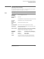
User’s Guide
Publication number E2456-97000
First edition, June 1994
For Safety information, Warranties, and Regulatory
information, see the pages behind the index
Hewlett-Packard Company 1994
All Rights Reserved
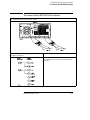
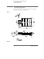
HP E2456A MC68306
Preprocessor Interface
The HP E2456A Preprocessor
Interface—At a Glance
The HP E2456A Preprocessor Interface provides a complete interface for
state or timing analysis between any Motorola MC68306 target system and
the following HP logic analyzers:
•
•
•
•
•
•
•
•
•
•
HP 1650A
HP 1650B
HP 1652B
HP 16510A
HP 16510B
HP 16511B
HP 16550A (one- or two-card)
HP 16555A (one- or two-card)
HP 1660A/61A/62A
HP 1660AS/61AS/62AS (with oscilloscope)
The preprocessor interface connects the target microprocessor to the logic
analyzer, and performs any functions unique to the target microprocessor.
The configuration software on the flexible disk sets up the format
specification menu of the logic analyzer for compatibility with the
preprocessor interface. The inverse assembler allows you to obtain displays
of the MC68306 data bus in 68000 core assembly language mnemonics.
The HP E2456A Preprocessor Interface requires the HP E3417A 132-pin QFP
adapter, which clamps over the existing processor, and supports limited
rotation for connecting to target systems with physical layout limitations. The
preprocessor connects to the HP E3417A adapter via a 144-pin full matrix
PGA socket. The HP E2456A does not support the 144-pin TQFP processor
package.
For more information on the logic analyzers or microprocessor, refer to the
appropriate reference manuals for those products.
ii
MC68306 Preprocessor
Introduction
The HP E2456A Preprocessor Interface—At a Glance
HP E2456A Preprocessor Interface
MC68306 Preprocessor
iii
In This Book
This book is the user’s guide for the HP E2456A Preprocessor Interface. It
assumes that you have a working knowledge of the logic analyzer used and
the microprocessor being analyzed.
This user’s guide is organized into three chapters and one appendix:
Chapter 1 explains how to install and configure the preprocessor
interface for state or timing analysis with the supported logic
analyzers.
Chapter 2 provides reference information on the format specification
and symbols configured by the preprocessor interface software and
information about the inverse assembler and status encoding.
Chapter 3 contains reference information on the preprocessor
interface hardware, including the characteristics and signal mapping
for the preprocessor interface.
Appendix A contains information on troubleshooting problems or
difficulties which may occur with the preprocessor interface.
For more information on the logic analyzers or microprocessor, refer to the
appropriate reference manual for those products.
iv
MC68306 Preprocessor
Contents
1 Setting Up the Preprocessor Interface
Before You Begin 1–3
Setting Up the Preprocessor Interface Hardware 1–5
To select state or timing analysis 1–6
To connect to the target system 1–7
To rotate the adapter connection 1–9
To connect to the HP 1650A/B analyzer 1–11
To connect to the HP 1652B analyzer 1–12
To connect to the HP 16510A/B analyzer 1–13
To connect to the HP 16511B analyzer 1–14
To connect to the HP 16550A one-card analyzer 1–15
To connect to the HP 16550A two-card analyzer 1–16
To connect to the HP 16555A one-card analyzer 1–17
To connect to the HP 16555A two-card analyzer 1–18
To connect to the HP 1660A/AS analyzer 1–19
To connect to the HP 1661A/AS analyzer 1–20
To connect to the HP 1662A/AS analyzer 1–21
To probe the preprocessor interface with an oscilloscope 1–22
To connect the termination adapters 1–24
To power up or power down 1–25
To protect the preprocessor interface when not in use 1–25
Setting Up the Preprocessor Interface Software 1–26
To load the configuration and inverse assembler files 1–27
To set up the preprocessor interface for timing 1–28
2 Analyzing the Motorola MC68306
Displaying Information 2–3
To display the format specification 2–3
To display the configuration labels and symbols 2–5
To display captured state data 2–9
MC68306 Preprocessor
v
Contents
Using the Inverse Assembler 2–10
To synchronize the inverse assembler 2–13
Inverse Assembler Error Messages 2–14
3 Preprocessor Interface Hardware Reference
Operating Characteristics 3–3
Theory of Operation and Clocking 3–4
Signal-to-Connector Mapping 3–5
Circuit Board Dimensions 3–16
Repair Strategy 3–17
A If You Have a Problem
Analyzer Problems A–3
Intermittent data errors A–3
Unwanted triggers A–3
No activity on activity indicators A–4
No trace list display A–4
Preprocessor Problems A–5
Target system will not boot up A–5
Erratic trace measurements A–6
Capacitive loading A–6
Inverse Assembler Problems A–8
No inverse assembly or incorrect inverse assembly A–8
Inverse assembler will not load or run A–9
Intermodule Measurement Problems A–10
An event wasn’t captured by one of the modules A–10
vi
MC68306 Preprocessor
Contents
Messages A–11
“. . . Inverse Assembler Not Found” A–11
“Measurement Initialization Error” A–12
“No Configuration File Loaded” A–13
“Selected File is Incompatible” A–13
“Slow or Missing Clock” A–13
“State Clock Violates Overdrive Specification” A–14
“Time from Arm Greater Than 41.93 ms” A–14
“Waiting for Trigger” A–14
MC68306 Preprocessor
vii
Figures
Preprocessor Interface Assembly 1–8
Adapter Rotation Orientations 1–10
Pin Numbers and Ground Pins 1–23
Connecting the Termination Adapter 1–24
PC-based Addressing Mode Listing 2–12
PGA Pin Assignments 3–5
Dimensions 3–16
Tables
Logic Analyzers Supported 1–4
Logic Analyzer Configuration Files 1–28
MC68306 STAT Label Bits 2–5
MC68306 Symbols 2–6
Operating Characteristics 3–3
MC68306 Signal List 3–7
MC68306 Power/Ground List 3–14
Replaceable Parts 3–17
viii
MC68306 Preprocessor
1
Setting Up the Preprocessor
Interface
Setting Up the Preprocessor Interface
This chapter explains how to set up the HP E2456A Preprocessor Interface
hardware and software, configure the preprocessor, and connect the
preprocessor to supported logic analyzers.
1–2
MC68306 Preprocessor
Before You Begin
This section lists the logic analyzers supported by the HP E2456A, and
provides other information about the analyzers and the preprocessor
interface.
Equipment Supplied
• The preprocessor interface hardware, which includes the preprocessor
circuit card.
• The inverse assembler software and configuration files on a 3.5-inch disk.
• This User’s Guide.
MC68306 Preprocessor
1–3
Setting Up the Preprocessor Interface
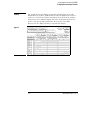
Minimum Equipment Required
• The HP E2456A MC68306 preprocessor interface and inverse assembler.
• The HP E3417A 132-pin QFP adapter.
• One of the logic analyzers listed in the following table:
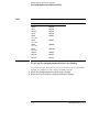
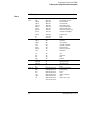
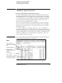
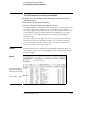
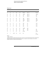
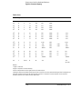
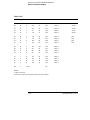
Table 1
Logic Analyzers Supported
Logic Analyzer
Channel Count
State Speed
Timing Speed
Memory Depth
1650A
80
25 MHz
100 MHz
1 k states
1650B
80
35 MHz
100 MHz
1 k states
1652B
80
35 MHz
100 MHz
1 k states
16510A
80
25 MHz
100 MHz
1 k states
16510B
80
35 MHz
100 MHz
1 k states
16511B
160
35 MHz
100 MHz
1 k states
16550A
(one card)
102
100 MHz
250 MHz
4 k states
16550A
(two card)
204
100 MHz
250 MHz
4 k states
16555A
(one card)
68
100 MHz
250 MHz
1 M states
16555A
(two card)
136
100 MHz
250 MHz
1 M states
1660A/AS
136
100 MHz
250 MHz
4 k states
1661A/AS
102
100 MHz
250 MHz
4 k states
1662A/AS
68
100 MHz
250 MHz
4 k states
1
1. The HP 1650A requires system software version V1.11 or higher.
1–4
MC68306 Preprocessor
Setting Up the Preprocessor Interface
Hardware
Setting up for the preprocessor interface hardware consists of the following
major steps:
1 Turn off the logic analyzer and the target system.
Caution
To protect your equipment, remove the power from both the logic analyzer
and the target system before you make or break connections. Because the
logic analyzer supplies power to the preprocessor interface, the logic
analyzer should always be powered up before the target system; when
powering down, power down the target system first and then power down
the logic analyzer.
2 Install the preprocessor interface in the target system.
3
4 Connect the logic analyzer pods to the cable connectors of the
preprocessor interface board.
The remainder of this section contains a separate subsection for each logic
analyzer this interface supports that show the analyzer pod cable
connections.
The remainder of this section describes these general steps in more
detail.
MC68306 Preprocessor
1–5
Setting Up the Preprocessor Interface
To select state or timing analysis
To select state or timing analysis
The HP E2456A preprocessor interface uses the same connections and
configuration for both state and timing analysis. The only difference is that
you choose Timing as the Type in the module Configuration menu of your
logic analyzer. See "To set up the preprocessor interface for timing" later in
this chapter and also Chapter 3 for line loading and timing skew (if any)
information.
The terminated (2X20) P4 connector provides delayed versions of ~UDS and
~LDS. For correct timing information on these signals, use the unterminated
(2X10) P7 connector with either a termination adapter (HP 01650-63203) or the
General Purpose (GP) probes supplied with your logic analyzer.
1–6
MC68306 Preprocessor
Setting Up the Preprocessor Interface
To connect to the target system
To connect to the target system
1. To prevent equipment damage, remove power from both the logic
analyzer and the target system.
2. Using the instructions in the "QFP Probe Adapter Assembly
Operating Note," connect the probe adapter assembly to the target
system microprocessor. Ensure that pin 1 is properly aligned.
Caution
Serious damage to the target system or preprocessor interface can result
from incorrect connection. Note the position of pin 1 and pin A1 on the
preprocessor interface, probe adapter assembly, and microprocessor prior
to making any connection. Also, take care to align the preprocessor
interface connector with the pins on the probe adapter assembly so that all
pins are making contact.
The preprocessor interface requires a QFP Probe Adapter Assembly for
connecting to the MC68306 microprocessor. The probe adapter assembly
allows the preprocessor interface to be connected without removing the
microprocessor from the target system. The adapter supports rotations of 0,
90, 180, and 270 degrees. See the next section for information about rotated
connections.
3. Install the preprocessor interface into the PGA socket on the QFP
probe adapter, again ensuring that pin A1 is properly aligned.
MC68306 Preprocessor
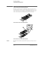
1–7
Setting Up the Preprocessor Interface
To connect to the target system
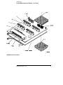
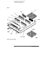
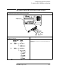
Figure 1
Preprocessor Interface Assembly
1–8
MC68306 Preprocessor
Setting Up the Preprocessor Interface
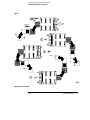
To rotate the adapter connection
To rotate the adapter connection
• Connect the adapter and preprocessor in one of the rotations shown
in Figure 2.
The HP E3417A adapter supports rotations of 0, 90, 180, and 270 degrees.
First, rotate the adapter with respect to the microprocessor the desired
number of degrees. Then, rotate the preprocessor with respect to the adapter
the same number of degrees. Rotation and perhaps the use of additional PGA
pin protector adapters can allow you to clamp onto difficult-to-reach
processors.
MC68306 Preprocessor
1–9
Setting Up the Preprocessor Interface
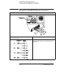
To rotate the adapter connection
Figure 2
Adapter Rotation Orientations
1–10
MC68306 Preprocessor
Setting Up the Preprocessor Interface
To connect to the HP 1650A/B analyzer
To connect to the HP 1650A/B analyzer
1. Locate the pod cables in the back of the analyzer.
2. Connect the pod cables to the preprocessor interface
according to this diagram.
3. Load the configuration file C68306E0.
P1 and P3 on the preprocessor side refer to the
terminated 2X20 connectors, not the unterminated 2X10
connectors.
MC68306 Preprocessor
1–11
Setting Up the Preprocessor Interface
To connect to the HP 1652B analyzer
To connect to the HP 1652B analyzer
1. Locate the pod cables in the back of the analyzer.
2. Connect the pod cables to the preprocessor interface
according to this diagram.
3. Load the configuration file C68306E0.
P1 and P3 on the preprocessor side refer to the
terminated 2X20 connectors, not the unterminated 2X10
connectors.
1–12
MC68306 Preprocessor
Setting Up the Preprocessor Interface
To connect to the HP 16510A/B analyzer
To connect to the HP 16510A/B analyzer
1. Locate the pod cables in the back of the analyzer.
2. Connect the pod cables to the preprocessor interface
according to this diagram.
3. Load the configuration file C68306E0.
P1 and P3 on the preprocessor side refer to the
terminated 2X20 connectors, not the unterminated 2X10
connectors.
MC68306 Preprocessor
1–13
Setting Up the Preprocessor Interface
To connect to the HP 16511B analyzer
To connect to the HP 16511B analyzer
1. Locate the cards and pod cables in the back of the analyzer (slot positions are relative, actual card positions may vary).
2. Connect the pod cables to the preprocessor interface
according to this diagram.
3. Load the configuration file C68306E2.
P1 and P3 on the preprocessor side refer to the
terminated 2X20 connectors, not the unterminated 2X10
connectors.
1–14
MC68306 Preprocessor
Setting Up the Preprocessor Interface
To connect to the HP 16550A one-card analyzer
To connect to the HP 16550A one-card analyzer
1. Locate the card and pod cables in the back of the analyzer.
2. Connect the pod cables to the preprocessor interface
according to this diagram.
3. Load the configuration file C68306S1.
P1 and P3 on the preprocessor side refer to the
terminated 2X20 connectors, not the unterminated 2X10
connectors.
MC68306 Preprocessor
1–15
Setting Up the Preprocessor Interface
To connect to the HP 16550A two-card analyzer
To connect to the HP 16550A two-card analyzer
1. Locate the cards and pod cables in the back of the analyzer (slot positions are relative, actual card positions may vary).
2. Connect the pod cables to the preprocessor interface
according to this diagram.
3. Load the configuration file C68306S2.
P1 and P3 on the preprocessor side refer to the
terminated 2X20 connectors, not the unterminated 2X10
connectors.
1–16
MC68306 Preprocessor
Setting Up the Preprocessor Interface
To connect to the HP 16555A one-card analyzer
To connect to the HP 16555A one-card analyzer
1. Locate the card and pod cables in the back of the analyzer.
2. Connect the pod cables to the preprocessor interface
according to this diagram.
3. Load the configuration file C68306M1.
P1 and P3 on the preprocessor side refer to the
terminated 2X20 connectors, not the unterminated 2X10
connectors.
MC68306 Preprocessor
1–17
Setting Up the Preprocessor Interface
To connect to the HP 16555A two-card analyzer
To connect to the HP 16555A two-card analyzer
1. Locate the cards and pod cables in the back of the analyzer (slot positions are relative, actual card positions may vary).
2. Connect the pod cables to the preprocessor interface
according to this diagram.
3. Load the configuration file C68306M2.
P1 and P3 on the preprocessor side refer to the
terminated 2X20 connectors, not the unterminated 2X10
connectors.
1–18
MC68306 Preprocessor
Setting Up the Preprocessor Interface
To connect to the HP 1660A/AS analyzer
To connect to the HP 1660A/AS analyzer
1. Locate the pod cables in the back of the analyzer.
2. Connect the pod cables to the preprocessor interface
according to this diagram.
3. Load the configuration file C68306J0.
P1 and P3 on the preprocessor side refer to the
terminated 2X20 connectors, not the unterminated 2X10
connectors.
MC68306 Preprocessor
1–19
Setting Up the Preprocessor Interface
To connect to the HP 1661A/AS analyzer
To connect to the HP 1661A/AS analyzer
1. Locate the pod cables in the back of the analyzer.
2. Connect the pod cables to the preprocessor interface
according to this diagram.
3. Load the configuration file C68306S1.
P1 and P3 on the preprocessor side refer to the
terminated 2X20 connectors, not the unterminated 2X10
connectors.
1–20
MC68306 Preprocessor
Setting Up the Preprocessor Interface
To connect to the HP 1662A/AS analyzer
To connect to the HP 1662A/AS analyzer
1. Locate the pod cables in the back of the analyzer.
2. Connect the pod cables to the preprocessor interface
according to this diagram.
3. Load the configuration file C68306J2.
P1 and P3 on the preprocessor side refer to the
terminated 2X20 connectors, not the unterminated 2X10
connectors.
MC68306 Preprocessor
1–21
Setting Up the Preprocessor Interface
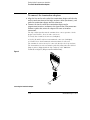
To probe the preprocessor interface with an oscilloscope
To probe the preprocessor interface with an
oscilloscope
1 Connect the ground lead of the oscilloscope probe to one of the
ground pins on the preprocessor interface.
There are two ground pins on the top of the preprocessor interface. Refer to
Figure 3 for the locations of the ground pins.
2 Connect the other lead to the signal to be measured.
You also can probe all microprocessor signals at the PGA socket. Chapter 3
includes an illustration showing the locations of the preprocessor signals on
the PGA socket.
1–22
MC68306 Preprocessor
Setting Up the Preprocessor Interface
To probe the preprocessor interface with an oscilloscope
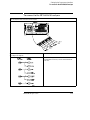
Figure 3
Pin Numbers and Ground Pins
MC68306 Preprocessor
1–23
Setting Up the Preprocessor Interface
To connect the termination adapters
To connect the termination adapters
1 Align the key on the male end of the termination adapter with the slot
on the connector of one of the logic analyzer cables (not shown), and
push the termination adapter into the connector.
2 Connect the female end of the termination adapter to the
preprocessor interface as shown in the figure below. For connectors
without a guide slot, orient the adapter the same as for other
connectors.
The logic analyzer probes must be terminated for correct operation. On the
preprocessor interface, there are nine connectors.
• P4 only has a terminated connector (2x20 pins).
• P2, P5, P6 and P7 only have nonterminated connectors (2x10 pins).
• P1 and P3 have both terminated and nonterminated connectors.
The terminated connectors may be connected directly to the logic analyzer.
The nonterminated connectors must be probed by using either the General
Purpose probes (shipped with the logic analyzer) or the 100 kOhm
Termination Adapters (HP part number 01650-63203).
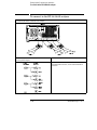
Figure 4
Connecting the Termination Adapter
1–24
MC68306 Preprocessor
Setting Up the Preprocessor Interface
To power up or power down
To power up or power down
When powering up, the logic analyzer must be powered up first, and then the
target system. The logic analyzer provides the power to the active circuits on
the preprocessor interface; unpowered circuits may cause improper
operation of the target system.
When powering down, the target system should be powered down first, and
then the logic analyzer.
To protect the preprocessor interface when not in use
1 Cover the socket assembly pins of the preprocessor interface with a
conductive foam wafer or conductive plastic pin protector.
The socket assembly pins of the preprocessor interface were covered at the
time of shipment with either a conductive foam wafer or conductive pin
protector. If this device is not damaged, it may be reused repeatedly.
2 Store the preprocessor interface in an antistatic bag or container.
The socket assembly pins of the preprocessor interface should be covered
with a conductive foam wafer or pin protector to protect the delicate gold
plated pins of the assembly from damage due to impact. Covering the pins
and properly storing the preprocessor interface also protects the active
circuitry on the preprocessor interface from electrostatic discharge.
Electrostatic Discharge
MC68306 Preprocessor
1–25
Setting Up the Preprocessor Interface
To protect the preprocessor interface when not in use
Setting Up the Preprocessor Interface Software
Setting up for the preprocessor interface software consists of the following
major steps:
1 The first time you set up the preprocessor interface, make a duplicate
copy of the master disk.
For information on duplicating disks, refer to the reference manual for your
logic analyzer.
2 Insert the preprocessor interface disk in the front disk drive of the
logic analyzer.
3 Load the appropriate configuration file into the logic analyzer.
Once you have the hardware and software set up, you are ready to make
measurements with the logic analyzer and preprocessor interface. The rest
of this section provides more detailed information on setting up the
preprocessor software.
1–26
MC68306 Preprocessor
Setting Up the Preprocessor Interface
To load the configuration and inverse assembler files
To load the configuration and inverse assembler files
1 Insert the preprocessor interface disk in the front disk drive of the
logic analyzer.
2 Depending on your logic analyzer, select one of the following menus:
• For the HP 1650-series logic analyzers, press the I/O menu key and
•
•
•
3
4
5
use the knob to select "Disc Operations"
For the HP 1660-series logic analyzers, select the "System Disk" menu
For the HP 16500A mainframe, select the "System Front Disk" menu
For the HP 16500B mainframe, select the "System Flexible Disk"
menu
Configure the menu to "Load" the analyzer configuration from disk.
For HP 16500-series and HP 1660-series logic analyzers, select the
appropriate module (such as "100/500 MHz LA" or "Analyzer") for the
load.
Use the knob to select the appropriate configuration file.
Your configuration file choice depends on which analyzer you are using, the
software version(s) of your analyzer software, and, in some cases, which
inverse assembler you want to use. See the summary table following these
instruction steps.
6 Execute the load operation to load the file into the logic analyzer.
The logic analyzer is configured for MC68306 analysis by loading the
appropriate MC68306 configuration file. Loading this file also automatically
loads the inverse assembler.
The following table lists the correct configuration file to for each logic
analyzer. For more information about the inverse assembler, see Chapter 2.
MC68306 Preprocessor
1–27
Setting Up the Preprocessor Interface
To set up the preprocessor interface for timing
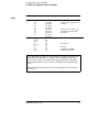
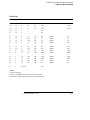
Table 2
Logic Analyzer Configuration Files
Logic Analyzer
Configuration File
1650A/B
C68306E0
1652B
C68306E0
16510A/B
C68306E0
16511B
C68306E2
16550A
(one card)
C68306S1
16550A
(two card)
C68306S2
16555A
(one card)
C68306M1
16555A
(two card)
C68306M2
1660A/AS
C68306J0
1661A/AS
C68306S1
1662A/AS
C68306J2
To set up the preprocessor interface for timing
The same format specification loaded for state analysis is also used for timing
analysis. To configure the logic analyzer for timing analysis:
1 Select the Configuration menu of the logic analyzer.
2 Select the Type field for the analyzer and select Timing.
1–28
MC68306 Preprocessor
2
Analyzing the Motorola
MC68306
Analyzing the Motorola MC68306
This chapter describes how to display configuration information and
preprocessor interface data, gives status information label and symbol
encodings, and provides information about the available inverse
assembler.
2–2
MC68306 Preprocessor
Displaying Information
This section describes how to display analyzer configuration information,
state and timing data captured by the preprocessor interface, and symbol
information that has been set up by the preprocessor interface configuration
software.
Unwanted Triggers
The logic analyzer captures prefetches, even if they are not executed. Care
must be taken when you are specifying a trigger condition or a storage
qualification that follows an instruction that may cause branching. An
unused prefetch may generate an unwanted trigger.
Since the microprocessor only prefetches at most one word, one technique to
avoid unwanted triggering from unused prefetches is to add "2" to the trigger
address. This trigger condition will only be satisfied if the branch is not taken.
To display the format specification
• Select the format specification menu for your logic analyzer.
The MC68306 configuration files contain predefined format specifications.
These format specifications include all labels for monitoring the
microprocessor and any coprocessors connected directly to the
microprocessor.
Chapter 3 of this guide contains a table that lists the signals for the MC68306
processor and on which pod and probe line the signal comes to the logic
analyzer. Refer to this table and to the logic analyzer connection information
for your analyzer in chapter 1 to determine where the processor signals
should be on the format specification screen.
For those logic analyzers which have a Clock Period field, the Clock Period field
should remain in the current selection (> 60 ns) to use time-tags. For more
information on the Clock Period field, refer to the reference manual for your
logic analyzer.
MC68306 Preprocessor
2–3
Analyzing the Motorola MC68306
To display the format specification
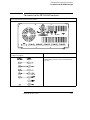
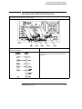
Example
The format specification display shown in the following figure is from the
HP 16550A logic analyzer. Additional labels and pod assignments are listed
off the screen. Select the "Labels" field and rotate the knob on the analyzer
front panel to view additional signals. Select the "Pods" field and rotate the
knob to view other pod-bit assignments. There may be some slight
differences in the display shown by your particular analyzer.
Figure 5
2–4
MC68306 Preprocessor
Analyzing the Motorola MC68306
To display the configuration labels and symbols
To display the configuration labels and symbols
• Select the "Symbols" field on the format specification menu and then
choose a label name from the "Label" pop-up. The logic analyzer will
display the symbols associated with the label.
The HP E2456A configuration software sets up symbol tables on the logic
analyzers. The tables contain alphanumeric symbols which identify data
patterns or ranges. Labels have been defined in the format specification
menu to make triggering on specific MC68306 cycles easier. The label base in
the symbols menu is set to hexadecimal to convserve space in the listing
menu.
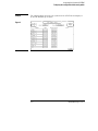
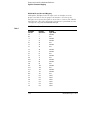
MC68306 STAT Label Bits
Table 3
Bit
0
Status
Signal
R/~W
1
2
~LDS
~UDS
These active-low signals are the lower and upper
data strobes for data bus control.
3
~RESET
If asserted externally, this signal resets the
microprocessor. When asserted internally, all
external system devices are reset without affecting
the internal state of the processor.
4
5
6
FC0
FC1
FC2
These three signals indicate the type of cycle the
microprocessor is executing.
7
~BGACK
For 3-wire bus arbitration, this signal is low when the
microprocessor has given ownership of the bus to
another device. In a 2-wire bus arbitration system,
this signal is always high.
MC68306 Preprocessor
Description
This signal is high for read cycles and low for write
cycles.
2–5
Analyzing the Motorola MC68306
To display the configuration labels and symbols
MC68306 Symbols
Table 4
Label
STAT
FC
SIZE
R/~W
DATA_B
2–6
Symbol
dma
udat wr
udat rd
upgm rd
sdat wr
sdat rd
spgm rd
int ack
Pattern (binary)
0xxx xxxx
1001 xxx0
1001 xxx1
1010 xxx1
1101 xxx0
1101 xxx1
1110 xxx1
1111 xxxx
Description
direct memory access
user data write
user data read
user program read
supervisor data write
supervisor data read
supervisor program read
interrupt acknowledge
pgm rd
wr
rd
res 0
udat 1
upgm 2
res 3
res 4
sdat 5
spgm 6
cpu 7
1x10 xxx1
xxxx xxx0
xxxx xxx1
000
001
010
011
100
101
110
111
program read
write
read
reserved, undefined
user data
user program
reserved, undefined
reserved, undefined
supervisor data
supervisor program
CPU space
usr
sup
dat
pgm
word
high byte
low byte
rd
wr
BSR
BRA
Bxx
RTx
JSR
JMP
Jxx
---
0xx
1xx
x01
x10
00
01
10
1
0
0110 0001 xxxx xxxx
0110 0000 xxxx xxxx
0110 xxxx xxxx xxxx
0100 1110 0111 0xxx
0100 1110 10xx xxxx
0100 1110 11xx xxxx
0100 1110 1xxx xxxx
xxxx xxxx xxxx xxxx
,
user
supervisor
data
program
word transfer
high byte transfer
low byte transfer
read
write
branch to subroutine
branch always
branch
return
jump to subroutine
jump
jump (JMP or JSR)
MC68306 Preprocessor
Analyzing the Motorola MC68306
To display the configuration labels and symbols
MC68306 Symbols
Table 4
Label
CS
BUS
Symbol
cs0
cs1
cs2
cs3
cs4
cs5
cs6
cs7
--br_bg_ack
br_bg
br_ack
br
bg_ack
bg
ack
local
Pattern (binary)
xxxx xxx0 x
xxxx xx0x x
xxxx x0xx x
xxxx 0xxx x
xxx0 xxxx 1
xx0x xxxx 1
x0xx xxxx 1
0xxx xxxx 1
xxxx xxxx x
000
001
010
011
100
101
110
111
Description
signals ~CS3 to ~CS0 are always
available
signals ~CS7 to ~CS4 are only
available in chip select mode
(AMODE=1)
bus request
bus grant
bus grant acknowledge
MC68306 is bus master
Do not modify the bits in the STAT or DATA labels, or the lower bits in the ADDR
label in the format specification if you want inverse assembly. Changes may
cause incorrect results. Also note that if the trigger specification is modified to
store only selected bus cycles, incorrect or incomplete inverse assembly may
result.
The lower ADDR bits are bits 0 to 15. You can modify ADDR bits 16 to 23 with no
side effects.
MC68306 Preprocessor
2–7
Analyzing the Motorola MC68306
To display the configuration labels and symbols
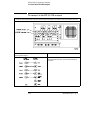
Example
The following figure shows the the symbols for the STAT label as displayed
by the HP 16550A logic analyzer:
Figure 6
2–8
MC68306 Preprocessor
Analyzing the Motorola MC68306
To display captured state data
To display captured state data
• Select the Listing Menu for your logic analyzer.
The logic analyzer displays captured data in the Listing Menu. The inverse
assembler disassembles the captured data in a format that closely resembles
the assembly source code for your processor. For those preprocessors that
have more than one inverse assembler, the inverse assembler used depends
on your logic analyzer and logic analyzer software version. See the logic
analyzer software compatibility table in chapter 1.
The inverse assembler often cannot determine where an instruction starts.
For correct inverse assembly, you must synchronize the inverse assembler
with the start of an instruction. See "To synchronize the inverse assembler"
later in this chapter.
If your trace listing doesn’t otherwise appear to be correct (capturing the
same RAM address twice, for example), make sure the preprocessor interface
hardware is configured for state analysis. The "Invasm" field will appear at the
top of the Listing Menu screen when the logic analyzer is configured for state
analysis. See Chapter 1 to review the hardware configuration, correct it if
needed, and then run the trace again.
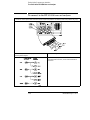
Example
The following figure shows the Listing Menu display for the HP 16550A logic
analyzer using the IA68306 inverse assembler:
Figure 7
Top line of display.
Synchronization begins
here.
Unexecuted prefetch
Missing opcodes
(caused by unexecuted
prefetch)
Cursor position
Don’t care bytes
Prefetch that may or may
not have been executed.
MC68306 Preprocessor
2–9
Using the Inverse Assembler
This section discusses the general output format of the inverse assembler,
and any processor-specific information you will need.
The MC68306 microprocessor does not indicate externally which word
fetched is the beginning of a new instruction. You may have to "point" to the
first state of an instruction fetch to synchronize the inverse assembler. Once
synchronized, the inverse assembler will disassemble from this state through
the end of the screen. See "To synchronize the inverse assembler" later in
this chapter for more information.
General Output Format
The next few paragraphs describe the general output format of the inverse
assembler.
Numeric Format
Unless a value is followed by a suffix character, numeric output from the
inverse assembler is in hexadecimal format. For example, decimal values
have a period (.) as the suffix character; binary values have a percent sign
(%).
Missing Opcodes
Asterisks (*) in the inverse assembler output indicate that a portion (or
portions) of an instruction was not captured by the analyzer. Missing
opcodes occur frequently and are primarily due to microprocessor prefetch
activity. Storage qualification, or the use of storage windows, can also lead to
such occurrences.
Don’t Care Bytes
The MC68306 microprocessor can perform byte, word, and long word
transfers. During operand reads and writes, entire 16-bit (word) values
appear on the microprocessor data bus. lines. The inverse assembler displays
"xx" for any bytes in a transfer that are ignored by the microprocessor. You
can determine exactly which byte or bytes of data were used as an operand.
2–10
MC68306 Preprocessor
Analyzing the Motorola MC68306
To display captured state data
Unexecuted Prefetched Instructions
The preprocessor interface sends all of the bus transactions by both the
microprocessor and coprocessor to the logic analyzer. Prefetched
instructions which are not executed by the microprocessor are marked by a
hyphen "-".
In some cases, it is impossible to determine from bus activity whether a
branch is taken or a prefetch is executed. In these cases, the inverse
assembler marks the disassembled line with the prefix "?".
IA68306 Processor-Specific Output Format
This section discusses issues specific to the IA68306 inverse assembler.
Bus Arbitration
Use of two-wire bus arbitration may cause the inverse assembler to
incorrectly disassemble state information. See the "Theory of Operation and
Clocking" section in Chapter 3 for more information.
PC-based Addressing Modes
The microprocessor may occasionally make an operand fetch from program
space when program-counter-based (PC-based) addressing modes are used.
MOVE.L
0[PC,D0.L],D7
When this occurs, the resulting memory read is classified as a program
reference by the microprocessor, and the Function Code lines are driven
accordingly (they indicate a program read rather than a data read).
When the inverse assembler detects an instruction of this type, it will attempt
to locate the operand fetch and tag it so that it will not be disassembled.
Instead, it will be classified as "program data" by the inverse assembler and
displayed in hexadecimal format.
MC68306 Preprocessor
2–11
Analyzing the Motorola MC68306
To display captured state data
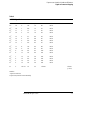
In the following example, state 350 has the instruction, and states 355 and
356 have the data.
Label
Base
> ADDR
> Hex
DATA
Invasm
348
349
350
351
352
353
354
355
356
357
358
359
360
361
362
363
04D214
04D216
04D218
F4083E
F40840
F4D21A
04D21C
04D654
04D656
04D21E
086BBC
086BBA
04D220
086BB8
086BB6
04D222
MOVE.L
FFCE
MOVE.L
43D8
6DFB
043A
MOVE.L
4400
0000
JSR
0000
4400
0003
6DFB
43D8
523C
STAT
Symbol
D7,FFCE[A4]
user program read
04D654[PC],-[A7]
user data write
user data write
user program read
D7,-[A7]
user program data
user program data
03523C
user data write
user data write
user program read
user data write
user data write
user program read
upgm rd
upgm rd
upgm rd
udat rd
udat rd
upgm rd
upgm rd
upgm rd
upgm rd
upgm rd
udat rd
udat rd
upgm rd
udat rd
udat rd
upgm rd
PC-based Addressing Mode Listing
2–12
MC68306 Preprocessor
Analyzing the Motorola MC68306
To synchronize the inverse assembler
To synchronize the inverse assembler
1 Identify a line on the display that you know is the first state of an
instruction fetch.
2 Roll this line to the top of the listing.
3 Select the "Invasm" field at the top of the screen.
The listing will inverse assemble from the top line down. Any data before this
screen is left unchanged. Rolling the screen up will inverse assemble the
lines as they appear on the bottom of the screen. If you jump to another area
of the listing by entering a new line number or by rolling the screen down,
you may have to re-synchronize the inverse assembler by repeating the
described steps.
Each time you inverse assemble a block of memory, the analyzer will keep
that block in the inverse assembled condition. You can inverse assemble
several different blocks in the analyzer memory, but the activity between
those blocks will not be inverse assembled.
Example
Synchronize the inverse assembler by positioning the first instruction to be
disassembled at the top of the listing display and choosing "Invasm" from the
top of the display.
Figure 8
Synchronization begins
at the top of the display,
not at the cursor position.
Cursor position.
MC68306 Preprocessor
2–13
Inverse Assembler Error Messages
Any of the following list of error messages may appear during analysis of your
target software. Included with each message is a brief explanation.
Illegal Task Request
Displayed if the inverse assembler is used with an instrument other than the
supported logic analyzers.
Fatal Data Error
Displayed if the trace memory could not be read properly on entry into the
inverse assembler.
Invalid Status
Displayed if the status field for the current state is not valid.
Illegal Opcode
Displayed if the inverse assembler encounters an illegal instruction.
Reserved Opcode
Displayed if the inverse assembler encounters a reserved coprocessor
instruction.
No Operand
Displayed if the inverse assembler cannot find a complete operand field for
an instruction. Prefetch activity or storage qualification is often the cause.
2–14
MC68306 Preprocessor
3
Preprocessor Interface
Hardware Reference
Preprocessor Interface
Hardware Reference
This chapter contains reference information on the HP E2456A
hardware including the characteristics and signal mapping for the
preprocessor interface. This chapter also includes a brief theory of
operation, circuit board dimensions, and information on repairing the
preprocessor interface.
3–2
MC68306 Preprocessor
Preprocessor Interface Hardware Reference
Operating Characteristics
Operating Characteristics
The following operating characteristics are not specifications, but are typical
operating characteristics for the preprocessor interface.
Table 5
Operating Characteristics
Microprocessor
Compatibility
Motorola MC68306 microprocessor
Microprocessor
Package
132-pin QFP
The HP E2456A does not support the 144-pin TQFP processor package.
Accessories
Required
HP E3417A generic PGA to 132-pin QFP probe adapter.
Maximum Clock
Speed
16.67 MHz Clockout (8.33 MHz ~AS rate).
Power Requirements
100 mA at +5 Vdc maximum, supplied by the logic analyzer.
Probes Required
Seven 16-channel pods are available. Three are required for inverse
assembly with state analysis.
Signal Line Loading
Loading when using only pods P1, P3, and P4 is 20 pF in parallel with
100 kOhm on all lines (except 10 pF on EXTAL and XTAL). Connecting
additional pods may increase loading on certain signals.
Environmental
Temperature
Operating
Nonoperating
0 to 55 degrees C (+32 to +131 degrees F)
-40 to +75 degrees C (-40 to +167 degrees F)
Altitude
Operating
Nonoperating
4,600 m (15,000 ft)
15,300 m (50,000 ft)
Humidity
Up to 90% noncondensing. Avoid sudden, extreme temperature
changes which could cause condensation within the instrument.
MC68306 Preprocessor
3–3
Preprocessor Interface Hardware Reference
Theory of Operation and Clocking
Theory of Operation and Clocking
Clocking
The microprocessor address strobe (~AS) indicates that address, function
code, size, and R/~W state information is on the bus and valid. The rising
edge of ~AS is used to clock information into the logic analyzer.
On a read cycle, data must be valid for 10 ns before the rising edge of ~AS for all
logic analyzers except the HP 1660A/61A/62A, HP 16550A, and HP 16555A.
Bus Arbitration
Bus arbitration is the method used by the microprocessor and other possible
bus master devices to request, grant, and acknowledge bus ownership. The
MC68306 microprocessor provides two different ways to arbitrate the bus,
2-wire and 3-wire arbitration.
If 3-wire bus arbitration is used, the ~BGACK signal is asserted when the
microprocessor has given ownership of the bus to another device. The
inverse assembler will not attempt to interpret any data as instruction fetches
until ~BGACK is negated.
In 2-wire bus arbitration, however, ~BGACK must always be pulled high.
Signals ~BR and ~BG indicate changes in bus control, but are asynchronous
with ~AS which clocks the logic analyzer. The inverse assembler has no way
of positively determining whether the microprocessor has bus control and
instead must rely on the function code signals. Once another device assumes
bus ownership, the microprocessor tri-states the function code lines. If the
new bus master happens to drive the function codes to combinations which
are recognized as valid by the inverse assembler, then incorrect disassembly
may result.
If your microprocessor target system uses 2-wire bus arbitration, you can
work around this potential problem by synchronizing the inverse assembler
on the first state of an instruction fetch which occurs at least one or more
states after ~BG goes high.
3–4
MC68306 Preprocessor
Preprocessor Interface Hardware Reference
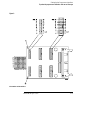
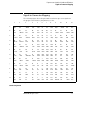
Signal-to-Connector Mapping
Signal-to-Connector Mapping
The following figure shows the pin numbers and microprocessor signals for
the preprocessor interface pin-grid-array socket.
1
2
3
4
5
6
7
8
9
10
11
12
A
50
N/C
51
FC1
54
~BERR
57
D14
61
VDD
65
D7
69
D4
73
VDD
76
IRQ4
80
~IACK4
82
PB7
83
N/C
B
49
FC2
48
~RESET
52
FC0
58
D13
62
D10
66
D6
68
D5
72
D1
78
~IACK7
79
GND
81
~IACK1
84
PB6
C
47
~HALT
46
GND
53
~DTACK
55
GND
59
D12
63
D9
71
D2
75
IRQ7
77
IRQ1
86
PB4
85
PB5
87
PB3
D
43
EXTAL
45
CLKOUT
44
XTAL
56
D15
60
D11
64
D8
70
D3
74
D0
89
PB2
88
GND
91
PB0
90
PB1
E
40
VDD
39
~BGACK
42
~BR
41
~BG
GP7
GND
GP8
GND
67
GND
GP6
GND
93
PA6
92
PA7
95
PA5
94
VDD
F
36
~UDS
35
~LDS
38
~AS
37
R/~W
34
GND
GP9
GND
GP4
GND
GP5
GND
97
PA3
96
PA4
99
PA1
98
PA2
G
32
~LW
33
~UW
30
~DRAMW
31
~OE
GPB
GND
GPA
GND
GP3
GND
100
GND
103
X2
104
IP2
101
PA0
102
X1
H
28
VDD
29
~RAS1
26
~CAS1
27
~RAS0
GPC
GND
1
GND
GP2
GND
GP1
GND
107
RXDA
108
TXDA
105
OP3
106
VDD
J
24
~CS0
25
~CAS0
22
GND
23
~CS1
8
A6
4
A9
130
A14
126
A17
122
TDO
110
TXDB
111
IP0
109
RXDB
K
21
~CS2
19
A20
20
~CS3
11
A3
9
A5
5
A8
129
A15
125
A18
121
GND
119
TMS
112
GND
113
IP1
L
18
A21
15
A23
13
GND
12
A2
6
A7
2
A11
132
A12
128
A16
124
A19
118
TCK
114
OP0
115
OP1
M
17
N/C
16
A22
14
A1
10
A4
7
VDD
3
A10
131
A13
127
VDD
123
120
AMODE TDI
117
~TRST
116
N/C
Notation: ~ indicates signal is active low.
PGA Pin Assignments
MC68306 Preprocessor
3–5
Preprocessor Interface Hardware Reference
Signal-to-Connector Mapping
The following table describes the electrical interconnections implemented
with the preprocessor interface.
The signal list table column descriptions are as follows:
POD
PIN
LA BIT
PGA PIN
QFP PIN
68306 LABEL
BUS LABEL
ALT BUS
SIG LABEL
3–6
The preprocessor connector that carries the signal.
The probe within the pod that carries the signal.
The logic analyzer bit associated with the signal.
The PGA adapter pin associated with the signal.
The microprocessor package pin number.
The manufacturer’s signal name.
An analyzer bus label identifies a collection of signals, such as all ADDR
or DATA. This signal is one of those in the bus label.
An additional bus label also assigned to the signal (if any).
An individual analyzer label associated with this signal only.
MC68306 Preprocessor
Preprocessor Interface Hardware Reference
Signal-to-Connector Mapping
Table 6
MC68306 Signal List
POD
P11
P11
P11
P11
PIN
19
18
17
16
LA BIT
0
1
2
3
PGA PIN
D8
B8
C7
D7
QFP PIN
74
72
71
70
68306 LABEL
D0
D1
D2
D3
BUS LABEL
DATA
DATA
DATA
DATA
P11
P11
P11
P11
15
14
13
12
4
5
6
7
A7
B7
B6
A6
69
68
66
65
D4
D5
D6
D7
DATA
DATA
DATA
DATA
P11
P11
P11
P11
11
10
9
8
8
9
10
11
D6
C6
B5
D5
64
63
62
60
D8
D9
D10
D11
DATA
DATA
DATA
DATA
P11
P11
P11
P11
7
6
5
4
12
13
14
15
C5
B4
A4
D4
59
58
57
56
D12
D13
D14
D15
DATA
DATA
DATA
DATA
P1
3
Clock 1
C3
53
~DTACK
ALT BUS
SIG LABEL
~DTACK
(J clock)
Notation:
~ Signal is active low.
1 Signal is required for inverse assembly.
MC68306 Preprocessor
3–7
Preprocessor Interface Hardware Reference
Signal-to-Connector Mapping
Table 6 (Cont.)
MC68306 Signal List
POD
P2
P2
P2
P2
PIN
19
18
17
16
LA BIT
0
1
2
3
PGA PIN
M9
C3
G4
G1
QFP PIN
123
53
31
32
68306 LABEL
AMODE
~DTACK
~OE
~LW
BUS LABEL
STAT_B
STAT_B
STAT_B
STAT_B
ALT BUS
SIG LABEL
AMODE
~DTACK
~OE
~LW
P2
P2
P2
P2
15
14
13
12
4
5
6
7
G2
C1
A3
F3
33
47
54
38
~UW
~HALT
~BERR
~AS
STAT_B
STAT_B
STAT_B
STAT_B
~UW
~HALT
~BERR
~AS
P2
P2
P2
P2
11
10
9
8
8
9
10
11
J1
J4
K1
K3
24
23
21
20
~CS0
~CS1
~CS2
~CS3
CS
CS
CS
CS
~CS0
~CS1
~CS2
~CS3
P25
P2
P2
P2
7
6
5
4
12
13
14
15
E2
E4
E3
D2
39
41
42
45
~BGACK
~BG
~BR
CLKOUT
BUS
BUS
BUS
P2
3
Clock 1
L10
118
TCK
~BG
~BR
CLKOUT
TCK
(K clock)
Notation:
~ Signal is active low.
5. Although ~BGACK is available on both preprocessor connectors P2 and P4, the individual signal label is assigned to P4
in the logic analyzer Format menu because this pod connection is required for inverse assembly. The P2 version of
~BGACK is used as one of the bits for BUS LABEL "BUS".
3–8
MC68306 Preprocessor
Preprocessor Interface Hardware Reference
Signal-to-Connector Mapping
Table 6 (Cont.)
MC68306 Signal List
POD
P31,2
P31
P31
P31
PIN
19
18
17
16
LA BIT
0
1
2
3
PGA PIN
F1
M3
L4
K4
QFP PIN
36
14
12
11
68306 LABEL
~UDS
A1
A2
A3
BUS LABEL
ADDR
ADDR
ADDR
ADDR
P31
P31
P31
P31
15
14
13
12
4
5
6
7
M4
K5
J5
L5
10
9
8
6
A4
A5
A6
A7
ADDR
ADDR
ADDR
ADDR
P31
P31
P31
P31
11
10
9
8
8
9
10
11
K6
J6
M6
L6
5
4
3
2
A8
A9
A10
A11
ADDR
ADDR
ADDR
ADDR
P31
P31
P31
P31
7
6
5
4
12
13
14
15
L7
M7
J7
K7
132
131
130
129
A12
A13
A14
A15
ADDR
ADDR
ADDR
ADDR
P3
3
Clock 1
D2
45
CLKOUT
ALT BUS
SIG LABEL
CLKOUT
(L clock)
Notation:
~ Signal is active low.
1 Signal is required for inverse assembly.
2 This is a delayed version of the signal (10 nsec) for state analysis.
MC68306 Preprocessor
3–9
Preprocessor Interface Hardware Reference
Signal-to-Connector Mapping
Table 6 (Cont.)
MC68306 Signal List
POD
P41
P41
P41
P41
PIN
37
35
33
31
LA BIT
0
1
2
3
PGA PIN
L8
J8
K8
L9
QFP PIN
128
126
125
124
68306 LABEL
A16
A17
A18
A19
BUS LABEL
ADDR
ADDR
ADDR
ADDR
ALT BUS
SIG LABEL
P41
P41
P41
P41
29
27
25
23
4
5
6
7
K2
L1
M2
L2
19
18
16
15
A20
A21
A22
A23
ADDR
ADDR
ADDR
ADDR
CS
CS
CS
CS
~CS4
~CS5
~CS6
~CS7
P41
P41,2
P41,2
P4
21
19
17
15
8
9
10
11
F4
F2
F1
B2
37
35
36
48
R/~W
~LDS
~UDS
~RESET
STAT
STAT
STAT
STAT
SIZE
SIZE
R/~W
~LDS
~UDS
~RESET
P41
P41
P41
P41,5
13
11
9
7
12
13
14
15
B3
A2
B1
E2
52
51
49
39
FC0
FC1
FC2
~BGACK
STAT
STAT
STAT
STAT
P41
3
Clock 1
F3
38
~AS
FC
FC
FC
FC0
FC1
FC2
~BGACK
~AS
(M clock)
Notation:
~ Signal is active low.
1 Signal is required for inverse assembly.
2 This is a delayed version of the signal (10 nsec) for state analysis.
5. Although ~BGACK is available on both preprocessor connectors P2 and P4, the individual signal label is assigned to P4
in the logic analyzer Format menu because this pod connection is required for inverse assembly. The P2 version of
~BGACK is used as one of the bits for BUS LABEL "BUS".
3–10
MC68306 Preprocessor
Preprocessor Interface Hardware Reference
Signal-to-Connector Mapping
Table 6 (Cont.)
MC68306 Signal List
POD
P5
P5
P5
P5
PIN
19
18
17
16
LA BIT
0
1
2
3
PGA PIN
J2
H3
H4
H2
QFP PIN
25
26
27
29
68306 LABEL
~CAS0
~CAS1
~RAS0
~RAS1
BUS LABEL
DRAM
DRAM
DRAM
DRAM
ALT BUS
SIG LABEL
~CAS0
~CAS1
~RAS0
~RAS1
P5
P5
P5
P5
15
14
13
12
4
5
6
7
G3
B11
A10
B9
30
81
80
78
~DRAMW
~IACK1
~IACK4
~IACK7
DRAM
INT
INT
INT
~DRAMW
~IACK1
~IACK4
~IACK7
P5
P5
P5
P5
11
10
9
8
8
9
10
11
C9
A9
C8
M11
77
76
75
117
IRQ1
IRQ4
IRQ7
~TRST
INT
INT
INT
JTAG
IRQ1
IRQ4
IRQ7
~TRST
P5
P5
P5
P5
7
6
5
4
12
13
14
15
J9
M10
K10
L10
122
120
119
118
TDO
TDI
TMS
TCK
JTAG
JTAG
JTAG
JTAG
TDO
TDI
TMS
TCK
P54
3
Clock 1
N/C
Notation:
~ Signal is active low.
4. "No Connect." Signal is not passed through to the logic analyzer.
MC68306 Preprocessor
3–11
Preprocessor Interface Hardware Reference
Signal-to-Connector Mapping
Table 6 (Cont.)
MC68306 Signal List
POD
P6
P6
P6
P6
PIN
19
18
17
16
LA BIT
0
1
2
3
PGA PIN
D11
D12
D9
C12
QFP PIN
91
90
89
87
68306 LABEL
PB0
PB1
PB2
PB3
BUS LABEL
PORT_B
PORT_B
PORT_B
PORT_B
P6
P6
P6
P6
15
14
13
12
4
5
6
7
C10
C11
B12
A11
86
85
84
82
PB4
PB5
PB6
PB7
PORT_B
PORT_B
PORT_B
PORT_B
P6
P6
P6
P6
11
10
9
8
8
9
10
11
G11
F11
F12
F9
101
99
98
97
PA0
PA1
PA2
PA3
PORT_A
PORT_A
PORT_A
PORT_A
P6
P6
P6
P6
7
6
5
4
12
13
14
15
F10
E11
E9
E10
96
95
93
92
PA4
PA5
PA6
PA7
PORT_A
PORT_A
PORT_A
PORT_A
P64
3
Clock 1
ALT BUS
SIG LABEL
~IACK2
~IACK3
~IACK5
~IACK6
IRQ2
IRQ3
IRQ5
IRQ6
N/C
Notation:
~ Signal is active low.
4. "No Connect." Signal is not passed through to the logic analyzer.
3–12
MC68306 Preprocessor
Preprocessor Interface Hardware Reference
Signal-to-Connector Mapping
Table 6 (Cont.)
MC68306 Signal List
POD
P73
P73
P74
P74
PIN
19
18
17
16
LA BIT
0
1
2
3
PGA PIN
F2
F1
QFP PIN
35
36
68306 LABEL
~LDS
~UDS
N/C
N/C
BUS LABEL
ALT BUS
SIG LABEL
~LDS_T
~UDS_T
P7
P7
P7
P7
15
14
13
12
4
5
6
7
J11
K12
G10
L11
111
113
104
114
IP0
IP1
IP2
OP0
SERIAL
SERIAL
SERIAL
SERIAL
IP0
IP1
IP2
OP0
P7
P7
P7
P7
11
10
9
8
8
9
10
11
L12
H11
J10
J12
115
105
110
109
OP1
OP3
TXDB
RXDB
SERIAL
SERIAL
SERIAL
SERIAL
OP1
OP3
TXDB
RXDB
P7
P7
P7
P7
7
6
5
4
12
13
14
15
H10
H9
G12
G9
108
107
102
103
TXDA
RXDA
X1
X2
SERIAL
SERIAL
SERIAL
SERIAL
TXDA
RXDA
X1
X2
P7
3
Clock 1
N/C
Notation:
~ Signal is active low.
3. This is an undelayed version of the signal for timing analysis.
4. "No Connect." Signal is not passed through to the logic analyzer.
MC68306 Preprocessor
3–13
Preprocessor Interface Hardware Reference
Signal-to-Connector Mapping
MC68306 Power/Ground Mapping
Although the VDD pins for the microprocessor are brought out to the
preprocessor PGA socket, the preprocessor interface does not use the
microprocessor’s power; these pins are treated as no-connects. The "Shield"
signal below is connected to the preprocessor interface ground but does not
correspond to any particular MC68306 GND pin.
MC68306 Power/Ground List
Table 7
HP E2456A
PGA Pin
H6
M5
L3
J3
H1
F5
E1
C2
C4
A5
E7
A8
B10
D10
E12
G8
H12
K11
K9
M8
E5
E6
E8
F6
F7
F8
3–14
MC68306
QFP-132 Pin
1
7
13
22
28
34
40
46
55
61
67
73
79
88
94
100
106
112
121
127
N/C
N/C
N/C
N/C
N/C
N/C
MC68306
Signal Name
GROUND
VDD
GROUND
GROUND
VDD
GROUND
VDD
GROUND
GROUND
VDD
GROUND
VDD
GROUND
GROUND
VDD
GROUND
VDD
GROUND
GROUND
VDD
Shield
Shield
Shield
Shield
Shield
Shield
MC68306 Preprocessor
Preprocessor Interface Hardware Reference
Signal-to-Connector Mapping
MC68306 Power/Ground List
Table 7
HP E2456A
PGA Pin
G5
G6
G7
H5
H7
H8
MC68306
QFP-132 Pin
N/C
N/C
N/C
N/C
N/C
N/C
MC68306 Preprocessor
MC68306
Signal Name
Shield
Shield
Shield
Shield
Shield
Shield
3–15
Preprocessor Interface Hardware Reference
Circuit Board Dimensions
Circuit Board Dimensions
Figure gives the dimensions for the preprocessor interface assembly. The
dimensions are listed in inches and millimeters.
Figure 9
Dimensions
3–16
MC68306 Preprocessor
Preprocessor Interface Hardware Reference
Repair Strategy
Repair Strategy
The repair strategy for this preprocessor interface is board replacement.
However, the following table lists some mechanical parts that may be
replaced if they are damaged or lost. Contact your nearest Hewlett-Packard
Sales Office for further information on servicing the board.
Exchange assemblies are available when a repairable assembly is returned to
Hewlett-Packard. These assemblies have been set up on the "Exchange
Assembly" program. This allows you to exchange a faulty assembly with one
that has been repaired, calibrated, and performance verified by the factory.
The cost is significantly less than that of a new assembly.
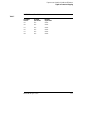
Table 8
Replaceable Parts
HP Part Number
Description
HP E2456-66501
Identity circuit board assembly (upper)
HP E2413-66505
ADDR/DATA circuit board assembly (lower)
HP E2456-68701
Inverse assembler disk pouch
5081-7736
Generic PGA to 132-pin QFP probe adapter
1200-1712
PGA pin protector socket
MC68306 Preprocessor
3–17
3–18
MC68306 Preprocessor
A
If You Have a Problem
If You Have a Problem
Occasionally, a measurement may not give the expected results. If you
encounter difficulties while making measurements, use this chapter to
guide you through some possible solutions. Each heading lists a
problem you may encounter, along with some possible solutions.
If you still have difficulty using the analyzer after trying the
suggestions in this chapter, please contact your local Hewlett-Packard
service center.
CAUTION
When you are working with the analyzer, be sure to power down both the
analyzer and the target system before disconnecting or connecting cables,
probes, and preprocessors. Otherwise, you may damage circuitry in the
analyzer, preprocessor, or target system.
A–2
MC68306 Preprocessor
Analyzer Problems
This section lists general problems that you might encounter while
using the analyzer.
Intermittent data errors
This problem is usually caused by poor connections, incorrect signal levels, or
marginal timing.
Remove and reseat all cables and probes; ensure that there are no bent
pins on the preprocessor interface or poor probe connections.
Adjust the threshold level of the data pod to match the logic levels in the
system under test.
Use an oscilloscope to check the signal integrity of the data lines.
Clock signals for the state analyzer must meet particular pulse shape and
timing requirements. Data inputs for the analyzer must meet pulse shape and
setup and hold time requirements.
See Also
See “Capacitive Loading” in this chapter for information on other sources of
intermittent data errors.
Unwanted triggers
Unwanted triggers can be caused by instructions that were fetched but not
executed.
Add the prefetch queue or pipeline depth to the trigger address to avoid
this problem.
The logic analyzer captures prefetches, even if they are not executed. When
you are specifying a trigger condition or a storage qualification that follows an
instruction that may cause branching, an unused prefetch may generate an
unwanted trigger.
MC68306 Preprocessor
A–3
If You Have a Problem
No activity on activity indicators
Since the microprocessor only prefetches at most one word, one technique to
avoid unwanted triggering from unused prefetches is to add "2" to the trigger
address. The trigger condition will only be satisfied if the branch is not taken.
No activity on activity indicators
On the HP 16510A Logic Analyzer, check the fuse that allows power to
the preprocessor interface.
On other logic analyzers, check for loose cables, board connections, and
preprocessor interface connections.
Check for bent or damaged pins on the preprocessor probe.
No trace list display
If there is no trace list display, it may be that your analysis specification is not
correct for the data you want to capture, or that the trace memory is only
partially filled.
Check your analysis sequencer specification to ensure that it will
capture the events of interest.
Try stopping the analyzer; if the trace list is partially filled, this should
display the contents of trace memory.
A–4
MC68306 Preprocessor
Preprocessor Problems
This section lists problems that you might encounter when using a
preprocessor. If the solutions suggested here do not correct the
problem, you may have a defective preprocessor. Contact your local
Hewlett-Packard Sales Office if you need further assistance.
Target system will not boot up
If the target system will not boot up after connecting the preprocessor
interface, the microprocessor (if socketed) or the preprocessor interface may
not be installed properly, or they may not be making electrical contact.
Ensure that you are following the correct power-on sequence for the
preprocessor and target system.
1 Power up the analyzer and preprocessor.
2 Power up the target system.
If you power up the target system before you power up the preprocessor,
interface circuitry in the preprocessor may latch up, preventing proper target
system operation.
Verify that the microprocessor and the preprocessor interface are
properly rotated and aligned, so that the index pin on the
microprocessor (such as pin 1 or A1) matches the index pin on the
preprocessor interface.
Verify that the microprocessor and the preprocessor interface are
securely inserted into their respective sockets.
Verify that the logic analyzer cables are in the proper sockets of the
preprocessor interface and are firmly inserted.
Reduce the number of extender sockets.
See Also
“Capacitive Loading” in this appendix.
MC68306 Preprocessor
A–5
If You Have a Problem
Erratic trace measurements
Erratic trace measurements
There are several general problems that can cause erratic variations in trace
lists and inverse assembly failures.
Ensure that the preprocessor configuration switches are correctly set
for the measurement you are trying to make.
Some preprocessors include configuration switches for various features (for
example, to allow dequeueing of the trace list). See chapter 1 for information
about setting configuration switches.
Try doing a full reset of the target system before beginning the
measurement.
Some preprocessor designs require a full reset to ensure correct
configuration.
Ensure that your target system meets the timing requirements of the
processor with the preprocessor probe installed.
See “Capacitive Loading” in this chapter. While preprocessor loading is slight,
pin protectors, extenders, and adapters may increase it to unacceptable
levels. If the target system design has close timing margins, such loading may
cause incorrect processor functioning, giving erratic trace results.
Ensure that you have sufficient cooling for the microprocessor.
Microprocessors such as the i486, Pentium, and MC68040 generate
substantial heat. This is exacerbated by the active circuitry on the
preprocessor board. You should ensure that you have ambient temperature
conditions and airflow that meet or exceed the requirements of the
microprocessor manufacturer.
Capacitive loading
Excessive capacitive loading can degrade signals, resulting in incorrect
capture by the preprocessor interface, or system lockup in the
microprocessor. All preprocessor interfaces add additional capacitive loading,
as can custom probe fixtures you design for your application.
Careful layout of your target system can minimize loading problems and
result in better margins for your design. This is especially important for
systems that are running at frequencies greater than 50 MHz.
A–6
MC68306 Preprocessor
If You Have a Problem
Capacitive loading
Remove as many pin protectors, extenders, and adapters as possible.
If multiple preprocessor interface solutions are available, try using one
with lower capacitive loading.
MC68306 Preprocessor
A–7
Inverse Assembler Problems
This section lists problems that you might encounter while using the
inverse assembler.
When you obtain incorrect inverse assembly results, it may be unclear
whether the problem is in the preprocessor or in your target system. If
you follow the suggestions in this section to ensure that you are using
the preprocessor and inverse assembler correctly, you can proceed
with confidence in debugging your target system.
No inverse assembly or incorrect inverse assembly
This problem is due to incorrect synchronization, modified configuration,
incorrect connections, or a hardware problem in the target system. A locked
status line can cause incorrect or incomplete inverse assembly.
Verify that the inverse assembler has been synchronized by placing an
opcode at the top of the display (not at the cursor position) and pressing
the Invasm key.
Because the inverse assembler works from the first line of the trace display,
if you jump to the middle of a trace and select Invasm, prior trace states may
not be disassembled correctly. If you move to several random places in the
trace list and synchronize the disassembly each time, the trace disassembly is
only guaranteed to be correct for the portion of the trace list disassembled.
See "To synchronize the inverse assembler" in Chapter 2 for more
information.
Ensure that each logic analyzer pod is connected to the correct
preprocessor connector.
There is not always a one-to-one correspondence between analyzer pod
numbers and preprocessor cable numbers. Preprocessors must supply
address (ADDR), data (DATA), and status (STAT) information to the
analyzer in a predefined order, so the cable connections for each
preprocessor are often altered to support that need. Thus, one preprocessor
might require that you connect cable 2 to analyzer pod 2, while another will
require you to connect cable 5 to analyzer pod 2. See chapter 1 for
connection information.
A–8
MC68306 Preprocessor
If You Have a Problem
Inverse assembler will not load or run
Check the activity indicators for status lines locked in a high or low
state.
Verify that the STAT, DATA, and ADDR format labels have not been
modified from their default values.
These labels must remain as they are configured by the configuration file. Do
not change the names of these labels or the bit assignments within the labels.
Some preprocessors also require other data labels; see chapter 2 for more
information.
Verify that all microprocessor caches and memory managers have been
disabled.
In most cases, if the microprocessor caches and memory managers remain
enabled you should still get inverse assembly, but it may be incorrect since
some of the execution trace was not visible to the logic analyzer.
Verify that storage qualification has not excluded storage of all the
needed opcodes and operands.
Inverse assembler will not load or run
You need to ensure that you have the correct system software loaded on your
analyzer.
Ensure that the inverse assembler is on the same disk as the
configuration files you are loading.
Configuration files for the state analyzer contain a pointer to the name of the
corresponding inverse assembler. If you delete the inverse assembler or
rename it, the configuration process will fail to load the disassembler.
See chapter 1 for details.
MC68306 Preprocessor
A–9
Intermodule Measurement Problems
Some problems occur only when you are trying to make a
measurement involving multiple modules.
An event wasn’t captured by one of the modules
If you are trying to capture an event that occurs very shortly after the event
that arms one of the measurement modules, it may be missed, due to internal
analyzer delays. For example, suppose you set the oscilloscope to trigger
upon receiving a trigger signal from the logic analyzer, because you are trying
to capture a pulse that occurs right after the analyzer’s trigger state. If the
pulse occurs too soon after the analyzer’s trigger state, the oscilloscope will
miss the pulse.
Adjust the skew in the Intermodule menu.
You may be able to specify a skew value that enables the event to be
captured.
Change the trigger specification for modules upstream of the one with
the problem.
If you’re using a logic analyzer to trigger the scope, try specifying a trigger
state one state before the one you are using. This may be more difficult than
working with the skew, because the prior state may occur more often and not
always be related to the event you’re trying to capture with the oscilloscope.
A–10
MC68306 Preprocessor
Messages
This section lists some of the messages that the analyzer displays
when it encounters a problem.
“. . . Inverse Assembler Not Found”
This error occurs if you rename or delete the inverse assembler file that is
attached to the configuration file. Ensure that the inverse assembler file is
not renamed or deleted.
MC68306 Preprocessor
A–11
If You Have a Problem
“Measurement Initialization Error”
“Measurement Initialization Error”
This error occurs when you have installed the cables incorrectly for one or
two HP 16550A logic analysis cards. The following diagrams show the correct
cable connections for one-card and two-card installations. Ensure that your
cable connections match the drawing, then repeat the measurement.
Cable Connections for One-Card HP 16550A Installations
Cable Connections for Two-Card HP 16550A Installations
See Also
The HP 16550A 100-MHz State/500-MHz Timing Logic Analyzer Service
Guide.
A–12
MC68306 Preprocessor
If You Have a Problem
“No Configuration File Loaded”
“No Configuration File Loaded”
This is usually caused by trying to load a configuration file for one type of
module/system into a different type of module/system.
Verify that the appropriate module has been selected from the Load
{module} from File {filename} in the HP 16500A/B disk operation menu.
Selecting Load {All} will cause incorrect operation when loading most
preprocessor interface configuration files.
See Also
Chapter 1 describes how to load configuration files.
“Selected File is Incompatible”
This occurs when you try to load a configuration file for the wrong module.
Ensure that you are loading the appropriate configuration file for your logic
analyzer.
“Slow or Missing Clock”
This error message might occur if the logic analyzer cards are not firmly
seated in the HP 16500A/B or HP 16501A frame. Ensure that the cards
are firmly seated.
This error might occur if the target system is not running properly.
Ensure that the target system is on and operating properly.
If the error message persists, check that the logic analyzer pods are
connected to the proper connectors on the preprocessor interface. See
chapter 1 to determine the proper connections.
For HP 16510A Logic Analyzers, check the preprocessor interface power
fuse in the logic analyzer.
MC68306 Preprocessor
A–13
If You Have a Problem
“State Clock Violates Overdrive Specification”
“State Clock Violates Overdrive Specification”
At least one 16-channel pod in the state analysis measurement stored a
different number of states before trigger than the other pods. This is usually
caused by sending a clocking signal to the state analyzer that does not meet
all of the specified conditions, such as minimum period, minimum pulse
width, or minimum amplitude. Poor pulse shaping could also cause this
problem.
The error message “State Clock Violates Overdrive Specification” should occur
only for HP 16510A,B, and HP 16511B Logic Analyzers with the Clock Period field
set to <60 ns. If this error message is observed with the Clock Period set to >60
ns, you may have a faulty logic analyzer. If a failure is suspected in your logic
analyzer, contact your nearest Hewlett-Packard Sales Office for information on
servicing the instrument.
“Time from Arm Greater Than 41.93 ms”
The state/timing analyzers have a counter to keep track of the time from
when an analyzer is armed to when it triggers. The width and clock rate of
this counter allow it to count for up to 41.93 ms before it overflows. Once the
counter has overflowed, the system does not have the data it needs to
calculate the time between module triggers. The system must know this time
to be able to display data from multiple modules on a single screen.
“Waiting for Trigger”
If a trigger pattern is specified, this message indicates that the specified
trigger pattern has not occurred. Verify that the triggering pattern is
correctly set.
When analyzing microprocessors that fetch only from word-aligned
addresses, if the trigger condition is set to look for an opcode fetch at an
address not corresponding to a word boundary, the trigger will never be
found.
A–14
MC68306 Preprocessor
If You Have a Problem
“Waiting for Trigger”
If a “don’t care” trigger condition is set, this message indicates:
For an HP 16511B Logic Analyzer, only one of the two cards is receiving
its state clock. Refer to “Slow or Missing Clock.”
For an HP 16510A,B Logic Analyzer, the pattern duration is probably set
to less than (<) instead of greater than (>). Since a “don’t care” pattern is
always true, the “less than” condition is never satisfied. Set the trigger
correctly for the measurement that is desired.
MC68306 Preprocessor
A–15
A–16
MC68306 Preprocessor
DECLARATION OF CONFORMITY
according to ISO/IEC Guide 22 and EN 45014
Manufacturer’s Name:
Hewlett-Packard Company
Manufacturer’s Address:
1900 Garden of the Gods Road
Colorado Springs , CO 80901
U.S.A.
Declares, That the product
Product Name:
Preprocessor Interface
Model Number(s):
HP E2456A
Product Options:
All
Conforms to the following Product Specifications:
Safety:
IEC 348 / HD 401
UL 1244
CSA - C22.2 No. 231 Series M-89
EMC:
CISPR 11:1990 /EN 55011 (1991): Group 1 Class A
IEC 801-2:1991 /EN 50082-1 (1992): 4 kV CD, 8 kV AD
IEC 801-3:1984 /EN 50082-1 (1992): 3 V/m
IEC 801-4:1988 /EN 50082-1 (1992): 1 kV
Supplementary Information:
The product herewith complies with the requirements of the Low Voltage
Directive 73/23/EEC and the EMC Directive 89/336/EEC.
Colorado Springs, July 5, 1993
John Strathman, Quality Manager
European Contact: Your local Hewlett-Packard Sales and Service Office or Hewlett-Packard GmbH,
Department ZQ / Standards Europe, Herrenberger Strasse 130, 71034 Böblingen Germany (FAX: +49-7031-143143)
Copyright HewlettPackard Company 1994
All Rights Reserved.
Reproduction, adaptation, or
translation without prior
written permission is
prohibited, except as allowed
under the copyright laws.
Publication number
E2456-97000
First edition, June, 1994
Printed in USA.
Warranty
The information contained in
this document is subject to
change without notice.
Hewlett-Packard makes
no warranty of any kind
with regard to this
material, including, but
not limited to, the implied
warranties or
merchantibility and
fitness for a particular
purpose.
Hewlett-Packard shall not be
liable for errors contained
herein or for incidental or
consequential damages in
connection with the
furnishing, performance, or
use of this material.
This Hewlett-Packard
product has a warranty
against defects in material
and workmanship for a period
of one year from date of
shipment. During the
warranty period,
Hewlett-Packard Company
will, at its option, either
repair or replace products
that prove to be defective.
Hewlett-Packard
P.O. Box 2197
1900 Garden of the Gods Road
Colorado Springs, CO 80901
For warranty service or
repair, this product must be
returned to a service facility
designated by
Hewlett-Packard.
For products returned to
Hewlett-Packard for warranty
service, the Buyer shall
prepay shipping charges to
Hewlett-Packard and
Hewlett-Packard shall pay
shipping charges to return
the product to the Buyer.
However, the Buyer shall pay
all shipping charges, duties,
and taxes for products
returned to Hewlett-Packard
from another country.
Hewlett-Packard warrants
that its software and firmware
designated by
Hewlett-Packard for use with
an instrument will execute its
programming instructions
when properly installed on
that instrument.
Hewlett-Packard does not
warrant that the operation of
the instrument software, or
firmware will be
uninterrupted or error free.
Limitation of Warranty
The foregoing warranty shall
not apply to defects resulting
from improper or inadequate
maintenance by the Buyer,
Buyer-supplied software or
interfacing, unauthorized
modification or misuse,
operation outside of the
environmental specifications
for the product, or improper
site preparation or
maintenance.
No other warranty is
expressed or implied.
Hewlett-Packard specifically
disclaims the implied
warranties or merchantability
and fitness for a particular
purpose.
Exclusive Remedies
The remedies provided herein
are the buyer’s sole and
exclusive remedies.
Hewlett-Packard shall not be
liable for any direct, indirect,
special, incidental, or
consequential damages,
whether based on contract,
tort, or any other legal theory.
Assistance
Product maintenance
agreements and other
customer assistance
agreements are available for
Hewlett-Packard products.
For any assistance, contact
your nearest Hewlett-Packard
Sales Office.
Certification
Hewlett-Packard Company
certifies that this product met
its published specifications at
the time of shipment.
Hewlett-Packard further
certifies that its calibration
measurements are traceable
to the United States National
Institute of Standards and
Technology, to the extent
allowed by the Bureau’s
calibration facility, and to the
calibration facilities of other
International Standards
Organization members.
Safety
This product has been
designed and tested
according to International
Safety Requirements. To
ensure safe operation and to
keep the product safe, the
information, cautions, and
warnings in this user’s guide
must be heeded.
Safety Symbols
W arning
The Warning symbol calls
attention to a procedure,
practice, or the like, which, if
not correctly performed or
adhered to, could result in
personal injury. Do not
proceed beyond a Warning
symbol until the indicated
conditions are fully
understood and met.
Caution
The Caution symbol calls
attention to an operating
procedure, practice, or the
like, which, if not correctly
performed or adhered to,
could result in damage to or
destruction of part or all of
the product. Do not proceed
beyond a Caution symbol
until the indicated conditions
are fully understood or met.
About this edition
This is the first edition of the
HP E2456A MC68306
Preprocessor Interface
User’s Guide. Edition dates
are as follows:
1st edition, June, 1994
New editions are complete
revisions of the manual.
Update packages, which are
issued between editions,
contain additional and
replacement pages to be
merged into the manual by
you. The dates on the title
page change only when a new
edition is published.
A software or firmware code
may be printed before the
date. This code indicates the
version level of the software
or firmware of this product at
the time the manual or
update was issued. Many
product updates and fixes do
not require manual changes;
and, conversely, manual
corrections may be done
without accompanying
product changes. Therefore,
do not expect a one-to-one
correspondence between
product updates and manual
updates.
The following list of pages
gives the date of the current
edition and of any changed
pages to that edition. Within
the manual, any page
changed since the last edition
is indicated by printing the
date the changes were made
on the bottom of the page. If
an update is incorporated
when a new edition of the
manual is printed, the change
dates are removed from the
bottom of the pages and the
new edition date is listed on
the title page.
June, 1994: All pages original
edition