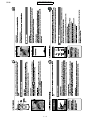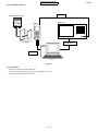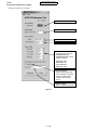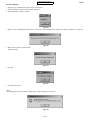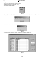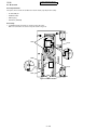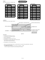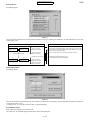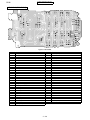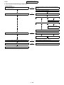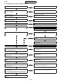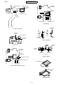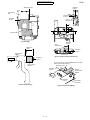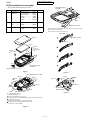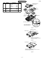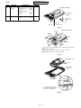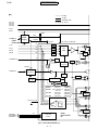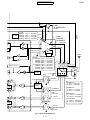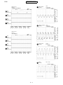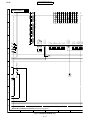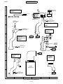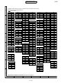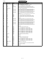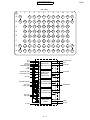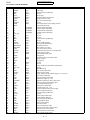
1
CONFIDENTIAL
GX30
SERVICE MANUAL
No. S5409TQGX30/B
DIGITAL MOBILE PHONE
MODEL
GX30
(INTERNAL MODEL NAME:
TQ-GX30E/G/R/T/S/H/EP/PP/W/B/D/A/Z/Q/L/F/C/K/U)
E : For U.K.
R : For Ireland
S : For Spain
EP: For U.K. (Prepaid)
W : For Sweden
D : For Greece
Z : For New Zealand
L : For Malta
C : For Switzerland
U : For Belgium
G : For Germany
T : For Italy
H : For Netherlands
PP: For Portugal (Prepaid)
B : For Hungary
A : For Australia
Q : For Egypt
F : For France
K : For Austria
• In the interests of user-safety the set should be restored to its
original condition and only parts identical to those specified
should be used.
• Caution
Risk of explosion if battery is replaced by an incorrect type,
dispose of used batteries according to the instruction.
CONTENTS
SERVICING CONCERNS
CHAPTER 1. GENERAL DESCRIPTION
[1] Specifications ................................................. 1-1
[2] Names of parts............................................... 1-2
[3] Operation manual .......................................... 1-3
CHAPTER 2. ADJUSTMENTS,
PERFORMANCE CHECK, AND
FIRMWARE UPGRADE
[1] SHARP Program Support Tool (SPST).......... 2-1
[2] Test points.................................................... 2-44
[3] Troubleshooting ........................................... 2-48
CHAPTER 3. DISASSEMBLY AND REASSEMBLY
[1] Servicing Concerns........................................ 3-1
[2] Disassembly and reassembly ........................ 3-4
CHAPTER 4. DIAGRAMS
[1] Block diagram................................................ 4-1
CHAPTER 5. SCHEMATIC DIAGRAM AND
WIRING SIDE OF P.W.BOARD
[1] Notes on schematic diagram......................... 5-1
[2] Types of transistor and LED .......................... 5-1
[3] Waveforms of circuit ...................................... 5-2
[4] Schematic diagram/
Wiring side of P.W.Board ............................. 5-5
CHAPTER 6. OTHERS
[1] Function table of IC ....................................... 6-1
[2] Function table of Camera ............................ 6-27
[3] Function table of Display ............................. 6-28
Parts Guide
Parts marked with "
" are important for maintaining the safety of the set. Be sure to replace these parts with specified ones for
maintaining the safety and performance of the set.
SHARP CORPORATION
This document has been published to be used
for after sales service only.
The contents are subject to change without notice.
GX30
CONFIDENTIAL
GX30
Phone
Service
E
Market
ManualCONCERNS
SERVICING
1. When requested, back-up user’s handset data using SPST (SHARP Program Support Tool). Otherwise, before servicing, warn the user that data
in the memory may be lost during repairs.
2. Upgrade the firmware to the latest version using SPST before returning the handset to the customer.
3. After repairs, inspect the handset according to the following flowchart.
Repairs are completed.
(Fixed parts have been checked for proper operation.)
Check IMEI NO./Operator code (Destination)/
Firmware version by Identity function of SPST.
Inspect each device using performance check
adjustment function of SPST.
Carry out RF performance check with SPST.
All completed.
4. When storing or transporting a PWB, put it into a conductive bag or wrap it in aluminum foil. (C-MOS IC may be damaged by electrostatic
charges.)
5. Do not leave fingerprints, etc. on ornamental parts including a cabinet, especially clear windows for main and sub displays. Wear fingerstalls to
avoid this.
Also, ensure not to leave fingerprints on the surface of main and external display panels.
6. To prevent oxidation which causes connection problems, do not touch any terminals on the electric board, microphone, vibrator, earpiece and
speaker.
When handling these parts, wear fingerstalls. Should you touch these parts, clean them with a soft dry cloth.
Always wear fingerstalls when handling a shield case on the electric board. Otherwise oxidation may occur causing handset performance deterioration.
7. The FPC is a precision device. Handle it carefully to prevent any damages.
8. Do not expose the moisture sensor to liquids.
If the sheet gets wet, red ink runs. In this case, replace the sheet with a new one.
Be careful about your perspiration.
9. Before you disassemble or reassemble handset, make sure to remove the Li-Ion battery.
10.Be sufficiently careful with static electricity of integrated circuits and other circuits. Wear static electricity prevention bands while servicing.
i
GX30
CONFIDENTIAL
GX30
Phone
Service
E
Market
Manual 1. GENERAL DESCRIPTION
CHAPTER
FOR A COMPLETE DESCRIPTION OF THE OPERATION OF THIS UNIT, PLEASE
REFER TO THE OPERATION MANUAL.
[1] Specifications
General:
Dimensions
(folded, excluding the aerial)
(H x W x D):
Weight:
Battery operating
temperature:
Main display:
Quad - band (GSM 850 MHz/GSM 900 MHz/
DCS 1800 MHz/PCS 1900MHz)
GPRS-enabled
WAP, MMS, SMS
Sound:
Mobile light:
External DC
supply voltage:
Battery:
Standby time:
Talk time:
Others:
95 x 49 x 26 mm
110 g
0°C - 40°C
Display dimensions: 240 x 320 pixels
LCD display: CGS 262,144 colours with backlight
LCD back light: LED back light white colour LEDs
External display: Display dimensions: 64 x 96 pixels
LCD display: STN 65,536 colours LCD with back
light
Camera:
CCD 1M pixels built-in camera
Zoom: Wide and zoom mode
[Supported 20 (when image size is
160 x 120 pixels) x zoom]
Lens: F2.8, f = 3.7 mm
40-polyphonic ring melodies
7 colours
5.2 V
3.7 V, 780 mAh, Li-Ion
100 ~ 250 hours
160 ~ 240 min.
Side key
Infrared port 1.2 L/P (maximum distance 20 cm)
Connector for AC charger and data cable
Standard hands free connector (ø2.5)
Battery running time depends on the battery and SIM card as well as
the network conditions and usage
Specifications for this model are subject to change without prior
notice.
T9 Text Input is licensed under one or more of the following:
U.S. Pat. Nos. 5,818,437, 5,953,541, 5,187,480, 5,945,928,
and 6,011,554; Australian Pat. No. 727539; Canadian Pat.
No. 1,331,057;United Kingdom Pat. No. 2238414B; Hong
Kong Standard Pat. No. HK0940329; Republic of
Singapore Pat. No. 51383; Euro. Pat. No. 0 842 463
(96927260.8) DE/DK, FI, FR, IT, NL,PT.ES,SE,GB;
Republic of Korea Pat. Nos. KR201211B1 and
KR226206B1; and additional patents are pending
worldwide.
Powered by JBlend TM Copyright 19972003 Aplix Corporation. All rights reserved.
JBlend and all JBlend-based trademarks
and logos are trademarks or registered
trademarks of Aplix Corporation in Japan
and other countries.
R
Powered by Mascot Capsule /Micro3D Edition TM
R
Mascot Capsule is a registered trademark of HI Corporation
C 2002-2003 HI Corporation. All Rights Reserved.
SD logo
Licensed by Inter Digital Technology Corporation under
one or more of the following United States Patents and/or
their domestic or foreign counterparts and other patents
pending, including U.S. Patents: 4,675,863: 4,779,262:
4,785,450 & 4,811,420.
is a trademark.
Bluetooth is a trademark of the Bluetooth SIG, Inc.
The Bluetooth word mark and logos are owned by the
Bluetooth SIG, Inc. and any use of such marks by Sharp is
under license. Other trademarks and trade names are
those of their respective owners.
Licensed under U.S. Patent 4,558,302 and foreign counterparts.
CP8 PATENT
1–1
GX30
CONFIDENTIAL
[2] Names of parts
1
8
2
3
4
5
6
7
9
10
11
20
15
16
17
18
21
19
22
24
25
26
23
27
12
13
14
1. Earpiece
2. Navigation Keys (Arrow Keys):
Moves cursor to select
menu items, etc.
, , ,
in this
manual indicate these keys.
Up/Down arrow keys: Displays Contacts List
entries in stand-by mode.
Left arrow key:
Displays list of
Applications in stand-by
mode.
Right arrow key:
Displays Pictures screen in
stand-by mode.
3. Centre Key:
Displays Main menu in
stand-by mode and
executes functions.
in this manual indicates
this key.
4. Left Soft Key:
Executes the function at the
bottom left of the screen.
in this manual indicates
this key.
5. Send Key:
Makes or accepts calls,
views the call in stand-by
mode.
6. Voice Mail Key:
Press and hold this key to
connect to the Voice mail
centre automatically.
(Depends on the SIM card.)
7. * /Shift Key,
Viewfinder Switch Key:
Switches character case
among four modes: Abc,
ABC, 123 and abc.
Switches viewfinders
between main display and
external display in digital
camera/video camera
mode.
8. Main Display
9. Right Soft Key:
Executes the function at the
bottom right of the screen.
in this manual indicates
this key.
Used to access “Vodafone
live!” by opening the
browser in stand-by mode.
10.End/Power Key:
Ends a call, turns power on/
off.
1–2
11.Camera Key:
12.Keypad
13.#/Flash light Key:
14.Microphone
15.Aerial
16.Camera
17.Speaker
18.Mobile Light:
19.External Display
20.Infrared Port:
Starts the digital camera in
stand-by mode.
Switches symbol screens.
Press and hold this key to
shift text input method
between multi-tap and T9
mode.
Turns the flash/auxiliary
light on or off in digital
camera/video camera
mode.
Used as a flash or an
auxiliary light in digital
camera/video camera
mode, as a battery charge
indicator, or notification for
incoming calls, data/fax
calls or messages.
Sends and receives data via
infrared.
21.RF Connector
22.Side-Up/Side-Down Keys:
Moves cursor to select
menu items, adjusts
earpiece volume, etc.
In stand-by mode, press
and hold this key to turn the
mobile light on and off.
When the mobile light is
on, press this key to change
the light colour.
23.Battery Cover
24.Macro Switch:
Switches between normal
(Close-up)
( ) and macro ( )
position.
25.Handsfree Kit Connector
26.Memory Card Slot Cover
27.External Connector:
Used to connect either the
charger or USB data cable.
CONFIDENTIAL
[3] Operation manual
(Page numbers refer to the user guide)
[Optional Accessories]
Spare Lithium-ion battery (XN-1BT30)
High capacity Lithium-ion battery (XN-1BT31)
Cigarette lighter charger (XN-1CL30)
USB data cable (USB cable: XN-1DC30)
AC charger (XN-1QC30, XN-1QC31, XN-1QC32)
Personal handsfree kit (XN-1ER20)
The above accessories may not be available in all regions.
For details, please contact your dealer.
[Quickstart Guide]
1–3
GX30
12
1–4
Messages
Games
Sport
New
Download
News
GX30
CONFIDENTIAL
GX30
7-5
1-3
6-3-3
CONFIDENTIAL
1–5
GX30
CONFIDENTIAL
– MEMO –
1–6
GX30
CONFIDENTIAL
GX30
Phone
Service
E
Market
Manual 2. ADJUSTMENTS, PERFORMANCE CHECK, AND FIRMWARE
CHAPTER
UPGRADE
SPST (SHARP Program Support Tool) allows you to adjust settings, conduct performance checks, and upgrade the firmware.
[1] SHARP Program Support Tool (SPST)
1. System requirements
•
IBM PC compatible personal computer (standard COM1 115,200 bps serial port and USB required)
Supported OS: Windows 98/98SE/2000/XP (except for Windows 95/ME/NT)
(English, German, Italian, Spanish, French and Chinese versions)
•
Data cable
<During RF adjustment>
•
GSM tester: CMU200
•
GPIB interface: National Instruments USB-GPIB cable (Model No.: NI GPIB-USB-B)
2. Introduction
2.1. Functions
SPST offers seven key functions:
1) Firmware download
2) User data transfer (processes all data at once but not individually.)
3) RF calibration check and test
4) Default setting
5) Identification
6) Performance check and adjustment
7) User password reset
2.2. Installation
1. Use Windows Explorer to execute the “setup.exe” file on the CD-ROM.
2. The SPST GX30 setup wizard appears. Follow the installation instructions.
3. After the installation is complete, shortcuts to SPST are created on the desktop and under the “Start” — “Programs” — “GX30” menu. Start SPST
from the shortcuts.
2–1
GX30
CONFIDENTIAL
2.3. Starting up
Connect GX30 to an operable serial port of the PC with the supplied data cable. Make sure that the battery is fully charged.
Start SPST from the desktop.
1. The Input password dialog box appears. Enter the password, select a port where GX30 is connected from the list box, and click “OK”.
If you do not know SPC, click “Cancel” to exit.
Figure 1
2. To change the password, enter the current password in figure 1, and then click “Change Password”.
Figure 2
3. To check the usage status of tools, click “Show Repair Log” in figure 1.
4. Click “Downloader for Emergency”.
Figure 3
The above screen appears. Select a model to use and execute the Downloader. (Use this to initialize the flash, etc.)
2–2
GX30
CONFIDENTIAL
5. When the password is correct, a connection is established and the following screen appears.
Refer to the attachment 1
for the destination and
operator name.
Software version:
A02-006-0184-GX30
Figure 4
Buttons
Default Set
User Data Back-up
User Data Restore
Downloader
RF Calibration & Check
RF Test
User Password Reset
Performance check adjustment
**** mode release
Exit
Refer to “4.1. Default setting”. (see page 2-5)
Refer to “4.2. User data back-up”. (see page 2-6)
Refer to “4.3. User data restore”. (see page 2-7)
Refer to “4.4. Downloader”. (see page 2-8)
Refer to “4.5. RF calibration & check”. (see page 2-19)
Refer to “4.6. RF test tool”. (see page 2-28)
Refer to “4.7. Password reset”. (see page 2-34)
Refer to “4.8. Performance check and adjustment”. (see page 2-35)
Refer to “4.9. ****mode release”. (see page 2-42)
End SPST.
Attachment 1 Destination and Operator name Chart
No.
01
02
03
04
05
06
08
10
11
12
13
14
15
16
17
18
19
48
50
Operator name
Vodafone UK
Airtel
SFR
Vodafone Omnitel
D2
Vodafone NL
Vodafone Ireland
Vodafone Greece
Vodafone Hungary
Vodafone Australia
Vodafone New Zealand
Vodafone Sweden
Vodafone Egypt
Vodafone Malta
Swisscom
mobilkom austria
Belgacom mobile
Vodafone PT
Vodafone UK
Post-Paid
Post-Paid
Post-Paid
Post-Paid
Post-Paid
Post-Paid
Post-Paid
Post-Paid
Post-Paid
Post-Paid
Post-Paid
Post-Paid
Post-Paid
Post-Paid
Post-Paid
Post-Paid
Post-Paid
Pre-Paid
Pre-Paid
2–3
Country
UK
Spain
France
Italy
Germany
Netherlands (Holland)
Ireland
Greece
Hungary
Australia
New Zealand
Sweden
Egypt
Malta
Switzerland
Austria
Belgium
Portugal
UK
Model name
A4TQGX30E
A4TQGX30S
A4TQGX30F
A4TQGX30T
A4TQGX30G
A4TQGX30H
A4TQGX30R
A4TQGX30D
A4TQGX30B
A4TQGX30A
A4TQGX30Z
A4TQGX30W
A4TQGX30Q
A4TQGX30L
A4TQGX30C
A4TQGX30K
A4TQGX30U
A4TQGX30PP
A4TQGX30EP
GX30
CONFIDENTIAL
3. Adjustments for GX30
1. Adjustments are required after replacing the following parts. (
Parts
Temperature
adjustment
(Camera)
Temperature
adjustment
(Battery)
)
Main display
flicker
adjustment
External display contrast
adjustment
White defect
correction
Black defect
correction
TH101
TH701
Main display unit
External display unit
Camera unit
When replacing other parts in the RF section, carry out RF calibration.
2. Click the buttons on the SPST screen for adjustments.
RF calibration
To adjust the device, click this button
(Performance check adjustment).
Figure 5
3. The following screen appears.
Temperature adjustment (Camera section)
Temperature adjustment (Battery section)
Main display flicker adjustment
External display contrast adjustment
White defect correction
Black defect correction
Figure 6
2–4
CONFIDENTIAL
4. Functions
4.1. Default setting
SPST can restore the factory settings.
This function
1. Deletes all user data in the file system;
2. Restores all WAP settings to default; and
3. Restores the values set by the user to default;
(MEP_LOCK settings and the destination and operator name do not change.)
<Operation>
1) Set the COM port on the SPST initial screen and click “Default Set”.
2) Click “Yes” to proceed. Click “No” to exit.
Figure 7
3) Click “Yes” to back-up the MEPLOCK data. Click “No” to restore default settings.
Figure 8
4) Communication starts.
Figure 9
5) The following appears when you select “Yes” in step 3 and MEPLOCK data exists. Click “Yes” to restore the data.
Figure 10
2–5
GX30
GX30
CONFIDENTIAL
6) After the handset is turned on, the initialization is complete.
Figure 11
4.2. User data back-up
SPST saves all the data stored on the handset.
1. Set the COM port on the SPST initial screen and click “User Data Back-up”.
2. Specify the file name in the following dialog box and click “Save”.
Figure 12
3. The communicating dialog box appears while processing.
Figure 13
4. When completed, the following message appears. Click “OK”.
Figure 14
2–6
CONFIDENTIAL
4.3. User data restore
SPST completely restores the backed up data.
1. Set the COM port on the SPST initial screen and click “User Data Restore”.
2. Specify the file name in the following dialog box and click “Save”.
Figure 15
3. The communicating dialog box appears while processing.
Figure 16
4. When the restore is complete, click “OK”.
Figure 17
2–7
GX30
GX30
CONFIDENTIAL
4.4. Downloader
4.4.1 Introduction
Downloader allows you to upgrade the firmware.
1) Required devices
The following devices are required to rewrite MOT files using Communication Box.
Conversion connector (16-pin → 10-pin)
This conversion connector is required to connect GX30 with Communication Box since the cable connector of Communication Box has 16 pins.
Figure 18
2) Connecting handset to a PC
A) Using a cable for upgrading
1. Connect the cable to a PC.
2. Connect the cable to handset.
3. The photo below shows handset connected to a PC.
Figure 19
B) Using Communication Box
1. Connect a PC to Communication Box via a serial cable.
2. Connect the AC charger to Communication Box and then plug it into the outlet.
All SET POWER SW on Communication Box must be turned off.
3. Connect the conversion connector to Communication Box Cables.
Connect the conversion connector in the following order, label side up.
From upper right end: Cable No. 1, 3, 5, 7, and 9.
From lower right end: Cable No. 2, 4, 6, 8, and 10.
Figure 20
2–8
CONFIDENTIAL
4. The photo below shows the conversion connector connected to Communication Box Cable 1.
Figure 21
5. Connect the other end of the conversion connector to handset.
Figure 22
6. The photo below shows handset, Communication Box and a PC (all connected).
Make sure handset and Communication Box Cable 1 are connected via the conversion connector.
Figure 23
[Note]
Handset must be turned off before making any connections.
Press and hold the Power key to turn off handset.
Do not turn off in other ways. Malfunction may occur and the MOT file rewrite operation may fail.
Make sure the handset battery is sufficiently charged.
If the battery is low, the MOT file rewrite operation may fail.
Charge the battery before the operation.
Disconnect the AC charger from a cable for upgrading.
When rewriting MOT files using the upgrading tool, do not connect the AC charger to the cable.
If you connect the cable connected to the AC charger to handset, charging starts and the MOT file rewrite operation is interrupted.
All SET POWER SW on Communication Box must be turned off.
If handset is connected with SET POWER SW turned on, charging starts and the MOT file rewrite operation is interrupted.
Make sure handset and Communication Box Cable 1 are connected via the conversion connector.
(When using Communication Box, the only handset connected to Cable 1 can be operated on the PC.)
2–9
GX30
GX30
CONFIDENTIAL
4.4.2 Rewriting MOT files
This section describes how to rewrite MOT files using the upgrading tool.
1) Activating Software
1. Double click the shortcut icon on your desktop or click “The GX30 Upgrading Tool” on the Start menu.
Figure 24
2. The upgrading tool is activated.
Figure 25
[Note]
Disable the power saving mode before rewriting MOT files.
If the power saving mode is active, the rewrite operation may fail depending on the PC.
2 – 10
GX30
CONFIDENTIAL
2) Selecting options and COM port
1. Uncheck the check box when using a cable for upgrading. Leave it checked when using Communication Box.
2. To initialize user area, check the File System Initialize check box. (User data will be deleted and the handset status will return to the default.)
3. Click here and in the pull-down list, select a communications port where the cable or Communication Box is connected.
1
3
2
Figure 26
When using Communication Box, set Wait Time.
Check the Communication Box check box to adjust Wait Time (default: 8 seconds). The time to delete the program data varies between handsets.
Handsets wait for the set Wait Time until the whole process is completed. If an error occurs, increase the value.
Figure 27
[Notes for the Wait Time setting]
When the set value is smaller than the default (8), the message on the left appears alerting you a possible error.
Click the “OK” button to proceed, and click the “Cancel” button to change the value.
Figure 28
2 – 11
GX30
CONFIDENTIAL
You can shorten time for the MOT file rewrite operation by selecting a smaller value for Wait Time.
Example: Time to rewrite two MOT files at a time.
At the default setting (8 seconds), rewrite time is approximately one hour.
If the value is set to 1, the rewrite time will be reduced to approximately 30 minutes.
If an error occurs at 1, increase the value.
The error screen will appear on handsets No. 2 to No.10.
If this screen appears, increase Wait Time and retry.
Error screen
Flash Loader 5.02
CORRESPONDENCE_ERROR
Figure 29
When the File System Initialize check box is checked, a confirmation message appears.
Click the [OK] button.
Figure 30
[Note]
When you check File System Initialize check box and click the “OK” button, handset status returns to the default.
In this case, user data is initialized after the MOT file rewrite operation. Uncheck the check box to avoid this.
2 – 12
GX30
CONFIDENTIAL
3) Selecting a MOT file
1. Click the “Select File” button.
The Open dialog box appears.
Figure 31
[Open dialog box]
2. Click the “
” button to open a desired folder.
3. A Motorola file (.mot) in the folder appears. Click a file to write in.
4. Click the “Open” button to open the file.
2
3
4
Figure 32
[Note]
Make sure to select a MOT file.
If the File name field is blank, you cannot rewrite a MOT file.
Use MOT files in the hard disk.
If the selected MOT file is stored in other locations, an error message appears and you cannot complete the rewrite operation.
Figure 33
To use MOT files on CDs or on the network, copy or download them to the hard disk first.
2 – 13
GX30
CONFIDENTIAL
4) Rewriting a MOT file
Click the “Start Loading Flash” button to start rewriting.
Figure 34
1. “Press Power Button” appears.
<When using a cable for upgrading>
Hold down the Power key.
<When using the Communication Box>
Turn on handsets from No.10 down to No.1 (turn on only the handsets you are using).
Figure 35
2. “Keep Pressing Power Button” appears.
<When using a cable for upgrading>
Hold down the Power key until the “Keep Pressing Power Button” disappears.
<When using the Communication Box>
Leave the handsets turned on.
Figure 36
2 – 14
CONFIDENTIAL
GX30
3. The MOT file rewrite operation starts.
<When using a cable for upgrading>
When “Keep Pressing Power Button” disappears, release the Power key.
<When using the Communication Box>
Leave the handsets turned on.
Figure 37
4. When the rewrite operation starts, handset display screen shows the software version and process of communications with the PC.
Flash Loader 5.02
XXXXXXXCommand
Figure 38
Canceling the ongoing rewrite operation:
Click the “QUIT” button.
To rewrite MOT files later, remove and install the battery first.
[Notes for the use of a cable for upgrading]
1. Disconnect the AC charger from the cable. Otherwise charging starts and the MOT file rewrite operation is interrupted.
2. Make sure the handset battery is sufficiently charged.
If the battery is low, the rewrite operation may fail. Charge the battery before the operation.
3. If the ongoing rewrite operation is canceled, or interrupted by an error, remove and reinstall the battery and retry.
[Notes for the use of the Communication Box]
1. When “Press Power Button!” appears, turn on handsets from No.10 down to No.1. If the handset No.1 is first turned on, the rewrite on handsets
No. 2 to No. 10 operation will fail.
2. The time to delete the program data varies between handsets. If the process fails at the default Wait Time (8 seconds), increase the value.
Consequently, this will increase the time to complete the rewrite operation.
2 – 15
GX30
CONFIDENTIAL
5) Checking the value of SUM
When the rewrite operation is completed, a confirmation message appears with SUM.
Figure 39
SUM also appears on handset.
<When using a cable for upgrading>
After 8 seconds, SUM disappears.
<When using Communication Box>
When SET POWER SW is turned off, SUM disappears.
Flash Loader 5.02
SUM Check End
SUM = 0xdb3d
Figure 40
Make sure SUM is the same between the PC and handset.
The same SUM means that the rewrite operation is completed properly. If the value is different, try again to ensure completion of the operation.
If the MOT file rewrite operation fails, an error message appears on handset.
* The screen shot on the left shows an error in erasing Flash data.
“ADR” and “STR” appear only when an error occurs in the FLASH-related operation.
Start over the MOT file rewrite operation.
<When other error messages appear>
Find the message in [4.4.3.2) Error messages for Loading loader (see page 2-18)], and follow the instructions.
Error screen
Flash Loader 5.02
FLASH_ERROR
ERROR_ERASE
ADR = 0x1000000
STR = 0xA0
Figure 41
2 – 16
GX30
CONFIDENTIAL
6) After the operation
Disconnect the cable for upgrading from handset.
When using the Communication Box, turn off SET POWER SW and then disconnect the cable from handset.
7) Initializing only the file system
Follow the instructions below to initialize only the file system.
(User data will be deleted and the handset status will return to the default.)
* Perform this procedure when the handset does not turn on.
1. Check the File System Initialize check box.
2. Leave the Load File text box blank.
3. Click the “Start Loading Flash” button.
1
2
3
Figure 42
For further operations, refer to [4.4.2.4) Rewriting a MOT file (see page 2-14)] or [4.4.2.5) Checking the value of SUM (see page 2-16)].
2 – 17
GX30
CONFIDENTIAL
4.4.3 Error message list
Below is the list of error messages for the upgrading tool (on the PC side) and Loading loader (on the handset side).
1) Error messages for the upgrading tool (on the PC side)
1
No.
Message
Select a file for Downloading or check the box of Initializing.
2
Unable to open file.
3
You need to set the Wait Time!
4
The file you selected is unsuitable for Upgrading.
5
Cannot Setup COM port.
6
RAM Loader not responding to Commands.
7
RAM Loader responding Parameter Error.
8
RAM Loader responding Flash Error (XXXX).
9
Correspondence Error.
Descriptions/Instructions
Load File is not set.
Select a MOT file.
Failed to open the MOT file.
Start over the rewrite operation.
WaitTime (S) is not set.
Set WaitTime (S) value.
The selected file cannot be rewritten for upgrading.
Select an appropriate MOT file.
The selected COM port does not exist or is used for other operations.
Select a COM port connected to the PC cable.
No response from Loading loader.
Start over the rewrite operation.
Information sent from the PC is illegal.
Reinstall the upgrading tool.
Start over the rewrite operation.
Failed to initialize FLASH ROM in (XXXX).
Start over the rewrite operation.
Undefined response from Loading loader.
Start over the rewrite operation.
2) Error messages for Loading loader (on the handset side)
No.
*
Message
1
FLASH_ERROR
2
ERROR_PARAM
3
ERROR_WPROTECT
4
ERROR_READ
5
ERROR_WRITE
6
ERROR_ERASE
7
ERROR_VERIFY
8
ERROR_RWE_TMOUT
9
CORRESPONDENCE_ERROR
10
11
ADR = XXXXXXXX
STR =XX
Descriptions/Instructions
An error in Flash Rom.
Start over the rewrite operation.
The upgrading tool is damaged.
Uninstall and reinstall the upgrading tool, and start over the rewrite
operation.
Flash Rom is protected.
Battery may be too low.
Use a sufficiently charged battery and start over the rewrite operation.
Failed to read Flash Rom data and the operation was aborted.
Start over the rewrite operation.
Failed to write to Flash Rom and the operation was aborted.
Start over the rewrite operation.
Failed to erase Flash Rom data and the operation was aborted.
Start over the rewrite operation.
The rewrite operation was aborted since there was a mismatch
between data written to Flash Rom and that written to handset.
Start over the rewrite operation.
Communication was terminated since there was no response from
Flash Rom for a certain period of time.
Start over the rewrite operation.
Communication was terminated since serial data communication
failed.
Start over the rewrite operation.
Indicates the address of Flash (the error source).
Indicates the status of Flash (the error source).
When No.1 occurs, handset screen shows error messages for No.2 to No.8 as well as the address (No.10) and status (No.11) of the error source
at the same time.
2 – 18
GX30
CONFIDENTIAL
4.5. RF calibration & check
RF cable
Stabilized power supply
GSM tester
Handset
Test battery
GPIB cable
Data cable
PC
Figure 43
4.5.1 Preparation
•
Connect PC and GSM tester with a GPIB cable.
•
Connect PC and handset with a Data cable. (Use a test battery or one close.)
•
Connect a RF cable of GSM tester to handset.
2 – 19
GX30
CONFIDENTIAL
4.5.2 Default setting for the program.
•
Activate the program and set defaults.
1) Select the COM port.
2) Set the GPIB No.
3) Select the test instrument.
4) Set the GPIB address.
5) Set the "Cable Offset" values.
For cables with connector
QCNWK0138AFZZ/
QCNWK0136AFZZ, set the
values as follows:
GSM 900: 0.60
DCS 1800: 0.95
PCS 1900: 0.96
GSM 850: 0.60
6) Auto Dial Setting
When the Auto Dial check
box is checked, an entered
number is automatically
dialed for performance
check.
7) Number Setting
Enter a number for Auto Dial.
Figure 44
2 – 20
CONFIDENTIAL
GX30
4.5.3 RF calibration
1. Apply 4 V using a stabilized power supply and turn on the handset.
2. Start “RF calibration & check” on SPST and click “Calibration”.
3. When initialization is complete, click “OK”.
Figure 45
4. Apply 4 V using a stabilized power supply and turn on the handset. After the handset enters Standby mode, lower the voltage to 3.7 V, click “OK”.
Figure 46
5. Make sure the handset is on and click “OK”.
(Adjustment starts.)
Figure 47
6. Click “OK”.
Figure 48
7. The initial screen returns.
<Note>
The following appears when the handset software (mot) is outdated. Upgrade to a new version.
Figure 49
2 – 21
GX30
CONFIDENTIAL
4.5.4 RF performance check
1. Apply 4 V using a stabilized power supply and turn on the handset.
2. Start “RF calibration & check” on SPST and click “Check”.
3. When initialization is complete, click “OK”.
Figure 50
4. Apply 4 V using a stabilized power supply and turn on the handset. After the handset enters Standby mode, lower the voltage to 3.7 V, enter the
PIN code and click “OK”.
Figure 51
5. Make sure the handset is in the idle mode and click “OK”.
Figure 52
6. RF performance check is complete. Click “Save As...” and name the file to save the result. Click “OK” to exit.
Figure 53
2 – 22
CONFIDENTIAL
The following will be displayed in case of failure.
See the attachment 2 for troubleshooting.
Figure 54
7. Click “OK”.
Figure 55
8. The initial screen returns.
2 – 23
GX30
GX30
CONFIDENTIAL
Attachment 2
Whole inspection list by RF performance check.
Band
GSM
900
Sending/
Recei
ve
Tx
No.
1
2
3
4
5
6
7
8
9
10
11
12
13
14
15
16
17
18
19
20
21
22
23
24
25
26
27
28
29
30
31
32
33
34
35
36
37
38
39
40
41
42
43
44
45
46
47
48
49
50
51
52
53
54
55
56
57
58
59
60
Item to be inspected
Burst Power
Burst Power
Burst Power
Burst Power
Burst Power
Frequency Error
Frequency Error
Frequency Error
Phase Error (RMS)
Phase Error (RMS)
Phase Error (RMS)
Phase Error (Peak)
Phase Error (Peak)
Phase Error (Peak)
Mod_spectrum –800
Mod_spectrum –600
Mod_spectrum –400
Mod_spectrum –250
Mod_spectrum –200
Mod_spectrum +200
Mod_spectrum +250
Mod_spectrum +400
Mod_spectrum +600
Mod_spectrum +800
Mod_spectrum –800
Mod_spectrum –600
Mod_spectrum –400
Mod_spectrum –250
Mod_spectrum –200
Mod_spectrum +200
Mod_spectrum +250
Mod_spectrum +400
Mod_spectrum +600
Mod_spectrum +800
Mod_spectrum –800
Mod_spectrum –600
Mod_spectrum –400
Mod_spectrum –250
Mod_spectrum –200
Mod_spectrum +200
Mod_spectrum +250
Mod_spectrum +400
Mod_spectrum +600
Mod_spectrum +800
Mod_spectrum –800
Mod_spectrum –600
Mod_spectrum –400
Mod_spectrum –250
Mod_spectrum –200
Mod_spectrum +200
Mod_spectrum +250
Mod_spectrum +400
Mod_spectrum +600
Mod_spectrum +800
Mod_spectrum –800
Mod_spectrum –600
Mod_spectrum –400
Mod_spectrum –250
Mod_spectrum –200
Mod_spectrum +200
Band
Channel
PCL
37CH
975CH
124CH
37CH
37CH
37CH
975CH
124CH
37CH
975CH
124CH
37CH
975CH
124CH
37CH
37CH
37CH
37CH
37CH
37CH
37CH
37CH
37CH
37CH
975CH
975CH
975CH
975CH
975CH
975CH
975CH
975CH
975CH
975CH
124CH
124CH
124CH
124CH
124CH
124CH
124CH
124CH
124CH
124CH
37CH
37CH
37CH
37CH
37CH
37CH
37CH
37CH
37CH
37CH
37CH
37CH
37CH
37CH
37CH
37CH
PCL5
PCL5
PCL5
PCL11
PCL19
PCL5
PCL5
PCL5
PCL5
PCL5
PCL5
PCL5
PCL5
PCL5
PCL5
PCL5
PCL5
PCL5
PCL5
PCL5
PCL5
PCL5
PCL5
PCL5
PCL5
PCL5
PCL5
PCL5
PCL5
PCL5
PCL5
PCL5
PCL5
PCL5
PCL5
PCL5
PCL5
PCL5
PCL5
PCL5
PCL5
PCL5
PCL5
PCL5
PCL11
PCL11
PCL11
PCL11
PCL11
PCL11
PCL11
PCL11
PCL11
PCL11
PCL19
PCL19
PCL19
PCL19
PCL19
PCL19
Sending/
Recei
ve
Rx
DCS
2 – 24
Tx
No.
Item to be inspected
Channel
PCL
61
62
63
64
65
66
67
68
69
70
71
72
73
74
75
76
77
78
79
80
81
82
83
84
85
86
87
88
89
90
91
92
93
94
95
96
97
98
99
100
101
102
103
104
105
106
107
108
109
110
111
112
113
114
115
116
117
118
119
120
121
122
Mod_spectrum +250
Mod_spectrum +400
Mod_spectrum +600
Mod_spectrum +800
Switch_Spectrum –1800
Switch_Spectrum –1200
Switch_Spectrum –600
Switch_Spectrum –400
Switch_Spectrum +400
Switch_Spectrum +600
Switch_Spectrum +1200
Switch_Spectrum +1800
Switch_Spectrum –1800
Switch_Spectrum –1200
Switch_Spectrum –600
Switch_Spectrum –400
Switch_Spectrum +400
Switch_Spectrum +600
Switch_Spectrum +1200
Switch_Spectrum +1800
Switch_Spectrum –1800
Switch_Spectrum –1200
Switch_Spectrum –600
Switch_Spectrum –400
Switch_Spectrum +400
Switch_Spectrum +600
Switch_Spectrum +1200
Switch_Spectrum +1800
Switch_Spectrum –1800
Switch_Spectrum –1200
Switch_Spectrum –600
Switch_Spectrum –400
Switch_Spectrum +400
Switch_Spectrum +600
Switch_Spectrum +1200
Switch_Spectrum +1800
Switch_Spectrum –1800
Switch_Spectrum –1200
Switch_Spectrum –600
Switch_Spectrum –400
Switch_Spectrum +400
Switch_Spectrum +600
Switch_Spectrum +1200
Switch_Spectrum +1800
Burst Timing
Burst Timing
Burst Timing
Burst Timing
Burst Timing
Rx Sensitivity
Rx Sensitivity
Rx Sensitivity
Usable Receiver Level
Rx Level Reports
Burst Power
Burst Power
Burst Power
Burst Power
Burst Power
Frequency Error
Frequency Error
Frequency Error
37CH
37CH
37CH
37CH
37CH
37CH
37CH
37CH
37CH
37CH
37CH
37CH
975CH
975CH
975CH
975CH
975CH
975CH
975CH
975CH
124CH
124CH
124CH
124CH
124CH
124CH
124CH
124CH
37CH
37CH
37CH
37CH
37CH
37CH
37CH
37CH
37CH
37CH
37CH
37CH
37CH
37CH
37CH
37CH
37CH
975CH
124CH
37CH
37CH
37CH
975CH
124CH
37CH
37CH
699CH
512CH
885CH
699CH
699CH
699CH
512CH
885CH
PCL19
PCL19
PCL19
PCL19
PCL5
PCL5
PCL5
PCL5
PCL5
PCL5
PCL5
PCL5
PCL5
PCL5
PCL5
PCL5
PCL5
PCL5
PCL5
PCL5
PCL5
PCL5
PCL5
PCL5
PCL5
PCL5
PCL5
PCL5
PCL11
PCL11
PCL11
PCL11
PCL11
PCL11
PCL11
PCL11
PCL19
PCL19
PCL19
PCL19
PCL19
PCL19
PCL19
PCL19
PCL5
PCL5
PCL5
PCL11
PCL19
PCL5
PCL5
PCL5
PCL5
PCL5
PCL0
PCL0
PCL0
PCL5
PCL15
PCL0
PCL0
PCL0
GX30
CONFIDENTIAL
Band
Sending/
Recei
ve
No.
Item to be inspected
Channel
PCL
123
124
125
126
127
128
129
130
131
132
133
134
135
136
137
138
139
140
141
142
143
144
145
146
147
148
149
150
151
152
153
154
155
156
157
158
159
160
161
162
163
164
165
166
167
168
169
170
171
172
173
174
175
176
177
178
179
180
181
182
183
184
Phase Error (RMS)
Phase Error (RMS)
Phase Error (RMS)
Phase Error (Peak)
Phase Error (Peak)
Phase Error (Peak)
Mod_spectrum –800
Mod_spectrum –600
Mod_spectrum –400
Mod_spectrum –250
Mod_spectrum –200
Mod_spectrum +200
Mod_spectrum +250
Mod_spectrum +400
Mod_spectrum +600
Mod_spectrum +800
Mod_spectrum –800
Mod_spectrum –600
Mod_spectrum –400
Mod_spectrum –250
Mod_spectrum –200
Mod_spectrum +200
Mod_spectrum +250
Mod_spectrum +400
Mod_spectrum +600
Mod_spectrum +800
Mod_spectrum –800
Mod_spectrum –600
Mod_spectrum –400
Mod_spectrum –250
Mod_spectrum –200
Mod_spectrum +200
Mod_spectrum +250
Mod_spectrum +400
Mod_spectrum +600
Mod_spectrum +800
Mod_spectrum –800
Mod_spectrum –600
Mod_spectrum –400
Mod_spectrum –250
Mod_spectrum –200
Mod_spectrum +200
Mod_spectrum +250
Mod_spectrum +400
Mod_spectrum +600
Mod_spectrum +800
Mod_spectrum –800
Mod_spectrum –600
Mod_spectrum –400
Mod_spectrum –250
Mod_spectrum –200
Mod_spectrum +200
Mod_spectrum +250
Mod_spectrum +400
Mod_spectrum +600
Mod_spectrum +800
Switch_Spectrum –1800
Switch_Spectrum –1200
Switch_Spectrum –600
Switch_Spectrum –400
Switch_Spectrum +400
Switch_Spectrum +600
699CH
512CH
885CH
699CH
512CH
885CH
699CH
699CH
699CH
699CH
699CH
699CH
699CH
699CH
699CH
699CH
512CH
512CH
512CH
512CH
512CH
512CH
512CH
512CH
512CH
512CH
885CH
885CH
885CH
885CH
885CH
885CH
885CH
885CH
885CH
885CH
699CH
699CH
699CH
699CH
699CH
699CH
699CH
699CH
699CH
699CH
699CH
699CH
699CH
699CH
699CH
699CH
699CH
699CH
699CH
699CH
699CH
699CH
699CH
699CH
699CH
699CH
PCL0
PCL0
PCL0
PCL0
PCL0
PCL0
PCL0
PCL0
PCL0
PCL0
PCL0
PCL0
PCL0
PCL0
PCL0
PCL0
PCL0
PCL0
PCL0
PCL0
PCL0
PCL0
PCL0
PCL0
PCL0
PCL0
PCL0
PCL0
PCL0
PCL0
PCL0
PCL0
PCL0
PCL0
PCL0
PCL0
PCL5
PCL5
PCL5
PCL5
PCL5
PCL5
PCL5
PCL5
PCL5
PCL5
PCL15
PCL15
PCL15
PCL15
PCL15
PCL15
PCL15
PCL15
PCL15
PCL15
PCL0
PCL0
PCL0
PCL0
PCL0
PCL0
Band
Sending/
Recei
ve
Rx
PCS
2 – 25
Tx
No.
Item to be inspected
Channel
PCL
185
186
187
188
189
190
191
192
193
194
195
196
197
198
199
200
201
202
203
204
205
206
207
208
209
210
211
212
213
214
215
216
217
218
219
220
221
222
223
224
225
226
227
228
229
230
231
232
233
234
235
236
237
238
239
240
241
242
243
244
245
246
Switch_Spectrum +1200
Switch_Spectrum +1800
Switch_Spectrum –1800
Switch_Spectrum –1200
Switch_Spectrum –600
Switch_Spectrum –400
Switch_Spectrum +400
Switch_Spectrum +600
Switch_Spectrum +1200
Switch_Spectrum +1800
Switch_Spectrum –1800
Switch_Spectrum –1200
Switch_Spectrum –600
Switch_Spectrum –400
Switch_Spectrum +400
Switch_Spectrum +600
Switch_Spectrum +1200
Switch_Spectrum +1800
Switch_Spectrum –1800
Switch_Spectrum –1200
Switch_Spectrum –600
Switch_Spectrum –400
Switch_Spectrum +400
Switch_Spectrum +600
Switch_Spectrum +1200
Switch_Spectrum +1800
Switch_Spectrum –1800
Switch_Spectrum –1200
Switch_Spectrum –600
Switch_Spectrum –400
Switch_Spectrum +400
Switch_Spectrum +600
Switch_Spectrum +1200
Switch_Spectrum +1800
Burst Timing
Burst Timing
Burst Timing
Burst Timing
Burst Timing
Rx Sensitivity
Rx Sensitivity
Rx Sensitivity
Usable Receiver Level
Rx Level Reports
Burst Power
Burst Power
Burst Power
Burst Power
Burst Power
Frequency Error
Frequency Error
Frequency Error
Phase Error (RMS)
Phase Error (RMS)
Phase Error (RMS)
Phase Error (Peak)
Phase Error (Peak)
Phase Error (Peak)
Mod_spectrum –800
Mod_spectrum –600
Mod_spectrum –400
Mod_spectrum –250
699CH
699CH
512CH
512CH
512CH
512CH
512CH
512CH
512CH
512CH
885CH
885CH
885CH
885CH
885CH
885CH
885CH
885CH
699CH
699CH
699CH
699CH
699CH
699CH
699CH
699CH
699CH
699CH
699CH
699CH
699CH
699CH
699CH
699CH
699CH
512CH
885CH
699CH
699CH
699CH
512CH
885CH
699CH
699CH
661CH
512CH
810CH
661CH
661CH
661CH
512CH
810CH
661CH
512CH
810CH
661CH
512CH
810CH
661CH
661CH
661CH
661CH
PCL0
PCL0
PCL0
PCL0
PCL0
PCL0
PCL0
PCL0
PCL0
PCL0
PCL0
PCL0
PCL0
PCL0
PCL0
PCL0
PCL0
PCL0
PCL5
PCL5
PCL5
PCL5
PCL5
PCL5
PCL5
PCL5
PCL15
PCL15
PCL15
PCL15
PCL15
PCL15
PCL15
PCL15
PCL0
PCL0
PCL0
PCL5
PCL15
PCL0
PCL0
PCL0
PCL0
PCL0
PCL0
PCL0
PCL0
PCL5
PCL15
PCL0
PCL0
PCL0
PCL0
PCL0
PCL0
PCL0
PCL0
PCL0
PCL0
PCL0
PCL0
PCL0
GX30
Band
CONFIDENTIAL
Sending/
Recei
ve
No.
Item to be inspected
Channel
PCL
247
248
249
250
251
252
253
254
255
256
257
258
259
260
261
262
263
264
265
266
267
268
269
270
271
272
273
274
275
276
277
278
279
280
281
282
283
284
285
286
287
288
289
290
291
292
293
294
295
296
297
298
299
300
301
302
303
304
305
306
307
308
Mod_spectrum –200
Mod_spectrum +200
Mod_spectrum +250
Mod_spectrum +400
Mod_spectrum +600
Mod_spectrum +800
Mod_spectrum –800
Mod_spectrum –600
Mod_spectrum –400
Mod_spectrum –250
Mod_spectrum –200
Mod_spectrum +200
Mod_spectrum +250
Mod_spectrum +400
Mod_spectrum +600
Mod_spectrum +800
Mod_spectrum –800
Mod_spectrum –600
Mod_spectrum –400
Mod_spectrum –250
Mod_spectrum –200
Mod_spectrum +200
Mod_spectrum +250
Mod_spectrum +400
Mod_spectrum +600
Mod_spectrum +800
Mod_spectrum –800
Mod_spectrum –600
Mod_spectrum –400
Mod_spectrum –250
Mod_spectrum –200
Mod_spectrum +200
Mod_spectrum +250
Mod_spectrum +400
Mod_spectrum +600
Mod_spectrum +800
Mod_spectrum –800
Mod_spectrum –600
Mod_spectrum –400
Mod_spectrum –250
Mod_spectrum –200
Mod_spectrum +200
Mod_spectrum +250
Mod_spectrum +400
Mod_spectrum +600
Mod_spectrum +800
Switch_Spectrum –1800
Switch_Spectrum –1200
Switch_Spectrum –600
Switch_Spectrum –400
Switch_Spectrum +400
Switch_Spectrum +600
Switch_Spectrum +1200
Switch_Spectrum +1800
Switch_Spectrum –1800
Switch_Spectrum –1200
Switch_Spectrum –600
Switch_Spectrum –400
Switch_Spectrum +400
Switch_Spectrum +600
Switch_Spectrum +1200
Switch_Spectrum +1800
661CH
661CH
661CH
661CH
661CH
661CH
512CH
512CH
512CH
512CH
512CH
512CH
512CH
512CH
512CH
512CH
810CH
810CH
810CH
810CH
810CH
810CH
810CH
810CH
810CH
810CH
661CH
661CH
661CH
661CH
661CH
661CH
661CH
661CH
661CH
661CH
661CH
661CH
661CH
661CH
661CH
661CH
661CH
661CH
661CH
661CH
661CH
661CH
661CH
661CH
661CH
661CH
661CH
661CH
512CH
512CH
512CH
512CH
512CH
512CH
512CH
512CH
PCL0
PCL0
PCL0
PCL0
PCL0
PCL0
PCL0
PCL0
PCL0
PCL0
PCL0
PCL0
PCL0
PCL0
PCL0
PCL0
PCL0
PCL0
PCL0
PCL0
PCL0
PCL0
PCL0
PCL0
PCL0
PCL0
PCL5
PCL5
PCL5
PCL5
PCL5
PCL5
PCL5
PCL5
PCL5
PCL5
PCL15
PCL15
PCL15
PCL15
PCL15
PCL15
PCL15
PCL15
PCL15
PCL15
PCL0
PCL0
PCL0
PCL0
PCL0
PCL0
PCL0
PCL0
PCL0
PCL0
PCL0
PCL0
PCL0
PCL0
PCL0
PCL0
Band
Sending/
Recei
ve
Rx
GSM
850
2 – 26
Tx
No.
Item to be inspected
Channel
PCL
309
310
311
312
313
314
315
316
317
318
319
320
321
322
323
324
325
326
327
328
329
330
331
332
333
334
335
336
337
338
339
340
341
342
343
344
345
346
347
348
349
350
351
352
353
354
355
356
357
358
359
360
361
362
363
364
365
366
367
368
369
370
Switch_Spectrum –1800
Switch_Spectrum –1200
Switch_Spectrum –600
Switch_Spectrum –400
Switch_Spectrum +400
Switch_Spectrum +600
Switch_Spectrum +1200
Switch_Spectrum +1800
Switch_Spectrum –1800
Switch_Spectrum –1200
Switch_Spectrum –600
Switch_Spectrum –400
Switch_Spectrum +400
Switch_Spectrum +600
Switch_Spectrum +1200
Switch_Spectrum +1800
Switch_Spectrum –1800
Switch_Spectrum –1200
Switch_Spectrum –600
Switch_Spectrum –400
Switch_Spectrum +400
Switch_Spectrum +600
Switch_Spectrum +1200
Switch_Spectrum +1800
Burst Timing
Burst Timing
Burst Timing
Burst Timing
Burst Timing
Rx Sensitivity
Rx Sensitivity
Rx Sensitivity
Usable Receiver Level
Rx Level Reports
Burst Power
Burst Power
Burst Power
Burst Power
Burst Power
Frequency Error
Frequency Error
Frequency Error
Phase Error (RMS)
Phase Error (RMS)
Phase Error (RMS)
Phase Error (Peak)
Phase Error (Peak)
Phase Error (Peak)
Mod_spectrum –800
Mod_spectrum –600
Mod_spectrum –400
Mod_spectrum –250
Mod_spectrum –200
Mod_spectrum +200
Mod_spectrum +250
Mod_spectrum +400
Mod_spectrum +600
Mod_spectrum +800
Mod_spectrum –800
Mod_spectrum –600
Mod_spectrum –400
Mod_spectrum –250
810CH
810CH
810CH
810CH
810CH
810CH
810CH
810CH
661CH
661CH
661CH
661CH
661CH
661CH
661CH
661CH
661CH
661CH
661CH
661CH
661CH
661CH
661CH
661CH
661CH
512CH
810CH
661CH
661CH
661CH
512CH
810CH
661CH
661CH
190CH
128CH
251CH
190CH
190CH
190CH
128CH
251CH
190CH
128CH
251CH
190CH
128CH
251CH
190CH
190CH
190CH
190CH
190CH
190CH
190CH
190CH
190CH
190CH
128CH
128CH
128CH
128CH
PCL0
PCL0
PCL0
PCL0
PCL0
PCL0
PCL0
PCL0
PCL5
PCL5
PCL5
PCL5
PCL5
PCL5
PCL5
PCL5
PCL15
PCL15
PCL15
PCL15
PCL15
PCL15
PCL15
PCL15
PCL0
PCL0
PCL0
PCL5
PCL15
PCL0
PCL0
PCL0
PCL0
PCL0
PCL7
PCL7
PCL7
PCL11
PCL19
PCL7
PCL7
PCL7
PCL7
PCL7
PCL7
PCL7
PCL7
PCL7
PCL7
PCL7
PCL7
PCL7
PCL7
PCL7
PCL7
PCL7
PCL7
PCL7
PCL7
PCL7
PCL7
PCL7
GX30
CONFIDENTIAL
Band
Tx
Rx
Sending/
Recei
ve
No.
Item to be inspected
Channel
PCL
371
372
373
374
375
376
377
378
379
380
381
382
383
384
385
386
387
388
389
390
391
392
393
394
395
396
397
398
399
400
401
402
403
404
405
406
407
408
409
410
411
412
413
414
415
Mod_spectrum –200
Mod_spectrum +200
Mod_spectrum +250
Mod_spectrum +400
Mod_spectrum +600
Mod_spectrum +800
Mod_spectrum –800
Mod_spectrum –600
Mod_spectrum –400
Mod_spectrum –250
Mod_spectrum –200
Mod_spectrum +200
Mod_spectrum +250
Mod_spectrum +400
Mod_spectrum +600
Mod_spectrum +800
Mod_spectrum –800
Mod_spectrum –600
Mod_spectrum –400
Mod_spectrum –250
Mod_spectrum –200
Mod_spectrum +200
Mod_spectrum +250
Mod_spectrum +400
Mod_spectrum +600
Mod_spectrum +800
Mod_spectrum –800
Mod_spectrum –600
Mod_spectrum –400
Mod_spectrum –250
Mod_spectrum –200
Mod_spectrum +200
Mod_spectrum +250
Mod_spectrum +400
Mod_spectrum +600
Mod_spectrum +800
Switch_Spectrum –1800
Switch_Spectrum –1200
Switch_Spectrum –600
Switch_Spectrum –400
Switch_Spectrum +400
Switch_Spectrum +600
Switch_Spectrum +1200
Switch_Spectrum +1800
Switch_Spectrum –1800
128CH
128CH
128CH
128CH
128CH
128CH
251CH
251CH
251CH
251CH
251CH
251CH
251CH
251CH
251CH
251CH
190CH
190CH
190CH
190CH
190CH
190CH
190CH
190CH
190CH
190CH
190CH
190CH
190CH
190CH
190CH
190CH
190CH
190CH
190CH
190CH
190CH
190CH
190CH
190CH
190CH
190CH
190CH
190CH
128CH
PCL7
PCL7
PCL7
PCL7
PCL7
PCL7
PCL7
PCL7
PCL7
PCL7
PCL7
PCL7
PCL7
PCL7
PCL7
PCL7
PCL11
PCL11
PCL11
PCL11
PCL11
PCL11
PCL11
PCL11
PCL11
PCL11
PCL19
PCL19
PCL19
PCL19
PCL19
PCL19
PCL19
PCL19
PCL19
PCL19
PCL7
PCL7
PCL7
PCL7
PCL7
PCL7
PCL7
PCL7
PCL7
Test item
Burst Power
Frequency Error
Phase Error
Mod_spectrum
Switch_Spectrum
Burst Timing
Rx Sensitivity
Usable Receiver Level
Rx Level Reports
Check parts for GSM900
IC802, FL803, FL905
TCX801
IC801
IC801, TCX801
IC801, IC802
IC802
IC801, FL803, FL902,
FL904, FL905
IC801
IC801, FL803, FL902,
FL904, FL905
Band
Sending/
Recei
ve
Rx
Troubleshooting list
Check parts for DCS
IC802, FL803, FL905
TCX801
IC801
IC801, TCX801
IC801, IC802
IC802
IC801, FL803, FL902,
FL905
IC801
IC801, FL803, FL902,
FL905
2 – 27
No.
Item to be inspected
Channel
PCL
416
417
418
419
420
421
422
423
424
425
426
427
428
429
430
431
432
433
434
435
436
437
438
439
440
441
442
443
444
445
446
447
448
449
450
451
452
453
454
455
456
Switch_Spectrum –1200
Switch_Spectrum –600
Switch_Spectrum –400
Switch_Spectrum +400
Switch_Spectrum +600
Switch_Spectrum +1200
Switch_Spectrum +1800
Switch_Spectrum –1800
Switch_Spectrum –1200
Switch_Spectrum –600
Switch_Spectrum –400
Switch_Spectrum +400
Switch_Spectrum +600
Switch_Spectrum +1200
Switch_Spectrum +1800
Switch_Spectrum –1800
Switch_Spectrum –1200
Switch_Spectrum –600
Switch_Spectrum –400
Switch_Spectrum +400
Switch_Spectrum +600
Switch_Spectrum +1200
Switch_Spectrum +1800
Switch_Spectrum –1800
Switch_Spectrum –1200
Switch_Spectrum –600
Switch_Spectrum –400
Switch_Spectrum +400
Switch_Spectrum +600
Switch_Spectrum +1200
Switch_Spectrum +1800
Burst Timing
Burst Timing
Burst Timing
Burst Timing
Burst Timing
Rx Sensitivity
Rx Sensitivity
Rx Sensitivity
Usable Receiver Level
Rx Level Reports
128CH
128CH
128CH
128CH
128CH
128CH
128CH
251CH
251CH
251CH
251CH
251CH
251CH
251CH
251CH
190CH
190CH
190CH
190CH
190CH
190CH
190CH
190CH
190CH
190CH
190CH
190CH
190CH
190CH
190CH
190CH
190CH
128CH
251CH
190CH
190CH
190CH
128CH
251CH
190CH
190CH
PCL7
PCL7
PCL7
PCL7
PCL7
PCL7
PCL7
PCL7
PCL7
PCL7
PCL7
PCL7
PCL7
PCL7
PCL7
PCL11
PCL11
PCL11
PCL11
PCL11
PCL11
PCL11
PCL11
PCL19
PCL19
PCL19
PCL19
PCL19
PCL19
PCL19
PCL19
PCL7
PCL7
PCL7
PCL11
PCL19
PCL7
PCL7
PCL7
PCL7
PCL7
Check parts for PCS
IC802, FL803, FL905
TCX801
IC801
IC801, TCX801
IC801, IC802
IC802
IC801, FL803, FL903,
FL905
IC801
IC801, FL803, FL903,
FL905
Check parts for GSM850
IC802, FL803, FL905
TCX801
IC801
IC801, TCX801
IC801, IC802
IC802
IC801, FL803, FL901,
FL904, FL905
IC801
IC801, FL803, FL901,
FL904, FL905
GX30
CONFIDENTIAL
4.6. RF test tool
4.6.1 Requirements
For repairs, this test checks the condition of an electric board (especially the RF section).
•
PC with COM port
•
GX30 Data Cable
•
PWB repair jig
•
GSM Tester (CMU200)
4.6.2 Setup
1. Set PWB and make connections as shown in Figures 56 and 57.
Make sure connections are correct at the points shown in Figure 58.
Hook
Hook
Hook
PWB
Hook
Hook
Hook
Figure 56 PWB installation
2 – 28
GX30
CONFIDENTIAL
Black
Red
GSM Tester
(CMU 200)
PC
PWB repair jig
Data Cable
Figure 57 Connections
Points
Figure 58 Contact points
2 – 29
GX30
CONFIDENTIAL
2. Apply 4 V using a stabilized power supply and turn on the handset.
Push
Figure 59 Turning power on
3. Start RF test tool.
4. Select a COM port to which Data Cable is connected. (Figure 60)
5. Press the “Initialize & Read Data” button. (Figure 60)
Figure 60
6. Figure 61 appears (wait a few seconds).
Figure 61
7. Click “OK” to proceed.
2 – 30
GX30
CONFIDENTIAL
4.6.3 Tests
1) BAND Select & Channel
Select a band and a channel to test. Settings are applied to all tests.
Input box
Band selection
Channel bar
Figure 62
[Procedure]
1. Select a band. (GSM850, GSM900, DCS or PCS)
2. Select or enter a channel using Channel bar or Input box.
2) TX test
Test burst transmission.
TX frequency of selected channels
Current PCL (Read only)
PCL bar
TX ON/OFF button
This indicator appears during
burst transmission.
Data patterns
Figure 63
[Procedure]
1. Select a band and channel. [see 4.6.3.1)]
2. Select PCL (Power Control Level) using PCL bar.
3. Select Data pattern.
4. Click TX ON to start burst transmission.
(You can check each part in this state.)
5. Click TX OFF to end burst transmission.
*
Data pattern (TSC 5) includes Training Sequence GSM 5, and other part is pseudo random data.
2 – 31
GX30
CONFIDENTIAL
GX30 TX power Table (25°C, voltage: 3.7[V])
GSM850 Band
PCL
GSM850
[dBm]
7
29
8
27
9
25
10
23
11
21
12
19
13
17
14
15
15
13
16
11
17
9
18
7
19
5
Tolerance
+/–2 dB
+/–3 dB
+/–3 dB
+/–3 dB
+/–3 dB
+/–3 dB
+/–3 dB
+/–3 dB
+/–3 dB
+/–5 dB
+/–5 dB
+/–5 dB
+/–5 dB
GSM900 Band
PCL
GSM900
[dBm]
5
33
6
31
7
29
8
27
9
25
10
23
11
21
12
19
13
17
14
15
15
13
16
11
17
9
18
7
19
5
Tolerance
+/–2 dB
+/–3 dB
+/–3 dB
+/–3 dB
+/–3 dB
+/–3 dB
+/–3 dB
+/–3 dB
+/–3 dB
+/–3 dB
+/–3 dB
+/–5 dB
+/–5 dB
+/–5 dB
+/–5 dB
DCS/PCS Band
PCL
DCS/PCS
[dBm]
0
30
1
28
2
26
3
24
4
22
5
20
6
18
7
16
8
14
9
12
10
10
11
8
12
6
13
4
14
2
15
0
Tolerance
+/–2 dB
+/–3 dB
+/–3 dB
+/–3 dB
+/–3 dB
+/–3 dB
+/–3 dB
+/–3 dB
+/–3 dB
+/–4 dB
+/–4 dB
+/–4 dB
+/–4 dB
+/–4 dB
+/–5 dB
+/–5 dB
3) RX test
The handset receives burst signals in this test.
RX frequency of selected channels
Current RX Gain (Read only)
RX Gain Setting bar
RX ON/OFF button
This indicator appears while
receiving burst signals.
Sniff ON/OFF
Figure 64
[Procedure]
1. Select a channel and band. [see 4.6.3.1)]
2. Select RX Gain using RX Gain Setting bar.
3. Choose Sniff ON or OFF.
4. Click “RX ON” to start receiving burst signals.
5. From GSM tester, send burst signals in the specified channel.
(You can check each part in this state.)
6. Click “RX OFF” to end receiving burst signals.
*
In this test, the reception timing cannot be synchronized with burst signals from Signal Generator or GSM tester.
*
The standard RX Gain Setting is:
(Input power at the aerial connector of the handset) + (RX Gain) = –16 dBm
Excessive Input power or RX Gain may cause damage to the handset.
2 – 32
GX30
CONFIDENTIAL
4) RSSI Measure
The handset notifies you of input power value at the aerial connector.
Measured power box
Estimated Power
Input box
(Integer only)
Measure button
Figure 65
[Procedure]
1. Connect the handset and GSM tester (or Signal Generator) with RF cable.
2. Select a band and channel. [see 4.6.3.1)]
3. Send signals (*) from GSM tester.
4. Enter the value of input power from GSM tester in integers (from –10 to –110) considering RF cable loss.
5. Press the [Measure] button.
6. The result appears in Measured Power box.
*
The signal type from GSM tester must be either of two:
1. Continuous sine wave (without modulation) with the frequency as follows:
(Frequency of the measured channel) + 67.708kHz.
(Ex. channel: GSM 37ch → the result: 942.467708 MHz)
Power: –110 to –10 dBm
2. BCCH signal of the measured channel
Power: –110 to –10 dBm
Result
When the handset is properly calibrated, the error between “Estimated Power” and “Measured Power” is less than 3dB.
4.6.4 Termination
Turn off the handset to ensure proper operations.
4.6.5 Trouble imfomation
When switching DCS and PCS, change the channel number as well. Or the band does not change properly.
Example: If you change DCS 512 CH to PCS 512 CH, the band remains DCS.
2 – 33
GX30
CONFIDENTIAL
4.7. Password reset
SPST resets the password (handset code is set to “0000”).
<Operation>
1) Set the COM port on the SPST initial screen and click “User Password Reset”. Click “Yes” to reset. Click “No” to exit.
Figure 66
2) When completed, the following appears.
Figure 67
2 – 34
CONFIDENTIAL
GX30
4.8. Performance check and adjustment
With this function, SPST checks the performance of the handset and makes adjustments.
<Operation>
1) Set the COM port on the SPST initial screen and click “Performance check and adjustment”. The following dialog box appears while processing.
Figure 68
2) When completed, the following is displayed. Click “Back to main menu” to exit.
Figure 69
The functions of each button are described below.
4.8.1 Main back light check
The main display back light turns on and the message appears on the PC.
Figure 70
Check the back light and press “OK”.
• If a failure occurs, see “10. Back Light does not turn on.” in [3] Troubleshooting.
2 – 35
GX30
CONFIDENTIAL
4.8.2 External back light check
The external display back light turns on and the message appears on the PC. Check the back light and press “OK”.
• If a failure occurs, see “10. Back Light does not turn on.” in [3] Troubleshooting.
4.8.3 Key back light check
The keypad back light turns on and the message appears on the PC. Check the back light and press “OK”.
4.8.4 LED check
The LED lights up in a specified color and the message appears on the PC. Check the LED and press “OK”.
• If a failure occurs, see “15. Flash light does not work.” in [3] Troubleshooting.
4.8.5 Battery voltage check
Click to display the current battery voltage.
• If a failure occurs, see “1. Power is not turned on.” in [3] Troubleshooting.
4.8.6 SD read/write test
Insert an SD card (otherwise a message prompts you to do so) and click the button to perform the SD card read/write test.
• If a failure occurs, see “17. SD (Memory) card is not recognized.” in [3] Troubleshooting.
4.8.7 Vibrator test
Click to vibrate the handset. Click “OK” to exit.
• If a failure occurs, see “5. Vibrator does not work.” in [3] Troubleshooting.
4.8.8 Melody test
A message describes test items. Click “Yes” to proceed and “No” to exit.
The order of the test items:
speaker → hands free → hands free (stereo) → speaker (analog melody)
Troubleshooting (based on [3] Troubleshooting)
Trouble found by SPST
(1) Speaker
(2) Hands free
(3) Hands free (stereo)
(4) Speaker (analog melody)
See "7. Speaker does not work."
Sound is heard in audio test.
Parts between IC105 pin 10 and IC103 pin 93 are defective, or IC103 is defective.
No sound is heard in audio test.
See "Hands free kit (monaural headset)" in the section "3. No voice is heard from the earpiece."
Sound is heard in audio test.
Parts between IC105 pin 10 and IC103 pin 93; IC105 pin 11 and IC103 pin 94 are defective.
Otherwise IC103 is defective.
No sound is heard in audio test.
See "Hands free kit (stereo headset) - Option" in the section "3. No voice is heard from
the earpiece."
See "9. Video/Voice Recorder playback is impossible."
Otherwise parts between IC105 pin 10 and IC103 pin 93 are defective, or IC103 is defective.
2 – 36
GX30
CONFIDENTIAL
4.8.9 Audio test
The following appears.
Figure 71
Select a test item from Audio device. Check the output sound from the receiver by speaking to the microphone, etc. Click “Back to test menu” to return
to the previous screen.
Troubleshooting (based on [3] Troubleshooting)
Trouble found by SPST
(1)
Handset microphone
Handset receiver
(2)
Handset microphone
Hands free receiver
(1) & (2): No voice is heard.
(3)
Hands free microphone
Hands free receiver
(4)
Hands free microphone
Handset receiver
(1) & (2): No voice is heard.
See "Phone" in the section "2. Voice transmission/recording is impossible."
(1): Voice is heard.
(2): No voice is heard.
See "Hands free kit (monaural headset)" in the section "3. No voice is heard
from the earpiece" or "Hands free kit (stereo headset) - Option" in the section
"3. No voice is heard from the earpiece."
(1): No voice is heard.
(2): Voice is heard.
See "Phone" in the section "3. No voice is heard from the earpiece."
(3) & (4): No voice is heard.
See "Hands free kit (headset)" in the section
"2. Voice transmission/recording is impossible."
(3): Voice is heard.
(4): No voice is heard.
(3): No voice is heard.
(4): Voice is heard.
4.8.10 Camera check
The following appears.
Figure 72
Select a Camera mode from the pull-down menu. Click “Shutter” to check that the camera operates properly. Click “Back to performance check menu”
to return to the previous screen.
• If a failure occurs, see “14. Pictures cannot be taken.” in [3] Troubleshooting.
4.8.11 Memory check
Click “S-RAM” and “PSRAM” to see each test result.
For “Check Sum”, the calculation appears after the SPST communicating dialog box.
2 – 37
GX30
CONFIDENTIAL
4.8.12 LCD test
Check that the specified color appears on the main display.
• If a failure occurs, see “12. The display does not appear on Main Display.” and “13. The display does not appear on External Display (in 65K color
mode).“ in [3] Troubleshooting.
4.8.13 Temperature adjustment
The following appears.
Setting temp. indicates the current temperature. The relative temperature is displayed in the text box below.
(Only the relative temperature is adjustable.)
If displayed Setting temp. value differs from the current temperature, click “
“Save”.
” or “
” to set a correction value in the range of –99 to +99 and click
Correction value = (Setting temp.) --- (current temp.) + (displayed correction value)
Figure 73
4.8.14 Main display flicker adjustment
The following is displayed.
Figure 74
Check a main display visually within a distance of 20 cm from a fluorescent light, and adjust the value to minimize flicker on the display with the “
and “
” buttons. Click “Save” and confirm that the main display does not flicker.
(Fine adjustment for DC voltage between display electrodes)
Enlarged view
(A black line appears
after each gradation line.)
8-level gradation pattern with alternate black and gradation lines (black and white)
Figure 75
2 – 38
”
CONFIDENTIAL
GX30
4.8.15 External display contrast adjustment
Click the “External display contrast adjustment” button. The following screen appears.
DEN:
075
8-level gradation pattern (black & white pattern)
Figure 76
Comparing with an adjusted handset, click “
the pattern on the external display.
” or “
” to adjust the value so that the same gradation pattern is displayed. Click “Save” and confirm
4.8.16 White defect correction
* White defect correction:
Defective pixels in a camera light sensor appear as bright points in the display even when light is blocked completely (display is all black). Perform
white defect correction to eliminate errors in these pixels.
1. Protect the handset camera from light completely with a black cover.
2. Click the “White defect correction” button. The following screen appears.
Figure 77
Click the “Yes” button and leave it for about 20 seconds. When completed, the following message appears.
Figure 78
2 – 39
GX30
CONFIDENTIAL
When an error occurs, the corresponding message appears. Solve the problem according to “Solution”.
•
Error 1
Error message: “There are too many white cracks.”
Cause: The light is not sufficiently blocked.
Solution: Block the light completely and perform white defect correction again.
•
Error 2
Error message: “There are many white cracks.”
Cause: The light is not sufficiently blocked.
Solution: Block the light completely and perform white defect correction again.
•
Error 3
Error message: “There are too many white cracks cannot be rectified.”
Cause: There is a hardware error.
Solution: Replace the camera unit.
4.8.17 Black defect correction
*Black defect correction:
Defective pixels in a camera light sensor appear as black points in the display even when a captured image is completely white (display is all white).
Perform black defect correction to eliminate errors in these pixels.
1) Requirements
•
Desk top type of fluorescent lamp
•
Black defect correction sheet
•
Illuminance meter
Figure 79
2) Procedure
1. Cover the camera section with the black defect correction sheet as shown in Figure 80.
Attach the sheet to the handset firmly with
clear scotch tape.
Figure 80
2 – 40
CONFIDENTIAL
2. Check the distance from the fluorescent lamp by using an illuminance meter.
In the proper position for black defect correction, illuminance is between 8,000 and 10,000 lux.
Figure 81
3. Hold the handset in the proper position.
Figure 82
4. Click the “Black defect correction” button.
The following message is displayed.
Figure 83
5. Click the “Yes” button. Communication starts.
Figure 84
2 – 41
GX30
GX30
CONFIDENTIAL
6. The result is displayed within a minute as follows.
Figure 85
When an error occurs, the corresponding message appears. Solve the problem according to “Solution”.
•
Error 1
Error message: “There are too many black cracks.”
Cause: The light is too weak or strong.
Solution: At the proper distance from the light source (8,000 - 10,000 lux), perform black defect correction again.
•
Error 2
Error message: “There are many black cracks.”
Cause: The light is too weak or strong.
Solution: At the proper distance from the light source (8,000 - 10,000 lux), perform black defect correction again.
•
Error 3
Error message: “There are too many black cracks cannot be rectified.”
Cause: There is a hardware error.
Solution: Replace the camera unit.
4.9. ****mode release
When the handset does not turn on and enter the normal mode, use this function to change ****mode to the normal mode.
<Operation>
1) Select the COM port on the SPST initial screen and click “****mode release”. The following dialog box appears.
Figure 86
2) If SPST cannot communicate with the handset, the following message is displayed. Make sure the handset is turned on and click “Retry”. To exit,
click “Cancel”.
Figure 87
3) When complete, the following message appears.
Figure 88
2 – 42
CONFIDENTIAL
GX30
5. Other tests
SPST does not provide tests of Bluetooth/USB communication. Check them according to the following instructions.
5.1. Bluetooth
Connect GX30 to the network and check that a conversation (talking and listening) is possible using a Bluetooth headset.
Recommended Bluetooth headset:
JABRA BT200
PLANTRONICS M1000
PLANTRONICS M3000
5.2. USB
Connect GX30 and a PC with a USB cable. Check that GX30 is recognized as a device.
If the USB driver for GX30 (SHARP GSM GPRS USB Driver) is not installed on the PC, “Found New Hardware” window appears and “Found New
Hardware Wizard” starts (the handset is recognized).
2 – 43
GX30
CONFIDENTIAL
[2] Test points
TP729
TP727
TP738
TP730
TP701
TP736
TP702
TP713
TP717
TP706
TP707
TP733
TP732
TP728
TP737
TP731
TP712
TP716
TP715
TP709
TP705
TP720
TP711
TP714
TP723
TP724
TP734
TP722
TP735
TP721
TP710
MAIN PWB-A (FRONT SIDE)
Figure 89 TEST POINT
TP No.
TP701
TP702
TP705
TP706
TP707
TP709
TP710
TP711
TP712
TP713
TP714
TP715
TP716
TP717
TP720
TP721
Signal name
SP1
SP2
VCCD (2.5V)
Terminal for APPLICATION POWER adhesion check 1
Terminal for APPLICATION POWER adhesion check 2
VDD6 (3.1V)
Backlight (LED+)
Backlight (LED–)
CAMCLK
13MHzCLK
VLCD (1.8V)
Terminal for LCDC adhesion check 1
Terminal for LCDC adhesion check 2
VOUT (External Display)
VDD2
RECIVER_OUTN
TP No.
TP722
TP723
TP724
TP727
TP728
TP729
TP730
TP731
TP732
TP733
TP734
TP735
TP736
TP737
TP738
2 – 44
Signal name
RECIVER_OUTP
Terminal for LCDC adhesion check 3
Terminal for LCDC adhesion check 4
LIGHT1
LEDCTL
LEDR
LEDG
LEDB
Power supply for camera (+15V)
Power supply for camera (–8V)
RECIVER_OUTN
RECIVER_OUTP
AVDD (3.1V)
VPLUS2
Connector connection check terminal
GX30
CONFIDENTIAL
TP719
TP718
Figure 90 TEST POINT
TP No.
TP703
Signal name
SP1
TP No.
TP704
2 – 45
Signal name
SP2
TP703
TP704
TP708
MAIN PWB-A (REAR SIDE)
GX30
CONFIDENTIAL
TP109
TP173
TP524
Signal name
USC [0]
USC [1]
USC [2]
USC [4]
USC [5]
USC [6]
VVIB
USC [3]
MIC
AUDIO_IN
JACK_L
RESET
PWRON
SP1
SP2
Terminal for STACK MEMORY adhesion check 1
Terminal for STACK MEMORY adhesion check 2
VPP Flash
Analog Power Supply IC INT
VINT (3V)
HEDSET_DET
STEREO_SW
REMOTE_SW
JACK_R
VABB
VT (2.75V)
VUSB
VRTC (1.8V)
VBACK (3V)
VSIM (2.85V)
VMEM (2.8V)
TP No.
TP171
TP172
TP173
TP174
TP176
TP177
TP178
TP179
TP180
TP181
TP182
TP183
TP184
TP502
TP503
TP506
TP514
TP515
TP521
TP523
TP524
TP525
TP526
TP527
TP528
TP535
TP536
TP537
TP801
TP802
2 – 46
TP102
TP101
TP103
TP515
TP118
TP119
TP120
Signal name
VCORE (1.8V)
VAPP
VINT (3V)
LIGHT3 (KEYLED)
VMIC
AUXADC1, 2
TEMP
AUXADC1, 2
CHGIN_A (5.2V)
Flexible PWB insert check terminal 1
Flexible PWB insert check terminal 2
Flexible PWB insert check terminal 3
Flexible PWB insert check terminal 4
VBAT
VBAT
BATT_SENSE
BT_VCC (3.0V)
VBUS_IN
POWONKEY
USB D+
USB D–
RTS
CTS
DGND
DGND
Reserved
ManufactUre Specific
CHGIN
VTCXO (2.9V)
VRF (2.9V)
TP180
TP152
TP151
TP150
TP149
TP125
TP108
TP169
TP521
TP166
TP537
TP172
TP171
TP523
Figure 91 TEST POINT
TP No.
TP103
TP104
TP105
TP107
TP108
TP109
TP113
TP118
TP119
TP120
TP121
TP123
TP124
TP126
TP127
TP144
TP147
TP153
TP157
TP158
TP160
TP161
TP162
TP163
TP164
TP165
TP166
TP167
TP168
TP169
TP170
TP525
TP107
TP535
TP105
TP104
TP536
TP526
TP124
TP176
TP155
TP178
TP157
TP506
TP177
TP164
TP158
TP153
TP154
TP167
TP123
TP168
TP528
TP179
TP174
TP802
TP527
TP181
TP801
TP165
TP147
TP144
TP161
TP162
TP121
TP163
TP503
TP502
TP514
TP182
TP184
TP170
TP135
TP160
TP183
TP113
TP126
TP127
KEY PWB-B (FRONT SIDE)
GX30
CONFIDENTIAL
TP140
TP156
TP130
TP145
TP143
TP137
TP132
TP148
TP138
TP522
TP504
TP142
TP146
TP141
TP117 TP110 TP106
TP134
TP133
TP139 TP131
TP508
TP111
TP112
TP532
TP505
TP534
TP531
TP519
TP520
TP517
TP501
TP533
TP530
TP529
TP516
TP518
TP128
KEY PWB-B (REAR SIDE)
TP122
TP114
TP115
TP116
Figure 92 TEST POINT
TP No.
TP111
TP112
TP501
TP504
Signal name
VVIB
DGND
BATT
DGND
TP No.
TP505
TP520
TP522
TP534
2 – 47
Signal name
DGND
BATT
POWONKEY
BATT_SENSE
TP136
GX30
CONFIDENTIAL
[3] Troubleshooting
1.
2.
3.
4.
5.
6.
7.
8.
9.
10.
11.
12.
13.
14.
15.
16.
17.
18.
19.
20.
Power is not turned on.
Voice transmission/recording is impossible.
No voice is heard from the earpiece.
Battery does not charge.
Vibrator does not work.
Clock Settings are reset.
Speaker does not work.
MP3 cannot be played.
Video/Voice Recorder playback is impossible.
Back Light does not turn on.
Out of range and incoming/outgoing calls are impossible.
The display does not appear on Main Display.
The display does not appear on External Display (in 65K color mode).
Pictures cannot be taken.
Flash light does not work.
SIM card is not recognized.
SD (Memory) card is not recognized.
IrDA (Infrared) communication is not possible.
Bluetooth communication is impossible.
USB connection is impossible.
See page 2-48
See page 2-50
See page 2-52
See page 2-54
See page 2-54
See page 2-55
See page 2-55
See page 2-56
See page 2-57
See page 2-58
See page 2-59
See page 2-60
See page 2-61
See page 2-62
See page 2-63
See page 2-64
See page 2-65
See page 2-66
See page 2-67
See page 2-68
1. Power is not turned on.
Connect a battery of 4.0 V or more.
Execute File System Initialization of Downloader in SPST
without loading a file.
Does File System Initialize start properly?
YES
NO
Is the user area (file system) initialized by Flash Loader?
NO
YES
5-level stack memory (IC101)
and IC106 are defective.
Does normal mode start?
YES
NO
5-level stack memory (IC101)
data is corrupted.
Is it possible to rewrite the firmware?
NO
YES
5-level stack memory (IC101)
and IC106 are defective.
Does normal mode start after restart?
NO
5-level stack memory (IC101)
and IC106 are defective.
A
(To page 2-49)
2 – 48
YES
Program code of 5-level stack
memory (IC101) is garbled.
CONFIDENTIAL
GX30
(From page 2-48)
A
Is 3.6 V or more applied to BATT terminal (TP520)?
NO
Battery terminals are defective, connector terminal is dirty, or
soldering is improper.
YES
Is the voltage 1.2 V or lower on SENSE terminal (TP506)?
NO
The battery is defective or set improperly.
YES
Is there conduction through fuse (FS501)?
NO
Fuse (FS501) is blown.
NO
5-level stack memory (IC106) is installed improperly.
NO
IC103 is defective.
YES
Is 5-level stack memory (IC101) installed properly?
YES
Is 2.8 V and 1.8 V applied to VMEM (TP170) and VCORE
(TP171) respectively?
YES
Is 3.0 V applied to VINT (TP173)?
NO
IC111 is defective.
YES
Is the waveform of signals from R169 connected to X101 (32
kHz) correct? Are R167, R169, R174A, C176, X101, and
IC106 good in appearance and mounted properly?
NO
X101 (32 kHz oscillator), R167, R169, C174, and C176 are
defective or mounted improperly.
Or oscillating circuit of IC106 is defective.
YES
IC106, R179, and R110A are defective or mounted improperly.
CN701 and CN102 are connected improperly.
YES
IC801 is defective.
NO
Power Supply (IC804) is defective.
YES
Is the rectangular wave of 13 MHz properly sent to TP713?
NO
Is the triangular wave of 13 MHz sent from C833?
NO
Is 2.9 V supplied from VTCXO (TP801)?
YES
IC801 and peripheral circuits are defective.
2 – 49
GX30
CONFIDENTIAL
2. Voice transmission/recording is impossible.
Phone (Handset)
Replace the microphone.
Is the problem solved?
YES
NO
The built-in microphone is defective or in a poor contact with
the PWB.
L101, L102, and C101 are defective.
YES
Is 1.2 - 2.1 V applied to both ends of C101?
NO
Is 1.2 - 2.1 V applied to TP119?
NO
YES
Is 2.4 - 2.5 V applied to TP176?
YES
NO
R125 is defective.
Is 2.4 - 2.5 V applied to IC103 pin 76?
YES
NO
R115 and C108 are defective.
IC103 is defective.
Is approx. 1.7 V applied to IC103 pin 80?
NO
Is approx. 1.7 V applied to IC103 pin 96?
NO
YES
R263 and R130 are defective.
Is 2.7 or more voltage applied to R192 (IC106 pin 89 side)?
IC103 is defective.
NO
R192 is defective. (Headset mode is set.)
YES
C126 or C133 is defective.
YES
Replace C126 or C133. Is the problem solved?
YES
NO
IC103 and IC106 are defective.
2 – 50
GX30
CONFIDENTIAL
Hands free kit (Headset)
(The following procedure applies to both monaural and stereo headsets.)
Replace the hands free kit.
YES
Is the signal sent?
NO
Hands free kit is defective.
R104A, R112, and V101 are defective.
YES
Is 0.7 - 1.8 V applied to JK101 pin 2?
NO
Is 0.7 - 1.8 V applied to TP120?
NO
YES
Is 2.4 - 2.5 V applied to TP176?
YES
NO
R122 is defective.
Is 2.4 - 2.5 V applied to IC103 pin 76?
YES
NO
R115 and C108 are defective.
IC103 is defective.
Is approx. 1.7 V applied to IC103 pin 79?
NO
Is approx. 1.7 V applied to IC103 pin 95?
NO
YES
R262 and R129 are defective.
Is the voltage 0 V on R192 (IC106 pin 89 side)?
YES
IC103 is defective.
NO
Jack JK101 is defective, or the jack plug is in a poor contact
with hands free kit (Handset mode is set.)
YES
C127 or C134 is defective.
YES
JK101 is defective, or the jack plug pin 2 is in a poor contact
with hands free kit.
YES
Replace C127 or C134. Is the problem solved?
NO
Replace JK101. Is the problem solved?
NO
IC103 and IC106 are defective.
2 – 51
GX30
CONFIDENTIAL
3. No voice is heard from the earpiece.
Phone (Handset)
Is the signal sent to the contact terminal of the earpiece?
YES
The built-in earpiece is defective, or in a poor contact with
TP734 or TP735.
YES
The camera relay FPC, CN103, or CN701 is defective. Or the
camera is in a poor contact with CN103 and CN701.
YES
L107, L108, C115, and C120 are defective.
NO
Is the signal sent to CN103 pins 17 and 18?
NO
Is the signal sent to vsGNDs at both ends of C132?
NO
Is 2.7 or more voltage applied to R192 (IC106 pin 89 side)?
NO
R192 is defective. (Headset mode is set.)
NO
IC103 is defective.
YES
Is approx. 1.2 V applied to IC103 pins 59 and 63?
YES
IC103 or IC106 is defective.
Hands free kit (monaural headset)
Replace the hands free kit. Is the signal sent?
YES
Hands free kit is defective.
NO
Is the signal sent to JK101 pin 3?
YES
Jack JK101 is defective, or the jack plug is in a poor contact
with hands free kit.
YES
L103 is defective.
YES
C107, C103, and V106 are defective.
YES
R124 is defective.
NO
Jack JK101 is defective, or the jack plug is in a poor contact
with hands free kit. (Handset mode is set.)
NO
IC103 is defective.
NO
Is the signal sent to TP121?
NO
Is the signal sent to the positive pole of C107?
NO
Is the signal sent to IC103 pin 60?
NO
Is the voltage 0 V on R192 (IC106 pin 89 side)?
YES
Is approx. 1.2 V applied to IC103 pin 60?
YES
IC103 or IC106 is defective.
2 – 52
GX30
CONFIDENTIAL
Hands free kit (stereo headset) - Option
The headset cannot be used. (It works as a monaural headset.)
NO
Is the stereo headset the one specified by Sharp?
NO
Is the plug a 6 pole type with a ring?
YES
Is R-ch only the channel that does not send signals?
YES
YES
B
NO
Replace the hands free kit. Is the signal sent?
YES
Hands free kit is defective.
YES
Jack JK101 is defective, or the jack plug is in a poor contact
with hands free kit.
YES
L103 is defective.
NO
Is the signal sent to JK101 pin 3?
NO
Is the signal sent to TP121?
NO
Is the signal sent to the positive pole of C107?
YES
C107, C103, and V106 are defective.
NO
Is the signal sent to IC103 pin 60?
YES
R124 is defective.
NO
Is the voltage 0 V on R192 (IC106 pin 89 side)?
NO
Jack JK101 is defective, or the jack plug is in a poor contact
with hands free kit. (Handset mode is set.)
NO
IC103 is defective.
YES
Is approx. 1.2 V applied to IC103 pin 60?
YES
IC103 or IC106 is defective.
B
Is the signal sent to JK101 pin 1?
YES
Jack JK101 is defective, or the jack plug is in a poor contact
with hands free kit.
YES
L105 is defective.
YES
C110, C105, and V109 are defective.
YES
R126 is defective.
NO
Is the signal sent to TP163?
NO
Is the signal sent to the positive pole of C110?
NO
Is the signal sent to IC103 pin 64?
NO
Is the voltage 0.1 V or lower on R191 (IC106 pin 100 side)?
NO
Jack JK101 is defective, or the jack plug is in a poor contact
with hands free kit. (Monaural mode is set.)
NO
IC103 is defective.
YES
Is approx. 1.2 V applied to IC103 pin 64?
YES
IC103 or IC106 is defective.
2 – 53
GX30
CONFIDENTIAL
4. Battery does not charge.
Set a battery of 3.8 - 3.9 V and connect the charger.
CN701 and CN103 are connected improperly, and IC103 is
defective.
YES
NO
Is the mobile light turned on red?
NO
Does the waveform periodically change between “H” and “L”
at R701?
YES
YES
Set a battery of 4.0 - 4.2 V. Click the “Performance check
adjustment” button on SPST.
Click the “Temperature adjustment” button. Is the value of
“temp” normal? (Measurement tolerance: ± 5 deg.)
LED702 of the mobile light is defective.
* For settings and connections for SPST, refer to the “ADJUSTMENTS,
PERFORMANCE CHECK, AND FIRMWARE UPGRADE” (see page 2-1).
TH701, TH101, and IC103 are defective. CN701 and CN103
NO
are connected improperly.
YES
Click the “Battery voltage check” button. Is the voltage 4.0 4.2 V?
NO
IC103 is defective.
NO
R535, R536, Q108, IC115, and IC103 are defective.
NO
IC115 is defective.
NO
R535, R536, Q108, IC115, IC103, D103, and D105 are defective.
YES
Set a battery of 3.3 - 4.2 V and start in normal mode.
Connect the charger to the external connector. Is the voltage
applied to TP537 higher than that of battery?
YES
When the charger is inserted to the external connector, is
IC115 pin 1 at “L”?
YES
Connect the charger to the external connector. After approx.
15 seconds, do the voltages on TP180 and TP520 increase by
more than 0.05 V?
YES
The battery is defective, or the battery cycle is shortened.
5. Vibrator does not work.
Are vibrator terminals in contact with the land?
NO
Are terminals and the land clean?
Hereafter check with Vibrator working.
Vibrator is deformed and defective. (When vibrator terminals
and the land are dirty, clean or replace them.)
YES
Is rectangular wave of 3 V sent to between Vibrator terminals
in sync with the vibration pattern?
YES
Vibrator is defective.
NO
IC109 is soldered improperly.
NO
Is VBAT voltage applied to IC109 pin 5?
YES
Is signal synchronized with the vibration pattern sent to IC109
pin 1?
YES
IC109 is defective.
YES
IC105 is soldered improperly.
NO
Is signal synchronized with the vibration pattern sent from
IC105 pin 19?
NO
R158, C167 and C168 are defective.
NO
Is approx. 3 V applied to IC105 pin 7?
NO
YES
R158, C167 and C168 good in appearance and mounted
properly?
YES
IC105 is defective, or the control signal line to IC106 is defective.
2 – 54
GX30
CONFIDENTIAL
6. Clock Settings are reset.
The holder is installed improperly.
NO
Is 2.5 V or more applied to TP168 with a battery in the handset?
NO
Is back-up battery holder properly installed to SD/SIM FPC?
YES
YES
• The remaining power of back-up battery is insufficient.
• Back-up battery is defective.
• Back-up battery holder is defective.
• SD/SIM FPC is broken, or CN104 is defective.
• R254 is defective.
Is 1.5 V or more applied to TP167 without a battery in the
handset?
NO
IC103 is defective.
YES
X101, R169, R174A, and C176 are defective.
7. Speaker does not work.
* When ring tones sound, but keypad tones do not, “Keypad Tones” is set to Off.
* When Ringer Volume is set to “Silent”:
· Voice Recorder playback sound is not produced.
· Playback sound of Video and MP3 can be heard by increasing the volume during playback.
Are speaker terminals in contact with the land?
NO
Speaker is defective.
YES
Is the impedance between speaker terminals approx. 8 ohms?
NO
Speaker is defective.
YES
Is the signal sent to TP701, TP702, or speaker contact pad?
YES
Speaker is defective.
YES
The camera relay FPC, CN103, or CN701 is defective. Or the
camera is in a poor contact with CN103 and CN701.
NO
R139 is defective.
NO
R158 is defective.
NO
Is the signal sent to CN103 pins 3 and 4?
NO
Is VBAT voltage applied to IC105 pin 15?
YES
Is approx. 3 V applied to IC105 pins 7 and 32?
YES
Is the signal sent to IC105 pin 12?
YES
NO
IC105 or the control line to IC106 is defective.
2 – 55
R145 and R146 are defective, or IC105 is defective.
GX30
CONFIDENTIAL
8. MP3 cannot be played.
Speaker
Not defective.
YES
Is Ringer Volume set to “Silent”?
YES
Cancel “Silent”. Is sound produced?
NO
NO
Go to the section “Video/Voice Recorder playback is impossible.” (see page 2-57)
YES
Is output of the video and voice recorder normal?
NO
Are keypad tones and ring tones normal?
NO
YES
Go to the section “Speaker does not work.” (see page 2-55)
Insert an SD card with MP3 files recorded on a normal unit.
Do they play?
YES
Not defective.
Or SD card is defective.
NO
Is the SD card recognized?
NO
Go to the section “SD (Memory) card is not recognized.” (see
page 2-65)
YES
Parts between IC103 pin 60 and IC105 pins 14 & 13 are
defective or soldered improperly.
YES
Is the signal sent to IC103 pin 60?
NO
IC103 is defective.
Hands free kit (headset)
(The following procedure applies to both monaural and stereo headsets.)
Is sound normally produced from Speaker?
NO
Go to the section regarding Speaker.
YES
Replace the hands free kit. Is sound produced?
YES
NO
Go to “Hands free kit (monaural headset)” in the section “No
voice is heard from the earpiece.” (see page 2-52)
2 – 56
Hands free kit is defective.
GX30
CONFIDENTIAL
9. Video/Voice Recorder playback is impossible.
Speaker
Are keypad tones and ring tones normal?
NO
Go to the section “Speaker does not work.” (see page 2-55)
YES
In Playback window, does playback start normally and the
capacity bar change?
NO
YES
IC101 or IC106 is defective.
Not defective.
YES
Is Ringer Volume set to “Silent”?
YES
Cancel “Silent”. Is sound produced?
NO
Is the signal sent to IC103 pin 60?
NO
YES
Parts between IC103 pin 60 and IC105 pins 14 & 13 are
defective or soldered improperly.
NO
IC103 is defective.
Hands free kit (headset)
* If R-ch is the only channel of stereo headset that does not send signals, see “Hands free kit (stereo headset) - Option” in the section
“No voice is heard from the earpiece.” (see page 2-53)
Replace the hands free kit.
Hands free kit is defective.
YES
Is the signal sent?
NO
In Playback window, does playback start normally and the
capacity bar change?
NO
YES
IC101 or IC106 is defective.
Not defective.
YES
Is Ringer Volume set to “Silent”?
YES
Cancel “Silent”. Is sound produced?
NO
NO
Go to “Hands free kit (monaural headset)” in the section “No voice is heard from the earpiece.” (see page 2-52)
2 – 57
GX30
CONFIDENTIAL
10. Back Light does not turn on.
FS701 is mounted improperly, or the fuse is brown.
NO
Is VBAT voltage applied to C701?
NO
Is fuse (FS701) in good appearance, mounted properly, and is
there conduction?
YES
YES
C701, C703, and L701 are defective.
External display only.
Which back light does not turn on, Main or External?
C
Main Display only or both.
Is back light setting for External Display set to On?
NO
Go to the setting as follows and set it to On:
Settings → Phone settings
Main display → Back light
NO
Does it turn on?
YES
YES
Not defective.
Is CN705 in good appearance and mounted properly?
NO
YES
CN705 is defective.
Back light FPC or CN705 is defective.
NO
Is the contact point of back light FPC clean?
Is back light FPC properly inserted to CN705?
NO
Clean back light FPC and insert it again. Does it turn on?
YES
YES
Not defective.
Is 13 - 24 V applied between TP710 and TP711?
YES
Back light FPC is defective.
NO
Are C790, C791, C702, C707, C713, R718, and D702 in good
appearance and mounted properly?
NO
C790, C791, C702, C707, C713, R718, and D702 are defective.
NO
Go to the setting as follows and set it to On:
Settings → Phone settings
External display → Back light
NO
Does it turn on?
YES
IC707, and R707 are defective.
C
Is back light setting for Sub Display set to On?
YES
YES
Not defective.
Is 7 V applied between LED703 anode (A) terminal and
LED704 cathode (K) terminal?
NO
YES
LED703 and LED704 are defective.
2 – 58
IC707 is defective or mounted improperly.
CONFIDENTIAL
11. Out of range and incoming/outgoing calls are impossible.
[Checkpoints in RF Test Tool]
Is transmission possible using RF Test Tool?
YES
[Sender]
NO
Is voltage (applox. 2.9 V) supplied to pin 6 of IC804?
NO
IC804 is defective.
YES
Is IQ signal supplied to pins 23, 24, 25, and 26 of IC801?
NO
IC103, IC106, or PWB is defective.
YES
Is frequency signal sent?
GSM850/GSM900 bands ......... IC801 pin 17
DCS1800/PCS1900 bands ...... IC801 pin 19
NO
IC801 is defective.
YES
Is frequency signal supplied?
GSM850/GSM900 bands ........ FL803 pin 15
DCS1800/PCS1900 bands ..... FL803 pin 13
NO
IC802 is defective.
YES
Is frequency signal supplied to pin 1 of FL905?
NO
FL803 is defective.
NO
FL905 is defective.
YES
Is frequency signal supplied to pin 1 of J801?
YES
J801 is defective.
[Receiver]
–70 dBm input.
Is frequency signal supplied?
GSM850/GSM900 bands ............. IC801 pins 9, 10
DCS1800 band ............................ IC801 pins 6, 7
PCS1900 band ............................ IC801 pins 3, 4
IC801 is defective.
YES
NO
Is frequency signal supplied?
GSM850 band ..............................FL904 pins 9, 10
GSM900 band...............................FL904 pins 6, 7
DCS1800/PCS1900 bands ......... Go to the next step.
FL904 is defective.
YES
NO
Is frequency signal supplied?
GSM850 band ................................ FL901 pin 1
GSM900 band ................................ FL902 pin 9
DCS1800 band ............................... FL902 pin 6
PCS1900 band ............................... FL903 pin 1
FL901, FL902, or FL903 is defective.
YES
NO
Is frequency signal supplied to pin 9 of FL803?
YES
NO
FL905 or J801 is defective.
2 – 59
FL803 is defective.
GX30
GX30
CONFIDENTIAL
12. The display does not appear on Main Display.
Is Main Display unit fully inserted to CN704?
NO
Improperly inserted to the connector.
YES
The contact point of the connector is dirty.
YES
Main Display unit is defective.
NO
Go to the section “Power is not turned on.” (see page 2-48)
NO
Go to the section “Power is not turned on.” (see page 2-48)
NO
Go to the section “Power is not turned on.” (see page 2-48)
YES
Clean the contact point of CN704 and insert the unit again.
Does the display appear?
NO
Replace Main Display.
Does the display appear?
NO
Is 3.6 or more voltage applied to VBAT terminal (FS701) and
VBAT_L terminal (FS702)?
YES
Is 2.8 ± 0.1 V applied to TP170?
YES
Is 3.0 ± 0.1 V or more applied to TP173?
YES
Regulator IC703 or R716 is defective.
NO
Is 1.8 ± 0.1 V or more applied to TP714?
NO
Is 3.0 ± 0.1 V applied to IC703 pin 1?
Are R743 and C728 good in appearance and mounted properly?
YES
YES
YES
Are CN701 and CN103 good in appearance and mounted
properly?
NO
CN703 and CN103 are defective or mounted improperly. And
FPC is defective.
Is 13 MHz applied to clock TP713?
NO
Go to the section “Power is not turned on.” (see page 2-48)
YES
Is 3.0 ± 0.1 V supplied from LCD_RST (L749)?
Are L749, C736, C751, CN701, and CN703 good in appearance and mounted properly?
NO
L749, C736, C751, CN701, and CN703 are defective or
mounted improperly.
NO
CN704, R737, R738, C774, and C775 are defective or
mounted improperly.
NO
Display controller IC (IC704) and C761 are defective or
mounted improperly.
NO
Display controller IC (IC704), C758, C759, C760, and C761
are defective or mounted improperly.
NO
Main Display unit, CN704, C771, C772, C773, C776, C777,
C779, C780, C781, C782, and C783 are defective.
YES
Is 3.0 V ± 0.1 V applied to CN704 pins 34, 37, and 38?
Are R737, R738, C774, and C775 good in appearance and
mounted properly?
YES
Is 3.0 ± 0.1 V applied to the LCD reset (CN704 pin 33 and
C766)?
Is C766 good in appearance and mounted properly?
YES
Is the signal of approx. 62 Hz present on C760?
Are C758, C759, C760, and C761 good in appearance and
mounted properly?
YES
Is the following voltage applied to the terminal?
TP720: approx. 10 V
Are C771, C772, C773, C776, C777, C779, C780, C781,
C782, and C783 good in appearance and mounted properly?
YES
Main Display unit is defective, or connector CN704 is mounted
improperly.
2 – 60
CONFIDENTIAL
GX30
13. The display does not appear on External Display (in 65K color mode).
Does the display appear on Main Display?
NO
Go to the section “Power is not turned on.” (see page 2-48)
NO
Go to the setting as follows and set it to On:
Settings → Phone settings
External display → Display On/Off
YES
Is External Display On/Off setting set to On?
YES
Is External Display unit fully inserted to CN703?
NO
Improperly inserted to the connector.
YES
Clean the contact point of the connector CN703 and insert the
unit again. Does the display appear?
YES
The contact point of the connector is dirty.
NO
R723 is defective or mounted improperly.
NO
CN703 and CN103 are defective or mounted improperly. And
FPC is defective.
NO
IC707, C736, C751, and L749 are defective or mounted
improperly.
NO
R222 is defective or mounted improperly.
NO
Is 3 ± 0.1 V applied to CN703 pin 9?
Is R723 good in appearance and mounted properly?
YES
Are CN701 and CN103 good in appearance and mounted
properly?
YES
Is 3.0 ± 0.1 V supplied from LCD_RST (CN703 pin 27 and
C751)?
YES
Is R222 good in appearance and mounted properly?
YES
Are C755, C756, and C758 good in appearance and mounted
properly?
Is electric potential normal at both ends of C755, C756, and
C757? Are rectangular waves sent?
C755: rectangular wave of approx. 3 V
C756: rectangular wave of approx. 6 V
C757: rectangular wave of approx. 9 V
C755, C756, C757, and CN703 are defective, or External Display unit is defective.
NO
YES
Is approx. 11.8 V applied to CN703 pin 7 (TP717)?
Are the following voltages applied to V0 - V4?
V0 (C744): approx. 8.56 V
V1 (C745): approx. 7.33 V
V2 (C747): approx. 6.11 V
V3 (C748): approx. 2.42 V
V4 (C750): approx. 1.20 V
YES
NO
C744, C745, C747, C748, C750, CN703, and IC704 are
defective. The control signal line to IC704 or External Display
unit is defective.
* After a period of time the back light turns off, the voltage on TP717 decreases
to approx. 9 V.
External Display unit is defective.
2 – 61
GX30
CONFIDENTIAL
14. Pictures cannot be taken.
Replace camera relay FPC. Does camera work?
YES
Camera relay FPC is defective.
NO
Is 2.5 V applied to TP705?
NO
Regulator IC701 or R705 is defective.
NO
CN701 is defective.
Camera relay FPC is broken.
NO
Regulator IC111 or R239 is defective.
NO
R101 and CN102 are defective.
Camera relay FPC is broken.
YES
Is 2.5 V applied to pin 23 of camera unit?
YES
Is 3.0 V applied to TP173?
YES
Is 3.0 V applied to pins 33 & 34 of camera unit?
YES
NO
Is 3.0 V applied to TP736?
Regulator IC708 or R758 is defective.
YES
Is 3.0 V applied to pin 32 of camera unit?
NO
YES
CN701 is defective.
Camera relay FPC is broken.
IC704 is defective.
NO
NO
Is 3.1 V applied to TP709?
Is 3.0 V applied to IC702 pin 1?
YES
YES
Regulator IC702 is defective.
Is 3.1 V applied to pin 35 of camera unit?
NO
YES
CN701 is defective.
Camera relay FPC is broken.
IC707 or peripheral circuits are defective.
YES
NO
Is 15 V applied to TP732?
Does the LED of the flash work properly?
NO
YES
IC707 or peripheral circuits are defective. Also IC704 or the
control line is defective.
CN701 is defective.
Camera relay FPC is broken.
YES
Is 15 V applied to pin 42 of camera unit?
NO
Are C741 and C724 good in appearance and mounted properly?
NO
YES
C741 and C724 are defective.
IC707 or peripheral circuits are defective.
YES
NO
Is -8 V applied to TP733?
Does the LED of the flash work properly?
NO
YES
IC707 or peripheral circuits are defective. Also IC704 or the
control line is defective.
D
(To page 2-63)
2 – 62
GX30
CONFIDENTIAL
(From page 2-62)
CN701 is defective.
Camera relay FPC is broken.
D
YES
Is -8 V applied to pin 36 of camera unit?
NO
Are C740 and C726 good in appearance and mounted properly?
NO
YES
C740 and C726 are defective.
NO
Is signal properly sent from CAMCK (TP712)?
IC704 is defective.
YES
IC106, parts of the control signal line, CN102, and CN702 are
defective.
15. Flash light does not work.
Click the “Performance check adjustment” button on SPST to
perform LED check. See in which color of RGB the flash does
not work.
* For operations and settings for SPST, refer to “ADJUSTMENTS,
PERFORMANCE CHECK, AND FIRMWARE UPGRADE” (see page 2-1).
The control line between IC707 and IC704 is defective. Or
IC707 and IC704 are defective.
YES
Red only
Which color?
Replace with a battery of 3.8 - 3.9 V, and connect the charger
to the external connector. Does the flash light?
Blue, green, or all three colors
NO
CN103 pin 29 and IC707 pin 10 are connected improperly, or
IC707 is defective.
Is VBAT voltage applied to C714?
YES
Q702, L702, D703, and R704 are mounted improperly, or the
parts are defective.
NO
FS701 is mounted improperly, or the fuse is blown.
NO
IC113 and peripheral parts are defective or mounted improperly.
YES
IC707 is defective.
NO
Is fuse (FS701) in good appearance, mounted properly, and is
there conduction?
YES
Is 3 V applied to TP728?
YES
Does the camera work properly?
NO
The control line between IC707 and IC704 is defective. Or
IC707 and IC704 are defective.
2 – 63
GX30
CONFIDENTIAL
16. SIM card is not recognized.
Replace the SIM card. Is it recognized?
NO
Is 2.85 V supplied from pins 1, 2, and 6 of the SIM card?
And is periodic pulse wave (3.25 MHz) sent from pin 3 of the
SIM card?
YES
SIM card is defective or not the one specified.
Hereafter, check the signal waveform of each SIM when the power is turned on
without a SIM card inserted.
(SIM signal waveform appears for approx. 70 ms after the power is turned on.)
YES
NO
The contact point of the SIM card connector is deformed or
dirty.
Replace C210 or C159.
NO
Is 2.85 V supplied from CN104 pin 28?
NO
Are C210 and C159 good in appearance and mounted properly?
YES
YES
IC103 is defective.
Replace R195 or C216.
NO
Is 2.85 V supplied from CN104 pin 30?
NO
Are R195 and C216 good in appearance and mounted properly?
YES
YES
IC106 is defective.
Replace R164 or C217.
NO
Is periodic pulse wave sent from CN104 pin 31?
NO
Are R164 and C217 good in appearance and mounted properly?
YES
YES
IC106 is defective.
Replace R163, R249, or C218.
NO
Is 2.85 V supplied from CN104 pin 27?
NO
Are R163, R249, and C218 good in appearance and mounted
properly?
YES
YES
CN104 or SD/SIM FPC is defective.
IC106 is defective.
2 – 64
GX30
CONFIDENTIAL
17. SD (Memory) card is not recognized.
Is the SD card checked for operation?
NO
Use an SD card that has been checked.
NO
Is SD/SIM FPC properly inserted to CN104?
YES
Is the SD card recognized on PC, etc.?
YES
Is the card insertion detected?
YES
NO
YES
Reinsert SD/SIM FPC, and
try again.
Does the signal of SD_DET become “L” when the card is
inserted?
YES
IC106 is defective.
Is 2.75 V or more applied to VAPP?
NO
NO
SD card socket and CN104
are in poor contact. Hardwiring on PWB is broken.
IC103 or Q103 is defective.
YES
Can the SD card be formatted?
NO
SD card socket and CN104 are in poor contact. SD_CLK,
SD_CMD, and SD_DAT [3:0] on PWB are broken or short-circuited. IC106 is defective or has come off.
YES
After formatting, can the SD card be used?
NO
YES
File system on the SD card is damaged.
2 – 65
IC106 is defective or has come off.
GX30
CONFIDENTIAL
18. IrDA (Infrared) communication is not possible.
Set the distance and angle within the specification for the IrDA
communication.
Is 2.8 V supplied from Q104 pin 2?
Check in IrDA inspection mode.
NO
IC106 is defective.
YES
Is 2.8 V applied to UN101 pin 6?
NO
YES
Q104 is defective or UN101 pin 6 is soldered improperly.
R183 is defective.
NO
Does the send signal (UN101 pin 5) send pulse waves periodically?
NO
Is R183 good in appearance and mounted properly?
YES
YES
IC106 is defective.
R185 and C197 are defective.
NO
Is 3.0 V supplied from VCC (UN101 pin 1)?
NO
Are R185 and C197 good in appearance and mounted properly?
YES
YES
IC106 is defective.
Is SD signal (UN101 pin 3) 0.2 V or lower?
NO
IC106 is defective.
YES
Does the RxD signal (UN101 pin 4) send pulse waves periodically?
NO
IrDA port (UN101) is defective.
NO
IrDA port (UN101) is defective or mounted improperly.
NO
IC106 is defective.
YES
Is UN101 good in appearance and mounted properly?
YES
Is communication possible after replacing IrDA port (UN101)?
YES
IrDA port (UN101) is defective.
2 – 66
CONFIDENTIAL
19. Bluetooth communication is impossible.
A connection cannot be established via Bluetooth.
YES
Is 3 V supplied from IC505 pin 5?
NO
IC505 is defective.
NO
IC106 is defective.
NO
IC506 is defective.
NO
IC106 is defective.
NO
IC106 is defective.
NO
IC106 is defective.
YES
Is R514 (RESET signal side) always at “H”?
YES
Is waveform periodically sent from R516 (UARTTX signal
side)?
YES
Is waveform periodically sent from R547 (UARTRX signal
side)?
YES
IC506 is defective.
Handset can be connected to Bluetooth headset, but sound is
not heard.
YES
Is waveform of PCMCLK signal (approx. 256 kHz clock) sent
from R188?
YES
Is waveform of 8 kHz periodically sent from R550 (PCMSYNC
signal side)?
YES
Is waveform of PCMIN signal periodically sent from TP508?
NO
IC506 is defective.
YES
Is waveform periodically sent from R515 (PCMOUT signal
side)?
NO
YES
IC506 is defective.
2 – 67
IC106 is defective.
GX30
GX30
CONFIDENTIAL
20. USB connection is impossible.
Connect a properly working handset to the Data/USB cable
that is not recognized. Is it recognized?
NO
Reinstall the driver and replace the USB cable to connect the
handset.
NO
IC106, IC502, and IC504 are defective.
NO
The signal line from CN502 pin 8 to IC106 pin 90 is short-circuited with GND. Or R566 is has come off.
NO
CN502 is connected improperly.
NO
Q503 is defective.
NO
IC103 or IC106 is defective.
YES
Is a communication with the handset established via SPST for
GX30?
YES
Connect to a Data with the USB cable.
Is TP536 at “H”?
YES
Is 5 V or more applied to TP515?
YES
Is Q503 pin 3 at “L”?
YES
Is 3 V or more applied to TP166?
YES
IC106 and IC502 are defective.
2 – 68
GX30
CONFIDENTIAL
GX30
Phone
Service
E
Market
Manual 3. DISASSEMBLY AND REASSEMBLY
CHAPTER
[1] Servicing Concerns
•
MOUNT THE PWB
1. For disassembling
Key PWB-B
(Rear Side)
1. Please do not remove the board of base band section by pulling
external interface connector, otherwise you will make damage to
the board.
2. Shield case is attached on shield case holder without clearance.
When you remove it, please take care not to remove together with
shield case holder. If you remove shield case holder together, you
can not attach it again because it is attached by solder and in such
a case, you should have taken electric pattern on the board as well.
Shield Case, BB
1
3
2. For reassembling
1. Please make sure that all cosmetic parts have no scratch and
clean.
2. Please make sure that you can open and close handset smoothly
and hear tick sound of hinges.
2
3. Please make sure that main screen display panel is placed in
proper position without inclination.
4. Please make sure that all three battery terminals protrude evenly.
5. Please make sure that the pawl of aerial is upside.
•
NG
FASTENING TORQUE (Referential Value)
• Back Cabinet (Key)/
Front Cabinet (Key)
• Back Cabinet (Display)/
Front Cabinet (Display)
The PWB is set
into the hole 3 .
The PWB is
out of the holes 1 and 2 .
SOLDERING SPECIFICATION
•
The PWB is
out of the hole 3 .
STANDARD POSITION OF ATTACHMENT
When replacing the following labels (marked with
put new ones on the specified positions.
NOTES FOR REPLACING THE EARPIECE
1. When replacing the earpiece, make sure the earpiece sheets (B)
are removed. Also, attach the earpiece sheet (A) to the specified
position.
2. When replacing the front cabinet (display) with the earpiece
sheets (B), replace the earpiece at the same time.
3. The earpiece sheets (B) is not supplied.
Application range
Standard
position
Standard
position
Sheet,
Earpiece (A)
Standard
position
Magnet
Cushion,
Driver
[Magnet/Cushion, Driver]
Standard position
Application
range
Camera Unit
Sheet,
Earpiece (B)
Cushion, Camera Unit
[Cushion, Camera Unit]
Front Cabinet, Display
3–1
), be sure to
Front Cabinet,
Display
Standard
position
Standard position
Earpiece
NG
NG
Soldering iron must be set to 350° C for 5 seconds.
•
OK
OK
The PWB is set
into the holes 1 and 2 .
17.6 ± 2 N • cm
(1.8 ± 0.2 Kgf • cm)
The value is for reference when an electric screwdriver (HIOS
CL4000) is used.
•
OK
GX30
CONFIDENTIAL
Camera Relay FPC
PWB-F
Key PWB-B
(Rear Side)
Standard position
Standard
position
Sheet,
Aerial
Cushion, Connector
Shield Case end
SIM Connector end
[Sheet, Aerial]
Standard
position
[Cushion, Connector]
A
Standard
position
Sensor, Moisture
A
Sheet,
Hinge Cover
Standard
position
Section A-A
[Sheet, Hinge Cover]
Front Cabinet,
Key
Cushion,
Battery
Standard
position
Key PWB-B
(Rear Side)
Standard
position
Sheet,
Side keys
Standard
position
Section A-A
[Cushion, Battery]
RF Shield Case end
BB Shield Case end
External Display
[Sensor, Moisture/Sheet, Side keys]
Standard
position
Standard
position
[External Display]
3–2
GX30
CONFIDENTIAL
Standard position
Standard
position
Shield Case,
BB
Standard
position
Standard
position
Spacer,
Infrared Port
B
Section B-B
B
Insulator, BB
A
A
[Insulator, BB]
Standard
position
Tape,
Infrared Port
Application
range
Standard
position
Camera FPC
PWB-F
Section A-A
[Spacer, Infrared Port/Tape Infrared Port]
Standard
position
Be careful to avoid contact of AN501 (Bluetooth aerial)
with the Camera Ground FPC.
Protect Sheet,
Camera
Bluetooth aerial
Standard
position
Camera
Ground FPC
PWB-D
Standard
position
[Protect Sheet, Camera]
[Camera Ground FPC PWB-D]
3–3
Key PWB-B
(Rear Side)
GX30
CONFIDENTIAL
[2] Disassembly and reassembly
•
Back Cabinet (Key)
Assembly
To reassemble, follow the reverse procedure.
STEP
1
REMOVAL
Back Cabinet
(Key) Ass’y
PROCEDURE
1.Battery Cover........ (A1)x1
2.Li-Ion Battery......... (A2)x1
3.Screw Cover.......... (A3)x2
4.Screw.................... (A4)x4
5.Hook..................... (A5)x4
6.Hook..................... (A6)x1
FIGURE
1
2
(B1) x 1
2
SD Card Cover
Belt
1.Stoper...................
2.Hook.....................
(B1)x1
(B2)x4
3
3
Aerial
1.Aerial Cover..........
2.Hook.....................
(C1)x1
(C2)x1
4
SD Card Cover Unit
Open the SD card cover and turn it as indicated by the arrow to release the stopper.
Then pull out the cover downward.
Remove the SD cover belt as instructed below.
SD Card Cover
(A1) x 1
1
SD Card Cover Belt
(B2) x 4
(A2) x 1
(A3) x 2
2
(A4) x 2
1.7 x 5 mm
(A4) x 2
1.7 x 5 mm
PUSH
3
PULL
Back Cabinet (Key)
Assembly
4
External Connector Cover
Figure 1
Figure 3
Back Cabinet (Key) Assembly
(A5) x 2
Aerial
(A6) x 1
(C1) x 1
2 SLIDE
3
1 UP
1 PUSH
(C2) x 1
(A5) x 2
SWING
Back Cabinet
(Key) Assembly
2 SLIDE
Jig
2 PULL
Front Cabinet (Key)
Figure 4
(Use something flat and hard,
for example guitar picks.)
1 Remove the external connector cover.
Insert a jig into the slot and slightly lift up the back cabinet (key) assembly.
2 Insert jigs into the space.
Slide jigs on the both sides to release 4 hooks (A5).
3 Move the cabinet assembly gently from side to side
to release the other hook (A6).
Figure 2
3–4
GX30
CONFIDENTIAL
STEP
4
REMOVAL
Key PWB-B
PROCEDURE
1.Jack Cover
2.Side Key
3.Hook..................... (D1)x7
4.Solder................... (D2)x1
5.Flat Cable............. (D3)x3
FIGURE
5
5
SD/SIM FPC
PWB-G
1.Hook.....................
2.Hook.....................
(E1)x1
(E2)x2
6
BB Shield
Plate
1.Hook.....................
(F1)x1
7
(D1) x 5
SD/SIM FPC PWB-G/
BB Shield Case
(D3) x 1
6
(D2) x 1
(D3) x 2
(D1) x 2
Key PWB-B
Side Keys
Jack Cover
(Hands Free)
Key PWB-B
Back Cabinet (Display) Assembly
To unhook the key PWB-B,
insert a small flat head screwdriver
and lever it up as illustrated.
Hook
Minus
Driver
Figure 5
SD/SIM FPC PWB-G
BB Shield Case
(E1) x 1
(E2) x 2
Through the hole of BB shield case,
push up the center of SD/SIM FPC PWB-G
and release the hook (E1).
Figure 6
BB Shield Plate
BB Shield Case
Slide
(F1) x 1
Through the hole of BB shield case,
push up the center of BB shield plate and release the hook (F1).
Slide the BB shield plate to remove it.
Figure 7
3–5
GX30
STEP
7
8
CONFIDENTIAL
REMOVAL
Back Cabinet
(Display)
Main PWB-A
Unit
PROCEDURE
Open the handset
1.Screw Cover.......... (G1)x3
2.Screw.................... (G2)x4
Close the handset
3.Hook..................... (G3)x4
4.Hook..................... (G4)x1
FIGURE
8
Open the handset
1.Hook.....................
10
Back Cabinet (Display)
9
Front Cabinet
(Display)
(H1)x2
(G2) x 2
1.7 x 5 mm
OPEN
(G2) x 2
1.7 x 5 mm
(G1) x 2
(G1) x 1
Figure 8
(G3) x 2
Back Cabinet (Display)
2 SLIDE
CLOSE
1
UP
(G3) x 2
Jig
2 SLIDE
3 (G4) x 1
1 Insert a jig into the gap and slightly lift up the back cabinet (display) assembly.
2 Insert jigs into the space.
Slide them in the direction of the arrow to release 4 hooks (G3).
3 Being careful with the claw, release the hook (G4).
Figure 9
Main PWB-A Unit
(H1) x 2
Front Cabinet
(Display)
OPEN
Main PWB-A
To unhook the main PWB-A,
insert a small flat head screwdriver
and lever it up as illustrated.
Hook
Figure 10
3–6
Minus
Driver
GX30
CONFIDENTIAL
STEP
9
REMOVAL
Main PWB-A
PROCEDURE
1.Socket................... (I1)x1
2.Solder................... (I2)x3
3.Hook..................... (I3)x7
4.Flat Cable............. (I4)x3
FIGURE
11
10
Front Cabinet
(Key)/
Front Cabinet
(Display)
1.Side Frame...........
2.Hinge....................
12
(J1)x1
(J2)x2
External Display/
External Display Holder
Assembly
(I3) x 3
(I4) x 3
Main PWB-A
(I2) x 2
(I2) x 1
(I3) x 4
(I1) x 1
Main Display/
Main Display Holder
Assembly
Minus
Driver
Main Display
Be careful dirt and dust do not get inside
when replacing the display.
Figure 11
Front Cabinet (Key)
(J1) x 1
Front Cabinet (Display)
PULL
(J2) x 2
Pinch hooks of the hinge with tweezers, etc.
and push out the hinge.
PULL
PUSH
PUSH
Hinge
Tweezers
PULL
Figure 12
3–7
GX30
CONFIDENTIAL
GX30
Phone
Service
E
Market
Manual 4. DIAGRAMS
CHAPTER
[1] Block diagram
[Main]
RF I/F
VBAT
AFCDAC, PA
IC103
AD6535
ANALOG BASEBAND
IP, INQP,
QN
CLKON, GPO_1 (TXON),
GPO_9 (BS3), GPO_11(BS4)
GPO_16 (BS1) GPO_17(BS2)
GPO_18 (SYNTHEN)
GPO_20 (SYNTHDATA)
GPO_21 (SYNTHCLK)
CLKI
(13M
BASEBAND SECTION
DAC
Filter
GMSK
MOD
Filter
IC106
AD6529
DIG
Baseband
Serial
Port
DAC
Filter
ADC
Filter
ADC
Filter
RAMP DAC
Ramp RAM
BSIFS BSDI
BSOFS BSDO
GPO_1 (TXON),
GPO_0 (RXON),
GPO_5 (ASM)
AFC DAC
LIGHT1
LIGHT2
LIGHT3
For BATTERY
TH101
THERMISTOR
REFCHG
Light Controller
TEMP2
Control
Serial
Port
TEMP1
TH701
THERMISTOR
For CAMERA
REFOUT
GPO_29(RESETABB)
x3
AUXADC2
AIN3L
Voltage Reference
BUFFER
CLKOUT
(13MHz)
AUXRILY SECTION
GPIO_36
Tone Generator
AOUT3R
D
AOUT3L
D
MIC100
MICROPHONE
AIN2P/AIN2N
GPIO_7(Headset SW detect)
DAC
Filter
ADC
VMIC
LDO
USB_VBUS
VABB
LDO
9
RESET
VCHG
VUSB
LDO
BATTERY
CHARGER
REGULATOR
CONTOROL
IC116
RQ5RW45B
REG
4.5V
SIM
LDO
Q504
VMEM
LDO
VCORE
LDO
VHGOSC, GATEDR
CHGDACREF, ISEN
REFCHG, VBATSEN
GPIO_11
KEYPADROW[4:0]
KEYPADCOL[4:0]
GPIO_10(DETECT)
VINT
Manufacture(GPIO_09)
VUSB
GPIO_39
(USB_PU_Control)
GPO_4
VEXT
LDO
KEYOUT
VCXO
LDO
VAPP
LDO
D505
PWRON
(DBBON),
CLKON
(VCXOEN)
(LDOEN)
KEYON
VBAT
MODESEL2
7
nRESET
IC108
R3112Q261A
VOLTAGE
DETECTOR
2.6V
POWER ON
RESET GENERATOR
FLIP-KEY
VSIM
SIMD
SIMC
GPIO
LIGHT3
SIM
CARD
POWER-UP
KEY
KEY PAD
BACK LIGHT
USB_VBUS
3.0V / (1.8V)
KEYPAD:5 x 5
VIN
LIGHT2
8
2
4
CN502
EXTERNAL CONNECTOR
5
1
Figure 1 MAIN BLOCK DIAGRAM (1/2)
4–1
EN
IC507
TC7SET00FU
LOGIC
5.2V/600mA
from AC/DC CHARGER
3
VINT
Filter
POWER MANAGEMENT SECTION
IC502
BU7870KN
USB CONTROLLER
6
ASFS ASDI
ASDO
Audio
Serial
Port
VRTC
LDO
MODESEL1
USB D+
Filter
DAC
AUDIO SECTION
VMIC
VBACK
LDO
GPO_19(MODESEL3)
USC[1](RxD)
GPIO_48(Hook SW detect)
GPIO_8(Stereo / MONO DEC)
USC[0](Genie_Tx)
USC[5](CTS/Genie_Tx)
USC[2](TxD)
REG
3.0V
USC[4](RTS/Genie_Rx)
IC508
817A30NB
USB D-
PGA
PGA
VUSB
USC[6](GPIO_31
/Genie_Rx
/RTC_monitor)
PGA
AIN1P/AIN1N
JK101
HANDS FREE
CONNECTOR
Se
num
AIN3R
Analog SW
AOUT1P/1N
BO
R
GPIO_37
(Interrupt)
INTERRUPT LOGIC
A
EP100
RECEIVER
VVCXO
MCU
MCLKEN
REFEN, REF
VCORE
CSFS CSDI
CSDO
AUX ADC
10
IC503
TK73840
REG
for USB p
GX30
CONFIDENTIAL
IC506
UGNZ2
BLUETOOTH
MODULE
IC505
XC620930
GPO_7 (Power_on/off)
REG
3.0V
GPIO_3(RTS), GPIO_4(CTS),
GPIO_33(RXD), GPIO_34(TXD)
GPIO_14(PCM_CLK), GPIO_15(PCM_DATAIN)
GPIO_16(PCM_SYNC), GPIO_17(PCM_DATAOUT)
THEN)
THDATA)
THCLK)
X101
32kHz
CRYSTAL
BOOTCTRL[1]
BOOTCTRL[0]
CLKIN
(13MHz)
OSCIN
OSCOUT
IC106
AD6529B
DIGITAL BASEBAND
JTAG I/F
DSP Subsystem
SPORT-0
SPORT-1
ASPORT
HSL/
Trace
DSP
ADSP-218x
Viterbi
Coprocessor
BOOT
ROM
MCU
ARM7TDMI
Serial
number
CLK
&
BS GEN
58.5MHz
IC704
LR38863
DISPLAY CONTROLLER
GPIO_12
Internal
SRAM
(2Mbit x 2)
RESET
IC703
R116018B
VDDCORE
REG
1.8V
Controlled by VCORE
HOUSE-KEEPING
MMI
GSM-SYSTEM
System DMA
MicroSM
DISPLAY
WDT
Slow Clocking
RTC
General Timers
CSPORT
KEYPAD
IRQ-CTRL & RAU
Synth i/f
A
DISPLAY
DRIVER
SE_D0, SE_LD2
SE,CK, PWM_LCD
VINT 3.0V
REG
3.0V
Controlled by VCORE
SET
GPIO
IC707
BD6015
POWER VPLUS2
MANAGEMENT
Peripheral Subsystem
USC
GPO_3(LED OFF)
UART
45B
USB 1.1
CAMN
SPI(MMC)
EN)
VCORE, VINT_ABB
VMEM, VEXT
VRTC, VSIM
VUSB, VMC
External Circuit
For Charging
BLUE
LED
A
LED
EQ
D
VBAT
GREEN
LED
IC105
YMU762C
SOUND
HP_OUTL
HP_OUTR
LCD001
EXTERNAL
DISPLAY
EXTERNAL DISPLAY
BACK LIGHT
RED
LED
LEDCTL
Back light
SC, GATEDRIVE,
ACREF, ISENSE(ADC)
G, VBATSENSE(ADC)
C
GPIO_38(INT),
nWR,nRD
ADD[1],DATA[15:0]
GPIO_24(RESET),
nAUXCS2
I2C
N)
CAMP
Peripheral PLL
Fast IrDA
),
B
VDDPLL
DISPLAY
BACK LIGHT
RESET
IC111
R1160N30B
BMC
SIM
MP4RESET_B
REG
3.1V
LCD1000
MAIN DISPLAY
GPIO_40(13M CLKOUT)
RBUS
PBUS
Cpher
Enginei
IC702
TK11131C
nRD, GPO_10(BUFOFF) nWR,
nDISPLAYCS1,nWAIT,GPIO_22(RSP)
DATA[15:0],GPIO_6(LCDINT)
DMA and BUS
ARBITRATION
C
VDD6
VDD
REG
2.5V
Controlled by VCORE
EBUS
SBUS
B
MODE
EXCKI
IC701
R116025B
78MHz
-8V
V-DRIVER
VDD2
DM (16k word)
Cache
(16k byte)
MCUSubsystem
GPIO_13(CINT)
PM (16k word)
IDMA
15V
IP PART
Cache RAM
(4k word)
PLL
Cipher
Coprocessor
AVDD
CAMERA RELAY FPC
CA1001
CAMERA UNIT
CCD
SENSOR
DSP PART
RESET
ADD[2:1], ADD[19:17],
DATA[15:0], nDISPLAYCS2,
nWR, nRD,
IC708
TK11130C
REG
3.0V
GPIO_47 (RESET)
JTAGEN
BSPORT
B)
When JTAG=H,
automaticaly
GPO_18 TCK
GPO_19 TMS
GPIO_20 TDI
GPIO_21 TDO
GTDIO_B(RESET)
RESET
LIGHT1
IC113
TC7SZ08A
AND GATE
SPOUT1/2
SP100
SPEAKER
IC109
NJM2871F03
REG
3.0V
MO100
VIBRATOR
ADDRESS & DATA BUS/GPIO (INT)
GPO_8
VSIM
SIMDATAIO
SIMCLK
GPIO_23(RESET)
GPIO_0 (TxD)
GPIO_1(RxD)
VMEM2.8V
VAPP
Q104
UN101
INFRARED PORT
SIM
CARD
SD_CLK
SD_CMD
SD_DAT[3:0]
GPIO_5 (SD_DETECT)
GPIO_35(SD_WP)
COMMON
Flash memory
IC101
LRS1B27
5-LEVEL STACK MEMORY
SD
: nRD, nWR, ADD[23:1], DATA[15:0]
: nROMCS1, GPO_22(VPP), ADD[0](WP),
nRESET
Super AND Flash : nGPCS1, nADV(ALE), nAUXCS1(CLE),
GPO_2(WP for Super AND)
SRAM, P-SRAM : nRAMCS1,nRAMCS2, nGPCS2, UBS, LBS,
GPO_23(Sleep Control for PSRAM2)
3.0V / (1.8V)
VBAT
SRAM
4Mbit(x 16)
nGPCS2
IC503
TK73840B
REG
for USB power
VBACK
BATTYPE
MP4_P0((LCDC port)
P-SRAM 2
64Mbit(x 16)
nRAMCS2
VINT
3.0V
Li-ION
BATTERY
780mAh
BAT100
BACK-UP
BATTERY
Figure 2 MAIN BLOCK DIAGRAM (2/2)
4–2
P-SRAM 1
64Mbit(x 16)
nRAMCS1
Flash
128Mbit(x 16)
nROMCS1
Super AND Flash
128Mbit(x 16)
nGPCS1
GX30
CONFIDENTIAL
[RF]
Rx LINE
Tx LINE
CONTROL LINE
BS1 (D)
BS2 (D)
BS3 (D)
BS4 (D)
(D): Digilal, (A): Analog
PA (A)
VBAT
2
1,3
TCXOEN (D)
IC804
R5322N002B
Power
Supply
TP802
6
VRF
4
VTCXO
TP801
36,41,42
5
1,13,14,22,27,37,40,43,48
23
IP (A)
IN (A)
24
QP (A)
25
QN (A)
26
I&Q
MOD
DPD
31
TCXOOUT (D)
1/2
1/2
90deg
shift (1/2)
TCX801
1
AFCDAC (A)
4
26MHz
VCTCXO
35
RF
3
1/2
2
1/2
LOOP
FILTER
28
IF Synthesizer
1/2
GSM850
GSM900
DCS1800
PCS1900
ARFCN
128 to 251
975 to 1023,0 to 9
10 to 124
512 to 670
671 to 885
512 to 810
IFVCO
640 MHz
656 MHz
640 MHz
640 MHz
656 MHz
640 MHz
90deg
Shift(1/2)
PGA Part
2,5,8,11,15,16,18
PGA
90deg
Shift(1/2)
(D)
SYNTHEN
SYNTHDATA (D)
SYNTHCLK (D)
29
32
30
Serial data
interface
Figure 3 RF BLOCK DIAGRAM (1/2)
4–3
IC801
HD155155NP
RF
GX30
CONFIDENTIAL
BS2
BS3
1,2
4
5
LOOP
FILTER
12
Tx VCO
GSM850 824.2 to 848.8 MHz
GSM900 880.2 to 914.8 MHz
DCS1800 1710.2 to 1784.8 MHz
PCS1900 1850.2 to 1909.8 MHz
BS2
VBAT
3,6,13
19
18
17
1
IC805
NL17SZ32XV5T2
LOGIC
17 2
BS1
BS2
BS3
BS4
IC802
PF08141B
PA MODULE
16
12
1800 / 1900
PA
7
850 / 900
PD
4,5,8,9,10,11,14,
15,19,20,21,22,23
APC
RFVCO
Tx GSM850
GSM900
DCS1800
PCS1900
Rx GSM850
GSM900
DCS1800
PCS1900
RF Synthesizer
38,39
3616.8
3848.8
3580.4
3860.4
3476.8
3700.8
3610.4
3860.4
to
to
to
to
to
to
to
to
AERIAL
3715.2 MHz
3979.2 MHz
3729.6 MHz
3979.6 MHz
3575.2 MHz
3839.2 MHz
3759.6 MHz
3979.6 MHz
LOOP
FILTER
15
RF CONNECTOR
2
9
1
J801
3,7,8,16
4
10 1
0deg
ft(1/2)
LNA
9
5
1 2
1 GSM850 Rx
3
10
6 2
9 GSM900 Rx
1
7
3
6
4
FL902
SAW FILTER
6
LNA
0deg
ft(1/2)
DCS Rx
4
3
3
4
1
2,5
PCS Rx
FL903
SAW FILTER
Figure 4 RF BLOCK DIAGRAM (2/2)
4–4
5
3,4
FL803
RF SWITCH
GSM900 Band;
Tx: 880.2 to 914.8 MHz
Rx: 925.2 to 959.8 MHz
DCS1800 Band;
Tx: 1710.2 to 1784.8 MHz
Rx: 1805.2 to 1879.8 MHz
PCS1900 Band;
Tx: 1850.2 to 1909.8 MHz
Rx: 1930.2 to 1989.8 MHz
5,7,8,10
LNA
4
GSM850 Band;
Tx: 824.2 to 848.8 MHz
Rx: 869.2 to 893.8 MHz
2,5
MATCHING 3,8
DEVICE
7
11
6,10,12,14
FL901
SAW FILTER
FL904
9
13
GX30
CONFIDENTIAL
GX30
Phone
Service
E
Market
Manual 5. SCHEMATIC DIAGRAM AND WIRING SIDE OF P.W.BOARD
CHAPTER
[1] Notes on schematic diagram
•
The indicated voltage in each section is the one measured by Digital Multimeter between such a section and the chassis with no signal given.
•
Conditions: SIM card inserted, power on, in stand-by mode
(opened)
•
Schematic diagram and Wiring Side of P.W. Board for this model
are subject to change for improvement without prior notice.
•
Parts marked with “ ” are important for maintaining the safety of
the set. Be sure to replace these parts with specified ones for maintaining the safety and performance of the set.
Resistor:
To differentiate the units of resistors, the symbols K and M are
used. The symbol K means 1000 ohm and the symbol M means
1000 kohm. The resistor without any symbol is an ohm resistor.
•
•
Capacitor:
To indicate the unit of capacitor, the symbol is used.
The symbol P means pico-farad and the unit of the capacitor without such a symbol is microfarad. As to electrolytic capacitor, the
expression “capacitance/withstand voltage” is used.
(CH), (RH), (UJ): Temperature compensation
(ML): Mylar type
(S): Styrol type
(PP): Polypropylene type
[2] Types of transistor and LED
B
(3)
(G)
E
(1)
(S)
TOP
VIEW
2SK3019
RT1N144 U
TOP VIEW
1SS388
1SS405
MA2SD31
MA2SD32
RB160M30
RB521S30
RB551V30
TOP VIEW
C
(2)
(D)
D
1
TOP
VIEW
D
G
6
3
1
D
D
4
CPH6311
S
8
S1
G1
S2
D1
TOP
VIEW
G2
4
D2
D2
ECH8603
TOP VIEW
TOP VIEW
HN2S01FU
GM56271A
TOP VIEW
TOP VIEW
GP2W0116
YPY1105C
D1
NECW008A
5–1
5
1
(D)
2
(D)
3
(G)
TOP
VIEW
MCH6413
TOP VIEW
RSB6.8S
6
(D)
5
(D)
4
(S)
4
PD
PD
3
1
TOP
VIEW
EC4301 C
EC4401 C
PG
PS
2
GX30
CONFIDENTIAL
[3] Waveforms of circuit
RF Test Tool
Tx test
Data pattern...TSC 5
RF Test Tool
Tx test
GSM850, GSM900 Band
1
IP
C811
(IC801 23Pin)
8
BS1
C870
(FL803 10Pin)
2
IN
C811
(IC801 24Pin)
9
BS2
C871
(FL803 6Pin)
3
QP
C812
(IC801 25Pin)
10
BS3
C872
(FL803 12Pin)
4
QN
C812
(IC801 26Pin)
11
BS4
C874
(FL803 14Pin)
RF Test Tool
Tx test
DCS1800, PCS1900 Band
RF Test Tool
Rx Test
channel_62, Gain 64 dB, SniffOFF
1
IP
C811
(IC801 23Pin)
8
BS1
C870
(FL803 10Pin)
2
IN
C811
(IC801 24Pin)
9
BS2
C871
(FL803 6Pin)
3
QP
C812
(IC801 25Pin)
10
BS3
C872
(FL803 12Pin)
4
QN
C812
(IC801 26Pin)
11
BS4
C874
(FL803 14Pin)
RF Test Tool
Rx test
GSM850 Band
RF Test Tool
Rx Test
GSM900 Band (channel 62)
5
SYNTHEN
R835
(IC801 29Pin)
8
BS1
C870
(FL803 10Pin)
6
SYNTHCLK
R836
(IC801 30Pin)
9
BS2
C871
(FL803 6Pin)
7
SYNTHDATA
R837
(IC801 32Pin)
10
BS3
C872
(FL803 12Pin)
11
BS4
C874
(FL803 14Pin)
5–2
GX30
CONFIDENTIAL
RF Test Tool
Rx test
GSM900, DCS1800 Band
8
BS1
C870
(FL803 10Pin)
9
BS2
C871
(FL803 6Pin)
10
BS3
C872
(FL803 12Pin)
11
BS4
C874
(FL803 14Pin)
12
13M-IN (CLKIN)
(Stand-by)
C833
(IC106 142Pin)
13
13M-OUT (CLKOUT)
(Stand-by)
R166
(IC106 84Pin)
14
OSCIN (32 kHz)
(Stand-by)
R174A
(IC106 49Pin)
15
DCLK
(Stand-by)
R750 or C758
RF Test Tool
Rx test
PCS1900 Band
8
BS1
C870
(FL803 10Pin)
9
BS2
C871
(FL803 6Pin)
10
BS3
C872
(FL803 12Pin)
11
BS4
C874
(FL803 14Pin)
5–3
CONFIDENTIAL
16
VSYNC
(Stand-by)
C760
17
SUBFLM
(Stand-by)
L711 1Pin
18
TCXOEN
(Stand-by)
IC804 1Pin
5–4
GX30
GX30
CONFIDENTIAL
[4] Schematic diagram/Wiring side of P.W.Board
MAIN PWB-A
CAMERA GROUND FPC PWB-D
5-19 (6-A)
RECEPTION SIGNAL
(4-C)
TRANSMISSION SIGNAL
CAM_CTL
SPEAKER SIGNAL
B
G
H
60
GND
59
SP+
58
SP-
57
GND
56
GND
55
AGND
54
RECEIVER-
53
RECEIVER+
52
AGND
51
LCDCS
50
VBAT
49
VBAT
48
VBAT
47
VINT
46
VINT
45
LCDINT
44
LCDRESET
43
LCDWAIT
42
D8
41
D9
40
AVDD(3.1V)
39
VDD6(3.1V)
38
VDD4(-8V)
37
VDD3(+15V)
36
GND
35
LCDCLK
34
4
Np(Vref) Vout
3
C795
1
5
Vin
GND
C794
0.01
61
GND
TP738
TP701
TP702
Battery
VBAT_L
RECEVER_P
RECEVER_N
/LCD_CS
VBAT_BL
3.0V
VINT
LCD_INT
/LCD_RESET
/LCD_WAIT
DATA[8]
DATA[9]
GND
33
CAMCK
32
GND
31
GND
30
D3
29
D2
28
D1
27
D0
26
WE
25
LCDCLK
R704A
0
CAMCK
DATA[3]
DATA[2]
DATA[1]
DATA[0]
/WE
13M_CLK
/RD
RD
24
VCCD
23
D4
22
D5
21
D6
20
D7
19
BUFOFF
18
VCCD
DATA[4]
DATA[5]
DATA[6]
D12
17
LCDRSP
16
D13
15
BTRESET
14
D14
13
DATA[7]
BUFOFF
DATA[12]
LCD_RSP
DATA[13]
DATA[14]
USB C CNT
NOTES ON SCHEMATIC DIAGRAM can be found on page 5-1.
1
2
4
3
Figure 1 SCHEMATIC DIAGRAM (1/22)
5–5
5
GND
3
CE
G
C743
1
62
GND
C746
1
63
GND
IC708
TK11130C
REGULATOR
C740
1
G)
5-30 (12-B
F
FROM CAMERA RELAY FPC PWB-F
E
64
TP736
C742
1
D
GND
GND
C741
1
C
CAM_CTL
G
Cont
(6-B)
CN701
2
SP100
SPEAKER
1
C792
0.1
TP704
Vdd
2
G
R758
0
TP703
1
C706
0.001
MAIN PWB-A
a
C705
1
TO KEY PWB-B (1/3)
Battery
VBAT
R761
0
A
6
GX30
CONFIDENTIAL
IC701
R116025B
2.5V REGULATOR
G
R743
0
R756
0
Np(Vref)
1
Vdd
2
GND
3
CE
Vout
5
ECO 4
IC702
TK11131C
REGULATOR
C721
0.01
3
C728
1
C722
1
3.0V
VINT
Vout 4
5
Vin
R712
0
C706
0.001
R720
1
ECO 4
GND
CE
Cont
3
R705
0
2
GND
TP705
5
1
2
Vout
C709
2.2
Vdd
C718
0.1
TP709
1
IC703
R116018B
1.8V REGULATOR
5-11 (5-F)
BUFOFF
BUFOFF
CAM_3V_CTL
TP7
(
) : Not Mount
7
8
10
9
Figure 2 SCHEMATIC DIAGRAM (2/22)
5–6
11
12
GX30
CONFIDENTIAL
MAIN PWB-A
B
15
14
D14
13
USB_C_CNT
12
D15
11
LED
10
D11
9
LIGHT1
8
DATA[13]
DATA[14]
USB_C_CNT
DATA[15]
LED
DATA[11]
LIGHT1
DATA[10]
D10
7
REFOUT
6
VCORE
5
TEMP
4
VBAT
3
VBAT
2
VBAT
1
R760
470K
A
D13
BTRESET
FS702
1.25A
C703
4.7
L702
4.7µH
D703
RB551V30
C701
4.7
L701
4.7µH
C
TH701
10K
THERMISTOR
R703
10K
FS701
0.63A
CN701
D
LED702
GM56271A
G
4
3
R
5
2
B
1
C704
1
6
MOBILE
LIGHT
D704
C707
MA2SD31 1
C702
0.47
C713
2.2
R701
3.3K
D702
MA2SD31
R718
3.3
E
D701
MA2SD32
TP727
C708
22
F
G
TP728
H
NOTES ON SCHEMATIC DIAGRAM can be found on page 5-1.
1
2
4
3
Figure 3 SCHEMATIC DIAGRAM (3/22)
5–7
5
6
GX30
CONFIDENTIAL
TP732
TP733
C714
4.7
TRSW
15
SENSP
16
SENSN
21
VPLUS2
27 38
CAPN2
CAMN
22 17
CAMP
NC
14 19
CAP3
NC
13
RSTB 40
IC707
BD6015
POWER MANAGEMENT
1
2
3
4
5
6
7
A
1
2
3
4
5
86
7
B
9
10
11
12
C
15
16
18
19
D
20
21
22
23
E
24
25
26
27
F
28
29
30
31
G
32
33
H
39
40
TP737
DATA 28
STRB 24
CLK 25
8
FRP 29
TP729
LEDR
2
LEDG
11
LEDB
42
SW
45
VPLUS11
26
VPLUS12
41
BLED
34
FLED
36
SBD
37
VNEG
41
TP735
13
17
TP734
14
34
35
36
37
38
42
43
44
45
46
ERROUT 33
NC
LSO11
5
NC
LSO12
6
NC
WVOUT
7
BACK LIGHT FPC
PWB-C
CN705
35
23
GNDP
3
GND3
9
GND2
GND1
30
TEST
39
2
C725
0.1
3
4
TP711
43
C710
2.2
C790
0.01
TP708
D705
MA2SD31
TP707
R708
120K
46
IREF
8
T4
1
T3
T2
LEDCTL 32
TP710
1
VREF 31
TP706
C708
2.2
D704
C707
MA2SD31 1
TP731
10
T1
TP730
C791
0.01
12
20 18
CAPP2
VBAT1
R704
0.1
OBILE
GHT
44
CAPP1
4
1
CAPN1
3
CPIN
4
VIO
2
2
C726
2.2
C712
47P(CH)
1
5
VBAT2
6
3
C711
47P(CH)
C719
0.1
Q702
MCH6413
D702
56271A
R
C724
2.2
R707
0
R745
0
R744
0
3.0V
VINT
EP100
EARPIECE
TP721
TP722
(
) : Not Mount
7
8
10
9
Figure 4 SCHEMATIC DIAGRAM (4/22)
5–8
11
12
GX30
CONFIDENTIAL
MAIN PWB-A
A
LCD001
EXTERNAL DISPLAY
R716
0
1.8V
VLCD
TP714
D6
D7
LP
FLM
GND
CK
CKS
20
D5
21
D3
22
D4
23
D2
24
D0
25
D1
26
RD
27
RS
28
WR
29
19
18
17
16
15
14
13
12
11
10
C744
1
C745
1
C747
1
C748
1
C750
1
R729
0
R730
0
R728
0
R727
100K
NC
FL701
NA004
2
TP712
RESET_B
3
1
54
XIN
42
XOUT
85
CAMCK
2
VDDPLL
15
VDDCORE
19
VDDCORE
74
VDDCORE
84
VDDCORE
90
VDDCORE
C737
0.1
C732
0.1
2
3
4
5
6
7
8
9
10
11
12
1
2
3
4
5
6
7
8
9
10
11
12
B
13
14
15
16
17
18
19
20
21
22
23
24
C
25
26
27
28
29
30
31
32
33
34
35
36
D
37
38
39
40
41
42
43
44
45
46
47
48
E
49
50
51
52
53
54
55
56
57
58
59
VDDIO
43
VDDIO
60
F
61
62
63
64
65
66
67
68
69
70
71
76
VDDIO
72
G
73
74
75
76
77
78
79
80
81
82
83
C739
0.1
C734
0.1
82
84
H
85
86
87
88
89
90
91
92
93
94
95
H
97
96
J
97
98
99
100
101
102
103
104
105
106
107
108
VDDIO
VDDIO
NOTES ON SCHEMATIC DIAGRAM can be found on page 5-1.
1
2
4
3
Figure 5 SCHEMATIC DIAGRAM (5/22)
5–9
5
6
SUBCKS
SUBD7
66
67
SUBDB3
SUBDB4
SUBDB5
SUBCKS
SUBDB7
1
A
VDDIO
26
SUBD1
SUBCK
L711
FERRITE
BEADS
SUBCKS
SUBFLMIN
SUBWR_B
IC704
LR38863
DISPLAY CONTROLLER
143 VDDCORE
23
R717
0
SUBCK
SUBD7
SUBCS_B
35 136 122 110 123 78
SUBRS
17
SUBLPIN
21
139 VDDCORE
3.0V
VINT
L710
FERRITE
SUBD6
SUBLP
R732
470K
DB0
47
RSP
60
69
DB1
70
DATA[0]
DATA[1]
DATA[2]
DB3
71
DB2
DATA[3]
DB4
DATA[4]
72
DB5
DATA[5]
81
DB6
DATA[6]
93
DB7
DATA[7]
94
4
G
SUBD3
SUBD5
SUBRS
SUBFLM
SUBFLM
SUBD4
SUBWR
LCD_RSP
C787
100P(CH)
DATA[8]
DATA[9]
DB9
DB11
DB10
DB12
DB13
DB14
95
DB8
DATA[10]
DATA[11]
DATA[12]
DATA[13]
DATA[14]
DATA[15]
DB15
LCDINT
BUFOFF_B
WAIT_B
CS_B
46 121 24 131 120 119 118 108 107 106 96
RD_B
34
R705A
0
TP713
F
56
22
WR_B
C736
0.01
E
L749
FERRITE
BEADS
SUBLP
SUBD3
SUBCS
SUBD2
SUBD1
SUBRS
BUFOFF
LCD_INT
/RD
/LCD_WAIT
17
R747
0
L746
FERRITE
BEADS
R748
0
/LCD_CS
VLCD
/LCD_RESET
D
/WE
BUFOFF
/LCD_RESET
SUBCS
C751
100P(CH)
C
SUBWR
R723
0
VINT
SUBD0
B
CSB
30
RESB
V3
31
V4
V2
32
GND
V0
V1
33
R713
1
C729
1
5
GX30
CKS
VDD
VREG
VOUT
CAPA1-
CAPA1+
CAPA2-
CAPA2+
CAPA3-
CAPA3+
11
10
9
8
7
6
5
4
3
2
1
TP717
CN703
IC706
TC7SZ08A
LOGIC
SUBD0
SUBD2
L709
FERRITE
BEADS
SUBD5
SUBD4
SUBD6
SUBD3
SUBD7
SUBD1
L710
FERRITE
BEADS
SUBCK
SUBCKS
C752
0.1
C754
1
C753
0.1
C757
1
CK
12
C756
1
GND
13
C755
1
FLM
CONFIDENTIAL
5
1
Vcc
2
66
67
27
80
55
57
58
SUBDB4
SUBDB1
SUBCK
SUBDB6
SUBDB0
SUBDB2
SUBDB5
GND
3
CN704
C770
4.7
G0
87
G1
86
G2
77
G3
65
G4
G5
R4
R2
L734
FERRITE
BEADS
C769
1
SUBCKS
23 78
SUBDB3
4
60
R740
56K
C784
4.7
B0
64
L735
FERRITE
BEADS
63
B1
B2
89
B3
99
B4
B5
R0 101
L736
FERRITE
BEADS
R1 100
R3
R5
G0
G1
98
G2
88
G3
B5
B4
B3
G4
28
L733
FERRITE
BEADS
29
30
B2
38
B1
39
B0
40
G5
R0
R1
L714
60(100MHz)
L715
60(100MHz)
1
T-COM
2
T-COM
3
TFT-COM
4
COMC
5
COMC
6
COMDC
7
VCOMH
8
B0
9
B1
10
B2
11
B3
12
B4
13
B5
14
G0
15
G1
16
G2
17
G3
18
G4
19
G5
20
R0
21
R1
22
R2
23
R3
24
R4
R2
R3
R4
R5
(
) : Not Mount
7
The number 17 is waveform number shown in page 5-4.
8
10
9
Figure 6 SCHEMATIC DIAGRAM (6/22)
5 – 10
11
12
GX30
CONFIDENTIAL
MAIN PWB-A
82
A
97
G
73
74
75
76
77
78
79
80
81
82
83
H
85
86
87
88
89
90
91
92
93
94
95
84
96
J
97
98
99
100
101
102
103
104
105
106
107
108
K
109
110
111
112
113
114
115
116
117
118
119
120
L
121
122
123
124
125
126
127
128
129
130
131
132
M
133
134
135
136
137
138
139
140
141
142
143
144
VDDIO
VDDIO
115 VDDIO
132 VDDIO
135 VDDIO
GND
48
GND
75
GND
83
GND
PWM0/PORT3
61
59
37
68
20
91 13
33 105 92
79 104 116 128 126 138
710
TP724
TP723
CAM_3V_CTL
5-6 (7-C)
C790
0.01
TP711
F
G
LED704
NECW008A
C791
0.01
E
LED703
NECW008A
D
TP716
TP715
NC
49
HSD7
8
HSD6
7
HSD5
6
HSD3
9
HSD4
10
HSD2
11
HSEN
HSCK
TESTI
32
HSD1
73
HSD0
134 130
STKCHK
DUMMY1
DUMMY2
12 133 144
HSWRD
1
12
P(CH)
DUMMY3
142 GND
11
P(CH)
DUMMY4
127 GND
SE_LD2/PORT5
C
SE_LD3/PORT6
111 GND
G
H
NOTES ON SCHEMATIC DIAGRAM can be found on page 5-1.
1
2
4
3
Figure 7 SCHEMATIC DIAGRAM (7/22)
5 – 11
5
BSPIXEL3
GND
44
BSPIXEL4
GND
31
BSPIXEL5
GND
18
BSPIXEL6
PLLGND
16
BSPIXEL7
PLLDIV2
3
BSCLK
PLLDIV1
BSBLK_B
5
14
BSVS_B
PLLDIV0
BSHS_B
4
PWM1/PORT8
B
SCANEN
PWMLCD/PORT4
45
6
GX30
CONFIDENTIAL
39
B0
40
R750
0
DCLK
15
L714
60(100MHz)
L715
60(100MHz)
R2
16
R5
R3
R4
50
TP718
HSYNC
VSYNC
C760
10P(CH)
DCLK
27
HSY
28
VSY
29
SO
30
SI
140
SE_DO/PORT0
117
SE_CK/PORT1
129
31
SCLK
SE_LD1/PORT2
141
32
CS
33
RESET
34
VCC
35
GND
36
GND
37
VDC
38
VDC
39
COM2
40
VCL AM
41
VSS2
42
VSS1
43
NC
44
VDD2
C776
1
45
C5-
46
C5+
C777
1
47
C4-
48
C4+
49
C3-
50
C3+
C779
4.7
51
C2-
52
C2+
C780
4.7
53
C1-
54
C1+
55
VDC2
56
VDC2
57
VR
58
VS
59
VS
NC
TP719
103
NC
EXCS_B1
41
NC
EXCS_B2
62
NC
EXCS_B3
53
NC
C759
10P(CH)
EXCS_B0
C761
10P(CH)
R714
470K
MP4_PLLCK
MP4_P0
GTDIO_B
MP4 RESET_B
BSPIXEL0
BSPIXEL1
BSPIXEL2
BSPIXEL3
BSPIXEL4
BSPIXEL5
R5
26
SE_DI/PORT7
DA1
BSPIXEL6
R4
25
51
DCS_B
3.0V
VINT
R737
0
C774
2.2
R738
0
C775
4.7
DA0
R741
0
D710
1SS405
114
C771
1
124
112
C773
1
C772
1
TP720
NC
25 102 109
NC
36
R3
24
VSYNC
D709
RB521S30
16 128 126 138 137 125 113
R2
23
HSYNC
52
C758
10P(CH)
22
LCD1000
MAIN DISPLAY
B1
C766
0.01
NC
C781
4.7
C782
2.2
C783
4.7
61
(
) : Not Mount
7
The numbers 15 , 16 are waveform numbers shown in pages 5-3 ,5-4.
8
10
9
Figure 8 SCHEMATIC DIAGRAM (8/22)
5 – 12
11
12
GX30
CONFIDENTIAL
MAIN PWB-A (FRONT SIDE)
A
TP722
TP721
TP734
TP735
EP100
EARPIECE
TP715
TP723
B
TP732
TP733
TP716
TP724
TP707
TP710
TP706
TP711
TP714
C
TP720
D
TP712
E
TP717
TP737
TP713
TP731
TP705
TP729
F
TP730
TP736
TP709
R704A
TP728
FS701
FS702
30
G
25
20
TP702
TP727
15
10
TP738
R760
5
1
C740
45
C743
C746
C742
40
35
5-31 (6-A)
FROM
CAMERA RELAY FPC
PWB-F
CN701
31
TP701
50
55
60
C741
H
1
2
4
3
Figure 9 WIRING SIDE P.W.BOARD (1/5)
5 – 13
5
6
GX30
CONFIDENTIAL
MAIN PWB-A (REAR SIDE)
TP718
15
C773
C784
R705A
R738
L734
C776
C736
C719
R708
L733
C766
IC704
R744
R745
C724
L746
C787
R747
C725
TP708
TP719
C761 C759
C732 R732
LED704
R748
LED703
IC707
1
2
C714
1
C758
C726
3
5
C737
C777 D709
R714
L736
L735
R740
4
R741
IC706
C770
C772
C771
C779
C769
4
D710 R737
1
CN705
FROM
BACK LIGHT FPC
PWB-C
R717
L715
L714
17
C760
R750
C734
L709
L711
L710
R707
L749
C774
C790
5-31 (3-A)
C775
FL701 C739
C711
C712
C791
16
5
C707
D705
D704
10
15
C710
C708
20
35
D701
R704
C713
30
R718
FROM
LCD1000
C702
25
CN704
5-31 (4-F)
D702
40
D703
Q702
C704
45
50
L702
55
L701
C703
C782
C701
C757
R713
3
C794
3
4
R758
C795
IC702
32
SOLDER
C752
R723
C781
R701
R703
R761
C722
30
MOBILE LIGHT
5-31 (2-C)
FROM CAMERA
GROUND FPC
PWB-D
33
C750
C792
3
5
C706 4 R756
C705
TH701
5
1
3
C718
1
1
R730
R729
4
IC701
15
25
IC708
LED702
R728
R720
R712
C721
C728
R743
C709
5
20
CN703
10
C754
C751
C748
R727
C747
C745
R716
C729
5
IC703
R705
FROM
LCD001
1
2
4
1
5-31 (6-H)
C755
C756
C780
5
C753
C744
C783
59
SOLDER
A
5-31 (2-C)
B FROM CAMERA
TP704
GROUND FPC
PWB-D
SP100
SPEAKER
SOLDER
5-31 (5-B)
E FROM CAMERA
RELAY FPC
PWB-F
TP703
The numbers 15 to 17 are waveform numbers shown in pages 5-3 ,5-4.
7
8
10
9
Figure 10 WIRING SIDE P.W.BOARD (2/5)
5 – 14
11
12
GX30
CONFIDENTIAL
KEY PWB-B (1/3)
A
KEY PWB-B (1/3)
RECEPTION SIGNAL
TRANSMISSION SIGNAL
SPEAKER SIGNAL
B
C
D
KEYPADCOL[0-4],KEYPADROW[0-4],POWONKEY
G
MODESEL3
G
USB_D+
USB_D-
G
USC[2]
USC[6]
5-23
(6-D)
R293
150K
R295
120K
IC115
XC61CN27
REGULATOR
R281
0
USC[2]
USC[4]
G
USC[5]
R284
27K
USC[6]
G
G
USB_CURRENT_CTL
G
USB_CURRENT_CTL
R282
1.8K
USC[0]
R283
2.2K
USB_CHG_EN
TP103
4
0V
S1
G1
3.54V
S2
3.53V
G2
D1
D1
D2
D2
0.15V
0.15V
3.69V
3.69V
Q108
ECH8603
NC
3
USC[2]
TP105
1
2
USC[1]
TP104
F
C229
0.001
0V
8
G
G
7
USC[1]
5-23
(5-F)
USC[5]
5-23 (4-G)
USC[0]
6
5-23 (2-G)
USC[4]
G
5
USC[0]
1
G
USC[1]
USB_PU
2
5-23 (2-F)
5.2V
CHGIN
USB_DET
3
G
G
R294
120K
4
5-23 (6-E) USB_PU
5-23 USB_DET
(6-E)
R292
150K
GND Vout
E
USB_D-
Vin
5-23
(6-E)
MODESEL3
G
USB_D+
NC
5-23 (4-G)
MODESEL2
5-23 (6-B)
TP118
USC[4]
TP107
USC[5]
TP108
USC[6]
TP109
TCXOEN
G
TCXOEN
G
5-25 (1-B)
TP180
BS1
5-25
(2-H)
BS2
BS2
G
BS3
BS4
BS3
G
G
G
SYNTHEN
G
TP114
SYNTHCLK
TP115
SYNTHDATA
TP116
SYNTHEN
1
GND
CE
4
2
VDD
VOUT
3
H
D103
RB160M30
3.53V
D
Q101
2SK3019
S
3.69V
BATTYPE
G
R128
91K
5-23
(6-C)
D106
RB521S30
C236
1
C235
1
SYNTHDATA
R131
270
BS4
G
SYNTHCLK
5-25
(2-E)
IC116
RQ5RW45B
4.5V REGULATOR
BS1
G
NOTES ON SCHEMATIC DIAGRAM can be found on page 5-1.
1
2
4
3
Figure 11 SCHEMATIC DIAGRAM (9/22)
5 – 15
5
6
3.52V
G
GX30
NB
5
VOUT 4
DATA[3]
24 D3
DATA[2]
HPOUT-R 11
R158
0
HPOUT-L/MONO 10
EQ1 12
2.85V
VSIM
C167
4.7
C168
0.1
VREF
9
VSS
8
VDD
7
PLLC
6
N.C.
5
/RST
4
/IRQ
3
LED
2
CLK1
1
C231
47P(CH)
C169
0.1
R159 C171
3.3K 0.001
NC
R161
0
DATA[0]
DATA[1]
C142
1
D105
1SS388
TP112
EQ2 13
25 D2
26 D1
TP113
C157
0.047
23 D4
C139
0.1
L113
FERRITE BEADS
TP111
EQ3 14
IC105
YMU762C
SOUND
22 D5
32 IOVDD
3
21 D6
DATA[4]
31 /RD
GND
20 D7
DATA[5]
C143
0.1
CONT VIN
19 MTR
DATA[6]
VBAT
2
18 SPOUT2
DATA[7]
IC109
NJM2871F03
3.0V REGULATOR
1
17 SPOUT1
30 A0
SP2-1
R135
0
R136
0
TP127
29 /CS
G
VINT
28 /WR
TP126
G
SP1-1
27 D0
5-22
(11-C)
SPVSS 16
M
SPVDD 15
C149
4.7
VBAT
R15
0
3.0V
VAPP
C210
0.1
C154
220P
(CH)
R139
0
R160
470K
R142
27K
C170
0.1
C148
0.047
R146
18K
R278
27K
C152
0.1
MO100
VIBRATOR
C226
0.047
R145
68K
CONFIDENTIAL
3.0V
VINT
C215
0.1
7
D2
0.15V
6
D2
0.15V
3.69V
5
D1
8
NC
D1
3.69V
1
NC
Vcc
1
5
2
IC113
TC7SZ08A
AND GATE
Vcc 5
2
4
3 GND
POWONKEY
MODESEL2,MODESEL3,USB_CURRENT_CTL,USB_D+,USB_D-,USB_DET,USB_PU,USC[0-2,4-6]
4
3 GND
R152
0
3
R285
470K
IC111
R116030B
REGULATOR
C213
1
VBAT
R133
0.18
Vdd
2
GND
3
CE
Vout
ECO
/CAM_RESET
KE
KE
KE
R239
0
KE
3.0V
VINT
KE
5
KE
C214
1
TP173
4
KE
KE
R238
1
R134
100
5.0V
VBUS_IN
C145 C146
0.1
0.1
C147
0.1
USC[1]
NC
NC
R162
0
USC[0]
V
USC[2]
R138
0
USC[3]
USC[4]
USC[5]
(
) : Not Mount
7
KE
3.0V
VINT
R137
0
R286
470K
C144
10
KE
3.0V
VINT
R256
0
C141
0.0047
3.52V
G
1
KEYPADROW[4]
POWONKEY
USC[3]
8
10
9
Figure 12 SCHEMATIC DIAGRAM (10/22)
5 – 16
11
12
GX30
CONFIDENTIAL
KEY PWB-B (1/3)
A
G
IP
5-25
(2-D)
IP
IN
IN
G
QN
IP
PA
IN
QP
QN
5-25 (3-A)
G
G
QP
G
PA
BATTYPE
G
R128
91K
5-23
(6-C)
G
AFCDAC
AFCDAC
QP
QN
5-25 (2-F)
PA
5-22
(11-B)
RECIVER_OUTP
AFCDAC
C116A
1
G
RECIVER_OUTN
C120A
1
Q107
EC4401 C
C115
47P(CH)
R280
470K
4
NG
ND
C228
2.2
C232
47P(CH)
C110
22/4
TP119
L101
C101
47P(CH) FERRITE BEADS
TP101
ZD101
RSB6.8S
6.8V
MIC100
MICROPHONE
C104
47P(CH)
L102
FERRITE BEADS
TP102
R277
0
PD
C
C107
22/4
C108
10
PG
1
1
4
2.98V
V101
100P
R264
0
TP121
TP120
TP176
R129
2.2K
R263
6.8K
R262
6.8K
C122
47P(CH)
TP177
R192
470K
TP179
L105
FERRITE
BEADS
7
ZD104
RSB6.8S
6.8V
2
5-23 (5-G)
AUDIO_OUT
4
VMIC
G
R268
120K
G
C224
0.1
R148
10K
VABB
3 GND
TP163
AUDIO_IN
F
5-20 (11-G)
TEMP1
G
A
106 S
90
S
91
A
89
A
105 A
A
76
V
80
A
96
A
79
A
95
A
68
L
71
L
72
L
75
L
9
A
27
R
25
T
39
R
T
113 A
114 A
117 A
118 A
119 A
120 A
C223
1
C220
0.1
C222
0.1
121 A
122 A
123 A
124 A
125 A
C221
0.1
R267
68K
A
63
116 A
2.5V
VMIC
R266
470K
59
115 A
Vcc 5
TP178
1
1
TH101
10K
THERMISTOR
4
2.75V
VT
V124
650P
3
A
8
V106
650P
V104
650P
V109
650P
R246
1K R104A
0
L103
FERRITE
BEADS
P
30
C118
26 A
0.1
HEDSET_DET
C103
0.1
2
R127
470K
STEREO_SW
C105
0.1
5
Q
28
60
C127
0.1
C134
47P(CH)
REMOTE_SW
R245
1K
6
E
2.75V
VT
R191
470K
R244
1K
R132
100K
JK101
HANDS FREE
CONNECTOR
2.75V
VT
NC
C126
0.1
C116
47P(CH) C133
47P(CH)
C112
47P(CH)
TP162
1.8V
VCORE
Q
14
R126 64
A
0
VMIC
TP161
D
I
15
107 A
R124 NC
0
C121
47P(CH)
R115
100
R130
2.2K
R112
0
TP160
VBAT
L108
FERRITE
BEADS
C120
47P(CH)
C117
0.001
ND
NS
C113
0.001
0V
R125
2.2K
PD
2
PS
3
2
3.01V
R122
2.2K
Q106
EC4301 C
RECIVER_OUTN
3
VINT
I
13
L107
93 A
FERRITE C132
94 A
BEADS 47P(CH)
R248
0
B
RECIVER_OUTP
G
12
1
IN(+)
2
Vss
3
IN(-)
C219
0.1
REFOUT
G
Vdd
5
Out
4
126 A
127 A
128 A
IC114
HA1631S03CME
COMPARATOR
129 A
130 A
131 A
R190
560
R178
560
R111
560
R110
560
R107
560
R106
560
LED109
YPY1105C
LED119
YPY1105C
GREEN
LED118
YPY1105C
GREEN
LED111
YPY1105C
GREEN
LED110
YPY1105C
GREEN
LED106
YPY1105C
GREEN
LED107
YPY1105C
GREEN
TP174
LED104
YPY1105C
GREEN
LED103
YPY1105C
GREEN
G
R104
560
R103
180
VBAT
TCXOOUT
G
5-25 (2-E)
H
NOTES ON SCHEMATIC DIAGRAM can be found on page 5-1.
1
2
4
3
Figure 13 SCHEMATIC DIAGRAM (11/22)
5 – 17
5
6
GX30
CONFIDENTIAL
NC
NC
92
52
35
51
55
NC_R12
NC_G16
VBAT1
VBAT2
VBAT2
C147
0.1
USC[1]
V
USC[2]
R138
0
USC[3]
USC[4]
3
19
85
84
74
82
78
47
86
VBAT3
VBAT4
VBAT5
VCOREIN
VMEMIN
VMEMIN
VUSBIN
VRTCIN
13
IN
15
QP
VBACKSEL 101
14
QN
VMEMSEL 83
PA
AFCDAC
TMS
TP164
C153
0.1
C158
2.2
VABB 56
VMEM 98
AIN3L
132
94 AIN3R
7P(CH)
VCORE 77
2.8V
R153
VMEM
0
C160
1
1.8V
VCORE
AOUT1N
VCORE 73
VVCXO 40
106 SPWR
4 NC
NC
VAPPGATE 44
90
SPWR
91
AOUT2P
VAPP 48
107 AOUT2P
VUSB 43
89
VEXT
AOUT2N
105 AOUT2N
60
AOUT3L
R126 64
AOUT3R
0
33
P(CH)
34
(CH)
76
VMIC
80
AIN1P
AIN1N
79
AIN2P
95
AIN2N
68
LIGHT1
71
LIGHT2
LIGHT3
75
LGND
C118
26 AUXADC1
0.1
AUXADC2
27
REFOUT
25
TEMP1
39
REFCHG
TEMP2
8
4
5
6
7
8
9 10 11 12 13 14 15 16
A
1
2
3
4
5
6
7
8
91 10 11 12
B
17 18 19 20 21 22 23 24 25 26 27 28 29 30 31 32
LDOEN 108
3 14 15 16
33 34
TP128
TDO 33
35 36
D
37 38
E
41 42
113 114 115
116 117 118
43 44
F
45 46
119 120 121
122 123 124
47 48
G
49 50
125 126 127
128 129 130
H
53 54
TDI
39 40
51 52
57 58
K
61 62
131 132 133
134 135 136
63 64
L
65 66
137 138 139
140 141 142
67 68
M 69 70
143 144 145
146 147 148
71 72
1
NC
TMS 17
NC
TCK 18
NC
59 60
73 74
75 76
79 80
P
77 78
R
81 82 83 84 85 86 87 88 89 90 91 92 93 94 95 96
T
97 98 99 100 101 102 103 104 105 106 107 108 109 110 111 112
RXON 61
MC_DAT[0]
MC_DAT[1]
TP171
MC_DAT[2]
MC_DAT[3]
Q103
CPH6311
VAPP
3
5
2
6
1
VUSB
LCD_RSP
3.68V
0V
0V
USB_D+
USB_D-
TP166
TP167 VRTC
BT_POWER_ON
VBACK
BS3
C166
1
BUFOFF
TP168
BS4
BS1
BS2
GPI 34
55 56
J
NC
MC_CMD
TP170
2.75V
4
R147
0
R140
1.2M
3
N
113 AGND0
0.1
4
VBACK 100
2
C
72
9
0V
IBIAS 111
96
3.68V
0V
VRTC 103
1
VT
VBAT
VEXT 20
IC103
AD6535
ANALOG BASEBAND
MC_CLK
TP165
C161
1
C162
0.47
R248
0
63
AOUT1P
TP169
C159
1
C165
0.1
C164 C163
1
1
59
VMEM 99
TDO
2.85V
VSIM
VSIM 102
93
TDI
VABB
TP172
IP
30
TCK
CRST 81
12
28
JTAGEN
KEYON 110
KEYOUT 109
C206
10
23
VBAT3
21
CHGOSC
22
BATTYPE
CHGDACREF
7
24
VBATSENSE
6
GATEDRIVE
ISENSE
5
VCHG(VCHGIN)
USC[5]
USC[6]
SYNTHEN
R141
100K
MODESEL3
SYNTHDATA
TXON 62
SYNTHCLK
ASM 57
CSDI 54
CSFS
66
CSDO 53
BSDI 50
TOP VIEW
114 AGND0
BSIFS 45
115 AGND0
BSDO 42
116 AGND0
BSOFS 49
117 AGND0
ASDI 41
118 AGND0
ASDO 38
119 AGND0
ASFS
46
120 AGND0
ABBRESET 69
121 AGND0
MCLKEN 58
122 AGND0
MCLK
R144
0
13MHZ_CLK_TYPHOON
65
C151
0.001
123 AGND0
124 AGND0
TCXOEN
INT 37
125 AGND0
VCXOEN
2
126 AGND0
DBBON(PWRON)
87
127 AGND0
TCXOEN
RESET 97
R143
330
128 AGND0
129 AGND0
DGND
C155
1
C150
1
70
104 SGND
AGND3
67
SGND
AGND2
11
88
AGND1
32
112 AGND4
AGND0
29
148 AGND0
147 AGND0
146 AGND0
145 AGND0
144 AGND0
143 AGND0
142 AGND0
141 AGND0
140 AGND0
139 AGND0
138 AGND0
137 AGND0
136 AGND0
REFEN 36
135 AGND0
REFEN 16
134 AGND0
REFBB 10
131 AGND0
133 AGND0
130 AGND0
132 AGND0
REFIN 31
TP123
1
Vdd
Out
4
2
GND Cd
3
C205
0.01
REMOTE_SW
R211
560
3.0V
VINT
IC108
R3112Q261A
VOLTAGE DETECTOR
LED120
YPY1105C
GREEN
R176
560
LED117
YPY1105C
GREEN
R113
560
LED112
YPY1105C
GREEN
LED109
YPY1105C
GREEN
R109
560
VBAT
TCXOOUT
(
) : Not Mount
7
8
10
9
Figure 14 SCHEMATIC DIAGRAM (12/22)
5 – 18
11
12
GX30
CONFIDENTIAL
KEY PWB-B (1/3)
5-23 (5-B)
5-5 (3-A)
VINT
TDI
TMS
TCK
TDO
RESET
GND
8
7
6
5
4
3
2
1
R156
0
R195
0
3.0V
VINT
R199
0
R151
470K
R155
470K
R201
0
TP149
1
Vdd
3
Out
Gnd
R157
1K
JTAGEN
TP151
TDO
TCK
TMS
TP152
TDI
USC[3]
2
IC107
EW6671
HALL
TP150
MC_DAT[2]
R200
0
MC_CMD
MC_CLK
3.0V
VAPP
TP125
MC_DAT[3]
R203
0
R198
0
MC_DAT[0]
MC_DAT[1]
SIMIO
SIMCLK
R202
0
R197
0
R196
0
V103
100P
SIMRST
R220
0
V102
100P
R249
20K
C194
0.1
3.0V
VINT
3.0V
VINT
0.1
B
a
CN104
Genie_RX_USC[3]
JTAGEN
9
10 Genie_TX/USC[5]
11 Genie_TX/USC[0]
FROM CAMERA
GROUND FPC PWB-D
12 SD_DAT2
13 SD_DAT3
14 SD_CMD
15 GND
16 GND
17 VSD
18 VSD
19 SD_CLK
20 GND
21 SD_DAT0
23 SD_WP
24 VBACK
25 GND
26 SIM_OP
27 SIMIO
28 VSIM
29 SD_DET
30 SIMRST
31 SIMCLK
32 KEYPADCOL[1]
34 KEYPADCOL[2]
35 GND
R254
7.5K
VBACK
33 KEYPADROW[0]
A
22 SD_DAT1
FROM SD/SIM FPC PWB-G
R182
0
C218
27P(CH)
C217
12P(CH)
C216
27P(CH)
KEYPADCOL[1]
KEYPADCOL[2]
KEYPADROW[0]
C
C193
0.1
A
KEYPADCOL[1]
KEYPADCOL[2]
H
USC[3]
5-23
(5-G)
BOOTCTRL1
G
R168
0
VINT 3.0V
R279
470K
C208
0.1
C207 R177
0.1
0
VMC 30
VINT
5
VEXT 179
VEXT 166
VEXT 110
VEXT 68
VEXT 41
VMEM 173
15 KEYPADROW[4]
KEYPADCOL[0]
R291
470K
90
[USB detect] GPIO_10
77
99
14 KEYPADCOL[1]
[LCD controller RESET, Sub LCD RESET, Camera Power on] GPIO_12
78
33 KEYPADCOL[2]
[Camera Controller Interrupt] GPIO_13
88
32 KEYPADCOL[3]
[PCM CLK of Bluetooth] GPIO_14
76
KEYPADCOL[4]
Boot Control 0
51 GPIO_55 [Boot Control 1]
High
12 GPIO_56 [Boot Control 0]
USB BOOT
(External referance clock)
G
5-23
(5-G)
[MUM of Bluetooth] GPIO_09
[Flip Switch Detection] GPIO_11
67 KEYPADCOL[0]
13
/LC D_INT
89
[Stereo / Mono detect of Headset Jack] GPIO_08 100
53 KEYPADROW[3]
KEYPADROW[4]
R162
0
BOOTCTRL0
[Headset SW detect from Headset Jack] GPIO_07
16 KEYPADROW[2]
KEYPADROW[3]
3.0V
VINT
BT_CTS
[LCD controller interrupt] GPIO_06 102
54 KEYPADROW[1]
KEYPADROW[2]
KEYPADCOL[4]
BT_RTS
[UART CTS of Bluetooth] GPIO_04 112
40 KEYPADROW[0]
KEYPADROW[1]
3.0V
VINT
US B_C URRENT_CTL
[SD card detect] GPIO_05 101
KEYPADROW[0]
KEYPADCOL[3]
[IrDA Tx]
GPIO_00 126
[IrDA Rx] GPIO_01 124
[BT_RTS] GPIO_03 114
157 GPIO_47
G
TP158
[USB_CURRENT_CTL] GPIO_02 113
197 GPIO_24 [Sound IC RESET]
ESET
C191 R175
0.1
0
R237
0
R174
0
C188
0.1
C189
0.1
3.0V
VINT
C190
0.1
VMEM 170
VMEM 128
VMEM 79
VMEM 44
VSIM 143
8
VCC 160
VCC 132
VCC 130
VCC 120
VCC 98
R164
195 GPIO_23 [SIM RESET]
0
C187
0.1
C184
0.1
C185
0.1
C186
0.1
177 SIMCLK
1.8V
3.0V
3.0V
VCORE VUSB VAPP
VDDUSB 194
SIMRST
VCC 82
196 SIMDATAIO
VCC 62
R163
0
SIMIO
SIMCLK
C183
0.1
C180
0.1
VCC 31
SC[3]
3.0V
VINT
VEXT 66
C178
0.1
C179
0.1
F
C181 R172
0.1
0
R171
0
R170
0
C177
0.1
3.0V
VINT
C182 R173
0.1
0
1.8V 2.85V
VRTC VSIM
1.8V
VCORE
VDDRTC
E
USC[5]
USC[0]
D
Boot
Control 1
High
Low
Low
USB BOOT
(Internal referance clock)
UART BOOT
Flash BOOT
[PCM DATAIN of Bluetooth] GPIO_15
69
[PCM SYSNC of Bluetooth] GPIO_16
70
[PCM DATAOUT of Bluetooth] GPIO_17
56
[UART RXD of Bluetooth] GPIO_33
55
[UART TXD of Bluetooth] GPIO_34
36
[SD card WP] GPIO_35
20
[Modesel2 of Interface IC] GPIO_36
18
148 USC[0] [Genie TX]
146 USC[1] [RXD]
133 USC[2] [TXD]
[Typhoon Interrupt] GPIO_37
35
[Sound IC Interrupt] GPIO_38
17
[USB pullup control of Interface IC] GPIO_39
34
145 USC[3] [Genie RX]
134 USC[4] [RTS / Genie RX]
USB_DET
/LCD_RESET
CAM_INT
R188
0
BT_PCMCLK
BT_PCMOUT
BT_PCMSYNC
BT_PCMIN
BT_TXD
BT_RXD
USB_CURREN T_CTL
MODESEL2
TP157
USB_PU
TP153
NOTES ON SCHEMATIC DIAGRAM can be found on page 5-1.
1
2
4
3
Figure 15 SCHEMATIC DIAGRAM (13/22)
5 – 19
5
6
GX30
CONFIDENTIAL
3.8V
VMEM
94
1
2.95V
2.83V
2.83V
Q104
EMD6
UN101
INFRARED PORT
3
4
5
2
6
1
0V
0V
C196
4.7
7
671
L
3.0V
VINT
R184
470K
2
Gnd
R185
0
R183
470K
C197
4.7
7
SGND
6
LEDA
5
TXD
4
RXD
3
SD
2
GND
1
Vcc
3.0V
VINT
R101
0
3
TP181
CN102
35 GND
C227
1
2
3
DATA[10]
3
4
ADD[1]
5
8
3
6
5
5
8
7
6
3
4
1
4
1
7
2
2
3
DATA[3]
3
4
2
2
6
2
1
5
1
4
DATA[13]
4
3
FL102
NOISE FILTER
FL103
NOISE
FILTER 1
7
DATA[14]
3
4
1
28 D3
5
2
DATA[9]
DATA[1]
29 D2
6
1
8
4
FL101
NOISE FILTER
2
1
3
DATA[5]
R275
47
2
DATA[0]
30 D1
4
DATA[8]
DATA[6]
10
4
R276
47
9
10
9
10
9
31 D0
7
7
1
3
DATA[11]
R274
47
2
R189
470K
/CAM_CS
CAM_INT
DATA[2]
9
6
4
DATA[7]
DATA[4]
32 VINT
8
27 D4
8
26 D5
FL206
EMI FILTER
25 D6
24 D7
5
23 D8
8
22 D9
FL205
7
EMI FILTER
21 D10
6
20 D11
5
19 D12
8
18 D13
7
17 D14
6
10
16 D15
5
15 RD
FL204
EMI FILTER
14 CAMCS
13 WE
3
12 CAMINT
4
ADD[2]
1
ADD[19]
ADD[18]
ADD[17]
9
11 A1
8
10 A2
2
7
9
A17
3
6
8
A18
5
7
A19
6
CAMRST
5
GND
4
GND
3
LCDCLK
2
GND
1
GND
4
10
/CAM_RESET
FL208
EMI FILTER
ADD[1-23]
R272
0
R210
0
5-17 (2-F)
G
BT_POWER_ON
BT_POWER_ON
D_INT
HEDSET_DET
STERE O_SW
5-23 (4-H)
GPIO_09
G
BT_PCMCLK
BT_PCMOUT
BT_PCMSYNC
BT_PCMIN
BT_RXD
BT_TXD
BT_CTS
BT_RTS
G
BT_PCMCLK
G
BT_PCMSYNC
G
BT_RXD
G
BT_CTS
5-24 (8-A)
REFOUT
G
G
BT_PCMOUT
TP183
CN103
5-24 (8-B)
VBAT
35 VBAT
34 VBAT
G
BT_TXD
33 VBAT
R231
0
5-24 (8-C)
G
BT_RTS
R218
0
URREN T_CTL
BT_RESET
G
R225
0
BUFOFF
5-24 (8-C)
3.0V
VINT
LCD_RSP
/LCD_WAIT
/LCD RESET
(
TP182
TEMP1
G
G
BT_PCMIN
R110A
0
R212
0
R219
0
R226
0
R224
0
L223
FERRITE BEADS R222
32 VCORE
31 TEMP
30 REFOUT
29 LIGHT1
28 LED
27 USB_C_CNT
26 BTRESET
25 BUFOFF
24 LCDRSP
23 LCDWAIT
) : Not Mount
7
8
10
9
Figure 16 SCHEMATIC DIAGRAM (14/22)
5 – 20
11
12
FPC PWB-F
8
1
DATA[12]
1
7
3
DATA[15]
6
1
FL104
NOISE FILTER
33 VINT
FL207
EMI FILTER
R273
47
2
2
34 GND
5-29 (4 6-H) FROM CAMERA RELAY
ADD[1]
GX30
CONFIDENTIAL
KEY PWB-B (1/3)
5 23
(5-G)
VINT 3.0V
R291
470K
USC[3]
A
R165
10K
JTAGEN
[Modesel2 of Interface IC] GPIO_36
18
133 USC[2] [TXD]
[Typhoon Interrupt] GPIO_37
35
[Sound IC Interrupt] GPIO_38
17
134 USC[4] [RTS / Genie RX]
[USB pullup control of Interface IC] GPIO_39
34
125 USC[5] [CTS / Genie TX]
[Flash VPP] GPO_22
75
[Sleep of SCRAM2] GPO_23
42
145 USC[3] [Genie RX]
131 USC[6] [GPIO_31 / Genie RX / (RTC monitor)]
[Flash_Memory_1 /CS] NROMCS1 140
178 JTAGEN
TCK
TMS
TDI
122 GPIO_18 [TCK]
[SCRAM1 /CS] NRAMCS1 191
198 GPIO_19 [TMS]
[SCRAM2 /CS] NRAMCS2 154
158 GPIO_20 [TDI]
TDO
[Super-AND Flash /CS]
NGPCS1 172
[CLE of Super-AND]
NAUXCS1 192
[LCD Controller /CS]
GPIO_42 141
[Camera /CS]
GPIO_43 193
199 GPIO_21 [TDO]
L106
60 (100MHz)
C_CLK
B
146 USC[1] [RXD]
C_CMD
C_DAT[0]
97 MC_CLK
[SD card]
50 MC_CMD
[SD card]
IC106
AD6529B
DIGITAL BASEBAND
10 MC_DAT[0] [SD card]
C_DAT[1]
64 MC_DAT[1] [SD card]
C_DAT[2]
[LCD RSP]
11 GPIO_22
176 DPLUS
[USB D+]
121 DMINUS
[USB D-]
A
B
27 GPO_00 [RXON]
48 GPO_01 [TXON]
C
TP106
200 GPO_02 [WP contorl for Super-AND]
180 GPO_03 [HUM of Bluetooth]
G MODESEL1
OWER_ON
5-23
(4-F)
181 GPO_04 [MODESEL1]
GPO_05 [ASM]
7
TP130
26 GPO_06 [Not use]
182 GPO_07 [power on/off of Bluetotth]
202 GPO_08 [IrDA Power on/off]
203 GPO_09 [BS3]
FF
204 GPO_10 [BUFOFF]
167 GPO_11 [BS4]
1
2
3
4
5
6
7
8
9 10 11 12 13 14 15 16 17 18
1
2
3
4
5
6
7
8
91 10 11 12
GPIO_45 174
[Sound_IC /CS]
GPIO_46 175
19
20
C
21
22 23 24 25 26 27 28 29 30 31 32 33 34 35
36
D
37
38 39
40 41
42
E
43
44
45 46 47 48 49 50 51 52 53 54
55
56
F
57
58
59 60 61 62 63 64 65 66 67 68
69
70
G
71
72
73 74
75 76
77
78
H
79
80
81 82
87 88
89
90
J
83 84 85 86
NHWR 185
[/LBS]
NLWR 187
[LCD Controller /Wait]
NWAIT 188
[ALE of Super-AND]
NADV 171
TP131
TP132
TP133
TP134
TP117
TP135
/LCD_CS
TP122
/CAM_CS
TP143
TP136
TP154
DATA[0]
DATA[1]
DATA[1] 118
DATA[2]
DATA[2] 115
91
92
93 94
95 96 97 98
99 100
101
102
104
105 106
107 108 109 110
111 112
113
114
L 115
116
117 118
119 120 121 122
123 124
125
126
M 127
128
129 130
131 132
133
134
N 135
136
137 138 139 140 141 142 143 144 145 146
147
148
P 149
150
151 152 153 154 155 156 157 158 159 160
161
162
R 163
164 165
166 167
168
T 169
170 171 172 173 174 175 176 177 178 179 180 181 182 183
184
DATA[3]
DATA[3] 119
DATA[4]
DATA[4] 127
DATA[5]
DATA[5] 117
DATA[6]
DATA[6] 136
DATA[7]
DATA[7] 135
DATA[8]
DATA[8] 150
DATA[9]
DATA[9] 138
DATA[10]
DATA[10] 149
186
DATA[11]
DATA[11] 164
DATA[12]
DATA[12] 163
TOP VIEW
DATA[13]
DATA[13] 139
186 GPO_19 [Modesel3 of Interface IC]
DATA[14] 152
168 GPO_20 [SYNTHDATA]
DATA[15] 169
[WP control of Flash memory 1] ADD[0]
DATA[14]
DATA[15]
ADD[1]
45
96 CSFS
ADD[2]
38
25 CSDI
ADD[3]
60
24 BSDO
ADD[4]
37
3
BSOFS
ADD[5]
59
2
BSDI
ADD[6]
74
23 BSIFS
ADD[7]
43
1
ADD[8]
73
19 ASDI
ADD[9]
58
22 ASFS
ADD[10]
83
ASDO
ADD[11]
57
47 CLKOUT_GATE
ADD[12]
72
84 CLKOUT
[13MHz Output]
ADD[13]
71
4
[Remote control SW]
ADD[14]
80
ADD[15]
94
ADD[16]
95
ADD[17]
92
ADD[18]
93
63 PWRON
ADD[19]
91
189 NRESET
ADD[20] 106
[Typhoon RESET]
GPO_29
GPIO_48
142 CLKIN
13
159 CLKON
TP124
C173
0.001
156 VSSUSB
VSSRTC
9
201 GND
153 GND
147 GND
144 GND
137 GND
129 GND
109 GND
111 GND
123 GND
87 GND
107 GND
86 GND
81 GND
65 GND
61 GND
52 GND
28 OSCOUT
R169
0
R174A
10M
REMOTE_SW
A
TP138
A
A
A
A
TP139
A
A
AD
AD
TP140
AD
AD
TP141
AD
AD
AD
AD
AD
AD
AD
AD
AD
ADD[23] 108
[13MHz clock
for LCDC and sound IC] GPIO_40 105
AD
TP156
13MHZ
R179
27
C192
47P(CH)
X101
32kHz
C176
2P(CH)
14
A
TP137
ADD[22] 103
49 OSCIN
R167
20M
G
A
ADD[21] 104
39 GND
F
TP155
21
46 CSDO
6
R166
0
/LCD_WAIT
TP110
162 GPO_21 [SYNTHCLK]
E
R181
100
DATA[0] 116
K 103
161 GPO_18 [SYNTHEN]
R180
100
BURSTCLK 190
V 187 188 189 190 191 192 193 194 195 196 197 198 199 200 201 202 203 204
184 GPO_17 [BS2]
ESEL3
NWE 165
[/UBS]
3 14 15 16 17 18
U 185
183 GPO_16 [BS1]
D
USB_PU
TP153
NRD 151
85 MC_DAT[3] [SD card]
P
TP157
GPIO_44 155
[SRAM /CS]
29 MC_DAT[2] [SD card]
C_DAT[3]
MODESEL2
H
NOTES ON SCHEMATIC DIAGRAM can be found on page 5-1.
1
2
4
3
Figure 17 SCHEMATIC DIAGRAM (15/22)
5 – 21
5
6
GX30
CONFIDENTIAL
3.0V
VINT
/LCD_INT
RECIVER_OUTN
G
5-17
(2-B)
26 BTRESET
25 BUFOFF
R224
0
24 LCDRSP
L223
FERRITE BEADS R222
0
L221
FERRITE
R296
BEADS
470K
R234
0
/LCD_WAIT
/LCD_RESET
SCRAM1_/CS
R226
0
G
23 LCDWAIT
22 LCDRESET
21 LCDINT
20 AGND
19 AGND
18 RECEIVER17 RECEIVER+
R233
0
RECIVER_OUTP
16 AGND
15 AGND
D_CS
/LCD_CS
14 LCDCS
R235
0
M_CS
13 VBAT
12 VBAT
VBAT
11 VBAT
3.0V
VINT
10 VINT
NC
WAIT
5-16
(7,8-B)
SP1-1
G
R228
0
SP2-1
G
R227
0
DATA[0]
DATA[1]
9
VINT
8
GND
7
GND
6
GND
5
GND
4
SP-
3
SP+
2
GND
1
GND
FPC PWB-F
R225
0
BUFOFF
LCD_RSP
5-30 (8 11-A) FROM CAMERA RELAY
G
BT_RESET
5-24 (8-C)
DATA[2]
DATA[3]
DATA[4]
DATA[5]
TP184
DATA[6]
DATA[7]
DATA[8]
DATA[9]
DATA[10]
DATA[11]
DATA[12]
DATA[13]
DATA[14]
R258
0
DATA[15]
ADD[1]
ADD[2]
ADD[3]
ADD[4]
7
A12
6
A13
5
A14
4
A15
LB# 55
UB# 56
S/SC-WE# 19
SC-CE2/NC 28
S-CE1# 85
S/SC1-CE2 40
SC2-CE1#/NC(F2-CE#) 38
SC1-CE1# 73
SF-WP# 77
SF-R/B# 13
SF-WE# 65
5
6
7
8
9 10 11 12
2
3
4
5
6
7
8
9
DQ9 59
10 11
B
12 13 14 15 16 17 18 19 20 21 22 23
24 25 26 27 28 29 30 31 32 33
D
34 35 36 37 38 39 40 41 42 43
E
44 45 46 47 48 49 50 51 52 53
F
54 55 56 57 58 59 60 61 62 63
DQ10 50
DQ11 48
DQ12 39
DQ13 29
DQ14 20
DQ15 18
DATA[4]
DATA[5]
DATA[6]
DATA[7]
DATA[8]
DATA[9]
DATA[10]
DATA[11]
DATA[12]
DATA[13]
DATA[14]
DATA[15]
R186 3.0V
0
VINT
C198
0.1
H 76 77 78 79 80 81 82 83 84 85 86 87
66 A18
SF/F/SC-VCC 34
SF/F/SC-VCC 42
47 A19
A20
SF/F/SC-VCC 49
27 A21
S-VCC 41
37 A22
86 NC
NC
R187
0
NC
76 NC
75 NC
64 NC
74 NC
NC
63 NC
9
2.8V
VBACK
TP148
TP144
TP145
NC
TP142
58 NC
VccIO/NC
87 NC
2
DATA[3]
G 64 65 66 67 68 69 70 71 72 73 74 75
67 A17
) : Not Mount
7
CLE 44
ALE 54
4
C
14 A16
8
(
SF-RE# 24
SF-CE# 78
WP# 45
F-VPP 46
F1-CE# 82
F-RY/BY#
1
A
GND
ADD[23]
A11
3
NC
ADD[22]
3
2
NC
ADD[21]
DQ7 21
TP147
ADD[20]
DQ6 30
57 NC
ADD[19]
DQ5 32
NC
ADD[18]
1
53 NC
ADD[17]
DQ4 31
DATA[2]
GRAND FPC PWB-E
ADD[16]
13MHZ_CLK
DQ3 52
DATA[1]
C200
0.1
ADD[15]
ADD[23]
SCRAM & SRAM Signal DQ2 51
DATA[0]
C199
0.1
ADD[14]
ADD[22]
DQ1 62
DQ8 60
16 A10
ADD[13]
ADD[21]
DQ0 61
17 A9
43 NC
ADD[12]
ADD[20]
15 A8
NC
ADD[11]
ADD[19]
68 A7
NC
ADD[18]
69 A6
33 NC
ADD[10]
IC101
LRS1B27
5-LEVEL
STACK MEMORY
NC
ADD[17]
79 A5
23 NC
ADD[9]
80 A4
22 NC
ADD[8]
ADD[16]
Super-AND Flash Signal
12 NC
ADD[7]
ADD[15]
Nor-Flash Signal
NC
ADD[6]
ADD[14]
70 A3
11 NC
ADD[5]
ADD[13]
71 A2
NC
ADD[12]
72 A1
1
ADD[4]
81 A0
10 NC
ADD[3]
F-RST# 36
ADD[2]
ADD[11]
35 GND
ADD[1]
ADD[9]
83 GND
ADD[8]
ADD[10]
OE# 84
ADD[7]
F-WE# 25
ADD[6]
26
NC
TP146
ADD[5]
The numbers 13 , 14 are waveform numbers shown in page 5-3.
8
10
9
Figure 18 SCHEMATIC DIAGRAM (16/22)
5 – 22
11
12
GX30
CONFIDENTIAL
KEY PWB-B (2/3)
A
KEY PWB-B (2/3)
SD/SIM FPC PWB-G
RECEPTION SIGNAL
TRANSMISSION SIGNAL
BAT100
BACK-UP BATTERY
SD CARD CONNECTOR
SPEAKER SIGNAL
SIM CARD CONNECTOR
SW_Side_UP
SW_Side_DOWN
BUCK-UP BATTERY
HOLDER
B
5-19 (2 5-A)
CN104
KEYPADCOL[1]
G
KEYPADCOL[2]
G
KEYPADROW[0]
G
TP521
SW522
KEYPADCOL[0-4],KEYPADROW[0-4],POWONKEY
TP522
POWONKEY
G
SW501
SW502
SW506
SW510
SW514
BATTYPE
G
5-15 (5-H)
TP534
SW518
C504
0.001
KEYPADROW[1]
C
TP520
SW511
SW507
SW519
SW515
BATT
G
TP501
KEYPADROW[2]
SW504
SW508
SW512
SW516
SW520
KEYPADROW[3]
SW505
SW509
SW513
SW517
TP502
CN501
BATTERY
CONTACT
SW521
BATT
TP503
Battery
VBAT
VBAT
G
1
FS501
2.5A
SENSE 2
KEYPADCOL[4]
KEYPADCOL[3]
KEYPADCOL[2]
KEYPADCOL[1]
KEYPADROW[4]
KEYPADCOL[0]
5-25 (3-A)
GND
5-25 (1-B)
C505
22
3
TP527
TP504
TP528
TP505
USB_CURRENT_CTL
G
5-15 (2-F)
V504
100P
V505
100P
Battery
VBAT
5-15 (2-E)
KEYPADROW0
CENTRE
KEYPADROW1
RIGHT
KEYPADROW2
KEYPADROW3
UP
DOWN
Side UP
Side DOWN
0
1
4
2
5
Not
Not
#
R560
10K
Not
Not
RIGHT SOFT
SW_Spe
3
R561
120K
LEFT
7
8
9
LEFT SOFT
CE 4
2
VDD VOUT
5-15 (2-E)
3
5-21 (1-C)
5
2
4
3
USB_PU
G
USB_D+
G
5-15 (2-E)
G
USB_D-
1
6
NC
KEYPADROW4
GND
D505
HN2S01FU
MODESEL1
G
Not
CAMERA
1
IC508
817A30NB
3.0V REGULATOR
Not
Special
6
C523
1
VUSB
Ghost
KEYPADCOL0 KEYPADCOL1 KEYPADCOL2 KEYPADCOL3 KEYPADCOL4
E
USB_CHG_EN
G
USB_DET
G
C524
1
V501
100P
R504
SW503
D
5-15 (2-D)
TP506
KEYPADROW[0]
NC
END/POWER
R503
0
R564
470K
F
G
1
G
5-15 (2-E)
R565
470K
R563
0
MODESEL3
5-15 (2-E)
AUDIO_IN
G
5-17 (3-F)
USC[6]
G
BOOTCTRL1
G
5-19 (2-G)
AUDIO_OUT
G
G
5-19 (1-H)
BOOTCTRL0
3.0V
VINT
3
4
GPIO_09
G
PD
PS
PD
PG
2
1
5-20 (8-G)
H
NOTES ON SCHEMATIC DIAGRAM can be found on page 5-1.
1
2
4
3
Figure 19 SCHEMATIC DIAGRAM (17/22)
5 – 23
5
5
7
R559
470K
GND
2
VCC
3
4
6
G
USC[0]
C525
0.1
USC[4]
G
6
5-15 (2-E)
G
USC[5]
VINT
5
R562
0
5-15 (2-E)
C506
0.1
G
USC[2]
3
USC[1]
G
4
5-15 (2-E)
1
2
IC509
LVC2G34P
BUFFER
6
GX30
CONFIDENTIAL
NC 4
NC
BT_POWER_ON
G
USBP
NC
2
USBN
8
UARTCTS
3
UARTRTS
3
Vin
2
1 0V
ENT_CTL
2
8 14 20 26 32
4
3
9 15 21 27 33
5
4 10 16 22 28 34
6
5 11 17 23 29
PIO5 20
TP517
PIO4 26
TP518
9
TP519
PIO6 21
TP516
PIO7 27
TP529
PIO2 33
TP530
PIO8
PIO3 22
TP531
15 XTAL±OUT
PIO1 28
TP532
16 RESET
PIO0 34
TP533
GND
14 XTAL±IN
4
5 23 30
AN501
BLUETOOTH AERIAL
NC
1
NC
NC 6
NC
2
GND
Feed
point
NC 5
NC
NC 4
NC
3
RF±IO 29
5.0V
VBUS_IN
TP515
0.01V
1
GND
NS
ND
3
4
NG
ND
2
1
0V
R542
0
2
OUT
3
GND
4 GND
5.2V
CHGIN
5 GND
6 GND
0V
CN503
BLUETOOTH
AERIAL TERMINAL
R520
47K
4
R540
0
Q505
EC4401 C
2
C511
0.01
2
0V
3
1 IN
5 Vcc
R509
18K
3
0V
7 13 19 25 31
R545
3.3K
NC
0.01V
R508
2.7K
Q501
RT1N144 U
F
6 12 18 24 30
1
GND
R547
100K
on/off 1
C D E
SPICSB 32
NC
R518
100K
PE
1
C510
1
2
R544
0
SPICLK 25
GND
R515
470K
8 5 2
VOUT 7 4 1
Vfb
C B A
PC
6 GND
7
3
R511
47K
R507 NC
0
3
6
9
SPIMOSI 24
2
IC503
TK73840B
REGULATOR
BOTTOM VIEW
5 GND
8
NC
R514
470K
BT_RESET
9
R517
470K
G
D503
RB160M30
C507
1
19 PCMIN
1
B
1
13 PCMSYNC
G
4 ACL
5-20 (10-H)
A
18 PCMCLK
TP508
BT_RTS
UARTRX
12 PCMOUT
G
BT_CTS
7
R543
0
10 11 17
SPIMISO 31
G
BT_PCMSYNC
G
BT_PCMIN
UARTTX
GND
BT_PCMOUT
G
BT_PCMCLK
5-20 (9-G)
R552
100K
G
6
R519
100K
BT_RXD
R516
470K
G
BT_TXD
G
IC506
UGNZ2
BLUETOOTH
MODULE
R550
100K
R523
470K
5-20 (9-G)
TP514
C522
2.2
3 CE
R527
0
VCC
Vss
VDD18V
2
VCC±IO
Vin Vout 5
C518
0.1
C512
1
VINT
1
C516
1
IC505
XC620930
REGULATOR
VBAT
3
IC507
TC7SET00FU
LOGIC
3.0V
VINT
R522
10K
EN
Q503
RT1N144 U
2
2.97V
3
0V
R504
470K
1 0V
VUSB
R505
1.5K
G
USBD+/RXD 22
GND2 21
USBD-/TXD 20
UART_RXD
BSYNC/RTS 19
4
UART_TXD
BDATA/CTS 18
5
CPUVDD
NC 17
NC
NC
R529
0
4
C508
0.1
R531
100
R502
0
NC
4
3
NC
0V
(
3
4
PD
PD
PS
PG
2
1
2.97V
Hands Free
GND UART
GND UART
2
USB D+
RXD
RXD
3
USB D-
TXD
TXD
4
USB VBUS
Not connect
Not connect
5
Power Supply (Power Supply) (Power Supply)
6
Reserved
Synchronisation
Clock
Manufacturer
Specific
Reserved
(Reserved)
(reserve)
RTS
Manufacturer
Specific
CTS
Audio-OUT
Manufacturer
Specific
Audio-IN
GND
GND
GND (Audio)
7
8
9
10
12
TP526
13
14
TP536
5.2V
CHGIN
0V
UART
GND USB
EXTERNAL CONNECTOR
TP537
3.0V
VINT
Q504
EC4301 C
USB
1
11
V513
100P
1
2
V512
15P
6
5
R530
100
R532
100
D504
HN2S01FU
3.0V
VINT
TP535
R513
10K
IC502
BU7870KN
USB CONTROLLER
TP525
R558
100
R501
0
C509
0.1
14 GND1
13 RXANAIN
5
CN502
R528
0
TP523
TP524
RXANAOUT 15
12 TXANAOUT
9 BDATA
BSYNC
11 MODESEL3
UART_RTS
7
2
3
TXANAN 16
10 BCNT
6
6
V514
15P
MODESEL2
3
1
V555
15P
CPU_USB_D+ 23
PU15 26
IC504
USBUF2W6
USB EMI FILTER
2
8 UART_CTS
6
MODESEL1
CPU_USB_D- 24
1
PUEA 27
R503
REG33 25
GND3 28
D-
R535
0
R566
270K
2.89V
R536
0
) : Not Mount
7
8
10
9
Figure 20 SCHEMATIC DIAGRAM (18/22)
5 – 24
11
12
GX30
CONFIDENTIAL
KEY PWB-B (3/3)
A
KEY PWB-B (3/3)
PA
RECEPTION SIGNAL
G
5-17 (2-B)
TRANSMISSION SIGNAL
BATT
VOUT1
6
VDD
GND
5
3
CE2
VOUT2
4
VRF
C807
0.01
CE1
2
G
TP801
5-23
(6-D)
C801
1
VBAT
1
C806
2.2
5-15
(2-G)
TXOUT_
R810
1
B
TCXOEN
G
TP802
IC804
R5322N002B
POWER SUPPLY
18
BATT
G
5-23 (6-C)
VTCXO
C803
0.01
R811 C802
2.2
1
G
2
4
3
C810
1
G
L822
2.2nH
QN
G
L821
2.2nH
IN
QP
C811
22P(CH)
5-17 (2-A,B)
G
C812
22P(CH)
D
L801
FERRITE BEADS
1
IP
R807 C850
33
0.015
TXOU
C851
0.0018
C
31
VCXOOUT
32
SDATA
BS3
BS4
HIGH
LOW
RX
HIGH
LOW
LOW
HIGH
TX
HIGH
LOW
HIGH
LOW
RX
HIGH
LOW
LOW
LOW
TX
LOW
HIGH
LOW
LOW
RX
HIGH
LOW
LOW
LOW
TX
LOW
HIGH
LOW
LOW
RX
LOW
LOW
LOW
LOW
GSM
900
L809
6.8nH
VCCOPLL
TXVCOD
TXOUTG
TXVCODB
COMMONGND
TXOUTD
TXVCOGB
VCCIO
TXVCOG
VCCTXVCO
DCSLNAIB
7
DCSLNAI
6
PCSDCSGND
5
PCSLNAIB
4
2
VCCLNA
1
GSM850 10
NC
GSM850
9
3
GND
GND
8
4
NC
GSM900
7
5
Out
GSM900
6
C852
0.5P(CH)
L804
2.7nH
L803
2.7nH
L805
1.2nH
L806
1.2nH
C845
0.1
37 38 39 40 41 42 43 44 45 46 47 48 49
VRF
C844
C843
0.0018 0.0018
C840
330P
DCS
PCS
BS1
5-15 (2-G)
BS2
BS3
BS4
G
G
G
G
H
NOTES ON SCHEMATIC DIAGRAM can be found on page 5-1.
1
2
4
3
Figure 21 SCHEMATIC DIAGRAM (19/22)
5 – 25
5
1
2
3
4
GND
VCCMIX
3
PCSGND
CAPI
PCSLNAI
VCXOB
CAPIB
VCXOE
Out
2
R806
6.8K
BS2
LOW
8
35
C841
0.0033
G
BS1
HIGH
TX
DCSGSMGND
34
CAPQ
C836
100P(CH)
TCX801
26MHz
VCTCXO
9
33 GNDVCXO
C837
0.1
GSM
850
IC801
HD155155NP
RF
36 VCCVCXO
1 Vcont GND 2
OUTPUT
4 Vcc
3
R804
10
CLK
CAPQB
C835
0.1
NC
30
VCCRFLO
AFCDAC
NC
LE
VCCBB
5-17 (2-B)
G
C834
0.1
F
7
6
29
GSMLNAI
1
C842
0.1
R837
0
12
CPIFSYN
FLOCK
SYNTHDATA
28
NC
NC
GSMLNAIB 10
DIVON
G
VCCIFSYN
CPRFSYN
TCXOOUT
C833
100P(CH)
27
PLLOUT 12
GSMGND 11
VCCRFVCO
G
QOUTB/QINB
L802
FERRITE
BEADS
5-17 (2-H)
5-15 (2-G)
R836
0
G
26
FL904
MATCHING
DEVICE
R805
6.8K
SYNTHCLK
G
QOUT/QIN
VCCRFSYN
SYNTHEN
R835
0
25
VTCXO
5-15
(2-G)
C830
1
C831 R802
0.0022 4.7K
IOUT/IIN
5
C832
270P(CH)
E
IOUTB/IINB
24 23 22 21 20 19 18 17 16 15 14 13
6
GX30
CONFIDENTIAL
C861A
82P(CH)
R812
15K
Pin2
Pin16
LOW
HIGH
LOW
HIGH
DCS
HIGH
HIGH
PCS
HIGH
HIGH
GSM
850
GSM
900
C861
100P(CH)
C860
C867
47P(CH)
FL823
FERRITE
BEADS
C862
100P(CH)
TXOUT_DCS/PCS
4
6
GND
9
GND
8
GND
Vdd1
Pout_GSM
850/900
GND
5
GND
GND
4
GND
GND
3
GND
VddIC
2
23 24 25 26 27 28 29
C866
C865
C864
47P(CH)
BS2
7
GND
GND
GND
GND
GND
GND
Vdd2
Pout_DCS
1800/1900
GND
Pin_GSM
850/900
Vband
BS2
GND 10
1
TXOUT_GSM
GND 11
GND
3
2
1
21 GND
BS3
Vtxb
IC802
PF08141B
PA MODULE
20 GND
22 GND
GND
Vramp
Pin_DCS
1800/1900
19 GND
GND
36 35 34 33 32 31 30
18 17 16 15 14 13 12
IC805
NL17SZ32XV5T2
LOGIC
GND
5
C863
47P(CH)
L871
3.3nH
This Parts is Supplied
with Cabinet Parts
104
C876
1P(CH)
10
FL803
RF SWITCH 16
GND
9
(
GND
ANT
8
5
ANT801
AERIAL
TERMINAL
4
FL905
ESD
DEVICE
1
C870
47P(CH)
8
6
BS1
2
3
R884
0
1
C881
47P(CH)
C832A
4P(CH)
2
3
4
J801
RF CONNECTOR
VRF
FL903
SAW FILTER
) : Not Mount
7
Vc1
C873
0.001
C857
22P(CH)
BS3
2
VDD
GSM1900_RX
Vc2
9
RX_PCS
10 11 12 13 14 15
2
5
1
3
BS2
C856
22P(CH)
C872
47P(CH)
BS1
4
6
VcGSMTx
9
IN
GSM1800/1900-TX
GND
GSM1800_RX
C874
47P(CH)
BS4
GND
GND
RX_DCS
C871
47P(CH)
Out2
5
4
DCS
FL902
SAW FILTER
8
3
7
GND
4
Out1
Vc850RX
GSM900_RX
5
3
11
GSM850_RX GSM850/900-TX
6
9
2
IN
Out1
GSM900
Out2
GND
1
RX_GSM900
BS2
6
GND
7
C855
47P(CH)
10
7
1
8
L834
6.8nH
2
10
C831A
1P(CH)
3
RX_GSM850
FL901
SAW FILTER
AERIAL
L872
3.3nH
1
C875
2P(CH)
NC
C854
47P(CH)
C885
1P(CH)
5
BS4
4
The numbers 1 to 12 and 18 are waveform numbers shown in pages 5-2 to 5-4.
8
10
9
Figure 22 SCHEMATIC DIAGRAM (20/22)
5 – 26
11
12
GX30
CONFIDENTIAL
KEY PWB-B (FRONT SIDE)
FROM
D GROUND
5-31 (3-D)
FPC PWB-E
FROM
CAMERA RELAY FPC
PWB-F
CN103
2
TP135
C197
R185
R184
R212
R219
R226
R224
R222
R218 R235 L221
R231 L223 R234
R225 R233
R227 R228
A
5-31 (2-H)
SOLDER
1
Q104 C196
10
20
5
30
15
36
25
35
TP126
TP127
TP183
B
TP170 TP184
TP182
TP113
TP514
TP181
LEFT
SOFT
RIGHT
SOFT
TP503 TP502
CENTRE
C
SEND
END/
POWER
TP121
LED104
R104
TP163
TP160
LED103
TP162 TP161
R113
D
CAMERA
R107
LED106
LED107
TP174
1
TP179
TP144
TP527
TP528
LED112
E
R103
R106
R109
TP801 TP802
LED111
2
TP123
TP168
TP147
LED109
LED110
R110
R111
3
TP164
4
TP165
TP506
TP177
TP157
5
TP167
TP178
6
TP154
TP155
TP176
TP153
7
TP521
TP171
TP124
8
TP105
TP104
R190
LED119
R178
LED118
TP169
TP537
TP166
R211
TP119
TP173
#
0
TP109
R176
TP120
TP158
TP107
TP172
LED120
9
LED117
F
G
TP151
TP103
TP108
TP118
D106
C235
TP524
ZD101
C101
TP535
TP526
1
C194
IC107
2
MIC100
MICROPHONE
3
TP101
TP102
TP180
C193
R182
TP152
TP515
L102
TP150
L101
TP149
TP125
TP523
TP525
TP536
H
1
2
4
3
Figure 23 WIRING SIDE P.W.BOARD (3/5)
5 – 27
5
6
GX30
CONFIDENTIAL
KEY PWB-B (REAR SIDE)
5-31 (4-D)
J801
FL208
R296
FL205
RF CONNECTOR
FL905
FL204
R276
C885
C861
TP518
TP517
4
5
16
15
IC105
32
Q503
C844
C843
C841
C150
R127
C118
C155
D503
C231
R161
R160
C170
R159
C171
C169
1
R281
R507
5
C147
R124
R126
R277
R115
C108
R122
S
C115
L107
R137 C132
C121 C113
C122 C127
C117
R129
C126 R262
C116 C112
R263 R125
30
5-31 (6-E)
20
Q108
4
3
1
1
2
IC116
C216
V102
R249
C210
R196
R197
R199
R157
R282
C511
R511 IC507
R509
R508
R535
1
FROM
SD/SIM FPC
PWB-G
10
R133
R540 R520 R284
5
C163
R130
Q505
IC503
10
L108
4
5
C162
C232
R280
35
G
C229
R283
R285
3
4
C509 R501
C158
R140
1
3
10
9
Q106
C120
Q101
R153
C160
C159
21
15
1
12
R238
C214
R239
TP128
D103 R286
IC115
2
C508 R502 22Q501
14
17
IC502 25
D
6
7
C217
R164
R195
R202
C218
R163
R198
R203
R200
R201
R155
C236
C510
R518
R519
20
R806
2
4
R151 R156
1
28 R504
5
R805
R536
3
25
26
1 R564
5
10
1
R293
C141
C506
7
8
37
C133
R138
C166
Q103
3
R505
4
2
C507
1
R561
R560
R559
D505
TP114
C206 C144
R162
4
L802
35 36
C205 3
1
X101
IC106
30
5
IC103
TP115
C842
2
C840
C213
R266
30
C836
3
IC111
4
R134
C222
C219
R268
R295
C220
C183
C184
R173
R188
4
5
3
TP130
R503
C190
C189
C187
C221
R267
IC504
C182
R172
R272
IC1141
TP145
TP143
TP137
TP138
40
IC801
C228
C107
TP140
R179 TP106 R258 R186
TP131
TP133
R187
TP132
TP148
R532
R531
R530
R558
R529
R528
R522
R513
C185
C186
R175
C207
R165
C168 C167
C215 R563 IC509
R565
Q504
C525
C524
R562
R566
D504
IC101
45
25
C831
C199
48
5
L822
L821
C830
20
24
C200
TP122
C173
TP136
IC508
R152 R291
R145
C154
R142
C148
IC113
C157
R146
R278
C226
C835
C192
R183
R180
R181
V514
V513
V512
V555
C188
R174
R279
V504
C523
14
R158
C152
R139
C149
TP110
C153
R143
R256
C834
10
15
C803 R810
C811
TCX801C812
R244 R132
TP116
C191 C224
R128
C145 R177
C146
R174A
R167
R169
C176
13
C802
18
C845
1
13
9
This Parts is Supplied
with Cabinet Parts 104
C852
12
R804
TP146 TP142
TP141
TP156
TP117
TP134
TP139
FL904
C860
L801
C806
6
R811
4
10
C871
C850 R807 C851 L809
1
3
IC804
R104A
ZD104
C198
L106 R168
4
C807
C110
C103
V106
3
V501
V505
5
3
C801
L103
R237
R148
R170
C179
TH101
C180
C177 R141 C164
C178 R166
C181
R144 C151
R171
C208 C161
1
IC805
1
FL803
C855 C856
R294 R802
C832
R835
R836
IC108 C833
R837
C837
TP504
L105
JK101
HANDS FREE
CONNECTOR
8
L872
FL902
C504
4
R112
11
C865 C866
C810
3
C505
R292
4
V104 C139 R523
TP522
FL823
TP534 TP520
5
1
C867
IC505
FS501
3
TP501
TP505
C864
1
C142
R192 R191
V124
V101 C105
C104 V109
R245
R246
5
C516
L113
D105
IC802
CN501
CONTACT BATTERY
C143 C512
IC109
TP508
C874
C165
R131
R248
R264 C116A
C120A
V103
R254 R220
C862
R147 Q107
TP516
TP519
C863
C134
TP529
C861A R812
L871
C876
FL901
C854 C875
TP530
C223
R550
IC506
R545
R544
R543
R515
R516
TP111
TP112
TP533
L803
L804
L805
L806
R275
R274
ANT801
AERIAL
TERMINAL
C857
FL206
R514 R273
TP531
35
R101 C227
FL903
25
FL207
R884
C831A
C832A
15
34
CN104
R136
TP532
R542
R517 C518
R552 R527
R210
R547
R189
30
L834
5
R135 C522 R110A
FL101
1
M
MO100
VIBRATOR
20
FROM CAMERA
C GROUND FPC
PWB-D
C872
C873
C870
C881
10
FL103
CN102
2
FL102
CN503
BLUETOOTH
AERIAL
TERMINAL
(103-11)
AERIAL
5-31 (2-E)
SOLDER
UN101
INFRARED PORT
FL104
AN501
BLUETOOTH AERIAL
FROM
CAMERA RELAY
FPC PWB-F
CN502
EXTERNAL CONNECTOR
CHARGER CONNECTOR
The numbers 1 to 14 and 18 are waveform numbers shown in pages 5-2 to 5-4.
7
8
10
9
Figure 24 WIRING SIDE P.W.BOARD (4/5)
5 – 28
11
12
GX30
CONFIDENTIAL
A
CAMERA RELAY FPC PWB-F
1
2
3
4
5
6
7
8
9
10
11
12
GND 30
NC
GND 29
NC
GND 28
NC
GND 27
NC
GND 26
NC
GND 25
NC
CA1001
CAMERA UNIT
13
14
15
16
17
18
19
20
21
22
23
24
D
A1
A2
A17
A18
A19
OD15
OD14
OD13
OD12
OD11
OD10
OD9
OD8
OD7
OD6
OD5
OD4
OD3
OD2
OD1
OD0
RSTN
VDD1
GND
C
VDD3
CINT
WRB
CSB
EXCKI
RDB
VDD4
VDD6
VDD2
VDD5
AVDD
GND
42
41
40
39
38
37
36
35
34
33
32
31
B
4
3
2
1
4
3
2
1
4
3
2
1
4
3
2
1
E
9
10
9
10
9
10
9
5
6
7
8
5
6
7
8
5
6
7
8
5
6
7
8
GND
GND
VINT
VINT
D0
D1
D2
D3
D4
D5
D6
D7
D8
D9
D10
D11
D12
D13
D14
D15
RD
CAMCS
WE
CAMINT
A1
A2
A17
A18
A19
CAMRST
35
34
33
32
31
30
29
28
27
26
25
24
23
22
21
20
19
18
17
16
15
14
13
12
11
10
9
8
7
6
GND 5
GND 4
LCDCLK 3
3
G
2
4
1
F
10
H
CN102 5-20 (12-D F)
NOTES ON SCHEMATIC DIAGRAM can be found on page 5-1.
1
2
4
3
Figure 25 SCHEMATIC DIAGRAM (21/22)
5 – 29
5
6
GX30
CONFIDENTIAL
5-20 (12-G,H)
5-22 (12-A C)
VBAT
VBAT
VBAT
TEMP
VCORE
REFOUT
DATA10
LIGHT1
DATA11
LED
DATA15
USB_C_CNT
DATA14
BTRESET
DATA13
LCDRSP
DATA12
BUFOFF
DATA7
DATA6
DATA5
DATA4
VCCD
/RD
/WR
DATA0
DATA1
DATA2
DATA3
GND
GND
CAMCLK
GND
LCDCLK
GND
+15V
-8V
VDD6
NC
DATA9
DATA8
/LCDWAIT
/LCDRESET
/LCDINT
VINT
VINT
VBAT
VBAT
VBAT
/LCDCS
AGND
RECEIVER+
RECEIVERAGND
GND
GND
SPSP+
GND
GND
A19 7
CAMRST 6
GND 5
GND 4
LCDCLK 3
GND 2
GND 1
1
2
3
4
5
6
7
8
9
10
11
12
13
14
15
16
17
18
19
20
21
22
23
24
25
26
27
28
29
30
31
32
33
34
35
36
37
38
39
40
41
42
43
44
45
46
47
48
49
50
51
52
53
54
55
56
57
58
59
60
7
8
10
9
Figure 26 SCHEMATIC DIAGRAM (22/22)
5 – 30
11
12
5-5 (2-C H)
CN701 5-7 (2-A,B)
NC
35
34
33
32
31
30
29
28
27
26
25
24
23
22
21
20
19
18
17
16
15
14
13
12
11
10
9
8
7
6
5
4
3
2
1
VBAT
VBAT
VBAT
VCORE
TEMP
REFOUT
LIGHT1
LED
USB_C_CNT
BTRESET
BUFOFF
LCDRSP
LCDWAIT
LCDRESET
LCDINT
AGND
AGND
RECEIVERRECEIVER+
AGND
AGND
LCDCS
VBAT
VBAT
VBAT
VINT
VINT
GND
GND
GND
GND
SPSP+
GND
GND
CN103
GX30
CONFIDENTIAL
5-13 (3-G)
BACK LIGHT FPC
PWB-C
A
CN701
CN705
MAIN PWB-A
(FRONT SIDE)
5-14 (8-B)
TO MAIN PWB-A
(REAR SIDE)
CA1001
CAMERA UNIT
B
SOLDER
5-14 (9-G)
TO MAIN PWB-A
(REAR SIDE)
5-14 (12-G)
MAIN PWB-A
E TO
(REAR SIDE)
CAMERA RELAY FPC
PWB-F
A
SOLDER
5-14 (12-G)
D
CN103
CN102
TO KEY PWB-B
(FRONT SIDE)
TO KEY PWB-B
(REAR SIDE)
5-27 (4-A)
5-28 (9-A)
MEMORY CARD
SLOT CONNECTOR
CAMERA
GROUND FPC
PWB-D
SD/SIM FPC
PWB-G
5-28 (11-A)
E
SOLDER
[SIDE]
SOLDER
MAIN PWB-A
B TO
(REAR SIDE)
SIM CARD
CONNECTOR
C
KEY PWB-B
C TO
(REAR SIDE)
BAT100
BACK-UP
BATTERY
BACK-UP BATTERY
HOLDER
CN104
TO KEY PWB-B
(REAR SIDE)
5-28 (11-G)
CN704
GROUND FPC
PWB-E
F
5-14 (8-D)
TO MAIN PWB-A
(REAR SIDE)
LCD001
EXTERNAL
DISPLAY
G
LCD1000
MAIN DISPLAY
SOLDER
5-27 (4-A)
KEY PWB-B
D TO
(FRONT SIDE)
H
1
2
5-14 (11-E)
CN703
TO MAIN PWB-A
(REAR SIDE)
4
3
Figure 27 WIRING SIDE P.W.BOARD (5/5)
5 – 31
5
6
GX30
CONFIDENTIAL
A
B
C
D
Conditions: SIM card inserted, power on (battery=3.7V), in stand-by mode (opened)
Measuring instrument: Digital multimeter
: Unmeasurable
IC105
PIN NO. VOLTAGE
1
1.41V
2
0V
3
2.98V
4
2.98V
5
---------6
0V
7
2.98V
8
0V
9
0V
10
1.13V
11
0.27V
12
---------13
0V
14
0V
15
3.69V
16
0V
17
0V
18
0V
19
0V
20
0.49V
21
0.7V
22
0.91V
23
0.95V
24
1.01V
25
1.08V
26
0.73V
27
1.36V
28
2.39V
29
2.97V
30
1.79V
31
2.07V
32
2.98V
E
IC107
PIN NO. VOLTAGE
1
2.98V
2
0V
3
2.98V
F
G
IC111
PIN NO. VOLTAGE
1
---------2
---------3
---------4
---------5
----------
IC113
PIN NO. VOLTAGE
1
0V
2
2.98V
3
0V
4
0V
5
2.98V
IC114
PIN NO. VOLTAGE
1
---------2
---------3
---------4
---------5
----------
IC115
PIN NO. VOLTAGE
1
0V
2
0V
3
Not used
4
0V
IC116
PIN NO. VOLTAGE
1
0V
2
0.14V
3
0V
4
0.14V
IC108
PIN NO. VOLTAGE
1
---------2
---------3
---------4
----------
IC502
PIN NO. VOLTAGE
1
0V
2
0V
3
2.99V
4
2.97V
5
2.99V
6
2.97V
7
---------8
2.99V
9
0V
10
0V
11
0V
12
0.01V
13
1.31V
14
0V
15
---------16
---------17
Not used
18
---------19
---------20
---------21
0V
22
---------23
---------24
0.01V
25
0V
26
---------27
0V
28
0V
IC503
PIN NO. VOLTAGE
1
0V
2
0.03V
3
0.03V
4
0V
5
0V
6
0V
7
Not used
8
3.68V
9
2.25V
IC504
PIN NO. VOLTAGE
1
---------2
0V
3
---------4
---------5
Not used
6
----------
IC109
PIN NO. VOLTAGE
1
0V
2
0V
3
0V
4
0V
5
3.69V
IC505
PIN NO. VOLTAGE
1
3.69V
2
0V
3
0V
4
Not used
5
----------
IC506
PIN NO. VOLTAGE
1
Not used
2
Not used
3
0V
4
0V
5
0V
6
0.01V
7
0V
8
0.01V
9
0V
10
0V
11
0V
12
0.01V
13
0V
14
Not used
15
Not used
16
0V
17
0V
18
0V
19
0V
20
1.87V
21
0V
22
1.8V
23
0V
24
0V
25
0V
26
1.8V
27
0V
28
2.78V
29
0V
30
0V
31
0V
32
1.7V
33
7.75V
34
1.75V
IC507
PIN NO. VOLTAGE
1
0V
2
0V
3
0V
4
0V
5
0V
IC508
PIN NO. VOLTAGE
1
0V
2
3.69V
3
2.99V
4
3.69V
IC509
PIN NO. VOLTAGE
1
2.97V
2
0V
3
2.99V
4
2.97V
5
2.97V
6
2.95V
IC701
PIN NO. VOLTAGE
1
3.69V
2
0V
3
1.81V
4
2.98V
5
2.51V
IC702
PIN NO. VOLTAGE
1
0V
2
0V
3
0V
4
0V
5
3.69V
IC703
PIN NO. VOLTAGE
1
2.96V
2
0V
3
1.81V
4
2.98V
5
1.79V
IC706
PIN NO. VOLTAGE
1
3.58V
2
1.82V
3
0V
4
1.78V
5
3.58V
IC801
PIN NO. VOLTAGE
1
2.89V
2
0V
3
0V
4
0V
5
0V
6
0V
7
0V
8
0V
9
0V
10
0V
11
0V
12
0V
13
2.89V
14
2.89V
15
0V
16
0V
17
0V
18
0V
19
0V
20
0V
21
0V
22
2.89V
23
0.21V
24
0.21V
25
0.21V
26
0.21V
27
2.89V
28
0.27V
29
0V
30
0V
31
1.14V
32
0V
33
0V
34
0V
35
1.82V
36
2.89V
37
2.89V
38
0.26V
39
0V
40
2.89V
41
2.89V
42
2.89V
43
2.89V
44
2.87V
45
2.87V
46
2.87V
47
2.87V
48
2.89V
49
0V
IC708
PIN NO. VOLTAGE
1
1.81V
2
0V
3
1.3V
4
2.99V
5
3.69V
IC802
PIN NO. VOLTAGE
1
0V
2
0V
3
3.70V
4
0V
5
0V
6
3.70V
7
0V
8
0V
9
0V
10
0V
11
0V
12
2.44V
13
3.70V
14
0V
15
0V
16
0V
17
0V
18
0V
19
0V
20
0V
21
0V
22
0V
23
0V
24
0V
25
0V
26
0V
27
0V
28
0V
29
0V
30
0V
31
0V
32
0V
33
0V
34
0V
35
0V
36
0V
IC804
PIN NO. VOLTAGE
1
2.96V
2
3.80V
3
2.96V
4
2.89V
5
0V
6
2.89V
IC805
PIN NO. VOLTAGE
1
0V
2
0V
3
0V
4
0V
5
2.89V
H
NOTES ON SCHEMATIC DIAGRAM can be found on page 5-1.
1
2
4
3
5 – 32
5
6
GX30
CONFIDENTIAL
– MEMO –
5 – 33
CONFIDENTIAL
GX30
Phone
Service
E
Market
Manual 6. OTHERS
CHAPTER
[1] Function table of IC
IC101 (LRS1B27): 5-LEVEL STACK MEMORY
Pin No.
1*
2
3
4
5
6
7
8
9*
10*
11*
12*
13
14
15
16
17
18
Terminal name
NC
A20
A11
A15
A14
A13
A12
GND
NC
NC
NC
NC
SF-RY/BY
A16
A8
A10
A9
DQ15
Input/Output
–
Input
Input
Input
Input
Input
Input
–
–
–
–
–
Output
Input
Input
Input
Input
Input/Output
19
20
S/SC-/WE
DQ14
Input
Input/Output
21
DQ7
Input/Output
22*
23*
24
25
26*
NC
NC
SF-/RE
F-/WE
F-RY/-BY
–
–
Input
Input
Output
27
28
29
A21
SC2-CE2
DQ13
Input
Input
Input/Output
30
DQ6
Input/Output
31
DQ4
Input/Output
32
DQ5
Input/Output
33*
34
35
36
NC
SF/F/SC-VCC
GND
/RST
–
–
–
Input
37
38
Input
Input
39
A22
SC2-/CE1/NC
(F2-/CE)
DQ12
Input/Output
40
41
42
43*
44
45
S/SC1-CE2
S-VCC
SF/F/SC-VCC
NC
CLE
/WP (F-/WP)
Input
–
–
–
Input
Input
Description of terminal
Not used
Address input (NOR Flash, Smartcombo RAM)
Address input (NOR Flash, Smartcombo RAM, SRAM)
Address input (NOR Flash, Smartcombo RAM, SRAM)
Address input (NOR Flash, Smartcombo RAM, SRAM)
Address input (NOR Flash, Smartcombo RAM, SRAM)
Address input (NOR Flash, Smartcombo RAM, SRAM)
Ground
Not used (VCC IO/NC)
Not used
Not used
Not used
Ready busy output (Smartcombo Flash)
Address input (NOR Flash, Smartcombo RAM, SRAM)
Address input (NOR Flash, Smartcombo RAM, SRAM)
Address input (NOR Flash, Smartcombo RAM, SRAM)
Address input (NOR Flash, Smartcombo RAM, SRAM)
Data input/output (NOR Flash, Smartcombo RAM, SRAM)
Command, Address, and Data input/output (Smartcombo Flash)
Write enable input (SRAM, Smartcombo RAM)
Data input/output (NOR Flash, Smartcombo RAM, SRAM)
Command, Address, and Data input/output (Smartcombo Flash)
Data input/output (NOR Flash, Smartcombo RAM, SRAM)
Command, Address, and Data input/output (Smartcombo Flash)
Not used
Not used
Read enable input (Smartcombo Flash)
Write enable input (NOR Flash)
Ready busy output (NOR Flash)
When deleting/writing: VOL
When interrupting block delete/write: High-Z (High impedance)
Address input (NOR Flash, Smartcombo RAM 2)
Sleep state input (Smartcombo RAM 2)
Data input/output (NOR Flash, Smartcombo RAM, SRAM)
Command, Address, and Data input/output (Smartcombo Flash)
Data input/output (NOR Flash, Smartcombo RAM, SRAM)
Command, Address, and Data input/output (Smartcombo Flash)
Data input/output (NOR Flash, Smartcombo RAM, SRAM)
Command, Address, and Data input/output (Smartcombo Flash)
Data input/output (NOR Flash, Smartcombo RAM, SRAM)
Command, Address, and Data input/output (Smartcombo Flash)
Not used
Power (NOR Flash ,Smartcombo Flash , Smartcombo RAM)
Ground
Reset input (NOR Flash) (F-/RST)
When deleting block/writing: VIH
When reading: VIH
Reset: VIL
Address input (NOR Flash)
Chip enable input (Smartcombo RAM 2)
Data input/output (NOR Flash, Smartcombo RAM, SRAM)
Command, Address, and Data input/output (Smartcombo Flash)
Chip enable input (SRAM), sleep state input (Smartcombo RAM 1)
Power (SRAM)
Power (NOR Flash ,Smartcombo Flash , Smartcombo RAM)
Not used
Command latch enable input (Smartcombo Flash)
Write protect input (NOR Flash)
6–1
GX30
GX30
CONFIDENTIAL
Pin No.
46
Terminal name
VPP (F-VPP)
Input/Output
Input/–
47
48
A19
DQ11
Input
Input/Output
49
50
SF/F/SC-VCC
DQ10
–
Input/Output
51
DQ2
Input/Output
52
DQ3
Input/Output
53*
54
55
56
57*
58*
59
NC
ALE
/LB
/UB
NC
NC
DQ9
–
Input
Input
Input
–
–
Input/Output
60
DQ8
Input/Output
61
DQ0
Input/Output
62
DQ1
Input/Output
63*
64*
65
66
67
68
69
70
71
72
73
74*
75*
76*
77
78
79
80
81
82
83
84
85
86*
87*
NC
NC
SF-/WE
A18
A17
A7
A6
A3
A2
A1
SC1-/CE1
NC
NC
NC
SF-/WP
SF-/CE
A5
A4
A0
F-/CE (F1-/CE)
GND
/OE
S-/CE1
NC
NC
–
–
Input
Input
Input
Input
Input
Input
Input
Input
Input
–
–
–
Input
Input
Input
Input
Input
Input
–
Input
Input
–
–
Description of terminal
Power voltage detect terminal (NOR Flash)
When deleting/writing: VPP = VPPH
When deleting/writing is prohibited: VPP < VPPLK
Address input (NOR Flash, Smartcombo RAM)
Data input/output (NOR Flash, Smartcombo RAM, SRAM)
Command, Address, and Data input/output (Smartcombo Flash)
Power (Flash, Smartcombo RAM)
Data input/output (NOR Flash, Smartcombo RAM, SRAM)
Command, Address, and Data input/output (Smartcombo Flash)
Data input/output (NOR Flash, Smartcombo RAM, SRAM)
Command, Address, and Data input/output (Smartcombo Flash)
Data input/output (NOR Flash, Smartcombo RAM, SRAM)
Command, Address, and Data input/output (Smartcombo Flash)
Not used
Address latch enable input (Smartcombo Flash)
Byte enable input (DQ0 – DQ7) (Smartcombo RAM, SRAM)
Byte enable input (DQ8 – DQ15) (Smartcombo RAM, SRAM)
Not used
Not used
Data input/output (NOR Flash, Smartcombo RAM, SRAM)
Command, Address, and Data input/output (Smartcombo Flash)
Data input/output (NOR Flash, Smartcombo RAM, SRAM)
Command, Address, and Data input/output (Smartcombo Flash)
Data input/output (NOR Flash, Smartcombo RAM, SRAM)
Command, Address, and Data input/output (Smartcombo Flash)
Data input/output (NOR Flash, Smartcombo RAM, SRAM)
Command, Address, and Data input/output (Smartcombo Flash)
Not used
Not used
Write enable input (Smartcombo Flash)
Address input (NOR Flash, Smartcombo RAM)
Address input (NOR Flash, Smartcombo RAM, SRAM)
Address input (NOR Flash, Smartcombo RAM, SRAM)
Address input (NOR Flash, Smartcombo RAM, SRAM)
Address input (NOR Flash, Smartcombo RAM, SRAM)
Address input (NOR Flash, Smartcombo RAM, SRAM)
Address input (NOR Flash, Smartcombo RAM, SRAM)
Chip enable input (Smartcombo RAM 1)
Not used
Not used
Not used
Write protect input (Smartcombo Flash)
Chip enable input (Smartcombo Flash)
Address input (NOR Flash, Smartcombo RAM, SRAM)
Address input (NOR Flash, Smartcombo RAM, SRAM)
Address input (NOR Flash, Smartcombo RAM, SRAM)
Chip enable input (NOR Flash)
Ground
Output enable input (NOR Flash, Smartcombo RAM, SRAM)
Chip enable input (SRAM)
Not used
Not used
In this unit, the terminal with asterisk mark (*) is (open) terminal which is not connected to the outside.
6–2
GX30
CONFIDENTIAL
(TOP VIEW)
1
3
4
5
6
7
8
9
10
11
12
2
A20
3
A11
4
A15
5
A14
6
A13
7
A12
8
GND
9
NC
10
NC
11
NC
13
SF-RY/BY
14
A16
15
A8
16
A10
17
A9
18
DQ15
19
S/SC-/WE
20
DQ14
21
DQ7
22
NC
23
NC
C
24
SF-/RE
25
F-/WE
26
F-RY/-BY
27
A21
28
SC2-CE2
29
DQ13
30
DQ6
31
DQ4
32
DQ5
33
NC
D
34
F/SF/SC-VCC
35
GND
36
/RST
37
A22
38
SC2-/CE1/NC
39
DQ12
40
S/SC1-CE2
41
S-VCC
42
F/SF/SC-VCC
43
NC
E
44
CLE
45
/WP
46
VPP
47
A19
48
DQ11
49
SF/F/SC-VCC
50
DQ10
51
DQ2
52
DQ3
53
NC
F
54
ALE
55
/LB
56
/UB
57
NC
58
NC
59
DQ9
60
DQ8
61
DQ0
62
DQ1
63
NC
A
1
NC
B
12
NC
2
G
64
NC
65
SF-/WE
66
A18
67
A17
68
A7
69
A6
70
A3
71
A2
72
A1
73
SC1-/CE1
74
NC
75
NC
H
76
NC
77
SF-/WP
78
SF-/CE
79
A5
80
A4
81
A0
82
F-/CE
83
GND
84
/OE
85
S-/CE1
86
NC
87
NC
A22
A21
A0~A17
A18~A20
F-/WE,/WP,/RST
/OE
F-/CE
SF-/WE,SF-/WP
ALE,CLE,SF-/RE
SF-/CE
S/SC-/WE,/LB,/UB
SC1-/CE1
S/SC1-CE2
128M (x16) bit
NOR Flash memory
128M (x16) bit
Smartcombo
Flash memory
SC1: 32M (x16) bit
Smartcombo RAM
SF/F/SC-VCC
VPP
F-RY/-BY
SF-RY/BY
DQ0~DQ15
SC2: 64M (x16) bit
Smartcombo RAM
SC2-/CE1
SC2-CE2
4M (x16) bit
SRAM
S-/CE1
6–3
GND
S-VCC
GX30
CONFIDENTIAL
IC103 (AD6535): ANALOG BASEBAND
Pin No.
1*
2
3
4*
5
6
7
8
9*
10
11
12
13
14
15
16*
17*
18*
19
20*
21
22
23
24
25
26
27
28
29
30
31
32
33*
34*
35
36*
37
38
39
40
41
42
43
44
45
46
47
48
49
50
51
52*
53
54
55
56
57
58
59
60
61
62
63
Terminal name
TDI
VCXOEN
VBAT3
VEXT
VCHG
GATEDRIVE
ISENSE
TEMP2
AUXADC2
REFBB
AGND2
IP
IN
QN
QP
RSVD_A16
TMS
TCK
VBAT3
VEXT
CHGOSC
BATTYPE
CHGDACREF
VBATSENSE
TEMP1
AUXADC1
REFOUT
PA
AGND0
AFCDAC
REF
AGND1
TDO
GPI
VBAT1
RSVD_C16
INT
ASDO
REFCHG
VVCXO
ASDI
BSDO
VUSB
VAPPGATE
BSIFS
ASFS
VUSBIN
VAPP
BSOFS
BSDI
VBAT2
NC_G16
CSDO
CSDI
VBAT2
VABB
ASM
MCLKEN
AOUT1P
AOUT3L
RXON
TXON
AOUT1N
Input/Output
Input
Input
Input
Output
Input
Output
Input
Input
Input
Output
–
Input/Output
Input/Output
Input/Output
Input/Output
–
Input
Input
Input
Output
Input
Input
Output
Input
Input
Input
Output
Output
–
Output
Output
–
Output
Input
Input
–
Output
Output
Output
Output
Input
Output
Output
Output
Input
Output
Input
Output
Output
Input
Input
–
Output
Input
Input
Output
Input
Output
Output
Output
Input
Input
Output
Description of terminal
Not used
VCXO supply
External interface regulator input
Not used
Charge supply
Charge DAC (FET) output control
Charge current sense input
Temp sensor input for battery
Not used
Baseband transmit & receive voltage reference
Analog baseband ground
I-channel positive input/output
I-channel negative input/output
Q-channel positive input/output
Q-channel negative input/outpu
Not used
Not used
Not used
External interface regulator input
Not used
Charge oscillator capacitor
Battery type identification input
Charge DAC reference
Battery voltage sense input
Temp sensor input for camera
Auxiliary ADC input for temp. sensor adjustment
Voltage reference output
Power amplifier control output
Analog ground
Automatic frequency control DAC output
Voltage reference
Analog ground
Not used
Not used
Voltage controlled crystal oscillator regulator input
Not used
Digital BB interrupt
Audio serial port data output
Voltage reference output
Voltage controlled crystal oscillator supply 2.71 - 2.79 V (VT)
Audio serial port data input
Baseband serial port data output
USB interface supply 3.0 - 3.6 V
Application regulator pass device gate control
Baseband serial port input framing signal
Audio serial port framing signal
USB interface regulator input
Application supply 2.75 - 3.3 V
Baseband serial port output framing signal
Baseband serial port data input
Analog baseband regulator input
Not used
Control serial port data output
Control serial port data input
Analog baseband regulator input
Analog baseband supply
Advanced state machine
Master clock enable
Receiver audio positive output
Headset receiver audio L-channel output
Baseband receive section control
Baseband transmit section control
Receiver audio negative output
6–4
CONFIDENTIAL
Pin No.
64
65
66
67
68
69
70
71
72
73
74
75
76
77
78
79
80
81
82
83
84
85
86
87
88
89*
90*
91*
92*
93
94
95
96
97
98
99
100
101
102
103
104
105*
106*
107*
108
109
110
111
112
113
114
115
116
117
118
119
120
121
122
123
124
125
126
127
Terminal name
AOUT3R
MCLK
CSFS
AGND3
LIGHT1
ABBRESET
DGND
LIGHT2
LIGHT3
VCORE
VCOREIN
LGND
VMIC
VCORE
VMEMIN
AIN2P
AIN1P
CRST
VMEMIN
VMEMSEL
VBAT5
VBAT4
VRTCIN
DBBON
SGND
AOUT2N
SPWR
AOUT2P
NC_R12
AIN3L
AIN3R
AIN2N
AIN1N
RESET
VMEM
VMEM
VBACK
VBACKSEL
VSIM
VRTC
SGND
AOUT2N
SPWR
AOUT2P
LDOEN
KEYOUT
KEYON
IBIAS
AGND4
AGND0
AGND0
AGND0
AGND0
AGND0
AGND0
AGND0
AGND0
AGND0
AGND0
AGND0
AGND0
AGND0
AGND0
AGND0
Input/Output
Output
Input
Input
–
Output
Input
–
Output
Output
Output
Input
–
Output
Output
Input
Input
Input
Output
Input
Input
Input
Input
Input
Input
–
Output
Input
Output
–
Input
Input
Input
Input
Output
Output
Output
Output
Input
Output
Output
–
Output
Input
Output
Output
Output
Input
Output
–
–
–
–
–
–
–
–
–
–
–
–
–
–
–
–
Description of terminal
Headset receiver audio R-channel output
Master clock
Control serial port framing signal
Analog audio ground
Charge LED control
Reset input
Digital ground
USB charge enable
Key-pad LED control
Digital core supply 1.72 - 1.9 V
Digital core regulator input
Light driver ground
Microphone supply 2.4 - 2.6 V
Digital core supply 1.72 - 1.9 V
Memory interface regulator input
Headset mic audio positive input
Mic audio positive input
Power-on reset capacitor
Memory interface regulator input
Memory supply voltage selection
Back-up battery regulator input
SIM interface regulator input
Real-time clock regulator input
Digital BB supply regulator on signal
AOUT2P/N ground
Not used
Not used
Not used
Not used
Sound IC audio L-channel input
Sound IC audio R-channel input
Headset mic audio negative input
Mic audio negative input
Reset output
Memory interface supply 2.75 - 3.05 V
Memory interface supply 2.75 - 3.05 V
Back-up battery supply 2.72 - 3.05 V
Back-up battery supply voltage selection
SIM interface supply 2.75 - 2.95 V
Real-time clock supply 1.6 - 2.0 V
AOUT2P/N ground
Not used
Not used
Not used
Regulator enable output
Power-on key output
Power-on key input
Regulator bias current reference
Power management analog ground
Thermal ground for power supply
Thermal ground for power supply
Thermal ground for power supply
Thermal ground for power supply
Thermal ground for power supply
Thermal ground for power supply
Thermal ground for power supply
Thermal ground for power supply
Thermal ground for power supply
Thermal ground for power supply
Thermal ground for power supply
Thermal ground for power supply
Thermal ground for power supply
Thermal ground for power supply
Thermal ground for power supply
6–5
GX30
GX30
Pin No.
128
129
130
131
132
133
134
135
136
137
138
139
140
141
142
143
144
145
146
147
148
CONFIDENTIAL
Terminal name
AGND0
AGND0
AGND0
AGND0
AGND0
AGND0
AGND0
AGND0
AGND0
AGND0
AGND0
AGND0
AGND0
AGND0
AGND0
AGND0
AGND0
AGND0
AGND0
AGND0
AGND0
Input/Output
–
–
–
–
–
–
–
–
–
–
–
–
–
–
–
–
–
–
–
–
–
Description of terminal
Thermal ground for power supply
Thermal ground for power supply
Thermal ground for power supply
Thermal ground for power supply
Thermal ground for power supply
Thermal ground for power supply
Thermal ground for power supply
Thermal ground for power supply
Thermal ground for power supply
Thermal ground for power supply
Thermal ground for power supply
Thermal ground for power supply
Thermal ground for power supply
Thermal ground for power supply
Thermal ground for power supply
Thermal ground for power supply
Thermal ground for power supply
Thermal ground for power supply
Thermal ground for power supply
Thermal ground for power supply
Thermal ground for power supply
In this unit, the terminal with asterisk mark (*) is (open) terminal which is not connected to the outside.
6–6
GX30
CONFIDENTIAL
IC105 VHIYMU762C+-1L (YMU762C): SOUND
Pin No.
1
2
3
4
5*
6
7
8
9
10
11
12
13
14
15
16
17
18
19
20
21
22
23
24
25
26
27
28
29
30
31
32
Terminal name
CLKI
LED
/IRQ
/RST
NC
PLLC
VDD
VSS
VREF
HPOUT-L/MONO
HPOUT-R
EQ1
EQ2
EQ3
SPVDD
SPVSS
SPOUT1
SPOUT2
MTR
D7
D6
D5
D4
D3
D2
D1
D0
/WR
/CS
A0
/RD
IOVDD
Input/Output
Input
Output
Output
Input
–
–
–
–
–
Output
Output
–
–
–
–
–
Output
Output
Output
Input/Output
Input/Output
Input/Output
Input/Output
Input/Output
Input/Output
Input/Output
Input/Output
Input
Input
Input
Input
–
Description of terminal
Clock input terminal
External LED control terminal
Interrupt output terminal
Hardware reset input terminal
Not used
Built-in PLL capacitor terminal
Power supply (Typ + 3.0 V)
Ground
Analog reference voltage terminal
Headphone output L-ch
Headphone output R-ch
Equalizer terminal 1
Equalizer terminal 2
Equalizer terminal 3
Analog power supply for speaker amplifier (Typ + 3.6 V)
Analog ground for speaker amplifier
Speaker terminal 1
Speaker terminal 2
External motor control terminal
CPU I/F data bus 7
CPU I/F data bus 6
CPU I/F data bus 5
CPU I/F data bus 4
CPU I/F data bus 3
CPU I/F data bus 2
CPU I/F data bus 1
CPU I/F data bus 0
CPU I/F write enable
CPU I/F chip select input
CPU I/F address signal
CPU I/F read enable
Power supply for terminal
IOVDD
VDD
VSS
PLLC
CLKI
HPOUT-R
HPOUT-L/
MONO
In this unit, the terminal with asterisk mark (*) is (open) terminal which is not connected to the outside.
32
7
8
6
1
11
10
Timing Generator
PLL
20 ~ 27
D0~D7
Intermediate register
29
30
28
31
CPU interface
/CS
A0
/WR
/RD
Interface register
FiFO
64 byte
FiFO
512 byte
Sequencer
Buffer
Control register SRAM/ROM
/RST 4
FM +
Wave Table
Synthesizer
HP
Vol R
HP
Vol L
Select
Vol
R-ch
Mono
R-ch
16-bit
DAC
Vol
L-ch
PCM/ADPCM
Play back
EQ
Vol
12 EQ1
L-ch
13 EQ2
VREF
+ 14 EQ3
SP
Vol
Soft IRQ
/IRQ 3
17 SPOUT1
LED 2
LED control
MTR 19
Vibrator control
TIMER
18 SPOUT2
VREF
NC 5
6–7
SPVSS
16 15
Analog power supply
for speaker amplifier
SPVDD
VREF
9
GX30
CONFIDENTIAL
IC106 (AD6529B): DIGITAL BASEBAND
Pin No.
1
2
3
4
5
6
7
8
9
10
11
12
13
14
15
16
17
18
19
20
21
22
23
24
25
26*
27
28
29
30
31
32
33
34
35
36
37
38
39
40
41
42
43
44
45
46
47
48
49
50
51
52
53
54
55
56
57
58
59
60
61
62
63
Terminal name
ASDO
BSDI
BSOFS
GPIO_48
VINT
GPO_29
GPO_5
VDDRTC
VSSRTC
MC_DAT[0]
GPIO_22
GPIO_56
KEYPADCOL[4]
KEYPADCOL[1]
KEYPADROW[4]
KEYPADROW[2]
GPIO_38
GPIO_36
ASDI
GPIO_35
ADD[0]
ASFS
BSIFS
BSDO
CSDI
GPO_6
GPO_0
OSCOUT
MC_DAT[2]
VMC
VCC
KEYPADCOL[3]
KEYPADCOL[2]
GPIO_39
GPIO_37
GPIO_34
ADD[4]
ADD[2]
GND
KEYPADROW[0]
VEXT
GPO_23
ADD[7]
VMEM
ADD[1]
CSDO
CLKOUT_GATE
GPO_1
OSCIN
MC_CMD
GPIO_55
GND
KEYPADROW[3]
KEYPADROW[1]
GPIO_33
GPIO_17
ADD[11]
ADD[9]
ADD[5]
ADD[3]
GND
VCC
PWRON
Input/Output
Output
Input
Output
Input
Input
Output
Output
Input
–
Input/Output
Output
Input
Output
Output
Input
Input
Input
Output
Input
Input
Output
Input
Input
Output
Input
Output
Output
Output
Input/Output
Input
Input
Output
Output
Output
Input
Output
Output
Output
–
Input
Input
Output
Output
Input
Output
Output
Input
Output
Input
Input/Output
Input
–
Input
Input
Input
Output
Output
Output
Output
Output
–
Input
Output
Description of terminal
Audio serial port data output to analog BB
Baseband serial port data input from analog BB
Baseband serial port output framing signal output to analog BB
Hook switch of hands free kit (earphone) detection
Analog BB interface power supply 1.7 - 3.3 V (VCORE)
Analog BB reset output (ABBRESET)
Advanced state machine of analog BB
RTC power supply 1.0 - 1.9 V (VRTC)
RTC ground
SD interface data bus 0
RSP for main LCD controller
Boot control 2 (Hardware version select)
KEYIN signal output 4
KEYIN signal output 1
KEYIN signal input 4
KEYIN signal input 2
Interrupt input from sound generator IC
Mode select 2 for interface IC / AOUT3 bias control
Audio serial port data input from analog BB
SD card interface write protect
Write protect control for flash memory 2
Audio serial port framing signal input from analog BB
Baseband serial port input framing signal input from analog BB
Baseband serial port data output to analog BB
Control serial port data input from analog BB
Not used
Analog baseband receive section control (RXON)
32.768 kHz crystal oscillator output
SD interface data bus 2
SD card interface power supply 1.7 - 3.3 V (VAPP)
Core power supply 1.7 - 1.9 V (VCORE)
KEYIN signal output 3
KEYIN signal output 2
USB PU control for interface IC
Interrupt input from analog BB
UART_TXD for Bluetooth module
Processor address bus 4
Processor address bus 2
Ground
KEYIN signal input 0
System interface power supply 2.4 - 3.3 V (VINT)
SLEEP control for SRAM 2
Processor address bus 7
Memory power supply 2.7 - 3.3 V (VMEM)
Processor address bus 1
Control serial port data output to analog BB
Master clock enable from analog BB (MCLKEN)
Analog baseband transmit section control (TXON)
32.768 kHz crystal oscillator input
SD interface CMD (SD_CMD)
Boot control 1 (Hardware version select)
Ground
KEYIN signal input 3
KEYIN signal input 1
UART_RXD for Bluetooth module
PCM data output for Bluetooth module
Processor address bus 11
Processor address bus 9
Processor address bus 5
Processor address bus 3
Ground
Core power supply 1.7 - 1.9 V (VCORE)
System power control for analog BB
6–8
CONFIDENTIAL
Pin No.
64
65
66
67
68
69
70
71
72
73
74
75
76
77
78
79
80
81
82
83
84
85
86
87
88
89
90
91
92
93
94
95
96
97
98
99
100
101
102
103
104
105
106
107
108
109
110
111
112
113
114
115
116
117
118
119
120
121
122
123
124
125
126
127
Terminal name
MC_DAT[1]
GND
VEXT
KEYPADCOL[0]
VEXT
GPIO_15
GPIO_16
ADD[13]
ADD[12]
ADD[8]
ADD[6]
GPO_22
GPIO_14
GPIO_10
GPIO_12
VMEM
ADD[14]
GND
VCC
ADD[10]
CLKOUT
MC_DAT[3]
GND
GND
GPIO_13
GPIO_7
GPIO_9
ADD[19]
ADD[17]
ADD[18]
ADD[15]
ADD[16]
CSFS
MC_CLK
VCC
GPIO_11
GPIO_8
GPIO_5
GPIO_6
ADD[22]
ADD[21]
GPIO_40
ADD[20]
GND
ADD[23]
GND
VEXT
GND
GPIO_4
GPIO_2
GPIO_3
DATA[2]
DATA[0]
DATA[5]
DATA[1]
DATA[3]
VCC
DMINUS
GPIO_18
GND
GPIO_1
USC[5]
GPIO_0
DATA[4]
Input/Output
Input/Output
–
Input
Output
Input
Input
Output
Output
Output
Output
Output
Output
Output
Input
Output
Input
Output
–
Input
Output
Output
Input/Output
–
–
Input
Input
Input
Output
Output
Output
Output
Output
Output
Input
Input
Input
Input
Input
Input
Output
Output
Output
Output
–
Output
–
Input
–
Output
Output
Input
Input/Output
Input/Output
Input/Output
Input/Output
Input/Output
Input
Input
Output
–
Input
Input
Output
Input/Output
Description of terminal
SD interface data bus 1
Ground
System interface power supply 2.4 - 3.3 V (VINT)
KEYIN signal output 0
System interface power supply 2.4 - 3.3 V (VINT)
PCM data input for Bluetooth module
PCM SYNC output for Bluetooth module
Processor address bus 13
Processor address bus 12
Processor address bus 8
Processor address bus 6
VPP control for flash memory 1
PCM clock output for Bluetooth module
USB detection
Reset output for main LCD controller/Sub LCD driver/Power management IC
Memory power supply 2.7 - 3.3 V (VMEM)
Processor address bus 14
Ground
Core power supply 1.7 - 1.9 V (VCORE)
Processor address bus 10
13 MHz clock output for analog BB (CLKOUT)
SD interface data bus 3
Ground
Ground
Interrupt input from camera module
Hands free kit (earphone) detection
Manufacturer specific input from I/O connector
Processor address bus 19
Processor address bus 17
Processor address bus 18
Processor address bus 15
Processor address bus 16
Control serial port framing signal output to analog BB
SD interface clock (SD_CLK)
Core power supply 1.7 - 1.9 V (VCORE)
Flip switch detection
Stereo/monaural detection for hands free kit (earphone)
SD card detection
Interrupt input from main LCD controller
Processor address bus 22
Processor address bus 21
13 MHz clock output for main LCD controller & Sound generator IC
Processor address bus 20
Ground
Processor address bus 23
Ground
System interface power supply 2.4 - 3.3 V (VINT)
Ground
UART_CTS for Bluetooth module
USB charge current control
UART_RTS for Bluetooth module
Processor data bus 2
Processor data bus 0
Processor data bus 5
Processor data bus 1
Processor data bus 3
Core power supply 1.7 - 1.9 V (VCORE)
USB DJTAG TCK
Ground
IrDA receive data
USC pin (CTS/Ginie_TX)
IrDA transmit data
Processor data bus 4
6–9
GX30
GX30
Pin No.
128
129
130
131
132
133
134
135
136
137
138
139
140
141
142
143
144
145
146
147
148
149
150
151
152
153
154
155
156
157
158
159
160
161
162
163
164
165
166
167
168
169
170
171
172
173
174
175
176
177
178
179
180
181
182
183
184
185
186
187
188
189
190*
191
CONFIDENTIAL
Terminal name
VMEM
GND
VCC
USC[6]
VCC
USC[2]
USC[4]
DATA[7]
DATA[6]
GND
DATA[9]
DATA[13]
NROMCS1
GPIO_42
CLKIN
VSIM
GND
USC[3]
USC[1]
GND
USC[0]
DATA[10]
DATA[8]
NRD
DATA[14]
GND
NRAMCS2
GPIO_44
VSSUSB
GPIO_47
GPIO_20
CLKON
VCC
GPO_18
GPO_21
DATA[12]
DATA[11]
NWE
VEXT
GPO_11
GPO_20
DATA[15]
VMEM
NADV
NGPCS1
VMEM
GPIO_45
GPIO_46
DPLUS
SIMCLK
JTAGEN
VEXT
GPO_3
GPO_4
GPO_7
GPO_16
GPO_17
NHWR/NUSB
GPO_19
NLWR/NLSB
NWAIT
NRESET
BURSTCLK
NRAMCS1
Input/Output
Input
–
Input
Input
Input
Input
Input
Input/Output
Input/Output
–
Input/Output
Input/Output
Output
Output
Input
Input
–
Input
Input
–
Input
Input/Output
Input/Output
Output
Input/Output
–
Output
Input
–
Output
Output
Output
Input
Output
Output
Input/Output
Input/Output
Output
Input
Output
Output
Input/Output
Input
Output
Output
Input
Output
Output
Input
Output
Input
Input
Output
Output
Output
Output
Output
Output
Output
Output
Input
Input
Output
Output
Description of terminal
Memory power supply 2.7 - 3.3 V (VMEM)
Ground
Core power supply 1.7 - 1.9 V (VCORE)
USC pin (GPIO_31/Ginie_RX)
Core power supply 1.7 - 1.9 V (VCORE)
USC pin (TXD)
USC pin (RTS/Ginie_RX)
Processor data bus 7
Processor data bus 6
Ground
Processor data bus 9
Processor data bus 13
Chip select for flash memory 1
Chip select for main LCD controller
13 MHz clock input
SIM power supply 1.7 - 3.3 V (VSIM)
Ground
Pull up to VINT
USC pin (RXD)
Ground
USC pin (Ginie_TX)
Processor data bus 10
Processor data bus 8
Processor read strobe
Processor data bus 14
Ground
Chip select for SRAM 2
Wakeup mode select
USB ground
Camera module reset
JTAG TDI
13 MHz oscillator power control signal (VCXOEN)
Core power supply 1.7-1.9V (VCORE)
SYNTH enable for RF (SYNTHEN)
SYNTH clock output for RF (SYNTHCLK)
Processor data bus 12
Processor data bus 11
Processor write strobe
System interface power supply 2.4 - 3.3 V (VINT)
Band select 4 for RF (BS4)
SYNTH data output for RF (SYNTHDATA)
Processor data bus 15
Memory power supply 2.7 - 3.3 V (VMEM)
Address latch enable for flash memory 2
Chip select for flash memory 2
Memory power supply 2.7 - 3.3 V (VMEM)
Chip select for 4M SRAM
Chip select for sound generator IC
USB D+
System interface clock output
JTAG enable
SIM power supply 2.4 - 3.3 V (VINT)
Incoming LED OFF control
Mode select 1 for interface IC
Bluetooth module power ON/OFF control
Band select 1 for RF (BS1)
Band select 2 for RF (BS2)
Processor high write strobe
Mode select 3 for interface IC
Processor low write strobe
Processor wait input
System reset input
Not used
Chip select for SRAM 1
6 – 10
GX30
CONFIDENTIAL
Pin No.
192
193
194
195
196
197
198
199
200
201
202
203
204
Terminal name
NAUXCS1
GPIO_43
VDDUSB
GPIO_23
SIMDATAIO
GPIO_24
GPIO_19
GPIO_21
GPO_2
GND
GPO_8
GPO_9
GPO_10
Input/Output
Output
Output
Input
Output
Input/Output
Output
Output
Output
Output
–
Output
Output
Output
Description of terminal
Command latch enable for flash memory 2
Chip select for Camera module
USB power supply 2.8 - 3.3 V (VUSB)
SIM interface reset
SIM interface data input/output
Sound generator IC reset
JTAG TMS
JTAG TDO
Write protect control for flash memory 1
Ground
IrDA power ON/OFF control
Band select 3 for RF (BS3)
BUF OFF for main LCD controller
In this unit, the terminal with asterisk mark (*) is (open) terminal which is not connected to the outside.
IC107 VHIEW6671++-1R (EW6671): HALL
Pin No.
1
2
3
Terminal name
VDD
GND
OUT
Input/Output
Input
–
Output
Description of terminal
Input
Ground
Output
VDD
1
Reg.
Pulse Regulator
3
Amplifier
Output
stage
3 OUTPUT
Hall cell
1
Schmitt trigger
& Latch
2
2 GND
IC108 VHIR3112Q26-1L (R3112Q261A): VOLTAGE DETECTOR
Pin No.
1
2
3
4
Terminal name
VDD
GND
CD
OUT
Input/Output
–
–
Input
Output
Description of terminal
Power supply
Ground
External condenser connection terminal for delay
Output terminal (L: when output is detected, H: when output is canceled)
4 OUT
VDD 1
RD
+
VREF
-
2 GND
3
CD
6 – 11
GX30
CONFIDENTIAL
IC109 VHINJ287130-1L (NJM2871F03): 3.0 V REGULATOR
Pin No.
1
2
3
4
5
Terminal name
CONT
GND
NB
VOUT
VIN
Input/Output
Input
–
–
Output
Input
Description of terminal
Control
Ground
Noise bypass
Output
Input
VIN 5
4
VOUT
3
NB
Thermal
Protection
CONT 1
Bandgap
Reference
GND 2
IC111 VHIR116030B-1L (R1160N301B): REGULATOR
IC703 VHIR116018B-1L (R116018B): 1.8 V REGULATOR
Pin No.
1
2
3
4
5
Terminal name
VDD
GND
CE
ECO
VOUT
Input/Output
Input
–
Input
Input
Output
Description of terminal
Input
Ground
Chip enable
High speed/low consumption selector switch
Output
ECO
4
5 VOUT
VDD 1
+
VREF
CURRENT LIMIT
2 GND
CE 3
IC113, 706 VHITC7SZ08A-1L (TC7SZ08A): AND GATE/LOGIC
Pin No.
1
2
3
4
5
Terminal name
A
B
GND
Y
VCC
Input/Output
Input
Input
–
Output
Input
Description of terminal
Signal input
Signal input
Ground
Logic value output
Power supply
5
4
VCC
Y
(TOP VIEW)
A
B
GND
1
2
3
6 – 12
GX30
CONFIDENTIAL
IC114 RH-IXA007AFZZL (HA1631S03CME): COMPARATOR
Pin No.
1
2
3
4
5
Terminal name
IN+
VSS
INVOUT
VDD
Input/Output
Input
–
Input
Output
–
Description of terminal
Input
Ground
Input
Output
Power supply
VDD
VOUT
5
4
1
2
3
IN+
VSS
IN-
IC115 VHIXC61CN27-1L (XC61CN27): REGULATOR
Pin No.
1
2
3*
4
Terminal name
VOUT
VIN
NC
GND
Input/Output
Output
Input
–
–
Description of terminal
Output
Supply voltage input
Not used
Ground
In this unit, the terminal with asterisk mark (*) is (open) terminal which is not connected to the outside.
VIN 2
1 VOUT
+
VREF
4 VSS
NC 3
IC116 VHIRQ5RW45B-1L (RQ5RW45B): 4.5 V REGULATOR
Pin No.
1
2
3
4
Terminal name
GND
VDD
VOUT
CE
Input/Output
–
–
Output
Input
Description of terminal
Ground
Power supply
Output
Chip enable
3 VOUT
VDD 2
+
VREF
CURRENT LIMIT
1 GND
CE 4
6 – 13
GX30
CONFIDENTIAL
IC502 VHIBU7870KN-1L (BU7870KN): USB CONTROLLER
Pin No.
1
2
3
4
5
6
7
8
9
10
11
12
13
14
15
16
17*
18
19
20
21
22
23
24
25
26
27
28
Terminal name
MODESEL1
MODESEL2
UART_RXD
UART_TXD
CPUVDD
UART_RTS
BSYNC
UART_CTS
BDATA
BCNT
MODESEL3
TXANAOUT
RXANAIN
GND1
RXANAOUT
TXANAIN
NC
BDATA/CTS
BSYNC/RTS
USBD-/TXD
GND2
USBD+/RXD
CPU_USB_D+
CPU_USB_DREG33
PU15
PUEA
GND3
Input/Output
Input
Input
Output
Input
–
Input
Input
Output
Input
Input
Input
Output
Input
–
Output
Input
–
Input/Output
Output
Input/Output
–
Input/Output
Input/Output
Input/Output
–
Output
Input
–
Description of terminal
Operation mode switching 1
Operation mode switching 2
UART_RXD output
UART_TXD input
Digital power supply
UART_RTS input
BSYNC input
UART_CTS output
BDATA input
BDATA input control
Operation mode switching 3
Hands free sending external output
Hands free receiving external input
Ground
Hands free receiving output
Hands free sending input
Not used
BDATA/CTS switching external input/output
BSYNC/RTS switching external output
USBD-/TXD switching external input/output
Ground
USBD+/RXD switching external input/output
CPU_USB_D+ input/output
CPU_USB_D- input/output
Power supply voltage for USB
PMOS open drain output
PU15 control input
Ground
GND2
USBD-/TXD
BSYNC/RTS
BDATA/CTS
NC
TXANAIN
RXANAOUT
In this unit, the terminal with asterisk mark (*) is (open) terminal which is not connected to the outside.
21
20
19
18
17
16
15
MODE 0,2,3: OFF
MODE 1,5: ON
USBD+/RXD 22
MODE 0,1,2: ON
MODE 3,5: OFF
MODE 0,1,2: ON
MODE 3,5: OFF
14 GND1
MODE 0,2,3,5: OFF
MODE 1: ON
GND3 28
MODE 0,1,2: OFF
MODE 3,5: ON
CPUVDD
13 RXANAIN
12 TXANAOUT
MODE 0,2,3,5: L
MODE 1: H
CPUVDD
11 MODESEL3
10 BCNT
MODE 0,2,3,5: L
MODE 1: H
CPUVDD
MODE 0,2,3,5: L
MODE 1: H
CPUVDD
MODE 0,1,3,5: H
MODE 2: L
PUEA 27
CPUVDD
CPUVDD
MODE 0,1,5: H
MODE 2,3: L
CPUVDD
H: ON
L: OFF
CPUVDD
9 BDATA
8 UART_CTS
DEC
MODESEL2
UART_RXD
4
5
6
7
BSYNC
3
UART_RTS
2
CPUVDD
1
MODESEL1
CPUVDD
UART_TXD
PU15 26
MODE 0,1,5: H
MODE 2,3: L
REG33 25
MODE 0,1,5: OFF
MODE 2,3: ON
10K
CPU_USB_D- 24
MODE 0,1,3,5: H
MODE 2: L
10K
CPU_USB_D+ 23
MODE 0,1,3,5: OFF
MODE 2: ON
CPUVDD
6 – 14
GX30
CONFIDENTIAL
IC505 VHIXC620930-1L (XC620930): REGULATOR
Pin No.
1
2
3
4*
5
Terminal name
VIN
VSS
CE
NC
VOUT
Input/Output
Input
–
Input
–
Output
Description of terminal
Input
Ground
ON/OFF Control
Not used
Output
In this unit, the terminal with asterisk mark (*) is (open) terminal which is not connected to the outside.
1 VIN
ON/OFF
Control
CE 3
+
Each ciruit
Current
Limit
Voltage
Reference
5 VOUT
2 VSS
IC506 RUNTZA005AFZZL (UGNZ2): BLUETOOTH MODULE
Pin No.
1*
2*
3
4
5
6
7
8
9
10
Terminal name
USBP
USBN
UART_RTS
GND
GND
UART_TxD
UART_RxD
UART_CTS
PIO8
VCC_IO
Input/Output
Input/Output
Input/Output
Output
–
–
Output
Input
Input
Input/Output
Input
11
VCC
Input
12
13
PCM_OUT
PCM_SYNC
Output
Input/Output
14*
15*
16
17
18
XTAL_IN
XTAL_OUT
RESETB
VDD18V
PCMCLK
Input
Input
Input
Output
Input/Output
19
20
21
22
23
24
25
26
27
28
29
30
31
32*
33
34
PCM_IN
PIO5
PIO6
PIO3
GND
SPIMOSI
SPICLK
PIO4
PIO7
PIO1
RF_IO
GND
SPIMISO
SPICSB
PIO2
PIO0
Input
Input/Output
Input/Output
Input/Output
–
Input/Output
Input/Output
Input/Output
Input/Output
Input/Output
Input/Output
–
Input/Output
Input/Output
Input/Output
Input/Output
Description of terminal
USB DATA+ (Not used)
USB DATA- (Not used)
UART/Ready to send to DTE
Ground
Ground
UART/TxD to DTE
UART/RxD from DTE
UART/Clear to send from DTE
General purpose I/O
Positive supply voltage for IO voltage
Connect the VCC, if IO voltage is same as VCC
Main supply voltage input 1
Regulated DC source recommended
PCM data stream output
Connection to PCM frame sync
Input/output of 8 kHz
Ext clock in (Not used)
Ext clock out (Not used)
System reset
VDD_CORE decupling capacitor
Connction to PCM reference
Clock input/output of 256 kHz
PCM data stream input
General purpose I/O
General purpose I/O
General purpose I/O
Ground
For factory use only
For factory use only
General purpose I/O
General purpose I/O
General purpose I/O
RF input/output
Ground
For factory use only
For factory use only (Not used)
General purpose I/O
General purpose I/O
In this unit, the terminal with asterisk mark (*) is (open) terminal which is not connected to the outside.
6 – 15
GX30
CONFIDENTIAL
IC507 VHITC7SET00FU- (TC7SET00FU): LOGIC
Pin No.
1
2
3
4
5
Terminal name
INB
INA
GND
OUT Y
VCC
Input/Output
Input
Input
–
Output
–
Description of terminal
Input B
Input A
Ground
Output Y
Power supply
VCC
OUT Y
5
4
(TOP VIEW)
1
2
3
IN B
IN A
GND
IC508 VHI817A30NB-1R (817A30NB): 3.0 V REGULATOR
Pin No.
1
2
3
4
Terminal name
VSS
VIN
VOUT
NC
Input/Output
–
Input
Output
–
Description of terminal
Ground (GND)
Input voltage (VDD)
Output voltage
Not used (CE)
3 VOUT
VIN 2
+
Reference
voltage
Short-circuit
protection circuit
4 NC
VSS 1
IC509 VHILVC2G34P-1R (LVC2G34P): BUFFER
Pin No.
1
2
3
4
5
6
Terminal name
1A
GND
2A
2Y
VCC
1Y
Input/Output
Input
–
Input
Output
–
Output
Description of terminal
Input
Ground
Input
Output
Power supply
Output
1A
1
6
1Y
2A
3
4
2Y
GND
2
5
VCC
6 – 16
GX30
CONFIDENTIAL
IC701 VHIR116025B-1L (R116025B): 2.5V REGULATOR
Pin No.
1
2
3
4
5
Terminal name
VDD
GND
CE
ECO
VOUT
Input/Output
Input
–
Input
Input
Output
Description of terminal
Input
Ground
Chip enable
High speed/low consumption selector switch
Output
ECO
4
5 VOUT
VDD 1
+
VREF
CURRENT LIMIT
2 GND
CE 3
IC702 VHITK11131C-1R (TK11131C): REGULATOR
Pin No.
1
2
3
4
5
Terminal name
CONT
GND
NP
VOUT
VIN
Input/Output
Input
–
Input
Output
Input
Description of terminal
Control
Ground
Capacitor (Vref)
Output
Input
VOUT
4
VIN
5
Control
Circuit
Over Heat &
Over Current
Protection
- +
320K
500K
1
CONT
Bandgap
Reference
2
GND
6 – 17
3
NP
GX30
CONFIDENTIAL
IC704 (LR38863): DISPLAY CONTROLLER
Pin No.
1
2
3
4
5
6
7
8
9
10
11
12
13*
Terminal name
DUMMY4
VDDPLL
PLLGND
PLLDIV0
PLLDIV1
HSD0
HSD1
HSD2
HSWRD
HSEN
HSCK
DUMMY3
PWM1/PORT8
Input/Output
–
–
–
Input
Input
Input/Output
Input/Output
Input/Output
Input/Output
Input/Output
Input/Output
–
Output
14
15
16
17
18
19
20
PLLDIV2
VDDCORE
GND
SUBWR_B
GND
VDDCORE
PWM0/PORT3
Input
–
–
Input/Output
–
–
Output
21
22
23
24
25
26
27
28
29
30
31
32
33
34
35
36
37
38
39
40
41*
42*
43
44
45
SUBCS_B
CS_B
VDDIO
LCDINT
GTDIO_B
VDDIO
SUBDB1
BDATA[5] (B5)
BDATA[5] (B4)
BDATA[5] (B3)
GND
TESTI
BSHS_B
WR_B
SUBRS
MP4 RESET_B
HSD6
BDATA[2] (B2)
BDATA[2] (B1)
BDATA[2] (B0)
EXCS_B1
XOUT
VDDIO
GND
SCANEN
Input/Output
Input/Output
–
Output
Output
–
Input/Output
Output
Output
Output
–
Input
Input/Output
Input/Output
Input/Output
Output
Input/Output
Output
Output
Output
Input/Output
Output
–
–
Input
46
47
RD_B
RSP
Input/Output
Input/Output
48
49
50
51
52
53*
54
GND
HSD3
DCLK
VSYNC
HSYNC
EXCS_B3
XIN
–
Input/Output
Input/Output
Input/Output
Input/Output
Input/Output
Input
55
56
SUBDB6
RESET_B
Input/Output
Input
Description of terminal
Dummy 4
PLL Power supply 1.8 V (1.6 V~ 2.0 V)
PLL Ground
PLL multiply switching signal
PLL multiply switching signal
Data bus for high-speed serial transfer
Data bus for high-speed serial transfer
Data bus for high-speed serial transfer
Read/Write determination signal for high-speed serial transfer
High-speed serial data effective signal High is active
Standard clock for high-speed serial transfer (5 to 33 MHz)
Dummy 3
PWM output 1
General-purpose PORT output (default) (Not used)
PLL multiply switching signal
CORE Power supply 1.8 V (1.6 V~ 2.0 V)
Logic ground
Light signal for External display
Logic ground
CORE Power supply 1.8 V (1.6 V~ 2.0 V)
PWM output 0
General-purpose PORT output (default)
Chip select signal for External display
Device select signal (Display is active when CS_B is “Low”)
IO Power supply 3.0 V (2.7 V~ 3.3 V)
External interrupt signal (Starting varies when interruption occurs.)
MPEG4ASIC internal core power-cut signal (“Low” is active.)
IO Power supply 3.0 V (2.7 V~ 3.3 V)
Data bus for External display
Display panel B output signa
Display panel B output signa
Display panel B output signa
Logic ground
Test terminal (Connected to GND normally)
External Bit Stream horizontal synchronization signal (“Low” is active)
Host write strobe signal
Data determination signal for External display
MPEG4ASIC reset control signal (“Low” is active)
Data bus for high-speed serial transfer
Display panel B output signal
Display panel B output signal
Display panel B output signal
Chip select output 1 (internal decode output) (Not used)
Oscillation circuit output (Not used)
IO Power supply 3.0 V (2.7 V~ 3.3 V)
Logic ground
Full scan effective signal “High” is active
(Connected to GND normally)
Host read strobe signal
Register selection signal
HOST_IF section : RSP = Low...Display access
RSP = High...Control access
Hyper_Serial section : RSP = Low...Control acces
RSP = High...Display access
Logic ground
Data bus for high-speed serial transfer
Data sampling clock (display clock)
Vertical synchronization signal
Horizontal synchronization signal
Chip select output 3 (internal decode output) (Not used)
Oscillation circuit input/External clock input signal
Clock input for full scan
Data bus for External display
Master reset (All registers are initialized when Low is activated)
6 – 18
CONFIDENTIAL
Pin No.
57
58
59
60
61
62*
63
64
65
66
67
68
69
70
71
72
73
Terminal name
SUBDB0
SUBDB2
HSD5
DB0
HSD4
EXCS_B2
GDATA[5] (G5)
GDATA[4] (G4)
GDATA[3] (G3)
SUBDB3
SUBDB4
HSD7
DB1
DB2
DB3
DB4
STKCHK
Input/Output
Input/Output
Input/Output
Input/Output
Input/Output
Input/Output
Input/Output
Output
Output
Output
Input/Output
Input/Output
Input/Output
Input/Output
Input/Output
Input/Output
Input/Output
Input
74
75
76
77
78
79
80
81
82
83
84
85
86
87
88
89
90
91*
VDDCORE
GND
VDDIO
GDATA[2] (G2)
SUBDB5
BSCLK
SUBCK
DB5
VDDIO
GND
VDDCORE
CAMCK
GDATA[1] (G1)
GDATA[0] (G0)
RDATA[5] (R5)
RDATA[4] (R4)
VDDCORE
PWMLCD/PORT4
–
–
–
Output
Input/Output
Input/Output
Output
Input/Output
–
–
–
Output
Output
Output
Output
Output
–
Output
92
93
94
95
96
97
98
99
100
101
102*
103*
104
105
106
107
108
109*
110
111
112
113
114
115
116
117
BSBLK_B
DB6
DB7
DB8
DB9
VDDIO
RDATA[3] (R3)
RDATA[2] (R2)
RDATA[1] (R1)
RDATA[0] (R0)
MP4_P0
EXCS_B0
BSPIXEL7
BSVS_B
DB10
DB11
DB12
MP4_PLLCK
SUBDB7
GND
DA0
BSPIXEL0
DCS_B
VDDIO
BSPIXEL6
SE_DO/PORT0
Input/Output
Input/Output
Input/Output
Input/Output
Input/Output
–
Output
Output
Output
Output
Output
Input/Output
Input/Output
Input/Output
Input/Output
Input/Output
Input/Output
Output
Input/Output
–
Input/Output
Input/Output
Input
–
Input/Output
Output
118
DB13
Input/Output
GX30
Description of terminal
Data bus for External display
Data bus for External display
Data bus for high-speed serial transfer
Data bus
Data bus for high-speed serial transfer
Chip select output 2 (internal decode output) (Not used)
Display panel G output signal
Display panel G output signal
Display panel G output signal
Data bus for External display
Data bus for External display
Data bus for high-speed serial transfer
Data bus
Data bus
Data bus
Data bus
Setting BS-related output terminal to Hi-z when a stack is installed
(Connected to GND normally)
CORE Power supply 1.8 V (1.6 V~ 2.0 V)
Logic ground
IO Power supply 3.0 V (2.7 V~ 3.3 V)
Display panel G output signal
Data bus for External display
External Bit Stream data clock
Clock for External display
Data bus
IO Power supply 3.0 V (2.7 V~ 3.3 V)
Logic ground
CORE Power supply 1.8 V (1.6 V~ 2.0 V)
Clock for camera operation
Display panel G output signal
Display panel G output signal
Display panel R output signal
Display panel R output signal
CORE Power supply 1.8 V (1.6 V~ 2.0 V)
PWM LCD output
General-purpose PORT output (default) (Not used)
External Bit Stream data effective signal (“High” is active when transferring the data)
Data bus
Data bus
Data bus
Data bus
IO Power supply 3.0 V (2.7 V~ 3.3 V)
Display panel R output signal
Display panel R output signal
Display panel R output signal
Display panel R output signal
MPEG4 control
Chip select output 0 (internal decode output) (Not used)
External Bit Stream data bus
External Bit Stream vertical synchronization signal (“Low” is active)
Data bus
Data bus
Data bus
MPEG4ASIC clock 15.36 MHz/CPU supply XIN clock (Not used)
Data bus for External display
Logic ground
Address input for chip select decode
External Bit Stream data bus
Chip select input dedicated for chip select decode
IO Power supply 3.0 V (2.7 V~ 3.3 V)
External Bit Stream data bus
Data output for 4-wire serial IF (default)
General-purpose PORT output
Data bus
6 – 19
GX30
CONFIDENTIAL
Pin No.
119
120
121
122
123
124
125
126
127
128
129
Terminal name
DB14
DB15
WAIT_B
SUBFLMIN
SUBCKS
DA1
BSPIXEL1
BSPIXEL4
GND
BSPIXEL5
SE_CK/PORT1
Input/Output
Input/Output
Input/Output
Output
Input
Output
Input/Output
Input/Output
Input/Output
–
Input/Output
Output
130
SE_LD2/PORT5
Output
131
BUFOFF_B
Input
132
133
134*
VDDIO
DUMMY2
SE_LD3/PORT6
–
–
Output
135
136
137
138
139
140
VDDIO
SUBLPIN
BSPIXEL2
BSPIXEL3
VDDCORE
SE_DI/PORT7
–
Input
Input/Output
Input/Output
–
Input/Output
141
SE_LD1/PORT2
Output
142
143
144
GND
VDDCORE
DUMMY1
–
–
–
Description of terminal
Data bus
Data bus
External wait signal (“Low” is active)
Driver FLM signal input for External display
Clock switching signal for External display
Address input for chip select decode
External Bit Stream data bus
External Bit Stream data bus
Logic ground
External Bit Stream data bus
Control clock for 4-wire serial IF (default)
General-purpose PORT output
Load signal 2 for 4-wire serial IF
General-purpose PORT output (default)
Buffer Gated switching signal for I/O through current prevention
(High when Host_IF signal is activated)
IO Power supply 3.0 V (2.7 V~ 3.3 V)
Dummy 2
Load signal 3 for 4-wire serial IF
General-purpose PORT output (default) (Not used)
IO Power supply 3.0 V (2.7 V~ 3.3 V)
Driver LP input External display
External Bit Stream data bus
External Bit Stream data bus
CORE Power supply 1.8 V (1.6 V~ 2.0 V)
4-wire serial input (default)
General-purpose PORT output
Load signal 1 for 4-wire serial IF (default)
General-purpose PORT output
Logic ground
CORE Power supply 1.8 V (1.6 V~ 2.0 V)
Dummy 1Dummy 4
In this unit, the terminal with asterisk mark (*) is (open) terminal which is not connected to the outside.
6 – 20
GX30
Clock
Generator
Oscillation
circuit
Oscillation
ON/OFF
·····PWM
·····External MPEG4_ASIC
·····External CAMERA_DSP
ReadDATA (72bit)
VDRD
Read Buffer
6 bit x 4
ReadDATA
RSP
RAM for mag/dif/sol
SEL
MCLK system
buffer
LINE_Buffer (160 pixels x 48 x 4)
Buffer RAM for 1 line
Buffer RAM for 1 line
Buffer RAM for 1 line
Buffer RAM for 1 line
Conversion from YUV
to RGB
(Available for highspeed pipelines)
PalletRAM
Solidify
3D circuit
Display size
320 x 240
Pixel
260,000
colors
Memory Interface
·18 bit x 4
·Vertical and horizontal
access
(No limitation for the
start address)
·Available for mask bit
WREQ
72
SEL
SEL
Diffusion
Error diffusion
circuit
SE_CK/PORT1
SE_LD1/PORT2
SE_DI/PORT7
MaskBit Memory
320x240
Pixcel
(2bit)
320x240
Pixcel
32bit
RGBOUT0,2
32bit
RGB
6bit
Conversion
from YUV to RGB
(18bitx4
=72bit)
Commonly used
for sub-LCD
VRAM
PIO for
MPEG4ASIC
control
External
clock
output
Available for sub-LCD
130,000 colors
Equivalent to LR38840
UV determination
and latch circuit
SUBCK
SUBCKS
CAMCK
MP4_PLLCK
MP4_P0
GTDIO_B
I/F
Timing
Control
MP4RESET_B
BSPIXEL[7:0]
Conversion from
8-bit to 16-bit
6bit
17bit
6 – 21
17
8bit
4SCAN FRC
CPU_DataBus
DB[7:0]
Blue Palette
6bit
YUVIN0,2
5~20MHzmax
BSCLK
BSBLK_B
BSVS_B
BSHS_B
H/V effective
signal creation
Display Memory
Buffer section
BUF_
BUF_
DATA0 DATA1
UV determination
and latch control
signal creation
LCD
I/F
Palette
I/F
Red Palette
Available for
MPEG4
R[5:0]
B[5:0]
Green Palette
Magnify
Solidify
Magnification 3D circuit
circuit
BLUE
Pallet
R[4:0],B[4:0]
SEL
Bit Stream circuit A
Buffer
control
creation
RED
Pallet
SUBRS
SUBCS_B
SUBWR_B
For BS magnification function/
3D data sort function
MCLK
phase
conversion
VSYNC
Available for
260,000 colors
ColorDepthExpand
Buffer
18bitx4
RAM for BS mag/sol
BS_CLK
HSYNC
72bit BS_DATA[71:0]
BS circuit
LINE_Buffer (160 pixels x 48 x 4)
Buffer RAM for 1 line
Buffer RAM for 1 line
Buffer RAM for 1 line
Buffer RAM for 1 line
DCLK
RW
Command
function
(Transmission)
Buffer
18bitx4
Pallet
RAM(R)
8bitx256
RAM(G)
RAM(B)
STKCHK
RACK
RACK
WACK
Magnify
Magnification
circuit
Pallet gamma circuit
ADDRESS
DECODE
EXCS_B[3:0]
For magnification function/
3D data sort function
VideoSignalProcessor
HSD[7:0]
DA[1:0]
LINE_Buffer (160 pixels x 36 x 1)
Buffer RAM for 1 line
Format conversion
circuit
HSWRD
HSEN
HSCK
DCS_B
For error diffusion
CPU system
buffer
SEL
LCDINT
WriteDATA
HOST Interface
WAIT_B
SE_DO/PORT0
CDE
RD_B
Available for
Address
Bus
magnification
Generator
Controller
function
LCD Panel Interface
DB[15:0]
LCD Output Timing Generator
VideoDisplay IF
Selector
BUFOFF_B
CS_B
PWMLCD/PORT4
PWM1/PORT8
Registor
Current consumption
is decreased in a
standby mode.
WR_B
SE_LD3/PORT6
PWM0/PORT3
·····SIO
SUBDB[7:0]
XIN/
SCANCK
SCANCK
LowSpeedClock (LCLK)
100 kHz~200 kHz
PWMClock (PCLK)
XIN clock
MPEGClock (MPCLK)
15.36MHz or XIN
CameraClock (CAMCK)
Approx.16.128 MHz
SE_LD2/PORT5
PWM/
PO
PLL
FULL
Scan
TEST
MasterClock (MCLK)
·····VRAM/HOST/HS/BS/
Some MHz to 33 MHz
VDIF/VSPetc
LCDTimingClock (TCLK) ·····TG/Pallet/LCD IF
5MHz~10MHz
/CDE/BS
SUBLCDTimingClock
·····SUB
(STCK) XIN clock
SUBFLMIN
XOUT
Dividing
PLLDIV[2:0]
PLL
Some MHz
to 68 MHz
4-wire SO/PO
Reset
Halt
Ctrl
SUBLPIN
RESET_B
PO
TESTI
SCANEN
CONFIDENTIAL
RDATA[5:0]
GDATA[5:0]
BDATA[5:0]
GX30
CONFIDENTIAL
IC707 RH-IXA021AFZZL (BD6015): POWER MANAGEMENT
Pin
No.
Terminal
name
Input/Output
Input
level
1
2
T1
LEDG
–
Output
–
–
ESD Diode
Power side
GND side
–
GND1
–
GND1
3
4
5*
6*
7
8
9
10
11
12
13
14*
GND1
VBAT1
LSO11
LSO12
WVOUT
T2
TEST
LEDR
LEDB
TRSW
CAPP1
CAPN1
–
–
O, CMOS output
O, CMOS output
Output
–
I, CMOS input
Output
Output
Output
Output
Output
–
–
–
–
–
–
–
–
–
–
–
–
VBAT1
–
WVOUT
WVOUT
–
–
VBAT1
VBAT1
–
VBAT1
WVOUT
WVOUT
–
GND1
GND3
GND3
GND3
GND1
GND1
GND1
GND1
GND1
GND3
GND3
15
SENSP
Input
–
VBAT1
GND1
16
SENSN
Input
–
VBAT1
GND1
17
18
19
20
21
22*
CAP3
CPIN
CAPP2
VIO
VPLUS2
CAPN2
Output
Input
Output
–
Input
Output
–
–
–
–
–
–
–
–
WVOUT
–
–
CPIN
GND3
GND3
GND3
GND2
GND1
GND3
23
24
25
26
GND3
STRB
CLK
VPLUS12
–
I, CMOS input
I, CMOS input
Input
–
VIO
VIO
–
VBAT1
VIO
VIO
–
–
GND2
GND2
GND3
27
28
29
30
31
32
33*
34
35
36
37
38
39
40
41
42
43
44
45
CAMP
DATA
FRP
IREF
VREF
LEDCTL
ERROUT
FLED
GND2
SBD
VNEG
CAMN
T4
RSTB
BLED
SW
GNDP
VBAT2
VPLUS11
Output
I, CMOS input
I, CMOS input
Output
Output
I, CMOS input
Output
Output
–
Input
Input
Output
–
I, CMOS input
Output
Output
Output
–
Input
–
VIO
VIO
–
–
VIO
–
–
–
–
–
–
–
VIO
–
–
–
–
–
VPLUS12
VIO
VIO
VBAT1
VBAT1
VIO
VBAT2
–
VBAT2
–
VBAT1
VBAT1
–
VIO
–
–
VBAT2
–
–
GND3
GND2
GND2
GND3
GND3
GND2
GND2
GND2
–
GND2
–
–
GND3
GND2
GND2
GNDP
–
GND2
GND2
46
T3
–
–
–
GND3
Description of terminal
Dummy terminal (internally connected with T2)
Green LED drive output terminal (constant current
drive)
Ground
VBAT power supply terminal
Level shift output 1 (Not used)
Level shift output 1 (Not used)
2/4 times step-up charge pump output
Dummy terminal (internally connected with T1)
Test terminal (pulldown with IC, inside)
Red LED drive output terminal (constant current drive)
Blue LED drive output terminal (constant current drive)
DC-DC switching Tr drive terminal for R/G/B LED
2/4 times step-up charge pump C1 connection terminal
2/4 times step-up charge pump C1 connection terminal
(Not used)
DC-DC switching current sense terminal for R/G/B
LED
DC-DC switching current sense terminal for R/G/B
LED
2/4 times step-up charge pump output terminal
2/4 times step-up charge pump input terminal
2/4 times step-up charge pump C2 connection terminal
Logic system power supply terminal
DC-DC step-up voltage feedback input for R/G/B LED
2/4 times step-up charge pump C2 connection terminal
(Not used)
Ground
Three-wire serial strobe input
Three-wire serial clock input
DC-DC step-up voltage feedback input for front/rear
backlights
+15 V voltage output terminal for camera
Three-wire serial data input
Level shift circuit, rectangular wave input terminal
Resistor connection terminal for current reference
Voltage reference terminal (connected with C)
On/Off control terminal for R/G/B LED
SWREG1 error detection amplifier output (Not used)
White LED drive terminal for front backlight
Ground
SBD input terminal
Negative power supply terminal for camera
–8 V voltage output terminal for camera
Dummy terminal (internally connected with T3)
Reset input (reset by low input)
White LED drive terminal for rear backlight
DC-DC coil switching terminal for front/rear backlights
Ground
VBAT power supply
DC-DC step-up voltage feedback input for front/rear
backlights
Dummy terminal (internally connected with T4)
In this unit, the terminal with asterisk mark (*) is (open) terminal which is not connected to the outside.
6 – 22
Initial status
–
LED off
–
–
0 V output
0 V output
Step-up stop
–
–
LED off
LED off
Step-up stop
Step-up stop
Step-up stop
Step-up stop
Step-up stop
Step-up stop
–
Step-up stop
–
Step-up stop
Step-up stop
–
–
–
Step-up stop
0 V output
–
–
–
–
–
No output
LED off
–
–
–
0 V output
–
–
LED off
Step-up stop
–
–
Step-up stop
–
GX30
CONFIDENTIAL
H
:T3
:VPLUS11 :VBAT2
:GNDP
:SW
:RSTB
:T4
G
:CAMN
:VNEG
:GND2
:FLED
:ERROUT
:LEDCTL
F
:VREF
:IREF
:FRP
:DATA
E
:CAMP
:VPLUS12
:CLK
:STRB
D
:GND3
:CAPN2
:VPLUS2
:VIO
C
:CAPP2
:CPIN
:SENSN
:SENSP
B
:CAPN1
:CAPP1
A
:T2
:WVOUT
8
:SBD
:BLED
:CAP3
:LSO12
7
6
:LSO11
:TRSW
:LEDB
:LEDR
:TEST
:VBAT1
:GND1
:LEDG
:T1
3
2
5
4
IC708 VHITK11130C-1R (TK11130C): REGULATOR
Pin No.
1
2
3
4
5
Terminal name
VCONT
GND
NP
VOUT
VIN
Input/Output
Input
–
–
Output
Input
Description of terminal
Control
Ground
Capacitor (Vref)
Output
Input
VOUT
4
VIN
5
Control
Circuit
Over Heat &
Over Current
Protection
320K
500K
1
VCONT
+
Bandgap
Reference
2
GND
6 – 23
3
NP
1
GX30
CONFIDENTIAL
IC801 VHIHD155155-1L(HD155155NP): RF
Pin No.
1
2
3
4
5
6
7
8
9
10
11
12
13
14
15
16
17
18
19
20
21
22
23
24
25
26
27
28
29
30
31
32
33*
34*
35
36
37
38
39
40
41
42
43
44
45
46
47
48
49
Terminal name
VCCLNA
PCSGND
PCSLNAI
PCSLNAIB
PCSDCSGND
DCSLNAI
DCSLNAIB
DCSGSMGND
GSMLNAI
GSMLNAIB
GSMGND
PLLOUT
VCCOPLL
VCCTXVCO
GNDTXVCOD
GNDTXVCODB
TXOUTG
COMMONGND
TXOUTD
TXVCOGB
TXVCOG
VCCIQ
IOUT/IIN
IOUTB/IINB
QOUT/QIN
QOUTB/QIN
VCCIFSYN
CPIFSYN
LE
CLK
VCXOOUT
SDATA
GNDVCXO
VCXOE
VCXOB
VCCVCXO
VCCRFSYN
CPRFSYN
FLOCK
VCCBB
VCCRFVCO
DIVON
VCCRFLO
CAPQB
CAPQ
CAPIB
CAPI
VCCMIX
GNDLNA
Input/Output
Input
–
Input
Input
–
Input
Input
–
Input
Input
–
Output
Input
–
–
Output
–
Output
Input
Input
Input
Input/Output
Input/Output
Input/Output
Input/Output
Input
Output
Input
Input
Output
Input
–
–
Input
Input
Input
Output
Output
Input
Input
Output
Input
Output
Output
Output
Output
Input
–
Description of terminal
VCC for LNA transistor and LNA Bias
GND for Emitter of LNA transistor(PCS)
Positive input for LNA transistor(PCS)
Negative input for LNA transistor(PCS)
GND for Emitter of LNA transistor(PCS,DCS)
Positive input for LNA transistor(DCS)
Negative input for LNA transistor(DCS)
GND for Emitter of LNA transistor(DCS,GSM)
Positive input for LNA transistor(GSM)
Negative input for LNA transistor(GSM)
GND for Emitter of LNA transistor(GSM)
Current output to control and modulate TXVCO
VCC for OPLL and Phase comparator
VCC for TXVCO
GND for DCS/PCS TxVCO
GND for DCS/PCS TxVCO
Tx output for GSM
GND for common
Tx output for DCS/PCS
Negative TxVCO output for GSM
Positive TxVCO output for GSM
VCC for IQ modulator
Positive output/input of I channel/modulator
Negative output/input of I channel/modulator
Positive output/input of Q channel/modulator
Negative output/input of Q channel/modulator
VCC for IFVCO Buffer and Divider, and IF Synthesiser
Charge Pump output of IF Synthesiser
Load enable for serial data
Clock for serial data
Output for VCXO
Serial Data
GND for VCXO (Not used)
Emitter of VCXO transistor (Not used)
Base of VCXO transistor
VCC for VCXO
VCC for RF Synthesiser
Charge Pump output of RF Synthesise
FLOCK,Output,Fast Lock control for RF Synthesiser
VCC for Base band and State Logic
VCC for RF VCO
VCXOOUT divider control input
VCC for RF Local Buffer and Divider
Capacitor for Q channel LPF(Negative output)
Capacitor for Q channel LPF(Positive output)
Capacitor for I channel LPF(Negative output)
Capacitor for I channel LPF(Positive output)
VCC for Direct conversion Mixer
GND for LNA Bias
In this unit, the terminal with asterisk mark (*) is (open) terminal which is not connected to the outside.
6 – 24
GX30
CONFIDENTIAL
IC802 VHIPF08141B-1L(PF08141B): PA MODULE
Pin No.
1
2
3
4
5
6
7
8
9
10
11
12
13
14
15
16
17
18
19
20
21
22
23
24
25
26
27
28
29
Terminal name
Pin_GSM850/900
Vband
Vdd IC
GND
GND
Vdd1
Pout_GSM850/900
GND
GND
GND
GND
PoutDCS1800/1900
Vdd2
GND
GND
Vtxb
Vramp
Pin_DCS1800/1900
GND
GND
GND
GND
GND
GND
GND
GND
GND
GND
GND
Input/Output
Input
Input
Input
–
–
Input
Output
–
–
–
–
Output
Input
–
–
Input
Input
Input
–
–
–
–
–
–
–
–
–
–
–
Description of terminal
Input power from TXVCO (GSM850/900)
Band select voltage
Input,Power supply
Ground
Ground
Power supply
Output power (GSM850/900)
Ground
Ground
Ground
Ground
Output power (DCS/PCS)
Power supply
Ground
Ground
Txon Voltage
Power control voltage
Input power from TXVCO (DCS/PCS)
Ground
Ground
Ground
Ground
Ground
Ground
Ground
Ground
Ground
Ground
Ground
Vramp
Vtxb
Vdd2
17
16
13
Pin_DCS/PCS 18
12 Pout_DCS/PCS
control
circuit
Pin_GSM
7
1
2
VBAND
3
6
Vdd IC
6 – 25
Vdd1
Pout_GSM
GX30
CONFIDENTIAL
IC804 VHIR5322N29-1L(R5322N002B): POWER SUPPLY
Pin No.
1
2
3
4
5
6
Terminal name
CE1
VDD
CE2
VOUT2
GND
VOUT1
Input/Output
Input
Input
Input
Output
–
Output
Description of terminal
Chip Enable1
Power supply
Chip Enable2
VCC for VRF
Ground
VCC for VTCXO
CE1 1
6 VOUT
VDD 2
5 GND
CE2 3
4 VOUT2
IC805 VHINL17SZ32-1L(NL17SZ32XV5T2): LOGIC
Pin No.
1
2
3
4
5
Terminal name
VIN1
VIN2
GND
VOUT
VCC
Input/Output
Input
Input
–
Output
Input
Description of terminal
Input power
Input power
Ground
Logic value output
VCC for VRF
Vin1 1
5 Vcc
Vin2 2
GND 3
4 Vout
6 – 26
CONFIDENTIAL
[2] Function table of Camera
CA1001 DKENDW108AFSN: CAMERA UNIT
Pin No.
1
2
3
4
5
6
7
8
9
10
11
12
13
14
15
16
17
18
19
20
21
22
23
24
25
26
27
28
29
30
31
32
33
34
35
36
37
38
39
40
41
42
Terminal name
A1
A2
A17
A18
A19
OD15
OD14
OD13
OD12
OD11
OD10
OD9
OD8
OD7
OD6
OD5
OD4
OD3
OD2
OD1
OD0
RSTN
VDD1
GND
GND
GND
GND
GND
GND
GND
GND
AVDD
VDD5
VDD2
VDD6
VDD4
RDB
EXCKI
CSB
WRB
CINT
VDD3
Input/Output
Input
Input
Input
Input
Input
Input/Output
Input/Output
Input/Output
Input/Output
Input/Output
Input/Output
Input/Output
Input/Output
Input/Output
Input/Output
Input/Output
Input/Output
Input/Output
Input/Output
Input/Output
Input/Output
Input
–
–
–
–
–
–
–
–
–
–
–
–
–
–
Input
Input
Input
Input
Output
–
Description of terminal
Address signal
Address signal
Address signal
Address signal
Address signal
Data bus signal 15
Data bus signal 14
Data bus signal 13
Data bus signal 12
Data bus signal 11
Data bus signal 10
Data bus signal 9
Data bus signal 8
Data bus signal 7
Data bus signal 6
Data bus signal 5
Data bus signal 4
Data bus signal 3
Data bus signal 2
Data bus signal 1
Data bus signal 0
Reset signal
Power supply input (2.5 V/DSP core)
Ground
Ground
Ground
Ground
Ground
Ground
Ground
Ground
Power supply input (+3.1 V/DSP analog)
Power supply input (+2.9 V/For YUV output buffer)
Power supply input (+3.1 V/I/O)
Power supply input (+3.3 V/V-Driver)
Power supply input (–8 V/Sensor)
IP parameter read signal
External clock input
Chip select input
IP parameter write signal
Interruption signal
Power supply input (+15 V/Sensor)
42
1
6 – 27
GX30
GX30
CONFIDENTIAL
[3] Function table of Display
LCD1000 RLCUB0048AF03: MAIN DISPLAY
Pin
No.
1
2
3
4
5
6
7
8
9
10
11
12
13
14
15
16
17
18
19
20
21
22
23
24
25
26
27
28
29
30
31
32
33
34
35
36
37
38
39
40
41
42
43*
44
45
46
47
48
49
50
51
52
53
54
55
56
57
58
59
Terminal
name
T-COM
T-COM
TFT-COM
COMC
COMC
COMDC
VCOMH
B0
B1
B2
B3
B4
B5
G0
G1
G2
G3
G4
G5
R0
R1
R2
R3
R4
R5
DCLK
HSY
VSY
SO
SI
SCLK
CS
RESET
VCC
GND
GND
VDC
VDC
COM2
VCLAMP
VSS2
VSS1
NC
VDD2
C5–
C5+
C4–
C4+
C3–
C3+
C2–
C2+
C1–
C1+
VDC2
VDC2
VR
VS
VS
Input/
Output
Input
Input
Input
Output
Output
Output
Output
Input
Input
Input
Input
Input
Input
Input
Input
Input
Input
Input
Input
Input
Input
Input
Input
Input
Input
Input
Input
Input
Output
Input
Input
Input
Input
–
–
–
–
–
–
Output
Output
Output
–
Output
–
–
–
–
–
–
–
–
–
–
Output
Output
Output
Output
Output
Description of terminal
COM electric potential input for CS
COM electric potential input for CS
COM voltage input
COM signal output
COM signal output
COM center voltage output
COM amplitude voltage output
Blue data signal (LSB)
Blue data signal
Blue data signal
Blue data signal
Blue data signal
Blue data signal (MSB)
Green data signal (LSB)
Green data signal
Green data signal
Green data signal
Green data signal
Green data signal (MSB)
Red data signal (LSB)
Red data signal
Red data signal
Red data signal
Red data signal
Red data signal (MSB)
Data sampling clock
Horizontal sync signal
Vertical sync signal
serial data output
serial data input
serial clock input
serial interface chip select
Hardware reset
Logic power
Ground
Ground
Analog power
Analog power
COM control for CS
Voltage for CS output
DC/DC converter output
DC/DC converter output
Not used
DC/DC converter output
Booster capacitor connection terminal
Booster capacitor connection terminal
Booster capacitor connection terminal
Booster capacitor connection terminal
Booster capacitor connection terminal
Booster capacitor connection terminal
Booster capacitor connection terminal
Booster capacitor connection terminal
Booster capacitor connection terminal
Booster capacitor connection terminal
DC/DC converter output
DC/DC converter output
Reference power supply output
Source power supply output
Source power supply output
MAIN DISPLAY
1
To Input Terminal
59
In this unit, the terminal with asterisk mark (*) is (open) terminal which is not connected to the outside.
6 – 28
GX30
CONFIDENTIAL
LCD001 RLCUB0049AFZZ : EXTERNAL DISPLAY
Pin No.
1
2
3
4
5
6
7
8
9
Terminal name
V0
V1
V2
V3
V4
GND
RESB
CSB
RS
Input/Output
–
–
–
–
–
–
Input
Input
Input
Description of terminal
Display drive power supply terminal
Display drive power supply terminal
Display drive power supply terminal
Display drive power supply terminal
Display drive power supply terminal
Ground
Reset signal
Chip select signal
Register select signal
10
11
12
13
14
15
16
17
18
19
20
21
22
23
24
25
26
WRB
RDB
D0
D1
D2
D3
D4
D5
D6
D7
LP
FLM
GND (VSS)
CK
CKS
VDD/VEE
VREG
Input
Input
Input/Output
Input/Output
Input/Output
Input/Output
Input/Output
Input/Output
Input/Output
Input/Output
Input/Output
Output
–
Input
Input
–
Output
27
28
29
30
31
32
33
VOUT
CAP1–
CAP1+
CAP2–
CAP2+
CAP3–
CAP3+
Output
Output
Output
Output
Output
Output
Output
Write signal
Read signal
Data signal
Data signal
Data signal
Data signal
Data signal
Data signal
Data signal
Data signal
Latch signal
Display sync signal
Ground
Master clock external input terminal
Master clock input selection terminal
Logic system power supply terminal
Output terminal for generating constant voltage
Built-in step-up circuit output terminal
Booster capacitor connection terminal (–)
Booster capacitor connection terminal (+)
Booster capacitor connection terminal (–)
Booster capacitor connection terminal (+)
Booster capacitor connection terminal (–)
Booster capacitor connection terminal (+)
EXTERNAL
DISPLAY
1
33
To Input Terminal
6 – 29
Notes
–
–
–
–
–
–
–
–
“0”: Display RAM data
“1”: Command data
“L”: Activated
“L”: Activated
–
–
–
–
–
–
–
–
–
–
–
–
“L”: Built-in oscillation
–
–
–
–
–
–
–
–
–
GX30
CONFIDENTIAL
– MEMO –
6 – 30
GX30
CONFIDENTIAL
PARTS GUIDE
No. S5409TQGX30/B
DIGITAL MOBILE PHONE
MODEL
GX30
CONTENTS
[1] INTEGRATED CIRCUITS
[9] ARRAY PARTS
[2] TRANSISTORS
[10] CAPACITORS
[3] DIODES
[11] RESISTORS
[4] FILTERS
[12] OTHER CIRCUITRY
PARTS
[5] COILS
[13] CABINET PARTS
[6] VARIABLE RESISTORS
[7] VIBRATORS
[14] ACCESSORIES/PACKING
PARTS
[8] THERMISTOR
[15] P.W.B. ASSEMBLY
Parts marked with " " are important for maintaining the safety of the set. Be sure to replace these
parts with specified ones for maintaining the safety and performance of the set.
SHARP CORPORATION
This document has been published to be used
for after sales service only.
The contents are subject to change without notice.
GX30
CONFIDENTIAL
NO.
PARTS CODE
PRICE NEW PART
RANK MARK RANK
DESCRIPTION
[1] INTEGRATED CIRCUITS
!
!
!
!
!
IC101
IC103
IC105
IC106
IC107
IC108
IC109
IC111
IC113
IC114
IC115
IC116
IC502
IC503
IC504
IC505
IC506
IC507
IC508
IC509
IC701
IC702
IC703
IC704
IC706
IC707
IC708
IC801
IC802
IC804
IC805
--------------VHIYMU762C+-1L
-------VHIEW6671++-1R
VHIR3112Q26-1L
VHINJ287130-1L
VHIR116030B-1L
VHITC7SZ08A-1L
RH-IXA007AFZZL
VHIXC61CN27-1L
VHIRQ5RW45B-1L
VHIBU7870KN-1L
VHITK73840B-1L
VHIUSBUF2W6-1L
VHIXC620930-1L
RUNTZA005AFZZL
VHITC7SET00FUVHI817A30NB-1R
VHILVC2G34P-1R
VHIR116025B-1L
VHITK11131C-1R
VHIR116018B-1L
-------VHITC7SZ08A-1L
RH-IXA021AFZZL
VHITK11130C-1R
VHIHD155155-1L
VHIPF08141B-1L
VHIR5322N29-1L
VHINL17SZ32-1L
--AX
-AD
AD
AE
AE
AD
AE
AD
AD
AM
AF
AF
AD
BC
AC
AD
AD
AE
AD
AE
-AD
AS
AE
AV
AV
AF
AC
This Parts is Supplied with Cabinet Parts 104
This Parts is Supplied with Cabinet Parts 104
Sound,YMU762C
This Parts is Supplied with Cabinet Parts 104
Hall,EW6671
Voltage Detector,R3112Q261A
3.0V Regulator,NJM2871F03
Regulator,R1160N301B
And Gate,TC7SZ08A
Comparator,HA1631S03CME
Regulator,XC61CN27
4.5V Regulator,RQ5RW45B
USB CONTROLLER,BU7870KN
Regulator,TK73840B
USB EMI Filter,USBUF2W6
Regulator,XC620930
Bluetooth Module,UGNZ2
Logic,TC7SET00FU
3.0V Regulator,817A30NB
Buffer,LVC2G34P
2.5V Regulator,R116025B
Regulator,TK11131C
1.8V Regulator,R116018B
This Parts is Supplied with Cabinet Parts 104
Logic,TC7SZ08A
Power Management,BD6015
Regulator,TK11130C
RF,HD155155NP
PA Module,PF08141B
Power Supply,R5322N002B
Logic,NL17SZ32XV5T2
AC
AE
AC
AB
AB
AF
AB
AB
AB
AB
AD
FET,2SK3019
FET,CPH6311
Digital,PNP/NPN,EMD6
FET,EC4301 C
FET,EC4401 C
FET,ECH8603
Digital,NPN,RT1N144 U
Digital,NPN,RT1N144 U
FET,EC4301 C
FET,EC4401 C
FET,MCH6413
AC
AB
AB
AC
AD
AD
AB
AB
AC
AB
AB
AB
AC
AC
AC
AC
AC
AC
AC
AC
AC
AC
AC
AC
AC
AS
AH
AH
AK
AC
AC
Silicon,RB160M30
Silicon,1SS388
Silicon,RB521S30
Silicon,RB160M30
Silicon,HN2S01FU
Silicon,HN2S01FU
Silicon,MA2SD32
Silicon,MA2SD31
Silicon,RB551V30
Silicon,MA2SD31
Silicon,MA2SD31
Silicon,RB521S30
Silicon,1SS405
LED,Green,YPY1105C
LED,Green,YPY1105C
LED,Green,YPY1105C
LED,Green,YPY1105C
LED,Green,YPY1105C
LED,Green,YPY1105C
LED,Green,YPY1105C
LED,Green,YPY1105C
LED,Green,YPY1105C
LED,Green,YPY1105C
LED,Green,YPY1105C
LED,Green,YPY1105C
LED,Red/Blue/Green,GM56271A
LED,White,NECW008A
LED,White,NECW008A
Infrared Port
Zener,6.8V,RSB6.8S
Zener,6.8V,RSB6.8S
[2] TRANSISTORS
Q101
Q103
Q104
Q106
Q107
Q108
Q501
Q503
Q504
Q505
Q702
VS2SK3019//-1+
VSCPH6311++-1R
VSEMD6+++++-1R
VSEC4301C++-1L
VSEC4401C++-1L
VSECH8603++-1L
VSRT1N144U/-1+
VSRT1N144U/-1+
VSEC4301C++-1L
VSEC4401C++-1L
VSMCH6413++-1R
[3] DIODES
D103
D105
D106
D503
D504
D505
D701
D702
D703
D704
D705
D709
D710
LED103
LED104
LED106
LED107
LED109
LED110
LED111
LED112
LED117
LED118
LED119
LED120
LED702
LED703
LED704
UN101
ZD101
ZD104
VHDRB160M30-1L
VHD1SS388//-1+
VHDRB521S30-1VHDRB160M30-1L
VHDHN2S01FU-1L
VHDHN2S01FU-1L
VHDMA2SD32+-1L
VHDMA2SD31+-1L
VHDRB551V30-1VHDMA2SD31+-1L
VHDMA2SD31+-1L
VHDRB521S30-1VHD1SS405++-1L
VHPYPY1105C-1L
VHPYPY1105C-1L
VHPYPY1105C-1L
VHPYPY1105C-1L
VHPYPY1105C-1L
VHPYPY1105C-1L
VHPYPY1105C-1L
VHPYPY1105C-1L
VHPYPY1105C-1L
VHPYPY1105C-1L
VHPYPY1105C-1L
VHPYPY1105C-1L
VHPGM56271A-1L
VHPNECW008A-1L
VHPNECW008A-1L
VHPGP2W0116-1R
VHERSB6R8S+-1L
VHERSB6R8S+-1L
2
GX30
CONFIDENTIAL
NO.
PARTS CODE
PRICE NEW PART
RANK MARK RANK
DESCRIPTION
[4] FILTERS
!
FL101
FL102
FL103
FL104
FL701
FL803
FL823
FL901
FL902
FL903
FL904
FL905
RFILNA004AFZZN
RFILNA004AFZZN
RFILNA004AFZZN
RFILNA004AFZZN
RFILNA004AFZZN
RFILRA006AFZZL
RFILN0020AFZZN
RFILRA004AFZZL
RFILRA003AFZZL
RFILRA005AFZZL
RFILRA007AFZZL
RFILR0256AFZZL
AC
AC
AC
AC
AC
AF
AB
AF
AH
AF
AF
AE
Noise Filter
Noise Filter
Noise Filter
Noise Filter
Noise Filter
RF Switch
Ferrite Beads
SAW Filter
SAW Filter
SAW Filter
Matching Device
ESD Device
AC
AC
AB
AB
AB
AC
AC
AC
AB
AB
AC
AC
AB
AB
AB
AB
AB
AB
AC
AC
AB
AB
AA
AC
AC
AA
AA
AA
Ferrite Beads
Ferrite Beads
Ferrite Beads
Ferrite Beads
60 ohms (100MHz)
Ferrite Beads
Ferrite Beads
Ferrite Beads
Ferrite Beads
Ferrite Beads
4.7 µ H
4.7 µ H
60 ohms (100MHz)
60 ohms (100MHz)
Ferrite Beads
Ferrite Beads
Ferrite Beads
Ferrite Beads
2.7 nH
2.7 nH
1.2 nH
1.2 nH
6.8 nH
2.2 nH
2.2 nH
6.8 nH
3.3 nH
3.3 nH
AB
AB
AB
AB
AB
AB
AB
AB
AB
AB
AB
AB
AB
AB
Varistor,100 pF,8V
Varistor,100 pF,8V
Varistor,100 pF,8V
Varistor,650 pF,8V
Varistor,650 pF,8V
Varistor,650 pF,8V
Varistor,650 pF,8V
Varistor,100 pF,8V
Varistor,100 pF,8V
Varistor,100 pF,8V
Varistor,15 pF,27V
Varistor,100 pF,8V
Varistor,15 pF,27V
Varistor,15 pF,27V
AN
AF
VCTCXO,26 MHz
Crystal,32 kHz
AF
AF
Thermistor,10 kohm
Thermistor,10 kohm
AF
AF
AF
AF
AF
AD
AD
AD
AD
AD
AD
AD
AB
AB
AB
AB
Array,EMI Filter
Array,EMI Filter
Array,EMI Filter
Array,EMI Filter
Array,EMI Filter
Array,Ferrite Beads
Array,Ferrite Beads
Array,Ferrite Beads
Array,Ferrite Beads
Array,Ferrite Beads
Array,Ferrite Beads
Array,Ferrite Beads
Array,47 ohms
Array,47 ohms
Array,47 ohms
Array,47 ohms
[5] COILS
L101
L102
L103
L105
L106
L107
L108
L113
L221
L223
L701
L702
L714
L715
L746
L749
L801
L802
L803
L804
L805
L806
L809
L821
L822
L834
L871
L872
RCILZ1088YCZZRCILZ1088YCZZRCILZ0315AFZZT
RCILZ0315AFZZT
RCILZ0370AFZZN
RCILZ1088YCZZRCILZ1088YCZZRCILZ1088YCZZRCILZ0387AFZZN
RCILZ0387AFZZN
RCILC0385AFZZL
RCILC0385AFZZL
RCILZ0370AFZZN
RCILZ0370AFZZN
RCILZA008AFZZN
RCILZ0387AFZZN
RCILZ1103YCZZRCILZA005AFZZN
VPCAMT27S0000VPCAMT27S0000VPCAMT12S0000VPCAMT12S0000VPCAMT68J0000VPCAMT22S0000VPCAMT22S0000VPCAMT68J0000VPCAMT33S0000VPCAMT33S0000-
[6] VARIABLE RESISTORS
V101
V102
V103
V104
V106
V109
V124
V501
V504
V505
V512
V513
V514
V555
VHV10080MBB-1N
VHV10080MBB-1N
VHV10080MBB-1N
VHV10080MAB-1N
VHV10080MAB-1N
VHV10080MAB-1N
VHV10080MAB-1N
VHV10080MBB-1N
VHV10080MBB-1N
VHV10080MBB-1N
VHV10270MBB-1N
VHV10080MBB-1N
VHV10270MBB-1N
VHV10270MBB-1N
[7] VIBRATORS
TCX801
X101
RTCOXA002AFZZL
RCRSC0065AFZZL
[8] THERMISTOR
TH101
TH701
RH-HXA001AFZZN
RH-HXA001AFZZN
[9] ARRAY PARTS
FL204
FL205
FL206
FL207
FL208
L709
L710
L711
L733
L734
L735
L736
R273
R274
R275
R276
RFILN0024AFZZR
RFILN0024AFZZR
RFILN0024AFZZR
RFILN0024AFZZR
RFILN0024AFZZR
RCILZ0376AFZZN
RCILZ0376AFZZN
RCILZ0376AFZZN
RCILZ0376AFZZN
RCILZ0376AFZZN
RCILZ0376AFZZN
RCILZ0376AFZZN
RMPTR4470ACZZN
RMPTR4470ACZZN
RMPTR4470ACZZN
RMPTR4470ACZZN
3
GX30
CONFIDENTIAL
NO.
PARTS CODE
PRICE NEW PART
RANK MARK RANK
DESCRIPTION
[10] CAPACITORS
C101
C103
C104
C105
C107
C108
C110
C112
C113
C115
C116
C116A
C117
C118
C120
C120A
C121
C122
C126
C127
C132
C133
C134
C139
C141
C142
C143
C144
C145
C146
C147
C148
C149
C150
C151
C152
C153
C154
C155
C157
C158
C159
C160
C161
C162
C163
C164
C165
C166
C167
C168
C169
C170
C171
C173
C176
C177
C178
C179
C180
C181
C182
C183
C184
C185
C186
C187
C188
C189
C190
C191
C192
C193
C194
C196
C197
C198
C199
C200
C205
C206
C207
C208
C210
C213
VCCCCZ1EH470JT
VCKYCZ1AB104KT
VCCCCZ1EH470JT
VCKYCZ1AB104KT
VCSAPR0GJ226MRC-KZ1315AFZZN
VCSAPR0GJ226MVCCCCZ1EH470JT
VCKYCZ1EB102KT
VCCCCZ1EH470JT
VCCCCZ1EH470JT
VCKYCZ0JB105KT
VCKYCZ1EB102KT
VCKYCZ1AB104KT
VCCCCZ1EH470JT
VCKYCZ0JB105KT
VCCCCZ1EH470JT
VCCCCZ1EH470JT
VCKYCZ1AB104KT
VCKYCZ1AB104KT
VCCCCZ1EH470JT
VCCCCZ1EH470JT
VCCCCZ1EH470JT
VCKYCZ1AB104KT
VCKYCZ1EB472KT
VCKYCY1AB105KT
VCKYCZ1AB104KT
RC-KZ1315AFZZN
VCKYCZ1AB104KT
VCKYCZ1AB104KT
VCKYCZ1AB104KT
VCKYCZ1AB473KT
RC-KZ1308AFZZT
VCKYCZ0JB105KT
VCKYCZ1EB102KT
VCKYCZ1AB104KT
VCKYCY1AB104KT
VCCCCZ1EH221JT
VCKYCZ0JB105KT
VCKYCZ1AB473KT
VCKYCY0JB225KT
VCKYCZ0JB105KT
VCKYCZ0JB105KT
VCKYCZ0JB105KT
VCKYCY1AB474KT
VCKYCZ0JB105KT
VCKYCZ0JB105KT
VCKYCZ1AB104KT
VCKYCY1AB105KT
RC-KZ1308AFZZT
VCKYCZ1AB104KT
VCKYCZ1AB104KT
VCKYCZ1AB104KT
VCKYCZ1EB102KT
VCKYCZ1EB102KT
VCCCCZ1EH2R0CT
VCKYCZ1AB104KT
VCKYCZ1AB104KT
VCKYCZ1AB104KT
VCKYCZ1AB104KT
VCKYCZ1AB104KT
VCKYCZ1AB104KT
VCKYCZ1AB104KT
VCKYCZ1AB104KT
VCKYCZ1AB104KT
VCKYCZ1AB104KT
VCKYCZ1AB104KT
VCKYCZ1AB104KT
VCKYCZ1AB104KT
VCKYCZ1AB104KT
VCKYCZ1AB104KT
VCCCCZ1EH470JT
VCKYCZ1AB104KT
VCKYCZ1AB104KT
RC-KZ1308AFZZT
RC-KZ1308AFZZT
VCKYCZ1AB104KT
VCKYCZ1AB104KT
VCKYCZ1AB104KT
VCKYCZ1CB103KT
RC-KZ1315AFZZN
VCKYCZ1AB104KT
VCKYCZ1AB104KT
VCKYCZ1AB104KT
VCKYCZ0JB105KT
AB
AA
AB
AA
AD
AC
AD
AB
AB
AB
AB
AB
AB
AA
AB
AB
AB
AB
AA
AA
AB
AB
AB
AA
AB
AB
AA
AC
AA
AA
AA
AB
AD
AB
AB
AA
AC
AA
AB
AB
AC
AB
AB
AB
AC
AB
AB
AA
AB
AD
AA
AA
AA
AB
AB
AB
AA
AA
AA
AA
AA
AA
AA
AA
AA
AA
AA
AA
AA
AA
AA
AB
AA
AA
AD
AD
AA
AA
AA
AB
AC
AA
AA
AA
AB
47 pF (CH),25V
0.1 µ F,10V
47 pF (CH),25V
0.1 µ F,10V
22 µ F,4V
10 µ F,6.3V
22 µ F,4V
47 pF (CH),25V
0.001 µ F,25V
47 pF (CH),25V
47 pF (CH),25V
1 µ F,6.3V
0.001 µ F,25V
0.1 µ F,10V
47 pF (CH),25V
1 µ F,6.3V
47 pF (CH),25V
47 pF (CH),25V
0.1 µ F,10V
0.1 µ F,10V
47 pF (CH),25V
47 pF (CH),25V
47 pF (CH),25V
0.1 µ F,10V
0.0047 µ F,25V
1 µ F,10V
0.1 µ F,10V
10 µ F,6.3V
0.1 µ F,10V
0.1 µ F,10V
0.1 µ F,10V
0.047 µ F,10V
4.7 µ F,6.3V
1 µ F,6.3V
0.001 µ F,25V
0.1 µ F,10V
0.1 µ F,10V
220 pF (CH),25V
1 µ F,6.3V
0.047 µ F,10V
2.2 µ F,6.3V
1 µ F,6.3V
1 µ F,6.3V
1 µ F,6.3V
0.47 µ F,10V
1 µ F,6.3V
1 µ F,6.3V
0.1 µ F,10V
1 µ F,10V
4.7 µ F,6.3V
0.1 µ F,10V
0.1 µ F,10V
0.1 µ F,10V
0.001 µ F,25V
0.001 µ F,25V
2 pF (CH),25V
0.1 µ F,10V
0.1 µ F,10V
0.1 µ F,10V
0.1 µ F,10V
0.1 µ F,10V
0.1 µ F,10V
0.1 µ F,10V
0.1 µ F,10V
0.1 µ F,10V
0.1 µ F,10V
0.1 µ F,10V
0.1 µ F,10V
0.1 µ F,10V
0.1 µ F,10V
0.1 µ F,10V
47 pF (CH),25V
0.1 µ F,10V
0.1 µ F,10V
4.7 µ F,6.3V
4.7 µ F,6.3V
0.1 µ F,10V
0.1 µ F,10V
0.1 µ F,10V
0.01 µ F,16V
10 µ F,6.3V
0.1 µ F,10V
0.1 µ F,10V
0.1 µ F,10V
1 µ F,6.3V
4
GX30
CONFIDENTIAL
NO.
PARTS CODE
PRICE NEW PART
RANK MARK RANK
DESCRIPTION
[10] CAPACITORS
C214
C215
C216
C217
C218
C219
C220
C221
C222
C223
C224
C226
C227
C228
C229
C231
C232
C235
C236
C504
C505
C506
C507
C508
C509
C510
C511
C512
C516
C518
C522
C523
C524
C525
C701
C702
C703
C704
C705
C706
C707
C708
C709
C710
C711
C712
C713
C714
C718
C719
C721
C722
C724
C725
C726
C728
C729
C732
C734
C736
C737
C739
C740
C741
C742
C743
C744
C745
C746
C747
C748
C750
C751
C752
C753
C754
C755
C756
C757
C758
C759
C760
C761
C766
C769
VCKYCZ0JB105KT
VCKYCZ1AB104KT
VCCCCZ1EH270JT
VCCCCZ1EH120JT
VCCCCZ1EH270JT
VCKYCZ1AB104KT
VCKYCZ1AB104KT
VCKYCZ1AB104KT
VCKYCZ1AB104KT
VCKYCZ0JB105KT
VCKYCZ1AB104KT
VCKYCZ1AB473KT
VCKYCZ0JB105KT
VCKYCY0JB225KT
VCKYCZ1EB102KT
VCCCCZ1EH470JT
VCCCCZ1EH470JT
VCKYCY1AB105KT
VCKYCZ0JB105KT
VCKYCZ1EB102KT
RC-KZ1321AFZZN
VCKYCZ1AB104KT
VCKYCZ0JB105KT
VCKYCZ1AB104KT
VCKYCZ1AB104KT
VCKYCZ0JB105KT
VCKYCZ1CB103KT
VCKYCY1AB105KT
VCKYCY1AB105KT
VCKYCZ1AB104KT
RC-KZ1319AFZZN
VCKYCZ0JB105KT
VCKYCZ0JB105KT
VCKYCZ1AB104KT
RC-KZ1308AFZZT
VCKYCY1EB474KT
RC-KZ1308AFZZT
RC-KZ1300AFZZN
VCKYCZ0JB105KT
VCKYCZ1EB102KT
RC-KZ1300AFZZN
RC-KZ1319AFZZN
VCKYCY0JB225KT
RC-KZ1319AFZZN
VCCCCZ1EH470JT
VCCCCZ1EH470JT
RC-KZ1319AFZZN
RC-KZ1308AFZZT
VCKYCZ1AB104KT
VCKYCZ1AB104KT
VCKYCZ1CB103KT
VCKYCZ0JB105KT
RC-KZ1319AFZZN
VCKYCZ1AB104KT
RC-KZ1327AFZZN
VCKYCZ0JB105KT
VCKYCZ0JB105KT
VCKYCZ1AB104KT
VCKYCZ1AB104KT
VCKYCZ1CB103KT
VCKYCZ1AB104KT
VCKYCZ1AB104KT
RC-KZ1317AFZZN
RC-KZ1314AFZZN
VCKYCZ0JB105KT
VCKYCZ0JB105KT
RC-KZ1317AFZZN
RC-KZ1317AFZZN
VCKYCZ0JB105KT
RC-KZ1317AFZZN
VCKYCZ0JB105KT
VCKYCZ0JB105KT
VCCCCZ1EH101JT
VCKYCZ1AB104KT
VCKYCY1CB104KT
RC-KZ1317AFZZN
VCKYCZ0JB105KT
VCKYCZ0JB105KT
VCKYCZ0JB105KT
VCCCCZ1HH100DT
VCCCCZ1HH100DT
VCCCCZ1HH100DT
VCCCCZ1HH100DT
VCKYCZ1CB103KT
VCKYTV1CB105KT
1 µ F,6.3V
0.1 µ F,10V
27 pF (CH),25V
12 pF (CH),25V
27 pF (CH),25V
0.1 µ F,10V
0.1 µ F,10V
0.1 µ F,10V
0.1 µ F,10V
1 µ F,6.3V
0.1 µ F,10V
0.047 µ F,10V
1 µ F,6.3V
2.2 µ F,6.3V
0.001 µ F,25V
47 pF (CH),25V
47 pF (CH),25V
1 µ F,10V
1 µ F,6.3V
0.001 µ F,25V
22 µ F,6.3V
0.1 µ F,10V
1 µ F,6.3V
0.1 µ F,10V
0.1 µ F,10V
1 µ F,6.3V
0.01 µ F,16V
1 µ F,10V
1 µ F,10V
0.1 µ F,10V
2.2 µ F,25V
1 µ F,6.3V
1 µ F,6.3V
0.1 µ F,10V
4.7 µ F,6.3V
0.47 µ F,25V
4.7 µ F,6.3V
1 µ F,16V
1 µ F,6.3V
0.001 µ F,25V
1 µ F,16V
2.2 µ F,25V
2.2 µ F,6.3V
2.2 µ F,25V
47 pF (CH),25V
47 pF (CH),25V
2.2 µ F,25V
4.7 µ F,6.3V
0.1 µ F,10V
0.1 µ F,10V
0.01 µ F,16V
1 µ F,6.3V
2.2 µ F,25V
0.1 µ F,10V
2.2 µ F,16V
1 µ F,6.3V
1 µ F,6.3V
0.1 µ F,10V
0.1 µ F,10V
0.01 µ F,16V
0.1 µ F,10V
0.1 µ F,10V
1 µ F,16V
1 µ F,25V
1 µ F,6.3V
1 µ F,6.3V
1 µ F,16V
1 µ F,16V
1 µ F,6.3V
1 µ F,16V
1 µ F,6.3V
1 µ F,6.3V
100 pF (CH),25V
0.1 µ F,10V
0.1 µ F,16V
1 µ F,16V
1 µ F,6.3V
1 µ F,6.3V
1 µ F,6.3V
10 pF (CH),50V
10 pF (CH),50V
10 pF (CH),50V
10 pF (CH),50V
0.01 µ F,16V
1 µ F,16V
AB
AA
AA
AB
AA
AA
AA
AA
AA
AB
AA
AB
AB
AC
AB
AB
AB
AB
AB
AB
AD
AA
AB
AA
AA
AB
AB
AB
AB
AA
AC
AB
AB
AA
AD
AB
AD
AC
AB
AB
AC
AC
AC
AC
AB
AB
AC
AD
AA
AA
AB
AB
AC
AA
AB
AB
AB
AA
AA
AB
AA
AA
AB
AC
AB
AB
AB
AB
AB
AB
AB
AB
AB
AA
AA
AB
AB
AB
AB
AA
AA
AA
AA
AB
AC
5
GX30
CONFIDENTIAL
NO.
PARTS CODE
PRICE NEW PART
RANK MARK RANK
DESCRIPTION
[10] CAPACITORS
C770
C771
C772
C773
C774
C775
C776
C777
C779
C780
C781
C782
C783
C784
C787
C790
C791
C792
C794
C795
C801
C802
C803
C806
C807
C810
C811
C812
C830
C831
C831A
C832
C832A
C833
C834
C835
C836
C837
C840
C841
C842
C843
C844
C845
C850
C851
C852
C854
C855
C856
C857
C860
C861
C861A
C862
C863
C864
C865
C866
C867
C870
C871
C872
C873
C874
C875
C876
C881
C885
RC-KZ1308AFZZT
RC-KZ1317AFZZN
VCKYCZ0JB105KT
RC-KZ1317AFZZN
VCKYCY0JB225KT
RC-KZ1308AFZZT
VCKYCY1AB105KT
VCKYCY1AB105KT
RC-KZ1308AFZZT
RC-SZ1165AFZZL
RC-KZ3021AFZZN
VCKYCY0JB225KT
RC-KZ1308AFZZT
RC-KZ1308AFZZT
VCCCCZ1EH101JT
VCKYCZ1EB103KT
VCKYCZ1EB103KT
VCKYCZ1AB104KT
VCKYCZ1CB103KT
VCKYCZ0JB105KT
VCKYCZ0JB105KT
VCKYCY0JB225KT
VCKYCZ1CB103KT
VCKYCY0JB225KT
VCKYCZ1CB103KT
VCKYCZ0JB105KT
VCCCCZ1EH220JT
VCCCCZ1EH220JT
VCKYCZ0JB105KT
RC-KZ3009AFZZN
VCCCCZ1EH1R0CT
VCCCCZ1EH271JT
VCCCCZ1EH4R0CT
VCCCCZ1EH101JT
VCKYCZ1AB104KT
VCKYCZ1AB104KT
VCCCCZ1EH101JT
VCKYCZ1AB104KT
VCKYCZ1EB331KT
RC-KZ3010AFZZN
VCKYCZ1AB104KT
RC-KZ3011AFZZN
RC-KZ3011AFZZN
VCKYCZ1AB104KT
RC-CZ3001AFZZN
VCKYCZ1EB182KT
VCCCCZ1EH0R5CT
VCCCCZ1EH470JT
VCCCCZ1EH470JT
VCCCCZ1EH220JT
VCCCCZ1EH220JT
-------VCCCCZ1EH101JT
VCCCCZ1EH820JT
VCCCCZ1EH101JT
VCCCCZ1EH470JT
VCCCCZ1EH470JT
--------------VCCCCZ1EH470JT
VCCCCZ1EH470JT
VCCCCZ1EH470JT
VCCCCZ1EH470JT
VCKYCZ1EB102KT
VCCCCZ1EH470JT
VCCCCZ1EH2R0CT
VCCCCZ1EH1R0CT
VCCCCZ1EH470JT
VCCCCZ1EH1R0CT
AD
AB
AB
AB
AC
AD
AB
AB
AD
AD
AC
AC
AD
AD
AB
AA
AA
AA
AB
AB
AB
AC
AB
AC
AB
AB
AA
AA
AB
AA
AA
AA
AA
AB
AA
AA
AB
AA
AA
AB
AA
AA
AA
AA
AB
AA
AB
AB
AB
AA
AA
-AB
AA
AB
AB
AB
--AB
AB
AB
AB
AB
AB
AB
AA
AB
AA
4.7 µ F,6.3V
1 µ F,16V
1 µ F,6.3V
1 µ F,16V
2.2 µ F,6.3V
4.7 µ F,6.3V
1 µ F,10V
1 µ F,10V
4.7 µ F,6.3V
4.7 µ F,10V,Tantalum,Electrolytic
4.7 µ F,6.3V
2.2 µ F,6.3V
4.7 µ F,6.3V
4.7 µ F,6.3V
100 pF (CH),25V
0.01 µ F,25V
0.01 µ F,25V
0.1 µ F,10V
0.01 µ F,16V
1 µ F,6.3V
1 µ F,6.3V
2.2 µ F,6.3V
0.01 µ F,16V
2.2 µ F,6.3V
0.01 µ F,16V
1 µ F,6.3V
22 pF (CH),25V
22 pF (CH),25V
1 µ F,6.3V
0.0022 µ F,50V
1 pF (CH),25V
270 pF (CH),25V
4 pF (CH),25V
100 pF (CH),25V
0.1 µ F,10V
0.1 µ F,10V
100 pF (CH),25V
0.1 µ F,10V
330 pF,25V
0.0033 µ F,50V
0.1 µ F,10V
0.0018 µ F,50V
0.0018 µ F,50V
0.1 µ F,10V
0.015 µ F,50V
0.0018 µ F,25V
0.5 pF (CH),25V
47 pF (CH),25V
47 pF (CH),25V
22 pF (CH),25V
22 pF (CH),25V
This Parts is Supplied with Cabinet Parts 104
100 pF (CH),25V
82 pF (CH),25V
100 pF (CH),25V
47 pF (CH),25V
47 pF (CH),25V
This Parts is Supplied with Cabinet Parts 104
This Parts is Supplied with Cabinet Parts 104
47 pF (CH),25V
47 pF (CH),25V
47 pF (CH),25V
47 pF (CH),25V
0.001 µ F,25V
47 pF (CH),25V
2 pF (CH),25V
1 pF (CH),25V
47 pF (CH),25V
1 pF (CH),25V
AB
AA
AA
AA
AA
AA
AA
AA
AB
AA
AB
AA
AB
AB
0 ohm,Jumper,0.5x1.0mm
180 ohms,1/16W
560 ohms,1/16W
0 ohm,Jumper,0.8x1.55mm,Green
560 ohms,1/16W
560 ohms,1/16W
560 ohms,1/16W
560 ohms,1/16W
0 ohm,Jumper,0.5x1.0mm
560 ohms,1/16W
0 ohm,Jumper,0.5x1.0mm
560 ohms,1/16W
100 ohm,1/16W
2.2 kohms,1/16W
[11] RESISTORS
R101
R103
R104
R104A
R106
R107
R109
R110
R110A
R111
R112
R113
R115
R122
VRS-CZ1JB000JT
VRS-CZ1JB181JT
VRS-CZ1JB561JT
VRS-CY1JB000JT
VRS-CZ1JB561JT
VRS-CZ1JB561JT
VRS-CZ1JB561JT
VRS-CZ1JB561JT
VRS-CZ1JB000JT
VRS-CZ1JB561JT
VRS-CZ1JB000JT
VRS-CZ1JB561JT
VRS-CZ1JB101JT
VRS-CZ1JB222JT
6
GX30
CONFIDENTIAL
NO.
PARTS CODE
PRICE NEW PART
RANK MARK RANK
DESCRIPTION
[11] RESISTORS
R124
R125
R126
R127
R128
R129
R130
R131
R132
R133
R134
R135
R136
R137
R138
R139
R140
R141
R142
R143
R144
R145
R146
R147
R148
R151
R152
R153
R155
R156
R157
R158
R159
R160
R161
R162
R163
R164
R165
R166
R167
R168
R169
R170
R171
R172
R173
R174
R174A
R175
R176
R177
R178
R179
R180
R181
R182
R183
R184
R185
R186
R187
R188
R189
R190
R191
R192
R195
R196
R197
R198
R199
R200
R201
R202
R203
R210
R211
R212
R218
R219
R220
R222
R224
R225
VRS-CZ1JB000JT
VRS-CZ1JB222JT
VRS-CZ1JB000JT
VRS-CZ1JB474JT
VRS-CZ1JB913JT
VRS-CZ1JB222JT
VRS-CZ1JB222JT
VRS-CZ1JB271JT
VRS-CZ1JB104FT
RR-NZ1103AFZZN
VRS-CZ1JB101JT
VRS-CY1JB000JT
VRS-CY1JB000JT
VRS-CZ1JB000JT
VRS-CZ1JB000JT
VRS-CY1JB000JT
VRS-CZ1JB125JT
VRS-CZ1JB104JT
VRS-CZ1JB273JT
VRS-CZ1JB331JT
VRS-CZ1JB000JT
VRS-CZ1JB683JT
VRS-CZ1JB183JT
VRS-CZ1JB000JT
VRS-CZ1JB103DT
VRS-CZ1JB474JT
VRS-CZ1JB000JT
VRS-CZ1JB000JT
VRS-CZ1JB474JT
VRS-CY1JB000JT
VRS-CZ1JB102JT
VRS-CZ1JB000JT
VRS-CZ1JB332JT
VRS-CZ1JB474JT
VRS-CZ1JB000JT
VRS-CZ1JB000JT
VRS-CZ1JB000JT
VRS-CZ1JB000JT
VRS-CZ1JB103JT
VRS-CZ1JB000JT
VRS-CZ1JB206JT
VRS-CZ1JB000JT
VRS-CZ1JB000JT
VRS-CZ1JB000JT
VRS-CZ1JB000JT
VRS-CZ1JB000JT
VRS-CZ1JB000JT
VRS-CZ1JB000JT
VRS-CZ1JB106JT
VRS-CZ1JB000JT
VRS-CZ1JB561JT
VRS-CZ1JB000JT
VRS-CZ1JB561JT
VRS-CZ1JB270JT
VRS-CZ1JB101JT
VRS-CZ1JB101JT
VRS-CZ1JB000JT
VRS-CZ1JB474JT
VRS-CZ1JB474JT
VRS-CY1JB000JT
VRS-CY1JB000JT
VRS-CZ1JB000JT
VRS-CZ1JB000JT
VRS-CZ1JB474JT
VRS-CZ1JB561JT
VRS-CZ1JB474JT
VRS-CZ1JB474JT
VRS-CZ1JB000JT
VRS-CZ1JB000JT
VRS-CZ1JB000JT
VRS-CZ1JB000JT
VRS-CZ1JB000JT
VRS-CZ1JB000JT
VRS-CZ1JB000JT
VRS-CZ1JB000JT
VRS-CZ1JB000JT
VRS-CZ1JB000JT
VRS-CZ1JB561JT
VRS-CZ1JB000JT
VRS-CZ1JB000JT
VRS-CZ1JB000JT
VRS-CZ1JB000JT
VRS-CZ1JB000JT
VRS-CZ1JB000JT
VRS-CZ1JB000JT
AB
AB
AB
AB
AA
AB
AB
AA
AA
AC
AB
AA
AA
AB
AB
AA
AA
AA
AA
AB
AB
AA
AB
AB
AB
AB
AB
AB
AB
AA
AA
AB
AA
AB
AB
AB
AB
AB
AA
AB
AA
AB
AB
AB
AB
AB
AB
AB
AA
AB
AA
AB
AA
AA
AB
AB
AB
AB
AB
AA
AA
AB
AB
AB
AA
AB
AB
AB
AB
AB
AB
AB
AB
AB
AB
AB
AB
AA
AB
AB
AB
AB
AB
AB
AB
0 ohm,Jumper,0.5x1.0mm
2.2 kohms,1/16W
0 ohm,Jumper,0.5x1.0mm
470 kohms,1/16W
91 kohms,1/16W
2.2 kohms,1/16W
2.2 kohms,1/16W
270 ohms,1/16W
100 kohm,1/16W
0.18 ohms,1/2W
100 ohm,1/16W
0 ohm,Jumper,0.8x1.55mm,Green
0 ohm,Jumper,0.8x1.55mm,Green
0 ohm,Jumper,0.5x1.0mm
0 ohm,Jumper,0.5x1.0mm
0 ohm,Jumper,0.8x1.55mm,Green
1.2 Mohms,1/16W
100 kohm,1/16W
27 kohms,1/16W
330 ohms,1/16W
0 ohm,Jumper,0.5x1.0mm
68 kohms,1/16W
18 kohms,1/16W
0 ohm,Jumper,0.5x1.0mm
10 kohm,1/16W
470 kohms,1/16W
0 ohm,Jumper,0.5x1.0mm
0 ohm,Jumper,0.5x1.0mm
470 kohms,1/16W
0 ohm,Jumper,0.8x1.55mm,Green
1 kohm,1/16W
0 ohm,Jumper,0.5x1.0mm
3.3 kohms,1/16W
470 kohms,1/16W
0 ohm,Jumper,0.5x1.0mm
0 ohm,Jumper,0.5x1.0mm
0 ohm,Jumper,0.5x1.0mm
0 ohm,Jumper,0.5x1.0mm
10 kohm,1/16W
0 ohm,Jumper,0.5x1.0mm
20 Mohms,1/16W
0 ohm,Jumper,0.5x1.0mm
0 ohm,Jumper,0.5x1.0mm
0 ohm,Jumper,0.5x1.0mm
0 ohm,Jumper,0.5x1.0mm
0 ohm,Jumper,0.5x1.0mm
0 ohm,Jumper,0.5x1.0mm
0 ohm,Jumper,0.5x1.0mm
10 Mohm,1/16W
0 ohm,Jumper,0.5x1.0mm
560 ohms,1/16W
0 ohm,Jumper,0.5x1.0mm
560 ohms,1/16W
27 ohms,1/16W
100 ohm,1/16W
100 ohm,1/16W
0 ohm,Jumper,0.5x1.0mm
470 kohms,1/16W
470 kohms,1/16W
0 ohm,Jumper,0.8x1.55mm,Green
0 ohm,Jumper,0.8x1.55mm,Green
0 ohm,Jumper,0.5x1.0mm
0 ohm,Jumper,0.5x1.0mm
470 kohms,1/16W
560 ohms,1/16W
470 kohms,1/16W
470 kohms,1/16W
0 ohm,Jumper,0.5x1.0mm
0 ohm,Jumper,0.5x1.0mm
0 ohm,Jumper,0.5x1.0mm
0 ohm,Jumper,0.5x1.0mm
0 ohm,Jumper,0.5x1.0mm
0 ohm,Jumper,0.5x1.0mm
0 ohm,Jumper,0.5x1.0mm
0 ohm,Jumper,0.5x1.0mm
0 ohm,Jumper,0.5x1.0mm
0 ohm,Jumper,0.5x1.0mm
560 ohms,1/16W
0 ohm,Jumper,0.5x1.0mm
0 ohm,Jumper,0.5x1.0mm
0 ohm,Jumper,0.5x1.0mm
0 ohm,Jumper,0.5x1.0mm
0 ohm,Jumper,0.5x1.0mm
0 ohm,Jumper,0.5x1.0mm
0 ohm,Jumper,0.5x1.0mm
7
GX30
CONFIDENTIAL
NO.
PARTS CODE
PRICE NEW PART
RANK MARK RANK
DESCRIPTION
[11] RESISTORS
R226
R227
R228
R231
R233
R234
R235
R237
R238
R239
R244
R245
R246
R248
R249
R254
R256
R258
R262
R263
R264
R266
R267
R268
R272
R277
R278
R279
R280
R281
R282
R283
R284
R285
R286
R291
R292
R293
R294
R295
R296
R501
R502
R503
R504
R505
R507
R508
R509
R511
R513
R514
R515
R516
R517
R518
R519
R520
R522
R523
R527
R528
R529
R530
R531
R532
R535
R536
R540
R542
R543
R544
R545
R547
R550
R552
R558
R559
R560
R561
R562
R563
R564
R565
R566
VRS-CZ1JB000JT
VRS-CZ1JB000JT
VRS-CZ1JB000JT
VRS-CZ1JB000JT
VRS-CZ1JB000JT
VRS-CZ1JB000JT
VRS-CZ1JB000JT
VRS-CZ1JB000JT
VRS-CZ1JB1R0JT
VRS-CZ1JB000JT
VRS-CZ1JB102JT
VRS-CZ1JB102JT
VRS-CZ1JB102JT
VRS-CZ1JB000JT
VRS-CZ1JB203JT
VRS-CZ1JB752JT
VRS-CZ1JB000JT
VRS-CZ1JB000JT
VRS-CZ1JB682JT
VRS-CZ1JB682JT
VRS-CZ1JB000JT
VRS-CZ1JB474DT
VRS-CZ1JB683DT
VRS-CZ1JB124JT
VRS-CZ1JB000JT
VRS-CZ1JB000JT
VRS-CZ1JB273JT
VRS-CZ1JB474JT
VRS-CZ1JB474JT
VRS-CZ1JB000JT
VRS-CZ1JB182DT
VRS-CZ1JB222DT
VRS-CZ1JB273JT
VRS-CZ1JB474JT
VRS-CZ1JB474JT
VRS-CZ1JB474JT
VRS-CZ1JB154JT
VRS-CZ1JB154JT
VRS-CZ1JB124JT
VRS-CZ1JB124JT
VRS-CZ1JB474JT
VRS-CZ1JB000JT
VRS-CZ1JB000JT
VRS-CZ1JB000JT
VRS-CZ1JB474JT
VRS-CZ1JB152JT
VRS-CZ1JB000JT
VRS-CZ1JB272JT
VRS-CZ1JB183JT
VRS-CZ1JB473JT
VRS-CZ1JB103JT
VRS-CZ1JB474JT
VRS-CZ1JB474JT
VRS-CZ1JB474JT
VRS-CZ1JB474JT
VRS-CZ1JB104JT
VRS-CZ1JB104JT
VRS-CZ1JB473JT
VRS-CZ1JB103JT
VRS-CZ1JB474JT
VRS-CZ1JB000JT
VRS-CZ1JB000JT
VRS-CZ1JB000JT
VRS-CZ1JB101JT
VRS-CZ1JB101JT
VRS-CZ1JB101JT
VRS-CY1JB000JT
VRS-CY1JB000JT
VRS-CY1JB000JT
VRS-CZ1JB000JT
VRS-CZ1JB000JT
VRS-CZ1JB000JT
VRS-CZ1JB332JT
VRS-CZ1JB104JT
VRS-CZ1JB104JT
VRS-CZ1JB104JT
VRS-CZ1JB101JT
VRS-CZ1JB474JT
VRS-CZ1JB103JT
VRS-CZ1JB124JT
VRS-CZ1JB000JT
VRS-CZ1JB000JT
VRS-CZ1JB474JT
VRS-CZ1JB474JT
VRS-CZ1JB274JT
AB
AB
AB
AB
AB
AB
AB
AB
AA
AB
AA
AA
AA
AB
AA
AA
AB
AB
AA
AA
AB
AA
AA
AB
AB
AB
AA
AB
AB
AB
AA
AA
AA
AB
AB
AB
AA
AA
AB
AB
AB
AB
AB
AB
AB
AA
AB
AA
AB
AA
AA
AB
AB
AB
AB
AA
AA
AA
AA
AB
AB
AB
AB
AB
AB
AB
AA
AA
AA
AB
AB
AB
AA
AA
AA
AA
AB
AB
AA
AB
AB
AB
AB
AB
AA
0 ohm,Jumper,0.5x1.0mm
0 ohm,Jumper,0.5x1.0mm
0 ohm,Jumper,0.5x1.0mm
0 ohm,Jumper,0.5x1.0mm
0 ohm,Jumper,0.5x1.0mm
0 ohm,Jumper,0.5x1.0mm
0 ohm,Jumper,0.5x1.0mm
0 ohm,Jumper,0.5x1.0mm
1 ohm,1/16W
0 ohm,Jumper,0.5x1.0mm
1 kohm,1/16W
1 kohm,1/16W
1 kohm,1/16W
0 ohm,Jumper,0.5x1.0mm
20 kohms,1/16W
7.5 kohms,1/16W
0 ohm,Jumper,0.5x1.0mm
0 ohm,Jumper,0.5x1.0mm
6.8 kohms,1/16W
6.8 kohms,1/16W
0 ohm,Jumper,0.5x1.0mm
470 kohms,1/16W
68 kohms,1/16W
120 kohms,1/16W
0 ohm,Jumper,0.5x1.0mm
0 ohm,Jumper,0.5x1.0mm
27 kohms,1/16W
470 kohms,1/16W
470 kohms,1/16W
0 ohm,Jumper,0.5x1.0mm
1.8 kohms,1/16W
2.2 kohms,1/16W
27 kohms,1/16W
470 kohms,1/16W
470 kohms,1/16W
470 kohms,1/16W
150 kohms,1/16W
150 kohms,1/16W
120 kohms,1/16W
120 kohms,1/16W
470 kohms,1/16W
0 ohm,Jumper,0.5x1.0mm
0 ohm,Jumper,0.5x1.0mm
0 ohm,Jumper,0.5x1.0mm
470 kohms,1/16W
1.5 kohms,1/16W
0 ohm,Jumper,0.5x1.0mm
2.7 kohms,1/16W
18 kohms,1/16W
47 kohms,1/16W
10 kohm,1/16W
470 kohms,1/16W
470 kohms,1/16W
470 kohms,1/16W
470 kohms,1/16W
100 kohm,1/16W
100 kohm,1/16W
47 kohms,1/16W
10 kohm,1/16W
470 kohms,1/16W
0 ohm,Jumper,0.5x1.0mm
0 ohm,Jumper,0.5x1.0mm
0 ohm,Jumper,0.5x1.0mm
100 ohm,1/16W
100 ohm,1/16W
100 ohm,1/16W
0 ohm,Jumper,0.8x1.55mm,Green
0 ohm,Jumper,0.8x1.55mm,Green
0 ohm,Jumper,0.8x1.55mm,Green
0 ohm,Jumper,0.5x1.0mm
0 ohm,Jumper,0.5x1.0mm
0 ohm,Jumper,0.5x1.0mm
3.3 kohms,1/16W
100 kohm,1/16W
100 kohm,1/16W
100 kohm,1/16W
100 ohm,1/16W
470 kohms,1/16W
10 kohm,1/16W
120 kohms,1/16W
0 ohm,Jumper,0.5x1.0mm
0 ohm,Jumper,0.5x1.0mm
470 kohms,1/16W
470 kohms,1/16W
270 kohms,1/16W
8
GX30
CONFIDENTIAL
NO.
PARTS CODE
PRICE NEW PART
RANK MARK RANK
DESCRIPTION
[11] RESISTORS
R701
R703
R704
R704A
R705
R705A
R707
R708
R712
R713
R714
R716
R717
R718
R720
R723
R727
R728
R729
R730
R732
R737
R738
R740
R741
R743
R744
R745
R747
R748
R750
R756
R758
R760
R761
R802
R804
R805
R806
R807
R810
R811
R812
R835
R836
R837
R884
VRS-CZ1JB332JT
VRS-CZ1JB103DT
VRS-TV2ABR10JT
VRS-CZ1JB000JT
VRS-CZ1JB000JT
VRS-CZ1JB000JT
VRS-CZ1JB000JT
VRS-CZ1JB124DT
VRS-CZ1JB000JT
VRS-CZ1JB1R0JT
VRS-CZ1JB474JT
VRS-CZ1JB000JT
VRS-CZ1JB000JT
VRS-CZ1JB3R3JT
VRS-CZ1JB1R0JT
VRS-CZ1JB000JT
VRS-CZ1JB104JT
VRS-CZ1JB000JT
VRS-CZ1JB000JT
VRS-CZ1JB000JT
VRS-CZ1JB474JT
VRS-CZ1JB000JT
VRS-CZ1JB000JT
VRS-CZ1JB563JT
VRS-CZ1JB000JT
VRS-CZ1JB000JT
VRS-CZ1JB000JT
VRS-CZ1JB000JT
VRS-CZ1JB000JT
VRS-CZ1JB000JT
VRS-CZ1JB000JT
VRS-CZ1JB000JT
VRS-CZ1JB000JT
VRS-CZ1JB474JT
VRS-CZ1JB000JT
VRS-CZ1JB472JT
VRS-CZ1JB100JT
VRS-CZ1JB682JT
VRS-CZ1JB682JT
VRS-CZ1JB330JT
VRS-CZ1JB1R0JT
VRS-CZ1JB1R0JT
VRS-CZ1JB153JT
VRS-CZ1JB000JT
VRS-CZ1JB000JT
VRS-CZ1JB000JT
VRS-CZ1JB000JT
AA
AB
AA
AB
AB
AB
AB
AB
AB
AA
AB
AB
AB
AA
AA
AB
AA
AB
AB
AB
AB
AB
AB
AA
AB
AB
AB
AB
AB
AB
AB
AB
AB
AB
AB
AB
AA
AA
AA
AA
AA
AA
AA
AB
AB
AB
AB
3.3 kohms,1/16W
10 kohm,1/16W
0.1 ohm,1/10W
0 ohm,Jumper,0.5x1.0mm
0 ohm,Jumper,0.5x1.0mm
0 ohm,Jumper,0.5x1.0mm
0 ohm,Jumper,0.5x1.0mm
120 kohms,1/16W
0 ohm,Jumper,0.5x1.0mm
1 ohm,1/16W
470 kohms,1/16W
0 ohm,Jumper,0.5x1.0mm
0 ohm,Jumper,0.5x1.0mm
3.3 ohms,1/16W
1 ohm,1/16W
0 ohm,Jumper,0.5x1.0mm
100 kohm,1/16W
0 ohm,Jumper,0.5x1.0mm
0 ohm,Jumper,0.5x1.0mm
0 ohm,Jumper,0.5x1.0mm
470 kohms,1/16W
0 ohm,Jumper,0.5x1.0mm
0 ohm,Jumper,0.5x1.0mm
56 kohms,1/16W
0 ohm,Jumper,0.5x1.0mm
0 ohm,Jumper,0.5x1.0mm
0 ohm,Jumper,0.5x1.0mm
0 ohm,Jumper,0.5x1.0mm
0 ohm,Jumper,0.5x1.0mm
0 ohm,Jumper,0.5x1.0mm
0 ohm,Jumper,0.5x1.0mm
0 ohm,Jumper,0.5x1.0mm
0 ohm,Jumper,0.5x1.0mm
470 kohms,1/16W
0 ohm,Jumper,0.5x1.0mm
4.7 kohms,1/16W
10 ohm,1/16W
6.8 kohms,1/16W
6.8 kohms,1/16W
33 ohms,1/16W
1 ohm,1/16W
1 ohm,1/16W
15 kohms,1/16W
0 ohm,Jumper,0.5x1.0mm
0 ohm,Jumper,0.5x1.0mm
0 ohm,Jumper,0.5x1.0mm
0 ohm,Jumper,0.5x1.0mm
AG
AE
AG
BX
AL
AL
AK
AG
AM
AF
AH
AK
AM
AD
AK
AC
AC
AC
AG
AF
BD
Aerial,Bluetooth
Terminal,Aerial
Battery,Back-up
Camera Unit
Socket,35Pin
Socket,35Pin
Socket,35Pin
Contact,Battery
Connector,External
Terminal,Bluetooth Aerial
Plug,60Pin
Socket,33Pin
Socket,59Pin
Socket,4Pin
Earpiece
Fuse,2.5A
Fuse,0.63A
Fuse,1.25A
Connector,RF
Hands Free Connector
External Display
RLCUB0048AFZZ
BS
Main Display
RMICC0213AFZZ
RMOTV0557AFZZ
RSP-ZA001AFZZ
AL
AM
AM
Microphone
Vibrator
Speaker
[12] OTHER CIRCUITRY PARTS
AN501
ANT801
BAT100
CA1001
CN102
CN103
CN104
CN501
CN502
CN503
CN701
CN703
CN704
CN705
EP100
FS501
FS701
FS702
J801
JK101
LCD001
LCD100
0
MIC100
MO100
SP100
RANTDA001AFZZL
QCNTAA003AFZZN
RDNTL0015AFZZ
DKENDW108AFSN
QCNCWTL35AFZZL
QCNCWTL35AFZZL
QCNCWUB35AFZZL
QCNTAA002AFZZN
QCNCW915KAFZZL
QCNCW947FAFZZL
QCNCMXO60AFZZN
QCNCWTV33AFZZL
QCNCWUB59AFZZL
QCNCW951DAFZZL
RPHODA002AFZZ
QFS-L252EAFNZN
QFS-L631EAFNZN
QFS-L132BAFNZN
QCNCW927AAFZZR
QJAKMA001AFZZL
RLCUB0049AFZZ
9
GX30
CONFIDENTIAL
[13] CABINET PARTS
102-3
109x2
601x2
124
A
103-4
601x2
103-9
103-3
102
103
102-5
103-6
103-8
103-7x2
B
102-1
105
102-2
123
(SP100)
103-1
103-11
102-4
104-23
(LCD001)
103-5
103-2
116
103-10
C
121
(MO100)
111
115
104-4
(CA1001)
104-1
(PWB-A)
104-10
104-20
104-20
104-5
104-18
(PWB-D)
104-14
104-26
104-12
104-8
104-13
125
104-11
122
(EP100)
104-15
104-21x5
104-3
(PWB-C)
104-9
104-24
(PWB-F)
104-7
E
104-17
119
(BAT100)
104-25
(PWB-G)
D
104-6
118
104-22
(LCD1000)
104-19
(PWB-E)
101-6
117
104-2
(PWB-B)
F
104-21x2
104-16
101-5
112
101-7
101-12
101-9
104
101-4
101-10
113
G
101-4
110
101-8
101-11
601x2
101-3
101-12
120
(MIC100)
107
101-11
4
3
10
108
106x2
101-2
2
601x2
101
114
H
1
101-1
5
6
126x2
GX30
CONFIDENTIAL
NO.
PARTS CODE
PRICE NEW PART
RANK MARK RANK
DESCRIPTION
[13] CABINET PARTS
!
!
!
!
!
101
101
101
101- 1
101- 2
101- 3
101- 4
101- 5
101- 6
101- 7
101- 8
101- 9
101-10
101-11
101-12
102
102
102
102
102
102- 1
102- 2
102- 3
102- 4
102- 5
103
103- 1
103- 2
103- 3
103- 4
103- 5
103- 6
103- 7
103- 8
103- 9
103-10
103-11
104
104
104
104
104
104
104
104
104
104
104
104
104
104
104
104
104
104
104
104- 1
104- 2
104- 3
104- 4
104- 5
104- 6
104- 7
104- 8
104- 9
104-10
104-11
104-12
104-13
104-14
104-15
104-16
104-17
104-18
104-19
104-20
104-21
104-22
104-23
104-24
104-25
104-26
105
106
DCABAW108AFSM
DCABAW108AFSP
DCABAW108AFS1
-------GCABC7023AFSA
GCOVH1356AFSA
MHNG-0210AFSB
PCUSSA019AFZZ
PCUSS1033AFZZ
PMAGZ0072AFZZ
PSHEZA026AFZZ
PSHEZA049AFZZ
PSHEZA166AFZZ
PSHEZA175AFZZ
TLABZ2783AFZZ
DCABBW108AFSP
DCABBW108AFSG
DCABBW108AFSH
DCABBW108AFSM
DCABBW108AFS1
-------GCOVH1357AFSA
HPNLZ1209AFSA
LX-BZA001AFZZ
PCUSSA023AFZZ
DCABDW108AFS1
-------GCOVH1360AFZZ
GFTAB1413AFSA
JKNBZ2370AFSA
LHLDZ1956AFZZ
MSPRC1011AFZZ
PCUSSA022AFZZ
PFILW0123AFZZ
PSHEZA170AFZZ
PSHEZA183AFZZ
QANTHA001AFSA
DKENDW108AFSA
DKENDW108AFSB
DKENDW108AFSC
DKENDW108AFSD
DKENDW108AFSE
DKENDW108AFSF
DKENDW108AFSG
DKENDW108AFSH
DKENDW108AFSM
DKENDW108AFSP
DKENDW108AFS1
DKENDW108AFS2
DKENDW108AFS3
DKENDW108AFS4
DKENDW108AFS5
DKENDW108AFS6
DKENDW108AFS7
DKENDW108AFS8
DKENDW108AFS9
--------------CUITKA003AFZZ
DKENDW108AFSN
LHLDZ1953AF01
LHLDZ1954AF01
LHLDZ1958AFZZ
PCUSSA024AFZZ
PCUSSA037AFZZ
PCUSSA086AFZZ
PCUSSA121AFZZ
PSHEZA036AFZZ
PSHEZA178AFZZ
PSLDC3350AFZZ
PSLDMA015AFZZ
PSLDMA016AFZZL
PSLDMA017AFZZL
QPWBH0749AFZZ
QPWBHA049AFZZ
QTANZ9193AFZZL
QTANZA001AFZZL
RLCUB0048AFZZ
RLCUB0049AFZZ
RUNTKA014AFZZ
RUNTKA016AFZZ
TLABZ2595AFZZ
GCOVA2546AFSB
GCOVA2552AFSJ
BE
BE
BD
-AQ
AG
AG
AE
AB
AD
AB
AD
AC
AB
AA
BA
BA
BA
BA
BA
-AG
AK
AA
AA
AZ
-AB
AH
AC
AC
AA
AA
AD
AC
AB
AM
CW
CW
CW
CW
CW
CW
CW
CW
CU
CU
CW
CW
CW
CW
CW
CW
CW
CW
CW
--AM
BX
AR
AN
AH
AC
AB
AB
AB
AC
AB
AC
AE
AE
AD
AK
AH
AB
AB
BS
BD
BC
AX
AA
AC
AC
Front Cabinet Assembly [K]
Front Cabinet Assembly [U]
Front Cabinet Assembly(Except for [K, U])
Front Cabinet (Display) (Not Replacement Item)
Front Cabinet (Key)
Cover,Hinge (A)
Hinge
Cushion,Display
Cushion,Driver
Magnet
Sheet,Hinge Cover
Leak Mesh
Sheet,Hinge
Spacer,Hinge
Sensor,Moisture
Back Cabinet (Display) Assembly [U]
Back Cabinet (Display) Assembly [F]
Back Cabinet (Display) Assembly [C]
Back Cabinet (Display) Assembly [K]
Back Cabinet (Display) Assembly(Except for [F, C, K, U])
Back Cabinet (Display) (Not Replacement Item)
Cover,Hinge (B)
Panel,Camera
Screw (1.7x3.5)
Cushion,Board
Back Cabinet (Key) Assembly
Back Cabinet (Key) (Not Replacement Item)
Cover,Aerial
Cover,SD Card
Knob,Battery Cover
Belt,SD Card Cover
Spring,Battery Lock
Cushion,Battery
Filter,Infrared Port
Spacer,Infrared Port
Tape,Infrared Port
Aerial
Board Unit [W]
Board Unit [B]
Board Unit [Z]
Board Unit [D]
Board Unit [Q]
Board Unit [L]
Board Unit [F]
Board Unit [C]
Board Unit [K]
Board Unit [U]
Board Unit [E]
Board Unit [G]
Board Unit [A]
Board Unit [EP]
Board Unit [R]
Board Unit [T]
Board Unit [PP]
Board Unit [S]
Board Unit [H]
Main (Not Replacement Item) (PWB-A)
Key (Not Replacement Item) (PWB-B)
Back Light FPC (PWB-C)
Camera Unit (CA1001)
Main Display Holder Assembly
External Display Holder Assembly
Shield Case,BB
Cushion,Aerial
Cushion,Connector
Cushion,Camera Unit
Protect Sheet,Camera
Insulator,BB
Sheet,Side Keys
Shield Plate,BB
Case RF,Shield (Cover)
Case RF,Shield (Frame)
Case,Shield
Camera Ground FPC (PWB-D)
Ground FPC (PWB-E)
Contact,Spring (A)
Contact,Spring (B)
Main Display (LCD1000)
External Display (LCD001)
Camera Relay FPC (PWB-F)
SD/SIM FPC (PWB-G)
Sensor,Moisture
Cap,Aerial
Screw Cover,Display (Small)
11
GX30
CONFIDENTIAL
NO.
PARTS CODE
PRICE NEW PART
RANK MARK RANK
DESCRIPTION
[13] CABINET PARTS
107
108
109
110
111
112
113
114
115
116
117
118
119
120
121
122
123
124
124
124
125
126
601
GCOVA2569AFSA
GCOVAA039AFZZ
GCOVD1119AFSU
GCOVH1358AFSA
GCOVH1359AFSA
JKNBPA002AFSA
JKNBZ2371AFSA
JKNBZ2372AFSA
LHLDZ1952AFSA
PCUSSA029AFZZ
PSHEMA001AFZZ
PSLDCA002AFZZ
RDNTL0015AFZZ
RMICC0213AFZZ
RMOTV0557AFZZ
RPHODA002AFZZ
RSP-ZA001AFZZ
TSPC-A088AFZZ
TSPC-A089AFZZ
TSPC-A090AFZZ
PSHEZA204AFZZ
-------LX-EZ0195AFZZ
AD
AR
AB
AC
AD
AG
AW
AG
AC
AC
AD
AD
AG
AL
AM
AK
AM
DD
DD
DD
AB
-AB
Screw Cover,Display (Large)
Frame,Side
Screw Cover,Key
Cover,Jack (Hands Free)
Cover,External Connector
Lever,Close-up
Button,10 Key
Keys,Side
Holder,Camera
Cushion,Camera
Sheet,Aerial
Shield Case,Camera
Battery,Back-up (BAT100)
Microphone (MIC100)
Vibrator (MO100)
Earpiece (EP100)
Speaker (SP100)
Label,Specifications (Except for [A, Z, F])
Label,Specifications [A, Z]
Label,Specifications [F]
Sheet,Earpiece (A)
Sheet,Earpiece (B) (Not Replacement Item)
Screw (1.7x5)
12
GX30
CONFIDENTIAL
[14] ACCESSORIES/PACKING PARTS
13, 14 ([T] Only),
15, 16 ([B] Only),
17, 18, 19
24 ([EP] [H] [F] [C]
[K] [U] Only)
10
1
9, 23
11
3
22
7
2
25
8
6
Handset
27 ([U] Only)
21
24
28 ([B] Only)
4
5
20 ([E] [B] [D] Only)
26 ([G] Only)
AC Charger
RADPAA001AF01
NO.
RADPAA002AF01
PARTS CODE
RADPAA003AF01
PRICE NEW PART
RANK MARK RANK
DESCRIPTION
[14] ACCESSORIES/PACKING PARTS
!
!
!
1
2
2
2
3
4
5
5
5
5
6
7
8
9
10
11
11
13
13
13
GFTAB1412AFSA
RADPAA001AF01
RADPAA002AF01
RADPAA003AF01
RUNTZ0893AFZZ
SPAKA2823AFZZ
SPAKCA031AFZZ
SPAKCA067AFZZ
SPAKCA086AFZZ
SPAKCA162AFZZ
SPAKP1252AFZZ
SPAKP1284AFZZ
SPAKXA019AFZZ
SSAKAA003AFZZ
SSAKH0329AFZZ
SSAKH0337AFZZ
SPAKPA013AFZZ
TCADHA015AFZZ
TCADHA016AFZZ
TCADHA017AFZZ
AG
**
**
**
AS
AG
AM
AK
AM
AK
AC
AC
AD
AC
AA
AB
AC
AF
AF
AP
Cover,Battery
AC Charger [E, EP, R, L] (XN-1QC30)
AC Charger [G, T, PP, S, H, W, B, D, Q, F, C, K, U] (XN-1QC31)
AC Charger [A, Z] (XN-1QC32)
Hands Free Kit
Packing Add.
Packing Case [E, G, B, D, PP, R, T, S, W, L, Q]
Packing Case [EP, H, F, C, K]
Packing Case [A, Z]
Packing Case [U]
Polyethylene Bag,AC Charger
Polyethylene Bag,Unit
Spacer
SD Soft Case
Polyethylene Bag,Battery Cover
Polyethylene Bag,User Guide (Except for [U])
Polyethylene Bag,User Guide [U]
Quick Start Guide [E, EP, A, Z, Q, R, L]
Quick Start Guide [G]
Quick Start Guide [S]
13
GX30
NO.
PARTS CODE
PRICE NEW PART
RANK MARK RANK
DESCRIPTION
[14] ACCESSORIES/PACKING PARTS
!
13
13
13
13
13
13
14
15
15
15
15
15
15
15
15
15
15
15
15
15
16
17
17
17
17
17
17
17
17
17
17
17
18
18
18
18
18
18
18
18
18
18
18
18
18
18
19
19
19
19
19
19
19
19
19
19
19
19
19
19
19
19
20
21
22
23
23
24
25
26
27
28
TCADHA018AFZZ
TCADHA019AFZZ
TCADHA020AFZZ
TCADHA021AFZZ
TCADHA022AFZZ
TCADHA023AFZZ
TCADZ0263AFZZ
TCADZA006AFZZ
TCADZA013AFZZ
TCADZA014AFZZ
TCADZA016AFZZ
TCADZA017AFZZ
TCADZA018AFZZ
TCADZA019AFZZ
TCADZA034AFZZ
TCADZA042AFZZ
TCADZA051AFZZ
TCADZA053AFZZ
TCADZA055AFZZ
TCADZA057AFZZ
TCADZA020AFZZ
TCADZA022AFZZ
TCADZA023AFZZ
TCADZA024AFZZ
TCADZA025AFZZ
TCADZA026AFZZ
TCADZA028AFZZ
TCADZA038AFZZ
TCADZA052AFZZ
TCADZA054AFZZ
TCADZA056AFZZ
TCADZA058AFZZ
TGANEA001AFZZ
TGANEA009AFZZ
TGANEA010AFZZ
TGANEA011AFZZ
TGANGA002AFZZ
TGANIA002AFZZ
TGANZA012AFZZ
TGANZA013AFZZ
TGANZA014AFZZ
TGANZA015AFZZ
TGANZA016AFZZ
TGANZA017AFZZ
TGANZA018AFZZ
TGANZA026AFZZ
TINSEA004AFZZ
TINSEA018AFZZ
TINSEA028AFZZ
TINSFA012AFZZ
TINSFA014AFZZ
TINSGA002AFZZ
TINSGA019AFZZ
TINSGA020AFZZ
TINSHA008AFZZ
TINSHA013AFZZ
TINSIA007AFZZ
TINSPA010AFZZ
TINSSA009AFZZ
TINSWA011AFZZ
TINSZA005AFZZ
TINSZA006AFZZ
TLABZ2793AFZZ
UBATIA004AFZZ
UDSKAA014AF01
UIMC-A002AFZZ
UIMC-A003AFZZ
-------SSAKA0233AFZZ
TLABZA044AFZZ
TLABZA061AFZZ
TLABZA059AFZZ
AG
AP
AP
AP
AL
AH
AC
AB
AB
AC
AE
AE
AC
AD
AC
AC
AC
AB
AB
AB
AD
AB
AD
AD
AD
AD
AC
AB
AB
Quick Start Guide [T]
Quick Start Guide [PP]
Quick Start Guide [H]
Quick Start Guide [B]
Quick Start Guide [W]
Quick Start Guide [D]
Card,Free Service ( [T] Only)
Post Card Service Guide [E, EP, H, R]
Post Card Service Guide [G]
Post Card Service Guide [T]
Post Card Service Guide [S]
Post Card Service Guide [PP]
Post Card Service Guide [D]
Post Card Service Guide [W]
Post Card Service Guide [C]
Post Card Service Guide [F]
Post Card Service Guide [K]
Post Card Service Guide [U (English)]
Post Card Service Guide [U (Datch)]
Post Card Service Guide [U (French)]
DOC Copy ( [B]Only)
MML Service Guide [E, EP, R]
MML Service Guide [S]
MML Service Guide [T]
MML Service Guide [PP]
MML Service Guide [H]
MML Service Guide [D]
MML Service Guide [C]
MML Service Guide [K]
MML Service Guide [U (English)]
MML Service Guide [U (Datch)]
MML Service Guide [U (French)]
Guarantee [Q, L]
Guarantee [E, EP]
Guarantee [R]
Guarantee [A, Z]
Guarantee [K]
Guarantee [T]
Guarantee [PP]
Guarantee [D]
Guarantee [W]
Guarantee [B]
Guarantee [C]
Guarantee [H]
Guarantee [S]
Guarantee [U]
User Guide [E, EP, R, Q, L]
User Guide [A, Z]
User Guide [U (English)]
User Guide [F]
User Guide [U (French)]
User Guide [G]
User Guide [C]
User Guide [K]
User Guide [H]
User Guide [U (Datch)]
User Guide [T]
User Guide [PP]
User Guide [S]
User Guide [W]
User Guide [D]
User Guide [B]
Sheet,Security ( [E, B, D] Only)
Rechargeable Li-ion Battery (XN-1BT30)
CD-ROM
SD Card (Except for [C, F, K, U])
SD Card ( [C, F, K, U] Only)
Label,Case
Polyethylene Bag,CD-ROM
Sheet,Transparent ( [G] Only)
Label,Battery ( [U] Only)
Label,Hungary ( [B] Only)
--AM
AK
AH
BC
AX
Main (Not Replacement Item)
Key (Not Replacement Item)
Back Light FPC
Camera Ground FPC
Ground FPC
Camera Relay FPC
SD/SIµ FPC
AC
AB
AE
AB
AE
AE
AC
AC
AE
AC
AD
AE
AD
AE
AE
AC
AK
AP
AK
AL
AK
AK
AL
AL
AP
AK
AL
AP
AP
AP
AN
AN
AA
**
AK
BC
BC
-AD
AC
[15] P.W.B. ASSEMBLY
!
!
PWB-A
PWB-B
PWB-C
PWB-D
PWB-E
PWB-F
PWB-G
--------------CUiTKA003AFZZ
QPWBH0749AFZZ
QPWBHA049AFZZ
RUNTKA014AFZZ
RUNTKA016AFZZ
14
GX30
INDEX
– MEMO –
15
CONFIDENTIAL
GX30
COPYRIGHT
© 2004
BY SHARP CORPORATION
ALL RIGHTS RESERVED.
No part of this publication may be reproduced,
stored in a retrieval system, or transmitted in
any form or by any means, electronic, mechanical,
photocopying, recording, or otherwise, without
prior written permission of the publisher.
SHARP CORPORATION
Communication Systems Group
Quality & Reliability Control Center
Higashihiroshima, Hiroshima 739-0192, Japan
B0406-PDF KS KJ J