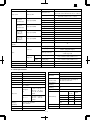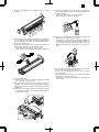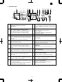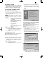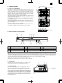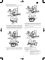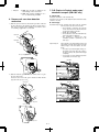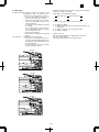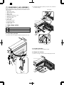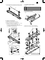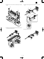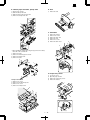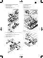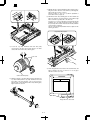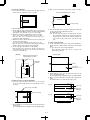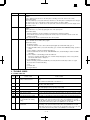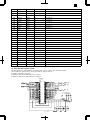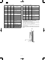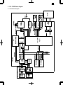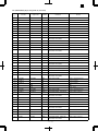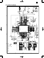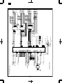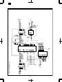
1
DM-1505 CODE: 00ZDM1505/A1E DIGITAL COPIER MODEL DM-1500 DM-1505 (DM-1505) CONTENTS [ 1 ] GENERAL . . . . . . . . . . . . . . . . . . . . . . . . . . . 1 - 1 [ 2 ] SPECIFICATIONS . . . . . . . . . . . . . . . . . . . . . . 2 - 1 [ 3 ] CONSUMABLE PARTS . . . . . . . . . . . . . . . . . . . 3 - 1 [ 4 ] EXTERNAL VIEWS AND INTERNAL STRUCTURES . . . 4 - 1 [ 5 ] UNPACKING AND INSTALLATION . . . . . . . . . . . . . 5 - 1 [ 6 ] OPERATIONAL DESCRIPTIONS . . . . . . . . . . . . . . 6 - 1 [ 7 ] DISASSEMBLY AND ASSEMBLY . . . . . . . . . . . . . . 7 - 1 [ 8 ] ADJUSTMENTS . . . . . . . . . . . . . . . . . . . . . . . 8 - 1 [ 9 ] SIMULATION TROUBLE CODES . . . . . . . . . . . . . . 9 - 1 [10] USER PROGRAM . . . . . . . . . . . . . . . . . . . . . . 10 - 1 [11] ELECTRICAL SECTION . . . . . . . . . . . . . . . . . . . 11 - 1 [12] CIRCUIT DIAGRAM . . . . . . . . . . . . . . . . . . . . . 12 - 1 Parts marked with “ ” are important for maintaining the safety of the set. Be sure to replace these parts with specified ones for maintaining the safety and performance of the set. SHARP CORPORATION This document has been published to be used for after sales service only. The contents are subject to change without notice. DM-1505 CAUTION This product is a class 1 laser product that complies with 21CFR 1040.10 and 1040.11 of the CDRH standard and IEC825. This means that this machine does not produce hazardous laser radiation. The use of controls, adjustments or performance of procedures other than those specified herein may result in hazardous radiation exposure. This laser radiation is not a danger to the skin, but when an exact focusing of the laser beam is achieved on the eye’s retina, there is the danger of spot damage to the retina. The following cautions must be observed to avoid exposure of the laser beam to your eyes at the time of servicing. 1) When a problem in the laser optical unit has occurred, the whole optical unit must be exchanged as a unit, not as individual parts. 2) Do not look into the machine with the main switch turned on after removing the developer unit, toner cartridge, and drum cartridge. 3) Do not look into the laser beam exposure slit of the laser optical unit with the connector connected when removing and installing the optical system. 4) The middle frame contains the safety interlock switch. Do not defeat the safety interlock by inserting wedges or other items into the switch slot. CAUTION INVISIBLE LASER RADIATION, WHEN OPEN AND INTERLOCKS DEFEATED. AVOID EXPOSURE TO BEAM. VORSICHT UNSICHTBARE LASERSTRAHLUNG, WENN ABDECKUNG GEÖFFNET UND SICHERHEITSVERRIEGELUNG ÜBERBRÜCKT. NICHT DEM STRAHL AUSSETZEN. VARO ! AVATTAESSA JA SUOJALUKITUS OHITETTAESSA OLET ALTTIINA NÄKYMÄTTÖMÄLLE LASERSÄTEILYLLE ÄLÄ KATSO SÄTEESEEN. ADVARSEL USYNLIG LASERSTRÅLNING VED ÅBNING, NÅR SIKKERHEDSBRYDERE ER UDE AF FUNKTION. UNDGÅ UDSAETTELSE FOR STRÅLNING. VARNING ! LASER WAVE – LENGTH : 780 ∼ 795 Pulse times : 0.481 ms/6 mm Out put power : 0.20 ± 0.03 mW OSYNLIG LASERSTRÅLNING NÄR DENNA DEL ÄR ÖPPNAD OCH SPÄRREN ÄR URKOPPLAD. BETRAKTA EJ STRÅLEN. – STRÅLEN ÄR FARLIG. DM-1505 At the production line, the output power of the scanner unit is adjusted to 0.57 MILLI-WATT PLUS 20 PCTS and is maintained constant by the operation of the Automatic Power Control (APC). Even if the APC circuit fails in operation for some reason, the maximum output power will only be 15 MILLI-WATT 0.1 MICRO-SEC. Giving and accessible emission level of 42 MICRO-WATT which is still-less than the limit of CLASS-1 laser product. Caution This product contains a low power laser device. To ensure continued safety do not remove any cover or attempt to gain access to the inside of the product. Refer all servicing to qualified personnel. VAROITUS! LAITTEEN KÄYTTÄMINEN MUULLA KUIN TÄSSÄ KÄYTTÖOHJEESSA MAINITULLA TAVALLA SAATTAA ALTISTAA KÄYTTÄJÄN TURVALLISUUSLUOKAN 1 YLITTÄVÄLLE NÄKYMÄTTÖMÄLLE LASERSÄTEILYLLE. VARNING - OM APPARATEN ANVÄNDS PÅ ANNAT SÄTT ÄN I DENNA BRUKSANVISNING SPECIFICERATS, KAN ANVÄNDAREN UTSÄTTAS FÖR OSYNLIG LASERSTRÅLNING, SOM ÖVERSKRIDER GRÄNSEN FÖR LASERKLASS 1. The foregoing is applicable only to the 220V model, 230V model and 240V model. LUOKAN 1 LASERLAITE KLASS 1 LASER APPARAT DM-1505 [1] GENERAL 1. Major functions Item CPM SB/MB DM-1500 15CPM MB DM-1505 15CPM MB 2 Tray SPF R-SPF FAX Model GDI with USB GDI without USB PCL with USB SOPM Descriptions of items CPM: Copy speed (Copies Per Minute) SB/MB: SB = Manual feed single bypass, MB = Manual feed multi bypass 2 tray: Second cassette unit. SPF: Original feed unit R-SPF: Duplex original feed unit FAX: FAX function. GDI with USB: GDI printer function with USB. GDI without USB: GDI printer function without USB. PCL with USB: PCL printer function with USB. SOPM: Scan One Print Many function (Many copies are made by one scan.) Duplex: Auto duplex copy function Descriptions of table : Standard provision : No function or no option available 2. System Configuration (DM-1505) (DM-1500) 1 – 1 Duplex DM-1505 [2] SPECIFICATIONS 1. Basic specifications of copier A. Basic specifications Item Spec. Type Desktop Copy system Dry, electrostatic Segment (class) Digital personal copier External dimensions (W × D × H) (mm) DM-1500/DM-1505: 518mm × 482.6mm × 464mm DM-1500: Approx. 25Kg, (drum cartridges included) DM-1505: Approx. 26Kg, (drum cartridges included) Weight B. Operation specification Section Item Details Spec. Paper feed system DM-1500/DM-1505: 2 tray (250 sheets) + multi bypass (50 sheets) Paper size Tray paper feed section A4, B5, A5 (Landscape) 56 – 80g/m2 Paper weight Paper feed capacity Kinds Remark AB system User adjustment of paper guide available Paper size A4, B5, A5, B6, A6 (Landscape) 52 – 128g/m2 Paper weight Multi bypass paper feed section Paper feed section Paper feed capacity Remark User adjustment of paper guide available 8-1/2″ × 14″, 8-1/2″ × 11″, 8-1/2″ × 5-1/2″ (Landscape) Paper size Paper weight 15 – 21 lbs. Paper feed capacity 250 sheets Kinds Standard paper, specified paper, recycled paper Remark Inch system User adjustment of paper guide available 8-1/2″ × 14″, 8-1/2″ × 11″, 8-1/2″ × 5-1/2″, 3-1/2″ × 5-1/2″ (Landscape) Paper size Multi bypass paper feed section Paper weight 14 – 34.5 lbs. Paper feed capacity 50 sheets Kinds ∗1 Standard paper, specified paper, recycled paper, OHP, Label, Postal card Remark User adjustment of paper guide available Paper size A4, B5, A5 (Landscape) 56 – 80 g/m2 Paper weight AB system Standard paper, Specified paper, Recycled paper Kinds Paper for Duplex 50 sheets Standard paper, specified paper, recycled paper, OHP, Label, Postal card Kinds ∗1 Tray paper feed section 250 sheets Standard paper, specified paper, recycled paper 8-1/2″ × 14″, 8-1/2″ × 11″, 8-1/2″ × 5-1/2″ (Landscape) Paper size Paper weight 15-21 lbs. Inch system Standard paper, Specified paper, Recycled paper Kinds ∗1: OHP, Label, Postal card: each 1 pc. 2 – 1 DM-1505 Section Paper exit section Item Details Spec. Exit way Face down Capacity of output tray 100 sheets Original set Center Registration (left edge) B4 (10″ × 14″) Max. original size Originals Original kinds sheet Original size detection None Scanning system CCD sensor Optical section Scanning section CCD sensor scanning by lighting lamp scanner Resolution 400 dpi Type Lighting lamp Xenon lamp Voltage 1.5kV 11 ± 3W Power consumption Gradation Writing section 256 gradations/8bit Writing system Writing to OPC drum by the semiconductor laser Laser unit Resolution Photoconductor 600 dpi Type OPC (30φ) Life Image forming 18k Charging system Saw -tooth charging with a grid Transfer system (+) DC corotron system Separation system (–) DC corotron system Developing Developing system Dry, 2-component magnetic brush development system Cleaning Cleaning system Charger Counter blade system (Counter to rotation) Fusing system Fusing section Heat roller system Upper heat roller Type Teflon roller Lower heat roller Type Silicon rubber roller Type Halogen lamp Heater lamp Voltage 100V/120V/230V Power consumption 800W Voltage Power source Local AC voltage Frequency Common use for 50 and 60Hz Max. Electrical section Power consumption DM-1500/DM-1505: 1000W Average (during copying) *1) DM-1500/DM-1505: 310Wh/H Average (stand-by) *1) DM-1500/DM-1505: 70Wh/H Pre-heat mode * 1) DM-1500/DM-1505: 40Wh/H 1) Auto power shut-off mode * DM-1500/DM-1505: 20Wh/H *1) May fluctuate due to environmental conditions and the input voltage. C. Copy performance Section Copy magnification Item Details Spec. 3R + 2E (AB system: 50, 70, 81, 100, 141, 200%) (Inch system: 50, 64, 78, 100, 129, 200%) Fixed magnification ratios 50 ∼ 200% (151 steps in 1% increments) Zooming magnification ratios Exposure mode Auto/Manual/Photo Manual steps (manual, photo) 5 steps 2 – 2 DM-1505 Section Item Details Spec. 9.6 sec. or below (A4) (Pre-heat mode: 16 sec. or below / Auto power-shut-off mode: 23 sec. or above) Tray paper feed Copy speed First copy time 10.0 sec (Pre-heat mode: 16 sec. or below / Auto power-shut-off mode: 23 sec. or above) Manual paper feed AB system: A4 (Landscape) AB system: B5 (Landscape) Copy speed (CPM) Copy speed (CPM) Inch system: 8-1/2″ × 14″ (Landscape) Copy speed (CPM) Inch system: 8-1/2″ × 11″ (Landscape) Copy speed (CPM) Same size 15 Enlargement 15 Reduction 15 Same size 15 Enlargement 15 Reduction 15 Same size 12 Enlargement 12 Reduction 12 Same size 15 Enlargement 15 Reduction 15 Max. continuous copy quantity 99 Void area Leading edge 1 ∼ 4mm Trailing edge 4mm or less, 6mm or less (Duplex copying/both images) Side edge void area machine with side edge void 0.5mm ∼ 4.5mm (Total of both edge voids) OC mode Leading edge Same size: 3.0mm or less / Enlarge (200%): 1.5mm or less / Reduction (50%): 6.0mm or less SPF/R-SPF/ Duplex Leading edge Same size: 4.0mm or less / Enlarge (200%): 3.0mm or less / Reduction (50%): 8.0mm or less Void Image loss Warm-up time 0 sec. Power save mode reset time 0 sec. Paper jam recovery time 0 sec. D. Printer specifications Item Contents Print speed 15 PPM First print 9.6 sec Resolution 600 dpi, 300 dpi Toner save No Duplex print Yes (for duplex capable copier) Paper feed tray Multi bypass tray Tray 1, Tray 2 Multi bypass tray Paper size Tray 1 ∼ 2 Item Interface (Standard) A4R, B5R, A5R, 8.5" × 14", 8.5" × 11"R, 8.5" × 5.5"R, 8.5" × 13", 8.5" × 12.4"R, DL, C5, COM10, Monarch A4R, B5R, A5R, 8.5" × 14"R, 8.5" × 11"R, 8.5" × 5.5"R, 8.5" × 13"R, 8.5" × 12.4"R Page description language (standard) PCL6 (PCL XL) emulation PCL5e emulation Dot emulation None Page protection Yes IEEE1284 port × 1 USB port × 1 Applicable Interface Cable Parallel cable compliant IEEE1284 and less than 2.0m (Shield and earth equipped) USB cable less than 2.0 m Auto Interface Switching No Auto Emulation Switching Yes Plug and Play Yes Printer Driver(*) 2 – 3 Contents PCL6 (PCL XL) PCL5e MS Windows3.1 No Yes MS Windows95 Yes Yes MS Windows98 Yes Yes MS Windows NT4.0 Yes Yes Resident Font 45 outline fonts compatible to PCL6 Screen Font 45 outline fonts compatible to PCL6 DM-1505 Item Memory Contents Standard Maximum 8MB 72MB Expansion Slot for Memory One DIMM slots Expansion Memory 64MB, 32MB, 16MB (commercially-available DIMM:EDO) Operation Panel Applicable PC Switches 1 (Online/Offline) Lamps 2 (DATA, ONLINE) Display None IBM PC-AT Compatibles *: Only Win 98 can be used for USB users. Operations when both of USB/parallel ports are connected at the same time. The USB port has a priority over the parallel port. Smartsharing is invalid. Interface connected previously USB (Unfinished print job YES/NO) Interface connected later Parallel port Operation USB: Enable Parallel port: Disable Parallel port (Unfinished print job YES/NO) USB When USB is connected after 30sec of no communication through the parallel port, the mode is shifted to the USB mode instantaneously. If no communication state does not reach 30sec yet, shifting to the USB mode is retained until 30sec passes. During that time, print jobs are performed through the parallel port. Parallel port (Unfinished print job YES/NO) USB After completion of unfinished print jobs, if there is no communication for 30sec, shifting to the USB mode is made. Within 30sec, print jobs are performed through the parallel port. 2 – 4 DM-1505 [3] CONSUMABLE PARTS 1. Supply system table A. USA, CANADA No. 1 2 Name Content Developer cartridge (Black) <With IC> Drum cartridge Life Toner/developer cartridge (Toner: 220g, Developer: 190g) × 1 IC chip × 1 Warranty Card × 1 Postcard label × 1 Returned Operation Manual × 1 Polyethene bag × 1 Drum cartridge × 1 Warranty Card × 1 Product name Package 6K DM-150TD 5 18K DM-150DR 5 Remark Life setup is based on A4 5% documents. For 6% coverage, 5K life. (4) Supply storage condition 2. Environmental The environmental conditions for assuring the copy quality and the machine operations are as follows: Humidity (RH) 90% (1) Normal operating condition Temperature:20˚C~25 Humidity:65 ± 5%RH (2) Acceptable operating condition Humidity (RH) 85% 20% 60% –5˚C 45˚C 3. Production control number(lot No.) identification 〈Developing cartridge〉 20% 10˚C 30˚C 35˚C Production month Production day Destination code (Dealer, distributor, OEM, etc.) Production place (3) Optical condition (SOCC: Fixed to B.) End digit of year Version No. Humidity (RH) 90% 60% ∗:Destination Division EX Destination Option Destination 15% –25˚C 30˚C 40˚C 3 – 1 No. A same pack G B same pack H A P B Q DM-1505 〈Drum cartridge〉 The label on the drum cartridge shows the date of production. (SOCC production) Production month Production day Destination code (Dealer, distributor, OEM, etc.) Production place (SOCC: Fixed to B.) End digit of year Version No. Production control label attachment position 〈JAPAN production〉 Ver.A 9 1 1 0001 X Production month (1 - 9 = Jan. - Sep. 0 = Oct. X = Nov. Y = Dec.) Serial number of month Fixed to 1. Pack division (See table below) End digit of year Version No. Production control label attachment position(*1) Division No. Ex production 1 Option 2 Same pack 3 ∗1 The production control label is not attached to the cartridge of a China product. 3 – 2 DM-1505 4. Memory Device A. Function The memory device is used to monitor the life of the developer cartridge in the way that the machine reads and writes information (e.g.page count) to the memory device equipped in the developer cartridge. When the life is reached, the memory device becomes nonfunctional to prevent the deterioration of image/text quality and machine damages. Therefore, unnecessary service costs would be saved. B. Flowchart New developer cartridge Handshake Machine Installed to the machine Yes Is 8K print reached ? No Copying No Is toner empty detected ? Yes Conditions for end of life (1) Copy/print volume = 8K. (2) Toner empty is detected. End of life C. Display timing of DM-1500/1505 maintenance lamps, toner lamp and error codes Remaining print quantity ≥ 8K Start During maintenance Toner Near period Toner End Start After maintenance Toner Near period Toner End Remaining print quantity < 8K Maintenance lamp Toner lamp Error code OFF OFF OFF ON OFF ON Remaining print quantity = 0 Maintenance lamp Toner lamp Error code Toner lamp Error code – OFF OFF – OFF – – OFF ON – ON – BLINK – OFF BLINK F2 BLINK F2 OFF – ON OFF – OFF – ON ON – ON ON – ON – ON BLINK – ON BLINK F2 BLINK F2 Note: When the memory device is faulty, “U2” will be displayed. 3 – 3 DM-1505 2) Remove the DVF cover unit. • When removing, be careful not to break the two pins. 5. Consumable parts refill procedure [External view check points] Check for breakage of the four pins (*) and the ATC sensor connector of the DV BOX unit. *Pins *Pins ATC sensor connector Check for breakage of molt and suede. (For reattachment, refer to the reattachment procedure.) DV molt F DV molt Side sheet F 3) Remove the THBOX unit. DV molt R Side sheet R A. TD cartridge 4) Remove the DV blade. • Remove excessive glue. • Remove together with the base PET. 1) Remove the waste toner box unit 3 – 4 DM-1505 5) Tilt the DV box unit and rotate the DV18T clockwise to remove developer. 11) Face the toner supply port of the TH box unit upward, and press and insert the refill hose into the toner supply port with the toner bottle kept straight up. • Hold the left side of the TH box with your hand. • Press and insert the refill hose completely. 12) Lift the toner bottle and shake it left and right and supply toner until the bottle and the filling hose are empty. • It takes about one minute to fill toner completely in TH BOX UN from lifting the toner bottle to emptying the bottle and the hose. • If toner remains in the hose, when removing the hose from TH BOX UN, the remaining toner may disperse. Use great care for that. 6) Clean the DV box unit by sucking or blowing with a vacuum cleaner to remove developer from the MG roller and toner from the DV box unit. Check that there is no toner or no foreign material attached to the connector and the gear. 7) Shake the developer bottle 10 times up and down, and remove the bottle cap and supply developer into the DV box unit. • Slowly slant the bottle to supply developer evenly. • Check the label to insure that developer is suitable for the model. 13) Check that there is no toner remaining in the bottle and remove the hose, and slowly pull and remove the hose. (If there is any toner remaining in the bottle or the hose, perform toner supply again.) Bend the refill hose and remove it from the TH box unit without dispersing toner. Attach the toner cap. • Attach the toner cap with the toner supply port of the TH box unit faced upward. 8) Install the THBOX unit. • Insert two bosses of TH box on the drive side into the positioning hole of the DV box and fix together. 9) Remove the toner cap, look into the toner supply port and stop the THD Mylar at the position shown in the figure below. (Rotate the THK gear on the rear side of the TH box counterclockwise to rotate the TM shaft.) 10) Shake the toner box 20 times up and down, and remove the bottle cap and install the refill hose. Check the label to insure that toner is suitable for the model. 3 – 5 DM-1505 20) Install the MG cover. Put the unit straight with the MG roller on the upper side. Rotate the DV18T several times forward and reverse to store developer on the MG roller into the inside. Check that there is no developer on the MG roller surface, and install the MG cover. Note: When attaching the MG cover, be careful not to wind around the DV blade. 14) Clean the DV box unit with alcohol and attach the DV blade. • After drying the unit, attach the DV blade. • After attachment, check that there is no scratch and waves on the DV blade. • After attachment, be careful not to damage the DV blade. • Check that there is no foreign material in the DV blade and the section. 0.5 0.5 0 0 15) Install the DVF cover to the DV-TH box unit. 16) Clean the waste toner box unit and install it to the DV box unit. (Check that there is no toner in the waste toner box) Be careful of the pawl. 17) Replace the IC connector. Check that there is no oil on the IC connector pins. (Do not touch with fingers.) Note for MG cover installation • When installing, check that there is no breakage and peel-off of the MG cover sheet and the MG cover molt attached to the MG cover. • Check that there is no winding into the DV blade, deformation and scratches of DV molt F and R. Put a white mark on the above position. At that time, put marking for checking of the number of refilling. 18) Check the operations of the DV lever and the toner box shutter. 19) Shake the DV box unit 5 times horizontally. Rotate the DV18T clockwise and check developer state on the MG roller. (Visually check that developer state is normal and there is no foreign material.) 3 – 6 DM-1505 [The reattachment procedure] Remove the side sheets on the both sides of DV box unit. Clean the DV box unit with alcohol and reattach the side sheets F and R to the both sides. 0 0 .5 0 0 0 0 .5 0 .5 0 .5 DV box unit F side DV box unit R side .Remove glue completely before reattaching. .After drying alcohol, attach the side sheet F,R. Remove the DV molt F,R and DV molt and clean with alcohol. After attaching the DV molt F and R, attach the DV molt with the DV molt R edge as the reference. DV molt attachment 0 reference (DV box edge) DV molt F attachment reference (DV box edge) 0.5 0 DV molt attachment reference (DV box edge) 0 1 DV molt R attachment 0.5 reference (DV box edge) 0.5 0.5 0 0 DV molt attachment reference (DV box edge) .Do not allow clearance between DV molt and DV molt F. (Pull and attach them. Overlap may be allowed.) .Remove glue completely before reattaching. .After drying alcohol, attach the DV side sheet. 0.5 0 When attaching the DV molt F, projection in the arrow direction is not allowed. When attaching the DV molt R, 0 projection in the arrow direction is not allowed. 0 0 0.5 0.5 3 – 7 0.5 DM-1505 3) Remove the drum fixing plate and the photoconductor drum. (Note) Dispose the drum fixing plate which was removed. B. Drum unit 1) Check the external view. • Check for damage or cracks on the boss and the boss hole. • Check to insure that the waste toner pipe shutter slides smoothly. • Check to insure that the star ring and the CRU washer rotate smoothly. LO C K (2) (3) 4) Check the cleaning blade and the red felt for no damage. • If there is any damage, execute all procedures from item 5) and later. • If there is no damage, execute the procedure of item 12). 5) Remove the main charger. (Cleaning the screen grid and the sawteeth.) 2) Remove the drum cover. (4 Lock Tabs) 6) Remove the cleaning blade. Note: Dispose the cleaning blade which was removed. 3 – 8 DM-1505 7) Clean the cleaning section and the waste toner pipe to remove waste toner completely with a vacuum cleaner. 8) Remove the felt and duplex tape completely. Note: Be careful not to scratch or bend the sub blade. 9) Attach the cleaning blade. Securely insert the plate section of the cleaning blade into the dove and fix it with a screw. Do not touch the cleaning blade rubber with your hand. When attaching the cleaning blade, press the cleaning blade in the arrow direction and attach. 12) Attach the drum fixing plate and the photoconductor drum. Apply grease to the inside of the photoconductor drum. (Dia. 2) 10) Attach the felt. Attach the drum from (b). (Prevention against the sub blade edge breakage) Attach the drum so that its position with the sub blade is as shown. 13) Attach the detection gear. Note: • The detection gear is not installed to the drum cartridge packed with the main body. Add a new one. 14) Attach the drum cover. Note: After attaching the drum cover, do not make a copy. When attaching the drum cover, engage the detection gear 20T rib with the 30T gear rib, and attach the drum cover to the process frame. 15) Mark the number of times of recycling on the side of the cover with white paint. Max. times of recycling: 5 times Attach the mocket with slightly pressing section A of the cleaning blade. Do not touch the tip of the cleaning blade. Do not put the mocket under the cleaning blade. Do not put the mocket on the sub blade. Do not press the sub blade with the mocket. 11) Attach the main charger. Securely set the MC holder on the projection of the process frame. Securely insert two projections of the MC holder into the groove in the process frame. When attaching the MC holder ass’y, be careful not to make contact with the cleaning blade. 3 – 9 Note: Another method of cleaning the drum counter is available with SIM 24-07. DM-1505 [4] EXTERNAL VIEWS AND INTERNAL STRUCTURES 1. Appearance Original cover DM-1500 17 10 9 18 11 19 1 12 2 8 13 3 4 7 6 DM-1505 21 20 18 19 16 14 15 5 20 1 Original cover 2 Side cover 3 Bypass tray 4 Bypass tray guides 5 Side cover open button 6 Front cover 7 Paper tray 8 Operation panel 9 Original table 10 Handle 11 PCL printer interface 12 Paper output tray 13 Paper output tray extension 14 Handle 15 Power switch 16 Power cord socket 17 SPF exit area ∗1 18 Original guides 19 Document feeder tray 20 Feeding roller cover 21 RSPF exit area ∗2 ∗1 DM-1500 only ∗2 DM-1505 only 2. Internal 1 3 2 4 7 5 6 1 TD cartridge lock release button 2 TD cartridge 3 Drum cartridge 4 Drum cartridge handle 5 Fusing unit release lever 6 Charger cleaner 7 Transfer charger 4 – 1 DM-1505 3. Operation panel 1 2 3 4 5 15 6 7 8 16 9 17 10 18 11 12 19 13 14 20 2 Exposure mode selector key and indicators Use to sequentially select the exposure modes: AUTO, MANUAL or PHOTO. Selected mode is shown by a lit indicator. 3 Light and dark keys and exposure indicators Use to adjust the MANUAL or PHOTO exposure level. Selected exposure level is shown by a lit indicator. Use to start and terminate user program setting. 4 Alarm indicators :Drum replacement required indicator :Misfeed indicator :TD cartridge replacement required indicator :Maintenance indicator 5 SPF indicator 6 SPF misfeed indicator 7 Copy ratio selector key and copy ratio indicators Use to sequentially select preset reduction/enlargement copy ratios. Selected copy ratio is shown by a lit indicator. 8 Zoom indicator 9 Copy ratio display (%) key 10 Display Displays the specified copy quantity, zoom copy ratio, user program code, and error code. 11 ON LINE indicator / ON LINE KEY Lights up when the machine is used as a printer. To use as a printer, an optional printer expansion kit is needed. 12 ON LINE key Changes between the on-line and off-line modes. 13 DATA indicator Indicates that the printer is receiving or processing print data 14 Power save indicator Lights up when the copier is in a power save mode. 15 Tray select key Use to select a paper feed station (paper tray or bypass tray). 16 Paper feed location indicators Light up to show the selected paper feed station. 17 Zoom keys Use to select any reduction or enlargement copy ratio from 50% to 200% in 1% increments. 18 Copy quantity keys • Use to select the desired copy quantity (1 to 99). • Use to make user program entries. 19 Clear key • Press to clear the display, or press during a copy run to terminate copying. • Press and hold down during standby to display the total number of copies made to date. 20 Print key and ready indicator • Copying is possible when the indicator is on. • Use to set a user program. 1 Duplex Mode select key and indicator (DM-1505 only) 4 – 2 DM-1505 4. Motors and solenoids 3 2 8 4 1 5 7 6 No. Part name Control signal Function,operation 1 Main motor MM Drives the copier. 2 Mirror motor MRMT Drives the optical mirror base (scanner unit). 3 Toner motor TM Supplies toner. 4 Cooling fan motor VFM Cools the optical section. 5 Resist roller solenoid RRS Resist roller rotation control solenoid 6 Paper feed solenoid CPFS1 Cassette Paper feed solenoid 7 Multi paper feed solenoid MPFS Multi manual pages feed solenoid 8 SPF motor SPFM Drives the single pass feeder 4 – 3 DM-1505 5. Sensors and switches 1 12 2 10 11 3 4 13 5 9 6 7 14 8 No. MHPS Transmission sensor 2 Name Mirror home position sensor POD sensor POD Transmission sensor 3 PPD2 sensor PPD2 Transmission sensor 4 Cassette detection switch CED1 Microswitch 5 Manual feed detection switch MFD Transmission sensor 6 PPD1 sensor PPD1 Transmission sensor 7 Door switch DSW Micro switch 8 Door switch DSW Micro switch 9 Drum reset switch DRST Micro switch 10 SPF sensor SPID/SD Transmission sensor SW 11 SPPD sensor SPPD Transmission sensor 12 SDOD sensor SDOD Transmission sensor 13 2nd cassette DSW Micro switch 14 PPD3 sensor PPD3 Transmission sensor 1 Signal Type 4 – 4 Function Mirror (scanner unit) home position detection Paper exit detection Paper transport detection 2 Cassette installation detection Manual feed paper detection (single only) Paper transport detection 1 Door open/close detection (safety switch for 5V) Door open/close detection (safety switch for 24V) New drum detection switch Paper entry detection Cover open/close detection Paper transport detection SPF open/close detection Book sensor 2nd cassette door open detection Paper transport detection 3 Output “H” at home position “H” at paper pass “L” at paper pass “H” at cassette insertion “L” at paper detection “L” at paper pass 1 or 0V of 5V at door open 1 or 0V of 24V at door open Instantaneously “H” at insertion of new drum “L” at paper pass “L” at paper pass “L” at paper pass 1 or 0V of 5V at door open “L” at paper pass DM-1505 6. PWB unit 10 11 2 1 9 5 8 6 4 3 7 No. Name Function 1 Exposure lamp invertor PWB Exposure lamp (Xenon lamp) control 2 Main PWB (MCU) Copier control 3 Operation PWB Operation input/display 4 Power PWB AC power input, DC voltage control, High voltage control 5 CCD sensor PWB For image scanning 6 LSU motor PWB For polygon motor drive 7 TCS PWB For toner sensor control 8 LSU PWB For laser control 9 Memory PWB 6MB For memorying data 10 I/F PWB I/F PWB between PCL and PC 11 PCL control PWB PCL printer control 4 – 5 DM-1505 7. Cross sectional view 19 4 5 16 17 6 3 18 1 2 7 8 9 10 11 12 15 No. 14 Part name 13 Function and operation 1 Scanner unit Illuminates the original with the copy lamp and passes the reflected light to the lens unit (CCD). 2 Exposure lamp Exposure lamp (Xenon lamp) Illuminates original 3 Lens unit Scans the original image with the lens and the CCD. 4 LSU (Laser unit) Converts the original image signal into laser beams and writes onto the drum. 5 Paper exit roller Roller for paper exit 6 Main charger Provides negative charges evenly to the drum surface. 7 Heat roller Fuses toner on the paper. (Teflon roller) 8 Pressure roller Fuses toner on the paper. (Silicon rubber roller) 9 Drum Forms images. 10 Transfer unit Transfers images onto the drum. 11 Pickup roller Picks up the manual feed paper. (In multi feed only) 12 Manual paper feed tray Tray for manual feed paper 13 Manual paper feed roller Transport the paper from the manual paper feed port. 14 PS roller unit Takes synchronization between the lead edge and the rear edge of the paper. 15 Paper feed roller Picks up a sheet of paper from the cassette. 16 Pickup roller Picks up documents. 17 Separation roller Separates documents to feed properly. 18 PS roller Feeds documents to the scanning section. 19 Paper exit roller Discharges documents. 4 – 6 DM-1505 [5] UNPACKING AND INSTALLATION 8"(20cm) 8"(20cm) 1. COPIER INSTALLATION Improper installation may damage the copier. Please note the following during initial installation and whenever the copier is moved. 4" (10cm) Caution: If the copier is moved from a cool place to a warm place, condensation may form inside the copier. Operation in this condition will cause poor copy quality and malfunctions. Leave the copier at room temperature for at least 2 hours before use. 4" (10cm) 2. CAUTIONS ON HANDLING Be careful in handling the copier as follows to maintain the performance of this copier. Do not install your copier in areas that are: ● damp, humid, or very dusty Do not drop the copier, subject it to shock or strike it against any object. ● exposed to direct sunlight Do not expose the drum cartridge to direct sunlight. Doing so will damage the surface (green portion) of the drum cartridge, causing poor print quality. ● poorly ventilated Store spare supplies such as drum cartridges and TD cartridges in a dark place without removing from the package before use. If they are exposed to direct sunlight, poor print quality may result. Do not touch the surface (green portion) of the drum cartridge. Doing so will damage the surface of the cartridge, causing poor print quality. ● subject to extreme temperature or humidity changes, e.g., near an air conditioner or heater. The copier should be installed near an accessible power outlet for easy connection. Be sure to connect the power cord only to a power outlet that meets the specified voltage and current requirements. Also make certain the outlet is properly grounded. Be sure to allow the required space around the machine for servicing and proper ventilation. 5 – 1 DM-1505 3. CHECKING PACKED COMPONENTS AND ACCESSORIES 6. INSTALLING THE TD CARTRIDGE The TD cartridge replacement required ( ) indicator will light up when toner is needed. If copying is continued while the indicator is lit, copies will gradually become lighter until the copier stops and the indicator begins blinking. Replace the old TD cartridge by following the procedure given below. Open the carton and check if the following components and accessories are included. Power cord Note: ● After the copier stops, it may be possible to make a few more copies by taking the TD cartridge out of the copier, shaking it horizontally, then reinstalling it. If copying is not possible after this operation, replace the TD cartridge. ● During long copy run of a dark original, the ready ( ) indicator may blink, the indicator light up, and the copier stop, even though toner is left. The copier will feed toner up to 2 minutes and then the ready ( ) indicator will light up. Press the print ( ) key to restart copying. TD cartridge 1) Ensure that the bypass tray is open and then open the side cover while pressing the side cover open button. Copier Drum cartridge (installed in copier) 4. UNPACKING Be sure to hold the handles on both sides of the copier to unpack the copier and carry it to the installation location. 2) Remove the CAUTION tape from the front cover and remove the two protective pins from the fusing unit by pulling the strings upward one at a time. 3) Push gently on both sides of the front cover to open the cover. 5. REMOVING PROTECTIVE PACKING MATERIALS 1) Remove pieces of tape and protective cover. Then open the original cover and remove protective materials (a) and (b). 4) Remove the TD cartridge from the bag. Remove the protective paper. Hold the cartridge on both sides and shake it horizontally four or five times. 2) Use a coin (or suitable object) to remove the screw. Store the screw in the paper tray because it will be used if the copier has to be moved. 4 or 5 times 5 – 2 DM-1505 5) Hold the tab of the protective cover and pull the tab to remove the cover. 2) Remove the pressure plate lock. Rotate the pressure plate lock in the direction of the arrow to remove it while pressing down the pressure plate of the paper tray. 3) Store the pressure plate lock which has been removed in step 2 and the screw which has been removed when unpacking in the front of the paper tray. To store the pressure plate lock, rotate the lock to fix it on the relevant location. 4) Adjust the paper guides on the paper tray to the copy paper width and length. Squeeze the lever of paper guide (A) and slide the guide to match with the width of the paper. Move paper guide (B) to the appropriate slot as marked on the tray. 6) Gently insert the TD cartridge until it locks in place. Paper guide (B) Paper guide (A) 5) Fan the copy paper and insert it into the tray. Make sure the edges go under the corner hooks. Note: Do not load paper above the maximum height line ( ). Exceeding the line will cause a paper misfeed. 7) Close the front cover and then the side cover by pressing the round projections near the side cover open button. The indicator will go out and the ready ( ) indicator will light up. Note: When closing the covers, be sure to close the front cover securely and then close the side cover. If the covers are closed in the wrong order, the covers may be damaged. 6) Gently push the paper tray back into the copier. Note: After loading copy paper, to cancel the blinking “P” without restarting copying, press the clear ( ) key. The “P” in the display will go out and the ready ( ) indicator will light up. 7. LOADING COPY PAPER Note: This copier is equipped with two paper trays. Load copy paper into the two paper trays. 1) Raise the handle of the paper tray and pull the paper tray out until it stops. 5 – 3 DM-1505 4) When using Windows 95 on a personal computer with plug & play*, the “Update Device Driver Wizard” window will appear. Insert the installation CD-ROM into the CD-ROM drive. Click the Next button and follow the on-screen instructions. If the “Copying Files” window appears during this operation, enter R:\ (if the CD-ROM is designated as drive R), click the OK button and follow the on-screen instructions. 8. POWER TO COPIER 1) Ensure that the power switch of the copier is in the OFF position. Insert the attached power cord into the power cord socket at the rear of the copier. 2) Plug the other end of the power cord into the nearest outlet. 9. INSTALLING THE PRINTER DRIVER (Description of the printer driver) The printer driver is the software program which runs the printer. It converts the data in your file into information that the printer can understand. It also controls communication between the printer and computer as the data is printed. (Checking the hardware and software requirements) You will need the following hardware and software in order to install the printer driver. Computer type IBM PC/AT or compatible computer equipped with a bi-directional parallel or USB interface, and CD-ROM drive Windows type Windows 3.1x, Windows 95, Windows 98*, Windows NT 4.0 * USB is supported on Windows 98 preinstalled only. CPU 486DX 66MHz or better Physical RAM Windows 95, Windows 3.1x: 8MB (16MB or more is recommended.) Windows NT 4.0: 12MB (16MB or more is recommended.) Windows 98: 16MB (32MB or more is recommended.) Display 640 × 480 dots (VGA) or better Hard disk free space 10MB or more Caution: The printer driver included in this product cannot be used under Windows NT 3.5x, OS/2, pure MS-DOS and other operating systems which are not described above. Note: The PCL6 printer driver is not available in Windows 3.1 environment. ● If you use Windows 95 and the “New Hardware Found” window will appear, select Driver from Disk Provided by Hardware Manufacturer and then click the OK button. Proceed to step 6. ● If you use Windows 95 and the screen shown above or the “New Hardware Found” window does not appear, proceed to step 5. ● If you use Windows NT 4.0, proceed to step 5. * Plug & play This feature is effective if both the computer and peripheral equipment are equipped with IEEE 1284 compliant parallel interface. Note: The screen displayed depends on the version of Windows you are using. 5) Insert the installation CD-ROM into the CD-ROM drive. Click the Start button and select Run. When the screen shown below appears, type R:\SETUP (if the CD-ROM is designated as drive R) and click the OK button. Follow the on-screen instructions. (Installing the printer driver) The software for your printer is provided on CD-ROM. Before installing the printer driver, be sure to check the following items. ● Is the printer connected properly to the computer? ● Does the printer have paper? A. Windows 95/Windows NT 4.0 Installation Instructions: With both the computer and the printer turned off, connect the printer to the computer with a parallel interface cable. 1) Load paper into the paper tray of the printer. For instructions on loading paper, see the section LOADING COPY PAPER in the copier operation manual. 2) Turn on the printer. 3) Turn on your computer and start Windows. Note: Before installing the printer driver, be sure to close all other applications which may be open. 6) The “Install From Disk” window will appear. Insert the installation CD-ROM into the CD-ROM drive. Type R:\ (if the CD-ROM is designated as drive R) and click the OK button. Follow the on-screen instructions. Note: If you have any problem with the test print, check the symptoms and solutions. Print the test page again after resolving the problem. 5 – 4 DM-1505 B. Windows 98: With both the computer and the printer turned off, connect the printer to the computer with either a parallel or a USB interface cable. 1) Load paper into the paper tray of the printer. For instructions on loading paper, see the section LOADING COPY PAPER found in the copier operation manual. 2) Turn on the printer. 3) Turn on your computer and start Windows. When using the USB interface: ● Connect your personal computer and the printer using a USB interface cable if you have not already done so. (For information about connecting the USB interface cable) ● When the “Add New Hardware Wizard” window appears, insert the installation CD-ROM, click the Next button, follow the on-screen instructions, and finally click the Finish button. 7) Windows driver file search will find the device “SHARP AR-150 Series PCL”. Click the Next button and follow the on-screen instructions. 8) Insert the installation CD-ROM into the CD-ROM drive. (If you are using the USB interface, confirm that the installation CD-ROM is in the CD-ROM drive.) Click the Start button and select Run. When the window shown below appears, type R:\SETUP (if the CD-ROM is designated as drive R) and click the OK button. Follow the onscreen instructions. Note: Before installing the printer driver, be sure to close all other applications which may be open. 4) When using Windows 98 on a personal computer with plug & play*, the “Add New Hardware Wizard” window will appear. Click the Next button and follow the on-screen instructions. ● If the “Add New Hardware Wizard” window does not appear, proceed to step 8. C. Windows 3.1x: With both the computer and the printer turned off, connect the printer to the computer with a parallel interface cable. 1) Load paper into the paper tray of the printer. For instructions on loading paper, see the section LOADING COPY PAPER in the copier operation manual. 2) Turn on the printer and then start Windows on your computer. Note: Before installing the printer driver, be sure to close all other applications which may be open. 3) Insert the installation CD-ROM into the CD-ROM drive. 4) Choose File from the Menu bar in Program Manager, and then choose the Run... command. 5) Type R:\SETUP (if the CD-ROM is designated as drive R) in the command line box and then click the OK button. 5) Select Search for the best driver for your device and click the Next button. 6) Insert the installation CD-ROM into the CD-ROM drive. (If you are using the USB interface, confirm that the installation CD-ROM is in the CD-ROM drive.) Select the CD-ROM drive and click the Next button. 6) Follow the on-screen instructions. D. AR-150 Series PCL printer driver group When you install the printer driver, the SHARP AR-150 Series PCL printer driver group is automatically created. The printer driver group includes the following items: 5 – 5 DM-1505 Uninstall AR-150 Series PCL The printer driver can be uninstalled. If the driver is uninstalled, printing can no longer be performed on the printer. For proper uninstallation, be sure to use the SHARP uninstall program of the printer driver group. Readme The latest information on the printer driver is included in this document. Read the Readme first. Status Monitor The Status Monitor window provides visual information about the printer state and current job. Status Monitor HELP Assistance and information for Status Monitor. ● Be sure to read the “Readme” document found in the printer driver group before using your SHARP AR-150 Series PCL printer. ● You cannot use both the status monitor and the Print Manager at the same time in Windows 3.1 environment. 12. TEST PRINTING To test print the configuration page and font list, use the following procedure: 1) Press and hold down the light and dark keys simultaneously for more than 5 seconds until all the alarm indicators blink and “--” appears in the display. 2) Set “6” (configuration page) or “7” (font list) using the left copy quantity key. The selected number will blink in the left side of the display. 3) Press the print key. The entered program number will be steadily lit and the currently selected parameter number for the program will blink on the right side of the display. 4) Select the desired parameter using the right copy quantity key. The entered parameter number will blink on the right of the display. Program No. Mode 6 Configuration page 7 Font list Parameters 0 → English 1 → French 3 → Italian 4 → German 0 → English 1 → French 3 → Italian 4 → German 2 → Spanish 2 → Spanish 5) Press the print key. The test page prints. Note: To change the setting or to set another mode, press the clear key. The printer will return to step 2. Configuration Page items 1st level item 2nd level item 3rd level item Machine Information Language Hardware Specs Basic Memory Total Memory Hardware Status Processor 64 bit RISC Interface Menu I/O Timeout ROM Version Total Page Count Version Information PCL6 Bypass Tray Input Paper Tray Tray 1 Tray 2 5 – 6 DM-1505 [6] OPERATIONAL DESCRIPTIONS 1. Outline of operation The outline of operation is described referring to the basic configuration. (Basic configuration) Scanner section PC CCD Operation section MCU (Main control/image process section) PCL control PCL I / F LSU (Laser unit) Laser diode, Polygon mirror lens Laser beam Paper exit Fusing section Process section Printer section Paper transport section Cassette paper feed section Manual paper feed section (Outline of copy operation) Setting conditions 1) Set copy conditions such as the copy quantity and the copy density with the operation section, and press the COPY button. The information on copy conditions is sent to the MCU. Image scanning 2) When the COPY button is pressed, the scanner section starts scanning of images. The light from the copy lamp is reflected by the document and passed through the lens to the CCD. Photo signal/Electric signal conversion 3) The image is converted into electrical signals by the CCD circuit and passed to the MCU. Image process 4) The document image signal sent from the CCD circuit is processed under the revised conditions and sent to the LSU (laser unit) as print data. Electric signal/Photo signal (laser beam) conversion 5) The LSU emits laser beams according to the print data. (Electrical signals are converted into photo signals.) 6) The laser beams are radiated through the polygon mirror and various lenses to the OPC drum. Printing 7) Electrostatic latent images are formed on the OPC drum according to the laser beams, and the latent images are developed to be visible images (toner images). 8) Meanwhile the paper is fed to the image transfer section in synchronization with the image lead edge. 9) After the transfer of toner images onto the paper, the toner images are fused to the paper by the fusing section. The copied paper is discharged onto the exit tray. 6 – 1 DM-1505 Sub scanning direction 2. Scanner section Sensor scanning area A. How to scan documents Main scanning direction The scanner has sensors that are arranged in a line. These sensors scan a certain area of a document at a time and deliver outputs sequentially. When the line is finished, the next line is scanned, and this procedure is repeated. The figure below shows the case where the latter two sections of an image which are scanned are shown with solid lines and the former two sections which are being transmitted are shown with dotted lines. The direction of this line is called “main scanning direction,” and the scanning direction “sub scanning direction.” In the figure above, one line is divided into 4 sections. Actually, however, one line is divided into thousands of sections. For scanning, the light receiving element called CCD is used. The basic resolution indicates the scanner capacity. The basic resolution is expressed in dpi (dot/inch) which shows the number of light emitting elements per inch on the document. The basic resolution of this machine is 400dpi. In the sub scanning direction, at the same time, the motor that drives the optical system is controlled to scan the image at the basic resolution. Original 1 2 3 4 5 Image data sent to the ICU PWB 5 4 3 2 1 To MCU PWB B. Basic structure of scanner section (11) (1) (4) (5) (2) (8) (3) (7) (6) (9) (10) 1 Copy lamp (Xenon lamp) 2 Reflector (light conversion plate) 3 No. 1 mirror 4 No. 2 mirror 5 No. 3 mirror 6 Lens 7 No. 2/3 mirror unit 8 Copy lamp unit 9 CCD 10 Mirror motor 11 MHPS (Mirror home position sensor) The scanner unit performs scanning in the digital optical system. The light from the light source (Xenon lamp) is reflected by a document and passed through three mirrors and reduction lenses to the CCD element (image sensor) where images are formed. This system is known as the reduction image sensor system. Photo energy on the CCD element is converted into electrical signals (analog signals). (Photo-electric conversion). The output signals (analog signals) are converted into digital signals (A/D conversion) and passed to the MCU (main control/image process section). The resolution at that time is 400dpi. The mirror unit in the scanner section is driven by the mirror motor. The MHPS is provided to detect the home position of the copy lamp unit. 3. Laser unit The image data sent from the MCU (image process circuit) is sent to the LSU (laser unit), where it is converted into laser beams. (3) A. Basic structure (2) (1) (4) The LSU unit is the writing section of the digital optical system. The semiconductor laser is used as the light source, and images are formed on the OPC drum by the polygon mirror and fθ lens, etc. The laser beams are passed through the collimator lens, the cylindrical lens, the polygon mirror, the fθ lens, and the mirror to form images on the OPC drum in the main scanning direction. The laser emitting PWB is provided with the APC (auto power control) in order to eliminate fluctuations in the laser power. The BF PWB works for measurement of the laser writing start point. : Laser beam path for BF PWB (5) 6 – 2 DM-1505 No. Component 4. Fuser section Function (1) Semiconductor laser Generates laser beams. (2) Collimator lens Converges laser beams in parallel. (3) Polygon mirror, polygon motor Reflects laser beams at a constant rpm. (4) BD (Mirror, lens, PWB) Detects start timing of laser scanning. Converges laser beams at a spot on the drum. (5) Makes the laser scanning speeds at both ends of the drum same as each other. (Refer to the figure below.) fθ lens Makes the laser scanning speeds at both ends of the drum same as each other. a≠b≠c a b d=e=f c d e A. General description f General block diagram (cross section) Thermal fuse Separator pawl PPD2 f θ LENS B. Laser beam path Thermistor Pressure roller Heat roller Paper guide Top view Heat roller C. Composition Thermistor Thermal fuse Heater lamp Separator pawl Effective scanning width: 216mm (max.) Resolution: 600dpi Beam diameter: 75um in the main scanning direction, 80um in the sub scanning direction Image surface power: 0.20 ±0.03mW (Laser wavelength 780 – 795nm) Polygon motor section: Brushless motor 20.787rpm No. of mirror surfaces: 6 surfaces (1) Heat roller A pressure roller is used for the heat roller and a silicone rubber roller is used for the lower heat roller for better toner fusing performance and paper separation. (2) Separator pawl Three separator pawls are used on the upper heat roller. The separator pawls are teflon coated to reduce friction with the roller and prevent a smear on the paper caused by the separator pawl. 6 – 3 DM-1505 2. The surface temperature of the upper heat roller is set to 165˚C ∼ 190˚C. The surface temperature during the power save mode is set to 100˚C. (3) Thermal control 1. The heater lamp, thermistor, main PWB, DC power supply PWB, and triac within the power supply unit are used to control the temperature in the fuser unit. To prevent against abnormally high temperature in the fuser unit, a thermal breaker and thermal fuse are used for safety purposes. 3. The self-check function comes active when one of the following malfunctions occurs, and an "H" is displayed on the multicopy window. a. When the heat roller surface temperature rises above 240˚C. b. When the heat roller surface temperature drops below 100˚C during the copy cycle. c. Open thermistor d. Open thermal fuse e. When the heat roller temperature does not reach 190˚C within 27 second after supplying the power. Heated by the heater lamp.(950W) Saftey device (Thermal breaker, thermal fuse) Triac (in the power supply unit) The surface temperature of the upper heat roller is sensed by the thermistor. (4) Fusing resistor Fusing resistor This model is provided with a fusing resistor in the fusing section to improve transfer efficiency. General descriptions are made in the following. Level of the thermistor is controlled by the main PWB . General descriptions Since the upper heat roller is conductive when copy paper is highly moistured and the distance between the transfer unit and the fusing unit is short, the transfer current leaks through the copy paper, the upper heat roller and the discharging brush. With th e signal from the main PWB, the triac is controlled on and o ff. (power supply PWB ) 5. Paper feed section and paper transport section A. Paper transport path and general operations (2) (1) (5) (3) (4) (6) (7) (8) (9) (10) (11) (15) (14) (13) (12) (1) Scanner unit (6) Main charger (11) Pickup roller (2) Copy lamp (7) Heat roller (12) Manual paper feed tray (3) Lens unit (8) Pressure roller (13) Manual paper feed roller (4) LSU (Laser unit) (9) Drum (14) PS roller unit (5) Paper exit roller (10) Transfer unit (15) Paper feed roller Paper feed is made in two ways; the tray paper feed and the manual paper feed. The tray is of universal-type, and has the capacity of 250 sheets. The front loading system allow you to install or remove the tray from the front cabinet. The general descriptions on the tray paper feed and the manual paper feed are given below. 6 – 4 DM-1505 (1) Cassette paper feed operation 1) The figure below shows the positions of the pick-up roller, the paper feed clutch sleeve, and the paper feed latch in the initial state without pressing the COPY button after lighting the ready lamp. The paper feed latch is in contact with the projection of the clutch sleeve. 5) At this time, the paper is fed passed the paper entry detection switch (PPD1), and detected by it. After about 0.15 sec from detection of paper by PPD1, the tray paper feed solenoid (PFS) turns on so that the clutch sleeve projection comes into contact with the paper feed latch to stop the pick-up roller. Then the pick-up roller rotates for about 0.15 sec so that the lead edge of the paper is evenly pressed on the resist roller, preventing against skew feeding. 2) When the COPY button is pressed, the main drive motor starts rotating to drive each drive gear. The pick-up drive gear also is driven at that time. Since, however, the paper feed latch is in contact with the projection of the clutch sleeve, rotation of the drive gear is not transmitted to the pick-up roller, which does not rotate therefore. PFS OFF PFS ON RRS OFF OFF OFF 6) To release the resist roller, the tray paper feed solenoid and the resist solenoid are turned on by the paper start signal to disengage the resist start latch from the clutch sleeve projection, transmitting rotation of the resist drive gear to the resist roller shaft. Thus the paper is transported by the resist roller. 3) After about 0.1 sec from when the main motor start rotating, the tray paper feed solenoid (PFS) turns on at a moment. This disengages the paper feed latch from the projection of the clutch sleeve, transmitting rotation of the pick-up drive gear to the paper feed roller shaft, rotating the pick-up roller to feed the paper. PFS RRS 7) After the resist roller starts rotating, the paper is passed through the pre-transfer guide to the transfer section. Images are transferred on the paper, which is separated from the OPC drum by the drum curve and the separation section. RRS PFS OFF OFF 4) After more than half rotation of the pick-up roller, the paper feed latch is brought in contact with the projection of the clutch sleeve, stopping rotation of the pick-up roller. RRS ON 8) The paper separated from the drum is passed through the fusing paper guide, the heat roller (fusing section), POD (paper out detector) to the copy tray. 6 – 5 DM-1505 (2) Manual multi paper feed operation 1) Before paper feed operation, the manual paper feed solenoid (MPFS) is turned OFF as shown in the figure below. A C A C ON MPFS OFF MPFS 4) The lead edge of the transported paper is pressed on the resist roller by the transport roller. Then the paper is stopped temporarily to make synchronization with the lead edge of the image on the OPC drum. The operations hereinafter are the same as the paper feed operations from the tray. (Refer to A-5 ∼ 8.) 2) When the PRINT button is pressed, the manual paper feed solenoid (MPFS) turns on to disengage the manual paper feed latch A from the manual paper feed clutch sleeve A, rotating the manual paper feed roller and the manual take-up roller. At the same time, the manual paper feed stopper opens and the manual take-up roller is pressed to the surface of the paper to start paper feeding. 5) The solenoid turns off to close the gate and return to the initial state. C A A C ON OFF MPFS MPFS 3) When pawl C of the manual paper feed clutch sleeve is hung on the manual feed latch, the manual feed stopper falls and the manual take-up roller rises. At that time, the manual paper feed roller is rotating. (3) Conditions of occurrence of paper misfeed a. When the power is turned on: PPD or POD is ON when the power is turned on. b. Copy operation a. PPD1 jam 1) PPD1 does not turn off within 4 sec b. PPD2 jam 6 – 6 after turning on the resist roller. 1) PPD2 is off immediately after turning on the resist roller. 2) PPD2 does not turn off within 1.2 sec after turning off the resist roller. DM-1505 c. POD jam 1) POD does not turn on within 2.9 sec after turning on the resist roller. 2) POD does not turn off within 1.5 sec ∼ 2.7 sec after turning off PPD2. 7. D-D (Duplex to Duplex) mode paper/ document transport (DM-1505 only) A. Initial state Set duplex documents on the document tray. Set paper on the cassette. (In the duplex mode, the manual feed tray cannot be selected.) 6. Process unit new drum detection mechanism B. Front copy 1) When the power is turned on, the detection gear 38T is rotated in the arrow direction by the detection gear 20T to push the microswitch (process detection switch) installed to the machine sensor cover, making a judgement as a new drum. Document transport: The document feed roller feeds the document from the paper feed roller to the PS roller. → The document is exposed in the exposure section, and sent to the document exit section by the transport/paper exit roller. → R-SPF gate solenoid ON → The document is sent to the intermediate tray (but not discharged completely.) → The document is stopped once, then switchback operation is performed. (To the back copy) Gear 20T Gear 38T Paper transport: Process detection switch The document is passed through the paper feed roller and the PS roller by the paper feed roller and the images on the front surface are transferred. → The paper is passed through the fusing section and the lower side of the gate section to the paper exit tray side, (but not discharged completely.) → It is stopped once and switchback operation is performed. (To the back copy) Gate OFF Lower Side of Gate 2) When the any more The latch projection detection gear 38T turns one rotation, there is no gear and it stops. section of the 38T gear is latched and fixed with the of the process cover. Gear notch Gate ON Gear pawl Projection Gear notch Projection Gear pawl 6 – 7 DM-1505 Switchback operation is made after back copying in order to discharge documents according to the setting. Set document Documents after discharge, 1 4 3 with empty feed without empty feed 2 3 4 3 2 1 4 1 2 There are following job modes as well as D-D mode. C. Back copy Document transport: By switchback operation, the document is sent through the PS roller to the exposure section, where the back of the document is exposed. → It is sent to the document exit section by the transport roller and the paper exit roller. → R-SPF gate solenoid ON. The document is sent to the intermediate tray, (but not discharged completely.) → It is stopped once and switchback operation is performed. → It is sent through the PS roller and the exposure section (without exposure operation) to the document exit section. → R-SPF gate solenoid OFF → The document is discharged to the document exit tray. Paper transport: Switchback operation is performed. → The paper is sent through the upper side of the gate section and the duplex transport section, and the PS roller, and the images on the back are transferred. → It is sent through the fusing section and discharged to the paper exit tray. S - S (Simplex to Simplex) S - D (Simplex to Duplex), Rotation copy mode (The back images are rotated 180˚.) S - D (Simplex to Duplex), Copy mode without rotation D - S (Duplex to Simplex) Rotation copy mode: The front and the back are in upside down each other. Copy mode without rotation: The front and the back are not in upside down. Gate ON Upper Side of Gate Gate ON Gate OFF 6 – 8 DM-1505 (2) Push up the lock pawls (2 positions) of the side cover, and remove the transfer charger. [7] DISASSEMBLY AND ASSEMBLY Before disassembly, be sure to disconnect the power cord for safety. The disassembly and assembly procedures are described for the following sections: 1. High voltage section 2. Operation panel section 3. Optical section 4. Fusing section 5. Tray paper feed/transport section 6. Manual paper feed section 7. Rear frame section 8. Power section 9. SPF section 10. 2nd cassette section 11. DUP motor section 12. Reverse roller section 13. RSPF section Lock pawl rear 1) 1. High voltage section A. List No. Part name Ref. 1 Transfer charger unit 2 Charger wire 2) B. Disassembly procedure Transfer charger (1) Press the side cover open/close button and open the side cover. 1) Lock pawl front C. Assembly procedure For assembly, reverse the disassembly procedure. D. Charger wire cleaning (1) Remove the charger cleaner from the manual paper feed unit. 1) 2) 1) 7 – 1 DM-1505 (2) Set the charger cleaner to the transfer unit, and move it reciprocally a few times in the arrow direction shown in the figure below. 2. Operation panel section A. List No. 4) 3) Part name Ref. 1 Operation panel unit 2 Operation PWB B. Disassembly procedure 2) (1) Remove the screws (4 pcs.), the harness, and the operation panel unit. 1) 1) 1) 2) 3) 1) E. Charger wire replacement (1) Remove the TC cover and remove the screw. (2) Remove the spring and remove the charger wire. (3) Install a new charger wire by reversing the procedures (1) and (2). At that time, be careful of the following items. ● The rest of the charger wire must be within 1.5mm. ● The spring hook section (charger wire winding section) must be in the range of the projection section. ● Be careful not to twist the charger wire. (2) Remove the screws (3 pcs.) and the PWB holder. (3) Remove the screws (3 pcs.) and the operation PWB. 1) 3) 1) Charger wire 1) 3) 2) 3) 2) 3) 1mm 4) Protrusion 1.5mm Note that there are 13 pawls 7 – 2 DM-1505 (2) Remove the screws (2pcs.), and remove the copy lamp unit from the mirror base drive wire. C. Assembly procedure For assembly, reverse the disassembly procedure 3. Optical section A. List NO. Part name Ref. 1 Copy lamp unit 2 Copy lamp 3 Lens unit 2) B. Disassembly procedure (1) Remove the parts as shown below. 3) 1) 1) 2) 3) 1) 2) 4) 9) 7) 4) Hook (3) Pull the copy lamp unit toward you to remove the harness. 10) 6) 3) 4) 2) 5) 8) 3) 1) 1) 2) 3) (4) Remove the screw (4 pc) and remove the cover. 7 – 3 DM-1505 (5) Remove the screws (2 pcs.), the harness, and the optical unit. 4. Fusing section 1) A. List No. 4) Part name Ref. 1 Thermistor 2 PPD2 sensor 3 Heater lamp 4 Pressure roller 5 Heat roller 3) 2) 5) B. Disassembly procedure (1) Remove the connectors (3 pcs.) of the rear cabinet. (2) Open the side cover, remove two screws, and remove the fusing unit. When installing the lens unit, refer to “8-6. Lens unit installation reference.” C. Assembly procedure 1) Basically reverse the disassembly procedure. The mirror base drive wire and the lens drive wire stretching methods are described below. a. Mirror base drive wire stretching 1. Hook the metal fixture of the mirror base drive wire on the projection of the optical base plate. 2. Pass the wire through the external groove of the double pulley. (At that time, check that No. 2/3 mirror unit is in contact with the mirror base positioning plate.) 3. Hold so that the winding pulley groove is up, and wind the mirror base drive wire 9 turns. 4. Put the 8th turn of the mirror base drive wire in the winding pulley groove and fix with a screw. 5. Pass the wire under Mo. 2/3 mirror unit plate and wind it around pulley A. 6. Pass the wire through the internal groove of the double pulley, and pass through pulley B. 7. Hook the spring hook on the optical base plate. 3) 2) 2) Wind closely 6 2 5 7 (3) Cut the binding band, remove the screw, and remove the thermistor. 7 2 6 1) 3 6 6 6 5 1 2 1 6 3 2) Wind closely 4 2 After installing the mirror base drive wire, be sure to perform main scanning direction image distortion adjustment. Thermistor 7 – 4 3) DM-1505 (4) Remove the screw and remove the U-turn guide. (7) Remove the plate spring on the right and remove the heater lamp. 1) 2) 1) 2) Pressure roller section disassembly (5) Hearter lamp Remove the three screws, remove the fusing cover lower on the right side, and open the heat roller section. 2) 3) 4) (8) Remove the spring and remove the separation pawls (3 pcs.). 6) 3) 5) 1) 2) 5) 6) (6) Remove the screw and remove the PPD2 sensor. 1) 1) (9) Remove the E-ring and remove the reverse gate. 2) PPD2 sensor 3) 1) 2) 7 – 5 DM-1505 (10) Remove the pressure release levers on the right and the left sides. (6) Remove the C-ring and the fusing bearing, and remove the heat roller. 1) 2) 1) 3) Heat roller 1) (7) Remove the parts from the heat roller. Note: Apply grease to the sections specified with ✽. (11) Remove the pressure roller, the pressure bearing, and the spring. Note: Apply grease to the sections specified with ✽. ✽ ✽ Pressure roller ✽ 1) 3) 3) 2) ✽ 2) 1) 1) 2) (8) Remove two screws and remove the thermo unit. 3) 1) Heat roller disassembly (Continued from procedure (4).) (5) Remove screws, remove the fusing cover, and open the heat roller section. 3) 2) 2) 1) 3) 2) 3) C. Assembly procedure For assembly, reverse the disassembly procedure. 7 – 6 DM-1505 (3) Remove two screws and remove the toner motor. 5. Tray paper feed/transport section A. List No. Part name Ref. 1 PPD1 sensor PWB 2 LSU unit 3 Intermediate frame unit 4 Paper feed roller 2) B. Disassembly procedure (1) Remove six connectors and screws of the main PWB, and lift the optical unit and the main PWB to remove. 2) 2) 1) 2) (4) Remove two springs and open the intermediate frame unit. 2) 1) 3) 1) 1) 2) (2) Remove the PWB insulation mylar and remove the paper transport detection sensor (PPD2). 2) 1) 3) 7 – 7 DM-1505 (7) Release the belt pulley (a) lock and remove the belt pulley bearing. (5) Remove the pulleys on the both sides and remove the paper exit roller. 3) 2) 3) 1) 4) 2) 1) (8) Remove the paper exit roller. (6) Pull out the paper exit roller knob and remove the belt. 2) 1) 7 – 8 DM-1505 (9) Remove the harness guide. (11) Remove the parts as shown below, and remove the pressure release solenoid and the paper feed solenoid. 3) 4) 2) 1) 1) (10) Remove five screws and remove the main drive plate and the belt. 4) 2) 2) 1) 3) (12) Remove six screws and remove the LSU unit. 2) 3) 1) 1) 1) CAUTION:Attach the gears securely 7 – 9 DM-1505 (13) Remove two screws and remove the fusing connector. (14) Remove five screws and the connector, and lift the intermediate frame unit to remove. (17) Remove three screws and remove the TC front paper guide. 1) 3) 4) 2) 2) (18) Remove the screw and the connector, and remove the PPD1 sensor PWB. 2) 1) 1) (15) Remove the screw and the E-ring, and remove the PS semi-circular earth plate and the PS roller unit. (16) Remove the E-ring and remove the spring clutch from the PS roller unit. 2) 5) 4) PS roller unit 4) PS semi-circuler earth plate 1) 2) 3) 7 – 10 DM-1505 (19) Remove two E-rings and remove the paper feed roller. (20) Remove three E-rings and remove the clutch unit. 6. Manual paper feed section A. List No. Back 5) Clutch unit Part name Ref. 1 Manual transport roller 2 Cassette detection switch 3 PPD1 sensor PWB 4 Side door detection unit 4) B. Disassembly procedure Paper feed roller Single unit (1) Remove the screw and remove the single upper cover. 1) 4) 3) Front 1) 2) 2) C. Assembly procedure For assembly, reverse the disassembly procedure. 7 – 11 DM-1505 (4) Remove the PPD1 sensor PWB. (2) Remove the screw and remove the side door detection unit. 2) 1) 3) 2) 1) Wire treatment Back (3) Remove three screws and remove the single manual feed upper frame. 1) Wire treatment 1) (5) Remove the E-ring and remove the manual paper feed transport roller. 2) 4) 3) 3) 1) 2) 7 – 12 DM-1505 (6) Remove the cassette detection switch. Multi unit (1) Remove the screw and remove the multi upper cover. 1) 1) 3) 3) 2) 2) Wire treatment (2) Remove the screw and remove the side door detection unit. (7) Remove the multi cover. Orange Multi cover Red 1) 2) 1) Back 7 – 13 Wire treatment DM-1505 (5) Remove three E-rings and remove the manual paper feed roller B9. (3) Remove three screws and remove the multi paper feed upper frame. 1) 1) 1) 1) 1) 3) 2) 2) L O CK T O K (4) Remove two screws and remove the multi feed bracket unit from the multi paper feed upper frame. (6) Remove the pick-up roller. 2) 1) 1) 1) 2) 2) 7 – 14 DM-1505 (7) Cut the binding band and remove the multi paper feed solenoid. 7. Rear frame section A. List 1) No. Part name Ref. 1 Mirror motor 2 Main motor 3 Exhaust fan motor B. Disassembly procedure (1) Remove three screws and remove the rear cabinet. 1) Multi paper feed solnoid 3) 2) 2) 1) 1) C. Assembly procedure For assembly, reverse the disassembly procedure. (2) Remove two screws, the harness, and the mirror motor. D. Pressure plate holder attachment (1) Attach the pressure plate holder so that the resin section is not covered with the seal M1-N. Seal M1-N Pressure plate holder Attachment reference 3) 1) 2) Attachment reference 2) 7 – 15 DM-1505 (3) Remove two screws and one harness, and remove the main motor. 8. Power section A. List No. 1 Part name Ref. Power PWB B. Disassembly procedure (1) Remove two screws and one connector, and remove the power PWB. 3) 2) 1) 1) 2) 3) 2) C. Assembly procedure (4) Remove two screws and one connector, and remove the exhaust fan motor. For assembly, reverse the disassembly procedure. 9. SPF section (DM-1500 only) No. 1) Part name Ref. A Sensor PWB B Pickup solenoid C Clutch D Manual paper feed roller, pickup roller E Belt F SPF motor G Paper entry sensor H PS roller I Paper exit roller Pickup unit removal 1) Remove three fixing pawls from the bottom of the machine. 2) Remove the front cover and the rear cover. 3) 2 2 C. Assembly procedure For assembly, reverse the disassembly procedure. 1 7 – 16 DM-1505 1) Remove the belt, the paper feed frame SP, and two harnesses. 2) Remove the pickup unit. B. Pickup solenoid 1) Remove two screws. 2) Remove the pickup solenoid 1 2 1 1 2 3 4 3 A 1 1 ∗ When installing, hang iron core A on the solenoid arm. C. Clutch 1) 2) 3) 4) ∗ When installing the parts, be careful of the hole position of the paper frame SP. Remove the E-ring. Remove the pulley and bush. Slide the bush in the arrow direction. Lift the clutch, and 5) remove the clutch. A. Sensor PWB 1) Remove two screws from the bottom of the pickup unit. 2) Remove the upper cover. 2 2 1 5 3 4 1 1 1) Remove the E-ring. 2) Remove the parts. 1) Remove two screws. 2) Remove the sensor PWB. 3) Remove the harness. 1 1 1 3 2 2 7 – 17 DM-1505 D. Manual paper feed roller, pickup roller E. Belt 1) 2) 3) 4) 1) Remove the belt. Lift the paper stopper. Slide the takeup roller unit. Slide the bush in the arrow direction. Remove the takeup roller unit. A 1 1 F. SPF motor 2 1) 2) 3) 4) 5) 6) 4 Remove Remove Remove Remove Remove Remove the harness. four screws. the drive unit. the belt. two screws. the SPF motor. 6 3 2 1 5 ∗ When installing the takeup roller, hang the projection of the takeup roller unit on the solenoid arm. 1) Remove the parts. 2) Remove the manual paper feed roller. 3) Remove the pickup roller. 4) Remove the parts. 5 2 3 4 4 3 1 1 G. Paper entry sensor 2 1) 2) 3) 4) 1 Transport unit removal 1) Remove two screws. 2) Remove the document tray unit. 3) Remove five screws. 4) Remove the transport unit. Loosen the screw. Open the paper exit PG. Remove the paper entry sensor. Remove the harness. 2 3 1 3 4 3 3 3 1 1 4 2 7 – 18 DM-1505 1) 2) 3) 4) H. PS roller 1) Remove the parts. 2) Remove the PS roller. Open the right cabinet. Remove three screws. Remove one connector. While tilting down the 2nd connection arm A, pull and remove the paper feed unit toward you. C D 1 D 2 1 I. Paper exit roller 3 4 1) Remove the parts. 2) Remove the paper exit roller. B 1 A 1 2 ∗ When installing, securely insert two bosses C on the machine side and two bosses D on the paper feed unit side. Be sure to fix the earth B. ∗ Insert the 2nd page feed. 1 A. Paper sensor 2 1) Remove the pawl. 2) Remove the paper sensor. 3) Remove the harness. 10. 2nd cassette section No. 2 Part name Ref. A Paper sensor B Cassette detection SW C Paper feed solenoid D Transport roller E Paper feed clutch F 2nd paper feed roller 3 Paper feed unit removal 1) Remove the screw. 2) Remove the rear cover. ∗ When installing, engage the pawl and install the unit. 2 1 1 A 7 – 19 DM-1505 B. Cassette detection SW E. Paper feed clutch 1) Remove the pawl. 2) Remove the cassette detection SW. 3) Remove the harness. 1) Remove the E-ring. 2) Remove the paper feed clutch. 3) Remove the parts. 1 A 2 3 1 2 3 C. Paper feed solenoid 1) Remove the screw. 2) Remove the connector. 3) Remove the paper feed solenoid. 2 3 ∗ When installing, fit the cut surface A. F. 2nd paper feed roller 1) Remove the E-ring and the parts. 2) Remove the 2nd paper feed roller. A 1 1 D. Transport roller 1) Remove two E-rings. 2) Remove the transport roller. B 4 2 1 C 1 D B A 3 2 ∗ When installing, hang the 2nd connection arm on the 2nd connection arm SP B. Be sure to install so that the earth spring C is in contact under the bearing D. ∗ Install so that the earth spring A is brought into contact over bearing B. 7 – 20 DM-1505 11. DUP motor section (DM-1505 only) 12. Reverse roller section (DM-1505 only) A. Remove the rear cabinet. A. Remove the reverse unit. 1) Remove four screws. 2) Remove the rear cabinet. 1) Remove four screws 2) Remove the spring, and the earth wire 3) Remove the reverse unit. B. Remove the shield plate. 1) Remove six screws. 2) Remove the open/close detection unit, and the earth wire. 3) Remove the shield plate. 3 2 2 3 2 1 B. Remove the reverse roller. 1 1) Bend the reverse roller and remove it. C. Remove the main PWB. 1) Remove six screws. 2) Remove connectors. 3) Remove the main PWB. 2 3 2 1 2 2 2 2 13. RSPF section (DM-1505 only) 2 1 A. RSPF (1) Remove the rear cabinet. 1) Remove four screws. 2) Remove the rear cabinet. D. Remove the DUP motor. 1) Remove two screws. 2) Remove the DUP motor cover. 3) Remove the DUP motor. (2) 1) 2) 3) Remove the shield plate. Remove six screws. Remove the open/close detection unit, and the earth wire. Remove the shield plate. 3 2 1 3 1 2 Note: When reassembling, be sure to engage the DUP motor gear 7 – 21 with the belt on the main body side. 2 1 DM-1505 (3) Remove the RSPF. 1) Remove the connector and the cable. 2) Remove the RSPF. D. Pickup unit 1) Remove the belt, the paper feed frame spring, and two harnesses. 2) Remove the pickup unit. 1 1 2 2 1 1 1 B. Intermediate tray 1) Remove the intermediate tray. 1 NOTE: When reassembling, be careful of the hole position for the paper feed frame spring. E. Upper cover of the pickup unit. 1) Remove two screws from the bottom of the pickup unit. 2) Remove the upper cover. 2 C. Upper cover 1) Remove four screws from the bottom of the main body. 2) Remove the upper cover. 2 1 1 1 1 1 7 – 22 DM-1505 F. Sensor PWB H. Clutch 1) Remove two screws. 2) Remove the sensor PWB. 3) Remove the harness. (1) 1) 2) 3) 4) 5) 1 1 Remove the clutch unit. Remove the E-ring. Remove the pulley and the bush. Slide the bush in the arrow direction. Lift the clutch pawl. Remove the clutch unit. 3 2 2 1 5 3 4 G. Pickup solenoid 1) Remove two screws. 2) Remove the pickup solenoid. (2) Remove the clutch 1) Remove the E-ring. 2) Remove the parts. 2 1 1 A NOTE: When reassembling, hang the iron core on the solenoid arm. 2 7 – 23 DM-1505 I. Manual paper feed roller, pickup roller J. Transport unit removal (1) 1) 2) 3) 4) 1) 2) 3) 4) 5) Remove the pickup unit. Lift the paper stopper. Slide the takeup roller unit. Slide the bush in the arrow direction. Remove the takeup roller. Remove Remove Remove Remove Remove the harness. two screws. the document tray unit. five screws. the transport unit. A 1 1 3 4 2 2 4 4 4 4 2 3 5 K. Belt 1 1) Remove the belt. NOTE: When reassembling, hang the convex portion of the roller unit on the solenoid arm. (2) 1) 2) 3) 4) Remove the Manual paper feed roller, pickup roller. Remove the parts. Remove the manual paper feed roller. Remove the pickup roller. Remove the parts. 4 3 1 1 1 2 1 7 – 24 DM-1505 L. Belt 2 O. Clutch 1) Remove three screws. 2) Remove the drive unit. 3) Remove 1) Cut the band with nippers. 2) Remove the harness. 3) Remove the clutch. 1 2 1 3 3 2 NOTE: When reassembling, hang the belt on the boss. M. SPF motor 1 1) Remove the harness. 2) Remove two screws. 3) Remove the SPF motor. 3 1 1 P. PS roller (1) Remove the parts. 1) Remove the two screws. 2) Remove the parts. 2 1 N. Solenoid 1) Remove the harness. 2) Remove two screws. 3) Remove the solenoid. 3 1 2 7 – 25 1 2 DM-1505 (2) 1) 2) 3) 4) Remove the PS roller. Loosen the screw. Open the paper exit PG. Remove the parts. Remove the PS roller. R. Transport roller1. 1 (1) Remove the parts. 1) Remove the parts. 1 1 1 2 (2) 1) 2) 3) 3 Remove the parts. Loosen the screw. Open the paper exit PG. Remove the parts. 3 4 3 Q. Paper entry sensor 1) 2) 3) 4) Loosen the screw. Open the paper exit PG. Remove the paper entry sensor. Remove the harness. 2 1 (3) Remove the transport roller. 1) Remove the paper exit PG. 2) Remove the transport roller. 4 3 2 1 1 2 7 – 26 DM-1505 S. Paper exit roller T. Solenoid (1) Remove the parts. 1) Remove two screws. 2) Remove the parts. (1) Remove the reverse gate 1) Remove the ring 2) Remove the reverse gate 1 2 1 2 1 (2) Remove the paper feed PG upper. 1) Remove two screws. 2) Remove the paper feed PG upper. NOTE: When reassembling, be careful of the groove and the hole positions of the spring. NOTE: When reassembling, hang 2) on the solenoid. 2 (2) Remove the solenoid. 1) Remove the screw. 2) Remove the solenoid. 2 1 1 (3) Remove the paper exit roller. 1) Remove the parts. 2) Remove the paper exit roller. 1 1 2 7 – 27 DM-1505 d. Adjustment procedure [8] ADJUSTMENTS 1. Optical section 1) Remove the right cabinet (manual paper feed unit), the document reference plate. A. Image distortion adjustment 2) Remove the document glass. There are following two types of image distortion. ● Horizontal image distortion ● Vertical image distortion In this machine, the image distortion is adjusted by changing the parallelism of mirrors (copy lamp unit, No. 2/3 mirror unit). (1) Horizontal image distortion adjustment a. Summary Parallelism of mirrors can be made by installing the copy lamp unit and No. 2/3 mirror unit to the reference position. However, it must be checked by making a copy, and must be adjusted if necessary. 1) 2) 3) b. Cases when the adjustment is required 1) When the copy lamp unit and No.2/3 mirror unit are disassembled or their part is replaced. 2) When the copy lamp unit and No.2/3 mirror unit drive section is disassembled or its part is replaced. 3) When the copy image is distorted as shown below: 3) Loosen the fixing screw of the copy lamp unit wire. Document Copy B Copy A c. Necessary tools ● Screwdriver (+) ● Hex wrench ● Scale ● Test chart for distortion adjustment (Make a chart shown below by yourself.) Draw a rectangle on a paper (B4 or 8 1/2″ × 14″) as shown below. Be sure to make four right angles. L L L L = 10mm L Fixing Screws 4) Manually turn the copy lamp unit/No.2/3 mirror unit drive gear to bring No.2/3 mirror unit into contact with No.2/3 mirror unit positioning plate. When No.2/3 mirror unit makes contact with No.2/3 mirror unit positioning plate in the rear frame side simultaneously, the mechanical parallelism of No.2/3 mirror unit is proper. If one side of No.2/3 mirror unit makes contact with No.2/3 mirror unit positioning plate and the other side does not, the parallelism is improper. If the parallelism is improper, perform the procedure of step 5). 8 – 1 DM-1505 7) Manually turn the copy lamp unit/No.2/3 mirror unit drive gear to bring No.2/3 mirror unit into contact with the positioning plate, and perform the procedure of step 4). Repeat procedures of steps 4) to 7) until the parallelism of No.2/3 mirror unit is properly set. 8) With No.2/3 mirror unit positioning plate in contact with No.2/3 mirror unit, bring the copy lamp unit into contact with the right frame and fix the copy lamp unit to the drive wire. Procedures 1) to 8) are for adjustment of mechanical horizontal parallelism. The copy lamp unit and No.2/3 mirror are fixed to the specified positions and the mechanical horizontal parallelism of No.2/3 mirror is adjusted. Then the optical horizontal parallelism must be adjusted in the following procedures. Copy lamp unit projection 5) Loosen the copy lamp unit/No.2/3 mirror unit drive pulley setscrew in the side where No.2/3 mirror unit does not make contact with No.2/3 mirror unit positioning plate. Set screw 9) Set the image distortion check chart on the document table, and make a reduction copy (75%) on an A4 or 11″ × 8 1/2″ paper with the document cover open. Scanner unit drive pulley 6) Without moving the copy lamp unit/No.2/3 mirror unit drive pulley shaft, manually turn the copy lamp unit/No.2/3 mirror unit drive pulley in the same direction of the loosened setscrew. When it makes contact with No.2/3 mirror unit positioning plate, tighten and fix the setscrew. 50mm Image distortion check chart 8 – 2 DM-1505 10) Check the horizontal image distortion. If LL = LR, there is no horizontal distortion LL (2) Vertical image distortion adjustment a. Summary In this adjustment, the left and right balance is adjusted by changing the left and right balance of the No. 2 scanner unit frame on the front frame side. LL and LR: Distance between the copy image horizontal line and the edge of the black LR background. b. Note ● Horizontal image distortion adjustment Black background c. Cases when the adjustment is required 1) When the copy lamp unit/No.2/3 mirror unit drive section is disassembled or its part is replaced. 2) When the copy image is distorted as follows: 11) If LL is not equal to LR, perform the following procedure. Loosen the setscrew of the copy lamp unit/No.2/3 mirror unit drive pulley in the front or the rear frame. Document Copy D Copy C Set screw d. Necessary tools ● Screwdriver (+) ● Screwdriver (–) ● Scale ● Test chart for distortion adjustment (Make by yourself.) Draw a rectangle on A4 or 8 1/2″ × 11″ paper as shown below: Be sure to make four right angles. L L Scanner unit drive pulley 12) Without moving the copy lamp unit/No.2/3 mirror unit drive pulley shaft, manually turn the copy lamp unit/No.2/3 mirror unit drive pulley whose setscrew was loosened, and adjust the parallelism of copy lamp unit/No.2/3 mirror unit. L L = 10mm L e. Adjustment procedure 1) Set the test chart for image distortion adjustment on the document glass, and make a normal copy on a paper of A4 or 8 1/2″ × 11″. 2) Check image distortion in the right and the left sides. If the both vertical lines are in parallel with each other, the rightleft distortion balance is proper. (However, there may be some distortion.) 2) If all the four angles are right angles, there in no distortion and the following procedures are not required. Greater distortion 13) Tighten the set screw of the copy lamp unit/No.2/3 mirror unit drive pulley. 14) Check the image distortion in the same manner as step 10). Repeat procedures 11) to 14) until horizontal image distortion is eliminated. 8 – 3 Smaller distortion DM-1505 3) If the right-left distortion balance is improper, loosen the fixing screw of No.2/3 mirror unit rail to change and adjust the right-left balance of No.2/3 mirror unit rail. (1) Outline The main scanning (front/rear) direction magnification ratio adjustment is made automatically or manually. Automatic adjustment: The width of the reference line marked on the shading correction plate is scanned to perform the main scanning (front/rear) direction magnification ratio adjustment automatically. Manual adjustment: The adjustment is made by manual key operations. (In either of the automatic and manual adjustments, the zoom data register set value is changed for adjustment.) The magnification ratio in the sub scanning direction is adjusted by changing the mirror base (scanner) scanning speed. (2) Main scanning direction magnification ratio adjustment a. Note Before performing this adjustment, the following adjustments must have been completed. If not, this adjustment cannot be performed properly. ● Image distortion adjustment ● The lens unit must be installed in the reference position. b. Cases when the adjustment is required 1) When the lens and the mirror unit are disassembled or the part is replaced. (Note) If the distortion in the lead edge side (when viewed in the paper transport direction) is greater, change the height of the left rail of No.2/3 mirror unit. If the distortion in the rear edge side (when viewed in the paper transport direction) is greater, change the height of the right rail of No.2/3 mirror unit. 2) When the copy lamp unit/No.2/3 mirror unit drive section is disassembled or the part is replaced. 3) When the main PWB is replaced. 4) When the EEPROM in the main PWB is replaced. 5) When “U2” trouble occurs. 6) When the copy image distortion adjustment is performed. c. Necessary tools ● Screwdriver (+) ● Scale Change the height of the right side of the rail. d. Adjustment procedure 1) Set the scale vertically on the document table. (Use a long scale for precise adjustment.) Change the height of the left side of the rail. 4) Make a copy to check the vertical image distortion. If the four angles are right angles, the adjustment is completed. B. Copy magnification ratio adjustment The copy magnification ratio must be adjusted in the main scanning direction and in the sub scanning direction. To adjust, use SIM 48-1. 2) Set the copy magnification ratio to 100%. 3) Make a copy on A4 or 81⁄2″ × 11″ paper. 8 – 4 DM-1505 4) Measure the length of the copied scale image. 5) Calculate the main scanning direction magnification ratio. Main scanning direction magnification ratio = Copy image dimensions × 100 (%) Original dimension (When a 100mm scale is used as the original.) Original (Scale) HARDDENCD STAINLESS mm 1/2mm JAPAN 10 20 100 110 120 130 140 150 Shizuoka HARDDENCD STAINLESS Paper feed direction mm 1/2mm JAPAN 10 20 100 110 120 130 140 150 Shizuoka Reference Comparison point Copy 110 6) Check that the copy magnification ratio is within the specified range. If it is not within the specified range, perform the following procedures. b. Cases when the adjustment is required 1) When the lens and the mirror unit are disassembled or the part is replaced. 7) Execute SIM 48-1 to select the main scanning direction copy magnification ratio adjustment mode. To select the adjustment mode, use the copy mode select key. 2) When the scanner unit drive section is disassembled or the part is replaced. 3) When the main PWB is replaced. 4) When the EEPROM in the main PWB is replaced. In the case of the automatic adjustment, when the PRINT switch is pressed, the mirror base unit moves to the white plate for shading to scan the width of the reference line, calculating the correction value and displaying and storing this value. After execution of the automatic adjustment, go out from the simulation mode and make a copy to check the magnification ratio. If the magnification ratio is not in the specified range (100 ±1.0%), manually adjust as follows. 5) When “U2” trouble occurs. 6) When the copy image distortion adjustment is performed. c. Necessary tools ● Screwdriver (+) ● Scale d. Adjustment procedure Adjustment mode Lighting lamp Main scanning direction auto copy magnification ratio adjustment Auto exposure lamp ON Main scanning direction manual copy magnification ratio adjustment Manual exposure lamp ON Sub scanning direction copy magnification ratio adjustment Photo exposure lamp ON 1) Set the scale on the document table as shown below. (Use a long scale for precise adjustment.) 8) Set the adjustment mode to Manual with the copy mode select key. 9) Enter the new set value of main scanning direction copy magnification ratio with the copy quantity set key, and press the COPY button. 10) Change the set value and repeat the adjustment until the ratio is within the speoified range. When the set value is changed by 1, the magnification ration is changed by 0.1%. 2) Set the copy magnification ratio to 100%. (3) Sub scanning direction copy magnification ratio 3) Make a copy on A4 or 81⁄2″ × 11″ paper. a. Note Before performing this adjustment, the following adjustments must have been completed. If not, this adjustment cannot be performed properly. ● Image distortion adjustment ● Must be installed to the lens unit reference position. 4) Measure the length of the copied scale image. 5) Calculate the sub scanning direction copy magnification ratio. Sub scanning direction copy magnification ratio = Copy image dimension × 100 (%) Original dimension 8 – 5 DM-1505 110 Original (Scale) HARDDENCD STAINLESS mm 1/2mm JAPAN 10 20 100 110 120 130 140 150 Shizuoka HARDDENCD STAINLESS mm 1/2mm JAPAN 10 20 100 110 120 130 140 Paper feed direction 150 Shizuoka Reference Comparison point 6) Check that the actual copy magnification ratio is within the specified range. (100 ± 1.0%). If it is not within the specified range, perform the following procedures. Copy D. Image position adjustment There are following five kinds of image position adjustments, which are made by laser control except for the image scan start position adjustment. For the adjustments, SIM 50 – 01 and SIM 50 – 10 are used. 7) Execute SIM 48-1 to select the sub scanning direction copy magnification ratio adjustment mode. To select the adjustment mode, use the copy mode select key. (Photo exposure lamp ON) No. 8) Enter the new set value of sub scanning direction copy magnification ratio with the copy quantity set key, and press the COPY button. Repeat procedures 1) — 8) until the sub scanning direction actual copy magnification ratio in 100% copying is within the specified range. Adjustment item Simulation 1 Print start position 50 – 01 2 Image lead edge void amount 50 – 01 3 Image scan start position 50 – 01 4 Image rear edge void amount 50 – 01 5 Center offset 50 – 10 To select the adjustment mode with SIM 50 – 01, use the copy density select key. The relationship between the adjustment modes and the lighting lamps are as shown in the table below. When the set value is changed by 1, the magnification ration is changed by 0.1%. C. Lens unit attachment reference Attach the lens unit so that the lens unit number on the lens adjustment plate is aligned with the scribe line on the base plate. Adjustment mode Print start position Image lead edge void amount Lens unit number Image scan start position Image rear edge void amount Lighting lamp Auto (AE) lamp Manual (TEXT) lamp Photo lamp Auto, Manual, Photo lamps To select the adjustment mode with SIM 50 – 10, use the copy mode select key. (–) direction The relationship between the adjustment modes and the lighting lamps are as shown in the table below. Reference line (0) (+) direction Machine with the multi manual paper feed unit Adjustment mode Print center offset (cassette) Example: Lens unit number –2.8 Attach the lens unit at 2 scales in the paper exit direction from the reference line. Note: Never touch the other screws than the unit attachment screw. The lens unit is supplied only in a whole unit. Lighting lamp Auto, Cassette Print center offset (manual feed) Auto, Manual Document center offset Auto, Manual Machine with the single manual paper feed unit Print center offset (cassette) Print center offset (manual feed) Document center offset 8 – 6 Auto, Cassette Auto Auto, Manual DM-1505 (1) Lead edge adjustment 1) Set a scale to the center of the paper lead edge guide as shown below, and cover it with B4 or 8 1/2″ × 14″ paper. 3) Make a copy and measure the void amount of image rear edge. Void amount (Standard value: 2 – 3mm) Scale image Paper rear edge 2) Execute SIM 50 – 01 3) Set the print start position (AE lamp ON) (A), the lead edge void amount (TEXT lamp ON) (B), and the scan start position (PHOTO lamp ON) (C) to 0, and make a copy of a scale at 100%. 4) Measure the image loss amount (R mm) of the scale image. Set C = 10 × R (mm). (Example: Set the value of C to 30.) When the value of C is increased by 10, the image loss is decreased by 1mm. (Default: 50) 5) Measure the distance (H mm) between the paper lead edge and the image print start position. Set A = 10 × H (mm). (Example: Set the value of A to 50.) When the value of A is increased by 10, the image lead edge is shifted to the paper lead edge by 1mm. (Default: 50) 6) Set the lead edge void amount to B = 50 (2.5mm). When the value of B is increased by 10, the void amount is increased by about 1mm. For 25 or less, however, the void amount becomes zero. (Default: 50) 4) If the measurement value is out of the specified range, change the set value and repeat the adjustment procedure. The default value is 50. Note: The rear edge void cannot be checked with the first sheet after entering the simulation mode, the first sheet after turning off/on the power, or the first sheet after inserting the cassette. Use the second or later sheet to check the rear edge void. (3) Center offset adjustment 1) Set the self-made test chart for the center position adjustment so that its center line is aligned with the center mark of the document guide. ● Test chart for the center position adjustment Draw a line at the center of A4 or 8 1/2″ × 11″ paper in the paper transport direction. (Example) Document guide Distance between paper lead edge and image: H = 5mm Image loss: R = 3mm Center Copy paper (A4 or 8 1/2″ × 11″) 5mm 2) Execute SIM 50 – 10 to select the print center offset (cassette paper feed) adjustment mode. The set adjustment value is displayed on the copy quantity display. 3) Make a copy and check that the copied center line is properly positioned. The standard value is 0 ± 2mm from the paper center. 10mm (2) Image rear edge void amount adjustment 1) Set a scale to the rear edge section of A4 or 11″ × 8 1/2″ paper size as shown in the figure below, and cover it with B4 or 8 1/2″ × 14″ paper. (Copy A) 2.0mm or less Copy image B4 or 8 1/2″ × 14″ paper Shift Copy paper folding line A4 size rear edge (Copy B) 2.0mm or less Copy image Shift (Paper feed direction) 2) Execute SIM 50 – 01 to select the image rear edge void amount adjustment mode. The set adjustment value is displayed on the copy quantity display. 8 – 7 Copy paper folding line DM-1505 4) If the measured value is out of the specified range, change the set value and repeat the adjustment procedure. When the set value is increased by 1, the copy image is shifted by 0.1mm toward the rear frame. ● For the manual paper feed, change the manual paper feed adjustment mode and perform the similar procedures. ● Since the document center offset is automatically adjusted by the CCD which scan the reference lines (F/R) on the back of document guide, there is no need to adjust manually. E. Copy density adjustment procedure Use SIM 46-01 to set the copy density for each copy mode. For selection of modes, use the copy mode select key. (1) Test chart (UKOG-0162FCZZ) setting 1) Place the test chart so that its edge is aligned with the A4 (Letter) reference line on the document table. Then place a B4 (14″ × 8 1/2″) white paper on the test chart and close the document cover. 2. Copy density adjustment A. Copy density adjustment timing The copy density adjustment must be performed in the following cases: ● When maintenance is performed. ● When the developing bias/grid bias voltage is adjusted. ● When the optical section is cleaned. ● When a part in the optical section is replaced. ● When the optical section is disassembled. ● When the OPC drum is replaced. ● When the main control PWB is replaced. ● When the EEPROM on the main control PWB is replaced. ● When the memory trouble (U2) occurs. White paper B. Note for copy density adjustment 1) Arrangement before execution of the copy density adjustment ● Clean the optical section. ● Clean or replace the charger wire. ● Check that the voltage at the high voltage section and the developing bias voltage are in the specified range. Test chart C. Necessary tool for copy density adjustment ● One of the following test charts: UKOG-0162FCZZ, UKOG-0089CSZZ, KODAK GRAY SCALE ● B4 (14″ × 8 1/2″) white paper ● The user program AE setting should be “3.” 1 2 3 4 5 6 7 (2) Perform the adjustment in each mode. 1) Execute SIM 46-1. 8 9 10 2) Select the mode to be adjusted with the exposure mode select key. Set the exposure level to 3 for all adjustment. (Except for the auto mode.) W (1) (2) Test chart comparison table UKOG0162FCZZ DENSITY No. 1 UKOG0089CSZZ DENSITY No. 0.1 KODAK GRAY SCALE 2 3 4 0.2 1 5 6 7 8 0.3 2 3 4 9 10 W 0.5 1.9 0 (1) Mode select key/display lamp 19 A (2) Exposure level select key/display lamp D. Features of copy density adjustment For the copy density adjustment, the image data shift function provided in the image process LSI is used. List of the adjustment modes Adjustment mode Exposure mode display lamp Exposure level Auto mode Auto lamp ON — “3” is slightly copied. Sharp gray chart adjustment level Auto Mode Brightness 1 step only Manual Mode Brightness 5 steps. Adjustment of only the center brightness is made. Manual mode Manual lamp ON 3 Photo Mode Brightness 5 steps. Adjustment of only the center brightness is made. “3” is slightly copied. Photo mode Photo lamp ON 3 “3” is slightly copied. Manual T/S mode Brightness 5 steps. Adjustment of only the center brightness is made. Manual T/S mode Manual lamp/Photo lamp ON 3 “4” is slightly copied. T/S Auto mode Brightness 1 step only Auto T/S mode Auto lamp/Photo lamp ON 3 “4” is slightly copied. 8 – 8 DM-1505 3) Make a copy. Check the adjustment level (shown in the above table) of the exposure test chart (Sharp Gray Scale). B. DV bias adjustment Note: ● A digital multi meter with internal resistance of 1GΩ must be use for correct adjustment. Sharp Gray Scale adjustment level 1 2 3 Non toner save mode 4 5 6 7 8 9 10 W Procedures 1. Set the digital multi meter range to DC500V. 2. Set the positive side of the test rod to the connector CN-10-1 (DV BIAS) and set the negative side to the connector CN10-2 (FG). 3. Execute SIM 8-1. (The developing bias is outputted for 30 sec.) 4. Adjust the control volume (VR-121) so that the output voltage is – 400 ±5V. Slightly copied. Not copied. 1 2 Toner save mode 3 4 5 6 7 8 9 10 W Slightly copied. Not copied. (When too bright): Decrease the value displayed on the copy quantity display. (When too dark): Increase the value displayed on the copy quantity display. * The value can be set in the range of 1 — 99. 3. High voltage adjustment A. Main charger (Grid bias) Note: ● Use a digital multi meter with internal resistance of 10MΩ or more measurement. ● After adjusting the grid LOW output, adjust the HIGH output. Do not reverse the sequence. Procedures 1. Set the digital multi meter range to DC700V. 2. Set the positive side of the test rod to the connector CN11-3 (GRID) of high voltage section of the power PWB and set the negative side to the frame ground (radiating plate). 3. Execute SIM 8-3. (The main charger output is supplied for 30 sec in the grid voltage LOW output mode.) 4. Adjust the control volume (VR-141) so that the output voltage is – 400 ±20V. 5. Execute SIM 8-2. (The main charger output is supplied for 30 sec in the grid voltage HIGH output mode.) 6. Adjust the control volume (VR-142) so that the output voltage is 580 ±10V. 4. Duplex adjustment A. Adjusting the paper reverse position in memory for duplex copying This step adjusts the front surface printing (odd-number pages of a document set) in the S-D mode copying and the leading edge position of an image on even-number pages in the D-S mode. That is, it covers the adjustment of the second surface printing mode (image loss at the front edge of an image) in which image data is once stored in memory. The image data is read, starting from its front end in the document delivery direction (Reference direction of document setting in the OC mode)and stored in memory. This stored image data is printed starting at the printing start position, in the order of last-stored data to the first-stored data. In other words, the front edge image loss of the image can be adjusted by changing the document read end position. (Adjustment procedure) 1) Preparing test chart (Draw a scale at the rear end of one side of a sheet of A4 white paper or letter paper) 5 10 8 – 9 DM-1505 2) Set the test chart so that the scale is positioned as shown below, in the S-D mode and the D-S mode. Scale (S-D mode) (Adjustment procedure) (1) Paper trailing edge void quantity 1) Preparing test chart (Draw a scale at the rear end of one side of a sheet of A/4 white paper or letter paper) 2) Set the test chart on the document glass as shown below. Scale (D-S mode) Document guide The trailing edge has a scale 3) Execute simulation 50-18 to make a copy and check the front edge image loss at the area where the scale is printed. Adjust the setting so that the front edge image loss is less than 4.0 mm in the R-SPF mode. An increase of 1 in setting represents an increase of 0.1 mm in image loss. Table glass 3) Using the user simulation [18], set the paper size of the first cassette. Letter paper: 4 A4 paper: 3 4) Execute simulation 50-19 to turn on the TEXT lamp and make the printing mode in OC-D mode. Make a copy of the test chart to check the void area of the scale on the image. Front edge of paper The front edge of the scale on test chart less than 4 mm Void area 5 10 Void position to be check Paper The trailing edge void on the first printing surface is shown above. Adjust the setting so that the void area is 4 - 5 mm. An increase in 1 of setting represents 0.1 mm in void area. 2nd printing surface where scale is printed (lower side) (2) Image cut trailing edge void quantity (R-SPF) 1) Set the test chart so that the scale is positioned as shown below. B. Adjusting trailing edge void in duplex copyin mode This is the adjustment of the first surface printing mode (rear end void) in duplex copying. In a duplex copying operation, the paper is delivered starting from the rear end of the first printing surface. It is therefore necessary to make a void area at the rear end on the first printing surface to prevent paper jam at the fusing part. There are two adjustment modes: 1) Image cut rear end void quantity (R-SPF) 50-19(AE) The size (length) of a document read from the R-SPF is detected, the image at the trailing edge of the first printing surface is cut to make a void area. (The adjustment of void quantity at the time when the cassette paper size is not recognized.) 2) Paper trailing edge void quantity 50-19 (TEXT) This adjustment is made when the cassette paper size is recognized. The trailing edge void quantity can be adjusted by changing the trailing edge image laser OFF timing. The paper void quantity should be first adjusted before the image cut trailing edge void quantity (R-SPF) is adjusted. Scale (D-D mode) 2) Execute simulation 50-19 to turn on the AE lamp and make the printing mode in the D-D mode. 3) Remove and reinsert the cassette. NOTE: Make sure to carry out this step before making a copy during this adjustment. 4) Make a copy and check the void area of the scale on the image. Adjust the setting so that the void area is 2 - 4 mm. An increase of 1 in setting represents an increase of 0.1 mm in void area. l Void position to be checked 8 – 10 DM-1505 [9] SIMULATION TROUBLE CODES 1. List of simulations The simulations for the AR-F151 (with Fax functions) are shown in bold fonts. Sim No. Kind of main code Sub code 01 Optical system 01 Mirror scan operation 02 SPF Individual load operation 02 03 04 05 SPF sensor status display Motor ON Paper feed solenoid ON Pressure release solenoid ON (RSPF) Resist clutch ON (RSPF) Gate solenoid ON (RSPF) 06 07 05 Lamp ON check 03 Operation panel display check Fusing lamp ON + Cooling fan HIGH/LOW speed Copy lamp ON 06 Machine individual load operation 01 02 Paper feed solenoid ON Resist solenoid ON Aging 01 06 Warm up display and aging with jam Intermittent aging 01 02 03 06 Developing bias Main charger (Grid high) Grid voltage (Low) Transfer charger 07 01 02 Sim No. Operation 26 Kind of main code Various setup Sub code 01 02 03 04 06 07 20 30 38 39 40 42 43 44 Operation Manual feed setup SPF setup Second cassette setup Machine duplex setup Destination setup Machine conditions check Rear edge void setup CE mark conformity control ON/OFF setup Cancel of stop at drum life over Memory capacity setup Polygon motor OFF time setup Transfer ON timing control setup Side void setup SPF document rear edge read setup (SC only) 30 Sensor operation check (Standard provision) 01 Paper sensor status display 43 Fusing temperature setup 01 04 05 Normal copy Fusing temperature setup 2 Duplex mode fusing temperature setup Postcard size paper fusing control setup 08 High voltage output check 10 Other None Toner motor aging 14 Trouble reset None Cancel troubles other than U2 46 Exposure adjustment 01 Copy density adjustment 16 U2 trouble reset None Cancel of U2 trouble 48 Magnification ratio correction 01 Front/rear scan direction 20 Maintenance counter clear 01 Maintenance counter clear 50 Lead edge adjustment 01 21 Counter setup (When maintenance) 01 Maintenance cycle setup Counter display 01 02 04 05 06 08 12 14 17 18 21 22 Maintenance counter display Maintenance preset value display Jam total counter display Total counter display DV counter display SPF counter display Drum counter display P-ROM version display Copy counter display Printer counter display Scanner counter display SPF jam total counter display Lead edge image position adjustment Paper lead edge/rear edge void adjustment Paper center offset + OC/Document center offset + SPF document center offset Memory reverse position adjustment Duplex copy rear edge void adjustment 09 10 18 22 24 Special counter clear 01 04 07 08 09 13 14 Jam total counter clear SPF counter clear Drum counter clear Copy counter clear Printer counter clear Scanner counter clear SPF jam total counter clear 25 Main motor ON 01 Main motor system ON + Cooling fan low speed (For the duplex model, the duplex motor is simultaneously turned on.) Polygon motor ON 10 19 51 Timing adjustment 02 06 Resist quantity adjustment SPF exposure correction 61 Laser system operation 03 Polygon motor check (HSYNC output check) 63 Shading 01 Shading check 64 Self print 01 Self print only with the engine (1 by 2 mode) 14 Program download to PCL PWB 67 9 – 1 DM-1505 2. Contents of simulations (new or revised simulations only) Input method: Clear key → Exposure Select key → Clear key → Exposure Select key Main code Sub code 01 01 Content Mirror scan operation (Operation/Procedure) 1. When this simulation is executed, the mirror home position is detected. Sensor name Mirror home position sensor Display lamp OPC drum cartridge replacement lamp 2. When the _START key is pressed, scanning is executed at the speed corresponding to the currently set copy magnification ratio. The copy magnification ratio can be arbitrarily set with the magnification ratio select key/zoom key. 02 02 SPF sensor status display ON/OFF of the sensors in the SPF can be checked with the following lamps. Display Developer cartridge replacement lamp Jam lamp Photoconductor cartridge replacement lamp SPF jam lamp SPF lamp 05 06 Sensor Document set detection (SPID) SPF document transport detection (SPPD) SPF cover open detection (SCOD) SPF open/close detection (SDSW) FAX document size detection Paper size detection FAX/SPF B4 size detection (SB4D) 03 Motor ON (Operation/Procedure) When the start key is pressed, the SPF motor rotates for 10 sec at the speed corresponding to the currently set magnification ratio. 04 Paper feed solenoid ON (Operation/Procedure) When the start key is pressed, the SPF paper feed solenoid repeats ON (500 ms) and OFF (500 ms) 20 times. 05 Pressure release solenoid ON (RSPF) (Operation/Procedure) When the start key is pressed, the RSPF document transport solenoid (SPFS) repeats ON (500 ms) and OFF (500 ms) 20 times. 06 Resist clutch ON (RSPF) (Operation/Procedure) When the start key is pressed, the RSPF resist clutch (SRRC) repeats ON (500 ms) and OFF (500 ms) 20 times. 07 Gate solenoid ON (RSPF) (Operation/Procedure) When the start key is pressed, the RSPF gate solenoid (SGS) repeats ON (500 ms) and OFF (500 ms) 20 times. 01 Operation panel display check When the PRINT switch is pressed, the LED on the operation panel is lighted for 5 sec. The LED on the FAX panel and the LCD balck background are displayed simultaneously. 02 Fusing lamp ON + cooling fan HIGH/LOW speed (Operation/Procedure) When the START key is pressed, the fusing lamp repeats ON (500ms) and OFF (500msec) 5 times. During this period, the cooling fan rotates in the high speed mode. After completion of the operation, the cooling fan rotates in the low speed mode. 03 Copy lamp ON (Operation/Procedure) When the START key is pressed, the copy lamp is lighted for 5 sec. 01 Paper feed solenoid ON (Operation/Procedure) When the START key is pressed, the paper feed solenoid selected by the tray select key repeats ON (500ms) and OFF (500ms) 20 times. 02 Resist solenoid ON (Operation/Procedure) When the START key is pressed, the resist solenoid (RRS) repeats ON (500ms) and OFF (500ms) 20 times. 9 – 2 DM-1505 Main code Sub code 07 01 Warm-up display and aging with jam (Operation/Procedure) 1. When the simulation is executed, warming up is started. 2. Warm-up time is counted and displayed every second on the copy quantity display. 3. After completion of warm-up, the time count is stopped and the ready lamp is lighted. 4. Press the clear key to clear the warm-up time display, set the copy quantity, and press the START key, and the machine will copy the set quantity repeatedly. 06 Intermittent aging (Operation/Procedure) 1. When the simulation is executed, warming up is started. 2. After completion of warm-up, the ready lamp is lighted. 3. Set the copy quantity and press the START key, and the machine will copy the set quantity repeatedly. 4. After 3 sec of the interval time from completion of copying the set quantity, the machine will resume copying. 5. The above operation 4 is repeated. 01 Developing bias (Operation/Procedure) When the START key is pressed, the developing bias is outputted for 30 sec. 02 Main charger (Grid high) (Operation/Procedure) When the START key is pressed, the main charger output is supplied for 30 sec in the grid voltage HIGH mode. 03 Grid voltage (Low) (Operation/Procedure) When the START key is pressed, the main charger output is supplied for 30 sec in the grid voltage LOW mode. 06 Transfer charger (Operation/Procedure) When the START key is pressed, the transfer charger output is supplied for 30 sec. 08 Content 10 None Toner motor aging (Operation/Procedure) When the START key is pressed, the toner motor output is supplied for 30 sec. 14 None Cancel of troubles other than U2 (Operation/Procedure) After canceling the trouble, the simulation is also automatically canceled. 16 None Cancel of U2 trouble (Operation/Procedure) 1. When the START key is pressed, the EEPROM total counter check sum is rewritten and the trouble is canceled. 2. After canceling the trouble, the simulation is also automatically canceled. 20 01 Maintenance counter clear When the PRINT switch is pressed, the maintenance counter value is cleared and the value of 000000 is displayed. 21 01 Maintenance cycle setup The currently set maintenance cycle code is displayed (initial display), and the set data is stored. Code 0 1 2 3 4 5 22 Setup 3,000 sheets 6,000 sheets 9,000 sheets 13,000 sheets 18,000 sheets Free (999,999 sheets) ∗ Default 01 Maintenance counter display The display method is the same as the total count value display. 02 Maintenance preset value display The value corresponding to the code set with SIM 21-01 is displayed. The display method is the same as the total count value display. 04 Jam total counter display The display method is the same as the total count value display. 05 Total counter display The total count value is dispalyed in 3 digits × 2 times repeatedly. <Display example: 12345> 012 → Blank → 345 → Blank → 012 0.7s 0.3s 0.7s 1.0s 0.7s 9 – 3 DM-1505 Main code Sub code 22 06 DV counter display The display method is the same as the total count value display. 08 SPF counter display The display method is the same as the total count value display. 12 Drum counter display The display method is the same as the total count value display. 14 P-ROM versiondisplay The P-ROM version is displayed in 3 digits on the value display section. (AR, DM, PCL models: 100% Zoom lamp display) 17 Copy counter display The display method is the same as the total count value display. 18 Printer counter display The display method is the same as the total count value display. 21 Scanner counter display The display method is the same as the total count value display. 22 SPF jam total counter display The display method is the same as the total count value display. 01 Jam total counter clear When the PRINT switch is pressed, the jam total count value is reset to 0. 04 SPF counter clear When the PRINT switch is pressed, the SPF count value is reset to 0. 07 Drum counter clear When the PRINT switch is pressed, the drum count value is reset to 0. 08 Copy counter clear When the PRINT switch is pressed, the copy count value is reset to 0. 09 Printer counter clear When the PRINT switch is pressed, the printer count value is reset to 0. 13 Scanner counter clear When the PRINT switch is pressed, the scanner count value is reset to 0. 14 SPF jam total counter clear When the PRINT switch is pressed, the SPF jam total count value is reset to 0. 01 Main motor system ON + Cooling fan low speed (For the duplex model, the duplex motor is simultaneously turned on.) (Operation/Procedure) When the START key is pressed, the main motor is rotated for 30 sec. To save toner consumption, the different operations are executed depending on installation of the developing unit. ⋅ When the developing unit is installed, the developing bias, the main charger, and the grid are also outputted. ⋅ When the developing unit is not installed, only the motor is rotated. ∗ Do not turn on the door open/close switch forcibly to execute this simulation. 10 Polygon motor ON (Operation/Procedure) When the START key is pressed, the polygon motor is operated for 30sec. 01 Manual feed setup (Operation/Procedure) 1. When this simulation is executed, the currently set bypass code number is displayed. 2. Enter the code number corresponding to the bypass and press the START key, and the setting will be changed. 24 25 26 Content Code number 0 1 Bypass Single bypass Multi bypass 9 – 4 DM-1505 Main code Sub code Content 26 02 SPF setup When this simulation is executed, the currently set SPF code number is displayed. Enter the code number of the SPF to be set and press the PRINT switch. The setup is changed. Code No. 0 1 2 03 Second cassette setup (Operation/Procedure) 1. When this simulation is executed, the currently set code number of the second cassette is displayed. 2. Enter the code number and press the start key. The setting is changed. Code number 0 1 04 Copy quantity display 10 12 15 The machine type is shown with the lamp display. AL series: None AR-A series: AE mode lamp ON AR-B series: TEXT mode lamp ON DM series: Photo mode lamp ON Rear edge void setup (Operation/Procedure) 1. When this simulation is executed, the currently set code number of rear edge void setting is displayed. 2. Enter the code number of rear edge void setting and press the START key, and the setting will be changed. Code number 0 1 30 Destination Inch series EX AB series Japan AB series Machine conditions check (Operation/Procedure) When this simulation is executed, the current machine setting is displayed. CPM 10 cpm 12 cpm 15 cpm 20 Duplex Without Duplex With Duplex Destination setup (Operation/Procedure) 1. When this simulation is executed, the currently set destination code number is displayed. 2. Enter the code number corresponding to the destination and press the START key, and the setting will be changed. Code number 0 1 2 07 Second cassette Without second cassette With second cassette Machine duplex setup (Operation/procedure) 1. When this simulation is executed, the currently set duplex code number is displayed. 2. Enter the code number corresponding to the duplex and press the ENTER key, and the setup will be changed. Code number 0 1 06 SPF Without SPF With SPF (Setup is required when installing FAX.) With RSPF Rear edge void setting Rear edge void allowed Rear edge void not allowed CE mark conformity control ON/OFF setup (Operation/Procedure) 1. When this simulation is executed, the currently set code number of CE mark application is displayed. 2. Enter the code number of CE mark application and press the START key, and the setting will be changed. Code number 0 1 CE mark application setting CE mark application control OFF CE mark application control ON 9 – 5 DM-1505 Main code Sub code 26 38 Content Cancel of stop at drum life over (Operation/Procedure) 1. When this simulation is executed, the currently set code number is displayed. 2. Enter the code number and press the START key, and the setting will be changed. Code number 0 1 39 Memory capacity setup (Operation/Procedure) 1. When this simulation is executed, the currently set code number is displayed. 2. Enter the code number and press the START key, and the setting will be changed. Code number 0 1 2 40 Setting No memory 4 Mbyte 6 Mbyte Polygon motor OFF time setup (Operation/Procedure) 1. When this simulation is executed, the currently set code number is displayed. 2. Enter the code number and press the START key, and the setting will be changed. Code number 0 1 2 3 42 Setting Stop at drum life over Stop cancel at drum life over Setting 0 sec 30 sec 60 sec 90 sec Transfer ON timing control setup (Operation / Procedure) 1. When this simulation is executed, the currently set code number is displayed. 2. Enter the code number and press the START key, and the setting will be changed. (For any number different from the following ones, the default time is automatically set.) Code number 0 1 2 3 4 5 6 7 8 9 Setting Default (330 msec) –40 msec –30 msec –20 msec –10 msec Default (330 msec) +10 msec +20 msec +30 msec +40 msec 9 – 6 DM-1505 Main code Sub code 26 43 Content Side void setup (Operation/Procedure) 1. When this simulation is executed, the currently set code number of the side void amount is displayed. 2. Enter the code number and press the start key. The setting is changed. Code number 0 1 2 3 4 5 6 7 8 9 10 44 Setting 0 mm 0.5 mm 1.0 mm 1.5 mm 2.0 mm *Default 2.5 mm 3.0 mm 3.5 mm 4.0 mm 4.5 mm 5.0 mm SPF document rear edge read setup + Fax document rear edge scan setup. When this simulation is executed, the currently set code number is displayed. Enter the desired code number and press the START key, and the display will be changed. The document rear edge scanning area in SPF reduction (less than 100%) copy is changed. The code number is changeable in the range of 0 – 8. The default value is 4, and 2 mm of the document rear edge is cut. When the value is changed by 1, the area is changed by 1 mm. 30 01 Paper sensor status display The paper sensor status is displayed with the lamps on the operation panel. Display Developer cartridge replacement lamp JAM lamp Photoconductor cartridge replacement lamp 2nd cassette lamp Zoom lamp AE lamp Exposure level 1 (Light) lamp Exposure level 5 (Dark) lamp 43 01 Sensor Paper detection before resist (PPD1) Fusing section paper detection (PPD2) Paper exit paper detection (POD) 2nd CS paper detection (PPD3) New drum cartridge detection (PUIS) Single manual feed paper detection (MFD) Main cassette A4 width detection (PSW1) 2nd cassette A4 width detection (PSW2) Fusing temperature setup (Normal copy) (Operation/Procedure) 1. When this simulation is executed, the currently set code number is displayed. 2. Enter the code number and press the START key, and the setting will be changed. Code number 0 1 2 3 4 5 Set temperature (˚C) 175 180 185 190 195 (∗ Default) 200 9 – 7 DM-1505 Main code Sub code 43 04 Content Fusing temperature setup 2 (Operation/Procedure) 1. When this simulation is executed, the currently set code number is displayed. 2. Enter the code number and press the START key, and the setting will be changed. Code number 0 1 2 3 4 5 05 Set temperature (˚C) 155 160 165 170 (∗ Default) 175 180 Duplex mode fusing temperature setup (Operation/Procedure) 1. When this simulation is executed, the currently set code number is displayed. 2. Enter the code number corresponding to the duplex and press the START key. The setting is changed accordingly. Code number 0 1 2 3 4 5 6 7 8 9 Shift temperature (˚C) ±0˚C –8˚C –6˚C –4˚C –2˚C ±0˚C +2˚C +4˚C +6˚C +8˚C ∗ The above shift temperature set by this simulation is added to the fusing temperature of single copy. 09 Postcard size paper fusing control setup Code number 0 1 46 01 Setup Cancel (Default) Setup Copy density adjustment (Outline) Used to adjust the copy density in each copy mode.(The copy density can be set by changing the set value of ASIC GAMMA ADJUST register.) Setting in each copy mode is performed at exposure level 3. When the copy density (exposure) is adjusted arbitrarily, the max, and min. exposure levels are automatically calculated and set. (The change amounts (gradient, change amount) at level 1 – 5 are predetermined.) (Operation/Procedure) 1. When this simulation is executed, warming up and shading are performed and the current set value is displayed in two digits. 2. Press the copy mode select key to select each setting mode and setting display. ∗ The copy mode setting is indicated with the following lamps as shown below. 3. Change the setting with the value up-down key and press the START key, and a copy will be made with the entered set value. 4. Press the clear key to store the set value and exit the simulation. Copy mode AE mode TEXT mode PHOTO mode TS mode (TEXT) TS mode (AE) Display lamp AE mode lamp TEXT mode lamp PHOTO mode lamp TEXT mode lamp & PHOTO mode lamp AE mode lamp & PHOTO mode lamp 9 – 8 DM-1505 Main code Sub code 46 01 Content Relationship between the displayed values and the GAMMA ADJUST register AE TEXT PHOTO T/S Exp1 –24 –24 –24 –24 Exp2 –12 –12 –12 –12 Exp3 0 0 0 0 Exp4 +12 +12 +12 +12 Exp5 +24 +24 +24 +24 The value displayed after execution of this simulation can be set in the range of 0 – 99 with 50 as the center value. When the text mode set value is Gat3, for example, the GAMMA ADJUST register value set at Exp1 is: Text Exp1 = Gat3 – 50 – 24 When 40 is set to Gat3, Text Exp1 = 40 – 50 – 24 = –34 Then set the GAMMA ADJUST register set value to –34. Perform the same procedure for each mode and each Exp. ∗ The above table may subject to change. ∗ For the gradient, there is a similar table, though not specified here. The value set with SIM 46, however, is not reflected. ∗ The AE mode Exp selection is not specified, but corresponds to the grades for AE exposure selection in the former models. 48 01 Front/rear scan direction (Outline) (1) Front/rear scanning direction magnification ratio auto correction: (Performed by changing the set value of ZOOM DATA register for asic.) The width of the reference line marked on the shading correction plate is scanned to perform the front/rear direction magnification ratio adjustment automatically. (Performed by changing the set value of ZOOM DATA register for ASIC.) (2) Front/rear scanning direction magnification ratio manual correction: Used to set the front/rear (main scanning) direction magnification ratio by key operations. (Performed by changing the set value of ZOOM DATA register for ASIC.) (3) Scanning direction magnification ratio correction: The scanning direction magnification ratio in the OC mode is set by key operations. (Performed by changing the scanning speed.) (4) SPF mode scanning direction magnification ratio correction: The scanning direction magnification ratio in the OC mode is set by key operations. (Performed by changing the scanning speed.) (Operation/Procedure) 1. When this simulation is executed, the current set value is displayed in two digits. (Center value: 50) 2. When the copy mode select key is pressed, the setting mode and the setting display are changed sequentially. ∗ The selected adjustment mode is indicated by the lamps as follows: 3. In the front/rear scanning direction adjustment, when the START key is pressed, the mirror base unit moves to the white plate for shading and the width of the reference line is read and the correction value is calculated and displayed and the value is stored. In the case of the manual adjustment, enter the adjustment value with the 10-key and press the START key. Then the entered value is stored and a copy is made. (An increase of 1 in the set value corresponds to an increase of 1&.) 4. Press the clear key to store the set value and exit the simulation. Adjustment mode Front/rear direction magnification ratio auto correction Front/rear direction magnification ratio manual correction Scanning direction magnification ratio correction SPF mode scanning direction magnification ratio correction Lamps ON AE lamp TEXT lamp PHOTO lamp AE, TEXT, PHOTO lamps In the front-rear direction magnification ratio correction: (1) The result of calculation of the scan correction value is ±5% or less, “- -” is displayed. (Cause) The white plate reference position error or the lens unit installing error (2) In case of a scanning error of the reference line, the JAM lamp is turned on. (Cause) CCD error or no white plate ∗) If the automatic correction of magnification ratio does not work properly, adjust and correct manually. 9 – 9 DM-1505 Main code Sub code 50 01 Content Lead edge image position adjustment + Paper lead edge/rear edge void adjustment (Outline) This adjustment is used to adjust the copy image position and lead edge/rear edge void amount on the copy paper by adjusting the image scan start position and the print start position (resist roller ON timing) at 100%. (Operation/Procedure) 1. When this simulation is executed, the currently set value is displayed in two digits. (Center value: 50) 2. When the copy mode select key is pressed, each setting mode and the display are changed. ∗ The selected adjustment mode is indicated by the lamps as shown in the table below. 3. Enter the adjustment value with the 10-key and press the start key. The set value is stored and a copy is made. (When the set value is increased by 1, the void amount is shifted by 0.1 mm.) 4. When the clear key is pressed, the set value is stored and the simulation mode is terminated. Adjustment mode Print start position (Main cassette) Print start position (2nd cassette) Print start position (Manual paper feed) Image lead edge void quantity Image scan start position Image rear edge void quantity SPF image scan start position Lighting lamps AE, Main cassette lamps AE, 2nd lamps AE, Manual feed lamps TEXT lamp PHOTO lamp AE, TEXT, PHOTO lamps AE, TEXT lamps (Adjustment method) 1. Set the print start position (A: AE ON), the lead edge void amount (B: TEXT ON), the scanning start position (C: PHOTO ON) to zero and make a copy of a scale at 100%. 2. Measure the image loss R (mm) of the scale. Set as C = 10 × R (mm). (Example: Set to 30.) ∗ When C is increased by 10, the image loss is decreased by 1 mm. (Default: 5) 3. Measure the distance H (mm) from the paper lead edge to the image print start position. Set as A = 10 × R (mm). (Example: Set to 50.) (Example) Distance from the paper lead edge to the image H = 5mm Image loss R = 3mm ∗ When the value of A is increased by 10, the image lead edge is shifted toward the paper lead edge by 1 mm. (Default: 50) 4. Set the lead edge void amount as B = 50 (2.5 mm). (Default: 50) ∗ When the value of B is increased by 10, the void is increased by about 1 mm. (For 25 or less, however, the void amount becomes zero.) ✩ The SPF adjustment is made by adjusting the SPF image scan start position immediately after turning on the power. 9 – 10 DM-1505 Main code Sub code 50 10 Content Paper center offset + OC/Document center offset + SPF document center offset (Outline) The center offset position of copy image on the copy paper and that of document scan are adjusted by adjusting the scan left margin of ASIC and the print left margin register set value. (Operation/Procedure) 1. When this simulation is executed, the currently set value is displayed. 2. For a machine with a multi manual paper feed unit installed, when the copy mode select key is pressed, each set mode and display are changed. For a machine with a single manual paper feed unit installed, when the copy mode select key is pressed, each set mode and display are changed. ✩ Machine with a multi manual paper feed unit Adjustment mode Print center offset (Main cassette paper feed) Print center offset (2nd cassette paper feed) Print center offset (Manual paper feed) OC/Document center offset SPF/Document center offset AE, AE, AE, AE, AE, Display lamp main cassette lamp 2nd cassette lamp Manual paper feed lamp TEXT lamp TEXT, PHOTO lamp ✩ Machine with a single manual paper feed unit Adjustment mode Print center offset (Main cassette paper feed) Print center offset (Manual paper feed) OC/Document center offset SPF/Document center offset 18 Display lamp AE, Main cassette lamp AE lamp (Blinking) AE, TEXT lamp AE, TEXT, PHOTO lamp Memory reverse position adjustment in duplex copy When this simulation is executed, the currently set correction value is displayed. Enter the desired correction value with the 10-key and press the print key. The entered value is stored. (The correction value ranges from 1 to 99. 0 or 50 for zero correction.) Front print in the S-D mode and even page print in the D-S mode are performed with reverse memory operation from the rear of the original. When, therefore, the print position adjustment of the output image is required, perform the adjustment as follows: The image direction in reverse memory copy is shown in Fig. 1. When the original scanning is made in the arrow direction, output images are printed from the rear edge of scanning. If, therefore, the print lead edge is shifted, set the reference chart so that the reference position is in the rear and use this simulation to change the simulation set value so that the lead edge of print images comes in the proper position. Printing is started at the print start position and executed from the final memory image data to the head data. By changing the position of the end data stored in memory with the simulation set value, the image lead edge position is adjusted and the read edge position of scanning is changed. Therefore, the end position of scanning is changed by the simulation set value to change the position of the end data stored in memory. The image lead edge is adjusted in this manner. Paper transport direction Original transport direction Lead edge of scanning End position of scanning (Default: Scan cut by void(1)) Rear edge of scanning Scanning direction 9 – 11 Print lead edge Lead edge void (1) Print start position Rear edge void Print rear edge DM-1505 Main code Sub code 50 19 Content Duplex copy rear edge void adjustment Used to adjust the rear edge void in duplex copy. (Operating procedure) When this simulation is executed, the currently set value is displayed in 2 digits. When the copy mode select key is pressed, the set mode and the display are switched sequentially. Enter the adjustment value with the 10-key and press the print key, and the entered value is stored and a copy is made. When the clear key is pressed, the entered value is stored and the simulation mode is terminated. (When the set value is increased by 1, the void is increased by about 0.1mm.) Adjustment mode Image cut rear edge void (RSPF) Paper rear edge void 51 02 Lamp ON AE lamp TEXT lamp Resist quantity adjustment Used to adjust the contact pressure of paper onto the copier resist roller and the RSPF resist roller. (Operation/Procedure) 1. When this simulation is executed, the currently set value is displayed. 2. In a machine with the multi paper feed unit installed, press the copy mode select key, and each setting mode and display are changed sequentially. In a machine with the single paper feed unit installed, press the copy mode select key, and each setting mode and display are changed sequentially. ∗ The selected adjustment mode is indicated by the lamps as follows: 3. Enter the adjustment value with the 10-key and press the SORT key. Then the set value is stored and a copy is made. 4. Press the clear key to store the set value and exit the simulation. ∗ Machine with the multi manual paper feed Adjustment mode Main cassette paper feed 2nd cassette paper feed Manual paper feed RSPF document feed (front) RSPF document feed (back) Duplex back ∗ Display lamp AE, Main cassette lamp AE, 2nd cassette lamp AE, Manual paper feed lamp AE, TEXT, PHOTO lamp AE, TEXT lamp TEXT, PHOTO lamp Machine with the single manual paper feed Adjustment mode Main cassette paper feed Manual paper feed RSPF document feed (front) RSPF document feed (back) Duplex back 06 Display lamp AE, Main cassette lamp AE blinking (Main cassette lamp ON) AE, TEXT, PHOTO lamp AE, TEXT lamp TEXT, PHOTO lamp SPF exposure correction (Outline) The APF exposure correction amount is adjusted by adjusting the change in Vref voltage for the OC mode. (Operation/Procedure) 1. When this simulation is executed, the currently set value is displayed. 2. Enter the adjustment value with the 10-key and press the start key. The entered value is stored and a copy is made. ∗ When the adjustment value is changed by 1, the D/A output is changed by +1 digit (dark) for OC exposure. When it is changed by –1, the output is changed by –1 digit (light). 3. When the clear key is pressed, the entered value is stored and the simulation mode is terminated. 61 03 Polygon motor check (HSYNC output check) (Operation/Procedure) When the START key is pressed, HSYNC is performed and the polygon motor is rotated for 30 sec. At that time, the Zoom lamp is lighted for 100msec e3very time when HSYNC is detected. 9 – 12 DM-1505 Main code Sub code Content 63 01 Shading check (Outline) Used to display the detection level of the white plate for shading. (Vref of AD conversion IC is fixed.) (Operation/Procedure) When the START key is pressed, the mirror base unit moves to the white plate for shading and Vref+ voltage of AD conversion IC is set to 4.5V and Vref- voltage to 0.5V, and the copy lamp is lighted. This state is kept for 10 sec, and the level of one pixel at the center is detected every second to display on the value display section. 64 1 Self print only with the engine (1 by 2 mode) (Outline) Used to print in the 1 by 2 mode by ignoring the state of the optical system. (Operation/Procedure) 1. When this simulation is executed, warming up is made and the ready lamp is lighted. 2. Select with the cassette select key and press the start key. Paper is fed from the selected cassette and printing is performed. In the 1 by 2 mode, one line is printed and two lines are not printed. 67 14 PCL PWB program download Used to download the PCL PWB control program. (Operation/Procedure) 1. Download procedures 1) When the simulation code is entered, the Ready lamp lights up and the Online lamp goes off. 2) When the PRINT switch is pressed, the Read lamp goes off and the Flash ROM data deleting operation is started. 3) After completion of deletion, the Online lamp lights up. 4) Enter the DOS mode PC, and execute “COPY/Bxxxx.BIN LPT:”, and downloading is started. The Online lamp blinks. 5) After completion of downloading, perform the SUM check. If there is no problem, the Online lamp goes off and the Ready lamp lights up. If there is any problem, “F9-10: PCL PWB trouble” is displayed. 6) Turn OFF/ON the power. 2. When downloading is failed, turn OFF/ON the power and perform the download procedures of 1 again. 3. Necessary items for Flash downloading 1) PC 2) Parallel cable 3) Program data file 3. TROUBLE CODES A. Trouble codes list Main code Sub code E7 01 Duplex model memory setup error, memory not-detected error The memory is not set properly or the memory capacity is not set to the duplex setup (6M). Cancel method: Set SIM 26-39 code number to 2. E7 03 HSYNC not detected. LSU (laser diode, reception element, APC circuit) trouble LSU drive circuit (ASIC) trouble E7 04 CCD white level trouble CCD drive circuit (CCD PWB, ASIC harness) trouble Copy lamp lighting trouble (Copy lamp, invertor PWB) E7 05 CCD black level trouble CCD drive circuit (CCD PWB, ASIC, harness) trouble E7 12 Shading trouble (White correction) Dirt on white plate for scanning white level E7 14 ASIC connection trouble Improper connection between CPU and ASIC (pattern cut, improper connection of lead pin) E7 15 Copy lamp disconnection trouble Copy lamp or copy lamp drive circuit (invertor PWB) trouble Copy lamp disconnection L1 00 Feeding is not completed within the specified time after starting feeding. When the mirror base is returned for the specified time (6 sec) in mirror initializing after turning on the power, the mirror home position sensor (MHPS) does not turn OFF. Or when the mirror base is fed for the specified time (about 6 sec) after start of copy return, the mirror home position sensor (MHPS) does not turn OFF. L3 00 Return is not completed within the specified time. When the mirror base is returned for the specified time (6 sec) in mirror initializing after turning on the power, the mirror home position sensor (MHPS) does not turn ON.Or when the mirror base is returned for the specified time (about 6 sec) after start of copy return, the mirror home position sensor (MHPS) does not turn ON. Trouble content Detail of trouble 9 – 13 DM-1505 Main code Sub code L4 01 Main motor lock When the main motor encoder pulse is not detected for 100msec. L6 10 Polygon motor lock The lock signal (specified rpm signal) does not return within a certain time (about 20sec) from starting the polygon motor rotation H2 00 Thermistor open detection The fusing thermistor is open. H3 00 Heat roller abnormally high temperature The fusing temperature rises above 240˚C. H4 00 Heat roller abnormally low temperature The fusing temperature does not reach 185˚C within 27 sec of turning on the power, or the fusing temperature keeps at 140˚C. U2 01 Counter sum check error When the counter check sum value stored in the EEPROM is abnormal. U2 04 EEPROM serial communication error When a communication trouble occurs with the EEPROM. Main code Sub code F9 10 80 Trouble content Detail of trouble Content Printer PWB trouble Detail Communication trouble between MCU and PRT Cause Printer PWB connector disconnection Printer unit PWB MCU PWB harness failure Printer PWB ROM defect, data failure Check and remedy Check the connectors and harness of the printer PWB and the MCU PWB. Check grounding of the machine. Check the ROM of the printer PWB. Content Printer PWB communication trouble (protocol) Detail Communication trouble between MCU and printer PWB (Protocol error) Cause Printer PWB connector disconnection Printer PWB MCU PWB harness failure Printer PWB ROM defect, data failure Check and remedy 81 82 Detail of trouble Main code Sub code F9 82 84 Check the connectors and harness of the printer PWB and the MCU PWB. Check grounding of the machine. Check the ROM of the printer PWB. 88 Detail of trouble Cause Printer PWB connector disconnection Printer PWB MCU PWB harness failure Printer PWB ROM defect, data failure Check and remedy Check the connectors and harness of the Printer PWB and the MCU PWB. Check grounding of the machine. Check the ROM of the Printer PWB. Content Printer PWB communication trouble (Framing) Detail Communication trouble between MCU and printer PWB (Framing error) Cause Printer PWB connector disconnection Printer PWB MCU PWB harness failure Printer PWB ROM defect, data failure Check and remedy Check the connectors and harness of the Printer PWB and the MCU PWB. Check grounding of the machine. Check the ROM of the Printer PWB. Content Printer PWB communication trouble (Time-out) Detail Communication trouble between MCU and printer PWB (Time-out error) Cause Printer PWB connector disconnection Printer PWB MCU PWB harness failure Printer PWB ROM defect, data failure Check and remedy Check the connectors and harness of the Printer PWB and the MCU PWB. Check grounding of the machine. Check the ROM of the Printer PWB. Content Printer PWB communication trouble (Parity) Detail Communication trouble between MCU and printer PWB (Parity error) Cause Printer PWB connector disconnection Printer PWB MCU PWB harness failure Printer PWB ROM defect, data failure Check and remedy Check the connectors and harness of the printer PWB and the MCU PWB. Check grounding of the machine. Check the ROM of the printer PWB. Content Printer PWB communication trouble (Overrun) U2 40 Content Serial communication error with memory device chip Detail Communication trouble between MCU and printer PWB (Overrun error) F2 04 Content Toner cartridge error (Use of toner cartridge is inhibited.) 9 – 14 DM-1505 [10] USER PROGRAM The conditions of factory setting can be changed according to the use conditions. Functions which can be set with the user program Function Contents Factory setting ● When a certain time is passed after completion of copying, this function returns to the initial state Auto clear. automatically. The time to reach the initial state can be set in the range of 30 sec to 120 sec by the unit of 30 sec. This function can be disabled. 60 sec ● When the copier is left unused with the power ON, the power consumption is automatically reduced to about 40Wh/H (∗ Note). The time to start this function can be set in the range of 30 sec to 90 sec by the unit of 30 sec. This function cannot be disabled. Pre-heat. 90 sec ● When this function is operated, the pre-heat lamp on the operation panel lights up. To return to the initial state, press any key on the operation panel. (When the COPY button is pressed, a copy is made after returning to the initial state.) ● When the copier is left unused with the power ON, the power consumption is automatically reduced Auto shut off passing time. to about 18Wh/H (∗ Note). The time to start this function can be set in the range of 2 min to 120 min. ● When this function is operated, all the lamps except for the pre-heat lamp on the operation panel 5 min turn off. To return to the initial state, press the COPY button. Stream feeding. Only models with SPF. Set Auto shut off setting ● Used to set or cancel this function. Set ∗Note: The power consumption values in pre-heat and auto shut off may be varied depending on the use conditions. Change the setting. Function name Example: Changing the time to operate the auto shut off function (Change from 60 sec to 90 sec) Auto clear 1 Pre-heat 2 Function code 1. Press the right and the left exposure adjustment keys simultaneously to start setting. Auto shut off passing time 3 ● Keep pressing the keys for five sec. ● Display lamps ( , , , blink simultaneously and “- -” is displayed on the copy quantity display. Stream feeding 4✽ Auto shut off setting 5 [Cancel] If a wrong code is entered, press the clear key and enter the correct function code. ✽ SPF only 2. Select the function code with the 10-digit key (copy quantity set key). 3. Press the COPY button. ● The number of the selected function blinks on the digit of 10 on the copy quantity display. ● For auto clear, select “1.” ● For setting, refer to the following function codes. ● The number blinking on the digit of 10 of the coyp quantity display is lighted. ● The number of the current set code blinks on the digit of 1. 4. Select the setting code with 1-digit key (copy quantity set key). ● To set to 90 sec, select “3.” ● For setting, refer to the following set codes. Function name Auto clear Set code Function name Set code Function name Set code Function name Set code Function name Set code 0 (Cancel) 0 (30 sec) 0 (2 min) 0 (Cancel) 0 (Cancel) 1 (30 sec) 1 (60 sec) ∗1 (5 min) ∗1 (Setting) ∗1 (Setting) ∗2 (60 sec) Pre-heat 3 (90 sec) ∗2 (90 sec) Auto shut off 2 (15 min) 3 (30 min) 4 (120 sec) 4 (60 min) 5 (10 sec) 5 (120 min) ∗ : Factory setting ● The number of the selected set code blinks on the digit of 1 of the copy quantity display. Stream feeding Auto shut off setting [Note] To set another function, press the clear key after completion of this operation and perform the procedure from 2. 6. Press either one of exposure adjustment keys ( or ) to complete the setting. [Cancel] When a wrong number of the function code is set, press the clear key and perform the procedure again from 2. ● Display lamps ( , , , ) go off and the copy quantity display returns to the normal state. 5. Press the COPY button. ● The number blinking on the digit of 1 of the copy quantity display is lighted up. This means the setting is completed. 10 – 1 Printed Visual Data LSU 11 – 1 COPY LAMP MPFS RRS MAIN MOTOR CN 902 CRU Reset Switch OPE PANEL Duplex Motor (DM-1505 Only) CPFS1 VFM MIRROR MOTOR Other Loads LASER CCD SPF(DM-1500), R-SPF(DM-1505) UNIT MCU PWB Overall block diagram CN20 AND SRAM CN3 AND AND UART CN5 AND CN15 CN9 AC INPUT MCU PWB 5V RESET IC JITTER SYNC IC CN16 EEPROM CPU ASIC SRAM EPROM Reference AND CN23 CN30 CN26 24V GND 3.3V FM Power UNIT 5V 12V INTERLOCK SWITCH GRIDL TC PR HL SDOD MHPS DVSEL PPD1 POD RTH CED2 CED1 PPD2 TCS Other Inputs MMLD MHPS HLOUT CN3 High Voltage Control Unit MC BIAS AC PWB CRSM UNIT PCL/USB UNIT Toner Motor Print MEMORY PSW2 PSW1 DM-1505 [11] ELECTRICAL SECTION 1. Block diagram A. Overall block diagram 11 – 2 PAPER EXIT DETECTOR RESIST ROLLER SOLENOID SOLENOID IC3 KEY MOTOR LOCK DETECTOR MAIN MOTOR CN20 CN18 OP-CLK MMLD /MM OP-LATCH OP-DATA MAIN IC8 MIRROR HOME POSITION SENSOR MHPS CN27 IC113 IC9 CPU (H8S/2350) IC106 IC105 IC8 IC106 IC108 IC103 OPE PWB PSW KIN1 KIN2 CN22 IC105 IC3 NEW PROCESS UNIT SENSOR DRST /RRS POD CN11 IC102 IC105 PSW2 IC3 IC103 /CPFS2 PAPER MANUAL DETECTOR MFD CN12 PAPER PAPER FEED FEED /MPFS PAPER WIDTH DETECTION PAPER PAPER FEED CASSETTE2 SOLENOID CN6 CN10 PAPER WIDTH DETECTION POLYGON MOTOR HSYNC LASER UNIT (LSU) MIRROR MOTOR CN28 IC12 IC104 TONER CONTROL SENSOR TCS CN17 IC3 TONER MOTOR IC2 FTH IC8 IC3 VFMOUT /VFMCNT COPY LAMP /CL CN14 IC16 IC105 CN13 CN4 CN3 CN17 /BIAS DVSEL POWER RELAY FW /PR PPD2 RTH-IN 24V(DSWS) MAIN CHARGER TRANSFER CHARGER GRID CONTROL DEVELOPING BIAS DV SENSOR THERMISTOR HEATER LAMP PAPER DETECTOR2 (In FUSER UNIT) INTERLOCK INTERLOCK HLOUT ELECTRIC SOURCE HIGH VOLTAGE CONTROL UNIT CRSM UNIT 5V(DSWS) PAPER DETECTOR1 (Near RESIST ROLLER) PPD1 IC103 IC109 IC101 CCDHI CCDLO etc.. IC109 CN17 IC110 CN30 etc.. CCD PWB IC103 IC103 IC105 CN31 SDOD IC12 IC113 IC2 IC105 CN25 IC113 IC13 VENCH RATION FAN MOTOR CN21 CN9 TMa-O TMb-O IC1 IC10 ASIC (HG73CO25FD) IC105 IC111 IC106 CN15 SPID/SPUS SB4D /SRRC /SGS/SPFS CN16 CN26 SPF UNIT GDI MEMORY SPPD USB-IN GDI/USB UNIT IC8 /FAXPRQ /VIDEO USB-EN /FAXACK /FAXCSPMRDY PMCLK-A S/H /PMD /LDEN USB-ON /FAXREQ etc.. CN23 GDI-IN /1284-EN IC105 /CPFS1 IC3 PSW1 IC104 /CED1 /CED2 CN7 PAPER PAPER FEED CASSETTE1 SOLENOID TRAY EMPTY DETECTOR CN1 /SCANST /PRSTART /POFF CN5 /FRTS etc.. FAX PWB TRAY EMPTY DETECTOR FAX OPE PWB DM-1505 MCU PWB UNIT DM-1505 B. MCU PWB unit DM-1505 2. Circuit descriptions A. Man PWB (MCU) (1) CPU signal table PIN No. Signal code Input/output 1 /CS1 Output Chip Select for SRAM 2 /CS0 Output Chip Select for EPROM 3 D-GND 4 D-GND 5 5V 6 A0 Output Address Bus (NC-pull up) 7 A1 Output Address Bus 8 A2 Output Address Bus 9 A3 Output Address Bus 10 A4 Output Address Bus 12 A5 Output Address Bus 13 A6 Output Address Bus 14 A7 Output Address Bus 15 A8 Output Address Bus 16 A9 Output Address Bus 17 A10 Output Address Bus 18 A11 Output Address Bus 19 Signal code A12 Output Address Bus 21 A13 Output Address Bus 22 A14 Output Address Bus 23 A15 Output Address Bus 24 A16 Output Address Bus 25 A17 Output Address Bus 26 A18 Output Address Bus 27 A19 Output Address Bus (NC-pull up) 28 40 D0 Data input/output Data Bus 41 D1 Data input/output Data Bus 42 D2 Data input/output Data Bus 43 D3 Data input/output Data Bus 44 D-GND 45 D4 Data input/output Data Bus 46 D5 Data input/output Data Bus 47 D6 Data input/output Data Bus 48 D7 Data input/output Data Bus 49 D8 Data input/output Data Bus 50 D9 Data input/output Data Bus 51 D10 Data input/output Data Bus 52 D11 Data input/output Data Bus 54 D12 Data input/output Data Bus 55 D13 Data input/output Data Bus 56 D14 Data input/output Data Bus 57 D15 Data input/output Data Bus 53 D-GND D-GND A20 Output 30 Address Bus (NC-pull up) NC-pull up 31 (SPPD) Interruption level input 32 USB-IN Input 33 (MHPS) Interruption level input Mirror Home Position Sensor 34 /CPU SYNC Interruption level input Horizontal Synchronous (from G/A) SPF Paper Pass Detector USB Connector-In Detect 35 D-GND 36 D-GND 58 5V 59 (OPDATA) Output Data Signal for Operation Panel 60 FTXD Output TXD for Additional Board 61 FRTS Output RTS for Additional Board 62 FRXD Input RXD for Additional Board 63 (OP-CLK) Output Clock for Operation Panel 64 TMON Output Power Supply Signal for Toner Motor Driver IC 65 37 ZC Interruption level input Zero-cross signal 38 /ASICINT Interruption level input Intterupt from G/A 66 11 – 3 Operating 5V D-GND 20 Input/output 39 D-GND 11 29 PIN No. Operating D-GND FCTS Input CTS for Additional Board 67 D-GND 68 D-GND DM-1505 PIN No. Signal code Input/output 69 PSW Input Print switch input 70 KIN1 Input Key input 1 71 KIN2 Input Key input 2 72 TMCLK Timer output 73 /TMEN Output On-Off Control for Toner Motor Power Off Signal for Additional Board 74 /POFF Output 75 PMCLK Timer output 76 /PRSTART PIN No. Operating 110 Clock for Toner Motor Clock for Polygon Motor Output Printing Start Signal Signal code Input/output Operating SIN4 Input 111 DAH Analog output Sensor input 4 Reference Voltage (High) for CCD 112 DAL Analog output Reference Voltage (Low) for CCD 113 AN-GND 114 D-GND 115 DMT-3 Motor output Duplex Motor Excitement 116 DMT-2 Motor output Duplex Motor Excitement 117 DMT-1 Motor output Duplex Motor Excitement 77 /SCANSP Output Scaning Stop Signal 118 DMT-0 Motor output Duplex Motor Excitement 78 /SCANST Output Scaning Start Signal 119 MRMT3 Motor output Mirror Motor Excitement On-Off Control for Heatrer Lamp MRMT2 Motor output Mirror Motor Excitement HL Output (Timer output) 120 79 121 MRMT1 Motor output Mirror Motor Excitement 122 MRMT0 Motor output Mirror Motor Excitement Output Watchdog Timer 80 81 WDTOVF- Input Reset 82 RES- Input pull up 83 Input pull up 84 5V 123 Input CPU MODE SET <MODE 4> GND 124 Input CPU MODE SET <MODE 4> GND 125 Input CPU MODE SET <MODE 4> Vcc 85 XTAL Clock 126 86 EXTAL Clock 127 DRST Input Drum reset detection D-GND 128 /CS2 Output Chip Select for ASIC 87 88 CPUCLK Output 90 /AS Output pull up 91 /RD Output Read Signal 92 /HWR Output Write Signal (High Address) 93 /LWR Output Write Signal (Low Address) 94 SELIN3 Output Input select 3 95 SELIN2 Output Input select 2 96 SELIN1 Output Input select 1 97 PR Output Power relay control PR 98 RRS Output Resist roller solenoid RPC 89 System Clock for G/A D-GND 100 D-GND 101 SCLK Output Clock Line for EEPROM 102 SDA Output Data Line for EEPROM 103 A5V 104 Analog Reference Voltage-A5V 105 ∗ The signals which are hatched are added or revised to or from the AL-1000. 5V 99 RTH Analog input 107 SIN1 Input Sensor input 1 108 SIN2 Input Sensor input 2 109 SIN3 Input Sensor input 3 NC-pull up Fusing Thermister 106 11 – 4 DM-1505 (2) ASIC (Signal table) PIN No. Signal name IN/OUT Connected to Description 1 /SCANSP IN CPU (I/O) Scanner process interrupt signal 2 /PRSTART IN CPU Print start trigger signal 3 /TMEN IN CPU Toner motor ON/OFF 4 TMCLK IN CPU Toner motor reference clock 5 3.3V Power 6 CPUAD7 IN CPU CPU address bus 7 CPUAD6 IN CPU CPU address bus 8 GND Power 9 CPUAD5 IN CPU CPU address bus 10 CPUAD4 IN CPU CPU address bus 11 CPUAD3 IN CPU CPU address bus 12 CPUAD2 IN CPU CPU address bus 13 CPUAD1 IN CPU CPU address bus 14 /CPUSYNC OUT CPU Horizontal synchronization signal 15 /ASICINT OUT CPU Interruption request signal 16 /CS2 IN CPU CPU chip select signal 17 /RESET IN RESET IC Reset signal 18 5V Power 19 GND Power 20 3.3V Power 21 GND Power 22 MDATA15 IN/OUT DRAM Data bus of DRAM (page memory) 23 MDATA14 IN/OUT DRAM Data bus of DRAM (page memory) 24 MDATA13 IN/OUT DRAM Data bus of DRAM (page memory) 25 MDATA12 IN/OUT DRAM Data bus of DRAM (page memory) 26 MDATA11 IN/OUT DRAM Data bus of DRAM (page memory) 27 MDATA10 IN/OUT DRAM Data bus of DRAM (page memory) 28 MDATA9 IN/OUT DRAM Data bus of DRAM (page memory) 29 MDATA8 IN/OUT DRAM Data bus of DRAM (page memory) 30 MDATA7 IN/OUT DRAM Data bus of DRAM (page memory) 31 3.3V Power 32 MDATA6 IN/OUT DRAM Data bus of DRAM (page memory) 33 MDATA5 IN/OUT DRAM Data bus of DRAM (page memory) 34 GND Power 35 MDATA4 IN/OUT DRAM Data bus of DRAM (page memory) 36 MDATA3 IN/OUT DRAM Data bus of DRAM (page memory) 37 MDATA2 IN/OUT DRAM Data bus of DRAM (page memory) 38 MDATA1 IN/OUT DRAM Data bus of DRAM (page memory) 39 MDATA0 IN/OUT DRAM Data bus of DRAM (page memory) 40 /RAS0 OUT DRAM RAS signal 0 of DRAM (page memory) 41 /RAS1 OUT DRAM RAS signal 1 of DRAM (page memory) 42 /RAS2 OUT DRAM RAS signal 2 of DRAM (page memory) 43 /RAS64 OUT DRAM control (for panther) (Reserved) 44 3.3V Power 45 /RAS16 OUT DRAM control (for panther) (Reserved) 46 MAD0 OUT DRAM Address bus of DRAM (page memory) 11 – 5 DM-1505 PIN No. Signal name IN/OUT Connected to Description 47 GND Power 48 MAD1 OUT DRAM Address bus of DRAM (page memory) 49 MAD2 OUT DRAM Address bus of DRAM (page memory) 50 MAD3 OUT DRAM Address bus of DRAM (page memory) 51 MAD4 OUT DRAM Address bus of DRAM (page memory) 52 MAD5 OUT DRAM Address bus of DRAM (page memory) 53 MAD6 OUT DRAM Address bus of DRAM (page memory) 54 MAD7 OUT DRAM Address bus of DRAM (page memory) 55 MAD8 OUT DRAM Address bus of DRAM (page memory) 56 MAD9 OUT DRAM Address bus of DRAM (page memory) 57 3.3V Power 58 MAD10 OUT DRAM Address bus of DRAM (page memory) 59 MAD11 OUT DRAM Address bus of DRAM (page memory) 60 GND Power 61 /CAS0 OUT DRAM CAS signal of DRAM (page memory) 62 /CAS1 OUT DRAM CAS signal of DRAM (page memory) 63 /OE OUT DRAM Read enable signal of DRAM (page memory) 64 /WE OUT DRAM Write enable signal of DRAM (page memory) 65 OUTD0 OUT Reserved 66 OUTD1 OUT Reserved 67 OUTD2 OUT Reserved 68 OUTD3 OUT Reserved 69 3.3V Power 70 OUTD4 OUT Reserved 71 OUTD5 OUT Reserved 72 GND Power 73 OUTD6 OUT Reserved 74 OUTD7 OUT Reserved 75 OUTD8 OUT Reserved 76 OUTD9 OUT Reserved 77 OUTD10 OUT Reserved 78 OUTD11 OUT Reserved 79 OUTD12 OUT Reserved 80 OUTD13 OUT Reserved 81 OUTD14 OUT Reserved 82 OUTD15 OUT Reserved 83 /HSYNC OUT PCL board Horizontal sync signal with print area output only 84 /PCLPRD IN PCL board Print video data (serial) from PCL board 85 /PCLREQ OUT PCL board DREQ signal to PCL board 86 /PCLACK IN PCL board ACK signal from PCL board 87 /PCLCS IN PCL board 88 3.3V Power 89 GND Power 90 5V Power 91 GND Power 92 /FAXPRD IN Reserved 93 /FAXREQ OUT Reserved 94 /FAXACK IN Reserved 95 3.3V Power 11 – 6 DM-1505 PIN No. 96 Signal name /FAXCS IN/OUT IN Connected to Description Reserved Electric sort board ∗ 97 /ESPRD IN (Reserved) 98 GND Power 99 /ESREQ OUT 100 /ESACK IN 101 /ESCS IN 102 PARAD0 IN/OUT 1284 board connector DATA bus (IEEE1284 communication port) 103 PARAD1 IN/OUT 1284 board connector DATA bus (IEEE1284 communication port) 104 PARAD2 IN/OUT 1284 board connector DATA bus (IEEE1284 communication port) 105 PARAD3 IN/OUT 1284 board connector DATA bus (IEEE1284 communication port) 106 PARAD4 IN/OUT 1284 board connector DATA bus (IEEE1284 communication port) 107 PARAD5 IN/OUT 1284 board connector DATA bus (IEEE1284 communication port) 108 5V Power 109 PARAD6 IN/OUT 1284 board connector DATA bus (IEEE1284 communication port) 110 PARAD7 IN/OUT 1284 board connector DATA bus (IEEE1284 communication port) 111 GND Power (Reserved) Electric sort board ∗ (Reserved) (Reserved) Electric sort board ∗ (Reserved) (Reserved) Electric sort board (Reserved) ∗ (Reserved) 112 /REV OUT 1284 board connector ECP mode I/O select (LOW:P → H) 113 INIT IN 1284 board connector INIT signal (IEEE1284 communication port) 114 /SLCTIN IN 1284 board connector /SLCTIN signal (IEEE1284 communication port) 115 /AUTOFD IN 1284 board connector /AUTOFD signal (IEEE1284 communication port) 116 /STB IN 1284 board connector /STB signal (IEEE1284 communication port) 117 /ACK OUT 1284 board connector /ACK signal (IEEE1284 communication port) 118 BUSY OUT 1284 board connector BUSY signal (IEEE1284 communication port) 119 PE OUT 1284 board connector PE signal (IEEE1284 communication port) 120 /FAULT OUT 1284 board connector /FAULT signal (IEEE1284 communication port) 121 5V Power 122 SLCT OUT 1284 board connector /SLCTIN signal (IEEE1284 communication port) 123 /TESTPIN0 IN TEST PIN High: Normal Low: Test 124 GND Power 125 PFCLK IN Transmitter Write clock 126 /TESTPIN1 IN TEST PIN High: Normal Low: Test 127 /SYNCEN OUT JITTER ADJUSTMENT IC Jitter adjustment IC trigger signal 128 SD10 IN/OUT SRAM (separation) Data line to SRAM before are separation 129 SD11 IN/OUT SRAM (separation) Data line to SRAM before are separation 130 SD12 IN/OUT SRAM (separation) Data line to SRAM before are separation 131 SD13 IN/OUT SRAM (separation) Data line to SRAM before are separation 132 SD14 IN/OUT SRAM (separation) Data line to SRAM before are separation 133 5V Power 134 SD15 IN/OUT SRAM (separation) Data line to SRAM before are separation 135 SD16 IN/OUT SRAM (separation) Data line to SRAM before are separation 136 GND Power 137 SD17 IN/OUT SRAM (separation) Data line to SRAM before are separation 138 SOE1 OUT SRAM (separation) Read enable line to SRAM before area separation 139 SWE1 OUT SRAM (separation) Write enable line to SRAM before area separation 140 SCS1 OUT SRAM (separation) Chip select line to SRAM before area separation 11 – 7 DM-1505 PIN No. Signal name IN/OUT Connected to Description 141 SOE0 OUT SRAM (separation) Read enable line to SRAM before area separation 142 SWE0 OUT SRAM (separation) Write enable line to SRAM before area separation 143 SCS0 OUT SRAM (separation) Chip select line to SRAM before area separation 144 SD00 IN/OUT SRAM (separation) Data line to SRAM before are separation 145 SD01 IN/OUT SRAM (separation) Data line to SRAM before are separation 146 5V Power 147 SD02 IN/OUT SRAM (separation) Data line to SRAM before are separation 148 SD03 IN/OUT SRAM (separation) Data line to SRAM before are separation 149 GND Power 150 SD04 IN/OUT SRAM (separation) Data line to SRAM before are separation 151 SD05 IN/OUT SRAM (separation) Data line to SRAM before are separation 152 SD06 IN/OUT SRAM (separation) Data line to SRAM before are separation 153 SD07 IN/OUT SRAM (separation) Data line to SRAM before are separation 154 SAD0 OUT SRAM (separation) Address line to SRAM before area separation 155 SAD1 OUT SRAM (separation) Address line to SRAM before area separation 156 SAD2 OUT SRAM (separation) Address line to SRAM before area separation 157 SAD3 OUT SRAM (separation) Address line to SRAM before area separation 158 SAD4 OUT SRAM (separation) Address line to SRAM before area separation 159 SAD5 OUT SRAM (separation) Address line to SRAM before area separation 160 SAD6 OUT SRAM (separation) Address line to SRAM before area separation 161 SAD7 OUT SRAM (separation) Address line to SRAM before area separation 162 GND Power 163 SAD8 OUT SRAM (separation) Address line to SRAM before area separation 164 SAD9 OUT SRAM (separation) Address line to SRAM before area separation 165 SAD10 OUT SRAM (separation) Address line to SRAM before area separation 166 SAD11 OUT SRAM (separation) Address line to SRAM before area separation 167 SAD12 OUT SRAM (separation) Address line to SRAM before area separation 168 SAD13 OUT SRAM (separation) Address line to SRAM before area separation 169 /f1 OUT CCD PWB CCD drive signal transfer clock (First phase) 170 /f2 OUT CCD PWB CCD drive signal transfer clock (Second phase) 171 /SH OUT CCD PWB CCD drive signal shift pulse 172 5V Power 173 RS OUT CCD PWB CCD drive signal reset pulse 174 SP OUT CCD PWB CCD drive signal sampling hold pulse 175 GND Power 176 CP OUT CCD PWB A/D conversion IC latch clock 177 BCLK OUT CCD PWB CCD shield output latch signal 178 IDIN0 IN CCD PWB (AD conversion) Image scan data (after 8bit A/D conversion) 179 IDIN1 IN CCD PWB (AD conversion) Image scan data (after 8bit A/D conversion) 180 IDIN2 IN CCD PWB (AD conversion) Image scan data (after 8bit A/D conversion) 181 IDIN3 IN CCD PWB (AD conversion) Image scan data (after 8bit A/D conversion) 182 IDIN4 IN CCD PWB (AD conversion) Image scan data (after 8bit A/D conversion) 183 IDIN5 IN CCD PWB (AD conversion) Image scan data (after 8bit A/D conversion) 184 IDIN6 IN CCD PWB (AD conversion) Image scan data (after 8bit A/D conversion) 11 – 8 DM-1505 PIN No. Signal name IN/OUT Connected to Description 185 5V Power 186 IDIN7 IN CCD PWB (AD conversion) Image scan data (after 8bit A/D conversion) 187 /SDCLK OUT CHECK Effective image area signal 188 GND Power 189 SFCLK IN Transmitter CCD drive clock (48MHz), Also used as an internal clock. 190 TEST port 0 IN AUTO SCAN TEST High: Normal Low: Test 191 /SYNC IN LSU Horizontal synchronization signal (HSYNC) from LSU 192 /LD OUT LSU Laser drive signal 193 /LEND OUT LSU Laser APC signal 194 USB-EN OUT GDI/USB PWB USB port enable signal 195 1284-EN OUT GDI/USB PWB 1284 port enable signal 196 PORTOUT26 OUT 197 3.3V Power 198 PORTOUT25 OUT (Not used) 199 PORTOUT24 OUT (Not used) 200 GND Power 201 SGS OUT 202 SRRC OUT Tr array IC SPF resist roller solenoid 203 SPUS OUT Tr array IC SPF PU solenoid 204 /READY OUT Reserved 205 OP-LATCH OUT Tr array IC Latch signal for operation circuit. Data latch at LOW. 206 MRPS2 OUT Tr array IC Mirror speed control signal. Mirror speed 2 at LOW. 207 MRPS1 OUT Tr array IC Mirror speed control signal. Mirror speed 1 at LOW. 208 SPFS OUT Tr array IC SPF paper feed solenoid 209 SMSEL OUT Tr array IC SPF motor/Mirror motor select signal 210 3.3V Power 211 TC OUT Tr array IC Transfer charger control signal. ON at HIGH. 212 GRIDL OUT Tr array IC Main charger grid control signal. ON at HIGH. 213 GND Power 214 MC OUT Tr array IC Main charger control signal. ON at HIGH. 215 BIASL OUT Tr array IC DV bias voltage control signal. ON at HIGH. 216 BIASH OUT Tr array IC DV bias voltage control signal. ON at HIGH. 217 BIAS OUT Tr array IC DV bias output control signal. ON at HIGH. 218 CL OUT Tr array IC Copy lamp control signal. ON at HIGH. (Not used) Tr array IC SPF gate solenoid 219 VFMCNT OUT Tr array IC Ventilation fan rotating speed control signal. Low speed at HIGH, high speed at LOW. 220 VFM OUT Tr array IC Ventilation fan control signal. Fan ON at HIGH. 221 LDEN OUT Tr array IC Laser circuit control signal. Laser circuit ON at HIGH. 222 PMD OUT Tr array IC Polygon motor control signal. Polygon motor ON at HIGH. 223 5V Power 224 MM OUT Tr array IC Main motor control signal. Main motor ON at HIGH. 225 MPFS OUT Tr array IC Manual paper feed solenoid control signal. Multi paper feed ON at HIGH. 226 GND Power 227 CPFS2 OUT Tr array IC Second cassette paper feed solenoid control signal. Second cassette paper feed at HIGH. 228 CPFS1 OUT Tr array IC Cassette paper feed solenoid control signal. One-stage cassette paper feed at HIGH. 229 TM OUT Tr array IC Toner motor drive output (+) 11 – 9 DM-1505 PIN No. Signal name IN/OUT Connected to Description 230 TM_ OUT Tr array IC Toner motor drive output (–) 231 CPUD15 IN/OUT CPU CPU data bus 232 CPUD14 IN/OUT CPU CPU data bus 233 CPUD13 IN/OUT CPU CPU data bus 234 CPUD12 IN/OUT CPU CPU data bus 235 CPUD11 IN/OUT CPU CPU data bus 236 5V Power 237 CPUD10 IN/OUT CPU CPU data bus 238 CPUD9 IN/OUT CPU CPU data bus 239 GND Power 240 CPUD8 IN/OUT CPU CPU data bus 241 CPUD7 IN/OUT CPU CPU data bus 242 CPUD6 IN/OUT CPU CPU data bus 243 CPUD5 IN/OUT CPU CPU data bus 244 CPUD4 IN/OUT CPU CPU data bus 245 CPUD3 IN/OUT CPU CPU data bus 246 CPUD2 IN/OUT CPU CPU data bus 247 CPUD1 IN/OUT CPU CPU data bus 248 CPUD0 IN/OUT CPU CPU data bus 249 3.3V Power 250 /CPUWR IN CPU CPU write signal 251 /CPURD IN CPU CPU read signal 252 GND Power 253 CPUCLK IN CPU CPU system clock 254 GND Power 255 TEST PORT1 IN AUTO SCAN TEST High: Normal Low: Test 256 /SCANST IN CPU (I/O) Scanner process start signal ∗ The signals which are hatched are added or revised to or from AL-1000. (3) Expanded PWB interface section The MCU PWB and the expanded PWB are connected by CN5 connector to make serial communication (UART). The FAX PWB uses signals in Table A, and the PCL PWB uses signals in Table B. Recognition of FAX PWB or PCL PWB: If /FREADY is LOW, the FAX PWB expansion is recognized. If /PREADY is LOW, the PCL PWB expansion is recognized. PCL/FAX CN CN5 R128 10J /SCLINE C141 (1-D4) /SCANST 18p (7-E1) /PREADY (7-E1) FTXD /PREADY FTXD /FRTS (7-E2)/FRTS (1-E1) /F-RESET (5-E2) /HSYNC (5-E1) OUTD1 (5-E1) (5-E2) (5-E2) OUTD3 OUTD5 OUTD7 (5-E2) OUTD9 (5-E2) OUTD11 (5-E2) OUTD13 (5-E2) OUTD15 (5-E2) /PCLREQ (5-E2) /PCLCS (5-E2) /FAXREQ (5-E2) /FAXCS F-RESET /HSYNC OUTD1 OUTD3 OUTD5 OUTD7 OUTD9 OUTD11 OUTD13 OUTD15 /PCLREQ /PCLCS /FAXREQ /FAXCS 1 31 2 32 3 33 4 34 5 35 6 36 7 37 8 38 9 39 10 40 11 41 12 42 13 43 14 44 15 45 16 46 17 47 18 48 19 49 20 50 21 51 22 52 23 53 24 54 25 55 26 56 27 57 28 58 29 59 30 60 /PRLINE /FPAGE /FREADY /READY FRXD /FCTS OUTD2 OUTD4 OUTD6 OUTD8 OUTD10 OUTD12 OUTD14 /PCLPRD /PCLACK /FAXPRD /FAXACK 10J R131 10J (1-D2) (7-E2) /FREADY (7-E2) FRXD (7-E1) /FCTS (7-D1) C140 C142 18p 18p OUTD0 (5-E1) OUTD2 (5-E1) OUTD4 (5-E2) OUTD6 (5-E2) OUTD8 (5-E2) /READY (5-A3) /POFF (1-C1) 10J R132 /POFF OUTD0 R130 /PRSTART /PAGE C143 18p C134 OUTD10 (5-E2) C135 0.1u OUTD14 (5-E2) /PCLPRD (5-E2) 0.1u 0.1u 12V /PCLACK (5-E2) 5V /FAXPRD (5-E2) /FAXACK (5-E2) L2 3.3V SBO-02SAN L3 SBO-02SAN L1 SBO-02SAN TX25-60P-23ST-H1 C118 0.1u 11 – 10 C137 OUTD12 (5-E2) C3 C119 47u 25V 0.1u C5 47u 16V C117 0.1u C2 47u 16V DM-1505 Table A (Signals used in the FAX PWB) PIN No. (CN5) Signal name IN/OUT Table B (Signals used in PCL PWB) Descriptions PIN No. (CN5) Signal name IN/OUT Descriptions 3 /SCLINE OUT Effective input image area 5 /PREADY IN PCL PWB recognition signal 6 FTXD OUT Serial communication data 6 FTXD OUT Serial communication data 7 /FRTS OUT Serial reception ready (Machine side) 7 /FRTS OUT Serial reception READY (Machine side) 12 /F-RESET OUT Reset signal 12 /F-RESET OUT Reset signal OUT Horizontal sync signal 13 /HSYNC OUT Horizontal sync signal 34 /FPAGE IN Page data READY 36 /READY OUT READY signal on the machine side 37 FRXD IN Serial communication data 38 /FCTS IN Serial reception READY (PCL side) 52 /PCLPRD IN Video data from PCL PWB 13 /HSYNC 14 ∼ 21, 44 ∼ 51 OUTD1 ∼ OUTD15 OUT Data to the expanded PWB 24 /FAXREQ OUT Data transfer REQ signal 25 /FAXCS IN OUTD bus enable signal 33 /PRLINE OUT Effective print area 34 /FPAGE IN Page data READY 35 /FREADY IN FAX PWB recognition signal 36 /READY OUT READY signal on the machine side 37 FRXD IN Serial communication data 38 /FCTS IN Serial reception READY (FAX side) 43 /POFF OUT Power OFF signal 54 /FAXPRD IN Video data from FAX PWB 55 /FAXACK IN Data transfer ACK signal (4) 1284/USB circuit select control section The GDI/USB PWB is connected to CN15 connector to control switching between IEEE1284 port and USB port. If USB cable isn’t connected to the GDI/USB PWB, the /1284-EN signal becomes LOW to allow the user of IEEE1284 port. If USB cable is connected, the /USB-EN signal becomes LOW to allow the use of USB port. Since USB has priority, when USB cable is connected, it is selected. That is, when USB cable is connected, IEEE1284 port (parallel port) is disabled. GDI/USB CN 5V CN15 1 2 3 (5-D2) PARAAD0 4 (5-D2) PARAAD1 5 (5-D2) PARAAD2 6 (5-D2) PARAAD3 7 (5-D2) PARAAD4 8 (5-D2) PARAAD5 9 (5-D2) PARAAD6 10 (5-D2) PARAAD7 11 (5-D3) (5-D3) (5-D3) (5-D3) /REV INIT /SLCTIN /AUTOFD 12 13 14 15 (5-D3) /STB 16 (5-D3) /ACK 17 (5-D3) BUSY (5-D3) PE 18 19 (5-D3) /FAULT 20 (5-D3) SLCT 21 (2-D3) /GDI-IN 22 23 24 25 26 (5-A3) (1-B1) 3.3V (5-A3) (5-A3) USB-IN 27 /USB-EN 28 USB-ON 29 /1284-EN 30 31 31FT-BT-VK-N 11 – 11 CONN USB CONN PARA Bridge IEEE1284 to USB USS725 11 – 12 Code ROM(1) BOOT ROM(1) EEPROM ASIC I/F ROMCS0 SYSAD[31:0] RAD[21:0] ROMCS3 SYSAD[31:0] RAD[21:0] PIACS0 SYSAD[15:0] RAD[21:0] ROMCS[3:0] IDT RV4650 133MHz Pegasus Chipset ASIC SYSAD[63:0] MODEIN RAD[21:1] CPU SYSCMD[8:0] MODECLK RAS/CAS MD[63:0] MA[11:0] =13.98MHz VFCLK UCLK=14.318MHz 22.22MHz PLL IC CY2292 CONN Video RAS/CAS MD[63:0] MA[11:0] RAS/CAS MD[63:0] MA[11:0] M66236FP MasterCLK=44.44MHz 14.31818MHz DRAM SLOT 168pin DIMM 8MB On board DM-1505 3. PCL PWB Block diagram A. Overall block diagram SYSAD[31:0] DM-1505 4. Block diagram functional descriptions Descriptions of each block PCL PWB Controls PCL print. Operational descriptions Connected to PARACONN or USBCONN of PCL I/F PWB (CPWBF0057QS51). Print data made by page description language is inputted from an external device. CPU Control IC Chipset ASIC Image forming, ROM/RAM access PLL IC CPU/ASIC/M66236fp clock generation M66236FP Jitter adjustment IC I/F ASIC IEEE1284 parallel conversion ASIC EEPROM Stores device ID and data necessary for control. BOOTROM (1) Stores data necessary for booting programs. Code ROM (1) Stores PCL process program and fonts. USS725 USB to IEEE1284 Bridge Converts USB standard signals into IEEE1284 standard signals. The PCL I/F PWB (CPWBF0057QS51) is provided with two kinds of connectors for external devices. The suitable connector is determined according to the connection type with an external device as follows: • An external device is connected to PARACONN, and not connected to USBCONN. → Data sent from the external device connected to PARACONN is printed. • An external device is not connected to PARACONN, but connected to USBCONN. → Data sent from the external device connected to USBCONN is printed. • An external device is connected to PARACONN, and not connected to USBCONN. → Data sent from the external device connected to USBCONN is printed. The external device connected to PARACONN is not recognized. DRAM On board 8 MB Work RAM for the system and PCL process Data inputted to PCL I/F PWB is inputted to PCL PWB and PCLdecoded and converted to generate BITMAP data for print. 168 pin DIMM SLOT Max 64 MB Work RAM for PCL process (Expanded by expansion RAM.) Video CONN Interface connector for communication between MCU PWB and PCL PWB To generate BITMAP data for print, DRAM On board 8 MB and the expansion RAM inserted into the 168 pin DIMM are used as the work area. 14.31818 MHz PCL I/F PWB PLL IC reference clock Interface PWB for connection of external device and PCL PWB PARACONN IEEE1284 conforming Centronics connector USB CONN USB connector MCU PWB BITMAP data generated in PCL PWB are subject to jitter adjustment by M66236FP, and inputted to MCU PWB through Video CONN to perform laser output and print. Digital copier main control PWB 11 – 13 DM-1505 CPU (VHIIDT79RC465) I/O pin arrangement list (PCL Model) PIN No. Pin name Signal name IN/OUT Destination Function 1 N.C N.C N.C, 2 N.C N.C N.C 3 N.C N.C N.C 4 N.C N.C N.C 5 N.C N.C N.C 6 N.C N.C N.C 7 N.C N.C N.C 8 N.C N.C N.C 9 N.C N.C N.C 10 SYSAD11 SYSAD11 IN/OUT 11 VSS GND IN GND 12 VCC 3.3V IN Power source 13 SYSCMD8 SYSCMD8 OUT ASIC (KZ4H167V06) 14 SYSAD42 SYSAD42 IN/OUT ASIC(KZ4H167V06), 74LVC16244 System address data bus 15 SYSAD10 SYSAD10 IN/OUT ASIC(KZ4H167V06), 16M FLASH, 8M FLASH, 74LVC16245 System address data bus 16 SYSCMD7 SYSCMD7 OUT ASIC (KZ4H167V06) 17 VSS GND IN 18 VCC 3.3V IN 19 SYSAD41 SYSAD41 IN/OUT ASIC(KZ4H167V06), 74LVC16244 System address data bus 20 SYSAD9 SYSAD9 IN/OUT ASIC(KZ4H167V06), 16M FLASH, 8M FLASH, 74LVC16245 System address data bus 21 SYSCMD6 SYSCMD6 OUT ASIC (KZ4H167V06) System command data bus 22 SYSAD40 SYSAD40 IN/OUT ASIC(KZ4H167V06), 74LVC16244 23 VSS GND IN GND 24 VCC 3.3V IN Power source 25 SYSAD8 SYSAD8 IN/OUT ASIC(KZ4H167V06), 16M FLASH, 8M FLASH, 74LVC16245 26 SYSCMD5 SYSCMD5 OUT ASIC (KZ4H167V06) 27 SYSADC4 IN NC (3.3V pull up) 28 SYSADC0 IN NC (3.3V pull up) 29 VSS GND IN GND 30 VCC 3.3V IN Power source 31 SYSCMD4 SYSCMD4 OUT ASIC (KZ4H167V06) System command data bus 32 SYSAD39 SYSAD39 IN/OUT ASIC(KZ4H167V06), 74LVC16244 System address data bus 33 SYSAD7 SYSAD7 IN/OUT ASIC(KZ4H167V06), 16M FLASH, 8M FLASH, 74LVC16245 System address data bus 34 SYSCMD3 SYSCMD3 OUT ASIC (KZ4H167V06) System command data bus 35 VSS GND IN 36 VCC 3.3V IN 37 SYSAD38 SYSAD38 IN/OUT ASIC(KZ4H167V06), 74LVC16244 System address data bus 38 SYSAD6 SYSAD6 IN/OUT ASIC(KZ4H167V06), 16M FLASH, 8M FLASH, 74LVC16245 System address data bus 39 MODECLOCK MODECLK OUT ASIC(KZ3H008302) 40 WR RDY READY_ IN 41 SYSAD37 SYSAD37 IN/OUT ASIC(KZ4H167V06), 74LVC16244 System address data bus 42 SYSAD5 SYSAD5 IN/OUT ASIC(KZ4H167V06), 16M FLASH, 8M FLASH, 74LVC16245 System address data bus ASIC(KZ4H167V06), 16M FLASH, 8M FLASH, 74LVC16245 System address data bus System command data bus System command data bus GND Power source System address data bus System address data bus System command data bus GND Power source Boot mode clock External IC write ready 11 – 14 DM-1505 PIN No. Pin name Signal name IN/OUT Destination Function 43 VSS GND IN GND 44 VCC 3.3V IN Power source 45 N.C N.C N.C 46 N.C N.C N.C 47 N.C N.C N.C 48 N.C N.C N.C 49 N.C N.C N.C 50 N.C N.C N.C 51 N.C N.C N.C 52 N.C N.C N.C 53 N.C N.C N.C 54 N.C N.C N.C 55 N.C N.C N.C 56 N.C N.C N.C 57 SYSCMD2 SYSCMD2 OUT ASIC (KZ4H167V06) System command data bus 58 SYSAD36 SYSAD36 IN/OUT ASIC(KZ4H167V06), 74LVC16244 System address data bus 59 SYSAD4 SYSAD4 IN/OUT ASIC(KZ4H167V06), 16M FLASH, 8M FLASH, 74LVC16245 System address data bus 60 SYSCMD1 SYSCMD1 OUT ASIC (KZ4H167V06) System command data bus 61 VSS GND IN 62 VCC 3.3V IN 63 SYSAD35 SYSAD35 IN/OUT ASIC(KZ4H167V06), 74LVC16244 System address data bus 64 SYSAD3 SYSAD3 IN/OUT ASIC(KZ4H167V06), 16M FLASH, 8M FLASH, 74LVC16245 System address data bus 65 SYSCMD0 SYSCMD0 OUT ASIC (KZ4H167V06) System command data bus 66 SYSAD34 SYSAD34 IN/OUT ASIC(KZ4H167V06), 74LVC16244 67 VSS GND IN 68 VCC 3.3V IN 69 SYSAD2 SYSAD2 IN/OUT 70 INT5 71 SYSAD33 SYSAD33 IN/OUT ASIC(KZ4H167V06), 74LVC16244 System address data bus 72 SYSAD1 SYSAD1 IN/OUT ASIC(KZ4H167V06), 16M FLASH, 8M FLASH, 74LVC16245 System address data bus 73 VSS GND IN GND 74 VCC 3.3V IN Power source 75 INT4 IN NC (3.3V pull up) 76 SYSAD32 SYSAD32 IN/OUT ASIC(KZ4H167V06) System address data bus 77 SYSAD0 SYSAD0 IN/OUT ASIC(KZ4H167V06), 16M FLASH, 8M FLASH, 74LVC16245 System address data bus 78 INT3 PARINTR_ IN ASIC(KZ3H008302) 79 VSS GND IN 80 VCC 3.3V IN 81 INT2 INTR2_ IN ASIC(KZ4H167V06) ASIC interruption 2 82 SYSAD16 SYSAD16 IN/OUT ASIC(KZ4H167V06), 16M FLASH, 8M FLASH System address data bus 83 SYSAD48 SYSAD48 IN/OUT ASIC (KZ4H167V06), 16M FLASH, 8M FLASH, 74LVC16244 System address data bus 84 INT1 INTR1_ IN ASIC(KZ4H167V06) ASIC interruption 1 GND Power source System address data bus GND Power source ASIC(KZ4H167V06), 16M FLASH, 8M FLASH, 74LVC16245 IN System address data bus NC (3.3V pull up) Print request interruption input GND Power source 11 – 15 DM-1505 PIN No. Pin name Signal name IN/OUT Destination Function 85 VSS GND IN GND 86 VCC 3.3V IN 87 SYSAD17 SYSAD17 IN/OUT 88 SYSAD49 SYSAD49 IN/OUT ASIC (KZ4H167V06), 74LVC244 System address data bus 89 INT0 INTR0_ IN ASIC(KZ4H167V06) ASIC interruption 0 90 SYSAD18 SYSAD18 IN/OUT ASIC(KZ4H167V06), 16M FLASH, 8M FLASH System address data bus 91 VSS GND IN GND 92 VCC 3.3V IN Power source 93 SYSAD50 SYSAD50 IN/OUT ASIC (KZ4H167V06), 74LVC244 94 VALID IN VALIN_ IN ASIC (KZ4H167V06) VALID INPUT (from ASIC) 95 SYSAD19 SYSAD19 IN/OUT ASIC(KZ4H167V06), 16M FLASH, 8M FLASH System address data bus 96 SYSAD51 SYSAD51 IN/OUT ASIC (KZ4H167V06), 74LVC244 97 VSS GND IN 98 VCC 3.3V IN 99 VALID OUT VALOUT_ OUT ASIC (KZ4H167V06) VALID OUTPUT(to ASIC) 100 SYSAD20 SYSAD20 IN/OUT ASIC(KZ4H167V06), 16M FLASH, 8M FLASH System address data bus 101 N.C N.C N.C 102 N.C N.C N.C 103 N.C N.C N.C 104 N.C N.C N.C 105 N.C N.C N.C 106 N.C N.C N.C 107 N.C N.C N.C 108 N.C N.C N.C 109 N.C N.C N.C 110 N.C N.C N.C 111 N.C N.C N.C 112 N.C N.C N.C 113 N.C N.C 114 SYSAD52 SYSAD52 115 EXT RQST 116 VCC 117 VSS 118 Power source ASIC(KZ4H167V06), 16M FLASH, 8M FLASH System address data bus System address data bus System address data bus GND Power source N.C IN/OUT ASIC (KZ4H167V06), 74LVC244 EXTRQ_ IN ASIC(KZ4H167V06) 3.3V IN Power source GND IN GND SYSAD21 SYSAD21 IN/OUT ASIC(KZ4H167V06), 16M FLASH, 8M FLASH System address data bus 119 SYSAD53 SYSAD53 IN/OUT ASIC (KZ4H167V06), 74LVC244 System address data bus 120 RDRDY READY_ IN ASIC(KZ4H167V06) External IC read ready 121 MODEIN MODEIN IN ASIC(KZ3H008302) Boot mode data input 122 SYSAD22 SYSAD22 IN/OUT ASIC(KZ4H167V06), 16M FLASH, 8M FLASH System address data bus 123 SYSAD54 SYSAD54 IN/OUT ASIC (KZ4H167V06) 124 VCC 3.3V IN Power source 125 VSS GND IN GND 126 RELEASE RLS_ OUT ASIC(KZ4H167V06) 11 – 16 System address data bus External request System address data bus Interface open state DM-1505 PIN No. Pin name Signal name IN/OUT Destination Function 127 SYSAD23 SYSAD23 IN/OUT ASIC(KZ4H167V06), 16M FLASH, 8M FLASH System address data bus 128 SYSAD55 SYSAD55 IN/OUT ASIC (KZ4H167V06) System address data bus 129 NMI NMI_ IN ASIC(KZ4H167V06) Non-maskable interruption 130 VCC 3.3V IN Power source 131 VSS GND IN GND 132 SYSADC2 3.3V IN Power source 133 SYSADC6 3.3V IN Power source 134 SYSAD24 SYSAD24 IN/OUT 135 VCC 3.3V IN 136 VSS GND IN 137 SYSAD56 SYSAD56 IN/OUT ASIC (KZ4H167V06) System address data bus 138 SYSAD25 SYSAD25 IN/OUT ASIC(KZ4H167V06), 16M FLASH, 8M FLASH System address data bus 139 SYSAD57 SYSAD57 IN/OUT ASIC (KZ4H167V06) System address data bus ASIC(KZ4H167V06), 16M FLASH, 8M FLASH System address data bus Power source GND 140 VCC 3.3V IN Power source 141 VSS GND IN GND 142 N.C N.C 143 SYSAD26 SYSAD26 IN/OUT ASIC(KZ4H167V06), 16M FLASH, 8M FLASH 144 SYSAD58 SYSAD58 IN/OUT ASIC (KZ4H167V06) 145 N.C N.C 146 VCC 3.3V IN 147 VSS GND IN 148 SYSAD27 SYSAD27 IN/OUT 149 N.C N.C N.C 150 N.C N.C N.C 151 N.C N.C N.C 152 N.C N.C N.C 153 N.C N.C N.C 154 N.C N.C N.C 155 N.C N.C N.C 156 N.C N.C N.C 157 N.C N.C N.C 158 N.C N.C N.C 159 SYSAD59 SYSAD59 IN/OUT ASIC (KZ4H167V06) System address data bus 160 COLD RESET COLDRES_ IN ASIC(KZ4H167V06) Clod reset 161 SYSAD28 SYSAD28 IN/OUT ASIC(KZ4H167V06), 16M FLASH, 8M FLASH System address data bus 162 VCC 3.3V IN 163 VSS GND IN 164 SYSAD60 SYSAD60 IN/OUT ASIC (KZ4H167V06) 165 RESET CPURES_ IN ASIC(KZ4H167V06) CPU reset 166 SYSAD29 SYSAD29 IN/OUT ASIC(KZ4H167V06), 16M FLASH, 8M FLASH System address data bus 167 SYSAD61 SYSAD61 IN/OUT ASIC (KZ4H167V06) System address data bus N.C System address data bus System address data bus N.C Power source GND ASIC(KZ4H167V06), 16M FLASH, 8M FLASH System address data bus Power source GND 11 – 17 System address data bus DM-1505 PIN No. Pin name Signal name IN/OUT Destination ASIC(KZ4H167V06), 16M FLASH, 8M FLASH Function 168 SYSAD30 SYSAD30 IN/OUT 169 VCC 3.3V IN Power source 170 VSS GND IN GND 171 SYSAD62 SYSAD62 IN/OUT ASIC (KZ4H167V06) System address data bus 172 SYSAD31 SYSAD31 IN/OUT ASIC(KZ4H167V06), 16M FLASH, 8M FLASH System address data bus 173 SYSAD63 SYSAD63 IN/OUT ASIC (KZ4H167V06) System address data bus 174 VCC 3.3V IN Power source 175 VSS GND IN GND 176 VCC OK VCCOK IN 177 SYSADC3 IN NC (3.3V pull up) 178 SYSADC7 IN NC (3.3V pull up) 179 N.C N.C N.C 180 N.C N.C N.C 181 N.C N.C N.C 182 N.C N.C N.C 183 N.C N.C N.C 184 N.C N.C 185 VCCP 3.3V IN Power source 186 VSSP GND IN GND 187 MASTER CLOCK MASTERCLK IN 188 VCC 3.3V IN Power source 189 VSS GND IN GND 190 SYSADC5 IN NC (3.3V pull up) 191 SYSADC1 IN NC (3.3V pull up) 192 VCC IN Power source 193 VSS GND IN 194 SYSAD47 SYSAD47 IN/OUT ASIC (KZ4H167V06), 74LVC16244 System address data bus 195 SYSAD15 SYSAD15 IN/OUT ASIC(KZ4H167V06), 16M FLASH, 8M FLASH, 74LVC16245 System address data bus 196 SYSAD46 SYSAD46 IN/OUT ASIC (KZ4H167V06), 74LVC16244 System address data bus 197 VCC 3.3V IN Power source 198 VSS GND IN GND 199 SYSAD14 SYSAD14 IN/OUT ASIC(KZ4H167V06), 16M FLASH, 8M FLASH, 74LVC16245 System address data bus 200 SYSAD45 SYSAD45 IN/OUT ASIC (KZ4H167V06), 74LVC16244 System address data bus 201 SYSAD13 SYSAD13 IN/OUT ASIC(KZ4H167V06), 16M FLASH, 8M FLASH, 74LVC16245 System address data bus 202 SYSAD44 SYSAD44 IN/OUT ASIC (KZ4H167V06), 74LVC16244 203 VSS GND IN GND 204 VCC 3.3V IN Power source 205 SYSAD12 SYSAD12 IN/OUT 206 SYSCMDP 207 SYSAD43 SYSAD43 208 N.C N.C ASIC (KZ4H167V06), ASIC(KZ3H008302) System address data bus VCC states effective N.C 3.3V ASIC(KZ4H167V06), PLL IC(CY2292) GND ASIC(KZ4H167V06), 16M FLASH, 8M FLASH, 74LVC16245 IN IN/OUT Master clock System address data bus System address data bus NC (3.3V pull up) ASIC(KZ4H167V06), 74LVC16244 System address data bus N.C 11 – 18 DM-1505 ChipsetASIC (VHIKZ4H167V06) I/O pin arrangement list (PCL Model) PIN No. Pin name Signal name IN/OUT Destination Function 1 VCC 3.3V IN 2 SYSAD16 SYSAD16 IN/OUT CPU, 16M FLASH, 8M FLASH Power source System address data bus 3 SYSAD17 SYSAD17 IN/OUT CPU, 16M FLASH, 8M FLASH System address data bus 4 SYSAD18 SYSAD18 IN/OUT CPU, 16M FLASH, 8M FLASH System address data bus 5 SYSAD19 SYSAD19 IN/OUT CPU, 16M FLASH, 8M FLASH System address data bus 6 SYSAD20 SYSAD20 IN/OUT CPU, 16M FLASH, 8M FLASH System address data bus 7 SYSAD21 SYSAD21 IN/OUT CPU, 16M FLASH, 8M FLASH System address data bus 8 SYSAD22 SYSAD22 IN/OUT CPU, 16M FLASH, 8M FLASH System address data bus 9 VCC 3.3V IN Power source 10 GND GND IN GND 11 SYSAD23 SYSAD23 IN/OUT CPU, 16M FLASH, 8M FLASH System address data bus 12 SYSAD24 SYSAD24 IN/OUT CPU, 16M FLASH, 8M FLASH System address data bus 13 SYSAD25 SYSAD25 IN/OUT CPU, 16M FLASH, 8M FLASH System address data bus 14 SYSAD26 SYSAD26 IN/OUT CPU, 16M FLASH, 8M FLASH System address data bus 15 SYSAD27 SYSAD27 IN/OUT CPU, 16M FLASH, 8M FLASH System address data bus 16 SYSAD28 SYSAD28 IN/OUT CPU, 16M FLASH, 8M FLASH System address data bus 17 SYSAD29 SYSAD29 IN/OUT CPU, 16M FLASH, 8M FLASH 18 VCC 3.3V IN Power source 19 GND GND IN GND 20 SYSAD30 SYSAD30 IN/OUT CPU, 16M FLASH, 8M FLASH System address data bus 21 SYSAD31 SYSAD31 IN/OUT CPU, 16M FLASH, 8M FLASH System address data bus 22 SYSAD32 SYSAD32 IN/OUT CPU System address data bus 23 SYSAD33 SYSAD33 IN/OUT CPU, 74LVC16244 System address data bus 24 SYSAD34 SYSAD34 IN/OUT CPU, 74LVC16244 System address data bus 25 SYSAD35 SYSAD35 IN/OUT CPU, 74LVC16244 System address data bus 26 SYSAD36 SYSAD36 IN/OUT CPU, 74LVC16244 System address data bus 27 VCC 3.3V IN 28 GND GND IN 29 SYSAD37 SYSAD37 IN/OUT CPU, 74LVC16244 System address data bus 30 SYSAD38 SYSAD38 IN/OUT CPU, 74LVC16244 System address data bus 31 SYSAD39 SYSAD39 IN/OUT CPU, 74LVC16244 System address data bus 32 SYSAD40 SYSAD40 IN/OUT CPU, 74LVC16244 System address data bus 33 SYSAD41 SYSAD41 IN/OUT CPU, 74LVC16244 System address data bus 34 SYSAD42 SYSAD42 IN/OUT CPU, 74LVC16244 System address data bus 35 SYSAD43 SYSAD43 IN/OUT CPU, 74LVC16244 System address data bus 36 GND GND IN GND 37 GND GND IN GND 38 GND GND IN GND 39 VCC 3.3V IN Power source 40 SYSAD44 SYSAD44 IN/OUT CPU, 74LVC16244 System address data bus 41 SYSAD45 SYSAD45 IN/OUT CPU, 74LVC16244 System address data bus 42 SYSAD46 SYSAD46 IN/OUT CPU, 74LVC16244 System address data bus 43 SYSAD47 SYSAD47 IN/OUT CPU, 74LVC16244 System address data bus 44 SYSAD48 SYSAD48 IN/OUT CPU, 16M FLASH, 8M FLASH, 74LVC16244 System address data bus 45 SYSAD49 SYSAD49 IN/OUT CPU, 74LVC244 System address data bus 46 SYSAD50 SYSAD50 IN/OUT CPU, 74LVC244 System address data bus System address data bus Power source GND 11 – 19 DM-1505 PIN No. 47 Pin name Signal name IN/OUT SYSAD51 SYSAD51 IN/OUT Destination CPU, 74LVC244 Function System address data bus 48 VCC 3.3V IN Power source 49 GND GND IN GND 50 SYSAD52 SYSAD52 IN/OUT CPU, 74LVC244 51 SYSAD53 SYSAD53 IN/OUT CPU, 74LVC244 System address data bus 52 SYSAD54 SYSAD54 IN/OUT CPU System address data bus 53 SYSAD55 SYSAD55 IN/OUT CPU System address data bus 54 SYSAD56 SYSAD56 IN/OUT CPU System address data bus 55 SYSAD57 SYSAD57 IN/OUT CPU System address data bus 56 SYSAD58 SYSAD58 IN/OUT CPU System address data bus 57 SYSAD59 SYSAD59 IN/OUT CPU System address data bus 58 VCC 3.3V IN 59 GND GND IN 60 SYSAD60 SYSAD60 IN/OUT CPU System address data bus 61 SYSAD61 SYSAD61 IN/OUT CPU System address data bus 62 SYSAD62 SYSAD62 IN/OUT CPU System address data bus 63 SYSAD63 SYSAD63 IN/OUT CPU System address data bus 64 VCC 3.3V IN Power source 65 GND GND IN GND 66 MASTERCLK MASTERCLK IN 67 TESTMODE IN Test pin (3.3V) 68 DC2_TEST IN Test pin (GND) 69 SCAN_TEST IN Test pin (GND) 70 SCAN_EN 71 PLL_EN 72 PLL_TEST 73 System address data bus Power source GND PLL IC(CY2292) IN Master clock Scan enable (GND) RESET_ IN 74LS244 PLL enable IN Test pin (GND) GND GND IN GND 74 VCC 3.3V IN Power source 75 VCC 3.3V IN Power source 76 CPOUT OUT Charge pump output 77 PLLGND GND IN PLL GND 78 PLLVDD 3.3V IN PLL power 79 VCOIN IN Loop filter input 80 GND GND IN 81 SYSCMD8 SYSCMD8 IN/OUT CPU System command data bus 82 SYSCMD7 SYSCMD7 IN/OUT CPU System command data bus 83 SYSCMD6 SYSCMD6 IN/OUT CPU System command data bus 84 SYSCMD5 SYSCMD5 IN/OUT CPU System command data bus 85 SYSCMD4 SYSCMD4 IN/OUT CPU System command data bus 86 SYSCMD3 SYSCMD3 IN/OUT CPU System command data bus 87 SYSCMD2 SYSCMD2 IN/OUT CPU System command data bus 88 SYSCMD1 SYSCMD1 IN/OUT CPU 89 VCC 3.3V IN Power source 90 GND GND IN GND 91 SYSCMD0 SYSCMD0 IN/OUT 92 /DACK3 N.C NC 93 /DACK2 N.C NC GND CPU 11 – 20 System command data bus System command data bus DM-1505 PIN No. Pin name Signal name IN/OUT Destination Function 94 /DACK1 N.C NC 95 /DACK0 PARACK_ OUT ASIC(KZ3H008302) ACK_ signal to interface ASIC 96 /CPURST CPURST_ OUT CPU CPU reset signal 97 /CRST COLDRES_ OUT CPU Cold reset signal 98 VCCOK VCCOK OUT CPU, ASIC(KZ3H008302) 99 VCC 3.3V IN Power source 100 GND GND IN GND 101 /NMI NMI_ OUT CPU Non-maskable interruption output 102 /INTR2 INTR2_ OUT CPU Interruption output 2 103 /INTR1 INTR1_ OUT CPU Interruption output 1 104 /INTR0 INTR0_ OUT CPU Interruption output 0 105 /EXREQ EXREQ_ OUT CPU Bus open request 106 /READY READY_ OUT CPU Command reception ready from CPU 107 /VALIN VALIN_ OUT CPU VALID INPUT(to CPU) 108 /PIARD PIARD_ OUT 74LVC16245, ASIC(KZ3H008302) External peripheral Read Enable 109 VCC 3.3V IN Power source 110 GND GND IN GND 111 GND GND IN GND 112 GND GND IN GND 113 SCLK SCLK 114 /DREQ3 IN NC (3.3V pull up) 115 /DREQ2 IN NC (3.3V pull up) 116 /DREQ1 IN NC (3.3V pull up) 117 /DREQ0 PARREQ_ 118 /POR RESET_ IN 74LS244 Power on reset 119 /RLS RLS_ IN CPU Bus open recognition 120 /VALOUT VALOUT_ IN CPU VALID OUTPUT(from CPU) 121 /WAIT 122 /PIAWE 123 /PIACS5 NC 124 /PIACS4 NC 125 /PIACS3 NC 126 /PIACS2 127 VCC 3.3V IN 128 GND GND IN 129 /PIACS1 130 /PIACS0 LDTOE_ , 1284CS_ OUT 131 /ROMCS3 RCS3_ OUT 132 /ROMCS2 RCS2_ 133 /ROMCS1 RCS1_ 134 /ROMCS0 RCS0_ OUT LH28F016SUT Code ROM chip select 135 /MWE MWE_ OUT 74LVC16244 DRAM write enable 136 /MOE MOE_ OUT 74LVC16244 137 VCC 3.3V IN Power source 138 GND GND IN GND 139 /CAS7 CAS7_ OUT IN IN PLL IC(CY2292) ASIC(KZ3H008302) IN PIAWE_ OUT VCC states effective Serial clock DREQ_ signal from interface ASIC GND ASIC(KZ3H008302) External peripheral Write Enable NC Power source GND NC 74LVC16245, ASIC(KZ3H008302) Interface ASIC chip select NC NC OUT LH28F800SUT 16M Flash, DIMM168 11 – 21 Boot ROM chip select DRAM output enable DRAM CAS_ signal DM-1505 PIN No. Pin name Signal name IN/OUT Destination Function 140 /CAS6 CAS6_ OUT 16M Flash, DIMM168 DRAM CAS_ signal 141 /CAS5 CAS5_ OUT 16M Flash, DIMM168 DRAM CAS_ signal 142 /CAS4 CAS4_ OUT 16M Flash, DIMM168 DRAM CAS_ signal 143 /CAS3 CAS3_ OUT 16M Flash, DIMM168 DRAM CAS_ signal 144 /CAS2 CAS2_ OUT 16M Flash, DIMM168 DRAM CAS_ signal 145 /CAS1 CAS1_ OUT 16M Flash, DIMM168 DRAM CAS_ signal 146 /CAS0 CAS0_ OUT 16M Flash, DIMM168 DRAM CAS_ signal 147 GND GND IN GND 148 VCC 3.3V IN Power source 149 VCC 3.3V IN Power source 150 /RAS3 RAS3_ OUT NC 151 /RAS2 RAS2_ OUT 74LVC16244 DRAM RAS_ signal 152 /RAS1 RAS1_ OUT 74LVC16244 DRAM RAS_ signal 153 /RAS0 RAS0_ OUT 16M Flash DRAM RAS_ signal 154 MD63 MD63 IN/OUT 16M Flash, DIMM168 DRAM data signal 155 MD31 MD31 IN/OUT 16M Flash, DIMM168 DRAM data signal 156 MD62 MD62 IN/OUT 16M Flash, DIMM168 DRAM data signal 157 MD30 MD30 IN/OUT 16M Flash, DIMM168 158 VCC 3.3V IN Power source 159 GND GND IN GND 160 MD61 MD61 IN/OUT 16M Flash, DIMM168 DRAM data signal 161 MD29 MD29 IN/OUT 16M Flash, DIMM168 DRAM data signal 162 MD60 MD60 IN/OUT 16M Flash, DIMM168 DRAM data signal 163 MD28 MD28 IN/OUT 16M Flash, DIMM168 DRAM data signal 164 MD59 MD59 IN/OUT 16M Flash, DIMM168 DRAM data signal 165 MD27 MD27 IN/OUT 16M Flash, DIMM168 DRAM data signal 166 MD58 MD58 IN/OUT 16M Flash, DIMM168 DRAM data signal 167 VCC 3.3V IN 168 GND GND IN 169 MD26 MD26 IN/OUT 16M Flash, DIMM168 DRAM data signal 170 MD57 MD57 IN/OUT 16M Flash, DIMM168 DRAM data signal 171 MD25 MD25 IN/OUT 16M Flash, DIMM168 DRAM data signal 172 MD56 MD56 IN/OUT 16M Flash, DIMM168 DRAM data signal 173 MD24 MD24 IN/OUT 16M Flash, DIMM168 DRAM data signal 174 MD55 MD55 IN/OUT 16M Flash, DIMM168 DRAM data signal 175 MD23 MD23 IN/OUT 16M Flash, DIMM168 DRAM data signal 176 VCC 3.3V IN Power source 177 GND GND IN GND 178 MD54 MD54 IN/OUT 16M Flash, DIMM168 DRAM data signal 179 MD22 MD22 IN/OUT 16M Flash, DIMM168 DRAM data signal 180 MD53 MD53 IN/OUT 16M Flash, DIMM168 DRAM data signal 181 MD21 MD21 IN/OUT 16M Flash, DIMM168 DRAM data signal 182 MD52 MD52 IN/OUT 16M Flash, DIMM168 DRAM data signal 183 MD20 MD20 IN/OUT 16M Flash, DIMM168 DRAM data signal 184 GND GND IN GND 185 GND GND IN GND 186 GND GND IN GND DRAM data signal Power source GND 11 – 22 DM-1505 PIN No. Pin name Signal name IN/OUT Destination Function 187 VCC 3.3V IN Power source 188 MD51 MD51 IN/OUT 16M Flash, DIMM168 DRAM data signal 189 MD19 MD19 IN/OUT 16M Flash, DIMM168 DRAM data signal 190 MD50 MD50 IN/OUT 16M Flash, DIMM168 DRAM data signal 191 MD18 MD18 IN/OUT 16M Flash, DIMM168 DRAM data signal 192 MD49 MD49 IN/OUT 16M Flash, DIMM168 DRAM data signal 193 MD17 MD17 IN/OUT 16M Flash, DIMM168 DRAM data signal 194 MD48 MD48 IN/OUT 16M Flash, DIMM168 195 VCC 3.3V IN 196 GND GND IN 197 MD16 MD16 IN/OUT 16M Flash, DIMM168 DRAM data signal 198 MD47 MD47 IN/OUT 16M Flash, DIMM168 DRAM data signal 199 MD15 MD15 IN/OUT 16M Flash, DIMM168 DRAM data signal 200 MD46 MD46 IN/OUT 16M Flash, DIMM168 DRAM data signal 201 MD14 MD14 IN/OUT 16M Flash, DIMM168 DRAM data signal 202 MD45 MD45 IN/OUT 16M Flash, DIMM168 DRAM data signal 203 MD13 MD13 IN/OUT 16M Flash, DIMM168 DRAM data signal 204 VCC 3.3V IN Power source 205 GND GND IN GND 206 MD44 MD44 IN/OUT 16M Flash, DIMM168 DRAM data signal 207 MD12 MD12 IN/OUT 16M Flash, DIMM168 DRAM data signal 208 MD43 MD43 IN/OUT 16M Flash, DIMM168 DRAM data signal 209 MD11 MD11 IN/OUT 16M Flash, DIMM168 DRAM data signal 210 MD42 MD42 IN/OUT 16M Flash, DIMM168 DRAM data signal 211 MD10 MD10 IN/OUT 16M Flash, DIMM168 DRAM data signal 212 MD41 MD41 IN/OUT 16M Flash, DIMM168 213 VCC 3.3V IN Power source 214 GND GND IN GND 215 MD9 MD9 IN/OUT 16M Flash, DIMM168 DRAM data signal 216 MD40 MD40 IN/OUT 16M Flash, DIMM168 DRAM data signal 217 MD8 MD8 IN/OUT 16M Flash, DIMM168 DRAM data signal 218 MD39 MD39 IN/OUT 16M Flash, DIMM168 DRAM data signal 219 MD7 MD7 IN/OUT 16M Flash, DIMM168 DRAM data signal 220 MD38 MD38 IN/OUT 16M Flash, DIMM168 DRAM data signal 221 MD6 MD6 IN/OUT 16M Flash, DIMM168 DRAM data signal 222 VCC 3.3V IN Power source 223 VCC 3.3V IN Power source 224 GND GND IN GND 225 MD37 MD37 IN/OUT 16M Flash, DIMM168 DRAM data signal 226 MD5 MD5 IN/OUT 16M Flash, DIMM168 DRAM data signal 227 MD36 MD36 IN/OUT 16M Flash, DIMM168 DRAM data signal 228 MD4 MD4 IN/OUT 16M Flash, DIMM168 DRAM data signal 229 MD35 MD35 IN/OUT 16M Flash, DIMM168 DRAM data signal 230 MD3 MD3 IN/OUT 16M Flash, DIMM168 DRAM data signal 231 MD34 MD34 IN/OUT 16M Flash, DIMM168 232 VCC 3.3V IN Power source 233 GND GND IN GND DRAM data signal Power source GND 11 – 23 DRAM data signal DRAM data signal DM-1505 PIN No. Pin name Signal name MD2 IN/OUT IN/OUT Destination 16M Flash, DIMM168 Function 234 MD2 DRAM data signal 235 MD33 MD33 IN/OUT 16M Flash, DIMM168 DRAM data signal 236 MD1 MD1 IN/OUT 16M Flash, DIMM168 DRAM data signal 237 MD32 MD32 IN/OUT 16M Flash, DIMM168 DRAM data signal 238 MD0 MD0 IN/OUT 16M Flash, DIMM168 DRAM data signal 239 MA11 MA11 IN/OUT 74LVC16244 DRAM address signal 240 MA10 MA10 IN/OUT 74LVC16244 DRAM address signal 241 VCC 3.3V IN Power source 242 GND GND IN GND 243 MA9 MA9 IN/OUT 74LVC16244 DRAM address signal 244 MA8 MA8 IN/OUT 74LVC16244 DRAM address signal 245 MA7 MA7 IN/OUT 74LVC16244 DRAM address signal 246 MA6 MA6 IN/OUT 74LVC16244 DRAM address signal 247 MA5 MA5 IN/OUT 74LVC16244 DRAM address signal 248 MA4 MA4 IN/OUT 74LVC16244 DRAM address signal 249 MA3 MA3 IN/OUT 74LVC16244 DRAM address signal 250 VCC 3.3V IN Power source 251 GND GND IN 252 MA2 MA2 IN/OUT 74LVC16244 DRAM address signal GND 253 MA1 MA1 IN/OUT 74LVC16244 DRAM address signal 254 MA0 MA0 IN/OUT 74LVC16244 DRAM address signal 255 TXD1 CMD OUT 74LVC244 Serial data output 1 256 TXD2 N.C 257 /SYNCEN SYNCEN_ OUT 258 GND GND IN GND 259 GND GND IN GND 260 GND GND IN GND 261 VCC 3.3V IN 262 VFCLK VFCLK IN M66236FP 263 RXD1 STS IN 74LS244 264 RXD2 265 /HSYNC 266 /TC 267 NC M66236FP Jitter adjustment circuit control signal Power source IN Video I/F clock Serial data input 1 NC (3.3V pull up) HSYNC_ IN 74LS244 Print horizontal sync signal /PAGE PAGE_ OUT 74LVC244 PAGE sync signal 268 /VDATA VDATA_ OUT 74LVC244 VIDEO data 269 /ROMWE ROMWE_ OUT 74LVC244 Flash ROM write enable 270 /BUFOE 271 /BUFDIR BUFDIR OUT 272 VCC 3.3V IN Power source 273 GND GND IN GND 274 SYSAD0 SYSAD0 IN/OUT CPU, 16M FLASH, 8M FLASH, 74LVC16245 System address data bus 275 SYSAD1 SYSAD1 IN/OUT CPU, 16M FLASH, 8M FLASH, 74LVC16245 System address data bus 276 SYSAD2 SYSAD2 IN/OUT CPU, 16M FLASH, 8M FLASH, 74LVC16245 System address data bus NC NC 74LVC244 11 – 24 BUS buffer direction DM-1505 PIN No. Pin name Signal name IN/OUT Destination Function 277 SYSAD3 SYSAD3 IN/OUT CPU, 16M FLASH, 8M FLASH, 74LVC16245 System address data bus 278 SYSAD4 SYSAD4 IN/OUT CPU, 16M FLASH, 8M FLASH, 74LVC16245 System address data bus 279 SYSAD5 SYSAD5 IN/OUT CPU, 16M FLASH, 8M FLASH, 74LVC16245 System address data bus 280 SYSAD6 SYSAD6 IN/OUT CPU, 16M FLASH, 8M FLASH, 74LVC16245 System address data bus 281 VCC 3.3V IN Power source 282 GND GND IN GND 283 SYSAD7 SYSAD7 IN/OUT CPU, 16M FLASH, 8M FLASH, 74LVC16245 System address data bus 284 SYSAD8 SYSAD8 IN/OUT CPU, 16M FLASH, 8M FLASH, 74LVC16245 System address data bus 285 SYSAD9 SYSAD9 IN/OUT CPU, 16M FLASH, 8M FLASH, 74LVC16245 System address data bus 286 SYSAD10 SYSAD10 IN/OUT CPU, 16M FLASH, 8M FLASH, 74LVC16245 System address data bus 287 SYSAD11 SYSAD11 IN/OUT CPU, 16M FLASH, 8M FLASH, 74LVC16245 System address data bus 288 SYSAD12 SYSAD12 IN/OUT CPU, 16M FLASH, 8M FLASH, 74LVC16245 System address data bus 289 SYSAD13 SYSAD13 IN/OUT CPU, 16M FLASH, 8M FLASH, 74LVC16245 System address data bus 290 VCC 3.3V IN Power source 291 GND GND IN GND 292 SYSAD14 SYSAD14 IN/OUT CPU, 16M FLASH, 8M FLASH, 74LVC16245 System address data bus 293 SYSAD15 SYSAD15 IN/OUT CPU, 16M FLASH, 8M FLASH, 74LVC16245 System address data bus 294 GND GND IN GND 295 GND GND IN GND 296 VCC 3.3V IN Power source 11 – 25 DM-1505 Interface ASIC (VHIKZ3H008302) I/O pin arrangement list (PCL Model) PIN No. Pin name Signal name IN/OUT Destination Function 1 VDD 3.3V IN 2 CPUD13 LDT13 IN/OUT 74LVC16245 Power source Data bus 3 CPUD14 LDT14 IN/OUT 74LVC16245 Data bus 4 CPUD15 LDT15 IN/OUT 74LVC16245 Data bus 5 MODECLK MODECLK OUT 74LS244 Boot mode clock 6 MODEIN MODEIN OUT CPU CPU boot mode setup serial data output 7 CPUINTR_1 PARINTR_ OUT CPU Print request interruption output 8 DAMMY 1284-EN_ , USBEN_ , USB-ON OUT USS-725, 74LVX244, I/F_CN IEEE1284/USB selection enable signal 9 EREADY_1 PREADY_ OUT 74LVC244 Print ready signal 10 SRDY_1 SRDY_ OUT 74LVC244 PCL side reception ready signal 11 GND GND IN 12 GND GND IN 13 AD2 RAD2 IN/OUT 74LVC16244, 8M Flash, 16M Flash Address bus 14 AD3 RAD3 IN/OUT 74LVC16244, 8M Flash, 16M Flash Address bus 15 AD4 RAD4 IN/OUT 74LVC16244, 8M Flash, 16M Flash Address bus 16 AD5 RAD5 IN/OUT 74LVC16244, 8M Flash, 16M Flash Address bus 17 READY_1 EREADY_ IN 74LS244 MCU side ready signal 18 CRDY_1 CRDY_ IN 74LS244 MCU side reception ready signal 19 PSON_1 20 NETON_1 21 EXON_1 USB-IN IN I/F_CN USB input detection signal 22 SCK SCK IN 24C16 EEPROM serial clock 23 SDAOUT SDAOUT IN 24C16 EEPROM serial data output 24 SDAIN SDAIN IN 24C16 EEPROM serial data input 25 BSEL4 IN Process speed setup JP (3.3V pull up) 26 BSEL3 IN Process speed setup JP (GND pull down) 27 BSEL2 IN Process speed setup JP (GND pull down) 28 BSEL1 IN Process speed setup JP (GND pull down) 29 BSEL0 IN Process speed setup JP (3.3V pull up) 30 SLCT SLCT OUT 74LCX244, USS-725 Printer selection state 31 FAULT_1 FAULT_ OUT 74LCX244, USS-725 Printer error 32 PE PE OUT 74LCX244, USS-725 Paper end 33 BUSY BUSY OUT 74LCX244, USS-725 Printer busy state 34 ACK_1 ACK_ OUT 74LCX244, USS-725 ACK status 35 STB_1 STB_ IN 74LCX244 STROBE control signal 36 AUTOFD_1 AUTOFD_ IN 74LCX244 Automatic new-line control signal 37 SLCTIN_1 SLCTIN_ IN 74LCX244 Printer selection 38 INIT_1 INIT_ IN 74LCX244 Printer initializing 39 PARAD7 PARAD7 IN 74LCX245, USS-725 Parallel I/F data bus 40 VDD 3.3V IN Power source 41 VDD 3.3V IN Power source 42 PARAD6 PARAD6 IN GND GND IN NC (3.3V pull up) IN NC (3.3V pull up) 74LCX245, USS-725 11 – 26 Parallel I/F data bus DM-1505 PIN No. Pin name Signal name IN/OUT Destination 74LCX245, USS-725 Function 43 PARAD5 PARAD5 IN Parallel I/F data bus 44 GND GND IN 45 PARAD4 PARAD4 IN 74LCX245, USS-725 Parallel I/F data bus 46 PARAD3 PARAD3 IN 74LCX245, USS-725 Parallel I/F data bus 47 PARAD2 PARAD2 IN 74LCX245, USS-725 48 VDD 3.3V IN 49 PARAD1 PARAD1 IN 74LCX245, USS-725 50 PARAD0 PARAD0 IN 74LCX245, USS-725 51 GND GND IN 52 GND GND IN 53 REV_1 REV_ OUT 54 SCAN_EN GND IN 55 SCAN_TEST GND IN 56 PDACK_1 PARACK_ IN ASIC(KZ4H167V06) DMA acknowledge signal from ChipsetASIC 57 PDREQ_1 PARREQ_ OUT ASIC(KZ4H167V06) DMA request signal to ChipsetASIC 58 SCLK GA2CLK IN PLL IC (CY2292) Clock 59 DEVCS_1 1284CS_ IN ASIC(KZ4H167V06) OS_ signal to interface ASIC 60 DEVWR_1 PIAWE_ IN ASIC(KZ4H167V06) Write signal to interface ASIC 61 DEVRD_1 PIARD_ IN ASIC(KZ4H167V06), 74LVC16245 Read signal to interface ASIC 62 RES_1 RESET_ IN CPU Reset signal 63 VCCOK VCCOK IN ASIC(KZ4H167V06) VCC states effective 64 CPUD0 LDT0 IN/OUT 74LVC16245 Data bus 65 CPUD1 LDT1 IN/OUT 74LVC16245 Data bus 66 CPUD2 LDT2 IN/OUT 74LVC16245 Data bus 67 CPUD3 LDT3 IN/OUT 74LVC16245 Data bus 68 CPUD4 LDT4 IN/OUT 74LVC16245 Data bus 69 GND GND IN 70 CPUD5 LDT5 IN/OUT 74LVC16245 Data bus 71 CPUD6 LDT6 IN/OUT 74LVC16245 Data bus GND Parallel I/F data bus Power source Parallel I/F data bus Parallel I/F data bus GND GND 74LCX245, I/F_CN Data direction control GND GND GND 72 VDD 3.3V IN 73 CPUD7 LDT7 IN/OUT 74LVC16245 Power source Data bus 74 CPUD8 LDT8 IN/OUT 74LVC16245 Data bus 75 CPUD9 LDT9 IN/OUT 74LVC16245 76 GND GND IN 77 CPUD10 LDT10 IN/OUT 74LVC16245 Data bus 78 CPUD11 LDT11 IN/OUT 74LVC16245 Data bus 79 CPUD12 LDT12 IN/OUT 74LVC16245 Data bus 80 VDD 3.3V IN Data bus GND Power source 11 – 27 12 – 1 A 1000p 0.1u 24V R129 D10 R139 1KJ B 1SS133 FW 9.1KJ 1000p C139 C372 0.1u 74HC14 20KJ D6 (6-A4) 74HC14 C 47p C371 1KJ R282 20KJ D7 D6 D5 D4 D3 D2 D1 D0 12 BR42 IC113F 20KJ D11 D10 D9 D8 13 BR41 47p BR43 10 8 7 6 5 8 7 6 5 C198 IC113E 20KJ D15 D14 D13 D12 11 BR40 1SS133 8 7 6 5 R125 33KJ R201 1SS133 D5 5V 20KJ R214 KIN2 (6-C4) (4-A3) (4-A3) KIN1 (6-C4) (7-D1) (7-D2) (7-E1) (OP-CLK) (OP-DATA) TMON (4-C1) (FRXD) (/FRTS) (FTXD) C231 0.1u C234 100p 100p DAP202U D27 DAN202U D R217 R218 1000p D C269 1000p 10KJ 10KJ C265 R228 5V BR49 20KJ BR48 20KJ R223 1KJ R229 1KJ R224 330J NFM839 NFM839 47J 47J R232 C254 47p NF2 NF1 C255 47p R200 20KJ C256 D26 R213 20KJ DA204K D106 1 47p C199 47J R215 47J R207 102 101 100 99 98 97 96 95 94 93 92 91 90 89 88 87 86 85 84 83 82 81 80 79 78 77 76 75 74 73 72 71 70 69 68 67 66 65 0.1u C232 R206 68J 2 2 A11 47J R202 0.1u C393 IC9 H8S/2350 A5V RTH (2-D2) 3 1 D15 D14 D13 D12 D11 (4-D4) (4-D4) (3-B3) (3-B4) (2-E3) (2-E3) (2-E3) (2-E4) P53/ADTRGP52 Vss Vss P51 P50 PF0/BREQPF1/BACKPF2/LCAS-/WAIT-/BREQOPF3/LWRPF4/HWRPF5/RDPF6/ASVcc PF7/ Vss EXTAL XTAL Vcc STBYNMI RESWDTOVFP20/PO0/TIOCA3 P21/PO1/TIOCB3 P22/PO2/TIOCC3 P23/PO3/TIOCD3 P24/PO4/TIOCA4 P25/PO5/TIOCB4 P26/PO6/TIOCA5 P27/PO7/TIOCB5 P63/TEND1P62/DREQ1P61/TEND0-/CS5Vss Vss P60/DREQ0-/CS4Vss R208 47p 8 7 6 5 A14 A9 A10 A12 C200 C399 47J 100p C242 0.1u DMT2 DMT3 DAL DAH SIN4 SIN3 SIN2 SIN1 3 W24257AJ-12 28 27 26 25 24 23 22 21 20 19 18 17 16 15 (1-D3) H8S/2350 BR39 VDD /WE A13 A8 A9 A11 /OE A10 /CE I/O8 I/O7 I/O6 I/O5 I/O4 /HWR 0.1u C394 R203 3.3KJ 47J A14 A12 A7 A6 A5 A4 A3 A2 A1 A0 I/O1 I/O2 I/O3 GND SBO-02SAN L4 C225 0.1u BR38 1 2 3 4 1 2 3 4 5 6 7 8 9 10 11 12 13 14 0.1u C224 PG3/CS1PG4/CS0Vss Vss Vcc PC0/A0 PC1/A1 PC2/A2 PC3/A3 Vss PC4/A4 PC5/A5 PC6/A6 PC7/A7 PB0/A8 PB1/A9 PB2/A10 PB3/A11 Vss PB4/A12 PB5/A13 PB6/A14 PB7/A15 PA0/A16 PA1/A17 PA2/A18 PA3/A19 Vss PA4/A20/IRQ4PA5/A21/IRQ5PA6/A22/IRQ6PA7/A23/IRQ7P67/CS7-/IRQ3P66/CS6-/IRQ2Vss Vss P65/IRQ1P64/IRQ0- C227 100p 47J A15 A13 A8 A7 A6 A5 A4 A3 A2 A1 D8 D9 D10 5V 20KJ R303 1KJ R137 22u 16V 5V 100p 5V 47J C11 USB-IN 100p C207 1 2 3 4 47p (8-B2) 100p 47p C206 47p C211 C210 BR28 20KJ 47J R187 BR25 47J 1 2 3 4 5 6 7 8 9 10 11 12 13 14 15 16 17 18 19 20 21 22 23 24 25 26 27 28 29 30 31 32 33 34 35 36 37 38 C171 /CS1 (1-B3) 47p C172 47p C209 C208 8 7 6 5 BR27 20KJ 1 2 3 4 1 2 3 4 47J R186 8 BR26 7 6 5 47J 8 BR24 7 6 5 1 2 3 4 0.1u C233 DMT1 DMT0 MRMT3 MRMT2 MRMT1 MRMT0 /CS2 BR37 1 2 3 4 1 2 3 4 IC7 D7 D6 D5 D4 D3 A11 A14 A9 A10 A12 /ASICINT (SPPD) A13 A14 A15 A16 A17 A18 A5 A6 A7 A8 A9 A10 A11 A12 8 7 6 5 BR23 47J BR22 20KJ (4-D4) (4-D4) (3-C1) (3-C1) (3-C1) (3-C1) (5-C1) 47J 1000P 28 27 26 25 24 23 22 21 20 19 18 17 16 15 (5-C1) (2-B1) (5-B1) (5-B1) (5-B1) (5-B1) (5-B1) (5-B1) (5-B1) 100p C205 1KJ BR36 1 2 3 4 0.1u VDD /WE A13 A8 A9 A11 /OE A10 /CE I/O8 I/O7 I/O6 I/O5 I/O4 W24257AJ-12 A14 A12 A7 A6 A5 A4 A3 A2 A1 A0 I/O1 I/O2 I/O3 GND IC5 (1-D3) (MHPS) (2-B4) (5-C1) /CPUSYNC /RD /LWR (1-D3) A1 A2 A3 A4 A5 A6 A7 /CS1 /CS0 1000p C283 64 63 62 61 60 59 58 57 56 55 54 53 52 51 50 49 48 47 46 45 44 43 42 41 40 39 C201 1 2 3 4 5 6 7 8 9 10 11 12 13 14 5V 0.1u C183 A1 A2 A3 A4 A5 A6 A7 A1 A2 A3 A4 (1-B2) (1-A2) 1000p C296 1KJ R247 7.5KJ R249 R240 P35/SCK1 P34/SCK0 P33/RxD1 P32/RxD0 P31/TxD1 P30/TxD0 Vcc PD7/D15 PD6/D14 PD5/D13 PD4/D12 Vss PD3/D11 PD2/D10 PD1/D9 PD0/D8 PE7/D7 PE6/D6 PE5/D5 PE4/D4 Vss PE3/D3 PE2/D2 PE1/D1 PE0/D0 Vcc C409 A15 A13 A8 A7 A6 A5 A4 A3 A2 A1 D0 D1 D2 C173 C410 47p D0 D1 D2 D3 D4 D5 D6 D7 D8 D9 D10 D11 D12 D13 D14 D15 5V 5V C 2 1 2 C181 0.1u 19 18 17 16 15 14 13 12 10 9 8 7 6 5 4 3 3 /CS0 (1-B3) D0 D1 D2 D3 D4 D5 D6 D7 D8 D9 D10 D11 D12 D13 D14 D15 1 DAP202U D28 2 2 C178 IC6 PSW 1 MX27C4096 A0 A1 A2 A3 A4 A5 A6 A7 A8 A9 A10 A11 A12 A13 A14 A15 A16 A17 CE OE VPP DRST (6-C4) (6-C4) 5V 3 20KJ AVcc Vref P40/AN0 P41/AN1 P42/AN2 P43/AN3 P44/AN4 P45/AN5 P46/AN6/DA0 P47/AN7/DA1 AVss Vss P17/PO15/TIOCB2/TCLKD P16/PO14/TIOCA2 P15/PO13/TIOCB1/TCLKC P14/PO12/TIOCA1 P13/PO11/TIOCD0/TCLKB P12/PO10/TIOCC0/TCLKA P11/PO9/TIOCB0/DACK1P10/PO8/TIOCA0/DACK0MD0 MD1 MD2 PG0/CASPG1/CS3PG2/CS2- C9 10u 16V 21 22 23 24 25 26 27 28 29 31 32 33 34 35 36 37 38 39 2 20 1 D0 D1 D2 D3 D4 D5 D6 D7 D8 D9 D10 D11 D12 D13 D14 D15 DAN202U D29 4.7KJ R239 BR21 103 104 105 106 107 108 109 110 111 112 113 114 115 116 117 118 119 120 121 122 123 124 125 126 127 128 SBO-02SAN L20 5V A1 A2 A3 A4 A5 A6 A7 A8 A9 A10 A11 A12 A13 A14 A15 A16 A17 A18 D0 D1 D2 D3 D4 D5 D6 D7 D8 D9 D10 D11 D12 D13 D14 D15 18p 47p (5-A2) (5-A2) (5-A2) (5-A2) (5-A2) (5-A2) (5-A2) (5-A2) (5-A2) (5-A2) (5-A2) (5-A2) (5-A2) (5-A2) (5-A2) (5-A2) C103 C102 B 1 3 4 MCU 1 (CPU SECTION) A 100p C279 BR52 20KJ BR47 20KJ AN-GND (/FCTS) /TMEN TMCLK HL /SCANST /SCANSP /PRSTART PMCLK /POFF CPUCLK RRS PR SELIN1 SELIN2 SELIN3 /LWR /HWR /RD (7-E1) (5-B1) (5-B1) (4-D2) (5-A1,7-C4) (5-B1) (5-B1,7-E4) (3-A4) (7-D4) (5-A1) (4-D3) (4-D3) (2-C4) (2-C4) (2-C4) (1-A2,5-A2) (1-B1) (1-B2,5-A2) (8-C3) (8-C3) SDA SCL 100p C314 5V R257 10KJ 5V 10KJ 22000p C177 0.1u C329 E 13 12 5V C357 0.1u 74VHC08 R258 2 5V IC111A 10KJ 10KJ 1 R271 R272 E C10 0.82u 11 /RST (6-E3) 74VHC08 47J R300 22000p C170 47J R260 47p C389 18p C268 18p C267 M24C02WBN6 SDA SCL /WC VCC IC16 5V AT-51 19.6608MHz X1 IC111D 3 C356 22000p 5 6 7 8 1 2 3 4 5 47p C315 (5-C1) M51953 VCC NC GND CD OUT IC4 5V /RESET /F-RESET (7-D4) VSS4 A2 3 A1 2 A0 1 1 2 3 4 DM-1505 [12] CIRCUIT DIAGRAM 20KJ 20KJ 12 – 2 SB4D (7-A1) 1 SPPD 2 3 (7-B1) 3 PMRDY 2 (6-D4) 1 POD 3 3 SPID 1 3 1 2 2 1 1 2 2 1 1 2 2 1 D37 DAP202U DAP202U 3 D30 3 DAP202U 3 D36 1000p C121 C155 C156 C154 C153 1000p 1000p C340 1000p C388 1000p C385 10KJ 20KJ C327 R285 R298 1000p 10KJ 1000p R270 1000p 20KJ 1000p R263 1000p B 1 4 3 2 8 BR71 5 1KJ 6 7 1 2 7 8 3 1 8 6 2 7 4 3 6 BR51 5 1KJ 4 BR17 5 1KJ (SB4D) (SPPD) (PMRDY) (POD) (SPID) (SDSW) (PSW2) (PSW1) (PSH2) (PPD3) (CED2) (CED1) (2-E3) (1-B2) (2-E4) (2-E4) (2-E3) (2-E3) (2-E3) (2-E3) (2-E3) (2-C1) (2-E3) (2-E4) (7-C1) PSH1 AN-GND RTH-IN (6-C1) 5V DA204K D105 1 1000p C384 20KJ 20KJ DAN202U C383 R297 R296 D38 C120 1000p 1 8 (2-E3) R152 10KF MA700 D16 DA204K D104 10KF R177 620F R178 A5V 22000p C196 5V C 7.5KJ 1MF 6 5 2 3 1000p C150 20KJ R141 4.7KJ R153 R154 R155 12V - + 1KJ R140 - + 12V - + 12V 2 3 THERMISTER SENSE CIRCUIT 4 A C176 2 7 (PPD2) (2-E4) 1KF R151 A5V 8 (6-C1) 2 2 1000p 3 6 (PPD1) (SDOD) (2-E3) (1-B2) (MMLD) (2-E3) (MHPS) 1 LM358 IC109A 1 7 NJM2903 (PSH1) 300J R252 5 3 1 A5V (6-D1) 100p C276 6 100p C278 4 100p C288 2 (2-E3) AN-GND 100J R216 FTH (4-D2) 74LS07 IC108C 74LS07 IC108B 74LS07 IC108A THOPEN DA204K D107 1SS133 D18 1.2KJ R170 5V 5V C303 0.1u 5V (2-E3) 0.1u C317 0.1u C180 100p C275 22000p C188 10KJ R179 SELIN3 5V NJM2903 IC101A (1-D3) 100p C287 C277 100p SELIN2 (1-D3) IC101B 4 (7-A1) 3 1 DAN202U C182 4 BR18 5 1KJ 1KJ R277 1KJ SELIN1 (1-D3) 5V 2 SDSW 3 D31 1 DAN202U 2 1000p 7.5KJ 7.5KJ R283 (2-E4) (2-E4) 4 D35 3 DAP202U 2 DAP202U 1 5V 3 D7 1 D8 2 2 DAP202U 3 1 DAP202U 3 D2 20KJ IC113A 2 (TCS) (MFD) (2-E4) 1 D15 20KJ R145 74HC14 1 8 R146 1KJ 2 7 1 3 6 DVS1 1 AN-GND 0.1u C253 (6-E1) /MEMORY-IN 47J R233 47J R234 47J R242 5V 1.5KJ*3 (6-A1) 0J JUMPER J.P12 10KJ R301 1000p 1KJ R142 10KJ R143 0.1u 5V C151 D 1000p C212 1KJ R188 10KJ R189 (6-B4) (6-B4) (6-B4) C152 RTH (1-D3) /GDI-IN 5V SELIN3O SELIN2O SELIN1O 5V 1SS133 D4 0J JUMPER J.P13 10KJ R302 24V1(DSWS) 5V (7-E2) (7-E1) (7-C2) (7-E3) (2-B3) (2-B2) (2-B2) (2-B1) (2-B1) (2-B4) (2-C3) (2-B2) (2-B3) (2-B3) (2-D2) (2-B3) (2-E2) (2-B4) (2-B3) (2-B1) (2-B4) (2-B3) (2-B4) (2-B1) (2-B4) P-GND R2 0.22J2W D9 1SS133 (/FREADY) (/PREADY) (POFD) (/PAGE) (PSH2) (PSW2) (SDSW) (SPID) (SB4D) (SDOD) (PSH1) (PSW1) (PPD2) (PPD3) THOPEN (CED2) DSWS (MMLD) (PPD1) (POD) (MFD) (CED1) (TCS) (PMRDY) DVS1 INPUT PORT SELECT CIRCUIT } 2 0 1 2 3 4 5 6 7 IC105 D102 1KJ2W R1 P-GND DA204K 5V 74HC151 0 7 MUX IC102 74HC151 0 7 MUX IC104 74HC151 0 7 MUX IC103 74HC151 0 7 MUX G } EN 0 2 0 1 2 3 4 5 6 7 G } EN 0 2 0 1 2 3 4 5 6 7 G G } EN 0 2 0 1 2 3 4 5 6 7 EN 0 R136 4.3KJ1/4W 7 11 10 9 4 3 2 1 15 14 13 12 7 11 10 9 4 3 2 1 15 14 13 12 7 11 10 9 4 3 2 1 15 14 13 12 7 11 10 9 4 3 2 1 15 14 13 12 2 (7-B1) PSW2 (6-D2) 7.5KJ 7.5KJ 20KJ 20KJ DAN202U R148 R278 4 BR20 5 1KJ 8 1 1 2 PSW1 PPD3 (6-D2) (7-C1) CED2 (6-C2) DAN202U R147 1000p C362 20KJ 20KJ C382 R279 R284 1000p R124 1000p R123 1000p R171 1000p R172 1000p D13 DAP202U D32 C202 10KJ R183 D R195 PSH2 CED1 (6-D3) DAN202U DAN202U D14 DAP202U C186 10KJ R182 C R194 (6-D2) PPD2 (6-C1) 1 PPD1 2 2 (6-C1) 3 1 8 3 3 D1 1 D20 2 2 D17 3 1 5V 3 DAP202U 1 D19 C187 20KJ 10KJ DAN202U C185 R180 R181 D33 3 2 2 DETECTER CN MHPS MMLD TCS MFD DVSEL DAN202U D22 3 1 SPF DOOR OPEN B3B-PH-K-M 1 2 3 CN31 (6-D2) (6-A2) (6-B2) (8-C3) (8-C3) 150J1/4W R295 DAN202U D21 B R193 4 5V MCU 2 (INPUT SECTION) A 1000p 24V1 C165 0.1u C222 5V 0.1u C249 5V 0.1u C223 5V 0.1u 1KJ E 5V C252 R149 5 6 5 6 5 6 5 6 E 24V1 DSWS 10J R184 10J R199 10J R185 10J R205 (6-A2,6-A4) (2-E3) 33p C197 33p C241 33p C203 33p C248 SIN4 SIN3 SIN2 SIN1 (1-D4) (1-C4) (1-C4) (1-C4) 1 2 3 4 DM-1505 2 2 A 74VHC08 12 – 3 C14 470p 470p /MRPS1 P-GND C298 R255 47KJ C297 5V 300J R236 100J R248 750J R256 B /MRPS2 (4-D2) AN-GND 2MJ R265 620J R235 (1-C4) (1-C4) (1-C4) (1-C4) - + 12V - + MRMT2 MRMT0 MRMT3 MRMT1 1J 2W R5 2.4KJ R268 2.4KJ R267 1J 2W R4 6 5 6 5 - + 4 (4-D2) 47u 25V R254 47KJ /VIDEO (6-D4) DAL 2 3 8 1 8 (1-C4) AN-GND 2MJ R266 4 2 9 10 (6-D4) DAH 12V 8 /LD 100p IC111C C235 PMCLK-A 100p 5V 74LS07 6 C236 0.1u C263 5 IC106C (1-C4) C345 0.1u 4 (5-B4) (1-D2) PMCLK 5V 22000p C344 B 8 3 4 MCU 3 (OUTPUT SECTION 1) A 2200p C342 2200p C341 7 LM358 IC109B 7 NJM3414A IC110B 1 NJM3414A IC110A AN-GND 10KF R273 10KF R274 AN-GND C C 2200p C343 2 13 9 3 14 10 5 6 16 17 SLA7027MU TDA TDB RSA REFA REFB RSB IN/A IN A IN/B IN B IC12 VSA VSB GA GB 4 15 1 8 11 18 7 12 (6-E3) (6-E3) OUT/A OUT A OUT/B OUT B CCDLO CCDHI 0.1u 10u 16V C355 C331 C16 24V D 1000pF*8 C322 C316 47u 35V ICP-N38 (ROHM) CP2 C379 C15 A5V D C304 C289 C305 C290 0.1u C358 HF50ACC201209 L7 HF50ACC201209 L8 HF50ACC201209 L14 HF50ACC201209 L13 24V 16 1 13 4 RY2 1 16 13 4 RY1 150J1/4W 150J1/4W R294 R275 150J1/4W 220J1/4W 150J1/4W 150J1/4W R150 R156 R169 R269 HF50ACC201209 L15 5V 9 11 8 6 9 11 8 6 RSB-24 RSB-24 (6-C2) (7-B1) (6-B2) (6-D1) (6-D2) (6-C1) (4-D3) (7-A1) (6-A1) (7-B1) (6-A1) (7-B1) (6-A1) (7-A1) (6-A1) (6-A1,7-B1) /SMSEL SPMT-1 MRMT-1 SPMT-3 MRMT-3 SPMT-0 MRMT-0 SPMT-2 MRMT-2 24V-mir E LEDMHPS LEDSPPD LEDMFD LEDPPD2 LEDPPD1 LEDPOD E 1 2 3 4 DM-1505 12 – 4 47KJ 5V OUT2 5 VSS TA7291S OUT1 VCC2 1 IN2 VCC1 9 IN1 (6-C4) 2 VDD IC1 OP-DATA (6-C4) 3 7 8 6 TMb-O (6-A3) B 0.47u 50V TMa-O (6-A3) + C4 2200p C115 5V 9 3 8 R104 4.7KJ E1 2SA1036K 1SS133 IC113D 74HC14 Q102 C1 DTC114EKA 4 IC113B 74HC14 74VHC08 IC111B D3 Q101 4.7KJ1/4W R122 5V 5 4 3 A R133 R126 47KJ C128 10 OP-CLK (7-B1) B1 TM- TM 22000p 74LS07 IC108E IC108D 74LS07 8 /SPFS 47KJ R103 6 2 + 1SS133 D12 10u 35V C7 24V C C TMON DMT3 (1-C4) SRRC SGS SPUS SMSEL DMT2 (1-C4) (1-C1) (5-A3) (5-A3) (5-A3) (5-A3) DMT1 (1-C4) 2.2KJ 2.2KJ 2.2KJ 2.2KJ MM MRPS1 MRPS2 PMD LDEN HL FTH (5-A2) (5-A3) (5-A3) (5-A2) (5-A2) (1-D2) (2-D3) 2.2KJ 2.2KJ 2.2KJ 2.2KJ MC BIAS BIASL BIASH TC GRIDL CL R251 R250 R262 R261 CPFS1 CPFS2 MPFS RRS VFM VFMCNT PR R225 R226 R230 R227 (5-A2) (5-A2) (5-A2) (5-A2) (5-A3) (5-A2) (5-A2) (5-A2) (5-A2) (5-A2) (1-D3) (5-A2) (5-A2) (1-D3) DMT0 (1-C4) 1 2 3 4 5 6 7 8 1 2 3 4 5 6 7 8 3 4 5 6 10 11 12 13 14 15 1 2 3 4 5 6 7 8 3 4 5 6 10 11 12 13 14 15 D TD62503F I1 I2 I3 I4 I5 I6 I7 G IC8 TD62003 I1 I2 I3 I4 I5 I6 I7 GND IC2 O4 O3 O2 O1 O1 O2 O3 O4 O5 O6 O7 CM O1 O2 O3 O4 O5 O6 O7 NC O1 O2 O3 O4 O5 O6 O7 CM COM COM TD62064AF GND GND I1 NC NC I2 NC I3 NC NC I4 NC IC13 TD62003 I1 I2 I3 I4 I5 I6 I7 GND IC3 16 9 7 2 16 15 14 13 12 11 10 9 16 15 14 13 12 11 10 9 1 8 16 9 7 2 16 15 14 13 12 11 10 9 1 COM 8 COM O4 O3 O2 O1 TD62064F/AF GND GND I1 NC NC I2 NC I3 NC NC I4 NC IC11 D /MM /MRPS1 /MRPS2 /PMD /LDEN /MC /BIAS /BIASL /BIASH /TC /GRIDL /CL /SRRC /SGS /SPUS (6-A2) (3-B1) (3-B1) (6-D4) (6-D4) /HL /FTH (6-A4) (6-A4) (6-B4) (6-B4) (6-B4) (6-A4) (6-B3) 24V (7-B1) (7-B1) (7-B1) (3-E1) (6-B3) (6-B4) /VFMCNT /PR 24V /SMSEL (6-B2) (6-C3) (6-B2) (6-B3) (7-A2) (7-A2) (7-A2) (7-A2) /CPFS1 /CPFS2 /MPFS /RRS /DMT3 /DMT2 /DMT1 /DMT0 /VFM 2 DTA143XKA 4.7KJ1/4W R135 B1 47KJ R134 MTZJ22B D23 E 5V E 120J1/4W R192 Q104 HLOUT 2SA1036K Q103 24V 24Vdup 1 (5-A2) (5-A2) 11 9 P-GND 2SD1853 Q1 1SS133 D34 B C1 1 2 (OP-DATA) 5V 3 1 (1-D1) 1.5KJ (OP-CLK) SPFS (1-D1) (5-A3) R281 2 E1 3 4 24V MCU 4 (OUTPUT SECTION 2) A (6-A4) VFMOUT (6-B3) 1 2 3 4 DM-1505 3 1 3 12 – 5 D8 D7 D6 D5 D4 D3 D2 D1 D0 (1-A3) (1-A3) (1-A3) (1-A4) (1-A4) (1-A4) (1-A4) (1-A4) (1-A4) /SCANST D10 D9 (1-A3) (1-A3) (1-D2) CPFS2 CPFS1 TM TMD15 D14 D13 D12 D11 (4-D3) (4-D3) (4-A1) (4-A1) (1-A3) (1-A3) (1-A3) (1-A3) (1-A3) /LWR /RD MM MPFS (4-D2) (4-D3) CPUCLK MC BIASL BIASH BIAS CL VFMCNT VFM LDEN PMD (4-D2) (4-D2) (4-D2) (4-D2) (4-D2) (4-D3) (4-D3) (4-D2) (4-D2) (1-D3) TC GRIDL (4-D2) (4-D2) (1-D3) (1-D3) MRPS2 MRPS1 SPFS SMSEL (4-D2) (4-D2) (4-A4) (4-D3) C238 47p C239 47p 33p 20KJ 20KJ C237 R238 R237 5V C12 10u 16V C13 B 0.1u 0.1u C228 R197 R196 10u 16V 0.1u C258 C398 0.1u 47J 47J BR66 47J 47J BR59 47J BR67 47J BR60 20KJ BR54 47J 20KJ BR61 47J VHIHG73C025FD /CS2 (1-C4) (1-B2) /ASICINT /CPUSYNC (1-B2) (1-A3) (1-A3) (1-A3) (1-A3) (1-A3) A6 A7 (1-A2) (1-A2) TMCLK /TMEN /PRSTART /SCANSP (1-D2) (1-D2) (1-D2) (1-D2) 20KJ A1 A2 A3 A4 A5 100p 20KJ 20KJ BR5 BR9 20KJ BR4 20KJ 100p C217 100p C179 BR12 20KJ BR11 20KJ BR10 20KJ 20KJ BR13 47J BR30 /WE /OE /CAS1 /CAS0 (6-D1) (6-D1) (6-E1) (6-E1) (6-E1) MAD11 MAD10 MAD9 MAD8 MAD7 MAD6 MAD5 MAD4 MAD3 MAD2 MAD1 MAD0 (6-E1) /RAS2 /RAS1 /RAS0 MDATA0 MDATA1 MDATA2 MDATA3 MDATA4 (6-E1) MDATA5 MDATA6 (6-D1) (6-D1) MDATA7 MDATA8 MDATA9 MDATA10 MDATA11 MDATA12 MDATA13 MDATA14 MDATA15 (6-D1) (6-D1) (6-D1) (6-D1) (6-D1) (6-D1) (6-D1) (6-D1) (6-D1) (6-E1) (6-E1) (6-D2) (6-D2) (6-D2) (6-D2) (6-D2) C R191 C240 BR6 20KJ 47J BR29 20KJ R198 1KJ 1KJ BR7 0.1u C397 0.1u 0.1u C259 128 127 126 125 124 123 122 121 120 119 118 117 116 115 114 113 112 111 110 109 108 107 106 105 104 103 102 101 100 99 98 97 96 95 94 93 92 91 90 89 88 87 86 85 84 83 82 81 80 79 78 77 76 75 74 73 72 71 70 69 68 67 66 65 C285 128 127 126 125 124 123 122 121 120 119 118 117 116 115 114 113 112 111 110 109 108 107 106 105 104 103 102 101 100 99 98 97 96 95 94 93 92 91 90 89 88 87 86 85 84 83 82 81 80 79 78 77 76 75 74 73 72 71 70 69 68 67 66 65 0.1u C286 BR63 BR62 64 63 62 61 60 59 58 57 56 55 54 53 52 51 50 49 48 47 46 45 44 43 42 41 40 39 38 37 36 35 34 33 32 31 30 29 28 27 26 25 24 23 22 21 20 19 18 17 16 15 14 13 12 11 10 9 8 7 6 5 4 3 2 1 SBO-02SAN L5 L9 SBO-02SAN 3.3V BR58 BR65 20KJ BR68 64 63 62 61 60 59 58 57 56 55 54 53 52 51 50 49 48 47 46 45 44 43 42 41 40 39 38 37 36 35 34 33 32 31 30 29 28 27 26 25 24 23 22 21 20 19 18 17 16 15 14 13 12 11 10 9 8 7 6 5 4 3 2 1 0.1u C257 C396 193 194 195 196 197 198 199 200 201 202 203 204 205 206 207 208 209 210 211 212 213 214 215 216 217 218 219 220 221 222 223 224 225 226 227 228 229 230 231 232 233 234 235 236 237 238 239 240 241 242 243 244 245 246 247 248 249 250 251 252 253 254 255 256 BR57 47J 20KJ 20KJ 129 130 131 132 133 134 135 136 137 138 139 140 141 142 143 144 145 146 147 148 149 150 151 152 153 154 155 156 157 158 159 160 161 162 163 164 165 166 167 168 169 170 171 172 173 174 175 176 177 178 179 180 181 182 183 184 185 186 187 188 189 190 191 192 A 10KJ R219 100p SGS SRRC SPUS /READY 193 194 195 196 197 198 199 200 201 202 203 204 205 206 207 208 209 210 211 212 213 214 215 216 217 218 219 220 221 222 223 224 225 226 227 228 229 230 231 232 233 234 235 236 237 238 239 240 241 242 243 244 245 246 247 248 249 250 251 252 253 254 255 256 30J BR69 BR73 BR72 0.1u 1 2 3 4 5 6 7 8 9 10 11 12 13 14 0.1u C336 0.1u C271 0.1u C408 0.1u C395 0.1u C264 SAD12 SAD7 SAD6 SAD5 SAD4 SAD3 SAD2 SAD1 SAD0 SD00 SD01 SD02 C229 0.1u C250 0.1u C406 VDD /WE A13 A8 A9 A11 /OE A10 /CE I/O8 I/O7 I/O6 I/O5 I/O4 D 10J 10J 10J 10J 10J 10J 10J 10J 10J 10J 10J 10J 10J 10J 10J 10J 10J R204 R176 R175 R174 R173 R168 R167 R166 R165 R164 R163 R162 R161 R160 R159 R158 R157 BR33 20KJ BR2 20KJ BR32 10J BR46 20KJ BR3 20KJ BR8 20KJ BR19 20KJ BR1 20KJ Other Section is 5V PULL UP 20KJ BR14 10J BR35 20KJ R190 BR16 10J BR45 20KJ R210 BR34 10J 20KJ SCS[0] 18p (5-C4) SOE[0] (5-C4) C332 18p C334 SWE[0] (5-C4) 18p C221 10J 10J 18p C220 18p C219 18p C218 18p C192 (7-C3) /FAXREQ 18p 18p C189 (7-D3) /FAXPRD C190 (7-C3) (7-D3) /FAXCS /FAXACK C191 18p 0.1u 0.1u BR15 10J 100p 100p E CNTCK CKO PULSE SD17 SD16 SD15 SD14 SD13 SAD10 SAD13 SAD8 SAD9 SAD11 100p C246 VCK 100p C247 Vcc Vcc -CKO/2 CKO/2 -CKO 28 27 26 25 24 23 22 21 20 19 18 17 16 15 M66236FP GND GND GND TR CLK IN TEST1 TEST2 TEST3 IC107 0.1u C337 C245 5 8 14 13 1 2 3 15 E VDD /WE A13 A8 A9 A11 /OE A10 /CE I/O8 I/O7 I/O6 I/O5 I/O4 W24257AJ-12 A14 A12 A7 A6 A5 A4 A3 A2 A1 A0 I/O1 I/O2 I/O3 GND IC14 C244 1 2 3 4 5 6 7 8 9 10 11 12 13 14 C339 C407 SAD12 SAD7 SAD6 SAD5 SAD4 SAD3 SAD2 SAD1 SAD0 SD10 SD11 SD12 10J (8-B2) (8-B2) (8-B2) (8-B2) (8-B2) (8-B2) (8-B2) (8-B2) (8-B2) (8-B2) (8-B2) (8-B2) (8-B2) (8-B2) (8-B2) (8-B2) (8-B2) (8-B2) 33p PARAAD7 PARAAD6 PARAAD5 PARAAD4 PARAAD3 PARAAD2 PARAAD1 PARAAD0 BR31 10J R231 C274 /FAULT PE BUSY /ACK /STB /AUTOFD /SLCTIN INIT /REV SLCT X2 <1329> 13.9867MHz 8 Vcc OUT 5 22000p C302 R221 5V This Section is 3.3V PULL UP 10J 0.1u 10J 0.1u C301 SBO-02SAN L11 18p C333 BR50 20KJ 20KJ SD07 SD06 SD05 SD04 SD03 SAD10 SAD13 SAD8 SAD9 SAD11 BR44 20KJ 28 27 26 25 24 23 22 21 20 19 18 17 16 15 R212 C260 R211 R209 R220 0.1u C335 W24257AJ-12 A14 A12 A7 A6 A5 A4 A3 A2 A1 A0 I/O1 I/O2 I/O3 GND IC15 D 4 1 2 IC106B 74LS07 4 (4-D3) (4-D3) (4-D3) (7-E4) 0.1u 10J OP-LATCH C291 BR53 20KJ /SYNC 100p /SDCLK 5V 1 1 (6-C3) IC106A C243 6 5 4 3 2 1 4 3 2 129 130 131 132 133 134 135 136 137 138 139 140 141 142 143 144 145 146 147 148 149 150 151 152 153 154 155 156 157 158 159 160 161 162 163 164 165 166 167 168 169 170 171 172 173 174 175 176 177 178 179 180 181 182 183 184 185 186 187 188 189 190 191 192 74LS07 2 C281 8 7 100p 0.1u 30J BR56 47J 47J 5 6 7 20KJ C292 R244 S/H 4 BR53 20KJ (6-D4) 5V 10J 1 2 /1284-EN C282 0.1u C270 0.1u BR64 8 10J 3 4 5 6 7 8 5 6 7 BR55 /f1 /f2 /SH R246 R245 4 3 2 GND 3 (8-B2) C284 47p C280 SAD0 SAD1 SAD2 SAD3 SAD4 SAD5 SAD6 SAD7 100p 33p SAD8 SAD9 SAD10 SAD11 SAD12 SAD13 C295 33p C347 20KJ BR70 SD14 SD15 SD16 SD17 74HC14 5 33p R243 2KJ SD10 SD11 SD12 SD13 (8-B2) 6 33p C349 5V R241 33p 33p C368 BR74 10J CP BCLK 33p C346 RS SP (8-A2) (8-A2) 33p C370 C348 4 3 2 1 4 3 2 1 (8-B2) (8-B2) C367 6 7 8 5 6 7 8 BR75 5 10J (8-C3) (8-C3) (8-C2) C369 /LD (3-A3) SD04 SD05 SD06 SD07 USB-ON 47J SD00 SD01 SD02 SD03 IC113C 12p C299 R253 C SOE[1] SWE[1] SCS[1] SOE[0] SWE[0] SCS[0] 5V GND /USB-EN 5 CCDD7 (8-B2) OUT (6-E4) 22000p C320 Vcc (6-D4) <1330> 22.000MHz X3 CCDD0 CCDD1 CCDD2 CCDD3 CCDD4 CCDD5 CCDD6 0.1u 8 (6-E4) (6-E4) (6-E4) (6-E4) (6-E4) (6-E4) (6-E4) C319 5V B (5-E4) (5-E4) (5-E4) (5-D4) (5-D4) (5-D4) 4 SBO-02SAN L12 MCU 5 (ASIC SECTION) A 12 16 6 7 10 9 11 4 5V OUTD3 OUTD2 OUTD1 OUTD0 OUTD5 OUTD4 /PCLPRD /HSYNC OUTD15 OUTD14 OUTD13 OUTD12 OUTD11 OUTD10 OUTD9 OUTD8 OUTD7 OUTD6 (7-C4) (7-D4) (7-C4) (7-D4) (7-C4) (7-D4) (7-D3) (7-D4) (7-D3) (7-D3) (7-D3) (7-D3) (7-D3) (7-D3) (7-D3) (7-D3) (7-C4) (7-C3) (7-D3) (7-D3) /PCLCS /PCLACK 47p /PCLREQ 0.1u C273 12p C261 R222 C272 18p 47J SCS[1] (5-C4) SOE[1] (5-C4) C325 SBO-02SAN L6 18p C324 18p 1 2 3 4 C326 SWE[1] (5-C4) DM-1505 (6-E1) (6-E1) (6-E1) (6-E1) (6-E1) (6-E2) (6-E2) (6-E2) (6-E2) (6-E2) /RESET (1-E1) 12 – 6 1 (3-E2) (3-E1) (3-E2) (3-E1) (3-E2) /MM MMLD P-GND (4-D2) (2-A4) B2P-VH 1 2 CN9 24V1 D-GND 1000p C193 24V-mir MRMT-3 MRMT-2 MRMT-1 MRMT-0 A (6-D4) (2-D1) 0.1u C127 5V 08FE-BT-VK-N 1 2 3 4 5 6 7 8 CN18 52147-0510 1 2 3 4 5 CN28 MIRROR MOTOR CN (2-E2) TM CN MAIN MOTOR CN (4-B1) TMa-O TMb-O (4-B1) 0.1u C107 D-GND 12V 22u 35V C1 L16 0.1u C101 (4-E3) /RRS 240J1/4W R102 24V L10 1000p C162 RRS CN 240J1/4W R101 ELKT B4P-VH 1 2 3 4 CN4 B4B-PH-K-S 1 2 3 4 B B5B-PH-K-S 1 2 3 4 5 CN21 L19 CN11 HF50ACC201209 B3B-PH-K-S 1 2 3 CN7 P-GND L17 VFM UNIT CN ELKT DSW UNIT CN D-GND (4-D3) 24V 1000p C145 CPFS1 CN /VFMCNT VFMOUT POWER PWB CN 24V1(DSWS) 5V1(DSWS) (4-D4) /CPFS1 2 4 6 8 10 12 14 16 18 20 22 24 26 28 B28B-PHDSS-B 1 3 5 7 9 11 13 15 17 19 21 23 25 27 CN3 (4-D3) 24V L18 SBO-02SAN (2-E2) 24V1 C6 22u 16V POD UNIT CN D-GND 1 2 3 4 5 CN12 (4-D2) /CL 24V B3B-PH-K-S 1 2 3 CN22 (1-B4) C DRST C 04FE-BT-VK-N 1 2 3 4 CN25 1 2 3 4 5 6 7 8 9 10 11 12 13 14 15 16 17 18 CN20 AN-GND (2-C2) 0.1u D-GND PPD2 CN D-GND C164 RTH-IN LEDPPD2 PPD2 (2-A3) (3-E4) PPD1 CN 1000p C374 LEDPPD1 PPD1 (2-A3) (3-E4) D-GND LEDMHPS (3-E3) MHPS (2-A4) MHPS UNIT CN P-GND 22000p C166 B5B-PH-K-M 1 2 3 4 5 CN13 2 4 6 8 10 12 14 1000p B14B-PHDSS-B C148 1 3 5 7 9 11 13 CN6 CSS2 CN P-GND PMRDY D-GND 100J R276 B3B-PH-K-S 1 2 3 CN27 D-GND (2-A1) /VIDEO (3-A3) B3B-PH-K-R 1 2 3 CN14 1000p C363 1000p 1000p PPD3 PSH2 PSW2 CED2 /CPFS2 C147 (2-A3) (2-A3) (2-A3) (2-A3) (4-D3) B3B-PH-K-K 1 2 3 CN1 CED1 CN C138 D-GND CED1 18FE-BT-VK-N (2-A3) (1-B4) PSW (1-D1) KIN2 (1-D1) KIN1 (4-A3) OP-CLK (6-A3) OP-LATCH OP-DATA (4-A3) D-GND CL UNIT CN 5V B5B-PH-K-R P-GND C149 C8 0.1u 100u 16V LEDPOD (3-E4) POD (2-A1) D-GND D11 1N4005 D25 1SS133 SELIN3O 3.3V (2-D4) SELIN2O MANUAL FEED CN /MPFS (4-D3) LEDMFD (3-E3) MFD (2-A4) 24V 0.1u DAN202U D24 1000p C308 OPE PANEL CN SELIN1O (2-D4) (4-D2) (4-D2) (4-D2) (4-D3) C133 /BIASL /BIASH /TC /PR (2-D4) 5V 2 (4-D2) /BIAS P-GND (4-D2) /MC (4-D2) /GRIDL (1-B1) FW (4-E2) HLOUT 0.1u 50V C116 ELKT 24V 1 2 B 3 3 4 A MCU 6 (CONNECTOR SECTION/POWER SECTION) D D 2 4 6 8 10 12 14 16 18 0.1u C130 B18B-PHDSS-B 1 3 5 7 9 11 13 15 17 CN23 LSU UNIT CN 1000p C129 24V (1-E1) (1-E3) (1-E3) 24V 5V D-GND (3-A4) (4-D2) /RST SDA SCL PMCLK-A /PMD S/H (6-A3) /LDEN (4-D2) /SYNC (5-B4) 5V1(DSWS) (6-A1) E CHECKER CN B6B-PH-K-R 1 2 3 4 5 6 CN29 E 1 2 3 4 DM-1505 12 – 7 1 2 3 4 24V 24V1 (3-E1) (3-E2) D-GND (2-A1) (2-A1) (4-D4) (4-D4) (4-D4) (4-D4) SPMT-1 SPMT-2 SPID SB4D A /DMT0 /DMT1 /DMT2 /DMT3 CP1 ICP-N38 (ROHM) 2 4 6 8 10 12 14 16 18 20 22 24 B24B-PHDSS-B 1 3 5 7 9 11 13 15 17 19 21 23 CN26 SPF UNIT CN B05B-XASK-1 1 2 3 4 5 CN19 24Vdup /SPUS /SPFS /SRRC /SGS SPMT-3 SPMT-0 SPPD LEDSPPD SDSW (4-D3) (4-A4) (4-D3) (4-D3) (3-E1) (3-E2) (2-A1) (3-E3) (2-A2) 24V-mir 5V MCU 7 (CONNECTOR SECTION 2) A (3-E2) B B (2-E2) (7-E2) (1-D4) (POFD) /FRTS /SCANST R259 1KJ R128 5V 20KJ R264 10J C C (2-A2) 18p C141 PSW1 (1-E1) (5-E2) (5-E1) (5-E1) (5-E2) (5-E2) (5-E2) (5-E2) (5-E2) (5-E2) (5-E2) (5-E2) (5-E2) (5-E2) (7-E1) (7-E1) /F-RESET /HSYNC OUTD1 OUTD3 OUTD5 OUTD7 OUTD9 OUTD11 OUTD13 OUTD15 /PCLREQ /PCLCS /FAXREQ /FAXCS /PREADY FTXD B3B-PH-K-M 1 2 3 CN10 F-RESET /HSYNC OUTD1 OUTD3 OUTD5 OUTD7 OUTD9 OUTD11 OUTD13 OUTD15 /PCLREQ /PCLCS /FAXREQ /FAXCS /PREADY FTXD /FRTS /SCLINE 31 32 33 34 35 36 37 38 39 40 41 42 43 44 45 46 47 48 49 50 51 52 53 54 55 56 57 58 59 60 D TX25-60P-23ST-H1 1 2 3 4 5 6 7 8 9 10 11 12 13 14 15 16 17 18 19 20 21 22 23 24 25 26 27 28 29 30 CN5 PCL/FAX CN D (7-D4) (1-D1) (1-D1) /FCTS (FRXD) (/FRTS) /POFF OUTD0 OUTD2 OUTD4 OUTD6 OUTD8 OUTD10 OUTD12 OUTD14 /PCLPRD /PCLACK /FAXPRD /FAXACK /PRLINE /FPAGE /FREADY /READY FRXD /FCTS R111 10J R110 10J R112 10J 5V 5V OUTD0 OUTD2 OUTD4 OUTD6 OUTD8 OUTD10 OUTD12 OUTD14 /PCLPRD /PCLACK /FAXPRD /FAXACK FRXD /FCTS /PAGE /FREADY 0.1u /FREADY E 5V 5V 5V 5V 18p C113 18p C112 18p (1-D2) (/FCTS) (7-E4) FRXD (7-C4) (1-D1) (FTXD) (7-C4) /PREADY (7-E4) R109 10J R108 10J 5V L1 18p C108 20KJ R113 18p C111 20KJ R116 18p C110 20KJ R115 18p C109 3.3V 0.1u C137 C2 SBO-02SAN 5V (7-C4) FTXD (2-E2) (/PREADY) (2-E3) (/FREADY) (2-E2) (/PAGE) 0.1u 47u 16V C117 20KJ C114 12V 0.1u C135 (1-C1) SBO-02SAN R114 R107 10J R106 10J 47u 16V C5 L3 (1-D2) (5-A3) 0.1u C134 /POFF /READY /PRSTART SBO-02SAN 10J 10J 10J 20KJ /FRTS L2 C119 /PAGE 47u 25V C3 (7-C4,7-D4) 0.1u C118 18p C143 18p 18p R132 C142 C140 R131 R130 R119 (5-E1) (5-E1) (5-E2) (5-E2) (5-E2) (5-E2) (5-E2) (5-E2) (5-E2) (5-E2) (5-E2) (5-E2) (7-E1) (7-D1) (7-E2) (7-E2) E 1 2 3 4 DM-1505 A 0.1u C366 10u 25V 10u 25V 0.1u C386 47u 16V C17 5.1KJ R286 0.1u C364 3.3V 12 – 8 (5-A3) (1-B1) (5-A3) (5-A3) (5-D2) (5-D2) (5-D2) (5-D2) (5-D2) (5-D2) (5-D2) (5-D2) (5-D3) (5-D3) (5-D3) (5-D3) (5-D3) (5-D3) (5-D3) (5-D3) (5-D3) (5-D3) (2-D3) 0.1u USB-IN /USB-EN USB-ON /1284-EN PARAAD0 PARAAD1 PARAAD2 PARAAD3 PARAAD4 PARAAD5 PARAAD6 PARAAD7 /REV INIT /SLCTIN /AUTOFD /STB /ACK BUSY PE /FAULT SLCT /GDI-IN 5V GDI/USB CN C378 0.1u CCDLO CCDHI C377 (3-C3) (3-C4) 1 2 3 4 5 6 7 8 9 10 11 12 13 14 15 16 17 18 19 20 21 22 23 24 25 26 27 28 29 30 31 32 31FT-BT-VK-N 1 2 3 4 5 6 7 8 9 10 11 12 13 14 15 16 17 18 19 20 21 22 23 24 25 26 27 28 29 30 31 CN15 FF4-32-S15D3 1 2 3 4 5 6 7 8 9 10 11 12 13 14 15 16 17 18 19 20 21 22 23 24 25 26 27 28 29 30 31 32 CN30 B D-GND TCS (2-A4) (2-A4) DVSEL 24V (2-A4) (2-A4) B4B-PH-K-R 1 2 3 4 CN17 TCS DVSEL 24V 2 4 6 8 10 D-GND (5-C1) (5-C1) (5-C1) (5-C1) (5-C1) (5-C1) (5-C1) (5-C1) (5-C1) (5-C1) (5-C1) (5-C1) (5-C1) (5-C1) (5-C1) (5-C1) (5-D1) (5-D1) B10-PHDSS-B 1 3 5 7 9 CN17 DV UNIT CN MDATA0 MDATA1 MDATA2 MDATA3 MDATA4 MDATA5 MDATA6 MDATA7 MDATA8 MDATA9 MDATA10 MDATA11 MDATA12 MDATA13 MDATA14 MDATA15 /OE /WE 52340-0401 1 2 3 4 5 6 7 8 9 10 11 12 13 14 15 16 17 18 19 20 CN16 GDI MEMORY CN D109 DA204K 5V 5V C R305 R304 3.3V 300J 300J SDA SCL (1-E3) (1-E3) MAD0 (5-C1) MAD1 (5-C1) MAD2 (5-C1) MAD3 (5-C1) MAD4 (5-C1) MAD5 (5-C1) MAD6 (5-C1) MAD7 (5-C1) MAD8 (5-C1) MAD9 (5-C1) MAD10 (5-C1) MAD11 (5-C1) /CAS0 (5-C1) /CAS1 (5-C1) /RAS0 (5-C1) /RAS1 (5-C1) /RAS2 (5-C1) /MEMORY-IN (2-D3) C D110 DA204K 21 22 23 24 25 26 27 28 29 30 31 32 33 34 35 36 37 38 39 40 2 1 0.1u 0.1u C19 C18 /SH /f1 /f2 CCDD7 CCDD6 CCDD5 CCDD4 CCDD3 CCDD2 CCDD1 CCDD0 2 2 C365 C376 5V (5-C4) (5-C4) (5-C4) RS SP CP BCLK (5-B4) (5-B4) (5-B4) (5-B4) (5-B4) (5-C4) (5-C4) (5-C4) 1 AN-GND A5V 12V (5-C4) (5-C4) (5-C4) (5-C4) CCD PWB CN B 1 3 4 MCU 8 (CONNECTOR SECTION 3) A D D E E 1 2 3 4 DM-1505 OPU DM-1505 12 – 9 12 – 10 A C534 C535 C562 0.1u C563 0.1u 0.1u 0.1u 0.1u 0.1u C689 4.7K C690 0.1u C560 0.1u C533 0.1u C688 0.1u C559 0.1u C531 0.1u C687 0.1u C554 0.1u C526 0.1u (2-4A) (2-4A) (2-4A) (2-4A) (2-4A) C548 0.1u 0.1u 0.1u C518 0.1u C684 0.1u BR525-8 BR525-5 BR529-8 BR529-5 BR531-6 BR533-7 SYSCMD4 SYSCMD5 SYSCMD6 SYSCMD7 SYSCMD8 0.1u C556 C544 0.1u C517 0.1u 0.1u C538 0.1u C516 0.1u C682 0.1u 0.1u C514 C537 0.1u C515 0.1u C553 MASTERCLK VALOUT_ VALIN_ READY_ RLS_ 3.3V BR509-1 EXREQ_ BR509-4 SYSCMD3 B 22u 22u C709 + C708 + 3.3V BR524-5 R952 BR510-3 SYSCMD2 10 10 10 10 10 10 10 10 10 -3 -1 -2 -4 -2 -1 22u + C579 3.3V 4.7K 4.7K -2 -3 -4 -1 -4 -1 -8 -5 -6 4.7K 4.7K 4.7K BR539-6 BR539-7 BR548-8 4.7K 4.7K R954 4.7K BR548-7 4.7K 4.7K BR539-8 BR539-5 R953 SYSCMD1 3.3V 3.3V B SYSCMD0 C683 0.1u C501 C550 0.1u C525 0.1u C685 22u 22u C686 + C507 +C555 -3 1 2 (3-2A) MODECLK (3-3A) MODEIN CPURES_ (2-3A) 4.7K NMI_ -4 BR548-6 VCCOK 4.7K 4.7K COLDRES_ -3 -2 R798 (2-4A) BR522-6 -2 4.7K -3 4.7K (2-3A) BR522-7 4.7K -1 4.7K R797 (2-3A,3-3A) BR522-8 4.7K 4.7K BR556-7 PARINTR_ -1 BR556-8 BR556-6 (3-4A) -3 INTR2_ -8 4.7K (2-4A) BR519-6 (2-1B,2-1C,2-3C) -4 4.7K INTR1_ BR530-1 -1 INTR0_ BR528-5 4.7K 3.3V -2 (2-4A) BR528-8 4.7K (2-4A) 3.3V BR518-7 3 SYSCMD[8:0] 4.7K 4 (2-4A) PCL1 (CPU) A 0.1u C561 0.1u C569 178 204 197 146 98 92 44 192 188 174 169 162 140 135 130 124 116 86 80 74 68 62 36 30 24 18 12 186 185 121 39 165 160 176 129 70 75 78 81 84 89 187 99 94 40 120 126 115 206 13 16 21 26 31 34 57 60 65 133 190 SYSADC7 SYSADC5 SYSADC6 27 SYSADC4 28 132 SYSADC2 177 191 SYSADC1 SYSADC3 SYSADC0 IDT79RV4650-133DT VCC VCC VCC VCC VCC VCC VCC VCC VCC VCC VCC VCC VCC VCC VCC VCC VCC VCC VCC VCC VCC VCC VCC VCC VCC VCC VSSP VCCP MODEIN MODECLK RESET_ COLDRES_ VCCOK NMI_ INT5_ INT4_ INT3_ INT2_ INT1_ INT0_ MASTERCLK VALIDOUT_ VALIDIN_ WRRDY_ RDRDY_ RELEASE_ EXTRQST_ SYSCMDP SYSCMD8 SYSCMD7 SYSCMD6 SYSCMD5 SYSCMD4 SYSCMD3 SYSCMD2 SYSCMD1 SYSCMD0 SYSADC7 SYSADC6 SYSADC5 SYSADC4 SYSADC3 SYSADC2 SYSADC1 SYSADC0 IC505 C GND GND GND GND GND GND GND GND GND GND GND GND GND GND GND GND GND GND GND GND GND GND GND GND GND GND SYSAD63 SYSAD62 SYSAD61 SYSAD60 SYSAD59 SYSAD58 SYSAD57 SYSAD56 SYSAD55 SYSAD54 SYSAD53 SYSAD52 SYSAD51 SYSAD50 SYSAD49 SYSAD48 SYSAD47 SYSAD46 SYSAD45 SYSAD44 SYSAD43 SYSAD42 SYSAD41 SYSAD40 SYSAD39 SYSAD38 SYSAD37 SYSAD36 SYSAD35 SYSAD34 SYSAD33 SYSAD32 SYSAD31 SYSAD30 SYSAD29 SYSAD28 SYSAD27 SYSAD26 SYSAD25 SYSAD24 SYSAD23 SYSAD22 SYSAD21 SYSAD20 SYSAD19 SYSAD18 SYSAD17 SYSAD16 SYSAD15 SYSAD14 SYSAD13 SYSAD12 SYSAD11 SYSAD10 SYSAD9 SYSAD8 SYSAD7 SYSAD6 SYSAD5 SYSAD4 SYSAD3 SYSAD2 SYSAD1 SYSAD0 C 203 198 193 147 141 97 91 43 189 175 170 163 136 131 125 117 85 79 73 67 61 35 29 23 17 11 BR540-1 173 BR542-1 167 BR540-3 BR542-3 164 171 BR544-1 159 BR546-1 139 BR544-3 BR546-3 137 144 BR549-1 128 BR549-3 BR551-3 119 123 BR515-5 114 BR515-7 96 BR513-5 83 BR514-5 BR537-4 194 93 BR537-2 196 BR514-7 BR535-4 200 88 BR535-2 BR533-4 BR533-1 BR531-2 BR529-3 BR525-3 BR523-4 202 207 14 19 22 32 37 BR523-2 BR509-7 58 41 BR510-8 BR510-5 BR511-6 BR513-7 BR540-2 63 66 71 76 172 BR540-4 BR542-2 166 168 BR542-4 BR544-2 BR544-4 BR546-2 BR546-4 BR549-2 BR549-4 161 148 143 138 134 127 122 BR551-4 BR515-6 118 BR515-8 BR514-6 100 BR514-8 95 90 BR513-6 BR537-3 BR537-1 BR535-3 BR535-1 BR533-3 BR531-4 87 82 195 199 201 205 10 15 BR531-1 BR529-2 25 20 BR525-2 BR523-3 BR523-1 BR509-6 BR510-7 BR511-7 BR511-5 BR513-8 33 38 42 59 64 69 72 77 -8 -6 -8 -6 -8 -6 -8 -6 -8 -6 -6 -4 -2 -4 -2 -4 -5 -7 -5 -7 -5 -8 -7 -6 -6 -5 -7 -2 -1 -4 -3 -2 -7 -5 -7 -5 -6 -5 -7 -5 -7 -5 -5 -3 -1 -3 -1 -3 -6 -8 -6 -8 -6 -5 -8 -7 -7 -6 -8 -3 -1 -1 -4 -1 SYSAD11 SYSAD12 SYSAD13 SYSAD14 SYSAD15 SYSAD16 SYSAD17 SYSAD18 SYSAD11 SYSAD12 SYSAD13 SYSAD14 SYSAD15 SYSAD16 SYSAD17 SYSAD18 BR557-1 BR558-4 SYSAD24 SYSAD25 SYSAD26 SYSAD24 SYSAD25 SYSAD26 BR530-2 BR543-1 SYSAD41 SYSAD42 SYSAD41 SYSAD42 BR520-3 SYSAD53 SYSAD53 BR554-2 BR554-1 SYSAD60 SYSAD61 SYSAD60 SYSAD61 SYSAD63 SYSAD62 180,181,182,183,184, D 142,145,149,150,151,152,153,154,155,156,157,158,179, 101,102,103,104,105,106,107,108,109,110,111,112,113, BR541-1 BR554-3 SYSAD59 SYSAD59 SYSAD63 BR554-4 SYSAD58 SYSAD58 BR541-3 BR555-1 SYSAD57 SYSAD57 SYSAD62 BR555-2 SYSAD56 SYSAD56 BR555-3 SYSAD55 SYSAD55 BR555-4 BR526-1 SYSAD52 SYSAD52 SYSAD54 BR526-3 SYSAD51 SYSAD51 SYSAD54 BR517-1 SYSAD50 BR516-1 SYSAD48 SYSAD48 SYSAD50 BR521-4 SYSAD47 SYSAD47 BR517-3 BR521-2 SYSAD46 SYSAD46 SYSAD49 BR543-4 SYSAD45 SYSAD45 SYSAD49 BR543-3 SYSAD44 SYSAD44 BR543-2 BR530-4 SYSAD43 BR519-4 SYSAD40 SYSAD43 BR538-2 SYSAD39 SYSAD40 BR519-1 SYSAD38 SYSAD39 SYSAD37 SYSAD37 SYSAD38 BR528-3 SYSAD36 SYSAD36 BR524-2 SYSAD33 SYSAD33 BR518-4 BR516-3 SYSAD32 SYSAD32 SYSAD35 BR541-2 SYSAD31 SYSAD31 SYSAD35 BR541-4 SYSAD30 SYSAD30 BR518-1 BR520-2 SYSAD29 SYSAD29 SYSAD34 BR558-1 SYSAD28 SYSAD28 SYSAD34 BR558-2 SYSAD27 SYSAD27 BR558-3 BR557-2 BR557-3 BR520-4 SYSAD23 SYSAD22 SYSAD21 BR526-2 BR526-4 BR517-2 BR517-4 BR516-2 BR521-3 BR521-1 BR536-4 BR536-3 BR536-2 BR536-1 BR530-3 BR538-4 BR538-3 BR519-2 BR538-1 BR528-2 BR518-3 BR524-3 BR524-1 BR516-4 SYSAD23 SYSAD22 SYSAD21 SYSAD20 SYSAD10 SYSAD10 SYSAD19 SYSAD9 SYSAD9 SYSAD20 SYSAD8 SYSAD8 SYSAD19 SYSAD7 SYSAD6 SYSAD5 SYSAD4 SYSAD3 SYSAD2 SYSAD1 SYSAD0 SYSAD7 SYSAD6 SYSAD5 SYSAD4 SYSAD3 SYSAD2 SYSAD1 SYSAD0 NC:1,2,3,4,5,6,7,8,9,45,46,47,48,49,50,51,52,53,54,55,56, 10 10 10 10 10 10 10 10 10 10 10 10 10 10 10 10 10 10 10 10 10 10 10 10 10 10 10 10 10 10 10 10 10 10 10 10 10 10 10 10 10 10 10 10 10 10 10 10 10 10 10 10 10 10 10 10 10 10 10 10 10 10 10 10 D 4.7K 4.7K 4.7K 4.7K 4.7K 4.7K 4.7K 4.7K 4.7K 4.7K 4.7K 4.7K 4.7K 4.7K 4.7K 4.7K 4.7K 4.7K 4.7K 4.7K 4.7K 4.7K 4.7K 4.7K 4.7K 4.7K 4.7K 4.7K 4.7K 4.7K 4.7K 4.7K 4.7K 4.7K 4.7K 4.7K 4.7K 4.7K 4.7K 4.7K 4.7K 4.7K 4.7K 4.7K 4.7K 4.7K 4.7K 4.7K 4.7K 4.7K 4.7K 4.7K 4.7K 4.7K 4.7K 4.7K 4.7K 4.7K 4.7K 4.7K 4.7K 4.7K 4.7K 4.7K -7 -6 -8 -7 -6 -5 -8 -7 -6 -5 -6 -8 -6 -8 -6 -8 -5 -7 -5. -6 -7 -8 -7 -5 -5 -7 -8 -6 -5 -8 -7 -6 -7 -5 -7 -8 -7 -6 -5 -8 -7 -6 -5 -7 -5 -7 -5 -7 -6 -8 -5 -6 -7 -8 -6 -5 -6 -7 -8 -7 -6 -6 -8 -5 3.3V 53 52 51 QS E MODEL (4-2C,2-4C,4-4A,5-4A) XC,DUPLEX SC,DUPLEX SC,SIMPLEX SYSAD[63:0] E 1 2 3 4 DM-1505 BR522-5 12 – 11 1 2 3 4 READY_ EXREQ_ RLS_ (1-3B) (1-3B) RESET_ CPURES_ COLDRES_ NOTE *1 2 13 12 16 15 5 4 CLKC S1 CY2292 XTALOUT XTALIN CLKB A GND GND VCC VCC XBUF CLKD CLKA S0 CPUCLK SHUTDN_ SP_ IC513 R720 R993 11 3 2 14 6 7 1 9 10 8 10 10 10 R714 3.3V 3.3V R716 R738,R731,R721 avd EF1 are not mounted. 14.318MHz X501 PAGE_ VDATA_ (7-4A) HSYNC_ VFCLK (7-4A) 1 (7-3E) (2-1C,2-3B,7-3C) (7-4D) CMD SYNCEN_ (7-4A) STS PARACK_ (7-4D) (3-4A) PARREQ_ (,2-3C,3-3A,7-4D) (1-3A) (1-3A) VCCOK NMI_ INTR2_ INTR1_ (3-3A,1-3A) (1-3A) (1-3A) (1-3A) INTR0_ VALIN_ (1-3B) (1-3B) (1-3A) VALOUT_ (1-3B) (1-4A) SYSCMD[8:0] PCL2 (ASIC (1)) A 84 83 82 81 SYSCMD5 SYSCMD6 SYSCMD7 SYSCMD8 R937 R725 10 10u + C615 *1 10u + C601 4.7K 10 4.7K R715 10 10 R722 10 4.7K R939 BR560-5 4.7K R938 -3 -2 -1 -4 -3 -2 -1 -4 4.7K EF1 R743 10 10 10 10 10 10 10 10 10 R972 BR560-6 BR560-7 BR560-8 BR559-5 BR559-6 BR559-7 BR559-8 BR552-5 BR552-6 -3 85 SYSCMD4 10 86 SYSCMD3 BR552-7 87 SYSCMD2 -2 88 SYSCMD1 R732 0.1u C616 0.1u C602 10 SBO-02SAN L506 10 VHIKZ4H167V06 SCLK MASTERCLK VDATA_ PAGE_ HSYNC_ VFCLK SYNCEN_ TXD2 RXD2 TXD1 RXD1 TC_ DACK3_ DACK2_ DACK1_ DACK0_ DREQ3_ DREQ2_ DREQ1_ DREQ0_ POR_ CPURST_ CRST_ VCCOK NMI_ INTR2_ INTR1_ INTR0_ RLS_ EXREQ_ READY_ VALIN_ VALOUT_ SYSCMD8 SYSCMD7 SYSCMD6 SYSCMD5 SYSCMD4 SYSCMD3 SYSCMD2 SYSCMD1 SYSCMD0 IC512-1 *1 R731 113 66 268 267 265 262 257 256 264 255 263 266 92 93 94 95 114 115 116 117 118 96 97 98 101 102 103 104 119 105 106 107 120 91 SYSCMD0 0.1u C629 3.3V WAIT PIARD_ PIAWE_ PIACS5_ PIACS4_ PIACS3_ PIACS2_ PIACS1_ PIACS0_ SYSAD63 SYSAD62 SYSAD61 SYSAD60 SYSAD59 SYSAD58 SYSAD57 SYSAD56 SYSAD55 SYSAD54 SYSAD53 SYSAD52 SYSAD51 SYSAD50 SYSAD49 SYSAD48 SYSAD47 SYSAD46 SYSAD45 SYSAD44 SYSAD43 SYSAD42 SYSAD41 SYSAD40 SYSAD39 SYSAD38 SYSAD37 SYSAD36 SYSAD35 SYSAD34 SYSAD33 SYSAD32 SYSAD31 SYSAD30 SYSAD29 SYSAD28 SYSAD27 SYSAD26 SYSAD25 SYSAD24 SYSAD23 SYSAD22 SYSAD21 SYSAD20 SYSAD19 SYSAD18 SYSAD17 SYSAD16 SYSAD15 SYSAD14 SYSAD13 SYSAD12 SYSAD11 SYSAD10 SYSAD9 SYSAD8 SYSAD7 SYSAD6 SYSAD5 SYSAD4 SYSAD3 SYSAD2 SYSAD1 SYSAD0 B -8 PIAWE_ (3-3A) LDTOE_ SYSAD45 41 SYSAD52 SYSAD53 SYSAD54 SYSAD55 SYSAD56 SYSAD57 SYSAD58 50 51 52 53 54 55 56 (4-1C) C *1 R721 10k R737 0 10 10k BR552-1 *1 R738 R742 108 121 122 (3-3A,4-1C) (3-1A) (7-3C) GA2CLK VCLK (2-1C,2-3C,1-3B) MASTERCLK 3.3V PIARD_ 80 295 294 291 282 273 260 259 258 251 242 233 224 214 205 196 186 185 184 177 168 159 147 138 128 112 111 110 100 90 73 49 38 37 36 28 19 10 77 65 10u + 78 67 68 69 70 76 79 71 72 271 270 269 131 132 133 134 135 136 139 140 141 142 143 144 145 146 59 D 0.1u C583 C581 -2 -4 -3 -2 -1 -4 -3 -2 -1 123 0.1u C575 3.3V 20K 10 -1 10 10 10 10 10 10 10 10 150 151 152 153 124 10 R934 3.3V BR561-7 10 10 BR562-5 BR562-6 BR562-7 BR562-8 BR563-5 BR563-6 BR563-7 BR563-8 BR561-8 R748 (2-3A,3-3A,7-4D) (4-2A) (4-2A) (5-3A) (5-3A) (5-2A) (4-3C) (4-3C) (6-1A,6-3C) (6-1A,6-3C) (6-2A,6-3C) (6-2A,6-3C) (6-3A,6-3C) (6-3A,6-3C) (6-4A,6-4C) (6-4A,6-4C) (4-3C) 10 239 240 243 244 245 246 247 248 249 252 253 254 125 (3-3A) 0.01u 75 RESET_ BUFDIR ROMWE_ RCS3_ RCS1_ RCS0_ MWE_ MOE_ CAS7_ CAS6_ CAS5_ CAS4_ CAS3_ CAS2_ CAS1_ CAS0_ RAS2_ R768 D 126 129 BR561-3 SYSAD63 130 SYSAD62 63 SYSAD61 SYSAD60 62 61 60 SYSAD59 SYSAD51 47 57 SYSAD50 SYSAD49 SYSAD48 SYSAD47 46 45 44 43 SYSAD46 SYSAD44 40 42 SYSAD43 SYSAD42 SYSAD41 SYSAD40 35 34 33 32 SYSAD39 SYSAD38 30 31 SYSAD37 SYSAD36 SYSAD35 SYSAD34 SYSAD33 SYSAD32 SYSAD31 SYSAD30 SYSAD29 SYSAD28 SYSAD27 SYSAD26 SYSAD25 SYSAD24 SYSAD23 SYSAD22 SYSAD21 SYSAD20 SYSAD19 SYSAD18 SYSAD17 SYSAD16 SYSAD15 SYSAD14 SYSAD13 SYSAD12 29 26 25 24 23 22 21 20 17 16 15 14 13 12 11 8 7 6 5 4 3 2 293 292 289 288 287 1284CS_ MA10 SYSAD10 286 C587 MA9 SYSAD9 285 (4-3D) MA8 SYSAD8 284 (6-4A) MA7 SYSAD7 283 280 RAS1_ MA6 SYSAD6 RAS0_ MA5 MA11 MA4 SYSAD11 MA3 279 278 277 276 MA2 MA0 SYSAD5 R933 MA[11:0] SYSAD4 (4-4C) SYSAD3 -6 (4-2C,1-4E,4-4A,5-4A) SYSAD2 10 SYSAD[63:0] MA1 SYSAD0 C SYSAD1 275 274 B VCC GND VCC VCC VCC VCC VCC VCC VCC GND GND GND GND GND GND GA1 VCC GND VCC GND VCC VCC VCC VCC GND GND GND GND VCC GND VCC VCC GND GND GND VCC VCC GND GND VCC VCC GND VCC VCC VCC GND GND GND VCC GND VCC GND VCC GND GND VCC VCC GND GND VCC VCC VCC VCC VCC MD63 MD62 MD61 MD60 MD59 MD58 MD57 MD56 MD55 MD54 MD53 MD52 MD51 MD50 MD49 MD48 MD47 MD46 MD45 MD44 MD43 MD42 MD41 MD40 MD39 MD38 MD37 MD36 MD35 MD34 MD33 MD32 MD31 MD30 MD29 MD28 MD27 MD26 MD25 MD24 MD23 MD22 MD21 MD20 MD19 MD18 MD17 MD16 MD15 MD14 MD13 MD12 MD11 MD10 MD9 MD8 MD7 MD6 MD5 MD4 MD3 MD2 MD1 MD0 GND GND GND GND GND GND GND GND GND GND GND PLLGND PLLVDD TESTMODE DC2_TEST SCAN_TEST SCAN_EN CPOUT VCOIN PLL_EN PLL_TEST BUFDIR BUFOE_ ROMWE_ ROMCS3_ ROMCS2_ ROMCS1_ ROMCS0_ MWE_ MOE_ CAS7_ CAS6_ CAS5_ CAS4_ CAS3_ CAS2_ CAS1_ CAS0_ RAS3_ RAS2_ RAS1_ RAS0_ MA11 MA10 MA9 MA8 MA7 MA6 MA5 MA4 MA3 MA2 MA1 MA0 IC512-2 MD38 MD52 MD57 MD58 170 166 296 290 281 272 261 250 241 232 223 222 213 204 195 187 176 167 158 149 148 137 127 109 99 89 75 74 64 58 48 39 27 18 9 1 154 156 160 162 0.1u 0.1u C691 0.1u C628 0.1u C636 0.1u C620 0.1u C611 0.1u C584 C610 MD63 MD62 MD61 MD60 MD59 MD56 172 164 MD55 174 MD54 MD53 MD51 178 180 182 MD50 MD49 MD48 MD47 MD46 MD45 MD44 MD43 MD42 MD41 MD40 188 190 192 194 198 200 202 206 208 210 212 216 MD39 MD37 218 220 MD36 MD35 MD34 MD33 MD32 MD31 MD30 MD29 MD28 MD27 MD26 MD25 MD24 MD23 MD22 MD21 MD20 MD19 MD18 MD17 MD16 MD15 MD14 MD13 MD12 MD11 MD10 MD9 MD8 MD7 MD6 MD5 MD4 MD3 MD2 MD1 MD0 225 227 229 231 235 237 155 157 161 163 165 169 171 173 175 179 181 183 189 191 193 197 199 201 203 207 209 211 215 217 219 221 226 228 230 234 236 238 0.1u C635 0.1u C619 0.1u C600 0.1u C582 0.1u C574 0.1u 0.1u C638 E 0.1u C634 0.1u C618 0.1u C599 0.1u C580 0.1u 0.1u C633 0.1u C614 0.1u C591 0.1u C577 0.1u C572 10u + C622 3.3V L507 0.1u C632 0.1u C612 0.1u C590 0.1u C576 0.1u C571 10u + C609 SBO-02SAN MD[63:0] (6-4E) C573 C637 E 1 2 3 4 DM-1505 12 – 12 1 C564 24C16 GND A2 A1 0.1u SDA SCK TEST VCC GA2CLK PREADY_ (7-4A) (2-1B) SRDY_ (7-4A) 5 6 7 3.3V 3.3V 10K 10K 10K R608 R609 R610 R680 R622 10K 10K 10K 22 R619 B 22 R620 3.3V 58 8 9 10 24 23 22 21 20 19 18 17 VHIKZ3H008302 SCLK DUMMY EREADY_ SRDY_ SDAIN SDAOUT SCK EXON_ NETON_ PSON_ CRDY_ READY_ REV_ GND GND GND GND GND GND GND VDD VDD VDD VDD VDD VDD SCANTEST SCANEN 24 24 BR502-2 BR502-3 0.1u C703 76 69 52 51 44 12 11 80 72 IC520A 0.1u C 4 C545 0.1u TC7SH04FU 3.3V 22u C567 USB-ON USB-EN_ 0.1u (7-1C) (3-4E,8-1B) 0.1u 0.1u 1284-EN_ C565 C566 D 24J BR578-1 41 + 24J BR578-2 40 48 24J BR578-3 24J 1 BR579-4 24J 0.1u C543 SBO-02SAN BR578-4 0.1u C700 -1 24J 1 19 9 8 7 6 -2 24JK DIR G A8 A7 A6 A5 A4 5 4 -2 24J L504 74LCX245 B8 B7 B6 B5 B4 A3 2.2k BR579-1 C551 3.3V 11 12 13 14 B3 2.2k BR579-2 -6 -7 -8 -5 15 16 -4 BR579-3 55 54 53 39 42 2 24 BR502-1 43 C578 24 BR501-4 45 -6 -7 -8 -7 -6 -5 -8 -7 -6 -5 3.3V E -4 A Note (*1): R606,R610,R625,R626andR627 are NOT mounted 4 3 A0 8 USB-IN 10K R607 BSEL4 PARAD7 PARAD6 PARAD5 24 BR501-3 46 -1 (7-2A) 10K R606 25 BSEL3 BSEL2 BSEL1 24 BR501-2 47 -3 2 1 IC508 3.3V 10K R624 26 27 PARAD4 PARAD3 PARAD2 3.3V 2.2k R621 10K R625 BSEL0 MODEIN 3 2 2.2k CRDY_ 10K R626 28 29 6 A2 A1 2.2k *1 10K R627 10 IC601 B2 B1 -1 EREADY_ 3.3V 10K R628 R617 17 18 2.2k (7-4D) VCCOK MODEIN -8 -3 (7-4D) (1-3A) 24 24 R961 49 BR571-8 BR501-1 50 BR571-7 PARAD1 PARAD0 BR571-6 VCCOK BR571-5 MODECLK RES_ BR572-8 5 3 BR572-7 63 74LCX244 2G 2Y4 5 7 9 BR572-6 MODECLK 2A4 1G 2Y3 2Y2 2Y1 12 14 16 18 2.2k (1-3A) 19 1 17 2A3 2A2 2A1 1Y4 1Y3 1Y2 1Y1 3.3V E BR572-5 (2-3A,1-3A) DEVRD_ 0.1u C701 15 13 11 1A4 1A3 1A2 1A1 2.2k 62 DEVWR_ -5 8 6 4 2.2k RESET_ 61 60 24 BR505-4 -6 -7 -8 2.2k (2-3A,3-3A,2-3C,7-4D) PIARD_ PIAWE_ 24 BR505-3 -3 (2-2B) 24 BR505-2 -4 (2-2B,4-1C) 30 24 BR505-1 -1 DEVCS_ SLCT 31 32 33 R963 59 CPUD15 CPUD14 PE BUSY FAULT_ -2 1284CS_ 4 CPUD13 CPUD12 CPUD11 CPUD10 CPUD9 CPUD8 CPUD7 CPUD6 CPUD5 CPUD4 IC602 -4 (2-2C) LDT15 3 2 79 78 77 75 74 73 71 70 68 2 -3 2 3 LDT14 LDT13 LDT12 LDT11 LDT10 LDT9 LDT8 LDT7 LDT6 -5 2.2k 24 BR573-8 BR512-4 0.1u C702 BR573-7 LDT5 34 19 1 17 15 13 11 8 6 4 2.2k LDT4 ACK_ 2G 1G 2A4 2A3 2A2 2A1 1A4 1A3 1A2 1A1 BR573-5 CPUD3 74LCX244 2Y4 2Y3 2Y2 2Y1 1Y4 1Y3 1Y2 1Y1 -4 CPUD2 3.3V 3 5 7 9 12 14 16 -3 CPUD1 CPUD0 -6 -7 -8 2.2k 67 24 BR512-3 -2 66 65 64 24 BR512-2 BR573-6 LDT3 24 BR512-1 36 35 37 3.3V -1 LDT2 STB_ 2.2k LDT1 ADR5 ADR4 INIT_ SLCTIN_ AUTOFD_ 2.2k LDT0 16 15 ADR3 ADR2 CPUINTR_ PDREQ_ PDACK_ 2.2k LDT[15:0] RAD5 RAD4 14 13 7 57 3.3V 2.2k RAD3 RAD2 10 10 2 2.2k (4-2E) RAD[21:1] R618 R683 IC603 BR575-8 (4-4C,5-4A) PARACK_ 18 BR575-7 PARINTR_ -5 BR575-6 24 BR575-5 BR502-4 38 BR574-5 PARREQ_ IC507 D BR574-6 (1-3A) 56 C BR574-7 (2-2C) (2-3A) B BR574-8 4 PCL3 (ASIC (2)) A (7-2C) AUTOFD_ STB_ (7-2C) (7-2C) REV_ (8-3B) (8-3B) (8-3B) (8-3B) (8-3B) (8-4B) (8-4B) (8-4B) (8-4B) (8-3B) (8-3B) (8-3B) (8-3B) (8-3B) (8-3B) (8-3B) (8-3B) (7-1A) (7-1A) (7-1A) (7-1A) (7-1A) (7-1A) (7-1A) (7-1A) (7-2C) UPARAD7 UPARAD6 UPARAD5 UPARAD4 UPARAD3 UPARAD2 UPARAD1 UPARAD0 1284-EN_ PARAD7 PARAD6 PARAD5 PARAD4 PARAD3 PARAD2 PARAD1 PARAD0 USLCT UFAULT_ UPE UBUSY UACK_ (7-1C) (7-2C) SLCT (7-2C) FAULT_ PE BUSY ACK_ USB-EN_ USTB_ UAUTOFD_ USLCTIN_ (3-1C.8-1B) (7-1C) SLCTIN_ UINIT_ (7-1C) (7-2A) INIT_ 1 2 3 4 DM-1505 2.2k 2.2k 2.2k -2 R964 1.2k 12 – 13 1 2 3 4 ROMWE_ BUFDIR (2-3D) SYSAD[63:0] (2-3D) (2-4C,1-4E) A 44 43 41 40 38 37 36 35 33 32 30 29 27 26 SYSAD35 SYSAD36 SYSAD37 SYSAD38 SYSAD39 SYSAD40 SYSAD41 SYSAD42 SYSAD43 SYSAD44 SYSAD45 SYSAD46 SYSAD47 SYSAD48 4 6 8 11 SYSAD50 SYSAD51 SYSAD52 SYSAD53 19 1 17 15 13 2 SYSAD49 3.3V 46 SYSAD34 0.1u 0.1u 0.1u C523 C524 C521 0.1u GND VCC 2Y4 2Y3 2Y2 2Y1 1Y4 1Y3 1Y2 10 20 3 5 7 9 12 14 16 18 GND GND GND GND GND GND GND 0.1u 1Y1 4Y4 4Y3 4Y2 4Y1 3Y4 3Y3 3Y2 3Y1 2Y4 2Y3 2Y2 2Y1 1Y4 1Y3 1Y2 1Y1 GND C542 C541 74LVC16244 VCC VCC VCC VCC 4OE_ 3OE_ 2OE_ 1OE_ 4A4 4A3 4A2 4A1 3A4 3A3 3A2 3A1 2A4 2A3 2A2 2A1 1A4 1A3 1A2 1A1 IC504 74LVC244 2G 1G 2A4 2A3 2A2 2A1 1A4 1A3 1A2 1A1 IC501 42 31 18 7 24 25 48 1 47 SYSAD33 PCL4 (MEMORY BUFFER) A 45 39 34 28 21 15 10 4 23 22 20 19 17 16 14 13 12 11 9 8 6 5 3 2 R501 R502 R503 R566 R565 R564 R563 B BR570-1 BR570-2 BR570-3 BR570-4 BR568-1 BR568-2 BR568-3 BR568-4 BR569-1 BR569-2 BR569-3 BR569-4 BR567-5 BR567-6 BR567-7 BR567-8 B 3.3V 10 10 10 10 10 10 10 10 10 10 10 10 10 10 10 10 10 10 10 10 10 10 10 -8 -7 -6 -5 -8 -7 -6 -5 -8 -7 -6 -5 -4 -3 -2 -1 RAD21 RAD20 RAD19 RAD18 RAD17 RAD16 RAD15 RAD14 RAD13 RAD12 RAD11 RAD10 RAD9 RAD8 RAD7 RAD6 RAD5 RAD4 RAD3 RAD2 RAD1 ROE_ FWE_ (5-2A) (5-2A) (3-4A,5-4A) RAD[21:1] C MA[11:0] MBA[11:0] (2-2C) (2-2B,3-3A) (2-4C,1-4E,5-4A) (2-4D) (6-4A) C MOE_ MWE_ RAS2_ RAS1_ LDTOE_ PIARD_ SYSAD[15:0] (2-3D) (2-3D) (2-4D) (2-4D) 46 40 38 37 36 35 33 32 30 29 27 26 SYSAD5 SYSAD6 SYSAD7 SYSAD8 SYSAD9 SYSAD10 SYSAD11 SYSAD12 SYSAD13 SYSAD14 SYSAD15 3.3V 41 SYSAD4 42 31 18 7 25 48 24 1 43 44 47 SYSAD3 SYSAD2 SYSAD1 42 31 18 7 24 25 48 1 26 27 29 SYSAD0 3.3V 32 MA11 30 33 35 36 37 38 40 41 43 44 46 47 MA10 MA9 MA8 MA7 MA6 MA5 MA4 MA3 MA2 MA1 MA0 0.1u 0.1u 0.1u 0.1u 0.1u 0.1u C540 C558 D 0.1u 0.1u GND GND GND GND GND GND GND GND 2B8 2B7 2B6 2B5 2B4 2B3 2B2 2B1 1B8 1B7 1B6 1B5 1B4 1B3 1B2 1B1 GND GND GND GND GND GND GND GND 4Y4 4Y3 4Y2 4Y1 3Y4 3Y3 3Y2 3Y1 2Y4 2Y3 2Y2 2Y1 1Y4 1Y3 1Y2 1Y1 C539 C557 74LVC16245 VCC VCC VCC VCC 2OE_ 1OE_ 2DIR 1DIR 2A8 2A7 2A6 2A5 2A4 2A3 2A2 2A1 1A8 1A7 1A6 1A5 1A4 1A3 1A2 1A1 IC506 C607 C606 C627 C626 74LVC16244 VCC VCC VCC VCC 4OE_ 3OE_ 2OE_ 1OE_ 4A4 4A3 4A2 4A1 3A4 3A3 3A2 3A1 2A4 2A3 2A2 2A1 1A4 1A3 1A2 1A1 IC517 D 45 39 34 28 21 15 10 4 23 22 20 19 17 16 14 13 12 11 9 8 6 5 3 2 45 39 34 28 21 15 10 4 23 22 20 19 17 16 14 13 12 11 9 8 6 5 3 2 R698 R699 R713 BR565-1 BR565-2 BR565-3 BR565-4 BR566-1 BR566-2 BR566-3 BR566-4 BR564-1 BR564-2 BR564-3 BR564-4 LDT15 LDT14 LDT13 LDT12 LDT11 LDT10 LDT9 LDT8 LDT7 LDT6 LDT5 LDT4 LDT3 LDT2 LDT1 LDT0 10 10 10 10 10 10 10 10 10 10 10 10 10 10 10 -8 -7 -6 -5 -8 -7 -6 -5 -8 -7 -6 -5 MBA11 MBA10 MBA9 MBA8 MBA7 MBA6 MBA5 MBA4 MBA3 MBA2 MBA1 MBA0 (,6-4C) (3-3A) (6-4A,6-3C) (6-4A,6-3C) LDT[15:0] MBOE_ MBWE_ MBRAS1_ E E 1 2 3 4 DM-1505 12 – 14 1 2 3 4 *1 (4-2B) (4-2B) (2-3D) (2-3D) (2-3D) 0 R959 *1 0 R958 3 1 3 2 J503 J502 A Jumper 2 Jumper CN502,R957,and R959 are not mounted ROE_ FWE_ RCS0_ RCS1_ RCS3_ 1 0 R957 *1 0 RAD[21:1] SYSAD[63:0] R956 (3-4A,4-4C) (4-2C,2-4C,1-4E) PCL5 (ROM) A 3.3V 10 8 7 6 5 RAD16 RAD17 RAD18 RAD19 RAD20 3.3V R686 R767 11 0 D1 D2 D3 D4 D5 D6 D7 D8 D9 D10 D11 D12 D13 D14 D15 A1 A2 A3 A4 A5 A6 A7 A8 A9 A10 A11 A12 A13 A14 A15 Vcc A20 NC NC 26 25 24 23 22 20 19 18 17 13 12 11 10 8 7 6 5 4 RAD4 RAD5 RAD6 RAD7 RAD8 RAD9 RAD10 RAD11 RAD12 RAD13 RAD14 RAD15 RAD16 RAD17 RAD18 RAD19 RAD20 RAD21 0 27 RAD3 1 53 56 31 16 54 55 2 14 28 32 D14 D15 A14 A15 Vcc A20 NC GND GND RY/BY_ 3/5_ LH28F800SUT GND WP_ BYTE_ RP_ NC OE_ NC WE_ CE1_ Vcc Vcc A19 CE0_ Vpp A18 A17 A16 D13 A13 D8 A8 D12 D7 A7 A12 D6 A6 D11 D5 A5 A11 D4 A4 D9 D3 A3 D10 D2 A2 A10 D1 A1 A9 D0 48 42 21 30 29 3 43 37 9 15 52 50 47 45 41 39 36 34 51 49 46 44 40 38 35 33 A0 IC509 LH28F800SUT GND GND RY/BY_ 3/5_ GND WP_ BYTE_ RP_ OE_ NC WE_ CE1_ Vcc Vcc A19 CE0_ Vpp A18 A17 A16 D0 A0 IC515 RAD2 RAD1 1 53 56 31 16 54 55 2 14 4 12 RAD15 RAD21 13 RAD13 RAD14 17 22 RAD8 RAD12 23 RAD7 18 24 RAD6 RAD11 25 RAD5 19 26 RAD4 20 27 RAD3 RAD9 28 RAD2 RAD10 32 RAD1 B 48 42 21 30 29 3 43 37 9 15 52 50 47 45 41 39 36 34 51 49 46 44 40 38 35 33 B R656 0.1u C640 R707 0.1u C585 0.1u C625 5V 5V 3.3V 18 17 RAD11 RAD12 RAD13 SYSAD10 SYSAD11 SYSAD12 0.1u 0.1u C592 RAD19 D3 D4 D5 D6 D7 D8 D9 D10 D11 D12 D13 D14 D15 A3 A4 A5 A6 A7 A8 A9 A10 A11 A12 A13 A14 A15 NC NC C SYSAD28 6 0.1u C586 7 RAD18 RAD19 0.1u C547 3.3V RAD21 1 53 56 31 16 54 55 2 14 4 5 8 RAD17 RAD20 10 3.3V 11 RAD16 SYSAD31 12 RAD15 SYSAD30 RAD14 13 RAD13 SYSAD27 SYSAD29 17 RAD12 SYSAD26 18 RAD10 RAD11 SYSAD25 19 20 RAD9 SYSAD24 23 RAD7 22 24 RAD6 RAD8 SYSAD23 SYSAD22 25 SYSAD21 26 RAD5 27 RAD3 RAD4 SYSAD19 28 32 LH28F016SUT 3/5_ RY/BY_ WP_ BYTE_ RP_ OE_ WE_ CE1_ CE0_ A20 A19 A18 A17 A16 A15 A14 A13 A12 A11 A10 A9 A8 A7 A6 A5 A4 A3 A2 A1 A0 IC510 LH28F016SUT GND GND RY/BY_ 3/5_ GND WP_ BYTE_ RP_ OE_ NC WE_ CE1_ Vcc Vcc A20 CE0_ Vcc A19 A18 A17 Vpp D2 A2 SYSAD20 1 53 56 31 16 54 55 2 14 4 5 6 D1 A1 A16 D0 A0 IC516 SYSAD18 RAD2 RAD1 RAD21 RAD20 SYSAD17 SYSAD16 0.1u C596 3.3V 8 7 10 RAD16 RAD17 SYSAD15 RAD18 RAD15 SYSAD14 11 12 13 19 RAD14 20 RAD10 SYSAD9 SYSAD13 22 RAD8 RAD9 SYSAD7 23 RAD7 SYSAD6 SYSAD8 24 25 26 RAD6 RAD5 RAD4 SYSAD5 SYSAD4 SYSAD3 C546 0 0 28 27 32 SYSAD1 RAD3 RAD1 RAD2 SYSAD0 SYSAD2 C 48 42 21 30 29 3 43 37 9 15 52 50 47 45 41 39 36 34 51 49 46 44 40 38 35 33 GND GND GND NC NC NC Vcc Vcc Vcc Vpp D15 D14 D13 D12 D11 D10 D9 D8 D7 D6 D5 D4 D3 D2 D1 D0 48 42 21 30 29 3 43 37 9 15 52 50 47 45 41 39 36 34 51 49 46 44 40 38 35 33 0.1u C631 0.1u 0.1u C597 0.1u C589 SYSAD31 SYSAD30 SYSAD29 SYSAD28 SYSAD27 SYSAD26 SYSAD25 SYSAD24 SYSAD23 SYSAD22 SYSAD21 SYSAD20 SYSAD19 SYSAD18 SYSAD17 SYSAD16 C588 0.1u C641 SYSAD15 SYSAD14 SYSAD13 SYSAD12 SYSAD11 SYSAD10 SYSAD9 SYSAD8 SYSAD7 SYSAD6 SYSAD5 SYSAD4 SYSAD3 SYSAD2 SYSAD1 SYSAD0 5V 0.1u C552 0.1u C598 3.3V 0.1u C549 3.3V 5V D D 3.3V *1 16 RAD5 RAD21 RAD20 RAD19 RAD18 RAD17 RAD16 RAD15 11 45 46 48 19 47 44 43 42 41 40 71 70 69 68 67 66 65 36 34 RAD13 RAD14 33 29 32 31 28 18 RAD12 RAD11 RAD10 RAD9 RAD8 RAD7 17 15 RAD4 RAD6 14 13 12 RAD3 RAD2 RAD1 DIMM72 VCC1 VSS2 VSS1 VSS1 VSS1 VCC2 VCC1 3/5_ VPP D31 D30 D29 D28 D27 D26 D25 D24 D23 D22 D21 D20 D19 D18 D17 D16 D15 D14 D13 D12 D11 D10 D9 D8 D7 D6 D5 D4 D3 D2 D1 D0 RY/BY_ WP BYTE_ RP WE_ OE_ 2CE1_ 2CE0_ 1CE1_ 1CE0_ A20 A19 A18 A17 A16 A15 A14 A13 A12 A11 A10 A9 A8 A7 A6 A5 A4 A3 A2 A1 A0 CN502 72 39 20 1 61 30 10 55 64 63 62 59 60 58 57 56 54 53 52 51 50 49 38 37 35 27 26 25 24 23 22 21 9 8 7 6 5 4 3 2 E 0.1u C568 22u + C536 SYSAD31 SYSAD30 SYSAD29 SYSAD28 SYSAD27 SYSAD26 SYSAD25 SYSAD24 SYSAD23 SYSAD22 SYSAD21 SYSAD20 SYSAD19 SYSAD18 SYSAD17 SYSAD16 SYSAD15 SYSAD14 SYSAD13 SYSAD12 SYSAD11 SYSAD10 SYSAD9 SYSAD8 SYSAD7 SYSAD6 SYSAD5 SYSAD4 SYSAD3 SYSAD2 SYSAD1 SYSAD0 E 0.1u C617 0.1u C595 0.1u C570 5V 3.3V 1 2 3 4 DM-1505 12 – 15 1 2 3 4 A CAS6_ CAS7_ (2-3D,6-3C) CAS5_ (2-3D,6-3C) CAS4_ (2-3D,6-3C) CAS3_ (2-3D,6-3C) CAS2_ (2-3D,6-3C) MBOE_ (2-4D,6-3C) (6-3C,4-3E) MBWE_ CAS1_ (2-4D,6-4C) (6-3C,4-3E) CAS0_ RAS0_ MBA[11:0] (2-4D,6-4C) (2-4D) (4-4C) PCL6 (DRAM) A 3.3V 3.3V 3.3V 3.3V 29 30 31 32 20 19 MBA6 MBA7 MBA8 MBA9 MBA10 MBA11 30 31 32 20 19 MBA7 MBA8 MBA9 MBA10 MBA11 28 29 30 31 32 MBA5 MBA6 MBA7 MBA8 MBA9 B 27 MBA4 29 30 31 32 20 MBA6 MBA7 MBA8 MBA9 MBA10 0.1u 28 MBA5 0.1u 27 MBA4 C674 24 MBA3 C675 23 MBA2 25 6 1 16 15 33 17 34 35 18 19 22 MBA1 MBA11 21 0.1u 0.1u 25 MBA0 C672 C673 6 1 16 15 33 17 34 35 18 19 24 MBA3 MBA11 23 MBA2 20 22 MBA1 MBA10 21 25 6 1 16 15 33 17 34 35 MBA0 0.1u 29 MBA6 0.1u 28 MBA5 0.1u 27 MBA4 C668 24 MBA3 C676 23 MBA2 C669 22 MBA1 18 21 25 6 1 16 15 33 17 34 35 MBA0 0.1u 28 MBA5 0.1u 27 MBA4 0.1u 24 MBA3 C677 23 MBA2 C660 22 MBA1 18 21 MBA0 C659 B GND GND GND Vcc Vcc NC NC NC DQ16 DQ15 DQ14 DQ13 DQ12 DQ11 DQ10 DQ09 DQ8 DQ7 DQ6 DQ5 DQ4 DQ3 DQ2 DQ1 16M16TSOP GND GND GND NC NC NC DQ16 DQ15 DQ14 DQ13 DQ12 DQ11 DQ10 DQ09 DQ8 DQ7 DQ6 DQ5 DQ4 DQ3 DQ2 DQ1 16M16TSOP Vcc NC NC /OE /WE /UCAS /LCAS /RAS A11 A10 A9 A8 A7 A6 A5 A4 A3 A2 A1 A0 IC528 Vcc Vcc Vcc NC NC /OE /WE /UCAS /LCAS /RAS A11 A10 A9 A8 A7 A6 A5 A4 A3 A2 A1 A0 IC527 GND GND Vcc Vcc GND NC NC NC DQ16 DQ15 DQ14 DQ13 DQ12 DQ11 DQ10 DQ09 DQ8 DQ7 DQ6 DQ5 DQ4 DQ3 DQ2 DQ1 16M16TSOP GND GND GND NC NC NC DQ16 DQ15 DQ14 DQ13 DQ12 DQ11 DQ10 DQ09 DQ8 DQ7 DQ6 DQ5 DQ4 DQ3 DQ2 DQ1 16M16TSOP Vcc NC NC /OE /WE /UCAS /LCAS /RAS A11 A10 A9 A8 A7 A6 A5 A4 A3 A2 A1 A0 IC525 Vcc Vcc Vcc NC NC /OE /WE /UCAS /LCAS /RAS A11 A10 A9 A8 A7 A6 A5 A4 A3 A2 A1 A0 IC526 MBRAS1_ CAS6_ CAS7_ (2-3D,6-1A) (2-3D,6-1A) C CAS5_ (2-3D,6-2A) 24 25 50 45 26 40 36 11 49 48 47 46 44 43 42 41 10 9 8 7 5 4 3 2 50 45 26 40 36 11 49 48 47 46 44 43 42 41 10 9 8 7 5 4 3 2 135 136 137 MD45 MD46 MD47 MD63 MD62 MD61 MD60 MD59 MD58 162 148 138 MD56 MD57 127 MD55 116 107 MD53 MD54 96 85 78 64 54 43 32 23 12 1 164 163 147 146 MD52 MD51 MD50 MD49 MD48 134 MD44 145 132 129 128 126 MD43 MD42 MD41 MD40 125 115 MD38 MD39 114 111 109 108 106 MD37 MD36 MD35 MD34 MD33 105 81 80 79 63 62 61 53 50 45 51 50 52 MD32 22 42 21 167 166 165 83 82 MD31 10K 10K 10K 10K 10K 44 31 MD30 R791 R790 R789 R787 R786 MBOE_ 48 27 131 130 113 112 47 46 29 MD29 3.3V (6-4A,4-3E) MBWE_ CAS4_ (2-3D,6-2A) (6-4A,4-3E) CAS3_ CAS2_ CAS1_ (2-3D,6-3A) (2-4D,6-3A) (2-4D,6-4A) 28 45 30 39 MD28 MD27 MD26 MD25 MD24 MD23 MD22 MD21 MD20 MD19 MD18 MD17 MD16 MD15 MD14 MD13 CAS0_ MBA11 MD12 (2-4D,6-4A) 38 MBA10 MD11 122 121 MBA9 MD10 37 MBA8 MD9 120 MBA7 MD8 119 MBA5 36 35 MBA6 (4-3E) 34 118 117 MBA4 MBA3 MBA2 33 MBA1 MBA0 MD7 MD6 MD5 MD4 MD3 MD2 MD1 MD0 26 40 36 11 49 48 47 46 44 43 42 41 10 9 8 7 5 4 3 2 50 45 26 40 36 11 49 48 47 46 44 43 42 41 10 9 8 7 5 4 3 2 C DIMM168 VSS VSS VSS VSS VSS VSS VSS VSS VSS VSS VSS VSS VSS VSS VSS VSS NC NC NC NC NC NC NC NC NC NC NC NC NC NC NC NC NC NC NC NC NC NC NC NC NC NC NC NC NC NC NC NC NC NC NC NC SA2 SA1 SA0 SCL SDA OE2_ OE0_ WE2_ WE0_ CAS7_ CAS6_ CAS5_ CAS4_ CAS3_ CAS2_ CAS1_ CAS0_ RAS2_ RAS0_ A12 A11 A10 A9 A8 A7 A6 A5 A4 A3 A2 A1 A0 CN503 VCC VCC VCC VCC VCC VCC VCC VCC VCC VCC VCC VCC VCC VCC VCC VCC VCC DQ63 DQ62 DQ61 DQ60 DQ59 DQ58 DQ57 DQ56 DQ55 DQ54 DQ53 DQ52 DQ51 DQ50 DQ49 DQ48 DQ47 DQ46 DQ45 DQ44 DQ43 DQ42 DQ41 DQ40 DQ39 DQ38 DQ37 DQ36 DQ35 DQ34 DQ33 DQ32 DQ31 DQ30 DQ29 DQ28 DQ27 DQ26 DQ25 DQ24 DQ23 DQ22 DQ21 DQ20 DQ19 DQ18 DQ17 DQ16 DQ15 DQ14 DQ13 DQ12 DQ11 DQ10 DQ9 DQ8 DQ7 DQ6 DQ5 DQ4 DQ3 DQ2 DQ1 DQ0 168 157 143 133 124 110 102 90 84 73 59 49 41 40 26 18 6 161 160 159 158 156 155 154 153 151 150 149 144 142 141 140 139 104 103 101 100 99 98 97 95 94 93 92 91 89 88 87 86 77 76 75 74 72 71 70 69 67 66 65 60 58 57 56 55 20 19 17 16 15 14 13 11 10 9 8 7 5 4 3 2 D D 0.1u C642 MD63 MD62 MD61 MD60 MD59 MD58 MD57 MD56 MD55 MD54 MD53 MD52 MD51 MD50 MD49 MD48 MD47 MD46 MD45 MD44 MD43 MD42 MD41 MD40 MD39 MD38 MD37 MD36 MD35 MD34 MD33 MD32 MD31 MD30 MD29 MD28 MD27 MD26 MD25 MD24 MD23 MD22 MD21 MD20 MD19 MD18 MD17 MD16 MD15 MD14 MD13 MD12 MD11 MD10 MD9 MD8 MD7 MD6 MD5 MD4 MD3 MD2 MD1 MD0 0.1u C651 0.1u C650 0.1u C649 0.1u C648 0.1u C647 0.1u C646 3.3V 0.1u C667 0.1u C665 0.1u C664 E 0.1u C663 E 0.1u C662 MD[63:0] 0.1u C661 (2-4E) 0.1u C666 22u + C655 1 2 3 4 DM-1505 IC502 1A1 1A2 1A3 1A4 2A1 2A2 2A3 2A4 0.1u 12 – 16 STB_ PARAD[7:0] (3-4C) C509 0.1u 0.1u PARAD4 PARAD5 PARAD6 PARAD7 15 16 17 18 PARAD4 PARAD5 PARAD6 PARAD7 I/F_CN STB_ PARAD0 PARAD1 PARAD2 PARAD3 CN501 100u 100u 10 11 12 13 14 0.1u C522 + C513 + 100p C505 PARAD0 PARAD1 PARAD2 PARAD3 3.3V 5V 0.1u C520 100p 100p GND GND USB-IN 5V 5V 5V 3.3V 3.3V 3.3V 100u 100u C510 C504 C506 1 2 3 4 5 6 7 8 9 C512 + C511 + 10 10 10 B 100p C502 /PCLACK /PRLINE /PCLREQ /PCLCS ACK_ BUSY PE SLCT AUTOFD_ REV_ INIT_ FAULT_ SLCTIN_ VBUS DMNS DPLS USB-ON GND 1 2 10 11 26 29 30 31 32 41 42 59 60 19 20 21 22 23 24 25 26 27 28 29 30 31 32 GND GND GND GND GND GND GND GND GND GND GND GND GND 56 +12V 27 +5V 57 +5V 28 +3.3V 58 +3.3V 53 33 22 23 /PREADY /FPAGE /FCTS FRXD /PCLPRD VIDEO_CN 25 24 8 9 40 35 4 54 55 21 51 20 50 19 49 18 48 17 47 16 46 15 45 14 44 12 13 36 7 6 100p C527 ACK_ (3-3C) BUSY (3-3C) PE (3-3C) SLCT (3-3C) AUTOFD_ (3-4C) REV_ (3-2E) INIT_ (3-4C) FAULT_ (3-3C) SLCTIN_ (3-4C) VBUS (8-4D) DMNS (8-4E) DPLS (8-3E) USB-ON (8-2C) /POFF 43 FRXD 39 /SCLINE 3 /FAXCS /FAXREQ FTXD /FRTS /FCTS /FREADY /FPAGE /FAXPRD /FAXACK OUTD15 OUTD14 OUTD13 OUTD12 OUTD11 OUTD10 OUTD9 OUTD8 OUTD7 OUTD6 OUTD5 OUTD4 OUTD3 OUTD2 OUTD1 OUTD0 F-RESET /HYSNC /READY /FRTS FTXD 100p C503 C (2-1C,2-3A,2-3B) 100p C528 R685 R684 (2-1B) VCLK SYNCEN_ 100p C530 4.7k 4.7k 2.2K C508 5V 3.3V R518 R517 R519 5 34 38 37 52 TC7SH08FU 4 5V 2.2K A (3-2C) 18 16 14 12 9 7 5 3 VCC 20 GND 10 1Y1 1Y2 1Y3 1Y4 2Y1 2Y2 2Y3 2Y4 (3-2B) USB-IN 3.3V C519 74LVC244 1 1G 19 2G 2 4 6 8 11 13 15 17 0.1u C710 IC605 R516 1 PREADY_ PAGE_ SRDY_ CMD VDATA_ CN901 2 1 5V C R594 2 (3-1A) (2-2A) (3-1A) (2-3A) (2-2A) B R593 3 4 PCL7 (CONNECTOR) A IC503 1A1 1A2 1A3 1A4 2A1 2A2 2A3 2A4 1 2 3 4 5 6 7 8 CLK IN TEST1 TEST2 PULSE GND CK0/2# CK0/2 GND Vcc TEST3 GND TR Vcc CK0 CK0# CNTCK 0.1u IC511 18 16 14 12 9 7 5 3 VCC 20 GND 10 1Y1 1Y2 1Y3 1Y4 2Y1 2Y2 2Y3 2Y4 M66236FP C532 74LS244 1 1G 19 2G 2 4 6 8 11 13 15 17 16 15 14 13 12 11 10 9 D D 5V C604 0.1u C603 0.1u R703 R702 4.7k 4.7k SBO-02SAN L505 5V RESET_ HSYNC_ EREADY_ CRDY_ STS VFCLK (2-2A) (2-3D,2-3A,3-3A) (2-2A) (3-2A) (3-2A) (2-3A) E E 1 2 3 4 DM-1505 2.2K 12 – 17 1 2 3 4 NOTE *1;R794 is NOT mounted A PCL8 (USB to 1284 Bridge) A USB-EN_ 0.1u 0.1u B 0.1u C657 SBO-02SAN L509 C653 3.3V C678 UPARAD7 UPARAD6 UPARAD5 UPARAD4 UPARAD3 UPARAD2 UPARAD1 UPARAD0 USLCT UFAULT_ UPE UBUSY UACK_ USTB_ UAUTOFD_ USLCTIN_ (3-1C.3-4E) (3-2E) (3-2E) (3-2E) (3-2E) (3-2E) (3-2E) (3-2E) (3-2E) (3-4E) (3-4E) (3-4E) (3-4E) (3-3E) (3-4E) (3-4E) (3-4E) (3-4E) UINIT_ B 0.1u C671 0.1u C679 0.1u C654 15p C681 1 0.1u C652 12.00MHz X502 2 0.1u C656 0.1u C658 15p C680 49 48 56 43 35 32 23 12 5 42 39 57 45 38 24 8 59 22 13 4 58 63 3 10 16 20 27 31 15 9 2 19 26 36 37 14 18 7 25 PDATA1[0] Vdd5 USS-725 PDATA1[2] Vdd5 RESET Disable1284 GND GND GND GND C SUSPEND 16BIT HLH GND PLH GND PCONTROL[0] PCONTROL[1] GND VssA VddA PCONTROL[3] Vdd PCONTROL[2] PCONTROL[4] Vdd Vdd Vdd Vdd PDATA1[3] Vdd5 PDATA1[0] PDATA1[4] PDATA1[5] PDATA1[6] PDATA1[7] SELF_POWERED SCL SDA CLKSEL0 CLKSEL1 DPLS DMNS /USB_RESET Vdd5 PDATA0[7] PDATA0[6] PDATA0[5] PDATA0[4] PDATA0[3] PDATA0[2] PDATA0[1] PDATA0[0] SELECT /FAULT PE BUSY /ACK CLK_LO CLK_HI /STROBE /AUTOFD /SLCTIN /INIT IC524 C 34 44 29 30 1 62 61 55 54 28 21 17 11 6 64 4 2 1 3 3.3V *1 24 24 60 0J R794 0J R795 R793 R792 53 50 52 51 47 46 40 41 33 C670 24C16 GND 0.1u SDA SCK TEST A1 A2 VCC JUMPER2 J504 JUMPER2 J505 A0 IC523 3.3V 1.5k R788 5 6 7 8 3.3V (7-1C) (7-1C) (7-1C) D 3.3V 10k R960 DPLS DMNS VBUS D 10k R796 E E 1 2 3 4 DM-1505 12 – 18 1 2 3 4 *1 NOTE 5V C25 IS NOT MOUNTED. PARAD7 PARAD6 PARAD5 PARAD4 PARAD3 PARAD2 PARAD1 PARAD0 3.3V 18 17 16 15 14 13 12 11 10 9 8 7 6 5 4 3 2 1 A I/F_CN PARAD7 PARAD6 PARAD5 PARAD4 PARAD3 PARAD2 PARAD1 PARAD0 STB_ 3.3V 3.3V 3.3V 5V 5V 5V USB-IN GND GND CN3 PCL9 (PCL I/F) A ACK_ GND USB-ON DPLS DMNS VBUS SLCTIN_ FAULT_ INIT_ REV_ AUTOFD_ SLCT PE BUSY 32 31 30 29 28 27 26 25 24 23 22 21 20 19 0.1u C24 3.3V 3.3V 2 IC4A 14 16 17 PARAD5 PARAD6 PARAD7 B 13 9 PARAD4 8 12 11 PARAD3 PARAD2 48 1 6 5 4 3 2 24 19 PARAD1 4 10k 10k 23 22 21 20 PARAD0 TC7SH04FU 3.3V R18 R16 B A8 A7 A6 A5 A4 A3 A2 A1 DIR HD A13 A12 A11 A10 A9 74LVX161284 HOST L OUT PL_IN A17 A16 A15 A14 IC2 B8 B7 B6 B5 B4 B3 B2 B1 GND GND GND GND Vcc Vcc Y13 Y12 Y11 Y10 Y9 HOST L IN PL_OUT Vcc CABLE Vcc CABLE C17 C16 C15 C14 32 33 35 36 37 38 40 41 39 34 15 10 7 18 43 44 45 46 47 25 30 31 42 26 27 28 29 R23 0.1u C17 100p C1 0.1u C21 10k 5V C 100p 100p C3 22u + C18 3.3V 5V C2 0.1u C22 C 100p C4 100p C20 100p C5 100p C19 100p C16 100p C6 100p C15 100p C9 100p C7 100p C14 100p C10 TC7SH08FU 4 IC3 TC7SH08FU 4 IC1 100p C8 R3 R4 R5 R6 R7 R8 R9 R10 100p C13 R25 R24 R21 R20 R19 100p C11 R14 R22 R12 R13 2 1 2 1 22 22 22 22 22 22 22 22 22 22 22 22 22 22 D 0.1uF C23 3.3V 0.1uF C12 3.3V 22 22 22 D 22 R26 22 R2 R15 *1 C25 100(1/2W) 100K R1 9 8 7 6 5 4 3 2 PARACONN L3 L2 L1 Data Bit 7 Data Bit 6 Data Bit 5 Data Bit 4 Data Bit 3 Data Bit 2 Data Bit 1 Data Bit 0 SLCT /ERROR PE BUSY /ACK VCC /STROBE AUTO FD XT /SLCT IN /INIT CN1 R27 13 32 12 11 10 18 1 14 36 31 0J 0J 0J 1K 4 3 2 1 E USB_CN Shield GND DATA+ DATA- Vcc +5V CN2 D-GND D-GND D-GND D-GND D-GND D-GND D-GND D-GND D-GND D-GND D-GND D-GND D-GND FG SG NC NC VCC E 33 30 29 28 27 26 25 24 23 22 21 20 19 17 16 34 15 35 3.3K R11 5V 1 2 3 4 DM-1505 12 – 19 R19 223J R18 104J R17 104J A R21 333J C17 2 R24 102K HA17431 TL431 L5431 IC1 PC817 101J(1/4W Fuse) PC2 R108 203J R102 273J Q105 C1213A C2785 R101 472J B HSS81 1SS244 R10 153J 472K C14 R12 153J R11 223J ZD2 RD20 RD39ESAB1 7 6 5 D102 C 8,9,10 R129 124J R103 330J(Fuse) D104 ERA92-02 223K C110 C104 470uF/35V(ZL) HSS81 1SS244 122J R130 PC817 PC1-1 220uF/25V C103 333J R115 TL431 L5431 Q103 472J R116 C105 1000uF/35V R132 223J 1001F R136 R133 5101F C115 104K 100J(Fuse) R119 561J R118 561J R117 R104 100J(Fuse) L101 6.8uH Z0400 C1213A C2785 R131 331J IC101 IC103 HA17431 PQ12RF1 PQ12RF11 1SS270A (Option) D105 D107 R134 393J R121 123J 1SS270A R137 472J 472J R120 R122 472J C112 104K A673 A1175 Q102 VR101 5K-ohm C111 104K R105 221J B1136 A1451 Q101 D TL494 IR9494 IR3M02 IC104 C113 471K R124 104J R123 472J 471K C114 R125 YG802C04 FMB-24L D106 Z0484 160uH L102 15 D4 C12 103K ZD3 11 C102 470uF/35V(ZL) 12 -I2 R20 103J 104K C1213A C2785 Q2 PC817 PC1-2 331J(2W) R9 C19 2.2uF/50V 4 12,13,14 D103 YG902C2R D92M-02 DTCon PC3 S21ME5Y C13 R8 563J R16 104J R4 104J-474J 2 BEADS BJ101 823J R109 392J R106 101J 11 D101 1SS270A 680uF/200V ZD1 RD16 HZS15-3 4R7J(Fuse) R15 D3 ERA22-06 R3 104J-474J T1 Z0651 1 Vcc C16 104K RY1-1 C9 103K/250V C18 1SS270A (Option) D5 R01J 103J R126 R107 1 R23 121J(1/4W Fuse) C10 R2 R13 102J R6 330-271J(Fuse) 100uF/35V (Option) R5 101-271J 3 FBack 8 C2 SDT-SS-124DM R7 220J(2W) C11 471K/1kV Q1 K2257 K2755 K2879 R25 3R3-150J (5W) 104J(1/2W) TM541 BCR5PM-10 CR6PM-10 TF541 5 CT R22 C7 472K/AC250V(Y) D5SBA60 DB1 SCR1 6 RT C1 121J(1/2W Fuse) TRC1 TM1641P L5 Z0202 222K/AC250V(Y) C6 C8 104K/AC250V(X) 2 -I1 16 +I1 C15 104K/AC250V(X) D2 C5 222K/AC250V(Y) D 14 RefOut +I2 1 4 3 2 1 D1 1N4005 1N4005 Z0202 L4 C 7 GND 9 E1 10 E2 13 OC 2 SDT-SS-124DM B04P-XL ENC471-10D ZR1 1 SDDJE-3 R1 684J F3 5A/125V 4 SW1-2 C4 224K/AC250V(X) 3 CN3 RY1-2 SW1-1 SDDJE-3 1 FG F1 15A/125V 2 4 N L AC-P07 3 3 4 B CIRCUIT DIAGRAM (LOW VOLTAGE BLOCK) A 470J R127 R112 R33J(5W) PQ3RD23 IC102 1N4005 (Option) D108 R111 2200uF/10V 100uF/16V C106 C109 C108 33uF/25V TF321 CR3PM-8 SCR101 2401D E R114 181J R113 2101D R110 C107 1uF/50V 330J ZD101 RD30 E 9 11 12 16 15 4 3 1 8 7 6 5 2 14 13 FW HL /PR GND +3.3V +5V +12V +24V B16B-PHDSS-B CN1 1 2 3 4 DM-1505 4 1 12 – 20 PPD1 CED1 D-GND CPFS1 RRS TM LSU 24V 24V /MM MMLD GND GND 1 2 5 6 7 8 1 2 Motor Mirror CL SINGLE BYPASS VERSION ONLY MFD MPFS MULTI BYPASS VERSION ONLY CED1 MM VFM RTH PPD2 POD H DSW BR GY PM C N Y S 6 1 3 2 5 4 8 7 1 2 3 4 5 5V1(DSWS) D-GND /VIDEO S/H D-GND /LDEN /H SYNC D-GND PMCLK-A PMRDY /PMD P-GND 24V BL PK PL GY RD OR GY PL PK GY LB PK GY PK BL GY 1 2 1 2 DSW RTH AN-GND 1 2 3 1 LEDPPD2 2 PPD2 3 D-GND PL GY PK BL GY ACTUAL WIRING DIAGRAM 1/5 CN13 LEDPPD2 PPD2 D-GND RTH-IN AN-GND CN22 LEDPOD POD D-GND CN23 5V1(DSWS) D-GND /VIDEO S/H D-GND /LDEN LASERCNT /H SYNC D-GND D-GND P-GND PMCLK-A PMRDY /PMD P-GND 24V CN18 24V1 24V1 /MM MMLD P-GND P-GND RD RD OR OR CN12 24V /MPFS LEDMFD MFD D-GND CN25 P-GND P-GND /CL 24V CN28 24V MRMT-3 MRMT-2 MRMT-1 MRMT-0 1 2 3 4 1 2 3 4 5 CN4 1 24V 2 24V1(DSWS) 3 5V1(DSWS) 4 5V 1 2 3 4 5 CN14 1 LEDPPD1 2 PPD1 3 D-GND PK PL GY PK BL GY CN1 1 CED1 2 D-GND CN7 1 24V 2 /CPFS1 CN11 1 24V 2 /RRS CN9 1 TMa-O 2 TMb-O 2 3 5 6 7 8 9 10 11 12 13 14 15 16 17 18 1 2 5 6 7 8 CN21 1 VFM 3 /VFMCNT 4 P-GND 1 2 3 4 5 1 2 3 BR GY BL PK PL GY RD PK GY OR GY PL PK GY LB PK BL GY PL GY PK LB GY MCU PWB A A CN3 24V1 BIAS /MC /TC GRIDL P-GND P-GND 24V 24V /PSOFF FW /PR HLOUT 3.3V 12V 3.3V 5V 5V D-GND D-GND D-GND 1 9 11 14 13 5 6 7 8 12 15 16 17 18 19 20 21 22 23 24 25 2 4 6 8 1 3 5 7 32 31 30 29 28 27 26 25 24 23 22 21 20 19 18 17 16 15 14 13 12 11 10 9 8 7 6 5 4 3 2 1 CN30 D-GND AN-GND CCDHI CCDLO A5V 5V 12V D-GND F1 D-GND F2 D-GND /SH D-GND RS D-GND SP D-GND CP D-GND BCLK D-GND CCD-D0 CCD-D1 CCD-D2 CCD-D3 CCD-D4 CCD-D5 CCD-D6 CCD-D7 D-GND D-GND CN17 5V SDA SCL D-GND 24V TCS DVS D-GND 1 2 3 1 2 3 4 5 6 7 8 9 10 11 16 18 CN27 LEDMHPS MHPS D-GND CN20 D-GND DRST 5V1 PSW KIN2 KIN1 OP-CLK OP-LATCH OP-DATA SELIN10 SELIN20 SELIN30 D-GND RD LB PL BR PK GY GY RD RD BL PL LB PL YE PK YE OR OR GY GY GY RD PL BR GY RD PK BR GY GY GY RD RD BL PL LB PL YE PK YE OR OR GY GY GY RD LB PL BR PK RD GY 1 2 3 4 5 6 7 8 9 10 11 12 13 14 15 16 17 18 19 20 21 22 23 24 25 26 27 28 29 30 31 32 15 16 13 14 10 9 12 11 7 2 8 5 6 1 3 4 5 4 1 2 3 PWB CCD 24V TCS DVS D-GND BIAS CN1 P-GND P-GND 24V 24V /PSOFF FW /PR HLOUT 3.3V 12V 3.3V 5V 5V D-GND D-GND D-GND CN6 24V1 BIAS /MC /TC GRIDL CN10 BIAS F-GND 1 2 6 5 8 CN301 D-GND AN-GND CCDHI CCDLO A5V 5V 12V D-GND F1 D-GND F2 D-GND /SH D-GND RS D-GND SP D-GND CP D-GND BCLK D-GND CCD-D0 CCD-D1 CCD-D2 CCD-D3 CCD-D4 CCD-D5 CCD-D6 CCD-D7 D-GND D-GND PWB SUPPLY POWER 1 2 6 5 8 1 2 3 4 CN11 TCS CN3 HLL HLN PWB SUPPLY POWER CN901 D-GND DRST 5V PSW KIN2 KIN1 OP-CLK OP-LATCH OP-DATA SELIN10 SELIN20 SELIN30 D-GND N GND L CN3 HLL HLN BC TC GRID MCFB MC 1 2 3 4 5 6 7 8 9 10 11 16 18 1 4 BK WH INLET BK WH RD WH WH RD RD DV un 2 3 PWB OP 1 3 100V EX ONLY 1 2 200V EX ONLY HLL HLN 1 HLL 2 HLN 1 2 CN902 DRST D-GND BK BK 1 2 1 2 MHPS DRST D-GND HL THERMOSTAT HL THERMOSTAT WH WH BR GY DRST 1 DM-1505 12 – 21 1 2 3 4 GDI MEMORY PWB A 3.3V MDATA0 MDATA1 MDATA2 MDATA3 MDATA4 MDATA5 MDATA6 MDATA7 MDATA8 MDATA9 MDATA10 MDATA11 MDATA12 MDATA13 MDATA14 MDATA15 /OE /WE D-GND 3.3V MAD0 MAD1 MAD2 MAD3 MAD4 MAD5 MAD6 MAD7 MAD8 MAD9 MAD10 MAD11 /CAS0 /CAS1 /RAS0 /RAS1 /RAS2 /MEMORY D-GND CN701 1 2 3 4 5 6 7 8 9 10 11 12 13 14 15 16 17 18 19 20 21 22 23 24 25 26 27 28 29 30 31 32 33 34 35 36 37 38 39 40 1 2 3 4 5 6 7 8 9 10 11 12 13 14 15 16 17 18 19 20 21 22 23 24 25 26 27 28 29 30 31 32 33 34 35 36 37 38 39 40 MCU PWB 3.3V MDATA0 MDATA1 MDATA2 MDATA3 MDATA4 MDATA5 MDATA6 MDATA7 MDATA8 MDATA9 MDATA10 MDATA11 MDATA12 MDATA13 MDATA14 MDATA15 /OE /WE D-GND 3.3V MAD0 MAD1 MAD2 MAD3 MAD4 MAD5 MAD6 MAD7 MAD8 MAD9 MAD10 MAD11 /CAS0 /CAS1 /RAS0 /RAS1 /RAS2 /MEMORY D-GND CN16 ACTUAL WIRING DIAGRAM 2/5 A B B CN5 D-GND D-GND /SCLINE D-GND /PREADY FTXD /FRTS D-GND D-GND D-GND D-GND F-RESET /HSYNK OUTD1 OUTD3 OUTD5 OUTD7 OUTD9 OUTD11 OUTD13 OUTD15 /PCLREQ /PCLCS /FAXREQ /FAXCS D-GND 5V 3.3V D-GND D-GND D-GND D-GND /PRLINE /FPAGE /FREADY /READY FRXD /FCTS D-GND D-GND D-GND D-GND /POFF OUTD0 OUTD2 OUTD4 OUTD6 OUTD8 OUTD10 OUTD12 OUTD14 /PCLPRD /PCLACK /FAXPRD /FAXACK 12V 5V 3.3V D-GND D-GND PCL PWB CN901 1 D-GND 1 2 D-GND 2 3 /SCLINE 3 4 D-GND 4 5 /PREADY 5 6 FTXD 6 7 /FRTS 7 8 D-GND 8 9 D-GND 9 10 10 D-GND 11 11 D-GND 12 12 F-RESET 13 13 /HSYNK 14 14 OUTD1 15 15 OUTD3 16 16 OUTD5 17 17 OUTD7 18 18 OUTD9 19 19 OUTD11 20 20 OUTD13 21 21 OUTD15 22 22 /PCLREQ 23 23 /PCLCS 24 24 /FAXREQ 25 25 /FAXCS 26 26 D-GND 27 27 5V 28 28 3.3V 29 29 D-GND 30 30 D-GND 31 31 D-GND 32 32 D-GND 33 33 /PRLINE 34 34 /FPAGE 35 35 /FREADY 36 36 /READY 37 37 FRXD 38 38 /FCTS 39 39 D-GND 40 40 D-GND 41 41 D-GND 42 42 D-GND 43 43 /POFF 44 44 OUTD0 45 45 OUTD2 46 46 OUTD4 47 47 OUTD6 48 48 OUTD8 49 49 OUTD10 50 50 OUTD12 51 51 OUTD14 52 52 /PCLPRD 53 53 /PCLACK 54 54 /FAXPRD 55 55 /FAXACK 56 56 12V 57 57 5V 58 58 3.3V 59 59 D-GND 60 60 D-GND C CN501 D-GND D-GND USB-IN 5V 5V 5V 3.3V 3.3V 3.3V /STB PARAD0 PARAD1 PARAD2 PARAD3 PARAD4 PARAD5 PARAD6 PARAD7 /ACK BUSY PE SLCT /AUTOFD /REV /INIT /FAULT /SLCTIN VBUS DMNS DPLS USB-ON D-GND C 1 2 3 4 5 6 7 8 9 10 11 12 13 14 15 16 17 18 19 20 21 22 23 24 25 26 27 28 29 30 31 32 1 2 3 4 5 6 7 8 9 10 11 12 13 14 15 16 17 18 19 20 21 22 23 24 25 26 27 28 29 30 31 32 INTERFACE PWB CN3 D-GND D-GND USB-IN 5V 5V 5V 3.3V 3.3V 3.3V /STB PARAD0 PARAD1 PARAD2 PARAD3 PARAD4 PARAD5 PARAD6 PARAD7 /ACK BUSY PE SLCT /AUTOFD /REV /INIT /FAULT /SLCTIN VBUS DMNS DPLS USB-ON D-GND D D CN2 5V USB DATA DATA + D-GND 1 2 3 4 1 2 3 4 5 6 7 8 9 10 11 12 13 /AUTO FD XT 14 /ERROR 32 /INIT 31 /SLCT IN 36 D-GND 33 19 D-GND 21 D-GND D-GND 23 D-GND 25 D-GND 27 D-GND 29 30 D-GND CN1 /STROBE Data Bit 0 Data Bit 1 Data Bit 2 Data Bit 3 Data Bit 4 Data Bit 5 Data Bit 6 Data Bit 7 /ACK BUSY PE SLCT E Personal Computer(USB PORT) Personal Computer(IEEE1284 PORT) E 1 2 3 4 DM-1505 12 – 22 1 2 A 2CS UN CED2 PSW2 PPD3 3 2 1 OR BR GY B 2 1 BL RD BL RD OR BR GY BR GY BR GY GY 14 13 11 8 7 6 4 2 1 9 /CPFS2 24V 5V PPD3 D-GND PSW2 D-GND CED2 D-GND FG BL 1 RD 2 OR 4 BR 7 GY 8 BR 9 GY 11 BR 13 GY 14 GY 6 FG C BL RD OR BR GY BR GY BR GY 1 2 4 7 8 11 12 13 14 CN6 /CPFS2 24V 5V PPD3 D-GND PSW2 D-GND CED2 D-GND MCU PWB D E E CED2 D-GND PSW2 D-GND 5V PPD3 D-GND 1 2 1 2 BR GY BR GY FG 1 2 3 /CPFS2 24V D 3 2 1 C 4 CPFS2 B 4 ACTUAL WIRING DIAGRAM 3/5 A DM-1505 12 – 23 1 2 3 4 2 3 1 A LEDSDOD SDOD D-GND CN31 MCU PWB 3 D-GND 6 SDSW SPID 5 SB4D 7 5V 8 24V 11 /SPUS 12 1 D-GND SPPD 2 4 LEDSPPD 19 SPMT-1 20 SPMT-3 21 SPMT-2 22 SPMT-0 23 24Vmir 24 24Vmir CN26 BL GY PK GY PL BL LB OR RD BR GY BR PK PL PK BL BR RD RD FG ACTUAL WIRING DIAGRAM 4/5 A SDOD B SPF UN B FG C C RD BR GY PL BL LB OR 2 1 1 2 3 4 5 24V /SPUS D-GND SDSW SPID SB4D 5V 1 2 5 4 3 2 1 BL BL GY PL BL LB OR D D PL PK BL BR RD RD GY BR PK 3 1 6 4 2 5 2 3 1 5 4 3 2 1 SPMT-1(B) SPMT-3(/B) SPMT-2(/A) SPMT-0(A) 24Vmir 24Vmir SPPD SPUS D-GND SDSW SPID SB4D 5V SPMT PAPER FEED UNIT Senser PWB E E 1 2 3 4 DM-1505 12 – 24 1 2 3 4 B 5V 8 SPMT-2 SPMT-0 24Vmir 24Vmir 24V /SPFS 24V /SRRC 24V /SGS 21 22 23 24 13 14 15 16 17 18 SDOD D-GND 2 3 A LEDSDOD 1 CN126 MCU PWB SPMT-1 SPMT-3 LEDSPPD 4 19 SPPD 2 20 D-GND 1 /SPUS NC 7 24V SPID 12 SDSW 6 5 11 D-GND 3 CN123 FG B FG C RD RD GY BL PK BL RD PL RD PK RD RD RD BR BL PK PL PK BR GY BR RD BL BL RD RD PL PL RD RD PK PK 1 1 2 24V /SGS 1 2 1 2 24V /SRRC 1 2 2 24V /SPFS 1 2 BL BL BL BL BL BL BL BL BL BL BL BL BL BL BR RD OR PL PL OR GY DSPF UN C GY SDOD ACTUAL WIRING DIAGRAM 5/5 A 1 2 5 4 3 2 1 /SPUS 24V 5V NC SPID SDSW D-GND BL BL OR BL PL SGS SRRC SPFS 2 1 1 2 3 4 5 GY D D RD RD RD RD BR BR BL BL PK PK PL PL PK PK BR BR GY GY 5 2 1 3 4 6 1 3 2 1 2 3 4 5 24Vmir 24Vmir SPMT-0(A) SPMT-2(/A) SPMT-3(/B) SPMT-1(B) SPPD SPUS 5V NC SPID SDSW D-GND Senser PWB SPMT PAPER FEED UNIT E E 1 2 3 4 DM-1505 DM-1505 CAUTION FOR BATTERY REPLACEMENT (Danish) ADVARSEL ! Lithiumbatteri – Eksplosionsfare ved fejlagtig håndtering. Udskiftning må kun ske med batteri af samme fabrikat og type. Levér det brugte batteri tilbage til leverandoren. (English) Caution ! Danger of explosion if battery is incorrectly replaced. Replace only with the same or equivalent type recommended by the manufacturer. Dispose of used batteries according to manufacturer’s instructions. (Finnish) VAROITUS Paristo voi räjähtää, jos se on virheellisesti asennettu. Vaihda paristo ainoastaan laitevalmistajan suosittelemaan tyyppiin. Hävitä käytetty paristo valmistajan ohjeiden mukaisesti. (French) ATTENTION Il y a danger d’explosion s’ il y a remplacement incorrect de la batterie. Remplacer uniquement avec une batterie du même type ou d’un type équivalent recommandé par le constructeur. Mettre au rebut les batteries usagées conformément aux instructions du fabricant. (Swedish) VARNING Explosionsfara vid felaktigt batteribyte. Använd samma batterityp eller en ekvivalent typ som rekommenderas av apparattillverkaren. Kassera använt batteri enligt fabrikantens instruktion. (German) Achtung Explosionsgefahr bei Verwendung inkorrekter Batterien. Als Ersatzbatterien dürfen nur Batterien vom gleichen Typ oder vom Hersteller empfohlene Batterien verwendet werden. Entsorgung der gebrauchten Batterien nur nach den vom Hersteller angegebenen Anweisungen. DM-1505 COPYRIGHT © 1999 BY SHARP CORPORATION All rights reserved. Printed in Japan. No part of this publication may be reproduced, stored in a retrieval system, or transmitted, in any form or by any means, electronic, mechanical, photocopying, recording, or otherwise, without prior written permission of the publisher. Trademark acknowledgments Windows and Windows NT are trademarks of Microsoft Corporation in the U.S.A. and other countries. IBM and PC/AT are trademarks of International Business Machines Corporation. PCL is a trademark of Hewlett-Packard Company. Pentium is a registered trademark of Intel Corporation. All other trademarks and copyrights are the property of their respective owners. SHARP CORPORATION Digital Document Systems Group Quality & Reliability Control Center Yamatokoriyama, Nara 639-1186, Japan 1999 November Printed in Japan N