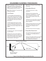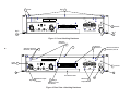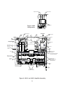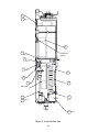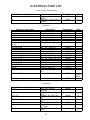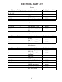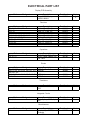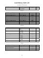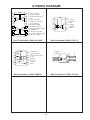
1
®
®
Model 1600VI and 1800VI Professional
Stereo Power Amplifiers
©
1998 Bose Corporation
Service Manual
Part Number 199747 Rev. 00
CONTENTS
Safety Information ............................................................................................................................ 4
Electrostatic Discharge Sensitive (ESDS) Device Handling ........................................................ 4
1800VI Specifications ................................................................................................................... 5-6
1600VI Specifications ................................................................................................................... 7-8
Figure 1. 1600VI and 1800VI Block Diagram .................................................................................. 9
Theory of Operation .................................................................................................................. 10-18
Disassembly/Assembly Procedures ....................................................................................... 19-30
Figure 2. Cover Removal Screw Location Side View ..................................................................... 19
Figure 3. Cover Attaching Hardware .............................................................................................. 20
Figure 4. Rear View - Attaching Hardware ..................................................................................... 20
Figure 5. 240V Configuration ......................................................................................................... 21
Figure 6. 1600VI and 1800VI Amplifier Assembly ......................................................................... 21
Figure 7. Bottom Mounted Components ........................................................................................ 22
Figure 8. Side View - Bottom Mounted Components ..................................................................... 27
Figure 9. Heatsink Bridge ............................................................................................................... 27
Figure 10. Input Module Screw Location ........................................................................................ 29
Test Procedures ........................................................................................................................ 31-33
Figure 11. EQ Card Placement ...................................................................................................... 31
Frequency Response Test Table .................................................................................................. 32
Part List Notes ................................................................................................................................ 34
Main Part List ............................................................................................................................. 35-37
Figure 12. Amplifier Test Setup Diagram ....................................................................................... 31
Figure 13. Front Panel Views, 100V and 120V Variation, 240V Variation ...................................... 37
Figure 14. Back Panel View ........................................................................................................... 37
Figure 15. Cross Section View ....................................................................................................... 38
Figure 16. 1600VI and 1800VI Amplifier Top View ........................................................................ 39
Figure 17. 1600VI and 1800VI, Amplifier Assembly Removed View ............................................. 40
Electrical Part List ..................................................................................................................... 41-54
Packing List .................................................................................................................................... 55
Figure 18. 1600VI and 1800VI Amplifiers Packing Diagram ......................................................... 55
Wiring Diagrams ........................................................................................................................ 56-57
Figure 19. 1600VI and 1800VI Wiring Diagram ............................................................................. 56
Figure 20. 1600VI and 1800VI 240V Wiring Diagram ................................................................... 57
IC Pinout Diagrams ................................................................................................................... 58-59
2
CAUTION: The Bose® 1600VI and 1800VI Professional
Stereo Power Amplifiers contain no user-serviceable
parts. To prevent warranty infractions, refer servicing
to warranty service centers or factory service.
PROPRIETARY INFORMATION
THIS DOCUMENT CONTAINS PROPRIETARY INFORMATION OF
BOSE® CORPORATION WHICH IS BEING FURNISHED ONLY FOR
THE PURPOSE OF SERVICING THE IDENTIFIED BOSE PRODUCT
BY AN AUTHORIZED BOSE SERVICE CENTER OR OWNER OF THE
BOSE PRODUCT, AND SHALL NOT BE REPRODUCED OR USED
FOR ANY OTHER PURPOSE.
3
SAFETY INFORMATION
1. Parts that have special safety characteristics are identified by the
symbol on schematics or by special notes on the parts list. Use only replacement parts that have critical characteristics recommended by the manufacturer.
2. Make leakage current or resistance measurements to determine that exposed parts are
acceptably insulated from the supply circuit before returning the unit to the customer. Use the
following checks to perform these measurements:
A. Leakage Current Hot Check-With the unit completely reassembled, plug the AC line cord
directly into a 120V AC outlet. (Do not use an isolation transformer during this test.) Use a
leakage current tester or a metering system that complies with American National Standards
Institute (ANSI) C101.1 "Leakage Current for Appliances" and Underwriters Laboratories (UL)
1492 (71). With the unit AC switch first in the ON position and then in OFF position, measure
from a known earth ground (metal waterpipe, conduit, etc.) to all exposed metal parts of the
unit (antennas, handle bracket, metal cabinet, screwheads, metallic overlays, control shafts,
etc.), especially any exposed metal parts that offer an electrical return path to the chassis. Any
current measured must not exceed 0.5 milliamp. Reverse the unit power cord plug in the outlet
and repeat test. ANY MEASUREMENTS NOT WITHIN THE LIMITS SPECIFIED HEREIN
INDICATE A POTENTIAL SHOCK HAZARD THAT MUST BE ELIMINATED BEFORE RETURNING THE UNIT TO THE CUSTOMER.
B. Insulation Resistance Test Cold Check-(1) Unplug the power supply and connect a
jumper wire between the two prongs of the plug. (2) Turn on the power switch of the unit. (3)
Measure the resistance with an ohmmeter between the jumpered AC plug and each exposed
metallic cabinet part on the unit. When the exposed metallic part has a return path to the
chassis, the reading should be between 1 and 5.2 Megohms. When there is no return path to
the chassis, the reading must be "infinite". If it is not within the limits specified, there is the
possibility of a shock hazard, and the unit must be repaired and rechecked before it is returned
to the customer.
ELECTROSTATIC DISCHARGE SENSITIVE (ESDS)
DEVICE HANDLING
This unit contains ESDS devices. We recommend the following precautions when repairing,
replacing or transporting ESDS devices:
• Perform work at an electrically grounded work station.
• Wear wrist straps that connect to the station or heel straps that connect to conductive floor
mats.
• Avoid touching the leads or contacts of ESDS devices or PC boards even if properly
grounded. Handle boards by the edges only.
• Transport or store ESDS devices in ESD protective bags, bins, or totes. Do not insert unprotected devices into materials such as plastic, polystyrene foam, clear plastic bags, bubble wrap
or plastic trays.
4
1800VI SPECIFICATIONS
Size:
3.5"H (2U) x 19"W x 13.25"D
89mm x 483mm x 337mm
Weight:
Net: 33 lbs. (15 kg)
Shipping weight: 39 lbs. (17.7 kg)
Display:
7 LED indicators per channel
1 green - READY, 5 yellow - SIGNAL,
1 red - CLIP/PROTECT
Operating Temperature:
0° to 50° C, up to 85% RH
Performance Specifications
Continuous Average Output Power,
both channels driven:
450 Watts per channel into 8 Ohms from
20 Hz to 20 kHz, with no more than 0.2% THD
600 Watts per channel into 4 Ohms from
20 Hz to 20 kHz, with no more than 0.2% THD
Bridged Mono Operation:
1400 Watts into 8 Ohms from 20 Hz to 20 kHz,
with no more than 0.2% THD
Voltage Output:
60 V line voltage per channel into 8 Ohms
49 V line voltage per channel into 4 Ohms
Dynamic Headroom:
1.0 dB nominal
Power Bandwidth:
5 Hz to 40 kHz (+0, -3 dB)
Frequency Response:
20 Hz to 20 kHz (±0.75 dB)
Channel Separation:
> 65 dB @ 1 kHz; > 55 dB @ 10 kHz
Damping Factor:
> 170
Input Impedance:
25k Ohms unbalanced, each leg to ground,
50k Ohms balanced
*Sensitivity:
High: .775 Vrms for rated power into 4 Ohms @
1 kHz, 57 mVrms for 1W into 4 Ohms @ 1 kHz
Low: 1.5 Vrms for rated power into 4 Ohms @ 1 kHz,
116 mVrms for 1W into 4 Ohms @ 1 kHz
*Gain:
High: 36.0 dB (±0.5 dB)
Low: 30.3 dB (±0.5 dB)
*The amplifier sensitivity is set to 0.775V rms for rated output. To reduce the sensitivity by 6 dB to
1.5V rms, remove JP100 (CH1) and JP200 (CH2), located on the main amplifier board.
5
1800VI SPECIFICATIONS
Input Overload:
+18 dBu
IM Distortion:
< 0.1%
THD:
@ 0.775 V Sensitivity, < 0.2%
@ 1.5 V Sensitivity, < 0.1%
Signal-to-Noise Ratio:
> 100 dB, A-weighted, referenced to rated
power into 4 Ohms (high gain)
> 78 dBW, A-weighted, referenced to 1 W into
4 Ohms (high gain)
Slew Rate:
10 V/µS (bandwidth limited)
40 V/µS (RFI filtering removed)
CMRR:
> 80 dB @ 1 kHz (without Bose® input module)
> 60 dB from 20 Hz - 20 kHz (without Bose
input module)
Power Consumption:
55 W at idle
800 W with musical program
1500 W at full power into 8 Ohms (continuous)
2400 W at full power into 4 Ohms (continuous)
Power Requirements:
120 VAC/50-60 Hz (USA and Canada)
230 VAC/50-60 Hz (Europe/UK)
240 VAC/50-60 Hz (Australia)
100 VAC/50-60 Hz (Japan)
Fusing:
15 Amp Slo-Blo (125 V/60 Hz)
8 Amp Slo-Blo (230 V/50 Hz)
6
1600VI SPECIFICATIONS
Size:
3.5"H (2U) x 19"W x 13.25"D
89mm x 483mm x 337mm
Weight:
Net: 30 lbs. (13.6 kg)
Shipping weight: 36 lbs. (16.3 kg)
Display:
7 LED indicators per channel
1 green - READY, 5 yellow - SIGNAL,
1 red - CLIP/PROTECT
Operating Temperature:
0° to 50° C, up to 85% RH
Performance Specifications
Continuous Average Output Power,
both channels driven:
240 Watts per channel into 8 Ohms from
20 Hz to 20 kHz, with no more than 0.2% THD
325 Watts per channel into 4 Ohms from
20 Hz to 20 kHz, with no more than 0.2% THD
Bridged Mono Operation:
700 Watts into 8 Ohms at 1 kHz, with no
more than 0.2% THD
Voltage Output:
43.8 V line voltage per channel into 8 Ohms
36.0 V line voltage per channel into 4 Ohms
Dynamic Headroom:
2.0 dB nominal
Power Bandwidth:
5 Hz to 40 kHz (+0, -3 dB)
Frequency Response:
20 Hz to 20 kHz (±0.75 dB)
Channel Separation:
> 65 dB @ 1 kHz; > 55 dB @ 10 kHz
Input Impedance:
25k Ohms unbalanced, each leg to ground,
50k Ohms balanced
*Sensitivity:
High: 0.775 Vrms for rated power into 4 Ohms,
83 mVrms for 1 W into 4 Ohms
Low: 1.5 Vrms for rated power into 4 Ohms,
160 mVrms for 1 W into 4 Ohms @ 1 kHz
*Gain:
High: 33.3 dB (±0.5 dB)
Low: 27.6 dB (±0.5 dB)
*The amplifier sensitivity is set to 0.775V rms for rated output. To reduce the sensitivity by 6 dB to
1.5V rms, remove JP100 (CH1) and JP200 (CH2), located on the main amplifier board.
7
1600VI SPECIFICATIONS
Input Overload:
+18 dBu
IM Distortion:
< 0.1%
THD:
@ 0.775 V Sensitivity, < 0.2%
@ 1.5 V Sensitivity, < 0.1%
Signal-to-Noise Ratio:
> 100 dB, A-weighted, referenced to rated
power into 4 Ohms (high gain)
> 78 dBW, A-weighted, referenced to 1 W into
4 Ohms (high gain)
Slew Rate:
40 V/µS (bandwidth limited)
CMRR:
> 80 dB @ 1 kHz (without Bose® input module)
> 60 dB from 20 Hz - 20 kHz (without Bose
input module)
Power Consumption:
45 W at idle
500 W with musical program
1000 W at full power into 8 Ohms (continuous)
1550 W at full power into 4 Ohms (continuous)
Power Requirements:
120 VAC/50-60 Hz (USA and Canada)
230 VAC/50-60 Hz (Europe/UK)
240 VAC/50-60 Hz (Australia)
100 VAC/50-60 Hz (Japan)
Fusing:
10 Amp Slo-Blo (125V/60Hz)
7 Amp Slo-Blo (230V/50Hz)
8
H
Fuse
9
Figure 1. 1600VI and 1800VI Block Diagram
Line
Filter
AC
Sequence
Commutation
Control
(Class H)
Power Supplies
(230V)
Only
N
CH 2
CH 1
On/Off
Standby
Sequence
Regulation (not used
with 1600VI)
Phase Control
Send
Amplifier
CH 1
Rcv
CH 2
Sequence
Control
CH 1
Input
Level
Control
Input
Module
CH 2
CH 1
Lowpass
Filter
CH 2
Display
CH 1
OUT
Temperature
Sense
CH 2
OUT
Output
Relays
CH 1
OUT
Fan Drive
CH 2
OUT
Protection
Bose ®
EQ Card(s)
Display
Drive
THEORY OF OPERATION
1. General
The Bose® Model 1600VI and 1800VI Professional Stereo Power Amplifiers are two-channel,
installed/portable amplifiers made for professional sound applications. The 1600VI is rated at
240 Watts into 8 Ohms and 325 Watts into 4 Ohms. In the bridged-mono setting it can deliver
700 Watts. The 1800VI is rated at 450 Watts into 8 Ohms and 600 Watts into 4 Ohms. In the
bridged-mono setting it can deliver 1400 Watts.
The protection circuits designed into the amplifiers will protect them from unexpected faults,
excessive temperature, continuous current limiting and shorted outputs.
The balanced inputs use high quality, high common-mode rejection differential amplifiers for
exceptional hum and noise rejection.
Through the use of equalization cards the amplifier can provide active equalization for Bose
402™, 502®A, 502B, 802®, Model 25/32, Model 8, Model 1B and FreeSpace® 360 professional
loudspeakers. These cards fit into the J6, Channel 1 and J7, Channel 2 connectors located on
the Input Module motherboard or the Bose ACM-1 Amplifier Control Module.
Additional Features are as follows:
• Two input connectors per channel allow 1/4" TRS, XLR, or quick connect terminal block
connection
• Two input connectors for each channel are wired in parallel
• Accepts balanced or unbalanced lines
• Independent CH 1 and CH 2 Level Controls with 11 detented positions
• Level Control Defeat Switch
• Dual Mono Mode for combining the power of both channels into a single higher powered
channel
• Sequencer connection for sequentially powering-up multiple amplifiers to limit instantaneous
in-rush current
• Bi-Amp/Full Range configurable
• Internally configurable for Parallel Mono mode for single channel low impedance operation
• Internally configurable for 0.775V or 1.5V rms input sensitivity
• Internally configurable input polarity of XLR connectors
• Class H dual-rail power supply
• Additional protection circuitry includes Clipping Eliminator, AC Lines Fuse
• Power Connected/Standby Indicator
• 7 LED display per channel, including power ready and Clip/Protect indicators
• Two-speed fan cooled
2. Circuit Descriptions
This section discusses the theory of operation of the 1600VI and 1800VI Amplifiers.
For a better understanding of the circuitry involved, refer to the schematics included with this
manual. Component pin designation is notated as follows: U1-7 means U1 at pin 7.
Unless otherwise noted, this discussion centers around the CH 1 circuitry.
The CH 2 circuitry is essentially identical.
10
THEORY OF OPERATION
2.1 Input Module
Note: Some amplifiers will be equipped with the Bose® ACM-1 Amplifier Control Module in
place of the Bose Input Module. This module retains all of the capabilities of the Bose Input
Module, except sequence (see section 2.8), and includes the ability to control and monitor the
amplifier over a control network. Refer to the ACM-1 Amplifier Control Module service manual,
part number 199746 for more information.
The Input Module consists of signal input connections, mode switching, optional equalization,
and power sequencing circuitry. The module operates from +15V and -15V, supplied by the
host amplifier through J2-2 and J2-1 respectively.
The signal inputs are designed for balanced connection, though unbalanced inputs can be
configured by proper input wiring. Channel 1 (CH1) line-level inputs are made via P4 and J4,
Channel 2 (CH2) input connections are made via P1 and J5. P4 and P1 allow for the insertion
of either male XLR or phone plugs. The phone plug terminations are: tip positive (+), ring
negative (-), and sleeve ground. The XLR connections pins 2 and 3 are user configurable. As
shipped, jumper blocks JB2 and JB1 have jumpers between pins 2 to 3 and 5 to 6. This jumper
configuration assigns XLR pin 2 to positive (+) and pin 3 to negative (-), pin 1 is ground in all
configurations. If the jumpers are placed across JB1/JB2 pins 1 to 2 and 4 to 5 the XLR pin
assignment becomes pin 2 negative (-), and pin 3 positive (+). The Euro-block terminal block
connectors J4 and J5 assignments are: pin 1 positive (+), pin 2 negative (-), and pin 3 ground.
The CH1 input signal is applied to ICs U1, and the CH2 signal to U2. U1 and U2 are unity gain
(0 dB) differential amplifiers (SSM2141). These inputs are protected against RFI (Radio
Frequency Interference) and ESD (Electro-Static Discharge). The signals are then routed to
the A inputs of op-amp/switch ICs (BA3128) U4 (CH1) and U3 (CH2) and to EQ card
connectors J6-4 and J7-4 respectively. The switch’s B inputs are driven by the output of the EQ
cards via J6-5 and J7-5.
The input module detects the presence of EQ cards via J7-6 and J6-6. Without the card
installed these pins are pulled high (+15V) which keeps both CH1 and CH2 sections of dual
LED D23 extinguished. This logic high signal is also applied to the control pins of the switch
ICs which selects the A (unequalized) input. When an EQ is plugged into J7 and/or J6 pin 6 the
EQ is detected and pulls the control pin low (+7.5V), turning on the corresponding LED(s) and
switching the IC to the B input which selects the output of the EQ card.
On some EQ cards the equalization can be modified for either full range “FULL BANDWIDTH”
or bi-amplified “HF ONLY” operation. The equalization mode switch SW2 selects either FULL
BANDWIDTH or HF ONLY modes of the EQ cards installed. These control signals are sent to
the EQ cards via J6-7, 8 and J7-7, 8.
The selected signals from U4 and U3 are buffered by U7B and U7A which are wired to P2 and
P3. These phone connectors provide balanced, buffered, equalized outputs (if an EQ card is
installed) to drive additional amplifiers or other equipment. This allows external equipment to
provide equalized signals without the need for additional equalization. The pin assignment for
these connectors are the same as for the input phone connectors P1B and P4B. The output
circuitry is also protected from RFI and EMI.
The amplifier can be operated in four different output modes: normal (two independent channels) dual mono (one input channel, two separate channels), bridged mono, or parallel mono.
These modes are selected via SW1 and control the operation of op-amp/switching ICs U6 and
U5. Parallel mono operation requires internal modifications to the amplifier, contact the local
Bose Pro Product dealer for information on parallel mono operation.
11
THEORY OF OPERATION
When SW1 is set to the NORMAL mode, CH1 and CH2 operate independently. In this mode a
logic high is applied to the control pins of U6 and U5. This routes the outputs of U4 and U3 to
their respective channels in the amplifier via J1-20 and J1-16.
In DUAL MONO mode both amplifier channels are driven by the signal applied to the CH2
input. U6-1 is driven high (+15V) and U5-1 is driven low (+7.5V), selecting CH2 to drive both
channels of the amplifier.
In BRIDGED MONO operation the CH2 signal is routed directly from the equalizer switch U3 to
the amplifier inputs. U5 control pin 1 is driven low (+7.5V) selecting the inverting input of the
op-amp switching IC signal. This inverting signal is then sent to the B input of U6 whose
control signal at pin 1 is driven low selecting the B input. This routes the inverted signal to the
CH1 input of the amplifier.
For information on sequence operation see Section 2.8, Sequence Send/Receive.
2.2 Power Amplifier Circuitry
The 1600VI and 1800VI amplifiers use a conventional class AB push-pull power amplifier
circuit, with a commutated two-stage (dual-rail, class H) power supply. U100A-1 is the input
stage, providing differential inputs for input and feedback connections as well as most of the
open-loop voltage gain of the circuit. Local and global negative feedback from the output stage
via R109, R113, R111/ R112 and R129 sets the closed-loop gain at 33.3 dB for the 1600VI and
36.0 dB for the 1800VI. Removing jumper JP100 disconnects R111 from the circuit and sets
the closed-loop gain at 27.6 dB for the 1600VI and 30.3 dB for the 1800VI. The factory default
settings are 33.3 dB for the 1600VI gain and 36.0 dB for the 1800VI gain. The output of
U100A-1 drives Q100 and Q101, operating as common emitters that level-shift the drive signal
and couple it to the pre-driver amplifiers Q102 and Q103. Q102 and Q103 provide additional
voltage gain, and when combined with the voltage gain of the input op-amp is sufficient to
swing the input signal between the +90V/1600VI and +106V/1800VI power supply rails. Q104
and Q122 are connected as an NPN-PNP conjugate pair and used as a VBE multiplier for bias
control. Q104 is thermally connected to the output transistors and together with Q122 provides
bias stabilization over a wide temperature range. R124 allows the bias current to be adjusted
to its optimum value.
The predrivers Q102 and Q103 provide the base current to the drivers Q108 and Q109.
These drive the output transistors; Q110, Q112, Q114, Q116, Q118 and Q120 for the positive
half-cycle, and Q111, Q113, Q115, Q117, Q119 and Q121 for the negative half-cycle.
Note: Output transistors Q112, 118, 212 and 218, along with the corresponding channel 2
output transistors Q113, 119, 213, 219, are not used in the 1600VI amplifier.
Q105 operates as a V-I limiter, sensing the voltage drop across emitter resistor R148 (Q106
across R149 for the negative side), and reducing the drive signal to the output stage under
overload conditions (see Section 3.1 Over-Current Protection for more information). From the
Amplifier Board, the signal passes to the Output Board via E100 (E200 for CH 2). R100, L100,
R110 and C100 on the Output PCB comprise the output pole circuit for amplifier stabilization.
12
THEORY OF OPERATION
2.3 Output Relays
Note: Refer to the Output PCB schematic for the following.
Relay K100 is used to connect the output signal to the Speaker Output Binding Posts through
J1. The CH1 and CH2 (K100 and K200) output relays are energized independantly of each
other. In CH1, immediately after the power switch is turned on, +6 Vdc is applied to terminal 2
of D105 (ready LED) on the display board via the voltage divider formed by R112/R113. Terminal 1 of D105 is connected to pin 6 of K100 via J3-8 and J6-5 on the I/O board. A small amount
of current is drawn through R102 and the relay coil, which is enough to illuminate the red LED
portion of D105 but not enough to activate the relay. In the meantime, C13 begins to charge
through R26 on the I/O board, which delays turning on Q2 and Q3 by a few seconds.
When Q3 turns on, VLF+ is applied to pin 6 of K100 which activates the relay. VLF+ is also
applied to terminal 1 of D105, which reverse biases the red LED and D107, and forward biases
the green LED, drawing current from ground through R112.
2.4 Magnetic Field Power Supply
When the power switch is OFF (S1 across E1 and E2) and the linecord is connected to an AC
voltage, D1 illuminates (Standby LED). When the power switch is turned ON (S1 across E2
and E3), the LED goes off and gate voltage is applied to triac Q1, which turns it on and energizes the transformer primary winding.
The secondary winding of the power transformer has two taps that supply the two pairs of DC
supply voltages, ±90 Vdc and ±45 Vdc for the 1600VI and ±106 Vdc and ±53 Vdc for the
1800VI, each having its own bridge rectifier and filter capacitors. The ±15 Vdc is tapped from
the ±53 Vdc for the 1800VI and the ±45 Vdc for the 1600VI through R6 and R8, and regulated
by Q2, Q3 and zener diodes D3 and D6. The ±15 Vdc supply powers the op-amps and smallsignal transistors.
Note: Refer to the Regulator Board schematic diagram for the following.
The Regulator Board is not used on the 1600VI.
In the 1800VI, the triac Q1 drives the primary of the magnetic field power transformer by
operating as a phase controlled switch; its gate signal depends on the signal supplied to
opto-isolator U3 located on the regulator board. U4B provides steering for the photodiac in U3,
allowing the triac to fire on both alternations of the power line. U2 on the Regulator Board
provides AC to DC conversion, with the AC line voltage providing the input to the converter
through limit resistors R3 and R4, and the 12.5 Vdc output determined by feedback resistor
R6. This voltage provides the positive supply for U4, DC reference for comparators U4C and
U4D, and the current through opto-isolator U1 which sets the voltage for the voltage-to-current
converter U4A. Note that U4 (MC3405) is a dual op-amp and dual-voltage comparator in a
singe package (U4A/U4B are op-amps and U4C/U4D are open collector comparators).
2.5 Start-up Sequence (1800VI only)
When the power switch is OFF (S1 across E1 and E2) and the linecord is connected to an AC
voltage, D1 illuminates (STANDBY LED). When the power switch is turned ON (S1 across E2
and E3), the LED goes off and AC HI is supplied to the Regulator Board.
13
THEORY OF OPERATION
D2 and D3 on the Regulator Board provide overvoltage protection to U4. U4B-14 is a full-wave
rectifier that outputs positive pulses to comparator U4C. The reference voltage is set at 0.7Vdc
by R10 at pin 3. Where pin 2 crosses the threshold, the output of U4C-1 goes open and C6
begins to charge through R21 and U4A-8.
U4A is a voltage-to-current converter (Howland current pump), whose output current is
determined by the voltage at the junction of R12 and R13. As the voltage increases, the
charging current to C6 increases.
The voltage on C6 is connected to comparator U4D-6. The reference voltage is set at 0.7Vdc
by R22 at pin 5. When pin 6 crosses the threshold, the output of U4D-7 goes open and base
current is supplied to Q1 through R14. Q1 turns on, and current flows through the LED portion
of U3, illuminating it and turning on the diac. This applies voltage to the gate of triac Q1 on the
Power Supply Board which fires it and allows it to conduct current through the primary side of
the power transformer.
When the output of U4B-14 drops below the threshold voltage of U4C-3, U4C-1 goes low and
C6 discharges rapidly through it. When the voltage on C6 drops below the threshold voltage of
U4D-5, U4D-7 goes low and Q1 and U3 turn off, removing the gate voltage to the triac
momentarily interrupting the current through the primary side of the transformer.
The triac is switched on and off every half-cycle of the 60Hz AC line. Thus, the triac switches
the AC line current off at a rate twice the line frequency, at the instant the line current crosses
the zero axis. The triac will then remain off for a number of degrees of the sinusoid, before
switching on again. The phase angle at which the triac switches on is the “firing angle” of the
triac. This produces enough voltage to the primary of the power transformer to allow the
secondary regulator stage to begin to operate.
2.6 Power Supply Regulation (1800VI only)
The firing angle of the triac controls the voltage on the primary of the transformer, and is
determined by the conduction of the optocoupler U3 on the Regulator Board.
As the conduction of the optocoupler increases, so does the conduction angle of the triac. The
photodiac conduction of the optocoupler is controlled by the current through the LED portion of
the optocoupler, the amount of current through the LED is equal to the amount of current
through transistor Q1. When the LED in U3 is fully ON, the triac conducts earliest in the AC
cycle: the power supply is operating at maximum output. The LED current is supplied by
voltage regulator U2 on the Regulator PCB. U5A differential amplifier senses the secondary
supply voltages through R37 and R38. The output voltage at U5A-1 increases at the rate
determined by R30 and C8 (slow start-up). The idle secondary voltages are set by R36 on the
Regulator Board .
2.7 Load Regulation (1800VI only)
When the amplifier is driven at high power into a load, the high DC supplies (rail voltages) will
begin to “sag”. Differential amplifier U5A-1 senses this and increases the LED current to
optocoupler U1. This action increases the phototransistor conduction, which increases the
output current of U4-8, increasing the charging rate on C6. This ultimately increases the triac
conduction which increases the primary voltage, which increases the secondary voltages, thus
providing steady, regulated DC supplies for the amplifier stage.
14
THEORY OF OPERATION
The -15Vdc supplied to U5A-4 is backed up with a voltage divider off the -106Vdc supply (R26/
R27). Without this, if the -15Vdc supply should fail for some reason, the output of U5A-1 would
go high, drawing maximum current through the LED in U1 and latching the triac into full conduction. To prevent this, D8 will become forward biased and supply negative DC to U5A-4,
keeping it operating normally. Note that if the +15Vdc supply should fail, the output of U5A-1
would go negative, turning off the triac.
2.8 Sequence Send/Receive
The amplifier can be powered up while the power switch is in the OFF position by applying a
DC control voltage of +7V to +15V to the Sequence RCV terminal. Q3 on the Input Module
Board will turn on and carry the control voltage through to the SND terminal, which is connected to the next amplifier in the sequential chain. Q1 also turns on which turns on Q2,
providing enough current to pass through the LED portion of optocoupler U1 on the Power
Supply Board to illuminate it and turn on the diac. This provides a gate voltage to fire triac Q1,
which powers up the primary circuit. Once the secondary voltages are up, the +15Vdc supply
keeps the Receive circuit operating.
2.9 Commutators
Under idle or small-signal conditions, the low-rail voltage is applied to the collectors of the
output transistors through D13 and D19 on the Power Supply Board. The output of the amplifier is connected to the Power Supply Board via J1-10/J2-10. The signal is half-wave rectified
by D7 and D14, sending the positive half of the signal to comparator U2A-1 and the negative
half to comparator U2B-7. When the signal level exceeds the threshold of the comparator, Q4
(positive) or Q10 (negative) turns on. Current can now flow from ground through Q8 which acts
as a current source for Q6. Q6 or Q11 turn on providing gate drive to the power FET Q9 (positive) or Q14 (negative). When the FETs turn on, the high-rail voltage is connected to the collectors of the output transistors. D13 and D19 become reversed biased and switch off the low-rail
voltage from the circuit. Zener diodes D11 and D18 provide gate protection to the FETs.
Q7 and Q12 speed up the turn off time of the FETs.
This two-stage approach minimizes the voltage across each of the output devices which also
minimizes the power dissipation required. Without this approach, the output transistors would
be required to support the entire power supply voltage under small-signal conditions and the
“unused” portion of the power supply voltage would be turned into heat.
2.10 Display Circuit
In addition to the READY LEDs discussed in section 2.3 (Output Relays), the Display Board
contains five SIGNAL LEDs and one CLIP/PROTECT LED per channel.
The clipping indicators are driven by transistors Q100 (CH1), and Q200 (CH2) located on the
Display Board. The signal for the clipping indicators initially comes from U100A-1 and U100B-7
on the Amplifier Board. This is the same signal that operates the anti-clipping opto-isolator on
the I/O Board. D30 on the I/O Board half-wave rectifies the positive-going portion of the signal
and drives comparator U9B which is a switch. C9 and R62 establish the time constant of the
clipping indicator. D23 rectifies the negative-going portion and also drives comparator U9B.
When clipping occurs, U9B-7 changes from positive to negative, which forward biases D100
on the Display Board and turns on Q100. Q100 supplies current for clipping LED D104,
causing it to illuminate.
15
THEORY OF OPERATION
The output signal is sensed at the speaker output via the I/O Board (J2-3 Output Board to J6-3
I/O Board to J3-6 I/O Board to J1-6 Display Board). D22 half-wave rectifies the signal and
provides a DC voltage proportional to the amplifier’s output to drive the signal display circuit.
C2 and R19 determine the response characteristics of the display.
The signal driver circuit comprised of U1-U4 is basically a ladder comparator driving LEDs,
with a twist. Assume that the signal at U2A-3 is zero volts (ignore R24 and D23 for now). R13
and R14 are a voltage divider that establishes a reference voltage for the comparators (four
per channel). The comparators compare this reference voltage against the voltages established by the tapped voltage divider made up of R22, R20, R15 and R25. The CH1 LEDs are in
the following sequence (lowest to highest): D105 (red/ green), D13 (amber), D15 (amber), D14
(amber), D12 (amber), D11 (amber), and D104 (red).
With the input at zero volts, all of the comparator outputs are at -12V, except for U2B-7 which
is high. None of the signal LEDs have any voltage across them, all are extinguished. As the
input signal rises, it crosses in sequence at the thresholds established at each of the four
comparators. First U2A-1 fires; its output goes high and D13 illuminates. Next U1B-7 fires, its
output goes high, D13 extinguishes (no net voltage across it) and D15 illuminates. Finally U1A1 fires, D15 extinguishes, and (this is the twist) D23/R24 supply current to the bottom of the
R15, R20, R22 and R25 voltage divider, which inverts the relationship of the comparators to
each other.
When U1A-1 fires, the current through R24 reverses the sequence of the voltages that establish the thresholds for the three comparators. This allows the same comparators to perform
double-duty. The new thresholds leave U1A-1 high, U2B-7 low, U2A-1 and U1B-7 low and D14
on. D11 and D12 are off. As the input signal rises further, U1B-7 fires, extinguishing D14 and
illuminating D12. Next U2A-1 fires, extinguishing D12 and illuminating D11. Finally U2B-7 fires,
extinguishing D11. The last LED is the clipping indicator, D104.
3.0 Protection Circuitry
Protection functions are provided that will deactivate the output relays. Protection is provided
for the following fault conditions:
3.1 Over-Current Protection
The amplifiers are protected from short-term excess current through the output stage by
electronic current limiters. When the current through the output transistors becomes excessive,
the voltage drop across the emitter resistors R148 and R149 bias the current limiter transistors
Q105 and Q106 on, which shunt the drive current via D106 and D107. R139, D102, R140 and
D103 determine the V-I limits.
When the current-limiters turn on, the voltage at voltage divider R127/R128 becomes less
positive, providing base current for Q1 on the I/O Board through R38. When Q1 turns on two
things happen; current flows through U3 (LED/LDR module) via D31 which attenuates the
input signal, removing the high current condition as well as providing base current to Q5
through D1 which turns off Q2 and Q3, causing the relay to disengage. C13 provides a time
delay to prevent the relay from disengaging during momentary program peaks. When the relay
disengages, it causes the red LED in D105 (READY LED) to illuminate and also turns on Q100
and D104 (CLIP/PROTECT LED).
16
THEORY OF OPERATION
3.2 Clipping Eliminator Circuit
This circuit is controlled by the LED/LDR opto-isolator U3, located on the I/O Board. The LED
portion of this component is driven from a bridge rectifier (D4) that gets its input signal from
U100A-1 on the Amplifier Board. Under normal conditions (undistorted amplifier output) there
is almost no signal at this point. If the amplifier is driven into clipping, the signal level at
U100A-1 rises rapidly because the feedback signal no longer represents the input signal.
Once this occurs, the LED in U3 illuminates, reducing the resistance of the LDR portion which
in turn reduces the input signal. The clipping-eliminator circuit is activated by switch S2B on
the I/O Board. When the switch is off, the signal driving the bridge rectifier is shorted to ground.
3.3 DC Offset
DC offset is sensed by the comparator amplifier U2A on the I/O Board. If a DC component
should appear at the output, it is sensed through either D6 or D7, depending on its polarity.
The output of U2A-1 will switch from -14Vdc to +14Vdc, which turns on Q5 via D8. This deactivates the relay, turns the READY LED red, and turns on the CLIP/PROTECT LED.
In addition, the output of U2A-1 is conveyed to the Regulator Board via D15, J100-10 to
Regulator Board J1-12 and D9. The positive voltage on U5A-2 causes the output of U5A-1 to
become less positive, shutting off the conduction current through optocoupler U1, which shuts
off the triac and primary current.
Note: The Regulator PCB is not used in the 1600VI amplifier.
3.4 Overheated Output Transistors
A thermistor (RT100) is positioned near the amplifier PCB's heatsink. As the negative coefficient thermistor heats up, the voltage on comparator U2B-6 located on the I/O PCB drops.
When it crosses the reference voltage set up by voltage divider R42/R43, U2B-7 goes positive.
This forward biases D17, turning on Q5, which deactivates relay K100. As the heatsink temperature cools, the thermistor will cool until the voltage at U2B-6 once again crosses the
reference voltage at U2B-5, allowing the relay to reactivate.
3.4 Fan Speed Control
The fan operates at low speed when the amplifier is first turned on. The voltage at the
thermistor is connected to the Fan Drive circuit on the Output Board via D16 (on the I/O Board)
and J6-4/J2-4. As the heatsink temperature increases, the voltage at U1A-3 on the Output
Board decreases until it crosses the threshold set by voltage divider R4 and R6. When this
occurs, the output of U1A-1 toggles low, which turns on Q1. Q1 shorts across R1 and applies
the full VF+ voltage to the fan, kicking it into high speed.
3.5 Major Faults
The slo-blo line fuse protects the unit from further damage when a major fault such as a
shorted output transistor or a secondary power supply fault occurs. If the unit is run at or near
its rated power, the fuse will eventually blow. The rated line fuse allows the unit to be operated
without interruption for all musical applications.
17
THEORY OF OPERATION
4.0 Operating Modes
The Bose® 1600VI and 1800VI amplifiers are capable of being configured to operate in several
different modes in order to allow greater flexibility in use.
4.1 Bridged Mono/Dual Mono Switching
The Stereo/Mono Switch (S1) on the Input Board is a three-position switch used to select
Normal Stereo, Bridged Mono or Dual Mono operation. In the Bridged Mono position, it connects CH 1 in parallel with the CH 2 input, but inverts the signal to CH 1. The CH 1 input
connection becomes disabled. The speaker output signals are identical except CH 1 is 180
degrees out of phase. In this way, a single speaker can be connected between the two “+”
speaker terminals and receive twice the voltage as a single channel. When connected in this
way, each channel “sees” one-half the impedance of the speaker that is connected between
them. If an 8 ohm speaker is used, each channel will see a 4 ohm load. The result is twice the
rated power (per channel) into twice the rated impedance.
Note: Each channel can still be independently controlled with its own level control so it is
important that both level controls be set to the same position for a balanced output.
When S1 is switched to the Dual Mono position, CH 1 is connected in parallel with the CH 2
input, but in phase. The CH 1 input connection becomes disabled. This allows both channels
to be driven with the same signal without the use of special patch cords. Each channel can still
be independently controlled with its own level control.
4.2 Parallel Mono
To operate in Parallel Mono mode, leave S1 in the Normal Stereo position. Removing jumpers
JP201 and JP203 will disconnect the CH 2 predrivers from the output stage. Installing jumpers
JP102, JP104, JP202 and JP204 will connect the CH 1 predrivers to the CH 2 output stage. In
this way, both channels will operate at exactly the same level, and will be controlled by the
CH 1 level control.
In addition, removing JP1 will prevent the CH 2 clip LED from activating, and installing a 16 ga.
jumper wire between WL100 and WL200 on the Output Board will tie both amplifier outputs
together before the relays.
When operating in parallel mono, either of the speaker output terminals (CH 1 or CH 2) can be
used since they both have exactly the same signal present. When a speaker is connected to
the output terminals it can be driven with twice the current capacity of a single channel. The
result is twice the rated power (per channel) into half the rated impedance.
18
DISASSEMBLY/ASSEMBLY PROCEDURES
Note: It's advisable to mark or note wiring
configuration before any disassembly
begins. For more information refer to the
Wiring Diagrams Figures 19 and 20.
Note: Refer to Figure 6 for the following
procedures.
3. Display Board Removal
Note: Refer to Figures 2, 3 and 4 for the
following procedures.
3.1 Remove the cover (1) using
procedure 1.
1. Cover Removal
3.2 Remove the connectors from
transformer (4) terminals 6-11. This will
give you access to the screw on the
display board (5) which is next to the
transformer.
1.1 Use a phillips-head screwdriver to
remove seven screws (3) from the back
and sides of the chassis cover (1) and the
two longer screws that are located in the
center behind the rack-mount brackets.
See Figure 2.
3.3 Remove two screws (20) on the solder
side of the display board with a phillipshead screwdriver.
1.2 Lift the back of the cover up, while
moving it forward (front panel) from the
chassis (2). The front lip of the cover is
hinged on the two front angle pieces of the
chassis.
3.4 Move the board back from the chassis
front panel and disconnect the wiring
harness from the display board J1
connector.
2. Cover Replacement
3.5 Lift the board out from the chassis.
2.1 Align the cover (1) so its front angle fits
over the chassis.
4. Display Board Replacement
4.1 Connect the wiring harness from the
I/O board (6) to the display board (5)
J1 connector.
2.2 Secure the cover to the chassis by
tightening seven screws (3) and the two
longer screws located in the center behind
the rack-mount brackets with a phillipshead screwdriver. See Figure 2.
4.2 Secure the display board to the chassis
standoffs by tightening two screws (20)
with a phillips-head screwdriver.
Remove these screws
rear
front
Side View
Do not remove
these screws
Figure 2. Cover Removal Screw Location Side View
19
Qty 3 3
1 Cover
1800 SERIES V PROFESSIONAL AMPLIFIER
FOR BRIDGED
OPERATIONS
BRIDGED
1400 W 8
D.O.M.
CONSULT
OWNERS MANUAL
BOSE CORPORATION, FRAMINGHAM, MA 01701-9168 MADE IN U.S.A.
LICENSED UNDER U.S. PAT. NO. 4,484,150
700 W 4
CAUTION
700 W 4
AVIS
WARNING
TO REDUCE THE RISK OF FIRE OR ELECTRIC SHOCK
DO NOT EXPOSE THIS EQUIPMENT TO RAIN OR MOISTURE.
Qty 3
3
- CH 2 +
+ CH 1 SPEAKER OUTPUTS
AC
100V
50-60Hz
1800 W
2 Chassis
Qty 3
3
CLASS 1 WIRING SHALL BE USED
Figure 3. Cover Attaching Hardware
Attaches
I/O Board
11
Attaches
11 I/O Board
20
3
Attaches Heatsink
Brackets, Item 22
3
Attaches Heatsink
Brackets, Item 22
1800 SERIES V PROFESSIONAL AMPLIFIER
FOR BRIDGED
OPERATIONS
CONSULT
OWNERS MANUAL
3
BRIDGED
1400 W 8
D.O.M.
BOSE CORPORATION, FRAMINGHAM, MA 01701-9168 MADE IN U.S.A.
LICENSED UNDER U.S. PAT. NO. 4,484,150
700 W 4
Input 17
Module
CAUTION
700 W 4
AVIS
WARNING
TO REDUCE THE RISK OF FIRE OR ELECTRIC SHOCK
DO NOT EXPOSE THIS EQUIPMENT TO RAIN OR MOISTURE.
- CH 2 +
+ CH 1 SPEAKER OUTPUTS
AC
100V
50-60Hz
1800 W
2 Chassis
CLASS 1 WIRING SHALL BE USED
3
3
Fan Exhaust Slot
3 Attaches Input
Qty 2
Module
3 Qty 2
Attaches Lower
Fan Shield
Figure 4. Rear View - Attaching Hardware
Attaches 11
Output Board
36
Sequence Switch
53
9
Power Switch
LOAD
LINE
10
Figure 5. 240V
Configuration
240V Line Filter
100V and 120V
Configuration
5 Display Board
45
35
Qty 2
47
20
Qty 2
R101
J1
Qty 2
32 Fuse Holder
4
Front Panel
Hinge
R102
20
Qty 2
Nylon
Standoff
Display Board 50
Wiring Harness
6
7
8
2
1
Transformer
9
10
11
Nylon Clamp
Anchors C4-C7 21
Capacitors
9 Power Switch
Board
LINE
5
3
4
LOAD
Power Supply 7
Board
10 Line Filter
A
A
44
J1
Cover
Qty 2
8 Regulator Board
1
Nylon Standoff
Power Supply Board Terminals
WL1-WL3 and WL5-WL7
Attaches Transistors
to Heatsink, Item 18 29
Large Ribbon Cable
Qty 28
16 Output Board
Terminals WL1, WL2,
WL100, WL101,
WL200 and WL201
Amplifier 15
Board
3
Shield Over 19
Q214 and Q216
I/O Board
J3 Connector
6 I/O Board
48
31
I/O Board J100
and J200 Connectors
Figure 6. 1600VI and 1800VI Amplifier Assembly
21
Qty 6
Figure 7. Bottom Mounted Components
22
37
40
Qty 2
42
37
41
Input Module
Assembly
17
Qty 4
I/O Board
2-Pin
Harness
Connector
Part of
I/O Board
Qty 2
51
Input Module
J1 Connector
I/O Board
Ribbon
Cable
Fan 23
B1
Gray 3
9 Black
12
Qty 4
28
27
Upper
Shield
11 Yellow
13
Vio 5
8 Black
Lower
Shield
26
Brn 4
Wht 1
7 Red
10 Red
Blu 2
25
24
Qty 4 13
6 Yellow
T1
4
Binding Post
Terminal Plug
14
31
P1
14 Qty 4
LOAD
LINE
E1
9
12
11
Qty 2
Qty 2
12 Qty 2
34 F1
33
32
Output Board
J2 Connector
16 Output Board
43 J1
11
10 FL1
2
DISASSEMBLY/ASSEMBLY PROCEDURES
6.2 Carefully line up the holes of the
regulator board with the nylon standoffs
mounted on the power supply board.
Snap three corners of the board onto each
nylon standoff.
4.3 Connect the power supply cables back
to transformer (4) terminals 6-11.
4.4 Replace the cover (1) using
procedure 2.
6.3 Replace the transformer (4) using
procedure 12. Refer to Figures 7 and16 for
correct wire locations.
Note: Refer to Figures 3, 4 and 6 for the
following procedures.
5. Regulator Board Removal
6.4 Connect the cables from the line cord
(31) (for 240V, line cord and ground) to the
line filters terminals (10).
Note: The regulator board is not used in
the 1600VI amplifier.
6.5 Connect the cables to power supply
board (7) terminals WL1-WL3 and WL5WL7. These terminals are directly over the
regulator board.
5.1 Remove the cover (1) using
procedure 1.
5.2 Note the wiring configuration and
disconnect cables WL1-WL3 and WL5-WL7
from the power supply board (7) terminals.
This will allow easier access to the regulator board (8). These terminals are located
directly over the regulator board in the
1800VI.
6.6 Replace the cover (1) using
procedure 2.
Note: Refer to Figures 5 and 6 for the
following procedures.
7. Power or Sequence Switch Removal
5.3 Disconnect the cables from the
terminals of the line filter (10) that are
next to the regulator board.
7.1 Remove the cover (1) using
procedure 1.
5.4 Remove the transformer (4) using
procedure 11. This will allow easier access
to the standoffs that secure the regulator to
the power supply board.
7.2 Unsolder the three tabs that secure the
power switch board (9) to the switch.
7.3 Push the switch through the chassis (2)
front panel.
5.5 Unsnap the regulator board from the
nylon standoffs mounted on the power
supply board. This will also disengage the
regulator board from the power supply
J1 connector.
8. Power or Sequence Switch
Replacement
8.1 Push the switch into the chassis (2)
front panel.
6. Regulator Board Replacement
8.2 Solder the power switch board (9) to
the switch terminals. For 100V and 120V
units, make sure the LED is lined up with
the panel hole labeled "Standby". For 240V
units, make sure the board's LED is aligned
underneath the "ON" position icon.
6.1 Line up and insert the pins of the
regulator board (8) J1 connector (solder
side) into the power supply (7)
J1 connector.
8.3 Replace the cover (1) using
procedure 2.
23
DISASSEMBLY/ASSEMBLY PROCEDURES
Note: Refer to Figures 5, 6 and 7 for the
following procedures.
11.3 Place the chassis (2) on its side.
11.4 While holding the transformer with one
hand, use a phillips-head screwdriver to
remove four screws (13) and washers (14)
from the bottom of the chassis.
9. Line Filter Removal
9.1 Remove the cover (1) using
procedure 1.
11.5 Remove the transformer from the
chassis.
9.2 Make a note of the wiring configuration
of the line filter (10) and disconnect the
wires.
12. Transformer Replacement
9.3 Using a phillips-head screwdriver and a
5/16 wrench, remove the two screws (11)
and locknuts (12) that attach the line filter
to the chassis (2). The screws are driven
from the bottom of the chassis.
12.1 Place the chassis (2) on its side. Align
the transformer (4) in the chassis so that
the six terminal side of the transformer is
next to the large capacitors of the power
supply board (7).
9.4 Remove the line filter from the
chassis.
12.2 While holding the transformer with one
hand, use a phillips-head screwdriver to
tighten four screws (13) and washers (14)
from the bottom of the chassis.
10. Line Filter Replacement
10.1 Align the line filter (10) to the
chassis (2). Refer to Figures 16 and 17.
12.3 Return the cables to their designated
terminals on the transformer. Refer to the
Wiring Diagrams, Figures 19 and 20 for
proper hookup.
10.2 Secure the line filter to the chassis
using the two screws (11) and locknuts (12)
removed in procedure 9.3. The screws are
driven from the bottom of the chassis.
12.4 Replace the cover (1) using
procedure 2.
10.3 Connect the cables from the line
cord (31) and power supply to the
terminals of the line filter. Refer to the
Wiring Diagrams Figures 19 and 20.
Note: Refer to Figures 6 and 7 for the
following procedures.
13. Amplifier Board Removal
10.4 Replace the cover using procedure 2.
13.1 Remove the cover (1) using
procedure 1.
Note: Refer to Figure 7 for the following
procedures.
13.2 Disconnect the two ribbon cables
connected to the I/O board (6), J101 and
J201, from the amplifier board (15).
11. Transformer Removal
11.1 Remove the cover (1) using
procedure 1.
13.3 Disconnect the large ribbon cable
JP200 from the power supply board (7).
11.2 Make a note of the wiring configuration
and disconnect all of the connectors
attached to the transformer (4) terminals.
13.4 Make a note of the wiring configuration and disconnect the cables connected
to terminals WL1, WL2, WL100, WL101,
WL200 and WL201 on the output
board (16).
24
DISASSEMBLY/ASSEMBLY PROCEDURES
14.5 Connect the amplifier and power
supply board (7) cables to the output board
(16) WL1, WL2, WL100, WL101, WL200
and WL201 terminals. Refer to Wiring
Diagram Figure 19.
Note: Some cables are bundled together.
Cut any wire wraps when necessary.
13.5 Note the locations of RT100, RT200,
Q104 and Q204 at the corners of the
amplifier board and their placement against
the heatsink.
14.6 Replace the cover (1) using
procedure 2.
13.6 Remove one screw (29) and washer
from each of the twenty-eight transistors
that attaches the amplifier board to the
heatsink (18).
Note: Refer to Figures 7, 8 and 9 for the
following procedures.
15. Output Board Removal
Note: Make a note of the location and
alignment of the shield over Q214 and
Q216.
15.1 Remove the cover (1) using
procedure 1.
15.2 Disconnect the display board (5)
wiring harness from the I/O board (6) J3
connector.
13.7 Lift the amplifier board from the
heatsink.
14. Amplifier Board Replacement
15.3 Disconnect the amplifier board (15)
two ribbon cables from the I/O board
J100 and J200 connectors.
14.1 Place the amplifier board (15) onto
the heatsink (18). Align the board so that
the large ribbon cable is facing the power
supply board (7). Be sure that RT100,
RT200, Q104 and Q204 are aligned
properly against the heatsink and that they
have sufficient heatsink compound
between the component and the heatsink.
15.4 Make a note of the wiring configuration
and disconnect the cables connected to the
output board (16) WL1, WL2, WL100,
WL200 and WL201 terminals.
15.5 If necessary, unsolder the red and
white wires from the I/O board E10 and E11
terminals. They are located near the
amplifier board transistor shield (19).
14.2 Secure the amplifier board to the
heatsink by tightening one screw (29) and
washer to each of the power transistors.
Torque the screws to 5.7 inch-pounds.
Note: Make sure the shield (19) is attached to Q214 and Q216 transistors.
Refer to Figure 6 for shield alignment.
15.6 Make a note of the wiring configuration
and disconnect the cables from the power
supply WL1-WL8 terminals. WL8 is located
near the large power supply capacitors.
14.3 Connect the two ribbon cables J101
and J201 to I/O board (6) connectors, J100
and J200).
15.7 Make a note of the wiring configuration
and disconnect all of the cables connected
to the transformer.
14.4 Connect the large ribbon cable
(JP200) to the power supply board (7)
connector J2.
15.8 Using a phillips-head screwdriver,
remove one screw from the nylon clamp
(21) that fastens the power supply
capacitors (7) C4-C7 to the chassis (2).
25
DISASSEMBLY/ASSEMBLY PROCEDURES
15.9 Using a phillips-head screwdriver,
remove four screws (29) from the two
brackets (22) that secure the heatsink (18)
to the inside of the chassis back panel.
16.4 Connect the output board black wires
to the binding posts (items 24 or 25) by
tightening four nuts with a wrench. Refer to
Figure 19 for the proper wiring.
15.10 To release the heatsink base from
the bottom of the chassis, use a phillipshead screwdriver to remove four screws (3)
from the chassis bottom panel. Move the
entire heatsink away from the output board.
16.5 Connect the I/O board (6) ribbon cable
to the output board J2 connector.
15.11 Disconnect the fan (23) from the
output board J3 connector.
16.7 Return the heatsink (18) to it's location. Use a phillips-head screwdriver to
tighten four screws (29) to the two brackets
(22) that fasten the heatsink to the chassis
back panel.
16.6 Connect the fan (23) connector to the
output board J3 connector.
15.12 Disconnect the I/O board ribbon
cable from the output board J2 connector.
16.8 Secure the heatsink to the bottom of
the chassis by tightening four screws (3)
with a phillips-head screwdriver. The
screws are driven from the bottom of the
chassis.
15.13 Use a phillips-head screwdriver to
remove two screws (11) that fasten the
output board to the bottom of the chassis.
15.14 Use a phillips-head screwdriver to
remove two screws (11) on the back panel
that attach to the two brackets on the
output board. They are located underneath
the red and black binding posts.
16.9 Secure the power supply (7) large
capacitors to the inside of the chassis by
tightening one screw (20) into the nylon
clamp that wraps around one of the
capacitors.
15.15 Use a wrench to remove four nuts
from the binding posts (items 24 or 25).
Release the wires from the posts.
Note: Refer to wiring diagrams Figures 19
and 20 for the following procedures.
15.16 Lift the output board out of the
chassis.
16.10 Connect the cables from the
amplifier (15) and power supply board to
the output board WL1, WL2, WL100,
WL200 and WL201 terminals.
16. Output Board Replacement
16.1 Place the output board (16) into the
chassis (2). Align the board so the two
brackets on the board face the back panel
of the chassis.
16.11 Connect the amplifier board ribbon
cables to the I/O Board J100 and J200
connectors.
16.12 Connect the display board (5) wiring
harness to the I/O board J3 connector.
16.2 Secure the output board to the bottom
of the chassis by tightening two screws (11)
with a phillips-head screwdriver.
16.13 Solder the red and white wires from
the 2-pin harness connector to the I/O
board E10 and E11 terminals. They are
located near the amplifier board transistor
shield (19).
16.3 Use a phillips-head screwdriver to
tighten two screws (11) into the output
board brackets. The screws are driven
from the outside of the back panel.
26
DISASSEMBLY/ASSEMBLY PROCEDURES
Attach Bridge
to Heatsink
16.14 Connect the cables from the line
filter (10) power or sequence switch board
(9) and fuse holder (32) to the power
supply WL1-WL8 terminals.
16.15 Connect all the cables connected to
the transformer.
30
Power Supply Board
Heatsink
Bridge
16.16 Replace the cover (1) using
procedure 2.
39
Note: Refer to Figures 6, 8 and 9 for the
following procedures.
18
Figure 9. Heatsink Bridge
17.3 Disconnect the amplifier board (15)
ribbon cable from the power supply (7)
J2 connector.
17. Power Supply Board Removal
17.1 Remove the cover (1) using
procedure 1.
17.4 Make a note of the wiring configuration and disconnect the wiring from power
supply terminals WL1-WL8.
17.2 Remove the transformer (4) using
procedure 11.
17.5 Make a note of the wiring configuration and disconnect all of the wires connected to terminals E5-E17 of the power
supply board.
Front
Chassis 2
Heatsink, Amplifier
13
Attaches
Transformer 14
17.6 Use a phillips-head screwdriver to
remove one screw from the nylon clamp
(21) that secures the power supply large
capacitors to the chassis.
Qty 4
17.7 Remove two screws (30) from the
heatsink bridge with a phillips-head
screwdriver. Refer to Figure 9.
21 Nylon Clamp
Attaches Power Supply
Board to Heatsink
30
Attaches
Nylon Clamp
Qty 4
Attaches Heatsink
to Chassis
3
Qty 4
17.8 Disconnect the regulator board (8)
from the power supply using procedure 5.
Note: The regulator board is not used in
the 1600VI amplifier.
Attaches Fan
Shield to
3
Chassis
Qty 2
18
Heatsink
Attaches
Shields 12
to Fan
Connector 51
Bracket
35 Insulation
17.9 Remove four screws (30), one from
each corner of the power supply board with
a phillips-head screwdriver.
AIR FLOW
29
52
Shield
Bracket 38 Qty 2
Qty 4
Attaches
Bracket to
Heatsink
17.10 Lift the power supply board from the
chassis.
Heatsink Bracket
22 Qty 2
Back
Figure 8. Side View - Bottom Mounted
Components
27
DISASSEMBLY/ASSEMBLY PROCEDURES
18. Power Supply Board Replacement
The screws are located over the fan
exhaust slot.
18.1 Attach the power supply board (7) to
the heatsink (18) by tightening four screws
(30) into each corner of the board. Use a
phillips-head screwdriver. Refer to Figure 7.
19.4 Release the lower shield from the
bottom of the chassis by removing two
screws (3) with a phillips-head screwdriver.
18.2 Seat the regulator board into the
power supply board, see Procedure 6.
19.5 Disconnect the fan cable (J1) from the
output board (16) J3 connector.
18.3 Secure the power supply heatsink
bridge to the heatsink by tightening two
screws (30) with a phillips-head
screwdriver.
19.6 Lift out the fan and shield. To disassemble the fan from the shields, (upper
(27) and lower (26)) use a phillips-head
screwdriver and 5/16" wrench to remove
four screws (28) and locknuts (12).
18.4 Secure the power supply large
capacitors to the chassis by tightening one
screw into the nylon clamp (21). See
Figure 8.
20. Fan Replacement
20.1 Place the fan (23) label-side down
onto the lower shield (26). The fan is
seated flush on one side of the lower shield
and a 1/2" space on the other side. Align
the fan so that the red and black wires are
on the side of the shield with the 1/2"
space.
18.5 Connect all wiring to the power supply
WL1-WL8 terminals.
18.6 Connect all wires attached to the
power supply terminals E5-E17.
18.7 Connect the amplifier board ribbon
cable to the power supply J2 connector.
20.2 Place the upper shield (27) on the
back of the fan. Use a phillips-head screwdriver and 5/16" wrench to tighten four
screws (28) and locknuts (12).
18.8 Replace the transformer (4) using
procedure 12.
20.3 Secure the fan and shield to the
chassis back panel by tightening two
screws (3) with a phillips-head screwdriver.
The screws are located over the fan
exhaust slot.
18.9 Replace the cover (1) using
procedure 2.
Note: Refer to Figures 6 and 7 for the
following procedures.
20.4 Secure the lower shield to the bottom
of the chassis by tightening two screws (3)
with a phillips-head screwdriver.
19. Fan Removal
19.1 Remove the cover (1) using
procedure 1.
20.5 Connect the fan cable into the output
board (16) J3 connector (Pin 1 is red,
Pin 2 is black).
19.2 Use procedure 15, Steps 15.2-15.12
to move the heatsink (18), with the amplifier, power supply and regulator boards
attached, to allow access to the fan (23).
20.6 Use procedure 16, Steps 16.4-16.15
to install the heatsink (18) and cabling.
19.3 Release the fan and shield (26) from
the chassis back panel by removing two
screws (3) with a phillips-head screwdriver.
20.7 Replace the cover (1) using
procedure 2.
28
DISASSEMBLY/ASSEMBLY PROCEDURES
Note: Refer to Figure 6 for the following
procedures.
Note: Refer to Figures 4, 10 and 11 for the
following procedures.
21. I/O Board Removal
23. Input Module Removal
21.1 Use Procedure 15, Steps 15.1-15.12
to remove the chassis cover (1), disconnect
cabling, and to move the heatsink (18),
which will allow access to the I/O board (6).
23.1 Use a phillips-head screwdriver to
remove two screws (3) from the input
module (17) connector panel.
23.2 Pull the input module out of the
chassis (2).
21.2 Disconnect the I/O board ribbon cable
from the output board (16) J2 connector.
23.3 Disconnect the I/O board (6) ribbon
cable from the input module J1 connector.
21.3 To release the I/O board from the
chassis back panel, use a phillips-head
screwdriver to remove four screws (11)
from the board standoffs.
23.4 Once the input module is out of the
amplifier chassis the equalization cards can
be accessed.
21.4 If necessary, unsolder the cables from
the I/O board E1-E9 terminals.
24. Input Module Replacement
21.5 Lift the I/O board from the chassis.
24.1 Slide the input module (17) into its
slot far enough so you can connect the I/O
board (6) ribbon cable into the input
module J1 connector.
22. I/O Board Replacement
22.1 Place the I/O board (6) into the
chassis (2) with the component side of
the board facing the back panel.
24.2 Slide the input module into the
chassis slot until the input module J2
connector is completely seated into the
I/O board two-pin harness connector.
The input module should be flush with the
chassis back panel.
22.2 Solder the cables from the display (5)
and power supply board (7) to the I/O
board E1-E9 terminals if they were
unsoldered in Procedure 21.4. Refer to the
wiring diagrams Figures 19 and 20 for
proper connection.
24.3 Secure the input module to the
amplifier chassis by tightening two screws
(3) with a phillips-head screwdriver.
22.3 Connect the I/O board ribbon cable to
the output board (16) J2 connector.
22.4 Attach the I/O board to the chassis
back panel by tightening four screws (11)
with a phillips-head screwdriver. The
screws are driven from the outside of the
back panel.
22.5 Use Procedure 16, Steps 16.4-16.15
to install the heatsink (18) and cables.
22.6 Replace the cover (1) using
procedure 2.
Figure 10. Input Module Screw Location
29
DISASSEMBLY/ASSEMBLY PROCEDURES
Note: The Bose® ACM-1 Amplifier Control
Module is used in place of the standard
Input Module to allow control and monitoring of the amplifier by use of a control
network. It uses the same types of audio
input connectors as the standard Input
Module, as well as EQ outputs and sequence control. It will accommodate one
Bose EQ card for each channel. Refer to
the ACM-1 Amplifier Control Module service
manual part number 199746 for more
information.
the opening in the rear of the amplifier for
the ACM-1 module. Pin 1 is to the right.
This corresponds to the red stripe on the
ribbon cable.
26.2 Slide the ACM-1 module into the
chassis slot until the input module J2
connector is completely seated into the
I/O board two-pin harness connector.
The ACM-1 module should be flush with
the chassis back panel.
26.3 Secure the ACM-1 module to the
amplifier chassis by tightening two screws
(3) with a phillips-head screwdriver.
Note: Refer to Figures 4, 10 and 11 for the
following procedures.
Note: Bose Equalizer PCBs can be
installed into both the standard Input
Module and the ACM-1 Amplifier Control
Module to allow active equalization of Bose
loudspeakers as used in various installations. For more information, refer to the
Equalizer PCB Assemblies service manual
part number 181812-S2 for the 402™,
502®A, 502B, 802®, 3202®, 4402®, 9702®
and LT II loudspeakers, and service
manual part number 181812-S5 for the
Model 8 and Model 25/32 loudspeakers.
25. Bose ACM-1 Amplifier Control
Module Removal
25.1 Use a phillips-head screwdriver to
remove two screws (3) from the Bose
ACM-1 module (17) connector panel.
25.2 Pull the ACM-1 module out of the
chassis (2).
25.3 Disconnect the I/O board (6) ribbon
cable from the ACM-1 module J1
connector.
Note: Refer to Figure 11 for the following
procedures.
25.4 Disconnect the ACM-1 ribbon cable
from J2 on the amplifier I/O board.
27. Equalizer PCB Installation and
Removal
25.5 Once the ACM-1 module is out of the
amplifier chassis the equalization cards can
be accessed.
27.1 Remove the Input Module or ACM-1,
as applicable, using procedure 23 or 25.
26. Bose ACM-1 Amplifier Control
Module Replacement
27.2 Located on the motherboard for the
module, you will see two jacks labelled J6
and J7. J6 corresponds to channel 1 of the
amplifier, and J7 corresponds to channel 2.
26.1 Slide the ACM-1 module (17) into its
slot far enough so you can connect the
amplifier I/O board (6) ribbon cable into the
ACM-1 module J1 connector. Pin 1 is to the
right as you face the rear of the amplifier.
This corresponds to the red stripe on the
ribbon cable.
27.3 Plug the EQ card into the desired
channel. Be sure that it is firmly seated into
the connector. If you are removing an EQ
card, grip it firmly and gently pull it straight
out of the connector located on the module.
26.2 Connect the ACM-1 ribbon cable to J2
located on the amplifier I/O board.
This jack is located on the top right side of
27.4 Replace the module using procedure
24 or 26, as applicable.
30
TEST PROCEDURES
Only if you are connected to a Bose control
network using the required Bose software
will you be able to pass audio through an
amplifier with a Bose ACM-1 Amplifier
Control Module installed. Refer to the
ACM-1 service manual part number
199746 for more information.
Audio Signal
Generator
dB Meter
Loads
Figure 11. EQ Card Placement
Inputs
Input Module
Amplifier
rear panel
Outputs
Test Setup Parameters:
1. In order to test these amplifiers at full
power, you will need at least one 4Ω, 500W
load and one 8Ω, 500W load.
Figure 12. Amplifier Test Setup Diagram
1. Gain Test
2. Set up the amplifier under test as shown
in the Test Setup Diagram, Figure 12.
1.1 Apply a 41 mVrms, 1 kHz signal to the
input of the amplifier channel under test.
3. For the following tests it is recommended
that you apply balanced signals for all input
levels. If you do not have the ability to
provide balanced signal inputs, you may
use a single-ended input signal. Be sure to
connect the negative leg of the wiring to
ground for proper gain levels.
1.2 Reference a dB meter to the input level.
4. You will need input cables with either
XLR, TRS, or the 3-pin connectors (Bose®
part number 182769) in order to be able to
apply an input signal to the amplifier. Refer
to section 2.1 of the Theory of Operation for
the wiring scheme.
1.3 Measure the output level for the
channel under test. For the 1600VI amplifier, it should be +27.6 dB ± 0.5 dB for low
sensitivity units, and +33.3 dB ± 0.5 for
high sensitivity units. For the 1800VI
amplifier, it should be +30.3 dB ± 0.5 dB for
low sensitivity units, and +36.0 dB ± 0.5 for
high sensitivity units.
2. Frequency Response Test
2.1 Apply a 16 mVrms, 1 kHz signal to the
amplifier channel under test.
5. The input levels shall be the actual level
as measured at the input jack, not the
signal generator open circuit level.
2.2 Reference a dB meter to the output
level. This is the reference level.
6. If you have an amplifier with the Bose
ACM-1 Amplifier Control Module installed,
you will need to replace it with a standard
Input Module in order to be able to test it.
2.3 Measure the frequency response. It
should be 0.0 dB ± 0.75 dB from 20 Hz to
20 kHz.
31
TEST PROCEDURES
3. Distortion Level
6. Thermal Shut Down Test
3.1 Apply a 1.5 Vrms, 1 kHz signal for low
sensitivity units, or a 775 mVrms, 1 kHz
signal for high sensitivity units, to the
amplifier channel under test.
6.1 Remove the top cover using Disassembly/Assembly procedure 1.
6.2 Apply a 16 mVrms, 1 kHz signal to the
input jacks of both channels of the amplifier
under test.
3.2 Set the CH1 or CH2 level controls, as
appropriate, to the full on position (fully
clockwise).
6.3 On the amplifier PCB, locate RT100
and RT200. They are located near the
corners of the PCB. See the amplifier PCB
layout diagram for more information.
3.3 Measure the distortion level. It should
be ≤ .2% THD.
4. DC Offset
4.1 With no signal applied, measure the
DC voltage level at the amplifier output.
6.4 Apply a short to RT100. Verify that the
appropriate protection LED for CH 1 illuminates on the front panel and that the fan
speed increases while RT100 is shorted.
4.2 It should be ≤ 35 mVdc.
6.5 Remove the short on RT100.
5. Overcurrent Shut Down Test
6.6 Apply a short to RT200. Verify that the
appropriate protection LED for CH 2 illuminates on the front panel and that the fan
speed increases while RT200 is shorted.
5.1 Apply a 1.0 Vrms, 1 kHz signal to the
amplifier channel under test.
5.2 Use a 0.1 Ω, 50 W resistor to simulate
a short circuit across the amplifier channel
under test. Do not apply a dead short
across the amplifier output as damage
could result. Test duration should be approximately 5 seconds.
6.7 Remove the short on RT200 and
replace the top cover using Disassembly/
Assembly procedure 2.
7. Channel Imbalance Test
7.1 Apply a 775 mVrms, 1 kHz signal to
both channels of the amplifier under test.
5.3 The amplifier protection circuit should
cause the output relays to drop out, removing the output signal from the binding
posts. After a short period, the amplifier
should attempt to come out of protect
mode. If the short is still applied, the amplifier should stay in protect mode.
Once the short is removed, the output
relays should stay on and provide signal
output to the binding posts.
7.2 With both gain pots on the front panel
fully CW, reference a dB meter to the
output level of one channel.
7.3 Measure the output level on the other
channel of the amplifier. There should be
less than a 0.5 dB difference between
channels.
32
TEST PROCEDURES
8. Potentiometer Tracking Test
10.1 Using a DVM, measure the DC
voltage across one of the emitter resistors.
For the 1600VI amplifier, measure across
R144, R145, R148, R149, R150, R151,
R154 or R155 for channel 1. Measure
across the corresponding emitter resistors
for channel 2. For the 1800VI amplifier,
measure across R144 through R155.
Measure across the corresponding emitter
resistors for channel 2. Refer to the amplifier PCB schematic diagrams located in
this service manual for more information.
8.1 Apply a 16 mVrms, 1 kHz signal to both
channels of the amplifier under test.
8.2 With both gain pots on the front panel
fully CW, reference a dB meter to the
output level of one channel.
8.3 On the same channel, turn the gain pot
CCW one notch and note the dB reading.
8.4 Repeat step 8.3 for each of the first
seven notches of the gain pot for the
channel under test.
10.2 While reading across one of the
emitter resistors, adjust R124 for channel 1,
or R224 for channel 2, until you read a
1.5 mVdc voltage drop across the resistor.
Note: To ensure that the emitter resistors
share the bias current equally, it is recommended that you measure two or three of
the emitter resistors for that channel. Equal
bias current sharing is indicated by a
1.5 mVdc voltage drop across each emitter
resistor.
8.5 Turn the pot fully CW again, and repeat
steps 8.2 to 8.5 for the other channel.
8.6 Compare the output levels noted for
both channels for the first seven notches of
the gain pots, and verify that all of the steps
are within 1.5 dB of each other from one
channel to the other.
9. Display Test
11. 1800VI Amplifier High-Voltage Rail
Adjustment
9.1 With both gain pots fully CW, apply a
10 mVrms, 1 kHz signal to both channels of
the amplifier under test.
Note: The rail voltages should be set with
the AC line input voltage at its nominal
value and with no input signal or output
load. Refer to the layout diagrams for part
locations. The rail voltage for the 1600VI
amplifier is not adjustable.
9.2 The bottom-most LEDs on the display
located on the front panel should be
illuminated.
9.3 While observing the LEDs on the front
panel, slowly increase the input level. You
should see each one of the LEDs light up
one at a time from bottom to the top of the
display until the red clipping indicator for
each channel illuminates. Be careful not to
overdrive the amplifier for too long a period.
11.1 Use a DVM to measure the DC level
across TP1 to TP3 located on the power
supply PCB.
11.2 Adjust R36 on the regulator PCB until
you read -106 Vdc ± 2 Vdc.
11.3 The reading across TP1 and TP2 on
the power supply PCB should be approximately +104 Vdc.
10. Amplifier PCB Bias Adjustment
Note: The bias level should be set without
an input signal or a load on the outputs.
Refer to the PCB layout diagrams for part
locations.
33
PART LIST NOTES
1. This part is not normally available from Customer Service. Approval from the Field Service
Manager is required before ordering.
2. The individual parts located on the PCBs are listed in the Electrical Part List.
3.
This part is critical for safety purposes. Failure to use a substitute replacement with the
same safety characteristics as the recommended replacement part might create shock, fire
and/or other hazards.
4. Used on the 1600VI amplifier.
5. Used on the 1800VI amplifier.
6. Domestic units.
7. European units.
8. Australian units.
9. Japanese units.
PART LISTS AND EXPLODED VIEWS
The following section contains part lists and exploded views for the 1600VI and 1800VI
Amplifiers. The part lists are broken down as follows:
• Main Part List and Layout Views
• Packing Part List and Exploded View
Electrical and Mechanical Part Lists:
• Amplifier PCB Assembly - page 40
• Power Supply PCB Assembly - page 42
• Input/Output (I/O) PCB Assembly - page 45
• Output PCB Assembly - page 47
• Regulator PCB Assembly - page 49
• Power Switch PCB Assembly - page 50
• Display PCB Assembly - page 51
• Input Module Assembly (includes: Input PCB, Barrier PCB and Dual Input Panel Assembly) page 52
PCB layouts and schematics are located in the back of the service manual.
34
MAIN PART LIST
1600VI and 1800VI Amplifiers (see Figures 13-17)
Item
Number
1
2
Part Number
Qty.
Note
Cover, PC, Gray
Chassis, 1800VI, DOM
1800VI, ECE
1600VI, DOM
1600VI, ECE
Screw, Sheetmetal, PHP, SERR, 6 x 1/4, blk, hs
brkt (4), cover (9), input (2), hs (4), fan brkt (4)
Transformer, UI, 1800VI, 1250W, 120V
1800VI, 1250W, IEC, 230/240V
1800VI, 1250W, 100V
1600VI, 750W, 120V
1600VI, 750W, IEC, 230/240V
1600VI, 750W, 100V
PCB Assy, Display, 1600VI/1800VI
PCB Assy, Input/Output, 1600VI/1800VI
PCB Assembly, Power Supply, 1600VI
1800VI
182740
182739
199793
199791
199792
182721
1
1
1
1
1
27
5, 6, 9
5, 7, 8
4, 6, 9
4, 7, 8
182766
182765
182767
199784
199783
199785
182762
182758
199782
182757
1
8
9
PCB Assy, Regulator, 1800VI
PCB Assy, Power Switch
182760
182761
1
1
1, 2, 5
1, 2, 3,
4, 5
10
Line Filter, 16A/20A, 120V and 100V
w/Tabs, 8A, 230V
182763
182764
1
3, 6, 9
3, 7, 8
11
Screw, SEMS, PHP, 6-32 x 1/4, BO WAX, I/O
(4), output (4), L.F. (2)
Nut, 6-32 Hex, Kep, STZ, linefilter (2), fan (2),
chassis gnd (2)
Screw, SEMS, PHP, 10-32 x 3/8, BO, WAX, xfmr
(4)
Washer, Int Lock, #10, STZ, binding post (4)
PCB Assy, Amplifier, 1600VI
1800VI
PCB Assy, Output, 1600VI/1800VI
PCB Assy, Input, 1600VI/1800VI
Heatsink, Amplifier
Shield, Noise, Q214, 216
Screw, SEMS, PHP, 6-32 x 3/8, BO, WAX
Clamp, Cable, 1.38, Nylon, caps
Bracket, Heatsink
Fan, 24VDC, High Flow
Post, Binding, Dual, Short, Red/Black, 120V and
100V
Bind Post, Dual, Short RT Entry, 230V
Bind Post, Dual, Short LT Entry, 230V
Plug, Terminal, Blanking, Red, 230V
Plug, Terminal, Blanking, Black, 230V
Shield, Fan, Lower, Fab
Shield, Fan, Upper, Fab
182723
12
199774
8
182721
4
182730
199781
182756
182759
182755
182745
182749
182724
182732
182741
182710
182711
4
1
1
1
1
1
4
1
1
1
2
182712
182713
182714
182715
182751
182748
1
1
2
2
1
1
3
4
5
6
7
12
13
14
15
16
17
18
19
20
21
22
23
24
24
24
25
25
26
27
Description
35
1
1
1
3, 5, 6
3, 5, 7, 8
3, 5, 9
3, 4, 6
3, 4, 7
3, 4, 9
1, 2, 4, 5
1, 2, 4, 5
1, 2, 3, 4
1, 2, 3, 5
1, 2, 4
1, 2, 5
1, 2, 4, 5
1, 2, 4, 5
5, 8
5, 7
5, 7
7
7
MAIN PART LIST
1600VI and 1800VI Amplifiers (see Figures 13-17)
Item
Number
28
Description
Part Number
Qty.
182718
4
182722
32
Note
Screw, MA, FHP, 6-32 x 1-1/4, blk, upper fan
shield
Screw, STP, PHP, 4 x 1/2, AB, w/washer, BO,
transistors (28), hs brkt (4)
Screw, #4 x 1/2”, PHP, Type B STZ, p/s
mounting (4), hs block (2)
Line Cord, 14/3, SJT, SHLD, 15A
Euro, 16A, 7ft.
Australia
16/3, SJT, SHLD, 13A
Fuseholder, Panel Mount 120/230V
182720
6
182738
182737
199769
199768
182706
1
33
Fuse Carrier, 100V
230V
182707
182708
1
3, 4, 9
3, 5, 7
34
Fuse, MDA, 15A, 250V
Time Lag, 8A
MDA, 10A, 250V
MDA, 7A, 250V
Insulation Film, .010 thick 2.2” x 14” Heatsink, 7” x
10.5”
Strain Relief, Threaded Nylon
Screw, Machine, FHP, 4-40 x 1/2, card slide, conn
brkt
Screw, TF, 4-40 x 1/4, FHP, UC, ST, BZ, shield
brkt
Screw, PHSL, 4-40 x 3/8, Nylon, 6/6
Kepnut, 4-40, ZC
Nut, 4-40, mini card slide
Slide Card
Connector, .100 ctr, 2-pin, on fan wires
Fast NYL, 16-14 AWG, Blu .250
Pot, Rotary, 11 Det, Wire Tabs, 1KB
Knob, Soft Touch, 13mm
Nut, 7mm, Metric, Dress
Insulator, Sil-Pad, K-6, 7-Pos
Shield, Pot Noise, over leads R102
Harness, Conn, 13p, 22AWG, 23in
Bracket, Connector
Brkt, Shield, Fab, PM1400/1800V
Switch, Rocker, SPST, QICDIS, 15A
182736
183551
199763
199764
182709
1
3, 5, 6, 9
3, 5, 7, 8
3, 4, 6
3, 4, 7
199780
182717
1
4
199771
4
182726
182727
182729
182731
182733
182734
182735
182744
182746
182747
182750
182754
182742
199790
183550
1
2
4
2
1
2
2
2
2
4
1
1
1
1
1
PCB Assy, Barrier
Brkt, 2U, Rack Ear, PC, Gray
Panel, I/O, SS, Gray
Brkt, Heatsink
Brkt, Connector
182774
199790
199786
199787
199788
1
2
1
2
1
29
30
31
32
35
36
37
38
39
40
41
42
43
44
45
46
47
48
49
50
51
52
53
-
36
1
3, 5, 6, 9
3, 4, 5, 7
3, 5, 8
3, 4, 6
3, 4, 6, 7
-
5, 8
3, 5, 7, 8
4, 5
MAIN PART LIST
1600VI and 1800VI Amplifiers (see Figures 13-17)
Item
Number
-
Description
Part Number
Qty.
199751
3
199776
199777
199757
199758
199772
199773
182772
182832
2
1
1
2
1
1
4
9
Standoff, .280d x .625l, Locking Nylon, between
pwr supply and reg.
Standoff, PEM, 6-32 x 1/2, ST UP
Standoff, PEM, 6-32 x .188, ST UP
Screw, MA, BSC, 6-32 x 1/2, blk, chassis gnd
Screw, Sheetmetal, PHP, SERR, 6 x 3/8, B, BO
Screw, MA, 6-32 x 3/16, WHSR, STZ
Screw, MA, 6-32 x 1/4, PHP, WSHR, STZ
Washer, Int Lock, #4, Blk
Washer, Shldr, #4, .252 x .093, Nylon
-
Note
5, 8
9
53
POWER
Figure 13. Front Panel Views
I
O
SEQUENCE
T 8A 250V
1
240V Variation
100V and 120V Variation
9
46
Qty 2
1 CHANNEL 2
POWER
PEAK/PROTECT
5
8
3.5
2
12
ON
1
20
T
1800 SERIES VI PROFESSIONAL AMPLIFIER
15A 125V
STANDBY
40
.25
OFF
0
dB
0
3
6
9
12
PEAK/PROTECT
5
8
3.5
2
12
1
20
40
.25
OFF
0
ON
11
11
Qty 2
3
Qty 3
3
3
1800 SERIES VI PROFESSIONAL AMPLIFIER
FOR BRIDGED
OPERATIONS
CONSULT
OWNERS MANUAL
BRIDGED
1400 W 8
D.O.M.
BOSE CORPORATION, FRAMINGHAM, MA 01701-9168 MADE IN U.S.A.
LICENSED UNDER U.S. PAT. NO. 4,484,150
700 W 4
CAUTION
700 W 4
100V
AC
50-60Hz
1800 W
AVIS
WARNING
TO REDUCE THE RISK OF FIRE OR ELECTRIC SHOCK
DO NOT EXPOSE THIS EQUIPMENT TO RAIN OR MOISTURE.
- CH 2 +
+ CH 1 SPEAKER OUTPUTS
CLASS 1 WIRING SHALL BE USED
36
3
Qty 2
3
Qty 2
11
Qty 3
Figure 14. Back Panel View
37
13
14
Qty 4
21
30
Attaches
clamp
Qty 4
3
Qty 4
3
Qty 2
18
12
51
35
AIR FLOW
29
52
Qty 4
38 Qty 2
22 Qty 2
Figure 15. Cross Section View
38
Figure 16. 1600VI and 1800VI Amplifier Top View
39
29
Qty 28
15
1
7
50
Qty 2
21
20
R101
19
J1
45
Qty 2
R102
5
3
4
9
10
11
2
1
5
Qty 2
6
7
8
47
35
6
J1
BLU
BRN
LOAD
LINE
48
100V and 120V
Configuration
10
9
3
8
44
20
Qty 6
Qty 2
Qty 2
9
LOAD
LINE
240V Line Filter
240V Configuration
53
Figure 17. 1600VI and 1800VI, Amplifier Assembly Removed View
40
37
40
Qty 4
Qty 2
42
37
41
Part of
I/O Board
Qty 2
51
17
23
27
28
B1
11
Qty 4
12
26
3
9
4
5
8
10
1
2
7
6
4
T1
25
24
14
Qty 4
31
P1
LOAD
LINE
E1
9
11
10
12
11
16
43
A3
J1
Qty 2
FL1
2
Qty 2
12
34
33
32
Qty 2
F1
ELECTRICAL PART LIST
Amplifier PCB Assembly
Reference Designator
A5
A5
Description
PCB Assy, Amplifier,
1600VI
PCB Assy, Amplifier,
1800VI
Part Number
199781
Note
1, 2, 4
182756
1, 2, 5
Part Number
182788
182800
182802
Note
Resistors
Reference Designator
R100, 200
R101, 115, 201, 215
R102, 107, 114, 116, 202, 207, 214,
216
R103, 117, 203, 217
R104, 119, 204, 219
R105, 120, 143, 205, 220, 243
R106, 121, 206, 221
R108, 118, 208, 218
R109, 209
R109, 209
R110, R210
R111, 112, 211, 212
R113, 213
R122, 222
R123, 223
R124, 224
R125, 126, 225, 226
R127, 128, 134, 227, 228, 234
R129, 229
R130, 230
R131, 132, 231, 232
R133
R136, 236
R138, 141, 238, 241
R138, 141, 238, 241
R139, 140, 239, 240
R144, 145, 146, 147, 148, 149, 150,
151, 152, 153, 154, 155, 244, 245,
246, 247, 248, 249, 250, 251, 254, 255
RT100, 200
Description
1k, CF, 1/4W, 5%
10.0k, MF, 1/4W, 1%
1.5k, MF, 1/4W, 1%
4.7k, CF, 1/4W, 5%
910Ω, MF, Fuse, 1/4W, 5%
100Ω, MF, Fuse, 1/4W, 5%
43Ω, MF, Fuse, 1/4W, 5%
750Ω, MF, Fuse, 1/4W, 5%
29.4k, MF, 1/4W, 1%
45.3k, MF, 1/4W, 1%
2.2k, CF, 1/4W, 5%
909Ω, MF, 1/4W, 1%
100k, MF, 1/4W, 1%
16k, CF, 1/4W, 5%
3.6k, CF, 1/4W, 5%
Pot, Trim, PCMT, 5kΩ
4.7Ω, MF, Fuse, 1/4W, 5%
51k, CF, 1/4W, 5%
100k, CF, 1/4W. 5%
510k, CF, 1/4W, 5%
750Ω, CF, 1/4W, 5%
10Ω, CF, 1/4W, 5%
10kΩ, CF, 1/4W, 5%
150Ω, CF, 1/4W, 5%
220Ω, CF, 1/4W, 5%
4.3k, CF, 1/2W, 5%
0.22Ω, Metal Oxide Film,
2W
182796
182810
182806
182807
182809
199754
182803
182793
182804
182801
182791
182794
182786
182808
182797
182790
182798
182799
182787
182789
199753
182792
182795
182805
Thermistor, NTC, 1/2W,
5%, 1000Ω
182785
4
5
4
5
5
Capacitors
Reference Designator
C101, 201
C102, 202
C103, 203
C104, 108, 204, 208
C105, 107, 205, 207
Description
30pF, Ceramic Disc, 10%,
1000V
470uF, AE, AXL, 20%, 6.3V
68pF, Ceramic Disc, 10%,
1000V
22uF, AE, AXL, 20%, 35V
50pF, Ceramic Disc, 10%,
1000V
41
Part Number
182779
182783
182778
182782
182777
Note
ELECTRICAL PART LIST
Capacitors
Reference Designator
C106, 206
C109, 209
C110, 111
C112, 113, 210, 211
Description
22pF, Ceramic Disc, 10%,
1000V
4.7uF, AE, AXL, 20%, 50V
.01uF, CRML, RDL, +80
-20, 100V
.082uF, MPE, 5%, 50V
Part Number
182776
Note
182784
182780
182781
Diodes
Reference Designator
D100, 101, 102, 103, 106, 107, 200,
201, 202, 203, 206, 207
D104, 105, 204, 205
Description
1SS143
1N4004, 400V
Part Number
199762
Note
182811
Transistors
Reference Designator
Q100, 107, 200, 207
Q101, 106, 201, 206
Q102, 202
Q103, 203
Q104, 204
Q105, 205
Q108, 110, 112, 114, 116, 118, 120,
208, 210, 212, 214, 216, 218, 220
Q109, 111, 113, 115, 117, 119, 121,
209, 211, 213, 215, 217, 219, 221
Q122, 222
Description
NPN, MPSA42, Small
Signal
PNP, MPSA92, TO92
PNP, 2SA1381E, TO126
NPN, 2SC3503E, TO126
NPN, MPSA18, TO92
NPN, MPSA42, Small
Signal
NPN, 2SC3281, Motorola,
TO3PL
PNP, 2SA1302, Motorola,
TO3PL
PNP, 2N4125, TO92, Small
Signal
Part Number
182817
Note
182818
182820
182819
182816
182817
182813
5
182814
5
182815
Integrated Circuits
Reference Designator
U100
Description
Dual Op-Amp, Bi-FET,
TL072
Part Number
182821
Note
Part Number
182824
Note
Miscellaneous
Reference Designator
J1
J101, 201
Description
Harness Connector, 16p,
18AWG, 6in
Harness Connector, 10p,
22AWG, 4in
42
182823
ELECTRICAL PART LIST
Power Supply PCB Assembly
Reference Designator
A4
A4
Description
PCB Assy, Power Supply,
1600VI
PCB Assy, Power Supply,
1800VI
Part Number
199782
Note
1, 2, 4
182757
1, 2, 5
Part Number
182850
182857
182788
187934-18R0
182856
182861
182800
Note
Resistors
Reference Designator
R1
R2
R3, 12, 21, 32, 41, 52, 63
R4
R5, 9
R6, 7, 8
R10, 13, 15, 27, 29, 31, 42, 44, 46, 59,
60, 62
R11, 30, 43, 61
R14, 28, 45, 58
R16, 47
R17, 23, 39, 48, 54, 71
R18, 49
R19, 50
R20, 35, 51, 66
R22, 38, 53, 70
R24, 40, 55, 69
R25, 36, 56, 67
R26, 37, 57, 68
R33, 64
R34, 65
R72
Description
270Ω, CF, 1/4W, 5%
8.2Ω, CF, 1/2W, 5%
1k, CF, 1/4W, 5%
18Ω, HM, CC, 1/2W, 5%
6.2k, CF, 1/2W, 5%
1Ω, MF, Fuse, 1/4W, 5%
10.0k, MF, 1/4W, 1%
182858
182859
182851
182789
182855
182852
182810
182863
182806
182862
182848
182792
182854
182860
R73, 74, 75, 76
511Ω, MF, 1/4W, 1%
681Ω, MF, 1/4W, 1%
3.0k, CF, 1/4W, 5%
10k, CF, 1/4W, 5%
5.1k, CF, 1/4W, 5%
30k, CF, 1/4W, 5%
910Ω, MF, Fuse, 1/4W, 5%
220Ω, MF, Fuse, 1/4W, 5%
100Ω, MF, Fuse, 1/4W, 5%
200Ω, MF, Fuse, 1/4W, 5%
15k, CF, 1/4W, 5%
220Ω, CF, 1/4W, 5%
4.7k, CF, 1/2W, 5%
62k, Metal Oxide Film, 1W,
5%
470Ω, CF, 1/4W, 5%
R74, 76
150Ω, CF, 1/4W, 5%
199753
182853
Not
used on
1800VI
5
Capacitors
Reference Designator
C1, 2
C3, 9
C4, 5, 6, 7
C4, 5, 6, 7
C8
C10, 19, 26, 33
C11, 27
Description
.10uF, MP, 250VAC,
UL/CSA
22uF, AE, Radial, 20%,
25V
22000uF, AE, SCR, 20%,
50V
22000uF, AE, SCR, 20%,
63V
470uF, AE, AXL, 20%, 63V
.1uF, CRML, 20%, 100V,
X7R, 5mm
.001uF, PE, Radial, 10%,
100V
43
Part Number
182846
Note
182841
199760
4
182844
5
182842
199761
182839
ELECTRICAL PART LIST
Capacitors
Reference Designator
C12, 18, 21, 28, 32, 35, 42, 43
C13, 20, 29, 34
C14, 22, 30, 36
C15, 23, 31, 37
C16, 17, 24, 25
C38, 40
C39, 41
C44, 45
Description
.0018uF, PE, Radial, 10%,
100V
390pF, Ceramic Disc, 10%,
1000V
100uF , AE, AXL, 20%, 25V
.01uF, Ceramic Disc, 20%,
500V
.047uF, CRML, 20%,
200V, X7R
.01uF, CRML, Radial, +80
-20, 100V
.01uF, CRML, RDL, +80
-20, 100V
10uF, AE, Radial, 20%,
100V
Part Number
182840
Note
182835
182843
182836
182837
182780
182780
182845
Diodes
Reference Designator
D1, 2
D3, 6
D4, 5, 7, 14, 20, 26, 31
D8, 9, 10, 15, 17, 21, 22, 23, 27, 28
D11, 12, 16, 18, 24, 25, 29, 30
D13
D19
Description
Rectifier, Bridge, 25A, 400V
Zener, 1N4745C, 16V, 1W,
2%
1N4004, 400V
1N4148
Zener, 1N4744A, 15V, 1W
Rectifier, HW, Com
Cathode, 16A, 200V
Rectifier, HW, Com
Cathode, 16A, 200V
Part Number
182866
182870
Note
182811
182868
182869
182865
182864
Transistors
Reference Designator
Q1
Q1
Q2
Q3
Q4, 15
Q5, 7, 12, 16, 18, 23
Q6, 11, 17, 22
Q8, 13, 19, 24
Q9, 14, 20, 25
Q10, 21
Description
Triac, Q6025k6, 25A, 600V,
TO218AC
Triac, Q6040K7, 40A,
600V, TO218AC
NPN, 2N6488, TO220
PNP, 2N6490, TO220
NPN, MPSA43, TO92
PNP, MPSA56, TO92
NPN, MPSA06, TO92
NPN, MPSW06, 152, SM
SIG
N-Channel MosFET,
IRFZ44, TO220
PNP, MPSA93, TO92
44
Part Number
199765
Note
4
182867
5
182876
182877
182872
182875
182874
182871
182878
182873
ELECTRICAL PART LIST
Integrated Circuits
Reference Designator
U1
U2, 3
Description
Opto-Triac Driver,
MOC3052
Dual Volt Comparators,
LM393
Part Number
182880
Note
182879
Miscellaneous
Reference Designator
J1
J2
JP1, 2
JP3
JP4
WL1, 2, 3, 4, 5, 6, 7, 8
Description
Conn, 18 pin, Single Row,
.100, Gold
Header, Square pin, .156
CTR, Tin, 16 pin
Jumper, .2 x .25, 22AWG,
Insul Wht
Jumper, .2 x .25, 22AWG,
Insul Wht
Jumper, 18AWG, .5in,
Insulated
Connector Tab, .250,
PCMT
Heatsink, Power Supply,
1600VI/1800VI
Heatsink, .75H, TO-3,
Bridge Rectifier
Insulator, Sil-Pad, K-6, 8Pos
Insulator, Sil-Pad, K-6,
TO216
Spacer, Push-in .250L
Stand-off, .140id x .25
SWG x .25, L, AL
Stand-off, .250D, 6-32 x
.125, SWG, BRS
Screw, TF, 4-40 x 3.8,
PHP, STZ, item #27 on
DWG 602-00517-01
Screw, Machine, PHP, 6-32
x 5/8, Blk
Washer, Int Lock, #6, STZ
45
Part Number
182833
Note
5
182834
182881
4
182881
5
182882
182825
199794
199778
182886
182887
182826
182827
182828
199770
199756
182831
5
ELECTRICAL PART LIST
Input/Output PCB Assembly
Reference Designator
Description
PCB Assy, Input/Output,
1600VI/1800VI
Part Number
182758
Note
1, 2, 4,
5
Part Number
182906
199752
182793
182808
182790
182800
182788
182901
182789
182794
182979
182902
182852
182903
182798
182904
182810
182796
199754
199755
182907
182910
182900
182905
Note
Part Number
182898
Note
Resistors
Reference Designator
R1, 3
R4
R5
R6
R7, 8
R8, 12, 20, 27, 28, 53, 96, 97, 99, 100
R9, 11, 56, 92
R10, 26, 63, 76
R13, 16, 30, 38, 44, 59, 60, 62, 66, 78
R14, 65
R15, 67
R17, 91
R19, 70
R21, 22, 71, 72
R23, 73
R24, 74
R29, 77
R31, 79, 81, 95
R40, 83
R41, 84
R42, 85
R43, 86
R61, 93
R69, 94
Description
62k, CF, 1/4W, 5%
100k, MF, Fuse, 1/4W, 5%
2.2k, CF, 1/4W, 5%
4.7Ω, MF, Fuse, 1/4W, 5%
100k, CF, 1/4W, 5%
10.0k, MF, 1/4W, 1%
1k, CF, 1/4W, 5%
200k, CF, 1/4W, 5%
10k, CF, 1/4W, 5%
3.6k, CF, 14W, 5%
3.3k, CF, 1/4W, 5%
2.7k, CF, 1/4W, 5%
30k, CF, 1/4W, 5%
27k, CF, 1/4W, 5%
510k, CF, 1/4W, 5%
330k, CF, 1/4W, 5%
910Ω, MF, Fuse, 1/4W, 5%
4.7k, CF, 1/4W, 5%
29.4k, MF, 1/4W, 1%
3.32k, MF, 1/4W, 1%
11.5k, MF, 1/4W, 1%
825Ω, MF, 1/4W, 1%
1M, CF, 1/4W, 5%
3.9k, CF, 1/4W, 5%
Capacitors
Reference Designator
C2, 23
C3, 29
C4, 5
C6, 7, 17, 18, 19, 20, 21, 22
C8, 30
C9, 25, 33, 34
C10, 12, 15, 31
C11, 26
C13, 27
C14, 28
C16, 32
Description
1uF, AE, Radial, 20%,
100V
.18uF, MPE, 5%, 50V
270pF, CRML, 5%, 100V
.01uF, CRML, Radial, +80
-20, 100V
680pF, CRML, 5%, 100V
4.7uF, AE, Radial, 20%,
100V
470pF, Ceramic Disc, 10%,
1000V
22uF, AE, Radial, 20%,
25V
220uF, AE, SNP, 20%, 10V
47uF, AE, Radial, 20%,
25V
10uF, AE, Radial, 20%,
50V
46
182893
182891
182780
182892
182894
182890
182841
182899
182896
182895
ELECTRICAL PART LIST
Diodes
Reference Designator
D1, 2, 6, 7, 8, 9, 12, 13, 14, 15, 16, 17,
18, 20, 21, 22, 23, 24, 27, 29, 30, 31,
32, 33, 34, 36
D3, 4
D5, 19
D10, 26
D35, 37
Description
1N4148
Bridge Rect, 50V, 1.0A,
DF005
1SS143
1N4004, 400V
Zener, 1W, 15V, 1N4744A
Part Number
182868
Note
182912
199762
182811
182869
Transistors
Reference Designator
Q1, 3, 6, 10
Q2, 7
Q5, 13
Description
PNP, MPSA93, TO-92
NPN, MPSA06, TO-92
NPN, 2N4123, TO92, SM
SIG
Part Number
182873
182874
182913
Note
Part Number
182915
Note
Integrated Circuits
Reference Designator
U1
U2, 7, 9
U3, 8
Description
Op-Amp, Dual J-FET, 9
pin, SIP
Dual Op-Amp, 4558, 8 pin,
SIP
Optoisolator, VTL5C4
182914
199766
Miscellaneous
Reference Designator
S1, 2
J1
J2
J3
J6
J100, 200
W41, 42
Description
Slide, DPDT
CAF, 2x10, TRANS, 2x10,
RCPT, 6in
Header, 20 pin, Rt Angle,
Vert Ejector
Header, 13p, .1 CTR, Rt
Angle, Flat
CAF, 2x7, TRANS, 2x7,
RCPT, 6in
Header, 10p, Right Angle,
Square
Cable, Shielded, 3 cond,
22AWG
Harness, 2p, 22AWG,
Blind Mate
Standoff, .25od, 6-32 x
.625, SWG, BRS
47
Part Number
183001
182919
199759
182889
182918
182888
199767
182920
199750
Note
ELECTRICAL PART LIST
Output PCB Assembly
Reference Designator
A3
Description
PCB Assy, Output,
1600VI/1800VI
Part Number
182759
Note
1, 2, 4,
5
Part Number
182932
Note
Resistors
Reference Designator
R1
R2
R3
R4
R5
R6
R7
R8
R11
R100, 200
R102, 202
R103, 203
R110, 210
R111, 211
R112, 113, 212, 213
R114, 214
Description
130Ω, Metal Oxide Film,
3W, 5%
910Ω, MF, Fuse, 1/4W, 5%
27k, CF, 1/4W, 5%
20k, CF, 1/4W, 5%
10k, CF, 1/4W, 5%
6.2k, CF, 1/4W, 5%
47k, CF, 1/4W, 5%
91Ω, WW, 7W, 5%
56k, CF, 1/4W, 5%
6.8Ω, Metal Oxide Film,
5W, 5%
470Ω, Metal Oxide Film,
2W, 5%
.02Ω, WW, 5W, 5%
1Ω, Metal Oxide Film, 5W,
5%
1Ω, MF, Fuse, 1/4W, 5%
10Ω, MF, Fuse, 1/4W, 5%
1.1k, CF, 1/4W, 5%
182810
182903
182927
182789
182930
182928
182936
182929
182934
182933
182935
182931
182861
182937
182926
Capacitors
Reference Designator
C1, 2, 101, 201
C3
C4
C100, 200
Description
.01uF, Ceramic Disc, 20%,
500V
4.7uF, AE, Radial, 20%,
35V
4.7uF, AE, Radial, 20%,
63V
.33uF, MPE, Radial, 10%,
400V
Part Number
182836
Note
182925
182924
182923
Diodes
Reference Designator
D100, 101, 200, 201
Description
1N4004, 400V
Part Number
182811
Note
Part Number
182938
Note
Transistors
Reference Designator
Q1
Description
PNP, MPS6729, 152, SM
SIG
48
ELECTRICAL PART LIST
Integrated Circuits
Reference Designator
U1
Description
Dual Volt Comparators,
LM393
Part Number
182879
Note
Part Number
182942
Note
Miscellaneous
Reference Designator
K100, 200
L100, 200
J2
J3
WL1, 2, 100, 101, 200, 201
E1, 2
Description
Relay, SPST, NO, 24V,
20A
Choke, 5uH, 14AWG Wire
Header, 14p, Dual Row, .1
CTR, G
Header, 2p, .1 CTR,
LOCK ST POST
CONN TAB, .250, PCMT
Screw, Terminal PC Mnt
Standoff, .25od, 6-32 x
.187, SWG, BRS
49
182941
182922
182921
182825
199749
ELECTRICAL PART LIST
Regulator PCB Assembly
Note: The Regulator PCB Assembly is not used in the 1600VI Amplifier
Reference Designator
A11
Description
PCB Assy, Regulator,
1800VI
Part Number
182760
Note
1, 2, 5
Part Number
182947
182960
Note
Resistors
Reference Designator
R1
R3, 4
R5, 6, 34
R8
R9
R10, 22
R11
R12, 18
R13
R14, 17
R15
R16
R19, 21
R20
R23, 24
R25
R26
R27
R28, 29, 30, 31
R32
R33
R35
R36
R37, 38
R41
Description
150k, CF, 1W, 5%
390Ω, Metal Oxide Film,
2W, 5%
7.5k, CF, 1/4W, 5%
270Ω, CF, 1/2W, 5%
47k, CF, 1/4W, 5%
1.05k, MF, 1/4W, 1%
510k, CF, 1/4W, 5%
100k, MF, 1/4W, 1%
3.32k, MF, 1/4W, 1%
10k, CF, 1/4W, 5%
1k, CF, 1/4W, 5%
15k, CF, 1/4W, 5%
10.0k, MF, 1/4W, 1%
30k, CF, 1/4W, 5%
20k, MF, 1/4W, 1%
390Ω, CF, 1/4W, 5%
3.3k, CF, 1/4W, 5%
22k, Metal Oxide Film, 1W,
5%
681Ω, MF, 1/4W, 1%
18k, CF, 1/4W, 5%
5.1k, CF, 1/4W, 5%
910Ω, CF, 1/4W, 5%
5k, Pot, Trim, PC Mount
82k, CF, 1/2W, 5%
5.6k, CF, 1/4W, 5%
182953
182949
182927
182956
182798
182801
182958
182789
182788
182848
182800
182852
182957
182951
182979
182959
182859
182948
182855
182955
182786
182954
182952
Capacitors
Reference Designator
C1
C2
C3, 8
C4, 5
C6
C7
C9, 10
Description
.10uF, MP, 250VAC,
UL/CSA
330uF, AE, Radial, 20%,
25V
47uF, AE, Radial, 20%,
25V
150pF, Ceramic Disc, 10%,
1000V
.1uF, PE, Radial, 5%, 100V
10uF, AE, Radial, 20%,
50V
.01uF, CRML, PE, Radial,
+80 –20, 100V
50
Part Number
182846
182946
182896
182944
182945
182895
182780
Note
ELECTRICAL PART LIST
Diodes
Reference Designator
D2, 3
D4, 5, 7, 8, 9
D6
Description
Zener, 1N4736A, 6.8V
1N4148
Zener, 1N4735A, 6.2V
Part Number
182961
182868
182962
Note
Part Number
182913
Note
Part Number
182965
Note
Transistors
Reference Designator
Q1
Description
NPN, 2N4123, TO-92,
Small Signal
Integrated Circuits
Reference Designator
U1
U2
U3
U4
U5
Description
Opto-Isolator, PXSTR,
CNY17-2.300
Power Supply,
HV3-2405E-5
Opto-Triac Driver,
MOC3052
Op-Amp/Comparator,
MC3405P
Dual Op-Amp, 4558, 8 pin,
SIP
182963
182880
182964
182914
Miscellaneous
Reference Designator
J1
Description
Header, 18 pin, Single
Row, .1 Ctr, Gold
Part Number
182943
Note
Part Number
182761
Note
4, 5
Part Number
182970
Note
Part Number
182969
Note
Power Switch PCB Assembly
Reference Designator
A10
Description
Assy, PCB Power Switch
Diodes
Reference Designator
D1
Description
LED, Yellow
Miscellaneous
Reference Designator
S1
Description
Rocker, SPDT, 15A
51
ELECTRICAL PART LIST
Display PCB Assembly
Reference Designator
A6
Description
Assy, PCB Display,
1600VI/1800VI
Part Number
182762
Note
1, 2, 4,
5
Part Number
182800
182908
182974
182976
182977
182978
182789
182979
182975
182793
Note
Part Number
182973
182780
Note
Part Number
182982
182868
Note
Resistors
Reference Designator
R9, 10, 13, 17, 24, 35
R11, 18
R12, 19
R14, 36
R15, 20, 22, 25, 26, 28, 31, 34
R16, 21, 23, 27, 29, 32
R103, 149, 164, 203
R104, 204
R112, 212
R113, 142, 202, 213
Description
10.0k, MF, 1/4W, 1%
2.21k, MF, 1/4W, 1%
150k, CF, 1/4W, 5%
2.74k, MF, 1/4W, 1%
30.1k, MF, 1/4W, 1%
7.50k, MF, 1/4W, 1%
10k, CF, 1/4W, 5%
3.3k, CF, 1/4W, 5%
7.5k, CF, 1/2W, 5%
2.2k, CF, 1/4W, 5%
Capacitors
Reference Designator
C1, 2
C3, 4, 5, 6
Description
1uF, AE, AXL, 20%, 50V
.01uF, CRML, Radial, +80
-20, 100V
Diodes
Reference Designator
D1, 105, 205
D10, 21, 22, 23, 24, 25, 100, 101, 107,
200, 201, 207
D11, 12, 13, 14, 15, 16, 17, 18, 19, 20
D104, 204
Description
LED, Red/Green, 3mm
1N4148
LED, Yellow
LED, Red
182981
182980
Transistors
Reference Designator
Q100, 200
Description
PNP, 2N4125, TO-92, SM
SIG
Part Number
182815
Note
Part Number
182914
Note
Part Number
182972
Note
Integrated Circuits
Reference Designator
U1, 2, 3, 4
Description
Dual Op-Amp, 4558, 8 pin
SIP
Miscellaneous
Reference Designator
J1
Description
Header, 13p, .1 CTR, Lock,
Rt Angle
52
ELECTRICAL PART LIST
Input Module PCB Assembly
Reference Designator
Description
PCB Assy, Input Module,
1600VI/1800VI
Part Number
182755
Note
1, 2, 4,
5
Part Number
183000
182995
182789
182996
182998
182852
182999
182790
182927
182997
182994
182951
Note
Part Number
182992
Note
Resistors
Reference Designator
R52, 53, 54, 55, 60, 62
R56
R57, 58, 61, 64, 69, 70, 76, 77
R59
R63
R65
R66
R72, 79
R73, 74, 75, 78, 80, 81, 82, 83
R84, 87
R85, 88
R86, 89
Description
332k, MF, 1/4W, 1%
120Ω, CF, 1/4W, 5%
10k, CF, 1/4W, 5%
120k, CF, 1/4W, 5%
330Ω, CF, 1/4W, 5%
30k, CF, 1/4W, 5%
51Ω, CF, 1/4W, 5%
100k, CF, 1/4W, 5%
47k, CF, 1/4W, 5%
300Ω, CF, 1/4W, 5%
100Ω, CF, 1/4W, 5%
390Ω, CF, 1/4W, 5%
Capacitors
Reference Designator
C37, 38, 39, 40
C41
C42
C43
C44, 45, 46, 47
C57, 58, 60
C61
C59, 62
Description
330pF, Ceramic Disc, 5%,
100V
3300pF, Ceramic Disc,
10%, 100V
3300pF, Ceramic Disc,
10%, 100V
220uF, AE, Radial, 20%,
16V
.1uF, CRML, 20%, 100V,
X7R, 5mm
.01uF, CRML, Radial, +80
-20, 100V
.01uF, CRML, Radial, +80
-20, 100V
.001uF, PE, Radial, 10%,
100V
183883
183883
182993
199761
182780
182780
182839
Diodes
Reference Designator
D1, 4, 5, 22
D2, 3, 6, 7, 8, 9, 10, 15, 17, 20, 21, 24,
25, 26, 27, 28, 29, 30, 31
D15, 18
D23
Description
1N4004, 400V
1N4148
Zener, 1N4746A, 18V, 1W
LED, Bi-Level, Grn/Grn
53
Part Number
182811
182868
183003
183020
Note
ELECTRICAL PART LIST
Transistors
Reference Designator
Q1
Q2, 3
Description
NPN, MPSA06, TO-92
PNP, MPSA56, TO-92
Part Number
182874
182875
Note
Part Number
183005
183004
182821
Note
Part Number
183002
183001
182988
Note
Integrated Circuits
Reference Designator
U1, 2
U3, 4, 5, 6
U7
Description
Bal Line Rcvr, SSM2141
Op-Amp, w/Switch
Dual Op-Amp, BiFET,
TL072
Miscellaneous
Reference Designator
SW1
S2
J1
J2
J3
J4, 5
J6, 7
P1, 4
P2, 3
JB1, 2
Description
Slide, DPTT, Rt Angle
Slide, DPDT
Header, 20 pin, Dual Row,
.1 CTR
Header, 4 pin, Rt Angle,
Blind Mate
Header, 2 pin, .1 CTR,
Lock, ST Post
Header, 90deg, Closed
End, 3 pin
Header, 12 pin, .098 CTR,
Shroud
Jack, XLR/TRS, Right
Angle
Phone Jack, 1/4, PCMT
Header, 6 pin, Dual Row,
.1 CTR, Gold
Connector, Mini Link, .10
182991
182921
182990
182987
182984
182985
182989
182986
Barrier PCB Assembly
Reference
Designator
J2
J4, 5
Description
PCB Assy, Barrier
Term Block, 2p, .15 CTR, Angled
Plug, Right Angle, Term Block, 3 pin
Screw, Machine, Phillips, 3x8mm, blk
Screw, SEMS, PP, BLKOX, WX 6-32 x 1/4
Washer, Int lock, Blk #4
Panel, Rear, TRS
54
Part
Number
182774
182967
182769
182770
182771
182772
182773
Qty.
Note
4, 5
1
2
4
2
4
1
PACKING LIST
1600VI and 1800VI Amplifiers (see Figure 18)
Item
Number
1
2
3
4
5
-
Description
Box, Shipping, 1600VI
1800VI
Sleeve, Cord holder, 13 1/4 x 12
Foam, Packaging, 2U
Manual, Owners, 1600VI/1800VI
Bag, Plastic, 20 x 30
Foot, Rubber, Blk, .81sq x .3h
Part Number
Qty.
199798
199799
182752
182753
180118
199775
199779
1
1
(4) 3
5
I
2
4
Figure 18. 1600VI and 1800VI Amplifiers Packing Diagram
55
2
4
1
1
4
Note
6
FUSE
SW
LINECORD
56
F1
1
Figure 19. 1600VI and 1800VI Wiring Diagram
5
3
11
CHAN 1
J1
YEL
RED
BLK
BLK
RED
YEL
DISPLAY
BOARD
10
R102
LEVEL POT
9
R101
LEVEL POT
8
4
BLU
WHT
VIO
GRY
BRN
(Not used in
1600VI Amp)
LOAD
W35
W34
W33
W32
W31
W30
W26
W25
W29
W27
W28
RED
1
WHT
2
BLK
3
RED
1
WHT
2
BLK
3
W42
WL8
J2
E17
E16
W13
W5
W22
W7 W6
1
2
3
4
5
6
7
8
9
10
11
12
13
14
15
16
BLU
BRN
WL4
WL5
LINE
POWER
SUPPLY
BOARD
W41
E15
E14
E13
E12
E11
E10
E7
E8
E9
E6
E5
J1
WL6
J1
WL7
W3
WL3
WL2
WL1
W4
W2
W1
W24
1
2
3
4
5
6
7
8
9
10
11
12
13
REGULATOR
BOARD
RING
CHAN 2
7
E1
RED
E3
SWITCHE2 WHT
E1 BLU/BLK
BRN
GRN/YEL
BLU
T1
TRANSFORMER
2
TIP
P1
FL1
LINE FILTER
W40
BLK
BLK
1
2
3
4
5
6
7
8
9
10
11
12
13
14
15
16
J1
E100
E201
W10
E101
J201
10
9
8
7
6
5
4
3
2
1
10
9
8
7
6
5
4
3
2
1
J101
AMPLIFIER
BOARD
E200
W9
W8
W12
W11
W50
1
2
3
4
5
6
7
8
9
10
11
12
13
10
9
8
7
6
5
4
3
2
1
10
9
8
7
6
5
4
3
2
1
W51
E6
E7
E8
E9
E1
E2
E3
E4
J3
E5
J200
J100
I/O
BOARD
WHT/RED
WHT/BLK
1
2
3
4
5
6
7
8
9
10
11
12
13
14
1
2
3
4
5
6
7
8
9
10
11
12
13
14
15
16
17
18
19
20
J1
E1O
E11
J6
1
2
3
4
5
6
7
8
9
10
11
12
13
14
W18
1
2
3
4
5
6
7
8
9
10
11
12
13
14
15
16
17
18
19
20
+15V
-15V
W19
J1
J2
J2
WL1
J1
E1
1
BARRIER
E2
2
J3
INPUT
MODULE
BOARD
BARRIER
J4
J5
OUTPUT
BOARD
WL200 WL100
SEND RCV
W21
1 2
1 2
WL2
P1
P2
P3
P4
WL201
W39
W38
J1-3
W36
J1-4
W37
J1
J1-1
2
1
J1-2
WL101
J3
BLK
RED
-
+
+
FAN
CHANNEL 2
SPEAKER OUT
CHANNEL 1
SPEAKER OUT
B1
WIRING DIAGRAMS
WIRING DIAGRAMS
LINE
FL1
LOAD
LINE FILTER
L2
LINECORD
BRN
GRN/YEL
BLU
P1
L1
L1
BRN
GRN/YEL
BLU
E1
W52
W7
W6
RED
E3
SWITCH
WHT
E2
BLU/BLK
PCB
E1
SEQUENCE
SWITCH
FUSE
TIP
F1
W2
W1
W24
WL3
WL2
WL1
WL4
WL5
W3
WL7
E16
W60
WL6
RING
W4
POWER
SWITCH
S1
J1
J1
E17
POWER
SUPPLY
BOARD
REGULATOR
BOARD
(Not used in
1600VI Amp)
Figure 20. 1600VI and 1800VI 240V Wiring Diagram
57
W22
W5
IC PINOUT DIAGRAMS
1
8
2
-
3
+
7
+
4
6
5
Front View
1. Output1
2. Inverting input1
3. Non-inverting input 1
4. -Vcc
5. Non-inverting input 2
6. Inverting input 2
7. Output 2
8. +Vcc
Bose Part Number 182878, IRFZ44
Bose® Part Number 182821, TL072
1
8
2
-
7
3
+
6
+
4
5
1. Output1
2. Inverting input1
3. Non-inverting input 1
4. -Vcc
5. Non-inverting input 2
6. Inverting input 2
7. Output 2
8. +Vcc
8
2
-
3
+
4
7
+
6
5
1
6
2
5
3
4
1. Anode
2. Cathode
3. NC
4. Main Terminal
5. Substrate
(do not connect)
6. Main Terminal
Bose Part Number 182880, MOC3052
Bose Part Number 182879, LM393
1
1. Gate
2. Drain
3. Source
1 2 3
1. Output1
2. Inverting input1
3. Non-inverting input 1
4. VEE
5. Non-inverting input 2
6. Inverting input 2
7. Output 2
8. VCC
Bose Part Number 182914, 4558
1
8
2
7
3
6
4
5
1. AC Return
2. Pre-Reg cap (C2)
3. GND
4. Inhibit
5. Voltage Sense
6. Voltage Output
7. NC
8. AC High
Bose Part Number 182963, HV3-2405E-5
58
IC PINOUT DIAGRAMS
1. Comp 1 Output
2. Comp 1 Inv Input
3. Comp 1 Non-inv Input
4. Vcc
5. Comp 2 Inv Input
6. Comp 2 Non-inv Input
7. Comp 2 Output
8. Op-Amp 2 Output
9. Op-Amp 2 Inv Input
10. Op-Amp 2 Non-inv Input
11. VEE/GND
12. Op-Amp 1 Inv Input
13. Op-Amp 1 Non-inv Input
14. Op-Amp 1 Output
14
1
2
-
+
13
3
+
-
12
11
4
5
-
+
10
6
+
-
9
7
8
25k Ohm
8
25k Ohm
2
3
25k Ohm
-
7
+
6
4
5
25k Ohm
6
2
5
3
4
1. Anode
2. Cathode
3. NC
4. Emitter
5. Collector
6. Base
Bose Part Number 182965, CNY17-2
Bose® Part Number 182964, MC3405P
1
1
Cathode
Identifier
1. Reference
2. Inverting input
3. Non-inverting input
4. -Vcc
5. Sense
6. Output
7. +Vcc
8. NC
1
3
2
5
Bose Part Number 199766, VTL5C4
Bose Part Number 183005, SSM2141
59
SPECIFICATIONS AND FEATURES SUBJECT TO CHANGE WITHOUT NOTICE
®
®
Bose Corporation
The Mountain
Framingham, Massachusetts USA 01701
P/N: 199747 Rev. 00 12/98 FOR TECHNICAL ASSISTANCE OR PART ORDERS, CALL 1-800-367-4008