1
SD-EX200
SERVICE MANUAL
No. S5348SDEX200/
1-BIT DIGITAL AUDIO SYSTEM
MODEL
SD-EX200
SD-EX200 1-Bit Digital Audio System consisting of
SD-EX200 (main unit) and CP-EX200 (speaker system).
• In the interests of user-safety the set should be restored to its
original condition and only parts identical to those specified be
used.
CONTENTS
Page
IMPORTANT SERVICE NOTES (FOR U.S.A. ONLY) ....................................................................................................... 2
SPECIFICATIONS ............................................................................................................................................................. 3
NAMES OF PARTS ........................................................................................................................................................... 4
DISASSEMBLY .................................................................................................................................................................. 6
REMOVING AND REINSTALLING THE MAIN PARTS ..................................................................................................... 8
ADJUSTMENT ................................................................................................................................................................... 9
DESCRIPTION OF CIRCUIT FOR 1-BIT UNIT ................................................................................................................. 9
TO CHECK AND CANCEL PROTECT CIRCUIT DETECTION LINE .............................................................................. 10
TEST MODE .................................................................................................................................................................... 10
NOTES ON SCHEMATIC DIAGRAM .............................................................................................................................. 11
TYPES OF TRANSISTOR AND LED ............................................................................................................................... 11
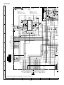
BLOCK DIAGRAM ........................................................................................................................................................... 12
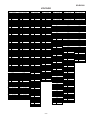
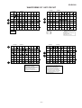
WIRING SIDE OF P.W.BOARD / SCHEMATIC DIAGRAM ............................................................................................. 18
VOLTAGE ........................................................................................................................................................................ 35
WAVEFORMS OF CD CIRCUIT ...................................................................................................................................... 36
WAVEFORMS OF 1-BIT CIRCUIT .................................................................................................................................. 37
TROUBLESHOOTING ..................................................................................................................................................... 38
FUNCTION TABLE OF IC ................................................................................................................................................ 42
REPLACEMENT PARTS LIST/EXPLODED VIEW
PACKING OF THE SET (FOR U.S.A. ONLY)
SHARP CORPORATION
This document has been published to be used
for after sales service only.
The contents are subject to change without notice.
SD-EX200
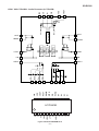
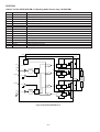
IMPORTANT SERVICE NOTES (FOR U.S.A. ONLY)
BEFORE RETURNING THE AUDIO PRODUCT
(Fire & Shock Hazard)
Before returning the audio product to the user, perform the
following safety checks.
1. Inspect all lead dress to make certain that leads are not
pinched or that hardware is not lodged between the chassis
and other metal parts in the audio product.
2. Inspect all protective devices such as insulating materials,
cabinet, terminal board, adjustment and compartment covers
or shields, mechanical insulators etc.
3. To be sure that no shock hazard exists, check for leakage
current in the following manner.
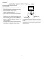
* Plug the AC line cord directly into a 120 volt AC outlet.
* Using two clip leads, connect a 1.5 kohm, 10 watt resistor
paralleled by a 0.15 µF capacitor in series with all exposed
metal cabinet parts and a known earth ground, such as
conduit or electrical ground connected to earth ground.
* Use a VTVM or VOM with 1000 ohm per volt, or higher,
sensitivity to measure the AC voltage drop across the
resistor (See diagram).
* Connect the resistor connection to all exposed metal parts
having a return path to the chassis (antenna, metal cabinet,
screw heads, knobs and control shafts, escutcheon, etc.)
and measure the AC voltage drop across the resistor.
VTVM
AC SCALE
1.5 kohms
10 W
0.15 µF
TEST PROBE
TO EXPOSED
METAL PARTS
CONNECT TO
KNOWN EARTH
GROUND
All check must be repeated with the AC line cord plug connection
reversed.
Any reading of 0.3 volt RMS (this corresponds to 0.2 milliamp.
AC.) or more is excessive and indicates a potential shock
hazard which must be corrected before returning the audio
product to the owner.
–2–
SD-EX200
FOR A COMPLETE DESCRIPTION OF THE OPERATION OF THIS UNIT, PLEASE REFER
TO THE OPERATION MANUAL.
SPECIFICATIONS
SD-EX200 (For Canada)
SD-EX200 (For U.S.A.)
General
General
Power source
AC 120 V, 60 Hz
Power source
AC 120 V, 60 Hz
Power consumption
Power on: 76 W
Power consumption
Power on: 76 W
Power stand-by: 0.5 W
Dimensions
Dimensions
Width: 15"(380 mm)
Height: 7-7/8"(200 mm)
Depth: 4-3/4"(120 mm)
Width: 380 mm (15")
Height: 200 mm (7-7/8")
Depth: 120 mm (4-3/4")
Weight
3.4 kg (7.5 lbs.)
Weight
7.5 lbs. (3.4 kg)
Output terminals
Speakers: 4 ohms
Output terminals
Speakers: 4 ohms
Headphones: 16 - 50 ohms (recommended: 32 ohms)
Digital output (optical)
Headphones: 16 - 50 ohms (recommended: 32 ohms)
Input terminals
Digital output (optical)
Input terminals
Auxiliary input: 500 mV/47 k ohms
Auxiliary input: 500 mV/47 k ohms
Amplifier
Amplifier
Amplification system
64fs 1-bit switching (Remarks: fs = 44.1 kHz)
Amplification system
64fs 1-bit switching (Remarks: fs = 44.1 kHz)
Output power
RMS: 200 W (100 W + 100 W) (1 % T.H.D.)
Power output
100 watts minimum RMS per channel into 4 ohms from
40 Hz to 20 kHz, 2 % total harmonic distortion
A/D noise shaping
7th-order
A/D noise shaping
7th-order
(delta - sigma) modulation
CD player
CD player
Type
1-disc vertical type compact disc player
Signal readout
Non-contact, 3-beam semiconductor laser pickup
D/A converter
24-bit/96 k D/A converter
Frequency response
20 - 20,000 Hz
Dynamic range
101 dB (1 kHz)
(delta - sigma) modulation
Type
1-disc vertical type compact disc player
Signal readout
Non-contact, 3-beam semiconductor laser pickup
D/A converter
24-bit/96 k D/A converter
Frequency response
20 - 20,000 Hz
Dynamic range
101 dB (1 kHz)
Tuner
Tuner
Frequency range
FM: 87.5 - 108 MHz
AM: 530 - 1.720 kHz
Frequency range
FM: 87.5 - 108 MHz
AM: 530 - 1.720 kHz
CP-EX200 (For Canada)
Type
CP-EX200 (For U.S.A.)
2-way type speaker system
5 cm (2") Tweeter
Type
2-way type speaker system
15 cm (5-7/8") Woofer
2" (5 cm) Tweeter
5-7/8" (15 cm) Woofer
Maximum input power
200 W
Rated input power
100 W
Impedance
4 ohms
Dimensions
Width: 7-1/2" (190 mm)
Height: 11-7/16" (290 mm)
Depth: 9-5/16" (235 mm)
Weight
Maximum input power
200 W
Rated input power
100 W
Impedance
4 ohms
Dimensions
Width: 190 mm (7-1/2")
Height: 290 mm (11-7/16")
Depth: 235 mm (9-5/16")
Weight
3.8 kg (8.4 lbs.)/each
8.4 lbs. (3.8 kg)/each
Specifications for this model are subject to change without
prior notice.
–3–
SD-EX200
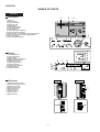
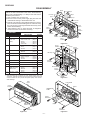
NAMES OF PARTS
SD-EX200
Front panel
1
2
3
1. CD Cover
2. Remote Sensor
3. Timer Set Indicator
4. Headphone Jack
5. CD Stop Button
6. CD Play/Pause Button
7. Tuner (Band) Button
8. Auxiliary Button
9. Volume Up and Down Buttons
10. CD Cover Open/Close Button
11. CD Track Down or Fast Reverse/Tuning Down Button
12. CD Track Up or Fast Forward/Tuning Up Button
13. Bass/Treble Button
14. Power On/Stand-by Button
4
5
6
7
8
10
11
12
13
9
14
1
2
3
4
5
Display
1. Surround Indicator
2. Timer Play Indicator
3. Sleep Indicator
4. FM Stereo Receiving Indicator
5. FM Stereo Mode Indicator
6. CD Memory Indicator
7. Random Play Indicator
8. Function Indicators
9. CD Repeat Play Indicator
10. CD Play Indicator
11. CD Pause Indicator
6
7
8
9
10
11
Side panel
Left side
1. FM 75 Ohms Antenna Jack
2. AM Antenna Ground Terminal
3. AM Antenna Terminal
4. Auxiliary Input Jacks
5. Digital Output Jack
6. AC Power Cord
7. Speaker Terminals
8. Left Side Cover
9. Right Side Cover
Right side
1
2
3
4
5
6
7
8
–4–
9
SD-EX200
SD-EX200
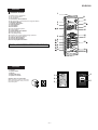
Remote control
1
1. Remote Control Transmitter
2. CD Play/Pause Button
3. CD Stop Button
4. Cursor/Tuner Preset Buttons
5. CD Track Down or Fast Reverse/Tuning Down Button
6. CD Memory Button
7. Program Clear Button
8. Surround Button
9. Timer Button
10. Enter Button
11. Power On/Stand-by Button
12. Auxiliary Button
13. CD Play Mode Select Button
14. Bass/Treble Button
15. Tuner (Band) Button
16. CD Track Up or Fast Forward/Tuning Up Button
17. Volume Up and Down Buttons
18. CD/Tuner Direct Buttons
19. CD Time Display Button
20.Clock Display/Dimmer Button
11
12
2
3
4
5
6
7
8
9
10
Buttons with " " mark in the illustration or highlighted in bold on the list can be operated on the remote control only.
13
14
15
16
17
18
19
20
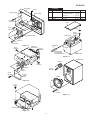
CP-EX200
1. Tweeter
2. Speaker Grille
3. Woofer
4. Bass Reflex Duct
5. Speaker Terminals
1
Speaker grilles are removable:
4
2
Make sure nothing comes into contact with
the speaker diaphragms when you remove
the speaker grilles.
5
3
–5–
SD-EX200
DISASSEMBLY
Caution on Disassembly
Follow the below-mentioned notes when disassembling
the unit and reassembling it, to keep it safe and ensure
excellent performance:
1. Take compact disc out of the unit.
2. Be sure to remove the power supply plug from the wall
outlet before starting to disassemble the unit.
3. Take off nylon bands or wire holders where they need to
be removed when disassembling the unit. After servicing
the unit, be sure to rearrange the leads where they were
before disassembling.
4. Take sufficient care on static electricity of integrated
circuits and other circuits when servicing.
(B4)x4
1-Bit Amp. Unit
REMOVAL
(B4)x1
Tuner Unit
(B2)x1
(B3)x1
ø3x8mm
Front
Panel
(B3)x4
ø3x10mm
(B1)x4
ø3x10mm
(B3)x1
ø3x8mm
PROCEDURE
FIGURE
1
Rear Cabinet
1. Screw ...................... (A1) x7
6-1
2
Main PWB/
Tuner Unit
(Note)
1. Screw ......................
2. Jack Cover, Left ......
3. Screw ......................
4. Socket .....................
5. Flat Cable ...............
(B1) x4
(B2) x1
(B3) x8
(B4) x9
(B5) x1
6-2
3
Front Panel
1. Screw ...................... (C1) x3
2. Hook ........................ (C2) x1
3. Socket ..................... (C3) x1
6-3
4
Power PWB
1. Screw ...................... (D1) x6
2. Bracket .................... (D2) x1
6-3
5
1-Bit Amp. Unit
1. Screw ...................... (E1) x4
6-3
6
Display PWB
1. Screw ....................... (F1) x6
6-4
2. Frame Support ......... (F2) x1
3. Screw ....................... (F3) x6
7-1
4. Socket ...................... (F4) x2 6-4, 7-1
7
Headphones PWB 1. Screw ...................... (G1) x1
8
Switch PWB
1. Screw ...................... (H1) x1
7-1
9
CD Mechanism
1. Screw ....................... (J1) x6
7-1
10
Protect Circuit
PWB/1-Bit Amp.
Shield Case
1. Screw ......................
2. Screw ......................
3. Bracket ....................
4. Screw ......................
(K1) x2
(K2) x2
(K3) x1
(K4) x3
7-2
1-Bit Amp. PWB
1. Screw ....................... (L1) x3
7-3
11
(B5)x1
(B4)x1
SD-EX200
STEP
(B4)x3
(B3)x1
ø3x8mm
Main PWB
(B3)x1
ø3x8mm
Figure 6-2
(D2)x1
(C3)x1 (D1)x6
ø3x10mm
(E1)x2
ø3x6mm
1-Bit Amp. Unit
Front
Panel
(E1)x2
ø3x10mm
6-4
Power PWB
(C1)x3
ø3x8mm
(C2)x1
Note:
1. After removing the connector for the optical pickup from the
connector, wrap the conductive aluminium foil around the front end
of the connector so as to protect the optical pickup from electrostatic damage.
Figure 6-3
Front
Panel
Front Panel
(A1)x3
ø3x12mm
(F2)x1
Headphones
PWB
(G1)x1
ø3x10mm
Rear
Cabinet
(F4)x1
(F1)x6
ø3x10mm
(A1)x4
ø3x10mm
Figure 6-1
Figure 6-4
–6–
SD-EX200
Front Panel
CP-EX200
(F4)x1
Display PWB
STEP
Switch PWB
PROCEDURE
FIGURE
1. Net Frame Ass'y ..... (A1) x1
2. Catching Holder ...... (A2) x4
3. Screw ...................... (A3) x4
7-4
REMOVAL
1
Front Panel
2
Woofer
1. Screw ...................... (B1) x4
7-5
3
Tweeter
1. Screw ...................... (C1) x2
7-5
(F3)x6
ø3x10mm
(A1)x1
(H1)x1
ø3x10mm
(A2)x4
(A3)x4
ø4x16mm
Front Panel
CD Mechanism
(J1)x2
ø3x10mm
(J1)x4
ø2.6x10mm
Figure 7-1
(K4)x1
ø3x8mm
Screwdriver
1-Bit Amp.
Shield Case
(K4)x1
ø3x6mm
Driver should
be pried away
from Speaker Box.
Speaker Box
Figure 7-4
Speaker Box
Tweeter
(K4)x1
ø3x8mm
(K3)x1
(C1)x2
ø3x10mm
(K2)x2
ø3x6mm
(K1)x2
ø3x8mm
Protect
Circuit
PWB
Woofer
Figure 7-2
(L1)x3
ø3x6mm
(B1)x4
ø4x16mm
Figure 7-5
1-Bit Amp. PWB
Figure 7-3
–7–
SD-EX200
REMOVING AND REINSTALLING THE MAIN PARTS
CD MECHANISM SECTION
(A1)x4
Perform steps 1, 2, 3, 6 and 9 of the disassembly method to
remove the CD mechanism.
CD Mechanism
Cover
How to remove the pickup unit (See Fig. 8-1)
(A2)x2
ø2.6x6mm
1. Remove the mechanism cover, paying attention to the
pawls (A1) x 4 pcs.
2. Remove the screws (A2) x 2 pcs., to remove the shaft
(A3) x 1 pc.
1. Remove the stop washer (A4) x 1 pc., to remove the gear
(A5) x 1 pc.
3. Remove the pickup.
CD Mechanism
Note
After removing the connector for the optical pickup from the
connector wrap the conductive aluminium foil around the front
end of connector so as to protect the optical pickup from
electrostatic damage.
Shaft
(A3)x1
Gear
(A5)x1
Stop Washer
(A4)x1
Pickup Unit
Figure 8-1
How to Remove the CD door motor
(See Fig. 8-2.)
1. Remove the screws (B1) x 2 pcs.
2. Remove the CD door motor.
Caution:
Be careful not to damage the gear.
(If the gear is damaged, noise is heard when searching.)
(B1)x2
ø1.8x4mm
CD Door Gear Unit Ass'y
CD Door Motor
Figure 8-2
–8–
SD-EX200
ADJUSTMENT
CD SECTION
Adjustment
Since this CD system incorporates the following automatic
adjustment functions, readjustment is not needed when
replacing the pickup. Therefore, different PWBs and pickups
can be combined freely.
Each time a disc is changed, these adjustments are preformed
automatically. Therefore, playback of each disc can be
preformed under optimum conditions.
1-BIT AMP. SECTION
1-bit amplifier's output offset voltage adjustment
1-BIT AMP. PWB
Adjust VRA100 and VRA101 so that the DC voltage between
speaker terminals + and - is set to 0 ± 5 mV at AC 120 V.
Output:
Speaker Terminal
Electronic
Voltage
+
Set
AC 120 V
SO421
VR : 0
Input : AUX
Figure 9-1 OUTPUT OFFSET LEVEL
VRA101
L-CH Output
Offset Adjustment
VRA100
R-CH Output
Offset Adjustment
Figure 9-2
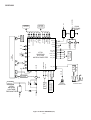
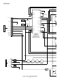
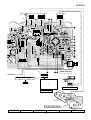
DESCRIPTION OF CIRCUIT FOR 1-BIT UNIT
(SEE THE WIRING DIAGRAMS ON PAGES 26 AND 27.)
Input section
Signals from CNA101 are coupled by CA100 and CA101 and
then sent into the A/D converter IC (ICA100).
Dynamic feedback circuit
The 1-bit signals switched by the output IC (ICA101 and
ICA102) oscillate between positive and negative voltage.
After resistance-division, the signals are fed back to the A/D
converter IC (ICA100) through NF resistance 75 kohms (RA155
~ RA158). The peak-to-peak voltage reaches approx. 5 V.
modulation 1-bit converter
Signals from the A/D converter IC (ICA100) are converted to
1-bit signals and sent differentially. Refer to the technical
manual of SM-SX100 for the details of conversion to 1-bit
signals.
Low pass filter circuit
1-bit signals switched by the output IC (ICA101 and ICA102)
are converted to analog signals through the lowpass filter
consisting of LA101 ~ LA107. The low pass filter functions
when a frequency exceeds 20 kHz, and reduces it by approx.
3 dB when it reaches approx. 40 kHz.
–9–
SD-EX200
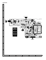
TO CHECK AND CANCEL PROTECT CIRCUIT DETECTION LINE
1 Abnormal drop in the output voltage of each regulator
1: In this model the microcomputer (IC701) detects the following
malfunctions once power is supplied, and cuts off power
from all the parts except for the circuit driving the
microcomputer.
Abnormal drop in the output voltage of each regulator
(below approx. 1.5 V)
Power is cut off instantly without display.
Output offset over voltage of the 1-bit amplifier
(above approx. DC 2 V)
Mains overvoltage of the 1-bit amplifier
(above approx. DC 5.5 A)
Power is cut off instantly without display.
Defects in the cooling fan or its drive circuit
(when stopped)
Power is cut off after “FAN LOCK” is displayed.
Connect a measuring device (such as an oscilloscope) to
the stabilizing output of the regulator, and turn on the unit.
If the detected voltage is extremely lower than the voltage
on the circuit diagram (below approx. 1.5 V), the regulator
itself or the circuit is defective.
1
2
3
2 Output offset overvoltage of the 1-bit amplifier
Adjust the voltage of the output offset. If a protective
operation is still activated, ICA401 on the 1-bit amplifier
could be defective (the detection circuit of the speaker
output DC voltage).
4
2: Criteria for abnormality, and checking and cancelling the
detection line
The criteria:
The voltage of pin 6 (PROTECT) on IC701.
The voltage of pin 32 (OFFSET) on IC701: Low (below
approx. 1 V) (abnormal) and High (above approx. 2.5
V) (normal) .
The motor stops when it is above approx. 1 V.
If the voltage of pin 10 (FAN LOCK) on IC701 is not
between approx. 0.21 V and 1.20 V whilst the motor
rotation is controlled, it is judged as abnormal.
1
2
3
Checking and cancelling the detection line:
Caution: If the PROTECT/OFFSET detection line is
disconnected in case of ,
or
above, a
protective operation does not function. The
disconnection by output short-circuit of each
regulator may cause the parts or PCBs to burn
out and therefore do not disconnect the detection
line when the cause is not identified.
(Power supply can be detected with an
oscilloscope or like during approx. 0.5 seconds
after an abnormality is found. Note that the
detection would be difficult with a tester as the
voltage rises and falls rapidly.)
12 3
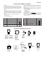
TEST MODE
During POWER OFF Mode, push below each 2 buttons and [POWER] button.
Then enter to each TEST MODE.
Version Display
Other Destination : [ME**** ]
Version Display : ME0701A_ (07: MONTH; 01: DAY; A/B/C (MICOM VERSION)
Notes:
Micom version will be display when entering to Button and Display Test Mode only. (Display for 2 seconds)
No.
Key
Test Mode
1
[SKIP UP] + [VOLUME DOWN]
2
[CD STOP] + [SKIP UP]
ALL CLEAR (RESET)
BUTTON & DISPLAY TEST
3
[CD PLAY/PAUSE] + [AUX]
CD TEST
4
[CD PLAY/PAUSE] + [SKIP UP]
CD TRAY AGING TEST
5
[TUNER (BAND)] + [VOLUME DOWN]
TUNER PRESET MEMORY CLEAR
6
[TUNER (BAND)] + [VOLUME UP]
TUNER PRESET MEMORY FOR PRODUCTION
7
[TUNER (BAND)] + [CD STOP]
RDS TUN SM
8
[AUX] + [VOLUME UP]
AUX TEST
– 10 –
SD-EX200
NOTES ON SCHEMATIC DIAGRAM
• Resistor:
To differentiate the units of resistors, such symbol as K and
M are used: the symbol K means 1000 ohm and the symbol
M means 1000 kohm and the resistor without any symbol is
ohm-type resistor. Besides, the one with “Fusible” is a fuse
type.
• Capacitor:
To indicate the unit of capacitor, a symbol P is used: this
symbol P means pico-farad and the unit of the capacitor
without such a symbol is microfarad. As to electrolytic
capacitor, the expression “capacitance/withstand voltage”
is used.
(CH), (TH), (RH), (UJ): Temperature compensation
(ML): Mylar type
(P.P.): Polypropylene type
• Schematic diagram and Wiring Side of P.W.Board for this
model are subject to change for improvement without prior
notice.
• The indicated voltage in each section is the one measured
by Digital Multimeter between such a section and the chassis with no signal given.
1. In the tuner section,
indicates AM
indicates FM stereo
2. In the CD section, the CD is stopped.
• Parts marked with “ 1 ” (
) are important for
maintaining the safety of the set. Be sure to replace these
parts with specified ones for maintaining the safety and
performance of the set.
POSITION
REF. NO
ON—OFF
SW609
ON/STAND-BY
ON—OFF
VOLUME DOWN
ON—OFF
SW610
OPEN/CLOSE
ON—OFF
VOLUME UP
ON—OFF
SW611
BASS/TREBLE
ON—OFF
SW604
SKIP/TUNING UP
ON—OFF
SW612
SKIP/TUNING DOWN
ON—OFF
SW606
AUX
ON—OFF
SW615
PLAY/PAUSE
ON—OFF
SW607
TUNER (BAND)
ON—OFF
SW771
CD DOOR OPEN/CLOSE
ON—OFF
SW608
STOP
ON—OFF
REF. NO
DESCRIPTION
SW4
PICKUP IN
SW601
SW602
DESCRIPTION
POSITION
TYPES OF TRANSISTOR AND LED
FRONT
VIEW
TOP VIEW
B
(3)
TOP
VIEW
TOP VIEW
C
(2)
E
(1)
E C B
(S)(G)(D)
(1)(2)(3)
2SK246 GR
KTA1023 Y
KTA1266 GR
KTA1270 Y
KTA1271 Y
KTC2874 B
KTC3199 GR
KTC3203 Y
KRA107 M
KRC102 M
KRC104 M
KRC107 M
2SB709 AR
2SD601 AR
KRA102 S
KRC102 S
KRC104 S
KRC107 S
KTA1504 GR
KTC3875 GR
AG01Z
AK09
DS1SS133
EK19
D1NL20U
SFPW56
GD1N4004
FRONT
VIEW
FRONT
VIEW
TOP VIEW
FRONT
VIEW
FRONT
VIEW
1. Anode
2. No Contact
3. Cathode
1 2 3
AC
KDS226
MA132WA
MA132WK
MA111
Cathode
Anode
AC
D5SB60
304BC2E9
304HT2P
304VT2E2
A503BC2E
– 11 –
SARS03
FMLG22S
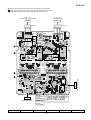
SD-EX200
TUN_CE
TUN_DI
TUN_CLK
TUN_DO
PROTECT
A/D_RESET
OFFSET PROTECT
DIG_FUNC
LID_SENS
CD_CE
CD_DRF
LEVEL_CONT
1
2 3 4 5
18 19 20
29 21 22 23 24 25 26 27 28
34
CD_CLK
CD_DI
CD_DO
CD_WRQ
CD RES
+7.9V
TO DISPLAY SECTION
CNP501
TO 1-BIT AMP./
PROTECT CIRCUIT
SECTION
A_GND
A_GND
FM_DET
TUN_SM
TUN_R
VCC_9V
TUN_L
TUN_DO
TUN_CLK
TUN_DI
TUN_CE
TO TUNER UNIT
1 7
2
3 4 5 6
8 9 10 11
+9V
TUNER
IC101
CS4340KS
DAC IC
LOUT 15 L
ROUT 12 R
1
2 DATA
A3.3V 14
16MOUT
3 BCK
4 LRCK
13
11
VCONT
CONT3
CONT2
VDD
64 DO
65 WRQ
48 XOUT
49 XIN
Q82
MUTING
FD0 21
TD0 20
7 8 9 10 79 80 11
CONSTANT
VOLTAGE
2
LASER DRIVER
+3.3V
Q1
Q3
9
8
M802
SPINDLE M
MOTOR
10
OUT1
11
22
12
1
3
TRACKING COIL
+7.9V
FOCUS COIL
IC2
LA6574H
FWD 27
REV 28
FOCUS/
TRACKING/
SPIN/SLED
VCC DRIVER VO5–
REG
19 IN
PICK UP UNIT
FD0
21 24 1 7 16 14
VREF
OUT2
VCONT 25
M801
SLED M
MOTOR
2 –
VO5+ 3 +
VO4–
VO4+
DIGITAL OUT
IC4
GP351TZ
Q2
1
4
+7.9V
SLDO 23
+3.3V
+5V
3
VREF
5 41 18 47 46
2
TIN2
PD
LDD
39
1
CONT5 26
SPDO 22
RFVDD
LVDD
ADAVDD
XVDD
RVDD
XL1
16.9344 MHz
68 VDD5
IC1
LC78646E
CD SERVO
IC3
LM358D
OP-AMP.
TDO
67 DRF
8
VCC
VO3–
VO3+
66 RES
Q84
FIN1
FIN2
TIN1
DIGITAL OUT
CONTROL
62 CLK
63 DI
75
69
57
56
55
51
50
44
43
40
37
28
19
6
+
BCK
LRCK
16MOUT
70 71 72
–
61 CE
77 38
+
–
DATA
60 59 58 54
VVDD
5
7 6
5 4
SW4
PICKUP IN
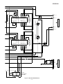
Figure 12 BLOCK DIAGRAM (1/6)
– 12 –
26
M1
CD DOOR
MOTOR
M
L_C
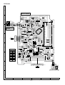
SD-EX200
OFFSET
SWITCHING
A/D RESET
SWITCHING QS05
OFFSET
SWITCHING
QS04
QS03
CURRENT
DETECT QS10
QS07
2
3
AD_RESET
D+5V
TUN_DO
TUN_CLK
TUN_DI
TUN_CE
1
QS01
OFFSET_PROTECT
Q551
Q552
CNPS01
4
5
6
CNPS02
1
2
3
4
1
2
3
4
BIS01
1
2
3
4
CNS531
R_CH
AUX
TUN_L
TUN_R
L 9
R 16
L 10
R 15
+9V
TO MAIN SECTION
23 5 20
VDD BASS
–6.8V
IC501
4 L_CH
LC75341M
21 R_CH
AUDIO PROCESSOR
L 12
R 13
IC502
NJM4565M
BUFFER AMP.
TO MAIN SECTION
+5.6V
3
5
4
–VCC 8
+VCC
2
CD
TO 1-BIT AMP. SECTION
1 R_CH
7
L_CH
6
TO 1-BIT AMP.
SECTION
GND DI CECLK
3
1 2 24
SURROUND Q538
Q539 MUTING
Q540
SURROUND
Q536
ON/OFF
Q545
Q543 MUTING
Q544
HEADPHONE
Q547
Q548
MUTING
SYSTEM
MUTE
Q535
Q546
CNP501
SP_RELAY
FAN_LOCK
11 13 14 15 17
FAN_MOTOR
7
H/P_L_OUT
SURROUND
6
H/P_R_OUT
SURROUND
ON/OFF
S_MUTE
TO DISPLAY SECTION
Q421
IC401
KIA7809AP
VOLTAGE
REGULATOR
IC400
KIA7812AP
VOLTAGE
REGULATOR
FAN
SWITCHING
FAN
SWITCHING
+12V
+9V
3
1
2
+3.3V
1
ZD401
A_–20V
M
–
2
ZD400
–6.8V
+
Q423
3
RELAY
SWITCHING
L_CH
JT501
AUX INPUT
TUNER
OFFSET_COMPA
SWITCHING
8 9 10 11
QS13 CURRENT
DETECT
SWITCHING
QS02
BASS
CONTROL
CURRENT
DETECT
SWITCHING
CURRENT QS14
DETECT
QS06
A/D RESET
SWITCHING
NIT
QS11
QS12
SP_RELAY
A/D RESET
SWITCHING
QS08
FAN
Q422 SWITCHING
Q424
+
IC402
KIA7808AP
VOLTAGE
REGULATOR
—
—
+
+7.9V
1
3
M401
FAN MOTOR
A_+20V
RL421
2
+5.1V
ZD402
TO PROTECT CIRCUIT SECTION
Figure 13 BLOCK DIAGRAM (2/6)
– 13 –
SO421
SPEAKER
TERMINAL
+5V
TO MAIN
SECTION
28
RX_IN 30
AVSS 97
VSS 21
Q608
18
TUN_DO 43
TUN_DI 42
TUN_CLK 41
IC701
IX0557AW
SYSTEM
MICROCOMPUTER
TUN_CE 40
TUN_SM 3
1
2
KEY3
KEY1
KEY2
KEY
SW601,602,608,615
SW604,606,607
SW609-SW612
TO MAIN
SECTION
D781
+7.9V
+5V
2
LED604
1
LED602
VF2
TO POWER
SECTION
Figure 14 BLOCK DIAGRAM (3/6)
– 14 –
HP_SW
100
34
TO POWER
SECTION
SWITCHING Q607
TO MAIN
SECTION
95 15
-
81 - 88
HP_SW 9
8
O/C_SW
SURROUND
89
S_MUTE
ILU_LED
96
-VP
56
41
IC780
AN78L05
VOLTAGE
REGULATOR
Q606
P_IN 31
80
5
2
1
1
MAIN/TUNER
SECTION
22 X_IN
3
3
1
VCC
23 X_OUT
2
RESET
CD_DI
CD_CLK
CD_RES
LID SENS
CD_CE/FLASH
24
CD_WRQ
CD_DRF
CD_DO
+5V
XL601
4.19 MHz
98 VREF
32 28 20 19 6
OFFSET
A/D_RESET
POWER
SP_RELAY
PROTECT
TO POWER
SECTION
VF1
39 38 37 36 35 34 33 7
+5V
-
FL601
FL DISPLAY
45
44
RM601
GP1UM271
2
IC608
PST9140
RESET
RESET
TO CD
SECTION
+5V(VREF)
SD-EX200
SW771
CD DOOR
OPEN/CLOSE
JHP601
HEADPHONES
SD-EX200
T903
SUB POWER TRANSFORMER
CNP931
D950
D953
D952
D5.6V (UNSW)
4
POWER
5
Q933
2 3
SWITCHING
PC902
6
1 4
-VF1
8
IC931
SE-B2
ERROR
AMP.
-VF2
7
VOLTAGE
REGULATOR
ZD931
2
2 3
1
PC901
1 4
-VP
9
3
Q931
+B_CHK
10
11
4 Vin
D942
D908
Q902
ZD933
5 FB/SYNC
SWITCHING
D944
1 OCP
SYNC
BI932
9
TO MAIN SECTION
8
2 GND
D939
A_–20V
Drain
10
A_+20V
A_+20V
3
D938
7
6
5
4
1
3
2
IC934
KIA78L05
VOLTAGE
REGULATOR
D902
IC933
KIA7809AP
VOLTAGE
REGULATOR
3
TO 1-BIT AMP. SECTION
B1900
1
D901
A_+5V
3
1
3
1
D937
2
2
3
2
D_+5V
L902
AC LINE
FILTER
4
D930
CNP934
DRIVER_+9V
1
TO 11BIT AMP. SECTION
IC901
STRF6238
SWITCHING REGULATOR
TO DISPLAY SECTION
D951
SUB TRAN +B
2
T901
MAIN POWER TRANSFORMER
L901
AC LINE
FILTER
F901
6A/125V
3
CNP901
2
1
CNS901
2
1
2
4
5
+40V
AC POWER
SUPPLY CORD
AC 120 V, 60 Hz
+40V
Figure 15 BLOCK DIAGRAM (4/6)
– 15 –
SD-EX200
GNDX 11
14 NFR1(+)
XO 10
15 NFR2(–)
CXA100
11.2896 MHz
XI 9
R-CH OUTPUT
OFFSET
ADJUSTMENT
VDDR 7
VRA100
OUTR(+) 6
AGND 1 6
VCC
17 R-CH IN
ANALOG IN R-CH
11
VDDX 8
AMP_VCC
R-CH_IN 1 7
RCH_1
VKK
16 GNDA
12
OUTR(–) 5
TO MAIN SECTION
L-CH OUTPUT
OFFSET
ADJUSTMENT
L-CH_IN 1 5
VRA101
GNDD 4
LCH_1
20 L-CH IN
ANALOG IN L-CH
OUTL(–) 3
RESET 4
21 RESET
22 NFL2(–)
PROTECT 3
OUTL(+) 2
23 NFL1(+)
A+5V
VDDL 1
24 VDA
OFFSET
PROTECT 2
D+5V
ICA100
IX0498AW
7TH ORDER ∆∑
MODULATION
CONVERSION LSI
OFFSET 1
COMPA
CNA101
VKK
VCC
11
12
TO POWER SECTION
CNA100
LFA402
A+5V 1
A+5V
QA415
QA414
QA416
QA400
PROTECT
DETECT
CURRENT
SENSOR
AGND_AD 2
PROTECT
DETECT
LFA403
D+5V 3
PROTECT
DETECT
D+5V
DGND_AD 4
2
3
1
DA404
4 V
8 V
Figure 16 BLOCK DIAGRAM (5/6)
– 16 –
8 VDD
—
+
6
5
4
3
2
1
VDD DTADJB
DTADJA
VBOOTB VBOOTA
VBBA
VBBA
OUTA
OUTA
SA
16
17 18 19 20 21
4 VSS
1
7
2
6
PSA400
– 17 –
DA107
OFFSET VOLTAGE
DETECTOR
SWITCHING AUDIO
POWER AMP.
1
VBBA
OUTA
OUTA
SA
OUTB
3
2
1
2
3
ICA401
TJM4558CD
OPE AMP.
5
Figure 17 BLOCK DIAGRAM (6/6)
TO PROTECT SECTION
DA116
OFFSET VOLTAGE
DETECTOR
SWITCHING AUDIO
POWER AMP.
ICA102
SLA5515M
SB
2
OUTB
17 18 19 20 21
3
ICA101
SLA5515M
SB
OUTB
OUTB
DTADJA
16
4
VBBA
5
VBBB
6
VBBB
7
VBOOTB VBOOTA
12 13 14 15
VBBB
INA
GND
8
VDD DTADJB
VKK
INB
9
VBBB
GND
VCC
VKK
LFA100
6 +B
5 +B
4 GND
LFA400
3 GND
1 DRIVER_+9V
BIA104
FROM POWER SECTION
7
VKK
8
INB
9
INA
12 13 14 15
11 10
VCC
VKK
11 10
+
—
AMP_VCC
SD-EX200
BIA103
1 R-CH_+1
3 R-CH_–1
4 L-CH_–1
5 L-CH_+1
3
1
LFA101
+B_AMP
SD-EX200
A
LASER DRIVER
LD
FO+
FO–
FO–
TR–
PD
GND
1
1
1
1
2
2
2
2
3
3
3
3
4
4
4
4
5
5
5
5
6
6
6
6
VR
D
7
LD
8
7
8
7
8
TR+
TR–
C86
0.047
FO+
FO–
FO+
PD
C18
0.01
LD
8
TP2
C11
10/50
LD
C12
3.3/16
C9
0.001
11 VREF
14 TEC
15 TE
LD_M–
C40
0.047
R33
1K
R34
1K
VSS
CONT3
CONT2
4
16 RFMON
17 JITTC
18 ADAVDD
+B
1 6
C17
0.022
SPDO
19 ADAVSS
TDO
FDO
R11
20 TDO
33K
MUTING
21 22 23 24 25 26 27 28 29 30 31 32 33 34 3
3
2
R82
39K
R14
10K
FDO
D82
DS1SS133
R12
2.7K
1 Q82
KRC104 M
SLDO
2
E
VCONT
C14
12 REF1
0.001
13 FE
C15
0.22/50
C16
100P(CH)
IC1
LC78646E
CD SERVO
10 TIN2 F
D_GND
VR
7
9 TIN1 E
TIN2_F
PD
R36
680
5
7 FIN1 A
8 FIN2 B
TIN1_E
D_GND
7
6 RFVSS
FIN2_B
FO–
6
5 RFVDD
TP1
FIN1_A
C87
0.047
8
3 EFMIN
4 RF
C6
0.0027
330
C7
22P
(CH)
+B
TR+
75 74 73 72 71 70 69
2 SLCIST
R10
R35
4.7K
C41
0.22/50
R9
10K
76
R15
1K
R13
12K
C82
33/25
O
TR+
TR+
FO+
C2
0.01
TR–
80 79 78 77
1
C4
C5
0.001 22P
(CH)
TP3
MONI2
DE_EMPH
TR–
C1
47/25
C3
0.047
FSEQ
MONI1
C
C
1
1
V/*P
1
CNS2B
1
TIN2_F
R2
8.2K
DEFECT
C
F
R37
680
2
C39
0.022
VVSS
2
PDO2
PDO1
2
22K
SBCK/FG
2
FIN2_B
R3
PCKIST
F
B
CONT5
3
PD
CONT4
3
FIN1_A
8.2K
PUIN
3
8.2K
R4
VVDD
3
R5
GPDAC
B
TIN1_E
A
SLDO
4
R16
3.9K
5
4
C42
0.1
R39
1.2K
5
4
FR
5
4
LDS
5
R38
12K
VREF
R1
8.2K
A
22K
CNP2
E
+B
VCC
VREF
E R6
SLCO
LDD
6
R8
27K
7
6
+B
+B
C10
0.001
7
6
+
D_+5V
C13
100/16
CNS1A
7
6
CNS2A
VCC
VREF
B
CNP1
CNS1B
7
PICKUP UNIT
LD_M+
C43
47/10
C44
0.001
R7
47
VCONT
R40
10
Q1
KTA1266 GR
SPDO
+B
R64
+
M
–
+
M
SLIDE
SPIN
6
SP+
4
5
6
7
8
SGND
C57
100/10
R63
100
+B
R61
3.9K
H
• NOTES ON SCHEMATIC DIAGRAM can be found on page 11.
1
2
3
4
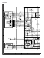
Figure 18 SCHEMATIC DIAGRAM (1/10)
– 18 –
VREF IN
3
FWD
VO3–
6
2
5
6
FO–
6
R62
6.8K
SP–
VO3+
6
SL+
1
FO+
5
VIN4G
VCC_S
4
5
7
VO4–
4
5
6
C54
0.1
+B
TR–
4
5
SL–
VIN4
4
5
PUIN
VCONT
3
VO4+
3
VO5+
3
1
TR+
3
D_GND
2
VO5–
2
2
0.022
1
2
3
26 25 24 23 22
R56
2.2K
VCC
1
2
4
C50
0.1
C51
0.1
GND
1
2
IC3
LM358D
OP-AMP.
1
CNP4
CNS4A
PU-IN
–
SW4
PICKUP IN
M801
SLED
MOTOR
M802
SPINDLE
MOTOR
CNS4B
G
CNP4A
R60
100K
REV
R57
12K
R55
100K
R59
12K
C52
0.1
CD MOTOR PWB-D
28 27
R84
4.7
C53
47/25
TDO
1
VCONT
R58
LD_M+
LD_M–
+B
VCC2
2
DZ6.2BSB
1
2
47/25
–
1
ZD1
+
M
3.9K
+B
C55
C56
M1
CD DOOR
MOTOR
CNP5
LID_SENS
CNS5
F
R72
4.7K
SD-EX200
R102
47K
ASLRCK 55
16MOUT 54
+B
L2
2.2 µH
C30
18P
(CH)
FSX/16MIN 50
XL1
R24 16.9344 MHz
220
+B
+B
P_GND
+A3.3V
C69
0.001
RVDD 46
R83
47
LVDD 41
39
+B
6
CD_LCH
7
CD_D_GND
8 LID_SENS
CD_CE
9 CD_CE
CD_CLK
10 CD_CLK
+B
CD_DI
11 CD_DI
C83
220/6.3
CD_DO
VINIG
VIN1
+B
CD_RES
D2
DS1SS133
VIN3
VCC1
13 CD_WRQ
D1
DS1SS133
VIN3G
SP+
SP–
VO1–
VO2–
CD_WRQ
C70
100/10
14 CD_RES
CD_DRF
15 CD_DRF
DIG_FUNC
16 DIG_FUNC
Q2
KTC3199 GR
REG IN
VO2+
SL–
9 10 11 12 13 14
FR
8
SL+
7
IC2
LA6574H
FOCUS/TRACKING/
SPIN/SLED DRIVER
REG OUT
VO3–
6
FO–
VO3+
5
FO+
VO4–
4
VIN2G
VIN2
VIN4G
VCC_S
VO4+
3
TR–
VO5+
2
TR+
VO5–
1
VO1+
18 17 16 15
VREF_IN
19
VIN4
21 20
VCONT
A_GND
12 CD_DO
26 25 24 23 22
SGND
5
LID_SENS
CONSTANT
VOLTAGE
Q3
KTA1270 Y
SPDO
SLDO
FDO
C59
100/25
TDO
VCONT
LD_M+
CD_RCH
Q84
KRA107 M
+B
2
+B
+B
VCC2
REV
FWD
4
R51
22
R53
47
R52
1.2K
C58
100/10
0
ZD2
DZ5.6BSB
C60
10/16
+B
+B
• The numbers 1 to 12 are waveform numbers shown in page 36.
7
8
9
10
Figure 19 SCHEMATIC DIAGRAM (2/10)
– 19 –
11
12
P20 1 - D, E
TO MAIN SECTION
+B
R64
LD_M–
1
3
R72
4.7K
+B
+A3.3V
DIGITAL OUT
CONTROL
C22
10P
(CH)
DIG_FUNC
28 27
P_GND
3
+B
40
R17
100
C19
100/10
C21
3.3/16
3.9K
+7.9V
2
TEST
VDD
LCHO 42
DOUT
VSS
V/*P
38
C20
0.022
PUIN
A_GND
1
LVSS 43
26 27 28 29 30 31 32 33 34 35 36 37
R73
3.3K
+B
C29
3.3/16
C81
0.01
RVSS 44
9
MONI4
MONI5
MONI2
DE_EMPH
FSEQ
MONI1
DEFECT
CONT5
SBCK/FG
RCHO 45
R15
1K
+A7.9V
+B
L1
0.82 µH
XVDD 47
3 GND
C31
18P
(CH)
XIN 49
XOUT 48
2 VCC
C85
100/10
C2F 52
XVSS 51
IC1
LC78646E
CD SERVO
R112
3.3K
1 V_IN
C88
0.001
EFLG 53
P20 1 - D
TO MAIN SECTION
CE
LRCK 58
ASDFIN 57
ASDACK 56
R111
3.3K
IC4
GP351TZ
DIGITAL OUT
10
IC101
CS4340KS
DAC IC
DATA 60
BCK 59
C115
0.0015
(ML)
L_OUT
11
3
7
R109 100
12
R115
2.2K
C103
10/50
7 SDA VCOM 10
8 DE-EMPH FILT 9
+B
C116
0.0015(ML)
C84
0.022
DI
DO
*WRQ
DRF
*RES
VSS
CONT3
CONT2
VVSS
67 66 65 64 63 62 61
VDD5
CL
R34
1K
R108 100
C107
10/25
C106
0.1
4 LRCK A_GND 13
5 16MOUT ROUT 12
6 SCL REF_GND 11
R106 100
R107 100
C109
1/50
R33
1K
R105 100
68
PDO2
PDO1
R104 100
C39 R32
0.022 5.6K
75 74 73 72 71 70 69
8
R103 100
R114
2.2K
+A3.3V
100P(CH)
C108
10/50
1 RST
16
2 DATA LOUT 15
3 BCK A3.2V 14
A_GND
C33
C117
0.001
R_OUT
100P(CH)
L101
0.82 µH
+B
C113
1/50
C35
VCONT
R36
680
R37
680
R35
4.7K
C41
0.22/50
C40
0.047
C42
0.1
+B
C114
0.022
100P(CH)
2
1
C110
0.022
C36
+B
3
C102
0.01
0.022
D101
DS1SS133
100P(CH)
C37
R101
100K
C38
CD SIGNAL
Q101
KRC102 M
C101
3.3/50
C105
3.3/16
CD_CE
CD_CLK
R25 1K
R26 1K
R27 1K
CD_DI
CD_DO
CD_WRQ
R28 1K
CD_RES
R29 1K
R30 1K
R31 1K
LD_M–
LD_M+
VCONT
CD_DRF
MAIN PWB-A1 (1/2)
SD-EX200
MAIN PWB-A1 (2/2)
QS03~QS05:A/D RESET SWITCHING
R525, R526: 1.2K
(SERIAL NO. 30300001~30400519)
[FOR U.S.A.]
(SERIAL NO. 30400001~30400050)
[FOR CANADA]
1.8K
(SERIAL NO. 30600520~) [FOR U.S.A.]
(SERIAL NO. 30600051~) [FOR CANADA]
R511, R512: 1.2K
(SERIAL NO. 30300001~30400519)
[FOR U.S.A.]
(SERIAL NO. 30400001~30400050)
[FOR CANADA]
820
(SERIAL NO. 30600520~) [FOR U.S.A.]
(SERIAL NO. 30600051~) [FOR CANADA]
3
CS06
0.022(ML)
DS02
DS1SS133 DS04
1 QS04
MA111
KRC102 S
2
RS03 DS01
3 4.7K MA111
CS05
0.001
3
CHASSIS
GND
DS03
DS1SS133
CS03
10/50
1
DS05
DS1SS133
A
QS06~QS08: OFFSET S
DS06
QS05
DS1SS133 KRC107 S 2
AUX SIGNAL
CD SIGNAL
FM SIGNAL
2
CS02
4.7/50
QS08
KTC3875 GR
RS05
1M
RS
4.7
RS06
4.7K
QS07
KTC3875 GR
SWITC
QS01
1 KRC1
QS03
KRA102 S
1
15
14
(CD/MD) R1 13
C528
47P(CH)
R523
270
R522
270
5
6
7
+B
+B
R526
+B
3
5
CD_R CH 4
P19 12 - D ~ G
FROM CD SECTION
D
A_+3.3V
3
P_GND
2
A_+7.9V
1
CD D_GND 7
LID_SENS 8
CD_CE
9
CD_CLK
10
CD_DI
11
CD_DO
12
CD_WRQ 13
CD_RES
E
CD_DRF
14
15
DIG_FUNC 16
2
3
2
1
C537
0.22/50
SURROUND
Q538
2SK246 GR S
G
D535
DS1SS133 D
1
R524
4.7K
R535
1.2K
+B
A_GND
CD_RCH
+B
+9V
P_GND
+B
+A7.9V
R541, R542: 1K
(
[
(
[
1
(
(
R556
100K
+A3.3V
R557
220
-6.8V
-B
+B
R53
2.2
R53
2.2
+B
CD_LCH
C538
680P
A_GND
R53
1.2K
Q535, Q536:
SURROUND ON/OFF
Q535
Q536
KRC107 M KRA107 M
DT_CONT
CD_L CH 6
SP_RELAY
4
C535
0.0047
C527
47P(CH)
3
AD_RESET
C512
0.22
R518
1K
6
1
C536
0.0047
16
R519
1K
R521
4.7K
C520
1/50
R516
1K
17
6
5
R555
220
12 L1
C525
10/50
CHASSIS
Q551
KTC3199 GR
C566
0.01
C523
2.2/50
C565
470P
R579
15K
18
C530
1.5
C522
2.2/50 R528
4.7K
R-IN
7 L-IN
C519
RSELO
8 LSELO
1/50
C521
R515
2.2/50
1K 9 L4 (AUX)
R4
10 L3 (TUNER) R3
R517
R2
11 L2
1K
5
4
R512
C514
0.0022
R520
1K
R525
BASS
CONTROL
R577
3.9K
L-CH
C
R-BASS 20
R-TRE 19
R513
3.3K
C564
470P
R578
3.9K
R527
DT_CONT 4.7K
R-CH
AUX IN
5 L-BASS
6 L-TRE
C515
0.0022
R580
15K
C524
2.2/50
JT501
AUX INPUT
R-OUT 21
C516
0.22
C513
0.22
4
3
C526
10/50
C531
1.5
4 L-OUT
C511
0.22
3
2
OFFSET_PROTECT
C504
3.3/16
R511
2
1
+B
C503
22/16
VDD 23
VREF 22
1
CD_D_GND
BI502
C
0
R
4
3
+B
OFFSET_COMPRA
TUN_CLK
CL 24
2 CE
3 VSS
180P(CH)
CNS502
SURROUND
C571
C502
0.022
C572
180P(CH)
D+5V(SWD)
1 DI
CNPS01
R503
1K
BASS
CONTROL
C570
180P(CH)
AUDIO
PROCESSOR
IC501
LC75341M
R501
1K
Q552
KTC3199 GR
R502
1K
QS06
KTC3875 GR
RS04
2
3 1M
QS02
KRA102 S
SWITCHING 1 +B
C501
100/16
R514
3.3K
B
TUN_DI
TUN_CE
2
R558
47
CD_D_GND
LID_SENS
CD_CE
CD_CLK
CD_DI
CD_DO
+B
CD_WRQ
+B
CD_RES
CD_DRF
R400
330
+3.3V
+B
DIG_FUNC
C406
10/16
ZD400
DZS3.3B
+7.9V
+B
+5.1V
R409 D404
1K DS1SS133
C410
-B -6.8V 0.022
R402
8.2K
1K
R408
D403
DS1SS133
FFC502
D400
DS1SS133
CNP502
2
TUN_R
3
4
VCC_9V
5
TUN_L
6
A_GND
7
8
9
DO
CL
DI 10
CE 11
+B
+9V
+B
D402
DS1SS133
2
R403
10K
FM_DET
TUN_SM
Q400
KRC107 M
1
3
+B
PROTECT
1
PROTECT
A GND
S_MUTE
F
TO TUNER UNIT
1
R405
180
ZD402
DZS5.1
+B
C411
10/16
+B
R412
1K
R411
1K
PROTECT
D401
DS1SS133
TUN_DO
TUN_CLK
TUN_DI
TUN_CE
11
CNP501
1
CD A GND
+/—9V_GND
34
CNS
P24
FROM POW
FFC501
CNP601
P23 12 - E
TO DISPLAY PWB
H
• NOTES ON SCHEMATIC DIAGRAM can be found on page 11.
2
P_GND
CD_D_GND
1 2 3 4 5
2 3 4 5 6 7 8 9 10 11 12 13 14 15 16 17 18 19 20 21 22 23 24 25 26 27 28 29 30 31 32 33 34
1
1
P_GND
MICOM_D_GND
DT_CONT
DIG_FUNC
CD_DRF
CD_RES
CD_WRQ
CD_DO
CD_DI
CD_CLK
CD_CE
LID_SENS
OFFSET_PROTECT
PROTECT
A/D_RESET
SP_RELAY
P_OUT_LEVEL
FAN_MOTOR
FAN_LOCK
H/P_L_OUT
D+5V(SWD)
H/P_R_OUT
A_GND
D_GND
S_MUTE
TUN_DO
TUN_CLK
TUN_DI
TUN_CE
+ 7.9V
G
SURROUND
+B
+B
3
4
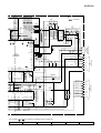
Figure 20 SCHEMATIC DIAGRAM (3/10)
– 20 –
5
6
SD-EX200
QS07
KTC3875 GR
S03 DS01
7K MA111
SWITCHING
QS01
1 KRC102 S
02 S
QS11
KTA1504 GR
RS11
0.1(3W)
RS15
4.7K
QS13
KTA1504 GR
QS14
KTA1504 GR
RS16
1K
RS19
1K
RS13
0.1(3W)
RS22
22K
RS07
4.7K
RS06
4.7K
QS10
KTA1504 GR
RS14
4.7K
RS05
1M
QS10, QS11: CURRENT DETECT
QS13, QS14: CURRENT DETECT
CS12
0.022
1
DS12 RS20
MA111 47K
QS08
KTC3875 GR
RS12
0.1(3W)
S133 DS04
4
MA111
02 S
QS12
KRC102 S
2
RS18
1K
RS10
0.1(3W)
CS03
10/50
S03
S133
PROTECT CIRCUIT PWB-A3
SWITCHING
QS06~QS08: OFFSET SWITCHING
RS21
22K
ING
RS17
1K
2
+B
C411
10/16
C410
-B -6.8V 0.022
1
-B
Q400
KRC107 M
1
3
R411
1K
L-CH_+1
3
1
R423
47K
Q423
KTC3203 Y
C424
10/16
Q421
KTA1271 Y
R432
Q422 100
KTC3199 GR
R422
560
R425
4.7K
C423
100/16
R424
120K
FAN_M+
+B
FAN_M–
R421
4.7
SP_RELAY
-20V
-B
A/D_RESET
4
PROTECT
3
OFFSET PROTECT
OFFSET COMPA
2
2
1
1
2
1
M401
FAN MOTOR
+
M
–
+ R-CH_+1
D422
DS1SS133
– R-CH_–1
– L-CH_–1
R429
RELAY
10K
SWITCHING
Q424
KTC3203 Y
R438
1K
5
SO421
SPEAKER
TERMINAL
LF402
R426
33K
C425
1/50
FAN_LOCK
L-CH_OUT
CNS401
OFFSET_COMPA
FAN_MOTOR
R407
1K
(1/2W)
CNS511
BI511
OFFSET_PROTECT
Q421~Q423: FAN SWITCHING
R428
1.5K
6
CNA101
P26 1 - C
FROM 1-BIT AMP. PWB
R550
100K
4
CNP401
C549
0.001
5
PROTECT
R427
220
PROTECT
D401
DS1SS133
A/D_RESET
R434
180
(1/2W)
C402
1/50
PS421
4.7
Posistor
KIA7812AP
VOLTAGE
REGULATOR
+20V
R406
1.5K
(1/2W)
R412
1K
C400
0.047
(ML)
+B
IC402
KIA7808AP
VOLTAGE
REGULATOR
D402
DS1SS133
2
2
C401
0.022
A_GND
LED507
304HT2P
Q548
KTC2874 B
MUTING
+B
C409 2 C408
0.047
0.022
(ML)
ZD401
D400
DS1SS133
C407
1/50
+12V
3
R569
47
D421
+5.1V
3
1
R575
2.2K
7
C559
100/16
DS1SS133
+B
R405
180
ZD402
DZS5.1BSB
C560
100/16
R576
2.2K
ZD421
MTZJ6.8A
+7.9V
2
C404
0.022
ZD400
DZS3.3BSB
IC400
+B
LED501
304HT2P
R-CH_OUT
LED503
304HT2P
6
C545
1/50
SYSTEM MUTE
Q546
KTA1266 GR
+B
1
C405
0.047
(ML)
C406
10/16
IC401
KIA7809AP
3
R400
330
+3.3V
R574
100K
LED502
304HT2P
LED505
304HT2P
Q543
KTC3199 GR
MUTING
R570
47
3
LED504
304HT2P
R547
1K
R545
18K
-B
Q545
KRA107 M
LED506
304HT2P
7
R551
4.7K
C543
47P
(CH)
1
C403
1/50
+9V
7
R552
4.7K
LED500
304HT2P
R549
100K
6
C569
33P
MUTING
Q544
KTC3199 GR
R433
180
R539
1K
2
+B
8
(1/2W)
1
(CH)
IC401
VOLTAGE
REGULATOR
+ L-CH_+1
R430
10K
LF401
D423
DS1SS133
RL421
+B
1 2 3 4 5 6 7 8 9 10
L-CH_IN_+1
L-CH_IN_—1
CNP513
CNP532
1
CNS932
P24 1 - D
FROM POWER PWB
7
R-CH_IN_—1
R-CH_IN_+1
+B
A_—20V
A_+20V
A_+20V
VOL_A_GND
CD_A_GND
+/—9V_GND
+B
P_GND
CD_D_GND
MICOM_D_GND
ZD401: MTZJ6.8A
(SERIAL NO. 30300001~30400519)
[FOR U.S.A.]
(SERIAL NO. 30400001~30400050)
[FOR CANADA]
DZ5.6BSC
(SERIAL NO. 30600520~) [FOR U.S.A.]
(SERIAL NO. 30600051~) [FOR CANADA]
P_GND
R403
10K
4 5
Q539, Q540: MUTING
R558
47
8
C421
47/25
Q539
KTC3199 GR
C541
1.5
C555
47/25
+9V
2
C422
10/16
R571
4.7K
R573
10K
C538
680P
R557
220
-6.8V
-B
+B
3
R541, R542: 1K
(SERIAL NO. 30300001~30400519)
[FOR U.S.A.]
(SERIAL NO. 30400001~30400050)
[FOR CANADA]
1.2K
(SERIAL NO. 30600520~) [FOR U.S.A.]
(SERIAL NO. 30600051~) [FOR CANADA]
R556
100K
+9V
R572
4.7K
C548
0.001
R535
1.2K
+B
Q540
KTC3199 GR
R542
R541
C546
1/50
R540 C568 C544
1K
33P 47P
(CH) (CH)
R544
10K
R537
2.2K
ZD556: MTZJ5.6A
(SERIAL NO. 30300001~30400519)
[FOR U.S.A.]
(SERIAL NO. 30400001~30400050)
[FOR CANADA]
DZ4.7BSC
(SERIAL NO. 30600520~) [FOR U.S.A.]
(SERIAL NO. 30600051~) [FOR CANADA]
R548
1K
C556
47/25
+B
R546
18K
R543
10K
C552
0.012
C536
0.0047
C535
0.0047
R555
220
R538
2.2K
CNS513
4
ZD556
C542
1.5
D535
DS1SS133 D
3
CNP513
P21 10 - H
TO MAIN PWB
R560
1K
(1/2W)
C553
0.012
2
2
BIS01
4
R559
1.5K
(1/2W)
SURROUND
Q538
2SK246 GR S
G
1
3
Q547
KTC2874 B
MUTING
AD_RESET
OFFSET_COMPRA
3
R402
8.2K
2
2
1
CNSA103
P27 12 - B
FROM 1-BIT AMP. PWB
R536
1.2K
6:
D ON/OFF
Q536
M KRA107 M
1
L-CH_–1
7
CNPS02
IC502
NJM4565M
BUFFER AMP.
6
6
4
R431
100K
5
5
3
R-CH_+1
4
4
2
R-CH_–1
3
1
L-CH_+1
6
L-CH_–1
5
SP_RELAY
4
OFFSET_PROTECT
3
R-CH_–1
CS01
0.0047
RS01
4.7K
3
+B
R-CH_+1
QS06
KTC3875 GR
S04
M
2
3
4
CNS513
P21 9 - B
FROM PROTECT CIRCUIT PWB
8
9
10
Figure 21 SCHEMATIC DIAGRAM (4/10)
– 21 –
11
12
SD-EX200
+B
A
+B
P5
P7
P8
P9
P10
P11
P12
P13
P14
P15
P16
P17
P18
P6
S_5
S_6
S_7
S_8
S_9
S_10
S_11
S_12
S_13
S_14
S_15
S_16
9 10 11 12 13 14 15 16 17 18 19 20 21 22 23 2
S_24
P19
P20
8
S_17
P21
7
S_18
P22
6
S_19
P23
5
S_20
P24
4
S_21
NP
3
2
S_22
NP
1
B
S_23
F–
F–
FL601
FL DISPLY
S 18
S_17
S_16
S_15
S_14
S_13
S_12
S_11
S_10
S_9
S_7
S_8
S_6
S_5
S_4
S_3
S_2
S_1
D_9
C618
1/50
SEG18
SEG17
SEG16
SEG15
SEG14
SEG13
SEG12
SEG11
SEG10
SEG9
SEG8
SEG7
SEG6
SEG5
82 DIG7
D_6
SEG4
D_7
SEG3
81 DIG8
SEG2
D_8
DIG9
SEG1
80 79 78 77 76 75 74 73 72 71 70 69 68 67 66 65 64 63
C
83 DIG6
84 DIG5
D_5
D_4
85 DIG4
D_3
86 DIG3
D_2
87 DIG2
88 DIG1
D_1
89 VEE
C619
1/50
C635
0.022
D
IC701
IX0557AW
SYSTEM
MICROCOMPUTE
90
91
92
C624
100P(CH)
SWITCH PWB-B3
4
SUB TRANS+B 2
3
P_IN 1
1
+5.6V
+B
R720
1.8K
SW607
TUNER
(BAND)
SW608
STOP
SP RELAY
POWER
RESET
R620
R673
C604
100P
SP_RELAY
R619
1K
1K
4.7K
304VT2E2 R739
RESET
R618
1K
1.8K
R616
R718
2.7K
SW606
AUX
R
SW604
SKIP/TUNING UP
PROTECT
SUB TRANS+B
40V RELAY
SW612
SKIP/TUNING
DOWN
R716
1.5K
+B
SW602
VOLUME UP
R725
1.5K
SW611
+B
• NOTES ON SCHEMATIC DIAGRAM can be found on page 11.
2
3
R724
1.2K
SW
BASS/TREBLE OPEN
SW601
VOLUME DOWN
H
1
TIMER_STBY
CNVSS VPP(FLASH)
S MUTE
1K
D615
DS1SS133
D616
DS1SS133
D617
DS1SS133
S_MUTE
LED601
R615
+B CHK
R614
+B_CHK
1K
PWR LEV 2
1K
R613
PWR_LEV_2
1K
R612
PWR_LEV_1
10K
1K
FAN_MOTOR R611
R719
R610
PWR LEV 1
H/P SW
FAN LOCK
D608
DS1SS133
R738
1.8K
R609
FAN MOTOR
O/C SW
1K
LID SENS (MOT LOCK)
1K
PROTECT
2.2K
1K
R606
+B
R721
1.2K
R728
1K
SW615
PLAY/PAUSE
BI601
5
CNS601
G
C603
100P(CH)
+5V(UNSW)
+5V(BACKUP)
PROTECT 3
1K
DAC_CLK
0.01
C785
1K
1K
1K
R714
10K
L602
2.2 µH
D603
DS1SS133
D604
DS1SS133
+5.6V
(USWD) 4
C602
0.001
P24 1 - B
TO POWER PWB
CNP931
D_GND
POWER
H/P_SW
6
C601
0.001
FAN_LOCK
POWER 5
+B
V– VF2
10K
7
KEY1
V+ VF1
R608
GND 6
R681
150K
O/C_SW
8
9 10 11 12 13 14 15 16 17 18 19
R652
7
8
R607
V–
7
LID_SENS
9
6
R734
10K
+B
F
5
4
PROTECT
V+ 8
–VP
2
R651
10K
10
R733
10K
R682
15K
+B_CHK
11
9
1
R603
–VP
99 INI
TUN_SM
+B CHK 10
CHASSIS_GND
12
98 VREF
100 KEY1
R700
1K
C625
0.001
CHASSIS GND 11
+B
R602
R699
1K
KEY1
3
97 AVSS
KEY3
2
TUN_SM
DAC_DATA
96 ILU_LED
C622
10/16
R601
BI771
CNS771
2
1K
O/C_SW
1
R709
10K
E
CLOSE
SW771
CD DOOR
OPEN/CLOSE
2
1
R710
10K
OPEN
1
94 DAC_ML
95 SURROUND
R696
KEY2
C770
0.01
1K
C623
0.022
R770
1.5K
CNP771
R771
2.7K
93
R695
SURROUND
4
Figure 22 SCHEMATIC DIAGRAM (5/10)
– 22 –
5
6
SD-EX200
DISPLAY PWB-B1
+B
SWITCHING
+B
Q607
KRC104 M
3
FM SIGNAL
2
1
2
C780
1/50
C782
0.047
+B
D781
DS1SS133
R762
150
C620
1/50
1
3
C781
0.047
+B
D780
DS1SS133
LED602
A503BC2E
D_1
D_2
D_3
D_4
D_5
D_6
D_7
D_8
D_9
S_1
S_2
S_3
S_4
S_5
S_6
S_7
S_8
S_9
S_10
S_11
6 17 18 19 20 21 22 23 24 25 26 27 28 29 30 31 32 33 34 35 36 37 38 39 40 41 42 43 44 45
S_12
VOLTAGE
REGULATOR
IC780
AN78L05
R761
150
F+
NP
NP
F+
1G
2G
3G
4G
5G
6G
7G
8G
9G
NC
NC
NC
P1
NC
P2
P3
P4
P5
P6
P7
P8
P9
P10
P11
P13
P12
FL601
FL DISPLY
H/P_L_OUT
CHASSIS_GND
H/P_R_OUT
R783
47K
40V RELAY 45
DT CONT 44
R647
R646
R645
DO 43
R644
DI 42
R643
CLK 41
R642
CE 40
R639
CD WRQ 39
R641
CD DRF 38
IC701
IX0557AW
SYSTEM
MICROCOMPUTER
CD CE SDA(FLASH) 36
VCC(FLASH)
DIG_FUNC
A/D_RESET
-B CONT
X_OUT
CD_FUNC
X_IN
VSS(FLASH)
SP RELAY
POWER
TUN_CLK
1K
TUN_CE
1K
CD_WRQ
CD_DRF
CD_DRF
CD_RES
CD_DI
270
CD_CLK
P_IN 31
CNP603
1 2 3 4 5 6 7 8
27
26
CD_DO
25
24
CD_CLK
23
22
LID_SENS
CD_RES
20
A/D_RESET
19
PROTECT
C636
100P
(CH)
C786
0.01
21
OFFSET
R741
100K
2.2K OFFSET
18
SP_RELAY
17
P_OUT_LEVEL
+B
16
15
FAN_LOCK
REMOTE
SENSOR
14
H/P_L_OUT
C613
10/16
13
A_GND
RM601
1 GP1UM271 2
C612
3
0.022
C611
150P(CH)
12
H/P_R_OUT
11
D+5V(SWD)
+B
A/D_RESET
R628
1K
R627
1K
RX_IN
DIG_FUNC
C607
18P(CH)
C609
0.022
L601
2.2 µH
C608
100/16
+B
10
D_GND
9
TUN_SM
8
S_MUTE
7
SURROUND
6
+B
R670
22
KEY3
KEY2
R673
100K
C604
100P
D615
DS1SS133
D616
DS1SS133
D617
DS1SS133
TUN_DO
5
TUN_CLK
4
TUN_DI
3
TUN_CE
2
+7.9V
1
+B
2
C638
10/16
FFC501
1
2
3
C627
0.1
1
1
RESET
IC608
PST9140
C639
0.01
RESET
Q608
KRC104 M
2
3
1
D605
DS1SS133
C629
0.01
RESET
POINT
3
RESET
RESET
Q606
KRC104 M
C630
4.7/50
470/10
R729 R730
C628 150
150
R776
82K
C650
100/10
ON/STAND-BY
C651
1/50
BASS/TREBLE OPEN/CLOSE
R774
1K
R723
1K
SW609
R775
470K
R724
1.2K
SW610
+B
R731
220K
PWR_LEV_1
SW604
SKIP/TUNING UP
R725
1.5K
SW611
P_OUT_LEVEL
+B
PWR_LEV_2
R717
1K
CNP601
R638
680
+B
R718
2.7K
C634
0.001
28
CD_CE
270
R631
1K
1
29
CD_WRQ
R671
10K
1K
1
R648
27
31
30
DIG_FUNC
CD_DI
R635
1
+B
7
8
9
JHP601
HEADPHONES
L
R
GND
27
32
CD_DO
CD_CE
2
R772
10K
1K
R630
1K
R623
820
C637
0.022
R620
C605
12P(CH)
XL601
4.19 MHz
RESET
TUN_DI
270
2
C633
0.01
34
FAN_MOTOR
1K
1K
R619
SP_RELAY
1K
4.7K
304VT2E2 R739
RESET
R618
R616
1.8K
S MUTE
S_MUTE
LED601
R615
1K
+B CHK
1K
R614
+B_CHK
1K
1K
R612
R613
PWR_LEV_2
PWR_LEV_1
PWR LEV 2
24 25 26 27 28 29 30
PWR LEV 1
23
1K
1K
3
C632
0.01
R649
33
TUN_DO
1K
5
4
3
HEADPHONE PWB-B2
1K
R636
CD_DI 35
CD_CLK 34 R634
R633
CD RES 33
R632
OFFSET 32
12 13 14 15 16 17 18 19 20 21 22
1K
5
4
3
34
DT CONT
R659
18
TIMER_STBY
CNVSS VPP(FLASH)
CD_DO 37 R637
1K
C617
100P
46
C615
100P(CH)
47
C616
100P
48
R777
4.7K
R778
4.7K
R779
4.7K
R742
270
R785
10K
49
C614
100P
50
H/P_SW
6
5
4
CNP501
P20 4 - H
TO MAIN PWB
SEG 23 OE(FLASH)
SEG24
SEG22
SEG21
SEG20
SEG19
SEG18
SEG17
SEG16
SEG15
SEG14
SEG13
SEG12
SEG10
SEG11
70 69 68 67 66 65 64 63 62 61 60 59 58 57 56 55 54 53 52 51
CNS602
R743
47K
CNP602
BI602
S_23
S_24
S_22
S_21
S_20
S_19
S_18
S_17
S_16
S_15
S_14
S_13
S_12
S_11
S_10
LED604
304BC2E9
+B
10
Figure 23 SCHEMATIC DIAGRAM (6/10)
– 23 –
11
12
SD-EX200
CNP931
40V RELAY
1
A
+B
SUB TRAN +B
2
D944
AG01Z
R971
680
PROTECT
C9
470
3
C971
3.3/50
D5.6V (UNSW)
B
R974
100K
+B
R975
10K
POWER
Q933
KTC3199 GR
5
CNS601
P22 1 - F
FROM DISPLAY PWB
4
D_GND
6
R973
6.8K
SWITCHING
(UCOM)
+B
–VF2
7
ZD931
HZ3ALL
–VF1
8
R962
10
R983
4.7K
C950
47/50
+B_CHK
1.6
Posistor
PS935
11
ZD933
DZ3.6BSA
11
9
10
8
9
PC901
D908
AK09
8
6
7
5
6
4
3
2
5
4
3
1
1
E
1
PS931
-B
A_–20V
1.7
Posistor
C941
1000/25
PS932
C942
1000/25
A_+20V
+B
A_+20V
D939
AG01Z
C984
0.0022
+B
0.5
Posistor
VOL_A_GND
D938
EK19
CD_A_GND
+/-9V REG GND
CD_D_GND
P_GND
P_GND
D_GND (UCOM)
CNP934
DRIVER_+9V
+B
IC931
SE-B2
ERROR
AMP.
C940
2200/50
PWR_GND
2
PWR_GND
3
L931
3.3 µH
+B
+40V
D947
DS1SS133
5
F
+B
3
2
1
C939
220P
(CH)
R933
470
R980
1K
+40V
4
C932
2200/50
7
CNSA104
4
C981
0.0022
C985
0.0022
BI932
CNS932
CNP532
1
D942
D1NL20U
CHASSIS
GND
P27 12 - F
FROM 1-BIT AMP. PEB
3
+B
LUG904
P21 7 - H
TO MAIN PWB
2
1.6
Posistor
C951
220/25
C
D
4
C948
100/63
10
10
1
R930
2.7K
PS934
R963
4.7K
R964
100
ZD932
DZ27BSA
C949
47/50
C980
0.01
R985
22K
9
3
+B
VOLTAGE
REGULATOR
Q931
KTA1023 Y
–VP
2
PC902
R932
56K
VOLTAGE
REGULATOR
IC933
KIA7809AP
3
+B
C983
0.0022
2
R970
1K
C954
0.047
(ML)
D930
FMLG22S
T901
MAIN POWER
TRANSFORMER
+B
1
C955
0.047
(ML)
C930
0.0047
R931
3.9K
D937
EK19
C938
1000/25
C953
1/50
+B
+B
1
+B
A_+5V
2
C958
0.047
(ML)
CNA100
P26 1 - F
TO 1-BIT AMP. PWB
1
G
VOLTAGE
REGULATOR
IC934
3
1
AN78L05
D957
DS1SS133
BI900
CNSA100
+B
2
2
3
3
4
4
C957
0.047
(ML)
+B
C956
1/50
A_GND_AD
D_+5V
+B
D_GND_AD
LUG901
H
CHASSIS GND
• NOTES ON SCHEMATIC DIAGRAM can be found on page 11.
1
2
3
4
Figure 24 SCHEMATIC DIAGRAM (7/10)
– 24 –
5
6
SD-EX200
POWER PWB-A2
C965
0.047
(ML)
D953
GD1N4004
D952
GD1N4004
C966
0.047
(ML)
T903
SUB POWER TRANSFORMER
C967
470/25
2
3
1
4
2
3
1
4
LUG903
D950
GD1N4004
D951
GD1N4004
+B
PC902
R930
2.7K
PC901
R910
10
(1/2W)
SWITCHING
Q902
KTA1266 GR
D905
AG01Z
8
9
C919
33/35
R914
3.3K
D906
AG01Z
C918
4.7/50
SWITCHING
REGULATOR
IC901
STRF6238
4 Vin
R915
150K
R916
1.5K
5 FB/SYNC
C917
0.0047
(ML)
C920
0.0015
R902
220K
D907
AG01Z
1
OCP
SYNC
2 GND
C921
0.01
R909
0.1
(2W)
R918
220
R908
0.18
(2W)
Drain
C916
220P
3
R907
0.15
(2W)
L905
R917
47K
(2W)
C915
0.0022
1
D902
SARS03
2
3
C912
0.01
R905
47K
(1/2W)
R984
47K
(1/2W)
R906
47K
(1/2W)
R904
47K
(1/2W)
R903
4.7M
(1/2W)
C909
0.0022
D901
D5SB60
TH901
1.5
C908
0.0022
C911
820/200
L902
AC LINE
FILTER
R920
4.7M(1/2W)
C907
0.0022
C906
0.0022
T901
MAIN POWER
TRANSFORMER
C902
0.1
C905
0.0022
C903
0.001
C904
0.001
L901
AC LINE
FILTER
VA901
VA901: 10V271K
(SERIAL NO. 30300001~30400519)
[FOR U.S.A.]
(SERIAL NO. 30400001~30400050)
[FOR CANADA]
10V471K
(SERIAL NO. 30600520~) [FOR U.S.A.]
(SERIAL NO. 30600051~) [FOR CANADA]
C913
0.01
R901
390K(1/2W)
C901
0.1
F901
6A/125V
C914
0.01
CNP901
CNS901
2
1
2
1
AC POWER SUPPLY CORD
AC 120 V, 60 Hz
LUG902
CHASSIS GND
7
8
9
10
Figure 25 SCHEMATIC DIAGRAM (8/10)
– 25 –
11
12
SD-EX200
A
FM SIGNAL
RA158
75K
RA156
75K
+B
1
20 L-CH IN
21 RESET
RA159
1K
+B
CNA101
22 NFL2(–)
3
01
100/16
CA154
100/16
2
OUTL(+) 2
23 NFL1(+)
24 VDA
CA152
CA150
+B
GNDD 4
OUTL(–) 3
1
RA127
RA123
1K
VDDL 1
CA133
0.1
IC100
7TH ORDER ∆∑
MODULATION
CONVERSION LSI
1K
CA141
0.1
CA199
47/25
+B
D+5V
RA435 RA436
5.6K 2.2K
RA438
4.7K
+B
DGND-AD
RA437
5.6K
D
RA431 RA432
12K 6.8K
0.1
OFFSET
COMPA
OUTR(–) 5
ICA100
IX0498AW
100/16
2
19 L-CH Vref
CA137
0.001
CA138
0.1
CA151
OFFSET
PROTECT
VDDR 7
OUTR(+) 6
RA157
75K
3
4
CA131
0.1
CA130
0.001
PROTECT
18 R-CH Vref
CA103
10/10
RA155
75K
4
CA110
100P
(CH)
CA134
0.1
CA149
RA103
8.2K
5
RESET
CA104
0.001
CA105
0.001
CXA100
11.2896 MHz
CA124
18P(CH)
VDDX 8
CA132
47/25
L-CH_IN 1
CA102
10/10
A+5V
RA101
3.3K
6
XI 9
RA434
33K
RA108
CA100
20K
10/50
RA104
RA106
120K
120K
R-CH OUTPUT
OFFSET
VRA100
ADJUSTMENT
4.7K (B)
VRA101
L-CH OUTPUT
4.7K (B)
OFFSET
ADJUSTMENT RA105
RA107
120K
120K
CA101
RA109
10/50
LCH_1
20K
ANALOG IN L-CH
AGND_AD
C
P21 12 - D
FROM MAIN PWB
CNS511
AGND 1
17 R-CH IN
CA142
0.1
RA433
10K
7
15 NFR2(–)
16 GNDA
RCH_1
ANALOG IN R-CH
CA123
18P(CH)
CA135
0.1
RA102
8.2K
RA100
3.3K
R-CH_IN 1
1K
RA126
AMP_VCC
GNDX 11
XO 10
14 NFR1(+)
B
RA122
1K
MCK 12
13 TEST
CA153
100/16
+B
QA414~QA415: PROTECT DETECT
QA415
2SD601 AR
CA416
0.1
E
LFA402
CA410
47/25
AGND_AD 2
RA476
4.7K
+B
CA409
0.1
LFA403
D+5V 3
3
1
DA405
MA111
+B
CA411
0.1
RA430
100K
CNA100
F
10K 2
RA477
47K
RA478
1K
D+5V
CA412
47/25
DGND_AD 4
QA414
2SB709 AR
QA416
KRC104 S
RA475
RA479
47K
P24 1 - G
FROM POWER PWB
CNSA100
A+5V 1
RA480
10K
RA481
47K
3
2
1
DA404
MA132WA
+B
G
1-BIT AMP. PWB-C
H
• NOTES ON SCHEMATIC DIAGRAM can be found on page 11.
1
2
3
4
Figure 26 SCHEMATIC DIAGRAM (9/10)
– 26 –
5
6
CA407
1/50
C
SD-EX200
CA178
1/25
OUTB OUTA
OUTB OUTA
SA
+B
DA133
MA111
CA117
0.001
RA146
5.6K
3
1
RA135
680
BIA103
CNSA103
1
CA419
CA420
180P(CH) 180P(CH)
2
L-CH_–1
L-CH_+1
3
4
LFA101
CA183
0.01
CA179
1.5
CA193
0.001
RA149
5.6K
CA185
0.01
CA181
1.5
LA107
LA103
R-CH_-1
RA171
4.7K
LA105
CA175
1/25
R-CH_+1
RA153
4.7K
RA141
3.3K
11
CA417
CA418
180P(CH) 180P(CH)
5
RA145
1K
RA143
680
RA133
3.3K
DA116
MA132WA
RA138 15K
RA130 15K
RA172 15K
RA174 15K
4
2
CA194
100/50
CA159
0.33
1
RA152
4.7K
RA144
1K
RA137
1K
CA115
0.001
CA165
1/25
RA142
680
RA136
1K
RA173 15K
VBBB VBBA
6
2
IC101
SWITCHING AUDIO
POWER AMP.
VBBB VBBA
CA155
0.1
CA153
100/16
SB
DTADJA
VBOOTB VBOOTA
17 18 19 20 21
12 13 14 15
RA438
4.7K
DA113
SFPW56
VDD DTADJB
16
INA
1
VKK
2
GND
3
INB
4
VCC
5
VKK
6
0.1
7
100/16
8
CA151
RA434
33K
RA435 RA436
5.6K 2.2K
11 10 9
CA149
5.6K
10K
+B
DA111
SFPW56
ICA101
SLA5515M
5
DA115
SFPW56
CA143
0.1
CA141
0.1
RA431 RA432
12K 6.8K
DA109
SFPW56
1K
3
RA140
3.3K
RA134
680
LA101
RA127
RA123
1K
1
0.22
CA145
0.33
LFA100
DA107
MA132WK
DA131
MA111
RA150
47
RA170
4.7K
RA175 15K
CA160
0.33
CA116
0.001
RA132
3.3K
RA139 15K
DA132
MA111
DA114
SFPW56
CA188
0.22
3
RA131 15K
+B
LA106
CA196
0.22
CNPS02
P21 8 - B
TO PROTECT CIRCUIT PWB
CA166
1/25
LA102
SA
ICA102
SLA5515M
1
SB
OUTB OUTA
OUTB OUTA
2
17 18 19 20 21
CA156
0.1
CA154
100/16
3
IC102
SWITCHING AUDIO
POWER AMP.
16
4
VBBB VBBA
5
DA112
SFPW56
12 13 14 15
6
VBBB VBBA
DTADJA
7
VBOOTB VBOOTA
INA
VKK
VCC
0.1
8
VDD DTADJB
GND
INB
VKK
CA152
CA150
100/16
2 1
11 10 9
CA182
1.5
3
5.6K
DA401
KDS226
5.6K
RA151 CA197
0.22 CA187
47
+B
CA114
0.001
CA184
0.01
DA110
SFPW56
CA180
1.5
RA148
DA108
SFPW56
CA142
0.1
CA186 CA192
0.01
0.001
LA104
LA100
1K
RA126
CA144
0.1
RA122
1K
CA146
0.33
MA111
RA147
DA130
12
CURRENT
SENSOR
RA406
1K
RA415
0.1(2W)
RA416
0.1(2W)
DA405
MA111
8
7
6
5
CA404
0.1
6
RA424
22K
CA401
0.001
CA402
0.001
5
+B
5
+B
4
4
GND
3
3
GND
2
LFA400
RA426
68K
CA406
47/25
RA425
56K
RA422
330K
CA403
0.001
CA413
0.1
LA400
DRIVER_+9V
BIA104
1
• The numbers 1 to 6 , 11 , 12 are waveform numbers shown in page 37.
7
8
9
10
Figure 27 SCHEMATIC DIAGRAM (10/10)
– 27 –
11
1
12
CNP934
P24 1 - E
TO POWER PWB
4
CA408
0.01
+B_AMP
RA427
22K
CNSA104
3
+
–
CA407
1/50
2
CA405
0.1
1
ICA401
TJM4558CD
OPE AMP.
RA428 RA429
68K
2.7K
–
+
DA404
MA132WA
DA400
MA111
RA400
1K
2
1
DA403
MA111
RA403
2.2K
PSA400
RA421
330K
3
QA400
2SB709 AR
RA409
390 RA412
390
SD-EX200
M401
FAN MOTOR
A
RD
RD
WH
GR
WH
GR
WH
GR
6 5 4 3 2 1
RS04
QS11
RS13
QS13
RS15
QS08
COLOR TABLE
RS06
BR
QS02
CS06
QS03
QS04
CS05
RS20
RS21
RS17
RS07
DS03
CS12
RS11
QS01
CS01
CS03
4
RS05
DS05
DS06
CS02
CNPS02
RS19
RS12
4
RS22
DS12 QS10
QS12
3
RS16 DS04
RS10
2
RS18
RS14
QS14
G
1
BIS01
P33 8 - B
FROM 1-BIT AMP. PWB
CNSA103
RS03
1
QS06
6 5 4 3 2 1
CNPS01
RS01
DS02
CNS513
QS05
1
DS01
2
QS07
CNS502
F
4 3
CNS932
P30 4 - E
FROM POWER PWB
BROWN
RD(R)
RED
OR
ORANGE
YL
YELLOW
GR
GREEN
BL
BLUE
VL
VIOLET
GY
GRAY
WH(W)
WHITE
BK
BLACK
PK
PINK
PROTECT CIRCUIT PWB-A3
H
• The numbers 1 to 12 are waveform numbers shown in page 36.
1
2
3
4
Figure 28 WIRING SIDE OF P.W.BOARD (1/7)
– 28 –
5
6
ZD2
R520
R516
C516
C519
R517
R515
C405
ZD400
C403
ZD402
C404
1 2 3
IC401
1
CNA101
P33 8 - H
TO 1-BIT AMP. PWB
C5
C523
R525
E C
C406
R408
IC402
R405
C408
C409
1 2 3
BI502
1 2 3 4 5 6 7
R519
Q55
7
CNS511
R518
C512
C514
C513
D404
D403
E
12
IC501
C511
C5
13
15
10
R513
C515
R512
C504
C501
R503
C572
C502
C571
C570
R526
C503
C530
C538
R555
R557
R528
R501
R502
LED506
R556
1
C522
C411
ZD401
C410
1 2 3 4 5 6 7 8 910
CNP532
C531
C546
R548
LED504
1 2 3
R411
R412
R409
R438
D
Q400
20
5
R511
C407
D401
R431
R514
24
Q552
3 2 1 Q536
R406
D402
C401
R407
8
R402 R403
BI511
1
Q535
1
2
3
Q545
R549
R552
B
C
E
E
C
B
3 2 1
LED502
LED500
R550
Q544
LED503
B
C
E
B
C
E
Q543
LED507
Q547
Q424
C537
C520
R546 R540
C555
C544 C568
LED501
3 2 1
C402
R558
Q538
C542
R536
C536
R542
R538
R541
C552
R571
R539
R543
C541
R573
C545
R575
R576
R424
C423
R569
D535
D400
IC400
C560
WH
GR
WH
GR
WH
GR
LF402
ZD556
R547 R570
C548
C549
RD
C400
1
C556
E C B R551
PS421
R-CH
C535
R535
IC502
B C E
Q548
E
C
B
R427
C424
S
G
D
4
5
8
R560
D423
ZD421
C425
Q423
R429
R428
D422
R426
C
RL421
LF401
R425
B
C
E
R537
R544
B C E Q422
R430
L-CH
C569
C559
R559
R432
SO421
SPEAKER
TERMINAL
R572
E C B
Q546
Q539
LED505
4
D421
C543
3
R545
2
E
C
B
C422
B
E
2 1
CNP401 C
R574 B
R433
CNP513
1
CNS401
Q540
Q421
R434
R423
C421
R421 R422
LUG501
2 1
C553
BR
SD-EX200
BK
BK
BK
BK
BK
BK
BR
C12
R7
R5
C9
C10
R6
R3
C11
C13
C14
C17
C16
C15
R9
C3
C5
R8
C7
R10
C6
C4
C44
C43
5
B C E Q1
8
R40
Q84
R-CH
C564
R577
C565
R580
R28
R29
R30
R578
L-CH
C566
R579
R34
R35
7
R33
R32
C33 C102
R105
R104
C35 R103
R26
R27
Q101
3
2
1
R31
C31 R109
R24
C30
R102
D101
R36 C42 R39
C40 R38
R37
C41
C20
L1
C81
R83
R108
R106
C88
80
75
50
70
55 65
60 61
C117
R101
IC101
1
C109
C106
C107
16
45
4
1
IC1
XL1
C101
C114
C103
5
15
C108
40
41
8
10
R4
R1
R2
C1
R15
R14
R12
R11
C2
C18
C59
R114
C69
L101
C110
R107 R115 C29 C22
R17
R72
11
10
9
8
7
6
5
4
3
2
1
9
25 15
30
10
35
5
R25
CNS4A
CNP502
C105
JT501
AUX INPUT
3 2 1
L2
R524
C113
1
2
3
4
5
6
7
8
9
10
11
12
13
14
15
16
17
18
19
20
21
22
23
24
25
26
27
28
29
30
31
32
33
34
R111
2
21 20
C116
CNP501
1
2
3
C85
C84
R400
C405
B C E
C19
C21
IC4
11
1
FFC502
12 3
MAIN PWB-A1
11
34
1
FFC501
7
CNP601
P34 4 - G
TO DISPLAY PWB
1
1
8
TUN1
PICKUP UNIT(306)
TUNER UNIT
6 5 4 3 2 1 CNP4A
SW4
PICKUP IN
M802
SPINDLE MOTOR
–
ZD400
Q82
Q3
28
R73
R112
C115
R521
R517
R522
R523
R515
C519
3 2 1
C70
C57
R16
25
1
+
C406
15
5
R64
D82
R82
20
C525
R519
C521
C523
R525
E C B
C58
C82
C55
R13
C54
R61
C52
R60
R59
D2
D1
R63
R53
IC2
7 6 5 4 3 2 1
CNP1
–
3
C53
R62
12
Q551
01
R52
C527
C528
E
C
B
Q2
10
R527
R513
C515
13
C83
1
14
4
C51
R56
R55
C50
R57
R58
R84
ZD2
R51
C524
13
C60
C526
15
10
501
C56
ZD1
C520
R520
R516
C522
R518
C516
1
5
1 2 3 4 5 6 7 8
CNP2
C86
CNS1A
CD MOTOR PWB-D
7
8
9
10
Figure 29 WIRING SIDE OF P.W.BOARD (2/7)
– 29 –
M801
SLED MOTOR
11
+
4
IC3
7 6 5 4 3 2 1
9 6
CNS2A
C87
6 5 4 3 2 1
CNP4
2 1
CNP5
1 2 3 4 5 6 7 8
10
CNS1B
7 6 5 4 3 2 1
BR
BK
BK
BK
BK
BK
BK
BK
BR
BR
BR
BR
BR
RD
6 5 4 3 2 1
CNS5 2 1
8
1 2 3 4 5 6 7 8 CNS2B
+
C39
6 5 4 3 2 1 CNS4B
–
C36
C37
C38
M1
CD DOOR
MOTOR
12
SD-EX200
A
B
P33 11 - A
FROM 1-BIT AMP. PWB
C938
C942
3
4
D906
2
1
PC901
B
C
E
R914
3
4
D905
R902
2
1
C941
Q902
PC902
R974
E
C
B
R975
1
WH
BK
WH
BK
WH
BK
WH
BK
WH
11
Q933
2
3
R973
R933
1
R931
1
C939
R930
IC931
2
R932
BI932
D957
C958
3
CNP934
RD
IC934
4
C940
R980
PS931
R970
C953
1
2
3
C956
4
3 2 1
5
L931
IC933
PS932
1
BI900
1
2
3
4
CNSA100
C954
D947
C955
RD
WH
BL
WH
C957
C
P33 12 - F
TO 1-BIT AMP. PWB
CNA100
CNSA104
C985
LUG902
WH
BK
WH
BK
WH
BK
WH
BK
WH
RD
D
COLOR TABLE
BLUE
VL
VIOLET
GY
GRAY
WH(W)
WHITE
BK
BLACK
PK
PINK
ZD932
R963
LUG904
D937
C930
C981
GREEN
BL
R964
R983
ZD933
R971
ZD931
B C E Q931 D944
C971
C950
GR
CNP532
P28 5 - F
TO MAIN PWB
D942
YELLOW
C949
C980
YL
C932
ORANGE
R962
RED
OR
D930
BROWN
RD(R)
R985 PS934
E
C984
D938
C983
10 9 8 7 6 5 4 3 2 1
CNS932
C948
BR
R910
D939
C951
PS935
T901
MAIN POWER
TRANSFORMER
D908
LUG903
CNP931
11 10 9 8 7 6 5 4 3 2 1
CNS601
P34 1 - D
FROM DISPLAY PWB
F
G
H
1
2
3
4
Figure 30 WIRING SIDE OF P.W.BOARD (3/7)
– 30 –
5
6
SD-EX200
LUG901
C909
R920
C906
C907
C913
D901
D907
C908
1
C915
TH901
C916
R909
R908
AC POWER
SUPPLY CORD
AC 120 V, 60 Hz
R984
VA901
C966
D950
8
1
9
CNS901
F901
6A/125V
D951
C967
7
1
L901
C965
D953
LUG903
2
CNP901
D952
R905
2
LUG905
D902
R904
1 2 3
C903
R917
R906
C912
1
OWER
RMER
C905
C904
C921
T903
SUB POWER TRANSFORMER
R903
C919
C917
R907
C901
2
L902
C918
R910
3
4
R916
C911
L905
5
R918
IC901
R915
C920
R914
C902
R901
D906
D905
C914
POWER PWB-A2
10
Figure 31 WIRING SIDE OF P.W.BOARD (4/7)
– 31 –
11
12
WH
BK
SD-EX200
A
COLOR
TABLE
B
YL
OR
RD(R)
GR
BR
BROWN RED ORANGE YELLOW GREEN
BL
VL
VIOLET
BLUE
LFA400
CA420
PK
PINK
CA419
CA418
RA151
DA400
RA415
RA150
DA401
RA416
C
WH(W) BK
WHITE BLACK
GY
GRAY
DA403
DA107
CA194
DA116
DA112
DA130
CA160
DA132
CA145
DA111
DA114
DA110
CA146
DA113
DA109
CA159
DA131
DA133
DA115
DA108
CA175
CA178
CA166
E
CA165
D
RA123
1
24
1
ICA100
2
5
CA130
RA478
RA480
RA481
CA416
QA415
20
RA475
QA414
RA421
1
4
10 15
13
12
G
RA155
RA100
RA101
8
DA405
RA156
RA157
RA476
RA430
F
RA477
RA479
RA158
QA416
RA122
RA422
5 ICA401
DA404
CA132
1-BIT AMP. PWB-C
(TOP VIEW)
4
3
H
• The numbers 1 to 6 , 11 , 12 are waveform numbers shown in page 37.
1
2
3
4
Figure 32 WIRING SIDE OF P.W.BOARD (5/7)
– 32 –
5
6
SD-EX200
Through-hole where the top, bottom and +B patterns are connected.
Through-hole where the top, bottom and ground patterns are connected.
Through-hole where the top, and bottom patterns are connected.
P28 1 - G
TO PROTECT CIRCUIT PWB
CNPS02
CNSA103
CA196 CA188
1
RA412
CA402
CA184
RA140
LA106
RA130
RA172
LA103
LA100
RA139
RA175
RA144
RA136
RA174
RA138
RA145
RA143
RA131 RA135
RA133
RA141
LA104
CA404
RA425
LA105
RA424
CA182
RA137
LA400
CA180
CA186
RA142
RA173
RA149
RA153
CA193
RA171
CA413
RA427
CA181
LA107
CA403
CA406
RA406
RA146
RA403 RA400
QA400
RA148
RA170
RA409
RA428
CA405
RA152
CA192
LFA100
CA179
CA183
CA185
CA197
RA147
PSA400
RA132
CA417
CA187
11
1
BIA104
CA401
RA426
CA414
LA102
LA101
RA102
VRA100
R-CH OUTPUT
OFFSET
ADJUSTMENT
VRA101
L-CH OUTPUT
OFFSET
ADJUSTMENT
CA409
CXA100
4
3
2
1
CNSA100
P30 1 - C
FROM POWER PWB
LFA403
LFA402
CA412
CA124
CA123
CA104
CA133
RA104
VRA100
9
CA135
CA105
CA137
CA102
RA106
RA103
CNS511
P28 2 - F
FROM MAIN PWB
CA110
CA103
CA411
CA134
CA199
CA138
CA101
CA408
RA159
RA107
RA108
RA126 CA144
CA150
RA435 RA437
RA109
RA105
CA100
CNA101
1 2 3 4 5 6 7
CA154
RA436
CA131
CA149
CA153
CA155
CA407
RA434
RA438
RA432
VRA101
8
21 19 17 15 13 11 9 7 5 3 1
CA156
CA152
21 19 17 15 13 11 9 7 5 3 1
ICA102
CA115
20 18 16 14 12 10 8 6 4 2
5
7
CA114
CA142
20 18 16 14 12 10 8 6 4 2
CA116
CA141
CA151
RA431 CA143
RA127
RA433
6
ICA101
CA117
CNA100
12
6
RA429
BIA103
RA134
5
LFA101
CNSA104
WH
WH
WH
WH
RD
5 4 3 2 1
GY
GY
GY
RD
4 3 2 1
P30 4 - B
TO POWER PWB
CNP934
CA410
1-BIT AMP. PWB-C
(BOTTOM VIEW)
10
Figure 33 WIRING SIDE OF P.W.BOARD (6/7)
– 33 –
11
12
SD-EX200
A
C603
R700
R699
R651 C601 L602
R606
30
31
C620
10
R646
R647
C617
R779
R644
R777
C615
R645
R772
R641
50 51
SW606
AUX
R778
C614
R682
C637
CNS601
R742
R718
VL
VIOLET
GY
GRAY
WHITE
BK
BLACK
PK
PINK
D780
1 3 2
C782
IC780
SW610
OPEN/
CLOSE
C627
Q606
C638
R783
Q607 1 2 3
R785
CNP601
C612
34 32 30 28 26 24 22 20 18 16 14 12 10 8 6 4 2
33 31 29 27 25 23 21 19 17 15 13 11 9 7 5 3 1
C613
1
2
3
RM601
BI771
2
SW608
STOP
1
RD
WH(W)
C780
GR
BLUE
LED601
C611
BL
SW612
SKIP/
TUNING
DOWN
R741
GREEN
R761
LED602
SW615
PLAY/
PAUSE
R728
YELLOW
R725
D781
YL
GR
R724
C781
ORANGE
R670
RED
OR
3
2
1
R659
F
RD(R)
1
2
3
D605
C629
Q608
C630
D603
BROWN
1
2
3
4
5
6
7
8
C618
IC608
R671
R730
C639
R638
C636
C628
3
2
1
R729
BR
2
CNP603
R731
SW607
TUNER
(BAND)
SW604
SKIP/
TUNING UP
41
40
39
38
37
36
35
34
33
32
31
30
29
28
27
26
25
24
23
22
21
20
19
18
17
16
15
14
13
12
11
10
9
8
7
6
5
1
R720
COLOR TABLE
80
C616
SW611
BASS/
TREBLE
E
81
45
44
FL601
C609
XL601
R636
D604
C623
5 95
90
85
20
IC701 7075
25
65
35
40
60
45 55
R639
R643
R642
L601
R620
1
R695
R602 R603
R601
R609
R608
R607
R623
R627
C786
R618
R681
C604
C619
C635
15
R628
R630
R631
R619
12
R743
C622
C605
C607
R634
R635
R637
R721
R733
C785
C608
R739
BI601
D
C624
C651
R610
LED604
1 100
SW602
VOLUME
UP
R719
R616
R673
P30 5 - F
CNP931
TO POWER PWB
R717
R775
R774
R611
R716
11
10
9
8
7
6
5
4
3
2
1
R613
R614
C650
R762
R696
D617
D616
D615
R776
SW601
VOLUME
DOWN
BL
BL
BL
BL
BL
BL
BL
BL
BL
BL
RD
R612
R615
C
C602
D608
1
HEADPHONES
PWB-B2
R738
R652
6
BL
5 WH
4
BL
3
2 WH
1 RD
CNS602
BI602
C632
JHP601
HEADPHONES
CNP602
R649
5
4
C633 3
R648 2
1
C634
C625
R710
R709
R714
SW609
ON/
STAND-BY
R633
R632
B
R734
R723
DISPLAY PWB-B1
1 2 CNS771
CNP501
P29 8 - F
TO MAIN PWB
SW771
CD DOOR
OPEN/CLOSE
1 2 CNP771
R771 C770
G
R770
1
FFC501
34
SWITCH PWB-B3
H
1
2
3
4
Figure 34 WIRING SIDE OF P.W.BOARD (7/7)
– 34 –
5
6
SD-EX200
VOLTAGE
PIN NO.
1
2
3
4
5
6
7
8
9
10
11
12
13
14
15
16
17
18
19
20
21
22
23
24
25
26
27
28
29
30
31
32
33
34
35
36
37
38
39
40
41
42
43
44
45
46
47
48
49
50
VOLTAGE
5.05 V
5.05 V
0V
0V
0.81 V
5.09 V
2.26 V
2.38 V
0V
0V
5.21 V
0V
0V
2.39 V
4.76V
0V
0V
4.79 V
4.69 V
4.85 V
0V
2.16 V
2.30 V
4.87 V
0V
0V
0. V
4.87 V
0V
0V
5.05 V
5.12 V
4.87 V
3.79 V
4.24 V
1.10 V
4.41 V
0V
4.86 V
0V
0V
0V
5.23 V
0V
4.86 V
0V
0V
0V
0V
0V
IC701
PIN NO. VOLTAGE
51
0V
52
0V
53
54
55
56
57
58
59
60
61
62
63
64
65
66
67
68
69
70
71
72
73
74
75
76
77
78
79
80
81
82
83
84
85
86
87
88
89
90
91
92
93
94
95
96
97
98
99
100
0V
0V
0V
0V
25.99 V
-25.99 V
-25.99 V
-25.99 V
-25.99 V
0V
-25.99 V
0V
0V
-22.76 V
0V
0V
0.32 V
0V
1.01 V
25.99 V
0V
0V
25.89 V
0V
25.98 V
0V
22.66 V
0V
22.80 V
-22.46 V
-22.56 V
-22.50 V
-0.10 V
-22.73 V
-22.73 V
-22.48 V
25.89 V
0V
0V
0V
0.51 V
0V
0V
4.87 V
0V
5.05 V
0V
5.05 V
IC780
PIN NO. VOLTAGE
1
2.66 V
0.60 V
3
2
10.18 V
IC608
PIN NO. VOLTAGE
1
5.09 V
5.08 V
3
2
0V
Q606
PIN NO. VOLTAGE
E
0V
C
4.79 V
B
0V
Q608
PIN NO. VOLTAGE
E
0V
C
4.80 V
B
0V
Q607
PIN NO. VOLTAGE
E
0V
C
0.26 V
B
4.80 V
Q82
PIN NO. VOLTAGE
E
1.66 V
C
1.66 V
B
5.40 V
Q3
PIN NO. VOLTAGE
E
7.95 V
C
3.30 V
B
7.28 V
Q101
PIN NO. VOLTAGE
E
0V
C
3.28 V
B
0V
PIN NO.
1
2
3
4
5
6
7
8
9
10
11
12
13
14
15
16
17
18
19
20
21
22
23
24
25
26
27
28
29
30
31
32
33
34
35
36
37
38
39
40
41
42
43
44
45
46
47
48
49
50
51
52
53
54
55
56
57
58
59
60
61
62
63
64
65
66
67
68
69
70
71
72
73
74
75
76
77
78
79
80
IC1
VOLTAGE
1.62 V
1.07 V
1.06 V
0.50 V
3.29 V
15.33 V
1.66 V
1.66 V
1.66 V
1.66 V
1.67 V
1.66 V
0V
1.23 V
0V
0V
0V
3.29 V
0V
1.65 V
1.65 V
1.65 V
1.65 V
1.65 V
3.84 V
3.29 V
3.30 V
3.76 V
0V
3.30 V
0V
0V
0V
0V
0V
0V
0V
3.29 V
0V
0V
3.85 V
0V
0V
0V
0V
3.85 V
3.30 V
3.39 V
0V
0V
0V
0V
0V
3.30 V
0V
0V
0V
0V
0V
0V
3.85 V
0V
0V
0V
0V
3.85 V
3.29 V
3.30 V
0V
0V
0V
0V
0V
3.30 V
0V
0V
0V
0V
0V
0V
PIN NO.
1
2
3
4
5
6
7
8
9
10
11
12
13
14
15
16
17
18
19
20
21
22
23
24
25
26
27
28
IC2
VOLTAGE
7.87 V
0V
0V
Q539
PIN NO. VOLTAGE
E
0V
C
0V
B
0.65 V
IC934
PIN NO. VOLTAGE
1
9.00 V
2
0V
3
5.09 V
Q84
PIN NO. VOLTAGE
E
2.90 V
C
3.21 V
B
7.25 V
Q400
PIN NO. VOLTAGE
E
0V
C
5.02 V
B
0V
IC934
PIN NO. VOLTAGE
1
20.20 V
2
0V
3
9.00 V
Q2
PIN NO. VOLTAGE
E
4.89 V
C
5.56 V
B
7.46 V
Q545
PIN NO. VOLTAGE
E
2.29 V
C
2.26 V
B
0V
IC931
PIN NO. VOLTAGE
1
6.92 V
2
35.10 V
3
0V
IC501
VOLTAGE
0V
0V
Q547
PIN NO. VOLTAGE
E
0V
C
0V
B
0.69 V
Q931
PIN NO. VOLTAGE
E
-26.30 V
C
-54.90 V
B
-26.60 V
Q548
PIN NO. VOLTAGE
E
0V
C
0V
B
0.69 V
Q933
PIN NO. VOLTAGE
E
0V
C
0.55 V
B
0V
Q535
PIN NO. VOLTAGE
E
0V
C
5.35 V
B
0V
PC901
PIN NO. VOLTAGE
1
36.10 V
35.10 V
2
3
0V
0V
4
3.57 V
3.60 V
3.55 V
3.62 V
3.55 V
3.63 V
3.54 V
3.54 V
7.89 V
1.66 V
1.66 V
1.67 V
1.67 V
1.65 V
1.67 V
7.20 V
0V
1.67 V
7.87 V
1.67 V
1.67 V
3.88 V
0V
4.78 V
4.78 V
IC3
PIN NO. VOLTAGE
1
2.25 V
0.25 V
2
3
0.25 V
0V
4
2.26 V
5
6
2.26 V
7
2.26 V
8
6.21 V
PIN NO.
1
2
3
4
5
6
7
8
9
10
11
12
13
14
15
16
Q1
PIN NO. VOLTAGE
E
3.30 V
C
0V
B
3.28 V
IC101
VOLTAGE
3.28 V
0V
0V
0V
3.30 V
3.30 V
3.30 V
0V
0V
1.78 V
0V
0V
0V
0V
0V
3.64 V
PIN NO.
1
2
3
4
5
6
7
8
9
10
11
12
13
14
15
16
17
18
19
20
21
22
23
24
0V
0V
4.52 V
4.57 V
4.50 V
4.50 V
4.50 V
4.50 V
4.50 V
4.50 V
4.50 V
4.50 V
4.50 V
4.50 V
4.52 V
4.50 V
4.50 V
4.52 V
4.52 V
4.52 V
9V
0V
IC502
PIN NO. VOLTAGE
1
-14.90 V
0V
2
3
0V
0V
4
14.86 V
5
6
0V
7
0V
8
0V
IC401
PIN NO. VOLTAGE
1
19.02 V
2
0V
3
8.94 V
IC402
PIN NO. VOLTAGE
1
19.02 V
2
0V
3
7.95 V
Q536
PIN NO. VOLTAGE
E
8.95 V
C
5.87 V
B
8.91 V
Q538
PIN NO. VOLTAGE
E
0V
C
5.64 V
B
0V
– 35 –
Q546
PIN NO. VOLTAGE
E
2.29 V
C
2.25 V
B
1.65 V
Q421
PIN NO. VOLTAGE
E
0V
C
0V
B
6.11 V
Q540
PIN NO. VOLTAGE
E
0V
C
0V
B
0.66 V
IC400
PIN NO. VOLTAGE
1
19.03 V
2
0V
3
11.90 V
Q424
PIN NO. VOLTAGE
E
0V
C
11.90 V
B
0V
Q422
PIN NO. VOLTAGE
E
0V
C
6.11 V
B
0V
Q423
PIN NO. VOLTAGE
E
6.12 V
C
11.90 V
B
0V
PC902
PIN NO. VOLTAGE
1
0V
0.68 V
2
3
0V
0V
4
SD-EX200
WAVEFORMS OF CD CIRCUIT
Stopped
CH1=500 mV
DC 10:1
CH3=500 mV
DC 10:1
T
1
IC1 21
Stopped
CH1=200 mV
DC 10:1
500 ms/div
(500 ms/div)
NORM:20 kS/s
IC1 20
1999/04/07 09:51:15
500 ms/div
(500 ms/div)
NORM:20 kS/s
FDO
T
1
TDO
2
T
CH2=500 mV
DC 10:1
3
FDO
1
IC1 21
2
6
IC1 22
1
SPDO
CH1
v/DIV
500 mV
=Filter=
Smoothing : ON
BW : FULL
=Offset=
CH1 :
0.000 V
CH2 :
0.0 V
CH3 :
0.000 V
CH4 :
0.00 V
Stopped
CH1=500 mV
DC 10:1
1
IC1 21
3
IC1 67
CH2=10 V
DC 10:1
=Record Length=
Main :
100 K
Zoom :
2K
=Filter=
Smoothing : ON
BW : FULL
=Trigger=
Mode : AUTO
Type : EDGE CH1
Delay :
0.0 ns
Hold off :
0.2 µs
CH3=1 V
DC 10:1
Stopped
CH1=500 mV
DC 10:1
500 ms/div
(500 ms/div)
NORM:20 kS/s
T
2
IC1 73
CH3=1 V
DC 10:1
=Trigger=
Mode : NORMAL
Type : EDGE CH2
Delay :
2.924 ms
Hold off :
0.2 µs
1999/04/05 17:33:17
CH4=1 V
500 ms/div
(500 ms/div)
DC 10:1
NORM:20 kS/s
3
4
DRF
8
PDO2
IC1 74
T
TE
IC1 15
=Record Length=
Main :
100 K
Zoom :
2K
PDO1
7
FDO
1
4
=Offset=
CH1 :
0.000 V
CH2 :
0.000 V
CH3 :
0.00 V
CH4 :
0.00 V
3
CH Position To
-3 div
-1 div
0 div
+1 div
+3 div
=Filter=
=Offset=
=Record Length=
Smoothing : ON CH1 :
0.000 V
Main :
100 K
BW : FULL
CH2 :
0.0 V
Zoom :
2K
CH3 :
0.00 V
CH4 :
0.00 V
Stopped
CH1=10 V
DC 10:1
1
CH2
Position
0.20 div
IC1 21
FDO
1
CH1
v/DIV
500 mV
=Trigger=
Mode : AUTO
Type : EDGE CH1
Delay :
0.0 ns
Hold off :
0.2 µs
=Filter=
Smoothing : ON
BW : FULL
T
CH2=1 V
DC 10:1
Stopped
CH1=2 V
DC 10:1
100 ms/div
(100 ms/div)
NORM:100 kS/s
=Offset=
CH1 :
0.000 V
CH2 :
0.0 V
CH3 :
0.00 V
CH4 :
0.00 V
=Record Length=
Main :
100 K
Zoom :
2K
T
=Trigger=
Mode : AUTO
Type : EDGE CH2
Delay :
0.0 ns
Hold off :
0.2 µs
1999/04/07 09:25:28
500 ns/div
(500 ns/div)
NORM:200 MS/s
T
TE
4
IC1 15
2
9
3
IC1 67
T
1
IC1 39
1
DOUT
DRF
=Filter=
Smoothing : ON
BW : FULL
=Offset=
CH1 :
0.0 V
CH2 :
0.00 V
CH3 :
0.00 V
CH4 :
0.00 V
=Record Length=
Main :
100 K
Zoom :
2K
=Trigger=
Mode : NORMAL
Type : EDGE CH1
Delay :
2.924 ms
Hold off :
0.2 µs
=Filter=
Smoothing : ON
BW : FULL
Stopped
CH1=2 V
DC 10:1
10
=Offset=
CH1 :
0.00 V
CH2 :
0.00 V
CH3 :
0.00 V
CH4 :
0.00 V
=Record Length=
Main :
1K
Zoom :
100
T
CH2=2 V
DC 10:1
CH3=2 V
DC 10:1
=Trigger=
Mode : NORMAL
Type : EDGE CH1
Delay :
2.887 ms
Hold off :
0.2 µs
1999/04/05 20:50:17
5 µs/div
(5 µs/div)
NORM:100 kS/s
IC1 58
1
LRSY
5
11
IC1 4
IC1 59
2
DATACK
12
IC1 60
T
3
DATA
=Filter=
Smoothing : ON
BW : FULL
Vp-p=1.0 V~1.3 V
0.5 mV/div,0.5 µsec/div
– 36 –
CH3
v/DIV
2V
=Offset=
CH1 :
0.00 V
CH2 :
0.00 V
CH3 :
0.00 V
CH4 :
0.00 V
=Record Length=
Main :
5K
Zoom : 100
=Trigger=
Mode : AUTO
Type : EDGE CH3
Delay :
0.0 ns
Hold off :
0.2 µs
SD-EX200
WAVEFORMS OF 1-BIT CIRCUIT
2.00V/div
2.00 V/div
2.00V/div
AD IC Output
+ Side
2.00 V/div
LEVEL SHIFT OUT
T
1
2
5
6
T
2
DEAD TIME
5V
1
- Side
500 ns/div
194.545465 µs
520 mV
50.0 ns/div
Amplitude
from 0 to 5 V
2.00 V/div
10.0 V/div
3
-12.30 V
Dead time is generated by level
shift input.
Leading edge is delayed at CR,
passing R at DI.
Set value: 20 - 25 nsec.
ZOOM UP
2.00 V/div
0.0 s
10.0 V/div
+ FETOUT
+ SIDE
2
2
11
12
AD IC NF IN
1
4
500 ns/div
194.545465 µs
T
- SIDE
500 ns/div
-12.30 V
In partial pressure OUT, 4 to 7 V amplitude
of GND reference is observed.
In IC of 75 kohms, the reference is 2.5 V
because of VREF. Due to imaginary GND
of operational amplifier inside IC, the
waveform cannot be monitored.
This waveform is partial pressure OUT.
Waveforms before low-pass filters at both
ends of the speaker.
H-bridge may be considered as BTL.
However, here and at the gate drive, dead
time is not observed; since bootstrap
operates based on output, DEAD TIME
part is in floating condition. The waveform
on the HIGH side shows that only the
booted voltage lowers.
– 37 –
1
194.545465 µs
-12.3 V
SD-EX200
TROUBLESHOOTING
When the CD does not function
When the CD section does not operate when the objective lens of the optical pickup is dirty, this section may not operate. Clean
the objective lens, and check the playback operation. When this section does not operate even after the above step is taken, check
the following items.
Remove the cabinet and follow the trouble shooting instructions.
"Track skipping and/or no TOC (Table Of Contents) may be caused by build up of dust other foreign matter on the laser pickup
lens. Before attempting any adjustment make certain that the lens is clean. If not, clean it as mentioned below."
Turn the power off.
Gently clean the lens with a lens cleaning tissue and a small amount of isopropyl alcohol.
Do not touch the lens with the bare hand.
1.
Parts code
UDSKA0004AFZZ
CD optical pickup Lens cleaner disc
HOW TO USE
1. Using the brush in the cleaner cap, apply 1 or 2 drops of the cleaning fluid to the
brush on the CD cleaner disc which has the mark next to it.
2. Place the CD cleaner disc onto the CD disc tray with the brush side down, then
press the play button.
3. You will hear music for about 20 seconds and the CD player will automatically stop.
If it continuous to turn, press the stop button.
Cleaning fluid
CAUTION
The CD lens cleaner should be effective for 30-50 operations, however if the
brushes become worn out earlier then please the cleaner disc.
If the CD cleaner brushes become very wet then wipe off any excess fluid with a soft
cloth.
Do not drink the cleaner fluid or allow it to come in contact with the eyes. In the
event of this happening then drink and / or rinse with clean water and seek medical
advice.
The CD cleaner disc must not be used on car CD players or on computer CD-ROM
drives.
All rights reserved. Unauthorized duplicating, broadcasting and renting this product
is prohibited by law.
Cleaner disc
When a CD cannot be played
1. "E-CD01" is displayed.
(1) Check the power to IC1 (LC78646E), the presence of the clock signal (16.9344 MHz) and the status of the RESET terminal
(pin 66 on IC1).
(2) Does the pickup move to the PICKUP-IN Switch (SW4) position?
If (1) and (2) are OK, check the system microcomputer (especially the communication line with the DSP).
2. Pressing the CD operation key is accepted, but playback does not occur.
(1) Focus-HF system check
(2) Tracking system check
(3) Spin system check
(4) PLL system check
(5) Others
– 38 –
SD-EX200
Stopped
CH1=500 mV
DC 10:1
(1) Focus-HF system check.
Although a CD is inserted and the cover is closed, "NO
DISC" is displayed.
CH3=500 mV
DC 10:1
T
500 ms/div
(500 ms/div)
NORM:20 kS/s
FDO
1
Press the OPEN/CLOSE switch (SW771) without inserting a
disc, and try starting the playback operation.
TDO
3
CH1
v/DIV
500 mV
=Filter=
Smoothing : ON
BW : FULL
=Offset=
CH1 :
0.000 V
CH2 :
0.0 V
CH3 :
0.000 V
CH4 :
0.00 V
=Record Length=
Main :
100 K
Zoom :
2K
=Trigger=
Mode : AUTO
Type : EDGE CH1
Delay :
0.0 ns
Hold off :
0.2 µs
Figure 39-1
1. Does the pickup move to the PICKUP-IN Switch (SW4)
position ?
No
Sled motor (M801).
Yes
No
2. Does the focus (lens) move up and down ?
(Waveform drawing Figure 39-1)
Check the focus peripheral circuit.
Yes
No
3. Is the laser lit ?
Check the laser diode driver Q1 peripheral circuit.
Yes
No
4. Is the turntable rotating ?
Spindle motor (M802).
When a disc is loaded, start playback operation.
No
1. Is focus servo activated ?
(Waveform drawing Figure 39-2)
Pins 7~11, 79 and 80 on IC1
Check the laser diode driver Q1 peripheral circuit.
Yes
No
2. Does DRF change from "L" to "H" ?
Is the disc rotating ?
No
3. Is the HF waveform normal ?
(Waveform drawing Figure 39-3)
CH2=10 V
DC 10:1
CH3=1 V
DC 10:1
Check the spin system.
If the disc is spinning and a HF waveform is generated,
DRF will go H.
Yes
Stopped
CH1=500 mV
DC 10:1
No
If the level is not normal.
500 ms/div
(500 ms/div)
NORM:20 kS/s
FDO
1
T
2
DRF
TE
3
CH Position To
-3 div
-1 div
0 div
+1 div
+3 div
=Filter=
=Offset=
=Record Length=
Smoothing : ON CH1 :
0.000 V
Main :
100 K
BW : FULL
CH2 :
0.0 V
Zoom :
2K
CH3 :
0.00 V
CH4 :
0.00 V
CH2
Position
0.20 div
Vp-p=1.0 V~1.3 V
0.5 mV/div,0.5 µsec/div
=Trigger=
Mode : AUTO
Type : EDGE CH1
Delay :
0.0 ns
Hold off :
0.2 µs
Figure 39-3
Figure 39-2
– 39 –
SD-EX200
(2) Tracking system check.
Check the TE waveform at pin 15 on IC1.
If the waveform shown in Figure 40-1 appears and soon after
NO DISC appears ?
Yes
The tracking servo is not activated.
Check the peripheral circuits at pins 14, 15 and 20 on IC1, and
CNS1A/B.
Yes
A normal jump operation cannot be completed or the beginning of
the track cannot be found.
Check the around pin 20 on IC1.
No
"Initialization" is possible, but play is not possible ?
No
"Initialization" is not possible.
Data cannot be read. Check the VCO-PLL system.
Stopped
CH1=10 V
DC 10:1
T
CH2=1 V
DC 10:1
100 ms/div
(100 ms/div)
NORM:100 kS/s
TE
2
T
1
DRF
=Filter=
Smoothing : ON
BW : FULL
=Offset=
CH1 :
0.0 V
CH2 :
0.00 V
CH3 :
0.00 V
CH4 :
0.00 V
=Record Length=
Main :
100 K
Zoom :
2K
=Trigger=
Mode : NORMAL
Type : EDGE CH1
Delay :
2.924 ms
Hold off :
0.2 µs
Figure 40-1
(3) Spin system check.
Press the OPEN/CLOSE switch without inserting a disc, and
then try starting the play operation.
1. The turntable rotates a little ?
(Waveform drawing Figure 40-2)
The spin driver circuit is OK.
Yes
No
2. The turntable doesn't rotate.
Check around pin 22 on IC1, pins 15 and 16 on IC2, and CNS3A/B.
Stopped
CH1=200 mV
DC 10:1
T
1999/04/07 09:51:15
500 ms/div
(500 ms/div)
NORM:20 kS/s
CH2=500 mV
DC 10:1
T
FDO
2
1
SPDO
=Filter=
Smoothing : ON
BW : FULL
=Offset=
CH1 :
0.000 V
CH2 :
0.000 V
CH3 :
0.00 V
CH4 :
0.00 V
=Record Length=
Main :
100 K
Zoom :
2K
Figure 40-2
– 40 –
=Trigger=
Mode : NORMAL
Type : EDGE CH2
Delay :
2.924 ms
Hold off :
0.2 µs
SD-EX200
(4) PLL system check.
Stopped
CH1=500 mV
DC 10:1
When a disc is loaded, start play operation.
CH3=1 V
DC 10:1
1999/04/05 17:33:17
CH4=1 V
500 ms/div
(500 ms/div)
DC 10:1
NORM:20 kS/s
PDO1
3
4
The HF waveform is normal, but the TOC data cannot be
read.
PDO2
T
FDO
1
Check the PDO waveform. (Figure 41-1)
CH1
v/DIV
500 mV
=Filter=
Smoothing : ON
BW : FULL
=Offset=
CH1 :
0.000 V
CH2 :
0.0 V
CH3 :
0.00 V
CH4 :
0.00 V
=Record Length=
Main :
100 K
Zoom :
2K
=Trigger=
Mode : AUTO
Type : EDGE CH2
Delay :
0.0 ns
Hold off :
0.2 µs
Check around pins 73~78 on IC1.
Figure 41-1
(5) Others.
The HF waveform is normal and the time is displayed
normally, but no sound is produced. Or the sound
has dropouts.
No
Is pin 52 (C2F) on IC1 "L" ?
There are too many error flags on a damaged disc which
makes error correction impossible.
Yes
1. When playing at normal speed
Check the peripheral circuit at pin 39 (DOUT) on IC1 and
the waveform (Figure 41-2).
Check again using a known good disc.
Stopped
CH1=2 V
DC 10:1
If OK, Check the unit.
T
1999/04/07 09:25:28
500 ns/div
(500 ns/div)
NORM:200 MS/s
T
1
DOUT
=Filter=
Smoothing : ON
BW : FULL
=Offset=
CH1 :
0.00 V
CH2 :
0.00 V
CH3 :
0.00 V
CH4 :
0.00 V
=Record Length=
Main :
1K
Zoom :
100
Figure 41-2
– 41 –
=Trigger=
Mode : NORMAL
Type : EDGE CH1
Delay :
2.887 ms
Hold off :
0.2 µs
SD-EX200
FUNCTION TABLE OF IC
IC1 VHiLC78646E-1: CD Servo (LC78646E) (1/2)
Pin No.
Terminal Name Input/Output Setting in Reset
1
SLCO
2
Function
Output
—
Control output.
SLCIST
Input
—
3
EFMIN
Input
—
4
RF
Output
—
5
RFVDD
Input
—
RF power terminal.
6
RFVSS
—
—
RF earth terminal. To be connected to 0 V.
7
FIN1
Input
—
A+C signal input terminal.
8
FIN2
Input
—
B+D signal input terminal.
For slice level
control.
Resistor connection terminal for SLCO output current setting.
RF signal input terminal.
RF signal monitor terminal.
9
TIN1
Input
—
E signal input terminal.
10
TIN2
Input
—
F signal input terminal.
11
VREF
Output
RFVDD/2
12
REF1
Input
—
13*
FE
Output
ZHI
14
TEC
Output
—
15*
TE
Output
ZHI
TE signal monitor terminal.
16*
RFMON
Output
ZHI
RF internal signal monitor terminal.
17
JITTC
—
—
Capacitor connection terminal for jitter detection.
18
ADAVDD
Input
—
Power terminal for servo A/D, D/A.
19
ADAVSS
—
—
Earth terminal for serve A/D, D/A. To be connected to 0 V.
20
TDO
Output
ADAVDD/2
Output terminal for tracking control. D/A output.
21
FDO
Output
ADAVDD/2
Output terminal for focus control. D/A output.
22
SPDO
Output
ADAVDD/2
Output terminal for spindle control. D/A output.
23
SLDO
Output
ADAVDD/2
Output terminal for sled control. D/A output.
VREF voltage output terminal.
Reference supply setting terminal.
FE signal monitor terminal.
LPF capacitor connection terminal for TE signal.
24*
GPDAC
Output
ADAVDD/2
25
CONT4
Input/Output
Input Mode
Servo D/A general-purpose output terminal.
Controlled by commands from the
microcomputer. When not used, set
General-purpose I/O terminal 5.
them as input terminals and connect
General-purpose I/O terminal 6 or
to 0 V, or set them as output
Subcode reading clock input terminal. terminals and leave open.
26
CONT5
Input/Output
Input Mode
27*
SBCK/CONT6
Input/Output
Input Mode
28
SBCK/FG
Input
—
Subcode reading clock input terminal/FG signal input terminal/external
emphasis setting terminal. Terminal functions are set by commands. When
not used, connect to 0 V.
29*
DEFECT
Output
L
Defect terminal.
30*
V/*P
Output
H
Auto switching monitor output terminal for rough servo phase control. “H”:
rough servo, “L”: phase servo.
31*
FSEQ
Output
L
Sync signal detection output terminal.
The status changes to “H” when the sync signal detected in EFM and the
sync signal of internal generation are identified.
32*
MONI1
Output
L
Internal signal monitor terminal 1.
33*
MONI2
Output
L
Internal signal monitor terminal 2.
34
DE_EMPH
Output
L
Internal signal monitor terminal 3.
35*
MONI4
Output
L
Internal signal monitor terminal 4.
36*
MONI5
Output
L
Internal signal monitor terminal 5.
37
VSS
—
—
Digital system earth terminal. To be connected to 0 V.
38
VDD
Input
—
Digital system power terminal.
39
DOUT
Output
L
Digital OUT output terminal. (EIAJ format)
40
TEST
Input
L
Input terminal for test. To be connected to 0 V.
41
LVDD
Input
—
42*
LCHO
Output
LVDD/2
43
LVSS
—
—
General-purpose I/O terminal 4.
Left channel
D/A converter
Power supply for Left channel.
Left channel output.
GND for Left channel. Must be connected to 0 V.
In this unit, the terminal with asterisk mark (*) is (open) terminal which is not connected to the outside.
– 42 –
SD-EX200
IC1 VHiLC78646E-1: CD Servo (LC78646E) (2/2)
Pin No.
Terminal Name Input/Output Setting in Reset
44
RVSS
—
—
45*
RCHO
Output
LVDD /2
46
RVDD
Input
—
47
XVDD
Input
—
48
XOUT
49
XIN
50
FSX/16MIN
51
XVSS
52*
C2F
Output
—
Input
—
Input/Output
Input
—
—
Output
H
Function
Right channel
D/A converter
GND for Right channel. Must be connected to 0 V.
Right channel output.
Power supply for Right channel.
Power supply for crystal oscillator.
Crystal
Oscillator
Connected for the 33.8688 MHz crystal oscillator cement.
7.35 kHz Synchronization signal monitor port.
or Clock input port for Digital filter & D/A
Crystal
Oscillator
GND for crystal oscillator. Must be connected to 0 V.
C2 FLAG monitor port.
53*
EFLG
Output
L
54
16MOUT
Output
Clock
C1, C2 error corrected monitor port.
55
ASLRCK
Input
—
56
ASDACK
Input
—
57
ASDFIN
Input
—
58
LRCK
Output
L
59
BCK
Output
L
60
DATA
Output
L
61
CE
Input
—
62
CL
Input
—
Microcomputer
63
DI
Input
—
Interface
64
DO
Output
(H)
65
*WRQ
Output
H
Interruption signal output.
66
*RES
Input
—
Chip reset signal input port.
This port must be set LOW after first applied power on.
67
DRF
Output
L
Focus detection output port.
68
VDD5
Input
—
Power supply for Microprocessor.
69
VSS
—
—
70
CONT3
Input/Output
Input
71
CONT2
Input/Output
Input
72
CONT1
Input/Output
Input
73
PDO1
Output
—
74
PDO2
Output
Input
75
VVSS
—
—
76
PCKIST
Input
—
77
VVDD
Input
—
Power supply for internal VCO.
78
FR
Input
—
VCO frequency range adjustment port.
79
LDS
Input
—
LASER power detected signal input port.
80
LDD
Output
—
LASER power control signal output port.
16.9344 MHz output port.
Word clock input port.
(If this port does not use, must be connect to 0 V.)
Anti-shock
Bit clock input port.
(If this port does not use, must be connect to 0 V.)
Left/Right channel data input port.
(If this port does not use, must be connect to 0 V.)
Word clock output port.
Digital data
Bit clock output port.
Left/Right channel data output port.
Chip enable signal input port.
Data transfer clock input port.
Data input port.
Data output port. (N-ch. open drain output.)
GND for digital circuit. Must be connected to 0 V.
General purpose port 1. Controlled with serial data command from microcomputer. When not used, General purpose input/
General purpose port 2. output terminal 7. Set it as the input terminal and open
it by connecting to 0 V, or set it as the output terminal
General purpose port 3. and open it.
Internal VCO control phase comparator output port 1.
Internal VCO control phase comparator output port 2.
PLL
GND for internal VCO. Must be connected to 0 V.
PDO output current adjustment resistor connection port.
In this unit, the terminal with asterisk mark (*) is (open) terminal which is not connected to the outside.
Be sure to supply the same potential to each power terminal. (VVDD, ADAVDD, VDD, LVDD, RVDD, XVDD)
Terminal witch is controlled by the power terminal (VDD5 V) for a microcomputer interface :
CE (61 pin), CL (62 pin), DI (63 pin), DO (64 pin), WRQ (65 pin), RES (66 pin), DRF (67 pin)
– 43 –
SD-EX200
LDD
LDS
FR
VVDD
PCKIST
VVSS
PD02
PD01
CONT1
CONT2
CONT3
VSS
VDD5
DRF
*RES
*WRQ
DO
DI
CL
CE
IC1 VHiLC78646E-1: CD Servo (LC78646E)
80
79
78
77
76
75 74
73
72 71
70
69 68
67
66 65
64
63 62
61
SLCO
1
60 DATA
SLCIST
2
59 BCK
EFMIN
3
58 LRCK
RF
4
57 ASDFIN
RFVDD
5
56 ASDACK
RFVSS
6
55 ASLRCK
FIN1
7
54 16MOUT
FIN2
8
53 EFLG
TIN1
9
52 C2F
TIN2 10
51 XVSS
LC78646E
VREF 11
50 FSX/16MIN
REF1 12
49 XIN
35 36
37
FIN1
+
–
FIN2
+
–
TIN1
+
–
TIN2
+
–
MIX
MONI3
MONI4
(3.3V)VSS
AGC
38 39
40
TEST
34
DOUT
32 33
VDD
31
MONI5
29 30
RF
28
TEC
26 27
MONI2
25
FSEQ
24
TE
23
FE
22
V/*P
FDO
21
MONI1
41 LVDD
DEFECT
42 LCHO
TDO 20
SBCK/FG
43 LVSS
ADAVSS 19
SBCK/CONT6
44 RVSS
ADAVDD 18
CONT5
45 RCHO
JITTC 17
CONT4
46 RVDD
RFMON 16
SLDO
47 XVDD
TE 15
GPDAC
48 XOUT
TEC 14
SPDO
FE 13
EQ
RFVDD
RFVSS
PH
+
–
LPF
TBAL
+
BH
LPF
SW
+
–
LPF
+
–
+
–
–
TBAL
LEVEL SET
MONI
CONT
–
+
REF1
RFMON
RAM
VREF
DETECT
TRACK JUMP
ADIN
ADAVDD
ADAVSS
SERVO PROCESSOR
A/D
LDS
JITTER
DETECT
JITTC
SLCO
EFMIN
SLCIST
SW
DRF
XIN
XOUT
16MOUT
XVDD
XVSS
*RES
*WRQ
CL
CE
DI
DO
VDD5V
CONT1, 2, 3
CONT4, 5
SBCK/CONT6
VDD
RUPTURE DEFECT
PLL
VCEC
FRAME SYNC
DETECT,PROTECT INSERT,
EFN DECODE
CLV,CAV
CONTROL
SBCK/FG
FD0
TD0
SLD0
SPD0
GPDAC
D/A
S/H
SLICE LEVEL
CONTROL
PCK
PDO1
PDO2
FR
PCKIST
VVDD
VVSS
LDD
APC
AUTO ADJUST
DRF
FSEQ
V/*P
SUBCODE DECODE CRC
CLOCK
MONITOR SIGNAL SELECTOR
VDD
VSS
MONI1~5
GENERATOR
RAM
ERROR
COMMAND
CORRECTION
INTERFACE
AUDIO CD
FSK/16MIN
C2F
EFLG
AUDIO OUT
DOUT
8FS
DIGITAL FILTER
INTERPOLATION
MUTE
ATTENUATION
DEEMPHSIS
SERIAL
OUT
LRCK
BCK
DATA
1bit DAC
LPF
EXTERNAL
AUDIO IN
GENERAL-PURPOSE
PORTS
RVDD
RVSS
RCHO
LCHO
LVDD
LVSS
TEST
Figure 44 BLOCK DIAGRAM OF IC
– 44 –
ASLRCK
ASDQCK
ASDFIN
SD-EX200
IC101 VHiCS4340KS-1: DAC IC (CS4340KS) (1/2)
Pin No.
Port Name
Input/Output
Function
1
RST
Input
Reset
The device enters a low power mode and all internal state machines are reset to the default
settings when low. RST should be held low during power-up until the power supply, master
and left/right clocks are stable.
2
SDATA
Input
Serial Audio Data
Two's complement MSB-first serial data is input on this pin. The data is clocked into SDATA
via the serial clock and the channel is determined by the Left/Right clock.
The required relationship between the Left/Right clock, serial clock and serial data is defined
by the DIF1-0 pins.
3
SCLK
Input
Serial Clock
Clocks the individual bits of the serial data into the SDATA pin.
The required relationship between the Left/Right clock, serial clock and serial data is defined
by the DIF1-0 pins.
The CS4340 supports both internal and external serial clock generation modes.
Internal SCLK mode is used to gain access to extra de-emphasis modes.
Internal Serial Clock Mode
In the internal Serial Clock Mode, the serial clock is internally derived and synchronous with
the master clock and left/right clock.
The SCLK/LRCK frequency ratio is either 32, 48 or 64 depending upon the DIF1-0 pins.
Operation in this mode is identical to operation with an external serial clock synchronized with
LRCK.
External Serial Clock Mode
The CS4340 will enter the External Serial Clock Mode whenever 16 low to high transitions
are detected on the SCLK pin during any phase of the LRCK period.
The device will revert to Internal Serial Clock Mode if no low to high transitions are detected
on the SCLK pin for 2 consecutive periods of LRCK.
DEM1
Input
De-emphasis Control
Implementation of the standard 15 µs/50 µs digital de-enphasis filter response, required
reconfiguration of the digital filter to maintain the proper filter response for 32, 44.1 or 48 kHz
sample rates.
When using Internal Serial Clock Mode, as described above, Pin 3 is available for de-emphasis
control, DEM1, and all de-enphasis filters are available.
When using External Serial Clock Mode, as described above, Pin 3 is not available for
de-emphasis use and only the 44.1 kHz de-emphasis filter is available.
Note: De-emphasis is not available in High-Rate Mode.
DEM1
DESCRIPTION
0
Disabled
0
44.1 kHz
1
48 kHz
1
32 kHz
Internal Serial Clock Mode
4
LRCK
Input
Left/Right Clock
The Left/Right clock determines which channel is currently being input on the serial audio
data input, SDATA. The frequency of the Left/Right clock must be at the input sample rate.
Audio samples in Left/Right sample pairs will be simultaneously output from the digital- toanalog converter whereas Right/Left pairs will exhibit a one sample period difference.
The required relationship between the Left/Right clock, serial clock and serial data is defined
by the DIF1-0 pins.
5
MCLK
Input
Master Clock
The master clock frequency must be either 256x, 384x or 512x the input sample rate in Base
Rate Mode (BRM) and either 128x or 129x the input sample rate in High Rate Mode (HRM).
MCLK (MHz)
Sample
Rate
(kHz)
128x
192x
HRM
256x
BRM
384x
512x
16.3840
32
4.0960
6.1440
8.1920
12.2880
44.1
5.6448
8.4672
11.2896
16.9344
22.5792
48
6.1440
9.2160
12.2880
18.4320
24.5760
—
64
8.1920
12.2880
—
—
88.2
11.2896
16.9344
—
—
—
96
12.2880
18.4320
—
—
—
Common Master Clock Frequencies
– 45 –
SD-EX200
IC101 VHiCS4340KS-1: DAC IC (CS4340KS) (2/2)
Pin No.
6, 7
Port Name
DIF1, DIF0
Input/Output
Function
Input
Digital Interface Format
The required relationship between the Left/Right clock, serial clock and serial data is defined.
DIF1
DIF0
0
0
I2S, up to 24-bit data
DESCRIPTION
FORMAT
0
0
1
Left Justified, 24-bit Data
1
1
0
Right Justified, 24-bit Data
2
1
1
Right Justified, 16-bit Data
3
Digital Interface Format
8
DEM0
Input
De-emphasis Control
Implementation of the standard 15 µs/50 µs digital de-enphasis filter response, required
reconfiguration of the digital filter to maintain the proper filter response for 32, 44.1 or 48 kHz
sample rates.
When using Internal Serial Clock Mode, as described above, Pin 3 is available for de-emphasis
control, DEM1, and all de-enphasis filters are available.
When using External Serial Clock Mode, as described above, Pin 3 is not available for
de-emphasis use and only the 44.1 kHz de-emphasis filter is available.
Note: De-emphasis is not available in High-Rate Mode.
DEM0
DESCRIPTION
DEM0
DESCRIPTION
0
Disabled
0
Disabled
1
44.1 kHz
1
44.1 kHz
0
48 kHz
1
32 kHz
External Serial Clock Mode
Internal Serial Clock Mode
9
FILT+
Output
Positive Voltage Reference
Positive reference for internal sampling circuits.
An external capacitor is required from FILT+ to analog ground.
The recommended value will typically provide 60 dB of PSRR at 1 kHz and 40 dB of PSRR at 60 kHz.
FILT+ is not intended to supply external circuit. FILT+ has a typical source impedance of 250
kohms and any current drawn from this pin will alter device performance.
10
VQ
Output
Quiescent Voltage
Filter connection for internal quiescent reference voltage, typically 50 % of VA.
Capacitors must be connected from VQ to analog ground.
VQ is not intended to supply external current.
VQ has a typical source impedance of 250 kohms and any current drawn from this pin will
alter device performance.
11
REF_GND
Input
Reference Ground
Ground reference for the internal sampling circuits. Must be connected to analog ground.
12
AOUTR
13
AGND
Input
Ground
Ground Reference.
14
VA
Input
Analog Power
Analog power supply. Typically 3 to 5 VDC.
15
AOUTL
Output
Analog Output
The full scale analog output level is specified in the Analog Characteristics specifications table.
16*
MUTEC
Output
Mute Control
The Mute Control pin goes high during power-up initialization, reset, muting, master clock to
left/right clock frequency ratio is incorrect or power-down this pin is intended to be used as a
control for an external mute circuit to prevent the clicks and pops that can occur in any single
supply system. Use of Mute Control is not mandatory but recommended for designs requiring
the absolute minimum in extraneous clicks and pops.
Output
Analog Output
The full scale analog output level is specified in the Analog Characteristics specifications table.
In this unit, the terminal with asterisk mark (*) is (open) terminal which is not connected to the outside.
– 46 –
SD-EX200
DI
CLK
VDD
VREF
2
1
24
23
22
CCB
INTERFACE
LTRE 6
20 RBASS
CONTROL
CIRCUIT
CONTROL
CIRCUIT
LBASS 5
21 ROUT
CONTROL
CIRCUIT
LOUT 4
RVref
CE
3
LVref
VSS
IC501 VHiLC75341M-1: Audio Processor (LC75341M)
19 RTRE
18 RIN
LIN 7
LSEL0 8
L2
L1
R1
R2
R3
R4
RTRB
R2
L3
R3
L4
R4
16
RSEL0
15
RIN
14
RBASS
13
ROUT
12
VREF
11
VDD
10
CLK
9
R1
Video
Tape
Tuner
24 23 22 21 20 19 18 17 16 15 14 13
VSS
LOUT
LBASS
7
8
9
10 11 12
Figure 47 BLOCK DIAGRAM OF IC
– 47 –
L1
CE
6
L3
5
L4
4
LSEL0
3
LIN
2
LTRE
1
DI
LC75341M
L2
CD
17 RSEL0
SD-EX200
IC701 RH-iX0557AWZZ: System Microcomputer (IX0557AW) (1/2)
Pin No.
Port Name
Terminal Name
Input/Output
Function
1
PA5/AN5
KEY2
A/D Input
A/D input, main set key.
2
PA4/AN4
KEY3
A/D Input
A/D input, main set key.
3
PA3/AN3
TUN_SM
Output
TUNER IF signal monitor.
4*
PA2/AN2
DAC_DATA
Output
Fix to "L".
5*
PA1/AN1
DAC_CLOCK
A/D Input
Digital analog converter CLK output.
6
PA0/AN0
PROTECT
A/D Input
Power abnormal detection.
7
P97/BUZ02/AN15
MOT_LOCK
A/D Input
Lid motor over current detection.
8
P96/PWM0/AN14
O/C_SW
A/D Input
A/D input, CD open/close switch.
9
P95/RTP0/AN13
H/P_SW
10
P94/RTP1/AN12
FAN_LOCK
Input
11
P93/SRDY3/AN11
FAN_CHK
Input
Ventilation fan motor control. H: FAN ON
12
P92/SCLK3/AN10
POWER_LEVEL 1
Input
1-bit amp. and power switch protect.
13
P91/SOUT3/AN9
POWER_LEVEL 2
Input
Speaker protect.
14
P90/SIN3/AN8
+B_CHK
Input
Observe power on input and decide reset timing.
15
P83/CNTR0/CNTR2
S_MUTE
Output
Audio mute control. H: MUTE ON
16
P82/CNTR1
TIMER_STBY
Output
Timer stand-by LED control. H: LED ON
17
CNVSS
CNVSS
18
RESET
RESET
19
P81/XCOUT
SP_RELAY
Output
Speaker output control by relay. H: RELAY ON
20
P80/XCIN
POWER
Output
Main trans ON/OFF control by relay. H: RELAY ON
21
VSS
VSS
Input
GND
22
XIN
XIN
Input
Main clock input. 4.19 MHz
23
XOUT
XOUT
24
VCC
VCC
25*
P77/INT4/BUZ01
NO USE
Output
Open.
26*
P76/T3OUT
CD_FUNC
Output
CD & Ext. DIG function selector.
27
P75/T1OUT
DIG_FUNC
Output
Ext. DIG out ON/OFF control.
L: DIG OUT ON H: DIG OUT OFF
28
P74/PWM1
A/D_RESET
Output
1-bit amp. A/D reset control.
Output
A/D Input
Headphones switch input detection.
Fan stop detection.
Input
GND
Input
System microcomputer reset input. L: RESET
Output
Input
Main clock input. 4.19 MHz
Power supply 5 V.
29*
P73/INT3/DIMOUT
NO USE
30
P72/INT2
RX-IN
Input
Remote control decoder input.
31
P71/INT1
SYS_STOP
Input
AC power signal monitor.
32
P70/INT0
OFFSET
Input
1-bit amp. offset error detection.
33
P67/SRDY2/SCLK/
FLD55
CD_RESET
Output
SANYO CD DSP reset output.
L: RESET
34
P66/SCLK2/FLD54
CD_CLK
Output
SANYO CD DSP interface clock output.
35
P65/TXD/FLD53
CD_DI
Output
SANYO CD DSP interface data output.
36
P64/RXD/FLD52
CD_CE
Input
SANYO CD DSP interface chip enable.
37
P63/FLD51
CD_DO
Input
SANYO CD DSP interface data input.
38
P62/FLD50
CD_DRF
Input
SANYO CD DSP RF monitor signal.
39
P61/FLD49
CD_WRQ
Input
40
P60/FLD48
CE
41
P57/FLD47
CLK
Output
SANYO TUNER PLL/VOL IC interface clock output.
42
P56/FLD46
DI
Output
SANYO TUNER PLL/VOL IC interface data output.
43
P55/FLD45
DO
Input
44
P54/FLD44
EQ_CONT
Output
VOL 0-26: H VOL 27-40: L
POWER OFF, CLOCK CONFIRMATION: L
45
P53/FLD43
40V_RELAY
Output
40 V control port. "H": ACTIVE
46*-48*
P52/FLD42-P50/FLD40
NO USE
Output
Open.
Output
Open.
SANYO CD DSP interface syncro signal.
SANYO TUNER PLL/VOL IC interface chip enable output.
SANYO TUNER PLL/VOL IC interface data input.
49*-55*
P47/FLD39-P41/FLD33
NO USE
Output
Open.
56
P40/FLD32
SEG_24
Output
FL segment driver.
In this unit, the terminal with asterisk mark (*) is (open) terminal which is not connected to the outside.
– 48 –
"L": OFF
SD-EX200
IC701 RH-iX0557AWZZ: System Microcomputer (IX0557AW) (2/2)
Pin No.
Port Name
Terminal Name
Input/Output
Function
57-64
P37/FLD31-P30/FLD24
SEG_23-SEG_16
Output
FL segment driver.
65-72
P17/FLD23-P10/FLD16
SEG_15-SEG_8
Output
FL segment driver.
73-79
P07/FLD15-P01/FLD9
SEG_7-SEG_1
Output
FL segment driver.
80
P00/FLD8
DIG_9
Output
FL digit driver.
81-88
P27/FLD7-P20/FLD0
DIG_8-DIG1
Output
FL digit driver.
89
VEE
VEE
Input
VLOAD -35 V.
90*
PB6/SIN1
RDS_RST
91*
PB5/SOUT1
RDS_DATA
92*
PB4/SCLK11
RDS_CLK
93*
PB3/SSTB1
RDS_RDY
94*
PB2/SBUSY1
—
95
PB1/SRDY1
SURROUND
Output
Surround output control.
96
PB0/SCLK12/SVIN/DA
ILU_LED
Output
Illumination LED.
97
AVSS
AVSS
Input
A/D analog GND.
98
VREF
VREF
Input
A/D reference voltage 5 V.
99
PA7/AN7
INI
Input
A/D input, destination setting input.
100
PA6/AN6
KEY1
Input
A/D input, main set key.
Output
Input
RDS RAM reset.
RDS data input.
Output
RDS clock output.
Input
RDS ready output.
Output
Connect to ground.
In this unit, the terminal with asterisk mark (*) is (open) terminal which is not connected to the outside.
– 49 –
SD-EX200
KEY2
1
PA5/AN5
RDS-RDY
RDS-CLK
RDS-DATA
RDS-RST
VEE
DIG 1
DIG 2
DIG 3
DIG 4
DIG 5
DIG 6
DIG 7
DIG 8
93
92
91
90
89
88
87
86
85
84
83
82
81
PB3/SSTB1
PB5/SOUT1
PB6/SIN1
VEE
P20/FLD0
P21/FLD1
P22/FLD2
P23/FLD3
P24/FLD4
P25/FLD5
P26/FLD6
P27/FLD7
PB2/SBUSY1
94
PB4/SCLK11
SURROUND
PB1/SRDY1
(DAC ML)
AVSS
ILU-LED
AVSS
PB0/SCLK12/
SVIN/DA
VREF
95
INI
96
99
PA7/AN7
97
KEY1
98
100
PA6/AN6
VREF
IC701 RH-iX0557AWZZ: System Microcomputer (IX0557AW)
P00/FLD8
80
DIG 9
KEY3
2
PA4/AN4
P01/FLD9
79
SEG 1
TUN SM
3
PA3/AN3
P02/FLD10
78
SEG 2
(DAC DATA)
4
PA2/AN2
P03/FLD11
77
SEG 3
(DAC CLOCK)
5
PA1/AN1
P04/FLD12
76
SEG 4
PROTECT
6
PA0/AN0
P05/FLD13
75
SEG 5
7
P97/BUZ02/
AN15
P06/FLD14
74
SEG 6
8
P96/PWM0/
AN14
P07/FLD15
73
SEG 7
9
P95/RTP0/
AN13
P10/FLD16
72
SEG 8
10
P94/RTP1/
AN12
P11/FLD17
71
SEG 9
11
P93/SRDY3/
AN11
P12/FLD18
70
SEG 10
POWER-LEVEL 1
12
P92/SCLK3/
AN10
P13/FLD19
69
SEG 11
POWER-LEVEL 2
13
P91/SOUT3
/AN9
P14/FLD20
68
SEG 12
14
P90/SIN3/
AN8
P15/FLD21
67
SEG 13
MOT LOCK
O/C SW
H/P SW
FAN-LOCK
FAN-CHK
+B CHK
IX0557AW
S MUTE
15
P83/CNTR0/
CNTR2
P16/FLD22
66
SEG 14
TIMER STBY
16
P82/CNTR1
P17/FLD23
65
SEG 15
CNVSS
VPP(FLASH)
17
CNVSS
P30/FLD24
64
SEG 16
RESET
18
RESET
P31/FLD25
63
SEG 17
SP RELAY
19
P81/XCOUT
P32/FLD26
62
SEG 18
POWER
20
P80/XCIN
P33/FLD27
61
SEG 19
VSS
VSS(FLASH)
21
VSS
P34/FLD28
60
SEG 20
28
P74/PWM1
P43/FLD35
53
NO USE
NO USE
29
P73/INT3/
DIMOUT
P44/FLD36
52
NO USE
RX-IN
30
P72/INT2
P45/FLD37
51
NO USE
46
47
48
49
50
41
DI
45
P57/FLD47
44
40
CLK
43
P60/FLD48
42
39
CE
36
P61/FLD49
38
35
CD DO
37
P64/RXD/
FLD52
34
CD CE
SDA(FLASH)
33
P65/TXD/
FLD53
32
SYS STOP
31
P46/FLD38
A/D RESET
NO USE
NO USE
P47/FLD39
54
NO USE
P42/FLD34
P50/FLD40
P75/T1OUT
P51/FLD41
27
NO USE
DIG FUNC
NO USE
NO USE
P52/FLD42
55
NO USE
P41/FLD33
P53/FLD43
SEG 24
P76/T3OUT
40V RELAY
56
26
P55/FLD45
P40/FLD32
CD FUNC
P54/FLD44
P77/INT4/
BUZ01
DO
25
EQ CONT
NO USE
P56/FLD46
SEG 23
OE(FLASH)
P62/FLD50
57
CD DRF
P37/FLD31
CD WRQ
VCC
P63/FLD51
24
CD DI
VCC
VCC(FLASH)
P66/SCLK21/
FLD54
SEG 22
CD CLK
SLCK(FLASH)
SEG 21
58
P67/SRDY2/
SCLK22/FLD55
59
P36/FLD30
P70/INT0
P35/FLD29
XOUT
OFFSET
XIN
23
CD RESET
BUSY(FLASH)
22
P71/INT1
XIN
XOUT
Figure 50 BLOCK DIAGRAM OF IC
– 50 –
SD-EX200
ICA100 RH-iX0498AWZZ: 7th Order
Port Name
Pin No.
Modulation Conversion LSI (IX0498AW)
Input/Output
Input
Function
1
VDDL
2
OUTL (+)
Output
3
OUTL (–)
Output
4
GNDD
5
OUTR (–)
Output
R channel reverse output terminal.
6
OUTR (+)
Output
R channel forward output terminal.
7
VDDR
Input
R channel digital output section power terminal.
8
VDDX
Input
Oscillation section power terminal.
—
L channel digital output section power terminal.
L channel forward output terminal.
L channel reverse output terminal.
Digital output section ground terminal.
9
XI
Input
Quartz oscillator connection terminal. Clock necessary for the system is generated.
10
XO
Output
Quartz oscillator connection terminal. Clock necessary for the system is generated.
11
GNDX
12*
MCK
Output
13*
TEST
Input
Test terminal. As usual, it is used at "L".
14
NFR1 (+)
Input
R channel forward signal feedback input terminal.
15
NFR2 (–)
Input
16
GNDA
17
Rch IN
Input
R channel analog input terminal.
18
Rch Vref
Input
Reference voltage terminal for R channel.
19
Lch Vref
Input
Reference voltage terminal for L channel.
20
Lch IN
Input
L channel analog input terminal.
21
RESET
Input
Reset terminal. It is reset with "L".
22
NFL2 (–)
Input
L channel reverse signal feedback input terminal.
23
NFL1 (+)
Input
L channel forward signal feedback input terminal.
24
VDDA
Input
Analog current terminal for AD converter.
—
—
Oscillation section ground terminal.
System clock output terminal.
R channel reverse signal feedback input terminal.
Analog ground terminal for AD converter.
OUTL(+)
2
23 NFL1(+)
NFL1(+)
NFL2(–)
RESET
Lch IN
Lch Vref
Rch Vref
Rch IN
GNDA
OUTL(–)
3
22 NFL2(–)
24
23
22
21
20
19
18
17
16
GNDD
4
21 RESET
OUTR(–)
5
20 Lch IN
OUTR(+)
6
19 Lch Vref
VDDR
7
18 Rch Vref
VDDX
8
17 Rch IN
XI
9
16 GNDA
XO
10
15 NFR2(–)
GNDX
11
14 NFR1(+)
MCK
12
13 TEST
Lch 7th order
Modulation Circuit
TEST
24 VDDA
NFR1(+)
1
NFR2(–)
VDDL
VDA
In this unit, the terminal with asterisk mark (*) is (open) terminal which is not connected to the outside.
15
14
13
Rch 7th order
Modulation Circuit
Comparator
Comparator
Amplitude Doubling
Converter
Oscillator
1
2
3
4
5
6
7
8
9
10
11
12
VDDL
OUTL(+)
OUTL(–)
GNDD
OUTR(–)
OUTR(+)
VDDR
VDDX
XI
XO
GNDX
MCK
Amplitude Doubling
Converter
Figure 51 BLOCK DIAGRAM OF IC
– 51 –
SD-EX200
ICA101, ICA102 VHiSLA5515M-1: Switching Audio Power Amp. (SLA5515M)
Pin No.
Terminal Name
Function
1
SA
Output stage low-side source terminal.
2, 3
OUTA
Output stage switching output.
4, 5
VBBA
Output stage power supply.
6
VBOOTA
Bootstrap condenser terminal.
7, 8
DTADJA, DTADJB
Dead time adjusting terminal.
9
INA
Logic input.
10
VKK
Lowest potential terminal of controller.
11
VCC
Power supply to pre-driver.
12
VKK
Lowest potential terminal of controller.
13
INB
Logic input.
14
GND
Ground for controller.
15
VDD
Power supply to controller.
16
VBOOTB
Bootstrap condenser terminal.
17, 18
VBBB
Output stage power supply.
19, 20
OUTB
Output stage switching output.
21
SB
Output stage low-side source terminal.
VCC
VBOOTA
VBBA
UVLO
Level
Up
VKK
H/S
Driver
ChB_HO
OUTA
VDD
Level
Down
INA
COCD
Delay
DTADJA
ChB_LO
+
-
L
P
F
L/S
Driver
x4
SA
VKK
VBOOTB
VKK
VBBB
DTADJB
-
Level
Up
x4
H/S
Driver
ChB_HO
VKK
INB
L
P
F
+
OUTB
Level
Down
COCD
GND
Delay
L/S
Driver
ChB_LO
VKK
Figure 52 BLOCK DIAGRAM OF IC
– 52 –
SB
SD-EX200
PARTS GUIDE
1-BIT DIGITAL AUDIO SYSTEM
MODEL
SD-EX200
SD-EX200 1-Bit Digital Audio System consisting of
SD-EX200 (main unit) and CP-EX200 (speaker system).
“HOW TO ORDER REPLACEMENT PARTS”
To have your order filled promptly and correctly, please furnish the
following information.
1. MODEL NUMBER
2. REF. No.
3. PART NO.
4. DESCRIPTION
For U.S.A. only
Contact your nearest SHARP Parts Distributor to order.
For location of SHARP Parts Distributor,
Please call Toll-Free;
1-800-BE-SHARP
MARK: SPARE PARTS-DELIVERY SECTION
Explanation of capacitors/resistors parts codes
Capacitors
Resistors
VCC ....................... Ceramic type
VCK ........................ Ceramic type
VCT ........................ Semiconductor type
VC • • MF ............... Cylindrical type (without lead wire)
VC • • MN ............... Cylindrical type (without lead wire)
VC • • TV ................ Square type (without lead wire)
VC • • TQ ............... Square type (without lead wire)
VC • • CY ............... Square type (without lead wire)
VC • • CZ ............... Square type (without lead wire)
VC • • • • • • • • • J .. The 13th character represents capacity difference.
("J" ±5%, "K" ±10%, "M" ±20%, "N" ±30%,
"C" ±0.25 pF, "D" ±0.5 pF, "Z" +80-20%.)
VRD ....................... Carbon-film type
VRS ........................ Carbon-film type
VRN ....................... Metal-film type
VR • • MF ............... Cylindrical type (without lead wire)
VR • • MN ............... Cylindrical type (without lead wire)
VR • • TV ................ Square type (without lead wire)
VR • • TQ ............... Square type (without lead wire)
VR • • CY ............... Square type (without lead wire)
VR • • CZ ............... Square type (without lead wire)
VR • • • • • • • • • J .. The 13th character represents error.
("J" ±5%, "F" ±1%, "D" ±0.5%.)
If there are no indications for the electrolytic capacitors, error is ±20%.
CAUTION:FOR CONTINUED
PROTECTION AGAINST FIRE
HAZARD, REPLACE ONLY WITH
SAME TYPE F901 6A, 125V FUSE
If there are no indications for other parts, the resistors are ±5%
carbon-film type.
ATTENTION:POUR ASSURER
UNE LONGUE PROTECTION CONTRE
UNINCENDIE, REMPLACER SEULEMENT
PAR UN FUSIBLE DE
TYPE F901 6A, 125V
NOTE:
Parts marked with “
” are important for maintaining the safety of the set.
Be sure to replace parts with specified ones for maintaining the safety and performance of the set.
SD-EX200
NO.
PRICE
RANK
PART CODE
DESCRIPTION
SD-EX200
INTEGRATED CIRCUITS
IC1
IC2
VHILC78646E-1
VHILA6574H+-1
J
J
IC3
IC4
IC101
IC400
IC401
IC402
IC501
IC502
IC608
IC701
VHILM358D++-1
VHPGP351TZ/-1
VHICS4340KS-1
VHIKIA7812AP1
VHIKIA7809AP1
VHIKIA7808AP1
VHILC75341M-1
VHINJM4565M-1
VHIPST9140/-1
RH-IX0557AWZZ
J
J
J
J
J
J
J
J
J
J
IC780
1 IC901
IC931
IC933
IC934
ICA100
VHIAN78L05/-1
VHISTRF6238-1
VHISE-B2+++-1
VHIKIA7809AP1
VHIAN78L05/-1
RH-IX0498AWZZ
J
J
J
J
J
J
ICA101,102
VHISLA5515M-1
J
ICA401
VHITJM4558CD1
J
AY CD Servo,LC78646E
AN Focus/Tracking/Spin/Sled Driver,
LA6574H
AE OP-Amp.,LM358D
AM Digital Out,GP351TZ
AN DAC IC,CS4340KS
AF Voltage Regulator,KIA7812AP
AF Voltage Regulator,KIA7809AP
AF Voltage Regulator,KIA7808AP
AM Audio Processor,LC75341M
AC Buffer Amp.,NJM4565M
AG Reset,PST9140
AX System Microcomputer,
IX0557AW
AE Voltage Regulator,AN78L05
AZ Switching Regulator,STRF6238
AL Error Amp.,SE-B2
AF Voltage Regulator,KIA7809AP
AE Voltage Regulator,AN78L05
AZ 7th Order
Modulation
Conversion LSI,IX0498AW
BB Switching Audio Power Amp.,
SLA5515M
AE Ope Amp.,TJM4558CD
J
J
J
J
J
J
J
J
J
J
J
J
J
J
J
J
J
J
J
J
J
J
J
J
J
J
J
J
J
J
J
J
J
J
J
AB
AB
AD
AC
AE
AC
AC
AC
AB
AC
AC
AE
AB
AB
AB
AE
AB
AC
AB
AC
AB
AE
AB
AB
AB
AC
AC
AB
AB
AB
AB
AB
AB
AB
AB
TRANSISTORS
Q1
Q2
Q3
Q82
Q84
Q101
Q400
Q421
Q422
Q423,424
Q535
Q536
Q538
Q539,540
Q543,544
Q545
Q546
Q547,548
Q551,552
Q606~608
1 Q902
Q931
Q933
QA400
QA414
QA415
QA416
QS01
QS02,03
QS04
QS05
QS06~08
QS10,11
QS12
QS13,14
VSKTA1266GR-1
VSKTC3199GR-1
VSKTA1270Y/-1
VSKRC104M//-1
VSKRA107M//-1
VSKRC102M//-1
VSKRC107M//-1
VSKTA1271Y/-1
VSKTC3199GR-1
VSKTC3203Y/-1
VSKRC107M//-1
VSKRA107M//-1
VS2SK246GR/-1
VSKTC3199GR-1
VSKTC3199GR-1
VSKRA107M//-1
VSKTA1266GR-1
VSKTC2874B+-1
VSKTC3199GR-1
VSKRC104M//-1
VSKTA1266GR-1
VSKTA1023Y/-1
VSKTC3199GR-1
VS2SB709AR+-1
VS2SB709AR+-1
VS2SD601AR/-1
VSKRC104S//-1
VSKRC102S//-1
VSKRA102S//-1
VSKRC102S//-1
VSKRC107S//-1
VSKTC3875GR-1
VSKTA1504GR-1
VSKRC102S//-1
VSKTA1504GR-1
Silicon,PNP,KTA1266 GR
Silicon,NPN,KTC3199 GR
Silicon,PNP,KTA1270 Y
Digital,NPN,KRC104 M
Digital,PNP,KRA107 M
Digital,NPN,KRC102 M
Digital,NPN,KRC107 M
Silicon,PNP,KTA1271 Y
Silicon,NPN,KTC3199 GR
Silicon,NPN,KTC3203 Y
Digital,NPN,KRC107 M
Digital,PNP,KRA107 M
FET,2SK246 GR
Silicon,NPN,KTC3199 GR
Silicon,NPN,KTC3199 GR
Digital,PNP,KRA107 M
Silicon,PNP,KTA1266 GR
Silicon,NPN,KTC2874 B
Silicon,NPN,KTC3199 GR
Digital,NPN,KRC104 M
Silicon,PNP,KTA1266 GR
Silicon,PNP,KTA1023 Y
Silicon,NPN,KTC3199 GR
Silicon,PNP,2SB709 AR
Silicon,PNP,2SB709 AR
Silicon,NPN,2SD601 AR
Digital,NPN,KRC104 S
Digital,NPN,KRC102 S
Digital,PNP,KRA102 S
Digital,NPN,KRC102 S
Digital,NPN,KRC107 S
Silicon,NPN,KTC3875 GR
Silicon,PNP,KTA1504 GR
Digital,NPN,KRC102 S
Silicon,PNP,KTA1504 GR
1 D902
1 D905~907
D908
D930
D937,938
D939
D942
D944
D947
1 D950~953
D957
DA107
DA108~115
DA116
DA130~133
DA400
DA401
DA403
DA404
DA405
DS01
DS02,03
DS04
DS05,06
DS12
LED500~507
LED601
LED602
LED604
ZD1
ZD2
ZD400
ZD401
PRICE
RANK
PARTS CODE
VHDSARS03++-1
VHDAG01Z+++-1
VHDAK09++++-1
VHDFMLG22S+-1
VHDEK19++++-1
VHDAG01Z+++-1
VHDD1NL20U+-1
VHDAG01Z+++-1
VHDDS1SS133-1
VHDGD1N4004-1
VHDDS1SS133-1
VHDMA132WK/-1
VHDSFPW56++-1
VHDMA132WA/-1
VHDMA111///-1
VHDMA111///-1
VHDKDS226//-1
VHDMA111///-1
VHDMA132WA/-1
VHDMA111///-1
VHDMA111///-1
VHDDS1SS133-1
VHDMA111///-1
VHDDS1SS133-1
VHDMA111///-1
VHP304HT2P+-1
VHP304VT2E2-1
VHPA503BC2E-1
VHP304BC2E9-1
VHEDZ6R2BSB-1
VHEDZ5R6BSB-1
VHEDZ3R3BSB-1
VHEMTZJ6R8A-1
J
J
J
J
J
J
J
J
J
J
J
J
J
J
J
J
J
J
J
J
J
J
J
J
J
J
J
J
J
J
J
J
J
AN
AD
AE
AM
AF
AD
AD
AD
AB
AB
AB
AB
AE
AB
AC
AC
AB
AC
AB
AC
AC
AB
AC
AB
AC
AC
AC
AN
AK
AC
AC
AB
AA
ZD401
VHEMTZJ6R8A-1
J
AA
ZD401
VHEDZ5R6BSC-1
J
AC
ZD401
VHEDZ5R6BSC-1
J
AC
ZD402
ZD421
ZD556
VHEDZ5R1BSB-1
VHEMTZJ6R8A-1
VHEMTZJ5R6A-1
J
J
J
AC
AA
AC
ZD556
VHEMTZJ5R6A-1
J
AC
ZD556
VHEDZ4R7BSC-1
J
ZD556
VHEDZ4R7BSC-1
J
ZD931
ZD932
ZD933
VHEHZ3ALL//-1
VHEDZ270BSA-1
VHEDZ3R6BSA-1
J
J
J
AC
AB
AB
DESCRIPTION
Silicon,SARS03
Silicon,AG01Z
Silicon,AK09
Silicon,FMLG22S
Silicon,EK19
Silicon,AG01Z
Silicon,D1NL20U
Silicon,AG01Z
Silicon,DS1SS133
Silicon,GD1N4004
Silicon,DS1SS133
Silicon,MA132WK
Silicon,SFPW56
Silicon,MA132WA
Silicon,MA111
Silicon,MA111
Silicon,KDS226
Silicon,MA111
Silicon,MA132WA
Silicon,MA111
Silicon,MA111
Silicon,DS1SS133
Silicon,MA111
Silicon,DS1SS133
Silicon,MA111
LED,Red,304HT2P
LED,Red,304VT2E2
LED,White,A503BC2E
LED,Blue,304BC2E9
Zener,6.2V,DZ6.2BSB
Zener,5.6V,DZ5.6BSB
Zener,3.3V,DZ3.3BSB
Zener,6.8V,MTZJ6.8A
(Serial No. 30300001~30400519)
[For U.S.A.]
Zener,6.8V,MTZJ6.8A
(Serial No. 30400001~30400050)
[For Canada]
Zener,5.6V,DZ5.6BSC
(Serial No. 30600520~)
[For U.S.A.]
Zener,5.6V,DZ5.6BSC
(Serial No. 30600051~)
[For Canada]
Zener,5.1V,DZ5.1BSB
Zener,6.8V,MTZJ6.8A
Zener,5.6V,MTZJ5.6A
(Serial No. 30300001~30400519)
[For U.S.A.]
Zener,5.6V,MTZJ5.6A
(Serial No. 30400001~30400050)
[For Canada]
Zener,4.7V,DZ4.7BSC
(Serial No. 30600520~)
[For U.S.A.]
Zener,4.7V,DZ4.7BSC
(Serial No. 30600051~)
[For Canada]
Zener,3V,HZ3ALL
Zener,27V,DZ27BSA
Zener,3.6V,DZ3.6BSA
TRANSFORMERS
1 T901
1 T903
RTRNZ0007AWZZ J
RTRNP0483AWZZ J
AX Power,Main
AL Power,Sub
VP-XHR82K0000
VP-XH2R2K0000
VP-XHR82K0000
VP-XH2R2K0000
RCILZ0063AWZZ
RCORF0023AWZZ
RCILZ0064AWZZ
RCORF0023AWZZ
RCILZ0048AWZZ
RCORF0020AWZZ
RCILZ0055AWZZ
RCILZ0055AWZZ
AC
AB
AC
AB
AL
AB
AE
AB
AM
AD
AH
AH
COILS
DIODES
D1,2
D82
D101
D400~404
D421~423
D535
D603~605
D608
D615~617
D780,781
1 D901
NO.
VHDDS1SS133-1
VHDDS1SS133-1
VHDDS1SS133-1
VHDDS1SS133-1
VHDDS1SS133-1
VHDDS1SS133-1
VHDDS1SS133-1
VHDDS1SS133-1
VHDDS1SS133-1
VHDDS1SS133-1
VHDD5SB60++1F
J
J
J
J
J
J
J
J
J
J
J
AB
AB
AB
AB
AB
AB
AB
AB
AB
AB
AH
Silicon,DS1SS133
Silicon,DS1SS133
Silicon,DS1SS133
Silicon,DS1SS133
Silicon,DS1SS133
Silicon,DS1SS133
Silicon,DS1SS133
Silicon,DS1SS133
Silicon,DS1SS133
Silicon,DS1SS133
Silicon,D5SB60
L1
L2
L101
L601,602
1 L901,902
1 L905
L931
LA100~103
LA104~107
LA400
LF401,402
LFA100,101
–1–
J
J
J
J
J
J
J
J
J
J
J
J
0.82 µH
2.2 µH,Choke
0.82 µH
2.2 µH,Choke
AC Line Filter
Core,Ferrite Core
3.3 µH
Core,Ferrite Core
Coil
Core,Ferrite Core
Coil
Coil
SD-EX200
NO.
LFA400
LFA402,403
PRICE
RANK
PART CODE
RCILZ0054AWZZ
RCILZ0040AWZZ
DESCRIPTION
NO.
J
J
AH Coil
AH Coil
AC 4.7 kohms (B),Semi-VR
[R-CH Output Offset Adjustment]
AC 4.7 kohms (B),Semi-VR
[L-CH Output Offset Adjustment]
VARIABLE RESISTORS
VRA100
RVR-M0024AWZZ
J
VRA101
RVR-M0024AWZZ
J
VIBRATORS
CXA100
XL1
XL601
RCRSP0030AWZZ J
RCRSP0020AWZZ J
RCRSP0003AWZZ J
AF Crystal,11.2896 MHz
AG Crystal,16.9344 MHz
AH Crystal,4.19 MHz
THERMISTOR
1 PS421
1 PS931
1 PS932
1 PS934,935
1 PSA400
1 TH901
RH-QX0006AWZZ
RH-QX0017AWZZ
RH-QX0010AWZZ
RH-QX0016AWZZ
RH-QX0022AWZZ
RH-QX0019AWZZ
J
J
J
J
J
J
AE
AG
AE
AK
AF
AM
Posistor,4.7 ohms
Posistor,1.7 ohms
Posistor,0.5 ohms
Posistor,1.6 ohms
Posistor
Thermistor,1.5 ohms
J
J
J
J
J
J
J
J
J
J
J
J
J
J
J
J
J
J
J
J
J
J
J
J
J
J
J
J
J
J
J
J
J
J
J
J
J
J
J
J
J
J
J
J
J
J
J
J
J
J
J
J
J
AB
AB
AB
AA
AA
AA
AA
AA
AB
AD
AB
AA
AB
AA
AB
AA
AB
AB
AD
AA
AD
AA
AA
AA
AB
AA
AB
AB
AB
AB
AB
AA
AB
AA
AB
AB
AB
AB
AB
AB
AB
AC
AA
AB
AB
AB
AC
AB
AB
AB
AA
AB
AA
47 µF,25V,Electrolytic
0.01 µF,50V
0.047 µF,50V
22 pF (CH),50V
0.001 µF,50V
0.0027 µF,50V
22 pF (CH),50V
0.001 µF,50V
10 µF,50V,Electrolytic
3.3 µF,16V,Electrolytic
100 µF,16V,Electrolytic
0.001 µF,50V
0.22 µF,50V,Electrolytic
100 pF (CH),50V
0.022 µF,25V
0.01 µF,50V
100 µF,10V,Electrolytic
0.022 µF,25V
3.3 µF,16V,Electrolytic
10 pF (CH),50V
3.3 µF,16V,Electrolytic
18 pF (CH),50V
100 pF (CH),50V
100 pF (CH),50V
0.022 µF,25V
100 pF (CH),50V
0.022 µF,25V
0.047 µF,50V
0.22 µF,50V,Electrolytic
0.1 µF,16V
47 µF,10V,Electrolytic
0.001 µF,50V
0.1 µF,16V
0.1 µF,25V
0.1 µF,16V
47 µF,25V,Electrolytic
0.1 µF,16V
0.022 µF,25V
47 µF,25V,Electrolytic
100 µF,10V,Electrolytic
100 µF,25V,Electrolytic
10 µF,16V,Electrolytic
0.001 µF,50V
100 µF,10V,Electrolytic
0.01 µF,50V
33 µF,25V,Electrolytic
220 µF,6.3V,Electrolytic
0.022 µF,25V
100 µF,10V,Electrolytic
0.047 µF,50V
0.001 µF,50V
3.3 µF,50V,Electrolytic
0.01 µF,50V
CAPACITORS
C1
C2
C3
C4
C5
C6
C7
C9,10
C11
C12
C13
C14
C15
C16
C17
C18
C19
C20
C21
C22
C29
C30,31
C33
C35,36
C37
C38
C39
C40
C41
C42
C43
C44
C50
C51
C52
C53
C54
C55
C56
C57,58
C59
C60
C69
C70
C81
C82
C83
C84
C85
C86,87
C88
C101
C102
RC-EZY476AF1E
VCKYCY1HF103Z
VCKYCY1HB473K
VCCCCY1HH220J
VCKYCY1HB102K
VCKYCY1HB272K
VCCCCY1HH220J
VCKYCY1HB102K
RC-EZY106AF1H
RC-EZ0004AWZZ
RC-EZY107AF1C
VCKYCY1HB102K
RC-EZY224AF1H
VCCCCY1HH101J
VCKYCY1EF223Z
VCKYCY1HB103K
RC-EZY107AF1A
VCKYCY1EF223Z
RC-EZ0004AWZZ
VCCCCY1HH100D
RC-EZ0004AWZZ
VCCCCY1HH180J
VCCCCY1HH101J
VCCCCY1HH101J
VCKYCY1EF223Z
VCCCCY1HH101J
VCKYCY1EF223Z
VCKYCY1HB473K
RC-EZY224AF1H
VCKYCY1CB104K
RC-EZY476AF1A
VCKYCY1HB102K
VCKYCY1CB104K
VCKYCY1EF104Z
VCKYCY1CB104K
VCEAZA1EW476M
VCKYCY1CB104K
VCKYCY1EF223Z
VCEAZA1EW476M
VCEAZA1AW107M
VCEAZA1EW107M
VCEAZA1CW106M
VCKYPA1HB102K
VCEAZA1AW107M
VCKYCY1HF103Z
VCEAZA1EW336M
VCEAZA0JW227M
VCKYCY1EF223Z
VCEAZA1AW107M
VCKYCY1HB473K
VCKYBT1HB102K
VCEAZA1HW335M
VCKYCY1HB103K
–2–
C103
C105
C106
C107
C108
C109
C110
C113
C114
C115,116
C117
C400
C401
C402,403
C404
C405
C406
C407
C408
C409
C410
C411
C421
C422
C423
C424
C425
C501
C502
C503
C504
C511~513
C514,515
C516
C519
C520
C521
C522
C523,524
C525,526
C527,528
C530,531
C535,536
C537
C538
C541,542
C543,544
C545,546
C548,549
C552,553
C555,556
C559,560
C564,565
C566
C568,569
C570~572
C601,602
C603
C604
C605
C607
C608
C609
C611
C612
C613
C614
C615
C616,617
C618~620
C622
C623
C624
C625
C627
C628
C629
C630
C632,633
C634
C635
C636
PRICE
RANK
PARTS CODE
RC-EZ0047AWZZ
RC-EZ0004AWZZ
VCKYCY1EF104Z
VCEAZA1EW106M
RC-EZ0047AWZZ
VCEAZA1HW105M
VCKYCY1EF223Z
VCEAZA1HW105M
VCKYCY1EF223Z
VCQYKA1HM152K
VCKYCY1HB102K
VCQYKA1HM473K
VCKZPA1HF223Z
VCEAZA1HW105M
VCKZPA1HF223Z
VCQYKA1HM473K
VCEAZA1CW106M
VCEAZA1HW105M
VCKZPA1HF223Z
VCQYKA1HM473K
VCKZPA1HF223Z
VCEAZA1CW106M
VCEAZA1EW476M
VCEAZA1CW106M
VCEAZA1CW107M
VCEAZA1CW106M
VCEAZA1HW105M
VCEAZA1CW107M
VCKYCY1EF223Z
VCEAZA1CW226M
RC-EZ0004AWZZ
VCFYFA1HA224J
VCKYCY1HB222K
VCFYFA1HA224J
VCEAZA1HW105M
RC-EZY105AF1H
VCEAZA1HW225M
RC-EZY225AF1H
VCEAZA1HW225M
RC-EZ0047AWZZ
VCCCCY1HH470J
VCFYFA1HA155J
VCKYCY1HB472K
VCEAZA1HW224M
VCKYCY1HB681K
VCFYFA1HA155J
VCCCCY1HH470J
VCEAZA1HW106M
VCKYCY1HB102K
VCKYCY1HB123K
VCEAZA1EW476M
VCEAZA1CW107M
VCKYCY1HB471K
VCKYCY1HB103K
VCCCCY1HH330J
VCCCCY1HH181J
VCKYCY1HB102K
VCCCCY1HH101J
VCKYPA1HB101K
VCCCCY1HH120J
VCCCCY1HH180J
RC-EZY107AF1C
VCKYCY1EF223Z
VCCCCY1HH151J
VCKYCY1EF223Z
RC-EZY106AF1C
VCKYPA1HB101K
VCCCCY1HH101J
VCKYPA1HB101K
RC-EZY105AF1H
RC-EZY106AF1C
VCKYCY1EF223Z
VCCCCY1HH101J
VCKYCY1HB102K
VCKYCY1EF104Z
VCEAZA1AW477M
VCKYCY1HB103K
RC-EZY475AF1H
VCKYCY1HB103K
VCKYCY1HB102K
VCKYCY1EF223Z
VCCCCY1HH101J
J
J
J
J
J
J
J
J
J
J
J
J
J
J
J
J
J
J
J
J
J
J
J
J
J
J
J
J
J
J
J
J
J
J
J
J
J
J
J
J
J
J
J
J
J
J
J
J
J
J
J
J
J
J
J
J
J
J
J
J
J
J
J
J
J
J
J
J
J
J
J
J
J
J
J
J
J
J
J
J
J
J
AC
AD
AA
AB
AC
AB
AB
AB
AB
AB
AA
AB
AA
AB
AA
AB
AC
AB
AA
AB
AA
AC
AB
AC
AC
AC
AB
AC
AB
AC
AD
AC
AA
AC
AB
AB
AB
AB
AB
AC
AA
AF
AA
AB
AA
AF
AA
AB
AA
AB
AB
AC
AA
AA
AA
AA
AA
AA
AA
AA
AA
AB
AB
AA
AB
AB
AA
AA
AA
AB
AB
AB
AA
AA
AA
AC
AA
AB
AA
AA
AB
AA
DESCRIPTION
10 µF,50V,Electrolytic
3.3 µF,16V,Electrolytic
0.1 µF,25V
10 µF,25V,Electrolytic
10 µF,50V,Electrolytic
1 µF,50V,Electrolytic
0.022 µF,25V
1 µF,50V,Electrolytic
0.022 µF,25V
0.0015 µF,50V,Mylar
0.001 µF,50V
0.047 µF,50V,Mylar
0.022 µF,50V
1 µF,50V,Electrolytic
0.022 µF,50V
0.047 µF,50V,Mylar
10 µF,16V,Electrolytic
1 µF,50V,Electrolytic
0.022 µF,50V
0.047 µF,50V,Mylar
0.022 µF,50V
10 µF,16V,Electrolytic
47 µF,25V,Electrolytic
10 µF,16V,Electrolytic
100 µF,16V,Electrolytic
10 µF,16V,Electrolytic
1 µF,50V,Electrolytic
100 µF,16V,Electrolytic
0.022 µF,25V
22 µF,16V,Electrolytic
3.3 µF,16V,Electrolytic
0.22 µF,50V,Thin Film
0.0022 µF,50V
0.22 µF,50V,Thin Film
1 µF,50V,Electrolytic
1 µF,50V,Electrolytic
2.2 µF,50V,Electrolytic
2.2 µF,50V,Electrolytic
2.2 µF,50V,Electrolytic
10 µF,50V,Electrolytic
47 pF (CH),50V
1.5 µF,50V,Thin Film
0.0047 µF,50V
0.22 µF,50V,Electrolytic
680 pF,50V
1.5 µF,50V,Thin Film
47 pF (CH),50V
10 µF,50V,Electrolytic
0.001 µF,50V
0.012 µF,50V
47 µF,25V,Electrolytic
100 µF,16V,Electrolytic
470 pF,50V
0.01 µF,50V
33 pF (CH),50V
180 pF (CH),50V
0.001 µF,50V
100 pF (CH),50V
100 pF,50V
12 pF (CH),50V
18 pF (CH),50V
100 µF,16V,Electrolytic
0.022 µF,25V
150 pF (CH),50V
0.022 µF,25V
10 µF,16V,Electrolytic
100 pF,50V
100 pF (CH),50V
100 pF,50V
1 µF,50V,Electrolytic
10 µF,16V,Electrolytic
0.022 µF,25V
100 pF (CH),50V
0.001 µF,50V
0.1 µF,25V
470 µF,10V,Electrolytic
0.01 µF,50V
4.7 µF,50V,Electrolytic
0.01 µF,50V
0.001 µF,50V
0.022 µF,25V
100 pF (CH),50V
SD-EX200
NO.
C637
C638
C639
C650
C651
C770
C780
C781,782
C785,786
1 C901,902
1 C903,904
1 C905~909
1 C911
1 C912
1 C913,914
1 C915
1 C916
1 C917
1 C918
1 C919
1 C920
1 C921
C930
C932
C938
C939
C940
C941,942
C948
C949,950
C951
C953
C954,955
C956
C957,958
C965,966
C967
C971
C980
C981
C983~985
CA100,101
CA102,103
CA104,105
CA110
CA114~117
CA123,124
CA130
CA131
CA132
CA133~135
CA137
CA138
CA141~144
CA145,146
CA149,150
CA151,152
CA153,154
CA155,156
CA159,160
CA165,166
CA175
CA178
CA179~182
CA183~186
CA187,188
CA192,193
CA194
CA196,197
CA199
CA401~403
CA404,405
CA406
CA407
CA408
CA409
CA410
CA411
CA412
CA413
CA416
CA417~420
PRICE
RANK
PART CODE
VCKYCY1EF223Z
RC-EZY106AF1C
VCKYCY1HB103K
RC-EZY107AF1A
RC-EZY105AF1H
VCKYCY1HB103K
RC-EZY105AF1H
VCKYCY1EF473Z
VCKYBT1HB103K
RC-QZ0030AWZZ
RC-KZ0089GEZZ
RC-KZ007LAWZZ
RC-EZ0127AWZZ
RC-QZ0029AWZZ
RC-KZ009LAWZZ
RC-QZ0032AWZZ
VCKYCY1HB221K
VCQYKA1HM472K
VCEA4U1HN475M
RC-EZ0099AWZZ
VCKYPA1HB152K
VCKYCY1HB103K
RC-QZ0028AWZZ
RC-EZ0120AWZZ
RC-EZ0097AWZZ
VCCCCY1HH221J
RC-EZ0123AWZZ
RC-EZ0097AWZZ
RC-EZ0121AWZZ
VCEAZA1HW476M
VCEAZA1EW227M
VCEAZA1HW105M
VCQYKA1HM473K
VCEAZA1HW105M
VCQYKA1HM473K
VCQYKA1HM473K
VCEAZA1EW477M
VCEAZA1HW335M
VCKYCY1HB103K
RC-KZ007LAWZZ
RC-KZ007LAWZZ
RC-EZ0047AWZZ
RC-EZ0007AWZZ
VCKYCY1HB102K
VCCCCY1HH101J
VCKYCY1HB102K
VCCCCY1HH180J
VCKYCY1HB102K
VCKYCY1EF104Z
VCEAZA1EW476M
VCKYCY1EF104Z
VCKYCY1HB102K
VCKYCY1EF104Z
VCKYCY1EF104Z
VCKYTV1HB334K
VCEAZA1CW107M
VCKYCY1EF104Z
VCEAZA1CW107M
VCKYCY1EF104Z
VCKYTV1HB334K
RC-KZ0007AWZZ
RC-KZ0007AWZZ
RC-KZ0007AWZZ
VCFYFA1HA155J
VCKYCY1HB103K
VCFYFA1HA224J
VCKYCY1HB102K
VCEAZA1HW107M
VCFYFA1HA224J
VCEAZA1EW476M
VCKYCY1HB102K
VCKYCY1EB104K
VCEAZA1EW476M
VCEAZA1HW105M
VCKYCY1EB103K
VCKYCY1EF104Z
VCEAZA1EW476M
VCKYCY1EF104Z
VCEAZA1EW476M
VCKYCY1EF104Z
VCKYCY1EF104Z
VCCCCY1HH181J
J
J
J
J
J
J
J
J
J
J
J
J
J
J
J
J
J
J
J
J
J
J
J
J
J
J
J
J
J
J
J
J
J
J
J
J
J
J
J
J
J
J
J
J
J
J
J
J
J
J
J
J
J
J
J
J
J
J
J
J
J
J
J
J
J
J
J
J
J
J
J
J
J
J
J
J
J
J
J
J
J
J
AB
AB
AA
AB
AB
AA
AB
AB
AB
AD
AC
AD
AE
AE
AE
AA
AB
AC
AC
AA
AA
AE
AL
AF
AA
AK
AF
AD
AB
AC
AB
AB
AB
AB
AB
AD
AB
AA
AD
AD
AC
AF
AA
AA
AA
AA
AA
AA
AB
AA
AA
AA
AA
AC
AC
AA
AC
AA
AC
AG
AG
AG
AF
AA
AC
AA
AC
AC
AB
AA
AD
AB
AB
AA
AA
AB
AA
AB
AA
AA
AA
DESCRIPTION
0.022 µF,25V
10 µF,16V,Electrolytic
0.01 µF,50V
100 µF,10V,Electrolytic
1 µF,50V,Electrolytic
0.01 µF,50V
1 µF,50V,Electrolytic
0.047 µF,25V
0.01 µF,50V
0.1 µF,250V
0.001 µF,250V,Ceramic
0.0022 µF,250V
820 µF,200V,Electrolytic
0.01 µF,630V
0.01 µF,400V
0.0022 µF,630V
220 pF,50V
0.0047 µF,50V,Mylar
4.7 µF,50V,Electrolytic
33 µF,35V,Electrolytic
0.0015 µF,50V
0.01 µF,50V
0.0047 µF,630V
2200 µF,50V,Electrolytic
1000 µF,25V,Electrolytic
220 pF (CH),50V
2200 µF,50V,Electrolytic
1000 µF,25V,Electrolytic
100 µF,63V,Electrolytic
47 µF,50V,Electrolytic
220 µF,25V,Electrolytic
1 µF,50V,Electrolytic
0.047 µF,50V,Mylar
1 µF,50V,Electrolytic
0.047 µF,50V,Mylar
0.047 µF,50V,Mylar
470 µF,25V,Electrolytic
3.3 µF,50V,Electrolytic
0.01 µF,50V
0.0022 µF,250V
0.0022 µF,250V
10 µF,50V,Electrolytic
10 µF,10V,Electrolytic
0.001 µF,50V
100 pF (CH),50V
0.001 µF,50V
18 pF (CH),50V
0.001 µF,50V
0.1 µF,25V
47 µF,25V,Electrolytic
0.1 µF,25V
0.001 µF,50V
0.1 µF,25V
0.1 µF,25V
0.33 µF,50V
100 µF,16V,Electrolytic
0.1 µF,25V
100 µF,16V,Electrolytic
0.1 µF,25V
0.33 µF,50V
1 µF,25V,Electrolytic
1 µF,25V,Electrolytic
1 µF,25V,Electrolytic
1.5 µF,50V,Thin Film
0.01 µF,50V
0.22 µF,50V,Thin Film
0.001 µF,50V
100 µF,50V,Electrolytic
0.22 µF,50V,Thin Film
47 µF,25V,Electrolytic
0.001 µF,50V
0.1 µF,25V
47 µF,25V,Electrolytic
1 µF,50V,Electrolytic
0.01 µF,25V
0.1 µF,25V
47 µF,25V,Electrolytic
0.1 µF,25V
47 µF,25V,Electrolytic
0.1 µF,25V
0.1 µF,25V
180 pF (CH),50V
NO.
CS01
CS02
CS03
CS05
CS06
CS12
PRICE
RANK
PARTS CODE
VCKYCY1HB472K
VCEAZA1HW475M
VCEAZA1HW106M
VCKYBT1HB102K
VCQYKA1HM223K
VCKYCY1EF223Z
DESCRIPTION
J
J
J
J
J
J
AA
AB
AB
AA
AB
AB
0.0047 µF,50V
4.7 µF,50V,Electrolytic
10 µF,50V,Electrolytic
0.001 µF,50V
0.022 µF,50V,Mylar
0.022 µF,25V
J
J
J
J
J
J
J
J
J
J
J
J
J
J
J
J
J
J
J
J
J
J
J
J
J
J
J
J
J
J
J
J
J
J
J
J
J
J
J
J
J
J
J
J
J
J
J
J
J
J
J
J
J
J
J
J
J
J
J
J
J
J
J
J
J
J
J
J
J
J
J
J
J
AA
AA
AA
AA
AA
AA
AA
AA
AA
AA
AA
AA
AA
AA
AA
AA
AA
AA
AA
AA
AA
AA
AA
AA
AA
AA
AA
AA
AA
AA
AA
AA
AA
AA
AA
AA
AA
AA
AA
AA
AA
AA
AA
AA
AA
AA
AA
AA
AA
AA
AA
AA
AA
AA
AA
AA
AA
AA
AA
AA
AA
AA
AA
AA
AA
AA
AA
AA
AA
AA
AA
AA
AA
0 ohm,Jumper,0.8×1.55mm,Green
8.2 kohms,1/6W
22 kohms,1/6W
8.2 kohms,1/6W
22 kohms,1/6W
47 ohms,1/6W
27 kohms,1/16W
10 kohm,1/16W
330 ohms,1/16W
33 kohms,1/16W
2.7 kohms,1/16W
12 kohms,1/6W
10 kohm,1/16W
1 kohm,1/16W
3.9 kohms,1/6W
100 ohm,1/16W
220 ohms,1/16W
1 kohm,1/6W
5.6 kohms,1/16W
1 kohm,1/16W
4.7 kohms,1/16W
680 ohms,1/16W
12 kohms,1/16W
1.2 kohms,1/16W
10 ohm,1/6W
22 ohms,1/16W
1.2 kohms,1/16W
47 ohms,1/4W
100 kohm,1/16W
2.2 kohms,1/16W
12 kohms,1/16W
1 ohm,1/16W
12 kohms,1/16W
100 kohm,1/16W
3.9 kohms,1/16W
6.8 kohms,1/16W
100 ohm,1/4W
3.9 kohms,1/16W
4.7 kohms,1/16W
3.3 kohms,1/16W
39 kohms,1/16W
47 ohms,1/16W
4.7 ohms,1/16W
100 kohm,1/16W
47 kohms,1/16W
100 ohm,1/16W
100 ohm,1/6W
100 ohm,1/16W
100 ohm,1/6W
3.3 kohms,1/16W
2.2 kohms,1/6W
330 ohms,1/4W
8.2 kohms,1/16W
10 kohm,1/16W
180 ohms,1/4W
1.5 kohms,1/2W
1 kohm,1/2W
1 kohm,1/16W
1 kohm,1/16W
4.7 ohms,1/4W
560 ohms,1/16W
47 kohms,1/16W
120 kohms,1/16W
4.7 kohms,1/16W
33 kohms,1/16W
220 ohms,1/6W
1.5 kohms,1/6W
10 kohm,1/6W
100 kohm,1/6W
100 ohm,1/16W
180 ohms,1/2W
1 kohm,1/16W
1 kohm,1/16W
RESISTORS
R1,2
R3
R4,5
R6
R7
R8
R9
R10
R11
R12
R13
R14
R15
R16
R17
R24
R25~31
R32
R33,34
R35
R36,37
R38
R39
R40
R51
R52
R53
R55
R56
R57
R58
R59
R60
R61
R62
R63
R64
R72
R73
R82
R83
R84
R101
R102
R103~105
R106
R107,108
R109
R111,112
R114,115
R400
R402
R403
R405
R406
R407
R408,409
R411,412
R421
R422
R423
R424
R425
R426
R427
R428
R429,430
R431
R432
R433,434
R438
R501,502
–3–
VRS-CY1JB000J
VRD-ST2CD822J
VRD-ST2CD223J
VRD-ST2CD822J
VRD-ST2CD223J
VRD-ST2CD470J
VRS-CY1JB273J
VRS-CY1JB103J
VRS-CY1JB331J
VRS-CY1JB333J
VRS-CY1JB272J
VRD-ST2CD123J
VRS-CY1JB103J
VRS-CY1JB102J
VRD-ST2CD392J
VRS-CY1JB101J
VRS-CY1JB221J
VRD-ST2CD102J
VRS-CY1JB562J
VRS-CY1JB102J
VRS-CY1JB472J
VRS-CY1JB681J
VRS-CY1JB123J
VRS-CY1JB122J
VRD-ST2CD100J
VRS-CY1JB220J
VRS-CY1JB122J
VRD-ST2EE470J
VRS-CY1JB104J
VRS-CY1JB222J
VRS-CY1JB123J
VRS-CY1JB1R0J
VRS-CY1JB123J
VRS-CY1JB104J
VRS-CY1JB392J
VRS-CY1JB682J
VRD-ST2EE101J
VRS-CY1JB392J
VRS-CY1JB472J
VRS-CY1JB332J
VRS-CY1JB393J
VRS-CY1JB470J
VRS-CY1JB4R7J
VRS-CY1JB104J
VRS-CY1JB473J
VRS-CY1JB101J
VRD-ST2CD101J
VRS-CY1JB101J
VRD-ST2CD101J
VRS-CY1JB332J
VRD-ST2CD222J
VRD-ST2EE331J
VRS-CY1JB822J
VRS-CY1JB103J
VRD-ST2EE181J
VRD-RT2HD152J
VRD-RT2HD102J
VRS-CY1JB102J
VRS-CY1JB102J
VRD-ST2EE4R7J
VRS-CY1JB561J
VRS-CY1JB473J
VRS-CY1JB124J
VRS-CY1JB472J
VRS-CY1JB333J
VRD-ST2CD221J
VRD-ST2CD152J
VRD-ST2CD103J
VRD-ST2CD104J
VRS-CY1JB101J
VRD-RT2HD181J
VRS-CY1JB102J
VRS-CY1JB102J
SD-EX200
NO.
PRICE
RANK
PART CODE
R503
R511,512
VRD-ST2CD102J
VRD-ST2CD122J
J
J
R511,512
VRD-ST2CD122J
J
R511,512
VRD-ST2CD821J
J
R511,512
VRD-ST2CD821J
J
R513,514
R515~520
R521
R522,523
R524
R525,526
VRS-CY1JB332J
VRS-CY1JB102J
VRS-CY1JB472J
VRS-CY1JB271J
VRS-CY1JB472J
VRS-CY1JB122J
J
J
J
J
J
J
R525,526
VRS-CY1JB122J
J
R525,526
VRS-CY1JB182J
J
R525,526
VRS-CY1JB182J
J
R527,528
R535
R536
R537,538
R539
R540
R541,542
VRD-ST2CD472J
VRD-ST2CD122J
VRS-CY1JB122J
VRS-CY1JB222J
VRD-ST2CD102J
VRS-CY1JB102J
VRS-CY1JB102J
J
J
J
J
J
J
J
R541,542
VRS-CY1JB102J
J
R541,542
VRS-CY1JB122J
J
R541,542
VRS-CY1JB122J
J
R543,544
R545,546
R547,548
R549,550
R551,552
R555
R556
R557
R558
R559
R560
R569,570
R571
R572
R573
R574
R575,576
R577,578
R579,580
R601,602
R603
R606
R607
R608,609
R610,611
R612~615
R616
R618,619
R620
R623
R627,628
R630,631
R632
R633,634
VRS-CY1JB103J
VRS-CY1JB183J
VRS-CY1JB102J
VRS-CY1JB104J
VRS-CY1JB472J
VRD-ST2EE221J
VRS-CY1JB104J
VRD-ST2EE221J
VRD-ST2EE470J
VRD-RT2HD152J
VRD-RT2HD102J
VRD-ST2EE470J
VRD-ST2CD472J
VRS-CY1JB472J
VRD-ST2CD103J
VRS-CY1JB104J
VRS-CY1JB222J
VRS-CY1JB392J
VRS-CY1JB153J
VRS-CY1JB102J
VRD-ST2CD102J
VRS-CY1JB222J
VRD-ST2CD102J
VRS-CY1JB102J
VRD-ST2CD102J
VRS-CY1JB102J
VRS-CY1JB182J
VRS-CY1JB102J
VRD-ST2CD102J
VRS-CY1JB821J
VRS-CY1JB102J
VRS-CY1JB102J
VRS-CY1JB222J
VRS-CY1JB271J
J
J
J
J
J
J
J
J
J
J
J
J
J
J
J
J
J
J
J
J
J
J
J
J
J
J
J
J
J
J
J
J
J
J
DESCRIPTION
NO.
AA 1 kohm,1/6W
AA 1.2 kohms,1/6W
(Serial No. 30300001~30400519)
[For U.S.A.]
AA 1.2 kohms,1/6W
(Serial No. 30400001~30400050)
[For Canada]
AA 820 ohms,1/6W
(Serial No. 30600520~)
[For U.S.A.]
AA 820 ohms,1/6W
(Serial No. 30600051~)
[For Canada]
AA 3.3 kohms,1/16W
AA 1 kohm,1/16W
AA 4.7 kohms,1/16W
AA 270 ohms,1/16W
AA 4.7 kohms,1/16W
AA 1.2 kohms,1/16W
(Serial No. 30300001~30400519)
[For U.S.A.]
AA 1.2 kohms,1/16W
(Serial No. 30400001~30400050)
[For Canada]
AA 1.8 kohms,1/16W
(Serial No. 30600520~)
[For U.S.A.]
AA 1.8 kohms,1/16W
(Serial No. 30600051~)
[For Canada]
AA 4.7 kohms,1/6W
AA 1.2 kohms,1/6W
AA 1.2 kohms,1/16W
AA 2.2 kohms,1/16W
AA 1 kohm,1/6W
AA 1 kohm,1/16W
AA 1 kohm,1/16W
(Serial No. 30300001~30400519)
[For U.S.A.]
AA 1 kohm,1/16W
(Serial No. 30400001~30400050)
[For Canada]
AA 1.2 kohms,1/16W
(Serial No. 30600520~)
[For U.S.A.]
AA 1.2 kohms,1/16W
(Serial No. 30600051~)
[For Canada]
AA 10 kohm,1/16W
AA 18 kohms,1/16W
AA 1 kohm,1/16W
AA 100 kohm,1/16W
AA 4.7 kohms,1/16W
AA 220 ohms,1/4W
AA 100 kohm,1/16W
AA 220 ohms,1/4W
AA 47 ohms,1/4W
AA 1.5 kohms,1/2W
AA 1 kohm,1/2W
AA 47 ohms,1/4W
AA 4.7 kohms,1/6W
AA 4.7 kohms,1/16W
AA 10 kohm,1/6W
AA 100 kohm,1/16W
AA 2.2 kohms,1/16W
AA 3.9 kohms,1/16W
AA 15 kohms,1/16W
AA 1 kohm,1/16W
AA 1 kohm,1/6W
AA 2.2 kohms,1/16W
AA 1 kohm,1/6W
AA 1 kohm,1/16W
AA 1 kohm,1/6W
AA 1 kohm,1/16W
AA 1.8 kohms,1/16W
AA 1 kohm,1/16W
AA 1 kohm,1/6W
AA 820 ohms,1/16W
AA 1 kohm,1/16W
AA 1 kohm,1/16W
AA 2.2 kohms,1/16W
AA 270 ohms,1/16W
–4–
R635
R636
R637
R638
R639
R641~644
R645
R646,647
R648,649
R651,652
R659
R670
R671
R673
R681
R682
R695,696
R699,700
R709,710
R714
R716
R717
R718
R719
R720
R721
R723
R724
R725
R728
R729
R730
R731
R733,734
R738
R739
R741
R742
R743
R761,762
R770
R771
R772
R774
R775
R776
R777
R778,779
R783
R785
1 R901
1 R902
1 R903
1 R904~906
1 R907
1 R908
1 R909
1 R910
1 R914
1 R915
1 R916
1 R917
1 R918
1 R920
R930
R931
R932
R933
R962
R963
R964
R970
R971
R973
R974
R975
R980
R983
1 R984
R985
RA100,101
RA102,103
PRICE
RANK
PARTS CODE
VRS-CY1JB102J
VRS-CY1JB271J
VRS-CY1JB102J
VRS-CY1JB681J
VRS-CY1JB102J
VRS-CY1JB102J
VRD-ST2CD102J
VRS-CY1JB102J
VRS-CY1JB270J
VRS-CY1JB103J
VRD-ST2CD180J
VRD-ST2CD220J
VRD-ST2CD103J
VRD-ST2CD104J
VRD-ST2CD154J
VRS-CY1JB153J
VRD-ST2CD102J
VRD-ST2CD102J
VRS-CY1JB103J
VRD-ST2CD103J
VRD-ST2CD152J
VRD-ST2CD102J
VRD-ST2CD272J
VRS-CY1JB103J
VRS-CY1JB182J
VRD-ST2CD122J
VRD-ST2CD102J
VRD-ST2CD122J
VRS-CY1JB152J
VRD-ST2CD102J
VRD-ST2CD151J
VRS-CY1JB151J
VRD-ST2CD224J
VRD-ST2CD103J
VRS-CY1JB182J
VRD-ST2CD472J
VRD-ST2CD104J
VRD-ST2CD271J
VRS-CY1JB473J
VRS-CY1JB151J
VRS-CY1JB152J
VRS-CY1JB272J
VRS-CY1JB103J
VRD-ST2CD102J
VRD-ST2CD474J
VRD-ST2CD823J
VRS-CY1JB472J
VRD-ST2CD472J
VRS-CY1JB473J
VRS-CY1JB103J
VRD-RT2HD394J
VRD-ST2CD224J
VRD-RT2HD475J
VRD-RT2HD473J
VRS-VV3DAR15J
VRS-VV3DAR18J
VRS-VV3DAR10J
VRD-RT2HD100J
VRS-CY1JB332J
VRS-CY1JB154J
VRD-ST2CD152J
VRS-VV3DA473J
VRD-ST2CD221J
RR-HZ0001AWZZ
VRD-ST2EE272J
VRD-ST2EE392J
VRD-ST2CD563J
VRS-CY1JB471J
VRD-ST2EE100J
VRD-ST2EE472J
VRS-CY1JB101J
VRS-CY1JB102J
VRD-ST2EE681J
VRS-CY1JB682J
VRS-CY1JB104J
VRD-ST2CD103J
VRS-CY1JB102J
VRD-ST2EE472J
VRD-RT2HD473J
VRS-CY1JB223J
VRS-CY1JB332J
VRS-CY1JB822J
J
J
J
J
J
J
J
J
J
J
J
J
J
J
J
J
J
J
J
J
J
J
J
J
J
J
J
J
J
J
J
J
J
J
J
J
J
J
J
J
J
J
J
J
J
J
J
J
J
J
J
J
J
J
J
J
J
J
J
J
J
J
J
J
J
J
J
J
J
J
J
J
J
J
J
J
J
J
J
J
J
J
AA
AA
AA
AA
AA
AA
AA
AA
AA
AA
AA
AA
AA
AA
AA
AA
AA
AA
AA
AA
AA
AA
AA
AA
AA
AA
AA
AA
AA
AA
AA
AA
AA
AA
AA
AA
AA
AA
AA
AA
AA
AA
AA
AA
AA
AA
AA
AA
AA
AA
AB
AA
AA
AB
AB
AA
AA
AA
AA
AB
AA
AE
AA
AA
AA
AA
AA
AA
AA
AA
AA
AA
AA
AA
AA
AA
AA
AA
AA
DESCRIPTION
1 kohm,1/16W
270 ohms,1/16W
1 kohm,1/16W
680 ohms,1/16W
1 kohm,1/16W
1 kohm,1/16W
1 kohm,1/6W
1 kohm,1/16W
27 ohms,1/16W
10 kohm,1/16W
18 ohms,1/6W
22 ohms,1/6W
10 kohm,1/6W
100 kohm,1/6W
150 kohms,1/6W
15 kohms,1/16W
1 kohm,1/6W
1 kohm,1/6W
10 kohm,1/16W
10 kohm,1/6W
1.5 kohms,1/6W
1 kohm,1/6W
2.7 kohms,1/6W
10 kohm,1/16W
1.8 kohms,1/16W
1.2 kohms,1/6W
1 kohm,1/6W
1.2 kohms,1/6W
1.5 kohms,1/16W
1 kohm,1/6W
150 ohms,1/6W
150 ohms,1/16W
220 kohms,1/6W
10 kohm,1/6W
1.8 kohms,1/16W
4.7 kohms,1/6W
100 kohm,1/6W
270 ohms,1/6W
47 kohms,1/16W
150 ohms,1/16W
1.5 kohms,1/16W
2.7 kohms,1/16W
10 kohm,1/16W
1 kohm,1/6W
470 kohms,1/6W
82 kohms,1/6W
4.7 kohms,1/16W
4.7 kohms,1/6W
47 kohms,1/16W
10 kohm,1/16W
390 kohms,1/2W
220 kohms,1/6W
4.7 Mohms,1/2W
47 kohms,1/2W
0.15 ohms,2W
0.18 ohms,2W
0.1 ohm,2W
10 ohm,1/2W
3.3 kohms,1/16W
150 kohms,1/16W
1.5 kohms,1/6W
47 kohms,2W
220 ohms,1/6W
4.7 Mohms,1/2W
2.7 kohms,1/4W
3.9 kohms,1/4W
56 kohms,1/6W
470 ohms,1/16W
10 ohm,1/4W
4.7 kohms,1/4W
100 ohm,1/16W
1 kohm,1/16W
680 ohms,1/4W
6.8 kohms,1/16W
100 kohm,1/16W
10 kohm,1/6W
1 kohm,1/16W
4.7 kohms,1/4W
47 kohms,1/2W
22 kohms,1/16W
3.3 kohms,1/16W
8.2 kohms,1/16W
SD-EX200
NO.
RA104~107
RA108,109
RA122,123
RA126,127
RA130,131
RA132,133
RA134,135
RA136,137
RA138,139
RA140,141
RA142,143
RA144,145
RA146~149
RA150,151
RA152,153
RA155~158
RA159
RA170,171
RA172~175
RA400
RA403
RA406
RA409
RA412
RA415,416
RA421,422
RA424
RA425
RA426
RA427
RA428
RA429
RA430
RA431
RA432
RA433
RA434
RA435
RA436
RA437
RA438
RA475
RA476
RA477
RA478
RA479
RA480
RA481
RS01
RS03
RS04,05
RS06
RS07
RS10~13
RS14,15
RS16~19
RS20
RS21,22
PRICE
RANK
PART CODE
VRS-CY1JB124D
VRS-CY1JB203D
VRS-CY1JB102J
VRS-CY1JB102J
VRS-CY1JB153D
VRS-CY1JB332D
VRS-CY1JB681D
VRS-CY1JB102D
VRS-CY1JB153D
VRS-CY1JB332D
VRS-CY1JB681D
VRS-CY1JB102D
VRS-CY1JB562J
VRN-CM05N470J
VRS-CY1JB472J
VRS-CY1JB753D
VRS-CY1JB102J
VRS-CY1JB472J
VRS-CY1JB153D
VRS-CY1JB102J
VRS-CY1JB222J
VRS-CY1JB102J
VRS-CY1JB391J
VRS-CY1JB391J
VRS-VV3DAR10J
VRS-CY1JB334J
VRS-CY1JB223J
VRS-CY1JB563J
VRS-CY1JB683J
VRS-CY1JB223J
VRS-CY1JB683J
VRS-CY1JB272J
VRS-CY1JB104J
VRS-CY1JB123J
VRS-CY1JB682J
VRS-CY1JB103J
VRS-CY1JB333J
VRS-CY1JB562J
VRS-CY1JB222J
VRS-CY1JB562J
VRS-CY1JB472J
VRS-CY1JB103J
VRS-CY1JB472J
VRS-CY1JB473J
VRS-CY1JB102J
VRS-CY1JB473J
VRS-CY1JB103J
VRS-CY1JB473J
VRD-ST2CD472J
VRD-ST2CD472J
VRD-ST2CD105J
VRD-ST2CD472J
VRS-CY1JB472J
RR-WZ0003AWZZ
VRS-CY1JB472J
VRS-CY1JB102J
VRS-CY1JB473J
VRS-CY1JB223J
J
J
J
J
J
J
J
J
J
J
J
J
J
J
J
J
J
J
J
J
J
J
J
J
J
J
J
J
J
J
J
J
J
J
J
J
J
J
J
J
J
J
J
J
J
J
J
J
J
J
J
J
J
J
J
J
J
J
DESCRIPTION
AA
AB
AA
AA
AA
AA
AA
AA
AA
AA
AA
AA
AA
AE
AA
AA
AA
AA
AA
AA
AA
AA
AA
AA
AB
AA
AA
AA
AA
AA
AA
AA
AA
AA
AA
AA
AA
AA
AA
AA
AA
AA
AA
AA
AA
AA
AA
AA
AA
AA
AA
AA
AA
AD
AA
AA
AA
AA
120 kohms,1/16W
20 kohms,1/16W
1 kohm,1/16W
1 kohm,1/16W
15 kohms,1/16W
3.3 kohms,1/16W
680 ohms,1/16W
1 kohm,1/16W
15 kohms,1/16W
3.3 kohms,1/16W
680 ohms,1/16W
1 kohm,1/16W
5.6 kohms,1/16W
47 ohms,5W,Metal Film
4.7 kohms,1/16W
75 kohms,1/16W
1 kohm,1/16W
4.7 kohms,1/16W
15 kohms,1/16W
1 kohm,1/16W
2.2 kohms,1/16W
1 kohm,1/16W
390 ohms,1/16W
390 ohms,1/16W
0.1 ohm,2W
330 kohms,1/16W
22 kohms,1/16W
56 kohms,1/16W
68 kohms,1/16W
22 kohms,1/16W
68 kohms,1/16W
2.7 kohms,1/16W
100 kohm,1/16W
12 kohms,1/16W
6.8 kohms,1/16W
10 kohm,1/16W
33 kohms,1/16W
5.6 kohms,1/16W
2.2 kohms,1/16W
5.6 kohms,1/16W
4.7 kohms,1/16W
10 kohm,1/16W
4.7 kohms,1/16W
47 kohms,1/16W
1 kohm,1/16W
47 kohms,1/16W
10 kohm,1/16W
47 kohms,1/16W
4.7 kohms,1/6W
4.7 kohms,1/6W
1 Mohm,1/6W
4.7 kohms,1/6W
4.7 kohms,1/16W
0.1 ohm,3W
4.7 kohms,1/16W
1 kohm,1/16W
47 kohms,1/16W
22 kohms,1/16W
AF
AF
AG
AF
AD
AE
AG
AH
AH
AK
AC
AB
AC
AC
AC
AC
AA
AA
AE
AC
AC
Connector Ass’y,7/6Pin
Connector Ass’y,8/7Pin
Connector Ass’y,12/11Pin
Connector Ass’y,6/5Pin
Connector Ass’y,2/2Pin
Connector Ass’y,4/4Pin
Connector Ass’y,11/10Pin
Connector Ass’y,5/4Pin
Connector Ass’y,6/5Pin
Connector Ass’y,4/4Pin
Plug,4Pin
Plug,7Pin
Plug,7Pin
Plug,8Pin
Plug,6Pin
Plug,6Pin
Plug,2Pin
Plug,2Pin
Socket,34Pin
Socket,11Pin
Plug,4Pin
OTHER CIRCUITRY PARTS
BI502/CNS502 QCNWN2628AWZZ J
BI511/CNS511 QCNWN2543AWZZ J
BI601/CNS601 QCNWN2547AWZZ J
BI602/CNS602 QCNWN2549AWZZ J
BI771/CNS771 QCNWN2548AWZZ J
BI900/CNSA100 QCNWN2546AWZZ J
BI932/CNS932 QCNWN2553AWZZ J
BIA103/CNSA103 QCNWN2544AWZZ J
BIA104/CNSA104 QCNWN2545AWZZ J
BIS01/CNS513 QCNWN2627AWZZ J
CNA100
92LCONE4P53254 J
CNA101
92LCONE7P53254 J
CNP1
92LCONE7P53253 J
CNP2
92LCONE8P53253 J
CNP4
92LCONE6P53253 J
CNP4A
92LCONE6P53254 J
CNP5
QCNCM705BAFZZ J
CNP401
QCNCM705BAFZZ J
CNP501
QCNCWZG34AWZZ J
CNP502
QCNCWZX11AWZZ J
CNP513
QCNCM050DAWZZ J
NO.
CNP532
CNP601
CNP602
CNP603
CNP771
1 CNP901
CNP931
CNP934
CNPS01
CNPS02
CNS1A/B
CNS2A/B
CNS4A/B
CNS5
CNS401
1 F901
FFC501
FFC502
FL601
JHP601
JT501
LUG501
LUG901~905
M1(202-6)
M401
M801
M802
1 PC901,902
RL421
RM601
SO421
SW4
SW601
SW602
SW604
SW606
SW607
SW608
SW609
SW610
SW611
SW612
PRICE
RANK
PARTS CODE
92LCONEAP53253
QCNCWZF34AWZZ
92LCONE5P53254
QCNCW060HAWZZ
92LCONE2P53253
QCNCM049BAWZZ
92LCONEBP53253
QCNCM050EAWZZ
92LCONE6P53253
QCNCM050DAWZZ
QCNWN2539AWZZ
QCNWN2540AWZZ
QCNWN2541AWZZ
QCNWN2542AWZZ
QCNWN2552AWZZ
QFS-D602DAWNI
QCNWN2550AWZZ
QCNWN2551AWZZ
VVK09SS40T+-1
QJAKM0004AWZZ
QSOCJ0229AWZZ
QLUGP0001AWZZ
QLUGP0001AWZZ
RMOTV0043AWZZ
RMOTV0027AWZZ
92LMTR1854BASY
92LMTR4734CASY
RH-FX0008GEZZ
RRLYD0014AWZZ
VHLGP1UM271-1
QTANA0424AWZZ
QSW-F9001AW01
92LSWICHT1663T
92LSWICHT1663T
92LSWICHT1663T
92LSWICHT1663T
92LSWICHT1663T
92LSWICHT1663T
92LSWICHT1663T
92LSWICHT1663T
92LSWICHT1663T
92LSWICHT1663T
J
J
J
J
J
J
J
J
J
J
J
J
J
J
J
J
J
J
J
J
J
J
J
J
J
J
J
J
J
J
J
J
J
J
J
J
J
J
J
J
J
J
AC
AE
AB
AE
AB
AC
AC
AD
AC
AC
AF
AG
AF
AC
AC
AC
AF
AD
AX
AK
AD
AC
AC
AN
AM
AP
BA
AE
AK
AH
AE
AD
AC
AC
AC
AC
AC
AC
AC
AC
AC
AC
92LSWICHT1663T
QSW-B0004AWZZ
J
J
AC
AF
TUN1
1 VA901
RTUNS0029AWZZ J
VHVTN10V271-1
J
BE
AE
1 VA901
VHVTN10V271-1
J
AE
1 VA901
VHVTN10V471-1
J
AE
1 VA901
VHVTN10V471-1
J
AE
SW615
SW771
DESCRIPTION
Plug,10Pin
Socket,34Pin
Plug,5Pin
Plug,8Pin
Plug,2Pin
Plug,2Pin
Plug,11Pin
Plug,5Pin
Plug,6Pin
Plug,4Pin
Connector Ass’y,7/7Pin
Connector Ass’y,8/8Pin
Connector Ass’y,6/6Pin
Connector Ass’y,2Pin
Connector Ass’y,2Pin
Fuse,6A/125V
Flat Cable,34Pin
Flat Cable,11Pin
FL Display
Jack,Headphones
Jack,AUX Input
Lug
Lug
CD Door Motor
Motor,Air Cooling Fan
Motor with Gear [Sled]
Motor with Chassis [Spindle]
Photo-Coupler
Relay
Remote Sensor,GP1UM271
Terminal,Speaker
Switch,Push Type [Pickup In]
Switch,Key Type [Volume Down]
Switch,Key Type [Volume Up]
Switch,Key Type [Skip/Tuning Up]
Switch,Key Type [Aux]
Switch,Key Type [Tuner (Band)]
Switch,Key Type [Stop]
Switch,Key Type [On/Stand-by]
Switch,Key Type [Open/Close]
Switch,Key Type [Bass/Treble]
Switch,Key Type
[Skip/Tuning Down]
Switch,Key Type [Play/Pause]
Switch,Lever Type
[CD Door Open/Close]
Tuner Unit
Varistor,10V271K
(Serial No. 30300001~30400519)
[For U.S.A.]
Varistor,10V271K
(Serial No. 30400001~30400050)
[For Canada]
Varistor,10V471K
(Serial No. 30600520~)
[For U.S.A.]
Varistor,10V471K
(Serial No. 30600051~)
[For Canada]
CD MECHANISM PARTS
301
302
303
304
1 306
306- 1
NGERH0011AWZZ
NGERH0012AWZZ
MLEVP0010AWZZ
NSFTM0020AWFW
92LHPC1LXASY
————
J
J
J
J
J
AC
AC
AC
AD
BD
—
306- 2
306- 3
701
702
703
704
M801
M802
SW4
NGERR0043AFZZ
MSPRC0961AFZZ
XBSSD26P06000
XHBSD20P05000
XBBSD20P03000
LX-WZ1070AFZZ
92LMTR1854BASY
92LMTR4734CASY
QSW-F9001AW01
J
J
J
J
J
J
J
J
J
AC
AA
AA
AA
AA
AA
AP
BA
AD
–5–
Gear,Middle
Gear,Drive
Rail,Guide
Shaft,Guide
Pickup Unit Ass’y
Pickup Unit
(Not Replacement Item)
Gear,Rack
Spring,Rack
Screw,ø2.6×6mm
Screw,ø2×5mm
Screw,ø2×3mm
Washer,ø1.5×ø3.8×0.25mm
Motor with Gear [Sled]
Motor with Chassis [Spindle]
Switch,Push Type [Pickup In]
SD-EX200
NO.
PRICE
RANK
PART CODE
DESCRIPTION
NO.
CABINET PARTS
201
201- 1
92LCAB5115ASY1 J
————
—
201- 2
201- 3
201- 4
201- 5
201- 6
201- 7
201- 8
201- 9
201-10
201-11
201-12
201-13
201-14
201-15
201-16
202
202- 1
202- 2
202- 3
202- 4
202- 5
202- 6(M1)
202- 7
203
203
204
205
206
207
208
209
210
211
212
213
214
215
216
217
218
219
220
221
222
223
224
225
226
227
228
229
230
231
232
233
234
235
236
1 237
GDORF0121AWSA
HDECQ0995AWSA
HDECQ1046AWSA
HDECQ0997AWSA
JKNBZ0945AWSA
JKNBZ0946AWSA
LHLDM5001AWSA
PMAGF0004AWZZ
LPLTM0011AWFW
PFLT-0074AWZZ
PCUSG0061AWZZ
HBDGB1001AWSA
HDECQ0832AWSA
PSHEP0136AWZZ
PSHEG0004AWZZ
DUNTZ5113AW01
LHLDZ1393AWZZ
LHLDZ1394AWZZ
NGERH0132AWZZ
NGERW0027AWZZ
NGERW0029AWZZ
RMOTV0043AWZZ
NGERH0163AWZZ
GCABB1326AWSA
GCABB1338AWSA
GDORS0001AWSA
GDORS0002AWSA
HDECQ1000AWSA
LANGK0210AWFW
LANGK0354AWFW
LANGK0378AWFW
LANGK0387AWFW
LANGK0404AWFW
LANGQ0016AWFW
LANGQ0017AWFW
LBSHC0005AWZZ
LCHSA0005AWFW
LCHSM0181AWFW
LHLDZ1325AW00
LHLDZ1397AWZZ
LHLDZ9015AWZZ
LHLDZ9016AWZZ
MSPRD0108AWFJ
NBRGC0003AWZZ
NFANP0003AWSA
PCOVP1007AWSA
PCOVQ1017AWSA
PCOVQ1018AWSA
PCUSG0008AWZZ
PCUSG0022AWZZ
PCUSG0095AWZZ
PRDAR0103AWFW
PRDAR0281AWFW
PRDAR0282AWFW
PRDAR0283AWFW
PRDAR0285AWFW
PSHEP0133AWSA
PSLDM3115AWFW
QACCD0032AWZZ
J
J
J
J
J
J
J
J
J
J
J
J
J
J
J
J
J
J
J
J
J
J
J
J
J
J
J
J
J
J
J
J
J
J
J
J
J
J
J
J
J
J
J
J
J
J
J
J
J
J
J
J
J
J
J
J
J
J
J
1 239
240
241
244
244
QFSHD0001AWZZ
RCORF0018AWZZ
RCORF0024AWZZ
TSPC-1243AWZZ
TSPC-1244AWZZ
J
J
J
J
J
AB
AG
AD
AD
92LCSPR1431C
92LNBAND1318A
LX-BZ0073AWFD
LX-BZ0880AFZZ
LX-EZ0005AWFD
LX-JZ0010AFFD
LX-JZ0022AFFD
LX-JZ0036AWFD
LX-JZ0045AWFD
XBPSD30P06KS0
J
J
J
J
J
J
J
J
J
J
AA
AA
AB
AC
AA
AA
AA
AB
AB
AA
245
246
601
602
603
604
605
606
607
608
AL
AL
AN
AK
AG
AE
AF
AC
AC
AB
AD
AD
AC
AB
AT
AF
AF
AD
AC
AE
AN
AE
AS
AE
AE
AG
AB
AC
AF
AD
AD
AF
AE
AD
AF
AM
AC
AD
AK
AF
AC
AC
AD
AE
AE
AE
AB
AB
AD
AE
AE
AH
AF
AM
AF
AH
AL
Front Panel Ass’y
Front Panel
(Not Replacement Item)
CD Door
Decoration Panel,CD Door
Panel,CD
Panel,FL Display
Button,Volume
Button,Operation
Stabilizer
Magnet
Plate,York
Felt,CD Door
Cushion,CD Lid
Badge,SHARP
Cover,1-Bit Amp. Indicator
Sheet,Diffusion
Sheet,Stabilizer
CD Door Gear Unit Ass’y
Gear Box,A
Gear Box,B
Gear,Drive,A
Gear,Worm,B
Gear,Worm Wheel,B
CD Door Motor
Gear,Drive,B
Rear Cabinet [For U.S.A.]
Rear Cabinet [For Canada]
Cover,Rear Cabinet,Left
Cover,Rear Cabinet,Right
Panel,Edge Light
Bracket,Headphones Support
Bracket,Switch
Bracket,Fan Support
Bracket,PWB Support
Bracket,Protect Circuit PWB
Bracket,Earth,Left
Bracket,Earth,Right
Bushing,AC Power Supply Cord
Chassis,1-Bit Amp.
Chassis,Main
Holder,Edge
Holder,Delta LED
Frame Support
Holder,Edge Light
Spring,Fan Motor
Bearing Metal
Rotary Fan
Cover,CD Mechanism
Cover,Jack,Right
Cover,Jack,Left
Cushion,Fan Support
Cushion,Leg
Cushion,CD Mechanism
Heat Sink
Heat Sink,Main,A
Heat Sink,Main,B
Heat Sink
Heat Sink,1-Bit Amp.
Sheet,Edge Light
Shield Case,1-Bit Amp.
AC Power Supply Cord with
CNS901
Holder,Fuse
Core
Core
Label,Specifications [For U.S.A.]
Label,Specifications
[For Canada]
Spring,Ring
Nylon Band,80mm
Screw,Special
Screw,ø2×2.2mm
Screw,ø2.6×10mm
Screw,ø3×10mm
Screw,ø3×10mm
Screw,Special
Screw,ø3×10mm
Screw,ø3×6mm
–6–
609
610
611
612
613
614
615
616
617
618
619
PRICE
RANK
PARTS CODE
XEBSD26P08000
XEBSD26P10000
XEBSD30P10000
XEBSD30P12000
XHBSD26P06000
XJBSD30P06000
XJBSD30P08000
XJBSF30P08000
XJBSF30P10000
XWHSD32-08170
XHBSD30P06000
J
J
J
J
J
J
J
J
J
J
J
AA
AA
AA
AA
AA
AA
AA
AA
AA
AA
AA
DESCRIPTION
Screw,ø2.6×8mm
Screw,ø2.6×10mm
Screw,ø3×10mm
Screw,ø3×12mm
Screw,ø2.6×6mm
Screw,ø3×6mm
Screw,ø3×8mm
Screw,ø3×8mm
Screw,ø3×10mm
Washer,ø3.2×ø17×0.8mm
Screw,ø3×6mm
PACKING PARTS (Except for U.S.A.)
SPAKA0427AWZZ
SPAKA0428AWZZ
SPAKC1608AWZZ
SPAKZ1022AWZZ
SPAKZ1023AWZZ
SPAKZ1080AWZZ
SSAKA0007AWZZ
SSAKH0122AWZZ
SSAKH0123AWZZ
SSAKH0139AWZZ
J
J
J
J
J
J
J
J
J
J
AF
AF
AF
AE
AF
AB
AE
AE
AB
Packing Add.,Left
Packing Add.,Right
Packing Case
Pad,Accessories
Pad,Center
Spacer,CD Door
Polyethylene Bag,Accessories
Polyethylene Bag
Polyethylene Bag
Polyethylene Bag,CD Door
ACCESSORIES
QANTL0014AWZZ J
TCAUH0093AWZZ J
TGANE0014AWZZ J
TINSE0523AWZZ
TINSK0153AWZZ
TINSZ0905AWZZ
TLABM0183AWZZ
TLABZ0593AWZZ
92LFANT1535A
RRMCG0375AWSA
GFTAB1051AWSA
J
J
J
J
J
J
J
J
AP AM Loop Antenna
Sheet,Speaker Connection
AD Resistraion Card
[For U.S.A. Only]
AE Operation Manual [For U.S.A.]
AG Operation Manual [For Canada]
AC Quick Guide [For U.S.A. Only]
AD Label,Feature
AB Label,Energy Star (Set)
AF FM Antenna
AR Remote Control
Battery Lid,Remote Control
P.W.B. ASSEMBLY (Not Replacement Item)
1 PWB-A1~3
92LPWB5115MANS J
PWB-B1~3
92LPWB5113DPLS J
PWB-C
PWB-D
92LPWB5113AMPS J
QPWBF0027AWZZ J
—
Main/Power/Protect Circuit
(Combined Ass’y)
— Display/Headphones/Switch
(Combined Ass’y)
— 1-Bit
AD CD Motor (PWB Only)
OTHER SERVICE PART
UDSKA0004AFZZ
J
AZ
CD Pickup Lens Cleaner
BC
AY
AV
AX
AC
Speaker Box Ass’y
Front Panel Ass’y
Net Frame Ass’y
Decoration Panel,Tweeter
Felt
Label,Specifications
Lead Wire Ass’y
(with Capacitor C1,2)
Duct Pipe
Absorber,Rear
Terminal,Speaker
Leg,Cushion
Catching Holder
Screw,ø2.6×8mm
Screw,ø3×10mm
Screw,ø4×16mm
Screw,ø4×16mm
Cushion,Port Tube
Absorber,Bottom
Cushion,Tweeter Decoration
Panel
CP-EX200
SPEAKER BOX PARTS
901
902
903
904
905
906
907
GBOXS6012AWSA
CPNLS1086AW01
CWAKP1081AW01
HDECQ1002AWSA
PFLT-0046AWZZ
TSPC-1321AWZZ
QCNWN2537AWZZ
J
J
J
J
J
J
J
908
909
910
911
912
913
914
915
916
917
918
919
PDUC-0026AWSA
PKYU-0010AWZZ
QTANA9010AWZZ
PCUSG0147AWZZ
LHLDZ8002AWZZ
XEBSD26P08000
XJBSD30P10000
XMBSD40P16000
XMPSD40P16000
PCUSS0070AWZZ
PKYU-0013AWZZ
PCUSS0069AWZZ
J
J
J
J
J
J
J
J
J
J
J
J
AH
AG
AG
AA
AA
AC
SD-EX200
NO.
SP1,2
SP3,4
PRICE
RANK
PART CODE
RSPA10102AW4W J
RSPA00088AW4T J
DESCRIPTION
BE Woofer
AY Tweeter
PACKING PARTS (Except for U.S.A.)
SPAKA0425AWZZ
SPAKZ1020AWZZ
SPAKZ1021AWZZ
SSAKH0121AWZZ
SSAKK0001AWZZ
J
J
J
J
J
AG Packing Add.,Top/Bottom
C-Pad,Center
Sheet,Miramat
AF Polyethylene Bag,Speaker
AB Polyethylene Bag,Speaker Cord
ACCESSORIES
QCNWH0011AWZZ J
TLABZ1375AWZZ J
Speaker Cord
AB Label,Model
–7–
SD-EX200
SD-EX200
306-2
A
306
306-1
306-3
701
704
B
304
701
C
302
702x2
301
D
303
703x2
E
M802
F
M801
G
SW4
H
PWB-D
1
2
3
4
Figure 8 CD MECHANISM EXPLODED VIEW
–8–
5
6
SD-EX200
SD-EX200
605x2
M401
227
612x3
617x4
A
204
222
209
602x2
245
611x6 223
617x4
221
227
212
226
214
B
615
203
PWB-A1
237
219
610x3
244
TUNER UNIT
228x2
611x4
240
202-2
615
611
202-3
225
607x2
205
601x2
617x2
C
IC401
202-7
202-5
611
202-4
607
IC402
233
615
604x6
232
IC901
606
618x2
D
230
607
239x2
607
229
229
CD
MECHANISM
IC933
210
611x6
220
224
PWB-A2
615x2
206
201-1
E
615
D930
230
PWB-B1
229
229
Silicon
Grease
231
611x2
202-6
202
D902
241
Silicon
Grease
603x4
202-1
213
616x3
218
235
PWB-A3
PWB-B3
611
201
619x2
201-7
613
211
208
201-14
607x4
ICA102
201-6
201-12x2
615
236
201-15
F
615
217
ICA101
228x2
611
234
207
Silicon
Grease
PWB-B2
217
614
614x2
608x3
615x3
201-5
G
609x6
201-8
201-16x3
201-3
201-9
201-10
611x2
201-4
PWB-C
215
216
H
201-11
201-13
1
2
3
246
201-2
4
Figure 9 CABINET EXPLODED VIEW
–9–
5
6
SD-EX200
CP-EX200
917
901
908
SP3, 4
A
914x2
B
906
905
SP1, 2
910
C
909
911x4
919
D
904
902
915x4
913x6
E
916x4
912x4
918
F
C1, 2
SP3, 4
TWEETER
907
RD
C1, C2
Capacitor
2.2 µF,
100 V (N.P.)
BK
RD
G
903
SP3, 4
TWEETER
RD
C1, C2
Capacitor
2.2 µF,
100 V (N.P.)
BK
SP1, 2
WOOFER
H
1
2
3
SP1, 2
WOOFER
4
Figure 10 SPEAKER EXPLODED VIEW
– 10 –
5
6
SD-EX200
PACKING OF THE SET (FOR U.S.A. ONLY)
SPEAKER
UNIT
CP-EX200
SD-EX200
SSAKH0123AWZZ
Polyethylene Bag
SSAKH0121AWZZ
Polyethylene Bag, Speaker
SPAKZ1021AWZZ
Sheet, Miramat
Feature
Label
Energy Star
Label
SSAKH0139AWZZ
Polyethylene Bag,
CD Door
SSAKK0001AWZZ
Polyethylene Bag,
Speaker Cord
SPAKZ1080AWZZ
Spacer, CD Door
FR
ON
T
SSAKH0122AWZZ
Polyethylene Bag
Speaker Cord
SPAKA0427AWZZ
Packing Add., Left
SPAKZ1020AWZZ
C-Pad, Center
SPAKA0425AWZZ
Packing Add.,
Top/Bottom
FR
ON
T
Model Label
SPAKA0428AWZZ
Packing Add., Right
B
SPAKZ1023AWZZ
Pad, Center
P
R
A
H
S
SSAKA0007AWZZ
Polyethylene Bag,
Accessories
A
AM Loop Antenna
Remote Control
Resistration Card
Operation Manual
Quick Guide
FM Antenna
Sheet, Speaker Connection
B
SPAKZ1022AWZZ
Pad, Accessories
A
SPAKC1608AWZZ
Packing Case
COPYRIGHT
©
Not Replacement Item
2003 BY SHARP CORPORATION
ALL RIGHTS RESERVED.
No part of this publication may be reproduced,
stored in a retrieval system, or transmitted in
any form or by any means, electronic, mechanical,
photocopying, recording, or otherwise, without
prior written permission of the publisher.
SHARP CORPORATION
AV Systems Group
Audio Systems Division
Higashihiroshima, Hiroshima 739-0192, Japan
Printed in Japan
A0305-1447DS•HA•M
SC • SL