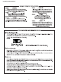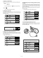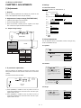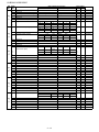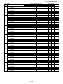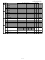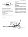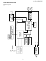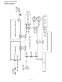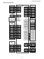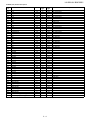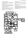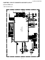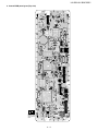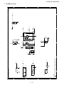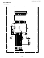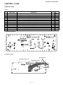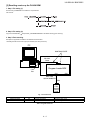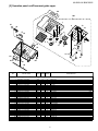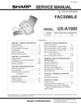
1
UX-B20U/UX-B20C/B25C SERVICE MANUAL No. 00ZUXB20U/SME FACSIMILE UX-B20 UX-B25 MODEL MODEL UX-B20 UX-B20/B25 Illustration: UX-B20U SELECTION CODE DESTINATION U U.S.A. C Canada CONTENTS CHAPTER 1. GENERAL DESCRIPTION [1] Specifications ................................................. 1-1 [2] Operation panel.............................................. 1-2 [3] Transmittable documents ............................... 1-3 [4] Installation ...................................................... 1-4 [5] Quick setup guide ........................................ 1-10 [6] Quick reference guide .................................. 1-11 CHAPTER 2. ADJUSTMENTS [1] Adjustments ................................................... 2-1 [2] Diagnostics and service soft switch ............... 2-2 [3] Troubleshooting ........................................... 2-23 [4] Error code table............................................ 2-24 CHAPTER 3. MECHANISM BLOCKS [1] General description ........................................ 3-1 [2] Ink jet printer .................................................. 3-3 [3] Disassembly and assembly procedures......... 3-6 CHAPTER 4. DIAGRAMS [1] Block diagram ................................................ 4-1 [2] Wiring diagram ............................................... 4-2 [3] Point-to-point diagram.................................... 4-3 [2] [3] [4] [5] Circuit description of control PWB ................5-2 Circuit description of LIU PWB ....................5-15 Circuit description of power supply PWB......5-17 Circuit description of CIS unit ......................5-17 CHAPTER 6. CIRCUIT SCHEMATICS AND PARTS LAYOUT [1] Control PWB circuit .......................................6-1 [2] LIU PWB circuit ........................................... 6-11 [3] Power Supply PWB circuit...........................6-16 [4] Operation Panel PWB circuit .......................6-18 [5] Ink PWB circuit ............................................6-21 CHAPTER 7. OPERATION FLOWCHART [1] Protocol .........................................................7-1 [2] Power on sequence.......................................7-2 CHAPTER 8. OTHER [1] Service tools ..................................................8-1 [2] Changing the record paper size ....................8-4 [3] Rewriting version up the FLASH ROM ..........8-5 Parts Guide CHAPTER 5. CIRCUIT DESCRIPTION [1] Circuit description........................................... 5-1 Parts marked with " " are important for maintaining the safety of the set. Be sure to replace these parts with specified ones for maintaining the safety and performance of the set. SHARP CORPORATION This document has been published to be used for after sales service only. The contents are subject to change without notice. UX-B20U/UX-B20C/B25C –i– UX-B20U/UX-B20C/B25C UX-B20U/UX-B20C/B25C FAX Service E Market Manual 1. GENERAL DESCRIPTION CHAPTER [1] Specifications Automatic feeding: Width: 5.8 to 8.5" (148 to 216 mm) Length(10 sheets): 5.5 to 11" (140 to 279 mm) Length(5 sheets): 5.5 to 14" (140 to 356 mm) Manual feeding: Width: 5.8 to 8.5" (148 to 216 mm) Length: 5.5 to 23.6" (140 to 600 mm) 8.3" (210 mm) max. Effective scanning width: Horizontal: 203 pixels/inch (8 dots/ Scanning resolution: mm) Vertical:Standard: 98 lines/inch (3.85 lines/mm) Fine/Halftone: 196 lines/inch (7.7 lines/mm) Super fine: 391 lines/inch (15.4 lines/mm) 64 levels Halftone (grayscale): Automatic/Dark selectable Contrast control: Single / Multi (99 copies/page) Copy function: 16-digit LCD display Display: 120 V AC, 60 Hz Power requirements: Stand-by: 4.5 W Power consumption: Maximum: 30 W 60 - 90°F (15 - 32°C) Operating temperature: 25 - 80 % RH Humidity: Dimensions (without attach- Width: 13.9" (354 mm) Depth: 9.7" (247 mm) ments): Height: 5.4" (138 mm) Weight (without attachApprox. 7.0 lbs. (3.2 kg) ments): Input document size: Initial cartridge Quality mode OFF: Approx. 300 letter pages Quality mode ON: Approx. 200 letter pages Replacement cartridge: SHARP UX-C70B Quality mode OFF: Approx. 600 letter pages Quality mode ON: Approx. 400 letter pages Letter: Approx. 100 sheets (20-lb.copier Paper tray capacity: paper at room temperature; maximum stack height should not be higher than the line on the tray) Legal: 10 sheets Recommended paper weight: 20-lb. Copy Bond Thermal inkjet Recording system: 600 x 600 dpi Print resolution: 8.0" (203 mm) max. Effective printing width: 448 KB (approx. 24 average pages) Memory size*: 9,600 bps with auto fallback to lower Modem speed: speeds Approx. 15 seconds Transmission time*: ITU-T (CCITT) G3 mode Compatibility: MR, MH, MMR Compression scheme: 30 numbers Automatic dialing: Yes (cannot be used if power fails) Telephone function: Applicable telephone line: Public switched telephone network TEL/FAX Reception modes: Letter/A4: 10 sheets max. (20 lb. paper) Automatic document Legal: 5 sheets max. feeder: Print cartridge yield*: (at 4% coverage**) *Quality mode is initially turned on. To turn off Quality mode. **Based on Sharp Standard Chart at standard resolution, excluding time for protocol signals (i.e., ITU-T phase C time only). As a part of our policy of continuous improvement, SHARP reserves the right to make design and specification changes for product improvement without prior notice. The performance specifications figures indicated are nominal values of production units. There may be some deviations from these values in individual units. 1–1 UX-B20U/UX-B20C/B25C [2] Operation panel 23 4 1 56 5 RESOLUTION/ RECEPTION INK 7 Z A 8 9 10 11 12 13 Illustration: UX-B20U 1. Display 8. POLL key This displays messages and prompts to help you operate the machine. 2. FLASH key This key is used for Call Waiting and other special service that requires subscription from your phone company. Your phone company will provide you with details on how to use the key. 3. RESOLUTION / RECEPTION MODE key When a document is in the feeder, press this key to adjust the resolution for faxing or copying. At any other time, press this key to select the reception mode (an arrow in the display will point to the currently selected reception mode). 4. INK key Press this key after dialing another fax machine to receive a document (previously loaded in the other machine's feeder) without assistance from the operator of the other machine. 9. HOLD key Press this key to put the other party on hold during a phone conversation. 10. SPEAKER key Press this key to listen to the line and fax tones through the speaker when faxing a document. 11. STOP key Press this key to cancel operations before they are completed. 12. START/MEMORY key Press this key after dialing to begin fax transmission. Press this key before dialing to send a fax through memory. The key can also be pressed in the date and time display to show the percentage of memory currently used. Press this key before installing or replacing the print cartridge to move the print cartridge holder to the replacement position. 5. Arrow keys Use these keys to scroll through and select setting, and to search for auto-dial numbers. 13. COPY/HELP key When a document is in the feeder, press this key to make a copy of a document. At any other time, press this key to print 6. FUNCTION key out the Help List, a quick reference guide to the operation of your fax machine. Press this key to followed by the arrow keys select special functions and settings. 7. Number key Use these keys to dial numbers, and enter numbers and letters when storing auto-dial numbers. 1–2 UX-B20U/UX-B20C/B25C [3] Transmittable documents 5. Automatic Document Feeder Capacity 1. Document Sizes Number of pages that can be placed into the feeder at anytime is as follows: Normal size Width Length Normal size: max. ADF 10 pages 148 - 216 mm 140 - 279 mm Special size: single sheet only (manual feed) NOTE: • When you need to send or copy more pages than the feeder limit, place additional pages in feeder when last page in feeder is being scanned. • Place additional pages carefully and gently in feeder. If force is used, double-feeding or a document jam may result. (Max.) (Max.) Letter size (Min.) 140mm 148mm 6. Readable Width & Length 600mm The readable width and length of a document are slightly smaller than the actual document size. 279mm 216mm [Normal size] Note that characters or graphics outside the effective document scanning range will not be read. 216mm [Special size] • Readable width 8.3” (210mm), max Use document carrier sheet for smaller documents. • With special sizes, only one sheet can be fed into the machine at a time. Insert next page into feeder as current page is being scanned. 2. Paper Thickness & Weight Paper weight Paper thickness (ref.) Paper size Feeder capacity 10 sheets 1sheet(Manual) 70 kg 70 kg ~ 135 kg 80 g/m2 52 g/m2 ~ 157g/m2 0.1 mm 0.1 mm ~ 0.18mm LGL (216 mm x 355.6 mm) A4 (210 mm x 297 mm) LTR (216 mm x 279 mm) A4/LTR: 10 sheets max. LGL : 1 sheets max. Readable width • Readable length This is the length of the document sent minus 0.16” (4mm) from the top and bottom edges. 0.16"(4mm) 3. Document Types • Normal paper Readable length Documents handwritten in pencil (No. 2 lead or softer), fountain pen, ball-point pen, or felt-tipped pen can be transmitted. Documents of normal contrast duplicated by a copying machine can also be transmitted. • Diazo copy (blue print) • Diazo copy documents of a normal contrast may be transmitted. • Carbon copy 0.16"(4mm) A carbon copy may be transmitted if its contrast is normal. 4. Cautions on Transmitting Documents • Documents written in yellow, greenish yellow, or light blue ink cannot be transmitted. • Ink, glue, and correcting fluid on documents must be dry before the documents can be transmitted. • All clips, staples and pins must be removed from documents before transmission. • Patched (taped) documents should be copied first on a copier and then the copies used for transmission. • All documents should be fanned before insertion into the feeder to prevent possible double feeds. 1–3 UX-B20U/UX-B20C/B25C [4] Installation 2) Open the print compartment cover. 1. Site selection Take the following points into consideration when selecting a site for this model. ENVIRONMENT • The machine must be installed on a level surface. • Keep the machine away from air conditioners, heaters, direct sunlight, and dust. • Provide easy access to the front, back, and sides of the machine. In particular, keep the area in front of the machine clear, or the original document may jam as it comes out after scanning. • The temperature should be between 60 - 90°F (15 - 32°C). • The humidity should be between 25% and 80% (without condensation). 3) Remove the tape. ELECTRICITY AC 120V, 60Hz, grounded(3-prong) AC outlet is required. Caution! • Connection to a power source other than that specified will cause damage to the equipment and is not covered under the warranty. • If your area experiences a high incidence of lightning or power surges, we recommend that you install a surge protector for the power and telephone lines. Surge protectors can be purchased at most telephone specialty stores. 4) Close the print compartment cover and then the operation panel. If the machine is moved from a cold to a warm place... Condensation may form on the reading glass if machine is moved from a cold to a warm place, this will prevent proper scanning of documents for transmission. Turn on the power and wait approximately 2 hours before using machine. TELEPHONE JACK A standard RJ-11C single-line wall telephone jack must be located near the machine. This is the telephone jack commonly used in most homes and offices. • Plugging the fax machine into a jack which is not RJ-11C single-line wall telephone jack may result in damage to the machine or your telephone system. If you do not know what kind of jack you have, or need to have one installed, contact the telephone company. 3. Connecting the handset Connect the handset as shown and place it on the handset rest. 2. Removing the packing tape 1) Open the operation panel. 1–4 • The ends of the handset cord are identical, so they will go into either jack. • Make sure the handset cord goes into the jack marked with a handset symbol on the side of the machine! • Use the handset to make ordinary phone calls, or to transmit and receive faxes manually. UX-B20U/UX-B20C/B25C 4. Attaching the paper tray 2) Insert the stack of paper into the tray, PRINT SIDE UP. 1) Attach the paper tray. • If paper remains in the tray, take it out and combine it into a single stack with the new paper. • Be sure to load the paper so that printing takes place on the print side of the paper. Printing on the reverse side may result in poor print quality. • GENTLY LOAD PAPER INTO THE PAPER TRAY. • DO NOT FORCE IT DOWN INTO THE FEED SLOT. The stack should not be higher than this line. Note: Do not use paper that has already been printed on, or paper that is curled. 2) Attach the paper tray extension. 6. Connecting the power cord Plug the power cord into a 120 V, 60 Hz, grounded AC (3-prong) outlet. Click! Caution! • Do not plug the power cord into any other kind of outlet. This will damage the machine and is not covered under the warranty. • Make sure you have removed all of the packing tape before plugging in the power cord. Plugging in the power cord without doing so may damage the machine. • The machine does not have a power on/off switch, so the power is turned on and off by simply plugging in or unplugging the power cord. • “CHECK CARTRIDGE” normally appears in the display the first time you plug in the machine. This message appears until you install the print cartridge. 5. Loading printing paper You can load letter or legal size paper in the paper tray. Recommended paper weight is 20-lb. Copy Bond. The maximum number of sheets is as follows: Letter size: Approx. 100 sheets (20-lb. copier paper at room temperature; maximum stack height should not be higher than the line on the tray) Legal size: 10 sheets (20-lb. copier paper at room temperature) 1) Fan the paper, and then tap the edge against a flat surface to even the stack. Make sure the stack edges are even. Note: If you area experiences a high incidence of lightning or power surges, we recommend that you install surge protectors for the power and telephone lines. Surge protectors can be purchased at most telephone specialty stores. 1–5 UX-B20U/UX-B20C/B25C 7. Installing the print cartridge 3) Open the print compartment cover. Follow these steps to install or replace the print cartridge. • When replacing the print cartridge, be sure to use a SHARP UXC70B cartridge. Print cartridge yield (at 4% coverage) Initial cartridge Quality mode OFF: Approx. 300 letter pages Quality mode ON: Approx. 200 letter pages Replacement cartridge (SHARP UX-C70B) Quality mode OFF: Approx. 600 letter pages Quality mode ON: Approx. 400 letter pages Quality mode is initially turned on. To turn off Quality mode, see page 1-8. Caution! Do not open the print compartment cover or insert your hand in the machine while it is printing. Note: Keep print cartridges sealed in their packages until you are ready to install them. It is recommended that you do not use a cartridge that has been left unused for a long time after opening, as the print quality may be considerably degraded. • Make sure the machine’s power cord is plugged in and paper is laded before installing or replacing the print cartridge. • If a document is inserted in the feeder, remove the document before installing or replacing the print cartridge. 4) Remove only the tape from the new cartridge. • Important: Make sure you remove all of the tape. • CAUTION! DO NOT touch the gold contact area on the cartridge. If PRINTER ERROR or PRINTER ERROR/CHECK PAPER appears... In the event that the display shows either of the above messages, you must clear the error before installing the print cartridge. The error can usually be cleared by pressing , or if a paper jam has occurred, by removing the paper jam. 1) Press • INK . Make sure the handset is on its cradle. If the handset is not on the cradle, pressing • INK will have no effect. The print cartridge holder moves to the cartridge replacement position. 5) Make sure the cartridge holder has moved slightly away from the right side of the compartment, and then pull the green lever and open the cartridge holder cover. Display: • If you are replacing the cartridge, remove the old cartridge. If you are going to use the old cartridge again, place it in an airtight container. • CAUTION! DO NOT touch the contact area inside the cartridge holder, or pull on the cable that is connected to the cartridge holder. REPLACE INK & PRESS INK KEY 2) Open the operation panel. Note: if the print compartment cover is left open for approximately 30 minutes with a cartridge installed, the cartridge will automatically return to its home position. To make the cartridge return to the cartridge replacement position when this has happened, press Cable 1–6 INK . Gold contact area UX-B20U/UX-B20C/B25C 6) Insert the new print cartridge into the cartridge holder. 10)Press INK to make the print cartridge holder return to its home position. CHANGE CARTRIDGE 1=NEW, 2=OLD 11)Press (NEW) if the cartridge you installed is new. Press (OLD) if the cartridge you installed is old. 7) Place your index finger on the tab as shown and close the cartridge holder cover with your thumb. Make sure the cover clicks into place. Display when "NEW" is selected: NEW CART. OK? OK: PRESS START 12)Press START/ MEMORY . If you selected “OLD” in the previous step, this completes the installation procedure. (Note: If you find that print quality is not satisfactory after reinstalling the old cartridge, align the cartridge as explained.) 8) Close the print compartment cover. If you selected “NEW”, the display will show the alternating messages at right. Continue with the following steps to align the print cartridge. Display when "NEW" is selected: ALIGN CARTRIDGE 1=PRINT,2=SET 13)Press value without printing an alignment page, press 9) Close the operation panel, pressing down firmly to make sure it clicks into place. Display: to print an alignment page. (To enter an alignment .) 14)In the alignment page that the machine prints, locate the line that comes closest to forming a completely straight line. REPLACE INK & Aft f er the alignment page is printed, the display shows: PRESS INK KEY In this example, "15" comes closest to fo f rming a straight line. 1–7 ENTER (0-30) 15 UX-B20U/UX-B20C/B25C 10. High-quality fax print setting (fast/slow printing of faxes) 15)Press the number keys to enter the number of the straightest line. Example: • If you make a mistake, press 16)Press • START/ MEMORY The high-quality fax print setting controls the speed at which faxes are printed. If you prefer a higher quality image at a slower printing speed, turn on this setting. If you prefer a faster printing speed over image quality, turn off the setting. and then repeat the entry. Note: This setting only affects the printing speed. It does not affect the amount of ink used. . This completes the alignment procedure. • 8. Setting the paper size The machine has been set at the factory to scale received faxes to letter size paper. If you loaded legal paper, you must change the paper size setting to LEGAL. 1 Press 2 Press once and once and Display: twice. PRINT SET-UP PAPER SIZE SET once. The high-quality fax print setting is initially turned off. 1 Press 2 Press once and 3 Press once. 4 Press print, or 3 Press 4 Select the paper size: LETTER: 5 Press 1=LETTER,2=LEGAL once. 5 Press once and twice. 4 times. Display: PRINT SET-UP HQ FAX PRINT 1=YES, 2=NO to turn on high-quality fax The display briefly shows your selection, then: HQ COPY to turn it off. to return to the date and time display. The display briefly shows your selection, then: COPY CUT-OFF LEGAL: 11. Connecting the telephone line cord Insert one end of the line cord into the jack on the back of the machine marked TEL. LINE. Insert the other end into a standard (RJ11C) single-line wall telephone jack. to return to the date and time display. Note: If at any time the display shows the alternating messages at right, check the printing paper. If the tray is empty, add paper. If there is paper in the tray, take it out and then reinsert it. When you are finished, press START/ MEMOR Y ADD PAPER & . PRESS START KEY 9. Quality mode (using more/less ink) If you prefer a higher quality image when printing faxes and copies, turn on Quality mode. If you wish to use less ink or speed up ink drying time, turn off Quality mode. • Quality mode is initially turned on. Display: 1 Press 2 Press once and 3 Press once. 4 Press once and twice. 3 times. PRINT SET-UP QUALITY MODE Setting the dial mode to turn on Quality mode, or to turn it off. 5 Press 1=YES, 2=NO The fax machine is set for tone dialing. If you are on a pulse dial line, you must set the fax machine for pulse dialing. Press the panel keys as follows: The display briefly shows your selection, then: 1 Press once and 3 times. Display: OPTION SETTING HQ FAX PRINT to return to the date and time display. 2 Press once and 3 Press once. 4 Select the dial mode: TONE: 5 1–8 Press PULSE: to exit. 3 times. DIAL MODE 1=TONE, 2=PULSE The display briefly shows your selection, then: DISTINCTIVE UX-B20U/UX-B20C/B25C 12. Clearing a jammed document 13. Clearing jammed printing paper If the original document doesn’t feed properly during transmission or copying, or DOCUMENT JAMMED appears in the display, first try pressing the START/MEMORY key. If the document doesn’t feed out, remove it as explained below. Gently pull the jammed paper out of the machine, taking care not to tear it. After removing the jammed paper, press error message (PAPER JAMMED) from the display. Important: • Do not try to remove a jammed document without releasing it as explained below. This may damage the feeder mechanism. Normal operation cannot be resumed until you press the error message. 1) Open the operation panel. 2) Gently and remove the document. • to clear the Be careful not to tear the document. 3) Close the operation panel, pressing down firmly to make sure it clicks into place. 1–9 to clear UX-B20U/UX-B20C/B25C [5] Quick setup guide 1 1. Open the operation panel. 2. Open the print compartment cover. 3. Remove the packing tape. 4. Close the print compartment cover. 5. Close the operation panel. IMPORTANT!! Should you require any assistance setting up or operating your product, please 2 DO NOT RETURN YOUR PRODUCT TO THE STORE. 3 Connect the handset. 1. Attach the paper tray. Insert horizontally and rotate up After referring to the setup guide and operation manual, if you still require assistance please consult our web page at www.sharpusa.com. From our web page you will be able to directly e-mail our customer support team. If you would like personal assistance, please call our Customer Assistance Center at 1-877-794-8675. 4 Click! If the tabs do not go into the holes, turn the extension over. 5 Load paper. 1. Fan the paper. 2. Attach the paper tray extension. 2. Gently insert paper into the paper tray, print side up.. Connect the phone line cord to the TEL. LINE jack and a wall jack. 6 Plug the power cord into a 120-V grounded outlet. The stack should not be higher than this line Do not force paper down into the feed slot Note: If you are loading legal paper, see of the operation manual to change the paper size setting to LEGAL. 7 Install the Print Cartridge. 1. Make sure the handset is on its cradle and then press INK 2. Open the 3. Open the print operation panel. compartment cover. . 4. Remove only the tape from the new cartridge. IMPORTANT: Make sure you remove all of the tape. Caution! Do not touch the gold contact area. The cartridge holder moves to the cartridge replacement position. 6. Insert the new print cartridge into the cartridge holder. 7. Place your index finger on the tab and close the cartridge holder cover with your thumb. 5. Make sure the cartridge holder has moved slightly away from the right side of the compartment, and then pull the green lever and open the cartridge holder cover. Do not pull on the cable or touch the gold contact area. Gold contact area Cable 8. Close the print compartment cover and then the operation panel. 9. Press INK to make the cartridge holder return to its home position. Display: CHANGE CARTRIDGE 1=NEW, 2=OLD 10.a. Press b. Press to select NEW. START/ MEMOR Y ALIGN CARTRIDGE 11.In the alignment page that the machine prints, locate the line that comes closest to forming a completely straight line. Enter the number of that line. 12. Press START/ MEMOR Y . Example: 1=PRINT,2=SET (If you make a mistake, press c. Press to print an alignment page. and then repeat the entry.) Note: To enter your name and fax number and set the date and time so that they appear at the top of each fax you send, see page Chapter 1 of your operation manual. 1 – 10 UX-B20U/UX-B20C/B25C [6] Quick reference guide 3. Storing Auto Dial Numbers 1. Sending Faxes 1. Press Place your document (up to 10 pages) face down in the document feeder. 2. Enter the full fax number. 3. Press once and START/ MEMORY twice. . 4. Enter a name by pressing number keys. (To enter two letters in succession that require the same key, press after entering the first letter.) G= N= A= H= O= V= B= I = P= W= SPACE = 1.1. Normal Dialing 1. Lift the handset or press . 2. Dial the fax number. 3. Wait for the reception tone (if a person answers, ask them to press their Start key). 4. Press START/ MEMORY 1.2. Automatic Dialing 1. Press or until the desired destination appears in the display. 2. Press START/ MEMORY . 1.3. Direct Keypad Dialing 1. Dial the fax number. 2. Press START/ MEMORY . 2. Receiving Faxes Press the RESOLUTION/ RECEPTION until the arrow in the display points to the desired reception mode. TEL FAX RESOLUTION/ RECEPTION JAN-03 10:30 TEL FAX JAN-03 10:30 FAX mode: The fax machine automatically answers and receives faxes. TEL mode: Answer all calls (even faxes) by picking up the handset. To begin fax reception, press START/ MEMORY C= J= Q= X= D= K= R= Y= E= L= S= Z= F= M= T= 5. Press . . 1 – 11 U= START/ MEMORY and then . UX-B20U/UX-B20C/B25C UX-B20U/UX-B20C/B25C FAX Service E Market Manual 2. ADJUSTMENTS CHAPTER 4. Settings 4.1. Dial mode selector [1] Adjustments DIAL mode (Soft Switch No. SW-B4 Data No. 3) 1. General (step 1) Select "OPTION SETTING". Since the following adjustments and settings are provided for this model, make adjustments and/or setup as necessary. KEY : FUNCTION DISPLAY: 2. Adjustments of output voltage (FACTORY ONLY) KEY: Push until DIAL MODE indicated because the number of 's changes by the model. 1. Install the power supply unit in the machine. 2. Set the recording paper and document. DISPLAY: 3. When the document is loaded, power is supplied to the output lines. Confirm that outputs are within the limits below. 1 CNPW CNFDMT CNCRMT 8 CNPRG CNPN CNHEAD1 CNBKL CNSP FINE PRIORITY DIAL MODE is 1=TONE, 2=PULSE (step 3) Select, using "1" or "2". 2.1. Output voltage settings CNHEAD2 OPTION SETTING (step 2) Select "DIAL MODE". KEY: 1 DISPLAY: TONE SELECTED KEY: 2 DISPLAY: PULSE SELECTED CNLIU (step 4) End, using the "STOP" key. CNCIS KEY: CONTROL PWB 5. Volume adjustments 8 You can adjust the volume of the speaker, handset, and ringer using the UP and DOWN arrow keys. 1 CNPW LIU PWB 5.1. Speaker POWER SUPPLY PWB CNLIU Output +5V +30V Voltage limits 4.75V ~ 5.25V 27.0V ~ 33.0V Connector No. Pin No. 1 2 3 4 5 6 7 8 1 Press . CNPW 2 +30V +30V MG MG DG DG +5V +5V Press or to select the desired vo lume le vel. • Press again to turn off the speaker. Display: SPEAKER: HIGH SPEAKER: MIDDLE SPEAKER: LOW 5.2. Handset 1 3. IC protectors replacement Press or to select the desired vo lume le vel. (Make sure ICPs (IC Protectors) are installed to protect the motor driver circuit. ICPs protect various ICs and electronic circuits from an overcurrent condition. Display: RINGER: HIGH has not been pressed, the handset is not lifted, and a document is not loaded in the feeder.) RINGER: MIDDLE • The ringer will ring once at the selected RINGER: LOW level. The location of ICPs are shown below: RINGER: OFF OK ? CNHEAD2 CNPRG CNPN CNLIU CNCRMT CNHEAD1 CNFDMT FU101 CNBKL CNSP 2 CNCIS If yo u selected RINGER: OFF OK ? to turn off the ringer , press START/ MEMORY . CNPW FU100 CONTROL PWB (TOP SIDE) 5.3. Ringer 1) FU100 (KAB5002) is installed in order to protect IC's from an overcurrent generated in the motor drive circuit. If FU100 is open, replace it with a new one. 1 2) FU101 (KAB3202) is installed in order to protect IC's from an overcurrent generated in the motor drive circuit. If FU101 is open, replace it with a new one. When talking thr ough the handset, Display: press or to select the desired vo lume le vel. RECEIVER: HIGH • Note: The volume reverts to MIDDLE RECEIVER: MIDDLE each time you replace the handset. RECEIVER: LOW 2–1 UX-B20U/UX-B20C/B25C [2] Diagnostics and service soft switch 1. Entering the diagnostic mode Press FUNC → 9 → ROM Ver. TC25 → 8 → # → 7 , and the following display will appear. After 2 sec: DIAG MODE or TC44 TC25 (UX-B20U) TC44 (UX-B20C/UX-B25C) Then press the START key. Select the desired item with the UP key or the DOWN key or select with the rapid key. Enter the mode with the START key. (Diag· specifications) FUNC 9 8 TC25 or TC44 7 DIAG MODE START START START Entry data rcv. ROM & RAM check START START Entry data send Aging mode START START Auto feeder mode Panel key test START START Shading mode Check pattern START START Memory clear Signal send mode START Soft switch mode If the diag mode cannot be set, repeat the diag mode operation, performing the following operation. After the power is turned on and "WAIT A MOMENT" is indicated, press the STOP key. START/ MEMORY "Power ON" + STOP KEY START KEY In relation with the process response (request from Production Engineering) "WAIT A MOMENT" clock indication may appear depending on STOP key timing. If the STOP key is held down, "MEMORY CLEAR?" appears. 2. Diagnostic items ITEM No. Contents Function 1 SOFT SWITCH MODE Soft switches are displayed and changed. List can be output. 2 ROM & RAM CHECK ROM sum-check and RAM is matched. Result list is output. 3 AGING MODE 10 sheets of check patterns are output every 5 minutes per sheet. 4 PANEL KEY TEST Panel keys are tested. Result list is output. 5 CHECK PATTERN Check pattern is output. 6 SIGNAL SEND MODE Various signals of FAX communication are output. 7 MEMORY CLEAR Back-up memory is cleared, and is set at delivery. 8 SHADING MODE Shading compensation is performed in this mode. 9 AUTO FEEDER MODE Insertion and discharge of document are tested. 10 ENTRY DATA SEND Registered content is sent. 11 ENTRY DATA RECEIVE Registered content is received, and its list is output. 2–2 UX-B20U/UX-B20C/B25C 3. Diagnostic items description 3.6. Signal send mode This mode is used to send various signals to the circuit during FAX communication. Every push of START key sends a signal in the following sequence. Moreover, the signal sound is also output to the speaker when the line monitor of the soft switch is on. 3.1. Soft switch mode Used to change the soft switch settings. The soft switch which is stored internally is set by using the keys. The available soft switches are SW-A1 to SW-P7. The content of soft switches is shown in Soft switch description. The contents are set to factory default settings. The result will be notified with the number of short sounds of the buzzer as well as by printing the ROM & RAM check list. [1] [2] [3] [4] [5] [6] [7] [8] Number of short sounds of buzzer 0 → No error 3.7. Memory clear 3.2. ROM & RAM check ROM executes the sum check, and RAM executes the matching test. 1 → FAX engine ROM error No signals 9600BPS (V.29) 7200BPS (V.29) 4800BPS (V.27ter) 2400BPS (V.27ter) 300BPS (FLAG) 2100Hz (CED) 1100Hz (CNG) This mode is used to clear the backup memory and reset to the default settings. 2 → RAM error (4Kbytes SRAM or 512Kbytes DRAM) 3.8. Shading mode 3.3. Aging mode The mode is used for the shading compensation. For reading, set up the special original paper. (Refer to page 8-3) The compensation memorizes the reference data of white and black for reading. Moreover, the memorized data is not erased even if memory clear mode is executed. The check pattern will be printed sheet by sheet. This operation will be executed at a rate of one sheet per 5 minutes, and will be ended at a total of 10 sheets. 3.4. Panel key test 3.9. Auto feeder mode This mode is used to check whether each key operates properly. Press the key on the operation panel, and the key will be displayed on the LCD. Therefore, press all keys. At this time, finally press the STOP key. When the STOP key is pressed, the keys that are not judged as "pressed" will be printed on the result list. • In this mode, a document is inserted and discharged to check the auto feed function. After this mode is started, set a document, and the document feed will be automatically tested. LED part of the contact image sensor (CIS) is kept on during the term from when "START" of the panel test mode to end with the STOP key. 3.10. Entry data send 3.5. Check pattern This mode is used to send the registered data to another machine and make the other machine copy the registered content. Check patterns are printed on one sheet. Printing performance:The following 4 items are checked. Before sending in this mode, it is necessary to set the other machine at the entry data receive mode. • Print area:Checks that the print area is reserved. The following, information will be sent to the remote machine: • Nozzles:When checking the nozzle, make sure at least 1 line is printed in each block: all the blocks of horizontal black bars and the black line patterns in (B) and (C) ((B):16 patterns, (C):13 patterns). (Note: If the nozzle (A) is not spraying properly, checking the area (B) and (C) may be difficult (or may not be printed at all). In this case, print again. 1. Telephone list data • Vertical align:Checks that the straight vertical line is drawn instead of crooked line. 6. Recording setting list data • Skew:Checks the skew of the recording paper. 3.11. Entry data receive 2. Sender register data 3. Optional setting content 4. Soft switch content 5. Junk fax number In this mode, the registered data sent from the other machine is received and the received data is registered in the machine. When this mode is used for receiving, the other machine must be in the entry data send mode. Detailed of check patterns (1)Top skew (2)Nozzle test (3)Vertical lines (4)Bottom skew (5)Top margin (6)Left margin (7)Bottom margin (6) After receiving is completed, the following lists are printed. (1) 1. Telephone list data (5) 2. Sender register list (*) 3. Optional setting list (*) (A) (B) 4. Soft switch content (2) (C) 5. Junk fax number list (*) 6. Recording setting list data (*) (*): Refer to SETUP LIST (3) 0 1 2 3 4 5 6 7 8 9 10 11 12 13 14 15 16 17 18 19 20 21 22 23 24 25 26 27 28 29 30 (7) (4) 2–3 UX-B20U/UX-B20C/B25C 4. Entering the printer diagnostic mode Press FUNC 9 8 # 6 , and the following display will appear. PRINT DIAG MODE Then press the START key. Select the desired item with the up key or the down key or select with the rapid key. Enter the mode with the START key. (Diag· specifications) FUNC 9 8 6 PRINT DIAG MODE 4% DATA PRINT AGING START ASF AGING START ASF SKEW CHECK AGING START CROSS PATTERN START INITIAL CARTRIDGE DATA SETTING START IJP LIST MODE START PRINTER ERROR CHECK MODE START START If the diagnostic mode cannot be set, repeat the diagnostic mode operation, performing the following operation. After the power is turned on and "WAIT A MOMENT" is indicated, press the STOP key. START/ MEMORY "Power ON" + STOP KEY In relation with the process response (request from Production Engineering) "WAIT AMOMENT" clock indication may appear depending on STOP key timing. If the STOP key is held down, "MEMORY CLEAR?" appears. START KEY 5. Printer diagnostic items Item No. 1 2 3 4 5 6 7 Contents 4% DATA PRINT AGING ASF AGING ASF SKEW CHECK AGING CROSS PATTERN INITIAL CARTRIDGE DATA SETTING IJP LIST MODE PRINTER ERROR CHECK MODE Function 4% of printing data continue to be printed. The feed of the paper is continued. The frame pattern continues to be printed to check the inclination performance. The image data of the cross pattern to be printed. It makes the dot counter the setting for the initial cartridge. The maintenance data is printed. The cause of “PRINTER ERROR” message is displayed. 6. Printer diagnostic items description 6.1. 4% data print aging 6.4. Cross pattern This mode is the aging mode that prints the text pattern of 4% This mode prints the test pattern that tests the performance of the printer. 6.2. ASF aging (all white) 6.5. Initial cartridge data setting This mode is the aging mode that tests the performance of the ASF function. This mode makes the dot counter the setting for initial cartridge, and this mode resets the following counter. 6.3. ASF skew check aging 1. Replacement counter of the cartridge This mode is the aging mode that tests the performance of the ASF function. 2. Paper jam counter Detailed of check patterns 1. Top skew 2. Bottom skew 3. Top margin 4. Bottom margin 2–4 UX-B20U/UX-B20C/B25C 6.6. IJP list mode Maintenance data of the printer is output. [Details of maintenance data] Item Dot counter Page counter Number of head cleaning (Wiping of cartridge) Replacement counter of the cartridge Jam counter Clear timing At the replacement cartridge At the replacement cartridge At the initial cartridge setting At the initial cartridge setting At the initial cartridge setting Update timing After printing After printing At the maintenance At the replacement of cartridge At every paper jam 6.7. Printer error check mode The cause of “PRINTER ERROR” message is displayed. [Details of Display] Display PRINTER ERR 01 PRINTER ERR 02 PRINTER ERR 03 PRINTER ERR 04 PRINTER ERR 05 PRINTER ERR 06 PRINTER ERR 07 PRINTER ERR 08 PRINTER ERR 09 PRINTER ERR 10 PRINTER ERR 20 PRINTER ERR 21 PRINTER ERR 22 PRINTER ERR 23 PRINTER ERR 24 PRINTER ERR 25 PRINTER ERR 26 Cause of “PRINTER ERROR” message Power on reset response was not received from printer. Print data transfer from Printer interface ASIC to printer was not completed for 180 sec. Cap position check of the carrier is failed. Printing 1 page is not finished during 5 min. Carrier moving from cartridge change position to cap position is failed. Carrier moving to cartridge change position is failed. Cartridge replacement is failed. Cartridge ID check is failed. Carrier was not reached to cap position for 60 sec after last printed page was exited. Paper pick up is failed. Carrier stall error. Carrier stall error. Carrier stall error. Carrier stall error. Printer head short error. Printer head heater control is failed. Print start position setting is abnormal. 2–5 UX-B20U/UX-B20C/B25C 7. How to make soft switch setting To enter the soft switch mode, press the following key entries in sequence. Press FUNCTION DATA No. 9 8 7 START START 1 2 3 4 5 6 7 8 S F T SW-A1 = 0 0 0 0 0 0 0 0 Press FUNCTION key. S F T SW-A1 = 1 0 0 0 0 0 0 0 Press key. Press key. S F T SW-A1 = 1 0 0 0 0 0 0 0 S F T SW-A1 = 1 0 0 0 0 0 0 0 Bit1 - 8 are set. S F T SW-A1 = 1 0 0 0 0 0 0 0 Press START key during setting. S F T SW-A2 = 0 0 0 0 0 0 0 0 Soft SW-A2 - SW-P7 are set. S F T SW-P7 = 0 0 0 0 0 0 0 0 To finish the settings halfway between SW-A1 and SW-P7, press the STOP key. In this case, the setting being done to the SW No. on display will be nullified while settings done to the preceding SW No. remain in effect. When the COPY key is pressed, the contents of soft switches are printed. The soft switch mode is terminated. 2–6 UX-B20U/UX-B20C/B25C 8. Soft switch description 8.1. Soft switch SW NO. SW l A1 DATA NO. 1 2 3 4 5 6 7 8 SW I A2 1 2 3 4 5 6 7 8 Protect from echo Forced 4800 BPS reception Footer print Length limitation of copy/send/ receive CSI transmission DIS receive acknowledgement during G3 Non-modulated carrier for V29 transmission modem EOL detect timer Modem speed Sender’s information transmit H2 mode Communication error treatment in RTN sending mode (reception) CNG transmission CED tone signal interval 1 2 SW l A3 3 4 5 6 7 8 1 2 3 4 5 MR coding Reserved Reserved Reserved Reserved Reserved Signal transmission level 6 7 8 Protocol monitor (Error print) Protocol monitor Line monitor Digital line equalization setting (Reception) SW l A5 3 4 5 6 7 8 1 No Yes Yes No limit Yes No No Copy/send: 60 cm Receive: 1 m Transmitted NSF: Once DIS: Twice No No transmitted Twice Yes 25sec No. 1 0 0 0 0 V.29 9600bps V.29 7200bps V.27ter 4800bps V.27ter 2400bps No No No communication error No No. 1 No. 2 No Initial setting U/C 0 0 0 0 0 1000ms 1 1 750ms 1 0 0 0 0 13sec No.2 No. 3 0 0 0 1 0 1 0 0 Yes Yes Communication error Yes 500ms 0 1 Yes Digital line equalization setting (Transmission) Digital cable equalizer setting (Reception for Caller ID) Error criterion Anti junk fax check 2–7 0 0 0 1 0 0 0 0 0 Binary input 16 8 4 2 1 1 2 3 4 5 EX 0 0 1 1 1 eg. Signal transmission level is set to -7dBm. Printed at communication error Not printed Yes No Yes No 7.2km No. 1 1 No. 2 1 7.2km No. 3 1 No. 4 1 7.2km No. 5 1 No. 6 1 10 ~ 20% 5 ~ 10 % Yes No 0 No. 4 1 1 0 0 0 75ms 0 0 No. = SW l A4 1 2 Switch setting and function ITEM 0 0 0 0 0 0 0 0 1 1 1 0 0 0 0km 0 0 0km 0 0 0km 0 0 1 1 0 0 0 0 0 1 Remarks UX-B20U/UX-B20C/B25C SW NO. SW l A6 DATA NO. 1 2 3 4 5 6 7 8 1 2 3 4 Switch setting and function ITEM Reserved Reserved Disconnect the line when DIS is received in RX mode Equalizer freeze control (MODEM) Equalizer freeze control 7200 BPS only CNG transmission in manual TX mode Initial compression scheme for sharp fax in TX mode Modem speed automatic fallback when RX level is under -40dBm Recall interval 1 0 Initial setting U/C 0 0 1 No Yes On No Off Yes 0 0 Yes No 1 MR mode H2 mode 0 Yes No 0 Remarks 0 1 0 1 Binary input No. = 8 4 2 1 1 2 3 4 EX 0 1 0 1 eg. Recall interval is set to 5 min. SW l B1 5 6 7 8 Recall times 0 0 1 1 Binary input No. = 8 4 2 1 5 6 7 8 EX 0 0 1 1 eg. Recall time is set to 3 times. SW l B2 SW l B3 1 2 3 4 4 sec No 5 6 7 8 1 2 3 4 5 8 1 2 3 4 5 6 7 8 No. 5 No. 6 Reserved Reserved Reserved Reserved Reserved Reserved Reserved Auto dial mode delay timer of before line connect Hold key Auto dial mode delay timer of after line connect Dial mode Pulse → Tone change function by key Dial pulse make/break ratio (%) Reserved Reserved Recalling fixed only one time when dialing was unsuccessful without detecting busy tone signal 2 sec Yes No Waiting time after dialing 6 7 SW l B4 Dial pausing (sec/pause) Dial tone detection (before auto dial) Reserved Busy tone detection (after auto dial) 45 sec 0 0 55 sec 0 1 Yes 90 sec 1 0 0 1 0 0 140 sec 1 1 0 0 0 0 0 0 0 0 0 No. 6 No. 7 Enable No. 1 No. 2 Tone Enable 0 sec 0 0 1.5 sec 0 1 1.7 sec 0 0 3.0 sec 0 1 3.0 sec 1 0 Disable 3.6 sec 1 0 Pulse Disable 40/60 33/67 Yes No 2–8 4.5 sec 1 1 0 0 1 4.0 sec 1 1 0 0 1 1 1 0 0 1 OPTION UX-B20U/UX-B20C/B25C SW NO. DATA NO. 1 2 3 4 5 Switch setting and function ITEM 1 DTMF signal transmission level (Low) Binary input 16 8 4 2 1 1 2 3 4 5 (n x 0.5dBm) EX 0 0 1 1 0 eg. Signal transmission level is set to -3dBm. No. = SW l B5 6 7 8 1 2 3 4 5 Reserved Reserved Reserved DTMF signal transmission level (High) Binary input 16 8 4 2 1 1 2 3 4 5 (n x 0.5dBm) EX 0 0 0 1 1 No. = SW l B6 Initial setting U/C 0 0 1 1 0 Remarks 0 0 0 0 0 0 1 1 eg. Signal transmission level is set to -1.5dBm. 6 7 8 Reserved Reserved Reserved Reading slice (Binary) 0 0 0 No. 1 No. 2 1 2 SW l C1 0 Reading slice (Half tone) 3 4 5 6 7 8 1 2 3 4 Line density selection Reserved MTF correction in half tone mode Reserved Number of rings for auto receive No. 3 No. 4 Fine Factory setting 0 0 Factory setting 0 0 Light Dark 1 0 Light 0 1 Dark 1 0 0 1 Standard No Darker in dark 1 1 Darker in dark 1 1 Binary input No. = 8 4 2 1 1 2 3 4 EX 0 1 0 0 0 0 0 0 0 0 1 0 0 Yes SW l D1 0 0 OPTION OPTION 0 eg. Number of rings for auto receive is set to 4times. 5 6 Automatic switching manual to auto receive mode Reserved Cl detect frequency Reception after 5 rings 1 2 3 Distinctive ringing setting (PATTERN 4 and 5 are for CANADA only) 4 5 6 7 8 Reserved Caller ID function Caller ID detect during CI off Reserved Reserved SW l D2 0 0 No. 7 No. 8 7 8 No reception As PTT 0 0 OFF STANDARD PATTERN1 PATTERN2 PATTERN3 PATTERN4 PATTERN5 Yes All times 11.5Hz 0 1 No. 1 0 0 0 0 1 1 1 13.0Hz 1 0 No. 2 0 0 1 1 0 0 1 No Only first 2–9 20.0Hz 1 1 No. 3 0 1 0 1 0 1 0 0 0 0 0 0 0 0 0 0 0 OPTION OPTION UX-B20U/UX-B20C/B25C SW NO. DATA NO. 1 2 3 4 5 Switch setting and function ITEM 1 Cl off detection timer (0-1550ms setting by 50ms step) Binary input 16 8 4 2 1 1 2 3 4 5 (n x 50ms) EX 0 1 1 1 0 eg. CI signal OFF detect time is set to 700ms. No. = SW l D3 SW l E1 SW l E2 SW l E3 6 7 8 1 2 3 4 5 6 7 8 1 2 3 4 5 6 7 8 1 2 3 4 5 6 7 8 Reserved Reserved Reserved Reserved Reserved Reserved Reserved Reserved Reserved Reserved Reserved Reserved Reserved Reserved Reserved Reserved Reserved Reserved Reserved Reserved Reserved Reserved Reserved Reserved Reserved Reserved Reserved DTMF detection time 1 2 3 4 SW l F1 5 6 7 8 0 Protection of remote reception (5 ) detect Remote reception with GE telephone Remote operation code figure by external TEL (0~9) Initial setting U/C 0 1 1 1 0 0 0 0 0 0 0 0 0 0 0 0 0 0 0 0 0 0 0 0 0 0 0 0 0 0 0 0 No. 1 No. 2 Yes 50ms 0 0 Compatible 80ms 0 1 100ms 1 0 No 120ms 1 1 1 Not compatible 2 – 10 1 0 1 0 1 Binary input No. = 8 4 2 1 5 6 7 8 EX 0 1 0 1 eg. Remote operation code is set to 5 0 0 . Remarks UX-B20U/UX-B20C/B25C SW NO. SW l F2 SW l G1 SW l G2 SW l G3 SW l H1 SW l H2 SW l I1 DATA NO. 1 2 3 4 5 6 7 8 1 2 3 4 5 6 7 8 1 2 3 4 5 6 7 8 1 2 3 4 5 6 7 8 1 2 3 4 5 6 7 8 1 2 3 4 5 6 7 8 1 2 3 4 5 6 7 8 Switch setting and function ITEM CNG detection in STAND-BY mode Reserved Reserved Number of CNG detect (STAND-BY mode) 1 0 Yes No. 4 No. 5 No 1pulse 0 0 2pulses 0 1 Reserved Reserved Reserved Reserved Reserved Reserved Reserved Reserved Reserved Reserved Reserved Reserved Reserved Reserved Reserved Reserved Reserved Reserved Reserved Reserved Reserved Reserved Reserved Reserved Reserved Reserved Reserved Reserved Reserved Reserved Reserved Reserved Reserved Reserved Reserved Reserved Reserved Reserved Reserved Reserved Reserved Reserved Reserved Reserved Reserved Reserved Reserved Reserved Reserved Reserved Reserved 3pulses 1 0 4pulses 1 1 Initial setting U/C 1 0 0 0 1 0 0 0 0 0 0 0 0 0 0 0 0 0 0 0 0 0 0 0 0 0 0 0 0 0 0 0 0 0 0 0 0 0 0 0 0 0 0 0 0 0 0 0 0 0 0 0 0 0 0 0 2 – 11 Remarks OPTION UX-B20U/UX-B20C/B25C SW NO. SW l I2 SW l I3 SW l I4 SW l I5 SW l I6 SW l I7 DATA NO. 1 2 3 4 5 6 7 8 1 2 3 4 5 6 7 8 1 2 3 4 5 6 7 8 1 2 3 4 5 6 7 8 1 2 3 4 5 6 7 8 1 2 3 4 5 6 7 8 ITEM Switch setting and function 1 Reserved Reserved Reserved Reserved Reserved Reserved Reserved Reserved Reserved Reserved Reserved Reserved Reserved Reserved Reserved Reserved Reserved Reserved Reserved Reserved Reserved Reserved Reserved Reserved Reserved Reserved Reserved Reserved Reserved Reserved Reserved Reserved Reserved Reserved Reserved Reserved Reserved Reserved Reserved Reserved Reserved Reserved Reserved Reserved Reserved Reserved Reserved Reserved 2 – 12 0 Initial setting U/C 0 0 0 0 0 0 0 0 0 0 0 0 0 0 0 0 0 0 0 0 0 0 0 0 0 0 0 0 0 0 0 0 0 0 0 0 0 0 0 0 0 0 0 0 0 0 0 0 Remarks UX-B20U/UX-B20C/B25C SW NO. SW l J1 DATA NO. 1 2 3 4 5 6 Switch setting and function ITEM Reserved Reserved Sender’s phone number setting Reserved Reserved Summer time setting Ringer volume 1 Cannot change No. 1 No. 2 Off 0 0 Low 0 0 Low 0 1 Low 0 1 Yes Middle 1 0 Middle 1 0 High 1 1 High 1 1 No. 4 No. 5 Low 0 0 Low 0 1 Middle 1 0 High 1 1 Speaker volume (3 stages) 1 2 SW l J2 3 6 7 8 1 SW l J3 SW l K1 SW l L1 SW l L2 Reserved Handset receiver volume 4 5 2 3 4 5 6 7 8 1 2 3 4 5 6 7 8 1 2 3 4 5 6 7 8 1 2 3 4 5 6 7 8 OPTION OPTION 1 0 OPTION 1 0 OPTION 1 0 0 0 0 0 E/T/M No. 2 No. 3 No. 4 Send only 0 0 1 0 0 0 Yes Enable Enable Always No print Err only 0 1 0 0 1 1 1 0 0 No Disable Disable No. 1 No. 2 Automatic reduce of receive Reserved Reserved Reserved Reserved Reserved Remarks 0 Reserved Reserved Reserved Reserved Communication results printout (Transaction report) Reserved Reserved Reserved Reserved Reserved Reserved Reserved Reserved Reserved Reserved Reserved Reserved Reserved Reserved Reserved Reserved Cut off mode (COPY mode) A4 paper enable LEGAL & LETTER paper enable Reserved Paper set size Change allowed No No. 7 No. 8 7 8 Initial setting U/C 0 0 0 0 0 1 0 LETTER 0 0 Auto 2 – 13 LEGAL 0 1 100 % A4 1 0 OPTION 1 0 0 0 0 0 0 0 0 0 0 0 0 0 0 0 0 0 0 1 0 1 0 OPTION OPTION 0 0 1 0 0 0 0 0 OPTION UX-B20U/UX-B20C/B25C SW NO. SW l M1 SW l M2 SW l N1 SW l N2 SW l N3 SW l O1 SW l O2 DATA NO. 1 2 3 4 5 6 7 8 1 2 3 4 5 6 7 8 1 2 3 4 5 6 7 8 1 2 3 4 5 6 7 8 1 2 3 4 5 6 7 8 1 2 3 4 5 6 7 8 1 2 3 4 5 6 7 8 ITEM Switch setting and function 1 Reserved Reserved Reserved Reserved Reserved Reserved Reserved Reserved Reserved Reserved Reserved Reserved Reserved Reserved Reserved Reserved Reserved Reserved Reserved Reserved Reserved Reserved Reserved Reserved Reserved Reserved Reserved Reserved Reserved Reserved Reserved Reserved Reserved Reserved Reserved Reserved Reserved Reserved Reserved Reserved Reserved Reserved Reserved Reserved Reserved Reserved Reserved Reserved Reserved Reserved Reserved Reserved Reserved Reserved Reserved Reserved 2 – 14 0 Initial setting U/C 0 0 0 0 0 0 0 0 0 0 0 0 0 0 0 0 0 0 0 0 0 0 0 0 0 0 0 0 0 0 0 0 0 0 0 0 0 0 0 0 0 0 0 0 0 0 0 0 0 0 0 0 0 0 0 0 Remarks UX-B20U/UX-B20C/B25C SW NO. SW l O3 SW l O4 SW l O5 SW l O6 SW l P1 SW l P2 SW l P3 DATA NO. 1 2 3 4 5 6 7 8 1 2 3 4 5 6 7 8 1 2 3 4 5 6 7 8 1 2 3 4 5 6 7 8 1 2 3 4 5 6 7 8 1 2 3 4 5 6 7 8 1 2 3 4 5 6 7 8 ITEM Switch setting and function 1 Reserved Reserved Reserved Reserved Reserved Reserved Reserved Reserved Reserved Reserved Reserved Reserved Reserved Reserved Reserved Reserved Reserved Reserved Reserved Reserved Reserved Reserved Reserved Reserved Reserved Reserved Reserved Reserved Reserved Reserved Reserved Reserved Reserved Reserved Reserved Reserved Reserved Reserved Reserved Reserved Reserved Reserved Reserved Reserved Reserved Reserved Reserved Reserved Reserved Reserved Reserved Reserved Reserved Reserved Reserved Reserved 2 – 15 0 Initial setting U/C 0 0 0 0 0 0 0 0 0 0 0 0 0 0 0 0 0 0 0 0 0 0 0 0 0 0 0 0 0 0 0 0 0 0 0 0 0 0 0 0 0 1 1 0 1 1 1 1 0 0 0 0 0 0 0 0 Remarks UX-B20U/UX-B20C/B25C SW NO. SW l P4 SW l P5 SW l P6 SW l P7 DATA NO. 1 2 3 4 5 6 7 8 1 2 3 4 5 6 7 8 1 2 3 4 5 6 7 8 1 2 3 Reserved Reserved Reserved Reserved Reserved Reserved Reserved Reserved Reserved Reserved Reserved Reserved Reserved Reserved Reserved Reserved Ink save mode Half tone copy ink save mode printing fixed Reserved Reserved Reserved Reserved Reserved Reserved Reserved Reserved Reserved End buzzer 4 5 6 7 8 Switch setting and function ITEM Key error/Communication error beep End beep (3sec) Key touch tone 1 0 Yes Yes No No Initial setting U/C 0 0 0 0 0 0 0 0 0 0 0 0 0 0 0 0 0 1 Remarks OPTION 0 0 0 0 0 0 0 0 0 3sec 0 0 No. 4 No. 5 No beep No beep No beep 1sec 0 1 Beep Beep Beep 2 – 16 No beep 1 0 0 0 0 OPTION 0 0 OPTION OPTION UX-B20U/UX-B20C/B25C 8.2. Soft switch function description SW-A2 No. 5 Sender’s information transmit SW-A1 No. 1 Protect from echo SW-A1 No. 2 Forced 4800BPS reception (SENDER’S INFORMATION TRANSMISSION) is a switch to set the function to print the content of HEADER PRINT described in the passcode list at the front end of receiver’s original when original is sent to the remote machine. When line conditions warrant that receptions take place at 4800 BPS repeatedly. If this switch is set to "NO", the HEADER PRINT is not output at the receiving machine. It may improve the success of receptions by setting at 4800BPS. SW-A2 No. 6 H2 mode This improves the receiving document quality and reduces handshake time due to fallback during training. Used to determine reception of H2 mode (15 sec transmission mode). When set to OFF, H2 mode reception is inhibited even though the transmitting machine has H2 mode function. Used to protect from echo in reception. SW-A1 No. 3 Footer print SW-A2 No. 7 Communication error treatment in RTN sending mode (Reception) When set to "1", the date of reception, the sender machine No., and the page No. are automatically recorded at the end of reception. Used to determine communication error treatment when RTN is sent by occurrence of a received image error in G3 reception. When it is set to "1", communication error is judged as no error. SW-A1 No. 4 Length limitation of copy/send/receive Used to set the maximum page length. To avoid possible paper jam, the page length is normally limited to 0.6 meter for copy or transmit, and 1 meters for receive. SW-A2 No. 8 CNG transmission It is possible to set it to "No limit" to transmit a long document, such as a computer print form, etc. (In this case, the receiver must also be set to no limit.) When set to "0" , this model allows CNG transmission by pressing the Start key in the key pad dialing mode. When set to "1", CNG transmission in the key pad dialing mode cannot be performed. In either case. CNG transmission can be performed in the auto dial mode. SW-A1 No. 5 CSI transmission SW-A3 No. 1, No. 2 CED tone signal interval (CSI TRANSMISSION) is a switch to set whether the machine sends or does not send the signal (CSI signal) informing its own telephone No. to the remote fax machine when information is received. When "nonsending" is set, the telephone No. is not output on the remote transmitting machine if the remote transmitting machine has the function to display or print the telephone No. of receiving machine, using this CSI signal. For international communication, the 2100Hz CED tone may act as an echo suppression switch, causing a communication problem. Though SW-A3 No. 1 and No. 2 are normally set to 0, this setting is used to change the time between the CED tone signal to eliminate the communication caused by echo. TX RX SW-A1 No. 6 DIS receive acknowledgment during G3 transmission CED Used to make a choice of whether reception of DIS (NSF) is acknowledged after receiving two DISs (NSFs) or receiving one DIS (two NSFs). DIS It may be useful for overseas communication to avoid an echo suppression problem, if set to 1. SW-A3 No. 3 MR Coding SW-A1 No. 7 Non-modulated carrier for V.29 transmission modem SW-A3 No. 4 ~ No. 8 Reserved Though transmission of a non-modulated carrier is not required for transmission by the V.29 modem according to the CCITT recommendation, it may be permitted to a send non-modulated carrier before the image signal to avoid an echo suppression problem. It may be useful for overseas communication to avoid an echo suppression problem, if set to 1. Set to "0". T MR Coding is enable. SW-A4 No. 1 ~ No. 5 Signal transmission level Used to control the signal transmission level in the range of-0dB to31dB. SW-A4 No. 6 Protocol monitor (Error print) SW-A1 No. 8 EOL (End Of Line) detect timer If set to "1", protocol is printed at communication error. Used to make a choice of whether to use the 25-second or 13-second timer for detection of EOL. SW-A4 No. 7 Protocol monitor This is effective to override communication failures with some facsimile models that have longer EOL detection. Normally set to "0". If set to "1", communication can be checked, in case of trouble, without using a G3 tester or other tools. SW-A2 No. 1 ~ No. 4 Modem speed When communication FSK data transmission or reception is made, the data is taken into the buffer. When communication is finished, the data is analyzed and printed out. When data is received with the line monitor (SW-A4 No. 8) set to "1" the reception level is also printed out. Used to set the initial modem speed. The default is 9600BPS. It may be necessary to program it to a slower speed when frequent line fallback is encountered, in order to save the time required for fallback procedure. SW-A4 No. 8 Line monitor Normally set to "0". If set to "1", the transmission speed and the reception level are displayed on the LCD. Used for line tests. 2 – 17 UX-B20U/UX-B20C/B25C SW-A5 No. 1, No. 2 Digital line equalization setting (Reception) SW-B1 No. 1 ~ No. 4 Recall interval Line equalization when reception is to be set according to the line characteristics. Choice is made for a redial interval for speed and rapid dial calls. Use a binary number to program this. If set to 0 accidentally, 1 will be assumed. Setting should be made according to distance between the telephone and the telephone company central switching station. SW-B1 No. 5 ~ No. 8 Recall times SW-A5 No. 3, No. 4 Digital line equalization setting (Transmission) Choice is made as to how many redials there should be. Line equalization when transmitter is to be set according to the line characteristics. SW-B2 No. 1 Dialing pause (sec/pause) Pauses can be inserted between telephone numbers of direct dial connection. Selection of 4 sec or 2 sec pause is available. Setting should be made according to distance between the telephone and the telephone company central switching station. SW-B2 No. 2 Dial tone detection (before auto dial) SW-A5 No. 5, No. 6 Digital cable equalizer setting (Reception for Caller ID) Used to set YES/NO of dial tone detection in auto dialing. Line equalization when reception for CALLER ID is to be set according to the line characteristics. SW-B2 No. 3 Reserved Setting should be made according to distance between the telephone and the telephone company central switching station. SW-B2 No. 4 Busy tone detection (after auto dial) Set to "0". SW-A5 No. 7 Error criterion Used to set busy tone detection in auto dialing. Used to select error criterion for sending back RTN when receiving image data. SW-B2 No. 5, No. 6 Waiting time after dialing SW-A5 No. 8 Anti junk fax check SW-B2 No. 7, No. 8 Reserved When using the Anti junk fax function, set to "1". Set to "0". SW-A6 No. 1, No. 2 Reserved SW-B3 No. 1 ~ No. 5 Reserved Set to "0". Set to "0". SW-A6 No. 3 Disconnect the line when DIS is received in RX mode SW-B3 No. 6, No. 7 Auto dial mode Delay timer of before line connect Bit1= 0: When DIS signal is received during RX mode, the line is disconnected immediately. Delay time between the dial key input and line connection under the auto dial mode. This is time waiting for the opponent’s signals after dialing. Bit1= 1: When DIS signal is received during RX mode, the line is disconnected on the next tone. RAPID01 CML RELAY ON SW-A6 No. 4 Equalizer freeze control (MODEM) DIALLING This switch is used to perform reception operation by fixing the equalizer control of modem for the line which is always in an unfavorable state and picture cannot be received. * Usually, the control is executed according to the state of line where the equalizer setting is changed always. SW-A6 No. 5 Equalizer freeze control 7200BPS only Setting which specifies SW-A3 No. 6 control only in the condition of 7200BPS modem speed. No.6 No.7 0 0 1 1 0 1 0 1 0sec 1.5sec 3.0sec 4.5sec SW-B3 No. 8 Hold key Used to set YES/NO of holding function by the Hold key. SW-A6 No. 6 CNG transmission in manual TX mode SW-B4 No. 1, No. 2 Auto dial mode Delay timer of after line connect When set to "1", fax transmit the CNG signal in case of manual transmission mode (User press the START key after waiting for the fax answering signal from handset or speaker). Delay time between the line connection and dial data output under the auto dial mode. SW-A6 No. 7 Initial compression scheme for sharp fax in TX mode When set to "0", if the other fax is Sharp model, fax transmit the document by H2 mode. When set to "1", even if the other fax is Sharp model, fax transmit the document by MR mode. RAPID01 DIAL DATA CML RELAY ON SW-A6 No. 8 Modem speed automatic fallback when RX level is under -40dBm When set to "1", if fax signal level is under -40dBm during reception, machine selects the slower modem speed automatically. It is effective when noises occur on the received document due to the long distance communications. No.1 No.2 0 0 1 1 0 1 0 1 1.7sec 3.0sec 3.6sec 4.0sec SW-B4 No. 3 Dial mode When using the pulse dial, set to 1. When using the tone dial, set to 0. SW-B4 No. 4 Pulse → Tone change function by When setting to 1, the mode is changed by pressing the the pulse dial mode to the tone dial mode. 2 – 18 key key from UX-B20U/UX-B20C/B25C SW-B4 No. 5 Dial pulse make/break ratio (%) SW-C1 No. 8 Reserved When using the 33% make ratio pulse dial, set to "0". Set to "0". When using the 40% make ratio pulse dial, set to "1". SW-D1 No. 1 ~ No. 4 Number of rings for auto receive SW-B4 No. 6, No. 7 Reserved When the machine is set in the auto receive mode, the number of rings before answering can be selected. It may be set from one to four rings using a binary number. Since the facsimile telephone could be used as an ordinary telephone if the handset is taken off the hook, it should be programmed to the user’s choice. If the soft switch was set to 1, direct connection is made to the facsimile. If a facsimile calling beep was heard when the handset is taken off the hook, press the START key and put the handset on the hook to have the facsimile start receiving. If it was set to 0 accidentally, receive ring is set to 1. Set to "0". SW-B4 No. 8 Recalling fixed only one time when dialing was unsuccessful without detecting busy tone signal When dialing results in failure since the busy tone cannot be detected, recalling is fixed to one time. Supplementary explanation If time-out termination is made when dialing, only single recall is possible even if the setting time of recalls (SW-B1 No. 5 - No. 8) has been set to some times. This soft switch is added in order to meet FCC. NOTE: If the machine is set to answer after a large number of rings, it may not be able to receive faxes successfully. If you have difficulty receiving faxes, reduce the number of rings to a maximum of 6. SW-B5 No. 1 ~ No. 5 DTMF signal transmission level (Low) SW-D1 No. 5 Automatic switching manual to auto receive mode The dial signal of a push button telephone is called DTMF (dual-tone multi-frequency). These tones consist of two signals, one from a high group of frequencies and one from a low group of frequencies. Represent each of the push button telephone characters shown as below. This soft switch is used to select whether the machine should switch to the auto receive mode after 5 rings in the manual receive mode or remain in the same way as SW-D1 No. 1, No. 2, No. 3 and No. 4 "0"1"0"1"(5 rings). High Frequency Low Frequency 1209Hz 1336Hz 1477Hz 1 2 3 697Hz 4 5 6 770Hz 7 8 9 852Hz 0 941Hz SW-D1 No. 6 Reserved Set to "0". SW-D1 No. 7, No. 8 CI detect frequency Detection frequency of ring signal for auto reception is set. When set to No. 6=0, No. 7=0, frequency is set to PTT recommendation. When set to No. 6=0, No. 7=1, frequency is set to 11.5Hz or more. When set to No. 6=1, No. 7=0, frequency is set to 13.0Hz or more. When set to No. 6=1, No. 7=1, frequency is set to 20.0Hz or more. The transmission level of DTMF signal is adjusted. (lower frequency) 00000: 0dBm ↓ 11111: -15.5 dBm (-0.5dBm x 31) SW-D2 No. 1 ~ No. 3 Distinctive ringing setting (PATTERN 4 and 5 are for CANADA only) SW-B5 No. 6 ~ No. 8 Reserved Set to "0". This function allows reception of services offered by USA and Canada telephone companies in which the customer contracts with the telephone company to have up to 4 telephone numbers (USA) or 6 telephone numbers (Canada) established for one line. SW-B6 No. 1 ~ No. 5 DTMF signal transmission level (High) The transmission level of DTMF signal is adjusted. (higher frequency) 00000: 0dBm Each telephone number is signaled by a different ringing pattern, and the customer can allocate each number to a specific use. ↓ 11111: -15.5 dBm (-0.5dBm x 31) <Example of use> SW-B6 No. 6 ~ No. 8 Reserved Phone Number Set to "0". Ring Pattern SW-C1 No. 1, No. 2 Reading slice (Binary) Used to determine the set value of reading density in standard/fine mode. The standard setting is "00" (Factory setting is "00") SW-C1 No. 3, No. 4 Reading slice (Half tone) 555-1234 555-1235 555-1236 555-1237 Used to determine the set value of reading density in half tone mode. Intended Purpose Voice Calls Facsimile Calls Answering Machine PC Modem Ring Pattern Standard Pattern 1 Pattern 2 Pattern 3 <Distinctive Ringing Timing Specifications> The standard setting is "00" (Factory setting is "00") SW-C1 No. 5 Line density selection DISTINCTIVE RING → 1:RING PATTERN 1 → 2:RING PATTERN 2 ↑ ↓ 7:OFF SETTING 3:RING PATTERN 3 ↓ ↑ 6:STANDARD RING ← 5:RING PATTERN 5 ← 4:RING PATTERN 4 Used to set the transmission mode which is automatically selected when the Resolution key is not pressed. In the copy mode, however, the fine mode is automatically selected unless the Resolution key is manually set to another mode. SW-C1 No. 6 Reserved Set to "0". SW-C1 No. 7 MTF correction in half tone mode • This allows selection of MTF correction (dimness correction) in the half tone mode. Ring Pattern STANDARD has 5 ring patterns, and DISTINCTIVE has 9 patterns, Ring Patterns 1~4 for USA, and 5~9 for Canada. However, to make the setting procedure as easy as possible for the user to understand these patterns are grounded as follows: When "NO" (=1) is selected, the whole image becomes soft and mild. Clearness of characters will be reduced. Normally set to "YES" (=0). 2 – 19 UX-B20U/UX-B20C/B25C SW-D3 No. 1 ~ No. 5 CI off detection timer (0-1550ms setting by 50ms step) Set the minimum time period of CI signal interruption which affords to be judged as a CI OFF section with 50ms steps. (Example). A B 400msec 2000msec 1 2 01110 (50ms ~ 14): 700ms (CI interruption>700ms:Judged as a CI OFF section) The section 1 is not judged as a CI OFF section, the CI signal A is counted as one signal. The section 2 is judged as a CI OFF section, the CI signal B is considered as the second signal. 2S ring STANDARD 4S ring 2S ring 00111 (50ms ~ 7): 2S ring 350ms (CI interruption>350ms:Judged as a CI OFF section) The section 1 is judged as a CI OFF section, and the CI signal A is counted as two signals. The section 2 is judged as a CI OFF section, and the CI signal B is considered as the third signal. 1.5S ring 3S ring 1S ring 4S ring 1.5S ring SW-D3 No. 6 ~ No. 8 Reserved 0.5S RING PATTERN 1 for USA RING PATTERN 2 for USA RING PATTERN 3 for USA RING PATTERN 4 for USA RING PATTERN 5 for CANADA RING PATTERN 6 for CANADA RING PATTERN 7 for CANADA RING PATTERN 8 for CANADA RING PATTERN 9 for CANADA 0.8S Set to "0". 4S ring 0.5S 0.8S SW-E1 No. 1 ~ No. 8 Reserved 1S 0.2S Set to "0". 4S ring 0.4S 0.3S 0.3S SW-E2 No. 1 ~ No. 8 Reserved Set to "0". 4S ring 0.2S 0.4S 0.4S 0.8S SW-E3 No. 1 ~ No. 8 Reserved Set to "0". 4S ring 0.2S 0.2S 1S 1S SW-F1 No. 1, No. 2 DTMF detect time 4S ring 1S 1S Used to set detect time of DTMF (Dual Tone Multi Frequency) used in remote reception (5 ). The longer the detect time is, the less the error detection is caused by noises. 1S 0.5S 0.5S 1S 0.5S 0.5S 0.5S 0.5S 0.5S SW-F1 No. 3 Protection of remote reception (5 0.5S 1S Used to set the function of remote reception (5 "1", the remote reception function is disabled. 0.5S ) detect ). When set to SW-F1 No. 4 Remote reception with GE telephone 0.25S 0.25S 0.25S (Corresponding to TEL mode by GE) P. B. X. 0.2S 0.2S "1": Compatible with TEL mode by GE 0.25S 0.25S "0": Not compatible 0.2S 6S • When sending (5 ) for remote reception with a GE manufactured telephone remote reception may not take place because of special specifications in their DTMF. To overcome this, a soft SW is provided to change the modem setting to allow for remote reception. • If this soft SW is set to "1", other telephone sets may be adversely affected. SW-D2 No. 4 Reserved Set to "0". SW-D2 No. 5 Caller ID function Used for Caller ID function. SW-F1 No. 5 ~ No. 8 Remote operation code figure by external TEL (0 ~ 9) SW-D2 No. 6 Caller ID detect during CI off Remote operation codes can be changed from 0 through 9. If set to greater than 9, it defaults to 9. The "5 " is not changed. Ex-7 (Default: 5 ) Detection of caller ID signal is performed as follows: 0:First CI OFF only 1:All of CI OFF SW-D2 No. 7, No. 8 Reserved Set to "0". 2 – 20 UX-B20U/UX-B20C/B25C SW-F2 No. 1 CNG detection in STAND-BY mode SW-J2 No. 3 Reserved When setting to "1", the CNG signal detection function during stand-by stops. Set to "0". SW-J2 No. 4, No. 5 Handset receiver volume SW-F2 No. 2, No. 3 Reserved Used to adjust sound volume from a handset receiver volume. Set to "0". SW-J2 No. 6 ~ No. 8 Reserved SW-F2 No. 4, No. 5 Number of CNG detect (STAND-BY mode) Set to "0". Used for detection of CNG in 1 to 4 pulses. SW-J3 No. 1 Reserved SW-F2 No. 6 ~ No. 8 Reserved Set to "0". Set to "0". SW-J3 No. 2 ~ No. 4 Communication result printout (Transaction report) SW-G1 No. 1 ~ No. 8 Reserved Set to "0". Every communication, the result can be output. As usual, it is set to print the timer sending communication error alone. If No. 2: 0 No. 3: 1 No. 4: 0 are set, printing is always on (printed even if it is normally ended). SW-G3 No. 1 ~ No. 8 Reserved 000: Error, timer and memory sending/receiving Set to "0". 001: Sending SW-H1 No. 1 ~ No. 8 Reserved 010: Continuous printing Set to "0". SW-G2 No. 1 ~ No. 8 Reserved 011: Not printed Set to "0". 100: Communication error SW-H2 No. 1 ~ No. 8 Reserved SW-J3 No. 5 ~ No. 8 Reserved Set to "0". Set to "0". SW-I1 No. 1 ~ No. 8 Reserved SW-K1 No. 1 ~ No. 8 Reserved Set to "0". Set to "0". SW-I2 No. 1 ~ No. 8 Reserved SW-L1 No. 1 ~ No. 4 Reserved Set to "0". Set to "0". SW-I3 No. 1 ~ No. 8 Reserved SW-L1 No. 5 Cut off mode (COPY mode) Set to "0". Set to "0". Whether the excessive part is printed on the next recording paper or discarded is selected to copy a document which is longer than the recording paper. SW-I5 No. 1 ~ No. 8 Reserved SW-L1 No. 6 A4 Paper enable Set to "0". The use of recording paper of A4 is enabled. SW-I6 No. 1 ~ No. 8 Reserved SW-L1 No. 7 LEGAL and LETTER paper enable Set to "0". The use of recording paper of LEGAL and LETTER is enabled. SW-I7 No. 1 ~ No. 8 Reserved SW-L1 No. 8 Reserved Set to "0". Set to "0". SW-J1 No. 1, No. 2 Reserved SW-L2 No. 1, No.2 Paper set size Set to "0". At present size of the recording paper. SW-J1 No. 3 Sender’s phone number setting SW-L2 No. 3 Automatic reduce of receive Used to make a choice of whether the registered sender’s phone number can be changed or not. If the switch is set to "1", new registration of the sender’s phone number is disabled to prevent accidental wrong input. If set to 1, it is reduced automatically when receiving. SW-J1 No. 4, No. 5 Reserved SW-M1 No. 1 ~ No. 8 Reserved Set to "0". Set to "0". SW-J1 No. 6 Summer time setting SW-M2 No. 1 ~ No. 8 Reserved This is used to set YES/NO of automatic clock adjustment for European Summer time. Set to "0". SW-I4 No. 1 ~ No. 8 Reserved SW-L2 No. 4 ~ No. 8 Reserved Set to "0". SW-N1 No. 1 ~ No. 8 Reserved SW-J1 No. 7, No. 8 Ringer volume Set to "0". Used to adjust ringing volume. SW-N2 No. 1 ~ No. 8 Reserved SW-J2 No. 1, No. 2 Speaker volume (3 stages) Set to "0". Used to adjust sound volume from a speaker. SW-N3 No. 1 ~ No. 8 Reserved Set to "0". 2 – 21 UX-B20U/UX-B20C/B25C SW-O1 No. 1 ~ No. 8 Reserved Set to "0". SW-O2 No. 1 ~ No. 8 Reserved Set to "0". SW-O3 No. 1 ~ No. 8 Reserved Set to "0". SW-O4 No. 1 ~ No. 8 Reserved Set to "0". SW-O5 No. 1 ~ No. 8 Reserved Set to "0". SW-O6 No. 1 ~ No. 8 Reserved Set to "0". SW-P1 No. 1 ~ No. 8 Reserved Set to "0". SW-P2 No. 1 Reserved Set to "0". SW-P2 No. 2, No. 3 Reserved Set to "1". SW-P2 No. 4 Reserved Set to "0". SW-P2 No. 5 ~ No. 8 Reserved Set to "1". SW-P3 No. 1 ~ No. 8 Reserved Set to "0". SW-P4 No. 1 ~ No. 8 Reserved Set to "0". SW-P5 No. 1 ~ No. 8 Reserved Set to "0". SW-P6 No. 1 Ink save mode If set to “1”, printing is done with half of ink. SW-P6 No. 2 Half tone copy ink save mode printing fixed If set to “1”, copy of half tone resolution is printed with ink save mode regardless of SW-P6 No. 1 setting. If set to “0”, copy of half tone resolution is printed based on SW-P6 No. 1 setting. SW-P6 No. 3 ~ No. 8 Reserved Set to "0". SW-P7 No. 1 ~ No. 3 Reserved Set to "0". SW-P7 No. 4, No. 5 End buzzer The sounding length of the buzzer for normal end of operation set. SW-P7 No. 6 Key error/ Communication error beep When set to “1”, the machine will not sound the alert beep when the communication error/printer error/key error are occurred. SW-P7 No. 7 End buzzer (3sec) When set to “1”, the machine will not sound the end-beep (3sec) when the communication or copy etc. has finished normally. SW-P7 No. 8 Key touch tone When set to “1”, the machine will not sound the key touch tone (except for key error tone). 2 – 22 UX-B20U/UX-B20C/B25C [3] Troubleshooting • Refer to the following actions to troubleshoot any of the problems mentioned in 1-4. Apply line equalization SOFT SWITCH A2-1, 2, 3, 4. May be used in case [1] [2] [3] [4]. • Slow down the transmission speed SOFT SWITCH A2-1, 2, 3, 4. May be used in case [2] [3]. • Replace the LIU PWB. May be used in all cases. • Replace the control PWB. May be used in all cases. • If transmission problems still exist on the machine, use the following format and check the related matters. [1] A communication error occurs. [2] Image distortion produced. [3] Unable to do overseas communication. [4] Communication speed slow due to FALLBACK. • In crease the transmission level SOFT SWITCH A4-1, 2, 3, 4, 5. May be used in case [1] [2] [3]. • Decrease the transmission level SOFT SWITCH A4-1, 2, 3, 4, 5. May be used in case [3]. TO: ATT: Ref.No. : CC: ATT: Date : Dept : Sign : FM: From: Mr. Our customer Other party Problem mode ***** Facsimile communication problem ***** Fax Tel No.: Name Address Contact person Name Address Contact person Line: Domestic / international Reception / Transmission Frequency: Confirmation item Our customer A1 A2 Ref.No.: Date: Model: G3 Automatic reception / Manual reception Automatic dialing / Manual dialing / Others % ROM version: Other party B1 B2 C1 D2 C2 E1 E2 Our service D1 Other party's service Comment Countermeasure **** Please attach the G3 data and activity report on problem. **** * Please complete this report before calling the "TAC" hotline if problem still occurs. 2 – 23 Tel No. Fax No. Model name Tel No. Fax No. Model name Phase: A, B, C, D. Please mark problem with an X. No problem is: 0. A1 A2 B1 B2 C1 C2 D1 D2 E1 E2 Transmission level setting is ( customer Transmission level ( ) dBm Reception level ( ) dBm By level meter at B1 and B2 ) dB at our UX-B20U/UX-B20C/B25C [4] Error code table 1. Communication error code table 1.1. G3 Transmission Code 0 1 Final received signal Incomplete signal frame NSF, DIS 2 3 4 CFR FTT MCF 5 PIP or PIN 6 7 8 RTN or RTP No signal or DCN - 11 - 12 13 - Error Condition (Receiver side) Cannot recognize bit stream after flag Cannot recognize DCS signal by echo etc. Cannot recognize NSS signal (FIF code etc.) Disconnects line during reception (carrier missing etc.) Disconnects line by fall back Disconnects line during reception of multi page Cannot recognize NSS, DCS signal in the case of mode change The line is hung up without replying to telephone request from the receiving party. Cannot recognize NSS, DCS signal after transmit RTN or RTP signal. No response in receiver side or DCN signal received* (transmitter side) Owing to error in some page the error could not be corrected although the specified number of error retransmissions were attempted. Error occurred after or while reception by the remote (receiving) machine was revealed to be impossible. Error occurred just after fallback. Error occurred after a response to retransmission end command was received. 1.2. G3 Reception Code 0 1 Final received signal Incomplete signal frame NSS, DCS 2 3 4 5 6 7 8 9 10 11 NSC, DTC EOP EOM MPS PR1-Q No signal or DCN - 12 13 - Error Condition (Receiver side) Cannot recognize bit stream after flag Cannot recognize CFR or FTT signal Disconnects line during transmission (line error) Cannot recognize NSS signal (FIF code etc.) Cannot recognize MCF, PIP, PIN, RTN, RTP signal Cannot recognize MCF, PIP, PIN, RTN, RTP signal in the case of mode change The line is hung up without replying to communication request. Cannot recognize PIP, PIN signal in the case of TALK request No response in transmitter (cannot recognize DIS signal) or DCN signal received* (receiver side) Error occurred upon completion of reception of all pages. Error occurred when mode was changed or Transmission/Reception switching was performed. Error occurred during partial page or physical page reception. Error occurred after or during inquiry from the remote (transmitting) machine as to whether reception is possible or not. Error occurred during or just after fallback. Error occurred after the retransmission end command was received. 2 – 24 UX-B20U/UX-B20C/B25C UX-B20U/UX-B20C/B25C FAX Service E Market Manual 3. MECHANISM BLOCKS CHAPTER 3.2. Automatic document feed 1) Use of the paper feed roller and separate plate ensures error-free transport and separation of documents. The paper feed plate spring presses the document to the paper feed roller to assure smooth feeding of the document. [1] General description 1. Document feed block and diagram 2) Document separation method: Separate plate Paper feed plate Document guide lower Document guide upper Separate rubber FRSNS sensor Separate plate Sub feed plate ORGSNS sensor Document guide upper Back roller Document PO pinch roller Document guide lower Paper feed roller Paper feed roller Fig. 3 CIS Exit roller 3.3. Documents applicable for automatic feed Fig. 1 2. Document feed operation Paper weight 1) The original, which is set in the document hopper, feeds automatically when the FRSNS sensor is activated. This in turn activates the drive motor which drives the paper feed roller. The document stops when the lead edge is detected by the ORGSNS sensor. Paper thickness (ref.) Paper size 2) The lead edge of the original is fed a specified number of pulses after the lead edge of the document is detected for the reading process to begin. Feeder capacity 3) The trailing edge of the original is fed a specific number of pulses after the trailing edge of the document deactivates the ORGSNS sensor. The read process then stops and the original is discharged. 10 sheets 1sheet(Manual) 70 kg 70 kg ~ 135 kg 21.5 lbs. 14 lbs. ~ 42 lbs. (80 g/m2) (52 g/m2 ~ 157g/m2) 0.1 mm 0.1 mm ~ 0.18mm LGL (216 mm x 355.6 mm) A4 (210 mm x 297 mm) LTR (216 mm x 279 mm) A4/LTR: 10 sheets max. LGL : 5 sheets max. NOTE: Double-side coated documents and documents on facsimile recording paper should be inserted manually. The document feed quantity may be changed according to the document thickness. 4) When the FRSNS sensor is in the OFF state (any document is not set up in the hopper guide), the drive will be stopped when the document is discharged. Documents corresponding to a paper weight heavier than 70 kg (80 g/ m2) and lighter than 135 kg (157 g/m2) are acceptable for manual feed. 3. Hopper mechanism Documents heavier than 135 kg (157 g/m2) in terms of the paper weight must be duplicated on a copier to make it operative in the facsimile. 3.1. General view 3.4. Loading the documents 1. Make sure that the documents are of suitable size and thickness, and free from creases, folds, curls, wet glue, wet ink, clips, staples and pins. 2. Place documents face down in the hopper. i) Adjust the document guides to the document size. ii) Align the top edge of documents and gently place them into the hopper. The first page under the stack will be taken up by the feed roller to get ready for transmission. NOTE: 1) Curled edge of documents, if any, must be straightened out. 2) Do not load the documents of different sizes and/or thicknesses together. Fig. 2 The hopper section contains document guides that are used to adjust the hopper to the width of the original document. This ensures that the original feeds straight into the fax machine for scanning. Document width: 148 mm to 216 mm (A5 longitudinal size to Letter longitudinal size) NOTE: Adjust the document guide after setting up the document. 3–1 UX-B20U/UX-B20C/B25C 4. Document release Back of document 4.1. General Last page of document Paper feed plate To correct a jammed document or to clean the document running surface, pull the insertion side of document center of the operation panel. To open the upper document guide, the operation panel must be opened first. Separate rubber Separate plate Sub feed plate Document guide upper First page of document Document Document guide lower 5. Recording block Paper feed roller 1) The pulse motor is rotated by the PICK UP ROLLER to feed the recording sheet. The PICKUP ROLLER feeds one by one from the top sheet. Fig. 4 3.5. Documents requiring use of document carrier 2) The recording sheet contacts the P-IN SENSOR. 1) Documents smaller than 148mm (W) x 140mm (L). 3) The FEED ROLLER rotates in the reverse direction of paper feed (refer to the figure of PICKUP ROLLER). The tip of recording sheet is set parallel to the FEED ROLLER when it reaches to the FEED ROLLER and the PRESS ROLLER after through the PICK UP ROLLER. 2) Documents thinner than the thickness of 0.06mm. 3) Documents containing creases, folds, or curls, especially those whose surface is curled (maximum allowable curl is 5mm). 4) Documents containing tears. 4) Then the FEED ROLLER rotates in the paper feed direction to feed the recording sheet downwards. (refer to the figure of PAPER FEED) 5) Carbon-backed documents. (Insert a white sheet of paper between the carbon back and the document carrier to avoid transfer of carbon to the carrier.) 5) The CARTRIDGE prints the recording sheet, which is then ejected by the EXIT ROLLER and STAR WHEEL. 6) Documents containing an easily separable writing material (e.g., those written with a lead pencil). 7) Transparent documents. 8) Folded or glued documents. Document in document carrier should be inserted manually into the feeder. 5.1. General view Print cartridge Housing buckler B Pick up roller Star wheel Paper Exit roller Feed roller Fig. 5 3–2 Friction pad Housing buckler rubber P-IN sensor Press roller UX-B20U/UX-B20C/B25C [2] Ink jet printer 4.2. Electrical system 1. Engine specifications The PWB provides mechanical control for Ink Jet Printer. Fig. 1 shows the interconnection of PWB and other electrical component in the print mechanism. 1.1. Mechanism Photo Sensor Resolution:600dpi x 600dpi address ability FFC Print speed:2.9PPM text with black cartridge To Control PWB Print swath:8 inches Duty cycle:250 pages per month average FPC Dimensions:330mm x 100mm x 130mm Weight:1.98punds(900g)(1p=453g) Acoustics:50db in letter quality mode Fig. 1 1.2. Electrical 4.3. Electrical overview No electrical hardware included with the type B engine except for the carrier drive stepping motor, the Sensor FPC assembly which includes a photo interrupter for sensing home position, the carrier cables, and the printhead cable. The information in this section appears in a sequence relative to the system diagram in the following figure. Driver 2. Abbreviations EOF End-of Form ESD Electrostatic Discharge FRU Field Replaceable Unit Control PWB Sensor Home Position HVPS High Voltage Power Supply LVPS Low Voltage Power Supply OEM Original Equipment Manufacturer Fig. 2 4.4. Power supply connector The mechanism requires two voltages (+3.3V, +11.82V and +30V). These three voltages supplied from CNHEAD1 connector. POST Power-On Self Test V ac Volts alternating current V dc Volts direct current ZIF Head 4.5. Host interface connector FFC on the Ink PWB provides 23 lines from the host unit, for control of various operating options available to the host. The two primary functions of the host interface are: Zero Insertion Force 3. Diagnostic information Printing data for the Ink Jet Printer 3.1. Print cartridge Error status to the host Black Print Cartridge 208 Nozzles 4.6. Driver IC Pigment based(Water proof) One driver IC drive 208 (MONO) nozzles on the cartridge. This driver IC, located on the Ink PWB, also connected back to the ASIC, on Control PWB. initial cartridge Approx.yield 300 letter pages at 4%coverage Replacement cartridge:SHARP UX-C70B Approx.yield 600 letter pages at 4%coverage 4.7. Ink cartridge carrier The carriage connects via a FPC on the Ink PWB. The ink cartridge contacts connect to the carriage contacts. The ASIC controls the carriage and ink cartridge. * When Ink Save mode is enabled. 3.2. Start Power-On Self Test (POST) Sequence 4.8. Home position When you turn the printer on it performs a POST. Turn the machine on and check for a correct POST operation by observing the following: Measure the position of the carrier unit by reading the scale of the encoder ((1) in the figure) with the photo sensor ((2) in the figure). When power is supplied, the carrier unit moves right until it contacts the dead-end of the right main frame ((3) in the figure). We call this home position and hereinafter, regard as the starting point to measure the position of the carrier unit by reading the scale of the encoder with the photo sensor. The home position shall be applied to all operations. 1. The carrier moves. 2. The paper feed gears turn. 3. After 30 seconds the carrier moves over the maintenance station and caps the printhead. 4. All motors stop (2) (1) 4. Circuit description (3) 4.1. General description The compact design of Ink PWB is obtained by using Head Driver IC and Home position Sensor. Fig. 3 3–3 UX-B20U/UX-B20C/B25C 5. Overall troubleshooting of Printer • BOTH CARRIER MOTOR AND FEED MOTOR ARE NG. FUSE "FU101" REPLACE FU101 OPEN OK +30V CNHEAD1(8PIN) NG OK CHECK RESISTANCE BETWEEN +30V AND GND. SHORT OR NOT CHECK +30V PATTERN NO SHORT REPLACE CONTROL PWB CHECK IC10 NG REPLACE IC10 OK REPLACE CONTROL PWB • FEED MOTOR IS NG (CARRIER MOTOR IS GOOD) CHECK WAVEFORMS IC10 (19,21,25,27PIN) NG REPLACE CONTROL PWB OK REPLACE FEED MOTOR • CARRIER MOTOR IS NG (FEED MOTOR IS GOOD) CHECK WAVEFORMS IC10 (19,21,25,20PIN) NG OK REPLACE CARRIER 3–4 REPLACE CONTROL PWB UX-B20U/UX-B20C/B25C • MISSING NOZZLES (RESULT OF CHECK PATTERN OR CLEAN NOZZLES) CLEAN NOZZLES NG REPLACE ANOTHER CARTRIDGE NG MISSING MANY NOZZLES CHECK IC AND CONNECTOR NO YES CHECK THE SOLDER CNHEAD1,2 (CONTROL PWB) NG CORRECT SOLDER OK CHECK +11.82V (CNHEAD1-5,6PIN) OK CHECK RESISTANCE BETWEEN +11.82V AND GND, SHORT OR NOT. NG CHECK +11.82V PATTERN CHECK +30V (CNHEAD1-8PIN) OK NG CHECK RESISTANCE BETWEEN +30V AND GND, SHORT OR NOT. OK REPLACE CONTROL PWB SHORT NO CHECK +30V PATTERN CHECK +3.3V (CNHEAD1-4PIN) SHORT NO NG CHECK RESISTANCE BETWEEN +3.3V AND GND, SHORT OR NOT. REPLACE CONTROL PWB SHORT NO REPLACE IC10 CHECK +3.3V PATTERN 3–5 REPLACE CONTROL PWB UX-B20U/UX-B20C/B25C [3] Disassembly and assembly procedures • This chapter mainly describes the disassembly procedures. For the assembly procedures, reverse the disassembly procedures. • Easy and simple disassembly/assembly procedures of some parts and units are omitted. For disassembly and assembly of such parts and units, refer to the Parts List. • The numbers in the illustration, the parts list and the flowchart in a same section are common to each other. • To assure reliability of the product, the disassembly and the assembly procedures should be performed carefully and deliberately. 1 ASF cover/Top cabinet/Document guide under Parts list (Fig. 1) No. Document guide under Part name Qty 1 Mechanism unit 1 2 Screw (3x12) 2 3 Screw (3x10) 1 4 ASF cover 1 5 Screw (3x12) 3 6 Top cabinet 1 7 Document guide under 1 7 2 5 2 ASF cover 4 5 3 5 6 Top cabinet NOTE: For disassembly of the inside of the unit, refer to the exploded view in the parts guide. 1 Mechanism unit Fig.1 3–6 UX-B20U/UX-B20C/B25C 2 Main frame unit/Operation panel unit/ Speaker Parts list (Fig. 2) No. NOTE: For disassembly of the inside of the unit, refer to the exploded view in the parts guide. Qty No. 1 Mechanism unit Part name 1 6 Speaker spring Part name Qty 1 2 Connector 2 7 Speaker 1 3 Screw (3x10) 5 8 Screw (3x10) 1 4 Screw (3x10) 1 9 Operation panel unit 5 Screw (3x6) 1 10 Main frame unit 1 1 Control PWB 3 3 4 3 Main frame unit 10 5 3 3 2 LIU PWB 9 2 Operation panel unit 8 Power supply PWB 6 1 Mechanism unit Fig.2 3–7 Speaker 7 UX-B20U/UX-B20C/B25C 3 PWB's Parts list (Fig. 3) No. NOTE: For disassembly of the inside of the unit, refer to the exploded view in the parts guide. 5 Qty No. Part name Qty 1 Mechanism unit Part name 1 7 Power supply PWB unit 1 2 Screw (3x10) 2 8 Screw (3x6) 3 3 Screw (3x6) 1 9 Sheet 1 4 LIU PWB unit 1 10 Connector 5 5 Screw (3x10) 1 11 Flat cable 2 6 Screw (4x6) 1 12 Control PWB unit 1 11 7 Power supply PWB 10 10 2 2 Control PWB 12 6 8 Washer 3 Core FG earth cable DG earth cable 8 9 4 LIU PWB 8 1 Mechanism unit Fig.3 3–8 Main frame unit UX-B20U/UX-B20C/B25C 4 Wire treatment Parts list (Fig. 4) No. Part name Qty 1 Band (100mm) 8 2 Wire holder 2 3 Screw (4x6) 1 4 Screw (3x6) 1 5 Core (F2147) 1 6 Core (F0049) 1 Feed motor cable Carrier motor cable Filament tape FPC flat cable Panel cable Speaker cable Feed motor cable 6 1 1 CIS cable Rib 1 1 Rib 1 Rib Speaker cable Control PWB 1 CIS cable Carrier motor cable 2 LIU cable Panel cable 1 Panel cable Main frame unit Operation Panel unit FPC flat cable 1 1 Rib Carrier unit FG earth cable AC cord 3 CML1 4 T1 5 LIU PWB DG earth cable Power supply PWB AC cord earth cable Fig.4 3–9 5 : The AC cord earth cable puss to the core 2 times. POWER SUPPLY PWB UNIT CIS UNIT LIU PWB UNIT HANDSET 4–1 +5V +30V D-RAM(4MBIT) FLASH(4MBIT) (PROGRAM) FAX ENGINE (SCE209L) PIN SD-RAM (16MBIT) ASIC IMAGE PROCESSING PRINTER CONTROL CONTROL PWB UNIT OPERATION PANEL PWB UNIT (KEY,SENSOR) LCD UNIT SPIT FIRE FPC THUNDERBOLT MOTOR DRIVER POS INK PWB UNIT FEED MOTOR CARRIER MOTOR UX-B20U/UX-B20C/B25C UX-B20U/UX-B20C/B25C FAX Service E Market Manual 4. DIAGRAMS CHAPTER [1] Block diagram SPEAKER TEL LINE HANDSET CIS 2 4–2 7 CNCIS CNPRG CNLCD 14 CNFDMT CNCRMT CNHEAD2 CNHEAD1 OPERATION PANEL PWB UNIT CNPN 16 CNPN CONTROL PWB UNIT CNPW 8 12 CNLIU CNPW AC CORD 4 4 FEED MOTOR CARRIER MOTOR INK PWB UNIT FPC LCD UNIT 12 12 CN1 POWER SUPPLY PWB UNIT CNLIU LIU PWB UNIT CNSP CNLNJ CNHJ UX-B20U/UX-B20C/B25C [2] Wiring diagram UX-B20U/UX-B20C/B25C [3] Point-to-point diagram CIS VO 1 VG 2 CISVDD 3 øT 4 CISCLK 5 GLED 6 +24V 7 CNCIS 1 VO 2 VG 3 CISVDD 4 øT 5 CISCLK 6 GLED 7 +24V SPEAKER SP+ 1 SPD2 CNSP SP+ 1 SPD2 DOWNLOAD cable FLTXD 1 DG 2 FLRXD 3 CNPRG FLTXD 1 DG 2 3 FLRXD OPERATION PANEL PWB UNIT CNPN 1 KEN4A 2 KEN3A 3 KEN2A 4 KEN1A 5 DG 6 +3.3V ORGSNS- 7 8 FRSNS9 E 10 SEN0 11 SEN1 12 SEN2 13 SEN3 14 SEN4 15 SEN5 SEN6 16 POWER SUPPLY PWB UNIT CNPW +30V 1 +30V 2 MG 3 MG 4 DG 5 DG 6 +5V 7 +5V 8 CONTROL PWB UNIT CNPN KEN4A 1 KEN3A 2 KEN2A 3 KEN1A 4 DG 5 +3.3V 6 7 ORGSNSFRSNS8 E 9 SEN0 10 SEN1 11 SEN2 12 SEN3 13 SEN4 14 SEN5 15 SEN6 16 CNPW +30V 1 +30V 2 MG 3 MG 4 DG 5 DG 6 +5V 7 +5V 8 4–3 CNLIU 1 +24V ADG 2 ADG 3 +5V 4 5 RHS6 TELIN TELMUTE 7 RXIN 8 TXOUT 9 10 CML 11 CIMICMUTE 12 LIU PWB UNIT CNLIU 1 +24V 2 ADG 3 ADG 4 +5V 5 RHS6 TELIN 7 TELMUTE 8 RXIN 9 TXOUT 10 CML 11 CI12 MICMUTE CNHEAD1 DG 1 ACLK 2 AGATE 3 +3.3VS 4 +11.82V 5 +11.82V 6 PCLK 7 +30VHD 8 PHID1 9 OK2PRT 10 DG 11 DG 12 INK PWB UNIT CNHEAD1 1 DG 2 ACLK 3 AGATE 4 +3.3VS 5 +11.82V 6 +11.82V 7 PCLK 8 +30VHD 9 PHID1 10 OK2PRT 11 DG 12 DG CNHEAD2 DG 1 PENABLE 2 PLOAD 3 PHD0 4 PHD1 5 PHD2 6 PHD3 7 LHXS 8 LCN 9 SPRES- 10 POS 11 DG 12 CNHEAD2 DG 1 2 PENABLE PLOAD 3 PHD0 4 PHD1 5 PHD2 6 PHD3 7 LHXS 8 LCN 9 10 SPRESPOS 11 DG 12 CNCRMT CMA+ 1 CMB+ 2 CMA3 CMB4 CARRIER MOTOR 1 CMA+ CMB+ 2 CMA3 CMB4 CNFDMT FMA+ 1 FMB+ 2 FMA3 FMB4 FEED MOTOR FMA+ 1 FMB+ 2 FMA3 FMB4 UX-B20U/UX-B20C/B25C UX-B20U/UX-B20C/B25C FAX Service E Market Manual 5. CIRCUIT DESCRIPTION CHAPTER [1] Circuit description 3. Operational description Operational descriptions are given below: 1. General description • The compact design of the control PWB is obtained by using CONEXANT fax engine in the main control section and high density printing of surface mounting parts. Each PWB is independent according to its function as shown in Fig. 1. When a document is loaded in stand-by mode, the state of the document sensor is sensed via the 1 chip fax engine (SCE209L). With depression of the START key in the off-hook state, transmission takes place. Then, the procedure is sent out from the modem and the motor is rotated to move the document down to the scan line. In the scan processor, the signal scanned by the CIS is sent to the internal image processor and the AD converter to convert the analog signal into binary data. This binary data is transferred from the scan processor to the image buffer within the RAM and encoded and stored in the transmit buffer of the RAM. The data is then converted from parallel to serial form by the modem where the serial data is modulated and sent onto the line. 2. PWB configuration MOTOR LCD UNIT • INK PWB CIS CONTROL PWB PANEL PWB Receive operation There are two ways of starting reception, manual and automatic. Depression of the START key in the off-hook mode in the case of manual receive mode, or CI signal detection by the LIU in the automatic receive mode. First, the SCE209L controls the procedure signals from the modem to be ready to receive data. When the program goes into phase C, the serial data from the modem is converted to parallel form in the modem interface of the 1 chip fax engine (SCE209L) which is stored in the receive buffer of the RAM. The data in the receive buffer is decoded software-wise to reproduce it as binary image data in the image buffer. The data is sent to ASIC by serial data. ASIC controls printing system. LIU PWB POWER SUPPLY PWB Transmission operation AC CORD • Copy operation To make a copy on this facsimile, the COPY key is pressed when the machine is in stand-by with a document on the document table and the telephone set is in the on-hook state. First, depression of the COPY key advances the document to the scan line. Similar to the transmitting operation, the image signal from the CIS is converted to a binary signal in the DMA mode via the 1 chip fax engine (SCE209L) which is then sent to the image buffer of the RAM. Next, the data is transferred to ASIC and modify the data to send to Spitfire (Ink PWB) ASIC controls Feed Motor and Carrier Motor. Fig.1 2.1. Control PWB The Control PWB controls peripheral PWBs, mechanical parts, transmission, and performs overall control of the unit. This machine employs a 1-chip modem (SCE209L) which is installed on the Control PWB. 2.2. LIU PWB This PWB controls connection of the two telephone lines to the unit. 2.3. Power supply PWB This PWB provides voltages of +5V and +30V to the other PWBs. 2.4. Panel PWB The panel PWB allows input of the operation keys. 2.5. LCD UNIT This unit controls the LCD display. 2.6. Ink PWB This PWB controls the Ink cartridge. 5–1 UX-B20U/UX-B20C/B25C [2] Circuit description of control PWB 2.2.2 DRAM Controller The CX06835 includes a DRAM controller with signal and page mode access support which supports fast, normal, or slow refresh time. DRAM memory space is provided in one block up to 4 MB. A maximum of 4 MB of DRAM is supported. This space has a programmable size and starting address. Refresh is performed automatically and is supported in stand-by mode. CAS and RAS signal support is provided for one-DRAM banks for both 4-bit and 8-bit organizations. Access speeds from 50ns to 70ns can be supported. 1. General description Fig. 2 shows the functional blocks of the control PWB, which is composed of 5 blocks. (4) ASIC (1) SCE209L IA(CX06835) MEMORY(SRAM) (5) DRAM 2.2.3 DMA Channels (2) FLASH Six internal DMA channels support memory access for scanner, T.4/ T.6, and resolution conversion. DMA Channel 2 can be reprogrammed for external access to thermal printing, thermal transfer, or plain paper inkjet printing. (3) DRAM 2.2.4 External RAM and ROM Fig. 2 Control PWB functional block diagram Moveable and programmable size external SRAM memory of up to 1 MB, DRAM memory of up to 4 MB, and ROM of up to 2 MB can be directly connected to the SCE209L. By using an external address decoder, the size of SRAM and/or ROM can be extended. The ROM stores all the program object code. 2. Description of each block 2.1. Main control block The main control block is composed of CONEXANT 1 chip fax engine (SCE209L), FLASH (4Mbit), DRAM (16Mbit), ASIC (µPD65945). 2.2.5 Flash Memory Controller Devices are connected to the bus to control the whole unit. The SCE209L includes a flash memory controller that supports NOR, NAND, and Serial NAND-type flash memory. The supported size of NOR-type memory is up to 1 MB and the supported size of NAND-type memory is unlimited. 2.1.1 SCE209L (IC5): pin-176 QFP (FAX CONTROLLER) 1 chip fax engine has Internal Integrated Analog (CX06835) and Internal memory (SRAM : 32kbit). 2.2.6 Stepper Motor Control 2.1.2 PMC39LV040 (IC7): pin-32 TSOP (FLASH) Eight outputs are provided to external current drivers: four to the scanner motor and four to the printer motor. The stepping patterns are programmable and selectable line times are supported. A time out circuit controls the power control of the motors. The printer or scanner motor outputs can be programmed as GPOs for applications using single motor or paper printers. FLASH of 4Mbit equipped with software for the main CPU. 2.1.3 MSM51V4800E (IC1): pin-28 SOJ (DRAM) • Image memory for recording process. • Memory for recording pixel data without paper. • Memory for system work and ECM receive buffer. 2.2.7 T.4/T.6 Compression/Decompression MH, MR and MMR compression and decompression are provided in hardware. T.4 line lengths of up to 8192 pixels are supported. MMR and Alternating Compression/Decompression (ACD) on a line by line basis provide support for up to three independent compression and decompression processes. 2.1.4 µPD65945 (IC4): pin-144 TSOP (ASIC) ASIC between SCE209L and SPITFIRE. It converts the resolution and the aspect ratio of the serial scanning data sent by SCE209L and sends the converted data to Spitfire by parallel IF. 2.2.8 Bi-level Resolution Conversion 2.2. IC5 (SCE209L) Hardware description One independent programmable bi-level 1D-resolution conversion block is provided to perform expansion or reduction on the T.4 decompressed data and scan image data. Image expansion can be programmed up to 200% and reduction down to 33%. Vertical line O-Ring and data output bit order reversal is also provided. 2.2.1 Integrated Controller (SCC) 2.2.9 Printer IF The Controller contains an internal MC24 Processor with a 16-MB address space and dedicated circuitry optimized for facsimile image processing and monitoring and for thermal or thermal transfer printer support. The CPU provides fast instruction (up to 10 MHz clock speed) execution and memory efficient input/output bit manipulation. The CPU connects to other internal functions over an 8-bit data bus and 24-bit address bus and dedicated control lines. The 24-bit external address bus, 8-bit data bus, control, status and decoded chip select signals support connection to external DRAM and FLASH memory. The Printer Interface provides a standard connection between the SCE209L and a thermal printhead to support thermal printing or thermal transfer. The thermal printer interface consists of programmable data, latch, clock, and up to four strobe signals. Programmable timing supports traditional thermal printers, as well as the latchless split mode printers, and line lengths of up to 2048 pixels. Line times from 5 ms to 40 ms are supported. The SCE209L includes a thermal ADC (TADC) function utilizing a D/A converter and a comparator to monitor the printhead temperature. External terminating resistors must be supplied; the values are determined by the specific printhead selected. As an option, plain paper inkjet printing can be supported. 2.1.5 M12L16161A-7TG (IC3): pin-28 SOJ (DRAM) Dedicated image buffer for ASIC (IC4). 5–2 UX-B20U/UX-B20C/B25C 2.2.10 Scanner and Video Control 2.2.17 Watchdog Timer Five programmable control and timing signals support common CCD and CIS scanners. The video control function provides signals for controlling the scanner and for processing its video output. Three programmable control signals (START, CLK1n, and CLK2) provide timing related to line and pixel timing. These are programmable with regard to start time, relative delay and pulse width. Two video control output signals (VIDCTL[1:0]) provide digital control for external signal preprocessing circuitry. These signals provide a per pixel period, or per line period, timing with programmable polarity control for each signal. The Programmable Watchdog Timer is intended to guard against firmware lockup on the part of either executive-controlled background tasks or interrupt-driven tasks, and can only be enabled by a sequence of events under control of the Watchdog Control Logic. Once the Watchdog Timer has been enabled, it can not be disabled unless a system reset occurs. 2.2.18 Reset and Power Control The RESETn I/O pin provides an internally generated reset output to external circuits, or it can accept an externally generated reset signal. This reset signal will not reset the RTC. Separate RTC battery power inputs are provided for battery-backup functions. A BATRSTn pin is provided, which resets the RTC circuits and other SCC circuits. 2.2.11 Video Processing The CX06835 supports two modes of shading correction for scanner data non-uniformity arising from uneven sensor output or uneven illumination. Corrections are provided on either an 8-pixel group or are applied separately to each pixel. Dark level correction and gamma correction are also provided. Two-dimensional Error Diffusion/Dithering is performed on halftone images. The CX06835 includes an 8 x 8 dither table, which is programmable and stored internally (8-bit per table entry). The table is arranged in a matrix of 8 rows by 8 columns. The video processing circuit provides mixed-mode detection/processing and multi-level Resolution Conversion for the scanner multi-level data. The conversion ratio of the multi-level Resolution Conversion is fixed to B4-A4 conversion. 2.2.19 Power Up/Down Control Power Up/Down detection is provided internally. The threshold voltages are: • 2.2.12 Operator Panel Interface 2.2.20 Stand-by and Sleep Modes Operation Panel functions are supported by the operator output bus OPO[6:0], the operator input bus OP[3:0], and two control outputs (LCDCS and LEDCTRL). The CX06835 can directly interface to a 28key keypad. A 2-line LCD display module with 20 characters per line can be supported. Two power saving modes are provided to reduce the power consumption. In stand-by mode, the CPU is functional, but the modem clock is turned off to save power. When this occurs, the modem may be activated by software under different conditions. In sleep mode, the clock is cut off from both the modem and the CPU to increase the power savings. 2.2.13 Synchronous Serial Interface (SSIF) One or optionally two Synchronous only Serial Interfaces (SSIF) are built into the CX06835, which allows it to communicate with external peripherals. Each SSIF provides separate signals for Data (SSTXD, SSRXD), Clock (SSCLK), and Status (SSSTAT). Each SSIF is a duplex, three-wire system. The SSIF may be configured to operate as either a master or a slave interface. The bit rate, clock polarity, clock phase, and data shifting order are programmable. The system can be activated by paper insertion, key pressing events, and telephone ring detection. 2.2.21 Embedded Modem DSP The embedded modem DSP is a synchronous 9600 bps half-duplex modem with error detection and DTMF generation/reception. It provides data transmission/reception from regular PSTN lines, PBX, or private lines. The modem can operate at any standard V.29 data speed up to 9600 bps as well as in V.21 and V.23 modes. The modem is designed for use in Group 3 facsimile machines. It satisfies the requirements specified in ITU-T recommendations V.29, V.27ter, V.21 Channel 2, and T.4 , and meets the signaling requirements of T.30. It also performs HDLC framing according to T.30 at all speeds. 2.2.14 Synchronous/Asynchronous Serial Interface (SASIF) One or optionally two Synchronous/Asynchronous Serial Interface (SASIF) performs the following: • Serial-parallel conversion of data received from a peripheral device. • Parallel-to-serial conversion of data for transmission to a peripheral device. Power Up detection level = 2.83V to 2.95V. An internally generated power down signal controls internal switching between primary and battery power. This control signal is also provided as an output on the PWRDWNn pin. An externally generated power down detector (optional) can be provided as an input on the PWRDWNn pin by setting the INTPWRDWNEn pin. NOTE: For technical details, refer to the FM209/FM214 Designer’s Guide, (document 1175). 2.2.22 Software and Firmware Support Features This interface consists of serial transmit data (SASTXD), serial receive data (SASRXD), and a serial clock(SASCLK). The SASIF includes a programmable bit rate generator for asynchronous and synchronous operations. The data shifting order, data bit number, and the SASCLK polarity are programmable. The optional SASIF 2 has an additional pin called DSS_AVAIL. This signal can be used to tristate the SASCLK2 and SASTXD2 signals. Available software and embedded firmware provides the following: • Modem support for speeds up to 9600 bps. • ECM under conditional assembly. • DRAM memory support under conditional assembly. • MH, MR and MMR support. 2.2.15 Real Time Clock (RTC) • Page memory receiving. The CX06835 includes a battery backup real time clock. The RTC will automatically maintain the proper date and time for 32 years. Leap year compensation is included. A 32.768 kHz or 65.536 kHz crystal is required by the RTC. • 5 ms minimum scan line time. • Conditional Error Diffusion or Dither table (8x8) support. 2.2.16 Tone Generator (ALT_TONE) The CX06835 provides a programmable tone generator output. The frequency of the tone generator is programmable from 400 Hz to 4 kHz. By using a PWM programmable high frequency as a modulation frequency, the output level can be made programmable. 5–3 • Dark Level Correction support. • Single motor support. • 28-key operator panel support. • Call progress support for Europe and U.S.A. • Monochrome inkjet print engine support. UX-B20U/UX-B20C/B25C SCE209L (IC5) Terminal descriptions Pin No. 1 2 3 4 5 6 7 8 9 10 11 12 13 14 15 16 17 18 19 20 21 22 23 24 25 26 27 28 29 30 31 32 33 34 35 36 37 38 39 40 41 42 43 44 45 46 47 48 49 50 51 52 53 54 55 56 57 58 59 60 61 62 Pin List I/O VDDPLL VSSPLL ROMCSn SYNC/GPO[20] WRn RDn DEBUGn TSTCLK VSS SXIN SXOUT OPO[0]/GPO[8]/SMPWRCTRL OPO[1]/GPO[9]/PMPWRCTRL OPO[2]/GPO[10]/RINGER OPO[3]/GPO[11] OPO[4]/GPO[12]/SSTXD1 OPO[5]/GPO[13] OPO[6]/GPO[14] OPI[0]/GPIO[21]/SSRXD1 OPI[1]/GPIO[22]/SSSTAT1 OPI[2]/GPIO[23]/SSCLK1 OPI[3]/GPIO[24] LCDCS/GPO[17] VDD RASn CAS[0]n DWRn VBAT XIN XOUT WRPROTn TEST[1] TEST[0] BATRTSn INTPWRDWNEn PWRDWNn N.C. ADGA VREFn/CLREF VIN ADGA ADVA ADXG VREFp VSS IVREFn IVREFp VDD THADI VSS GPIO[17]/DSPIRQn GPIO[16]/IRQ[8] GPIO[15]/CS[5]n GPIO[13]/CS[3]n GPIO[37]/IRQ15n/DSPCSn GPIO[4]/CPCIN/TPHPWRCTRL/DMAREG STRB[0] STRB[1] STRB[2] STRB[3] PLAT PDAT — — — O O O I O — I O O O OZ O O O O I/O I/O I/O I/O O — O O O — I O O I I I I I/O — — I I — — — I — O O — I — I/O I/O I/O I/O I I/O O O O O O O Input Type — — — — — — Hu — — Osc0 — — — — — — — — Hu Hu Hu Hu — — — — — — Osc1 — — Hd Hd H H H — VADG VRVA VADG VADV VXG VR — — — — Analog — Hu Hu Hu Hu Hu Hu — — — — — — 5–4 Output Type — — 13Xs 13Xs 13Xs 13Xs — 13Xs — — Osc0 13Xs 13Xs 13Xs 13Xs 13Xs 13Xs 13Xs 13Xs 13Xs 13Xs 13Xs 1XC — 13Xs 13Xs 13Xs — — Osc1 1XC — — — — 13Xs — — — — — — — — — VRVR+ — — — 13Xs 13Xs 13Xs 13Xs 13Xs 13Xs 1XC 1XC 1XC 1XC 3XC 2XC Pin Description PLL Power PLL GND — — — — — — Digital GND — — — — — — — — — — — — — — Digital Power — — — RTC Battery Power — — — — — — — — — PADC Analog GND PADC PADC PADC Analog GND PADC Analog Power PADC PADC VSS Digital GND PADC PADC Digital Power TADC Digital GND — — — — — — — — — — — — UX-B20U/UX-B20C/B25C SCE209L (IC5) Terminal descriptions Pin No. 63 64 65 66 67 68 69 70 71 72 73 74 75 76 77 78 79 80 81 82 83 84 85 86 87 88 89 90 91 92 93 94 95 96 97 98 99 100 101 102 103 104 105 106 107 108 109 110 111 112 113 114 115 116 117 118 119 120 121 122 123 124 Pin List PCLK/DMAACK VDD GPIO[11]/BE/SERINP/SR4IN GPIO[19]/RDY/SEROUT START CLK1n/GPO[25] CLK2/GPO[24] GND MCLK CTRLI TESTC SOUT SIN FSYNC POR GND LINE_INP MIC_INP MIC_INM MIC_BIAS BG VC AVDD GND LINE_OUTP SPKR_OUTP SPKR_OUTM DVDD MODE_0 ICLK VSS FCSn[1]/VIDCTL[0]/GPO[23] IARESET IACLK VDD IA1CLK SR3IN/DSPIRQn SR4OUT SR1IO SA1CLK GPIO[7]/SSRXD2/SASRXD2 GPIO[6]/SSTXD2/SASTXD2 GPIO[5]/SSCLK2/SASCLK2 GPIO[10]/SSSTAT2/DSS_AVAIL VSS RESETn GPIO[3]/SASCLK GPIO[2]/SASRXD GPIO[1]/SASTXD GPIO[9]/FRDn GPIO[8]/FWRn A[0] A[1] A[2] A[3] A[4] VDD A[5] A[6] A[7] A[8] A[9] I/O O — I/O I/O O O O — ID ID ID OD ID I/OD IA — IA IA IA OA OA OA PWR — OA OA OA PWD ID I/OD — O O O — I I O O I I/O I/O I/O I/O — I/O I/O I/O I/O I/O I/O I/O I/O I/O I/O I/O — I/O I/O I/O I/O I/O Input Type — — Hu Hu — — — — — d d — d d d — — — — — — — — — — — — — u — — — — — — H H — — H Hu Hu Hu Hu — Hu Hu Hu Hu Hu Hu Tu Tu Tu Tu Tu — Tu Tu Tu Tu Tu 5–5 Output Type 3XC — 13Xs 13Xs 2XC 13Xs 13Xs — — — — T — — — — — — — — — — — — — — — — — — — 13Xs 13Xs 13Xs — — — 13Xs 13Xs — 13Xs 13Xs 13Xs 13Xs — 2XC 13Xs 13Xs 13Xs 13Xs 13Xs 13Xs 13Xs 13Xs 13Xs 13Xs — 13Xs 13Xs 13Xs 13Xs 13Xs Pin Description — Digital Power — — — — — IA GND Main Clock from DSP Control Data from DSP IA Test Serial Data to DSP Serial Data to DSP Frame Sync Signal (IA) Hardware Reset IA GND Analog Input to Line Pre-Amp. Positive differential Analog Input to Microphone Pre-Amp. Negative differential Analog Input to Microphone Pre-Amp. 2.2 V Nominal DC Bias Source for Electret Microphone Analog reference Voltage Output Analog Ground Bias Output IA Analog Power IA GND Line Driver Output Positive Speaker Driver Output Negative Speaker Driver Output IA Digital Power Connect to VSS (IA Mode Selection) IA Bit Clock Input/Output VSS Digital GND — DSP to EXTIA POR DSP to EXTIA MCLK Digital Power DSP from EXTIA ICLK DSP from primary EXTIA SOUT/EXT. Modem IRQn DSP to primary EXTIA SIN DSP to EXTIA CTRL1 DSP from EXTIA FSYNC — — — — Digital GND — — — — — — CPU Address Bus CPU Address Bus CPU Address Bus CPU Address Bus CPU Address Bus Digital power CPU Address Bus CPU Address Bus CPU Address Bus CPU Address Bus CPU Address Bus UX-B20U/UX-B20C/B25C SCE209L (IC5) Terminal descriptions Pin No. 125 126 127 128 129 130 131 132 133 134 135 136 137 138 139 140 141 142 143 144 145 146 147 148 149 150 151 152 153 154 155 156 157 158 159 160 161 162 163 164 165 166 167 168 169 170 171 172 173 174 175 176 Pin List A[10] A[11] A[12] A[13] A[14] A[15] A[16] VDD VSS A[17] A[18] A[19] A[20] A[21]/EYECLK A[22]/EYESYNC A[23]/EYEXY D[0] D[1] D[2] D[3] D[4] D[5] D[6] D[7] GPIO[20]/ALTTONE GPIO[26] GPIO[27] GPIO[28] GPO[26] GPO[27] GPO[28] GPO[29] GPO[30]/SR3OUT GPIO[29] GPIO[31] GPIO[32] VDD GPIO[34] GPIO[35] GPIO[36] Vss VDD PM[0]/GPO[0] PM[1]/GPO[1] PM[2]/GPO[2] PM[3]/GPO[3] SM[0]/GPO[4] SM[1]/GPO[5] SM[2]/GPO[6] SM[3]/GPO[7] REGDMA/GPO[18]/CLKDIV[0] WAITn/GPO[19]/CLKDIV[1] I/O I/O I/O I/O I/O I/O I/O I/O — — I/O I/O I/O I/O I/O I/O I/O I/O I/O I/O I/O I/O I/O I/O I/O I/O I/O I/O I/O O O O O O I/O I/O I/O — I/O I/O I/O — — O O O O O O O O I/O I/O Input Type Tu Tu Tu Tu Tu Tu Tu — — Tu Tu Tu Tu Tu Tu Tu Tu Tu Tu Tu Tu Tu Tu Tu Hu Hu Hu Hu — — — — — Hu Hu Hu — Hu Hu Hu — — — — — — — — — — T T 5–6 Output Type 13Xs 13Xs 13Xs 13Xs 13Xs 13Xs 13Xs — — 13Xs 13Xs 13Xs 13Xs 13Xs 13Xs 13Xs 13Xs 13Xs 13Xs 13Xs 13Xs 13Xs 13Xs 13Xs 13Xs 13Xs 13Xs 13Xs 13Xs 13Xs 13Xs 13Xs 13Xs 13Xs 13Xs 13Xs — 13Xs 13Xs 13Xs — — 13Xs 13Xs 13Xs 13Xs 13Xs 13Xs 13Xs 13Xs 13Xs 13Xs Pin Description CPU Address Bus CPU Address Bus CPU Address Bus CPU Address Bus CPU Address Bus CPU Address Bus CPU Address Bus Digital Power Digital GND CPU Address Bus CPU Address Bus CPU Address Bus CPU Address Bus CPU Address Bus CPU Address Bus CPU Address Bus CPU Data Bus CPU Data Bus CPU Data Bus CPU Data Bus CPU Data Bus CPU Data Bus CPU Data Bus CPU Data Bus — — — — — — — — — — — — Digital power — — — Digital GND Digital Power — — — — — — — — — — UX-B20U/UX-B20C/B25C 2.3. Panel control block The following controls are performed by the SCE209L. • Operation panel key scanning • Operation panel LCD display 2.4. Mechanism/recording control block Recording control block diagram OPERATOR PANEL, KEYPAD, LCD OPO[4:0]* OPI[3:0]* LCDCS* CLOCK INTN WAIT ASICRES GACSN RDN WRN THUNDERBOLT DRAM TBRESN CSN SCK SDI CLK DWEN CAS_N RAS_N D[15:0] A[11:0] µPD65944 TEST[1:0] BATRSTN RESETN TONE ALTTONE TSTCLK REGDMA WAITN SYNC PWRDWNN INTPWRDWNEN XIN XOUT RTC CRYSTAL SXIN SXOUT SYSCLK CRYSTAL PDAT PCLK PLAT A[5:0] D[7:0] TELEPHONE LINE SCANNER MOTOR DRIVERS SCANNER CONTROLS SCANNER VIDEO PREPROCESSING FLASHWRN START CLK2 ROMCSN FLASH MEMORY A[23:0] D[7:0] RDN WRN ROMCSN VIN SSCLK[2:1]* SSTXD[2:1]* SSRXD[2:1]* SSSTAT[2:1]* GENERAL PURPOSE I/O GPIO EXTERNAL BUS RDN CAS[0,1]N, RASN, DWRN DRAM CS[5:0]N* DEBUGN VDD VDRAM VBAT VSS ADVA ADGA SASCLK* SASTXD* SASRXD* PIN INK PWB LINE INTERFACE SM[3:0]* SERIAL SYNC PORTS (SSIF) SYNC/ASYNC SERIAL PORT SASIF RXIN TXOUT INTERNAL IA SCE209L 1-CHIP FAX ENGINE PHD[3:0] LHCS, LCN, PLAD, PENABLE SPERSN, ACLK, AGATE, PCLK OK2PRT, POS, PHID1 • PIN SENSOR Fig. 3 5–7 NOTES: * ALTERNATIVE GPO, GPI OR GPIO LINES **FOR SAMSUNG NAND-TYPE FLASH UX-B20U/UX-B20C/B25C 2.5. Modem block (CX06835) 2.5.1 Integrated Analog Control Resisters for CX06835 The CX06835 IA can be used as a Primary Integrated Analog (PIA) codec or as a Secondary Integrated Analog (SIA) codec, depending on the signal connection with the SCE Controller ASIC device. In the SCE100 product, both the PIA and the SIA are packaged external to the SCE Controller device, whereas in the SCE209, the PIA is packaged with the SCE209 Controller and the SIA is external. The CX06835 IA provides gain, filtering, internal analog switching, and an internally sourced microphone bias output. The IA is controlled by three control registers and an address register located in internal RAM space which are accessed via the modem interface memory. These registers provide individual controls for the IA’s inputs, outputs, gain settings, and switching. The registers are located in internal DSP RAM. Each bit of each 8-bit IA control register has exactly the same meaning for the PIA and the SIA. The LSB of each 16-bit address contents is used to control the PIA. The MSB of each 16-bit address contents is used to control the SIA. The following table the PIA/SIA control register RAM access code. Register SBRAMx BRx Crx IACR1 0 0 0 IACR2 0 0 0 IACR3 0 0 0 IAADD 0 0 0 NOTES: *Registers to use when x=1. When x=2, add 10h. IOx 0 0 0 0 AREXx 0 0 0 0 • For changes made to IACR1 to be effective, the host must write to IAADD with a value of 0002h. • For changes made to IACR2 to be effective, the host must write to IAADD with a value of 0006h. • For changes made to IACR3 to be effective, the host must write to IAADD with a value of 0007h. ADDx D0 D4 D5 CE PIA Reg* 0 0 0 0, 1 Configuration default values are shown below. DEFAULT VALUE CONFIGURATION V.17/V.33 V.29 V.27ter V.21 Ch. 2 V.23/Caller ID Tone Transmit/Detect Voice/Audio Codec Speakerphone IACR1 1D9Eh 1D9Eh 1D9Eh 1D9Eh 1D9Eh 1D9Eh 0D16h 0D16h IACR2 0008h 0008h 0008h 0008h 0008h 0008h 0008h 0008h IACR3 0000h 0000h 0000h 0000h 0000h 0000h 0000h 0000h The following signal flow block diagram is for a signal IA and it applies to both PIA and SIA. LINE IN ENABLE MIC ENABLE MICM LINEIN MIC/LINE SELECT MICP GAIN LPF ADC 0, 20, 25, 30 dB(MIC IN) 0dB(LINE IN) SOUT 0, +4 dB LINE OUT ENABLE (1,0) (1,1) LINE OUT LINE DRIVER LINE IN SELECT (0,0) Mute, 0, -6, -12 dB SPKRP SPKRM SPEAKER DRIVER RT Loop (0,0) DAC (1,0) (0,1) 0, 6 dB SPEAKER OUT ENABLE (1,1) Fig. 4 PIA/SIA Signal Flow Control 5–8 SIN SIA Reg* 1 1 1 0, 1 UX-B20U/UX-B20C/B25C 2.6. IC4 (µPD65945) Hardware description 2.6.5 Split Printing/White Skip Measuring Circuit 2.6.1 Entire Mechanism Sequence Controller This circuit monitors data which is converted by the enlargement/ reduction/resolution conversion circuit to be written to the print buffer to calculate the number of print dots. 4800 dots for horizontal scanning are divided into 8 areas (600 dots per each) and the calculation is made for each area. Depending on data processing of the entire ASIC, this controller manages the following automatic drive sequences: • Power-on/reset sequence • CAP position check sequence • CAP position movement sequence 1 • CAP position movement sequence 2 • Cartridge replacement sequence 1 (movement to replacement position) • Cartridge replacement sequence 2 (return to the CAP position) • Print sequence • Next page print sequence • Head failure check sequence • Cartridge ID check sequence This circuit sends the split printing status when detecting an area with 62400 (600 x 208 divided by 2) dots or more, and sends the white skip status if there are no dots in any areas. The status is sent to the enlargement/reduction/resolution conversion circuit and then reflected in Flag Word. This circuit checks Flag Word when starting the swath printing, and performs the split printing or white skip operation accordingly using Spitfire controller or the entire mechanism sequence controller. 2.6.6 Print Buffer When Fax Engine sends a motor drive command, this controller activates the motor control circuit after automatic drive sequences to control the motor. This buffer stores image data which is converted to 600 dpi x 600 dpi by the enlargement/reduction/resolution conversion circuit. This buffer sends a notification to notifies the entire mechanism sequence controller when detecting a swath (208 lines) of data. When the entire mechanism sequence controller sends a release command, this buffer frees memory space for a swath of image data. 2.6.2 Serial Data Receiving Circuit 2.6.7 Spitfire controller This circuit stores received serial print data in the input buffer. It receives data (PDAT) using a 16-bit shift register when the clock (PCLK) is activated and then writes the data to the buffer by every 16 dots (2 bytes). When the entire mechanism sequence controller sends a print start command, this controller controls Spitfire by reading data dot by dot from the print buffer and converting the length and width according to the head alignment. Input data is fixed to 216 bytes (1728 dots) per line, and the maximum serial transfer frequency is 3.3 MHz. When receiving a split printing command, this controller masks odd and even slice data in white to send to the first and second paths respectively. When Fax Engine sends a page break command (Page End register = 1), this circuit adds Flag Word (data indicating the last line of a page) after to the last piece of data. Also, it counts dots when sending data to Spitfire to calculate the number of dots per swath. 2.6.3 Input Buffer 2.6.8 Carriage Motor Control Circuit This buffer uses 384 kWord of memory space for receiving serial data. It is based on a FIFO system and equipped with an address counter. This circuit drives the carriage motor by controlling Thunderbolt according to the motor acceleration/deceleration table. The carriage motor drives by steps specified by the entire mechanism sequence controller in the order of “Still”, “Acceleration”, “Constant”, and “Deceleration”. This buffer also has a determining circuit to show the FIFO status (FULL, NEARFULL or EMPTY). 2.6.4 Enlargement/Reduction/Resolution Conversion Circuit Moreover, the motor drives by specified steps at a constant speed when the home position detection sensor is switched ON/OFF, and then decelerates to stop. The carriage is stopped at a fixed distance after the sensor is switched, which has made it possible to identify its position at the time of initialization. This circuit reads data from the input buffer and enlarges or reduces image data dot by dot. Based on SHARP’s conversion algorithm (oversampling technique), this process has made it possible to enlarge/ reduce the length and width individually with the following register setting: horizontal scanning direction KH (15:0) and vertical scanning direction KV (16:0). 2.6.9 Feeder Motor Control Circuit This circuit drives the feeder motor by controlling Thunderbolt according to the motor acceleration/deceleration table. The feeder motor drives by steps specified by the entire mechanism sequence controller in the order of “Still”, “Acceleration”, “Constant”, and “Deceleration”. Along the horizontal scanning direction, this circuit removes right and left dots after enlargement, and fills right and left space with white dots after reduction to send the center of images (centering). Moreover, the motor drives by specified steps at a constant speed when the recording paper detection sensor is switched ON/OFF, and then decelerates to stop. The motor is stopped at a fixed distance after the sensor is switched, which has made it possible to locate the beginning of the recording paper. After conversion, there are 4800 dots (fixed value) along the horizontal scanning direction. 16 extra white dots are inserted at the right and left edges for 16-dot long odd and even nozzles of the cartridge head. In total, 4832 dots are sent per line. To make voids (margins) at the right and left edges, this circuit masks dots on both sides individually (in white) according to the register setting from Fax Engine (maximum dots: 255 on the left, and 511 on the right). After converted in both scanning directions, image data is stored in the print buffer. When converting a swath of data, this circuit sends a notification to the entire mechanism sequence controller. It identifies Flag Word (indicating a page break) on each line. If some sections have less than a swath (208 lines) of data on the last page, this circuit fills them with white dots. 2.6.10 Thunderbolt Interface Circuit This circuit receives control signals from the carriage motor control circuit and the feed motor control circuit, and converts them to serial signals to send to the motor driver IC (Thunderbolt). Using its head power circuit, this circuit controls the head power ON/ OFF bit in serial signals (converts to serial signals). In the ink save mode, output data is equivalent to 300 dpi of the vertical scanning. 5–9 UX-B20U/UX-B20C/B25C 2.6.11 Fax Engine Bus Interface 2.6.14 SDRAM Controller This interface has a bridging function for connecting the external bus of Fax Engine LSI and the internal bus of ASIC. Due to the system clock condition, 1WAIT or more must be set to activate Fax Engine. This controller accesses the memory by controlling the read cycle, write cycle, and AUTO refresh cycle of a 16-bit wide 16Mbit Synchronous DRAM. 2.6.12 Interrupt Controller A refresh cycle is automatically inserted by distributed refresh executed every 15.6µs (maximum), and when initialization sequence is performed after reset. This controller logs major causes of interruption in the ASIC and sends interrupt signals according to the interrupt status of the Fax Engine firmware (allowed or prohibited). The causes can be cleared or stored. External interrupt to Fax Engine is generated at L active level. 2.6.15 Sensor Detection Circuit For home position sensor input and paper detection sensor input, this circuit eliminates noises such as chattering. The detection method is based on multiple sampling (sequential matching). The sampling clock is 1.008 MHz and detection time in the register setting should be approximately between 2µs ~ 65 ms, and can be set for the rising edge and the falling edge individually. 2.6.13 Memory Access Arbiter This arbiter arbitrates memory access from each buffer. There are 7 access channels. The arbitration is controlled by priority to maintain the data transfer rate of the data output channel to the head. After arbitration, this arbiter notifies the SDRAM controller of memory addresses and access types and then waits until memory access is completed. System Clock 32.256MHz Fax Engine Serial Data I/F Fax Engine Bus I/F PrinterASIC Serial Data Receiving Circuit Interrupt Controller Test etc. Fax Engine Bus Interface Registers Input Buffer 384kWord Memory Bus Memory Access Arbiter Enlargement/ Reduction/ Resolution Conversion Circuit SDRAM Controller x16 SDRAM 16Mbit Motor table 128kWord Input Buffer 384kWord Print Buffer 512kWord Print Buffer 512kWord Spitfire controller White Skip indication Split Printing/ White Skip Measuring Circuit Split Printing indication Carriage Motor Control Circuit Feeder Motor Control Circuit Entire Mechanism Sequence Controller Sensor Detection Circuit Thunderbolt I/F Serial Control I/F Spitfire-LSI Ink Cartridge (208 Heaters) Serial Control I/F Thunderbolt Carrier Motor Sensors Feed Motor Fig. 5 5 – 10 UX-B20U/UX-B20C/B25C µPD65945 (IC4) Pin descriptions SYMBOL PIN NO. System Operation Signals (3 pin) XIN 75 XOUT 74 ASICRES 70 I/O SYMBOL PIN NO. Fax Engine Bus Interface (21 pin) SYSCLK 83 A0 104 A1 103 A2 102 A3 101 A4 100 A5 99 D0 95 D1 94 D2 93 D3 92 D4 91 D5 90 D6 89 D7 88 CS_N 68 I/O I O I O I I I I I I I/O I/O I/O I/O I/O I/O I/O I/O I RD_N 106 I WR_N 107 I INT_N 67 O RDY 61 O SCANSYNC 60 I SYMBOL PIN NO. Thunderbolt Control Interfaces (4 pin) SCS_N 141 SCLK 142 SDAT 140 SRST_N 133 I/O SYMBOL PIN NO. Spitfire Control Signals (14 pin) SFRES_N 127 ACLK 130 AGATE 129 PLCLK 128 PDATA0 120 PDATA1 119 PDATA2 118 PDATA3 117 PLOAD 113 PENABLE 114 LCN 111 LHCS 112 OK2PRT 125 PHID 126 I/O O O O I O O O O O O O O O O O O I I DESCRIPTION X’tal in X’tal out Reset L: Operate H: Reset PAD CELL. OSI1 OSO1 FIS1 DESCRIPTION System clock for Fax Engine Address bus L: Logic 0 H: Logic 1 Data bus L: Logic 0 H: Logic 1 Chip select L: Select H: Deselect Read strobe L: Read Write strobe L: Write Interrupt L: Interrupt Hi-Z: No Interrupt External Wait L: Wait Hi-Z: Ready Scanner Motor Sync. Signal Rise: Sync. DESCRIPTION Chip Select Clock Data Reset Reset A-Line Counter Clock Reset A-Line to Low Shift Clock for P-Line Data Serial Data Output#0 Serial Data Output#1 Serial Data Output#2 Serial Data Output#3 Latches into Holding Reg. Enables P-Line Output Drive Latch Control Register Latch Heater States P-Line Driver Status Print Head ID Compare Status 5 – 11 32.256 MHz Schmitt PAD CELL. NOTE FE04 FI01 FI01 FI01 FI01 FI01 FI01 B00C B00C B00C B00C B00C B00C B00C B00C FI01 32.256 MHz Output FI01 Schmitt FI01 Schmitt Schmitt EXTH Open Drain EXTH Open Drain FISI Schmitt PAD CELL. FO09 FO09 FO09 FISI DESCRIPTION NOTE NOTE Schmitt PAD CELL. FE04 FE04 FE04 FE04 FE04 FE04 FE04 FE04 FE04 FE04 FE04 FE04 FISI FISI NOTE Schmitt Schmitt UX-B20U/UX-B20C/B25C µPD65945 (IC4) Pin descriptions SYMBOL Sensor Signals (2 pin) POS PIN NO. I/O 124 I 47 I PIN NO. I/O 136 138 135 137 139 51 52 53 I I I I O I I I TEST 50 I DEBUG 54 O PIN_N SYMBOL Test Pins (10 pin) SCK AMC SMC SIN SOT TM0 TM1 TM2 SYMBOL PIN NO. Power/Ground Pins (55 pin) VDD 1,10,25, 36,56,57, 73,76,79, 80,86,87, 98,108, 121,134 GND 11,20,21, 23,24,37, 3845,46, 48,49,55, 58,59,62, 63,69,71, 72,77,78, 81,82,84, 85,96,97, 105,109, 110,115, 116,122, 123,131, 132,143, 144 I/O SYMBOL PIN NO. Serial Data Interface (3 pin) PCLK 64 PDAT 65 I/O PLAT 66 DESCRIPTION Home position Sensor Input L: No Position H: Home Position Paper-in Sensor Input L: Paper Exist H: No Paper DESCRIPTION Scan clock Scan mode control Scan in Scan out Test mode select LLL: Normal operation Else: Test/Debug operations Test mode enable L: Normal operation H: Test mode Debug output DESCRIPTION PAD CELL. FIS1 Schmitt FIS1 Schmitt PAD CELL. Schmitt+Pull Down Schmitt+Pull Down Schmitt+Pull Down FDS1 Schmitt+Pull Down FO09 PAD CELL. Power +3.3V - - Ground - I I I Serial clock Serial data L: White Dot H: Black Dot Serial data latch strobe (Negative Pulse) 5 – 12 NOTE FDS1 FO09 FDS1 FDS1 FDS1 - DESCRIPTION NOTE NOTE PAD CELL. NOTE FIS1 FIS1 Schmitt Schmitt FIS1 Schmitt UX-B20U/UX-B20C/B25C µPD65945 (IC4) Pin descriptions SYMBOL PIN NO. SDRAM Bus Interface (33 pin) RA0 35 RA1 34 RA2 33 RA3 32 RA4 31 RA5 30 RA6 29 RA7 28 RA8 27 RA9 26 RA10 39 I/O DESCRIPTION PAD CELL. O O O O O O O O O O O Address bus L: Logic-0 H: Logic-1 FO09 FO09 FO09 FO09 FO09 FO09 FO09 FO09 FO09 FO09 FO09 RB 40 O FO09 RD0 RD1 RD2 RD3 RD4 RD5 RD6 RD7 RD8 RD9 RD10 RD11 RD12 RD13 RD14 RD15 9 8 7 6 5 4 3 2 19 18 17 16 15 14 13 12 I/O I/O I/O I/O I/O I/O I/O I/O I/O I/O I/O I/O I/O I/O I/O I/O Black select L: Bank-0 H: Bank-1 Data bus L: Logic-0 H: Logic-1 RCS_N 41 O FO09 RRAS_N RCAS_N RWE_N PCLK 42 43 44 22 O O O O Chip select L: Select H: Deselect Command/Control L: Active H: In Active NOTE B00U B00U B00U B00U B00U B00U B00U B00U B00U B00U B00U B00U B00U B00U B00U B00U SDRAM operation clock 5 – 13 FO09 FO09 FO09 FE04 32.256 MHz UX-B20U/UX-B20C/B25C 2.7. IC10 (PLCC44) Hardware description PLCC44 (IC10) Pin descriptions This specfication describes a multifunction analog ASIC to be used in inkjet printer applications. This ASIC integrates two Switching Voltage Regulator circuits, two motor drive circuits and a Reset circuit in a single IC. PIN NO. 1 2 3 4 5 6 7 8 9 10 The functions implemented are: • • Two DC-to-DC converters providing the following voltages from an unregulator input of +21 volts to +42 volts DC: • VCC Voltage Regulator circuit - A buck type switching regulator using a MOSFET (internal to the ASIC), current sense resistor (internal to the ASIC), Schottky diode (external to the ASIC), external inductor and filter capacitor. This converter shall be programmable to provide either +3.3 volts, +5 volts, +5%/-4%, at a current of 10ma.(min.) to 500 ma.(max./ave.). • VPH Voltage Regulator circuit - A buck type switching regulator using a MOSFET (internal to the ASIC), current sense resistor (internal to the ASIC), Schottky diode (external to the ASIC), external inductor and filter capacitor. This converter is to have a programmable output voltage (by means of an external resistor divider network) in the range of +10 volts to +15 volts, +/2% with a VBULK input voltage range of +21 volts to +42 volts. With VPH = +11.75 volts the load current is 10 ma.(min.), 1amp. (max./ave.) with a peak of 1300 ma. (peak/ave.) for 400 ms. The VPH regulator shall have a ENABLE bit in the serial register that allows software to turn on and off this converter. • The ENABLE bit when set low shall place this ASIC into its lowest stand-by power mode in order to minimize idle power. The VCC regulator is not effected by ENABLE bit. Two Motor Drivers: • • 11 12 13 14 15 16 17 18 19 20 21 22 23 24 25 26 27 28 29 30 31 32 33 34 35 36 Both Motor Drivers are to be selectable as EITHER a bidirection DC motor driver with PWM control with peak currents of 2.0 amps and RMS currents of TBD mA or a Bipolar stepper motor driver with current levels (average) of 183 ma., 367 ma. and 550 ma. per phase with quarter step mode capability. In stepper mode both drivers shall be capable of being operated in the quarter step mode. nRESET Generation All ASIC input control lines are to be compatible with CMOS type +3.3 volts and +5 volts logic. 37 38 39 40 41 42 43 44 5 – 14 PIN NAME VCP CP2 CP1 nRESET VCC GND GND VCC_FB MD1_MODE VCC_SOURCE PIN DESCRPTION (Capacitor VBULK) (Capacitor to CP1) (Capacitor to CP2) Reset Port VCC Supply Voltage Substrate Ground Substrate Ground VCC Regulator Feedback Input Mode Select for Motor Driver MD1 Source of internal MOSFET for VCC Regulator VBULK VBULK Supply Voltage MD2_OUT_A+ MD2-Motor Driver Output a Plus MD_R_SENSE_A MD2-Output A Current Sense Resistor MD2_OUT_AMD2-Motor Driver Output A Minus VBULK VBULK Supply Voltage VBULK VBULK Supply Voltage GND Substrate Ground GND Substrate Ground MD1_OUT_A+ MD!-MOtor Driver Output A Plus MD1_R_SENSE_A MD1-Output A Current Sense Resistor MD1_OUT_AMD1-Motor Driver Output A Minus MD1_DCM_PWM MD1_DC Motor Driver PWM Input VBULK VBULK Supply Voltage MD2_DCM_PWM MD2-DC Motor Driver PWM Input MD1_OUT_BMD1-Motor Driver Output B Minus MD1_R_SENSE_B MD1-Output B Current Sense MD1_OUT_B+ MD1-Motor Driver Output B Plus GND Substrate Ground GND Substrate Ground VBULK VBULK Supply Voltage VBULK VBULK Supply Voltage MD2_OUT_BMD2-Motor Driver Output B Minus MD2_R_SENSE_B MD2-Output B Current Sense Resistor MD2_OUT_B+ MD2-Motor Driver Output B Plus VBULK VBULK Supply Voltage VPH_SOURCE Source of internal MOSFET for VPH Regulator MD2_MODE Mode Select for Motor Driver MD2 VPH_FB VPH Regulator Feedback Input GND Substrate Ground GND Substrate Ground SDI Serial Port Data Input SCLK Serial Port Clock nCS Serial Port Chip Select AGND Analog Ground UX-B20U/UX-B20C/B25C [3] Circuit description of LIU PWB 1. LIU block operational description 1.1. Block diagram LIU PWB CONTROL PWB (20438 I/A) CML 3 LINE IC101A OP AMP T1 5 4 OP AMP SIGTX C IC4 UPD65945 ASIC 0,0 1,1 SPKRN TXOUT RTLoop SPKRP DAC SIN SP Out Enable IC101B OP AMP CI DETECTOR Mic Enable OP AMP SIGRX RXIN MICP Line OP AMP Sel C TELMUTE (H:MUTE) HANDSET TELMUTE C (H:MUTE) Line In Enable Line Out Enable E E DG C IC101D OP AMP DG TX B B E B DG B LINEOUT C LPF 0,20dB ect IC101C OP AMP RX DG Mic/ LninSel 1,1 0,0 ADC Mute,0,-6,-12dB SOUT DG E DG IC6 IC5 SCE209L FAX ENGINE SPOUT SPEAKER SPMUTE (H:MUTE) DTMFMUTE RCVOL SPMUTE TELMUTE MICMUTE CI CML RHS +24V +5V PH DG Fig. 6 1.2. Circuit description The LIU PWB is composed of the following 7 blocks. 1.3. Block description 1. Speech circuit section 1. Speech circuit section 2. Dial transmission section • 3. Speaker amplifier section The receiver volume is an electronic volume type, this model is switched in 3 steps. 4. Ringer circuit section 2. Dial transmission section 5. CI detection circuit • D.P. transmission: The CML relay is turned on and off for control in the DP calling system. (Refer to the attached sheet.) • DTMF transmission: It is formed in the modem, and is output. 6. Signal/DTMF transmission level & receiving level 7. Power supply and bias circuit 3. Speaker amplifier section • Ringer volume:It is controlled by the combination of the attenuator value of the LINE DRIVER in the modem and the ringer sending level sent from the modem. • Speaker volume:It is controlled by the attenuator value of the LINE DRIVER in the modem. 4. Ringer circuit section • The ringer sound is formed in the tone of modem when CI signal is detected. The amplifier circuit drives the speaker of the main body. 5. CI detection circuit • 5 – 15 CI is detected by the photo coupler which is integrated in series in the primary side TEL circuit well proven in the existing unit. UX-B20U/UX-B20C/B25C 6. Signal/DTMF transmission level & receiving level • Signal transmission level setting: ATT -8 dB Circuit output: -11.5 dBm. • DTMF transmission level setting: HF -2.5 dBm SLF -4.0 dBm Thus, set the level. 7. Power supply and bias circuit • The voltage of +5 V and +24 V are supplied from the control PWB unit. 1.4. Signal selection [Signals for status recognition according to input signals] The following signals are used to control the transmission line of TEL/ FAX signal. For details, refer to the signal selector matrix table. Signal Name RHS- [Control signals from output port] Signal Name CML SP MUTE TELMUTE RCVOL DTMFMUTE Description Line connecting relay and DP generating relay H: Line make L: Line break Speaker tone must control signal H: Muting L: Muting cancel Handset reception mute control signal H: Muting L: Muting cancel Speaker volume control signal RCVOL DPMFMUTE High Middle L L L H Low & DTMF H H Function H: The handset is in the on-hook state. L: The handset is in the off-hook state. Incoming call (CI) detection signal. CI[Other signals] Signal Name TEL IN SPOUT TXOUT Function Receiving signal from line or modem. Speaker output signal. Transmission (DTMF) analog signal output from modem. Reception (DTMF, others) analog signal input into modem. RXIN NO 1 2 3 4 5 6 Signal Name (CNLIU) +24V ADG ADG +5V RHSTELIN NO 7 8 9 10 11 12 Signal Name (CNLIU) TELMUTE RXIN TXOUT CML CIMICMUTE (Example: SENDING/RECEIVING) LIU PWB CONTROL PWB (20438 I/A) CML 3 LINE IC101A OP AMP T1 5 4 OP AMP SIGTX C IC4 UPD65945 ASIC 0,0 1,1 SPKRN TXOUT RTLoop SPKRP DAC SIN SP Out Enable IC101B OP AMP CI DETECTOR Mic Enable OP AMP SIGRX MICP Line RXIN Sel OP AMP C TELMUTE (H:MUTE) HANDSET B TELMUTE C (H:MUTE) Line In Enable Line Out Enable E E DG C IC101D OP AMP DG TX B E B DG B LINEOUT C LPF 0,20dB ect IC101C OP AMP RX DG Mic/ LninSel 1,1 0,0 Mute,0,-6,-12dB SOUT DG E DG IC6 IC5 SCE209L FAX ENGINE SPOUT SPEAKER SPMUTE (H:MUTE) DTMFMUTE RCVOL SPMUTE TELMUTE MICMUTE CI CML RHS +24V +5V PH DG : FAX SENDING/RECEVING Fig. 7 5 – 16 ADC UX-B20U/UX-B20C/B25C [4] Circuit description of power supply PWB 1. Block diagram This power supply unit has the function to convert the AC 120 V (60 Hz) to DC 5 V, and provide these outputs to the equipment. The following explains the function of each block. TRANSFORMER INPUT (2) FILTER CIRCUIT BLOCK (3) (6) +30V CIRCUIT BLOCK (4) SWITCHING CIRCUIT BLOCK RECTIFICATION AND SMOOTHING CIRCUIT BLOCK +30V (7) +5V CIRCUIT BLOCK +5V (5) CONTROL CIRCUIT BLOCK GND PHOTO-COUPLER Fig.8 2. Filter circuit block 5. Control circuit block This circuit reduces the outgoing noise through the input lines which is generated in the power supply unit, and prevents the invasion of the noise from the lines.(the excessive surge such as the thunder is prevented by the varistor(Z1).) This circuit block controls the output voltage by transmitting the detected +5 V voltage to the primary control circuit through the photocoupler(PC1). In case of the over-current, this circuit reduces providing the energy to the transformer. In case of the over-voltage, this circuit reduces providing the energy to the transformer by letting the Power-Zener(D104; connected between the +30 V output voltage and GND) into the short mode and letting the over-current protection circuit work. 3. Rectification and smoothing circuit block This circuit rectifies and smoothes the AC input, and provides the DC voltage to the switching circuit block. 6. +30V circuit block 4. Switching circuit block This circuit block rectifies and smoothes the high-frequency pulse voltage provided by the transformer, and provides the DC +30 V output to the equipment. This circuit converts the DC voltage (provided from the Rectification and smoothing circuit block) to the high frequency pulse voltage by FET(Q1)’s switching (on/off repeat), and provides the energy to the transformer(T1). It discharges the energy (charged during the FET ON time) to the secondary side during the FET OFF time through the secondary windings. The output voltage on the secondary side provided by the energy depend on the ratio of the winding turns (primary : secondary) etc. 7. +5V circuit block This circuit block rectifies and smoothes the high-frequency pulse voltage provided by the transformer, and provides about DC +5 V output to the equipment. The output voltage is adjusted by the variable resistor (VR101). [5] Circuit description of CIS unit 1. CIS Cis is an image sensor which puts the original paper in close contact with the full-size sensor for scanning, being a monochromatic type with the pixel number of 1,728 dots and the main scanning density of 8 dots/mm. 5ms Approx.3.3V ΦT It is composed of sensor, rod lens, LED light source, light-conductive plate, control circuit and so on, and the reading line and focus are previously adjusted as the unit. 0V 2µs CISCLK Due to the full-size sensor, the focus distance is so short that the set is changed from the light weight type to the compact type. VO 0.6V~2.6V (White original paper) 2. Waveforms The following clock is supplied from SCE209L of the control board, and VO is output. Fig.9 5 – 17 1 2 3 4 (1-1D) ENABLE A DG PLAT PDAT (4-3A) (4-3A) PCLK <¿T> ¿T CISCLK 1 2 3 <CISCLK> (4-3A) SCANSYNC CNCIS-4 CNCIS-5 C280 100pF R127 33 C120 CLOCK IC13 TC7SET08FU (4-2A) DG DG 4 5 DG C121 5 270 270 270 R117 R116 R115 B DG C322 N.M. E DG C 60 59 58 57 63 62 61 67 69 11 10 32 33 +3.3V CNPN-9 100pFx8 C1 C328 C324 C326 C327 C329 C325 C323 270 R170 N.M. 0 R28 +5V 100 R172 C281 15pF N.M. C53 C122 C130 1u/10V 42 STRB3 STRB2 STRB1 STRB0 PCLK PDAT PLAT START CLK2 SXOUT SXIN TEST1 TEST0 C131 1u/10V 43 6 R125 470 Main Control Block C SEN4 ADVA SEN5 CNPN-15 SEN6 CNPN-16 41 38 RA1 470 ADGA ADGA SEN3 CNPN-13 SEN2 CNPN-12 +3.3V D D SEN0 DG 1u/10V C128 24 C129 1u/10V 4 3 2 1 5 6 7 8 SEN1 CNPN-11 R123 470 CNPN-14 ADXG 46 IVREFn 47 IVREFp OPO6 OPO5 OPO4 OPO3 OPO2 OPO1 OPO0 LCDCS CNPN-10 B 97 RA2 470 DG C319 C318 C317 C316 48 VDD CNPN-2 18 17 16 15 14 13 12 23 R122 470 (1-2A) ENABLE VDD KEN4A CNPN-1 119 VDD 132 VDD 161 E E N.M. VDD 166 VDD C7 C192 1u/10V C30 1u/10V C6 1u/10V 1u/10V C5 C13 1u/10V 1u/10V C194 1u/10V C14 1u/10V C123 1u/10V 1 F IC5 SCE209L (1/2) F FAX CONTROLLER VDDPLL 9 VSS 45 VSS 50 VSS 64 OPI3 OPI2 OPI1 OPI0 22 21 20 19 ALTTONE (BZ) 70 VSS 2 VSSPLL SM3 SM2 SM1 SM0 174 173 172 171 VDD KEN2A CNPN-3 KEN1A 4 3 2 1 5 6 7 8 VDD CNPN-4 DG VIN (6-5D) 149 BZOUT1 (7-3E) 107 VSS DG DG 165 N.M. C132 DG C124 22pF X1 10M R130 DG G <M> G C126 18pF DEBUGn 133 VREFp 44 THADI VIN VREFn/CLREF 49 40 39 +3.3V VSS XIN 29 VSS 30 XOUT 7 32.768KHz <K> 8 TSTCLK DG <L> 108 RESET DG 36 RAS CAS DWR RD WR ROMCS CS3 FCS1 A3 A2 A1 A0 A7 A6 A5 A4 A11 A10 A9 A8 A15 A14 A13 A12 A23 A22 A21 A20 A19 A18 A17 A16 H N.M. C127 1 2 3 4 R121 R119 117 116 115 114 6 5 <G> 3 54 94 176 175 DG DG H C125 1u/10V 53 C133 1u/10V R131 220K CS5 DG <J> I R126 68 R120 33 R173 33 A3 A2 A1 A0 A7 A6 A5 A4 A11 A10 A9 A8 A15 A14 A13 A12 <DG> I <BATRSTA> DG INT (4-3A) RAS- (2-4G) CAS- (2-4G) DWR- (2-4G) RD- (2-3A) (4-3A) W R- (2-3A) (4-3A) ROMCS- (2-4A) GACS(4-3A) (2-4D) FLCS- RA19 33 RA18 33 RA17 33 RA16 33 <BATRST> <CS5n> A[18:0] (2-6A) (4-4A) 1/8 R200 33 R201 33 R202 33 D[7:0] (2-5A) (4-3A) A18 A17 A16 <CS5> DG C153 100pF 10K <I> R118 R128 68 R124 8 7 6 5 8 7 6 5 8 7 6 5 8 7 6 5 N.M. 68 1 2 3 4 122 121 120 118 25 26 27 33 1 2 3 4 126 125 124 123 R205 33 1 2 3 4 <H> <A> <B> <C> <D> <E> <F> 130 129 128 127 140 139 138 137 136 135 134 131 SYNC/GPO20 4 WRPROT 31 WAIT/GPO19/CLKDIV1 REGDMA/GPO18/CLKDIV0 VBAT 28 VBAT PWRDWN VBATn BATRST 34 INTPWRDOWNE 35 R132 10K R133 0 +3.3V D7 D6 D5 D4 148 147 146 145 D7 D6 D5 D4 D3 D2 D1 D0 144 143 142 141 D3 D2 D1 D0 IRQ15n 6–1 55 A 1 2 3 4 5 6 UX-B20U/UX-B20C/B25C UX-B20U/UX-B20C/B25C FAX Service E Market Manual 6. CIRCUIT SCHEMATICS AND PARTS LAYOUT CHAPTER [1] Control PWB circuit 1. Main Control Block (1/8) 6–2 1 2 3 4 5 6 (4-3A) (1-3I) RD- (4-3A) (1-3I) WR- (1-3I) ROMCS- (1-6I) D[7:0] (4-3A) (1-5I) A[18:0] (4-4A) A R199 10K +3.3V R158 10K +3.3V Memory Block A A0 A1 A2 A3 A4 A5 A6 A7 A8 A9 A10 A11 A12 A13 A14 A15 A16 A17 A18 B B CE A0 A1 A2 A3 A4 A5 A6 A7 A8 A9 A10 A11 A12 A13 A14 A15 A16 A17 A18 D0 D1 D2 D3 D4 D5 D6 D7 WE OE GND VDD IC7 7 32 24 8 21 22 23 25 26 27 28 29 Pm39LV040 FLASH 30 20 19 18 17 16 15 14 13 3 2 31 1 12 4 5 11 10 6 9 C D0 D1 D2 D3 D4 D5 D6 D7 C DG C238 0.1uF +3.3V (1-3I) FLCS- +3.3V D R159 N.M. D A0 A1 A2 A3 A4 A5 A6 A7 A8 A9 A10 A11 A12 A13 A14 A15 A16 A17 A18 30 20 19 18 17 16 15 14 13 3 2 31 1 12 4 5 11 10 6 9 E E CE A0 A1 A2 A3 A4 A5 A6 A7 A8 A9 A10 A11 A12 A13 A14 A15 A16 A17 A18 IC8 WE OE GND VDD D0 D1 D2 D3 D4 D5 D6 D7 7 32 24 8 21 22 23 25 26 27 28 29 N.M. D0 D1 D2 D3 D4 D5 D6 D7 F R155 10K +3.3VA DG C239 0.1uF +3.3V F (4-4B) (4-4B) SDCLK SDWE- (4-4B) SDCAS- N.M. SDCE(4-4B) SDRAS- (4-4B) (1-3I)DWR- (1-3I) CAS- (1-3I) RAS- G DG C10 DG A(A)0 A(A)1 A(A)2 A(A)3 A(A)4 A(A)5 A(A)6 A(A)7 A(A)8 A(A)9 A(A)10 A(A)11 R114 10K +3.3V G NC1 NC2 CKE CLK UDQM LDQM WE CAS RAS CE A0 A1 A2 A3 A4 A5 A6 A7 A8 A9 A10 A11 OE WE CAS RAS NC A0 A1 A2 A3 A4 A5 A6 A7 A8 A9 IC1 GND GND NC VCC VCC DQ0 DQ1 DQ2 DQ3 DQ4 DQ5 DQ6 DQ7 28 15 21 1 14 2 3 4 5 24 25 26 27 IC3 GNDQ GNDQ GNDQ GNDQ GND GND VDDQ VDDQ VDDQ VDDQ VDD VDD D0 D1 D2 D3 D4 D5 D6 D7 D8 D9 D10 D11 D12 D13 D14 D15 4 10 41 47 26 50 C178 0.1uF 7 13 38 44 1 25 2 3 5 6 8 9 11 12 39 40 42 43 45 46 48 49 H RA9 1 2 3 4 C119 0.1uF 33 DG C147 C146 0.1uF 0.1uF C110 0.1uF C176 0.1uF RA12 100 I DG C177 0.1uF +3.3VA (4-6B) D(A)[15:0] (4-6B) A(A)[11:0] C4 0.1uF +3.3V 8 7 6 5 D0 D1 D2 D3 D4 D5 D6 D7 2/8 RA10 33 8 7 6 5 1 2 3 4 I RA11 100 D(A)0 4 5 D(A)1 3 6 D(A)2 2 7 D(A)3 1 8 5 D(A)4 4 6 D(A)5 3 7 D(A)6 2 8 D(A)7 1 D(A)8 4 5 3 6 RA6 100 D(A)9 D(A)10 2 7 D(A)11 1 8 5 D(A)12 4 6 D(A)13 RA7 100 3 7 D(A)14 2 8 D(A)15 1 MSM51V4800E DRAM 22 7 23 8 6 10 11 12 13 16 17 18 19 20 9 M12L16161A-7TG DRAM 33 37 34 35 36 14 15 16 17 18 21 22 23 24 27 28 29 30 31 32 20 19 R113 10K A0 A1 A2 A3 A4 A5 A6 A7 A8 A9 H 1 2 3 4 5 6 UX-B20U/UX-B20C/B25C 2. Memory Block (2/8) 1 2 3 4 5 6 CNBKL-3 CNBKL-2 C BKL2 A C BKL1 Q103 Q104 DG DG B B DG C193 1000pF N.M. N.M. B CNLIU-12 DG MICMUTE C (7-3I) VOLA (7-3I) VOLB (7-3I) VOLC (4-4H) (6-3F) PIN R129 R183 R184 N.M. N.M. DG C350 R182 R204 FLRXD 470 D 270 100 100 33 N.M. R169 1k +3.3V R167 R162 R163 R203 N.M. 270 270 (7-3E) W-TONE R161 R160 (6-1A) LEDON (4-3A) WAIT N.M. C321 1000p F C191 C331 DG DG DG FLTXD DG C320 1000p F DG C190 C330 FRSNSORGSNS- DPMUTE DPON R165 CML C195 1000pF R164 DG N.M. DG N.M. C189 C155 158 170 169 153 113 112 151 56 150 104 103 106 110 111 109 66 163 164 167 168 156 160 155 152 159 270 RCVOL 68 162 51 52 105 154 270 270 270 D DTMFMUTE SIGMUTE C TELMUTE R217 R218 C2 82 N.M. R168 RHS- DG R171 HS- C154 C156 R222 SPMUTE B CI- R215 R216 CNPRG-3 CNPRG-1 (4-4A) ASICRES CNPN-7 CNPN-8 CNLIU-16 CNLIU-15 (7-3D) CML CNLIU-10 CNLIU-7 (7-2E) RCVOL (7-2E) DTMFMUTE (7-3A) SIGMUTE (7-3I) SPMUTE CNLIU-5 CNLIU-14 CNL IU-11 FAX Modem Block E E GPIO29 GPO3 GPO2 GPO26 GPIO8 GPIO9 GPIO27 E IC5 SCE209L (2/2) MODEM BLOCK GPIO4 GPIO26 SASTXD2 SASRXD2 DSS_PARK SASRXD SASTXD GPIO3 RDY GPIO35 GPIO36 GPO0 GPO1 GPO29 GPIO32 GPO28 GPIO28 GPIO31 GPO27 GPO25 GPIO34 GPIO17 GPIO16 GPIO5 E F DVSS(IIA) DVDD (IIA) AGND (IIA) VREF (IIA) AVSS2 (IIA) AVSS1 (IIA) AVDD (IIA) LINE_OUTP (IIA) LINE_INP (IIA) SPKR_OUTM (IIA) SPKR_OUTP (IIA) MIC_BIAS (IIA) MIC_INM (IIA) MIC_INP (IIA) TESTC MCDE0 N.C. GPIO11/SERIN/SR4IN GPO30/SR3OUT POR (IIA) IARESET SOUT (IIA) SR3IN SIN (IIA) SR4OUT CTRLI (IIA) SR1IO MCLK (IIA) IACLK ICLK (IIA) IA1CLK FSYNC (IIA) SA1CLK F 93 90 84 83 78 86 85 87 79 89 88 82 81 80 73 91 37 65 157 77 95 74 99 75 100 72 101 71 96 92 98 76 102 ADG C243 0.1uF C31 0.1uF C283 10u/10V (2012) C241 0.1uF 2.2K R187 C196 0.1uK ADG ADG C197 1000p F 1K C284 0.1uF R186 G +3.3V C285 10u/10V (2012) C242 10u/10V (2012) ADG N.M. R166 N.M. R188 N.M. R174 R206 N.M. R185 G 0.1uK DG 15 C347 R149 R22 R240 R103 C52 ADG SPOUT (7-2E) L104 R227 R225 R108 10k 10k N.M. R223 R224 110k +3.3V ADG 0.1uK MICIN (7-1A) C346 C345 VREF H H ADG Ð + C286 0 1u/50V . 1 ADG R231 3.3k ADG I N.M. I IC12A LM2902NSR +24V 2 3 110k R229 N.M. 100p C288 R242 SIGRX (7-2E) DATAO (7-6B) DATAI (7-6B) CDCRST (7-5A) CTRLSIN (7-6B) MCLK (7-6B) ICLK (7-6B) FSYNC (7-6B) 11 6–3 4 A SIGTX (7-4D) 3/8 1 2 3 4 5 6 UX-B20U/UX-B20C/B25C 3. FAX Modem Block (3/8) 6–4 1 2 3 4 5 6 A[5:0] INT WAIT PDAT PCLK PLAT (1-3I) (3-3C) (1-3A) (1-3A) (1-3A) (1-5A) CLOCK RD- WR- (1-3I) (1-3I) GACS- (1-2I) (1-6I) D[7:0] (2-5A) (1-5I) (2-6A) (3-3B) ASICRES A ASIC Block SDCLK (1-3A) SCANSYNC (2-1G) (2-2G) SDWE(2-2G) SDCAS(2-2G) SDRAS(2-2G) SDCE- B (2-3I) (2-3I) D(A)[15:0] A(A)[11:0] C152 22pF C DG 1M R110 A(A)11 A(A)10 A(A)0 A(A)1 A(A)2 A(A)3 A(A)4 A(A)5 A(A)6 A(A)7 A(A)8 A(A)9 32.256MHz X2 D(A)0 D(A)1 D(A)2 D(A)3 D(A)4 D(A)5 D(A)6 D(A)7 D(A)8 D(A)9 D(A)10 D(A)11 D(A)12 D(A)13 D(A)14 D(A)15 R134 0 D0 D1 D2 D3 D4 D5 D6 D7 D(A)[15:0] A(A)[11:0] 150 R111 C113 4 3 2 1 5 6 7 8 5 6 7 8 DG C118 10pF DG C12 N.M. 5 6 7 8 D DG DG C11 RA5 100 4 3 2 1 RA4 100 R248 0 R112 120 R3 200 DG 33 C115 1000pF 100 R2 RA8 100 R109 A0 A1 A2 A3 A4 A5 4 3 2 1 4 3 2 1 RA3 100 D 22 44 43 42 41 9 8 7 6 5 4 3 2 19 18 17 16 15 14 13 12 135 136 137 138 139 74 75 N.M. 83 60 66 64 65 61 107 106 68 67 95 94 93 92 91 90 89 88 104 103 102 101 100 99 N.M. DG 70 5 6 7 8 40 39 35 34 33 32 31 30 29 28 27 26 SMC SCK SIN AMC SOT XOUT XIN SYSCLK SCANSYNC PLAT PCLK PDAT RDY WR_N RD_N CS_N INT_N D0 D1 D2 D3 D4 D5 D6 D7 A0 A1 A2 A3 A4 A5 ASICRES RCLK RWE_N RCAS_N RRAS_N RCS_N RD0 RD1 RD2 RD3 RD4 RD5 RD6 RD7 RD8 RD9 RD10 RD11 RD12 RD13 RD14 RD15 RB RA10 RA0 RA1 RA2 RA3 RA4 RA5 RA6 RA7 RA8 RA9 E SCS_N SCLK SDAT E GND GND GND GND GND GND GND GND GND GND GND GND GND GND GND GND GND GND GND GND GND GND GND GND GND GND GND GND GND GND GND GND GND GND GND GND GND VDD VDD VDD VDD VDD VDD VDD VDD VDD VDD VDD VDD VDD VDD VDD VDD PIN_N DMYOUT DEBUG TEST TM0 TM1 TM2 PDATA0 PDATA1 PDATA2 PDATA3 LHCS LCN PLOAD PENABLE SFRES_N ACLK AGATE PLCLK OK2PRT POS PHID SRST_N IC4 µPD65945 ASIC 11 20 21 23 24 37 38 45 46 48 49 58 59 62 63 69 71 72 77 78 81 82 84 85 96 97 105 109 110 115 116 122 123 131 132 143 144 1 10 25 36 56 57 73 76 79 80 86 87 98 108 121 134 47 55 54 50 51 52 53 120 119 118 117 112 111 113 114 127 130 129 128 125 124 126 133 141 142 140 8 7 6 5 8 7 6 5 RA13 33 DG 33 33 33 1 2 3 4 1 2 3 4 8 7 6 5 C180 0.1uF DG 33 RA15 C224 1000pF 33 R198 33 RA14 33 <DMYOUT> <DEBUG> R245 R246 R247 R197 R196 F 1 2 3 4 33 (5-6B) (5-5B) (5-5B) (5-5B) N.M. R181 TBRES- nCS SCK SDI G F R157 47k +3.3VA G C179 0.1uF DG +3.3VA 470pF 470pF 470pF 470pF C232 C231 C230 C229 C 470pF 470pF 470pF 470pF C233 C234 C236 C235 C184 0.1uF C186 0.1uF C185 0.1uF C151 0.1uF C150 0.1uF C116 0.1uF C117 0.1uF C114 0.1uF C111 0.1uF C149 0.1uF C148 0.1uF 470pF 470pF 470pF 470pF C227 C226 C225 C228 B R156 5.1k H C46 1u H C112 100pF DG C181 470pF C183 470pF C182 470pF A C47 1u DG CNHEAD2-11 CNHEAD1-10 (PHD0) (PHD1) (PHD2) (PHD3) CNHEAD2-4 CNHEAD2-5 CNHEAD2-6 CNHEAD2-7 I (LHCS) (LCN) (PLOAD) (PENABLE) CNHEAD2-8 CNHEAD2-9 CNHEAD2-3 CNHEAD2-2 PIN (6-3F) (SPRES-) (ACLK) (AGATE) (PCLK) (PHID1) (POS) (OK2PRT) 4/8 CNHEAD2-10 CNHEAD1-2 CNHEAD1-3 CNHEAD1-7 CNHEAD1-9 I 1 2 3 4 5 6 UX-B20U/UX-B20C/B25C 4. ASIC Block (4/8) 1 2 3 4 5 6 MG DG C270 1000pF R243 10 +3.3VS +30VHD +11.82V A DG N.M. C310 0 R104 0 0 R177 R105 0 R176 C311 0.1u/50V +11.82V C50 100p C37 220uF/25V C212 100p B FG3 CNHEAD2-12 CNHEAD2-1 CNHEAD1-12 CNHEAD1-11 CNHEAD1-1 CNHEAD1-4 CNHEAD1-8 CNHEAD1-6 CNHEAD1-5 MG ZD1 N.M. (4-6G) nCS (4-6G) SCK (4-6G) SDI (4-6G) TBRES- C170 0.1u/50V C299 0.1u/50V C298 2700pF DG C211 100p MG +VM C26 0.01uF R211 100_F VR1 MG 3 2 39 40 38 36 8 10 5 24 37 22 9 43 42 41 MG N.M. D6 SS16 +3.3VS DG N.M. 4 C MG +30V C23 100uF/50V D KAB3202 202 FU101 D C215 0.1u/50V CP1 CP2 GND GND VPH_FB VPH_Src VCC_FB VCC_Src VCC Motor2_PWM Motor2_Mode Motor1_PWM Motor1_Mode nCS SCK SDI nRESET C259 C256 C171 0.1u/50V 0.1u/50V 0.1u/50V C172 C258 0.1u/50V 0.1u/50V R212 2.00K_ F L1 680uH DG C169 1u/10V +3.3VS DG C213 R178 1k R234 7.87K_ F +3.3VS R195 33 C IC10 PLCC44 THUNDERBOLT MG +VM C24 47uF/50V MG AGND Thunderbolt Block B GND GND GND GND GND GND 6 7 17 18 28 29 6–5 44 VCP VBULK VBULK VBULK VBULK VBULK VBULK VBULK 0 0 R214 R213 E 0 R236 Motor2_B_R Motor2_A_R Motor2_A+ Motor2_AMotor2_B+ Motor2_B- Motor1_B_R Motor1_A_R Motor1_A+ Motor1_AMotor1_B+ Motor1_B- E D10 DG R17 0.91 (1W) 0.91 (1W) 1SR154-400TE25 +VM 33 13 R7 0.91 (1W) R10 12 14 34 32 0.91 (1W) R8 C25 47uF/50V 26 +VM 20 19 21 27 25 1 11 15 16 23 30 31 35 F MG F MG C38 100uF/50V MG MG G D4 SS14 SS14 D5 SS14 D9 R235 47K MG +30VHD G N.M. C261 C262 C217 C216 D3 SS14 A D1 SS14 SS14 D7 SS14 D2 D8 SS14 N.M. MG C264 2200p MG C268 2200p C304 2200p C305 2200p C266 2200p C267 2200p C303 2200p CMA+ CMACMB+ CMB- C265 2200p FMA+ FMAFMB+ FMB- I CNCRMT-1 CNCRMT-3 CNCRMT-2 CNCRMT-4 CNFDMT-1 CNFDMT-3 CNFDMT-2 CNFDMT-4 5/8 H I NOTE: This mark indicates a safety-critical part(s). MG C260 C257 C174 C173 H 1 2 3 4 5 6 UX-B20U/UX-B20C/B25C 5. Thunderbolt Block (5/8) 1 2 3 4 5 VO R219 0 <VO> B MG D101 <VBT1> B R220 5.1K VG C279 0.1uF R237 N.M. CNCIS-2 CNCIS-3 R18 220 (2W) CISVDD <VG> VG C240 1000pF <VBT> Q105 2SA1530AS N.M. CISVDD K K CISVDD +3.3VA D102 RB715F Q108 2SC2411KR DG L106 0 C33 47uF/25V VG R221 51k A2 A2 A B NOTE: This mark indicates a safety-critical part(s). LEDON (3-3C) +3.3V C NCIS-1 + DG BAT1 CR2032 5.6K R106 +3.3VA A1 A1 6 E C DG VBAT DG C C48 <VIN> C R153 390 C332 0.1u/50V R154 390 +5V N.M. R25 MG CNCIS-6 DG D CNPW-6 CNPW-5 CNPW-8 CNPW-7 R107 D +3.3VA DG N.M. CNLIU-2 CNLIU-3 CNLIU-4 +3.3VA DG DG +5V +5V PH1 FRSNS GP1S094HCZ VIN (1-1F) 1 2 B 3 A C E C271 1u +30V 33 R152 DG DG +5V 0 L105 E DG + <+5V> (3-2C) (4-5G) DG +3.3VS N.M. R102 R1 11 (2W) PIN <MG> <+30V> R151 C8 0.1uF <+3.3VS> MG MG +30V +30V N.M. C269 KAB5002 201 FU100 C144 1000pF PIN CNPW-4 CNPW-3 CNPW-2 <PIN> DG C9 47uF/25V CNPW-1 C237 0.1uF E F R24 R23 +5V N.M. C16 1000pF (1608) N.M. FG3 N.M. C141 <DG> C187 0.1uF FG3n C220 1u/10V C103 0.1u/50V +5V DG C18 + 1000pF (1608) C28 47uF/25V C2 F 1 1 ON/OFF Vin D103 1SS355 G K D100 1SS355 A DG ON/OFF Vin A DG FG1 Vout 5 C17 C221 N.M. 0 0 R100 C104 0.1u/50V 4 5 4 R101 3 Nr Vout Nr Vout REG3 S-815A33AMC K D104 1SS355 REG1 BA178M24FP-E2 3 1 A REG2 S-815A33AMC K + C15 22uF/50V 3 Vin C167 0.1u/50V G 2 4 VSS 2 VSS 2 6–6 VSS Video/Sensor/Power Supply Block H MG R179 R180 0 + +24V C348 C166 0.1u/50V L103 <+3.3V> N.M. DG DG DG 1000p I 0 R150 FG2 CNLIU-1 CNCIS-7 +3.3VA CNPRG-2 CNPN-5 CNPN-6 6/8 R193 +24V +24V + C27 47uF/25V <+24V> I +3.3V <+3.3VA> + C29 47uF/25V <DG> +3.3V C222 1u/10V MG +30V C188 1u/10V 0 L102 C3 22uF/50V 0 L100 N.M. C165 1000p/50V H 1 2 3 4 5 6 UX-B20U/UX-B20C/B25C 6. Video/Sensor/Power Supply Block (6/8) 1 2 3 4 5 ADG 9 +24V R12 C34 Ð + ADG C340 ADG R21 14 N.M. ADG Ð + +24V C41 B C162 ADG +3.3V 0 0 R20 C246 C245 N.M. ADG C294 C349 1u/10V R15 C42 0 ADG R16 3.3k 8 39k 220pF N.M. C19 C20 ADG N.M. C290 N.M. IC12D LM2902NSR 13 12 R19 0 C43 N.M. L101 N.M. ADG N.M. +3.3V 10 C249 C R13 39k ADG ADG TELOUT N.M. N.M. C44 D105 +3.3V CNLIU-13 A 0.1uK C35 R14 1k C36 Q106 ADG C198 R6 (3-4H) DATAI (3-4H) DATAO (3-5H) CTRLSIN (3-6H) ICLK (3-5H) MCLK IC12C LM2902NSR ADG 0 L107 VREF N.M. C248 B C339 ADG TXOUT C338 2200pF RXIN MICIN (3-2H) CNLIU-8 SIGMUTE (3-5B) CN LIU-9 (3-5H) C DCRST +3.3V E ADG N.M. N.M. 0.1uK 39K R208 C C244 C ADG R194 1M R210 7.5K 1u/10V C253 R232 VREF ADG B ADG Q100 N.M. C247 R209 3.9K N.M. ADG C202 DVSS DVDD AVSS_RX AVSS_TX AVDD AGND VREF POR SIN SOUT C293 B 0 C C292 220p IC11 CTRLSIN CTRLSOUT ICLK MCLK FSYNC C291 20 21 8 16 15 14 13 7 5 4 1 26 31 6 C 2 Q107 C252 C C22 10uF C21 C295 R233 C49 0.1uF C201 C158 C159 R5 R9 E 6 K A N.M. ADG +3.3V N.M. C251 C N.M. C205 D ADG C203 C200 N.M. C209 B Q102 RT1N141C C250 0.1uK N.M. SIGTX (3-3H) R190 ADG ADG N.M. E E (1-1F) BZOUT1 ADG C207 0.1uF 5 4 IC9 ADG C136 4700pF 20K R135 RCVOL (3-5B) DTMFMUTE (3-5B) SIGRX (3-3H) +3.3V R192 (3-2H) SPOUT (3-3C) W-TONE C208 N.M. R191 N.M. R189 C199 ADG N.M. R207 TP205 TP204 TP203 CML (3-4B) Q101 RT1N141C B D106 1SS355 25 27 28 29 30 32 NC1 NC2 NC3 NC4 NC5 NC6 N.M. 22 3 24 23 17 18 19 9 11 10 12 D XCLOKO TEST MODE0 MODE1 LINEO SPKROP SPKRON LINEIN MICINN MICINP MICBIAS E F C137 0.01uF C138 0.1uF R138 1k ADG ADG N.M. 3 2 1 F C39 22uF/50V R241 10k 82K R140 18K R139 +5V 1 ADG 2 (3-6H) FSYNC 4 11 K A G 0 R238 R239 R148 4 2 R143 R145 5 R147 1 12 15 R142 13 14 R141 R175 C161 ADG X7 X6 X5 X4 X3 X2 X1 X0 220K 3 2 4 + Ð H C B A GND VEE E- VDD X ADG CNMIC-2 (8-2D) CNMIC-1 (8-2D) 9 10 11 8 7 6 16 3 C343 C160 0.1uF C139 0.1uF 0 ADG 5 N.M. R226 3.3k C289 DG ADG DG C32 47uF/25V I N.M. SPMUTE (3-5B) VOLC (3-1C) VOLB (3-2C) VOLA (3-2C) +3.3V C342 CNSP-1 (8-2D) C45 N.M. SPCNSP-2 (8-2D) SP+ C344 10u/10V (2012) +5V CNLIU-6 7/8 TELIN I ADG C337 2200pF IC12B LM2902NSR MIC- MIC+ +5V ADG 220pF 7 IC2 ADG C135 1u/10V R144 R146 Ð + IC6 NJM2113 6 5 +24V 220pF 220k C287 ADG C335 C334 H R228 ADG C333 R230 13k ADG R11 1k C40 R136 100K VREF N.M. N.M. VREF C336 0.1uF R137 G 4 11 Analog Signal Block 4 11 1 B E E 6 7 6–7 8 1 2 A 1 2 3 4 5 6 UX-B20U/UX-B20C/B25C 7. Analog Signal Block (7/8) 6–8 1 2 3 4 5 6 A +24V MG DG +5V +5V 6 7 8 A2001WV2-3PM 3 2 1 CNMIC ADG MIC- MIC+ SP- 2 A2001WV2-2PE SP+ 1 CNSP A2001WV2-8PE MG DG 5 B MG 3 4 +30V 2 GLED T VG DPMUTE HS- MICMUTE CML RXIN TELIN +5V +30V DG +30V +24V CISCLK CISVDD VO DPON TELOUT CI- TXOUT TELMUTE RHS- ADG +24V B 1 CNPW +5V A2001WV2-7PE 1 2 3 4 5 6 7 CNCIS A2001WV2-12PE 1 2 3 4 5 6 7 8 9 10 11 12 13 14 15 16 CNLIU Connector Block A ADG ADG C C BKL2 BKL1 A2001WR2-3PE 3 FLRXD FLTXD DG 2 BKL2 BKL1 +5V SEN5 SEN3 SEN1 E ORGSNS- DG KEN2A KEN4A 1 CNPRG A2001WV2-4PE 1 2 3 4 CNFDMT A2001WV2-4PA 1 2 3 4 CNCRMT A2001WV2-3PA 3 2 1 CNBKL A2001WV2-16PE 1 2 3 4 5 6 7 8 9 10 11 12 13 14 15 16 CNPN D FMA+ FMB+ FMAFMB- CMA+ CMB+ CMACMB- DG C341 1000pF +5V SEN6 SEN4 SEN2 SEN0 FRSNS- KEN1A KEN3A D R244 10 +5V R26 E R27 0 N.M. E DG C134 0.1uF +3.3V DG C142 0.1uF +3.3VS +3.3V ADG C206 0.1uF +3.3V C218 0.1uF MG C168 0.1u/50V F C163 0.1uF +VM F C164 0.1uF C157 0.1uF C263 0.1u/50V C140 0.1uF MG C302 0.1u/50V +11.82V HLW12S-2C7 1 2 3 4 5 6 7 8 9 10 11 12 CNHEAD2 HLW12S-2C7 1 2 3 4 5 6 7 8 9 10 11 12 CNHEAD1 G DG +5V MG DG C105 0.1uF C100 0.1uF +24V C314 G C107 0.1uF C101 0.1uF C306 C315 C108 0.1uF C102 0.1uF C308 C312 N.M. C309 C272 CNHEAD2-1 CNHEAD2-2 CNHEAD2-3 CNHEAD2-4 CNHEAD2-5 CNHEAD2-6 CNHEAD2-7 CNHEAD2-8 CNHEAD2-9 CNHEAD2-10 CNHEAD2-11 CNHEAD2-12 N.M. CNHEAD1-1 CNHEAD1-2 CNHEAD1-3 CNHEAD1-4 CNHEAD1-5 CNHEAD1-6 CNHEAD1-7 CNHEAD1-8 CNHEAD1-9 CNHEAD1-10 CNHEAD1-11 CNHEAD1-12 I 8/8 C143 0.1uF H C145 0.1uF C109 0.1uF C219 0.1uF C223 0.1uF C175 0.1uF I C301 C300 C210 C254 C255 C296 C297 0.1u/50V 0.1u/50V 0.1u/50V 0.1u/50V 0.1u/50V 0.1u/50V 0.1u/50V C51 0.1uF C313 C277 C275 C274 C273 C278 C307 DG C276 H 1 2 3 4 5 6 UX-B20U/UX-B20C/B25C 8. Connector Block (8/8) UX-B20U/UX-B20C/B25C 9. Control PWB parts layout (Top side) The CONTROL PWB of the model employs lead-free solder. 6–9 UX-B20U/UX-B20C/B25C 10. Control PWB parts layout (Bottom side) The CONTROL PWB of the model employs lead-free solder. 6 – 10 A B C D C14 EX-T2 T2 L2 L1 T1 RA501P-C6 AR3 N.M. RA-391P-V6-2 L3 L8 JP(12.5mm) N.M. JP4 N.M. JP JP ARG L6 JP7 JP8 L7 L4 N.M. N.M. 5 NOTE: This mark indicates a safety-critical part(s). CNTLJ-4 CNLNJ-2 CNLNJ-4 CNLNJ-3 CNLNJ-5 AR1 N.M. AR2 CNTLJ-3 JP CML1A N.M. 4 R8 51(1W) B M A5X-G-24E-908 C L5 C118 JP6 0.82u/250V C5 R7 N.M. ZD7 HZ27-1 PC3A 1 PS2501A-1 2 1N4148 D2 22k(1/4W) R6 N.M. ZD9 PC4A R15 JP(1/4W) ZD10 22k(1/2W) JP JP5 3 3 ~ Ð RE C1 ~ + R135 C13 R13 JP(12.5mm) VA1 EX-T1 R14 ZD8 4 4 PC2B R5 N.M. C4 3 C6 0.01u ZD5 5 2 2 R2 R101 T1 I2164 ZD2 HZ2C1 + ZD3 HZ2C1 ZD1 C1 C7 Q1 G DG + 22u/50V R3 R120 100 D S R1 1 R103 PC1A 6 – 11 2 LIU PWB Circuit 1 1 JP1 N.M. Vref A IN/OUT 1/3 A B C D UX-B20U/UX-B20C/B25C [2] LIU PWB circuit 1. LIU PWB Circuit (1/3) R102 C103 1000p C119 N.M. A B CNHJ-3 CNHJ-2 CNLIU-12 CNHJ-1 CNHJ-4 C107 2200p 0 RX- RX+ MICMUTE TX- TX+ C132 5 N.M. B N.M. E C Q105 RT1N436C 620 R109 C105 0 0 L9 620 R133 HSDG N.M. N.M. JP JP9 L1 JP JP2 N.M. L2 JP JP3 Vref A C108 C131 N.M. N.M. R107 N.M. D4 C N.M. C141 C142 R134 C104 R19 C17 4.7u/25V Vref A Vref B 1u R106 DG 4 3.3k (1608&2125) DG DG + C130 DG N.M. C138 B O 33p 82k + Ð + 3 2 9 Ð N.M. R132 B E Q103 O 8 3 DG + C N.M. C10 82k R122 8.2k R119 IC101C LM2902 16k R117 2200p C113 RT1P141C C 10 + Vref A IC101A LM2902 1 Q2 KTC3198GR-AT 1k R118 24VA R11 100(1/4W) C116 N.M. R108 N.M. 1k D3 1N4148 C129 C139 C128 IN/OUT ( 1-1D) N.M. C102 D R12 N.M. C114 220p C12 C127 R105 R125 N.M. 2200p 22u/16V C115 1000p C123 C124 1000p R126 N.M. C E 3 DG E B Q104 RT1N436C 3.3k R130 0 C106 N.M. + Vref A 0 C122 14 O 13k R131 220p C125 IC101D LM2902 DG + Ð 0 12 13 R115 820p C109 22k R112 24k R111 39k R110 TELOUT Vref A TELOUT 0.1u/16V(k) R121 3.3k LIU PWB Circuit C112 C16 150(1/4W) N.M. R116 C2 C11 DG + 13k R129 DG 2 O 7 C126 IC101B LM2902 + Ð R113 15k C110 33p 10k 0.1u/16V(k) Vref B R128 5 6 R127 11k 2 R114 DG TELOUT ZD6 DG DG ZD4 HZ9C3 DG RXIN DG TELOUT TELOUT 1 TXOUT C137 TELIN DG C140 1 TELMUTE DG C135 4 N.M. CNLIU-9 CNLIU-7 CNLIU-6 CNLIU-13 CNLIU-8 N.M. C136 2200p N.M. 6 – 12 2200p 5 2/3 A B C D UX-B20U/UX-B20C/B25C 2. LIU PWB Circuit (2/3) + 3.3k (1608&2125) A B C 4 R104 4 3 1 D1 2 A5X-G-24E-908 CML1B 1N4148 PC2A DG PC4B C 1000p DG C B N.M. DG B Q102 RT1N436C Q101 DG C117 N.M. DPON HS- CML CNLIU-10 CNLIU-15 CNLIU-14 5 NOTE: This mark indicates a safety-critical part(s). +24V +5V DG PC1B E 3 C101 DG 4 + Vref A C8 DG 100u/25V CNLIU-11 1k(1/4W) R10 +24VA R9 Ci N.M. PC3B PS2501A-1 C15 Vref B + IC101E 100u/50V 4 11 DG R16 3 Vref A 100(1/2W) C120 D E ZD11 LM2902 N.M. R123 N.M. C111 0.1u R124 6 – 13 1k FG + 22u/50V 0.1u/16V(k) +24VA C134 C3 C143 N.M. 3 DG + 1 D101 3 C9 47u/16V DG 2 Vin Vout GND R17 +24V REG1 N.M LIU PWB Circuit 4 R18 +5V JP(1/4W) N.M. 5 DG DG +5V +24V +5V 2 2 R4 CNLIU-3 CNLIU-2 CNLIU-4 CNLIU-1 220(1/4W) DG PH1 SG206 RHS- 1 CNLIU-5 1 3/3 A B C D UX-B20U/UX-B20C/B25C 3. LIU PWB Circuit (3/3) C133 C121 UX-B20U/UX-B20C/B25C 4. LIU PWB parts layout (Top side) The TEL/LIU PWB of the model employs lead-free solder. 6 – 14 UX-B20U/UX-B20C/B25C 5. LIU PWB parts layout (Bottom side) The TEL/LIU PWB of the model employs lead-free solder. 6 – 15 6 – 16 1 2 3 4 5 6 FG C7 4700P 3 1 CNAC A Q1 2SK3563 F1 250V/2.5A C8 220P Z1 ENC241 B Q2 C10 0.033 R1 2.2M B R19 10 C1 0.1 R41 2.2M A Power Supply PWB Circuit C6 4700P BEA1 BL02RN1 R5 15K D5 HZS9 R12 22K L1 C9 4700P C R6 820 D7 D13 D10 R10 D3 1SS133 6.8K N.M. D4 1SS133 D11 D12 D10 - D13 ERA15-06 x 4 R9 100 C5 120/200 C R7 R11 10K NTC1 JUMPER R13 820 R8 33K PC1 PC123 D D R17 680 C11 100P D6 1SS133 R3 180K R4 0 R2 180K 2 3 4 6 D8 HZS30 T1 07D1 12 9 8 E D102 EC31QS03L D106 N.M. C111 D101 ERC91-02 E N.M. C101 100/50 R106 7.5K F N.M. FG F C102 470/16 VR101 1K R115 5.6K C103 R113 6.2K R112 820 R107 5.6K R101 7.5K G C110 0.1 R102 7.5K G PC1 PC123 R110 100 R105 7.5K BEA101 BL02RN1 IC101 TA76431AS R111 2.7K R108 7.5K H P101 JUMPER H D104 HZ-36P R109 7.5K C104 120/16 R104 5.6K R103 5.6K I I 3 MG 4 MG 5 DG 6 DG 8 +5V 7 +5V 2 +30V 1 CNPW +30V 1 2 3 4 5 6 1. Power Supply PWB circuit [3] Power Supply PWB circuit UX-B20U/UX-B20C/B25C UX-B20U/UX-B20C/B25C 2. Power Supply PWB parts layout (Top side) R103 C103 P101 D104 C6 CNPW J1 BEA101 R104 C104 IC101 PC1 D5 C7 AC250V F1 2.5A D3 D4 VR101 R107 C111 C101 C1 Z1 1 D6 D12 D7 T1 D101 D11 BEA1 L1 C102 1 Q1 R19 C5 C8 CNAC NTC1 D13 D8 D106 D10 The POWER PWB of the model employs lead-free solder. 3. Power Supply PWB parts layout (Bottom side) The POWER PWB of the model employs lead-free solder. R2 R3 R4 R112 R11 R7 R13 R17 R8 C9 R10 R111 C110 R113 R6 C11 R115 C10 D102 Q2 R105 R106 R41 R108 R1 R102 R5 R12 R9 R110 R101 R109 6 – 17 6 – 18 A B C D +3.3V A A A A SPEAKER COPY/HELP HOLD INKRESET # START A FLASH/ INTERCOM 0 UP DOWN REC/MEMO * STOP Z PLAY DG SPEED/DIAL 9 8 SEN3 SEN4 SEN5 14 15 ORGSNS- FRSNS- CNPN-7 CNPN-8 5 DG CNPN-6 CNPN-5 +3.3V CNPN-9 SW1 SW2 4 200 6.2k 3 R6 R5 CNLCD-4 CNLCD-5 LD3 RS R/W CNLCD-1 LD1 LD2 LD3 12 13 14 LD0 N.C 11 N.C 2 1 Note: Since the parts of PWB cannot be supplied, change it as a unit. DG CNLCD-2 CNLCD-3 CNLCD-14 CNLCD-6 CNLCD-13 LD2 VO CNLCD-12 LD1 E CNLCD-11 N.C LD0 N.C 8 KEN4A 9 E 7 KEN3A 10 R/W 2 6 DG +3.3V 1 CNLCD 5 +3.3V SEN2 13 KEN2A C2 220p SEN1 12 SEN6 SEN0 11 16 E FRSNS- 8 9 ORGSNS- 7 10 DG KEN1A +3.3V KEN2A 3 4 6 KEN3A 5 KEN4A 2 KEN1A 7 RESOLUTION 6 5 4 A2001WR2-16PE (JWT) 1 1 CNPN VO C1 22u/50V 1N4148 K D5 1N4148 K D1 1N4148 K D2 1N4148 K D6 A A RS + D7 1N4148 K 1N4148 K FUNCTION 3 2 1 2 4 SEN6 SEN5 SEN4 SEN3 SEN2 SEN1 D4 A 3 3 E CNPN-1 CNPN-3 CNPN-2 CNPN-4 CNPN-16 CNPN-15 CNPN-14 CNPN-13 CNPN-12 CNPN-11 D3 1N4148 K R3 SEN0 R4 CNPN-10 R2 4 N.M. Operation Panel PWB Circuit R1 5 A B C D UX-B20U/UX-B20C/B25C [4] Operation Panel PWB circuit 1. Operation Panel PWB circuit UX-B20U/UX-B20C/B25C 2. Operation Panel PWB parts layout (Top side) The OPERATION PANEL PWB of the model employs lead-free solder. Note: Since the parts of PWB cannot be supplied, change it as a unit. 6 – 19 UX-B20U/UX-B20C/B25C 3. Operation Panel PWB parts layout (Bottom side) The OPERATION PANEL PWB of the model employs lead-free solder. Note: Since the parts of PWB cannot be supplied, change it as a unit. 6 – 20 6 – 21 1 2 3 4 5 6 A CNHEAD2 CNHEAD1 A 1 2 3 4 5 6 7 8 9 10 11 12 1 2 3 4 5 6 7 8 9 10 11 12 GND PENABLE PLOAD PD0 PD1 PD2 PD3 LHCS LCN NHDRESET nHOME GND GND ACLK AGATE +3.3V +11.82V +11.82V PCLK +30V ID1 OK2PRT GND GND N.M. GND C108 GND PLOAD PENABLE nHOME LHCS LCN OK2PRT NHDRESET ID1 GND ACLK AGATE +3.3V +11.82V +11.82V PCLK +30V PD3 PD2 PD1 PD0 B B GND 3 0 R103 2 39 39 R100 R101 C101 180P/50V GP1S094HCZ PI1 C111 0.1u/50V 4 1 GND R106 120 GND C +3.3V +11.82V C R109 120 N.M. C103 GND C110 C109 GND R107 5.1K R108 5.1K GND C112 GND D N.M. 32 58 59 35 62 30 34 50 49 54 53 52 51 57 GND GND VREF LOAD_HTR_CS LATCH_CTRL OK2PRT RESET PH_ID1 PH_ID2 PLOAD PENABLE PD3 PD2 PD1 PD0 PCLK ACLK AGATE VCC1 GND C107 C106 0.1u/50V 0.1u/50V 61 60 55 GND C105 N.M. +3.3V C104 0.1 +3.3V GND N.M. D +11.82V GND +30V E GND E IC100 SPITFIRE GND GND 16 36 C100 180P/50V C1 1000u/25V 2 5 8 11 14 38 41 44 47 56 VCC2 VCC2 VCC2 VCC2 VCC2 VCC2 VCC2 VCC2 VCC2 VCC3 Ink PWB Circuit BH CH HSMD HSCD ID1 ID2 P1 P2 P3 P4 P5 P6 P7 P8 P9 P10 P11 P12 P13 P14 P15 P16 A1 A2 A3 A4 A5 A6 A7 A8 A9 A10 A11 A12 A13 BH12 BS1 F BSEL 13 15 64 63 31 33 BCA1 BCA2 BCA3 BCA4 BCA5 BCA6 BCA7 BCA8 BCA9 BCA10 BCA11 BCA12 BCA13 BCP1 BCP2 BCP3 BCP4 BCP5 BCP6 BCP7 BCP8 BCP9 BCP10 BCP11 BCP12 BCP13 BCP14 BCP15 BCP16 R105 3.9K 46 42 45 40 43 39 4 37 3 12 1 9 6 7 48 10 26 25 24 23 22 21 27 20 19 18 17 28 29 R104 3.9K +11.82V R102 3.9K C102 0.047u/50V F BCA[ 13:1],BCP[ 16:1],BH12,BSEL,BS1 G G BCA1 BCP2 BSEL BCP6 BCP4 BCA2 BCP8 BCA5 BCA3 BCA4 BCP14 BCA6 BCP12 BCP16 BS1 BH12 BCP10 BCP9 BCA7 BCA13 BCP15 BCP11 BCA12 BCP13 BCA10 BCA9 BCA11 BCP7 BCA8 BCP3 BCP5 BCP1 GND CNFPC 1 2 3 4 5 6 7 8 9 10 11 12 13 14 15 16 17 18 19 20 21 22 23 24 25 26 27 28 29 30 31 32 33 34 35 36 37 38 39 40 41 42 H H 1 2 3 4 5 6 UX-B20U/UX-B20C/B25C [5] Ink PWB circuit 1. Ink PWB Circuit UX-B20U/UX-B20C/B25C 2. Ink PWB parts layout (Top side) FPC 3. Ink PWB parts layout (Bottom side) FPC 6 – 22 UX-B20U/UX-B20C/B25C UX-B20U/UX-B20C/B25C FAX Service E Market Manual 7. OPERATION FLOWCHART CHAPTER [1] Protocol Receive side G3 communication Transmitter side (Document inserted into document sensor during standby) CED To recording position CED NSF NSF CSI CSI DIS DIS TSI Document inserted to the reading position TSI (DCS) NSS NSS (DCS) TCF TCF CFR IMAGE SIGNAL IMAGE SIGNAL CFR 1st page RTC RTC Next page insert command Cut line printed MPS MPS MCF IMAGE SIGNAL IMAGE SIGNAL MCF RTC RTC EOP EOP Cut line printed MCF MCF DCN DCN Recording paper ejected 7–1 Document ejected UX-B20U/UX-B20C/B25C [2] Power on sequence START CPU initialized MODEM initialized "WAIT A MOMENT" display STOP key ? NO "MEMORY CLEAR ?" display NO 3 sec ? YES 1 YES STAND-BY START key ? NO 2 YES COPY key ? 1 2 "MEMORY CLEARED" display "MEMORY CLEARED" display Memory clear Memory clear STAND-BY PROCESS CHECK MODE NO YES STOP key ? NO 3 sec ? NO YES STAND-BY 7–2 UX-B20U/UX-B20C/B25C UX-B20U/UX-B20C/B25C FAX Service E Market Manual 8. OTHER CHAPTER [1] Service tools 1. List NO. 1 2 3 4 5 6 7 8 9 10 11 12 13 14 PARTS CODE CPWBX3439SC01 PSHEZ3579SCZZ LBNDJ2006XHZZ QCNWG223CSCZZ QCNWG224CSCZZ QCNWG225CSCZZ QCNWG232CSCZZ QCNWG233CSCZZ QCNWG226CSCZZ QCNWG227CSCZZ QCNWG228CSCZZ QCNWG229CSCZZ QCNWG230CSCZZ QCNWG231CSCZZ DESCRIPTION QTY Extension board unit Shading wave memory standard paper Band(100mm) CIS EXTENSION CABLE (7PIN) [CNCIS/CNCIS-2] PANEL EXTENSION CABLE (16PIN) [CNPN/CNPN-2] SPEAKER EXTENSION CABLE (2PIN) [CNSP/CNSP-2] BLK EXTENSION CABLE (3PIN) [CNBLK/CNBLK-2] MIC EXTENSION CABLE (3PIN) [CNMIC/CNMIC-2] (NOT USED) POWER SUPPLY EXTENSION CABLE (8PIN) [CNPW/CNPW-2] FEED MOTOR EXTENSION CABLE (4PIN) [CNFDMT/CNFDMT-2] CARRIER MOTOR EXTENSION CABLE (4PIN) [CNCRMT/CNCRMT-2] INK 1 EXTENSION CABLE (12PIN) [CNHEAD1/CNHEAD1-2] INK 2 EXTENSION CABLE (12PIN) [CNHEAD2/CNHEAD2-2] PIN EXTENSION CABLE (2PIN) [CNPIN] 1 1 3 1 1 1 1 1 1 1 1 1 1 1 1.1. Extension board unit CNHEAD2 CNMIC CNFDMT CNPN PI1 CNSP-2 CNMIC-2 CNCIS CNPN-2 CNBLK-2 CNSP CNBLK CNHAED1-2 CNPW CNCRMT-2 CNFDMT-2 CNHEAD1 CNHAED2-2 CNCRMT CNPW2 CNPIN 1.2. Position of band Band(100mm) Extension board unit CNMIC(Not used) 8–1 CNCIS-2 PRICE RANK CE AD AA AY BB AR AS AQ AY AU AU AY AY AX UX-B20U/UX-B20C/B25C 2. Relay board unit 2.1. Relay board unit 1. Remove the LIU, Control PWB and Power Supply PWB from this unit, and mount the board unit instead. Before connecting the wiring to the relay board unit, set the test PWB switches to the fixed position. 2. The setting is as follows. +3.3V (GREEN) Extension cable 12 CNLIU 1 · The extension cables are used as one pair. · The hook switch is manually operated. CNLIU CHECK LIU PWB The hook switch is operated by the mechanical unit switch and the test PWB switch. When performing installation in the machine unit, set the test PWB switches to the fixed position. Mechanical unit PWB to be tested Actual operation with mechanical unit Hook SW PIN (YELLOW) Hook SW CHECK CONTROL PWB TO PIN(YELLOW) EXTENSION +3.3V(GREEN) PWB ON/OFF operation ON-HOOK PWB sensor check ON-HOOK ON/OFF operation PIN EXTENSION CABLE (QCNWG231CSCZZ) YELLOW GREEN TO CHECK CONTROL PWB 8–2 UX-B20U/UX-B20C/B25C 3. Shading paper • The white and black basis is applied to remember the shading waveform. Be sure to perform this operation when replacing the battery or replacing the control PWB. Execute in the shading mode of DIAG mode. SHADING WAVE MEMORY STANDARD PAPER (PSHEZ3579SCZZ) 8–3 UX-B20U/UX-B20C/B25C [2] Changing the record paper size 1. How to change the A4 size and letter size of the record papers 1) It becomes the record paper of the A4 size by installing A4 paper guide (PGiDM2673XHZZ) which shows in the drawing. Remove A4 paper guide when you use the record paper of the letter size. A4 PAPER GUIDE PGiDM2673XHZZ Hook Paper tray 2) Set soft switch SW-L2 No.1 and the initialization of SW-L2 No.2 as follows. SW NO. SW l L2 DATA NO. Switch setting and function ITEM 1 Paper set size 1 2 No. 1 No. 2 8–4 Initial setting 0 LETTER 0 0 LEGAL 0 1 A4 1 0 Remarks OPTION 0 0 UX-B20U/UX-B20C/B25C [3] Rewriting version up the FLASH ROM 1. Step 1 File setting (1) Execute “FAX_LOADER.EXE” and extract the compressed file. File contents: 2. Step 2 File setting (2) Copy the downloaded file ( .VER) to ¥FAX_LOADER¥DATA¥FAX¥ in the default directory (given directory). 3. Step 3 Flash rewriting Description for application is detailed in the attached document below. • Rewriting the flash for the FAX engine (with software (Tera Term) for the PC) PC DUNTK404CSCZZ RS-232C Cable RS-232C DSUB 9PIN Program Loader BOX Com Port CN1 CN2 Main Cable QCNW-306BSCZZ 3PIN CNPRG FAX Machine Control PWB Fig. 1 Connected chart PARTS CORD DUNTK404CSCZZ QCNW-306BSCZZ PRICE RANK DG BF NAME Program loader BOX Main cable Table 1. Program loader unit 8–5 REMARKS Includes RS-232C cable Connects Program loader BOX and FAX machine. UX-B20U/UX-B20C/B25C FRONT PANEL MAIN SW CALIBRATION BACK PANEL PARK SW BAT SW RS-232C DSUB 9PN ON ON ON ON OFF OFF OFF OFF IC Voltage 5V MODE CALIBRATION CALIBRATION Cordless MAIN DOWNLOAD CN1 3.3V FUSE CN2 DOWNLOAD AC CORD Fig. 2. Program loader BOX FAX PWB rewriting (1) Before connecting the PC and Program loader BOX with RS-232C cable. (2) After connecting the PC and Program loader BOX with RS-232C cable. (1*) (3) Power supply to the FAX machine. Set the switches of Program loader BOX as follows. (a) MAIN SW OFF (down) (b) CALIBRATION OFF (down) (c) BATSW OFF (down) (d) PARK SW OFF (down) (e) IC Voltage to 3.3V (down) (f) MODE to DOWNLOAD (down) Set the switch of Program loader BOX as follows. (g) MAIN SW ON (up) Plug the power cable of the FAX machine to the outlet. (2*) (4) Connect Program loader BOX and the Control PWB of the FAX machine (CNPRG) with Main cable. (3*) — Table 2. Program loader BOX connection procedures 1*: Connect one end of RS-232C cable to the COM port of the PC and the other end to RS-232C DSUB 9PIN of Program loader BOX. 2*: Press and hold down the keys 1 and 3 simultaneously while turning on the FAX machine and until “DOWNLOAD MODE” appears. 3*: Perform the procedure (3) before (4). (Turn on the Program loader BOX and the FAX machine before connecting Main cable and the FAX machine.) Connect one end of Main cable to the connector of the Control PWB connector for the FAX machine (CNPRG) (refer to Fig. 3), and the other end to CN1 of Program loader BOX. Main Cable QCNW-306BSCZZ From Program Loader BOX (CN1) Download cover Control PWB CN PR G FAX machine Fig. 3. Connection of Main cable 8–6 UX-B20U/UX-B20C/B25C 4. Using software for the PC (Tera Term) Uncompress the compressed file of Tera Term. Execute the “SETUP.EXE” from compressed files to install Tera Term. Execute the “ttermpro.exe” to start Tera Term. 1. Select “New connection” from the pull-down menu of “File”. 1) Check “Serial”. 2) Select the port number in which the RS-232C cable is connected to. 3) Click “OK” for confirmation. ↓ Proceed to 2. 8–7 UX-B20U/UX-B20C/B25C 2. Select “Serial port” from the pull-down menu of “Setup”. Select the port number which the RS-232C cable is connected to. Set the other parameters as follows and click “OK” for confirmation. ↓ Proceed to 3. 8–8 UX-B20U/UX-B20C/B25C 3. Perform procedures described in Table 3. FAX PWB rewriting (1) Before connecting the PC and Program loader BOX with RS-232C cable. (2) After connecting the PC and Program loader BOX with RS-232C cable. (1*) (3) Power supply to the FAX machine. Set the switches of Program loader BOX as follows. (a) MAIN SW OFF (down) (b) CALIBRATION OFF (down) (c) BATSW OFF (down) (d) PARK SW OFF (down) (e) IC Voltage to 3.3V (down) (f) MODE to DOWNLOAD (down) Set the switch of Program loader BOX as follows. (g) MAIN SW ON (up) Plug the power cable of the FAX machine to the outlet. (2*) (4) Connect Program loader BOX and the Control PWB of the FAX machine (CNPRG) with Main cable. (3*) — Table 3. Program loader BOX connection procedures 1*: Connect one end of RS-232C cable to the COM port of the PC and the other end to RS-232C DSUB 9PIN of Program loader BOX. 2*: Press and hold down the keys 1 and 3 simultaneously while turning on the FAX machine and until “DOWNLOAD MODE” appears. 3*: Perform the procedure (3) before (4). (Turn on the Program loader BOX and the FAX machine before connecting Main cable and the FAX machine.) Connect one end of Main cable to the connector of the Control PWB connector for the FAX machine (CNPRG) (refer to Fig. 3), and the other end to CN1 of Program loader BOX. After performing procedures described in Table 3, press down the START key on the FAX machine. “DOWNLOAD MODE WT” appears on the LCD. ↓ Proceed to 4. 8–9 UX-B20U/UX-B20C/B25C 4. Select “Send file” from the pull-down menu of “File”. Enable the Binary in “Option” and open “Atl0. cmd”. ↓ Proceed to 5. 8 – 10 UX-B20U/UX-B20C/B25C 5. If the description above does not appear, return to 4. If the description above appears, proceed to 6. 8 – 11 UX-B20U/UX-B20C/B25C 6. Select “Send file” from the pull-down menu of “File”. Enable the Binary in “Option” and open “ta.ver”. (Select a file you want to download here.) ↓ Proceed to 7. 8 – 12 UX-B20U/UX-B20C/B25C 7. If the description above appears, return to 4. If the description above appears, downloading was completed normally. ↓ Proceed to 8. 8 – 13 UX-B20U/UX-B20C/B25C 8. 1. To go on to download FLASH ROM, perform the following procedures. 1-1. Only perform procedures (1) and (2) described in Table 4. 1-2. Return to 3. 2. To complete downloading FLASH ROM, perform the following procedures. 2-1. Perform procedures (1) through (3) described in Table 4. 2-2. Terminate “Tera Term”. (1) Remove the connector from the Control PWB (CNPRG) of the FAX machine. — (2) Turn off the FAX machine. (3) Turn off the Program loader BOX. Turn off the FAX machine. Set the switch of Program loader BOX as follows. (a) MAIN SW OFF (down) FAX PWB rewriting Table 4. Termination procedures (1*) 1*. Perform procedures (1) through (3) in numerical order. 8 – 14 UX-B20U/UX-B20C/B25C PARTS GUIDE UX-B20 UX-B25 MODEL MODEL UX-B20 UX-B20/B25 SELECTION CODE DESTINATION U U.S.A. C Canada CONTENTS [1] Cabinet,etc. [5] LIU PWB unit [2] Operation panel unit/Document guide upper [6] Power supply PWB unit [3] Packing material & Accessories [7] Operation panel PWB unit [8] Ink PWB unit [4] Control PWB unit INDEX Parts marked with " " are important for maintaining the safety of the set. Be sure to replace these parts with specified ones for maintaining the safety and performance of the set. SHARP CORPORATION This document has been published to be used for after sales service only. The contents are subject to change without notice. UX-B20U/UX-B20C/B25C [1] Cabinet,etc. 11 29 OPERATION PANEL UNIT/ DOCUMENT GUIDE UPPER B7 61 66 113 63 55 60 54 122 64 114 67 68 62 6 7 2 B8 5 B5 52 28 B1 B5 59 13 10 9 65 27 57 4 B3 31 8 106 53 B4 80 23 53 B9 B4 45 77 126 42 43 B4 49 47 33 105 123 94 B3 105 117 124 85 40 116 39 95 100 107 B3 120 99 B3 120 102 102 83 76 B4 B2 84 B4 3 96 114 46 W1 W2 20 93 B3 46 22 DG EARTH CABLE B3 47 108 B3 120 112 B4 119 79 86 21 FG EARTH B4 B3 CABLE 103 92 B3 18 1 73 70 102 74 109 71 89 72 90 88 2 15 16 17 32 85 50 91 B3 118 85 111 W3 B4 B4 121 104 117 75 78 87 125 B3 36 81 29 105 94 B3 B3 82 45 101 110 B3 41 B4 51 44 34 94 121 121 37 117 B5 B6 98 97 28 57 69 58 115 24 26 25 30 B5 B5 12 48 19 16 14 UX-B20U/UX-B20C/B25C NO. PARTS CODE PRICE NEW PART RANK MARK RANK DESCRIPTION [1] Cabinet,etc. ! ! ! 1 2 3 3 4 5 6 7 8 9 10 11 12 13 14 15 16 17 18 19 20 21 22 23 23 24 25 26 27 28 29 30 31 32 33 34 36 37 39 40 41 42 43 44 45 46 47 48 49 50 51 52 53 54 55 57 58 59 60 61 62 63 64 65 66 67 68 69 70 71 72 73 74 75 76 77 78 79 80 81 82 83 84 85 DCEKL253DXH01 DCEKI256DXH01 DCEKC284TXHZZ DCEKC386TXHZZ GCABA2440XHSA GCOVA2502XHSA MLEVP2395XHSA MSPRC3469XHZZ PSHEZ3831XHZZ PSPO-2023XHZZ NGERP2318XHZZ PGIDM2670XHSA PGIDM2671XHSA PGIDM2672XHSA CCNWN202CXH01 GCABB2441XHSA GLEGG2088XHZZ LBNDJ2006XHZZ LPLTM3317XHZZ MSPRC3470XHZZ QACCD2090XHZZ RCORF2147XHZZ RDENT2208XHZZ GCOVA2501XHSA GCOVA2501XHSB LPLTP3321XHZZ NROLP2492XHZZ PGUMS2196XHZZ PSHEZ3817XHZZ PSHEZ3828XHZZ QCNWN498BXHZZ PSHEZ3842XHZZ CROLR2518XH01 CROLP2499XH01 MSPRC3488XHZZ MSPRC3489XHZZ NGERH2636XHZZ NGERH2637XHZZ NGERH2639XHZZ NROLR2483XHZZ NSFTP2385XHZZ RUNTZ2145XHZZ LHLDZ2276XHZZ LHLDZ2277XHZZ QCNWN499BXHZZ QCNWN200CXHZZ QCNWN201CXHZZ PSPO-2022XHZZ LPLTP3334XHZZ PTPEH2114XHZZ PSHEZ3840XHZZ TLABH441HXHZZ LHLDW2290XHZZ GCOVA2465XHZA GCOVA2466XHZZ LHLDZ2221XHZZ LHLDZ2222XHZZ LHLDZ2245XHZA LHLDZ2246XHZZ LHLDZ2247XHZZ MLEVP2377XHZZ MSPRD3382XHZZ MSPRD3383XHZZ MSPRD3413XHZZ MSPRP3279XHZZ MSPRP3384XHZZ MSPRP3388XHZZ PGUMS2188XHZZ LHLDZ2215XHZZ LHLDZ2278XHZZ MSPRC3362XHZZ PCAPH2090XHZZ PGUMM2189XHZZ LFRM-2258XHZZ NGERH2564XHZZ NGERH2565XHZZ NROLP2478XHZZ PGUMR2186XHZA CMOTZ2192XH01 LPLTM3328XHZZ MSPRC3465XHZZ NGERH2392XHZZ NGERH2563XHZZ NGERH2611XHZZ BC BG BY BW AY AF AF AE AG AE AD AF AG AQ AN AY AE AA AL AF AS AG BG AS AS AE AT AG AF AF AR AF AX AM AE AE AF AF AF AL AF BN AF AF AP AL AP AG AL AC AF AE AE AL AG AD AD AM AE AG AE AE AE AE AE AG AE AC AE AG AD AE AE AL AE AE AE AG AX AX AE AC AE AE N N N N N N N N N N N N N N N N N N N N N N N N N N N N N N N N N N N N N N N N N N N N N N N N N N N N LIU PWB unit Ink PWB unit with FPC Control PWB unit(Within ROM) Control PWB unit(Within ROM) Top cabinet Download cover Hook switch lever Hook switch lever spring Static sheet Hopper cushion Pinion gear Hopper guide,left Hopper guide,right Document guide lower Speaker ass'y Bottom cabinet Rubber leg Band(100mm) Shield plate Speaker spring AC cord Core Power supply PWB unit ASF cover ASF cover Housing buckler B Idler roller Housing buckler rubber Friction pad ASF cover sheet Panel cable Backler sheet Back roller ass'y Exit roller ass'y CIS spring,left CIS spring,right Document PO gear,21Z Reduction gear,25/50Z Reduction gear,16/28Z Paper feed roller Paper feed shaft CIS unit CIS holder,left CIS holder,right CIS cable Power supply cable LIU cable Speaker cushion CIS plate FFC tape Control PWB protect sheet Ink exchange label Cable clip C/T front cover C/T top cover FPC stopper,side FPC stopper,bottom Carrier C/T front holder C/T top holder C/T lock lever Front cover spring Lock lever spring Top cover spring C/T lock spring C/T side spring Top holder spring Support rubber Cap holder Sled holder Cap spring Cap Wiper Pick roller frame Gear,pick A Gear,pick B Pickup roller Pick tire Carrier motor ass'y ASF frame Pick spring Reduction gear,17/21Z Gear,ASF D Idler gear,18Z E E E E D C C C C C C C C C C D C C C C B B E C C C C C C C C C C C C C C C C C C B C C C C C C C C C D C C C C C C C C C C C C C C C C C C C C C C C C C C B C C C C C 3 [20U] [20C/25C] [20U] [20C/25C] UX-B20U/UX-B20C/B25C NO. PARTS CODE PRICE NEW PART RANK MARK RANK DESCRIPTION [1] Cabinet,etc. ! 86 87 88 89 90 91 92 93 94 95 96 97 98 99 100 101 102 103 104 105 106 107 108 109 110 111 112 113 114 115 116 117 118 119 120 121 122 123 124 125 126 B1 B2 B3 B4 B5 B6 B7 B8 B9 W1 W2 W3 NGERH2633XHZZ PSHEZ3829XHZZ CROLP2517XH01 CROLR2516XH01 LBSHP2157XHZZ LCHSM2078XHZZ LFRM-2257XHZZ LHLDZ2291XHZZ LHLDZ2275XHZZ LHLDZ2288XHZZ LPLTM3316XHZZ LPLTM3329XHZZ MARMP2036XHZZ MARMP2037XHZZ MLEVP2396XHZZ MLEVP2397XHZZ MSPRC3360XHZZ MSPRC3387XHZZ MSPRC3458XHZZ MSPRC3459XHZZ MSPRC3460XHZZ MSPRC3461XHZZ MSPRC3462XHZZ MSPRC3463XHZZ MSPRC3464XHZZ MSPRC3490XHZZ MSPRK3503XHZZ MSPRK3502XHZZ NBLTT2065XHZZ MSPRC3457XHZZ NGERH2634XHZZ NGERH2638XHZZ NGERH2643XHZZ NPLYD2095XHZZ NROLM2480XHZZ NROLP2477XHZZ NSFTM2384XHZZ PFLT-2030XHZZ RMOTS2193XHZZ RCORF0049CFZZ PSHEZ3841XHZZ LX-BZ2308XHZZ LX-BZ2282XHZZ XEBS730P10000 XHBS730P06000 XEBS730P12000 XHBS730P10000 LX-BZ2205XHZZ XEPS726P04000 XUPSD30P10XS0 XWHSN40-08100 LX-WZ2273XHZZ LX-WZ2309XHZZ AF AF AX AX AE AP AY AE AF AF AF AX AF AE AF AF AE AD AE AE AE AE AE AE AE AE AF AF AR AE AF AF AF AE AE AE AR AE AX AR AF AE AB AC AC AC AD AC AD AA AA AE AE N N N N N N N N N N N N N N N N N N N N N N N N N N N N N N N N N N N N N N N N N ASF gear,22/23Z Insulation sheet Exit roller ass'y Feed roller ass'y Roller bearing Frame chassis Main frame Idler Holder Press roller holder FFC clamper Earth plate Motor heat sink Change arm Friction arm Sensor lever Latch lever Star wheel spring Idler pulley spring Sensor lever spring Press roller spring Change arm spring Earth spring 2 Earth spring 1 Sled spring Latch lever spring Friction arm spring Carrier spring,right Carrier spring,left Carrier belt Feed gear spring Reduction gear 1,29/67Z Idler gear,26Z Exit roller gear,17/60Z Idler pulley Star wheel Press roller Carrier shaft Ink felt Feed motor Core ASF guide sheet Screw with washer(3x10) Screw with washer(4x6) Screw(3x10) Screw(3x6) Screw(3x12) Screw(3x10) Screw(3x10) Screw(2.6x4) Screw(3x10) Washer Washer Washer C C C C C C C C C C C C C C C C C C C C C C C C C C C C C C C C C C C C C C B B C C C C C C C C C C C C C 4 UX-B20U/UX-B20C/B25C [2] Operation panel unit/Document guide upper 26 901 1 21 9 19 17 20 16 13 10 6 4 2 3 12 5 18 25 8 15 B1 7 11 14 22 B1 23 22 B2 B2 B1 24 NO. PARTS CODE PRICE NEW PART RANK MARK RANK DESCRIPTION [2] Operation panel unit/Document guide upper 1 2 3 4 5 6 7 8 9 10 11 12 13 14 15 16 17 18 19 20 21 22 23 24 25 26 26 B1 B2 901 GCASP2187XHSA JBTN-2463XHSA JBTN-2464XHSA JBTN-2465XHSA JBTN-2466XHSA JBTN-2467XHSA JBTN-2468XHSA JBTN-2469XHSA DCEKP255DXH01 QSW-K0005AWZZ QSW-M2246AXZZ QSW-M2294XHZZ RUNTZ2080XH02 PSHEZ3830XHZZ QCNWN498BXHZZ LPLTG3311XHZZ LPLTP3312XHZZ LPLTP3313XHZZ LPLTP3314XHZZ MSPRC3455XHZZ MSPRC3456XHZZ MSPRD3495XHZZ NROLP2332XHZZ PBRS-2066XHZZ PGIDM2669XHZZ HPNLH2444XHSA HPNLH2444XHSF XEBS720P06000 XEBS730P10000 (Unit) DCEKP254DXH01 AW AL AG AF AF AF AL AP BF AC AH AE BA AE AR AF AE AE AE AE AE AE AD AV AS AL AL AC AC BL N N N N N N N N N N N N N N N N N N N N N N N D C C C C C C C E C C C B C C C C C C C C C C C C D D C C Panel case 12 key Start key Stop key Copy key Function key Cursol key Ink set key Operation panel PWB unit Tact switch FRSNS sensor ORGSNS sensor LCD unit Protection sheet Panel cable Separate rubber Separate plate Paper feed plate Sub feed plate Separate spring Sub feed spring PO pinch roller spring PO pinch roller Static brush Document guide upper Decoration panel Decoration panel Screw(2x6) Screw(3x10) E Operation panel unit 5 [SW] [SW1] [SW2] [20U/C] [25C] UX-B20U/UX-B20C/B25C [3] Packing material & Accessories 17 12 13 15 3 TAPE 2 TAPE 9 6 AC CORD 10 5 4 7 16 14 TAPE TAPE TAPE 8 11 TAPE 1 NO. PARTS CODE PRICE NEW PART RANK MARK RANK DESCRIPTION [3] Packing material & Accessories ! ! 1 1 1 2 3 4 5 6 7 8 9 10 11 12 13 14 14 15 15 16 17 CPAKC448FXH01 SPAKC482FXHTZ CPAKC202GXH01 LPLTP3318XHZZ CPLTP3222XHR3 QCNWG209BXHGR DUNTK245DXHGY QCNWG370BXHZZ SPAKA446FXHZZ SPAKA447FXHZZ SPAKA450FXHZZ SPAKA451FXHZZ SPAKP449FXHZZ TCADH3685XHZZ TCADZ2891XHZZ TCADZ3683XHZZ TCADZ3700XHZZ TINSE4427XHTZ TINSK4436XHTZ UINK-2034XHZZ TCADZ3701XHZZ AZ AS BA AP BA AN BA AL AH AH AK AE AG AE AF AG AG AQ AZ AE AG N N N N N N N N N N N N N N N N N Packing case with label Packing case Packing case with label Paper tray Paper tray extension ass'y Handset cord Handset Telephone line cord Packing add.,left Packing add.,right Pad,A Pad,B Vinyl cover Setup guide Registration card Pop card(English) Pop card(English) Operation manual Operation manual Print cartridge(Intial cartridge) Pop card(French) D D D D D C E C D D D D D D D D D D D S D 6 [20U] [20C] [25C] [20U] [20U] [20U] [20C/25C] [20U] [20C/25C] [20C/25C] UX-B20U/UX-B20C/B25C NO. PARTS CODE PRICE NEW PART RANK MARK RANK DESCRIPTION [4] Control PWB unit 1 2 3 4 5 6 7 8 9 10 11 12 13 14 15 16 17 18 19 20 21 22 23 24 25 26 27 28 29 30 31 32 33 34 35 36 37 38 39 40 41 42 43 44 45 46 47 48 49 50 51 52 53 54 55 56 57 58 59 60 61 62 63 64 65 66 67 68 69 70 71 72 73 74 75 76 77 78 79 80 81 82 83 84 85 UBATL2049SCZZ VCEAGA1HW226M VCKYCY1HF104Z VCKYCY1AF105Z VCKYCY1AF105Z VCKYCY1AF105Z VCKYCY1HF104Z VCEAGA1EW476M VCKYCY1AF105Z VCKYCY1AF105Z VCEAGA1HW226M VCKYCY1HB102K VCKYCY1HB102K VCKYTV1AF106Z VCEAGA1HW107M VCEAGA1HW476M VCEAGA1HW476M VCKYCY1HB103K VCEAGA1EW476M VCEAGA1EW476M VCEAGA1EW476M VCKYCY1AF105Z VCKYCY1HF104Z VCEAGA1EW476M VCEAGA1EW476M VCCCCY1HH221J VCKYCY1CB104K VCEAGA1EW227M VCEAGA1HW107M VCEAGA1HW226M VRS-CY1JB000J VCKYCY1AF105Z VCKYCY1AF105Z VCKYCY1HF104Z VCCCCY1HH101J VCKYCY1HF104Z VCKYCY1HF104Z VCKYCY1HF104Z VCKYCY1HF104Z VCKYCY1HF104Z VCKYCY1HF104Z VCKYCY1HF104Z VCKYCY1HF104Z VCKYCY1HF104Z VCKYCY1HF104Z VCKYCY1HF104Z VCKYCY1HF104Z VCCCCY1HH101J VCKYCY1HF104Z VCKYCY1HB102K VCKYCY1HF104Z VCKYCY1HF104Z VCCCCY1HH100D VCKYCY1HF104Z VCKYCY1AF105Z VCCCCY1HH220J VCKYCY1AF105Z VCCCCY1HH180J VCKYCY1AF105Z VCKYCY1AF105Z VCKYCY1AF105Z VCKYCY1AF105Z VCKYCY1AF105Z VCKYCY1HF104Z VCKYCY1AF105Z VCKYCY1HB472K VCKYCY1CB104K VCKYCY1HB103K VCKYCY1HF104Z VCKYCY1HF104Z VCKYCY1HF104Z VCKYCY1HF104Z VCKYCY1HB102K VCKYCY1HF104Z VCKYCY1HF104Z VCKYCY1HF104Z VCKYCY1HF104Z VCKYCY1HF104Z VCKYCY1HF104Z VCKYCY1HF104Z VCCCCY1HH220J VCCCCY1HH101J VCKYCY1HF104Z VCKYCY1HF104Z VCCCCY1HH221J AF AB AA AC AC AC AA AA AC AC AB AA AA AC AA AB AB AA AA AA AA AC AA AA AA AA AB AB AA AB AA AC AC AA AA AA AA AA AA AA AA AA AA AA AA AA AA AA AA AA AA AA AA AA AC AA AC AA AC AC AC AC AC AA AC AA AB AA AA AA AA AA AA AA AA AA AA AA AA AA AA AA AA AA AA Battery(CR2032T23) Capacitor(50WV 22µ F) Capacitor(50WV 0.1µ F) Capacitor(10WV 1µ F) Capacitor(10WV 1µ F) Capacitor(10WV 1µ F) Capacitor(50WV 0.1µ F) Capacitor(25WV 47µ F) Capacitor(10WV 1µ F) Capacitor(10WV 1µ F) Capacitor(50WV 22µ F) Capacitor(50WV 1000PF) Capacitor(50WV 1000PF) Capacitor(10WV 10µ F) Capacitor(50WV 100µ F) Capacitor(50WV 47µ F) Capacitor(50WV 47µ F) Capacitor(50WV 0.01µ F) Capacitor(25WV 47µ F) Capacitor(25WV 47µ F) Capacitor(25WV 47µ F) Capacitor(10WV 1µ F) Capacitor(50WV 0.1µ F) Capacitor(25WV 47µ F) Capacitor(25WV 47µ F) Capacitor(50WV 220PF) Capacitor(16WV 0.1µ F) Capacitor(25WV 220µ F) Capacitor(50WV 100µ F) Capacitor(50WV 22µ F) Resistor(1/16W 0Ω ± 5%) Capacitor(10WV 1µ F) Capacitor(10WV 1µ F) Capacitor(50WV 0.1µ F) Capacitor(50WV 100PF) Capacitor(50WV 0.1µ F) Capacitor(50WV 0.1µ F) Capacitor(50WV 0.1µ F) Capacitor(50WV 0.1µ F) Capacitor(50WV 0.1µ F) Capacitor(50WV 0.1µ F) Capacitor(50WV 0.1µ F) Capacitor(50WV 0.1µ F) Capacitor(50WV 0.1µ F) Capacitor(50WV 0.1µ F) Capacitor(50WV 0.1µ F) Capacitor(50WV 0.1µ F) Capacitor(50WV 100PF) Capacitor(50WV 0.1µ F) Capacitor(50WV 1000PF) Capacitor(50WV 0.1µ F) Capacitor(50WV 0.1µ F) Capacitor(50WV 10PF) Capacitor(50WV 0.1µ F) Capacitor(10WV 1µ F) Capacitor(50WV 22PF) Capacitor(10WV 1µ F) Capacitor(50WV 18PF) Capacitor(10WV 1µ F) Capacitor(10WV 1µ F) Capacitor(10WV 1µ F) Capacitor(10WV 1µ F) Capacitor(10WV 1µ F) Capacitor(50WV 0.1µ F) Capacitor(10WV 1µ F) Capacitor(50WV 4700PF) Capacitor(16WV 0.1µ F) Capacitor(50WV 0.01µ F) Capacitor(50WV 0.1µ F) Capacitor(50WV 0.1µ F) Capacitor(50WV 0.1µ F) Capacitor(50WV 0.1µ F) Capacitor(50WV 1000PF) Capacitor(50WV 0.1µ F) Capacitor(50WV 0.1µ F) Capacitor(50WV 0.1µ F) Capacitor(50WV 0.1µ F) Capacitor(50WV 0.1µ F) Capacitor(50WV 0.1µ F) Capacitor(50WV 0.1µ F) Capacitor(50WV 22PF) Capacitor(50WV 100PF) Capacitor(50WV 0.1µ F) Capacitor(50WV 0.1µ F) Capacitor(50WV 220PF) B C C C C C C C C C C C C C C C C C C C C C C C C C C C C C C C C C C C C C C C C C C C C C C C C C C C C C C C C C C C C C C C C C C C C C C C C C C C C C C C C C C C C 7 [BAT1] [C3] [C4] [C5] [C6] [C7] [C8] [C9] [C13] [C14] [C15] [C16] [C18] [C22] [C23] [C24] [C25] [C26] [C27] [C28] [C29] [C30] [C31] [C32] [C33] [C34] [C35] [C37] [C38] [C39] [C42] [C46] [C47] [C49] [C50] [C51] [C100] [C101] [C102] [C103] [C104] [C105] [C107] [C108] [C109] [C110] [C111] [C112] [C114] [C115] [C116] [C117] [C118] [C119] [C123] [C124] [C125] [C126] [C128] [C129] [C130] [C131] [C133] [C134] [C135] [C136] [C137] [C138] [C139] [C140] [C142] [C143] [C144] [C145] [C146] [C147] [C148] [C149] [C150] [C151] [C152] [C153] [C157] [C160] [C161] UX-B20U/UX-B20C/B25C NO. PARTS CODE PRICE NEW PART RANK MARK RANK DESCRIPTION [4] Control PWB unit 86 87 88 89 90 91 92 93 94 95 96 97 98 99 100 101 102 103 104 105 106 107 108 109 110 111 112 113 114 115 116 117 118 119 120 121 122 123 124 125 126 127 128 129 130 131 132 133 134 135 136 137 138 139 140 141 142 143 144 145 146 147 148 149 150 151 152 153 154 155 156 157 158 159 160 161 162 163 164 165 166 167 168 169 170 VCKYCY1HF104Z VCKYCY1HF104Z VCKYCY1HB102K VCKYCY1HF104Z VCKYCY1HF104Z VCKYCY1HF104Z VCKYCY1AF105Z VCKYCY1HF104Z VCKYCY1HF104Z VCKYCY1HF104Z VCKYCY1HF104Z VCKYCY1HF104Z VCKYCY1HF104Z VCKYCY1HF104Z VCKYCY1HF104Z VCKYCY1HF104Z VCKYCY1HB471K VCKYCY1HB471K VCKYCY1HB471K VCKYCY1HF104Z VCKYCY1HF104Z VCKYCY1HF104Z VCKYCY1HF104Z VCKYCY1AF105Z VCKYCY1AF105Z VCKYCY1HB102K VCKYCY1AF105Z VCKYCY1HB102K VCKYCY1CB104K VCKYCY1HB102K VCKYCY1HF104Z VCKYCY1HF104Z VCKYCY1HF104Z VCCCCY1HH101J VCCCCY1HH101J VCKYCY1HF104Z VCKYCY1HF104Z VCKYCY1HF104Z VCKYCY1AF105Z VCKYCY1AF105Z VCKYCY1HF104Z VCKYCY1HB102K VCKYCY1HB471K VCKYCY1HB471K VCKYCY1HB471K VCKYCY1HB471K VCKYCY1HB471K VCKYCY1HB471K VCKYCY1HB471K VCKYCY1HB471K VCKYCY1HB471K VCKYCY1HB471K VCKYCY1HB471K VCKYCY1HB471K VCKYCY1HF104Z VCKYCY1HF104Z VCKYCY1HF104Z VCKYCY1HB102K VCKYCY1HF104Z VCKYTV1AF106Z VCKYCY1HF104Z VCKYCY1CB104K VCKYCY1AF105Z VCKYCY1CB104K VCKYCY1HF104Z VCKYCY1HF104Z VCKYCY1HF104Z VCKYCY1HF104Z VCKYCY1HF104Z VCKYCY1HF104Z VCKYCY1HB222K VCKYCY1HB222K VCKYCY1HB222K VCKYCY1HB222K VCKYCY1HB222K VCKYCY1HB102K VCKYCY1AF105Z VCKYCY1HF104Z VCCCCY1HH101J VCCCCY1HH101J VCKYTV1AF106Z VCKYCY1HF104Z VCKYTV1AF106Z VCKYCY1HF104Z VCCCCY1HH221J AA AA AA AA AA AA AC AA AA AA AA AA AA AA AA AA AB AB AB AA AA AA AA AC AC AA AC AA AB AA AA AA AA AA AA AA AA AA AC AC AA AA AB AB AB AB AB AB AB AB AB AB AB AB AA AA AA AA AA AC AA AB AC AB AA AA AA AA AA AA AA AA AA AA AA AA AC AA AA AA AC AA AC AA AA Capacitor(50WV 0.1µ F) Capacitor(50WV 0.1µ F) Capacitor(50WV 1000PF) Capacitor(50WV 0.1µ F) Capacitor(50WV 0.1µ F) Capacitor(50WV 0.1µ F) Capacitor(10WV 1µ F) Capacitor(50WV 0.1µ F) Capacitor(50WV 0.1µ F) Capacitor(50WV 0.1µ F) Capacitor(50WV 0.1µ F) Capacitor(50WV 0.1µ F) Capacitor(50WV 0.1µ F) Capacitor(50WV 0.1µ F) Capacitor(50WV 0.1µ F) Capacitor(50WV 0.1µ F) Capacitor(50WV 470PF) Capacitor(50WV 470PF) Capacitor(50WV 470PF) Capacitor(50WV 0.1µ F) Capacitor(50WV 0.1µ F) Capacitor(50WV 0.1µ F) Capacitor(50WV 0.1µ F) Capacitor(10WV 1µ F) Capacitor(10WV 1µ F) Capacitor(50WV 1000PF) Capacitor(10WV 1µ F) Capacitor(50WV 1000PF) Capacitor(16WV 0.1µ F) Capacitor(50WV 1000PF) Capacitor(50WV 0.1µ F) Capacitor(50WV 0.1µ F) Capacitor(50WV 0.1µ F) Capacitor(50WV 100PF) Capacitor(50WV 100PF) Capacitor(50WV 0.1µ F) Capacitor(50WV 0.1µ F) Capacitor(50WV 0.1µ F) Capacitor(10WV 1µ F) Capacitor(10WV 1µ F) Capacitor(50WV 0.1µ F) Capacitor(50WV 1000PF) Capacitor(50WV 470PF) Capacitor(50WV 470PF) Capacitor(50WV 470PF) Capacitor(50WV 470PF) Capacitor(50WV 470PF) Capacitor(50WV 470PF) Capacitor(50WV 470PF) Capacitor(50WV 470PF) Capacitor(50WV 470PF) Capacitor(50WV 470PF) Capacitor(50WV 470PF) Capacitor(50WV 470PF) Capacitor(50WV 0.1µ F) Capacitor(50WV 0.1µ F) Capacitor(50WV 0.1µ F) Capacitor(50WV 1000PF) Capacitor(50WV 0.1µ F) Capacitor(10WV 10µ F) Capacitor(50WV 0.1µ F) Capacitor(16WV 0.1µ F) Capacitor(10WV 1µ F) Capacitor(16WV 0.1µ F) Capacitor(50WV 0.1µ F) Capacitor(50WV 0.1µ F) Capacitor(50WV 0.1µ F) Capacitor(50WV 0.1µ F) Capacitor(50WV 0.1µ F) Capacitor(50WV 0.1µ F) Capacitor(50WV 2200PF) Capacitor(50WV 2200PF) Capacitor(50WV 2200PF) Capacitor(50WV 2200PF) Capacitor(50WV 2200PF) Capacitor(50WV 1000PF) Capacitor(10WV 1µ F) Capacitor(50WV 0.1µ F) Capacitor(50WV 100PF) Capacitor(50WV 100PF) Capacitor(10WV 10µ F) Capacitor(50WV 0.1µ F) Capacitor(10WV 10µ F) Capacitor(50WV 0.1µ F) Capacitor(50WV 220PF) C C C C C C C C C C C C C C C C C C C C C C C C C C C C C C C C C C C C C C C C C C C C C C C C C C C C C C C C C C C C C C C C C C C C C C C C C C C C C C C C C C C C C 8 [C163] [C164] [C165] [C166] [C167] [C168] [C169] [C170] [C171] [C172] [C175] [C176] [C177] [C178] [C179] [C180] [C181] [C182] [C183] [C184] [C185] [C186] [C187] [C188] [C192] [C193] [C194] [C195] [C196] [C197] [C206] [C207] [C210] [C211] [C212] [C215] [C218] [C219] [C220] [C222] [C223] [C224] [C225] [C226] [C227] [C228] [C229] [C230] [C231] [C232] [C233] [C234] [C235] [C236] [C237] [C238] [C239] [C240] [C241] [C242] [C243] [C250] [C252] [C253] [C254] [C255] [C256] [C258] [C259] [C263] [C264] [C265] [C266] [C267] [C268] [C270] [C271] [C279] [C280] [C281] [C283] [C284] [C285] [C286] [C287] UX-B20U/UX-B20C/B25C NO. PARTS CODE PRICE NEW PART RANK MARK RANK DESCRIPTION [4] Control PWB unit ! ! ! 171 172 173 174 175 176 177 178 179 180 181 182 183 184 185 186 187 188 189 190 191 192 193 194 195 196 197 198 199 200 201 202 203 204 205 206 207 208 209 210 211 212 213 214 215 216 217 218 219 220 221 222 223 224 225 226 227 228 229 230 231 232 233 234 235 236 237 238 239 239 240 241 242 243 244 245 246 247 248 249 250 251 252 253 254 VCCCCY1HH101J VRS-CY1JB000J VCKYCY1AF105Z VRS-CY1JB000J VCCCCY1HH221J VRS-CY1JB000J VCKYCY1HF104Z VCKYCY1HF104Z VCKYCY1HB272K VCKYCY1HF104Z VCKYCY1HF104Z VCKYCY1HF104Z VCKYCY1HF104Z VCKYCY1HB222K VCKYCY1HB222K VCKYCY1HB222K VCKYCY1HF104Z VCKYCY1HB102K VCKYCY1HB102K VCCCCY1HH101J VCCCCY1HH101J VCCCCY1HH101J VCCCCY1HH101J VCCCCY1HH101J VCCCCY1HH101J VCCCCY1HH101J VCCCCY1HH101J VCKYCY1HF104Z VCKYCY1HF104Z VCKYCY1HB222K VCKYCY1HB222K VCKYCY1HB102K VCKYTV1AF106Z VCKYCY1CB104K VCKYCY1CB104K VRS-CY1JB000J QCNCM2666XH0G QCNCM2681XH0D QCNCM2666XH0D QCNCW2556SC1B QCNCW2556SC1B QCNCM2666XH1B QCNCM2666XH1F QCNCM2667XH0C QCNCM2666XH0H QCNCM2666XH0B VHDSS14////-1 VHDSS14////-1 VHDSS14////-1 VHDSS14////-1 VHDSS14////-1 VHDSS16////-1 VHDSS14////-1 VHDSS14////-1 VHDSS14////-1 VHD1SR154/4-1 VHD1SS355//-1 VHDRB715F//-1 VHD1SS355//-1 VHD1SS355//-1 VHD1SS355//-1 QFS-L2016XHZZ QFS-L1027YCZZ RH-IX2168SCZZ RH-IX2418XHZZ RH-IX2405XHZZ VHISCE209L/-1 VHINJM2113M-1 VHIF004/TC25F VHIF004/TC44B VHIPC901054-1 RH-IX2383XHZZ RCILF2175XHZZ VRS-CY1JB000J VRS-CY1JB000J VRS-CY1JB000J VRS-CY1JB150J VRS-CY1JB000J VRS-CY1JB000J VRS-CY1JB000J VHPGP1S094HCZ VSRT1N141C/-1 VSRT1N141C/-1 VS2SA1530AS-1 VS2SC2411KR-1 AA AA AC AA AA AA AA AA AB AA AA AA AA AA AA AA AA AA AA AA AA AA AA AA AA AA AA AA AA AA AA AA AC AB AB AA AE AD AD AG AG AE AF AD AE AD AF AF AF AF AF AF AF AF AF AC AB AF AB AB AB AD AE BB BA BD BK AG BA BA AY AG AL AA AA AA AA AA AA AA AG AB AB AC AC N N N N N N N N N N N Capacitor(50WV 100PF) Resistor(1/16W 0Ω ± 5%) Capacitor(10WV 1µ F) Resistor(1/16W 0Ω ± 5%) Capacitor(50WV 220PF) Resistor(1/16W 0Ω ± 5%) Capacitor(50WV 0.1µ F) Capacitor(50WV 0.1µ F) Capacitor(50WV 2700PF) Capacitor(50WV 0.1µ F) Capacitor(50WV 0.1µ F) Capacitor(50WV 0.1µ F) Capacitor(50WV 0.1µ F) Capacitor(50WV 2200PF) Capacitor(50WV 2200PF) Capacitor(50WV 2200PF) Capacitor(50WV 0.1µ F) Capacitor(50WV 1000PF) Capacitor(50WV 1000PF) Capacitor(50WV 100PF) Capacitor(50WV 100PF) Capacitor(50WV 100PF) Capacitor(50WV 100PF) Capacitor(50WV 100PF) Capacitor(50WV 100PF) Capacitor(50WV 100PF) Capacitor(50WV 100PF) Capacitor(50WV 0.1µ F) Capacitor(50WV 0.1µ F) Capacitor(50WV 2200PF) Capacitor(50WV 2200PF) Capacitor(50WV 1000PF) Capacitor(10WV 10µ F) Capacitor(16WV 0.1µ F) Capacitor(16WV 0.1µ F) Resistor(1/16W 0Ω ± 5%) Connector(7pin) Connector(4pin) Connector(4pin) Connector(12pin) Connector(12pin) Connector(12pin) Connector(16pin) Connector(3pin) Connector(8pin) Connector(2pin) Diode(SS14) Diode(SS14) Diode(SS14) Diode(SS14) Diode(SS14) Diode(SS16) Diode(SS14) Diode(SS14) Diode(SS14) Diode(1SR154) Diode(1SS355) Diode(RB715F) Diode(1SS355) Diode(1SS355) Diode(1SS355) IC protector(KAB5002 201) IC protector(KAB3202 202) IC(MSM51V4800E) IC(M12L16161A-7TG) IC(µ PD65945) IC(SCE209L) IC(NJM2113M) IC,FLASH ROM(4MB)(Ver.:TC25F)(20U) IC,FLASH ROM(4MB)(Ver.:TC44B)(20C/25C) IC(PLCC44) IC(LM2902NSR) Coil(680µ H) Resistor(1/16W 0Ω ± 5%) Resistor(1/16W 0Ω ± 5%) Resistor(1/16W 0Ω ± 5%) Resistor(1/16W 15Ω ± 5%) Resistor(1/16W 0Ω ± 5%) Resistor(1/16W 0Ω ± 5%) Resistor(1/16W 0Ω ± 5%) Photo transistor(GP1S094HCZ) Transistor(RT1N141C) Transistor(RT1N141C) Transistor(2SA1530AS) Transistor(2SC2411KR) C C C C C C C C C C C C C C C C C C C C C C C C C C C C C C C C C C C C C C C C C C C C C C B B B B B B B B B B B B B B B A A B B B B B B B B B C C C C C C C C B B B B B 9 [C288] [C289] [C290] [C291] [C292] [C294] [C296] [C297] [C298] [C299] [C300] [C301] [C302] [C303] [C304] [C305] [C311] [C320] [C321] [C322] [C323] [C324] [C325] [C326] [C327] [C328] [C329] [C332] [C336] [C337] [C338] [C341] [C344] [C345] [C346] [C349] [CNCIS] [CNCRMT] [CNFDMT] [CNHEAD1] [CNHEAD2] [CNLIU] [CNPN] [CNPRG] [CNPW] [CNSP] [D1] [D2] [D3] [D4] [D5] [D6] [D7] [D8] [D9] [D10] [D100] [D102] [D103] [D104] [D106] [FU100] [FU101] [IC1] [IC3] [IC4] [IC5] [IC6] [IC7] [IC7] [IC10] [IC12] [L1] [L100] [L102] [L103] [L104] [L105] [L106] [L107] [PH1] [Q101] [Q102] [Q105] [Q108] UX-B20U/UX-B20C/B25C NO. PARTS CODE PRICE NEW PART RANK MARK RANK DESCRIPTION [4] Control PWB unit 255 256 257 258 259 260 261 262 263 264 265 266 267 268 269 270 271 272 273 274 275 276 277 278 279 280 281 282 283 284 285 286 287 288 289 290 291 292 293 294 295 296 297 298 299 300 301 302 303 304 305 306 307 308 309 310 311 312 313 314 315 316 317 318 319 320 321 322 323 324 325 326 327 328 329 330 331 332 333 334 335 336 337 338 339 VRS-HT3DA110J VRS-CY1JB101J VRS-CY1JB201J VRS-HT3AAR91J VRS-HT3AAR91J VRS-HT3AAR91J VRS-CY1JB102J VRS-CY1JB393J VRS-CY1JB393J VRS-CY1JB102J VRS-CY1JB332J VRS-HT3AAR91J VRS-HT3DA221J VRS-CY1JB000J VRS-CY1JB000J VRS-CY1JB000J VRS-CY1JB000J VRS-CY1JB000J VRS-CY1JB000J VRS-CY1JB000J VRS-CY1JB562J VRS-CY1JB330J VRS-CY1JB105J VRS-CY1JB151J VRS-CY1JB121J VRS-CY1JB103J VRS-CY1JB103J VRS-CY1JB271J VRS-CY1JB271J VRS-CY1JB271J VRS-CY1JB103J VRS-CY1JB330J VRS-CY1JB330J VRS-CY1JB330J VRS-CY1JB471J VRS-CY1JB471J VRS-CY1JB680J VRS-CY1JB471J VRS-CY1JB680J VRS-CY1JB330J VRS-CY1JB680J VRS-CY1JB106J VRS-CY1JB224J VRS-CY1JB103J VRS-CY1JB000J VRS-CY1JB000J VRS-CY1JB203J VRS-CY1JB104J VRS-CY1JB000J VRS-CY1JB102J VRS-CY1JB183J VRS-CY1JB823J VCKYCY1HB102K VRS-CY1JB330J VRS-CY1JB391J VRS-CY1JB391J VRS-CY1JB103J VRS-CY1JB512J VRS-CY1JB473J VRS-CY1JB103J VRS-CY1JB271J VRS-CY1JB271J VRS-CY1JB271J VRS-CY1JB471J VRS-CY1JB330J VRS-CY1JB271J VRS-CY1JB102J VRS-CY1JB271J VRS-CY1JB271J VRS-CY1JB100J VRS-CY1JB330J VRS-CY1JB224J VRS-CY1JB000J VRS-CY1JB000J VRS-CY1JB102J VRS-CY1JB271J VRS-CY1JB102J VRS-CY1JB222J VRS-CY1JB000J VRS-CY1JB105J VRS-CY1JB330J VRS-CY1JB330J VRS-CY1JB330J VRS-CY1JB330J VRS-CY1JB103J AE AA AA AB AB AB AA AA AA AA AA AB AB AA AA AA AA AA AA AA AA AA AA AA AA AA AA AA AA AA AA AA AA AA AA AA AA AA AA AA AA AA AA AA AA AA AA AA AA AA AA AD AA AA AA AA AA AA AA AA AA AA AA AA AA AA AA AA AA AA AA AA AA AA AA AA AA AA AA AA AA AA AA AA AA N C C C C C C C C C C C C C C C C C C C C C C C C C C C C C C C C C C C C C C C C C C C C C C C C C C C C C C C C C C C C C C C C C C C C C C C C C C C C C C C C C C C C C Resistor(2W 11Ω ± 5%) Resistor(1/16W 100Ω ± 5%) Resistor(1/16W 200Ω ± 5%) Resistor(1W 0.91Ω ± 5%) Resistor(1W 0.91Ω ± 5%) Resistor(1W 0.91Ω ± 5%) Resistor(1/16W 1KΩ ± 5%) Resistor(1/16W 39KΩ ± 5%) Resistor(1/16W 39KΩ ± 5%) Resistor(1/16W 1KΩ ± 5%) Resistor(1/16W 3.3KΩ ± 5%) Resistor(1W 0.91Ω ± 5%) Resistor(2W 220Ω ± 5%) Resistor(1/16W 0Ω ± 5%) Resistor(1/16W 0Ω ± 5%) Resistor(1/16W 0Ω ± 5%) Resistor(1/16W 0Ω ± 5%) Resistor(1/16W 0Ω ± 5%) Resistor(1/16W 0Ω ± 5%) Resistor(1/16W 0Ω ± 5%) Resistor(1/16W 5.6KΩ ± 5%) Resistor(1/16W 33Ω ± 5%) Resistor(1/16W 1MΩ ± 5%) Resistor(1/16W 150Ω ± 5%) Resistor(1/16W 120Ω ± 5%) Resistor(1/16W 10KΩ ± 5%) Resistor(1/16W 10KΩ ± 5%) Resistor(1/16W 270Ω ± 5%) Resistor(1/16W 270Ω ± 5%) Resistor(1/16W 270Ω ± 5%) Resistor(1/16W 10KΩ ± 5%) Resistor(1/16W 33Ω ± 5%) Resistor(1/16W 33Ω ± 5%) Resistor(1/16W 33Ω ± 5%) Resistor(1/16W 470Ω ± 5%) Resistor(1/16W 470Ω ± 5%) Resistor(1/16W 68Ω ± 5%) Resistor(1/16W 470Ω ± 5%) Resistor(1/16W 68Ω ± 5%) Resistor(1/16W 33Ω ± 5%) Resistor(1/16W 68Ω ± 5%) Resistor(1/16W 10MΩ ± 5%) Resistor(1/16W 220KΩ ± 5%) Resistor(1/16W 10KΩ ± 5%) Resistor(1/16W 0Ω ± 5%) Resistor(1/16W 0Ω ± 5%) Resistor(1/16W 20KΩ ± 5%) Resistor(1/16W 100KΩ ± 5%) Resistor(1/16W 0Ω ± 5%) Resistor(1/16W 1KΩ ± 5%) Resistor(1/16W 18KΩ ± 5%) Resistor(1/16W 82KΩ ± 5%) Capacitor(50WV 1000PF) Resistor(1/16W 33Ω ± 5%) Resistor(1/16W 390Ω ± 5%) Resistor(1/16W 390Ω ± 5%) Resistor(1/16W 10KΩ ± 5%) Resistor(1/16W 5.1KΩ ± 5%) Resistor(1/16W 47KΩ ± 5%) Resistor(1/16W 10KΩ ± 5%) Resistor(1/16W 270Ω ± 5%) Resistor(1/16W 270Ω ± 5%) Resistor(1/16W 270Ω ± 5%) Resistor(1/16W 470Ω ± 5%) Resistor(1/16W 33Ω ± 5%) Resistor(1/16W 270Ω ± 5%) Resistor(1/16W 1KΩ ± 5%) Resistor(1/16W 270Ω ± 5%) Resistor(1/16W 270Ω ± 5%) Resistor(1/16W 10Ω ± 5%) Resistor(1/16W 33Ω ± 5%) Resistor(1/16W 220KΩ ± 5%) Resistor(1/16W 0Ω ± 5%) Resistor(1/16W 0Ω ± 5%) Resistor(1/16W 1KΩ ± 5%) Resistor(1/16W 270Ω ± 5%) Resistor(1/16W 1KΩ ± 5%) Resistor(1/16W 2.2KΩ ± 5%) Resistor(1/16W 0Ω ± 5%) Resistor(1/16W 1MΩ ± 5%) Resistor(1/16W 33Ω ± 5%) Resistor(1/16W 33Ω ± 5%) Resistor(1/16W 33Ω ± 5%) Resistor(1/16W 33Ω ± 5%) Resistor(1/16W 10KΩ ± 5%) 10 [R1] [R2] [R3] [R7] [R8] [R10] [R11] [R12] [R13] [R14] [R16] [R17] [R18] [R19] [R27] [R28] [R100] [R101] [R104] [R105] [R106] [R109] [R110] [R111] [R112] [R113] [R114] [R115] [R116] [R117] [R118] [R119] [R120] [R121] [R122] [R123] [R124] [R125] [R126] [R127] [R128] [R130] [R131] [R132] [R133] [R134] [R135] [R136] [R137] [R138] [R139] [R140] [R150] [R152] [R153] [R154] [R155] [R156] [R157] [R158] [R160] [R161] [R164] [R165] [R167] [R168] [R169] [R170] [R171] [R172] [R173] [R175] [R176] [R177] [R178] [R182] [R186] [R187] [R193] [R194] [R195] [R196] [R197] [R198] [R199] UX-B20U/UX-B20C/B25C NO. PARTS CODE PRICE NEW PART RANK MARK RANK DESCRIPTION [4] Control PWB unit 340 341 342 343 344 345 346 347 348 349 350 351 352 353 354 355 356 357 358 359 360 361 362 363 364 365 366 367 368 369 370 371 372 373 374 375 376 377 378 379 380 381 382 383 384 385 386 387 388 389 390 391 392 393 394 395 396 397 901 901 VRS-CY1JB330J VRS-CY1JB330J VRS-CY1JB330J VRS-CY1JB101J VRS-CY1JB101J VRS-CY1JB392J VRS-CY1JB752J VRSCY1JB1000F VRS-CY1JB202F VRS-CY1JB000J VRS-CY1JB000J VRS-CY1JB000J VRS-CY1JB512J VRS-CY1JB513J VRS-CY1JB271J VRS-CY1JB114J VRS-CY1JB103J VRS-CY1JB332J VRS-CY1JB103J VRS-CY1JB224J VRS-CY1JB114J VRS-CY1JB133J VRS-CY1JB332J VRS-CY1JB393J VRSCY1JB7871F VRS-CY1JB473J VRS-CY1JB000J VRS-CY1JB103J VRS-CY1JB100J VRS-CY1JB100J VRS-CY1JB330J VRS-CY1JB330J VRS-CY1JB330J VRS-CY1JB000J RR-TZ3018SCZZ RR-TZ3018SCZZ RR-TZ3023SCZZ RR-TZ3023SCZZ RR-TZ3023SCZZ RR-TZ3023SCZZ RR-TZ3023SCZZ RR-TZ3023SCZZ RR-TZ3016SCZZ RR-TZ3016SCZZ RR-TZ3023SCZZ RR-TZ3023SCZZ RR-TZ3016SCZZ RR-TZ3016SCZZ RR-TZ3016SCZZ RR-TZ3016SCZZ RR-TZ3016SCZZ RR-TZ3016SCZZ RR-TZ3016SCZZ VHIBA178M24-1 RH-IX2360XHZZ RH-IX2360XHZZ RCRSB2185XHZZ RCRSP2176SCZZ (Unit) DCEKC284TXHZZ DCEKC386TXHZZ AA AA AA AA AA AA AA AA AC AA AA AA AA AA AA AA AA AA AA AA AA AA AA AA AA AA AA AA AA AA AA AA AA AA AC AC AC AC AC AC AC AC AA AA AC AC AA AA AA AA AA AA AA AL AL AL AD AG BY BW N N N C C C C C C C C C C C C C C C C C C C C C C C C C C C C C C C C C C C C B B B B B B C C B B C C C C C C C B B B B B Resistor(1/16W 33Ω ± 5%) Resistor(1/16W 33Ω ± 5%) Resistor(1/16W 33Ω ± 5%) Resistor(1/16W 100Ω ± 5%) Resistor(1/16W 100Ω ± 5%) Resistor(1/16W 3.9KΩ ± 5%) Resistor(1/16W 7.5KΩ ± 5%) Resistor(1/16W 100Ω ± 1%) Resistor(1/16W 2.0KΩ ± 1%) Resistor(1/16W 0Ω ± 5%) Resistor(1/16W 0Ω ± 5%) Resistor(1/16W 0Ω ± 5%) Resistor(1/16W 5.1KΩ ± 5%) Resistor(1/16W 51KΩ ± 5%) Resistor(1/16W 270Ω ± 5%) Resistor(1/16W 110KΩ ± 5%) Resistor(1/16W 10KΩ ± 5%) Resistor(1/16W 3.3KΩ ± 5%) Resistor(1/16W 10KΩ ± 5%) Resistor(1/16W 220KΩ ± 5%) Resistor(1/16W 110KΩ ± 5%) Resistor(1/16W 13KΩ ± 5%) Resistor(1/16W 3.3KΩ ± 5%) Resistor(1/16W 39KΩ ± 5%) Resistor(1/16W 7.87KΩ ± 1%) Resistor(1/16W 47KΩ ± 5%) Resistor(1/16W 0Ω ± 5%) Resistor(1/16W 10KΩ ± 5%) Resistor(1/16W 10Ω ± 5%) Resistor(1/16W 10Ω ± 5%) Resistor(1/16W 33Ω ± 5%) Resistor(1/16W 33Ω ± 5%) Resistor(1/16W 33Ω ± 5%) Resistor(1/16W 0Ω ± 5%) Block resistor(470Ω x4) Block resistor(470Ω x4) Resistor array(100Ω x4) Resistor array(100Ω x4) Resistor array(100Ω x4) Resistor array(100Ω x4) Resistor array(100Ω x4) Resistor array(100Ω x4) Block resistor(33Ω x4) Block resistor(33Ω x4) Resistor array(100Ω x4) Resistor array(100Ω x4) Block resistor(33Ω x4) Block resistor(33Ω x4) Block resistor(33Ω x4) Block resistor(33Ω x4) Block resistor(33Ω x4) Block resistor(33Ω x4) Block resistor(33Ω x4) IC(BA178M24FP-E2) IC(S-815A33AMC-I2S-TF) IC(S-815A33AMC-I2S-TF) Crystal(32.768kHz) Crystal(32.256MHz) [R200] [R201] [R202] [R203] [R204] [R209] [R210] [R211] [R212] [R213] [R214] [R219] [R220] [R221] [R222] [R224] [R225] [R226] [R227] [R228] [R229] [R230] [R231] [R232] [R234] [R235] [R236] [R241] [R243] [R244] [R245] [R246] [R247] [R248] [RA1] [RA2] [RA3] [RA4] [RA5] [RA6] [RA7] [RA8] [RA9] [RA10] [RA11] [RA12] [RA13] [RA14] [RA15] [RA16] [RA17] [RA18] [RA19] [REG1] [REG2] [REG3] [X1] [X2] E E Control PWB unit(Within ROM) Control PWB unit(Within ROM) [20U] [20C/25C] B B C C C C C C C C C C C C C C C C C C C C Varistor(RA-391P-V6-2) Varistor(RA-501P-C6) ARG earth cable Capacitor(50WV 22µ F) Capacitor(250WV 0.82µ F) Capacitor(50WV 0.01µ F) Capacitor(50WV 22µ F) Capacitor(25WV 100µ F) Capacitor(16WV 47µ F) Capacitor(50WV 100µ F) Capacitor(16WV 22µ F) Capacitor(25WV 4.7µ F) Capacitor(50WV 1000PF) Capacitor(50WV 1000PF) Resistor(1/16W 0Ω ± 5%) Capacitor(16WV 0.1µ F) Resistor(1/16W 0Ω ± 5%) Capacitor(50WV 820PF) Capacitor(50WV 33PF) Capacitor(50WV 0.1µ F) Capacitor(50WV 2200PF) Capacitor(50WV 220PF) [5] LIU PWB unit 1 2 3 4 5 6 7 8 9 10 11 12 13 14 15 16 17 18 19 20 21 22 VHVRA391PV6-1 VHVRA501PC6-1 QCNWN205CXHZZ VCEAGA1HW226M RC-FZ3024SCZZ VCKYPA1HB103K VCEAGA1HW226M VCEAGA1EW107M VCEAGA1CW476M VCEAGA1HW107M VCEAEA1CW226M VCEAEA1EW475M VCKYCY1HB102K VCKYCY1HB102K VRS-CY1JB000J VCKYCY1CB104K VRS-CY1JB000J VCKYCY1HB821K VCCCCY1HH330J VCKYCY1HF104Z VCKYCY1HB222K VCCCCY1HH221J AE AG AF AB AG AA AB AB AB AA AA AA AA AA AA AB AA AA AA AA AA AA N 11 [AR1] [AR3] [ARG] [C3] [C5] [C6] [C7] [C8] [C9] [C15] [C16] [C17] [C101] [C103] [C105] [C106] [C107] [C109] [C110] [C111] [C113] [C114] UX-B20U/UX-B20C/B25C NO. PARTS CODE PRICE NEW PART RANK MARK RANK DESCRIPTION [5] LIU PWB unit ! ! 23 24 25 26 27 28 29 30 31 32 33 34 35 36 37 38 39 40 41 42 43 44 45 46 47 48 49 50 51 52 53 54 55 56 57 58 59 60 61 62 63 64 65 66 67 68 69 70 71 72 73 74 75 76 77 78 79 80 81 82 83 84 85 86 87 88 901 VCKYCY1HB102K VCKYCY1AF105Z VRS-CY1JB000J VCCCCY1HH330J VCKYCY1HB102K VCCCCY1HH221J VCKYCY1CB104K VCKYCY1HB222K VCKYCY1HB222K VCKYCY1HB222K VCKYCY1HB222K VCKYCY1CB104K RRLYD3439XHZZ QJAKZ2079XH0D QCNCM2666XH1B QJAKZ2060SC0B VHD1N4148//-1 VHD1N4148//-1 VHD1N4148//-1 QCNWN205CXHZZ RH-IX2383XHZZ VHPPS2501AL-1 VHPSG206S//-1 VSKTC3198GR-1 VSRT1N436C/-1 VSRT1P141C+-1 VSRT1N436C/-1 VSRT1N436C/-1 VRD-HT2EY221J VRD-HT2EY223J VRS-HT3AA510J VRD-HT2EY102J VRD-HT2EY101J VRD-HT2EY151J VRD-HT2HY223J VRS-RE2HA101J VRS-CY1JB102J VRS-CY1JB621J VRS-CY1JB000J VRS-CY1JB393J VRS-CY1JB243J VRS-CY1JB223J VRS-CY1JB153J VRS-CY1JB332J VRS-CY1JB000J VRS-CY1JB332J VRS-CY1JB163J VRS-CY1JB822J VRS-CY1JB101J VRS-CY1JB000J VRS-CY1JB823J VRS-CY1JB102J VRS-CY1JB823J VRS-CY1JB332J VRS-CY1JB113J VRS-CY1JB103J VRS-CY1JB133J VRS-CY1JB332J VRS-CY1JB133J VRS-CY1JB621J VRS-CY1JB102J RTRNI2164XHZZ VHEHZ2C1///-1 VHEHZ2C1///-1 VHEHZ9C3///-1 VHEHZ27-1//-1 (Unit) DCEKL253DXH01 AA AC AA AA AA AA AB AA AA AA AA AB AM AD AE AD AA AA AA AF AG AF AG AD AD AB AD AD AA AA AA AA AA AA AA AB AA AA AA AA AA AA AA AA AA AA AA AA AA AA AD AA AD AA AA AA AA AA AA AA AA AG AA AA AE AB BC N N N C C C C C C C C C C C C B C C C B B B C B B B B B B B B C C C C C C C C C C C C C C C C C C C C C C C C C C C C C C C C C B B B B B Capacitor(50WV 1000PF) Capacitor(10WV 1µ F) Resistor(1/16W 0Ω ± 5%) Capacitor(50WV 33PF) Capacitor(50WV 1000PF) Capacitor(50WV 220PF) Capacitor(16WV 0.1µ F) Capacitor(50WV 2200PF) Capacitor(50WV 2200PF) Capacitor(50WV 2200PF) Capacitor(50WV 2200PF) Capacitor(16WV 0.1µ F) Relay(A5X-G-24E-908) Jack Connector(12pin) Jack Diode(1N4148) Diode(1N4148) Diode(1N4148) FG earth cable IC(LM2902NS) Photo coupler(PS2501A) Photo transistor(SG206S) Transistor(KTC3198GR) Transistor(RT1N436C) Transistor(RT1P141C) Transistor(RT1N436C) Transistor(RT1N436C) Resistor(1/4W 220Ω ± 5%) Resistor(1/4W 22KΩ ± 5%) Resistor(1W 51Ω ± 5%) Resistor(1/4W 1KΩ ± 5%) Resistor(1/4W 100Ω ± 5%) Resistor(1/4W 150Ω ± 5%) Resistor(1/2W 22KΩ ± 5%) Resistor(1/2W 100Ω ± 5%) Resistor(1/16W 1KΩ ± 5%) Resistor(1/16W 620Ω ± 5%) Resistor(1/16W 0Ω ± 5%) Resistor(1/16W 39KΩ ± 5%) Resistor(1/16W 24KΩ ± 5%) Resistor(1/16W 22KΩ ± 5%) Resistor(1/16W 15KΩ ± 5%) Resistor(1/16W 3.3KΩ ± 5%) Resistor(1/16W 0Ω ± 5%) Resistor(1/16W 3.3KΩ ± 5%) Resistor(1/16W 16KΩ ± 5%) Resistor(1/16W 8.2KΩ ± 5%) Resistor(1/16W 100Ω ± 5%) Resistor(1/16W 0Ω ± 5%) Resistor(1/16W 82KΩ ± 5%) Resistor(1/16W 1KΩ ± 5%) Resistor(1/16W 82KΩ ± 5%) Resistor(1/16W 3.3KΩ ± 5%) Resistor(1/16W 11KΩ ± 5%) Resistor(1/16W 10KΩ ± 5%) Resistor(1/16W 13KΩ ± 5%) Resistor(1/16W 3.3KΩ ± 5%) Resistor(1/16W 13KΩ ± 5%) Resistor(1/16W 620Ω ± 5%) Resistor(1/16W 1KΩ ± 5%) Transformer(I2164) Zener diode(HZ2C1) Zener diode(HZ2C1) Zener diode(HZ9C3) Zener diode(HZ27-1) E LIU PWB unit C C C C C C C C C C C C C C C Ferrite beads(BL02RN1) Ferrite beads(BL02RN1) Capacitor(250WV 0.1µ F) Capacitor(200WV 120µ F) Capacitor(4700PF) Capacitor(4700PF) Capacitor(1KWV 220PF) Capacitor(50WV 4700PF) Capacitor(25WV 0.033µ F) Capacitor(50WV 100PF) Capacitor(50WV 100µ F) Capacitor(16WV 470µ F) Capacitor(16WV 120µ F) Capacitor(16WV 0.1µ F) Connector(2pin) [C115] [C116] [C122] [C123] [C124] [C125] [C126] [C127] [C135] [C136] [C141] [C143] [CML1] [CNHJ] [CNLIU] [CNLNJ] [D1] [D2] [D3] [FG] [IC101] [PC3] [PH1] [Q2] [Q102] [Q103] [Q104] [Q105] [R4] [R6] [R8] [R10] [R11] [R12] [R14] [R16] [R108] [R108] [R109] [R110] [R111] [R112] [R113] [R114] [R115] [R116] [R117] [R119] [R120] [R121] [R122] [R123] [R125] [R126] [R127] [R128] [R129] [R130] [R131] [R133] [R134] [T1] [ZD2] [ZD3] [ZD4] [ZD7] [6] Power supply PWB unit 1 2 3 4 5 6 7 8 9 10 11 12 13 14 15 0KYL5051AQ001 0KYL5051AQ001 0KYC2131QS104 0KYC3126KS121 0KYC1384QL472 0KYC1384QL472 0KYC10A9RQ221 0KYC1102EC472 0KYC1102CC333 0KYC10Q1EQ101 0KYC30A0EQ101 0KYC30A0BQ471 0KYC30A0BQ121 0KYC10Q2BQ104 0KYK2051AQ002 AE AE AG AS AH AH AG AC AC AC AH AL AG AC AG N N N 12 [BEA1] [BEA101] [C1] [C5] [C6] [C7] [C8] [C9] [C10] [C11] [C101] [C102] [C104] [C110] [CNAC] UX-B20U/UX-B20C/B25C NO. PARTS CODE PRICE NEW PART RANK MARK RANK DESCRIPTION [6] Power supply PWB unit 16 17 18 19 20 21 22 23 24 25 26 27 28 29 30 31 32 33 34 35 36 37 38 39 40 41 42 43 44 45 46 47 48 49 50 51 52 53 54 55 56 57 58 59 60 61 62 63 64 65 66 67 68 69 ! 901 0KYK2148LS002 0KYD2051AQ002 0KYD2051AQ002 0KYD4066AQ060 0KYD2051AQ002 0KYD4066AQ105 0KYD1057AQ006 0KYD1057AQ006 0KYD1057AQ006 0KYD1057AQ006 0KYD2049BQ202 0KYD20Q0AQ003 0KYD4061AQ380 0KYK7124AS2R5 0KYH1053AQ003 0KYW0000AQ015 0KYL1173JL353 0KYW0000AQ005 0KYW0000AQ012 0KYH7148AS003 0KYT3563KL001 0KYT4097CC002 0KYR3133AC225 0KYR3126TC184 0KYR3126TC184 0KYR3121TC000 0KYR3114VC153 0KYR3121TC821 0KYR3111VC333 0KYR3121TC101 0KYR3111VC682 0KYR3114VC103 0KYR3111VC223 0KYR3111VC821 0KYR3121TC681 0KYR1053UQ100 0KYR3133AC225 0KYR3131AC752 0KYR3131AC752 0KYR1053UQ562 0KYR1053UQ562 0KYR3131AC752 0KYR3131AC752 0KYR1053UQ562 0KYR3131AC752 0KYR3131AC752 0KYR3121TC101 0KYR3111VC272 0KYR3111VC821 0KYR3114VC622 0KYR3114VC562 0KYL2100DS007 0KYR8054EQ102 0KYD7062AQ241 (Unit) RDENT2208XHZZ AG AD AD AF AD AF AF AF AF AF AQ AL AK AL AP AC AS AC AC AM AT AG AC AB AB AB AC AC AB AB AB AC AB AB AB AC AC AC AC AC AC AC AC AC AC AC AB AC AB AC AC AY AG AH N BG N N N N N N N N N N N N N N N N N N C B B B B B B B B B B B B B B C C C C B B B C C C C C C C C C C C C C C C C C C C C C C C C C C C C C B C B Connector(8pin) Diode(1SS133) Diode(1SS133) Zener diode(HZS9) Diode(1SS133) Zener diode(HZS30) Diode(ERA15-06) Diode(ERA15-06) Diode(ERA15-06) Diode(ERA15-06) Diode(ERC91-02) Diode(EC31QS03L) Zener diode(HZ-36P) Fuse(AC250V 2.5A) IC(TA76431AS) Jumper wire Inductor(SS11VL-04350) Jumper wire Jumper wire Optical isolater(PC123) FET(2SK3563) Transistor(2SC4097) Resistor(1/4W 2.2MΩ ) Resistor(1/8W 180KΩ ) Resistor(1/8W 180KΩ ) Resistor(1/8W 0Ω ) Resistor(1/10W 15KΩ ) Resistor(1/8W 820Ω ) Resistor(1/10W 33KΩ ) Resistor(1/8W 100Ω ) Resistor(1/10W 6.8KΩ ) Resistor(1/10W 10KΩ ) Resistor(1/10W 22KΩ ) Resistor(1/10W 820Ω ) Resistor(1/8W 680Ω ) Resistor(1/4W 10Ω ) Resistor(1/4W 2.2MΩ ) Resistor(1/4W 7.5KΩ ) Resistor(1/4W 7.5KΩ ) Resistor(1/4W 5.6KΩ ) Resistor(1/4W 5.6KΩ ) Resistor(1/4W 7.5KΩ ) Resistor(1/4W 7.5KΩ ) Resistor(1/4W 5.6KΩ ) Resistor(1/4W 7.5KΩ ) Resistor(1/4W 7.5KΩ ) Resistor(1/8W 100Ω ) Resistor(1/10W 2.7KΩ ) Resistor(1/10W 820Ω ) Resistor(1/10W 6.2KΩ ) Resistor(1/10W 5.6KΩ ) Transformer(07D1) Variable resistor(1/10W 1KΩ ) Transient voltage surge suppressor(ENC241) E Power supply PWB unit C C C Tact switch FRSNS sensor ORGSNS sensor E Operation panel PWB unit C C C C C C C C C C B B C C C C C C C C Capacitor(25WV 1000µ F) (25WV 180PF) (25WV 180PF) Capacitor(50WV 0.047µ F) Capacitor(50WV 0.1µ F) Capacitor(50WV 0.1µ F) Capacitor(50WV 0.1µ F) Capacitor(50WV 0.1µ F) FFC,Ink cable 1 FFC,Ink cable 2 IC(IX2248) Photo transistor(GP1S094HCZ) Resistor(1/16W 39Ω ± 5%) Resistor(1/16W 39Ω ± 5%) Resistor(1/16W 3.9KΩ ± 5%) Resistor(1/16W 0Ω ± 5%) Resistor(1/16W 3.9KΩ ± 5%) Resistor(1/16W 3.9KΩ ± 5%) Resistor(1/16W 120Ω ± 5%) Resistor(1/16W 5.1KΩ ± 5%) [CNPW] [D3] [D4] [D5] [D6] [D8] [D10] [D11] [D12] [D13] [D101] [D102] [D104] [F1] [IC101] [J1] [L1] [NTC1] [P101] [PC1] [Q1] [Q2] [R1] [R2] [R3] [R4] [R5] [R6] [R8] [R9] [R10] [R11] [R12] [R13] [R17] [R19] [R41] [R101] [R102] [R103] [R104] [R105] [R106] [R107] [R108] [R109] [R110] [R111] [R112] [R113] [R115] [T1] [VR101] [Z1] [7] Operation panel PWB unit 1 2 3 901 QSW-K0005AWZZ QSW-M2246AXZZ QSW-M2294XHZZ (Unit) DCEKP255DXH01 AC AH AE BF N [SW] [SW1] [SW2] [8] Ink PWB unit 1 2 3 4 5 6 7 8 9 10 11 12 13 14 15 16 17 18 19 20 RC-EZ3074XHZZ VCCCCZ1EH181J VCCCCZ1EH181J VCKYCY1HF473Z VCKYCY1HF104Z VCKYCY1HF104Z VCKYCY1HF104Z VCKYCY1HF104Z QCNWN203CXHZZ QCNWN203CXHZZ RH-IX2248XHZZ VHPGP1S094HCZ VRS-CZ1JB390J VRS-CZ1JB390J VRS-CZ1JB392J VRS-CZ1JB000J VRS-CZ1JB392J VRS-CZ1JB392J VRS-CZ1JB121J VRS-CZ1JB512J AG AA AA AA AA AA AA AA AP AP BF AG AA AA AD AA AD AD AA AD N N 13 [C1] [C100] [C101] [C102] [C104] [C106] [C107] [C111] [CNHEAD1] [CNHEAD2] [IC100] [PI1] [R100] [R101] [R102] [R103] [R104] [R105] [R106] [R107] UX-B20U/UX-B20C/B25C NO. PARTS CODE PRICE NEW PART RANK MARK RANK DESCRIPTION [8] Ink PWB unit 21 22 23 24 25 26 27 901 VRS-CZ1JB512J VRS-CZ1JB121J PSHEP3680XHZZ PTPEH2098XHZZ PTPEH2086XHZZ PTPEH2086XHZZ PTPEH2096XHZZ (Unit) DCEKI256DXH01 AD AA AD AD AC AC AD BG N C C C C C C C Resistor(1/16W 5.1KΩ ± 5%) Resistor(1/16W 120Ω ± 5%) C1 sheet FPC tape FFC tape 1 FFC tape 1 FPC tape 2 E Ink PWB unit with FPC 14 [R108] [R109] [SHEET1] [TAPE1] [TAPE2] [TAPE3] [TAPE4] UX-B20U/UX-B20C/B25C INDEX INDEX PARTS CODE [ C CCNWN202CXH01 CMOTZ2192XH01 CPAKC202GXH01 CPAKC448FXH01 CPLTP3222XHR3 CROLP2499XH01 CROLP2517XH01 CROLR2516XH01 CROLR2518XH01 [ D DCEKC284TXHZZ " DCEKC386TXHZZ " DCEKI256DXH01 " DCEKL253DXH01 " DCEKP254DXH01 DCEKP255DXH01 " DUNTK245DXHGY [ G GCABA2440XHSA GCABB2441XHSA GCASP2187XHSA GCOVA2465XHZA GCOVA2466XHZZ GCOVA2501XHSA GCOVA2501XHSB GCOVA2502XHSA GLEGG2088XHZZ [ H HPNLH2444XHSA HPNLH2444XHSF No. PRICE NEW PART RANK MARK RANK ] 1-14 1-80 3-1 3-1 3-3 1-32 1-88 1-89 1-31 AN AX BA AZ BA AM AX AX AX N N N N N N N N C B D D D C C C C 1-3 4-901 1-3 4-901 1-2 8-901 1-1 5-901 2-901 2-9 7-901 3-5 BY BY BW BW BG BG BC BC BL BF BF BA N N N N N N N N N N N N E E E E E E E E E E E E 1-4 1-15 2-1 1-54 1-55 1-23 1-23 1-5 1-16 AY AY AW AL AG AS AS AF AE N N N N N N N D D D C C C C C C 2-26 2-26 AL AL N N D D 2-2 2-3 2-4 2-5 2-6 2-7 2-8 AL AG AF AF AF AL AP N N N N N N N C C C C C C C 1-17 1-90 1-91 1-92 1-75 1-53 1-70 1-57 1-58 1-59 1-60 1-61 1-94 1-43 1-44 1-71 1-95 1-93 2-16 1-96 1-18 1-81 1-97 2-17 2-18 2-19 3-2 1-24 1-49 1-B7 1-B2 1-B1 1-W2 1-W3 AA AE AP AY AL AE AE AD AD AM AE AG AF AF AF AG AF AE AF AF AL AX AX AE AE AE AP AE AL AC AB AE AE AE ] ] ] [ J ] JBTN-2463XHSA JBTN-2464XHSA JBTN-2465XHSA JBTN-2466XHSA JBTN-2467XHSA JBTN-2468XHSA JBTN-2469XHSA [ L ] LBNDJ2006XHZZ LBSHP2157XHZZ LCHSM2078XHZZ LFRM-2257XHZZ LFRM-2258XHZZ LHLDW2290XHZZ LHLDZ2215XHZZ LHLDZ2221XHZZ LHLDZ2222XHZZ LHLDZ2245XHZA LHLDZ2246XHZZ LHLDZ2247XHZZ LHLDZ2275XHZZ LHLDZ2276XHZZ LHLDZ2277XHZZ LHLDZ2278XHZZ LHLDZ2288XHZZ LHLDZ2291XHZZ LPLTG3311XHZZ LPLTM3316XHZZ LPLTM3317XHZZ LPLTM3328XHZZ LPLTM3329XHZZ LPLTP3312XHZZ LPLTP3313XHZZ LPLTP3314XHZZ LPLTP3318XHZZ LPLTP3321XHZZ LPLTP3334XHZZ LX-BZ2205XHZZ LX-BZ2282XHZZ LX-BZ2308XHZZ LX-WZ2273XHZZ LX-WZ2309XHZZ N N N N N N N N N N N N N N N N N N N N N N N N N C C C C C C C C C C C C C C C C C C C C C C C C C C D C C C C C C C PARTS CODE [ M ] MARMP2036XHZZ MARMP2037XHZZ MLEVP2377XHZZ MLEVP2395XHSA MLEVP2396XHZZ MLEVP2397XHZZ MSPRC3360XHZZ MSPRC3362XHZZ MSPRC3387XHZZ MSPRC3455XHZZ MSPRC3456XHZZ MSPRC3457XHZZ MSPRC3458XHZZ MSPRC3459XHZZ MSPRC3460XHZZ MSPRC3461XHZZ MSPRC3462XHZZ MSPRC3463XHZZ MSPRC3464XHZZ MSPRC3465XHZZ MSPRC3469XHZZ MSPRC3470XHZZ MSPRC3488XHZZ MSPRC3489XHZZ MSPRC3490XHZZ MSPRD3382XHZZ MSPRD3383XHZZ MSPRD3413XHZZ MSPRD3495XHZZ MSPRK3502XHZZ MSPRK3503XHZZ MSPRP3279XHZZ MSPRP3384XHZZ MSPRP3388XHZZ [ N ] NBLTT2065XHZZ NGERH2392XHZZ NGERH2563XHZZ NGERH2564XHZZ NGERH2565XHZZ NGERH2611XHZZ NGERH2633XHZZ NGERH2634XHZZ NGERH2636XHZZ NGERH2637XHZZ NGERH2638XHZZ NGERH2639XHZZ NGERH2643XHZZ NGERP2318XHZZ NPLYD2095XHZZ NROLM2480XHZZ NROLP2332XHZZ NROLP2477XHZZ NROLP2478XHZZ NROLP2492XHZZ NROLR2483XHZZ NSFTM2384XHZZ NSFTP2385XHZZ [ P ] PBRS-2066XHZZ PCAPH2090XHZZ PFLT-2030XHZZ PGIDM2669XHZZ PGIDM2670XHSA PGIDM2671XHSA PGIDM2672XHSA PGUMM2189XHZZ PGUMR2186XHZA PGUMS2188XHZZ PGUMS2196XHZZ PSHEP3680XHZZ PSHEZ3817XHZZ PSHEZ3828XHZZ PSHEZ3829XHZZ PSHEZ3830XHZZ PSHEZ3831XHZZ PSHEZ3840XHZZ PSHEZ3841XHZZ 15 No. PRICE NEW PART RANK MARK RANK 1-98 1-99 1-62 1-6 1-100 1-101 1-102 1-72 1-103 2-20 2-21 1-115 1-104 1-105 1-106 1-107 1-108 1-109 1-110 1-82 1-7 1-19 1-33 1-34 1-111 1-63 1-64 1-65 2-22 1-113 1-112 1-66 1-67 1-68 AF AE AE AF AF AF AE AD AD AE AE AE AE AE AE AE AE AE AE AE AE AF AE AE AE AE AE AE AE AF AF AE AG AE N N 1-114 1-83 1-84 1-76 1-77 1-85 1-86 1-116 1-36 1-37 1-117 1-39 1-118 1-10 1-119 1-120 2-23 1-121 1-78 1-25 1-40 1-122 1-41 AR AC AE AE AE AE AF AF AF AF AF AF AF AD AE AE AD AE AE AT AL AR AF N 2-24 1-73 1-123 2-25 1-11 1-12 1-13 1-74 1-79 1-69 1-26 8-23 1-27 1-28 1-87 2-14 1-8 1-51 1-126 AV AE AE AS AF AG AQ AE AG AC AG AD AF AF AF AE AG AF AF N N N N N N N N N N N N N N N N N N N N N N N N N N N N N N N N N N N N N N N N N N N N N C C C C C C C C C C C C C C C C C C C C C C C C C C C C C C C C C C C C C C C C C C C C C C C C C C C C C C C C C C C C C C C C C C C C C C C C C C C C UX-B20U/UX-B20C/B25C PARTS CODE PSHEZ3842XHZZ PSPO-2022XHZZ PSPO-2023XHZZ PTPEH2086XHZZ " PTPEH2096XHZZ PTPEH2098XHZZ PTPEH2114XHZZ [ Q ] QACCD2090XHZZ QCNCM2666XH0B QCNCM2666XH0D QCNCM2666XH0G QCNCM2666XH0H QCNCM2666XH1B " QCNCM2666XH1F QCNCM2667XH0C QCNCM2681XH0D QCNCW2556SC1B " QCNWG209BXHGR QCNWG370BXHZZ QCNWN200CXHZZ QCNWN201CXHZZ QCNWN203CXHZZ " QCNWN205CXHZZ " QCNWN498BXHZZ " QCNWN499BXHZZ QFS-L1027YCZZ QFS-L2016XHZZ QJAKZ2060SC0B QJAKZ2079XH0D QSW-K0005AWZZ " QSW-M2246AXZZ " QSW-M2294XHZZ " [ R ] RC-EZ3074XHZZ RC-FZ3024SCZZ RCILF2175XHZZ RCORF0049CFZZ RCORF2147XHZZ RCRSB2185XHZZ RCRSP2176SCZZ RDENT2208XHZZ " RH-IX2168SCZZ RH-IX2248XHZZ RH-IX2360XHZZ " RH-IX2383XHZZ " RH-IX2405XHZZ RH-IX2418XHZZ RMOTS2193XHZZ RRLYD3439XHZZ RR-TZ3016SCZZ " " " " " " " " RR-TZ3018SCZZ " RR-TZ3023SCZZ " " " " " " " RTRNI2164XHZZ No. PRICE NEW PART RANK MARK RANK 1-30 1-48 1-9 8-25 8-26 8-27 8-24 1-50 AF AG AE AC AC AD AD AC N N N 1-20 4-216 4-209 4-207 4-215 4-212 5-37 4-213 4-214 4-208 4-210 4-211 3-4 3-6 1-46 1-47 8-9 8-10 5-3 5-42 1-29 2-15 1-45 4-233 4-232 5-38 5-36 2-10 7-1 2-11 7-2 2-12 7-3 AS AD AD AE AE AE AE AF AD AD AG AG AN AL AL AP AP AP AF AF AR AR AP AE AD AD AD AC AC AH AH AE AE N 8-1 5-5 4-242 1-125 1-21 4-396 4-397 1-22 6-901 4-234 8-11 4-394 4-395 4-241 5-43 4-236 4-235 1-124 5-35 4-382 4-383 4-386 4-387 4-388 4-389 4-390 4-391 4-392 4-374 4-375 4-376 4-377 4-378 4-379 4-380 4-381 4-384 4-385 5-84 AG AG AL AR AG AD AG BG BG BB BF AL AL AG AG BD BA AX AM AA AA AA AA AA AA AA AA AA AC AC AC AC AC AC AC AC AC AC AG N N N N N N N N N N N N N N N N N N N N N N N C C C C C C C C B C C C C C C C C C C C C C C C C C C C C C C A A C C C C C C C C C C C B B B B E E B B B B B B B B B B C C C C C C C C C C C B B B B B B B B B PARTS CODE RUNTZ2080XH02 RUNTZ2145XHZZ [ S SPAKA446FXHZZ SPAKA447FXHZZ SPAKA450FXHZZ SPAKA451FXHZZ SPAKC482FXHTZ SPAKP449FXHZZ [ T TCADH3685XHZZ TCADZ2891XHZZ TCADZ3683XHZZ TCADZ3700XHZZ TCADZ3701XHZZ TINSE4427XHTZ TINSK4436XHTZ TLABH441HXHZZ [ U UBATL2049SCZZ UINK-2034XHZZ [ V VCCCCY1HH100D VCCCCY1HH101J " " " " " " " " " " " " " " " VCCCCY1HH180J VCCCCY1HH220J " VCCCCY1HH221J " " " " " VCCCCY1HH330J " VCCCCZ1EH181J " VCEAEA1CW226M VCEAEA1EW475M VCEAGA1CW476M VCEAGA1EW107M VCEAGA1EW227M VCEAGA1EW476M " " " " " VCEAGA1HW107M " " VCEAGA1HW226M " " " " VCEAGA1HW476M " VCKYCY1AF105Z " " " " " " " " 16 No. PRICE NEW PART RANK MARK RANK 2-13 1-42 BA BN B B 3-7 3-8 3-9 3-10 3-1 3-11 AH AH AK AE AS AG N N N N N N D D D D D D 3-12 3-13 3-14 3-14 3-17 3-15 3-15 1-52 AE AF AG AG AG AQ AZ AE N D D D D D D D D 4-1 3-16 AF AE B S 4-53 4-35 4-48 4-82 4-119 4-120 4-164 4-165 4-171 4-190 4-191 4-192 4-193 4-194 4-195 4-196 4-197 4-58 4-56 4-81 4-26 4-85 4-170 4-175 5-22 5-28 5-19 5-26 8-2 8-3 5-11 5-12 5-9 5-8 4-28 4-8 4-19 4-20 4-21 4-24 4-25 4-15 4-29 5-10 4-2 4-11 4-30 5-4 5-7 4-16 4-17 4-4 4-5 4-6 4-9 4-10 4-22 4-32 4-33 4-55 AA AA AA AA AA AA AA AA AA AA AA AA AA AA AA AA AA AA AA AA AA AA AA AA AA AA AA AA AA AA AA AA AB AB AB AA AA AA AA AA AA AA AA AA AB AB AB AB AB AB AB AC AC AC AC AC AC AC AC AC C C C C C C C C C C C C C C C C C C C C C C C C C C C C C C C C C C C C C C C C C C C C C C C C C C C C C C C C C C C C ] ] N N N N N N ] ] UX-B20U/UX-B20C/B25C PARTS CODE " " " " " " " " " " " " " " " " " VCKYCY1CB104K " " " " " " " " " VCKYCY1HB102K " " " " " " " " " " " " " " " " " " VCKYCY1HB103K " VCKYCY1HB222K " " " " " " " " " " " " " " VCKYCY1HB272K VCKYCY1HB471K " " " " " " " " " " " " " " VCKYCY1HB472K VCKYCY1HB821K VCKYCY1HF104Z No. 4-57 4-59 4-60 4-61 4-62 4-63 4-65 4-92 4-109 4-110 4-112 4-124 4-125 4-148 4-162 4-173 5-24 4-27 4-67 4-114 4-147 4-149 4-204 4-205 5-16 5-29 5-34 4-12 4-13 4-50 4-73 4-88 4-111 4-113 4-115 4-127 4-143 4-161 4-188 4-189 4-202 4-307 5-13 5-14 5-23 5-27 4-18 4-68 4-156 4-157 4-158 4-159 4-160 4-184 4-185 4-186 4-200 4-201 5-21 5-30 5-31 5-32 5-33 4-179 4-102 4-103 4-104 4-128 4-129 4-130 4-131 4-132 4-133 4-134 4-135 4-136 4-137 4-138 4-139 4-66 5-18 4-3 PRICE NEW PART RANK MARK RANK AC AC AC AC AC AC AC AC AC AC AC AC AC AC AC AC AC AB AB AB AB AB AB AB AB AB AB AA AA AA AA AA AA AA AA AA AA AA AA AA AA AA AA AA AA AA AA AA AA AA AA AA AA AA AA AA AA AA AA AA AA AA AA AB AB AB AB AB AB AB AB AB AB AB AB AB AB AB AB AA AA AA PARTS CODE C C C C C C C C C C C C C C C C C C C C C C C C C C C C C C C C C C C C C C C C C C C C C C C C C C C C C C C C C C C C C C C C C C C C C C C C C C C C C C C C C C " " " " " " " " " " " " " " " " " " " " " " " " " " " " " " " " " " " " " " " " " " " " " " " " " " " " " " " " " " " " " " " " " " " " " " " " " " " " " " " " " " 17 No. 4-7 4-23 4-34 4-36 4-37 4-38 4-39 4-40 4-41 4-42 4-43 4-44 4-45 4-46 4-47 4-49 4-51 4-52 4-54 4-64 4-69 4-70 4-71 4-72 4-74 4-75 4-76 4-77 4-78 4-79 4-80 4-83 4-84 4-86 4-87 4-89 4-90 4-91 4-93 4-94 4-95 4-96 4-97 4-98 4-99 4-100 4-101 4-105 4-106 4-107 4-108 4-116 4-117 4-118 4-121 4-122 4-123 4-126 4-140 4-141 4-142 4-144 4-146 4-150 4-151 4-152 4-153 4-154 4-155 4-163 4-167 4-169 4-177 4-178 4-180 4-181 4-182 4-183 4-187 4-198 4-199 5-20 PRICE NEW PART RANK MARK RANK AA AA AA AA AA AA AA AA AA AA AA AA AA AA AA AA AA AA AA AA AA AA AA AA AA AA AA AA AA AA AA AA AA AA AA AA AA AA AA AA AA AA AA AA AA AA AA AA AA AA AA AA AA AA AA AA AA AA AA AA AA AA AA AA AA AA AA AA AA AA AA AA AA AA AA AA AA AA AA AA AA AA C C C C C C C C C C C C C C C C C C C C C C C C C C C C C C C C C C C C C C C C C C C C C C C C C C C C C C C C C C C C C C C C C C C C C C C C C C C C C C C C C C UX-B20U/UX-B20C/B25C PARTS CODE " " " " VCKYCY1HF473Z VCKYPA1HB103K VCKYTV1AF106Z " " " " VHD1N4148//-1 " " VHD1SR154/4-1 VHD1SS355//-1 " " " VHDRB715F//-1 VHDSS14////-1 " " " " " " " VHDSS16////-1 VHEHZ27-1//-1 VHEHZ2C1///-1 " VHEHZ9C3///-1 VHIBA178M24-1 VHIF004/TC25F VHIF004/TC44B VHINJM2113M-1 VHIPC901054-1 VHISCE209L/-1 VHPGP1S094HCZ " VHPPS2501AL-1 VHPSG206S//-1 VHVRA391PV6-1 VHVRA501PC6-1 VRD-HT2EY101J VRD-HT2EY102J VRD-HT2EY151J VRD-HT2EY221J VRD-HT2EY223J VRD-HT2HY223J VRS-CY1JB000J " " " " " " " " " " " " " " " " " " " " " " " " " " " " " " No. 8-5 8-6 8-7 8-8 8-4 5-6 4-14 4-145 4-166 4-168 4-203 5-39 5-40 5-41 4-226 4-227 4-229 4-230 4-231 4-228 4-217 4-218 4-219 4-220 4-221 4-223 4-224 4-225 4-222 5-88 5-85 5-86 5-87 4-393 4-239 4-239 4-238 4-240 4-237 4-250 8-12 5-44 5-45 5-1 5-2 5-55 5-54 5-56 5-51 5-52 5-57 4-31 4-172 4-174 4-176 4-206 4-243 4-244 4-245 4-247 4-248 4-249 4-268 4-269 4-270 4-271 4-272 4-273 4-274 4-299 4-300 4-303 4-327 4-328 4-333 4-349 4-350 4-351 4-366 4-373 5-15 5-17 PRICE NEW PART RANK MARK RANK AA AA AA AA AA AA AC AC AC AC AC AA AA AA AC AB AB AB AB AF AF AF AF AF AF AF AF AF AF AB AA AA AE AL BA BA AG AY BK AG AG AF AG AE AG AA AA AA AA AA AA AA AA AA AA AA AA AA AA AA AA AA AA AA AA AA AA AA AA AA AA AA AA AA AA AA AA AA AA AA AA AA N N N N C C C C C C C C C C C B B B B B B B B B B B B B B B B B B B B B B B B B B B B B B B B B B C C C C C C C C C C C C C C C C C C C C C C C C C C C C C C C C C C C C C PARTS CODE " " " " VRSCY1JB1000F VRS-CY1JB100J " " VRS-CY1JB101J " " " VRS-CY1JB102J " " " " " " " " VRS-CY1JB103J " " " " " " " " " " VRS-CY1JB104J VRS-CY1JB105J " VRS-CY1JB106J VRS-CY1JB113J VRS-CY1JB114J " VRS-CY1JB121J VRS-CY1JB133J " " VRS-CY1JB150J VRS-CY1JB151J VRS-CY1JB153J VRS-CY1JB163J VRS-CY1JB183J VRS-CY1JB201J VRS-CY1JB202F VRS-CY1JB203J VRS-CY1JB222J VRS-CY1JB223J VRS-CY1JB224J " " VRS-CY1JB243J VRS-CY1JB271J " " " " " " " " " " VRS-CY1JB330J " " " " " " " " " " " " " 18 No. 5-25 5-61 5-67 5-72 4-347 4-324 4-368 4-369 4-256 4-343 4-344 5-71 4-261 4-264 4-304 4-321 4-329 4-331 5-59 5-74 5-83 4-280 4-281 4-285 4-298 4-311 4-314 4-339 4-356 4-358 4-367 5-78 4-302 4-277 4-334 4-296 5-77 4-355 4-360 4-279 4-361 5-79 5-81 4-246 4-278 5-65 5-69 4-305 4-257 4-348 4-301 4-332 5-64 4-297 4-326 4-359 5-63 4-282 4-283 4-284 4-315 4-316 4-317 4-320 4-322 4-323 4-330 4-354 4-276 4-286 4-287 4-288 4-294 4-308 4-319 4-325 4-335 4-336 4-337 4-338 4-340 4-341 PRICE NEW PART RANK MARK RANK AA AA AA AA AA AA AA AA AA AA AA AA AA AA AA AA AA AA AA AA AA AA AA AA AA AA AA AA AA AA AA AA AA AA AA AA AA AA AA AA AA AA AA AA AA AA AA AA AA AC AA AA AA AA AA AA AA AA AA AA AA AA AA AA AA AA AA AA AA AA AA AA AA AA AA AA AA AA AA AA AA AA C C C C C C C C C C C C C C C C C C C C C C C C C C C C C C C C C C C C C C C C C C C C C C C C C C C C C C C C C C C C C C C C C C C C C C C C C C C C C C C C C C UX-B20U/UX-B20C/B25C PARTS CODE " " " " VRS-CY1JB332J " " " " " " VRS-CY1JB391J " VRS-CY1JB392J VRS-CY1JB393J " " " VRS-CY1JB471J " " " VRS-CY1JB473J " VRS-CY1JB512J " VRS-CY1JB513J VRS-CY1JB562J VRS-CY1JB621J " VRS-CY1JB680J " " VRS-CY1JB752J VRSCY1JB7871F VRS-CY1JB822J VRS-CY1JB823J " " VRS-CZ1JB000J VRS-CZ1JB121J " VRS-CZ1JB390J " VRS-CZ1JB392J " " VRS-CZ1JB512J " VRS-HT3AA510J VRS-HT3AAR91J " " " VRS-HT3DA110J VRS-HT3DA221J VRS-RE2HA101J VS2SA1530AS-1 VS2SC2411KR-1 VSKTC3198GR-1 VSRT1N141C/-1 " VSRT1N436C/-1 " " VSRT1P141C+-1 [ X ] XEBS720P06000 XEBS730P10000 " XEBS730P12000 XEPS726P04000 XHBS730P06000 XHBS730P10000 XUPSD30P10XS0 XWHSN40-08100 [ 0 ] 0KYC10A9RQ221 0KYC10Q1EQ101 0KYC10Q2BQ104 0KYC1102CC333 0KYC1102EC472 No. PRICE NEW PART RANK MARK RANK 4-342 4-370 4-371 4-372 4-265 4-357 4-362 5-66 5-68 5-76 5-80 4-309 4-310 4-345 4-262 4-263 4-363 5-62 4-289 4-290 4-292 4-318 4-313 4-365 4-312 4-352 4-353 4-275 5-60 5-82 4-291 4-293 4-295 4-346 4-364 5-70 4-306 5-73 5-75 8-16 8-19 8-22 8-13 8-14 8-15 8-17 8-18 8-20 8-21 5-53 4-258 4-259 4-260 4-266 4-255 4-267 5-58 4-253 4-254 5-46 4-251 4-252 5-47 5-49 5-50 5-48 AA AA AA AA AA AA AA AA AA AA AA AA AA AA AA AA AA AA AA AA AA AA AA AA AA AA AA AA AA AA AA AA AA AA AA AA AD AD AD AA AA AA AA AA AD AD AD AD AD AA AB AB AB AB AE AB AB AC AC AD AB AB AD AD AD AB 2-B1 1-B3 2-B2 1-B5 1-B8 1-B4 1-B6 1-B9 1-W1 AC AC AC AC AD AC AD AA AA 6-7 6-10 6-14 6-9 6-8 AG AC AC AC AC N N N N N C C C C C C C C C C C C C C C C C C C C C C C C C C C C C C C C C C C C C C C C C C C C C C C C C C C C C C C C C B B B B B B B B B PARTS CODE 0KYC1384QL472 " 0KYC2131QS104 0KYC30A0BQ121 0KYC30A0BQ471 0KYC30A0EQ101 0KYC3126KS121 0KYD1057AQ006 " " " 0KYD2049BQ202 0KYD2051AQ002 " " 0KYD20Q0AQ003 0KYD4061AQ380 0KYD4066AQ060 0KYD4066AQ105 0KYD7062AQ241 0KYH1053AQ003 0KYH7148AS003 0KYK2051AQ002 0KYK2148LS002 0KYK7124AS2R5 0KYL1173JL353 0KYL2100DS007 0KYL5051AQ001 " 0KYR1053UQ100 0KYR1053UQ562 " " 0KYR3111VC223 0KYR3111VC272 0KYR3111VC333 0KYR3111VC682 0KYR3111VC821 " 0KYR3114VC103 0KYR3114VC153 0KYR3114VC562 0KYR3114VC622 0KYR3121TC000 0KYR3121TC101 " 0KYR3121TC681 0KYR3121TC821 0KYR3126TC184 " 0KYR3131AC752 " " " " " 0KYR3133AC225 " 0KYR8054EQ102 0KYT3563KL001 0KYT4097CC002 0KYW0000AQ005 0KYW0000AQ012 0KYW0000AQ015 C C C C C C C C C C C C C C 19 No. 6-5 6-6 6-3 6-13 6-12 6-11 6-4 6-22 6-23 6-24 6-25 6-26 6-17 6-18 6-20 6-27 6-28 6-19 6-21 6-69 6-30 6-35 6-15 6-16 6-29 6-32 6-67 6-1 6-2 6-51 6-55 6-56 6-59 6-48 6-63 6-44 6-46 6-49 6-64 6-47 6-42 6-66 6-65 6-41 6-45 6-62 6-50 6-43 6-39 6-40 6-53 6-54 6-57 6-58 6-60 6-61 6-38 6-52 6-68 6-36 6-37 6-33 6-34 6-31 PRICE NEW PART RANK MARK RANK AH AH AG AG AL AH AS AF AF AF AF AQ AD AD AD AL AK AF AF AH AP AM AG AG AL AS AY AE AE AC AC AC AC AB AC AB AB AB AB AC AC AC AC AB AB AB AB AC AB AB AC AC AC AC AC AC AC AC AG AT AG AC AC AC N N N N N N N N N N N N N N N N N N N N C C C C C C C B B B B B B B B B B B B B B B C C B C B C C C C C C C C C C C C C C C C C C C C C C C C C C C C C C C C B B C C C UX-B20U/UX-B20C/B25C COPYRIGHT © 2004 XXXXBY BYSHARP COPYRIGHT SHARP CORPORATION CORPORATION ALL RIGHTS ALL RIGHTS RESERVED. RESERVED. No part No part of of this this publication publication may may be be reproduced, reproduced, stored in a retrieval system, or transmitted stored in a retrieval system, or transmitted in in any form any form or or by by any any means, means, electronic, electronic, mechanical, mechanical, photocopying, recording, photocopying, recording, or or otherwise, otherwise, without without prior written prior written permission permission of of the the publisher. publisher. SHARP CORPORATION Communication Systems Group Quality & Reliability Control Center Higashihiroshima, Hiroshima 739-0192, Japan A0405-DS•IS•T