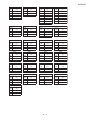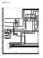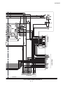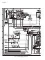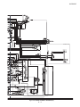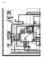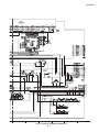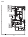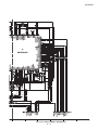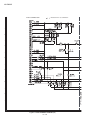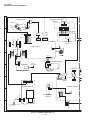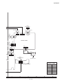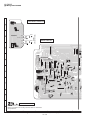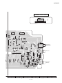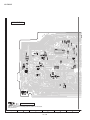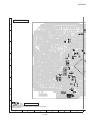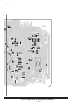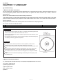
1
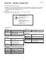
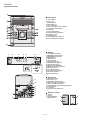
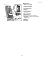
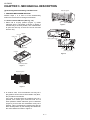
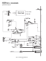
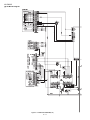
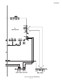
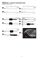
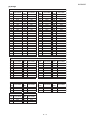
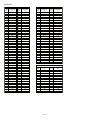
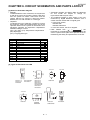
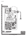
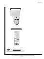
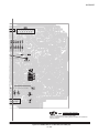
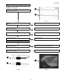
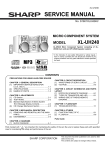
XL-DK225
SERVICE MANUAL
No. S7734XLDK225/
MICRO COMPONENT SYSTEM
MODEL
VIDEO
/AUX
XL-DK225
XL-DK225 Micro Component System consisting of
XL-DK225 (main unit) and CP-DK225 (speaker system).
• In the interests of user-safety (Required by safety regulations in
some countries) the set should be restored to its original condition
and only parts identical to those specified be used.
CONTENTS
PRECAUTIONS FOR USING LEAD-FREE SOLDER
CHAPTER 1. GENERAL DESCRIPTION
[1] Important Service Safety Precaution ........... 1-1
[2] Specifications............................................... 1-1
[3] Names Of Parts ........................................... 1-2
CHAPTER 2. ADJUSTMENTS
[1] CD Section .................................................. 2-1
[2] Test Mode .................................................... 2-2
[3] Standard Specification Of Stereo System
Error Message Display Contents ................. 2-4
CHAPTER 3. MECHANICAL DESCRIPTION
[1] Removing And Reinstalling The Main Parts
..................................................................... 3-1
[2] Disassembly ................................................ 3-2
CHAPTER 4. BLOCK DIAGRAM
[1] Block Diagram ............................................. 4-1
CHAPTER 5. CIRCUIT DESCRIPTION
[1] Waveforms Of Servo Circuit ........................ 5-1
[2] IC Voltage .................................................... 5-3
CHAPTER 6. CIRCUIT SCHEMATICS AND PARTS
LAYOUT
[1] Notes On Schematic Diagram ..................... 6-1
[2] Types Of Transistor And LED ...................... 6-1
[3] Schematic Diagram ..................................... 6-2
[4] Charts Of Connecting Wires ...................... 6-10
[5] Wiring Side of PWB ................................... 6-12
CHAPTER 7. FLOWCHART
[1] Troubleshooting ........................................... 7-1
CHAPTER 8. OTHER
[1] Function Table Of IC .................................... 8-1
[2] FL Display.................................................... 8-9
PARTS GUIDE
Parts marked with " ! " are important for maintaining the safety of the set. Be sure to replace these parts with
specified ones for maintaining the safety and performance of the set.
SHARP CORPORATION
–1
This document has been published to be used for
after sales service only.
The contents are subject to change without notice.
XL-DK225
Service
XL-MP150
Audio
E
Market
XLMP150
Manual FOR USING LEAD-FREE SOLDER
PRECAUTIONS
1. Employing lead-free solder
"MAIN, POWER, SPEAKER, TRANSIT iPOD, DISPLAY, HEADPHONE, RE-FLASH, VOLUME LED, iPOD,
CD MP3 PWB" of this model employs lead-free solder.
The LF symbol indicates lead-free solder, and is attached on the PWB and service manuals. The alphabetical
character following LF shows the type of lead-free solder.
Example:
Indicates lead-free solder of tin, silver and copper.
2. Using lead-free wire solder
When fixing the PWB soldered with the lead-free solder, apply lead-free wire solder. Repairing with
conventional lead wire solder may cause damage or accident due to cracks.
As the melting point of lead-free solder (Sn-Ag-Cu) is higher than the lead wire solder by 40 C, were
commend you to use a dedicated soldring bit, if you are not familiar with how to obtain lead-free wire solder or
soldering bit, contact our service station or service branch in your area.
3. Soldering
As the melting point of lead-free solder (Sn-Ag-Cu) is about 220 C which is higher than the conventional lead
solder by 40 C, and as it has poor solder wettability, you may be apt to keep the soldering bit in contact with the
PWB for extended period of time. However, since the land may be peeled off or the maximum heat-resistance
temperature of parts may be exceeded, remove the bit from the PWB as soon as you confirm the steady
soldering condition.
Lead-free solder contains more tin, and the end of the soldering bit may be easily corrected. Make sure to turn on
and off the power of the bit as required.
If a different type of solder stays on the tip of the soldering bit, it is alloyed with lead-free solder. Clean the bit
after every use of it.
When the tip of the soldering bit is blackened during use, file it with steel wool or fine sandpaper.
Be careful when replacing parts with polarity indication on the PWB silk.
Lead-free wire solder for servicing
Ref No.
Description
Parts No.
PWB-A
92LPWB6895MANS
MAIN (A1), POWER (A2), SPEAKER (A3), TRANSIT iPOD (A4)
PWB-B
92LPWB6894DPLS
DISPLAY (B1), HEADPHONE (B2), RE-FLASH (B3), VOLUME LED (B4)
PWB-C
92LPWB6894PODS
iPOD
PWB-D
92LPWB6894CDUS
CD MP3
– 2i
XL-DK225
CHAPTER 1. GENERAL DESCRIPTION
[1] Important Service Safety Precaution
CAUTION : “These servicing instructions are for use by qualified service personnel only. To reduce
the risk of electric shock do not perform any servicing other than that contained in the operating
instructions unless you are qualified to do so”.
WARNING
1. For continued safety, no modification of any circuit should be attempted.
2. Disconnect AC power before servicing.
CAUTION: FOR CONTINUED
PROTECTION AGAINST FIRE
HAZARD, REPLACE ONLY WITH
SAME TYPE F801, F802, 3.15A, 125V/
F803, F804 2A, 125V/
F805 1.6A, 125V FUSES.
ATTENTION: POUR ASSURER
UNE LONGUE PROTECTION CONTRE
UN INCENDIE, REMPLACER SEULEMENT
PAR UN FUSIBLE DE
TYPE F801, F802, 3.15A, 125V/
F803, F804 2A, 125V/
F805 1.6A, 125V FUSES.
[2] Specifications
General
Tuner
Power source
Power
consumption
AC 120 V - 60 Hz
105 W
Dimensions
Width: 6-3/4" (175 mm)
Height: 9-1/2" (240 mm)
Depth: 12-1/5" (315 mm)
Weight
10.5 lbs (4.78 kg)
Frequency range
Speaker
Type
Amplifier
Output power
20 watts minimum RMS per channel into
6 ohms from 100 Hz to 20 kHz, 10% total
harmonic distortion
Output terminals
Speakers: 6 ohms
Headphones: 16 - 50 ohms
(recommended: 32 ohms)
Subwoofer pre-out (audio signal):
200 mV/10 k ohms at 70 Hz
Video/Auxiliary (audio signal):
500 mV/47 k ohms
Input terminals
D/A converter
Frequency
response
Dynamic range
Maximum input
power
Rated input power
Impedance
Dimensions
Weight
CD player
Type
Signal readout
FM: 87.5 - 108 MHz
AM: 530 - 1,720 kHz
5-disc multi-play compact disc player
Non-contact, 3-beam semiconductor laser
pickup
Multi bit D/A converter
20 - 20,000 Hz
90 dB (1 kHz)
1–1
3
2-way type speaker system
2" (5 cm) tweeter
4-3/4" (12 cm) woofer
40 W
20 W
6 ohms
Width: 5-13/16" (148 mm)
Height: 10-1/4" (260 mm)
Depth: 6-7/8" (175.5 mm)
4.93 lbs. (2.24 kg)/each
XL-DK225
[3] Names Of Parts
Front panel
1. iPod Terminal
2. Disc Trays
3. Timer Indicator
4. Remote Sensor
5. Disc Stop Button
6. Disc or iPod Play or Pause Button
7. Power On/Standby Button
8. CD Button
9. Tuner (Band) Button
10. Video/Auxiliary/iPod Button
11. Headphone Jack
12. Volume Control
13. Disc Number Select Buttons
14. Disc Tray Open/Close Button
10
Display
1
2
3
4
5
6 7
13 14
9 10 11
8
15
16
12
1. Disc Number Indicators
2. MP3/WMA Folder Indicator
3. MP3/WMA Title Indicators
4. MP3 Indicator
5. WMA Indicator
6. Sleep Indicator
7. Timer Play Indicator
8. MP3/WMA Total Indicator
9. Daily Timer Indicator
10. FM Stereo Mode Indicator
11. FM Stereo Receiving Indicator
12. Memory Indicator
13. Extra Bass Indicator
14. Disc Repeat Play Indicator
15. Disc Pause Indicator
16. Disc Play Indicator
Rear panel
3
4
5
6
1
2
7
8
9
1. Speaker Terminals
2. AC Power Cord
3. FM 75 Ohms Antenna Jack
4. AM Antenna Ground Terminal
5. AM Loop Antenna Terminal
6. Video/Auxiliary (Audio Signal) Input Jacks
7. Video Out Jack
8. Cooling Fan
9. Subwoofer Pre-output Jack
Speaker system
1.
2.
3.
4.
Tweeter
Woofer
Bass Reflex Duct
Speaker Wire
1
3
2
4
4
1–2
XL-DK225
Remote control
1
2
7
8
9
11
13
12
14
15
10
16
3
4
5
18
17
19
20
23
21 22
6
5
1–3
1. Remote Control Transmitter
2. Disc Number Select Buttons
3. Disc Direct Search Buttons
4. Equalizer Mode Select Button
5. Extra Bass/Demo Button
6. Volume Up and Down Buttons
7. Power On/Stand-by Button
8. CD Button
9. Tuner (Band) Button
10. Video/Auxiliary/iPod Button
11. Disc Clear/Dimmer Button
12. Disc Stop Button
13. Memory Button
14. Disc Play or Pause Button
15. iPod Play or Pause Button
16. Tuning Up Button
17. CD Track Up or Fast Forward, Tuner Preset Up,
Time Up Button
18. CD Track Down or Fast Reverse, Tuner Preset Down,
Time Down Button
19. Tuning Down Button
20. Play Mode Button
21. Display Button
22. Folder Button
23. Clock/Timer Button
XL-DK225
CHAPTER 2. ADJUSTMENTS
[1] CD Section
1. CD SECTION
• Adjustment
Since this CD system incorporates the following
automatic adjustment functions, readjustment is not
needed when replacing the pickup. Therefore,
different PWBs and pickups can be combined freely.
Each time a disc is changed, these adjustments are
performed automatically. Therefore, playback of
each disc can be performed under optimum
conditions.
Items adjusted automatically
1) Offset adjustment (The offset voltage between the
head amplifier output and the VREF reference
voltage is compensated inside the IC.)
* Focus offset adjustment
* Tracking offset adjustment
2) Tracking balance adjustment
3) Gain adjustment (The gain is compensated inside
the IC so that the loop gain at the gain crossover
frequency will be 0 dB.)
* Focus gain adjustment
* Tracking gain adjustment
2. CD ERROR CODE DESCRIPTION
Error
10*
11*
20*
21*
Explanation
CAM error. Can't detect CAM switch when CAM is moving.
When it detect cam operation error during initialize process.
TRAY error. Can't detect TRAY switch when TRAY is
moving.
When it detect TRAY operation error during initialize
process.
* 'CHECKING'
If Error is detected, 'CHECKING' will be displayed
instead of 'ER-CD**'. 'ER-CD**' display will only be
displayed when error had been detected for the 5th
times.
2–1
XL-DK225
[2] Test Mode
• Setting the test mode
During stand-by mode, press STOP button while
3 button and
44 button. Then,
pressing down the
press the CD button to enter the test mode.
\
CD
Step 1
TE ST
IL isn’t done
OPEN/CLOSE operation is using manual.
IL isn’t done
<<
/ >> key input.
Laser ON.
Step 2
<<
/ >> key input.
Focus ON
Step 3
<<
/ >> key input.
CLV Servo ON
Step 4
<<
/ >> key input.
Tracking Servo ON
Step 5
<<
/ >> key input.
Reading Sub-code and Display
<<STOP>> key input.
STOP and return to Step 1
Hold down << CD >> key for more than 2 sec.
Start Auto Adjustment at current pick-up location.
<<STOP>> key input.
2–2
XL-DK225
STOP and return to Step 1
Everytime << DISPLAY >> key input
a) Focus Balance
b) Focus Gain
c) Tracking Balance
d) Tracking Gain
e) Focus Offset
f) Tracking Offset
g) RFRP
h) Focus Error
(RW Judgement)
i) Focus Error
(Other than RW Judgement)
= FB : XX
= FG : XX
= TB : XX
= TG : XX
= FOFF : XX
= TOFF : XX
= RFRP : XX
= RW : XX - XXXX
= DA : XX - XXXX
<<STOP>> key input.
STOP and return to Step 1
Note Sliding the PICKUP with <<
in STOP mode or play mode.
During at Step 1 , if press <<
goes to step 5 .
To cancel: Power OFF
2–3
>>, <<
/
>> button can be set
>> for more than 1 sec, it directly
XL-DK225
[3] Standard Specification Of Stereo System Error Message Display Contents
CD
Error Contents
CD Changer Mechanism Error.
TUNER
Focus Not Match/IL Time Over.
PLL Unlock.
DISPLAY
‘ER-CD**’ (*)
Notes
10: CAM SW Detection NG during normal operation
11: CAM SW Detection NG during initialize process
20: TRAY SW Detection NG during normal operation
21: TRAY SW Detection NG during initialize process
‘NO DISC’
FM
87.50
PLL Unlock.
MHz
(*) CHECKING:
If CD changer mechanism error is detected, 'CHECKING' will be display instead of 'ER-CD**'. 'ER-CD**' will only be
display when error had been detected for the 5th times.
Speaker abnormal detection and +B PROTECTION display
In case speaker abnormal detection or +B PROTECTION had occurred, the unit will automatically enter to stand-by
mode and Timer indicator will flashing as below.
Example: In case of speaker abnormal
FLASHING
ON
TIMER
LED OFF
NO. 1
ON
OFF
OFF
OFF
FLASHING
ON
NO. 1
OFF
ON
OFF
OFF
NO. 2
NO. 2
1 FRAME
(REPEAT)
NO. 1 : +B PROTECTION
NO. 2 : Speaker abnormal
BEFORE TRANSPORTING THE UNIT
The following process need to be taken after set tapering/parts replacement.
1. Press the POWER ON/STAND-BY button to enter stand-by mode.
3 button and the
2. While pressing down the
number will be displayed as "X5U_10**".
3. Press the
4
4
button, press the
button until "WAIT"--> "FINISHED" appears.
4. Unplug the AC cord and the unit is ready for transporting.
2–4
button. The Micro Computer version
XL-DK255
CHAPTER 3. MECHANICAL DESCRIPTION
[1] Removing And Reinstalling The Main Parts
Reduction gear D
1. CHANGER MECHANISM SECTION
Perform steps 1, 2, 9 and 10 of the disassembly
method to remove the CD changer mechanism.
1.1 How to remove CD Disc (See Fig. 1-4)
1. When CD is at play position (Figure 1), rotate
reduction gear C clock-wise as shown in Figure 2
until disc tray is at stock position, then rotate further
to eject the disc tray so that CD can be removed
from the tray.
Up
Down
Figure 3
CD Disc
Disc Tray
Guide Tray
Gear up down board
Mark 1 Mark 3 Mark 5
(DISC 1) (DISC 3) (DISC 5)
Mark 2 Mark 4
(DISC 2) (DISC 4)
CD at play position.
CD Disc
Figure 4
CD at stalk position.
Figure 1
Reduction gear C
Front
Rear
Figure 2
2. In another case, if CD mechanism is at tray No.1
play position and to remove CD located in tray No.3,
the procedure is as follows:
If the gear up down board is located at tray No.1
position, then rotate gear clock-wise until it is at
stock postiiton. Rotate reduction gear D clockwise
(Figure 3) to move the CD mechanism to tray No.3
position. This is confirmed by checking the gear up
down board position by the marking as indicated on
the main chassis as shown in Figure 4.
3–1
XL-DK255
[2] Disassembly
Caution on disassembly
Follow the below-mentioned notes when disassembling
the unit and reassembling it, to keep it safe and ensure
excellent performance:
1) Take cassette tape and compact disc out of the unit.
2) Be sure to remove the power supply plug from the
wall outlet before starting to disassemble the unit.
3) Take off nylon bands or wire holders where they
need to be removed when disassembling the unit.
After servicing the unit, be sure to rearrange the
leads where they were before disassembling.
4) Take sufficient care on static electricity of integrated
circuits and other circuits when servicing.
STEP
REMOVAL
PROCEDURE
Top Cabinet
(A1)x2
3x12mm
(B1)x2
3x10mm
(A1)x2
3x12mm
Side Panel
(Left)
Side Panel
(Right)
(A1)x2
3x12mm
(B1)x2
3x10mm
Rear Panel
(B1)x2
3x10mm
FIGURE
1
Top Cabinet
1. Screw ............................ (A1) X 6
1
2
Side Panel
(Left/Right)
1. Screw ............................ (B1) X 8
1
CD Changer unit
1. Screw ............................(C1) X 2
3
Front Panel
(B1)x2
3x10mm
Figure 1
(C4)x2 (C3)x2
CD MP3 PWB
CD Changer Unit
2
2. Hook ..............................(C2) X 2
(C3)x1
3. Socket ...........................(C3) X 3
Front Panel
4. Flat Cable ......................(C4) X 2
4
Rear Panel with
Speaker PWB
1. Screw ............................(D1) X 4
PULL
2
(C1)x1
3x10mm
Hook
(C2)x1
2. Socket ...........................(D2) X 1
3. Flat Cable ......................(D3) X 1
Hook
(C2)x1
PULL
5
Front Panel
1. Screw ............................ (E1) X 3
3
2. Flat Cable ...................... (E2) X 2
(C1)x1
3x10mm
3. Socket ........................... (E3) X 1
4. Hook .............................. (E4) X 2
6
Main PWB
1. Screw ............................ (F1) X 3
Rear Panel
3
Speaker PWB
(D3)x1
2. Socket ........................... (F2) X 2
7
Power PWB
1. Screw ............................(G1) X 4
3
8
Speaker PWB
1. Screw ............................(H1) X 2
4
9
Display PWB
1. Knob ...............................(J1) X 1
5
(D1)x4
3x10mm
(D2)x1
Figure 2
(E1)x1
3x6mm
(F1)x1
3x6mm
2. Nut ..................................(J2) X 1
3. Washer ...........................(J3) X 1
4. Screw .............................(J4) X 6
10
USB PWB / SUB PWB
1. Screw ............................ (K1) X 2
5
11
Jack PWB
1. Screw ............................ (L1) X 1
5
12
Re-Flash PWB
1. Screw ........................... (M1) X 1
6
13
CD MP3 PWB
1. Screw ............................(N1) X 3
7
2. Flat Cable ......................(N2) X 2
(E4)x1
PULL
Front panel
(E3)x1
(F2)x1
(G1)x4
4x6mm
(E2)x2
Power PWB
3. Socket ...........................(N3) X 1
14
CD Mechanism
1. Screw ............................ (P1) X 4
7
2. Screw ............................ (P2) X 4
8
Hook
(E4)x1
PULL
Note:
After removing the connector for the optical pickup from
the connector, wrap the conductive aluminium foil around
the front end of the connector so as to protect the optical
pickup from electrostatic damage.
3–2
(F2)x1
Main PWB
Figure 3
(F1)x2
3x10mm
(E1)x2
3x10mm
XL-DK255
Rear Panel
(P2)x4
Special
(H1)x2
Ø3x10mm
CD Mechanism
CD Changer Unit
Speaker PWB
Figure 4
Front Panel
Display PWB
(J2)x1
(J4)x6
Ø2.6x10mm
Figure 8
(J1)x1
(J3)x1
STEP
1
REMOVAL
Woofer
SUB PWB
PROCEDURE
FIGURE
1. Net Frame Ass’y............ (A1) X 1
9, 10
2. Catching Holder............. (A2) X 4
3. Screw ............................ (A3) X 4
4. Screw ............................ (A4) X 4
USB PWB
2
(K1)x2
Ø2.6x10mm
Jack PWB
Tweeter
1. Screw ............................ (B1) X 2
(L1)x1
Special
10
Speaker Box
Figure 5
Re-Flash PWB
Net Frame Ass’y
(A1) x1
(M1)x1
Ø3x10mm
Main Chassis
Figure 6
(A2)x4
(A3)x4
Ø4x20mm
Figure 9
CD Changer
Unit
Front Board
Tweeter
(B1)x2
Ø3x14mm
Tweeter Ring
(A4)x4
Ø3.5x14mm
Woofer
Woofer Ring
(N2)x2
(P1)x2
Ø3x10mm
(P1)x2
Ø3x10mm
(N3)x1
Figure 10
(N1)x3
Ø3x10mm
Figure 7
3–3
XL-DK255
-MEMO-
3–4
XL-DK225
CHAPTER 4. DIAGRAMS
[1] Main Block Diagram
Figure 4-1: MAIN BLOCK DIAGRAM (1/2)
4–1
XL-DK225
Figure 4-2: MAIN BLOCK DIAGRAM (2/2)
4–2
XL-DK225
[2] CD Block Diagram
Figure 4-3: CD BLOCK DIAGRAM (1/2)
4–3
XL-DK225
Figure 4-4: CD BLOCK DIAGRAM (2/2)
4–4
XL-DK225
CHAPTER 5. CIRCUIT DESCRIPTION
[1] Waveforms Of CD Circuit
1
IC1
22
FDO
1
FDO
22
IC1
2
IC1
TDO
23
5
IC1
SPDO
25
PDOUT 0
1
IC1
3
IC1
22
16
FDO
6
IC1
28
7
IC1
27
PDOUT 1
TE
1
FDO
22
IC1
3
IC1
16
TE
4
2
IC1
4
IC1
2
RFOUT
5–1
RFOUT
XL-DK225
[2] Voltage
IC1
PIN
NO
1
2
3
4
5
6
7
8
9
10
11
12
13
14
15
16
17
18
19
20
21
22
23
24
25
VOLTAGE
0.02
1.63
0.76
0.70
0.59
0.70
1.63
3.27
1.63
1.63
1.63
1.63
1.63
0.01
0.52
0.55
0.01
0.01
1.11
0.36
0.26
0.01
0.26
0.34
0.54
PIN
NO
26
27
28
29
30
31
32
33
34
35
36
37
38
39
40
41
42
43
44
45
46
47
48
49
50
PIN
NO
51
52
53
54
55
56
57
58
59
60
61
62
63
64
65
66
67
68
69
70
71
72
73
74
75
VOLTAGE
0.01
1.52
3.03
1.52
1.52
0.01
3.27
0.03
4.53
1.53
0.01
3.25
2.41
2.14
2.59
2.25
0.61
3.25
0.04
0.04
0.04
0.04
0.10
1.64
1.65
VOLTAGE
1.53
0.03
3.27
0.03
0.03
3.27
1.53
3.27
0.04
3.27
0.03
0.03
0.03
0.03
1.62
1.65
3.24
1.49
0.02
1.63
3.26
1.61
1.31
0.02
1.38
PIN
NO
76
77
78
79
80
81
82
83
84
85
86
87
88
89
90
91
92
93
94
95
96
97
98
99
100
VOLTAGE
3.26
1.63
0.98
0.02
1.74
1.63
1.63
1.68
1.63
1.62
1.64
1.66
1.62
0.50
3.27
3.25
0.01
0.02
1.63
1.63
1.63
1.63
1.63
1.64
1.63
IC2
PIN
NO
1
2
3
4
5
6
7
8
9
VOLTAGE
3.18
3.17
3.19
3.20
3.19
3.18
0.00
4.39
7.08
PIN
NO
10
11
12
13
14
15
16
17
18
Q1
PIN
NO
E
C
B
VOLTAGE
3.26
0.89
4.37
VOLTAGE
5.08
5.05
4.37
3.27
1.63
1.63
1.63
1.63
1.63
1.63
1.62
1.62
PIN
NO
19
20
21
22
23
24
25
26
27
Q2
PIN
NO
E
C
B
Q5
PIN
NO
E
C
B
VOLTAGE
VOLTAGE
5.05
3.26
4.37
VOLTAGE
3.20
3.20
0.01
0.01
0.01
0.01
0.00
7.03
7.08
Q3
PIN
NO
E
C
B
VOLTAGE
1.48
3.26
2.17
Q8
PIN
NO
E
C
B
PIN
NO
28
29
30
31
32
33
34
35
36
VOLTAGE
0.00
0.04
2.98
5–2
VOLTAGE
7.09
0.01
1.63
2.24
3.15
3.16
2.69
3.16
3.16
Q4
PIN
NO
E
C
B
VOLTAGE
0.01
0.02
3.11
XL-DK225
IC701
IC702
PIN
NO
VOLTAGE
(V)
PIN
NO
VOLTAGE
(V)
PIN
NO
VOLTAGE
(V)
PIN
NO
VOLTAGE
(V)
1
2
3
4
5
6
7
8
9
10
11
12
13
14
15
16
17
18
19
20
21
22
23
24
25
26
27
28
29
30
31
32
33
34
35
36
37
38
39
40
41
42
43
44
45
46
47
48
49
50
3.22
3.22
0.00
0.00
0.00
3.22
0.00
0.00
0.00
0.47
0.63
3.19
1.54
0.00
0.00
3.24
3.24
1.05
0.00
3.18
0.00
0.00
0.00
0.00
0.71
0.00
0.00
3.24
0.00
0.00
3.24
0.00
3.24
3.24
3.24
3.28
3.27
0.00
0.00
0.00
0.00
0.00
0.76
0.63
0.00
3.23
0.00
0.58
0.00
0.00
51
52
53
54
55
56
57
58
59
60
61
62
63
64
65
66
67
68
69
70
71
72
73
74
75
76
77
78
79
80
81
82
83
84
85
86
87
88
89
90
91
92
93
94
95
96
97
98
99
100
3.30
3.14
3.31
3.31
3.15
3.23
3.24
3.23
3.24
3.24
3.31
3.24
0.00
0.00
0.00
0.00
3.14
0.00
0.00
3.22
3.31
0.00
0.00
3.24
3.24
3.24
0.00
0.00
0.00
0.00
3.24
3.22
3.28
0.00
3.31
3.24
0.00
0.00
0.00
0.00
3.31
3.28
3.28
3.28
3.28
0.00
3.28
3.30
3.24
0.00
1
2
3
4
5
6
7
8
9
10
11
12
13
14
15
16
17
18
19
20
21
22
23
24
25
26
27
28
29
30
31
32
-26.44
-26.40
-26.40
-26.40
3.24
3.20
3.24
3.24
0.00
0.00
3.29
1.51
1.51
0.00
-24.10
-28.77
-28.78
-28.77
-28.77
-28.75
-28.77
-28.77
-21.70
-28.97
-26.40
-28.77
-28.76
-28.76
21.71
-24.06
-24.07
-24.07
33
34
35
36
37
38
39
40
41
42
43
44
45
46
47
48
49
50
51
52
53
54
55
56
57
58
59
60
61
62
63
64
-26.42
-28.77
-26.41
-26.40
-26.41
-24.06
-17.00
-26.40
-24.07
-9.89
-26.40
-9.98
-17.00
-12.34
-9.94
-26.40
-26.42
-24.06
-14.67
-12.36
-28.76
-28.76
-28.76
-28.75
-26.45
-26.41
-26.41
-26.40
-26.40
-26.40
-26.40
-26.40
PIN
NO
VOLTAGE
(V)
PIN
NO
VOLTAGE
(V)
1
2
3
4
5
6
7
8
9
10
11
12
13
14
4.62
4.62
4.63
4.63
4.62
4.62
4.63
4.65
4.61
4.65
4.61
4.65
4.65
4.64
15
16
17
18
19
20
21
22
23
24
25
26
27
28
4.65
0.00
0.00
4.64
4.64
0.00
0.00
0.00
4.63
9.28
0.00
4.65
4.65
4.63
IC601
5–3
XL-DK225
IC703
IC705
IC901
PIN
NO
VOLTAGE
(V)
PIN
NO
VOLTAGE
(V)
PIN
NO
VOLTAGE
(V)
PIN
NO
VOLTAGE
(V)
1
2
3
4
5
3.30
3.30
0.00
-
1
2
3
3.90
0.60
5.60
1
2
3
4
5
6
7
8
-0.10
-0.10
21.90
-20.70
0.00
0.00
23.10
9
10
11
12
13
14
15
-23.00
0.00
0.00
-22.10
0.00
-0.10
-0.10
IC852
IC853
IC851
PIN
NO
VOLTAGE
(V)
PIN
NO
VOLTAGE
(V)
PIN
NO
VOLTAGE
(V)
PIN
NO
VOLTAGE
(V)
1
2
3
15.80
0.00
4.90
1
2
3
3.30
0.00
5.10
1
2
3
4
5.10
13.00
16.40
0.00
5
6
7
16.20
10.00
8.50
PIN
NO
1
2
3
PIN
NO
1
2
3
IC854
VOLTAGE
(V)
5.60
0.60
13.90
Q701
VOLTAGE
(V)
0.00
3.20
0.00
PIN
NO
1
2
3
PIN
NO
1
2
3
PIN
NO
Q801
VOLTAGE
(V)
PIN
NO
1
2
3
-28.90
-29.50
-37.60
1
2
3
PIN
NO
Q902
VOLTAGE
(V)
PIN
NO
1
2
3
PIN
NO
1
2
3
0.00
3.30
0.00
1
2
3
Q603
VOLTAGE
(V)
0.00
0.00
0.70
Q702
VOLTAGE
(V)
0.00
3.20
0.00
Q841
VOLTAGE
(V)
0.80
0.00
0.00
Q903
VOLTAGE
(V)
0.00
3.10
0.00
PIN
NO
1
2
3
PIN
NO
1
2
3
PIN
NO
1
2
3
PIN
NO
1
2
3
Q604
VOLTAGE
(V)
0.00
0.00
0.70
Q704
VOLTAGE
(V)
0.00
3.30
0.00
Q860
VOLTAGE
(V)
0.00
3.50
0.00
Q904
VOLTAGE
(V)
0.00
3.10
0.00
Q906
VOLTAGE
(V)
0.70
0.00
3.60
5–4
PIN
NO
1
2
3
PIN
NO
1
2
3
PIN
NO
1
2
3
PIN
NO
1
2
3
Q608
VOLTAGE
(V)
2.20
2.20
0.00
Q706
VOLTAGE
(V)
0.00
0.00
3.00
Q901
VOLTAGE
(V)
0.00
3.40
0.00
Q905
VOLTAGE
(V)
0.00
0.00
0.70
XL-DK225
-MEMO-
5–5
XL-DK225
CHAPTER 6. CIRCUIT SCHEMATICS AND PARTS LAYOUT
[1] Notes On Schematic Diagram
• Resistor:
To differentiate the units of resistors, such symbol as
K and M are used: the symbol K means 1000 ohm
and the symbol M means 1000 kohm and the
resistor without any symbol is ohm-type resistor.
Besides, the one with “Fusible” is a fuse type.
• Capacitor:
To indicate the unit of capacitor, a symbol P is used:
this symbol P means pico-farad and the unit of the
capacitor without such a symbol is microfarad. As to
electrolytic capacitor, the expression “capacitance/
withstand voltage” is used.
(CH), (TH), (RH), (UJ): Temperature compensation
(ML): Mylar type
(P.P.): Polypropylene type
REF. NO
SW701
SW702
SW703
SW704
SW705
SW706
SW707
SW708
SW709
SW710
SW711
SW712
VR701
DESCRIPTION
DISC4
DISC5
OPEN/CLOSE
DISC1
DISC2
DISC3
POWER ON/STAND-BY
PLAY/REPEAT
STOP
VIDEO/AUX/USB
TUNER (BAND)
CD
VOLUME
• Schematic diagram and Wiring Side of P.W.Board
for this model are subject to change for
improvement without prior notice.
• The indicated voltage in each section is the one
measured by Digital Multimeter between such a
section and the chassis with no signal given.
1. In the tuner section,
indicates AM
indicates FM stereo
2. In the CD section, the CD is stopped.
• Parts marked with “
” (
) are
important for maintaining the safety of the set. Be
sure to replace these parts with specified ones for
maintaining the safety and performance of the set.
POSITION
ON—OFF
ON—OFF
ON—OFF
ON—OFF
ON—OFF
ON—OFF
ON—OFF
ON—OFF
ON—OFF
ON—OFF
ON—OFF
ON—OFF
MAX—MIN
[2] Types Of Transistor And LED
FRONT
VIEW
TOP
VIEW
E C B
(S)(G)(D)
(1)(2)(3)
KTA1271 Y
KTA1274 Y
KIA78L05
KTC3199 GR
KTC3203 Y
TOP VIEW
TOP VIEW
HSS4148
1N4004S
DRL204F
MA111
B
(3)
C
(2)
E
(1)
KRA102 S
KRC107 S
KRC102 S
KRC104 S
KTA1504 GR
KTC3875 GR
KTA1544 T
KTC3265 Y
TOP VIEW
FRONT
VIEW
FRONT
VIEW
AC
KDS184
FRONT
VIEW
1 2 3
AC
343VC3F
503BC2E30
10XB60F
S4B05GM
6–1
KIA7805A
XL-DK225
[3] Schematic Diagram
A
C
TO POWER IC SECTION
B
TO CD
D
FROM POWER SECTION
E
TUNER SECTION
F
G
H
1
2
3
4
Figure 6-1: MAIN SCHEMATIC DIAGRAM (1/2)
6–2
5
6
XL-DK225
7
8
9
10
Figure 6-2: MAIN SCHEMATIC DIAGRAM (2/2)
6–3
11
12
XL-DK225
A
B
C
D
TO MAIN SECTION
E
TO DISPLAY
F
G
H
1
2
3
4
Figure 6-3: POWER SCHEMATIC DIAGRAM (1/2)
6–4
5
6
XL-DK225
AC SUPPLY
120V ~ 60Hz
SPEAKER JACK PWB
7
8
9
10
Figure 6-4: POWER SCHEMATIC DIAGRAM (2/2)
6–5
11
12
XL-DK225
SYSTEM MICOM REFLASH PWB
TO PWR SECTION
A
B
C
TO MAIN SECTION
D
E
TO MAIN SECTION
F
G
H
1
2
3
4
Figure 6-5: DISPLAY SCHEMATIC DIAGRAM (1/2)
6–6
5
6
FOR MICOM REFLASH ONLY
TO MP3 SERVO
TO MP3 SERVO
XL-DK225
7
8
9
10
Figure 6-6: DISPLAY SCHEMATIC DIAGRAM (2/2)
6–7
11
12
XL-DK225
A
B
C
D
E
F
G
H
1
2
3
4
Figure 6-7: CD MP3 SCHEMATIC DIAGRAM (1/2)
6–8
5
6
XL-DK225
7
8
9
10
Figure 6-8: CD MP3 SCHEMATIC DIAGRAM (2/2)
6–9
11
12
XL-DK225
RESISTOR WITH 1% TOLERANCE
IPOD CONNECTION
A
B
C
D
E
F
G
H
1
2
3
4
Figure 6-9: iPOD SCHEMATIC DIAGRAM (1/2)
6 – 10
5
6
XL-DK225
TO TRANSIT iPOD
7
8
9
10
Figure 6-10: iPOD SCHEMATIC DIAGRAM (2/2)
6 – 11
11
12
XL-DK225
9
[4] Charts Of Connecting Wires
TUNER PACK
A
TRANSIT iPOD
PWB-A4
1
12
1
ANTENNA
FFC301
2 4 6 8 10 12
1 3 5 7 9 11
CNPU4
FM
CNPU5
1 2 3 4 5 6 7 8 9 10 11 12
9
GND
1 2 3 4 5 6 7 8 9 10 11 12
B
9 8 7 6 5 4 3 2 1
iPOD PWB-C
1 2 3 4 5 6 7 8 9 10 11 12 13
1
9
1
BI101
11
GY
BK
GY
BK
GY
BK
GY
BK
BR
CNS601
FFC301
RD
WH
BL
WH
BL
WH
BL
WH
BL
WH
BL
WH
AM
17
CNP701B
1
CNPU3
FROM EXTERNAL
iPOD DEVICE
10 9 8 7 6 5 4 3 2 1
BI601
1 2 3 4 5 6 7 8 9 10 11
WH
BK
WH
BK
WH
BK
WH
BK
WH
RD
WH
BK
WH
BK
WH
BK
WH
BK
WH
RD
BI801
1
MAIN PWB -A1
1 2
CNP971
1 3 5 7 9 11 13 15 17
2 4 6 8 10 12 14 16
2 4 6 8 10 12
1 3 5 7 9 11
FAN MOTOR
BI902
5 43 2 1
GR
WH
GR
RD
4 32 1
SPEAKER PWB-A3
1 2 3 4
R-CH
JK701
E
CNP902
L-CH
L-CH
R-CH
HEADPHONE PWB-B2
SPEAKER TERMINAL
SO901
CNS701
6 5 4 3 2 1
12
7 6 5 4 3 2 1
BI701
CNP801
F
1 2 3 4 5 6 7 8 9 10
1
17
1
10
11 9 7 5 3 1
12 10 8 6 4 2
2 4 6 8 10
13579
CNP705
CNP702
1 2 3 4 5 6
CNS703
CNP802
WH
PT801
RD
DISPLAY PWB-B1
BI702
CNP805
VOLUME LED
PWB-B4
WH
BK
RD
WH
BK
WH
BK
WH
BK
WH
PT841
1
CNS702
AC POWER SUPPLY CORD
AC 120V~60Hz
8 7 6 5 4 3 2 1
CNS 805
G
WH
BK
WH
BK
WH
BK
WH
RD
1 2
9 8 7 6 5 4 3 2 1
CNP703
1 2
1 2
BI703
POWER PWB-A2
H
F
MAIN
CN
TO
CD MP3 PWB-D
CNP6
L-CH
R-CH
FFC702
FROM
HEADPHONE
FFC705
CNP708
1 2 3 4 5
CNS902
BL
GR
BL
GR
BL
RD
D
CNP301
CNS801
1 2 3 4 5 6 7 8 9 10
C
TO
DISPLAY PWB-B1
CNP701A
FFC701
CNP101
2 4 6 8
1 3 5 7 9
2
3
4
Figure 6-11: WIRING CONNECTION (1/2)
6 – 12
5
6
17 15 13
16 14
C
XL-DK225
FROM
DISPLAY PWB-B1
CNP702
FFC702
FFC705
1
1
CNP5
4
3
6
5
8
7
10
9
1
CNP4
CNP6
CD MP3 PWB-C
1 2 3 4 5 6
CNP2
WH
GR
WH
GR
WH
RD
2
9 8 7 6 5 4 3 2 1
CNP3
CNS2
FFC4
2 4 6 8 10
1 3 5 7 9 11
11
11 9 7 5 3 1
12 10 8 6 4 2
1 2 3 4 5 6
CNP1
FROM
MAIN PWB-A1
CNP701B
17
2 4 6 8 10 12 14 16
1 3 5 7 9 11 13 15
FFC701
TO
CD MOTOR PWB
TO
CD CHANGER
MECHANISM UNIT
12
10
1
1
16
FFC1
1
17 15 13 11 9 7 5 3 1
16 14 12 10 8 6 4 2
02
1
CNP701A
FROM
EXTERNAL MICOM
DEVICE
16
TO
CD PICK-UP UNIT
-B1
1 2 3 4 5 6 7 8
1 2 3 4 5 6 7 8
CNPU2
CNPU1
COLOR TABLE
RE-FLASH PWB-A4
7
8
9
10
Figure 6-12: WIRING CONNECTION (2/2)
6 – 13
11
BR
BL
GY
BK
GR
WH
BROWN
BLUE
GRAY
BLACK
GREEN
WHITE
RD
RED
12
XL-DK225
[5] Wiring Side Of PWB
L-CH
L-CH
MAIN PWB-A1
10 9 8 7 6 5 4 3 2 1
E C B
1 3 5 7 9 11 13 15 17
2 4 6 8 10 12 14 16
1 2 3 4
R-CH
1 2
3
4 5 6 8 9 10 11
B C E
Lead-free solder indication
Lead-free solder is used in the MAIN PWB.
Refer to "Precautions for handling lead-free solder" for instructions
and precautions.
Figure 6-13: WIRING SIDE OF MAIN PWB (TOP VIEW) (1/2)
6 – 14
E C B
R-CH
SO901
SPEAKER TERMINAL
SPEAKER PWB-A3
B C E
XL-DK225
TRANSIT iPOD PWB-A4
2 4 6 8 10 12
1 3 5 7 9 11
1 2 3 4 5 6 7 8 9 10 11 12
2 4 6 8
1 3 5 7 9
1
2 4 6 8 1012
3 5 7 9 11
B C E
VIDEO/AUX IN
L-CH and R-CH
VIDEO OUT
1 2
1 2 3 4 5 6 7 8 9 10 11121314 15
SUBWOOFER
PRE-CUT
5 4 3 2
1
Figure 6-14: WIRING SIDE OF MAIN PWB (TOP VIEW) (2/2)
6 – 15
XL-DK225
MAIN PWB-A1
Lead-free solder indication
Lead-free solder is used in the MAIN PWB.
Refer to "Precautions for handling lead-free solder" for instructions
and precautions.
Figure 6-15: WIRING SIDE OF MAIN PWB (BOTTOM VIEW) (1/2)
6 – 16
XL-DK225
Figure 6-16: WIRING SIDE OF MAIN PWB (BOTTOM VIEW) (2/2)
6 – 17
XL-DK225
POWER PWB-A2
5
4
6
3
7
8
2
9
1
BK
WH
6
5
4
3
2
1
T.F.
8
9
POWER SUPPLY
AC 120V~60Hz
10 11 12 13 14 15 16 17
B C E
B C E
10 9 8 7 6 5 4 3 2 1
1
2
3
6 54 32 1
Lead-free solder indication
COLOR TABLE
Lead-free solder is used in the POWER PWB.
Refer to "Precautions for handling lead-free solder"
for instructions and precautions.
WH
BK
Figure 6-17: WIRING SIDE OF POWER PWB
6 – 18
WHITE
BLACK
XL-DK225
-MEMO-
6 – 19
XL-DK225
DISPLAY PWB-B1
51 50 49 48 47 46 45 44 43 42 41 40 39 38 37 36 35 34 33 32 31 30 29 28 2
9
10 8
2
1
4
3
6
5
8 10 12 14 16
7
9 11 13 15 17
Lead-free solder indication
Lead-free solder is used in the DISPLAY PWB.
Refer to "Precautions for handling lead-free solder" for instructions
and precautions.
Figure 6-18: WIRING SIDE OF DISPLAY PWB (TOP VIEW) (1/2)
6 – 20
7
5
6
1
3
4
2
XL-DK225
2
1
31 30 29 28 27 26 25 24 23 22 21 20 19 18 17 16 15 14 13 12 11 10 9 8 7 6 5 4 3 2 1
1 2 3 4 5 6 7 8 9
1 2 3
2
1
1
4
3
6
5
8 10 12
7
9
11
1 2 3 4 5 6 7
Figure 6-19: WIRING SIDE OF DISPLAY PWB (TOP VIEW) (2/2)
6 – 21
XL-DK225
DISPLAY PWB-B1
1 2 3 4 5 6 7 8 9 10 11 12 13 14 15 16 17 18 19 20 21 22 23 24 25 26 27 2
Lead-free solder indication
Lead-free solder is used in the DISPLAY PWB.
Refer to "Precautions for handling lead-free solder" for instructions
and precautions.
Figure 6-20: WIRING SIDE OF DISPLAY PWB (BOTTOM VIEW) (1/2)
6 – 22
XL-DK225
24 25 26 27 28 29 30 31 32 33 34 35 36 37 38 39 40 41 42 43 44 45 46 47 48 49 50 51
Figure 6-21: WIRING SIDE OF DISPLAY PWB (BOTTOM VIEW) (2/2)
6 – 23
XL-DK225
HEADPHONE PWB-B2
A
1 2 34 5
B
C
FROM
HEADPHONE
D
REFLASH PWB-B3
8 7 654 321
8 7 654 321
E
VOLUME LED PWB-B4
1
2
F
G
Lead-free solder indication
H
Lead-free solder is used in the HEADPHONE, REFLASH, VOLUME LED PWB.
Refer to "Precautions for handling lead-free solder" for instructions
and precautions.
1
2
3
4
5
Figure 6-22: WIRING SIDE OF HEADPHONE, REFLASH, VOLUME LED PWB (TOP VIEW)
6 – 24
6
XL-DK225
HEADPHONE PWB-B2
A
B
C
D
VOLUME LED PWB-B4
E
F
G
Lead-free solder indication
H
Lead-free solder is used in the HEADPHONE, VOLUME LED PWB.
Refer to "Precautions for handling lead-free solder" for instructions
and precautions.
1
2
3
4
5
Figure 6-23: WIRING SIDE OF HEADPHONE, VOLUME LED PWB (BOTTOM VIEW)
6 – 25
6
XL-DK225
13 12 11 10 9 8 7 6 5 4 3 2 1
iPOD PWB-C
Lead-free solder indication
Lead-free solder is used in the iPOD PWB.
Refer to "Precautions for handling lead-free solder"
for instructions and precautions.
Figure 6-24: WIRING SIDE OF iPOD PWB (TOP VIEW)
6 – 26
XL-DK225
iPOD PWB-C
Lead-free solder indication
Lead-free solder is used in the iPOD PWB.
Refer to "Precautions for handling lead-free solder"
for instructions and precautions.
Figure 6-25: WIRING SIDE OF iPOD PWB (BOTTOM VIEW)
6 – 27
XL-DK225
CD MP3 PWB-D
12 10 8 6 4 2
9 8 7 6 5 4 3 2 1
2 4 6 8 10 11
1 2 3 4 5 6
SCREW
TO CHASSIS
B C E
1 3 5 7 9
11 9 7 5 3 1
2 4 6 8 10 12
1 3 5 7 9 11 13
Figure 6-26: WIRING SIDE OF CD MP3 PWB (TOP VIEW) (1/2)
6 – 28
XL-DK225
3 2 1
2 4 6 8 10 12 14
1 3 5 7 9 11 13
6 8 10 12 14 16
7 9 11 13 15
Lead-free solder indication
Lead-free solder is used in the CD MP3 PWB.
Refer to "Precautions for handling lead-free solder" for instructions
and precautions.
Figure 6-27: WIRING SIDE OF CD MP3 PWB (TOP VIEW) (2/2)
6 – 29
XL-DK225
CD MP3 PWB-D
Lead-free solder indication
Lead-free solder is used in the CD MP3 PWB.
Refer to "Precautions for handling lead-free solder" for instructions
and precautions.
Figure 6-28: WIRING SIDE OF CD MP3 PWB (BOTTOM VIEW) (1/2)
6 – 30
XL-DK225
Figure 6-29: WIRING SIDE OF CD MP3 PWB (BOTTOM VIEW) (2/2)
6 – 31
XL-DK225
CHAPTER 7. FLOWCHART
[1] Troubleshooting
1. When the CD does not function
The CD section may not operate when the objective lens of the optical pickup is dirty. Clean the objective lens, and
check the playback operation. When this section does not operate even after the above step is taken, check the
following items.
Remove the cabinet and follow the trouble shooting instructions.
"Track skipping and/or no TOC (Table Of Contents) may be caused by build up of dust other foreign matter on the laser
pickup lens. Before attempting any adjustment make certain that the lens is clean. If not, clean it as mentioned below."
Turn the power off.
Gently clean the lens with a lens cleaning tissue and a small amount of isopropyl alcohol.
Do not touch the lens with the bare hand.
1.
Parts code
UDSKA0004AFZZ
CD optical pickup Lens cleaner disc
HOW TO USE
1. Using the brush in the cleaner cap, apply 1 or 2 drops of the cleaning fluid to the
brush on the CD cleaner disc which has the mark next to it.
2. Place the CD cleaner disc onto the CD disc tray with the brush side down, then
press the play button.
3. You will hear music for about 20 seconds and the CD player will automatically stop.
If it still play continuously, press the stop button.
Cleaning fluid
CAUTION
The CD lens cleaner should be effective for 30-50 operations, however if the
brushes become worn out earlier then please replace the cleaner disc.
If the CD cleaner brushes become very wet then wipe off any excess fluid with a soft
cloth.
Do not drink the cleaner fluid or allow it contact with the eyes. In the event of this
happening then drink and / or rinse with clean water and seek medical advice.
The CD cleaner disc must not be used on car CD players or on computer CD-ROM
drives.
All rights reserved. Unauthorized duplicating, broadcasting and renting this product
is prohibited by law.
2. When a CD cannot be played
2.1. Pressing the CD operation key is accepted, but playback does not occur.
1) Focus-HF system check
2) Tracking system check
3) Spin system check
4) PLL system check
5) Others
7–1
Cleaner disc
XL-DK225
(1) Focus-RF system check.
Although a CD is inserted and the cover is closed,
"NO DISC" is displayed.
1
Press the Tray1 CD Eject Button without inserting a disc, and try
starting the playback operation.
IC1
22
2
IC1
FDO
TDO
23
Figure 1
1. Does the pickup move to the PICKUP-IN Switch (NSW1)
position?
Yes
2. Does the focus (lens) move up and down?
(Waveform drawing Figure 1)
No
Sled motor (NM2).
No
Check the focus peripheral circuit.
No
Check the laser diode driver Q1 peripheral circuit.
No
Spindle motor (NM1).
No
Pins 5~9, 11, 18 19 and 22 on IC1
Check the laser diode driver Q1 peripheral circuit.
No
If the level is not normal.
Yes
3. Is the laser lit?
Yes
4. Is the turntable rotating?
When a disc is loaded, start playback operation.
1. Is focus servo activated?
(Waveform drawing Figure 2)
Yes
2. Is the RF waveform normal?
(Waveform drawing Figure 3)
1
IC1
22
FDO
4
2
IC1
3
IC1
16
RFOUT
TE
Figure 2
Figure 3
7–2
XL-DK225
(2) Focus-RF system check.
Check the TE waveform at pin 16 on IC1.
If the waveform shown in Figure 4 appears and soon after NO
DISC appears?
No
"Initialization" is possible, but play is not possible?
The tracking servo is not activated.
Check the peripheral circuits at pins 15, 16 and 23 on IC1,
and FFC1.
Yes
A normal jump operation cannot be completed or the
beginning of the track cannot be found.
Check the around pin 23 on IC1.
Yes
No
"Initialization" is not possible.
Data cannot be read. Check the VCO-PLL (Pin26~30 on IC1)
system.
3
IC1
16
TE
4
IC1
2
RFOUT
Figure 4
(3) Spin system check.
Press the OPEN/CLOSE switch without inserting a disc, and
then try starting the play operation.
1. The turntable rotates a little?
(Waveform drawing Figure 5)
Yes
The spin driver circuit is OK.
No
2. The turntable doesn't rotate.
Check around pin 25 on IC1, pins 1 and 2 on CNP2.
1
FDO
22
IC1
5
IC1
SPDO
25
Figure 5
7–3
XL-DK225
(4) PLL system check.
When a disc is loaded, start play operation.
PDOUT 0
6
IC1
28
7
IC1
27
The RF waveform is normal, but the TOC data cannot be read.
Check the PDOUT waveform. (Figure 6)
1
PDOUT 1
FDO
22
IC1
Check around pins 26~30 on IC1.
Figure 6
7–4
XL-DK225
PARTS GUIDE
MICRO COMPONENT SYSTEM
MODEL
XL-DK225
XL-DK225 Micro Component System consisting of
XL-DK225 (main unit) and CP-DK225 (speaker system).
CONTENTS
[1] INTEGRATED CIRCUITS
[9] OTHER CIRCUITRY PARTS
[2] TRANSISTORS
[10] CABINET PARTS /
CD MECHANISM PARTS
[3] DIODES
[11] SPEAKER BOX PARTS
[4] TRANSFORMERS
[12] ACCESSORIES / PACKING
PARTS
[5] COILS
[6] CRYSTALS / VIBRATORS
[13] P.W.B. ASSEMBLY
(Not Replacement Item)
[7] CAPACITORS
[14] OTHER SERVICE PARTS
[8] RESISTORS
Parts marked with " ! " are important for maintaining the safety of the set. Be sure to replace these parts with
specified ones for maintaining the safety and performance of the set.
SHARP CORPORATION
This document has been published to be used for
after sales service only.
The contents are subject to change without notice.
XL-DK225
NO.
PARTS CODE
PRICE NEW PART
RANK MARK RANK
DESCRIPTION
[1] INTEGRATED CIRCUITS
IC1
IC2
IC601
IC701
IC702
IC703
IC705
IC851
IC852
IC853
IC854
IC901
VHiTC94A70FG2
VHiLA6261//-1
VHiR2S15904-1
RH-iXA158AW00
VHiM66005AHP1
VHiPST3227N1E
VHi6201P332-1
VHiAN80T53/-1
VHiKiA7805AP1
VHi6201P332-1
VHiKiA78L05-1
VHiSTK43205-1
BD
AN
AL
AS
AD
AE
AL
AF
AE
AF
AT
CD MP3 Decorder
CD Driver
Audio Pro
System Microcomputer, IXA158AW
FL Driver
Reset IC
Voltage Regulator, 3.3V
Multi Regulator, AN80T53
Constant Voltage Regulator, KIA7805AP
Voltage Regulator, 3.3V
Constant Voltage Regulator, KIA78L05
Power IC, STK432-050
AB
AC
AB
AB
AD
AB
AB
AB
AB
AB
AB
AB
AB
AB
AB
AB
AB
AB
AE
AB
AB
AB
AB
AB
AB
AC
AC
Silicon,PNP,KTA1504 GR
Silicon,PNP,KTA1271 Y
Silicon,NPN,KTC3875 GR
Digital,NPN,KRC104 S
Silicon,PNP,KTA1544 T
Digital,NPN,KRC107 S
Silicon,NPN,KTC3875 GR
Silicon,NPN,KTC3875 GR
Digital,PNP,KRA102 S
Silicon,NPN,KTC3875 GR
Silicon,NPN,KTC3875 GR
Silicon,NPN,KTC3875 GR
Silicon,NPN,KTC3875 GR
Silicon,PNP,KTA1504 GR
Digital,NPN,KRC104 S
Digital,NPN,KRC104 S
Digital,NPN,KRC104 S
Digital,NPN,KRC102 S
Silicon,PNP,KTA1274 Y
Silicon,NPN,KTC3199 GR
Digital,NPN,KRC104 S
Silicon,NPN,KTC3875 GR
Silicon,NPN,KTC3875 GR
Silicon,NPN,KTC3875 GR
Silicon,NPN,KTC3875 GR
Silicon,NPN,KTC3265 Y
Silicon,NPN,KTC3203 Y
AB
AC
AC
AA
AB
AB
AC
AC
AC
AC
AC
AC
AC
AC
AC
AB
AB
AA
AC
AA
AG
AC
AC
AB
AB
AB
AB
AB
AB
AB
AB
AB
AB
AB
AB
AA
AA
AA
AC
AC
AA
AA
AC
Silicon,KDS184
Silicon,MA111
Silicon,MA111
Silicon,DHSS4148
Silicon,DS1N4004S
Silicon,DS1N4004S
Silicon,MA111
Silicon,MA111
Silicon,MA111
Silicon,MA111
Silicon,MA111
Silicon,MA111
Silicon,MA111
Silicon,MA111
Silicon,MA111
Silicon,DS1N4004S
Silicon,DS1N4004S
Silicon,DHSS4148
Silicon,MA111
Silicon,DHSS4148
Rectifier, 4B05GM
Silicon,RL204F
Silicon,RL204F
Silicon,DS1N4004S
Silicon,DS1N4004S
Silicon,DS1N4004S
Silicon,DS1N4004S
Silicon,DS1N4004S
Silicon,DS1N4004S
Silicon,DS1N4004S
Silicon,DS1N4004S
Silicon,DS1N4004S
Silicon,DS1N4004S
Silicon,DS1N4004S
Silicon,DS1N4004S
Silicon,DHSS4148
Silicon,DHSS4148
Silicon,DHSS4148
Silicon,MA111
Silicon,MA111
Silicon,DHSS4148
Silicon,DHSS4148
Silicon,MA111
[2] TRANSISTORS
Q1
Q2
Q3
Q4
Q5
Q8
Q603
Q604
Q608
Q610
Q611
Q612
Q613
Q614
Q701
Q702
Q704
Q706
Q801
Q841
Q860
Q901
Q902
Q903
Q904
Q905
Q906
VSKTA1504GR-1
VSKTA1271Y/-1
VSKTC3875GR-1
VSKRC104S//-1
VSKTA1544T/-1
VSKRC107S//-1
VSKTC3875GR-1
VSKTC3875GR-1
VSKRA102S//-1
VSKTC3875GR-1
VSKTC3875GR-1
VSKTC3875GR-1
VSKTC3875GR-1
VSKTA1504GR-1
VSKRC104S//-1
VSKRC104S//-1
VSKRC104S//-1
VSKRC102S//-1
VSKTA1274Y/-1
VSKTC3199GR-1
VSKRC104S//-1
VSKTC3875GR-1
VSKTC3875GR-1
VSKTC3875GR-1
VSKTC3875GR-1
VSKTC3265Y/-1
VSKTC3203Y/-1
[3] DIODES
D1
D104
D105
D603
D604
D605
D607
D608
D609
D610
D611
D613
D615
D701
D702
D705
D706
D707
D712
D713
D802
D803
D804
D805
D806
D842
D843
D844
D845
D846
D847
D848
D849
D850
D853
D855
D856
D860
D861
D862
D863
D864
D868
VHDKDS184//-1
VHDMA111///-1
VHDMA111///-1
VHDHSS4148+-1
VHD1N4004S/-1
VHD1N4004S/-1
VHDMA111///-1
VHDMA111///-1
VHDMA111///-1
VHDMA111///-1
VHDMA111///-1
VHDMA111///-1
VHDMA111///-1
VHDMA111///-1
VHDMA111///-1
VHD1N4004S/-1
VHD1N4004S/-1
VHDHSS4148+-1
VHDMA111///-1
VHDHSS4148+-1
VHDTS4B05GM-1
VHDGDRL204F-1
VHDGDRL204F-1
VHD1N4004S/-1
VHD1N4004S/-1
VHD1N4004S/-1
VHD1N4004S/-1
VHD1N4004S/-1
VHD1N4004S/-1
VHD1N4004S/-1
VHD1N4004S/-1
VHD1N4004S/-1
VHD1N4004S/-1
VHD1N4004S/-1
VHD1N4004S/-1
VHDHSS4148+-1
VHDHSS4148+-1
VHDHSS4148+-1
VHDMA111///-1
VHDMA111///-1
VHDHSS4148+-1
VHDHSS4148+-1
VHDMA111///-1
1
XL-DK225
NO.
PARTS CODE
PRICE NEW PART
RANK MARK RANK
DESCRIPTION
[3] DIODES
D905
D906
D907
D911
D912
D913
D914
D918
LED701
LED708
ZD801
ZD802
ZD803
ZD805
ZD860
ZD861
VHDMA111///-1
VHDMA111///-1
VHDMA111///-1
VHDHSS4148+-1
VHDMA111///-1
VHDMA111///-1
VHDHSS4148+-1
VHDMA111///-1
VHPSLR343VC3F
VHP503BC2E30Z
VHEZJ6R2A++1E
VHEZJ8R2A++1E
VHEZJ30B+++1E
VHEZJ15B+++1E
VHEZJ11B+++1E
VHEZJ6R8B++1E
AC
AC
AC
AA
AC
AC
AA
AC
AC
AG
AB
AB
AB
AB
AB
AB
Silicon,MA111
Silicon,MA111
Silicon,MA111
Silicon,DHSS4148
Silicon,MA111
Silicon,MA111
Silicon,DHSS4148
Silicon,MA111
LED,Red,SLR343VC3F
LED,Blue,504BC2E30
Zener, 6.2V
Zener, 8.2V
Zener, 30V
Zener, 15V
Zener, 11V
Zener, 6.8V
RTRNPA088AWZZ
RTRNP0483AWZZ
BD
AL
Power ( Main )
Power ( Sub )
RBLN-0061TAZZ
RBLN-0061TAZZ
VP-DH220K0000
VP-DH220K0000
VP-DH470K0000
RCILZA017AWZZ
RCILZA017AWZZ
VP-DH2R2K0000
AB
AB
AB
AB
AB
AB
AB
AB
Chip Ferrite Core
Chip Ferrite Core
22µH,Peaking
22µH,Peaking
47µH,Peaking
0.29 µH
0.29 µH
2.2µH,Peaking
AG
AE
AD
Crystal,16.93 MHz
Crystal,32.768 KHz
Resonator,9.83 MHz
AB
AB
AB
AB
AB
AB
AA
AA
AB
AA
AA
AA
AB
AB
AB
AA
AB
AA
AA
AB
AB
AB
AB
AB
AB
AA
AB
AA
AB
AB
AB
AA
AB
AB
AA
AA
AB
AB
AB
AC
AB
AB
AA
AB
AA
AA
AA
AA
AA
AA
0.1 µF,16V
100 µF,10V,Electrolytic
0.1 µF,16V
100 µF,10V,Electrolytic
0.1 µF,16V
0.1 µF,16V
47pF(CH),50V
0.015 µF,50V
0.1 µF,16V
0.01 µF,50V
0.01 µF,50V
0.0047 µF,50V
0.1 µF,16V
100 µF,10V,Electrolytic
0.1 µF,16V
0.01 µF,50V
0.1 µF,16V
68pF(CH),50V
0.015 µF,50V
0.1 µF,16V
100 µF,10V,Electrolytic
0.1 µF,16V
0.033 µF,50V
0.033 µF,50V
0.1 µF,16V
470pF(CH),50V
0.1 µF,16V
470pF(CH),50V
0.047 µF,50V
0.047 µF,50V
0.1 µF,16V
2200pF(CH),50V
0.1 µF,16V
0.1 µF,16V
15pF(CH),50V
15pF(CH),50V
0.1 µF,16V
100 µF,10V,Electrolytic
0.1 µF,16V
22 µF,16V,Electrolytic
0.1 µF,16V
0.1 µF,16V
0.01 µF,50V
0.1 µF,16V
100pF(CH),50V
100pF(CH),50V
100pF(CH),50V
100pF(CH),50V
100pF(CH),50V
100pF(CH),50V
[4] TRANSFORMERS
!
!
PT801
PT841
[5] COILS
FB1
FB2
L701
L702
L703
L901
L902
L903
[6] CRYSTALS / VIBRATORS
X1
XL701
XL702
RCRSP0020AWZZ
RCRSPA010AWZZ
RCRM-A002AWZZ
[7] CAPACITORS
C1
C2
C3
C4
C5
C6
C7
C8
C10
C11
C12
C13
C14
C15
C16
C17
C18
C19
C20
C21
C22
C23
C25
C26
C27
C28
C29
C30
C31
C32
C33
C34
C35
C36
C37
C38
C39
C40
C41
C42
C43
C44
C45
C46
C48
C49
C50
C51
C52
C53
VCKYCY1CB104K
VCEAZA1AW107M
VCKYCY1CB104K
VCEAZA1AW107M
VCKYCY1CB104K
VCKYCY1CB104K
VCCCCY1HH470J
VCKYCY1HB153K
VCKYCY1CB104K
VCKYCY1HB103K
VCKYCY1HB103K
VCKYCY1HB472K
VCKYCY1CB104K
VCEAZA1AW107M
VCKYCY1CB104K
VCKYCY1HB103K
VCKYCY1CB104K
VCCCCY1HH680J
VCKYCY1HB153K
VCKYCY1CB104K
VCEAZA1AW107M
VCKYCY1CB104K
VCKYCY1HB333K
VCKYCY1HB333K
VCKYCY1CB104K
VCCCCY1HH471J
VCKYCY1CB104K
VCCCCY1HH471J
VCKYCY1HB473K
VCKYCY1HB473K
VCKYCY1CB104K
VCCCCY1HH222J
VCKYCY1CB104K
VCKYCY1CB104K
VCCCCY1HH150J
VCCCCY1HH150J
VCKYCY1CB104K
VCEAZA1AW107M
VCKYCY1CB104K
VCEAZA1CW226M
VCKYCY1CB104K
VCKYCY1CB104K
VCKYCY1HB103K
VCKYCY1CB104K
VCCCCY1HH101J
VCCCCY1HH101J
VCCCCY1HH101J
VCCCCY1HH101J
VCCCCY1HH101J
VCCCCY1HH101J
2
XL-DK225
NO.
PARTS CODE
PRICE NEW PART
RANK MARK RANK
DESCRIPTION
[7] CAPACITORS
C54
C55
C56
C57
C58
C59
C60
C61
C62
C63
C64
C65
C66
C67
C69
C71
C72
C75
C76
C100
C101
C104
C105
C108
C110
C111
C112
C601
C602
C603
C605
C606
C607
C608
C611
C612
C613
C614
C617
C618
C621
C622
C623
C624
C637
C638
C640
C641
C642
C646
C647
C648
C649
C650
C652
C653
C677
C678
C683
C684
C690
C691
C693
C694
C701
C702
C703
C704
C705
C706
C707
C708
C709
C715
C716
C717
C718
C719
C720
C721
C725
C726
C727
C728
C729
C730
C731
C732
VCKYCY1CB104K
VCKYCY1CB104K
VCKYCY1CB104K
VCEAZA1AW107M
VCKYCY1CB104K
VCKYCY1CB104K
VCEAZA1AW107M
VCKYCY1CB104K
VCKYCY1CB104K
VCEAZA0JW108M
VCKYCY1CB104K
VCEAZA1AW107M
VCKYCY1CB104K
VCEAZA1AW227M
VCEAZA1AW227M
VCCCCY1HH101J
VCCCCY1HH101J
VCEAZA1HW106M
VCEAZA1HW106M
VCCCCY1HH101J
VCKYCY1HB104K
VCKYCY1HB104K
VCKYCY1HB104K
RC-EZD226AF1C
VCKYCY1HB102K
VCCCCY1HH101J
VCKYCY1HB102K
VCEAZA1CW227M
VCKYCY1EF223Z
VCEAZA1HW105M
VCFYFA1HA683J
VCFYFA1HA683J
VCQYKA1HM332K
VCQYKA1HM332K
VCFYFA1HA124J
VCFYFA1HA124J
VCEAZA1HW105M
VCEAZA1HW105M
VCEAZA1HW105M
VCEAZA1HW105M
VCEAZA1HW105M
VCEAZA1HW105M
VCEAZA1HW105M
VCEAZA1HW105M
VCKYCY1HB102K
VCKYCY1HB102K
VCEAZA1HW226M
VCKYCY1HB102K
VCKYCY1HB102K
VCKYCY1HB102K
VCKYCY1HB102K
VCEAZA1HW105M
VCCCCY1HH101J
VCCCCY1HH101J
VCKYCY1HB221K
VCKYCY1HB221K
VCEAZA1EW476M
VCKYCY1HB103K
VCEAZA1HW105M
VCEAZA1HW105M
VCKYCY1HB391K
VCKYCY1HB391K
VCEAZA1HW105M
VCEAZA1HW105M
VCCCCY1HH150J
VCCCCY1HH180J
VCEAZU0JW108M
VCCCCY1HH101J
VCKYCY1HB103K
RC-EZD475AF1H
VCKYCY1HB103K
VCKYCY1EF104Z
RC-EZD106AF1C
VCKYCY1CF105Z
VCKYCY1CF105Z
VCCCCY1HH151J
VCKYCY1EF223Z
RC-EZD476AF1C
VCKYCY1HB102K
VCKYCY1HB102K
VCCCCY1HH271J
VCEAZA1HW474M
VCCCCY1HH820J
VCEAZA1HW226M
VCKYCY1EF104Z
VCKYCY1HB103K
VCCCCY1HH271J
VCCCCY1HH271J
AB
AB
AB
AB
AB
AB
AB
AB
AB
AC
AB
AB
AB
AC
AC
AA
AA
AB
AB
AA
AB
AB
AB
AB
AA
AA
AA
AC
AB
AB
AB
AB
AA
AA
AB
AB
AB
AB
AB
AB
AB
AB
AB
AB
AA
AA
AB
AA
AA
AA
AA
AB
AA
AA
AA
AA
AB
AA
AB
AB
AA
AA
AB
AB
AA
AA
AC
AA
AA
AB
AA
AA
AB
AB
AB
AA
AB
AC
AA
AA
AA
AB
AA
AC
AA
AA
AA
AA
0.1 µF,16V
0.1 µF,16V
0.1 µF,16V
100 µF,10V,Electrolytic
0.1 µF,16V
0.1 µF,16V
100 µF,10V,Electrolytic
0.1 µF,16V
0.1 µF,16V
1000 µF,6.3V,Electrolytic
0.1 µF,16V
100 µF,10V,Electrolytic
0.1 µF,16V
220 µF,10V,Electrolytic
220 µF,10V,Electrolytic
100pF(CH),50V
100pF(CH),50V
10 µF,50V,Electrolytic
10 µF,50V,Electrolytic
100pF(CH),50V
0.1 µF,50V
0.1 µF,50V
0.1 µF,50V
22 µF,16V,Electrolytic
0.001 µF,50V
100pF(CH),50V
0.001 µF,50V
220 µF,16V,Electrolytic
0.022 µF,25V
1 µF,50V,Electrolytic
0.068 µF,50V,Thin Film
0.068 µF,50V,Thin Film
0.0033 µF,50V,Mylar
0.0033 µF,50V,Mylar
0.12 µF,50V,Thin Film
0.12 µF,50V,Thin Film
1 µF,50V,Electrolytic
1 µF,50V,Electrolytic
1 µF,50V,Electrolytic
1 µF,50V,Electrolytic
1 µF,50V,Electrolytic
1 µF,50V,Electrolytic
1 µF,50V,Electrolytic
1 µF,50V,Electrolytic
0.001 µF,50V
0.001 µF,50V
22 µF,50V,Electrolytic
0.001 µF,50V
0.001 µF,50V
0.001 µF,50V
0.001 µF,50V
1 µF,50V,Electrolytic
100pF(CH),50V
100pF(CH),50V
220 pF,50V
220 pF,50V
47 µF,25V,Electrolytic
0.01 µF,50V
1 µF,50V,Electrolytic
1 µF,50V,Electrolytic
390pF,50V
390 pF,50V
1 µF,50V,Electrolytic
1 µF,50V,Electrolytic
15pF(CH),50V
18pF(CH),50V
1000 µF,6.3V,Electrolytic
100pF(CH),50V
0.01 µF,50V
4.7 µF,50V,Electrolytic
0.01 µF,50V
0.1 µF,25V
10 µF,16V,Electrolytic
1 µF,16V
1 µF,16V
150pF(CH),50V
0.022 µF,25V
47 µF,16V,Electrolytic
0.001 µF,50V
0.001 µF,50V
270pF(CH),50V
0.47 µF,50V,Electrolytic
82pF(CH),50V
22 µF,50V,Electrolytic
0.1 µF,25V
0.01 µF,50V
270pF(CH),50V
270pF(CH),50V
3
XL-DK225
NO.
PARTS CODE
PRICE NEW PART
RANK MARK RANK
DESCRIPTION
[7] CAPACITORS
!
C733
C734
C735
C736
C737
C738
C739
C740
C742
C743
C754
C755
C756
C757
C758
C801
C802
C803
C804
C805
C806
C807
C808
C809
C817
C818
C819
C841
C842
C843
C844
C854
C855
C856
C859
C860
C861
C864
C865
C866
C868
C869
C870
C874
C875
C876
C877
C878
C879
C901
C902
C903
C904
C905
C906
C907
C908
C909
C910
C911
C912
C913
C914
C915
C916
C921
C922
C925
C928
C929
C930
C931
C946
C960
CA3
VCCCCY1HH271J
VCEAZA1HW106M
VCKYCY1EF104Z
RC-EZD105AF1H
VCEAZA1HW105M
VCKYCY1EF104Z
VCKYCY1HB222K
VCKYCY1HB222K
VCKYCY1HB222K
RC-EZD107AF1A
VCCCCY1HH101J
VCCCCY1HH101J
VCCCCY1HH101J
VCCCCY1HH101J
VCEAZA1HW106M
VCEAZA1VW107M
VCEAZA1HW476M
VCEAZA1HW476M
VCEAZA1JW227M
VCEAZA2AW226M
VCFYFA1HA104J
VCFYFA1HA104J
VCFYFA1HA224J
VCFYFA1HA224J
VCFYFA1HA104J
VCFYFA1HA104J
VCEAZA1EW108M
VCEAZA0JW108M
VCEAZA1EW477M
VCQYKA1HM473K
RC-KZ002LAWZZ
VCEAZA1CW107M
VCEAZA1HW106M
VCEAZW1EW688M
VCEAZA1EW226M
VCEAZA1EW476M
VCQYKA1HM223K
VCEAZA1EW226M
VCEAZA1EW226M
VCEAZA1EW476M
VCKYCY1CF105Z
VCKYCY1CF105Z
VCEAZA1HW106M
VCFYFA1HA104J
VCFYFA1HA104J
VCFYFA1HA104J
VCEAZA1EW476M
VCKYCY1HB104K
VCKYCY1HB104K
VCEAZA1HW224M
VCEAZA1HW224M
VCKYCY1HB102K
VCKYCY1HB102K
VCCCCY1HH3R0C
VCCCCY1HH3R0C
VCKYCY1HB471K
VCKYCY1HB471K
VCEAZA1EW476M
VCEAZA1EW476M
VCKYCY1EF223Z
VCKYCY1EF223Z
VCEAZA1JW107M
VCEAZA1JW107M
VCEAZA1JW106M
VCEAZA1JW106M
VCEAZW1VW228M
VCEAZW1VW228M
VCEAZA1HW476M
VCFYFA1HA104J
VCFYFA1HA104J
VCEAZA1HW476M
VCEAZA1HW106M
VCEAZA1HW104M
VCEAZA1HW335M
VCCCCY1HH101J
AA
AC
AA
AB
AB
AA
AA
AA
AA
AB
AA
AA
AA
AA
AC
AC
AB
AB
AD
AC
AC
AC
AC
AC
AC
AC
AE
AC
AD
AB
AC
AC
AB
AL
AB
AB
AB
AB
AB
AB
AB
AB
AB
AC
AC
AC
AB
AB
AB
AB
AB
AA
AA
AA
AA
AA
AA
AB
AB
AB
AB
AC
AC
AB
AB
AH
AH
AB
AC
AC
AB
AB
AB
AB
AA
270pF(CH),50V
10 µF,50V,Electrolytic
0.1 µF,25V
1 µF,50V,Electrolytic
1 µF,50V,Electrolytic
0.1 µF,25V
0.0022 µF,50V
0.0022 µF,50V
0.0022 µF,50V
100 µF,10V,Electrolytic
100pF(CH),50V
100pF(CH),50V
100pF(CH),50V
100pF(CH),50V
10 µF,50V,Electrolytic
100 µF,35V,Electrolytic
47 µF,50V,Electrolytic
47 µF,50V,Electrolytic
220 µF,63V,Electrolytic
22 µF,100V,Electrolytic
0.1 µF,50V,Thin Film
0.1 µF,50V,Thin Film
0.22 µF,50V,Thin Film
0.22 µF,50V,Thin Film
0.1 µF,50V,Thin Film
0.1 µF,50V,Thin Film
1000 µF,25V,Electrolytic
1000 µF,6.3V,Electrolytic
470 µF,25V,Electrolytic
0.1 µF,50V,Mylar
4700 pF, 250V
100 µF,16V,Electrolytic
10 µF,50V,Electrolytic
6800µF, 25V
22 µF,25V,Electrolytic
47 µF,25V,Electrolytic
0.022 µF,50V,Mylar
22 µF,25V,Electrolytic
22 µF,25V,Electrolytic
47 µF,25V,Electrolytic
1 µF,16V
1 µF,16V
10 µF,50V,Electrolytic
0.1 µF,50V,Thin Film
0.1 µF,50V,Thin Film
0.1 µF,50V,Thin Film
47 µF,25V,Electrolytic
0.1 µF,50V
0.1 µF,50V
0.22 µF,50V,Electrolytic
0.22 µF,50V,Electrolytic
0.001 µF,50V
0.001 µF,50V
3pF(CH),50V
3pF(CH),50V
470pF,50V
470pF,50V
47 µF,25V,Electrolytic
47 µF,25V,Electrolytic
0.022 µF,25V
0.022 µF,25V
100 µF,63V,Electrolytic
100 µF,63V,Electrolytic
10 µF,63V,Electrolytic
10 µF,63V,Electrolytic
2200 µF,50V,Electrolytic
2200 µF,50V,Electrolytic
47 µF,50V,Electrolytic
0.1 µF,50V,Thin Film
0.1 µF,50V,Thin Film
47 µF,50V,Electrolytic
10 µF,50V,Electrolytic
0.1 µF,50V,Electrolytic
3.3 µF,50V,Electrolytic
100pF(CH),50V
AA
AA
AA
AA
AA
AA
AA
AA
AA
AA
AA
0 ohms,Jumper,0.8x1.55mm,Green
0 ohms,Jumper,0.8x1.55mm,Green
0 ohms,Jumper,0.8x1.55mm,Green
0 ohms,Jumper,0.8x1.55mm,Green
0 ohms,Jumper,0.8x1.55mm,Green
0 ohms,Jumper,0.8x1.55mm,Green
0 ohms,Jumper,0.8x1.55mm,Green
0 ohms,Jumper,0.8x1.55mm,Green
0 ohms,Jumper,0.8x1.55mm,Green
0 ohms,Jumper,0.8x1.55mm,Green
0 ohms,Jumper,0.8x1.55mm,Green
[8] RESISTORS
FB704
J709
JP3
JP4
JP101
JP102
JP104
JP702
JP703
JP706
JP901
VRS-CY1JB000J
VRS-CY1JB000J
VRS-CY1JB000J
VRS-CY1JB000J
VRS-CY1JB000J
VRS-CY1JB000J
VRS-CY1JB000J
VRS-CY1JB000J
VRS-CY1JB000J
VRS-CY1JB000J
VRS-CY1JB000J
4
XL-DK225
NO.
PARTS CODE
PRICE NEW PART
RANK MARK RANK
DESCRIPTION
[8] RESISTORS
JP902
JP903
JP904
L101
R1
R2
R3
R4
R5
R6
R7
R8
R9
R10
R11
R14
R15
R16
R17
R18
R19
R20
R21
R22
R23
R24
R25
R26
R27
R28
R29
R30
R31
R32
R33
R34
R35
R36
R37
R38
R39
R40
R41
R42
R43
R44
R45
R46
R47
R48
R49
R50
R51
R52
R53
R54
R55
R56
R92
R93
R95
R96
R107
R110
R113
R115
R116
R117
R118
R119
R120
R121
R122
R123
R128
R129
R131
R132
R133
R134
R602
R603
R606
R607
R608
R609
R614
R615
VRS-CY1JB000J
VRS-CY1JB000J
VRS-CY1JB000J
VRS-CY1JB000J
VRS-CY1JB562J
VRS-CY1JB154J
VRS-CY1JB334J
VRS-CY1JB153J
VRS-CY1JB473J
VRS-CY1JB100J
VRS-CY1JB223J
VRS-CY1JB000J
VRS-CY1JB000J
VRS-CY1JB000J
VRS-CY1JB000J
VRS-CY1JB000J
VRD-ST2CD103J
VRS-CY1JB123J
VRD-ST2CD123J
VRD-ST2CD103J
VRD-ST2CD392J
VRS-CY1JB221J
VRS-CY1JB101J
VRS-CY1JB000J
VRS-CY1JB105J
VRS-CY1JB102J
VRS-CY1JB102J
VRD-ST2CD103J
VRD-ST2CD221J
VRD-ST2CD221J
VRD-ST2CD221J
VRD-ST2CD221J
VRD-ST2CD221J
VRD-ST2CD221J
VRD-ST2CD221J
VRS-CY1JB103J
VRD-ST2CD101J
VRD-ST2CD221J
VRS-CY1JB103J
VRS-CY1JB103J
VRS-CY1JB101J
VRS-CY1JB102J
VRD-ST2CD102J
VRD-ST2CD102J
VRD-ST2CD102J
VRD-ST2CD102J
VRS-CY1JB472J
VRS-CY1JB472J
VRS-CY1JB562J
VRS-CY1JB682J
VRS-CY1JB102J
VRS-CY1JB103J
VRS-CY1JB682J
VRD-ST2CD271J
VRS-CY1JB471J
VRS-CY1JB102J
VRS-CY1JB103J
VRS-CY1JB103J
VRS-CY1JB102J
VRS-CY1JB473J
VRD-ST2CD103J
VRD-ST2CD103J
VRS-CY1JB101J
VRS-CY1JB274D
VRS-CY1JB101J
VRS-CY1JB000J
VRS-CY1JB562D
VRS-CY1JB274D
VRS-CY1JB102J
VRS-CY1JB102J
VRS-CY1JB104J
VRS-CY1JB104J
VRS-CY1JB104D
VRS-CY1JB104D
VRS-CY1JB104D
VRS-CY1JB104D
VRS-CY1JB154D
VRS-CY1JB154D
VRS-CY1JB154D
VRS-CY1JB154D
VRD-ST2CD102J
VRD-ST2CD102J
VRD-ST2CD562J
VRD-ST2CD562J
VRS-CY1JB822J
VRS-CY1JB822J
VRS-CY1JB333J
VRS-CY1JB333J
AA
AA
AA
AA
AA
AA
AA
AA
AA
AA
AA
AA
AA
AA
AA
AA
AA
AA
AA
AA
AA
AA
AA
AA
AA
AA
AA
AA
AA
AA
AA
AA
AA
AA
AA
AA
AA
AA
AA
AA
AA
AA
AA
AA
AA
AA
AA
AA
AA
AA
AA
AA
AA
AA
AA
AA
AA
AA
AA
AA
AA
AA
AA
AA
AA
AA
AA
AA
AA
AA
AA
AA
AA
AA
AA
AA
AA
AA
AA
AA
AA
AA
AA
AA
AA
AA
AA
AA
0 ohms,Jumper,0.8x1.55mm,Green
0 ohms,Jumper,0.8x1.55mm,Green
0 ohms,Jumper,0.8x1.55mm,Green
0 ohms,Jumper,0.8x1.55mm,Green
5.6 kohms,1/16W
150 kohms,1/16W
330 kohms,1/16W
15 kohms,1/16W
47 kohms,1/16W
10 ohms,1/16W
22 kohms,1/16W
0 ohms,Jumper,0.8x1.55mm,Green
0 ohms,Jumper,0.8x1.55mm,Green
0 ohms,Jumper,0.8x1.55mm,Green
0 ohms,Jumper,0.8x1.55mm,Green
0 ohms,Jumper,0.8x1.55mm,Green
10 kohms,1/6W
12 kohms,1/16W
12 kohms,1/6W
10 kohms,1/6W
3.9 kohms,1/6W
220 ohms,1/16W
100 ohms,1/16W
0 ohms,Jumper,0.8x1.55mm,Green
1 Mohms,1/16W
1 kohms,1/16W
1 kohms,1/16W
10 kohms,1/6W
220 ohms,1/6W
220 ohms,1/6W
220 ohms,1/6W
220 ohms,1/6W
220 ohms,1/6W
220 ohms,1/6W
220 ohms,1/6W
10 kohms,1/16W
100 ohms,1/6W
220 ohms,1/6W
10 kohms,1/16W
10 kohms,1/16W
100 ohms,1/16W
1 kohms,1/16W
1 kohms,1/6W
1 kohms,1/6W
1 kohms,1/6W
1 kohms,1/6W
4.7 kohms,1/16W
4.7 kohms,1/16W
5.6 kohms,1/16W
6.8 kohms,1/16W
1 kohms,1/16W
10 kohms,1/16W
6.8 kohms,1/16W
270 ohms,1/6W
470 ohms,1/16W
1 kohms,1/16W
10 kohms,1/16W
10 kohms,1/16W
1 kohms,1/16W
47 kohms,1/16W
10 kohms,1/6W
10 kohms,1/6W
100 ohms,1/16W
270 kohms,1/16W
100 ohms,1/16W
0 ohms,Jumper,0.8x1.55mm,Green
5.6 kohms,1/16W
270 kohms,1/16W
1 kohms,1/16W
1 kohms,1/16W
100 kohms,1/16W
100 kohms,1/16W
100 kohms,1/16W
100 kohms,1/16W
100 kohms,1/16W
100 kohms,1/16W
150 kohms,1/16W
150 kohms,1/16W
150 kohms,1/16W
150 kohms,1/16W
1 kohms,1/6W
1 kohms,1/6W
5.6 kohms,1/6W
5.6 kohms,1/6W
8.2 kohms,1/16W
8.2 kohms,1/16W
33 kohms,1/16W
33 kohms,1/16W
5
XL-DK225
NO.
PARTS CODE
PRICE NEW PART
RANK MARK RANK
DESCRIPTION
[8] RESISTORS
R616
R617
R618
R619
R620
R623
R625
R626
R627
R641
R642
R643
R644
R645
R646
R648
R649
R651
R652
R653
R654
R657
R658
R661
R662
R663
R664
R690
R691
R692
R693
R703
R704
R707
R708
R709
R711
R712
R713
R717
R718
R719
R720
R722
R725
R728
R731
R732
R733
R734
R735
R736
R737
R738
R739
R741
R746
R751
R752
R753
R754
R755
R756
R757
R758
R759
R760
R761
R762
R763
R764
R767
R770
R771
R772
R773
R774
R775
R776
R777
R778
R779
R780
R782
R783
R784
R785
R786
R787
VRS-CY1JB222J
VRD-ST2CD222J
VRD-ST2CD682J
VRD-ST2CD682J
VRS-CY1JB223J
VRS-CY1JB332J
VRS-CY1JB332J
VRS-CY1JB474J
VRS-CY1JB104J
VRD-ST2CD822J
VRD-ST2CD822J
VRS-CY1JB103J
VRS-CY1JB103J
VRS-CY1JB472J
VRS-CY1JB472J
VRS-CY1JB472J
VRS-CY1JB472J
VRD-ST2CD222J
VRD-ST2CD222J
VRS-CY1JB222J
VRS-CY1JB222J
VRS-CY1JB103J
VRS-CY1JB103J
VRS-CY1JB822J
VRS-CY1JB822J
VRS-CY1JB472J
VRS-CY1JB472J
VRS-CY1JB153J
VRS-CY1JB153J
VRS-CY1JB273J
VRS-CY1JB273J
VRD-ST2CD102J
VRD-ST2CD102J
VRS-CY1JB681J
VRS-CY1JB102J
VRS-CY1JB102J
VRS-CY1JB000J
VRS-CY1JB102J
VRS-CY1JB221J
VRS-CY1JB103J
VRS-CY1JB102J
VRD-ST2CD101J
VRD-ST2CD102J
VRS-CY1JB103J
VRS-CY1JB223J
VRS-CY1JB102J
VRS-CY1JB221J
VRD-ST2CD221J
VRS-CY1JB221J
VRD-ST2CD221J
VRD-ST2CD102J
VRD-ST2CD271J
VRD-ST2CD102J
VRD-ST2CD272J
VRS-CY1JB103J
VRD-ST2CD102J
VRD-ST2CD473J
VRD-ST2CD102J
VRS-CY1JB102J
VRS-CY1JB102J
VRS-CY1JB102J
VRS-CY1JB102J
VRS-CY1JB102J
VRS-CY1JB102J
VRS-CY1JB102J
VRS-CY1JB102J
VRS-CY1JB102J
VRS-CY1JB102J
VRS-CY1JB332J
VRD-ST2EE181J
VRS-CY1JB103J
VRD-ST2CD102J
VRD-ST2CD102J
VRD-ST2CD102J
VRD-ST2CD102J
VRS-CY1JB102J
VRS-CY1JB102J
VRS-CY1JB102J
VRS-CY1JB102J
VRS-CY1JB102J
VRS-CY1JB102J
VRS-CY1JB102J
VRS-CY1JB102J
VRD-ST2CD102J
VRD-ST2CD102J
VRD-ST2CD102J
VRS-CY1JB102J
VRS-CY1JB102J
VRS-CY1JB102J
AA
AA
AA
AA
AA
AA
AA
AA
AA
AA
AA
AA
AA
AA
AA
AA
AA
AA
AA
AA
AA
AA
AA
AA
AA
AA
AA
AA
AA
AA
AA
AA
AA
AA
AA
AA
AA
AA
AA
AA
AA
AA
AA
AA
AA
AA
AA
AA
AA
AA
AA
AA
AA
AA
AA
AA
AA
AA
AA
AA
AA
AA
AA
AA
AA
AA
AA
AA
AA
AA
AA
AA
AA
AA
AA
AA
AA
AA
AA
AA
AA
AA
AA
AA
AA
AA
AA
AA
AA
2.2 kohms,1/16W
2.2 kohms,1/6W
6.8 kohms,1/6W
6.8 kohms,1/6W
22 kohms,1/16W
3.3 kohms,1/16W
3.3 kohms,1/16W
470 kohms,1/16W
100 kohms,1/16W
8.2 kohms,1/6W
8.2 kohms,1/6W
10 kohms,1/16W
10 kohms,1/16W
4.7 kohms,1/16W
4.7 kohms,1/16W
4.7 kohms,1/16W
4.7 kohms,1/16W
2.2 kohms,1/6W
2.2 kohms,1/6W
2.2 kohms,1/16W
2.2 kohms,1/16W
10 kohms,1/16W
10 kohms,1/16W
8.2 kohms,1/16W
8.2 kohms,1/16W
4.7 kohms,1/16W
4.7 kohms,1/16W
15 kohms,1/16W
15 kohms,1/16W
27 kohms,1/16W
27 kohms,1/16W
1 kohms,1/6W
1 kohms,1/6W
680 ohms,1/16W
1 kohms,1/16W
1 kohms,1/16W
0 ohms,Jumper,0.8x1.55mm,Green
1 kohms,1/16W
220 ohms,1/16W
10 kohms,1/16W
1 kohms,1/16W
100 ohms,1/6W
1 kohms,1/6W
10 kohms,1/16W
22 kohms,1/16W
1 kohms,1/16W
220 ohms,1/16W
220 ohms,1/6W
220 ohms,1/16W
220 ohms,1/6W
1 kohms,1/6W
270 ohms,1/6W
1 kohms,1/6W
2.7 kohms,1/6W
10 kohms,1/16W
1 kohms,1/6W
47 kohms,1/6W
1 kohms,1/6W
1 kohms,1/16W
1 kohms,1/16W
1 kohms,1/16W
1 kohms,1/16W
1 kohms,1/16W
1 kohms,1/16W
1 kohms,1/16W
1 kohms,1/16W
1 kohms,1/16W
1 kohms,1/16W
3.3 kohms,1/16W
180 ohms,1/4W
10 kohms,1/16W
1 kohms,1/6W
1 kohms,1/6W
1 kohms,1/6W
1 kohms,1/6W
1 kohms,1/16W
1 kohms,1/16W
1 kohms,1/16W
1 kohms,1/16W
1 kohms,1/16W
1 kohms,1/16W
1 kohms,1/16W
1 kohms,1/16W
1 kohms,1/6W
1 kohms,1/6W
1 kohms,1/6W
1 kohms,1/16W
1 kohms,1/16W
1 kohms,1/16W
6
XL-DK225
NO.
PARTS CODE
PRICE NEW PART
RANK MARK RANK
DESCRIPTION
[8] RESISTORS
!
!
!
!
R788
R789
R790
R791
R792
R793
R794
R795
R798
R799
R801
R802
R803
R804
R805
R806
R807
R808
R841
R842
R843
R844
R853
R854
R858
R860
R863
R864
R890
R891
R892
R901
R902
R903
R904
R905
R906
R907
R908
R909
R910
R913
R914
R915
R916
R917
R918
R919
R920
R921
R922
R923
R924
R925
R927
R928
R935
R936
R937
R940
R941
R942
R943
R946
R944
R945
R947
R949
R950
R956
R957
R958
R961
R962
R965
R966
R968
R974
R977
RA5
RA14
RA15
RA16
RD01
RD02
RD03
RD04
RD05
VRS-CY1JB102J
VRD-ST2CD102J
VRD-ST2CD102J
VRD-ST2CD102J
VRS-CY1JB102J
VRS-CY1JB102J
VRS-CY1JB102J
VRD-ST2CD102J
VRS-CY1JB103J
VRD-ST2CD102J
VRD-ST2CD563J
VRD-ST2CD333J
VRD-ST2CD123J
VRD-ST2EE470J
VRD-ST2EE470J
VRD-ST2CD473J
VRD-ST2EE101J
VRD-RT2HD222J
VRD-ST2CD224J
VRD-ST2CD102J
VRD-ST2CD473J
VRD-ST2EE820J
VRS-CY1JB223J
VRS-CY1JB332J
VRD-ST2CD221J
VRS-CY1JB103J
VRD-RT2HD3R3J
VRD-ST2CD223J
RR-HZA003AWZZ
VRS-CY1JB331J
VRD-ST2CD100J
VRS-CY1JB563J
VRS-CY1JB563J
VRS-CY1JB102J
VRS-CY1JB102J
VRS-CY1JB821J
VRS-CY1JB821J
VRS-CY1JB563J
VRS-CY1JB563J
VRS-CY1JB102J
VRS-CY1JB102J
VRN-VV3AAR15J
VRN-VV3AAR15J
VRS-CY1JB392J
VRS-CY1JB392J
VRN-VV3DAR22J
VRN-VV3DAR22J
VRN-VV3DAR22J
VRN-VV3DAR22J
VRG-ST2EC101J
VRG-ST2EC101J
VRS-CY1JB182J
VRS-CY1JB182J
VRD-ST2CD223J
VRD-ST2EE223J
VRD-ST2EE223J
VRD-ST2CD563J
VRD-ST2CD563J
VRS-CY1JB563J
VRD-ST2EE4R7J
VRD-ST2EE4R7J
VRD-RT2HD681J
VRD-RT2HD681J
VRS-CY1JB473J
VRD-ST2CD152J
VRD-ST2CD152J
VRD-ST2CD153J
VRS-CY1JB102J
VRS-CY1JB683J
VRD-ST2CD102J
VRD-RT2HD681J
VRD-RT2HD681J
VRS-CY1JB333J
VRS-CY1JB102J
VRD-RT2HD822J
VRD-RT2HD822J
VRD-RT2HD681J
VRS-CY1JB102J
VRD-ST2CD153J
VRS-CY1JB470J
VRS-CY1JB000J
VRS-CY1JB000J
VRS-CY1JB000J
VRS-CY1JB182J
VRD-ST2CD222J
VRD-ST2CD332J
VRS-CY1JB562J
VRS-CY1JB103J
AA
AA
AA
AA
AA
AA
AA
AA
AA
AA
AA
AA
AA
AA
AA
AA
AA
AA
AA
AA
AA
AA
AA
AA
AA
AA
AA
AA
AD
AA
AA
AA
AA
AA
AA
AA
AA
AA
AA
AA
AA
AB
AB
AA
AA
AC
AC
AC
AC
AB
AB
AA
AA
AA
AA
AA
AA
AA
AA
AA
AA
AA
AA
AA
AA
AA
AA
AA
AA
AA
AA
AA
AA
AA
AA
AA
AA
AA
AA
AA
AA
AA
AA
AA
AA
AA
AA
AA
1 kohms,1/16W
1 kohms,1/6W
1 kohms,1/6W
1 kohms,1/6W
1 kohms,1/16W
1 kohms,1/16W
1 kohms,1/16W
1 kohms,1/6W
10 kohms,1/16W
1 kohms,1/6W
56 kohms,1/6W
33 kohms,1/6W
12 kohms,1/6W
47 ohms,1/4W
47 ohms,1/4W
47 kohms,1/6W
100 ohms,1/4W
2.2 kohms,1/2W
220 kohms,1/6W
1 kohms,1/6W
47 kohms,1/6W
82 ohms,1/4W
22 kohms,1/16W
3.3 kohms,1/16W
220 ohms,1/6W
10 kohms,1/16W
3.3 ohms,1/2W
22 kohms,1/6W
4.7 ohms,1/2W
330 ohms,1/16W
10 ohms,1/6W
56 kohms,1/16W
56 kohms,1/16W
1 kohms,1/16W
1 kohms,1/16W
820 ohms,1/16W
820 ohms,1/16W
56 kohms,1/16W
56 kohms,1/16W
1 kohms,1/16W
1 kohms,1/16W
0.15 ohms,1W
0.15 ohms,1W
3.9 kohms,1/16W
3.9 kohms,1/16W
0.22 ohms,2W
0.22 ohms,2W
0.22 ohms,2W
0.22 ohms,2W
100 ohms,1/4W,Fusible
100 ohms,1/4W,Fusible
1.8 kohms,1/16W
1.8 kohms,1/16W
22 kohms,1/6W
22 kohms,1/4W
22 kohms,1/4W
56 kohms,1/6W
56 kohms,1/6W
56 kohms,1/16W
4.7 ohms,1/4W
4.7 ohms,1/4W
680 ohms,1/2W
680 ohms,1/2W
47 kohms,1/16W
1.5 kohms,1/6W
1.5 kohms,1/6W
15 kohms,1/6W
1 kohms,1/16W
68 kohms,1/16W
1 kohms,1/6W
680 ohms,1/2W
680 ohms,1/2W
33 kohms,1/16W
1 kohms,1/16W
8.2 kohms,1/2W
8.2 kohms,1/2W
680 ohms,1/2W
1 kohms,1/16W
15 kohms,1/6W
47 ohms,1/16W
0 ohms,Jumper,0.8x1.55mm,Green
0 ohms,Jumper,0.8x1.55mm,Green
0 ohms,Jumper,0.8x1.55mm,Green
1.8 kohms,1/16W
2.2 kohms,1/6W
3.3 kohms,1/6W
5.6 kohms,1/16W
10 kohms,1/16W
7
XL-DK225
NO.
PARTS CODE
PRICE NEW PART
RANK MARK RANK
DESCRIPTION
[8] RESISTORS
RD06
RD07
RD08
RD09
RP745
RP746
RP747
RP748
RP749
RP750
RP752
RP753
RP755
RP757
RP758
RP761
RP762
RP763
RP767
RP768
RP770
RP771
RP772
RP773
RP774
RP776
RP777
RP778
RP779
VRS-CY1JB182J
VRS-CY1JB222J
VRS-CY1JB182J
VRD-ST2CD222J
VRS-CY1JB272J
VRS-CY1JB272J
VRD-ST2CD102J
VRD-ST2CD102J
VRD-ST2CD102J
VRD-ST2CD102J
VRD-ST2EE1R5J
VRD-ST2EE1R5J
VRS-CY1JB103J
VRS-CY1JB104J
VRS-CY1JB224J
VRD-ST2CD103J
VRS-CY1JB103J
VRS-CY1JB151J
VRD-ST2EE331J
VRD-ST2CD333J
VRS-CY1JB272J
VRS-CY1JB272J
VRD-ST2CD272J
VRD-ST2CD272J
VRS-CY1JB103J
VRS-CY1JB103J
VRD-ST2CD103J
VRD-ST2CD103J
VRS-CY1JB272J
AA
AA
AA
AA
AA
AA
AA
AA
AA
AA
AA
AA
AA
AA
AA
AA
AA
AA
AA
AA
AA
AA
AA
AA
AA
AA
AA
AA
AA
1.8 kohms,1/16W
2.2 kohms,1/16W
1.8 kohms,1/16W
2.2 kohms,1/6W
2.7 kohms,1/16W
2.7 kohms,1/16W
1 kohms,1/6W
1 kohms,1/6W
1 kohms,1/6W
1 kohms,1/6W
1.5 ohms,1/4W
1.5 ohms,1/4W
10 kohms,1/16W
100 kohms,1/16W
220 kohms,1/16W
10 kohms,1/6W
10 kohms,1/16W
150 ohms,1/16W
330 ohms,1/4W
33 kohms,1/6W
2.7 kohms,1/16W
2.7 kohms,1/16W
2.7 kohms,1/6W
2.7 kohms,1/6W
10 kohms,1/16W
10 kohms,1/16W
10 kohms,1/6W
10 kohms,1/6W
2.7 kohms,1/16W
AM
AH
AF
AG
AC
AM
AF
AC
AD
AB
AC
AC
AD
AC
AQ
AC
AD
AD
AC
AB
AC
AC
AC
AC
AC
AC
AB
AC
AC
AD
AD
AD
AG
AC
AC
AC
AB
AB
AE
AE
AD
AC
AE
AD
AE
AB
AB
AB
AB
AB
AB
AB
AB
AB
AB
Connector Ass'y,13 / 13 Pin
Connector Ass'y,9 / 10 Pin
Connector Ass'y,6 / 7 Pin
Connector Ass'y,9 / 8 Pin with CNS702
Flat Wire, 2 Pin
Connector Ass'y,10 / 11 Pin
Connector Ass'y,4 / 5 Pin
Socket,11 Pin
Socket,16 Pin
Plug,6 Pin
Socket,12 Pin
Socket,11 Pin
Plug,9 Pin
Socket,10 Pin
Socket,30 Pin
Socket,9 Pin
Socket,17 Pin
Socket,17 Pin
Socket,10 Pin
Plug,2 Pin
Socket,12 Pin
Socket,12 Pin
Plug, 10 Pin
Plug,6 Pin
Plug,2 Pin
Socket,4 Pin
Plug,2 Pin
Plug,8 Pin
Plug,8 Pin
Plug,12 Pin
Plug,12 Pin
Plug,12 Pin
Connector Ass'y,6 Pin with CNS2B
Connector Ass'y,2 Pin ( FAN WIRE )
Fuse,3.15A,125V
Fuse,3.15A,125V
Fuse,2A,125V
Fuse,2A,125V
Fuse,1.6A,125V
Flat Cable,16 Pin
Flat Cable,11Pin
Flat Cable,9 Pin
Flat Cable,21 Pin
Flat Cable,10 Pin
Flat Cable,12 Pin
Fuse Holder
Fuse Holder
Fuse Holder
Fuse Holder
Fuse Holder
Fuse Holder
Fuse Holder
Fuse Holder
Fuse Holder
Fuse Holder
[9] OTHER CIRCUITRY PARTS
!
!
!
!
!
!
!
!
!
!
!
!
!
!
!
!
Bi101
Bi601
Bi701
Bi702
Bi703
Bi801
Bi902
CNB1
CNP1
CNP2
CNP3
CNP4
CNP5
CNP6
CNP101
CNP301
CNP701A
CNP701B
CNP702
CNP703
CNP705
CNP708
CNP801
CNP802
CNP805
CNP902
CNP971
CNPU1
CNPU2
CNPU3
CNPU4
CNPU5
CNS2A
CNS971
F801
F802
F803
F804
F805
FFC1
FFC4
FFC301
FFC701
FFC702
FFC705
FH801
FH802
FH803
FH804
FH805
FH806
FH807
FH808
FH809
FH810
QCNWNA849AWPZ
QCNWNA587AWPZ
QCNWNA056AWPZ
QCNWN2715AWPZ
QCNWNA848AWPZ
QCNWNA847AWPZ
QCNWNA551AWPZ
QCNCWZO11AWZZ
QCNCWYP16AWZZ
QCNCM705FAFZZ
QCNCWZY12AWZZ
QCNCWZX11AWZZ
92LCONE9P53254
QCNCWZY10AWZZ
QCNCWA046AW30
QCNCWZX09AWZZ
QCNCWZX17AWZZ
QCNCWZY17AWZZ
QCNCWZY10AWZZ
92LCONE2P53253
QCNCWZY12AWZZ
QCNCW012EAWZZ
QCNCM035KAWZZ
92LCONE6P53253
QCNCM049BAWZZ
QCNCM035DAWZZ
92LCONE2P53253
92LCONE8P53254
92LCONE8P53254
QCNCWYG12AWZZ
QCNCWYH12AWZZ
92LCONECP53254
QCNWNA750AWPZ
QCNWNA057AWPZ
QFS-D322BSJNi
QFS-D322BSJNi
QFS-D202BSJNi
QFS-D202BSJNi
QFS-D162BSJNi
QCNWN2700AWPZ
QCNWN2701AWPZ
QCNWNA844AWPZ
QCNWNA753AWPZ
QCNWNA810AWPZ
QCNWNA758AWPZ
92LFSHOLD1652T
92LFSHOLD1652T
92LFSHOLD1652T
92LFSHOLD1652T
92LFSHOLD1652T
92LFSHOLD1652T
92LFSHOLD1652T
92LFSHOLD1652T
92LFSHOLD1652T
92LFSHOLD1652T
8
XL-DK225
NO.
PARTS CODE
PRICE NEW PART
RANK MARK RANK
DESCRIPTION
[9] OTHER CIRCUITRY PARTS
!
!
FL701
FW901
JK690
JK691
JK701
JK953
LG2
LG3
LG4
LG5
LUG1
RL841
RL914
RX701
SO901
SW701
SW702
SW703
SW704
SW705
SW706
SW707
SW708
SW709
SW710
SW711
SW712
TP1
VR701
WIRE_B
WTM901
VVKNA12MM54-1
QCNWNA277AWPZ
QSOCJ0224AWZZ
QSOCJ0120AWZZ
QJAKM0004AWZZ
QSOCJA010AWZZ
QLUGPA001AWZZ
QLUGPA001AWZZ
QLUGPA001AWZZ
QLUGPA001AWZZ
QCNWNA863AWPZ
RRLYDA002AWZZ
RRLYD0016AWZZ
VHLK2013TH2E1
QTANA0423AWZZ
92LSWICHT1663T
92LSWICHT1663T
92LSWICHT1663T
92LSWICHT1663T
92LSWICHT1663T
92LSWICHT1663T
92LSWICHT1663T
92LSWICHT1663T
92LSWICHT1663T
92LSWICHT1663T
92LSWICHT1663T
92LSWICHT1663T
RTUNSA012AWZZ
QSW-ZA001AWZZ
QCNWN2593AWZZ
QCNCW019EAWZZ
AU
AC
AC
AD
AK
AC
AC
AC
AC
AC
AF
AH
AG
AE
AC
AC
AC
AC
AC
AC
AC
AC
AC
AC
AC
AC
AZ
AE
AB
AB
FL Display
Flat Wire, 5 Pin
Socket, VIDEO / AUX IN
RCA Jack
Headphone Jack
Socket, Sub Woofer Pre Out
Lug Terminal
Lug Terminal
Lug Terminal
Lug Terminal
Lug Wire
Relay,Power
Relay
Remote Sensor
Speaker Jack
Switch,Key Type [ DISC 4 ]
Switch,Key Type [ DISC 5 ]
Switch,Key Type [ OPEN/CLOSE ]
Switch,Key Type [ DISC 1 ]
Switch,Key Type [ DISC 2 ]
Switch,Key Type [ DISC 3 ]
Switch,Key Type [ POWER ON/STAND-BY ]
Switch,Key Type [ PLAY/REPEAT ]
Switch,Key Type [ STOP ]
Switch,Key Type [ VIDEO/AUX ]
Switch,Key Type [ TUNER / XM ]
Switch,Key Type [ CD ]
Tuner Pack
Volume ( Jog type )
Single Wire,White,80mm
Socket, 5 Pin
9
XL-DK225
-MEMO-
10
XL-DK225
[10] CABINET PARTS / CD MECHANISM PARTS
CD CHANGER
MECHANISM UNIT
609X2
229
225
A
205
CD MECHANISM
WITH CUSHION
206x5
609x2
304
301
302
303
B
613x2
303
613x2
602x4
609x2
208
217
PWB-C
209
608x3
608x2
613x2
608x2
C
216
PWB-D
216
613x2
608x3
219
D
PWB-B1
TUNER PACK
PWB-A4
207
231
616x2
613x8
607x6
PWB-A1
218
614x3
603x2
PWB-B4
224x2
222
224x2
220
FL701
E
PWB-B2
602
611x2
PWB-A3
IC901
IC851
IC852
612x4
605x2
608
201
201-4
201-7
Silicon
Grease
604x2
202-3
606x2
201-1
201-2
F
PWB-A2
202
202-4
201-6
201-5
202-1
201-3
202-2
215x6
215x4
613x2
213
203
608
214
226
223
G
227
615x2
613
216x2
221
CAUTION : MUST VISUAL CHECK
AFTER FULLY INSERTED THE FAN TO
MOTOR.
613
PWB-B3
212
230
CAUTION : RING SPRING ASSY.INTO
FAN POSITION.
OK
NG
RING GAP
RING GAP
H
( FOR REFERENCE ONLY )
GAP IS 4.9 mm BETWEEN FAN AND FAN
MOTOR BRACKET.
4.9mm
210
FAN BLADE
FAN RIB
1
2
3
4
11
FAN RIB
5
FAN MOTOR BRACKET.
XL-DK225
NO.
PARTS CODE
PRICE NEW PART
RANK MARK RANK
DESCRIPTION
[10] CABINET PARTS / CD MECHANISM PARTS
!
!
!
201
201-1
201-2
201-3
201-4
201-5
201-6
201-7
202
202-1
202-2
202-3
202-4
203
205
206
207
207
208
209
210
212
213
214
215
216
217
218
219
220
221
222
223
224
225
225
226
227
229
230
231
301
302
303
304
602
603
604
605
606
607
608
609
610
611
612
613
614
615
616
CCABA6896AW01
----------------------HDECQA392AWSA
HBDGB1001AWSA
JKNBZA182AWSA
JKNBZA183AWSA
HDECQA242AWSA
HDECQA241AWSA
----------------------LANGK0434AWFW
NFANP0001AWZZ
RMOTVA015AWZZ
92LCSPR1431C
92LCSPR1431C
GCAB-A052AWSB
GCOVAA137AWSA
GiTARA457AWSA
GITARA461AWSA
GiTASA140AWSB
GiTASA141AWSB
JKNBKA021AWSA
LBND-1011AWZZ
LBSHC0005AWZZ
LCHSMA071AWFW
92LFSHOLD1652T
PCUSG0022AWZZ
LCHSZA010AWZZ
LHLDZ9024AWZZ
LHLDZA047AWZZ
LHLDZA122AWZZ
92LNBAND1318A
PRDARA154AWFW
QACCDA002AWZZ
QLUGPA001AWZZ
TSPC-A800AWZZ
TSPC-A801AWZZ
--------------------------------------------CDCMECA6663SRC
LANGT0042AWFW
PSHEPA091AWZZ
KMECZA004AWZZ
PCUSG0004AWSA
PCUSGA099AWSA
PCUSG0001AWSA
LX-EZ0005AWF7
LX-JZ0010AFF7
LX-JZ0036AWF7
LX-JZ0037AWF7
XBBY720P04000
XEBY726P10000
XEBY730P10000
XEBY730P12000
LX-JZA019AWF7
XHBY730P06000
XHBY740P06000
XJBY730P10000
XJBY830P08000
XJSY730P10000
XJBY730P06000
AX
AM
AD
AE
AE
AD
AH
AF
AD
AH
AA
AA
AS
AD
AL
AL
AL
AL
AM
AA
AD
AP
AB
AB
AN
AD
AC
AC
AA
AR
AN
AC
AD
AD
BK
AC
AB
AB
AD
AC
AD
AB
AB
AC
AC
AA
AA
AA
AA
AB
AB
AB
AA
AB
AA
AA
Front Panel Ass'y
Front Panel
Panel, FL Display
Badge, SHARP
Button, Function, A
Button, Disc No.
Indicator, Volume Knob
Decoration, Panel
Fan Motor Ass'y
Bracket, Fan Motor
Rotary, Fan
Motor, Air Cooling Fan (M971)
Spring, Ring
Spring, Ring
Top Cabinet
Disc Tray Cover
Rear Panel [For America]
Rear Panel [For Canada]
Side Panel, Left
Side Panel, Right
Knob, VOLUME
Nylon Band
Bushing, AC Power Supply Cord
Chassis, Main
Holder, Fuse
Cushion, Leg
Chassis, Changer Unit
Holder, FL Display
Holder, LED
Holder, LED
Nylon Band, 80mm
Heat Sink, Main
AC Power Supply Cord
Lug (LG2-5)
Label, Specification [For America]
Label, Specification [For Canada]
Nut (Not Replacement Item )
Washer (Not Replacement Item )
Changer Mechanism Unit
Bracket, PWB Support
Sheet, PC
CD Mechanism Unit
Cushion
Cushion
Cushion
Screw, Special
Screw, M3 X10mm
Screw, Special
Screw, Special
Screw, M2 X4mm
Screw, M2.6 X10mm
Screw, M3 X10mm
Screw, M3 X12mm
Screw, Special
Screw, M3 X6mm
Screw, M4 X6mm
Screw, M3 X10mm
Screw, M3 X8mm
Screw, M3 X10mm
Screw, M3 X6mm
NOTE: FOR CD MECHANISM PARTS, ITEM NO. ARE 3XX
12
XL-DK225
[11] SPEAKER BOX PARTS
A
B
C
D
E
F
G
H
1
2
3
4
13
5
6
XL-DK225
NO.
PARTS CODE
PRICE NEW PART
RANK MARK RANK
DESCRIPTION
[11] SPEAKER BOX PARTS
901
902
903
904
905
906
907
908
909
910
911
912
913
SP1,2
SP3,4
GBOXSA166AW01
CWAKPA010AW05
GITASA172AWSC
LHLDZ8002AWSB
PCUSGA020AWZZ
TSPC-A778AWZZ
HDECQA355AWSC
HDECQA354AWSC
XEBY730P14000
XEMY835P14000
XMBY840P20000
PCUSSA057AWZZ
PCUSSA058AWZZ
RSP-ZA257AWZZ
RSP-ZA256AWZZ
BP
AS
BC
AF
AB
AC
AH
AK
AB
AC
AC
Wooden Box Ass'y
Net Frame Ass'y
Front Board
Catching Holder
Cushion, Leg
Label, Specification
Tweeter Ring
Woofer Ring
Screw, M3 x 14mm
Screw, M3.5 x 14mm
Screw, M4 x 20mm
Cushion, Top/Bottom
Cushion, Side
Woofer
Tweeter
AZ
AT
[12] ACCESSORIES / PACKING PARTS
92LFANT1535A
QANTL0010AWZZ
RRMCGA133AWSA
TINSEA191AWZZ
TINSZA282AWZZ
TINSKA029AWZZ
UACRTA008AW01
AF
AP
AR
AF
AD
FM Antenna
AM Loop Antenna
Remote Control
Operation Manual [For America]
Quick Guide [For America]
Operation Manual [For Canada]
Adaptor Accessories
AP
[13] P.W.B. ASSEMBLY ( Not Replacement Item )
!
PWB-A
PWB-B
PWB-C
PWB-D
92LPWB6895MANS
92LPWB6894DPLS
92LPWB6894PODS
92LPWB6894CDUS
-
Main A1 / Power A2 / Speaker A3 / Transit iPod A4
Display B1 / Headphone B2 / Reflash B3 / Volume LED B4
iPod
CD MP3
[14] OTHER SERVICE PARTS
UDSKA0004AFZZ
AZ
CD Optical Pickup Lens Cleaner Disc
14
XL-DK225
[12] ACCESSORIES / PACKING PARTS
PACKING METHOD (FOR U.S.A. ONLY)
UNIT
Front Speaker(L/R)
Polyethylene Bag,Unit
SSAKH0094AWZZ
Polyethylene Bag,Speaker
SSAKHA087AWZZ
Packing,Add.,
Front Speaker,Top/Bottom
SPAKAA160AWZZ
Packing Add.,Unit,Top/Bottom
SPAKAA166AWZZ
Label,POP
TLABZA556AWZZ
Bottom
Label,POP
TLABZA538AWZZ
A
B
Adaptor Accessories
AM Loop
Antenna
FM Antenna
Remote Control
Polyethylene Bag,Accessories
SSAKAA011AWZZ
Operation Manual
Quick Guide
B
FRO
NT
A
Packing Case
SPAKCA470AWZZ
Front of Packing Case
: Not Replacement Item
15
XL-DK225
XL-DK225
COPYRIGHT
2007 BY SHARP CORPORATION
ALL RIGHTS RESERVED.
No part of this publication may be reproduced,
stored in a retrieval system, or transmitted in
any form or by any means, electronic, mechanical,
photocopying, recording, or otherwise, without
prior written permission of the publisher.
SHARP CORPORATION
Sharp-Roxy Corporation
Sungai Petani, Kedah,
Malaysia
Printed in Malaysia
A0702-1MX•RR•M
SC