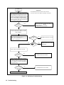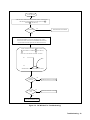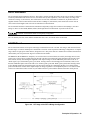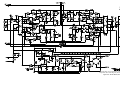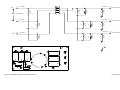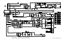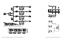
1
SERVICE MANUAL
GPIB DC Power Supplies
Agilent Series 669xA
For instruments with Serial Numbers:
Agilent 6690A: MY41000131
Agilent 6691A: MY41000119
Agilent 6692A: MY41000133
For manual updates, a change page may be included.
For a history of manual updates, see Appendix A.
Agilent Part No. 5969-2907
Printed in Malaysia
November, 2002
CERTIFICATION
Agilent Technologies certifies that this product met its published specifications at time of shipment from the factory. Agilent
Technologies further certifies that its calibration measurements are traceable to the United States National Bureau of
Standards, to the extent allowed by the Bureau's calibration facility, and to the calibration facilities of other International
Standards Organization members.
WARRANTY
This Agilent Technologies hardware product is warranted against defects in material and workmanship for a period of three
years from date of delivery. Agilent Technologies software and firmware products, which are designated by Agilent
Technologies for use with a hardware product and when properly installed on that hardware product, are warranted not to
fail to execute their programming instructions due to defects in material and workmanship for a period of 90 days from date
of delivery. During the warranty period Agilent Technologies will, at its option, either repair or replace products which
prove to be defective. Agilent Technologies does not warrant that the operation of the software, firmware, or hardware shall
be uninterrupted or error free.
For warranty service, with the exception of warranty options, this product must be returned to a service facility designated
by Agilent Technologies. Customer shall prepay shipping charges by (and shall pay all duty and taxes) for products
returned to Agilent Technologies for warranty service. Except for products returned to Customer from another country,
Agilent Technologies shall pay for return of products to Customer.
Warranty services outside the country of initial purchase are included in Agilent Technologies product price, only if
Customer pays Agilent Technologies international prices (defined as destination local currency price, or U.S. or Geneva
Export price).
If Agilent Technologies is unable, within a reasonable time to repair or replace any product to condition as warranted, the
Customer shall be entitled to a refund of the purchase price upon return of the product to Agilent Technologies.
LIMITATION OF WARRANTY
The foregoing warranty shall not apply to defects resulting from improper or inadequate maintenance by the Customer,
Customer-supplied software or interfacing, unauthorized modification or misuse, operation outside of the environmental
specifications for the product, or improper site preparation and maintenance. NO OTHER WARRANTY IS EXPRESSED
OR IMPLIED. AGILENT TECHNOLOGIES SPECIFICALLY DISCLAIMS THE IMPLIED WARRANTIES OF
MERCHANTABILITY AND FITNESS FOR A PARTICULAR PURPOSE.
EXCLUSIVE REMEDIES
THE REMEDIES PROVIDED HEREIN ARE THE CUSTOMER'S SOLE AND EXCLUSIVE REMEDIES. AGILENT
SHALL NOT BE LIABLE FOR ANY DIRECT, INDIRECT, SPECIAL, INCIDENTAL, OR CONSEQUENTIAL
DAMAGES, WHETHER BASED ON CONTRACT, TORT, OR ANY OTHER LEGAL THEORY.
ASSISTANCE
The above statements apply only to the standard product warranty. Warranty options, extended support contracts, product
maintenance agreements and customer assistance agreements are also available. Contact your nearest Agilent
Technologies Sales and Service office for further information on Agilent Technologies' full line of Support Programs.
2
SAFETY CONSIDERATIONS
GENERAL. This is a Safety Class 1 instrument (provided with terminal for connection to protective earth ground).
OPERATION. BEFORE APPLYING POWER verify that the product is set to match the available line voltage, the
correct line fuse is installed, and all safety precautions (see following warnings) are taken. In addition, note the instrument's
external markings described under "Safety Symbols".
WARNING.
• Servicing instructions are for use by service-trained personnel. To avoid dangerous electrical shock, do not perform
any servicing unless you are qualified to do so.
• BEFORE SWITCHING ON THE INSTRUMENT, the protective earth terminal of the instrument must be connected to
the protective conductor of the (mains) power cord. The mains plug shall be inserted only in an outlet socket that is
provided with a protective earth contact. This protective action must not be negated by the use of an extension cord
(power cable) that is without a protective conductor (grounding). Grounding one conductor of a two-conductor outlet is
not sufficient protection.
• If this instrument is to be energized via an auto-transformer (for voltage change), make sure the common terminal is
connected to the earth terminal of the power source.
• Any interruption of the protective (grounding) conductor (inside or outside the instrument), or disconnecting of the
protective earth terminal will cause a potential shock hazard that could result in personal injury.
• Whenever it is likely that the protective earth connection has been impaired, this instrument must be made inoperative
and be secured against any unintended operation.
• Only fuses with the required rated current, voltage, and specified type (normal blow, time delay, etc.) should be used.
Do not use repaired fuses or short-circuited fuseholders. To do so could cause a shock or fire hazard.
• Do not operate this instrument in the presence of flammable gases or fumes.
• Do not install substitute parts or perform any unauthorized modification to this instrument.
• Some procedures described in this manual are performed with power supplied to the instrument while its protective
covers are removed. If contacted, the energy available at many points may result in personal injury.
• Any adjustment, maintenance, and repair of this instrument while it is opened and under voltage should be avoided as
much as possible. When this is unavoidable, such adjustment, maintenance, and repair should be carried out only by a
skilled person who is aware of the hazard involved.
• Capacitors inside this instrument may hold a hazardous electrical charge even if the instrument has been disconnected
from its power source.
SAFETY SYMBOLS
Instruction manual symbol. The instrument will be marked with this symbol when it is necessary for you to refer to the
instruction manual in order to protect against damage to the instrument.
This sign indicates hazardous voltages.
This sign indicates an earth terminal (sometimes used in the manual to indicate circuit common connected to a ground
chassis).
The WARNING sign denotes a hazard. It calls attention to a procedure, practice, or the like, which, if not correctly
performed or adhered to, could result in personal injury. Do not proceed beyond a WARNING sign until the
indicated conditions are fully understood and met.
The CAUTION sign denotes a hazard. It calls attention to an operating procedure, or the like, which, if not correctly
performed or adhered to, could result in damage to or destruction of part or all of the product. Do not proceed
beyond a CAUTION sign until the indicated conditions are fully understood and met.
.
3
Safety Symbol Definitions
Symbol
Description
Symbol
Description
Direct current
Terminal for Line conductor on permanently
installed equipment
Alternating current
Caution, risk of electric shock
Both direct and alternating current
Caution, hot surface
Three-phase alternating current
Caution (refer to accompanying documents)
Earth (ground) terminal
In position of a bi-stable push control
Protective earth (ground) terminal
(Intended for connection to external
protective conductor.)
Out position of a bi-stable push control
Frame or chassis terminal
On (supply)
Terminal for Neutral conductor on
permanently installed equipment
Off (supply)
Terminal is at earth potential
(Used for measurement and control
circuits designed to be operated with
one terminal at earth potential.)
Standby (supply)
Units with this symbol are not completely
disconnected from ac mains when this switch is
off. To completely disconnect the unit from ac
mains, either disconnect the power cord or have
a qualified electrician install an external switch.
Printing History
The edition and current revision of this manual is indicated below. Reprints of this manual containing minor corrections
and updates may have the same printing date. Revised editions are identified by a new printing date. A revised edition
incorporates all new or corrected material since the previous printing date. Significant changes to the manual occurring
between revisions are covered by change sheets shipped with the manual. Note that not all changes made to the power
supply affect the content of the manual. Refer to appendix A for a history of manual updates.
Edition 1
November, 2002
© Copyright 2002 Agilent Technologies, Inc.
This document contains proprietary information protected by copyright. All rights are reserved. No part of this document
may be photocopied, reproduced, or translated into another language without the prior consent of Agilent Technologies,
Inc. The information contained in this document is subject to change without notice.
4
Table of Contents
Introduction ............................................................................................................................................................................ 7
Scope and Organization ...................................................................................................................................................... 7
Instrument Identification..................................................................................................................................................... 7
Related Documents .......................................................................................................................................................... 8
Manual Revisions............................................................................................................................................................. 7
Firmware Revisions ......................................................................................................................................................... 8
Safety Considerations ......................................................................................................................................................... 8
Electrostatic Discharge ....................................................................................................................................................... 8
Verification.............................................................................................................................................................................. 9
Introduction......................................................................................................................................................................... 9
Tests .................................................................................................................................................................................... 9
Test Equipment Required.................................................................................................................................................... 9
Equipment List ................................................................................................................................................................. 9
Current-Monitoring Resistor ............................................................................................................................................ 9
Electronic Load ................................................................................................................................................................ 9
Programming the Tests ..................................................................................................................................................... 10
General Considerations .................................................................................................................................................. 10
General Measurement Techniques .................................................................................................................................... 11
Performance Test Record Sheets ...................................................................................................................................... 11
Operation Verification Tests ............................................................................................................................................. 11
Performance Tests............................................................................................................................................................. 11
Constant Voltage (CV) Tests ......................................................................................................................................... 12
Constant Current (CC) Tests .......................................................................................................................................... 15
Averaging the CC Measurements................................................................................................................................... 19
Troubleshooting .................................................................................................................................................................... 25
Introduction....................................................................................................................................................................... 25
Test Equipment Required ............................................................................................................................................. 25
Power-On Selftest ............................................................................................................................................................. 26
Troubleshooting Charts .................................................................................................................................................. 26
Firmware Revisions ....................................................................................................................................................... 42
Test Headers................................................................................................................................................................... 42
Post-Repair Calibration..................................................................................................................................................... 43
When Required .............................................................................................................................................................. 43
Inhibit Calibration Jumper ............................................................................................................................................. 43
Calibration Password ..................................................................................................................................................... 43
Restoring Factory Calibration Constants ....................................................................................................................... 44
EEPROM Initialization ..................................................................................................................................................... 44
Transferring Calibration Constants to Factory Preset Locations....................................................................................... 44
Disassembly Procedures ................................................................................................................................................... 48
Tools Required ............................................................................................................................................................... 49
Top Cover ...................................................................................................................................................................... 49
Removing Protective RFI Shield (Galvanized Sheet Metal).......................................................................................... 49
GPIB Board.................................................................................................................................................................... 49
A4 AC Input Assembly.................................................................................................................................................. 50
A5 DC RAIL Assembly ................................................................................................................................................. 50
A6 BIAS Assembly........................................................................................................................................................ 50
A3 FET Board................................................................................................................................................................ 50
A10 Control Assembly................................................................................................................................................... 50
Front Panel Assembly .................................................................................................................................................... 51
S1 Line Switch ............................................................................................................................................................... 51
A1 Front Panel Board..................................................................................................................................................... 51
5
A1DSP1 LCD Display ................................................................................................................................................... 51
A1G1 and A1G2 Rotary Controls .................................................................................................................................. 51
A1KPD Keypad ............................................................................................................................................................. 51
Output Bus Boards A7, A81 and A9 & Chassis Components........................................................................................ 52
Principles of Operation ........................................................................................................................................................ 59
Introduction....................................................................................................................................................................... 59
A2 GPIB Board................................................................................................................................................................. 59
A1 Front Panel Assembly ................................................................................................................................................. 60
A10 Control Board.......................................................................................................................................................... 60
A4 AC Input Board ........................................................................................................................................................... 62
A5 DC Rail Board............................................................................................................................................................. 63
A3 FET Board................................................................................................................................................................... 63
Output Circuits.................................................................................................................................................................. 64
Replaceable Parts.............................................................................................................................................................. 65
Introduction...................................................................................................................................................................... 65
How to Order Parts ........................................................................................................................................................... 65
Diagrams................................................................................................................................................................................ 69
Introduction....................................................................................................................................................................... 69
Backdating............................................................................................................................................................................. 99
Index .................................................................................................................................................................................... 101
6
1
Introduction
Scope and Organization
This manual contains information for troubleshooting and repairing Agilent Series 669xA, 6.6-kilowatt power supplies to
the assembly level. The supplied schematics at the back of the manual are not intended for component level repair, only to
provide additional information for isolating a problem to a specific assembly. The chapters of this manual are organized as
follows:
Chapter
Chapter 2
Chapter 3
Chapter 4
Chapter 5
Chapter 6
Description
Verification procedures to determine the performance level of the supply either before or after repair.
Troubleshooting procedures for isolating a problem, procedures for replacing the defective assembly
and, if required, post-repair calibration and EEPROM initialization procedures.
Principles of power supply operation on a block-diagram level.
Assembly-level replaceable parts, including parts ordering information.
Diagrams, including schematics, component location drawings, and troubleshooting test points.
Instrument Identification
Agilent Technologies instruments are identified by a 10-digit serial number. The format is described as follows: first two
letters indicate the country of manufacture. The next four digits are a code that identify either the date of manufacture or of
a significant design change. The last four digits are a sequential number assigned to each instrument.
Item
MY
3648
0101
Description
The first two letters indicates the country of manufacture, where US = USA; MY = Malaysia.
This is a code that identifies either the date of manufacture or the date of a significant design change.
The last four digits are a unique number assigned to each power supply.
Manual Revisions
The edition and current revision of this manual is indicated on page 4. Reprints of this manual containing minor
corrections and updates may have the same printing date. Revised editions are identified by a new printing date. A revised
edition incorporates all new or corrected material since the previous printing date. Significant changes to the manual
occurring between revisions are covered by change sheets shipped with the manual. Note that not all changes made to the
power supply affect the content of the manual. Refer to appendix A for a history of manual updates.
This manual was written for power supplies that have the same serial prefixes (first part) as those listed on the title page and
whose serial numbers (second part) are equal to or higher than those listed in the title page.
Note
1) A revised edition incorporates all new or corrected material since the previous printing date.
2) If they are significant to the operation and/or servicing of the power supply, those differences are
documented in one or more Manual Changes sheets included with this manual. These changes will also
be incorporated at future updates of the manual.
3) A history of changes to this manual that affect previously manufactured units is provided in Appendix A
- Manual Backdating.
Introduction
7
Firmware Revisions
The power supply's firmware resides in the A10 control board microprocessor chip and in ROM chips on the A2 GPIB and
A1 Front Panel boards. You can obtain the firmware revision number by either reading the integrated circuit label, or query
the power supply using the GPIB *IDN query command (see Chapter 3 - Troubleshooting). Also, see Chapter 3, Firmware
Revisions for the actual Agilent BASIC program that does this.
Related Documents
Operating and Programming Manuals
Each power supply is shipped with an operating and programming manual (see Replaceable Parts, Chapter 5 for part
numbers) that covers the following topics:
•
•
•
•
•
•
•
•
•
•
•
•
Options, accessories, specifications, supplementary characteristics, output characteristic curve, typical output
impedance curves.
Connecting the power cord, load, and remote sensing.
Connecting power supplies in series or autoparallel.
Connecting the remote controller and setting the GPIB address.
Configuring the digital port for remote inhibit, relay link, or digital I/O operation.
Connecting the analog port for external voltage programming control.
Turn-on tests, including selftest errors and runtime errors.
Front panel operation.
SCPI programming, an introduction to syntax, language dictionary, and status register operation.
Compatibility-language programming for operation with Agilent Series 603xA power supplies.
Replacement of line fuse and conversion of line voltage.
Calibration procedure (front panel and remote).
Safety Considerations
This power supply is a Safety Class I instrument, which means it has a protective earth terminal. This terminal must be
connected to earth ground through a power source equipped with a 4-wire, ground receptacle. Refer to the "Safety
Summary" page at the beginning of this manual for general safety information. Before operation or repair, check the power
supply and review this manual for safety warnings and instructions. Safety warnings for specific procedures are located at
appropriate places in the manual.
Hazardous voltage exist within the power supply chassis, at the output terminals, and at the analog
programming terminals.
Electrostatic Discharge Precautions
The power supply has components that can be damaged by ESD (electrostatic discharge). Failure to
observe standard, antistatic practices can result in serious degradation of performance, even when an
actual failure does not occur.
When working on the power supply observe all standard, antistatic work practices. These include, but are not limited to:
•
•
•
•
•
8
working at a static-free station such as a table covered with static-dissipative laminate or with a conductive table mat
(Agilent P/N 9300-0797, or equivalent).
using a conductive wrist strap, such as Agilent P/N 9300-0969 or 9300-0970.
grounding all metal equipment at the station to a single common ground.
connecting low-impedance test equipment to static-sensitive components only when those components have power
applied to them.
removing power from the power supply before removing or installing printed circuit boards.
Introduction
2
Verification
Introduction
This chapter provides test procedures for checking the operation of Agilent Series 669xA power supplies. The required test
equipment is specified and sample performance test record sheets are included. Instructions are given for performing the
tests either from the front panel or from a controller over the GPIB.
Tests
Two types of procedures are provided: Operation Verification tests and Performance tests.
Type of Test
Operation Verification
Performance
Purpose
These tests do not check all parameters, but comprise a short procedure to verify that the power
supply is performing properly.
These tests verify all the Specifications (not Supplementary Characteristics) listed in Table 1-1
of the Power Supply Operating Manual.
If you encounter failures or out-of-specification test results, see Troubleshooting Procedures (Chapter 3). The procedures
will determine if repair and/or calibration is required.
Note
The power supply must pass the selftest at power-on before the following tests can be performed. If the
power supply fails selftest, go to Chapter 3.
Test Equipment Required
Equipment List
Table 2-1 lists the equipment required to perform the tests given in this chapter. Only the equipment marked with the
superscript "1'' is needed for the Operation Verification test.
Current-Monitoring Resistor
The four-terminal, current-monitoring resistor (current shunt) listed in Table 2-1 is required to eliminate output current
measurement error caused by voltage drops in leads and connections. The specified current shunts have special
current-monitoring terminals inside the load connection terminals. The accuracy of the current shunt must be 0.04% or
better. Connect the current monitor directly to these current-monitoring terminals.
Electronic Load
Many of the test procedures require the use of a variable load capable of dissipating the required power. If a variable
resistor is used, switches must be used for connecting, disconnecting, and shorting the load resistor. For most tests, an
electronic load (see Table 2-1) is easier to use than a variable resistor. However, an electronic load may not be fast enough
for testing transient recovery time or may be too noisy for testing noise (PARD). In these cases, fixed load resistors of
suitable power dissipation can be used with minor changes to the test procedures given in this chapter.
Verification 9
Table 2-1. Test Equipment Required
Required Characteristics
Recommended Model
Type
Digital Voltmeter1
Current Monitor Resistor1
DC Power Supply
Electronic Load
Resistor Load
Oscilloscope
RMS Voltmeter
Resolution: 10 nV @ 1V
Readout: 8 1/2 digits
Accuracy: 20 ppm
Agilent 6691A, 6692A:
0.001Ω ± 0.04%, 300A, 100W
Agilent 6690:
0.0001Ω ± 0.05%, 1000A, 100W
DC Power Source with current capability
equal to UUT
Range: Voltage and current range must
exceed that of supply under test. Power:
7kW minimum
or
6.6 Kilowatt minimum
Agilent 6690A = 34.1 milliohms 6600W
Agilent 6691A = 136 milliohms 6600W
Agilent 6692A = 545 milliohms. 6600W
Sensitivity: 1mV
Bandwidth Limit: 20MHz
Probe: 1:1 with RF tip
Agilent 3458A
True RMS Bandwidth: 20MHz
Sensitivity: 100 µV
Rhode & Schwartz
Guildline 9230/300
Burster Type 1280
Agilent 6680A
4 each Agilent N3300A, with/3
each Agilent N3306A per
mainframe for all units
Agilent Infinium
or equivalent
Model URE3 RMS-P-P
voltmeter
Current Transformer
Variable-Voltage
Transformer (AC Source)
0.1Volt per ampere: 1Hz to 20MHz
Power: 3 Phase 24KVA; Range:
180-235V 47 - 63Hz; 360- 440V
47 - 63Hz
Pearson Model 411
Superior Powerstat
1156DT-3Y, 0-280V, 50A,
24.2 KVA or equivalent .
GPIB Controller2
Full GPIB capabilities
HP Series 200/300
1
2
Required for Operation Verification Tests.
Required for remote testing of 669xA models.
Programming the Tests
General Considerations
Procedures are given for programming these tests either from the front panel keypad or from a GPIB controller. The
procedures assume you know how to use the front panel keypad or how to program over the GPIB (see the Power Supply
Operating Manual for more information). When using computer-controlled tests, you may have to consider the relatively
slow (compared to computer and system voltmeters) settling times and slew rates of the power supply. Suitable WAIT
statements can be inserted into the test program to give the power supply time to respond to the test commands.
This power supply can provide more than 240VA at more than 2 volts. If the output connections touch each
other, severe arcing can occur resulting in burns, ignition or welding of parts. DO NOT ATTEMPT
TO MAKE CONNECTIONS WHILE OUTPUT POWER IS ON. These connections should be performed
only by qualified electronics personnel.
10 Verification
Programming Parameters
Table 2-2 lists the programming voltage and current values for each model. You can enter these values either from the front
panel or from a controller over the GPIB.
Agilent Model
Agilent 6690A
Agilent 6691A
Agilent 6692A
Table 2-2. Programming Voltage and Current Values
Full Scale
Max. Prog.
Full Scale
Max. Prog.
Voltage
Voltage
Current
Current
15V
15.375V
440A
450A
30V
30.75V
220A
225A
60V
60.5V
110A
112A
Max. Prog.
Overvoltage
18V
36V
69V
General Measurement Techniques
Figure 2-1 shows the setup for the Constant Voltage tests. Measure the dc output voltage directly at the sense (+S and -S)
terminals. Connect these terminals for local sensing. Be certain to use load leads of sufficient wire gauge to carry the output
current (see Chapter 4 of the Power Supply Operating Manual). To avoid noise pickup, use coaxial cable or shielded pairs
for the test leads. If you use more than one meter or a meter and an oscilloscope, connect separate leads for each instrument
to avoid mutual-coupling effects.
Performance Test Record Sheets
When performing the tests in this chapter, refer to the Performance Test Record sheets supplied at the end of this chapter.
Table 2-6 is for recording common information, such as, the test equipment used and the environmental conditions. Tables
2-7 through 2-11 are dedicated to specific models. Each sheet lists the acceptable test ranges for the model and provides a
place to record the results of the test.
Note
It is recommended that before you perform the tests in either Table 2-4 or Table 2-5, that you first locate
the appropriate Performance Test Record sheet from Tables 2-7 through Table 2-11 for your specific
model. Make a copy of this sheet, and record the actual observed values in it while performing the tests.
Use the sheets in Tables 2-7 through Table 2-11 as master reference sheets to run copies at any time.
Operation Verification Tests
Table 2-3 lists the requirements for operation verification, which is a subset of the performance tests.
1
2
3
Table 2-3. Operation Verification Tests
Test
Refer To
Turn-On Checkout
Power Supply Operating Manual
Voltage Programming and Readback Accuracy
Table 2-4
Current Programming and Readback Accuracy
Table 2-5
Note: Record the results of Tests 2 and 3 in the appropriate Performance Test Record sheets
Performance Tests
Performance tests check all the specifications of the power supply. The tests are grouped into constant-voltage mode tests
(Table 2-4) and constant-current mode tests (Table 2-5).
Verification 11
Constant Voltage (CV) Tests
Test Setup
Connect your dc voltmeter leads to only +S and -S (see Figure 2-1), because the power supply regulates the voltage
between these points, not between the + and - output terminals.
Test Procedures
Perform the test procedures in Table 2-4. The CV tests are:
• Voltage Programming and Readback Accuracy
• CV Load Effect
• CV Source Effect
• CV Noise (PARD)
• Transient Recovery Time
Note
The tests are independent and may be performed in any order.
DVM -
+
Electronic Load
+
S
-
S
+
a) CV Test Setup with 6.6kW Electronic Load
+
DVM -
6.6kW Load
Resistor
S
+
b) CV Test Setup with 6.6kW Load Resistor
Note: Start with switch closed, take full load reading,
open switch and take no load reading.
Figure 2-1. Constant Voltage (CV) Test Setup
12 Verification
S
-
Table 2-4. Constant Voltage (CV) Tests
Action
Normal Result
Voltage Programming and Readback Accuracy
This test verifies that the voltage programming, GPIB readback (GPIB system power supplies only), and front panel display
functions are within specifications. With system power supplies, values read back over the GPIB should be the same as
those displayed on the front panel.
1
Turn off the power supply and connect a DVM across +S and -S
(see Fig. 2-1).
2
Turn on the power supply with no load and program the output for 0 volts
and maximum programmable current (see Table 2-2).
CV annunciator on. Output current near
0.
3
Record voltage readings at DVM and on front panel display.
Readings within specified Low Voltage
limits.
4
Program voltage to full scale (see Table 2-2).
5
Record voltage readings of DVM and on front panel display.
Readings within specified High Voltage
limits.
CV Load Effect
This test measures the change in output voltage resulting from a change in output current from full-load to no-load.
1
Turn off the power supply and connect a DVM across +S and -S
(see Fig. 2-1).
2
Turn on the power supply and program the current to its maximum
programmable value and the voltage to its full-scale value (see Table 2-2).
3
Adjust the load to produce full-scale current (see Table 2-2) as shown on
the front panel display.
4
Record voltage reading of the DVM.
5
Adjust load to draw 0 amperes (open load). Record voltage reading of the
DVM.
6
Check test result.
CV annunciator is on. If it is not, adjust
the load to slightly reduce the output
current until the annunciator comes on.
The difference between the DVM
readings in steps 4 and 5 are within the
specified Load Effect limits.
CV Source Effect
This test measures the change in output voltage resulting from a change in ac line voltage from its minimum to maximum
value within the line voltage specifications.
1
Turn off the power supply and connect the ac power input through a
variable-voltage transformer.
2
Set the transformer to the nominal ac line voltage. Connect the DVM
across +S and -S (see Fig. 2-1).
3
Turn on the power supply and program the current to its maximum
programmable value and the voltage to its full-scale value (see Table 2-2).
Verification 13
Table 2-4. Constant Voltage (CV) Tests (continued)
Action
Normal Result
CV Source Effect (cont)
4
Adjust the load to produce full-scale current (see Table 2-2) as shown on
the front panel display.
5
Adjust the transformer to decrease the ac input voltage to the low- line
condition (174Vac or 191Vac). Record the output voltage reading of the
DVM.
6
Adjust the transformer to increase the ac input voltage to the high-line
condition (220Vac or 250Vac). Record the output voltage reading on the
DVM.
7
Check test result.
CV annunciator is on. If it is not, adjust
the load to slightly reduce the output
current until the annunciator comes on.
The difference between the DVM
readings in steps 5 and 6 are within the
specified Source Effect limits.
CV Noise (PARD)
Periodic and random deviations (PARD) in the output (ripple and noise) combine to produce a residual ac voltage
superimposed on the dc output voltage. This test measures CV PARD, specified as the rms and peak-to-peak output
voltages over the frequency range of 20Hz to 20MHz.
1
Turn off the power supply and connect an a-c coupled oscilloscope across
the + and -output terminals (see Fig. 2-1). Set the oscilloscope bandwidth
limit to 20MHz (30MHz for the Agilent 54504A) and use an RF tip on the
oscilloscope probe.
2
Turn on the power supply and program the current to its maximum
programmable value and the voltage to its full-scale value (see Table 2-2).
3
Adjust the load to produce full-scale current (see Table 2-2) as shown on
the front panel display.
CV annunciator is on. If it is not, adjust
the load to slightly reduce the output
current until the annunciator comes on.
4
Record the amplitude of the waveform.
Amplitude is within the specified PARD
Peak-to-Peak limits.
5
Replace the oscilloscope connection with an ac rms voltmeter.
6
Record the reading obtained in Step 5.
Amplitude is within the specified PARD
rms limits.
Transient Recovery Time
This test measures the time required for the output voltage to return to within 100mV of its final value following a 50%
change in output load current. Measurements are made on both the unloading transient (from full load to 1/2 load) and the
loading transient (from 1/2 load to full load).
1
Turn off the power supply and connect an oscilloscope across +S and -S
(see Fig. 2-1).
2
Turn on the power supply and program the current to its maximum
programmable value and the voltage to its full-scale value (see Table 2-2).
14 Verification
Table 2-4. Constant Voltage (CV) Tests (continued)
Action
Normal Result
Transient Recovery (cont)
3
Program the Electronic Load as follows:
•
•
•
•
•
Operating mode to constant current.
Input load current to 1/2 the supply's full rated output current.
Transient current level to the supply's full rated output current.
Transient generator frequency = 100Hz.
Transient generator duty cycle = 50%.
4
Turn on the transient and adjust the oscilloscope to display response
waveform.
See Fig. 2-2.
5
Measure both the loading and unloading transients by triggering the
oscilloscope on both the negative and positive slopes of the transient.
Record the voltage level obtained at the 900-µs interval .
Specified voltage level is reached within
900µs.
Figure 2-2. Transient Response Waveform
Constant Current (CC) Tests
Test Setup
Connect the appropriate current monitoring resistor (see Table 2-l) as shown in Figure 2-3. The accuracy of the resistor
must be as specified in the table.
Test Procedures
The test procedures are given in Table 2-5. The tests are independent and may be performed in any order. The CC tests are:
•
•
•
Current Programming and Readback Accuracy.
CC Load Effect.
CC Source Effect.
Verification 15
+
Electronic Load +
DVM
-
Current Monitor
Resistor
*
Power Supply +
S
+
S
-
-
a) CC Test Setup with 6.6kW Electronic Load
* Note: Series power source required for CC Load Regulation Test, allows
UUT to operate at 0 volts and electronic load to operate at its
minimum input voltage specification. Voltage source must always
be in CV mode. UUT must be in CC mode for all CC tests.
+
DVM
-
Current Monitor
Resistor
6.6kW Load
Resistor
S
+
b) CC Test Setup with 6.6kW Load Resistor
Note: Start with switch closed, take reading at 0 output voltage.
Open switch and take full load reading.
UUT must be in CC mode for all CC tests.
Figure 2-3. CC Load Effect Test Setup
16 Verification
S
-
Table 2-5. Constant Current (CC) Tests
Action
Normal Result
Current Programming and Readback Accuracy
This test verifies that the current programming and readback are within specification.
1
Turn off the power supply and connect the current monitoring resistor as
shown in Fig. 2-3. Connect a DVM across the resistor .
2
Turn on the power supply and program the output for 5 volts and 0
amperes.
3
Short the load.
4
Observe the DVM voltage reading. Divide this by the resistance of the
current monitor resistor. Record the result as the Low Current value.
Value within specified Low Current
limits.
5
Record the front panel display readback.
Value within specified readback limits.
6
Program output current to full scale (see Table 2-2).
7
Repeat Steps 4 and 5.
Both current readings within specified
High Current and readback limits.
CC Load Effect
This test measures the change in output current resulting from a change in load from full-load voltage to a short circuit. It is
recommended that you use averaged readings for Steps 5 and 6 of this test (see Averaging AC Measurements at the end of
this chapter).
Note: Refer to Figure 2-3. If you are using Agilent N3306A electronic loads, a series DC power source is required to
supply the minimum 3 volt input required by the Agilent N3306A electronic loads. The series DC source must be capable
of 3VDC at a current level that is greater than the output current of the supply being tested. A switch can be used in
place of the series supply if the electronic loads are used in place of a load resistor as shown in Fig. 2-3(b).
1
Turn off the power supply and connect a DVM across the current
monitoring resistor (see Fig. 2-3).
2
Turn on the power supply and program the current to its full scale value
and the voltage to its maximum programmable value (see Table 2-2).
3
Set the Electronic Load to CV mode and its voltage to full scale as
indicated on its front panel display. Set the series supply for 3VDC and a
current greater than that being tested. Series source should be in CV mode.
Power supply output current is full scale
and its CC annunciator is on. If not,
reduce the Electronic Load voltage
slightly until the annunciator comes on.
4
Observe the DVM reading. Divide this by the resistance of the current
monitoring resistor to obtain the output current. Record the result.
You may want to use an averaged
reading for this measurement.
5
Program the Electronic Load input to 3 volts or short the Electronic Load
input and repeat Step 5.
You may want to use averaged reading
for this measurement.
6
Check the result.
The difference between the current
readings taken in Step 5 and Step 6 must
be within specified “Load Effect” limits
(see Table 2-2).
Verification 17
Table 2-5. Constant Current (CC) Tests (continued)
Action
Normal Result
CC Source Effect
This test measures the change in output current resulting from a change in ac line voltage from its minimum to its
maximum value within the line voltage specifications. It is recommended that you use averaged readings for Steps 6 and 8
of this test (see "Averaging AC Measurements" at the end of this chapter) .
1
Turn off the power supply and connect the ac power input through a
variable-voltage transformer.
2
Set the transformer to the nominal ac line voltage. Connect the DVM
across the current monitoring resistor (see Fig. 2-3).
3
Turn on the power supply and program the current to its full-scale value
and the voltage to its maximum programmable value (see Table 2-2).
4
Set the Electronic Load to CV mode and its voltage to full scale.
5
Adjust the transformer to decrease the ac input voltage to the low-line
condition (180Vac or 360Vac).
Observe the DVM reading. Divide this voltage by the resistance of the
current monitoring resistor to obtain the output current. Record the result.
6
The power supply output current is full
scale and its CC annunciator is on. If
not, reduce the Electronic Load voltage
slightly until the annunciator comes on.
You may want to use an averaged
reading for this measurement.
7
Adjust the transformer to increase the ac input voltage to the high-line
condition (235Vac or 440Vac).
8
Observe the DVM reading. Divide this voltage by the resistance of the
current monitoring resistor to obtain the output current. Record the result.
You may want to use an averaged
reading for this measurement.
9
Check the test result.
The difference between the current
readings found in Step 6 and Step 8 is
within the specified current Source
Effect limits.
18 Verification
Averaging the CC Measurements
The CC Load Effect and CC Source Effect tests measure the dc regulation of the power supply's output current. When
doing these tests, you must be sure that the readings taken are truly dc regulation values and not instantaneous ac peaks of
the output current ripple. You can do this by making each measurement several times and then using the average of the
measurements as your test value. Voltmeters such as the Agilent 3458A System Voltmeter can be programmed to take just
such statistical average readings as required by these tests.
The following steps show how to set up the voltmeter from its front panel to take a statistical average of l00 readings.
represents the unlabeled shift key in the FUNCTION/RANGE group.
1.
2.
3.
5.
Program 10 power line cycles per sample by pressing
Program 100 samples per trigger by pressing
Set up voltmeter to take measurements in the statistical mode as follows:
a. Press
.
until MATH function is selected, then press
.
b. Press
until STAT function is selected, then press
.
c. Press
Now set up voltmeter to read the average of the measurements as follows:
a. Press
.
until RMATH function is selected, then press
.
b. Press
until MEAN function is selected, then press
.
c. Press
Execute the average reading program by pressing
6.
Wait for 100 readings and then read the average measurement by pressing
4.
.
.
.
.
Record this as your result.
Verification 19
Table 2-6. Performance Test Record Form
Test Facility:
__________________________________________
__________________________________________
__________________________________________
Model_____________________________________
Serial No __________________________________
Options ____________________________________
Firmware Revision ___________________________
Report No._________________________________________
Date______________________________________________
Customer__________________________________________
Tested By__________________________________________
Ambient Temperature (°C)_____________________________
Relative Humidity (%)________________________________
Nominal Line Frequency (Hz)__________________________
Special Notes:
____________________________________________________________________________________________
____________________________________________________________________________________________
____________________________________________________________________________________________
____________________________________________________________________________________________
____________________________________________________________________________________________
____________________________________________________________________________________________
____________________________________________________________________________________________
____________________________________________________________________________________________
Test Equipment Used:
Description
Model No.
1. AC Source
_______________
_______________
_________________
2. DC Voltmeter
_______________
_______________
_________________
3. RMS Voltmeter
_______________
_______________
_________________
4. Oscilloscope
_______________
_______________
_________________
5. Electronic Load
_______________
_______________
_________________
6. Current Monitoring
Shunt
_______________
_______________
_________________
20 Verification
Trace No.
Cal. Due Date
Table 2-7. Performance Test Record for Agilent Model 6690A
MODEL Agilent_____________
Report No.________
Test Description
Minimum Spec.
Date___________
Results
*
Maximum Spec.
Constant Voltage Tests
Voltage Programming
and Readback
Low Voltage (0V) Vout
Front Panel Display Readback
-15mV
Vout - 22.5mV
________mV
________mV
+15mV
Vout + 22.5mV
High Voltage (15V) Vout
Front Panel Display Readback
14.979V
Vout -30mV
_________V
_______mV
15.021V
Vout + 30mV
Load Effect
Vout - 0.95mV
_______mV
Vout + 0.95mV
Source Effect
Vout - 0.95mV
_______mV
Vout + 0.95mV
0
0
_______mV
_______mV
15mV
2.5 mV
0
_______mV
150mV
PARD (Ripple and Noise)
Peak-to-Peak
RMS
Transient Response Time
(at 900 µs)
Constant Current Tests
Current Programming
and Readback
Low Current (0A) Iout
Front Panel Display Readback
-230mA
Iout - 300mA
_______mA
_______mA
+230mA
Iout + 300mA
High Current (440A) Iout
Front Panel Display Readback
439.33A
Iout - 740mA
_________A
_______mA
440.67A
Iout + 740mA
Iout - 62mA
________mA
Iout + 62mA
Iout - 62.5mA
________mA
Iout + 62.5mA
Load Effect
Source Effect
*Enter your test results in this column.
Verification 21
Table 2-8. Performance Test Record for Agilent Model 6691A
MODEL Agilent_____________
Report No.________
Test Description
Minimum Spec.
Date___________
Results
*
Maximum Spec.
Constant Voltage Tests
Voltage Programming
and Readback
Low Voltage (0V) Vout
Front Panel Display Readback
-30mV
Vout - 45mV
________mV
________mV
+30mV
Vout + 45mV
High Voltage (30V) Vout
Front Panel Display Readback
29.958V
Vout - 60mV
_________V
_______mV
30.042V
Vout + 60mV
Load Effect
Vout - 1.7mV
_______mV
Vout + 1.7mV
Source Effect
Vout - 1.25mV
_______mV
Vout + 1.25mV
0
0
_______mV
_______mV
25mV
2.5mV
0
_______mV
150mV
PARD (Ripple and Noise)
Peak-to-Peak
RMS
Transient Response Time
(at 900 µs)
Constant Current Tests
Current Programming
and Readback
Low Current (0A) Iout
Front Panel Display Readback
-125mA
Iout - 165mA
_______mA
_______mA
+125mA
Iout + 165mA
High Current (220A) Iout
Front Panel Display Readback
219.655A
Iout - 385mA
_________A
_______mA
220.345A
Iout + 385mA
Load Effect
Iout - 28mA
________mA
Iout + 28mA
Source Effect
Iout - 28mA
________mA
Iout + 28mA
*Enter your test results in this column.
22 Verification
Table 2-9. Performance Test Record for Agilent Model 6692A
MODEL Agilent_____________
Report No.________
Test Description
Minimum Spec.
Date___________
Results
*
Maximum Spec.
Constant Voltage Tests
Voltage Programming
and Readback
Low Voltage (0V) Vout
Front Panel Display Readback
-60mV
Vout - 90mV
________mV
________mV
+60mV
Vout + 90mV
High Voltage (60V) Vout
Front Panel Display Readback
59.916V
Vout - 120mV
_________V
_______mV
60.084V
Vout + 120mV
Load Effect
Vout - 3.4mV
_______mV
Vout + 3.3mV
Source Effect
Vout -1.85mV
_______mV
Vout + 1.85mV
0
0
_______mV
_______mV
25mV
2.5mV
0
_______mV
150mV
PARD (Ripple and Noise)
Peak-to-Peak
RMS
Transient Response Time
(at 900 µs)
Constant Current Tests
Current Programming
and Readback
Low Current (0A) Iout
Front Panel Display Readback
-65mA
Iout - 80mA
_______mA
_______mA
+65mA
Iout + 80mA
High Current (110A) Iout
Front Panel Display Readback
109.825A
Iout - 190mA
_________A
_______mA
+110.175A
Iout + 190mA
Load Effect
Iout - 14.5mA
________mA
Iout + 14.5mA
Source Effect
Iout - 14.5mA
________mA
Iout + 14.5mA
*Enter your test results in this column.
Verification 23
3
Troubleshooting
Introduction
Shock Hazard: Most of the procedures in this chapter must be performed with power applied and
protective covers removed. These procedures should be done only by trained service personnel aware of
the hazard from electrical shock.
This instrument uses components that can be damaged or suffer serious performance degradation due to
ESD (electrostatic discharge). Observe standard antistatic precautions to avoid damage to the
components (see Chapter 1).
This chapter provides troubleshooting and repair information for the power supply. Before beginning troubleshooting
procedures, make certain the problem is in the power supply and not with an associated circuit, the GPIB controller (for
GPIB system power supplies), or ac input line. Without removing the covers, you can use the Verification tests in Chapter 2
to determine if the power supply is operating normally.
The information in this chapter is organized as follows:
Topic
Information Given
Test Equipment Required
Equipment required for completing all the tests in this chapter.
Troubleshooting Procedures
An explanation of the error codes and messages generated during the power-on selftest.
A series of flow charts for systematic location of defective boards, circuits, and
components.
Post-Repair Adjustments
Calibration and EEPROM initialization procedures required after the replacement of
certain critical components.
Disassembly Procedures
Gaining access to and/or replacing components.
Test Equipment Required
Equipment
Table 3-1. Test Equipment Required
Purpose
Recommended Model
Test Clips
To gain access to IC pins.
AP Products No. LTC
Ammeter/Current Shunt
To measure output current.
Agilent 6690A: Burster 1280
Agilent 6691A, 6692A: Guildline 9230/300
Oscilloscope
To check waveforms and signal levels.
Agilent 54504A
GPIB Controller
To communicate with power supply
via the GPIB (for system units).
Agilent BASIC series
DC Voltmeter
To measure output voltage and
current, bias and references.
Agilent 3458A
Troubleshooting 25
Power-On Selftest
Description
The procedures in the troubleshooting charts make use of the power-on selftest. The power-on selftest tests the front panel,
GPIB interface (for GPIB system power supplies), and secondary interface circuits. If the power supply fails the selftest, the
output remains disabled (turned off) and the front panel normally displays an error code or message (see Table 3-2). The
message is displayed indefinitely and the power supply will not accept GPIB or front panel commands.
Disabling The Power-On Selftest
In order to perform troubleshooting procedures that require programming of the power supply, you must disable the
power-on self test. Do this as follows:
1.
2.
3.
4.
Turn off the power supply.
Hold down the
key and turn on the supply.
Continue holding down the
for 2 seconds and wait until the PWR ON INIT indicator goes off.
The power supply is now on without executing power-on selftest.
Using the *TST? Query
You can get the power supply to execute a partial selftest by sending it the GPIB *TST? query command. Table 3-2 shows
the tests that are performed in response to this command. These tests do not interfere with normal operation or cause the
output to change. The command returns a value of "0" if all tests pass. Otherwise, the command returns the error code of
the first test that failed. No error codes are displayed on the front panel and the power supply will attempt to continue
normal operation.
Troubleshooting Charts
Figure 3-1 gives overall troubleshooting procedures to isolate the fault to a circuit board or particular circuit (see Figure
3-20 for the location of the circuit boards). Some results of Figure 3-1 lead to more detailed troubleshooting charts that
guide you to specific components.
Many of the following troubleshooting procedures begin by checking the bias and/or reference voltages. Table 6-3 of
chapter 6 lists the test points for these voltages and gives the correct reading for each. Test points are identified by an
encircled number such as U in schematic diagrams and component location drawings. The circuit board component
location diagrams identify these points on each board.
The troubleshooting charts are organized as follows:
Chart
Figure 3-1
Figure 3-2
Figure 3-3
Figure 3-4
Figure 3-5
Figure 3-6
Figure 3-7
Figure 3-8
Figure 3-9
Figure 3-10
Figure 3-11
Trouble or Circuit
Overall procedure checks selftest errors, calibration errors, ac input circuit, fan, readback circuits,
A10 Control Board, GPIB cable, digital port, serial link, rotary controls, current amplifier.
No display (from Figure 3-1).
OV circuit not firing (from Figure 3-1).
OV circuit is on at turn on (from Figure 3-1).
Output level is held low (from Figure 3-1).
Output level is held high (from Figure 3-1).
DAC circuits (from Figure 3-1).
Serial Down circuit (from Figure 3-1).
Secondary interface circuit (from Figure 3-1).
Slow downprogramming circuit (from Figure 3-1).
FET troubleshooting (from table 3-2).
26 Troubleshooting
Code and/or
Message
Table 3-2. Selftest Error Codes/Messages
Description
Probable Cause Selftest Error
Codes/Messages
El FP RAM
Front panel RAM test failed (power-on).
A1 board probably defective.*
E2 FP ROM
Front panel ROM test failed (power-on
and *TST?).
A1 board probably defective.*
E3 EE CHKSM
Front panel EEPROM checksum test failed
(power-on and *TST?).
EEPROM U6 on the A1 board probably defective.*
E4 PRI XRAM
Primary interface external RAM test failed
(power-on).
A2 board probably defective.
E5 PRI IRAM
Primary interface internal RAM test failed
(power-on).
A2 board probably defective.
E6 PRI ROM
Primary interface ROM test failed
(power-on and *TST?).
A2 board probably defective.
E7 GPIB
GPIB interface test failed (power-on).
A2 board probably defective.
E8 SEC RAM
Secondary interface RAM test failed
(power-on).
A10 board probably defective.*
E9 SEC ROM
Secondary interface ROM test failed
(power-on and *TST?).
A10 board probably defective.*
E10 SEC 5V
Secondary interface 5 volt readback test
failed (power-on and *TST?).
A10 board probably defective,* or A6 bias board
defective
E11 TEMP
Ambient temperature readback test failed
(power-on and *TST?).
A10 board probably defective.*
E12 DACS
CV or CC DAC tests failed (power-on).
A10 board probably defective,* or A6 bias board
defective (see Figure 3-7).
NOTE: The following error messages can appear because of a failure while the unit is operating or during selftest.
SERIAL TIMOUT
Serial data line failure on A2 board.
See Figure 3-8.
SERIAL DOWN
Serial data line failure on A2 board.
See Figure 3-8.
UART PARITY
UART failed.
A2 board probably defective.
UART FRAMING
UART failed.
A2 board probably defective.
UART OVERRUN
UART failed.
A2 board probably defective.
SBUF OVERRUN
Serial buffer failure UART.
A2 board probably defective or A2 board is in SA
mode (see Figure 3-12).
SBUF FULL
Serial buffer failure.
A2 board probably defective or A2 board is in SA
mode (see Figure 3-12).
EE WRITE ERR
EEPROM write failure.
SECONDARY DN
Serial data line failure on Main board.
EEPROM U6 on the A1 board probably defective
or calibration error.*
See Figure 3-9.
* If you replace either the Al or A10 board, the power supply must be reinitialized and calibrated.
Troubleshooting 27
START
"OVERALL TROUBLESHOOTING"
YES
DID YOU DO
TROUBLE SHOOTING IN
PAGE 3-5 IN OPERATING
MANUAL ?
NO
PERFORM CHECKS IN OPERATING
MANUALS,
YES
TURN OFF SUPPLY AND REMOVE THE TOP COVER
AND RFI SHIELD. DISCONNECT LOAD. CONNECT
SENSE TERMINALS FOR LOCAL SENSING.
TURN ON SUPPLY AND CHECK FOR INDICATION
(FAN RUNNING, DISPLAY ON, DC RAIL LED DS420,
DS421 ON) THAT AC POWER IS ON.
YES
IS
NO
FAN RUNNING ?
CHECK FOR AC POWER ON A4 BOARD. CHECK
F800 AND CHECK FOR 24 V BIAS ON A6 BOARD.
CHECK AC LINE SWITCH A1S1.
YES
NO
IS
DISPLAY
ON?
GO TO NO DISPLAY TROUBLESHOOTING FIG. 3-2
YES
ERROR
MESSAGE
DISPLAYED?
YES
SEE SELF TEST ERROR CODES, TABLE 3-2
NO
WITH FRONT PANEL KEYS, PROGRAM FULL SCALE
VOLTAGE AND CURRENT (SEE TABLE 2-2). USE DVM
TO MEASURE VOLTAGE AT OUTPUT TERMINALS.
OUTPUT
VOLTAGE WITHIN
SPEC?
NO
VOLTAGE
RIGHT BUT OUTOF SPEC?
YES
YES
CALIBRATE THE SUPPLY
NO
A
B
GO TO SHEET 2
GO TO SHEET 4
Figure 3-1. Overall Troubleshooting (Sheet 1 of 4)
28 Troubleshooting
A
FROM SHEET 1
VOLTAGE
DISPLAY WITHIN SPECS?
READS
OK BUT OUTSIDE
SPECS?
NO
YES
NO
PROBABLE DEFECTIVE A10 BOARD
YES
CALIBRATE SUPPLY.
IS CV
ANNUNCIATOR
ON?
YES
NO
PROBABLE DEFECTIVE A10 BOARD
TURN OFF SUPPLY AND CONNECT A SHUNT
(SEE TABLE 3-1) ACROSS THE OUTPUT
TERMINALS. TURN ON SUPPLY AND PROGRAM
FULL-SCALE VOLTAGE AND CURRENT.
OUTPUT
CURRENT WITHIN
SPECS?
NO
CURRENT
OK BUT OUTSIDE
SPECS?
YES
CURRENT
DISPLAY WITHIN SPECS?
YES
CALIBRATE SUPPLY.
NO
READS
OK BUT OUTSIDE
SPECS?
NO
C
GO TO SHEET 4
NO
PROBABLE DEFECTIVE A10 BOARD
YES
YES
CALIBRATE SUPPLY.
IS CC
ANNUNCIATOR
ON?
NO
PROBABLE DEFECTIVE A10 BOARD
YES
TURN OFF SUPPLY AND REMOVE SHUNT. TURN
ON SUPPLY AND PROGRAM VOLTAGE AND CURRENT TO FULL SCALE. PROGRAM OV TO 1/2 FS
VOLTAGE. CHECK THAT SUPPLY GOES INTO AN
OV CONDITION (PROT ON AND OUTPUT=0).
OV
CONDITION
OCCURRED?
NO
GO TO "OV WILL NOT FIRE"
TROUBLESHOOTING FIG 3-3.
YES
D
GO TO SHEET 3
Figure 3-1. Overall Troubleshooting (Sheet 2 of 4)
Troubleshooting 29
FROM SHEET 2
D
PROGRAM OV TO MAXIMUM AND PRESS PROT
CLEAR KEY. OUTPUT SHOULD GO TO FULL
SCALE VOLTAGE.
PRESS OUTPUT ON/OFF REPEATEDLY WHILE
WATCHING VOLTAGE DISPLAY. DOWNPROGRAMMING SHOULD TAKE < 1 SECOND.
NO
LESS THAN
1 SECOND?
GO TO 'SLOW DOWN PROGRAMMING'
TROUBLESHOOTING (SEE FIG. 3-12).
YES
TURN OFF SUPPLY AND CONNECT A GPIB
CONTROLLER TO SUPPLY. CHECK IF SUPPLY
ACCEPTS GPIB COMMANDS.
ACCEPTS
COMMANDS?
NO
PROBABLE DEFECTIVE A2 BOARD
YES
CHECK OPERATION OF DIGITAL CONTROL
PORT, SERIAL LINK AND THE FRONT PANEL
V/I ROTARY CONTROLS.
DIGITAL
CONTROL PORT
NO
PROBABLE DEFECTIVE A2 BOARD
OK?
YES
NO
SERIAL
LINK OK?
PROBABLE DEFECTIVE A2 BOARD
YES
FRONT PANEL
CONTROLS OK?
NO
CHECK VOLTAGE RPG (A1G1) AND/OR
CURRENT RPG (A1G2) CONTROLS AND
CABLE CONNECTIONS.
YES
NO PROBLEMS FOUND. PERFORM VERIFICATION
TESTS IN CHAPTER 2 TO ISOLATE PROBLEM.
Figure 3-1. Overall Troubleshooting (Sheet 3 of 4)
30 Troubleshooting
FROM SHEET 2
FROM SHEET 1
C
B
PROT
ANNUNCIATOR
NO
OUTPUT
NO
VOLTAGE NEAR
ON?
OV?
YES
GO TO "OUTPUT HELD LOW"
TROUBLESHOOTING FIG. 3-5
YES
GO TO "OUTPUT HELD HIGH"
PRESS PROTECT KEY
YES
VOLTAGE RIGHT BUT
OUTSIDE SPEC?
NO
PROBABLE DEFECTIVE A10 BOARD
TROUBLESHOOTING FIG. 3-6.
YES
"OT"
PROBABLE DEFECTIVE A10 BOARD
DISPLAYED?
NO
"OV"
YES
DISPLAYED?
GO TO "OV AT TURN-ON"
TROUBLESHOOTING FIG 3-4.
NO
"OC"
YES
DISPLAYED?
CHECK IF OCP IS ENABLED AT
TURN-ON AND CURRENT IS
PROGRAMMED TO ZERO,
OR OUTPUT SHORTED
NO
RI (REMOTE INHIBIT) DISPLAYED.
CHECK FOR SHORT BETWEEN
A2TB101-3 AND GROUND.
Figure 3-1. Overall Troubleshooting (Sheet 4 of 4)
Troubleshooting 31
START
"NO DISPLAY"
WARNING:
THS CONFIGURATION IS FOR THE TEST ONLY. DO NOT
TURN OFF SUPPLY, REMOVE TOP COVER AND RFI
SHIELD. UNPLUG CABLE W5 FROM J108 ON A2 GPIB
BOARD AND UNPLUG CABLE W4 FROM J507 ON A10
CONTROL BOARD. PLUG CABLE W5 INTO J507 ON
A10 BOARD. THIS REMOVES GPIB BOARD FROM THE
DATA PATH AND CONNECTS THE FRONT PANEL
DIRECTLY TO THE CONTROL BOARD, SEE WARNING.
TURN ON THE SUPPLY AND TRY TO PROGRAM THE
SUPPLY FROM THE FRONT PANEL.
SUPPLY
OPERATES
PROPERLY?
FLOAT THE OUTPUT OR ATTEMPT TO OPERATE THE SUPPLY.
CHECK TEST POINTS 1 - 4 . (SEE TABLE 6-3).
CHECK CABLE W4.
PROBABLE DEFECTIVE A6 BOARD.
YES
NO
TURN OFF THE SUPPLY IN ORDER TO ACCESS
A1 FRONT PANEL BOARD. REMOVE A1 FRONT
PANEL ASSEMBLY.
TURN ON SUPPLY. CHECK +5V BIAS AT R1-6
CONNECT METER COMMON TO R1-3.
CHECK THE FOLLOWING DISPLAY VOLTAGES:
1.1V AT R1-14; 2.2V AT R1-2.
DISPLAY
& BIAS VOLTAGES
OK?
NO
PROBABLE DEFECTIVE A1 BOARD
YES
YES
CHECK
PCLR (RESET*)
A2U2-16 = 5V?
NO
PROBABLE DEFECTIVE A1 BOARD
OR A2 BOARD
CHECK 12 MHz CLOCK SIGNAL AT A1U3-66.
IS
12MHz
SIGNAL OK?
NO
PROBABLE DEFECTIVE A1 BOARD
YES
CONNECT EXTERNAL VOLTMETER TO OUTPUT
TERMINALS. PROGRAM VOLTAGE AND CURRENT
AT THE FRONT PANEL. MEASURE VOLTAGE AT
OUTPUT TERMINALS. (IF OUTPUT IS DISABLED,
PRESS OUTPUT KEY).
IS
OUTPUT VOLTAGE
PRESENT?
NO
PROBABLE DEFECTIVE A1 BOARD
YES
LCD DSP1 OR CABLE W2 IS DEFECTIVE.
Figure 3-2. No Display Troubleshooting)
32 Troubleshooting
START
"OV WILL NOT FIRE"
TURN OFF SUPPLY, REMOVE TOP COVER AND RFI SHIELD. TURN ON SUPPLY
AND CHECK BIAS AND REFERENCE VOLTAGES (TEST POINTS 15
THROUGH 22 . SEE TABLE 6-3).
NO
PROBABLE DEFECTIVE A6 BOARD
VOLTAGES OK?
YES
TURN SUPPLY ON AND PROGRAM THE OUTPUT
VOLTAGE AND CURRENT TO 1/2 SCALE. PROGRAM THE OV TO ZERO.
INSURE THAT OUTPUT VOLTAGE IS AS PROGRAMMED AND THE OVERVOLTAGE CONDITION IS NOT DETECTED (OV ANNUNCIATOR IS OFF).
CHECK VOLTAGES AT A10U502-12 70 AND A10U502-14
63 WITH RESPECT TO COMMON 36 (See TABLE 6-3)
NOTE: U502-14 PULSES ARE LOW WHEN "OV" FIRES.
5V
0V
APPROXIMATELY 1 MILLISEC.LOW WHEN "OV" FIRES.
A10U502-12
NEGATIVE?
NO
PROBABLE DEFECTIVE A10 BOARD
YES
NO
A10U502-14
LOW?
PROBABLE DEFECTIVE A10 BOARD
YES
PROBABLE DEFECTIVE A10 BOARD
OR A9 DOWNPROGRAMMER BOARD
Figure 3-3. OV Will Not Fire Troubleshooting)
Troubleshooting 33
START
"OV AT TURN-ON"
WARNING:
DURING THESE TESTS THE OUTPUT MAY BE AT
HAZARDOUS LEVELS.
CHECK THAT THE OUTPUT VOLTAGE SETTING
IS NOT HIGHER THAN THE OV SETTING IN THE
MEMORY REGISTER. PROGRAM 0 VOLTS AND
MAXIMUM OV. THEN SAVE IN REGISTER 0
(PRESS THE SHIFT, SAVE, 0, ENTER KEYS).
CONNECT A DC SCOPE ACROSS THE OUTPUT
TERMINALS. TURN ON SUPPLY AND CHECK
THAT OUTPUT DOES NOT MOMENTARILY GO
HIGHER THAN THE VOLTAGE SETTINGS.
TURN OFF SUPPLY.
MOMENTARILY
GOES HIGHER?
YES
GO TO "OUTPUT HELD HIGH"
TROUBLESHOOTING FIG. 3-6.
NO
TURN OFF SUPPLY. REMOVE TOP COVER AND
RFI SHIELD. DISABLE THE OV INPUT BY LIFTING
A10R536. TURN ON SUPPLY AND CHECK
OUTPUT VOLTAGE.
IS
OUTPUT
HIGH?
YES
GO TO "OUTPUT HELD HIGH"
TROUBLESHOOTING FIG. 3-6.
NO
YES
OV STILL
OCCURS?
PROBABLE DEFECTIVE A10 BOARD
NO
CHECK VOLTGES AT A10U521-7 84 ,
A10U502-12 70 , AND A10U502-14 63
WITH RESPECT TO COMMON 30
CHECK THAT A10U521-7 GOES FROM 0 V
DOES
A10U521-7
= +5.4 +/- 0.5 V?
NO
TO APPROX. 5.4 V AS OVERVOLTAGE
IS PROGRAMMED FROM 0 TO MAXIMUM.
IF NOT, PROBABLE DEFECTIVE A10 BOARD
YES
IS
A10U502-12
> +0.5V?
NO
PROBABLE DEFECTIVE A10 BOARD
YES
IS
A10U502-14
HIGH?
NO
PROBABLE DEFECTIVE A10 BOARD
YES
PROBABLE DEFECTIVE A10 BOARD
OR A9 DOWNPROGRAMMER BOARD
Figure 3-4. OV At Turn-On Troubleshooting)
34 Troubleshooting
START
"OUTPUT HELD LOW"
THE OUTPUT IS HELD LOW AND PROT IS NOT ON.
TURN OFF SUPPLY, DISCONNECT THE LOAD, REMOVE TOP
COVER AND RFI SHIELD. TURN ON SUPPLY AND CHECK BIAS
VOLTAGES (TEST POINTS 9 THROUGH 22 , SEE TABLE 6-3).
ARE
VOLTAGES
OK?
NO
PROBABLE DEFECTIVE
A6 BOARD
YES
TURN OFF SUPPLY AND GO TO "A5 CONTROL BOARD TROUBLESHOOTING SETUP" (TABLE 6-3). TURN ON SUPPLY AND PROGRAM
OUTPUT TO 1/2 FULL SCALE VOLTAGE AND CURRENT. PROGRAM
OV TO MAXIMUM, OCP OFF, AND ENABLE THE OUTPUT.
YES
IS CC
ANNUNCIATOR
ON?
NO
IS UNR
ANNUNCIATOR
ON?
NO
CHECK CV PROGRAMMING
LEVEL AT A10U513-6 39
YES
CHECK CURRENT READING
ON FRONT PANEL DISPLAY
DISPLAY
READS 1/2 F.S.
CURRENT?
YES
USE DIFFERENTIAL INPUT OSCILLOSCOPE
DOES
TP 56
= -5V?
NO
TO CHECK FOR PULSES AT A10J511 62 ,
A10U602-9 52 , A10U600-10 56 , A10U607-1 51,
CHECK FOR SHORT
CIRCUIT IN OUTPUT
A10U604-8 59 AND A10U605-7 55 .
SEE CORRECT WAVEFORMS IN FIG 6-1.
YES
CHECK VOLTAGE CALIBRATION.
SEE APPENDIX A IN OPERATING
NO
MANUAL.
CHECK CC PROGRAM LEVEL
AT A10U514-6 40
40 = -5V ?
NO
NO
IS TP 62
OK?
15V, 40KHz
YES
CHECK CURRRENT
CALIBRATION
PROBABLE DEFECTIVE
A10 BOARD
SEE "FET TROUBLESHOOTING" FIG 3-11
YES
PROBABLE DEFECTIVE
A10 BOARD
Figure 3-5. Output Held Low Troubleshooting)
Troubleshooting 35
START
"OUTPUT HELD HIGH"
TURN OFF THE SUPPLY AND REMOVE THE
COVER AND RFI SHIELD. DISCONNECT LOAD.
TURN SUPPLY ON AND CHECK THE BIAS AND
REFERENCE VOLTAGES (TEST POINTS 9
THROUGH 22 . SEE TABLE 6-3.
ARE
VOLTAGES
NO
PROBABLE DEFECTIVE A6 BOARD
OK?
YES
DISABLE THE OV CIRCUIT BY LIFTING
A10R536. TURN ON SUPPLY AND PROGRAM
OUTPUT VOLTAGE AND CURRENT TO ZERO.
CHECK IF CV "OR" GATE DIODE
A10D652 IS CONDUCTING
A10D652
NO
CONDUCTING?
PROBABLE DEFECTIVE A10 BOARD
YES
CHECK VOLTAGE LEVEL AT FAST SENSE
DIFF AMP A10U608-7 49 .
DOES
TP 49
= -10V?
NO
PROBABLE DEFECTIVE A10 BOARD
OR A8 FAST SENSE BOARD
YES
PROBABLE DEFECTIVE A10 BOARD
Figure 3-6. Output Held High Troubleshooting)
36 Troubleshooting
START
"DAC DEFECTIVE"
TURN OFF SUPPLY AND REMOVE TOP COVER.
TURN ON SUPPLY AND CHECK BIAS AND
REFERENCE VOLTAGES (TEST POINTS 9
THE SUPPLY, DEPRESS THE 7 KEY AND THEN
TURN IT ON WHILE HOLDING THE KEY DOWN
SO AS TO SKIP SELF TEST.
THOUGH 22 . (SEE TABLE 6-3*).
ARE
VOLTAGES
OK?
* IF THE SUPPLY FAILS SELF TEST, TURN OFF
NO
PROBABLE DEFECTIVE A6 BOARD
YES
SHORT A10U506-1 (SA MODE) TO A10U506-20 (COM),
SEE FIG. 3-15. TURN ON SUPPLY AND WAIT TWO
SECONDS THEN REMOVE SHORT. WAIT FOR "POWER
ON INIT" TO COMPLETE. USE A SCOPE TO CHECK
THE CV DAC (A10U513-6), CC DAC (A10U514-6) AND
READBACK DAC (A10U515-6) OUTPUTS. COMPARE
THE WAVEFORMS TAKEN AT THESE POINTS WITH
THE WAVEFORMS GIVEN IN FIG 6-1.
IS ONE
YES
DAC MISSING
PROBABLE DEFECTIVE A10 BOARD
STEPS?
NO
ARE ALL
DACS MISSING
STEPS?
YES
PROBABLE DEFECTIVE A10 BOARD
NO
IS
CV OR CC DAC
DEFECTIVE?
YES
CHECK REF VOLTAGE FOR CV/CC DACS AT
A10U504-6
37 WITH RESPECT TO 36 .
NO
PROBABLE DEFECTIVE A10 BOARD
DOES A10U504-6
= 10V?
YES
PROBABLE DEFECTIVE A10 BOARD
NO
PROBABLE DEFECTIVE A10 BOARD
Figure 3-7. DAC Circuits Troubleshooting)
Troubleshooting 37
START
"SERIAL DOWN"
WARNING:
THIS REMOVES THE GPIB BOARD
FROM THE DATA PATH AND CONNECTS THE
FRONT PANEL DIRECTLY TO THE CONTROL BOARD.
THIS CONFIGURATION IS FOR TEST ONLY. DO NOT
FLOAT THE OUTPUT OR ATTEMPT TO OPERATE
OPERATE THE SUPPLY IN THIS CONFIGURATION.
TURN OFF SUPPLY, REMOVE TOP COVER AND RFI SHIELD.
UNPLUG CABLE W5 FROM J108 ON A2 GPIB BOARD AND
UNPLUG CABLE W4 FROM J507 ON A10 CONTROL BOARD.
PLUG CABLE W5 INTO J507 ON A10 BOARD (SEE WARNING).
TURN ON THE SUPPLY AND TRY TO PROGRAM IT FROM THE
FRONT PANEL.
SUPPLY
OPERATES
PROPERLY?
YES
PROBABLE DEFECTIVE A2 BOARD
NO
TURN OFF SUPPLY. REMOVE FRONT PANEL
ASSEMBLY TO ACCESS THE A1 FRONT PANEL
BOARD. TURN ON SUPPLY AND CHECK FOR
PULSES AT A1U3-17 AND A1U3-18 .
PULSES
AT A1U3-17?
YES
NO
CHECK CABLE W5.
YES
PULSES
AT A1U3-18?
NO
PROBABLE DEFECTIVE
A1 BOARD
Figure 3-8. Serial Down Troubleshooting)
38 Troubleshooting
START
"SECONDARY DOWN"
DISPLAY READS "SECONDARY DN". TURN OFF SUPPLY
AND REMOVE TOP COVER. TURN ON SUPPLY AND CHECK FOR
SERIAL DATA PULSES AT A2U110-8 TEST POINT
WITH RESPECT TO PRIMARY GROUND
1 .
PULSES
5
(SEE TABLE 6-3).
NO
PROBABLE DEFECTIVE A2 BOARD
AT A2U110-8?
YES
CHECK FOR 5V AT A2U110-8 WITH RESPECT TO SECONDARY
COMMON (A2U110-5) 12
CHECK CABLE W4. CHECK
5V AT
NO
SECONDARY BIAS CIRCUIT TEST POINTS 20
A2U110-8
21
AND 22 . (SEE TABLE 6-3).
YES
CHECK FOR SERIAL DATA PULSES AT THE A10 CONTROL BOARD
CIRCUIT POINTS AS INDICATED BELOW WITH RESPECT TO
SECONDARY COMMON 12 .
PULSES
NO
PROBABLE DEFECTIVE A2 BOARD
CHECK FOR CABLE W4 OPEN.
NO
PROBABLE DEFECTIVE A10 BOARD
AT A10U506-10?
YES
PULSES
AT A10U504-11 AND
A10U505-14 ?
YES
PROBABLE DEFECTIVE A2 BOARD
Figure 3-9. Secondary Interface Down)
Troubleshooting 39
START
"SLOW DOWN PROGRAMMING"
TURN ON SUPPLY
AND PROGRAM OUTPUT VOLTAGE AND
CURRENT TO 1/2 FULL SCALE.
CHECK VOLTAGE LEVELS AT A10U609-1 AND
A10U610-1 WITH RESPECT TO SECONDARY
COMMON 36 . SEE TABLE 6-3.
CHECK FUSES A9F980, F981 BY
MEASURING CONTINUITY
A10U610-1
NO
= +2.5V?
PROBABLE DEFECTIVE A10 BOARD
YES
A10U609-1
< 10V?
NO
PROBABLE DEFECTIVE A10 BOARD
YES
PROBABLE DEFECTIVE A9 BOARD
NOTE:
SHOULD TOGGLE BETWEEN <1 V WITH OUTPUT
OFF AND APPROX. 11 V WITH OUTPUT ON
Figure 3-10. Slow Downprogramming Troubleshooting)
40 Troubleshooting
Note
Because test points on the FET board are not accessible when the board is installed, troubleshooting must
be performed with the board removed from the power supply (refer to the disassembly procedures at the
back of this chapter
If any power FET (Q201-204, Q301-304, Q211, Q311, Q222, Q322, Q233, Q333, Q244, Q344) is
defective, you must replace all eight with a matched set.
TURN OFF SUPPLY AND REMOVE
A3 FET BOARD WITH HEATSINK
ASSEMBLY ATTACHED.
(SEE DISASSEMBLY PROCEDURES)
NOTE:
BECAUSE TEST POINTS ON THE A3 FET BOARD ARE NOT
ACCESSIBLE WHEN THE BOARD IS INSTALLED, TROUBLESHOOTING
MUST BE PERFORMED WITH THE BOARD REMOVED FROM THE SUPPLY.
MEASURE RESISTANCE BETWEEN
+RAIL AND -RAIL (E201 AND E301)
NO
>=20 Mohm?
PROBABLE DEFECTIVE
A3 BOARD
YES
MEASURE RESISTANCE BETWEEN
THE GATE OF EACH FET AND
COMMON (-RAIL)
NO
>15 Kohms?
PROBABLE DEFECTIVE
A3 BOARD
YES
MEASURE RESISTANCE ACROSS
CAPACITOR C201 AND C301.
approx.
150 ohms?
NO
PROBABLE DEFECTIVE
A3 BOARD
YES
MEASURE RESISTANCE ACROSS
15V BIAS INPUT.
(E206 TO E207 AND E306 TO E307)
1k ohm forward?
490 ohm reverse?
NO
PROBABLE DEFECTIVE
A3 BOARD
YES
CONTINUE WITH DYNAMIC
TROUBLESHOOTING IN TABLE 6-3.
Figure 3-11. FET Troubleshooting Chart)
Troubleshooting 41
Firmware Revisions
Firmware revision labels are located on the Front panel ROM, AlU3, and on the Secondary microprocessor, A5U504. You
can obtain the revisions with the GPIB *IDN? query command. The following sample Agilent BASIC program does this:
10 ALLOCATE L$[52]
20 OUTPUT 705;"*IDN?"
30 ENTER 705;L$
40 DISP L$
50 END
For a typical Model 6691A, the controller will return a string with four comma-separated fields, as follows:
"Hewlett-Packard ,6691A,O,fA.01.05sA.01.04pA.0l.02"
The first three fields are the manufacturer, model number and 0. The last field gives the firmware information as follows:
f= front panel firmware revision (A.01.05).
s= secondary interface firmware revision (A.01.04).
p= primary interface firmware revision (A.01.02).
Note
The firmware revisions numbers shown here may not match the firmware revision of your instrument.
Firmware revision numbers are subject to change whenever the firmware is updated.
Test Headers
The power supply has two test headers as shown in Figure 3-12, each with a jumper that can be moved to different
positions for various functions. To gain access to the headers, remove the power supply top cover.
Pins
Description
Primary Interface Test Connector A2J106
7 and 8 (FLT/INH)
Normal operating (and storage) position. DIG CNTL port** is configured for
fault indicator (FLT) output and remote inhibit (RI) input .
1 and 2 (SA Mode)
NOT AVAILABLE
3 and 4 (DIG I/O)
Install jumper here to configure DIG CNTL port** for digital I/O operation .
5 and 6 (RELAY LINK)
Install jumper here to configure DIG CNTL port** for control of external relay
accessories.
** See Appendix D in power supply Operating Manual for information about the
digital control port.
Front Panel Test Connector A1J3
7 and 8 (NORM)
Normal operating (and storage) position of jumper.
1 and 2 (SA Mode)
NOT AVAILABLE
3 and 4 (INHIBIT CAL)
Install jumper here to disable calibration commands and prohibit calibration.
5 and 6 (FACTORY PRESET CAL)
Install jumper here to restore original factory calibration constants.
42 Troubleshooting
Figure 3-12. Test Header Jumper Positions
Post-Repair Calibration
When Required
Calibration is required annually and also whenever certain components are replaced. If components in any of the circuits
listed below are replaced, the supply must be recalibrated.
Note
For calibration procedures, see Appendix A of the Operating Manual.
Location
A10 Control Board
Component
CV/CC DACs/operational amplifiers, CV/CC control circuit amplifiers, readback
DAC/operational amplifier, readback comparators.
A1 Front Panel Assy
A1 Front Panel Board or EEPROM AlU6.
Note: If either of these front panel components is replaced, the power supply must first be
reinitialized before calibration (see "EEPROM Initialization" ) .
Inhibit Calibration Jumper
If CAL DENIED appears on the display when front panel calibration is attempted (or error code 1 occurs when GPIB
calibration is attempted on a Systems Supply), the INHIBIT CAL jumper (see Figure 3-15) is installed. This prevents the
power supply calibration from being changed. To calibrate the power supply first move this jumper from the INHIBIT CAL
position to the NORM position.
Calibration Password
In order to enter the calibration mode, you must use the correct password as described in Appendix A of the Operating
Manual. As shipped from the factory, the supply's model number (e.g., "6681") is the password. If you use an incorrect
password, PASSWD ERROR appears on the display during front panel calibration, or error code 2 occurs during GPIB
calibration, and the calibration mode is disabled. If you do not know the password, you can recover the calibration function
by restoring the preset factory calibration constants as described below.
Troubleshooting 43
Restoring Factory Calibration Constants
This procedure allows you to recover the factory calibration constants. The ability to do this allows you to operate the
power supply for troubleshooting and/or to recalibrate it as required. To restore the original factory calibration constants,
proceed as follows:
1.
Turn off the supply and remove the top cover.
2.
Move the jumper in test header J3 on the A1 Front Panel Board from the NORM to the FACTORY PRESET CAL
position (see Figure 3-15).
3.
Turn on the power supply and note that ADDR 5 and then PWR ON INIT appear briefly on the front panel display.
4.
When PWR ON INIT no longer appears, the supply's factory calibration constants have been restored and the password
has been changed to 0. There is no longer any password protection. You can now turn off the supply and restore the
calibration jumper to the NORM position (see Figure 3-15).
5.
Turn on the supply. You may now set a new password (if desired) and recalibrate the power supply.
EEPROM Initialization
EEPROM AlU6 on the A1 Front Panel Board stores the supply's GPIB address, model number, and constants required to
program and calibrate the power supply. If either the front panel board or the EEPROM is replaced, the power supply must
be reinitialized with the proper constants by running the program listed in Figure 3-18.
When the program pauses and asks you to make a selection, respond as follows:
Initialization (I) or Factory Preset Replacement (F)? I
After the power supply has been initialized, it must be calibrated as described in Appendix A of the Operating Manual.
After calibration, transfer the new calibration constants to the EEPROM's "Factory Cal" locations as described next.
Transferring Calibration Constants to Factory Preset Locations
A newly initialized and calibrated power supply has calibration constants in operating locations but does not have the new
factory calibration constants stored in EEPROM. This procedure transfers the calibration constants into the EEPROM
FACTORY PRESET CAL locations by running the program listed in Figure 3-13.
When the initialization program pauses and asks you to make a selection, respond as follows:
Initialization (I) or Factory Preset Replacement (F)? F
The new calibration constants will then be stored. Pre-initialized and tested A1 Front Panel boards are available for Analog
Programmable "bench" series supplies. (See Chapter 5, Table 5-4 for part numbers.)
A Bench Series Supply can be initialized and the new Factory Preset calibration constants loaded by temporarily replacing
the A2 Isolator board with an A2 GPIB board. Then follow the instructions above for "EEPROM INITIALIZATION" and
also "TRANSFERRING CALIBRATION CONSTANTS TO THE FACTORY PRESET LOCATIONS" described above.
After the supply has been Initialized, Calibrated, and the new Factory Presets stored, remove the GPIB board and reinstall
the original Isolator board.
44 Troubleshooting
10 !
Program to initialize EPROM or move factory preset data in 669xA
20 ! power supplies.
30 ! RE-STORE " INIT_669X"
40 ! Rev A.00.00 dated Feb 2002
50 !
60
DIM Init_data(1:49),Model$[5],Idn$[21],Cal_data$[40]
70
INTEGER Addr(1:49),Length(1:49)
80
ASSIGN @Ps TO 705
! Supply must be at address 705
90
CLEAR SCREEN
100
!
110 Eprom_data_addr:
! Data address
120
DATA 2,6,10,14,18,19,20,24,28,32
130
DATA 36,37,38,42,46,50,54,55,56,57
140
DATA 64,68,72,76,80,116,l52,153,154,155
150
DATA l56,158,160,162,163,164,165,166,167,168
160
DATA 169,170,171,172,174,176,180,184,188
170
!
180 Eprom_data_len:
! Data for word length
190
DATA 4,4,4,4,1,1,4,4,4,4
200
DATA 1,1,4,4,4,4,1,1,1,1
210
DATA 4,4,4,4,4,1,1,1,1,1
220
DATA 2,2,2,1,1,1,1,1,1,1
230
DATA 1,1,1,2,1,4,4,4,4
240
!
250 Eprom_data_6690: !
! EEPROM data for 6690A
260
DATA 175,74,15.375,0,83,0,15,73,450,0
270
DATA 98,21,8.7,10,18.0,0,83,255,20,10
280
DATA 6690,162,96,15,96,128,5,255,0,0
290
DATA 1296,6690,0,20,180,20,180,175,33,98
300
DATA 115,30,20,1,127,.002701,.2,.000307,10.25
310
!
320 Eprom_data_6691: !
! EPROM data for 6691A
330
DATA 116,74,30.75,0,83,0,23,75,225,0
340
DATA 98,21,5.5,10,36.0,0,83,255,20,10
350
DATA 6691,108,96,23,97,128,5,255,0,0
360
DATA 1296,6691,0,20,180,20,180,175,33,98
370
DATA 115,30,20,1,127,.002701,.2,.00042,10.25
380
!
390 Eprom_data_6692: !
! EEPROM data for 6692A
400
DATA 93,74,61.5,0,83,0,29,70,112,0
410
DATA 98,21,4.6,10,69,0,83,255,20,10
420
DATA 6692,87,97,28,93,128,5,255,0,0
430
DATA 1296,6692,0,20,180,20,180,175,33,98
440
DATA 115,30,20,1,127,.002701,.2,.000333,10.234375
450
!
460
INPUT “Input Power Supply model number. Example:""6691A""",Model$
470
CLEAR SCREEN
480
!
490
RESTORE Eprom_data_addr
500
!
510
FOR I=l T0 49
520
READ Addr(I)
530
NEXT I
540
!
Figure 3-13. Initialization and Factory Preset Replacement Program Listing (Sheet 1 of 4)
Troubleshooting 45
550
RESTORE Eprom_data_len
560
!
570
FOR I=l T0 49
580
READ Length(I)
590
NEXT I
600
!
610
SELECT TRIM$(UPC$(Model$))
! Delete leading/trailing zeros and set to uppercase
620
CASE "6690A"
630
RESTORE Eprom_data_6690
640
CASE "6691A"
650
RESTORE Eprom_data_6691
660
CASE "6692A"
670
RESTORE Eprom_data_6692
680
!
690
CASE ELSE
700
PRINT "Model number not found. Program is for models"
710
PRINT "Agilent 6690A, 6691A, and 6692A only"
720
STOP
730
END SELECT
740
!
750
FOR I=l T0 49
! Read model dependent data
760
READ Init_data(I)
770
NEXT I
780
!
790
OUTPUT @Ps;"*CLS"
! Clears power supply registers
800
!
810
OUTPUT @Ps;"CAL;STATE ON,"
! Turn on cal mode, "0" passcode
820
!
830 GOSUB Ps_error
! Error if passcode is not "0"!
840 IF Err THEN
850
OUTPUT @Ps;"*IDN?"
! Get data from model # location
860
ENTER @Ps;Idn$
870
Model=VAL(Idn$[POS(Idn$,”,”)+1] )
880
ELSE
890
GOTO Start
900
END IF
910
!
920
OUTPUT @Ps;"CAL:STATE ON,";Model
! Turn on cal mode, passcode =
930
! data at model number location
940
!
950 GOSUB Ps_error
! Error if passcode is not same as
960
! data at model # location
970 IF Err THEN
980
OUTPUT @Ps;"CAL:STATE ON,";Model$[l,4]
! Turn on cal mode, passcode =
990
! model #
1000
GOSUB Ps_error
1010
IF Err THEN
1020
PRINT "Change pass code to the power supply model # or zero then restart the program."
1030
STOP
1040
ELSE
1050
GOTO Start
1060
END IF
1070 END IF
1080
!
Figure 3-13. Initialization and Factory Preset Replacement Program Listing (Sheet 2 of 4)
46 Troubleshooting
1090
1100
1110
1120
1130
1140
1150
1160
1170
1180
1190
1200
1210
1220
1230
1240
1250
1260
1270
1280
1290
1300
1310
1320
1330
1340
1350
1360
1370
1380
1390
1400
1410
1420
1430
1440
1450
1460
1470
1480
1490
1500
1510
1520
1530
1540
1550
1560
1570
1580
1590
1600
1610
1620
Start:
!
!
INPUT “Select Initialization (I) or Factory preset replacement (F).”,Sel$
CLEAR SCREEN
SELECT (UPC$(Sel$))
CASE "I"
! Select Initialization
GOTO Init_eeprom
CASE "F"
! Select install new factory data
GOTO Fact_preset
CASE ELSE
BEEP
GOTO Start
END SELECT
!
Init_eeprom:
!
PRINT “Initializing EEPROM”
!
FOR I=1 TO 49
OUTPUT @Ps;"DIAG:EEPR '';Addr(I);'','';Length(I);'','';Init_data(I)
NEXT I
GOTO Cal_off
!
Fact_preset:
!
CLEAR SCREEN
PRINT "This program should ONLY be completed if your power supply”
PRINT "EEPROM has been replaced or a component that will effect"
PRINT "the calibration AND the alignment of voltage, overvoltage"
PRINT "and current is complete AND unit has passed the performance"
PRINT "test.
Enter C to continue, any other key to abort.”
INPUT Cont_prog$
IF (UPC$(Cont_prog$))< >"C" THEN GOTO Cal_off
!
CLEAR SCREEN
PRINT "Transferring calibration data to factory preset locations."
!
Fact_cal_sour:
! Address of factory calibration data source
DATA 2,6,68,72,20,24,76,80,150
!
Fact_cal_dest
: ! Address of factory calibration data destination
DATA 84,88,92,96,100,104,108,112,116
!
Fact_cal_len:
! Length of factory calibration data
DATA 4,4,4,4,4,4,4,4,1
!
RESTORE Fact_cal_sour
FOR I=1 TO 9
READ Cal_sour_addr(I)
NEXT I
!
RESTORE Fact_cal_dest
FOR I=1 T0 9
READ Cal_dest_addr(I)
NEXT I
!
Figure 3-13. Initialization and Factory Preset Replacement Program Listing (Sheet 3 of 4)
Troubleshooting 47
1630
RESTORE Fact_cal_len
1640
FOR I=1 T0 9
1650
READ Cal_length(I)
1660
NEXT I
1670
!
1680
FOR I=1 T0 9
! Locations of good data
1690
OUTPUT @Ps;"DIAG:EEPR? ";Cal_sour_addr(I);",";Cal_length(I)
! Read good data
1700
ENTER @Ps;Cal_data$
! Enter good data
1710
OUTPUT @Ps;"DIAG:EEPR";Cal_dest_addr(I);",";Cal_length(I);”,”;Cal_data$
1720
! Write good data to factory preset locations
1730
NEXT I
1740
!
1750
!
1760 Cal_off
1770
CLEAR SCREEN
1780
OUTPUT @Ps;"CaL:STATE OFF"
! Turn off cal mode
1790
!
1800
GOSUB Ps_error
! Check for errors
1810
IF Err THEN
1820
PRINT "An error occurred during the EEPROM read/write, Check for"
1830
PRINT "programming errors. Initialization data may be incorrect."
1840
STOP
1850
END IF
1860
!
1870
PRINT "Operation complete. Program stopped."
1880
STOP
1890
!
1900 Ps_error:
! Error handling subroutine
1910
OUTPUT @Ps;"SYST:ERR?"
! Check for errors
1920
ENTER @Ps;Err
1930
RETURN
1940
!
1950 END
Figure 3-13. Initialization and Factory Preset Replacement Program Listing (Sheet 4 of 4)
Disassembly Procedures
Shock Hazard: To avoid the possibility of personal injury, remove the power supply from service before
removing the top cover. Turn off the ac power and disconnect the line cord, GPIB cable, load leads, and
remote sense leads before attempting any disassembly. Any disassembly work must only be performed by
a qualified support technician.
Observe that the DC RAIL assembly LEDs (DS420 & DS421) are fully extinguished (no live voltages
present) before attempting any disassembly work. Any disassembly work must only be performed by a
qualified support technician.
Cable connections are shown in Figure 6-2 of Chapter 6 and component part numbers are given in Chapter 5. Reassembly
procedures are essentially the reverse of the corresponding disassembly procedures.
48 Troubleshooting
Tools Required
•
•
•
•
•
TORX screwdriver size T-15 (for most all retaining screws).
TORX screwdriver size T-20 (for power supply carry straps).
Seven (7) mm metric hex driver (to remove GPIB read connector).
Pencil, paper, and labels to make notes to aid in the reinstallation of components.
Work at a static-free station such as a table covered with static-dissipative laminate or with a conductive table mat
(Agilent P/N 9300-0797, or equivalent) using a conductive wrist strap where necessary, such as, Agilent P/N
9300-0969 or 9300-0970.
Top Cover
1.
2.
Remove the four screws that secure the carrying straps (two TORX 20 screws on each side). These same screws secure
the cover to the chassis.
Spread the bottom rear of the cover, and then pull the cover backwards towards the rear of the power supply to
disengage it from the front panel.
Shock Hazard: Hazardous voltage can exist inside the power supply even after it has been turned off.
Check the INPUT RAIL LED (A4CR402) under the RFI shield (see Figure 3-18 end of this section for
LED location). If the LED is on, there is still hazardous voltage inside the supply. Wait until the LED goes
off (approximately 7 minutes after power is removed) before proceeding.
Removing Protective RFI Shield (Galvanized Sheet Metal)
Once you remove the top cover of the power supply, you will see the RFI galvanized sheet metal cover preventing the
power supply from emanating RFI fields. The RFI shield covers most components and circuit boards, as well as, many of
the chassis-mounted components. You must remove this shield in order to gain access to the inside of the power supply.
Remove the shield as follows:
1.
2.
3.
4.
5.
There are approximately 21 screws holding the cover to the frame.
There are two screws at the top of the shield that secure a retaining clip for the GPIB board. You do not need to remove
these screws, simply loosen the screws and slide the GPIB retaining clip backwards free of the GPIB board.
Remove all shield securing screws using a TORX T-15 screwdriver and save for later reinstallation .
Lift the RF shield out of the chassis.
When DC RAIL LEDs are extinguished, it is safe to work inside the power supply. (See Warning note above.)
Note
The following procedures describe the removal of most of the circuit boards within the power supply.
Once the GPIB board is removed, you will have access to the A4 AC Input Assembly and the A5 DC Rail
Assembly. Similarly, once the A10 control board is removed along with the Rectifier HS you will have
access to other components and boards within the supply.
It is recommended that when you disconnect any wires and/or cable connectors you should immediately
label them to simplify their reinstallation later.
GPIB Board
To remove the GPIB board, disconnect the cables from the following connectors at the GPIB board:
1.
2.
3.
4.
5.
6.
7.
Disconnect the cable going to connector P101.
Disconnect phone cable going to J107.
Disconnect phone cable going to J107.
Disconnect phone cable going to J108.
Remove two (2) holding screws at read of chassis holding GPIB board in place.
Using a 7 mm driver, remove the two (2) screws holding the GPIB connector at rear of chassis.
The GPIB board can now be lifted out from the chassis.
Troubleshooting 49
A4 AC Input Assembly
To remove the A4 AC Input Board first remove the GPIB board, then disconnect these cables from the following
connectors at the GPIB board:
1.
2.
3.
4.
5.
6.
Disconnect the cables going to connector J417 and J420.
Disconnect the cable going to connector J419.
Remove the holding screw at the center of board just to the left of the 3-phase choke.
Disconnect phone cable going to J108.
Slide the board to the right and lift out.
Other wires going to the board can now be removed/unsoldered.
A5 DC RAIL Assembly
Disconnect these cables from the following connectors at the A5 DC RAIL board:
1.
2.
3.
Disconnect the cables going to four connectors: J430, J431, J432, and J433.
Remove the four (4) holding screws TORX T-15 holding the A5 DC RAIL board in place.
Lift the board out and remove/desolder any other wires preventing the board from being removed.
A6 BIAS Assembly
Disconnect the cables from the following connectors at the A6 BIAS Assembly board:
1.
2.
3.
4.
Disconnect cables from connectors J809, J821, J830, and J831 on the A6 BIAS Board.
Remove two (2) holding screws at top side of board.
Slide board upward until board is free of slotted standoffs. There is one of these standoffs at the top of the board and
two at the bottom. Wiggle the board slightly to clear all three standoffs then lift the board out.
Once the board is free from its restraining standoffs, you can proceed to remove/unsolder any other wires/cables as
necessary to remove the A6 BIAS Board entirely.
Note
It is recommended that you label any connectors you disconnect from the A6 BIAS Board to facilitate the
reinstallation of these cables/wires to their correct locations later. If you have trouble later in determining
which cable goes to which connector during reinstallation, refer to the cabling diagram in Chapter 6.
A3 FET Board
Follow this procedure to remove the A3 FET Board:
1.
2.
3.
4.
5.
Remove the four (4) holding screws that secure the two black caps over the Rectifier HS assembly.
Once these caps are removed, you can remove the Rectifier HS which faces the A3 FET Board.
Disconnect two connectors, P430 and P431, at the A5 DC RAIL assembly.
Disconnect two connectors P/O cable assemblies P/N 5080-2283, at the A5 DC RAIL assembly.
You can now lift out the A3 FET board and remove/unsolder any other wires necessary to fully remove the A3 board.
A10 Control Assembly
Disconnect the cables from the following connectors at the A10 DC RAIL board:
1.
2.
3.
4.
5.
Disconnect the ribbon cable going from to the A6 Bias board. This cable connects to J509 on the A10 board but it is
easier to disconnect it at the A6 Bias Board.
Disconnect cables from connector J507 (phone) and connectors J510, J511, J512, and J513 on the A10 Control Board.
At rear of power supply, remove holding screw directly above fan. This screw holds the frame and A10 control board.
At rear of power supply unplug connector DIG CNTL from A10 Control Board.
Move board to the right and lift board and associated steel frame out of chassis.
50 Troubleshooting
Front Panel Assembly
1.
2.
3.
4.
5.
6.
Peel off vinyl trim (one strip on each side of front panel) to access the four screws that secure the front panel assembly
to the chassis.
Remove the four screws (two on each side) using a size T-10 TORX.
Disconnect phone cable W5 from J6 on the A1 Front Panel Board.
Record the color code and the location of each of the four wires connected to line switch S1.
Disconnect the wires from the switch assembly.
Remove the front panel assembly.
S1 Line Switch
1.
2.
Remove Front Panel Assembly and disconnect switch wires as described in that procedure.
Release the switch locking tabs by pressing them inward against the body of the switch and removing the switch.
A1 Front Panel Board
1.
2.
Remove the Front Panel Assembly and disconnect the switch as described under "Front Panel Assembly".
Disconnect LCD display ribbon cable W2 from J2 on the A1 Front Panel Board.
Note
3.
Use a small Allen wrench (0.050") to loosen the set screws that are inset in the knobs. (These are the AlG1 and AlG2
Voltage/Current control shafts that extend through the front panel.) Remove knobs and shaft bushings.
Note
4.
5.
When reinstalling the LCD ribbon cable, be sure to line up the "stripe" of the ribbon cable with pin 1
on J2.
Be careful not to unscrew the knob set screws too far out as they can easily fall out of the knob and
become lost.
Remove screw (if installed) that secures board to the Front Panel Assembly. The screw is located near J4 on the Front
Panel Board.
Lift tab (near J6 on front panel board) and slide left to release board from the A1 Front Panel Assembly and remove
board.
A1DSP1 LCD Display
1.
2.
Remove the A1 Front Panel Board as described in that procedure.
Remove the nuts securing the LCD display to the front panel assembly and remove the LCD and attached ribbon cable
(see CAUTION below). (When reinstalling this cable, be sure to line up the cable stripe over the LCD connector pin
marked with a square.)
The display connector is fragile. When removing the cable from the LCD display, carefully rock the
cable connector back and forth while gently pulling it back.
A1G1 and A1G2 Rotary Controls
1.
2.
3.
Remove the A1 Front Panel Board as described in that procedure.
Remove the AlG1 and AlG2 cables from connectors A1J4 and A1J5.
Remove nuts securing the AlG1 AlG2 controls to the board and remove controls.
A1KPD Keypad
1.
2.
Remove the A1 Front Panel Board as described in that procedure.
With board removed, keypad can easily be lifted out of the Front Panel Assembly.
Troubleshooting 51
Output Bus Boards A7, A81 and A9 & Chassis Components
Note
To remove the A7 Snubber Board, A8 Fast Sense Assembly, A9 Downprogrammer and other chassis
mounted components, first remove the A10 Control Board frame assembly and the two Rectifier Heat
Sinks described earlier. Once the heat sinks are removed you will have access to the A7, A8, and A9
boards as well as other chassis mounted components.
Should you have any difficulty in removing power supply components or boards, contact the Agilent
Technologies Support Line for help.
Shock Hazard: Hazardous voltage can exist inside the power supply even after it has been turned off.
Check the INPUT RAIL LED (A4CR402) under the RFI shield (see Figure 3-14 for LED location).
It the LED is on, there is still hazardous voltage inside the supply. Wait until the LED goes
off (approximately 7 minutes after power is removed) before proceeding.
A7 Snubber Assy
L900 (top), L901 (bottom)
A8 Fast Sense Assy
Heat sink
D900 (top), D901 (bottom)
A9 DownProgrammer
Slow Sense Assy
T900 (top), T901 (bottom)
Output Bus
Keypad
A10 Control Assy
(on top tray)
A1 Front Panel PC Assy
A6 Bias Assy
Fan
Display
Fuses
3O Line Choke
(underneath A5)
A2 GPIB Assy
(above A4)
RFI Filter (underneath A4)
A4 AC Input Assy
A5 DC Rail Assy
24V Bias Xfmr (underneath A5)
A3 FET Assy
Figure 3-14. Component Locations (Top Cover and RFI Shield Removed)
52 Troubleshooting
Figure 3-15. 3-Inch Front Panel Frame Assembly
Troubleshooting 53
Figure 3-16. Assembly A10, Exploded View
54 Troubleshooting
Figure 3-17. Assembly A10, Exploded View (6690A)
Troubleshooting 55
Figure 3-18. Assembly A10, Exploded View (6691A, 6692A)
56 Troubleshooting
Figure 3-19. Three-Phase Line Choke Subchassis Wiring
Troubleshooting 57
Figure 3-20. 24 Volt Fan Transformer
58 Troubleshooting
4
Principles of Operation
Introduction
Figure 4-3 (at the end of this chapter) is a block diagram showing the major circuits within the power supply. The power
supply consists of the following circuits:
•
•
•
•
•
•
•
•
•
•
A1 Front Panel Board circuits.
A2 GPIB circuits.
A10 Control Board including the secondary interface ckts, CV/CC control ckts, switching/downprogramming control
circuits.
Power circuits on the A4 AC Input Board.
A3 FET Assembly circuits.
A5 DC Rail Board circuits.
Output bus circuits which include the A7 Snubber Board, A8 Slow Sense Board, and A9 Downprogrammer Board
circuits.
Output rectifiers and filter capacitors.
Ferrite cores mounted on the output bus form the output filter inductors.
A6 Bias Board supply which supplies low-voltage, low-power, bias voltages where required.
Each block in Figure 4-3 identifies a schematic diagram in Chapter 6 where the circuits are shown in detail. You can refer
to the component location diagrams in Chapter 6 to locate specific components mentioned in this description. Chapter 6
also has a cabling diagram showing the circuit board interconnections.
A2 GPIB Board
Circuits on the A2 GPIB board provide the interface between the GPIB controller and the power supply. All
communications between the power supply and the GPIB controller are processed by the GPIB interface and primary
microprocessor circuits on the A2 board.
The primary microprocessor circuits (microprocessor, U114, ROM U106, and RAM U108) decode and execute all
instructions and control all data transfers between the GPIB controller and the Secondary Interface on the A10 Control
Board. The primary microprocessor also processes measurement and status data received from the Secondary Interface.
A UART (universal asynchronous receive/transmit) IC (U112) on the A2 board converts data between the primary
microprocessor's 8-bit, parallel bus and the serial I/O port. The serial data is transferred between the primary interface and
the secondary interface via a programmed GAL (gated array logic) IC (U119) and optical isolator ICs (U110/U111).
These ICs isolate the primary interface circuits (referenced to earth ground) from the secondary interface circuits
(referenced to power supply common). The GAL IC also provides a serial I/O port to the A1 Front Panel Board to enable
front panel control of the power supply.
A serial link interface IC (U109) on the A2 GPIB Board allows up to sixteen supplies to be connected together and
programmed from one GPIB address. The first supply is the only supply connected directly to the GPIB controller and is
set to the primary GPIB address. The remaining supplies are set to secondary addresses and are linked (daisy chained)
together via the Jl/J2 phone jacks at the rear of each supply. The serial link configuration is described in the Power Supply
Operating Manual.
Principles Of Operation 59
A digital control interface on the A2 GPIB Board provides the following power supply functions:
•
Relay link.
•
Digital 1/0.
•
Remote inhibit (INH).
•
Discrete fault indicator (FLT).
An optical isolator IC (U113) isolates the FLT output signal common from the external fault circuit common. The desired
digital interface function is selected by placing a jumper in a header (J106) on the A2 GPIB Board. Appendix D in the
Power Supply Operating Manual describes how to select one of these functions and how to make the appropriate external
connections to the DIG CNTL connector on the supply's rear panel. Another jumper position on the header selects the SA
(signature analysis) mode. Signature analysis troubleshooting is not supported.
The A2 Board has a bias supply regulator IC (U121) that provides +5V (with respect to earth ground) for the primary
interface circuits and the bias voltage for the front panel board circuits, the LCD, and the keypad. The A2 Board also has a
line or bias voltage detector IC (U101) that generates a power clear signal (PCLR). This signal initializes certain primary
interface and front panel circuits when normal ac line voltage is applied, and also shuts these circuits down when the line
voltage drops below the required minimum.
A1 Front Panel Assembly
The power supply A1 Front Panel Assembly contains a circuit board, keypad, liquid crystal display (LCD), and the power
on/off switch.
The Front Panel Circuit Board A1 contains microprocessor circuits (microprocessor U3 and ROM U4) that decode and
execute all front panel keypad commands. These are transferred to the power supply output via the serial I/O port to the A2
board GAL (gated-array logic) IC and isolators, and to the secondary interface circuits on the A10 Control Board. The front
panel microprocessor circuits also process power supply measurement and status data received from the serial I/O port.
This data is displayed on the LCD.
IC EEPROM, U6, (electrically-erasable, programmable, read-only memory) on the A1 Front Panel Board stores data and
configuration information. This information includes calibration constants, GPIB address, the present programming
language, and model-dependent data such as the minimum and maximum values of voltage and current.
One of the EEPROM storage locations holds a checksum value used to verify the integrity of this EEPROM data. Access to
the calibration data in the EEPROM is controlled by the combination of a password and jumper options on a header (J3)
located on the A1 board (see Post-Repair Calibration in Chapter 3).
The power supply can be calibrated manually using the front panel keys, or via the GPIB bus with SCPI (Standard
Commands for Programmable Instruments) commands. The calibration procedure is in Appendix A of the Power Supply
Operating Manual).
A10 Control Board
The A10 Control Board contains the Secondary Interface, CV/CC Control Circuits, Readback Circuits, PWM Switching
Circuits and OV/Downprogramming Circuits. These circuits are shown schematically in the A10 Control Board schematic.
Secondary Interface (P/O A10 board)
These circuits are shown in detail on the A10 Control Board schematic and include the Secondary Microprocessor (U506),
Programmed GAL (U505), three DAC/OpAmp circuits (U510-U515), Readback Comparator circuits (U516, U517) and
OV/Shunt DAC OpAmp circuit, (U520, U521).
60 Principles Of Operation
The Secondary Microprocessor translates serial data received from the A2 board into parallel 12 bit data. The data bus is
connected directly to the four DAC/OpAmp circuits. Under control of the lip the selected DAC converts the bus data into
an analog signal. The DAC reference circuit (U503, U504) provides a +10V reference for the CV and CC DACs and a
-11.6V reference for the readback DAC. Zener VR501 provides a-6.2V reference for the OV Shunt DAC.
The CV DAC/OpAmp (U510, U513) converts the programmed voltage value from the bus or front panel into the CVPROG
signal. CVPROG is sent to the CV Error Amp and compared with the VMON signal to control the magnitude of the output
voltage in the CV mode. The range of CVPROG is 0 volts to -10 volts, which corresponds to the zero-to-full-scale output
voltage range of the supply.
The CC DAC/OpAmp (U511, U514) converts the programmed current value from the bus or front panel into the CCPROG
signal. CCPROG is sent to the CC Error Amp and is compared with the IMON signal to control the magnitude of the output
current in the CC mode. The range of CCPROG is 0 volts to -10 volts, which corresponds to the zero-to-full-scale output
current range of the supply.
The Readback Comparators (U516, U517) operate with the Readback DAC/OpAmp (U512, U515) to return the following
signals to the µP:
•
The monitored output voltage (VMON).
•
The monitored output current (IMON).
•
The ambient temperature (AMB_SENSE).
•
The programmed voltage value (CVPROG).
•
The programmed current value (CCPROG).
•
The fan detector (FAN_DEW).
The readback DAC circuit is controlled by the µP to successively approximate (to 12-bit resolution) the value of each
signal monitored. The CVPROG and CCPROG signals are used during selftest to check DAC/OpAmp operation. The µP
monitors the fan speed and ambient temperature and generates the FAN_PWM control signal to adjust fan speed depending
upon the ambient temperature measured internally in the power supply.
A dual DAC, Shunt-Trim/OV, Amplifier circuit (U520, U521) performs two functions. One is to convert the programmed
overvoltage value from the bus or front panel into the OVREF signal. The OVREF signal is compared by U502 with the
output voltage. Second, the Shunt Trim DAC calibrates the IMON signal by sampling the current flowing through
current-sense resistor (R900) on the output power bus together with the TRIM input signal.
Figure 4-1. AC Calibration of IMON
During power initiation, the secondary processor generates PWM DISABLE to the power supply's output off for 10
seconds. After 10 seconds PWM DISABLE is removed and the supply's output can be programmed.
CV/CC Control (P/O A10 Board) These circuits are shown in detail on the A10 Control Board schematic and include the
CV (constant voltage) and CC (constant current) control loops. The power supply must act as either a CV or CC supply for
any value of load impedance. Switching between CV and CC is done automatically by the CV/CC control circuits at a
value of load impedance equal to the ratio of the programmed voltage value to the programmed current value.
Principles Of Operation 61
A low-level CV or CC signal is generated by the applicable status comparator (P/O U502) and returned to the secondary
processor to indicate that the corresponding mode, CV or CC, is in effect.
In CV mode, an OR gate diode (D652) conducts and the CV loop regulates the output voltage. A CV error amplifier (P/O
U621) compares the programmed voltage signal CVPROG to VMON which is the output signal from the V_DIF
amplifier(P/O U621). The range of VMON is 0 volts to +10 volts which corresponds to the zero-to-full-scale output voltage
of the supply. If the output voltage exceeds the programmed voltage the OR GATE signal goes low causing the output
voltage to decrease to the programmed value.
Conversely, if the output voltage is less than the programmed voltage, the OR GATE signal goes high causing the output
voltage to increase to the programmed value. An externally applied dc signal, VPROG, can be used to program the output
voltage. A 0 volt to -5 volt VP level produces a proportional zero-to-full-scale output voltage.
In CC mode, an OR gate diode (D651) conducts and the CC loop regulates the output voltage. A CC error amplifier (P/O
U620) compares the programmed voltage signal CCPROG to IMON which is the output signal of 2nd I_AMP (P/O U620).
The range of IMON is 0 volts to +10 volts which corresponds to the zero-to-full-scale output voltage of the supply. If the
output current exceeds the programmed current, the OR GATE signal goes low causing the output current to decrease to the
programmed value.
Conversely, if the output current is less than the programmed current, the OR GATE signal goes high causing the output
current to increase to the programmed value. An externally applied dc signal, IPROG, can be used to program the output
current. A 0 volt to -5 volt IP level produces a proportional zero-to-full-scale output current.
Switching/Downprogramming Control (P/O A10) These circuits include a Ramp Generator, Divider /Deadtime Latch, Fast
Sense Differential Amplifier, Pulse Width Modulator, Summing Comparator, Down-Programmer Control and OV
Comparator circuits.
The Divider/Deadtime Latch (U600, U601, U602) divides the 2-MHz ALE_CK signal from the Secondary µP and supplies
40 KHz pulses to the Ramp Generator (U607) and ON Latch ( U604).
The OR-GATE signal (CV or CC control signal as previously described) is summed with the 40 KHz triangular waveform
produced by the Ramp Generator. An input from the Fast Sense Differential Amplifier is also summed to compensate for a
sudden transient in the rectified output.
The width of the output pulses from the Summing Amplifier vary as the OR-GATE control signal increases or decreases.
These pulses are applied to the Pulse-Width Modulator (U603) via the On Latch. The PWM generates the square wave
pulses that are applied to the A3 FET assembly to turn the FET switches on and off. The Deadtime Latch resets the ON
Latch to provide a minimum off time for the FET switches.
The OV circuit compares the output voltage level with the OVREF signal which represents the programmed overvoltage
level. When the output voltage exceeds the programmed OV value, the downprogrammer circuits are activated and the FET
switches are turned off
The Downprogrammer control circuit generates control signal DP CONTROL whenever an OV or disable condition has
been detected, or when the output voltage exceeds the programmed value. DP CONTROL causes the downprogrammer
FETs (Q980, Q981) on the A9 Downprogrammer/Fast Sense board to conduct and conduct current away from the load.
A4 AC Input Board
The A4 Input Board contains the Inrush-Current Limit relay (K401), Main Power Relays (K402, K403), and
current-limiting resistors (R407, R408). On power-on, the current-limit relay (K401) closes allowing the dc rail capacitors
to charge under a controlled condition. This applies ac voltage to the A6 Bias Board. After the turn-on initialization period
(approximately 10 seconds), the main relays (K402, K403) close, shorting out the current-limit resistor.
62 Principles Of Operation
A5 DC Rail Board
The A5 DC Rail board contains the full-wave, three-phase, rectifiers and the input filter circuits. The ac mains are full-wave
rectified by D420-D425 and converted to two, 300-volt dc rails by filter capacitors, C423-C426, and by two range select
connectors. In range 1 (180-235Vac), J438 connects the two DC rails, called Rail #1 and Rail #2, in parallel. Each rail
supplies 300Vdc to the A3 FET board via J430 and J431. In Range 2 (360-440Vac), J439 connects the two DC rails in
series. Each rail still supplies 300 Vdc to the A3 FET board via J430 and J431.
The A5 DC Rail board also contains the bias transformer and primary range select connectors J436 (Range 1) and J437
(Range 2). There are two LEDS (DS420, DS421) which light when more than 40Vdc is present on the dc rails.
As a precaution always disconnect power supply from ac mains and wait 7 minutes before handling dc rail
board. Be certain that the LEDs are completely extinguished.
The +24 auxiliary bias fuse, F420, and the standard bias fuse, F421, are located on the dc rail board.
A3 FET Board
The A3 FET board consists of two power FET stages connected between the +rail and -rail voltages, and connected across
the FET stages is a chassis mounted power transformer. The entire circuit represents an H-bridge configuration. A complete
stage consists of eight, power FETs and two, bridge-driver ICs. The power FETs are mounted on but isolated from the heat
sink assembly. The two power FET stages are isolated from each other.
The DRIVElA, lB and DRIVE2A, 2B pulses, received from the A10 Control board, are used by the bridge drivers (U201,
U202, U301, U302) to derive control pulses for the FET switches. The width of the pulses determines the ON time of the
FET switches, thereby determining the magnitude of the output voltage or current. DRIVElA pulses turn on one set of
+RAIL (Q301, Q311) and -RAIL (Q303, Q333) FETs, causing current to flow through power transformer, T900, in one
direction. DRIVE2A pulses turn on the other set of +RAIL (Q304, Q344) and -RAIL (Q302, Q322) FETs causing current
to flow through T900 in the opposite direction. The FET on/off periods are controlled by the duty-cycle detect and the
peak-current detection circuits. If the output attempts to change, regulation is accomplished by the CV/CC control circuits
on the A10 Control board. These circuits vary the width of the drive pulses and the duration of the FET on/off periods.
Figure 4-2. 1ST Stage of the FET H-Bridge Configuration
Principles Of Operation 63
Output Circuits
The output circuits include the following circuits:
•
Chassis mounted components.
•
Two power transformers, T900/T901.
•
Two inductors, L900/L901.
•
Two rectifiers, D900/D901.
•
Output capacitors.
•
A7 Snubber board mounted to the heat sink.
•
A8 Fast Sense board.
•
A9 Slow/Downprogrammer board and output bus bars.
Each combination of power transformers, T900/T901, and rectifiers, D900/D901, couples the output pulses from the A3
FET board. The output of each transformer/rectifier combination is connected in parallel before being applied to the output
filter. The output filter assembly consists of bus bars with the filter capacitors bolted to them. The filter chokes, L902
through L906, consist of ferrite cores enclosing the bus bar. The current-sense resistor, R900, is part of the positive-output
bus bar.
P/O SNUBBER
BOARD
+RAIL
1
RFI
2
FILTER
3
AC INPUT
DC RAIL
BOARD
BOARD
-RAIL
R900
T900
FET
BOARD
FAST
SLOW SENSE
SENSE
DOWN PROG
T901
P/O SNUBBER
BOARD
LOWER
FRONT
PANEL
ASSY
BIAS
ON\OFF
+24V
BOARD
AUX BIAS
TRANS.
KEY PAD
DISPLAY
UPPER
FRONT
PANEL
ASSY
FRONT PANEL
BOARD
CONTROL BOARD
FAN
SECONDARY
INTERFACE
GPIB
CONTROLLER
CT/CC
SWITCHING
CONTROL
DP
CIRCUITS
CONTROL
GPIB
BOARD
+S
-S
SERIAL
Vp
LINK
Ip
I MON
DIGITAL
CONTROL
Figure 4-3. Agilent Series 669xA Power Supply, Block Diagram
64 Principles Of Operation
5
Replaceable Parts
Introduction
This section lists the replaceable electrical and mechanical parts for the Agilent 669xA series power supplies.
(Component location diagrams are located in Chapter 6.) The lists consist of tables organized by assemblies as
follows:
Assembly
Main chassis (see Figure 3-20 for location of all assemblies)
A1 Front Panel Board
A2 GPIB Board
A3 FET Board
A4 AC Input Board
A5 DC Rail Board
A6 Bias Board
A7 Snubber Board
A9 Down Programming/Slow Sense Board
See
Table 5-1
Table 5-2
Table 5-3
Table 5-4
Table 5-5
Table 5-6
Table 5-7
Table 5-8
Table 5-9
A8 and A10 assemblies contain no user- replaceable parts.
How to Order Parts
You can order parts from your local Agilent Technologies, Inc. Sales and Support Office (see the list of offices in
the back of this manual). When ordering a part, please include the following information:
• the Agilent part number
• the part description
• the desired quantity
• the model number of the power supply (for example, Agilent 6692A)
Ref. Desig.
A1
A2
A3
A4
A5
A6
A7
6690A
6691A
6692A
A8
A9
6690A
6691A
6692A
A10
6690A
6691A
6692A
Table 5-1. Main Chassis, Replaceable Parts
Agilent Part No.
Description
ASSEMBLIES & SUBASSEMBLIES
5060-3553
TESTED FRONT FRAME ASSEMBLY
5060-3542
TESTED KEYBOARD PC ASSEMBLY
5063-4851
TESTED GPIB PC ASSEMBLY
5065-0642
TESTED FET PC ASSEMBLY
5065-0644
TESTED AC INPUT PC ASSEMBLY
5065-0645
TESTED DC RAIL PC ASSEMBLY
5065-6937
TESTED BIAS PC ASSEMBLY
06682-60021
06683-60021
06692-60021
06681-60023
SNUBBER PC BOARD
SNUBBER PC BOARD
SNUBBER PC BOARD
FAST SENSE PC BOARD
06690-60024
06691-60022
06692-60022
DOWN PROGRAMMER / SLOW SENSE BOARD
DOWN PROGRAMMER / SLOW SENSE BOARD
DOWN PROGRAMMER / SLOW SENSE BOARD
06690-61020
06691-61020
06692-61020
TESTED CONTROL PC BOARD
TESTED CONTROL PC BOARD
TESTED CONTROL PC BOARD
Replaceable Parts 65
Table 5-1. Main Chassis, Replaceable Parts (continued)
ELECTRICAL PARTS
C900-905
6690A
6691A
6692A
C906
6690A
C907
6690A
6691A
6692A
C920-925
D900A,B
6690A
6691A
6692A
D90lA,B
6690A
6691A
6692A
L900, 901
6690A
6691A
6692A
L902, 903
L904 - 906
R900
6690A
6691A
6692A
T900, 901
6690A
6691A
6692A
0180-4615
0180-4596
0181-0028
CAP 18000uF 28V
CAP 13000uF 45V
CAP 4700uF 80V
0180-4615
CAP 18000uF 28V
0180-4615
0180-4596
0181-0028
0160-4183
CAP 18000uF 28V
CAP 13000uF 45V
CAP 4700uF 80V
CAP 1000pF 250V
1906-0722
1906-0397
1906-0398
RECTIFIER 400A, 100V
RECTIFIER 20020
RECTIFIER 20040/20140
1906-0722
1906-0397
1906-0398
RECTIFIER 400A, 100V
RECTIFIER 20020
RECTIFIER 20040/20140
06690-80001
06691-80001
06692-80001
5080-2257
9170-1571
CHOKE - OUTPUT
CHOKE - OUTPUT
CHOKE - OUTPUT
CORE
CORE
5080-2297
06682-80002
5080-2324
SHUNT-CURRENT
SHUNT-CURRENT
SHUNT-CURRENT
9100-6062
9100-6063
9100-6064
POWER TRANSFORMER
POWER TRANSFORMER
POWER TRANSFORMER
9100-6065
3160-4116
2110-1077
2110-1078
5065-6934
5065-6935
5080-2148
5080-2168
5080-2280
5080-2287
5080-2316
24V BIAS TRANSFORMER
FAN-TUBEAXIAL
FUSE 20A 690V (3 required for 400VAC)
FUSE 40A 690V (3 required for 208VAC)
FUSE KIT FOR 208VAC (contains 3 fuses )
FUSE KIT FOR 400VAC (contains 3 fuses )
CABLE - CHAINING (2 meters)
CABLE - A2 GPIB/A1 FRONT PANEL
CABLE - A6 BIAS/A10 CONTROL
CABLE - A10 CONTROL/A8 FAST SENSE
CABLE - A10 CONTROL/A9 SLOW SENSE
MECHANICAL PARTS
5040-1694
BUSS BAR, PLUS, output end (large)
5040-1696
BUSS BAR, PLUS, internal end (small)
5060-3489
BUSS BAR, MINUS (WITH L902/L903 CORE)
5040-1688
BUSS BAR BEZEL (ON REAR PANEL)
5040-1689
SUPPORT-PLASTIC (BUSS BAR PLUS TO CHASSIS)
5040-1701
BRACE-PLASTIC (ACROSS BUSS BARS)
66 Replaceable Parts
Table 5-1. Main Chassis, Replaceable Parts (continued)
06652-00005
1252-1488
1252-3698
3160-4117
5001-0538
5001-0539
5001-6776
5002-1591
5182-9192
5001-6779
5040-1697
5001-6793
5020-2783
5020-2785
5020-2797
5040-1691
5002-1592
9310-6711
5065-6933
2110-1312
5041-8801
5041-8819
5041-8820
5062-3705
5080-2545
5080-2418
5080-2414
5080-2415
5964-8269
Ref. Desig.
A1
Table 5-2. Front Panel Assembly, Replaceable Parts
Agilent Part No.
Description
5060-3542
0370-3238
0515-2535
1000-0842
5001-6794
5040-1735
5040-1687
5040-1698
5185-1342
06690-80002
06691-80002
06692-80002
Ref. Desig.
GROUND BRACKET (A9 BOARD TO CHASSIS)
TERM-BLOCK-4 POSITION GPIB)
TERM-BLOCK-7 POSITION CONTROL)
FAN FINGER GUARD
TRIM-SIDES
TRIM SIDES,FRENCH GRAY
CHASSIS, BASE
REAR PANEL
LABEL - REAR PANEL
COVER-GREY
SPACER BLOCK - 2 (COVER TO REAR PANEL)
GPIB-BRACKET (A2 BOARD TO CHASSIS TOP)
HEATSINK-DIODE
HEATSINK-FET
SHIELD-PLASTIC - 2 (FET/DIODE HEATSINK)
PLENUM (FAN TO FET/DIODE HEATSINK)
AC INPUT COVER
CLAMP- POWER CORD
KIT (AC INPUT COVER WITH CLAMP)
FUSEHOLDER 3-PHASE
FOOT - 4
CAP-STRAP HANDLE
CAP-STRAP HANDLE
STRAP HANDLE
CARTON ( shipping container )
TRAY ( shipping container )
SKID ( shipping container )
FOAM PAD ( shipping container )
MANUAL-OPERATING
A1 KEYPAD PC BOARD (tested)
KNOB Ref: G1, G2
SCREW - Ref: keypad PCB to front frame
WINDOW (3 inch front frame)
BLINDER (5 inch front frame)
KEYPAD
FRONT FRAME - 88.1mm ( 3.5 inch )
FRONT FRAME - 132.6mm ( 5.25 inch )
LABEL (3.5 inch & 5.25 inch front frame)
NAMEPLATE front panel model description
NAMEPLATE front panel model description
NAMEPLATE front panel model description
Table 5-3. A2 GPIB Board, Replaceable Parts
Agilent Part No.
Description
1205-0758
0515-0642
0515-0911
HEATSINK (U121)
SCREW (U121)
SCREW M3x0 5 (J101)
Replaceable Parts 67
Table 5-4. A3 FET Assembly, Replaceable Parts
Agilent Part No.
Description
Ref. Desig.
Q201-204, 211, 222, 233, 244
Q301-304, 311, 322, 333, 344
1855-1674
1855-1674
5080-2279
5080-2283
Table 5-5. A4 AC Input Assembly, Replaceable Parts
Agilent Part No.
Description
Ref. Desig.
J419
K401
1251-6832
0490-1908
5080-2284
CONNECTOR
RELAY 24V COIL
CABLE RELAY CTRL (E411-E413 to BIAS J827)
Table 5-6. A5 DC Rail Assembly, Replaceable Parts
Agilent Part No.
Description
Ref. Desig.
F420
F421
J430, 431
J432
J436, 437, 438, 439
J440
J441
2110-1066
2110-0934
1251-7616
1251-6832
1251-3837
1252-0055
1252-0056
5080-2286
5080-2289
5080-2293
5080-2294
FUSE 1AM, 500V
FUSE .5AM, 500V
CONNECTOR
CONNECTOR
CONNECTOR
CONNECTOR
CONNECTOR
CABLE BIAS 24V (E440-E443 to BIAS J816)
CABLE AC BIAS (E430-E434 to AC INPUT J419)
CABLE LINE SELECT (E444-E447 to J436/J437)
CABLE LINE SELECT (E448-E451 to J438/J439)
Table 5-7. A6 Bias Assembly, Replaceable Parts
Agilent Part No.
Description
Ref. Desig.
F800
F803, 804, 805, 806
J801
J816
J827
J830, 831
Ref. Desig.
MOSFET 500V 20A (replace as matched set)
MOSFET 500V 20A (replace as matched set)
CABLE FET CTRL (E208-E209 to CONTROL J511)
CABLE +15V BIAS (E206-E207 to BIAS J831)
2110-0712
2110-0679
1252-1670
1252-0056
1251-7070
1252-0055
5080-2292
FUSE-SUBMIN 4A
FUSE 1.5AM, 125V
CONNECTOR
CONNECTOR
CONNECTOR
CONNECTOR
CABLE BIAS (E800-E804 to DC RAIL J432)
Table 5-8. A8 Fast Sense Assembly, Replaceable Parts
Agilent Part No.
Description
5080-2287
CABLE (El001-El003 to CONTROL J512)
Table 5-9. A9 Down Programmer/Slow Sense, Replaceable Parts
Ref. Desig.
Agilent Part No.
Description
Q981, 982
68 Replaceable Parts
1855-1003
0340-1507
5080-2212
POWER MOSFET
INSULATOR - 2 (Q981, 982 TO HEATSINK)
CABLE (J910 to CONTROL J510)
6
Diagrams
Introduction
This chapter contains drawings and diagrams for troubleshooting and maintaining Agilent Series 669xA Power
Supplies. Unless otherwise specified, a drawing or diagram applies to all models of the series. Wiring connections to
external equipment are shown in the Power Supply Operating Manual.
In the diagrams, the name of a complementary signal is sometimes shown with a bar above the signal mnemonic. In
other diagrams and in the text, complementary signals are shown with an asterisk (*) after the mnemonic (such as
PCLR*). A mnemonic with a bar over it or an asterisk after it represents the same signal.
Table 6-1 summarizes the contents of this chapter.
Function
Table 6-1. Summary of Chapter Contents
Description
See
Signal names
Table of signal name mnemonics
Table 6-2
Test points
Description of each test point. The location of each test point is shown on
the appropriate schematic and its associated parts location drawing.
Table 6-3
Schematic notes
A list of general notes that are applicable to all schematic diagrams.
Notes that apply to a specific schematics appear on the schematic sheet.
Table 6-4
Waveforms
Test point waveforms for Table 6-3.
Figure 6-1
Interconnections
Drawing identifying each circuit board, the cables between boards, and
schematic diagram for each board.
Figure 6-2
Schematics
Al Front Panel Board.
A2 GPIB Board.
A3 FET Board.
A4 AC Input Power Board.
A5 DC Rail Board.
A6 Bias Board.
A7 Snubber Board.
A8 Fast Sense Board.
A9 Down Programming/Slow Sense Board.
A10 Control Board.
Assembly and
component
locations
A diagram that shows the location of components on a circuit board is
included with each circuit board schematic.
Figure 3-15
A drawing showing location of each circuit board in the chassis is in
Chapter 3.
Diagrams 69
Mnemonic
A(0)--A(15)
AD (O)--AD(7)
AMB_SENSE
ANA(0)--ANA(7)
ATN
BIAS_OK
BOVPROG
BSTX
cc
CCPROG
cv
CVPROG
D(0)_D(7)
D101--Dl08
DAV
DFI
DFI-EN
DPS
DN_PGM
DRIVE_A/B
EOI
FAC_CAL
FAN_PWM
FPRX
FPTX
FS
HSRQ
IFC
IMON
INH_CAL
IP
IPROG
ISEN
ISRQ
KO(0)-KO(5)
KI(0)--KI(5)
Table 6-2. Signal Name Mnemonics
Description
Mnemonic
Description
Address lines
Microprocessor service request
MSRQ
Address bus
Not data accepted (GPIB)
NDAC
Ambient temperature sense
NEG_IMON
Negative current monitor
Analog Signal readback bus
Not ready or data (GPIB)
NRFD
Attention (GPIB)
Overvoltage
OV
Overvoltage clear
OV_CLR
±15V bias supplies have stabilized
BuFfered OV programming
Overvoltage comparator
OVCMP
BuFfered secondary transmit
Overvoltage protection bias
OVP_BIAS
Constant current status
Overvoltage programming
OVPROG
Constant current programming
OVSCR
Overvoltage SCR (crowbar)
Constant voltage status
Primary power clear
PCLR
Constant voltage programming
Primary reference voltage (2.53V)
PREF
Data lines
Primary reference voltage (1.0V)
PREF_2
Data lines (GPIB)
Primary remote enable
PREN
Data valid (GPIB)
Primary receive serial data
PRX
Discrete fault indicator
PTX
Primary transmit serial data
Discrete fault indicator enable
Pulse width modulator enable
PWM_EN
Downprogramming shunt
Random access memory
RAM
Down programming
Ready
RDY
FET drive signals
Reference pulse width modulator
REF_PWM
End or identify (GPIB)
REN
Remote enable
Factory calibration
Remote inhibit
RI
Fan pulse width modulation
Read only memory
ROM
Front panel receive serial data
Secondary power clear
SPCLR
Front panel transmit serial data
Receive serial data
RX
Fast sense
Receive Serial Data
RxD
GPIB service request
SA
Signature analysis
Interface clear (GPIB)
Service request (GPIB)
SRQ
Current monitor
Secondary receive serial data
SRX
Inhibit calibration
Secondary transmit serial data
STX
External current programming
Transmit Serial Data
TxD
Current programming
Universal asynchronous receive/transmit
UART
Current sense
VMON
Voltage monitor
Interface service request
Voltage programming
VPROG
Keypad output data bus
Write
WR
Keypad input data bus
Table 6-3. Test Points
Signal Tested
TEST POINT No. & Loc.
J106-4
A2 GPIB BOARD
Primary/chassis ground
U101- 1
U101-6
+ 5V primary bias
PCLR
U101-8
PCLR*
U110-3
U111-6
U119-4
U119-18
STX
SRX
FPRX
FPTX
70 Diagrams
Measurement and Conditions
Connect meter or scope common here. Make
measurements at test points 2 through 8.
+ 5V + 0.2V
Goes high for approximately 40 ms at power on,
then goes low.
Held low for approximately 40 ms at power on,
then goes high.
Toggles between 0 and +5V.
Toggles between 0 and +5V.
Toggles between 0 and +5V.
Toggles between 0 and +5V.
TEST POINT No. & Loc.
Table 6-3. Test Points (continued)
Signal Tested
Measurement and Conditions
A4 AC Input Board
Connect meter between TP 9 and 10, or 9 and 11, or 10 and 11, and measure approximately 220VAC or 440VAC.
AC Mains Voltage
J418-1/J417-7
J418-2/J417-8
J418-3/J417-9
K402 coil
AC Mains Voltage
AC Mains Voltage
24VDC Coil Voltage
J430-1 (+) to J430-2 (-)
J431-1 (+) to J431-2 (-)
Rail #1 Voltage
Rail #2 Voltage
J801-4 to J801-5
J801-1 (+) to J801-2 (-)
J827-1 (+) to J827-2 (-)
J827-1 (+) to J827-3 (-)
J816-3 to J816-4
R813
R806
R812
GPIB 5V Bias
Fan voltage
Inrush relay coil
Rail relay coil
24V Primary
-15V bias
+ 5V bias
+15V bias
Turns on PS, and after power-on initialization
test, reads approximately 24VDC.
A5 DC Rail Board
Measure approximately 290VDC
Measure approximately 290VDC
A6 Bias Board
+15 ± 0.9V measure approx. 11VAC
Measure 24Vdc
Measure 24Vdc
Measure 24Vdc after power-on initialization test.
Measure approximately 34VAC
-15V
+5V
+15V
A3 FET Board
NOTE: Because test points on the FET board are not accessible when the board is installed; troubleshooting must be
performed with the board removed from the power supply (refer to the disassembly procedures at the back of chapter 3).
1.
2.
3.
4.
5.
Turn off the power supply and remove the A3 FET Board with its heat sink assembly.
Short the collectors of Q251 and Q253 or Q351 and Q353 by connecting the collector (case) of each transistor to
common ( E507) .
Connect waveform generator to J200-1 and J200-2.
Set generator to produce a 20 kHz, 20V p-p triangular waveform
Connect 15V from an external supply to E206 or E306 (positive) and E207 or E307 (common).
Secondary common (Sheet 1,2)
Connect meter or scope common here. Make
E207/E307
measurements at test points 27 through 35.
Bias voltage (Sheet 1, 2)
+5V
U203-1/U303-1
Bias trip point (Sheet 1, 2)
Voltage goes from low (0V) to high (5V) at an
U204-1/U304-1
input of ≈ 12V; and from high to low at ≈ 13V.
Drive 1 waveform (Sheet 1)
See Figure 6-1
U201-1/U301-1
Drive
2
waveform
(Sheet
2)
See Figure 6-1
U201-12/U301-12
Drive pulses (Sheet 1, 2)
See Figure 6-1
U201-10/U301-10
Drive pulses (Sheet 1, 2)
See Figure 6-1
U201-7/U301-7
Drive
pulses
(Sheet
1,
2)
See Figure 6-1
U202-1/U302-1
Drive pulses (Sheet 1, 2)
See Figure 6-1
U202-7/U302-7
VREF
voltage
(Sheet
1)
≈
1.7V
U205-2
Diagrams 71
TEST POINT No. & Loc.
Table 6-3. Test Points (continued)
Signal Tested
Measurement and Conditions
A10 Control Board
Secondary common (Sheet 1)
U603-13
Connect meter or scope common here. Make
measurements at test points 37 - 61, and 62 - 70.
CC/CC DACs reference (Sheet 1)
+10V ± 0.05V
Readback DAC reference (Sheet 1)
-11.6V ± 0.1V
CVPROG (Sheets 2,4)
See Figure 6-1
See Figure 6-1
CCPROG (Sheets 2,4)
NOTE: Measurement and Conditions for test points 41 through 70 are as follows:
1. Voltage = ½ scale
a. CV mode measurement is with no load
2. Current = ½ scale
b. CC mode measurement is with output
3. OV = full scale
shorted.
CV mode =+4.6V CC mode = 0V
VMON (Sheet 4)
CV CONTROL (Sheet 4)
CV mode =+2.4V CC mode = +10V
CV* (Sheet 4)
CV mode =0V
CC mode = 5V
CC CLAMP AMP output (Sheet 4)
CV mode =+2.2V CC mode = +2.2V
1ST I AMP output (Sheet 4)
CV mode =0V
CC mode = -0.4V
2ND I AMP output (Sheet 4)
CV mode =0V
CC mode = +4.5V
CC CONTROL (Sheet 4)
CV mode =+10V
CC mode = +0.4V
CC* (Sheet 4)
CV mode =+5V
CC mode = 0V
FAST SENSE AMP (Sheet 3)
CV mode = -4V
CC mode = 0V
RAMP GEN (Sheet 3)
See Figure 6-1
RAMP GEN (Sheet 3)
See Figure 6-1
DIVIDER output (Sheet 3)
See Figure 6-1
SUMMING POINT (Sheet 3)
See Figure 6-1
DEADTIME LATCH (Sheet 3)
See Figure 6-1
SUM COMPARATOR (Sheet 3)
See Figure 6-1
DIVIDER CLOCK (Sheet 3)
See Figure 6-1
DIVIDER RESET (Sheet 3)
See Figure 6-1
ON LATCH CLOCK (Sheet 3)
See Figure 6-1
ON LATCH (Sheet 3)
See Figure 6-1
PWM_EN (Sheet 3)
Held high for approximately 12 seconds at
power-on, then goes low.
REF_PWM (Sheet 3)
+5 ± 0.2V
J511-1,2
U502-14
U521-7
Q610, collector
U609-7
NOTE: Temporarily move both scope leads to J511 for TP
DRV A, DRV B (Sheet 3)
See Figure 6-1
OV COMPARATOR (Sheet 1)
+5V
OVREF (Sheet 2)
+5.4V
DP CONTROL (Sheet 3)
CV Mode = N/A
DP CONTROL (Sheet 3)
CV Mode = +13V
+C500
U504-6
U503-7
U513-6
U514-6
U621-1
U621-7
U502-2
U624-1
U622-6
U620-7
U620-1
U502-3
U608-7
U607-7
U607-1
U602-9
U605-3
U602-6
U605-7
U600-10
U601-6
U601-3
U604-3
U603-3
72 Diagrams
CC Mode = -0.14V
CC Mode = 0V
Table 6-4. General Schematic Notes
1.
2.
3.
4.
5.
6.
Schematic sheets are not intended for component-level troubleshooting. Component values and ratings do
not match the values used on all models.
All resistors are in ohms ±1%, 1/8W, unless otherwise specified.
All capacitors are in microfarads unless otherwise specified.
Signal lines that are terminated by flags continue on other sheets, and may also go to other locations on the same
sheet. Example: CVPROG (SH.2 8C); "SH.2 8C" indicates the sheet number and the coordinates on that sheet
where the CVPROG signal line goes.
Unterminated signal lines go to a least one other location on the same sheet.
Unless otherwise noted, bias connections to integrated-circuit packages are as follows:
Common
+ 5V
14-pin packages
pin 7
pin 14
16-pin packages
pin 8
pin 16
20-pin packages
pin 10
pin 20
5.00 V /div
10 us/div
TEST SIGNAL FROM SIGNAL GENERATOR
5.00 V /div
TEST POINT
29
1.00 V /div
TEST POINT
10 us/div
5.00 V /div
30
TEST POINT
0.2 ms/div
39
40
1.00 V /div
10 us/div
31 THRU
34
0.2 ms/div
READBACK DAC (U515 pin 6)
Figure 6-1. Test Point Waveforms for Table 6-3 (sheet 1 of 2)
Diagrams 73
Figure 6-1. Test Point Waveforms for Table 6-3 (sheet 2 of 2)
74 Diagrams
FAN
180-235 VAC
J801
RANGE 1
3O
A2 GPIB
P101
5182-9185
LINE
CHOKE
5182-9200
RANGE 2
A6 BIAS
ASSEMBLY
360-440 VAC
E412
J809
5080-2280
5080 (W4)
2168
J830
5080-2283
J507
5080-2316
J910
J512
5080-2287
E1000
A8
E1001
FAST SENSE
E1002
A9
5080-2284
J827
E413
E800
TO
E803
J509
A10
CONTROL
ASSEMBLY
5080
2283
J831
E411
J511
J816
A4 AC
INPUT
ASSEMBLY
GRA
J510
J821
OR
T418
RFI
FILTER
J6
J107
J417
A1
FRONT PANEL
ASSEMBLY
5080-2168
(W5)
J108
SLOW SENSE
DOWNPROGRAM
5080
E400
5080
5080
2292
2286
2279
BLACK
E401
J432
WHT/RED/GRA
E402
E430
J419
5080-2289
E440
E306
E208
TO
E307
E209
E443
TO
E206
E207
E434
A3
A5
E420
J420
5065-0637
TO
E425
DC
RAIL
ASSEMBLY
J430
J441
E201
FET
ASSEMBLY
E202
J431
J440
5065-0635
J433
5185
5080
1343
2290
5065-0636
E301
E302
J223
J224
S1
J226
POWER
XFMR
POWER
XFMR
FRONT PANEL
J225
24V
BIAS
XFMR
5060-3327
RECT
5182-9190
RECT
WHT/BRN/GRA
RED
RECT
WHITE
RECT
FUSES
F1, F2, F3
5060-3327
A7 SNUBBER
Figure 6-2. Circuit Board Cabling Diagram
Figure 6-3. A1 Front Panel Board, Assembly Diagram
Schematic sheets are not intended for component-level troubleshooting.
Component values and ratings may not match the values used on all models.
Figure 6-4. A1 Front Panel Board, Schematic Diagram
Figure 6-5. A2 GPIB Board, Component Location
2
3
4
5
6
7
1
8
Schematic sheets are not intended for component-level troubleshooting.
Component values and ratings may not match the values used on all models.
Figure 6-6. A2 GPIB Board, Schematic Diagram
Figure 6-7. A3 FET Board, Component and Test Point Location
Schematic sheets are not intended for component-level troubleshooting.
Component values and ratings may not match the values used on all models.
Figure 6-8. A3 FET Board, Schematic Diagram (sheet 1 of 2)
Schematic sheets are not intended for component-level troubleshooting.
Component values and ratings may not match the values used on all models.
Figure 6-8. A3 FET Board, Schematic Diagram (sheet 2 of 2)
12_AWG_AMPIN
PHASE 2
PHASE 1
L1
BLK
3
4
1
2
12_AWG_AMPIN
TO AC INPUT RAIL E401 (GRA)
C7
4.7M 5%
1/4W 900
0683-4755
R1
1UF 20%
275V PM
0160-7606
6
9140-2548
C4
5
E19411
.01UF 20%
250V PM
0160-4355
SINGLE PHASE INPUT
1UF 20%
275V PM
0160-7606
C1
E1942
CHASSIS
12_AWG_AMPIN
PHASE 1
PHASE 2
12_AWG_AMPIN
TO AC INPUT E402 (WHT/GRA/BRN)
WHT
E19132
.01UF 20%
250V PM
0160-4355
C8
4.7M 5%
1/4W 900
0683-4755
R2
1UF 20%
275V PM
0160-7606
C5
1UF 20%
275V PM
0160-7606
C2
E19413
CHASSIS
12_AWG_AMPIN
PHASE 3
PHASE 3
12_AWG_AMPIN
TO AC INPUT E400 (WHT/GRA/RED)
RED
E19415
.01UF 20%
250V PM
0160-4355
C9
4.7M 5%
1/4W 900
0683-4755
R3
1UF 20%
275V PM
0160-7606
C6
1UF 20%
275V PM
0160-7606
C3
E19133
CHASSIS
MP2
1
0590-2027
CHASSIS
Figure 6-9. RFI Board, Component and Test Point Location
Figure 6-10. RFI Board, Schematic Diagram
12
11
10
9
Figure 6-11. A4 AC Input Board, Component and Test Point Location
1
J419
2
3
5 PIN
UTILITY
4
TO BIAS PCB
5
1251-6832
BIAS / FUSE LED
E400
TO J19133
WHT / RED / GRA
CONNECTOR
X
K401
LUG
E401
TO J19132
GRA
Y
LUG
E402
WHT / BRN / GRA
8
3
4
5
6
1
2
LUG
1UF 20%
275V PM
0160-7606
C402
C401
1UF 20%
275V PM
0160-7606
C400
9
R407
27
5%
20W
0699-3191
R408
1
J417
2
27
5%
20W
0699-3191
0490-1908
1UF 20%
275V PM
0160-7606
TO J1942
Z
7
3
4
10
5
12 PIN
UTILITY
6
7
+24.5V INRUSH
RANGE 1
8
9
10
11
12
R435
1253-0755
C428
LINE CHOKE
22
5%
2W 200
0698-3609
.01 20%
440V PM
0160-7898
R436
CONNECTOR
(SEE LINE CHOKE CONNECTION DETAIL)
C429
22
5%
2W 200
0698-3609
.01 20%
440V PM
0160-7898
R437
1
22
5%
2W 200
0698-3609
J418
2
C430
3
4
.01 20%
440V PM
0160-7898
5
6
12 PIN
UTILITY
7
K402
5
8
6
9
4
7
LINE CHOKE CONNECTION DETAIL
9
10
11
12
0490-2010
1
RANGE 2
8
PHASE X
1253-0755
LINE CHOKE
2
2
PHASE Y
PHASE Z
1
3
RANGE 1
RANGE 1
4
6
RANGE 2
RANGE 2
7
9
RANGE 1
RANGE 1
CONNECTOR
+24.5V MAIN
RANGE 1
1
2
J420
3
5
4
6 PIN
UTILITY
5
6
R438
1253-0754
C431
22
5%
2W 200
0698-3609
DC RAIL
.01 20%
440V PM
0160-7898
R439
RANGE 2
CONNECTOR
8
C432
22
5%
2W 200
0698-3609
.01 20%
440V PM
0160-7898
R440
C433
22
5%
2W 200
0698-3609
RANGE 1
E411
+24.5V
1
BRN
0362-0807
.01 20%
440V PM
0160-7898
10
11
12
E412
INRUSH
1
RED
FROM BIAS PCB
0362-0807
K403
5
8
4
7
E413
MAIN
1
ORN
0362-0807
6
NOTE:
IF RANGE 1 IS SELECTED BY CHOKE PLUG, PIN NUMBERS REFER TO J417
9
0490-2010
1
2
IF RANGE 2 IS SELECTED BY CHOKE PLUG, PIN NUMBERS REFER TO J418
Schematic sheets are not intended for component-level troubleshooting.
Component values and ratings may not match the values used on all models.
+24.5V MAIN
Figure 6-12. A4 AC Input Board, Schematic Diagram
13
14
Figure 6-13. A5 DC Rail Board, Component and Test Point Location
R429
8.2K 5%
2W 200
0764-0044
R430
8.2K 5%
2W 200
0764-0044
13
L420
8.2K 5%
2W 200
0764-0044
ASSY: 5064-0070
8.2K 5%
2W 200
0764-0044
DS420
L421
RED
(COIL: 5080-2263 / SLUG: 9170-1575)
DS421
1
2
5080-2300
.022 20%
250V PM
NL0160-4048
C419
.022 20%
250V PM
0160-4048
C418
MP8
1990-0517
RED
R431
50-10% 1500
AL 400V
149674
1
1252-1346
8.2K 5%
2W 200
0764-0044
1
2
1205-0350
R428
ASSY: 5064-0070
1901-1717
ASSY: 5064-0070
1205-0350
D425
1205-0350
HS425
1
2
1901-1717
D424
1901-1717
D423
27
5%
2W 200
0698-3611
HS424
1
2
1UF 20%
275V PM
0160-7606
R422
C422
R421
27
5%
2W 200
0698-3611
1UF 20%
275V PM
0160-7606
C420
1252-1346
C421
R420
1
27
5%
2W 200
0698-3611
HS423
E425
1UF 20%
275V PM
0160-7606
WHT / BRN / GRA
R427
1
1252-1346
E451
WHT
8.2K 5%
2W 200
0764-0044
E424
1
14
J431
1
2 PIN DC RAIL 2
UTILITY
2
8.2K 5%
2W 200
0764-0044
1252-1346
J439
1253-4842
1252-1346
UTILITY
4 PIN
2
1
BLK
2 PIN DC RAIL 1
UTILITY
2
1253-4842
1990-0517
(AC INPUT PCB)
1
3
J438
50-10% 1500
AL 400V
149674
J420
3
2
GRA
UTILITY
4 PIN
1252-1346
C425
1
8.2K 5%
2W 200
0764-0044
R426
E423
8.2K 5%
2W 200
0764-0044
1
8.2K 5%
2W 200
0764-0044
CONNECTOR
E449
1252-1346
GRA
E450
1251-3837
4
4
R432
1252-1346
1
TO
RED
RANGE 2
1251-3837
R433
E422
DC RAIL
C424
RANGE 1
E448
1
R434
1
C423
E421
50-10% 1500
AL 400V
149674
WHT / RED / GRA
1252-1346
J430
1
50-10% 1500
AL 400V
149674
1252-1346
(COIL: 5080-2263 / SLUG: 9170-1575)
C426
8.2K 5%
2W 200
0764-0044
1
8.2K 5%
2W 200
0764-0044
ASSY: 5064-0070
R424
R423
1
2
1205-0350
R425
ASSY: 5064-0070
ASSY: 5064-0070
E420
1205-0350
D422
1901-1717
1205-0350
HS422
1
2
1901-1717
HS421
1
2
D421
AC INPUT
1901-1717
D420
HS420
1
2
5080-2300
HEADER
2
1252-0055
1
J440
BLOWN
FUSE
TO LED PCB
DETECT
SCREW_M4_P
NOTE:
E448
E449
E450
E451
RANGE 1
RANGE 2
J438-2
J438-3
J438-1
J438-4
J439-2
J439-3
J439-1
J439-4
CONNECTS TO
CONNECTS TO
CONNECTS TO
CONNECTS TO
E441
1
WHT / YEL
TO J816 - 4
WHT / ORN
TO J816 - 3
WHT / RED
TO J816 - 2
0362-0807
E440
1
0362-0807
E444
E445
E446
E447
CONNECTS TO
CONNECTS TO
CONNECTS TO
CONNECTS TO
J436-3
J436-4
J436-1
J436-2
TO BIAS PCB
E442
J437-3
J437-4
J437-1
J437-2
1
0362-0807
RELAYS
WHT / BRN
J441
DEW LED
2
BIAS INPUT
3
4
E430
J419 - 4
BLK / GRN
TO J816 - 1
0362-0807
1
BLK / ORN
FAN
E443
1
Schematic sheets are not intended for component-level troubleshooting.
Component values and ratings may not match the values used on all models.
J419 - 2
24V REGULATOR
4 PIN
POST
FP
SWITCH
TO LED PCB
(FP)
1252-0056
1
0362-0807
E431
1
1
0362-0807
1
BLK / WHT
AC INPUT PCB
0362-0807
E433
J419 - 5
2
1A
2110-1066
4
5
SEE NOTE
1
BLK / YEL
E434
BLK / RED
1
0362-0807
F421
1
RANGE 1
RANGE 2
1251-3837
1251-3837
0362-0807
E444
.5A
2110-0934
(CLIP: 2110-0726)
4
3
2
1
4
UTILITY
4 PIN
J436
3
2
1
1
BLK / YEL
6 PIN
UTILITY
PRIMARY
BIAS XFMR
J437
2
1
3
4
E446
FUSE
CLIP
BLK / RED
1
TB03
MOUNTED ON
PRIMARY
TB01
0362-0807
E447
BLK / ORN
TO / FROM 24V
CHASSIS
1251-3819
1
UTILITY
4 PIN
0362-0807
NOTE: FOR F420
SECONDARY
6
E445
BLK / GRN
0362-0807
J419 - 1
J433
3
.047 20%
440V PM
0160-7743
J419 - 3
F420
C427
TO
E432
TB02
J432
TO BIAS PCB
5 PIN
UTILITY
PRIMARY
5
1251-6832
0362-0807
668X SERIES
2110-0921 (0.5A)
2110-1107
669X SERIES
2110-1066 (1A)
2110-1072
Figure 6-14. A5 DC Rail Board, Schematic Diagram
20
19
22
19
17
18
16
15
Figure 6-15. A6 Bias Board, Component and Test Point Location
19
668xA
669xA
21
22
20
Schematic sheets are not intended for component-level troubleshooting.
Component values and ratings may not match the values used on all models.
Figure 6-16. A6 Bias Board, Schematic Diagram (Sheet 1of 2)
17
18
16
15
Schematic sheets are not intended for component-level troubleshooting.
Component values and ratings may not match the values used on all models.
Figure 6-16. A6 Bias Board, Schematic Diagram (Sheet 2 of 2)
Figure 6-17. Power Mesh, Schematic Diagram, All Models
Schematic sheets are not intended for component-level troubleshooting.
Component values and ratings may not match the values used on all models.
Figure 6-18. A7 Snubber Board, Component Location and Schematic Diagram
Figure 6-19. A8 Fast Sense Board, Component Location and Schematic Diagram
Schematic sheets are not intended for component-level troubleshooting.
Component values and ratings may not match the values used on all models.
Figure 6-20. A9 Down Programming/Slow Sense, Component Location and Schematic Diagram
45
44
42
41
47
46
48
43
63
53
55
51
50
38
49
37
21
36
22
20
39
40
36
60
62
61
59
54
52
57
58
56
64
Figure 6-21. A10 Control Board, Component and Test Point Location
21
22
36
20
37
38
63
Schematic sheets are not intended for component-level troubleshooting.
Component values and ratings may not match the values used on all models.
Figure 6-22. A10 Control Board, Schematic Diagram (Sheet 1 of 4)
39
40
64
Schematic sheets are not intended for component-level troubleshooting.
Component values and ratings may not match the values used on all models.
Figure 6-22. A10 Control Board, Schematic Diagram (Sheet 2 of 4)
50
58
54
56
52
51
57
61
59
53
49
60
55
62
65
66
Schematic sheets are not intended for component-level troubleshooting.
Component values and ratings may not match the values used on all models.
Figure 6-22. A10 Control Board, Schematic Diagram (Sheet 3 of 4)
43
39
41
48
42
47
45
46
40
44
Schematic sheets are not intended for component-level troubleshooting.
Component values and ratings may not match the values used on all models.
Figure 6-22. A10 Control Board, Schematic Diagram (Sheet 4 of 4)
A
Backdating
Manual backdating describes changes that must be made to this manual for power supplies whose serial numbers
predate the latest revision of this manual.
Look in the following table and locate your Agilent model. Then look at each serial number listed for this group. If
the serial number of your power supply is prior to any of the serial number(s) listed, perform the change indicated
in the Change column. Note that several changes can apply to your supply.
Serial Numbers
Change
Model 6690A
MY41000131
1
Model 6691A
MY41000119
1
Model 6692A
MY41000133
1
Change 1
In Table 5-1 Main Chassis
DELETE CABLE, PN 5185-1343.
ADD LED BOARD, P/N 5060-3483.
CABLE, P/N 5080-2281
CABLE, P/N 5080-2283
CABLE, P/N 5080-2286
CHANGE BIAS BOARD, from P/N 5065-6937, to
5065-0643.
In Table 5-2 Front Panel,
CHANGE LABEL from PN 5185-1342, to P/N 51829191.
Backdating 99
Index
A
averaging
constant current measurements, 19
B
backdating, 99
block diagram, 64
C
cabling diagram, 75
CAL DENIED, 43
calibration
inhibit, 43
jumper, 43
post-repair, 43
constant current load effect test, 17
constant current source effect test, 18
constant voltage load effect test, 13
constant voltage noise test, 14
constant voltage source effect test, 13
current programming and readback accuracy test, 17
E11 TEMP, 27
E12 DACS, 27
E2 FP ROM, 27
E3 EE CHKSM, 27
E4 PRI XRAM, 27
E5 PRI IRAM, 27
E6 PRI ROM, 27
E7 GPIB, 27
E8 SEC RAM, 27
E9 SEC ROM, 27
EE WRITE ERR, 27
SBUF FULL, 27
SECONDARY DN, 27
SERIAL DOWN, 27
SERIAL TIMOUT, 27
SUBF OVERRUN, 27
UART FRAMING, 27
UART OVERRUN, 27
UART PARITY, 27
F
firmware revision, 8
firmware revisions, 42
flowchart
troubleshooting, 26
D
disassembly
A10 assembly, 54
component locations, 52
fan transformer, 58
front frame, 53
line choke, 57
procedures, 48
tools required, 49
E
E1 FP RAM, 27
E10 SEC 5 V, 27
E11 TEMP, 27
E12 DACS, 27
E2 FP ROM, 27
E3 EE CHKSM, 27
E4 PRI XRAM, 27
E5 PRI IRAM, 27
E6 PRI ROM, 27
E7 GPIB, 27
E8 SEC RAM, 27
E9 SEC ROM, 27
EE WRITE ERR, 27
EEPROM initialization, 44
electrostatic discharge
precautions, 8
error messages
E1 FP RAM, 27
E10 SEC 5V, 27
I
identification, 7
inhibit calibration, 43
initialization, 44
program, 45
transferring CAL constants, 44
J
jumper
DIG I/O, 42
FACTORY PRESET CAL, 42
FLT/INH, 42
INHIBIT CAL, 42
NORM, 42
RELAY LINK, 42
SA Mode, 42
M
manual
revision, 7
manual backdating, 99
mnemonics, 70
O
operation
ac calibration, 61
control board, 60
Backdating 101
dc rail board, 63
FET board, 63
front panel, 60
GPIB board, 59
H bridge, 63
input board, 62
output circuits, 64
principles of, 59
SERIAL TIMOUT, 27
signal names, 70
SUBF OVERRUN, 27
T
P
performance
tests, 9, 11
power-on selftest, 26
disabling, 26
R
replaceable parts
ac input assembly, 68
bias assembly, 68
chassis, 65
dc rail assembly, 68
down programmer/slow sense, 68
fast sense assembly, 68
FET assembly, 68
front panel, 67
GPIB board, 67
S
safety
symbols, 4
SBUF FULL, 27
schematic
ac input board, 85
bias board, 89
cabling diagram, 75
control board, 95
dc rail board, 87
down programming/fast sense, 93
fast sense board, 92
FET board, 81
front panel board, 77
GPIB board, 79
notes, 73
power mesh, 91
RFI board, 83
snubber board, 92
SECONDARY DN, 27
selftest
error messages, 27
SERIAL DOWN, 27
serial number, 7
102 Index
test equipment
troubleshooting, 25
test header, 42
test points, 70
waveforms, 73
test record form
6690A, 21
6691A, 22
6692A, 23
tests
constant current, 15
constant voltage, 12
equipment required, 10
performance, 9, 11
selftest, 26
verification, 9, 11
transient recovery time test, 14
troubleshooting
DAC circuits, 37
FETs, 41
no display, 32
output held high, 36
output held low, 35
OV at turn on, 34
OV will not fire, 33
overall, 28
secondary interface down, 39
serial down, 38
slow downprogramming, 40
TST? query, 26
U
UART OVERRUN, 27
UART FRAMING, 27
UART PARITY, 27
V
verification
tests, 9, 11
voltage programming and readback accuracy test, 13
W
warranty, 2