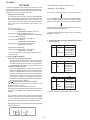
1
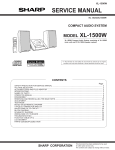
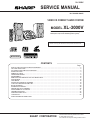
XL-3000V
SERVICE MANUAL
No. S8149XL3000V/
VIDEO CD COMPACT AUDIO SYSTEM
MODEL
XL-3000V
XL-3000V Video CD Compact Audio System consisting of XL3000V (main unit) and CP-XL3000U (speaker system).
• In the interests of user-safety the set should be restored to its original
condition and only parts identical to those specified should be used.
NTSC/PAL
CONTENTS
Page
SAFETY PRECAUTION FOR SERVICE MANUAL .......................................................................................................... 2
VOLTAGE SELECTION .................................................................................................................................................... 2
AC POWER CORD AND PLUG ADAPTOR ..................................................................................................................... 2
SPECIFICATIONS ............................................................................................................................................................ 3
NAMES OF PARTS .......................................................................................................................................................... 4
OPERATION MANUAL ..................................................................................................................................................... 6
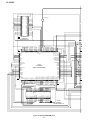
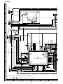
DISASSEMBLY ............................................................................................................................................................... 10
REMOVING AND REINSTALLING THE MAIN PARTS .................................................................................................. 12
ADJUSTMENT ................................................................................................................................................................ 13
TEST MODE ................................................................................................................................................................... 16
NOTES ON SCHEMATIC DIAGRAM ............................................................................................................................. 19
TYPES OF TRANSISTOR AND LED .............................................................................................................................. 19
BLOCK DIAGRAM .......................................................................................................................................................... 20
SCHEMATIC DIAGRAM ................................................................................................................................................. 26
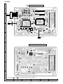
WIRING SIDE OF P.W.BOARD ...................................................................................................................................... 36
WAVEFORMS OF CD CIRCUIT ..................................................................................................................................... 41
TROUBLESHOOTING .................................................................................................................................................... 42
FUNCTION TABLE OF IC .............................................................................................................................................. 48
LCD DISPLAY ................................................................................................................................................................. 62
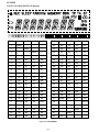
PARTS GUIDE/EXPLODED VIEW
SHARP CORPORATION
–1–
This document has been published to be used
for after sales service only.
The contents are subject to change without notice.
XL-3000V
SAFETY PRECAUTION FOR SERVICE MANUAL
This product is classified as a CLASS 1 LASER PRODUCT.
Precaution to be taken when replacing and servicing the Laser Pickup.
The AEL (Accessible Emission Level) of Laser Power Output is less than Class 1 but the laser component is capable of emitting
radiation exceeding the limit for Class1. Therefore it is important that the following precautions must be observed during servicing
to protect your eyes against exposure to the Laser beam.
(1) When the cabinet has been removed, the power is turned on without a compact disc, and the Pickup is on a position outer than
the lead-in position, the Laser will light for several seconds to detect a disc. Do not look into the Pickup Lens.
(2) The Laser Power Output of the Pickup inside the unit and replacement service parts have already been adjusted prior to shipping.
(3) No adjustment to the Laser Power should be attempted when replacing or servicing the Pickup.
(4) Under no circumstances look directly into the Pickup Lens at any time.
(5) CAUTION - Use of controls or adjustments, or performance of procedures other than those specified herein may result in
hazardous radiation exposure.
CAUTION
Laser Diode Properties
Material: GaAIAs
Wavelength: 780 nm
Emission Duration: continuous
Laser Output: max. 0.6 mW
● This Video CD Compact Audio System is classified as a CLASS
1 LASER product.
● The CLASS 1 LASER PRODUCT label is located on the rear
cover.
● Use of controls, adjustments or performance of procedures other than those specified herein may result in hazardous radiation
exposure.
As the laser beam used in this compact disc player is harmful to
the eyes, do not attempt to disassemble the cabinet. Refer servicing to qualified personnel only.
CAUTION-INVISIBLE LASER RADIATION WHEN OPEN. DO NOT STARE INTO BEAM
OR VIEW DIRECTLY WITH OPTICAL INSTRUMENTS.
ADVERSEL-USYNLIG LASERSTRALING VED ABNING. SE IKKE IND I
STRALEN-HELLER IKKE MED OPTISKE INSTRUMENTER.
VARO! AVATTAESSA OLET ALTTIINA NAKYMATON LASERSATEILYLLE. ALA
TUIJOTA SATEESEEN ALAKA KATSO SITA OPTISEN LAITTEEN LAPI.
VARNING-OSYNLIG LASERSTRALNING NAR DENNA DEL AR OPPNAD. STIRRA EJ
IN I STRALEN OCH BETRAKTA EJ STRALEN GENOM OPTISKT INSTRUMENT.
VOLTAGE SELECTION
Before operating the unit on mains, check the preset voltage. If the voltage is different from your local voltage, adjust the voltage
as follows, Turn the selector with a screwdriver unit the appropriate voltage number appears in the window (110 V,127 V, 220 V
or 230 V - 240 V AC).
AC POWER CORD AND PLUG ADAPTOR
QACCE0001SJZZ
QPLGA0250AFZZ
QACCA0001SJ00
QPLGA0253AFZZ
QACCB0001SJ00
–2–
XL-3000V
FOR A COMPLETE DESCRIPTION OF THE OPERATION OF THIS UNIT, PLEASE REFER
TO THE OPERATION MANUAL.
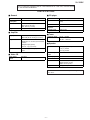
SPECIFICATIONS
■ General
■ CD player
Power source
AC 110/127/220/230 - 240 V, 50/60 Hz
Type
Compact disc player
Power
consumption
56 W
Signal readout
Non-contact, 3-beam semiconductor laser
pickup
Dimensions
Width: 230 mm (9-1/16")
Height: 128 mm (5-1/16")
Depth: 293 mm (11-9/16")
D/A converter
1-bit D/A converter
3.3 kg (7.3 lbs.)
Frequency
response
20 - 20,000 Hz
Weight
Dynamic range
90 dB (1 kHz)
■ Amplifier
Output power
MPO: 60 W (30 W + 30 W) (10 % T.H.D.)
RMS: 40 W (20 W + 20 W) (10 % T.H.D.)
Output terminals
CD digital output (optical)
Video out: 1 Vp-p (75 ohms)
PAL/NTSC
FM: 88 - 108 MHz
AM: 531 - 1,602 kHz
■ Speaker
Type
2-way type speaker system
5 cm (2") Tweeter
Video/Auxiliary (audio signal): 500 mV/47
kohms
■ Video CD
Video output
format
Frequency range
Speakers: 6 ohms
Headphones: 16 - 50 ohms (recommended:
32 ohms)
Input terminals
■ Tuner
10 cm (4") Woofer
Maximum input
power
40 W
Rated input power
20 W
Impedance
6 ohms
Dimensions
Width: 140 mm (5-9/16")
Height: 288 mm (11-3/8")
Depth: 187 mm (7-3/8")
Weight
2.3 kg (5.1 lbs.)/each
Specifications for this model are subject to change without
prior notice.
–3–
XL-3000V
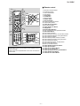
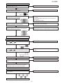
NAMES OF PARTS
■ Front panel
7
1. Disc Compartment
2. Volume Up and Down Buttons
3. On/Stand-by Button
4. Function Selector Button
5. Memory/Set Button
6. Bass/Treble Selector Button
7. Video CD/CD Play or Pause,
Tuning Up Button
8. Video CD Stop or Return, CD Stop,
Tuning Down Button
9. Video CD Skip or Previous, CD Track Down,
Tuner Preset Down Button
10. Disc Compartment Cover Open/Close Button
11. Video CD Skip or Next, CD Track Up,
Tuner Preset Up Button
10
8
1
11
9
2
3
5
4
1
■ Display
1. Timer Play Indicator
2. Sleep Indicator
3. Video CD/CD Random Play Indicator
4. Memory Indicator
5. FM Stereo Mode Indicator
6. Video CD/CD Play Indicator
7. Video CD/CD Repeat Play Indicator
8. FM Stereo Receiving Indicator
9. Surround Indicator
6
2
4
3
5
8
6
9
7
■ Rear panel
1
6
7
2
8
3
9
10
4
11
5
1. CD Digital Output Socket
2. AM Aerial Terminal
3. Aerial Earth Terminal
4. FM 75 Ohms Aerial Socket
5. Headphone Socket
6. Video Output Socket
7. Cooling Fan
8. Video/Auxiliary (Audio Signal) Input Sockets
9. AC Voltage Selector
10. AC Power Input Socket
11. Speaker Terminals
The rating label is located
on the bottom of the unit.
■ Speaker system
1. Tweeter
2. Woofer
3. Bass Reflex Duct
4. Speaker Terminals
1
2
3
4
–4–
XL-3000V
■ Remote control
1
2
3
4
5
6
7
8
11
12
13
14
15
16
17
19
20
23
21
24
22
25
26 27
18
9
10
28
32
29
33
30
34
31
35
Buttons with " " mark in the illustration can be operated on the remote control only.
Other buttons can be operated both on the main unit and the remote control.
–5–
1. Remote Control Transmitter
2. On/Stand-by Button
3. Video CD/CD Button
4. Tuner Button
5. Timer Button
6. Clock Button
7. Memory Button
8. Dimmer Button
9. Surround Button
10. Volume Up and Down Buttons
11. Video/Auxiliary Button
12. Video CD TV Type Button
13. Band Selector Button
14. Video CD/CD Clear Button
15. Sleep Button
16. Random/Repeat Button
17. Disc Compartment Cover Open/Close Button
18. Audio Mode Button
19. Tuner Preset Up Button
20. Video CD Skip or Previous, CD Track Down Button
21. Video CD/CD Fast Reverse, Tuning Down Button
22. Video CD/CD Play Button
23. Video CD Skip or Next, CD Track Up Button
24. Video CD/CD Fast Forward, Tuning Up Button
25. Video CD/CD Pause Button
26. Video CD Stop or Return, CD Stop Button
27. Tuner Preset Down Button
28. Bass Up and Down Buttons
29. Video CD/CD Direct Search Buttons
30. Video CD Intro Button
31. Video CD Track Digest Button
32. Treble Up and Down Buttons
33. Video CD Playback Control Auto/Off Button
34. Video CD/CD Display Button
35. Video CD Time Search Button
XL-3000V
OPERATION MANUAL
Setting the Clock
3
Within 1 minute, press the PRESET ( or ) button to
adjust the hour and then press the MEMORY button.
When the 12-hour display is selected, "AM" will change automatically to "PM".
4
This may be operated only with the remote control.
In this example, the clock is set for the 24-hour (0:00) display.
1
Press the CLOCK button and within 3 seconds, press
the MEMORY button.
Within 1 minute, press the PRESET ( or ) button to
adjust the minutes and then press the MEMORY button.
● The hour will not advance even if minutes advance from "59"
to "00".
● The clock starts from "0" second. (Seconds are not displayed.)
2
Within 1 minute, press the PRESET ( or ) button to
select 24-hour or 12-hour display and then press the
MEMORY button.
To confirm the time display when the power is on:
Press the CLOCK button.
The time display will appear for about 5 seconds.
"0:00"
The 24-hour display will appear.
(0:00 - 23:59)
Note:
The time will flash at the push of the CLOCK button when the AC
power supply is restored after a power failure or unplugging the unit.
Readjust the clock as follows.
"AM 12:00"
The 12-hour display will appear.
(AM 12:00 - PM 11:59)
Note that this can only be set when the unit is first installed or it
has been reset.
To readjust the clock:
Perform "Setting the Clock" from the beginning.
To change the 24-hour or 12-hour display:
1 Clear all the programmed contents.
2 Perform "Setting the Clock" from the beginning.
Remote Control
Troubleshooting
■ Battery installation
■ If trouble occurs
1
2
When this product is subjected to strong external interference
(mechanical shock, excessive static electricity, abnormal supply
voltage due to lightning, etc.) or if it is operated incorrectly, it may
malfunction.
3
Remove the battery cover.
Insert the batteries according to the direction indicated in
the battery compartment.
When inserting or removing the batteries, push them towards the
battery terminals.
Replace the cover.
If such a problem occurs, do the following:
1 Set the unit to the stand-by mode and turn the power on again.
2 If the unit is not restored in the previous operation, unplug and
plug in the unit, and then turn the power on.
Note:
If neither operation above restores the unit, clear all the memory by
resetting it.
■ Clearing all the memory (reset)
Precautions for battery use:
● Replace all old batteries with new ones at the same time.
● Do not mix old and new batteries.
● Remove the batteries if the unit will not be used for long periods
of time. This will prevent potential damage due to battery leakage.
1
2
3
Caution:
● Do not use rechargeable batteries (nickel-cadmium battery, etc.).
● Installing the batteries incorrectly may cause the unit to malfunction.
Notes concerning use:
● Replace the batteries if the operating distance is reduced or if the
operation becomes erratic. Purchase 2 "AAA" size batteries (UM4, R03, HP-16 or similar).
● Periodically clean the transmitter on the remote control and the
sensor on the unit with a soft cloth.
● Exposing the sensor on the unit to strong light may interfere with
operation. Change the lighting or the direction of the unit.
● Keep the remote control away from moisture, heat, shock, and
vibrations.
Press the ON/STAND-BY button to enter the power stand-by
mode.
Unplug the AC power lead from the AC INPUT socket on the
unit.
Whilst pressing down the MEMORY/SET button and the
button, plug the AC power lead into the AC INPUT socket on the
unit.
AC INPUT
Caution:
● This operation will erase all data stored in memory including
clock, timer settings, tuner preset, and CD programme.
● After the above operation, interval span setting for AM will be
returned to 9 kHz (50 kHz for FM) automatically.
–6–
XL-3000V
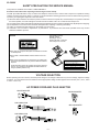
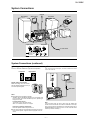
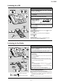
System Connections
FM aerial
AM loop aerial
Right speaker
MD recorder
Left speaker
not supplied
TV
Right speaker
Left speaker
To a wall socket
Black wire
with white dots
Black wire
System Connections (continued)
■ Placing the speaker system
■ TV/monitor connection
There is no distinction between the right and the left speakers.
If the TV/monitor has a video input, connect it to VIDEO OUT socket
on the rear of the unit.
Left speaker
Right speaker
TV
To video
input socket
Speaker grilles are removable:
Make sure nothing comes into contact
with the speaker diaphragms when you
remove the speaker grilles.
Video cable
Notes:
● The speakers are magnetically shielded.
Therefore, they do not affect the display even you use them near
the TV. However, some colour variation may occur, depending on
the type of TV used.
If colour variation occurs...
Turn off the TV (from the power switch).
After 15 - 30 minutes, turn the TV on again.
If the colour variation is still present...
Move the speakers further away from the TV.
● If any kind of magnet or an electromagnet is placed too close to
the TV and the system, irregular colours may appear on the TV
screen.
Note:
If the TV/monitor does not have a video input, the VIDEO OUT
socket on the unit should be connected to a VCR with a video input,
which in turn should be connected to the TV/monitor through the TV
ANTENNA/CABLE input. (Be sure to turn on the VCR, and set the
VCR's input mode to "auxiliary".)
–7–
XL-3000V
System Connections (continued)
■ Setting the AC voltage selector
■ Connecting the AC power lead
Check the setting of the AC voltage selector located on the rear
panel before plugging the unit into a wall socket. If necessary, adjust
the selector to correspond to the AC power voltage used in your
area.
After checking all the connections have been made correctly,
connect the AC power lead to the AC power input socket, then
into the wall socket.
Wall socket
Turn the selector with a screwdriver until the appropriate voltage number appears in the window (110 V, 127 V, 220 V or 230 V
- 240 V AC).
1
2
Notes:
● Unplug the AC power lead from the wall socket if the unit will not
be in use for a prolonged period of time.
● Never use a power lead other than the one supplied. Use of a
power lead other than the one supplied may cause an electric shock or fire.
AC Plug Adaptor
In areas (or countries) where a wall socket as shown in illustration
is used, connect the unit using the AC plug adaptor supplied with
the unit, as illustrated. The AC plug adaptor is not included in areas
where the wall socket and AC power plug can be directly connected
(see illustration ).
System Connections (continued)
■ Setting the AM/FM interval
The International Telecommunication Union (ITU) has established
that member countries should maintain either a 10 kHz or 9 kHz
interval between broadcasting frequencies of AM stations and 100
kHz or 50 kHz for FM stations. The illustration shows the 50/9 kHz
zones (regions 1 and 3), and the 100/10 kHz zone (region 2).
This product is not equipped with a span selector. However, it will be
adjusted to a 9 kHz AM (50 kHz FM) interval when shipped from the
factory.
Before using the unit, be sure to set it to the AM/FM tuning interval
(span) used in your area.
To check the tuning span currently selected:
1 Press the ON/STAND-BY button to turn the power on.
2 Press the FUNCTION button until "AM" appears on the display.
● If "AM 531 kHz" is displayed, it means that AM stations have
been adjusted for a 9 kHz span and FM stations for 50 kHz
span. If "AM 530 kHz" is displayed, AM stations have been adjusted for a 10 kHz span and FM stations for 100 kHz span.
To change from a 9 kHz AM (50 kHz FM) interval to a 10 kHz AM
(100 kHz FM) interval:
1 Press the ON/STAND-BY button to enter the stand-by mode.
2 Hold down the
button and the MEMORY/SET button for at
least 4 seconds. Release the buttons when "AM SP 10 kHz" and
"FM SP 100 kHz" are displayed alternately.
● The clock display will reappear.
To return to a 9 kHz AM (50 kHz FM) interval:
1 Press the ON/STAND-BY button to enter the stand-by mode.
2 Hold down the
button and the MEMORY/SET button for at
least 4 seconds. Release the buttons when "AM SP 9 kHz" and
"FM SP 50 kHz" are displayed alternately.
● The clock display will reappear.
Caution:
● When the unit is left for a few hours after the span has been
switched and the AC power lead disconnected, the AM span will
be automatically returned to 9 kHz (FM span to 50 kHz). If this
happens, set the span again.
● When the span is switched, all the memorised stations will be
cancelled.
–8–
XL-3000V
Listening to a CD
1
2
Press the ON/STAND-BY button to turn the power on.
Press the FUNCTION button until "CD" or "NO DISC"
appears on the display.
When operating with the remote control, press the CD button.
3
Press the
(OPEN/CLOSE) button to open the disc
compartment.
4
Place a CD on the spindle, label side up.
Be sure to place 8 cm (3") disc in the middle of a disc holder.
5
Press the
(OPEN/
CLOSE) button to
close the disc comTotal number of
partment.
Total playing time
tracks
6
Press the
( ) button to start playback from track 1.
When the last track on the disc has finished playing, the unit will
stop automatically.
To interrupt playback:
Main unit operation:
Press the
button.
To resume playback from the same point, press the
Remote control operation:
Press the button.
To resume playback from the same point, press the
button again.
button.
To stop playback:
Press the button.
To remove the CD:
Whilst in the stop mode, press the (OPEN/CLOSE) button.
Press the disc eject button and remove the CD.
Listening to the Radio
1
2
Press the ON/STAND-BY button to turn the power on.
Press the FUNCTION button until "FM" or "AM" appears on the display.
When operating with the remote control, press the TUNER button, and then the BAND button to select "FM" or "AM".
3
Press the TUNING (
sired station.
or
) button to tune in to the de-
Manual tuning:
Press the TUNING button as many times as required to tune in
to the desired station.
Auto tuning:
When the TUNING button is pressed for more than 0.5 seconds, scanning will start automatically and the tuner will stop at
the first receivable broadcast station.
Notes:
● This can be operated by pressing the TUN. ( or ) button
on the remote control.
● When radio interference occurs, auto scan tuning may stop
automatically at that point.
● Auto scan tuning will skip weak signal stations.
● To stop the auto tuning, press the TUNING button again.
FM stereo mode indicator
FM stereo receiving indicator
To receive an FM stereo transmission:
Press the FUNCTION (BAND) button to display the "ST" indicator.
● " " will appear when an FM broadcast is in stereo.
● If the FM reception is weak, press the FUNCTION (BAND) button
to extinguish the "ST" indicator. The reception changes to monaural, and the sound becomes clearer.
After use:
Press the ON/STAND-BY button to enter the power stand-by mode.
–9–
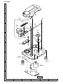
XL-3000V
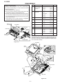
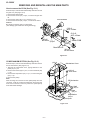
DISASSEMBLY
STEP
Caution on Disassembly
Follow the below-mentioned notes when disassembling
the unit and reassembling it, to keep it safe and ensure
excellent performance:
1. Take compact disc out of the unit.
2. Be sure to remove the power supply plug from the wall
outlet before starting to disassemble the unit.
3. Take off nylon bands or wire holders where they need to
be removed when disassembling the unit. After servicing
the unit, be sure to rearrange the leads where they were
before disassembling.
4. Take sufficient care on static electricity of integrated
circuits and other circuits when servicing.
(A1) x2
ø3 x10mm
1
2
Top Cabinet
Fan Motor
Rear Panel
Top Cabinet/
Video PWB
1. Screw .................. (B1) x2
2. Hook .................... (B2) x5
3. Flat Cable ............ (B3) x2
4. Socket ................. (B4) x9
5. Screw .................. (B5) x3
6. Socket ................. (B6) x1
10-2
10-1
10-1,2
10-1
11-1
10-2
3
Tuner PWB
1. Screw .................. (C1) x2
2. Socket ................. (C2) x1
11-1
4
Power PWB
1. Socket ................. (D1) x2
2. Hook .................... (D2) x1
11-1
5
Main PWB
1. Socket ................. (E1) x1
2. Screw .................. (E2) x8
11-1
6
Display PWB
1. Screw .................. (F1) x4
2. Hook .................... (F2) x4
11-2
7
CD Mechanism
1. Screw .................. (G1) x4
11-2
8
Gear Box
1. Screw .................. (H1) x1
2. Holder .................. (H2) x1
3. Lever ................... (H3) x1
4. Screw .................. (H4) x3
5. Lever ................... (H5) x1
11-2
9
LED PWB
1. Screw .................. (J1) x1
11-2
(A4) x2
ø3 x8mm
Note:
After removing the connector for the optical pickup from the
connector, wrap the conductive aluminium foil around the
front end of connector remove to protect the optical pickup
from electrostatic damage.
Rear Panel
(A1) x2
ø3 x10mm
FIGURE
1. Screw .................. (A1) x7
2. Socket ................. (A2) x4
3. Screw .................. (A3) x4
4. Screw .................. (A4) x2
(A3) x3
ø3 x12mm
(A1) x3
ø3 x10mm
PROCEDURE
REMOVAL
Rear Panel/
Terminal PWB/
Fan Motor
(A2) x4
Terminal PWB
Figure 10-1
Top Cabinet
HooK
(B2) x2
(B4) x1
CD Mechanism
Hook
(B2) x3
(B6) x1
(B4) x2
Top Cabinet
(B4) x4
Up
(B3) x1
Slide
Hook
Bottom Cabinet
(A3) x1
ø3 x10mm
Lug
Power
PWB
Bottom Cabinet
Video PWB
(B4) x1
(B3) x1
(B1) x2
ø2.5 x8mm
Main PWB
(B4) x1
Figure 10-2
– 10 –
XL-3000V
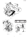
Power PWB
Tuner PWB
(D1) x2
(C1) x1
ø3 x8mm
Holder
PWB
(E2) x7
ø3 x8mm
(E1) x1
(C2) x1
(B5) x3
ø3 x6mm
Tuner PWB
Video
PWB
Main PWB
Bracket
Bottom Cabinet
(C1) x1
ø3 x6mm
Hook
(D2) x1
Washer
Bracket
Main PWB
(E2) x1
ø3 x14mm
Figure 11-1
(H4) x2
ø2.5 x10mm
Gear Box
(H3) x1
(H1) x1
ø3 x8mm
STEP
1
REMOVAL
Speaker
(H5) x1
Switch
PWB
(H4) x1
ø2.5 x8mm
(H2) x1
Bracket
Shield
Cover
(J1) x1
ø2.5 x10mm
(G1) x2
ø2.5 x10mm
Holder PWB
Front Panel
( A2 ) x1
( A3 ) x2
ø4 x12mm
( A3 ) x4
ø4 x12mm
Hook
(F2) x4
Display PWB
11-3
Net Frame
( A1 ) x1
(F1) x4
ø2.5 x10mm
CD Mechanism
FIGURE
Tweeter
(G1) x2
ø2.5 x10mm
Holder PWB
LED PWB
PROCEDURE
1. Net Frame ........... (A1) x1
2. Front Panel ......... (A2) x1
3. Screw .................. (A3) x6
Woofer
Screwdriver
Top Cabinet
Figure 11-2
Figure 11-3
– 11 –
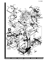
XL-3000V
REMOVING AND REINSTALLING THE MAIN PARTS
How to remove the CD lid (See Fig. 12-1.)
Perform steps 1,2 and 8 of the disassembly method to remove
the gear box. (See page 10,11)
1. Remove the switch PWB.
2. Remove the screws (A1) x 4 pcs., to remove the gear box
lid.
3. Remove the gears (A2) x 1 pc. and (A3) x 1 pc.
4. Remove the screws (A4) x 2 pcs., to remove the motor.
Caution:
Be careful so that the gear is not damaged.
(The damage gear emits noise during searching.)
CD Lid Motor
(A2) x1
(A1) x1
ø2.5 x14mm
(A1) x2
ø2.5 x12mm
(A4) x2
ø2 x5mm (A3) x1
Switch PWB
Gear Box Lid
(A1) x1
ø2.5 x10mm
Figure 12-1
CD MECHANISM SECTION (See Fig. 12-2.)
(A1) x4
Perform steps 1,2 and 7 of the disassembly method to remove
the CD mechanism. (See page 10,11)
1. Remove the mechanism cover, paying attention to the
pawls (A1) x 4 pcs.
2. Remove the screws (A2) x 2 pcs., to remove the shaft (A3)
x 1 pc.
3. Remove the stop washer (A4) x 1 pc., to remove the gear
(A5) x 1 pc.
4. Remove the pickup.
Note:
After removing the connector for the optical pickup from the
connector, wrap the conductive aluminium foil around the
front end of connector remove to protect the optical pickup
from electrostatic damage.
Mechanism Cover
(A2) x2
ø2.6 x6mm
CD Mechanism
Shaft
(A3) x1
Gear
(A5) x1
Stop Washer
(A4) x1
Pickup unit
Figure 12-2
– 12 –
XL-3000V
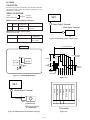
ADJUSTMENT
TUNER SECTION
fL: Low-range frequency
fH: High-range frequency
• AM IF/RF
Signal generator: 400 Hz, 30%, AM modulated
Frequency Frequency
Display
• FM Mute Level
Signal generator: 1 kHz, 40 kHz dev., FM modulated
Setting/ Instrument
Adjusting Connection
Parts
T351
*1
AM IF
450 kHz
1,602 kHz
AM Band
Coverage
—
531 kHz
(fL): T306 *2
1.1 ± 0.1 V
AM
Tracking
990 kHz
990 kHz
(fL): T302
98.00 MHz
(25±1 dBµV)
VR351*1
Input: SO301
Output: Speaker
Terminal
• Check FM VT
Signal generator: 1 kHz, 40 kHz dev., FM modulated
Frequency
10.7 MHz
Frequency
Display
98.0 MHz
Setting/
Adjusting
Parts
FM Band
Coverage
—
87.50 MHz
FM RF
98.00 MHz
(10~30 db)
98.00 MHz
Setting/ Instrument
Adjusting Connection
Parts
(fL): L303 *1
3.4 ± 0.1 V
L302
*2
Instrument
Connection
87.5 MHz
87.5 MHz
3.4 V ± 0.1 V
TP301
108 MHz
108 MHz
7.8 V ± 1.0 V
TP301
FM
Preset No.
1
2
3
4
5
• FM RF
Signal generator: 1 kHz, 75 kHz dev., FM modulated
Frequency
Display
Check Point
• Setting the Test Mode
Keeping the FF/PRESET UP button and MEMORY/SET button
pressed, turn on ON/STAND-BY. Then, the frequency is
initially set in the memory as shown in Table. Call it with the
VOLUME UP/DOWN button to use it for adjustment and check
of tuner circuit.
Instrument
Connection
T304(Turn Input: Pin 1 of
the core of IC301
T304 fully
counterclockwise.)
Frequency
Display
Frequency
• FM Detection
Signal generator: 10.7 MHz, FM sweep generator
FM IF
98.00 MHz
Instrument
Connection
*1. Adjust so that an output signal appears.
*1
*1. Input: Antenna, Output: Speaker Terminal
*2. Input: Input is not connected, Output: TP301
Test
Stage
Adjusting
Parts
Display
Frequency
87.50 MHz
108.00 MHz
98.00 MHz
90.20 MHz
106.00 MHz
FM
75
SO301 OHMS
ANTENNA
TERMINAL
AM
Preset No.
6
7
8
9
10
531 kHz
1,602 kHz
990 kHz
612 kHz
1,404 kHz
TUNER PWB-A2
GND
AM
*1. Input: Antenna, Output: TP301
*2. Input: Antenna, Output: Speaker Terminal
TP301
20
FM ANT.
FM RF
IC301
1
IC302
L302
FM OSC. L303
FM Band
Coverage fL
T302
AM
Tracking fL
T304
FM IF
VR351
FM Mute
Level
T351
AM IF
IC303
T306
AM Band
Coverage fL
Figure 13-1 ADJUSTMENT POINTS
– 13 –
XL-3000V
CD SECTION
Since this CD system incorporates the following automatic
adjustment function, when the pickup is replaced, it is not
necessary to readjust it.
VIDEO CD SECTION
A-BEX
TEST VIDEO CD
Model No. TVD-581
TVD-581A
SET
• Measurement of oscillation frequency
Disc
Instrument
Connection
Adjusting
Point
CD Stop TC100V
27.00000 MHz
± 160 Hz
Specified Value
Video Output Terminal
1 of R163V and
2 of C183V
Video Input Terminal
• Checking of video output signal
Checking of color bar
Instrument
Connection
Adjusting Point
Disc
Track 2
Video output terminal
TV
Figure 14-3 Checking of video output signal
Chroma Peak Level
100 ± 15 IRE
IH (59.94Hz/NTSC)
VIDEO PWB-D
100 100
88.5
100 IRE
75
75
Color bar signal
waveform
70
1 PCLK2X
(0.714V)
140 IRE
IC15V
IC14V
(1V)
R163V
C183V
2 GND
41.5
33.5
20
5
40 IRE
(0.286V)
0
Blue
Red
Green
Magenta
Color Burst
Figure 14-1 ADJUSTMENT POINTS
Cyan
-40
Yellow
40 IRE
-25 -25
Gray
X1V
Horizontal
sync signal
-13.5
-20
TC100V
Figure 14-4
SET
GND
Vectorscope
Waveform monitor
or oscilloscope
TV monitor
Figure 14-2 Measurement of oscillation frequency
Figure 14-5
– 14 –
Blue
75 ohms
Red
Magenta
Green
Cyan
Yellow
Gray
VIideo Output Terminal
XL-3000V
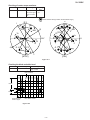
Checking of vector scope waveform
Disc
Checking
Track 2
VIDEO OUT
Setting
Checking
Item
Set the phase of
color burst signal
(B) to 180°-360°
line.
Phase check
± 10°
(
Check that the setting is within the illustrated range.)
V
cy
R-Y
I
R
g
Q
MG
R
MG
75%
YL
YL
b
B-Y
75%
-Q
B
B
yl
G
CY
G
U
CY
-I
[NTSC]
[PAL]
Figure 15-1
Checking the black-and-white level
Disc
Track 16
Checking
VIDEO OUT
Checking Item
Output level
100 ± 10 IRE
100% Luminance
100IRE
40IRE
40IRE
Horizontal Interval
reference signal
100% WHITE LEVEL
Figure 15-2
– 15 –
mg
XL-3000V
TEST MODE
• The TUNER TEST2 mode is obtained with
>>
The test mode applied to this microcomputer has three modes,
namely the ordinary test mode for adjustment or measurement,
the aging test mode, and the self-diagnosis test mode for selfjudgment in case of final product inspection.
+ MEMORY + ON/STAND-BY.
->
Turn off AC in the TEST2 mode to restore the initial state.
1. Turning on the test mode
For obtaining each test mode, press the ON/STAND-BY
button, while keeping pressing the following two buttons in
the ordinary stand-by mode (power off ). In this case, the
main unit buttons are valid. When turning the ON/STANDBY on with remote control buttons, test modes are not
obtained.
Turn off POWER to protect the memory of TEST2 mode.
Turn off POWER again to obtain the ordinary operation
while the data is stored in the memory (besides TUNER).
If AC OFF state is maintained in this state for about 1/2 day,
start is executed in the initial state.
[Ordinary test mode]
1. Tuner Test Mode (TEST 2)
.......................REW/PRESET DOWN + CD PLAY
2. Electronic Volume Test Mode (TEST 3)
.......................REW/PRESET DOWN + FF/PRESET UP
3. Timer Test Mode (TEST 4)
.......................FUNCTION + VOLUME UP
4. LCD Test Mode (TEST 5)
.......................FUNCTION + FF/PRESET UP
5. Electric CD Lid Aging Test Mode (TEST 8)
.......................FUNCTION + CD PLAY
• To clear the whole memory, insert the AC cord, pressing
MEMORY + CD PLAY.
3. Preset frequencies for various destinations (random
preset memory)
CH
[Self-diagnosis Test Mode]
1. Button input diagnosis test mode (TEST6)
.......................FUNCTION + VOLUME
Processes are different depending on destinations at
initial settings.
1
2
3
4
5
2. Tuner Test Mode (TEST 2)
1. Outline of tuner (radio) test mode
The tuner test mode is intended to store the adjustment
and measurement frequencies in the preset memory
CH. When adjusting the tuner section in the production
line, adjusting personnel are not required to set frequency.
2. Details of tuner test mode
Press the "REW/PRESET DOWN" and "CD PLAY"
buttons in POWER OFF state and turn on the power by
the use of "ON/STAND-BY" button to preset and store
frequency for adjustment and measurement of destination
specified by the AREA terminal in the preset memory
CH. However, Ordinary 1 and Ordinary 2 are stored in
the destinations (selected by SPAN switching operation)
when the test mode is obtained.
("FF " + "MEMORY/SET" KEY SPAN CHANGE)
(As for frequencies to be preset and stored for each
destination, refer to item 3.)
The tuner test mode is started from preset No.1.
The operations of test mode are identical with the ordinary
operations of TUNER function. FUNCTION switching is
invalid.
CH
6
7
8
9
10
CH
16-25
26
27
28
29
30
BAND
FM
STEREO
BAND
AM
BAND
FM
MONO
FM
FM 87.50 MHz
FM108.00 MHz
FM 98.00 MHz
FM 90.20 MHz
FM106.00 MHz
AM
AM 531 kHz
AM1602 kHz
AM 990 kHz
AM 612 kHz
AM1404 kHz
FM
FM106.00 MHz
FM 90.20 MHz
FM 98.00 MHz
FM108.00 MHz
FM 87.50 MHz
• The slant line sections of the table store no memory.
It is necessary to discard the content of preset memory
when the tuner test mode is ended; be sure to write "0000"
or "1111" bits in the memory to be checked for judging
memory error at initial setting and to initialize memory.
When the tuner test mode is obtained, the following display
lights for one second.
– 16 –
XL-3000V
3. Electronic volume Test Mode (TEST 3)
When this test mode is obtained, the following display lights
for one second.
5. LCD Test Mode (TEST 5)
When the LCD test mode is obtained, all the LCD segments
are lighted. Then pressing the "PLAY" button switches
display as below.
Lighting of all segments
In this mode, volume is -14 dB (STEP28), BASS/TREBLE
is set to 0 (0 dB) and SURROUND mode to OFF, and startup function to CD, respectively. The button operations in
the test mode are the same as those of ordinary operation
except volume UP/DOWN.
(1) The display is the same as that of ordinary operation
except test mode setting.
(2) Unlike the ordinary state, the volume is controlled with
the volume UP/DOWN button in accordance with the
following three steps.
Lighting of odd segments
Lighting of even segments
<->
Volume- ∞ (STEP 0)
<->
Volume-14 dB (STEP 23)
Volume-0 (STEP 30)
(3) BASS/TREBLE and SURROUND are switched when
button is pressed.
4. Timer test Mode (TEST 4)
When this test mode is obtained, the following display lights
for one second.
Set the current time and timer time according to the following
procedure to reproduce the timer.
1. Set the current time to 1:00, the timer to ON time 1:05, the
function to CD, and volume to STEP 12, respectively. One
minute is counted as one second, and the timer is
reproduced. The fade-in (when playback is started) is
executed at a rate of one step for 1 sec. After completion
of fade-in, the fade-out is executed at a rate of one step for
1 sec (WAIT 1 sec inserted).
After completion of fade-out, the power is turned off (after
WAIT 1 sec), and the mode is shifted to the standby.
The display during operation is the same as that of ordinary
timer operation.
– 17 –
XL-3000V
6. Key input diagnosis Test Mode (TEST 6)
When the test mode is obtained, the following is displayed.
7. Electric CD lid Aging Test Mode (TEST 8) (Only for
model with electric CD lid)
Outline
OPEN/CLOSE operations of electric CD lid are repeated.
The number of repeated times and time period are
monitored. If the lid does not move to the regular position
after the specified time, operation is stopped. When an
error is detected by [CLID_PRO] during CLOSE, operation
is also stopped.
This test mode is intended to check whether all the main
unit buttons can be detected. Accordingly, in this test
mode, it is checked whether the "ON/STAND-BY" button
was pressed after all the buttons shown below were pressed.
If the result is OK, OK is displayed. If any one of keys was
not pressed, an error is displayed. In both cases of OK
termination or error termination, the mode is shifted to the
standby mode if the "ON/STAND-BY" button is pressed
subsequently.
a. POWER ON for function AUX
CD lid position is checked.
CLOSE position: Operation proceeds to the next
process.
Position other than CLOSE: After the lid moves to
CLOSE,operation
proceeds to the next process.
b. CD lid operation started
OPEN operation
WAIT 1 second
CLOSE operation
WAIT 1 second
c. Operations above are repeated.
Specified monitoring time
OPEN operation: 5 seconds
CLOSE operation: 5 seconds
All models using this type of microcomputer are not always
provided with the same buttons. Since the buttons used are
different depending on models, types of buttons to be used
are determined by whether RDS, SURROUND, and an
electric lid are available at the initial setting by MODEL port.
The order of buttons to be pressed is not determined.
Accordingly, it is checked whether all buttons have been
pressed.
d. Display
OPEN>CLOSE is counted as 1. I to 59999 are counted;
if the count is over 59999, display is returned to 0 to
repeat counting.
1. PU-IN buttons: REW/PRESET DOWN + CD STOP
Since this model is provided with SURROUND (HAVE
OR NOT), RDS (HAVE OR NOT), and electric CD lid, the
following 10 buttons are detected as all buttons.
PLAY, BASS/TREBLE, FUNCTION, VOLUME UP/
DOWN, MEMORY/SET, REW, FF, STOP, CD-OPEN/
CLOSE
The OK/NG display of test result is as follows.
Display when the lid does not move to the regular
position after the specified time
(Ex: Defective operation occurring in the middle of
1538.)
Highlight display of stop when an error is detected by
[CLID-PRO]
(Ex: Defective operation occurring in the middle of
1538.)
– 18 –
XL-3000V
NOTES ON SCHEMATIC DIAGRAM
• Resistor:
To differentiate the units of resistors, such symbol as K and
M are used: the symbol K means 1000 ohm and the symbol
M means 1000 kohm and the resistor without any symbol is
ohm-type resistor. Besides, the one with “Fusible” is a fuse
type.
• Capacitor:
To indicate the unit of capacitor, a symbol P is used: this
symbol P means micro-micro-farad and the unit of the
capacitor without such a symbol is microfarad. As to
electrolytic capacitor, the expression “capacitance/withstand
voltage” is used.
(CH), (TH), (RH), (UJ): Temperature compensation
(ML): Mylar type
(P.P.): Polypropylene type
• Schematic diagram and Wiring Side of P.W.Board for this
model are subject to change for improvement without prior
notice.
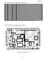
REF. NO
DESCRIPTION
NSW801
PICKUP IN
SW651
VOLTAGE SELECTOR
SW709
ON/STAND-BY
SW710
CD LID OPEN/CLOSE
• The indicated voltage in each section is the one measured
by Digital Multimeter between such a section and the chassis with no signal given.
1. In the tuner section,
( ) : AM mode
: FM stereo mode
2. In the CD section, the CD is stopped.
• Parts marked with “
”(
) are important for
maintaining the safety of the set. Be sure to replace these
parts with specified ones for maintaining the safety and
performance of the set.
POSITION
REF. NO
ON—OFF
SW718
VOLUME DOWN
DESCRIPTION
POSITION
110V
SW721
MEMORY/SET
ON—OFF
ON—OFF
SW722
BASS/TREBLE
ON—OFF
ON—OFF
SW725
CD STOP/TUNING DOWN
ON—OFF
REW/PRESET DOWN
ON—OFF
ON—OFF
SW711
FF/PRESET UP
ON—OFF
SW726
SW712
CD PLAY/PAUSE/TUNING UP
ON—OFF
SW727
FUNCTION
ON—OFF
SW713
VOLUME UP
ON—OFF
SW802
CD LID
ON—OFF
FRONT
VIEW
E C B
(S) (G) (D)
(1) (2) (3)
2SB562 C
2SC535 C
2SK246 GR
2SC1740 SR
2SD1858 R2
KRA102 M
KRC102 M
KRC104 M
KRC107 M
KTA1266 GR
KTA1268 GR
KTC3199 GR
KTC3200 GR
FRONT
VIEW
FRONT
VIEW
B C E
2SD2012 Y
DB5306X
1
2
3
SVC348S
KDV147C
Figure 19 TYPES OF TRANSISTOR AND LED
– 19 –
XL-3000V
FROM
VIDEO PWB
FROM
DISPLAY PWB
10 9 8 7 6 5 4 3 2 1
1
4
5
6
TU
7
SD
FM ST
DO
CL
+8V
+5V
D_GND
L–CH
R–CH
Q902
A_GND
VDAC
Q901
11 10 9
8
CNP307
A_GND
CLID_DW
CLID_UP
CLID_PRO
CLID_SW
FAN_DEC
AMP_DEC
CD_STB
DIMMER
LIGHT
FAN
+B4
3
LED PWB
CNP702
Q804
Q805
2
+B2
SWITCH PWB
+B4
Q907
IC805
TA7291S
CD LID
MOTOR DRIVER
SW802
CD LID
OPEN/CLOSE
Q804
Q805
Q802
8
1 9 5
2
3
6
7
+B1
M_GND
Q908
M_GND
Q908
+B8
SO401
M801
CD LID
OPEN/CLOSE
MOTOR
VIDEO
OUT
R-CH
M
+B4
VIDEO/AUX
INPUT
5V
+B7
Q861
CD_6R2V
L-CH
M802
FAN
MOTOR
+B5
+
SP+
SP–
SP+
SL–
PU-IN
GND
–
+
–
M
NM802
SPINDLE
MOTOR
M
NM801
SLED
MOTOR
CNP810
1
2
M
CNP807
1
2
M_GND
GND
MUTE
REG O
TRB
VIN4
VG1
VIN1
VO4+
VO4VO1+
GND
VO1-
21 22 23 24 25 26 27 28
+B5
16 17 18 19
BIAS
VG4
VO3+
VIN3
VG3
VCC
VCC
PO1+
VO3-
PO1-
OPO
GND
VO2VO2+
VIN2
VG2
13 12 11 10 9 8 7 6 5 4 3 2 1
NSW801
PICKUP IN
J801
DIGITAL
OUT
CD MOTOR PWB
IC804
MM1469XH
FOCUS/TRACKING/
SPIN/SLED DRIVER
1
2
3
TERMIN
PWB
FO
TR
PU_IN
LRCK
BCK
DATA
FMO
3
DOUT 9
/RST
BUS0
BUS1
BUS2
BUS3
BUCK
/CCE
SEL 57
2VREF 56
TEBC
RFGC
VREF
TRO
5 LRCK
7 BCK
8 AOUT
IC802
TC9462F
SERVO/SIGNAL CONTROL
CNS801
X801
16.93MHz
78 XI
79 XO
FOO
TEZI
TEI
TSIN
SBAD
FEI
52
51
50
49
48
47
46
45
44
43
PICKUP UN
FOCUS COIL
TRACKING COIL
13
14
15
16
17
18
19
20
21
22
23
24
RFRP 42
RFCT 40
RFI 38
14 VDD
23 VDD
VCOREV
PVREV
LPFO
LPFN
39 AVDD
62 VDD
94 VDD
33
32
31
D_GND
DVSR
DVSL
M_GND
XVSS
81 86
PXI
6 15 24 63 71 72 73 74 77 95
VSS
VSS
TESI01
P2VREF 25
36
D_GND
34
TMAX 30
PDO 28
76 VDD
80 XVDD
VSS
TESIN
+B7
TESIOO
12
100
90
91
92
93
96
97
VSS
8
9
10
11
/RST
BUS0
BUS1
BUS2
BUS3
BUCK
/CCE
53
VSS
2
3
4
5
6
7
55
AVSS
TO
VIDEO PWB
1
DMO
+B2
SBAD
FEO
FEN
VRO
RFRP
RFIS
RFGO
RFGC
AGCI
RFO
GND
RFN
TEO
TEN
2VRO
TEB
SEL
LDO
MDI
TN1
TPI
FPI
FNI
VCC
12
11
10
9
8
7
6
5
4
3
2
1
IC801
TA2109F
SERVO PRE AMP.
A_GND
+B7
SWITCHING
LD
Q801
E
F
B
A
MON
+B7
C
1/2V
+B7
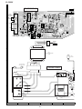
Figure 20 BLOCK DIAGRAM (1/6)
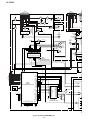
– 20 –
5V
XL-3000V
FROM
DISPLAY PWB
1 10 9 8
7 6 5 4 3 2 1
1
2
3
4
5
6
7
8
9
10 11 12 13
IC201
KIA4558P
SURROUND CONTROL
TO
TUNER PWB
R-CH IN
5V
P_STB
A_24V
D_GND
DI
CD +B
P_MUTE
CL
CE
SD
DO
STEREO
FM ST
DO
CL
CE
DI
A_12V
D_GND
TUN L
TUN R
A_GND
CNP703
R-CH OUT
SURROUND
ON/OFF
SURROUND
Q203
5
6
7
8
4
3
2
1
+B6
A_12V
Q201
+B8
+B3
+B6
L-CH OUT
L-CH IN
R-CH OUT
AUX R
14
13
10
11
12
9
8
7
6
4
5
3
2
1
VSS
15
DI
CE
TUN R
CD R
NC
VDD
LOGIC
16
19
18
20
21
22
23
24
25
26
27
28
29
IC401
LC75342M
FUNCTION/VOLUME
EQUALIZER
SO601
SPEAKER TERMINAL
AUX L
30
CL
17
CD L
TUN L
L-CH OUT
+B6 A_12V
IC601
STK40202
POWER AMP.
PRE
–VCC
8
9
12
GND
–VCC
4
+VE2
–VE2
+VCC
L-CH 1 15 R-CH
+
PRE
+VCC
IN1
RMINAL
PWB
IN2
Q601
Q602
+VE1
–VE1
MUTE
+B7
6 7 10 11
L-CH R-CH
13
R-CH
+
J601
HEADPHONES
3
2
1
+B
–B
IC682
KIA7805API
Q101
Q104
F651
T3.15A L 250V
D651~D654
VOLTAGE
REGULATOR
2
–B
F652
T3.15A L 250V
A_GND
F653
T1.6A L 250V
Q904
P UNIT
1
2
3
4
5
1
2
3
4
5
T651
TF
D_GND
Q608
+B5
N
+B3
4
3
2
1
IC681
KIA7805API
VOLTAGE
REGULATOR
3
1
D_GND
1
3
5
7
9
1
CNP651
3
5
7
9
Q681
2
VOLTAGE
REGULATOR
D688
1N4004
Q607
VOLTAGE
REGULATOR
Q606
CNP707
VOLTAGE
REGULATOR
FROM
DISPLAY PWB
D657~D660
Q610
OIL
USWD_5R6V
IL
POWER
TRANSFORMER
(MAIN)
P_CONT
Q683
CD_6R2V
CD +B
RLY601
Q609
M_12V
+B4
1
2
CNP652
FROM
DISPLAY PWB
D681~D684
+B8
5V
Q605
F654
T.F 2A,250V
Q903
VOLTAGE
REGULATOR
+B6
A_12V
110V
127V
220V
230~240V
VOLTAGE
REGULATOR
CNP801
1
A_24V
3
4
5
9
10
Q103
Q102
+B1
L-CH
POWER PWB-B
Q603
Q604
MAIN PWB
AC 110/127/220/
230~240V, 50/60Hz
Figure 21 BLOCK DIAGRAM (2/6)
– 21 –
T681
POWER
TRANSFORMER
(SUB)
SO655
AC INPUT
SOCKET
AC 110/127/220/
230~240V, 50/60Hz
AC POWER SUPPLY CORD
SW651
VOLTAGE
SELECTOR
XL-3000V
AM
Tracking fL
FM MUTE
LEVEL
T302
AM
X3
456
GND
BF301
2
1
3
1
2
3
4
5
6
1
8
7
FM IF
9
FM IF
Q306
CF303
2
19
18
3
4
FM IF
AM IF
AM IF
CF302
T351
CF352
5
6
FM DET
STEREO
AM LOW
CUT
FM/AM
OUT
20
SD
IC301
TA7358AP
FM FRONT END
BAD PASS
FILTER
21
AM IF
IN
GND
FM IF AM OSC
OUT
IN
AM MIX
OUT
AM OSC
IN
REG
AM Band
Coverage fL
SO301
ANTENNA
TERMINAL
22
VSM
24 23
VR351
T306
+5V
AM RF
IN
FM
75ohms
FM AFC
+5V
VD301
7
FM +B
T304
TP301
+5V
Q302
VT
+5V
VD302
DI
CL
DO
FM
MUTE
VDD
17 1
PD
18
AIN
19
CE
X352
4.5MHz
22 21 20
AOUT
FM +B
VSS
L303
FM OSC.
FM Band
Coverage fL
FM RF
X IN X OUT
L302
FM ANT.
IC302
LC72131
PLL(TUNER)
FM +B
VD303
3
4
5
6
7
8
1
DISPLAY PWB
LCD701
LCD DISPLAY
4
1
100
67
SEG33
6 VLC2
38
SEG0
5 VLC3
5
COM3
4
COM0
1
CLID_DW
CLID_UP
CLID_PRO
7 VLC1
8 VDD
FAN
9 OSC2
10 OSC1
X701
IC701
IX0038SJ
SYSTEM MICROCOMPUTER/
FL DRIVER
11 VSS
8MHz
X702
12 XI
13 XO
32.768kHz
25 26 27 34
RESET
2
Q701
Q702
Q703
RX701
REMOTE
SENSOR
LAMP PWB
Q708
A_24V
LMP701
SWITCHING
Q707
GND
Figure 22 BLOCK DIAGRAM (3/6)
– 22 –
Q709
5V
Q706
SWITCHING
SD
CD+B
STB
43 44 45 46 49 50
4
1
STEREO
37 38 39
P–MUTE
32
P–STB
USWD_5R6V
SURR
47 P–CONT
CE
18 KEY2
P_CONT
CL
17 KEY1
D_GND
DI
3
16 CLID_SW
SW710
DO
3
SW709
REMOCON
2
24 VREF+
POWER
2
VD_DI
VD_DO
ACK
BUSY
CLID_OUT
15 VREF–
RESET
1
14 MMOD
SYS_STOP
CNW707
CNS707
1
CNS652
TO
MAIN PWB
TO
POWER PWB
SW711~713
SW718
SW721,722
SW725~727
CD_STB
AMP_DEC
LIGHT
DIMMER
MOT_DEC
B-LIGHT
XL-3000V
TUNER PWB
SWITCHING
Q351
AM IF
AM IF
T351
CF352
10 11
12
IC303
LA1832S
FM IF DET./
FM MPX./AM IF
9
13
MO/ST
R-CH
OUT
L-CH
OUT
MPX VCO
8
15 14
PHASE
(AM/FM)
7
VCC
FM DET
STEREO
6
16
PHASE
5
CF351
4
SD
REG
3
17
MPX IN
18
IF OUT
19
AM LOW
CUT
FM/AM
OUT
AM RF
IN
20
VSM
21
AM IF
IN
GND
22
FM AFC
AM OSC
IN
X351
456kHz
+5V
+5V
SD
7
8
AM IN
9
10
11
10
DO
VOLTAGE
REGULATOR
9
CL
+5V
8
CE
7
DI
FM +B
Q360
6
A_12V
+B
5
D_GND
4
TUN_L
TO
MAIN PWB
6
IF REQ IF IN
5
MO/ST
4
14 13 12
FM
FM
3
1
VDD
MUTE FM IN
DO
PD
CL
17 16 15
DI
18
CE
AOUT
VSS
X IN X OUT
19
AIN
PLL(TUNER)
ZD351
22 21 20
11
FM ST
+5V
3
TUN_R
2
A_GND
1
CNS307
67
FAN 55
60
52
53
54
21
CD_STB
AMP_DEC
LIGHT
DIMMER
MOT_DEC
SEG33
25 26 27 34
VD_DI
VD_DO
ACK
29
28
30
31
35
1
2
3
4
5
6
7
BUSY
CLID_OUT
GND
STB
STB 40
CNW704
SD
CD+B
VD_DI
VD_DO
ACK
BUSY
CLID_OUT
STEREO
P–MUTE
P–STB
SURR
CE
CL
DO
C701
0038SJ
CROCOMPUTER/
DRIVER
DI
CNW702
CLID_DW
1
CLID_UP
2
CLID_PRO
3
CLID_SW
4
FAN
5
CD_STB
6
AMP_DEC
7
LIGHT
8
DIMMER
9
FAN_DEC
10
CLID_DW 57
CLID_UP 56
CLID_PRO 20
CNS702
10
9
8
7
6
5
4
3
2
1
1
2
3
4
5
6
7
TO
MAIN PWB
0
TO
VIDEO PWB
38
CNS704
B-LIGHT 51
CNS703
43 44 45 46 49 50
SD
STEREO
DO
CL
CE
DI
CD+B
P_MUTE
P_STB
A_24V
A_24V
D_GND
SURROUND
5V
5V
– 23 –
1
2
2
3
3
4
4
5
5
6
6
7
7
8
8
9
9
10
10
11
11
12
12
13
13
CNW703A
Figure 23 BLOCK DIAGRAM (4/6)
1
TO
MAIN PWB
5
SEG0
LCD701
CD DISPLAY
XL-3000V
VCC 32
1 VPP
2 A16
REGULATOR
A18 31
A17 30
3 A15
4 A12
Q11V
A14 29
A13 28
5 A7
6 A6
3.3V
A8 27
A9 26
7 A5
8 A4
A11 25
OE 24
9 A3
10 A2
A10 23
CE 22
11 A1
12 A0
D7 21
13 D0
D6 20
14 D1
15 D2
D5 19
16 VSS
D3 17
D4 18
IC10V
IX0041SJ
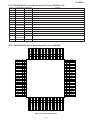
ROM 256K x 16
R163V
83 LA13
VD_DI
VCC3
AUX5
DSC_STB
AUX6
/MRQ
AUX7/STB
LD1
LDO
LD2
LD3
LD4
LD5
LD6
LD7
LOE
LWR
LSCE1
LROMCE
LA0
LSCE0
LA1
LA2
LA3
LA4
LA5
LA6
LA7
LA8
LA9
LA10
VSS
81 VCC
82 LA12
LA11
80 79 78 77 76 75 74 73 72 71 70 69 68 67 66 65 64 63 62 61 60 59 58 57 56 55 54 53 52 51
VSSK 5 0
AUX4
49
AUX3/VD_DI 48
84 LA14
AUX2/VD_DO 47
85 LA15
AUX1/DSADATA 46
86 LA16
AUX0/DSAACK 45
87 LA17
PCLKQSCN 44
88 AUDIO_CLK
PCLK2XSCN 43
89 AUDIO_DATA
DCLK 42
HSYNC 41
VSYNC 40
IC15V
ES3880F
VIDEO CD DECODER
90 BCLK
91 LR
92 DRAS1/DOE
YUV7 39
RESET
DBUS15
DBUS14
DBUS13
DBUS12
DBUS11
DBUS10
DA5
DBUS9
DA4
DBUS8
DA3
DBUS7
DA2
4
5
6 7
8
9 10 11 12 13 14 15 16 17 18 19 20 21 22 23 24 25 26 27 28 29 30
VCC
D3
D2
D1
D0
VCC
VSS
D12
D13
D14
D15
VSS
1
D4
2
D5
3
D11
4
D10
5
D6
6
D7
7
D9
8
D8
LCAS
WE
A0
A7
UCAS
A1
A6
RAS
A2
A5
OE
A3
A4
A8
VCC
VSS
20 19 18 17 16 15 14 13 12 11 10 9
VCC3 31
VSS
DA8
DA1
3
2
DA7
DA0
1
DA6
DWE
YUV0 32
VCC3
DRAS
DBUS6
YUV1 33
99 DCAS
100 VSS
DBUS5
YUV2 34
98 TDMFS
DBUS4
YUV3 35
97 TDMDR
DBUS3
YUV4 36
96 TDMCLK
DBUS2
YUV5 37
95 RWS
DBUS1
YUV6 38
94 RBCLK
DBUS0
93 RSD
21 22 23 24 25 26 27 28 29 30 31 32 33 34 35 36 37 38 39 40
IC16V
IX0025SJ
D-RAM 256K x 16
Figure 24 BLOCK DIAGRAM (5/6)
– 24 –
VD_DO
27M
VDAC
AGNDV
– +
+–
6
5
1
L_CH
2
AGNDA
R_CH
3
+5V
4
8
DGND
+12V
V_AMP
2
1
3
2
4
3
5
4
6
5
7
6
8
7
9
8
Q12V
CNP804V
BUSY
1
VD_DI
2
VD_DO
3
ACK
4
STB
5
DGND
6
CLID_OUT
7
FROM DISPLAY PWB
7
1
TC100V
V
27MHz
X1V
27MHz
82 HSYNC
83 DSC_D6
VSSA
VREF
RSET
VREFM
COMP
VSSAV
VSSAV
VCCA
CDAC
VCCA
YDAC
VSSAV
VDAC
VSSAV
VCC
ACAP
AUX6
AUX5
AUX4
AUX3
VSS
XOUT
XIN
VCC
VSS
VSS
VCC
PCLK
MIC2 50
MIC1 49
AOL+ 48
84 VSYNC
AOL- 47
85 DSC_D5
AOR- 46
86 YUV7
AOR+ 45
87 YUV6
VCCA 44
88 YUV5
VREFP 43
89 YUV4
VCM 42
IC14V
ES3883F
VIDEO CD ENCODER
90 VCC
91 VSS
92 YUV3
VSSA 41
AUX15 40
AUX14 39
93 DSC_D4
LA18/AUX13 38
94 YUV2
RBCK 37
95 DSC_D3
AUX12 36
96 YUV1
AUX11 35
97 DSC_D2
AUX10 34
98 YUV0
SQSO
SQCK
VSS
VSS
RSTOUT
RWS
TBCK
TSD
VCC 32
VSS 31
BCLK
TWS
AUX9
AUDIO_DATA
LR
AUX8
9 10 11 12 13 14 15 16 17 18 19 20 21 22 23 24 25 26 27 28 29 30
MCLK
8
VCC
6 7
MUTE
5
AUDIO_CLK
4
AUX7
AUX1
3
RST
DSC_D0
2
DCLK
AUX0
1
AUX2
DSC_CLK
VSS
100 VSS
DSC_STB
VCC
RSD 33
99 DSC_D1
CNP801V
DGND
/RST
BUS0
BUS1
BUS2
BUS3
BUCK
/CCE
PICK_IN
LRCK
BCK
DATA
Figure 25 BLOCK DIAGRAM (6/6)
– 25 –
1
2
3
4
5
6
7
8
9
10
11
12
TO MAIN PWB
DSC_D7
81
PCLK2X
80 79 78 77 76 75 74 73 72 71 70 69 68 67 66 65 64 63 62 61 60 59 58 57 56 55 54 53 52 51
TO MAIN PWB
IC11V
NJM4565M
BUFFER AMP.
CNS802
CNW802V
XL-3000V
XL-3000V
P35 12-A,B
FROM
VIDEO PWB-D CNS802
TERMINAL PWB-A4
2
3
4
5
6
7
11 10 9 8
8
7 6 5 4 3 2 1
1
2
3
4
5
6
DI
CD +B
CL
CE
SD
DO
STEREO
SD
FM ST
DO
CL
CE
DI
A_12V
D_GND
TUN L
TUN R
A_GND
+8V
R-CH
+5V
D_GND
L-CH
CNP307
A_GNDA
C852
0.0022
C853
0.0047
1
CNP802A
VDAC
J801
DIGITAL OUT
FROM
MAIN PWB-A1(2/2)
CNS805
P28 1-G
3
2
1
A_GNDV
A
L802 CNP805
0.82µH
C851
100/10
1
2
3
P33 12CNS7
P31 12-E
TO
CNS307 TUNER PWB-A2
CFW852
TO CHASSIS
GND
LUG(205)
CNP810
1
2
M
1
2
FROM
MAIN PWB-A1(2/2)
CNS807
P28 1-A
CNP807
1
2
SO401
L402
0.82µH
VIDEO
OUT
CNP608
1
2
R-CH
CNW608
CNS608
1
2
1
2
R408 R407
2.2K 2.2K
R405
27K
CNW607
1
2
3
R401
1K
C413
0.0047
C414
220P
CFW452
Q607
2SD2012 Y
+B
CFW451
CHASSIS
GND
TO CHASSIS
GND
LUG(205)
Q610
2SD2012 Y
R402
1K
1
2
3
1
2
3
CNS607
+B
19V
CNW601
1
2
3
7V
7.8V
19V
7V
CNP601
1
2
3
+B
1
1
2
2
3
3
CNW602 CNP602
+B
F651
7
9
0.7V
R688
1K
R689
1K
0V
Q683
KTC3199 GR
+B
R686
47K
12.2V
R619
47
Q604
2SD2012 Y
20V
D681
1N4004
D683
1N4004
D684
1N4004
POWER PWB-B
T681
POWER
TRANSFORMER
(SUB)
SO655
AC INPUT SOCKET
AC 110/127/220/
230~240V, 50/60Hz
Q603
KTC3200 GR
C625
10/16
+B
11.7V
SW651
VOLTAGE
SELECTOR
C622
0.022
D602
1N4148
R624
22K
Q903
KTC3199 GR
4.9V
11.2V
D603
1N4148
R628 13V
100
C620
470/25
C683
2200/35
12.3V
20V
R629
820
D682
1N4004
R623
22K
+B
110V
127V
220V
230~240V
F654
T.F 2A,250V
+B
Q605
2SD2012 Y
CNW653 2 1
G
C624
0.022
11.7V
20V
0V
R685
10K
+B
D604
1N4148
RLY601
0.72V
CNP653
20V
R612
820
9.4V
Q609
1
KRC107 M
4.8V
2 3
2 9.4V
3
C630
0V
R613
R611
4700/25
4.7K
Q608
100
1
0V
KRA102 M
ZD602
C629
C626
4.7/25 MTZJ9.1C
100/25
+BGND
9.2V
+B
D685
1N4004
D689
1N4004
0.11V
R687
2.7K
ZD684
MTZJ16C
P_CONT
2 1
C601
0.047
9.3V
Q681
KTC3199 GR
ZD683
C689
0.47/50 MTZJ16C
2
0.6V
1
C688
0.047
C665
0.047
D688
1N4004
D_GND
3
9.2V
IC681
KIA7805API
VOLTAGE
REGULATOR
5.7V
ZD901
DZ24BSD
7.7V
CNP651
D606 D605
1N4004 1N4004
5
C628
10/16
3
C903
10/50
R913
10
R617
33K
ZD601
DZ130BSA
5.6V
R912
470
C621
100/25
+B
C906
100/10
1
R911
100
C627
0.022
9
Q904
KTC3200 GR
24.4V
38.9V
Q606
KTC3200 GR
7
C902
220/50
C901
220/50
+B2
5
USWD_5R6V
4
3
2
1
CNP707
P32 1-E,F
FROM
CNS707 DISPLAY PWB-A3
F
3
R126
680(3W)
R910
2.7K
D659
1N4004
D660
1N4004
1
–B
C126
2200/35
D901
D902
1N4004 1N4004
C658
0.1
D658
1N4004
C659
0.1
D657
1N4004
C660 C657
0.1
0.1
T1.6A L 250V
+
–B1
F653
T651
POWER
TRANSFORMER(MAIN)
E
0V
R125
680(3W)
R610
47
T3.15A L 250V
1
2
3
4
5
+B
5V
3
2
R614
47
CNP801
1
2
3
4
5
TF
1
7.8V
D652
1N5402M
C125
2200/35
F652
C654
0.1
T3.15A L 250V
0V
D686
1N4004
IC682
KIA7805API
VOLTAGE
REGULATOR
D653
1N5402M
24.9V
230~240V
220V
127V
110V
D654
1N5402M
C602
47/16
C651
0.1
D
C904
10/50
7.8V
R620
47
C
D412
1N4148
R406
27K
L-CH
CNP607
L401
2.2µH
D411
1N4148
C412
330P
R621
22K
C411
330P
VIDEO/
AUX IN
D651
1N5402M
B
M802
FAN
MOTOR
AC POWER SUPPLY CORD
ZD902
DZ5.6BSB
CNP652
AC 110/127/220/
230~240V, 50/60Hz
P32 1-F FROM
CNS652 DISPLAY PW
• NOTES ON SCHEMATIC DIAGRAM can be found on page 19.
2
3
+B
1 2
H
1
C905
100/10
4
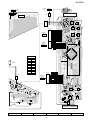
Figure 26 SCHEMATIC DIAGRAM (1/10)
– 26 –
5
6
XL-3000V
P33 12-F,G
FROM
CNS703 DISPLAY PWB-A3
PWB-A2
1
2
3
4
5
6
7
8
9
MAIN PWB-A1(1/2)
10 11 12 13
C209
47/16
0.14V
DI
28
29
D403
1N4004
C431
220P
C430
100/16
D402
1N4004
D401
1N4004
+B
SO601
SPEAKER TERMINAL
CL
DI
CE
C432
220P
30
C429
33/16
R439
3.9K
1K
1K
1K
C433
220P
CL
CE
0.14V
VREF VSS
27
VDD
1
TEST
2
4.8V
26
3
0V
25
0V
C426
10/16
0V
C424
0.1(ML)
4.8V
4
ROUT LOUT
RBAS2 LBAS2
4.8V
5
C423
0.1(ML) 4.8V
C421
0.1(ML)
24
4.8V
RBAS1 LBAS1
4.8V
6
C425 4.8V
10/16
C422
0.1(ML)
4.8V
RTRE LTRE
4.8V
23
C417
2.2/50
R215
12K
R201
8.2K
L
+B
1 C215 R217
1/50 12K
R203
100K
C213
4.7/50
R205
10K
R423
R424
R425
7
C419
0.0027
C407
10/16
R204
100K
10.2V
2
C203
1/50
R440
3.9K
C420
0.0027
R438
6.8K
C416
10/16
C418
2.2/50
RIN
4.8V
LIN
4.8V
L4
RSEL0 LSEL0
0V
R4
0V
22
C208
100/16
C201
0.0056
3
5.1V
4
8
R437
6.8K
C403
10/16
R421
1K
R417
1K
21
4.8V
20
C415
10/16
19
9
10
4.8V
R422
1K
L3
L2
4.8V
18
4.8V
17
11
R3
L1
4.8V
12
R2
4.8V 4.8V
16
13
R1
0V
C401
10/16
CD L
TUN L
14
4.8V
R403
1.8K
15
5V
IC401
LC75342M
FUNCTION/
VOLUME
EQUALIZER
AUX L
+B
R416
1K
C402
10/16
R404
1.8K
R415
1K
AUX R
R418
1K
C404
10/16
TUN R
CD R
8
R210
10K
C211
0.0033
C408
10/16
R209
10K
R214
12K
R212
2.7K
5.1V
7
4.8V
S
Q201
2SK246 GR 5V
0V
R218 R208
12K
330
C216
1/50
9.6V
D201
1N4148
1
6
5.1V
4.44V
5
IC201
KIA4558P
SURROUND
CONTROL
0V
0V
D 5V
0V G
R202
8.2K
C202
0.0056
R216
12K
R211
2.7K
R207
47K
2
5.1V
Q203
KRC107 M
SURROUND 3
5.1V
R206
10K
5.1V
FM SIGNAL
C204
1/50
C214
4.7/50
C212
0.0033
R213
12K
VIDEO SIGNAL
CD SIGNAL
5V
A_24V
D_GND
P_STB
DI
CD +B
P_MUTE
CL
CE
SD
STEREO
DO
CNP703
R607
6.8K
+B
IN2
R106
470
C107
100/50
R115
56K
R113
100
C111 C112
10/50 10/50
R604
10K
Q602 0V
KTC3199 GR
C102
10/50
D606 D605
1N4004 1N4004
C628
10/16
C120
220/16
R638
4.7
CHASSIS
GND
L602
3µH
C110
0.001
0.6V
L603
10µH
Q101
KTC3200 GR
0V
R120
1K
R-CH
+
C616
0.1
Q103
KTC3200 GR
R121
10K
Q104
KTC3200 GR 0.6V
R118
47K
1.2V
0.6V
L-CH
R102
39K
R124
47K
R123
10K
R122
1K
C627
0.022
C106
10/50
R104
56K
+B
R119
33K
C614
0.1
C109
3P
Q102
KTA1268 GR
+B
R110
1K
C104
3P
A GND
+
C613
0.1
C639
0.0047
NF2
15
C640
0.0047
GND
14
0.1V
PRE
–VCC
13
C108
R108 0.0015
1K
0.1V
+VE2
–VE2
12
C114
100/50
0V
–VCC
–21.7V
10 11
20.2V
+VCC
21.8V
9
C116
0.022
+VE1
–VE1
BIAS
–18.9V
N.C. 0V
PRE
+VCC
20.6V
NF1
8
R101
39K
0.6V
.4V
IN1
0V
6 7
R109
22K
R637
4.7
C615
0.1
CHASSIS
GND
R662
330
J601
HEADPHONES
R661
330
–B
5
L601
3µH
R114
100
0.6V
R603
10K 0V
0.1V
0.1V
Q601
KTC3199 GR 0V
4
C103 R105
10/50 470
C603
33/16
2
3
R111
1K
IC601
STK40202
POWER AMP.
C101
10/50
+B
1
R103 1K
47/16
R634
3.3K
C105
0.0015
R608
1K
R609
1K
R
3
2
1
4
5
9
10
C113
0.022
+B
A
B
+B
8
+B
5.6V
C905
100/10
C906
100/10
903
99 GR
4.9V
+B
+B
+B
+B
1
2
P29 11-C,D
5V
A_GND
M_GND
3
M_12V
4
CD_GND
5
CD_6R2V
6
902
6BSB
32 1-F FROM
CNS652 DISPLAY PWB-A3
7
8
9
10
Figure 27 SCHEMATIC DIAGRAM (2/10)
– 27 –
11
12
TO
MAIN PWB-A1(2/2)
P28 1-F P28 1-C
–B
A
P26 3-B TO
CNP807 TERMINAL
PWB-A4
XL-3000V
R883
8.2
CNW807
CNS807
2
1
2
1
Q805
KTA1266 GR
R884
8.2
11.3V
D805
1N4004
0.63V
R880
3.3K
R888
10K
0V
R837
1K
0V
2
3
4
R873
3.3K
C892
47/16
R881
470K
0.9V
C893
47/16
0.7V
0V
Q806
2SC535 C
R866
4.7K
C872
0.1
Q803
KTC3199 GR
+B
R864 D803
27K 1N4004
A
B
R882
6.8K
Q807
KTC3200 GR
0.1V
FAN
1
LIGHT
2
DIMMER
3
CD_STB
4
AMP_DEC
5
FAN_DEC
6
CLID_SW
7
CLID_PRO
8
CLID_UP
9
CLID_DW
10
CNP702
1
4.9V
0.64V
R865 D804
27K 1N4004
D802
1N4004
0V
R887
22K
R813
10
+B
+B
+B
L80
10µ
CNS801
1
DGND
1
2
3
4
5
6
7
8
9
10
11
12
R836
1K
R834
1K
R832
1K
R830
1K
/RST
R835
1K
R833
1K
R831
1K
L801
D
P35 12-G,H TO
CNP801V VIDEO PWB-D
C
11.7V
R868
27K
R885
22K
TO MAIN PWB-A1(1/2)
P27 12-G
B
P33 12-C,D
FROM
CNS702
DISPLAY PWB-A3
0V
Q804
KTC3199 GR
0.57V
R867
3.3K
0.67V
11.6V
0.2V
R870
33K
0V
10.6V
PU_IN
LRCK
L806
10µH
BCK
CNW801 12
R814
3.3K
C822
220/10
R811
2.2K
XVDD
XO
XI
XVSS
VDD
PXO
PXI
VSS
TESI01
TESIN
/DACT
/CKSE
/DMOUT
I03
I02
I01
I00
VSS
VDD
FLGD
FLGC
FLGB
FLGA
SEL
2VREF
DMO
FVO
FMO
TEBC
RFGC
4
81 DVSR
82 RO
14
CNS805
7
5
FOO
TEZI
TEI
TSIN
SBAD
FEI
RFRP
RFZI
RFCT
AVDD
RFI
SLCO
AVSS
VCOF
VCOREV
PVREV
1
TESTO
/HSO
UHSO
EMPH
LRCK
VSS
BCK
AOUT
DOUT
MBOV
IFP
SBOK
CLCK
VDD
VSS
DATA
SFSY
SBSY
SPCY
SPDA
COFS
MONIT
VDD
TESIOO
P2VREF
HSSW
ZDET
PDO
TMAXS
TMAX
99 /TSMOD
100 /RST
13
2.1V
2.1V
2.1V
0V
2.1V
0V
2.4V
0V
0V
0.6V
1.7V
0V
5V
0V
4.3V
1.2V
5V
0V
0V
0V
5V
1 2 3 4 5 6 7 8 9 10 11 12 13 14 15 16 17 18 19 20 21 22 23 24 25 26 27 28 29 30
R801
10K
C838
47/10
C820
0.01
3
2
1
50 VREF
49 TRO
6
IC802
TC9462F
SERVO/SIGNAL CONTROL
R851
330
3
2
1
11
C829
100/10
R810
3.3K
50
49
48
47
46
45
44
43
42
41
40
39
38
37
36
35
34
33
32
31
C810
0.001
2.1V
2.1V
R809
10K
2.2V
2.2V R808
C809
0.0047
2.2V 3.3K
2.1V
2.1V
2.2V
2.1V
C807
0.033
2.1V
R807
2.1V
10K
5V
C806
0.0047
2.1V
2.1V
C805
0.0027
0V
C804
1.4V
0.01
2.1V
2.1V
C803
47/10
LPFO 2.1V
LPFN
2.1V
R806 C802
15K
0.015
12
R804
100K
R802
47K
C801
100P
+B
CNW805
+B
H
• NOTES ON SCHEMATIC DIAGRAM can be found on page 19.
• The numbers 1 to 15 are waveform numbers shown in page 41.
1
2
3
4
Figure 28 SCHEMATIC DIAGRAM (3/10)
– 28 –
5
6
C811
47/10
C812
0.01
C813
0V
2.6V
2.2V
0V
5V
5V
0V
0V
0V
0V
0V
5V
0V
0V
0V
0V
5V
0V
5V
0V
0V
5V
0V
2.5V
4.3V
2.2V
0V
DVDD
DVR
LO
DVSL
TEST1
TEST2
TEST3
BUS0
BUS1
BUS2
BUS3
VDD
VSS
BUCK
/CCE
TEST4
5V
5V
5V
0V
1.4V
0V
2.5V
0V
2.5V
R852
100K
R853
100K
R855
100K
R854
100K
C836
100/10
8
C817
0.1
C818
0.1
15
80 79 78 77 76 75 74 73 72 71 70 69 68 67 66 65 64 63 62 61 60 59 58 57 56 55 54 53 52 51
0V
81
2.4V
C830
C828
82
0.056
100/10
0V
83
2.3V
84
2.4V
85
0V
86
5V
C840
87
100/10 C862
5V
C869
0.001
88
R819
220P
5V
89
220
4.3V
C868
90
220P
4.3V
91
4.3V
C867
92
220P
4.3V
C866
93
220P
5V
94
0V
+B
95
4V
96
3.3V
C865
97
220P
C835
5V 98
0.056
5V 99
100
C864
C837
4.9V
220P
470P
C821
0.1
C824
0.056
R812 C819
3.3K
0.1
2.1V
2.1V
1.8V
X801
16.93MHz
BUS0
BUS2
BUS1
BUS3
BUCK
/CCE
TO MAIN PWB-A1(1/2)
P27 12-G
P26 3-A
TO
CNP805 TERMINAL PWB-A4
C823
0.01
R820
1K
F
G
C827
15P(CH)
C887
0.0027
DATA
E
C826
15P(CH)
C825
0.056
C86
470
XL-3000V
10.7V
3
R902
47K
0V
11.6V
0.57V
0V
0V
11.6V
6.1V
4.6V
4.8V
0V 1
3
4
5
6
7
8
9
CNS701
R901
2.2K
1
1
2
SWITCH PWB-A5
10.6V
4.4V
Q907
KTA1266 GR
2 R904
2.2K
Q908
KRC102 M
Q802
KRC102 M
3
0V
3
R879
3.3K
R874
2.2K
10.7V
1
1
1
1
2
2
2
3
3
3
CNW806
2
0V
SW802
CD LID
OPEN/CLOSE
CNS806
CNP806
R905
47K
D801
AUY3333
2
11.4V
0V
R914
470
CNW701
1
2
CNP701
IC805
TA7291S
CD LID
MOTOR DRIVER
C871
47/16
R873
3.3K
LED PWB-A6
11.4V
2
4.1V
2
MAIN PWB-A1(2/2)
11.4V
Q902
KTA1266 GR
Q901
KRC102 M
R877
68K
4.5V
R876
150K
0V 1
CNP804
C872
0.1
+B
1
CNW804
M
+B
M801
CD LID
OPEN/CLOSE
MOTOR
5V
A_GND
+B
2
1
+B
+B
3
4
5
6
R861
2.2K
R862
2.2K
6.4V
L803
10µH
1
2
M_GND
M_12V
D_GND
CD_6R2V
C870
0.001
Q861
2SB562 C
7.1V
5V
P27 12-G,H
TO
MAIN PWB-A1(1/2)
+B
+B
CNS804
2
R843
1K
3.2V
3.1V
2.1V
2.1V
0V
4.8V
5V
6.4V
2.1V
2.3V
4.4V
1.9V
CNW803
C859
470/10
C860
0.1
MUTE
REG O
TRB
VIN4
VG1
VIN1
VO4+
VO4VO1+
GND
VO1BIAS
VG4
3
3.2V
2.1V
7.0V
7.0V
2.1V
2.1V
2.1V
3.2V
15 16 17 18 19 20 21 22 23 24 25 26 27 28
SP+
SP–
SL+
SL–
PU-IN
GND
0V
GND
VO3+
VIN3
VG3
VCC
VCC
CD MOTOR PWB-C
+B
+B
R823
1K
C812
0.01
C813
100/10
C850
220/10
C849
0.056
C855
100/10
10
9
8
2.2V
2.1V
4.3V
2.1V
2.5V
3.4V
0V
2.1V
2.1V
2.1V
2.1V
5V
R824
47K
12
11
10
9
8
7
6
5
4
3
2
1
C842
47/10
R821
150
R822
33
4.1V
Q801
KTA1266 GR
3.4V
6
5
4
3
2
1
–
+
–
M
NM802
SPINDLE
MOTOR
M
NM801
SLED
MOTOR
PICKUP UNIT(308)
CNP802
FO16
TR+
15
TR14
FO+
13
PD
12
VR
11
LD
10
GND
9
F
8
C
7
B
6
A
5
C
4
E
3
+5V
2
1
R80B
68K
2V
2.1V
2.2V
2.1V
2.1V
2.1V
2.1V
2.1V
2.1V
2.1V
1.7V
0V
2.1V
C841
100/10
13
R825
82K 14
C845
15
100/10
16
C846
17
0.1
18
19
C847
20
0.1
21
C848 R826
2.7K
39P
22
23
R828
1.2K
24
R829 R827 C839
39K 2P
68K
C863
470P
6
5
4
3
2
1
6
5
4
3
2
1
+
SP+
SP–
SP+
SL–
PU-IN
GND
NSW801
PICKUP IN
811
7/10
+B
CNS803
2
R863
2.2K
C844
0.0068
CNP803
6.5V
0V
PO1+
VO3-
PO1-
OPO
GND
VO2VO2+
VIN2
VG2
14 13 12 11 10 9 8 7 6 5 4 3 2 1
0.8V
1V
3.2V
3.2V
2.1V
IC804
MM1469XH
FOCUS/TRACKING/
SPIN/SLED DRIVER
C857
47/16
C858
0.01
L801
10µH
+B
C843
0.1
IC801
TA2109F
SERVO PRE AMP.
R80E
82K
CNW3
16
15
14
13
12
11
10
9
8
7
6
5
4
3
2
1
FO-
FO–
TR+
TR–
TR+
TR-
FO+
PD
VR
LD
GND
F
C
B
A
C
E
+5V
PO+
ACTUATOR
1/2VCC
1/2V
R80A
R80C 82K
82K
R80F
82K
+B
+
-
B
+
-
A
+
-
E
VREF
R80G
68K
F
C
GND
+B
MON
VCC
7
8
9
10
Figure 29 SCHEMATIC DIAGRAM (4/10)
– 29 –
11
LD
12
+
+
-
XL-3000V
A
T302
AM
Tracking
C343
33P
C362
3.3/50
C329
0.022
D301
1N4148
VR351
10K(B)
VD301
SVC348S
C332
0.022
C331
0.047
C330
12P(CH)
C302
0.001
R358
8.2K
FM Mute
Level
B
L353
1mH
+B
1.5V
0V
5.2V
4.4V
3.8V
5
6
7
8
C351
0.022
3.6V
0V
R308
10K
2.3V
0.8V
0V
+B
R382
330
R305
680
C315
100P
R386
330
TP301
C316
10/16
C317
0.022
R315
33
R313
680
R304
47K
C309
0.001
C308
0.022
D306
1N4148
C314
22P
(CH)
R314
C310 33
0.022
C311
10P(CH)
C307
0.0047
C305
0.0047
FM
75ohms
C312
33P
2 CF302
0.8V
AM
GND
R312
2.2K
Q306
2SC535 C
R301
22
R316
330
CF303
1
3
3
2
C313
6P(UJ)
R303
33K
L303
FM OSC.
Q302
2SC535 C
D305
1N4148
E
C306
7P(UJ)
FM RF
R307
47
Coverage
L302
FM ANT.
R302
100K
C303
0.001
C304
0.01
FM IF
T304
1
9
R306
10
VD302
KDV147C
C318
5P
SO301
ANTENNA
TERMINAL
2
C381
12P(CH)
F
R310
4.7K
X352
4.5MHz
R309
470
C301
0.012
CHASSIS
GND
2
C352
10/16
5.2V
4
1
5.2V
1.5V
3
FM Band
3
2
VD303
KDV147C
2
1
1
C319
18P(CH)
BF301
BAND PASS
FILTER
D
0.8V
IC301
TA7358AP
FM FRONT END
24 23
2.1V
R351
5.6K
C337
0.022
AM Band
Coverage
5V
T306
C
5V
2.5V
R336
5.6K
FM IF AM OSC
OUT
IN
AM MIX
OUT
AM OSC
IN
R323
68K
IC303
LA1832S
FM IF DET./
FM MPX./AM IF
D302
1N4148
C334
27P(UJ)
C335
560P
C382
15P(CH)
C349
0.001
C384
0.001
G
+B
H
• NOTES ON SCHEMATIC DIAGRAM can be found on page 19.
1
2
3
4
Figure 30 SCHEMATIC DIAGRAM (5/10)
– 30 –
5
6
IC
LC
PLL
R374
1K
4
1
IC302
LC72131
PLL(TUNER)
7
3
4
5
6
7
8
C386
330P
L351
100µH
R387
5.6K
R393
1K
9
10
11
C383
0.022
R395
47K
R376
10K
C355
22P
C356
0.001
C370
1/50
C357
2.2/50
R355
3.3K
3.8V
(1.9V)
C358
1/50
3.8V
(1.2V)
4V
(2.2V)
MPX IN
R-CH
OUT
L-CH
OUT
PHASE
(AM/FM)
MO/ST
1.3V
13
1.3V
2.1V
15 14
IF OUT
VCC
2.3V (0V)
16
MPX VCO
FM DET
STEREO
17
PHASE
9
C365
0.022
C363
0.022
C362
3.3/50
C369
56P
C368 R356
1/50 1K
X351
456kHz
C371 R361
1/50 5.6K
10 11
12
+B
R377
5.6K
14 13 12
9
4.7V
(0V) 2
R391
390
R383
5.6K
R384
6.8K
C391
47/16
17 16 15
0V
2
C399
0.022
8
R365
10K
IF REQ IF IN
8
MO/ST
CF352
C385
0.01
5V
7
FM
+B
2.9V
R353 (4.3V)
270
5V
C398
100/10
0V
SD
0V (0.9V)
2.3V
18
0V
18
CF351
5V
6
0V
(2.6V)
C353
0.022
C354
0.022
AM LOW
CUT
FM/AM
OUT
0.6V
2.1V (2.7V)
C367
1/50
AM IN
C387
0.022
AM IF
IN
GND
VSM
AM RF
IN
2.1V (2.7V)
5V
R350
2.7K
3.5V
(0V)
19
2.6V (0V)
R379
2.2K
3
5.2V
0.9V
5
VDD
MUTE FM IN
FM
22 21 20
PD
1
0V
4
3.7V
(0V)
3.9V
DO
C380
10/16
T351
AM IF
19
1.7V
(11.4V)
0.9V
3
AIN
R352
1K 2.1V
FM AFC
20
5.1V
C392
0.001
C394
47/16
C350
0.022
4.8V
CL
2
DI
86
0
R381
10K
21
0.1V
0V
2.1V
22
CE
1
0.1V
2.6V
AOUT
C397
0.022
82
0
0V
OUT
IN
AM MIX
OUT
AM OSC
IN
REG
23
R373
1K
R372
1K
R371
1K
CH)
VSS
2
Hz
0V
CH)
X IN X OUT
5V
2
2.6V
C352
10/16
R363
3.3K
R364
3.3K
C373
0.018
R357
470K
C374
0.018
C366
0.001
C364
10/16
C360
0.022
C361
0.022
XL-3000V
TUNER PWB-A2
AM SIGNAL
FM SIGNAL
Q351
KRC104 M
1 0V
3.7V
(0V)
3
C372 R362
1/50 5.6K
+B
R366
2.2K
ZD351
DZ5.1BSB
FM ST
SD
DO
L352
100µH
C396
100/10
C395
0.022
+B
R392
390
C393 R380
1/50 1.5K
Figure 31 SCHEMATIC DIAGRAM (6/10)
– 31 –
10
11
10
11
CE
CL
DI
D_GND
A_12V
TUN_R
TUN_L
A_GND
9
8
7
6
5
TO
MAIN PWB-A1(1/2)
CNP307
P26 5,6-A
4
3
2
CNS307
1
Q360
KTA1266 GR
+B 11.7V
10.8V
10.9V
+B
R385
5.6K
R359
1.8K
R360
4.7K
D308
1N4148
12
XL-3000V
DISPLAY PWB-A3
A
SW727
FUNCTION
SW726
REW
PRESET DOWN
R706
3.9K
1
2
3
4
5
6
7
8
9 10 11 12 13 14
SW718
VOLUME DOWN
2.47V
0V
7
5V 8
2.49V
9
2.47V
10
0V
11
2.24V
12
2.47V 13
C703
0.1
R702
10K
X701
8MHz
24V
C701
22P(CH)
SW710
CD LID
OPEN/CLOSE
LMP701
R795
47K
0V 14
(CH)
GND
C702
22P
32.768kHz X702
5V
0V
R731 1K
5V
R732 1K
5V
R733 1K
1
2
2
3
3
2 5V
2.5V
2.5V
2.5V
SEG9
SEG8
SEG7
SEG6
XO
MMOD
SYSTEM
15 VREF–
16 CLID_SW
DO
4.9V 22
0V
23 VSM
4.9V
24 VREF+
0V
25 DI
USWD_5R6V
+B
4
D723
1N4148
+B
+B
5V
0.4V
5V
4.2V
R796
1K
G
Q707
KTA1266 GR
24.5V
24.5V
R792
47K
+B
23.7V
RX701
REMOTE
SENSOR
1
R7A1
1K
5V
R7A3
100
C715
100/10
R7A4
120
Q703
KTC3199 GR
R7A8
82
Q708
KTA1266 GR
0.4V
1.1V
C714
560P
2
3
C713
10/16
1
0V
+B
R7B0
10K
ZD701
DZ3.3BSB
2
0V
0.4V
Q702
KTC3199 GR
0.4V
C712
0.01
4.8V
3
C710
0.01
R7A7
1K
Q701
KRC102 M
R7A2
100K
CNS652
R7A6
1K
D721
1N4148
2
R7A0
1K R7A5
10K
C711
3.3/50
D720
1N4148
1
R7A9
3.3K
5V
R798
4.7K
R778 47K
Q709
KRC102 M
R779
47K
3
2
4.5V
R797 0.1V
2.2K
1 0V
R780 47K
R781
47K
R783
33K
+B
R793
10K
Q706
KRC102 M
3
2
0.1V
4.1V
1 0V
C704
0.022
+B
+B
H
• NOTES ON SCHEMATIC DIAGRAM can be found on page 19.
2
3
4
Figure 32 SCHEMATIC DIAGRAM (7/10)
– 32 –
5
6
R765
0V
R741 4.9V
1K 4.9V
5V
R760 1K
0V
R763 1K
0V
R762 1K 4.9V
R761 1K 4.9V
R738
1K
D_GND
P_CONT
+B
1
2.5V
2.5V
2.5V
2.5V
SEG5
SEG4
SEG3
XI
R744
1K
5V
TO MAIN P26 5-H
PWB-A1(1/2) CNP652
R782
1K
R725
10K
C705
0.01
D722
1N4148
F
VSS
5V 26 27 28 29 30 31 32 33 34 35
L702
2.2µH
1K
R799
1
+B
OSC1
17 KEY1
5V 18 KEY2
5V 19
MODEL
0V
20 CLID_PRO
0V
21 MOT_DEC
CFW701A
CNW707
CNS707
P26 1-F TO
CNP707 POWER PWB-B
E
R722
10K
R721
10K
3 2 1
CLID_PRO
R735
1K
OSC2
R740 1K 0V
3 2 1
R734 1K
VDD
R739
1K
D
CFW701B
VLC1
CLID_OUT
SW709
ON/
STAND-BY
3.25V
+B
R728 1K
CE
R723 47K
5 VLC3
6 VLC2
RESET
LAMP PWB-A7
1.7V
4 COM0
BUSY
R729
47K
+B
3 COM1
ACK
R727
47K
C
2 COM2
2.47V
R720B
1.2K
VD_DI
R720A
SW711 1.2K
FF
PRESET UP
R711
1.2K
100 99 98 97 96 95 94 93 92 91
1 COM3
VD_DO
SW721
MEMORY/SET
R719
1.2K
2.47V
SW712
CD PLAY/ PAUSE
TUNING UP
R710
2.7K
2.47V
SW722
BASS/TREBLE
2.5V
R708
2.2K
2.5V
SEG0 2.5V
B
R718
1.5K
SW713
VOLUME UP
SEG1
SEG2
R707
2.7K
CL
SW725
CD STOP
TUNING DOWN
XL-3000V
LCD701
LCD DISPLAY
75
SEG26
74
SEG27
73
SEG28
72
SEG29
71
SEG30
70
SEG31
69
SEG32
68
SEG33
67
66
65
64
63
62
61
CD_STB
60
CD_RES
59
PU–IN
58
CLID_DW
57
CLID_UP
56
FAN
55
DIMMER
54
SD
52
0V
0V
R777 1K
4.9V
R758 1K 4.8V
R759 1K 4.8V
2.5V
2.5V
2.5V
2.5V
2.5V
4.9V
5V
CNW702
CLID_DW
1
CLID_UP
2
CLID_PRO
3
CLID_SW
4
FAN
5
CD_STB
6
AMP_DEC
7
LIGHT
8
DIMMER
9
FAN_DEC
10
5V
5V
5V
5V
R766 1K
CD_STB
0V
R769 1K
CLID_DW
4.9V
R770 1K
CLID_UP
4.9V
4.9V
4.9V
0V
4.72V
R772 1K
4.76V
R773 1K
CNS702
10
9
8
7
6
5
4
3
2
1
R771
1K
4.8V AMP_DEC
R768
1K
4.8V
51
B-LIGHT R785
1K
CNS704
1
VD_DI
VD_DO
ACK
BUSY
CLID_OUT
GND
STB
STB
1
2
2
3
3
4
4
5
5
6
6
7
7
CNW704
P_CONT
CNS703
SD
SD
STEREO
STEREO
DO
CL
+B
CLID_OUT
CE
BUSY
DI
CD+B
CD+B
+B
P_MUTE
P_MUTE
P_STB
P_STB
ACK
A_24V
VD_DI
D_GND
VD_DO
SURROUND
5V
CE
CL
1
1
2
2
3
3
4
4
5
5
6
6
7
7
8
8
9
9
10
10
11
11
12
12
13
13
CNW703A
DO
DI
+B
CLID_SW
B-LIGHT
SURROUND
+B
7
8
9
10
Figure 33 SCHEMATIC DIAGRAM (8/10)
– 33 –
11
12
TO
CNP703 MAIN PWB-A1(1/2)
P26,27 6,7,8-A
R757 1K 4.8V
4.9V
R755
1K 4.8V
R742 1K 4.8V
5V
R764
1K 4.9V
R751 1K 4.9V
5V
R750 1K
0V
5V
R765
1KR749
1K
0V
R741 4.9V
1K 4.9V
5V
R760 1K
0V
0 31 32 33 34 35 36 37 38 39 40 41 42 43 44 45 46 47 48 49 50
R763 1K
53
2.5V
R776
1K
STEREO
P–CONT
CD+B
P–MUTE
P–STB
SURR
LIGHT
STB
REMOCON
SYS_STOP
POWER
CLID_OUT
CE
RESET
ACK
BUSY
IC701
IX0038SJ
SYSTEM MICROCOMPUTER/
FL DRIVER
2.5V
TO
CNP702 MAIN PWB-A1(2/2)
P28 1-B,C
SEG25
TO
CNP804V VIDEO PWB-D
P35 12-C
SEG22
SEG21
SEG20
SEG19
SEG18
SEG17
SEG16
SEG15
SEG14
SEG13
SEG12
SEG11
SEG10
SEG9
SEG8
SEG7
SEG6
SEG5
SEG4
6 95 94 93 92 91 90 89 88 87 86 85 84 83 82 81 80 79 78 77 76
2.5V
2.5V
SEG24
2.5V
2.5V
SEG23 2.5V
2.5V
2.5V
2.5V
2.5V
2.5V
2.5V
2.5V
2.5V
2.5V
2.5V
2.5V
2.5V
2.5V
2.5V
2.5V
2.5V
2.5V
9 10 11 12 13 14 15 16 17 18 19 20 21 22 23 24 25 26 27 28 29 30 31 32 33 34 35 36 37 38
XL-3000V
VIDEO PWB-D
A
Q11V
2SD1858 R2
+B
+B
5V
C105V
0.1
C125V
100/10
4.5V
3.8V
C126V
0.1
R143V
220
R5V
4.7K
B
1
2
3
4
5
6
7
8
9
3.4V
1.6V
1.6V
1.8V
1.8V
1.9V
1.9V
1.9V
2.0V
1.9V
C
1.7V
1.2V
1.3V
C122V
0.1
1.6V
0V
10
11
12
13
14
15
16
C112V
0.1
5V
C115V
5V 22/25
VCC 32
5V
31 PGM/A18
VPP
A16
A15
A12
A7
A6
A5
A4
A3
A2
A1
A0
D0
D1
D2
VSS
A17
A14
A13
A8
A9
A11
OE
A10
CE
D7
D6
D5
D4
D3
R91V
4.7K
3.2V
30
29
28
27
26
25
24
23
22
21
20
19
18
17
+B
R98V
4.7K
R93V
4.7K
2.0V
1.3V
1.7V
1.6V
+B
1.6V
0V
1.9V
0.3V
1.2V
1.5V
1.4V
1.4V
1.4V
0V
5V
R157V
820
2.6V
0V
3.0V
C110V
0.1
0V
2.6V
2.7V
3.5V
3.3V
1.2V
1.3V
1.6V
1.4V
1.4V
1.4V
1.5V
3.5V
1.2V
0V
0.3V
3.5V
3.5V
1.7V
1.9V
2.0V
1.9V
1.9V
1.9V
1.8V
1.8V
1.7V
1.6V
VSS
LA11
LA10
LA9
LA8
LA7
LA6
LA5
LA4
LA3
LA2
LA1
LA0
LSCE0
LSCE1
LROMCE
LOE
LWR
LD7
LD6
LD5
LD4
LD3
LD2
LD1
LD0
AUX7/STB
AUX5
DSC_STB
AUX6/SCK
VCC3
IC15V
ES3880F
VIDEO CD DECODER
R164V
10
R165V
10
5V
0V
2.4V
0.9V
2.4V
2.4V
0.4V
0.9V
2.9V
1.3V
2.2V
1.5V
2.8V
2.7V
0.4V
0.5V
2.9V
1.8V
1.3V
1.7V
1.8V
1.8V
1.8V
1.4V
1.8V
1.7V
1.8V
1 2 3 4 5 6 7 8 9 10 11 12 13 14 15 16 17 18 19 20 21 22 23 24 25 26 27 28 29 30
3.6V
0V
VSS 50
0.2V
AUX4 49
5V VD_DI
48
0.2V VD_DO
AUX2/VD_DO 47
AUX1/DSADATA 46 5V
5V
AUX0/DSAACK 45
2.3V
PCLKQSCN 44
2.2V
PCLK2XSCN 43
0.2V
DCLK 42
4.5V
HSYNC 41
4.8V
VSYNC 40
1.0V
YUV7 39
1.2V
YUV6 38
1.9V
YUV5 37
1.9V
YUV4 36
2.3V
YUV3 35
0.6V
YUV2 34
0.6V
YUV1 33
1.8V
YUV0 32
VCC3 31 3.6V
48 AUX3/VD_DI
R160V
4.7K
R159V
820
R158V
820
3.5V
3.5V
R169V
33
3.5V
R170V
4.7K
3.4V
3.2V
R161V
33 MCLK1.5V
TSD0.1V
R168V TBCK1.8V
33
TWS2.1V
0.1V
R156V
4.7K
0V
VCC
LA12
LA13
LA14
LA15
LA16
LA17
AUDIOCLK
AUDATA
BCLK
LR
DRAS1/DOE
RSD
RBCLK
RWS
TDMCLK
TDMDR
TDMFS
DCAS
VSS
C121V
22/25
1.6V
R166V
33
R163V
33
C120V
0.1
2.0V
81
82
83
84
85
86
87
88
89
90
91
92
93
94
95
96
97
98
99
100
VCC3
DRAS
DWE
DA0
DA1
DA2
DA3
DA4
DA5
DA6
DA7
DA8
DBUS0
DBUS1
DBUS2
DBUS3
DBUS4
DBUS5
DBUS6
DBUS7
DBUS8
DBUS9
DBUS10
DBUS11
DBUS12
DBUS13
DBUS14
DBUS15
RESET
VSS
1.6V
1.3V
E
C119V
0.1
80 79 78 77 76 75 74 73 72 71 70 69 68 67 66 65 64 63 62 61 60 59 58 57 56 55 54 53 52 51
5V
+B
1.9V
0V
C109V
100/10
C108V
0.1
D
1.6V
IC10V
IX0041SJ
ROM 256Kx16
TO CHASSIS
GND
F
R97V
4.7K
+B
+B
C116V
0.1
+B
5V
1.3V
2.9V
0.5V
0.4V
5V
2.7V
2.8V
1.5V
2.2V
3.5V
3.5V
1.8V
1.7V
1.8V
1.4V
+B
20 19 18 17 16 15 14 13 12 11 10 9 8 7 6 5 4 3 2 1
C117V
0.1
VCC
A3
A2
A1
A0
NC
RAS
WE
NC
NC
D7
D6
D5
D4
VCC
D3
D2
D1
D0
VCC
C102V
22/25
VSS
A4
A5
A6
A7
A8
OE
UCAS
LCAS
NC
D8
D9
D10
D11
VSS
D12
D13
D14
D15
VSS
C111V
0.1
R162V
4.7K
5V
+B
0V
2.4V
0.9V
2.4V
2.9V
0.4V
0.4V
0V
2.9V
1.3V
3.3V
3.3V
0.1V
1.8V
1.7V
1.8V
1.8V
0V
1.8V
21 22 23 24 25 26 27 28 29 30 31 32 33 34 35 36 37 38 39 40
C118V
22/25
AUX0
G
IC16V
IX0025SJ
D-RAM 256Kx16
R08A
4.7K
R12AV
4.7K
H
• NOTES ON SCHEMATIC DIAGRAM can be found on page 19.
• The numbers 16 and 17 are waveform numbers shown in page 41.
1
2
3
4
Figure 34 SCHEMATIC DIAGRAM (9/10)
– 34 –
5
6
VDAC
Q12V
2SC1740 SR
2.9V
R112V
56
3.6V
R124V
220
R114V
6.8K
C104V
100/10
5.7V
1
2
3
4
5
6
7
C169V
0.1
C161V
100/10
C158V
100/10
0V
1.3V
5V
2.3V
0V
0V
0V
5V
0V
5V
0V
+B
C160V
0.1
R194V
270
C124V
0.1
C150V
0.1
0V
5V
2.4V
0V
5V
2.3V
0V
0.8V
+B
2V
TC100V
10P
C129V
27P(CH)
0V
5V
2.3V
2.2V
L104V
3.3µH
C136V
0.1
C184V
0.1
BUSY
VD_DI
VD_DO
ACK
STB
DGND
CLID_OUT
CNP804V
R171V
100K
X1V
27MHz
R137V
1K
R138V
33
R140V
1K
R141V
1K
L103V
3.3µH
+B
R178V
82
R167V
33
C168V
22P(CH)
C137V
10/25
R139V
1K
C183V
22P(CH) 80 79 78 77 76 75 74 73 72 71 70 69 68 67 66 65 64 63 62 61 60 59 58 57 56 55 54 53 52 51
81
82
83
4.8V
84
1.4V
85
1.0V
86
1.2V
87
1.9V
88
1.9V
89
5V
90
0V
91
2.3V
92
1.4V
93
0.6V
94
1.4V
95
0.8V
96
1.6V
97
0.8V
98
1.3V
99
0V
100
C127V
0.1
HSYN_B
DSC_D6
VSYN_B
DSC_D5
YUV7
YUV6
YUV5
YUV4
VCC
VSS
YUV3
DSC_D4
YUV2
DSC_D3
YUV1
DSC_D2
YUV0
DSC_D1
VSS
MIC2
MIC1
AOL+
AOL–
AOR–
AOR+
VCCA
VREFP
VCM
VSSA
BUSY/AUX15
S_EN/AUX14
LA18/AUX13
RBCK
NC/AUX12
NC/AUX11
NC/AUX10
RSD
VCC
VSS
DSC_D7
IC14V
ES3883F
VIDEO CD ENCODER
50
49
48
47
46
45
44
43
42
41
40
39
38
37
36
35
34
33
32
31
2.3V
2.3V
2.3V
2.3V
0V
C162V
0.1
C164V
47/10
5V
C165V
0.1
5V
0V
2.3V
0V
0V
5V
R105V
4.7K
+B
+B
C166V
22/25
C159V
0.1
0V
0V
5V
5V
1.8V
0.1V
2.1V
1.5V
C135V
0.1
5V
5V
0V
2.7V
5V
0V
0V
3.5V
C106V
1
0V
1.2V
3.5V
5V
0V
1 2 3 4 5 6 7 8 9 10 11 12 13 14 15 16 17 18 19 20 21 22 23 24 25 26 27 28 29 30
C130V
0.1
+B
+B
R06AV
4.7K
R142V
33
R01AV
4.7K
R100V
4.7K
0V
R193V
4.7K
R07AV
4.7K
R10AV
4.7K
R02AV
4.7K
R03AV
4.7K
CNP801V
DGND
1
/RST
2
BUS0
3
BUS1
4
BUS2
5
BUS3
6
BUCK
7
/CCE
8
PU_IN
9
LRCK
10
BCK
11
DATA
R11AV
4.7K
EAUX0
EAUX01
EAUX02
EAUX03
EAUX08
EAUX04
R08AV
4.7K
R09AV
4.7K
CNS801 TO
P28 1-D,E MAIN PWB-A1(2/2)
1.5V
4.5V
PAL R94BV
(LOGO)
0
1.2V
VSS
NC
NC
NC
VCC
DSC_CLK
AUX0
DSC_D0
AUX1
DSC_STB
AUX2
NC
RESET_B
AUX7
NC
VCC
MCLK
AUX8
TWS
AUX9
TSD
TBCK
RWS
RSTOUT
VSS
VSS
SQCK
SQSO
NC
NC
R164V
10
R165V
10
PCLK2X
PCLK
VCC
VSS
NC
VSS
XIN
VCC
VSS
XOUT
AUX3
AUX4
AUX5
AUX6
VCC
ACAP
VDAC
VSSAV
VSSAV
YDAC
VCCA
VCCA
CDAC
VSSAV
VSSAV
COMP
RSET
VREFM
VREF
VSSAA
27MHz
NTSC R94AV
(LOGO) 4.7K
R163V
33
2AV
.7K
C167V
22P(CH)
R102V
100K
R190V
10K
R188V
10K
C147V
100/10
C139V
10/25
R111V
2.2K
+B
1
2
3
4
5
6
7
8
C138V
10/25
+B
C131V
0.001(CH)
L11V
10µH
CNS802
1
2
3
4
5
6
7
8
9
CNW802V
R195V
100
C101V
1000/6.3
VDAC
AGNDV
L-CH
AGNDA
R-CH
+5V
DGND
+12V
C140V
10/25
+B
R113V
100
R116V
15K
CNS704 FROM
P33 12-E DISPLAY PWB-A3
C103V
22/25
C172V
10/25
R103V
6.8K
R121V
3.3K
C148V
100/10
R181V
R183V 100K C149V
100K
0.1
C141V
33P
(CH)
R187V
10K
R123V
75
+B
R189V
10K
+B
R115V
15K
C142V
33P(CH)
–+
6
5.3V 5
R185V 8
10.9V
10K
5.3V
C171V
10/25
R101V
100K
33P(CH)
1 6.1V
R108V
+–
10K
5.3V
2
5.3V
3
4
R186V
0V
10K
R184V
100K
R107V
10K
C143V
33P
6.1V 7
(CH)
R182V
100K
VIDEO SIGNAL
CD SIGNAL
+B
IC11V
NJM4565M 17
BUFFER AMP. C144V
R104V
10K
16
CNP802A TO
MAIN PWB-A1(1/2)
P26 4-A
XL-3000V
1
CNW801
12
12
7
8
9
10
Figure 35 SCHEMATIC DIAGRAM (10/10)
– 35 –
11
12
XL-3000V
TERMINAL PWB-A4
A
C412
SO401
R408
LEFT
CNP810
R406
VIDEO/
AUX IN
B
CFW452
D412
D411
L402
C851
L802
C853
WH
1
2
3
4
5
C660
C630
F653
T1.6A L 250V
D657
C657 D901
C658
D658
C901
C651
C126
12
GY
C614
R638
CNP801
C659
D660
CFW852 TO CHASSIS GND
LUG(205)
L602
RIGHT
TO CHASSIS GND
LUG(205)
CNS805
WH
3
2
1
RD
3
2
1
CNP805
C852
J801
DIGTAL
OUT
CNS608
2
1
CNP608 2
1
3
2
1
L601
C615
FROM
POWER
TRANSFORMER
P38 4-C,D
D659
C414
C613
LEFT
R637
GY
BK
CNS607
WH
3
2
1
RD
3
2
1
CNP607
VIDEO
OUT
C
BK
RD
2
1
2
1
2
2
1
1
CNP807
CNS807
R407
L401
R405
C411
RIGHT
SO601
SPEAKER
TERMINAL
M802
FAN MOTOR
TO CHASSIS GND
LUG(205)
CFW451
C413
CHASSIS
GND
C616
C654
T
D902
D
C902
C640
CHASSIS
GND
C125
C639
LUG
(205)
C101
R104
R115
R103
C104
16 14 12 10 8 6 4 2
15 13 11 9 7 5 3 1
D651
D653
R105
C109
R101
R661
R662
R111
D652
L603
R873
CNP802
1
Q908 2
D654
C103
3
C105
PK
Q601
R102
PINK
E C B
R108
R123
E C B
B C E
Q103
Q101 R119
G
B
E
E C B
C
E
Q104 R120
C
GY
GY
BK
CNW602
3
2
1
GY
GY
BK
3
2
1
B C E
C120
R609
3 2 1
C602 IC682
R121
R122
E C B
Q602
R124
CNP601
1
2
3
R864
R118
1
2
3
E
B
R613
R607
R610
R614
Q607
C102
C601
Q102
C621
C626
R612
R80C
R628
1
1
C
2
B C906 R912
C905 3
4
ZD902
5
6
D603
CNP652
7
2 1
C629
8
D604
C603
E
2
R
R621
D605
C627
1
2
3
Q608
1
2 C628
3 Q609
R634
D803
D804
1 2 3 4 5 6 7 8 9 10
R865
CNW601
CNP
FROM DISPLAY
CNS652
PWB-A3
P39 10-A
FROM CNS802
VIDEO
PWB-D P40 1-A,B
5
CNS307 TO TU
PWB
P38,39 6,7-A
H
• The numbers 1 to 15 are waveform numbers shown in page 41.
1
2
3
C83
R829
C843
C849
Q606
C
CNP602
Q610
B
B
C
E
R110
R902
R827
W
R80F
R80E
BLACK
R619
R629
R80A
BK
Q603
Q903
CNW608
GRAY
WHITE
C620
D602
E C B
CNP802A
GY
WH (W)
B
C
E
ZD601
VIOLET
3
R90
B C
R901
R617
VL
Q901 2
R821
R913
BLUE
1
C904
ZD602
BL
CHASSIS
GND
C622
GREEN
R624
GR
R620
C625
YELLOW
R611
YL
C110
Q604
ORANGE
R603
RED
OR
Q904
ZD901
R608
R D (R )
B C E
R911
1
2
C113
3
R109
4
5
6
C112
7
C116
8
9
R114
10
11
C114
C108
12
13
14 R106
15
C106
R604
F
BROWN
R910
C624
R623
IC601
COLOR TABLE
BR
C903
C107
C111
R113
Q605
E
R905
J601
HEAD
PHONES
4
Figure 36 WIRING SIDE OF P.W.BOARD (1/5)
– 36 –
5
6
XL-3000V
CNS804
1 BK
2 RD
CNW804
MAIN PWB-A1
RED
R217
C403
C425
Q805
C430
E C B
C651
R866
L801
R80B
R80G
12
C817
C824
C821
C818
R425
R424
1
C870
R823
C842
C819
B C E
Q801
R861
6
CNW803
R824
C841
WH
GY
GY
GY
GY
GY
L803
B
C
E
CD MOTOR PWB-C
4
L806
Q861
C811
1
2
3
4
5
6
CNS803
14
C858
1
14
10
R862
5
IC804
20
PICKUP UNIT(308)
25
R863
3
2
7
8
2
CNW3
R914
LED PWB-A6
1
1
D801
CNW701
1
1 2 3 4 5 6 7 8 9 10 11
CNP307
1
16
CNS701
1 WH
BK
2
7 8 10 9 6
16
28
15
D606
CNS307 TO TUNER
PWB-A2
P38,39 6,7-A
CNP803
1 23 45 6
R843
X801
R814
F3895AF
R855
C862
R820
C823
R810
NSW801
PICKUP IN
CNW801
FROM DISPLAY
PWB-A3
CNS702
P39 10-F
NM801
SLED
MOTOR
R819
C826
C860
IC801
NM802
SPINDLE
MOTOR
13
C840
R813
C822
55
C859
C843
C849
R80A
1
C845
C847
R80C
R80F
R80E
R827 R826 R828
C844
C846
C839
R825
13
24
R829
20
15
60
50 51
C864
C872
C807
10
45
R853
R852
C827
70
65
40
12
C867
C868
C869
C830
81
80
75
IC802
35
C804
R807
C813
C848
5
90
85
R811
R812
CNP701
C803
C850
C806
C855
5 95
20
R808
R809
R901
1 2
10
25
R804
3
C805
R902
FROM DISPLAY
PWB-A3
CNS703
P39 10-B,C
TO VIDEO
PWB-D
CNP801V
P40 2-B,C
C835 R832
C866
C828
15
R802 R806 30
Q902
31
C801
C802
C812
B C E
Q901 2
1
C838
1
C863
R801
3
1
CNW805
C820
C809
R874
R905
Q907
Q807
R836
R833
R834 R835
C837 C836
1100
WH R851
C871 RD
C829
E
C
3
R904 B
IC805
Q802
C810
R879
1 2 3
B C E
R822
E C B
1
Q908 2
R882
CNS801
12 10 8 6 4 2
11 9 7 5 3 1
1 2 3 4 5 6 7 8 9 10 R837
R877
R876
D802
1
3 2 1
2
R830
R887
CNP806
CNP804 R831
C865
9 8 7 6 5 4 3 2 1
Q803
R873
1
R880
B
C
E
CNP703
CNP702
2
2
GY
GY
BK
1
02
2
1
R868
1
CNW806
3
2
1
CNS806
R423
13 12 11 10 9 8 7 6 5 4 3 2 1
C857
C654
Q804 R867
R870
F651
T3.15A L 250V
3
C419
30 C431
Q806
B C E
ASSIS
GND
C892
C893
D403
D402
D401
C429
C420
25
R881
C421
C423
R439
C901
16
R421
C417
20
R415
R417
C657 D901
5
R884
F652
T3.15A L 250V
10
IC401
R404
SW802
CD LID
OPEN/CLOSE
R207
C433 Q203
C432
1
R885
R883
R888
C404
R403
C415
R212
3 2 1
C422
R422
C426
15
R418
C402 R416
R854
C660
C407
SWITCH PWB-A5
8 7 6 5
R216
R214
C424
R401
C825
D659
C408
WH
3
CNW607
1
2
3
4
5
C401
MER
D
R440
D201
CNW807
GY
BK
D805
R402
1
R210
IC201
S G D
C216
C418
R438
C416
1 2 3 4
R215
Q201
R218
C204
R209
C212
C211
R206
R203
RD
CNP801
R213
R211
R205
C213
C203
C214
R201
R204
R202
R437
C202
R208
C201
C209
M801
CD LID
OPEN/CLOSE
MOTOR
C215
C887
C208
1
16
11 15
9
10
Figure 37 WIRING SIDE OF P.W.BOARD (2/5)
– 37 –
11
12
XL-3000V
R377
R366
C373
C371
C374
R362
C372
R357
C364
R364
R363
R393
C363
C366
C369
Q306
R361
R383
R395
L352
R376
C354
X351
C353
C356
C352
C351
3 2 1
C358 Q351
C368
T306
R355
R350
C329
C386
C385
R310
CF303
C335
VD301
D302
R336
R314
R312
C310
C349
L302
C357
C367
CHASSIS
GND
C
C302
D301
C365
D306
IC303
C396
ZD351
C355
CF302 R352 R353
C399
1 2 3
1 2 3 4 5 6 7 8 9 10 1112
R313
R351
B
C360
C
C350 C361
E
24 23 22 21 20 19 18 17 16 15 14 13
R358
C319
R385
R384
C398
CF351
C362
3
VR351
R303
1 2 3
R307
R302
C307
VD303
C303
C332
C306
CF352
1
2
3
C308
C309
C395
C370
T351
C343
2
VD302
R308
C313
C391
R391
R392
R382
L353
R309
L303
C330
C331
C334
R323
BF301 1
R316
C383
AM
E
C
B
R386
R387
L351
C314
Q360
D308
C384
IC302
9
8
7
6
5
4
3 C305
2
1
D305
R305
C317
B
Q302 C
R304
E
R315
C304
R373
R372
R371
R301
R306
C312
C393
C315
C316
GND
C311
B
C301
IC301 C318
FM
75
OHMS
CNS307 1 2 3 4 5 6 7 8 9 1011
X352
R374
1
2
3
4
5
6
7
8
9
10
11
T304
SO301
ANTENNA
TERMINAL
CNP307 TO
PW
P36,37 6,7-G
C337
TP301
22
21
C397
R379 20
C380
19 C392
18
R365
17
C394 R380 16
15 C387
14
13
R381 12
R359
R360
C381
A
C382
TUNER PWB-A2
R356
T302
YL
BK
YL
BR
BR
5
4
3
2
1
TO MAIN
PWB-A1
CNP801
P36,37 6,7-B,C
D
T651
POWER TRANSFORMER
(MAIN)
F654
T.F 2A,250V
7
BK
WH
5
3
1
BK
POWER PWB-B
AC POWER SUPPLY CORD
RD
9
RD
BL
AC110/127/220/
230~240V, 50/60Hz
RD
E
1 2
RLY601
F
9
7
5
3
SW651
VOLTAGE SELECTOR
D689
1
D685
CNP651
R685
220V
1
2
B C E
Q683
CNP653
230~240V
E C B
Q681
D6
R686
G
127V
C683
110V
SO655
AC POWER
INPUT SOCKET
AC110/127/220/
230~240V, 50/60Hz
T681
POWER TRANSFORMER
(SUB)
H
1
2
3
4
Figure 38 WIRING SIDE OF P.W.BOARD (3/5)
– 38 –
5
6
XL-3000V
LMP701
1
TO MAIN
PWB-A1
CFW701B
CNP307 TO MAIN
PWB-A1
P36,37 6,7-G
CNP652
P36 5-F
3
LAMP PWB-A7
3 4 5 6 7 8 9 1011
CNS652
R764
SW709
ON/STAND-BY
26
7
CNW704
25
R768
BROWN
BK
BLACK
PK
PINK
CNW653
TO MAIN
PWB-A1
1 2
CNP702
P37 8-D
89
85
CNS702
1
2
3
4
5
6
7
8
9
10
R785
R7A4
C711
R7A1
R7B0
R7A2
D721
3 2 1
SW710
D681
C704
Q701
R7A9
D688
C688
C683
E C B Q702
R7A8
C712
C710
D720
C689
R687
IC681
R686
3
2
1
R7A7
R7A6
R688
R7A5
C715
R689
R7A0
E C B
ZD683
CNP707
D684
SW712
CD PLAY/PAUSE
TUNING
UP
R707
R720A
CD LID
OPEN/CLOSE
D683
D682
DISPLAY PWB-A3
7
8
9
10
Figure 39 WIRING SIDE OF P.W.BOARD (4/5)
– 39 –
11
12
BASS/
TREBLE
R711
SW722 R706
R710
R783
1
Q703
R735
R731
ZD701
D723
D686
2
D722
Q681
3
C665
CNP653
E C B
4
ZD684
1
2
B C E
R766
1
R685
683
MEMORY/
SET
10
BK
GY
GY
GY
GY
GY
GY
GY
GY
GY
1
2
3
4
5
6
7
8
9
10
11
12
13
14
15
16
17
18
19
20
21
22
23
24
25
26
27
28
29
30
31
32
33
34
35
36
37
38
LCD701
FL DISPLAY
WHITE
L702
GRAY
W H( W )
SW726
REW
PRESET
DOWN
VIOLET
SW711
FF
PRESET
UP
VL
GY
R772
R795
BLUE
76
75
R769
GREEN
BL
85
70 80
SW725
CD STOP
TUNING
DOWN
YELLOW
90
65
R770
YL
GR
1
100
95
R773
ORANGE
55
R771
RED
OR
5
IC701
60
CNW702
BK
RD
F654
T.F 2A,250V
R702
15
10
45
R744
R750
BR
R723
R727
R729
30 20
35
50
51
RD( R)
R7A3
R782
40
COLOR TABLE
X702
R725
R728 X701
R777
RX701
REMOTE
SENSOR
C703
C701
1
R776
R734
R733
R732
C702
1
VOLUME
DOWN
1
2
3
R722
R741
C713
R761
VOLUME R719
UP
R721
R749
SW721
R718
C714
R739
R720B
SW713
R778
R755
R742
R757
R758
R751
SW727
FUNCTION
Q709
R798 R797
R793
CFW701A
SW718
R781
R738
BK
GY
GY
GY
GY
GY
GY
3
R779
R780
R759
CNP804V
P40 4,5-C
1
2
3
4
5
6
7
CNS704
13
R708
E C B Q708
R762
TO VIDEO
PWB-D
GY
GY
GY
GY
GY
GY
GY
GY
GY
GY
GY
GY
BK
R792
Q707
1
R760
CNP703
P37 8,9-D
B
C
E
3
R740
C373
1
CNS703
13
12
11
10
9
8
7
6
5
4
3
2
1
1
2
3
R765 R763
TO MAIN
PWB-A1
WH
BK
BK
WH
CNW703A
1
2
3
4
Q706
3 2 1
R796
CNS707
R799
CNW707
2 1
XL-3000V
17 16
C141V R181V
R185V
R186V
1
CNW801 1
TO MAIN
PWB-A1
CNS801
P37 9-D
R08AV
R12AV
12
12
11
10
9
8
7
6
5
4
3
2
1
25
C
20
15
10
IC14V
90
45
C164V
55
50
51
C150V
60
65
70
10
100
5
C184V
C136V
L104V
C161V
85
55
50
R161V
60
65
70
75
TC100V
80
L11V
CNP804V
C
7
6
5
4
3
2
31
3
30
4
29
5
28
6
27
26
8
IC10V
9
25
24
10
23
11
22
12
21
13
20
14
19
15
18
17
R143V
C105V
1
R91V
B
R5V
R124V
C131V
32
2
16
Q12V
C104V
C109V
C103V
E
C125V
R123V
R121V
X1V
R112V
R111V
R170V
81
C108V
C183V
R171V
R178V
IC15V
81
80
R194V
R159V
45
R167V
R156V
R160V
R169V
R168V
R166V
R158V
90
51
75
C124V
C158V
C127V
85
C169V
L103V
15
1
7
C110V
95
40
R165V
R164V
R163V
95
40
C160V
20
25
100
5
35
R100V
R94AV
C162V
31
35
31
C165V
1
30
C120V
R105V
R09AV
C121V
1
30
CNP801V
R162V
20
C116V
C159V
C166V
15
C148V
C147V
C138V
10
5
R157V
B
C140V
C112V
R137V
R102V
C102V
R13V8
1
IC16V
R139V
2
R104V
C149V
C139V
C137V
C115V
8
1
C167V
C168V
R116V
21
C111V
R140V
3
C143V
C171V
R182V 5
R189V
25
30
R141V
4
R115V
R184V
R103V
R195V
R187V
35
C117V
C129V
5
R101V
40
C172V
C130V
R01AV
6
9
C118V
C144V
R142V
R02AV
R03AV
TO MAIN
PWB-A1
CNP802A
P36 5-F
GY
GY
GY
GY
GY
GY
GY
GY
IC11V
C142V
R183V
7
1
R11AV
R10AV
R07AV
R06AV
R94BV
R193V
C135V
C106V
8
R190V
R188V
CNW802V
CNS802
C122V
R108V
4
R107V
A
VIDEO PWB-D (TOP VIEW)
C126V
R93V
C101V
R114V
R113V
E
B
C
Q11V
R97V
R98V
FROM DISPLAY
CNS704 PWB-A3
P39 10-C,D
D
VIDEO PWB-D (BOTTOM VIEW)
E
Q11V
C101V
X1V
E
C
B
C104V
C158V
C125V
C161V
L104V
L103V
E
Q12V
TC100V
7
6
5
4
3
2
1
CNP804V
L11V
C103V
16
17
15
18
3
14
19
5
13
20
12
21
11
22
10
23
CNP801V
F
C109V
1
2
4
6
7
8
R5V
B
C
C164V
9
10
11
12
9
C166V
1
8
C121V
CNW802V
G
C137V
C139V
C140V
C138V
C147V
C148V
C171V
9
C102V
C172V
IC10V
26
6
27
5
28
4
29
3
30
2
31
1
32
C115V
CHASSIS
GND
H
• The numbers 16 and 17 are waveform numbers shown in page 41.
2
3
4
Figure 40 WIRING SIDE OF P.W.BOARD (5/5)
– 40 –
5
25
7
C118V
1
24
6
XL-3000V
WAVEFORMS OF CD CIRCUIT
NO DISC FOCUS SEARCH
1
STOP
12
1
FOO
FO+
13
2
IC804 26pin
3
FO-
SEL
5
6
11
2
15
3
FMO
6
1
FEI
3
TEI
1
TRO
2
IC802 46pin
SBAD
11
2
IC802 49pin
RFO
15
3
FMO
3
IC802 53pin
IC801 22pin
STOP
PLAY
REVIEW
6
1
FEI
TEI
1
TRO
2
IC802 46pin
IC802 43pin
RFGO
11
2
IC801 19pin
IC802 49pin
RFRP
15
3
IC801 17pin
3
FMO
IC802 53pin
STOP
TEI
PLAY
TCD-782 TNO-02 PLAYBACK
16
1
IC802 46pin
TRO
SBAD
LO
1
RO
2
IC11V 7pin
2
IC802 49pin
7
2
CUE
IC802 44pin
11
TRO
PLAY
IC802 43pin
6
1
IC802 53pin
STOP
10
TEI
IC802 49pin
TEI
5
PLAY
IC802 46pin
IC802 46pin
5
3
STOP
1
FEI
6
DMO
TOC IL
IC802 43pin
9
2
IC802 55pin
IC802 57pin
8
SBOK
14
3
FOCUS SEARCH
7
1
IC802 12pin
IC804 27pin
4
TMAX
IC802 30pin
IC802 48pin
2
PLAY
17
IC11V 1pin
3
IC802 44pin
– 41 –
XL-3000V
TROUBLESHOOTING
When the CD does not function
When the CD section does not operate when the objective lens of the optical pickup is dirty, this section may not operate. Clean
the objective lens, and check the playback operation. When this section does not operate even after the above step is taken, check
the following items.
Remove the cabinet and follow the troubleshooting instructions.
"Track skipping and/or no TOC (Table Of Contents) may be caused by build up of dust other foreign matter on the laser pickup
lens. Before attempting any adjustment make certain that the lens is clean. If not, clean it as mentioned below."
Turn off the power, and wipe the lens softly using a cleaning paper moistened with commercially available cleaning solution so
as not to damage it.
Be careful not to touch the lens with bare hands.
Dust gradually accumulates on the objective lens during use, and it may degrade performance.
To avoid this problem, use a cleaning disc designed for CD optical pickup lenses.
HOW TO USE
1. Using the brush in the cleaner cap, apply 1 or 2 drops of the cleaning fluid to the brush on the CD cleaner disc which has
the mark next to it.
2. Place the CD cleaner disc onto the CD disc tray with the brush side down, then press the play button.
3. You will hear music for about 20 seconds and the CD player will automatically stop. If it continues to turn, press the stop button.
CAUTION
The CD lens cleaner should be effective for 30 - 50 operations, however if the brushes become worn out earlier then please
replace the cleaner disc.
If the CD cleaner brushes become very wet then wipe off any excess fluid with a soft cloth.
Do not drink the cleaner fluid or allow it to come in contact with the eyes. In the event of this happening then drink and / or
rinse with clean water and seek medical advice.
The CD cleaner disc must not be used on car CD player or on computer CD ROM drives.
All rights reserved. Unauthorized duplicating, broadcasting and renting product is prohibited by law.
Cleaner Liquid
Cleaning Disc
PARTS CODE: UDSKA0004AFZZ
– 42 –
XL-3000V
Make sure that the disc is normal, and set the CD TEST MODE (STEP 1).
Is the measured voltage as specified in circuit diagram?
Check the main unit power supply circuit.
No
Yes
Is "Er-CD01" displayed"?
No
Yes
Move the pickup to most internal circumference side of disc.
Turn the power off and reset the CD TEST MODE (STEP 1).
Is "PU ERROR " not displayed?
No
Check the pattern between pin 58 (PU_IN) of IC701 and
CNW803/CNS803.
Check the between CNW803/CNS803 and PU-IN switch.
Yes
Is +5V applied to pin 100 (/RST) of IC802?
No
Check the PWB pattern between pin 59 (CD_RES) of IC701 and
pin 100 (/RST) of IC802.
No
Is CD Lid switch SW802
ON condition ?
Yes
Does the CD TEST MODE advance from "STEP 2"?
Yes
No
Set ON condition the CD
Lid switch.
Yes
Check the between pattern IC701 and SW802 If OK.
Check the main unit power supply circuit.
Does the laser come on in CD TEST MODE "STEP 2"?
No
Check the procedure in "LASER FAILURE".
Yes
Does the CD TEST MODE advance from "STEP 3" to "STEP
4"?
Yes
No
Does the spindle motor rotate normally when the CD TEST
MODE changes from "STEP 4" to "STEP 3"?
No
Check the procedure in "FOCUS FAILURE".
Check the procedure in "SPINDLE MOTOR CLV SERVO
FAILURE".
Yes
Is the HF output on pin 38 of IC802 in CD TEST MODE "STEP 5"?
No
Check the procedure "HF ERROR".
Yes
Does the sound heard when the optical pickup move to the
selected play by the FF
/REW
key.
No
Does the sled motor
move ?
No
Yes
Check the procedure in
"SLED MOTOR
OPERATING FAILURE ".
Yes
Check the procedure "NO SOUND"
Does the LCD track number and time indicator work properly ?
No
Check the pattern between IC701 and LCD701.
Yes
Turn the power off and then back on.
Does the unit initialize properly and start playback when PLAY
key is pressed?
No
Is "Er-CD01 "
displayed ?
No
Check the procedure in
"HF ERROR".
Yes
Yes
Check the pattern between pin 58 (PU_IN) of IC701
and CNW803/CNS803. Check the between CNW803/
CNS803 and PU-IN switch.
Does the unit play in order in the FF mode?
No
Check the procedure in "TRACK SEARCH FAILURE".
Yes
Does playback continue for 30 seconds after the start of
playback ?
No
Yes
Normal
– 43 –
Check the procedure in "SLED SERVO FAILURE".
XL-3000V
• Laser failure.
Is +6.2V applied to the emitter of Q861 ?
No
Check the PWB pattern between emitter of Q607 and emitter of
Q861.
Yes
Check the peripheral parts of IC804 and Q861.
Is +5V applied to the collector of Q861 ?
No
Yes
No
Check the PWB pattern between collector of Q861 and pin 62 of
IC802.
No
Check the PWB pattern between collector of Q861 and pin 1 of
IC801.
No
Does the laser come on when pattern cut between pin 8 (SEL) of
IC801 and pin 57 (SEL) of IC802 ?
Is +5V applied to the pin 62 (VDD) of IC802 ?
Yes
Is +5V applied to the pin 1 (VCC) of IC801 ?
Yes
Is 0V applied to the pin 57 (SEL) of IC802 ?
Yes
Yes
No
Check the PWB pattern between IC701 and IC802 (BUCK/CCE/
BUS0~3)
Is approx. 2V applied to the collector of Q801.
No
Check the peripheral parts of IC801 and Q801. If it is normal, the
optical pickup is faulty.
No
Check as stated in item "FOCUS SERVO SAWTOOTH WAVE
FAILURE".
Yes
Check CNP802/CNW3. If it is normal, the optical pickup is
faulty.
• Focus failure.
Does the optical pickup move up and down when the disc is
removed?
Yes
Is the following waveform output at the pin 43 (FEI) of IC802
when the disc is set?
Check the periphery of IC801 and CNP802/CNW3. Is it normal?
No
Yes
Yes
pin 43
The optical pickup is faulty.
(FEI)
pin 48
(FOO)
pin 44
(SBAD)
Is the waveform shown above input at the pin 44 (SBAD) of
IC802?
No
Yes
IC801 is faulty.
– 44 –
Check the pattern between pin 13 of IC801 and pin 44 of IC802.
Check the periphery of IC801 and CNP802/CNW3.
XL-3000V
• Focus servo sawtooth wave failure.
Is sawtooth wave output to the pin 48 (FOO) of IC802 ?
No
IC802 is faulty.
Yes
1.5~2.5sec
Check the PWB pattern between emitter of Q607 and IC804.
Is +6.2V applied to the pins 21 and 22 (VCC) of IC804 ?
No
Yes
Is sawtooth wave obtained between pins 26 and 27 of IC804 ?
No
Yes
Is +5V applied to the pin 7
(MUTE) of IC804 ?
No
Yes
1.5~2.5sec
Check the PWB pattern
between pin 7 of IC804
and pin 60 (CD STB) of
IC701.
Check the PWB pattern between pin 48 (FOO) of IC802 and pins
24 and 25 of IC804. If OK. IC804 is faulty.
Is sawtooth wave obtained between pins 13 and 16 of
CNP802/CNW3 ? (as shown above)
Check the PWB pattern between CNP802/CNW3 and IC804.
No
Yes
CNP802/CNW3 connection failure or optical pickup failure.
• Spindle motor clv servo failure.
Is following wave output to the pin 55 (DMO) of IC802 when
the CD TEST MODE "STEP 3" is changed to " STEP 4" ?
No
Check the procedure in "HF ERROR".
If OK. IC802 is faulty.
No
Check the PWB pattern between pin 55 (DMO) of IC802 and pins
9 and 10 of IC804. If OK. IC804 is faulty.
Yes
DMO
Is above wave obtained between pins 11 and 12 of IC804 ?
Yes
Is above wave obtained between pins 9 and 12 of CNP802/
CNW3 ?
Check the PWB pattern between CNP802/CNW3 and IC804.
No
Yes
CNP802/CNW3 connection failure or optical pickup failure.
– 45 –
XL-3000V
• HF error.
Is output (tracking error signal) obtained at the pins 46 (TEI)
and 47 (TEZI) of IC802 the CD TEST MODE "STEP 4" is
changed to "STEP 5"?
No
Is output obtained at the pins 3 and
No
8 of CNP802/CNW3.
Optical pickup failure.
Yes
Yes
test mode "step 4"
Check the periphery of IC801.
Check the PWB pattern between
pin 12 (TEO) of IC801 and pins 46
and 47 of IC802.
Is it normal ?
test mode "step 5"
TEI
TEZI
IC801 is faulty.
No
Yes
Check the PWB pattern between pin 49 (TRO) of IC802 and pin 19
of IC804.
Check the periphery of IC804 and CNP802/CNW3.
If OK. Optical pickup failure.
Is output (HF signal) obtained at the pin 38 (RFI) of IC802
when the CD TEST MODE "STEP 4" is changed to "STEP 5"?
No
Optical pickup failure.
Yes
Yes
test mode "step 4"
test mode "step 5"
Check the periphery of IC801.
Check the PWB pattern between pin 19 (RFGO) of IC801 and pin
38 (RFI) of IC802.
If OK. IC801 is faulty
RFI
Is output (HF signal) obtained at the pins 41 (RFZI) and 42
(RFRP) of IC802 when the CD TEST MODE "STEP 4" is
changed to "STEP 5"?
Yes
Is output obtained at the pins 4 and
5,6 of CNP802/CNW3.
No
test mode "step 4"
No
Check the periphery of IC801.
Check the PWB pattern between pin17 (RFRP) of IC801 and pins
41 (RFZI) and 42 (RFRP) of IC802.
If OK. IC801 is faulty.
test mode "step 5"
RFZI
RFRP
Is the following wave output to the pin 55 (DMO) of IC802
when the CD TEST MODE "STEP 4" or "STEP 5"?
Yes
test mode "step 4"
No
Check the periphery pins 28~32 of IC802.
If OK. IC802 failure.
test mode "step 5"
DMO
Normal.
• No sound.
Check the soldering and parts of IC14V.
Is the wave output at pins 45~48 on IC14V?
No
Yes
Check the soldering and parts of IC11V.
Is the wave output at pins 1 and 7 on IC11V?
Yes
No
Is the wave output at pins 14 and 17 on IC401?
Yes
Check the connection between IC11V and IC401.
No
Check areas between pins 5 and 26 on IC401 and IC601.
– 46 –
XL-3000V
• Track search failure
Does the sled motor run in FF/REW state when the SERVO
TEST MODE "STEP1" is set?
No
Check as stated in item "SLED MOTOR OPERATION FAILURE".
Yes
Is the following wave output to the pin 49 (TRO) of IC802
during track search in normal playback?
No
IC802 failure.
Yes
TRO
Is the following wave output to the pins 12 (TEO) of IC801
during track search in normal playback?
No
Yes
TEO
TEI
Check the PWB pattern between pin 49 (TRO) of IC802 and pin
19 of IC804.
Check the PWB pattern between pins 17 and 18 of IC804 and
Optical pickup.
If OK. Optical pickup failure.
TEZI
Is the above wave output to the pins 46 (TEI) and 47 (TEZI) of
IC802 during track search in normal playback?
No
Check the PWB pattern between pin 12 (TEO) of IC801 and pins 46
and 47 of IC802. If OK. IC801 failure.
No
Check the PWB pattern between pin 17 (RFO) and 18 (RFIS), 19
(RFRP) of IC801 and pins 41 and 42 of IC802. If OK. IC801 failure.
Yes
Is the following wave output to the pin 41 (RFZI) and 42
(RFRP) of IC802 during track search in normal playback?
Yes
RFRP
RFZI
Normal.
• Sled motor operation failure.
Is following sled feed signal output the pin 53 (FMO) of IC802
when FF
/REW
key is pressed after the CD TEST
MODE "STEP 1" is set?
FF
REW
Yes
C802 is faulty.
No
FMO
Is following sled feed signal output the pins 3 and 4 of IC804
when FF
/REW
key is pressed after the CD TEST
MODE "STEP 1" is set?
FF
Yes
No
Check the PWB pattern between pin 53 of IC802 and pins 3 and 4
of IC804.
REW
SL ±
Is sled feed signal output the pins 1 and 2 of IC804?
No
Check the peripheral parts of IC804. If OK, IC804 is faulty.
Yes
Is sled feed voltage applied between both terminals of sled
motor?
Yes
No
Check the CNW803/CNS803.
Check the CD mechanism (periphery of sled motor).
If the sled motor does not run when DC2.0V is applied to
both terminals of sled motor, the sled motor is faulty.
• Sled servo failure.
Is following sled signal output the pin 53 (FMO) of IC802
during playback?
IC802 is faulty.
No
Yes
FMO
Normal.
– 47 –
XL-3000V
FUNCTION TABLE OF IC
IC401 VHiLC75342M-1: Function/Volume Equalizer (LC75342M)
Pin No.
Port Name
Function
1
DI
Serial data and clock input pin for control.
2
CE
Chip enable pin. Data written into an internal latch in a timing of [H] -> [L]. Each analog switch is activated.
Data transfer enabled at [H] level.
3
VSS
Ground pin.
4
TEST
Electronic volume control pin. To be set to the VSS potential.
5
LOUT
Volume + equalizer output pin.
6
LBASS2
Bass-band filter comprising capacitor and resistor connection pin.
7
LBASS1
Bass-band filter comprising capacitor and resistor connection pin.
8
LTRE
Capacitor connection pin comprising treble band filter.
9
LIN
Volume + equalizer input pin.
10
LSEL0
Input selector output pin.
11
L4
Input signal pin.
12*
L3
Input signal pin.
13
L2
Input signal pin.
14
L1
Input signal pin.
15*
NC
No CONNECT pin. To be open or connected to VSS.
16*
NC
No CONNECT pin. To be open or connected to VSS.
17
R1
Input signal pin.
18
R2
Input signal pin.
19*
R3
Input signal pin.
20
R4
Input signal pin.
21
RSEL0
Input selector output pin.
22
RIN
Volume + equalizer input pin.
23
RTRE
Capacitor connection pin comprising treble band filter.
24
RBASS1
Bass-band filter comprising capacitor and resistor connection pin.
25
RBASS2
Bass-band filter comprising capacitor and resistor connection pin.
26
ROUT
Volume + equalizer output pin.
27*
NC
No CONNECT pin. To be open or connected to VSS.
28
Vref
0.5 x VDD voltage generation block for analog ground. Capacitor of several 10µF to be connected between
Vref and AWSS (VSS) as a counter measure against power ripple.
29
VDD
Supply pin.
30
CL
Serial data and clock input pin for control.
In this unit, the terminal with asterisk mark (*) is (open) terminal which is not connected to the outside.
– 48 –
XL-3000V
IC401 VHiLC75342M-1: Function/Volume Equalizer (LC75342M)
TEST VSS CE
4
3
2
DI
CL VDD Vref
NC
1
30
29
27
28
LOUT 5
CONTROL
CIRCUIT
LBASS1 7
LTRE 8
RVref
25 RBASS2
24 RBASS1
CONTROL
CIRCUIT
LBASS2 6
LOGIC
CIRCUIT
CCB
INTERFACE
LVref
26 ROUT
23 RTRE
22 RIN
LIN 9
21 RSEL0
LSEL0 10
11
12
13
14 15 16 17
18
19
20
L4
L3
L2
L1 NC NC R1
R2
R3
R4
Figure 49 BLOCK DIAGRAM OF IC
– 49 –
XL-3000V
IC701 RH-iX0038SJZZ: System Microcomputer/FL driver (IX0038SJ) (1/2)
Pin No.
Terminal Name Input/Output
1-4
COM3-COM0
5-7
VLC3-VLC1
8
VDD
Output
—
Input
Function
LCD common output terminal.
LCD power supply terminal.
Microcomputer power supply +5V.
9
OSC2
Output
Oscillator ground terminal for main clock. f=8MHz
10
OSC1
Input
Oscillator ground terminal for main clock. f=8MHz
11
VSS
12
XI
Input
Oscillator ground terminal for sub clock. f=32.768kHz
13
XO
Output
Oscillator ground terminal for sub clock. f=32.768kHz
14
MMOD
15
VREF-
16
KEY0 AN0/PA0
Input
CD lid status detection input.
17
KEY1 AN0/PA1
Input
Operation button input, Max-8 buttons.
18
KEY2 AN0/PA2
Input
Operation button input, Max-8 buttons.
19
KEY3 AN0/PA3
Input
MODEL/TUNER destination input.
20
KEY4 AN0/PA4
Input
Current detection of CD lid control motor.
Used to decide the CD lid drive error to control it.
21
KEY5 AN0/PA5
Input
Fan motor auto adjustment mode selection input.
22*
KEY6 AN0/PA6
Input
—
Input
—
Microcomputer power supply GND.
Memory mode selection terminal.
Power supply GND for AD converter.
23*
KEY7 AN7/PA7
Input
Tuner signal meter (S meter) voltage input terminal.
24
VREF+
Input
Power supply for A/D converter +5V.
25
TXD SBO0/P00
Output
26
RXD SBI0/P01
Input
27
SBT0/P02
Output
Synchronous clock output with TUNER PLL IC.
28
SBO1/P03
Output
VIDEO CD DECORDER DATA output.
29
SBI1/P04
Output
VIDEO CD DECORDER DATA input.
30
SBT1/P05
Output
VIDEO CD DECORDER CLOCK signal.
31
DK/BZER P06
Output
VIDEO CD DECORDER BUSY signal.
32
RST/P27
Input
Data output terminal to TUNER PLL IC.
Data input from TUNER PLL IC.
Reset signal input.
33*
RMOUT P10
Input
CLOCK/TIMER/SLEEP button input.
34
P11
Input
Tape run/END detection input.
35
TM2IO P12
Output
36*
TM3IO P13
Output
37
TM4IO P14
Input
Power (POWER) button input detection.
38
IRQ0 P20
Input
Switches to the HALT mode when changing to . "L" at power failure detection input.
39
SENS IRQ1/P21
Input
Remote control signal input.
40
IRQ2 P22
Input
VIDEO CD DECORDER STROBE signal.
41*
IRQ3 P23
Input
42*
IRQ4 P24
Input
43
P30
Output
SURROUND control output.
44
P31
Output
POWER IC STAND-BY terminal CONTROL.
45
P32
Output
Power mute output. "H" = MUTE ON "L" = MUTE OFF
46
LED0 WE/P50
Output
CD servo power supply circuit control output. "H" = CD power ON "L" = CD power OFF
47
LED1 RE/P51
Output
Main TRANS RELAY CONTROL. "H" = ON "L" = OFF
48*
LED2 CS/P52
Input
Data input from RDS IC.
49
LDE3/S51 A16/P53
Input
Radio stereo broadcast reception detection input. "L" = During stereo broadcast reception
50
LED4/S50 A17/P54
Input
51
SEG49 P60/A0
Output
CD LID output signal.
Recording bias oscillation frequency selection control output.
Broadcast reception status detection input. "L" = During broadcasting signal reception
LCD backlight control signal output. "H" = Backlight ON, "L" = Backlight OFF
52
SEG48 P61/A1
Output
Amp. signal detection.
53
SEG47 P62/A2
Output
LED illumination control. "H" = ON "L" = OFF
In this unit, the terminal with asterisk mark (*) is (open) terminal which is not connected to the outside.
– 50 –
XL-3000V
IC701 RH-iX0038SJZZ: System Microcomputer/FL driver (IX0038SJ) (2/2)
Pin No.
Terminal Name Input/Output
Function
54
SEG46 P63/A3
Output
LED dimmer signal.
55
SEG45 P64/A4
Output
Fan control signal.
56
SEG44 P65/A5
Output
Electric CD lid OPEN.
57
SEG43 P66/A6
Output
Electric CD lid CLOSE.
58*
SEG42 P67/A7
Input
59*
SEG41 P70/A8
Output
60
SEG40 P71/A9
Output
61*-64*
SEG39 P72/A10- Input/Output
SEG36 P75/A13
65*
SEG35 P76/A14
Output
Data synchronous clock output.
66*
SEG34 P77/A15
Output
Chip enable terminal. "L" = BUS terminal active
67
SEG33 P87/D7
Output
LCD segment output.
68
SEG32 P86/D6
Output
LCD segment output.
69-74
SEG31 P85/D5SEG26 P80/D0
Output
LCD segment output.
75-100
SEG25-SEG0
Output
LCD segment output.
ON/OFF output terminal of CD servo control IC. "H" = Servo ON "L" = Servo stand-by
Data input/output terminal control.
100
99
98
97
96
95
94
93
92
91
90
89
88
87
86
85
84
83
82
81
80
79
78
77
76
S
S
S
S
S
S
S
S
S
S
S
S
S
S
S
S
S
S
S
S
S
S
S
S
S
SEG0
SEG1
SEG2
SEG3
SEG4
SEG5
SEG6
SEG7
SEG8
SEG9
SEG10
SEG11
SEG12
SEG13
SEG14
SEG15
SEG16
SEG17
SEG18
SEG19
SEG20
SEG21
SEG22
SEG23
SEG24
IC701 RH-iX0038SJZZ: System Microcomputer/FL driver (IX0038SJ)
I
O
I
I
I
I
I
I
I
I
I
O
26
27
28
29
30
31
32
33
34
35
36
37
38
39
40
41
42
43
44
45
46
47
48
49
50
O
I
75
74
73
72
71
70
69
68
67
66
65
64
63
62
61
60
59
58
57
56
55
54
53
52
51
1
2
3
4
5
6
7
8
9
10
11
12
13
14
15
16
17
18
19
20
21
22
23
24
25
I
O
O
O
O
O
I
I
I
O
O
I
I
I
I
I
I
O
O
O
O
O
O
O
I
O
O
O
O
DO
CL
VD_DO
VD_DI
ACK
BUSY
RESET
NC
CE
CLID_OUT
NC
POWER
SYS_STOP
REMOCON
STB
NC
NC
SURR
P-STB
P-MUTE
CD+B
P-CONT
NC
STEREO
SD
COM3
COM2
COM1
COM0
VLC3
VLC2
VLC1
VDD
OSC2
OSC1
VSS
XI
XO
MMOD
VREF–
CLID_SW
KEY1
KEY2
MODEL
CLID_PRO
MOT_DEC
NC
NC
VREF+
DI
Figure 51 BLOCK DIAGRAM OF IC
– 51 –
S
S
S
S
S
S
S
S
S
O
O
I/O
I/O
I/O
I/O
O
O
I
O
O
O
O
O
SEG25
SEG26
SEG27
SEG28
SEG29
SEG30
SEG31
SEG32
SEG33
NC
NC
NC
NC
NC
NC
CD_STB
CD_RES
PU-IN
CLID_DW
CLID_UP
FAN
DIMMER
LIGHT
AMP_DEC
O B-LIGHT
XL-3000V
IC801 VHiTA2109F/-1:Servo Pre Amp. (TA2109F)
Pin No.
Function
Input/Output
Terminal Name
1
VCC
—
2
FNI
Input
Main beam amp input terminal
3
FPI
Input
Main beam amp input terminal
4
TPI
Input
Sub-beam amp input terminal
5
TNI
Input
Sub-beam amp input terminal
6
MDI
Input
Monitor photodiode amp input terminal
7
LDO
Output
8
SEL
Input
Laser diode control signal input and APC circuit ON/OFF signal input terminal
9
TEB
Input
Tracking error balance adjustment signal input terminal
To be controlled by 3-value PWM signal. (PWM carrier = 88.2 kHz)
10
2VRO
11
TEN
Input
12
TEO
Output
13
SBAD
Output
Sub-beam addition signal output terminal
14
FEO
Output
Focus error signal generation amp output terminal
15
FEN
Input
16
VRO
Output
Standard voltage (VR) output terminal. When Vcc = 5V, VR = 2.1V.
17
RFRP
Output
Track count signal generation amp output terminal
18
RFIS
19
RFGO
Output
20
RFGC
Input
RF amplitude adjustment control signal input terminal
The amplitude of RF signal can be controlled by using the 3-value PWM signal (PWM
carrier = 88.2 kHz) which is output from the RFGC terminal of TC9432F.
21
AGCI
Input
RF signal amplitude adjustment amp input terminal
22
RFO
Output
23
GND
—
24
RFN
Input
Output
Input
Power voltage terminal
Laser diode amp output terminal
Standard voltage (2VR) output terminal. When Vcc = 5V, 2VR = 4.2V.
Tracking error signal generation amp reversed phase input terminal
Tracking error signal generation amp output terminal
Focus error signal generation amp reversed phase input terminal
RFRP detection circuit input terminal
RF signal output terminal
RF signal generation amp output terminal
GND terminal
RF reversed phase input terminal
IC801 VHiTA2109F/-1:Servo Pre Amp. (TA2109F)
15kΩ
15kΩ
SBAD 13
7.67kΩ
12 TEO
30kΩ
20µA
50kΩ
10pF
20pF
10kΩ
10kΩ
36pF
21kΩ
29kΩ
24kΩ
24kΩ
11 TEN
7.96kΩ
10 2VRO
10kΩ
VRO 16
21kΩ
RFRP 17
20kΩ
50µA
47kΩ SW1
12kΩ
LDC
1kΩ
SW2
65µA
SW3
PEAK
BOTTOM
RFGO 19
8 SEL
1.74kΩ
20kΩ
20kΩ
9 TEB
3 STATE
DET.
21kΩ
12kΩ
RFIS 18
SEL
10kΩ
FEO 14
FEN 15
30kΩ
10kΩ
7 LDO
680kΩ
180kΩ
13kΩ
20pF
RFGC 20
2.12kΩ
6 MDI
I.I
5 TNI
I.I
4 TPI
180kΩ
12kΩ
AGCI 21
20pF
23.5kΩ
re = 130Ω
20kΩ
180kΩ
RFO 22
40pF
20kΩ
60kΩ
3 FPI
20kΩ
2 FNI
40pF
20kΩ
1 VCC
3.3kΩ
3.3kΩ
RFN 24
1.53kΩ
180kΩ
60kΩ
GND 23
Figure 52 BLOCK DIAGRAM OF IC
– 52 –
L
HiZ
H
LDC
SW1 SW2
ON OFF
OFF ON
OFF ON
SW3
OFF
ON
ON
XL-3000V
IC802 VHiTC9462F/-1: Servo/Signal Control (TC9462F) (1/3)
Pin No.
Port Name
Function
Input/Output
1*
TEST0
Input
Test mode terminal. To be opened usually.
2*
3*
/HSO
/UHSO
Output
Output
Playback speed mode flag output terminal.
/UHSO
/HSO
Playback speed
H
H
x1 speed playback
H
L
x2 speed playback
L
H
x4 speed playback
L
L
—
4*
EMPH
Output
Sub-code Q data emphasis flag output terminal. "H": Emphasis ON "L": Emphasis OFF
The output polarity can be inverted by command.
5
LRCK
Output
Channel clock (44.1 kHz) output terminal. "L": L channel "H": R channel
The output polarity can be inverted by command.
6
VSS
—
7
BCK
Output
8
AOUT
Output
Audio data output terminal.
9
DOUT
Output
Digital out output terminal.
10*
MBOV
Output
Buffer memory over signal output terminal. "H": Over
11*
IPF
Output
Correction flag output terminal.
"H": When AOUT output is correction-disabled symbol in case of C2 correction output.
12*
SBOK
Output
13*
CLCK
Input/Output
14
VDD
Input
Digital + power terminal.
15
VSS
—
Digital ground terminal.
16*
DATA
Output
Sub-code P-W data output terminal.
17*
SFSY
Output
Playback system frame sync signal output terminal.
18*
SBSY
Output
Sub-code block sync output terminal. "H": On S1 position when the sub-code sync is detected.
19*
SPCK
Output
Processor status signal read clock (176.4 kHz) output terminal.
20*
SPDA
Output
Processor status signal output terminal.
21*
COFS
Output
Correction system frame clock (7.35 kHz) output terminal.
22*
MONIT
Output
LSI internal signal monitor terminal.
It is possible to monitor the DSP internal flag and PLL system clock with the microcomputer
command. Terminal for serial output of text data according to command .
23
VDD
Input
Digital + power terminal.
24
TESIO0
Input
Test input/output terminal. To be fixed to "L" usually.
Terminal to input the text data read clock according to command.
—
Digital ground terminal.
Bit clock (1.4122 MHz) output terminal.
Sub-code Q data CRCC judgment result output terminal. "H": When judgment result is OK.
Sub-code P-W data read clock output/input terminal. Selectable with command bit.
25
P2VREF
26*
HSSW
27*
ZDET
Output
1-bit DAC zero detection flag output terminal.
28
PDO
Output
Terminal to output the phase difference between EFM signal and PLCK signal.
29*
TMAXS
Output
TMAX detection result output terminal. To be selected with command bit TMPS.
30
TMAX
Output
TMAX detection result output terminal. To be selected with command bit TMPS.
Output
2VREF terminal for PLL system.
VREF voltage in case of x2 speed/x4 speed.
TMAX detection result
TMAX output
Longer than specific period
"P2VREF"
Shorter than specific period
"VSS"
Within specific period
"HIZ"
31
LPFN
Input
32
LPFO
Output
33
PVREF
Input
VREF terminal for PLL system.
34
VCOREF
Input
VCO center frequency standard level terminal. To be fixed to PVref usually.
35
VCOF
36
AVSS
—
37
SLCO
Output
38
RFI
Output
Input
Low-pass filter amp inverted input terminal.
Low-pass filter amp output terminal.
VCO filter terminal.
Analog system ground terminal.
Data slice level generation DAC output terminal.
RF signal input terminal.
In this unit, the terminal with asterisk mark (*) is (open) terminal which is not connected to the outside.
– 53 –
XL-3000V
IC802 VHiTC9462F/-1: Servo/Signal Control (TC9462F) (2/3)
Pin No.
Port Name
Function
Input/Output
39
AVDD
Input
Analog system power terminal.
40
RFCT
Input
RFRP signal center level input terminal.
41
RFZI
Input
RFRP zero cross input terminal.
42
RFIP
Input
RF ripple signal input terminal.
43
FEI
Input
Focus error signal input terminal.
44
SBAD
Input
Sub-beam addition signal input terminal.
45
TSIN
Input
Test input terminal. To be fixed to Vref usually.
46
TEI
Input
Tacking error input terminal. (Tracking servo ON: Taking-in).
47
TEZI
Input
Tracking error, zero cross input terminal.
48
FOO
Output
49
TRO
Output
50
VREF
Input
51
RFGC
Output
RF amplitude adjustment control signal output terminal.
3-value PWM signal is output. (PWM carrier = 88.2 kHz)
52
TEBC
Output
Tracking balance control signal output terminal.
3-value PWM signal is output. (PWM carrier = 88.2 kHz)
53
FMO
Output
Feed equalizer output terminal. 3-value PWM signal is output. (PWM carrier = 88.2 kHz)
54*
FVO
Output
Speed error signal or feed search EQ output terminal.
3-value PWM signal is output. (PWM carrier = 88.2 kHz)
55
DMO
Output
Disc equalizer output terminal.
3-value PWM signal is output. (PWM carrier = DSP system 88.2 kHz, sync with PXO)
56
2VREF
57
SEL
Output
APC circuit ON/OFF signal output terminal.
When laser is ON and UHS = L, "Hi-Z". When UHS = H, "H" output is obtained.
58*
FLGA
Output
Internal signal monitor external flag output terminal.
TEZC, FOON, FOK and RFZC signals can be selected with command.
59*
FLGB
Output
Internal signal monitor external flag output terminal.
DFCT, FOON, FMON and RFZC signals can be selected with command.
60*
FLGC
Output
Internal signal monitor external flag output terminal.
TRON, TRSR, FOK, and SRCH signals can be selected with command.
61*
FLGD
Output
Internal signal monitor external flag output terminal.
TRON, DMON, HYS and SHC signals can be selected with command.
62
VDD
Input
Input
Focus equalizer output terminal.
Tracking equalizer output terminal.
Analog standard power terminal.
Analog standard power terminal (2xVREF)
Digital + power terminal.
63
VSS
—
64*
65*
66*
67*
IO0
IO1
IO2
IO3
Input/Output
68*
/DMOUT
Input
Terminal to set the mode to output 2-value PWM of feed equalizer from IO0,1 terminal and 2value PWM of disc equalizer from IO2,3 terminal. "L" active
69*
/CKSE
Input
To be opened usually.
70*
/DACT
Input
DAC test mode terminal. To be opened usually.
71
TESIN
Input
Test input terminal (externally provided VCO clock input terminal). To be fixed to "L" usually.
72
TESIO1
Input
Test input/output terminal. To be fixed to "L" usually.
73
VSS
—
74
PXI
Input
75*
PXO
Output
76
VDD
Input
77
XVSS
—
78
XI
Input
79
XO
Output
80
XVDD
Input
System clock oscillation circuit + power terminal.
81
DVSR
Input
R channel D/A converting section power terminal.
82*
RO
Output
Digital ground terminal.
General-use I/O port.
The input port and output port can be selected with command. In case of input port the terminal
state (H/L) can be read with the read command.
In case of output port the terminal state (H/L/HiZ) can be controlled with command.
Digital ground terminal.
DSP system clock oscillation circuit input terminal. To be fixed to "L" usually.
DSP system clock oscillation circuit output terminal.
Digital + power terminal.
System clock oscillation circuit ground terminal.
System clock oscillation input terminal.
System clock oscillation circuit output terminal.
R channel data forward rotation output terminal.
In this unit, the terminal with asterisk mark (*) is (open) terminal which is not connected to the outside.
– 54 –
XL-3000V
IC802 VHiTC9462F/-1: Servo/Signal Control (TC9462F) (3/3)
Function
Input/Output
Port Name
Pin No.
83
DVDD
Input
D/A converting section power terminal.
84
DVR
Input
Reference voltage terminal.
85*
LO
86
DVSL
Input
L channel D/A converting section power terminal.
87*
TEST1
Input
Test mode terminal. To be opened usually.
88*
TEST2
Input
Test mode terminal. To be opened usually.
89*
TEST3
90-93
BUS0-BUS3
94
VDD
Input
Digital + power terminal.
95
VSS
—
Digital ground terminal.
96
BUCK
Input
Microcomputer interface clock input terminal.
97
/CCE
Input
Microcomputer interface chip enable signal input terminal. "L": BUS0 to 3 is active.
98*
TEST4
Input
Test mode terminal. To be opened usually.
Output
L channel data forward rotation output terminal.
Input
Test mode terminal. To be opened usually.
Input/Output
Microcomputer interface data input/output terminal.
99*
/TSMOD
Input
Local test mode selection terminal.
100
/RST
Input
Reset signal input terminal. "L": Reset.
In this unit, the terminal with asterisk mark (*) is (open) terminal which is not connected to the outside.
Figure 55 BLOCK DIAGRAM OF IC
– 55 –
XO 79
XVDD 80
99 100
98
97
/CCE
96
BUCK
95
VSS
94
VDD
93
BUS3
92
BUS2
91
BUS1
90
BUS0
89
TEST3
88
TEST2
87
TEST1
86
DVSL
85
LO
84
DVR
83
LPF
XI 78
VDD 76
PXI 74
VSS 73
TESIN 71
TESIO1 72
/DACT 70
/CKSE 69
/DMOUT 68
IO3 67
IO2 66
IO1 65
IO0 64
VSS 63
VDD 62
FLGD 61
FLGC 60
FLGB 59
SEL 57
PWM
XVSS 77
1Bit
DAC
PXO 75
D/A
Microcomputer
interface
RAM
ROM
Address
circuit
TEST4
DVDD
82
Synchronizing
signal guarantee
EFM demodulation
Correction
circuit
/RST
RO
81
1 TEST0
2 /HSO
3 /UHSO
4 EMPH
5 LRCK
6 VSS
7 BCK
8 AOUT
9 DOUT
10 MBOV
11 IPF
12 SBOK
13 CLCK
14 VDD
15 VSS
16 DATA
17 SFSY
18 SBSY
19 SPCK
20 SPDA
21 COFS
22 MONIT
23 VDD
25 P2VREF
24 TESIO0
Digital equalizer
adjustment circuit
FLGA 58
VREF
16KRAM
Servo control
2VREF 56
TRO
Audio output
circuit
Clock
generator
FVO 54
FOO
CLV
servo
A/D
DMO 55
TEZI
Data
slicer
FMO 53
TEI
Digital
out
VCO
TEBC 52
TSIN
Sub-code
demodulation
circuit
Status
RFGC 51
SBAD
26 HSSW
27 ZDET
28 PDO
PLL
TMAX
31
32
34
35
36
37
38
41
FEI
49
RFRP
50
RFZI
42
RFCT
43
AVDD
44
RFI
45
SLCO
46
AVSS
47
VCOF
48
VCOREF
39
PVREF
40
LPFO
33
LPFN
29 TMAXS
30 TMAX
IC802 VHiTC9462F/-1: Servo/Signal Control (TC9462F)
DVSR
/TSMOD
XL-3000V
IC804 VHiMM1469XH-1: Focus/Tracking/Spin/Sled Driver (MM1469XH)
Pin No.
Port Name
Function
1
CH1-OUT-A
Driver CH1 negative output
2
CH1-OUT-B
Driver CH1 positive output
3
CH1-IN-A
Driver CH1 input
4
CH1-IN-B
Driver CH1 input, gain adjustment pin
5
Tr-B
Connect to external transistor base
6
VREG-OUT
Constant voltage output, connects to external transistor collector
7
MUTE
Driver mute control input
8
GND
GND
9
CH2-IN-B
Driver CH2 input, gain adjustment pin
10
CH2-IN-A
Driver CH2 input
11
CH2-OUT-B
Driver CH2 positive output
12
CH2-OUT-A
Driver CH2 negative output
13
Substrate GND
Substrate GND
14*
OP-OUT
Operational amplifier output
15*
OP-IN(–)
Operational amplifier input, negative
16*
OP-IN(+)
Operational amplifier input, positive
17
CH3-OUT-A
Driver CH3 negative output
18
CH3-OUT-B
Driver CH3 positive output
19
CH3-IN-A
Driver CH3 input
20*
CH3-IN-B
Driver CH3 input, gain adjustment pin
21
Vcc
Vcc
22
Vcc
Vcc
23
BIAS-IN
Bias amplifier input
24
CH4-IN-B
Driver CH4 input, gain adjustment pin
25
CH4-IN-A
Driver CH4 input
26
CH4-OUT-B
Driver CH4 positive output
27
CH4-OUT-A
Driver CH4 negative output
28
Substrate GND
Substrate GND
In this unit, the terminal with asterisk mark (*) is (open) terminal which is not connected to the outside.
GND (lowest potential) is connected to the frame of pin center.
CH3-IN-A
19
10kΩ
18
17
D.BUF D.BUF
14
Level shift
DRIVER MUTE
50kΩ
10kΩ
10kΩ
VREG-OUT
MUTE
10
CH2-OUT-A
Tr-B
9
Figure 56 BLOCK DIAGRAM OF IC
– 56 –
D.BUF D.BUF
11
12
8
CH2-OUT-B
7
CH2-IN-A
6
CH2-IN-B
5
GND
4
CH1-IN-B
CH1-IN-A
13
50kΩ
10kΩ
Level shift
CH1-OUT-B
15
10kΩ
VCC
10kΩ
CH1-OUT-A
16
Level shift
T.S.D
D.BUF D.BUF
1
2
3
OP-IN(–)
CH3-IN-B
20
OP-OUT
Vcc
21
VCC
OP-IN(+)
Vcc
22
SUBGND
BIAS-IN
23
CH3-OUT-A
CH4-IN-B
24
CH3-OUT-B
CH4-IN-A
CH4-OUT-B
26
25
27
D.BUF D.BUF
Level shift
28
CH4-OUT-A
SUBGND
T.S.D : Thermal Shut Down
D.BUF : Driver Buffer
XL-3000V
IC14V VHiES3883F/-1: Video CD Encoder (ES3883F) (1/2)
Pin No.
1
Terminal Name
VSS
Function
Input/Output
Input
—
Ground.
2*-4*
NC
5
VCC
Input
Voltage supply, 5V.
6
DSC_CLK
Input
Clock for programming to access internal registers.
7
AUX0
Input/Output
8
DSC_D0
Input/Output
Data for programming to access internal registers.
9
AUX1
Input/Output
Servo Reverse Control pin.
10
DSC_STB
11
AUX2
12*
DCLK/EXT_CLK
13
RESET_B
14
AUX07
Input/Output
15*
MUTE
Output
Input
Input/Output
Output
No connect. Do not connect to these pins.
Servo Forward Control pin.
Strobe for programming to access internal registers.
Servo LDON or Control pin.
Dual-purpose pin. DCLK is the MPEG decoder clock.
Input
EXT_CLK is the extemal clock. EXT_CLK is an input during bypass PLL mode.
Input
Video reset (active low).
Servo BRKM/Sense or Control pin/VFD_DI.
Audio mute.
16
VCC
Input
Voltage supply, 5V.
17
MCLK
Input
Audio master clock.
18
AUX8
Input/Output
19
TWS/SPLL_OUT
Input
Output
Servo Mute/Open or Control pin/VFD_CLK.
Dual-purpose pin. TWS is the transmit audio frame sync.
SPLL_OUT is the select PLL output.
20*
AUX09
Input/Output
Servo SQS0 or Control pin.
21
22
TSD
Input
Transmit audio data input.
TBCK
Input
23
RWS/SEL_PLL1
Output
23
RWS/SEL_PLL1
Input
24
RSTOUT_B
25, 26
VSS
27*
NC (SQCK)
—
No connect. Do not connect to these pins.
28*
NC (SQSO)
—
No connect. Do not connect to these pins.
29*, 30*
NC
—
No connect. Do not connect to these pins.
31
VSS
Input
Ground.
32
VCC
Input
Voltage supply, 5V.
33
RSD/SEL_PLL0
Output
33
RSD/SEL_PLL0
Input
34
AUX10
Input/Output
Servo SQCK or Control pin.
35
AUX11
Input/Output
3880 IRQ or Interrupt Output or Control pin.
36*
AUX12
Input/Output
CD C2PO or Interrupt or Control pins.
37
RBCK/SER_IN
Output
Input
Output
Input
Transmit audio bit clock.
Dual-purpose pin. RWS is the receive audio frame sync.
Pins SEL_PLL [1:0] select the PLL clock frequency for DCLK output.
SEL_PLL1 SEL_PLL0 DCLK
0
0
Bypass PLL (Input Mode)
0
1
27MHz (Output Mode)
1
0
32.4MHz (Output Mode)
1
1
40.5MHz (Output Mode)
Reset output (active low).
Ground.
Dual-purpose pin. RSD is the receive audio data input.
SEL_PLL0 along with SEL_PLL1 select the PLL clock frequency for the DCLK output.
See the table for pin number 23.
Dual purpose pin. RBCK is the receive audio bit clock.
SER_IN is serial input DSC mode.
0 = Parallel DSC mode.
1 = Serial DSC mode.
38
AUX13
Input/Output
Serial Interrupt/CD-Mute or Control pin.
39
AUX14
Input/Output
Servo SCOR(S0S1) or Interrupt Input or Control pin.
40
AUX15
Input/Output
Interrupt Input or Control pin.
41
VSSA
Input
Audio Analog ground.
42
VCM
Input
ADC Common Mode Reference (CMR) buffer output. CMR is approximately 2.25V.
Bypass to analog ground with 47 µF electrolytic in parallel with 0.1 µF.
43
VREFP
Input
DAC and ADC maximum reference. Bypass to VCMR with 10 µF in parallel with 0.1 µF.
44
VCCAA
Input
Analog VCC, 5V.
In this unit, the terminal with asterisk mark (*) is (open) terminal which is not connected to the outside.
– 57 –
XL-3000V
IC14V VHiES3883F/-1: Video CD Encoder (ES3883F) (2/2)
Pin No.
Terminal Name
Input/Output
Function
45
AOR +
Output
Right channel output.
46
AOR -
Output
Right channel output.
47
AOL -
Output
Left channel output.
48
AOL +
Output
Left channel output.
49*
MIC1
Input
Microphone input 1.
50*
MIC2
Input
Microphone input 2.
51
VSSAA
Input
Audio Analog ground.
52
VREF
Input
Internal resistor divider generates Common Mode Reference (CMR) voltage.
Bypass to analog ground with 0.1 µF.
53
VREFM
Input
DAC and ADC minimum reference. Bypass to VCMR with 10 µF in parallel with 0.1 µF.
54
RSET
Input
Full scale DAC current adjustment.
55
COMP
Input
Compensation pin.
56, 57
VSSAV
Input
Video Analog ground.
58*
CDAC
Output
59, 60
VCCAV
Input
61*
YDAC
Output
62, 63
VSSAV
Input
64
VDAC
Output
65
ACAP
Input
66
VCC
Input
67*
AUX6
Input/Output
Modulated chrominance output.
Video VCC, 5V.
Y luminance data bus for screen video port.
Video Analog ground.
Composite video output.
Audio CAP.
Voltage supply, 5V.
Servo XLAT or Control pin/VFD_DO.
68*
AUX5
Input/Output
Servo Data or Control pin.
69
AUX4
Input/Output
Servo CCW/Close or Control pin.
70
AUX3
Input/Output
Servo CW/Limit or Control pin.
71
XOUT
Output
72
VSS
Input
Ground.
73
VCC
Input
Voltage supply, 5V.
74
XIN
Input
27 MHz crystal input.
75
VSS
Input
Ground.
76*
NC
—
77
VSS
Input
78
VCC
Input
79
PCLK
Input/Output
13.5 MHz pixel clock.
80
2XPCLK
Input/Output
27 MHz (2 times pixel clock).
81
DSC_D7
Input/Output
Data for programming to access internal registers.
82
HSYN_B
Output
83
DSC_D6
Input/Output
84
VSYN_B
Output
85
DSC_D5
Input/Output
Crystal output.
No connect. Do not connect to these pins.
Ground.
Voltage supply, 5V.
Horizontal sync (active low).
Data for programming to access internal registers.
Vertical sync (active low).
Data for programming to access internal registers.
86-89
YUV7-YUV4
Input
YUV data bus for screen video port.
90
VCC
Input
Voltage supply. 5V.
91
VSS
Input
Ground.
92
YUV3
Input
YUV data bus for screen video port.
93
DSC_D4
94
YUV2
95
DSC_D3
96
YUV1
97
DSC_D2
98
YUV0
99
DSC_D1
100
VSS
Input/Output
Input
Input/Output
Input
Input/Output
Input
Input/Output
Input
Data for programming to access internal registers.
YUV data bus for screen video port.
Data for programming to access internal registers.
YUV data bus for screen video port.
Data for programming to access internal registers.
YUV data bus for screen video port.
Data for programming to access internal registers.
Ground.
In this unit, the terminal with asterisk mark (*) is (open) terminal which is not connected to the outside.
– 58 –
XL-3000V
NC
NC
81
82
83
84
85
86
87
88
89
90
91
92
93
94
95
96
97
98
99
100
NC
NC
NC
NC
NC
IC14V
ES3883F
NC 50 MIC2
NC 49 MIC1
48 AOL +
47 AOL 46 AOR 45 AOR +
44 VCCAA
43 VREFP
42 VCM
41 VSSAA
40 AUX15/IR
39 AUX14/SOS1
NC 38 AUX13/SP
37 RBCK/SER_IN
NC 36 AUX12/C2PO
35 AUX11/RQ
34 AUX10/SQCK
33 RSD/SEL_PLL0
32 VCC
31 VSS
VSS
NC
NC
NC
VCC
DSC_CLK
AUX0
DSC_D0
AUX1
DSC_STB
AUX2
DCLK/EXT_CLK
RSTET_B
AUX7/VFD_DI
MUTE
VCC
MCLK
AUX8/VFD_CLK
TWS/SPLL_OUT
AUX9/SQSO
TSD
TBCK
RWS/SEL_PLL1
RSTOUT_B
VSS
VSS
SQCK
SQSO
NC
NC
1
2
3
4
5
6
7
8
9
10
11
12
13
14
15
16
17
18
19
20
21
22
23
24
25
26
27
28
29
30
DSC_D7
HSYN_B
DSC_D6
VSYN_B
DSC_D5
YUV7
YUV6
YUV5
YUV4
VCC
VSS
YUV3
DSC_D4
YUV2
DSC_D3
YUV1
DSC_D2
YUV0
DSC_D1
VSS
NC
NC
80
79
78
77
76
75
74
73
72
71
70
69
68
67
66
65
64
63
62
61
60
59
58
57
56
55
54
53
52
51
2XPCLK
PCLK
VCC
VSS
NC
VSS
XIN
VCC
VSS
XOUT
AUX3
AUX4
AUX5
AUX6/VFD_DO
VCC
ACAP
VDAC
VSSAV
VSSAV
YDAC
VCCAV
VCCAV
CDAC
VSSAV
VSSAV
COMP
RSET
VREFM
VREF
VSSAA
ICV14 VHiES3883F/-1 :Video CD Encoder (ES3883F)
Figure 59-1 BLOCK DIAGRAM OF IC
IC16V RH-iX0025SJZZ: D-RAM 256Kx16 (IX0025SJ)
Pin No.
Port Name
Function
Vcc
1
40 Vcc
DQ1
2
39 DQ16
DQ2
3
38 DQ15
Data input/data output
DQ3
4
37 DQ14
11*,12* NC
Not used
DQ4
5
36 DQ13
13
WE
Write enable
Vcc
6
35 Vss
14
RAS
Low address strobe
DQ5
7
34 DQ12
15*
NC
Not used
DQ6
8
33 DQ11
16-19
A0-A3
Address input
20
VCC
Power (5V)
DQ7
9
32 DQ10
1
VCC
Power (5V)
2-5
DQ1-DQ4
Data input/data output
6
VCC
Power (5V)
7-10
21
DQ5-DQ8
VSS
DQ8 10
Ground
31 DQ9
22-26
A4-A8
Address input
NC 11
30 NC
27
OE
Output enable
NC 12
29 LCAS
28
UCAS
Upper column address strobe
WE 13
28 UCAS
29
LCAS
Lower column address strobe
30*
NC
Not used
RAS 14
27 OE
NC 15
26 A8
31-34
DQ9-DQ12
Data input/data output
35
VSS
Ground
A0 16
25 A7
36-39
DQ13-DQ16
Data input/data output
A1 17
24 A6
40
VSS
Ground
A2 18
23 A5
A3 19
22 A4
Vcc 20
21 Vss
In this unit, the terminal with asterisk mark (*) is (open)
terminal which is not connected to the outside.
Figure 59-2 BLOCK DIAGRAM OF IC
– 59 –
XL-3000V
IC15V VHiES3880F/-1: Video CD Decoder (ES3880F)
Pin No.
Terminal Name
Input/Output
Function
1
VDD
Input
2
RAS#
Output
DRAM row address strobe (active low).
3
DWE#
Output
DRAM write enable (active low).
4-12
DA0-DA8
13-28
DBUS0-DBUS15
29
RESET#
Input
Ayatem reset (active low).
30
VSS
Input
Ground.
31
VDD
Input
Voltage supply for 3.3V.
32-39
YUV0-YUV7
40
VSYNC
Input/Output
Vertival sync for screen video interface, programmable for rising or falling edge.
41
HSYNC
Input/Output
Horizontal sync for screen video interface, programmable for rising or falling edge.
42*
CPUCLK
Input
43
PCLK2X
Input/Output
Pixel clock; two times the actual pixel clock for screen video interface.
44
PCLK
Input/Output
Pixel clock qualifier in for screen video interface.
Input/Output
Auxiliary control pins (AUX0 and AUX1 are open collectors).
45,46*-49 AUX0-AUX4
Output
Input/Output
Output
Voltage supply for 3.3V.
DRAM multiplaxed row and column address bus.
DRAM data bus.
Y is luminance, UV are chrominance data bus for screen video interface.
YUV0-YUV7 for 8-bit YUV mode.
RISC and system clock input. CPUCLK is used only if SEL_PLL0, SEL_PLL1=00.
50
VSS
Input
51
VDD
Input
Ground.
52-54
AUX5-AUX7
Input/Output
Auxiliary control pins.
55-62
LD0-LD7
Input/Output
RISC interface data bus.
63*
LWR#
Output
RISC interface write enable (active low).
64
LOE#
Output
RISC interface output enable (active low).
65
LCS3#
Output
RISC interface chip enable (active low).
66,67*
LCS1#, LCS0#
Output
RISC interface chip enable (active low).
68-79
LA0-LA11
Output
RISC interface address bus.
Voltage supply for 3.3V.
80
VSS
Input
Ground.
81
VCC
Input
Digital supply voltage for 5V.
82-87
LA12-LA17
Output
RISC interface address bus.
88
ACLK
89
AOUT/SEL_PLL0
Input/Output
Output
Input
90
ATCLK
91
ATFS/SEL_PLL1
Input/Output
Output
Input
Output
Master clock for external audio DAC (8.192 MHz, 11.2896 MHz, 12.288 MHz, 16.9344
MHz and 18.432 MHz).
Dual-purpose pin. AOUT is the audio interface serial data output.
Pins SEL_PLL0, SEL_PLL1 select phase-lock loop (PLL) clock frequency CPUCLK for the
Visba:
00 = bypass PLL.
01 = 54 MHz PLL.
10 = 67.5 MHz PLL.
11 = 81 MHz PLL.
Audio transmit bit clock.
Dual-purpose pin. ATFS is the audio interface transmit frame sync.
Pins SEL_PLL0, SEL_PLL1 select phase-lock loop (PLL) clock frequency CPUCLK for the
Viaba.
See the SEL_PLL0 pin above for the settings.
92
DA9/DOE#
93
AIN
Input
Audio interface serial data input.
94
ARCLK
Input
Audio receive bit clock.
95
ARFS
Input
Audio interface receive frame sync.
96
TDMCLK
Input
TDM interface serial clock.
97
TDMDR
Input
TDM interface serial data receive.
98
TDMFS
Input
99
CAS#
100
VSS
Output
Input
Dual purpose pin: DRAM output enable (active low)/DRAM multiplexed row column
address bus.
TDM interface frame sync.
DRAM column address strobe bank 0 (active low).
Ground.
In this unit, the terminal with asterisk mark (*) is (open) terminal which is not connected to the outside.
– 60 –
XL-3000V
VSS
LA11
LA10
LA9
LA8
LA7
LA6
LA5
LA4
LA3
LA2
LA1
LA0
LCS0#
LCS1#
LCS3#
LOE#
LWR#
LD7
LD6
LD5
LD4
LD3
LD2
LD1
LD0
AUX7
AUX6
AUX5
VDD
IC15V VHiES3880F/-1: Video CD Decoder (ES3880F)
NC
NC
80 79 78 77 76 75 74 73 72 71 70 69 68 67 6665 64 63 62 61 60 59 58 57 56 55 54 53 52 51
81
50
82
49
83
48
84
47
85
NC 46
86
45
87
44
88
43
89
NC 42
90
41
91
40
92
39
93
38
94
37
95
36
96
35
97
34
98
33
99
32
100
31
1 2 3 4 5 6 7 8 9 10 11 12 13 14 1516 17 18 19 20 21 22 23 24 25 26 27 28 29 30
ES3880F
VDD
RAS#
DWE#
DA0
DA1
DA2
DA3
DA4
DA5
DA6
DA7
DA8
DBUS0
DBUS1
DBUS2
DBUS3
DBUS4
DBUS5
DBUS6
DBUS7
DBUS8
DBUS9
DBUS10
DBUS11
DBUS12
DBUS13
DBUS14
DBUS15
RESET#
VSS
VCC
LA12
LA13
LA14
LA15
LA16
LA17
ACLK
AOUT/SEL_PLL0
ATCLK
ATFS/SEL_PLL1
DA9/DOE#
AIN
ARCLK
ARFS
TDMCLK
TDMDR
TDMFS
CAS#
VSS
Figure 61 BLOCK DIAGRAM OF IC
– 61 –
VSS
AUX4
AUX3
AUX2
AUX1
AUX0
PCLK
PCLK2X
CPUCLK
HSYNC
VSYNC
YUV7
YUV6
YUV5
YUV4
YUV3
YUV2
YUV1
YUV0
VDD
XL-3000V
LCD701: RV-LX0012SJZZ LCD Display
z1
z4
z2
r
z3
q
1 2 3 4 5 6 7 8 9 10 11 12 13 14 15 16 17 18 19 20 21 22 23 24 25 26 27 28 29 30 31 32 33 34 35 36 37 38 39 40 41 42
PinNo
com1
1
com1
2
com2
com3
PinNo
com1
com2
com3
com4
22
h5
j5
l5
k5
23
g5
n5
m5
d5
24
a5
p5
f5
e5
com4
25
RDS
b6
c6
ST
com4
com2
3
com3
4
5
z1
b1
c1
z2
26
h6
j6
l6
k6
6
h1
j1
l1
k1
27
g6
n6
m6
d6
7
g1
n1
m1
d1
28
a6
p6
f6
e6
8
a1
p1
f1
e1
29
r
b7
c7
q
9
REC
b2
c2
z3
30
h7
j7
l7
k7
10
h2
j2
l2
k2
31
g7
n7
m7
d7
11
g2
n2
m2
d2
32
a7
p7
f7
e7
12
a2
p2
f2
e2
33
TP
b8
c8
13
SLEEP
b3
c3
MHz
34
h8
j8
l8
k8
14
h3
j3
l3
k3
35
g8
n8
m8
d8
15
g3
n3
m3
d3
36
a8
p8
f8
e8
16
a3
p3
f3
e3
37
EON
PTY
TI
TA
17
RANDOM
b4
c4
kHz
38
SRS(0)
18
h4
j4
l4
k4
39
com4
19
g4
n4
m4
d4
40
20
a4
p4
f4
e4
41
21
MEMORY
b5
c5
z4
42
Figure 62 LCD SEGMENT
– 62 –
com3
com2
com1
XL-3000V
PARTS GUIDE
VIDEO CD COMPACT AUDIO SYSTEM
MODEL
XL-3000V
XL-3000V Video CD Compact Audio System consisting of XL3000V (main unit) and CP-XL3000U (speaker system).
“HOW TO ORDER REPLACEMENT PARTS”
To have your order filled promptly and correctly, please furnish the
following information.
1. MODEL NUMBER
2. REF. No.
3. PART NO.
4. DESCRIPTION
For U.S.A. only
Contact your nearest SHARP Parts Distributor to order.
For location of SHARP Parts Distributor,
Please call Toll-Free;
1-800-BE-SHARP
MARK: SPARE PARTS-DELIVERY SECTION
Explanation of capacitors/resistors parts codes
Capacitors
Resistors
VCC ....................... Ceramic type
VCK ........................ Ceramic type
VCT ........................ Semiconductor type
VC • • MF ............... Cylindrical type (without lead wire)
VC • • MN ............... Cylindrical type (without lead wire)
VC • • TV ................ Square type (without lead wire)
VC • • TQ ............... Square type (without lead wire)
VC • • CY ............... Square type (without lead wire)
VC • • CZ ............... Square type (without lead wire)
VC • • • • • • • • • J .. The 13th character represents capacity difference.
("J" ±5%, "K" ±10%, "M" ±20%, "N" ±30%,
"C" ±0.25 pF, "D" ±0.5 pF, "Z" +80-20%.)
VRD ....................... Carbon-film type
VRS ........................ Carbon-film type
VRN ....................... Metal-film type
VR • • MF ............... Cylindrical type (without lead wire)
VR • • MN ............... Cylindrical type (without lead wire)
VR • • TV ................ Square type (without lead wire)
VR • • TQ ............... Square type (without lead wire)
VR • • CY ............... Square type (without lead wire)
VR • • CZ ............... Square type (without lead wire)
VR • • • • • • • • • J .. The 13th character represents error.
("J" ±5%, "F" ±1%, "D" ±0.5%.)
If there are no indications for the electrolytic capacitors, error is ±20%.
If there are no indications for other parts, the resistors are ±5%
carbon-film type.
NOTE:
Parts marked with “
” are important for maintaining the safety of the set.
Be sure to replace parts with specified ones for maintaining the safety and performance of the set.
XL-3000V
NO.
PRICE
RANK
PARTS CODE
DESCRIPTION
INTEGRATED CIRCUITS
IC10V
IC11V
IC14V
IC15V
IC16V
IC201
IC301
IC302
IC303
RH-IX0041SJZZ
VHINJM4565M-1
VHIES3883F/-1
VHIES3880F/-1
RH-IX0025SJZZ
VHIKIA4558P-1
VHITA7358AP-1
VHILC72131/-1
VHILA1832S/-1
J
J
J
J
J
J
J
J
J
AC
BA
BB
AW
AC
AG
AP
AN
IC401
VHILC75342M-1
J
AN
IC601
IC681,682
IC701
VHISTK40202-1
VHIKIA7805API
RH-IX0038SJZZ
J
J
J
AW
AF
IC801
IC802
IC804
VHITA2109F/-1
VHITC9462F/-1
VHIMM1469XH-1
J
J
J
AL
AZ
AN
IC805
VHITA7291S/-1
J
AH
ROM 256×16,IX0041SJ
Buffer Amp.,NJM4565M
Video CD Encoder,ES3883F
Video CD Decoder,ES3880F
D-RAM 256K×16,IX0025SJ
Surround Control,KIA4558P
FM Front End,TA7358AP
PLL (Tuner),LC72131
FM IF Det./FM Mpx./AM IF,
LA1832S
Function/Volume Equalizer,
LC75342M
Power AMP.,STK40202
Voltage Regulator,KIA7805API
System Microcomputer/FL Driver,
IX0038SJ
Servo Pre Amp.,TA2109F
Servo/Signal Control,TC9462F
Focus/Tracking/Spin/Sled Driver,
MM1469XH
CD Lid Motor Driver,TA7291S
J
J
J
J
J
J
J
J
J
J
J
J
J
J
J
J
J
J
J
J
J
J
J
J
J
J
J
J
J
J
J
J
J
J
J
J
J
J
J
J
AC
AB
AC
AC
AC
AB
AC
AC
AC
AC
AB
AB
AC
AF
AC
AF
AC
AC
AF
AB
AB
AC
AB
AC
AB
AC
AB
AC
AB
AB
AB
AC
AC
AD
AC
AB
AB
AC
AB
AC
Silicon,NPN,2SD1858 R2
Silicon,NPN,2SC1740 SR
Silicon,NPN,KTC3200 GR
Silicon,PNP,KTA1268 GR
Silicon,NPN,KTC3200 GR
FET,2SK246 GR
Digital,NPN,KRC107 M
Silicon,NPN,2SC535 C
Silicon,NPN,2SC535 C
Digital,NPN,KRC104 M
Silicon,PNP,KTA1266 GR
Silicon,NPN,KTC3199 GR
Silicon,NPN,KTC3200 GR
Silicon,NPN,2SD2012 Y
Silicon,NPN,KTC3200 GR
Silicon,NPN,2SD2012 Y
Digital,PNP,KRA102 M
Digital,NPN,KRC107 M
Silicon,NPN,2SD2012 Y
Silicon,NPN,KTC3199 GR
Silicon,NPN,KTC3199 GR
Digital,NPN,KRC102 M
Silicon,NPN,KTC3199 GR
Digital,NPN,KRC102 M
Silicon,PNP,KTA1266 GR
Digital,NPN,KRC102 M
Silicon,PNP,KTA1266 GR
Digital,NPN,KRC102 M
Silicon,NPN,KTC3199 GR
Silicon,NPN,KTC3199 GR
Silicon,PNP,KTA1266 GR
Silicon,NPN,2SC535 C
Silicon,NPN,KTC3200 GR
Silicon,PNP,2SB562 C
Digital,NPN,KRC102 M
Silicon,PNP,KTA1266 GR
Silicon,NPN,KTC3199 GR
Silicon,NPN,KTC3200 GR
Silicon,PNP,KTA1266 GR
Digital,NPN,KRC102 M
TRANSISTORS
Q11V
Q12V
Q101
Q102
Q103,104
Q201
Q203
Q302
Q306
Q351
Q360
Q601,602
Q603
Q604,605
Q606
1 Q607
Q608
Q609
1 Q610
Q681
Q683
Q701
Q702,703
Q706
Q707,708
Q709
Q801
Q802
Q803
Q804
Q805
Q806
Q807
Q861
Q901
Q902
Q903
Q904
Q907
Q908
VS2SD1858R2-1
VS2SC1740SR-1
VSKTC3200GR-1
VSKTA1268GR-1
VSKTC3200GR-1
VS2SK246GR/-1
VSKRC107M//-1
VS2SC535-C/-1
VS2SC535-C/-1
VSKRC104M//-1
VSKTA1266GR-1
VSKTC3199GR-1
VSKTC3200GR-1
VS2SD2012Y/-1
VSKTC3200GR-1
VS2SD2012Y/-1
VSKRA102M//-1
VSKRC107M//-1
VS2SD2012Y/-1
VSKTC3199GR-1
VSKTC3199GR-1
VSKRC102M//-1
VSKTC3199GR-1
VSKRC102M//-1
VSKTA1266GR-1
VSKRC102M//-1
VSKTA1266GR-1
VSKRC102M//-1
VSKTC3199GR-1
VSKTC3199GR-1
VSKTA1266GR-1
VS2SC535-C/-1
VSKTC3200GR-1
VS2SB562-C/-1
VSKRC102M//-1
VSKTA1266GR-1
VSKTC3199GR-1
VSKTC3200GR-1
VSKTA1266GR-1
VSKRC102M//-1
DIODES
D201
D301,302
D305,306
D308
D401~403
D411,412
D602~604
D605,606
1 D651~654
1 D657~660
D681~686
D688,689
D720~723
VHD1N4148//-1
VHD1N4148//-1
VHD1N4148//-1
VHD1N4148//-1
VHD1N4004//-1
VHD1N4148//-1
VHD1N4148//-1
VHD1N4004//-1
VHD1N5402M/-1
VHD1N4004//-1
VHD1N4004//-1
VHD1N4004//-1
VHD1N4148//-1
J
J
J
J
J
J
J
J
J
J
J
J
J
AA
AA
AA
AA
AB
AA
AA
AB
AE
AB
AB
AB
AA
Silicon,1N4148
Silicon,1N4148
Silicon,1N4148
Silicon,1N4148
Silicon,1N4004
Silicon,1N4148
Silicon,1N4148
Silicon,1N4004
Silicon,1N5402M
Silicon,1N4004
Silicon,1N4004
Silicon,1N4004
Silicon,1N4148
NO.
D801
D802~805
D901,902
ZD351
ZD601
ZD602
ZD683,684
ZD701
ZD901
ZD902
PRICE
RANK
PARTS CODE
DESCRIPTION
VHPDB5306X+-1
VHD1N4004//-1
VHD1N4004//-1
VHEDZ5R1BSB-1
VHEDZ130BSA-1
VHEMTZJ9R1C-1
VHEMTZJ160C-1
VHEDZ3R3BSB-1
VHEDZ240BSD-1
VHEDZ5R6BSB-1
J
J
J
J
J
J
J
J
J
J
AR
AB
AB
AC
AC
AB
AB
AB
AB
AC
LED,DB5306X
Silicon,1N4004
Silicon,1N4004
Zener,5.1V,DZ5.1BSB
Zener,13V,DZ13BSA
Zener,9.1V,MTZJ9.1C
Zener,16V,MTZJ16C
Zener,3.3V,DZ3.3BSB
Zener,24V,DZ24BSD
Zener,5.6V,DZ5.6BSB
RFILR0008AWZZ
RFILF0004SJZZ
RFILF0003AWZZ
RFILA0003SJZZ
J
J
J
J
AE
AG
AK
AF
Band Pass Filter
FM RF,10.7 MHz
FM IF
AM IF
RCILA0007SJZZ
RCILI0005SJZZ
RCILB0009SJZZ
RCILI0004SJZZ
RTRNP0068SJZZ
RTRNP0061SJZZ
J
J
J
J
J
J
AG
AF
AG
AF
AM Tracking
FM IF
AM Band Coverage
AM IF
Power Transformer (Main)
AM Power Transformer (Sub)
VP-XF100K0000
VP-XF3R3K0000
RCILR0003SJZZ
RCILB0010SJZZ
VP-DH101K0000
VP-DH102K0000
VP-DH2R2K0000
VP-DHR82K0000
RCILZ0024AWZZ
VP-DH100K0000
VP-DH2R2K0000
VP-DH100K0000
VP-XHR82K0000
VP-DH100K0000
VP-DH100K0000
J
J
J
J
J
J
J
J
J
J
J
J
J
J
J
AB
AB
AD
AG
AB
AB
AB
AE
AC
AB
AB
AB
AC
AB
AB
J
AB 10 kohm (B),Semi-VR
[FM Mute Level]
FILTERS
BF301
CF302,303
CF351
CF352
TRANSFORMERS
T302
T304
T306
T351
1 T651
1 T681
COILS
L11V
L103V,104V
L302
L303
L351,352
L353
L401
L402
L601,602
L603
L702
L801
L802
L803
L806
10 µH,Choke
3.3 µH,Choke
FM RF
FM OSC.
100 µH,Choke
1 mH,Choke
2.2 µH,Peaking
0.82 µH,Choke
3 µH,Choke
10 µH,Choke
2.2 µH,Peaking
10 µH,Choke
0.82 µH
10 µH,Choke
10 µH,Choke
VARIABLE RESISTOR
VR351
RVR-M0999AFZZ
VARIABLE CAPACITORS
TC100V
VD301
VD302,303
RTO-H1004SJZZ
VHCSVC348S/-1
VHCKDV147C/-1
J
J
J
AF Trimmer,10 pF
AK Variable Capacitance,SVC348S
AH Variable Capacitance,KDV147C
J
J
J
J
J
J
AG
AG
AF
AG
AE
AL
Crystal,27 MHz
VCO,456 kHz
Crystal,4.5 MHz
Ceramic,8 MHz
Crystal,32.768 kHz
Crystal,16.93 MHz
J
J
J
J
J
J
J
J
J
J
J
J
J
J
J
AB
AC
AB
AD
AD
AB
AA
AA
AD
10 µF,50V,Electrolytic
1000 µF,6.3V,Electrolytic
22 µF,25V,Electrolytic
10 µF,50V,Electrolytic
3 pF,50V
100 µF,10V,Electrolytic
0.0015 µF,50V
0.1 µF,25V
10 µF,50V,Electrolytic
1 µF,16V
100 µF,50V,Electrolytic
0.0015 µF,50V
0.1 µF,25V
3 pF,50V
100 µF,10V,Electrolytic
VIBRATORS
X1V
X351
X352
X701
X702
X801
RCRSB0002SJZZ
RCRM-0007SJZZ
RCRSP0006SJZZ
RCRM-0008SJZZ
RCRSP0007SJZZ
RCRSP0002SJZZ
CAPACITORS
C101,102
C101V
C102V,103V
C103
C104
C104V
C105
C105V
C106
C106V
C107
C108
C108V
C109
C109V
–1–
RC-GZA106AF1H
RC-GZV108AF0J
RC-GZA226AF1E
RC-EZ0002SJZZ
VCCSCY1HL3R0C
RC-GZA107AF1A
VCKYPA1HB152K
VCKYCY1EF104Z
RC-EZ0002SJZZ
VCKYCY1CF105Z
RC-EZ0003SJZZ
VCKYPA1HB152K
VCKYCY1EF104Z
VCCSCY1HL3R0C
RC-GZA107AF1A
AD
AA
AA
AD
AB
XL-3000V
NO.
PARTS CODE
C110
C110V~112V
C111,112
C113
C114
C115V
C116
C116V,117V
C118V
C119V,120V
C120
C121V
C122V
C124V
C125,126
C125V
C126V,127V
C129V
C130V
C131V
C135V,136V
C137V~140V
C141V~144V
C147V,148V
C149V,150V
C158V
C159V,160V
C161V
C162V
C164V
C165V
C166V
C167V,168V
C169V
C171V,172V
C183V
C184V
C201,202
C203,204
C208
C209
C211,212
C213,214
C215
C216
C301
C302
C303
C304
C305
C306
C307
C308
C309
C310
C311
C312
C313
C314
C315
C316
C317
C318
C319
C329
C330
C331
C332
C334
C335
C337
C343
C349
C350,351
C352
C353,354
C355
C356
C357
C358
C360,361
C362
VCKYPA1HB102K
VCKYCY1EF104Z
RC-EZ0002SJZZ
VCKYPA1HF223Z
RC-EZ0003SJZZ
RC-GZA226AF1E
VCKYPA1HF223Z
VCKYCY1EF104Z
RC-GZA226AF1E
VCKYCY1EF104Z
RC-GZA227AF1C
RC-GZA226AF1E
VCKYCY1EF104Z
VCKYCY1EF104Z
RC-GZW228AF1V
RC-GZA107AF1A
VCKYCY1EF104Z
VCCCCY1HH270J
VCKYCY1EF104Z
VCCCCY1HH102J
VCKYCY1EF104Z
RC-GZA106AF1E
VCCCCY1HH330J
RC-GZA107AF1A
VCKYCY1EF104Z
RC-GZA107AF1A
VCKYCY1EF104Z
RC-GZA107AF1A
VCKYCY1EF104Z
RC-GZA476AF1A
VCKYCY1EF104Z
RC-GZA226AF1E
VCCCCY1HH220J
VCKYCY1EF104Z
RC-GZA106AF1E
VCCCCY1HH220J
VCKYCY1EF104Z
VCKYCY1HB562K
RC-GZA105AF1H
RC-GZA107AF1C
RC-GZA476AF1C
VCKYCY1HB332K
RC-GZA475AF1H
RC-GZA105AF1H
RC-EZD105AF1H
VCKYPA1HF123Z
VCKYCY1HB102K
VCKYCY1HB102K
VCKYCY1EF103Z
VCKYCY1HB472K
VCCUCY1HJ7R0D
VCKYCY1HB472K
VCKYCY1EF223Z
VCKYCY1HB102K
VCKYCY1EF223Z
VCCCCY1HH100J
VCCSCY1HL330J
VCCUCY1HJ6R0D
VCCCCY1HH220J
VCKYCY1HB101K
RC-GZA106AF1C
VCKYCY1EF223Z
VCCSCY1HL5R0C
VCCCCY1HH180J
VCKYCY1EF223Z
VCCCPA1HH120J
VCKYCY1EF473Z
VCKYPA1HF223Z
VCCUPA1HJ270J
VCKYCY1HB561K
VCKYPA1HF223Z
VCCSCY1HL330J
VCKYCY1HB102K
VCKYCY1EF223Z
RC-GZA106AF1C
VCKYCY1EF223Z
VCCSCY1HL220J
VCKYCY1HB102K
RC-GZA225AF1H
RC-GZA105AF1H
VCKYCY1EF223Z
RC-GZA335AF1H
PRICE
RANK
J
J
J
J
J
J
J
J
J
J
J
J
J
J
J
J
J
J
J
J
J
J
J
J
J
J
J
J
J
J
J
J
J
J
J
J
J
J
J
J
J
J
J
J
J
J
J
J
J
J
J
J
J
J
J
J
J
J
J
J
J
J
J
J
J
J
J
J
J
J
J
J
J
J
J
J
J
J
J
J
J
J
AA
AA
AD
AB
AD
AB
AB
AA
AB
AA
AB
AB
AA
AA
AF
AB
AA
AA
AA
AA
AA
AA
AA
AB
AA
AB
AA
AB
AA
AB
AA
AB
AA
AA
AA
AA
AA
AA
AB
AB
AB
AA
AB
AB
AB
AD
AA
AA
AA
AA
AB
AA
AB
AA
AB
AA
AD
AB
AA
AB
AB
AB
AD
AA
AB
AA
AB
AB
AA
AA
AB
AD
AA
AB
AB
AB
AD
AA
AB
AB
AB
AB
DESCRIPTION
NO.
0.001 µF,50V
0.1 µF,25V
10 µF,50V,Electrolytic
0.022 µF,50V
100 µF,50V,Electrolytic
22 µF,25V,Electrolytic
0.022 µF,50V
0.1 µF,25V
22 µF,25V,Electrolytic
0.1 µF,25V
220 µF,16V,Electrolytic
22 µF,25V,Electrolytic
0.1 µF,25V
0.1 µF,25V
2200 µF,35V,Electrolytic
100 µF,10V,Electrolytic
0.1 µF,25V
27 pF (CH),50V
0.1 µF,25V
0.001 µF (CH),50V
0.1 µF,25V
10 µF,25V,Electrolytic
33 pF (CH),50V
100 µF,10V,Electrolytic
0.1 µF,25V
100 µF,10V,Electrolytic
0.1 µF,25V
100 µF,10V,Electrolytic
0.1 µF,25V
47 µF,10V,Electrolytic
0.1 µF,25V
22 µF,25V,Electrolytic
22 pF (CH),50V
0.1 µF,25V
10 µF,25V,Electrolytic
22 pF (CH),50V
0.1 µF,25V
0.0056 µF,50V
1 µF,50V,Electrolytic
100 µF,16V,Electrolytic
47 µF,16V,Electrolytic
0.0033 µF,50V
4.7 µF,50V,Electrolytic
1 µF,50V,Electrolytic
1 µF,50V,Electrolytic
0.012 µF,50V
0.001 µF,50V
0.001 µF,50V
0.01 µF,25V
0.0047 µF,50V
7pF (UJ),50V
0.0047 µF,50V
0.022 µF,25V
0.001 µF,50V
0.022 µF,25V
10 pF (CH),50V
33 pF,50V
6 pF (UJ),50V
22 pF (CH),50V
100 pF,50V
10 µF,16V,Electrolytic
0.022 µF,25V
5 pF,50V
18 pF (CH),50V
0.022 µF,25V
12 pF (CH),50V
0.047 µF,25V
0.022 µF,50V
27 pF (UJ),50V
560 pF,50V
0.022 µF,50V
33 pF,50V
0.001 µF,50V
0.022 µF,25V
10 µF,16V,Electrolytic
0.022 µF,25V
22 pF,50V
0.001 µF,50V
2.2 µF,50V,Electrolytic
1 µF,50V,Electrolytic
0.022 µF,25V
3.3 µF,50V,Electrolytic
C363
C364
C365
C366
C367,368
C369
C370
C371,372
C373,374
C380
C381
C382
C383
C384
C385
C386
C387
C391
C392
C393
C394
C395
C396
C397
C398
C399
C401~404
C407,408
C411
C412
C413
C414
C415,416
C417,418
C419,420
C421~424
C425,426
C429
C430
C431~433
C601
C602
C603
C613~616
C620
C621
C622
C624
C625
C626
C627
C628
C629
C630
C639,640
1 C651
1 C654
1 C657~660
C665
C683
C688
C689
C701,702
C703
C704
C705
C710
C711
C712
C713
C714
C715
C801
C802
C803
C804
C805
C806
C807
C809
C810
C811
–2–
PRICE
RANK
PARTS CODE
VCKYCY1EF223Z
RC-GZA106AF1C
VCKYCY1EF223Z
VCKYCY1HB102K
RC-EZD105AF1H
VCCSCY1HL560J
RC-GZA105AF1H
RC-EZD105AF1H
VCTYPA1CX183K
RC-GZA106AF1C
VCCCCY1HH120J
VCCCCY1HH150J
VCKYCY1EF223Z
VCKYCY1HB102K
VCKYPA1HF103Z
VCKYPA1HB331K
VCKYCY1EF223Z
RC-GZA476AF1C
VCKYCY1HB102K
RC-GZA105AF1H
RC-GZA476AF1C
VCKYCY1EF223Z
RC-GZA107AF1A
VCKYCY1EF223Z
RC-GZA107AF1A
VCKYPA1HF223Z
RC-GZA106AF1C
RC-GZA106AF1C
VCKYPA1HB331K
VCKYPA1HB331K
VCKYPA1HB472K
VCKYPA1HB221K
RC-GZA106AF1C
RC-GZA225AF1H
VCKYCY1HB272K
RC-QZA104AFYJ
RC-GZA106AF1C
RC-GZA336AF1C
RC-GZA107AF1C
VCKYCY1HB221K
VCKYCY1EF473Z
RC-GZA476AF1C
RC-GZA336AF1C
VCFYFA1HA104J
RC-GZV477AF1E
RC-GZA107AF1E
VCKYPA1HF223Z
VCKYPA1HF223Z
RC-GZA106AF1C
RC-GZA107AF1E
VCKYPA1HF223Z
RC-GZA106AF1C
RC-GZA475AF1E
RC-GZW478AF1E
VCKYPA1HB472K
VCFYFA1HA104J
VCFYFA1HA104J
VCFYFA1HA104J
VCFYFA1HA473J
RC-GZW228AF1V
VCFYFA1HA473J
RC-GZA474AF1H
VCCCCY1HH220J
VCKYCY1EF104Z
VCKYCY1EF223Z
VCKYPA1HF103Z
VCKYCY1EB103K
RC-GZA335AF1H
VCKYCY1EB103K
RC-GZA106AF1C
VCKYCY1HB561K
RC-GZA107AF1A
VCCSCY1HL101J
VCKYCY1EB153K
RC-EZD476AF1A
VCKYCY1EB103K
VCKYCY1HB272K
VCKYCY1HB472K
VCKYCY1EB333K
VCKYCY1HB472K
VCKYCY1HB102K
RC-GZA476AF1A
J
J
J
J
J
J
J
J
J
J
J
J
J
J
J
J
J
J
J
J
J
J
J
J
J
J
J
J
J
J
J
J
J
J
J
J
J
J
J
J
J
J
J
J
J
J
J
J
J
J
J
J
J
J
J
J
J
J
J
J
J
J
J
J
J
J
J
J
J
J
J
J
J
J
J
J
J
J
J
J
J
J
AB
AB
AB
AA
AB
AD
AB
AB
AA
AB
AA
AA
AB
AA
AB
AA
AB
AB
AA
AB
AB
AB
AB
AB
AB
AB
AB
AB
AA
AA
AB
AA
AB
AB
AA
AC
AB
AB
AB
AA
AB
AB
AB
AC
AC
AB
AB
AB
AB
AB
AB
AB
AB
AG
AB
AC
AC
AC
AB
AF
AB
AA
AA
AA
AB
AB
AA
AB
AA
AB
AA
AB
AA
AA
AC
AA
AA
AA
AC
AA
AA
AB
DESCRIPTION
0.022 µF,25V
10 µF,16V,Electrolytic
0.022 µF,25V
0.001 µF,50V
1 µF,50V,Electrolytic
56 pF,50V
1 µF,50V,Electrolytic
1 µF,50V,Electrolytic
0.018 µF,16V
10 µF,16V,Electrolytic
12 pF (CH),50V
15 pF (CH),50V
0.022 µF,25V
0.001 µF,50V
0.01 µF,16V
330 pF,50V
0.022 µF,25V
47 µF,16V,Electrolytic
0.001 µF,50V
1 µF,50V,Electrolytic
47 µF,16V,Electrolytic
0.022 µF,25V
100 µF,10V,Electrolytic
0.022 µF,25V
100 µF,10V,Electrolytic
0.022 µF,50V
10 µF,16V,Electrolytic
10 µF,16V,Electrolytic
330 pF,50V
330 pF,50V
0.0047 µF,50V
220 pF,50V
10 µF,16V,Electrolytic
2.2 µF,50V,Electrolytic
0.0027 µF,50V
0.1 µF,50V,Mylar
10 µF,16V,Electrolytic
33 µF,16V,Electrolytic
100 µF,16V,Electrolytic
220 pF,50V
0.047 µF,25V
47 µF,16V,Electrolytic
33 µF,16V,Electrolytic
0.1 µF,50V,Thin Film
470 µF,25V,Electrolytic
100 µF,25V,Electrolytic
0.022 µF,50V
0.022 µF,50V
10 µF,16V,Electrolytic
100 µF,25V,Electrolytic
0.022 µF,50V
10 µF,16V,Electrolytic
4.7 µF,25V,Electrolytic
4700 µF,25V,Electrolytic
0.0047 µF,50V
0.1 µF,50V,Thin Film
0.1 µF,50V,Thin Film
0.1 µF,50V,Thin Film
0.047 µF,50V,Thin Film
2200 µF,35V,Electrolytic
0.047 µF,50V,Thin Film
0.47 µF,50V,Electrolytic
22 pF (CH),50V
0.1 µF,25V
0.022 µF,25V
0.01 µF,50V
0.01 µF,25V
3.3 µF,50V,Electrolytic
0.01 µF,25V
10 µF,16V,Electrolytic
560 pF,50V
100 µF,10V,Electrolytic
100 pF,50V
0.015 µF,25V
47 µF,10V,Electrolytic
0.01 µF,25V
0.0027 µF,50V
0.0047 µF,50V
0.033 µF,25V
0.0047 µF,50V
0.001 µF,50V
47 µF,10V,Electrolytic
XL-3000V
NO.
C812
C813
C817~819
C820
C821
C822
C823
C824,825
C826,827
C828
C829
C830
C835
C836
C837
C838
C839
C840,841
C842
C843
C844
C845
C846,847
C848
C849
C850
C851
C852
C853
C855
C857
C858
C859
C860
C862
C863
C864~869
C870
C871
C872
C887
C892,893
C901,902
C903,904
C905,906
PRICE
RANK
PARTS CODE
VCKYCY1EF103Z
RC-EZD107AF1A
VCKYCY1EB104K
VCKYCY1EF103Z
VCKYCY1EB104K
RC-GZA227AF1A
VCKYCY1EF103Z
VCKYCY1EB563K
VCCCCY1HH150J
RC-GZA107AF1A
RC-EZD107AF1A
VCKYCY1EB563K
VCKYCY1EB563K
RC-GZA107AF1A
VCKYCY1HB471K
RC-EZD476AF1A
VCCSCY1HL2R0C
RC-GZA107AF1A
RC-GZA476AF1A
VCKYCY1EF104Z
VCKYCY1HB682K
RC-GZA107AF1A
VCKYCY1EF104Z
VCCSCY1HL390J
VCKYCY1EB563K
RC-GZA227AF1A
RC-EZD107AF1A
VCQYKA1HM222J
VCKYPA1HB472K
RC-GZA107AF1A
RC-GZA476AF1C
VCKYCY1EF103Z
RC-GZA477AF1A
VCKYCY1EF104Z
VCKYPA1HB102K
VCKYCY1HB471K
VCKYCY1HB221K
VCKYPA1HB102K
RC-EZD476AF1C
VCKYCY1EB104K
VCKYCY1HB272K
RC-EZD476AF1C
RC-GZV227AF1H
RC-EZ0002SJZZ
RC-GZA107AF1A
DESCRIPTION
J
J
J
J
J
J
J
J
J
J
J
J
J
J
J
J
J
J
J
J
J
J
J
J
J
J
J
J
J
J
J
J
J
J
J
J
J
J
J
J
J
J
J
J
J
AA
AB
AD
AA
AD
AB
AA
AD
AA
AB
AB
AD
AD
AB
AA
AC
AD
AB
AB
AA
AA
AB
AA
AD
AD
AB
AB
AB
AB
AB
AB
AA
AC
AA
AA
AA
AA
AA
AC
AD
AA
AC
AC
AD
AB
0.01 µF,25V
100 µF,10V,Electrolytic
0.1 µF,25V
0.01 µF,25V
0.1 µF,25V
220 µF,10V,Electrolytic
0.01 µF,25V
0.056 µF,25V
15 pF (CH),50V
100 µF,10V,Electrolytic
100 µF,10V,Electrolytic
0.056 µF,25V
0.056 µF,25V
100 µF,10V,Electrolytic
470 pF,50V
47 µF,10V,Electrolytic
2 pF,50V
100 µF,10V,Electrolytic
47 µF,10V,Electrolytic
0.1 µF,25V
0.0068 µF,50V
100 µF,10V,Electrolytic
0.1 µF,25V
39 pF,50V
0.056 µF,25V
220 µF,10V,Electrolytic
100 µF,10V,Electrolytic
0.0022 µF,50V,Mylar
0.0047 µF,50V
100 µF,10V,Electrolytic
47 µF,16V,Electrolytic
0.01 µF,25V
470 µF,10V,Electrolytic
0.1 µF,25V
0.001 µF,50V
470 pF,50V
220 pF,50V
0.001 µF,50V
47 µF,16V,Electrolytic
0.1 µF,25V
0.0027 µF,50V
47 µF,16V,Electrolytic
220 µF,50V,Electrolytic
10 µF,50V,Electrolytic
100 µF,10V,Electrolytic
J
J
J
J
J
J
J
J
J
J
J
J
J
J
J
J
J
J
J
J
J
J
J
J
J
J
J
J
J
J
J
J
J
J
AA
AA
AA
AA
AA
AA
AA
AA
AA
AA
AA
AA
AA
AA
AA
AA
AA
AA
AA
AA
AA
AA
AA
AA
AA
AA
AA
AA
AA
AA
AA
AA
AA
AA
0 ohm,Jumper,0.8×1.55mm,Green
4.7 kohms,1/16W
4.7 kohms,1/16W
4.7 kohms,1/16W
1 kohm,1/16W
1 kohm,1/16W
100 kohm,1/16W
100 ohm,1/4W
120 ohms,1/16W
10 kohm,1/16W
1 kohm,1/16W
1 kohm,1/16W
82 ohms,1/16W
3.3 kohms,1/6W
10 kohm,1/16W
82 kohms,1/16W
68 kohms,1/16W
82 kohms,1/16W
82 kohms,1/16W
82 kohms,1/16W
68 kohms,1/6W
4.7 kohms,1/16W
4.7 kohms,1/16W
4.7 kohms,1/16W
0 ohm,Jumper,0.8×1.55mm,Green
4.7 kohms,1/16W
4.7 kohms,1/16W
4.7 kohms,1/16W
39 kohms,1/16W
100 kohm,1/16W
1 kohm,1/16W
6.8 kohms,1/16W
56 kohms,1/6W
10 kohm,1/16W
RESISTORS
R01AV~03AV
R06AV~12AV
R5V
R7A0
R7A1
R7A2
R7A3
R7A4
R7A5
R7A6
R7A7
R7A8
R7A9
R7B0
R80A
R80B
R80C
R80E
R80F
R80G
R91V
R93V
R94AV
R94BV
R97V
R98V
R100V
R101,102
R101V,102V
R103
R103V
R104
R104V
VRS-CY1JB000J
VRS-CY1JB472J
VRS-CY1JB472J
VRS-CY1JB472J
VRS-CY1JB102J
VRS-CY1JB102J
VRS-CY1JB104J
VRD-ST2EE101J
VRS-CY1JB121J
VRS-CY1JB103J
VRS-CY1JB102J
VRS-CY1JB102J
VRS-CY1JB820J
VRD-ST2CD332J
VRS-CY1JB103J
VRS-CY1JB823J
VRS-CY1JB683J
VRS-CY1JB823J
VRS-CY1JB823J
VRS-CY1JB823J
VRD-ST2CD683J
VRS-CY1JB472J
VRS-CY1JB472J
VRS-CY1JB472J
VRS-CY1JB000J
VRS-CY1JB472J
VRS-CY1JB472J
VRS-CY1JB472J
VRS-CY1JB393J
VRS-CY1JB104J
VRS-CY1JB102J
VRS-CY1JB682J
VRD-ST2CD563J
VRS-CY1JB103J
NO.
R105,106
R105V
R107V,108V
R108
R109
R110
R111
R111V
R112V
1 R113,114
R113V
R114V
R115
R115V,116V
R118
R119
R120
R121
R121V
R122
R123
R123V
R124
R124V
R125,126
R137V
R138V
R139V~141V
R142V
R143V
R156V
R157V~159V
R160V
R161V
R162V
R163V
R164V,165V
R166V~169V
R170V
R171V
R178V
R181V~184V
R185V~190V
R193V
R194V
R195V
R201
R202
R203,204
R205,206
R207
R208
R209
R210
R211
R212
R213~216
R217
R218
R301
R302
R303
R304
R305
R306
R307
R308
R309
R310
R312
R313
R314,315
R316
R323
R336
R350
R351
R352
R353
R355
R356
R357
–3–
PARTS CODE
VRD-ST2EE471J
VRS-CY1JB472J
VRS-CY1JB103J
VRD-ST2CD102J
VRD-ST2CD223J
VRS-CY1JB102J
VRD-ST2CD102J
VRS-CY1JB222J
VRS-CY1JB560J
VRG-ST2EC101J
VRS-CY1JB101J
VRS-CY1JB682J
VRD-ST2CD563J
VRS-CY1JB153J
VRD-ST2EE473J
VRS-CY1JB333J
VRS-CY1JB102J
VRS-CY1JB103J
VRS-CY1JB332J
VRS-CY1JB102J
VRD-ST2EE103J
VRS-CY1JB750J
VRS-CY1JB473J
VRS-CY1JB221J
VRS-VV3LA681J
VRS-CY1JB102J
VRS-CY1JB330J
VRS-CY1JB102J
VRS-CY1JB330J
VRS-CY1JB221J
VRS-CY1JB472J
VRS-CY1JB821J
VRS-CY1JB472J
VRS-CY1JB330J
VRS-CY1JB472J
VRS-CY1JB330J
VRS-CY1JB100J
VRS-CY1JB330J
VRS-CY1JB472J
VRS-CY1JB104J
VRS-CY1JB820J
VRS-CY1JB104J
VRS-CY1JB103J
VRS-CY1JB472J
VRS-CY1JB271J
VRS-CY1JB101J
VRD-ST2CD822J
VRS-CY1JB822J
VRS-CY1JB104J
VRS-CY1JB103J
VRD-ST2CD473J
VRD-ST2EE331J
VRS-CY1JB103J
VRD-ST2CD103J
VRS-CY1JB272J
VRD-ST2CD272J
VRS-CY1JB123J
VRD-ST2CD123J
VRS-CY1JB123J
VRD-ST2EE220J
VRS-CY1JB104J
VRD-ST2CD333J
VRS-CY1JB473J
VRS-CY1JB681J
VRS-CY1JB100J
VRD-ST2EE470J
VRS-CY1JB103J
VRD-ST2EE471J
VRS-CY1JB472J
VRS-CY1JB222J
VRS-CY1JB681J
VRS-CY1JB330J
VRS-CY1JB331J
VRS-CY1JB683J
VRD-ST2CD562J
VRS-CY1JB272J
VRS-CY1JB562J
VRS-CY1JB102J
VRS-CY1JB271J
VRS-CY1JB332J
VRS-CY1JB102J
VRS-CY1JB474J
J
J
J
J
J
J
J
J
J
J
J
J
J
J
J
J
J
J
J
J
J
J
J
J
J
J
J
J
J
J
J
J
J
J
J
J
J
J
J
J
J
J
J
J
J
J
J
J
J
J
J
J
J
J
J
J
J
J
J
J
J
J
J
J
J
J
J
J
J
J
J
J
J
J
J
J
J
J
J
J
J
J
PRICE
RANK
DESCRIPTION
AA
AA
AA
AA
AA
AA
AA
AA
AA
AB
AA
AA
AA
AA
AA
AA
AA
AA
AA
AA
AA
AA
AA
AA
AC
AA
AA
AA
AA
AA
AA
AA
AA
AA
AA
AA
AA
AA
AA
AA
AA
AA
AA
AA
AA
AA
AA
AA
AA
AA
AA
AA
AA
AA
AA
AA
AA
AA
AA
AA
AA
AA
AA
AA
AA
AA
AA
AA
AA
AA
AA
AA
AA
AA
AA
AA
AA
AA
AA
AA
AA
AA
470 ohms,1/4W
4.7 kohms,1/16W
10 kohm,1/16W
1 kohm,1/6W
22 kohms,1/6W
1 kohm,1/16W
1 kohm,1/6W
2.2 kohms,1/16W
56 ohms,1/16W
100 ohm,1/4W,Fusible
100 ohm,1/16W
6.8 kohms,1/16W
56 kohms,1/6W
15 kohms,1/16W
47 kohms,1/4W
33 kohms,1/16W
1 kohm,1/16W
10 kohm,1/16W
3.3 kohms,1/16W
1 kohm,1/16W
10 kohm,1/4W
75 ohms,1/16W
47 kohms,1/16W
220 ohms,1/16W
680 ohms,3W,Metal Oxide Film
1 kohm,1/16W
33 ohms,1/16W
1 kohm,1/16W
33 ohms,1/16W
220 ohms,1/16W
4.7 kohms,1/16W
820 ohms,1/16W
4.7 kohms,1/16W
33 ohms,1/16W
4.7 kohms,1/16W
33 ohms,1/16W
10 ohm,1/16W
33 ohms,1/16W
4.7 kohms,1/16W
100 kohm,1/16W
82 ohms,1/16W
100 kohm,1/16W
10 kohm,1/16W
4.7 kohms,1/16W
270 ohms,1/16W
100 ohm,1/16W
8.2 kohms,1/6W
8.2 kohms,1/16W
100 kohm,1/16W
10 kohm,1/16W
47 kohms,1/6W
330 ohms,1/4W
10 kohm,1/16W
10 kohm,1/6W
2.7 kohms,1/16W
2.7 kohms,1/6W
12 kohms,1/16W
12 kohms,1/6W
12 kohms,1/16W
22 ohms,1/4W
100 kohm,1/16W
33 kohms,1/6W
47 kohms,1/16W
680 ohms,1/16W
10 ohm,1/16W
47 ohms,1/4W
10 kohm,1/16W
470 ohms,1/4W
4.7 kohms,1/16W
2.2 kohms,1/16W
680 ohms,1/16W
33 ohms,1/16W
330 ohms,1/16W
68 kohms,1/16W
5.6 kohms,1/6W
2.7 kohms,1/16W
5.6 kohms,1/16W
1 kohm,1/16W
270 ohms,1/16W
3.3 kohms,1/16W
1 kohm,1/16W
470 kohms,1/16W
XL-3000V
NO.
R358
R359
R360
R361,362
R363
R364
R365
R366
R371~374
R376
R377
R379
R380
R381
R382
R383
R384
R385
R386
R387
R391,392
R393
R395
R401,402
R403,404
R405,406
R407,408
R415~418
R421,422
R423~425
R437,438
R439,440
R603,604
R607
R608,609
R610
R611
R612
R613
R614
R617
R619,620
R621
R623,624
R628
R629
R634
R637,638
R661,662
R685
R686
R687
R688
R689
R702
R706
R707
R708
R710
R711
R718
R719
R720A,B
R721,722
R723
R725
R727
R728
R729
R731~735
R738~742
R744
R749,750
R751
R755
R757,758
R759
R760~766
R768
R769~771
R772,773
R776,777
PRICE
RANK
PARTS CODE
VRS-CY1JB822J
VRS-CY1JB182J
VRS-CY1JB472J
VRS-CY1JB562J
VRD-ST2CD332J
VRS-CY1JB332J
VRS-CY1JB103J
VRS-CY1JB222J
VRS-CY1JB102J
VRD-ST2CD103J
VRD-ST2CD562J
VRS-CY1JB222J
VRD-ST2CD152J
VRS-CY1JB103J
VRD-ST2EE331J
VRS-CY1JB562J
VRD-ST2CD682J
VRD-ST2CD562J
VRD-ST2EE331J
VRD-ST2CD562J
VRD-ST2EE391J
VRS-CY1JB102J
VRD-ST2CD473J
VRS-CY1JB102J
VRS-CY1JB182J
VRD-ST2CD273J
VRD-ST2CD272J
VRS-CY1JB102J
VRS-CY1JB102J
VRD-ST2CD102J
VRS-CY1JB682J
VRS-CY1JB392J
VRS-CY1JB103J
VRS-CY1JB682J
VRS-CY1JB102J
VRD-ST2EE470J
VRD-ST2EE101J
VRD-ST2EE821J
VRS-CY1JB472J
VRD-ST2EE470J
VRD-ST2CD333J
VRD-ST2EE470J
VRS-CY1JB223J
VRS-CY1JB223J
VRD-ST2EE101J
VRD-ST2EE821J
VRD-ST2EE332J
VRD-ST2EE4R7J
VRD-ST2EE331J
VRD-ST2CD103J
VRD-ST2CD473J
VRD-RT2HD272J
VRD-ST2CD102J
VRD-ST2EE102J
VRS-CY1JB103J
VRS-CY1JB392J
VRS-CY1JB272J
VRS-CY1JB222J
VRS-CY1JB272J
VRS-CY1JB122J
VRS-CY1JB152J
VRS-CY1JB122J
VRS-CY1JB122J
VRS-CY1JB103J
VRS-CY1JB473J
VRS-CY1JB103J
VRS-CY1JB473J
VRS-CY1JB102J
VRS-CY1JB473J
VRS-CY1JB102J
VRS-CY1JB102J
VRD-ST2CD102J
VRS-CY1JB102J
VRD-ST2CD102J
VRS-CY1JB102J
VRS-CY1JB102J
VRD-ST2CD102J
VRS-CY1JB102J
VRS-CY1JB102J
VRD-ST2CD102J
VRS-CY1JB102J
VRS-CY1JB102J
J
J
J
J
J
J
J
J
J
J
J
J
J
J
J
J
J
J
J
J
J
J
J
J
J
J
J
J
J
J
J
J
J
J
J
J
J
J
J
J
J
J
J
J
J
J
J
J
J
J
J
J
J
J
J
J
J
J
J
J
J
J
J
J
J
J
J
J
J
J
J
J
J
J
J
J
J
J
J
J
J
J
AA
AA
AA
AA
AA
AA
AA
AA
AA
AA
AA
AA
AA
AA
AA
AA
AA
AA
AA
AA
AA
AA
AA
AA
AA
AA
AA
AA
AA
AA
AA
AA
AA
AA
AA
AA
AA
AA
AA
AA
AA
AA
AA
AA
AA
AA
AA
AA
AA
AA
AA
AA
AA
AA
AA
AA
AA
AA
AA
AA
AA
AA
AA
AA
AA
AA
AA
AA
AA
AA
AA
AA
AA
AA
AA
AA
AA
AA
AA
AA
AA
AA
DESCRIPTION
NO.
8.2 kohms,1/16W
1.8 kohms,1/16W
4.7 kohms,1/16W
5.6 kohms,1/16W
3.3 kohms,1/6W
3.3 kohms,1/16W
10 kohm,1/16W
2.2 kohms,1/16W
1 kohm,1/16W
10 kohm,1/6W
5.6 kohms,1/6W
2.2 kohms,1/16W
1.5 kohms,1/6W
10 kohm,1/16W
330 ohms,1/4W
5.6 kohms,1/16W
6.8 kohms,1/6W
5.6 kohms,1/6W
330 ohms,1/4W
5.6 kohms,1/6W
390 ohms,1/4W
1 kohm,1/16W
47 kohms,1/6W
1 kohm,1/16W
1.8 kohms,1/16W
27 kohms,1/6W
2.7 kohms,1/6W
1 kohm,1/16W
1 kohm,1/16W
1 kohm,1/6W
6.8 kohms,1/16W
3.9 kohms,1/16W
10 kohm,1/16W
6.8 kohms,1/16W
1 kohm,1/16W
47 ohms,1/4W
100 ohm,1/4W
820 ohms,1/4W
4.7 kohms,1/16W
47 ohms,1/4W
33 kohms,1/6W
47 ohms,1/4W
22 kohms,1/16W
22 kohms,1/16W
100 ohm,1/4W
820 ohms,1/4W
3.3 kohms,1/4W
4.7 ohms,1/4W
330 ohms,1/4W
10 kohm,1/6W
47 kohms,1/6W
2.7 kohms,1/2W
1 kohm,1/6W
1 kohm,1/4W
10 kohm,1/16W
3.9 kohms,1/16W
2.7 kohms,1/16W
2.2 kohms,1/16W
2.7 kohms,1/16W
1.2 kohms,1/16W
1.5 kohms,1/16W
1.2 kohms,1/16W
1.2 kohms,1/16W
10 kohm,1/16W
47 kohms,1/16W
10 kohm,1/16W
47 kohms,1/16W
1 kohm,1/16W
47 kohms,1/16W
1 kohm,1/16W
1 kohm,1/16W
1 kohm,1/6W
1 kohm,1/16W
1 kohm,1/6W
1 kohm,1/16W
1 kohm,1/16W
1 kohm,1/6W
1 kohm,1/16W
1 kohm,1/16W
1 kohm,1/6W
1 kohm,1/16W
1 kohm,1/16W
R778~781
R782
R783
R785
R792
R793
R795
R796
R797
R798
R799
R801
R802
R804
R806
R807
R808
R809
R810
R811
R812
R813
R814
R819
R820
R821
R822
R823
R824
R825
R826
R827
R828
R829
R830
R831~837
R843
R851
R852~855
R861~863
R864,865
R866
R867
R868
R870
R873
R874
R876
R877
R879
R880
R881
R882
R883,884
R885
R887
R888
R901
R902
R904
R905
R910
R911
R912
1 R913
R914
PRICE
RANK
PARTS CODE
VRS-CY1JB473J
VRS-CY1JB102J
VRS-CY1JB333J
VRS-CY1JB102J
VRS-CY1JB473J
VRS-CY1JB103J
VRD-ST2CD473J
VRD-ST2EE102J
VRS-CY1JB222J
VRS-CY1JB472J
VRD-ST2EE102J
VRD-ST2CD103J
VRS-CY1JB473J
VRS-CY1JB104J
VRS-CY1JB153J
VRS-CY1JB103J
VRS-CY1JB332J
VRS-CY1JB103J
VRS-CY1JB332J
VRS-CY1JB222J
VRS-CY1JB332J
VRD-ST2EE100J
VRS-CY1JB332J
VRD-ST2CD221J
VRS-CY1JB102J
VRD-ST2CD151J
VRD-ST2EE330J
VRD-ST2CD102J
VRS-CY1JB473J
VRS-CY1JB823J
VRS-CY1JB272J
VRS-CY1JB393J
VRS-CY1JB122J
VRD-ST2CD683J
VRD-ST2CD102J
VRS-CY1JB102J
VRD-ST2CD102J
VRS-CY1JB331J
VRS-CY1JB104J
VRS-CY1JB222J
VRD-ST2CD273J
VRD-ST2CD472J
VRS-CY1JB332J
VRS-CY1JB273J
VRS-CY1JB333J
VRD-ST2CD332J
VRS-CY1JB222J
VRS-CY1JB154J
VRS-CY1JB683J
VRS-CY1JB332J
VRS-CY1JB332J
VRS-CY1JB474J
VRS-CY1JB682J
VRD-ST2EE8R2J
VRS-CY1JB223J
VRS-CY1JB223J
VRD-ST2CD103J
VRS-CY1JB222J
VRS-CY1JB473J
VRS-CY1JB222J
VRS-CY1JB473J
VRD-ST2EE272J
VRD-ST2EE101J
VRD-ST2EE471J
VRG-ST2EM100J
VRD-ST2CD471J
J
J
J
J
J
J
J
J
J
J
J
J
J
J
J
J
J
J
J
J
J
J
J
J
J
J
J
J
J
J
J
J
J
J
J
J
J
J
J
J
J
J
J
J
J
J
J
J
J
J
J
J
J
J
J
J
J
J
J
J
J
J
J
J
J
J
DESCRIPTION
AA
AA
AA
AA
AA
AA
AA
AA
AA
AA
AA
AA
AA
AA
AA
AA
AA
AA
AA
AA
AA
AA
AA
AA
AA
AA
AA
AA
AA
AA
AA
AA
AA
AA
AA
AA
AA
AA
AA
AA
AA
AA
AA
AA
AA
AA
AA
AA
AA
AA
AA
AA
AA
AA
AA
AA
AA
AA
AA
AA
AA
AA
AA
AA
47 kohms,1/16W
1 kohm,1/16W
33 kohms,1/16W
1 kohm,1/16W
47 kohms,1/16W
10 kohm,1/16W
47 kohms,1/6W
1 kohm,1/4W
2.2 kohms,1/16W
4.7 kohms,1/16W
1 kohm,1/4W
10 kohm,1/6W
47 kohms,1/16W
100 kohm,1/16W
15 kohms,1/16W
10 kohm,1/16W
3.3 kohms,1/16W
10 kohm,1/16W
3.3 kohms,1/16W
2.2 kohms,1/16W
3.3 kohms,1/16W
10 ohm,1/4W
3.3 kohms,1/16W
220 ohms,1/6W
1 kohm,1/16W
150 ohms,1/6W
33 ohms,1/4W
1 kohm,1/6W
47 kohms,1/16W
82 kohms,1/16W
2.7 kohms,1/16W
39 kohms,1/16W
1.2 kohms,1/16W
68 kohms,1/6W
1 kohm,1/6W
1 kohm,1/16W
1 kohm,1/6W
330 ohms,1/16W
100 kohm,1/16W
2.2 kohms,1/16W
27 kohms,1/6W
4.7 kohms,1/6W
3.3 kohms,1/16W
27 kohms,1/16W
33 kohms,1/16W
3.3 kohms,1/6W
2.2 kohms,1/16W
150 kohms,1/16W
68 kohms,1/16W
3.3 kohms,1/16W
3.3 kohms,1/16W
470 kohms,1/16W
6.8 kohms,1/16W
8.2 ohms,1/4W
22 kohms,1/16W
22 kohms,1/16W
10 kohm,1/6W
2.2 kohms,1/16W
47 kohms,1/16W
2.2 kohms,1/16W
47 kohms,1/16W
2.7 kohms,1/4W
100 ohm,1/4W
470 ohms,1/4W
10 ohm,1/4W,Fusible
AA 470 ohms,1/6W
OTHER CIRCUITRY PARTS
CFW451,452
CFW701A,B
CFW852
CNP307
CNP601,602
CNP607
CNP608
1 CNP651
CNP652
CNP653
CNP701
CNP702
CNP703
–4–
QCNWN0308SJZZ
QCNWN0292SJZZ
QCNWN0303SJZZ
QCNCM010LAWZZ
QCNCM999CAFZZ
QCNCM999CAFZZ
QCNCM004BAFZZ
QCNCM041ESJZZ
QCNCM998BAFZZ
QCNCM998BAFZZ
QCNCM999BAFZZ
QCNCM999KAFZZ
QCNCM999NAFZZ
J
J
J
J
J
J
J
J
J
J
J
J
J
AB
AD
AB
AC
AG
AG
AB
AE
AC
AC
AD
Lead Wire
Flat Wire,3Pin
Lead Wire
Plug,11Pin
Plug,3Pin
Plug,3Pin
Plug,2Pin
Plug,5Pin
Plug,2Pin
Plug,2Pin
Plug,2Pin
Plug,10Pin
AC Plug,13Pin
XL-3000V
NO.
PRICE
RANK
PARTS CODE
CNP707
QCNCM998DAFZZ
CNP801
QCNCM037ESJZZ
CNP801V
QCNCW010MSJZZ
CNP802
QCNCW007RSJZZ
CNP802A
QCNCM999HAFZZ
CNP803
QCNCM035FSJZZ
CNP804
QCNCM038BSJZZ
CNP804V
QCNCM015GSJZZ
CNP805
QCNCM004CAFZZ
CNP806
QCNCM999CAFZZ
CNP807
QCNCM999BAFZZ
CNP810
QCNCM999BAFZZ
CNS307
QCNCW010LAWZZ
CNS801
QCNCW010MSJZZ
CNW3
QCNWN0288SJZZ
CNW601,602 QCNWN0326SJZZ
CNW607/CNS607 QCNWN0291SJZZ
CNW608/CNS608 QCNWN0314SJZZ
CNW653
QCNWN0331SJZZ
CNW701/CNS701 QCNWN0271SJZZ
CNW702/CNS702 QCNWN0311SJZZ
CNW703A/CNS703QCNWN0332SJZZ
CNW704/CNS704 QCNWN0324SJZZ
CNW707/CNS707/CNS652 QCNWN0301SJZZ
CNW801
QCNWN0312SJZZ
CNW802V/CNS802QCNWN0313SJZZ
CNW803/CNS803 QCNWN0276SJZZ
CNW804/CNS804 QCNWN0290SJZZ
CNW805/CNS805 QCNWN0296SJZZ
CNW806/CNS806 QCNWN0270SJZZ
CNW807/CNS807 QCNWN0271SJZZ
1 F651,652
QFS-D322ABGNI
1 F653
QFS-D162ABGNI
1 F654
QFS-T202BSJNO
J601
QJAKM0001SJZZ
J801
VHPPLT130T2-1
LCD701
RV-LX0012SJZZ
LMP701
RLMPP0001SJZZ
M801
RMOTV0004SJM1
M802
RMOTV0006SJZZ
NM801
RMOTV0409AFM1
NM802
RMOTV0408SJM1
NSW801
QSW-F9001AWZZ
1 RLY601
RRLYD0004SJZZ
RX701
VHLN64H380A-1
SO301
QTANC9003SJZZ
SO401
QSOCJ0302SJZZ
SO601
QTANA0007SJZZ
1 SO655
QSOCA0212AWZZ
1 SW651
QSOCE0008AWZZ
J
J
J
J
J
J
J
J
J
J
J
J
J
J
J
J
J
J
J
J
J
J
J
J
J
J
J
J
J
J
J
J
J
J
J
J
J
J
J
J
J
J
J
J
J
J
J
J
J
J
SW709
SW710
QSW-K0004SJZZ
QSW-K0004SJZZ
J
J
SW711
SW712
QSW-K0004SJZZ
QSW-K0004SJZZ
J
J
SW713
SW718
SW721
SW722
SW725
QSW-K0004SJZZ
QSW-K0004SJZZ
QSW-K0004SJZZ
QSW-K0004SJZZ
QSW-K0004SJZZ
J
J
J
J
J
SW726
QSW-K0004SJZZ
J
SW727
SW802
QSW-K0004SJZZ
QSW-B0001SJZZ
J
J
DESCRIPTION
AB Plug,4Pin
AD Plug,5Pin
Plug,12Pin
AF Socket,16Pin
AD Plug,8Pin
AD Plug,6Pin
AB Plug,2Pin
AB Plug,7Pin
AB Plug,3Pin
AG Plug,3Pin
AD Plug,2Pin
AD Plug,2Pin
AD Socket,11Pin
Socket,12Pin
AE Flat Cable,16Pin
Connector Ass’y,3Pin
AE Connector Ass’y,3/3Pin
Connector Ass’y,2/2Pin
Connector Ass’y,2Pin
AD Connector Ass’y,2/2Pin
Connector Ass’y,10/10Pin
Connector Ass’y,13/13Pin
Connector Ass’y,7/7Pin
AD Connector Ass’y,3/4/2Pin
Flat Cable,12Pin
Connector Ass’y,9/8Pin
AE Connector Ass’y,6/6Pin
AD Connector Ass’y,2Pin
AE Connector Ass’y,3/3Pin
AE Connector Ass’y,3/3Pin
AD Connector Ass’y,2/2Pin
AE Fuse,T3.15A L 250V
Fuse,T1.6A L 250V
Temperature Fuse,2A,250V
AG Jack,Headphones
AM Jack,CD Degital Output
AR LCD Display
AT Lamp
AM Motor with Gear [CD Lid]
AP Fan Motor
AN Motor with Gear [Sled]
AR Motor with Chassis [Spindle]
AE Switch,Push Type [Pickup In]
AG Relay
AK Remote Sensor
AF Terminal,Antenna
AE Socket,Video/AUX Input/Video Out
AF Terminal,Speaker
AD Socket AC Input
AH Switch,Rotary Type
[Voltage Selector]
AD Switch,Key Type [On/Stand-by]
AD Switch,Key Type
[CD Lid Open/Close]
AD Switch,Key Type [FF/Preset Up]
AD Switch,Key Type
[CD Play/Pause/Tuning Up]
AD Switch,Key Type [Volume Up]
AD Switch,Key Type [Volume Down]
AD Switch,Key Type [Memory/Set]
AD Switch,Key Type [Bass/Treble]
AD Switch,Key Type
[CD Stop/Tuning Down]
AD Switch,Key Type
[REW/Preset Down]
AD Switch,Key Type [Function]
AG Switch,Lever Type [CD Lid]
CD MECHANISM PARTS
301
302
303
304
305
306
307
1 308
308- 1
308- 2
308- 3
NGERH0586AFZZ
NGERH0587AFZZ
MLEVP0010AWZZ
NSFTM0291AFFW
PCOVP1333AFSA
PCUSG0001AWSA
PCUSG0004AWSA
DCTRH8005SJ01
————
J
J
J
J
J
J
J
J
NGERR0043AFZZ
MSPRC0961AFZZ
J
J
AC
AC
AC
AD
AF
AD
AD
BA
—
Gear,Middle
Gear,Drive
Rail,Guide
Shaft,Guide
Cover,Mechanism
Cushion (Green)
Cushion (Red-Brown)
Pickup Unit Ass’y
Pickup Unit
(Not Replacement Item)
AC Gear,Rack
AA Spring,Rack
NO.
701
702
703
704
NM801
NM802
NSW801
PRICE
RANK
PARTS CODE
LX-WZ1070AFZZ
XBBSD20P03000
XBSSD26P06000
XHBSD20P05000
RMOTV0409AFM1
RMOTV0408SJM1
QSW-F9001AWZZ
J
J
J
J
J
J
J
AA
AA
AA
AA
AN
AR
AE
DESCRIPTION
Washer,ø1.5×ø3.8×0.25mm
Screw,ø2×3mm
Screw,ø2.6×6mm
Screw,ø2×5mm
Motor with Gear [Sled]
Motor with Chassis [Spindle]
Switch,Push Type [Pickup In]
CABINET PARTS
200
201
202
203
204
205
206
207
208
209
210
211
212
213
214
215
216
217
218
219
220
221
222
223
224
225
226
228
229
230
231
232
233
234
235
236
237
238
239
240
GCABA1073SJSA
GCABB1066SJSA
GCOVA1013SJSA
GCOVA1005SJSA
GFTAT1008SJSA
LANGQ0002SJFW
HDECQ0060SJSA
HDECQ0051SJSA
JKNBZ0053SJSA
JKNBZ0054SJSA
LANGF0033SJFW
LANGF0034SJFW
LANGF0035SJFW
LANGK0025SJFW
LANGK0026SJFW
LCHSM0014SJFW
LHLDW1001SJZZ
LHLDZ1033SJSA
LHLDZ1034SJSA
LHLDZ1035SJSA
LHLDZ1036SJSA
LPLTP0001SJSA
MLEVP0006SJSA
MLEVP0007SJSA
NGERW0004SJSA
NGERW0005SJSA
NGERW0006SJSA
PCOVU9002SJZZ
PCOVZ1005SJSA
PCUSG0003SJZZ
PGUMS0002SJZZ
PRDAR0051SJFW
PRDAR0038SJFW
PREFL0001SJSA
PSHEP0003SJZZ
PSHEP0004SJZZ
QFSHD0001AWZZ
TLABS0004SJZZ
TLABS0036SJZZ
TSPC-0254SJZZ
J
J
J
J
J
J
J
J
J
J
J
J
J
J
J
J
J
J
J
J
J
J
J
J
J
J
J
J
J
J
J
J
J
J
J
J
J
J
J
J
240
TSPC-0271SJZZ
J
240
TSPC-0282SJZZ
J
241
242
243
244
245
246
247
248
249
250
251
252
601
602
603
604
605
606
607
608
609
610
611
612
613
615
PCOVS3005SJFW
PRDAR0048SJFW
LANGF0037SJFW
LANGK0029SJFW
LANGK0028SJFW
PCOVP1003SJZZ
PCOVP1004SJZZ
PSPAH0001SJZZ
PCOVM3001SJFW
PCOVU9001SJZZ
PCOVU9001SJZZ
LX-WZ9005SJZZ
LX-EZ0001SJFN
LX-WZ7094AFZZ
XEBSD25P08000
XEBSD25P10000
XEBSD25P12000
XEBSF25P08000
XHBSD20P05000
XHBSD30P06000
XHBSD40P08000
XJBSD30P06000
XJBSD30P08000
XJBSD30P10000
XJBSD30P14000
XJBSF30P10000
J
J
J
J
J
J
J
J
J
J
J
J
J
J
J
J
J
J
J
J
J
J
J
J
J
J
–5–
AL
AE
AN
AB
AE
AF
AF
AB
AB
AC
AE
AB
AH
AD
AD
AD
AE
AE
AE
AE
AE
AE
AE
AG
AB
AE
AC
AA
AE
AD
AE
AD
AB
AC
AB
AE
AC
AB
AC
AC
AC
AB
AA
AA
AA
AA
AA
AA
AA
AA
AA
AA
AA
AA
AA
Front Cabinet
Bottom Cabinet
Rear Panel
Cover,Remote Sensor
CD Lid
Lug
Clear Panel,CD Lid
Clear Panel,Display
Knob,Operation A
Knob,Operation B
Bracket,Main PWB
Bracket,Tuner PWB
Bracket,Gear Box
Bracket,Tuner PWB
Cover,Lamp
Chassis
Nylon Band
LCD Holder,A
LED Holder,A
Gear Box
Lid,Gear Box
Cam Plate
Rotate Lever,CD Lid,Left
Rotate Lever,CD Lid,Right
Drive Gear,A
Drive Gear,B
Drive Gear,C
Felt,CD Lid Cover
Indicator Panel
Cushion,Leg
Cushion,CD Lid
Radiator,Main
Radiator,Transistor
LCD Diffusion Plate
Sheet,LCD
LCD Reflect Paper
Holder,Fuse
Label,Laser
Label,Class 3A
Label,Specification
[Except for Thailand/Philippines]
Label,Specification
[For Thailand]
Label,Specification
[For Philippines]
Plate,Shield
Radiator,Sub
Bracket,Fan Motor
Bracket,Decode PWB
Bracket,Decode PWB
Shield Cover,Power PWB (A)
Shield Cover,Power PWB (B)
Felt
Shield Cover
Cover,Lamp
Felt
Thermo Shield Cover
Screw,ø2.5×10mm
Washer,Special Type
Screw,ø2.5×8mm
Screw,ø2.5×10mm
Screw,ø2.5×12mm
Screw,ø2.5×8mm
Screw,ø2×5mm
Screw,ø3×6mm
Screw,ø4×8mm
Screw,ø3×6mm
Screw,ø3×8mm
Screw,ø3×10mm
Screw,ø3×14mm
Screw,ø3×10mm
XL-3000V
NO.
616
617
618
619
620
621
622
623
PRICE
RANK
PARTS CODE
XJBSF30P12000
XJPSF30P11000
XEBSD25P14000
XHBSD25P08000
XESSD25P12000
XWSSE03-01050
LX-JZ0001SJFD
LX-WZ9006SJZZ
J
J
J
J
J
J
J
J
AA
AA
AA
AA
AA
AA
AA
DESCRIPTION
NO.
Screw,ø3×12mm
Screw,ø3×11mm
Screw,ø2.5×14mm
Screw,ø2.5×8mm
Screw,ø2.5×12mm
Washer,ø3×5mm×0.1mm
Screw,ø3×10mm
Thermo Shield Washer,Special Type
SPEAKER BOX PARTS
901
902
903
904
905
906
907
908
909
910
SP1,2
SP3,4
CPNLS1006SJ01
GBOXS0009SJSA
GWAKP1016SJ01
PDUC-0001SJZZ
PGUMM0003SJSA
PSPAG0002SJZZ
QTANA9011SJZZ
TSPC-0221SJZZ
HSY042SPK07
XTBSF40P12000
RSPA00005SJ6W
RSPA00004SJ6T
PRICE
RANK
PARTS CODE
DESCRIPTION
P.W.B. ASSEMBLY (Not Replacement Item)
PWB-A1~8
1 PWB-B
PWB-C
PWB-D
DCEKLV035SJ03
J
DCEKJV035SJ03
QPWBF3895AFZZ
DCEKS0005SJ03
J
J
J
Main/Tuner/Display/Terminal/
Switch/Led/Lamp/Holder
Power
AC CD Motor (PWB Only)
Video
J
AZ
OTHER SERVICE PART
J
J
J
J
J
J
J
J
J
J
J
J
AS
AZ
AM
AE
AD
AD
AE
AD
AE
AA
AQ
AK
Front Panel Ass’y
Box Ass’y
Net Flame Ass’y
Duct Pipe
Net Catcher
Gasket
Terminal
Specification Label
Capacitor,3.3 µF,50V (N.P.)
Screw,ø4×12mm
Woofer
Tweeter
UDSKA0004AFZZ
ACCESSORIES/PACKING PARTS
1
————
QACCA0001SJ00
J
1
QACCB0001SJ00
J
1
QACCE0001SJZZ
J
1
QANTL0001SJZZ
QANTW0002SJZZ
QCNWH0005SJ01
QPLGA0250AFZZ
J
J
J
J
1
QPLGA0253AFZZ
J
SPAKA0058SJZZ
SPAKA0059SJZZ
SPAKA0068SJZZ
J
J
J
SPAKC0178SJZZ
SPAKS0003SJZZ
SPAKZ0008SJZZ
SPAKZ0030SJZZ
SPAKZ0040SJZZ
SPAKZ0064SJZZ
SSAKA0002SJZZ
TGANE0002SJ15
TINSZ0103SJZZ
J
J
J
J
J
J
J
J
J
TINSZ0113SJZZ
TLABE0105SJZZ
J
J
TLABG0001SJZZ
TLABG0044SJZZ
J
J
TLABM0044SJZZ
TLABN0140SJZZ
TLABZ0009SJZZ
J
J
J
TLABZ0010SJZZ
J
TLABZ0011SJZZ
J
TLABZ0012SJZZ
J
TLABZ0015SJZZ
TLABZ0019SJZZ
TLSTS0004SJZZ
J
J
J
Z-SER-NO-LIST
J
RRMCG0030SJSA J
GCABB1064SJSA J
— Battery (Not Replacement Item)
AS AC Power Supply Cord
[For Saudi Arabia]
AW AC Power Supply Cord
[For Hong Kong]
AH AC Power Supply Cord
[Except for Saudi Arabia/Hong
Kong]
AK AM Loop Antenna
AH FM Antenna
Speaker Cord
AF AC Plug Adapter [For Malaysia/
Philippines]
AE AC Plug Adapter
[For Saudi Arabia]
AE Packing Add.,Left
AE Packing Add.,Right
Packing Add.,Speaker
[Top/Bottom]
Packing Case
Sleeve Carton,Speaker
Polyethylene Bag,Speaker
AC Pad,Accessories
AD Pad
AC Polyethylene Bag,Unit
AE Polyethylene Bag,Accessories
Warranty Card [For Philippines]
Operation Manual [Except for
Thailand]
Operation Manual [For Thailand]
Label,Bar Code [For Union of
Arab Emirates/ Hong Kong/
Thailand/ Philippines]
AB Label,Hong Kong
Label,Rated Input
[For Hong Kong]
AB Label,MP-3
Label,Serial No.
AD Label,Made in China
[For Syria]
AD Label,Made in China
[Except for Syria]
AD Label,SHARP Japan [For Syria/
Union of Arab Emirates]
AC Label,SHARP Corporation JAPAN
[For Syria/Union of Arab Emirates]
AC Label,VJ No.
AC Label,M-I-C
AB Service Station List
[For Saudi Arabia]
AC List,Serial No.
Remote Control
Battery Lid,Remote Control
–6–
CD Pickup Lens Cleaner Disc
XL-3000V
A
305
B
703
308
308-2
703
304
308-1
C
308-3
701
302
704x2
D
301
303
E
702x2
F
NM802
307x2
306x2
NM801
G
NSW801
H
PWB-C
1
2
3
4
Figure 7 CD MECHANISM EXPLODED VIEW
–7–
5
6
XL-3000V
601x2
A
222
206
219 604
228
207
M801
200
225
224
231x2
229
604 226
607
x2
PWB-A6 223
B
208
204
C
203 209
236
D
z||y,y,{
z
|
{ ,y,y|z{y,
|
611x2
PWB-D
PWB-A2
609x4
PWB-A8
Silicon
Grease
T651
611x7
615x2
616x3
611
211
232
205
245
603
241
611
210
215
613x2
237x6
213
611
242
622
F
604x2
246
Silicon
Grease 611
610x3
604x2
PWB-A8
PWB-B
Silicon
Grease 233
E
602
620x4
603
217
612x2
611
249
PWB-A3
247
611
221
238
PWB-A7
250
235
604
212
214
234
619 PWB-A5
604x1
218
239
220 618
605x2
252
615x2
615x3
243
611x2
251
PWB-A4
M802
617x2
248
612x2
244x2
202
623x2
G
PWB-A1
201
216
610
606x2
621
240
H
1
2
3
613
608x8
230x2
4
Figure 8 CABINET EXPLODED VIEW
–8–
5
6
XL-3000V
908
902
A
SP3,4
B
910x2
907
909
SP1,2
C
910x4
D
Tweeter
SP3 (L-CH)
SP4 (R-CH)
901
Black
906
Capacitor
909
E
White Line
White Line
905x2
904
Black
F
Woofer
SP1 (L-CH)
SP2 (R-CH)
G
Tweeter
SP3 (L-CH)
SP4 (R-CH)
903
Woofer
SP1 (L-CH)
SP2 (R-CH)
905x2
H
1
2
Capacitor
3.3µF,50V
(N.P)
909
3
4
5
6
Figure SPEAKER EXPLODED VIEW
COPYRIGHT
©
2001 BY SHARP CORPORATION
ALL RIGHTS RESERVED.
No part of this publication may be reproduced,
stored in a retrieval system, or transmitted in
any from or by any means, electronic, mechanical,
photocopying, recording, or otherwise, without
prior written permission of the publisher.
SHARP CORPORATION
AV Systems Group
Audio Systems Division
Higashihiroshima, Hiroshima 739-0192, Japan
Printed in Japan
A0108-1009SS•HA•C
EX