1
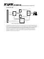
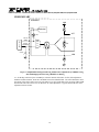
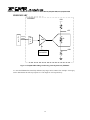
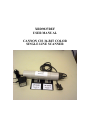
XRD9827REF
USER MANUAL
CANNON CIS 36-BIT COLOR
SINGLE LINE SCANNER
... the analog plus compa
TM
EXAR Corporation 48720 Kato Road, Fremont, CA 94538 Phone (510)-668-7000, Fax (510)-668-7030
PRELIMINARY
EVALUATION KIT PART LIST
This kit contains the following:
• XRD9827REF CIS 36-Bit Color Single Line Scanner
• XRD9827REF User Manual
• SenseIt 1.0 Software Installation Diskettes (2)
• XRD9827 Data Sheet
• Scan Targets (Black, White, Color)
FEATURES
•
•
•
•
•
One line scanning functionality of XRD9827 with CANON 600DPI CIS (Contact Image Sensor)
Easy to use with most personal computers through Parallel Port Interface
Simple way of loading the Serial Port of XRD9827 to adjust gain and offset
Software SenseIt 1.0 to view single line scan
Optimized PCB Layout with Four Layer
SYSTEM REQUIREMENTS
•
•
•
•
Intel 486 compatible computer with Windows 95 operating system
8 MBytes system memory
25-pin D-shape parallel port receptacles
3 1/2” floppy disk drive
INTRODUCTION
The XRD9827REF is a demo system which includes a PCB design with a CANON CVA-60216K 600DPI
Color Contact Image Sensor (CIS). It demonstrates how to interface a CIS with EXAR’s XRD9827, a 12bit Linear CIS/CCD Sensor Signal Processor to output a single line scan and display the amplitude of each
of the three colors. The XRD9827REF is designed to provide a signal path for the CIS output signals to be
processed, digitized by the XRD9827 and transmitted to a personal computer. There are no software
algorithms or hardware implementations, for example, gamma correction, to adjust for color response.
The XRD9827REF board is loaded with the XRD9827, a Vantis MACH435 CPLD, two FIFO SRAMs and
peripheral circuits for the CIS. The MACH435, which is a CMOS Programmable Logic Device (CPLD)
provides timing signals to the XRD9827, the SRAMs and the CIS. It also programs the XRD9827 to
operate in the correct mode and adjust for gain and offset values. The XRD9827 processes the analog
output from the CIS sensor, level-shifts and converts the signal into 12-bit digital codes. The SRAMs gate
the digitized data from the XRD9827 and stores the data temporarily. Controlled by the software, the
SRAMs send the data through a parallel port connection to the PC and histograms of raw data are
displayed in the monitor using the SenseIt software. A block diagram of the XRD9827REF is shown below
in Figure 1.
2
... the analog plus compa
TM
EXAR Corporation 48720 Kato Road, Fremont, CA 94538 Phone (510)-668-7000, Fax (510)-668-7030
PRELIMINARY
8-BIT DATA
FIFO
SRAM
CANON CVA-60216K 600DPI COLOR CIS
PARALLEL
PORT DB25
CONNECTOR
CIS OUTPUT
XRD9827
6-BIT BUS NIBBLE
DATA
CIS REFERENCE
VOLTAGE
INTEL 486 Compatible
FIFO
SRAM
8-BIT DATA
XRD9827 CONTROL SIGNALS
MACH435 CPLD
PARALLEL PORT CONTROL
CIS CONTROL SIGNALS
Figure 1. Block Diagram of XRD9827REF
The XRD9827 is a complete linear CIS or CCD sensor signal processor on a single monolithic chip. The
XRD9827 includes a high speed 12-Bit ADC, a 6-Bit Programmable Gain Amplifier with gain adjustment
of 1 to 10 and an 8-Bit programmable input referred offset calibration range of 800 mV. The XRD9827
also provides the necessary biasing voltage for the CANON CIS, eliminating the use of external
components (two diodes and two resistors). See the XRD9827EVAL User Manual / PCB board for
evaluating the XRD9827 CIS / CCD signal processor chip. A simplified functional block diagram of
XRD9827 is shown below for your reference.
3
... the analog plus compa
TM
EXAR Corporation 48720 Kato Road, Fremont, CA 94538 Phone (510)-668-7000, Fax (510)-668-7030
SYNCH
CLAMP
ADCCLK
AGND
AVDD
DGND
DB7:0
VREF+
TIMING &
CONTROL LOGIC
Power
Down
AGND
B
G
DC/AC
S/H
&
3-1
MUX
CLP
VRT
CIS
CCD
AGND
INT/EXT_VDCREF
_
VDCREF
BUFFER
+
Biasing Circuit for CANON
CIS
VBG
CIS/CCD
R
8-BIT OFFSET
REGISTERS
O<7:0>
8
8-BIT DAC
B
R
G
6-BIT GAIN
REGISTERS
6
PGA
G<5:0>
VRT
VRB
AVDD
RL12-BIT
ADC
Power
Down
12
DATA
I/O
PORT
8
DVDD
PRELIMINARY
VDCEXT
BLU
GRN
RED
CLAMP
Figure 2. Simplified Functional Block Diagram of XRD9827
OPERATIONAL PROCEDURE
The routine listed below will first calibrate the photo response of the CIS using the XRD9827 by optimize
its offset and gain. After calibration, the XRD9827REF can be used to scan any color target to show CIS
non-color corrected response. (Color correction is typically done in the digital ASIC.)
4
... the analog plus compa
TM
EXAR Corporation 48720 Kato Road, Fremont, CA 94538 Phone (510)-668-7000, Fax (510)-668-7030
PRELIMINARY
How to Run the XRD9827REF Demonstration
1.
2.
3.
4.
Make sure the computer is powered off and the AC power adapter is disconnected from a wall outlet
Connect the parallel port cable to the printer port of the computer
Connect the AC power adapter into a wall outlet
Turn on the computer and activate Windows 95
Loading EXAR Software
5.
6.
7.
8.
Load the diskette labeled SenseIt 1.0 Disk # 1 into the floppy drive
Select the Start menu in the program manager and choose RUN
Inside the small pop-up window, type: A:\setup
Follow the instructions to finish software installation
Parallel Port Configurations
9. Confirm the parallel port address as follows:
I.
Select the Start Menu, choose Settings, then choose Control Panel
II.
From the Control Panel window which pops up, double-click on System
III.
In the System Properties window, select Device Manager
IV.
From the Device Manager window, double-click on Ports (COM & LPT)
V.
Double-click on Printer Port (LPT1). If you can not find it, please goto Step 10
VI.
From the pop-up window, select Resources
VII.
Verify the Input/Output Range is set to 0378 - 037F
VIII.
If the range is not correct, clear the Use Automatic Settings check box by clicking it
IX.
Choose correct address which is 0378 by default and click OK
X.
Re-start the computer as advised
10. If you do not have a Printer Port configured on your computer, please follow the steps listed below:
I.
From the Control Panel window which pops up, double-click on Add New Hardware
II.
From the pop-up window, click the Next > button
III.
Select ‘No’ when prompted for ‘Do you want Windows to search for your new
hardware?’, then click the Next > button
IV.
Choose Ports (COM & LPT), then click the Next > button
V.
Choose Printer Port, then click the Next > button
VI.
Make a note of the Input/Output Range of Printer Port of your computer and click OK.
You will use these values later when configure the SenseIt software
VII.
Re-start the computer as advised
Offset Adjustment With a Black Target
11. Set the dip switches located on the side panel of the scanner to [110 01000000] as shown in Figure 3
and push the Serial Port button which is located on the front panel of the demo system. This will reset the
XRD9827.
5
... the analog plus compa
TM
EXAR Corporation 48720 Kato Road, Fremont, CA 94538 Phone (510)-668-7000, Fax (510)-668-7030
PRELIMINARY
S S S D D D D D D D D
2 1 0 7 6 5 4 3 2 1 0
1
0
Figure 3. Dip Switches Set to Value [110 01000000] to Reset XRD9827
12. Select the Start Menu, choose Programs, then choose SenseIt icon
13. A window will pop up as shown below. The upper window shows the plot of captured data and the
lower window shows the histogram of data. Figure 4 shows the pop-up window when SenseIt is first
started.
6
... the analog plus compa
TM
EXAR Corporation 48720 Kato Road, Fremont, CA 94538 Phone (510)-668-7000, Fax (510)-668-7030
PRELIMINARY
Figure 4. SenseIt Software Window Before Scanning
14. Select SETUP from the pull-down menu and choose I/O ADDRESS. In the window that pops up, type
in the Input/Output Range of Printer Port of your computer. The default setting is 378H.
15. Pick the black target out from the kit and put it on a flat area. Place the XRD9827REF on top of the
black target with the CIS sensor facing downwards. From the CAPTURE menu select SNAP SHOT (or
simply press CTRL and B buttons simultaneously) for a single line scan of the black target with the dip
switches set to [000 00000000]. A typical result of a black target scan is shown below:
7
... the analog plus compa
TM
EXAR Corporation 48720 Kato Road, Fremont, CA 94538 Phone (510)-668-7000, Fax (510)-668-7030
PRELIMINARY
Figure 5. Non-calibrated Black Target Scan
16. Set the dip switches to [110 00010000] to tie VDCREF and VDCEXT pin together internally. Push the
Serial Port button. The XRD9827 will subtract whatever voltage appears on VDCEXT (pin 16) from the
input and thus perform a global offset adjustment. A typical result of the global offset adjustment is shown
below. Please notice that the black code value has moved down.
8
... the analog plus compa
TM
EXAR Corporation 48720 Kato Road, Fremont, CA 94538 Phone (510)-668-7000, Fax (510)-668-7030
PRELIMINARY
Figure 6. Black Target Scan After Global Offset Adjust Using the 9827 Internal
Bandgap Reference Voltage
17. Then, set the dip switches to [111 00010000] and push the Serial Port button again. By doing this, a
1.24V reference voltage provided by an internal bandgap is applied to the VDCEXT pin. VDCEXT is
connected to VREF pin (Pin 5) of the CANON CIS, this voltage is used by the CIS as a biasing voltage.
Moreover, a 12K built-in resistor of the XRD9827 serves as a pull-down for the output of the CIS. By
interfacing the XRD9827 with a CANON CIS, a designer can save two biasing diodes and two resistors
and thus reduce cost.
9
... the analog plus compa
TM
EXAR Corporation 48720 Kato Road, Fremont, CA 94538 Phone (510)-668-7000, Fax (510)-668-7030
PRELIMINARY
XRD9827
1.24V
VDD
BANDGAP
VRT
12K
PIN 19
(RED)
C
I
S
PIN 16
(VDCEXT)
M
U
X
RL
2.2uF
VRB
Figure 7. Simplified Block Diagram Showing Global Offset Adjustment by XRD9827 Using
Internal Bandgap and CIS Using VDCEXT for Biasing
18. Set the dip switches to [001 01010000] to select the internal offset DAC for fine offset adjustment.
Push the Serial Port button. From the CAPTURE menu select SNAP SHOT. The offset should now move
the output of the CIS to almost zero scale. The other way to do a SNAP SHOT is by pressing CTRL and B
button at the same time. Please refer to data sheet for offset adjustment. A typical result of the fine offset
adjustment is shown below.
10
... the analog plus compa
TM
EXAR Corporation 48720 Kato Road, Fremont, CA 94538 Phone (510)-668-7000, Fax (510)-668-7030
PRELIMINARY
Figure 8. Black Target Scan After Global and Fine Adjustment
11
... the analog plus compa
TM
EXAR Corporation 48720 Kato Road, Fremont, CA 94538 Phone (510)-668-7000, Fax (510)-668-7030
PRELIMINARY
XRD9827
VDD
VRT
C
I
S
PIN 19
(RED)
M
U
X
RL
8-BIT
OFFSET
DAC
VRB
Figure 9. Simplified Block Diagram Showing Fine Offset Adjustment by XRD9827
19. Switch the black target to the enclosed white target. From the CAPTURE menu select SNAP SHOT
for a single line scan of the white target. A typical result of a white target is shown below.
12
... the analog plus compa
TM
EXAR Corporation 48720 Kato Road, Fremont, CA 94538 Phone (510)-668-7000, Fax (510)-668-7030
PRELIMINARY
Figure 10. White Target Scan Without Gain Adjustment
20. Set the dip switches to [000 00001000] to select the desired gain. Push the Serial Port button. From
the CAPTURE menu select SNAP SHOT. The gain should move the output of the CIS to almost full scale.
Please refer to data sheet for further gain adjustment and optimal values of dip switches for your scanner.
A typical result of the white target with gain adjustment is shown below.
13
... the analog plus compa
TM
EXAR Corporation 48720 Kato Road, Fremont, CA 94538 Phone (510)-668-7000, Fax (510)-668-7030
PRELIMINARY
Figure 11. White Target Scan After Gain Adjustment
14
... the analog plus compa
TM
EXAR Corporation 48720 Kato Road, Fremont, CA 94538 Phone (510)-668-7000, Fax (510)-668-7030
PRELIMINARY
XRD9827
VDD
VRT
C
I
S
PIN 19
(RED)
M
U
X
RL
PGA
6-BIT GAIN
REGISTER
VRB
Figure 12. Simplified Block Diagram Showing Gain Adjustment by XRD9827
21. Once the XRD9827 has been fully calibrated, any target can be scanned. For example: Scan a gray
scale to demonstrate the stair step response or a color target for color responsitivity.
15
... the analog plus compa
TM
EXAR Corporation 48720 Kato Road, Fremont, CA 94538 Phone (510)-668-7000, Fax (510)-668-7030
PRELIMINARY
Figure 13. Gray-scale Target Scan
22. To demonstrate the noise component is contributed from the CIS, we hooked up a DC reference to the
scanner and the results are shown below in Table 1.
REFERENCE DC (V)
STANDARD DEVIATION
SYSTEM SNR (dB) W/O CIS
NOISE COMPONENT
2.0
2.5
3.0
3.5
2.144328
3.48261
2.399188
1.983461
62.6117
58.3988
61.6356
63.28842
Table 1. Signal-to-Noise Ratio of the XRD9827REF with DC Source as Input (No CIS Noise
Component)
As we can see from Table 1, the SNR falls into the range of 58 dB to 63 dB when a DC reference is used
as input to the XRD9827REF. The system alone gives a 9 1/2 to 10 bit performance. The largest noise
source we saw in previous scans came from the CIS. A typical plot of the DC reference is shown in Figure
14.
16
... the analog plus compa
TM
EXAR Corporation 48720 Kato Road, Fremont, CA 94538 Phone (510)-668-7000, Fax (510)-668-7030
PRELIMINARY
Figure 14. Plot of 3.5V DC Source as Input to the XRD9827REF
Important:
1.
If at any time an unexpected result is shown or the demo system seems to not working, please pull
the AC adapter out from the wall outlet to cycle power. Start the procedures again from Step 11.
2.
Keep the scanner away from other electrical equipment, power cords, light dimmers, etc., as stray
electrical fields can end up in the digitized data.
3.
Switch off all unnesscessary light sources and place the scanner flat on the image, this can prevent
stray light from entering the sensor and disrupt the scan.
17
... the analog plus compa
TM
EXAR Corporation 48720 Kato Road, Fremont, CA 94538 Phone (510)-668-7000, Fax (510)-668-7030
PRELIMINARY
DVDD
U1
C1
C2
0.1uF
0.01uF
AVDD
15
C3
C4
1uF
0.1uF
CISOUT
VREF+
1
DVDD
10
DGND
AVDD
C6
0.1uF
0.01uF
14
AGND
AGND
DGND
C5
20
AGND
2
TP1
g t
1
19
18
17
AGND
16
VDCEXT
RED
GRN
BLU
9
8
7
6
5
4
3
2
DB7/LD
DB6/SDATA
DB5/SCLK
DB4
DB3
DB2
DB1
DB0
DB7/LD
DB6/SDATA
DB5/SCLK
DB4
DB3
DB2
DB1
DB0
11
12
VDCEXT ADCCLK
CLAMP
ADCCLK
13
SYNCH
SYNC
XRD9827
U2
1
AVDD
LM7805-5
OUT
GND
IN
C8
POWER SUPPLY
CIRCUITS
3
C9
DVDD
0.1uF
2
0.22uF
L1
JP1
1
2
1K
OPEN
AGND
10uH
GO TO LED ON THE
CASE OF SCANNER
HEADER 2
DGND
DGND
C32
C10
0.22uF
DGND
1
H:\PROJECT\ORCADWIN\9827\9827REFB.DSN
2
OPEN
IN
U3
C11
GND
POWERJACK
R3
L2
J1
0.47uF
OUT
DVDD
Title
XRD9827 REFERENCE BOARD
3
Size
B
LM7805-5
Date:
18
Document Number
XRD9827REF
Thursday, July 23, 1998
Rev
B
Sheet
1
of
3
... the analog plus compa
TM
EXAR Corporation 48720 Kato Road, Fremont, CA 94538 Phone (510)-668-7000, Fax (510)-668-7030
PRELIMINARY
U4
2
21
42
44
63
84
DVDD
77
S1
1
2
3
4
5
6
7
8
9
10
11
12
24
23
22
21
20
19
18
17
16
15
14
13
76
S2
S1
S0
D7
D6
D5
D4
D3
D2
D1
D0
R8
R9
R10
R11
R12
R13
R14
R15
R16
R17
R18
2.2K
2.2K
2.2K
2.2K
2.2K
2.2K
2.2K
2.2K
2.2K
2.2K
2.2K
75
73
72
71
70
69
SW DIP-12
R19
DGND
33
68
RCLK
67
ACK
R20
33
66
RST
65
62
61
D7
R21
DVDD
33
60
WCLK1
59
58
C14
C15
10uF
0.1uF 0.1uF
C16
C17
C18
C19
C20
0.01uF
0.01uF
0.01uF
0.01uF
57
D3
56
55
DGND
54
S1
52
DVDD
51
50
JP2
1
2
3
HEADER 3 DGND
49
SP_PB
48
47
D6
46
S0
R23
33
45
ADCCLK
41
IO60
IO2
IO59
IO3
IO58
IO4
IO57
IO5
IO56
IO6
IO55
IO7
IO54
IO8
IO53
IO9
IO52
IO10
IO51
IO11
IO50
IO12
IO49
IO13
MACH435
IO48
IO14
CLK3
IO15
CLK2
CLK0
IO47
CLK1
IO46
IO16
IO45
IO17
IO44
IO18
IO43
IO19
IO42
IO20
IO41
IO21
IO40
IO22
IO39
IO23
IO38
IO24
IO37
IO25
IO36
IO26
IO35
IO27
IO34
IO28
IO33
IO29
IO32
IO30
I1
1
78
IO1
11
DVDD
IO61
22
79
IO0
32
80
I2
IO62
43
WCLK2
IO63
DGND8
DGND7
DGND6
DGND5
DGND4
DGND3
DGND2
DGND1
81
53
33
64
R4
74
82
SYNC
DVDD6
DVDD5
DVDD4
DVDD3
DVDD2
DVDD1
MACH435
IO31
83
3 R5
33
4 R6
33
5 R7
33
6
DB5/SCLK
DB6/SDATA
DB7/LD
STROBE
7
8
S2
9
AUTOFD
10
12
13
14
15
D5
16
D1
17
DVDD
D4
U5
18
D2
19
4
D0
20
3
OUT
Oscillator
NC
GND
1
2
23
24
SP
25
26
C12
C13
1uF
0.1uF
WEN
27
DGND
28
29
30
31
33 R22
33
CISCLK
34
35
36
BLED
37
38
RLED
39
GLED
40
H:\PROJECT\ORCADWIN\9827\9827REFB.DSN
Title
Size
B
DGND
Date:
19
V+
XRD9827 REFERENCE BOARD
Document Number
XRD9827REF
Thursday, July 23, 1998
Rev
B
Sheet
2
of
3
... the analog plus compa
TM
EXAR Corporation 48720 Kato Road, Fremont, CA 94538 Phone (510)-668-7000, Fax (510)-668-7030
PRELIMINARY
U6
7
8
10
11
12
13
14
15
DB0
DB1
DB2
DB3
DB4
DB5/SCLK
DB6/SDATA
DB7/LD
DVDD
29
28
27
26
RS*
WEN1*
WCLK
WEN2*
WCLK2
24
23
22
21
20
19
18
17
16
LSB Q8
Q7
Q6
Q5
Q4
Q3
Q2
Q1
Q0
PAF*
PAE*
REN1*
RCLK
REN2*
OE*
EF*
FF*
DVDD
O7
O6
O5
O4
O3
O2
O1
O0
STROBE
J2
STROBE
O0
O1
O2
O3
O4
O5
O6
O7
9
GND
CY7C4261
30
31
32
1
2
3
4
5
6
DVDD
C21
0.1uF
7
8
10
11
12
13
C22
0.1uF
14
15
DGND
1
2
3
4
5
6
7
8
9
10
11
12
13
RCLK
U8
DGND
AVDD
D8
D7
D6
D5
D4
D3
D2
D1
D0
D8
D7
D6
D5
D4
D3
D2
D1
D0
25
DVDD
9
GND
ACK
O[7..0]
DGND
AVDD
CISOUT
C27
0.01uF
U7B
3
VDCEXT
4
R24
SPN
JP3
74HC04
U7C
5
6
R26
JP4
1
2
3
4
5
6
7
8
9
10
11
12
JUMPER
CISCLKN
R27
OPEN
300
BGND
9
3
74HC04
U7D
8
R28
2
10K
74HC04
U7E
11
10
R29
2
10K
74HC04
U7F
100uF
C29
0.1uF
C30
C33
47uF
47uF
CISOUT
MODE
GND (ANALOG)
VCC
VREF
SP
CISCLK
LED ANODE
BLED
GLED
RLED
GND (FRAME)
HEADER 12 TO CIS
DGND
AGND
3
RGND
12
7
100
100
100
C28
Q2
NPN_TO18
R30
2
1
13
C31
R33
R32
R34
R31
GGND
DVDD
14
Q1
NPN_TO18
3
SP
CISCLK
RLED
GLED
BLED
SP
CISCLK
RLED
GLED
BLED
R25
OPEN
1
2
3
300
AGND
1
C26
0.01uF
74HC04
O7
O6
O5
O4
O3
O2
O1
O0
1
C25
0.1uF
U7A
DGND
DVDD
C24
1uF
AUTOFD
INIT
RST
WEN
WCLK1
24
23
22
21
20
19
18
17
16
MSB Q8
Q7
Q6
Q5
Q4
Q3
Q2
Q1
Q0
PAF*
PAE*
REN1*
RCLK
REN2*
OE*
CY7C4261
C23
10uF
14
15
16
17
18
19
20
21
22
23
24
25
DB25
29
28
27
26
RS*
WEN1*
WCLK
WEN2*
EF*
FF*
AUTOFD
1
DGND
DVDD
25
2
30
31
32
1
2
3
4
5
6
10K
DGND
Q3
NPN_TO18
AGND
H:\PROJECT\ORCADWIN\9827\9827REFB.DSN
Title
74HC04
XRD9827 REFERENCE BOARD
0.1uF
Size
B
DGND
DGND
20
Date:
Document Number
XRD9827REF
Thursday, July 23, 1998
Rev
B
Sheet
3
of
3