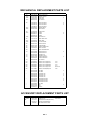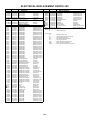
1
SERVICE MANUAL
19" WIDE TFT LCD TELEVISION WITH DIGITAL TUNER
HDLCD1909
All the specifications and features are subject to change without notice.
ORIGINAL
VERSION (B)
S/M CODE NO. M39A05WASM
DATE OF ISSUE 8/2009
IMPORTANT SERVICE SAFETY INFORMATION
Operating the receiver outside of its cabinet or with its
back removed involves a shock hazard. Work on
these models should only be performed by those who
are thoroughly familiar with precautions necessary
when working on high voltage equipment.
Before returning the receiver to the user, perform the
following safety checks:
1. Inspect all lead dress to make certain that leads are
not pinched or that hardware is not lodged between
the chassis and other metal parts in the receiver.
2. Replace all protective devices such as nonmetallic
control knobs, insulating fishpapers, cabinet backs,
adjustment and compartment covers or shields,
isolation resistor-capacitor networks, mechanical
insulators, etc.
3. To be sure that no shock hazard exists, a check for
the presence of leakage current should be made at
each exposed metal part having a return path to the
chassis (antenna, cabinet metal, screw heads,
knobs and/or shafts, escutcheon, etc.) in the
following manner.
Exercise care when servicing this chassis with power
applied. Many B plus and high voltage RF terminals are
exposed which, if carelessly contacted, can cause
serious shock or result in damage to the chassis.
Maintain interconnecting ground lead connections
between chassis, escutcheon, picture tube dag and
tuner cluster when operating the chassis.
These receivers have a "polarized" AC line cord. The AC
plug is designed to fit into standard AC outlets in one
direction only. The wide blade connects to the "ground
side" and the narrow blade connects to the "hot side" of
the AC line. This assures that the TV receiver is properly
grounded to the house wiring. If an extension cord must
be used, make sure it is of the "polarized" type.
Plug the AC line cord directly into a 120V AC receptacle.
(Do not use an Isolation Transformer during these
checks.) All checks must be repeated with the AC line
cord plug connection reversed. (If necessary, a
nonpolarized adapter plug must be used only for the
purpose of completing these checks.)
Since the chassis of this receiver is connected to one
side of the AC supply during operation, service should
not be attempted by anyone not familiar with the
precautions necessary when working on these types
of equipment.
If available, measure current using an accurate leakage
current tester. Any reading of 0.35mA or more is
excessive and indicates a potential shock hazard which
must be corrected before returning the receiver to the
owner.
When it is necessary to make measurements or tests with
AC power applied to the receiver chassis, an Isolation
Transformer must be used as a safety precaution and to
prevent possible damage to transistors. The Isolation
Transformer should be connected between the TV line
cord plug and the AC power outlet.
If a reliable leakage current tester is not available, this
alternate method of measurement should be used.
Using two clip leads, connect a 1500 ohm, 10 watt
resistor paralleled by a 0.15µF capacitor in series with
a known earth ground, such as a water pipe or conduit
and the metal part to be checked. Use a VTVM or
VOM with 1000 ohms per volt, or higher, sensitivity to
measure this AC voltage drop across the resistor. Any
reading of 0.35 volt RMS or more is excessive and
indicates a potential shock hazard which must be
corrected before returning the receiver to the owner.
When removing springs or spring mounted parts from the
tuner, tuner cluster or chassis, shatterproof goggles must
be worn. Keep others without shatterproof goggles away.
VT VM
AC SCALE
0.15K OHMS
10W
TO EXPOSED
METAL PARTS
A1-1
10µF
TEST PROBE
TO KNOWN
EARTH GROUND
ABOUT LEAD FREE SOLDER (PbF)
Distinction of PbF PCB:
PCBs (manufactured) using lead free solder will have a PbF printing on the PCB.
(Please refer to figures.)
Caution:
• Pb free solder has a higher melting point than standard solder;
Typically the melting point is 86oF~104oF(30oC~40oC) higher.
Please use a soldering iron with temperature control and adjust it to 650oF ± 20oF (350oC ± 10oC).
In case of using high temperature soldering iron, please be careful not to heat too long.
• Pb free solder will tend to splash when heated too high (about 1100oF/ 600oC).
• All products with the printed circuit board with PbF printing must be serviced with lead free solder.
When soldering or unsoldering, completely remove all of the solder from the pins or solder area,
and be sure to heat the soldering points with the lead free solder until it melts sufficiently.
Recommendations
Recommended lead free solder composition is Sn-3.0Ag-0.5Cu.
A1-2
TABLE OF CONTENTS
IMPORTANT.................................................................................................................................... A1-1
ABOUT LEAD FREE SOLDER (PbF)............................................................................................. A1-2
TABLE OF CONTENTS................................................................................................................... A2-1
GENERAL SPECIFICATIONS......................................................................................................... A3-1~A3-5
DISASSEMBLY INSTRUCTIONS
1. REMOVAL OF MECHANICAL PARTS AND P. C. BOARDS................................................. B1-1, B1-2
2. REMOVAL AND INSTALLATION OF FLAT PACKAGE IC.....................................................B2-1, B2-2
SERVICE MODE LIST..................................................................................................................... C-1
WHEN REPLACING EEPROM (MEMORY) IC................................................................................ C-2
CONFIRMATION OF INITIAL DATA............................................................................................... C-2
ELECTRICAL ADJUSTMENTS....................................................................................................... D-1~D-6
TROUBLESHOOTING GUIDE......................................................................................................... E-1~E-4
IC DESCRIPTION............................................................................................................................ F-1~F-6
SEMICONDUCTOR BASE CONNECTIONS................................................................................... G-1
BLOCK DIAGRAMS
POWER/SOUND AMP ............................................................................................................... H-1, H-2
SIGNAL (DIGITAL PCB).............................................................................................................. H-3, H-4
POWER(DIGITAL PCB).............................................................................................................. H-5, H-6
PRINTED CIRCUIT BOARDS
DIGITAL ...................................................................................................................................... I-1~I-4
POWER/OPERATION/REMOCON............................................................................................. I-5~I-8
SCHEMATIC DIAGRAMS
FLASH......................................................................................................................................... J-1, J-2
DDR............................................................................................................................................. J-3, J-4
HDMI............................................................................................................................................ J-5, J-6
LVDS........................................................................................................................................... J-7, J-8
SCALER...................................................................................................................................... J-9, J-10
SCALER POWER........................................................................................................................ J-11, J-12
TUNER........................................................................................................................................ J-13, J-14
SCALER VIDEO/AUDIO ............................................................................................................. J-15, J-16
JACK............................................................................................................................................ J-17, J-18
AV SWITCH................................................................................................................................. J-19, J-20
REGULATOR.............................................................................................................................. J-21, J-22
POWER....................................................................................................................................... J-23, J-24
BACKLIGHT INVERTER............................................................................................................. J-25, J-26
SOUND AMP............................................................................................................................... J-27, J-28
JACK OUT................................................................................................................................... J-29, J-30
INTERCONNECTION DIAGRAM..................................................................................................... J-31, J-32
WAVEFORMS.................................................................................................................................. K-1
MECHANICAL EXPLODED VIEWS................................................................................................ L-1, L-2
MECHANICAL REPLACEMENT PARTS LIST............................................................................... M1-1
ACCESSORY REPLACEMENT PARTS LIST................................................................................. M1-1
ELECTRICAL REPLACEMENT PARTS LIST................................................................................ M2-1~M2-5
A2-1
GENERAL SPECIFICATIONS
G-1
TV
System
LCD
LCD Size / Visual Size
LCD Type
Number of Pixels
View Range
Left/Right
Up/Down
Bright Dot
Zero Bright Dot Ratio
Color System
Speaker
Sound Output
G-2
Tuning
System
Broadcasting System
Tuner and
Receive CH
CH Coverage
Intermediate Digital
Frequency Analog
G-3
Signal
Power
Picture(FP)
Sound(FS)
FP-FS
Preset CH
Stereo/Dual TV Sound
Tuner Sound Muting
Video Signal
Input Level
Output Level
S/N Ratio (Weighted)
Horizontal Resolution at DVD Mode
RGB Signal
Audio Signal
G-4
Position
Size
Impedance
Max
10%(Typical)
Analog
Digital
System
Destination
Power Source
Power Consumption
Protector
Output Level
Input Level
Output Level
Digital Output Level
S/N Ratio at DVD (Weighted)
Harmonic Distortion
Frequency Response :
at DVD
at Video CD
at SVCD
at CD
AC
DC
at AC
at DC
Stand by (at AC)
Energy Star
Per Year
Power Fuse
Safety Circuit
IC Protector(Micro Fuse)
Safety
Radiation
Laser
Operation
Storage
Space Around Unit
G-5
Regulation
G-6
Temperature
G-7
G-8
Operating Humidity
Clock and
Clock
Timer
Sleep Timer
Max Time
On Timer
Program
Off Timer
Program
Game Timer
Wake Up Timer
Timer Back-up (at Power Off Mode)
Remote
Unit
Control
Glow in Dark Remocon
Remocon Format
Format
Custom Code
Power Source
Voltage(D.C)
UM size x pcs
Total Keys
Keys
Power
1
2
G-9
at DVD
at TV
more than
A3-1
18.50 inch / 470.1mmV
Color TFT LCD
1366(H) x 768(V)
85/85 degree
80/80 degree
<
n=3
70%
NTSC
2 Speaker
Front
1.0 x 2.7 inch
8 ohm
1.0W + 1.0W
--US System M
ATSC(8VSB)/QAM
1Tuner
US (W/CABLE)
2~69, 4A, A-5~A-1, A~I, J~W, W+1~W+94
44.00MHz
45.75MHz
41.25MHz
4.50MHz
No
US-Stereo
Yes
1 V p-p/75 ohm
------8.0dBm/50k ohm
---0.5 V p-p/75 ohm
------120V, 60Hz
-29W at 120V 60Hz
-0.8W at 120V 60Hz
Yes
-- kWh/Year
Yes
Yes
Yes
UL(UL60065_7th)
FCC
-o
o
+5 C ~ +40 C
o
o
-20 C ~ +60 C
10cm (4inch)
Less than 80% RH
No
120 Min
No
No
No
No
-Min
Sec
RC-RC
No
ORION
NEC
86-05 h
3V
UM-4 x 2 pcs
27 Keys
Yes
Yes
Yes
GENERAL SPECIFICATIONS
3
4
5
6
7
8
9
0
Recall (Quick View)
Sleep
Mute
CH+ / Up
CH- / Down
VOL+ / Right
VOL- / Left
Menu
Reset
Exit
Enter
Input Select
CCD (Closed Caption)
Display
Zoom (Picture Size)
FAV +
FAV Audio
G-10
Features
Yes
Yes
Yes
Yes
Yes
Yes
Yes
Yes
Yes
Yes
Yes
Yes
Yes
Yes
Yes
Yes
Yes
No
Yes
Yes
Yes
Yes
Yes
Yes
No
No
Yes
Yes
Auto Shut Off
Auto Search
Power On Memory
Comb Filter
No
Yes
Yes
3 -D
Game Position
Auto Setup(Language/CH Program)
Picture Setting(TV)
Picture Preference
Brightness , Contrast , Color
Tint
Sharpness
Color Temperature
DNR
Backlight
Picture Setting(PC)
HOR Position , VER Position
Phase, Clock
Red, Green, Blue
Auto Adjust
Audio
MTS
Tone Control (Bass/Treble/Balance)
Stable Sound
Surround
BBE
SRS WOW (SRS 3D/Focus/Tru Bass)
Variable Audio Out
Tuning
CH Program
Air/Cable
ADD/DELETE
Label
CH Label
Video Label
Favorite CH
V-Chip
Type
RRT Setup
Lock
Hotel Lock
Channel Lock
Video Lock
Panel Lock
Menu Language
DBC (Dynamic Backlight Control)
Signal Meter (DTV Signal)
Closed Caption
CC Advanced
V-Chip Clear
Picture Size
HD Zoom
Film Mode
Aspect
PFC(Power Factor circuit)
A3-2
No
Yes
Yes
Yes
Yes
Yes
Yes
Yes
Yes
Yes
Yes
Yes
Yes
No
Yes
Yes
Yes
No
Yes
No
No
No
Yes
Yes
Yes
Yes
Yes
No
Yes
USA Type
Yes
No
No
No
No
English
No
Yes
Yes
Yes
Yes
Yes
Yes
Yes
No
No
GENERAL SPECIFICATIONS
Freeze frame
PIP/POP
Direct Input Selection
Digital Out
No
No
Yes
Yes
Dolby Digital
MPEG
PCM
DTS
No
Yes
No
Yes
Yes (60,72,75Hz)
Yes (70Hz)
No
Yes (56,60,72,75Hz)
Yes (60,70,75Hz)
Yes (60Hz)
Yes (60Hz)
Yes (60Hz)
No
No
No
No
No
No
No
No
No
No
No
No
No
No
No
No
No
No
No
No
No
No
No
No
No
No
Yes
Yes (60Hz)
Yes (60Hz)
Yes (60Hz)
Yes (60Hz)
No
No
No
No
Yes (60Hz)
Yes (60Hz)
No
Yes (100 x 100)
M4 x 10
No
No
English
Yes
Yes
No
--No
-No
No
No
No
No
No
No
No
No
No
Yes
UM-4 x 2 pcs
PC Monitor Input
VGA (640x480)
VGA (720x400)
WVGA (848x480)
SVGA (800x600)
XGA (1024x768)
WXGA (1280x768)
WXGA (1280x720)
WXGA (1360x768)
SXGA (1280x1024)
HDMI Input
DVI to HDMI Input
VGA (640×480)
720×480i (4:3)
720×480i (16:9)
720×480p (4:3)
720×480p (16:9)
720×576i (4:3)
720×576i (16:9)
720×576p (4:3)
720×576p (16:9)
1280×720p
1920×1080i
1920×1080p
CEC (ORION Standard)
Deep Color
xvYCC
VGA (640x480)
VGA (720x400)
WVGA (848x480)
SVGA (800x600)
XGA (1024x768)
WXGA (1280x768)
WXGA (1280x720)
WXGA (1360x768)
SXGA (1280x1024)
Component Input
Wall Mount
Stand
G-11
Accessories
Owner's Manual
720×480i (4:3)
720×480i (16:9)
720×480p (4:3)
720×480p (16:9)
720×576i (4:3)
720×576i (16:9)
720×576p (4:3)
720×576p (16:9)
1280×720p
1920×1080i
1920×1080p
Size W x H(mm)
Screw Size
Tilt
Swievel
Language
w/Guarantee Card
Remote Control Unit
Rod Antenna
Poles
Terminal
Loop Antenna
Terminal
U/V Mixer
DC Car Cord (Center+)
Guarantee Card
Warning Sheet
Circuit Diagram
Antenna Change Plug
Service Facility List
Important Safeguard
Dew/AHC Caution Sheet
Quick Set-up Sheet
Battery
UM size x pcs
A3-3
GENERAL SPECIFICATIONS
G-12
Interface
G-13
Set Size
G-14
Weight
G-15
Carton
OEM Brand
AC Adapter
AC Cord (for AC Adapter)
AC Cord
AV Cord (2Pin-1Pin)
Registration Card (NDL Card)
300 to 75ohm Antenna Adapter
Sheet Information (FCC)
Sheet Information (Return)
Sheet Information (HDMI)
Stand
Stand Screw???
Switch
Side
Power (Tact)
Channel Up/Menu Up
Channel Down/Menu Down
Volume Up/Menu >
Volume Down/Menu <
Menu
Play
Eject
Skip+, Search+
Skip-, SearchStill/Pause
Stop
Main Power SW
Input Select/Enter
Rear
Main Power SW
Indicator
Stand-By
Power Wake Up
On Timer
Terminals
Rear
Video Input 1
Audio Input 1
S - Input 1
Video Input 2
Audio Input 2
S - Input 2
Video Output
Audio Output
Component Input 1
Analog Audio
Component Input 2
Analog Audio
HDMI Input 1
Analog Audio
HDMI Input 2
Analog Audio
Sub Woofer Out
PC Monitor Input
Analog Audio
Digital Audio Output
DC Jack (Center +)
VHF/UHF Antenna Input
Video Input 3
Audio Input 3
S - Input 3
Other Terminal
AC Inlet
Approx. W x D x H (mm)
w/o Handle, Stand Approx. W x D x H (mm)
Net (Approx.)
Net w/o Handle, Stand (Approx.)
Gross (Approx.)
Gross w/Master Carton (Approx.)
Master Carton
Content
Material
Dimensions
W x D x H(mm)
Description of Origin
Gift Box Material
W/Color Photo Label
W/Handle
Dimensions
W x D x H(mm)
Description of Origin
Drop Test
Height (cm)
Container Stuffing (40' container)
w/Pallet
w/Wrapping
A3-4
No
No
No
Yes
No
No
No
No
Yes
No
Yes
Yes (2pcs)
Yes
Yes
Yes
Yes
Yes
Yes
No
No
No
No
No
No
No
Yes
No
Yes (Red)
No
No
RCA x 1
RCA x 2(L/MONO, R)
Yes
No
No
No
No
No
RCA x 3
RCA x 2(L/MONO, R)
No
No
No
No
No
No
No
Yes
Mini Pin Jack( 3.5), STEREO
Coaxial
No
F Type
No
No
No
No
Yes
472 x 174 x 362
472 x 64 x 328
3.8kg
(8.4lbs)
3.5kg
(7.7lbs)
5.0kg
(11.1lbs)
--- kg
( --- lbs)
No
--- Sets
--- / ------Single/White
No
No
542 x 426 x 147
Yes
1 Corner / 3 Edges / 6 Surfaces
80
1852 Sets/40' container
No
No
GENERAL SPECIFICATIONS
G-16
Material
G-17
Environment
Cabinet
Front
Rear
Jack Panel
PCB
Non-Halogen Demand
Eyelet Demand
Environmental standard requirement
Pb-free
Measures for Whisker
A3-5
PS 94V0 NON-DECABROM
PS 94V0 NON-DECABROM
-No
Yes
Green procurement of ORION
Phase3(Phase3A)
Yes
DISASSEMBLY INSTRUCTIONS
1. REMOVAL OF MECHANICAL PARTS
AND P.C. BOARDS
1-3: FRONT CABI ASS'Y and LCD PANEL
(Refer to Fig. 1-3)
1. Turn up set and put the Front Cabi Ass'y of LCD
on the top.
2. Remove the Front Cabi Ass'y in the direction of
arrow (A).
3. Disconnect the following connector: (CD2801).
4. Remove the LCD Panel in the direction of arrow (B).
CAUTION
Be careful not to remove the LVDS cable forcibly, because
the LVDS cable may be damaged.
1-1: STAND ASS'Y (Refer to Fig. 1-1)
1. Remove the 2 screws (1).
2. Remove the Stand Ass'y in the direction of arrow.
(1)
(1)
(A)
Front Cabi Ass'y
Stand Ass'y
Fig. 1-1
11
1-2: COVER INVERTER (Refer to Fig. 1-2)
1. Remove the screw (1).
2. Remove the Cover Inverter in the direction of arrow.
3. Disconnect the following connectors:
(CP7001 and CP7002).
4. Remove the 2 screws (2)
5. Remove the 6 screws (3)
CD2801
(LVDS Cable)
(1)
Cover Inverter
(3)
(2)
(3)
(2)
(3)
(3)
(3)
LCD Panel
(3)
(B)
Fig. 1-2
Back Cabi Ass'y
Fig. 1-3
B1-1
DISASSEMBLY INSTRUCTIONS
1-4: DIGITAL PCB (Refer to Fig. 1-5)
1-5: POWER PCB, REMOCON PCB and OPERATION PCB
(Refer to Fig. 1-5)
1.
2.
3.
4.
5.
6.
Remove the 2 screws (1).
Remove the Holder LCD in the direction of arrow (A).
Remove the 2 screws (2).
Remove the Holder LVDS-3 in the direction of arrow (B).
Remove the 2 screws (3).
Disconnect the following connectors:
(CP501, CP2201 and CP8101).
7. Remove the Digital PCB in the direction of arrow (C).
1.
2.
3.
4.
5.
6.
7.
8.
9.
(1)
Disconnect the following connector: (CP7601).
Remove the 7 screws (1).
Remove the Power PCB in the direction of arrow (A).
Remove the screw (2).
Remove the Remocon PCB in the direction of arrow (B).
Push 9 supports (3).
Remove the Panel Side Ass'y in the direction of arrow (C).
Remove the 2 screws (4).
Remove the Operation PCB in the direction of arrow (D).
(1)
Holder LCD
(1)
(2) (2)
(1)
(1)
(1)
Holder LVDS-3
(3)
(B)
Digital PCB
(1)
(1)
(A)
(1)
(3)
(2)
Remocon PCB
Power PCB
(C)
(A)
(B)
C
Ass'y
Back Cabi
Fig. 1-4
Back Cabi Ass'y
(C)
(4)
(4)
Operation PCB
(D)
Panel Side Ass'y
(3)
(3)
Fig. 1-5
B1-2
DISASSEMBLY INSTRUCTIONS
2. REMOVAL AND INSTALLATION OF
FLAT PACKAGE IC
3. When IC starts moving back and forth easily after
desoldering completely, pickup the corner of the IC using
tweezers and remove the IC by moving with the IC
desoldering machine. (Refer to Fig. 2-3.)
REMOVAL
1. Put Masking Tape (cotton tape) around the Flat Package
IC to protect other parts from any damage.
(Refer to Fig. 2-1.)
NOTE
Some ICs on the PCB are affixed with glue, so be
careful not to break or damage the foil of each IC
leads or solder lands under the IC when removing it.
NOTE
Masking is carried out on all the parts located within
10 mm distance from IC leads.
Masking Tape
(Cotton Tape)
Blower type IC
desoldering machine
IC
Tweezers
Fig. 2-1
2. Heat the IC leads using a blower type IC desoldering
machine. (Refer to Fig. 2-2.)
IC
Fig. 2-3
NOTE
Do not rotate or move the IC back and forth , until IC
can move back and forth easily after desoldering the
leads completely.
4. Peel off the Masking Tape.
5. Absorb the solder left on the pattern using the Braided
Shield Wire. (Refer to Fig. 2-4.)
Blower type IC
desoldering machine
NOTE
Do not move the Braided Shield Wire in the vertical
direction towards the IC pattern.
Braided Shield Wire
Soldering Iron
IC
Fig. 2-2
IC pattern
Fig. 2-4
B2-1
DISASSEMBLY INSTRUCTIONS
INSTALLATION
4. When bridge-soldering between terminals and/or the
soldering amount are not enough, resolder using a
Thintip Soldering Iron. (Refer to Fig. 2-8.)
1. Take care of the polarity of new IC and then install the
new IC fitting on the printed circuit pattern. Then solder
each lead on the diagonal positions of IC temporarily.
(Refer to Fig. 2-5.)
Thin-tip Soldering Iron
IC
Soldering Iron
Fig. 2-8
Solder temporarily
5. Finally, confirm the soldering status on four sides of the
IC using a magnifying glass.
Confirm that no abnormality is found on the soldering
position and installation position of the parts around the
IC. If some abnormality is found, correct by resoldering.
Solder temporarily
Fig. 2-5
NOTE
2. Supply the solder from the upper position of IC leads
sliding to the lower position of the IC leads.
(Refer to Fig. 2-6.)
When the IC leads are bent during soldering and/or
repairing, do not repair the bending of leads. If the
bending of leads are repaired, the pattern may be
damaged. So, always be sure to replace the IC in this
case.
Solder
Soldering Iron
IC
Supply soldering
from upper position
to lower position
Fig. 2-6
3. Absorb the solder left on the lead using the Braided
Shield Wire. (Refer to Fig. 2-7.)
NOTE
Do not absorb the solder to excess.
Soldering Iron
IC
Braided Shield Wire
Fig. 2-7
B2-2
SERVICE MODE LIST
This unit is provided with the following SERVICE MODES so you can repair, examine and adjust easily.
To enter to the SERVICE MODE function, press and hold both buttons simultaneously on the main unit and on the remote
control for more than a the standard time in the appropriate condition. (See below chart.)
Set
Condition
Set Key
Remocon
Key
Standard
Time
POWER ON
VOL. DOWN
(Minimum)
0
2 sec.
Releasing of V-CHIP PASSWORD.
POWER ON
VOL. DOWN
(Minimum)
1
2 sec.
Initialization of factory TV data.
NOTE: If you set factory initialization, the memories are reset such
as the channel setting, and the POWER ON total hours.
POWER ON
VOL. DOWN
(Minimum)
6
2 sec.
Can be checked of the INITIAL DATA of MEMORY IC.
Refer to the "WHEN REPLACING EEPROM (MEMORY) IC".
POWER ON
VOL. DOWN
(Minimum)
8
2 sec.
Check of the SUM DATA and MICON VERSION on the screen.
Refer to the "WHEN REPLACING EEPROM (MEMORY) IC".
POWER ON
VOL. DOWN
(Minimum)
9
2 sec.
Display of the Adjustment MENU on the screen.
Refer to the "ELECTRICAL ADJUSTMENT"
(On-Screen Display Adjustment).
Operations
C-1
WHEN REPLACING EEPROM (MEMORY) IC
CONFIRMATION OF CHECK SUM, POWER ON TOTAL HOURS AND MICON VERSION
Initial total of MEMORY IC, POWER ON total hours and MICON VERSION can be checked on the screen. Total hours are
displayed in 16 system of notation.
NOTE: If you set a factory initialization, the total hours is reset to "0".
Please refer to "CONFIRMATION OF INITIAL DATA" when SUM DATA is not corresponding.
1. Turn on the POWER,, and set to the ALL mode.
2. Set the VOLUME to minimum.
3. Press both VOL. DOWN button on the set and Channel button (8) on the remote control for more than 2 seconds.
4. After the confirmation of each check sum, turn off the power.
NOTE: The each item value might be different according to each set.
CHECK SUM : 504A
Initial setting data check sum.
LCD PWR ON : 0000
POWER ON total hours.
= (16 x 16 x 16 x thousands digit value)
+ (16 x 16 x hundreds digit value)
Main Micon check Version.
EEPROM check Version.
DTV : CA06I96182
+ (16 x tens digit value)
EEPROM : K39A05WM00
+ (ones digit value)
Parameter check Picture Quality.
QUALITY :
@@@@.@@ (@@@@@@
@@:@@:@@)
Parameter check Picture Size.
SCALING :
@@@@.@@ (@@@@@@
@@:@@:@@)
FIG. 1
CONFIRMATION OF INITIAL DATA
If a service repair is undertaken where it has been required to change the MEMORY IC, the following steps should be taken
to ensure correct data settings while making reference to INITIAL SETTING TABLE (Attached "INITIAL DATA").
1. Turn on the POWER, and set to the ALL mode.
2. Set the VOLUME to minimum.
3. Press both VOL. DOWN button on the set and Channel button (6) on the remote control for more than 2 seconds.
ADDRESS and DATA should appear as FIG 2.
NOTE: No need to set data other position than 0D00~0EFF.
ADDRESS
INIT :
0001
DATA
0090
DTV : CA06I96182
EEPROM : K39A05WM00
FIG. 2
4. ADDRESS is now selected and should "blink". Using the CH. UP/DOWN buton on the remote, step through the ADDRESS
until required ADDRESS to be changed is reached.
5. Press VOL. UP/DOWN button to select DATA. When DATA is selected, it will "blink".
6 Again
6.
Again, step through the DATA using CH
CH. UP/DOWN button until required DATA value has been selected
selected.
7. Pressing VOL. UP/DOWN button will take you back to ADDRESS for further selection if necessary.
8. Repeat steps 4 to 6 until all data has been checked.
9. When satisfied correct DATA has been entered, turn POWER off (return to STANDBY MODE) to finish DATA input.
After the data input, set to the initializing of shipping.
10. Turn on the Power.
11. Set the VOLUME to minimum.
12. Press both VOL. DOWN button on the set and Channel button (1) on the remote control for more than 2 seconds.
13. After the finishing of the initializing of shipping, the unit will turn off automatically.
The unit will now have the correct DATA for the new MEMORY IC.
C-2
ELECTRICAL ADJUSTMENTS
1. ADJUSTMENT PROCEDURE
NO.
03
04
05
06
07
08
09
10
11
12
13
14
15
16
17
18
19
20
29
30
31
32
33
Read and perform these adjustments when repairing the
circuits or replacing electrical parts or PCB assemblies.
CAUTION
• Use an isolation transformer when performing any
service on this chassis.
• When removing a PCB or related component, after
unfastening or changing a wire, be sure to put the wire
back in its original position.
• When you exchange IC and Transistor with a heat sink,
apply silicon grease(YG6260M) on the contact section of
the heat sink. Before applying new silicon grease, remove
all the old silicon grease. (Old grease may cause damage
to the IC and Transistor).
Prepare the following measurement tools for electrical
adjustments.
1. Pattern Generator
On-Screen Display Adjustment
1. Set the VOLUME to minimum.
2. Press the VOL. DOWN button on the set and the
channel button (9) on the remote control for more than
2 seconds to display adjustment mode on the screen as
shown in Fig. 1-1.
FUNCTION
R DRIVE(N)
R CUTOFF(N)
G DRIVE(N)
G CUTOFF(N)
B DRIVE(N)
B CUTOFF(N)
R DRIVE(C)
R CUTOFF(C)
G DRIVE(C)
G CUTOFF(C)
B DRIVE(C)
B CUTOFF(C)
R DRIVE(W)
R CUTOFF(W)
G DRIVE(W)
G CUTOFF(W)
B DRIVE(W)
B CUTOFF(W)
BAK LIGHT CENT
BAK LIGHT MAX
BAK LIGHT MIN
BRIGHTNESS CENT
BRIGHTNESS MAX
NO.
34
35
36
37
38
39
40
41
42
43
44
45
46
47
48
49
50
51
52
53
54
55
58
FUNCTION
BRIGHTNESS MIN
TINT
SHARP H1 MAX
SHARP H1 MIN
SHARP H2 MAX
SHARP H2 MIN
SHARP H3 MAX
SHARP H3 MIN
SHARP H4 MAX
SHARP H4 MIN
SHARP H5 MAX
SHARP H5 MIN
SHARP V1 MAX
SHARP V1 MIN
SHARP V2 MAX
SHARP V2 MIN
CONTRAST CENTER
CONTRAST MAX
CONTRAST MIN
COLOR CENTER
COLOR MAX
COLOR MIN
CONTRAST 40
Fig. 1-2
2. BASIC ADJUSTMENTS
2-1: WHITE BALANCE
TV
FULL
Function
03 R DRIVE(N)
15
Step No.
Fig. 1-1
3. Use the CH UP/DOWN button or Channel button (0-9)
on the remote control to select the options shown in
Fig. 1-2.
4. Press the MENU button on the remote control to end
the adjustments.
5. To display the adjustment screen for TV, AV,COMPONENT
HDMI and PC mode, press the INPUT SELECT button on
the remote control.
6. Receive the DIGITAL broadcasting.
7. To display the adjustment screen fo DTV mode, select
the digital channel.
8. Press the VOL.DOWN buttom on the set and the channel
(9) on the remote control for more than 2 seconds.
1. Place the set in Aging Test for more than 30 minutes.
2. Receive the gray scale pattern from the Pattern
Generator.
3. Press the INPUT SELECT button on the remote control
to set to the AV mode.
4. Using the remote control, set the brightness and contrast
to normal position.
5. Activate the adjustment mode display of Fig. 1-1 and
press the channel button (03) on the remote control to
select"R DRIVE (N)".
6. Press the UP/DOWN button on the remote control to
select the "R CUTOFF (N)", "G DRIVE (N)",
G CUTOFF (N), "B DRIVE (N)", "B CUTOFF (N)",
R DRIVE (C), "R CUTOFF (C)", "G DRIVE (C)",
G CUTOFF (C), "B DRIVE (C)", "B CUTOFF (C)",
R DRIVE (W), "R CUTOFF (W)", "G DRIVE (W)",
G CUTOFF (W), "B DRIVE (W)" or "B CUTOFF (W)".
7. Adjust the LEF/RIGHT button on the remote control to
whiten the R CUTOFF (N), G DRIVE (N),
G CUTOFF (N), B DRIVE (N), B CUTOFF (N),
R DRIVE (C), R CUTOFF (C), G DRIVE (C),
G CUTOFF (C), B DRIVE (C), B CUTOFF (C),
R DRIVE (W), R CUTOFF (W), G DRIVE (W),
G CUTOFF (W), B DRIVE (W) and B CUTOFF (W)
at each step tone sections equally.
8. Perform the above adjustments 6 and 7 until the white
color is achieved.
D-1
ELECTRICAL ADJUSTMENTS
2-2: BRIGHTNESS CENT
2-3: CONTRAST MAX
1. Receive the color bar pattern. (RF Input)
2. Using the remote control, set the brightness and contrast
to normal position.
3. Activate the adjustment mode display of Fig. 1-1 and
press the channel button (32) on the remote control to
select "BRIGHTNESS CENT".
4. Press the VOL.UP/DOWN button on the remote control until
the contrast step No. becomes "130".
5. Check if the picture is normal.
6. Receive the color bar pattern. (VIDEO Input)
7. Press the INPUT SELECT button on the remote control
to set to the AV mode.
8. Using the remote control, set the brightness and contrast
to normal position.
9. Activate the adjustment mode display of Fig. 1-1 and
press the channel button (32) on the remote control to
select "BRIGHTNESS CENT".
10. Press the VOL.UP/DOWN button on the remote control until
the contrast step No. becomes "131".
11. Check if the picture is normal.
12. Receive the color bar pattern. (S-VIDEO Input)
13. Press the INPUT SELECT button on the remote control
to set to the AV(S) mode.
14. Using the remote control, set the brightness and contrast
to normal position.
15. Activate the adjustment mode display of Fig. 1-1 and
press the channel button (32) on the remote control to
select "BRIGHTNESS CENT".
16. Press the VOL.UP/DOWN button on the remote control until
the contrast step No
No. becomes "131"
131 .
17. Check if the picture is normal.
18. Playback the DVD(480i) disc. (COMPONENT Input)
19. Press the INPUT SELECT button on the remote control
to set to the COMPONENT mode.
20. Using the remote control, set the brightness and contrast
to normal position.
21. Activate the adjustment mode display of Fig. 1-1 and
press the channel button (32) on the remote control to
select "BRIGHTNESS CENT".
22. Press the VOL.UP/DOWN button on the remote control until
the contrast step No. becomes "132".
23. Check if the picture is normal.
24. Playback the DVD(480p) disc. (COMPONENT Input)
25. Press the INPUT button on the remote control
to set to the COMPONENT mode. Then perform the above
adjustments 20~23.
26. Playback the DVD(720p) disc. (COMPONENT Input)
27. Press the INPUT button on the remote control
to set to the COMPONENT mode. Then perform the above
adjustments 20~23.
28. Playback the DVD(1080i) disc. (COMPONENT Input)
29. Press the INPUT SELECT button on the remote control
to set to the COMPONENT mode. Then perform the above
adjustments 20~23.
1. Receive the color bar pattern. (RF Input)
2. Using the remote control, set the brightness and contrast
to normal position.
3. Activate the adjustment mode display of Fig. 1-1 and
press the channel button (51) on the remote control to
select "CONTRANT MAX".
4. Press the VOL.UP/DOWN button on the remote control until
the contrast step No. becomes "146".
5. Check if the picture is normal.
6. Receive the color bar pattern. (VIDEO Input)
7. Press the INPUT SELECT button on the remote control
to set to the AV mode.
8. Using the remote control, set the brightness and contrast
to normal position.
9. Activate the adjustment mode display of Fig. 1-1 and
press the channel button (51) on the remote control to
select "CONTRANT MAX".
10. Press the VOL.UP/DOWN button on the remote control until
the contrast step No. becomes "152".
11. Check if the picture is normal.
12. Receive the color bar pattern. (S-VIDEO Input)
13. Press the INPUT SELECT button on the remote control
to set to the AV(S) mode. Then perfrom the above
adjustments 8~11.
14. Playback the DVD(480i) disc. (COMPONENT Input)
15. Press the INPUT SELECT button on the remote control
to set to the COMPONENT mode.
16. Using the remote control, set the brightness and contrast
to normal position.
17 Activate the adjustment mode display of Fig.
17.
Fig 1
1-1
1 and
press the channel button (51) on the remote control to
select "CONTRANT MAX".
18. Press the VOL.UP/DOWN button on the remote control until
the contrast step No. becomes "151".
19. Check if the picture is normal.
D-2
ELECTRICAL ADJUSTMENTS
2-4: CONTRAST 40
2-5: CONTRAST CENTER
1. Receive the color bar pattern. (RF Input)
2. Using the remote control, set the brightness and contrast
to normal position.
3. Activate the adjustment mode display of Fig. 1-1 and
press the channel button (58) on the remote control to
select "CONTRAST 40".
4. Press the VOL.UP/DOWN button on the remote control until
the contrast step No. becomes "138".
5. Check if the picture is normal.
6. Receive the color bar pattern. (VIDEO Input)
7. Press the INPUT SELECT button on the remote control
to set to the AV mode.
8. Using the remote control, set the brightness and contrast
to normal position.
9. Activate the adjustment mode display of Fig. 1-1 and
press the channel button (58) on the remote control to
select "CONTRAST 40".
10. Press the VOL.UP/DOWN button on the remote control until
the contrast step No. becomes "144".
11. Check if the picture is normal.
12. Receive the color bar pattern. (S-VIDEO Input)
13. Press the INPUT SELECT button on the remote control
to set to the AV(S) mode.
14. Using the remote control, set the brightness and contrast
to normal position.
15. Activate the adjustment mode display of Fig. 1-1 and
press the channel button (58) on the remote control to
select "CONTRAST 40".
16. Press the VOL.UP/DOWN button on the remote control until
the contrast step No
No. becomes "144"
144 .
17. Check if the picture is normal.
18. Playback the DVD(480i) disc. (COMPONENT Input)
19. Press the INPUT SELECT button on the remote control
to set to the COMPONENT mode.
20. Using the remote control, set the brightness and contrast
to normal position.
21. Activate the adjustment mode display of Fig. 1-1 and
press the channel button (58) on the remote control to
select "CONTRAST 40".
22. Press the VOL.UP/DOWN button on the remote control until
the contrast step No. becomes "143".
23. Check if the picture is normal.
1. Receive the color bar pattern. (RF Input)
2. Using the remote control, set the brightness and contrast
to normal position.
3. Activate the adjustment mode display of Fig. 1-1 and
press the channel button (50) on the remote control to
select "CONTRAST CENTER".
4. Press the VOL.UP/DOWN button on the remote control until
the contrast step No. becomes "160".
5. Check if the picture is normal.
6. Receive the color bar pattern. (VIDEO Input)
7. Press the INPUT SELECT button on the remote control
to set to the AV mode.
8. Using the remote control, set the brightness and contrast
to normal position.
9. Activate the adjustment mode display of Fig. 1-1 and
press the channel button (50) on the remote control to
select "CONTRAST CENTER".
10. Press the VOL.UP/DOWN button on the remote control until
the contrast step No. becomes "160".
11. Check if the picture is normal.
12. Receive the color bar pattern. (S-VIDEO Input)
13. Press the INPUT SELECT button on the remote control
to set to the AV(S) mode.
14. Using the remote control, set the brightness and contrast
to normal position.
15. Activate the adjustment mode display of Fig. 1-1 and
press the channel button (50) on the remote control to
select "CONTRAST CENTER".
16. Press the VOL.UP/DOWN button on the remote control until
the contrast step No
No. becomes "160"
160 .
17. Check if the picture is normal.
18. Playback the DVD(480i) disc. (COMPONENT Input)
19. Press the INPUT SELECT button on the remote control
to set to the COMPONENT mode.
20. Using the remote control, set the brightness and contrast
to normal position.
21. Activate the adjustment mode display of Fig. 1-1 and
press the channel button (50) on the remote control to
select "CONTRAST CENTER".
22. Press the VOL.UP/DOWN button on the remote control until
the contrast step No. becomes "170".
23. Check if the picture is normal.
D-3
ELECTRICAL ADJUSTMENTS
3. ELECTRICAL ADJUSTMENT PARTS LOCATION GUIDE (WIRING CONNECTION)
LCD PANEL
POWER PCB
CP7001
CD2801
CP2804
CP8101
TU5801
CP4301
J8104
CD6202
J4302
CP4203
CP2803
SPEAKER
DIGITAL PCB
CP7601
AC IN
CD501
J4206
J8102
J8103
J501
CD7602
CD301
J8101
CP501
CP3001
CP7002
OS7601
CP2201
REMOCON PCB
OPERATION PCB
D-6
TROUBLESHOOTING GUIDE
(LCD SECTION)
POWER DOES NOT TURN ON
Is F501 broken?
Yes
Change F501.
No
Is there voltage at
pin 6 of IC501 21V?
No
Check IC501 and peripheral
circuit.
Yes
Change DIGITAL PCB.
E-1
TROUBLESHOOTING GUIDE
THE PICTURE APPEARS,
BUT THE AUDIO DOES NOT
APPEARS. (AT RF MODE)
No
Connect CD301.
Is CD301 connected?
Yes
Is there signal at pins
1 and 4 of CD301?
Yes
Change SP301 and SP302.
No
Is there signal at pins
2 and 4 of IC301?
Yes
Check IC301 and peripheral
circuit.
No
Is there signal at pins
A3 and C4 of IC2801?
Yes
Check R2836, R2837 and
peripheral circuit.
Yes
Check IC2801 and peripheral
circuit.
No
Is there signal at pin
5 of TU5801?
No
Change TU5801.
E-2
TROUBLESHOOTING GUIDE
THE PICTURE DOES NOT
APPEAR
No
Does backlight shine?
Is CP7001 and
CP7002 connected?
No
Connect CP7001 and
CP7002.
Yes
Yes
Is the voltage at pins
13, 15 of IC7001 8.3V?
No
Check IC7001 and
peripheral circuit.
Yes
No
Is CD2801 connected?
Connect CD2801
Yes
Is there voltage at pins
1, 2, 3, 16 and 17 of
CP2804 5V?
No
Check Q3008 and peripheral
circuit.
Yes
Is there signal at pins 7,
9, 10, 12, 13, 22, 23, 25,
26 and 28 of CP2804?
Yes
Change V2801(PANEL).
No
Change DIGITAL PCB.
E-3
TROUBLESHOOTING GUIDE
THE COLOR DOES NOT
APPEAR
Is setting of color
normal?
No
Adjust the color.
Yes
Is the color signal
received?
No
Receive the color signal.
Yes
Is there color signal at
IC2801?
No
Check IC2801 and
peripheral circuit.
Yes
Change DIGITAL PCB.
E-4
IC DESCRIPTION
R8J04012BG(IC2801)
No.
Ball NO.
PIN NAME
I/O
1
2
3
4
5
6
7
8
9
10
11
12
13
14
15
16
17
18
19
20
21
22
23
24
25
26
27
28
29
30
31
32
33
34
35
36
37
38
39
40
41
42
43
44
45
46
47
48
49
50
51
52
53
54
55
56
57
58
59
60
AB10
AA12
AB12
AB15
AA15
K3
H4
K4
Y12
Y13
AB11
J4
J3
H1
H3
G2
AB13
AB14
AA13
AB19
AB20
AA19
E1
F2
Y18
W15
F1
G3
G1
U21
U22
AB21
AA20
AB16
Y14
W13
AA14
AA16
Y15
AB17
AA17
Y16
AB18
W14
Y17
AA18
V20
V21
V22
U20
T19
V19
U19
W18
W17
T20
W22
W21
Y22
W20
RESET_N
XIN25
XOUT25
Unused
Unused
Unused
Unused
Unused
DVD_RESET
EXT_MUTE
S1_DET
Unused
SPDIF_OUT
Unused
SP_MUTE
Unused
Unused
DVD_RXD
DVD_TXD
Unused
Unused
Unused
TU_I2C_SCL
TU_I2C_SDA
E2P_I2C_SCL
E2P_I2C_SDA
IF_AGC
Unused
Unused
LIGHT_CTL
POWER_FAIL
DEBUG_RXD
DEBUG_TXD
SFCK
SFTX
SFRX
SFWP_N
I
I
O
O
I
O
O
O
O
I/O
I
O
O
O
I/O
O
O
I
O
O
O
O
O
I/O
O
I/O
I
O
O
O
I
I
O
O
O
I
I/O
I/O
O
I/O
I/O
O
O
O
O
O
O
I
I
I
I
I
O
O
O
O
I
O
O
O
SFCS_N
Unused
USB_P
USB_M
Unused
Unused
Unused
Unused
Unused
ASEBRKAK_N
ASEMD0
TRST_N
TCK
TMS
TDI
TDO
PANEL_POWER-H
HDMI_HPD1
SYS_POWER-H
TUNER_AFT
Unused
Unused
Unused
DESCRIPTION
Reset in (Active Low)
Main Clock in (25MHz)
Main Clock out (25MHz)
DVD Unit Reset Control (Active Low)
Audio out Terminal Sound Mute (Active High)
S Connector Detect
SPDIF out
Speaker Sound AMP Mute (Active High)
DVD Unit Control UART Rx
DVD Unit Control UART Tx
Tuner Control I2C Bus Clock
Tuner Control I2C Bus Data
E2PROM Control I2C Bus Clock
E2PROM Control I2C Bus Data
Tuner IF AGC for Digital
Backlight Control (PWM)
Power Failure Detect (Active Low)
For Debug
For Debug
Serial Flash Clock
Serial Flash Transmit
Serial Flash Receive
Serial Flash Write Protect
Serial Flash Chip Select
For Software Update
For Software Update
E10A interface
E10A interface
JTAG Interface
JTAG Interface
JTAG Interface
JTAG Interface
JTAG Interface
LCD Panel Power Control (Active High)
HDMI1 Hot Plug Control (Active High)
System Power Control (Active High)
Tuner AFT Voltage in
F-1
No.
Ball NO.
PIN NAME
I/O
61
62
63
64
65
66
67
68
69
70
71
72
Y21
Y20
AA22
W19
H2
AA21
J2
T21
Y19
W16
J1
M1
KEY_A
KEY_B
DISC_IN_DET
Unused
STANDBY-L
LIGHT_POWER-H
Unused
Unused
REMOCON_IN
HDMI_HPD2
Unused
I2C_OFF
I
I
I
O
O
O
O
O
I
O
O
I
73
L1
AV_SW0
74
75
76
77
78
79
80
81
82
83
84
85
86
87
88
89
90
91
92
93
94
95
96
97
98
99
100
101
102
103
104
105
106
107
108
109
110
111
112
113
114
115
116
117
118
119
120
121
M2
L2
K1
K2
W12
AA10
Y10
AA11
AB8
AB5
AB6
AA7
AA5
AA8
AB4
AA6
AA4
AB7
W5
W7
AB3
Y8
Y6
W9
R5
V7
AA2
Y2
AA1
W8
AB2
AA3
W6
Y4
N3
P2
N4
T2
R4
P4
R2
R3
R1
U3
N2
P1
V1
T4
AV_SW1
Unused
Unused
DVD-H
Unused
Unused
Unused
Unused
SDA12
SDA11
SDA10
SDA9
SDA8
SDA7
SDA6
SDA5
SDA4
SDA3
SDA2
SDA1
SDA0
SDBA2
SDBA1
SDBA0
SDVREF0
SDVREF1
SDODT
SDCLK
SDCLK_N
SDCKE
SDRAS
SDCAS
SDWE
SDCS
SDDM1
SDDQ15
SDDQ14
SDDQ13
SDDQ12
SDDQ11
SDDQ10
SDDQ9
SDDQ8
SDDM0
SDDQS1
SDDQS1_N
SDDQ7
SDDQ6
DESCRIPTION
Local Key Detect A
Local Key Detect B
Disc In Detect
Power LED Control (Active Low)
Backlight Power Control (Active High)
IR in for Remote Control
HDMI2 Hot Plug Control (Active High)
I2C Bus Stop Mode Control (Active Low)
Audio Mode Switching Control (AV_SW0, AV_SW1)
(Low, Low) DVD
(Low, High) Video2, Component
O
(High, Low) PC, HDMI
(High, High) Tuner, Video1
O
O
O
O
I
O
O
I
O
O
O
O
O
O
O
O
O
O
O
O
O
O
O
O
O
O
O
O
O
O
O
O
O
I/O
I/O
I/O
I/O
I/O
I/O
I/O
I/O
I/O
I/O
I/O
I/O
I/O
Refer to AV_SW0 (Ball No.L1)
DVD Mode Switching Control (Active High)
Always Pull-Up
Always Open
Always Pull-Down
DDR2 Interface
DDR2 Interface
DDR2 Interface
DDR2 Interface
DDR2 Interface
DDR2 Interface
DDR2 Interface
DDR2 Interface
DDR2 Interface
DDR2 Interface
DDR2 Interface
DDR2 Interface
DDR2 Interface
DDR2 Interface
DDR2 Interface
DDR2 Interface
DDR2 Interface
DDR2 Interface
DDR2 Interface
DDR2 Interface
DDR2 Interface
DDR2 Interface
DDR2 Interface
DDR2 Interface
DDR2 Interface
DDR2 Interface
DDR2 Interface
DDR2 Interface
DDR2 Interface
DDR2 Interface
DDR2 Interface
DDR2 Interface
DDR2 Interface
DDR2 Interface
DDR2 Interface
DDR2 Interface
DDR2 Interface
DDR2 Interface
DDR2 Interface
DDR2 Interface
F-2
No.
Ball NO.
PIN NAME
I/O
122
123
124
125
126
127
128
129
130
131
132
133
134
135
136
137
138
139
140
141
142
143
144
145
146
147
148
149
150
151
152
153
154
155
156
157
158
159
160
161
162
163
164
165
166
167
168
169
170
171
172
173
174
175
176
177
178
179
180
181
182
183
184
185
W2
V4
W3
W1
U4
V2
U2
U1
AA9
P21
P22
R21
R19
P19
N21
N19
R22
R20
P20
N22
N20
L19
L20
M21
L21
K21
K19
J21
M22
L22
K22
K20
J22
M19
B15
A15
C12
B13
A13
B12
A12
A11
B11
C11
D10
A10
B10
A9
B9
C10
D9
C9
A7
B7
A6
B8
B17
B16
D5
A4
B4
C6
B5
F20
SDDQ6
SDDQ5
SDDQ4
SDDQ3
SDDQ2
SDDQ1
SDDQ0
SDDQS0_N
DD_CL
LV0CKOP
LV0CKOM
LV0OUT4P
LV0OUT3P
LV0OUT2P
LV0OUT1P
LV0OUT0P
LV0OUT4M
LV0OUT3M
LV0OUT2M
LV0OUT1M
LV0OUT0M
LV1CKOP
LV1CKOM
LV1OUT4P
LV1OUT3P
LV1OUT2P
LV1OUT1P
LV1OUT0P
LV1OUT4M
LV1OUT3M
LV1OUT2M
LV1OUT1M
LV1OUT0M
REFR
SSIN1
SSIN2
LPF
VIN1A
VIN2A
VIN3A
VIN4A
VIN5A
VIN6A
VREFA
REXT
VIN1B
VIN2B
VIN3B
VIN4B
VREFB
VRP
VRM
VIN1C
VIN2C
VIN3C
VREFC
HSIN
VSIN
SIFIN
VSBINP
VSBINM
VRPVSA
VRMVSA
RXC0M
I/O
I/O
I/O
I/O
I/O
I/O
I/O
I/O
I/O
O
O
O
O
O
O
O
O
O
O
O
O
O
O
O
O
O
O
O
O
O
O
O
O
P
I
I
P
I
I
I
I
I
I
P
P
I
I
I
I
P
P
P
I
I
I
P
I
I
I
I
I
P
P
I
DESCRIPTION
DDR2 Interface
DDR2 Interface
DDR2 Interface
DDR2 Interface
DDR2 Interface
DDR2 Interface
DDR2 Interface
DDR2 Interface
LVDS clock out+ #0
LVDS clock out- #0
LVDS data out 4+ #0
LVDS data out 3+ #0
LVDS data out 2+ #0
LVDS data out 1+ #0
LVDS data out 0+ #0
LVDS data out 4- #0
LVDS data out 3- #0
LVDS data out 2- #0
LVDS data out 1- #0
LVDS data out 0- #0
LVDS clock out+ #1
LVDS clock out- #1
LVDS data out 4+ #1
LVDS data out 3+ #1
LVDS data out 2+ #1
LVDS data out 1+ #1
LVDS data out 0+ #1
LVDS data out 4- #1
LVDS data out 3- #1
LVDS data out 2- #1
LVDS data out 1- #1
LVDS data out 0- #1
External resistance
Video sync slicer input #1
Video sync slicer input #1
Video PLL low pass filter
Video in
Video in
Video in
Video in
Video in
Video in
Video in
External resistance
Video in
Video in
Video in
Video in
Video reference voltage
Video reference voltage
Video reference voltage
Video in
Video in
Video in
Video reference voltage
H sync in
V sync in
SIF input
Digital IF in +
Digital IF in Reference voltage
Reference voltage
HDMI clock in - ch#0
F-3
No.
Ball NO.
PIN NAME
I/O
186
187
188
189
190
191
192
193
194
195
196
197
198
199
200
201
202
203
204
205
206
207
208
209
210
211
212
213
214
215
216
217
218
219
220
221
222
223
224
225
226
227
228
229
230
231
232
233
234
235
236
237
238
239
240
241
242
243
244
245
246
247
248
249
F19
E21
E20
D22
D21
C22
C21
H21
H20
G21
G22
F21
F22
G20
G19
D20
D19
B22
B21
B22
B21
A22
A21
E18
A17
B18
C17
D16
D17
A18
A19
C18
B19
H19
J18
H18
B2
C3
A1
C4
A3
D4
E11
E13
E9
A16
C8
D11
B3
E3
E5
D7
E7
A14
A8
D12
D8
E10
E12
E8
A2
B1
D3
C5
RXC0P
RX00M
RX00P
RX10M
RX10P
I
I
I
I
I
I
I
I
I
I
I
I
I
I
I
I
I
I
I
I
I
I
I
I
I
I
I
I
I/O
I
I/O
I
I/O
P
P
P
I
P
I
O
O
P
P
P
P
P
P
P
P
P
P
P
P
G
G
G
G
G
G
G
G
G
G
G
RX20M
RX20P
RXC1M
RXC1P
RX01M
RX01P
RX11M
RX11P
RX21M
RX21P
RXC2M
RXC2P
RX02M
RX02P
RX12M
RX12P
RX22M
RX22P
EXT_RES
PWR0
PWR1
PWR2
DDC0_SCL
DDC0_SDA
DDC1_SCL
DDC1_SDA
DDC2_SCL
DDC2_SDA
PLL_XFC_A
PLL_XFC_X
PLL_XFC_P
AINL
VCOM
AINR
DA_LOUT
DA_ROUT
DA_VCOM
AVDD18
AVDD18
AVDD18
AVDD33
AVDD33
AVDD33
AVDD33AUA
AVDD33AUA
AVDD33AUD
AVDD33VSA
AVDD33VSA
AVSS
AVSS
AVSS
AVSS
AVSS
AVSS
AVSS
AVSSAUA
AVSSAUA
AVSSAUA
AVSSAUD
DESCRIPTION
HDMI clock in + ch#0
HDMI data 0 - ch#0
HDMI data 0 + ch#0
HDMI data 1 - ch#0
HDMI data 1 + ch#0
HDMI data 2 - ch#0
HDMI data 2 + ch#0
HDMI clock in - ch#1
HDMI clock in + ch#1
HDMI data 0 - ch#1
HDMI data 0 + ch#1
HDMI data 1 - ch#1
HDMI data 1 + ch#1
HDMI data 2 - ch#1
HDMI data 2 + ch#1
HDMI clock in - ch#2
HDMI clock in + ch#2
HDMI data 0 - ch#2
HDMI data 0 + ch#2
HDMI data 1 - ch#2
HDMI data 1 + ch#2
HDMI data 2 - ch#2
HDMI data 2 + ch#2
External resistance
HDMI PWR in ch#0
HDMI PWR in ch#1
HDMI PWR in ch#2
HDMI DDC SCL ch#0
HDMI DDC SDA ch#0
HDMI DDC SCL ch#1
HDMI DDC SDA ch#1
HDMI DDC SCL ch#2
HDMI DDC SDA ch#2
HDMI PLL filter
HDMI PLL filter
HDMI PLL filter
Audio A/D converter in L
Audio reference voltage
Audio A/D converter in R
Audio D/A converter out L
Audio D/A converter out R
Audio reference voltage
Video ADC power
Video ADC power
Video ADC power
Video ADC power
Video ADC power
Video ADC power
Audio ADC power
Audio ADC power
Audio DAC power
ADC power
ADC power
Video ADC ground
Video ADC ground
Video ADC ground
Video ADC ground
Video ADC ground
Video ADC ground
Video ADC ground
Audio ADC ground
Audio ADC ground
Audio ADC ground
Audio DAC ground
F-4
No.
Ball NO.
PIN NAME
I/O
250
251
252
253
254
255
256
257
258
259
260
261
262
263
264
265
266
267
268
269
270
271
272
273
274
275
276
277
278
279
280
281
282
283
284
285
286
287
288
289
290
291
292
293
294
295
296
297
298
299
300
301
302
303
304
305
306
307
308
309
310
311
312
313
E4
A5
D6
C14
D13
Y11
W11
V11
V12
W10
V10
N18
R18
C13
B14
L18
J20
T18
N1
N5
T1
T5
V3
Y1
Y5
Y9
H5
K5
V14
V18
K10
K12
K9
L10
L13
L14
L3
L4
L5
L9
M14
M3
M4
M5
M9
N14
N9
P12
P14
P9
V15
V17
V6
V8
E14
J10
J11
J12
J9
K11
E15
J13
K14
F18
AVSSAUD
AVSSVSA
AVSSVSA
DLLVDD
DLLVSS
PLL1AVCC
PLL1DVDD
PLL2AVCC
PLL2DVDD
PLL3AVCC
PLL3DVDD
PLL4AVCC
PLL4DVDD
PLLVDD
PLLVSS
VCC33BIAS
VCC33LVDS
VCC33LVDS
VCCQ18
VCCQ18
VCCQ18
VCCQ18
VCCQ18
VCCQ18
VCCQ18
VCCQ18
VCCQ33
VCCQ33
VCCQ33
VCCQ33
VDD
VDD
VDD
VDD
VDD
VDD
VDD
VDD
VDD
VDD
VDD
VDD
VDD
VDD
VDD
VDD
VDD
VDD
VDD
VDD
VDD
VDD
VDD
VDD
Reserved
VDD18
VDD18
VDD18
VDD18
VDD18
VDD18HDMI
VDD18HDMI
VDD18HDMI
VDD33_PLL
G
G
G
P
G
P
P
P
P
P
P
P
P
P
G
P
P
P
P
P
P
P
P
P
P
P
P
P
P
P
P
P
P
P
P
P
P
P
P
P
P
P
P
P
P
P
P
P
P
P
P
P
P
P
P
P
P
P
P
P
P
P
P
DESCRIPTION
Audio DAC ground
ADC ground
ADC ground
DLL power
DLL ground
PLL power
PLL power
PLL power
PLL power
PLL power
PLL power
PLL power
PLL power
PLL power
PLL ground
LVDS BIAS power
LVDS power
LVDS power
DDR2 power
DDR2 power
DDR2 power
DDR2 power
DDR2 power
DDR2 power
DDR2 power
DDR2 power
Digital IO power
Digital IO power
Digital IO power
Digital IO power
Digital core power
Digital core power
Digital core power
Digital core power
Digital core power
Digital core power
Digital core power
Digital core power
Digital core power
Digital core power
Digital core power
Digital core power
Digital core power
Digital core power
Digital core power
Digital core power
Digital core power
Digital core power
Digital core power
Digital core power
Digital core power
Digital core power
Digital core power
Digital core power
Do not connect any signals.
1.8V power
1.8V power
1.8V power
1.8V power
1.8V power
HDMI power
HDMI power
HDMI power
HDMI power
F-5
No.
Ball NO.
PIN NAME
I/O
314
315
316
317
318
319
320
321
322
323
324
325
326
327
328
329
330
331
332
333
334
335
336
337
338
339
340
341
342
343
344
345
346
347
348
349
350
351
352
353
354
355
356
357
358
359
360
361
362
363
364
365
366
367
368
369
370
371
372
373
374
375
376
K18
B20
E16
E22
D15
C16
AB1
AB22
AB9
D1
J5
L11
L12
M10
M11
M12
M13
N10
N11
N12
N13
P10
P11
P13
P18
P3
P5
T3
U18
U5
V13
V16
V5
V9
W4
Y3
Y7
M18
M20
T22
A20
E17
G18
H22
J14
K13
J19
C15
D14
C7
E19
E6
B6
C1
C2
D18
D2
E2
F3
F4
F5
G4
G5
VDD33_PLL
VDD33HDMI
VDD33HDMI
VDD33HDMI
VDD33IO
VPPOTP
VSS
VSS
VSS
VSS
VSS
VSS
VSS
VSS
VSS
VSS
VSS
VSS
VSS
VSS
VSS
VSS
VSS
VSS
VSS
VSS
VSS
VSS
VSS
VSS
VSS
VSS
VSS
VSS
VSS
VSS
VSS
VSS33BIAS
VSS33LVDS
VSS33LVDS
VSSHDMI
VSSHDMI
VSSHDMI
VSSHDMI
VSSHDMI
VSSHDMI
VSSHDMI
VSSIO
VSSIO
Reserved
Reserved
Reserved
NC
NC
NC
NC
NC
NC
NC
NC
NC
NC
NC
P
P
P
P
P
P
G
G
G
G
G
G
G
G
G
G
G
G
G
G
G
G
G
G
G
G
G
G
G
G
G
G
G
G
G
G
G
G
G
G
G
G
G
G
G
G
G
G
G
G
G
G
-
DESCRIPTION
HDMI power
HDMI power
HDMI power
HDMI power
HDMI power
HDMI power
Digital ground
Digital ground
Digital ground
Digital ground
Digital ground
Digital ground
Digital ground
Digital ground
Digital ground
Digital ground
Digital ground
Digital ground
Digital ground
Digital ground
Digital ground
Digital ground
Digital ground
Digital ground
Digital ground
Digital ground
Digital ground
Digital ground
Digital ground
Digital ground
Digital ground
Digital ground
Digital ground
Digital ground
Digital ground
Digital ground
Digital ground
LVDS BIAS ground
LVDS ground
LVDS ground
HDMI ground
HDMI ground
HDMI ground
HDMI ground
HDMI ground
HDMI ground
HDMI ground
HDMI ground
HDMI ground
Do not connect any signals.
Do not connect any signals.
Do not connect any signals.
Not connected.
Not connected.
Not connected.
Not connected.
Not connected.
Not connected.
Not connected.
Not connected.
Not connected.
Not connected.
Not connected.
F-6
SEMICONDUCTOR BASE CONNECTIONS
DIODE
1H3-A2
1H6-A2
1SS133T-77
MTZJ12B T-77
MTZJ33B T-77
SARS01-V1
31DQ10-FC
ZRM11C
1N4005-EIC
RU2AM-EIC
EC11FS2-TE12L
SMAB34
LTL-1CHEE-002A
IC
S10K150E2S5M4
BAT54WS
UDZSNP22B TE-17
UDZSNP33B TE-17
UDZSNP9.1B TE-17
MBRF1045CT
8
5
AT24C256BN-SH-T
TC74LVX4052FT
AT25DF321-SU
BD9323EFJ
FA5571N-D1-TE1
LA5797M TE L E
LA5797M-TE-L-E
UP7704U8
1
23
1
1
1
MA111-(TX)
R3111N291C-TR-F
KIA431A-AT
S-1170B50UC-OUJTFG
1
BD9893F-E2
1
LA42052-E
TRANSISTOR
E
B
CE
1
PS2561AL1-1-V(W)
D
D
S
D
G
D
SI3443BDV-T1-E3
H5PS5162FFR-S5C
R8J04012BG
C
KRA101SRTK
KRA103SRTK
KRC102SRTK
KTC3198-AT(Y,GR)
DD
D
D
G
S
G
S
FW256-TL-E
G-1
B
KRC103SRTK
KTA1504S_Y_RTK
KTC3875S_Y_RTK
G
DS
KHB9D0N50F2-U/P
MECHANICAL REPLACEMENT PARTS LIST
REF. NO.
PART NO.
101
101A
101B
7A701B329A
701WPJD847
713WPA0434
713WPAA291
800WQ00181
FRONT CABI ASS'Y
CABINET FRONT
GLASS LED
GLASS LED
FELT SHEET
7A702A969A
7A702A954A
7A702A970A
7A702B002A
702WPAB537
761WSA0709
BACK CABI ASS'Y
BACK CABI ASS'Y
BACK CABI ASS'Y
BACK CABI ASS'Y
CABINET BACK
ANGLE BACK
103B
7A7040108A
704WPBA110
704WPBA111
704WPBA124
800WRA0009
STAND ASS'Y
STAND
STAND
STAND
CUSHION LEG
104
104A
104B
7A711A179A
711WPDA913
735WPAB189
PANEL SIDE ASS'Y
PANEL SIDE
BUTTON FRAME
105
106
107
108
109
752WSA0737
704WPA0123
706WPA0031
722465A542
7230007075
SHIELD DIGITAL
STAND FRAME
COVER CONNECTOR
SHEET RATING
SHEET INFORMATION
110
114
744WUA0038
744WUAA005
761WPAA235
761WPA0554
702WPA1438
702WPAB497
800WQ0A060
SPRING EARTH-3
SPRING EARTH-3
HOLDER LCD
HOLDER LVDS-3
COVER INVERTER
COVER INVERTER
FELT SHEET
201
202
203
204
205
206
8109I30A0U
8109D30A0U
8109230A0U
8109230A4U
8110K3080U
8117140B5U
SCREW
SCREW
SCREW
SCREW
SCREW
SCREW
---
791WHA0189
791WHA0192
792WHA0782
792WHAA320
792WHAA342
792WHAA346
792WHA0783
792WHAA321
792WHAA343
792WHAA347
793WCDE207
795WCAA943
795WCA0733
8905000001
FILM BAG
FILM BAG
PACKAGE TOP
PACKAGE TOP
PACKAGE TOP
PACKAGE TOP
PACKAGE BOTTOM
PACKAGE BOTTOM
PACKAGE BOTTOM
PACKAGE BOTTOM
GIFT BOX
PAD
PAD
SCREW
101C
102
102A
102B
103
103A
111
112
113
---
---
-------
DESCRIPTION
or
or
or
or
or
or
TAP TITE(B) WH7
TAP TITE(B) WH8
TAP TITE(B) BIND
TAP TITE(B) BIND
TAP TITE(P) LAMI
TAPPING(B0) PAN
or
or
3x10
3x10
3x10
3x14
HEAD 3x8
4x25
or
or
or
or
or
or
or
or
ACCESSORY REPLACEMENT PARTS LIST
REF. NO.
PART NO.
TM101
! CD501
-------
076E0RC011
120Q119905
J34C1129A
J39A0501A
JA5K0000
DESCRIPTION
TRANSMITTER
CORD SET AC
INFORMATION SHEET(RETURN)
INSTRUCTION BOOK(EN)
POLYBAG,INSTRUCTION
M1-1
CR48D00
P201-2476-2
ELECTRICAL REPLACEMENT PARTS LIST
REF. NO.
PART NO.
R302
R304
R305
R306
R307
R313
R501
R502
R503
R504
R505
R506
R507
R508
R509
R510
R511
R512
R513
R515
R517
R518
R519
R523
R524
R525
R529
R531
R533
R535
R536
R538
R543
R544
R545
R546
R547
R549
R2202
R2203
R2204
R2205
R2206
R2802
R2803
R2804
R2805
R2807
R2808
R2809
R2812
R2813
R2815
R2816
R2817
R2818
R2819
R2820
R2822
R2823
R2824
R2825
R2828
R2829
R2830
R2831
R2832
R2835
R2836
R2837
R2838
R2839
R2841
R2842
R2843
R2844
R2845
R803R9102J
R803R9222J
R803R9222J
R803R9222J
R803R9222J
R002T4101J
R002T2223J
R002T4103J
RC31X1126J
R002T2223J
R63884330J
R803R9333J
R803R9101J
R002T4101J
RC31X1125J
R3K781010J
R002T4150J
R3K781563J
R002T4823J
R803R9102J
R002T4222J
R002T4101J
R803R9103J
R803R9222F
R803R9911F
R803R9222F
R002T4222J
R803R9103J
R803R9103F
R002T4822J
R803R9224F
R803R9103J
R803R9223J
R861R41R2F
R861R41R2F
R861R41R2F
R861R41R2F
R803R7102J
R803R9821J
R803R9153J
R803R9562J
R803R9562J
R803R9821J
R808R9103J
R808R9103J
R808R9103J
R808R9103J
R808R9472J
R808R9182J
R808R9181F
R808R9472J
R808R9472J
R808R9220J
R808R9220J
R808R9220J
R808R9220J
R808R9220J
R808R9105J
R808R9104J
R808R9222J
R808R9103J
R808R9103J
R808R9472J
R808R9102F
R808R9102F
R808R9121J
R808R9330J
R808R9472J
R808R9243J
R808R9243J
R808R9472J
R808R9472J
R808R9330J
R808R94R7J
R808R94R7J
R808R9820F
R808R9102F
!
!
!
!
!
!
!
!
!
DESCRIPTION
RESISTORS
RC
RC
RC
RC
RC
RC
RC
RC
RC
RC
R,FUSE
RC
RC
RC
RC
R,METAL OXIDE
RC
R,METAL OXIDE
RC
RC
RC
RC
RC
RC
RC
RC
RC
RC
RC
RC
RC
RC
RC
RC
RC
RC
RC
RC
RC
RC
RC
RC
RC
RC
RC
RC
RC
RC
RC
RC
RC
RC
RC
RC
RC
RC
RC
RC
RC
RC
RC
RC
RC
RC
RC
RC
RC
RC
RC
RC
RC
RC
RC
RC
RC
RC
RC
1K OHM 1/16W
2.2K OHM 1/16W
2.2K OHM 1/16W
2.2K OHM 1/16W
2.2K OHM 1/16W
100 OHM 1/4W
22K OHM 1/2W
10K OHM 1/4W
12M OHM 1W
22K OHM 1/2W
33 OHM 1/4W
33K OHM 1/16W
100 OHM 1/16W
100 OHM 1/4W
1.2M OHM 1W
1 OHM 1W
15 OHM 1/4W
56K OHM 1W
82K OHM 1/4W
1K OHM 1/16W
2.2K OHM 1/4W
100 OHM 1/4W
10K OHM 1/16W
2.2K OHM 1/16W
910 OHM 1/16W
2.2K OHM 1/16W
2.2K OHM 1/4W
10K OHM 1/16W
10K OHM 1/16W
8.2K OHM 1/4W
220K OHM 1/16W
10K OHM 1/16W
22K OHM 1/16W
1 2 OHM 1/4W
1.2
1.2 OHM 1/4W
1.2 OHM 1/4W
1.2 OHM 1/4W
1K OHM 1/10W
820 OHM 1/16W
15K OHM 1/16W
5.6K OHM 1/16W
5.6K OHM 1/16W
820 OHM 1/16W
10K OHM 1/16W
10K OHM 1/16W
10K OHM 1/16W
10K OHM 1/16W
4.7K OHM 1/16W
1.8K OHM 1/16W
180 OHM 1/16W
4.7K OHM 1/16W
4.7K OHM 1/16W
22 OHM 1/16W
22 OHM 1/16W
22 OHM 1/16W
22 OHM 1/16W
22 OHM 1/16W
1M OHM 1/16W
100K OHM 1/16W
2.2K OHM 1/16W
10K OHM 1/16W
10K OHM 1/16W
4.7K OHM 1/16W
1K OHM 1/16W
1K OHM 1/16W
120 OHM 1/16W
33 OHM 1/16W
4.7K OHM 1/16W
24K OHM 1/16W
24K OHM 1/16W
4.7K OHM 1/16W
4.7K OHM 1/16W
33 OHM 1/16W
4.7 OHM 1/16W
4.7 OHM 1/16W
82 OHM 1/16W
1K OHM 1/16W
REF. NO. PART NO.
R2846
R2847
R2848
R2849
R2850
R2851
R2852
R2853
R2854
R2856
R2857
R2858
R2859
R2860
R2861
R2862
R2863
R2866
R2867
R2868
R2873
R2874
R2876
R2879
R2882
R2883
R2894
R2896
R2901
R2906
R2915
R2916
R2917
R2918
R2919
R2920
R2927
R3004
R3012
R3017
R3021
R3023
R3024
R3027
R3029
R3030
R3034
R3037
R3038
R3039
R3040
R3057
R3058
R3059
R3060
R3431
R3600
R3602
R3603
R3605
R3606
R3609
R3610
R3613
R3616
R3618
R3619
R3621
R3623
R3624
R3626
R3627
R3628
R3629
R3630
R3631
R3654
M2-1
R808R9102F
R808R9562F
R808R9220J
R808R9103J
R808R9220J
R808R9103J
R808R9102F
R808R9102F
R808R9102F
R808R9682F
R808R9272J
R808R9272J
R808R9332J
R808R9332J
R808R9102J
R808R9153J
R808R9472J
R808R9472J
R808R9472J
R808R9103J
R808R9472J
R808R9472J
R808R9472J
R808R9472J
R808R9472J
R808R9472J
R808R9220J
R808R9220J
R808R9103J
R808R9103J
R808R9472J
R808R9472J
R808R9332J
R808R9103J
R808R9103J
R808R9103J
R808R9153J
R808R9102J
R808R9682J
R808R9822J
R808R9470J
R808R9103J
R808R9332J
R808R9102J
R808R9393J
R808R9103F
R808R9103F
R808R9332F
R808R9392F
R808R9101F
R808R9562F
R808R9433J
R808R9102F
R808R9273F
R808R9681F
R808R9471J
R808R9103J
R808R9103J
R808R9103J
R808R9103J
R808R9103J
R808R9103J
R808R9103J
R808R9103J
R808R9103J
R808R9103J
R808R9103J
R808R9103J
R808R9473J
R808R9473J
R808R9473J
R808R9473J
R808R9473J
R808R9473J
R808R9473J
R808R9473J
R808R9561J
DESCRIPTION
RESISTORS
RC
RC
RC
RC
RC
RC
RC
RC
RC
RC
RC
RC
RC
RC
RC
RC
RC
RC
RC
RC
RC
RC
RC
RC
RC
RC
RC
RC
RC
RC
RC
RC
RC
RC
RC
RC
RC
RC
RC
RC
RC
RC
RC
RC
RC
RC
RC
RC
RC
RC
RC
RC
RC
RC
RC
RC
RC
RC
RC
RC
RC
RC
RC
RC
RC
RC
RC
RC
RC
RC
RC
RC
RC
RC
RC
RC
RC
1K OHM 1/16W
5.6K OHM 1/16W
22 OHM 1/16W
10K OHM 1/16W
22 OHM 1/16W
10K OHM 1/16W
1K OHM 1/16W
1K OHM 1/16W
1K OHM 1/16W
6.8K OHM 1/16W
2.7K OHM 1/16W
2.7K OHM 1/16W
3.3K OHM 1/16W
3.3K OHM 1/16W
1K OHM 1/16W
15K OHM 1/16W
4.7K OHM 1/16W
4.7K OHM 1/16W
4.7K OHM 1/16W
10K OHM 1/16W
4.7K OHM 1/16W
4.7K OHM 1/16W
4.7K OHM 1/16W
4.7K OHM 1/16W
4.7K OHM 1/16W
4.7K OHM 1/16W
22 OHM 1/16W
22 OHM 1/16W
10K OHM 1/16W
10K OHM 1/16W
4.7K OHM 1/16W
4.7K OHM 1/16W
3.3K OHM 1/16W
10K OHM 1/16W
10K OHM 1/16W
10K OHM 1/16W
15K OHM 1/16W
1K OHM 1/16W
6.8K OHM 1/16W
8.2K OHM 1/16W
47 OHM 1/16W
10K OHM 1/16W
3.3K OHM 1/16W
1K OHM 1/16W
39K OHM 1/16W
10K OHM 1/16W
10K OHM 1/16W
3.3K OHM 1/16W
3.9K OHM 1/16W
100 OHM 1/16W
5.6K OHM 1/16W
43K OHM 1/16W
1K OHM 1/16W
27K OHM 1/16W
680 OHM 1/16W
470 OHM 1/16W
10K OHM 1/16W
10K OHM 1/16W
10K OHM 1/16W
10K OHM 1/16W
10K OHM 1/16W
10K OHM 1/16W
10K OHM 1/16W
10K OHM 1/16W
10K OHM 1/16W
10K OHM 1/16W
10K OHM 1/16W
10K OHM 1/16W
47K OHM 1/16W
47K OHM 1/16W
47K OHM 1/16W
47K OHM 1/16W
47K OHM 1/16W
47K OHM 1/16W
47K OHM 1/16W
47K OHM 1/16W
560 OHM 1/16W
ELECTRICAL REPLACEMENT PARTS LIST
REF. NO.
PART NO.
R3657
R4235
R4238
R4245
R4246
R4247
R4249
R4250
R4251
R4252
R4254
R4257
R4258
R4261
R4262
R4263
R4265
R4316
R4317
R4318
R4319
R5803
R5804
R5805
R5806
R5807
R5808
R5809
R5814
R5815
R5816
R5817
R5824
R6207
R6208
R6503
R6504
R6506
R6507
R6508
R6509
R6510
R6511
R7001
R7002
R7003
R7004
R7005
R7010
R7011
R7012
R7013
R7014
R7015
R7016
R7017
R7018
R7019
R7021
R7022
R7023
R7024
R7025
R7026
R7027
R7028
R7030
R7031
R7032
R7038
R7039
R7047
R7602
R7604
R7605
R8103
R8104
R808R9103J
R808R9222J
R808R9101J
R808R9152J
R808R9332J
R808R9101J
R808R9221J
R808R9101J
R808R9680J
R808R9332J
R808R9332J
R808R9104J
R808R9222J
R808R9750J
R808R9222J
R808R9750J
R808R9750J
R808R9102J
R808R9102J
R808R9563J
R808R9563J
R808R9154J
R808R9473J
R808R9104J
R808R9101J
R808R9101J
R808R9101J
R808R9101J
R808R9332J
R808R9332J
R808R9102J
R808R9101J
R808R9102J
R808R9103J
R808R9472J
R808R9153J
R808R9153J
R808R9153J
R808R9103J
R808R9103J
R808R9153J
R808R9153J
R808R9153J
R803R9272J
R803R9223J
R803R9472J
R803R9102J
R803R9101J
R803R9393F
R002T4104J
R002T4471J
R803R9683J
R002T4153J
R803R9223J
R803R9223J
R803R9223F
R803R9122J
R002T4471J
R803R9274J
R002T4332J
R002T4220J
R002T4220J
R803R9393F
R803R9822F
R803R9153J
R803R9104F
R803R9153F
R803R9272F
R803R9333J
R002T4330J
R002T4330J
R803R9103J
R803R9470J
R803R9391J
R803R9101J
R803R9750J
R803R9750J
DESCRIPTION
RESISTORS
RC
RC
RC
RC
RC
RC
RC
RC
RC
RC
RC
RC
RC
RC
RC
RC
RC
RC
RC
RC
RC
RC
RC
RC
RC
RC
RC
RC
RC
RC
RC
RC
RC
RC
RC
RC
RC
RC
RC
RC
RC
RC
RC
RC
RC
RC
RC
RC
RC
RC
RC
RC
RC
RC
RC
RC
RC
RC
RC
RC
RC
RC
RC
RC
RC
RC
RC
RC
RC
RC
RC
RC
RC
RC
RC
RC
RC
10K OHM 1/16W
2.2K OHM 1/16W
100 OHM 1/16W
1.5K OHM 1/16W
3.3K OHM 1/16W
100 OHM 1/16W
220 OHM 1/16W
100 OHM 1/16W
68 OHM 1/16W
3.3K OHM 1/16W
3.3K OHM 1/16W
100K OHM 1/16W
2.2K OHM 1/16W
75 OHM 1/16W
2.2K OHM 1/16W
75 OHM 1/16W
75 OHM 1/16W
1K OHM 1/16W
1K OHM 1/16W
56K OHM 1/16W
56K OHM 1/16W
150K OHM 1/16W
47K OHM 1/16W
100K OHM 1/16W
100 OHM 1/16W
100 OHM 1/16W
100 OHM 1/16W
100 OHM 1/16W
3.3K OHM 1/16W
3.3K OHM 1/16W
1K OHM 1/16W
100 OHM 1/16W
1K OHM 1/16W
10K OHM 1/16W
4.7K OHM 1/16W
15K OHM 1/16W
15K OHM 1/16W
15K OHM 1/16W
10K OHM 1/16W
10K OHM 1/16W
15K OHM 1/16W
15K OHM 1/16W
15K OHM 1/16W
2.7K OHM 1/16W
22K OHM 1/16W
4.7K OHM 1/16W
1K OHM 1/16W
100 OHM 1/16W
39K OHM 1/16W
100K OHM 1/4W
470 OHM 1/4W
68K OHM 1/16W
15K OHM 1/4W
22K OHM 1/16W
22K OHM 1/16W
22K OHM 1/16W
1.2K OHM 1/16W
470 OHM 1/4W
270K OHM 1/16W
3.3K OHM 1/4W
22 OHM 1/4W
22 OHM 1/4W
39K OHM 1/16W
8.2K OHM 1/16W
15K OHM 1/16W
100K OHM 1/16W
15K OHM 1/16W
2.7K OHM 1/16W
33K OHM 1/16W
33 OHM 1/4W
33 OHM 1/4W
10K OHM 1/16W
47 OHM 1/16W
390 OHM 1/16W
100 OHM 1/16W
75 OHM 1/16W
75 OHM 1/16W
REF. NO. PART NO.
R8105
R8106
R8107
R8108
R8110
R8111
R8112
R8113
R8114
R8115
R8116
R8117
R8118
R8119
R8120
R803R9750J
R803R9750J
R803R9750J
R803R9750J
R803R9102J
R803R9101J
R803R9101J
R803R9102J
R803R9102J
R803R9101J
R803R9102J
R803R9102J
R803R9101J
R803R9101J
R803R9101J
C301
C302
C303
C304
C305
C306
C307
C309
C310
C311
C323
C501
C502
C503
C504
C505
C506
C507
C508
C509
C510
C511
C513
C514
C516
C518
C519
C520
C521
C522
C523
C525
C526
C531
C534
C538
C539
C543
C545
C546
C2801
C2805
C2807
C2808
C2809
C2810
C2811
C2812
C2813
C2814
C2815
C2816
C2817
C2818
C2819
C2820
C2821
C2822
C2823
C2824
C2825
CS0PB0N16K
CS0PB0415K
CS0PB0N16K
E7ESU2101M
CS0PCH4Q2J
CS0PCH4Q2J
E7ESU5100M
E7EST2471M
E7EST2471M
E7EST2471M
E7ESU54R7M
CS0PB04E4K
E82DFC151M
CS0PCH4Q1J
E8E1F1222D
CS0PCH4W1J
P4K12D224K
CE39E0M13M
P4K12D104K
CS0PB0415K
CRGTB0415K
E7ESU2221M
C0PLRR713K
CE39E0MQ2K
E7ESU5470M
P332E4223J
C03L0R7H2K
E8E2U54R7D
P232W0184J
E8E1T2471M
P1S3T0472J
E8E1F3102M
CS0PB0413K
CS0PB0316K
CE39E0M13M
CS0PB03E5K
CS0PB03E5K
E7ESU5100M
CS0PB02E5K
CS0PB02E5K
CS0UB0N15K
CS0UB0214K
CS0UCH4H1J
CS0UCH4H1J
CS0UB0N15K
CS0UB0N15K
CS0RB0N17K
CS0UB0N15K
CS0UB0N15K
CS0UB0N15K
CS0UB0N15K
CS0UB0N15K
CS0UB0N15K
CS0UB0N15K
CS0UB0N15K
CS0UB0N15K
CS0UB0N15K
CS0UB0N15K
CS0UB0N15K
CS0UB0N15K
CS0UB0N15K
DESCRIPTION
RESISTORS
RC
RC
RC
RC
RC
RC
RC
RC
RC
RC
RC
RC
RC
RC
RC
75
75
75
75
1K
100
100
1K
1K
100
1K
1K
100
100
100
OHM 1/16W
OHM 1/16W
OHM 1/16W
OHM 1/16W
OHM 1/16W
OHM 1/16W
OHM 1/16W
OHM 1/16W
OHM 1/16W
OHM 1/16W
OHM 1/16W
OHM 1/16W
OHM 1/16W
OHM 1/16W
OHM 1/16W
CAPACITORS
!
!
!
!
!
!
!
!
!
!
!
!
M2-2
CC
CC
CC
CE
CC
CC
CE
CE
CE
CE
CE
CC
CE
CC
CE
CC
CMPP
CC
CMPP
CC
CC
CE
CC
CC
CE
CPP
CC
CE
CMPL
CE
CP
CE
CC
CC
CC
CC
CC
CE
CC
CC
CC
CC
CC
CC
CC
CC
CC
CC
CC
CC
CC
CC
CC
CC
CC
CC
CC
CC
CC
CC
CC
1 UF 10V B
0.1 UF 50V B
1 UF 10V B
100 UF 16V
470 PF 50V CH
470 PF 50V CH
10 UF 50V
470 UF 16V
470 UF 16V
470 UF 16V
4.7 UF 50V
0.015 UF 50V B
150 UF 200V
47 PF 50V CH
2200 UF 10V
82 PF 50V CH
0.22 UF 310V
0 001 UF 250V E
0.001
0.1 UF 310V
0.1 UF 50V B
0.1 UF 50V B
220 UF 16V
0.001 UF 2KV R
470 PF 250V E
47 UF 50V
0.022 UF 400V
220 PF 2KV R
4.7 UF 50V
0.18 UF 50V MMTS
470 UF 16V
0.0047UF 50V
1000 UF 25V
0.001 UF 50V B
1 UF 25V B
0.001 UF 250V E
0.15 UF 25V B
0.15 UF 25V B
10 UF 50V
0.15 UF 16V B
0.15 UF 16V B
0.1 UF 10V B
0.01 UF 16V B
22 PF 50V CH
22 PF 50V CH
0.1 UF 10V B
0.1 UF 10V B
10 UF 10V B
0.1 UF 10V B
0.1 UF 10V B
0.1 UF 10V B
0.1 UF 10V B
0.1 UF 10V B
0.1 UF 10V B
0.1 UF 10V B
0.1 UF 10V B
0.1 UF 10V B
0.1 UF 10V B
0.1 UF 10V B
0.1 UF 10V B
0.1 UF 10V B
0.1 UF 10V B
ELECTRICAL REPLACEMENT PARTS LIST
REF. NO.
PART NO.
C2826
C2827
C2828
C2829
C2830
C2831
C2832
C2833
C2834
C2835
C2836
C2837
C2838
C2839
C2840
C2841
C2842
C2843
C2844
C2845
C2846
C2848
C2851
C2854
C2855
C2856
C2857
C2858
C2859
C2860
C2861
C2862
C2863
C2864
C2865
C2866
C2867
C2868
C2869
C2870
C2871
C2872
C2873
C2874
C2875
C2876
C2877
C2878
C2879
C2880
C2881
C2882
C2883
C2884
C2885
C2888
C2889
C2891
C2895
C2902
C2903
C2904
C2905
C2906
C2907
C2908
C2909
C2911
C2912
C2913
C2914
C2915
C2916
C2917
C2918
C2919
C2925
CS0UB0N15K
CS0UB0N15K
CS0UB0N15K
CS0UB0N15K
CS0UB0N15K
CS0UB0N15K
CS0UB0N15K
CS0UB0N15K
CS0UB0N15K
CS0UB0N15K
CS0UB0N15K
CS0UB0N15K
CS0UB0N15K
CS0UB0N15K
CS0UB0N15K
E66UM0331D
E66UM1220D
CS0RB0N17K
CS0UB0N15K
CS0UB0N15K
CS0UB0N15K
CS0UB0N15K
E66UM0331D
CS0UB0N15K
E61UMQ331D
CS0RB0N17K
CS0UB0N15K
CS0UB0N15K
CS0UB0N15K
CS0RB0N17K
CS0RB0N17K
CS0RB0N17K
CS0RB0N17K
CS0UB0N15K
CS0UB0N15K
CS0UB0N15K
CS0UB0N15K
CS0UB0N15K
CS0UB0N15K
CS0UB0N15K
CS0UB0N15K
CS0UB0N15K
CS0UB0N15K
CS0UB0N15K
CS0UB0N15K
CS0UB0N15K
CS0UB0N15K
CS0UB0N15K
CS0UB0N15K
CS0UB0N15K
CS0UB0N15K
CS0UB0N15K
CS0UB0N15K
CS0UB0N15K
CS0UB0N15K
CS0PB0NQ5K
CS0UB0N15K
CS0UB0N15K
CS0UB0214K
CS0UB0N15K
CS0UB0N15K
CS0UB0N15K
CS0UB0N15K
CS0UB0N15K
CS0UB0N15K
CS0UB0N15K
CS0UB0N15K
CS0RB0N17K
CS0UB0N15K
CS0UB0N15K
CS0UB0N15K
CS0UB0N15K
CS0UB0N15K
CS0RB0N17K
CS0UB0N15K
CS0UB0N15K
CS0RB0N17K
DESCRIPTION
CAPACITORS
CC
CC
CC
CC
CC
CC
CC
CC
CC
CC
CC
CC
CC
CC
CC
CE
CE
CC
CC
CC
CC
CC
CE
CC
CE
CC
CC
CC
CC
CC
CC
CC
CC
CC
CC
CC
CC
CC
CC
CC
CC
CC
CC
CC
CC
CC
CC
CC
CC
CC
CC
CC
CC
CC
CC
CC
CC
CC
CC
CC
CC
CC
CC
CC
CC
CC
CC
CC
CC
CC
CC
CC
CC
CC
CC
CC
CC
0.1 UF 10V B
0.1 UF 10V B
0.1 UF 10V B
0.1 UF 10V B
0.1 UF 10V B
0.1 UF 10V B
0.1 UF 10V B
0.1 UF 10V B
0.1 UF 10V B
0.1 UF 10V B
0.1 UF 10V B
0.1 UF 10V B
0.1 UF 10V B
0.1 UF 10V B
0.1 UF 10V B
330 UF 6.3V
22 UF 10V
10 UF 10V B
0.1 UF 10V B
0.1 UF 10V B
0.1 UF 10V B
0.1 UF 10V B
330 UF 6.3V
0.1 UF 10V B
330 UF 4V
10 UF 10V B
0.1 UF 10V B
0.1 UF 10V B
0.1 UF 10V B
10 UF 10V B
10 UF 10V B
10 UF 10V B
10 UF 10V B
0 1 UF 10V B
0.1
0.1 UF 10V B
0.1 UF 10V B
0.1 UF 10V B
0.1 UF 10V B
0.1 UF 10V B
0.1 UF 10V B
0.1 UF 10V B
0.1 UF 10V B
0.1 UF 10V B
0.1 UF 10V B
0.1 UF 10V B
0.1 UF 10V B
0.1 UF 10V B
0.1 UF 10V B
0.1 UF 10V B
0.1 UF 10V B
0.1 UF 10V B
0.1 UF 10V B
0.1 UF 10V B
0.1 UF 10V B
0.1 UF 10V B
0.47 UF 10V B
0.1 UF 10V B
0.1 UF 10V B
0.01 UF 16V B
0.1 UF 10V B
0.1 UF 10V B
0.1 UF 10V B
0.1 UF 10V B
0.1 UF 10V B
0.1 UF 10V B
0.1 UF 10V B
0.1 UF 10V B
10 UF 10V B
0.1 UF 10V B
0.1 UF 10V B
0.1 UF 10V B
0.1 UF 10V B
0.1 UF 10V B
10 UF 10V B
0.1 UF 10V B
0.1 UF 10V B
10 UF 10V B
REF. NO. PART NO.
C2926
C2927
C2928
C2929
C2930
C2932
C2933
C2934
C2936
C2937
C2938
C2939
C2940
C2943
C2944
C2945
C2946
C2948
C2950
C2951
C2952
C2953
C2954
C2955
C2956
C2957
C2958
C2959
C2960
C2961
C2962
C2963
C2976
C2985
C2986
C3004
C3012
C3015
C3017
C3018
C3019
C3021
C3023
C3024
C3027
C3028
C3030
C3032
C3033
C3034
C3035
C3038
C3039
C3041
C3044
C3045
C3046
C3047
C3048
C3049
C3050
C3051
C3607
C4230
C4236
C4240
C4247
C5803
C5804
C5808
C5809
C5811
C5814
C5815
C5818
C5819
C5827
M2-3
CS0RB0N17K
CS0RB0N17K
CS0RB0N17K
CS0RB0N17K
E61UMQ331D
CS0UB0N15K
CS0UB0N15K
CS0UB0N15K
CS0UB0N15K
CS0UB0N15K
CS0UB0N15K
CS0UB0N15K
CS0UB0N15K
CS0UB0N15K
CS0UB0N15K
CS0UB0N15K
CS0PB0N16K
CS0PB0N16K
CS0UB0N15K
CS0RB0N17K
CS0UB0N15K
CS0UB0N15K
CS0UB0N15K
CS0UB0N15K
CS0UB0N15K
CS0UB0N15K
CS0UB0N15K
E66UM1220D
CS0UB0N15K
CS0UB0413K
CS0UB0413K
CS0UB0N15K
CS0UB0N15K
CS0RB0216K
E61UMQ331D
CS0UB0413K
CS0UB0413K
CS0RB0N17K
CS0UB0413K
CS0RB0N17K
CS0RB0N17K
CS0RB0N17K
CS0UB0NH5K
CS0RB0PH7M
CS0RB0PH7M
CS0RB0PH7M
CS0RB0N17K
CS0UB0N15K
CS0UB0413K
CS0UB0N15K
CS0UB0N15K
CS0UB04L3K
CS0UB0N15K
CS0RB0N17K
CS0UB0P16K
CS0UB0413K
CS0RB0N17K
CS0UB0N15K
CS0UB0N15K
CS0UB0413K
E71GMM151D
CS0RB0N17K
CS0UB0214K
CS0UB0N15K
CS0UB0N16K
CS0UB0N15K
CS0UCH412J
CS0UB0413K
E964M0221D
CS0UB0N15K
CS0PB0415K
CS0UCH4Q1J
CS0UCH4Q1J
CS0UB0N15K
CS0UB0N15K
CS0UB0N15K
CS0UB0214K
DESCRIPTION
CAPACITORS
CC
CC
CC
CC
CE
CC
CC
CC
CC
CC
CC
CC
CC
CC
CC
CC
CC
CC
CC
CC
CC
CC
CC
CC
CC
CC
CC
CE
CC
CC
CC
CC
CC
CC
CE
CC
CC
CC
CC
CC
CC
CC
CC
CC
CC
CC
CC
CC
CC
CC
CC
CC
CC
CC
CC
CC
CC
CC
CC
CC
CE
CC
CC
CC
CC
CC
CC
CC
CE
CC
CC
CC
CC
CC
CC
CC
CC
10 UF 10V B
10 UF 10V B
10 UF 10V B
10 UF 10V B
330 UF 4V
0.1 UF 10V B
0.1 UF 10V B
0.1 UF 10V B
0.1 UF 10V B
0.1 UF 10V B
0.1 UF 10V B
0.1 UF 10V B
0.1 UF 10V B
0.1 UF 10V B
0.1 UF 10V B
0.1 UF 10V B
1 UF 10V B
1 UF 10V B
0.1 UF 10V B
10 UF 10V B
0.1 UF 10V B
0.1 UF 10V B
0.1 UF 10V B
0.1 UF 10V B
0.1 UF 10V B
0.1 UF 10V B
0.1 UF 10V B
22 UF 10V
0.1 UF 10V B
0.001 UF 50V B
0.001 UF 50V B
0.1 UF 10V B
0.1 UF 10V B
1 UF 16V B
330 UF 4V
0.001 UF 50V B
0.001 UF 50V B
10 UF 10V B
0.001 UF 50V B
10 UF 10V B
10 UF 10V B
10 UF 10V B
0.22 UF 10V B
22 UF 6.3V B
22 UF 6.3V B
22 UF 6.3V B
10 UF 10V B
0.1 UF 10V B
0.001 UF 50V B
0.1 UF 10V B
0.1 UF 10V B
0.0033UF 50V B
0.1 UF 10V B
10 UF 10V B
1 UF 6.3V B
0.001 UF 50V B
10 UF 10V B
0.1 UF 10V B
0.1 UF 10V B
0.001 UF 50V B
150 UF 2V
10 UF 10V B
0.01 UF 16V B
0.1 UF 10V B
1 UF 10V B
0.1 UF 10V B
100 PF 50V CH
0.001 UF 50V B
220 UF 6.3V
0.1 UF 10V B
0.1 UF 50V B
47 PF 50V CH
47 PF 50V CH
0.1 UF 10V B
0.1 UF 10V B
0.1 UF 10V B
0.01 UF 16V B
ELECTRICAL REPLACEMENT PARTS LIST
REF. NO.
PART NO.
DESCRIPTION
CAPACITORS
C5828
C5829
C5830
C5831
C5832
C5833
C5834
C5835
C5836
C6201
C6202
C6210
C6213
C6501
C6503
C6505
C6510
C6514
C6516
C6518
C7001
C7002
C7003
C7004
C7007
C7008
C7009
C7010
C7011
C7012
C7017
C7018
C7020
C7022
C7026
C7030
C7031
C7032
C7033
C7602
C8102
C8103
C8104
C8105
C8106
C8107
C8108
C8109
C8110
C8111
CS0UB0214K
CS0UB0NL5K
CS0UB0P16K
CS0UCH4S1J
CS0UB0N15K
CS0UB0N15K
CS0UB0N15K
CS0UCH411J
CS0UCH4L1J
CS0UB0215K
CS0UB0215K
CS0UB0214K
CS0PB0N16K
CS0PB0N16K
CS0PB0N16K
E66VM2101D
CS0PB0N16K
CS0PB0N16K
CS0PB0N16K
CS0PB0N16K
CS0PB0315K
CS0PB04Q3K
CS0PB02U4K
CS0PB0413K
CS0PB04Q3K
CS0PB0NQ5K
CS0PB0315K
CS0PB0415K
CS0PB0316K
CS0PCH4H2J
C0JTB05H3K
C0JTB05H3K
CS0PB0414K
CS0SB0317K
CS0SB0317K
C339SLBB1J
CS0PB0414K
CS0PB0414K
C339SLBB1J
E70QU0101M
CS0PCH412J
CS0PCH412J
CS0PCH4Q2J
CS0PCH412J
CS0PCH4Q2J
CS0PCH4Q2J
CS0PCH4Q2J
CS0PCH412J
CS0PCH412J
CS0PCH4Q2J
CC
CC
CC
CC
CC
CC
CC
CC
CC
CC
CC
CC
CC
CC
CC
CE
CC
CC
CC
CC
CC
CC
CC
CC
CC
CC
CC
CC
CC
CC
CC
CC
CC
CC
CC
CC
CC
CC
CC
CE
CC
CC
CC
CC
CC
CC
CC
CC
CC
CC
D501
D504
D505
D506
D507
D508
D509
D510
D511
D512
D514
D515
D516
D517
D518
D519
D520
D521
D522
D523
D526
D527
D528
D3001
D3002
D3003
DE7RB3302B
D7KE101520
D2WXN40050
D28R11FS20
D4JXRM11C0
D4JXRM11C0
DE7RB3302B
D4JXRM11C0
D4CT01H6A0
D2BXARS010
D2WXRU2AM0
D28F31DQ10
D4CT01H3A0
D97U01201B
D4JXRM11C0
DGERMA1110
DGERMA1110
DGERMA1110
DGERMA1110
D2AA045CT0
DE7RB2202B
D97U03301B
D97U03301B
D2ARMAB340
D2ARMAB340
D2ARMAB340
DIODE ZENER
DIODE VARISTA
DIODE SILICON
DIODE
DIODE SILICON
DIODE SILICON
DIODE ZENER
DIODE SILICON
DIODE RECTIFIER
DIODE SILICON
DIODE SILICON
DIODE SCHOTTKY
DIODE RECTIFIER
DIODE,ZENER
DIODE SILICON
DIODE SILICON
DIODE SILICON
DIODE SILICON
DIODE SILICON
DIODE SCHOTTKY BARRIER
DIODE ZENER
DIODE,ZENER
DIODE,ZENER
DIODE SCHOTTKY
DIODE SCHOTTKY
DIODE SCHOTTKY
0.01 UF 16V B
0.33 UF 10V B
1 UF 6.3V B
56 PF 50V CH
0.1 UF 10V B
0.1 UF 10V B
0.1 UF 10V B
10 PF 50V CH
33 PF 50V CH
0.1 UF 16V B
0.1 UF 16V B
0.01 UF 16V B
1 UF 10V B
1 UF 10V B
1 UF 10V B
100 UF 16V
1 UF 10V B
1 UF 10V B
1 UF 10V B
1 UF 10V B
0.1 UF 25V B
0.0047UF 50V B
0.068 UF 16V B
0.001 UF 50V B
0.0047UF 50V B
0.47 UF 10V B
0.1 UF 25V B
0.1 UF 50V B
1 UF 25V B
220 PF 50V CH
0.0022UF 500V B
0.0022UF 500V B
0.01 UF 50V B
10 UF 25V B
10 UF 25V B
12 PF 6KV SL
0.01 UF 50V B
0.01 UF 50V B
12 PF 6KV SL
100 UF 6.3V
100 PF 50V CH
100 PF 50V CH
470 PF 50V CH
100 PF 50V CH
470 PF 50V CH
470 PF 50V CH
470 PF 50V CH
100 PF 50V CH
100 PF 50V CH
470 PF 50V CH
DIODES
!
!
!
!
!
!
!
!
!
!
UDZSNP33B TE-17
S10K150E2S5M4
1N4005-EIC
EC11FS2-TE12L
ZRM11C
ZRM11C
UDZSNP33B TE-17
ZRM11C
1H6-A2
SARS01-V1
RU2AM-EIC
31DQ10-FC
1H3-A2
MTZJ12B T-77
ZRM11C
MA111-(TX)
MA111-(TX)
MA111-(TX)
MA111-(TX)
MBRF1045CT
UDZSNP22B TE-17
MTZJ33B T-77
MTZJ33B T-77
SMAB34
SMAB34
SMAB34
REF. NO. PART NO.
DESCRIPTION
DIODES
D3004
D3006
D3403
D6204
D6206
D7003
D7004
D7012
D7013
D7014
D7017
D7018
D7024
D7601
D2ARMAB340
D2ARMAB340
DGERMA1110
DGJRT54WS0
DGERMA1110
DE7RB9R12B
DGERMA1110
D1VT001330
DGERMA1110
DGERMA1110
DGERMA1110
DGERMA1110
DGERMA1110
0021E2Q140
DIODE SCHOTTKY
DIODE SCHOTTKY
DIODE SILICON
DIODE SCHOTTKY BARRIER
DIODE SILICON
DIODE ZENER
DIODE SILICON
DIODE,SILICON
DIODE SILICON
DIODE SILICON
DIODE SILICON
DIODE SILICON
DIODE SILICON
LED
SMAB34
SMAB34
MA111-(TX)
BAT54WS
MA111-(TX)
UDZSNP9.1B TE-17
MA111-(TX)
1SS133T-77
MA111-(TX)
MA111-(TX)
MA111-(TX)
MA111-(TX)
MA111-(TX)
LTL-1CHEE-002A
IC301
IC501
IC502
IC503
IC505
IC2801
IC2802
IC2803
IC2804
IC2806
LA42052-E
FA5571N-D1-TE1
VARIABLE SHUNT REGULATOR TAPE KIA431A-AT
CHARGE POMP CONTROL
LA5797M-TE-L-E
PS2561AL1-1-V(W)
PHOTO COUPLER
SCALER C5+
R8J04012BG
H5PS5162FFR-S5C
DDR2-800 512M CL=5
IC3004
IC3006
IC3007
IC3008
IC6201
IC6501
IC7001
I03SP20520
ICAL055710
I1KJ9A431A
I03F9797M0
000220002W
I56M040120
IGXM05162E
S39A06JE02
----ICRJ0C2560
ICRJ0256B0
I5HJ950UC0
I07F993230
I07F993230
IGRF0704U0
IC7J0291C0
I55J040520
I07F098930
! Q501
Q503
Q504
Q505
Q2805
Q2806
Q3001
Q3002
Q3003
Q3004
Q3005
Q3008
Q3407
Q4204
Q4307
Q6502
Q6504
Q7001
Q7002
! Q7004
TJA0N50FS0
TPAAC05002
TNAAC05002
TAAA1504SY
TCAA3875SY
TCAA3875SY
TNAAB05003
TPAAA05001
TNAAB05003
TCAA3875SY
TNAAC05002
TK9A3443B0
TNAAB05003
TCAA3875SY
TPAAC05002
TNAAC05002
TNAAC05002
TCAA3875SY
TCATC31980
TS3M000040
FET
COMPOUND TRANSISTOR
COMPOUND TRANSISTOR
TRANSISTOR SILICON
TRANSISTOR SILICON
TRANSISTOR SILICON
COMPOUND TRANSISTOR
COMPOUND TRANSISTOR
COMPOUND TRANSISTOR
TRANSISTOR SILICON
COMPOUND TRANSISTOR
FET
COMPOUND TRANSISTOR
TRANSISTOR SILICON
COMPOUND TRANSISTOR
COMPOUND TRANSISTOR
COMPOUND TRANSISTOR
TRANSISTOR SILICON
TRANSISTOR,SILICON
COMPOUND TRANSISTOR
! L502
L503
L504
L3002
L3003
L3008
L5803
L5804
! T501
! T7001
029X000420
02167E220K
02167E100K
021AMG100M
021AMG100M
021AMG100M
021AS9224J
0216SD220J
0481280258
048137001R
COIL,LINE FILTER
COIL
COIL
COIL
COIL
COIL
COIL
COIL
TRANSFORMER,SWITCHING
TRANSFORMER,SWITCHING
! J501
J4206
J4302
J8101
J8102
J8103
J8104
064Q1A0014
060R401140
060R131024
062R750007
060R411058
060R431039
060R431040
JACK,AC
RCA JACK
HEADPHONE JACK
PLUG
RCA JACK
RCA JACK
RCA JACK
0504101T34
0504101T34
SWITCH,TACT
SWITCH,TACT
ICS
!
!
!
!
!
!
!
!
!
SOUND AMP 5W 2CH
POWER IC CONTROL
MEMORY DATA EEPROM 256K I2C
AT24C256BN-SH-T
MEMORY DATA FLASH 32M SPI 8PIN
AT25DF321-SU
AT24C256BN-SH-T
EEPROM 256K I2C
EEPROM 256K 12C
AT24C256BN-10SU-1.8
REGULATOR VO=5.0V IO=800MA
S-1170B50UC-OUJTFG
DC-DC CONVERTER 3.0A
DC-DC CONVERTER 3.0A
BD9323EFJ
BD9323EFJ
UP7704U8
R3111N291C-TR-F
TC74LVX4052FT
BD9893F-E2
2A DROPOUT LINEAR REGULATOR
RESET IC 2.9 V TYPE CMOS
DUAL 4CH ANALOG MULTIPLEXER
INVERTER CONTROL IC
TRANSISTORS
KHB9D0N50F2-U/P
KRA103SRTK
KRC103SRTK
KTA1504S_Y_RTK
KTC3875S_Y_RTK
KTC3875S_Y_RTK
KRC102SRTK
KRA101SRTK
KRC102SRTK
KTC3875S_Y_RTK
KRC103SRTK
SI3443BDV-T1-E3
KRC102SRTK
KTC3875S_Y_RTK
KRA103SRTK
KRC103SRTK
KRC103SRTK
KTC3875S_Y_RTK
KTC3198-AT(Y,GR)
FW256-TL-E
COILS &TRANSFORMERS
SS11VL-R10093
22 UH
10 UH
10 UH
10 UH
10 UH
0.22 UH
22 UH
81280258
8137001R
JACKS
CCT2302-0921FC
RCA-101HT(OR)
PJ-364H
DIN-417HA-01
RCA-341H(NI)-09
RCA-228H(3)NI-02
RCA-341H(2)NI-06
SWITCHES
SW2202
SW2203
M2-4
EVQ21505R
EVQ21505R
or
ELECTRICAL REPLACEMENT PARTS LIST
REF. NO.
PART NO.
SW2204
SW2205
SW2206
SW2207
SW2208
0504101T34
0504101T34
0504101T34
0504101T34
0504101T34
DESCRIPTION
SWITCHES
SWITCH,TACT
SWITCH,TACT
SWITCH,TACT
SWITCH,TACT
SWITCH,TACT
REF. NO. PART NO.
EVQ21505R
EVQ21505R
EVQ21505R
EVQ21505R
EVQ21505R
P.C.BOARD ASSEMBLIES
PCB240 A39A05W240 POWER PCB ASS'Y
PCB270 A39A06J270 OPERATION PCB ASS'Y
PCBDA0 A39A06JDA0 REMOCON PCB ASS'Y
PCBDH0 A39A05WDH0 DIGITAL PCB ASS'Y
CEH434A
CEH438A
CEH439A
CEJ483A
MISCELLANEOUS
B304
B305
B501
B2801
B2802
B2803
B2805
B2807
B2809
B2810
B2811
B2812
B2813
B2814
B2817
B2818
B3016
B3601
B4215
B5803
B5804
B5805
B6201
B6202
B6203
B6503
BT001
BT002
CD301
CP501
CD2801
CD6202
CD7602
CP2201
CP2801
CP2802
CP2803
CP2804
CP3001
CP4203
CP4301
CP7001
CP7002
CP7601
CP8101
EL2401
EL2402
! F501
! F7001
FH501
FH502
NR2801
NR2802
NR2803
NR2804
NR2805
NR2814
NR2815
NR3601
NR3602
024HC13914
024HC13914
024HT03564
024HC52213
024HC52216
024HC52216
024HC51816
024HC52216
024HC52216
024HC52216
024BC5121J
024BC5121J
024BC5121J
024BC5121J
024BC5121J
024BC5121J
024HC51816
024HC51816
024HC56005
024HC51023
024HC51023
024BC5121J
024HC51023
024HC51023
024HC51023
024HC52213
141U004021
141U004021
06CP143403
06977NM020
06EH2U2512
06CP231504
06CP250804
069S230639
06GG270029
06GG2B0029
06GFAA1004
06GG2U0051
06CK7N0301
06G7S21501
06CK7N0301
069SJ20019
069SJ20019
069S250629
06977NM020
124116281A
124120301A
081PC04005
0835C04003
067A0T0011
067A0T0011
110P4330M5
110P4330M5
110P4330M5
110P4220M5
110P4220M5
110P4330M5
110P4330M5
110P4473M5
110P4473M5
CORE,BEADS
CORE,BEADS
CORE,BEADS
CORE,BEADS
CORE,BEADS
CORE,BEADS
CORE,BEADS
CORE,BEADS
CORE,BEADS
CORE,BEADS
CORE,BEADS
CORE,BEADS
CORE,BEADS
CORE,BEADS
CORE,BEADS
CORE,BEADS
CORE,BEADS
CORE,BEADS
CORE,BEADS
CORE,BEADS
CORE,BEADS
CORE,BEADS
CORE BEADS
CORE,BEADS
CORE,BEADS
CORE,BEADS
CORE,BEADS
BATTERY,MANGAN
BATTERY,MANGAN
CORD CONNECTOR
CONNECTOR PCB SIDE
CORD CONNECTOR
CORD CONNECTOR
CORD CONNECTOR
CONNECTOR PCB SIDE
CONNECTOR PCB SIDE
CONNECTOR PCB SIDE
CONNECTOR PCB SIDE
CONNECTOR PCB SIDE
CORD CONNECTOR
CONNECTOR PCB SIDE
CORD CONNECTOR
CONNECTOR PCB SIDE
CONNECTOR PCB SIDE
CONNECTOR PCB SIDE
CONNECTOR PCB SIDE
EYE LET
EYE LET
FUSE
MICRO FUSE
HOLDER,FUSE
HOLDER,FUSE
R,NETWORK
R,NETWORK
R,NETWORK
R,NETWORK
R,NETWORK
R,NETWORK
R,NETWORK
R,NETWORK
R,NETWORK
HCB3216KF-391T20
HCB3216KF-391T20
W4BRH3.5X6X1.0
FCM1608KF-221T05
HCB1608KF-221T20
HCB1608KF-221T20
HCB1608KF-181T20
HCB1608KF-221T20
HCB1608KF-221T20
HCB1608KF-221T20
BLM18PG121SN1D
BLM18PG121SN1D
BLM18PG121SN1D
BLM18PG121SN1D
BLM18PG121SN1D
BLM18PG121SN1D
HCB1608KF-181T20
HCB1608KF-181T20
FCM1608CF-600T06
FCM1608KF-102T02
FCM1608KF-102T02
BLM18PG121SN1D
FCM1608KF 102T02
FCM1608KF-102T02
FCM1608KF-102T02
FCM1608KF-102T02
FCM1608KF-221T05
AAA(R03)
AAA(R03)
CP143403
127301123K2
EH2U2512
CP231504
CP250804
A2001WR2-3P
A2001WV-7A
A2001WV-11A
UA11-04010B140-R
A2006WV30
TWG-P23P-A1
WD-00021-R
TWG-P23P-A1
C3502WR0-2P-HK
C3502WR0-2P-HK
A2001WV2-5P
127301123K2
XRY16X28BD
XRY20X30BD
51MS040L
20N_4000FS
CNT47-0003A
CNT47-0003A
4D02WGJ0330TCE
4D02WGJ0330TCE
4D02WGJ0330TCE
4D02WGJ0220TCE
4D02WGJ0220TCE
4D02WGJ0330TCE
4D02WGJ0330TCE
4D02WGJ0473TCE
4D02WGJ0473TCE
!
!
!
!
!
DESCRIPTION
MISCELLANEOUS
NR3605 110P4473M5 R,NETWORK
NR3606 110P4473M5 R,NETWORK
NR6501 110P4223M5 R,NETWORK
NR6502 110P4223M5 R,NETWORK
NR6503 110P4223M5 R,NETWORK
NR6504 110P4223M5 R,NETWORK
OS7601 077Q038009 REMOTE RECEIVER
SP301
070Y433007 SPEAKER
SP302
070Y433007 SPEAKER
TH501 DSQDNE5R0L THERMISTOR
TU5801 0164100027 DIGITAL TUNER
V2801
A39A05W360 LCD MODULE ASS'Y
X2801
100GT02509 CRYSTAL
4D02WGJ0473TCE
4D02WGJ0473TCE
4D02WGJ0223TCE
4D02WGJ0223TCE
4D02WGJ0223TCE
4D02WGJ0223TCE
KSM-2003TCW2P
S0308F05
S0308F05
5D2-08LCS
ENG36E18KRF
M185B1-P01-CL01-OR1
SMD-49 C25000H025
RESISTOR
RC................... CARBON RESISTOR
CAPACITORS
CC................... CERAMIC CAPACITOR
CE................... ALUMI ELECTROLYTIC CAPACITOR
CP................... POLYESTER CAPACITOR
CPP.................. POLYPROPYLENE CAPACITOR
CPL.................. PLASTIC CAPACITOR
CMP.................. METAL POLYESTER CAPACITOR
CMPL................ METAL PLASTIC CAPACITOR
CMPP................ METAL POLYPROPYLENE CAPACITOR
M2-5
HOW TO ORDER PARTS
When placing a parts order, please have the following information.
A. MODEL NUMBER and VERSION NUMBER
Located on the back of the unit.
EX: VR0100 (Model no.), VERSION/A (Version no.)
B. PART NO. and DESCRIPTION
Located in your SERVICE MANUAL. ( See pages M1-1~M2-5)
STK5342, Voltage Regulator
EX: I235953420,
PART NO.
DESCRIPTION
C. QUANTITY
D. Mailing address and NAME
EX: ABC Service Center
111 Broadway
NEW YORK, N.Y. 10005
ATTN: MR. X Y Z
ORION SALES, INC.
HIGHWAY 41
ORION PLACE
PRINCETON, INDIANA 47670