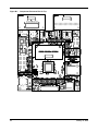
1
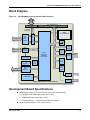
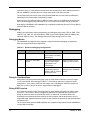
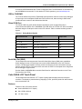
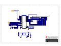
Stellaris® LM3S9B96 Development Kit User ’s Manual DK-LM3S9B96 -03 Co pyrigh t © 2 009– 201 0 Te xas In strumen ts Copyright Copyright © 2009–2010 Texas Instruments, Inc. All rights reserved. Stellaris and StellarisWare are registered trademarks of Texas Instruments. ARM and Thumb are registered trademarks, and Cortex is a trademark of ARM Limited. Other names and brands may be claimed as the property of others. Texas Instruments 108 Wild Basin, Suite 350 Austin, TX 78746 http://www.ti.com/stellaris 2 January 12, 2010 Stellaris® LM3S9B96 Development Kit User’s Manual Table of Contents Chapter 1: Stellaris® LM3S9B96 Development Board Overview ................................................................. 7 Features.............................................................................................................................................................. 7 Development Kit Contents ................................................................................................................................ 10 Block Diagram .................................................................................................................................................. 11 Development Board Specifications................................................................................................................... 11 Chapter 2: Stellaris® LM3S9B96 Development Board Hardware Description .......................................... 13 LM3S9B96 Microcontroller Overview ............................................................................................................... 13 Jumpers and GPIO Assignments.................................................................................................................. 13 Clocking ........................................................................................................................................................ 14 Reset............................................................................................................................................................. 15 Power Supplies ............................................................................................................................................. 15 USB............................................................................................................................................................... 15 Debugging..................................................................................................................................................... 16 Color QVGA LCD Touch Panel..................................................................................................................... 17 I2S Audio....................................................................................................................................................... 19 User Switch and LED.................................................................................................................................... 19 Chapter 3: Stellaris® LM3S9B96 Development Board External Peripheral Interface (EPI) ..................... 21 SDRAM Expansion Board ................................................................................................................................ 21 Flash and SRAM Memory Expansion Board .................................................................................................... 21 Chapter 4: Using the In-Circuit Debugger Interface .................................................................................... 23 Appendix A: Stellaris® LM3S9B96 Development Board Schematics........................................................ 25 Appendix B: Stellaris® LM3S9B96 Development Board Component Locations ...................................... 33 Appendix C: Stellaris® LM3S9B96 Development Board Connection Details ........................................... 35 DC Power Jack ................................................................................................................................................. 35 ARM Target Pinout ........................................................................................................................................... 35 Appendix D: Stellaris® LM3S9B96 Development Board Microcontroller GPIO Assignments ................ 37 Appendix E: Stellaris® LM3S9B96 Flash and SRAM Memory Expansion Board ..................................... 41 Installation......................................................................................................................................................... 41 Features............................................................................................................................................................ 42 Hardware Description ....................................................................................................................................... 43 Functional Description .................................................................................................................................. 43 Memory Map..................................................................................................................................................... 45 Component Locations....................................................................................................................................... 46 Schematics ....................................................................................................................................................... 46 Appendix F: References................................................................................................................................. 49 January 12, 2010 3 List of Figures Figure 1-1. Figure 1-2. Figure 2-1. Figure 4-1. Figure B-1. Figure E-1. Figure E-2. Figure E-3. Figure E-4. 4 DK-LM3S9B96 Development Board................................................................................................ 9 DK-LM3S9B96 Development Board Block Diagram ..................................................................... 11 Factory Default Jumper Settings ................................................................................................... 14 ICD Interface Out Mode ................................................................................................................ 23 Component Placement Plot for Top .............................................................................................. 34 DK-LM3S9B96-EXP-FS8 Board Image......................................................................................... 41 DK-LM3S9B96 Development Board.............................................................................................. 42 DK-LM3S9B96-EXP-FS8 Flash/SRAM/LCD IF Expansion Board Block Diagram ........................ 43 Component Placement Plot for Top and Bottom........................................................................... 46 January 12, 2010 Stellaris® LM3S9B96 Development Kit User’s Manual List of Tables Table 2-1. Table 2-2. Table 2-3. Table 2-4. Table 2-5. Table 2-6. Table 2-7. Table C-1. Table D-1. Table E-1. Table E-2. Board Features and Peripherals that are Disconnected in Factory Default Configuration ............ 13 USB-Related Signals..................................................................................................................... 15 Hardware Debugging Configurations ............................................................................................ 16 Debug-Related Signals ................................................................................................................. 17 LCD-Related Signals..................................................................................................................... 18 I2S Audio-Related Signals............................................................................................................. 19 Navigation Switch-Related Signals ............................................................................................... 19 Debug Interface Pin Assignments ................................................................................................. 35 Microcontroller GPIO Assignments ............................................................................................... 37 Flash and SRAM Memory Expansion Board Memory Map........................................................... 45 LCD Latch Register ....................................................................................................................... 45 January 12, 2010 5 6 January 12, 2010 C H A P T E R 1 Stellaris® LM3S9B96 Development Board Overview The Stellaris® LM3S9B96 Development Board provides a platform for developing systems around the advanced capabilities of the LM3S9B96 ARM® Cortex™-M3-based microcontroller. The LM3S9B96 is a member of the Stellaris Tempest-class microcontroller family. Tempest-class devices include capabilities such as 80 MHz clock speeds, an External Peripheral Interface (EPI) and Audio I2S interfaces. In addition to new hardware to support these features, the DK-LM3S9B96 board includes a rich set of peripherals found on other Stellaris boards. The development board includes an on-board in-circuit debug interface (ICDI) that supports both JTAG and SWD debugging. A standard ARM 20-pin debug header supports an array of debugging solutions. The Stellaris® LM3S9B96 Development Kit accelerates development of Tempest-class microcontrollers. The kit also includes extensive example applications and complete source code. Features The Stellaris® LM3S9B96 Development Board includes the following features. Simple set-up—USB cable provides debugging, communication, and power Flexible development platform with a wide range of peripherals Color LCD graphics display – TFT LCD module with 320 x 240 resolution – Resistive touch interface 80 MHz LM3S9B96 microcontroller with 256 K Flash, 96 K SRAM, and integrated Ethernet MAC+PHY, USB OTG, and CAN communications – – 8 MB SDRAM (plug-in EPI option board) – – EPI break-out board (plug-in option board) 1 MB serial Flash memory Precision 3.00 V voltage reference SAFERTOS™ operating system in microcontroller ROM I2S stereo audio codec – Line In/Out – Headphone Out – Microphone In Controller Area Network (CAN) Interface 10/100 BaseT Ethernet USB On-The-Go (OTG) Connector – Device, Host, and OTG modes January 12, 2010 7 User LED and push button Thumbwheel potentiometer (can be used for menu navigation) MicroSD card slot Supports a range of debugging options – Integrated In-circuit Debug Interface (ICDI) – JTAG, SWD, and SWO all supported – Standard ARM® 20-pin JTAG debug connector USB Virtual COM Port Jumper shunts to conveniently reallocate I/O resources Develop using tools supporting Keil™ RealView® Microcontroller Development Kit (MDK-ARM), IAR Embedded Workbench, Code Sourcery GCC development tools, Code Red Technologies development tools, or Texas Instruments’ Code Composer Studio™ IDE Supported by StellarisWare® software including the graphics library, the USB library, and the peripheral driver library An optional Flash and SRAM memory expansion board (DK-LM3S9B96-EXP-FS8) is also available for use with the DK-LM3S9B96 development board – Works with the External Peripheral Interface (EPI) of the Stellaris microcontroller – Provides Flash memory, SRAM, and an improved performance LCD interface For more information on the DK-LM3S9B96-EXP-FS8 memory expansion board, see Appendix E, “Stellaris® LM3S9B96 Flash and SRAM Memory Expansion Board,” on page 41. The DK-LM3S9B96-EXP-FS8 memory expansion board is available for purchase separately. 8 January 12, 2010 Stellaris® LM3S9B96 Development Kit User’s Manual Figure 1-1. DK-LM3S9B96 Development Board 5 VDC supply input USB Connector for Debug and /or Power On-board JTAG /SWD Debug Interface Headphone Output Audio Line Output Microphone Input Audio Line Input CAN Bus Interface EPI Expansion Board Reset switch JTAG/SWD In/ Out Connector Power and Ground Test Points USB connector with Host, Device and On-the-Go modes Stellaris LM3S39B96 Microcontroller 10/100 Ethernet User LED Potentiometer User Switch 3.00V Analog Reference microSD Card Slot 1MB Serial Flash Memory 3.5" LCD Touch Panel January 12, 2010 9 Development Kit Contents The Stellaris® LM3S9B96 Development Kit contains everything needed to develop and run a range of applications using Stellaris microcontrollers: LM3S9B96 development board 8 MB SDRAM expansion board EPI signal breakout board Retractable Ethernet cable USB Mini-B cable for debugger use USB Micro-B cable for OTG-to-PC connection USB Micro-A to USB A adapter for USB Host USB Flash memory stick microSD Card 20-position ribbon cable CD containing: – A supported version of one of the following (including a toolchain-specific Quickstart guide): • Keil™ RealView® Microcontroller Development Kit (MDK-ARM) • IAR Embedded Workbench • Code Sourcery GCC development tools • Code Red Technologies development tools • Texas Instruments’ Code Composer Studio™ IDE – Complete documentation – Quickstart application source code – Stellaris® Firmware Development Package with example source code 10 January 12, 2010 Stellaris® LM3S9B96 Development Kit User’s Manual Block Diagram DK-LM3S9B96 Development Board Block Diagram Target Cable Figure 1-2. I/O Signal Break-out SWD/JTAG Mux Debug USB USB Touch T Dual USB Device Controller Debug I/O Signal Break-out JTAG/SWD Output/Input QVGA Color LCD Module Debug UART0 OTG/Host/Device USB USB micro-AB connector +5V host supply +3.3V Regulator Ethernet USB I/O signals LED USB Control Stellaris Tempest-class LM3S9B96 Microcontroller MicroSD card slot 1GB 1MB Serial Flash Reset I2S Audio CODEC RJ45 Jack+ Magnetics 8MB SDRAM Switch Thumb wheel Pot Pot Headphone Jack Phones Line Out Jack Line Output EPI Tempest LM 3S9B96 Development Board Development Board Specifications Board supply voltage: 4.75–5.25 Vdc from one of the following sources: – Debugger (ICDI) USB cable (connected to a PC) – USB Micro-B cable (connected to a PC) – DC power jack (2.1 x 5.5mm from external power supply) January 12, 2010 Break-out power output: 3.3 Vdc (100 mA max) 11 Dimensions (excluding LCD panel): – 4.50” x 4.25” x 0.60” (LxWxH) with SDRAM board – 4.50” x 4.25” x 0.75” (LxWxH) with EPI breakout board Analog Reference: 3.0 V +/-0.2% RoHS status: Compliant NOTE: When the LM3S9B96 Development Board is used in USB Host mode, the host connector is capable of supplying power to the connected USB device. The available supply current is limited to ~200 mA unless the development board is powered from an external 5 V supply with a =600mA rating. 12 January 12, 2010 C H A P T E R 2 Stellaris® LM3S9B96 Development Board Hardware Description In addition to an LM3S9B96 microcontroller, the development board includes a range of useful peripheral features and an integrated in-circuit debug interface (ICDI). This chapter describes how these peripherals operate and interface to the microcontroller LM3S9B96 Microcontroller Overview The Stellaris LM3S9B96 is an ARM Cortex-M3-based microcontroller with 256-KB flash memory, 80-MHz operation, Ethernet, USB, EPI, SAFERTOS™ in ROM, and a wide range of peripherals. See the LM3S9B96 Microcontroller Data Sheet (order number DS-LM3S9B96) for complete microcontroller details. The LM3S9B96 microcontroller is factory-programmed with a quickstart demo program. The quickstart program resides in on-chip flash memory and runs each time power is applied, unless the quickstart has been replaced with a user program. Jumpers and GPIO Assignments Each peripheral circuit on the development board is interfaced to the LM3S9B96 microcontroller through a 0.1” pitch jumper/shunt. Figure 2-1 on page 14 shows the factory default positions of the jumpers. The jumpers must be in these positions for the quickstart demo program to function correctly. The development board offers capabilities that the LM3S9B96 cannot support simultaneously due to pin count and GPIO multiplexing limitations. For example, as configured, the board does not support SDRAM and I2S receive (microphone or line input) functions at the same time. The jumpers associated with I2S receive are omitted in the default configuration. Table 2-1 lists all features and peripherals that are disconnected in the factory default configuration. Using these peripherals requires that other peripherals be disconnected. Appendix D, “Stellaris® LM3S9B96 Development Board Microcontroller GPIO Assignments,” on page 37 lists alternative jumper configurations used in conjunction with some of the StellarisWare™ example applications for this board. Table 2-1. Board Features and Peripherals that are Disconnected in Factory Default Configuration Peripheral Jumpers I2S Receive (Audio Input) JP44, 45, 47, 49 Controller Area Network (CAN) JP14, 15 Ethernet Yellow Status LED (LED2) JP2 Analog 3.0V Reference JP33 See Appendix D, “Stellaris® LM3S9B96 Development Board Microcontroller GPIO Assignments,” on page 37, for a complete list of GPIO assignments. The table lists all default and alternate January 12, 2010 13 assignments that are supported by the 0.1” jumpers and PCB routing. The LM3S9B96 has additional internal multiplexing that enables additional configurations which may require discrete wiring between peripherals and GPIO pins. The ICDI section of the board has a GND-GND jumper that serves no function other than to provide a convenient place to ‘park’ a spare jumper. This jumper may be reused as required. Figure 2-1. Factory Default Jumper Settings Clocking The development board uses a 16.0-MHz (Y2) crystal to complete the LM3S9B96 microcontroller's main internal clock circuit. An internal PLL, configured in software, multiples this clock to higher frequencies for core and peripheral timing. A 25.0-MHz (Y1) crystal provides an accurate timebase for the Ethernet PHY. 14 January 12, 2010 Stellaris® LM3S9B96 Development Kit User’s Manual Reset The RESETn signal into the LM3S9B96 microcontroller connects to the reset switch (SW2) and to the ICDI circuit for a debugger-controlled reset. External reset is asserted (active low) under any one of the three following conditions: Power-on reset (filtered by an R-C network) Reset push switch SW2 held down By the ICDI circuit (U12 FT2232, U13D 74LVC125A) when instructed by the debugger (this capability is optional, and may not be supported by all debuggers) The LCD module has special Reset timing requirements requiring a dedicated control line from the microcontroller. Power Supplies The development board requires a regulated 5.0 V power source. Jumpers JP34-36 select the power source, with the default source being the ICDI USB connector. Only one +5 V source should be selected at any time to avoid conflict between the power sources. When using USB in Host mode, the power source should be set to either ICDI or to EXT if a +5 V power supply (not included in the kit) is available. The development board has two main power rails. A +3.3 V supply powers the microcontroller and most other circuitry. +5 V is used by the OTG USB port and In-circuit Debug Interface (ICDI) USB controller. A low drop-out (LDO) regulator (U5) converts the +5 V power rail to +3.3 V. Both rails are routed to test loops for easy access. USB The LM3S9B96’s full-speed USB controller supports On-the-Go, Host, and Device configurations. See Table 2-2 for USB-related signals. The 5-pin microAB OTG connector supports all three interfaces in conjunction with the cables included in the kit. The USB port has additional ESD protection diode arrays (D1, D2,D5) for up to 15 kV of ESD protection. Table 2-2. USB-Related Signals Microcontroller Pin Board Function Jumper Name Pin 70 USB0DM USB Data- - Pin 71 USB0DP USB Data+ - Pin 73 USB0RBIAS USB bias resistor - Pin 66 USB0ID OTG ID signal (input to microcontroller) OTG ID Pin 67 USB0VBUS Vbus Level monitoring +VBUS Pin 34 USB0EPE Host power enable (active high) EPEN Pin 35 USB0PFLT Host power fault signal (active low) PFLT U6, a fault-protected switch, controls and monitors power to the USB host port. USB0EPEN, the control signal from the microcontroller, has a pull-down resistor to ensure host-port power remains off during reset. The power switch will immediately cut power if the attached USB device draws January 12, 2010 15 more than 1 Amp, or if the switches’ thermal limits are exceeded by a device drawing more than 500 mA. USB0PFLT indicates the over-current status back to the microcontroller. The development board can be either a bus-powered USB device or self-powered USB device depending on the power-supply configuration jumpers. When using the development board in USB-host mode, power to the EVB should be supplied by the In-circuit Debugger (ICDI) USB cable or by a +5 V source connected to the DC power jack. Note that the LM3S9B96’s USB capabilities are completely independent from the In-Circuit Debug Interface USB functionality. Debugging Stellaris microcontrollers support programming and debugging using either JTAG or SWD. JTAG uses the TCK, TMS, TDI, and TDO signals. SWD requires fewer signals (SWCLK, SWDIO, and, optionally, SWO for trace). The debugger determines which debug protocol is used. Debugging Modes The LM3S9B96 development board supports a range of hardware debugging configurations. Table 2-3 summarizes these configurations. Table 2-3. Hardware Debugging Configurations Mode Debug Function Use Selected by... 1 Internal ICDI Debug on-board LM3S9B96 microcontroller over Debug USB interface. Default mode 2 ICDI out to JTAG/ SWD header The development board is used as a USB to SWD/ JTAG interface to an external target. Remove jumpers on TCk, TMS, TDI, TDO, and PIN1 3 In from JTAG/SWD header For users who prefer an external debug interface (ULINK, JLINK, etc.) with the development board. Connecting an external debugger to the JTAG/SWD header Debug In Considerations Debug Mode 3 supports board debugging using an external debug interface such as a Segger J-Link or Keil ULINK. Most debuggers use Pin 1 of the Debug connector to sense the target voltage and, in some cases, power the output logic circuit. Installing the VDD/PIN1 jumper will apply 3.3 V power to this pin in order to support external debuggers. Debug USB Overview An FT2232 device from Future Technology Devices International Ltd implements USB-to-serial conversion. The FT2232 is factory-configured to implement a JTAG/SWD port (synchronous serial) on channel A and a Virtual COM Port (VCP) on channel B. This feature allows two simultaneous communications links between the host computer and the target device using a single USB cable. Separate Windows drivers for each function are provided on the Documentation and Software CD. The In-Circuit Debug Interface USB capabilities are completely independent from the LM3S9B96’s on-chip USB functionality. 16 January 12, 2010 Stellaris® LM3S9B96 Development Kit User’s Manual A small serial EEPROM holds the FT2232 configuration data. The EEPROM is not accessible by the LM3S9B96 microcontroller. For full details on FT2232 operation, go to www.ftdichip.com. USB to JTAG/SWD The FT2232 USB device performs JTAG/SWD serial operations under the control of the debugger. A simple logic circuit multiplexes SWD and JTAG functions and, when working in SWD mode, provides direction control for the bidirectional data line. Virtual COM Port The Virtual COM Port (VCP) allows Windows applications (such as HyperTerminal) to communicate with UART0 on the LM3S9B96 over USB. Once the FT2232 VCP driver is installed, Windows assigns a COM port number to the VCP channel. Table 2-4 shows the debug-related signals. Table 2-4. Debug-Related Signals Microcontroller Pin Board Function Jumper Name Pin 77 TDO/SWO JTAG data out or trace data out TDO Pin 78 TDI JTAG data in TDI Pin 79 TMS/SWDIO JTAG TMS or SWD data in/out TMS Pin 80 TCK/SWCLK JTAG Clock or SWD clock TCK Pin 26 PA0/U0RX Virtual Com port data to LM3S9B96 VCPRX Pin 27 PA1/U0TX Virtual Com port data from LM3S9B96 VCPTX Pin 64 RSTn System Reset RSTn Serial Wire Out (SWO) The development board supports the Cortex-M3 Serial-Wire Output (SWO) trace capabilities. Under debugger control, on-board logic can route the SWO datastream to the VCP transmit channel. The debugger software can then decode and interpret the trace information received from the Virtual Com Port. The normal VCP connection to UART0 is interrupted when using SWO. Not all debuggers support SWO. See the Stellaris LM3S9B96 Microcontroller Data Sheet for additional information on the Trace Port Interface Unit (TPIU). Color QVGA LCD Touch Panel The development board features a TFT Liquid Crystal graphics display with 320 x 240 pixel resolution. The display is protected during shipping by a thin, protective plastic film which should be removed before use. Features Features of the LCD module include: Kitronix K350QVG-V1-F display 320 x RGB x 240 dots 3.5” 262 K colors January 12, 2010 17 Wide temperature range White LED backlight Integrated RAM Resistive touch panel Control Interface The Color LCD module has a built-in controller IC with a multi-mode parallel interface. The development board uses an 8-bit 8080 type interface with GPIO Port D providing the data bus. Table 2-4 shows the LCD-related signals. Table 2-5. LCD-Related Signals Microcontroller Pin Board Function Jumper Name PE6/ADC1 Touch X+ X+ PE3 Touch Y- Y- PE2 Touch X- X- PE7/ADC0 Touch Y+ Y+ PB7 LCD Reset LRSTn PD0..7 LCD Data Bus 0..7 LD0..7 PH7 LCD Data/Control Select LDC PB5 LCD Read Strobe LRDn PH6 LCD Write Strobe LWRn - Backlight control BLON Backlight The white LED backlight must be powered for the display to be clearly visible. U7 (FAN5331B) implements a 20 mA constant-current LED power source to the backlight. The backlight is not normally controlled by the microcontroller, however, the control signal is available on a header. A jumper may be installed to disable the backlight by connecting it to GND. Alternatively, a wire may be used to control this signal from a spare microcontroller GPIO line. Because the FAN5331B operates in a constant current mode, its output voltage will jump up if the LCD should become disconnected. To prevent over-voltage failure of the IC or diode D3, a zener (D4) clamps the voltage. The current will limit to 20 mA, but the total board current will be higher than when the LCD panel is connected. To avoid over-heating the backlighting circuit, install the BLON jumper to completely shut-down the backlighting circuit. Power The LCD module has internal bias voltage generators and requires only a single 3.3 V dc supply. Resistive Touch Panel The 4-wire resistive touch panel interfaces directly to the microcontroller, using 2 ADC channels and 2 GPIO signals. See the StellarisWare™ source code for additional information on touch panel implementation. 18 January 12, 2010 Stellaris® LM3S9B96 Development Kit User’s Manual I2S Audio The LM3S9B96 development board has advanced audio capabilities using an I2S-connected Audio TLV320AIC23 CODEC. The factory default configuration has Audio output (Line Out and/or Headphone output) enabled. Four additional I2S signals are required for Audio input (Line Input and/or Microphone). All four audio interfaces are through 1/8” (3.5mm) stereo jacks. Table 2-6 shows the I2S audio-related signals. Table 2-6. I2S Audio-Related Signals Microcontroller Pin Board Function Jumper Name I2C0SDA CODEC Configuration Data SDA I2C0SCL CODEC Configuration Clock SCL I2STXSD Audio Out Serial Data TXSD I2STXWS Audio Out Framing signal TXWS I2STXSCK Audio Out Bit Clock BCLKa I2STXMCLK Audio Out System Clock MCLK I2SRXSD Audio In Serial Data RXSDb I2SRXWS Audio In Framing signal RXWSb I2SRXSCK Audio In Bit Clock BCLKb I2SRXMCLK Audio In System Clock MCLKb a. Shares GPIO line with Analog voltage reference. Jumper installed by default. b. Shares GPIO line with LCD data bus – Port D. Jumper omitted by default. The Audio CODEC has a number of control registers which are configured using the I2C bus signals. CODEC settings can only be written, but not read, using I2C. See the StellarisWare™ example applications for programming information and the TLV320AIX23B data sheet for complete register details. The Headphone output can be connected directly to any standard headphones. The Line Output is suitable for connection to an external amplifier, including PC desktop speaker sets. User Switch and LED The development board provides a user push-switch and LED (see Table 2-7). Table 2-7. Navigation Switch-Related Signals Microcontroller Pin Board Function Jumper Name PJ7 User Switch SWITCH PF3 User LED LEDa a. Shared with Ethernet Jack Yellow LED. This jumper is installed by default. January 12, 2010 19 20 January 12, 2010 C H A P T E R 3 Stellaris® LM3S9B96 Development Board External Peripheral Interface (EPI) The External Peripheral Interface (EPI) is a high-speed 8/16/32-bit parallel bus for connecting external peripherals or memory without glue logic. Supported modes include SDRAM, SRAM, and Flash memories, as well as Host-bus and FIFO modes. The LM3S9B96 development kit includes an 8 MB SDRAM board in addition to an EPI break-out board. Other EPI expansion boards may be available. SDRAM Expansion Board The SDRAM board provides 8 MB of memory (4M x 16) which, once configured, becomes part of the LM3S9B96’s memory map at either 0x6000.0000 or 0x8000.0000. The SDRAM interface multiplexes DQ00..14 and AD/BA0..14 without requiring external latches or buffers. Of the 32 EPI signals, only 24 are used in SDRAM mode, with the remaining signals used for non-EPI functions on the board. Flash and SRAM Memory Expansion Board The optional Flash and SRAM memory expansion board (DK-LM3S9B96-EXP-FS8) is a plug-in for the DK-LM3S9B96 development board. This expansion board works with the External Peripheral Interface (EPI) of the Stellaris microcontroller and provides Flash memory, SRAM, and an improved performance LCD interface. For more information on the DK-LM3S9B96-EXP-FS8 memory expansion board (sold separately), see Appendix E, “Stellaris® LM3S9B96 Flash and SRAM Memory Expansion Board,” on page 41. January 12, 2010 21 22 January 12, 2010 C H A P T E R 4 Using the In-Circuit Debugger Interface The Stellaris® LM3S9B96 Development Kit can operate as an In-Circuit Debugger Interface (ICDI). ICDI acts as a USB to the JTAG/SWD adaptor, allowing debugging of any external target board that uses a Stellaris microcontroller. See “Debugging Modes” on page 16 for a description of how to enter ICDI Out mode. Figure 4-1. ICD Interface Out Mode JTAG or SWD connects to the external microcontroller LM3S9B96 Dev Board PC with IDE/ debugger TDO Stellaris MCU Stellaris MCU Target Board VDD TDI TCK Target Cable TMS ` USB to JTAG/ SWD +3.3V Remove jumpers to use ICDI Out Feature The debug interface operates in either serial-wire debug (SWD) or JTAG mode, depending on the configuration in the debugger IDE. The IDE/debugger does not distinguish between the on-board Stellaris microcontroller and an external Stellaris microcontroller. The only requirement is that the correct Stellaris device is selected in the project configuration. The Stellaris target board should have a 2x10 0.1” pin header with signals as indicated in Table C-1 on page 35. This applies to both an external Stellaris microcontroller target (Debug Output mode) and to external JTAG/SWD debuggers (Debug Input mode). ICDI does not control RST (device reset) or TRST (test reset) signals. Both reset functions are implemented as commands over JTAG/SWD, so these signals are usually not necessary. January 12, 2010 23 24 January 12, 2010 A P P E N D I X A Stellaris® LM3S9B96 Development Board Schematics This section contains the schematics for the DK-LM3S9B96 development board. Micro, EPI connector, USB, and Ethernet on page 26 LCD CAN, Serial Memory, and User I/O on page 27 Power Supplies on page 28 I2S Audio Expansion Board on page 29 EPI and SDRAM Expansion Boards on page 30 In-circuit Debug Interface (ICDI) on page 31 January 12, 2010 25 Schematic page 1 4 PC0/TCK PC1/TMS PC2/TDI PC3/TDO 80 79 78 77 25 24 23 22 PC4/EPI02 PC5/EPI03 PC6/EPI04 PC7/EPI05 PE0/EPI08 PE1/EPI09 PE2/EPI24 PE3/EPI25 B 74 75 95 96 6 5 2 1 PE4/I2STXWS PE5/I2STXSD PE6/ADC1 PE7/ADC0 PG0/EPI13 PG1/EPI14 PG7/EPI31 19 18 36 PJ0/EPI16 PJ1/EPI17 PJ2/EPI18 PJ3/EPI19 PJ4/EPI28 PJ5/EPI29 PJ6/EPI30 14 87 39 50 52 53 54 55 PJ7 64 RESETn PA0/U0RX PA1/U0TX PA2/SSI0CLK PA3/SSI0FSS PA4/SSI0RX PA5/SSI0TX PA6/USB0EPEN PA7/USB0PFLT PB0/USB0ID PB1/USB0VBUS PB2/CCP0 PB3 PB4/EPI0S23 PB5/EPI0S22 PB6/AVREF PB7/NMI PC0/TCK/SWCLK PC1/TMS/SWDIO PC2/TDI PC3/TDO/SWO PC4/EPI0S02 PC5/EPI0S03 PC6/EPI0S04 PC7/EPI0S05 PD0 PD1 PD2/EPI0S20 PD3/EPI0S21 PD4 PD5 PD6 PD7 PE0/EPI0S08 PE1/EPI0S09 PE2/EPI0S24 PE3/EPI0S25 PE4/ADC3 PE5/ADC2 PE6/ADC1 PE7/ADC0 PF0 PF1 PF2/LED1 PF3/LED0 PF4/EPI0S12 PF5/EPI0S15 PG0/EPI0S13 PG1/EPI0S14 PG7/EPI0S31 PJ0/EPI0S16 PJ1/EPI0S17 PJ2/EPI0S18 PJ3 PJ4 PJ5 PJ6 PJ7 PH0/EPI0S06 PH1/EPI0S07 PH2/EPI0S01 PH3/EPI0S00 PH4/EPI0S10 PH5/EPI0S11 PH6/EPI0S26 PH7/EPI0S27 MDIO TXOP RST_n TXON C 1 Y1 OSC0 OSC1 48 49 XTLN XTLP OSC0 OSC1 10PF C3 10PF 51 C4 10PF R1 33 12.4K NC RXIN 86 85 84 83 76 63 62 15 58 3 4 9 21 45 57 69 82 94 USB0RBIAS USB0DP USB0DM VDDA C5 0.1UF PD2/EPI20 PD3/EPI21 PD4/I2SRXSD PD5/I2SRXMCLK PD6 PD7 PF0 PF1/TXMCLK PF2/LED1 GNDA GND GND GND GND GND GND GND VDD VDD VDD VDD VDD VDD VDD VDD LDO VDD25 VDD25 2 LED1 PF3/LED0 PF4/EPI12 PF5/EPI15 10K USB On-the-Go PC4/EPI02 PC5/EPI03 PC6/EPI04 PC7/EPI05 USB Micro AB G1 VBUS +3.3V D- D+ G2 G +VBUS D1 D2 2 PE1/EPI09 PE0/EPI08 PH5/EPI11 PH6/EPI26 1 1 B72590D0050H160 2 B72590D0050H160 +VBUS PB1/USBVBUS B JP3 OTG ID D5 1 PB0/USBID JP2 JP4 2 B72590D0050H160 Note: R60-61 = 10 Ohms for LM3S9B96 Rev B1 (see errata) R60,R11 = 0 Ohms for LM3S9B96 Rev C +3.3V Ethernet 10/100baseT J1 +3.3V R4 49.9 R6 49.9 C13 10pF 330 3 +3.3V R60 G- 1CT:1 TX+ 1 TX- 2 5 10 0.1UF 46 G+ 12 11 R8 C16 10pF C18 RX+ 3 4 4 7 40 C19 +3.3V R7 49.9 C14 10pF +3.3V 5 RX- 6 1CT:1 C21 0.01UF 7 6 8 C 8 +3.3V R9 C17 10pF R61 10 0.1UF 37 330 R3 9.10K ID +5V PG7/EPI31 PJ2/EPI18 PF5/EPI15 PF4/EPI12 DF12D-50DP 43 73 A J3 JP1 LED2 PH0/EPI06 PH1/EPI07 PH2/EPI01 PH3/EPI00 PH4/EPI10 PH5/EPI11 PH6/EPI26 PH7/EPI27 M+3.3V R2 2 1 Y- 9 10 NC Y+ GND +3.3V 71 70 J3011G21DNL 8 20 32 44 56 68 81 93 M+3.3V C6 C8 C10 0.01UF 0.01UF 0.1UF C12 0.1UF C15 2.2UF History Revision U16 FAN2558S12X 7 5 38 88 C7 C9 0.01UF 0.1UF VOUT C11 2.2UF U16 Required only for LM3S9B96 Rev B1. See errata. LM3S9B96 1 PD0/I2SRXSCK PD1/I2SRXWS ERBIAS M+3.3V D RXIP 47 61 60 59 42 41 PB6/TXSCK/AVREF PB7/NMI R5 49.9 16.00MHz C2 10PF 17 16 10 11 12 13 97 98 99 100 PB4/ADC10/EPI23 PB5/EPI22 PB0/USBID PB1/USBVBUS PB2/I2C0SCL PB3/I2C0SDA Y2 2 25.00MHz C1 XTLN XTALP 66 67 72 65 92 91 90 89 50 49 48 47 46 45 44 43 42 41 40 39 38 37 36 35 34 33 32 31 30 29 28 27 26 GL GR 26 27 28 29 30 31 34 35 PA0/U0RX PA1/U0TX PA2/SSI0CLK PA3 PA4/SSI0RX PA5/SSI0TX PA6/USBEPE/CAN0RX PA7/USBPFLT/CAN0TX J2 1 2 PG0/EPI13 3 PG1/EPI14 4 PH7/EPI27 5 PJ0/EPI16 6 PD3/EPI21 7 PD2/EPI20 8 PJ6/EPI30 9 PJ5/EPI29 10 PJ4/EPI28 11 PJ3/EPI19 12 PE3/EPI25 13 PE2/EPI24 14 PB4/ADC10/EPI23 15 PB5/EPI22 16 PJ1/EPI17 17 PH0/EPI06 18 PH1/EPI07 19 PH2/EPI01 20 PH3/EPI00 21 PH4/EPI10 22 23 24 25 5 U1 3 +5V VIN GND A EPI Expansion Connector PE2/EPI24 PE3/EPI25 PD2/EPI20 PD3/EPI21 PB4/ADC10/EPI23 PB5/EPI22 PH6/EPI26 PH7/EPI27 4 Stellaris Microcontroller 6 3 PE2/EPI24 PE3/EPI25 PD2/EPI20 PD3/EPI21 PB4/ADC10/EPI23 PB5/EPI22 PH6/EPI26 PH7/EPI27 5 2 3 1 2 EN PG 0 A Date Description Indicates factory-default jumper position. 11 Mar 09 Initial Prototype 15 Apr 09 First production release 1 D 3 4 Drawing Title: LM3S9B96 Development Board Page Title: Micro, EPI connector, USB and Ethernet 2 1 Size Date: 4 5 B Document Number: 4/23/2009 DB-LM3S9B96 Sheet 6 1 of 6 Rev A Schematic page 2 2 3 +3.3V GND DO DATA0 RSV DATA1 JP12 LED_A JP16 PE6/ADC1 JP17 PE3/EPI25 JP18 PE2/EPI24 +3.3V 12 11 9 10 RESETn 100 C26 0.1UF JP19 PE7/ADC0 R16 10K LED_K ILED+ R59 SW-B3S1000 CARD JP13 ILED- FR4 MISO PA4/SSI0RX SW2 N/C DATA2 CS DATA3 DI CMD VDD 2908-05WB-MG CLOCK FR3 JP11 MISO R19 10K Reset 1 2 3 4 5 6 7 8 +3.3V SSICLK PA2/SSI0CLK X+ TOUCH_XP TOUCH_YN TOUCH_XN TOUCH_YP YX- XR YD XL YU +3.3V Y+ C28 C30 C31 C33 0.01UF 0.01UF 0.01UF 0.01UF R20 10K C24 0.1UF LCD_RSTn CSn SPICLK SPISDI LRSTn +3.3V +3.3V PB7/NMI R18 JP20 330 LED2 Green 1MB Serial Flash +3.3V B Power FLCSn FLASH_CSn PF0 JP8 3 6 1 2 5 nHOLD VDD JP22 PD1/I2SRXWS +3.3V 7 JP21 PD0/I2SRXSCK U2 +3.3V R13 10K JP23 PD2/EPI20 8 JP24 PD3/EPI21 nWP SCK nCE SO SI C25 0.1UF VSS JP25 PD4/I2SRXSD JP26 PD5/I2SRXMCLK 4 JP27 PD6 W25X80AVSSIG-ND JP28 PD7 LD0 LCD_D0 LD1 R21 10K LCD_D1 LD2 LCD_D2 LD3 LD0 LD1 LD2 LD3 LD4 LD5 LCD_D0 LCD_D1 LCD_D2 LCD_D3 LCD_D4 LCD_D3 LD4 LCD_D5 LCD_D6 LCD_D7 LCD_D4 LD5 LCD_D5 LD6 LD6 LD7 LD8 LD9 LD10 LD11 LCD_D6 LD7 LCD_D7 LD12 LD13 LD14 LD15 LD16 LD17 HSYNC VSYNC DCLK LCD_D[0..7] LED R11 JP5 330 PF3/LED0 +3.3V LED1 Green +3.3V LDC User LED PH7/EPI27 AVDD JP29 LRDn C R10 10K SWITCH PJ7 JP6 PB5/EPI22 PH6/EPI26 User Switch JP31 +3.3V C29 0.1UF CAN Transceiver TXD U3 PA7/USBPFLT/CAN0TX JP14 RXD 1 4 PA6/USBEPE/CAN0RX JP15 8 VREF_3.0V POT R12 50K PB4/ADC10/EPI23 JP7 D R17 10K 2 TXD RXD CANH CANL CANH CANL TERM 120 JP58 +5V RS GND 7 6 R58 VCC VREF 3 5 C27 0.1UF VCC DC RD WR PS0 PS1 PS2 PS3 LCD_DC LCD_RDn LCD_WRn JP30 LWRn SW1 SW-B3S1000 C32 0.1UF OE CAN Connector A 1 2 3 4 5 6 7 8 9 10 11 12 13 14 15 16 17 18 19 20 21 22 23 24 25 26 27 28 29 30 31 32 33 34 35 36 37 38 39 40 41 42 43 44 45 46 47 48 49 50 51 52 53 54 55 56 57 58 59 60 B C J5 1 3 5 7 9 2 4 6 8 +VCAN 10 M2 +VCAN +5V FPC_Socket_60pin JP32 C22 0.1UF Indicates factory-default jumper position. SN65HVD1050D D C23 0.1UF Thumbwheel Potentiometer Drawing Title: LM3S9B96 Development Board Page Title: LCD, CAN, Serial Memory, User IO Size Date: 1 J6 M1 FR2 JP10 SCLK QVGA LCD Panel with touch interface 8-bit 8080 mode MOSI PA5/SSI0TX 6 +3.3V J4 FR1 JP9 MOSI microSD Card Slot R15 10K SD_CSn PA3 5 +3.3V R14 10K SDCSn A 4 QVGA LCD Panel 1 2 3 4 5 B Document Number: 4/23/2009 DB-LM3S9B96 Sheet 6 2 of 6 Rev A Schematic page 3 1 2 3 4 5 6 TP1 3.3V +3.3V P3V U5 PQ1LA333MSPQ TP3 5.0V DBG+5V +VBUS 4 +5V ICDI 3 C34 0.1UF VOUT A M+3.3V M3V 5 NR 1 C42 2.2UF C39 TP2 GND 0.01UF 2 1 3 2 PJ-002BH-SMT ON C37 2.2UF JP35 EXT J7 VIN JP61 JP34 OTG +5V DC INPUT JP60 +5V GND A GND JP59 JP36 Main +3.3V Supply Power Source Selection +3.3V B EPEN PA6/USBEPE/CAN0RX JP37 PFLT PA7/USBPFLT/CAN0TX U6 TPS2051BDBV +VBUS +5V 5 USB0EPE 4 3 IN EN OCn USB0PFLT B 1 C40 2.2UF 2 JP38 OUT GND R23 10K C20 0.1UF C36 2.2UF C41 2.2UF C43 2.2UF R24 10K VBUS Fault Protected Switch C C +3.3V VREF_3.0V VREF 3.00V R22 1.5K U4 1 PB6/TXSCK/AVREF CATHODE JP33 +5V C35 2.2UF 3 NC +5V 2 ANODE R25 10K LM4040B30IDB Backlight 3.0V 0.2% Voltage Reference ILED+ L1 D3 NR4018T100M 10uH FYV0704SMTF D4 BZT52C24 24V ILED- U7 5 BLON 4 JP39 2 C38 2.2UF VIN SW SHDN FB 1 3 GND R26 15 FAN5333B C44 0.1UF C45 0.1UF C46 0.1UF Indicates factory-default jumper position. D D LED Backlight Controller Drawing Title: LM3S9B96 Development Board Page Title: Power Supplies Size Date: 1 2 3 4 5 B Document Number: 4/23/2009 DB-LM3S9B96 Sheet 6 3 of 6 Rev A Schematic page 4 1 2 J8 3 4.7K R55 STX-3000 0.47UF R56 4.7K R30 10K 1 2 3 Microphone Input C47 R28 10K STX-3000 6 C79 0.47UF 4.7K A J9 5 C77 R54 1 2 3 Line Input 4 C76 27PF C48 2.2UF R57 4.7K A C78 27PF R31 4.7K 27PF C54 R27 4.7K B + +3.3V R29 4.7K SDA 20 19 17 18 PB3/I2C0SDA JP40 SCL MICBIAS MICIN PB2/I2C0SCL JP41 TXSD PE5/I2STXSD TXSD 23 24 22 21 Rework 2: Loop TXWS to RXWS. PE4/I2STXWS PD4/I2SRXSD JP44 RXWS PD1/I2SRXWS JP45 PB6/BCLK PB6/TXSCK/AVREF RXSD 4 5 6 7 3 LRC 25 26 BITCLK JP46 PD0/BCLK PD0/I2SRXSCK JP47 PF1/MCLK C PF1/TXMCLK 4V LLINEIN RLINEIN MICBIAS MICIN R32 47K 220UF 1 27 MCLK JP48 PD5/MCLK SDIN SCLK MODE nCS C57 28 JP49 100 R37 R33 47K HPVDD AVDD DGND HPGND AGND Audio Line Output 100 0.47UF R35 47K 2 XTI/MCLK CLKOUT XTO VMID C50 0.1UF PD5/I2SRXMCLK R36 0.47UF C58 DIN LRCIN DOUT LRCOUT BCLK BVDD DVDD 1 J11 2 3 STX-3000 B R34 47K 12 13 LOUT ROUT Audio Headphone Output C55 9 10 LHPOUT RHPOUT 4V JP42 TXWS JP43 RXSD 220UF U8 1 J10 2 3 STX-3000 + +3.3V 16 8 14 C56 0.1UF C59 2.2UF C60 2.2UF C C61 2.2UF C52 0.1UF 11 15 TLV320AIC23BPW Analog +3.3V 50mA Power Supply U9 PQ1LA333MSPQ +5V 4 VIN VOUT 5 NR 1 C51 C53 2.2UF D 0.01UF 2 D ON GND Indicates factory-default jumper position. 3 C49 2.2UF Drawing Title: LM3S9B96 Development Board Page Title: I2S Audio Expansion Board Size Date: 1 2 3 4 5 B Document Number: 4/23/2009 DB-LM3S9B96 Sheet 6 4 of 6 Rev A Schematic page 5 1 2 3 4 5 6 SDRAM Expansion Board U10 A Expansion Connector J12 AD2 AD3 AD4 AD5 +3.3V C62 2.2UF B SDCLK CASn D15 D12 AD9 AD8 AD11 50 49 48 47 46 45 44 43 42 41 40 39 38 37 36 35 34 33 32 31 30 29 28 27 26 1 2 3 4 5 6 7 8 9 10 11 12 13 14 15 16 17 18 19 20 21 22 23 24 25 BA0/D13 BA1/D14 DQM0 SDCKE CSn WEn RASn DQM1 AD6 AD7 AD1 AD0 AD10 AD0 AD1 AD2 AD3 AD4 AD5 AD6 AD7 AD8 AD9 AD10 AD11 23 24 25 26 29 30 31 32 33 34 22 35 BA0/D13 BA1/D14 20 21 CSn WEn RASn CASn 19 16 18 17 SDCLK SDCKE DQM1 DQM0 38 37 39 15 28 41 54 6 12 46 52 DF12A-50DS 8MB SDRAM A0 A1 A2 A3 A4 A5 A6 A7 A8 A9 A10 A11 BA0 BA1 CS WE RAS CAS CLK CKE DQMH DQML VSS VSS VSS VSSQ VSSQ VSSQ VSSQ DQ0 DQ1 DQ2 DQ3 DQ4 DQ5 DQ6 DQ7 DQ8 DQ9 DQ10 DQ11 DQ12 DQ13 DQ14 DQ15 NC NC VDD VDD VDD VDDQ VDDQ VDDQ VDDQ 2 4 5 7 8 10 11 13 AD0 AD1 AD2 AD3 AD4 AD5 AD6 AD7 42 44 45 47 48 50 51 53 AD8 AD9 AD10 AD11 D12 BA0/D13 BA1/D14 D15 A 36 40 B +3.3V 1 14 27 3 9 43 49 +3.3V C63 0.01UF C64 0.01UF C65 0.1UF C66 0.1UF MT48LC4M16A2 EPI Signal Breakout Board Expansion Connector C C J15 X_PC4/EPI02 X_PC5/EPI03 X_PC6/EPI04 X_PC7/EPI05 X+3.3V X+5V X_PG7/EPI31 X_PJ2/EPI18 X_PF5/EPI15 X_PF4/EPI12 X_PE1/EPI09 X_PE0/EPI08 X_PH5/EPI11 X_PH6/EPI26 D 50 49 48 47 46 45 44 43 42 41 40 39 38 37 36 35 34 33 32 31 30 29 28 27 26 1 2 3 4 5 6 7 8 9 10 11 12 13 14 15 16 17 18 19 20 21 22 23 24 25 X_PG0/EPI13 X_PG1/EPI14 X_PH7/EPI27 X_PJ0/EPI16 X_PD3/EPI21 X_PD2/EPI20 X_PJ6/EPI30 X_PJ5/EPI29 X_PJ4/EPI28 X_PJ3/EPI19 X_PE3/EPI25 X_PE2/EPI24 X_PB4/EPI23 X_PB5/EPI22 X_PJ1/EPI17 X_PH0/EPI06 X_PH1/EPI07 X_PH2/EPI01 X_PH3/EPI00 X_PH4/EPI10 D DF12A-50DS Drawing Title: LM3S9B96 Development Board Page Title: EPI and SDRAM Expansion Boards Size Date: 1 2 3 4 5 B Document Number: 4/23/2009 DB-LM3S9B96 Sheet 6 5 of 6 Rev A Schematic page 6 2 3 4 5 6 13 1 TCK 11 1 12 Debugger USB Interface 2 54819-0572 D- D+ ID G R43 U13A SN74LVC125A +3.3V 7 USBSH 7 USBDM USBDP R44 1.5K B +5V R39 10K U11 VCC NC ORG GND CS SK DI DO 1 2 3 4 48 1 2 47 R40 1.5K CAT93C46 43 44 1K 64X16 1 Y3 2 4 5 +5V 6.00MHz C68 C69 27PF 27PF EECS EESK EEDATA TEST XTIN XTOUT BDBUS0 BDBUS1 BDBUS2 BDBUS3 BDBUS4 BDBUS5 BDBUS6 BDBUS7 BCBUS0 BCBUS1 BCBUS2 BCBUS3 SI/WUB RESET# RSTOUT# PWREN# GND GND GND GND VCC VCC VCCIOA VCCIOB 15 13 12 11 10 U14C SN74LVC125A 6 U13B SN74LVC125A FT_SRSTN DBGENn DBG_JTAG_EN 2 C 45 2 3 B +3.3V VCP_RX 40 39 38 37 36 35 33 32 12 11 VCP_TX_SWO R53 10K 5 AGND AVCC U15B SN74LVC126A SRSTN 30 29 28 27 26 8 +3.3V 3 42 14 31 +3.3V 6 5 C R45 46 330 C72 C73 C74 C75 0.1UF 0.1UF 0.1UF 0.1UF U14B SN74LVC125A 0.1UF Channel A : JTAG / SW Debug 11 12 Channel B : Virtual Com Port PC3/TDO JP53 RSTn RESETn JP54 VCPTX PA1/U0TX JP55 VCPRX PA0/U0RX 10 R46 J14 20 18 16 14 12 10 8 6 4 2 TDO_SWO SRSTN VCP_TX 19 17 15 13 11 9 7 5 3 1 27 R47 27 R48 27 R49 PIN1 2X10 HDR-SHRD VCP_RX JP57 JP56 +3.3V 27 R50 SRSTN 8 TDO_SWO +3.3V +3.3V +3.3V TCK TMS_SWDIO VCC TDI U13E SN74LVC125A VCC U14E SN74LVC125A 14 JP52 TDO JTAG/SWD In/Out TDI VCC GND GND GND 7 PC2/TDI TMS_SWDIO 14 JP51 TDI U15D SN74LVC126A 7 PC1/TMS TCK 14 JP50 TMS 7 TCK PC0/TCK D TDO_SWO 9 U15C SN74LVC126A 41 FT2232D R38 10K 6 SN74LVC125A U13D SN74LVC125A SWO_EN C71 +3.3v TMS_SWDIO 3 U15A SN74LVC126A U14A +5V 9 18 25 34 TDI 13 +5V 4 ACBUS0 ACBUS1 ACBUS2 ACBUS3 SI/WUA 5 8 10 8 R42 27 0.01UF 3V3OUT 0.1UF R41 27 FT_TCK FT_TDI/DI FT_TDO/DO FT_TMS/OUTEN 24 23 22 21 20 19 17 16 A 4 C67 ADBUS0 ADBUS1 ADBUS2 ADBUS3 ADBUS4 ADBUS5 ADBUS6 ADBUS7 1 6 R51 10K 13 C70 8 7 6 5 9 U12 5 4 3 1 2 USB Device Controller DBG+5V R52 10K 1 5V 6 U14D SN74LVC125A 3 4 J13 10 A 27 VCP_TX 9 U13C SN74LVC125A Indicates factory-default jumper position. +3.3V U15E SN74LVC126A D C80 Drawing Title: LM3S9B96 Development Board Page Title: In-circuit Debug Interface (ICDI) 0.1UF Size Date: 1 2 3 4 5 B Document Number: 4/23/2009 DB-LM3S9B96 Sheet 6 6 of 6 Rev A 32 January 12, 2010 A P P E N D I X B Stellaris® LM3S9B96 Development Board Component Locations This appendix contains details on component locations, including: January 12, 2010 Component placement plot for top (Figure B-1) 33 Figure B-1. Component Placement Plot for Top 34 January 12, 2010 A P P E N D I X C Stellaris® LM3S9B96 Development Board Connection Details This appendix contains the following sections: DC Power Jack (see page 35) ARM Target Pinout (see page 35) DC Power Jack The EVB provides a DC power jack for connecting an external +5 V regulated (+/-5%) power source. Center Positive (+) The socket is 5.5 mm dia with a 2.1 mm pin. ARM Target Pinout In ICDI input and output mode, the Stellaris® LM3S9B96 Development Kit supports ARM’s standard 20-pin JTAG/SWD configuration. The same pin configuration can be used for debugging over serial-wire debug (SWD) and JTAG interfaces. Table C-1. Debug Interface Pin Assignments Function Pin Number TDI 5 TDO/SWO 13 TMS/SWDIO 7 TCK/SWCLK 9 System Reset 15 VDD 1 GND 4, 6, 8, 10, 12, 14, 16, 18, 20 No Connect 2, 3, 11, 17, 19 Insert Jumper VDD/PIN1 Jumper (JP57) only when using the development board with an external debug interface such as a ULINK or JLINK. January 12, 2010 35 36 January 12, 2010 A P P E N D I X D Stellaris® LM3S9B96 Development Board Microcontroller GPIO Assignments Table D-1 shows the pin assignments for the LM3S9B96 microcontroller. Table D-1. Microcontroller GPIO Assignments LM3S9B96 GPIO Pin Number Development Board Use Description Default Function 26 PA0 U0Rx Virtual Com Port 27 PA1 U0Tx Virtual Com Port 28 PA2 SSI0Clk SPI 29 PA3 SSI0Fss SD Card CSn 30 PA4 SSI0Rx SPI 31 PA5 SSI0Tx SPI 34 PA6 USB0EPEN USB Pwr Enable CAN0RX 35 PA7 USB0PFLT USB Pwr Fault CAN0TX 66 PB0 USB0ID USB OTG ID 67 PB1 USB0VBUS USB Vbus 72 PB2 I2C0SCL Audio I2C 65 PB3 I2C0SDA Audio I2C 92 PB4 ADC10 Potentiometer EPI0S23 EPI Breakout 91 PB5 PB5 LCD RDn EPI0S22 EPI Breakout 90 PB6 PB6 I2STXSCK AVREF Ext Volt Ref 89 PB7 PB7 LCD RST 80 PC0 TCK/SWCLK JTAG 79 PC1 TMS/SWDIO JTAG 78 PC2 TDI JTAG 77 PC3 TDO/SWO JTAG 25 PC4 EPI0S2 SDRAM D02 EPI0S02 24 PC5 EPI0S3 SDRAM D03 EPI0S03 23 PC6 EPI0S4 SDRAM D04 EPI0S04 22 PC7 EPI0S5 SDRAM D05 EPI0S05 January 12, 2010 Default Use Alt. Function Alternate Use 37 Table D-1. Microcontroller GPIO Assignments (Continued) LM3S9B96 GPIO Pin Number 38 Development Board Use Description Default Function 10 PD0 PD0 11 PD1 12 Default Use Alt. Function Alternate Use LCD Data 0 I2SRXSCK I2S Audio In PD1 LCD Data 1 I2S0RXWS I2S Audio In PD2 PD2 LCD Data 2 EPI0S20 EPI Breakout 13 PD3 PD3 LCD Data 3 EPI0S21 EPI Breakout 97 PD4 PD4 LCD Data 4 I2SRXSD I2S Audio In 98 PD5 PD5 LCD Data 5 I2SRXMCLK I2S Audio In 99 PD6 PD6 LCD Data 6 100 PD7 PD7 LCD Data 7 74 PE0 EPI0S8 SDRAM D8 EPI0S08 75 PE1 EPI0S9 SDRAM D9 EPI0S09 95 PE2 PE2 Touch XN EPI0S24 96 PE3 PE3 Touch YN EPI0S25 6 PE4 I2STXWS I2S Audio Out 5 PE5 I2STXSD I2S Audio Out 2 PE6 ADC1 ADC Touch XP 1 PE7 ADC0 ADC Touch YP 47 PF0 PF0 Flash CSn 61 PF1 I2STXMCLK I2S Audio Out 60 PF2 LED1 Green Enet LED 59 PF3 PF3 User LED 42 PF4 EPI0S12 SDRAM D12 41 PF5 EPI0S15 SDRAM D15 19 PG0 EPI0S13 SDRAM D13 18 PG1 EPI0S14 SDRAM D14 36 PG7 EPI0S31 SDRAM CLK 86 PH0 EPI0S06 SDRAM D06 85 PH1 EPI0S07 SDRAM D07 84 PH2 EPI0S01 SDRAM D01 83 PH3 EPI0S00 SDRAM D00 76 PH4 EPI0S10 SDRAM D10 LED0 Yw Enet LED January 12, 2010 Stellaris® LM3S9B96 Development Kit User’s Manual Table D-1. Microcontroller GPIO Assignments (Continued) LM3S9B96 GPIO Pin Number Development Board Use Alt. Function Alternate Use LCD_WRn EPI0S26 EPI Breakout EPI0S27 LCD_DC EPI0S27 EPI Breakout PJ0 EPI0S16 SDRAM DQM 87 PJ1 EPI0S17 SDRAM DQM 39 PJ2 EPI0S18 SDRAM CAS 50 PJ3 EPI0S19 SDRAM RAS 52 PJ4 EPI0S28 SDRAM WEn 53 PJ5 EPI0S29 SDRAM CSn 54 PJ6 EPI0S30 SDRAM SDCKE 55 PJ7 PJ7 User Switch January 12, 2010 Description Default Function Default Use 63 PH5 EPI0S11 SDRAM D11 62 PH6 EPI0S26 15 PH7 14 39 40 January 12, 2010 A P P E N D I X E Stellaris® LM3S9B96 Flash and SRAM Memory Expansion Board This document describes the Flash and SRAM memory expansion board (DK-LM3S9B96-EXP-FS8) plug-in for the DK-LM3S9B96 development board. This expansion board works with the External Peripheral Interface (EPI) port of the Stellaris microcontroller and provides Flash memory, SRAM, and an improved performance LCD interface. Figure E-1. DK-LM3S9B96-EXP-FS8 Board Image Installation To install the expansion board on the DK-LM3S9B96 development board, do the following: 1. Remove the DK-LM3S9B96-EXP-FS8 memory expansion board from the antistatic bag. 2. On the DK-LM3S9B96 board, remove any installed board on EPI connector J2. 3. On the DK-LM3S9B96 board remove the shunt jumpers on JP16-JP31 and the JP39 headers as shown in Figure E-1 on page 41. January 12, 2010 41 Figure E-2. DK-LM3S9B96 Development Board Remove board Remove jumpers 4. Install the two snap-in nylon standoffs on mounting holes above the EPI connector J2. 5. Place the expansion board on top of the DK-LM3S9B96 board and align the standoffs, the EPI connector, and the 2x17 J2 header. 6. Press firmly downward until the board snaps in, then verify that the board is firmly seated on the EPI connector, the 2x17 header, and the standoffs. 7. When powering up the board, verify that the power indicator LED D1 is lit. Features The DK-LM3S9B96-EXP-FS8 memory expansion board has the following features: 42 8 Megabytes of Flash memory January 12, 2010 Stellaris® LM3S9B96 Development Kit User’s Manual 1 Megabyte of SRAM Memory-mapped LCD I/F for improved LCD performance 1 kilobit of I2C memory for storing configuration data Power LED indicator Hardware Description The Flash and SRAM memory expansion board is designed for use with the Stellaris EPI module configured in Host Bus 8 address/data multiplexed mode. This mode requires the use of an external 8-bit latch for storing the lower 8 address lines A[7:0] transmitted during the address phase of an EPI transfer. This latch can be seen on the expansion board block diagram shown in Figure E-3. Figure E-3. DK-LM3S9B96-EXP-FS8 Flash/SRAM/LCD IF Expansion Board Block Diagram EPI Connector EPI[7:0] EPI[27:8] EPI30 MAD[7:0] D Q L MA[27:8] MA[7:0] FLASH A D MAD[7:0] ALE 8MB MA27 EPI28 EPI29 OEn WRn CS OE WE SRAM A D MA26 MA27 1MB CE1 CE2 OE WE LCD DECODE LCD Control LCD Data FLASH/SRAM/LCD IF Board LCD Connector Functional Description The Flash and SRAM memory expansion board schematics are described in this section. The first page of the schematics shows the memory devices and address latch part of the design. The second page shows the LCD I/F and regulator. Flash/SRAM (Schematic 1 on page 47) Page 1 of the schematics shows the EPI connector, address latch, and memory devices. January 12, 2010 43 EPI Connector The EPI connector J1 is a 50-pin receptacle with 0.5 mm pitch that plugs into the EPI header on the DK-LM3S9B96 board. The 32 EPI signals and the 2 I2C0 signals from the LM3S9B96 are provided on this connector. It also provides 5 V for the on-board DC regulator. Note that not all EPI signals are used in this design. 8-bit Latch This 8-bit latch is used to store the lower 8-bits of the address, which are transmitted during the address phase of an EPI transfer. The EPI must be configured in Host bus 8 mode 0 mode (HB8 ADMUX), with EPI30 configured as an Address Latch Enable (ALE) signal to control this latch. Flash Memory The Flash memory used is a 64 Mbit, 90-nsec Spansion S29GL064N90TFI040. This 8/16 bit memory is used in 8-bit mode. Note that MA27 is used as a chip select signal for this memory. SRAM The SRAM used is an 8 Mbit, 45 nsec Cypress Semiconductor CY62158EV30LL-45ZSX, which is an 8-bit memory. Note that MA27 and MA26 are used as chip selects for this memory. I2C Memory This I2C serial memory is used for storing configuration data. This is a 1 kilobit On-Semiconductor memory. LCD I/F, Power (Schematic 2 on page 48) Page 2 of the schematics shows the LCD_DECODE CPLD, LCD interface connector, and the 3.3 V regulator. LCD_DECODE CPLD The LCD DECODE CPLD provides address latch and decode for the LCD interface. The LCD Command and Data registers are mapped on the EPI memory space to streamline access to these registers. The LCD panel control signals L_RDn, L_RWn, and L_DC and the L_D bus are controlled by decode logic on the CPLD with timing derived from EPI signals and do not require direct control from the microcontroller. The LCD latch register is provided to control the XN and YN signals used for the touchscreen and also the reset signal to the LCD. The LCD backlight signal L_BL is controlled by the Stellaris GPIO PE2 (MA[24]). PE2 can be programmed as a GPIO for ON/OFF control of the LCD. A second option is to configure PE2 for use as CCP2 or CCP4 with a PWM output for brightness control. The TP1-TP4 testpoints connect to the CPLD JTAG signals and, along with TP5 and TP6, provide an interface for test and programming of the CPLD. LCD Interface Connector The LCD Interface Connector J2 is a 2x17 socket that connects to headers JP16-JP31 and JP39 on the DK-LM3S9B96. All signals previously driven to the LCD from the Stellaris MCU are replaced by equivalent signals driven from the LCD_DECODE CPLD. DC Regulator DC regulator U4 receives 5 V from the EPI connector and provides 3.3 V for the board. LED D1 provides a power indicator and lights when the regulator is providing power to the board. 44 January 12, 2010 Stellaris® LM3S9B96 Development Kit User’s Manual Memory Map The DK-LM3S9B96-EXP-FS8 expansion board memory map is shown in Table E-1 and Table E-2 shows the LCD Latch register. Table E-1. Flash and SRAM Memory Expansion Board Memory Map Device A[27:26] A[2:0] FLASH 0X XXX Flash memory (8 Megabytes) R/W 0x6000.0000 SRAM 10 XXX SRAM (1 Megabyte) R/W 0x6800.0000 11 000 LCD latch set R/W 0x6C00.0000 11 001 LCD latch clear R/W 0x6C00.0001 CPLD LCD LCD Description Access a Base address 11 010 LCD command port R /W 0x6C00.0002 11 011 LCD data port Ra/W 0x6C00.0003 11 110 LCD command port read start R 0x6C00.0006 11 111 LCD data port read start R 0x6C00.0007 a. For reads to the LCD Command and Data Port registers, the corresponding LCD Port Read Start register must be read first, followed by a 500 nsec delay before reading this register. Table E-2. LCD Latch Register 7 6 5 4 3 Reserved 0 0 0 0 0 2 1 0 RST YN XN R/W R/W R/W The LCD Latch register is implemented as a set/clear register. To set a bit, the corresponding bit must be set when writing to the LCD Latch Set register. To clear a bit, the corresponding bit must be set when writing to the LCD Latch Clear register. XN When clear, the L_XN signal is set to clear. When set, the L_XN signal is tri-stated. This signal is used for the X- input to the touchscreen. YN When clear, the L_YN signal is set to clear. When set, the L_YN signal is tri-stated. This signal is used for the Y- input to the touchscreen. RST When clear, the L_RSTN signal is set to clear. When set, the L_RSTN signal is reset. This signal is used to reset the LCD panel. January 12, 2010 45 Component Locations Figure E-4 shows the details of the component locations. Figure E-4. Component Placement Plot for Top and Bottom Top Bottom Schematics This section shows the schematics for the DK-LM3S9B96-EXP-FS8 memory expansion board: 46 Flash, SRAM on page 47 LCD Interface on page 48 January 12, 2010 Flash, SRAM 1 2 3 4 5 Revision History MAD[7..0] Revision MA[27..0] J1 3.3V A R5 2.80k R6 2.80k PC4/EPI2 PC5/EPI3 PC6/EPI4 PC7/EPI5 MAD2 MAD3 MAD4 MAD5 U5 1 2 3 7 4 A0 SCL A1 SDA A2 WP GND VCC 6 5 I2CSCL I2CSDA 3.3V 5V 3.3V 8 R1 CAT24C01 1K - 128X8 0 Note: R1 is not fitted C10 0.1uF TP7 MA18 MA15 MA12 PG7/EPI31 PJ2/EPI18 PF5/EPI15 PF4/EPI12 MA9 MA8 MA11 MA26 PE1/EPI9 PE0/EPI8 PH5/EPI11 PH6/EPI26 B 50 49 48 47 46 45 44 43 42 41 40 39 38 37 36 35 34 33 32 31 30 29 28 27 26 EPI I/F 1 2 3 4 5 6 7 8 9 10 11 12 13 14 15 16 17 18 19 20 21 22 23 24 25 U1 PG0/EPI13 PG1/EPI14 PH7/EPI27 PJ0/EPI16 PD3/EPI21 PD2/EPI20 PJ6/EPI30 PJ5/EPI29 PJ4/EPI28 PJ3/EPI19 PE3/EPI25 PE2/EPI24 PB4/EPI23 PB5/EPI22 PJ1/EPI17 PH0/EPI6 PH1/EPI7 PH2/EPI1 PH3/EPI0 PH4/EPI10 MA13 MA14 MA27 MA16 MA21 MA20 ALE MA19 MA25 MA24 MA23 MA22 MA17 3.3V MAD6 MAD7 MAD1 MAD0 MA10 DF12A-50DS R3 10K MA0 MA1 MA2 MA3 MA4 MA5 MA6 MA7 MA8 MA9 MA10 MA11 MA12 MA13 MA14 MA15 MA16 MA17 MA18 MA19 MA20 MA21 MA22 25 24 23 22 21 20 19 18 8 7 6 5 4 3 2 1 48 17 16 9 10 13 MA27 MOEn MWEn 26 28 11 12 47 U3 MAD0 MAD1 MAD2 MAD3 MAD4 MAD5 MAD6 MAD7 3 4 7 8 13 14 17 18 11 1 10 D1 D2 D3 D4 D5 D6 D7 D8 Q1 Q2 Q3 Q4 Q5 Q6 Q7 Q8 2 5 6 9 12 15 16 19 LE OE 27 46 MA0 MA1 MA2 MA3 MA4 MA5 MA6 MA7 GND VCC C12 0.1uF ALE C MOEn MWEn MA[27..0] MAD[7..0] F_RSTn Decode Table Device MA[27:26] A0 A1 A2 A3 A4 A5 A6 A7 A8 A9 A10 A11 A12 A13 A14 A15 A16 A17 A18 A19 A20 A21 DQ0 DQ1 DQ2 DQ3 DQ4 DQ5 DQ6 DQ7 DQ8 DQ9 DQ10 DQ11 DQ12 DQ13 DQ14 DQ15/A-1 RDY 29 31 33 35 38 40 42 44 Description FLASH 0X Flash memory SRAM 10 SRAM memory LCD 11 LCD Latch/Port MA0 MA1 MA2 MA3 MA4 MA5 MA6 MA7 MA8 MA9 MA10 MA11 MA12 MA13 MA14 MA15 MA16 MA17 MA18 MA19 5 4 3 2 1 44 43 42 39 28 27 26 25 24 23 22 21 20 19 18 MA26 MA27 MOEn MWEn 6 40 41 17 12 34 Date Description A 5/29/2009 Released for manufacturing. B 7/17/2009 Changed J2 to top entry, moved to bottom. Added R9-R11. A MAD0 MAD1 MAD2 MAD3 MAD4 MAD5 MAD6 MAD7 30 32 34 36 39 41 43 45 3.3V 15 R2 3.3V 10K TP8 B R4 10K CE OE WE RP BYTE VPP/WP 14 3.3V VSS VSS U2 20 74LVC373 FLASH VCC 37 C1 0.1uF S29GL064N 64Mbit 3.3V 6 C11 0.1uF SRAM A0 A1 A2 A3 A4 A5 A6 A7 A8 A9 A10 A11 A12 A13 A14 A15 A16 A17 A18 A19 DQ0 DQ1 DQ2 DQ3 DQ4 DQ5 DQ6 DQ7 NC NC NC NC NC NC NC NC 9 10 13 14 31 32 35 36 MAD0 MAD1 MAD2 MAD3 MAD4 MAD5 MAD6 MAD7 C 7 8 15 16 29 30 37 38 CE1 CE2 OE WE VSS VSS 3.3V VCC VCC 11 33 TI AEC - Austin C4 0.1uF CY62158EV30 8Mbit C5 0.1uF 108 Wild Basin Rd. Suite 350 Austin, TX 78746 Designer: D Drawing Title: Drawn by: Page Title: FLASH, SRAM Arnaldo Cruz Approved: Size Date: 2 3 4 Document Number: B * 1 D FLASH / SRAM / LCD IF board for DK-LM3S9B96 Arnaldo Cruz 5 Rev 0001 7/21/2009 B Sheet 1 6 of 2 LCD Interface 1 2 3 4 5 6 A A MAD[7..0] MA[27..0] MAD[7..0] MA[27..0] L_D[7..0] LCD_DECODE CPLD U6 MAD0 MAD1 MAD2 MAD3 MAD4 MAD5 MAD6 MAD7 MA24 MA25 MA26 MA27 B ALE MOEn MWEn TP1 TP2 TP3 TP4 TP5 TP6 44 45 46 47 48 2 3 4 7 8 9 10 14 15 16 17 43 18 19 42 CPLD_TCK CPLD_TMS CPLD_TDI CPLD_TDO 1 11 25 35 3.3V R9 R10 R11 5 29 13 37 10K 10K 10K A0/GOE0 A1 A2 A3 A4 A5 A6 A7 A8 A9 A10 A11 A12 A13 A14 A15 B0 B1 B2 B3 B4 B5 B6 B7 B8 B9 B10 B11 B12 B13 B14 B15/GOE1 20 21 22 23 24 26 27 28 31 32 33 34 38 39 40 41 L_D0 L_D1 L_D2 L_D3 L_D4 L_D5 L_D6 L_D7 L_DC L_RDn L_WRn L_YN L_XN L_BL L_RSTn F_RSTn F_RSTn J2 L_D4 L_D1 L_D0 L_D3 L_D6 L_D7 L_D2 L_D5 CLK0/IN0 CLK1/IN1 CLK2/IN2 CLK3/IN3 TDI TCK TMS TDO VCC01 VCC11 VCC1 VCC2 1 3 5 7 9 11 13 15 17 19 21 23 25 27 29 31 33 2 4 6 8 10 12 14 16 18 20 22 24 26 28 30 32 34 B SMT Socket 2x17 LCD I/F 3.3V GND01 GND11 GND1 GND2 L_BL L_XN L_YP L_YN L_XP L_D4 L_D1 L_DC L_D0 L_D3 L_D6 L_D7 L_D2 L_D5 L_RDn L_WRn L_RSTn 6 30 12 36 C2 0.1uF C3 0.1uF C7 0.1uF C13 0.1uF LC4032V C C 3.3V 5V U4 1 R8 10K 3 2 C8 4.7uF VIN VOUT 5 R7 330 SHDN GND NR C6 4.7uF 4 TPS73033 C9 0.1uF D1 GREEN_LED PWR Drawing Title: D D FLASH / SRAM / LCD IF board for DK-LM3S9B96 Page Title: LCD Interface Size Document Number: B Date: 1 2 3 4 5 Rev B 0001 7/18/2009 Sheet 2 6 of 2 A P P E N D I X F References In addition to this document, the following references are included on the Stellaris Family Development Kit documentation CD-ROM and are also available for download at www.ti.com/ stellaris: Stellaris LM3S9B96 Microcontroller Data Sheet Kitronix LCD Data Sheet StellarisWare Driver Library StellarisWare Driver Library User’s Manual, publication number SW-DRL-UG Additional references include: FT2232D Dual USB/UART FIFO IC Data sheet, version 0.91, 2006, Future Technology Devices International Ltd. Texas Instruments TLV320AIC23BPM Audio CODEC Data Sheet Information on development tool being used: – RealView MDK web site, www.keil.com/arm/rvmdkkit.asp – IAR Embedded Workbench web site, www.iar.com – Code Sourcery GCC development tools web site, www.codesourcery.com/gnu_toolchains/arm – Code Red Technologies development tools web site, www.code-red-tech.com – Texas Instruments’ Code Composer Studio™ IDE web site, www.ti.com/ccs January 12, 2010 49 50 January 12, 2010 IMPORTANT NOTICE Texas Instruments Incorporated and its subsidiaries (TI) reserve the right to make corrections, modifications, enhancements, improvements, and other changes to its products and services at any time and to discontinue any product or service without notice. Customers should obtain the latest relevant information before placing orders and should verify that such information is current and complete. All products are sold subject to TI’s terms and conditions of sale supplied at the time of order acknowledgment. TI warrants performance of its hardware products to the specifications applicable at the time of sale in accordance with TI’s standard warranty. Testing and other quality control techniques are used to the extent TI deems necessary to support this warranty. Except where mandated by government requirements, testing of all parameters of each product is not necessarily performed. TI assumes no liability for applications assistance or customer product design. Customers are responsible for their products and applications using TI components. To minimize the risks associated with customer products and applications, customers should provide adequate design and operating safeguards. TI does not warrant or represent that any license, either express or implied, is granted under any TI patent right, copyright, mask work right, or other TI intellectual property right relating to any combination, machine, or process in which TI products or services are used. Information published by TI regarding third-party products or services does not constitute a license from TI to use such products or services or a warranty or endorsement thereof. Use of such information may require a license from a third party under the patents or other intellectual property of the third party, or a license from TI under the patents or other intellectual property of TI. Reproduction of TI information in TI data books or data sheets is permissible only if reproduction is without alteration and is accompanied by all associated warranties, conditions, limitations, and notices. Reproduction of this information with alteration is an unfair and deceptive business practice. TI is not responsible or liable for such altered documentation. Information of third parties may be subject to additional restrictions. Resale of TI products or services with statements different from or beyond the parameters stated by TI for that product or service voids all express and any implied warranties for the associated TI product or service and is an unfair and deceptive business practice. TI is not responsible or liable for any such statements. TI products are not authorized for use in safety-critical applications (such as life support) where a failure of the TI product would reasonably be expected to cause severe personal injury or death, unless officers of the parties have executed an agreement specifically governing such use. Buyers represent that they have all necessary expertise in the safety and regulatory ramifications of their applications, and acknowledge and agree that they are solely responsible for all legal, regulatory and safety-related requirements concerning their products and any use of TI products in such safety-critical applications, notwithstanding any applications-related information or support that may be provided by TI. Further, Buyers must fully indemnify TI and its representatives against any damages arising out of the use of TI products in such safety-critical applications. TI products are neither designed nor intended for use in military/aerospace applications or environments unless the TI products are specifically designated by TI as military-grade or "enhanced plastic." Only products designated by TI as military-grade meet military specifications. Buyers acknowledge and agree that any such use of TI products which TI has not designated as military-grade is solely at the Buyer's risk, and that they are solely responsible for compliance with all legal and regulatory requirements in connection with such use. TI products are neither designed nor intended for use in automotive applications or environments unless the specific TI products are designated by TI as compliant with ISO/TS 16949 requirements. Buyers acknowledge and agree that, if they use any non-designated products in automotive applications, TI will not be responsible for any failure to meet such requirements. Following are URLs where you can obtain information on other Texas Instruments products and application solutions: Products Applications Amplifiers amplifier.ti.com Audio www.ti.com/audio Data Converters dataconverter.ti.com Automotive www.ti.com/automotive DLP® Products www.dlp.com Communications and Telecom www.ti.com/communications DSP dsp.ti.com Computers and Peripherals www.ti.com/computers Clocks and Timers www.ti.com/clocks Consumer Electronics www.ti.com/consumer-apps Interface interface.ti.com Energy www.ti.com/energy Logic logic.ti.com Industrial www.ti.com/industrial Power Mgmt power.ti.com Medical www.ti.com/medical Microcontrollers microcontroller.ti.com Security www.ti.com/security RFID www.ti-rfid.com Space, Avionics & Defense www.ti.com/space-avionics-defense RF/IF and ZigBee® Solutions www.ti.com/lprf Video and Imaging www.ti.com/video Wireless www.ti.com/wireless-apps Mailing Address: Texas Instruments, Post Office Box 655303, Dallas, Texas 75265 Copyright © 2010, Texas Instruments Incorporated