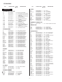
1
CD-BA1200H
SERVICE MANUAL
No. S4029CDBA1200
CD-BA1200H
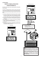
CD-BA1200H Mini Component System consisting of
CD-BA1200H (main unit) and CP-BA1200H (speaker system).
• In the interests of user-safety the set should be restored to its
original condition and only parts identical to those specified be
used.
• Note for users in U.K.
Recording and playback of any material may require consent
which SHARP is unable to give. Please refer particularly to the
provisions of Copyright Act 1956, the Dramatic and Musical
Prefomers Protection Act 1956, the Preformers Protection Acts
1963 and 1972 and to any subsequent statutory enactments and
orders.
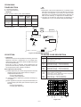
CONTENTS
Page
SAFETY PRECAUTION FOR SERVICE MANUAL ........................................................................................................... 2
IMPORTANT SERVICE NOTES (FOR U.K. ONLY) .......................................................................................................... 3
SPECIFICATIONS ............................................................................................................................................................. 3
NAMES OF PARTS ........................................................................................................................................................... 4
OPERATION MANUAL ...................................................................................................................................................... 6
QUICK GUIDE ................................................................................................................................................................... 7
DISASSEMBLY .................................................................................................................................................................. 9
REMOVING AND REINSTALLING THE MAIN PARTS ................................................................................................... 12
ADJUSTMENT ................................................................................................................................................................. 13
NOTES ON SCHEMATIC DIAGRAM .............................................................................................................................. 15
WAVEFORMS OF CD CIRCUIT ...................................................................................................................................... 16
BLOCK DIAGRAM ........................................................................................................................................................... 17
SCHEMATIC DIAGRAM / WIRING SIDE OF P.W.BOARD ............................................................................................. 20
VOLTAGE ........................................................................................................................................................................ 36
TROUBLESHOOTING (CD SECTION) ........................................................................................................................... 37
FUNCTION TABLE OF IC ................................................................................................................................................ 41
FL DISPLAY ..................................................................................................................................................................... 47
REPLACEMENT PARTS LIST/EXPLODED VIEW
PACKING METHOD (FOR U.K. ONLY)
SHARP CORPORATION
–1–
This document has been published to be used
for after sales service only.
The contents are subject to change without notice.
CD-BA1200H
(Except for U.K.)
SAFETY PRECAUTION FOR
SERVICE MANUAL
Precaution to be taken when replacing and servicing the
Laser Pickup.
The AEL (Accessible Emission Level) of Laser Power Output
for this model is specified to be lower than Class I Requirements.
However, the following precautions must be observed during
servicing to protect your eyes against exposure to the Laser
beam.
(1) When the cabinet has been removed, the power is turned
on without a compact disc, and the Pickup is on a position
outer than the lead-in position, the Laser will light for several
seconds to detect a disc. Do not look into the Pickup Lens.
(2) The Laser Power Output of the Pickup inside the unit and
replacement service parts have already been adjusted prior
to shipping.
(3) No adjustment to the Laser Power should be attempted
when replacing or servicing the Pickup.
(4) Under no circumstances look directly into the Pickup Lens
at any time.
(5) CAUTION - Use of controls or adjustments, or performance
of procedures other than those specified herein may result
in hazardous radiation exposure.
Laser Diode Properties
Material: GaAIAs
Wavelength: 780 nm
Emission Duration: continuous
Laser Output: max. 0.6 mW
(For U.K.)
CAUTION-INVISIBLE LASER RADIATION WHEN OPEN. DO NOT STARE INTO
BEAM OR VIEW DIRECTLY WITH OPTICAL INSTRUMENTS.
VARNING-OSYNLIG LASERSTRALNING NAR DENNA DEL AR OPPNAD. STIRRA
EJ IN I STRALEN OCH BETRAKTA EJ STRALEN MED OPTISKA INSTRUMENT.
ADVERSEL-USYNLIG LASERSTRALING VED ABNING. SE IKKE IND I
STRALEN-HELLER IKKE MED OPTISKE INSTRUMENTER.
VARO! AVATTAESSA OLET ALTTIINA NAKYMATON LASERSATEILYLLE.
ALA TUIJOTA SATEESEEN ALAKA KATSO SITA OPTISEN LAITTEEN LAPI.
VARNING-OSYNLIG LASERSTRALNING NAR DENNA DEL AR OPPNAD.
STIRRA EJ IN I STRALEN OCH BETRAKTA EJ STRALEN GENOM OPTISKT
INSTRUMENT.
ADVERSEL-USYNLIG LASERSTRALING NAR DEKSEL APNES. STIRR IKKE
INN I STRALEN ELLER SE DIREKTE MED OPTISKE INSTRUMENTER.
VAROITUS! LAITTEEN KÄYTTÄMINEN MUULLA KUIN
TÄSSÄ
KÄYTTÖOHJEESSA MAINITULLA TAVALLA SAATTAA
ALTISTAA KÄYTTÄJÄN TURVALLISUUSLUOKAN 1
YLITTÄVÄLLE NÄKYMÄTTÖMÄLLE LASERSÄTEILYLLE.
VARNING - OMAPPARATENANVÄNDS PÅ ANNAT SÄTT
ÄN I DENNA BRUKSANVISNING SPECIFICERAS. KAN
ANVÄNDAREN
UTSÄTTAS
FÖR
OSYNLIG
LASERSTRÅLNING, SOM ÖVERSKRIDER GRÄNSEN
FÖR LASERKLASS 1.
–2–
CD-BA1200H
IMPORTANT SERVICE NOTES (FOR U.K. ONLY)
WITHSTANDING
VOLTAGE TESTER
Before returning the unit to the customer after completion of a
repair or adjustment it is necessary for the following withstand
voltage test to be applied to ensure the unit is safe for the
customer to use.
Setting of Withstanding Voltage Tester and set.
Set name
PROBE
+
AC
OUT
-
set value
SHORT-CIRCUIT
AC POWER
SUPPLY CORD
Withstanding Voltage Tester
Test voltage
4,240 VPEAK
3,000 VRMS
Set time
6 secs
Set current (Cutoff current)
4 mA
UNIT
CONNECT THE PROBE
TO GND OF CHASSIS
SCREW
Unit
Judgment
OK: The “GOOD” lamp lights.
NG: The “NG” lamp lights and the buzzer sounds.
CHASSIS SCREW
FOR A COMPLETE DESCRIPTION OF THE OPERATION OF THIS UNIT, PLEASE REFER
TO THE OPERATION MANUAL.
SPECIFICATIONS
CD-BA1200H
General
Power source:
Power consumption:
Dimensions:
Weight:
Cassette deck section
AC 230 V, 50 Hz
32 W
Width; 270 mm (10-5/8")
Height; 300 mm (11-13/16")
Depth; 373 mm (14-11/16")
5.0 kg (11.0 lbs.)
Frequency response:
Signal/noise ratio:
Wow and flutter:
(For U.K.)
Wow and flutter:
(Except For U.K.)
50-14,000 Hz (Normal tape)
55 dB (TAPE 1, playback)
50 dB (TAPE 2, recording/playback)
0.3 % (WRMS)
0.35 % (DIN 45 511)
Amplifier section
Output power:
(For U.K.)
Output power:
(Except For U.K.)
Output terminals:
RMS; 20 W (10 W + 10 W)
(10 % T.H.D.)
RMS; 14.6 W (7.3 W + 7.3 W)
(0.9 % T.H.D.)
PMPO; 64 W
MPO; 32 W (16 W + 16 W)
(DIN 45 324)
RMS; 20 W (10 W + 10 W)
(DIN 45 324)
RMS; 14.6 W (7.3 W + 7.3 W)
(DIN 45 500)
Speakers; 8 ohms
Headphones; 16-50 ohms
(recommended; 32 ohms)
CP-BA1200H
Type:
10 cm (4") full-range speaker
Maximum input power: 20 W
Rated input power:
10 W
Impedance:
8 ohms
Dimensions:
Width; 220 mm (8-11/16")
Height; 300 mm (11-13/16")
Depth; 180 mm (7-1/16")
Weight:
2.0 kg (4.4 lbs.)/each
Specifications for this model are subject to change without
prior notice.
Compact disc player section
Type:
Signal readout:
D/A converter:
Frequency
response:
Dynamic range:
3-disc multi-play compact
disc player
Non-contact, 3-beam semiconductor laser pickup
1-bit D/A converter
20 - 20,000 Hz
90 dB (1 kHz)
Tuner section
Frequency range:
FM; 87.5-108 MHz
AM; 522-1,620 kHz
–3–
CD-BA1200H
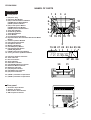
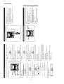
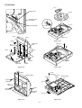
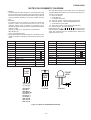
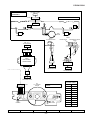
NAMES OF PARTS
CD-BA1200H
1 2
Front panel
3
4
5
6
1. (CD) Disc Tray
2. (CD) Disc Skip Button
3. (CD) Track Down/Review Button
(TUNER) Preset Down Button
(TAPE 2) Rewind Button
4. (CD) Track Up/Cue Button
(TUNER) Preset Up Button
(TAPE 2) Fast Forward Button
5. Timer Set Indicator
6. On/Stand-by Button
7. Timer/Sleep Button
8. Clock Button
9. Function Selector Buttons
10. Equalizer Mode Selector/Extra Bass/Demo Mode
Button
11. Volume Up/Down Buttons
12. (CD) Open/Close Button
13. Headphone Socket
14. Memory/Set Button
15. (CD/TAPE) Stop Button
16. (CD) Play/Repeat Button
(TAPE) Play Button
17. (TAPE 2) Record Pause Button
18. Tuning and Time Up/Down Buttons
10
7
11
12
8
9
13 14 15 16 17
18
19 20 21 22 23 24 25 26
19. (CD) Disc Number Indicators
20. Timer Indicator
21. Record Indicator
22. Sleep Indicator
23. Extra Bass Indicator
24. (CD/TUNER) Memory Indicator
25. FM Stereo Mode Indicator
26. FM Stereo Indicator
27. (CD) Repeat Indicator
28. (CD/TAPE) Play Indicator
29. (CD) Pause Indicator
27 28 29
30
31
30. (TAPE 1) Cassette Compartment
31. (TAPE 2) Cassette Compartment
Rear panel
1. AC Power Input Socket
2. Speaker Terminals
3. FM 75 Ohms Aerial Socket
4. AM Loop Aerial Socket
2
1
–4–
3
4
CD-BA1200H
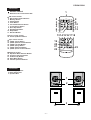
CD-BA1200H
Remote control
1
1. Remote Control Transmitter LED
CD control section
2. Disc Number Select Buttons
3. Memory Button
4. Pause Button
5. Clear Button
6. Track Down/Review Button
7. Track Up/Cue Button
8. Disc Skip Button
9. Play/Repeat Button
10. Stop Button
11. Random Button
2
3
4
5
6
7
8
9
10
11
12
13 14 15 1617 18
Tuner control section
12. Preset Up/Down Buttons
Tape control section
13. (TAPE 1) Play Button
14. (TAPE 2) Record Pause Button
15. (TAPE 1/2) Stop Button
16. (TAPE 2) Play Button
17. (TAPE 2) Rewind Button
18. (TAPE 2) Fast Forward Button
19
20
21
22
23
Common section
19. Equalizer Mode Selector Button
20. Function Selector Buttons
21. On/Stand-by Button
22. Extra Bass Button
23. Volume Up/Down Buttons
CP-BA1200H
1. Full-Range Speaker
2. Bass Reflex Duct
3. Speaker Wire
1
2
3
–5–
–6–
5
AM 12:00
) button to select the
(AM 12:00 - PM 11:59)
The 12-hour display will appear.
(AM 0:00 - PM 11:59)
The 12-hour display will appear.
(0:00 - 23:59)
The 24-hour display will appear.
AM 0:00
or
Press the MEMORY/SET button.
Note that this can only be set when the unit is first
installed or it has been reset.
"AM 12:00"
"AM 0:00"
"0:00"
0:00
Press the TUNING/TIME (
time display mode.
Within 5 seconds, press the MEMORY/SET button.
3
4
Press the CLOCK button.
Press the ON/STAND-BY button to enter the standby mode.
2
1
TUNING/TIME
(
)
CLOCK
MEMORY/SET
ON/
STAND-BY
(Main unit operation)
In this example, the clock is set for the 24-hour (0:00) system.
SETTING THE CLOCK
or
) button to adjust
or
) button to adjust
The clock starts operating from "0" second. (Seconds are
not displayed.) And then the clock display will disappear
after a few seconds.
Press the MEMORY/SET button.
Press the TUNING/TIME (
or
) button once to
advance the time by 1 minute. Hold it down to change the
time in 5 - minute intervals.
The hour setting will not advance even if minutes
advance from "59" to "00".
Press the TUNING/TIME (
the minutes.
Press the MEMORY/SET button.
Press the TUNING/TIME (
or
) button once to
advance the time by 1 hour. Hold it down to advance continuously.
When the 12-hour display is selected, "AM" will change
automatically to "PM".
Press the TUNING/TIME (
the hour.
To change the time display mode:
1 Perform steps 1 - 2 in "RESETTING THE MICROCOMPUTER".
2 Perform steps 1 - 9 above.
To change the clock time:
1 Press the CLOCK button.
2 Within 5 seconds, press the MEMORY/SET button.
3 Perform steps 6 - 9 above.
Note:
The clock display will flash on and off at the push of the
CLOCK button when the AC power supply is restored
after a power failure occurs or after the AC power lead is
disconnected. If this happens, follow the procedure below
to change the clock time.
To see the time display:
Press the CLOCK button.
The time display will appear for about 5 seconds.
9
8
7
6
15
0.2 m - 6 m
(8" - 20')
ON/
STAND-BY
EQUALIZER
X-BASS/
DEMO
RESETTING THE MICROCOMPUTER
15
REMOTE CONTROL
Whilst pressing down the
/
button and the
EQUALIZER/X-BASS/DEMO button, hold down the
ON/STAND-BY button for at least 1 second.
"CLEAR AL" will appear.
Press the ON/STAND-BY button to enter the standby mode.
Caution:
The operation explained above will erase all data stored
in memory including clock and timer settings, and tuner
and CD presets.
2
1
Reset the microcomputer under the following conditions:
To erase all of the stored memory contents (clock and
timer settings, and tuner and CD presets).
If the display is not correct.
If the operation is not correct.
Notes concerning use:
Replace the batteries if the operating distance is reduced
or if the operation becomes erratic.
Periodically clean the transmitter LED on the remote control and the sensor on the main unit with a soft cloth.
Exposing the sensor on the main unit to strong light may
interfere with operation. Change the lighting or the direction of the unit.
Keep the remote control away from moisture, excessive
heat, shock, and vibrations.
CD-BA1200H
OPERATION MANUAL
FM aerial × 1
3
AC power lead × 1
–7–
10 cm (4")
10 cm (4")
Placing the system
Remote control × 1
10 cm (4")
10 cm (4")
3 Replace the battery cover.
2 "AA" size batteries
(UM/SUM-3, R6, HP-7 or similar)
2 Insert the batteries.
Putting batteries into the remote control
1 Remove the battery cover.
2
AC power lead × 1
[Except for U.K.]
AM loop aerial × 1
Check the supplied accessories
[For U.K.]
1
4 Connections
FM aerial
2
1
[For U.K.]
AC 230 V, 50 Hz
[Except for U.K.]
Black
Red
Left speaker
3 Connect the AC power lead.
Right speaker
2 Connect the speaker system.
AM loop
aerial
1 Connect the AM and FM aerials.
CD-BA1200H
7
6
5
–8–
4
3
PUSH
EJECT
4
1
2
TAPE 1
3
TAPE 2
2
3
PUSH
EJECT
5
6
Listening to a tape
2
1
Listening to the radio
7
3,6
5
8 cm (3")
12 cm (5")
8
5
1
2
4
Listening to a CD
or
) button to tune in-
2) button to select the TAPE 1
5 Press the button to start playback.
6 Adjust the sound volume using the VOLUME buttons.
or TAPE 2.
4 Press the TAPE (1
And then, close the cassette door completely until it is locked.
compartment.
3 Load the cassette into the TAPE 1 or TAPE 2 cassette
"PUSH EJECT".
1 Press the ON/STAND-BY button to turn the power on.
2 Open the cassette door by pushing the area marked
4 Adjust the sound volume using the VOLUME buttons.
to the desired station.
3 Press the TUNING/TIME (
or AM.
1 Press the ON/STAND-BY button to turn the power on.
2 Press the TUNER (BAND) button to select FM ST, FM
6 Press the OPEN/CLOSE button to close the disc tray.
7 Press the
button.
8 Adjust the sound volume using the VOLUME buttons.
to turn the disc tray, then place the CD in the open position.
1 Press the ON/STAND-BY button to turn the power on.
2 Press the CD button.
3 Press the OPEN/CLOSE button to open the disc tray.
4 Place the CD(s) on the disc tray, label side up.
5 When loading a third disc, press the DISC SKIP button
1
3
TAPE 2
PUSH
EJECT
2
4
5
Recording from CDs
1 Press the ON/STAND-BY button to turn the power on.
2 Load a cassette into the TAPE 2 cassette compartment.
3 Press the CD button and load the desired disc.
4 Press the REC PAUSE button.
5 Press the
button.
2
2
Cleaning disc
Caution:
The operation explained above will erase all data stored
in memory including clock and timer settings, and tuner
and CD presets.
button and the
EQUALIZER/X-BASS/DEMO button, hold down the
ON/STAND-BY button for at least 1 second.
"CLEAR AL" will appear.
2 Whilst pressing down the
mode.
1 Press the ON/STAND-BY button to enter the stand-by
Clean the dust or stain on the CD pickup lens
using a commercial cleaning disc (brush type).
CD pickup cleaning
1,2
If this product is subjected to strong external interference
(mechanical shock, excessive static electricity, abnormal
supply voltage due to lightning, etc.) or if it is operated incorrectly, it may malfunction or the display may not function correctly. If such a problem occurs, do the following:
Resetting the microcomputer
8
CD-BA1200H
CD-BA1200H
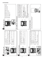
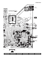
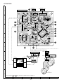
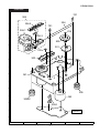
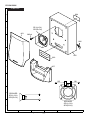
DISASSEMBLY
CD-BA1200H
Caution on Disassembly
Follow the below-mentioned notes when disassembling
the unit and reassembling it, to keep it safe and ensure
excellent performance:
1. Take cassette tape and compact disc out of the unit.
2. Be sure to remove the power supply plug from the wall
outlet before starting to disassemble the unit.
3. Take off nylon bands or wire holders where they need to
be removed when disassembling the unit. After servicing
the unit, be sure to rearrange the leads where they were
before disassembling.
4. Take sufficient care on static electricity of integrated
circuits and other circuits when servicing.
Top Cabinet
(A1)x2
ø3x12mm
Side Panel
(Right)
(A1)x2
ø3x12mm
(B1)x1
ø3x10mm
CD-BA1200H
STEP
REMOVAL
PROCEDURE
FIGURE
1
Top Cabinet
1. Screw ..................... (A1) x4
9-1
2
Side Panel
(Left/right)
1. Screw ..................... (B1) x4
9-1
3
CD Player Unit/
CD Tray Cover
1. Turn on the power supply,
open the disc tray, take out the
CD cover, and close. (Note 1)
2. Screw ..................... (C1) x1
3. Hook ....................... (C2) x3
4. Hook ....................... (C3) x2
5. Socket .................... (C4) x2
9-2
(B1)x2
ø3x12mm
Side Panel
(Left)
Rear
Panel
(B1)x1
ø3x10mm
Figure 9-1
CD Tray Cover
CD Servo
PWB
(C4)x2
(C2) x3
1
4
Rear Panel
1. Screw ..................... (D1) x6
9-2
5
Main/Headphones 1. Screw ........................ (E1) x8
PWB
2. Socket .................... (E2) x4
3. Flat Cable .............. (E3) x1
4. Tip .......................... (E4) x1
10-2
6
Front Panel
1. Screw ..................... (F1) x3
10-2
7
Display PWB
1. Screw ..................... (G1) x9
2. Flat Cable .............. (G2) x1
10-3
8
Tape Mechanism 1. Open the cassette holder.
2. Screw...................... (H1) x5
10-3
9
Turntable
1. Hook ....................... (J1) x2
2. Cover ..................... (J2) x1
10-4
10
Disc Tray
1. Turn fully the lock lever in the
arrow direction.
2. While holding the lock lever, rotate
the cam gear until the cam gear
rib engages with the clamp lever.
3. Push the slide holder backward to
engage the claw with the groove
and remove it in the direction
of the arrow. .............. (K1) x6
9-3
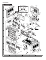
(C3) x1
Pull
1
2
CD Player
Unit
Rear
Panel
(C3)x1
(C1)x1
ø3x12mm
10-1
Main PWB
(D1)x6
ø3x8mm
10-5
11
CD Servo PWB
(Note 2)
1. Screw ..................... (L1) x1
2. Hook ....................... (L2) x2
3. Socket .................... (L3) x4
10-6
12
CD Mechanism
1. Hook ....................... (M1) x2
2. Hook ....................... (M2) x3
11-1
13
Loading Motor PWB 1. Hook ....................... (N1) x5
11-1
Figure 9-2
Lock Lever
CD Player Unit
(Bottom View)
Note 1:
How to open the changer manually. (Fig. 9-3)
1. In this state, turn fully the lock lever in the arrow direction
through the hole on the loading chassis bottom.
2. While holding the lock lever, rotate the cam gear anticlockwise
until the cam gear rib engages with the clamp lever. (Fig. 10-1)
3. After that, push forward the CD slide holder.
Note 2:
1. After removing the connector for the optical pickup from the
connector, wrap the conductive aluminium foil around the
front end of the connector to protect the optical pickup from
electrostatic damage.
Figure 9-3
Note 3:
1. Be careful not to break the claw of the CD mechanism.
2. When fining back the cam gear assembly, let it lock by front
movement.
–9–
CD-BA1200H
(J2) x1
Clamp Lever
Turntable
CD Player Unit
(Top View)
Disc Tray
(J1) x2
Cam Gear Rib
Figure 10-1
(E3)x1
CD Player Unit
(E2)x2
(E2)x1
Figure 10-4
Headphones
PWB
(E1)x7
ø3x10mm
(K1) x3
2
(E4)x1
(E2)x1
1
(E1)x1
ø3x10mm
Main PWB
(K1) x3
(F1)x3
ø3x8mm
Figure 10-2
Figure 10-5
(G2)x1
Display PWB
(L3) x2
(G1)x9
ø3x10mm
(L1)x1
ø3x8mm
CD Servo
PWB
(L2) x2
Tape
Mechanism
Open
(H1)x5
ø3x10mm
Cassette
Holder
(L3) x2
Figure 10-6
Figure 10-3
– 10 –
Slide Chassis
CD-BA1200H
Cam Gear
(M2) x3
CD
Mechanism
Loading
Motor
PWB
(M1) x1
(M1) x1
(N1) x5
Figure 11-1
CP-BA1200H
STEP
1
PROCEDURE
REMOVAL
Speaker
1. Net .......................... (A1) x1
2. Duct Panel .............. (A2) x1
3. Screw ...................... (A3) x4
FIGURE
11-2
11-3
CP-BA1200H
Speaker Box
Speaker Box
(A1)x1
Speaker
(A2)x1
(A3)x4
ø3.5x13mm
Driver should be
pried away from
Speaker Box.
Driver
Direction of handle
Figure 11-3
Figure 11-2
– 11 –
CD-BA1200H
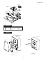
REMOVING AND REINSTALLING THE MAIN PARTS
TAPE MECHANISM SECTION
TAPE 2
Perform steps 1 to 6 and 8 of the disassembly method to
remove the tape mechanism.
Record/Playback
Head
How to remove the record/playback and erase
heads (TAPE 2) (See Fig. 12-1)
1. Carefully remove the record/playback head and erase head
screw (A1) x 2 pcs.
Erase Head
How to remove the playback head (TAPE 1)
(See Fig. 12-2)
(A1)x2
Ø2 x 9mm
1. Carefully remove the playback head screw (B1) x 2 pcs.
Figure 12-1
TAPE 1
How to remove the pinch roller (TAPE 1/2)
(See Fig. 12-3)
Playback
Head
1. Carefully bend the pinch roller pawl in the direction of the
arrow <A>, and remove the pinch roller (C1) x1 pc., in the
direction of the arrow <B>.
Note:
When installing the pinch roller, pay attention to the spring
mounting position.
(B1)x1
Ø2x9mm
How to remove the belt (TAPE 2) (See Fig. 12-4)
1. Remove the main belt (D1) x 1 pc., from the motor side.
2. Remove the FF/REW belt (D2) x 1 pc.
(B1)x1
Ø2x5mm
Figure 12-2
How to remove the belt (TAPE 1) (See Fig. 12-4)
1. Remove the main belt (E1) x 1 pc., from the motor side.
2. Remove the FF/REW belt (E2) x 1 pc.
How to remove the motor (See Fig. 12-5)
1. Remove the screws (F1) x 2 pcs., to remove the motor.
Pinch Roller
(C1)x1
Pull
Pull <A>
Pinch
Roller
Pawl
<B>
Figure 12-3
Motor
Motor
TAPE 2
FF/REW
Belt
(D2)x1
Motor
TAPE2
Main Belt
(D1)x1
TAPE1
Main Belt
(E1)x1
(F1) x2
Ø 2.6 x 5mm
TAPE 1
(D1)x1
(E1)x1
Figure 12-5
Figure 12-4
– 12 –
FF/REW
Belt
(E2)x1
CD-BA1200H
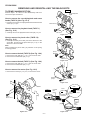
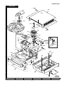
CD MECHANISM SECTION
Perform steps 1, 2, 3, 9 and 12 of the disassembly method to
remove the CD mechanism.
How to remove the loading motor
(See Fig. 13-1)
Loading Motor
1. Bend the hooks (A1) x 5 pcs., to remove the loading motor.
(A1)x1
(A1)x2
(A1)x2
Slide Chassis
Figure 13-1
How to remove the pickup (See Fig. 13-2)
Stop Washer
(B1) x2
(B3) x1
ø2.6 x6mm
1. Remove the screws (B1) x 2 pcs., to remove the shaft (B2).
2. Remove the stop washer (B3) x 1 pc., to remove the gear
(B4).
3. Remove the pickup.
Note
After removing the connector for the optical pickup from the
connector, wrap the conductive aluminium foil around the
front end of connector to protect the optical pickup from
electrostatic damage.
Pickup
CD Mechanism
Shaft
(B2) x1
Gear
(B4) x1
Figure 13-2
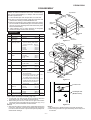
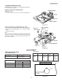
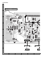
ADJUSTMENT
• Tape Speed
MECHANISM SECTION
• Driving Force Check
Torque Meter
Test Tape
Adjusting
Point
Specified
Value
MTT-111
Variable
Resistor in
motor.
3,000 ±
30 Hz
Specified Value
Play: TW-2111
Normal
speed
Tape 1: Over 80 g
Tape 2: Over 80 g
• Torque Check
Torque Meter
Specified Value
Tape 1
Tape 2
Play: TW-2111
30 to 80 g.cm
30 to 80 g.cm
Fast forward: TW-2231
—
70 to 180 g.cm
Rewind: TW-2231
—
70 to 180 g.cm
TAPE MECHANISM
Motor
Variable Resistor
in motor
Figure 13-3
– 13 –
Instrument
Connection
Speaker
terminal
(Load
resistance:
6 ohms)
CD-BA1200H
• FM
Notes:
1: Description of the "FM IF Adjustment" is not carried on this
Manual. It is because the IF coil in the FM front end section
has been best adjusted in the factory so that its further
adjustment is not needed at the field. When replacing the
FM front end assembly, no adjustment is needed either.
2: The parts in the FM front end section are prepared in a
complete unit, so you can't obtain each part individually
TUNER SECTION
fL: Low-range frequency
fH: High-range frequency
• AM IF/RF
Signal generator: 400 Hz, 30%, AM modulated
Frequency
Frequency
Display
AM IF
450 kHz
1,620 kHz
T351
AM Band
Coverage
—
522 kHz
(fL): T306 *2
1.1 ± 0.1 V
990 kHz
(fL): T303
Test Stage
AM Tracking 990 kHz
*1. Input: Antenna
*2. Input: Antenna
Setting/ Instrument
Adjusting Connection
Parts
*1
*1
Output: TP302
Output: TP301
SO301
FM ANTENNA
TERMINAL
1
CNP302
AM LOOP
ANTENNA
MAIN PWB
FE301
TP301
T303
AM
TRACKING fL
AM BAND
COVERAGE fL
R381
T306
T351
AM IF
R357
TP302
Figure 14-1 ADJUSTMENT POINTS
CD ERROR CODE DESCRIPTION
CD SECTION
• Adjustment
Since this CD system incorporates the following automatic
adjustment functions, readjustment is not needed when
replacing the pickup. Therefore, different PWBs and pickups
can be combined freely.
Each time a disc is changed, these adjustments are
performed automatically. Therefore, playback of each disc
can be performed under optimum conditions.
Items adjusted automatically
(1) Offset adjustment (The offset voltage between the head
amplifier output and the VREF reference voltage is
compensated inside the IC.)
* Focus offset adjustment
* Tracking offset adjustment
(2) Tracking balance adjustment (waveform drawing Fig.
14-2 EFBL)
(3) Gain adjustment (The gain is compensated inside the IC
so that the loop gain at the gain crossover frequency will
be 0dB.)
* Focus gain adjustment
* Tracking gain adjustment
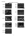
Error
State Code
0001
0002
[Servo System Error]
Cannot detect Pickup-in SW
DSP access error
0101
0103
[Error during close operation]
Open/Close SW Low → High not functioning
Open/Close SW High → Low not functioning
0201
0203
[Error during open operation]
Open/Close SW Low → High not functioning
Open/Close SW High → Low not functioning
0302
0306
0307
0308
[Error during skip operation]
Pickup-in SW is not detected
During Disc 1 search, Open/Close SW or Clamp SW
or Disc SW do not change to low.
Clamp SW Low → High not functioning
Clamp SW High → Low not functioning
T
Stopped
CH1=500mV
DC 10:1
T
CH2=200mV
DC 10:1
CH3=1V
DC 10:1
1999/04/05 20:26:47
500ms/div
(500ms/div)
NORM:20kS/s
FDO
1
TE
3
EFBL
2
CH2
v/DIV
200mV
=Filter=
Smoothing : ON
BW : FULL
=Offset=
CH1 :
0.000V
CH2 :
0.000V
CH3 :
0.00V
CH4 :
0.00V
=Record Length=
Main : 100K
Zoom :
2k
Figure 14-2
– 14 –
=Trigger=
Mode : SINGLE
Type : EDGE CH1
Delay :
0.0ns
Hold off :
0.2us
CD-BA1200H
NOTES ON SCHEMATIC DIAGRAM
• The indicated voltage in each section is the one measured
by Digital Multimeter between such a section and the chassis with no signal given.
1. In the tuner section,
( ) indicates AM
< > indicates FM stereo
2. In the main section, a tape is being played back.
3. In the deck section, a tape is being played back.
( ) indicates the record state.
4. In the power section, a tape is being played back.
5. In the CD section, the CD is stopped.
• Parts marked with “
”(
) are important for
maintaining the safety of the set. Be sure to replace these
parts with specified ones for maintaining the safety and
performance of the set.
• Resistor:
To differentiate the units of resistors, such symbol as K and
M are used: the symbol K means 1000 ohm and the symbol
M means 1000 kohm and the resistor without any symbol is
ohm-type resistor. Besides, the one with “Fusible” is a fuse
type.
• Capacitor:
To indicate the unit of capacitor, a symbol P is used: this
symbol P means micro-micro-farad and the unit of the
capacitor without such a symbol is microfarad. As to
electrolytic capacitor, the expression “capacitance/withstand
voltage” is used.
(CH), (TH), (RH), (UJ): Temperature compensation
(ML): Mylar type
(P.P.): Polypropylene type
• Schematic diagram and Wiring Side of P.W.Board for this
model are subject to change for improvement without prior
notice.
POSITION
REF. NO
SW1
REF. NO
OPEN/CLOSE
DESCRIPTION
ON—OFF
SW714
CD
ON—OFF
SW2
CLAMP
ON—OFF
SW715
TAPE
ON—OFF
SW3
DISC NUMBER
ON—OFF
SW716
TUNING /TIME DOWN
ON—OFF
SW4
PICKUP IN
ON—OFF
SW717
MEMORY/SET
ON—OFF
SW701
ON/STAND-BY
ON—OFF
SW718
REWIND
ON—OFF
SW702
CLOCK
ON—OFF
SW719
FAST FORWARD
ON—OFF
SW703
TIMER/SLEEP
ON—OFF
SW720
PLAY/REPEAT
ON—OFF
SW709
DISC SKIP
ON—OFF
SW721
STOP
ON—OFF
SW710
OPEN/CLOSE
ON—OFF
SW723
REC/PAUSE
ON—OFF
SW711
EQUALIZER/X-BASS/DEMO
ON—OFF
SW724
TUNING/TIME UP
ON—OFF
SW712
VOLUME UP
ON—OFF
SW725
TUNER (BAND)
ON—OFF
SW713
VOLUME DOWN
ON—OFF
DESCRIPTION
FRONT
VIEW
FRONT
VIEW
FRONT
VIEW
E C B
(S) (G) (D)
(1) (2) (3)
B C E
2SC1845 F
2SC3331
2SC380 O
KTA1266 GR
KTA1271 Y
KTA1273 Y
KTC3203 Y
KRC102 M
KRC104 M
KRC107 M
KTC2026
4204SRT7
Figure 15 TYPES OF TRANSISTOR AND LED
– 15 –
POSITION
CD-BA1200H
WAVEFORMS OF CD CIRCUIT
Stopped
CH1=500mV
DC 10:1
CH3=500mV
DC 10:1
T
Stopped
CH1=500mV
DC 10:1
500ms/div
(500ms/div)
NORM:20kS/s
CH3=1V
DC 10:1
1999/04/05 17:33:17
CH4=1V
500ms/div
(500ms/div)
DC 10:1
NORM:20kS/s
PDO1
1
7
FDO
IC2 24
1
IC2 1
3
4
8
2
IC2 23
T
3
1
CH1
v/DIV
500mV
=Filter=
Smoothing : ON
BW : FULL
=Offset=
CH1 :
0.000V
CH2 :
0.0V
CH3 :
0.000V
CH4 :
0.00V
Stopped
CH1=500mV
DC 10:1
1
IC2 24
3
IC2 72
4
PDO2
IC2 2
TDO
CH2=10V
DC 10:1
=Record Length=
Main :
100K
Zoom :
2K
CH3=1V
DC 10:1
IC2 24
FDO
1
CH1
v/DIV
500mV
=Trigger=
Mode : AUTO
Type : EDGE CH1
Delay :
0.0ns
Hold off :
0.2us
=Filter=
Smoothing : ON
BW : FULL
Stopped
CH1=2V
DC 10:1
500ms/div
(500ms/div)
NORM:20kS/s
=Offset=
CH1 :
0.000V
CH2 :
0.0V
CH3 :
0.00V
CH4 :
0.00V
=Record Length=
Main :
100K
Zoom :
2K
T
=Trigger=
Mode : AUTO
Type : EDGE CH2
Delay :
0.0ns
Hold off :
0.2us
1999/04/07 09:25:28
500ns/div
(500ns/div)
NORM:200MS/s
FDO
T
1
T
2
IC1 18 ,
DRF
9
IC2 37
1
DOUT
TE
3
IC2 16
CH Position To
-3div
-1div
0div
+1div
+3div
=Filter=
=Offset=
=Record Length=
Smoothing : ON CH1 :
0.000V
Main :
100K
BW : FULL
CH2 :
0.0V
Zoom :
2K
CH3 :
0.00V
CH4 :
0.00V
CH2
Position
0.20div
=Trigger=
Mode : AUTO
Type : EDGE CH1
Delay :
0.0ns
Hold off :
0.2us
=Filter=
Smoothing : ON
BW : FULL
Stopped
CH1=2V
DC 10:1
10
=Offset=
CH1 :
0.00V
CH2 :
0.00V
CH3 :
0.00V
CH4 :
0.00V
=Record Length=
Main :
1K
Zoom :
100
T
CH2=2V
DC 10:1
CH3=2V
DC 10:1
=Trigger=
Mode : NORMAL
Type : EDGE CH1
Delay :
2.887ms
Hold off :
0.2us
1999/04/05 20:50:17
5us/div
(5us/div)
NORM:100kS/s
IC2 57
1
LRSY
5
IC1 27
11
IC2 58
2
DATACK
12
IC2 59
T
3
DATA
Vp-p=1.0V~1.3V
0.5mV/div,0.5µsec/div
=Filter=
Smoothing : ON
BW : FULL
CH2=1V
DC 10:1
100ms/div
(100ms/div)
NORM:100kS/s
1
4
IC2 24
T
CH2=200mV
DC 10:1
=Record Length=
Main :
5K
Zoom : 100
CH3=1V
DC 10:1
=Trigger=
Mode : AUTO
Type : EDGE CH3
Delay :
0.0ns
Hold off :
0.2us
1999/04/05 20:26:47
500ms/div
(500ms/div)
NORM:20kS/s
FDO
1
TE
IC1 18 ,
2
IC2 16
4
3
=Offset=
CH1 :
0.00V
CH2 :
0.00V
CH3 :
0.00V
CH4 :
0.00V
T
Stopped
CH1=500mV
DC 10:1
T
Stopped
CH1=10V
DC 10:1
CH3
v/DIV
2V
IC2 72
T
1
IC1 18 ,
TE
3
IC2 16
DRF
13
IC1 13 ,
EFBL
2
IC2 22
CH2
v/DIV
200mV
=Filter=
Smoothing : ON
BW : FULL
=Offset=
CH1 :
0.0V
CH2 :
0.00V
CH3 :
0.00V
CH4 :
0.00V
Stopped
CH1=200mV
DC 10:1
=Record Length=
Main :
100K
Zoom :
2K
T
=Trigger=
Mode : NORMAL
Type : EDGE CH1
Delay :
2.924ms
Hold off :
0.2us
=Filter=
Smoothing : ON
BW : FULL
1999/04/07 09:51:15
500ms/div
(500ms/div)
NORM:20kS/s
CH2=500mV
DC 10:1
T
FDO
1
IC2 24
2
6
IC2 25
1
SPDO
=Filter=
Smoothing : ON
BW : FULL
=Offset=
CH1 :
0.000V
CH2 :
0.000V
CH3 :
0.00V
CH4 :
0.00V
=Record Length=
Main :
100K
Zoom :
2K
=Trigger=
Mode : NORMAL
Type : EDGE CH2
Delay :
2.924ms
Hold off :
0.2us
– 16 –
=Offset=
CH1 :
0.000V
CH2 :
0.000V
CH3 :
0.00V
CH4 :
0.00V
=Record Length=
Main : 100K
Zoom :
2k
=Trigger=
Mode : SINGLE
Type : EDGE CH1
Delay :
0.0ns
Hold off :
0.2us
CD-BA1200H
SW2
SW3
SW1
OPEN/ CLAMP DISC
NUMBER
CLOSE
M3
T/T
UP/DOWN
MOTOR
M
6
7
8
9 10
4
5
6
1
2
3
4
5
6
1
2
3
4
5
6
CNP12
BI4
3
CNS4
CLAMP SW
5
2
CNP4
+
-
1
GND
CD RES
4
CLK
CE
3
DI
2
DO
1
DRF
5
CDINT
4
WRQ
+5V(+B4)
3
CNP11
2
TO DISPLAY SECTION
DGND
1
L-CH
R-CH
AGND
TO MAIN SECTION
(TO IC601)
CONT2
30
CONT3
32 31
RCHO
LVSS
RVSS
45 46 47 48
LCHO
76
CONT4
66 CL
75
CONT7
65 CE
CONT6
Q2
74
64
67 DI
40
68 DO
19
13
69 INT
IC2
LC78641E
SERVO/SIGNAL
CONTROL
70 WRQ
71 RES
3
CONT5
33
SLDO
26
SPDO
25
72 DEF
RFENV
FDO
24
TDO
23
15 16
+3.3V
+5V
TE
HFL
14
FE
XVDD
7
RVDD
5 18 36 44 49 50
LVDD
73
51 XIN
VDD
VDD5V
VVDD
XL1
16.9344MHz
ADAVDD
52 XOUT
1
CONSTANT
VOLTAGR
RFEV
FE-
FE
+5V
IC1
LA9235M
SERVO AMP.
LASER
DRIVER
2
3 4
Q3
LDD
PD
TIN2
TIN1
FIN2
FIN1
1
29
IC3
M63001FP
FOCUS/TRACKING/
SPIN/SLED DRIVER
VCC4
24 VCC2
11
9
38 39
18 VCC1
40
23
41 42
35
30
+3.3V
17 25
20 21 22
TE-
HFL
19
TE
17 18
Q1
2
21
23
14
28 VCC3
8
4
+3.3V
22
5
6
7
15
16 26 27
7 8
TRACKING COIL
FOCUS COIL
PICKUP UNIT
+5V
M1
SPINDLE
MOTOR
M
M2
SLED
MOTOR
M
SW4
PICKUP IN
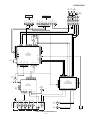
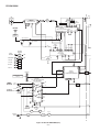
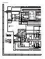
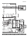
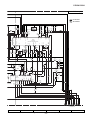
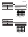
Figure 17 BLOCK DIAGRAM (1/3)
– 17 –
CD-BA1200H
+B3
FM
ANTENNA
FE301
TA7358AP
FM FRONT END
8
6
CF302
AM LOOP
ANTANNA
CF351
X351
456kHz
5
T351 CF352
4
3
7
Q301
Q
AM IF
FMOSC
2
CF301
1
4 5
1 2
8
9
IC303 AM IF GND FM+B FM
DET
LA1832S
FM IF DET./FM MPX./AM IF
AM MIX
17 13
VCO MO/ST
L 14
R
FM/AM
OUT MPXIN
18
7
16
12
STEREO
AMRFIN
L341
BALUN
FMAFC
AMOSCIN
23 22 21 24
15
FM/AM
AM TRACKING
AM BAND
COVERAGE
TAPE
MOTOR
M
SOLENOID
T2 PLAY
OSC
Q706
+2B
Q704
Q705
IC701
54PIN
+2B
R.PLAY
IC701
53PIN
IC701
56PIN
F.PLAY
IC701
55PIN
T1 PLAY
SWITCHING
FM +B
Q360
17
7
9
10
21
+B3
23
9
16
TAPE L 10
R 15
TUNER L 1
R 14
CD L 12
R 13
2
3
IC101
AN7345K
PLAYBACKANDRECORD
/PLAYBACKAMP.
4
5
L(T1) 1
R(T1) 24
L-CH
R-CH
SWITCHING
Q104~
Q107
LNF
4
21 R
21 R
4 L
Q601
Q602
SYSTEM
MUTE
3
Q110
Q111
MUTING
PB
REC/PLAY
5
20
3
RNF 22
H/N
POP
REDUCE 6 T1/T2
7 L REC
18 R
LREC 9 REC
RREC 16
8 LNF
17 RNF
REF 14
12 NOR/
HIGH
T1/T2
15 12
10 ALC
19
SWITCHING
Q108
Q109
IC601
LC75341
AUDIOPROCESSOR
+B3
13
P.B
L(T2) 2
R(T2) 23
DI 1
CE 2
CL 24
7 8 17 18
L
ACBIAS
6
+B3
FROMCDSECTION
CNP11
L-CH
TAPE2
RECPBHEAD R-CH
4 5
FM
1
REC
P.B.
11 3
IC302
LC72131
PLL(TUNER)
FM/AM MO/ST
CNS601
TAPE1
PBHEAD
22 15 16
1
DO
CE
20
MOTOR
DRIVER
CL
X352
4.5MHZ
VT
DI
T306
T303
T1/T2
Q103
SWITCHING
Q101
Q102
BIAS
SWITCHING
ERASE
HEAD
Q114
L104
BIAS
OSC
Q112
L103
Q113
SWITCHING
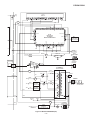
Figure 18 BLOCK DIAGRAM (2/3)
– 18 –
BAIS
CD-BA1200H
+B3
FL701
DISPLAY
1 2
10
3
13 15 16 19 20 22 26
11
14 17 18 21 27
30
31
32 33
Q701
+B6
59 58 57 56 55 54 53 52 51 50 49 48 47 46 45 44 43 42 41 40
39
38
37
SYS.STOP 36
35
+B6
AVDD 34
33
VDD
71
78
79 VLOAD
IC701
IX0337AW
SYSTEM
MICROCOMPUTER
80
91
92
31
1
4 5 6
9 10 11 12 13 15 16 17
7
XL701
4.1943 MHz
+B6
DO
DI
CL
CE
100
VDD
VDD
RESET
99
KEY
SW701-SW703
SW709-SW721
SW723-SW725
20 21 22 23 24
+B6
TO CD
SECTION
RESET
SP.DET. Q901
Q902
4
1 R
L
R 5
Vcc
4
10
SYSTEM
MUTE
+B6
+B2
9
7 R-OUT
11 L-OUT
PT801
MAIN POWER
TRANSFORMER
F901
T2.5A L 250V
Q904
RL801
D907 910
+B1
REC/PLAY
+B2
+B3
+B4
M10V
SO902
AC INPUT
Q903
D911 D914
IC902
A10V
KIA7810AP
VOLTAGE
REGULATOR
+5V
KIA7810AP
VOLTAGE
REGULATOR
VF1
T1/T2
JK901
HEADPHONES
SO901
SPEAKER
TERMINAL
IC901
LA4282
POWER AMP.
L 2
Q601
Q602
RESET IC
1
3 IC704
KIA7042PA
2
Q707
F902
T1.6A L 250V
L801
LINE
FILTER
IC904
VF2
T.F.
D806
5W +5V
+B5
Q803
BAIS
IC903
+B6
UNSWITCH
5V
PT802
SUB POWER
D802~805 TRANSFORMER
AN7805
CONSTANT
VOLTAGE REGULATOR
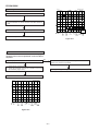
Figure 19 BLOCK DIAGRAM (3/3)
– 19 –
AC POWER
SUPPLY CORD
AC 230V,50Hz
CD-BA1200H
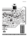
CD SERVO PWB-B
A
B
F
7
6
7
6
7
6
5
5
5
5
R51
68K
TIN1
4
4
4
4
R52
68K
FIN1
3
3
3
3
R53
68K
FIN2
2
2
2
2
R54
68K
1
1
1
C23
0.047
TIN2
R56
68K
IC1
LA9235M
SERVO AMP.
R55
68K
C24
2.2/50
C11
0.47/6.3
1
FIN1
CNP1
C
7
6
30
1
FIN2
REF
2
29
REF
TIN1
C54
47/10
C
C55
0.01
C7
10/16
VREF
R47
3.3
D
REF
EFBL
27
RFSW
R42
120K
RF-
DH
24
ODRV
22
PH/BH
REF
LPF
9
REF
10
11
ODRV
12
AGCON
20
REF
19
LPF
18
REF
REF
13
TEST0 14
TES1
21
LPF
C18
3P
(CH)
R5
39K
R6
27K
C21
0.1
C8
0.02
P
R11
12K
R1
1.2
S
C17
0.0047
10K
C42
68P
C14
0.33
C27
0.1
RFEV
PH(RF
FE-
R3
FE
100K
TE-
R4
TE
10K
AD
HFL
C82
0.022
REF
17
REF
16 TEST
4
Q3
KTA1266GR
C29
0.1
A
C28
47/10
C41
100/10
REF
15
R13
680
R15
R8
330
BH
R79
1.5M
R80
1M
C20
0.1
C13
0.01
PH
C22
100P
R10
27K
5
NC
23
APC
R7
6.8K
RF
26
25
REF
6
7
AGON
R25
10K
REF
PH
8
LDON
+B
28
5
LDD
C51
47/10
AGCON
3
TIN2
4
C6
100/10
REF1
GND
C53
0.001
C12
0.1
REF
C8
0.1
+B
VCC
ODRV
REF
7
R12
680
C26
0.047
E
R50
47
C25
0.1
Vref
B
8
+B
C19
100/10
Vcc
CNS1A
CNS1B
A
P
2
B
LASER DRIVER
R44
1K
EFBL
R43
220K
D93
DS1SS133
3
4
4
4
4
5
5
5
5
6
6
6
6
7
7
7
7
8
PICKUP UNIT
8
8
8
FO+
FO
FO+
FO-
FO-
GND
TR+
PD
TR-
VR
3
+
+
4
7
11
13
14
VCC1
STANDBY
R48
6.8K
G
Vref
CNS3B
CNS3A
+
6
6
6
6
+
5
5
5
5
4
4
4
4
-
3
3
3
3
2
2
2
2
1
1
1
1
CNP3A
M1
SPINDLE
MOTOR
M
M2
SLED
MOTOR
M
SW4
PICKUP IN
C50
100/16
C49
100/16
MUTE
CD MOTOR PWB-C
32
30
29
27
+
GND
31
16
18
C47
100/16
34
28
+
LOADING M-
33
15
17
+B
LOADING M+
36
26
+
-
SLDO
+B
LD_MVCC4
35
-
SL+
39
37
12
SL-
40
38
9
GND
+
5
10
CNP2
41
6
8
LD
42
-
IC3
M63001FP
FOCUS/TRACKING/
SPIN/SLED DRIVER
3
CNS2A
3
CNS2B
3
C46
0.022
-
+
+
19
+
20
+
-
21
25
24
VCC3
SPSP+
SPO SPDO
VCC2(SPN)
23
+
LD
ACTUATOR
TR+
LD_M+
+
2
+
VR
2
1
-
PD
TR-
2
FD
-
F
2
TO
FDO
-
GND
2
TDO
-
FOFO-
TR-
-
FO+
1
-
FO+
1
-
TR+
1
-
TR+
1
+B
-
TR-
+B
+
C52
0.01
+
E
-
22
SPSP+
SL+
+B
SL-
+B
PUIN
GND(D)
CNP3
H
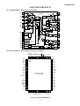
• NOTES ON SCHEMATIC DIAGRAM can be found on page 15.
1
2
3
4
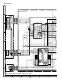
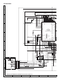
Figure 20 SCHEMATIC DIAGRAM (1/10)
– 20 –
5
6
FDO
TDO
13
CD-BA1200H
1K
100P
R75
1K
DO
C76
100P
R76
1K
DI
C77
100P
R77
1K
CL
C78
100P
R78
1K
L62
2.2µH
CE
CL
DI
DO
INT
WRQ
DEF
RES
C80
0.1
COMMAND
INTERFACE
64
SUBCODE
DECODE
CRC
63 PW
62 SBSY
59 DATA
58 DATACK
A/D
51
50
17
18
49
48
+
19
47
LPF
1BIT
DAC
-
46
XIN
EFLG
CONT4
CONT5
RVDD
38
R-CH
R82
2.2K
LCHO
C2F
VDD
DGND
+5V
C83
0.022
9
C31
100/10
CONSTANT VOLTAGE
+B
R16
10K
L61
0.82µH
Q1
KTC3203Y
+B
+B
INT
WRQ
DRF
CE
+B
DI
CL
R22
470
D22
DS1SS133
34
33
32
WRQ
DRF
CE
DO
DI
7
CLK
8
CD RES
CLAMP SW
10
3
P25 12 - B
CNS702
TO DISPLAY PWB
5
6
9
35
2
CDINT
2
4
RES
37
1
3
DO
LOADING M-
D21
DS1SS133
5
+B
+B
+B
C47
100/16
4
+B
LOADING M+
36
P22 1 - B
CNS601
TO MAIN PWB
3
CNP11
LD_M-
R21
470
2
L-CH
C56
330/6.3
ZD61
DZ3.9BSB
VCC4
1
AGND
R81
2.2K
LVDD C39
10/16 +B
LD_M+
40
C34
0.022
LVSS
+B
39
+B
RCHO
RVSS
41 EMPH
DOUT
PCK
1K
1K
1.2K
C30
0.1
+B
+B
41
+B
XVDD
42 MUTEL
FSX
R17
R46
SLDO
SPDO
FDO
6
+B
42
R20
220
43 MUTER
AUDIO
OUT
27 28 29 30 31 32 33 34 35 36 37 38 39 40 TEST
R45
R39
470
CONT3
LASER
1
25 26
R38
270
TDO
ERROR
CORRECT
23
SPDO
EFBL
13
D/A
FDO 24
R35
1K
44
GENERAL
S/H
22
R44
1K
XOUT
45
BHREF 21
TBLO
TDO
XVSS
R84
10K
SW
ASLRCK
220
16
SERVO
PROCESSEROR
52
DIGITAL
FILTER
15
TE
AUTO
ADJUST
53
R58
14
54
ASDACK
R83
10K
SW
XL1
16.9344MHz
ASDFIN
C64
0.47/6.3
JITER
DEFECT
CONTROL
13
FE
56
55
PHREF 20
2
12
11
10
61 SFSY
60 16M
57 LRSY
12
ADAVDD
C45
100/10
SBCK
C43 C40
0.0015 0.0015
IC2
LC78641E
SERVO/SIGNAL
CONTROL
SLICE
LEVEL
CONTROL
9
C29
0.1
ADAVSS
C44
0.1
73 72 71 70 69 68 67 66 65
10
VREF
CE
+B
+B
7
PH(RFENV)
R43
220K
INT
C75
8
BH
D93
DS1SS133
1K
SERIAL
OUT
6
JITTV 11
JITTC
C41
100/10
R74
CLOCK
GENERATOR
EFMIN
C28
47/10
100P
EXTERNAL
AUDIO IN
SLCO
10K
C82
0.022
WRQ
C74
INTERPOLATION
MUTE
ATTENUATION
DEEMPHASIS
R15
C27
0.1
1K
CLV
CONTROL
CONT2
C42
68P
R73
C38
10/16
FR
1.2K HFL
C26
0.047
C17
0.0047
100P
FRAME SYNC
DEFECT,PROTECT
EFM DECODE
5
SLCIST
R8
330
RES
C73
R19
47
PCKIST
VVDD
R14
PLL
VCEC
4
CONT1
C20
0.1
3
C81
0.022
R80
1M
1K
2
VVSS
R11
12K
DRF
R72
GENERAL
1.2K
R10
27K
1
R13
680 PD02
C21
0.1
1K
0.01
VDD5V
R40
C22
100P
R79
1.5M
R71
C72
80 79 78 77 76 75 74
PD01
SLDO
C19
100/10
C25
0.1
C24
2.2/50
R12
680
100P
EFMO
7
FG(D_Vref)
C23
0.047
FSEQ
DEFECT
V/vP
CONT7
+B
CONT6
R68
8
R67
1K
R95
10K
C71
VSS
DISC_NO
R94
10K
O/C
3
CD SIGNAL
GND
CNP12
Q2
1
KRC102M
GND
31
30
29
28
27
26
25
24
VCC3
SP-
CNS4
SP+
O/C
SPO SPDO
GND(D)
VCC2(SPN)
DISC_NO
23
M+
22
M-
BI4
SW1
OPEN/
CLOSE
1
1
1
2
2
2
3
3
3
4
4
4
5
5
5
+
6
6
6
-
M
CNP4
SW2
CLAMP
SW3
DISC
NUMBER
M3
T/T
UP/DOWN
LOADING
CD LOADING
MOTOR PWB-E
+B
+B
• The numbers 1 to 13 are waveform numbers shown in page 16.
7
8
9
10
Figure 21 SCHEMATIC DIAGRAM (2/10)
– 21 –
11
12
CD-BA1200H
A
IC601
LC75341
AUDIO PROCESSOR
3
4
4
5
CD_GND
+5v
CE
2
L-CH
5
C607
+B
B
C613
0.0027
C617
1/50
SYSTEM MUTE
Q601
2SC3331
D902
1SS133
C629
1/50
LSEL0
8
R607
2.2K
R603
1.8K
C633
0.001
C601
0.001
L3
10
L
R608
2.2K
4
R2
TUN
L1
12
Q602
2SC3331
SYSTEM MUTE
GND (A_GND)
R3
DECK
L2
11
R617
3.3K
17
P26 1 - G
TO POWER PWB
C625
1/50
C602
0.001
R604
1.8K
C614
0.0027
C618
1/50
17
R4
AUX
R1
CD
R616
3.9K
C612
0.1(ML)
18
RSEL0
L4
9
C623
1/50
C610
0.1(ML)
19
RIN
+
-
+B
21
20
RTRE
LIN
7
C608
10/50
RBASS
LTRE
6
C605
0.022
C606
22/50
22
ROUT
LBASS
5
23
VREF
+
-
LOUT
4
C611
0.1(ML)
+
-
R601
330
CCB
INTERFACE
VSS
3
10/50
C609
0.1(ML)
R615
3.9K
BI601
R609
10K
C
C604
100/25
24
VDD
+
-
CNS601
+B
CLK
DI
1
A_GND
+
-
3
R-CH
+
-
2
C630
1/50
+
-
1
2
+
-
P21 12 - D
CNP11
TO CD SERVO
PWB
1
16
15
C624
1/50
14
C626
1/50
R618
3.3K
13
C627
1/50
C628
1/50
R
18
12
19
+5V
R610
10K
R602
330
+B
C603
22/25
GND (CD_GND)
R625
22K
+B
D
REC_R
FM SIGNAL
PLAYBACK SIGNAL
RECORD SIGNAL
CD SIGNAL
R157
100
Q102
KRC104 M
3
R142
220K
TAPE2_R2
3
4
A_GND
4
5
5
TAPE2_R1
R110
6
6
TAPE2_L1
6
7
7
7
TAPE2_L2
7
SWITCHING
Q107
2SC1845F
CNP102
R115
1K
R109
3.3K
C105
180P
R107
2.2K
G
Q105
2SC1845F
+
-
2
C107
560P
4
6
5
+
-
7
C119
0.033
C117
100/25
R117
56
C121
560P
C123
1/50
R123
5.6K
C137
0.022
• NOTES ON SCHEMATIC DIAGRAM can be found on page 15.
4
Figure 22 SCHEMATIC DIAGRAM (3/10)
– 22 –
5
6
220/10
C134
47/25
H
3
10
11
C129
22/25
R138
15K
2
9
56K
8
C139
3.3/50
R119 R121
100K 3.9K
15
Hich=CHROME
C115
330P
L101
2.2mH
16
56K
SWITCHING
1
R136
10K
R134
100
C132
0.0033
R132
1.5K
R130
3.9K
112K
3
C138
SWITCHING
C113
330P
5
6
CNS102A
1
+
IC101
AN7345K
Hich=T1
L
Q106
2SC1845F
SWITCHING
17
C135
47/25
R135
10K
14
RIPPLE
3
4
18
ALC
3
4
19
112K
Nor/CrO2
3
20
21
+
ALC
2
22
23
R
0.0033
ERASE
24
C133
2
R108
3.3K
C128
22/25
C114
330P
R133
100
2
C104
180P
0.7V
R140
10K
270P
1
R120
3.9K
C127
M_GND
4.7K
1
2
5
L-CH
1
R118
100K
L102
2.2mH
C112
330P
R112
1
R114
1K
R111
4.7K
R-CH
R106
2.2K
R113
47K
ERASE
HEAD
47K
SWITCHING
Q104
2SC1845F
CNS102B
RECORD/
PLAYBACK HEAD
C120
560P
R105
1K
C103
560P
C106
560P
CNP101
TAPE2
F
R122
5.6K
C122
1/50
C118
0.033
C126
270P
2
3
R128
6.8K
A_GND
TAPE1_L
R127
6.8K
2
3
3.9K
2
3
C116
100/25
R129
2
3
R124
33K
R116
56
R104
1K
1
Q108
2SC3331
TAPE1_R
Q109
2SC3331
SWITCHING
1
CNS101B
L-CH
1
CNS101A
1
R-CH
R141
10K
0.7V
68K
C102
560P
M
Q
2S
MUTING
Q110
2SC3331
0V
IC101:PLAYBACK AND RECORD/
PLAYBACK AMP.
R137
15K
R126
TAPE1
PLAYBACK
HEAD
R125
33K
E
3
Q103
SWITCHING KRC104 M
C146
0.001
2
Q101
KTA1266 GR
SWITCHING
0V
22/25
1
LUG1
MECHA BASE GND
C136
C108
100/16
1
R103
4.7K
C130
0.022
2
C131
0.022
SWITCHING
1.5K
R101
10K
R102
10K
R131
C101
0.047
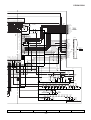
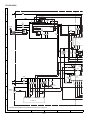
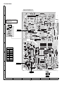
CD-BA1200H
MAIN PWB-A1(1/3)
+B
23
DD
REF
C605
0.022
C606
22/50
22
+B
C604
100/25
24
C608
10/50
OUT
21
SS
20
TRE
L0
10
GND
(A_GND)
4
A_10V
+B
+B
C614
0.0027
18
R3
R2
R1
5
CE
C618
1/50
7
DI
6
17
R4
GND
R616
3.9K
C612
0.1(ML)
19
RIN
(D_GND)
C610
0.1(ML)
CLK
9
C630
1/50
16
TUN_R
2
15
C624
1/50
14
C626
1/50
P29 12 - H
TO TUNER PWB
CLK
TUN_L
3
DO
R618
3.3K
13
8
SM
1
C628
1/50
1
SM
1
CE
2
DO
3
DI
4
CLK
5
T_BIAS
6
T_T1/T2
7
REC/PLAY
8
REC_R
REC_L
M_GND
+B
+B
M_10V
SMUTE
VF1
-VP
VF2
R142
220K
0V
MUTING
Q111
2SC3331
MUTING
Q110
2SC3331
R141
10K
AC_RLY_CONT
R143
220K
UN_SW 5V
+B
D_GND
SW_5V
+B
0V
POWER
0.7V
0.7V
R140
10K
0V
0V
9
CNP701
P25 12 - D
TO DISPLAY PWB
+B
10
11
12
13
14
15
16
17
18
19
20
11.7V
0V
R145
4.7K
L103
100µH
0V 1
0V
+B
C140
0.0082
(PP)
C141
0.039
(ML)
+B
POWER
M_10V
R149
4.7
C148
0.047
+B
GND (D_GND)
+B
0V
GND (M_GND)
0V
0V
Q114
KTC3203 Y
BIAS OSC
R148
22K
UN_SW_5V
R147
47K
R135
10K
-VP
C133
C131
0.022
R131
1.5K
0.0033
R133
100
C135
47/25
3
Q113
KRC104 M
BIAS
VF2
270P
C127
6.8K
3.9K
2
11.6V
R146
82
(1/2W)
AC_RLY_CONT
12
SW_5V
11
C145
470P
220/10
C138
Vcc
22/25
C136
10
R144
47K
11.6V
A_10V
9
Q112
KTA1266 GR
SWITCHING
C129
22/25
R129
FCC21
+B
+B
VF1
56K
8
13
GND
+
-
CNP701
R136
10K
Hich=CHROME
7
14
ALC
56K
R139
180
ALC
+
15
Nor/CrO2
16
17
1
5K
21
+B
C134
47/25
C132
0.0033
C128
22/25
18
+B
RIPPLE
6.8K
C126
270P
C130
0.022
R132
1.5K
3.9K
R134
100
21
C142
47/25
L104
330µH
5
15 14 16
21 10 12 22 11 13 20
P26 1 - G
TO POWER PWB
7
8
9
10
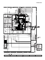
Figure 23 SCHEMATIC DIAGRAM (4/10)
– 23 –
11
12
CD-BA1200H
A
F
F
P15
P16
P13
P20
P14
P11
P10
P9
P8
P7
P6
5G
P5
P4
6G
7G
P3
P2
8G
P1
P12
P19
P18
P17
1G
2G
3G
4G
9G
F
FL701
FL DISPLAY
1 2
3 4 5 6 7 8
9 10 11 12 13 14 15 16 17 18 19 20 21 22 23 24 25 26 27 28 29 30 31 32
2
C705
100/10
C708
1/50
R743
33
+B
S-BUSY
77 P10
76 P11
T_T1/T2
75 P14
REC/PLAY
74 P20
RES OUT
T-BIAS
DRF
WRQ
71 P15
70 DIST0
RESET
67 DIST3
66
65
64
D712
1SS133
CE 21
DISTOUT/SW OUT
33 KEY 2
CLK 22
53 T1 PLAY SW_A
DO 24
52 CD CLAMP SW
AVSS 25
55 FPA
51 T2 RUN
DI 23
M-BUSY/TUN SM 26
AVDD
AVref
SYS STOP
NO USE
SP_RLY
REMOCON
VSS
SMUTE
T_SOL_B
T_SOL_A
SPEANA1 29
SPEANA0 30
R755
4.7K
+B
R759
10K
+B
R775
10K
R776
10K
R756
68K
R757
68K
R758
10K
+B
C711
10/16
R760
1K
Q702
2SC3331
M
FFC13
T2 PLAY
G
PH
SOLENOID
SOLENOID
R.PLAY
PH
T1 PLAY
F.PLAY
0V
1
2
3
4
5
6
7
8
9
10
11
12
13
1
2
3
4
5
6
7
8
9
10
11
12
13
T2 PLAY
+5V
T2 RUN
+MTR
SOL2
SOL1
+B
F_REC
R763
47K
D705
1SS133
12V
12V
Q704
KTA1271Y
R768
10K
Q706
KTA1273Y
12V
Q705 0V
KTA1271Y
T1 RUN
T1 PLAY
GND
Q703
2SC3331
B
A
+
-
D703
1SS133
C710
47/25
R777
10K
R766
10K
TAPE
MOTOR
D704
1SS133
TAPE MECHANISM PWB-E
R762
47K
C712 R761
10/16 1K
R767
10K
12V
D702
1SS133
CNP703
H
• NOTES ON SCHEMATIC DIAGRAM can be found on page 15.
1
2
3
4
Figure 24 SCHEMATIC DIAGRAM (5/10)
– 24 –
5
R719
1K
R722
10K
R721
1K
R720
1K
R724
1K
2.2K
2.2K
2.2K
2.2K
R729
R728
R727
R726
+B
LED722
4204SRT7
F
R7
SPEANA2 28
50 49 48 47 46 45 44 43 42 41 40 39 38 37 36 35 34 33 32 31
E
+B
R7
R7
R7
R7
R7
R7
R7
R7
SPEANA3 27
T_MOTOR
52
51
SPK_DET
T1 RUN
53
TIMER LED
57 MIC IN
56 FPB
VDD
54 T2 PLAY SW_B
AC RLY_CONT
58 KARAOKE LATCH
POWER
10K
CD CE 20
32 KEY 1
1K
1K
1K
1K
R753
CD DO 19
SPN
54
X
R7
15
VDD 16
31 KEY 0
61
D701
1SS133
+B
10K
10K
10K
10K
CD INT
62
R737
R736
R735
R734
R733
R748
R749
R750
R751
X1 12
XT2 14
CD DI 18
1K 60
1K 59
+B
1K
1K
1K
1K
1K
5
VPP/IC 13
63
+B
R70
R70
R70
6
R70
7
R70
8
R70
9
R70
10
4
CD CLK 17
R732
R792
R778
R730
D
2
3
X2 11
IC701
IX0337AWZZ
SYSTEM
MICROCOMPUTER
69 DIST1
68 DIST2
R742
R741
VDD 1
-20dBATT
100 9G
80 P8
73 P13
72 P16
C
4G
3G
2G
1G
8G
7G
5G
6G
P17
P18
P1
P19
P2
P12
P3
P4
80
79 VLOAD
78 P9
P5
P7
81 82 83 84 85 86 87 88 89 90 91 92 93 94 95 96 97 98 99 100
P6
B
6
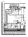
CD-BA1200H
P4
6G
7G
P3
P2
8G
P1
P12
P19
P18
P17
1G
2G
3G
4G
9G
F
F
01
PLAY
16 17 18 19 20 21 22 23 24 25 26 27 28 29 30 31 32 33
Q701
KRC107M
2
1
BI702
R779
3.3 (1/2W)
3
CD INT
WRQ(DSP)
C707
1/50
R744
1K
R745
100K
C701
0.022
4G
3G
2G
1G
8G
7G
6G
5G
P19
P17
P18
P1
P12
6 87 88 89 90 91 92 93 94 95 96 97 98 99 100
C702
220/10
VDD 1
1
CD INT
2
2
WRQ(DSP)
3
4
3
DRF
CD CE
5
6
5
6
7
8
7
8
9
9
10
10
RES OUT
CLAMP SW
CD_GND
+B
2
S-BUSY 3
1
DRF
CD CE
CD DO
CD DI
CD CLK
4
CD DO
CD DI
CD CLK
P21 12 - F
CNP12
TO CD SERVO
PWB
RES OUT
CLAMP SW
D_GND
-20dBATT
100 9G
T-BIAS
T_T1/T2
REC/PLAY
RES OUT
DRF
WRQ
RESET
CNS702
R702
R703
R704
6
R705
7
R706
8
R707
9
R708
10
4
5
X2 11
IC701
IX0337AWZZ
SYSTEM
MICROCOMPUTER
FFC21
1
1
2
3
4
5
X1 12
VPP/IC
XT2
CD INT
XL701 C704
13
18P
14
R709
1K
15
VDD 16
CD CLK 17
CD DI 18
CD DO 19
31 KEY 0
CD CE 20
32 KEY 1
CE 21
33 KEY 2
CLK 22
DI 23
54 T2 PLAY SW_B
53 T1 PLAY SW_A
DO 24
52 CD CLAMP SW
AVSS 25
M-BUSY/TUN SM 26
R710
R711
R712
R713
R714
R715
R716
R717
1K
1K
1K
1K
1K
1K
1K
1K
R718
1K
6
7
8
+B
9
10
11
12
13
14
17
D706
1SS133
AVDD
SPEANA1 29
SPEANA0 30
+B
R719
1K
+B
P23 12 - D
CNP701
TO MAIN PWB
21
R725
1K
R755
4.7K
R722
10K
R721
1K
R720
1K
2.2K
2.2K
2.2K
5 44 43 42 41 40 39 38 37 36 35 34 33 32 31
R724
1K
18
19
20
21
SPEANA2 28
AVref
SYS STOP
SP_RLY
NO USE
REMOCON
VSS
SMUTE
T_SOL_B
T_SOL_A
T_MOTOR
+B
R769
10K
SPEANA3 27
R728
R727
R726
15
16
+B
TUN SM
CE
DO
DI
CLK
T_BIAS
T_T1/T2
REC/PLAY
M_GND
M_10V
SMUTE
VF1
-VP
VF2
AC_RLY CONT
UN_SW 5V
D_GND
SW_5V
POWER
SPAN
SW OUT
CNP701
51 T2 RUN
1K
1K
1K
1K
1K
1K
1K
C703
15P
+B
LED722
4204SRT7
+B
+B
+B
+B
+B
31
RD13
680
RD14
820
SW715
TAPE
SW714
CD
RD25
680
SW711
EQUALIZER/
X-BASS/DEMO
273Y
RD01
680
RD16
1.5K
RD15
1K
SW716
TUNING/
TIME
DOWN
RD17
2.2K
1
3
+B
RX701
REMOTE SENSOR
2
C716
0.022
RD18
2.7K
RD19
3.9K
RD20
5.6K
RD12
1.5K
RD05
2.2K
RD06
2.7K
RD07 RD08
3.9K 56K
SW702
CLOCK
7
8
9
C719
47/16
RD21 RD22 RD23 RD24
100K
10K
15K
33K
SW723
REC/
PAUSE
RD26
6.8K
SW709
DISC
SKIP
SW703
TIMER/
SLEEP
SW701
ON/STAND-BY
C718
0.022
SW724
TUNING
UP
SW725
TUNER
(BAND)
SW713
VOLUME
DOWN
SW712
VOLUME UP
RD03 RD04
1K
1.5K
D711
1SS133
R773
100
1 2 3
C717
10/50
SW719
SW720 SW721
SW717 SW718
FAST
PLAY/ STOP
MEMORY/ REWIND
FORWARD REPEAT
SET
RD10 RD11
820
1K
RD02
820
R771
100K
1
D710
1SS133
IC704
KIA7042AP
RESET
3
2
D709
1SS133
R777
10K
C714
0.01
C713
0.1/50
R775
10K
R776
10K
R770
47K
L701
100µH
+B
5V BACK UP
D708
1SS133
C715
RESET
3.3/50
Q707
KRC102M
+B
+B
D707
1SS133
R772
4.7K
RD09
100K
SW710
OPEN/
CLOSE
DISPLAY PWB-A2
10
Figure 25 SCHEMATIC DIAGRAM (6/10)
– 25 –
11
12
CD-BA1200H
IC901
LA4282
POWER AMP.
A
10
POWER
GND1
C915
470/25
R909
56K
C913
0.1(ML)
C914
470/25
R908
120
C919
10/50
C910
100/25
12
11
C936
100P
C911
0.022
C912
0.1(ML)
C903
470P
C904
470P
R910
270
(1/2W)
C917
0.1(ML)
R911
270
(1/2W)
C916
0.1(ML)
R913
4.7
R912
4.7
L OUT
9
8
OUT1
Vcc
MUTE
CIRCUIT
7
R OUT
6
5
POWER
GND2
OUT2
NF2
IN2
4
C918
220P
R905
120
PRE-GND
IN1
3
2
THERMAL OVER
VOL. PROTECTOR
CH2
C908
0.082
(ML) R906
1K
B
1
C907
100/25
C906
47/25
C905
0.022
C937
100P
RIPPLE
FILTER
R907
C909
0.082(ML) 1K
NF1
CH1
SP. DET.
C
Q902
1 KRC102 M
2
3
1
2
3
Q901
KRC102 M
SP. DET.
R914
22K
R915
820
C946
2200/35
D
C933
68P
IC905
KTC2026
+B
R923
33
IC902
KIA7810AP
VOLTAGE
REGULATOR
+B
G
19
5
+5V (CD +B)
+B
+B
R926
10K
3
GND (CD_GND)
13
+B
D904
1SS133
-VP
VF2
M 10V
+B
GND (D_GND)
SW_5V
+B
+B
UN SW 5V
+B
AC_RLY_CONT
GND (M_GND)
20
H
• NOTES ON SCHEMATIC DIAGRAM can be found on page 15.
1
2
3
4
Figure 26 SCHEMATIC DIAGRAM (7/10)
– 26 –
D91
1N4
C955
C954
100/50
R928
12K
C944
0.022
A 10V
D
1
+B
1
2
VF1
15
14
16
21
10
12
11
C940
0.1 (ML)
C939
0.1 (ML)
C938
47/25
IC904
KIA7805P
VOLTAGE REGULATOR
1
R929
220
12
C941
0.047(ML)
P22 1 - C, P23 11 - H
TO MAIN SECTION
18
3
2
R
D913
1N4004S
C947
3300/25
C945
0.1 (ML)
+B
4
+B
D918
1SS133
+B
D903
1SS133
GND
(A_GND)
C943
47/25
L
17
R925
22K
IC903
AN78L05
CONSTANT
VOLTAGE REGULATOR
22
F
1
2
POWER
C942
47/25
4
3
D911
1N4004S
+B
5
6
ZD903
MTZJ6.2A
GND
(A_GND)
R930
220
R922
22K
C934
0.047(ML)
E
C935
22/25
+B
K
CD-BA1200H
MAIN PWB-A1 (2/3)
FM SIGNAL
HEADPHONES PWB-A3
1
1
5
5
R916
330
FW902
L903
2.2mH
C922
220P
JK901
HEADPHONES
R OUT
L OUT
C921
220P
R917
330
SO901
SPEAKER
TERMINAL
L901
0.29µH
+
+
R920
6.8
R918
6.8
C923
0.022
C925
0.022
C924
0.022
C926
0.022
C927
0.022
C929
0.022
C928
0.022
C930
0.022
SP_Lch
SP_Rch
SPEAKER
–
–
SP_Lch_GND
SP_Rch_GND
R939
56
R919
6.8
C931
0.001
R921
6.8
R940 C932
56 0.001
C946
2200/35
L902
0.29µH
C388
0.001
C950
0.047
(ML)
D907
RL203F
Q904
KTA1266GR
CNP801
1
1
2
2
3
3
4
4
5
5
6
6
1
1
2
2
C801
0.0047/250
F902
T1.6A L 250V
CNP901
D801
1SS133
D916
1N4004S
C957
47/50
D917
1N4004S
RL801
C958 C953
100/50 0.047
(ML)
D915
IN4004S
ZD902
DZ30BSB
D914
1N4004S
C955
47/50
ZD903
MTZJ6.2A
SO902
AC INPUT
SOCKET
T.F
PT801
MAIN POWER
TRANSFORMER
L801
LINE
FILTER
AC POWER
SUPPLY CORD
AC 230V, 50Hz
D806
1SS133
R806
10K
7
8
D805
1N4004S
C805
0.001
C803
470/35
D803
1N4004S
D804
1N4004S
C802
0.047(ML)
R804
220
C804
1000/6.3
D802
1N4004S
+B
R805
47K
R928
12K
R930
220
R929
220
C954
100/50
D913
1N4004S
C947
3300/25
C951
0.047
(ML)
D910
RL203F
C952
D912
1N4004S 0.047
(ML)
R927 C956
2.2K 47/50
D911
1N4004S
D908
RL203F
C959
100/50
D909
RL203F
When Servising, pay attention as the
area enclosed by this line(
) is
directly connection with AC main voltage.
F901
T2.5A L250V
PT802
SUB POWER
TRANSFORMER
Q803
2SC3331
9
10
Figure 27 SCHEMATIC DIAGRAM (8/10)
– 27 –
11
12
CD-BA1200H
C302
0.001
A
AM TRACKING fL
T303
C332
0.022
AM ANT.
D301
1SS133
+B
+B
C
21
22
AM RF IN
23
FM AFC
24
1
2
3
3
C350
0.022
T351
CF302
C352
10/16
1
D
0.022
C361
0.022
C363
R351
5.6K
+B
REG
C334
27P(UJ)
AM OSC.
AM OSC IN
L341
BALUN
AM MIX OUT
2
AM OSC OUT
2
R358
3.9K
FM IF IN
1
T306
R336
10K
1
VD301
SVC348S
C335
560P
C362
3.3/50
AM BAND
COVERAGE fL
R323
68K
AM LOOP
ANTENNA
C342
0.022
D302
1SS133
CNP302
B
C331
0.047
C330
15P
(UJ)
C323
0.022
2
AM IF
+B
C394
47/16
R382
150
C392
0.001
R381
10K
C380
C397
0.022
E
R380
1.5K
R369
15
ANT
GND
GND
VCC
4
3
2
1
IF OUT
5
GND
6
VT
7
CL
5
• NOTES ON SCHEMATIC DIAGRAM can be found on page 15.
3
4
Figure 28 SCHEMATIC DIAGRAM (9/10)
– 28 –
6
R378
1K
R372
1K
IC302: PLL(TUNER)
Q301
2SC380-O
H
2
DO
DI
4
FE301
FM FRONT END
1
PD
AIN
CE
VSS
X OUT
AOUT
3
C341
0.022
F OUT
8
2
R346
330
L342
2.2mH
G
1
IC302
LC72131
R373
1K
3
R347
6.8K
SO301
FM ANTENNA
TERMINAL
19 18
22 21 20
R374
1K
1
C382
15P(CH)
R349
33
CF301
C347
0.022
2
R344
470
C301
0.022
C345
0.022
C346
0.022
D304
1SS133
R345
4.7K
C321
100/16
F
R348
680
X352
4.5MHz
D303
1SS133
X IN
C381
12P(CH)
R379
2 2K
C393
1/50
5
6
CD-BA1200H
MAIN PWB-A1(3/3)
FM SIGNAL
STEREO
FM DET
VCC
6
7
8
9
R361
1.2K
C372
1/50
R362
1.2K
13
MO/ST
C374
0.018
R-CH OUT
C371
1/50
R363
15K
C358 12
1/50
10 11
R353
270
C357 R355
2.2/50 3.3K
C398
100/10
C356
0.001
R388
3.9K
C355
22P
AM IF
C354
0.022
C353
0.022
2
C399
0.022
CF352
CF351
3
C370
1/50
1
C350
0.022
R364
15K
PHASE
(FM/AM)
SD
5
T351
R393
1K
L352
100µH
B
+B
+B
ZD351
DZ5.1BSB
Q360
KTA1266GR
R377
47K
10
11
C391
47/16
R376
1K
R360
4.7K
R370
1K
R378
1K
R372
1K
+B
2
3
4
5
6
7
8
9
P23 12 - B
TO MAIN SECTION
7
8
9
10
Figure 29 SCHEMATIC DIAGRAM (10/10)
– 29 –
11
12
D GND
CLK
DO
CE
A+12V
SM
1
A GND
+B
DI
R386
22K
L
R374
1K
LL(TUNER)
R385
5.6K
R384
5.6K
ST IND
9
R395
47K
R359
1.8K
SD
8
C386
330P
MO/ST
IF
CONT
6
+B
IF IN
FM IN
FM/AM
7
DO
CL
5
SWITCHING
0.022
R392
270
R391 +B
270
R383
5.6K
14 13 12
AM IN
AIN
DI
4
+B
+B
R373
1K
3
100/10
C395
C385
0.01
17 16 15
IC302
LC72131
CE
VSS
AOUT
X OUT
4.5MHz
X IN
2
PD
19 18
22 21 20
1
R387
5.6K
R379
2.2K
C393
1/50
L351
100µH
FM/AM
R380
1.5K
VDD
R381
10K
C392
0.001
C380
10/16
82
50
C387
0.022
C396
C394
47/16
C397
0.022
R C388
0.001
C352
10/16
R357
470K
R356
1K
X351
456kHz
GND
4
R352
1K
14
PHASE
AM LOW CUT
AM IF IN
IC303
LA1832S
FM IF DET./FM MPX./AM IF
15
IF OUT
AM RF IN
3
16
MPX IN
FM AFC
2
FM/AM OUT
AM OSC IN
1
17
MPX VCO
C365
20 19 18
AM OSC OUT
C364
21
VSM
22
REG
23
AM MIX OUT
24
FM IF IN
R351
5.6K
C363
R350
2.7K
C367
1/50
C373
0.018
C369
27P(UJ)
C368
1/50
L354
LOW PASS
FILTER
0.022
10/16
R358
3.9K
0.022
C361
0.022
C362
3.3/50
TP
L-CH OUT
C342
0.022
AM SIGNAL
10
CD-BA1200H
MAIN PWB-A1
A
C912
C905
C910
3 2 1
C951
D916
D917
C958
5
R929
R930
LUG1
R928
ZD903
C956
R134
C146
C122
R122
C120
R145
R601
3 2 1
E C B
Q601
Q113
C607
C601
1 2 3 4 5
R607
CNP11
P34 4 - A
TO CD SERVO PWB
2
3
4
Figure 30 WIRING SIDE OF P.W.BOARD (1/6)
– 30 –
5
R617
C625
C6
R604
1
CNS601
H
1
C623
C612
R616
R618
C602
R608
C617
C628
RD
WH
GY
WH
GY
P35 11 - E
TO TAPE2
RECORD/PLAYBACK
HEAD
IC601
C610
C630
C608
Q602 E C B
B C E
L103 R144
R602
C613
R603
C141
BI601
IC101
C139 R127
R120
C148
C140
E C B
R149 Q114
L104
C142
C614
1
C611
R609
R101
C101
C108
B
C
E
E C B
5
1
2
3
4
5
6
7
8
9
10
11
12
C626
R102
Q102
E C B
24
23
22
21
20
19
18
17
16
15
14
13
C606
C618
C624
3 2 1
R113
R103
R109
R107
R106
R137
R108
R148
R147
E C B
C60
C604
R146
C103
3 2 1
7
6
5
4
3
2
1
C605
C118
R610
G
2
1
Q103
P35 10 - E
TO TAPE1
PLAYBACK HEAD
E
C
B
CNP701
1 3 5 7 9 11 13 15 17 19 21
2 4 6 8 10 12 14 16 18 20
R118
L102
C114
Q112
Q109
C102 E
C
B
3
R138
PINK
R128
C126
R126
C116
Q106 Q104 Q105
PK
C121
C117
C104
BLACK
CNP102
WHITE
BK
R157
WH(W)
C119
R119
C107
R114
GRAY
13
14
15
16
17
18
19
20
21
22
23
24
R117 R116
C112 Q107
R105
C105 E C B
R104
C115
R121
12
11
10
9
8
7
6
5
4
3
2
1
R130
Q101
GY
L101
Q108
VIOLET
R123 C123 C137
C113
C128
C145
R110 C106
VL
R135
BLUE
C127
GREEN
BL
R115
GR
R143
R112
YELLOW
C136
C131
C133
R133
C129
R131
CNP101
YL
R129
R125
R111
ORANGE
Q111 E C B
C135
R140
B C E
Q110
R139
R141
COLOR TABLE
C132
R124
C130
C138
C957
C954
C955
C134
R142
R136
R132
R927
ZD902
Q904
E C B
FW901
OR
D804
C947
C959
1
RED
D803
D915
1
RD(R)
D802
C941
F902
T1.6A L 250V
BROWN
D805
1
2
3
C942
1 2 3 4 5 6
CNP901
C950
D
F
D918
D903
D902
P35 8 - C
TO POWER
TRANSFORMER
BR
P
SUB
TRAN
C945
C940
D904
F901
T2.5A L 250V
E
C943
C952
C921
L903
R916
FW901
5
W
ar
dir
C944
C939
D914
D913
D912
D911
D909
R917
C938
C953
C946
D907
3 2 1
R926
R914
D908
D910
C922
3 2 1
C907
R910
R911
C916
C
C935
C904
R912
JK901
HEADPHONES
3 2 1
R925
C802
C913
IC904
C933
R922
C903
Q901 Q902
HEADPHONES
PWB-A3
R923
C909
C914 C936
R906
C908
C915
B
E C B
C906
R908
R909
R913
C917
R915
IC901
IC902
IC903
Q903
C934
C937
12 11 10 9 8 7 6 5 4 3 2 1
LG901
R905
C918
C911
C919
R907
6
CD-BA1200H
SO902
AC INPUT
AC 230V, 50Hz
LG901
4
1
6
When Servicing, pay attention as the
area enclosed by this line (
) is
directly connected with AC main voltage.
L801
C944
C943
PT802
SUB POWER
TRANSFORMER
C945
D805
1
2
3
D802
C801
P38 8 - F
942
C802
D803
TO POWER
TRANSFORMER
CNP801
2
D804
SO901
SPEAKER
TERMINAL
C931
L901
—
C932
C928
ZD903
C926
Q803
R806
C955
L-CH
+
R920
C924
R939
E C B
—
R919
C925
C930
C954
D801
C804
C929
R804
C805
C957
R928
R805
D806
C803
D917
R921
6
C923
5
C927
RL801
1
L902
R-CH
+
C361
FE301
R345
C347
L342
C306
CF352
R381
R378
C301
D304
R373
11 10 9
R379
C381
C387
R349
R344
R348
B
3 2 1 CF301
IC302
C
8 7 6 5 4 3 2 1
E
C382
Q301R347
R372 R374 X352
C302
12 13 14 15 16 17 18 19 20 21 22
D303
C392
C341
C394
C397
C380
L351
1
2
SO301
FM ANTENNA
TERMINAL
C345
4
3
2
1
R346
R380
C385
R377
1
L341 2
CNP302
8
7
6
5
AM LOOP
ANTENNA
R369
C346
R358
R351
CF351 R352
C353
R353
C357
C398
R385 R383
R393
R360
C386
R625
C603
C625
R391
R392
R376
C393
R382
E
C
B
C391
R388
1
D302
D301
3 2 1
CF302
Q360
R359
C607
C626
C395
1
2
3
C323
T303
C350
C352
R386
R384
R387
R607
C396
R609
C601
R395
C627
R604
R336
T351
C370
ZD351
L352
C629
C633
R617
C617
R603
R618
R615
C613
C623
IC601
C612
R616
C611
C628
C354
C356
C609
1
2
3
4
5
6
7
8
9
10
11
12
IC303
12 11 10 9 8 7 6 5 4 3 2 1
R355
24
23
22
21
20
19
18
17
16
15
14
13
C369
C355
C358
C388
C399
C334
C362
C330
R365
C371
C367
R370
13 14 15 16 17 18 19 20 21 22 23 24
17 19 21
6 18 20
6
R350
X351
R362
C331
R323
C321
R356
C374
C373
R364
R361
R363
R940
VD301
C342
T306
C332
C365
L354
C364
C363
C368
C372
R357
R918
C335
21
FFC21
S601
CNS701
P33 7 - H
TO DISPLAY PWB
7
8
9
10
Figure 31 WIRING SIDE OF P.W.BOARD (2/6)
– 31 –
11
12
CD-BA1200H
A
DISPLAY PWB-A2
R745
B
Q701
3 2 1
SW711
EQUALIZER/
X-BASS/DEMO
C719
C718
FL701
C702
RD25
RD10
C
33 32 31 30 29 28 27 26 25 24 23 22 21 20 19 18 17 16 15
RX701
3 2 1
81
RD11
85
R701
C701
R703
95
5
10 I
15
XL701
C703
RD09
R704
R707
R706
R705
R709
R711
R712
R713
R710
R773
R724
R779
R768
Q706
B
C
E
R766
B
C
E
R708
R702
90
100
1
SW710
OPEN/CLOSE
RD07
R718
RD06
R716
R715
SW719
FAST
FORWARD
RD26
RD22
SW713
VOLUME
DOWN
RD17
RD08
RD12
E
R767
Q705
B
C
E
Q704
SW712
VOLUME
UP
D
R744
C704
C707
RD21
R714
RD18
SW723
REC/PAUSE
F
RD23
RD19
SW716
TUNING/
TIME DOWN
SW724
TUNING/
TIME UP
CNS701
2 4 6 8 10 12 1
1 3 5 7 9 11 13
C710
CNS703
2 4 6 8 10 12
1 3 5 7 9 11 13
R769
SW720
PLAY/
REPEAT
13
1
RD20
G
1
FFC13
CNP70
P31 8 TO MAIN P
P35 9 - A
TO TAPE
MECHANISM PWB
H
1
2
3
4
Figure 32 WIRING SIDE OF P.W.BOARD (3/6)
– 32 –
5
6
CD-BA1200H
P34 5 - A
TO CD SERVO PWB
CNP12
RD
WH
GY
WH
GY
WH
GY
WH
GY
WH
CNS702 1 2 3 4 5 6 7 8 9 10
1
10
BI702
2 1
LED722
FL701
SW701
ON/
STAND-BY
C715
C711
RD01
R763
D704
D705
D711
SW725
TUNER
(BAND)
RD13
SW717
MEMORY/SET
SW715
TAPE
RD14
COLOR TABLE
D706
CNS701
4 6 8 10 12 14 16 18 20
3 5 7 9 11 13 15 17 19 21
RD24
D703
D702
RD16
RD15
R769
L701
R775
R719 R777
R725
SW718
REWIND
R776 R722
R721
R720
R755
R726
R717
R716
RD
R715
9
R727
R728
R729
DISC SKIP
RD05
SW721
STOP
21
FFC21
CNP701
P31 8 - H
TO MAIN PWB
7
8
RD04
1 2 3
SW703
TIMER/
SLEEP
RD02
R772
SW714
CD
R732
Q707
1 2 3 SW702
CLOCK
IC704
R792
Q702
R762
C714
C712
R761
E C B
D709
R771
RD03
C708
C716
R760
SW709
R759
R730
30 31
Q703
B
C
E
R756
R757
51
50
R749
R758 R743
C704
C703
60
55
10 IC701
15
45
20
40
25 35
XL701
5
R748
R741
65
R751
R750
95
D708
C713
70
R778
100
1
85 75
R733
R734
R735
R736
R737
90
D701
D712
R742
C717
81 80
D707
R753
R770
C705
D710
20 19 18 17 16 15 14 13 12 11 10 9 8 7 6 5 4 3
9
10
Figure 33 WIRING SIDE OF P.W.BOARD (4/6)
– 33 –
11
BR
BROWN
RD(R)
RED
OR
ORANGE
YL
YELLOW
GR
GREEN
BL
BLUE
VL
VIOLET
GY
GRAY
WH(W)
WHITE
BK
BLACK
PK
PINK
12
CD-BA1200H
R71
R78
R73
R74
R75
R76
R77
R72
R19
C71
C78
C73
C74
C75
C76
C77
C72
L61
R12
C23
R67
R68
C80
Q1
C21
R13
C82
40 41
CNP3 6 5 4 3 2 1
E
1
6 5 4 3 2 1
C38
10
XL1
9
C56
CNP4
C39
R81
C43
R83
R46
R17
R16
R20
45
C34
35
R95
R94
R48
22
C50
50
C30
25
20
21
65
64
60
55
30
C31
Q2
70
IC2
R45
IC3
1 2 3
30
R22
35
10
15
D21
D22
24
25
R21
R40
40
5
10
20
3
12
11
75
15
R38
C47
42
1
5
R82
C40
R84
R3
C28
R44
R35
R39
C46
C42
R52
R53
R51
R54
R43
2
C49
R79
C19
C25
R11
C81
R15
C27
D93
8
7
C24
1 80
CNP1
D
C11
C12
R7
C44
R42
C20 C22
C29
C41
C
L62
R10
C26
R55
R56
4
B C E
R80
C6
7
6
5
4
3
2
1
C13
16
ZD61
R58
IC1
20
15
C54
C64
R5
R6
25
1 2 3 4 5 6 7 8 9 10
CNP12
C18
R8
R50
1 2 3 4 5
CNP11
C14
C7
CNP2
5
10
C83
R4
13
30
1
C8
C55
B
R25
E C B
Q3
CNS703
C45
R47 C53
8
7
6
5
4
3
2
1
CNS601
R14
C51
C52
P33 10 - A
TO DISPLAY PWB
C17
5
CD SERVO PWB-B
A
P30 5 - H
TO MAIN PWB
6
CNS3A
654 321
WH
GR
WH
GR
WH
RD
PICKUP UNIT(306)
654 321
F
CNS3B
CNS1A
CNS1B
GY
G
CNS2A
1
2
3
4
5
6
7
7
8
1
654 321
CNP3A
1
1
2
3
4
5
6
7
8
+
RD
WH
GY
WH
GY
WH
GY
WH
1
2
3
4
5
6
7
8
RD
WH
BL
PK
WH
YL
BK
M2
SLED MOTOR
RD
WH
BK
WH
PK
YL
BL
-
1
2
3
4
5
6
7
CD MOTOR
PWB-C
SW4
PICKUP IN
CNS2B
+
-
M1
SPINDLE MOTOR
H
• The numbers 1 to 13 are waveform numbers shown in page 16.
1
2
3
4
Figure 34 WIRING SIDE OF P.W.BOARD (5/6)
– 34 –
5
6
CD-BA1200H
P32 4 - H
TO DISPLAY PWB
CNP703
TAPE MECHANISM
ASSEMBLY
FC702
1
TAPE MECHANISM PWB-D
13
1 3 5 7 9 11 13
2 4 6 8 10 12
4
1
8
7
TAPE
MOTOR
B
A
+
-
SOLENOIDE
SOLENOIDE
TAPE 2
BL
GR
3 2 1
BL
YL
WH
BK
RD
WH
BK
WH
BK
PK
PT801
MAIN POWER
TRANSFORMER
RD
YL
WH
GR
BK
BR
YL
YL
RD
BL
BK
1 2 3 4 5 6
GR
0
RECORD/PLAYBACK
HEAD
PK
P30 2 - C
TO MAIN PWB
CNP901
WH
BK
3
2
1
ERASE HEAD
WH
TAPE 1
PLAYBACK HEAD
1 2 34 5 67
OR
CNS101
P30 2 - G
TO MAIN PWB
BL
2
1
CNS102
P30 4 - H
TO MAIN PWB
CNP801
P31 12 - C
TO POWER PWB
CNS4
CD LOADING MOTOR
PWB-E
WH
BK
WH
BK
WH
RD
6 5 4 3 2 1
COLOR TABLE
M3
T/T UP/DOWN
MOTOR
6
1
BI4
+
–
SW3
DISC
NUMBER
7
SW1
OPEN/
CLOSE
SW2
CLAMP
8
9
10
Figure 35 WIRING SIDE OF P.W.BOARD (6/6)
– 35 –
11
BR
BROWN
RD(R)
RED
OR
ORANGE
YL
YELLOW
GR
GREEN
BL
BLUE
VL
VIOLET
GY
GRAY
WH(W)
WHITE
BK
BLACK
PK
PINK
12
CD-BA1200H
VOLTAGE
IC1
PIN
NO.
1
2
3
4
5
6
7
8
9
10
11
12
13
14
15
16
17
18
19
20
21
22
23
24
25
26
27
28
29
30
VOLTAGE
1.6V
1.6V
1.6V
1.6V
1.6V
1.6V
0V
2.6V
0V
0V
0V
3.3V
1.6V
1.6V
1.6V
0V
0V
1.6V
1.6V
1.6V
1.6V
1.6V
0V
1.6V
0V
0V
0V
1.6V
1.6V
3.3V
IC3
PIN
NO.
1
2
3
4
5
6
7
8
9
10
11
12
13
14
15
16
17
18
19
20
21
22
23
24
25
26
27
28
29
30
31
32
33
34
35
36
37
38
39
40
41
42
VOLTAGE
1.6V
1.6V
1.8V
2.1V
2.1V
2.1V
2.1V
0V
0V
0V
0V
0V
0V
0V
2.1V
2.1V
1.6V
4.9V
3.5V
1.6V
0V
0V
4.9V
4.9V
1.6V
2.1V
2.1V
1.9V
0V
0V
0V
0V
0V
0V
0V
4.2V
0V
2.1V
2.1V
4.9V
2.1V
2.1V
IC2
PIN
NO.
1
2
3
4
5
6
7
8
9
10
11
12
13
14
15
16
17
18
19
20
21
22
23
24
25
26
27
28
29
30
31
32
33
34
35
36
37
38
39
40
41
42
43
44
45
46
47
48
49
50
51
52
53
54
55
56
57
58
59
60
61
62
63
64
65
66
67
68
69
70
71
72
73
74
75
76
77
78
79
80
VOLTAGE
0.7V
0V
0V
0V
3.3V
2.4V
0V
0V
1.6V
0V
4.7V
1.7V
0V
1.6V
1.6V
1.6V
1.6V
3.3V
0V
1.6V
1.6V
1.6V
1.6V
1.6V
1.6V
1.6V
1.6V
0V
0V
2.1V
2.1V
0V
3.3V
3.5V
3.3V
3.3V
3.3V
1.6V
1.6V
0V
0V
3.3V
3.3V
3.0V
1.5V
0V
0V
1.5V
3.0V
3.3V
1.8V
3.0V
0V
0V
0V
0V
1.7V
3.3V
0V
3.0V
1.6V
0V
2.4V
0V
0V
0V
0V
4.8V
4.9V
4.9V
4.6V
0V
4.9V
0V
0V
0V
3.2V
0V
0V
3.4V
IC101
PIN
NO.
1
2
3
4
5
6
7
8
9
10
11
12
13
14
15
16
17
18
19
20
21
22
23
24
VOLTAGE
0V
0V
0.55V
2.16V
0V
1.25V
0V
0.58V
3.17V
3.55V
0V
0V
4.72V
4.37V
0V
3.67V
0.38V
0V
0V
0V
2.16V
0.55V
0V
0V
IC301
PIN
NO.
1
2
3
4
5
6
7
8
9
VOLTAGE
0V
0V
16.27V
0V
0V
0V
16.72V
0V
0V
34.2V
16.6V
0V
IC902
PIN
NO.
1
2
3
VOLTAGE
19.12V
0V
10.04V
IC904
PIN
NO.
1
2
3
VOLTAGE
19.12V
0.64V
5.64V
VOLTAGE
0.8V (0V)
1.5V (0V)
3.6V (0.4V)
1.5V (0V)
0V (0V)
3.6V (0.4V)
2.8V (0.2V)
3.5V (0.3V)
3.6V (0.3V)
IC302
PIN
NO.
1
2
3
4
5
6
7
8
9
10
11
12
13
14
15
16
17
18
19
20
21
22
IC901
PIN
NO.
1
2
3
4
5
6
7
8
9
10
11
12
VOLTAGE
2.15V
0V
0V
0V
0V
4.83V
9.87V
4.4V
0V
0V
4.64V
2.27V
4.66V
0V
2.13V
0V
4.86V
0.73V
0.73V
6.3V
0V
2.33V
Q903
PIN
NO.
1
2
3
VOLTAGE
10.04V
19.05V
9.57V
IC704
PIN
NO.
1
2
3
VOLTAGE
4.9V
0V
4.9V
IC601
PIN
NO.
1
2
3
4
5
6
7
8
9
10
11
12
13
14
15
16
17
18
19
20
21
22
23
24
VOLTAGE
0V
0V
0V
4.96V
4.96V
4.96V
4.96V
4.89V
4.78V
4.78V
4.78V
4.78V
4.78V
4.78V
4.78V
4.78V
5.1V
5.5V
5.0V
4.66V
5.03V
4.97V
10.0V
0V
– 36 –
PIN
NO.
1
2
3
4
5
6
7
8
9
10
11
12
13
14
15
16
17
18
19
20
21
22
23
24
25
26
27
28
29
30
31
32
33
34
35
36
37
38
39
40
41
42
43
44
45
46
47
48
49
50
IC701
PIN
NO.
51
52
53
54
55
56
57
58
59
60
61
62
63
64
65
66
67
68
69
70
71
72
73
74
75
76
77
78
79
80
81
82
83
84
85
86
87
88
89
90
91
92
93
94
95
96
97
98
99
100
VOLTAGE
4.78V
0V
5.0V
0V
4.69V
4.74V
4.75V
0V
4.85V
4.30V
2.25V
1.16V
0V
0V
4.85V
4.78V
4.67V
0V
4.69V
0V
0V
0V
0V
4.82V
0V
0.3V
0V
0V
0V
0V
4.81V
4.81V
4.81V
4.9V
5.0V
4.9V
0V
0V
5.0V
0V
1.7V
9.45V
9.45V
9.45V
3.8V
4.89V
0V
4.89V
4.79V
4.78V
IC303
VOLTAGE
4.29V
0V
4.81V
4.81V
4.81V
4.81V
0V
0V
27.8V
–27.8V
0V
0V
0V
0V
0V
0V
–27.7V
–27.7V
–27.1V
–28.2V
–21.7V
–18.6V
–12.9V
–24.4V
–25.9V
–15.7V
–22.2V
–22.3V
–27.8V
–18.6V
–12.9V
–24.4V
–24.4V
–27.1V
–27.1V
–24.4V
–24.4V
–27.1V
–27.1V
–24.4V
–27.1V
–24.4V
–27.1V
–24.4V
–24.4V
–24.4V
–24.4V
–24.4V
–24.4V
–24.4V
PIN
NO.
1
2
3
4
5
6
7
8
9
10
11
12
13
14
15
16
17
18
19
20
21
22
23
24
VOLTAGE
2.12V
4.78V
2.12V
2.11V
0V
4.65V
4.65V
3.02V
4.78V
4.08V
1.63V
1.13V
2.08V
1.31V
1.29V
2.07V
0V
1.43V
1.99V
1.44V
2.08V
2.08V
4.48V
3.35V
CD-BA1200H
TROUBLE SHOOTING
When the CD does not function
When the CD section does not operate when the objective lens of the optical pickup is dirty, this section may not operate. Clean
the objective lens, and check the playback operation. When this section does not operate even after the above step is taken, check
the following items.
Remove the cabinet and follow the trouble shooting instructions.
"Track skipping and/or no TOC (Table Of Contents) may be caused by build up of dust other foreign matter on the laser pickup
lens. Before attempting any adjustment make certain that the lens is clean. If not, clean it as mentioned below."
Turn the power off.
Gently clean the lens with a lens cleaning tissue and a small amount of isopropyl alcohol.
Do not touch the lens with the bare hand.
1.
Parts code
UDSKA0004AFZZ
CD optical pickup Lens cleaner disc
HOW TO USE
1. Using the brush in the cleaner cap, apply 1 or 2 drops of the cleaning fluid to the
brush on the CD cleaner disc which has the mark next to it.
2. Place the CD cleaner disc onto the CD disc tray with the brush side down, then
press the play button.
3. You will hear music for about 20 seconds and the CD player will automatically stop.
If it continuous to turn, press the stop button.
Cleaner Fluid
CAUTION
The CD lens cleaner should be effective for 30-50 operations, however if the
brushes become worn out earlier then please the cleaner disc.
If the CD cleaner brushes become very wet then wipe off any excess fluid with a soft
cloth.
Do not drink the cleaner fluid or allow it to come in contact with the eyes. In the
event of this happening then drink and / or rinse with clean water and seek medical
advice.
The CD cleaner disk must not be used on car CD players or on computer CD ROM
drives.
All rights reserved. Unauthorized duplicating, broadcasting and renting this product
Cleaner disc
When a CD cannot be played
1. "E-CD01" is displayed.
(1) Check the power to IC2 (LC78641E), the presence of the clock signal (16.93 MHz) and the status of the RESET terminal
(pin 71 on IC2).
(2) Did the pickup move to the PICKUP-IN Switch (SW4) position?
If (1) and (2) are OK, check the system microcomputer (especially the communication line with the DSP).
2. Pressing the CD operation key is accepted, but playback does not occur.
(1) Focus-HF system check
(2) Tracking system check
(3) Spin system check
(4) PLL system check
(5) Others
– 37 –
CD-BA1200H
(1) Focus-HF system check
Stopped
CH1=500mV
DC 10:1
Although a CD is inserted and the cover is closed, "NO
DISC" is displayed.
CH3=500mV
DC 10:1
T
500ms/div
(500ms/div)
NORM:20kS/s
FDO
1
Press the OPEN/CLOSE switch (SW1) without inserting a
disc, and try starting the playback operation.
TDO
3
CH1
v/DIV
500mV
=Filter=
Smoothing : ON
BW : FULL
=Offset=
CH1 :
0.000V
CH2 :
0.0V
CH3 :
0.000V
CH4 :
0.00V
=Record Length=
Main :
100K
Zoom :
2K
=Trigger=
Mode : AUTO
Type : EDGE CH1
Delay :
0.0ns
Hold off :
0.2us
Figure 38-1
1. Did the pickup move to the PICKUP-IN Switch (SW4)
position?
No
Sled motor (M2)
Yes
No
2. Does the focus (lens) move up and down?
(Waveform drawing 38-1).
Check the focus peripheral circuit.
Yes
No
3. Is the laser lit?
Check the laser diode driver Q3 peripheral circuit.
Yes
No
4. Is the turntable rotating?
Spindle motor (M1).
When a disc is loaded, start playback operation.
1. Is focus servo activated? (Waveform drawing 38-2)
No
Yes
2. Does DRF change from "L" to "H"?
No
Is the disc rotating?
3. Is the HF waveform normal? (Waveform drawing 38-3)
CH2=10V
DC 10:1
CH3=1V
DC 10:1
No
Check the spin system.
If the disc is spinning and a HF waveform is generated,
DRF will go H.
Yes
Stopped
CH1=500mV
DC 10:1
Pins 1~11 on IC1
Check the laser diode driver Q3 peripheral circuit.
Focus error circuit (pins 20 and 21 on IC1)
No
If the level is not normal, check around pins 27~29 on IC1.
500ms/div
(500ms/div)
NORM:20kS/s
FDO
1
T
2
DRF
TE
3
CH Position To
-3div
-1div
0div
+1div
+3div
=Filter=
=Offset=
=Record Length=
Smoothing : ON CH1 :
0.000V
Main :
100K
BW : FULL
CH2 :
0.0V
Zoom :
2K
CH3 :
0.00V
CH4 :
0.00V
CH2
Position
0.20div
=Trigger=
Mode : AUTO
Type : EDGE CH1
Delay :
0.0ns
Hold off :
0.2us
Vp-p=1.0V~1.3V
0.5mV/div,0.5µsec/div
Figure 38-2
Figure 38-3
– 38 –
CD-BA1200H
(2) Tracking system check
Check the TE waveform at pin 18 on IC1.
Yes
If the waveform shown in Figure 39-1 appears and soon after
NO DISC appears.
No
"Initialization" is possible, but play is not possible.
Yes
No
"Initialization" is not possible.
The tracking servo is not activated.
Check the peripheral circuits at pins 18 and 19 on IC1, pin 23 on
IC2, and CNS1A/B.
A normal jump operation cannot be completed or the beginning of
the track cannot be found.
Check the around pin 23 on IC2.
Data cannot be read. Check the VCO-PLL system.
T
Stopped
CH1=10V
DC 10:1
CH2=1V
DC 10:1
100ms/div
(100ms/div)
NORM:100kS/s
TE
2
T
1
DRF
=Filter=
Smoothing : ON
BW : FULL
=Offset=
CH1 :
0.0V
CH2 :
0.00V
CH3 :
0.00V
CH4 :
0.00V
=Record Length=
Main :
100K
Zoom :
2K
=Trigger=
Mode : NORMAL
Type : EDGE CH1
Delay :
2.924ms
Hold off :
0.2us
Figure 39-1
(3) Spin system check
Press the OPEN/CLOSE switch without inserting a disc, and
then try starting the play operation.
Yes
The spin driver circuit is OK.
1. The turntable rotates a little. (Waveform drawing 39-2)
No
2. The turntable doesn't rotate.
Check around pin 25 on IC2, pins 15 and 16 on IC3, and CNS3A/B.
Stopped
CH1=200mV
DC 10:1
T
1999/04/07 09:51:15
500ms/div
(500ms/div)
NORM:20kS/s
CH2=500mV
DC 10:1
T
FDO
2
1
SPDO
=Filter=
Smoothing : ON
BW : FULL
=Offset=
CH1 :
0.000V
CH2 :
0.000V
CH3 :
0.00V
CH4 :
0.00V
=Record Length=
Main :
100K
Zoom :
2K
Figure 39-2
– 39 –
=Trigger=
Mode : NORMAL
Type : EDGE CH2
Delay :
2.924ms
Hold off :
0.2us
CD-BA1200H
(4) PLL system check
Stopped
CH1=500mV
DC 10:1
When a disc is loaded, start play operation.
CH3=1V
DC 10:1
1999/04/05 17:33:17
CH4=1V
500ms/div
(500ms/div)
DC 10:1
NORM:20kS/s
PDO1
3
4
The HF waveform is normal, but the TOC data cannot be
read.
PDO2
T
FDO
1
Check the PDO waveform. (Figure 40-1)
CH1
v/DIV
500mV
=Filter=
Smoothing : ON
BW : FULL
=Offset=
CH1 :
0.000V
CH2 :
0.0V
CH3 :
0.00V
CH4 :
0.00V
=Record Length=
Main :
100K
Zoom :
2K
=Trigger=
Mode : AUTO
Type : EDGE CH2
Delay :
0.0ns
Hold off :
0.2us
Check around pins 1~6 on IC2.
Figure 40-1
(5) Others
The HF waveform is normal and the time is displayed
normally, but no sound is produced. Or the sound has
dropouts.
No
Is pin 35 (C2F) on IC2 "L"?
There are too many error flags on a damaged disc which
makes error correction impossible.
Yes
1. When playing at normal speed
Check the peripheral circuit at pin 37 (DOUT) on IC2 and
the waveform (Figure 40-2).
Check again using a known good disc.
If both 1. and 2. are OK.
Stopped
CH1=2V
DC 10:1
T
1999/04/07 09:25:28
500ns/div
(500ns/div)
NORM:200MS/s
T
1
DOUT
=Filter=
Smoothing : ON
BW : FULL
=Offset=
CH1 :
0.00V
CH2 :
0.00V
CH3 :
0.00V
CH4 :
0.00V
=Record Length=
Main :
1K
Zoom :
100
=Trigger=
Mode : NORMAL
Type : EDGE CH1
Delay :
2.887ms
Hold off :
0.2us
Figure 40-2
– 40 –
CD-BA1200H
FUNCTION TABLE OF IC
IC1 VHiLA9235M/-1: Servo Amp. (LA9235M)
ODRV
FIN1 1
LA9235M
REF
FIN2 2
30 VCC
29 RFSW
REF
AGCON
REF
28 RF-
FIN3 3
REF
REF
PH
FIN4 4
27 RF
26 N/C
REF
25 PH
BH
24 BH
REF1 5
ODRV
REF
23 N/C
PH/BH
22 RFEV
REF
VREF 6
LDS 7
21 FE-
LPF
APC
LDD 8
20 FE
REF
REF
VEE 9
LDOF 10
ODRV 11
ODRV
AGON 12
AGCON
EFBL 13
TESO 14
18 TE
REF
REF
REF
REF
REF
LPF
TESI 15
19 TE-
LPF
17 HFL
16 TES
80
79
78
77
76
75
74
73
72
71
70
69
68
67
66
65
EFMO
DEFECT
FSEQ
V/P
CONT7
CONT6
VSS
VDD
DRF
RES
WRQ
INT
DO
DI
CL
CE
IC2 VHiLC78641E-1: Servo/Signal Control (LC78641E)
LC78641E
25
26
27
28
29
30
31
32
33
34
35
36
37
38
39
40
1
2
3
4
5
6
7
8
9
10
11
12
13
14
15
16
17
18
19
20
21
22
23
24
SPDO
SLDO
FG
LASER
CONT1
CONT2
CONT3
CONT4
CONT5
PCK
C2F
VDD
DOUT
FSX
EFLG
TEST
PDO1
PDO2
VVSS
PCKIST
VVDD
FR
HFL
SLCIST
SLCO
EFMIN
JITTV
JITTC
BH
PH(RFENV)
FE
TE
VREF
ADAVDD
ADAVSS
PHREF
BHREF
TBLO
TDO
FDO
Figure 41 BLOCK DIAGRAM OF IC
– 41 –
64
63
62
61
61
59
58
57
56
55
54
53
52
51
50
49
48
47
46
45
44
43
42
41
SBCK
PW
SBSY
SFSY
16M
DATA
DATACK
LRSY
ASDFIN
ASDACK
ASLRCK
XVSS
XOUT
XIN
XVDD
RVDD
RCHO
RVSS
LVSS
LCHO
LVDD
MUTER
MUTEL
EMPH
CD-BA1200H
IC2 VHiLC78641E-1: Servo/Signal Control (LC78641E) (1/2)
Pin No.
Terminal Name Input/Output Setting in Reset
1
PDO1
Output
–
2
PDO2
Output
–
Phase-comparison output terminal for built-in VOC control.
Rough servo : OFF, phase servo : ON.
3
VVSS
–
–
Ground terminal for built-in VCO.
4
PCKIST
AI
–
Resistor terminal for setting the PDO output current.
5
VVDD
–
–
Power terminal for built-in VCO.
6
FR
AI
–
7
HFL
Input
–
Mirror detection signal input terminal.
8
SLCIST
AI
–
For slice level control
9
SLCO
Output
–
10
EFMIN
Input
–
11*
JITTV
Output
Unfixed
12
JITTC
Output
–
Jitter detection/adjustment terminal.
13
BH
Input
–
BH signal input terminal. A/D input.
14
PH(RFENV)
Input
–
PH signal or RFENV signal input terminal. A/D input.
15
FE
Input
–
FE signal input terminal. A/D input.
16
TE
Input
–
TE signal input terminal. A/D input.
17
VREF
Input
–
VREF signal input terminal. A/D input.
18
ADAVDD
–
–
AD for servo, D/A power terminal.
19
ADAVSS
–
–
AD for servo, D/A ground terminal.
20*
PHREF
Output
(1/2VDD)
21*
BHREF
Output
(1/2VDD)
BH reference output terminal. D/A output.
22
TBLO
Output
(1/2VDD)
Output terminal for tracking balance. D/A output.
23
TDO
Output
(1/2VDD)
Output terminal for tracking control. D/A output.
24
FDO
Output
(1/2VDD)
Output terminal for focus control. D/A output.
25
SPDO
Output
(1/2VDD)
Output terminal for spindle control. D/A output.
26
SLDO
Output
(1/2VDD)
Output terminal for sled control. D/A output.
27*
FG
Input
–
FG signal input terminal. (When not used, connect to 0V)
28
LASER
Output
L
LASER ON/OFF control terminal.
29
CONT1
In/Output
Input mode
General purpose input/output terminal 1.
Controlled with serial data command
30
CONT2
In/Output
Input mode
General purpose input/output terminal 2.
from microcomputer. When not used,
31
CONT3
In/Output
Input mode
General purpose input/output terminal 3.
set it as the input terminal and
32
CONT4
In/Output
Input mode
General purpose input/output terminal 4.
open it by connecting to 0V, or set it
33
CONT5
In/Output
Input mode
General purpose input/output terminal 5.
as the output terminal and open it.
34*
PCK
Output
H
Clock monitor terminal for EFM data replay. 4.3218 MHz as phase clock.
35*
C2F
Output
H
C2 flag output terminal.
36
VDD
–
–
Power terminal of digital system.
37*
DOUT
Output
L
Output terminal of digital OUT. (EIAJ format)
38*
FSX
Output
L
Output terminal of synchronous signal of 7.35 kHz divided from quartz oscillation.
39*
EFLG
Output
L
C1, C2 correct monitor terminal.
40
TEST
Input
–
Input terminal for test. Surely connected to 0V.
41*
EMPH
In/Output
Input mode
42*
MUTEL
Output
H
Mute output terminal for L channel.
43*
MUTER
Output
H
Mute output terminal for R channel.
Function
For PULL
Phase-comparison output terminal for built-in VOC control.
Resistor terminal for setting the VCO frequency range.
Resistance connection terminal for current adjustment of
SLCO output.
Control output.
EFM signal input terminal.
Jitter detection/monitor terminal.
PH reference output terminal. D/A output.
Emphasis terminal. After resetting, it is configured as an input terminal. It can be controlled
from the outside. It is also becomes a emphasis monitor terminal under command control.
In this unit, the terminal with asterisk mark (*) is (open) terminal which is not connected to the outside.
– 42 –
CD-BA1200H
IC2 VHiLC78641E-1: Servo/Signal Control (LC78641E) (2/2)
Pin No.
Terminal Name Input/Output Setting in Reset
44
LVDD
–
–
45
LCHO
Output
1/2VDD
46
LVSS
–
–
47
RVSS
–
–
48
RCHO
Output
1/2VDD
49
RVDD
–
–
50
XVDD
51
XIN
52
53
54
ASLRCK
Input
–
For anti
55
ASDACK
Input
–
shock mode
56
ASDFIN
Input
–
57*
LRSY
Output
L
For digital
L/R clock output terminal.
58*
DATACK
Output
L
data output
Bit clock output terminal.
59*
DATA
Output
L
60*
16M
Output
Clock output
61*
SFSY
Output
L
Output terminal of synchronous signal of subcode frame.
It drops when subcode stand by.
62*
SBSY
Output
L
Output terminal of synchronous signal of subcode block.
63*
PW
Output
L
Output terminal of subcodes P,A,R,S,T,U and W.
64
SBCK
Input
–
Clock input terminal to read subcode. (When not used,connect to 0V)
65
CE
Input
–
For
66
CL
Input
–
microcomputer
67
DI
Input
–
interface
68
DO
Output
L
Data output terminal.
69
INT
Output
H
Interruption signal output terminal.
70
WRQ
Output
H
Interruption signal output terminal.
71
RES
Input
–
72
DRF
Output
L
Focus ON detection terminal.
73
VDD5V
–
–
Power terminal for microcomputer interface.
74
VSS
–
–
75
CONT6
In/Output
Input mode
General purpose input/output terminal 6.
Controlled with serial data command
from microcomputer. When not used,
76
CONT7
In/Output
Input mode
General purpose input/output terminal 7.
set it as the input terminal and
open it by connecting to 0V, or set it
as the output terminal and open it.
77*
V/ *P
Output
H
Monitor output terminal for automatic switch of rough servo/phase control.
"H" for rough servo, and "L" for phase servo.
78*
FSEQ
Output
L
Output terminal synchronous signal detection. "H" is output when synchronous signal
detected by EFM signal matches synchronous signal internally generated.
79
DEFECT
In/Output
Input mode
Defect terminal. After resetting, it is configured as an input terminal. It can be controlled
from the outside. It also becomes a defect monitor terminal under command control
80*
EFMO
Output
Unfixed
Function
L channel
Power terminal for L channel.
D/A converter L channel output terminal.
Ground terminal for L channel. Surely connected to 0V.
R channel
Ground terminal for R channel. Surely connected to 0V.
D/A converter R channel output terminal.
Power terminal for R channel.
–
–
For quartz
Power terminal for quartz oscillation.
Input
Oscillation
oscillation
Ground terminal of 16.9344 MHz quartz oscillation.
XOUT
Output
Oscillation
XVSS
–
–
Ground terminal for quartz oscillation. Surely connected to 0V.
L/R clock input terminal. (When not used,connect to 0V)
Bit clock input terminal. (When not used,connect to 0V)
L/R channel data input terminal. (When not used,connect to 0V)
L/R channel data output terminal.
16.9344MHz output terminal.
Chip enable signal input terminal.
Data transmission clock input terminal.
Data input terminal.
Reset input terminal of LC78640. When turning on power, set it at "L".
Ground terminal of digital system. Surely connected to 0V.
EFM signal output terminal.
In this unit, the terminal with asterisk mark (*) is (open) terminal which is not connected to the outside.
Be sure to supply the same potential to each power terminal. (VVDD,ADAVDD,VDD,LVDD,RVDD,XVDD)
Terminal witch is controlled by the power terminal (VDD5V) for a microcomputer interface :
CE (65pin), CL (66pin), DI (67pin), DO (68pin), INT (69pin), WRQ (70pin), RES (71pin), DRF (72pin),
CONT6 (75pin), CONT7 (76pin)
– 43 –
CD-BA1200H
IC701 RH-iX0337AWZZ: System Microcomputer (IX0337AW) (1/2)
Pin No.
Port Name
1
VDD
Terminal Name
VDD
Input/Output
—
—
Function
(+) POWER SUPPLY
2
P37
—
3*
P36
S-BUSY
Output
COMMUNICATE TO MPEG MICROCOMPUTER
GND
4
P35
T–BIAS
Output
TAPE RECORD BIAS
5
P34
T–T1/T2
Output
TAPE T1/T2 CHANGE
6
P33
REC/PLAY
Output
TAPE REC/PLAY CHANGE
7
P32
RES OUT
Output
CD DSP RESET & MPEG MICROCOMPUTER RESET
8
P31
DRF
Input
CD RF LEVEL DETECTION
9
P30
WRQ
Input
CD DSP WRITE REQUEST
10
RESET
RESET
Input
11
X2
X2
Output
MAIN CLOCK
Input
MAIN CLOCK
RESET
12
X1
X1
13
VPP/IC
VPP/IC
—
GND
14*
XT2
XT2
—
OPEN
15
P04
CD INT
16
VDD
VDD
17
P27
CD CLK/MCLK
Output
CD DSP CLOCK/MPEG MICROCOMPUTER CLOCK
18
P26
CD ID/MDI
Output
CD DSP COMMAND/MPEG MICROCOMPUTER COMMA
19
P25
CD DO/MDO
20
P24
CD CE
Output
CD DSP CE OUTPUT
21
P23
CE
Output
CE OUTPUT
22
P22
CLK
Output
CLOCK OUTPUT
23
P21
DI
Output
DATA OUTPUT
Output
24
P20
DO
25
AVSS
AVSS
26
ANI7
P17
TUN SM
M–BUSY
Input
—
Input
—
Input
Input
CD DSP INTERRUPT
(+) POWER SUPPLY
CD DSP CODE Q OUT/MPEG MICROCOMPUTER DATA INPUT
DATA INPUT
ANALOG GROUND
TUNER SIGNAL METER INPUT
COMMUNICATE TO MPEG MICROCOMPUTER M_BUSY
27
ANI6
NO USE
Input
GND
28
ANI5
SPEANA 2
Input
SPEANA DATA INPUT 16 kHz
29
ANI4
SPEANA 1
Input
SPEANA DATA INPUT 1 kHz
30
ANI3
SPEANA 0
Input
SPEANA DATA INPUT 63 kHz
31-33
ANI2-ANI0
KEY2-KEY0
Input
KEY INPUT
34
AVDD
AVDD
—
ANALOG VDD
35
AVREF
AVREF
—
ANALOG REF VOLTAGE
36
INTP3
SYS STOP
37*
P02
SPRLY
38
INTP1
NO USED
Input
39
INTP0
REMOCON
Input
40
VSS
VSS
Input
Output
—
SYSTEM STOP INPUT
SPEAKER OUTPUT RELAY CONTROL
GND
REMOCON INPUT
GROUND VOLTAGE
41
P74
SMUTE
Output
SYSTEM MUTE CONTROL
42
P73
T_SOL_B
Output
TAPE 2 SOLENOID CONTROL
43
P72
T_SOL_A
Output
TAPE 1 SOLENOID CONTROL
44
P71
T_MOTOR
Output
TAPE MOTOR CONTROL
45
P70
TIMER LED
Output
46
VDD
VDD
47
P127
48
P126
49
TIMER LED CONTROL
—
(+) POWER SUPPLY
AC RLY_CONT
Output
AC RELAY CONTROL
SPRLY
Output
SPEAKER OUTPUT RELAY CONTROL
P125
SP DET
Input
SPEAKER OUTPUT DETECTION
50
P124
T1 RUN
Input
TAPE 1 RUN PULSE INPUT
51
P123
T2 RUN
Input
TAPE 2 RUN PULSE INPUT
52
P122
CD CLAMP SW
Input
CD CHANGER CLAMP SWITCH
53
P121
T1 PLAY SW_A
Input
PLAY SWITCH FOR T1
In this unit, the terminal with asterisk mark (*) is (open) terminal which is not connected to the outside.
– 44 –
CD-BA1200H
IC701 RH-iX0337AWZZ: System Microcomputer (IX0337AW) (2/2)
Pin No.
Port Name
54
P120
T2 PLAY SW_B
Terminal Name
Input/Output
Input
PLAY SWITCH FOR T2
55
P119
PPA
Input
TAPE 2 A–SIDE FULL PROOF
56
P118
FPB
Input
TAPE 2 B_SIDE FULL PROOF
57
P117
MIC IN
Input
MIC SWITCH
Function
58*
P116
KARAOKE LATCH
Output
KARAOKE LATCH (When not used. Connect to 0V)
59
P115
DISTOUT/SW OUT
Output
DISTINATION OUTPUT
60
FIP39
SPN
Input
TUNER SPAN CHANGE
61*-62*
FIP38-FIP37 NO USE
Input
OPEN
63*-66*
FIP36-FIP33 P22-P19
Output
FL DISPLAY DRIVER
67-70*
(68*,69*)
FIP32-FIP29 P18-P15
P103-P100
DIST3-DIST0
Output
Input
FL DISPLAY DRIVER
DISTINATION INPUT
71-78
FIP28-FIP21 P14-P7
Output
FL DISPLAY DRIVER
79
VLOAD
VLOAD
80-85
FIP20-FIP15 P6-P1
86-89
FIP14-FIP11 ––
90-100
FIP30-FIP0
––
Output
Input
G11-G1
Output
FL DRIVER (–) POWER SUPPLY.–30V
FL DISPLAY SEGMENT
OPEN
FL DISPLAY SEGMENT DRIVER
In this unit, the terminal with asterisk mark (*) is (open) terminal which is not connected to the outside.
IC3 VHiM63001FP-1: Focus/Tracking/Spin/Sled Driver (M63001FP)
1
2
3
4
5
6
7
8-14
15
16
17
18
19
20
21
22
23
24
25
26
27
28
29-35
36*
37*
38
39
40
41
42
Terminal
Name
IN2IN1AIN1BOUT1OUT1+
OUT2OUT2+
GND
OUT3+
OUT3IN3VCC1
STANDBY
VRFE
MUTE
IN5IN5+
VCC2
IN4OUT4OUT4+
VCC3
GND
OUT5+
OUT5OUT6+
OUT6VCC4
IN6IN6+
Function
IN2–
CH2 inverted input.
CH1 inverted input.
CH1 output offset control.
CH1 inverted output.
CH1 non-inverted output.
CH2 inverted output.
CH2 non-inverted output.
GND
CH3 non-inverted output.
CH3 inverted output.
CH3 inverted input.
Power supply 1 (CH1, CH2, CH3)
STANDBY signal input.
CH1-CH4 Reference voltage input.
Mute signal input (CH6).
CH5 inverted input.
CH5 non-inverted input.
Power supply 2 (CH4).
CH4 inverted input.
CH4 inverted output.
CH4 non-inverted output.
Power supply 3 (CH5).
GND
CH5 non-inverted output.
CH5 inverted output.
CH6 non-inverted output.
CH6 inverted output.
Power supply 4 (CH6).
CH6 inverted input.
CH6 non-inverted input.
1
42
IN6+
IN1A–
2
41
IN6–
IN1B–
3
40
VCC4
OUT1–
4
39
OUT6–
OUT1+
5
38
OUT6+
OUT2–
6
37
OUT5–
OUT2+
7
36
OUT5+
8
35
9
34
10
11
GND
12
M63001FP
Pin No.
33
32
31
13
30
14
29
OUT3+
15
28
VCC3
OUT3–
16
27
OUT4+
IN3–
17
26
OUT4–
VCC1
18
25
IN4–
STANDBY
19
24
VCC2
VTEF
20
23
IN5+
MUTE
21
22
IN5–
In this unit, the terminal with asterisk mark (*) is (open)
terminal which is not connected to the outside.
Figure 45 BLOCK DIAGRAM OF IC
– 45 –
GND
CD-BA1200H
DI
CL
VDD
Yref
2
1
24
23
22
CCB
INTERFACE
LTRE 6
21 ROUT
20 RBASS
CONTROL
CIRCUIT
CONTROL
CIRCUIT
LBASS 5
CONTROL
CIRCUIT
LOUT 4
RVref
CE
3
LVref
YSS
IC601 VHiLC75341/-1: Audio Processor (LC75341)
19 RTRE
18 R1N
LIN 7
LSEL0 8
Video
R1
R2
R4
R3
16
R4
RIN
15
R3
RTRB
14
R2
RBASS
13
R1
ROUT
12
L1
VREF
11
L2
VDD
10
L3
CL
9
L4
RSEL0
Tape
Tuner
CD
17 RSEL0
24 23 22 21 20 19 18 17 16 15 14 13
10 11 12
Figure 46 BLOCK DIAGRAM OF IC
– 46 –
L1
9
L2
8
L3
LTRE
7
L4
6
LSEL0
5
LIN
4
LBASS
CE
3
LOUT
2
VSS
1
DI
LC75341
CD-BA1200H
FL701 VVKSVA9MS13-1: FL Display
1G
2G
3G
4G
5G
6G
T
V
9G
U
h j k
b
g
m
e
c
p
r
n
d
P1
P2
P3
P4
P5
P6
P7
P8
P9
P10
P11
P12
P13
P14
P15
P16
P17
P18
P19
P20
8G
W
a
f
7G
s
1G
2G
3G
4G
5G
6G
7G
U
T
V
W
a
b
k
j
h
f
m
d
g
p
e
n
r
c
s
U
T
V
W
a
b
k
j
h
f
m
d
g
p
e
n
r
c
s
U
T
V
W
a
b
k
j
h
f
m
d
g
p
e
n
r
c
s
U
T
V
W
a
b
k
j
h
f
m
d
g
p
e
n
r
c
s
U
T
V
W
a
b
k
j
h
f
m
d
g
p
e
n
r
c
s
U
T
V
W
a
b
k
j
h
f
m
d
g
p
e
n
r
c
s
U
T
V
W
a
b
k
j
h
f
m
d
g
p
e
n
r
c
s
8G
9G
:
Figure 47 FL DISPLAY
– 47 –
U
T
V
W
a
b
k
j
h
f
m
d
g
p
e
n
r
c
s
(L)
(R)
CD-BA1200H
—MEMO—
– 48 –
CD-BA1200H
PARTS GUIDE
CD-BA1200H
MODEL
CD-BA1200H Mini Component System consisting of
CD-BA1200H (main unit) and CP-BA1200H (speaker system).
“HOW TO ORDER REPLACEMENT PARTS”
To have your order filled promptly and correctly, please furnish the
following information.
1. MODEL NUMBER
2. REF. No.
3. PART NO.
4. DESCRIPTION
For U.S.A. only
Contact your nearest SHARP Parts Distributor to order.
For location of SHARP Parts Distributor,
Please call Toll-Free;
1-800-BE-SHARP
MARK: SPARE PARTS-DELIVERY SECTION
Explanation of capacitors/resistors parts codes
Capacitors
Resistors
VCC ....................... Ceramic type
VCK ........................ Ceramic type
VCT ........................ Semiconductor type
VC • • MF ............... Cylindrical type (without lead wire)
VC • • MN ............... Cylindrical type (without lead wire)
VC • • TV ................ Square type (without lead wire)
VC • • TQ ............... Square type (without lead wire)
VC • • CY ............... Square type (without lead wire)
VC • • CZ ............... Square type (without lead wire)
VC • • • • • • • • • J .. The 13th character represents capacity difference.
("J" ±5%, "K" ±10%, "M" ±20%, "N" ±30%,
"C" ±0.25 pF, "D" ±0.5 pF, "Z" +80-20%.)
VRD ....................... Carbon-film type
VRS ........................ Carbon-film type
VRN ....................... Metal-film type
VR • • MF ............... Cylindrical type (without lead wire)
VR • • MN ............... Cylindrical type (without lead wire)
VR • • TV ................ Square type (without lead wire)
VR • • TQ ............... Square type (without lead wire)
VR • • CY ............... Square type (without lead wire)
VR • • CZ ............... Square type (without lead wire)
VR • • • • • • • • • J .. The 13th character represents error.
("J" ±5%, "F" ±1%, "D" ±0.5%.)
If there are no indications for the electrolytic capacitors, error is ±20%.
If there are no indications for other parts, the resistors are ±5%
carbon-film type.
NOTE:
Parts marked with “
” are important for maintaining the safety of the set.
Be sure to replace parts with specified ones for maintaining the safety and performance of the set.
– 49 –
CD-BA1200H
NO.
PRICE
RANK
PARTS CODE
DESCRIPTION
NO.
INTEGRATED CIRCUITS
IC1
IC2
IC3
VHILA9235M/-1
VHILC78641E-1
VHIM63001FP-1
J
J
J
IC101
VHIAN7345K/-1
J
IC302
IC303
VHILC72131/-1
VHILA1832S/-1
J
J
IC601
IC701
VHILC75341/-1
RH-IX0337AWZZ
J
J
IC704
IC901
IC902
IC903
VHIKIA7042AP1
VHILA4282//-1
VHIKIA7810AP1
VHIAN78L05/-1
J
J
J
J
IC904
IC905
VHIKIA7805P-1
VSKTC2026//-1
J
J
AQ Servo Amp.,LA9235M
AV Servo/Signal Control,LC78641E
AX Focus/Tracking/Spin/Sled Driver,
M63001FP
AM Playback and Record/Playback
Amp.,AN7345K
AP PLL (Tuner),LC72131
AN FM IF Det./FM Mpx./AM IF,
LA1832S
AM Audio Processor,LC75341
AX System Microcomputer,
IX0337AW
AC Reset,KIA7042AP
AM Power AMP.,LA4282
AF Voltage Regulator,KIA7810AP
AE Constant Voltage Regulator,
AN78L05
AF Voltage Regulator,KIA7805P
AF Silicon,NPN,KTC2026
VSKTC3203Y/-1
VSKRC102M//-1
VSKTA1266GR-1
VSKTA1266GR-1
VSKRC104M//-1
VS2SC1845F/-1
VS2SC3331//-1
VSKTA1266GR-1
VSKRC104M//-1
VSKTC3203Y/-1
VS2SC380-O/-1
VSKTA1266GR-1
VS2SC3331//-1
VSKRC107M//-1
VS2SC3331//-1
VSKTA1271Y/-1
VSKTA1273Y/-1
VSKRC102M//-1
VS2SC3331//-1
VSKRC102M//-1
VSKTA1266GR-1
J
J
J
J
J
J
J
J
J
J
J
J
J
J
J
J
J
J
J
J
J
AC
AC
AB
AB
AC
AC
AB
AB
AC
AC
AC
AB
AB
AC
AB
AC
AE
AC
AB
AC
AB
Silicon,NPN,KTC3203 Y
Digital,NPN,KRC102 M
Silicon,PNP,KTA1266 GR
Silicon,PNP,KTA1266 GR
Digital,NPN,KRC104 M
Silicon,NPN,2SC1845 F
Silicon,NPN,2SC3331
Silicon,PNP,KTA1266 GR
Digital,NPN,KRC104 M
Silicon,NPN,KTC3203 Y
Silicon,NPN,2SC380 O
Silicon,PNP,KTA1266 GR
Silicon,NPN,2SC3331
Digital,NPN,KRC107 M
Silicon,NPN,2SC3331
Silicon,PNP,KTA1271 Y
Silicon,PNP,KTA1273 Y
Digital,NPN,KRC102 M
Silicon,NPN,2SC3331
Digital,NPN,KRC102 M
Silicon,PNP,KTA1266 GR
VHDDS1SS133-1
VHDDS1SS133-1
VHD1SS133//-1
VHD1SS133//-1
VHD1SS133//-1
VHD1N4004S/-1
VHD1SS133//-1
VHD1N4004S/-1
VHD1SS133//-1
VHDRL203F//-1
VHD1N4004S/-1
VHD1SS133//-1
VHP4204SRT7-1
VHEDZ3R9BSB-1
VHEDZ5R1BSB-1
VHEDZ300BSB-1
VHEMTZJ6R2A-1
J
J
J
J
J
J
J
J
J
J
J
J
J
J
J
J
J
AB
AB
AA
AA
AA
AB
AA
AB
AA
AE
AB
AA
AD
AC
AC
AB
AA
Silicon,DS1SS133
Silicon,DS1SS133
Silicon,1SS133
Silicon,1SS133
Silicon,1SS133
Silicon,1N4004S
Silicon,1SS133
Silicon,1N4004S
Silicon,1SS133
Silicon,RL203F
Silicon,1N4004S
Silicon,1SS133
LED,Red,4204SRT7
Zener,3.9V,DZ3.9BSB
Zener,5.1V,DZ5.1BSB
Zener,30V,DZ30BSB
Zener,6.2V,MTZJ6.2A
RCILF0072AFZZ
RFILF0003AWZZ
RFILA0009AWZZ
J
J
J
AC 510 µH,Bias Oscillator
AK FM IF
AE AM IF
J
J
J
J
J
AZ Power,Main
AN Power,Sub
AD AM Tracking
AM OSC
AD AM IF
TRANSISTORS
DIODES
D21,22
D93
D301~304
D701~712
D801
D802~805
D806
D902
D903,904
D907~910
D911~917
D918
LED722
ZD61
ZD351
ZD902
ZD903
FILTERS
CF301,302
CF351
CF352
TRANSFORMERS
!
!
PT801
PT802
T303
T306
T351
RTRNP0306AWZZ
RTRNP0313AWZZ
RCILA1064AFZZ
RCILB0058AFZZ
RCILI0019AWZZ
DESCRIPTION
COILS
CD-BA1200H
Q1
Q2
Q3
Q101
Q102,103
Q104~107
Q108~111
Q112
Q113
Q114
Q301
Q360
Q601,602
Q701
Q702,703
Q704,705
Q706
Q707
Q803
Q901,902
Q904
PRICE
RANK
PARTS CODE
!
L61
L62
L101,102
L103
L104
L341
L342
L351,352
L354
L701
L801
L901,902
L903
VP-XHR82K0000
VP-XH2R2K0000
VP-DH2R2K0000
VP-DH101K0000
VP-MK331K0000
RBLN-0002AWZZ
VP-DH2R2K0000
VP-DH101K0000
RFILL0001AWZZ
VP-DH101K0000
RCILZ0022AWZZ
RCILZ0137AFZZ
VP-DH2R2K0000
0.82 µH
2.2 µH,Choke
2.2 mH,Peaking
100 µH,Choke
330 µH,Choke
Balun
2.2 mH,Peaking
100 µH,Choke
Low Pass Filter
100 µH,Choke
Line Filter
0.29 µH
2.2 mH,Peaking
J
J
J
J
J
J
J
J
J
J
J
J
J
AC
AB
AB
AB
AB
J
AK Variable Capacitance,SVC348S
J
J
J
J
AF
AH
AH
AH
J
J
J
J
J
J
J
J
J
J
J
J
J
J
J
J
J
J
J
J
J
J
J
J
J
J
J
J
J
J
J
J
J
J
J
J
J
J
J
J
J
J
J
J
J
J
J
J
J
J
J
J
J
AB 100 µF,10V,Electrolytic
AC 10 µF,16V,Electrolytic
AB 0.1 µF,50V
0.47 µF,6.3V,Electrolytic
AB 0.1 µF,50V
AA 0.01 µF,50V
AB 0.33 µF,25V
AA 6 pF,50V
AA 0.0047 µF,50V
AA 3 pF (CH),50V
AB 100 µF,10V,Electrolytic
AB 0.1 µF,50V
AA 100 pF,50V
AA 0.047 µF,50V
AB 2.2 µF,50V,Electrolytic
AB 0.1 µF,50V
AA 0.047 µF,50V
AB 0.1 µF,50V
AB 47 µF,10V,Electrolytic
AB 0.1 µF,50V
AB 100 µF,10V,Electrolytic
AA 0.022 µF,25V
AC 10 µF,16V,Electrolytic
AA 0.0015 µF,50V
AB 100 µF,10V,Electrolytic
AA 68 pF,50V
AA 0.0015 µF,50V
AB 0.1 µF,50V
AB 100 µF,10V,Electrolytic
AA 0.022 µF,25V
AC 100 µF,16V,Electrolytic
AC 100 µF,16V,Electrolytic
AB 47 µF,10V,Electrolytic
AA 0.01 µF,16V
AA 0.001 µF,50V
AB 47 µF,10V,Electrolytic
AA 0.01 µF,50V
AC 330 µF,6.3V,Electrolytic
0.47 µF,6.3V,Electrolytic
AA 100 pF,50V
AA 0.01 µF,50V
AA 100 pF,50V
AB 0.1 µF,50V
AA 0.022 µF,25V
AA 0.047 µF,50V
AA 560 pF,50V
AA 180 pF,50V
AA 560 pF,50V
AC 100 µF,16V,Electrolytic
AA 0.001 µF,50V
AA 330 pF,50V
AB 100 µF,25V,Electrolytic
AA 0.033 µF,25V
AB
AB
AE
AB
AA
AB
VARIABLE CAPACITOR
VD301
VHCSVC348S/-1
VIBRATORS
X351
X352
XL1
XL701
92LCRSTL1425A
RCRSP0002AWZZ
92LCRSTL1746AT
RCRSP0003AWZZ
Crystal,456 kHz
Crystal,4.5 MHz
Crystal,16.9344 MHz
Crystal,4.1943 MHz
CAPACITORS
C6
C7
C8
C11
C12
C13
C14
C16
C17
C18
C19
C20,21
C22
C23
C24
C25
C26
C27
C28
C29,30
C31
C34
C38,39
C40
C41
C42
C43
C44
C45
C46
C47
C49,50
C51
C52
C53
C54
C55
C56
C64
C71
C72
C73~78
C80
C81~83
C101
C102,103
C104,105
C106,107
C108
C109
C112~115
C116,117
C118,119
–1–
VCEAZA1AW107M
VCEAZA1CW106M
VCKYTV1HB104K
RC-EZY474AF0J
VCKYTV1HB104K
VCKYTV1HB103K
VCKYTV1EF334Z
VCCSPA1HL6R0J
VCKYTV1HB472K
VCCCTV1HH3R0C
VCEAZA1AW107M
VCKYTV1HB104K
VCKYTV1HB101K
VCKYTV1HB473K
VCEAZA1HW225M
VCKYTV1HB104K
VCKYTV1HB473K
VCKYTV1HB104K
VCEAZA1AW476M
VCKYTV1HB104K
VCEAZA1AW107M
VCTYBT1EF223Z
VCEAZA1CW106M
VCKYTV1HB152K
VCEAZA1AW107M
VCCSTV1HL680J
VCKYTV1HB152K
VCKYTV1HB104K
VCEAZA1AW107M
VCKYTV1EF223Z
VCEAZA1CW107M
VCEAZA1CW107M
VCEAZA1AW476M
VCTYPA1CX103K
VCKYTV1HB102K
VCEAZA1AW476M
VCKYTV1HB103K
VCEAZA0JW337M
RC-EZY474AF0J
VCKYTV1HB101K
VCKYTV1HB103K
VCKYTV1HB101K
VCKYTV1HB104K
VCKYTV1EF223Z
VCKZPA1HF473Z
VCKYMN1HB561K
VCKYMN1HB181K
VCKYMN1HB561K
VCEAZA1CW107M
VCKYBT1HB102K
VCKYMN1HB331K
VCEAZA1EW107M
VCTYPA1EX333K
CD-BA1200H
NO.
C120,121
C122,123
C126,127
C128,129
C130,131
C132,133
C134,135
C136
C137
C138
C139
C140
C141
C142
C145
C146
C148
C301
C302
C321
C323
C330
C331
C332
C334
C335
C341,342
C344
C345~347
C350
C352
C353,354
C355
C356
C357
C358
C361
C362
C363
C364
C365
C366
C367,368
C369
C370~372
C373,374
C380
C381
C382
C385
C386
C387
C388
C391
C392
C393
C394
C395
C396
C397
C398
C399
C601,602
C603
C604
C605
C606
C607,608
C609~612
C613,614
C617,618
C623~630
C633
C701
C702
C703
C704
C705
C707,708
C710
C711,712
C713
PARTS CODE
VCKYMN1HB561K
VCEAZA1HW105M
VCKYMN1HB271K
VCEAZA1EW226M
VCKZPA1HF223Z
VCTYMN1CX332K
VCEAZA1EW476M
VCEAZA1EW226M
VCTYMN1EF223Z
VCEAZA1AW227M
VCEAZA1HW335M
VCQPKA2AA822J
VCQYKA1HM393K
VCEAZA1EW476M
VCKYMN1HB471K
VCKYMN1HB102K
VCKZPA1HF473Z
VCTYMN1EF223Z
VCKYMN1HB102K
VCEAZA1CW107M
VCTYMN1EF223Z
VCCUMN1HJ150J
VCKZPA1HF473Z
VCTYMN1EF223Z
VCCUMN1HJ270J
VCKYMN1HB561K
VCTYMN1EF223Z
VCCSMN1HL330J
VCTYMN1EF223Z
VCTYBT1EF223Z
VCEAZA1CW106M
VCTYMN1EF223Z
VCCSMN1HL220J
VCKYMN1HB102K
VCEAZA1HW225M
VCEAZA1HW105M
VCTYMN1EF223Z
VCEAZA1HW335M
VCTYMN1EF223Z
VCEAZA1CW106M
VCKZPA1HF223Z
VCKYMN1HB102K
VCEAZA1HW105M
VCCUMN1HJ270J
VCEAZA1HW105M
VCTYPA1CX183K
VCEAZA1CW106M
VCCCMN1HH120J
VCCCMN1HH150J
VCTYMN1CY103N
VCKYMN1HB331K
VCTYMN1EF223Z
VCKYPA1HB102K
VCEAZA1CW476M
VCKYMN1HB102K
VCEAZA1HW105M
VCEAZA1CW476M
VCTYMN1EF223Z
VCEAZA1AW107M
VCTYMN1EF223Z
VCEAZA1AW107M
VCTYMN1EF223Z
VCKYMN1HB102K
VCEAZA1EW226M
VCEAZA1EW107M
VCKZPA1HF223Z
VCEAZA1HW226M
VCEAZA1HW106M
VCQYKA1HM104K
VCTYPA1CX272K
VCEAZA1HW105M
VCEAZA1HW105M
VCKYBT1HB102K
VCTYBT1EF223Z
RC-EZD227AF1A
VCCSMN1HL150J
VCCSMN1HL180J
VCEAZA1AW107M
RC-EZD105AF1H
VCEAZA1EW476M
RC-EZD106AF1C
RC-EZD104AF1H
J
J
J
J
J
J
J
J
J
J
J
J
J
J
J
J
J
J
J
J
J
J
J
J
J
J
J
J
J
J
J
J
J
J
J
J
J
J
J
J
J
J
J
J
J
J
J
J
J
J
J
J
J
J
J
J
J
J
J
J
J
J
J
J
J
J
J
J
J
J
J
J
J
J
J
J
J
J
J
J
J
J
PRICE
RANK
DESCRIPTION
AA
AB
AA
AB
AA
AA
AB
AB
AA
AC
AB
AA
AB
AB
AA
AA
AA
AA
AA
AC
AA
AA
AA
AA
AA
AA
AA
AA
AA
AA
AC
AA
AA
AA
AB
AB
AA
AB
AA
AC
AA
AA
AB
AA
AB
AA
AC
AA
AA
AA
AA
AA
AA
AB
AA
AB
AB
AA
AB
AA
AB
AA
AA
AB
AB
AA
AB
AB
AB
AA
AB
AB
AA
AA
AC
AA
AA
AB
AB
AB
AB
AB
560 pF,50V
1 µF,50V,Electrolytic
270 pF,50V
22 µF,25V,Electrolytic
0.022 µF,50V
0.0033 µF,16V
47 µF,25V,Electrolytic
22 µF,25V,Electrolytic
0.022 µF,25V
220 µF,10V,Electrolytic
3.3 µF,50V,Electrolytic
0.0082 µF,100V,Polypropylene
0.039 µF,50V,Mylar
47 µF,25V,Electrolytic
470 pF,50V
0.001 µF,50V
0.047 µF,50V
0.022 µF,25V
0.001 µF,50V
100 µF,16V,Electrolytic
0.022 µF,25V
15 pF (UJ),50V
0.047 µF,50V
0.022 µF,25V
27 pF (UJ),50V
560 pF,50V
0.022 µF,25V
33 pF,50V
0.022 µF,25V
0.022 µF,25V
10 µF,16V,Electrolytic
0.022 µF,25V
22 pF,50V
0.001 µF,50V
2.2 µF,50V,Electrolytic
1 µF,50V,Electrolytic
0.022 µF,25V
3.3 µF,50V,Electrolytic
0.022 µF,25V
10 µF,16V,Electrolytic
0.022 µF,50V
0.001 µF,50V
1 µF,50V,Electrolytic
27 pF (UJ),50V
1 µF,50V,Electrolytic
0.018 µF,16V
10 µF,16V,Electrolytic
12 pF (CH),50V
15 pF (CH),50V
0.01 µF,16V
330 pF,50V
0.022 µF,25V
0.001 µF,50V
47 µF,16V,Electrolytic
0.001 µF,50V
1 µF,50V,Electrolytic
47 µF,16V,Electrolytic
0.022 µF,25V
100 µF,10V,Electrolytic
0.022 µF,25V
100 µF,10V,Electrolytic
0.022 µF,25V
0.001 µF,50V
22 µF,25V,Electrolytic
100 µF,25V,Electrolytic
0.022 µF,50V
22 µF,50V,Electrolytic
10 µF,50V,Electrolytic
0.1 µF,50V,Mylar
0.0027 µF,16V
1 µF,50V,Electrolytic
1 µF,50V,Electrolytic
0.001 µF,50V
0.022 µF,25V
220 µF,10V,Electrolytic
15 pF,50V
18 pF,50V
100 µF,10V,Electrolytic
1 µF,50V,Electrolytic
47 µF,25V,Electrolytic
10 µF,16V,Electrolytic
0.1 µF,50V,Electrolytic
NO.
–2–
!
C714
C715
C716
C717
C718
C719
C801
C802
C803
C804
C805
C807
C903,904
C905
C906
C907
C908,909
C910
C911
C912,913
C914,915
C916,917
C918
C919
C921,922
C923~930
C931,932
C933
C934
C935
C936,937
C938
C939,940
C941
C942,943
C944
C945
C946
C947
C950~953
C954
C955~957
C958,959
PRICE
RANK
PARTS CODE
VCTYMN1CY103N
VCEAZA1HW335M
VCTYBT1EF223Z
RC-EZD106AF1H
VCTYMN1EF223Z
RC-EZD476AF1C
RC-KZ001LAWZZ
VCQYKA1HM473K
VCEAZA1VW477M
VCEAZA0JW108M
VCKYPA1HB102K
VCKYPA1HB102K
VCKYPA1HB471K
VCKZPA1HF223Z
VCEAZA1EW476M
VCEAZA1EW107M
VCQYKA1HM823K
VCEAZA1EW107M
VCKZPA1HF223Z
VCQYKA1HM104K
VCEAZA1EW477M
VCQYKA1HM104K
VCKYPA1HB221K
VCEAZA1HW106M
VCCSPA1HL221J
VCKZPA1HF223Z
VCKYPA1HB102K
VCCSPA1HL680J
VCQYKA1HM473K
VCEAZA1EW226M
VCCSPA1HL101J
VCEAZA1EW476M
VCQYKA1HM104K
VCQYKA1HM473K
VCEAZA1EW476M
VCKZPA1HF223Z
VCQYKA1HM104K
VCEAZW1VW228M
VCEAZW1EW338M
VCQYKA1HM473K
VCEAZA1HW107M
VCEAZA1HW476M
VCEAZA1HW107M
DESCRIPTION
J
J
J
J
J
J
J
J
J
J
J
J
J
J
J
J
J
J
J
J
J
J
J
J
J
J
J
J
J
J
J
J
J
J
J
J
J
J
J
J
J
J
J
AC
AA
AA
AA
AA
AB
AB
AC
AB
AA
AB
AD
AB
AA
AB
AA
AA
AA
AA
AB
AB
AA
AB
AB
AB
AB
AA
AB
AH
AG
AB
AC
AB
AC
0.01 µF,16V
3.3 µF,50V,Electrolytic
0.022 µF,25V
10 µF,50V,Electrolytic
0.022 µF,25V
47 µF,16V,Electrolytic
0.0047 µF,250VAC,Ceramic
0.047 µF,50V,Mylar
470 µF,35V,Electrolytic
1000 µF,6.3V,Electrolytic
0.001 µF,50V
0.001 µF,50V
470 pF,50V
0.022 µF,50V
47 µF,25V,Electrolytic
100 µF,25V,Electrolytic
0.082 µF,50V,Mylar
100 µF,25V,Electrolytic
0.022 µF,50V
0.1 µF,50V,Mylar
470 µF,25V,Electrolytic
0.1 µF,50V,Mylar
220 pF,50V
10 µF,50V,Electrolytic
220 pF,50V
0.022 µF,50V
0.001 µF,50V
68 pF,50V
0.047 µF,50V,Mylar
22 µF,25V,Electrolytic
100 pF,50V
47 µF,25V,Electrolytic
0.1 µF,50V,Mylar
0.047 µF,50V,Mylar
47 µF,25V,Electrolytic
0.022 µF,50V
0.1 µF,50V,Mylar
2200 µF,35V,Electrolytic
3300 µF,25V,Electrolytic
0.047 µF,50V,Mylar
100 µF,50V,Electrolytic
47 µF,50V,Electrolytic
100 µF,50V,Electrolytic
J
J
J
J
J
J
J
J
J
J
J
J
J
J
J
J
J
J
J
J
J
J
J
J
J
J
J
J
J
J
J
J
J
J
J
J
AA
AA
AA
AA
AA
AA
AA
AA
AA
AA
AA
AA
AA
AA
AA
AA
AA
AA
AA
AA
AA
AA
AA
AA
AA
AA
AA
AA
AA
AA
AA
AA
AA
AA
AA
AA
0 ohm,Jumper,ø1.4×3.5mm,Ivory
100 kohm,1/10W
10 kohm,1/10W
39 kohms,1/10W
27 kohms,1/10W
6.8 kohms,1/10W
330 ohms,1/10W
27 kohms,1/10W
12 kohms,1/10W
680 ohms,1/10W
1.2 kohms,1/10W
10 kohm,1/10W
10 kohm,1/6W
1 kohm,1/6W
47 ohms,1/6W
220 ohms,1/10W
470 ohms,1/10W
10 kohm,1/6W
1 kohm,1/6W
270 ohms,1/6W
470 ohms,1/6W
1.2 kohms,1/10W
120 kohms,1/10W
220 kohms,1/10W
1 kohm,1/6W
1.2 kohms,1/10W
1 kohm,1/10W
3.3 ohms,1/4W
6.8 kohms,1/10W
47 ohms,1/10W
68 kohms,1/10W
68 kohms,1/6W
220 ohms,1/6W
1 kohm,1/6W
1.5 Mohms,1/10W
1 Mohm,1/6W
AA
AB
AA
AB
AA
AC
AB
AB
RESISTORS
R3
R4
R5
R6
R7
R8
R10
R11
R12,13
R14
R15
R16
R17
R19
R20
R21,22
R25
R35
R38
R39
R40
R42
R43
R44
R45
R46
R47
R48
R50
R51~54
R55,56
R58
R71~78
R79
R80
VRD-MN2BD000C
VRS-TV2AB104J
VRS-TV2AB103J
VRS-TV2AB393J
VRS-TV2AB273J
VRS-TV2AB682J
VRS-TV2AB331J
VRS-TV2AB273J
VRS-TV2AB123J
VRS-TV2AB681J
VRS-TV2AB122J
VRS-TV2AB103J
VRD-ST2CD103J
VRD-ST2CD102J
VRD-ST2CD470J
VRS-TV2AB221J
VRS-TV2AB471J
VRD-ST2CD103J
VRD-ST2CD102J
VRD-ST2CD271J
VRD-ST2CD471J
VRS-TV2AB122J
VRS-TV2AB124J
VRS-TV2AB224J
VRD-ST2CD102J
VRS-TV2AB122J
VRS-TV2AB102J
VRD-ST2EE3R3J
VRS-TV2AB682J
VRS-TV2AB470J
VRS-TV2AB683J
VRD-ST2CD683J
VRD-ST2CD221J
VRD-ST2CD102J
VRS-TV2AB155J
VRD-ST2CD105J
CD-BA1200H
NO.
R81,82
R83,84
R88
R94,95
R101,102
R103
R104,105
R106,107
R108,109
R110
R111,112
R113
R114,115
R116,117
R118,119
R120,121
R122,123
R124,125
R126
R127,128
R129,130
R131,132
R133,134
R135,136
R137
R138
R139
R140
R141
R142,143
R144
R145
R146
R147
R148
R149
R157
R323
R336
R344
R345
R346
R347
R348
R349
R350
R351
R352
R353
R355
R356
R357
R358
R359
R360
R361,362
R363,364
R365
R369
R370
R372~374
R376
R377
R378
R379
R380
R381
R382
R383
R384
R385
R386
R387
R388
R391,392
R393
R395
R601,602
R603,604
R607,608
R609,610
R615,616
PRICE
RANK
PARTS CODE
VRS-TV2AB222J
VRS-TV2AB103J
VRS-TV2AB682J
VRS-TV2AB103J
VRD-MN2BD103J
VRD-MN2BD472J
VRD-MN2BD102J
VRD-MN2BD222J
VRD-MN2BD332J
VRD-MN2BD473J
VRD-MN2BD472J
VRD-MN2BD473J
VRD-ST2CD102J
VRD-ST2CD560J
VRD-MN2BD104J
VRD-MN2BD392J
VRD-MN2BD562J
VRD-MN2BD333J
VRD-MN2BD683J
VRD-MN2BD682J
VRD-MN2BD392J
VRD-MN2BD152J
VRD-MN2BD101J
VRD-MN2BD103J
VRD-MN2BD153J
VRD-ST2CD153J
VRD-ST2EE181J
VRD-ST2CD103J
VRD-MN2BD103J
VRD-ST2CD224J
VRD-MN2BD473J
VRD-ST2CD472J
VRD-RT2HD820J
VRD-MN2BD473J
VRD-MN2BD223J
VRD-ST2CD4R7J
VRD-ST2EE101J
VRD-MN2BD683J
VRD-MN2BD103J
VRD-MN2BD471J
VRD-MN2BD472J
VRD-MN2BD331J
VRD-MN2BD682J
VRD-MN2BD681J
VRD-MN2BD330J
VRD-MN2BD272J
VRD-MN2BD562J
VRD-MN2BD102J
VRD-MN2BD271J
VRD-MN2BD332J
VRD-MN2BD102J
VRD-ST2CD474J
VRD-ST2CD392J
VRD-MN2BD182J
VRD-MN2BD472J
VRD-MN2BD122J
VRD-MN2BD153J
VRD-MN2BD103J
VRD-MN2BD150J
VRD-ST2CD102J
VRD-MN2BD102J
VRD-MN2BD102J
VRD-MN2BD473J
VRD-MN2BD102J
VRD-MN2BD222J
VRD-MN2BD152J
VRD-MN2BD103J
VRD-ST2EE151J
VRD-MN2BD562J
VRD-ST2CD562J
VRD-MN2BD562J
VRD-ST2CD223J
VRD-ST2CD562J
VRD-MN2BD392J
VRD-ST2EE271J
VRD-MN2BD102J
VRD-MN2BD473J
VRD-ST2CD331J
VRD-ST2CD182J
VRD-MN2BD222J
VRD-ST2CD103J
VRD-ST2CD392J
J
J
J
J
J
J
J
J
J
J
J
J
J
J
J
J
J
J
J
J
J
J
J
J
J
J
J
J
J
J
J
J
J
J
J
J
J
J
J
J
J
J
J
J
J
J
J
J
J
J
J
J
J
J
J
J
J
J
J
J
J
J
J
J
J
J
J
J
J
J
J
J
J
J
J
J
J
J
J
J
J
J
AA
AA
AA
AA
AA
AA
AA
AA
AA
AA
AA
AA
AA
AA
AA
AA
AA
AA
AA
AA
AA
AA
AA
AA
AA
AA
AA
AA
AA
AA
AA
AA
AA
AA
AA
AA
AA
AA
AA
AA
AA
AA
AA
AA
AA
AA
AA
AA
AA
AA
AA
AA
AA
AA
AA
AA
AA
AA
AA
AA
AA
AA
AA
AA
AA
AA
AA
AA
AA
AA
AA
AA
AA
AA
AA
AA
AA
AA
AA
AA
AA
AA
DESCRIPTION
2.2 kohms,1/10W
10 kohm,1/10W
6.8 kohms,1/10W
10 kohm,1/10W
10 kohm,1/8W
4.7 kohms,1/8W
1 kohm,1/8W
2.2 kohms,1/8W
3.3 kohms,1/8W
47 kohms,1/8W
4.7 kohms,1/8W
47 kohms,1/8W
1 kohm,1/6W
56 ohms,1/6W
100 kohm,1/8W
3.9 kohms,1/8W
5.6 kohms,1/8W
33 kohms,1/8W
68 kohms,1/8W
6.8 kohms,1/8W
3.9 kohms,1/8W
1.5 kohms,1/8W
100 ohm,1/8W
10 kohm,1/8W
15 kohms,1/8W
15 kohms,1/6W
180 ohms,1/4W
10 kohm,1/6W
10 kohm,1/8W
220 kohms,1/6W
47 kohms,1/8W
4.7 kohms,1/6W
82 ohms,1/2W
47 kohms,1/8W
22 kohms,1/8W
4.7 ohms,1/6W
100 ohm,1/4W
68 kohms,1/8W
10 kohm,1/8W
470 ohms,1/8W
4.7 kohms,1/8W
330 ohms,1/8W
6.8 kohms,1/8W
680 ohms,1/8W
33 ohms,1/8W
2.7 kohms,1/8W
5.6 kohms,1/8W
1 kohm,1/8W
270 ohms,1/8W
3.3 kohms,1/8W
1 kohm,1/8W
470 kohms,1/6W
3.9 kohms,1/6W
1.8 kohms,1/8W
4.7 kohms,1/8W
1.2 kohms,1/8W
15 kohms,1/8W
10 kohm,1/8W
15 ohms,1/8W
1 kohm,1/6W
1 kohm,1/8W
1 kohm,1/8W
47 kohms,1/8W
1 kohm,1/8W
2.2 kohms,1/8W
1.5 kohms,1/8W
10 kohm,1/8W
150 ohms,1/4W
5.6 kohms,1/8W
5.6 kohms,1/6W
5.6 kohms,1/8W
22 kohms,1/6W
5.6 kohms,1/6W
3.9 kohms,1/8W
270 ohms,1/4W
1 kohm,1/8W
47 kohms,1/8W
330 ohms,1/6W
1.8 kohms,1/6W
2.2 kohms,1/8W
10 kohm,1/6W
3.9 kohms,1/6W
NO.
R617
R618
R625
R702~704
R705~707
R708
R709~718
R719~721
R722
R724,725
R726~729
R730
R732
R733~737
R741,742
R743
R744
R745
R748~751
R753
R755
R756,757
R758,759
R760,761
R762,763
R765
R766~768
R769
R770
R771
R772
R773
R775~777
R778
R779
R792
R804
R805
R806
R905
R906,907
R908
R909
R910,911
R912,913
R914
R915
R916,917
R918~921
R922
R923
R925
R926
R927
R928
R929,930
R939,940
RD01
RD02
RD03
RD04
RD05
RD06
RD07
RD08
RD09
RD10
RD11
RD12
RD13
RD14
RD15
RD16
RD17
RD18
RD19
RD20
RD21
RD22
RD23
RD24
RD25
RD26
–3–
PRICE
RANK
PARTS CODE
VRD-ST2CD332J
VRD-MN2BD332J
VRD-ST2CD223J
VRD-MN2BD102J
VRD-ST2CD102J
VRD-MN2BD102J
VRD-ST2CD102J
VRD-MN2BD102J
VRD-MN2BD103J
VRD-ST2CD102J
VRD-ST2CD222J
VRD-MN2BD102J
VRD-ST2CD102J
VRD-MN2BD102J
VRD-MN2BD102J
VRD-ST2CD330J
VRD-MN2BD102J
VRD-MN2BD104J
VRD-MN2BD103J
VRD-MN2BD103J
VRD-ST2CD472J
VRD-MN2BD683J
VRD-MN2BD103J
VRD-MN2BD102J
VRD-MN2BD473J
VRD-MN2BD102J
VRD-MN2BD103J
VRD-ST2CD103J
VRD-MN2BD473J
VRD-ST2CD104J
VRD-MN2BD472J
VRD-ST2CD101J
VRD-MN2BD103J
VRD-MN2BD102J
VRD-RT2HD3R3J
VRD-ST2CD102J
VRD-ST2CD221J
VRD-ST2CD473J
VRD-ST2CD103J
VRD-ST2CD121J
VRD-ST2CD102J
VRD-ST2CD121J
VRD-ST2CD563J
VRD-RT2HD271J
VRD-ST2EE4R7J
VRD-ST2CD223J
VRD-ST2EE821J
VRD-ST2EE331J
VRD-ST2EE6R8J
VRD-ST2CD223J
VRD-ST2CD330J
VRD-ST2CD223J
VRD-ST2CD103J
VRD-ST2CD222J
VRD-ST2CD123J
VRD-ST2CD221J
VRD-ST2EE560J
VRD-ST2CD681J
VRD-MN2BD821J
VRD-ST2CD102J
VRD-MN2BD152J
VRD-ST2CD222J
VRD-MN2BD272J
VRD-MN2BD392J
VRD-ST2CD563J
VRD-MN2BD104J
VRD-MN2BD821J
VRD-MN2BD102J
VRD-MN2BD152J
VRD-MN2BD681J
VRD-ST2CD821J
VRD-MN2BD102J
VRD-MN2BD152J
VRD-MN2BD222J
VRD-ST2CD272J
VRD-MN2BD392J
VRD-MN2BD562J
VRD-ST2CD103J
VRD-ST2CD153J
VRD-MN2BD333J
VRD-MN2BD104J
VRD-MN2BD681J
VRD-MN2BD682J
J
J
J
J
J
J
J
J
J
J
J
J
J
J
J
J
J
J
J
J
J
J
J
J
J
J
J
J
J
J
J
J
J
J
J
J
J
J
J
J
J
J
J
J
J
J
J
J
J
J
J
J
J
J
J
J
J
J
J
J
J
J
J
J
J
J
J
J
J
J
J
J
J
J
J
J
J
J
J
J
J
J
J
AA
AA
AA
AA
AA
AA
AA
AA
AA
AA
AA
AA
AA
AA
AA
AA
AA
AA
AA
AA
AA
AA
AA
AA
AA
AA
AA
AA
AA
AA
AA
AA
AA
AA
AA
AA
AA
AA
AA
AA
AA
AA
AA
AA
AA
AA
AA
AA
AA
AA
AA
AA
AA
AA
AA
AA
AA
AA
AA
AA
AA
AA
AA
AA
AA
AA
AA
AA
AA
AA
AA
AA
AA
AA
AA
AA
AA
AA
AA
AA
AA
AA
AA
DESCRIPTION
3.3 kohms,1/6W
3.3 kohms,1/8W
22 kohms,1/6W
1 kohm,1/8W
1 kohm,1/6W
1 kohm,1/8W
1 kohm,1/6W
1 kohm,1/8W
10 kohm,1/8W
1 kohm,1/6W
2.2 kohms,1/6W
1 kohm,1/8W
1 kohm,1/6W
1 kohm,1/8W
1 kohm,1/8W
33 ohms,1/6W
1 kohm,1/8W
100 kohm,1/8W
10 kohm,1/8W
10 kohm,1/8W
4.7 kohms,1/6W
68 kohms,1/8W
10 kohm,1/8W
1 kohm,1/8W
47 kohms,1/8W
1 kohm,1/8W
10 kohm,1/8W
10 kohm,1/6W
47 kohms,1/8W
100 kohm,1/6W
4.7 kohms,1/8W
100 ohm,1/6W
10 kohm,1/8W
1 kohm,1/8W
3.3 ohms,1/2W
1 kohm,1/6W
220 ohms,1/6W
47 kohms,1/6W
10 kohm,1/6W
120 ohms,1/6W
1 kohm,1/6W
120 ohms,1/6W
56 kohms,1/6W
270 ohms,1/2W
4.7 ohms,1/4W
22 kohms,1/6W
820 ohms,1/4W
330 ohms,1/4W
6.8 ohms,1/4W
22 kohms,1/6W
33 ohms,1/6W
22 kohms,1/6W
10 kohm,1/6W
2.2 kohms,1/6W
12 kohms,1/6W
220 ohms,1/6W
56 ohms,1/4W
680 ohms,1/6W
820 ohms,1/8W
1 kohm,1/6W
1.5 kohms,1/8W
2.2 kohms,1/6W
2.7 kohms,1/8W
3.9 kohms,1/8W
56 kohms,1/6W
100 kohm,1/8W
820 ohms,1/8W
1 kohm,1/8W
1.5 kohms,1/8W
680 ohms,1/8W
820 ohms,1/6W
1 kohm,1/8W
1.5 kohms,1/8W
2.2 kohms,1/8W
2.7 kohms,1/6W
3.9 kohms,1/8W
5.6 kohms,1/8W
10 kohm,1/6W
15 kohms,1/6W
33 kohms,1/8W
100 kohm,1/8W
680 ohms,1/8W
6.8 kohms,1/8W
CD-BA1200H
NO.
PRICE
RANK
PARTS CODE
DESCRIPTION
NO.
OTHER CIRCUITRY PARTS
!
!
!
!
BI4/CNS4
BI601/CNS601
BI702/CNS702
CNP1
CNP2
CNP3
CNP3A
CNP4
CNP11
CNP12
CNP101
CNP102
CNP302
CNP701
CNP801
CNP901
CNS1A/B
CNS2A/B
CNS3A/B
CNS701
CNS703
F901
F902
FE301
FFC13
FFC21
FL701
FW901
JK901
LG901
LUG1
M1
M2
M3
QCNWN1572AWZZ
QCNWN1540AWZZ
QCNWN1541AWZZ
QCNCM704GAWZZ
QCNCM704HAFZZ
92LCONE6P53253
92LCONE6P53254
QCNCM705FAFZZ
92LCONE5P53254
92LCONEAP53254
QCNCM705CAFZZ
QCNCM705GAFZZ
92LCONE2P5268
QCNCWZX21AWZZ
QCNCM049BAWZZ
QCNCM035FAWZZ
QCNWN1537AWZZ
QCNWN1538AWZZ
QCNWN1539AWZZ
QCNCWZF21AWZZ
QCNCWZY13AWZZ
92LFUSET252E
92LFUSET162E
RTUNS0012AWZZ
QCNWN1544AWZZ
QCNWN1629AWZZ
VVKSVA9MS13-1
QCNWN1612AWZZ
QJAKM0010AWZZ
QLUGP0001AWZZ
QLUGP0002AWZZ
92LMTR2790CASY
92LMTR1854BASY
92LTWMEN7E6Y
J
J
J
J
J
J
J
J
J
J
J
J
J
J
J
J
J
J
J
J
J
J
J
J
J
J
J
J
J
J
J
J
J
J
AF
AF
AH
AC
AC
AC
AC
AB
AB
AD
AA
AB
AB
RL801
RX701
SO301
SO901
SO902
SW1
SW2
SW3
SW4
SW701
SW702
SW703
SW709
SW710
SW711
RRLYD0011AWZZ
VHLN63H380A-1
QTANC0101AWZZ
QTANA0416AWZZ
QSOCJ0204AWZZ
SWMPU10780MLB
SWMPU11470MLB
SWMPU11470MLB
QSW-F9001AW01
92LSWICHT1663T
92LSWICHT1663T
92LSWICHT1663T
92LSWICHT1663T
92LSWICHT1663T
92LSWICHT1663T
J
J
J
J
J
J
J
J
J
J
J
J
J
J
J
AD
AC
AC
AC
AC
AC
AC
SW712
SW713
SW714
SW715
SW716
92LSWICHT1663T
92LSWICHT1663T
92LSWICHT1663T
92LSWICHT1663T
92LSWICHT1663T
J
J
J
J
J
AC
AC
AC
AC
AC
SW717
SW718
SW719
SW720
SW721
SW723
SW724
92LSWICHT1663T
92LSWICHT1663T
92LSWICHT1663T
92LSWICHT1663T
92LSWICHT1663T
92LSWICHT1663T
92LSWICHT1663T
J
J
J
J
J
J
J
AC
AC
AC
AC
AC
AC
AC
SW725
92LSWICHT1663T
J
AC
AC
AC
AC
AD
AD
BD
—
AC
AC
AG
AG
AE
AF
AC
AD
AC
AV
AE
AH
AZ
AD
AF
AC
AB
BB
AP
AR
AE
AK
AF
AE
AE
Connector Ass’y,6/6Pin
Connector Ass’y,5/5Pin
Connector Ass’y,10/10Pin
Plug,7Pin
Plug,8Pin
Plug,6Pin
Plug,6Pin
Plug,6Pin
Plug,5Pin
Plug,10Pin
Plug,3Pin
Plug,7Pin
Plug,2Pin
Plug,21Pin
Plug,2Pin
Plug,6Pin
Connector Ass’y,7/7Pin
Connector Ass’y,8/8Pin
Connector Ass’y,6/6Pin
Plug,21Pin
Plug,13Pin
Fuse,T2.5A L 250V
Fuse,T1.6A L 250V
FM Front End
Flat Cable,13Pin
Flat Cable,21Pin
FL Display
Flat Wire,5Pin
Jack,Headphones
Lug
Lug
Motor with Chassis [Spindle]
Motor with Gear [Sled]
Motor with Worm Pulley
[T/T Up/Down Loading]
Relay
Remote Sensor,N63H380A
Terminal,FM Antenna
Terminal,Speaker
Socket,AC Input
Switch,Push Type [Open/Close]
Switch,Push Type [Clamp]
Switch,Push Type [Disc Number]
Switch,Leaf Type [Pickup In]
Switch,Key Type [ON/STAND-BY]
Switch,Key Type [CLOCK]
Switch,Key Type [TIMER/SLEEP]
Switch,Key Type [DISC SKIP]
Switch,Key Type [OPEN/CLOSE]
Switch,Key Type
[EQUALIZER/X-BASS/DEMO]
Switch,Key Type [Volume Up]
Switch,Key Type [Volume Down]
Switch,Key Type [CD]
Switch,Key Type [Tape]
Switch,Key Type
[Tuning/Time Down]
Switch,Key Type [Memory/Set]
Switch,Key Type [Rewind]
Switch,Key Type [Fast Forward]
Switch,Key Type [Play/Repeat]
Switch,Key Type [Stop]
Switch,Key Type [REC/PAUSE]
Switch,Key Type
[TUNING/TIME UP]
Switch,Key Type [Tuner (Band)]
CD MECHANISM PARTS
!
301
302
303
304
305
306
306- 1
NGERH0011AWZZ
NGERH0012AWZZ
MLEVP0080AWZZ
NSFTM0020AWFW
92LMCUSN1524A
92LHPC1LXASY
————
J
J
J
J
J
J
306- 2
306- 3
701
NGERR0043AFZZ
MSPRC0961AFZZ
XBSSD26P06000
J
J
J
Gear,Middle
Gear,Drive
Rail,Guide
Shaft,Guide
Cushion
Pickup Unit Ass’y
Pickup Unit
(Not Replacement Item)
AC Gear,Rack
AA Spring,Rack
AA Screw,ø2.6×6mm
–4–
702
703
704
M1
M2
SW4
PRICE
RANK
PARTS CODE
XHBSD20P05000
XBBSD20P03000
LX-WZ1070AFZZ
92LMTR2790CASY
92LMTR1854BASY
QSW-F9001AW01
J
J
J
J
J
J
AA
AA
AA
BB
AP
AD
201
201- 1
92LCAB3327AASY J
————
—
201- 2
201- 3
201- 4
201- 5
201- 6
201- 7
201- 8
201-10
201-11
201-12
GDORF0076AWSA
GDORF0077AWSA
GCOVA1270AWSA
GCOVA1271AWSA
HDECQ0541AWSA
HDECQ0542AWSA
HDECQ0577AWSA
JKNBZ0677AWSA
JKNBZ0678AWSA
JKNBZ0721AWSA
J
J
J
J
J
J
J
J
J
J
AE
AE
AH
AH
AE
AE
AG
AG
AD
AG
201-13
201-14
201-15
201-16
201-17
201-18
201-19
201-20
201-21
201-22
201-23
201-24
202
202- 1
JKNBZ0712AWSA
JKNBZ0713AWSA
JKNBZ0676AWSA
HDECQ0544AWSA
GCOVA1272AWSA
MLIFP0008AWZZ
MSPRD0092AWFJ
MSPRD0093AWFJ
92LBADGE1671A
JKNBZ0675AWSA
GCOVA1273AWSA
GCOVA1274AWSA
92LCAB3325BASY
————
J
J
J
J
J
J
J
J
J
J
J
J
J
AH
AH
AF
AH
AE
AD
AB
AB
AC
AF
AE
AE
202- 2
203
203- 1
PCUSG0022AWZZ J
92LCAB3325CASY J
————
AB
203- 2
204
204- 1
PCUSG0022AWZZ J
92LCOV3303AASY J
————
AB
204- 2
204- 3
205
206
206
208
209
213
214
219
220
221
222
224
225
226
230
231
232
234
235
236
237
238
239
240
241
242
243
244
245
246
247
248
249
250
GCOVA1254AWSA J
GCOVA1255AWSA J
GCAB-1184AWSA J
GITAR0584AWSA J
GITAR0585AWSA J
LANGK0110AWFW1 J
LANGK0111AWFW1 J
LCHSM0104AWFW J
LHLDZ1087AWSA1 J
MLOKC0003AWZZ J
MLOKC0004AWZZ J
MSPRD0109AWFJ J
MSPRD0110AWFJ J
92LPT0331105
J
PCUSG0022AWZZ J
PRDAR0153AWFW J
QCNWN1615AWZZ J
QFSHD0001AWZZ J
92LBE241414
J
92LEVA0330702
J
92LMAG0104302
J
92LMT0304302
J
92LNBAND1318A J
92LNM0305401
J
92LPT0303002
J
92LPT0304303
J
92LPT0304304
J
92LPT0304305
J
92LPT0304306
J
92LPT0304307
J
92LPT0304308
J
92LPT0304309
J
92LPT0305413
J
92LPT0309506
J
92LPT0309507
J
92LPT0309508
J
AE
AE
AP
AK
DESCRIPTION
Screw,ø2×5mm
Screw,ø2×3mm
Washer,ø1.5×ø3.8×0.25mm
Motor with Chassis [Spindle]
Motor with Gear [Sled]
Switch,Leaf Type [Pickup In]
CABINET PARTS
!
—
—
—
AD
AD
AC
AD
AD
AB
AB
AM
AB
AH
AC
AB
AD
AD
AE
AB
AA
AB
AB
AB
AB
AE
AG
AC
AB
AB
AG
AD
AD
AD
Front Panel Ass’y
Front Panel
(Not Replacement Item)
Holder,Cassette,Tape 1
Holder,Cassette,Tape 2
Cover,Cassette,Tape 1
Cover,Cassette,Tape 2
Panel,Cassette,Tape 1
Panel,Cassette,Tape 2
Panel,Amp.
Knob,Volume
Knob,Function Base
Knob,On/Stand-by/Clock/Timer/
Sleep
Knob,Play/Stop
Knob,FF/REW
Knob,Tuning
Panel,Decoration
Cover,Function Knob,A
Damper
Spring,Cassette,Tape 1
Spring,Cassette,Tape 2
Badge,SHARP
Knob,Equalizer/X-BASS/Demo
Cover,Function Knob,B
Cover,Function Knob,C
Side Panel Ass’y,Left
Side Panel,Left
(Not Replacement Item)
Cushion,Leg
Side Panel Ass’y,Right
Side Panel,Right
(Not Replacement Item)
Cushion,Leg
CD Tray Cover Ass’y
Cover,CD Tray
(Not Replacement Item)
Cover,CD Tray Panel,Left
Cover,CD Tray Panel,Right
Top Cabinet
Rear Panel [Except for U.K.]
Rear Panel [For U.K.]
Support,Cassette Lock,Tape 1
Support,Cassette Lock,Tape 2
Main Chassis
Holder,FL Display
Lock Lever,Cassette,Tape 1
Lock Lever,Cassette,Tape 2
Spring,Cassette Lock,Tape 1
Spring,Cassette Lock,Tape 2
Table Loading
Cushion,Leg
Heat Sink,Main
Lug Wire
Holder,Fuse
Belt
Velvet Carpet,Chassis
Magnet
Plate,Metal
Nylon Band,80mm
Velvet Carpet
Roller
Lever,Stop
Stopper
Lever,Lock
Stabilizer
Support,Cam
Lock Gear Pin
Cap,Pulley Stopper
Cam Gear Lower
Gear,Turntable Drive
Gear,Open/Close Drive
Gear,Planet
CD-BA1200H
NO.
251
252
253
254
255
256
257
258
259
260
262
263
264
268
270
271
272
273
601
604
605
606
610
611
612
613
614
616
618
619
620
621
PRICE
RANK
PARTS CODE
92LPT0309509
92LPT0309510
92LPT0309511
92LPT0311101
92LPT0311102
92LPT0312005
92LPT0320201
92LPT0330301
92LPT0330803
92LPT0331003
92LSP0304303
92LSP0304305
92LSP0304306
KMECB0012AWZZ
LHLDZ1230AWZZ
92LRDAT1468B
92LCAUT1706A1
92LCAUT1706B
LX-JZ0003AWFF
XEBSF30P12000
XESSD30P10000
XHBSD26P04000
XJBSF30P10000
XJBSD30P08000
LX-HZ0009AWFD
LX-HZ0082AFZZ
LX-JZ0010AFFD
LX-BZ2222AXZZ
92LSC0308MBZI
92LSC0308RBZI
XEBSD26P08000
XJBSF30P08000
J
J
J
J
J
J
J
J
J
J
J
J
J
J
J
J
J
J
J
J
J
J
J
J
J
J
J
J
J
J
J
J
DESCRIPTION
AD
AE
AD
AB
AC
AL
AE
AU
AK
AT
AB
AB
AB
BG
AC
AE
AC
AA
AA
AA
AA
AA
AA
AA
AC
AA
AA
Gear,Drive
Gear,Pulley
Gear,Middle
Lever,Clamp
Lever,Disc
Gear,Cam
Support,Stabilizer
Chassis,Loading
CD,Chassis
Chassis,Slide
Spring,Stopper
Spring,Lock
Spring,Lock Gear
Tape Mechanism Ass’y
Holder,LED
Heat Sink,Sub
Label,Class 3 Laser
Label,Laser
Screw,ø3×12mm
Screw,ø3×12mm
Screw,ø3×10mm
Screw,ø2.6×4mm
Screw,ø3×10mm
Screw,ø3×8mm
Screw,Special
Screw,ø4×8mm
Screw,Special
Screw,Special
AB Screw,ø3×8mm
Screw,ø3×8mm
AA Screw,ø2.6×8mm
AA Screw,ø3×8mm
NO.
1
QACCB0012AW00 J
!
1
QACCE0007AW00 J
AH
2
3
4
4
5
6
7
8
8
QANTL0008AWZZ
SPAKA0242AWZZ
SPAKC0896AWZZ
SPAKC0982AWZZ
SPAKP0013AWZZ1
SPAKZ0573AWZZ
TGAN-3170UMZZ
TINSE0310AWZZ
TINSZ0553AWZZ
J
J
J
J
J
J
J
J
J
AH
9
10
10
11
12
13
TINSE0314AWZZ
TLABE0375AWZZ
TLABE0425AWZZ
TLABZ0604AWZZ
TLABZ0605AWZZ
TLABZ0786AWZZ
J
J
J
J
J
J
13
14
15
16
TLABZ0788AWZZ
TLABZ0787AWZZ
92LBAG1460C1
92LBAG1770A
J
J
J
J
AB
AB
17
18
92LFANT1535A
J
RRMCG0229AWSA J
GFTAB1022AWSB J
AF
AR
AK
AR
AC
AE
AG
AP
AB
AB
AB
SPEAKER BOX PARTS
901
902
903
904
905
906
907
SP1,2
92LPWB3327MANS J
PWB-B
PWB-C
PWB-D
PWB-E
92LPWB3303CDUS J
QPWBF0027AWZZ J
————
92LPC99C017
J
1
2
3
AC Power Supply Cord
[For U.K./Hong Kong]
AC Power Supply Cord
[Except for U.K./Hong Kong]
AM Loop Antenna
Packing Add.,Left/Right
Packing Case [Except for U.K.]
Packing Case [For U.K.]
Polyethylene Bag,Unit
Sheet,CD Tray
Resistration Card [For U.K. Only]
Operation Manual [For U.K.]
Operation Manual
[Except for U.K.]
Quick Guide [For U.K. Only]
Label,Bar Code [For U.K.]
Label,Bar Code [Except for U.K.]
Label,Energy
Label,Saving Energy
Label,Feature,Tape 1
[Except for U.K.]
Label,Feature,Tape 1 [For U.K.]
Label,Feature,Tape 2
Polyethylene Bag,Accessories
Polyethylene Bag,AC Power
Supply Cord [For U.K. Only]
FM Antenna
Remote Control
Battery Lid,Remote Control
—
Main/Display/Headphones
(Combined Ass’y)
— CD Servo
AD CD Motor (PWB Only)
— Tape Mechanism
AE CD Loading Motor (PWB Only)
OTHER SERVICE PART
UDSKA0004AFZZ
J
AZ
92LJ1911B
92L9557-1
92LJ9797C
92LP5879-1
92LF1377A
92LD4680C
92LJ1912B
VSP0010PBY38A
J
J
J
J
J
J
J
J
AU Net Frame Ass’y
Speaker Box Ass’y
AE Port Cushion
Label,Specifications
AC Screw,ø3.5×13mm
Speaker Cord
AX Duct Panel
AU Speaker
J
J
J
AG Packing Add.,Speaker,Bottom
AG Packing Add.,Speaker,Top
AC Polyethylene Bag,Speaker
PACKING PARTS
P.W.B. ASSEMBLY (Not Replacement Item)
PWB-A1~3
DESCRIPTION
CP-BA1200H
ACCESSORIES/PACKING PARTS
!
PRICE
RANK
PARTS CODE
CD Pickup Lens Cleaner
–5–
92LN1885B
92LN1885T
92LV4974A
CD-BA1200H
CD-BA1200H
701
306
A
304
306-2
701
306-1
B
704
306-3
302
C
301
702
303
D
703x2
E
M1
F
305
M2
305x2
G
SW4
PWB-C
H
1
2
3
4
Figure 6 CD MECHANISM EXPLODED VIEW
–6–
5
6
CD-BA1200H
CD-BA1200H
BELT CONNECTION
202
A
FF/REW
ROLLER
ASS'Y
202-1
610
PWB-A2
MM1
601x3
FLYWHEEL
FLYWHEEL
ASS'Y
ASS'Y
MAIN
BELT
TAPE 2
TAPE 1
605x9
B
206
FF/REW
ROLLER
ASS'Y
616
621x7
610x3
202-2
IC902
IC904
610x2
270
PWB-A3
614x2
Q905
FL701
610x2
IC901
201
C
201-11
214
Silicon
grease
201-17
201-23
201-24
271x2
226
201-13
201-12
201-22
201-14
201-10
201-1
614x7
612
606x2
201-21
221
D
620
208
219
PWB-A1
201-15
605x5
201-18
231x4
230
PWB-D
209
606x2
220
E
201-18
620
201-8
222 612
268
213
F
611x3
225x2
201-19
613x4
201-16
201-3
201-2
G
201-4
203
201-5
201-20
201-6
PT801
203-1
201-7
610
203-2
237
H
Note: Only tape mechanism assembly and consumable parts are supplied for replacement purposes.
1
2
3
4
Figure 7 CABINET EXPLODED VIEW (1/2)
–7–
5
6
CD-BA1200H
CD-BA1200H
604x2
205
257
A
236
235
B
243
224
618
272
244
C
256
604x2
262
CD
MECHANISM
241
238
247
250x4
251
273
D
259
M3
252
255
249
PWB-E
SW3
SW1
253
SW2
248
239
232
M3
239
E
246
239
254
263
260
242
234
F
239x4
204-2
264
240
204-1
G
245
204
204-3
258
619
H
PWB-B
1
2
3
4
Figure 8 CABINET EXPLODED VIEW (2/2)
–8–
5
6
CD-BA1200H
CP-BA1200H
904
A
SP1(L-CH)
SP2(R-CH)
B
901
905x4
C
906
D
902
903
907
E
F
BK
RD
G
SPEAKER
SP1(L-CH)
SP2(R-CH)
SPEAKER
SP1(L-CH)
SP2(R-CH)
H
1
2
3
4
Figure 9 SPEAKER EXPLODED VIEW
–9–
5
6
CD-BA1200H
PACKING METHOD (FOR U.K. ONLY)
11. Label, Energy
12. Label, Saving Energy
13. Label, Feature, Tape 1
14. Label, Feature, Tape 2
15. Polyethylene Bag, Accessories
16. Polyethylene Bag,
AC Power Supply Cord
17. FM Antenna
18. Remote Control
Setting position of switches and knobs
Tape Mechanism
STOP
CD-BA1200H
1. AC Power Supply Cord
2. AM Loop Antenna
3. Packing Add., Left/Right
4. Packing Case
5. Polyethylene Bag, Unit
6. Sheet, CD Tray
7. Resistration Card
8. Operation Manual
9. Quick Guide
10. Label, Bar Code
QACCB0012AW00
QANTL0008AWZZ
SPAKA0242AWZZ
SPAKC0982AWZZ
SPAKP0013AWZZ1
SPAKZ0573AWZZ
TGAN-3170UMZZ
TiNSE0310AWZZ
TiNSE0314AWZZ
TLABE0375AWZZ
TLABZ0604AWZZ
TLABZ0605AWZZ
TLABZ0788AWZZ
TLABZ0787AWZZ
92LBAG1460C1
92LBAG1770A
92LFANT1535A
RRMCG0229AWSA
CP-BA1200H
1. Packing Add., Speaker, Bottom
2. Packing Add., Speaker, Top
3. Polyethylene Bag, Speaker
UNIT
FRONT SPEAKER
92LN1885B
92LN1885T
92LV4974A
CP-BA1200H
5
Top
3
ba
ck
3
6
Bottom
12
2
11 13
14
1
A
B
15
2
17
1
B
7
9
A
8
TOP
18
T
ON
FR
FRONT SIDE OF
SPEAKERS
16
10
4
– 10 –
CD-BA1200H
COPYRIGHT
©
2000 BY SHARP CORPORATION
ALL RIGHTS RESERVED.
No part of this publication may be reproduced,
stored in a retrieval system, or transmitted in
any from or by any means, electronic, mechanical,
photocopying, recording, or otherwise, without
prior written permission of the publisher.
SHARP CORPORATION
Communication Systems Group
Quality & Reliability Control Center
Higashihiroshima, Hiroshima 739-0192, Japan
Printed in Japan
A0004-2278DS•HA•M
SG • SK • EX