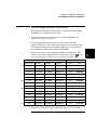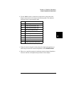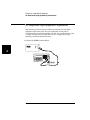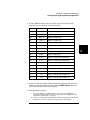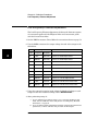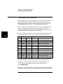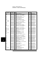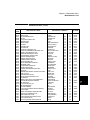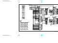
1
Service Guide
Publication Number 33250-90011 (order as 33250-90100 manual set)
Edition 2, March 2003
© Copyright Agilent Technologies, Inc. 2000, 2003
For Safety information, Warranties, and Regulatory information,
see the pages following the Index.
Agilent 33250A
80 MHz Function /
Arbitrary Waveform Generator
Agilent 33250A at a Glance
The Agilent Technologies 33250A is a high-performance 80 MHz
synthesized function generator with built-in arbitrary waveform and
pulse capabilities. Its combination of bench-top and system features
makes this function generator a versatile solution for your testing
requirements now and in the future.
Convenient bench-top features
• 10 standard waveforms
• Built-in 12-bit 200 MSa/s arbitrary waveform capability
• Precise pulse waveform capabilities with adjustable edge time
• LCD color display provides numeric and graphical views
• Easy-to-use knob and numeric keypad
• Instrument state storage with user-defined names
• Portable, ruggedized case with non-skid feet
Flexible system features
• Four downloadable 64K-point arbitrary waveform memories
• GPIB (IEEE-488) interface and RS-232 interface are standard
• SCPI (Standard Commands for Programmable Instruments) compatibility
Note: Unless otherwise indicated, this manual applies to all Serial Numbers.
2
The Front Panel at a Glance
1
2
3
4
5
6
Graph Mode/Local Key
Menu Operation Softkeys
Waveform Selection Keys
Knob
Modulation/Sweep/Burst Menus
State Storage Menu
7
8
9
10
Utility Menu
Instrument Help Topic Menu
Output Enable/Disable Key
Manual Trigger Key (used for
Sweep and Burst only)
11 Cursor Keys
Note: To get context-sensitive help on any front-panel key or menu softkey,
press and hold down that key.
3
The Front-Panel Display at a Glance
Menu Mode
Mode
Information
Trigger
Information
Units
Output
Status
Display
Icon
Numeric
Readout
Softkey Labels
Graph Mode
To enter the Graph Mode, press the
Parameter
Name
key.
Parameter
Value
Signal
Ground
The softkey colors correspond
to the waveform parameters.
4
Front-Panel Number Entry
You can enter numbers from the front-panel using one of two methods.
Use the knob and arrow keys to modify the displayed number.
+
Use the numeric keypad and menu softkeys to select the units.
5
The Rear Panel at a Glance
1
2
3
4
External 10 MHz Reference Input Terminal
Internal 10 MHz Reference Output Terminal
RS-232 Interface Connector
External Modulation Input Terminal
5 Input: External Trig/FSK/Burst Gate
Output: Trigger Output
6 GPIB Interface Connector
7 Chassis Ground
Use the
menu to:
• Select the GPIB or RS-232 interface (see chapter 2 in User’s Guide).
• Select the GPIB address (see chapter 2 in User’s Guide).
• Set the RS-232 baud rate, parity, and handshake (see chapter 2 in User’s Guide).
WARNING
For protection from electrical shock, the power cord ground must not be
defeated. If only a two-contact electrical outlet is available, connect the
instrument’s chassis ground screw (see above) to a good earth ground.
6
In This Book
Specifications Chapter 1 lists the function generator’s specifications.
Quick Start Chapter 2 prepares the function generator for use and
helps you get familiar with a few of its front-panel features.
Front-Panel Menu Operation Chapter 3 introduces you to the frontpanel menu and describes some of the function generator’s menu features.
Calibration Procedures Chapter 4 provides calibration, verification,
and adjustment procedures for the function generator.
Theory of Operation Chapter 5 describes the block diagram and
circuit-level theory related to the operation of the function generator.
Service Chapter 6 provides guidelines for returning your function
generator to Agilent Technologies for servicing, or for servicing it
yourself.
Replaceable Parts Chapter 7 contains a detailed parts list of the
function generator.
Backdating Chapter 8 describes the differences between this manual
and older issues of this manual.
Schematics Chapter 9 contains the function generator’s schematics
and component locator drawings.
If you have questions relating to the operation of the Agilent 33250A,
call 1-800-452-4844 in the United States, or contact your nearest Agilent
Technologies Office.
If your 33250A fails within three years of purchase, Agilent will either
repair or replace it free of charge. Call 1-877-447-7278 in the United
States (and ask for “Agilent Express”) or contact your local Agilent
Technologies Office.
7
8
Contents
Chapter 1 Specifications 13
Chapter 2 Quick Start
To Prepare the Function Generator for Use 21
To Adjust the Carrying Handle 22
To Set the Output Frequency 23
To Set the Output Amplitude 24
To Set a DC Offset Voltage 26
To Set the Duty Cycle 27
To Configure a Pulse Waveform 28
To View a Waveform Graph 29
To Output a Stored Arbitrary Waveform 30
To Use the Built-In Help System 31
To Rack Mount the Function Generator 33
4
Chapter 3 Front-Panel Menu Operation
Contents
Front-Panel Menu Reference 37
To Reset the Function Generator 39
To Select the Output Termination 39
To Read the Calibration Information 40
To Unsecure and Secure for Calibration 41
To Store the Instrument State 44
To Configure the Remote Interface 45
Chapter 4 Calibration Procedures
Agilent Technologies Calibration Services 49
Calibration Interval 50
Adjustment is Recommended 50
Time Required for Calibration 51
Automating Calibration Procedures 52
Recommended Test Equipment 53
Test Considerations 54
Performance Verification Tests 55
Internal Timebase Verification 60
AC Amplitude (high-impedance) Verification 61
Low Frequency Flatness Verification 62
0 dB Range Flatness Verification 63
+10 dB Range Flatness Verification 65
+20 dB Range Flatness Verification 66
9
Contents
Contents
Chapter 4 Calibration Procedures (continued)
Calibration Security 68
Calibration Message 70
Calibration Count 70
General Calibration/Adjustment Procedure 71
Aborting a Calibration in Progress 72
Sequence of Adjustments 72
Self-Test 73
Frequency (Internal Timebase) Adjustment 74
Internal ADC Adjustment 75
Output Impedance Adjustment 76
AC Amplitude (high-impedance) Adjustment 78
Low Frequency Flatness Adjustment 80
0 dB Range Flatness Adjustments 81
+10 dB Range Flatness Adjustments 83
+20 dB Range Flatness Adjustment 85
Pulse Width (Trailing Edge Delay) Adjustment 87
Pulse Edge Time Adjustment 88
Duty Cycle Adjustment 89
Output Amplifier Adjustment (Optional) 90
Calibration Errors 91
Chapter 5 Theory of Operation
Block Diagram 95
Main Power Supply 97
On-Board Power Supplies 98
Waveform DAC and Filters 100
Digital Waveform, Pulse, and Sync 101
Digital Waveform Translator 104
Amplitude Multiplier 106
Main Output Circuitry 107
System ADC 110
System DAC 112
10
Contents
Chapter 5 Theory of Operation (continued)
Synthesis IC 113
Timebase 115
Phase Locked Loops 116
Clock Divider 118
Trigger and Delay 120
Waveform RAM 122
Synchronous Multiplexer 123
Main Processor 124
Main Gate Array 125
DSP and Gateway 126
Earth-Referenced Logic 126
Front Panel 127
4
Chapter 6 Service
Contents
Operating Checklist 130
Types of Service Available 131
Repackaging for Shipment 132
Cleaning 132
Electrostatic Discharge (ESD) Precautions 133
Surface Mount Repair 133
Troubleshooting Hints 134
Self-Test Procedures 136
Disassembly 140
Chapter 7 Replaceable Parts
33250-66511 Main PC Assembly (A1) 153
33205-66502 Front-Panel PC Assembly (A2) 176
33250A Chassis Assembly 177
33250A Front-Panel Assembly 178
Manufacturer’s List 179
Chapter 8 Backdating 181
11
Contents
Contents
Chapter 9 Schematics
A1 Earth Referenced Communications Schematic 185
A1 Main Processor Schematic 186
A1 Main Gate Array Schematic 187
A1 Display Controller Schematic 188
A1 DSP Schematic 189
A1 Modulation Schematic 190
A1 System DAC Schematic 191
A1 Timebase Schematic 192
A1 Phase-Locked Loops Schematic 193
A1 Trigger Schematic 194
A1 Clock Divider and Control Schematic 195
A1 Synthesis IC Schematic 196
A1 Waveform Memory Schematic 197
A1 Synchronous Multiplexer Schematic 198
A1 Digital Waveform and Sync Schematic 199
A1 Variable-Edge Level Translation Schematic 200
A1 Waveform DAC, Filters, and Comparator Schematic 201
A1 Multiplier Schematic 202
A1 Main Output Circuitry Schematic 203
A1 Power Supply Schematic 204
A2 Keyboard Schematic 205
A2 Display Schematic 206
A1 Component Locator (top) 207
A1 Component Locator (bottom) 208
A2 Component Locator (top) 209
A2 Component Locator (bottom) 210
12
1
1
Specifications
Chapter 1 Specifications
Agilent 33250A Function / Arbitrary Waveform Generator
1
WAVEFORMS
SIGNAL CHARACTERISTICS
Standard Waveforms:
Sine, Square, Ramp,
Pulse, Noise, Sin(x)/x,
Exponential Rise,
Exponential Fall,
Negative Ramp,
Cardiac, DC Volts
Arbitrary Waveforms
Waveform Length:
Amplitude Resolution:
Repetition Rate:
Sample Rate:
Filter Bandwidth:
Non-Volatile Memory:
1 to 64K points
12 bits (including sign)
1 µHz to 25 MHz
200 MSa/s
50 MHz
Four 64K waveforms 1
FREQUENCY CHARACTERISTICS
Sine:
Square:
Ramp:
Pulse:
Noise (Gaussian):
Arb:
1 µHz to 80 MHz
1 µHz to 80 MHz
1 µHz to 1 MHz
500 µHz to 50 MHz
50 MHz bandwidth
1 µHz to 25 MHz
Resolution:
1 µHz;
except pulse, 5 digits
Accuracy (1 year):
2 ppm, 18°C to 28°C
3 ppm, 0°C to 55°C
Square Wave
Rise / Fall Time:
Overshoot:
Asymmetry:
Jitter (rms)
< 2 MHz:
> 2 MHz:
Duty Cycle
< 25 MHz:
25 MHz to 50 MHz:
50 MHz to 80 MHz:
20.0% to 80.0%
40.0% to 60.0%
50.0% (fixed)
Pulse
Period:
Pulse Width:
Variable Edge Time:
Overshoot:
Jitter (rms):
20.00 ns to 2000.0 s
8.0 ns to 1999.9 s
5.00 ns to 1.00 ms
< 5%
100 ppm + 50 ps
Ramp
Linearity:
Symmetry:
< 0.1% of peak output
0.0% to 100.0%
Arb
Minimum Edge Time:
Linearity:
Settling Time:
Jitter (rms):
< 8 ns 4
< 5%
1% of period + 1 ns
0.01% + 525 ps
0.1% + 75 ps
< 10 ns
< 0.1% of peak output
< 50 ns to 0.5% of
final value
30 ppm + 2.5 ns
SINEWAVE SPECTRAL PURITY
Harmonic Distortion
DC to 1 MHz:
1 MHz to 5 MHz:
5 MHz to 80 MHz:
< 3 Vpp2
-60 dBc
-57 dBc
-37 dBc
> 3 Vpp
-55 dBc
-45 dBc
-30 dBc
Total Harmonic Distortion
DC to 20 kHz:
< 0.2% + 0.1 mVrms
Spurious (non-harmonic) 3
DC to 1 MHz:
-60 dBc
1 MHz to 20 MHz:
-50 dBc
20 MHz to 80 MHz:
-50 dBc + 6 dBc/octave
Phase Noise (30 kHz band)
10 MHz
< -65 dBc (typical)
80 MHz
< -47 dBc (typical)
14
_______________
1
A total of four waveforms can be stored.
2
Harmonic distortion at low amplitudes is limited by
a -70 dBm floor.
3
Spurious noise at low amplitudes is limited by
a -75 dBm floor.
4
Edge time decreased at higher frequency.
Chapter 1 Specifications
Agilent 33250A Function / Arbitrary Waveform Generator
OUTPUT CHARACTERISTICS 1
BURST
2
Amplitude (into 50Ω):
10 mVpp to 10 Vpp
Accuracy (at 1 kHz, >10 mVpp, Autorange On):
± 1% of setting ±1 mVpp
Flatness (sinewave relative to 1 kHz, Autorange On)
< 10 MHz:
± 1% (0.1 dB) 3
10 MHz to 50 MHz:
± 2% (0.2 dB)
50 MHz to 80 MHz
± 5% (0.4 dB)
Units:
Vpp, Vrms, dBm,
High Level, Low Level
Resolution:
0.1 mV or 4 digits
Offset (into 50Ω):
± 5 Vpk ac + dc
Accuracy:
1% of setting + 2 mV
+ 0.5% of amplitude
Waveform Output
Impedance:
50Ω typical (fixed)
>10 MΩ (output disabled)
Isolation:
42 Vpk max. to Earth
Protection:
Short-circuit protected; 4
Overload relay automatically disables
main output
Waveforms:
Frequency:
Burst Count:
Start / Stop Phase:
Internal Period:
Gate Source:
Trigger Source:
Trigger Delay
N-Cycle, Infinite:
Sine, Square, Ramp,
Pulse, Noise, Arb
1 µHz to 80 MHz 5
1 to 1,000,000 cycles,
or Infinite
-360.0° to +360.0°
1 ms to 500 s
External Trigger
Single, External, or
Internal Rate
4
0.0 ns to 85.000 s
SWEEP
Waveforms:
Type:
Direction:
Start F / Stop F:
Sweep Time:
Trigger:
Marker:
Sine, Square, Ramp, Arb
Linear or Logarithmic
Up or Down
100 µHz to 80 MHz
1 ms to 500 s
Single, External, or
Internal
Falling edge of Sync
signal (programmable)
MODULATION CHARACTERISTICS
AM Modulation
Carrier Waveforms:
Modulating Waveforms:
Modulating Frequency:
Depth:
Source:
FM Modulation
Carrier Waveforms:
Modulating Waveforms:
Sine, Square, Ramp, Arb
Sine, Square, Ramp,
Noise, Arb
2 mHz to 20 kHz
0.0% to 120.0%
Internal / External
Modulating Frequency:
Peak Deviation:
Source:
Sine, Square, Ramp, Arb
Sine, Square, Ramp,
Noise, Arb
2 mHz to 20 kHz
DC to 80 MHz
Internal / External
FSK
Carrier Waveforms:
Modulating Waveforms:
Internal Rate:
Frequency Range:
Source:
Sine, Square, Ramp, Arb
50% duty cycle square
2 mHz to 100 kHz
1 µHz to 80 MHz
Internal / External
External Modulation Input
Voltage Range:
± 5V full scale
Input Impedance:
10 kΩ
Frequency:
DC to 20 kHz
_______________
1
Add 1/10th of output amplitude and offset
specification per °C for operation outside of
18 °C to 28 °C range (1-year specification).
2
20 mVpp to 20 Vpp into open-circuit load.
3
dB rounded to 1 digit. Instrument adheres
to “%” specification.
4
Short-circuit protected to ground at all times.
5
Sine and square waveforms above 25 MHz are
allowed only with an “Infinite” burst count.
15
1
Chapter 1 Specifications
Agilent 33250A Function / Arbitrary Waveform Generator
1
SYSTEM CHARACTERISTICS
Configuration TImes
Function Change
Standard: 2
Pulse:
Built-In Arb: 2
Frequency Change:
Amplitude Change:
Offset Change:
Select User Arb:
Modulation Change:
CLOCK REFERENCE
(typical) 1
102 ms
660 ms
240 ms
24 ms
50 ms
50 ms
< 400 ms for < 16K points
< 200 ms
Arb Download Times GPIB / RS-232 (115 Kbps) 3
Arb Length Binary ASCII Integer
64K points 23 sec
92 sec
16K points
6 sec
23 sec
8K points
3 sec
12 sec
4K points 1.5 sec
6 sec
2K points 0.75 sec
3 sec
ASCII Real
154 sec
39 sec
20 sec
10 sec
5 sec
Phase Offset
Range:
Resolution:
-360° to +360°
0.001°
External Reference Input
Lock Range:
Level:
Impedance:
Lock Time:
10 MHz ± 35 kHz
100 mVpp to 5 Vpp
1 kΩ nominal, ac coupled
<2s
Internal Reference Output
Frequency:
10 MHz
Level:
632 mVpp (0 dBm),
nominal
Impedance:
50Ω nominal, ac coupled
SYNC OUTPUT
Level:
Impedance:
TTL-compatible
into > 1 kΩ
50Ω nominal
TRIGGER CHARACTERISTICS
Trigger Input
Input Level:
Slope:
TTL-compatible
Rising or falling
(selectable)
> 100 ns
10 kΩ, DC coupled
Pulse Width:
Input Impedance:
Latency
Sweep:
Burst:
Jitter (rms)
Sweep:
Burst:
< 10 µs (typical)
< 100 ns (typical)
2.5 µs
1 ns;
except pulse, 300 ps
Trigger Output
Level:
Pulse Width:
Maximum Rate:
Fanout:
TTL-compatible into 50Ω
> 450 ns
1 MHz
< 4 Agilent 33250As
16
_______________
1
Time to change parameter and output new signal.
2
Modulation or sweep off.
3
Times for 5-digit integer and 12-digit real numbers.
Chapter 1 Specifications
Agilent 33250A Function / Arbitrary Waveform Generator
GENERAL SPECIFICATIONS
Power Supply:
100-240 V (±10%)
for 50-60 Hz operation,
100-127 V (±10%)
for 50-400 Hz operation.
IEC 60664 CAT II
Power Consumption:
140 VA
Operating Environment:
0 °C to 55 °C
80% R.H. to 40 °C
Safety Designed to:
EN61010-1, CSA1010.1,
UL-3111-1
EMC Tested to: 1
IEC-61326-1
IEC-61000-4-3 criteria B
IEC-61000-4-6 criteria B
Acoustic Noise:
40 dBA
Warm-Up Time:
1 hour
4
Operating Altitude:
3000 meters
Calibration Interval:
1 year
Pollution Degree:
Indoor or Sheltered Use,
IEC 60664 Degree 2
Warranty:
3 years standard
Storage Temperature:
-30 °C to 70 °C
Accessories Included:
Stored States:
Four (4) named user
configurations
Power-On State:
Default or Last
User’s Guide,
Service Guide,
Quick Reference Guide,
Test Data,
Connectivity Software,
RS-232 Cable,
Power Cord
Interface:
IEEE-488 and RS-232
standard
Language:
SCPI-1997, IEEE-488.2
_______________
1
Dimensions (WxHxD)
Bench Top:
Rack Mount:
254 x 104 x 374 mm
213 x 89 x 348 mm
Weight:
4.6 kg
Radiated and conducted immunity testing:
When the product is tested at 3 V/m according
to IEC/EN 61000-4-3:1995 or tested at 3 Vrms
according to IEC/EN 61000-4-6:1996, the product
may not meet criteria A, but does meet criteria B.
This ISM device complies with Canadian ICES-001.
Cet appareil ISM est conforme à la norme NMB-001
du Canada.
N10149
17
1
1
Chapter 1 Specifications
Agilent 33250A Function / Arbitrary Waveform Generator
PRODUCT DIMENSIONS
103.6 mm
254.4 mm
374.0 mm
88.5 mm
216.6 mm
348.3 mm
All dimensions are
shown in millimeters.
18
2
2
Quick Start
Quick Start
2
One of the first things you will want to do with your function generator
is to become acquainted with the front panel. We have written the
exercises in this chapter to prepare the instrument for use and help
you get familiar with some of its front-panel operations. This chapter
is divided into the following sections:
• To Prepare the Function Generator for Use, on page 21
• To Adjust the Carrying Handle, on page 22
• To Set the Output Frequency, on page 23
• To Set the Output Amplitude, on page 24
• To Set a DC Offset Voltage, on page 26
• To Set the Duty Cycle, on page 27
• To Configure a Pulse Waveform, on page 28
• To View a Waveform Graph, on page 29
• To Output a Stored Arbitrary Waveform, on page 30
• To Use the Built-In Help System, on page 31
• To Rack Mount the Function Generator, on page 33
20
Chapter 2 Quick Start
To Prepare the Function Generator for Use
To Prepare the Function Generator for Use
1 Check the list of supplied items.
2
Verify that you have received the following items with your instrument.
If anything is missing, please contact your nearest Agilent Sales Office.
❑ One power cord.
❑ One User’s Guide.
4
❑ This Service Guide.
❑ One folded Quick Reference Guide.
❑ Certificate of Calibration.
❑ Connectivity software on CD-ROM.
❑ One RS-232 cable.
Power
Switch
2 Connect the power cord and turn on the function generator.
Several power-on information messages are displayed after the function
generator performs its power-on self-test. The GPIB address is displayed.
The function generator powers up in the sine wave function at 1 kHz
with an amplitude of 100 mV peak-to-peak (into a 50Ω termination).
At power-on, the Output connector is disabled. To enable the Output
connector, press the
key.
If the function generator does not turn on, verify that the power cord is
firmly connected to the power receptacle on the rear panel (the powerline voltage is automatically sensed at power-on). You should also make
sure that the function generator is connected to a power source that is
energized. Then, verify that the function generator is turned on.
If you need further assistance, refer to chapter 6 for instructions on
returning the function generator to Agilent for service.
21
Chapter 2 Quick Start
To Adjust the Carrying Handle
To Adjust the Carrying Handle
2
To adjust the position, grasp the handle by the sides and pull outward.
Then, rotate the handle to the desired position.
Bench-top viewing positions
22
Carrying position
Chapter 2 Quick Start
To Set the Output Frequency
To Set the Output Frequency
At power-on, the function generator outputs a sine wave at 1 kHz with
an amplitude of 100 mV peak-to-peak (into a 50Ω termination).
The following steps show you how to change the frequency to 1.2 MHz.
1 Press the “Freq” softkey.
2
4
The displayed frequency is either the power-on value or the frequency
previously selected. When you change functions, the same frequency is
used if the present value is valid for the new function. To set the
waveform period instead, press the Freq softkey again to toggle to the
Period softkey (the current selection is highlighted).
2 Enter the magnitude of the desired frequency.
Using the numeric keypad, enter the value “1.2”.
3 Select the desired units.
Press the softkey that corresponds to the desired units. When you select
the units, the function generator outputs a waveform with the displayed
frequency (if the output is enabled). For this example, press MHz.
Note: You can also enter the desired value using the knob and arrow keys.
23
Chapter 2 Quick Start
To Set the Output Amplitude
To Set the Output Amplitude
2
At power-on, the function generator outputs a sine wave with an
amplitude of 100 mV peak-to-peak (into a 50Ω termination).
The following steps show you how to change the amplitude to 50 mVrms.
1 Press the “Ampl” softkey.
The displayed amplitude is either the power-on value or the amplitude
previously selected. When you change functions, the same amplitude is
used if the present value is valid for the new function. To set the amplitude
using a high level and low level, press the Ampl softkey again to toggle to
the HiLevel and LoLevel softkeys (the current selection is highlighted).
2 Enter the magnitude of the desired amplitude.
Using the numeric keypad, enter the value “50”.
3 Select the desired units.
Press the softkey that corresponds to the desired units. When you select
the units, the function generator outputs the waveform with the displayed
amplitude (if the output is enabled). For this example, press mVRMS.
Note: You can also enter the desired value using the knob and arrow keys.
24
Chapter 2 Quick Start
To Set the Output Amplitude
You can easily convert the displayed amplitude from one unit to another.
For example, the following steps show you how to convert the amplitude
from Vrms to Vpp.
2
4 Enter the numeric entry mode.
Press the
key to enter the numeric entry mode.
4
5 Select the new units.
Press the softkey that corresponds to the desired units. The displayed
value is converted to the new units. For this example, press the Vpp
softkey to convert 50 mVrms to its equivalent in volts peak-to-peak.
To change the displayed amplitude by decades, press the right-arrow
key to move the cursor to the units on the right side of the display.
Then, rotate the knob to increase or decrease the displayed amplitude
by decades.
25
Chapter 2 Quick Start
To Set a DC Offset Voltage
To Set a DC Offset Voltage
2
At power-on, the function generator outputs a sine wave with a dc offset
of 0 volts (into a 50Ω termination). The following steps show you how to
change the offset to –1.5 mVdc.
1 Press the “Offset” softkey.
The displayed offset voltage is either the power-on value or the offset
previously selected. When you change functions, the same offset is used
if the present value is valid for the new function.
2 Enter the magnitude of the desired offset.
Using the numeric keypad, enter the value “–1.5”.
3 Select the desired units.
Press the softkey that corresponds to the desired units. When you select
the units, the function generator outputs the waveform with the displayed
offset (if the output is enabled). For this example, press mVdc.
Note: You can also enter the desired value using the knob and arrow keys.
Note: To select dc volts from the front panel, press
and then select
the DC On softkey. Press the Offset softkey to enter the desired voltage level.
26
Chapter 2 Quick Start
To Set the Duty Cycle
To Set the Duty Cycle
Applies only to square waves. At power-on, the duty cycle for square
waves if 50%. You can adjust the duty cycle from 20% to 80% for output
frequencies up to 25 MHz. The following steps show you how to change
the duty cycle to 30%.
4
1 Select the square wave function.
Press the
key and then set the desired output frequency to any
value less than 25 MHz.
2 Press the “Duty Cycle” softkey.
The displayed duty cycle is either the power-on value or the percentage
previously selected. The duty cycle represents the amount of time per
cycle that the square wave is at a high level (note the icon on the right
side of the display).
3 Enter the desired duty cycle.
Using the numeric keypad or the knob, select a duty cycle value of “30”.
The function generator adjusts the duty cycle immediately and outputs a
square wave with the specified value (if the output is enabled).
27
2
Chapter 2 Quick Start
To Configure a Pulse Waveform
To Configure a Pulse Waveform
2
You can configure the function generator to output a pulse waveform
with variable pulse width and edge time. The following steps show you
how to configure a 500 ms pulse waveform with a pulse width of 10 ms
and edge times of 50 µs.
1 Select the pulse function.
Press the
key to select the pulse function and output a pulse
waveform with the default parameters.
2 Set the pulse period.
Press the Period softkey and then set the pulse period to 500 ms.
3 Set the pulse width.
Press the Pulse Width softkey and then set the pulse width to 10 ms.
The pulse width represents the time from the 50% threshold of the rising
edge to the 50% threshold of the next falling edge (note the display icon).
4 Set the edge time for both edges.
Press the Edge Time softkey and then set the edge time for both the rising
and falling edges to 50 µs. The edge time represents the time from the
10% threshold to the 90% threshold of each edge (note the display icon).
28
Chapter 2 Quick Start
To View a Waveform Graph
To View a Waveform Graph
In the Graph Mode, you can view a graphical representation of the
current waveform parameters. Each softkey parameter is shown in a
different color corresponding to the lines above the softkeys at the
bottom of the display. Note that the softkeys are listed in the same order
as in the normal display mode.
4
1 Enable the Graph Mode.
Press the
key to enable the Graph Mode. The name of the parameter
currently selected is shown in the upper-left corner of the display and the
numeric value is highlighted.
2 Select the desired parameter.
To select a specific parameter, note the colored bars above the softkeys at
the bottom of the display and select the corresponding color. For example,
to select amplitude, press the softkey below the magenta-colored bar.
• As in the normal display mode, you can edit numbers using the
numeric keypad or the knob and arrow keys.
• Parameters which normally toggle when you press a key a second time
(e.g., Freq / Period) also toggle in the Graph Mode.
• To exit the Graph Mode, press
The
key also serves as a
after remote interface operations.
again.
key to restore front-panel control
29
2
Chapter 2 Quick Start
To Output a Stored Arbitrary Waveform
To Output a Stored Arbitrary Waveform
2
There are five built-in arbitrary waveforms stored in non-volatile memory.
The following steps show you how to output the built-in “exponential fall”
waveform from the front panel.
1 Select the arbitrary waveform function.
When you press the
key to select the arbitrary waveform function,
a temporary message is displayed indicating which waveform is currently
selected (the default is “exponential rise”).
2 Select the active waveform.
Press the Select Wform softkey and then press the Built-In softkey to
select from the five built-in waveforms. Then press the Exp Fall softkey.
The waveform is output using the present settings for frequency,
amplitude, and offset unless you change them.
The selected waveform is now assigned to the
key. Whenever you
press this key, the selected arbitrary waveform is output. To quickly
determine which arbitrary waveform is currently selected, press
.
30
Chapter 2 Quick Start
To Use the Built-In Help System
To Use the Built-In Help System
The built-in help system is designed to provide context-sensitive
assistance on any front-panel key or menu softkey. A list of help topics
is also available to assist you with several front-panel operations.
2
4
1 View the help information for a function key.
Press and hold down the
key. If the message contains more
information than will fit on the display, press the ↓ softkey or turn the
knob clockwise to view the remaining information.
Press DONE to exit the help menu.
2 View the help information for a menu softkey.
Press and hold down the Freq softkey. If the message contains more
information than will fit on the display, press the ↓ softkey or rotate the
knob clockwise to view the remaining information.
Press DONE to exit the help menu.
31
Chapter 2 Quick Start
To Use the Built-In Help System
3 View the list of help topics.
2
Press the
key to view the list of available help topics. To scroll
through the list, press the ↑ or ↓ softkey or rotate the knob. Select the
third topic “Get HELP on any key” and then press SELECT.
Press DONE to exit the help menu.
4 View the help information for displayed messages.
Whenever a limit is exceeded or any other invalid configuration is found,
the function generator will display a message. For example, if you enter
a value that exceeds the frequency limit for the selected function,
a message will be displayed. The built-in help system provides additional
information on the most recent message to be displayed.
Press the
key, select the first topic “View the last message displayed”,
and then press SELECT.
Local Language Help: The built-in help system in available in multiple
languages. All messages, context-sensitive help, and help topics appear
in the selected language. The menu softkey labels and status line
messages are not translated.
To select the local language, press the
key, press the System
softkey, and then press the Help In softkey. Select the desired language.
32
Chapter 2 Quick Start
To Rack Mount the Function Generator
To Rack Mount the Function Generator
You can mount the Agilent 33250A in a standard 19-inch rack cabinet
using one of two optional kits available. Instructions and mounting
hardware are included with each rack-mounting kit. Any Agilent
System II instrument of the same size can be rack-mounted beside the
Agilent 33250A.
2
4
Note: Remove the carrying handle, and the front and rear rubber bumpers,
before rack-mounting the instrument.
To remove the handle, rotate it to vertical and pull the ends outward.
Front
Rear (bottom view)
To remove the rubber bumper, stretch a corner and then slide it off.
33
Chapter 2 Quick Start
To Rack Mount the Function Generator
2
To rack mount a single instrument, order adapter kit 5063-9240.
To rack mount two instruments side-by-side, order lock-link kit 5061-9694
and flange kit 5063-9212. Be sure to use the support rails in the rack cabinet.
In order to prevent overheating, do not block the flow of air into or out of
the instrument. Be sure to allow enough clearance at the rear, sides, and
bottom of the instrument to permit adequate internal airflow.
34
3
3
Front-Panel Menu Operation
Front-Panel Menu Operation
This chapter introduces you to the front-panel keys and menu operation.
This chapter does not give a detailed description of every front-panel key
or menu operation. It does, however, give you an overview of the frontpanel menus and many front-panel operations. See the Agilent 33250A
User’s Guide for a complete discussion of the function generator’s
capabilities and operation.
• Front-Panel Menu Reference, on page 37
3
• To Reset the Function Generator, on page 39
• To Select the Output Termination, on page 39
• To Read the Calibration Information, on page 40
• To Unsecure and Secure for Calibration, on page 41
• To Store the Instrument State, on page 44
• To Configure the Remote Interface, on page 45
36
Chapter 3 Front-Panel Menu Operation
Front-Panel Menu Reference
Front-Panel Menu Reference
This section gives an overview of the front-panel menus. The remainder
of this chapter shows examples of using the front-panel menus.
Configure the modulation parameters for AM, FM, and FSK.
•
•
•
•
•
4
Select the modulation type.
Select an internal or external modulation source.
Specify the AM modulation depth, modulating frequency, and modulation shape.
Specify the FM frequency deviation, modulating frequency, and modulation shape.
Specify the FSK “hop” frequency and FSK rate.
Configure the parameters for frequency sweep.
•
•
•
•
•
•
•
Select linear or logarithmic sweeping.
Select the start/stop frequencies or center/span frequencies.
Select the time in seconds required to complete a sweep.
Specify a marker frequency.
Specify an internal or external trigger source for the sweep.
Specify the slope (rising or falling edge) for an external trigger source.
Specify the slope (rising or falling edge) of the “Trig Out” signal.
Configure the parameters for burst.
•
•
•
•
•
•
•
•
Select the triggered (N Cycle) or externally-gated burst mode.
Select the number of cycles per burst (1 to 1,000,000, or Infinite).
Select the starting phase angle of the burst (-360° to +360°).
Specify the time from the start of one burst to the start of the next burst.
Specify a delay between the trigger and the start of the burst.
Specify an internal or external trigger source for the burst.
Specify the slope (rising or falling edge) for an external trigger source.
Specify the slope (rising or falling edge) of the “Trig Out” signal.
37
3
Chapter 3 Front-Panel Menu Operation
Front-Panel Menu Reference
Store and recall instrument states.
•
•
•
•
•
Store up to four instrument states in non-volatile memory.
Assign a custom name to each storage location.
Recall stored instrument states.
Restore all instrument settings to their factory default values.
Select the instrument’s power-on configuration (last or factory default).
3
Configure system-related parameters.
•
•
•
•
•
•
•
•
•
•
•
•
•
•
•
Generate a dc-only voltage level.
Enable/disable the Sync signal which is output from the “Sync” connector.
Select the output termination (1Ω to 10 kΩ, or Infinite).
Enable/disable amplitude autoranging.
Select the waveform polarity (normal or inverted).
Select the GPIB address.
Configure the RS-232 interface (baud rate, parity, and handshake mode).
Select how periods and commas are used in numbers displayed on the front panel.
Select the local language for front-panel messages and help text.
Enable/disable the tone heard when an error is generated.
Enable/disable the display bulb-saver mode.
Adjust the contrast setting of the front-panel display.
Perform an instrument self-test.
Secure/unsecure the instrument for calibration and perform manual calibrations.
Query the instrument’s firmware revision codes.
View the list of Help topics.
•
•
•
•
•
•
•
•
•
•
View the last message displayed.
View the remote command error queue.
Get HELP on any key.
How to generate a dc-only voltage level.
How to generate a modulated waveform.
How to create an arbitrary waveform.
How to reset the instrument to its default state.
How to view a waveform in the Graph Mode.
How to synchronize multiple instruments.
How to obtain Agilent Technical Support.
38
Chapter 3 Front-Panel Menu Operation
To Reset the Function Generator
To Reset the Function Generator
To reset the instrument to its factory default state, press
and then
select the Set to Defaults softkey. Select YES to confirm the operation.
A complete listing of the instrument’s power-on and reset conditions,
4
see the “Factory Default Settings” table inside the rear cover of this manual.
To Select the Output Termination
The Agilent 33250A has a fixed series output impedance of 50 ohms to
the front-panel Output connector. If the actual load impedance is
different than the value specified, the displayed amplitude and offset
levels will be incorrect. The load impedance setting is simply provided
as a convenience to ensure that the displayed voltage matches the
expected load.
1 Press
.
2 Navigate the menu to set the output termination.
Press the Output Setup softkey and then select the Load softkey.
3 Select the desired output termination.
Use the knob or numeric keypad to select the desired load impedance
or press the Load softkey again to choose “High Z”.
39
3
Chapter 3 Front-Panel Menu Operation
To Read the Calibration Information
To Read the Calibration Information
You can use the instrument’s calibration memory to read the calibration
count and calibration message.
3
Calibration Count You can query the instrument to determine how
many calibrations have been performed. Note that your instrument was
calibrated before it left the factory. When you receive your instrument,
read the count to determine its initial value. The count value increments
by one for each calibration point, and a complete calibration may
increase the value by many counts.
Calibration Message The instrument allows you to store one message
in calibration memory. For example, you can store such information as
the date when the last calibration was performed, the date when the
next calibration is due, the instrument’s serial number, or even the name
and phone number of the person to contact for a new calibration.
You can record a calibration message only from the remote interface
and only when the instrument is unsecured.
You can read the message from either the front-panel or over the remote
interface. You can read the calibration message whether the instrument
is secured or unsecured.
1 Select the Cal Info interface.
Press
and then select the Cal Info softkey from the “Test/Cal” menu.
The first line in the display shows the calibration count.
The second line shows the calibration message.
The last line indicates the current version of the firmware.
The calibration information will time-out and disappear after a few seconds.
Select the Cal Info softkey to show the information again.
2 Exit the menu.
Press the DONE softkey.
40
Chapter 3 Front-Panel Menu Operation
To Unsecure and Secure for Calibration
To Unsecure and Secure for Calibration
This feature allows you to enter a security code to prevent accidental
or unauthorized adjustments of the instrument. When you first receive
your instrument, it is secured. Before you can adjust the instrument,
you must unsecure it by entering the correct security code.
• The security code is set to AT33250A when the instrument is shipped
4
from the factory. The security code is stored in non-volatile memory,
and does not change when power has been off, after a Factory Reset
(*RST command), or after an Instrument Preset (SYSTem:PRESet
command).
• The security code may contain up to 12 alphanumeric characters.
The first character must be a letter, but the remaining characters
can be letters, numbers, or an underscore ( _ ). You do not have to
use all 12 characters but the first character must always be a letter.
Note: If you forget your security code, you can disable the security feature
by applying a temporary short inside the instrument as described in
“To Unsecure the Instrument Without the Security Code”, on page 69.
41
3
Chapter 3 Front-Panel Menu Operation
To Unsecure and Secure for Calibration
To Unsecure for Calibration
1 Select the Secure Code interface.
Press
and then select the Test/Cal softkey.
3
2 Enter the Secure Code.
Use the knob to change the displayed character. Use the arrow keys to
move to the next character.
+
When the last character of the secure code is entered, the instrument
will be unsecured.
3 Exit the menu.
Press the DONE softkey.
42
Chapter 3 Front-Panel Menu Operation
To Unsecure and Secure for Calibration
To Secure After Calibration
1 Select the Secure Code interface.
Press
and then select the Test/Cal softkey.
4
3
2 Enter a Secure Code.
Enter up to 12 alphanumeric characters. The first character must be
a letter.
Use the knob to change the displayed character. Use the arrow keys to
move to the next character.
+
3 Secure the Instrument.
Select the Secure softkey.
4 Exit the menu.
Press the DONE softkey.
43
Chapter 3 Front-Panel Menu Operation
To Store the Instrument State
To Store the Instrument State
You can store the instrument state in one of four non-volatile storage
locations. A fifth storage location automatically holds the power-down
configuration of the instrument. When power is restored, the instrument
can automatically return to its state before power-down.
1 Select the desired storage location.
3
Press
and then select the Store State softkey.
2 Select a custom name for the selected location.
If desired, you can assign a custom name to each of the four locations.
• The name can contain up to 12 characters. The first character must
be a letter but the remaining characters can be letters, numbers, or
the underscore character (“_”).
• To add additional characters, press the right-arrow key until the
cursor is to the right of the existing name and then turn the knob.
• To delete all characters to the right of the cursor position, press
• To use numbers in the name, you can enter them directly from the
numeric keypad. Use the decimal point from the numeric keypad to
add the underscore character (“_”) to the name.
3 Store the instrument state.
Press the STORE STATE softkey. The instrument stores the selected
function, frequency, amplitude, dc offset, duty cycle, symmetry, as well
as any modulation parameters in use. The instrument does not store
volatile waveforms created in the arbitrary waveform function.
44
.
Chapter 3 Front-Panel Menu Operation
To Configure the Remote Interface
To Configure the Remote Interface
The instrument is shipped with both a GPIB (IEEE-488) interface and an
RS-232 interface. Only one interface can be enabled at a time. The GPIB
interface is selected when the instrument is shipped from the factory.
4
3
GPIB Configuration
1 Select the GPIB interface.
Press
and then select the GPIB softkey from the “I/O” menu.
2 Select the GPIB address.
Press the GPIB Address softkey and enter the desired address using the
numeric keypad or knob. The factory setting is “10”.
The GPIB address is shown on the front-panel display at power-on.
3 Exit the menu.
Press the DONE softkey.
45
Chapter 3 Front-Panel Menu Operation
To Configure the Remote Interface
RS-232 Configuration
1 Select the RS-232 interface.
Press
and then select the RS-232 softkey from the “I/O” menu.
3
2 Set the baud rate.
Press the Baud Rate softkey and select one of the following:
300, 600, 1200, 2400, 4800, 9600, 19200, 38400, 57600 (factory setting),
or 115200 baud.
3 Select the parity and number of data bits.
Press the Parity / # Bits softkey and select one of the following:
None (8 data bits, factory setting), Even (7 data bits), or Odd (7 data bits).
When you set the parity, you are also setting the number of data bits.
4 Select the handshake mode.
Press the Handshake softkey and select one of the following:
None, DTR / DSR (factory setting), Modem, RTS / CTS, or XON / XOFF.
5 Exit the menu.
Press the DONE softkey.
46
4
4
Calibration Procedures
Calibration Procedures
This chapter contains procedures for verification of the instrument’s
performance and adjustment (calibration). The chapter is divided into
the following sections:
4
•
•
•
•
•
•
•
•
•
•
•
•
•
•
•
•
•
•
•
•
•
•
•
•
•
•
•
•
•
•
•
•
•
•
48
Agilent Technologies Calibration Services, on page 49
Calibration Interval, on page 50
Adjustment is Recommended, on page 50
Time Required for Calibration, on page 51
Automating Calibration Procedures, on page 52
Recommended Test Equipment, on page 53
Test Considerations, on page 54
Performance Verification Tests, on page 55
Internal Timebase Verification, on page 60
AC Amplitude (high-impedance) Verification, on page 61
Low Frequency Flatness Verification, on page 62
0 dB Range Flatness Verification, on page 63
+10 dB Range Flatness Verification, on page 65
+20 dB Range Flatness Verification, on page 66
Calibration Security, on page 68
Calibration Message, on page 70
Calibration Count, on page 70
General Calibration/Adjustment Procedure, on page 71
Sequence of Adjustments, on page 72
Aborting a Calibration in Progress, on page 72
Self-Test, on page 73
Frequency (Internal Timebase) Adjustment, on page 74
Internal ADC Adjustment, on page 75
Output Impedance Adjustment, on page 76
AC Amplitude (high-impedance) Adjustment, on page 78
Low Frequency Flatness Adjustment, on page 80
0 dB Range Flatness Adjustments, on page 81
+10 dB Range Flatness Adjustments, on page 83
+20 dB Range Flatness Adjustment, on page 85
Pulse Width (Trailing Edge Delay) Adjustment, on page 87
Pulse Edge Time Adjustment, on page 88
Duty Cycle Adjustment, on page 89
Output Amplifier Adjustment (Optional), on page 90
Calibration Errors, on page 91
Chapter 4 Calibration Procedures
Agilent Technologies Calibration Services
Closed-Case Electronic Calibration The instrument features closedcase electronic calibration. No internal mechanical adjustments are
required. The instrument calculates correction factors based upon the
input reference value you set. The new correction factors are stored in
non-volatile memory until the next calibration adjustment is performed.
Non-volatile EEPROM calibration memory does not change when power
has been off or after a remote interface reset.
4
Agilent Technologies Calibration Services
When your instrument is due for calibration, contact your local
Agilent Technologies Service Center for a low-cost recalibration.
The Agilent 33250A is supported on automated calibration systems
which allow Agilent to provide this service at competitive prices.
4
49
Chapter 4 Calibration Procedures
Calibration Interval
Calibration Interval
The instrument should be calibrated on a regular interval determined by
the measurement accuracy requirements of your application. A 1-year
interval is adequate for most applications. Accuracy specifications are
warranted only if adjustment is made at regular calibration intervals.
Accuracy specifications are not warranted beyond the 1-year calibration
interval. Agilent Technologies does not recommend extending calibration
intervals beyond 2 years for any application.
Adjustment is Recommended
4
Whatever calibration interval you select, Agilent Technologies
recommends that complete re-adjustment should always be performed
at the calibration interval. This will assure that the Agilent 33250A
will remain within specification for the next calibration interval.
This criteria for re-adjustment provides the best long-term stability.
Performance data measured using this method can be used to extend
future calibration intervals.
Use the Calibration Count (see page 70) to verify that all adjustments
have been performed.
50
Chapter 4 Calibration Procedures
Time Required for Calibration
Time Required for Calibration
The Agilent 33250A can be automatically calibrated under computer control.
With computer control you can perform the complete calibration
procedure and performance verification tests in approximately 30 minutes
once the instrument is warmed-up (see “Test Considerations” on page 54).
Manual adjustments and verifications, using the recommended test
4
equipment, will take approximately 2 hours.
START
Incoming
Verification?
4
YES
NO
Do Performance
Verification Tests
(approx 1 Hour)
Perform
Adjustments
(approx 1 Hour)
Do Performance
Verification Tests
(approx 1 Hour)
DONE
51
Chapter 4 Calibration Procedures
Automating Calibration Procedures
Automating Calibration Procedures
You can automate the complete verification and adjustment procedures
outlined in this chapter if you have access to programmable test
equipment. You can program the instrument configurations specified
for each test over the remote interface. You can then enter readback
verification data into a test program and compare the results to the
appropriate test limit values.
4
You can also adjust the instrument from the remote interface. Remote
adjustment is similar to the local front-panel procedure. You can use a
computer to perform the adjustment by first selecting the required
function and range. The calibration value is sent to the instrument and
then the calibration is initiated over the remote interface. The instrument
must be unsecured prior to initiating the calibration procedure.
For further information on programming the instrument, see chapters
3 and 4 in the Agilent 33250A User’s Guide.
52
Chapter 4 Calibration Procedures
Recommended Test Equipment
Recommended Test Equipment
The test equipment recommended for the performance verification and
adjustment procedures is listed below. If the exact instrument is not
available, substitute calibration standards of equivalent accuracy.
Instrument
Requirements
Recommended Model
Use*
Digital Multimeter
(DMM)
ac volts, true rms, ac coupled
accuracy: ±0.02% to 1 MHz
dc volts
accuracy: 50 ppm
resolution: 100 µV
Resistance
Offset-compensated
accuracy: ±0.1Ω
Agilent 3458A
Q, P, T
Power Meter
100 kHz to 100 MHz
1 µW to 100 mW (–30 dBm to +20 dBm)
accuracy: 0.02 dB
resolution: 0.01 dB
Agilent E4418B
Q, P, T
Power Head
100 kHz to 100 MHz
1 µW to 100 mW (–30 dBm to +20 dBm)
Agilent 8482A
Q, P, T
Attenuator
–20 dB
Agilent 8491A Opt 020
Q, P, T
Frequency Meter
accuracy: 0.1 ppm
Agilent 53131A Opt 010
(high stability)
Q, P, T
Oscilloscope
500 MHz
2 Gs/second
50Ω input termination
Agilent 54831B
Q, P, T
Adapter
N type (m) to BNC (m)
N type (m) to BNC (m)
Q, P, T
Cable
BNC (m) to dual-banana (f)
Agilent 10110B
Q, P, T
Cable (2 required)
Dual banana (m) to dual banana (m)
Agilent 11000-60001
Q, P, T
Cable
RG58, BNC (m) to dual banana
Agilent 11001-60001
Q, P, T
Cable
RG58, BNC (m) to BNC (m)
Agilent 8120-1840
Q, P, T
* Q = Quick Verification
T = Troubleshooting
4
4
P = Performance Verification
O = Optional Verification
53
Chapter 4 Calibration Procedures
Test Considerations
Test Considerations
For optimum performance, all procedures should comply with the
following recommendations:
• Assure that the calibration ambient temperature is stable and
between 18 °C and 28 °C. Ideally, the calibration should be performed
at 23 °C ±1 °C.
• Assure ambient relative humidity is less than 80%.
• Allow a 1-hour warm-up period before verification or adjustment.
• Keep the measurement cables as short as possible, consistent with
the impedance requirements.
4
• Use only RG-58 or equivalent 50Ω cable.
54
Chapter 4 Calibration Procedures
Performance Verification Tests
Performance Verification Tests
Use the Performance Verification Tests to verify the measurement
performance of the instrument. The performance verification tests use
the instrument’s specifications listed in the “Specifications” chapter
beginning on page 13.
You can perform four different levels of performance verification tests: 4
• Self-Test A series of internal verification tests that give high
confidence that the instrument is operational.
• Quick Verification A combination of the internal self-tests and
selected verification tests.
• Performance Verification Tests An extensive set of tests that are
recommended as an acceptance test when you first receive the
instrument or after performing adjustments.
• Optional Verification Tests Tests not performed with every
calibration. Perform these tests following repairs to the output amplifier.
55
4
Chapter 4 Calibration Procedures
Performance Verification Tests
Self-Test
A brief power-on self-test occurs automatically whenever you turn on the
instrument. This limited test assures that the instrument is operational.
To perform a complete self-test:
1 Press
on the front panel.
2 Select the Self Test softkey from the “Test/Cal” menu.
A complete description of the self-tests can be found in chapter 6.
The instrument will automatically perform the complete self-test
procedure when you release the key. The self-test will complete in
approximately 30 seconds.
4
• If the self-test is successful, “Self Test Pass” is displayed on the
front panel.
• If the self-test fails, “Self Test Fail” and an error number are displayed.
If repair is required, see chapter 6, “Service,” for further details.
56
Chapter 4 Calibration Procedures
Performance Verification Tests
Quick Performance Check
The quick performance check is a combination of internal self-test and
an abbreviated performance test (specified by the letter Q in the
performance verification tests). This test provides a simple method to
achieve high confidence in the instrument’s ability to functionally
operate and meet specifications. These tests represent the absolute
minimum set of performance checks recommended following any service
activity. Auditing the instrument’s performance for the quick check
4
points (designated by a Q) verifies performance for normal accuracy drift
mechanisms. This test does not check for abnormal component failures.
To perform the quick performance check, do the following:
1 Perform a complete self-test. A procedure is given on page 56.
4
2 Perform only the performance verification tests indicated with the
letter Q.
3 If the instrument fails the quick performance check, adjustment or
repair is required.
Performance Verification Tests
The performance verification tests are recommended as acceptance
tests when you first receive the instrument. The acceptance test results
should be compared against the specifications given in chapter 1.
After acceptance, you should repeat the performance verification tests at
every calibration interval.
If the instrument fails performance verification, adjustment or repair
is required.
Adjustment is recommended at every calibration interval. If adjustment
is not made, you must guard band, using no more than 80% of the
specifications listed in chapter 1, as the verification limits.
57
Chapter 4 Calibration Procedures
Performance Verification Tests
Amplitude and Flatness Verification Procedures
Special Note: Measurements made during the AC Amplitude (highimpedance) Verification procedure (see page 61) are used as reference
measurements in the flatness verification procedures (beginning on
page 62). Additional reference measurements and calculated references
are used in the flatness verification procedures. Photo-copy and use the
table on page 59 to record these reference measurements and perform
the calculations.
4
The flatness verification procedures use both a DMM and a Power Meter
to make the measurements. To correct the difference between the DMM
and Power Meter measurements, the Power Meter reference measurement
level is adjusted to set the 0.00 dB level to the DMM measurement made
at 1 kHz. The flatness error of the DMM at 100 kHz is used to set the
required 0.00 dB reference.
The instrument internally corrects the difference between the high-Z
input of the DMM and the 50Ω input of the Power Meter when setting
the output level.
The reference measurements must also be converted from Vrms (made
by the DMM) to dBm (made by the Power Meter).
The equation used for the conversion from Vrms (High-Z) to dBm
(at 50Ω) is as follows:
Power (dBm) = 10 log(5.0 * Vrms2)
Flatness measurements for the –10 dB, –20dB, and –30 dB attenuator
ranges are verified as a part of the 0 dB verification procedure.
No separate verification procedure is given for these ranges.
58
Chapter 4 Calibration Procedures
Performance Verification Tests
Amplitude and Flatness Verification Worksheet
1. Enter the following measurements (from procedure on page 61).
1kHz_0dB_reference
= __________________________ Vrms
1kHz_10dB_reference
= __________________________ Vrms
1kHz_20dB_reference
= __________________________ Vrms
2. Calculate the dBm value of the rms voltages.
1kHz_0dB_reference_dBm
= 10 * log(5.0 * 1kHz_0dB_reference2)
=
1kHz_10dB_reference_dBm
4
= 10 * log(5.0 * 1kHz_10dB_reference2)
=
1kHz_20dB_reference_dBm
__________________________ dBm
__________________________ dBm
= 10 * log(5.0 * 1kHz_20dB_reference2)
=
__________________________ dBm
3. Enter the following measurements (from the procedure on page 62).
100kHz_0dB_reference
= __________________________ Vrms
100kHz_10dB_reference
= __________________________ Vrms
100kHz_20dB_reference
= __________________________ Vrms
4. Calculate the dBm value of the rms voltages.
100kHz_0dB_reference_dBm
= 10 * log(5.0 * 100kHz_0dB_reference2)
= __________________________ dBm
100kHz_10dB_reference_dBm
= 10 * log(5.0 * 100kHz_10dB_reference2)
= __________________________ dBm
100kHz_20dB_reference_dBm
= 10 * log(5.0 * 100kHz_20dB_reference2)
= __________________________ dBm
5. Calculate the offset values.
100kHz_0dB_offset
= 100kHz_0dB_reference_dBm – 1kHz_0dB_reference_dBm
=
100kHz_10dB_offset
100kHz_20dB_offset
__________________________ dBm (use on page 63)
=
100kHz_10dB_reference_dBm – 1kHz_10dB_reference_dBm
=
__________________________ dBm (use on page 65)
= 100kHz_20dB_reference_dBm – 1kHz_20dB_reference_dBm
= __________________________ dBm (use on page 66)
59
Chapter 4 Calibration Procedures
Internal Timebase Verification
Internal Timebase Verification
This test verifies the output frequency accuracy of the instrument.
All output frequencies are derived from a single generated frequency.
1 Connect a frequency counter as shown below (the frequency counter
input should be terminated at 50Ω).
4
2 Set the instrument to the output described in the table below and
measure the output frequency. Be sure the instrument output is enabled.
Agilent 33250A
Q
Measurement
Function
Amplitude
Frequency
Nominal
Error
Sine Wave
1.00 Vpp
10.000,000,0 MHz
10.000 MHz
± 20 Hz
3 Compare the measured frequency to the test limits shown in the table.
60
Chapter 4 Calibration Procedures
AC Amplitude (high-impedance) Verification
AC Amplitude (high-impedance) Verification
This procedure checks the ac amplitude output accuracy at a frequency
of 1 kHz, and establishes reference measurements for the higher
frequency flatness verification procedures.
1 Set the DMM to measure Vrms Volts. Connect the DMM as shown below.
4
4
2 Set the instrument to each output described in the table below and
measure the output voltage with the DMM. Press
to set the output
impedance to High-Z. Be sure the output is enabled.
Agilent 33250A
Measurement
Output Setup
Function
Frequency
Amplitude
Nominal
Error*
Q
High Z
Sine Wave
1.000 kHz
20.0 mVrms
0.020 Vrms
± 0.00091 Vrms
Q
High Z
Sine Wave
1.000 kHz
67.0 mVrms
0.067 Vrms
± 0.00138 Vrms
Q
High Z
Sine Wave
1.000 kHz
200.0 mVrms
0.200 Vrms
± 0.00271 Vrms
Q
High Z
Sine Wave
1.000 kHz
670.0 mVrms
0.670 Vrms 1
± 0.00741 Vrms
Q
High Z
Sine Wave
1.000 kHz
2.000 Vrms
2.0000 Vrms 2
± 0.0207 Vrms
Q
High Z
Sine Wave
1.000 kHz
7.000 Vrms
7.000 Vrms 3
± 0.0707 Vrms
1.000 kHz
900.0 mVrms
0.900 Vrms
± 0.0100 Vrms
Q
High Z
Square Wave
4
* Based upon 1% of setting ±1 mVpp (50Ω); converted to Vrms for High-Z.
1 Enter the measured value on the worksheet (page 59) as 1kHz_0dB_reference.
2 Enter the measured value on the worksheet (page 59) as 1kHz_10dB_reference.
3 Enter the measured value on the worksheet (page 59) as 1kHz_20dB_reference.
4 Square wave amplitude accuracy is not specified. This measurement and error
may be used as a guideline for typical operation.
3 Compare the measured voltage to the test limits shown in the table.
61
Chapter 4 Calibration Procedures
Low Frequency Flatness Verification
Low Frequency Flatness Verification
This procedure checks the AC amplitude flatness at 100 kHz using the
reference measurements recorded in the Amplitude and Flatness
Verification Worksheet. These measurements also establish an error value
used to set the power meter reference. The transfer measurements are
made at a frequency of 100 kHz using both the DMM and the power meter.
1 Set the DMM to measure ac Volts. Connect the DMM as shown in the
figure on page 61.
2 Set the instrument to each output described in the table below and
measure the output voltage with the DMM. Press
to set the output
impedance to High-Z. Be sure the output is enabled.
4
Agilent 33250A
Q
Measurement
Output Setup
Function
Frequency
Amplitude
Nominal
Error
High Z
Sine Wave
100.000 kHz
670.0 mVrms
0.670 Vrms 1
± 0.0067 Vrms
2
± 0.020 Vrms
± 0.070 Vrms
Q
High Z
Sine Wave
100.000 kHz
2.0 Vrms
2.000 Vrms
Q
High Z
Sine Wave
100.000 kHz
7.000 Vrms
7.000 Vrms 3
1
Enter the measured value on the worksheet (page 59)
as 100kHz_0dB_reference.
2 Enter the measured value on the worksheet (page 59)
as 100kHz_10dB_reference.
3 Enter the measured value on the worksheet (page 59)
as 100kHz_20dB_reference.
3 Compare the measured voltage to the test limits shown in the table.
4 You have now recorded all the required measurements on the worksheet
(page 59). Complete the worksheet by making all the indicated calculations.
62
Chapter 4 Calibration Procedures
0 dB Range Flatness Verification
0 dB Range Flatness Verification
This procedure checks the high frequency ac amplitude flatness above
100 kHz on the 0 dB attenuator range.
1 Connect the power meter to measure the output amplitude of the
instrument as shown below.
4
4
2 Set the power meter reference level to equal 100kHz_0dB_offset.
This sets the power meter to directly read the flatness error
specification. 100kHz_0dB_offset is calculated on the Amplitude and
Flatness Verification Worksheet.
63
Chapter 4 Calibration Procedures
0 dB Range Flatness Verification
3 Set the instrument to each output described in the table below and
measure the output amplitude with the power meter. Press
to set
the output impedance to 50Ω. Be sure the output is enabled.
Agilent 33250A
Output Setup
Q
4
Q
Q
Q
Measurement
Function
Amplitude
Frequency
Nominal
Error
50 Ω
Sine Wave
+3.51 dBm
100.000 kHz
0 dB
± 0.086 dB
50 Ω
Sine Wave
+3.51 dBm
200.000 kHz
0 dB
± 0.086 dB
50 Ω
Sine Wave
+3.51 dBm
500.000 kHz
0 dB
± 0.086 dB
50 Ω
Sine Wave
+3.51 dBm
1.500 MHz
0 dB
± 0.086 dB
50 Ω
Sine Wave
+3.51 dBm
5.000 MHz
0 dB
± 0.086 dB
50 Ω
Sine Wave
+3.51 dBm
10.000 MHz
0 dB
± 0.086 dB
50 Ω
Sine Wave
+3.51 dBm
25.000 MHz
0 dB
± 0.177 dB
50 Ω
Sine Wave
+3.51 dBm
40.000 MHz
0 dB
± 0.177 dB
50 Ω
Sine Wave
+3.51 dBm
50.000 MHz
0 dB
± 0.177 dB
50 Ω
Sine Wave
+3.51 dBm
60.000 MHz
0 dB
± 0.423 dB
50 Ω
Sine Wave
+3.51 dBm
65.000 MHz
0 dB
± 0.423 dB
50 Ω
Sine Wave
+3.51 dBm
70.000 MHz
0 dB
± 0.423 dB
50 Ω
Sine Wave
+3.51 dBm
75.000 MHz
0 dB
± 0.423 dB
50 Ω
Sine Wave
+3.51 dBm
80.000 MHz
0 dB
± 0.423 dB
4 Compare the measured output to the test limits shown in the table.
64
Chapter 4 Calibration Procedures
+10 dB Range Flatness Verification
+10 dB Range Flatness Verification
This procedure checks the high frequency ac amplitude flatness above
100 kHz on the +10 dB attenuator range.
1 Connect the power meter to measure the output amplitude of the
instrument as shown on page 63.
2 Set the power meter reference level to equal to the calculated
100kHz_10dB_offset value. This sets the power meter to directly read
the flatness error specification. 100kHz_10dB_offset is calculated on
the Amplitude and Flatness Verification Worksheet.
4
3 Set the instrument to each output described in the table below and
measure the output amplitude with the power meter. Press
to set
the output impedance to 50Ω. Be sure the output is enabled.
Agilent 33250A
Output Setup
Q
Q
Q
Q
Measurement
Function
Amplitude
Frequency
Nominal
Error
50 Ω
Sine Wave
+13.00 dBm
100.000 kHz
0 dB
± 0.086 dB
50 Ω
Sine Wave
+13.00 dBm
200.000 kHz
0 dB
± 0.086 dB
50 Ω
Sine Wave
+13.00 dBm
500.000 kHz
0 dB
± 0.086 dB
50 Ω
Sine Wave
+13.00 dBm
1.500 MHz
0 dB
± 0.086 dB
50 Ω
Sine Wave
+13.00 dBm
5.000 MHz
0 dB
± 0.086 dB
50 Ω
Sine Wave
+13.00 dBm
10.000 MHz
0 dB
± 0.086 dB
50 Ω
Sine Wave
+13.00 dBm
25.000 MHz
0 dB
± 0.177 dB
50 Ω
Sine Wave
+13.00 dBm
40.000 MHz
0 dB
± 0.177 dB
50 Ω
Sine Wave
+13.00 dBm
50.000 MHz
0 dB
± 0.177 dB
50 Ω
Sine Wave
+13.00 dBm
60.000 MHz
0 dB
± 0.423 dB
50 Ω
Sine Wave
+13.00 dBm
65.000 MHz
0 dB
± 0.423 dB
50 Ω
Sine Wave
+13.00 dBm
70.000 MHz
0 dB
± 0.423 dB
50 Ω
Sine Wave
+13.00 dBm
75.000 MHz
0 dB
± 0.423 dB
50 Ω
Sine Wave
+13.00 dBm
80.000 MHz
0 dB
± 0.423 dB
4 Compare the measured output to the test limits shown in the table.
65
4
Chapter 4 Calibration Procedures
+20 dB Range Flatness Verification
+20 dB Range Flatness Verification
This procedure checks the high frequency ac amplitude flatness above
100 kHz on the +20 dB attenuator range.
1 Connect the power meter to measure the output voltage of the
instrument as shown below.
4
2 Set the power meter reference level to equal to the calculated
100kHz_20dB_offset value. This sets the power meter to directly read the
flatness error specification. 100kHz_20dB_offset is calculated on the
Amplitude and Flatness Verification Worksheet.
Caution
Most power meters will require an attenuator or special power head to
measure the +20 dB output.
66
Chapter 4 Calibration Procedures
+20 dB Range Flatness Verification
3 Set the instrument to each output described in the table below and
measure the output amplitude with the power meter. Press
to set
the output impedance to 50Ω. Be sure the output is enabled
Agilent 33250A
Output Setup
Q
Q
Q
Q
Measurement
Function
Amplitude
Frequency
Nominal
Error
50 Ω
Sine Wave
+23.90 dBm
100.000 kHz
0 dB
± 0.086 dB
50 Ω
Sine Wave
+23.90 dBm
200.000 kHz
0 dB
± 0.086 dB
50 Ω
Sine Wave
+23.90 dBm
500.000 kHz
0 dB
± 0.086 dB
50 Ω
Sine Wave
+23.90 dBm
1.500 MHz
0 dB
± 0.086 dB
50 Ω
Sine Wave
+23.90 dBm
5.000 MHz
0 dB
± 0.086 dB
50 Ω
Sine Wave
+23.90 dBm
10.000 MHz
0 dB
± 0.086 dB
50 Ω
Sine Wave
+23.90 dBm
25.000 MHz
0 dB
± 0.177 dB
50 Ω
Sine Wave
+23.90 dBm
40.000 MHz
0 dB
± 0.177 dB
50 Ω
Sine Wave
+23.90 dBm
50.000 MHz
0 dB
± 0.177 dB
50 Ω
Sine Wave
+23.90 dBm
60.000 MHz
0 dB
± 0.423 dB
50 Ω
Sine Wave
+23.90 dBm
65.000 MHz
0 dB
± 0.423 dB
50 Ω
Sine Wave
+23.90 dBm
70.000 MHz
0 dB
± 0.423 dB
50 Ω
Sine Wave
+23.90 dBm
75.000 MHz
0 dB
± 0.423 dB
50 Ω
Sine Wave
+23.90 dBm
80.000 MHz
0 dB
± 0.423 dB
4
4 Compare the measured output to the test limits shown in the table.
67
4
Chapter 4 Calibration Procedures
Calibration Security
Calibration Security
This feature allows you to enter a security code to prevent accidental
or unauthorized adjustments of the instrument. When you first receive
your instrument, it is secured. Before you can adjust the instrument,
you must unsecure it by entering the correct security code.
See “To Unsecure and Secure for Calibration”, on page 41 for a procedure
to enter the security code.
4
• The security code is set to AT33250A when the instrument is shipped
from the factory. The security code is stored in non-volatile memory,
and does not change when power has been off, after a Factory Reset
(*RST command), or after an Instrument Preset (SYSTem:PRESet
command).
• The security code may contain up to 12 alphanumeric characters.
The first character must be a letter, but the remaining characters
can be letters, numbers, or an underscore ( _ ). You do not have to
use all 12 characters but the first character must always be a letter.
Note: If you forget your security code, you can disable the security feature
by applying a temporary short inside the instrument as described on the
following page.
68
Chapter 4 Calibration Procedures
Calibration Security
To Unsecure the Instrument Without the Security Code
To unsecure the instrument without the correct security code, follow the
steps below. See “To Unsecure and Secure for Calibration” on page 41.
See “Electrostatic Discharge (ESD) Precautions” on page 133 before
beginning this procedure.
1 Disconnect the power cord and all input connections.
2 Remove the instrument cover. See “Disassembly” on page 140.
4
3 Remove the main power supply.
4 Apply a temporary short between the two exposed metal pads on the
A1 assembly. The general location is shown in the figure below. On the
PC board, the pads are marked CAL ORIDE.
5 Apply power and turn on the instrument.
WARNING
Be careful not to touch the power line connections or high voltages on the
power supply module.
6 The display will show the message “Calibration security has been
disabled”. The instrument is now unsecured.
7 Turn off the instrument and remove the power cord.
8 Reassemble the instrument.
Now you can enter a new security code, see “To Unsecure and Secure for
Calibration”, on page 41. Be sure you record the new security code.
69
4
Chapter 4 Calibration Procedures
Calibration Message
Calibration Message
The instrument allows you to store one message in calibration memory.
For example, you can store such information as the date when the last
calibration was performed, the date when the next calibration is due,
the instrument’s serial number, or even the name and phone number
of the person to contact for a new calibration.
You can record a calibration message only from the remote interface
and only when the instrument is unsecured.
4
You can read the message from either the front-panel or over the remote
interface. You can read the calibration message whether the instrument
is secured or unsecured. Reading the calibration message from the front
panel is described on “To Read the Calibration Information”, on page 40.
Calibration Count
You can query the instrument to determine how many calibrations have
been performed. Note that your instrument was calibrated before it left
the factory. When you receive your instrument, read the count to
determine its initial value. The count value increments by one for each
calibration point, and a complete calibration may increase the value by
many counts. See “To Read the Calibration Information”, on page 40.
70
Chapter 4 Calibration Procedures
General Calibration/Adjustment Procedure
General Calibration/Adjustment Procedure
The following procedure is the recommended method to complete an
instrument calibration. This procedure is an overview of the steps
required for a complete calibration. Additional details for each step in
this procedure are given in the appropriate sections of this chapter.
4
1 Read “Test Considerations” on page 54.
2 Unsecure the instrument for calibration (see page 68).
3 Perform the verification tests, beginning on page page 55, to characterize
the instrument (incoming data).
4 Press
4
on the front panel.
5 Select the “Test / Cal” menu.
6 Select Perform Cal.
7 Enter the Setup Number for the procedure being performed. The default
setup number is “1” and, from the front panel, the number will increment
as the procedures are performed.
8 Select BEGIN.
9 For setups that require an input, adjust the value shown in the display
to the measured value and select ENTER VALUE.
10 The setup will automatically advance to the next required value.
Note
To cancel the adjustment procedure, select CANCEL STEP. The display
will return to the setup number entry.
11 When finished, select END CAL.
12 Secure the instrument against calibration.
13 Note the new security code and calibration count in the instrument’s
maintenance records.
71
Chapter 4 Calibration Procedures
Aborting a Calibration in Progress
Aborting a Calibration in Progress
Sometimes it may be necessary to abort a calibration after the procedure
has already been initiated. You can abort a calibration at any time by
turning off the power. When performing a calibration from the remote
interface, you can abort a calibration by issuing a remote interface device
clear message followed by a *RST.
The instrument stores calibration constants at the end of each
adjustment procedure. If you lose power, or otherwise abort an
adjustment in progress, you will only need to perform the interrupted
adjustment procedure again.
Caution
4
If you abort a calibration in progress when the instrument is attempting
to write new calibration constants to EEPROM, you may lose all
calibration constants for the function. Typically, upon re-applying power,
the instrument will report error “705 Calibration Aborted”.
Sequence of Adjustments
The adjustment sequence shown in the following sections of this chapter
is recommended to minimize the number of test equipment set-up and
connection changes.
You may perform individual adjustments as necessary. Setups 1 through 7
must be performed in order and must be performed before any other
setup procedure.
Note
If you have repaired the output amplifier circuitry (U1903, U1904, and
associated components) you should perform the “Output Amplifier
Adjustment (Optional)”, on page 90 before beginning any other
adjustment procedures.
72
Chapter 4 Calibration Procedures
Self-Test
Self-Test
Self-Test is performed as the first step to ensure the instrument is in
working order before beginning any additional adjustments.
1 Press
on the front panel. Select Perform Cal on the “Test / Cal”
menu. Enter setup number “1” and select BEGIN.
4
Setup
1
Performs the Self-test. The Main Output is disabled during test.
2 If the instrument fails any self-test, you must repair the instrument
before continuing the adjustment procedures.
4
73
Chapter 4 Calibration Procedures
Frequency (Internal Timebase) Adjustment
Frequency (Internal Timebase) Adjustment
The function generator stores a calibration constant that sets the TCXO
to output exactly 10 MHz.
1 Set the frequency counter resolution to better than 0.1 ppm and the
input termination to 50Ω (if your frequency counter does not have a 50Ω
input termination, you must provide an external termination). Make the
connections shown below.
4
2 Use a frequency counter to measure the output frequency for each setup
in the following table.
Nominal Signal
Setup
Frequency
Amplitude
2
<10 MHz
1 Vpp
Output frequency is slightly less than 10 MHz
3
>10 MHz
1 Vpp
Output frequency is slightly more than 10 MHz
4
~10 MHz
1 Vpp
Output frequency should be near 10 MHz
5*
10 MHz
1 Vpp
Output frequency should be 10 MHz ±0.5 ppm
* Constants are stored after completing this setup.
3 Using the numerical keypad or knob, adjust the displayed frequency at
each setup to match the measured frequency. Select ENTER VALUE.
4 After performing setup 5:
a. If your calibration procedures require you to verify the adjustment just
made, exit the calibration menu and perform “Internal Timebase
Verification”, on page 60.
b. If you are making all the adjustments and then verifying the instrument’s
performance, continue with the next procedure in this chapter.
74
Chapter 4 Calibration Procedures
Internal ADC Adjustment
Internal ADC Adjustment
The function generator stores calibration constants related to the gain
and offset of the internal ADC. Setup 6 must always be performed
before any other adjustments are attempted. The internal ADC is then
used as a source for the calibration constants generated in setup 7.
1 Make the connections as shown below.
4
Modulation In
4
2 Set the DMM to display 5½ digits and measure the dc value.
Record the measurement.
3 Enter the following setup and use the numeric keypad or knob to enter
the measured value of the dc source.
Nominal Signal
Setup
DC level
6*
~1 Vdc ±10%
Calibrates the internal ADC.
* Constants are stored after completing this setup.
4 Disconnect all cables from the rear panel Modulation In connector.
75
Chapter 4 Calibration Procedures
Output Impedance Adjustment
5 Enter and begin the following setup.
Setup
7*
Self-calibration. The Main Output is disabled during test.
* Constants are stored after completing this setup.
6 There are no specific operational verification tests for setups 6 and 7
since the constants generated affect almost all behavior of the instrument.
Continue with the next adjustment procedure in this chapter.
Output Impedance Adjustment
4
The function generator stores calibration constants for the output
impedance. The output impedance constants are generated with and
without the distortion filter and using all five attenuator paths.
1 Set the DMM to measure offset-compensated, four-wire Ohms. Set the
DMM to use 100 NPLC integration. Make the connections as shown below.
76
Chapter 4 Calibration Procedures
Output Impedance Adjustment
2 Use the DMM to make a resistance measurement at the front panel
Output connector for each setup in the following table. The expected
measured value is approximately 50Ω.
Setup
8*
-30 dB range with distortion filter
9*
-20 dB range with distortion filter
10*
-10 dB range with distortion filter
11*
0 dB range with distortion filter
12*
+10 dB range with distortion filter
13*
-30 dB range without distortion filter
14*
-20 dB range without distortion filter
15*
-10 dB range without distortion filter
16*
0 dB range without distortion filter
17*
+10 dB range without distortion filter
4
4
* Constants are stored after completing this setup.
3 Using the numeric keypad or knob, adjust the displayed impedance at
each setup to match the measured impedance. Select ENTER VALUE.
4 There are no specific operational verification tests for Output Impedance.
Continue with the next adjustment procedure in this chapter.
77
Chapter 4 Calibration Procedures
AC Amplitude (high-impedance) Adjustment
AC Amplitude (high-impedance) Adjustment
The function generator stores a calibration constant for each highimpedance attenuator path. The gain coefficient of each path is
calculated using two measurements; one with the waveform DAC at the
+ output and one with waveform DAC at the – output. The setups,
therefore, must be performed in pairs.
1 Connect the DMM as shown below.
4
78
Chapter 4 Calibration Procedures
AC Amplitude (high-impedance) Adjustment
2 Use the DMM to measure the dc voltage at the front-panel Output
connector for each setup in the following table.
Nominal Signal
Setup
DC level
18
+0.015 V
Output of -30 dB range
19*
-0.015 V
Output of -30 dB range
20
+0.05 V
Output of -20 dB range
21*
-0.05 V
Output of -20 dB range
22
+0.15 V
Output of -10 dB range
23*
-0.15 V
Output of -10 dB range
24
+0.50 V
Output of 0 dB range
25*
-0.50 V
Output of 0 dB range
26
+0.15 V
Output of -10 dB range (Amplifier In)
27*
-0.15 V
Output of -10 dB range (Amplifier In)
28
+0.50 V
Output of 0 dB range (Amplifier In)
29*
-0.50 V
Output of 0 dB range (Amplifier In)
30
+1.5 V
Output of +10 dB range (Amplifier In)
31*
-1.5 V
Output of +10 dB range (Amplifier In)
32
+5 V
Output of +20 dB range (Amplifier In)
33*
-5 V
Output of +20 dB range (Amplifier In)
4
4
* Constants are stored after completing this setup.
3 Using the numeric keypad or knob, adjust the displayed voltage at each
setup to match the measured voltage. Select ENTER VALUE. (Entered
values are rounded to the nearest 100 µV.)
4 After performing setup 33:
a. If your calibration procedures require you to verify the adjustment
just made, exit the calibration menu and perform “AC Amplitude (highimpedance) Verification”, on page 61.
b. If you are making all the adjustments and then verifying the instrument’s
performance, continue with the next procedure in this chapter.
79
Chapter 4 Calibration Procedures
Low Frequency Flatness Adjustment
Low Frequency Flatness Adjustment
The Low Frequency Flatness adjustment calculates the flatness response
of 3 attenuator paths with the Elliptical filter and 2 attenuator paths
with the Linear Phase filter.
1 Set the DMM to measure Vrms. Make the connections shown on page 78.
2 Use the DMM to measure the output voltage for each of the setups in the
table below.
Nominal Signal
4
Setup
Frequency
Amplitude
34*
1 kHz
0.56 Vrms
Flatness for 0 dB, Elliptical Filter
35*
100 kHz
0.56 Vrms
Flatness for 0 dB, Elliptical Filter
36*
1 kHz
0.56 Vrms
Flatness for 0 dB, Linear Phase Filter
37*
100 kHz
0.56 Vrms
Flatness for 0 dB, Linear Phase Filter
38*
1 kHz
1.7 Vrms
Flatness for +10 dB, Elliptical Filter
39*
100 kHz
1.7 Vrms
Flatness for +10 dB, Elliptical Filter
40*
1 kHz
5.6 Vrms
Flatness for +20 dB, Elliptical Filter
41*
100 kHz
5.6 Vrms
Flatness for +20 dB, Elliptical Filter
42*
1 kHz
5.6 Vrms
Flatness for +20 dB, Linear Phase Filter
43*
100 kHz
5.6 Vrms
Flatness for +20 dB, Linear Phase Filter
* Constants are stored after completing this setup.
3 Using the numeric keypad or knob, adjust the displayed voltage at each
setup to match the measured voltage. Select ENTER VALUE.
4 After performing setup 43:
a. If your calibration procedures require you to verify the adjustment just
made, exit the calibration menu and perform “Low Frequency Flatness
Verification”, on page 62.
b. If you are making all the adjustments and then verifying the instrument’s
performance, continue with the next procedure in this chapter.
80
Chapter 4 Calibration Procedures
0 dB Range Flatness Adjustments
0 dB Range Flatness Adjustments
1 Connect the power meter as shown on page 83.
2 Use the power meter to measure the output amplitude for each of the
setups in the table below.
4
Setup 44 establishes the power meter reference for all the remaining
setups in this table. You must always perform setup 44 before any of the
following setups.
Note
Nominal Signal
4
Setup
Frequency
Amplitude
44*
100 kHz
0.28 Vrms
2 dBm
Power Meter Reference for 0 dB Range
45*
200 kHz
0.28 Vrms
2 dBm
Flatness for 0 dB, Elliptical Filter
46*
500 kHz
0.28 Vrms
2 dBm
Flatness for 0 dB, Elliptical Filter
47*
1.5 MHz
0.28 Vrms
2 dBm
Flatness for 0 dB, Elliptical Filter
48*
5 MHz
0.28 Vrms
2 dBm
Flatness for 0 dB, Elliptical Filter
49*
10.1 MHz
0.28 Vrms
2 dBm
Flatness for 0 dB, Elliptical Filter
50*
25.1 MHz
0.28 Vrms
2 dBm
Flatness for 0 dB, Elliptical Filter
51*
40.1 MHz
0.28 Vrms
2 dBm
Flatness for 0 dB, Elliptical Filter
52*
50.1 MHz
0.28 Vrms
2 dBm
Flatness for 0 dB, Elliptical Filter
53*
60.1 MHz
0.28 Vrms
2 dBm
Flatness for 0 dB, Elliptical Filter
54*
65.1 MHz
0.28 Vrms
2 dBm
Flatness for 0 dB, Elliptical Filter
55*
70.1 MHz
0.28 Vrms
2 dBm
Flatness for 0 dB, Elliptical Filter
56*
75.1 MHz
0.28 Vrms
2 dBm
Flatness for 0 dB, Elliptical Filter
57*
79.9 MHz
0.28 Vrms
2 dBm
Flatness for 0 dB, Elliptical Filter
* Constants are stored after completing this setup.
Continued on next page...
81
Chapter 4 Calibration Procedures
0 dB Range Flatness Adjustments
Nominal Signal
4
Setup
Frequency
Amplitude
58*
200 kHz
0.28 Vrms
2 dBm
Flatness for 0 dB, Linear Phase
59*
500 kHz
0.28 Vrms
2 dBm
Flatness for 0 dB, Linear Phase
60*
1.5 MHz
0.28 Vrms
2 dBm
Flatness for 0 dB, Linear Phase
61*
5 MHz
0.28 Vrms
2 dBm
Flatness for 0 dB, Linear Phase
62*
10.1 MHz
0.28 Vrms
2 dBm
Flatness for 0 dB, Linear Phase
63*
25.1 MHz
0.28 Vrms
2 dBm
Flatness for 0 dB, Linear Phase
64
25.1 MHz
0.15 Vrms
–4 dBm
Flatness reference measurement
65*
79.9 MHz
<0.15 Vrms
–4 dBm
Flatness high frequency measurement
* Constants are stored after completing this setup.
3 Using the numeric keypad or knob, adjust the displayed amplitude
at each setup to match the measured amplitude (in dBm).
Select ENTER VALUE.
4 After performing setup 65:
a. If your calibration procedures require you to verify the adjustment just
made, exit the calibration menu and perform “0 dB Range Flatness
Verification”, on page 63.
b. If you are making all the adjustments and then verifying the instrument’s
performance, continue with the next procedure in this chapter.
82
Chapter 4 Calibration Procedures
+10 dB Range Flatness Adjustments
+10 dB Range Flatness Adjustments
Note
The Linear Phase path is not adjusted. It is approximated using the other
path’s values.
1 Connect the power meter as shown below.
4
4
2 Use the power meter to measure the output amplitude for each of the
setups in the table on the next page.
Note
Setup 66 establishes the power meter reference for all the remaining
setups in this table. You must always perform setup 66 before any of
the following setups.
83
Chapter 4 Calibration Procedures
+10 dB Range Flatness Adjustments
Nominal Signal
4
Setup
Frequency
Amplitude
66*
100 kHz
0.9 Vrms
12 dBm
Power Meter Reference for +10 dB Range
67*
200 kHz
0.9 Vrms
12 dBm
Flatness for +10 dB, Elliptical Filter
68*
500 kHz
0.9 Vrms
12 dBm
Flatness for +10 dB, Elliptical Filter
69*
1.5 MHz
0.9 Vrms
12 dBm
Flatness for +10 dB, Elliptical Filter
70*
5 MHz
0.9 Vrms
12 dBm
Flatness for +10 dB, Elliptical Filter
71*
10.1 MHz
0.9 Vrms
12 dBm
Flatness for +10 dB, Elliptical Filter
72*
25.1 MHz
0.9 Vrms
12 dBm
Flatness for +10 dB, Elliptical Filter
73*
40.1 MHz
0.9 Vrms
12 dBm
Flatness for +10 dB, Elliptical Filter
74*
50.1 MHz
0.9 Vrms
12 dBm
Flatness for +10 dB, Elliptical Filter
75*
60.1 MHz
0.9 Vrms
12 dBm
Flatness for +10 dB, Elliptical Filter
76*
65.1 MHz
0.9 Vrms
12 dBm
Flatness for +10 dB, Elliptical Filter
77*
70.1 MHz
0.9 Vrms
12 dBm
Flatness for +10 dB, Elliptical Filter
78*
75.1 MHz
0.9 Vrms
12 dBm
Flatness for +10 dB, Elliptical Filter
79*
79.9 MHz
0.9 Vrms
12 dBm
Flatness for +10 dB, Elliptical Filter
* Constants are stored after completing this setup.
3 Using the numeric keypad or knob, adjust the displayed amplitude at
each setup to match the measured amplitude (in dBm).
Select ENTER VALUE.
4 After performing setup 79:
a. If your calibration procedures require you to verify the adjustment just
made, exit the calibration menu and perform “+10 dB Range Flatness
Verification”, on page 65.
b. If you are making all the adjustments and then verifying the instrument’s
performance, continue with the next procedure in this chapter.
84
Chapter 4 Calibration Procedures
+20 dB Range Flatness Adjustment
+20 dB Range Flatness Adjustment
Most power meters will require an attenuator (-20 dB) or special power
head to measure the +20 dB output.
Caution
Be sure to correct the measurements for the specifications of the
attenuator you use. For example, if the nominal attenuator value
is –20 dB at the specified frequency, you must add 20 dB to the power
meter reading before entering the value.
4
1 Make the connections as shown below.
4
2 Use the power meter to measure the output amplitude for each of the
setups in the table on the next page.
Setup 80 establishes the power meter reference for all the remaining
setups in this table. You must always perform setup 80 before any of the
following setups.
Note
Nominal Signal
Setup
Frequency
80*
100 kHz
2.8 Vrms
22 dBm
Power Meter Reference
81*
200 kHz
2.8 Vrms
22 dBm
Flatness for +20 dB, Elliptical Filter
82*
500 kHz
2.8 Vrms
22 dBm
Flatness for +20 dB, Elliptical Filter
83*
Amplitude
1.5 MHz
2.8 Vrms
22 dBm Flatness for +20 dB, Elliptical Filter
* Constants are stored after completing this setup.
Continued on next page...
85
Chapter 4 Calibration Procedures
+20 dB Range Flatness Adjustment
Nominal Signal
4
Setup
Frequency
Amplitude
84*
5 MHz
2.8 Vrms
22 dBm
Flatness for +20 dB, Elliptical Filter
85*
10.1 MHz
2.8 Vrms
22 dBm
Flatness for +20 dB, Elliptical Filter
86*
25.1 MHz
2.8 Vrms
22 dBm
Flatness for +20 dB, Elliptical Filter
87*
40.1 MHz
2.8 Vrms
22 dBm
Flatness for +20 dB, Elliptical Filter
88*
50.1 MHz
2.8 Vrms
22 dBm
Flatness for +20 dB, Elliptical Filter
89*
60.1 MHz
2.8 Vrms
22 dBm
Flatness for +20 dB, Elliptical Filter
90*
65.1 MHz
2.8 Vrms
22 dBm
Flatness for +20 dB, Elliptical Filter
91*
70.1 MHz
2.8 Vrms
22 dBm
Flatness for +20 dB, Elliptical Filter
92*
75.1 MHz
2.8 Vrms
22 dBm
Flatness for +20 dB, Elliptical Filter
93*
79.9 MHz
2.8 Vrms
22 dBm
Flatness for +20 dB, Elliptical Filter
94*
200 kHz
2.8 Vrms
22 dBm
Flatness for +20 dB, Linear Phase Filter
95*
500 kHz
2.8 Vrms
22 dBm
Flatness for +20 dB, Linear Phase Filter
96*
1.5 MHz
2.8 Vrms
22 dBm
Flatness for +20 dB, Linear Phase Filter
97*
5 MHz
2.8 Vrms
22 dBm
Flatness for +20 dB, Linear Phase Filter
98*
10.1 MHz
2.8 Vrms
22 dBm
Flatness for +20 dB, Linear Phase Filter
99*
25.1 MHz
2.8 Vrms
22 dBm
Flatness for +20 dB, Linear Phase Filter
100
60.1 MHz
3.4 Vrms
24 dBm
Flatness reference measurement
101*
79.9 MHz
~3.2 Vrms
23 dBm
Flatness high frequency measurement
* Constants are stored after completing this setup.
3 Using the numeric keypad or knob, adjust the displayed amplitude at
each setup to match the measured amplitude (in dBm).
Select ENTER VALUE.
4 After performing setup 101:
a. If your calibration procedures require you to verify the adjustment just
made, exit the calibration menu and perform “+20 dB Range Flatness
Verification”, on page 66.
b. If you are making all the adjustments and then verifying the instrument’s
performance, continue with the next procedure in this chapter.
86
Chapter 4 Calibration Procedures
Pulse Width (Trailing Edge Delay) Adjustment
Pulse Width (Trailing Edge Delay) Adjustment
The function generator stores calibration constants used to set the
trailing edge delay (see the discussion on page 110). These setups place
the instrument in pulse mode (at 8 MHz). Setup 102 must be performed
immediately prior to setup 103.
1 Set the oscilloscope to use averaging to determine the pulse width.
Set the oscilloscope to 50Ω input termination (if your oscilloscope
does not have a 50Ω input termination, you must provide an external
termination). Make the connections as shown below.
4
4
2 Use the oscilloscope to measure the pulse width of signal at the frontpanel Output terminal for each of the following setups.
Nominal Signal
Measurement: Pulse Width(s)
Setup
Freq
Amplitude
Pulse Width
102
8 MHz
1 Vpp
30 ns
Narrow pulse width
103*
8 MHz
1 Vpp
42 ns
Wide pulse width
* Constants are stored after completing this setup.
3 Using the numeric keypad or knob, adjust the displayed pulse width at
each setup to match the measured pulse width. Select ENTER VALUE.
4 There are no specific operational verification tests for the Pulse Width
Adjustment. Continue with the next adjustment procedure in this chapter.
87
Chapter 4 Calibration Procedures
Pulse Edge Time Adjustment
Pulse Edge Time Adjustment
The function generator stores calibration constants used to calculate the
slope and offset of the edge time DAC outputs. These setups output
100 Hz pulses with 5 ms pulse widths. The setups, following the first
three, must be done in pairs (i.e., 107 immediately before 108).
1 Set the oscilloscope to 50Ω input termination (if your oscilloscope does
not have a 50Ω input termination, you must provide an external
termination). Measure the rise time from the 10% to 90% points on the
waveform. Make the connections shown on page 87.
4
2 Use an oscilloscope to measure the rise time of the output signal at the
front-panel Output connector for each setup in the following table.
Nominal Signal
Setup
Freq
Amplitude
Rise Time 1
104
100 Hz
1 Vpp
3.2 ns
Fastest transition range 0
105*
100 Hz
1 Vpp
4.5 ns
Mid transition range 0
106*
100 Hz
1 Vpp
64 ns
Slowest transition range 0
107
100 Hz
1 Vpp
8 ns
Fastest transition range 1
108*
100 Hz
1 Vpp
241 ns
Slowest transition range 1
109
100 Hz
1 Vpp
161 ns
Fastest transition range 2
110*
100 Hz
1 Vpp
4.9 µs
Slowest transition range 2
111
100 Hz
1 Vpp
2.6 µs
Fastest transition range 3
112*
100 Hz
1 Vpp
82 µs
Slowest transition range 3
113
100 Hz
1 Vpp
57 µs
Fastest transition range 4
114*
100 Hz
1 Vpp
1.75 ms
Slowest transition range 4
* Constants are stored after completing this setup.
1 Rise time measured can vary greatly from the nominal values shown.
3 Using the numeric keypad or knob, adjust the displayed rise time
(10% to 90%) at each setup to match the measured rise time.
Select ENTER VALUE.
4 There are no specific operational verification tests for the Pulse Edge Time
Adjustment. Continue with the next adjustment procedure in this chapter.
88
Chapter 4 Calibration Procedures
Duty Cycle Adjustment
Duty Cycle Adjustment
The function generator stores a calibration constant used to calculate
the square wave duty cycle. This setup outputs a 25.1 MHz square wave.
The output frequency in this procedure is chosen to avoid artifacts of
DDS signal generation and internal clock frequencies.
The “Internal ADC Adjustment”, on page 75 must be completed before
4
doing this procedure.
1 Set the oscilloscope to 50Ω input termination (if your oscilloscope
does not have a 50Ω input termination, you must provide an external
termination). Make the connections shown on page 87.
2 Use an oscilloscope to measure the duty cycle of the signal at the frontpanel Output connector.
Nominal Signal
Setup
Freq
115*
25.1 MHz
Amplitude
1 Vpp
Duty Cycle
50%
Enter measured duty cycle
* Constants are stored after completing this setup.
3 Using the numeric keypad or knob, adjust the displayed duty cycle at
each setup to match the measured duty cycle. Select ENTER VALUE.
4 There are no specific operational verification tests for the
Duty Cycle Adjustment.
5 Secure the instrument against further adjustments as described
on page 43.
You have now completed the recommended adjustment procedures.
You should now verify the output specifications of the instrument using
the “Performance Verification Tests”, on page 55.
89
4
Chapter 4 Calibration Procedures
Output Amplifier Adjustment (Optional)
Output Amplifier Adjustment (Optional)
This adjustment should only be performed if repairs have been made the
output amplifier circuitry (U1903, U1904, and associated components).
This adjustment is performed at the factory and re-adjustment is not
needed or recommended.
Note
You must perform a complete calibration of the instrument following
this adjustment.
1 Disconnect the power cord and all input connections.
2 Remove the instrument cover. See “Disassembly”, on page 140.
4
3 Attach the power cord. Press and hold the “1” button and then turn on
the instrument. Be careful not to touch the power line connections.
4 The display shows a bar graph.
5 Use a long, small, flat-bladed screwdriver to adjust R1959 to minimize
the length of the bar in the display. The adjustment tool can reach R1959
through the slot in the sheet metal as shown.
6 Turn off the instrument and remove the power cord.
7 Re-assemble the instrument.
8 Perform the Adjustment and Verification procedures.
90
Chapter 4 Calibration Procedures
Calibration Errors
Calibration Errors
The following errors are failures that may occur during a calibration.
System error messages are described in chapter 5 of the Agilent 33250A
User’s Guide. Self-test error messages are described in this manual
beginning on page 137.
4
701
Calibration error; security defeated by hardware jumper
If you short the calibration secure jumper while turning ON the
instrument, this error will occur indicating the security password has
been overwritten.
702
Calibration error; calibration memory is secured
703
Calibration error; calibration memory is secured
704
Calibration error; secure code provided was invalid
705
Calibration error; calibration aborted
706
Calibration error; value out of range
You have typed in a value that was unexpected by the calibration firmware.
For example, if a number is expected such a 50.XX ohms, and you enter
10 ohms, that number is outside the expected range of valid inputs.
707
Calibration error; value out of range
Occurs during the ADC Adjustment, setup 6, if the 1 Volt input voltage is
too high.
850
Calibration error; set up is invalid
You have selected an invalid calibration setup number.
851
Calibration error; set up is out of order
Certain calibration steps require a specific beginning and ending sequence.
You may not enter into the middle of a sequence of calibration steps.
4
91
4
92
5
5
Theory of Operation
Theory of Operation
This chapter provides descriptions of the circuitry shown on the
schematics in chapter 9.
5
•
•
•
•
•
•
•
•
•
•
•
•
•
•
•
•
•
•
•
•
•
•
94
Block Diagram, on page 95
Main Power Supply, on page 97
On-Board Power Supplies, on page 98
Waveform DAC and Filters, on page 100
Digital Waveform, Pulse, and Sync, on page 101
Digital Waveform Translator, on page 104
Amplitude Multiplier, on page 106
Main Output Circuitry, on page 107
System ADC, on page 110
System DAC, on page 112
Synthesis IC, on page 113
Timebase, on page 115
Phase Locked Loops, on page 116
Clock Divider, on page 118
Trigger and Delay, on page 120
Waveform RAM, on page 122
Synchronous Multiplexer, on page 123
Main Processor, on page 124
Main Gate Array, on page 125
DSP and Gateway, on page 126
Earth-Referenced Logic, on page 126
Front Panel, on page 127
Chapter 5 Theory of Operation
Block Diagram
Block Diagram
A block diagram is shown on the next page. The function generator’s
circuits may be divided into three main categories: power supplies, analog
circuits, and digital circuits. Each portion of the block diagram is
described in the following sections.
The line input voltage is filtered, and then applied to the main power
supply. The main power supply provides all power to the instrument.
Secondary power supplies are contained on the main circuit board.
The secondary supplies control the fan, create the –2.1 V and +3.3 V
voltages, and provide the isolated +5 V supply.
4
The analog circuitry begins at the Waveform DAC and continues to the
main output. Sine, ramp, noise, and arbitrary waveforms pass directly
from the Waveform DAC to the main output circuitry. Square waves and
pulses are formed in the digital waveform and variable rate edge and
level translation circuits.
The digital circuitry contains all the waveform generation circuitry and
waveform memory. The main CPU and communications CPU (outguard)
are also included.
Conventions Used on Schematics and in this Discussion
Major signal and control lines are marked with a name in uppercase.
If the name is followed by an * (for example, TRIG_SYNC*), the line
is inverted logic. If the name is followed by a lowercase e, (for example,
TRIGe), the line is the ECL-level version of a TLL or CMOS signal.
95
5
Agilent 33250A Block Diagram
5
96
Chapter 5 Theory of Operation
Main Power Supply
Power Supplies
The line input voltage is filtered, and then applied to the main power
supply. The main power supply provides all power to the instrument.
Secondary power supplies are contained on the main circuit board.
The secondary supplies control the fan, create the –2.1 V and +3.3 V
voltages, and provide the isolated +5 V supply.
4
Main Power Supply
The main power supply is a switching supply. No schematic is given for
this supply since it should be replaced as a unit. It features a universal
input, eliminating the need to set power line voltage or frequency.
The main supply provides the following voltages to the main board:
• +5 V (for logic and analog circuitry)
• +16 V, –16 V (for analog circuitry)
5
• –5.2 V (for ECL logic and analog circuitry)
• +12 V isolated (for fan and earth-referenced logic)
• +12 V standby (for power switch and over-temperature shutdown
circuitry)
The main supply uses an electronic power switch, controlled by logic on
the main board, to turn the supplies on or off. The +12 V standby power
is always available when line power is applied. All the power supply
outputs can be checked on the main board.
97
Chapter 5 Theory of Operation
On-Board Power Supplies
On-Board Power Supplies
See “A1 Power Supply Schematic” on page 204.
The on-board power supply controls the on/off state of the power supply
and conditions the main supplies for use by the analog and digital circuits.
Over-temperature protection is also provided.
The main supply provides a +12 V standby power supply that is used by
the power on/off circuitry. The electronic power switch is controlled by
the PWR_SWITCH* line. This line is grounded when the front-panel
power switch is pushed and turns on Q2004 through R2026.
5
Pressing the power switch turns on Q2004, and C2043 and C2047 begin
to charge up. Depending upon the state of relay K2001, R2025 will be in
parallel with either R2023 or R2024, so one of the capacitors will charge
much faster than the other. The charged capacitor turns on either Q2006
or Q2008 and energizes the coil of K2001, changing the relay to the
opposite state. Repeatedly pushing the power switch toggles the relay
from one state to the other. In the ON state, PWR_ON* is grounded
through Q2009, turning on the main power supply.
Q2009 can turn off the main supplies if an over-temperature condition is
sensed by U2006, which is powered by the +12 V standby power supply.
U2006 has two trip points for over-temperature. The first trip point is set
at approximately 85 °C and is asserted by OUT 1. This is a warning to
the microprocessor and this condition can be read via GPIB in the status
byte. The second trip point is set at approximately 90 °C and is an actual
over-temperature condition that asserts OUT 2. This turns off Q2009
and shuts off the main supplies.
The actual temperature sensed by U2006 can be read by the microprocessor
through the MEAS_TEMP signal. This reading is used during the
calibration and adjustment process.
Secondary logic supplies are derived from the main power supply’s +5 V
(VCC). Switching regulator U2004 provides the +3.3 V supply (VDD) for
the synthesis IC and waveform memory. U2005 provides the –2.1 V ECL
termination supply (VTT).
The +12 V earth-referenced supply, +12V_ER, is reduced to +5 V by
voltage regulator U2003. This is the earth-referenced logic power supply
(+5_ER).
98
Chapter 5 Theory of Operation
On-Board Power Supplies
The variable-speed fan is driven by a temperature-controlled switching
regulator which is powered by +12V_ER. Comparator U2002-A is
configured as an oscillator whose output (at C2013) is a triangle wave.
Thermistor R2016 senses the incoming air temperature and U2001-A
converts it to a voltage. U2002-B compares this voltage to the triangle
wave and outputs a square wave whose duty cycle varies with temperature.
The square wave is buffered by U104-C and Q2001 and then filtered by
L2003 and C2004 to create a dc voltage that varies with the temperature
and is used to power the fan. Below 30 °C, the fan voltage is set to
4
approximately 7 volts by R2003 and R2015 (since CR2004 is reversebiased). Above 50 °C, U2001-A’s output voltage is below the minimum
voltage of the triangle wave, keeping Q2001 on constantly and applying
full voltage to the fan.
The PWR_FAIL* line is provided by the main supply to indicate brownout or sagging line input condition. The microprocessor uses this line to
initiate saving the current state of the instrument in non-volatile memory.
5
99
Chapter 5 Theory of Operation
Waveform DAC and Filters
Analog Circuitry
The analog circuitry begins at the Waveform DAC and continues to the
main output.
Sine, ramp, noise, and arbitrary waveforms pass directly from the
Waveform DAC to the main output circuitry. Square waves and pulses are
formed in the digital waveform and variable-rate level translation circuits.
Waveform DAC and Filters
See “A1 Waveform DAC, Filters, and Comparator Schematic” on page 201.
5
The 12-bit waveform DAC, U1701, is loaded with data by the
Synchronous Multiplexer of the digital circuitry. The most significant bit
of this data is inverted by U1401-B to convert the 2’s complement value
in memory to the offset-binary representation required by the DAC.
Data is clocked at a 200 MHz rate through differential clock inputs
WFDAC_CLK±. The waveform DAC clock is out of phase with the
LOGIC_CLK to provide ample setup and hold times for the data.
The DAC output, at pins 17 and 18, is centered at –250 mV and ranges
from 0 mV to –500 mV full scale.
Latching relay K1701 connects the DAC output to one of two filters:
• A 9th order elliptical filter with a cutoff frequency of 85 MHz.
This filter includes sin(x)/x correction. It is used for continuous
sine and square waves.
• A 7th order linear-phase filter with a cutoff frequency of 50 MHz. It is
used for ramp, noise, and arbitrary waveforms. It is also used for sine
and square waves in burst mode.
Relay K1701 is driven by the SET_STEP and SET_SINE lines from U306.
The output of the selected filter is applied to amplifier U1703. U1703 has
a gain of 4.3 and the output is level shifted to center at ground potential.
The output ranges from –1.1 V to +1.1 V. U1702 uses VREF (+2.5 V) to
provide an output level appropriate to shift the waveform DAC output to
center around ground.
100
Chapter 5 Theory of Operation
Digital Waveform, Pulse, and Sync
U1704 is a comparator driven by the 2.2 Vp-p signal from U1703 to
generate square waves. System DAC signal, V_THRESH, sets the duty
cycle of the square wave. The square wave output, SQUARE_DWF,
is sent to the SYNC selector (U1502) and the AND gate U1507-B where,
if it is enabled by SQUARE_DWF_EN being high, it is passed to the
Digital Waveform Translator.
Digital Waveform, Pulse, and Sync
4
See “A1 Digital Waveform and Sync Schematic” on page 199.
There are three timing parameters for pulse waveforms: period, width,
and leading/trailing edge time. At the beginning of each period, a short
pulse on LE clocks a “0” into flip-flop U1505-B to initiate the leading
edge on PULSE_DWF. Later, a short pulse on TE triggers a variabledelay circuit consisting of U1505-A,U1506-A, U1507-D and associated
components. The output of the delay circuit, DTE, sets U1505-B to cause
the pulse’s trailing edge.
PULSE_DWF is the digital version of the pulse waveform. If U1507-A
is enabled (PULSE_DWF_EN is high), the signal is passed to the Digital
Waveform Translator, where leading- and trailing-edge times are
controlled.
101
5
Chapter 5 Theory of Operation
Digital Waveform, Pulse, and Sync
LE and TE are outputs from register U1504 which is clocked
differentially by WFDAC_CLK±. The pulse period always consists of an
integral number of clocks; the clock frequency is controlled to achieve
fine period resolution. The pulse itself consists of a number of clocks plus
the delay provided by the delay circuit; fine control of the pulse width is
achieved by varying the delay via a control voltage, V_TEDLY.
5
Before the TE pulse, U1505-A holds integrating capacitor C1511 at an
ECL high logic level (approximately –0.8 V). When the TE pulse occur,
the flip-flop’s output goes low, but being an open-emitter output,
it cannot sink current from the capacitor. Instead, the capacitor begins
charging in a negative direction through R1549. U1506-A compares the
voltage on C1511 to a threshold determined by V_TEDLY. When the
capacitor’s voltage crosses the threshold, the comparator’s inverting
output goes high and sets U1505-A back to its original state. This rapidly
charges C1511 back to its original voltage and circuit is ready to be
triggered by the next TE pulse. The brief pulse that results at U1506-A’s
output while the capacitor voltage is below the threshold voltage is ORed with the global reset signal, INITe, in U1507-D. The result is DTE,
which forces PULSE_DWF back to the low state to end the pulse.
102
Chapter 5 Theory of Operation
Digital Waveform, Pulse, and Sync
U1508-D sets the current in Q1501 (from 0 to 60 µA) according to the
voltage difference between V_TEDLY and VREF (as buffered by U1508-A).
This current is converted to U1506-A’s threshold voltage (approximately
–0.8 V to –1.4 V) by U1508-B.
Multiplexer U1502 selects which signal is put out at the SYNC connector,
depending on the states of SYNC_CTL0 and SYNC_CTL1 from the
Synthesis IC. The SYNC signal may be a constant low, a constant high,
the output of square wave comparator U1704-A, or a signal, DSYNC,
4
generated within the Synthesis IC and coming by way of the
Synchronous Multiplexer and U1504. The output of U1502 (SYNCe) is
buffered and translated to TTL levels by U1503.
5
103
Chapter 5 Theory of Operation
Digital Waveform Translator
Digital Waveform Translator
See “A1 Variable-Edge Level Translation Schematic” on page 200.
Digital Waveform Translator converts the square or pulse waveform’s
(DWFe) ECL levels to the ±1 V levels required by Amplitude Multiplier.
It also sets the rise and fall time of the square wave or pulse.
The input signal, DWFe, is amplified and level translated to ±640 mV
by clamping amplifier U1602. Clamping levels are set by R1613, R1616,
R1628, and R1631. U1602’s output drives a diode switch (CR1601 and
CR1602) that steers currents from Q1606 and Q1608 into one of five
integrating capacitors (C1609 through C1613). The charge current is set
by U1601, Q1601, Q1602, and associated components, according to the
value of V_LEDGE (0 to +2.5 V). Similarly, the discharge current is set
by U1603, Q1607, Q1608, and associated components, according to the
value of V_TEDGE (0 to –2.5 V).
5
The voltage on the integrating capacitor is amplified and buffered by
another clamp amplifier, U1605, to ±1.1 V as required by the Amplitude
Multiplier. U1605’s clamp levels are set by U1604 and associated
components.
104
Chapter 5 Theory of Operation
Digital Waveform Translator
Edge speed range is set by TR_RNG(4:1) which control transistors Q1603
through Q1606. If a transistor is off, the associated integrating capacitor
(C1610 through C1613) floats and is effectively out of the circuit. If a
transistor is on, however, one end of the its capacitor is grounded and
capacitor is switched into the circuit.
U1602 converts the –0.8 V to –1.6 V to ±0.64 V levels. The upper clamp
voltage of –1.0 V is obtained from resistive divider R1613 and R1616 and
the VEE (–5.2 V) supply. The lower clamp level of –1.6 V is obtained from
4
resistive divider R1628 and R1631 and VEE.
The Schottky-diode bridge (CR1601 and CR1602) switches one of two
current sources into the capacitive charge circuit. The current source
used is set by the +0.64 V to –0.64 V input from level shifter U1602.
The two current sources are similar. They are controlled by the System
DAC signals V_LEDGE and V_TEDGE.
5
The V_LEDGE input varies from +65 mV to +1.95 V. This input range is
applied through amplifier U1601-B to Q1602 where it varies the current
through R1614 from 0.25 mA to 7.5 mA.
This varying current is applied to a current mirror consisting of U1601-A
and Q1601. The Schottky-diode bridge the steers this current in to the
integration capacitor.
There are five integration capacitors: C1609 through C1613. C1609 is
always in the circuit (<10 ns) and the other four are switched in response
to signals from the Main Gate Array (TR_RNG[4:1]).
The value on the integration capacitor is amplified to +1.1 V to –1.1 V
levels by clamp amplifier U1605. V_REF is used by U1604 to set the
upper and lower clamping levels.
105
Chapter 5 Theory of Operation
Amplitude Multiplier
Amplitude Multiplier
See “A1 Multiplier Schematic” on page 202.
Latching relay K1801 selects either the analog waveform, AWF, or the
digital waveform, DWF, for application to multiplier U1801. K1801 is
controlled by SET_AWF and SET_DWF from U306.
The amplitude multiplier provides approximately 10 dB of fine control to
the instrument’s output amplitude, interpolating between attenuator
steps. The multiplier also performs AM modulation.
U1801’s gain is determined by the differential voltage present at its “X”
input. This voltage, V_GAIN±, is generated in the Modulation circuitry
and typically ranges from 230 mV to 750 mV.
The waveform signal, as selected by K1801, is applied to U1801’s “Y1”
input and nominally ranges from –1 V to +1 V. The “Y2” input is driven
by V_NULL from the System DAC. V_NULL is set to correct for any
offset voltage present in the “Y1” input to ensure the multiplier’s output
offset remains constant as the gain voltage is changed.
5
The output of U1801 is buffered by U1802 to become the instrument’s
0 dB output (BUF_OUT).
106
Chapter 5 Theory of Operation
Main Output Circuitry
Main Output Circuitry
See “A1 Main Output Circuitry Schematic” on page 203.
The main output circuitry attenuates or amplifies the waveform to its
final amplitude level and adds any dc offset required. The output is
also protected against harmful combinations of load impedance and
output voltage.
4
0 dB path is shown
5
R1915, R1917, and R1918 form a –10 dB attenuator that is switched
by K1901. Similarly, R1916, R1919, R1920, and R1921 form a 20 dB
attenuator that is switched by K1902. U1903, U1904, and the associated
components form a 20 dB amplifier that is switched by K1903. K1901
through K1903 are latching relays controlled by signals from U305.
107
Chapter 5 Theory of Operation
Main Output Circuitry
Attenuators and/or the amplifier are switched in to set the output
amplitude range according to the following table:
Offset < 1 V
Amplitude Range
(Vpp into 50Ω)
–10 dB
–20 dB
Amp
–10 dB
–20 dB
Amp
In
In
Out
N/A
N/A
N/A
30 mV to 100 mV
Out
In
Out
N/A
N/A
N/A
96 mV to 316 mV
In
Out
Out
In
In
In
Out
Out
Out
Out
In
In
In
Out
In
In
Out
In
Out
Out
In
Out
Out
In
< 31.6 mV
300 mV to 1 V
0.96 V to 3.16 V
3 V to 10 V
5
Offset > 1 V
Note that adjacent ranges overlap, so relay chatter is eliminated when
small amplitude changes are made near range edges.
U1901, U1902, and associated components form a high-current amplifier
that injects DC Offset into the signal path through the parallel
combination of R1912, R1913, and R1914. Injecting the offset after the
attenuators allows small signals to be offset by relatively high dc
voltages. The impedance of the system up to the offset injection point is
62.5Ω, but the parallel combination of R1912 through R1914 (260Ω)
lowers the impedance to 50Ω. V_OFFSET from the System DAC (±2.5 V
range) is amplified by 5.2 (to ±13 V at U1902’s output), but is then
attenuated by R1912 through R1914. The range of offset available from
this circuit is, therefore, ±1.2 V into 50Ω.
When the peak ac voltage or dc offset of the signal exceeds 1 V, the output
amplifier consisting of U1903, U1904, and associated components is
switched in. U1904 is a hybrid circuit capable of driving 10 Vpp signals
into 50Ω at 80 MHz. U1903 is a “servo” amplifier that improves U1904’s
accuracy at frequencies below 1 MHz. R1959 must be adjusted to match
U1903’s gain to that of U1904. In a special adjustment mode (described
on page 90), the peak-to-peak voltage of MEAS_OA_ADJ is measured by
the Modulation A/D and displayed as a bar on the display. R1959 is then
set to minimize the width of the bar.
108
Chapter 5 Theory of Operation
Main Output Circuitry
Non-latching relays K1904 and K1905 switch a 100-MHz, 5th-order,
low-pass filter (L1907 through L1909 and C1923 through C1926) into the
signal path to reduce high-frequency distortion on continuous sine waves.
If the instrument is off, if the output has been disabled, or if the output
protection circuitry has been activated, the coils of both relays are
de-energized and the main output is disconnected from the rest of the
instrument.
There are two separate output protection circuits. U1905 and U1906 4
(configured as comparators) monitor U1904’s output voltage and current,
and assert OUT_FAULT* (low) if potentially harmful conditions exist.
When the output amplifier is switched out, dual comparator U1907
monitors the output voltage and asserts OUT_FAULT* if it exceeds
±3.5 V. Once OUT_FAULT* is asserted, the condition is latched in the
Main Gate Array, and relays K1904 and K1905 are de-energized.
User intervention is required to re-enable the output.
5
109
Chapter 5 Theory of Operation
System ADC
System ADC
See “A1 Modulation Schematic” on page 190.
Modulation by an external source, both AM and FM, is performed digitally
by sampling the external input at the modulation BNC, adjusting the
data to match the current modulation specification (deviation in FM,
depth in AM). The sampled data are sent to the DSP which applies the
resulting data to the waveform generation hardware. The sample rate is
468.75 kHz. All modulation processes in the 33250A are DC-coupled, and
can follow DC changes in the external modulation signal.
Modulation by an internal source is similar, except that the modulation
waveform is stored in the DSP memory and “played” back at the
frequency specified by the current instrument setup. The sample rate for
internal modulation is the same as for external modulation, 468.75 kHz.
5
In Amplitude Modulation, the modulation data are applied to the
amplitude control DACs, which control the amplitude multiplier and
thereby, the amplitude of the carrier waveform. When amplitude
modulation is enabled in the 33250A, the carrier waveform amplitude is
reduced to 50% of its unmodulated value, and the modulation signal then
may vary its amplitude up to the full nominal setting (or above,
if greater than 100% modulation is specified).
In Frequency Modulation, the modulation data are applied to the Phase
Increment Register (PIR) of the main DDS waveform synthesizer to vary
the frequency of the carrier waveform. The amount of frequency
deviation depends upon the amplitude of the modulating signal and the
current instrument setting for deviation.
Modulation circuitry consists of an input multiplexer, U603, an antialias filter, U604, an analog-to-digital converter (ADC), U606, and a
digital-to-analog converter (ADC), U607. There is also a voltage
reference, U601, that is used by the ADC and other circuits in the
system. In addition to modulation, the ADC is used for calibration and
self-test.
110
Chapter 5 Theory of Operation
System ADC
U603 is the final stage of a multiplexer used to select the ADC input
source. The rear panel modulation input is applied directly to one of the
multiplexer inputs for the ±1 V input range, and through divider R618
and R620 for the ±5 V input range. Other U603 inputs include ground,
+1.25 V (VREF_d2), MEAS_OA_ADJ from U1903, and three MEAS
lines, each of which are multiplexed signals from the first stage
multiplexers U706, U707, and U708. The multiplexer is controlled by the
MSEL lines from U308.
4
U603’s output is first buffered by U604-B and then applied to a 3rd-order,
low-pass filter. U604-A and associated components form a 2nd-order,
Gaussian, low-pass filter at 720 kHz. R613 and C620 form an additional
1-pole filter at 900 kHz. Together, the first two filter sections produce a
frequency response that is flat to 200 kHz. U604-A also shifts the
±1.25 V range of its input to 2.5 ±1.25 V, as required by the analog-todigital converter.
The analog-to-digital converter, U606, is clocked at 15 MHz by U605.
On-chip digital filtering reduces the output rate to 468.75 kHz. Output
samples are sent in a serial fashion using ADC_SCLK, ADC_SDATA,
and ADC_DRDY to the Synthesis IC, U1201, where they can be read by
either the DSP or Main Processor. ADC_DVAL is set low if the analog-todigital converter’s input is over-driven.
U601 provides the voltage reference. The 2.5 V output of U601 is applied
directly as the reference for the analog-to-digital converter U606.
The 2.5 V is divided by resistors R603 and R604 to 1 V, buffered by U602,
and then used as the reference for the waveform DAC.
Digital-to-analog converter U607 receives serial data from the Synthesis IC,
U1201, using DAC0_CLK, DAC0_STRB*, and DAC0_DATA. The analog
voltage from U607 is applied to multiplexer U608, which is controlled by
AM_nTEDLY from U302, and selects one of two functions for the U607
output. The two functions are:
• Trailing edge delay for fine control of the pulse width
(AM_nTEDLY “low”)
• Summing with V_AMPL (from the System DAC) to form the
V_GAIN± signal used by U1801 to set the amplitude multiplier
factor. This allows the DAC signal to be used for both amplitude
modulation and sine wave flatness correction.
111
5
Chapter 5 Theory of Operation
System DAC
System DAC
See “A1 System DAC Schematic” on page 191.
The System DAC provides dc voltages that control various parameters
of the instrument’s operation. This schematic page also includes analog
multiplexers that select various signals for measurement by the A/D
Converter.
The System DAC U701 is loaded with serial data from the Main Gate
Array, U302, using SYSDAC_CLK, SYSDAC_STRB*, and
SYSDAC_DATA. The DAC’s voltage reference is 2.5 V, provided by
U601, and its nominal output ranges from 0 V to +2.5 V. The DAC’s
output is buffered and amplified to a ±2.5 V range by U702-A and
applied to multiplexer U703.
5
Each switch in U703, along with an associated holding capacitor (C701
through 703, C707, and C709 through C712) and a buffer amplifier
(U704, U705, U1601-B, and U1603-B), makes up a track-and-hold circuit
whose output is a control voltage. In operation, SYSDAC_SEL(2:0)
(from U302) are driven to select one of the track-and-hold circuits, and
the DAC is loaded with a corresponding value. After allowing 1.5 µs for
the DAC to settle, the selected channel of the multiplexer is closed by the
assertion of SYSDAC_SMPL and the holding capacitor is driven to
U702-A’s output voltage. After 12.7 µs, SYSDAC_SMPL is negated and
process repeats for the next track-and-hold. All channels are
continuously refreshed in this manner by hardware in U302 and U202.
U703 Output Channel
0
V_CONTRAST
1
V_NULL
2
V_AMPL
3
V_OFFSET
4
V_LEDGE
5
V_TEDGE
6
V_THRESH
7
V_TBCAL
Function
Sets the display viewing angle.
Nulls the multiplier input offset voltage.
Sets the output amplitude.
Sets the output offset.
Sets the pulse leading edge time.
Sets the pulse trailing edge time.
Sets the square wave duty cycle.
Sets the timebase frequency.
Range
0 to +5 V
±2.5 V
±2.5 V
±2.5 V
0 to +2.5 V
0 to –2.5 V
±2.5 V
0 to +5 V
Multiplexers U706, U707, and U708 switch various measurement
signals into three output lines (MEAS1, MEAS2, and MEAS3).
These lines are applied to multiplexer U603 and are used to monitor the
instrument’s output and measure signals for self-test and calibration.
112
Chapter 5 Theory of Operation
Synthesis IC
Digital Circuitry
The digital circuitry contains all the waveform generation circuitry and
waveform memory. The main CPU and communications CPU (outguard)
are also included.
4
Synthesis IC
See “A1 Synthesis IC Schematic” on page 196.
U1201 is an SRAM-based field-programmable gate array that implements
most of the logic for waveform generation. The Main Processor loads data
into U1201 from main memory to implement one of two “personalities”:
DDS waveform generation or Pulse waveform generation.
The instructions are loaded into the Synthesis IC at wakeup or when
the instrument’s output mode is changed between DDS and Pulse.
The instructions are loaded via a serial interface using SYN_CLK,
SYN_STATUS*, SYN_CONFIG*, SYN_CONFDONE, and SYN_DATA0.
The Synthesis IC interfaces to the DSP and Main Processor through a
shared 16-bit bus (SHR_D(0:15) and SHR_A(0:15)).
The analog-to-digital converter sends serial data to U1201 using
ACD_SDATA, ADC_SCLK, and ADC_DRDY. The 15-MHz ADC_SCLK
clocks the data during the first half of the 32-cycle analog-to-digital
conversion cycle. ADC_DRDY marks the beginning of a new word and
synchronizes the internal shift register.
U1201 has two identical DAC interfaces, DAC0 and DAC1. DAC0 (U607)
is used for frequency-response leveling and amplitude modulation,
as well as fine delay for pulses. DAC1 (U1009) is the fine control for the
trigger delay.
Data is sent to the triggered phase lock loop (U904) through a serial
interface using TRG_DCLK, TRG_DATA, TRG_STRB. The VCO(0:6)
lines are used by U907 to coarsely set the triggered VCO’s frequency.
The main Synthesis IC clock is CLK_d4. This is the 200 MHz clock
divided by 4 (50 MHz). A second clock, CLK_d2, provides a 100 MHz
clock used by the Synthesis IC to “accelerate” the waveform addresses.
113
5
Chapter 5 Theory of Operation
Synthesis IC
DDS Behavior
DDS waveform generation begins with a high-resolution phase accumulator.
The most significant phase bits are interpolated into four waveform
address streams. These four address streams are then interleaved into
two streams at twice the rate. These two streams become the A_EVN
and A_ODD waveform address lines.
During burst operations, an on-chip counter provides coarse trigger
delay and circuitry that counts waveform cycles and stops the process
when the end of a burst is reached.
Pulse Behavior
5
“Even” and “Odd” leading- and trailing-edge bit streams are generated in
the Synthesis IC and emitted at the CLK_d2 rate (50 MHz to 100 MHz).
These bit streams are interleaved by the Synchronous Multiplexer into
single leading- and trailing-edge pulses which determine pulse period
and width to within one CLK cycle (5 ns to 10 ns). To achieve better
period resolution the frequency of the clock is varied between 100 MHz
and 200 MHz by the Triggered PLL. To achieve better pulse-width
resolution, a trailing-edge delay vernier circuit (U1505-A, U1506-A,
U1508, and associated components) is employed.
114
Chapter 5 Theory of Operation
Timebase
Timebase
See “A1 Timebase Schematic” on page 192.
The Timebase provides a 10 MHz clock from which all the waveform
generation timing signals are ultimately derived. This clock can have one
of two sources: the internal crystal oscillator (U803) or an External BNC
input connector.
4
U803’s frequency is controlled by the System DAC signal, V_TBCAL.
When an external timebase is used, EXT_TB_EN is asserted, turning
Q801 and U803 off. EXT_TB_EN also turns Q802 on, grounding U803’s
control voltage input. U804-buffers U803’s output and inverts it so when
U803 is off, U804-D’s output is high.
The external input is isolated by T801 and applied to comparator U802.
U802 has two complementary outputs. One output is enabled by
EXT_TB_EN. The other output drives a charge pump circuit made up of
C809, CR801, C811, and R808. The voltage on C811 builds up when an
external signal is present and asserts EXT_TB_DET to inform the main
controller to use the external input (and assert EXT_TB_EN).
The outputs of the two timebase sources are ORed by U804-A and
become the FREF and PRI_FREF reference signals used by various parts
of the instrument. U804-B buffers FREF, then drives it out the “10 MHz
Out” BNC, J802.
The +16 V supply is filtered then regulated to a clean +5 V by U801 for
use by the frequency reference circuits.
115
5
Chapter 5 Theory of Operation
Phase Locked Loops
Phase Locked Loops
See “A1 Phase-Locked Loops Schematic” on page 193.
There are two phase locked loops (PLLs). A primary PLL, which
ultimately furnishes the clocks for DDS waveforms, and a triggered PLL,
which is used in pulse generation.
The primary PLL multiplies the 10 MHz frequency reference to 800 MHz.
The PLL synthesizer, U901, is programmed at power on using the serial
transfer lines PRI_DATA, PRI_DCLCK, and PRI_STRB from the Main
Processor U202. The frequency reference, PRI_FREF, is obtained from
U804 in the timebase circuits.
Voltage controlled oscillator, U903, can be tuned from 797 MHz to 803 MHz.
Part of the 800 MHz output is fed back to the PLL synthesizer and
phase-compared to the reference frequency.
U901 asserts PRI_LOCK when the PLL is locked. This signal is used by
the main processor (and can be reported to the front panel display and
the GPIB status byte).
5
U902 buffers the VCO control voltage and sends it through U707 to be
measured during self-test. Q901 provides a means to turn off U903 for testing.
The triggered phase lock loop is programmed by the Synthesis IC
through lines TRG_DCLK, TRG_STRB, and TRG_DATA. The 25 MHz
frequency reference is derived from the 800 MHz clock by U1101, U1102,
and U1103. The triggered PLL is tuned from 100 MHz to 200 MHz in
2 kHz steps.
116
Chapter 5 Theory of Operation
Phase Locked Loops
The triggered PLL synthesizer, U904, drives U905 which shifts and
scales the output voltage to match the input requirements of varactor
CR901. U907 is a programmable delay, fed back upon itself through a
differential RC network (the capacitance of CR901, resistors R929 and
R930, and gate U906). U907 is programmed through the VCO(6:0) lines
from the Synthesizer IC.
4
VCO(6:0) are chosen to set the frequency as close as possible to the
desired frequency, then the loop adjusts the voltage on the varactor to
fine tune the frequency.
When the instrument is generating pulses, PRI_nTRGe is low to enable
U907; otherwise, PRI_nTGRe is high. TRIG_SYNC* for the Trigger
Delay Circuit goes low briefly when the instrument is triggered,
disabling U906 and stopping the oscillator. When TRIG_SYNC* goes
high again, the oscillator starts up synchronized to the trigger.
117
5
Chapter 5 Theory of Operation
Clock Divider
Clock Divider
See “A1 Clock Divider and Control Schematic” on page 195.
U1101 divides the 800 MHz clock from U903 by two, producing a
differential 400 MHz clock signal, CLKx2±. TRIG_SYNC from the
Trigger Delay circuits goes high briefly when the instrument is
triggered, disabling this divider for a short time to synchronize the
synthesizer with the trigger. U1102 and U1103 divide CLKx2± by 16
to create the 25 MHz frequency reference, TRG_FREF, for the triggered
PLL. U1104 and U1105 form a divide-by-2 circuit that can be disabled by
negating PRI_nTRGe (when the triggered PLL is used) or by asserting
STOPPEDe (when waiting for a trigger).
STOPPEDe also disables the output from the triggered PLL (TRG_VCO±)
at U1106-D. The differential outputs of U1105 (PRI_CLK±) and U1106-D
(TRG_CLK±) are OR-ed together by U1106-A and U1106-B to form
duplicate versions of the clock from which all other waveform-generation
timing is derived. Note that either PRI_CLK± or TRG_CLK±, but not
both, will be active (as determined by the state of PRI_nTRGe).
5
The output of U1106-A is fed to U1106-C, where it can be disabled by
WFDAC_HOLDe. U1106-C’s differential output (WFDAC_CLK±) clocks
the waveform DAC, U1701, and U1504. It is disabled by WFDAC_HOLDe
to keep the instrument’s output fixed while changing functions.
The complimentary outputs of U1106-B, LOGIC_CLK and LOGIC_CLK*,
provide timing for the remainder of the waveform-generation logic.
LOGIC_CLK is 180° out of phase with WFDAC_CLK to satisfy the
timing requirements of the waveform DAC.
118
Chapter 5 Theory of Operation
Clock Divider
One half of U1109-A divides LOGIC_CLK by two to create the 100 MHz
signal, CLK_d2e. The other half of U1109-A divides CLK_d2e by two to
create a 50 MHz signal that is delayed by 2.5 ns in U1110 to become
CLK_d4e. CLK_d2e* is gated by U1107-A and U1107-B, then re-clocked
by U1109-B to form two 100 MHz clocks, CLK_d2_ODDe and
CLK_d2_EVNe, that can be individually disabled by negating either
CLK_EN_ODD or CLK_EN_EVN. U1111 translates CLK_d4 and
CLK_d2_ODDe, CLK_d2_EVNe, and CLK_d2e into their TTL
equivalents. CLK_d4 and CLK_d2 are used by the Synthesis IC.
4
CLK_d2_ODD and CLK_d2_EVN are used by the Waveform RAM.
The state of the flip-flop U1108 determines whether the synthesizer is
“stopped” (waiting for trigger) or “running”. In normal operation, a trigger is
required to start the synthesizer and an assertion of STOP (from the
Synthesis IC by way of the Synchronous Multiplexer) is required to
stop it. When a trigger occurs, TRIG_SYNC is asserted to disable clock
divider U1108, causing STOPPEDe to go low. Then when TRIG_SYNC is
negated, clocks are allowed to propagate to the rest of the system and
synthesis begins. Normally, when STOP is asserted, a “1” is clocked into
U1108 and the system stops. In gated burst mode, however, STOP is
asserted at the end of each waveform cycle, but U1107-D and U1107-E
force U1108’s “D” input low unless the gate signal (TRIGe) is false.
119
5
Chapter 5 Theory of Operation
Trigger and Delay
Trigger and Delay
See “A1 Trigger Schematic” on page 194.
The instrument has a bi-directional, chassis referenced, TTL trigger
BNC connector. Triggering can occur either from the external trigger
BNC input or from the instrument’s internal trigger. The user can elect
to send the instrument’s internal trigger out the trigger BNC connector
to synchronize other instruments.
External trigger inputs are buffered by U1002-A and applied to the
opto-isolator U1003. U1002-A has a small amount of positive feedback
through R1019 to provide hysteresis. U1004-A converts the external
trigger to ECL voltages.
When the internal trigger is selected and a trigger out is desired, the
TRIG_OUT signal provides the trigger out. This signal is opto-isolated by
U1001 and applied to three-state buffers, U1002-B, C, D which provide
the current drive for the external trigger. TRG_OUT_EN* from U105
enables the outputs of U1002-B, C, D.
5
U1005-A, U1005-B, and U1005-C are AND gates whose outputs are
connected together to form the trigger input selector. Either slope of the
external input (EXT_TRG+ or EXT_TRG–) or the internal trigger signal
(INT_TRG) can be selected by asserting the proper enable signal
(EXT_TRG+_EN, EXT_TRG–_EN, INT_TRG_EN). U1005-D ensures
that the instrument cannot be triggered unless triggers are enabled
(TRG_CTL(0) is high) and the synthesizer is stopped.
A variable trigger-delay circuit consisting of U12004-B, U1006 through
U1009, and associated components is used to synchronize the synthesizer to
the selected trigger. This circuit can provide up to 40 ns of delay with
approximately 10 ps resolution. Trigger delays up to 85 seconds are
achieved by counting clocks in the Synthesis IC, and then interpolating
between the clocks with this circuit.
120
Chapter 5 Theory of Operation
Trigger and Delay
Assuming the synthesizer is stopped and triggers enabled, TRIG_ARM
will be high. A rising edge on TRIGe will then clock a “1” into flip-flop
U1007, causing U1008 pin 2 to go “low”, and allowing C1007 to begin
charging in a negative direction through R1049. TRIG_SYNC is also
asserted at this time to disable the synthesizer clocks. Comparator
U1004-B monitors the voltage on C1007 and asserts TRIG_START when
it falls below a threshold set by U1009, U1006, and associated components.
When TRIG_START is asserted, U1007 is reset, thereby negating
TRIG_SYNC and causing C1007 to quickly discharge back to the high 4
output level of U1008. When the voltage on C1007 rises above the
comparator’s threshold, TRIG_START is negated. When this circuit is
properly calibrated, TRIG_SYNC’s pulse width will vary from a
minimum of 15 ns (corresponding to a 0 ns trigger delay setting) to 55 ns.
TRIG_START’s pulse width is typically 5 ns.
U1009 is a DAC that sets the delay of this circuit by controlling U1004-B’s
threshold voltage. It receives serial data from U1201 via the DAC1_CLK,
DAC1_STRB, and DAC1_DATA lines. U1009’s output, V_TRIGDLY,
ranges from –3 V to +2.5 V (the lower the voltage, the longer the delay).
U1006-B sets the current in Q1001 (from 0 to 120 µA) according to the
difference between V_TRIGDLY and VREF, as buffered by U1006-A.
This current is converted to the comparator’s threshold voltage
(approximately –0.9 V to –1.6 V) by U1006-C.
U1007’s differential output is low-pass filtered and amplified by U1006-D
to form MEAS_TDCAL. The dc voltage on MEAS_TDCAL varies linearly
with TRIG_SYNC’s duty cycle. This voltage is measured by the modulation
A/D converter when the instrument internally calibrates this circuit.
121
5
Chapter 5 Theory of Operation
Waveform RAM
Waveform RAM
See “A1 Waveform Memory Schematic” on page 197.
There are two banks of waveform RAM, referred to as “ODD” (U1305)
and “EVEN” (U1304). These RAMs perform all operations synchronously.
When writing, address and data are clocked into input latches and then
stored in the memory by on-chip self-timed circuitry. When reading,
address is latched on one clock edge and data is clocked out on the next
clock edge.
U1304 and U1305 have two clock sources. In normal operation they are
clocked at 100 MHz using the CLK_d2_EVEN and CLK_d2_ODD clocks
generated by U1111. When being accessed by the Main CPU or DSP,
they are clocked by WFRAM_CLK from U302.
5
U1301, U1302, and U1303 are address multiplexers. U1306 and U1307
are data multiplexers. These multiplexers allow the waveform RAM to
be disconnected from the normal signal path and connected to the shared
bus. The multiplexers are “zero-delay” analog switches controlled by
PROG_USE*_EVN and PROG_USE*_ODD from U1201.
CR1301 is placed in the multiplexer’s power supply to lower the supply
voltage to approximately 4.3 V to protect the waveform RAM from higher
signal swings that may be exist on the shared bus.
122
Chapter 5 Theory of Operation
Synchronous Multiplexer
Synchronous Multiplexer
See “A1 Synchronous Multiplexer Schematic” on page 198.
Waveform data from the Waveform RAM is converted from TTL levels
to ECL levels using resistive dividers (R1402 through R1413, R1417
through R1428, R1437 through R1448, and R1455 through R1466).
The control signals from U1202 are converted from TTL to ECL by
4
U1402 and U1403.
U1404 through U1407 form a pipeline stage clocked at 100 MHz by
CLK_d2e. U1408 and U1409 interleave “even” and “odd” data from
U1404 through U1406 into a single 200 MHz data stream, WFD(11:0),
for the Waveform DAC. Similarly, “even” and “odd” signals from U1407
are interleaved by U1410. U1408 through U1410 are registers, clocked at
200 MHz by LOGIC_CLK, with input multiplexers that are controlled by
EVN_nODD (derived from CLK_d2e).
In normal operation, “even” waveform data is fed to the registers with
CLK_d2e is high, and “odd” data is selected when CLK_d2e is low.
However, U1401-D and U1401-C can override the state of CLK_d2e and
force EVN_nODD to be high or low, depending upon the states of
EVN_ONLY and ODD_ONLY (from U1201). Asserting EVN_ONLY
causes data from the “odd” waveform memory to be ignored, allowing the
memory to be accessed by the main processor or DSP while the system is
running. Similarly, asserting ODD_ONLY allows the “even” memory to
be accessed. Certain parameters, such as burst phase and ramp symmetry,
are modified by re-writing waveform memory while the system is running.
123
5
Chapter 5 Theory of Operation
Main Processor
Main Processor
See “A1 Main Processor Schematic” on page 186.
U202 is the main CPU for the instrument. U214 provides the 18 MHz
clock for the main CPU. The main CPU incorporates a number of on-chip
peripherals including:
• Asynchronous serial communications (UART)
• Autonomous synchronous serial communications (QSPI)
• Programmable periodic interrupt timer (PIT)
• 16-channel intelligent timer/counter (TPU)
Reset circuit U401 (shown on schematic 4) is the main CPU reset and
power failure circuit. U401 performs three functions:
1. Generates a shutdown on power fail.
5
2. At power up, ensures the clocks and CPU have stable power before
the CPU starts running.
3. Prevent multiple turn-on/turn-off cycles during unstable power
conditions by keeping RESET* asserted until power is steady.
The PWR_FAIL* signal from the main power supply indicates when
ac power has been lost. When PWR_FAIL* is asserted, U401 asserts
ACFAIL* for approximately 4 ms and then asserts RESET* for a timed
minimum duration or until power completely fails. The ACFAIL* signal
is applied to the CPU IRQ6 input and instructs the main CPU to save
the current state in non-volatile memory. The RESET* signal suspends
main CPU operation. The main CPU wake-up configuration is set by
R228 through R235.
The main CPU uses seven chip select lines; CS0 through CS5 and
CSBOOT. These lines select the RAM, FRAM, and Flash ROM when
appropriate. ROMs U207, U208, U209, and U210 are each 512k x 8,
providing 1 Meg of 16-bit words. U203 and U204 are 512k x 8 SRAM
chips, providing 512 k-words of 16-bit RAM space. U211 is a ferroelectric RAM used to store non-volatile calibration coefficients and the
power-on state of the instrument.
124
Chapter 5 Theory of Operation
Main Gate Array
Main Gate Array
See “A1 Main Gate Array Schematic” on page 187.
U302 is a Field-Programmable Gate Array. When RESET* is asserted,
U301 serially loads the gate array with its contents. U302 asserts
MAR_AWAKE* to indicate to the CPU that it is loaded and ready.
The Main Gate Array performs many functions within the instrument 4
including:
• Main CPU address decoding and bus handshaking. It detects two
address ranges; one for internal register programming and one for
accessing devices on the shared bus (including DSP program RAM,
DSP data RAM, and the Synthesis IC control registers.
• DSP and Waveform RAM bus interface.
• Timers. U302 has two internal timers. One timer is used for internal
trigger operations. The other timer generates the front panel LCD clock.
• DSP serial communications. This serial communication allows the
Main Gate Array to send incremental, low impact changes in the
waveform to the synthesizer without affecting the continuity of the
waveform or modulation output.
• QSPI scanned serial bus support. The QSPI data is decoded into
signals that control the analog output path attenuators and relays.
Additionally, the QSPI data can be set to a “loop-back” mode to test
the external data path and shift registers.
• Provides the serial interface required to load the configuration of the
Synthesis Gate Array, U1201.
• System DAC control. The Main Gate Array controls and times the
System DAC operations, including the sequence; disconnect the
System DAC from the present sample-and-hold output, latch new
data into the DAC, change the multiplexer address to the new output,
allow the System DAC to settle, and then connect the System DAC to
the new sample-and-hold circuit.
U303 and U304 act as a 16-bit serial-in parallel-out shift register.
The register converts serial data from the QSPI output of the Main CPU
to a parallel word. Registers U305, U306, U307, and U308 capture the
converted words and drive various logic-level signals. Registers U305
and U306 are devoted to driving relays.
125
5
Chapter 5 Theory of Operation
DSP and Gateway
DSP and Gateway
See “A1 DSP Schematic” on page 189.
U506 is the digital signal processor. It is clocked at 40.96 MHz from
U505. The DSP RAM, U507, is loaded by the Main CPU through the
gateway. U506 also communicates with the main CPU via a serial
connection, assisted by U302.
The bus gateway is controlled by the Main CPU U302. The gateway uses
U501, U502, U503, and U504 to allow the Main CPU to load the DSP
RAM (U507) and then isolates the two busses so the DSP can operate
independently of the main CPU.
The DSP has no ROM and instructions are loaded by the main CPU.
Earth-Referenced Logic
See “A1 Earth Referenced Communications Schematic” on page 185.
5
The earth-referenced logic provides triggers and communications.
Microprocessor U105 handles GPIB (IEEE-488) control through bus
interface chip U109 and bus receiver and driver chips U110 and U111.
U105 also controls the RS-232 interface through UART U106 and
transceiver chips U107 and U108. U107 and U108 provide the required
level shifting between the RS-232 ±9 V levels and the +5 V logic levels by
internal charge pumping circuits using capacitors C104 and C110.
Communication between the main CPU and the earth-referenced logic is
through an optically-isolated, bi-directional serial interface, U102 and U201.
U101 provides an independent reset of the floating microprocessor based
upon the +5_ER supply. The chassis ground and earth-referenced logic
ground (IOCOM) are dc coupled through transformer T101. IO Power
(IOVCC) is derived from the earth-referenced power supply (+5_ER)
through T101. T101 acts as a balun to reduce EMI.
126
Chapter 5 Theory of Operation
Front Panel
Front Panel
See “A2 Keyboard Schematic” on page 205 and “A2 Display Schematic”
on page 206.
The front panel contains a keyboard, a liquid crystal display (LCD),
a piezoelectric speaker, and a rotary encoder.
The keyboard is arranged in five columns and eight rows. The keys are4
scanned one column at a time. Some of the keys have an LED incorporated
into the key to indicate the instrument’s operating state. U301 scans the
columns and reads the key presses.
The rotary encoder uses a quadrature coding technique to allow the
motion, speed and direction to be detected. The two sense lines from the
rotary encoder are buffered by U215 and applied to two of the TPUCH
inputs of the main CPU. The main CPU tracks and accumulates knob
motion information.
The display is a 256 X 64 passive matrix color LCD. This display assembly
includes the backlight lamp and LCD driver circuitry. The display is
lighted by a replaceable, 3-watt, cold cathode fluorescent lamp. The lamp
is powered by an inverter module that is current-regulated to supply
4.8 mA at approximately 300 Vdc. The backlight inverter module can
be turned off by the LCD control circuitry.
U402 (on schematic 4) is the display controller. This controller reads the
main CPU data and address lines and stores appropriate display data in
SRAM U403. U403 runs continuously. U402 checks for main CPU
activity before turning on the display to prevent burn-out. The CPU
firmware incorporates a “bulb saver” feature that turns off the display
after 1 hour of inactivity. R410, R412, R413, R415, and R418 provide the
wake up configuration for the display controller.
The speaker is a piezoelectric element driven by U213-C from signals
generated in the main CPU U202. The frequency and duration of the
beeps are set by the main CPU.
127
5
5
128
6
6
Service
Service
This chapter discusses the procedures involved for returning a
failed instrument to Agilent Technologies for service or repair.
Subjects covered include the following:
• Operating Checklist, on page 130
• Types of Service Available, on page 131
• Repackaging for Shipment, on page 132
• Cleaning, on page 132
• Electrostatic Discharge (ESD) Precautions, on page 133
• Surface Mount Repair, on page 133
• Troubleshooting Hints, on page 134
• Self-Test Procedures, on page 136
• Disassembly, on page 140
Operating Checklist
Before returning your instrument to Agilent Technologies for service or
repair, check the following items:
Is the instrument inoperative?
• Verify that the ac power cord is connected to the instrument.
6
• Verify that the front-panel On/Standby switch has been pushed.
Does the instrument fail self-test?
Remove all external connections to the instrument. Errors may be
induced by ac signals present on the external wiring during a self-test.
Long test leads can act as an antenna causing pick-up of ac signals.
130
Chapter 6 Service
Types of Service Available
Types of Service Available
If your instrument fails during the warranty period (within three years
of original purchase), Agilent Technologies will replace or repair it free of
charge. After your warranty expires, Agilent will replace or repair it at a
competitive price. The standard repair process is “whole unit exchange”.
The replacement units are fully refurbished and are shipped with new
4
calibration certificates.
Standard Repair Service (worldwide)
Contact your nearest Agilent Technologies Service Center. They will
arrange to have your instrument repaired or replaced.
Agilent Express Unit Exchange (U.S.A. Only)
You will receive a refurbished, calibrated replacement Agilent 33250A in
1 to 4 days.
1 Call 1-877-447-7278 (toll free) to place your Agilent Express order.
a You will be asked for your serial number, shipping address, and a
credit card number to guarantee the return of your failed unit.
b If you do not return your failed unit within 15 business days, your
credit card will be billed for the cost of a new Agilent 33250A.
2 Agilent will immediately send a replacement 33250A directly to you.
a The replacement unit will come with instructions for returning your
failed unit. Please retain the shipping carton and packing materials
to return the failed unit to Agilent. If you have any questions
regarding these instructions, please call 1-877-447-7278.
b The replacement unit will have a different serial number than your
failed unit. If you need to track your original serial number, a blank
label will be shipped with the replacement unit to record your original
serial number.
131
6
Chapter 6 Service
Repackaging for Shipment
Repackaging for Shipment
If the unit is to be shipped to Agilent for service or repair, be sure to:
• Attach a tag to the unit identifying the owner and indicating the
required service or repair. Include the model number and full
serial number.
• Place the unit in its original container with appropriate packaging
material for shipping.
• Secure the container with strong tape or metal bands.
If the original shipping container is not available, place your unit in a
container which will ensure at least 4 inches of compressible packaging
material around all sides for the instrument. Use static-free packaging
materials to avoid additional damage to your unit.
Agilent suggests that you always insure shipments.
Cleaning
6
Clean the outside of the instrument with a soft, lint-free, slightly
dampened cloth. Do not use detergent. Disassembly is not required or
recommended for cleaning.
132
Chapter 6 Service
Electrostatic Discharge (ESD) Precautions
Electrostatic Discharge (ESD) Precautions
Almost all electrical components can be damaged by electrostatic
discharge (ESD) during handling. Component damage can occur at
electrostatic discharge voltages as low as 50 volts.
The following guidelines will help prevent ESD damage when servicing
the instrument or any electronic device.
4
• Disassemble instruments only in a static-free work area.
• Use a conductive work area to reduce static charges.
• Use a conductive wrist strap to reduce static charge accumulation.
• Minimize handling.
• Keep replacement parts in original static-free packaging.
• Remove all plastic, foam, vinyl, paper, and other static-generating
materials from the immediate work area.
• Use only anti-static solder suckers.
Surface Mount Repair
Surface mount components should only be removed using soldering
irons or desoldering stations expressly designed for surface mount
components. Use of conventional solder removal equipment will almost
always result in permanent damage to the printed circuit board and
will void your Agilent Technologies factory warranty.
133
6
Chapter 6 Service
Troubleshooting Hints
Troubleshooting Hints
This section provides a brief check list of common failures. Before
troubleshooting or repairing the instrument, make sure the failure is
in the instrument rather than any external connections. Also make
sure that the instrument is accurately calibrated within the last year
(see “Calibration Interval”, on page 50). The instrument’s circuits allow
troubleshooting and repair with basic equipment such as a 6½ digit
multimeter.
Unit is Inoperative
• Verify that the ac power cord is connected to the instrument.
• Verify that the front-panel On/Standby switch has been pushed.
Unit Reports Error 705
This error may be produced if you accidentally turn off power to the
unit during a calibration or while changing a non-volatile state of the
instrument. Recalibration or resetting the state should clear the error.
If the error persists, a hardware failure may have occurred.
Unit Fails Self-Test
6
Ensure that all terminal connections (both front panel and rear terminals)
are removed while the self-test is performed.
134
Chapter 6 Service
Troubleshooting Hints
Power Supplies
Verify the power supplies generated on the A1 board.
WARNING
Shock Hazard. To check the power supplies, remove the instrument
cover as described in “Disassembly”, on page 140. Be sure to use the
correct ground point when checking the supplies.
4
The power supply voltages are tabulated below.
Power Supply
Minimum
Maximum
+12v_ER
11.4 V
12.6 V
+5V_ER
4.75 V
5.25 V
–5.2 V
–5.46 V
–4.94 V
–16 V
–16.8 V
–15.2 V
+16 V
15.2 V
16.8 V
+5.2 V
4.94 V
5.46 V
+3.3 V
3.135
3.465
–2.1 V
–2.205
–1.995
• Power supply test points are marked on the A1 circuit board.
• Circuit failures can cause heavy supply loads which may pull down
the regulator output voltage.
• Always check that the power supplies are free of ac oscillations
using an oscilloscope.
• The main power supply contains a fuse rated F5AH250V.
Replacing this fuse is not recommended. Replace the entire main
power supply assembly.
135
6
Chapter 6 Service
Self-Test Procedures
Self-Test Procedures
Power-On Self-Test
Each time the instrument is powered on, a small set of self-tests are
performed. These tests check that the minimum set of logic and output
hardware are functioning properly. The power-on self test consists of
tests 601 through 606.
Complete Self-Test
To perform a complete self-test:
1 Press
on the front panel.
2 Select the Self Test softkey from the “Test / Cal” menu.
A complete description of the self-tests is given in the next section.
The instrument will automatically perform the complete self-test
procedure when you release the key. The self-test will complete in
approximately 30 seconds.
• If the self-test is successful, “Self Test Pass” is displayed on the
front panel.
6
• If the self-test fails, “Self Test Fail” and an error number are
displayed.
136
Chapter 6 Service
Self-Test Procedures
Self-Tests
A complete self-test performs the following tests. A failing test is
indicated by the test number and description in the display.
601
System logic failed
This test performs a write/readback test on the two control registers
(Control Register 1 and Control Register 2/Keyboard Readback) the main
4
logic FPGA, U302. Failure of this test indicates that the main CPU
(U202) can’t communicate with the main logic FPGA (U301).
602
DSP Failed
This test checks if the DSP (U506) is running and able to respond to
commands from the main processor.
603
Waveform logic failed
This test performs a write/readback test on several of the registers in the
waveform logic FPGA (U1201). Failure of this test indicates that the
main CPU (U202) can’t communicate with the waveform logic FPGA.
604
Even Waveform memory failed
This test performs a write/readback test of the entire waveform memory
(64k). The following procedure is carried out for each 16K memory block
in the even and odd memory banks (8 total). Waveform memory is zeroed
out then readback to verify that all memory locations are zero. Each
memory location is written with a data value equal to its address
(modulo 16384). The entire memory is readback to make sure that the
appropriate data values were written. When a memory address fails a
test, the routine reports an error and skips ahead to the next block of
waveform memory, without testing any more addresses in bad memory
block. Failure can occur due to waveform memory or waveform logic
problems.
605
Odd Waveform Memory Failed
Same as test 604, but is performed on the odd waveform memory bank.
606
Cross-isolation interface failed
This test verifies that the cross-isolation communications interface is
working properly. This test has the I/O processor U105-A) perform an
internal self-test and return the result. A failure indicates that I/O
processor either timed out or failed its self-test.
137
6
Chapter 6 Service
Self-Test Procedures
607 - 614
Power supplies failed
This test uses the internal ADC to measure the voltages of the internal
power supplies. A failure means one or more of the power supplies
measured outside the expected range. The error numbers and their
corresponding power supplies are listed below.
607:
608:
609:
610:
611:
612:
613:
614:
6
Ground
+16
+12V
+5V
+3.3V
-2.1V
-5.2V
-16V
615
Primary phase locked loop failed
This test looks at the lock signal on the primary phase locked loop to
determine if the PLL is locked. The instrument is then switched to pulse
mode and the secondary PLL’s lock is tested at 200 MHz and 100 MHz.
Primary PLL’s lock state is checked again after returning to normal (DDS)
mode. A failure indicates that the PLL’s (primary or secondary) are
having trouble maintaining a lock.
616
Secondary phase locked loop failed at 200MHz
This test looks at the lock signal on the secondary phase locked loop at a
frequency of 200 MHz to determine if the PLL is locked.
617
Secondary phase locked loop failed at 100MHz
Same as test 616 except the PLL is tested at 100 MHz.
138
Chapter 6 Service
Self-Test Procedures
618 - 625
System DAC failed
These tests use the internal ADC (U1701) to verify that the system DACs
are working correctly. There are eight system DACs. For each DAC, ADC
readings are taken at 25%, 50%, and 75% of full scale. The delta between
ADC readings are compared to the delta of DAC values to make sure the
DAC outputs scale proportionally to the inputs. A failure indicates a
malfunctioning system DAC(s), sysDac Mux channel(s) circuit, or ADC
Mux channel(s).
618:
619:
620:
621:
622:
623:
624:
625:
626 - 630
Contrast DAC
Leading Edge DAC
Trailing Edge DAC
Threshold DAC
Timebase Cal DAC
Offset DAC
Null DAC
Amplitude DAC
4
Relays failed
This test uses the internal ADC to test whether the output path relays,
hybrid amplifier, and output attenuators are working properly. First, the
straight through, no attenuator/amplifier, path is setup and an ADC
reading is taken. Each of the other attenuators and hybrid amplifier are
switched in, only one in the path at a time, and an ADC reading is taken
for each one. The gain of each path is given by the ratio of its ADC
reading to ADC reading of the straight through path.
A failure means that either the relay isn’t being properly switched or the
attenuator/amplifier isn’t providing the expected attenuation/gain.
626: Analog/Digital path selector
627: -10 dB attenuator path
628: -20 dB attenuator path
629: +20 dB amplifier path
630: Internal ADC overranged during one of the above tests
139
6
Chapter 6 Service
Disassembly
Disassembly
The following tools are recommended for disassembly.
• T15 Torx® driver (all screws)
• 11 mm nut driver (front-panel disassembly)
• 14 mm nut driver (rear-panel BNC connectors)
• 5 mm nut driver (rear-panel RS-232 connector)
• #1 Pozi-Drive (for display assembly)
WARNING
SHOCK HAZARD. Only service-trained personnel who are aware
of the hazards involved should remove the instrument covers.
To avoid electrical shock and personal injury, make sure to
disconnect the power cord from the instrument before removing
the covers.
6
Torx® is a registered trademark of Camcor/Textron, Inc.
140
Chapter 6 Service
Disassembly
General Disassembly Procedure
1 Turn off the power. Remove all cables from the instrument.
2 Rotate the handle upright and pull off.
4
3 Pull off the instrument bumpers.
6
4 Loosen the two captive screws in the rear bezel and remove the rear bezel.
Loosen Screws
141
Chapter 6 Service
Disassembly
5 Remove the screw in the bottom of the instrument cover.
Slide off the cover.
Slide Cover Off
Remove screw
6 Remove the screw securing the top shield. Slide the shield back and then
up to lift off. The A3 power supply assembly is attached to the top shield.
6
142
Chapter 6 Service
Disassembly
7 Lay the top shield and power supply assembly to the side.
4
Many of the service procedures can now be performed without further
disassembly. Troubleshooting and service procedures that require
power be applied can be performed with the instrument in this state
of disassembly.
WARNING
SHOCK HAZARD. Only service-trained personnel who are aware
of the hazards involved should remove the instrument covers.
Dangerous voltages may be encountered with the instrument
covers removed.
143
6
Chapter 6 Service
Disassembly
Removing the Main Power Supply Assembly
Disconnect the ribbon cable and the power cable. The main power supply
should be replaced as an assembly. Remove the four screws to remove
the power supply assembly from the top shield and safety shield. Be sure
to retain the top shield and safety shield for re-use.
Front-Panel Removal Procedure
1 Turn the unit over. Remove the bottom shield screw and bottom shield.
6
144
Chapter 6 Service
Disassembly
2 Pull up to remove the Sync and Output cable from the cable clip.
Disconnect the Sync and Output cable from the main board. Pull up the
clamp and disconnect the front panel ribbon cable from the main board.
Cable Clip
4
Ribbon Cable
3 Remove the two screws holding the front edge of the A1 assembly to
the chassis.
6
145
Chapter 6 Service
Disassembly
4 There should now be enough play in the chassis sides and front panel
plastic to allow the side of the front panel to be disconnected from
the chassis. Remove the right side first as shown.
6
146
Chapter 6 Service
Disassembly
Front-Panel Disassembly
1 Remove the captive screw holding the safety shield. Carefully pry the
RFI shield clips out of the slots in the safety shield and remove the
safety shield.
RFI Clip
4
Captive
Screw
RFI Clip
2 Unplug the inverter cable on the display assembly. Lift up the clamp and
unplug the ribbon cable. Lift out the display assembly.
6
Ribbon Cable
Inverter Cable
147
Chapter 6 Service
Disassembly
3 Remove the knob. Remove the nut holding the rotary encoder to the
front-panel. Lift out the A2 assembly.
6
148
Chapter 6 Service
Disassembly
Removing and Replacing the Fan
The fan is held in place by four custom vibration-reducing fasteners.
To remove the fan, disconnect the fan cable from the A1 assembly.
Pry up and pull out the center tab of the fasteners.
4
6
149
Chapter 6 Service
Disassembly
6
150
7
Replaceable Parts
7
Replaceable Parts
This chapter contains information for ordering replacement parts for
your instrument. The parts lists are divided into the following sections.
• 33250-66511 – Main PC Assembly (A1), on page 153
• 33250-66502 – Front-Panel PC Assembly (A2), on page 176
• 33250A Chassis Assembly, on page 177
• 33250-60201 – Front-Panel Assembly, on page 178
• Manufacturer’s List, on page 179
Parts are listed in alphanumeric order according to their schematic
reference designators. The parts lists include a brief description of each
part with applicable Agilent part number and manufacturer part number.
To Order Replaceable Parts
You can order replaceable parts from Agilent using the Agilent part
number or directly from the manufacturer using specified manufacturer’s
part number shown. Note that not all parts listed in this chapter are
available as field-replaceable parts. To order replaceable parts from
Agilent, do the following:
1 Contact your nearest Agilent Sales Office or Service Center.
2 Identify the parts by the Agilent part number shown in the replaceable
parts list.
3 Provide the instrument model number and serial number.
7
152
Chapter 7 Replaceable Parts
33250-66511 – Main PC Assembly (A1)
33250-66511 – Main PC Assembly (A1)
Reference
Designator
Agilent Part
Qty
Number
C101 - C102
C103
C104 - C107
C108
C109
C110 - C113
C114
C115 - C125
C201
0160-7798
0160-5947
0160-7736
0160-5961
0160-5957
0160-7736
0180-4918
0160-7798
0160-7798
C202
C203 - C205
C206 - C229
C301 - C323
C401
C402
C403
C404
C405
C406
0160-5947
0160-7736
0160-7798
0160-7798
0160-5947
0160-7061
0180-3751
0160-7736
0180-4577
0160-7798
C407
C408
C409 - C413
C501
C502
C503 - C518
C601 - C603
C604
C605 - C606
C607
C608
C609
C610
C611
C612
C613
C614
C615
C616
C617 - C618
C619
C620
C621
288
11
56
2
4
Part Description
Mfr.
Code
Mfr. Part Number
CAP 0.1UF 50V 10% X7R 0805
CAP-FXD 1000pF 50 V
CAP-FXD 1uF +-10% 16 V CER X7S
FIXED CAPACITOR; 22PF 50 VOLTS
CAP-FXD 47pF +-5% 50 V CER C0G
CAP-FXD 1uF +-10% 16 V CER X7S
CAP 100UF 10V 20% TANTD
CAP 0.1UF 50V 10% X7R 0805
CAP 0.1UF 50V 10% X7R 0805
06352
02010
06352
02010
02010
06352
05524
06352
06352
C2012X7R1H104K
08055C102KAT A
C3216X7R1C105K
08055A220JAT A
08055A470JAT A
C3216X7R1C105K
293D107X0010D2
C2012X7R1H104K
C2012X7R1H104K
CAP-FXD 1000pF 50 V
CAP-FXD 1uF +-10% 16 V CER X7S
CAP 0.1UF 50V 10% X7R 0805
CAP 0.1UF 50V 10% X7R 0805
CAP-FXD 1000pF 50 V
CAP-FXD 2200pF 50 V
CAP-FXD 1uF +-20% 35 V TA
CAP-FXD 1uF +-10% 16 V CER X7S
CAP-FXD 10uF +-20% 10 V TA
CAP 0.1UF 50V 10% X7R 0805
02010
06352
06352
06352
02010
02010
02010
06352
12340
06352
08055C102KAT A
C3216X7R1C105K
C2012X7R1H104K
C2012X7R1H104K
08055C102KAT A
08055C222KAT
TAJB105M035
C3216X7R1C105K
T491B106M010AS
C2012X7R1H104K
0160-8361
0160-5947
0160-7798
0160-7736
0160-5947
0160-7798
0160-7736
0160-7798
0160-7736
0180-4538
4
CAP 0.22UF 25 V
CAP-FXD 1000pF 50 V
CAP 0.1UF 50V 10% X7R 0805
CAP-FXD 1uF +-10% 16 V CER X7S
CAP-FXD 1000pF 50 V
CAP 0.1UF 50V 10% X7R 0805
CAP-FXD 1uF +-10% 16 V CER X7S
CAP 0.1UF 50V 10% X7R 0805
CAP-FXD 1uF +-10% 16 V CER X7S
16 CAP-FXD 100uF +-20% 10 V TA
06352
02010
06352
06352
02010
06352
06352
06352
06352
12340
C2012X7R1E224K
08055C102KAT A
C2012X7R1H104K
C3216X7R1C105K
08055C102KAT A
C2012X7R1H104K
C3216X7R1C105K
C2012X7R1H104K
C3216X7R1C105K
T495X107M010AS
0160-7736
0160-7798
0160-5945
0160-5957
0160-7736
0160-5945
0160-7736
0160-5945
0160-5950
0160-7736
0160-7798
0160-7911
0160-7307
CAP-FXD 1uF +-10% 16 V CER X7S
CAP 0.1UF 50V 10% X7R 0805
21 C MLYS .01U 50V CAP.
CAP-FXD 47pF +-5% 50 V CER C0G
CAP-FXD 1uF +-10% 16 V CER X7S
C MLYS .01U 50V CAP.
CAP-FXD 1uF +-10% 16 V CER X7S
C MLYS .01U 50V CAP.
3 CAP-FXD 470pF 50 V
CAP-FXD 1uF +-10% 16 V CER X7S
CAP 0.1UF 50V 10% X7R 0805
2 CAP-FXD 4700pF +-1% 50 V CER C0G
1 CAP-FXD 180pF 50 V
06352
06352
02010
02010
06352
02010
06352
02010
02010
06352
06352
12340
02010
C3216X7R1C105K
C2012X7R1H104K
08055C103KAT A
08055A470JAT A
C3216X7R1C105K
08055C103KAT A
C3216X7R1C105K
08055C103KAT A
08055A471JAT A
C3216X7R1C105K
C2012X7R1H104K
C1206C472F5GAC
08055A181FAT_A
1
3
1
3
4
153
7
Chapter 7 Replaceable Parts
33250-66511 – Main PC Assembly (A1)
Reference
Designator
7
Agilent Part
Qty
Number
C622
C623
C624
C625
C626
C627
C628
C629
C630
C631 - C632
0160-7061
0160-7736
0160-7798
0160-7736
0160-5945
0160-7798
0160-6444
0160-7061
0160-7798
0160-7736
C701 - C703
C704
C705
C706
C707
C708
C709 - C718
0160-7798
0160-7736
0160-5945
0160-5975
0160-7798
0160-7736
0160-7798
C801
C802 - C804
C805
C806 - C808
C809
C810
C811
C812 - C813
C814
C815
0180-4758
0160-7736
0180-4577
0160-7798
0160-5967
0160-7798
0160-7708
0160-7798
0160-5945
0160-7736
C816
C817
C901
C902
C903
C904
C905
C906
C907
C908
0160-7798
0160-7757
0160-7736
0160-5945
0160-5958
0160-5947
0160-7798
0160-5967
0160-7911
0160-5950
C909
C911
C912
C913
C914
C915 - C917
C918
C919
0160-5947
0160-8361
0160-7736
0160-5945
0160-7708
0160-7798
0160-5945
0160-6982
154
Part Description
Mfr.
Code
Mfr. Part Number
CAP-FXD 2200pF 50 V
CAP-FXD 1uF +-10% 16 V CER X7S
CAP 0.1UF 50V 10% X7R 0805
CAP-FXD 1uF +-10% 16 V CER X7S
C MLYS .01U 50V CAP.
CAP 0.1UF 50V 10% X7R 0805
CAP-FXD 0.022uF 50 V
CAP-FXD 2200pF 50 V
CAP 0.1UF 50V 10% X7R 0805
CAP-FXD 1uF +-10% 16 V CER X7S
02010
06352
06352
06352
02010
06352
02010
02010
06352
06352
08055C222KAT
C3216X7R1C105K
C2012X7R1H104K
C3216X7R1C105K
08055C103KAT A
C2012X7R1H104K
08055C223KAT
08055C222KAT
C2012X7R1H104K
C3216X7R1C105K
CAP 0.1UF 50V 10% X7R 0805
CAP-FXD 1uF +-10% 16 V CER X7S
C MLYS .01U 50V CAP.
CAP-FXD 10pF 50 V
CAP 0.1UF 50V 10% X7R 0805
CAP-FXD 1uF +-10% 16 V CER X7S
CAP 0.1UF 50V 10% X7R 0805
06352
06352
02010
02010
06352
06352
06352
C2012X7R1H104K
C3216X7R1C105K
08055C103KAT A
08055A100JAT A
C2012X7R1H104K
C3216X7R1C105K
C2012X7R1H104K
CAP-FXD 47uF +-20% 20 V TA
CAP-FXD 1uF +-10% 16 V CER X7S
CAP-FXD 10uF +-20% 10 V TA
CAP 0.1UF 50V 10% X7R 0805
9 CF 100PF 5%
CAP 0.1UF 50V 10% X7R 0805
19 CAP 1000pF 50 V
CAP 0.1UF 50V 10% X7R 0805
C MLYS .01U 50V CAP.
CAP-FXD 1uF +-10% 16 V CER X7S
12340
06352
12340
06352
06352
06352
02010
06352
02010
06352
T491D476M020AS
C3216X7R1C105K
T491B106M010AS
C2012X7R1H104K
C2012COG1H101J
C2012X7R1H104K
08055A102JATRA
C2012X7R1H104K
08055C103KAT A
C3216X7R1C105K
CAP 0.1UF 50V 10% X7R 0805
CAP-FXD 47pF +-1% 50 V CER C0G
CAP-FXD 1uF +-10% 16 V CER X7S
C MLYS .01U 50V CAP.
CAP-FXD 39pF +-5% 50 V CER C0G
CAP-FXD 1000pF 50 V
CAP 0.1UF 50V 10% X7R 0805
CF 100PF 5%
CAP-FXD 4700pF +-1% 50 V CER C0G
CAP-FXD 470pF 50 V
06352
02010
06352
02010
02010
02010
06352
06352
12340
02010
C2012X7R1H104K
08055A470FATMA
C3216X7R1C105K
08055C103KAT A
08055A390JAT A
08055C102KAT A
C2012X7R1H104K
C2012COG1H101J
C1206C472F5GAC
08055A471JAT A
CAP-FXD 1000pF 50 V
CAP 0.22UF 25 V
CAP-FXD 1uF +-10% 16 V CER X7S
C MLYS .01U 50V CAP.
CAP 1000pF 50 V
CAP 0.1UF 50V 10% X7R 0805
C MLYS .01U 50V CAP.
CAP-FXD 0.033uF 50 V
02010
06352
06352
02010
02010
06352
02010
02010
08055C102KAT A
C2012X7R1E224K
C3216X7R1C105K
08055C103KAT A
08055A102JATRA
C2012X7R1H104K
08055C103KAT A
08055C333KAT_A
3
4
2
5
1
1
Chapter 7 Replaceable Parts
33250-66511 – Main PC Assembly (A1)
Reference
Designator
Agilent Part
Qty
Number
C920
C921
C922 - C923
C924 - C925
C926
C1001 - C1002
C1003
C1004 - C1005
C1006
C1007
0160-5945
0160-7707
0160-7798
0160-5945
0160-7798
0160-7798
0160-5947
0160-7798
0160-5957
0160-7721
1
C1008
C1009
C1010
C1011
C1012
C1013
C1014
C1015- C1017
C1018 - C1019
C1020 - C1025
0160-7708
0160-7736
0160-5945
0160-7736
0160-7798
0160-5952
0160-5967
0160-7798
0160-5944
0160-7798
C1101
C1102
C1103
C1104
C1105
C1106
C1107
C1108 - C1117
C1118
C1119
0160-5967
0160-5945
0160-5963
0160-5955
0160-7798
0160-7736
0160-7798
0160-5944
0160-5945
0160-5944
C1120 - C1126
C1201
C1202 - C1219
C1220
C1301 - C1329
C1401 - C1426
C1501
C1502
C1503
C1504
C1505
C1506
C1507
C1508
C1509
Part Description
Mfr. Part Number
02010
06352
06352
02010
06352
06352
02010
06352
02010
02010
08055C103KAT A
C3216X7R1C474K
C2012X7R1H104K
08055C103KAT A
C2012X7R1H104K
C2012X7R1H104K
08055C102KAT A
C2012X7R1H104K
08055A470JAT A
08055A820FATMA
CAP 1000pF 50 V
CAP-FXD 1uF +-10% 16 V CER X7S
C MLYS .01U 50V CAP.
CAP-FXD 1uF +-10% 16 V CER X7S
CAP 0.1UF 50V 10% X7R 0805
4 CAP-FXD 330pF +-5% 50 V CER C0G
9 CF 100PF 5%
CAP 0.1UF 50V 10% X7R 0805
15 CAP-FXD 0.047uF +-10% 50 V CER X7R
CAP 0.1UF 50V 10% X7R 0805
02010
06352
02010
06352
06352
02010
06352
06352
02010
06352
08055A102JATRA
C3216X7R1C105K
08055C103KAT A
C3216X7R1C105K
C2012X7R1H104K
08055A331JAT A
C2012COG1H101J
C2012X7R1H104K
08055C473KAT A
C2012X7R1H104K
CF 100PF 5%
C MLYS .01U 50V CAP.
CAP-FXD 18pF 50 V
CAP-FXD 68pF +-5% 50 V CER C0G
CAP 0.1UF 50V 10% X7R 0805
CAP-FXD 1uF +-10% 16 V CER X7S
CAP 0.1UF 50V 10% X7R 0805
CAP-FXD 0.047uF +-10% 50 V CER X7R
C MLYS .01U 50V CAP.
CAP-FXD 0.047uF +-10% 50 V CER X7R
06352
02010
02010
02010
06352
06352
06352
02010
02010
02010
C2012COG1H101J
08055C103KAT A
08055A180JAT A
08055A680JATRA
C2012X7R1H104K
C3216X7R1C105K
C2012X7R1H104K
08055C473KAT A
08055C103KAT A
08055C473KAT A
0160-7798
0180-4538
0160-7798
0160-7736
0160-7798
0160-7798
0160-5945
0160-7736
CAP 0.1UF 50V 10% X7R 0805
CAP-FXD 100uF +-20% 10 V TA
CAP 0.1UF 50V 10% X7R 0805
CAP-FXD 1uF +-10% 16 V CER X7S
CAP 0.1UF 50V 10% X7R 0805
CAP 0.1UF 50V 10% X7R 0805
C MLYS .01U 50V CAP.
CAP-FXD 1uF +-10% 16 V CER X7S
06352
12340
06352
06352
06352
06352
02010
06352
C2012X7R1H104K
T495X107M010AS
C2012X7R1H104K
C3216X7R1C105K
C2012X7R1H104K
C2012X7R1H104K
08055C103KAT A
C3216X7R1C105K
0160-5945
0180-4577
0160-7798
0160-7736
0160-5945
0160-5976
0160-5945
C MLYS .01U 50V CAP.
CAP-FXD 10uF +-20% 10 V TA
CAP 0.1UF 50V 10% X7R 0805
CAP-FXD 1uF +-10% 16 V CER X7S
C MLYS .01U 50V CAP.
CAP-FXD 12pF 50 V
C MLYS .01U 50V CAP.
02010
12340
06352
06352
02010
02010
02010
08055C103KAT A
T491B106M010AS
C2012X7R1H104K
C3216X7R1C105K
08055C103KAT A
08051A120JAT A
08055C103KAT A
2
1
2
2
C MLYS .01U 50V CAP.
CAP-FXD 0.47uF +-10% 16 V CER X7R
CAP 0.1UF 50V 10% X7R 0805
C MLYS .01U 50V CAP.
CAP 0.1UF 50V 10% X7R 0805
CAP 0.1UF 50V 10% X7R 0805
CAP-FXD 1000pF 50 V
CAP 0.1UF 50V 10% X7R 0805
CAP-FXD 47pF +-5% 50 V CER C0G
CAP-FXD 82pF +-1% 50 V CER C0G
Mfr.
Code
4
155
7
Chapter 7 Replaceable Parts
33250-66511 – Main PC Assembly (A1)
Reference
Designator
7
Agilent Part
Qty
Number
C1510
C1511
C1512
C1513
C1514
C1515
C1516 - C1522
C1523
C1524 - C1531
C1532
0160-7798
0160-7722
0160-7708
0160-7736
0160-5952
0160-5967
0160-7798
0160-7736
0160-7798
0160-7736
C1533
C1601
C1602
C1603
C1604
C1605
C1606 - C1607
C1610
C1611
C1612
0160-7798
0160-7798
0180-4559
0160-8361
0160-7798
0160-6444
0160-7798
0160-5956
0160-6102
0160-7940
C1613
C1615
C1616
C1617
C1618
C1619
C1620
C1621
C1622 - C1625
0160-8779
0160-7798
0160-6444
0160-5942
0160-7798
0160-8361
0160-7798
0180-4559
0160-7798
C1701
C1702
C1703
C1704
C1705
C1707
C1708
C1709
C1710
0160-8279
0160-5962
0160-5961
0160-5975
0160-5962
0160-7757
0160-5969
0160-7722
0160-5970
C1711
C1712
C1713
C1714
C1716 - C1717
C1718
C1719
0160-7722
0160-8280
0160-5975
0160-5976
0160-7798
0160-7324
0160-5975
156
4
2
2
1
1
1
1
2
3
2
1
1
1
Part Description
Mfr.
Code
Mfr. Part Number
CAP 0.1UF 50V 10% X7R 0805
CAP-FXD 39pF +-1% 50 V CER C0G
CAP 1000pF 50 V
CAP-FXD 1uF +-10% 16 V CER X7S
CAP-FXD 330pF +-5% 50 V CER C0G
CF 100PF 5%
CAP 0.1UF 50V 10% X7R 0805
CAP-FXD 1uF +-10% 16 V CER X7S
CAP 0.1UF 50V 10% X7R 0805
CAP-FXD 1uF +-10% 16 V CER X7S
06352
02010
02010
06352
02010
06352
06352
06352
06352
06352
C2012X7R1H104K
08055A390FATMA
08055A102JATRA
C3216X7R1C105K
08055A331JAT A
C2012COG1H101J
C2012X7R1H104K
C3216X7R1C105K
C2012X7R1H104K
C3216X7R1C105K
CAP 0.1UF 50V 10% X7R 0805
CAP 0.1UF 50V 10% X7R 0805
CAP-FXD 68uF +-20% 10 V TA
CAP 0.22UF 25 V
CAP 0.1UF 50V 10% X7R 0805
CAP-FXD 0.022uF 50 V
CAP 0.1UF 50V 10% X7R 0805
CAP-FXD 56pF 50 V
CAT008 CAP,CER,CHIP
CAP-FXD 0.027uF +-10% 50 V CER X7R
06352
06352
12340
06352
06352
02010
06352
02010
02010
02010
C2012X7R1H104K
C2012X7R1H104K
T491D686M010AS
C2012X7R1E224K
C2012X7R1H104K
08055C223KAT
C2012X7R1H104K
08055A560JAT A
12065A152JATRA
08055C273KATA
CAP .056UF 50V 10% COG 1206
CAP 0.1UF 50V 10% X7R 0805
CAP-FXD 0.022uF 50 V
CAP-FXD 1pF 50 V
CAP 0.1UF 50V 10% X7R 0805
CAP 0.22UF 25 V
CAP 0.1UF 50V 10% X7R 0805
CAP-FXD 68uF +-20% 10 V TA
CAP 0.1UF 50V 10% X7R 0805
12340
06352
02010
02010
06352
06352
06352
12340
06352
C1206C564K4RAC
C2012X7R1H104K
08055C223KAT
08051A1R0CAT A
C2012X7R1H104K
C2012X7R1E224K
C2012X7R1H104K
T491D686M010AS
C2012X7R1H104K
CAP 2.7PF 50V +1-0.05PF COG 0805
CAP-FXD 15pF +-5% 50 V CER C0G
FIXED CAPACITOR; 22PF 50 VOLTS
CAP-FXD 10pF 50 V
CAP-FXD 15pF +-5% 50 V CER C0G
CAP-FXD 47pF +-1% 50 V CER C0G
CAPACITOR, FIXED CERAMIC CHIP
CAP-FXD 39pF +-1% 50 V CER C0G
CAP-FXD 3.9pF 50 V
02010
09939
02010
02010
09939
02010
02010
02010
06352
08055A2R7CATA
GRM40C0G150J050
08055A220JAT A
08055A100JAT A
GRM40C0G150J050
08055A470FATMA
08051A3R3CAT A
08055A390FATMA
C2012COG1H3R9C
CAP-FXD 39pF +-1% 50 V CER C0G
CAP-FXD 4.7PF +-5% 50 V CER COG
CAP-FXD 10pF 50 V
CAP-FXD 12pF 50 V
CAP 0.1UF 50V 10% X7R 0805
CAP-FXD 120pF 50 V
CAP-FXD 10pF 50 V
02010
02010
02010
02010
06352
02010
02010
08055A390FATMA
08055A4R7CATA
08055A100JAT A
08051A120JAT A
C2012X7R1H104K
08055A121FATMA
08055A100JAT A
Chapter 7 Replaceable Parts
33250-66511 – Main PC Assembly (A1)
Reference
Designator
Agilent Part
Qty
Number
C1720
C1721
C1722
C1723
C1724
C1725
C1726 - C1732
C1733 - C1734
C1735
C1737
0160-7757
0160-5972
0160-7722
0160-5972
0160-5969
0160-7707
0160-7798
0160-7708
0160-7798
0160-7416
C1738
C1739
C1740
C1741
C1742 - C1746
C1801 - C1802
C1803
C1804
C1805
C1806
C1807
0160-7736
0160-7798
0160-5962
0160-7736
0160-7798
0160-7798
0160-5971
0160-7736
0160-8279
0160-5949
0160-7798
C1808 - C1809
C1810
C1901
C1902
C1903
C1904
C1905
C1906
C1907 - C1910
C1911
0160-7708
0160-7798
0160-7798
0160-5950
0160-7798
0160-5945
0160-7798
0160-7736
0160-7708
0180-3975
C1912
C1913
C1914
C1915 - C1918
C1919
C1920 - C1921
C1923
C1924
C1925
0180-4535
0160-7798
0160-7736
0160-7798
0160-5979
0160-7798
0160-5977
0160-7757
0160-5977
C1926
C1927
C1929
C1930
C1931
0160-7757
0160-5947
0160-7798
0160-7736
0180-3975
2
1
1
1
2
7
1
2
Part Description
Mfr.
Code
Mfr. Part Number
CAP-FXD 47pF +-1% 50 V CER C0G
CAP-FXD 5.6pF 50 V CER C0G
CAP-FXD 39pF +-1% 50 V CER C0G
CAP-FXD 5.6pF 50 V CER C0G
CAPACITOR, FIXED CERAMIC CHIP
CAP-FXD 0.47uF +-10% 16 V CER X7R
CAP 0.1UF 50V 10% X7R 0805
CAP 1000pF 50 V
CAP 0.1UF 50V 10% X7R 0805
CAP-FXD 1500pF +-10% 50 V CER X7R
02010
06352
02010
06352
02010
06352
06352
02010
06352
06352
08055A470FATMA
C2012COG1H5R6D
08055A390FATMA
C2012COG1H5R6D
08051A3R3CAT A
C3216X7R1C474K
C2012X7R1H104K
08055A102JATRA
C2012X7R1H104K
C2012X7R1H152KT
CAP-FXD 1uF +-10% 16 V CER X7S
CAP 0.1UF 50V 10% X7R 0805
CAP-FXD 15pF +-5% 50 V CER C0G
CAP-FXD 1uF +-10% 16 V CER X7S
CAP 0.1UF 50V 10% X7R 0805
CAP 0.1UF 50V 10% X7R 0805
CAP-FXD 4.7pF +-10.64pct 50 V CER C0G
CAP-FXD 1uF +-10% 16 V CER X7S
CAP 2.7PF 50V +1-0.05PF COG 0805
CAP-FXD 680pF 50 V
CAP 0.1UF 50V 10% X7R 0805
06352
06352
09939
06352
06352
06352
09939
06352
02010
06352
06352
C3216X7R1C105K
C2012X7R1H104K
GRM40C0G150J050
C3216X7R1C105K
C2012X7R1H104K
C2012X7R1H104K
GRM2165C1H4R7DD01D
C3216X7R1C105K
08055A2R7CATA
C2012COG1H681J
C2012X7R1H104K
CAP 1000pF 50 V
CAP 0.1UF 50V 10% X7R 0805
CAP 0.1UF 50V 10% X7R 0805
CAP-FXD 470pF 50 V
CAP 0.1UF 50V 10% X7R 0805
C MLYS .01U 50V CAP.
CAP 0.1UF 50V 10% X7R 0805
CAP-FXD 1uF +-10% 16 V CER X7S
CAP 1000pF 50 V
CAP-FXD 2.2uF +-20% 20 V TA
02010
06352
06352
02010
06352
02010
06352
06352
02010
02010
08055A102JATRA
C2012X7R1H104K
C2012X7R1H104K
08055A471JAT A
C2012X7R1H104K
08055C103KAT A
C2012X7R1H104K
C3216X7R1C105K
08055A102JATRA
TAJB225M020
CAP-FXD 47uF +-20% 20 V TA
CAP 0.1UF 50V 10% X7R 0805
CAP-FXD 1uF +-10% 16 V CER X7S
CAP 0.1UF 50V 10% X7R 0805
CAP-FXD 1.5pF 50 V
CAP 0.1UF 50V 10% X7R 0805
CAPACITOR, CERAMIC
CAP-FXD 47pF +-1% 50 V CER C0G
CAPACITOR, CERAMIC
12340
06352
06352
06352
00939
06352
02010
02010
02010
T495X476M020AS
C2012X7R1H104K
C3216X7R1C105K
C2012X7R1H104K
GRM40-001COG1R5C050
C2012X7R1H104K
08051A2CATRA
08055A470FATMA
08051A2CATRA
CAP-FXD 47pF +-1% 50 V CER C0G
CAP-FXD 1000pF 50 V
CAP 0.1UF 50V 10% X7R 0805
CAP-FXD 1uF +-10% 16 V CER X7S
CAP-FXD 2.2uF +-20% 20 V TA
02010
02010
06352
06352
02010
08055A470FATMA
08055C102KAT A
C2012X7R1H104K
C3216X7R1C105K
TAJB225M020
4
157
7
Chapter 7 Replaceable Parts
33250-66511 – Main PC Assembly (A1)
Reference
Designator
7
Agilent Part
Qty
Number
Part Description
Mfr.
Code
Mfr. Part Number
C1932
C1933
C1934
C1935 - C1941
C1942
C1950
C2001
C2002 - C2003
C2004
C2005
C2006
0160-7798
0180-4535
0160-7798
0160-7708
0160-7798
0160-5972
0160-7798
0180-4535
0180-4758
0180-4538
0160-7736
CAP 0.1UF 50V 10% X7R 0805
CAP-FXD 47uF +-20% 20 V TA
CAP 0.1UF 50V 10% X7R 0805
CAP 1000pF 50 V
CAP 0.1UF 50V 10% X7R 0805
CAP-FXD 5.6pF 50 V CER C0G
CAP 0.1UF 50V 10% X7R 0805
CAP-FXD 47uF +-20% 20 V TA
CAP-FXD 47uF +-20% 20 V TA
CAP-FXD 100uF +-20% 10 V TA
CAP-FXD 1uF +-10% 16 V CER X7S
06352
12340
06352
02010
06352
06352
06352
12340
12340
12340
06352
C2012X7R1H104K
T495X476M020AS
C2012X7R1H104K
08055A102JATRA
C2012X7R1H104K
C2012COG1H5R6D
C2012X7R1H104K
T495X476M020AS
T491D476M020AS
T495X107M010AS
C3216X7R1C105K
C2007
C2008
C2009
C2010
C2011
C2012
C2013
C2014
C2015 - C2016
C2017
0160-7798
0180-4538
0180-4535
0160-7736
0160-5945
0160-7798
0160-5955
0160-7798
0180-4538
0180-4535
CAP 0.1UF 50V 10% X7R 0805
CAP-FXD 100uF +-20% 10 V TA
CAP-FXD 47uF +-20% 20 V TA
CAP-FXD 1uF +-10% 16 V CER X7S
C MLYS .01U 50V CAP.
CAP 0.1UF 50V 10% X7R 0805
CAP-FXD 68pF +-5% 50 V CER C0G
CAP 0.1UF 50V 10% X7R 0805
CAP-FXD 100uF +-20% 10 V TA
CAP-FXD 47uF +-20% 20 V TA
06352
12340
12340
06352
02010
06352
02010
06352
12340
12340
C2012X7R1H104K
T495X107M010AS
T495X476M020AS
C3216X7R1C105K
08055C103KAT A
C2012X7R1H104K
08055A680JATRA
C2012X7R1H104K
T495X107M010AS
T495X476M020AS
C2018
C2019
C2020 - C2022
C2023
C2024
C2025
C2026
C2027 - C2028
C2029
C2030
0160-7736
0180-4545
0160-7798
0180-4538
0160-7736
0160-5967
0160-5952
0180-4538
0160-7736
0160-5956
CAP-FXD 1uF +-10% 16 V CER X7S
CAP-FXD 4.7uF +-20% 20 V TA
CAP 0.1UF 50V 10% X7R 0805
CAP-FXD 100uF +-20% 10 V TA
CAP-FXD 1uF +-10% 16 V CER X7S
CF 100PF 5%
CAP-FXD 330pF +-5% 50 V CER C0G
CAP-FXD 100uF +-20% 10 V TA
CAP-FXD 1uF +-10% 16 V CER X7S
CAP-FXD 56pF 50 V
06352
12340
06352
12340
06352
06352
02010
12340
06352
02010
C3216X7R1C105K
T491B475M020AS
C2012X7R1H104K
T495X107M010AS
C3216X7R1C105K
C2012COG1H101J
08055A331JAT A
T495X107M010AS
C3216X7R1C105K
08055A560JAT A
C2031
C2032
C2033
C2034
C2035
C2036 - C2038
C2039
C2040 - C2042
C2043
0160-5947
0160-5967
0160-7734
0180-4535
0160-7798
0180-4538
0180-4545
0160-7798
0160-5944
CAP-FXD 1000pF 50 V
CF 100PF 5%
Capacitor-FXD 68pF +-1% 50 V CER C0G
CAP-FXD 47uF +-20% 20 V TA
CAP 0.1UF 50V 10% X7R 0805
CAP-FXD 100uF +-20% 10 V TA
CAP-FXD 4.7uF +-20% 20 V TA
CAP 0.1UF 50V 10% X7R 0805
CAP-FXD 0.047uF +-10% 50 V CER X7R
02010
06352
02010
12340
06352
12340
12340
06352
02010
08055C102KAT A
C2012COG1H101J
08055A680FAT_A
T495X476M020AS
C2012X7R1H104K
T495X107M010AS
T491B475M020AS
C2012X7R1H104K
08055C473KAT A
C2044
C2045
C2046
C2047
C2048
0160-7798
0160-5952
0160-5957
0160-5944
0160-5947
CAP 0.1UF 50V 10% X7R 0805
CAP-FXD 330pF +-5% 50 V CER C0G
CAP-FXD 47pF +-5% 50 V CER C0G
CAP-FXD 0.047uF +-10% 50 V CER X7R
CAP-FXD 1000pF 50 V
06352
02010
02010
02010
02010
C2012X7R1H104K
08055A331JAT A
08055A470JAT A
08055C473KAT A
08055C102KAT A
158
2
2
Chapter 7 Replaceable Parts
33250-66511 – Main PC Assembly (A1)
Reference
Designator
Agilent Part
Qty
Number
C2049
C2050
C2051 - C2052
C2053
C2054
C2055 - C2056
0160-5967
0160-7734
0180-4538
0160-5967
0160-7736
0180-4538
CR101
CR301
CR601 - CR602
CR603
CR604
CR701 - CR702
CR801
CR802
CR901
CR1001
CR1101
CR1301
CR1501
CR1601 - CR1602
CR1801
1906-0291
1906-0291
1906-0291
1906-0334
1906-0291
1906-0291
1900-0245
1906-0291
0122-0374
1906-0291
1906-0291
1906-0291
1906-0291
1900-0321
1906-0291
CR1901
CR1902 - CR1903
CR1904 - CR1906
CR2001
CR2002
CR2003
CR2004
CR2005
CR2006
CR2007
CR2008 - CR2010
CR2011
CR2012
CR2013
1902-1512
1906-0291
1902-1487
1901-1582
1901-1332
1901-1335
1906-0291
1901-1335
1901-1582
1901-1332
1906-0395
1901-1582
1901-1332
1906-0291
HS1901
1251-5613
J101
J102
J401
J601
J801 - J802
J803
J1001
J1501
J1901
1252-1325
1252-2161
1252-8157
1250-2886
1250-2886
1252-1325
1250-2886
1250-0257
1250-0257
Part Description
CF 100PF 5%
Capacitor-FXD 68pF +-1% 50 V CER C0G
CAP-FXD 100uF +-20% 10 V TA
CF 100PF 5%
CAP-FXD 1uF +-10% 16 V CER X7S
CAP-FXD 100uF +-20% 10 V TA
Mfr.
Code
Mfr. Part Number
06352
02010
12340
06352
06352
12340
C2012COG1H101J
08055A680FAT_A
T495X107M010AS
C2012COG1H101J
C3216X7R1C105K
T495X107M010AS
17 DIODE-DUAL 70V 100MA T0-236AA
DIODE-DUAL 70V 100MA T0-236AA
DIODE-DUAL 70V 100MA T0-236AA
1 DIODE- 200V 200MA
DIODE-DUAL 70V 100MA T0-236AA
DIODE-DUAL 70V 100MA T0-236AA
1 DIODE-SCHOTTKY SM SIG
DIODE-DUAL 70V 100MA T0-236AA
1 DIO VAR 2X OT23
DIODE-DUAL 70V 100MA T0-236AA
DIODE-DUAL 70V 100MA T0-236AA
DIODE-DUAL 70V 100MA T0-236AA
DIODE-DUAL 70V 100MA T0-236AA
2 DIODE-PAIR MATCHED
DIODE-DUAL 70V 100MA T0-236AA
02910
02910
02910
02237
02910
02910
02364
02910
02865
02910
02910
02910
02910
02364
02910
BAV99
BAV99
BAV99
3K49
BAV99
BAV99
HSMS-2805
BAV99
SMV1255-004
BAV99
BAV99
BAV99
BAV99
HSMS-2865
BAV99
1
DIODE-ZNR 7.5V 5% TO-236 (SOT-23)
DIODE-DUAL 70V 100MA T0-236AA
DIODE-ZENER 12V 5% TO 236
DIO-PWR-S
DIODE-PWR-S 40V 1A
DIO-PWR RECT W/CURRENT >5A
DIODE-DUAL 70V 100MA T0-236AA
DIO-PWR RECT W/CURRENT >5A
DIO-PWR-S
DIODE-PWR-S 40V 1A
DIODE-DUAL 75V TO-253
DIO-PWR-S
DIODE-PWR-S 40V 1A
DIODE-DUAL 70V 100MA T0-236AA
02910
02910
02910
36633
02037
36633
02910
36633
36633
02037
02910
36633
02037
02910
BZX84C7V5
BAV99
BZX84-C12
MBR0530T1
MBRS140T3
MURS140T3
BAV99
MURS140T3
MBR0530T1
MBRS140T3
BAS28
MBR0530T1
MBRS140T3
BAV99
1
CONN-SGL CONT
01380 62409-1
2
1
1
4
CONN-POST-TP-HDR
CONN-RECT MICRORBN 24-CKT 24-CONT
CONN_FFC_VERT_FEM_40PIN_FP_SMT
CONN_RF_BNC_RA
CONN_RF_BNC_RA
CONN-POST-TP-HDR
CONN_RF_BNC_RA
CONN-RF SMB
CONN-RF SMB
04726
01380
03418
05879
05879
04726
05879
01380
01380
3
3
3
2
3
2
4
7
N2510-6002UB
554923-2
52559-4092
456-117
456-117
N2510-6002UB
456-117
5162-5021-09
5162-5021-09
159
Chapter 7 Replaceable Parts
33250-66511 – Main PC Assembly (A1)
Reference
Designator
7
Agilent Part
Qty
Number
Part Description
J2001
K1701
K1801
K1901 - K1903
K1904 - K1905
K2001
1251-5066
0490-1937
0490-1937
0490-1937
0490-1638
0490-2653
1
5
L201 - L203
L401 - L402
L403
L501
L601
L602 - L606
L701 - L703
L801 - L804
L805
9170-1584
9170-1584
9170-1739
9170-1584
9170-1584
9170-1584
9170-1584
9170-1584
9140-2501
63 CORE MAGNETIC
CORE MAGNETIC
1 CORE-SHIELDING BEAD
CORE MAGNETIC
CORE MAGNETIC
CORE MAGNETIC
CORE MAGNETIC
CORE MAGNETIC
4 IDCTR 120nH 2% SMT 400MA 0805
L901
L902
L903 - L904
L1001
L1002 - L1006
L1101
L1102 - L1110
L1501 - L1503
L1504
L1506 - L1507
9170-1584
9140-1200
9170-1584
9140-2501
9170-1584
9140-1099
9170-1584
9170-1584
9140-1200
9170-1584
L1601 - L1602
L1701
L1702
L1703
L1704
L1705
L1706
L1707 - L1708
L1709
L1710
9170-1678
9140-2501
9140-2503
9140-2502
9140-2503
9140-2509
9140-2500
9140-2502
9140-2501
9140-2502
L1711 - L1714
L1715
L1716 - L1718
L1801
L1802
L1803 - L1804
L1805
L1806
L1901 - L1904
L1905
9170-1584
9140-1100
9170-1584
9170-1584
9170-1678
9170-1584
9170-1678
9170-1584
9170-1584
9170-1678
160
2
1
2
1
7
2
4
1
1
1
CONN-POST TYPE 2.5-PIN-SPCG-MTG-END
RELAY 2C 3VDC-COIL 1A 125VAC
RELAY 2C 3VDC-COIL 1A 125VAC
RELAY 2C 3VDC-COIL 1A 125VAC
RELAY 2C 5VDC-COIL 1A 125VAC
RELAY 2C 12VDC-COIL 2A LOW-SIGNAL
Mfr.
Code
Mfr. Part Number
03418
00467
00467
00467
01850
00467
22-04-1021
G6HU-2-100-DC3
G6HU-2-100-DC3
G6HU-2-100-DC3
TQ2E-5V
G6SK-2F-DC12
06352
06352
11702
06352
06352
06352
06352
06352
01886
MMZ2012Y102B
MMZ2012Y102B
FBMH4532HM681
MMZ2012Y102B
MMZ2012Y102B
MMZ2012Y102B
MMZ2012Y102B
MMZ2012Y102B
0805HS-121TGBC
CORE MAGNETIC
INDUCTOR 33nH +-5% 2.8W-mmX3.4LG-mm Q=25
CORE MAGNETIC
IDCTR 120nH 2% SMT 400MA 0805
CORE MAGNETIC
INDUCTOR 220nH +-5% 2.8W-mmX3.4LG-mm
CORE MAGNETIC
CORE MAGNETIC
INDUCTOR 33nH +-5% 2.8W-mmX3.4LG-mm Q=25
CORE MAGNETIC
06352
09891
06352
01886
06352
09891
06352
06352
09891
06352
MMZ2012Y102B
KL32TE033J
MMZ2012Y102B
0805HS-121TGBC
MMZ2012Y102B
KL32TER22J
MMZ2012Y102B
MMZ2012Y102B
KL32TE033J
MMZ2012Y102B
CORE-SHIELDING BEAD,FERRITE,NOT TRANSF
IDCTR 120nH 2% SMT 400MA 0805
IDCTR 100nH 2% SMT 400MA 0805
IDCTR 82nH 2% SMT 400MA 0805
IDCTR 100nH 2% SMT 400MA 0805
IDCTR 180nH 2% SMT 400MA 0805
IDCTR 56nH 2% SMT 500MA 0805
IDCTR 82nH 2% SMT 400MA 0805
IDCTR 120nH 2% SMT 400MA 0805
IDCTR 82nH 2% SMT 400MA 0805
11702
01886
01886
01886
01886
01886
01886
01886
01886
01886
FBMJ3216HS800-T
0805HS-121TGBC
0805HS-101TGBC
0805HS-820TGBC
0805HS-101TGBC
0805HS-181TGBC
0805HS-560TGBC
0805HS-820TGBC
0805HS-121TGBC
0805HS-820TGBC
CORE MAGNETIC
INDUCTOR 330nH +-5% 2.8W-mmX3.4LG-mm
CORE MAGNETIC
CORE MAGNETIC
CORE-SHIELDING BEAD,FERRITE,NOT TRANSF
CORE MAGNETIC
CORE-SHIELDING BEAD,FERRITE,NOT TRANSF
CORE MAGNETIC
CORE MAGNETIC
CORE-SHIELDING BEAD,FERRITE,NOT TRANSF
06352
09891
06352
06352
11702
06352
11702
06352
06352
11702
MMZ2012Y102B
KL32TER33J
MMZ2012Y102B
MMZ2012Y102B
FBMJ3216HS800-T
MMZ2012Y102B
FBMJ3216HS800-T
MMZ2012Y102B
MMZ2012Y102B
FBMJ3216HS800-T
Chapter 7 Replaceable Parts
33250-66511 – Main PC Assembly (A1)
Reference
Designator
Agilent Part
Qty
Number
L1906
L1907
L1908
L1909
L1910
L1911 - L1912
L1913 - L1917
L2001
L2002
L2003
9140-1240
9140-2498
9140-2499
9140-2498
9170-1584
9170-1678
9170-1584
9170-1663
9140-2512
9140-2504
L2004 - L2006
L2007
L2008 - L2009
L2010
L2011 - L2013
L2014
L2015
L2016
9170-1663
9140-1904
9170-1663
9140-2108
9170-1663
9140-1904
9140-2108
9140-1904
1
2
1
9
1
1
3
2
2
4
Part Description
Mfr.
Code
INDUCTOR 47uH +-5% 2.8W-mmX3.4LG-mm Q=30
IDCTR 105nH THT SHIELDED
IDCTR 179nH 5% THT SHIELDED
IDCTR 105nH THT SHIELDED
CORE MAGNETIC
CORE-SHIELDING BEAD,FERRITE,NOT TRANSF
CORE MAGNETIC
CORE-SHIELDING BEAD
IDCTR 150uH 20% 0.6ASMT
IDCTR 330uH 20% SMT 200MA
06352
01886
01886
01886
06352
11702
06352
11702
01886
01886
NL322522T-470J
X8088-A
X8089-A
X8088-A
MMZ2012Y102B
FBMJ3216HS800-T
MMZ2012Y102B
FBMH4532HM132
DT3316P-154
DS1608C-334
CORE-SHIELDING BEAD
INDUCTOR 3.3uH +20% -20%
CORE-SHIELDING BEAD
L SMT 10UH 20% 4.8A SLF12565
CORE-SHIELDING BEAD
INDUCTOR 3.3uH +20% -20%
L SMT 10UH 20% 4.8A SLF12565
INDUCTOR 3.3uH +20% -20%
11702
01886
11702
06352
11702
01886
06352
01886
FBMH4532HM132
DT3316P-332
FBMH4532HM132
CDRH127-100MC
FBMH4532HM132
DT3316P-332
CDRH127-100MC
DT3316P-332
02362
05313
05313
02121
02121
03118
03118
03118
03981
33120-00614
5606-4-31
5606-4-31
0380-0643
0380-0643
2190-0577
2190-0577
2190-0577
KFS2-M4
Mfr. Part Number
MAJ102
MAJ1501
MAJ1901
MBJ102
MCJ102
MDJ102
MEJ102
MFJ102
MP2
33120-00614
3050-1557
3050-1557
0380-0643
0380-0643
2190-0577
2190-0577
2190-0577
0590-1397
1
SHIELD - RFI
WASHER - FLAT
WASHER - FLAT
STANDOFF-HEX .255-IN-LG 6-32-THD
STANDOFF-HEX .255-IN-LG 6-32-THD
WASHER- NO. 10 .194-IN-ID .294-IN-OD
WASHER- NO. 10 .194-IN-ID .294-IN-OD
WASHER- NO. 10 .194-IN-ID .294-IN-OD
THD INSR-STAINLESS STEEL
P801
P2001
33250-61616
33250-61605
1
1
CABLE, 10 POS. PA
CABLE, POWER SUPPLY
02364 33250-61616
02364 33250-61605
Q401
Q801
Q802
Q901
Q1001
Q1501
Q1601
Q1602 - Q1606
Q1607
Q1608
1855-0734
1853-0580
1855-0734
1853-0580
1853-0568
1853-0568
1853-0516
1854-1148
1853-0516
1854-1148
7
2
TRANSISTOR,SRFCE MNTD,225mW,1 MHZ
TRANSISTOR PNP SI SOT-23 (TO-236AB)
TRANSISTOR,SRFCE MNTD,225mW,1 MHZ
TRANSISTOR PNP SI SOT-23 (TO-236AB)
TRANSISTOR PNP SI TO-236AA PD=350MW
TRANSISTOR PNP SI TO-236AA PD=350MW
TRANSISTOR PNP SI SOT-23 (TO-236AB)
TRANSISTOR NPN SI SOT-23 (TO-236AB)
TRANSISTOR PNP SI SOT-23 (TO-236AB)
TRANSISTOR NPN SI SOT-23 (TO-236AB)
02883
12125
02883
12125
36633
36633
02237
02237
02237
02237
2N7002
KST4403
2N7002
KST4403
MMBT5087LT1
MMBT5087LT1
MMBTH81
MMBTH10
MMBTH81
MMBTH10
Q1901 - Q1902
Q2001 - Q2003
Q2004
Q2005
Q2006
1855-0734
1855-0997
1853-0568
1855-0997
1855-0734
TRANSISTOR,SRFCE MNTD,225mW,1 MHZ
TRANSISTOR MOSFET N-CHAN E-MODE SI
TRANSISTOR PNP SI TO-236AA PD=350MW
TRANSISTOR MOSFET N-CHAN E-MODE SI
TRANSISTOR,SRFCE MNTD,225mW,1 MHZ
02883
02883
36633
02883
02883
2N7002
SI4410DY
MMBT5087LT1
SI4410DY
2N7002
2
3
3
2
6
5
4
7
161
Chapter 7 Replaceable Parts
33250-66511 – Main PC Assembly (A1)
Reference
Designator
7
Agilent Part
Qty
Number
Q2007
Q2008 - Q2009
R101
R102
R103
R104
R105
R106
R107
R108
R109
R110 - R111
1855-0997
1855-0734
0699-3051
0699-2977
0699-3034
0699-3051
0699-3034
0699-3058
0699-3034
0699-3053
0699-3077
0699-3051
R112
R113 - R114
R115
R116
R117
R118
R119
R120 - R126
R201
R202 - R206
0699-3035
0699-3051
0699-2965
0699-3073
0699-2965
0699-3058
0699-2965
0699-2965
0699-3034
0699-3051
R207
R208
R209 - R217
R218
R219
R220 - R221
R222 - R223
R224 - R225
R226
R227 - R235
0699-3058
0699-3034
0699-3051
0699-2643
0699-3058
0699-3053
0699-3058
0699-3034
0699-3058
0699-3051
R301 - R306
R307
R308
R310
R313 - R320
R321 -R336
R337 - R338
R339 - R340
R341
R342 - R347
0699-3051
0699-3058
0699-3051
0699-3051
0699-3051
0699-3058
0699-3051
0699-3058
0699-2977
0699-3058
R401
R402
R403
0699-3773
0699-3051
0699-3063
162
Part Description
Mfr. Part Number
02883
02883
00746
05524
05524
00746
05524
05524
05524
05524
05524
00746
SI4410DY
2N7002
MCR10-F-1002
CRCW08056810F
CRCW08051001F
MCR10-F-1002
CRCW08051001F
CRCW08051000F
CRCW08051001F
CRCW08051003F
CRCW08051004F
MCR10-F-1002
RESISTOR 1.47K +-1% .1W TKF TC=0+-100
RESISTOR 10K +-1% .1W TKF TC=0+-100
12 RESISTOR 46.4K +-1% .1W TKF TC=0+-100
2 RESISTOR 51.1K +-1% .1W TKF TC=0+-100
RESISTOR 46.4K +-1% .1W TKF TC=0+-100
RESISTOR 100 +-1% .1W TKF TC=0+-100
RESISTOR 46.4K +-1% .1W TKF TC=0+-100
RESISTOR 46.4K +-1% .1W TKF TC=0+-100
RESISTOR 1K +-1% .1W TKF TC=0+-100
RESISTOR 10K +-1% .1W TKF TC=0+-100
05524
00746
05524
00746
05524
05524
05524
05524
05524
00746
CRCW08051471F
MCR10-F-1002
CRCW08054642F
MCR10-F-5112
CRCW08054642F
CRCW08051000F
CRCW08054642F
CRCW08054642F
CRCW08051001F
MCR10-F-1002
RESISTOR 100 +-1% .1W TKF TC=0+-100
RESISTOR 1K +-1% .1W TKF TC=0+-100
RESISTOR 10K +-1% .1W TKF TC=0+-100
RESISTOR 0 +-5% .1W TKF TC=0+-300
RESISTOR 100 +-1% .1W TKF TC=0+-100
RESISTOR 100K +-1% .1W TKF TC=0+-100
RESISTOR 100 +-1% .1W TKF TC=0+-100
RESISTOR 1K +-1% .1W TKF TC=0+-100
RESISTOR 100 +-1% .1W TKF TC=0+-100
RESISTOR 10K +-1% .1W TKF TC=0+-100
05524
05524
00746
00746
05524
05524
05524
05524
05524
00746
CRCW08051000F
CRCW08051001F
MCR10-F-1002
MCR10-J-000
CRCW08051000F
CRCW08051003F
CRCW08051000F
CRCW08051001F
CRCW08051000F
MCR10-F-1002
RESISTOR 10K +-1% .1W TKF TC=0+-100
RESISTOR 100 +-1% .1W TKF TC=0+-100
RESISTOR 10K +-1% .1W TKF TC=0+-100
RESISTOR 10K +-1% .1W TKF TC=0+-100
RESISTOR 10K +-1% .1W TKF TC=0+-100
RESISTOR 100 +-1% .1W TKF TC=0+-100
RESISTOR 10K +-1% .1W TKF TC=0+-100
RESISTOR 100 +-1% .1W TKF TC=0+-100
RES 681 1% .1W
RESISTOR 100 +-1% .1W TKF TC=0+-100
00746
05524
00746
00746
00746
05524
00746
05524
05524
05524
MCR10-F-1002
CRCW08051000F
MCR10-F-1002
MCR10-F-1002
MCR10-F-1002
CRCW08051000F
MCR10-F-1002
CRCW08051000F
CRCW08056810F
CRCW08051000F
RESISTOR 20.5K +-1% .1W TKF TC=0+-100
RESISTOR 10K +-1% .1W TKF TC=0+-100
RESISTOR 825 +-1% .1W TKF TC=0+-100
00746 MCR10-F-2052
00746 MCR10-F-1002
05524 CRCW08058250F
161
5
46
89
24
7
TRANSISTOR MOSFET N-CHAN E-MODE SI
TRANSISTOR,SRFCE MNTD,225mW,1 MHZ
RESISTOR 10K +-1% .1W TKF TC=0+-100
RES 681 1% .1W
RESISTOR 1K +-1% .1W TKF TC=0+-100
RESISTOR 10K +-1% .1W TKF TC=0+-100
RESISTOR 1K +-1% .1W TKF TC=0+-100
RESISTOR 100 +-1% .1W TKF TC=0+-100
RESISTOR 1K +-1% .1W TKF TC=0+-100
RESISTOR 100K +-1% .1W TKF TC=0+-100
RESISTOR 1M +-1% .1W TKF TC=0+-100
RESISTOR 10K +-1% .1W TKF TC=0+-100
Mfr.
Code
3
1
1
3
Chapter 7 Replaceable Parts
33250-66511 – Main PC Assembly (A1)
Reference
Designator
Agilent Part
Qty
Number
Part Description
Mfr.
Code
Mfr. Part Number
R404 - R405
R406 - R407
R408
R409 - R410
R411
R412 - R413
R414
R415
R416 - R417
R418
R419 - R425
0699-3051
0699-3063
0699-3073
0699-3051
0699-3058
0699-3051
0699-3058
0699-3051
0699-3058
0699-3051
0699-3058
RESISTOR 10K +-1% .1W TKF TC=0+-100
RESISTOR 825 +-1% .1W TKF TC=0+-100
RESISTOR 51.1K +-1% .1W TKF TC=0+-100
RESISTOR 10K +-1% .1W TKF TC=0+-100
RESISTOR 100 +-1% .1W TKF TC=0+-100
RESISTOR 10K +-1% .1W TKF TC=0+-100
RESISTOR 100 +-1% .1W TKF TC=0+-100
RESISTOR 10K +-1% .1W TKF TC=0+-100
RESISTOR 100 +-1% .1W TKF TC=0+-100
RESISTOR 10K +-1% .1W TKF TC=0+-100
RESISTOR 100 +-1% .1W TKF TC=0+-100
00746
05524
00746
00746
05524
00746
05524
00746
05524
00746
05524
MCR10-F-1002
CRCW08058250F
MCR10-F-5112
MCR10-F-1002
CRCW08051000F
MCR10-F-1002
CRCW08051000F
MCR10-F-1002
CRCW08051000F
MCR10-F-1002
CRCW08051000F
R501 - R505
R506 - R507
R508 - R529
R530
R531
R532 - R533
R534
R601
R602
R603
0699-3051
0699-3058
0699-3051
0699-3058
0699-3034
0699-3051
0699-3832
0699-3058
0699-3034
0699-2828
RESISTOR 10K +-1% .1W TKF TC=0+-100
RESISTOR 100 +-1% .1W TKF TC=0+-100
RESISTOR 10K +-1% .1W TKF TC=0+-100
RESISTOR 100 +-1% .1W TKF TC=0+-100
RESISTOR 1K +-1% .1W TKF TC=0+-100
RESISTOR 10K +-1% .1W TKF TC=0+-100
19 RESISTOR 51.1 +-1% .1W TKF TC=0+-100
RESISTOR 100 +-1% .1W TKF TC=0+-100
RESISTOR 1K +-1% .1W TKF TC=0+-100
1 RESISTOR 1.5K +-0.1% .125W TF TC=0+-25
00746
05524
00746
05524
05524
00746
00746
05524
05524
01172
MCR10-F-1002
CRCW08051000F
MCR10-F-1002
CRCW08051000F
CRCW08051001F
MCR10-F-1002
MCR10-F-51R1
CRCW08051000F
CRCW08051001F
BLU-1206 1K5 .1% 25PPM
R604
R605
R606
R607
R608
R609
R610
R611
R612
R613
0699-2490
1810-1854
0699-3058
0699-3051
0699-3058
0699-3077
0699-3051
0699-2840
0699-2998
0699-3829
1
1
RESISTOR 1K +-0.1% .125W TF TC=0+-25
NET-RES 0 10.0K OHM
RESISTOR 100 +-1% .1W TKF TC=0+-100
RESISTOR 10K +-1% .1W TKF TC=0+-100
RESISTOR 100 +-1% .1W TKF TC=0+-100
RESISTOR 1M +-1% .1W TKF TC=0+-100
RESISTOR 10K +-1% .1W TKF TC=0+-100
RESISTOR 2.5K +-0.1% .125W TF TC=0+-25
RESISTOR 162K +-1% .1W TKF TC=0+-100
RESISTOR 38.3 +-1% .1W TKF TC=0+-100
01172
05524
05524
00746
05524
05524
00746
02499
05524
05524
BLU-1206 1K .1% 25PPM
MPM2002AT
CRCW08051000F
MCR10-F-1002
CRCW08051000F
CRCW08051004F
MCR10-F-1002
W1206R032501BT
CRCW08051623F
CRCW080538R3FRT2
R614
R615
R616
R617
R618
R619
R620
R621
R622 - R623
R624 - R625
0699-2840
0699-3061
0699-4288
0699-3058
0699-2823
0699-3058
0699-2847
0699-3051
0699-3058
0699-3051
RESISTOR 2.5K +-0.1% .125W TF TC=0+-25
RESISTOR 261 +-1% .1W TKF TC=0+-100
RESISTOR 68 +-5% 1W TKF TC=0+-200
RESISTOR 100 +-1% .1W TKF TC=0+-100
RESISTOR 8K +-0.1% .125W TF TC=0+-25
RESISTOR 100 +-1% .1W TKF TC=0+-100
RESISTOR 2K +-0.1% .125W TF TC=0+-25
RESISTOR 10K +-1% .1W TKF TC=0+-100
RESISTOR 100 +-1% .1W TKF TC=0+-100
RESISTOR 10K +-1% .1W TKF TC=0+-100
02499
05524
00746
05524
02499
05524
01172
00746
05524
00746
W1206R032501BT
CRCW08052610F
MCR100-J-68R0
CRCW08051000F
W1206R038001BT
CRCW08051000F
BLU-1206 2K .1% 25PPM
MCR10-F-1002
CRCW08051000F
MCR10-F-1002
R626
R627
R628 - R629
R630
0699-3058
0699-3034
0699-3051
0699-2975
RESISTOR 100 +-1% .1W TKF TC=0+-100
RESISTOR 1K +-1% .1W TKF TC=0+-100
RESISTOR 10K +-1% .1W TKF TC=0+-100
RESISTOR 562 +-1% .1W TKF TC=0+-100
05524
05524
00746
05524
CRCW08051000F
CRCW08051001F
MCR10-F-1002
CRCW08055620F
2
2
1
6
2
1
1
3
4
163
7
Chapter 7 Replaceable Parts
33250-66511 – Main PC Assembly (A1)
Reference
Designator
7
Agilent Part
Qty
Number
Part Description
Mfr.
Code
Mfr. Part Number
R631
R632
R633
R634
R635
R636
R637
R701
R702
R703 - R704
R705 - R706
R707 - R708
0699-3051
0699-3058
0699-3034
0699-3069
0699-3058
0699-3051
0699-3058
0699-3034
0699-3479
0699-3051
0699-3032
0699-3051
RESISTOR 10K +-1% .1W TKF TC=0+-100
RESISTOR 100 +-1% .1W TKF TC=0+-100
RESISTOR 1K +-1% .1W TKF TC=0+-100
7 RESISTOR 19.6K +-1% .1W TKF TC=0+-100
RESISTOR 100 +-1% .1W TKF TC=0+-100
RESISTOR 10K +-1% .1W TKF TC=0+-100
RESISTOR 100 +-1% .1W TKF TC=0+-100
RESISTOR 1K +-1% .1W TKF TC=0+-100
4 RESISTOR 40.2K +-1% .1W TKF TC=0+-100
RESISTOR 10K +-1% .1W TKF TC=0+-100
15 RESISTOR 511 +-1% .1W TKF TC=0+-100
RESISTOR 10K +-1% .1W TKF TC=0+-100
00746
05524
05524
00746
05524
00746
05524
05524
09891
00746
05524
00746
MCR10-F-1002
CRCW08051000F
CRCW08051001F
MCR10-F-1962
CRCW08051000F
MCR10-F-1002
CRCW08051000F
CRCW08051001F
RK73H2A4022F
MCR10-F-1002
CRCW08055110F
MCR10-F-1002
R709
R710
R711
R712
R713
R714
R715 - R716
R717
R718
R719
0699-3034
0699-3032
0699-3029
0699-3832
0699-3034
0699-3058
0699-3034
0699-3075
0699-3034
0699-3051
RESISTOR 1K +-1% .1W TKF TC=0+-100
RESISTOR 511 +-1% .1W TKF TC=0+-100
19 RESISTOR 316 +-1% .1W TKF TC=0+-100
RESISTOR 51.1 +-1% .1W TKF TC=0+-100
RESISTOR 1K +-1% .1W TKF TC=0+-100
RESISTOR 100 +-1% .1W TKF TC=0+-100
RESISTOR 1K +-1% .1W TKF TC=0+-100
2 RESISTOR 147K +-1% .1W TKF TC=0+-100
RESISTOR 1K +-1% .1W TKF TC=0+-100
RESISTOR 10K +-1% .1W TKF TC=0+-100
05524
05524
05524
00746
05524
05524
05524
05524
05524
00746
CRCW08051001F
CRCW08055110F
CRCW08053160F
MCR10-F-51R1
CRCW08051001F
CRCW08051000F
CRCW08051001F
CRCW08051473F
CRCW08051001F
MCR10-F-1002
R720
R721 - R722
R723
R724
R725
R726
R727
R728
R729
R730
0699-2995
0699-3051
0699-3034
0699-3479
0699-3051
0699-3479
0699-3051
0699-2987
0699-3051
0699-3828
1
RESISTOR 110K +-1% .1W TKF TC=0+-100
RESISTOR 10K +-1% .1W TKF TC=0+-100
RESISTOR 1K +-1% .1W TKF TC=0+-100
RESISTOR 40.2K +-1% .1W TKF TC=0+-100
RESISTOR 10K +-1% .1W TKF TC=0+-100
RESISTOR 40.2K +-1% .1W TKF TC=0+-100
RESISTOR 10K +-1% .1W TKF TC=0+-100
RESISTOR 23.7K +-1% .1W TKF TC=0+-100
RESISTOR 10K +-1% .1W TKF TC=0+-100
RESISTOR 21.5 +-1% .1W TKF TC=0+-100
05524
00746
05524
09891
00746
09891
00746
05524
00746
05524
CRCW08051103F
MCR10-F-1002
CRCW08051001F
RK73H2A4022F
MCR10-F-1002
RK73H2A4022F
MCR10-F-1002
CRCW08052372F
MCR10-F-1002
CRCW080521R5FRT
R731
R732
R733
R734
R735 - R739
R801
R802
R803
R804
R805
0699-3034
0699-3075
0699-3032
0699-3479
0699-3051
0699-4288
0699-2979
0699-2998
0699-3058
0699-3037
RESISTOR 1K +-1% .1W TKF TC=0+-100
RESISTOR 147K +-1% .1W TKF TC=0+-100
RESISTOR 511 +-1% .1W TKF TC=0+-100
RESISTOR 40.2K +-1% .1W TKF TC=0+-100
RESISTOR 10K +-1% .1W TKF TC=0+-100
RESISTOR 68 +-5% 1W TKF TC=0+-200
RESISTOR 1.21K +-1% .1W TKF TC=0+-100
RESISTOR 162K +-1% .1W TKF TC=0+-100
RESISTOR 100 +-1% .1W TKF TC=0+-100
RESISTOR 2.15K +-1% .1W TKF TC=0+-100
05524
05524
05524
09891
00746
05524
05524
05524
05524
05524
CRCW08051001F
CRCW08051473F
CRCW08055110F
RK73H2A4022F
MCR10-F-1002
CRCW2512680J
CRCW08051211F
CRCW08051623F
CRCW08051000F
CRCW08052151F
R806
R807
R808
0699-3058
0699-3037
0699-3051
RESISTOR 100 +-1% .1W TKF TC=0+-100
RESISTOR 2.15K +-1% .1W TKF TC=0+-100
RESISTOR 10K +-1% .1W TKF TC=0+-100
05524 CRCW08051000F
05524 CRCW08052151F
00746 MCR10-F-1002
164
1
2
5
6
Chapter 7 Replaceable Parts
33250-66511 – Main PC Assembly (A1)
Reference
Designator
Agilent Part
Qty
Number
Part Description
Mfr.
Code
Mfr. Part Number
R809
R810
R811
R812
R813
R814
R815
R816
R817
R818
R819 - R820
R821
0699-3834
0699-3077
0699-2976
0699-3051
0699-3038
0699-2971
0699-3034
0699-3032
0699-3058
0699-3033
0699-3051
0699-2972
109 RESISTOR 68.1 +-1% .1W TKF TC=0+-100
RESISTOR 1M +-1% .1W TKF TC=0+-100
2 RESISTOR 619 +-1% .1W TKF TC=0+-100
RESISTOR 10K +-1% .1W TKF TC=0+-100
2 RESISTOR 2.37K +-1% .1W TKF TC=0+-100
12 RESISTOR, FIXED, .1W, SMT, FLAT CHIP
RESISTOR 1K +-1% .1W TKF TC=0+-100
RESISTOR 511 +-1% .1W TKF TC=0+-100
RESISTOR 100 +-1% .1W TKF TC=0+-100
1 RESISTOR 750 +-1% .1W TKF TC=0+-100
RESISTOR 10K +-1% .1W TKF TC=0+-100
3 RESISTOR 178 +-1% .1W TKF TC=0+-100
00746
05524
05524
00746
00746
05524
05524
05524
05524
05524
00746
05524
MCR10-F-68R1
CRCW08051004F
CRCW08056190F
MCR10-F-1002
MCR10-F-2371
CRCW08051470F
CRCW08051001F
CRCW08055110F
CRCW08051000F
CRCW08057500F
MCR10-F-1002
CRCW08051780F
R822
R823
R824
R901
R902
R903
R904
R905
R906
R907
0699-3029
0699-3832
0699-3834
0699-3053
0699-3037
0699-2986
0699-3037
0699-3832
0699-3034
0699-2988
3
RESISTOR 316 +-1% .1W TKF TC=0+-100
RESISTOR 51.1 +-1% .1W TKF TC=0+-100
RESISTOR 68.1 +-1% .1W TKF TC=0+-100
RESISTOR 100K +-1% .1W TKF TC=0+-100
RESISTOR 2.15K +-1% .1W TKF TC=0+-100
RESISTOR 21.5K +-1% .1W TKF TC=0+-100
RESISTOR 2.15K +-1% .1W TKF TC=0+-100
RESISTOR 51.1 +-1% .1W TKF TC=0+-100
RESISTOR 1K +-1% .1W TKF TC=0+-100
RESISTOR 31.6K +-1% .1W TKF TC=0+-100
05524
00746
00746
05524
05524
05524
05524
00746
05524
05524
CRCW08053160F
MCR10-F-51R1
MCR10-F-68R1
CRCW08051003F
CRCW08052151F
CRCW08052152F
CRCW08052151F
MCR10-F-51R1
CRCW08051001F
CRCW08053162F
R908
R909
R910
R911
R912
R913
R914
R915
R916
R917
0699-3051
0699-2986
0699-3058
0699-2988
0699-2965
0699-3051
0699-3053
0699-3844
0699-3058
0699-3834
RESISTOR 10K +-1% .1W TKF TC=0+-100
RESISTOR 21.5K +-1% .1W TKF TC=0+-100
RESISTOR
RESISTOR 31.6K +-1% .1W TKF TC=0+-100
RESISTOR 46.4K +-1% .1W TKF TC=0+-100
RESISTOR 10K +-1% .1W TKF TC=0+-100
RESISTOR 100K +-1% .1W TKF TC=0+-100
15 RESISTOR 42.2 +-1% .1W TKF TC=0+-100
RESISTOR 100 +-1% .1W TKF TC=0+-100
RESISTOR 68.1 +-1% .1W TKF TC=0+-100
00746
05524
05524
05524
05524
00746
05524
05524
05524
00746
MCR10-F-1002
CRCW08052152F
CRCW08051000F
CRCW08053162F
CRCW08054642F
MCR10-F-1002
CRCW08051003F
CRCW080542R2FRT2
CRCW08051000F
MCR10-F-68R1
R918 - R919
R920
R921
R923
R924
R925 - R926
R927 - R928
R929 - R930
R931 - R932
R933 - R939
0699-3051
0699-3067
0699-2988
0699-3058
0699-3034
0699-2972
0699-3844
0699-3058
0699-3029
0699-3064
RESISTOR 10K +-1% .1W TKF TC=0+-100
RESISTOR 14.7K +-1% .1W TKF TC=0+-100
RESISTOR 31.6K +-1% .1W TKF TC=0+-100
RESISTOR 100 +-1% .1W TKF TC=0+-100
RESISTOR 1K +-1% .1W TKF TC=0+-100
RESISTOR 178 +-1% .1W TKF TC=0+-100
RESISTOR 42.2 +-1% .1W TKF TC=0+-100
RESISTOR 100 +-1% .1W TKF TC=0+-100
RESISTOR 316 +-1% .1W TKF TC=0+-100
49 RESISTOR 909 +-1% .1W TKF TC=0+-100
00746
05524
05524
05524
05524
05524
05524
05524
05524
05524
MCR10-F-1002
CRCW08051472F
CRCW08053162F
CRCW08051000F
CRCW08051001F
CRCW08051780F
CRCW080542R2FRT2
CRCW08051000F
CRCW08053160F
CRCW08059090F
R940 - R946
R1001 - R1002
R1003
0699-3631
0699-3045
0699-3051
50 RESISTOR 301 +-1% .1W TKF TC=0+-100
8 RESISTOR 5.11K +-1% .1W TKF TC=0+-100
RESISTOR 10K +-1% .1W TKF TC=0+-100
09891 RK73H2A3010F
00746 MCR10-F-5111
00746 MCR10-F-1002
3
3
4
165
7
Chapter 7 Replaceable Parts
33250-66511 – Main PC Assembly (A1)
Reference
Designator
7
Agilent Part
Qty
Number
R1004 - R1005
R1006
R1007 - R1008
R1009
R1010
R1011 - R1012
R1013
R1014
R1015 - R1016
R1017
R1018
R1019
0699-3045
0699-3051
0699-3064
0699-3034
0699-3834
0699-3064
0699-3834
0699-2975
0699-3064
0699-3739
0699-3058
0699-3067
R1020
R1021
R1022
R1023
R1024
R1025
R1026
R1027 - R1028
R1029 - R1030
R1031 - R1032
R1033 - R1039
0699-3032
0699-3064
0699-2975
0699-3832
0699-3834
0699-3844
0699-3034
0699-3834
0699-3029
0699-3030
0699-3029
R1040
R1041
R1042
R1043
R1044
R1045
R1046
R1047
R1048 - R1049
R1050
0699-3051
0699-3045
0699-3051
0699-2981
0699-3058
0699-3051
0699-3053
0699-2992
0699-3049
0699-3051
R1051
R1052
R1101
R1102
R1103
R1104
R1105
R1106
R1107
R1108 - R1110
R1112 - R1113
R1114
R1115 - R1117
0699-3058
0699-3051
0699-3064
0699-3029
0699-3034
0699-3058
0699-3834
0699-3034
0699-3032
0699-3030
0699-3844
0699-3058
0699-3844
166
2
7
2
2
3
Part Description
Mfr.
Code
Mfr. Part Number
RESISTOR 5.11K +-1% .1W TKF TC=0+-100
RESISTOR 10K +-1% .1W TKF TC=0+-100
RESISTOR 909 +-1% .1W TKF TC=0+-100
RESISTOR 1K +-1% .1W TKF TC=0+-100
RESISTOR 68.1 +-1% .1W TKF TC=0+-100
RESISTOR 909 +-1% .1W TKF TC=0+-100
RESISTOR 68.1 +-1% .1W TKF TC=0+-100
RESISTOR 562 +-1% .1W TKF TC=0+-100
RESISTOR 909 +-1% .1W TKF TC=0+-100
RESISTOR 47 +-5% .5W TKF TC=0+-200
RESISTOR 100 +-1% .1W TKF TC=0+-100
RESISTOR 14.7K +-1% .1W TKF TC=0+-100
00746
00746
05524
05524
00746
05524
00746
05524
05524
00746
05524
05524
MCR10-F-5111
MCR10-F-1002
CRCW08059090F
CRCW08051001F
MCR10-F-68R1
CRCW08059090F
MCR10-F-68R1
CRCW08055620F
CRCW08059090F
MCR50-J-470
CRCW08051000F
CRCW08051472F
RESISTOR 511 +-1% .1W TKF TC=0+-100
RESISTOR 909 +-1% .1W TKF TC=0+-100
RESISTOR 562 +-1% .1W TKF TC=0+-100
RESISTOR 51.1 +-1% .1W TKF TC=0+-100
RESISTOR 68.1 +-1% .1W TKF TC=0+-100
RESISTOR 42.2 +-1% .1W TKF TC=0+-100
RESISTOR 1K +-1% .1W TKF TC=0+-100
RESISTOR 68.1 +-1% .1W TKF TC=0+-100
RESISTOR 316 +-1% .1W TKF TC=0+-100
RESISTOR 383 +-1% .1W TKF TC=0+-100
RESISTOR 316 +-1% .1W TKF TC=0+-100
05524
05524
05524
00746
00746
05524
05524
00746
05524
05524
05524
CRCW08055110F
CRCW08059090F
CRCW08055620F
MCR10-F-51R1
MCR10-F-68R1
CRCW080542R2FRT2
CRCW08051001F
MCR10-F-68R1
CRCW08053160F
CRCW08053830F
CRCW08053160F
RESISTOR 10K +-1% .1W TKF TC=0+-100
RESISTOR 5.11K +-1% .1W TKF TC=0+-100
RESISTOR 10K +-1% .1W TKF TC=0+-100
RESISTOR 1.78K +-1% .1W TKF TC=0+-100
RESISTOR 100 +-1% .1W TKF TC=0+-100
RESISTOR 10K +-1% .1W TKF TC=0+-100
RESISTOR 100K +-1% .1W TKF TC=0+-100
RESISTOR 75K +-1% .1W TKF TC=0+-100
RESISTOR 8.25K +-1% .1W TKF TC=0+-100
RESISTOR 10K +-1% .1W TKF TC=0+-100
00746
00746
00746
05524
05524
00746
05524
00746
05524
00746
MCR10-F-1002
MCR10-F-5111
MCR10-F-1002
CRCW08051781F
CRCW08051000F
MCR10-F-1002
CRCW08051003F
MCR10-F-7502
CRCW08058251F
MCR10-F-1002
RESISTOR 100 +-1% .1W TKF TC=0+-100
RESISTOR 10K +-1% .1W TKF TC=0+-100
RESISTOR 909 +-1% .1W TKF TC=0+-100
RESISTOR 316 +-1% .1W TKF TC=0+-100
RESISTOR 1K +-1% .1W TKF TC=0+-100
RESISTOR 100 +-1% .1W TKF TC=0+-100
RESISTOR 68.1 +-1% .1W TKF TC=0+-100
RESISTOR 1K +-1% .1W TKF TC=0+-100
RESISTOR 511 +-1% .1W TKF TC=0+-100
RESISTOR 383 +-1% .1W TKF TC=0+-100
RESISTOR 42.2 +-1% .1W TKF TC=0+-100
RESISTOR 100 +-1% .1W TKF TC=0+-100
RESISTOR 42.2 +-1% .1W TKF TC=0+-100
05524
00746
05524
05524
05524
05524
00746
05524
05524
05524
05524
05524
05524
CRCW08051000F
MCR10-F-1002
CRCW08059090F
CRCW08053160F
CRCW08051001F
CRCW08051000F
MCR10-F-68R1
CRCW08051001F
CRCW08055110F
CRCW08053830F
CRCW080542R2FRT2
CRCW08051000F
CRCW080542R2FRT2
Chapter 7 Replaceable Parts
33250-66511 – Main PC Assembly (A1)
Reference
Designator
Agilent Part
Qty
Number
Part Description
Mfr.
Code
Mfr. Part Number
R1118
R1119 - R1122
R1123 - R1127
R1128
R1129 - R1130
R1131 - R1132
R1133 - R1134
R1135 - R1136
R1137 - R1138
R1139
R1140 - R1141
0699-3834
0699-3631
0699-3832
0699-3058
0699-3844
0699-3631
0699-3844
0699-3058
0699-3631
0699-3844
0699-3631
RESISTOR 68.1 +-1% .1W TKF TC=0+-100
RESISTOR 301 +-1% .1W TKF TC=0+-100
RESISTOR 51.1 +-1% .1W TKF TC=0+-100
RESISTOR 100 +-1% .1W TKF TC=0+-100
RESISTOR 42.2 +-1% .1W TKF TC=0+-100
RESISTOR 301 +-1% .1W TKF TC=0+-100
RESISTOR 42.2 +-1% .1W TKF TC=0+-100
RESISTOR 100 +-1% .1W TKF TC=0+-100
RESISTOR 301 +-1% .1W TKF TC=0+-100
RESISTOR 42.2 +-1% .1W TKF TC=0+-100
RESISTOR 301 +-1% .1W TKF TC=0+-100
00746
09891
00746
05524
05524
09891
05524
05524
09891
05524
09891
MCR10-F-68R1
RK73H2A3010F
MCR10-F-51R1
CRCW08051000F
CRCW080542R2FRT2
RK73H2A3010F
CRCW080542R2FRT2
CRCW08051000F
RK73H2A3010F
CRCW080542R2FRT2
RK73H2A3010F
R1142
R1143 - R1147
R1148 -R1152
R1153 - R1158
R1159
R1160
R1161 - R1162
R1163
R1164
R1165 - R1168
R1169
R1170
0699-3029
0699-3064
0699-3631
0699-3834
0699-3832
0699-3834
0699-3841
0699-3834
0699-3841
0699-3834
0699-3841
0699-3834
RESISTOR 316 +-1% .1W TKF TC=0+-100
RESISTOR 909 +-1% .1W TKF TC=0+-100
RESISTOR 301 +-1% .1W TKF TC=0+-100
RESISTOR 68.1 +-1% .1W TKF TC=0+-100
RESISTOR 51.1 +-1% .1W TKF TC=0+-100
RESISTOR 68.1 +-1% .1W TKF TC=0+-100
RESISTOR 23.7 +-1% .1W TKF TC=0+-100
RESISTOR 68.1 +-1% .1W TKF TC=0+-100
RESISTOR 23.7 +-1% .1W TKF TC=0+-100
RESISTOR 68.1 +-1% .1W TKF TC=0+-100
RESISTOR 23.7 +-1% .1W TKF TC=0+-100
RESISTOR 68.1 +-1% .1W TKF TC=0+-100
05524
05524
09891
00746
00746
00746
09891
00746
09891
00746
09891
00746
CRCW08053160F
CRCW08059090F
RK73H2A3010F
MCR10-F-68R1
MCR10-F-51R1
MCR10-F-68R1
RK73H2A23R7F
MCR10-F-68R1
RK73H2A23R7F
MCR10-F-68R1
RK73H2A23R7F
MCR10-F-68R1
R1201 - R1205
R1206
R1207
R1208 - R1209
R1210
R1211 - R1222
R1223 - R1225
R1301 - R1302
R1303
R1304 - R1305
0699-3034
0699-3058
0699-3034
0699-3058
0699-3034
0699-3051
0699-3058
0699-3051
0699-3034
0699-3051
RESISTOR 1K +-1% .1W TKF TC=0+-100
RESISTOR 100 +-1% .1W TKF TC=0+-100
RESISTOR 1K +-1% .1W TKF TC=0+-100
RESISTOR 100 +-1% .1W TKF TC=0+-100
RESISTOR 1K +-1% .1W TKF TC=0+-100
RESISTOR 10K +-1% .1W TKF TC=0+-100
RESISTOR 100 +-1% .1W TKF TC=0+-100
RESISTOR 10K +-1% .1W TKF TC=0+-100
RESISTOR 1K +-1% .1W TKF TC=0+-100
RESISTOR 10K +-1% .1W TKF TC=0+-100
05524
05524
05524
05524
05524
00746
05524
00746
05524
00746
CRCW08051001F
CRCW08051000F
CRCW08051001F
CRCW08051000F
CRCW08051001F
MCR10-F-1002
CRCW08051000F
MCR10-F-1002
CRCW08051001F
MCR10-F-1002
R1400
R1401
R1402 - R1413
R1414 - R1416
R1417 - R1428
R1429 - R1436
R1437 - R1448
R1449 - R1454
R1455 - R1466
R1467 - R1480
R1481 - R1482
R1483 - R1499
R1501 - R1502
0699-3064
0699-3029
0699-3064
0699-3834
0699-3631
0699-3834
0699-3064
0699-3834
0699-3631
0699-3834
0699-3832
0699-3834
0699-3834
RESISTOR 909 +-1% .1W TKF TC=0+-100
RESISTOR 316 +-1% .1W TKF TC=0+-100
RESISTOR 909 +-1% .1W TKF TC=0+-100
RESISTOR 68.1 +-1% .1W TKF TC=0+-100
RESISTOR 301 +-1% .1W TKF TC=0+-100
RESISTOR 68.1 +-1% .1W TKF TC=0+-100
RESISTOR 909 +-1% .1W TKF TC=0+-100
RESISTOR 68.1 +-1% .1W TKF TC=0+-100
RESISTOR 301 +-1% .1W TKF TC=0+-100
RESISTOR 68.1 +-1% .1W TKF TC=0+-100
RESISTOR 51.1 +-1% .1W TKF TC=0+-100
RESISTOR 68.1 +-1% .1W TKF TC=0+-100
RESISTOR 68.1 +-1% .1W TKF TC=0+-100
05524
05524
05524
00746
09891
00746
05524
00746
09891
00746
00746
00746
00746
CRCW08059090F
CRCW08053160F
CRCW08059090F
MCR10-F-68R1
RK73H2A3010F
MCR10-F-68R1
CRCW08059090F
MCR10-F-68R1
RK73H2A3010F
MCR10-F-68R1
MCR10-F-51R1
MCR10-F-68R1
MCR10-F-68R1
6
4
7
167
Chapter 7 Replaceable Parts
33250-66511 – Main PC Assembly (A1)
Reference
Designator
7
Agilent Part
Qty
Number
Part Description
Mfr.
Code
Mfr. Part Number
R1503 - R1504
R1505 - R1506
R1507 - R1508
R1509
R1510
R1511 - R1512
R1513
R1514 - R1515
R1516 - R1517
R1518
0699-3064
0699-3834
0699-3631
0699-3834
0699-3034
0699-3032
0699-3739
0699-3834
0699-3032
0699-3832
RESISTOR 909 +-1% .1W TKF TC=0+-100
RESISTOR 68.1 +-1% .1W TKF TC=0+-100
RESISTOR 301 +-1% .1W TKF TC=0+-100
RESISTOR 68.1 +-1% .1W TKF TC=0+-100
RESISTOR 1K +-1% .1W TKF TC=0+-100
RESISTOR 511 +-1% .1W TKF TC=0+-100
RESISTOR 47 +-5% .5W TKF TC=0+-200
RESISTOR 68.1 +-1% .1W TKF TC=0+-100
RESISTOR 511 +-1% .1W TKF TC=0+-100
RESISTOR 51.1 +-1% .1W TKF TC=0+-100
05524
00746
09891
00746
05524
05524
00746
00746
05524
00746
CRCW08059090F
MCR10-F-68R1
RK73H2A3010F
MCR10-F-68R1
CRCW08051001F
CRCW08055110F
MCR50-J-470
MCR10-F-68R1
CRCW08055110F
MCR10-F-51R1
R1519 - R1522
R1523 R1524
R1525
R1526 - R1528
R1529 - R1530
R1531 - R1532
R1533
R1534
R1535
R1536
0699-3834
0699-3035
0699-3845
0699-3834
0699-3631
0699-3834
0699-3828
0699-3029
0699-3051
0699-3834
RESISTOR 68.1 +-1% .1W TKF TC=0+-100
RESISTOR 1.47K +-1% .1W TKF TC=0+-100
RESISTOR,FIXED, .1W, SMT, FLAT CHIP
RESISTOR 68.1 +-1% .1W TKF TC=0+-100
RESISTOR 301 +-1% .1W TKF TC=0+-100
RESISTOR 68.1 +-1% .1W TKF TC=0+-100
RESISTOR 21.5 +-1% .1W TKF TC=0+-100
RESISTOR 316 +-1% .1W TKF TC=0+-100
RESISTOR 10K +-1% .1W TKF TC=0+-100
RESISTOR 68.1 +-1% .1W TKF TC=0+-100
00746
05524
00746
00746
09891
00746
05524
05524
00746
00746
MCR10-F-68R1
CRCW08051471F
MCR10-F-61R9
MCR10-F-68R1
RK73H2A3010F
MCR10-F-68R1
CRCW080521R5FRT
CRCW08053160F
MCR10-F-1002
MCR10-F-68R1
R1537
R1538 - R1539
R1540
R1541
R1542
R1543
R1544 - R1545
R1546
R1547
R1548 - R1550
R1551
R1552
R1553 - R1554
0699-3051
0699-3834
0699-3051
0699-2981
0699-3058
0699-3051
0699-3834
0699-3053
0699-2992
0699-3046
0699-3058
0699-3051
0699-4451
RESISTOR 10K +-1% .1W TKF TC=0+-100
RESISTOR 68.1 +-1% .1W TKF TC=0+-100
RESISTOR 10K +-1% .1W TKF TC=0+-100
RESISTOR 1.78K +-1% .1W TKF TC=0+-100
RESISTOR 100 +-1% .1W TKF TC=0+-100
RESISTOR 10K +-1% .1W TKF TC=0+-100
RESISTOR 68.1 +-1% .1W TKF TC=0+-100
RESISTOR 100K +-1% .1W TKF TC=0+-100
RESISTOR 75K +-1% .1W TKF TC=0+-100
RESISTOR 6.19K +-1% .1W TKF TC=0+-100
RESISTOR 100 +-1% .1W TKF TC=0+-100
RESISTOR 10K +-1% .1W TKF TC=0+-100
RESISTOR 2.2 +-5pct .1W TKF TC=0+-500
00746
00746
00746
05524
05524
00746
00746
05524
00746
00746
05524
00746
00746
MCR10-F-1002
MCR10-F-68R1
MCR10-F-1002
CRCW08051781F
CRCW08051000F
MCR10-F-1002
MCR10-F-68R1
CRCW08051003F
MCR10-F-7502
MCR10-F-6191
CRCW08051000F
MCR10-F-1002
MCR10-J-2R2
R1601
R1602 - R1603
R1604
R1605 - R1606
R1607
R1608
R1609
R1610
R1611
R1612
R1613
R1614
R1615
0699-3049
0699-2971
0699-3038
0699-3051
0699-3058
0699-3841
0699-3051
0699-3834
0699-3069
0699-3832
0699-2976
0699-3061
0699-3051
RESISTOR 8.25K +-1% .1W TKF TC=0+-100
RESISTOR, FIXED, .1W, SMT, FLAT CHIP
RESISTOR 2.37K +-1% .1W TKF TC=0+-100
RESISTOR 10K +-1% .1W TKF TC=0+-100
RESISTOR 100 +-1% .1W TKF TC=0+-100
RESISTOR 23.7 +-1% .1W TKF TC=0+-100
RESISTOR 10K +-1% .1W TKF TC=0+-100
RESISTOR 68.1 +-1% .1W TKF TC=0+-100
RESISTOR 19.6K +-1% .1W TKF TC=0+-100
RESISTOR 51.1 +-1% .1W TKF TC=0+-100
RESISTOR 619 +-1% .1W TKF TC=0+-100
RESISTOR 261 +-1% .1W TKF TC=0+-100
RESISTOR 10K +-1% .1W TKF TC=0+-100
05524
05524
00746
00746
05524
09891
00746
00746
00746
00746
05524
05524
00746
CRCW08058251F
CRCW08051470F
MCR10-F-2371
MCR10-F-1002
CRCW08051000F
RK73H2A23R7F
MCR10-F-1002
MCR10-F-68R1
MCR10-F-1962
MCR10-F-51R1
CRCW08056190F
CRCW08052610F
MCR10-F-1002
168
1
4
2
Chapter 7 Replaceable Parts
33250-66511 – Main PC Assembly (A1)
Reference
Designator
Agilent Part
Qty
Number
R1616
R1617 - R1618
R1619
R1620
R1621
R1622
R1623 - R1626
R1627
R1628
R1629
0699-2971
0699-3058
0699-3834
0699-3061
0699-3032
0699-2977
0699-3053
0699-3032
0699-3029
0699-3061
R1630
R1631
R1632
R1633
R1634 - R1637
R1638
R1639
R1640
R1641
R1642 - R1645
0699-3846
0699-2971
0699-3061
0699-3834
0699-3053
0699-3061
0699-3069
0699-3058
0699-3841
0699-2979
R1646 - R1647
R1648 - R1649
R1701 - R1709
R1710 - R1711
R1712 - R1715
R1716
R1717
R1718
R1719
R1720
0699-3051
0699-2971
0699-3834
0699-3832
0699-3834
0699-3058
0699-3832
0699-3834
0699-3836
0699-3051
R1721
R1722
R1723
R1724
R1725
R1726
R1727
R1728
R1729
R1730
0699-3058
0699-2973
0699-3604
0699-3766
0699-2489
0699-3037
0699-1447
0699-3575
0699-3054
0699-2848
R1731
R1732
R1733
R1801
R1802
0699-3058
0699-3040
0699-3032
0699-2887
0699-2963
1
1
1
1
1
1
1
1
1
1
2
1
1
Part Description
Mfr.
Code
Mfr. Part Number
RESISTOR, FIXED, .1W, SMT, FLAT CHIP
RESISTOR 100 +-1% .1W TKF TC=0+-100
RESISTOR 68.1 +-1% .1W TKF TC=0+-100
RESISTOR 261 +-1% .1W TKF TC=0+-100
RESISTOR 511 +-1% .1W TKF TC=0+-100
RES 681 1% .1W
RESISTOR 100K +-1% .1W TKF TC=0+-100
RESISTOR 511 +-1% .1W TKF TC=0+-100
RESISTOR 316 +-1% .1W TKF TC=0+-100
RESISTOR 261 +-1% .1W TKF TC=0+-100
05524
05524
00746
05524
05524
05524
05524
05524
05524
05524
CRCW08051470F
CRCW08051000F
MCR10-F-68R1
CRCW08052610F
CRCW08055110F
CRCW08056810F
CRCW08051003F
CRCW08055110F
CRCW08053160F
CRCW08052610F
RESISTOR 75 +-1% .1W TKF TC=0+-100
RESISTOR, FIXED, .1W, SMT, FLAT CHIP
RESISTOR 261 +-1% .1W TKF TC=0+-100
RESISTOR 68.1 +-1% .1W TKF TC=0+-100
RESISTOR 100K +-1% .1W TKF TC=0+-100
RESISTOR 261 +-1% .1W TKF TC=0+-100
RESISTOR 19.6K +-1% .1W TKF TC=0+-100
RESISTOR 100 +-1% .1W TKF TC=0+-100
RESISTOR 23.7 +-1% .1W TKF TC=0+-100
RESISTOR 1.21K +-1% .1W TKF TC=0+-100
00746
05524
05524
00746
05524
05524
00746
05524
09891
05524
MCR10-F-75R0
CRCW08051470F
CRCW08052610F
MCR10-F-68R1
CRCW08051003F
CRCW08052610F
MCR10-F-1962
CRCW08051000F
RK73H2A23R7F
CRCW08051211F
RESISTOR 10K +-1% .1W TKF TC=0+-100
RESISTOR, FIXED, .1W, SMT, FLAT CHIP
RESISTOR 68.1 +-1% .1W TKF TC=0+-100
RESISTOR 51.1 +-1% .1W TKF TC=0+-100
RESISTOR 68.1 +-1% .1W TKF TC=0+-100
RESISTOR 100 +-1% .1W TKF TC=0+-100
RESISTOR 51.1 +-1% .1W TKF TC=0+-100
RESISTOR 68.1 +-1% .1W TKF TC=0+-100
RESISTOR 90.9 +-1% .1W TKF TC=0+-100
RESISTOR 10K +-1% .1W TKF TC=0+-100
00746
05524
00746
00746
00746
05524
00746
00746
00746
00746
MCR10-F-1002
CRCW08051470F
MCR10-F-68R1
MCR10-F-51R1
MCR10-F-68R1
CRCW08051000F
MCR10-F-51R1
MCR10-F-68R1
MCR10-F-90R9
MCR10-F-1002
RESISTOR 100 +-1% .1W TKF TC=0+-100
RES 215, FIXED THIN FILM
RESISTOR 909 +-0.1% .125W TF TC=0+-25
RESISTOR 232 +-0.1% .125W TF TC=0+-25
RESISTOR 10K +-0.1% .125W TF TC=0+-25
RESISTOR 2.15K +-1% .1W TKF TC=0+-100
RESISTOR 261K +-1% .125W TKF TC=0+-100
RESISTOR 75 +-0.1% .125W TF TC=0+-25
RES 287K 1% .1W
RESISTOR 18K +-0.1% .125W TF TC=0+-25
05524
00746
02499
01172
01172
05524
09891
01172
05524
01172
CRCW08051000F
MCR10-F-2150
W1206R03-9090B
BLU-1206 2320 .1% 25PPM
BLU-1206 10K .1% 25PPM
CRCW08052151F
RK73H2BT2613F
BLU-1206 75R .1% 25PPM
CRCW08052873F
BLU-1206 18K .1% 25PPM
RESISTOR 100 +-1% .1W TKF TC=0+-100
RESISTOR 3.16K +-1% .1W TKF TC=0+-100
RESISTOR 511 +-1% .1W TKF TC=0+-100
RESISTOR 31.6 +-1% .1W TKF
RESISTOR 121 +-1% .1W TKF TC=0+-100
05524
00746
05524
00746
05524
CRCW08051000F
MCR10-F-3161
CRCW08055110F
MCR10-F-31R6
CRCW08051210F
4
169
7
Chapter 7 Replaceable Parts
33250-66511 – Main PC Assembly (A1)
Reference
Designator
7
Agilent Part
Qty
Number
R1803 - R1804
R1805
R1806
R1807
R1808
R1809
R1810
R1811
R1901
R1902
0699-1356
0699-3032
0699-3029
0699-3042
0699-3052
0699-3030
0699-3069
0699-2971
0699-2855
0699-2842
2
R1903
R1904
R1905
R1906
R1907
R1908
R1909
R1910
R1911
R1912 - R1914
0699-3698
0699-3037
0699-2986
0699-3053
0699-2989
0699-3042
0699-2994
0699-3064
0699-3051
0699-3212
1
R1915
R1916
R1917 - R1918
R1919
R1920 - R1921
R1922
R1923
R1924
R1925
R1926
0699-6232
0699-6233
0699-6229
0699-6230
0699-6231
0699-3042
0699-2971
0699-3068
0699-3039
0699-3064
1
1
2
1
2
R1927
R1928
R1929
R1930
R1931 - R1934
R1935
R1936
R1937
R1938
R1939
0699-3042
0699-2962
0699-3740
0699-2971
0699-3051
0699-3039
0699-2442
0699-2962
0699-3832
0699-2971
R1940
R1941 - R1942
R1943
R1944 - R1945
R1946
0699-3042
0699-6917
0699-3048
0699-6917
0699-3069
170
5
1
1
1
1
1
3
1
5
3
2
2
4
2
Mfr.
Code
Mfr. Part Number
RESISTOR 31.6 +-1% .125W TKF TC=0+-100
RESISTOR 511 +-1% .1W TKF TC=0+-100
RESISTOR 316 +-1% .1W TKF TC=0+-100
RESISTOR 3.83K +-1% .1W TKF TC=0+-100
RESISTOR 12.1K +-1% .1W TKF TC=0+-100
RESISTOR 383 +-1% .1W TKF TC=0+-100
RESISTOR 19.6K +-1% .1W TKF TC=0+-100
RESISTOR, FIXED, .1W, SMT, FLAT CHIP
RESISTOR 9.09K +-0.1% .125W TF TC=0+-25
RESISTOR 38.3K +-0.1% .125W TF TC=0+-25
09891
05524
05524
05524
05524
05524
00746
05524
01172
02499
RK73H2BT31R6F
CRCW08055110F
CRCW08053160F
CRCW08053831F
CRCW08051212F
CRCW08053830F
MCR10-F-1962
CRCW08051470F
BLU-1206 9K09 .1% 25PPM
W1206R033832BT
RESISTOR 10 +-1% .1W TKF TC=0+-100
RESISTOR 2.15K +-1% .1W TKF TC=0+-100
RESISTOR 21.5K +-1% .1W TKF TC=0+-100
RESISTOR 100K +-1% .1W TKF TC=0+-100
RESISTOR 38.3K +-1% .1W TKF TC=0+-100
RESISTOR 3.83K +-1% .1W TKF TC=0+-100
RESISTOR 90.9K +-1% .1W TKF TC=0+-100
RESISTOR 909 +-1% .1W TKF TC=0+-100
RESISTOR 10K +-1% .1W TKF TC=0+-100
RESISTOR 781 +-0.1% .125W TF TC=0+-25
09891
05524
05524
05524
05524
05524
00746
05524
00746
05524
RK73H2A10R0F
CRCW08052151F
CRCW08052152F
CRCW08051003F
CRCW08053832F
CRCW08053831F
MCR10-F-9092
CRCW08059090F
MCR10-F-1002
TNPW12067810BT-9
RESISTOR 90.9 0.1% .100W TC=25 100V 0805
R316 0.1% 0805
R121 0.1% 1206
R78.7 0.1% 1206
R154 0.1% 1206
RESISTOR 3.83K +-1% .1W TKF TC=0+-100
RESISTOR, FIXED, .1W, SMT, FLAT CHIP
RESISTOR 16.2K +-1% .1W TKF TC=0+-100
RESISTOR 2.61K +-1% .1W TKF TC=0+-100
RESISTOR 909 +-1% .1W TKF TC=0+-100
09891
09891
00746
09891
09891
05524
05524
05524
05524
05524
RN73E2A90R9B
RN73A3160B
RN73E2B1210B
RN73E2B78R7B
RN73E2B1540B
CRCW08053831F
CRCW08051470F
CRCW08051622F
CRCW08052611F
CRCW08059090F
RESISTOR 3.83K +-1% .1W TKF TC=0+-100
RESISTOR 68.1K +-1% .1W TKF TC=0+-100
RESISTOR 3.32K +-1% .1W TKF TC=0+-100
RESISTOR, FIXED, .1W, SMT, FLAT CHIP
RESISTOR 10K +-1% .1W TKF TC=0+-100
RESISTOR 2.61K +-1% .1W TKF TC=0+-100
RESISTOR 2.2 +-5% .125W TKF TC=0+-200
RESISTOR 68.1K +-1% .1W TKF TC=0+-100
RESISTOR 51.1 +-1% .1W TKF TC=0+-100
RESISTOR, FIXED, .1W, SMT, FLAT CHIP
05524
05524
09891
05524
00746
05524
09891
05524
00746
05524
CRCW08053831F
CRCW08056812F
RK73H2A3321F
CRCW08051470F
MCR10-F-1002
CRCW08052611F
RM73B2BT2R2J
CRCW08056812F
MCR10-F-51R1
CRCW08051470F
RESISTOR 3.83K +-1% .1W TKF TC=0+-100
RESISTOR 49.9 OHM +-1% 1W TF TC=0+-25
RESISTOR 7.5K +-1% .1W TKF TC=0+-100
RESISTOR 49.9 OHM +-1% 1W TF TC=0+-25
RESISTOR 19.6K +-1% .1W TKF TC=0+-100
05524
05524
05524
05524
00746
CRCW08053831F
PTN2512E49R9FB
CRCW08057501F
PTN2512E49R9FB
MCR10-F-1962
Part Description
Chapter 7 Replaceable Parts
33250-66511 – Main PC Assembly (A1)
Reference
Designator
Agilent Part
Qty
Number
R1947
R1948
R1949
R1950
R1951
R1952
R1953
R1954
R1955
R1956
0699-3077
0699-2491
0699-3048
0699-3039
0699-3045
0699-3051
0699-2962
0699-2971
0699-4284
0699-2442
R1957
R1959
R1960
R1961 - R1962
R2001
R2002
R2003
R2004
R2005 - R2006
R2007
R2008
0699-3740
2100-4198
0699-3069
0699-3053
0699-3053
0699-3530
0699-3721
0699-3053
0699-3034
0699-3040
0699-3053
R2009
R2010
R2011
R2012
R2013
R2014
R2015
R2016
R2017
0699-3058
0699-3053
0699-3045
0699-3053
0699-3034
0699-2977
0699-3045
0837-0487
0699-3360
R2018
R2019
R2020
R2021
R2022
R2023 - R2024
R2025
R2026
R2027
R2028
0699-2491
0699-3051
0699-4311
0699-3034
0699-3049
0699-3076
0699-3067
0699-2965
0699-3039
0699-3077
R2029
R2030
R2031
R2032
R2033
0699-3360
0699-3039
0699-3051
0699-3077
0699-3053
2
1
1
1
1
1
2
2
1
2
Part Description
Mfr.
Code
Mfr. Part Number
RESISTOR 1M +-1% .1W TKF TC=0+-100
RESISTOR 20K +-0.1% .125W TF TC=0+-25
RESISTOR 7.5K +-1% .1W TKF TC=0+-100
RESISTOR 2.61K +-1% .1W TKF TC=0+-100
RESISTOR 5.11K +-1% .1W TKF TC=0+-100
RESISTOR 10K +-1% .1W TKF TC=0+-100
RESISTOR 68.1K +-1% .1W TKF TC=0+-100
RESISTOR, FIXED, .1W, SMT, FLAT CHIP
RESISTOR 2.1K +-0.1% .125W TF TC=0+-25
RESISTOR 2.2 +-5% .125W TKF TC=0+-200
05524
02499
05524
05524
00746
00746
05524
05524
09891
09891
CRCW08051004F
W1206R032002BT
CRCW08057501F
CRCW08052611F
MCR10-F-5111
MCR10-F-1002
CRCW08056812F
CRCW08051470F
RN73E2B2101B
RM73B2BT2R2J
RESISTOR 3.32K +-1% .1W TKF TC=0+-100
RESISTOR-TRMR 200 20% TKF TOP-ADJ 1-TRN
RESISTOR 19.6K +-1% .1W TKF TC=0+-100
RESISTOR 100K +-1% .1W TKF TC=0+-100
RESISTOR 100K +-1% .1W TKF TC=0+-100
RESISTOR 3.01K +-1% .1W TKF TC=0+-100
RESISTOR 5.9K +-1% .1W TKF TC=0+-100
RESISTOR 100K +-1% .1W TKF TC=0+-100
RESISTOR 1K +-1% .1W TKF TC=0+-100
RESISTOR 3.16K +-1% .1W TKF TC=0+-100
RESISTOR 100K +-1% .1W TKF TC=0+-100
09891
03744
00746
05524
05524
05524
09891
05524
05524
00746
05524
RK73H2A3321F
3314G-1-201E
MCR10-F-1962
CRCW08051003F
CRCW08051003F
CRCW08053011F
RK73H2A5901F
CRCW08051003F
CRCW08051001F
MCR10-F-3161
CRCW08051003F
RESISTOR 100 +-1% .1W TKF TC=0+-100
RESISTOR 100K +-1% .1W TKF TC=0+-100
RESISTOR 5.11K +-1% .1W TKF TC=0+-100
RESISTOR 100K +-1% .1W TKF TC=0+-100
RESISTOR 1K +-1% .1W TKF TC=0+-100
RES 681 1% .1W
RESISTOR 5.11K +-1% .1W TKF TC=0+-100
THERMISTOR RECT CHIP 5K-OHM
RESISTOR .02 +-1% .5W TKF TC=0+-600
05524
05524
00746
05524
05524
05524
00746
05524
05524
CRCW08051000F
CRCW08051003F
MCR10-F-5111
CRCW08051003F
CRCW08051001F
CRCW08056810F
MCR10-F-5111
NTHS-1006N-02-5K-5%
WSL2010.021%
RESISTOR 20K +-0.1% .125W TF TC=0+-25
RESISTOR 10K +-1% .1W TKF TC=0+-100
RESISTOR 11.3K .1% 0805 100V .100W TC=25
RESISTOR 1K +-1% .1W TKF TC=0+-100
RESISTOR 8.25K +-1pct .1W TKF TC=0+-100
RESISTOR 464K +-1% .1W TKF TC=0+-100
RESISTOR 14.7K +-1% .1W TKF TC=0+-100
RESISTOR 46.4K +-1% .1W TKF TC=0+-100
RESISTOR 2.61K +-1% .1W TKF TC=0+-100
RESISTOR 1M +-1% .1W TKF TC=0+-100
02499
00746
01172
05524
00746
05524
05524
05524
05524
05524
W1206R032002BT
MCR10-F-1002
BLU-0805 11.3K .1% 25PPM
CRCW08051001F
MCR10-FZHM-F-8251
CRCW08054643F
CRCW08051472F
CRCW08054642F
CRCW08052611F
CRCW08051004F
RESISTOR .02 +-1% .5W TKF TC=0+-600
RESISTOR 2.61K +-1% .1W TKF TC=0+-100
RESISTOR 10K +-1% .1W TKF TC=0+-100
RESISTOR 1M +-1% .1W TKF TC=0+-100
RESISTOR 100K +-1% .1W TKF TC=0+-100
05524
05524
00746
05524
05524
WSL2010.021%
CRCW08052611F
MCR10-F-1002
CRCW08051004F
CRCW08051003F
4
171
7
Chapter 7 Replaceable Parts
33250-66511 – Main PC Assembly (A1)
Reference
Designator
7
Agilent Part
Qty
Number
R2034
R2035
R2036
R2037
R2038
R2039
R2040
R2041 - R2047
R2048
0699-3046
0699-3051
0699-2977
0699-3069
0699-4311
0699-3008
0699-2841
0699-3034
0699-3077
T101
T601
T801
T802
T1901
9170-1629
9170-1629
9100-4372
9170-1629
9170-1629
4
U101
U102
U103
U104
U106
U107 - U108
U109
U110
U111
1826-2264
1990-2050
1821-0055
1820-7312
1820-6863
1821-0250
1821-1721
1820-6175
1820-6176
1
4
1
3
1
2
1
1
1
U201
U202
U203 - U204
U211
U212
U213
U214
U215
1990-2050
1821-0765
1818-5651
1818-8163
1820-7312
1820-5938
1813-1450
1820-7312
U302
U303 - U304
U305 - U306
U307 - U308
U401
U402
U403
1821-2584
1821-0299
1821-0308
1821-0299
1826-2198
1821-4361
1818-6217
1
4
2
U501 - U504
U505
U506
U507
U601
U602
1821-0501
1813-1448
1821-2095
1818-6217
1826-3045
1826-1925
4
1
1
172
1
1
Mfr.
Code
Mfr. Part Number
RESISTOR 6.19K +-1% .1W TKF TC=0+-100
RESISTOR 10K +-1% .1W TKF TC=0+-100
RES 681 1% .1W
RESISTOR 19.6K +-1% .1W TKF TC=0+-100
RESISTOR 11.3K .1% 0805 100V .100W TC=25
RESISTOR
RESISTOR 9K +-0.1% .125W TF TC=0+-25
RESISTOR 1K +-1% .1W TKF TC=0+-100
RESISTOR 1M +-1% .1W TKF TC=0+-100
00746
00746
05524
00746
01172
05524
02499
05524
05524
MCR10-F-6191
MCR10-F-1002
CRCW08056810F
MCR10-F-1962
BLU-0805 11.3K .1% 25PPM
CRCW08055113F
W1206R039001BT
CRCW08051001F
CRCW08051004F
CORE-SHIELDING BEAD
CORE-SHIELDING BEAD
CORE-SHIELDING BEAD
CORE-SHIELDING BEAD
06352
06352
02739
06352
06352
ACM4532-801-2P
ACM4532-801-2P
T1-1-X65
ACM4532-801-2P
ACM4532-801-2P
IC 34064
40 NS PROP DELAY, SO-8 OPTOCOUPLER
IC SCHMITT-TRIG CMOS/ACT NAND QUAD 2-INP
IC SCHMITT-TRIG CMOS/ACT INV HEX
IC-16550
IC-INTERFACE DRVR/RCVR CMOS INV EIA
IC-GPIB CONTROLLER
IC-INTERFACE XCVR BIPOLAR BUS OCTL
IC-INTERFACE XCVR BIPOLAR BUS OCTL
36633
02364
36633
01698
03406
11302
01698
01698
01698
MC34064D-5R2
HCPL-0710
MC74ACT132D
SN74ACT14D
PC16550DVX
MAX232CWE
MP9914FNL
SN75ALS162DW
SN75ALS160DW
40 NS PROP DELAY, SO-8 OPTOCOUPLER
IC-32-BIT CPU W/2K RAM,TPU,QSM
IC 4M-BIT SRAM 70-NS CMOS
64KB FRAM
IC SCHMITT-TRIG CMOS/ACT INV HEX
IIC GATE CMOS/ACT NAND QUAD 2-INP
CRYSTAL CLOCK OSCILLATOR
IC SCHMITT-TRIG CMOS/ACT INV HEX
02364
02037
12125
14543
01698
01698
09235
01698
HCPL-0710
MC68332ACFC20
KM684000BLG-7
FM1608S-180SI
SN74ACT14D
SN74ACT00D
F3345-18.000MHZ
SN74ACT14D
EPF10K10QC208-4
IC FF BICMOS/ABT D-TYPE POS-EDGE-TRIG
74ACTQ273-FF,OCTAL,D-TYPE WL CLEAR
IC FF BICMOS/ABT D-TYPE POS-EDGE-TRIG
IC PWR MGT-V-REG-SWG 0/5V 16 PINS P-SOIC
IC INTF LCD CONTLR COLOR DOT MATRIX
IC SRAM, 1 MBIT, 15NS ACCESS
12880
01698
02237
01698
01698
12768
10253
EPF10K10QC208-4
74ABT273DW
74ACTQ273SCX.
74ABT273DW
TL7770-5CDW
SED1353F0A
IDT71016S15Y
IC TRANSCEIVER BICMOS/ABT BUS OCTL
OSC 40.96MHZ 5V CMOS 100PPM SMT
IC D&P 16BIT 25NS 2KRAM
IC SRAM, 1 MBIT, 15NS ACCESS
IC PWR MGT-V-REF-ADJ 2.5/3V 8 PINS
IC OP AMP LOW-NOISE SINGLE 8 PIN
01698
09235
01698
10253
03285
03285
SN74AABT245BDB
F3345-40.960MHZ
TMS320BC51PQ80
IDT71016S15Y
AD780AR
OP-27GS
Part Description
1
1
2
1
2
1
1
1
2
1
1
Chapter 7 Replaceable Parts
33250-66511 – Main PC Assembly (A1)
Reference
Designator
Agilent Part
Qty
Number
Part Description
Mfr.
Code
Mfr. Part Number
U603
U604
U605
U606
U607
U608
U609
1826-2147
1826-2176
1813-1449
1826-6561
1826-2793
1820-4346
1826-2176
5
4
1
1
2
1
ANALOG MULTIPLEXER 8 CHNL 16 -P-SOIC
IC OP AMP PRCN DUAL 8 PIN PLSTC-SOIC
Crystal-Clock Oscillator
IC-AD-16BPAR/SER-51G/DEL-EXT-AD7721AR
D/A 16-BIT 16-P-SOIC BICMOS
IC MUXR/DATA-SEL CMOS/HC 2-TO-1-LINE TPL
IC OP AMP PRCN DUAL 8 PIN PLSTC-SOIC
02883
03285
09235
03285
03285
02910
03285
DG408DY
AD712JR
F3345-15.000MHZ
AD7721AR
AD1851R
74HC4053D
AD712JR
U701
U702
U703
U704
U705
U706 - U708
1826-6642
1826-2176
1826-2147
1826-1622
1826-2176
1826-2147
1
D/A 14-BIT 14-SOIC +5V SERIAL INPUT
IC OP AMP PRCN DUAL 8 PIN PLSTC-SOIC
ANALOG MULTIPLEXER 8 CHNL 16 -P-SOIC
IC OP AMP LOW-BIAS-H-IMPD QUAD 14 PIN
IC OP AMP PRCN DUAL 8 PIN PLSTC-SOIC
ANALOG MULTIPLEXER 8 CHNL 16 -P-SOIC
11302
03285
02883
01698
03285
02883
MAX545BCSD
AD712JR
DG408DY
TL074CD
AD712JR
DG408DY
U801
U802
U803
U804
U901
U902
U903
U904
U905
U906
U907
1826-1734
1826-2387
1813-1433
1820-5938
1827-0030
1826-3184
1813-1506
1827-0030
1826-3184
1821-0459
1820-7756
1
1
1
IC PWR MGT-V-REG-FXD-POS 4.8/5.2V 3 PINS
IC COMPARATOR HS 14 PIN PLSTC-SOIC
TCXO 10 MHZ 5V CMOS
IC GATE CMOS/ACT NAND QUAD 2-INP
IC FREQ-SYNTH 20 PIN PLSTC-TSSOP
IC OP AMP LP 5 PIN PLSTC SOT23-5
PRECISION VCXO 797 to 803MHZ
IC FREQ-SYNTH 20 PIN PLSTC-TSSOP
IC OP AMP LP 5 PIN PLSTC SOT23-5
IC GATE ECL/10E AND-NAND 2-INP
IC MISC ECL/10E
01698
02910
14847
01698
03406
03406
12685
03406
03406
36633
36633
UA78M05CKTP
NE529D
TV2045A-LX-1-10.000
SN74ACT00D
LMX2332LTM
LMC7101AIM5
CLV0795E
LMX2332LTM
LMC7101AIM5
MC10EL05D
MC10E195FN
U1001
U1002
U1003
U1004
U1005
U1006
U1007
U1008
U1009
1990-2050
1820-8770
1990-2050
1826-3813
1820-5606
1826-1622
1821-0442
1821-0882
1826-2793
40 NS PROP DELAY, SO-8 OPTOCOUPLER
IC BFR CMOS/ACT NON-INV QUAD
40 NS PROP DELAY, SO-8 OPTOCOUPLER
IC-COMP SPT9687, DUAL HIGH-SPEED
IC GATE ECL/10KH AND QUAD 2-INP
IC OP AMP LOW-BIAS-H-IMPD QUAD 14 PIN
IC FF ECL/10E D-TYPE POS-EDGE-TRIG
IC GATE ECL/10E
D/A 16-BIT 16-P-SOIC BICMOS
02364
02237
02364
13735
36633
01698
36633
36633
03285
HCPL-0710
74ACT125SCX.
HCPL-0710
SPT9687SIS
MC10H104FNR2
TL074CD
MC10EL31D
MC10EL89D
AD1851R
U1101
U1102 - U1103
U1104
U1105
U1106
U1107
U1108
U1109
U1110
U1111
U1201
U1202
1821-0076
1821-0658
1821-0459
1821-3534
1821-1985
1820-7650
1821-0442
1820-6946
1821-0442
1820-5390
1821-8744
1820-5940
IC RGTR ECL/10E 5-BIT
IC DIVR ECL/10E DIV-X-4
IC GATE ECL/10E AND-NAND 2-INP
IC-MC10EL51D, FF, D-TYPE W/DIFF CLOCK
IC-MC10E404FN, GATE, QUAD DIFF AND/NAND
IC GATE ECL/10E AND-NAND QUINT 2-INP
IC FF ECL/10E D-TYPE POS-EDGE-TRIG
IC FF ECL/10E D-M/S POS-EDGE-TRIG COM
IC FF ECL/10E D-TYPE POS-EDGE-TRIG
IC XLTR ECL/10KH ECL-TO-TTL QUAD
IC PLD CPLD UNPRGMD CMOS 1K30
IC GATE CMOS/ACT AND QUAD 2-INP
36633
36633
36633
36633
36633
36633
36633
36633
36633
36633
12880
02237
MC10E452FN
MC10EL33D
MC10EL05D
MC10EL51D
MC10E404FN
MC10E104FN
MC10EL31D
MC10E131FN
MC10EL31D
MC10H125FN
EP1K30FC256-3
74ACT08SCX
3
2
5
1
2
1
1
3
2
3
1
2
2
1
1
2
3
2
3
1
1
4
7
173
Chapter 7 Replaceable Parts
33250-66511 – Main PC Assembly (A1)
Reference
Designator
7
Agilent Part
Qty
Number
U1203
U1301 - U1303
U1304 - U1305
U1306 - U1307
U1401
U1402 - U1403
U1404 - U1407
U1408 - U1410
U1501
U1502
U1503
U1504
U1505
U1506
U1507
U1508
1826-8786
1821-3346
1818-8134
1821-3346
1820-7650
1821-0698
1820-7647
1820-7686
1820-5390
1820-6781
1820-5390
1821-0076
1820-6946
1826-3813
1820-5606
1826-1622
U1601
U1602
U1603 - U1604
U1605
U1701
U1702
U1703
U1704
1826-3258
1826-6553
1826-3258
1826-6553
1827-0356
1826-3184
1826-3564
1826-3813
U1801
U1802
U1802
U1901
U1902
U1903
U1904
U1905 - U1906
U1907
1826-3242
1826-3564
1826-3564
1826-3258
1827-0112
1826-2144
1NB7-8420
1826-3184
1826-1572
U2001
U2002
U2003
U2004 - U2005
U2006
1826-1862
1826-1572
1826-3825
1826-3740
1826-3826
1
VR601
VR602
VR603
VR801 - VR802
VR803
1901-1276
0960-1073
1901-1276
0960-1073
1901-1346
6
7
174
1
5
2
2
4
3
1
4
2
1
1
2
1
1
1
2
1
2
1
4
Part Description
Mfr.
Code
Mfr. Part Number
IC PWR MGT-V-REG-LDO 2.5V 8 PIN SOIC
IC MUXR/DATA-SEL CMOS 2-TO-1-LINE 2-INP
SYNCH FAST STATIC RAM IC
IC MUXR/DATA-SEL CMOS 2-TO-1-LINE 2-INP
IC GATE ECL/10E AND-NAND QUINT 2-INP
IC XLTR ECL/10KH 6-BIT
IC RGTR ECL/10E STOR 9-BIT
IC MUXR/DATA-SEL ECL/10E 2-TO-1-LINE
IC XLTR ECL/10KH ECL-TO-TTL QUAD
IC-MC10H164FN
IC XLTR ECL/10KH ECL-TO-TTL QUAD
IC RGTR ECL/10E 5-BIT
IC FF ECL/10E D-M/S POS-EDGE-TRIG COM
IC-COMP SPT9687, DUAL HIGH-SPEED
IC GATE ECL/10KH AND QUAD 2-INP
IC OP AMP LOW-BIAS-H-IMPD QUAD 14 PIN
01698
01698
02037
01698
36633
36633
36633
36633
36633
36633
36633
36633
36633
13735
36633
01698
TPS77625D
SN74CBT16233DLR
MCM69P618CTQ5R
SN74CBT16233DLR
MC10E104FN
MC10H604FN
MC10E143FN
MC10E167FN
MC10H125FN
MC10H164FN
MC10H125FN
MC10E452FN
MC10E131FN
SPT9687SIS
MC10H104FNR2
TL074CD
IC OP AMP PRCN DUAL 8 PIN PLSTC-SOIC
SPECIAL PURPOSE AMP WIDEBAND SNGL 8 PIN
IC OP AMP PRCN DUAL 8 PIN PLSTC-SOIC
SPECIAL PURPOSE AMP WIDEBAND SNGL 8 PIN
D/A 12-BIT 64-TQFP BIPOLAR
IC OP AMP LP 5 PIN PLSTC SOT23-5
IC RF/IF AMPL HS 8 PIN PLSTC-SOIC
IC-COMP SPT9687, DUAL HIGH-SPEED
10858
03285
10858
03285
11302
03406
03285
13735
LT1112S8
AD8037AR
LT1112S8
AD8037AR
MAX555CCB
LMC7101AIM5
AD8009AR
SPT9687SIS
IC MULTIPLIER 4-QUAD 8 PIN PLSTC-SOIC
IC RF/IF AMPL HS 8 PIN PLSTC-SOIC
IC RF/IF AMPL HS 8 PIN PLSTC-SOIC
IC OP AMP PRCN DUAL 8 PIN PLSTC-SOIC
IC OP AMP HS VOLT-FDBK SGL 8-SOIC
IC OP AMP LOW-NOISE SINGLE 8 PIN
HYBRID PART
IC OP AMP LP 5 PIN PLSTC SOT23-5
IC COMPARATOR PRCN DUAL 8 PIN PLSTC-SOIC
03285
03285
03285
10858
01698
03285
02296
03406
02910
AD835AR
AD8009AR
AD8009AR
LT1112S8
THS4061CDGN
OP-37GS
1NB7-8420
LMC7101AIM5
LM393D
IC OP AMP LOW-BIAS-H-IMPD DUAL 8 PIN
IC COMPARATOR PRCN DUAL 8 PIN PLSTC-SOIC
I/C PWR MNGR VOLTAGE REG. SWITCHING
IC PWR MGT-V-REG-SWG 1.178/1.202V 16
IC-THERMOSTAT-DUAL-LOW POWER-LM56BIM
02037
02910
03406
10858
03406
TL072CD
LM393D
LM2594M-ADJ
LTC1435CS
LM56BIM
DIODE, TRANSORB-ZENER
ESD SUPPRESS OR (COL/0155633250-66511/ODIN)
DIODE, TRANSORB-ZENER
ESD SUPPRESS OR (COL/01556-66501/ODIN)
DIO,TVS,D0214AB,43V,1500WP,SMCJ43CA
02664
02805
02664
02805
22280
SMBJ5.0A
0805ESDA
SMBJ5.0A
0805ESDA
SMCJ43CA
Chapter 7 Replaceable Parts
33250-66511 – Main PC Assembly (A1)
Reference
Designator
VR804
VR805
VR1001
VR1002
VR1501
VR1502
VR1503
VR1901
VR1902
VR1903
VR2001
XJ1501
XJ1901
XJ9
XU105
XU207 - XU210
XU301
Y101
Y102
Agilent Part
Qty
Number
Part Description
Mfr.
Code
Mfr. Part Number
1901-1276
0960-1073
1901-1276
0960-1073
1901-1276
0960-1073
1901-1346
1901-1276
0960-1073
1901-1346
1901-1346
DIODE, TRANSORB-ZENER
ESD SUPPRESS OR (COL/01556-66501/ODIN)
DIODE, TRANSORB-ZENER
ESD SUPPRESS OR (COL/01556-66501/ODIN)
DIODE, TRANSORB-ZENER
ESD SUPPRESS OR (COL/01556-66501/ODIN)
DIO,TVS,D0214AB,43V,1500WP,SMCJ43CA
DIODE, TRANSORB-ZENER
ESD SUPPRESS OR (COL/01556-66501/ODIN)
DIO,TVS,D0214AB,43V,1500WP,SMCJ43CA
DIO,TVS,D0214AB,43V,1500WP,SMCJ43CA
02664
02805
02664
02805
02664
02805
22280
02664
02805
22280
22280
SMBJ5.0A
0805ESDA
SMBJ5.0A
0805ESDA
SMBJ5.0A
0805ESDA
SMCJ43CA
SMBJ5.0A
0805ESDA
SMCJ43CA
SMCJ43CA
3050-1557
3050-1557
33120-00614
1200-1592
1200-1593
1200-1590
1
4
1
WASHER - FLAT
WASHER - FLAT
SHIELD - RFI
SOCKET-IC-PLCC 44-CONT SQUARE J-LEAD
SOCKET-IC-PLCC 32-CONN RECT J-LEAD
SOCKET-IC-PLCC 20-CONT SQUARE J-LEAD
05313
05313
02362
01380
01380
01380
5606-4-31
5606-4-31
33120-00614
3-822275-1
3-822273-1
3-822269-1
0410-4009
0410-2622
1
1
CERO-RES 12MHZ +1-0.8%
CRYSTAL-QUARTZ 3.6864 MHZ
02010 PBRC-12.00BR07
09235 FPX0368-20
4
7
175
Chapter 7 Replaceable Parts
33250-66502 – Front-Panel PC Assembly (A2)
33250-66502 – Front-Panel PC Assembly (A2)
Reference
Designator
7
Agilent Part
Qty
Number
Mfr.
Code
Mfr. Part Number
C101
C103
C105 - C109
C111
C117 - C118
C221
C222 - C223
C224
0160-7798
0160-7798
0160-7798
0180-4758
0180-4538
0160-5967
0160-7798
0160-5967
CR100 - CR107
1901-1227
8
DS201 - DS215
1990-2411
15 GREEN LED
12416 CMD67-21VGC
E100
9164-0173
1
BEEPER, PC MOUNT
09939 PKM22EPP-4002 S
J100
J101
1252-8157
1253-0078
1
1
CONN_FFC_VERT_FEM_40PIN_FP_SMT
CONN FFC VERT FEM 14PIN .5MM SMT FP SMC
03418 52559-4092
02010 04-6214-014-010-800
L101
L102
L201
9170-1739
9170-1663
9170-1584
1
1
1
CORE-SHIELDING BEAD
CORE-SHIELDING BEAD
CORE MAGNETIC
11702 FBMH4532HM681
11702 FBMH4532HM132
06352 MMZ2012Y102B
P102
1253-3587
1
VERTICAL, SMT 4 POS 1.25MM PITCH
03418 53398-0490
Q100
1854-1037
1
TRANSISTOR NPN SI TO-236AA PD=350MW
00746 SST3904T116
R105 - R109
R120 - R121
R123 - R124
R200 - R214
R216
0699-3051
0699-3051
0699-3051
0699-3059
0699-3051
10 RESISTOR 10K +-1% .1W TKF TC=0+-100
RESISTOR 10K +-1% .1W TKF TC=0+-100
RESISTOR 10K +-1% .1W TKF TC=0+-100
15 RESISTOR 162 +-1% .1W TKF TC=0+-100
RESISTOR 10K +-1% .1W TKF TC=0+-100
00746
00746
00746
05524
00746
S203
0960-0892
1
ROTARY ENCODER
11318 EC16B2410402A
U201 - U202
U204
1821-0299
1826-2264
2
1
IC FF BICMOS/ABT D-TYPE POS-EDGE-TRIG
IC 34064
01698 74ABT273DW
36633 MC34064D-5R2
176
9
Part Description
1
2
2
CAP 0.1UF 50V 10% X7R 0805
CAP 0.1UF 50V 10% X7R 0805
CAP 0.1UF 50V 10% X7R 0805
CAP-FXD 47uF +-20% 20 V TA
CAP-FXD 100uF +-20% 10 V TA
CF 100PF 5%
CAP 0.1UF 50V 10% X7R 0805
CF 100PF 5%
06352
06352
06352
12340
12340
06352
06352
06352
C2012X7R1H104K
C2012X7R1H104K
C2012X7R1H104K
T491D476M020AS
T495X107M010AS
C2012COG1H101J
C2012X7R1H104K
C2012COG1H101J
DIODE-SWITCHING 75V 200MA 6NS TO-236
02910 BAS16
MCR10-F-1002
MCR10-F-1002
MCR10-F-1002
CRCW08051620F
MCR10-F-1002
Chapter 7 Replaceable Parts
33250A Chassis Assembly
33250A Chassis Assembly
Reference
Designator
Agilent Part
Qty
Number
Part Description
Mfr.
Code
Mfr. Part Number
CBL1
CLP1
33250-61612
1400-1780
1
1
CABLE, RS-232
CLIP-CABLE HOLDER
02364 33250-61612
39442 DCS-150-CZC
FAN1
FLT1
FRM1
33250-68501
33250-67601
33250-00611
1
1
1
FAN ASSEMBLY
LINE FILTER ASSEMBLY
POWER SUPPLY FRAME
02634 33250-68501
02634 33250-67601
02364 33250-00611
INS1
33250-44105
1
INSULATOR, POWER SUPPLY
02634 33250-44105
MP2
MP5
MP6
MP7
MP9
33250-80111
33250-84111
34401-45011
34401-86010
34401-88304
1
1
1
1
1
CHASSIS
COVER
HANDLE
KIT-BUMPERS/COVER
REAR BEZEL
02634
02364
02364
02364
02364
2940-0256
0535-0154
2
1
NUT-HEX-DBL-CHAM 1/2-28-THD .095-IN-THK
CABLE 3COPPER 600V 12 AWG .635IN OD
01380 1-329631-2
19400 8121-1070
5065-6621
33250-87910
1
1
HEX STANDOFF-MALE
POWER SUPPLY ASSEMBLY
02364 5065-6621
02634 33250-87910
RVT1 - RVT4
0361-1840
4
RIVET-FAN SNAP
11855 FSP-2
SCR1 - SCR9
SHD1
STD1 - STD2
SW1
0515-0433
33250-40603
0380-1858
33250-13603
9
1
2
1
SCREW M4x0.7x8MM
SAFETY SHIELD, POWER SUPPLY
STANDOFF-HEX .312-IN-LG 4-40-THD
INTUILINK ARB SOFTWARE
05610
02634
02121
02634
WSH1- WSH2
2190-0699
2
WASHER-LK INTL T 1/2 IN .5-IN-ID
01380 1-329632-2
NUT1 - NUT2
NUT3
PLT1
PWR1
4
33250-80111
33250-84111
33250-45011
34401-86010
34401-88304
0515-0433
33250-40603
ST9532-36
33250-13603
7
177
Chapter 7 Replaceable Parts
33250A Front-Panel Assembly
33250A Front-Panel Assembly
Reference Agilent Part
Qty
Designator Number
Part Description
Mfr.
Code
Mfr. Part Number
ASY1
33250-60201
1
FRONT-PANEL ASSEMBLY
(includes 33250-40201 and 33250-40202)
02634 33250-60201
CBL2-CBL3
CBL4
CBL5
33250-61606
33250-61611
33250-61613
2
1
1
CABLE, 50 OHM, BNC - SMB
CABLE, 14 CONDUCTOR RIBBON
CABLE, 40 CONDUCTOR RIBBON
02634 33250-61606
02364 33250-61611
02634 33250-61613
KNB1
33250-87401
1
KNOB
02634 33250-87401
MP1
MP2
33250-40201
33250-40202
1
1
BEZEL, FRONT
WINDOW FRAME
02634 33250-40201
02634 33250-40202
NUT3
0535-0154
1
NUT-HEX SGL-CHAM M9.0 X 0.75 2MM-THK
11239 3-9-03
PAD1
PLT2
PLT3
33250-88001
33250-04102
33250-44104
1
1
1
KEYPAD
PLATE, PLASTIC BACKER PLATE
SUPPORT PLATE, FRONT PANEL
02634 33250-88001
02634 33250-04102
02634 33250-44104
SHD2
33250-00604
1
SHIELD- EMC
02634 33250-00604
WIN1
WSH3
33250-49301
2190-0016
1
1
WINDOW, FRONT
WASHER-LK INTL T 3/8 IN .377-IN-ID
02634 33250-49301
02440 2190-0016
7
178
Chapter 7 Replaceable Parts
Manufacturer’s List
Manufacturer’s List
Mfr
Code
Manufacturer’s Name
Manufacturer’s Address
00467 OMRON ELECTRONICS INC
SCHAUMBURG
00746 ROHM CO LTD
KYOTO
01172
01380
01698
01886
01850
02010
02037
02121
02213
02237
02364
02440
02499
02664
02805
02865
02883
02910
03038
03118
03285
03406
03418
04726
05232
05313
05524
05610
06337
06352
07606
09141
09891
09235
09939
10800
10858
11116
11239
11302
11702
11855
MANCHESTER
HARRISBURG
DALLAS
CARY
NEW PROVIDENCE
MYRTLE BEACH
SCHAUMBURG
SPOKANE
SUNNYVALE
SOUTH PORTLAND
PALO ALTO
CHICAGO
BOONE
NEWBURY PARK
HOUSTON
WOBURN
SANTA CLARA
EINDHOVEN
WALLINGFORD
MILWAUKEE
NORWOOD
SANTA CLARA
LISLE
SAINT PAUL
MILWAUKEE
TWIN FALLS
MALVERN
PROVIDENCE
AMSTERDAM
MOUNT PROSPECT
GLENVIEW
OTA-KU
INA
FORT MYERS
SMYRNA
BUNKYO-KU
MILPITAS
MONTEBELLO
ALBUQUERQUE
SUNNYVALE
TOKYO
TAIPEI
RCD COMPONENTS INC
AMP INC
TEXAS INSTRUMENTS INC
COILCRAFT INC
AROMAT CORP
AVX CORP
MOTOROLA INC
LYN-TRON INC
HUGHES,R S COMPANY INC
FAIRCHILD SEMICONDUCTOR CORP FSC
AGILENT TECHNOLOGIES, INC.
THOMPSON BREMER DIV VARE
INTERNATIONAL RESISTIVE CO
SEMTECH CORPORATION
COOPER INDUSTRIES INC
SKYWORKS SOLUTIONS INC
VISHAY/SILICONIX INC
PHILIPS SEMICONDUCTORS BV
AMPHENOL CORP
ILLINOIS TOOL WORKS INC
ANALOG DEVICES INC
NATIONAL SEMICONDUCTOR CORP
MOLEX INC
3M/MINNESOTA MINING & MANUFACTURING
BRADY W H CO
SEASTROM MFG CO INC
VISHAY INTERTECHNOLOGY INC
TEXTRON INC
KONINKLIJKE PHILIPS ELECTRONICS NV
TDK CORPORATION OF AMERICA
ITW / MEDALIST
ALPS ELECTRIC CO LTD
KOA CORPORATION
FOX ELECTRONICS
MURATA ELECTRONICS NORTH AMERICA
OPTREX CORP
LINEAR TECHNOLOGY CORPORATION
SPECIALTY ENTERPRISES INC
NOBEL MERCANTILE CO
MAXIM INTEGRATED PRODUCTS INC
TAIYO YUDEN CO LTD
DELTA ELECTRONIC INDUSTRIES CO
IL
NH
PA
TX
IL
NJ
SC
IL
WA
CA
ME
CA
IL
NC
CA
TX
MA
CA
CT
WI
MA
CA
IL
MN
WI
ID
PA
RI
IL
IL
FL
GA
13
CA
CA
NM
CA
Zip Code
US
60173
JP
00746
US
US
US
US
US
US
US
US
US
US
US
US
US
US
US
US
US
NL
US
US
US
US
US
US
US
US
US
US
NL
US
US
JP
JP
US
US
JP
US
US
US
US
JP
TW
03101
17101
75201
60013
07974
29572
60159
99201
94086
04106
94303
60601
28607
91319
77044
01801
53201
4
06492
53201
02062
95050
60532
55101
53201
83301
19355
02901
60056
60025
33901
30080
95035
90640
87101
94085
179
7
Chapter 7 Replaceable Parts
Manufacturer’s List
Mfr
Code
12125
12322
12340
12416
12880
14543
19400
22280
25936
36633
39442
Manufacturer’s Name
SAMSUNG SEMICONDUCTOR INC
MAINE POLY INC
KEMET ELECTRONICS CORP
SLI INC/ CHICAGO MINIATURE LAMP INC
ALTERA CORP
RAMTRON
COLOTEX ELECTRIC SUPPLY
GENERAL SEMICONDUCTOR INC
TAI-TECH ADVANCED
ON SEMICONDUCTOR
DIE CO INC
7
180
Manufacturer’s Address
SAN JOSE
GREENE
SIMPSONVILLE
CANTON
SAN JOSE
COLORADO SPRINGS
LOVELAND
MELVILLE
SINGAPORE
PHOENIX
WILLOUGHBY
CA
ME
SC
MA
CA
CO
CO
NY
AZ
OH
Zip Code
US
US
US
US
US
US
US
US
SG
US
US
95101
04236
29680
02021
95101
80901
80537
11747
85001
44094
8
Backdating
8
Backdating
This chapter normally contains information necessary to adapt this
manual to instruments not directly covered by the current content.
At this printing, the manual applies to all instruments.
8
182
9
Schematics
9
Schematics
•
•
•
•
•
•
•
•
•
•
•
•
•
•
•
•
•
•
•
•
•
•
•
•
•
•
A1 Earth Referenced Communications Schematic, on page 185
A1 Main Processor Schematic, on page 186
A1 Main Gate Array Schematic, on page 187
A1 Display Controller Schematic, on page 188
A1 DSP Schematic, on page 189
A1 Modulation Schematic, on page 190
A1 System DAC Schematic, on page 191
A1 Timebase Schematic, on page 192
A1 Phase-Locked Loops Schematic, on page 193
A1 Trigger Schematic, on page 194
A1 Clock Divider and Control Schematic, on page 195
A1 Synthesis IC Schematic, on page 196
A1 Waveform Memory Schematic, on page 197
A1 Synchronous Multiplexer Schematic, on page 198
A1 Digital Waveform and Sync Schematic, on page 199
A1 Variable-Edge Level Translation Schematic, on page 200
A1 Waveform DAC, Filters, and Comparator Schematic, on page 201
A1 Multiplier Schematic, on page 202
A1 Main Output Circuitry Schematic, on page 203
A1 Power Supply Schematic, on page 204
A2 Keyboard Schematic, on page 205
A2 Display Schematic, on page 206
A1 Component Locator (top), on page 207
A1 Component Locator (bottom), on page 208
A2 Component Locator (top), on page 209
A2 Component Locator (bottom), on page 210
You may notice parts labeled as “No Load” on several of the schematics.
These are parts that were included for design and development but were
later removed to enhance performance or reduce cost.
9
184
Ô Binder Edge (RH Page)
Fold Here
Fold Here
Foldout Cut Size = 9 x 19 inches
33250-66511 (sheet 1 of 20)
A1 Earth Referenced Communications Schematic
185
Ô Binder Edge (RH Page)
Foldout Cut Size = 9 x 19 inches
Fold Here
Fold Here
Fold Here
Fold Here
Binder Edge (LH Page) Õ
Foldout Cut Size = 9 x 19 inches
33250-66511 (sheet 2 of 20)
A1 Main Processor Schematic
186
Fold Here
Fold Here
Binder Edge (LH Page) Õ
Foldout Cut Size = 9 x 19 inches
Ô Binder Edge (RH Page)
Fold Here
Fold Here
Foldout Cut Size = 9 x 19 inches
33250-66511 (sheet 3 of 20)
A1 Main Gate Array Schematic
187
Ô Binder Edge (RH Page)
Foldout Cut Size = 9 x 19 inches
Fold Here
Fold Here
Fold Here
Fold Here
Binder Edge (LH Page) Õ
Foldout Cut Size = 9 x 19 inches
33250-66511 (sheet 4 of 20)
A1 Display Controller Schematic
188
Fold Here
Fold Here
Binder Edge (LH Page) Õ
Foldout Cut Size = 9 x 19 inches
Ô Binder Edge (RH Page)
Fold Here
Fold Here
Foldout Cut Size = 9 x 19 inches
33250-66511 (sheet 5 of 20)
A1 DSP Schematic
189
Ô Binder Edge (RH Page)
Foldout Cut Size = 9 x 19 inches
Fold Here
Fold Here
Fold Here
Fold Here
Binder Edge (LH Page) Õ
Foldout Cut Size = 9 x 19 inches
33250-66511 (sheet 6 of 20)
A1 Modulation Schematic
190
Fold Here
Fold Here
Binder Edge (LH Page) Õ
Foldout Cut Size = 9 x 19 inches
Ô Binder Edge (RH Page)
Fold Here
Fold Here
Foldout Cut Size = 9 x 19 inches
33250-66511 (sheet 7 of 20)
A1 System DAC Schematic
191
Ô Binder Edge (RH Page)
Foldout Cut Size = 9 x 19 inches
Fold Here
Fold Here
Fold Here
Fold Here
Binder Edge (LH Page) Õ
Foldout Cut Size = 9 x 19 inches
33250-66511 (sheet 8 of 20)
A1 Timebase Schematic
192
Fold Here
Fold Here
Binder Edge (LH Page) Õ
Foldout Cut Size = 9 x 19 inches
Ô Binder Edge (RH Page)
Fold Here
Fold Here
Foldout Cut Size = 9 x 19 inches
33250-66511 (sheet 9 of 20)
A1 Phase-Locked Loops Schematic
193
Ô Binder Edge (RH Page)
Foldout Cut Size = 9 x 19 inches
Fold Here
Fold Here
Fold Here
Fold Here
Binder Edge (LH Page) Õ
Foldout Cut Size = 9 x 19 inches
33250-66511 (sheet 10 of 20)
A1 Trigger Schematic
194
Fold Here
Fold Here
Binder Edge (LH Page) Õ
Foldout Cut Size = 9 x 19 inches
Ô Binder Edge (RH Page)
Fold Here
Fold Here
Foldout Cut Size = 9 x 19 inches
33250-66511 (sheet 11 of 20)
A1 Clock Divider and Control Schematic
195
Ô Binder Edge (RH Page)
Foldout Cut Size = 9 x 19 inches
Fold Here
Fold Here
Fold Here
Fold Here
Binder Edge (LH Page) Õ
Foldout Cut Size = 9 x 19 inches
33250-66511 (sheet 12 of 20)
A1 Synthesis IC Schematic
196
Fold Here
Fold Here
Binder Edge (LH Page) Õ
Foldout Cut Size = 9 x 19 inches
Ô Binder Edge (RH Page)
Fold Here
Fold Here
Foldout Cut Size = 9 x 19 inches
33250-66511 (sheet 13 of 20)
A1 Waveform Memory Schematic
197
Ô Binder Edge (RH Page)
Foldout Cut Size = 9 x 19 inches
Fold Here
Fold Here
Fold Here
Fold Here
Binder Edge (LH Page) Õ
Foldout Cut Size = 9 x 19 inches
33250-66511 (sheet 14 of 20)
A1 Synchronous Multiplexer Schematic
198
Fold Here
Fold Here
Binder Edge (LH Page) Õ
Foldout Cut Size = 9 x 19 inches
Ô Binder Edge (RH Page)
Fold Here
Fold Here
Foldout Cut Size = 9 x 19 inches
33250-66511 (sheet 15 of 20)
A1 Digital Waveform and Sync Schematic
199
Ô Binder Edge (RH Page)
Foldout Cut Size = 9 x 19 inches
Fold Here
Fold Here
Fold Here
Fold Here
Binder Edge (LH Page) Õ
Foldout Cut Size = 9 x 19 inches
33250-66511 (sheet 16 of 20)
A1 Variable-Edge Level Translation Schematic
200
Fold Here
Fold Here
Binder Edge (LH Page) Õ
Foldout Cut Size = 9 x 19 inches
Ô Binder Edge (RH Page)
Fold Here
Fold Here
Foldout Cut Size = 9 x 19 inches
33250-66511 (sheet 17 of 20)
A1 Waveform DAC, Filters, and Comparator Schematic
201
Ô Binder Edge (RH Page)
Foldout Cut Size = 9 x 19 inches
Fold Here
Fold Here
Fold Here
Fold Here
Binder Edge (LH Page) Õ
Foldout Cut Size = 9 x 19 inches
33250-66511 (sheet 18 of 20)
A1 Multiplier Schematic
202
Fold Here
Fold Here
Binder Edge (LH Page) Õ
Foldout Cut Size = 9 x 19 inches
Ô Binder Edge (RH Page)
Fold Here
Fold Here
Foldout Cut Size = 9 x 19 inches
33250-66511 (sheet 19 of 20)
A1 Main Output Circuitry Schematic
203
Ô Binder Edge (RH Page)
Foldout Cut Size = 9 x 19 inches
Fold Here
Fold Here
Fold Here
Fold Here
Binder Edge (LH Page) Õ
Foldout Cut Size = 9 x 19 inches
33250-66511 (sheet 20 of 20)
A1 Power Supply Schematic
204
Fold Here
Fold Here
Binder Edge (LH Page) Õ
Foldout Cut Size = 9 x 19 inches
Ô Binder Edge (RH Page)
Fold Here
Fold Here
Foldout Cut Size = 9 x 19 inches
33250-66502 (sheet 1 of 2)
A2 Keyboard Schematic
205
Ô Binder Edge (RH Page)
Foldout Cut Size = 9 x 19 inches
Fold Here
Fold Here
Fold Here
Fold Here
Binder Edge (LH Page) Õ
Foldout Cut Size = 9 x 19 inches
33250-66502 (sheet 2 of 2)
A2 Display Schematic
206
Fold Here
Fold Here
Binder Edge (LH Page) Õ
Foldout Cut Size = 9 x 19 inches
Ô Binder Edge (RH Page)
Fold Here
Fold Here
Foldout Cut Size = 9 x 19 inches
33250-66511 (sheet 1 of 2)
A1 Component Locator (top)
207
Ô Binder Edge (RH Page)
Foldout Cut Size = 9 x 19 inches
Fold Here
Fold Here
Fold Here
Fold Here
Binder Edge (LH Page) Õ
Foldout Cut Size = 9 x 19 inches
33250-66511 (sheet 2 of 2)
A1 Component Locator (bottom)
208
Fold Here
Fold Here
Binder Edge (LH Page) Õ
Foldout Cut Size = 9 x 19 inches
33250-66502 (sheet 1 of 2)
A
2
C
o
m
p
o
n
e
n
t
4
L
o
c
a
t
o
r
(
t
o
p
)
33250-66502 (sheet 1 of 2)
A2 Component Locator (top)
209
33250-66502 (sheet 2 of 2)
A
2
C
o
m
p
o
n
e
n
t
L
o
c
a
t
o
r
(
b
o
t
t
o
m
)
33250-66502 (sheet 2 of 2)
A2 Component Locator (bottom)
210
© Copyright Agilent Technologies, Inc.
2000, 2003
No part of this manual may be reproduced in any form or by any means
(including electronic storage and
retrieval or translation into a foreign
language) without prior agreement
and written consent from Agilent
Technologies as governed by the United
States and international copyright laws.
Manual Part Number
33250-90011, March 2003
(order as 33250-90100 manual set)
Edition
Edition 2, March 2003
Edition 1, April 2000
Printed in Malaysia
Agilent Technologies, Inc.
815 14th Street S.W.
Loveland, Colorado 80537 U.S.A.
Assistance
Product maintenance agreements and
other customer assistance agreements
are available for Agilent Technologies
products. For assistance, contact your
nearest Agilent Technologies Sales and
Service Office. Further information is
available on the Agilent web site at
www.agilent.com/find/assist.
Trademark Information
Microsoft® and Windows® are U.S.
registered trademarks of Microsoft
Corporation. All other brand and
product names are trademarks or
registered trademarks of their
respective companies.
Certification
Agilent Technologies certifies that this
product met its published specifications
at the time of shipment from the factory.
Agilent Technologies further certifies
that its calibration measurements are
traceable to the United States National
Institute of Standards and Technology,
to the extent allowed by that organization’s calibration facility, and to the
calibration facilities of other International Standards Organization members.
Warranty
Safety Notices
The material contained in this
document is provided “as is,” and is
subject to being changed, without
notice, in future editions. Further,
to the maximum extent permitted
by applicable law, Agilent disclaims
all warranties, either express or
implied with regard to this manual
and any information contained
herein, including but not limited to
the implied warranties of merchantability and fitness for a
particular purpose. Agilent shall
not be liable for errors or for
incidental or consequential
damages in connection with the
furnishing, use, or performance of
this document or any information
contained herein. Should Agilent
and the user have a separate
written agreement with warranty
terms covering the material in this
document that conflict with these
terms, the warranty terms in the
separate agreement will control.
Do not defeat power cord safety ground
feature. Plug in to a grounded outlet.
Technologies Licenses
CAUTION
The hardware and/or software described
in this document are furnished under
a license and may be used or copied
only in accordance with the terms of
such license.
A CAUTION notice denotes a hazard.
It calls attention to an operating procedure, practice, or the like that, if not
correctly performed or adhered to,
could result in damage to the product or
loss of important data. Do not proceed
beyond a CAUTION notice until the
indicated conditions are fully understood
and met.
Restricted Rights Legend
If software is for use in the performance
of a U.S. Government prime contract or
subcontract, Software is delivered and
licensed as “Commercial computer software” as defined in DFAR 252.227-7014
(June 1995), or as a “commercial item”
as defined in FAR 2.101(a) or as
“Restricted computer software” as
defined in FAR 52.227-19 (June 1987)
or any equivalent agency regulation or
contract clause. Use, duplication or
disclosure of Software is subject to
Agilent Technologies’ standard commercial license terms, and non-DOD
Departments and Agencies of the U.S.
Government will receive no greater
than Restricted Rights as defined in
FAR 52.227-19(c)(1-2) (June 1987).
U.S. Government users will receive no
greater than Limited Rights as defined
in FAR 52.227-14 (June 1987) or DFAR
252.227-7015 (b)(2) (November 1995),
as applicable in any technical data.
Do not use product in any manner not
specified by the manufacturer.
Do not install substitute parts or
perform any unauthorized modification
to the product. Return the product to an
Agilent Technologies Sales and Service
Office for service and repair to ensure
that safety features are maintained.
WARNING
A WARNING notice denotes a hazard.
It calls attention to an operating procedure, practice, or the like that, if not
correctly performed or adhered to,
could result in personal injury or death.
Do not proceed beyond a WARNING
notice until the indicated conditions are
fully understood and met.
Symbols
Earth ground
Chassis ground
Risk of electric shock
WARNING
Main power disconnect: Unplug
product from wall outlet and remove
power cord before servicing. Only qualified, service-trained personnel should
remove the cover from the instrument.
For continued protection against fire,
replace the line fuse only with a fuse
of the specified type and rating.