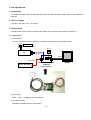
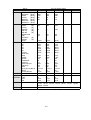
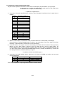
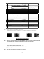
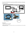
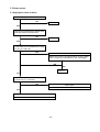
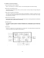
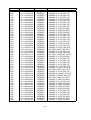
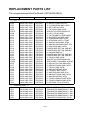
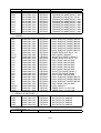
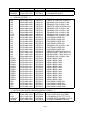
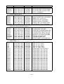
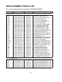
1
PART NO. 599910603 SERVICE MANUAL COLOR MONITOR MultiSync LCD1920NX MODELS LCD1920NX (A)/-BK(A)/(B)/-BK(B) NEC-MITSUBISHI ELECTRIC VISUAL SYSTEMS CORPORATION AUGUST 2002 200208 08EA1AAF 08EA2AAF 08EA1ABF 08EA2ABF WARNING The SERVICE PERSONNEL should have the appropriate technical training, knowledge and experience necessary to: • Be familiar with specialized test equipment, and • Be careful to follow all safety procedures to minimize danger to themselves and their coworkers. To avoid electrical shocks, this equipment should be used with an appropriate power cord. This equipment utilized a micro-gap power switch. Turn off the set by first pushing power switch. Next, remove the power cord from the AC outlet. To prevent fire or shock hazards, do not expose this unit to rain or moisture. This symbol warns the personnel that un-insulated voltage within the unit may have sufficient magnitude to cause electric shock. This symbol alerts the personnel that important literature concerning the operation and maintenance of this unit has been included. Therefore, it should be read carefully in order to avoid any problems. PRODUCT SAFETY CAUTION 1. When parts replacement is required for servicing, always use the manufacturer's specified replacement. 2. When replacing the component, always be certain that all the components are put back in the place. 3. As for a connector, pick and extract housing with fingers properly since a disconnection and improper contacts may occur, when wires of the connector are led. 4. Use a proper screwdriver. If you use screwdriver that does not fit, you may damage the screws. CONTENTS Page No. USER'S MANUAL ------------------------------------------------------------------- 1-1 SERIAL NUMBER INFORMATION --------------------------------------------- 2-1 DISASSEMBLY ----------------------------------------------------------------------- 3-1 ADJUSTMENT PROCEDURES -------------------------------------------------- 4-1 INSPECTION --------------------------------------------------------------------------- 5-1 TROUBLE SHOOTING ------------------------------------------------------------- 6-1 CIRCUIT DESCRIPTION ----------------------------------------------------------- 7-1 REPLACEMENT PARTS LIST --------------------------------------------------- 8-1 BLOCK DIAGRAM ------------------------------------------------------------------- 9-1 SCHEMATIC DIAGRAMS -------------------------------------------------------- 10-1 USER'S MANUAL 1. A Version ® MultiSync LCD1920NX 1-1 TM Index Warning .................................................................................................................... 1 Getting Started ..................................................................................................... 2 Adjusting the Monitor ......................................................................................... 3 Quick Installation ................................................................................................. 4 Operations .............................................................................................................. 6 OSD Main Menu .......................................................................................................7 Recommended Use .............................................................................................. 10 Specifications ....................................................................................................... 12 Features ................................................................................................................. 13 Troubleshooting .................................................................................................. 14 References ............................................................................................................. 15 Limited Warranty ................................................................................................. 16 TCO’95 ..................................................................................................................... 17 TCO’99 ..................................................................................................................... 19 Avertissement ..................................................................................................... 22 Pour vous aider à démarrer ............................................................................. 23 Régler le moniteur ............................................................................................. 24 Installation rapide .............................................................................................. 25 Fonctionnement .................................................................................................. 27 Menu principal OSD ............................................................................................ 28 Usage recommandé ............................................................................................ 31 Caractéristiques ................................................................................................. 33 Fonctions .............................................................................................................. 34 Dépannage ............................................................................................................ 35 Références ........................................................................................................... 36 Garantie limitée .................................................................................................. 37 TCO’95 .................................................................................................................... 38 TCO’99 .................................................................................................................... 40 1-2 WARNING TO PREVENT FIRE OR SHOCK HAZARDS, DO NOT EXPOSE THIS UNIT TO RAIN OR MOISTURE. ALSO, DO NOT USE THIS UNIT'S POLARIZED PLUG WITH AN EXTENSION CORD RECEPTACLE OR OTHER OUTLETS UNLESS THE PRONGS CAN BE FULLY INSERTED. REFRAIN FROM OPENING THE CABINET AS THERE ARE HIGH VOLTAGE COMPONENTS INSIDE. REFER SERVICING TO QUALIFIED SERVICE PERSONNEL. CAUTION CAUTION: TO REDUCE THE RISK OF ELECTRIC SHOCK, MAKE SURE POWER CORD IS UNPLUGGED FROM WALL SOCKET. TO FULLY DISENGAGE THE POWER TO THE UNIT, PLEASE DISCONNECT THE POWER CORD FROM THE AC OUTLET.DO NOT REMOVE COVER (OR BACK). NO USER SERVICEABLE PARTS INSIDE. REFER SERVICING TO QUALIFIED SERVICE PERSONNEL. This symbol warns user that uninsulated voltage within the unit may have sufficient magnitude to cause electric shock. Therefore, it is dangerous to make any kind of contact with any part inside this unit. This symbol alerts the user that important literature concerning the operation and maintenance of this unit has been included. Therefore, it should be read carefully in order to avoid any problems. Canadian Department of Communications Compliance Statement DOC: This Class B digital apparatus meets all requirements of the Canadian Interference-Causing Equipment Regulations. C-UL: Bears the C-UL Mark and is in compliance with Canadian Safety Regulations according to CAN/CSA C22.2 No. 950. FCC Information 1. Use the attached specified cables with the MultiSync LCD1920NX (L19GC061) color monitor so as not to interfere with radio and television reception. (1) Please use the supplied power cord or equivalent to ensure FCC compliance. (2) Please use the supplied AC Adapter. (3) Please use the supplied shielded video signal cable. Use of other cables and adapters may cause interference with radio and television reception. 2. This equipment has been tested and found to comply with the limits for a Class B digital device, pursuant to part 15 of the FCC Rules. These limits are designed to provide reasonable protection against harmful interference in a residential installation. This equipment generates, uses, and can radiate radio frequency energy, and, if not installed and used in accordance with the instructions, may cause harmful interference to radio communications. However, there is no guarantee that interference will not occur in a particular installation. If this equipment does cause harmful interference to radio or television reception, which can be determined by turning the equipment off and on, the user is encouraged to try to correct the interference by one or more of the following measures: • Reorient or relocate the receiving antenna. • Increase the separation between the equipment and receiver. • Connect the equipment into an outlet on a circuit different from that to which the receiver is connected. • Consult your dealer or an experienced radio/TV technician for help. If necessary, the user should contact the dealer or an experienced radio/television technician for additional suggestions. The user may find the following booklet, prepared by the Federal Communications Commission, helpful: ”How to Identify and Resolve Radio-TV Interference Problems.“ This booklet is available from the U.S. Government Printing Office, Washington, D.C., 20402, Stock No. 004-000-00345-4. 1 1-3 Getting Started Congratulations on your purchase of this LCD Monitor. Please read this section carefully to get an instant understanding of this product and its correct operations. Important! Please keep the original carton and all packing materials for future shipping needs. Package Contents Your LCD Monitor package includes the following items: • 19” LCD Color Monitor • Signal cable with 15 pin D-Sub connector • AC Adapter • Power cord • User’s Manual Unique Features • 8-bit panel, supporting 16.7M true colors • High brightness & high contrast, providing more vivid images • Built-in both analog and digital interfaces • TCO’99 and TCO’95 approved • Composite sync compatibility • Five languages in OSD (On Screen Display) • 9-stage smoothing function • Supports 19 sets of factory preset modes and 32 sets of user’s automatically saved modes • Wide Viewing Angle 2 1-4 Adjusting the Monitor Press down on the stand and gently adjust the monitor to a suitable viewing angle (see Figure below). Please note that this monitor can only be tilted forward to 5 degrees, backward to 20 degrees, and swiveled 90 degrees left/right. To prevent damage to the monitor, do not press the screen over its tolerant angles. 20° 90° 5° 3 1-5 90° Quick Installation • Make sure the computer is turned off. • Attach the female end of the power cord (Indication E) to the AC adapter (Indication D), then plug the AC adapter connector to the power “DC-IN (Indication A)” jack of the LCD monitor. • When using a power cord, plug the male end into the wall socket. • Plug one end of the 15 pin D-SUB signal cable (Indication F) in the “D-SUB” video signal connector (Indication B) of LCD monitor. If using a digital signal, plug one end of the 24 pin DVI-D signal cable (Indication G) in the “DVI-D” video signal connector (Indication C) of LCD monitor. • Turn on the computer. • Turn on the LCD monitor. • Before operating the monitor, please refer to page 6 “Operations” first. Connector Cover A C B G E D F A. B. C. D. DC In D-SUB DVI-D AC Adapter E. Power Cord F. D-SUB Signal Cable G. DVI-D Signal Cable (not included) NOTE : When operating this LCD monitor with an AC125-240V power source, please refer to “Recommended Use” for proper power cord selection. Use supplied AC adapter. 4 1-6 Quick Installation –continued Remove Monitor Stand for Mounting To prepare the monitor for alternate mounting purposes: Non-abrasive surface 1. Disconnect all cables. 2. Place monitor face down on a non-abrasive surface (Figure R.1). 3. Remove the 4 screws connecting the monitor to the stand and lift off the stand assembly (Figure R.1). The monitor is now ready for mounting in an alternate manner. 4. Connect the AC cord and signal cable to the back of the monitor. Figure R.1 5. Reverse this process to reattach stand. NOTE: Use only VESA-compatible alternative mounting method. 6. This LCD monitor is designed for use with a flexible arm. Please use the attached screws (4pcs) as shown in the picture when installing. To meet fhe safety requirements, the monitor must be mounted to an arm which guaranties the necessary stability under consideration of the weight of the monitor. The LCD monitor shall only be used with an approved arm (e.g. GS mark). Replace screws. 5 1-7 Operations To turn the monitor on or off, push the power button (Indication E) on the front of the monitor. When the power light (Indication F) turns green, the LCD is ready to use. F A Function Keys A. MENU B C D E 1. Press this button to turn on the OSD (On Screen Display) main menu. 2. Press this button to activate selected items. 3. Press this button 2 seconds or more to turn off the main menu. B. [–] 1. To scroll down the menu. 2. To decrease the value of selected item. C. [+] 1. To scroll up the menu. 2. To increase the value of selected item. D. AUTO Press this button to activate ”AUTO SYNC” function. E. Power switch Press this button to turn on/off the monitor. F. Power LED When the light is green, the power is on; amber light is when the power is off or in power saving mode. Hot Keys • Auto-Sync: Press the [AUTO] button to activate Auto Sync. • Auto-Contrast: Press the [+] button to activate the Auto Contrast adjustment. • Change Signal Input: Press the [–] button to change the signal input, “DVI” or “D-SUB”. 6 1-8 OSD Main Menu For screen adjustments, press the [MENU] button to display the OSD (On-Screen Display) Main Menu shown below. Press the [+] or [–] button to scroll up or down the menu to your required options. Please note that the OSD will automatically turn off in 30 seconds without any manipulation or by simply pressing the [MENU] button for 2 seconds. CONTRAST: Adjusts the contrast level of the screen image. Under Main Menu, select CONTRAST using the [+] or [–] button, then press [MENU] button to activate the function. Press the [+] button to increase contrast, [–] button to decrease contrast. Press [MENU] to return to Main Menu. AUTO-CONTRAST: Automatically adjusts the contrast level of the screen image. Press [+] or [–] button to select AUTO CONTRAST, then press [MENU] button to activate AUTO CONTRAST. VIDEO ANALOG/DIGITAL: Switches between analog and digital input signal. Press [+] or [–] button to select VIDEO ANALOG or VIDEO DIGITAL, then press [MENU] button to switch. BRIGHTNESS: Adjusts the brightness level of the screen image. Under the Main Menu, select BRIGHTNESS using [+] or [–] button, then press [MENU] button to activate the function. Press the [+] button to increase the brightness, [–] button to decrease the brightness. Press [MENU] to return to Main Menu. COLOR Sub-Menu: • Under the Main Menu, select COLOR using the [+] or [–] button, then press [MENU] button to activate the COLOR Sub-Menu. • Under the COLOR Sub-Menu, press [+] or [–] button to scroll up or down to your desired preset color mode. Then press [MENU] to activate the mode. • Choose user’s mode by adjusting R, G, B respectively. Press the [+] or [–] button select R or G or B bar, then press [MENU] to activate the adjustment. Press the [+] or [–] button to adjust the values, then press [MENU] button to save the value and return to color Sub-Menu to adjust another color. After adjusting R, G, B colors, press [MENU] to return to Main Menu. MAIN MENU: Returning to OSD main menu. Press [+] or [–] button to select MAIN MENU, then press [MENU] button to return to OSD Main Menu. 7 1-9 OSD Main Menu –continued LCD ADJUST Sub-Menu (Analog input only): Under the Main Menu, select LCD ADJUST using the [+] or [–] button, then press [MENU] button to enter LCD ADJUST Sub-Menu. PC/MAC: Switching between PC at 800X600 resolution and MAC at 832X624 resolution, using [+] or [–] button. Then press [MENU] to initiate the switch between PC and MAC shown as above. H SIZE: Adjusting the width of the screen image. Select H-SIZE, using [+] or [–] button, then press [MENU] button to activate the function. Press [+] button to increase the width of the screen image, press [–] button to decrease the width of the screen image shown below. Press [MENU] to return to LCD ADJUST Sub-Menu. H - POSITION: Moving the screen image to the right or left. Select H - POSITION using the [+] or [–] button, then press the [MENU] button to activate the function. Press [+] button to move the screen to the right, [–] button to move to the left. Press [MENU] to return to LCD ADJUST Sub-Menu. V - POSITION: Moving the screen image up or down. Select V - POSITION using the [+] or [–] button, then press [MENU] to activate the function. Press [+] button to move the screen image up, [–] button to move down. Press [MENU] to return to LCD ADJUST Sub-Menu. FINE TUNE: Aligning the performance slightly. Select FINE TUNE using the [+] or [–] button, then press [MENU] button to activate the function. Press [+] or [–] button until the screen image looks crisp, sharp and focused. Press [MENU] to return to LCD ADJUST Sub-Menu. AUTO-SYNC: Automatically adjusts the image to the best performance. Press [+] or [–] button to select AUTO SYNC, then press [MENU] button to activate AUTO SYNC. NOTE: • When setting up this monitor for the first time, perform AUTO-SYNC before use. • To perform AUTO-SYNC, first display an image that makes the entire screen very bright. MAIN MENU: Returning to OSD main menu. Press [+] or [–] button to select MAIN MENU, then press [MENU] button to return to OSD Main Menu. LANGUAGE: Selecting preferred language used in the OSD menus. Under Main Menu, scroll to Language using [+] or [–] button, then press[MENU] button to activate the function. Press [+] or [–] button to choose preferred Language, then press [MENU] to return to Main Menu. MAIN MENU: Returning to OSD main menu. Press [+] or [–] button to select MAIN MENU, then press [MENU] button to return to OSD Main Menu. 8 1-10 OSD Main Menu –continued MISC Sub-Menu Under the Main Menu, select MISC using the [+] or [–] button, then press [MENU] button to enter MISC Sub-Menu. RESOLUTION NOTIFIER: This optimal resolution is 1280 x 1024. If ON is selected, a message will appear on the screen after 30 seconds, notifying you that the resolution is not at 1280 x 1024. H-OSD POSITION: Moves the OSD position on the screen to the right or left. Select H-OSD POSITION using [+] or [–] button, then press [MENU] button to activate the function. Press the [+] button to move the OSD position to the right, [–] button to move left. Then press [MENU] to return to MISC Sub-Menu. V-OSD POSITION: Moves the OSD position on the screen up or down. Select V-OSD POSITION using [+] or [–] button, then press [MENU] button to activate the function. Press the [+] button to move the OSD position up, [–] button to move down. Then press [MENU] to return to MISC Sub-Menu. SMOOTHING: Makes the displayed texts smooth. Select SMOOTHING using [+] or [–] button, then press [MENU] button to activate the function. Press [+] or [–] button and adjust to your liking. Press [MENU] button to return to MISC Sub-Menu. INVISIBLE: Activates the OSD background to be invisible. Select INVISIBLE using the [+] or [–] button, then press [MENU] button to select either On or Off option. INFORMATION: Displays the timing mode (video signal input) coming from the graphics card in the computer. Select INFORMATION using the [+] or [–] button, then press [MENU] to display the mode. Then press [MENU] button to return to MISC Sub-Menu. RECALL: Returns the adjustments back to factory settings if the monitor is not operating at its original factory settings. Select RECALL using the [+] or [–] button, then press [MENU] button to reset the settings. MAIN MENU: Returns to OSD main menu. Press [+] or [–] button to select MAIN MENU, then press [MENU] button to return to OSD Main Menu. EXIT: Turns off the OSD. Select EXIT using the [+] or [–] button, then press [MENU] to exit the OSD. OSD Warning NO SIGNAL: This function gives a warning when there is no signal present. After power is turned on or when there is a change of input signal or video is inactive, the No Signal window will appear. RESOLUTION NOTIFIER: This function gives a warning of use with optimized resolution. After power is turned on or when there is a change of input signal or the video signal doesn’t have proper resolution, the Resolution Notifier window will open. This function can be disabled in the MISC Sub-menu. OUT OF RANGE: This function gives a recommendation of the optimized resolution and refresh rate. After the power is turned on or there is a change of input signal or the video signal doesn’t have proper timing, the Out Of Range menu will appear. 9 1-11 Recommended Use Safety Precautions and Maintenance FOR OPTIMUM PERFORMANCE, PLEASE NOTE THE FOLLOWING WHEN SETTING UP AND USING THE MULTISYNC® LCD COLOR MONITOR: • DO NOT OPEN THE MONITOR. There are no user serviceable parts inside and opening or removing covers may expose you to dangerous shock hazards or other risks. Refer all servicing to qualified service personnel. • Do not spill any liquids into the cabinet or use your monitor near water. • Do not insert objects of any kind into the cabinet slots, as they may touch dangerous voltage points, which can be harmful or fatal or may cause electric shock, fire or equipment failure. • Do not place any heavy objects on the power cord. Damage to the cord may cause shock or fire. • Do not place this product on a sloping or unstable cart, stand or table, as the monitor may fall, causing serious damage to the monitor. • When operating the MultiSync LCD monitor with its AC 125-240V power source, use a power supply cord that matches the power supply voltage of the AC power outlet being used. The power supply cord you use must have been approved by and comply with the safety standards of your country. (Type H05VV-F should be used in Europe) • In UK, use a BS-approved power cord with molded plug having a black (5A) fuse installed for use with this monitor. If a power cord is not supplied with this monitor, please contact your supplier. • Use supplied AC Adapter. Do not place any objects onto the AC Adapter and do not use the AC Adapter outdoors. • Do not place any objects onto the monitor and do not use the monitor outdoors. • The inside of the flourescent tube located within the LCD monitor contains mercury. Please follow the bylaws or rules of your municipality to dispose of the tube properly. Immediately unplug your monitor from the wall outlet and refer servicing to qualified service personnel under the following conditions: • When the power supply cord or plug is damaged. • If liquid has been spilled, or objects have fallen into the monitor. • If the monitor has been exposed to rain or water. • If the monitor has been dropped or the cabinet damaged. • If the monitor does not operate normally by following operating instructions. • Do not bend power cord. • Do not use monitor in high temperatured, humid, dusty, or oily areas. • If glass is broken, handle with care. • Do not cover vent on monitor. • If monitor or glass is broken, do not come in contact with the liquid crystal and handle with care. CAUTION • Allow adequate ventilation around the monitor so that heat can properly dissipate. Do not block ventilated openings or place the monitor near a radiator or other heat sources. Do not put anything on top of monitor. • The power cable connector is the primary means of detaching the system from the power supply. The monitor should be installed close to a power outlet which is easily accessible. • Handle with care when transporting. Save packaging for transporting. 10 1-12 Recommended Use –continued CORRECT PLACEMENT AND ADJUSTMENT OF THE MONITOR CAN REDUCE EYE, SHOULDER AND NECK FATIGUE. CHECK THE FOLLOWING WHEN YOU POSITION THE MONITOR: • For optimum performance, allow 20 minutes for warm-up. • Adjust the monitor height so that the top of the screen is at or slightly below eye level. Your eyes should look slightly downward when viewing the middle of the screen. • Position your monitor no closer than 16 inches and no further away than 28 inches from your eyes. The optimal distance is 21 inches. • Rest your eyes periodically by focusing on an object at least 20 feet away. Blink often. • Position the monitor at a 90° angle to windows and other light sources to minimize glare and reflections. Adjust the monitor tilt so that ceiling lights do not reflect on your screen. • If reflected light makes it hard for you to see your screen, use an anti-glare filter. • Clean the LCD monitor surface with a lint-free, non-abrasive cloth. Avoid using any cleaning solution or glass cleaner! • Adjust the monitor’s brightness and contrast controls to enhance readability. • Use a document holder placed close to the screen. • Position whatever you are looking at most of the time (the screen or reference material) directly in front of you to minimize turning your head while you are typing. • Avoid displaying fixed patterns on the monitor for long periods of time to avoid image persistence (after-image effects). • Get regular eye checkups. Ergonomics To realize the maximum ergonomics benefits, we recommend the following: • Adjust the Brightness until the background raster disappears • Do not position the Contrast control to its maximum setting • Use the preset Size and Position controls with standard signals • Use the preset Color Setting • Use non-interlaced signals with a vertical refresh rate between 60-75Hz • Do not use primary color blue on a dark background, as it is difficult to see and may produce eye fatigue to insufficient contrast For more detailed information on setting up a healthy work environment, call NEC at (800) 632-4662, NEC FastFacts™ information at (800) 366-0476 and request document #900108 or write the American National Standard for Human Factors Engineering of Visual Display Terminal Workstations – ANSI-HFS Standard No. 100-1988 – The Human Factors Society, Inc. P.O. Box 1369, Santa Monica, California 90406. 11 1-13 Specifications Monitor Specifications LCD Maximum Viewing Angles Input Signal Compatibility Resolution Power Connector Display Area Operating Conditions Storage Conditions Dimensions Weight Power State MultiSync® LCD1920NX™ Monitor Size Type Color Filter Glass surface Left/right Up/Down Video Sync PC Macintosh® Primary Mode Voltage Input Signal Full screen Temperature Humidity Altitude Temperature Humidity Altitude Physical Net Gross Power On Power Off 19.0" (full 19.0" viewable diagonal area) TFT (Thin Film Transistor), Active Matrix Panel 0.294mm pixel pitch RGB Vertical Stripe Anti-Glare 85°/85° 85°/85° RGB Analog (0.7/1.0 Vp-p, 75 ohms) DVI-D (100 ohms) Separate Sync, Composite Sync Fh: 31.5-80 kHz, Fv: 56-75 Hz Up to 1280 x 1024 Non-interlaced (NI) Up to 1280 x 1024 Non-interlaced (NI) VESA 1280 x 1024 @ 60Hz AC 100-240V, 50/60 Hz Analog: 15 pin D-sub Connector Digital: 24 pin DVI-D Connector 376.3 mm (H) x 301.1 mm (V) 41 F to 95 F (5 °C to 35 °C) 10% to 80% (non-condensing) to 10,000 feet (3,000m) 14 F to +140 F (-10 °C to +60 °C) 10% to 85% (non-condensing) to 40,000 feet (12,000m) 434.5 mm (W) x 205.0 mm (D) x 423.0 mm (H) 17.1 inches (W) x 8.1 inches (D) x 16.7 inches (H) 8.0 kg (17.6 lbs) 11.0 kg (24.3 lbs) <60W (green LED) <3W (amber LED) • All products and trademarks are brand names of their respective companies. • Specifications are subject to change without prior notice. 12 1-14 Features Reduced Footprint: Provides the ideal solution for environments requiring superior image quality but with size and weight limitations. The monitor’s small footprint and low weight allow it to be moved or transported easily from one location to another. AccuColor® Control Systems: Allows you to adjust the colors on your screen and customize the color accuracy of your monitor to a variety of standards. OSD (On-Screen Display) Controls: Allow you to quickly and easily adjust all elements of your screen image via simple to use on-screen menus. No-touch Auto Adjust: No-touch auto adjust automatically adjusts the monitor to optimal settings upon initial setup. ErgoDesign® Features: Enhance human ergonomics to improve the working environment, protect the health of the user and save money. Examples include OSD controls for quick and easy image adjustments, tilt base for preferred angle of vision, small footprint and compliance with MPRII and TCO guidelines for lower emissions. Plug and Play: The Microsoft® solution with the Windows® 95/98/Me/2000/XP operating system facilitates setup and installation by allowing the monitor to send its capabilities (such as screen size and resolutions supported) directly to your computer, automatically optimizing display performance. IPM™ (Intelligent Power Manager) System: Provides innovative power-saving methods that allow the monitor to shift to a lower power consumption level when on but not in use, saving two-thirds of your monitor energy costs, reducing emissions and lowering the air conditioning costs of the workplace. Multiple Frequency Technology: Automatically adjusts monitor to the display card’s scanning frequency, thus displaying the resolution required. FullScan™ Capability: Allows you to use the entire screen area in most resolutions, significantly expanding image size. VESA Standard Mounting Interface: Allows users to connect their MultiSync® monitor to any VESA standard third party mounting arm or bracket. Allows for the monitor to be mounted on a wall or an arm using any third party compliant device. 13 1-15 Troubleshooting No picture • The signal cable should be completely connected to the display card/computer. • The display card should be completely seated in its slot. • Front Power Switch and computer power switch should be in the ON position. • Check the LED of AC adapter is ON. • Check to make sure that a supported mode has been selected on the display card or system being used. (Please consult display card or system manual to change graphics mode.) • Check the monitor and your display card with respect to compatibility and recommended settings. • Check the signal cable connector for bent or pushed-in pins. Power Button does not respond • Unplug the power cord of the monitor from the AC outlet to turn off and reset the monitor. Image persistence • Image persistence is when a “ghost” of an image remains on the screen even after the monitor has been turned off. Unlike CRT monitors, LCD monitors’ image persistence is not permanent. To alleviate image persistence, turn the monitor off for as long as an image was displayed. If an image was on the monitor for one hour and a ”ghost” of that image remains, the monitor should be turned off for one hour to erase the image. NOTE: As with all personal display devices, NEC-Mitsubishi Electronics Display of America recommends using a screen saver at regular intervals whenever the screen is idle. Image is unstable, unfocused or swimming is apparent • Signal cable should be completely attached to the computer. • Use the OSD Image Adjust controls to focus and adjust display by increasing or decreasing the fine total. When the display mode is changed, the OSD Image Adjust settings may need to be re-adjusted. • Check the monitor and your display card with respect to compatibility and recommended signal timings. • If your text is garbled, change the video mode to non-interlace and use 60Hz refresh rate. LED • • • on monitor is not lit (no green or amber color can be seen) Power Switch should be in the ON position and power cord should be connected. Check the LED of AC adapter is ON. Make certain the computer is not in a power-saving mode (touch the keyboard or mouse). Display image is not sized properly • Use the OSD Image Adjust controls to increase or decrease the Coarse total. • Check to make sure that a supported mode has been selected on the display card or system being used. (Please consult display card or system manual to change graphics mode.) Selected resolution is not displayed properly • Use OSD Display Mode to enter Information menu and confirm that the appropriate resolution has been selected. If not, select corresponding option. 14 1-16 References • BBS (978) 742-8706 NEC-Mitsubishi Electronics Display of America Remote Bulletin Board System is an electronic service accessible with your system and a modem. Communication parameters are: 300/1200/2400/9600/14.4k/28.8k/33.6k bps, no parity, 8-data bits, 1 stop bit • Customer Service/ Technical Support Fax • Electronic Channels: Internet e-mail: Internet ftp site: World Wide Web: Product Registration: European Operations: Windows® 95/98/Me/2000/XP INF File: • FastFacts™ Information (800) 632-4662 (978) 742-7049 [email protected] ftp.necmitsubishi.com http://www.necmitsubishi.com http://www.necmitsubishi.com/productregistration http://www.nec-mitsubishi.com http://support.necmitsubishi.com/software.htm then download the file NECMSINF.ZIP (800) 366-0476 INFORMATION DESCRIPTION DOCUMENT # Glossary Definition of terms related to functions, features and installation of the MultiSync® monitor 900203 More Information Names and addresses of other groups involved in standards and features of the MultiSync monitor 900204 Macintosh Connection Detailed information on connecting the MultiSync monitor to a Macintosh 153006 Healthy Work Environment Detailed information on setting up a healthy work environment 900108 • Literature & Sales Info (800) NEC-INFO [(800) 632-4636] • MultiSync Fulfillment (800) 632-4662 [For software & accessories] • TeleSales (800) 284-4484 15 1-17 Limited Warranty NEC-Mitsubishi Electronics Display of America, Inc. (hereinafter “NMD-A”) warrants this Product to be free from defects in material and workmanship and, subject to the conditions set forth below, agrees to repair or replace (at NMD-A’s sole option) any part of the enclosed unit which proves defective for a period of three (3) years from the date of first consumer purchase. Spare parts are warranted for ninety (90) days. Replacement parts or unit may be new or refurbished and will meet specifications of the original parts or unit. This warranty gives you specific legal rights and you may also have other rights, which vary from state to state. This warranty is limited to the original purchaser of the Product and is not transferable. This warranty covers only NMD-A-supplied components. Service required as a result of third party components is not covered under this warranty. In order to be covered under this warranty, the Product must have been purchased in the U.S.A. or Canada by the original purchaser. This warranty only covers Product distribution in the U.S.A. or Canada by NMD-A No warranty service is provided outside of the U.S.A. or Canada. Proof of Purchase will be required by NMD-A to substantiate date of purchase. Such proof of purchase must be an original bill of sale or receipt containing name and address of seller, purchaser, and the serial number of the product. It shall be your obligation and expense to have the Product shipped, freight prepaid, or delivered to the authorized reseller from whom it was purchased or other facility authorized by NMD-A to render the services provided hereunder in either the original package or a similar package affording an equal degree of protection. All Products returned to NMD-A for service MUST have prior approval, which may be obtained by calling 1-800-632-4662. The Product shall not have been previously altered, repaired, or serviced by anyone other than a service facility authorized by NMD-A to render such service, the serial number of the product shall not have been altered or removed. In order to be covered by this warranty the Product shall not have been subjected to displaying of fixed images for long periods of time resulting in image persistence (afterimage effects), accident, misuse or abuse or operated contrary to the instructions contained in the User’s Manual. Any such conditions will void this warranty. NMD-A SHALL NOT BE LIABLE FOR DIRECT, INDIRECT, INCIDENTAL, CONSEQUENTIAL, OR OTHER TYPES OF DAMAGES RESULTING FROM THE USE OF ANY NMD-A PRODUCT OTHER THAN THE LIABILITY STATED ABOVE. THESE WARRANTIES ARE IN LIEU OF ALL OTHER WARRANTIES EXPRESS OR IMPLIED, INCLUDING, BUT NOT LIMITED TO, THE IMPLIED WARRANTIES OF MERCHANTABILITY OR FITNESS FOR A PARTICULAR PURPOSE. SOME STATES DO NOT ALLOW THE EXCLUSION OF IMPLIED WARRANTIES OR THE LIMITATION OR EXCLUSION OF LIABILITY FOR INCIDENTAL OR CONSEQUENTIAL DAMAGES SO THE ABOVE EXCLUSIONS OR LIMITATIONS MAY NOT APPLY TO YOU. This Product is warranted in accordance with the terms of this limited warranty. Consumers are cautioned that Product performance is affected by system configuration, software, the application, customer data, and operator control of the system, among other factors. While NMD-A Products are considered to be compatible with many systems, specific functional implementation by the customers of the Product may vary. Therefore, suitability of a Product for a specific purpose or application must be determined by consumer and is not warranted by NMD-A. For the name of your nearest authorized NEC-Mitsubishi Electronics Display service facility, contact NEC-Mitsubishi Electronics Display of America at 1-800-632-4662. 16 1-18 TCO’95 MultiSync LCD1920NX (L19GC061) Black Model Congratulations! You have just purchased a TCO’95 approved and labeled product! Your choice has provided you with a product developed for professional use. Your purchase has also contributed to reducing the burden on the environment and also, to the further development of environmentally adapted electronics products. Why do we have environmentally labelled computers? In many countries, environmental labelling has become an established method for encouraging the adaptation of goods and services to the environment. The main problem, as far as computers and other electronics equipment are concerned, is that environmentally harmful substances are used both in the products and during the manufacturing. Since it has not been possible for the majority of electronics equipment to be recycled in a satisfactory way, most of these potentially damaging substances sooner or later enter Nature. There are also other characteristics of a computer, such as energy consumption levels, that are important from the viewpoints of both the work (Internal) and natural (external) environments. Since all methods of conventional electricity generation have a negative effect on the environment (acidic and climate-influencing emissions, radioactive waste, etc.), it is vital to conserve energy. Electronics equipment in offices consume an enormous amount of energy since they are often left running continuously. What does labelling involve? This product meets the requirements for the TCO’95 scheme which provides for international and environmental labelling of personal computers. The labelling scheme was developed as a joint effort by the TCO (The Swedish Confederation of Professional Employees), Naturskyddsforeningen (The Swedish Society for Nature Conservation) and NUTEK (The National Board for Industrial and Technical Development in Sweden). The requirements cover a wide range of issues: environment, ergonomics, usability, emission of electrical and magnetic fields, energy consumption and electrical and fire safety. The environmental demands concern restrictions on the presence and use of heavy metals, brominated and chlorinated flame retardants, CFCs (freons) and chlorinated solvents, among other things. The product must be prepared for recycling and the manufacturer is obliged to have an environmental plan which must be adhered to in each country where the company implements its operational policy. The energy requirements include a demand that the computer and/or display, after a certain period of inactivity, shall reduce its power consumption to a lower level in one or more stages. The length of time to reactivate the computer shall be reasonable for the user. Labelled products must meet strict environmental demands, for example, in respect of the reduction of electric and magnetic fields, physical and visual ergonomics and good usability. TCO’95 is a co-operative project between TCO (The Swedish Confederation of Professional Employees), Naturskyddsforeningen (The Swedish Society for Nature Conservation) and NUTEK (The National Board for Industrial and Technical Development in Sweden). Environmental Requirements Brominated flame retardants Brominated flame retardants are present in printed circuit boards, cables, wires, casings and housings. In turn, they delay the spread of fire. Up to thirty percent of the plastic in a computer casing can consist of flame retardant substances. These are related to another group of environmental toxins, PCBs, which are suspected to give rise to similar harm, including 17 1-19 TCO’95 –continued reproductive damage in fisheating birds and mammals, due to the bio-accumulative* processes. Flame retardants have been found in human blood and researchers fear that disturbances in foetus development may occur. TCO’95 demand requires that plastic components weighing more than 25 grams must not contain organically bound chlorine and bromine. Lead** Lead can be found in picture tubes, display screens, solders and capacitors. Lead damages the nervous system and in higher doses, causes lead poisoning. TCO’95 requirement permits the inclusion of lead since no replacement has yet been developed. Cadmium** Cadmium is present in rechargeable batteries and in the colourgenerating layers of certain computer displays. Cadmium damages the nervous system and is toxic in high doses. TCO’95 requirement states that batteries may not contain more than 25 ppm (parts per million) of cadmium. The colourgenerating layers of display screens must not contain any cadmium. Mercury** Mercury is sometimes found in batteries, relays, switches, and back-light systems, Mercury damages the nervous system and is toxic in high doses. TCO’95 requirement states that batteries may not contain more than 25 ppm (parts per million) of mercury. It also demands that no mercury is present in any of the electrical or electronics components concerned with the display unit, except the back-light system. CFCs (freons) CFCs (freons) are sometimes used for washing printed circuit boards and in the manufacturing of expanded foam for packaging. CFCs break down ozone and thereby damage the ozone layer in the stratosphere, causing increased reception on Earth of ultraviolet light with consequent increased risks of skin cancer (malignant melanoma). The relevant TCO’95 requirement; Neither CFCs nor HCFCs may be used during the manufacturing of the product or its packaging. *Bio-accumulative is defined as substances which accumulate within living organisms. **Lead, Cadmium and Mercury are heavy metals which are Bio-accumulative. To obtain complete information on the environmental criteria document, order from: TCO Development Unit SE-114 94 Stockholm SWEDEN FAX Number: +46 8 782 92 07 E-mail (Internet): [email protected] You may also obtain current information on TCO’95 approved and labelled products by visiting their website at: http://www.tco-info.com/ 18 1-20 TCO’99 MultiSync LCD1920NX (L19GC061) White Model Congratulations! You have just purchased a TCO’99 approved and labeled product! Your choice has provided you with a product developed for professional use. Your purchase has also contributed to reducing the burden on the environment and also to the further development of environmentally adapted electronics products. Why do we have environmentally labelled computers? In many countries, environmental labelling has become an established method for encouraging the adaptation of goods and services to the environment. The main problem, as far as computers and other electronics equipment are concerned, is that environmentally harmful substances are used both in the products and during the manufacturing. Since it has not been possible for the majority of electronics equipment to be recycled in a satisfactory way, most of these potentially damaging substances sooner or later enter Nature. There are also other characteristics of a computer, such as energy consumption levels, that are important from the viewpoints of both the work (Internal) and natural (external) environments. Since all methods of conventional electricity generation have a negative effect on the environment (acidic and climate-influencing emissions, radioactive waste, etc.), it is vital to conserve energy. Electronics equipment in offices consume an enormous amount of energy since they are often left running continuously. What does labelling involve? This product meets the requirements for the TCO’99 scheme which provides for international and environmental labelling of personal computers. The labelling scheme was developed as a joint effort by the TCO (The Swedish Confederation of Professional Employees), Svenska Naturskyddsforeningen (The Swedish Society for Nature Conservation) and Statens Energimyndighet (The Swedish National Energy Administration). The requirements cover a wide range of issues: environment, ergonomics, usability, emission of electrical and magnetic fields, energy consumption and electrical and fire safety. The environmental demands concern restrictions on the presence and use of heavy metals, brominated and chlorinated flame retardants, CFCs (freons) and chlorinated solvents, among other things. The product must be prepared for recycling and the manufacturer is obliged to have an environmental plan which must be adhered to in each country where the company implements its operational policy. The energy requirements include a demand that the computer and/or display, after a certain period of inactivity, shall reduce its power consumption to a lower level in one or more stages. The length of time to reactivate the computer shall be reasonable for the user. Labelled products must meet strict environmental demands, for example, in respect of the reduction of electric and magnetic fields, physical and visual ergonomics and good usability. Environmental Requirements Flame retardants Flame retardants are present in printed circuit boards, cables, wires, casings and housings. In turn, they delay the spread of fire. Up to thirty percent of the plastic in a computer casing can consist of flame retardant substances. Most flame retardants contain bromine or chloride and these are related to another group of environmental toxins, PCBs, which are suspected to give rise to severe health effects, including reproductive damage in fisheating birds and mammals, due to the bio19 1-21 TCO’99 –continued accumulative* processes. Flame retardants have been found in human blood and researchers fear that disturbances in foetus development may occur. TCO’99 demand requires that plastic components weighing more than 25 grams must not contain flame retardants with organically bound chlorine and bromine. Flame retardants are allowed in the printed circuit boards since no substitutes are available. Lead** Lead can be found in picture tubes, display screens, solders and capacitors. Lead damages the nervous system and in higher doses, causes lead poisoning. TCO’99 requirement permits the inclusion of lead since no replacement has yet been developed. Cadmium** Cadmium is present in rechargeable batteries and in the colourgenerating layers of certain computer displays. Cadmium damages the nervous system and is toxic in high doses. TCO’99 requirement states that batteries, the colourgenerating layers of display screens and the electrical or electronics components must not contain any cadmium. Mercury** Mercury is sometimes found in batteries, relays and switches, Mercury damages the nervous system and is toxic in high doses. TCO’99 requirement states that batteries may not contain any Mercury. It also demands that no mercury is present in any of the electrical or electronics components associated with the display unit. CFCs (freons) CFCs (freons) are sometimes used for washing printed circuit boards. CFCs break down ozone and thereby damage the ozone layer in the stratosphere, causing increased reception on Earth of ultraviolet light with consequent increased risks of skin cancer (malignant melanoma). The relevant TCO’99 requirement; Neither CFCs nor HCFCs may be used during the manufacturing and assembly of the product or its packaging. *Bio-accumulative is defined as substances which accumulate within living organisms. **Lead, Cadmium and Mercury are heavy metals which are Bio-accumulative. To obtain complete information on the environmental criteria document, order from: TCO Development Unit SE-114 94 Stockholm SWEDEN FAX Number: +46 8 782 92 07 E-mail (Internet): [email protected] You may also obtain current information on TCO’99 approved and labelled products by visiting their website at: http://www.tco-info.com/ 20 1-22 Declaration of the Manufacturer We hereby certify that the color monitor MultiSync® LCD1920NX (L19GC061) is in compliance with Council Directive 73/23/EEC: – EN 60950 Council Directive 89/336/EEC: – EN 55022 – EN 61000-3-2 – EN 61000-3-3 – EN 55024 and marked with NEC-Mitsubishi Electric Visual Systems Corporation 4-13-23, Shibaura, Minato-Ku Tokyo 108-0023, Japan 21 1-23 2. B Version MultiSync LCD1920NX User’s Manual UÏivatelská pfiíruãka Bedienerhandbuch Οδηγίες Χρήσης Manual del usuario Manuel Utilisateur Manuale utente Gebruikershandleiding Podr´cznik u˝ytkownika Руководство пользователя Kullan∂c∂ Klavuzu 1-24 Canadian Department of Communications Compliance Statement DOC: This Class B digital apparatus meets all requirements of the Canadian Interference-Causing Equipment Regulations. C-UL: Bears the C-UL Mark and is in compliance with Canadian Safety Regulations according to CAN/CSA C22.2 No. 950. FCC Information 1. Use the attached specified cables with the MultiSync LCD1920NX (L19GC061) color monitor so as not to interfere with radio and television reception. (1) Please use the supplied power cord or equivalent to ensure FCC compliance. (2) Please use the supplied AC Adapter. (3) Please use the supplied shielded video signal cable. Use of other cables and adapters may cause interference with radio and television reception. 2. This equipment has been tested and found to comply with the limits for a Class B digital device, pursuant to part 15 of the FCC Rules. These limits are designed to provide reasonable protection against harmful interference in a residential installation. This equipment generates, uses, and can radiate radio frequency energy, and, if not installed and used in accordance with the instructions, may cause harmful interference to radio communications. However, there is no guarantee that interference will not occur in a particular installation. If this equipment does cause harmful interference to radio or television reception, which can be determined by turning the equipment off and on, the user is encouraged to try to correct the interference by one or more of the following measures: • Reorient or relocate the receiving antenna. • Increase the separation between the equipment and receiver. • Connect the equipment into an outlet on a circuit different from that to which the receiver is connected. • Consult your dealer or an experienced radio/TV technician for help. If necessary, the user should contact the dealer or an experienced radio/television technician for additional suggestions. The user may find the following booklet, prepared by the Federal Communications Commission, helpful: “How to Identify and Resolve RadioTV Interference Problems.” This booklet is available from the U.S. Government Printing Office, Washington, D.C., 20402, Stock No. 004-000-00345-4. DECLARATION OF CONFORMITY This device complies with Part 15 of FCC Rules. Operation is subject to the following two conditions. (1) This device may not cause harmful interference, and (2) this device must accept any interference received, including interference that may cause undesired operation. U.S. Responsible Party: Address: Tel. No.: NEC-Mitsubishi Electronics Display of America, Inc. 1250 North Arlington Heights Road, Suite 500 Itasca, Illinois 60143-1248 (630) 467-3000 Type of Product: Computer Monitor Equipment Classification: Class B Peripheral Model: MultiSync LCD1920NX We hereby declare that the equipment specified above conforms to the technical standards as specified in the FCC Rules. Windows is a registered trademark of Microsoft Corporation. NEC is a registered trademark of NEC Corporation. ENERGY STAR is a U.S. registered trademark. All other brands and product names are trademarks or registered trademarks of their respective owners. As an ENERGY STAR® Partner, NEC-Mitsubishi Electronics Display of America has determined that this product meets the Energy Star guidelenes for energy efficiency. The ENERGY STAR emblem does not represent EPA endorsement of any product or service. 1-25 TCO’95 MultiSync LCD1920NX Black Model Congratulations! You have just purchased a TCO’95 approved and labeled product! Your choice has provided you with a product developed for professional use. Your purchase has also contributed to reducing the burden on the environment and also, to the further development of environmentally adapted electronics products. Why do we have environmentally labelled computers? TCO’95 demand requires that plastic components weighing more than 25 grams must not contain organically bound chlorine and bromine. Lead** Lead can be found in picture tubes, display screens, solders and capacitors. Lead damages the nervous system and in higher doses, causes lead poisoning. TCO’95 requirement permits the inclusion of lead since no replacement has yet been developed. In many countries, environmental labelling has become an established method for encouraging the adaptation of goods and services to the environment. The main problem, as far as computers and other electronics equipment are concerned, is that environmentally harmful substances are used both in the products and during the manufacturing. Since it has not been possible for the majority of electronics equipment to be recycled in a satisfactory way, most of these potentially damaging substances sooner or later enter Nature. There are also other characteristics of a computer, such as energy consumption levels, that are important from the viewpoints of both the work (Internal) and natural (external) environments. Since all methods of conventional electricity generation have a negative effect on the environment (acidic and climate-influencing emissions, radioactive waste, etc.), it is vital to conserve energy. Electronics equipment in offices consume an enormous amount of energy since they are often left running continuously. Cadmium** What does labelling involve? CFCs (freons) This product meets the requirements for the TCO’95 scheme which provides for international and environmental labelling of personal computers. The labelling scheme was developed as a joint effort by the TCO (The Swedish Confederation of Professional Employees), Naturskyddsforeningen (The Swedish Society for Nature Conservation) and NUTEK (The National Board for Industrial and Technical Development in Sweden). The requirements cover a wide range of issues: environment, ergonomics, usability, emission of electrical and magnetic fields, energy consumption and electrical and fire safety. The environmental demands concern restrictions on the presence and use of heavy metals, brominated and chlorinated flame retardants, CFCs (freons) and chlorinated solvents, among other things. The product must be prepared for recycling and the manufacturer is obliged to have an environmental plan which must be adhered to in each country where the company implements its operational policy. The energy requirements include a demand that the computer and/or display, after a certain period of inactivity, shall reduce its power consumption to a lower level in one or more stages. The length of time to reactivate the computer shall be reasonable for the user. Labelled products must meet strict environmental demands, for example, in respect of the reduction of electric and magnetic fields, physical and visual ergonomics and good usability. TCO’95 is a co-operative project between TCO (The Swedish Confederation of Professional Employees), Naturskyddsforeningen (The Swedish Society for Nature Conservation) and NUTEK (The National Board for Industrial and Technical Development in Sweden). CFCs (freons) are sometimes used for washing printed circuit boards and in the manufacturing of expanded foam for packaging. CFCs break down ozone and thereby damage the ozone layer in the stratosphere, causing increased reception on Earth of ultraviolet light with consequent increased risks of skin cancer (malignant melanoma). The relevant TCO’95 requirement; Neither CFCs nor HCFCs may be used during the manufacturing of the product or its packaging. Cadmium is present in rechargeable batteries and in the colourgenerating layers of certain computer displays. Cadmium damages the nervous system and is toxic in high doses. TCO’95 requirement states that batteries may not contain more than 25 ppm (parts per million) of cadmium. The colourgenerating layers of display screens must not contain any cadmium. Mercury** Mercury is sometimes found in batteries, relays, switches, and back-light systems, Mercury damages the nervous system and is toxic in high doses. TCO’95 requirement states that batteries may not contain more than 25 ppm (parts per million) of mercury. It also demands that no mercury is present in any of the electrical or electronics components concerned with the display unit, except the back-light system. *Bio-accumulative is defined as substances which accumulate within living organisms. **Lead, Cadmium and Mercury are heavy metals which are Bio-accumulative. To obtain complete information on the environmental criteria document, order from: TCO Development Unit SE-114 94 Stockholm SWEDEN FAX Number: +46 8 782 92 07 E-mail (Internet): [email protected] You may also obtain current information on TCO’95 approved and labelled products by visiting their website at: http://www.tco-info.com/ Environmental Requirements Brominated flame retardants Brominated flame retardants are present in printed circuit boards, cables, wires, casings and housings. In turn, they delay the spread of fire. Up to thirty percent of the plastic in a computer casing can consist of flame retardant substances. These are related to another group of environmental toxins, PCBs, which are suspected to give rise to similar harm, including reproductive damage in fisheating birds and mammals, due to the bioaccumulative* processes. Flame retardants have been found in human blood and researchers fear that disturbances in foetus development may occur. 1-26 TCO’99 MultiSync LCD1920NX White Model Lead** Congratulations! You have just purchased a TCO’99 approved and labeled product! Your choice has provided you with a product developed for professional use. Your purchase has also contributed to reducing the burden on the environment and also to the further development of environmentally adapted electronics products. Lead can be found in picture tubes, display screens, solders and capacitors. Lead damages the nervous system and in higher doses, causes lead poisoning. TCO’99 requirement permits the inclusion of lead since no replacement has yet been developed. Cadmium** Cadmium is present in rechargeable batteries and in the colourgenerating layers of certain computer displays. Cadmium damages the nervous system and is toxic in high doses. TCO’99 requirement states that batteries, the colourgenerating layers of display screens and the electrical or electronics components must not contain any cadmium. Why do we have environmentally labelled computers? In many countries, environmental labelling has become an established method for encouraging the adaptation of goods and services to the environment. The main problem, as far as computers and other electronics equipment are concerned, is that environmentally harmful substances are used both in the products and during the manufacturing. Since it has not been possible for the majority of electronics equipment to be recycled in a satisfactory way, most of these potentially damaging substances sooner or later enter Nature. There are also other characteristics of a computer, such as energy consumption levels, that are important from the viewpoints of both the work (Internal) and natural (external) environments. Since all methods of conventional electricity generation have a negative effect on the environment (acidic and climate-influencing emissions, radioactive waste, etc.), it is vital to conserve energy. Electronics equipment in offices consume an enormous amount of energy since they are often left running continuously. Mercury** Mercury is sometimes found in batteries, relays and switches, Mercury damages the nervous system and is toxic in high doses. TCO’99 requirement states that batteries may not contain any Mercury. It also demands that no mercury is present in any of the electrical or electronics components associated with the display unit. CFCs (freons) CFCs (freons) are sometimes used for washing printed circuit boards. CFCs break down ozone and thereby damage the ozone layer in the stratosphere, causing increased reception on Earth of ultraviolet light with consequent increased risks of skin cancer (malignant melanoma). The relevant TCO’99 requirement; Neither CFCs nor HCFCs may be used during the manufacturing and assembly of the product or its packaging. What does labelling involve? This product meets the requirements for the TCO’99 scheme which provides for international and environmental labelling of personal computers. The labelling scheme was developed as a joint effort by the TCO (The Swedish Confederation of Professional Employees), Svenska Naturskyddsforeningen (The Swedish Society for Nature Conservation) and Statens Energimyndighet (The Swedish National Energy Administration). The requirements cover a wide range of issues: environment, ergonomics, usability, emission of electrical and magnetic fields, energy consumption and electrical and fire safety. The environmental demands concern restrictions on the presence and use of heavy metals, brominated and chlorinated flame retardants, CFCs (freons) and chlorinated solvents, among other things. The product must be prepared for recycling and the manufacturer is obliged to have an environmental plan which must be adhered to in each country where the company implements its operational policy. The energy requirements include a demand that the computer and/or display, after a certain period of inactivity, shall reduce its power consumption to a lower level in one or more stages. The length of time to reactivate the computer shall be reasonable for the user. Labelled products must meet strict environmental demands, for example, in respect of the reduction of electric and magnetic fields, physical and visual ergonomics and good usability. *Bio-accumulative is defined as substances which accumulate within living organisms. **Lead, Cadmium and Mercury are heavy metals which are Bio-accumulative. To obtain complete information on the environmental criteria document, order from: TCO Development Unit SE-114 94 Stockholm SWEDEN FAX Number: +46 8 782 92 07 E-mail (Internet): [email protected] You may also obtain current information on TCO’99 approved and labelled products by visiting their website at: http://www.tco-info.com/ Environmental Requirements Flame retardants Flame retardants are present in printed circuit boards, cables, wires, casings and housings. In turn, they delay the spread of fire. Up to thirty percent of the plastic in a computer casing can consist of flame retardant substances. Most flame retardants contain bromine or chloride and these are related to another group of environmental toxins, PCBs, which are suspected to give rise to severe health effects, including reproductive damage in fisheating birds and mammals, due to the bio-accumulative* processes. Flame retardants have been found in human blood and researchers fear that disturbances in foetus development may occur. TCO’99 demand requires that plastic components weighing more than 25 grams must not contain flame retardants with organically bound chlorine and bromine. Flame retardants are allowed in the printed circuit boards since no substitutes are available. 1-27 Index Warning, Caution .................................... English-1 Declaration ............................................. English-1 Getting Started ....................................... English-2 Adjusting the Monitor .............................. English-2 Quick Installation .................................... English-3 Operations .............................................. English-5 OSD Main Menu ..................................... English-6 Recommended Use ................................ English-8 Troubleshooting .................................... English-10 Waarschuwing, Let op! .................... Nederlands-1 Kennisgeving ................................... Nederlands-1 Aan de slag ..................................... Nederlands-2 De monitor afstellen ........................ Nederlands-2 Snel installeren ................................ Nederlands-3 Werking ........................................... Nederlands-5 Hoofdschermmenu .......................... Nederlands-6 Aanbevolen gebruik ......................... Nederlands-8 Problemen oplossen ...................... Nederlands-10 Varování, Upozornûní ............................... âesky-1 Prohlá‰ení ................................................ âesky-1 Zaãínáme .................................................. âesky-2 Nastavení monitoru .................................. âesky-2 Rychlá instalace ....................................... âesky-3 Operace .................................................... âesky-5 Hlavní nabídka OSD ................................. âesky-6 Provozní pokyny ....................................... âesky-8 OdstraÀování problémÛ .......................... âesky-10 Uwagi dotyczàce zasilania monitora ........ Polski-1 Ostrze˝enie, Uwaga ................................. Polski-2 OÊwiadczenie ........................................... Polski-2 Poczàtek pracy ......................................... Polski-3 Ustawianie monitora ................................. Polski-3 Szybka instalacja ...................................... Polski-4 Obs∏uga monitora ..................................... Polski-6 G∏ówne menu ekranowe (OSD) ............... Polski-7 Zalecenia eksploatacyjne ......................... Polski-9 Usuwanie usterek ................................... Polski-11 Warnung, Vorsicht ................................. Deutsch-1 Erklärung ............................................... Deutsch-1 Erste Schritte ......................................... Deutsch-2 Ausrichten des Monitors ........................ Deutsch-2 Installation ............................................. Deutsch-3 Bedienung ............................................. Deutsch-5 OSD-Hauptmenü ................................... Deutsch-6 Einsatzempfehlungen ............................ Deutsch-8 Fehlerbehebung .................................. Deutsch-10 Предупреждение, Внимание ............. Русский-1 Заявление ........................................... Русский-1 Приступая к работе ............................ Русский-2 Настройка монитора .......................... Русский-2 Быстрая установка ............................. Русский-3 Эксплуатация ...................................... Русский-5 Главное меню OSD ............................. Русский-6 Рекомендации по эксплуатации ........ Русский-8 Устранение неисправностей ........... Русский-10 ΠΡΟΕΙ∆ΟΠΟΙΗΣΗ, ΠΡΟΣΟΧΗ .......... Ελληνικά-1 ∆ήλωση .............................................. Ελληνικά-1 Προετοιµασία .................................... Ελληνικά-2 Ρύθµιση της Οθνης ........................ Ελληνικά-2 Γρήγορη Εγκατάσταση ..................... Ελληνικά-3 Λειτουργίες ....................................... Ελληνικά-5 Κύριο Μενού OSD ............................ Ελληνικά-6 Προτεινµενη Χρήση ....................... Ελληνικά-8 Εντοπισµς Βλαβών ....................... Ελληνικά-10 D∂kkat, Uyari ............................................ Türkçe-1 Bildirim ..................................................... Türkçe-1 Baµlarken ................................................ Türkçe-2 Monitörü Ayarlama ................................... Türkçe-2 H∂zl∂ Kurulum ........................................... Türkçe-3 ∑µlemler .................................................... Türkçe-5 OSD Ana Menü ....................................... Türkçe-6 Tavsiye Edilen Kullan∂m .......................... Türkçe-8 Sorun Giderme ...................................... Türkçe-10 Advertencia, Peligro .............................. Español-1 Declaración ........................................... Español-1 Introducción ........................................... Español-2 Ajuste del monitor .................................. Español-2 Instalación rápida .................................. Español-3 Funcionamiento ..................................... Español-5 Menú principal de OSD ......................... Español-6 Uso recomendado ................................. Español-8 Solución de problemas ........................ Español-10 Avertissement, Attention ....................... Français-1 Déclaration ........................................... Français-1 Prise en main ....................................... Français-2 Réglage du moniteur ............................ Français-2 Installation rapide ................................. Français-3 Fonctionnement .................................... Français-5 Menu principal OSD ............................. Français-6 Conseils d’utilisation ............................. Français-8 Résolution des problèmes .................. Français-10 Avvertenza, Attenzione ........................... Italiano-1 Dichiarazione .......................................... Italiano-1 Per cominciare ........................................ Italiano-2 Regolazione del monitor ......................... Italiano-2 Installazione rapida ................................ Italiano-3 Funzioni .................................................. Italiano-5 Menu Principale OSD ............................. Italiano-6 Uso consigliato ....................................... Italiano-8 Soluzione dei problemi più comuni ....... Italiano-10 1-28 English âesky Deutsch Ελληνικά Español Français Italiano Nederlands Polski Русский Türkçe 1-29 REFRAIN FROM OPENING THE CABINET AS THERE ARE HIGH VOLTAGE COMPONENTS INSIDE. REFER SERVICING TO QUALIFIED SERVICE PERSONNEL. CAUTION CAUTION: TO REDUCE THE RISK OF ELECTRIC SHOCK, MAKE SURE POWER CORD IS UNPLUGGED FROM WALL SOCKET. TO FULLY DISENGAGE THE POWER TO THE UNIT, PLEASE DISCONNECT THE POWER CORD FROM THE AC OUTLET. DO NOT REMOVE COVER (OR BACK). NO USER SERVICEABLE PARTS INSIDE. REFER SERVICING TO QUALIFIED SERVICE PERSONNEL. This symbol warns user that uninsulated voltage within the unit may have sufficient magnitude to cause electric shock. Therefore, it is dangerous to make any kind of contact with any part inside this unit. This symbol alerts the user that important literature concerning the operation and maintenance of this unit has been included. Therefore, it should be read carefully in order to avoid any problems. Declaration Declaration of the Manufacturer We hereby certify that the colour monitor MultiSync LCD1920NX is in compliance with Council Directive 73/23/EEC: – EN 60950 Council Directive 89/336/EEC: – EN 55022 – EN 61000-3-2 – EN 61000-3-3 – EN 55024 and marked with NEC-Mitsubishi Electric Visual Systems Corporation 4-13-23, Shibaura, Minato-Ku Tokyo 108-0023, Japan English-1 1-30 English WARNING TO PREVENT FIRE OR SHOCK HAZARDS, DO NOT EXPOSE THIS UNIT TO RAIN OR MOISTURE. ALSO, DO NOT USE THIS UNIT'S POLARIZED PLUG WITH AN EXTENSION CORD RECEPTACLE OR OTHER OUTLETS UNLESS THE PRONGS CAN BE FULLY INSERTED. Getting Started Congratulations on your purchase of this TFT LCD Monitor. Please read this section carefully to get instant understanding of this product and its correct operations. Important! Please keep the original carton and all packing materials for future shipping needs. Package Contents Your TFT LCD Monitor package includes the following items: • 19” TFT LCD Colour Monitor • Signal cable with 15 pin D-Sub connector • AC Adapter • Power cord • User’s Manual • CD-ROM Unique Features • 8-bit panel, supporting 16.7M true colours. • High brightness & high contrast, providing more vivid images. • Built-in both analog and digital interfaces. • TCO’99 and TCO’95 approved. • Composite sync and compatibility. • Five languages in OSD (On Screen Display). • 9-stage smoothing function. • Supports 19 sets of factory preset modes and 32 sets of user’s automatically saved modes. • Wide Viewing Angle. Adjusting the Monitor Press down on the stand and gently adjust the monitor to a suitable viewing angle (see Figure below). Please note that this monitor can only be tilted forward to 5 degrees, backward to 20 degrees, and swiveled 90 degrees left/right. To prevent damage to the monitor, do not press the screen over its tolerant angles. English-2 1-31 • Make sure the computer is turned off. • Attach the female end of the power cord (Indication E) to the AC adapter (Indication D), then plug the AC adapter connector to the power “DC-IN (Indication A)” jack of the LCD monitor. • When using a power cord, plug the male end into the wall socket. • Plug one end of the 15 pin D-Sub signal cable (Indication F) in the “D-SUB” video signal connector (Indication B) of LCD monitor. If you use digital signal, plug one end of the 24 pin DVI-D signal cable (Indication G) in the “DVI-D” video signal connector (Indication C) of LCD monitor. • Turn on the computer. • Turn on the LCD monitor. • Before your operations of the monitor, please refer to P.6 “Operations” first. Connector cover A C B E D F NOTE : A. DC In D. AC Adapter B. D-SUB E. Power Cord C. DVI-D F. D-Sub Signal Cable When operating this LCD monitor with an AC125-240V power source, please refer to “Recommended Use” for proper power code selection. Use supplied AC Adapter. English-3 1-32 English Quick Installation Quick Installation - continued Remove Monitor Stand for Mounting To prepare the monitor for alternate mounting purposes: Non-abrasive surface 1. Disconnect all cables. 2. Place monitor face down on a non-abrasive surface (Figure R.1). 3. Remove the 4 screws connecting the monitor to the stand and lift off the stand assembly (Figure R.1).The monitor is now ready for mounting in an alternate manner. 4. Connect the AC cord and signal cable to the back of the monitor. 5. Reverse this process to reattach stand. NOTE: Use only VESA-compatible alternative mounting method. 6. This LCD monitor is designed for use with a flexible arm. Please use the attached screws (4pcs) as shown in the picture when installing. To meet the safety requirements, the monitor must be mounted to an arm which guaranties the necessary stability under consideration of the weight of the monitor. The LCD monitor shall only be used with an approved arm (e.g. GS mark). Figure R.1 Replace screws. Thickness of Bracket (Arm) 2.0~3.2mm Tighten all screws 100mm 100mm English-4 1-33 Push the power button (Indication E) on the front of the LCD monitor to turn it on. When the power light (Indication F) turns green, the LCD is ready to use. Push the power switch button to turn off. F A B C D E Function Keys A. MENU 1. Press this button to turn on the OSD (On Screen Display) main menu. 2. Press this button to activate selected items. 3. Press this button 2 seconds or more to turn off the main menu. B. [–] 1. To scroll down the menu. 2. To decrease the value of selected item. C. [+] 1. To scroll up the menu. 2. To increase the value of selected item. D. AUTO Press this button to activate “AUTO SYNC” function. E. Power switch Press this button to turn on/off the monitor. F. Power LED When the light is green, the power is on; amber light is when the power is off or in power saving mode. Hot Keys • Auto-Sync: Press the [AUTO] button to activate Auto-Sync under any circumstances. • Auto-Contrast: Press the [+] button to activate the Auto-Contrast adjustment. • Change Signal Input: Press the [–] button to change the signal input, “DVI” or “D-SUB”. English-5 1-34 English Operations OSD Main Menu For screen adjustments, press the [MENU] button to display the OSD (On-Screen Display) Main Menu shown below. Press the [+] or [–] button to scroll up or down the menu to your required options. Please note that the OSD will automatically turn off in 30 seconds without any manipulation or by simply pressing the [MENU] button for 2 seconds. CONTRAST: Adjusting the contrast level of the screen image. Under Main Menu, select CONTRAST using the [+] or [–] button, then press [MENU] button to activate the function. Press the [+] button to increase contrast, [–] button to decrease contrast shown below. Press [MENU] to return to Main Menu. AUTO-CONTRAST: Automatically adjusts the contrast level of the screen image. Press [+] or [–] button to select AUTO CONTRAST, then press [MENU] button to activate AUTO CONTRAST. VIDEO ANALOG/DIGITAL: Switching between analog and digital input signal. Press [+] or [–] button to select VIDEO ANALOG or VIDEO DIGITAL, then press [MENU] button to switch. BRIGHTNESS: Adjusts the brightness level of the screen image. Under the Main Menu, select BRIGHTNESS using [+] or [–] button, then press [MENU] button to activate the function. Press the [+] button to increase the brightness, [–] button to decrease the brightness. Press [MENU] to return to Main Menu. COLOUR Sub-Menu: • Under the Main Menu, select COLOUR using the [+] or [–] button, then press [MENU] button to activate the COLOUR Sub-Menu. • Under the COLOUR Sub-Menu, press [+] or [–] button to scroll up or down to your desired preset colour mode. Then press [MENU] to activate the mode. • Or you may choose user’s mode by adjusting R, G, B respectively. Press the [+] or [–] button select R or G or B bar, then press [MENU] to activate the adjustment. Press the [+] or [–] button to adjust the values, then press [MENU] button to save the value and return to colour Sub-Menu to adjust another colour. After adjusting R, G, B colours, press [MENU] to return to Main Menu. MAIN MENU: Returning to OSD main menu. Press [+] or [–] button to select MAIN MENU, then press [MENU] button to return to OSD Main Menu. LCD ADJUST Sub-Menu (Analog input only): Under the Main Menu, select LCD ADJUST using the [+] or [–] button, then press [MENU] button to enter LCD ADJUST Sub-Menu. PC/MAC: Switching between PC at 800 X 600 resolution and MAC at 832 X 624 resolution, using [+] or [–] button. Then press [MENU] to initiate the switch between PC and MAC shown as above. H SIZE: Adjusting the width of the screen image. Select H-SIZE, using [+] or [–] button, then press [MENU] button to activate thefunction. Press [+] button to increase the width of the screen image, press [–] button to decrease the width of the screen image shown below. Press [MENU] to return to LCD ADJUST Sub-Menu. H - POSITION: Moving the screen image to the right or left. Select H - POSITION using the [+] or [–] button, then press the [MENU] button to activate the function. Press [+] button to move the screen to the right, [–] button to move to the left. Press [MENU] to return to LCD ADJUST Sub-Menu. V - POSITION: Moving the screen image up or down. Select V - POSITION using the [+] or [–] button, then press [MENU] to activate the function. Press [+] button to move the screen image up, [–] button to move down. Press [MENU] to return to LCD ADJUST Sub-Menu. FINE TUNE: Aligning the performance slightly. Select FINE TUNE using the [+] or [–] button, then press [MENU] button to activate the function. Press [+] or [–] button until the screen image looks crisp, sharp and focused. Press [MENU] to return to LCD ADJUST Sub-Menu. AUTO-SYNC: Automatically adjusts the image to the best performance. Press [+] or [–] button to select AUTO SYNC, then press [MENU] button to activate AUTO SYNC. NOTE: • When setting up this monitor for the first time, perform AUTO-SYNC before use. • To perform AUTO-SYNC, first display an image that makes the entire screen very bright. MAIN MENU: Returning to OSD main menu. Press [+] or [–] button to select MAIN MENU, then press [MENU] button to return to OSD Main Menu. English-6 1-35 [–] button, then press [MENU] button to activate the function. Press [+] or [–] button to choose preferred Language, then press [MENU] to return to Main Menu. MAIN MENU: Returning to OSD main menu. Press [+] or [–] button to select MAIN MENU, then press [MENU] button to return to OSD Main Menu. MISC Sub-Menu Under the Main Menu, select MISC using the [+] or [–] button, then press [MENU] button to enter MISC Sub-Menu. RESOLUTION NOTIFIER: This optimal resolution is 1280 x 1024. If ON is selected, a message will appear on the screen after 30 seconds, notifying you that the resolution is not at 1280 x 1024. H-OSD POSITION: Moving the OSD position on the screen to the right or left. Select H-OSD POSITION using [+] or [–] button, then press [MENU] button to activate the function. Press the [+] button to move the OSD position to the right, [–] button to move left. Then press [MENU] to return to MISC Sub-Menu. V-OSD POSITION: Moving the OSD position on the screen up or down. Select V-OSD POSITION using [+] or [–] button, then press [MENU] button to activate the function. Press the [+] button to move the OSD position up, [–] button to move down. Then press [MENU] to return to MISC Sub-Menu. SMOOTHING: Making the displayed texts smooth. Select SMOOTHING using [+] or [–] button, then press [MENU] button to activate the function. Press [+] or [–] button and adjust to your liking. Press [MENU] button to return to MISC Sub-Menu. INVISIBLE: Activating the OSD background to be invisible. Select INVISIBLE using the [+] or [–] button, then press [MENU] button to select either On or Off option. INFORMATION: Displaying the timing mode (video signal input) coming from the graphics card in the computer. Select INFORMATION using the [+] or [–] button, then press [MENU] to display the mode. Then press [MENU] button to return to MISC Sub-Menu. RECALL: Returning the adjustments back to factory settings if the monitor is not operating at its original factory settings. Select RECALL using the [+ or [–] button, then press [MENU] button to reset the settings. MAIN MENU: Returning to OSD main menu. Press [+] or [–] button to select MAIN MENU, then press [MENU] button to return to OSD Main Menu. EXIT: Turning off the OSD. Select EXIT using the [+] or [–] button, then press [MENU] to exit the OSD. OSD Warning NO SIGNAL: This function gives a warning when there is no signal present. After power is turned on or when there is a change of input signal or video is inactive, the No Signal window will appear. RESOLUTION NOTIFIER: This function gives a warning of use with optimized resolution. After power is turned on or when there is a change of input signal or the video signal doesn’t have proper resolution, the Resolution Notifier window will open. This function can be disabled in the MISC Sub-Menu. OUT OF RANGE: This function gives a recommendation of the optimized resolution and refresh rate. After the power is turned on or there is a change of input signal or the video signal doesn’t have proper timing, the Out Of Range menu will appear. English-7 1-36 English LANGUAGE: Selecting preferred language used in the OSD menus. Under Main Menu, scroll to Language using [+] or Recommended Use Safety Precautions and Maintenance FOR OPTIMUM PERFORMANCE, PLEASE NOTE THE FOLLOWING WHEN SETTING UP AND USING THE MULTISYNC LCD COLOR MONITOR: • DO NOT OPEN THE MONITOR. There are no user serviceable parts inside and opening or removing covers may expose you to dangerous shock hazards or other risks. Refer all servicing to qualified service personnel. • Do not spill any liquids into the cabinet or use your monitor near water. • Do not insert objects of any kind into the cabinet slots, as they may touch dangerous voltage points, which can be harmful or fatal or may cause electric shock, fire or equipment failure. • Do not place any heavy objects on the power cord. Damage to the cord may cause shock or fire. • Do not place this product on a sloping or unstable cart, stand or table, as the monitor may fall, causing serious damage to the monitor. • The power supply cord you use must have been approved by and comply with the safety standards of your country. (Type H05VV-F should be used in Europe), and matches the power supply voltage of the AC outlet being used. • In UK, use a BS-approved power cord with molded plug having a black (5A) fuse installed for use with this monitor. If a power cord is not supplied with this monitor, please contact your supplier. Note: Use the supplied AC power cord. If it does not match the shape and the voltage of AC power outlet being used, please refer to the Recommended Use section for proper use of the AC power cord. • Use supplied AC Adapter. Do not place any objects onto the AC Adapter and do not use the AC Adapter outdoors. • Do not place any objects onto the monitor and do not use the monitor outdoors. • The inside of the flourescent tube located within the LCD monitor contains mercury. Please follow the bylaws or rules of your municipality to dispose of the tube properly. Immediately unplug your monitor from the wall outlet and refer servicing to qualified service personnel under the following conditions: • When the power supply cord or plug is damaged. • If liquid has been spilled, or objects have fallen into the monitor. • If the monitor has been exposed to rain or water. • If the monitor has been dropped or the cabinet damaged. • If the monitor does not operate normally by following operating instructions. • Do not bend power cord. • Do not use monitor in high temperatured, humid, dusty, or oily areas. • If glass is broken, handle with care. • Do not cover vent on monitor. • If monitor or glass is broken, do not come in contact with the liquid crystal and handle with care. CAUTION • Allow adequate ventilation around the monitor so that heat can properly dissipate. Do not block ventilated openings or place the monitor near a radiator or other heat sources. Do not put anything on top of monitor. • The power cable connector is the primary means of detaching the system from the power supply. The monitor should be installed close to a power outlet which is easily accessible. • Handle with care when transporting. Save packaging for transporting. CORRECT PLACEMENT AND ADJUSTMENT OF THE MONITOR CAN REDUCE EYE, SHOULDER AND NECK FATIGUE. CHECK THE FOLLOWING WHEN YOU POSITION THE MONITOR: • For optimum performance, allow 20 minutes for warm-up. • Adjust the monitor height so that the top of the screen is at or slightly below eye level. Your eyes should look slightly downward when viewing the middle of the screen. • Position your monitor no closer than 16 inches and no further away than 28 inches from your eyes. The optimal distance is 23 inches. • Rest your eyes periodically by focusing on an object at least 20 feet away. Blink often. • Position the monitor at a 90° angle to windows and other light sources to minimize glare and reflections. Adjust the monitor tilt so that ceiling lights do not reflect on your screen. English-8 1-37 If reflected light makes it hard for you to see your screen, use an anti-glare filter. • Clean the LCD monitor surface with a lint-free, non-abrasive cloth. Avoid using any cleaning solution or glass cleaner! • Adjust the monitor’s brightness and contrast controls to enhance readability. • Use a document holder placed close to the screen. • Position whatever you are looking at most of the time (the screen or reference material) directly in front of you to minimize turning your head while you are typing. • Avoid displaying fixed patterns on the monitor for long periods of time to avoid image persistence (after-image effects). • Get regular eye checkups. Ergonomics To realize the maximum ergonomics benefits, we recommend the following: • Use the preset Size and Position controls with standard signals • Use the preset Colour Setting • Use non-interlaced signals with a vertical refresh rate between 60-75 Hz • Do not use primary colour blue on a dark background, as it is difficult to see and may produce eye fatigue to insufficient contrast English-9 1-38 English • Troubleshooting No picture • The signal cable should be completely connected to the display card/computer. • The display card should be completely seated in its slot. • Front Power Switch and computer power switch should be in the ON position. • Check the LED of AC adapter is ON. • Check to make sure that a supported mode has been selected on the display card or system being used. (Please consult display card or system manual to change graphics mode.) • Check the monitor and your display card with respect to compatibility and recommended settings. • Check the signal cable connector for bent or pushed-in pins. Power Button does not respond • Unplug the power cord of the monitor from the AC outlet to turn off and reset the monitor. Image persistence • Image persistence is when a “ghost” of an image remains on the screen even after the monitor has been turned off. Unlike CRT monitors, LCD monitors’ image persistence is not permanent. To alleviate image persistence, turn the monitor off for as long as an image was displayed. If an image was on the monitor for one hour and a “ghost” of that image remains, the monitor should be turned off for one hour to erase the image. NOTE: As with all personal display devices, NEC-Mitsubishi Electronics Display recommends using a screen saver at regular intervals whenever the screen is idle. Image is unstable, unfocused or swimming is apparent • Signal cable should be completely attached to the computer. • Use the OSD Image Adjust controls to focus and adjust display by increasing or decreasing the fine total. When the display mode is changed, the OSD Image Adjust settings may need to be re-adjusted. • Check the monitor and your display card with respect to compatibility and recommended signal timings. • If your text is garbled, change the video mode to non-interlace and use 60Hz refresh rate. LED on monitor is not lit (no green or amber colour can be seen) • Power Switch should be in the ON position and power cord should be connected. • Check the LED of AC adapter is ON. • Make certain the computer is not in a power-saving mode (touch the keyboard or mouse). Display image is not sized properly • Use the OSD Image Adjust controls to increase or decrease the Coarse total. • Check to make sure that a supported mode has been selected on the display card or system being used. (Please consult display card or system manual to change graphics mode.) Selected resolution is not displayed properly • Use OSD Display Mode to enter Information menu and confirm that the appropriate resolution has been selected. If not, select corresponding option. English-10 1-39 Serial Number Information Refer to the serial number information shown below. EX.) SERIAL NUMBER LABEL Model : LCD1920NX : LCD1920NX-BK SERIAL NO. : g g g g g g g g g Manufactured Year : ( Last digit ) Manufactured Month : January to September : 1 to 9 October : X November : Y December : Z Serial number (5 digits) White model : 00001 ~ 49999 Black model : 50001 ~ 99999 Sequential number at production month. Factory Code : Q: AmTRAN Taiwan factory Control Code : A: A ver. B: B ver. 2-1 DISASSEMBLY g Before you disassemble the set, turn off power and pull out the power plug. g Use the proper screwdriver. If oversize or undersize screwdriver is used, screws may be damaged. g Assembly is the opposite process of disassembly. SYMBOL 1 1 2 CODE 79PZ0164 79PZ0010 --- DESCRIPTION HINGE COVER LCD1920NX HINGE COVER LCD1920NX ( MAC. SCREW-MPSWF M4.0*10.0L,ZN 1 2 3-1 COLOR White Black SYMBOL 3 CODE --- DESCRIPTION TAP. SCREW-TB #3.0*10.0L,NI 3 SYMBOL 4 4 CODE 79PZ0166 79PZ0172 DESCRIPTION BACK COVER CAB. LCD1920NX BACK COVER CAB. LCD1920NX 4 3-2 COLOR White Black SYMBOL 5 CODE --- DESCRIPTION MAC. SCREW-MB M3.0*4.0L,Zn-Cc 5 W05 W04 SYMBOL 6 7 8 9 CN4 CODE ----79PZ0014 79PZ0008 DESCRIPTION MAC. SCREW-MRFW M3.0*4.0L,NI NUT #4-40*5.0L (BRONZE + Ni) LCD MAIN BD ASS'Y INVERTER DC-AC T65I008.00 CN5 6 9 W07 CN1 8 CN2 CN3 7 3-3 SYMBOL 10 11 CODE --79PZ0013 DESCRIPTION TAP. SCREW-TB #3.0*10.0L,NI LCD DISPLAY BD ASS'Y 10 W1 10 SYMBOL 10 12 12 CODE --79PZ0165 79PZ0171 DESCRIPTION TAP. SCREW-TB #3.0*10.0L,NI PANEL CAB. LCD1920NX (NEC PANEL CAB. LCD1920NX (NEC COLOR White Black 4 12 3-4 SYMBOL 13 13 12 12 CODE 79PZ0162 79PZ0009 79PZ0165 79PZ0171 DESCRIPTION POWER BUTTON LCD1920NX POWER BUTTON LCD1920NX PANEL CAB. LCD1920NX (NEC PANEL CAB. LCD1920NX (NEC 13 12 SYMBOL 14 CODE --- DESCRIPTION MAC.SCREW-MBSFW M3.0*12.0L.Zn-Cc 14 3-5 COLOR White Black White Black SYMBOL 15 CODE 79PZ0004 DESCRIPTION LCD MODULE 19.0 TFT FLC4" 15 3-6 SYMBOL 16 17 18 19 19 CODE ------79PZ0163 79PZ0001 DESCRIPTION MAC. SCREW-MPSWF M4.0*10.0L,ZN HINGE LEFT LCD1920NX HINGE RIGHT LCD1920NX BASE CAB. LCD1920NX BASE CAB. LCD1920NX 17 18 16 19 SYMBOL 20 21 21 22 CODE 79PZ0032 79PZ0003 ----- DESCRIPTION BASE FOOT (18.0*3.0T) BASE ROTATE LCD1920NX SWIVEL SHEET (187*0.5) MAC. SCREW-MB M3.0*4.0L,Zn-Cc 21 22 20 22 3-7 COLOR White Black SYMBOL 23 24 CODE ----- DESCRIPTION BASE BRACKET + HINGE HOLDER LCD1920NX MAC. SCREW-MB M3.0*4.0L,Zn-Cc 23 24 3-8 ADJUSTMENT PROCEDURES TABLE OF CONTENTS Page 1. Application ........................................................................................................................... 4-2 2. Basic operation .................................................................................................................... 4-2 2.1 General conditions ............................................................................................................. 4-2 2.2 Basic operation .................................................................................................................. 4-2 2.2.1 Video input change ......................................................................................................... 4-2 2.2.2 Factory mode .................................................................................................................. 4-3 3. Set adjustments ................................................................................................................... 4-4 3.1 Application ......................................................................................................................... 4-4 3.2 Source voltage ................................................................................................................... 4-4 3.3 Adjustments ....................................................................................................................... 4-4 3.3.1 Connection ...................................................................................................................... 4-4 3.3.2 Data writing procedures .................................................................................................. 4-5 3.4 Input video signal ............................................................................................................... 4-6 3.5 Setting before shipment ..................................................................................................... 4-7 4-1 1. Application This specification shall be applied to the adjustment of the LCD1920NX set. 2. Basic operation 2.1 General conditions Unless otherwise specified, adjustments shall be carried out under the following conditions: 1) Power source voltage : AC 100 - 120V/ 220 - 240V ± 10%, 50/60Hz 2) Equipment to be used : Equipment that can generate an output of the adjusted LCD1920NX unit or equivalent. 3) Connections : Connections are made to the D-SUB connector of the unit under inspection by means of the connector that can carry each output of the LCD1920NX. The VIDEO IN of the unit being inspected shall be changed over through D-SUB according to the instructions given in each item. 2.2 Basic operation 2.2.1 Video input change Irrespective of the presence of any signal input, the video input can be auto change by CPU if input only one source (digital or analog). The signal received first is displayed. An input change can also push the [-] button, when the OSD menu "VIDEO (ANALOG/DIGITAL)" or the OSD menu is not displayed. 4-2 2.2.2 Factory mode At the time of adjustment of this model, a suggestion may be given to enter the user (factory) mode. This will be explained below. (1) User mode: 1) Press the power Key and verify that LED is green. Press MENU to into OSD MENU. 2) Select COLOR and into color adjust. 3) PRESET1 and PRESET2 is factory setting value user cannot adjust it. 4) Select any one of R G B and into user mode color adjust, press [+] and [-] to adjust color. (2) Factory mode: 1) Power off the monitor. 2) Press the MENU : AUTO and POWER key at the same until LED is green entered into the Factory mode. 3) Press MENU key to display the OSD menu, and select the PRESET2 color temperature. Please do not adjust it because the value is factory value. 4) Select MAIN MENU → MISC → INFORMATION → [+] or [-] key and into HOURS RUNNING mode. It will show : a. USER ON : It means monitor used time by user. b. USER OFF : It means monitor standard by (power saving) and off time by user. c. FAC. ON : It means monitor used time since assembled in factory. d. FAC. OFF : It means monitor standard by (power saving) and off time since assembled in factory. e. CPU TYPE : MTV112MN32 f. CPU CODE : Code of CPU g. CPU VER. : CPU update date. Note: To return to user mode from factory mode, just power OFF → ON again. 4-3 3. Set adjustments 3.1 Application This adjustment specification is applicable when the LCD MAIN BD ASSY (MAIN PWB) or the E2PROM is replaced. 3.2 Source voltage 100-120V / 220-240V ±10% 50 / 60Hz 3.3 Adjustments Using DDC-2Bi communication, the initial value data of the color temperature 9300K are written in. 3.3.1 Connection (1) Configuration The unit configuration and the method of connection for this system are described below. Program Disk Part No. 599910602 DC +5V DESKTOP/NOTE PC Printer Cable (Jig) D-SUB Signal Cable Signal Generator CN5 CN3 CN7 CN6 CN4 DDC communication I/F BOAD Part No.599910541 (2) Input signal VESA 1280 × 1024@60Hz (all white pattern) (3) Program required RGB adjust software (Part No. 599910602) 4-4 Signal Cable Monitor 3.3.2 Data writing procedures (1) Connect the data writing unit, jigs, and others for the reception of VESA 1280 × 1024@60Hz (all white). (2) Let the data writing unit stay in the factory mode. (Refer to 2.2.2 User service mode / factory mode) (3) Copy all the files of RGB Adjust Software in an appropriate directory. (4) Execute RGB_ADJ.EXE from the command line. (5) When the screen as shown in Fig. 1 appears, press the ENTER key to write the data. Fig. 1 Fig. 2 (6) When the screen as shown in Fig. 2 is displayed in the mean time and normal data writing is finished, the screen as shown in Fig. 3 is displayed. Fig. 3 (7) Turn off the POWER switch of the writing unit and turn it on again, so that the user mode is assumed. (8) Display the OSD menu and execute [AUTO CONTRAST]. 4-5 3.4 Input video signal Preset Mode No. 1 VESA 1280*1024 (60) Signal Name Resolution 1280*1024 Dot Clock (MHz) 108.000 fh (kHz) 63.981 fv (Hz) 60.020 Total (dot) (uS) 1688 15.630 Disp (dot) 1280 (uS) 11.852 (dot) 48 (uS) 0.444 (dot) 112 (uS) 1.037 (dot) 248 (uS) 2.296 Total (H) (mS) 1066 16.661 Disp (H) 1024 (mS) 16.005 (H) 1 (mS) 0.016 (H) 3 (mS) 0.047 (H) 38 (mS) 0.594 (H/V) POS/POS Front Sync Pulse Back Front Sync Pulse Back Interlace Polarity NON Composite Sync Composite Video Character Font 7*9 Serration OFF EQP OFF 4-6 3.5 Setting before shipment CONTRAST : Approx. 60% (with an analog signal input) / Approx. 80% (with a digital signal input) BRIGHTNESS : Approx. 80% COLOR : R, G, B at MAX. in all cases (User) LANGUAGE : ENGLISH RESOLUTION NOTIFIER : ENABLE H-OSD POSITION / V-OSD POSITION : Center of the screen SMOOTHING : 5 / 9 steps INVISIBLE : ON 4-7 INSPECTION TABLE OF CONTENTS Page 1. Set Inspection .......................................................................................................... 5-2 1.1 Application ............................................................................................................. 5-2 1.2 Inspection conditions ............................................................................................ 5-2 1.2.1 Power source voltage ......................................................................................... 5-2 1.2.2 Equipment to be used ........................................................................................ 5-2 1.2.3 Brightness setting .............................................................................................. 5-2 1.2.4 Inspection mode ................................................................................................. 5-2 1.2.5 OSD functions ..................................................................................................... 5-2 1.2.6 Configuration of inspection jigs ....................................................................... 5-2 1.2.7 Inspection mode setting .................................................................................... 5-3 1.3 Operational description of OSD control ............................................................ 5-12 1.3.1 Function of each button ................................................................................... 5-12 1.3.2 Procedures for the basic operation ................................................................ 5-12 1.4 POWER ON ........................................................................................................... 5-13 1.5 Inspection ............................................................................................................. 5-13 1.5.1 Inspection of LCD brightness and contrast ................................................... 5-13 1.5.2 Inspection of automatic adjustment function ................................................ 5-14 1.5.3 Inspection of input signal discrimination ...................................................... 5-15 1.5.4 Inspection of VIDEO DETECT function .......................................................... 5-16 1.6 Setting before shipment ...................................................................................... 5-16 2. External inspection on the LCD module ............................................................. 5-17 2.1 External inspection of the display surface ....................................................... 5-17 2.1.1 Inspection items ............................................................................................... 5-17 2.1.2 Inspection standards ........................................................................................ 5-17 3. Inspection of PLUG & PLAY communication and OSD for model name/ serial number .................................................................... 5-20 3.1 System Connection ............................................................................................. 5-20 3.2 Input Signal .......................................................................................................... 5-20 3.3 Operational procedures ...................................................................................... 5-21 3.4 EDID data file ........................................................................................................ 5-22 5-1 1. Set Inspection 1.1 Application The inspection procedures specified in this item shall be applied to the inspection of the LCD1920Nx unit. 1.2 Inspection conditions Unless otherwise specified, inspection shall be carried out under the following conditions. 1.2.1 Power source voltage AC voltage: 100 - 120V/220 - 240V ± 10% 50/60Hz 1.2.2 Equipment to be used The signal generator VG-819 which can generate an adjustable output or equivalent can be used. The signal timing for the inspection ROM shall conform to the table provided in Paragraph 1.2.8 herein. 1.2.3 Brightness setting Unless otherwise specified, all the inspection shall be carried out under the condition that the LCD brightness is set at the highest level. 1.2.4 Inspection mode Each inspection shall be carried out in the inspection mode specified in each relevant inspection item. The detailed setting for each mode shall be specified in Paragraph 1.2.7 herein. 1.2.5 OSD functions If checking and operation by OSD are specified in each inspection item, display and operation of the OSD shall be carried out by operating the buttons of the unit under inspection, according to the instructions. Outline operation is described in Item 1.3, “Operation of OSD control.” 1.2.6 Configuration of inspection jigs 1) A video signal generator shall be used, which can generate an output of the VG-819 unit or equivalent. 2) Graphic Board, Model : Matrox Millennium G550 (Manufactured Matrox Electronic Systems Ltd.) 3) PC/AT interchange personal computer. 4) DVI-D to DVI-D Signal Cable. 5-2 1.2.7 Inspection mode setting The respective setting data shall be the data for the VG-819. Signal Mode H V OUTPUT PAT SEL CHRA PATTERN GRAY OPTION 2 CLOCK [MHz] HPERIOD [DOT] HDISP [DOT] HSYNC [DOT] HBACKP [DOT] HDSTART [DOT] HDWIDTH [DOT] VTOTAL [H] VDISP [H] VSYNC [H] VBACKP [H] EQP FP [H] EQP BP [H] SERRATION EQP VDSTART [H] [H] VDLINE SCAN NRZ/RZ HS VS CS HD VD CLOCK SYNC ON RGB VIDEO SETUP CLKMODE CLKOUT DISP,1CH,2CH SW0,SW1 RGB R(7-0),G(7-0),B(7-0) DELAY CLOCK DELAY Format Code Font Cell Direction : 0 01 02 28.322 900 720 108 54 0 0 449 350 2 60 0 0 OFF OFF 0 0 Nonint NRZ POSI NEGA NEGA NEGA NEGA NEGA 35.500 936 720 72 108 0 0 446 350 3 61 0 0 OFF OFF 0 0 Nonint NRZ POSI NEGA NEGA NEGA NEGA NEGA VG-819 setting values 03 04 Not used 21.053 28.322 848 900 640 720 64 108 84 54 0 0 0 0 440 449 400 400 8 2 25 35 0 0 0 0 OFF OFF OFF OFF 0 0 0 0 Nonint Nonint NRZ NRZ NEGA NEGA POSI NEGA NEGA NEGA NEGA NEGA NEGA NEGA NEGA NEGA 05 35.500 936 720 72 108 0 0 446 400 3 42 0 0 OFF OFF 0 0 Nonint NRZ NEGA POSI NEGA NEGA NEGA NEGA POSI POSI POSI POSI POSI 0.70V 0.70V 0.70V 0.70V 0.70V OFF OFF OFF OFF OFF 1/2 1/2 1/2 1/2 1/2 ALL ALL ALL ALL ALL POSI POSI POSI POSI POSI OFF OFF OFF OFF OFF 8 bit 8 bit 8 bit 8 bit 8 bit 11111111 11111111 11111111 11111111 11111111 ON ON ON ON ON 4 nsec 4 nsec 4 nsec 4 nsec 4 nsec OPTION 2 OPTION 2 OPTION 2 OPTION 2 OPTION 2 1 1 1 1 1 82 82 82 82 82 16*16 16*16 16*16 16*16 16*16 16*16 16*16 16*16 16*16 16*16 L0: 0 L1: 17 L2: 34 L3: 51 L4: 68 L5: 85 L6: 102 L7: 127 L8: 143 L9: 159 LA: 175 LB: 191 LC: 207 LD: 223 LE: 239 LF: 255 (Note 2) 5-3 Signal Mode H V OUTPUT PAT SEL CHRA PATTERN GRAY OPTION 2 CLOCK [MHz] HPERIOD [DOT] HDISP [DOT] HSYNC [DOT] HBACKP [DOT] HDSTART [DOT] HDWIDTH [DOT] VTOTAL [H] VDISP [H] VSYNC [H] VBACKP [H] EQP FP [H] EQP BP [H] SERRATION EQP [H] VDSTART [H] VDLINE SCAN NRZ/RZ HS VS CS HD VD CLOCK SYNC ON RGB VIDEO SETUP CLKMODE CLKOUT DISP,1CH,2CH SW0,SW1 RGB R(7-0),G(7-0),B(7-0) DELAY CLOCK DELAY Format Code Font Cell Direction : 0 VG-819 setting values 07 08 09 10 30.24 31.5 31.5 36.0 864 832 840 832 640 640 640 640 64 40 64 56 96 128 120 80 0 0 0 0 0 0 0 0 509 525 520 500 480 480 480 480 3 3 3 3 25 39 28 16 0 0 0 0 0 0 0 0 OFF OFF OFF OFF OFF OFF OFF OFF 0 0 0 0 0 0 0 0 Nonint Nonint Nonint Nonint NRZ NRZ NRZ NRZ NEGA NEGA NEGA NEGA NEGA NEGA NEGA NEGA NEGA NEGA NEGA NEGA NEGA NEGA NEGA NEGA NEGA NEGA NEGA NEGA NEGA NEGA NEGA NEGA G POSI POSI POSI POSI POSI 0.70V 0.70V 0.70V 0.70V 0.70V OFF OFF OFF OFF OFF 1/2 1/2 1/2 1/2 1/2 ALL ALL ALL ALL ALL POSI POSI POSI POSI POSI OFF OFF OFF OFF OFF 8 bit 8 bit 8 bit 8 bit 8 bit 11111111 11111111 11111111 11111111 11111111 ON ON ON ON ON 4 nsec 4 nsec 4 nsec 4 nsec 4 nsec OPTION 2 OPTION 2 OPTION 2 OPTION 2 OPTION 2 1 1 1 1 1 82 82 82 82 82 16*16 16*16 16*16 16*16 16*16 16*16 16*16 16*16 16*16 16*16 L0: 0 L1: 17 L2: 34 L3: 51 L4: 68 L5: 85 L6: 102 L7: 127 L8: 143 L9: 159 LA: 175 LB: 191 LC: 207 LD: 223 LE: 239 LF: 255 (Note 2) 06 25.18 800 640 96 48 0 0 525 480 2 33 0 0 OFF OFF 0 0 Nonint NRZ NEGA NEGA NEGA NEGA NEGA NEGA 5-4 Signal Mode H V OUTPUT PAT SEL CHRA PATTERN GRAY 11 CLOCK [MHz] HPERIOD [DOT] HDISP [DOT] HSYNC [DOT] HBACKP [DOT] HDSTART [DOT] HDWIDTH [DOT] VTOTAL [H] VDISP [H] VSYNC [H] VBACKP [H] EQP FP [H] EQP BP [H] SERRATION EQP [H] VDSTART [H] VDLINE SCAN NRZ/RZ HS VS CS HD VD CLOCK SYNC ON RGB VIDEO SETUP CLKMODE CLKOUT DISP,1CH,2CH SW0,SW1 RGB R(7-0),G(7-0),B(7-0) DELAY CLOCK DELAY Format Code Font Cell Direction : 0 36.0 1024 800 72 128 0 0 625 600 2 22 0 0 OFF OFF 0 0 Nonint NRZ POSI POSI NEGA NEGA NEGA NEGA 12 40.0 1056 800 128 88 0 0 628 600 4 23 0 0 OFF OFF 0 0 Nonint NRZ POSI POSI NEGA NEGA NEGA NEGA VG-819 setting values 13 14 49.5 50.0 1056 1040 800 800 80 120 160 64 0 0 0 0 625 666 600 600 3 6 21 23 0 0 0 0 OFF OFF OFF OFF 0 0 0 0 Nonint Nonint NRZ NRZ POSI POSI POSI POSI NEGA NEGA NEGA NEGA NEGA NEGA NEGA NEGA POSI POSI 0.70V 0.70V OFF OFF 1/2 1/2 ALL ALL POSI POSI OFF OFF 8 bit 8 bit 11111111 11111111 ON ON 4 nsec 4 nsec OPTION 2 OPTION 2 1 1 82 82 16*16 16*16 16*16 16*16 L0:0 L1:17 L2:34 L7:127 L8:143 L9:159 LE:239 LF:255 OPTION 2 POSI POSI POSI 0.70V 0.70V 0.70V OFF OFF OFF 1/2 1/2 1/2 ALL ALL ALL POSI POSI POSI OFF OFF OFF 8 bit 8 bit 8 bit 11111111 11111111 11111111 ON ON ON 4 nsec 4 nsec 4 nsec OPTION 2 OPTION 2 OPTION 2 1 1 1 82 82 82 16*16 16*16 16*16 16*16 16*16 16*16 L3:51 L4:68 L5:85 L6:102 LA:175 LB:191 LC:207 LD:223 (Note 2) 5-5 15 56.25 1048 800 64 152 0 0 631 600 3 27 0 0 OFF OFF 0 0 Nonint NRZ POSI POSI NEGA NEGA NEGA NEGA Signal Mode H V OUTPUT PAT SEL CHRA PATTERN GRAY OPTION 2 CLOCK [MHz] HPERIOD [DOT] HDISP [DOT] HSYNC [DOT] HBACKP [DOT] HDSTART [DOT] HDWIDTH [DOT] VTOTAL [H] VDISP [H] VSYNC [H] VBACKP [H] EQP FP [H] EQP BP [H] SERRATION EQP [H] VDSTART [H] VDLINE SCAN NRZ/RZ HS VS CS HD VD CLOCK SYNC ON RGB VIDEO SETUP CLKMODE CLKOUT DISP,1CH,2CH SW0,SW1 RGB R(7-0),G(7-0),B(7-0) DELAY CLOCK DELAY Format Code Font Cell Direction : 0 VG-819 setting values 16 17 18 19 20 57.28 65.0 70.49 75.0 78.75 1152 1344 1344 1328 1312 832 1024 1024 1024 1024 64 136 136 136 96 224 160 160 144 176 0 0 0 0 0 0 0 0 0 0 800 806 806 806 667 768 768 624 768 768 3 3 6 6 6 28 39 29 29 29 0 0 0 0 0 0 0 0 0 0 OFF OFF OFF OFF OFF OFF OFF OFF OFF OFF 0 0 0 0 0 0 0 0 0 0 Nonint Nonint Nonint Nonint Nonint NRZ NRZ NRZ NRZ NRZ POSI NEGA NEGA NEGA NEGA POSI NEGA NEGA NEGA NEGA NEGA NEGA NEGA NEGA POSI NEGA NEGA NEGA NEGA POSI NEGA NEGA NEGA NEGA POSI NEGA NEGA NEGA NEGA POSI G G POSI POSI POSI POSI POSI 0.70V 0.70V 0.70V 0.70V 0.70V OFF OFF OFF OFF OFF 1/2 1/2 1/2 1/2 1/2 ALL ALL ALL ALL ALL POSI POSI POSI POSI POSI OFF OFF OFF OFF OFF 8 bit 8 bit 8 bit 8 bit 8 bit 11111111 11111111 11111111 11111111 11111111 ON ON ON ON ON 4 nsec 4 nsec 4 nsec 4 nsec 4 nsec OPTION 2 OPTION 2 OPTION 2 OPTION 2 OPTION 2 1 1 1 1 1 82 82 82 82 82 16*16 16*16 16*16 16*16 16*16 16*16 16*16 16*16 16*16 16*16 L0:0 L1:17 L2:34 L3:51 L4:68 L5:85 L6:102 L7:127 L8:143 L9:159 LA:175 LB:191 LC:207 LD:223 LE:239 LF:255 (Note 2) 5-6 Signal Mode H V OUTPUT PAT SEL CHRA PATTERN GRAY 21 CLOCK [MHz] HPERIOD [DOT] HDISP [DOT] HSYNC [DOT] HBACKP [DOT] HDSTART [DOT] HDWIDTH [DOT] VTOTAL [H] VDISP [H] VSYNC [H] VBACKP [H] EQP FP [H] EQP BP [H] SERRATION EQP [H] VDSTART [H] VDLINE SCAN NRZ/RZ HS VS CS HD VD CLOCK SYNC ON RGB VIDEO SETUP CLKMODE CLKOUT DISP,1CH,2CH SW0,SW1 RGB R(7-0),G(7-0),B(7-0) DELAY CLOCK DELAY Format Code Font Cell Direction : 0 94.5 1376 1024 96 208 0 0 808 768 3 36 0 0 OFF OFF 0 0 Nonint NRZ POSI POSI NEGA NEGA NEGA NEGA 22 VG-819 setting values 23 24 94.50 1528 1152 128 208 0 0 937 900 4 31 0 0 OFF OFF 0 0 Nonint NRZ POSI POSI NEGA NEGA NEGA NEGA POSI POSI 0.70V 0.70V OFF OFF 1/2 1/2 ALL ALL POSI POSI OFF OFF 8 bit 8 bit 11111111 11111111 ON ON 4 nsec 4 nsec OPTION 2 OPTION 2 1 1 82 82 16*16 16*16 16*16 16*16 L0:0 L1:17 L2:34 L7:127 L8:143 L9:159 LE:239 LF:255 OPTION 2 108.00 1800 1280 112 312 0 0 1000 960 3 36 0 0 OFF OFF 0 0 Nonint NRZ POSI POSI NEGA NEGA NEGA NEGA POSI POSI POSI 0.70V 0.70V 0.70V OFF OFF OFF 1/2 1/2 1/2 ALL ALL ALL POSI POSI POSI OFF OFF OFF 8 bit 8 bit 8 bit 11111111 11111111 11111111 ON ON ON 4 nsec 4 nsec 4 nsec OPTION 2 OPTION 2 OPTION 2 1 1 1 82 82 82 16*16 16*16 16*16 16*16 16*16 16*16 L3:51 L4:68 L5:85 L6:102 LA:175 LB:191 LC:207 LD:223 (Note 2) 5-7 126.00 1680 1280 144 224 0 0 1000 960 3 36 0 0 OFF OFF 0 0 Nonint NRZ NEGA NEGA NEGA NEGA NEGA NEGA 25 Not used 107.50 1664 1280 192 160 0 0 1078 1024 4 43 0 0 OFF OFF 0 0 Nonint NRZ POSI POSI NEGA NEGA NEGA NEGA Signal Mode H V OUTPUT PAT SEL CHRA PATTERN GRAY CLOCK [MHz] HPERIOD [DOT] HDISP [DOT] HSYNC [DOT] HBACKP [DOT] HDSTART [DOT] HDWIDTH [DOT] VTOTAL [H] VDISP [H] VSYNC [H] VBACKP [H] EQP FP [H] EQP BP [H] SERRATION EQP [H] VDSTART [H] VDLINE SCAN NRZ/RZ HS VS CS HD VD CLOCK SYNC ON RGB VIDEO SETUP CLKMODE CLKOUT DISP,1CH,2CH SW0,SW1 RGB R(7-0),G(7-0),B(7-0) DELAY CLOCK DELAY Format Code Font Cell Direction : 0 26 108.00 1688 1280 112 248 0 0 1066 1024 3 38 0 0 OFF OFF 0 0 Nonint NRZ POSI POSI NEGA NEGA NEGA NEGA 27 117.00 1632 1280 112 224 0 0 1067 1024 8 33 0 0 OFF OFF 0 0 Nonint NRZ POSI POSI NEGA NEGA NEGA NEGA VG-819 setting values 28 29 135.00 135.00 1688 1664 1280 1280 144 64 248 288 0 0 0 0 1066 1066 1024 1024 3 8 38 32 0 0 0 0 OFF OFF OFF OFF 0 0 0 0 Nonint Nonint NRZ NRZ POSI POSI POSI POSI POSI POSI NEGA NEGA NEGA NEGA NEGA NEGA POSI POSI 0.70V 0.70V OFF OFF 1/2 1/2 ALL ALL POSI POSI OFF OFF 8 bit 8 bit 11111111 11111111 ON ON 4 nsec 4 nsec OPTION 2 OPTION 2 1 1 82 82 16*16 16*16 16*16 16*16 L0:0 L1:17 L2:34 L7:127 L8:143 L9:159 LE:239 LF:255 OPTION 2 POSI POSI POSI 0.70V 0.70V 0.70V OFF OFF OFF 1/2 1/2 1/2 ALL ALL ALL POSI POSI POSI OFF OFF OFF 8 bit 8 bit 8 bit 11111111 11111111 11111111 ON ON ON 4 nsec 4 nsec 4 nsec OPTION 2 OPTION 2 OPTION 2 1 1 1 82 82 82 16*16 16*16 16*16 16*16 16*16 16*16 L3:51 L4:68 L5:85 L6:102 LA:175 LB:191 LC:207 LD:223 (Note 2) 5-8 30 94.50 1480 1152 96 200 0 0 912 864 3 44 0 0 OFF OFF 0 0 Nonint NRZ POSI POSI POSI NEGA NEGA NEGA Signal Mode H V OUTPUT PAT SEL CHRA PATTERN GRAY CLOCK [MHz] HPERIOD [DOT] HDISP [DOT] HSYNC [DOT] HBACKP [DOT] HDSTART [DOT] HDWIDTH [DOT] VTOTAL [H] VDISP [H] VSYNC [H] VBACKP [H] EQP FP [H] EQP BP [H] SERRATION EQP [H] VDSTART [H] VDLINE SCAN NRZ/RZ HS VS CS HD VD CLOCK SYNC ON RGB VIDEO SETUP CLKMODE CLKOUT DISP,1CH,2CH SW0,SW1 RGB R(7-0),G(7-0),B(7-0) DELAY CLOCK DELAY Format Code Font Cell Direction : 0 31 108.00 1600 1152 128 256 0 0 900 864 3 32 0 0 OFF OFF 0 0 Nonint NRZ POSI POSI POSI NEGA NEGA NEGA 32 162.00 2160 1600 192 304 0 0 1250 1200 3 46 0 0 OFF OFF 0 0 Nonint NRZ POSI POSI POSI NEGA NEGA NEGA VG-819 setting values 33 34 108.00 1688 1280 112 248 0 0 1066 1024 3 6380 0 0 OFF OFF 0 0 Nonint NRZ POSI POSI NEGA NEGA NEGA NEGA POSI POSI 0.70V 0.70V OFF OFF 1/2 1/2 ALL ALL POSI POSI OFF OFF 8 bit 8 bit 11111111 11111111 ON ON 4 nsec 4 nsec OPTION 2 OPTION 2 1 1 82 82 16*16 16*16 16*16 16*16 L0:0 L1:17 L2:34 L7:127 L8:143 L9:159 LE:239 LF:255 OPTION 2 POSI 0.70V OFF 1/2 ALL POSI OFF 8 bit 11111111 ON 4 nsec OPTION 2 1 82 16*16 16*16 L3:51 L4:68 L5:85 L6:102 LA:175 LB:191 LC:207 LD:223 (Note 2) 5-9 35 Signal Mode H V OUTPUT 36 37 CLOCK [MHz] HPERIOD [DOT] HDISP [DOT] HSYNC [DOT] HBACKP [DOT] HDSTART [DOT] HDWIDTH [DOT] VTOTAL [H] VDISP [H] VSYNC [H] VBACKP [H] EQP FP [H] EQP BP [H] SERRATION EQP [H] VDSTART [H] VDLINE SCAN NRZ/RZ HS VS CS HD VD CLOCK SYNC ON RGB VIDEO SETUP CLKMODE CLKOUT DISP,1CH,2CH SW0,SW1 RGB R(7-0),G(7-0),B(7-0) DELAY CLOCK DELAY POSI 0.70V OFF 1/2 ALL POSI OFF 8 bit 11111111 ON 4 nsec CHARA PAT SEL CHRA PATTERN GRAY Format Code Font Cell Direction : 0 VG-819 setting values 38 39 34.40 800 640 96 48 0 0 1024 480 2 33 0 0 OFF OFF 0 0 Nonint NRZ NEGA POSI NEGA NEGA POSI NEGA 40 34.40 800 640 96 48 0 0 1024 480 2 33 0 0 OFF OFF 0 0 Nonint NRZ NEGA NEGA NEGA NEGA POSI NEGA POSI 0.70V OFF 1/2 ALL POSI OFF 8 bit 11111111 ON 4 nsec CHARA 1 1 82 82 16*16 16*16 16*16 16*16 L0:0 L1:17 L2:34 L3:51 L4:68 L5:85 L6:102 L7:127 L8:143 L9:159 LA:175 LB:191 LC:207 LD:223 LE:239 LF:255 5-10 Note 1: According to the designation of sync signals and the setting of each inspection mode, the analog outputs (BNC) of the signal generator shall be connected as specified below. (Except the cases when otherwise specified) 1) SEPARATE: R/G/B CONNECTION, HS ←→ H, VS ←→ V, CS not connected 2) COMPOSITE: R/G/B CONNECTION, CS ←→ H No connections for HS and VS 3) SYNC ON GREEN: R/G/B CONNECTION, No connections for HS, VS, and CS Note 2: Option 2 Screen 5-11 1.3 Operational description of OSD control Each OSD function is available by pressing the buttons (MENU, -, +, AUTO) located on the lower section of the front bezel. 1.3.1 Function of each button The basic function of each button (also called a key, but it bears the same meaning) is explained below. In case of no OSD display, either buttons of MENU, -, + or AUTO may be pressed to display an OSD menu. 1) OSD function control MENU : Displays the OSD and selecting the adjusting function by pressing this button or exiting the OSD after keeping press this button. - : Moves the cursor downward to select adjustment item after OSD menu is displayed or the tab is moved leftward to decrease the adjusting value by pressing this button after the adjustment function is selected. + : Moves the cursor upward to select adjustment item or the tab is moved to the right to increase the adjusting value by pressing this button. AUTO : The auto sync function is activated by pressing this button. 2) Hot key function control MENU : Displays the OSD and selecting the adjusting function by pressing this button or exiting the OSD after pressing this button. DVI/D-SUB (-) : An input signal is selected by defining whether it should be picked up from the DVI connector or the D-SUB connector. Each time this button is pressed directly, a change takes place between the DVI connector and the D-SUB connector. + : The auto contrast function is activated by press this button directly. AUTO : The auto sync function is activated by pressing this button. Note: Unless otherwise specified, the D-SUB input should be used in each inspection. 1.3.2 Procedures for the basic operation 1) Press the MENU button and confirm that the main menu shown below is displayed. 2) The selection tab moves to the way down rolling and up rolling with the -down and +up buttons. When the adjustment tab has been selected, select the adjustment item by the using the MENU button and set up the adjusting value with the +right and -left buttons. In case when an adjustment item of automatic adjustment function (AUTO-CONTRAST or AUTO-SYNC) has been selected, execute this automatic adjustment by the using the MENU button. 3) When the inspection is over, press the MENU button for a while or select EXIT item to exit from the OSD menu. 5-12 1.4 POWER ON Turn on the power supply in the procedures specified below. 1) Make connections according to the mode in which the VG-819 cable is being set. 2) Turn on the POWER switch of the VG-819 unit. 3) Connect the AC POWER cord to the unit under inspection. 4) Turn on the POWER switch of the unit under inspection. 5) The LED of the unit under inspection is lit in yellow-green after turning on the power. Note 1: When the POWER source switch is turned on for the first time, the initialization of EEPROM is effected. In this period (about 5 seconds), the POWER switch must not be moved to the ON or OFF position. Upon the completion of the initialization, a normal screen is displayed. (If no signal input is entered, the “NO SIGNAL” OSD is displayed.) Note 2: Since an electrified condition is assumed with the AC POWER cable left connected, connections for the connectors should be carried out always under the condition that the AC POWER cord plug has been pulled out. 1.5 Inspection 1.5.1 Inspection of LCD brightness and contrast 1) Enter input Signal 26 through the D-SUB port. This action makes the screen display in all white. 2) Display the OSD menu by pressing the MENU key and move the tab by pressing –down and +up keys. Display the BRIGHTNESS adjustment screen by pressing MENU button. 3) Confirm that the white bar makes changes and the screen brightness is also changes when the +right and -left buttons are operated. 4) Select contrast function on main menu by pressing. Adjust the cursor of CONTRAST by using the +right and -left buttons 5) Confirm that the white bar makes changes and the screen contrast is also changed when the +right and -left buttons are operated. 6) Select MISC by pressing –down or +up buttons and enter MISC menu from main menu by pressing MENU button, then select RECALL by pressing –down or +up buttons and execute RECALL to reset the contrast and brightness conditions. Make sure the contrast and brightness values are reset and the screen is returned to its original state. 5-13 1.5.2 Inspection of automatic adjustment function 1) Enter Signal 26 through D-SUB port. (A screen of one-dot missing plus external frame) 2) Display an OSD menu. Using the +up and -down buttons to select LCD ADJUST and enter the LCD ADJUST menu by press MENU button. Using the +up and -down buttons to select H-POSITION and display H-POSITION adjusting OSD by press MENU button. 3) Adjust the cursor to RIGHT/LEFT by using the +right and -left buttons to shift the horizontal position until the difference can be perceived visually. 4) Similarly as for UP/DOWN, make a shift from the initial value in operating on V-POSITION adjusting OSD. 5) Return to the tab by using the MENU button. Using the +up and -down buttons to select H-SIZE and display the H-SIZE adjusting OSD by press MENU button. 6) In the same manner as described above, shift H-SIZE from the initial values. 7) Return to the tab by using the MENU button. Using the +up and -down buttons to select FINE TUNE and display the FINE TUNE adjusting OSD by press MENU button. 8) In the same manner as described above, shift FINE TUNE from the initial values. 9) Return to the tab by using the MENU button. Using the +up and -down buttons to select AUTO-SYNC and press MENU button to do AUTO-SYNC adjustment. 10) Execute inspection with confirming that the screen (for position, size, and phase) has been normally adjusted. 5-14 1.5.3 Inspection of input signal discrimination Purpose of this inspection: Intended to confirm that a normal display is presented for any signal input. Unless otherwise specified, the display pattern shall conform to the initial screen as defined in 1.2.7, “Inspection mode setting.” --- Inspection of signal inputs --1) According to the table specified below, setting of input port/signal is performed and a signal input is entered. Mode No. 0 2 3 4 5 6 7 8 9 10 11 12 13 16 17 18 2) Inspection signal No. 1 4 6 8 9 7 11 12 14 13 16 17 19 20 23 28 When a screen display is presented, visually confirm that there is no abnormality in the display. (There shall be no extreme displacement in position, size, and phase. The screen shall be free from flickering. / There shall be no extreme error in the chromaticity.) 3) Check the OSD for the signals. Secure an OSD display and indicate the information screen by pressing MENU, +up and –down buttons. Adjust the cursor to MISC with the +up and –down buttons, the pressing MENU button to enter sub-menu of MISC. Adjust the cursor again to INFORMATION with the +up and –down buttons, display the [INFORMATION] screen by pressing the MENU key. Confirm that the displayed definition matches with the input signal. --- Inspection of SYNC on GREEN inputs --- 4) According to the table below, enter a signal input of SYNC on GREEN and confirm that a normal screen is displayed. Mode No. 6 11 16 Inspection signal No. 7 16 20 SYNC SYNC on GREEN SYNC on GREEN SYNC on GREEN At this stage, inspection of input signal discrimination has been finished. 5-15 1.5.4 Inspection of VIDEO DETECT function This inspection shall be carried out to confirm that the [VIDEO] function of the OSD menu is normally available and that the video input port is automatically changed according to the combination of video inputs. Signal : Digital signal (1280*1024@60Hz) Signal : 26 (SXGA, separate) : All black Equipment to be used for inspection: Signal Source 1 : Graphic Board, Model : Matrox Millennium G550 (Manufactured Matrox Electronic Systems Ltd.) or equivalent. Signal Source 2 : Analog output Initial conditions: Signal Source 1: Digital signal (1280*1024@60Hz) Signal Source 2: Set at Signal 26 The video input shall be available at D-SUB input. [Method of inspection] 1) In the initial state, enter OSD main menu. The current video input type is shown VIDEO ANALOG or VIDEO DIGITAL. Press MENU button to select the video input port. 2) In the procedures specified in the table below, try to connect and disconnect the cables for signal exchange in order to confirm whether the resultant operation is the same as described in the “result” shown in the table below. In the column on the right side of the table below, the conditions of connections at that time are described for the respective ports. Operation INITIAL STATE Pull out the D-SUB connector. Connect the D-SUB connector. Pull out the DVI connector. Connect the DVI connector. Result Selected port ANALOG DIGITAL DIGITAL ANALOG ANALOG Signal Source 1 DVI Digital signal (1280*1024@60Hz) Digital signal (1280*1024@60Hz) Digital signal (1280*1024@60Hz) × Digital signal (1280*1024@60Hz) Signal Source 2 D-SUB Signal 26 × Signal 26 Signal 26 Signal 26 “×” indicates that no connector is connected. The selected port can be examined according to the [VIDEO INPUT] OSD that is displayed at the time of signal changeover. (Displays of [NO SIGNAL], [OUT OF RANGE], etc. are regarded as rejection.) 1.6 Setting before shipment In order to recover the initial conditions of all settings, the contents of the memory are reset before shipment. This reset process involves actions in regard to the memory of signal modes. Therefore, these actions should be taken after the completion of all electrical inspection and display inspection. 1) Enter an input of Signal 26 through D-SUB input port. Operate the OSD to enter the sub-OSD of MISC. 2) Adjust the cursor to RECALL by using the +up and -down buttons, then press the MENU button. 3) When the OSD is displaying DONE following the word of RECALL, the resetting process has been finished. Keep pressing the MENU button for a while to exit and disappear the OSD. 5-16 2. External inspection on the LCD module 2.1 External inspection of the display surface The display surface shall be visually inspected according to the inspection items specified below. In cases of the discovery of extreme defects or doubtful judgment, final judgment should be made on the basis of relevant detailed standards for inspection. Unless otherwise specified, the inspection signals shall be used at the timing of Signal 25 specified in Paragraph 1.2.8 herein. However, the inspection screen shall be arranged according to the “Instructions 1) to 5) of the Inspection Standard” set forth in Paragraph 2.1.2 (1). 2.1.1 Inspection items 1) Examination of the missing of lines (horizontal or vertical lines failing to be displayed). 2) Presence of extreme missing of dots (bright dots and black dots), or conspicuous ones. 3) Presence of extreme flaws, wrinkles, air bubble, dents, lint, foreign matter, and conspicuous abnormality on the display surface. 2.1.2 Inspection standards Inspection standards for external appearance and display conditions (1) Inspection standards Use a fluorescent lamp of 20w1 (for the inspection of external appearance) or the display plane illuminance of 40 to 200lx (for the inspection of display conditions). Secure a distance of 35cm between the eyes and the sample, and that of 20 to 30cm between the fluorescent lamp and the sample. Under the above-mentioned conditions or better, inspections shall be carried out in the direction specified below. A: Angle of visibility for inspection (Right and left: 30°/Up and down: 20° to 0°) The direction of application shall be recorded in the column of direction. Inspection shall be carried out at a room temperature of 25 ± 5°C. The following screen shall be used for the inspection. 1) All black or gray in 3 gradations 2) 15-gradation dot checkers (R,G,B in single color each) 3) 15-gradation dot checkers reversal screen 4) All red, all green, or all blue screen in solid color each 5) All white solid screen (2) Standards for display conditions and external appearance inspection Standard for errors (defects) 5-17 No Item description Bright 1 Standard 1 dot (R/G/B) N≤4 2 dots adjacent ≤1 ≥3 dots Dot defect Black N=0 Total N≤4 1 dot N≤5 2 dots Adjacent N≤2 ≥3 dots N=0 Total N≤5 Distance (mm) Total (Bright Sub-pixel and/ or black) Pairs 2 3 4 6 Scratch polarizer, shape (mm) W≤0.01 on line 0.01<W≤0.05 W≤0.01 Lints, black/white line by foreign 0.01<W≤0.05 particles (mm) W>0.05 Dent on polarizer, 0.2<D≤0.4 dot shape (mm) 8 Back Light 4. See (Note 1) for detailed definition of 2 dots adjacent. 5. 2 dots adjacent defect is accounted as 1 defect. 6. Distance : (Note 2) N=0 L: ignore Ignore N≤ 4 N=0 Ignore L≤2 N≤3 L>2 N=0 Ignore N≤4 N=0 D≤0.2 Ignore D≤0.2 Light leakage by foreign articles 0.2<D≤0.5 (mm) D>0.5 3. “2 dots adjacent” means the 2 sub-pixels in 2 adjacent pixels or single pixel N≤2 D>0.4 Bubbles, peeling in 0.2<D≤0.5 polarizer (mm) 2. Slight bright & dark dot do not seen in 50% gray pattern is ignored. Ignore L≤10 W>0.05 D>0.5 7 N≤6 N≤2 D≤0.15 Black/white spot, (Foreign 0.15<D≤0.5 circular matter) (mm) D>0.5 D≤0.2 5 ≥15 Remark 1. Test pattern : Full white or Full black. N≤4 N=0 Ignore N≤4 N=0 Lamp defect It’s not allowed Pollution It’s not allowed Leakage By 8% ND filter 5-18 Invisible; (Note 3, 4) No FLC48SXC8V Specification (FJ) Content Clear mura (with clear border) By 8% ND filter (1)Test pattern : Full black/full white/50% gray Unclear mura (with unclear By 8% ND filter border) Light or dark hor. & Vertical By 8% ND filter bands By 8% ND filter 10 White dot spots 11 RGB segment defect It is not allowed 9 Mura (mm) 12 Vertical or horizontal line(s) defect Remarks (2)Invisible, (Note 3, 4) Invisible It is not allowed 13 Light bands defect It is not allowed 14 Over shoot (RGB) It is not allowed 15 Tab defect (Black strip with no image) It is not allowed 16 Block noise It is not allowed 17 White or black screen (no video) It is not allowed 18 Screen break It is not allowed 19 Panel noise (Twinkling) It is not allowed 20 Newton ring number N= 0 21 Rubbing mark Rubbingless 22 Mottling (Non-uniformity or mura) By 8% ND filter Invisible; (Note 3, 4) 23 Dim line (Vth shift line) By 8% ND filter Invisible; (Note 3, 4) 24 Line defective N=0 Pattern: Black, white 25 Fungus (mm) By 8% ND filter Invisible; Pattern: 50% gray Note 1 : Detailed definition of 2 dots adjacent is as follows. Dot defect distance category is not applied to the dot defects categorized in 2 dots adjacent. R R R R G G G G B B B B R R R R G G G G B B B B R R R R G G G G B B B B R R R R G G G G B B B B R R R R G G G G B B B B R R R R G G G G B B B B R R R R G G G G B B B B R R R R G G G G B B B B Both Horizontal and Vertical are allowed Note 2 : Definition of Defective distance is as follows. Defective distance is specified among bright dots and among dark dots each, as bright dot and dark dot are not seen at the same screen. Note 3 : How to use 8% ND filter. A: Measurement (1) The distance between LCD with ND filter : 3 cm (2) The viewing distance between LCD with inspector : 35 cm B: Criteria : Invisible Note 4 : Note 5 also use for ViewSonic 8%ND filter Mura judgement. 5-19 3. Inspection of PLUG & PLAY communication and OSD for model name/ serial number 3.1 System Connection This system should be connected as shown below. PROGRAM P a rt N o . 5 9 9 9 1 0 5 5 2 D V I to D -S U B S ig n a l C a b le (S p e c ia l) P a rt N o . 5 9 9 9 1 0 6 0 4 M O N IT O R D -S U B S ig n a l C a b le PC S ig n a l O u t B T yp e S ig n a l O u t A T yp e A U T O A D J I/F B O X S ig n a l In P C In DC +5V P rin te r C a b le C O N N E C T O R (P o w e r S u p p ly ) P a rt N o . 5 9 9 9 1 0 5 9 4 The pins of there points cuts it. DVI to D-SUB Signal Cable (Special) (Part No. : 599910604) 3.2 Input Signal Horizontal sync frequency: Not specified. Vertical sync frequency: Not specified. Because a writing equipment is in the signal-less condition at the time of EDID data writing, OSD of "NO Signal" is indicated on the screen. 5-20 3.3 Operational procedures 1. Start PNP.EXE from DOS mode or the Windows DOS prompt. 2. Operation key assignment • Determine the operation mode with the F1 ~ F9 and ESC keys. F1: Setting file changeover for respective models F4: EDID data for reading F5: D-SUB connector (Analog) for writing (EDID data) F8: DVI-D connector (Digital) for writing (EDID data) F9: D-SUB (Analog) and D-VI-D (Digital) for writing (Write ALL) ESC: End of program 3. Press the F1 key and enter an input of setting file for the related model. Press the Enter key. File name Model 08EA1AAF LCD1920NX 4. Writing and inspection procedures In this section, explanations are given in regard to an example of procedures used for the writing and inspection of all items. a. The D-SUB connector terminal of the writing equipment and AUTO ADJ I/F BOX are connected with the D-SUB signal cable. b. Press the F9 key (write ALL). c. Since the screen is changed over to the one that waits for an input of serial number, examine the serial number of the set, enter it from the keyboard, and press the Enter key. The message of the screen: Model Name "LCD1920NX" Input serial number (Enter only: Use previous number) d. EDID data writing for the D-SUB (ANALOG) When the Enter key is pressed, the EDID data of the D-SUB (ANALOG) are written. The message of the screen: Input 1 File 1 set N/A (Hit any key) e. EDID data writing for the DVI-D (DIGITAL) The DVI-D connector terminal of the writing device and AUTO ADJ I/F BOX are connected with the DVI to D-SUB Signal Cable (Special). When the Enter key is pressed, the EDID data of the DVI-D (DIGITAL) are written. The message of the screen: Input 2 File 2 set N/A (Hit any key) 5-21 f. Upon normal completion, a screen display is presented "OK". g. A power-supply switch is switched off -> turned on, A signal generator (There is no designation in the input signal.) and a writing equipment are connected with the D-SUB signal cable directly. h. Display “INFORMATION” of the OSD, and confirm that the model name (LCD1920NX) and serial number have been correctly written. 3.4 EDID data file The EDID data file text is shown below. When you write or inspect EDID for this monitor, the following table can be used. file name : EDID-208.TXT EDID-208 (Analog) 00 10 20 30 40 50 60 70 0 00 10 *1) 21 01 13 52 45 00 1 FF 0C *2) 50 01 00 0E 43 32 *3) 2 FF 01 3 FF 03 4 FF 0E 5 FF 26 6 FF 1E 7 00 8C 8 38 EA 9 A3 2C A DE 95 B 65 A6 C 01 58 D 01 4A E 01 9A F 01 26 54 01 78 00 20 34 BF 01 2D 0A 4C 30 EF 01 11 20 43 30 80 01 00 20 44 30 71 30 00 20 31 30 4F 2A 1E 20 39 31 81 00 00 20 32 51 80 98 00 20 30 41 01 51 00 00 4E 0A 01 00 FD 00 58 20 01 2A 00 00 00 20 01 40 32 FC 00 20 01 30 4B 00 00 00 01 70 1E 4E FF F4 *4) Table 1 Data list (Management number : EDID-208) file name : EDID-209.TXT EDID-209 (Digital) 00 10 20 30 40 50 60 70 0 00 10 *1) 21 01 13 52 45 00 1 FF 0C *2) 50 01 00 0E 43 32 *3) 2 FF 01 3 FF 03 4 FF 80 5 FF 26 6 FF 1E 7 00 8C 8 38 EA 9 A3 2C A DE 95 B 65 A6 C 01 58 D 01 4A E 01 9A F 01 26 54 01 78 00 20 34 BF 01 2D 0A 4C 30 EF 01 11 20 43 30 80 01 00 20 44 30 71 30 00 20 31 30 4F 2A 1E 20 39 31 81 00 00 20 32 51 80 98 00 20 30 41 01 51 00 00 4E 0A 01 00 FD 00 58 20 01 2A 00 00 00 20 01 40 32 FC 00 20 01 30 4B 00 00 00 01 70 1E 4E FF 82 *4) Table 2 Data list (Management number : EDID-209) Note 1: address 10h Week of manufacture = Month of manufacture × 4 Note 2: address 11h Year of manufacture - 1990 Note 3: address 71h ~ 7Dh Serial Number (ASCII coded) If less than 13 char, terminate with 0Ah and fill the rests with 20h. Note 4: address 7Fh Checksum The sum of entire 128 byte shall be equal to 00h. 5-22 TROUBLE SHOOTING TABLE OF CONTENTS Page 1. Power is not available .......................................................................................................... 6-2 2. No image display ................................................................................................................. 6-3 2.1 LED light, but no OSD, no back light and no image .......................................................... 6-3 2.2 LED green, and no OSD and no back light ........................................................................ 6-4 2.3 LED green, and OSD present, but no image ..................................................................... 6-5 3. Picture errors ....................................................................................................................... 6-6 3.1 High-light in white or black ............................................................................................... 6-6 3.2 Image is unclear ................................................................................................................. 6-7 3.3 Image noise ....................................................................................................................... 6-8 4. Others operational error ....................................................................................................... 6-9 4.1 DDC read error .................................................................................................................. 6-9 4.2 Back light malfunction ........................................................................................................ 6-9 5. Switching power circuit failure ........................................................................................... 6-10 Note Prior to the diagnostic servicing for troubleshooting, the following items should be examined to confirm the freedom from abnormality: (1) Power supply voltage: 100 to 240VAC (2) Input signal: 1280 x 1024 (60Hz), recommended (Separate) A: Analog D-SUB input Display pattern RGB 0.7Vp-p (when terminated with 75Ω) Display not in black (3) All connectors shall be correctly connected in the unit. < Explanations below are based on the analog D-SUB input.> 6-1 1. POWER is not available Confirm if there is any withdrawal of internal cables, disconnection, etc. Is +12V available at W09 on MB.? NO YES Failure point Check the power adapter. Is +5Vx system ok? +5Vx for system. (Pin7 for IC22) NO Failure point 1) Check fuse (F1) ok? 2) Check ZD04; Z03 ok? 3) Check switching power IC (include L33, D19, IC20, IC12…) ok? YES Is panel power ok? VLCD for panel power. (Pin5 for IC22) NO Failure point 1) Check fuse (F1) ok? 2) Check ZD04; Z03 ok? 3) Check switching power IC (include L34, D20, IC20, IC12…) is ok? YES Is +5V system ok? (Pin5 for IC18) NO YES Failure point Check MOSFET. (IC18) Power of ADC is available? (C79) NO Failure point 1) Check IC08 (1117-adj) ok. 2) Value of R198, R199 is correct? YES The power of scalar IC, LVDS is available? (IC02;IC36;IC37) NO Failure point 1) Check IC31 (7588-adj) ok? 2) value of R80,R128 is correct? YES The power of TMDS is available? (C171) NO YES Failure point 1) Check Q10 (A673); D115(1N4004); D116(11DQ06). 2) Check IC11 (SiI153B or SiI161) ok? END 6-2 2. No image display 2.1 LED green, but no OSD, no back light and no image Is the LED turned green when a power switch is pressed? NO Is +12V power source ok ? (It means +12V power is connect to W09 and ok?) NO Failure point Check power adapter . Check W04 to display BD. Control wire is ok? YES Is the OSD displayed? NO Failure point Go to “no OSD and no back light”. YES Is an image displayed? NO Failure point Go to “OSD presented but no image”. YES Normal 6-3 2.2 LED green, and no OSD and no back light Is +12V available at L01and L02? NO Failure point Check the power supply (Adapter). YES Is +12V is available at W05 Pin1, 2, 3: +12V for Inverter, and Pin8: +5V ok? NO Failure point Check JP01 and IC18, and inverter control circuit. YES Is 5V available at IC22 Pins 5, 6, 7, 8? (Pin5, 6 are system power; Pins7,8 are panel power) NO Failure point Check power system circuit of +5Vx and VLCD. YES Is there a clock signal at IC25 Pins 18,19? (Is CPU working?) NO Failure point Check XR02 (Crystal) ok? YES Is +5V is available at W07 Pin1, 2, 3. NO Failure point Check IC22. YES Is LVDS signal input to panel? (Is W07 connected to panel correctly?) NO YES Failure point Check LVDS signal cable and W07. Failure point Check panel is ok. OK END 6-4 2.3 LED green, and OSD present, but no image Is there a VIDEO signal at W01,and H-sync V-sync ok? NO Is there Digital (DVI) signal input on W06? YES Is there a digital signal output available of IC11 (H, V, CLK, DE, data)? YES Is there a H-sync, clock, data output available of IC01? NO Failure point 1) Check the power of IC08 2) Check H-sync circuit 3) Check IC01 if ok YES Is there a available signal output IC02? NO Failure point 1) Check power of IC02 (IC31, R128, R80) 2) Check IC02 if ok. YES Is there a available signal at IC36, IC37? YES Is signal output to panel ok? (Is W07 signal transfer to W07 to panel CN1 ok?) NO Failure point 1) Check W07 on PCB BD. 2) Check LVDS signal cable ok? END 6-5 Failure point 1) Check power of IC11. 2) Check IC11 if ok. 3. Picture errors 3.1 High-light in white or black Is High-light in white or black? OK Normal NG Use [AUTO CONTRAST] to adjust video gain and black-level offset value. OK Normal NG Is the RGB input maintained at 0.7Vp-p in L20, L21, and L22? NG Failure point Adjust the input on the signal side to 0.7Vp-p again. Then, use [AUTO CONTRAST] in this mode again. NG OK Normal OK Is the RGB input maintained at 0.7Vp-p at IC01 Pins 7, 15, and 22? NG Failure point Check L23, L25, and L26, and also the signal source. OK Failure point Check the conditions at IC01Pins 29 and 30. 6-6 3.2 Image is unclear Are image still unclear even though [H-SIZE] and [FINE TUNE] are adjusted? OK Normal NG Is the display used in the ENLARGE mode? YES Failure point 1) Change to resolution of 1280x1024. 2) Adjust [SMOOTHING] function. NG Replace the connection cable that is extended toward the PC. OK Normal NG Failure point Check waveforms on L20, L21, L22 (Is the R, G, B signal sourceclear?). OK END * For the auto-sync processing of H/V-POSITION, H-SIZE, and FINE TUNE, it is necessary to use images in the outermost periphery of the video activity area. During adjustments, use images of full-screen display by WINDOWS. 6-7 3.3 Image noise Is the image still unclear even though H-SIZE and FINE TUNE are adjusted? OK Normal NG Replace the video cable that is connected to the PC. OK Normal NG Is there any change in the noise when the contrast is adjusted? YES Failure point Analog Digital NO : Check power, output signal and peripheral circuit of IC01. : Check power, output signal and peripheral circuit of IC11. Failure point Analog Digital : Confirm the input signal level of D-SUB (Pin10, Pin6 of IC06) : 1) Confirm the Video card Driver IC frequency if over specification. 2) Check DVI signal cable. 6-8 4. Others operational error 4.1 DDC read error 1) D-SUB • Check the power supply for IC26. • Check the clock signal waveform at Pin 6 of IC26 and the data waveform at Pin 5. 2) DVI • Check the power supply for IC14(24C02). • Check the clock signal waveform at IC14 Pin 6 and the data waveform at Pin 5. 4.2 Back light malfunction • Check for loose cabbles, if any. • Is 12V available at W05 Pins1, 2, 3? • Is W05 Pin 8 maintained at 4.5V or above, and Pin7 at 0~5V ? If there is still no lighting even though the above-mentioned voltages are maintained, then the inverter PCB is considered to be out of order. 6-9 5. Switching power circuit failure Is +12V power source available? (IC18 pin7, 8) 1) Make sure that the voltage and GND approximate +5V. 2) Make sure that the voltage and GND approximate +5V 3) Make sure that the voltage and GND approximate +5V. 4) Make sure that the voltage and GND approximate +5V. NO of between IC18 pin1 of between IC22 pin5 of between IC22 pin7 of between IC18 pin5 Failure point 1) Check Adapter. 2) Check F1 (fuse). 3) Check JP01. YES Is +5Vx ok? (This is all TTL IC power source) Make sure that the voltage of between IC22 pins 7, 8 and GND approximately 5V. NO Is IC22 Pin 1 +5V? YES Failure point Check over voltage protection circuit work? (IC20 pin14 High level) NO Failure point 1) Check IC20 Pi 7 approximately +5.1V. (ZD04) 2) Check IC21 and IC22 if broken. 3) Check D19, L33, IC12, IC20 if any one break. YES Is VLCD approximately 5V?(This is panel power source) 1Make sure that the voltage of between IC22 pin 5 and pin6 to GND approximate 5V. Is IC22 Pin 3 about +5V? YES NO Failure point Check over voltage protection circuit work? (IC20 Pin13 High level) Failure point Failed Check power of IC18 Pin 5 and Pin 6 is 5V. (This is ADC, Scalar, LVDS power source) 1) Check IC20 Pin 5 approximate +5V. 2) Check IC19 and IC22 if broken. 3) Check D20, L34, IC12, IC20 if any one is broken? NO YES Failure point 1) Check IC25 Pin 3 (CPU) if Low-level. 2) Check IC18 ok? Next page 6-10 CONTNUE Is C79 “+” approximately 3.5V? NO Failure point 1) Check +5V ok? 2) Check IC08 ok? 3) Check the value of R198, R199. YES Is C65 “+” approximately 3.5V? NO Failure point 1) Check +5V ok? 2) Check IC31 ok? 3) Check the value of R80, R218. YES Is C172 “+” approximately 3.5V? (Digital signal input and change to digital source when input analog at the same time) NO Failure point Check the following parts: D115 (1N4004),D116(11DQ06),Q10,R145,R146 YES Check the power of IC18 pin5 and pin6 is under 1V. (When system is into power saving mode) YES Failure point Check the following parts: Q03, R87, IC23, IC25 NO END 6-11 CIRCUIT DESCRIPTION TABLE OF CONTENTS Page 1. Summary .............................................................................................................................. 7-2 2. Circuit description ................................................................................................................ 7-3 2.1 System block diagram ........................................................................................................ 7-3 2.2 Analog signal input circuit .................................................................................................. 7-4 2.3 A/D converter ..................................................................................................................... 7-5 2.4 AM121-2 and peripheral circuits ........................................................................................ 7-7 2.4.1 General description ......................................................................................................... 7-7 2.4.2 AM121-2 internal block diagram ..................................................................................... 7-8 2.4.3 Circuit diagram ................................................................................................................ 7-9 2.4.4 Pin description .............................................................................................................. 7-10 2.4.5 Function description ...................................................................................................... 7-13 2.5 Reset signal generator circuit .......................................................................................... 7-13 2.6 CPU (MTV112MN32) description ..................................................................................... 7-14 2.6.1 CPU internal block ........................................................................................................ 7-14 2.6.2 Features ........................................................................................................................ 7-14 2.6.3 Pin description .............................................................................................................. 7-15 2.6.4 H/V-sync processing ..................................................................................................... 7-16 2.6.5 DDC & IIC interface ...................................................................................................... 7-17 2.7 LVDS description ............................................................................................................. 7-18 2.7.1 Circuit ............................................................................................................................ 7-18 2.7.2 General description ....................................................................................................... 7-19 2.7.3 Function block diagram ................................................................................................. 7-19 2.8 DDC circuit description .................................................................................................... 7-20 2.8.1 Analog circuit ................................................................................................................ 7-20 2.8.2 Digital circuit .................................................................................................................. 7-20 2.8.3 General description ....................................................................................................... 7-20 2.9 Power system circuit and description .............................................................................. 7-21 2.10 Over voltage protection .................................................................................................. 7-22 2.11 TMDS signal process ..................................................................................................... 7-23 2.11.1 Circuit and description ................................................................................................. 7-23 2.11.2 Chip general description ............................................................................................. 7-24 2.11.3 Features ...................................................................................................................... 7-24 2.11.4 Pin description ............................................................................................................. 7-25 2.12 Waveforms ..................................................................................................................... 7-28 7-1 1.Summary LCD1920NX is a dual input, multi-frequency and multi mode color TFT LCD monitor. It supports different resolutions including SXGA, XGA, SVGA, VGA and other various high-resolution modes up to 1280x1024 for IBM, PC compatibles, Power PC and Macintosh. LCD1920NX uses a TFT LCD panel with a 0.294mm pixel pitch, providing 16.7 million color image. As the previous block diagram illustrates, LCD1920NX uses the Analog/Digital Interface Controller (IC02) ASIC for mode detection and resolution scaling from its preset values. Digital input we use SiL 153B (IC11). To extract TMDS link. The purpose of the two set of PLL is to provide the clock from multiple horizontal synchronous frequencies. The AD9884 (IC01), include PLL1 and A/D converters sample clock. PLL2 produces the LCD panel’s pixel clock with the TLC2933 (IC03). Furthermore, each TFT LCD monitor uses the 24LC21 (IC26) chip to provide DDC2B with Analog Plug & Play, 24C02 (IC14) for digital interface Plug & Play. The DDC data format is EDID v1.3. Upon receiving video signal input, the Analog Interface Controller (Digital Process and Control System) will trigger the mode detection function such that the internal controls can use the ROM preset information to drive the Analog Interface Controller. In addition, the preset values can determine A/D converter clock; LCD pixel clock; line buffer input/output rate; V-Sync and H-Sync pulse width; back porch and front porch to provide optimal performance for the TFT LCD monitors. Digital process and control system allows uses to control OSM menu values to change monitor setting that includes Auto-SYNC , AUTO-CONTRAST, brightness, contrast, color adjust, H/V position and H size. The following sections are a breakdown of the TFT LCD display control boards major section. 7-2 SOG comp. 7-3 74F153 5V 5Vx 24LC21 for analog DDC Speaker 24LC08 control Power system SDA -5V for DDC Vbk Digital SCL Digital 12V in V H sepreater Volume control SCL&SDA SCL&SDA Vbk Audio input W10 Audio AMP. CPU MTV112 V-sync H-sync V-sync H-sync V-sync H and V phase detect circuit H-sync R G B PLL IC DVI Digital input W06 24 bit TLC2933 SiI153B clock Href D-SUB Rin Gin Bin SCL SDA +5V for ddc Digital DDC V-sync H-sync Detection input mode control register generator clock SOG G B 24LC08 EEPROM interface AM121-2 SCALER center control Divider AD9884 ADC R OSD generator MTV118 OSD mix Scaling & Dithering Digital Data 24 bit PD panel TFT PWR_DN 64LC83 LVDS H, V, DE, CLK, data VLCD Power sequency control circuit 2. Circuit description 2.1 System block diagram 2.2 Analog signal input circuit This product uses 74F153 as a signal switch in order to support composite SYNC and SYNC on Green timings. The MPU (IC25) in this product provides the differential function to the Composite SYNC, so the SYNC processor circuit is simplified. The free run function in this product also make user to easily know the input signal is out of product specification or interrupted. When separat SYNC is detected through the V-in and H-in, MPU will set both the H-select and V-select will be X0, Y0 and MPU select digital interface will set IC06 X1, Y1 and MPU select SYNC on Green H-Sync set to X2, V-Sync set to Y2, when composite is select X3, Y3. V-composite is the vertical sync separated from the composite sync through MPU. And IC01 (AD9884) extracts H-Sync from Green. On the other hand, external system read IC26 EDID data by SDA and SCL buses. Signal switch of IC06(74F153) MPU detect mode A B L L Separator L H Digital H L Sync on green H H Composite 7-4 2.3 A/D converter The A/D converter (IC01) is used to convert the RGB video signals of about 0.7Vp-p into the digital signals of odd-numbered and even-numbered pixels of 8 bits each, 48 bits in total. In regard to the clocks for conversion into digital signals, the built-in PLL is used to generate the clock signals inside the IC01, based on the horizontal sync signal. The video signal passes through the built-in pre-amplifier, and is then A/D-converted by the sampling clock signal generated from the above-mentioned PLL circuit. The registers intended for the setting of the clamp level and the pre-amplifier gain are controlled through the IIC bus of Pins 29 to 30. C81, C82, and R50 connected to Pin 45 are used to compose a loop filter intended to generate the PLL clock signals. If this section becomes out of order, it is impossible to accomplish normal reproduction of images. During the entry of the SOG input and the composite sync input, the vertical blanking period and the PLL circuit are held by the coast signal input fed from Pin 41. If this signal is not available, the clock frequency is changed during the vertical period and a curve may be produced at the upper part of the screen. 7-5 The AD9884 is a complete 8-bit 140MSPS, monolithic graphics digitizer optimized for digitizing RGB graphics signals from personal computers and workstations. Its 140MSPS encode rate capability and full-power analog bandwidth of 500MHz supports display resolutions of up to 1280x1024 at 75Hz with sufficient input bandwidth to accurately acquire and digitize each pixel. To minimize system cost and power dissipation, the AD9884 includes +1.25V reference, PLL to generate a pixel clock from HSYNC and COAST, and programmable gains, offset, and clamp control. The user provides only a +3.3V power supply, analog input, and HSYNC and COAST signals. Three-state CMOS outputs may be powered from 2.5V to 3.3V. The AD9884’s on-chip PLL generates a pixel clock from HSYNC and COAST inputs. Pixel clock output frequencies range from 20 to 140MHz. PLL clock jitters is 500ps p-p typical relative to the input reference. When the COAST signal is presented, the PLL maintain its output frequency in the absence of HSYNC. A sampling phase adjustment is provided. Data, HSYNC and Clock output phase relationships are maintained. The PLL can be disabled and external clock input provided as the pixel clock. A clamp signal is generated internally or may be provided by the user through the CLAMP input pin. This device is fully programmable via a two wire serial port. Fabricated in an advanced CMOS process, the AD9884 is provided in a space-saving 128-lead MQFP surface mount plastic package and is specified over the 0°C to +85°C temperature range. 7-6 2.4 AM121-2and peripheral circuits The AM121-2 is enhanced version of the AM100 chip. It is an IC designed for dual-interface SXGA TFT LCD monitors. A dual-interface LCD monitor takes analog or digital RGB signals from a personal computer graphics card. This feature makes a dual-interface LCD monitor. 2.4.1 General description The analog input RGB signals are first sampled by six channels of the 8-bit A/D converter, and the 48-bit RGB data is then fed into AM121-2. For digital interface, the input data is first received by a TMDS receiver, and the 24/48 bit RGB output data of TMDS receiver is then fed into AM121-2. Without any manual adjustment, AM101 is capable of performing automatic detection of the display resolution and timing of input signals generated from various PC graphic cards. AM121-2 then automatically scales the input image to fill the full screen of the LCD monitor. AM121-2 can interface with TFT LCD panels from various manufacturers by generating either 24-bit or 48-bit RGB signal to the LCD panel based upon the timing parameters saved in the EEPROM. The AM121-2 implements four advanced display technologies: Advanced mode detection and auto-calibration without any external CPU assist Advanced programmable interpolation algorithm Stand-alone mode support, and Advanced true color support with both dithering and frame modulation The AM121-2 also provides distinguished system features to the TFT LCD monitor solution. The first one is “plug-and-play”, and the second one is “cost-effective system solution”. To be truly plug-and-display, the AM121-2 performs automatic input mode detection and auto phase calibration, so the LCD monitor can ensure that the A/D converters’ sample clock is precisely synchronized with the input video data, and to preserve the highest image bandwidth for the highest image quality. Furthermore, the AM121-2 can generate output video even when the input signal is beyond the specifications or no input signal is fed. For “cost-effective system solution”, the AM121-2 implements many system support features such as OSM mixer, error status indicators, 2-wire serial interface for both EEPROM and host CPU interface. Another important contributing factor is that the AM121-2 does not require external frame buffer memory for the automatic image 7-7 2.4.2 AM121-2 internal block diagram Input mode detection and auto calibration AM121-2 can handle up to 14 different modes, it can automatically detect the mode and scaling. Buffer memory and read/write control The AM121-2 uses internal buffer memory to store a portion of the input image for image scaling and output synchronization. Image scaling, interpolation and dithering The AM121-2 supports both automatic image scaling and interpolation. It supports 16.7million true color for a 6-bit panel. Two dithering algorithms are implemented and users can chose between them through the external micro-controller. OSM mixer and LCD interface At the output stage, the AM121-2 performs the OSM mixer function, and then generates the 24-bit/48-bit RGB signal to the LCD panel with the correct timing. EEPROM interface As mentioned in previous sections, the external EEPROM (IC07—24LC08) stores crucial information for the AM121-2 internal operations. The AM121-2 interfaces with the EEPROM through a 2-wire serial interface. CPU interface The Am121-2 supports a 2-wire serial interface to an external CPU. The interface allows the external CPU to access and modify control register inside the AM121-2. 7-8 2.4.3 Circuit diagram 7-9 2.4.4 Pin description Symbol B_IN10 B_IN11 B_IN12 B_IN13 DATA_SEL Pin # 1 2 3 4 5 I/O I I I I I B_IN14 B_IN15 B_IN16 B_IN17 ROM_SCL ROM_SDA GND CPU_SCL CPU_SDA PWM_CTL CLK_1M VDD CLK_1M_O RESET_B R_OSM G_OSM B_OSM EN_OSM 6 7 8 9 10 11 12 13 14 15 16 17 18 19 20 21 22 23 I I I I O I/O I I/O O I SCAN_EN TEST_EN VCLK01 FCLK0 VCLK00 FCLK1 VCLK1 HSYNC_O 24 25 26 27 28 29 30 31 I I I O I O I O VSYNC_O 32 O DCLK_OUT 33 O DE_OUT 34 O GND VDD R_OUT0_E R_OUT1_E R_OUT2_E R_OUT3_E VDD R_OUT5_E GND R_OUT6_E R_OUT7_E GND 35 36 37 38 39 40 46 47 48 49 50 51 O I I I I I O O O O O O O Description Channel B Data Input Color Blue (LSB) Channel B Data Input Color Blue Channel B Data Input Color Blue Channel B Data Input Color Blue Indicate Channel A or Channel B contains valid input data: 1: data in Channel A is valid 0: data in Channel B is valid Channel B Data Input Color Blue Channel B Data Input Color Blue Channel B Data Input Color Blue Channel B Data Input Color Blue (MSB) SCL in I2C for EEPROM interface SDA in I2C for EEPROM interface Ground SCL in I2C for CPU interface SDA in I2C for CPU interface PWM control signal (Detail description in PWM Operation Section) Free Running Clock (default: 1MHz) Power Supply Feedback of free Running Clock System Reset (active LOW) OSM Color Red OSM Color Green OSM Color Blue OSM Mixer Enable =0, No OSM output =1, R_OUT[7:0] = {R_OSM repeat 8 times} G_OUT[7:0] = {G_OSM repeat 8 times} B_OUT[7:0] = {B_OSM repeat 8 times} Manufacturing test pin (NC) Manufacturing test pin (NC) Input Clock 1 Input PLL Feedback Clock Input Clock 0 Output PLL Feedback Clock Output PLL Output Clock Output HSYNC (the polarity is programmable through CPU, default is active low) Output VSYNC (the polarity is programmable through CPU, default is active low) Output Clock to Control Panel (the polarity is Programmable through CPU) Output Display Enable for Panel (the polarity is Programmable through CPU, default is active HIGH) Ground Power Supply Output Color Red Even Pixel (left pixel) Output Color Red Even Pixel (left pixel) Output Color Red Even Pixel (left pixel) Output Color Red Even Pixel (left pixel) Power Supply Output Color Red Even Pixel (left pixel) Ground Output Color Red Even Pixel (left pixel) Output Color Red Even Pixel (left pixel) Ground 7-10 R_OUT0_O R_OUT1_O R_OUT2_O R_OUT3_O VDD R_OUT4_O R_OUT5_O R_OUT6_O R_OUT7_O GND G_OUT0_E G_OUT1_E G_OUT2_E G_OUT3_E G_OUT4_E VDD G_OUT5_E G_OUT6_E G_OUT7_E GND GND G_OUT0_O G_OUT1_O G_OUT2_O G_OUT3_O VDD G_OUT4_O G_OUT5_O G_OUT6_O G_OUT7_O GND GND B_OUT0_E B_OUT1_E B_OUT2_E B_OUT3_E B_OUT4_E B_OUT5_E B_OUT6_E VDD VDD B_OUT7_E GND B_OUT0_O B_OUT1_O B_OUT2_O B_OUT3_O VDD B_OUT4_O B_OUT5_O B_OUT6_O B_OUT7_O GND R_IN00 R_IN01 R_IN02 R_IN03 VDD R_IN04 52 53 54 55 56 57 58 59 60 61 62 63 64 65 66 67 68 69 70 71 72 73 74 75 76 77 78 79 80 81 82 83 84 85 86 87 88 89 90 91 92 93 94 95 96 97 98 99 100 101 102 103 104 105 106 107 108 109 110 O O O O O O O O O O O O O O O O O O O O O O O O O O O O O O O O O O O O O O O O I I I I I Output Color Red Odd Pixel (right pixel) Output Color Red Odd Pixel (right pixel) Output Color Red Odd Pixel (right pixel) Output Color Red Odd Pixel (right pixel) Power Supply Output Color Red Odd Pixel (right pixel) Output Color Red Odd Pixel (right pixel) Output Color Red Odd Pixel (right pixel) Output Color Red Odd Pixel (right pixel) Ground Output Color Green Even Pixel (left pixel) Output Color Green Even Pixel (left pixel) Output Color Green Even Pixel (left pixel) Output Color Green Even Pixel (left pixel) Output Color Green Even Pixel (left pixel) Power Supply Output Color Green Even Pixel (left pixel) Output Color Green Even Pixel (left pixel) Output Color Green Even Pixel (left pixel) Ground Ground Output Color Green Odd Pixel (right pixel) Output Color Green Odd Pixel (right pixel) Output Color Green Odd Pixel (right pixel) Output Color Green Odd Pixel (right pixel) Power Supply Output Color Green Odd Pixel (right pixel) Output Color Green Odd Pixel (right pixel) Output Color Green Odd Pixel (right pixel) Output Color Green Odd Pixel (right pixel) Ground Ground Output Color Blue Even Pixel (left pixel) Output Color Blue Even Pixel (left pixel) Output Color Blue Even Pixel (left pixel) Output Color Blue Even Pixel (left pixel) Output Color Blue Even Pixel (left pixel) Output Color Blue Even Pixel (left pixel) Output Color Blue Even Pixel (left pixel) Power Supply Power Supply Output Color Blue Even Pixel (left pixel) Ground Output Color Blue Odd Pixel (right pixel) Output Color Blue Odd Pixel (right pixel) Output Color Blue Odd Pixel (right pixel) Output Color Blue Odd Pixel (right pixel) Power Supply Output Color Blue Odd Pixel (right pixel) Output Color Blue Odd Pixel (right pixel) Output Color Blue Odd Pixel (right pixel) Output Color Blue Odd Pixel (right pixel) Ground Channel A Data Input Color Red (LSB) Channel A Data Input Color Red Channel A Data Input Color Red Channel A Data Input Color Red Power Supply Channel A Data Input Color Red 7-11 R_IN05 R_IN06 R_IN07 R_IN10 R_IN11 GND R_IN12 R_IN13 VDD R_IN14 R_IN15 R_IN16 R_IN17 GND G_IN00 G_IN01 G_IN02 G_IN03 VDD G_IN04 G_IN05 ADC_CLK0 G_IN06 G_IN07 GND G_IN10 G_IN11 ADC_CLK1 G_IN12 G_IN133 VDD G_IN14 G_IN15 G_IN16 G_IN17 GND B_IN00 B_IN01 B_IN02 VDD B_IN03 B_IN04 B_IN05 B_IN06 B_IN07 GND HSYNC_I VSYNC_I DE_IN VDD 111 112 113 114 115 116 117 118 119 120 121 122 123 124 125 126 127 128 129 130 131 132 133 134 135 136 137 138 139 140 141 142 143 144 145 146 147 148 149 150 151 152 153 154 155 156 157 158 159 160 I I I I I I I I I I I I I I I I I O I I I I O I I I I I I I I I I I I I I I I I Channel A Data Input Color Red Channel A Data Input Color Red Channel A Data Input Color Red (MSB) Channel B Data Input Color Red (LSB) Channel B Data Input Color Red Ground Channel B Data Input Color Red Channel B Data Input Color Red Power Supply Channel B Data Input Color Red Channel B Data Input Color Red Channel B Data Input Color Red Channel B Data Input Color Red (MSB) Ground Channel A Data Input Color Green (LSB) Channel A Data Input Color Green Channel A Data Input Color Green Channel A Data Input Color Green Power Supply Channel A Data Input Color Green Channel A Data Input Color Green Sample Clock for ADC 0 Channel A Data Input Color Green Channel A Data Input Color Green (MSB) Ground Channel B Data Input Color Green (LSB) Channel B Data Input Color Green Sample Clock for ADC 1 Channel B Data Input Color Green Channel B Data Input Color Green Power Supply Channel B Data Input Color Green Channel B Data Input Color Green Channel B Data Input Color Green Channel B Data Input Color Green (MSB) Ground Channel A Data Input Color Blue (LSB) Channel A Data Input Color Blue Channel A Data Input Color Blue Power Supply Channel A Data Input Color Blue Channel A Data Input Color Blue Channel A Data Input Color Blue Channel A Data Input Color Blue Channel A Data Input Color Blue (MSB) Ground Input HSYNC (any polarity) Input VSYNC (any polarity) DE input for digital interface Power Supply 7-12 2.4.5 Functional description The AM121-2 has the following major function block Input mode detection and auto calibration block Buffer memory and read/write control block Image scaling, interpolation and dithering block OSM mixer and LCD interface block EEPROM interface block CPU interface block 2.5 Reset signal generator circuit Q30 is a reset IC. MPU (IC25) needs a reset signal if the monitor powered On and OFF. Q30 will create a reset signal when +5Vx voltage is 4.2V. When we turn on the monitor and the +5Vx is increase to 4.2V, Q30 will create a reset signal to reset MPU(IC25 Pin 9) . Also when user turns OFF the monitor and +5Vx decreases to 4.2V, Q30 will create a reset signal to reset the MPU and the reset time is about 100ms (MPU needs 10ms to reset). 7-13 2.6 CPU (MTV112MN32) description 2.6.1 CPU internal block The MTV112MN32 micro-controller is an 8051 CPU core embedded device specially tailored to LCD monitor applications. It includes an 8051 CPU core, 256 bytes SRAM, fourteen built-in PWMDACs, DDC1/DDC2B interface, 24Cxx series EEPROM interface, A/D converter and a 32K bytes internal program EPROM. 2.6.2 Features 8051 core. 384 bytes internal RAM. 32K bytes program EPROM 14 channels 10V open drain PWM DAC, 10 dedicated channels and 4 channels shared with I/O pin. 20 bi-direction I/O pin, 12 dedicated pin, 4 shared with DAC, 4 shared with DDC/IIC interface. 3-output pin shared with H/V sync output and self test output pins. SYNC processor for composite separation, polarity and frequency check, and polarity adjust. Built-in monitor self-test pattern generator. Built-in Low Power Reset circuit. One slave mode IIC interface and one master mode IIC interface. IIC interface for DDC1/DDC2B and EEPROM, only one EEPROM needed to store DDC1/DDC2B and display mode information. Dual 4 bit ADC. Watch dog timer with programmable interval. 7-14 2.6.3 Pin description Name P1.0 P1.1/HALFV P1.2/HALFH P1.3/HCLAMP P1.4/AD2 P1.5/AD3 P1.6/AD0 P1.7/AD1 RST HSCL/P3.0/Rxd HSDA/P3.1/Txd ISDA/P3.2/INT0 HSYNC ISCL/P3.4/T0 VSYNC HBLANK/P4.1 VBLANK/P4.0 X2 X1 VSS P2.0/INT0 P2.1 P2.2 P2.3 DA13/P2.4 DA12/P2.5 DA11/P2.6 DA10/P2.7 STOUT/P4.2 DA9 DA8 DA7/P5.7 DA6/P5.6 DA5/P5.5 DA4/P5.4 DA3/P5.3 DA2/P5.2 DA1/P5.1 DA0/P5.0 VDD Type I/O I/O I/O I/O I/O I/O I/O I/O I I/O I/O I/O I I/O I O O O I I/O I/O I/O I/O I/O I/O I/O I/O O O O O O O O O O O O - Pin# 40 42 44 1 1 2 2 2 3 3 3 4 4 4 5 5 5 6 6 6 7 7 7 9 8 8 10 9 9 11 10 10 12 11 11 13 12 12 14 13 13 15 14 14 16 15 15 17 16 17 19 17 18 20 18 19 21 19 20 22 20 21 23 21 22 24 22 23 25 23 24 26 24 25 27 25 26 28 26 27 30 27 28 31 28 29 32 29 30 33 30 32 34 31 33 35 32 34 36 33 35 37 34 36 38 35 37 39 36 38 41 37 39 42 38 40 43 39 41 44 40 42 1 Description General purpose I/O General purpose I/O / V-sync half frequency output. General purpose I/O / H-sync half frequency output. General purpose I/O / H-sync clamp pulse output. General purpose I/O / ADC input. General purpose I/O / ADC input. General purpose I/O / ADC input. General purpose I/O / ADC input. Active high reset IIC clock / General purpose I/O / Rxd IIC data / General purpose I/O / Txd IIC data / General purpose I/O / INT0 Horizontal SYNC or Composite SYNC IIC clock / General purpose I/O / T0 Vertical SYNC Horizontal blank / General purpose output Vertical blank / General purpose output Oscillator output Oscillator input Ground General purpose I/O / INT0 General purpose I/O General purpose I/O General purpose I/O PWM DAC output / General purpose I/O (open-drain) PWM DAC output / General purpose I/O (open-drain) PWM DAC output / General purpose I/O (open-drain) PWM DAC output / General purpose I/O (open-drain) Self-test video / General purpose output PWM DAC output / General purpose I/O (open-drain) PWM DAC output / General purpose I/O (open-drain) PWM DAC output / General purpose I/O (open-drain) PWM DAC output / General purpose I/O (open-drain) PWM DAC output / General purpose I/O (open-drain) PWM DAC output / General purpose I/O (open-drain) PWM DAC output / General purpose I/O (open-drain) PWM DAC output / General purpose I/O (open-drain) PWM DAC output / General purpose I/O (open-drain) PWM DAC output / General purpose I/O (open-drain) Positive power supply 7-15 2.6.4 H/V-sync processing H/V Polarity Detection The Polarity functions detect the input HSYNC/VSYNC high and low pulse duty pluse. If the high pluse duration is longer than that of the low pluse, the negative polarity is asserted; otherwise, positive polarity is asserted. The HPLchg interrupt is set when the Hpol value changes. The VPLchg interrupt is set when the Vpol value changes. Output HBLANK/VBLANK Control and Polarity Adjustment The HBLANK is the mux output of HSYNC and self-test horizontal pattern. The VBLANK is the mux output of VSYNC, CVSYNC and the self-test vertical pattern. The mux selection and output polarity are S/W controllable. The VBLANK output is cut off when VSYNC frequency is over 200Hz or 133Hz depends on 8MHz/12MHz OSC selection. The HBLANK/VBLANK shares the output pin with P4.1/P4.0 VSYNC interrupt MTV112MN32 checks the VSYNC input pluse and generates an interrupt at its leading edge. The VSYNC1 flag is set each time MTV112MN32 detects a VSYNC pluse. H/V SYNC Processor Block Diagram 7-16 2.6.5 DDC & IIC Interface DDC1 Mode MTV112MN32 enters DDC1 mode after Reset. In this mode, VSYNC is a data clock. The HSCL pin should remain at high. The data output to the HSDA pin is taken from 8 bytes FIFO in MTV112MN32. MTV112MN32 fetches the data byte from FIFO, then sends it in a 9-bit packet format which includes a null bit (=1) as packet separator. The software program should load EDID data (original stored in EEPROM) into FIFO and take care of the FIFO depth. FIFO sets the FIFOI (FIFO low interrupt) flag when there are fewer than N (N=2,3,4 or 5 controlled by LS1, LS0) bytes to be output to the HSDA pin. To prevent FIFO from emptying, software needs to write EDID data to FIFO as soon as FIFOI is set. On the other hand, FIFO sets the FIFOI flag when its capacity is full. Software should not write additional data to FIFO in such instance. The FIFOI interrupt can be masked or enabled by an EFIFO control bit. A simple way to control FIFO is to set (LS1, LS0=1,0) and enable FIFOI interrupt, then software may load 4 bytes into FIFO each time a FIFOI interrupt arises. A special control bit “LDFIFO” can reduce the software effort when EDID data is stored in EEPROM. If LDFIFO=1, FIFO will be automatically loaded with MBUF data when software reads MBUF XFR. DDC2B Mode MTV112MN32 switches to DDC2B mode when it detects a high to low transition on the HSCL pin. Once MTV112MN32 enters DDC2B mode, the host can access the EEPROM using IIC bus protocol as if the HSDA and HSCL are directly bypassed to ISDA and ISCL pins. MTV112MN32 will return to DDC1 mode if HSCL is kept high for a 128 VSYNC clock period. However, it will lock in DDC2B mode if a valid IIC access has been detected on HSCL/HSDA bus. The DDC2 flag reflects the current DDC status. S/W may clear it by setting CLRDDC. Control bits M128/M256 are used to block the EEPROM write operating from the host if the address is over 128/256. 7-17 2.7 LVDS description 2.7.1 Circuit The 48-bit digital signal output from the scaling IC (IC02) is entered in the LVDS transmitter (IC36, IC37). The LVDS signal is transmitted from W07 to the panel control board, and decoded within this board. 7-18 2.7.2 General description The THC63LVDM83A transmitter converts 28 bit CMOS/TTL data into four LVDS (Low Voltage Differential Signaling) data streams. A phase-locked transmit clock is transmitted in parallel with the data streams over a fifth LVDS link. Every cycle of the transmit clock 28 bits of input data are sampled and transmitted. At a transmit clock frequency of 65MHz, 24 bits of RGB data and 3bits of LCD timing and control data (HSYNC, VSYNC, DATA ENABLE) are transmitted at a rate of 455 Mbps per LVDS data channel. Using a 65MHz clock, the data throughput is 227 Mbytes/sec. The THC63LVDM83A transmitter can be programmed for Rising edge strobe or Falling edge strobe through a dedicated pin. A Rising edge or Falling edge strobe transmitter will inter operate with a Falling edge strobe Receiver without any translation logic. This chipset is an ideal means to solve EMI and cable size problems associated with wide, high speed TTL interfaces. 2.7.3 Functional block diagram 7-19 2.8 DDC circuit description 2.8.1 Analog circuit 2.8.2 Digital circuit 2.8.3 General description The EEPROM for DDC are two pieces (IC26, IC14) in analog and digital. The EDID of both IC are same data. IC26 has DDC1 mode and DDC2B mode, but this circuit supported only DDC2B mode. IC14 only has DDC2B. The DDC2B communication uses the same line as Input 2 port. This mode activate at factory adjustment. Therefore it is set into inactive in shipment. The DDC2B communication is processed in SUB-CPU. Both Input port operates similar on DDC2B communication. Then following explanation is for D-SUB circuit. When the power supply of the set is turned OFF, the VDD of IC26 is applied to Pin 9 of W01 and power is through the D09. When the power supply of the set is turned ON, VDD is applied to IC22 through D09. Same principle of IC14. 7-20 2.9 Power system circuit and description The LCD1920NX uses an external power adaptor to provide the DC+12 voltage. In order to greatly reduce the power consumption when in power saving stage, the circuit is used not only to convert the +12V to +5V, but also to control the +5V ON/OFF status. When +12Vdc current enters W09 12V enters the whole system. There are two regulators that convert the 12V to 5V. They are +5Vx and VLCD. The comparator of IC20 will make the output of two regulators as a feed back to compare to the reference voltage. The compared result will then control ON/OFF of IC19. Time to achieve the voltage regulation affects ZD04 will create the reference voltage. Q13, Q14 and MC4049 are basically used to speed up the MOSFET ON/OFF switching time in order to reduce IC19 power consumption. This product is also equiped with over-voltage protection circuit. When voltage of +5V at W09 is over 6Volts, IC20 Pin 14 will be pull high and Power MOS will be turned off, the voltage of +5Vx is not support. The same theory of VLCD. The +5V and VLCD source provide most of the required power for the LCD1920NX and LCD panel. When system enter the power saving stage, the above two power sources will turn off through IC25 Pin 3. The +5V source provides power to the CPU and SYNC processor, so it must be isolated from other power source. When in power saving stage, IC25 Pin 3 will be set to low level to make the +5V and VLCD to be at cut off. 7-21 2.10 Over voltage protection Over voltage protection is needed on any power system. If some failure occurs and the voltage of +5Vx is too high, the power system has over voltage protection circuit. +5Vx system has a comparator (IC20-LM339), if the voltage of IC20 Pin 9 is higher than ZD03, IC20 Pin 14 will generate a High level output and MOSFET will turned OFF. And the +5Vx will not support of all system. The same principle of VLCD. And protection voltage is about (Zener voltage 5V/22K)*(22K+4.7K)= 6.1V. When voltage is over 6.1V, IC20 Pin 13 will output a High level output and VLCD will not support IC22 (MOSFET) . 7-22 2.11 TMDS signal process 2.11.1 Circuit and description This product uses IC11 (SiL153B) for digital interface, IC14 (24C02) is digital interface DDC data and uses W06 DVI interface for TMDS signal to IC11. When digital interface D6 is at Low level , Q10 is turned on and power of IC11 is output through D115 and D116 and the power will support about 3.5V. IC11 generates DE, CLK, H-Sync, V-Sync and data to AM121-2. When D6 is HIGH and Q10 is turned off, so IC11 will not support the power. At same condition IC15 (74LS14) Pin 6 will transfer a LOW level and IC11 enters into Power down status. 7-23 2.11.2 Chip general description IC11 uses PanelLink Digital technology to support displays ranging from VGA to SXGA (25-135MHz) which is ideal for desktop and specialty applications. The SiL161 receiver supports up to true color panels (24 bit/pixel, 16.7M colors) in 1 or 2 pixels/clock mode, and also features an inter-pair skew tolerance up to 1 full input clock cycle. In addition, the receiver output data is time staggered to reduce ground bounce which affects EMI. Since all PanelLink products are designed on scaleable CMOS architecture to support future performance requirements while maintaining the same logical interface. System designers can be assured that the interface will be fixed through a number of the technology and performance generations. PanelLink Digital technology simplifies PC design by resolving many of the system level issues associated with high-speed digital design, providing the system designer with a digital interface solution that is quicker to market and lower in cost. 2.11.3 Features Scaleable Bandwidth : SXGA(25-135MHz) Low Power 3.3V core operation & power-down mode High Skew Tolerance : 1 full input clock cycle (15ns at 65MHz) Time staggered data output for reduced ground bounce Sync Detect for Plug & Display “Hot Plugging” Cable Distance Support : over 5m with twisted-pair, fiber-optics ready Compliant with : VESA® P&DTM , VESA®FPDI-2TM , VESA®TMDSTM , DFP Port PIXS DF OCK_INV EXT_RES Termination Control RX2+ VCR RX2- Data Recovery CH2 24 DATA SYNC2 SYNC2 24 CTL3 VCR RX1- Data Recovery CH1 SYNC1 Channel SYNC DATA SYNC1 Decoder CTL1 DATA RX0+ VCR Data Recovery CH0 VCR PLL RX0- SYNC0 SYNC0 RXC+ RXCPDO STAG_OUT ST 7-24 QO[23:0] ODCK CTL2 RX1+ QE[23:0] DE Panel Interface Logic HSYNC VSYNC SDCT CTL1 VSYNC CTL2 HSYNC CTL3 2.11.4 Pin description Pin Name SCDT Pin # 8 Type Out PDO 9 In PD 2 In Description Sync Detect. A HIGH level is outputted when DE is actively toggling indicating that the link is alive. A LOW level is outputted when DE is inactive, indicating the link is down. Can be connected to PDO to power down the outputs when DE is not detected. The SCDT output itself, however, Remains in the active mode at all times. Output Driver Power Down (active LOW). A HIGH level indicates normal operation. A LOW level puts all the output drivers only (except SCDT and CTL1) into a high impedance (tri-stats) mode. A weak internal pull-down device brings each output to ground. PDO is a sub-set of the PD description. The chip is not in power-down mode with this pin. There is an internal pull-up resistor that defaults the chip to normal operation if left unconnected. SCDT and CTL1 are not tri-stated by this pin. Power Down (active LOW). A HIGH level indicates normal operation and a LOW level indicates power down mode. During power down mode, all output buffers are disabled and brought low, all analog logic is powered down, and all inputs are disabled. Differential Signal Data Pin Description Pin Name RX0+ Pin # 90 Type Analog RX0RX1+ RX1RX2+ RX2RXC+ 91 85 86 80 81 93 Analog Analog Analog Analog Analog Analog RXCPDO 94 9 Analog In Description TMDS Low Voltage differential Signal input data pairs. TMDS Low Voltage differential Signal input data pairs. Impedance Matching Control. Resistor value should be ten times the characteristic impedance of the cable. In the common case of 50Ω transmission line, an external 500Ω resistor must be connected between AVCC and this pin. 7-25 Output Pins Description Pin Name QE23 - QE0 Pin # See SiL161A Pin Diagram Type Out Description Output Even Data [23:0] corresponds to 24-bit pixel data for 1-pixel/clock input mode and to the first 24-bit pixel data for 2-pixels/clock mode. Output data is synchronized with output data clock (ODCK). Refer to the TFT Signal Mapping application note (SiL/AN-0007) which tabulates the relationship between the input data to the transmitter and output data from the receiver. QO23 - QO0 See SiL161A Pin Diagram Out A low level on PD or PDO will put the output drivers into a high impedance (tri-state) mode. A weak internal pull-down device brings each output to ground. Output Odd Data [23:0] corresponds to the second 24-bit pixel data for 2-pixels/clock mode. During 1-pixel/clock mode, these outputs are driven low. Output data is synchronized with output data clock (ODCK). Refer to the TFT Signal Mapping application note (SiL/AN-0007) which tabulates the relationship between the input data to the transmitter and output data from the receiver. ODCK 44 Out DE 46 Out HSYNC VSYNC CTL1 48 47 40 Out Out Out CTL2 CTL3 41 42 Out Out A low level on PD or PDO will put the output drivers into a high impedance (tri-state) mode. A weak internal pull-down device brings each output to ground. Output Data Clock. This output can be inverted using the OCK_INV pin. A low level on PD or PDO will put the output driver into a high impedance (tri-state) mode. A weak internal pull-down device brings the output to ground. Output Data Enable. This signal qualifies the active data area. A HIGH level signifies active display time and a LOW level signifies blanking time. This output signal is synchronized with the output data. A low level on PD or PDO will put the output driver into a high impedance (tri-state) mode. A weak internal pull-down device brings the output to ground. Horizontal Sync input control signal. Vertical Sync input control signal. General output control signal 1. This output is not powered down by PDO. General output control signal 2. General output control signal 3. A low level on PD or PDO will put the output drivers (except CTL1 by PDO) into a high impedance (tri-state) mode. A weak internal pull-down device brings each output to ground. 7-26 Reserved Pin Description Pin Name Reserved Pin # 99 Type In Description Must be tied HIGH for normal operation. Power and Ground Pin Description Pin Name VCC GND OVCC OGND AVCC AGND PVCC PGND Pin # 6,38,67 5,39,68 18,29,43,57,78 19,28,45,58,76 82,84,88,95 79,83,87,89,92 97 98 Type Power Ground Power Ground Power Ground Power Ground Description Digital Core VCC, must be set to 3.3V. Digital Core GND. Output VCC, must be set to 3.3V. Output GND. Analog VCC must be set to 3.3V. Analog GND. PLL Analog VCC must be set to 3.3V. PLL Analog GND. Configuration Pins Description Pin Name OCK_INV Pin # 100 Type In PIXS 4 In Description ODCK Polarity. A LOW level selects normal ODCK output. A HIGH level selects inverted ODCK output. All other output signals are not affected by this pin. They will maintain the same timing no matter the setting of OCK_INV pin. Pixel Select. A LOW level indicates one pixel (up to 24-bits) per clock mode using QE[23:0] A HIGH level indicates two pixels (up to 48-bits) per clock mode using DFO 1 In STAG_OUT 7 In ST 3 In QE[23:0] for first pixel and QO[23:0] for second pixel. Output Data Format. For all DVI applications, this pin should be tied LOW. Staggered Output. A HIGH level selects normal simultaneous outputs on all odd and even data lines. A LOW level selects staggered output drive. This function is only available in 2-pixels per clock mode. Output Drive. A HIGH level selects HIGH output drive strength. A LOW level selects LOW output drive strength. 7-27 2.12 Waveforms DE (IC02 Pin34) Vsync (IC02 Pin32) Hsync (IC02 Pin31) Data-clk (IC02 Pin33) Vsync & Hsync (CH1:Vsync CH2:Hsync) Vsync & DE (CH1:Vsync CH2:DE) 7-28 Free-run Hsync +5Vx switching power frequency (D19) VLCD switch power frequency(D20) Input signal (CH1:Hsync CH2:Data) Input signal (CH1:Vsync CH2:Data) ISCL & ISDA (CH1:ISDA CH2:ISCL) 7-29 2933 PFD (CH1:IC03 Pin4 CH2:IC03 Pin5) PLL output clk (IC03 Pin3) SOGIN (IC01 Pin14) “-“; ”function”; ”+”; ”select” (WO4 Pins 1~4) Crystal clk (IC25 Pins 18;19) Reset signal (CH1:5Vx CH2:Q30 output pin) 7-30 OSM Data (CH1:IC04 Pin15 ) vs. OSM DE (CH2:IC04 Pin12) Digital Vsync & DE (CH1:Vsync CH2:DE) Digital Hsync & DE (CH1:Hsync CH2:DE) Digital Hsync & CLK (CH1:Hsync CH2:CLK) 7-31 REPLACEMENT PARTS LIST The components specified for Model LCD1920NX(A) SYMBOL Part No for AmTRAN Part No for NMV DESCRIPTION *** ICS *** IC01 0430-8000-3846 IC02 0430-7007-4939 IC03 0430-7000-6015 IC04 0430-7007-7040 IC06 0430-1004-1035 IC07X 0990-0000-4400 IC08 0430-6002-0007 IC09 0430-1003-3635 IC11 0430-7007-9738 IC12 0430-0000-6004 IC14 0430-3001-1011 IC15 0430-1003-0035 IC16 0430-0000-8035 IC17 0430-1004-0635 IC18 0420-1001-3601 IC19 0420-1001-3601 IC20 0430-4000-2004 IC21 0420-1001-3601 IC22 0420-1001-3601 IC23 0430-1000-7035 IC24X 0990-0000-4500 IC25X 0990-2000-4406 IC26 0430-3000-2017 IC27 0430-1000-8035 IC28 0430-1000-7035 IC29 0430-1003-8635 IC30 0430-1005-2035 IC31 0430-6002-5051 IC33 0430-1000-8035 IC34 0430-1003-8635 IC36 0430-7003-7650 IC37 0430-7003-7650 Q30 0430-7004-4319 79PZ0154 79PZ0151 79PZ0148 79PZ0152 79PZ0141 79PZ0156 79PZ0146 79PZ0138 79PZ0153 79PZ0133 79PZ0144 79PZ0137 79PZ0134 79PZ0140 79PZ0132 79PZ0132 79PZ0145 79PZ0132 79PZ0132 79PZ0135 79PZ0157 79PZ0161 79PZ0143 79PZ0136 79PZ0135 79PZ0139 79PZ0142 79PZ0147 79PZ0136 79PZ0139 79PZ0149 79PZ0149 79PZ0150 IC AD9884AKS-140 SMD 128P IC AM121-2 SMD 160 PIN IC TLC2933IPWR SMD 14PIN IC MTV118P-49 16PIN IC 74F153SC SMD 16PIN S/W RDT191S EEPROM(IC07) IC LD1117S-ADJ SMD IC 74LCX245MTCX SMD 20PIN IC SII153BCT100 SMD 100PI IC CD4049UBM SMD 16PIN IC AT24C02N-10SC-2.7 SMD IC DM74LS14MX SMD 14PIN IC MM74HC4053WMX SMD 16PI IC DM74LS86 SMD 14PIN POWER MOS IRF7304 SMD 8PI POWER MOS IRF7304 SMD 8PI IC LM339M SMD-14 T POWER MOS IRF7304 SMD 8PI POWER MOS IRF7304 SMD 8PI IC 74HC14 SMD 14PIN S/W RDT191S EEPROM(IC24) SOFTWARE LCD1920NX CPU:NE IC MP24LC21AT/SN SMD 8PIN IC MM74HC74AMX SMD 14PIN IC 74HC14 SMD 14PIN IC MM74HC08 SMD 14PIN IC 74VHC32 SMD 14PIN IC AMC7588-ADJ SMD 3PIN IC MM74HC74AMX SMD 14PIN IC MM74HC08 SMD 14PIN IC THC63LVDM83A SMD 56PIN IC THC63LVDM83A SMD 56PIN IC PST994D TO-92 3PIN D=4 *** TRANSISTORS *** Q01 0410-5000-1610 Q02 0410-5000-1610 Q03 0410-5000-2610 Q04 0410-5000-1610 Q05 0410-5000-1610 Q06 0410-0000-2106 79PZ0130 79PZ0130 79PZ0131 79PZ0130 79PZ0130 79PZ0129 TRANSISTOR MMBT3904LT1 SM TRANSISTOR MMBT3904LT1 SM TRANSISTOR MMBT3906LT1 SM TRANSISTOR MMBT3904LT1 SM TRANSISTOR MMBT3904LT1 SM TRANSISTOR 2SA673AC TO-92 8-1 SYMBOL Q08 Q09 Q10 Q11 Q12 Q13 Q14 Q16 Q19 Q25 Part No for AmTRAN Part No for NMV DESCRIPTION 0410-0000-2106 0410-5000-1610 0410-0000-2106 0410-5000-1610 0410-5000-1610 0410-5000-1610 0410-5000-1610 0410-5000-1610 0410-5000-1610 0410-5000-1610 79PZ0129 79PZ0130 79PZ0129 79PZ0130 79PZ0130 79PZ0130 79PZ0130 79PZ0130 79PZ0130 79PZ0130 TRANSISTOR 2SA673AC TO-92 TRANSISTOR MMBT3904LT1 SM TRANSISTOR 2SA673AC TO-92 TRANSISTOR MMBT3904LT1 SM TRANSISTOR MMBT3904LT1 SM TRANSISTOR MMBT3904LT1 SM TRANSISTOR MMBT3904LT1 SM TRANSISTOR MMBT3904LT1 SM TRANSISTOR MMBT3904LT1 SM TRANSISTOR MMBT3904LT1 SM *** DIODES *** D01 0390-5000-1053 D02 0390-5001-9293 D05 0390-5001-9293 D06 0390-5001-9293 D07 0390-5001-9293 D08 0390-5001-9293 D09 0390-5001-8293 D11 0400-0541-2012 D115 0390-5000-4202 D116 0390-6000-1012 D12 0400-0541-2012 D13 0390-5000-1053 D14 0390-5000-1053 D15 0390-5000-1053 D17 0390-5000-1053 D18 0390-5000-1053 D19 0390-6000-9172 D20 0390-6000-9172 D24 0390-5000-1053 D26 0390-5001-8293 D27 0390-5001-9293 D28 0390-5001-9293 D31 0390-5000-1053 LED01 0440-5000-0020 ZD03 0400-0511-2000 ZD04 0400-0511-2000 79PZ0121 79PZ0124 79PZ0124 79PZ0124 79PZ0124 79PZ0124 79PZ0123 79PZ0128 79PZ0122 79PZ0125 79PZ0128 79PZ0121 79PZ0121 79PZ0121 79PZ0121 79PZ0121 79PZ0126 79PZ0126 79PZ0121 79PZ0123 79PZ0124 79PZ0124 79PZ0121 79PZ0155 79PZ0127 79PZ0127 GEN. DIODE 1N4148 SMD DUAL SURFACE DIODES BAV99 DUAL SURFACE DIODES BAV99 DUAL SURFACE DIODES BAV99 DUAL SURFACE DIODES BAV99 DUAL SURFACE DIODES BAV99 DUAL SURFACE DIODES BAV70 ZENER RLZ5.6B 5.45V~5.73V GEN. DIODE 1N4004F T SCHOTTKY DIODE 11DQ06 T ZENER RLZ5.6B 5.45V~5.73V GEN. DIODE 1N4148 SMD GEN. DIODE 1N4148 SMD GEN. DIODE 1N4148 SMD GEN. DIODE 1N4148 SMD GEN. DIODE 1N4148 SMD SCHOTTKY DIODE SB340 T SCHOTTKY DIODE SB340 T GEN. DIODE 1N4148 SMD DUAL SURFACE DIODES BAV70 DUAL SURFACE DIODES BAV99 DUAL SURFACE DIODES BAV99 GEN. DIODE 1N4148 SMD LED L-59GYW 5 ZENER 5C3 5.1-5.3V 1/2W ZENER 5C3 5.1-5.3V 1/2W *** RELAYS & SWITCHES *** SW1 0220-7020-0167 SW2 0220-7020-0167 SW3 0220-7020-0167 SW4 0220-7020-0167 SW5 0220-7020-0167 79PZ0109 79PZ0109 79PZ0109 79PZ0109 79PZ0109 SW TACTILE 6*6MM 4P SW TACTILE 6*6MM 4P SW TACTILE 6*6MM 4P SW TACTILE 6*6MM 4P SW TACTILE 6*6MM 4P *** PWB ASSYS *** DISBD 3190-0032-0156 79PZ0013 LCD DISPLAY BD ASS'Y 8-2 SYMBOL INV MAINBD Part No for AmTRAN Part No for NMV DESCRIPTION 0500-0105-0302 3190-0142-0150 79PZ0008 79PZ0014 INVERTER DC-AC T65I008.00 LCD MAIN BD ASS'Y *** COILS & FILTERS *** L01 0370-0000-1010 L02 0370-0000-1010 L05 0344-6880-0603 L06 0344-6880-0603 L07 0370-0000-1110 L08 0344-6880-0603 L11 0344-6880-0603 L16 0344-6880-0603 L160 0344-6880-0603 L161 0344-6880-0603 L20 0370-0000-3552 L21 0370-0000-3552 L22 0370-0000-3552 L23 0370-0000-5842 L24 0344-6880-0603 L25 0370-0000-5942 L26 0370-0000-5842 L32 0370-0000-1110 L33 0361-1000-0120 L34 0361-1000-0120 L35 0344-6880-0603 PRA01 0370-0010-0161 PRA02 0370-0010-0161 PRA05 0370-0010-0161 PRA06 0370-0010-0161 PRA09 0370-0010-0161 PRA10 0370-0010-0161 PRB03 0370-0010-0161 PRB04 0370-0010-0161 PRB07 0370-0010-0161 PRB08 0370-0010-0161 PRB11 0370-0010-0161 PRB12 0370-0010-0161 R39 0370-0000-4651 R40 0370-0000-4651 R72 0370-0000-2143 R73 0370-0000-2143 79PZ0113 79PZ0113 79PZ0111 79PZ0111 79PZ0114 79PZ0111 79PZ0111 79PZ0111 79PZ0111 79PZ0111 79PZ0116 79PZ0116 79PZ0116 79PZ0118 79PZ0111 79PZ0119 79PZ0118 79PZ0114 79PZ0112 79PZ0112 79PZ0111 79PZ0120 79PZ0120 79PZ0120 79PZ0120 79PZ0120 79PZ0120 79PZ0120 79PZ0120 79PZ0120 79PZ0120 79PZ0120 79PZ0120 79PZ0117 79PZ0117 79PZ0115 79PZ0115 FERRITE CORE RH 3.5X6X1.0 FERRITE CORE RH 3.5X6X1.0 PEAKING COIL 0.68UH 1/4W PEAKING COIL 0.68UH 1/4W FERRITE CORE W8 R6H 6X10 PEAKING COIL 0.68UH 1/4W PEAKING COIL 0.68UH 1/4W PEAKING COIL 0.68UH 1/4W PEAKING COIL 0.68UH 1/4W PEAKING COIL 0.68UH 1/4W CHIP BEAD CORE 30H CHIP BEAD CORE 30H CHIP BEAD CORE 30H CHIP BEAD CORE 40H PEAKING COIL 0.68UH 1/4W CHIP BEAD CORE 60H CHIP BEAD CORE 40H FERRITE CORE W8 R6H 6X10 DRUM CORE L:70UH 2A(10*16 DRUM CORE L:70UH 2A(10*16 PEAKING COIL 0.68UH 1/4W ARRAY BEAD 120H ARRAY BEAD 120H ARRAY BEAD 120H ARRAY BEAD 120H ARRAY BEAD 120H ARRAY BEAD 120H ARRAY BEAD 120H ARRAY BEAD 120H ARRAY BEAD 120H ARRAY BEAD 120H ARRAY BEAD 120H ARRAY BEAD 120H CHIP BEAD CORE 80H CHIP BEAD CORE 80H CHIP BEAD CORE 600H CHIP BEAD CORE 600H *** ELECTRICAL PARTS & MISCELLANEOUS PARTS *** ADAP 0300-7012-4414 79PZ0015 AC TO DC ADAPTOR (LSE9901 F1 0182-1502-3703 79PZ0108 PICO FUSE 125V 5A 3*7MM LCD 0211-0190-0165 79PZ0004 LCD MODULE 19.0 TFT FLC4" POWCD 0320-4000-0080 79PZ0160 POWER CORD 2000MM 110V UL SCSUB 0321-0000-0100 79PZ0018 S.CABLE 2000MM 15(3R-3R) 8-3 SYMBOL WHFI WHPH8 WHPH9 XR02 Part No for AmTRAN Part No for NMV 0460-3430-0130 0460-1008-0110 0460-1009-0210 0280-1100-0013 DESCRIPTION 79PZ0007 79PZ0005 79PZ0006 79PZ0110 WH FI-X30S-H/DF14-30S 157 WH PH8P-PH8P 1007#24 65MM WH PH9P-PH9P 1061#26 190M X'TAL 11.0592MHZ 79PZ0163 79PZ0166 79PZ0032 79PZ0003 79PZ0164 79PZ0165 79PZ0162 BASE CAB. LCD1920NX BACK COVER CAB. LCD1920NX BASE FOOT (18.0*3.0T) BASE ROTATE LCD1920NX HINGE COVER LCD1920NX PANEL CAB. LCD1920NX (NEC POWER BUTTON LCD1920NX *** PRINTED & PACKING MATERIALS *** BALB 1936-1100-4070 79PZ0170 CARD 1925-1900-0010 79PZ0028 CART 1925-1200-3640 79PZ0167 CUBO 1925-1000-1180 79PZ0020 CUTO 1925-1000-1170 79PZ0019 MANU 1925-1300-3660 79PZ0168 PEBAG3 1925-1100-0230 79PZ0022 PEBAG5 1925-1100-0420 79PZ0021 SETU 1925-1400-0920 79PZ0169 BACK LBL LCD1920NX AN NEC CARDBOARD FOR NMV CARTON LCD1920NX AN NEC CUSHION BOTTOM (EPS) LCD1 CUSHION TOP (EPS) LCD1920 MANUAL LCD1920NX AN/ANBK PE BAG 320*230*0.04T PE BAG 550*800*0.04T SETUP SHEET LCD1920NX AN/ *** RESISTORS *** D04 0130-0000-1859 D10 0130-4708-1859 L03 0130-2208-1858 L04 0130-0000-1858 L09 0130-1000-1858 PR13 0141-4700-3851 PR14 0141-1002-3851 PR27 0141-1002-3851 PR28 0141-1002-3851 PR29 0141-1002-3851 PR30 0141-1009-3851 PR31 0141-1002-3851 PR32 0141-1002-3851 PR51 0141-4709-3851 PR52 0141-4709-3851 PR53 0141-4709-3851 PR54 0141-4709-3851 PR55 0141-4709-3851 PR56 0141-4709-3851 PR57 0141-4709-3851 PR58 0141-4709-3851 PR59 0141-4709-3851 RES. CF 0.0H 1/4W J RES. CF 4.7H 1/4W J RES. CF 2.2H 1/8W J RES. CF 0.0H 1/8W J RES. CF 100H 1/8W J ARRAY RES. A(X) 470H 4R J ARRAY RES. A(X) 10K 4R J ARRAY RES. A(X) 10K 4R J ARRAY RES. A(X) 10K 4R J ARRAY RES. A(X) 10K 4R J ARRAY RES. A(X) 10H 4R J ARRAY RES. A(X) 10K 4R J ARRAY RES. A(X) 10K 4R J ARRAY RES. A(X) 47H 4R J ARRAY RES. A(X) 47H 4R J ARRAY RES. A(X) 47H 4R J ARRAY RES. A(X) 47H 4R J ARRAY RES. A(X) 47H 4R J ARRAY RES. A(X) 47H 4R J ARRAY RES. A(X) 47H 4R J ARRAY RES. A(X) 47H 4R J ARRAY RES. A(X) 47H 4R J *** APPEARANCE PARTS *** BACA 1701-0507-9000 BACO 1801-0204-6000 BAFO 1701-1000-0071 BARO 1712-0100-3120 HICO 1701-1901-8000 PACA 1801-0110-1010 POWBU 1701-0409-4000 79PZ0063 79PZ0097 79PZ0083 79PZ0062 79PZ0065 79PZ0106 79PZ0104 79PZ0104 79PZ0104 79PZ0104 79PZ0105 79PZ0104 79PZ0104 79PZ0107 79PZ0107 79PZ0107 79PZ0107 79PZ0107 79PZ0107 79PZ0107 79PZ0107 79PZ0107 8-4 SYMBOL PR60 PR61 PR62 PRA17 PRA18 PRA21 PRA22 PRA25 PRA26 R02 R05 R06 R07 R08 R09 R10 R100 R101 R103 R104 R105 R106 R107 R109 R11 R110 R111 R112 R114 R115 R116 R119 R12 R121 R122 R123 R124 R125 R126 R127 R128 R130 R132 R133 R135 R138 R14 R140 Part No for AmTRAN Part No for NMV 0141-4709-3851 0141-4709-3851 0141-4709-3851 0141-4709-3851 0141-4709-3851 0141-4709-3851 0141-4709-3851 0141-4709-3851 0141-4709-3851 0130-4700-0055 0130-7500-0055 0130-5100-0055 0130-4701-0055 0130-2209-0055 0130-4701-0055 0130-2209-0055 0130-4701-0055 0130-9109-0055 0130-1002-0055 0130-4302-0055 0130-4701-0055 0130-2202-0055 0130-2201-0055 0130-1009-0055 0130-1009-0055 0130-1002-0055 0130-1002-0055 0130-4302-0055 0130-3301-0055 0130-3301-0055 0130-2209-0055 0130-2201-0055 0130-2209-0055 0130-2700-0055 0130-2700-0055 0130-1002-0055 0130-2209-0055 0130-2209-0055 0130-2209-0055 0130-4701-0055 0130-2700-0055 0130-2209-0055 0130-3301-0055 0130-4701-0055 0130-1000-0055 0130-1002-1859 0130-1500-1858 0130-2209-0055 79PZ0107 79PZ0107 79PZ0107 79PZ0107 79PZ0107 79PZ0107 79PZ0107 79PZ0107 79PZ0107 79PZ0095 79PZ0101 79PZ0099 79PZ0096 79PZ0084 79PZ0096 79PZ0084 79PZ0096 79PZ0102 79PZ0067 79PZ0094 79PZ0096 79PZ0080 79PZ0079 79PZ0070 79PZ0070 79PZ0067 79PZ0067 79PZ0094 79PZ0090 79PZ0090 79PZ0084 79PZ0079 79PZ0084 79PZ0086 79PZ0086 79PZ0067 79PZ0084 79PZ0084 79PZ0084 79PZ0096 79PZ0086 79PZ0084 79PZ0090 79PZ0096 79PZ0064 79PZ0068 79PZ0074 79PZ0084 8-5 DESCRIPTION ARRAY RES. A(X) 47H 4R J ARRAY RES. A(X) 47H 4R J ARRAY RES. A(X) 47H 4R J ARRAY RES. A(X) 47H 4R J ARRAY RES. A(X) 47H 4R J ARRAY RES. A(X) 47H 4R J ARRAY RES. A(X) 47H 4R J ARRAY RES. A(X) 47H 4R J ARRAY RES. A(X) 47H 4R J RES. CF 470H 1/10W J RES. CF 750H 1/10W J RES. CF 510H 1/10W J RES. CF 4.7K 1/10W J RES. CF 22H 1/10W J RES. CF 4.7K 1/10W J RES. CF 22H 1/10W J RES. CF 4.7K 1/10W J RES. CF 91H 1/10W J RES. CF 10K 1/10W J RES. CF 43K 1/10W J RES. CF 4.7K 1/10W J RES. CF 22K 1/10W J RES. CF 2.2K 1/10W J RES. CF 10H 1/10W J RES. CF 10H 1/10W J RES. CF 10K 1/10W J RES. CF 10K 1/10W J RES. CF 43K 1/10W J RES. CF 3.3K 1/10W J RES. CF 3.3K 1/10W J RES. CF 22H 1/10W J RES. CF 2.2K 1/10W J RES. CF 22H 1/10W J RES. CF 270H 1/10W J RES. CF 270H 1/10W J RES. CF 10K 1/10W J RES. CF 22H 1/10W J RES. CF 22H 1/10W J RES. CF 22H 1/10W J RES. CF 4.7K 1/10W J RES. CF 270H 1/10W J RES. CF 22H 1/10W J RES. CF 3.3K 1/10W J RES. CF 4.7K 1/10W J RES. CF 100H 1/10W J RES. CF 10K 1/4W J RES. CF 150H 1/8W J RES. CF 22H 1/10W J SYMBOL R142 R143 R144 R145 R146 R147 R148 R149 R15 R150 R151 R152 R154 R157 R158 R159 R16 R160 R161 R162 R163 R164 R165 R166 R167 R168 R169 R17 R170 R171 R172 R173 R174 R175 R176 R178 R18 R180 R182 R183 R184 R185 R187 R189 R19 R190 R192 R194 Part No for AmTRAN Part No for NMV 0130-3901-0055 0130-2401-0055 0130-3301-0055 0130-1002-0055 0130-2200-0055 0130-4701-0055 0130-1009-0055 0130-1001-0055 0130-2203-0055 0130-4701-0055 0130-1500-0055 0130-1500-0055 0130-1002-0055 0130-0000-0055 0130-4701-0055 0130-4709-0055 0130-1500-1858 0130-4709-0055 0130-1009-0055 0130-1009-0055 0130-1009-0055 0130-1009-0055 0130-1009-0055 0130-1009-0055 0130-2208-0055 0130-2209-0055 0130-2209-0055 0130-1500-1858 0130-2209-0055 0130-2209-0055 0130-0000-0055 0130-1000-0055 0130-0000-1858 0130-2208-0055 0130-4709-0055 0130-0000-1858 0130-2202-0055 0130-3300-0055 0130-3301-0055 0130-5609-0055 0130-1002-0055 0130-1002-0055 0130-1002-0055 0130-1002-0055 0130-1000-0055 0130-1001-0055 0130-4701-0055 0130-4701-0055 79PZ0093 79PZ0085 79PZ0090 79PZ0067 79PZ0077 79PZ0096 79PZ0070 79PZ0066 79PZ0081 79PZ0096 79PZ0072 79PZ0072 79PZ0067 79PZ0061 79PZ0096 79PZ0098 79PZ0074 79PZ0098 79PZ0070 79PZ0070 79PZ0070 79PZ0070 79PZ0070 79PZ0070 79PZ0082 79PZ0084 79PZ0084 79PZ0074 79PZ0084 79PZ0084 79PZ0061 79PZ0064 79PZ0062 79PZ0082 79PZ0098 79PZ0062 79PZ0080 79PZ0089 79PZ0090 79PZ0100 79PZ0067 79PZ0067 79PZ0067 79PZ0067 79PZ0064 79PZ0066 79PZ0096 79PZ0096 8-6 DESCRIPTION RES. CF 3.9K 1/10W J RES. CF 2.4K 1/10W J RES. CF 3.3K 1/10W J RES. CF 10K 1/10W J RES. CF 220H 1/10W J RES. CF 4.7K 1/10W J RES. CF 10H 1/10W J RES. CF 1.0K 1/10W J RES. CF 220K 1/10W J RES. CF 4.7K 1/10W J RES. CF 150H 1/10W J RES. CF 150H 1/10W J RES. CF 10K 1/10W J RES. CF 0.0H 1/10W J RES. CF 4.7K 1/10W J RES. CF 47H 1/10W J RES. CF 150H 1/8W J RES. CF 47H 1/10W J RES. CF 10H 1/10W J RES. CF 10H 1/10W J RES. CF 10H 1/10W J RES. CF 10H 1/10W J RES. CF 10H 1/10W J RES. CF 10H 1/10W J RES. CF 2.2H 1/10W J RES. CF 22H 1/10W J RES. CF 22H 1/10W J RES. CF 150H 1/8W J RES. CF 22H 1/10W J RES. CF 22H 1/10W J RES. CF 0.0H 1/10W J RES. CF 100H 1/10W J RES. CF 0.0H 1/8W J RES. CF 2.2H 1/10W J RES. CF 47H 1/10W J RES. CF 0.0H 1/8W J RES. CF 22K 1/10W J RES. CF 330H 1/10W J RES. CF 3.3K 1/10W J RES. CF 56H 1/10W J RES. CF 10K 1/10W J RES. CF 10K 1/10W J RES. CF 10K 1/10W J RES. CF 10K 1/10W J RES. CF 100H 1/10W J RES. CF 1.0K 1/10W J RES. CF 4.7K 1/10W J RES. CF 4.7K 1/10W J SYMBOL R196 R197 R198 R199 R202 R203 R204 R205 R206 R207 R209 R21 R210 R211 R212 R213 R214 R215 R216 R217 R23 R24 R25 R29 R30 R32 R33 R34 R35 R36 R38 R41 R42 R43 R44 R45 R46 R47 R48 R49 R50 R52 R54 R55 R56 R59 R60 R61 Part No for AmTRAN Part No for NMV 0130-2209-0055 0130-0000-0055 0130-2200-0055 0130-1200-0055 0130-2200-1450 0130-2201-0055 0130-4700-0055 0130-2001-0055 0130-4700-0055 0130-0000-0055 0130-1001-0055 0130-0000-0055 0130-1001-0055 0130-2209-0055 0130-4700-0055 0130-3309-1859 0130-3309-1859 0130-1001-0055 0130-1001-0055 0130-1500-1250 0130-2209-0055 0130-2209-0055 0130-2703-0055 0130-2209-0055 0131-0000-0015 0130-4701-0055 0130-2703-0055 0130-4700-0055 0130-4700-0055 0130-2209-0055 0130-4701-0055 0130-1500-1858 0130-1500-1858 0130-1500-1858 0130-5100-0055 0130-1000-0055 0130-4700-0055 0130-1002-0055 0130-1002-0055 0130-4701-0055 0130-3001-0055 0130-1002-0055 0130-1002-0055 0130-2002-0055 0130-0000-0055 0130-0000-0055 0130-1001-0055 0130-4701-0055 79PZ0084 79PZ0061 79PZ0077 79PZ0071 79PZ0078 79PZ0079 79PZ0095 79PZ0075 79PZ0095 79PZ0061 79PZ0066 79PZ0061 79PZ0066 79PZ0084 79PZ0095 79PZ0092 79PZ0092 79PZ0066 79PZ0066 79PZ0073 79PZ0084 79PZ0084 79PZ0087 79PZ0084 79PZ0103 79PZ0096 79PZ0087 79PZ0095 79PZ0095 79PZ0084 79PZ0096 79PZ0074 79PZ0074 79PZ0074 79PZ0099 79PZ0064 79PZ0095 79PZ0067 79PZ0067 79PZ0096 79PZ0088 79PZ0067 79PZ0067 79PZ0076 79PZ0061 79PZ0061 79PZ0066 79PZ0096 8-7 DESCRIPTION RES. CF 22H 1/10W J RES. CF 0.0H 1/10W J RES. CF 220H 1/10W J RES. CF 120H 1/10W J RES. CF 220H 1/4W J A RES. CF 2.2K 1/10W J RES. CF 470H 1/10W J RES. CF 2K 1/10W J RES. CF 470H 1/10W J RES. CF 0.0H 1/10W J RES. CF 1.0K 1/10W J RES. CF 0.0H 1/10W J RES. CF 1.0K 1/10W J RES. CF 22H 1/10W J RES. CF 470H 1/10W J RES. CF 33H 1/8W J RES. CF 33H 1/8W J RES. CF 1.0K 1/10W J RES. CF 1.0K 1/10W J RES. CF 150H 1/2W J A RES. CF 22H 1/10W J RES. CF 22H 1/10W J RES. CF 270K 1/10W J RES. CF 22H 1/10W J RES. MF 0.0H 1/10W F RES. CF 4.7K 1/10W J RES. CF 270K 1/10W J RES. CF 470H 1/10W J RES. CF 470H 1/10W J RES. CF 22H 1/10W J RES. CF 4.7K 1/10W J RES. CF 150H 1/8W J RES. CF 150H 1/8W J RES. CF 150H 1/8W J RES. CF 510H 1/10W J RES. CF 100H 1/10W J RES. CF 470H 1/10W J RES. CF 10K 1/10W J RES. CF 10K 1/10W J RES. CF 4.7K 1/10W J RES. CF 3.0K 1/10W J RES. CF 10K 1/10W J RES. CF 10K 1/10W J RES. CF 20K 1/10W J RES. CF 0.0H 1/10W J RES. CF 0.0H 1/10W J RES. CF 1.0K 1/10W J RES. CF 4.7K 1/10W J SYMBOL R64 R65 R66 R68 R69 R70 R71 R74 R75 R76 R77 R79 R80 R82 R84 R86 R87 R88 R89 R95 R96 R97 R98 R99 Part No for AmTRAN Part No for NMV DESCRIPTION 0130-1500-0055 0130-1500-0055 0130-4701-0055 0130-4701-0055 0130-4709-0055 0130-4709-0055 0130-1003-0055 0130-3303-0055 0130-1002-0055 0130-2201-0055 0130-2201-0055 0130-1001-0055 0130-1500-0055 0130-1001-0055 0130-2700-0055 0130-2209-0055 0130-2201-0055 0130-4701-0055 0130-2202-0055 0130-1001-0055 0130-4701-0055 0130-1002-0055 0130-1002-0055 0130-4701-0055 79PZ0072 79PZ0072 79PZ0096 79PZ0096 79PZ0098 79PZ0098 79PZ0069 79PZ0091 79PZ0067 79PZ0079 79PZ0079 79PZ0066 79PZ0072 79PZ0066 79PZ0086 79PZ0084 79PZ0079 79PZ0096 79PZ0080 79PZ0066 79PZ0096 79PZ0067 79PZ0067 79PZ0096 RES. CF 150H 1/10W J RES. CF 150H 1/10W J RES. CF 4.7K 1/10W J RES. CF 4.7K 1/10W J RES. CF 47H 1/10W J RES. CF 47H 1/10W J RES. CF 100K 1/10W J RES. CF 330K 1/10W J RES. CF 10K 1/10W J RES. CF 2.2K 1/10W J RES. CF 2.2K 1/10W J RES. CF 1.0K 1/10W J RES. CF 150H 1/10W J RES. CF 1.0K 1/10W J RES. CF 270H 1/10W J RES. CF 22H 1/10W J RES. CF 2.2K 1/10W J RES. CF 4.7K 1/10W J RES. CF 22K 1/10W J RES. CF 1.0K 1/10W J RES. CF 4.7K 1/10W J RES. CF 10K 1/10W J RES. CF 10K 1/10W J RES. CF 4.7K 1/10W J *** CAPACITORS *** C01 0101-1101-1211 C02 0101-1101-1211 C03 0111-3221-5106 C04 0101-1101-1211 C05 0101-1101-1211 C06 0111-3200-5106 C07 0111-3200-5106 C10 0111-3104-2536 C101 0111-3104-2536 C103 0111-3104-2536 C104 0111-3221-5106 C106 0111-3104-2536 C107 0111-3104-2536 C108 0111-3104-2536 C109 0111-3104-2536 C110 0101-4331-1310 C114 0111-3104-2536 C115 0111-3104-2536 C116 0111-3104-2536 C117 0111-3100-5106 C118 0101-1331-1211 C119 0111-3104-2536 79PZ0039 79PZ0039 79PZ0054 79PZ0039 79PZ0039 79PZ0052 79PZ0052 79PZ0051 79PZ0051 79PZ0051 79PZ0054 79PZ0051 79PZ0051 79PZ0051 79PZ0051 79PZ0043 79PZ0051 79PZ0051 79PZ0051 79PZ0048 79PZ0040 79PZ0051 E/C GEN. 100UF 16V 105' F E/C GEN. 100UF 16V 105' F C/M MULTI 220PF 50V NPO E/C GEN. 100UF 16V 105' F E/C GEN. 100UF 16V 105' F C/M MULTI. 20PF 50V NPO C/M MULTI. 20PF 50V NPO C/M MULTI. 0.1UF 25V Y5V C/M MULTI. 0.1UF 25V Y5V C/M MULTI. 0.1UF 25V Y5V C/M MULTI 220PF 50V NPO C/M MULTI. 0.1UF 25V Y5V C/M MULTI. 0.1UF 25V Y5V C/M MULTI. 0.1UF 25V Y5V C/M MULTI. 0.1UF 25V Y5V E/C H-R 330UF 25V 105' NC/M MULTI. 0.1UF 25V Y5V C/M MULTI. 0.1UF 25V Y5V C/M MULTI. 0.1UF 25V Y5V C/M MULTI. 10PF 50V NPO E/C GEN. 330UF 16V 105' F C/M MULTI. 0.1UF 25V Y5V 8-8 SYMBOL C12 C124 C127 C129 C130 C131 C132 C133 C134 C135 C136 C137 C138 C139 C14 C140 C141 C142 C143 C144 C145 C149 C15 C150 C152 C153 C154 C157 C158 C159 C16 C160 C161 C162 C163 C164 C165 C166 C167 C168 C169 C17 C170 C171 C172 C175 C176 C177 Part No for AmTRAN Part No for NMV 0101-1471-1311 0111-3104-2536 0111-3103-5116 0111-3104-2536 0111-3104-2536 0101-1471-1211 0101-1471-1211 0111-3104-2536 0101-1471-1211 0101-1471-1211 0111-3104-2536 0101-7100-1214 0111-3104-2536 0101-7100-1214 0111-3471-5106 0111-3470-5106 0111-3104-2536 0111-3220-5106 0111-3220-5106 0101-7220-1214 0111-3104-2536 0111-3104-2536 0101-1331-1211 0111-3104-2536 0111-3104-2536 0111-3104-2536 0111-3104-2536 0111-3104-2536 0111-3104-2536 0111-3104-2536 0111-3104-2536 0111-3104-2536 0111-3104-2536 0111-3104-2536 0111-3104-2536 0111-3104-2536 0111-3104-2536 0111-3104-2536 0111-3104-2536 0111-3104-2536 0111-3104-2536 0111-3470-5106 0111-3104-2536 0101-1101-1211 0101-1101-1211 0111-3104-2536 0111-3104-2536 0101-1101-1211 79PZ0042 79PZ0051 79PZ0050 79PZ0051 79PZ0051 79PZ0041 79PZ0041 79PZ0051 79PZ0041 79PZ0041 79PZ0051 79PZ0044 79PZ0051 79PZ0044 79PZ0060 79PZ0059 79PZ0051 79PZ0053 79PZ0053 79PZ0046 79PZ0051 79PZ0051 79PZ0040 79PZ0051 79PZ0051 79PZ0051 79PZ0051 79PZ0051 79PZ0051 79PZ0051 79PZ0051 79PZ0051 79PZ0051 79PZ0051 79PZ0051 79PZ0051 79PZ0051 79PZ0051 79PZ0051 79PZ0051 79PZ0051 79PZ0059 79PZ0051 79PZ0039 79PZ0039 79PZ0051 79PZ0051 79PZ0039 8-9 DESCRIPTION E/C GEN. 470UF 25V 105' F C/M MULTI. 0.1UF 25V Y5V C/M MULTI 0.01UF 50V X7R C/M MULTI. 0.1UF 25V Y5V C/M MULTI. 0.1UF 25V Y5V E/C GEN. 470UF 16V 105' F E/C GEN. 470UF 16V 105' F C/M MULTI. 0.1UF 25V Y5V E/C GEN. 470UF 16V 105' F E/C GEN. 470UF 16V 105' F C/M MULTI. 0.1UF 25V Y5V E/C CHIP TYPE 10UF 16V 10 C/M MULTI. 0.1UF 25V Y5V E/C CHIP TYPE 10UF 16V 10 C/M MULTI 470PF 50V NPO C/M MULTI. 47PF 50V NPO C/M MULTI. 0.1UF 25V Y5V C/M MULTI. 22PF 50V NPO C/M MULTI. 22PF 50V NPO E/C CHIP TYPE 22UF 16V 10 C/M MULTI. 0.1UF 25V Y5V C/M MULTI. 0.1UF 25V Y5V E/C GEN. 330UF 16V 105' F C/M MULTI. 0.1UF 25V Y5V C/M MULTI. 0.1UF 25V Y5V C/M MULTI. 0.1UF 25V Y5V C/M MULTI. 0.1UF 25V Y5V C/M MULTI. 0.1UF 25V Y5V C/M MULTI. 0.1UF 25V Y5V C/M MULTI. 0.1UF 25V Y5V C/M MULTI. 0.1UF 25V Y5V C/M MULTI. 0.1UF 25V Y5V C/M MULTI. 0.1UF 25V Y5V C/M MULTI. 0.1UF 25V Y5V C/M MULTI. 0.1UF 25V Y5V C/M MULTI. 0.1UF 25V Y5V C/M MULTI. 0.1UF 25V Y5V C/M MULTI. 0.1UF 25V Y5V C/M MULTI. 0.1UF 25V Y5V C/M MULTI. 0.1UF 25V Y5V C/M MULTI. 0.1UF 25V Y5V C/M MULTI. 47PF 50V NPO C/M MULTI. 0.1UF 25V Y5V E/C GEN. 100UF 16V 105' F E/C GEN. 100UF 16V 105' F C/M MULTI. 0.1UF 25V Y5V C/M MULTI. 0.1UF 25V Y5V E/C GEN. 100UF 16V 105' F SYMBOL C178 C179 C18 C180 C181 C182 C183 C184 C185 C186 C187 C188 C189 C19 C198 C199 C20 C200 C201 C202 C203 C204 C205 C206 C207 C208 C209 C21 C210 C211 C23 C24 C25 C27 C30 C31 C32 C33 C35 C36 C37 C38 C39 C40 C41 C42 C43 C44 Part No for AmTRAN Part No for NMV 0111-3104-2536 0111-3104-2536 0111-3100-5106 0111-3104-2536 0111-3103-5116 0111-3103-5116 0111-3103-5116 0111-3103-5116 0111-3104-2536 0111-3104-2536 0111-3470-5106 0111-3470-5106 0111-3221-5106 0101-7109-1514 0111-3104-2536 0111-3104-2536 0111-3332-5116 0111-3104-2536 0111-3104-2536 0111-3104-2536 0111-3104-2536 0111-3104-2536 0111-3104-2536 0111-3104-2536 0111-3104-2536 0111-3104-2536 0111-3104-2536 0111-3104-2536 0111-3104-2536 0111-3104-2536 0111-3104-2536 0101-4331-1310 0111-3104-2536 0111-3270-5106 0111-3104-2536 0111-3104-2536 0111-3100-5106 0111-3101-5106 0111-3104-2536 0111-3104-2536 0111-3104-2536 0111-3104-2536 0111-3104-2536 0101-1331-1211 0111-3104-2536 0111-3104-2536 0111-3104-2536 0111-3104-2536 79PZ0051 79PZ0051 79PZ0048 79PZ0051 79PZ0050 79PZ0050 79PZ0050 79PZ0050 79PZ0051 79PZ0051 79PZ0059 79PZ0059 79PZ0054 79PZ0045 79PZ0051 79PZ0051 79PZ0056 79PZ0051 79PZ0051 79PZ0051 79PZ0051 79PZ0051 79PZ0051 79PZ0051 79PZ0051 79PZ0051 79PZ0051 79PZ0051 79PZ0051 79PZ0051 79PZ0051 79PZ0043 79PZ0051 79PZ0055 79PZ0051 79PZ0051 79PZ0048 79PZ0049 79PZ0051 79PZ0051 79PZ0051 79PZ0051 79PZ0051 79PZ0040 79PZ0051 79PZ0051 79PZ0051 79PZ0051 8-10 DESCRIPTION C/M MULTI. 0.1UF 25V Y5V C/M MULTI. 0.1UF 25V Y5V C/M MULTI. 10PF 50V NPO C/M MULTI. 0.1UF 25V Y5V C/M MULTI 0.01UF 50V X7R C/M MULTI 0.01UF 50V X7R C/M MULTI 0.01UF 50V X7R C/M MULTI 0.01UF 50V X7R C/M MULTI. 0.1UF 25V Y5V C/M MULTI. 0.1UF 25V Y5V C/M MULTI. 47PF 50V NPO C/M MULTI. 47PF 50V NPO C/M MULTI 220PF 50V NPO E/C CHIP TYPE 1UF 50V 105 C/M MULTI. 0.1UF 25V Y5V C/M MULTI. 0.1UF 25V Y5V C/M MULTI. 3300PF 50V X7R C/M MULTI. 0.1UF 25V Y5V C/M MULTI. 0.1UF 25V Y5V C/M MULTI. 0.1UF 25V Y5V C/M MULTI. 0.1UF 25V Y5V C/M MULTI. 0.1UF 25V Y5V C/M MULTI. 0.1UF 25V Y5V C/M MULTI. 0.1UF 25V Y5V C/M MULTI. 0.1UF 25V Y5V C/M MULTI. 0.1UF 25V Y5V C/M MULTI. 0.1UF 25V Y5V C/M MULTI. 0.1UF 25V Y5V C/M MULTI. 0.1UF 25V Y5V C/M MULTI. 0.1UF 25V Y5V C/M MULTI. 0.1UF 25V Y5V E/C H-R 330UF 25V 105' NC/M MULTI. 0.1UF 25V Y5V C/M MULTI. 27PF 50V NPO C/M MULTI. 0.1UF 25V Y5V C/M MULTI. 0.1UF 25V Y5V C/M MULTI. 10PF 50V NPO C/M MULTI. 100PF 50V NPO C/M MULTI. 0.1UF 25V Y5V C/M MULTI. 0.1UF 25V Y5V C/M MULTI. 0.1UF 25V Y5V C/M MULTI. 0.1UF 25V Y5V C/M MULTI. 0.1UF 25V Y5V E/C GEN. 330UF 16V 105' F C/M MULTI. 0.1UF 25V Y5V C/M MULTI. 0.1UF 25V Y5V C/M MULTI. 0.1UF 25V Y5V C/M MULTI. 0.1UF 25V Y5V SYMBOL C45 C46 C47 C48 C49 C50 C51 C52 C53 C54 C55 C56 C57 C58 C59 C60 C61 C62 C63 C64 C65 C66 C67 C69 C70 C71 C72 C73 C74 C77 C78 C79 C80 C81 C82 C83 C84 C85 C86 C89 C91 C92 C93 C94 C95 C96 C97 C98 Part No for AmTRAN Part No for NMV 0111-3104-2536 0111-3104-2536 0111-3104-2536 0111-3104-2536 0111-3470-5106 0111-3104-2536 0111-3104-2536 0111-3104-2536 0111-3104-2536 0111-3470-5106 0111-3220-5106 0111-3220-5106 0111-3104-2536 0111-3104-2536 0111-3104-2536 0111-3104-2536 0111-3104-2536 0111-3470-5106 0111-3104-2536 0111-3103-5116 0101-1331-1211 0111-3104-2536 0111-3471-5106 0101-7470-1114 0111-3470-5106 0111-3104-2536 0111-3104-2536 0111-3104-2536 0111-3104-2536 0111-3104-2536 0111-3103-5116 0101-1331-1211 0111-3104-2536 0111-3393-1616 0111-3392-5116 0101-1331-1211 0111-3220-5106 0111-3104-2536 0111-3220-5106 0111-3221-5106 0111-3200-5106 0111-3200-5106 0111-3104-2536 0111-3104-2536 0111-3104-2536 0111-3470-5106 0111-3470-5106 0111-3220-5106 79PZ0051 79PZ0051 79PZ0051 79PZ0051 79PZ0059 79PZ0051 79PZ0051 79PZ0051 79PZ0051 79PZ0059 79PZ0053 79PZ0053 79PZ0051 79PZ0051 79PZ0051 79PZ0051 79PZ0051 79PZ0059 79PZ0051 79PZ0050 79PZ0040 79PZ0051 79PZ0060 79PZ0047 79PZ0059 79PZ0051 79PZ0051 79PZ0051 79PZ0051 79PZ0051 79PZ0050 79PZ0040 79PZ0051 79PZ0058 79PZ0057 79PZ0040 79PZ0053 79PZ0051 79PZ0053 79PZ0054 79PZ0052 79PZ0052 79PZ0051 79PZ0051 79PZ0051 79PZ0059 79PZ0059 79PZ0053 8-11 DESCRIPTION C/M MULTI. 0.1UF 25V Y5V C/M MULTI. 0.1UF 25V Y5V C/M MULTI. 0.1UF 25V Y5V C/M MULTI. 0.1UF 25V Y5V C/M MULTI. 47PF 50V NPO C/M MULTI. 0.1UF 25V Y5V C/M MULTI. 0.1UF 25V Y5V C/M MULTI. 0.1UF 25V Y5V C/M MULTI. 0.1UF 25V Y5V C/M MULTI. 47PF 50V NPO C/M MULTI. 22PF 50V NPO C/M MULTI. 22PF 50V NPO C/M MULTI. 0.1UF 25V Y5V C/M MULTI. 0.1UF 25V Y5V C/M MULTI. 0.1UF 25V Y5V C/M MULTI. 0.1UF 25V Y5V C/M MULTI. 0.1UF 25V Y5V C/M MULTI. 47PF 50V NPO C/M MULTI. 0.1UF 25V Y5V C/M MULTI 0.01UF 50V X7R E/C GEN. 330UF 16V 105' F C/M MULTI. 0.1UF 25V Y5V C/M MULTI 470PF 50V NPO E/C CHIP TYPE 47UF 10V 10 C/M MULTI. 47PF 50V NPO C/M MULTI. 0.1UF 25V Y5V C/M MULTI. 0.1UF 25V Y5V C/M MULTI. 0.1UF 25V Y5V C/M MULTI. 0.1UF 25V Y5V C/M MULTI. 0.1UF 25V Y5V C/M MULTI 0.01UF 50V X7R E/C GEN. 330UF 16V 105' F C/M MULTI. 0.1UF 25V Y5V C/M MULTI 0.039UF 16V X7R C/M MULTI 3900PF 50V X7R E/C GEN. 330UF 16V 105' F C/M MULTI. 22PF 50V NPO C/M MULTI. 0.1UF 25V Y5V C/M MULTI. 22PF 50V NPO C/M MULTI 220PF 50V NPO C/M MULTI. 20PF 50V NPO C/M MULTI. 20PF 50V NPO C/M MULTI. 0.1UF 25V Y5V C/M MULTI. 0.1UF 25V Y5V C/M MULTI. 0.1UF 25V Y5V C/M MULTI. 47PF 50V NPO C/M MULTI. 47PF 50V NPO C/M MULTI. 22PF 50V NPO SYMBOL C99 Part No for AmTRAN Part No for NMV 0111-3470-5106 79PZ0059 8-12 DESCRIPTION C/M MULTI. 47PF 50V NPO REPLACEMENT PARTS LIST The components specified for Model LCD1920NX-BK(A) SYMBOL Part No for AmTRAN Part No for NMV DESCRIPTION *** ICS *** IC01 0430-8000-3846 IC02 0430-7007-4939 IC03 0430-7000-6015 IC04 0430-7007-7040 IC06 0430-1004-1035 IC07X 0990-0000-4400 IC08 0430-6002-0007 IC09 0430-1003-3635 IC11 0430-7007-9738 IC12 0430-0000-6004 IC14 0430-3001-1011 IC15 0430-1003-0035 IC16 0430-0000-8035 IC17 0430-1004-0635 IC18 0420-1001-3601 IC19 0420-1001-3601 IC20 0430-4000-2004 IC21 0420-1001-3601 IC22 0420-1001-3601 IC23 0430-1000-7035 IC24X 0990-0000-4500 IC25X 0990-2000-4406 IC26 0430-3000-2017 IC27 0430-1000-8035 IC28 0430-1000-7035 IC29 0430-1003-8635 IC30 0430-1005-2035 IC31 0430-6002-5051 IC33 0430-1000-8035 IC34 0430-1003-8635 IC36 0430-7003-7650 IC37 0430-7003-7650 Q30 0430-7004-4319 79PZ0154 79PZ0151 79PZ0148 79PZ0152 79PZ0141 79PZ0156 79PZ0146 79PZ0138 79PZ0153 79PZ0133 79PZ0144 79PZ0137 79PZ0134 79PZ0140 79PZ0132 79PZ0132 79PZ0145 79PZ0132 79PZ0132 79PZ0135 79PZ0157 79PZ0161 79PZ0143 79PZ0136 79PZ0135 79PZ0139 79PZ0142 79PZ0147 79PZ0136 79PZ0139 79PZ0149 79PZ0149 79PZ0150 IC AD9884AKS-140 SMD 128P IC AM121-2 SMD 160 PIN IC TLC2933IPWR SMD 14PIN IC MTV118P-49 16PIN IC 74F153SC SMD 16PIN S/W RDT191S EEPROM(IC07) IC LD1117S-ADJ SMD IC 74LCX245MTCX SMD 20PIN IC SII153BCT100 SMD 100PI IC CD4049UBM SMD 16PIN IC AT24C02N-10SC-2.7 SMD IC DM74LS14MX SMD 14PIN IC MM74HC4053WMX SMD 16PI IC DM74LS86 SMD 14PIN POWER MOS IRF7304 SMD 8PI POWER MOS IRF7304 SMD 8PI IC LM339M SMD-14 T POWER MOS IRF7304 SMD 8PI POWER MOS IRF7304 SMD 8PI IC 74HC14 SMD 14PIN S/W RDT191S EEPROM(IC24) SOFTWARE LCD1920NX CPU:NE IC MP24LC21AT/SN SMD 8PIN IC MM74HC74AMX SMD 14PIN IC 74HC14 SMD 14PIN IC MM74HC08 SMD 14PIN IC 74VHC32 SMD 14PIN IC AMC7588-ADJ SMD 3PIN IC MM74HC74AMX SMD 14PIN IC MM74HC08 SMD 14PIN IC THC63LVDM83A SMD 56PIN IC THC63LVDM83A SMD 56PIN IC PST994D TO-92 3PIN D=4 *** TRANSISTORS *** Q01 0410-5000-1610 Q02 0410-5000-1610 Q03 0410-5000-2610 Q04 0410-5000-1610 Q05 0410-5000-1610 Q06 0410-0000-2106 79PZ0130 79PZ0130 79PZ0131 79PZ0130 79PZ0130 79PZ0129 TRANSISTOR MMBT3904LT1 SM TRANSISTOR MMBT3904LT1 SM TRANSISTOR MMBT3906LT1 SM TRANSISTOR MMBT3904LT1 SM TRANSISTOR MMBT3904LT1 SM TRANSISTOR 2SA673AC TO-92 8-13 SYMBOL Q08 Q09 Q10 Q11 Q12 Q13 Q14 Q16 Q19 Q25 Part No for AmTRAN Part No for NMV DESCRIPTION 0410-0000-2106 0410-5000-1610 0410-0000-2106 0410-5000-1610 0410-5000-1610 0410-5000-1610 0410-5000-1610 0410-5000-1610 0410-5000-1610 0410-5000-1610 79PZ0129 79PZ0130 79PZ0129 79PZ0130 79PZ0130 79PZ0130 79PZ0130 79PZ0130 79PZ0130 79PZ0130 TRANSISTOR 2SA673AC TO-92 TRANSISTOR MMBT3904LT1 SM TRANSISTOR 2SA673AC TO-92 TRANSISTOR MMBT3904LT1 SM TRANSISTOR MMBT3904LT1 SM TRANSISTOR MMBT3904LT1 SM TRANSISTOR MMBT3904LT1 SM TRANSISTOR MMBT3904LT1 SM TRANSISTOR MMBT3904LT1 SM TRANSISTOR MMBT3904LT1 SM *** DIODES *** D01 0390-5000-1053 D02 0390-5001-9293 D05 0390-5001-9293 D06 0390-5001-9293 D07 0390-5001-9293 D08 0390-5001-9293 D09 0390-5001-8293 D11 0400-0541-2012 D115 0390-5000-4202 D116 0390-6000-1012 D12 0400-0541-2012 D13 0390-5000-1053 D14 0390-5000-1053 D15 0390-5000-1053 D17 0390-5000-1053 D18 0390-5000-1053 D19 0390-6000-9172 D20 0390-6000-9172 D24 0390-5000-1053 D26 0390-5001-8293 D27 0390-5001-9293 D28 0390-5001-9293 D31 0390-5000-1053 LED01 0440-5000-0020 ZD03 0400-0511-2000 ZD04 0400-0511-2000 79PZ0121 79PZ0124 79PZ0124 79PZ0124 79PZ0124 79PZ0124 79PZ0123 79PZ0128 79PZ0122 79PZ0125 79PZ0128 79PZ0121 79PZ0121 79PZ0121 79PZ0121 79PZ0121 79PZ0126 79PZ0126 79PZ0121 79PZ0123 79PZ0124 79PZ0124 79PZ0121 79PZ0155 79PZ0127 79PZ0127 GEN. DIODE 1N4148 SMD DUAL SURFACE DIODES BAV99 DUAL SURFACE DIODES BAV99 DUAL SURFACE DIODES BAV99 DUAL SURFACE DIODES BAV99 DUAL SURFACE DIODES BAV99 DUAL SURFACE DIODES BAV70 ZENER RLZ5.6B 5.45V~5.73V GEN. DIODE 1N4004F T SCHOTTKY DIODE 11DQ06 T ZENER RLZ5.6B 5.45V~5.73V GEN. DIODE 1N4148 SMD GEN. DIODE 1N4148 SMD GEN. DIODE 1N4148 SMD GEN. DIODE 1N4148 SMD GEN. DIODE 1N4148 SMD SCHOTTKY DIODE SB340 T SCHOTTKY DIODE SB340 T GEN. DIODE 1N4148 SMD DUAL SURFACE DIODES BAV70 DUAL SURFACE DIODES BAV99 DUAL SURFACE DIODES BAV99 GEN. DIODE 1N4148 SMD LED L-59GYW 5 ZENER 5C3 5.1-5.3V 1/2W ZENER 5C3 5.1-5.3V 1/2W *** RELAYS & SWITCHES *** SW1 0220-7020-0167 SW2 0220-7020-0167 SW3 0220-7020-0167 SW4 0220-7020-0167 SW5 0220-7020-0167 79PZ0109 79PZ0109 79PZ0109 79PZ0109 79PZ0109 SW TACTILE 6*6MM 4P SW TACTILE 6*6MM 4P SW TACTILE 6*6MM 4P SW TACTILE 6*6MM 4P SW TACTILE 6*6MM 4P *** PWB ASSYS *** DISBD 3190-0032-0156 79PZ0013 LCD DISPLAY BD ASS'Y 8-14 SYMBOL INV MAINBD Part No for AmTRAN Part No for NMV DESCRIPTION 0500-0105-0302 3190-0142-0150 79PZ0008 79PZ0014 INVERTER DC-AC T65I008.00 LCD MAIN BD ASS'Y *** COILS & FILTERS *** L01 0370-0000-1010 L02 0370-0000-1010 L05 0344-6880-0603 L06 0344-6880-0603 L07 0370-0000-1110 L08 0344-6880-0603 L11 0344-6880-0603 L16 0344-6880-0603 L160 0344-6880-0603 L161 0344-6880-0603 L20 0370-0000-3552 L21 0370-0000-3552 L22 0370-0000-3552 L23 0370-0000-5842 L24 0344-6880-0603 L25 0370-0000-5942 L26 0370-0000-5842 L32 0370-0000-1110 L33 0361-1000-0120 L34 0361-1000-0120 L35 0344-6880-0603 PRA01 0370-0010-0161 PRA02 0370-0010-0161 PRA05 0370-0010-0161 PRA06 0370-0010-0161 PRA09 0370-0010-0161 PRA10 0370-0010-0161 PRB03 0370-0010-0161 PRB04 0370-0010-0161 PRB07 0370-0010-0161 PRB08 0370-0010-0161 PRB11 0370-0010-0161 PRB12 0370-0010-0161 R39 0370-0000-4651 R40 0370-0000-4651 R72 0370-0000-2143 R73 0370-0000-2143 79PZ0113 79PZ0113 79PZ0111 79PZ0111 79PZ0114 79PZ0111 79PZ0111 79PZ0111 79PZ0111 79PZ0111 79PZ0116 79PZ0116 79PZ0116 79PZ0118 79PZ0111 79PZ0119 79PZ0118 79PZ0114 79PZ0112 79PZ0112 79PZ0111 79PZ0120 79PZ0120 79PZ0120 79PZ0120 79PZ0120 79PZ0120 79PZ0120 79PZ0120 79PZ0120 79PZ0120 79PZ0120 79PZ0120 79PZ0117 79PZ0117 79PZ0115 79PZ0115 FERRITE CORE RH 3.5X6X1.0 FERRITE CORE RH 3.5X6X1.0 PEAKING COIL 0.68UH 1/4W PEAKING COIL 0.68UH 1/4W FERRITE CORE W8 R6H 6X10 PEAKING COIL 0.68UH 1/4W PEAKING COIL 0.68UH 1/4W PEAKING COIL 0.68UH 1/4W PEAKING COIL 0.68UH 1/4W PEAKING COIL 0.68UH 1/4W CHIP BEAD CORE 30H CHIP BEAD CORE 30H CHIP BEAD CORE 30H CHIP BEAD CORE 40H PEAKING COIL 0.68UH 1/4W CHIP BEAD CORE 60H CHIP BEAD CORE 40H FERRITE CORE W8 R6H 6X10 DRUM CORE L:70UH 2A(10*16 DRUM CORE L:70UH 2A(10*16 PEAKING COIL 0.68UH 1/4W ARRAY BEAD 120H ARRAY BEAD 120H ARRAY BEAD 120H ARRAY BEAD 120H ARRAY BEAD 120H ARRAY BEAD 120H ARRAY BEAD 120H ARRAY BEAD 120H ARRAY BEAD 120H ARRAY BEAD 120H ARRAY BEAD 120H ARRAY BEAD 120H CHIP BEAD CORE 80H CHIP BEAD CORE 80H CHIP BEAD CORE 600H CHIP BEAD CORE 600H *** ELECTRICAL PARTS & MISCELLANEOUS PARTS *** ADAP 0300-7012-4414 79PZ0015 AC TO DC ADAPTOR (LSE9901 F1 0182-1502-3703 79PZ0108 PICO FUSE 125V 5A 3*7MM LCD 0211-0190-0165 79PZ0004 LCD MODULE 19.0 TFT FLC4" POWCD 0320-4000-0080 79PZ0160 POWER CORD 2000MM 110V UL SCSUB 0321-0000-0100 79PZ0018 S.CABLE 2000MM 15(3R-3R) 8-15 SYMBOL WHFI WHPH8 WHPH9 XR02 Part No for AmTRAN Part No for NMV 0460-3430-0130 0460-1008-0110 0460-1009-0210 0280-1100-0013 *** APPEARANCE PARTS *** BACA 1701-0507-9010 BACO 1801-0204-6010 BAFO 1701-1000-0071 BARO 1712-0100-3120 HICO 1701-1901-8010 PACA 1801-0110-1020 POWBU 1701-0409-4010 DESCRIPTION 79PZ0007 79PZ0005 79PZ0006 79PZ0110 WH FI-X30S-H/DF14-30S 157 WH PH8P-PH8P 1007#24 65MM WH PH9P-PH9P 1061#26 190M X'TAL 11.0592MHZ 79PZ0001 79PZ0172 79PZ0032 79PZ0003 79PZ0010 79PZ0171 79PZ0009 BASE CAB. LCD1920NX BACK COVER CAB. LCD1920NX BASE FOOT (18.0*3.0T) BASE ROTATE LCD1920NX HINGE COVER LCD1920NX ( PANEL CAB. LCD1920NX (NEC POWER BUTTON LCD1920NX *** PRINTED & PACKING MATERIALS *** BALB 1936-1100-4080 79PZ0174 CARD 1925-1900-0010 79PZ0028 CART 1925-1200-36501 79PZ0173 CUBO 1925-1000-1180 79PZ0020 CUTO 1925-1000-1170 79PZ0019 MANU 1925-1300-3660 79PZ0168 PEBAG3 1925-1100-0230 79PZ0022 PEBAG5 1925-1100-0420 79PZ0021 SETU 1925-1400-0920 79PZ0169 BACK LBL LCD1920NX ANBK N CARDBOARD FOR NMV CARTON LCD1920NX ANBK NEC CUSHION BOTTOM (EPS) LCD1 CUSHION TOP (EPS) LCD1920 MANUAL LCD1920NX AN/ANBK PE BAG 320*230*0.04T PE BAG 550*800*0.04T SETUP SHEET LCD1920NX AN/ *** RESISTORS *** D04 0130-0000-1859 D10 0130-4708-1859 L03 0130-2208-1858 L04 0130-0000-1858 L09 0130-1000-1858 PR13 0141-4700-3851 PR14 0141-1002-3851 PR27 0141-1002-3851 PR28 0141-1002-3851 PR29 0141-1002-3851 PR30 0141-1009-3851 PR31 0141-1002-3851 PR32 0141-1002-3851 PR51 0141-4709-3851 PR52 0141-4709-3851 PR53 0141-4709-3851 PR54 0141-4709-3851 PR55 0141-4709-3851 PR56 0141-4709-3851 PR57 0141-4709-3851 PR58 0141-4709-3851 PR59 0141-4709-3851 RES. CF 0.0H 1/4W J RES. CF 4.7H 1/4W J RES. CF 2.2H 1/8W J RES. CF 0.0H 1/8W J RES. CF 100H 1/8W J ARRAY RES. A(X) 470H 4R J ARRAY RES. A(X) 10K 4R J ARRAY RES. A(X) 10K 4R J ARRAY RES. A(X) 10K 4R J ARRAY RES. A(X) 10K 4R J ARRAY RES. A(X) 10H 4R J ARRAY RES. A(X) 10K 4R J ARRAY RES. A(X) 10K 4R J ARRAY RES. A(X) 47H 4R J ARRAY RES. A(X) 47H 4R J ARRAY RES. A(X) 47H 4R J ARRAY RES. A(X) 47H 4R J ARRAY RES. A(X) 47H 4R J ARRAY RES. A(X) 47H 4R J ARRAY RES. A(X) 47H 4R J ARRAY RES. A(X) 47H 4R J ARRAY RES. A(X) 47H 4R J 79PZ0063 79PZ0097 79PZ0083 79PZ0062 79PZ0065 79PZ0106 79PZ0104 79PZ0104 79PZ0104 79PZ0104 79PZ0105 79PZ0104 79PZ0104 79PZ0107 79PZ0107 79PZ0107 79PZ0107 79PZ0107 79PZ0107 79PZ0107 79PZ0107 79PZ0107 8-16 SYMBOL PR60 PR61 PR62 PRA17 PRA18 PRA21 PRA22 PRA25 PRA26 R02 R05 R06 R07 R08 R09 R10 R100 R101 R103 R104 R105 R106 R107 R109 R11 R110 R111 R112 R114 R115 R116 R119 R12 R121 R122 R123 R124 R125 R126 R127 R128 R130 R132 R133 R135 R138 R14 R140 Part No for AmTRAN Part No for NMV 0141-4709-3851 0141-4709-3851 0141-4709-3851 0141-4709-3851 0141-4709-3851 0141-4709-3851 0141-4709-3851 0141-4709-3851 0141-4709-3851 0130-4700-0055 0130-7500-0055 0130-5100-0055 0130-4701-0055 0130-2209-0055 0130-4701-0055 0130-2209-0055 0130-4701-0055 0130-9109-0055 0130-1002-0055 0130-4302-0055 0130-4701-0055 0130-2202-0055 0130-2201-0055 0130-1009-0055 0130-1009-0055 0130-1002-0055 0130-1002-0055 0130-4302-0055 0130-3301-0055 0130-3301-0055 0130-2209-0055 0130-2201-0055 0130-2209-0055 0130-2700-0055 0130-2700-0055 0130-1002-0055 0130-2209-0055 0130-2209-0055 0130-2209-0055 0130-4701-0055 0130-2700-0055 0130-2209-0055 0130-3301-0055 0130-4701-0055 0130-1000-0055 0130-1002-1859 0130-1500-1858 0130-2209-0055 79PZ0107 79PZ0107 79PZ0107 79PZ0107 79PZ0107 79PZ0107 79PZ0107 79PZ0107 79PZ0107 79PZ0095 79PZ0101 79PZ0099 79PZ0096 79PZ0084 79PZ0096 79PZ0084 79PZ0096 79PZ0102 79PZ0067 79PZ0094 79PZ0096 79PZ0080 79PZ0079 79PZ0070 79PZ0070 79PZ0067 79PZ0067 79PZ0094 79PZ0090 79PZ0090 79PZ0084 79PZ0079 79PZ0084 79PZ0086 79PZ0086 79PZ0067 79PZ0084 79PZ0084 79PZ0084 79PZ0096 79PZ0086 79PZ0084 79PZ0090 79PZ0096 79PZ0064 79PZ0068 79PZ0074 79PZ0084 DESCRIPTION ARRAY RES. A(X) 47H 4R J ARRAY RES. A(X) 47H 4R J ARRAY RES. A(X) 47H 4R J ARRAY RES. A(X) 47H 4R J ARRAY RES. A(X) 47H 4R J ARRAY RES. A(X) 47H 4R J ARRAY RES. A(X) 47H 4R J ARRAY RES. A(X) 47H 4R J ARRAY RES. A(X) 47H 4R J RES. CF 470H 1/10W J RES. CF 750H 1/10W J RES. CF 510H 1/10W J RES. CF 4.7K 1/10W J RES. CF 22H 1/10W J RES. CF 4.7K 1/10W J RES. CF 22H 1/10W J RES. CF 4.7K 1/10W J RES. CF 91H 1/10W J RES. CF 10K 1/10W J RES. CF 43K 1/10W J RES. CF 4.7K 1/10W J RES. CF 22K 1/10W J RES. CF 2.2K 1/10W J RES. CF 10H 1/10W J RES. CF 10H 1/10W J RES. CF 10K 1/10W J RES. CF 10K 1/10W J RES. CF 43K 1/10W J RES. CF 3.3K 1/10W J RES. CF 3.3K 1/10W J RES. CF 22H 1/10W J RES. CF 2.2K 1/10W J RES. CF 22H 1/10W J RES. CF 270H 1/10W J RES. CF 270H 1/10W J RES. CF 10K 1/10W J RES. CF 22H 1/10W J RES. CF 22H 1/10W J RES. CF 22H 1/10W J RES. CF 4.7K 1/10W J RES. CF 270H 1/10W J RES. CF 22H 1/10W J RES. CF 3.3K 1/10W J RES. CF 4.7K 1/10W J RES. CF 100H 1/10W J RES. CF 10K 1/4W J RES. CF 150H 1/8W J RES. CF 22H 1/10W J 8-17 SYMBOL R142 R143 R144 R145 R146 R147 R148 R149 R15 R150 R151 R152 R154 R157 R158 R159 R16 R160 R161 R162 R163 R164 R165 R166 R167 R168 R169 R17 R170 R171 R172 R173 R174 R175 R176 R178 R18 R180 R182 R183 R184 R185 R187 R189 R19 R190 R192 R194 Part No for AmTRAN Part No for NMV 0130-3901-0055 0130-2401-0055 0130-3301-0055 0130-1002-0055 0130-2200-0055 0130-4701-0055 0130-1009-0055 0130-1001-0055 0130-2203-0055 0130-4701-0055 0130-1500-0055 0130-1500-0055 0130-1002-0055 0130-0000-0055 0130-4701-0055 0130-4709-0055 0130-1500-1858 0130-4709-0055 0130-1009-0055 0130-1009-0055 0130-1009-0055 0130-1009-0055 0130-1009-0055 0130-1009-0055 0130-2208-0055 0130-2209-0055 0130-2209-0055 0130-1500-1858 0130-2209-0055 0130-2209-0055 0130-0000-0055 0130-1000-0055 0130-0000-1858 0130-2208-0055 0130-4709-0055 0130-0000-1858 0130-2202-0055 0130-3300-0055 0130-3301-0055 0130-5609-0055 0130-1002-0055 0130-1002-0055 0130-1002-0055 0130-1002-0055 0130-1000-0055 0130-1001-0055 0130-4701-0055 0130-4701-0055 79PZ0093 79PZ0085 79PZ0090 79PZ0067 79PZ0077 79PZ0096 79PZ0070 79PZ0066 79PZ0081 79PZ0096 79PZ0072 79PZ0072 79PZ0067 79PZ0061 79PZ0096 79PZ0098 79PZ0074 79PZ0098 79PZ0070 79PZ0070 79PZ0070 79PZ0070 79PZ0070 79PZ0070 79PZ0082 79PZ0084 79PZ0084 79PZ0074 79PZ0084 79PZ0084 79PZ0061 79PZ0064 79PZ0062 79PZ0082 79PZ0098 79PZ0062 79PZ0080 79PZ0089 79PZ0090 79PZ0100 79PZ0067 79PZ0067 79PZ0067 79PZ0067 79PZ0064 79PZ0066 79PZ0096 79PZ0096 DESCRIPTION RES. CF 3.9K 1/10W J RES. CF 2.4K 1/10W J RES. CF 3.3K 1/10W J RES. CF 10K 1/10W J RES. CF 220H 1/10W J RES. CF 4.7K 1/10W J RES. CF 10H 1/10W J RES. CF 1.0K 1/10W J RES. CF 220K 1/10W J RES. CF 4.7K 1/10W J RES. CF 150H 1/10W J RES. CF 150H 1/10W J RES. CF 10K 1/10W J RES. CF 0.0H 1/10W J RES. CF 4.7K 1/10W J RES. CF 47H 1/10W J RES. CF 150H 1/8W J RES. CF 47H 1/10W J RES. CF 10H 1/10W J RES. CF 10H 1/10W J RES. CF 10H 1/10W J RES. CF 10H 1/10W J RES. CF 10H 1/10W J RES. CF 10H 1/10W J RES. CF 2.2H 1/10W J RES. CF 22H 1/10W J RES. CF 22H 1/10W J RES. CF 150H 1/8W J RES. CF 22H 1/10W J RES. CF 22H 1/10W J RES. CF 0.0H 1/10W J RES. CF 100H 1/10W J RES. CF 0.0H 1/8W J RES. CF 2.2H 1/10W J RES. CF 47H 1/10W J RES. CF 0.0H 1/8W J RES. CF 22K 1/10W J RES. CF 330H 1/10W J RES. CF 3.3K 1/10W J RES. CF 56H 1/10W J RES. CF 10K 1/10W J RES. CF 10K 1/10W J RES. CF 10K 1/10W J RES. CF 10K 1/10W J RES. CF 100H 1/10W J RES. CF 1.0K 1/10W J RES. CF 4.7K 1/10W J RES. CF 4.7K 1/10W J 8-18 SYMBOL R196 R197 R198 R199 R202 R203 R204 R205 R206 R207 R209 R21 R210 R211 R212 R213 R214 R215 R216 R217 R23 R24 R25 R29 R30 R32 R33 R34 R35 R36 R38 R41 R42 R43 R44 R45 R46 R47 R48 R49 R50 R52 R54 R55 R56 R59 R60 R61 Part No for AmTRAN Part No for NMV 0130-2209-0055 0130-0000-0055 0130-2200-0055 0130-1200-0055 0130-2200-1450 0130-2201-0055 0130-4700-0055 0130-2001-0055 0130-4700-0055 0130-0000-0055 0130-1001-0055 0130-0000-0055 0130-1001-0055 0130-2209-0055 0130-4700-0055 0130-3309-1859 0130-3309-1859 0130-1001-0055 0130-1001-0055 0130-1500-1250 0130-2209-0055 0130-2209-0055 0130-2703-0055 0130-2209-0055 0131-0000-0015 0130-4701-0055 0130-2703-0055 0130-4700-0055 0130-4700-0055 0130-2209-0055 0130-4701-0055 0130-1500-1858 0130-1500-1858 0130-1500-1858 0130-5100-0055 0130-1000-0055 0130-4700-0055 0130-1002-0055 0130-1002-0055 0130-4701-0055 0130-3001-0055 0130-1002-0055 0130-1002-0055 0130-2002-0055 0130-0000-0055 0130-0000-0055 0130-1001-0055 0130-4701-0055 79PZ0084 79PZ0061 79PZ0077 79PZ0071 79PZ0078 79PZ0079 79PZ0095 79PZ0075 79PZ0095 79PZ0061 79PZ0066 79PZ0061 79PZ0066 79PZ0084 79PZ0095 79PZ0092 79PZ0092 79PZ0066 79PZ0066 79PZ0073 79PZ0084 79PZ0084 79PZ0087 79PZ0084 79PZ0103 79PZ0096 79PZ0087 79PZ0095 79PZ0095 79PZ0084 79PZ0096 79PZ0074 79PZ0074 79PZ0074 79PZ0099 79PZ0064 79PZ0095 79PZ0067 79PZ0067 79PZ0096 79PZ0088 79PZ0067 79PZ0067 79PZ0076 79PZ0061 79PZ0061 79PZ0066 79PZ0096 DESCRIPTION RES. CF 22H 1/10W J RES. CF 0.0H 1/10W J RES. CF 220H 1/10W J RES. CF 120H 1/10W J RES. CF 220H 1/4W J A RES. CF 2.2K 1/10W J RES. CF 470H 1/10W J RES. CF 2K 1/10W J RES. CF 470H 1/10W J RES. CF 0.0H 1/10W J RES. CF 1.0K 1/10W J RES. CF 0.0H 1/10W J RES. CF 1.0K 1/10W J RES. CF 22H 1/10W J RES. CF 470H 1/10W J RES. CF 33H 1/8W J RES. CF 33H 1/8W J RES. CF 1.0K 1/10W J RES. CF 1.0K 1/10W J RES. CF 150H 1/2W J A RES. CF 22H 1/10W J RES. CF 22H 1/10W J RES. CF 270K 1/10W J RES. CF 22H 1/10W J RES. MF 0.0H 1/10W F RES. CF 4.7K 1/10W J RES. CF 270K 1/10W J RES. CF 470H 1/10W J RES. CF 470H 1/10W J RES. CF 22H 1/10W J RES. CF 4.7K 1/10W J RES. CF 150H 1/8W J RES. CF 150H 1/8W J RES. CF 150H 1/8W J RES. CF 510H 1/10W J RES. CF 100H 1/10W J RES. CF 470H 1/10W J RES. CF 10K 1/10W J RES. CF 10K 1/10W J RES. CF 4.7K 1/10W J RES. CF 3.0K 1/10W J RES. CF 10K 1/10W J RES. CF 10K 1/10W J RES. CF 20K 1/10W J RES. CF 0.0H 1/10W J RES. CF 0.0H 1/10W J RES. CF 1.0K 1/10W J RES. CF 4.7K 1/10W J 8-19 SYMBOL R64 R65 R66 R68 R69 R70 R71 R74 R75 R76 R77 R79 R80 R82 R84 R86 R87 R88 R89 R95 R96 R97 R98 R99 Part No for AmTRAN Part No for NMV DESCRIPTION 0130-1500-0055 0130-1500-0055 0130-4701-0055 0130-4701-0055 0130-4709-0055 0130-4709-0055 0130-1003-0055 0130-3303-0055 0130-1002-0055 0130-2201-0055 0130-2201-0055 0130-1001-0055 0130-1500-0055 0130-1001-0055 0130-2700-0055 0130-2209-0055 0130-2201-0055 0130-4701-0055 0130-2202-0055 0130-1001-0055 0130-4701-0055 0130-1002-0055 0130-1002-0055 0130-4701-0055 79PZ0072 79PZ0072 79PZ0096 79PZ0096 79PZ0098 79PZ0098 79PZ0069 79PZ0091 79PZ0067 79PZ0079 79PZ0079 79PZ0066 79PZ0072 79PZ0066 79PZ0086 79PZ0084 79PZ0079 79PZ0096 79PZ0080 79PZ0066 79PZ0096 79PZ0067 79PZ0067 79PZ0096 RES. CF 150H 1/10W J RES. CF 150H 1/10W J RES. CF 4.7K 1/10W J RES. CF 4.7K 1/10W J RES. CF 47H 1/10W J RES. CF 47H 1/10W J RES. CF 100K 1/10W J RES. CF 330K 1/10W J RES. CF 10K 1/10W J RES. CF 2.2K 1/10W J RES. CF 2.2K 1/10W J RES. CF 1.0K 1/10W J RES. CF 150H 1/10W J RES. CF 1.0K 1/10W J RES. CF 270H 1/10W J RES. CF 22H 1/10W J RES. CF 2.2K 1/10W J RES. CF 4.7K 1/10W J RES. CF 22K 1/10W J RES. CF 1.0K 1/10W J RES. CF 4.7K 1/10W J RES. CF 10K 1/10W J RES. CF 10K 1/10W J RES. CF 4.7K 1/10W J *** CAPACITORS *** C01 0101-1101-1211 C02 0101-1101-1211 C03 0111-3221-5106 C04 0101-1101-1211 C05 0101-1101-1211 C06 0111-3200-5106 C07 0111-3200-5106 C10 0111-3104-2536 C101 0111-3104-2536 C103 0111-3104-2536 C104 0111-3221-5106 C106 0111-3104-2536 C107 0111-3104-2536 C108 0111-3104-2536 C109 0111-3104-2536 C110 0101-4331-1310 C114 0111-3104-2536 C115 0111-3104-2536 C116 0111-3104-2536 C117 0111-3100-5106 C118 0101-1331-1211 C119 0111-3104-2536 79PZ0039 79PZ0039 79PZ0054 79PZ0039 79PZ0039 79PZ0052 79PZ0052 79PZ0051 79PZ0051 79PZ0051 79PZ0054 79PZ0051 79PZ0051 79PZ0051 79PZ0051 79PZ0043 79PZ0051 79PZ0051 79PZ0051 79PZ0048 79PZ0040 79PZ0051 E/C GEN. 100UF 16V 105' F E/C GEN. 100UF 16V 105' F C/M MULTI 220PF 50V NPO E/C GEN. 100UF 16V 105' F E/C GEN. 100UF 16V 105' F C/M MULTI. 20PF 50V NPO C/M MULTI. 20PF 50V NPO C/M MULTI. 0.1UF 25V Y5V C/M MULTI. 0.1UF 25V Y5V C/M MULTI. 0.1UF 25V Y5V C/M MULTI 220PF 50V NPO C/M MULTI. 0.1UF 25V Y5V C/M MULTI. 0.1UF 25V Y5V C/M MULTI. 0.1UF 25V Y5V C/M MULTI. 0.1UF 25V Y5V E/C H-R 330UF 25V 105' NC/M MULTI. 0.1UF 25V Y5V C/M MULTI. 0.1UF 25V Y5V C/M MULTI. 0.1UF 25V Y5V C/M MULTI. 10PF 50V NPO E/C GEN. 330UF 16V 105' F C/M MULTI. 0.1UF 25V Y5V 8-20 SYMBOL C12 C124 C127 C129 C130 C131 C132 C133 C134 C135 C136 C137 C138 C139 C14 C140 C141 C142 C143 C144 C145 C149 C15 C150 C152 C153 C154 C157 C158 C159 C16 C160 C161 C162 C163 C164 C165 C166 C167 C168 C169 C17 C170 C171 C172 C175 C176 C177 Part No for AmTRAN Part No for NMV 0101-1471-1311 0111-3104-2536 0111-3103-5116 0111-3104-2536 0111-3104-2536 0101-1471-1211 0101-1471-1211 0111-3104-2536 0101-1471-1211 0101-1471-1211 0111-3104-2536 0101-7100-1214 0111-3104-2536 0101-7100-1214 0111-3471-5106 0111-3470-5106 0111-3104-2536 0111-3220-5106 0111-3220-5106 0101-7220-1214 0111-3104-2536 0111-3104-2536 0101-1331-1211 0111-3104-2536 0111-3104-2536 0111-3104-2536 0111-3104-2536 0111-3104-2536 0111-3104-2536 0111-3104-2536 0111-3104-2536 0111-3104-2536 0111-3104-2536 0111-3104-2536 0111-3104-2536 0111-3104-2536 0111-3104-2536 0111-3104-2536 0111-3104-2536 0111-3104-2536 0111-3104-2536 0111-3470-5106 0111-3104-2536 0101-1101-1211 0101-1101-1211 0111-3104-2536 0111-3104-2536 0101-1101-1211 79PZ0042 79PZ0051 79PZ0050 79PZ0051 79PZ0051 79PZ0041 79PZ0041 79PZ0051 79PZ0041 79PZ0041 79PZ0051 79PZ0044 79PZ0051 79PZ0044 79PZ0060 79PZ0059 79PZ0051 79PZ0053 79PZ0053 79PZ0046 79PZ0051 79PZ0051 79PZ0040 79PZ0051 79PZ0051 79PZ0051 79PZ0051 79PZ0051 79PZ0051 79PZ0051 79PZ0051 79PZ0051 79PZ0051 79PZ0051 79PZ0051 79PZ0051 79PZ0051 79PZ0051 79PZ0051 79PZ0051 79PZ0051 79PZ0059 79PZ0051 79PZ0039 79PZ0039 79PZ0051 79PZ0051 79PZ0039 DESCRIPTION E/C GEN. 470UF 25V 105' F C/M MULTI. 0.1UF 25V Y5V C/M MULTI 0.01UF 50V X7R C/M MULTI. 0.1UF 25V Y5V C/M MULTI. 0.1UF 25V Y5V E/C GEN. 470UF 16V 105' F E/C GEN. 470UF 16V 105' F C/M MULTI. 0.1UF 25V Y5V E/C GEN. 470UF 16V 105' F E/C GEN. 470UF 16V 105' F C/M MULTI. 0.1UF 25V Y5V E/C CHIP TYPE 10UF 16V 10 C/M MULTI. 0.1UF 25V Y5V E/C CHIP TYPE 10UF 16V 10 C/M MULTI 470PF 50V NPO C/M MULTI. 47PF 50V NPO C/M MULTI. 0.1UF 25V Y5V C/M MULTI. 22PF 50V NPO C/M MULTI. 22PF 50V NPO E/C CHIP TYPE 22UF 16V 10 C/M MULTI. 0.1UF 25V Y5V C/M MULTI. 0.1UF 25V Y5V E/C GEN. 330UF 16V 105' F C/M MULTI. 0.1UF 25V Y5V C/M MULTI. 0.1UF 25V Y5V C/M MULTI. 0.1UF 25V Y5V C/M MULTI. 0.1UF 25V Y5V C/M MULTI. 0.1UF 25V Y5V C/M MULTI. 0.1UF 25V Y5V C/M MULTI. 0.1UF 25V Y5V C/M MULTI. 0.1UF 25V Y5V C/M MULTI. 0.1UF 25V Y5V C/M MULTI. 0.1UF 25V Y5V C/M MULTI. 0.1UF 25V Y5V C/M MULTI. 0.1UF 25V Y5V C/M MULTI. 0.1UF 25V Y5V C/M MULTI. 0.1UF 25V Y5V C/M MULTI. 0.1UF 25V Y5V C/M MULTI. 0.1UF 25V Y5V C/M MULTI. 0.1UF 25V Y5V C/M MULTI. 0.1UF 25V Y5V C/M MULTI. 47PF 50V NPO C/M MULTI. 0.1UF 25V Y5V E/C GEN. 100UF 16V 105' F E/C GEN. 100UF 16V 105' F C/M MULTI. 0.1UF 25V Y5V C/M MULTI. 0.1UF 25V Y5V E/C GEN. 100UF 16V 105' F 8-21 SYMBOL C178 C179 C18 C180 C181 C182 C183 C184 C185 C186 C187 C188 C189 C19 C198 C199 C20 C200 C201 C202 C203 C204 C205 C206 C207 C208 C209 C21 C210 C211 C23 C24 C25 C27 C30 C31 C32 C33 C35 C36 C37 C38 C39 C40 C41 C42 C43 C44 Part No for AmTRAN Part No for NMV 0111-3104-2536 0111-3104-2536 0111-3100-5106 0111-3104-2536 0111-3103-5116 0111-3103-5116 0111-3103-5116 0111-3103-5116 0111-3104-2536 0111-3104-2536 0111-3470-5106 0111-3470-5106 0111-3221-5106 0101-7109-1514 0111-3104-2536 0111-3104-2536 0111-3332-5116 0111-3104-2536 0111-3104-2536 0111-3104-2536 0111-3104-2536 0111-3104-2536 0111-3104-2536 0111-3104-2536 0111-3104-2536 0111-3104-2536 0111-3104-2536 0111-3104-2536 0111-3104-2536 0111-3104-2536 0111-3104-2536 0101-4331-1310 0111-3104-2536 0111-3270-5106 0111-3104-2536 0111-3104-2536 0111-3100-5106 0111-3101-5106 0111-3104-2536 0111-3104-2536 0111-3104-2536 0111-3104-2536 0111-3104-2536 0101-1331-1211 0111-3104-2536 0111-3104-2536 0111-3104-2536 0111-3104-2536 79PZ0051 79PZ0051 79PZ0048 79PZ0051 79PZ0050 79PZ0050 79PZ0050 79PZ0050 79PZ0051 79PZ0051 79PZ0059 79PZ0059 79PZ0054 79PZ0045 79PZ0051 79PZ0051 79PZ0056 79PZ0051 79PZ0051 79PZ0051 79PZ0051 79PZ0051 79PZ0051 79PZ0051 79PZ0051 79PZ0051 79PZ0051 79PZ0051 79PZ0051 79PZ0051 79PZ0051 79PZ0043 79PZ0051 79PZ0055 79PZ0051 79PZ0051 79PZ0048 79PZ0049 79PZ0051 79PZ0051 79PZ0051 79PZ0051 79PZ0051 79PZ0040 79PZ0051 79PZ0051 79PZ0051 79PZ0051 DESCRIPTION C/M MULTI. 0.1UF 25V Y5V C/M MULTI. 0.1UF 25V Y5V C/M MULTI. 10PF 50V NPO C/M MULTI. 0.1UF 25V Y5V C/M MULTI 0.01UF 50V X7R C/M MULTI 0.01UF 50V X7R C/M MULTI 0.01UF 50V X7R C/M MULTI 0.01UF 50V X7R C/M MULTI. 0.1UF 25V Y5V C/M MULTI. 0.1UF 25V Y5V C/M MULTI. 47PF 50V NPO C/M MULTI. 47PF 50V NPO C/M MULTI 220PF 50V NPO E/C CHIP TYPE 1UF 50V 105 C/M MULTI. 0.1UF 25V Y5V C/M MULTI. 0.1UF 25V Y5V C/M MULTI. 3300PF 50V X7R C/M MULTI. 0.1UF 25V Y5V C/M MULTI. 0.1UF 25V Y5V C/M MULTI. 0.1UF 25V Y5V C/M MULTI. 0.1UF 25V Y5V C/M MULTI. 0.1UF 25V Y5V C/M MULTI. 0.1UF 25V Y5V C/M MULTI. 0.1UF 25V Y5V C/M MULTI. 0.1UF 25V Y5V C/M MULTI. 0.1UF 25V Y5V C/M MULTI. 0.1UF 25V Y5V C/M MULTI. 0.1UF 25V Y5V C/M MULTI. 0.1UF 25V Y5V C/M MULTI. 0.1UF 25V Y5V C/M MULTI. 0.1UF 25V Y5V E/C H-R 330UF 25V 105' NC/M MULTI. 0.1UF 25V Y5V C/M MULTI. 27PF 50V NPO C/M MULTI. 0.1UF 25V Y5V C/M MULTI. 0.1UF 25V Y5V C/M MULTI. 10PF 50V NPO C/M MULTI. 100PF 50V NPO C/M MULTI. 0.1UF 25V Y5V C/M MULTI. 0.1UF 25V Y5V C/M MULTI. 0.1UF 25V Y5V C/M MULTI. 0.1UF 25V Y5V C/M MULTI. 0.1UF 25V Y5V E/C GEN. 330UF 16V 105' F C/M MULTI. 0.1UF 25V Y5V C/M MULTI. 0.1UF 25V Y5V C/M MULTI. 0.1UF 25V Y5V C/M MULTI. 0.1UF 25V Y5V 8-22 SYMBOL C45 C46 C47 C48 C49 C50 C51 C52 C53 C54 C55 C56 C57 C58 C59 C60 C61 C62 C63 C64 C65 C66 C67 C69 C70 C71 C72 C73 C74 C77 C78 C79 C80 C81 C82 C83 C84 C85 C86 C89 C91 C92 C93 C94 C95 C96 C97 C98 Part No for AmTRAN Part No for NMV 0111-3104-2536 0111-3104-2536 0111-3104-2536 0111-3104-2536 0111-3470-5106 0111-3104-2536 0111-3104-2536 0111-3104-2536 0111-3104-2536 0111-3470-5106 0111-3220-5106 0111-3220-5106 0111-3104-2536 0111-3104-2536 0111-3104-2536 0111-3104-2536 0111-3104-2536 0111-3470-5106 0111-3104-2536 0111-3103-5116 0101-1331-1211 0111-3104-2536 0111-3471-5106 0101-7470-1114 0111-3470-5106 0111-3104-2536 0111-3104-2536 0111-3104-2536 0111-3104-2536 0111-3104-2536 0111-3103-5116 0101-1331-1211 0111-3104-2536 0111-3393-1616 0111-3392-5116 0101-1331-1211 0111-3220-5106 0111-3104-2536 0111-3220-5106 0111-3221-5106 0111-3200-5106 0111-3200-5106 0111-3104-2536 0111-3104-2536 0111-3104-2536 0111-3470-5106 0111-3470-5106 0111-3220-5106 79PZ0051 79PZ0051 79PZ0051 79PZ0051 79PZ0059 79PZ0051 79PZ0051 79PZ0051 79PZ0051 79PZ0059 79PZ0053 79PZ0053 79PZ0051 79PZ0051 79PZ0051 79PZ0051 79PZ0051 79PZ0059 79PZ0051 79PZ0050 79PZ0040 79PZ0051 79PZ0060 79PZ0047 79PZ0059 79PZ0051 79PZ0051 79PZ0051 79PZ0051 79PZ0051 79PZ0050 79PZ0040 79PZ0051 79PZ0058 79PZ0057 79PZ0040 79PZ0053 79PZ0051 79PZ0053 79PZ0054 79PZ0052 79PZ0052 79PZ0051 79PZ0051 79PZ0051 79PZ0059 79PZ0059 79PZ0053 DESCRIPTION C/M MULTI. 0.1UF 25V Y5V C/M MULTI. 0.1UF 25V Y5V C/M MULTI. 0.1UF 25V Y5V C/M MULTI. 0.1UF 25V Y5V C/M MULTI. 47PF 50V NPO C/M MULTI. 0.1UF 25V Y5V C/M MULTI. 0.1UF 25V Y5V C/M MULTI. 0.1UF 25V Y5V C/M MULTI. 0.1UF 25V Y5V C/M MULTI. 47PF 50V NPO C/M MULTI. 22PF 50V NPO C/M MULTI. 22PF 50V NPO C/M MULTI. 0.1UF 25V Y5V C/M MULTI. 0.1UF 25V Y5V C/M MULTI. 0.1UF 25V Y5V C/M MULTI. 0.1UF 25V Y5V C/M MULTI. 0.1UF 25V Y5V C/M MULTI. 47PF 50V NPO C/M MULTI. 0.1UF 25V Y5V C/M MULTI 0.01UF 50V X7R E/C GEN. 330UF 16V 105' F C/M MULTI. 0.1UF 25V Y5V C/M MULTI 470PF 50V NPO E/C CHIP TYPE 47UF 10V 10 C/M MULTI. 47PF 50V NPO C/M MULTI. 0.1UF 25V Y5V C/M MULTI. 0.1UF 25V Y5V C/M MULTI. 0.1UF 25V Y5V C/M MULTI. 0.1UF 25V Y5V C/M MULTI. 0.1UF 25V Y5V C/M MULTI 0.01UF 50V X7R E/C GEN. 330UF 16V 105' F C/M MULTI. 0.1UF 25V Y5V C/M MULTI 0.039UF 16V X7R C/M MULTI 3900PF 50V X7R E/C GEN. 330UF 16V 105' F C/M MULTI. 22PF 50V NPO C/M MULTI. 0.1UF 25V Y5V C/M MULTI. 22PF 50V NPO C/M MULTI 220PF 50V NPO C/M MULTI. 20PF 50V NPO C/M MULTI. 20PF 50V NPO C/M MULTI. 0.1UF 25V Y5V C/M MULTI. 0.1UF 25V Y5V C/M MULTI. 0.1UF 25V Y5V C/M MULTI. 47PF 50V NPO C/M MULTI. 47PF 50V NPO C/M MULTI. 22PF 50V NPO 8-23 SYMBOL C99 Part No for AmTRAN Part No for NMV 0111-3470-5106 79PZ0059 DESCRIPTION C/M MULTI. 47PF 50V NPO 8-24 REPLACEMENT PARTS LIST The components specified for Model LCD1920NX(B) SYMBOL Part No for AmTRAN Part No for NMV DESCRIPTION *** ICS *** IC01 0430-8000-3846 IC02 0430-7007-4939 IC03 0430-7000-6015 IC04 0430-7007-7040 IC06 0430-1004-1035 IC07X 0990-0000-4400 IC08 0430-6002-0007 IC09 0430-1003-3635 IC11 0430-7007-9738 IC12 0430-0000-6004 IC14 0430-3001-1011 IC15 0430-1003-0035 IC16 0430-0000-8035 IC17 0430-1004-0635 IC18 0420-1001-3601 IC19 0420-1001-3601 IC20 0430-4000-2004 IC21 0420-1001-3601 IC22 0420-1001-3601 IC23 0430-1000-7035 IC24X 0990-0000-4500 IC25X 0990-2000-4406 IC26 0430-3000-2017 IC27 0430-1000-8035 IC28 0430-1000-7035 IC29 0430-1003-8635 IC30 0430-1005-2035 IC31 0430-6002-5051 IC33 0430-1000-8035 IC34 0430-1003-8635 IC36 0430-7003-7650 IC37 0430-7003-7650 Q30 0430-7004-4319 79PZ0154 79PZ0151 79PZ0148 79PZ0152 79PZ0141 79PZ0156 79PZ0146 79PZ0138 79PZ0153 79PZ0133 79PZ0144 79PZ0137 79PZ0134 79PZ0140 79PZ0132 79PZ0132 79PZ0145 79PZ0132 79PZ0132 79PZ0135 79PZ0157 79PZ0161 79PZ0143 79PZ0136 79PZ0135 79PZ0139 79PZ0142 79PZ0147 79PZ0136 79PZ0139 79PZ0149 79PZ0149 79PZ0150 IC AD9884AKS-140 SMD 128P IC AM121-2 SMD 160 PIN IC TLC2933IPWR SMD 14PIN IC MTV118P-49 16PIN IC 74F153SC SMD 16PIN S/W RDT191S EEPROM(IC07) IC LD1117S-ADJ SMD IC 74LCX245MTCX SMD 20PIN IC SII153BCT100 SMD 100PI IC CD4049UBM SMD 16PIN IC AT24C02N-10SC-2.7 SMD IC DM74LS14MX SMD 14PIN IC MM74HC4053WMX SMD 16PI IC DM74LS86 SMD 14PIN POWER MOS IRF7304 SMD 8PI POWER MOS IRF7304 SMD 8PI IC LM339M SMD-14 T POWER MOS IRF7304 SMD 8PI POWER MOS IRF7304 SMD 8PI IC 74HC14 SMD 14PIN S/W RDT191S EEPROM(IC24) SOFTWARE LCD1920NX CPU:NE IC MP24LC21AT/SN SMD 8PIN IC MM74HC74AMX SMD 14PIN IC 74HC14 SMD 14PIN IC MM74HC08 SMD 14PIN IC 74VHC32 SMD 14PIN IC AMC7588-ADJ SMD 3PIN IC MM74HC74AMX SMD 14PIN IC MM74HC08 SMD 14PIN IC THC63LVDM83A SMD 56PIN IC THC63LVDM83A SMD 56PIN IC PST994D TO-92 3PIN D=4 *** TRANSISTORS *** Q01 0410-5000-1610 Q02 0410-5000-1610 Q03 0410-5000-2610 Q04 0410-5000-1610 Q05 0410-5000-1610 Q06 0410-0000-2106 79PZ0130 79PZ0130 79PZ0131 79PZ0130 79PZ0130 79PZ0129 TRANSISTOR MMBT3904LT1 SM TRANSISTOR MMBT3904LT1 SM TRANSISTOR MMBT3906LT1 SM TRANSISTOR MMBT3904LT1 SM TRANSISTOR MMBT3904LT1 SM TRANSISTOR 2SA673AC TO-92 8-25 SYMBOL Part No for AmTRAN Part No for NMV DESCRIPTION Q08 Q09 Q10 Q11 Q12 Q13 Q14 Q16 Q19 Q25 0410-0000-2106 0410-5000-1610 0410-0000-2106 0410-5000-1610 0410-5000-1610 0410-5000-1610 0410-5000-1610 0410-5000-1610 0410-5000-1610 0410-5000-1610 79PZ0129 79PZ0130 79PZ0129 79PZ0130 79PZ0130 79PZ0130 79PZ0130 79PZ0130 79PZ0130 79PZ0130 TRANSISTOR 2SA673AC TO-92 TRANSISTOR MMBT3904LT1 SM TRANSISTOR 2SA673AC TO-92 TRANSISTOR MMBT3904LT1 SM TRANSISTOR MMBT3904LT1 SM TRANSISTOR MMBT3904LT1 SM TRANSISTOR MMBT3904LT1 SM TRANSISTOR MMBT3904LT1 SM TRANSISTOR MMBT3904LT1 SM TRANSISTOR MMBT3904LT1 SM *** DIODES D01 D02 D05 D06 D07 D08 D09 D11 D115 D116 D12 D13 D14 D15 D17 D18 D19 D20 D24 D26 D27 D28 D31 LED01 ZD03 ZD04 *** 0390-5000-1053 0390-5001-9293 0390-5001-9293 0390-5001-9293 0390-5001-9293 0390-5001-9293 0390-5001-8293 0400-0541-2012 0390-5000-4202 0390-6000-1012 0400-0541-2012 0390-5000-1053 0390-5000-1053 0390-5000-1053 0390-5000-1053 0390-5000-1053 0390-6000-9172 0390-6000-9172 0390-5000-1053 0390-5001-8293 0390-5001-9293 0390-5001-9293 0390-5000-1053 0440-5000-0020 0400-0511-2000 0400-0511-2000 79PZ0121 79PZ0124 79PZ0124 79PZ0124 79PZ0124 79PZ0124 79PZ0123 79PZ0128 79PZ0122 79PZ0125 79PZ0128 79PZ0121 79PZ0121 79PZ0121 79PZ0121 79PZ0121 79PZ0126 79PZ0126 79PZ0121 79PZ0123 79PZ0124 79PZ0124 79PZ0121 79PZ0155 79PZ0127 79PZ0127 GEN. DIODE 1N4148 SMD DUAL SURFACE DIODES BAV99 DUAL SURFACE DIODES BAV99 DUAL SURFACE DIODES BAV99 DUAL SURFACE DIODES BAV99 DUAL SURFACE DIODES BAV99 DUAL SURFACE DIODES BAV70 ZENER RLZ5.6B 5.45V~5.73V GEN. DIODE 1N4004F T SCHOTTKY DIODE 11DQ06 T ZENER RLZ5.6B 5.45V~5.73V GEN. DIODE 1N4148 SMD GEN. DIODE 1N4148 SMD GEN. DIODE 1N4148 SMD GEN. DIODE 1N4148 SMD GEN. DIODE 1N4148 SMD SCHOTTKY DIODE SB340 T SCHOTTKY DIODE SB340 T GEN. DIODE 1N4148 SMD DUAL SURFACE DIODES BAV70 DUAL SURFACE DIODES BAV99 DUAL SURFACE DIODES BAV99 GEN. DIODE 1N4148 SMD LED L-59GYW 5 ZENER 5C3 5.1-5.3V 1/2W ZENER 5C3 5.1-5.3V 1/2W *** RELAYS & SWITCHES *** SW1 0220-7020-0167 SW2 0220-7020-0167 SW3 0220-7020-0167 SW4 0220-7020-0167 SW5 0220-7020-0167 79PZ0109 79PZ0109 79PZ0109 79PZ0109 79PZ0109 SW TACTILE 6*6MM 4P SW TACTILE 6*6MM 4P SW TACTILE 6*6MM 4P SW TACTILE 6*6MM 4P SW TACTILE 6*6MM 4P *** PWB ASSYS *** DISBD 3190-0032-0156 79PZ0013 LCD DISPLAY BD ASS'Y 8-26 SYMBOL INV MAINBD Part No for AmTRAN Part No for NMV DESCRIPTION 0500-0105-0302 3190-0142-0150 79PZ0008 79PZ0014 INVERTER DC-AC T65I008.00 LCD MAIN BD ASS'Y *** COILS & FILTERS *** L01 0370-0000-1010 L02 0370-0000-1010 L05 0344-6880-0603 L06 0344-6880-0603 L07 0370-0000-1110 L08 0344-6880-0603 L11 0344-6880-0603 L16 0344-6880-0603 L160 0344-6880-0603 L161 0344-6880-0603 L20 0370-0000-3552 L21 0370-0000-3552 L22 0370-0000-3552 L23 0370-0000-5842 L24 0344-6880-0603 L25 0370-0000-5942 L26 0370-0000-5842 L32 0370-0000-1110 L33 0361-1000-0120 L34 0361-1000-0120 L35 0344-6880-0603 PRA01 0370-0010-0161 PRA02 0370-0010-0161 PRA05 0370-0010-0161 PRA06 0370-0010-0161 PRA09 0370-0010-0161 PRA10 0370-0010-0161 PRB03 0370-0010-0161 PRB04 0370-0010-0161 PRB07 0370-0010-0161 PRB08 0370-0010-0161 PRB11 0370-0010-0161 PRB12 0370-0010-0161 R39 0370-0000-4651 R40 0370-0000-4651 R72 0370-0000-2143 R73 0370-0000-2143 79PZ0113 79PZ0113 79PZ0111 79PZ0111 79PZ0114 79PZ0111 79PZ0111 79PZ0111 79PZ0111 79PZ0111 79PZ0116 79PZ0116 79PZ0116 79PZ0118 79PZ0111 79PZ0119 79PZ0118 79PZ0114 79PZ0112 79PZ0112 79PZ0111 79PZ0120 79PZ0120 79PZ0120 79PZ0120 79PZ0120 79PZ0120 79PZ0120 79PZ0120 79PZ0120 79PZ0120 79PZ0120 79PZ0120 79PZ0117 79PZ0117 79PZ0115 79PZ0115 FERRITE CORE RH 3.5X6X1.0 FERRITE CORE RH 3.5X6X1.0 PEAKING COIL 0.68UH 1/4W PEAKING COIL 0.68UH 1/4W FERRITE CORE W8 R6H 6X10 PEAKING COIL 0.68UH 1/4W PEAKING COIL 0.68UH 1/4W PEAKING COIL 0.68UH 1/4W PEAKING COIL 0.68UH 1/4W PEAKING COIL 0.68UH 1/4W CHIP BEAD CORE 30H CHIP BEAD CORE 30H CHIP BEAD CORE 30H CHIP BEAD CORE 40H PEAKING COIL 0.68UH 1/4W CHIP BEAD CORE 60H CHIP BEAD CORE 40H FERRITE CORE W8 R6H 6X10 DRUM CORE L:70UH 2A(10*16 DRUM CORE L:70UH 2A(10*16 PEAKING COIL 0.68UH 1/4W ARRAY BEAD 120H ARRAY BEAD 120H ARRAY BEAD 120H ARRAY BEAD 120H ARRAY BEAD 120H ARRAY BEAD 120H ARRAY BEAD 120H ARRAY BEAD 120H ARRAY BEAD 120H ARRAY BEAD 120H ARRAY BEAD 120H ARRAY BEAD 120H CHIP BEAD CORE 80H CHIP BEAD CORE 80H CHIP BEAD CORE 600H CHIP BEAD CORE 600H *** ELECTRICAL PARTS & MISCELLANEOUS PARTS *** ADAP 0300-7012-4414 79PZ0015 AC TO DC ADAPTOR (LSE9901 F1 0182-1502-3703 79PZ0108 PICO FUSE 125V 5A 3*7MM LCD 0211-0190-0165 79PZ0004 LCD MODULE 19.0 TFT FLC4" POWCD 0320-3000-0050 79PZ0175 POWER CORD 2000MM 220V VD SCSUB 0321-0000-0100 79PZ0018 S.CABLE 2000MM 15(3R-3R) 8-27 SYMBOL WHFI WHPH8 WHPH9 XR02 Part No for AmTRAN Part No for NMV 0460-3430-0130 0460-1008-0110 0460-1009-0210 0280-1100-0013 DESCRIPTION 79PZ0007 79PZ0005 79PZ0006 79PZ0110 WH FI-X30S-H/DF14-30S 157 WH PH8P-PH8P 1007#24 65MM WH PH9P-PH9P 1061#26 190M X'TAL 11.0592MHZ 79PZ0163 79PZ0166 79PZ0032 79PZ0003 79PZ0164 79PZ0165 79PZ0162 BASE CAB. LCD1920NX BACK COVER CAB. LCD1920NX BASE FOOT (18.0*3.0T) BASE ROTATE LCD1920NX HINGE COVER LCD1920NX PANEL CAB. LCD1920NX (NEC POWER BUTTON LCD1920NX *** PRINTED & PACKING MATERIALS *** ADDR 1925-1600-0150 79PZ0181 BALB 1936-1100-4110 79PZ0182 CARD 1925-1900-0010 79PZ0028 CART 1925-1200-3680 79PZ0176 CAUT 1925-1400-1030 79PZ0180 CD 1925-1300-3720 79PZ0178 CUBO 1925-1000-1180 79PZ0020 CUTO 1925-1000-1170 79PZ0019 MANU 1925-1300-3700 79PZ0177 PEBAG3 1925-1100-0230 79PZ0022 PEBAG5 1925-1100-0420 79PZ0021 SETU 1925-1400-0990 79PZ0179 ADDRESS SHEET FOR LCD1920 BACK LBL LCD1920NX BN NEC CARDBOARD FOR NMV CARTON LCD1920NX BN/BNBK CAUTION SHEET LCD1920NX B CD-ROM LCD1920NX BN/BNBK CUSHION BOTTOM (EPS) LCD1 CUSHION TOP (EPS) LCD1920 MANUAL LCD1920NX BN/BNBK PE BAG 320*230*0.04T PE BAG 550*800*0.04T SETUP SHEET LCD1920NX BN/ *** RESISTORS *** D04 0130-0000-1859 D10 0130-4708-1859 L03 0130-2208-1858 L04 0130-0000-1858 L09 0130-1000-1858 PR13 0141-4700-3851 PR14 0141-1002-3851 PR27 0141-1002-3851 PR28 0141-1002-3851 PR29 0141-1002-3851 PR30 0141-1009-3851 PR31 0141-1002-3851 PR32 0141-1002-3851 PR51 0141-4709-3851 PR52 0141-4709-3851 PR53 0141-4709-3851 PR54 0141-4709-3851 PR55 0141-4709-3851 PR56 0141-4709-3851 RES. CF 0.0H 1/4W J RES. CF 4.7H 1/4W J RES. CF 2.2H 1/8W J RES. CF 0.0H 1/8W J RES. CF 100H 1/8W J ARRAY RES. A(X) 470H 4R J ARRAY RES. A(X) 10K 4R J ARRAY RES. A(X) 10K 4R J ARRAY RES. A(X) 10K 4R J ARRAY RES. A(X) 10K 4R J ARRAY RES. A(X) 10H 4R J ARRAY RES. A(X) 10K 4R J ARRAY RES. A(X) 10K 4R J ARRAY RES. A(X) 47H 4R J ARRAY RES. A(X) 47H 4R J ARRAY RES. A(X) 47H 4R J ARRAY RES. A(X) 47H 4R J ARRAY RES. A(X) 47H 4R J ARRAY RES. A(X) 47H 4R J *** APPEARANCE PARTS *** BACA 1701-0507-9000 BACO 1801-0204-6000 BAFO 1701-1000-0071 BARO 1712-0100-3120 HICO 1701-1901-8000 PACA 1801-0110-1010 POWBU 1701-0409-4000 79PZ0063 79PZ0097 79PZ0083 79PZ0062 79PZ0065 79PZ0106 79PZ0104 79PZ0104 79PZ0104 79PZ0104 79PZ0105 79PZ0104 79PZ0104 79PZ0107 79PZ0107 79PZ0107 79PZ0107 79PZ0107 79PZ0107 8-28 SYMBOL PR57 PR58 PR59 PR60 PR61 PR62 PRA17 PRA18 PRA21 PRA22 PRA25 PRA26 R02 R05 R06 R07 R08 R09 R10 R100 R101 R103 R104 R105 R106 R107 R109 R11 R110 R111 R112 R114 R115 R116 R119 R12 R121 R122 R123 R124 R125 R126 R127 R128 R130 R132 R133 R135 Part No for AmTRAN Part No for NMV 0141-4709-3851 0141-4709-3851 0141-4709-3851 0141-4709-3851 0141-4709-3851 0141-4709-3851 0141-4709-3851 0141-4709-3851 0141-4709-3851 0141-4709-3851 0141-4709-3851 0141-4709-3851 0130-4700-0055 0130-7500-0055 0130-5100-0055 0130-4701-0055 0130-2209-0055 0130-4701-0055 0130-2209-0055 0130-4701-0055 0130-9109-0055 0130-1002-0055 0130-4302-0055 0130-4701-0055 0130-2202-0055 0130-2201-0055 0130-1009-0055 0130-1009-0055 0130-1002-0055 0130-1002-0055 0130-4302-0055 0130-3301-0055 0130-3301-0055 0130-2209-0055 0130-2201-0055 0130-2209-0055 0130-2700-0055 0130-2700-0055 0130-1002-0055 0130-2209-0055 0130-2209-0055 0130-2209-0055 0130-4701-0055 0130-2700-0055 0130-2209-0055 0130-3301-0055 0130-4701-0055 0130-1000-0055 79PZ0107 79PZ0107 79PZ0107 79PZ0107 79PZ0107 79PZ0107 79PZ0107 79PZ0107 79PZ0107 79PZ0107 79PZ0107 79PZ0107 79PZ0095 79PZ0101 79PZ0099 79PZ0096 79PZ0084 79PZ0096 79PZ0084 79PZ0096 79PZ0102 79PZ0067 79PZ0094 79PZ0096 79PZ0080 79PZ0079 79PZ0070 79PZ0070 79PZ0067 79PZ0067 79PZ0094 79PZ0090 79PZ0090 79PZ0084 79PZ0079 79PZ0084 79PZ0086 79PZ0086 79PZ0067 79PZ0084 79PZ0084 79PZ0084 79PZ0096 79PZ0086 79PZ0084 79PZ0090 79PZ0096 79PZ0064 8-29 DESCRIPTION ARRAY RES. A(X) 47H 4R J ARRAY RES. A(X) 47H 4R J ARRAY RES. A(X) 47H 4R J ARRAY RES. A(X) 47H 4R J ARRAY RES. A(X) 47H 4R J ARRAY RES. A(X) 47H 4R J ARRAY RES. A(X) 47H 4R J ARRAY RES. A(X) 47H 4R J ARRAY RES. A(X) 47H 4R J ARRAY RES. A(X) 47H 4R J ARRAY RES. A(X) 47H 4R J ARRAY RES. A(X) 47H 4R J RES. CF 470H 1/10W J RES. CF 750H 1/10W J RES. CF 510H 1/10W J RES. CF 4.7K 1/10W J RES. CF 22H 1/10W J RES. CF 4.7K 1/10W J RES. CF 22H 1/10W J RES. CF 4.7K 1/10W J RES. CF 91H 1/10W J RES. CF 10K 1/10W J RES. CF 43K 1/10W J RES. CF 4.7K 1/10W J RES. CF 22K 1/10W J RES. CF 2.2K 1/10W J RES. CF 10H 1/10W J RES. CF 10H 1/10W J RES. CF 10K 1/10W J RES. CF 10K 1/10W J RES. CF 43K 1/10W J RES. CF 3.3K 1/10W J RES. CF 3.3K 1/10W J RES. CF 22H 1/10W J RES. CF 2.2K 1/10W J RES. CF 22H 1/10W J RES. CF 270H 1/10W J RES. CF 270H 1/10W J RES. CF 10K 1/10W J RES. CF 22H 1/10W J RES. CF 22H 1/10W J RES. CF 22H 1/10W J RES. CF 4.7K 1/10W J RES. CF 270H 1/10W J RES. CF 22H 1/10W J RES. CF 3.3K 1/10W J RES. CF 4.7K 1/10W J RES. CF 100H 1/10W J SYMBOL R138 R14 R140 R142 R143 R144 R145 R146 R147 R148 R149 R15 R150 R151 R152 R154 R157 R158 R159 R16 R160 R161 R162 R163 R164 R165 R166 R167 R168 R169 R17 R170 R171 R172 R173 R174 R175 R176 R178 R18 R180 R182 R183 R184 R185 R187 R189 R19 Part No for AmTRAN Part No for NMV 0130-1002-1859 0130-1500-1858 0130-2209-0055 0130-3901-0055 0130-2401-0055 0130-3301-0055 0130-1002-0055 0130-2200-0055 0130-4701-0055 0130-1009-0055 0130-1001-0055 0130-2203-0055 0130-4701-0055 0130-1500-0055 0130-1500-0055 0130-1002-0055 0130-0000-0055 0130-4701-0055 0130-4709-0055 0130-1500-1858 0130-4709-0055 0130-1009-0055 0130-1009-0055 0130-1009-0055 0130-1009-0055 0130-1009-0055 0130-1009-0055 0130-2208-0055 0130-2209-0055 0130-2209-0055 0130-1500-1858 0130-2209-0055 0130-2209-0055 0130-0000-0055 0130-1000-0055 0130-0000-1858 0130-2208-0055 0130-4709-0055 0130-0000-1858 0130-2202-0055 0130-3300-0055 0130-3301-0055 0130-5609-0055 0130-1002-0055 0130-1002-0055 0130-1002-0055 0130-1002-0055 0130-1000-0055 79PZ0068 79PZ0074 79PZ0084 79PZ0093 79PZ0085 79PZ0090 79PZ0067 79PZ0077 79PZ0096 79PZ0070 79PZ0066 79PZ0081 79PZ0096 79PZ0072 79PZ0072 79PZ0067 79PZ0061 79PZ0096 79PZ0098 79PZ0074 79PZ0098 79PZ0070 79PZ0070 79PZ0070 79PZ0070 79PZ0070 79PZ0070 79PZ0082 79PZ0084 79PZ0084 79PZ0074 79PZ0084 79PZ0084 79PZ0061 79PZ0064 79PZ0062 79PZ0082 79PZ0098 79PZ0062 79PZ0080 79PZ0089 79PZ0090 79PZ0100 79PZ0067 79PZ0067 79PZ0067 79PZ0067 79PZ0064 8-30 DESCRIPTION RES. CF 10K 1/4W J RES. CF 150H 1/8W J RES. CF 22H 1/10W J RES. CF 3.9K 1/10W J RES. CF 2.4K 1/10W J RES. CF 3.3K 1/10W J RES. CF 10K 1/10W J RES. CF 220H 1/10W J RES. CF 4.7K 1/10W J RES. CF 10H 1/10W J RES. CF 1.0K 1/10W J RES. CF 220K 1/10W J RES. CF 4.7K 1/10W J RES. CF 150H 1/10W J RES. CF 150H 1/10W J RES. CF 10K 1/10W J RES. CF 0.0H 1/10W J RES. CF 4.7K 1/10W J RES. CF 47H 1/10W J RES. CF 150H 1/8W J RES. CF 47H 1/10W J RES. CF 10H 1/10W J RES. CF 10H 1/10W J RES. CF 10H 1/10W J RES. CF 10H 1/10W J RES. CF 10H 1/10W J RES. CF 10H 1/10W J RES. CF 2.2H 1/10W J RES. CF 22H 1/10W J RES. CF 22H 1/10W J RES. CF 150H 1/8W J RES. CF 22H 1/10W J RES. CF 22H 1/10W J RES. CF 0.0H 1/10W J RES. CF 100H 1/10W J RES. CF 0.0H 1/8W J RES. CF 2.2H 1/10W J RES. CF 47H 1/10W J RES. CF 0.0H 1/8W J RES. CF 22K 1/10W J RES. CF 330H 1/10W J RES. CF 3.3K 1/10W J RES. CF 56H 1/10W J RES. CF 10K 1/10W J RES. CF 10K 1/10W J RES. CF 10K 1/10W J RES. CF 10K 1/10W J RES. CF 100H 1/10W J SYMBOL R190 R192 R194 R196 R197 R198 R199 R202 R203 R204 R205 R206 R207 R209 R21 R210 R211 R212 R213 R214 R215 R216 R217 R23 R24 R25 R29 R30 R32 R33 R34 R35 R36 R38 R41 R42 R43 R44 R45 R46 R47 R48 R49 R50 R52 R54 R55 R56 Part No for AmTRAN Part No for NMV 0130-1001-0055 0130-4701-0055 0130-4701-0055 0130-2209-0055 0130-0000-0055 0130-2200-0055 0130-1200-0055 0130-2200-1450 0130-2201-0055 0130-4700-0055 0130-2001-0055 0130-4700-0055 0130-0000-0055 0130-1001-0055 0130-0000-0055 0130-1001-0055 0130-2209-0055 0130-4700-0055 0130-3309-1859 0130-3309-1859 0130-1001-0055 0130-1001-0055 0130-1500-1250 0130-2209-0055 0130-2209-0055 0130-2703-0055 0130-2209-0055 0131-0000-0015 0130-4701-0055 0130-2703-0055 0130-4700-0055 0130-4700-0055 0130-2209-0055 0130-4701-0055 0130-1500-1858 0130-1500-1858 0130-1500-1858 0130-5100-0055 0130-1000-0055 0130-4700-0055 0130-1002-0055 0130-1002-0055 0130-4701-0055 0130-3001-0055 0130-1002-0055 0130-1002-0055 0130-2002-0055 0130-0000-0055 79PZ0066 79PZ0096 79PZ0096 79PZ0084 79PZ0061 79PZ0077 79PZ0071 79PZ0078 79PZ0079 79PZ0095 79PZ0075 79PZ0095 79PZ0061 79PZ0066 79PZ0061 79PZ0066 79PZ0084 79PZ0095 79PZ0092 79PZ0092 79PZ0066 79PZ0066 79PZ0073 79PZ0084 79PZ0084 79PZ0087 79PZ0084 79PZ0103 79PZ0096 79PZ0087 79PZ0095 79PZ0095 79PZ0084 79PZ0096 79PZ0074 79PZ0074 79PZ0074 79PZ0099 79PZ0064 79PZ0095 79PZ0067 79PZ0067 79PZ0096 79PZ0088 79PZ0067 79PZ0067 79PZ0076 79PZ0061 8-31 DESCRIPTION RES. CF 1.0K 1/10W J RES. CF 4.7K 1/10W J RES. CF 4.7K 1/10W J RES. CF 22H 1/10W J RES. CF 0.0H 1/10W J RES. CF 220H 1/10W J RES. CF 120H 1/10W J RES. CF 220H 1/4W J A RES. CF 2.2K 1/10W J RES. CF 470H 1/10W J RES. CF 2K 1/10W J RES. CF 470H 1/10W J RES. CF 0.0H 1/10W J RES. CF 1.0K 1/10W J RES. CF 0.0H 1/10W J RES. CF 1.0K 1/10W J RES. CF 22H 1/10W J RES. CF 470H 1/10W J RES. CF 33H 1/8W J RES. CF 33H 1/8W J RES. CF 1.0K 1/10W J RES. CF 1.0K 1/10W J RES. CF 150H 1/2W J A RES. CF 22H 1/10W J RES. CF 22H 1/10W J RES. CF 270K 1/10W J RES. CF 22H 1/10W J RES. MF 0.0H 1/10W F RES. CF 4.7K 1/10W J RES. CF 270K 1/10W J RES. CF 470H 1/10W J RES. CF 470H 1/10W J RES. CF 22H 1/10W J RES. CF 4.7K 1/10W J RES. CF 150H 1/8W J RES. CF 150H 1/8W J RES. CF 150H 1/8W J RES. CF 510H 1/10W J RES. CF 100H 1/10W J RES. CF 470H 1/10W J RES. CF 10K 1/10W J RES. CF 10K 1/10W J RES. CF 4.7K 1/10W J RES. CF 3.0K 1/10W J RES. CF 10K 1/10W J RES. CF 10K 1/10W J RES. CF 20K 1/10W J RES. CF 0.0H 1/10W J SYMBOL R59 R60 R61 R64 R65 R66 R68 R69 R70 R71 R74 R75 R76 R77 R79 R80 R82 R84 R86 R87 R88 R89 R95 R96 R97 R98 R99 Part No for AmTRAN Part No for NMV DESCRIPTION 0130-0000-0055 0130-1001-0055 0130-4701-0055 0130-1500-0055 0130-1500-0055 0130-4701-0055 0130-4701-0055 0130-4709-0055 0130-4709-0055 0130-1003-0055 0130-3303-0055 0130-1002-0055 0130-2201-0055 0130-2201-0055 0130-1001-0055 0130-1500-0055 0130-1001-0055 0130-2700-0055 0130-2209-0055 0130-2201-0055 0130-4701-0055 0130-2202-0055 0130-1001-0055 0130-4701-0055 0130-1002-0055 0130-1002-0055 0130-4701-0055 79PZ0061 79PZ0066 79PZ0096 79PZ0072 79PZ0072 79PZ0096 79PZ0096 79PZ0098 79PZ0098 79PZ0069 79PZ0091 79PZ0067 79PZ0079 79PZ0079 79PZ0066 79PZ0072 79PZ0066 79PZ0086 79PZ0084 79PZ0079 79PZ0096 79PZ0080 79PZ0066 79PZ0096 79PZ0067 79PZ0067 79PZ0096 RES. CF 0.0H 1/10W J RES. CF 1.0K 1/10W J RES. CF 4.7K 1/10W J RES. CF 150H 1/10W J RES. CF 150H 1/10W J RES. CF 4.7K 1/10W J RES. CF 4.7K 1/10W J RES. CF 47H 1/10W J RES. CF 47H 1/10W J RES. CF 100K 1/10W J RES. CF 330K 1/10W J RES. CF 10K 1/10W J RES. CF 2.2K 1/10W J RES. CF 2.2K 1/10W J RES. CF 1.0K 1/10W J RES. CF 150H 1/10W J RES. CF 1.0K 1/10W J RES. CF 270H 1/10W J RES. CF 22H 1/10W J RES. CF 2.2K 1/10W J RES. CF 4.7K 1/10W J RES. CF 22K 1/10W J RES. CF 1.0K 1/10W J RES. CF 4.7K 1/10W J RES. CF 10K 1/10W J RES. CF 10K 1/10W J RES. CF 4.7K 1/10W J *** CAPACITORS *** C01 0101-1101-1211 C02 0101-1101-1211 C03 0111-3221-5106 C04 0101-1101-1211 C05 0101-1101-1211 C06 0111-3200-5106 C07 0111-3200-5106 C10 0111-3104-2536 C101 0111-3104-2536 C103 0111-3104-2536 C104 0111-3221-5106 C106 0111-3104-2536 C107 0111-3104-2536 C108 0111-3104-2536 C109 0111-3104-2536 C110 0101-4331-1310 C114 0111-3104-2536 C115 0111-3104-2536 C116 0111-3104-2536 79PZ0039 79PZ0039 79PZ0054 79PZ0039 79PZ0039 79PZ0052 79PZ0052 79PZ0051 79PZ0051 79PZ0051 79PZ0054 79PZ0051 79PZ0051 79PZ0051 79PZ0051 79PZ0043 79PZ0051 79PZ0051 79PZ0051 E/C GEN. 100UF 16V 105' F E/C GEN. 100UF 16V 105' F C/M MULTI 220PF 50V NPO E/C GEN. 100UF 16V 105' F E/C GEN. 100UF 16V 105' F C/M MULTI. 20PF 50V NPO C/M MULTI. 20PF 50V NPO C/M MULTI. 0.1UF 25V Y5V C/M MULTI. 0.1UF 25V Y5V C/M MULTI. 0.1UF 25V Y5V C/M MULTI 220PF 50V NPO C/M MULTI. 0.1UF 25V Y5V C/M MULTI. 0.1UF 25V Y5V C/M MULTI. 0.1UF 25V Y5V C/M MULTI. 0.1UF 25V Y5V E/C H-R 330UF 25V 105' NC/M MULTI. 0.1UF 25V Y5V C/M MULTI. 0.1UF 25V Y5V C/M MULTI. 0.1UF 25V Y5V 8-32 SYMBOL C117 C118 C119 C12 C124 C127 C129 C130 C131 C132 C133 C134 C135 C136 C137 C138 C139 C14 C140 C141 C142 C143 C144 C145 C149 C15 C150 C152 C153 C154 C157 C158 C159 C16 C160 C161 C162 C163 C164 C165 C166 C167 C168 C169 C17 C170 C171 C172 Part No for AmTRAN Part No for NMV 0111-3100-5106 0101-1331-1211 0111-3104-2536 0101-1471-1311 0111-3104-2536 0111-3103-5116 0111-3104-2536 0111-3104-2536 0101-1471-1211 0101-1471-1211 0111-3104-2536 0101-1471-1211 0101-1471-1211 0111-3104-2536 0101-7100-1214 0111-3104-2536 0101-7100-1214 0111-3471-5106 0111-3470-5106 0111-3104-2536 0111-3220-5106 0111-3220-5106 0101-7220-1214 0111-3104-2536 0111-3104-2536 0101-1331-1211 0111-3104-2536 0111-3104-2536 0111-3104-2536 0111-3104-2536 0111-3104-2536 0111-3104-2536 0111-3104-2536 0111-3104-2536 0111-3104-2536 0111-3104-2536 0111-3104-2536 0111-3104-2536 0111-3104-2536 0111-3104-2536 0111-3104-2536 0111-3104-2536 0111-3104-2536 0111-3104-2536 0111-3470-5106 0111-3104-2536 0101-1101-1211 0101-1101-1211 79PZ0048 79PZ0040 79PZ0051 79PZ0042 79PZ0051 79PZ0050 79PZ0051 79PZ0051 79PZ0041 79PZ0041 79PZ0051 79PZ0041 79PZ0041 79PZ0051 79PZ0044 79PZ0051 79PZ0044 79PZ0060 79PZ0059 79PZ0051 79PZ0053 79PZ0053 79PZ0046 79PZ0051 79PZ0051 79PZ0040 79PZ0051 79PZ0051 79PZ0051 79PZ0051 79PZ0051 79PZ0051 79PZ0051 79PZ0051 79PZ0051 79PZ0051 79PZ0051 79PZ0051 79PZ0051 79PZ0051 79PZ0051 79PZ0051 79PZ0051 79PZ0051 79PZ0059 79PZ0051 79PZ0039 79PZ0039 8-33 DESCRIPTION C/M MULTI. 10PF 50V NPO E/C GEN. 330UF 16V 105' F C/M MULTI. 0.1UF 25V Y5V E/C GEN. 470UF 25V 105' F C/M MULTI. 0.1UF 25V Y5V C/M MULTI 0.01UF 50V X7R C/M MULTI. 0.1UF 25V Y5V C/M MULTI. 0.1UF 25V Y5V E/C GEN. 470UF 16V 105' F E/C GEN. 470UF 16V 105' F C/M MULTI. 0.1UF 25V Y5V E/C GEN. 470UF 16V 105' F E/C GEN. 470UF 16V 105' F C/M MULTI. 0.1UF 25V Y5V E/C CHIP TYPE 10UF 16V 10 C/M MULTI. 0.1UF 25V Y5V E/C CHIP TYPE 10UF 16V 10 C/M MULTI 470PF 50V NPO C/M MULTI. 47PF 50V NPO C/M MULTI. 0.1UF 25V Y5V C/M MULTI. 22PF 50V NPO C/M MULTI. 22PF 50V NPO E/C CHIP TYPE 22UF 16V 10 C/M MULTI. 0.1UF 25V Y5V C/M MULTI. 0.1UF 25V Y5V E/C GEN. 330UF 16V 105' F C/M MULTI. 0.1UF 25V Y5V C/M MULTI. 0.1UF 25V Y5V C/M MULTI. 0.1UF 25V Y5V C/M MULTI. 0.1UF 25V Y5V C/M MULTI. 0.1UF 25V Y5V C/M MULTI. 0.1UF 25V Y5V C/M MULTI. 0.1UF 25V Y5V C/M MULTI. 0.1UF 25V Y5V C/M MULTI. 0.1UF 25V Y5V C/M MULTI. 0.1UF 25V Y5V C/M MULTI. 0.1UF 25V Y5V C/M MULTI. 0.1UF 25V Y5V C/M MULTI. 0.1UF 25V Y5V C/M MULTI. 0.1UF 25V Y5V C/M MULTI. 0.1UF 25V Y5V C/M MULTI. 0.1UF 25V Y5V C/M MULTI. 0.1UF 25V Y5V C/M MULTI. 0.1UF 25V Y5V C/M MULTI. 47PF 50V NPO C/M MULTI. 0.1UF 25V Y5V E/C GEN. 100UF 16V 105' F E/C GEN. 100UF 16V 105' F SYMBOL C175 C176 C177 C178 C179 C18 C180 C181 C182 C183 C184 C185 C186 C187 C188 C189 C19 C198 C199 C20 C200 C201 C202 C203 C204 C205 C206 C207 C208 C209 C21 C210 C211 C23 C24 C25 C27 C30 C31 C32 C33 C35 C36 C37 C38 C39 C40 C41 Part No for AmTRAN Part No for NMV 0111-3104-2536 0111-3104-2536 0101-1101-1211 0111-3104-2536 0111-3104-2536 0111-3100-5106 0111-3104-2536 0111-3103-5116 0111-3103-5116 0111-3103-5116 0111-3103-5116 0111-3104-2536 0111-3104-2536 0111-3470-5106 0111-3470-5106 0111-3221-5106 0101-7109-1514 0111-3104-2536 0111-3104-2536 0111-3332-5116 0111-3104-2536 0111-3104-2536 0111-3104-2536 0111-3104-2536 0111-3104-2536 0111-3104-2536 0111-3104-2536 0111-3104-2536 0111-3104-2536 0111-3104-2536 0111-3104-2536 0111-3104-2536 0111-3104-2536 0111-3104-2536 0101-4331-1310 0111-3104-2536 0111-3270-5106 0111-3104-2536 0111-3104-2536 0111-3100-5106 0111-3101-5106 0111-3104-2536 0111-3104-2536 0111-3104-2536 0111-3104-2536 0111-3104-2536 0101-1331-1211 0111-3104-2536 79PZ0051 79PZ0051 79PZ0039 79PZ0051 79PZ0051 79PZ0048 79PZ0051 79PZ0050 79PZ0050 79PZ0050 79PZ0050 79PZ0051 79PZ0051 79PZ0059 79PZ0059 79PZ0054 79PZ0045 79PZ0051 79PZ0051 79PZ0056 79PZ0051 79PZ0051 79PZ0051 79PZ0051 79PZ0051 79PZ0051 79PZ0051 79PZ0051 79PZ0051 79PZ0051 79PZ0051 79PZ0051 79PZ0051 79PZ0051 79PZ0043 79PZ0051 79PZ0055 79PZ0051 79PZ0051 79PZ0048 79PZ0049 79PZ0051 79PZ0051 79PZ0051 79PZ0051 79PZ0051 79PZ0040 79PZ0051 8-34 DESCRIPTION C/M MULTI. 0.1UF 25V Y5V C/M MULTI. 0.1UF 25V Y5V E/C GEN. 100UF 16V 105' F C/M MULTI. 0.1UF 25V Y5V C/M MULTI. 0.1UF 25V Y5V C/M MULTI. 10PF 50V NPO C/M MULTI. 0.1UF 25V Y5V C/M MULTI 0.01UF 50V X7R C/M MULTI 0.01UF 50V X7R C/M MULTI 0.01UF 50V X7R C/M MULTI 0.01UF 50V X7R C/M MULTI. 0.1UF 25V Y5V C/M MULTI. 0.1UF 25V Y5V C/M MULTI. 47PF 50V NPO C/M MULTI. 47PF 50V NPO C/M MULTI 220PF 50V NPO E/C CHIP TYPE 1UF 50V 105 C/M MULTI. 0.1UF 25V Y5V C/M MULTI. 0.1UF 25V Y5V C/M MULTI. 3300PF 50V X7R C/M MULTI. 0.1UF 25V Y5V C/M MULTI. 0.1UF 25V Y5V C/M MULTI. 0.1UF 25V Y5V C/M MULTI. 0.1UF 25V Y5V C/M MULTI. 0.1UF 25V Y5V C/M MULTI. 0.1UF 25V Y5V C/M MULTI. 0.1UF 25V Y5V C/M MULTI. 0.1UF 25V Y5V C/M MULTI. 0.1UF 25V Y5V C/M MULTI. 0.1UF 25V Y5V C/M MULTI. 0.1UF 25V Y5V C/M MULTI. 0.1UF 25V Y5V C/M MULTI. 0.1UF 25V Y5V C/M MULTI. 0.1UF 25V Y5V E/C H-R 330UF 25V 105' NC/M MULTI. 0.1UF 25V Y5V C/M MULTI. 27PF 50V NPO C/M MULTI. 0.1UF 25V Y5V C/M MULTI. 0.1UF 25V Y5V C/M MULTI. 10PF 50V NPO C/M MULTI. 100PF 50V NPO C/M MULTI. 0.1UF 25V Y5V C/M MULTI. 0.1UF 25V Y5V C/M MULTI. 0.1UF 25V Y5V C/M MULTI. 0.1UF 25V Y5V C/M MULTI. 0.1UF 25V Y5V E/C GEN. 330UF 16V 105' F C/M MULTI. 0.1UF 25V Y5V SYMBOL C42 C43 C44 C45 C46 C47 C48 C49 C50 C51 C52 C53 C54 C55 C56 C57 C58 C59 C60 C61 C62 C63 C64 C65 C66 C67 C69 C70 C71 C72 C73 C74 C77 C78 C79 C80 C81 C82 C83 C84 C85 C86 C89 C91 C92 C93 C94 C95 Part No for AmTRAN Part No for NMV 0111-3104-2536 0111-3104-2536 0111-3104-2536 0111-3104-2536 0111-3104-2536 0111-3104-2536 0111-3104-2536 0111-3470-5106 0111-3104-2536 0111-3104-2536 0111-3104-2536 0111-3104-2536 0111-3470-5106 0111-3220-5106 0111-3220-5106 0111-3104-2536 0111-3104-2536 0111-3104-2536 0111-3104-2536 0111-3104-2536 0111-3470-5106 0111-3104-2536 0111-3103-5116 0101-1331-1211 0111-3104-2536 0111-3471-5106 0101-7470-1114 0111-3470-5106 0111-3104-2536 0111-3104-2536 0111-3104-2536 0111-3104-2536 0111-3104-2536 0111-3103-5116 0101-1331-1211 0111-3104-2536 0111-3393-1616 0111-3392-5116 0101-1331-1211 0111-3220-5106 0111-3104-2536 0111-3220-5106 0111-3221-5106 0111-3200-5106 0111-3200-5106 0111-3104-2536 0111-3104-2536 0111-3104-2536 79PZ0051 79PZ0051 79PZ0051 79PZ0051 79PZ0051 79PZ0051 79PZ0051 79PZ0059 79PZ0051 79PZ0051 79PZ0051 79PZ0051 79PZ0059 79PZ0053 79PZ0053 79PZ0051 79PZ0051 79PZ0051 79PZ0051 79PZ0051 79PZ0059 79PZ0051 79PZ0050 79PZ0040 79PZ0051 79PZ0060 79PZ0047 79PZ0059 79PZ0051 79PZ0051 79PZ0051 79PZ0051 79PZ0051 79PZ0050 79PZ0040 79PZ0051 79PZ0058 79PZ0057 79PZ0040 79PZ0053 79PZ0051 79PZ0053 79PZ0054 79PZ0052 79PZ0052 79PZ0051 79PZ0051 79PZ0051 8-35 DESCRIPTION C/M MULTI. 0.1UF 25V Y5V C/M MULTI. 0.1UF 25V Y5V C/M MULTI. 0.1UF 25V Y5V C/M MULTI. 0.1UF 25V Y5V C/M MULTI. 0.1UF 25V Y5V C/M MULTI. 0.1UF 25V Y5V C/M MULTI. 0.1UF 25V Y5V C/M MULTI. 47PF 50V NPO C/M MULTI. 0.1UF 25V Y5V C/M MULTI. 0.1UF 25V Y5V C/M MULTI. 0.1UF 25V Y5V C/M MULTI. 0.1UF 25V Y5V C/M MULTI. 47PF 50V NPO C/M MULTI. 22PF 50V NPO C/M MULTI. 22PF 50V NPO C/M MULTI. 0.1UF 25V Y5V C/M MULTI. 0.1UF 25V Y5V C/M MULTI. 0.1UF 25V Y5V C/M MULTI. 0.1UF 25V Y5V C/M MULTI. 0.1UF 25V Y5V C/M MULTI. 47PF 50V NPO C/M MULTI. 0.1UF 25V Y5V C/M MULTI 0.01UF 50V X7R E/C GEN. 330UF 16V 105' F C/M MULTI. 0.1UF 25V Y5V C/M MULTI 470PF 50V NPO E/C CHIP TYPE 47UF 10V 10 C/M MULTI. 47PF 50V NPO C/M MULTI. 0.1UF 25V Y5V C/M MULTI. 0.1UF 25V Y5V C/M MULTI. 0.1UF 25V Y5V C/M MULTI. 0.1UF 25V Y5V C/M MULTI. 0.1UF 25V Y5V C/M MULTI 0.01UF 50V X7R E/C GEN. 330UF 16V 105' F C/M MULTI. 0.1UF 25V Y5V C/M MULTI 0.039UF 16V X7R C/M MULTI 3900PF 50V X7R E/C GEN. 330UF 16V 105' F C/M MULTI. 22PF 50V NPO C/M MULTI. 0.1UF 25V Y5V C/M MULTI. 22PF 50V NPO C/M MULTI 220PF 50V NPO C/M MULTI. 20PF 50V NPO C/M MULTI. 20PF 50V NPO C/M MULTI. 0.1UF 25V Y5V C/M MULTI. 0.1UF 25V Y5V C/M MULTI. 0.1UF 25V Y5V SYMBOL C96 C97 C98 C99 Part No for AmTRAN Part No for NMV 0111-3470-5106 0111-3470-5106 0111-3220-5106 0111-3470-5106 79PZ0059 79PZ0059 79PZ0053 79PZ0059 8-36 DESCRIPTION C/M MULTI. 47PF 50V NPO C/M MULTI. 47PF 50V NPO C/M MULTI. 22PF 50V NPO C/M MULTI. 47PF 50V NPO REPLACEMENT PARTS LIST The components specified for Model LCD1920NX-BK(B) SYMBOL Part No for AmTRAN Part No for NMV DESCRIPTION *** ICS *** IC01 0430-8000-3846 IC02 0430-7007-4939 IC03 0430-7000-6015 IC04 0430-7007-7040 IC06 0430-1004-1035 IC07X 0990-0000-4400 IC08 0430-6002-0007 IC09 0430-1003-3635 IC11 0430-7007-9738 IC12 0430-0000-6004 IC14 0430-3001-1011 IC15 0430-1003-0035 IC16 0430-0000-8035 IC17 0430-1004-0635 IC18 0420-1001-3601 IC19 0420-1001-3601 IC20 0430-4000-2004 IC21 0420-1001-3601 IC22 0420-1001-3601 IC23 0430-1000-7035 IC24X 0990-0000-4500 IC25X 0990-2000-4406 IC26 0430-3000-2017 IC27 0430-1000-8035 IC28 0430-1000-7035 IC29 0430-1003-8635 IC30 0430-1005-2035 IC31 0430-6002-5051 IC33 0430-1000-8035 IC34 0430-1003-8635 IC36 0430-7003-7650 IC37 0430-7003-7650 Q30 0430-7004-4319 79PZ0154 79PZ0151 79PZ0148 79PZ0152 79PZ0141 79PZ0156 79PZ0146 79PZ0138 79PZ0153 79PZ0133 79PZ0144 79PZ0137 79PZ0134 79PZ0140 79PZ0132 79PZ0132 79PZ0145 79PZ0132 79PZ0132 79PZ0135 79PZ0157 79PZ0161 79PZ0143 79PZ0136 79PZ0135 79PZ0139 79PZ0142 79PZ0147 79PZ0136 79PZ0139 79PZ0149 79PZ0149 79PZ0150 IC AD9884AKS-140 SMD 128P IC AM121-2 SMD 160 PIN IC TLC2933IPWR SMD 14PIN IC MTV118P-49 16PIN IC 74F153SC SMD 16PIN S/W RDT191S EEPROM(IC07) IC LD1117S-ADJ SMD IC 74LCX245MTCX SMD 20PIN IC SII153BCT100 SMD 100PI IC CD4049UBM SMD 16PIN IC AT24C02N-10SC-2.7 SMD IC DM74LS14MX SMD 14PIN IC MM74HC4053WMX SMD 16PI IC DM74LS86 SMD 14PIN POWER MOS IRF7304 SMD 8PI POWER MOS IRF7304 SMD 8PI IC LM339M SMD-14 T POWER MOS IRF7304 SMD 8PI POWER MOS IRF7304 SMD 8PI IC 74HC14 SMD 14PIN S/W RDT191S EEPROM(IC24) SOFTWARE LCD1920NX CPU:NE IC MP24LC21AT/SN SMD 8PIN IC MM74HC74AMX SMD 14PIN IC 74HC14 SMD 14PIN IC MM74HC08 SMD 14PIN IC 74VHC32 SMD 14PIN IC AMC7588-ADJ SMD 3PIN IC MM74HC74AMX SMD 14PIN IC MM74HC08 SMD 14PIN IC THC63LVDM83A SMD 56PIN IC THC63LVDM83A SMD 56PIN IC PST994D TO-92 3PIN D=4 *** TRANSISTORS *** Q01 0410-5000-1610 Q02 0410-5000-1610 Q03 0410-5000-2610 Q04 0410-5000-1610 Q05 0410-5000-1610 Q06 0410-0000-2106 79PZ0130 79PZ0130 79PZ0131 79PZ0130 79PZ0130 79PZ0129 TRANSISTOR MMBT3904LT1 SM TRANSISTOR MMBT3904LT1 SM TRANSISTOR MMBT3906LT1 SM TRANSISTOR MMBT3904LT1 SM TRANSISTOR MMBT3904LT1 SM TRANSISTOR 2SA673AC TO-92 8-37 SYMBOL Part No for AmTRAN Part No for NMV DESCRIPTION Q08 Q09 Q10 Q11 Q12 Q13 Q14 Q16 Q19 Q25 0410-0000-2106 0410-5000-1610 0410-0000-2106 0410-5000-1610 0410-5000-1610 0410-5000-1610 0410-5000-1610 0410-5000-1610 0410-5000-1610 0410-5000-1610 79PZ0129 79PZ0130 79PZ0129 79PZ0130 79PZ0130 79PZ0130 79PZ0130 79PZ0130 79PZ0130 79PZ0130 TRANSISTOR 2SA673AC TO-92 TRANSISTOR MMBT3904LT1 SM TRANSISTOR 2SA673AC TO-92 TRANSISTOR MMBT3904LT1 SM TRANSISTOR MMBT3904LT1 SM TRANSISTOR MMBT3904LT1 SM TRANSISTOR MMBT3904LT1 SM TRANSISTOR MMBT3904LT1 SM TRANSISTOR MMBT3904LT1 SM TRANSISTOR MMBT3904LT1 SM *** DIODES D01 D02 D05 D06 D07 D08 D09 D11 D115 D116 D12 D13 D14 D15 D17 D18 D19 D20 D24 D26 D27 D28 D31 LED01 ZD03 ZD04 *** 0390-5000-1053 0390-5001-9293 0390-5001-9293 0390-5001-9293 0390-5001-9293 0390-5001-9293 0390-5001-8293 0400-0541-2012 0390-5000-4202 0390-6000-1012 0400-0541-2012 0390-5000-1053 0390-5000-1053 0390-5000-1053 0390-5000-1053 0390-5000-1053 0390-6000-9172 0390-6000-9172 0390-5000-1053 0390-5001-8293 0390-5001-9293 0390-5001-9293 0390-5000-1053 0440-5000-0020 0400-0511-2000 0400-0511-2000 79PZ0121 79PZ0124 79PZ0124 79PZ0124 79PZ0124 79PZ0124 79PZ0123 79PZ0128 79PZ0122 79PZ0125 79PZ0128 79PZ0121 79PZ0121 79PZ0121 79PZ0121 79PZ0121 79PZ0126 79PZ0126 79PZ0121 79PZ0123 79PZ0124 79PZ0124 79PZ0121 79PZ0155 79PZ0127 79PZ0127 GEN. DIODE 1N4148 SMD DUAL SURFACE DIODES BAV99 DUAL SURFACE DIODES BAV99 DUAL SURFACE DIODES BAV99 DUAL SURFACE DIODES BAV99 DUAL SURFACE DIODES BAV99 DUAL SURFACE DIODES BAV70 ZENER RLZ5.6B 5.45V~5.73V GEN. DIODE 1N4004F T SCHOTTKY DIODE 11DQ06 T ZENER RLZ5.6B 5.45V~5.73V GEN. DIODE 1N4148 SMD GEN. DIODE 1N4148 SMD GEN. DIODE 1N4148 SMD GEN. DIODE 1N4148 SMD GEN. DIODE 1N4148 SMD SCHOTTKY DIODE SB340 T SCHOTTKY DIODE SB340 T GEN. DIODE 1N4148 SMD DUAL SURFACE DIODES BAV70 DUAL SURFACE DIODES BAV99 DUAL SURFACE DIODES BAV99 GEN. DIODE 1N4148 SMD LED L-59GYW 5 ZENER 5C3 5.1-5.3V 1/2W ZENER 5C3 5.1-5.3V 1/2W *** RELAYS & SWITCHES *** SW1 0220-7020-0167 SW2 0220-7020-0167 SW3 0220-7020-0167 SW4 0220-7020-0167 SW5 0220-7020-0167 79PZ0109 79PZ0109 79PZ0109 79PZ0109 79PZ0109 SW TACTILE 6*6MM 4P SW TACTILE 6*6MM 4P SW TACTILE 6*6MM 4P SW TACTILE 6*6MM 4P SW TACTILE 6*6MM 4P *** PWB ASSYS *** DISBD 3190-0032-0156 79PZ0013 LCD DISPLAY BD ASS'Y 8-38 SYMBOL INV MAINBD Part No for AmTRAN Part No for NMV DESCRIPTION 0500-0105-0302 3190-0142-0150 79PZ0008 79PZ0014 INVERTER DC-AC T65I008.00 LCD MAIN BD ASS'Y *** COILS & FILTERS *** L01 0370-0000-1010 L02 0370-0000-1010 L05 0344-6880-0603 L06 0344-6880-0603 L07 0370-0000-1110 L08 0344-6880-0603 L11 0344-6880-0603 L16 0344-6880-0603 L160 0344-6880-0603 L161 0344-6880-0603 L20 0370-0000-3552 L21 0370-0000-3552 L22 0370-0000-3552 L23 0370-0000-5842 L24 0344-6880-0603 L25 0370-0000-5942 L26 0370-0000-5842 L32 0370-0000-1110 L33 0361-1000-0120 L34 0361-1000-0120 L35 0344-6880-0603 PRA01 0370-0010-0161 PRA02 0370-0010-0161 PRA05 0370-0010-0161 PRA06 0370-0010-0161 PRA09 0370-0010-0161 PRA10 0370-0010-0161 PRB03 0370-0010-0161 PRB04 0370-0010-0161 PRB07 0370-0010-0161 PRB08 0370-0010-0161 PRB11 0370-0010-0161 PRB12 0370-0010-0161 R39 0370-0000-4651 R40 0370-0000-4651 R72 0370-0000-2143 R73 0370-0000-2143 79PZ0113 79PZ0113 79PZ0111 79PZ0111 79PZ0114 79PZ0111 79PZ0111 79PZ0111 79PZ0111 79PZ0111 79PZ0116 79PZ0116 79PZ0116 79PZ0118 79PZ0111 79PZ0119 79PZ0118 79PZ0114 79PZ0112 79PZ0112 79PZ0111 79PZ0120 79PZ0120 79PZ0120 79PZ0120 79PZ0120 79PZ0120 79PZ0120 79PZ0120 79PZ0120 79PZ0120 79PZ0120 79PZ0120 79PZ0117 79PZ0117 79PZ0115 79PZ0115 FERRITE CORE RH 3.5X6X1.0 FERRITE CORE RH 3.5X6X1.0 PEAKING COIL 0.68UH 1/4W PEAKING COIL 0.68UH 1/4W FERRITE CORE W8 R6H 6X10 PEAKING COIL 0.68UH 1/4W PEAKING COIL 0.68UH 1/4W PEAKING COIL 0.68UH 1/4W PEAKING COIL 0.68UH 1/4W PEAKING COIL 0.68UH 1/4W CHIP BEAD CORE 30H CHIP BEAD CORE 30H CHIP BEAD CORE 30H CHIP BEAD CORE 40H PEAKING COIL 0.68UH 1/4W CHIP BEAD CORE 60H CHIP BEAD CORE 40H FERRITE CORE W8 R6H 6X10 DRUM CORE L:70UH 2A(10*16 DRUM CORE L:70UH 2A(10*16 PEAKING COIL 0.68UH 1/4W ARRAY BEAD 120H ARRAY BEAD 120H ARRAY BEAD 120H ARRAY BEAD 120H ARRAY BEAD 120H ARRAY BEAD 120H ARRAY BEAD 120H ARRAY BEAD 120H ARRAY BEAD 120H ARRAY BEAD 120H ARRAY BEAD 120H ARRAY BEAD 120H CHIP BEAD CORE 80H CHIP BEAD CORE 80H CHIP BEAD CORE 600H CHIP BEAD CORE 600H *** ELECTRICAL PARTS & MISCELLANEOUS PARTS *** ADAP 0300-7012-4414 79PZ0015 AC TO DC ADAPTOR (LSE9901 F1 0182-1502-3703 79PZ0108 PICO FUSE 125V 5A 3*7MM LCD 0211-0190-0165 79PZ0004 LCD MODULE 19.0 TFT FLC4" POWCD 0320-3000-0050 79PZ0175 POWER CORD 2000MM 220V VD SCSUB 0321-0000-0100 79PZ0018 S.CABLE 2000MM 15(3R-3R) 8-39 SYMBOL WHFI WHPH8 WHPH9 XR02 Part No for AmTRAN Part No for NMV 0460-3430-0130 0460-1008-0110 0460-1009-0210 0280-1100-0013 DESCRIPTION 79PZ0007 79PZ0005 79PZ0006 79PZ0110 WH FI-X30S-H/DF14-30S 157 WH PH8P-PH8P 1007#24 65MM WH PH9P-PH9P 1061#26 190M X'TAL 11.0592MHZ 79PZ0001 79PZ0172 79PZ0032 79PZ0003 79PZ0010 79PZ0171 79PZ0009 BASE CAB. LCD1920NX BACK COVER CAB. LCD1920NX BASE FOOT (18.0*3.0T) BASE ROTATE LCD1920NX HINGE COVER LCD1920NX ( PANEL CAB. LCD1920NX (NEC POWER BUTTON LCD1920NX *** PRINTED & PACKING MATERIALS *** ADDR 1925-1600-0150 79PZ0181 BALB 1936-1100-4120 79PZ0183 CARD 1925-1900-0010 79PZ0028 CART 1925-1200-3680 79PZ0176 CAUT 1925-1400-1030 79PZ0180 CD 1925-1300-3720 79PZ0178 CUBO 1925-1000-1180 79PZ0020 CUTO 1925-1000-1170 79PZ0019 MANU 1925-1300-3700 79PZ0177 PEBAG3 1925-1100-0230 79PZ0022 PEBAG5 1925-1100-0420 79PZ0021 SETU 1925-1400-0990 79PZ0179 ADDRESS SHEET FOR LCD1920 BACK LBL LCD1920NX BNBK N CARDBOARD FOR NMV CARTON LCD1920NX BN/BNBK CAUTION SHEET LCD1920NX B CD-ROM LCD1920NX BN/BNBK CUSHION BOTTOM (EPS) LCD1 CUSHION TOP (EPS) LCD1920 MANUAL LCD1920NX BN/BNBK PE BAG 320*230*0.04T PE BAG 550*800*0.04T SETUP SHEET LCD1920NX BN/ *** RESISTORS *** D04 0130-0000-1859 D10 0130-4708-1859 L03 0130-2208-1858 L04 0130-0000-1858 L09 0130-1000-1858 PR13 0141-4700-3851 PR14 0141-1002-3851 PR27 0141-1002-3851 PR28 0141-1002-3851 PR29 0141-1002-3851 PR30 0141-1009-3851 PR31 0141-1002-3851 PR32 0141-1002-3851 PR51 0141-4709-3851 PR52 0141-4709-3851 PR53 0141-4709-3851 PR54 0141-4709-3851 PR55 0141-4709-3851 PR56 0141-4709-3851 RES. CF 0.0H 1/4W J RES. CF 4.7H 1/4W J RES. CF 2.2H 1/8W J RES. CF 0.0H 1/8W J RES. CF 100H 1/8W J ARRAY RES. A(X) 470H 4R J ARRAY RES. A(X) 10K 4R J ARRAY RES. A(X) 10K 4R J ARRAY RES. A(X) 10K 4R J ARRAY RES. A(X) 10K 4R J ARRAY RES. A(X) 10H 4R J ARRAY RES. A(X) 10K 4R J ARRAY RES. A(X) 10K 4R J ARRAY RES. A(X) 47H 4R J ARRAY RES. A(X) 47H 4R J ARRAY RES. A(X) 47H 4R J ARRAY RES. A(X) 47H 4R J ARRAY RES. A(X) 47H 4R J ARRAY RES. A(X) 47H 4R J *** APPEARANCE PARTS *** BACA 1701-0507-9010 BACO 1801-0204-6010 BAFO 1701-1000-0071 BARO 1712-0100-3120 HICO 1701-1901-8010 PACA 1801-0110-1020 POWBU 1701-0409-4010 79PZ0063 79PZ0097 79PZ0083 79PZ0062 79PZ0065 79PZ0106 79PZ0104 79PZ0104 79PZ0104 79PZ0104 79PZ0105 79PZ0104 79PZ0104 79PZ0107 79PZ0107 79PZ0107 79PZ0107 79PZ0107 79PZ0107 8-40 SYMBOL PR57 PR58 PR59 PR60 PR61 PR62 PRA17 PRA18 PRA21 PRA22 PRA25 PRA26 R02 R05 R06 R07 R08 R09 R10 R100 R101 R103 R104 R105 R106 R107 R109 R11 R110 R111 R112 R114 R115 R116 R119 R12 R121 R122 R123 R124 R125 R126 R127 R128 R130 R132 R133 R135 Part No for AmTRAN Part No for NMV 0141-4709-3851 0141-4709-3851 0141-4709-3851 0141-4709-3851 0141-4709-3851 0141-4709-3851 0141-4709-3851 0141-4709-3851 0141-4709-3851 0141-4709-3851 0141-4709-3851 0141-4709-3851 0130-4700-0055 0130-7500-0055 0130-5100-0055 0130-4701-0055 0130-2209-0055 0130-4701-0055 0130-2209-0055 0130-4701-0055 0130-9109-0055 0130-1002-0055 0130-4302-0055 0130-4701-0055 0130-2202-0055 0130-2201-0055 0130-1009-0055 0130-1009-0055 0130-1002-0055 0130-1002-0055 0130-4302-0055 0130-3301-0055 0130-3301-0055 0130-2209-0055 0130-2201-0055 0130-2209-0055 0130-2700-0055 0130-2700-0055 0130-1002-0055 0130-2209-0055 0130-2209-0055 0130-2209-0055 0130-4701-0055 0130-2700-0055 0130-2209-0055 0130-3301-0055 0130-4701-0055 0130-1000-0055 79PZ0107 79PZ0107 79PZ0107 79PZ0107 79PZ0107 79PZ0107 79PZ0107 79PZ0107 79PZ0107 79PZ0107 79PZ0107 79PZ0107 79PZ0095 79PZ0101 79PZ0099 79PZ0096 79PZ0084 79PZ0096 79PZ0084 79PZ0096 79PZ0102 79PZ0067 79PZ0094 79PZ0096 79PZ0080 79PZ0079 79PZ0070 79PZ0070 79PZ0067 79PZ0067 79PZ0094 79PZ0090 79PZ0090 79PZ0084 79PZ0079 79PZ0084 79PZ0086 79PZ0086 79PZ0067 79PZ0084 79PZ0084 79PZ0084 79PZ0096 79PZ0086 79PZ0084 79PZ0090 79PZ0096 79PZ0064 8-41 DESCRIPTION ARRAY RES. A(X) 47H 4R J ARRAY RES. A(X) 47H 4R J ARRAY RES. A(X) 47H 4R J ARRAY RES. A(X) 47H 4R J ARRAY RES. A(X) 47H 4R J ARRAY RES. A(X) 47H 4R J ARRAY RES. A(X) 47H 4R J ARRAY RES. A(X) 47H 4R J ARRAY RES. A(X) 47H 4R J ARRAY RES. A(X) 47H 4R J ARRAY RES. A(X) 47H 4R J ARRAY RES. A(X) 47H 4R J RES. CF 470H 1/10W J RES. CF 750H 1/10W J RES. CF 510H 1/10W J RES. CF 4.7K 1/10W J RES. CF 22H 1/10W J RES. CF 4.7K 1/10W J RES. CF 22H 1/10W J RES. CF 4.7K 1/10W J RES. CF 91H 1/10W J RES. CF 10K 1/10W J RES. CF 43K 1/10W J RES. CF 4.7K 1/10W J RES. CF 22K 1/10W J RES. CF 2.2K 1/10W J RES. CF 10H 1/10W J RES. CF 10H 1/10W J RES. CF 10K 1/10W J RES. CF 10K 1/10W J RES. CF 43K 1/10W J RES. CF 3.3K 1/10W J RES. CF 3.3K 1/10W J RES. CF 22H 1/10W J RES. CF 2.2K 1/10W J RES. CF 22H 1/10W J RES. CF 270H 1/10W J RES. CF 270H 1/10W J RES. CF 10K 1/10W J RES. CF 22H 1/10W J RES. CF 22H 1/10W J RES. CF 22H 1/10W J RES. CF 4.7K 1/10W J RES. CF 270H 1/10W J RES. CF 22H 1/10W J RES. CF 3.3K 1/10W J RES. CF 4.7K 1/10W J RES. CF 100H 1/10W J SYMBOL R138 R14 R140 R142 R143 R144 R145 R146 R147 R148 R149 R15 R150 R151 R152 R154 R157 R158 R159 R16 R160 R161 R162 R163 R164 R165 R166 R167 R168 R169 R17 R170 R171 R172 R173 R174 R175 R176 R178 R18 R180 R182 R183 R184 R185 R187 R189 R19 Part No for AmTRAN Part No for NMV 0130-1002-1859 0130-1500-1858 0130-2209-0055 0130-3901-0055 0130-2401-0055 0130-3301-0055 0130-1002-0055 0130-2200-0055 0130-4701-0055 0130-1009-0055 0130-1001-0055 0130-2203-0055 0130-4701-0055 0130-1500-0055 0130-1500-0055 0130-1002-0055 0130-0000-0055 0130-4701-0055 0130-4709-0055 0130-1500-1858 0130-4709-0055 0130-1009-0055 0130-1009-0055 0130-1009-0055 0130-1009-0055 0130-1009-0055 0130-1009-0055 0130-2208-0055 0130-2209-0055 0130-2209-0055 0130-1500-1858 0130-2209-0055 0130-2209-0055 0130-0000-0055 0130-1000-0055 0130-0000-1858 0130-2208-0055 0130-4709-0055 0130-0000-1858 0130-2202-0055 0130-3300-0055 0130-3301-0055 0130-5609-0055 0130-1002-0055 0130-1002-0055 0130-1002-0055 0130-1002-0055 0130-1000-0055 79PZ0068 79PZ0074 79PZ0084 79PZ0093 79PZ0085 79PZ0090 79PZ0067 79PZ0077 79PZ0096 79PZ0070 79PZ0066 79PZ0081 79PZ0096 79PZ0072 79PZ0072 79PZ0067 79PZ0061 79PZ0096 79PZ0098 79PZ0074 79PZ0098 79PZ0070 79PZ0070 79PZ0070 79PZ0070 79PZ0070 79PZ0070 79PZ0082 79PZ0084 79PZ0084 79PZ0074 79PZ0084 79PZ0084 79PZ0061 79PZ0064 79PZ0062 79PZ0082 79PZ0098 79PZ0062 79PZ0080 79PZ0089 79PZ0090 79PZ0100 79PZ0067 79PZ0067 79PZ0067 79PZ0067 79PZ0064 8-42 DESCRIPTION RES. CF 10K 1/4W J RES. CF 150H 1/8W J RES. CF 22H 1/10W J RES. CF 3.9K 1/10W J RES. CF 2.4K 1/10W J RES. CF 3.3K 1/10W J RES. CF 10K 1/10W J RES. CF 220H 1/10W J RES. CF 4.7K 1/10W J RES. CF 10H 1/10W J RES. CF 1.0K 1/10W J RES. CF 220K 1/10W J RES. CF 4.7K 1/10W J RES. CF 150H 1/10W J RES. CF 150H 1/10W J RES. CF 10K 1/10W J RES. CF 0.0H 1/10W J RES. CF 4.7K 1/10W J RES. CF 47H 1/10W J RES. CF 150H 1/8W J RES. CF 47H 1/10W J RES. CF 10H 1/10W J RES. CF 10H 1/10W J RES. CF 10H 1/10W J RES. CF 10H 1/10W J RES. CF 10H 1/10W J RES. CF 10H 1/10W J RES. CF 2.2H 1/10W J RES. CF 22H 1/10W J RES. CF 22H 1/10W J RES. CF 150H 1/8W J RES. CF 22H 1/10W J RES. CF 22H 1/10W J RES. CF 0.0H 1/10W J RES. CF 100H 1/10W J RES. CF 0.0H 1/8W J RES. CF 2.2H 1/10W J RES. CF 47H 1/10W J RES. CF 0.0H 1/8W J RES. CF 22K 1/10W J RES. CF 330H 1/10W J RES. CF 3.3K 1/10W J RES. CF 56H 1/10W J RES. CF 10K 1/10W J RES. CF 10K 1/10W J RES. CF 10K 1/10W J RES. CF 10K 1/10W J RES. CF 100H 1/10W J SYMBOL R190 R192 R194 R196 R197 R198 R199 R202 R203 R204 R205 R206 R207 R209 R21 R210 R211 R212 R213 R214 R215 R216 R217 R23 R24 R25 R29 R30 R32 R33 R34 R35 R36 R38 R41 R42 R43 R44 R45 R46 R47 R48 R49 R50 R52 R54 R55 R56 Part No for AmTRAN Part No for NMV 0130-1001-0055 0130-4701-0055 0130-4701-0055 0130-2209-0055 0130-0000-0055 0130-2200-0055 0130-1200-0055 0130-2200-1450 0130-2201-0055 0130-4700-0055 0130-2001-0055 0130-4700-0055 0130-0000-0055 0130-1001-0055 0130-0000-0055 0130-1001-0055 0130-2209-0055 0130-4700-0055 0130-3309-1859 0130-3309-1859 0130-1001-0055 0130-1001-0055 0130-1500-1250 0130-2209-0055 0130-2209-0055 0130-2703-0055 0130-2209-0055 0131-0000-0015 0130-4701-0055 0130-2703-0055 0130-4700-0055 0130-4700-0055 0130-2209-0055 0130-4701-0055 0130-1500-1858 0130-1500-1858 0130-1500-1858 0130-5100-0055 0130-1000-0055 0130-4700-0055 0130-1002-0055 0130-1002-0055 0130-4701-0055 0130-3001-0055 0130-1002-0055 0130-1002-0055 0130-2002-0055 0130-0000-0055 79PZ0066 79PZ0096 79PZ0096 79PZ0084 79PZ0061 79PZ0077 79PZ0071 79PZ0078 79PZ0079 79PZ0095 79PZ0075 79PZ0095 79PZ0061 79PZ0066 79PZ0061 79PZ0066 79PZ0084 79PZ0095 79PZ0092 79PZ0092 79PZ0066 79PZ0066 79PZ0073 79PZ0084 79PZ0084 79PZ0087 79PZ0084 79PZ0103 79PZ0096 79PZ0087 79PZ0095 79PZ0095 79PZ0084 79PZ0096 79PZ0074 79PZ0074 79PZ0074 79PZ0099 79PZ0064 79PZ0095 79PZ0067 79PZ0067 79PZ0096 79PZ0088 79PZ0067 79PZ0067 79PZ0076 79PZ0061 8-43 DESCRIPTION RES. CF 1.0K 1/10W J RES. CF 4.7K 1/10W J RES. CF 4.7K 1/10W J RES. CF 22H 1/10W J RES. CF 0.0H 1/10W J RES. CF 220H 1/10W J RES. CF 120H 1/10W J RES. CF 220H 1/4W J A RES. CF 2.2K 1/10W J RES. CF 470H 1/10W J RES. CF 2K 1/10W J RES. CF 470H 1/10W J RES. CF 0.0H 1/10W J RES. CF 1.0K 1/10W J RES. CF 0.0H 1/10W J RES. CF 1.0K 1/10W J RES. CF 22H 1/10W J RES. CF 470H 1/10W J RES. CF 33H 1/8W J RES. CF 33H 1/8W J RES. CF 1.0K 1/10W J RES. CF 1.0K 1/10W J RES. CF 150H 1/2W J A RES. CF 22H 1/10W J RES. CF 22H 1/10W J RES. CF 270K 1/10W J RES. CF 22H 1/10W J RES. MF 0.0H 1/10W F RES. CF 4.7K 1/10W J RES. CF 270K 1/10W J RES. CF 470H 1/10W J RES. CF 470H 1/10W J RES. CF 22H 1/10W J RES. CF 4.7K 1/10W J RES. CF 150H 1/8W J RES. CF 150H 1/8W J RES. CF 150H 1/8W J RES. CF 510H 1/10W J RES. CF 100H 1/10W J RES. CF 470H 1/10W J RES. CF 10K 1/10W J RES. CF 10K 1/10W J RES. CF 4.7K 1/10W J RES. CF 3.0K 1/10W J RES. CF 10K 1/10W J RES. CF 10K 1/10W J RES. CF 20K 1/10W J RES. CF 0.0H 1/10W J SYMBOL R59 R60 R61 R64 R65 R66 R68 R69 R70 R71 R74 R75 R76 R77 R79 R80 R82 R84 R86 R87 R88 R89 R95 R96 R97 R98 R99 Part No for AmTRAN Part No for NMV DESCRIPTION 0130-0000-0055 0130-1001-0055 0130-4701-0055 0130-1500-0055 0130-1500-0055 0130-4701-0055 0130-4701-0055 0130-4709-0055 0130-4709-0055 0130-1003-0055 0130-3303-0055 0130-1002-0055 0130-2201-0055 0130-2201-0055 0130-1001-0055 0130-1500-0055 0130-1001-0055 0130-2700-0055 0130-2209-0055 0130-2201-0055 0130-4701-0055 0130-2202-0055 0130-1001-0055 0130-4701-0055 0130-1002-0055 0130-1002-0055 0130-4701-0055 79PZ0061 79PZ0066 79PZ0096 79PZ0072 79PZ0072 79PZ0096 79PZ0096 79PZ0098 79PZ0098 79PZ0069 79PZ0091 79PZ0067 79PZ0079 79PZ0079 79PZ0066 79PZ0072 79PZ0066 79PZ0086 79PZ0084 79PZ0079 79PZ0096 79PZ0080 79PZ0066 79PZ0096 79PZ0067 79PZ0067 79PZ0096 RES. CF 0.0H 1/10W J RES. CF 1.0K 1/10W J RES. CF 4.7K 1/10W J RES. CF 150H 1/10W J RES. CF 150H 1/10W J RES. CF 4.7K 1/10W J RES. CF 4.7K 1/10W J RES. CF 47H 1/10W J RES. CF 47H 1/10W J RES. CF 100K 1/10W J RES. CF 330K 1/10W J RES. CF 10K 1/10W J RES. CF 2.2K 1/10W J RES. CF 2.2K 1/10W J RES. CF 1.0K 1/10W J RES. CF 150H 1/10W J RES. CF 1.0K 1/10W J RES. CF 270H 1/10W J RES. CF 22H 1/10W J RES. CF 2.2K 1/10W J RES. CF 4.7K 1/10W J RES. CF 22K 1/10W J RES. CF 1.0K 1/10W J RES. CF 4.7K 1/10W J RES. CF 10K 1/10W J RES. CF 10K 1/10W J RES. CF 4.7K 1/10W J *** CAPACITORS *** C01 0101-1101-1211 C02 0101-1101-1211 C03 0111-3221-5106 C04 0101-1101-1211 C05 0101-1101-1211 C06 0111-3200-5106 C07 0111-3200-5106 C10 0111-3104-2536 C101 0111-3104-2536 C103 0111-3104-2536 C104 0111-3221-5106 C106 0111-3104-2536 C107 0111-3104-2536 C108 0111-3104-2536 C109 0111-3104-2536 C110 0101-4331-1310 C114 0111-3104-2536 C115 0111-3104-2536 C116 0111-3104-2536 79PZ0039 79PZ0039 79PZ0054 79PZ0039 79PZ0039 79PZ0052 79PZ0052 79PZ0051 79PZ0051 79PZ0051 79PZ0054 79PZ0051 79PZ0051 79PZ0051 79PZ0051 79PZ0043 79PZ0051 79PZ0051 79PZ0051 E/C GEN. 100UF 16V 105' F E/C GEN. 100UF 16V 105' F C/M MULTI 220PF 50V NPO E/C GEN. 100UF 16V 105' F E/C GEN. 100UF 16V 105' F C/M MULTI. 20PF 50V NPO C/M MULTI. 20PF 50V NPO C/M MULTI. 0.1UF 25V Y5V C/M MULTI. 0.1UF 25V Y5V C/M MULTI. 0.1UF 25V Y5V C/M MULTI 220PF 50V NPO C/M MULTI. 0.1UF 25V Y5V C/M MULTI. 0.1UF 25V Y5V C/M MULTI. 0.1UF 25V Y5V C/M MULTI. 0.1UF 25V Y5V E/C H-R 330UF 25V 105' NC/M MULTI. 0.1UF 25V Y5V C/M MULTI. 0.1UF 25V Y5V C/M MULTI. 0.1UF 25V Y5V 8-44 SYMBOL C117 C118 C119 C12 C124 C127 C129 C130 C131 C132 C133 C134 C135 C136 C137 C138 C139 C14 C140 C141 C142 C143 C144 C145 C149 C15 C150 C152 C153 C154 C157 C158 C159 C16 C160 C161 C162 C163 C164 C165 C166 C167 C168 C169 C17 C170 C171 C172 Part No for AmTRAN Part No for NMV 0111-3100-5106 0101-1331-1211 0111-3104-2536 0101-1471-1311 0111-3104-2536 0111-3103-5116 0111-3104-2536 0111-3104-2536 0101-1471-1211 0101-1471-1211 0111-3104-2536 0101-1471-1211 0101-1471-1211 0111-3104-2536 0101-7100-1214 0111-3104-2536 0101-7100-1214 0111-3471-5106 0111-3470-5106 0111-3104-2536 0111-3220-5106 0111-3220-5106 0101-7220-1214 0111-3104-2536 0111-3104-2536 0101-1331-1211 0111-3104-2536 0111-3104-2536 0111-3104-2536 0111-3104-2536 0111-3104-2536 0111-3104-2536 0111-3104-2536 0111-3104-2536 0111-3104-2536 0111-3104-2536 0111-3104-2536 0111-3104-2536 0111-3104-2536 0111-3104-2536 0111-3104-2536 0111-3104-2536 0111-3104-2536 0111-3104-2536 0111-3470-5106 0111-3104-2536 0101-1101-1211 0101-1101-1211 79PZ0048 79PZ0040 79PZ0051 79PZ0042 79PZ0051 79PZ0050 79PZ0051 79PZ0051 79PZ0041 79PZ0041 79PZ0051 79PZ0041 79PZ0041 79PZ0051 79PZ0044 79PZ0051 79PZ0044 79PZ0060 79PZ0059 79PZ0051 79PZ0053 79PZ0053 79PZ0046 79PZ0051 79PZ0051 79PZ0040 79PZ0051 79PZ0051 79PZ0051 79PZ0051 79PZ0051 79PZ0051 79PZ0051 79PZ0051 79PZ0051 79PZ0051 79PZ0051 79PZ0051 79PZ0051 79PZ0051 79PZ0051 79PZ0051 79PZ0051 79PZ0051 79PZ0059 79PZ0051 79PZ0039 79PZ0039 8-45 DESCRIPTION C/M MULTI. 10PF 50V NPO E/C GEN. 330UF 16V 105' F C/M MULTI. 0.1UF 25V Y5V E/C GEN. 470UF 25V 105' F C/M MULTI. 0.1UF 25V Y5V C/M MULTI 0.01UF 50V X7R C/M MULTI. 0.1UF 25V Y5V C/M MULTI. 0.1UF 25V Y5V E/C GEN. 470UF 16V 105' F E/C GEN. 470UF 16V 105' F C/M MULTI. 0.1UF 25V Y5V E/C GEN. 470UF 16V 105' F E/C GEN. 470UF 16V 105' F C/M MULTI. 0.1UF 25V Y5V E/C CHIP TYPE 10UF 16V 10 C/M MULTI. 0.1UF 25V Y5V E/C CHIP TYPE 10UF 16V 10 C/M MULTI 470PF 50V NPO C/M MULTI. 47PF 50V NPO C/M MULTI. 0.1UF 25V Y5V C/M MULTI. 22PF 50V NPO C/M MULTI. 22PF 50V NPO E/C CHIP TYPE 22UF 16V 10 C/M MULTI. 0.1UF 25V Y5V C/M MULTI. 0.1UF 25V Y5V E/C GEN. 330UF 16V 105' F C/M MULTI. 0.1UF 25V Y5V C/M MULTI. 0.1UF 25V Y5V C/M MULTI. 0.1UF 25V Y5V C/M MULTI. 0.1UF 25V Y5V C/M MULTI. 0.1UF 25V Y5V C/M MULTI. 0.1UF 25V Y5V C/M MULTI. 0.1UF 25V Y5V C/M MULTI. 0.1UF 25V Y5V C/M MULTI. 0.1UF 25V Y5V C/M MULTI. 0.1UF 25V Y5V C/M MULTI. 0.1UF 25V Y5V C/M MULTI. 0.1UF 25V Y5V C/M MULTI. 0.1UF 25V Y5V C/M MULTI. 0.1UF 25V Y5V C/M MULTI. 0.1UF 25V Y5V C/M MULTI. 0.1UF 25V Y5V C/M MULTI. 0.1UF 25V Y5V C/M MULTI. 0.1UF 25V Y5V C/M MULTI. 47PF 50V NPO C/M MULTI. 0.1UF 25V Y5V E/C GEN. 100UF 16V 105' F E/C GEN. 100UF 16V 105' F SYMBOL C175 C176 C177 C178 C179 C18 C180 C181 C182 C183 C184 C185 C186 C187 C188 C189 C19 C198 C199 C20 C200 C201 C202 C203 C204 C205 C206 C207 C208 C209 C21 C210 C211 C23 C24 C25 C27 C30 C31 C32 C33 C35 C36 C37 C38 C39 C40 C41 Part No for AmTRAN Part No for NMV 0111-3104-2536 0111-3104-2536 0101-1101-1211 0111-3104-2536 0111-3104-2536 0111-3100-5106 0111-3104-2536 0111-3103-5116 0111-3103-5116 0111-3103-5116 0111-3103-5116 0111-3104-2536 0111-3104-2536 0111-3470-5106 0111-3470-5106 0111-3221-5106 0101-7109-1514 0111-3104-2536 0111-3104-2536 0111-3332-5116 0111-3104-2536 0111-3104-2536 0111-3104-2536 0111-3104-2536 0111-3104-2536 0111-3104-2536 0111-3104-2536 0111-3104-2536 0111-3104-2536 0111-3104-2536 0111-3104-2536 0111-3104-2536 0111-3104-2536 0111-3104-2536 0101-4331-1310 0111-3104-2536 0111-3270-5106 0111-3104-2536 0111-3104-2536 0111-3100-5106 0111-3101-5106 0111-3104-2536 0111-3104-2536 0111-3104-2536 0111-3104-2536 0111-3104-2536 0101-1331-1211 0111-3104-2536 79PZ0051 79PZ0051 79PZ0039 79PZ0051 79PZ0051 79PZ0048 79PZ0051 79PZ0050 79PZ0050 79PZ0050 79PZ0050 79PZ0051 79PZ0051 79PZ0059 79PZ0059 79PZ0054 79PZ0045 79PZ0051 79PZ0051 79PZ0056 79PZ0051 79PZ0051 79PZ0051 79PZ0051 79PZ0051 79PZ0051 79PZ0051 79PZ0051 79PZ0051 79PZ0051 79PZ0051 79PZ0051 79PZ0051 79PZ0051 79PZ0043 79PZ0051 79PZ0055 79PZ0051 79PZ0051 79PZ0048 79PZ0049 79PZ0051 79PZ0051 79PZ0051 79PZ0051 79PZ0051 79PZ0040 79PZ0051 8-46 DESCRIPTION C/M MULTI. 0.1UF 25V Y5V C/M MULTI. 0.1UF 25V Y5V E/C GEN. 100UF 16V 105' F C/M MULTI. 0.1UF 25V Y5V C/M MULTI. 0.1UF 25V Y5V C/M MULTI. 10PF 50V NPO C/M MULTI. 0.1UF 25V Y5V C/M MULTI 0.01UF 50V X7R C/M MULTI 0.01UF 50V X7R C/M MULTI 0.01UF 50V X7R C/M MULTI 0.01UF 50V X7R C/M MULTI. 0.1UF 25V Y5V C/M MULTI. 0.1UF 25V Y5V C/M MULTI. 47PF 50V NPO C/M MULTI. 47PF 50V NPO C/M MULTI 220PF 50V NPO E/C CHIP TYPE 1UF 50V 105 C/M MULTI. 0.1UF 25V Y5V C/M MULTI. 0.1UF 25V Y5V C/M MULTI. 3300PF 50V X7R C/M MULTI. 0.1UF 25V Y5V C/M MULTI. 0.1UF 25V Y5V C/M MULTI. 0.1UF 25V Y5V C/M MULTI. 0.1UF 25V Y5V C/M MULTI. 0.1UF 25V Y5V C/M MULTI. 0.1UF 25V Y5V C/M MULTI. 0.1UF 25V Y5V C/M MULTI. 0.1UF 25V Y5V C/M MULTI. 0.1UF 25V Y5V C/M MULTI. 0.1UF 25V Y5V C/M MULTI. 0.1UF 25V Y5V C/M MULTI. 0.1UF 25V Y5V C/M MULTI. 0.1UF 25V Y5V C/M MULTI. 0.1UF 25V Y5V E/C H-R 330UF 25V 105' NC/M MULTI. 0.1UF 25V Y5V C/M MULTI. 27PF 50V NPO C/M MULTI. 0.1UF 25V Y5V C/M MULTI. 0.1UF 25V Y5V C/M MULTI. 10PF 50V NPO C/M MULTI. 100PF 50V NPO C/M MULTI. 0.1UF 25V Y5V C/M MULTI. 0.1UF 25V Y5V C/M MULTI. 0.1UF 25V Y5V C/M MULTI. 0.1UF 25V Y5V C/M MULTI. 0.1UF 25V Y5V E/C GEN. 330UF 16V 105' F C/M MULTI. 0.1UF 25V Y5V SYMBOL C42 C43 C44 C45 C46 C47 C48 C49 C50 C51 C52 C53 C54 C55 C56 C57 C58 C59 C60 C61 C62 C63 C64 C65 C66 C67 C69 C70 C71 C72 C73 C74 C77 C78 C79 C80 C81 C82 C83 C84 C85 C86 C89 C91 C92 C93 C94 C95 Part No for AmTRAN Part No for NMV 0111-3104-2536 0111-3104-2536 0111-3104-2536 0111-3104-2536 0111-3104-2536 0111-3104-2536 0111-3104-2536 0111-3470-5106 0111-3104-2536 0111-3104-2536 0111-3104-2536 0111-3104-2536 0111-3470-5106 0111-3220-5106 0111-3220-5106 0111-3104-2536 0111-3104-2536 0111-3104-2536 0111-3104-2536 0111-3104-2536 0111-3470-5106 0111-3104-2536 0111-3103-5116 0101-1331-1211 0111-3104-2536 0111-3471-5106 0101-7470-1114 0111-3470-5106 0111-3104-2536 0111-3104-2536 0111-3104-2536 0111-3104-2536 0111-3104-2536 0111-3103-5116 0101-1331-1211 0111-3104-2536 0111-3393-1616 0111-3392-5116 0101-1331-1211 0111-3220-5106 0111-3104-2536 0111-3220-5106 0111-3221-5106 0111-3200-5106 0111-3200-5106 0111-3104-2536 0111-3104-2536 0111-3104-2536 79PZ0051 79PZ0051 79PZ0051 79PZ0051 79PZ0051 79PZ0051 79PZ0051 79PZ0059 79PZ0051 79PZ0051 79PZ0051 79PZ0051 79PZ0059 79PZ0053 79PZ0053 79PZ0051 79PZ0051 79PZ0051 79PZ0051 79PZ0051 79PZ0059 79PZ0051 79PZ0050 79PZ0040 79PZ0051 79PZ0060 79PZ0047 79PZ0059 79PZ0051 79PZ0051 79PZ0051 79PZ0051 79PZ0051 79PZ0050 79PZ0040 79PZ0051 79PZ0058 79PZ0057 79PZ0040 79PZ0053 79PZ0051 79PZ0053 79PZ0054 79PZ0052 79PZ0052 79PZ0051 79PZ0051 79PZ0051 8-47 DESCRIPTION C/M MULTI. 0.1UF 25V Y5V C/M MULTI. 0.1UF 25V Y5V C/M MULTI. 0.1UF 25V Y5V C/M MULTI. 0.1UF 25V Y5V C/M MULTI. 0.1UF 25V Y5V C/M MULTI. 0.1UF 25V Y5V C/M MULTI. 0.1UF 25V Y5V C/M MULTI. 47PF 50V NPO C/M MULTI. 0.1UF 25V Y5V C/M MULTI. 0.1UF 25V Y5V C/M MULTI. 0.1UF 25V Y5V C/M MULTI. 0.1UF 25V Y5V C/M MULTI. 47PF 50V NPO C/M MULTI. 22PF 50V NPO C/M MULTI. 22PF 50V NPO C/M MULTI. 0.1UF 25V Y5V C/M MULTI. 0.1UF 25V Y5V C/M MULTI. 0.1UF 25V Y5V C/M MULTI. 0.1UF 25V Y5V C/M MULTI. 0.1UF 25V Y5V C/M MULTI. 47PF 50V NPO C/M MULTI. 0.1UF 25V Y5V C/M MULTI 0.01UF 50V X7R E/C GEN. 330UF 16V 105' F C/M MULTI. 0.1UF 25V Y5V C/M MULTI 470PF 50V NPO E/C CHIP TYPE 47UF 10V 10 C/M MULTI. 47PF 50V NPO C/M MULTI. 0.1UF 25V Y5V C/M MULTI. 0.1UF 25V Y5V C/M MULTI. 0.1UF 25V Y5V C/M MULTI. 0.1UF 25V Y5V C/M MULTI. 0.1UF 25V Y5V C/M MULTI 0.01UF 50V X7R E/C GEN. 330UF 16V 105' F C/M MULTI. 0.1UF 25V Y5V C/M MULTI 0.039UF 16V X7R C/M MULTI 3900PF 50V X7R E/C GEN. 330UF 16V 105' F C/M MULTI. 22PF 50V NPO C/M MULTI. 0.1UF 25V Y5V C/M MULTI. 22PF 50V NPO C/M MULTI 220PF 50V NPO C/M MULTI. 20PF 50V NPO C/M MULTI. 20PF 50V NPO C/M MULTI. 0.1UF 25V Y5V C/M MULTI. 0.1UF 25V Y5V C/M MULTI. 0.1UF 25V Y5V SYMBOL C96 C97 C98 C99 Part No for AmTRAN Part No for NMV 0111-3470-5106 0111-3470-5106 0111-3220-5106 0111-3470-5106 79PZ0059 79PZ0059 79PZ0053 79PZ0059 8-48 DESCRIPTION C/M MULTI. 47PF 50V NPO C/M MULTI. 47PF 50V NPO C/M MULTI. 22PF 50V NPO C/M MULTI. 47PF 50V NPO BLOCK DIAGRAM MODEL LCD1920NX SOG H 24 bit sepreater H-sync Digital R comp. 74F153 V D-SUB V-sync Digital Rin Gin Bin SOG clock H-sync SCL 24LC21 for analog DDC B VLCD Vbk SDA -5V for DDC G Power sequency control circuit AD9884 ADC control center generator PD Href TLC2933 LVDS 64LC83 PLL IC 12V in 5Vx Power system clock control register 5V Divider Digital Data PWR_DN H and V phase detect circuit control 24LC08 MTV112 CPU Vbk input mode H-sync V-sync Detection AM121-2 SCALER Scaling & Dithering TFT V-sync panel SCL&SDA SCL&SDA interface OSD mix H-sync V-sync Volume control Speaker Audio AMP. Audio input W10 R G B 24 bit SiI153B Digital DDC Digital input W06 SCL SDA +5V for ddc DVI 9-1 24LC08 EEPROM OSD generator MTV118 H, V, DE, CLK, data Schematic Diagram MODEL LCD1920NX LCD MAIN BD (1/7) SCHEMATIC DIAGRAM 10-1 MODEL LCD1920NX LCD MAIN BD (2/7) SCHEMATIC DIAGRAM 10-2 MODEL LCD1920NX LCD MAIN BD (3/7) SCHEMATIC DIAGRAM 10-3 MODEL LCD1920NX LCD MAIN BD (4/7) SCHEMATIC DIAGRAM 10-4 MODEL LCD1920NX LCD MAIN BD (5/7) SCHEMATIC DIAGRAM 10-5 MODEL LCD1920NX LCD MAIN BD (6/7) SCHEMATIC DIAGRAM 10-6 MODEL LCD1920NX LCD MAIN BD (7/7) SCHEMATIC DIAGRAM 10-7