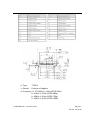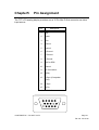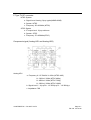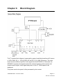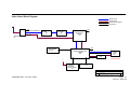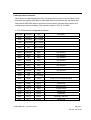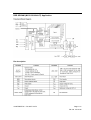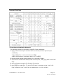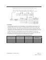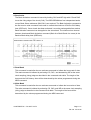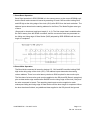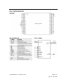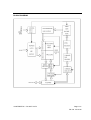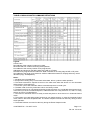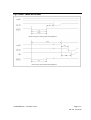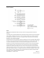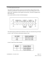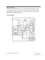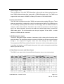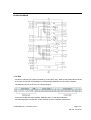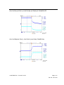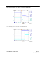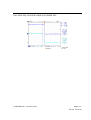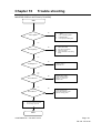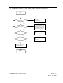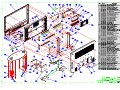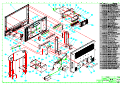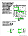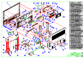
1
Service Manual
Model #: VIZIO L37
V, Inc
320A Kalmus Drive Costa Mesa, CA 92626
TEL : +714-668-0588 FAX :+714-668-9099
Top
Confidential
Table of Contents
CONTENTS
PAGE
Sections
1. Features
1-1
2. Specifications
2-1
3. On Screen Display
3-1
4. Factory Preset Timings
4-1
5. Pin Assignment
5-1
6. Main Board I/O Connections
6-1
7. Theory of Circuit Operation
7-1
8. Waveforms
8-1
9. Trouble Shooting
9-1
10. Block Diagram
10-1
11. Spare parts list
11-1
12. Complete Parts List
12-1
Appendix
1. Main Board Circuit Diagram
2. Main Board PCB Layout
3. Assembly Explosion Drawing
Block Diagram
VIZIO L37 Service Manual
VINC
Service Manual
VIZIO L37
COPYRIGHT © 2000 V, INC. ALL RIGHTS RESERVED.
IBM and IBM products are registered trademarks of International Business Machines
Corporation.
Macintosh and Power Macintosh are registered trademarks of Apple Computer, Inc.
VINC and VINC products are registered trademarks of V, Inc.
VESA, EDID, DPMS and DDC are registered trademarks of Video Electronics Standards
Association (VESA).
Energy Star is a registered trademark of the US Environmental Protection Agency (EPA).
No part of this document may be copied, reproduced or transmitted by any means for any
purpose without prior written permission from VINC.
FCC INFORMATION
This equipment has been tested and found to comply with the limits of a Class B digital device,
pursuant to part 15 of the FCC Rules. These limits are designed to provide reasonable
protection against harmful interference in a residential installation. This equipment generates,
uses and can radiate radio frequency energy, and if not installed and used in accordance with
the instructions, may cause harmful interference to radio communications. However, there is
no guarantee that the interference will not occur in a particular installation. If this equipment
does cause unacceptable interference to radio or television reception, which can be
determined by turning the equipment off and on, the user is encouraged to try to correct the
interference by one or more of the following measures -- reorient or relocate the receiving
antenna; increase the separation between equipment and receiver; or connect the into an
outlet on a circuit different from that to which the receiver is connected.
FCC WARNING
To assure continued FCC compliance, the user must use a grounded power supply cord and
the provided shielded video interface cable with bonded ferrite cores. Also, any unauthorized
changes or modifications to Amtrak products will void the user’s authority to operate this
device. Thus VINC Will not be held responsible for the product and its safety.
CE CERTIFICATION
This device complies with the requirements of the EEC directive 89/336/EEC with regard to
“Electromagnetic compatibility.”
SAFETY CAUTION
Use a power cable that is properly grounded. Always use the AC cords as follows – USA (UL);
Canada (CSA); Germany (VDE); Switzerland (SEV); Britain (BASEC/BS); Japan (Electric
Appliance Control Act); or an AC cord that meets the local safety standards.
VIZIO L37 Service Manual
Chapter 1
Features
1.
Built in TV channel selector for TV viewing
2.
Simulatnueous display of PC and TV images
3.
Connectable to PC’s analog RGB port
4.
Built in s-video, HDTV, composite video, HDMI ,TV and DTV out
5. Built in auto adjust function for automatic adjument of screen display
6.
Smoothing function enables display of smooth texts and graphics even if image
withresolution lower than 1366x768 is magnified
7.
Picture In Picture (PIP) funtion to show TV or VCR images
8. Power saving to reduce consumption power too less than 3W
9. On Screen Display: user can define display mode (i.e. color, brightness, contrast,
sharpness), sound setting, PIP, TV channel program, aspect and gamma or
reset all setting.
CONFIDENTIAL – DO NOT COPY
Page 1-1
File No. SG-0176
Chapter 2
Specification
1. LCD CHARACTERISTICS
Type: WXGA TFT LCD
Size: 37 inch
Display Size: 37.02 inches (940.3mm) diagonal
Outline Dimension: 877.0/878.0 mm (H) x 516.8 mm (V) x 55.5 (D) mm (Typ.)
Pixel Pitch: 0.200mm x 0.600mm x RGB
Pixel Format: 1366 horiz. By 768 vert. Pixels RGB strip arrangement
Contrast ratio: 600(Typ)
Luminance, White: 500 cd/m2 (Typ)
Display Operating Mode: normally Black
Surface Treatment : Hard coating(3H), Anti-glare treatment of the front polarizer
Color Depth : 8-bit, 16.7 M colors
Viewing Angle (CR>10) : Viewing angle free ( R/L 176(Typ.), U/D 176(Typ.))
Power Consumption : Total 125Watt (Typ.) (Logic=4.5W, Lamp=120W [IBL=6.0mA] )
2. OPTICAL CHARACTERISTICS
Viewing Angle by Contrast Ratio :
Left: 88°typ.
Right: 88°typ.
Top: 88°typ.
Bottom: 88°typ.
3. SIGNAL (Refer to the Timing Chart)
3.1 Input Voltage Level: 90~240 Vac, 50/ 60 Hz
3.2 Input Signal :
3.2.1 RCA-type (Yellow) Composite Video Connector :
a. Signal Level Video (Y+C): Analog 1Vp-p/75
Sync (H+V): 0.3V below Video (Y+C)
b. Frequency H: 15.734KHz V:60Hz (NTSC)
3.2.2 Four-Pin mini DIN S-Video Connector
a. Pin Assignment
CONFIDENTIAL – DO NOT COPY
Page 2-1
File No. SG-0176
b. Signal Level Video (Y): Analog 0.1Vp-p/75
Video (C): Analog 0.286p-p/75
Sync (H+V): 0.3V below Video (Y)
c. Frequency H: 15.734KHz V: 60Hz (NTSC)
3.2.3 F-Type TV RF connector
3.2.3.1 NTSC System:
a. Signal Level: Analog 1Vp-p typical(45dB~90dB)
b. System :NTSC
c. Frequency: 55~801MHz (NTSC)
3.2.3.2 ATSC System
a. IF-output level: 1Vp-p minimum
b. System: ATSC
c. Frequency: 57~863MHz(ATSC)
3.2.4 PC connector 15 pin male D-sub connector
a. Pin Assignment :
CONFIDENTIAL – DO NOT COPY
Page 2-2
File No. SG-0176
b. Signal Level Video (R, G, B) : Analog 0.7Vp-p/75
Sync (H, V) : TTL level
c. Sync Type TTL (Separate / Composite) or Sync. On-Green
d. Sync polarity Positive or Negative
e. Frequency : H: support to 30K~70KHz
V: support to 50~85Hz
Pixel Clock: support to 110MHz
3.2.5 HDMI Signal (Digital HD):
a. Pin Assignment
CONFIDENTIAL – DO NOT COPY
Page 2-3
File No. SG-0176
b. Type:
TYPE A
c. Polarity: Positive or Negative
d. Frequency: H: 15.734KHz V: 60Hz (NTSC-480i)
H: 31KHz V: 60Hz (NTSC-480p)
H: 45KHz V: 60Hz (NTSC-720p)
H: 33KHz V: 60Hz (NTSC-1080i)
CONFIDENTIAL – DO NOT COPY
Page 2-4
File No. SG-0176
3.2.6 Component signal (Analog HD1 and Analog HD2)
3.2.6.1 Analog HD1
a. Frequency H: 15.734KHz V: 60Hz (NTSC-480i)
H: 31KHz V: 60Hz (NTSC-480p)
H: 45KHz V: 60Hz (NTSC-720p)
H: 33KHz V: 60Hz (NTSC-1080i)
b. Signal level Y: 1Vp-p Pb: ±0.350Vp-p Pr: ±0.350Vp-p
c. Impedance 75
3.2.6.2 Analog HD2
a. Frequency
H: 15.734KHz V: 60Hz (NTSC-480i)
H: 31KHz V: 60Hz (NTSC-480p)
H: 45KHz V: 60Hz (NTSC-720p)
H: 33KHz V: 60Hz (NTSC-1080i)
b. Signal level Y: 1Vp-p Pb: ±0.350Vp-p Pr: ±0.350Vp-p
c. Impedance 75
3.2.7 Audio Signal
a. Signal Level 1Vrms
b. Frequency Response 250Hz-20KHz
4.Input Connectors
RJ11, D-SUB15PIN ,mini jack(PC Audio in), HDMI CONNECT, RCAX2 (component),
RCAX3 (AUDIO in), RCAX3 (composite), RCAX3 (AUDIO in),F CONNECTx2,S-Video
5. POWER SUPPLY
Power Consumption: 220W MAX
Power OFF: to less than 3W MAX
6.Speaker
Output 6Ω/10W (max) X2
7. ENVIRONMENT
7-1. Operating Temperature: 5°C ~35°C (Ambient)
7-2. Relative Humidity: Ta= 35 °C, 10~90%RH (Non-condensing)
7-3. Altitude: 0~40,0000 feet (Non-Operating)
CONFIDENTIAL – DO NOT COPY
Page 2-5
File No. SG-0176
8. DIMENSIONS (Physical dimension)
Width: 959.9mm.
Depth: 311.0mm
Height: 748.4mm
9. WEIGHT (Physical weight)
a. Net: 25.9kgs
b. Gross: 33.5kg
9-1. MOUNTING PRECAUTIONS
(1) You must mount a module using holes arranged in four corners or four sides.
(2) You should consider the mounting structure so that uneven force (ex. Twisted
stress) is not applied to the module. And the case on which a module is mounted
should have sufficient strength so that external force is not transmitted directly to
the module.
(3) Please attach the surface transparent protective plate to the surface in order to
protect the polarizer. Transparent protective plate should have sufficient strength
in order to the resist external force.
(4) You should adopt radiation structure to satisfy the temperature specification.
(5) Acetic acid type and chlorine type materials for the cover case are not desirable
because the former generates corrosive gas of attacking the polarizer at high
temperature and the latter causes circuit break by electro-chemical reaction.
(6) Do not touch, push or rub the exposed polarizes with glass, tweezers or anything
harder than HB pencil lead. And please do not rub with dust clothes with chemical
treatment.
Do not touch the surface of polarizer for bare hand or greasy cloth.(Some
cosmetics are detrimental to the polarizer.)
(7) When the surface becomes dusty, please wipe gently with absorbent cotton or
other soft materials like chamois soaks with petroleum benzene. Normal-hexane
is recommended for cleaning the adhesives used to attach front / rear polarizers.
Do not use acetone, toluene and alcohol because they cause chemical damage to
the polarizer.
(8) Wipe off saliva or water drops as soon as possible. Their long time contact with
polarizer causes deformations and color fading.
(9) Do not open the case because inside circuits do not have sufficient strength.
CONFIDENTIAL – DO NOT COPY
Page 2-6
File No. SG-0176
9-2. OPERATING PRECAUTIONS
(1) The spike noise causes the mis-operation of circuits. It should be lower than
following voltage :
V=±200mV(Over and under shoot voltage)
(2) Response time depends on the temperature.(In lower temperature, it becomes
longer.)
(3) Brightness depends on the temperature. (In lower temperature, it becomes lower.)
And in lower temperature, response time(required time that brightness is stable
after turned on) becomes longer.
(4) Be careful for condensation at sudden temperature change. Condensation makes
damage to polarizer or electrical contacted parts. And after fading condensation,
smear or spot will occur.
(5) When fixed patterns are displayed for a long time, remnant image is likely to
occur.
(6) Module has high frequency circuits. Sufficient suppression to the electromagnetic
interference shall be done by system manufacturers. Grounding and shielding
methods may be important to minimized the interference.
9-3. HANDLING PRECAUTIONS FOR PROTECTION
(1) The protection film is attached to the bezel with a small masking tape. When the
protection film is peeled off, static electricity is generated between the film and
polarizer. This should be peeled off slowly and carefully by people who are
electrically grounded and with well ion-blown equipment or in such a condition,
etc.
(2) When the module with protection film attached is stored for a long time,
sometimes there remains a very small amount of glue still on the bezel after the
protection film is peeled off.
(3) You can remove the glue easily. When the glue remains on the bezel surface or its
vestige is recognized, please wipe them off with absorbent cotton waste or other
soft material like chamois soaked with normal-hexane.
CONFIDENTIAL – DO NOT COPY
Page 2-7
File No. SG-0176
Chapter 3
On Screen Display
Main unit button
Power
Input
CH ▲
CH ▼
VOL +
VOL MUTE / EXIT
MENU
TV Source
A. PICTURE ADJUST:
a. PICTURE MODE (USER/ VIVID1 /VIVID2 / VIVID3)
b. Adjust the BACKLIGHT (0~100)
c. Adjust the BRIGHTNESS (0~100)
d. Adjust the CONTRAST (0~100)
e. Adjust the COLOR (saturation)(0~100)
f. Adjust the TINT (hue) (0~100)
g. Adjust the SHARPNESS (0~100)
h. CLOSED CAPTION (OFF/CC1/CC2/CC3/CC4/TT1/TT2/TT3/TT4)
B. AUDIO ADJUST:
a. VOLUME (0~100)
b. BASS (0~100)
c. TREBLE (0~100)
d. BALANCE (0~100)
e. SURROUND (ON/OFF)
f. REVERB (OFF, CONCERT, LIVINGROOM, HALL, ARENA)
g. MUTE (ON/OFF)
h. SPEAKERS (ON/OFF)
C. TV TUNER SETUP:
a. SOUND (SAP/MONO/STEREO)
b. TV/CABLE (TV/CABLE)
c. CHANNEL SEARCH (RUN)
d. SET CHANNEL
CONFIDENTIAL – DO NOT COPY
Page 3-1
File No. SG-0176
e. SKIP CHANNEL (YES/NO)
D. PARENTAL CONTROL:
a. PARENT LOCK ENABLE (ON/OFF)
b. TV RATING
c. MOVIE RATING
d. ACCESS CODE EDIT
E. PIP SETUP:
a. STYLE (OFF/PIP/POP)
b. Source (AV1、AV2、AV3、ANALOGHD1、ANALOG HD2、DIGITAL HD
RGB、DTV)
c. SIZE (SMALL (20%)/MEDIUM (30%)/LARGE (40%))
d. POSITION (TOP LEFT/TOP CENTER/TOP RIGHT/MIDDLE LEFT
/MIDDLE RIGHT/BOTTOM LEFT/BOTTOM CENTER/BOTTOM RIGHT)
F. SPECIAL FEATURES:
a. LANGUAGE (ENGLISH/FRANCE/SPANISH)
b. SLEEP TIMER (OFF/30/60/90/120)
c. WIDE FORMAT (NORMAL/WIDE/ZOOM/PANORAMIC)
d. RESET ALL SETTING
PC Analog Mode
A. PICTURE ADJUST:
a. AUTO PICTURE (Run)
b. Adjust the BACKLIGHT (0~100)
c. Adjust the BRIGHTNESS (0~100)
d. Adjust the CONTRAST (0~100)
e. Adjust the V-POSITION (0~100)
f. Adjust the H-SIZE (0~100)
g. Adjust the H-POSITION (0~100)
h. Adjust the FINETUNE (0~100)
B. COLOR TEMP:
a. COLOR TEMP. (User, 5000K, 6500K,9300K)
b. RED (0~255)
c. GREEN (0~255)
d. BLUE (0~255)
CONFIDENTIAL – DO NOT COPY
Page 3-2
File No. SG-0176
C. AUDIO ADJUST:
a. VOLUME (0~100)
b. BASS (0~100)
c. TREBLE (0~100)
d. BALANCE (0~100)
e. SURROUND (ON/OFF)
f. REVERB (OFF, CONCERT, LIVING ROOM, HALL, ARENA)
g. MUTE (ON/OFF)
h. SPEAKERS (ON/OFF)
D. PIP SETUP:
a. STYLE (OFF/PIP/POP)
b. SOURCE (AV1、AV2、AV3、TV)
c. SIZE (SMALL (20%)/MEDIUM(30%)/LARGE (40%))
d. POSITION (TOP LEFT/TOP CENTER/TOP RIGHT/MIDDLE LEFT
/MIDDLE RIGHT/BOTTOM LEFT/BOTTOM CENTER/BOTTOM RIGHT)
E. SPECIAL FEATURES:
a. LANGUAGE (ENGLISH/FRANCE/SPANISH)
b. SLEEP TIMER (OFF/30/60/90/120)
c. WIDE FORMAT (WIDE/ NORMAL)
d. RESET ALL SETTING
DIGITAL HD MODE
A. PICTURE:
a. PICTURE MODE (USER/ VIVID1 /VIVID2 / VIVID3)
b. Adjust the BACKLIGHT (0~100)
c. Adjust the BRIGHTNESS (0~100)
d. Adjust the CONTRAST (0~100)
e. Adjust the COLOR (saturation)(0~100)
f. Adjust the TINT (hue) (0~100)
g. Adjust the SHARPNESS (0~100)
B. AUDIO ADJUST:
a. VOLUME (0~100)
b. BASS (0~100)
c. TREBLE (0~100)
d. BALANCE (0~100)
e. SURROUND (ON/OFF)
CONFIDENTIAL – DO NOT COPY
Page 3-3
File No. SG-0176
f. REVERB (OFF, CONCERT, LIVING ROOM, HALL, ARENA)
g. MUTE (ON/OFF)
h. SPEAKERS (ON/OFF)
i. AUDIO SOURCE(DIGITAL HD/DTV)
C. PARENTAL CONTROL:
a. PARENT LOCK ENABLE (ON/OFF)
b. TV RATING
c. MOVIE RATING
d. ACCESS CODE EDIT
D. PIP SETUP:
a. STYLE (OFF/PIP/POP)
b. SOURCE (AV1、AV2、AV3、TV)
c. SIZE (SMALL (20%)/MEDIUM (30%)/LARGE (40%))
d. POSITION (TOP LEFT/TOP CENTER/TOP RIGHT/MIDDLE LEFT
/MIDDLE RIGHT/BOTTOM LEFT/BOTTOM CENTER/BOTTOM RIGHT)
E. SPECIAL FEATURES:
a. LANGUAGE (ENGLISH/FRANCE/SPANISH)
b. SLEEP TIMER (OFF/30/60/90/120)
c. WIDE FORMAT (NORMAL/WIDE/ZOOM)
d. RESET ALL SETTING
Video Sources:
AV1、AV2、AV3、ANALOG HD1、ANALOG HD2
A. PICTURE:
a. PICTURE MODE (USER/ VIVID1 /VIVID2 / VIVID3)
b. Adjust the BACKLIGHT (0~100)
c. Adjust the BRIGHTNESS (0~100)
d. Adjust the CONTRAST (0~100)
e. Adjust the COLOR (saturation)(0~100)
f. Adjust the TINT (hue) (0~100)
g. Adjust the SHARPNESS (0~100)
h. CLOSED CAPTION (OFF/CC1/CC2/CC3/CC4/TT1/TT2/TT3/TT4)
CONFIDENTIAL – DO NOT COPY
Page 3-4
File No. SG-0176
B. AUDIO ADJUST:
a. VOLUME (0~100)
b. BASS (0~100)
c. TREBLE (0~100)
d. BALANCE (0~100)
e. SURROUND (ON/OFF)
f. REVERB (OFF, CONCERT, LIVING ROOM, HALL, ARENA)
g. MUTE (ON/OFF)
h. SPEAKERS (ON/OFF)
C. PARENTAL CONTROL:
a. PARENT LOCK ENABLE (ON/OFF)
b. TV RATING
c. MOVIE RATING
d. ACCESS CODE EDIT
D. PIP SETUP:
a. STYLE (OFF/PIP/POP)
b. SOURCE (AV2、AV3、ANALOGHD1、ANALOG HD2、DIGITAL HD、
RGB、TV)
c. SIZE (SMALL (20%)/MEDIUM (30%)/LARGE (40%))
d. POSITION (TOP LEFT/TOP CENTER/TOP RIGHT/MIDDLE LEFT
/MIDDLE RIGHT/BOTTOM LEFT/BOTTOM CENTER/BOTTOM RIGHT)
E. SPECIAL FEATURES:
a. LANGUAGE (ENGLISH/FRANCE/SPANISH)
b. SLEEP TIMER (OFF/30/60/90/120)
c. WIDE FORMAT (NORMAL/WIDE/ZOOM/PANORAMIC)
d. RESET ALL SETTING
DTV Sources:
A. PICTURE:
a. PICTURE MODE (USER/ VIVID1 /VIVID2 / VIVID3)
b. Adjust the BACKLIGHT (0~100)
c. Adjust the BRIGHTNESS (0~100)
d. Adjust the CONTRAST (0~100)
e. Adjust the COLOR (saturation)(0~100)
f. Adjust the TINT (hue) (0~100)
CONFIDENTIAL – DO NOT COPY
Page 3-5
File No. SG-0176
g. Adjust the SHARPNESS (0~100)
B. AUDIO ADJUST:
a. VOLUME (0~100)
b. BASS (0~100)
c. TREBLE (0~100)
d. BALANCE (0~100)
e. SURROUND (ON/OFF)
f. REVERB (OFF, CONCERT, LIVING ROOM, HALL, ARENA)
g. MUTE (ON/OFF)
h. SPEAKERS (ON/OFF)
C.DTV OSD
a. DTV TUNER SETUP
1. TIME ZONE:
α. HAWALL
β. EASTTERN TIME
γ. INDIANA
δ. CENTRAL TIME
ε. MOUNTAIN TIME
ζ. ARIZONA
η. PACIFIC TIME
θ. ALASKA
2. AUTO SCAN
3. MANUAL SCAN PRESS<OK>
(1) ADD-ON MODE
(2) RANGE MODE
α. FORM CHANNEL(2~69)
β. TO CHANNEL(2~69)
4. CHANNEL SKIP PRESS<OK>
b. CLOSED CAPTION:
1. ANALOG COLOSED CAPTION
α.OFF
β.CC1
γ.CC2
δ.CC3
ε.CC4
CONFIDENTIAL – DO NOT COPY
Page 3-6
File No. SG-0176
2. DIGITAL COLOSED CAPTION
α.OFF
β.SERVICE1
γ.SERVICE2
δ.SERVICE3
ε.SERVICE4.
ζ.SERVICE5
η.SERVICE6
3. DIGITAL CAPTION STYLE PRESS<OK>
(1) AS BROADCASTER
(2)CUSTOM
FONT SIZE
α.LARGE
β.SMALL
γ.MEDIUM
FONT COLOR
α.BLACK
β.WHITE
γ.GREEN
δ.BLUE
ε.RED
ζ.CYAN
η.YELLOW
θ.MAGENTA
FONT OPACITY
α.SOLID
β.TRANSLUCENT
γ.TRANSPARENT
BLACKGROUND COLOR
α.BLACK
β.WHITE
γ.GREEN
δ.BLUE
ε.RED
ζ.CYAN
CONFIDENTIAL – DO NOT COPY
Page 3-7
File No. SG-0176
η.YELLOW
θ.MAGENTA
BLACKGROUND OPACITY
α.SOLID
β.TRANSLUCENT
γ.TRANSPARENT
WINDOW COLOR
α.BLACK
β.WHITE
γ.GREEN
δ.BLUE
ε.RED
ζ.CYAN
η.YELLOW
θ.MAGENTA
WINDOW OPACITY
α.SOLID
β.TRANSLUCENT
γ.TRANSPARENT
c.PARENTAL CONTROL
PASSWORD PRESS<OK>
1.0000
2.CHANNEL BLOCK PRESS<OK>
D. PARENTAL CONTROL:
a. PARENT LOCK ENABLE (ON/OFF)
b. TV RATING
c. MOVIE RATING
d. ACCESS CODE EDIT
E. PIP SETUP:
a. STYLE (OFF/PIP/POP)
b. SOURCE (AV1、AV2、AV3、TV)
c. SIZE (SMALL (20%)/MEDIUM (30%)/LARGE (40%))
d. POSITION (TOP LEFT/TOP CENTER/TOP RIGHT/MIDDLE LEFT
/MIDDLE RIGHT/BOTTOM LEFT/BOTTOM CENTER/BOTTOM RIGHT)
CONFIDENTIAL – DO NOT COPY
Page 3-8
File No. SG-0176
F. SPECIAL FEATURES:
a. LANGUAGE (ENGLISH/FRANCE/SPANISH)
b. SLEEP TIMER (OFF/30/60/90/120)
c. WIDE FORMAT (NORMAL/WIDE)
d. RESET ALL SETTING
CONFIDENTIAL – DO NOT COPY
Page 3-9
File No. SG-0176
Chapter4
Factory preset timings
This timing chart is already preset for the TFT LCD analog & digital display monitors.
Refresh
Horizontal
Vertical
Horizontal
Vertical
Pixel
rate
Frequency
Frequency
Polarity
Polarity
Rate
640x480
60Hz
31.5kHz
59.94Hz
N
N
25.175
640x480
75Hz
37.5kHz
75.00Hz
N
N
31.500
800X600
60Hz
37.9kHz
60.317Hz
P
P
40.000
800x600
75Hz
46.9kHz
75.00Hz
P
P
49.500
800X600
85Hz
53.7kHz
85.06Hz
P
P
56.250
1024x768
60Hz
48.4kHz
60.01Hz
N
N
65.000
1024X768
75Hz
60.0kHz
75.03Hz
P
P
78.750
720x400
70Hz
31.46kHz
70.08Hz
N
P
28.320
1366X768
60
47.7KHZ
60.00HZ
P
N
85.500
Resolution
Remark:
P: positive
N: negative
CONFIDENTIAL – DO NOT COPY
Page 4-1
File No. SG-0176
Chapter5
Pin Assignment
The TFT LCD analog display monitors use a 15 Pin Mini D-Sub connector as video
input source.
Pin
Description
1
Red
2
Green
3
Blue
4
Ground
5
Ground
6
R-Ground
7
G-Ground
8
B-Ground
9
+5V for DDC
10
Ground
11
No Connection
12
(SDA)
13
H-Sync (Composite
Sync)
14
V-Sync
15
(SCL)
Table 1.
1
5
6
11
CONFIDENTIAL – DO NOT COPY
10
15
Page 5-1
File No. SG-0176
PC connector 15 pin male D-sub connector
a. Pin Assignment Refer to Table 1
b. Signal Level Video (R, G, B): Analog 0.7Vp-p/75Ω
Sync (H, V): TTL level
RGB Signal:
a. Sync Type TTL (Separate / Composite) or Sync. On Green
b. Sync polarity Positive or Negative
c. Video Amplitude RGB: 0.7Vp-p
d. Frequency
H: support to 30K~70KHz
V: support to 50~85Hz
Pixel Clock: support to 110MHz
HDMI CONNECT PIN ASSIGNMENT
PIN
SIGNAL ASSIGNMENT
PIN
SIGNAL ASSIGNMENT
1
TMDS Data2+
11
TMDS Clock Shield
2
TMDS Data2 Shield
12
TMDS Clock-
3
TMDS Data2-
13
CEC
4
TMDS Data1+
14
Reserved (N.C on device)
5
TMDS Data1 Shield
15
SCL
6
TMDS Data1-
16
SDA
7
TMDS Data0+
17
DDC/CEC Ground
8
TMDS Data0 Shield
18
+5V Power
9
TMDS Data0-
19
Hot Plug Detect
10
TMDS Clock+
Table 2.
CONFIDENTIAL – DO NOT COPY
Page 5-2
File No. SG-0176
HDMI Signal (Digital HD):
a. Pin Assignment Refer to Table 2.
b. Type A
c. Polarity Positive or Negative
d. Frequency
H: 15.734KHz V: 60Hz (NTSC-480i)
H: 31KHz V: 60Hz (NTSC-480p)
H: 45KHz V: 60Hz (NTSC-720p)
H: 33KHz V: 60Hz (NTSC-1080i)
Four-Pin mini DIN S-Video Connector
a. Pin Assignment
CONFIDENTIAL – DO NOT COPY
Page 5-3
File No. SG-0176
b. Signal Level Video (Y): Analog 0.1Vp-p/75Ω
Video (C): Analog 0.286p-p/75
Sync (H+V): 0.3V below Video (Y)
Frequency H: 15.734KHz V: 60Hz (NTSC)
CONFIDENTIAL – DO NOT COPY
Page 5-4
File No. SG-0176
F-Type TV RF connector
NTSC System:
a. Signal Level: Analog 1Vp-p typical(45dB~90dB)
b. System :NTSC
c. Frequency: 55~801MHz (NTSC)
ATSC System
a. IF-output level: 1Vp-p minimum
b. System: ATSC
c. Frequency: 57~863MHz(ATSC)
Component signal (Analog HD1 and Analog HD2)
Analog HD1
a. Frequency H: 15.734KHz V: 60Hz (NTSC-480i)
H: 31KHz V: 60Hz (NTSC-480p)
H: 45KHz V: 60Hz (NTSC-720p)
H: 33KHz V: 60Hz (NTSC-1080i)
b. Signal level Y: 1Vp-p Pb: ±0.350Vp-p Pr: ±0.350Vp-p
c. Impedance 75Ω
CONFIDENTIAL – DO NOT COPY
Page 5-5
File No. SG-0176
Analog HD2
a. Frequency H: 15.734KHz V: 60Hz (NTSC-480i)
H: 31KHz V: 60Hz (NTSC-480p)
H: 45KHz V: 60Hz (NTSC-720p)
H: 33KHz V: 60Hz (NTSC-1080i)
b. Signal level Y: 1Vp-p Pb: ±0.350Vp-p Pr: ±0.350Vp-p
c. Impedance 75Ω
RCA-type (Yellow) Composite Video Connector(AV1,AV2,AV3)
a. Signal Level Video (Y+C): Analog 1Vp-p/75
Sync (H+V): 0.3V below Video (Y+C)
b. Frequency H: 15.734KHz V:60Hz (NTSC)
CONFIDENTIAL – DO NOT COPY
Page 5-6
File No. SG-0176
PHONE JACK AUDIO INPUT
:
a. Signal Level 1Vrms
b. Frequency Response 250Hz-20KHz
CONFIDENTIAL – DO NOT COPY
Page 5-7
File No. SG-0176
Chapter 6
Block Diagram
The TV system block diagram is powered by power board that transforms AC source
of 100V~240V AC +/- 10% @ 50/60 HZ into DC 5V & 12V& 24Vsource. The main
board receives different types of video signal into the MTK8205 Ic. Afterward, the
MTK8205 Ic process the signals control the various functions of the monitor and
outputs control signal, video signal and power to the 37” WXGA panel to be
displayed.
The power send to the panel is first processed by the inverter.
CONFIDENTIAL – DO NOT COPY
Page 6-1
File No. SG-0176
The function of the inverter is to step up the voltage supplied by the main board to the
power that is needed to light up the lamps in the panel. Simultaneously, the digital
video signals are processed in the panel and the outcome determines the brightness,
pixel on/off and the color displayed on the panel.
The analog video signals of S-video, YPbPr, TV, PC and A/V all video signals are
translated from analog signals into MTK8205 generates the vertical and horizontal
timing signals for display device.
The analog audio of s-video, YPbPr, TV, PC and A/V is transmitting to the WM8776
processed. The purpose is process the input audio signal to control volume, bass,
treble, surround, and balance. The HDMI video and audio is must transmitting to
sil9011 processed then TMDS signal to the MTK8205 generates the vertical and
horizontal timing signals for display device.
The DTV signal is processes to the tuner and output to MT5111 who handle ATSC
input to match MPEG-2 package, then transfer to MT5351. After passing through
decoder, the signal will be with the digital signal tri-dtate from HDMI transfer to digital
port of MT8205 . All functions are controllable by the main board. Plus, all functions in
the IC boards are programmable using I2C Bus.
CONFIDENTIAL – DO NOT COPY
Page 6-2
File No. SG-0176
Main Board Block Diagram
Video Signal
RJ11
P11
Audio Signal
Communicate Signal
24C02
U17
Control Pin
HDMI
CON.
P1
FFC 50PIN CON.
Sil9011
U16
+12V
For DTV Signal
+5V
+3.3V
+2.5V
24C02
U18
D_SUB
15PIN
P3
KEY
BOARD
CONN.
IR
CONN.
DDR SDRAM
U11,U12
DC/DC
FLASH
MEMORY
U10
DC
POWER
12V
IN
CONN.
Y
Cb
Cr
I2C
COMPONENT1&2
VIDEO P8
IDTQS3VH257
MT8205
U21
Y
Cb
37' LCD
Panel
U9
Cr
SEL
R
L
COMPONENT1&2
Audio P10
R
I2C
L
SY
V
V
R
R
L
L
Y+C
L/R
Y+C
L/R
SC
CVBS1
CVBS2
A/V RCA P2
AUO1L_SWO
U20
S-VIDEO J6
AUO1R_SWO
AUO2L_SWO
AUO2R_SWO
Y+C
V
DVI Audio
Input
P7
MM1492
Y
C
DETECT
PC Audio
Input
P5
Audio Processor
WM8776
U20
OPA
U28
R
RCA OUT
P9
L
HEAD
PHONE
J3
AV3 RCA J4
HEAD PHONE DETECT
I2C
R+
PWM1
TV CVBS
RTDA8946
UA1
SIF
PHILIPS FQ1236 TU1
L+
L-
Title
<Title>
Size
Document Number
Custom<Doc>
Date:
CONFIDENTIAL – DO NOT COPY
Monday, November 14, 2005
Rev
<RevCode>
Sheet
1
of
1
Page 6-3
File No. SG-0176
Video Board Block Diagram
Video Signal
Audio Signal
Communicate Signal
Control Pin
I2C
Narrow_IF_OP1&OP2
PORT SAW
FILTER
U7
AGC
Amplifiers
U8
IF AGC
PHILIPS TD1336
U6
I2C
Demodulator
MT5111
U9
I2C
DDR SDRAM
U12,U13
FCC
50PIN
CON.
J1
DTV Backend Decoder
MT5351
U10
AUD_CTRL
IDTQS3VH257
U18
For Main Board
DV33
VOLTAGE
CONTROL
CRYSTAL
OSCILLATOR
X1
Flash Memory
U15
Title
<Title>
Size
B
Date:
CONFIDENTIAL – DO NOT COPY
Document Number
<Doc>
Monday, November 14, 2005
Rev
<RevCode>
Sheet
1
of
1
Page 6-4
File No. SG-0176
Chapter7
Main Board I/o Connections
J7 CONNECTION (TOP→BOTTOM)
Pin
Description
1
“Auto”
2
“Left”
3
“Right”
4
“Down”
5
“Gnd”
6
“Up”
7
“Menu”
8
“Source”
9
“Power”
10
“LED”
11
“IR”
12
“+5V”
J1 CONNECTION (TOP→BOTTOM)
Pin
Description
1
“POWRSW”
2
“+12V”
3
“+12V”
4
“+12V”
5
“GND”
6
“GND”
7
“GND”
8
“GND”
9
“+5V”
10
“+5V”
11
“+5V”
12
“PWM”
13
“BL ON/OFF”
CONFIDENTIAL – DO NOT COPY
Page 7-1
File No. SG-0176
J3 CONNECTION (TOP→BOTTOM)
Pin
Description
Pin
Description
1
“+3.3V”
16
“HPR”
2
“GND”
17
“HPL”
3
“G/Y”
18
“GNDV”
4
“B/U”
19
“HPDET#”
5
“R/V”
20
“AV3_IN”
6
“LMAIN1”
21
“AV3_GND”
7
“RMAIN1”
22
“AV3L”
8
“+5.0V”
23
“AV3L GND”
9
“GND”
24
“AV3R”
10
“8302IR”
25
“AV3R GND”
11
“8302NET1”
26
“S1Y_IN”
12
“8302NET2”
27
“S1Y_GND”
13
“8302RXD”
28
“S1C_IN”
14
“8302TXD”
29
“S1C_GND”
15
“GNDV”
30
“SVDET2#”
CONFIDENTIAL – DO NOT COPY
Page 7-2
File No. SG-0176
J2 CONNECTION (TOP→BOTTOM)
Pin
Description
Pin
Description
1
“GND”
26
“GND”
2
“I2C_SW”
27
“VOG3”
3
“OREQUEST#”
28
“VOG2”
4
“OREADY#”
29
“VOG1”
5
“ORESET#”
30
“VOG0”
6
“GND”
31
“GND”
7
“VOPCLK”
32
“VOB7”
8
“VODE”
33
“VOB6”
9
“VOVSYNC”
34
“VOB5”
10
“VOHSYNC”
35
“VOB4”
11
“GND”
36
“GND”
12
“VOR7”
37
“VOB3”
13
“VOR6”
38
“VOB2”
14
“VOR5”
39
“VOB1”
15
“VOR4”
40
“VOB0”
16
“GND”
41
“GND”
17
“VOR3”
42
“AO1SDATA0”
18
“VOR2”
43
“AO1LRCK”
19
“VOR1”
44
“AO1BCK”
20
“VOR0”
45
“AO1MCLK”
21
“GND”
46
“GND”
22
“VOG7”
47
“U2RX”
23
“VOG6”
48
“U2TX”
24
“VOG5”
49
“U0RX”
25
“VOG4”
50
“U0TX”
CONFIDENTIAL – DO NOT COPY
Page 7-3
File No. SG-0176
J8 CONNECTION (TOP→BOTTOM)
Pin
Description
1
“+5V”
2
“GND”
3
“GND”
4
“+12V”
5
“+12V”
CONFIDENTIAL – DO NOT COPY
Page 7-4
File No. SG-0176
Chapter 8
Theory of Circuit Operation
The operation of D-SUB 15pin route
The D-SUB 15pin is input analog signal to the MTK8205 transfer A/D converter then
generates the vertical and horizontal timing signals for display device.
The operation of HDMII CON route
The HDMI CON is input digital signal the signal is process to the sil9011. Then transfer to the
MTK8205, the MTK8205 generates the vertical and horizontal timing signals for display
device.
The operation of HDTV & Component route
HDTV & Component signal is input to switch IDTQS3VH257 (Select Component1 or 2). Then
transfer to the MTK8205 the MTK8205 generates the vertical and horizontal timing signals for
display device.
The operation of Video 1,2,3 & S-Video route
The Video 1,2,3 and S-Video signal is transmission signal to main board MM1492 (Switch)
and output to MTK8205 the MTK8205 generates the vertical and horizontal timing signals for
display device.
The operation of TV route
TV signal is processes to the tuner and output to MM1492 (switch) then transfer to MTK8205
the MTK8205 generates the vertical and horizontal timing signals for display device. Audio is
processes to the tuner output to SIF circuit and output to MTK8205.Then MTK8205 process
to wm8776 and output to TDA8946J transfer to speaker
The operation of DTV route
DTV signal is processes to the tuner and output to MT5111 who handle ATSC input to match MPEG-2 package,
then transfer to MT5351. After passing through decoder, the signal will be with the digital signal tri-dtate from
HDMI transfer to digital port of MT8205
The operation of keypad
There are 8 keys to control and select the function of L32 and also has one LED to indicate
the status of operation. They are “Power, Mute/Exit, OSD, ▼▲, +
CONFIDENTIAL – DO NOT COPY
-, Input”.
Page 8-1
File No. SG-0176
1. The power key through POW and GND to control MTK8205, MTK8205 will receive a
low signal to turn on or off system while press the power key.
2. The other key the same as power key .
3. The LED is constructed with two separate LED which color is blue and orange. The
MTK8205 direct control the LED’s when MTK8205 (OGO5) is low the LED is orange
(Close power) when MTK8205 (OGO5) is high the LED is blue (Open power).
MT8205 Application
MT8205 is a highly integrated single chip for LCD TV supporting video input and output
format up to HDTV. It includes 3D comb filter TV Decoder to retrieve the best image from
popular composite signals. On-chip advanced motion adaptive de-interlacer converts
accordingly the interlace video into progressive one with overlay of a 2D Graphic processor.
Optional 2nd HDTV or SDTV inputs allows user to see multi-programs on same screen.
Flexible scalar provides wide adoption to various LCD panel for different video sources. Its
on-chip audio processor decodes analog signals from Tuner with lip sync control, delivering
high quality post-processed sound effect to customers. On-chip microprocessor reduces the
system BOM and shortens the schedule of UI design by high level C program. MT8205 is a
cost-effective and high performance HDTV-ready solution to TV manufactures.
CONFIDENTIAL – DO NOT COPY
Page 8-2
File No. SG-0176
BOLOCK DIAGRAM
1. Video input
a. Input Multiplexing
1.component X2
2.composite X3
3.s-videoX1
4.HDMI X1
5.VGA X1
6.RF X2
CONFIDENTIAL – DO NOT COPY
Page 8-3
File No. SG-0176
b. Input formats:
1.support HDTV 480i/480p/720p/1080p
2.support Y/C signal 1VP-P/75Ω
3.support Y/C signal 1VP-P/75Ω
4.support 480i/408p/720p/1080i/1080p
5.support VGA input up to 1366x168@60HZ
6.support NTSC system Frequency 55~801MHZ
7. support ATSC system Frequency 57~863MHZ
2. TV Decoder
For pip/pop:
Dual identical TVD on chip
3D-comb for both path
Dual VBI decoders for the application of V-chip
3. Support Formats:
Support NTSC, NTSC-4.43
Support ATSC
Automatic Luma / Chroma gain control
Automatic TV standard detection
NTSC Motion Adaptive 3D comb filter
Motion adaptive 3D Noise Reduction
VBI decoder for closed-caption/XDS/Teletext/WSS/VPS
Macro vision detection
CONFIDENTIAL – DO NOT COPY
Page 8-4
File No. SG-0176
BOLOCK DIAGRAM
4. 2D-Graphic/OSD processor
Two OSD planes.
Support alpha blending among these two planes and video
Support text/bitmap decoder
Support line/rectangle/gradient fill
Support bitblt
Support color key function
Support clip mask
65535/256/16/4/2-color bitmap format OSD
Automatic vertical scrolling of OSD image
Support OSD mirror and upside down
CONFIDENTIAL – DO NOT COPY
Page 8-5
File No. SG-0176
5. Microprocessor interface
When power is supplied and power key is pressed then the rest circuit lets Reset to low
state that will reset the MTK8205 to initial state. After that the Reset will transits to high
state and the MTK8205 start to work that microprocessor executes the programs and
configures the internal registers. The execution speed of CPU is 133 MHz.
a. The I/O ports are configured as follows:
Pin name
Function
Type
AF26
VGASCL
Input / Output
AE26
VGASDA
Input / Output
AB23
Description
REQUEST# Input / Output
AB24
READY#
Input / Output
AD22
SCL
Input / Output
AC22
SDA
Input / Output
OBO0
SOURCE
Input
Key detection
OBO1
MENU
Input
Key detection
OBO2
UP
Input
Key detection
OBO3
DOWN
Input
Key detection
OBO4
RIGHT
Input
Key detection
OBO5
LEFT
Input
Key detection
OBO6
AUTO
Input
Key detection
OBO7
POWER
Input
Key detection
OGO5
LED
Output
AF24
IR
Input / Output
AE23
GPIO
Output
Power on of TV board and panel
AD23
PWM0
Output
Backlight Adjustmance
AC23
PWM1
Output
Select mute
AF6
ORO6
Output
RCA out mute
AE20
UP1_4
Input
S-video Detect
AF20
UP1_3
Output
HDMI SCDT
AE19`
UP1_2
Output
YCBCRSEL
AE21
UP3_0
Output
Backlight ON/OFF
AD21
UP3_1
Output
HDMI CAB
CONFIDENTIAL – DO NOT COPY
Page 8-6
File No. SG-0176
b. PIP/POP HARDWARE LIMITION:
Secondary Window Source
Primary Window Source
A
B
C
D
E
F
G H
I
ATSC Tuner
A
X
9
9
9
9
X
X
X
X
NTSC Tuner
B
9 X
9
9
9
9
9
9
9
A/V1
C 9 9 X 9 9 9 9 9 9
A/V2
D 9 9 9 X 9 9 9 9 9
A/V3 (Side)
E
9 9 9 9 X 9 9 9 9
Analog HD1 (480i~1080i)
F
X 9 9 9 9 X
X
X
X
Analog HD2 (480i~1080i) G X 9 9 9 9 X
X
X
X
Digital HD1 (HDMI)
H X 9 9 9 9 X
X
X
X
RGB
I
X 9 9 9 9 X
X
X
X
Input Matrix for Windowing Functionality
6. Video processor
a. Color management
Flesh tone and multiple-color enhancement
Gamma/anti-Gamma correction
Color Transient Improvement (CTI)
Saturation/hue adjustment
Contrast/Brightness/Sharpness Management
Sharpness and DLTI/DCTI
Brightness and contrast adjustment
Black level extender
White peak level limiter
Adaptive Luma/Chroma Management
b. De-interlacing
Automatic detect film or video source
3:2/2:2 pull down source detection
Advanced Motion adaptive de-interlacing
CONFIDENTIAL – DO NOT COPY
Page 8-7
File No. SG-0176
c. Scaling
Arbitrary ratio vertical/horizontal scaling of video, from1/32X to 32X
Advanced linear and non-linear Panorama scaling
Programmable Zoom viewer
Picture in picture (PIP)
Picture in picture
d. Display
12/10 10/8 8/6 Dithering processing for LCD display
10bit gamma correction
Support Alpha blending for Video and two OSD panel
Frame rate conversion
7. DRAM Usage
8205,2pcs of 8X16 DDR166 is necessary
Here is a comparison chart between (2XDDR)and(1XDDR)
MTK8205 8MX16 DDRAM test report
CONFIDENTIAL – DO NOT COPY
Page 8-8
File No. SG-0176
8. Flash Usage
Flash is used to store FW code, fonts, bitmaps, and big tables for VGA, Video, and Gamma
2Mbyte is recommended to build a general TV model
MTK8205 Flash ROM support test report
CONFIDENTIAL – DO NOT COPY
Page 8-9
File No. SG-0176
DDR SDRAM (M13S128168A-6T) Application
Pin description
CONFIDENTIAL – DO NOT COPY
Page 8-10
File No. SG-0176
Command Truth Table
1. Power-Up and Initialization Sequence
The following sequence is required for POWER UP and Initialization.
1. Apply power and attempt to maintain CKE at a low state (all other inputs may be
undefined.)
- Apply VDD before or at the same time as VDDQ.
- Apply VDDQ before or at the same time as VTT & VREF).
2. Start clock and maintain stable condition for a minimum of 200us.
3. The minimum of 200us after stable power and clock (CLK, CLK), apply NOP & take CKE
high.
4. Issue precharge commands for all banks of the device.
5. Issue EMRS to enable DLL. (To issue “DLL Enable” command, provide “Low” to A0,
“High” to BA0 and “Low” to all of the rest address pins, A1~A11 and BA1)
CONFIDENTIAL – DO NOT COPY
Page 8-11
File No. SG-0176
6. Issue a mode register set command for “DLL reset”. The additional 200 cycles of clock
input is required to lock the DLL.(To issue DLL reset command, provide “High” to A8 and
“Low” to BA0)
7. Issue precharge commands for all banks of the device.
8. Issue 2 or more auto-refresh commands.
9. Issue a mode register set command with low to A8 to initialize device operation.
2. Mode Register Set (MRS)
The mode register stores the data for controlling the various operating modes of DDR
SDRAM. It programs CAS latency, addressing mode, burst length, test mode, DLL reset
and various vendor specific options to make DDR SDRAM useful for variety of different
applications. The default value of the register is not defined, therefore the mode register
must be written after EMRS setting for proper DDR SDRAM operation. The mode register
is written by asserting low on CS , RAS , CAS , WE and BA0 (The DDR SDRAM should be
in all bank recharge with CKE already high prior to writing into the mode register). The
state of address pins A0~A11 in the same cycle as CS , RAS , CAS , WE and BA0 going
low is written in the mode register. Two clock cycles are requested to complete the write
operation in the mode register. The mode register contents can be changed using the
same command and clock cycle requirements during operation as long as all banks are in
the idle state. The mode register is divided into various fields depending on functionality.
The burst length uses A0~A2, addressing mode uses A3, CAS latency (read latency from
column address) uses A4~A6. A7 is used for test mode. A8 is used for DLL reset. A7 must
be set to low for normal MRS operation. Refer to the table for specific codes for various
burst length, addressing modes and CAS latencies.
CONFIDENTIAL – DO NOT COPY
Page 8-12
File No. SG-0176
3. Precharge
The precharge command is used to precharge or close a bank that has activated. The
precharge command is issued when CS, RAS and WE are low and CAS is high at the
rising edge of the clock. The precharge command can be used to precharge each bank
respectively or all banks simultaneously. The bank select addresses (BA0, BA1) are used
to define which bank is precharged when the command is initiated. For write cycle,
tWR(min.) must be satisfied until the precharge command can be issued. After tRP from
the precharge, an active command to the same bank can be initiated.
Burst Selection for Precharge by Bank address bits
A10/AP
BA1
BA0
Precharge
0
0
0
Bank A Only
0
0
0
1
0
1
1
X
1
0
1
X
Bank B Only
Bank C Only
Bank D Only
CONFIDENTIAL – DO NOT COPY
All Banks
Page 8-13
File No. SG-0176
4. Row Active
The Bank Activation command is issued by holding CAS and WE high with CS and RAS
low at the rising edge of the clock (CLK). The DDR SDRAM has four independent banks;
so two Bank Select addresses (BA0, BA1) are required. The Bank Activation command to
the first read or write command must meet or exceed the minimum of RAS to CAS delay
time (tRCD min). Once a bank has been activated, it must be precharged before another
Bank Activation command can be applied to the same bank. The minimum time interval
between interleaved Bank Activation command (Bank A to Bank B and vice versa) is the
Bank-to-Bank delay time (tRRD min).
5. Read Bank
This command is used after the row activates command to initiate the burst read of data.
The read command is initiated by activating CS, CAS , and deasserting WE at the same
clock sampling (rising) edge as described in the command truth table. The length of the
burst and the CAS latency time will be determined by the values programmed during the
MRS command.
6. Write Bank
This command is used after the row activates command to initiate the burst write of data.
The write command is initiated by activating CS, CAS, and WE at the same clock sampling
(rising) edge as describe in the command truth table. The length of the burst will be
determined by the values programmed during the MRS command.
CONFIDENTIAL – DO NOT COPY
Page 8-14
File No. SG-0176
7. Burst Read Operation
Burst Read operation in DDR SDRAM is in the same manner as the current SDRAM such
that the Burst read command is issued by asserting CS and CAS low while holding RAS
and WE high at the rising edge of the clock (CLK) after tRCD from the bank activation. The
address inputs determine the starting address for the Burst, The Mode Register sets type
of burst.
(Sequential or interleave) and burst length (2, 4, 8). The first output data is available after
the CAS Latency from the READ command, and the consecutive data are presented on
the falling and rising edge of Data Strobe (DQS) adopted by DDR SDRAM until the burst
length is completed.
8. Burst Write Operation
The Burst Write command is issued by having CS , CAS and WE low while holding RAS
high at the rising edge of the clock (CLK). The address inputs determine the starting
column address. There is no write latency relative to DQS required for burst write cycle.
The first data of a burst write cycle must be applied on the DQ pins tDS (Data-in setup time)
prior to data strobe edge enabled after tDQSS from the rising edge of the clock (CLK) that
the write command is issued. The remaining data inputs must be supplied on each
subsequent falling and rising edge of Data Strobe until the burst length is completed. When
the burst has been finished, any additional data supplied to the DQ pins will be ignored.
CONFIDENTIAL – DO NOT COPY
Page 8-15
File No. SG-0176
MX29LV160BTTC (Flash) Application
The MX29LV800T/B & MX29LV800AT/AB is a 8-mega bit Flash memory organized as 1M
bytes of 8 bits or 512K words of 16 bits. MXIC's Flash memories offer the most cost-effective
and reliable read/write non-volatile random access memory. The MX29LV800T/B &
MX29LV800AT/AB is packaged in 44-pin SOP, 48-pin TSOP, and 48-ball CSP. It is designed
to be reprogrammed and erased in system or in standard EPROM programmers.
CONFIDENTIAL – DO NOT COPY
Page 8-16
File No. SG-0176
BLOCK DIAGRAM
1. COMMAND DEFINITIONS
Device operations are selected by writing specific address and data sequences into the
command register. Writing incorrect address and data values or writing them in the
improper sequence will reset the device to the read mode. Table 5 defines the valid
register command sequences. Note that the Erase Suspend (B0H) and Erase Resume
(30H) commands are valid only while the Sector Erase operation is in progress.
CONFIDENTIAL – DO NOT COPY
Page 8-17
File No. SG-0176
2. WRITE COMMANDS/COMMAND SEQUENCES
To program data to the device or erase sectors of memory, the system must drive WE and
CE to VIL, and OE to VIH. The device features an Unlock Bypass mode to facilitate faster
programming. Once the device enters the Unlock Bypass mode, only two write cycles are
required to program a byte, instead of four. The "byte Program Command Sequence"
section has details on programming data to the device using both standard and Unlock
Bypass command sequences. An erase operation can erase one sector, multiple sectors,
or the entire device. Table indicates the address space that each sector occupies. A
"sector address" consists of the address bits required to uniquely select a sector. The
"Writing specific address and data commands or sequences into the command register
initiates device operations. Figure 1 defines the valid register command sequences.
Writing incorrect address and data values or writing them in the improper sequence resets
the device to reading array data. Section has details on erasing a sector or the entire chip,
or suspending/resuming the erase operation.
CONFIDENTIAL – DO NOT COPY
Page 8-18
File No. SG-0176
After the system writes the auto select command sequence, the device enters the auto
select mode. The system can then read auto select codes from the internal register (which
is separate from the memory array) on Q7-Q0. Standard read cycle timings apply in this
mode. Refer to the Auto select Mode and Auto select Command Sequence section for
more information. ICC2 in the DC Characteristics table represents the active current
specification for the write mode. The "AC Characteristics" section contains timing
specification table and timing diagrams for write operations.
Figure 1
3. READ/RESET COMMAND
The read or reset operation is initiated by writing the read/reset command sequence into
the command register. Microprocessor read cycles retrieve array data. The device remains
enabled for reads until the command register contents are altered. If program-fail or
erase-fail happen, the write of F0H will reset the device to abort the operation. A valid
command must then be written to place the device in the desired state.
CONFIDENTIAL – DO NOT COPY
Page 8-19
File No. SG-0176
4. READING ARRAY DATA
The device is automatically set to reading array data after device power-up. No commands
are required to retrieve data. The device is also ready to read array data after completing
an Automatic Program or Automatic Erase algorithm. After the device accepts an Erase
Suspend command, the device enters the Erase Suspend mode. The system can read
array data using the standard read timings, except that if it reads at an address within
erase suspended sectors, the device outputs status data. After completing a programming
operation in the Erase Suspend mode, the system may once again read array data with the
same exception. See Erase Suspend/Erase Resume Commands” for more information on
this mode. The system must issue the reset command to re-enable the device for reading
array data if Q5 goes high, or while in the auto select mode. See the "Reset Command"
section, next.
5. RESET COMMAND
Writing the reset command to the device resets the device to reading array data.
Addresses bits are don't care for this command. The reset command may be written
between the sequence cycles in an erase command sequence before erasing begins. This
resets the device to reading array data. Once erasure begins, however, the device ignores
reset commands until the operation is complete. The reset command may be written
between the sequence cycles in a program command sequence before programming
begins. This resets the device to reading array data (also applies to programming in Erase
Suspend mode). Once programming begins, however, the device ignores reset commands
until the operation is complete. The reset command may be written between the sequence
cycles in an SILICON ID READ command sequence. Once in the SILICON ID READ mode,
the reset command must be written to return to reading array data (also applies to
SILICON ID READ during Erase Suspend). If Q5 goes high during a program or erase
operation, writing the reset command returns the device to reading array data (also applies
during Erase Suspend).
CONFIDENTIAL – DO NOT COPY
Page 8-20
File No. SG-0176
MT5111 Application:
MT5111 Functional Block Diagram
MT5111 is fully integrated single-chip 8-VSB , designed specifically for the digital terrestrial.
HDTV receivers . The chip is fully compliant with the ATSC A/53 digital TV standard.
MT5111 includes a 10-bit A/D converter , 8-VSB demodulator , TCM(Trellis-Coded
Modulation).
Decoder . and Reed-Solomon Forward Error Correction decoder . Moreover , an internal
controller handles the acquisition and tracking to ensure the best receiving performance .
The internal controller communicates with the external host controller via the I2C-compatible
interface , and also provides direct control to the RF tuner via the second I2C-compatible
interface.
MT5111 accepts either the direct IF signals centered at 44MHZ or 43.75MHZ , or the low IF
signal Centered at 5.38MHZ . The center frequency of the incoming IF signal can also be
programmed to other frequencies for Various applications . An On-chip programmable
gain-controlled amplifier is designed to provide sufficient signal amplitude when the received
RF signal is weak . The If signal is first sampled by a 10-bit A/D converter . Afterward , the
digitized samples are further processed for adjacent channel interference rejection.
MT5111 measures the power level of the digitized sequence , and feeds the control
voltages back to the RF tuner and the IF amplifier respectively . The control voltages are
converted to analog signals through the on-chip 1-bit sigma-delta D/A converters plus the
off-chip R-C low-pass filters . The automatic gain control keeps the received power level at a
desired
level and maximizes the received SNR .
CONFIDENTIAL – DO NOT COPY
Page 8-21
File No. SG-0176
The carrier frequency offset and symbol timing offset are both estimated and compensated
by a fully digital synchronizer . The synchronizer also controls the rate conversion in the
digital re-sampling device by estimating the sampling frequency offset . All synchronization in
MT5111 are integrated in digital circuits , no external VCXO is required.
The equalizer is adopted to cancel the effect of multi-path fading channel during signal
propagation in the air . The equalizer is not only capable of acquiring correct coefficients
combination by specified adaptive algorithms , but also programmable to different
configurations for various channel conditions.
The following FEC decoder corrects most of the errors by the concatenation of TCM and
Reed-Solomon decoders . The on-chip error rate estimator can simultaneously monitor the
receiving qualities at the three stages: equalizer output , TCM decoder , and transport stream
packets . The chip finally outputs the decoded MPEG-2 packets in either the serial or parallel
transport stream format.
In addition to the demodulation of HDTV signal , MT5111 also provides the capability to
remove the NTSC co-channel interference.To achieve the best reception condition , an
antenna interface compliant with EIA/CEA-909 is designed to control the antenna
parameters.
MT5111 is designed with efficient mechanisms of power saving . When configured to enter
the sleep mode by the system host , it can immediately turn off almost all embedded
hardware except the on-chip controller to reduce the power consumption . Resuming form
sleep mode is also triggered by the system host . Upon returning to the operation mode , the
chip will try to re-acquire the DTV signal automatically.
MT5111 Key Features:
1 . ATSC compliant 8-VSB demodulator
2 . Accepts dirtect IF (44 MHZ or 43.75 MHZ) and low IF (5.38 MHZ)
3 . Differential IF input with programmable input signal level : 0.5 Vpp to 2 Vpp
4 . NTSC interference rejection capability
5 . Compensate echo up to –5 to +47 us range
6 . On-chip 10-bit ADC for HDTV demodulator
7 . On-chip programmable gain amplifier
CONFIDENTIAL – DO NOT COPY
Page 8-22
File No. SG-0176
8 . 25MHZ crystal for clock generation
9 . Full-digital timing recovery , no VCXO is required
10. Full-digital frequency offset recovery with wide acquisition range –1MHZ~+1MHZ
11. Dual digital AGC control for IF and RF respectively
12. MPEG-2 transport stream output in parallel or serial format
13. On-chip error rate estimators for TS packets , TCM decoder , and equalizer
14. EIA/CEA-909 antenna interface
15. Controlled by I2C interface
16. Supports sleep mode to save power consumption
17. Core power supply : 1.8V , peripheral power supply : 3.3V
18.100-LQFP package
MT5351 Application :
MediaTek MT5351 is a DTV Backend Decoder SOC which support flexible transport demux ,
HD MPEG-2 video decoder , JPEG decoder , MPEG1,2,MP3,AC3 audio decoder , HDTV
encoder . The MT5351 enables consumer electronics manufactures to build high quality ,
feature-rich DTV , STB or other home entertainment audio/video device.
World-Leading Technology : HW support worldwide major broadcast network and CA
standards , include ATSC , DVB , OpenCable , DirectTV , MHP.
Rich Feature for high value product : To enrich the feature of DTV , the MT5351 support
1394-5C component to external DVHS . Dual display , PIP/POP and quad pictures provide
user a whole new viewing experience.
Credible Audio/Video Quality : The MT5351 use advanced motion-adaptive de-interlace
algorithm to achieve the best movie/video playback , The embedded 4X over-sample video
DAC could generate very fine display quality . Also , the audio 3D surround and equalizer
provide professional entertainment.
CONFIDENTIAL – DO NOT COPY
Page 8-23
File No. SG-0176
General Feature List :
A . Host CPU:
1. ARM 926EJ
2.16K I-Cache and 16K D-Cache
3. 8K Data TCM and 8K instruction
4. JTAG ICE interface
5. Watch Dog timers
B . Transport Demuxer :
1. Support 3 independent transport stream inputs
2. Support serial/parallel interface for each transport stream input
3. Support ATSC , DVB , and MPEG2 transport stream inputs.
4. Programmable sync detection.
5. Support DES/3-DES De-scramble.
6. 96 PID filter and 128 section filters.
7. Support TS recording via IEEE1394 interface.
C . MPEG2 Decoder :
1. Support dual MPEG-2 HD decoder or up to 8 SD decoder.
2. Complaint to MP@ML , MP@HL and MPEG-1 video standards.
D . JPEG Decoder :
1. Decode Base-line or progressive JPEG file.
E . 2D Graphics :
1. Support multiple color modes.
2. Point , horizontal/vertical line primitive drawing.
3. Rectangle fill and gradient fill functions.
4. Bitblt with transparent , alpha blending , alpha composition and stretch.
5. Font rendering by color expansion.
6. Support clip masks.
7. YCrCb to RGB color space transfer.
F . OSD Display :
1. 3 linking list OSDs with multiple color mode.
2. OSD scaling with arbitary ratio from 1/2x to 2x.
3. Square size , 32x32 or 64x64 pixel , hardware cursor.
CONFIDENTIAL – DO NOT COPY
Page 8-24
File No. SG-0176
G . Video Processing :
1. Advanced Motion adaptive de-interlace on SDTV resolution.
2. Support clip
3. 3:2/2:2 pull down source detection.
4. Arbitrary ratio vertical/horizontal scaling of video , from 1/15X to 16X.
5. Support Edge preserve.
6. Support horizontal edge enhancement.
7. Support Quad-Picture.
H . Main Display :
1. Mixing two video and three OSD and hardware cursor.
2. Contrast/Brightness adjustment.
3. Gamma correction.
4. Picture-in-Picture( PIP ).
5. Picture-Out-Picture( POP ).
6. 480i/576i/480p/576p/720p/1080i output
I . Auxiliary Display :
1. Mixing one video and one OSD.
2. 480i/576i output.
J . TV Encoder :
1. Support NTSC M/N , PAL M/N/B/D/G/H/I
2. Macrovision Rev 7.1.L1
3. CGMS/WSS.
4. Closed Captioning.
5. Six 12-bit video DACs for CVBS , S-video or RGB/YPbPr output.
K . Digital Video Interface :
1. Support SAV/EAV.
2. Support 8/16 for SD/HD digital video input.
3. Support 8/16/24 bits digital output for main display.
4. Support 8 bits digital output for aux display.
L . DRAM Controller :
1. Support 64Mb to 1Gb DDR DRAM devices.
2. Configurable 32/64 bit data bus interface.
3. Support DDR266 , DDR333 , DDR400 , JEDEC specification compliant SDRAM.
CONFIDENTIAL – DO NOT COPY
Page 8-25
File No. SG-0176
M . Peripheral Bus Interface :
1. Support NOR/NAND flash.
2. Support CableCard host control bus.
N . Audio :
1. Support Dolby Digital AC-3 decoding.
2. MPEG-1 layer I/II , MP3 decoding.
3. Dolby prologic II.
4. Main audio output : 5.1ch + 2ch ( down mix )
5. Auxiliary audio output : 2ch.
6. Pink noise and white noise generator.
7. Equalizer.
8. Bass management.
9. 3D surround processing include virtual surround.
10. Audio and video lip synchronization.
11. Support reverberation.
12. SPDIF out.
13. I2S I/F.
O . Peripherals :
1. Three UARTs with Tx and Rx FIFO , two of them have hardware flow control.
2. Two serial interfaces , one is master only the other can be set to master mode or slave
mode.
3. Two PWMs.
4. IR blaster and receiver.
5. IEEE1394 link controller.
6. IDE bus : ATA/ATAPI7 UDMA mode 5 , 100MB/s.
7. Real-time clock and watchdog controller.
8. Memory card I/F : MS/MS-pro ,SD ,CF ,and MMC
9. PCMCIA/POD/CI interface
P . IC Outline :
1. 471 Pin BGA Package.
2. 3.3V/1.2V dual Voltage.
CONFIDENTIAL – DO NOT COPY
Page 8-26
File No. SG-0176
MX29LV320BTTC (Flash) Application :
The MX29LV320AT/B is a 32-mega bit Flash memory organized as 4M bytes of 8 bits and
2M words of 16 bits. MXIC's Flash memories offer the most cost-effective and reliable
read/write non-volatile random access memory.
The MX29LV320AT/B is packaged in 48-pin TSOP and 48-ball CSP. It is designed to be
reprogrammed and erased in system or in standard EPROM programmers. The standard
MX29LV320AT/B offers access time as fast as 70ns, allowing operation of high-speed
microprocessors without wait states. To eliminate bus contention, the MX29LV320AT/B has
separate chip enable (CE) and output enable (OE) controls.
MXIC's Flash memories augment EPROM functionality with in-circuit electrical erasure and
programming. The MX29LV320AT/B uses a command register to manage this functionality.
MXIC Flash technology reliably stores memory contents even after 100,000 erase and
program cycles. The MXIC cell is designed to optimize the erase and program mechanisms.
In addition, the combination of advanced tunnel oxide processing and low internal electric
fields for erase and programming operations produces reliable cycling.
The MX29LV320AT/B uses a 2.7V to 3.6V VCC supply to perform the High Reliability Erase
and auto Program/Erase algorithms.
The highest degree of latch-up protection is achieved with MXIC's proprietary non-epi
process. Latch-up protection is proved for stresses up to 100 milliamperes on address and
data pin from -1V to VCC + 1V.
CONFIDENTIAL – DO NOT COPY
Page 8-27
File No. SG-0176
CONFIDENTIAL – DO NOT COPY
Page 8-28
File No. SG-0176
BLOCK DIAGRAM
CONFIDENTIAL – DO NOT COPY
Page 8-29
File No. SG-0176
BUS OPERATION--1
Legend:
L=Logic LOW=VIL, H=Logic High=VIH, VID=12.0 0.5V, VHH=11.5-12.5V, X=Don't Care,
AIN=Address IN, DIN=Data IN,DOUT=Data OUT
Notes:
1. When the WP/ACC pin is at VHH, the device enters the accelerated program mode. See
"Accelerated Program Operations" for more information.
2.The sector group protect and chip unprotect functions may also be implemented via
programming equipment. See the "Sector Group Protection and Chip Unprotection"
section.
3.If WP/ACC=VIL, the two outermost boot sectors remain protected. If WP/ACC=VIH, the two
outermost boot sector protection depends on whether they were last protected or
unprotected using the method described in "Sector/Sector Block Protection and
Unprotection". If WP/ACC=VHH, all sectors will be unprotected.
4.DIN or Dout as required by command sequence, data polling, or sector protection
algorithm.
5.Address are A20:A0 in word mode (BYTE=VIH), A20:A-1 in byte mode (BYTE=VIL).
CONFIDENTIAL – DO NOT COPY
Page 8-30
File No. SG-0176
BUS OPERATION--2
Notes:
1.Code=00h means unprotected, or code=01h protected.
2.Code=99 means factory locked, or code=19h not factory locked.
WRITE COMMANDS/COMMAND SEQUENCES
To program data to the device or erase sectors of memory , the system must drive WE and
CE to VIL, and OE to VIH.
An erase operation can erase one sector, multiple sectors , or the entire device. A "sector
address" consists of the address bits required to uniquely select a sector. Writing specific
address and data commands or sequences into the command register initiates device
operations. Table A defines the valid register command sequences. Writing incorrect address
and data values or writing them in the improper sequence resets the device to reading array
data. Section has details on erasing a sector or the entire chip, or suspending/resuming the
erase operation.
After the system writes the Automatic Select command sequence, the device enters the
Automatic Select mode. The system can then read Automatic Select codes from the internal
register (which is separate from the memory array) on Q7-Q0. Standard read cycle timings
apply in this mode. Refer to the Automatic Select Mode and Automatic Select Command
Sequence section for more information.
ICC2 in the DC Characteristics table represents the active current specification for the write
mode. The "AC Characteristics" section contains timing specification table and timing
diagrams for write operations.
CONFIDENTIAL – DO NOT COPY
Page 8-31
File No. SG-0176
TABLE A. MX29LV320AT/B COMMAND DEFINITIONS
Legend:
X=Don't care
RA=Address of the memory location to be read.
RD=Data read from location RA during read operation.
PA=Address of the memory location to be programmed.
Addresses are latched on the falling edge of the WE or CE pulse.
PD=Data to be programmed at location PA. Data is latched on the rising edge of WE or CE pulse.
SA=Address of the sector to be erased or verified. Address bits A20-A12 uniquely select any sector.
ID=22A7h(Top), 22A8h(Bottom)
Notes:
1. All values are in hexadecimal.
2. Except when reading array or Automatic Select data, all bus cycles are write operation.
3. The Reset command is required to return to the read mode when the device is in the Automatic
Select mode or if Q5 goes high.
4. The fourth cycle of the Automatic Select command sequence is a read cycle.
5. The data is 99h for factory locked and 19h for not factory locked.
6. The data is 00h for an unprotected sector/sector block and 01h for a protected sector/sector block.
In the third cycle of the command sequence, address bit A20=0 to verify sectors 0~31, A20=1 to verify
sectors 32~70 for Top Boot device.
7. Command is valid when device is ready to read array data or when device is in Automatic Select
mode.
8. The system may read and program functions in non-erasing sectors, or enter the Automatic Select
mode, when in the erase Suspend mode. The Erase Suspend command is valid only during a sector
erase operation.
9. The Erase Resume command is valid only during the Erase Suspend mode.
CONFIDENTIAL – DO NOT COPY
Page 8-32
File No. SG-0176
STANDBY MODE
MX29LV320AT/B can be set into Standby mode with two different approaches. One is using both CE
and RESET pins and the other one is using RESET pin only.
When using both pins of CE and RESET, a CMOS Standby mode is achieved with both pins held at
Vcc ±0.3V. Under this condition, the current consumed is less than 0.2uA (typ.). If both of the CE and
RESET are held at VIH, but not within the range of VCC ± 0.3V, the device will still be in the standby
mode, but the standby current will be larger. During Auto Algorithm operation, Vcc active current (ICC2)
is required even CE = "H" until the operation is completed. The device can be read with standard
access time (tCE) from either of these standby modes.
When using only RESET, a CMOS standby mode is achieved with RESET input held at Vss ± 0.3V,
Under this condition the current is consumed less than 1uA (typ.). Once the RESET pin is taken high,
the device is back to active without recovery delay.
In the standby mode the outputs are in the high impedance state, independent of the OE input.
MX29LV320AT/B is capable to provide the Automatic Standby Mode to restrain power consumption
during readout of data. This mode can be used effectively with an application requested low power
consumption such as handy terminals.
To active this mode, MX29LV320AT/B automatically switch themselves to low power mode when
MX29LV320AT/B addresses remain stable during access time of tACC+30ns. It is not necessary to
control CE, WE, and OE on the mode. Under the mode, the current consumed is typically 0.2uA
(CMOS level).
RESET OPERATION
01The RESET pin provides a hardware method of resetting the device to reading array data. When the
RESET pin is driven low for at least a period of tRP, the device immediately terminates any operation
in progress, tristates all output pins, and ignores all read/write commands for the duration of the
RESET pulse. The device also resets the internal state machine to reading array data. The operation
that was interrupted should be reinitiated once the device is ready to accept another command
sequence, to ensure data integrity.
Current is reduced for the duration of the RESET pulse. When RESET is held at VSS±0.3V, the device
draws CMOS standby current (ICC4). If RESET is held at VIL but not within VSS±0.3V, the standby
current will be greater.
The RESET pin may be tied to system reset circuitry. A system reset would that also reset the Flash
memory, enabling the system to read the boot-up firm-ware from the Flash memory.
If RESET is asserted during a program or erase operation, the RY/BY pin remains a "0" (busy) until the
internal reset operation is complete, which requires a time of tREADY (during Embedded Algorithms).
CONFIDENTIAL – DO NOT COPY
Page 8-33
File No. SG-0176
The system can thus monitor RY/BY to determine whether the reset operation is complete. If RESET
is asserted when a program or erase operation is not executing (RY/BY pin is "1"), the reset operation
is completed within a time of tREADY (not during Embedded Algorithms). The system can read data
tRH after the RESET pin returns to VIH. Refer to the AC Characteristics tables for RESET parameters
and to Figure 14 for the timing diagram.
WRITE PROTECT (WP)
The write protect function provides a hardware method to protect boot sectors without using VID.
If the system asserts VIL on the WP/ACC pin, the device disables program and erase functions in the
two "outermost" 8 Kbyte boot sectors independently of whether those sectors were protected or
unprotected using the method described in Sector/Sector Group Protection and Chip Unprotection".
The two outermost 8 Kbyte boot sectors are the two sectors containing the lowest addresses in a
bottom-boot-configured device, or the two sectors containing the highest addresses in a
top-boot-configured device.
If the system asserts VIH on the WP/ACC pin, the device reverts to whether the two outermost 8K Byte
boot sectors were last set to be protected or unprotected. That is, sector protection or unprotection for
these two sectors depends on whether they were last protected or unprotected using the method
described in "Sector/Sector Group Protection and Chip Unprotection".
Note that the WP/ACC pin must not be left floating or unconnected; inconsistent behavior of the device
may result.
SOFTWARE COMMAND DEFINITIONS :
Device operations are selected by writing specific address and data sequences into the command
register. Writing incorrect address and data values or writing them in the improper sequence will reset
the device to the read mode. Table 3 defines the valid register command sequences. Note that the
Erase Suspend (B0H) and Erase Resume (30H) commands are valid only while the Sector Erase
operation is in progress. Either of the two reset command sequences will reset the device
(whenapplicable).
All addresses are latched on the falling edge of WE or CE, whichever happens later. All data are
latched on rising edge of WE or CE, whichever happens first.
WRITE OPERATION STATUS
The device provides several bits to determine the status of a write operation: Q2, Q3, Q5, Q6, Q7, and
RY/BY.Table B and the following subsections describe the functions of these bits. Q7, RY/BY, and Q6
each offer a method for determining whether a program or erase operation is complete or in progress.
These three bits are discussed first.
CONFIDENTIAL – DO NOT COPY
Page 8-34
File No. SG-0176
Table B. Write Operation Status
Notes:
1. Performing successive read operations from the erase-suspended sector will cause Q2 to toggle.
2. Performing successive read operations from any address will cause Q6 to toggle.
3. Reading the byte/word address being programmed while in the erase-suspend program mode will
indicate logic "1" at the Q2 bit.
However, successive reads from the erase-suspended sector will cause Q2 to toggle.
Fig C. COMMAND WRITE OPERATION
CONFIDENTIAL – DO NOT COPY
Page 8-35
File No. SG-0176
Fig D. READ TIMING WAVEFORMS
CONFIDENTIAL – DO NOT COPY
Page 8-36
File No. SG-0176
Fig E. RESET TIMING WAVEFORM
CONFIDENTIAL – DO NOT COPY
Page 8-37
File No. SG-0176
DDR SDRAM (NT5DS16M16CS-5T) Application :
Functional Description
The 256Mb DDR SDRAM is a high-speed CMOS, dynamic random-access memory containing 268,
435, 456 bits. The 256Mb DDR SDRAM is internally configured as a quad-bank DRAM.
The 256Mb DDR SDRAM uses a double-data-rate architecture to achieve high-speed operation. The
double-data-rate architecture is essentially a 2n prefetch architecture, with an interface designed to
transfer two data words per clock cycle at the I/O pins. A single read or write access for the 256Mb
DDR SDRAM consists of a single 2n-bit wide, one clock cycle data transfer at the internal DRAM core
and two corresponding n-bit wide, one-half clock cycle data transfers at the I/O pins.
Read and write accesses to the DDR SDRAM are burst oriented; accesses start at a selected location
and continue for a programmed number of locations in a programmed sequence. Accesses begin with
the registration of an Active command, which is then followed by a Read or Write command. The
address bits registered coincident with the Active command are used to select the bank and row to be
accessed (BA0, BA1 select the bank; A0-A12 select the row). The address bits registered coincident
with the Read or Write command are used to select the starting column location for the burst access.
Prior to normal operation, the DDR SDRAM must be initialized. The following sections provide detailed
information covering device initialization, register definition, command descriptions and device
operation.
CONFIDENTIAL – DO NOT COPY
Page 8-38
File No. SG-0176
Block Diagram (16Mb x 16)
Note: This Functional Block Diagram is intended to facilitate user understanding of the operation of the
device; it does not represent an actual circuit implementation.
Note: DM is a unidirectional signal (input only), but is internally loaded to match the load of the
bidirectional DQ and DQS signals.
CONFIDENTIAL – DO NOT COPY
Page 8-39
File No. SG-0176
Pin Configuration - 400mil TSOP II (x4 / x8 / x16)
CONFIDENTIAL – DO NOT COPY
Page 8-40
File No. SG-0176
Mode Register Operation
Operating Mode
The normal operating mode is selected by issuing a Mode Register Set Command with bits A7-A12 to
zero, and bits A0-A6 set to the desired values. A DLL reset is initiated by issuing a Mode Register Set
command with bits A7 and A9-A12 each set to zero, bit A8 set to one, and bits A0-A6 set to the desired
values. A Mode Register Set command issued to reset the DLL should always be followed by a Mode
Register Set command to select normal operating mode.
All other combinations of values for A7-A12 are reserved for future use and/or test modes. Test modes
and reserved states should not be used as unknown operation or incompatibility with future versions
may result.
CONFIDENTIAL – DO NOT COPY
Page 8-41
File No. SG-0176
Extended Mode Register
The Extended Mode Register controls functions beyond those controlled by the Mode Register; these
additional functions include DLL enable/disable, bit A0; output drive strength selection, bit A1; and
QFC output enable/disable, bit A2 (NTC optional). These functions are controlled via the bit settings
shown in the Extended Mode Register Definition. The Extended Mode Register is programmed via the
Mode Register Set command (with BA0 = 1 and BA1 = 0) and retains the stored information until it is
programmed again or the device loses power. The Extended Mode Register must be loaded when all
banks are idle, and the controller must wait the specified time before initiating any subsequent
operation. Violating either of these requirements result in unspecified operation.
Extended Mode Register Definition
CONFIDENTIAL – DO NOT COPY
Page 8-42
File No. SG-0176
Truth Table a: Commands
1. CKE is high for all commands shown except Self Refresh.
2. BA0, BA1 select either the Base or the Extended Mode Register (BA0 = 0, BA1 = 0 selects Mode
Register; BA0 = 1, BA1 = 0 selects ,Extended Mode Register; other combinations of BA0-BA1 are
reserved; A0-A12 provide the op-code to be written to the selected Mode Register.)
3. BA0-BA1 provide bank address and A0-A12 provide row address.
4. BA0, BA1 provide bank address; A0-Ai provide column address (where i = 9 for x8 and 9, 11 for x4);
A10 high enables the Auto Precharge feature (non-persistent), A10 low disables the Auto Precharge
feature.
5. A10 LOW: BA0, BA1 determine which bank is precharged.A10 HIGH: all banks are precharged and
BA0, BA1 are “Don’t Care.”
6. This command is auto refresh if CKE is high; Self Refresh if CKE is low.
7. Internal refresh counter controls row and bank addressing; all inputs and I/Os are “Don’t Care”
except for CKE.
8. Applies only to read bursts with Auto Precharge disabled; this command is undefined (and should
not be used) for read bursts with Auto Precharge enabled or for write bursts
9. Deselect and NOP are functionally interchangeable.
Active
The Active command is used to open (or activate) a row in a particular bank for a subsequent access.
The value on the BA0,BA1 inputs selects the bank, and the address provided on inputs A0-A12 selects
the row. This row remains active (or open) for accesses until a Precharge (or Read or Write with Auto
Precharge) is issued to that bank. A Precharge (or Read or Write with Auto Precharge) command must
be issued and completed before opening a different row in the same bank.
Read
The Read command is used to initiate a burst read access to an active (open) row. The value
on the BA0, BA1 inputs selects the bank, and the address provided on inputs A0-Ai, Aj
(where [i = 9, j = don’t care] for x8; where [i = 9, j = 11] for x4) selects the starting column
location. The value on input A10 determines whether or not Auto Precharge is used. If Auto
Precharge is selected, the row being accessed is precharged at the end of the Read burst; if
Auto Precharge is not selected, the row remains open for subsequent accesses.
CONFIDENTIAL – DO NOT COPY
Page 8-43
File No. SG-0176
Write
The Write command is used to initiate a burst write access to an active (open) row. The value on the
BA0, BA1 inputs selects the bank, and the address provided on inputs A0-Ai, Aj (where [i = 9, j = don’t
care] for x8; where [i = 9, j = 11] for x4) selects the starting column location. The value on input A10
determines whether or not Auto Precharge is used. If Auto Precharge is selected, the row being
accessed is precharged at the end of the Write burst; if Auto Precharge is not selected, the row
remains open for subsequent accesses. Input data appearing on the DQs is written to the memory
array subject to the DM input logic level appearing coincident with the data. If a given DM signal is
registered low, the corresponding data is written to memory; if the DM signal is registered high, the
corresponding data inputs are ignored, and a Write is not executed to that byte/column location.
Auto Refresh
Auto Refresh is used during normal operation of the DDR SDRAM and is analogous to CAS Before
RAS (CBR) Refresh in previous DRAM types. This command is nonpersistent, so it must be issued
each time a refresh is required.
The refresh addressing is generated by the internal refresh controller. This makes the address bits
“Don’t Care” during an Auto Refresh command. The 256Mb DDR SDRAM requires Auto Refresh
cycles at an average periodic interval of 7.8μs (maximum).
Self Refresh
The Self Refresh command can be used to retain data in the DDR SDRAM, even if the rest of the
system is powered down.When in the self refresh mode, the DDR SDRAM retains data without
external clocking. The Self Refresh command is initiated as an Auto Refresh command coincident with
CKE transitioning low. The DLL is automatically disabled upon entering Self Refresh, and is
automatically enabled upon exiting Self Refresh (200 clock cycles must then occur before a Read
command can be issued). Input signals except CKE (low) are “Don’t Care” during Self Refresh
operation.
The procedure for exiting self refresh requires a sequence of commands. CK (and CK) must be stable
prior to CKE returning high. Once CKE is high, the SDRAM must have NOP commands issued for
tXSNR because time is required for the completion of any internal refresh in progress. A simple
algorithm for meeting both refresh and DLL requirements is to apply NOPs for 200 clock cycles before
applying any other command.
CONFIDENTIAL – DO NOT COPY
Page 8-44
File No. SG-0176
Operations :
Reads
Subsequent to programming the mode register with CAS latency, burst type, and burst length, Read
bursts are initiated with a Read command.
The starting column and bank addresses are provided with the Read command and Auto Precharge is
either enabled or disabled for that burst access. If Auto Precharge is enabled, the row that is accessed
starts precharge at the completion of the burst, provided tRAS has been satisfied. For the generic
Read commands used in the following illustrations, Auto Precharge is disabled.
During Read bursts, the valid data-out element from the starting column address is available following
the CAS latency after the Read command. Each subsequent data-out element is valid nominally at the
next positive or negative clock edge (i.e. at the next crossing of CK and CK). The following timing
figure entitled “Read Burst: CAS Latencies (Burst Length=4)” illustrates the general timing for each
supported CAS latency setting. DQS is driven by the DDR SDRAM along with output data. The initial
low state on DQS is known as the read preamble; the low state coincident with the last data-out
element is known as the read postamble . Upon completion of a burst, assuming no other commands
have been initiated, the DQs and DQS goes High-Z. Data from any Read burst may be concatenated
with or truncated with data from a subsequent Read command. In either case, a continuous flow of
data can be maintained. The first data element from the new burst follows either the last element of a
completed burst or the last desired data element of a longer burst which is being truncated. The new
Read command should be issued x cycles after the first Read command, where x equals the number
of desired data element pairs (pairs are required by the 2n prefetch architecture). This is shown in
timing figure entitled “Consecutive Read Bursts: CAS Latencies (Burst Length =4 or 8)”.A Read
command can be initiated on any positive clock cycle following a previous Read command.
Nonconsecutive Read data is shown in timing figure entitled “Non-Consecutive Read Bursts: CAS
Latencies (Burst Length = 4)”. Full-speed Random Read Accesses: CAS Latencies (Burst Length = 2,
4 or 8) within a page (or pages) can be performed as shown on following:
CONFIDENTIAL – DO NOT COPY
Page 8-45
File No. SG-0176
Random Read Accesses: CAS Latencies (Burst Length = 2, 4 or 8)
CONFIDENTIAL – DO NOT COPY
Page 8-46
File No. SG-0176
Read Command
Writes
Write bursts are initiated with a Write command, as shown in timing figure Write Command on
following:
The starting column and bank addresses are provided with the Write command, and Auto Precharge is
either enabled or disabled for that access. If Auto Precharge is enabled, the row being accessed is
precharged at the completion of the burst. For the generic Write commands used in the following
illustrations, Auto Precharge is disabled.
During Write bursts, the first valid data-in element is registered on the first rising edge of DQS following
the write command, and subsequent data elements are registered on successive edges of DQS. The
Low state on DQS between the Write command and the first rising edge is known as the write
preamble; the Low state on DQS following the last data-in element is known as the write postamble.
The time between the Write command and the first corresponding rising edge of DQS (tDQSS) is
specified with a relatively wide range (from 75% to 125% of one clock cycle), so most of the Write
diagrams that follow are drawn for the two extreme cases (i.e. tDQSS(min) and tDQSS(max)). Timing
figure Write Burst (Burst Length = 4) on page 33 shows the two extremes of tDQSS for a burst of four.
Upon completion of a burst, assuming no other commands have been initiated, the DQs and DQS
enters High-Z and any additional input data is ignored.
CONFIDENTIAL – DO NOT COPY
Page 8-47
File No. SG-0176
Data for any Write burst may be concatenated with or truncated with a subsequent Write command. In
either case, a continuous flow of input data can be maintained. The new Write command can be
issued on any positive edge of clock following the previous Write command. The first data element
from the new burst is applied after either the last element of a completed burst or the last desired data
element of a longer burst which is being truncated. The new Write command should be issued x cycles
after the first Write command, where x equals the number of desired data element pairs (pairs are
required by the 2n prefetch architecture).
Write Command
CONFIDENTIAL – DO NOT COPY
Page 8-48
File No. SG-0176
Data Input (Write)
Data Output (Read)
WM8776 Application
The WM8776 is a high performance, stereo audio codec with five channel input selector. The
WM8776 is ideal for surround sound processing applications for home hi-fi, DVD-RW and
other audiovisual equipment. Etch ADC channel has programmable gain control with
automatic level control. Digital audio output word lengths from 16-32 bits and sampling rates
from 32kHZ to 96KHZ are supported. The DAC has an input mixer allowing an external
analogue signal to be mixed with the DAC signal. There are also Headphone and line outputs,
with control for the headphone
The WM8776 supports fully independent sample rates for the ADC and DAC. The audio data
interface supports I2S, left justified, right justified and DSP formats.
CONFIDENTIAL – DO NOT COPY
Page 8-49
File No. SG-0176
BLOCK DIAGRAM
1. Audio sample rate
The master clock forWM8776 supports DAC and ADC audio sampling rates 256fs to 768fs,
where fs is the audio sample frequency (DACLRC or ADCLRC) typically 32KHZ, 44.1KHZ,
48KHZ or 96KHZ (the DAC also supports operation at 128fs and 192fs and 192KHZ
sample rate). The master clock is used to operate the digital filters and the noise shaping
circuits.
In slave mode the WM8776 has a master detection circuit that automatically determines
the relationship between the master clock frequency and the sampling rate (to within +/- 32
system clocks) If there is a greater than 32 clocks error the interface is disabled and
ADCLRC/DACLRC for optical performance, although the WM8776 is tolerant of phase
variations or jitter on this clock.
Table shows the typical master clock frequency inputs for the WM8776.
CONFIDENTIAL – DO NOT COPY
Page 8-50
File No. SG-0176
2. DIGITAL AUDIO INTERFACE
a. Slave mode
The audio interfaces operations in either slave mode selectable using the MS control bit. In
slave mode DIN is always an input to the WM8776 and DOUT is always an output. The
default is Slave mode. In slave mode (ms=0) ADCLRC, DACLRC, ADCBCLK, DACBCLK
are input to the WM8776 .
DIN and DACLRC are sampled by the WM8776 on the rising edge of DACBCLK; ADCLRC
is sampled on the rising edge of ADCBCLK. ADC data is output on DOUT and changes on
the falling edge of ADCBCLK. By setting control bit BCLKINV the polarity of ADCBCLK and
DACBCLK may be reversed so that DIN and DACLRC are sample on the falling edge of
DACBCLK, ADCLRC is sampled on the falling edge of ADCBCLK and DOUT changes on
the rising of ADCBCLK Slave mode as shown in the following figure.
CONFIDENTIAL – DO NOT COPY
Page 8-51
File No. SG-0176
b. 2 Wire serial control mode
The wm8776 supports software control via a 2-wire serial bus. Many devices can be
controlled by the same bus, and each device has a uni ue 7-bit address (this is not the
same as the 7-bit address of each register in the wm8776). The wm8776 operates as a
slave device only.
2-wire serial interface as shown in the following figure.
The wm8776 has two possible device addresses, which can be selected using the CE pin
In the L37 LCD TV CE pin is LOW (device address is 34h).
In the L37 wm8776 has 2-wire interface
CONFIDENTIAL – DO NOT COPY
Page 8-52
File No. SG-0176
Sil9011 Application
The sil9011 provides a complete solution for receiving HDMI compliant digital audio and
video. Specialized audio and video processing is available within the sil9011 to easily and
cost effectively adds HDMI capability to consumer electronics devices such as digital TVs,
plasma displays, LCD TVs and projectors.
BLOCK DIAGRAM
CONFIDENTIAL – DO NOT COPY
Page 8-53
File No. SG-0176
1. TMDS Digital Core
The core performs 10-to-8-bit TMDS decoding on the audio and video received from the
three TMDS differential data lines along with a TMDS differential clock. The TMDS core
supports link clock rates to 165MHZ, including CE modes to 720P/1080I/1080P.
2. Active port detection
The Pane Link core detects an active TMDS clock and actively toggling DE signal. These
states are accessible in register bits, useful for monitoring the status of the HDMI input or
for automatically powering down the receiver. The 5V supply from the HDMI connector is
used as a cable detect indicator. The sil9011 can monitor the presence of this+5V supply
and, if and when necessary, provide a fast audio mute without pops when it senses the
HDMI cable pulled. The microcontroller can also poll registers in the sil9011 to check
whether an HDMI cable is connected.
3. HDCP Decryption engine
The HDCP decryption engine contains all necessary logic to decrypt the incoming audio
and video data. The decryption process is entirely controlled by the host microprocessor
through a set sequence of register reads and wires through the DDC channel.
Pre-programmed HDCP keys and key Selection Vector are used in the decryption process.
A resulting calculated to an XOR mask during each clock cycle to decrypt the audio/video
data in sync with the host.
4. Video Data Conversion and Video Output
The Sil9011 can output video in many different formats as shown in the following figure.
CONFIDENTIAL – DO NOT COPY
Page 8-54
File No. SG-0176
The receiver can also process the video data before it is output as show below figure
5. I2c Interface to Display Controller
The Controller I2c interface (CSDA, CSCL) on the sil9011 is a slave interface capable of
running up to 400KHZ. This bus is used to configure the SIL9011 by reading/writing to the
appropriate registers. The SIL9011 is accessible on the local I2c bits at two-device address.
The logic state of the CI2CA pin is latched on the rising edge of REST# providing a choice
of two pairs of device address.
Control of local I2c address with CI2CA pin
MM1942 Application
The MM1942 IC is a 5-input 2-output AV switch controlled by the I2C BUS developed for use in
television.
CONFIDENTIAL – DO NOT COPY
Page 8-55
File No. SG-0176
BLOCK DIAGRAM
1. I2c Bus
I2C BUS is interring bus system controlled by 2 lines (SDA, SCL). Data are transmitted and received
in the units of byte and Acknowledge. It is transmitted by MSB first from the Start conditions.
The data format is set as shown in the following figure.
In the L32 TV MM1492 slave address, ADR terminal is L, and 90H is selected.
The following figure indicates the control contents of control registers and switches.
CONFIDENTIAL – DO NOT COPY
Page 8-56
File No. SG-0176
2. Switch control table
a. Video output 1
b. Audio output 1
c. Audio gain
CONFIDENTIAL – DO NOT COPY
Page 8-57
File No. SG-0176
TDA8946 Application
In L32 TV the TDA8946AJ is a dual-channel audio power amplifier with DC gain control. It has an
output power of 2 × 10 W at an 8 Ω load and a 12 V supply.
Block diagram
1. Input configuration
The TDA8946AJ inputs can be driven symmetrical (floating) as well as asymmetrical. In the
asymmetrical mode one input pin is connected via a capacitor to the signal source and the other
input is connected to the signal ground. The signal ground should be as close as possible to the
SVR (electrolytic) capacitor ground. Note that the DC level of the input pins is half of the supply
voltage VCC, so coupling capacitors for both pins are necessary.
CONFIDENTIAL – DO NOT COPY
Page 8-58
File No. SG-0176
2. Output power measurement
The output power as a function of the supply voltage is measured on the output pins at THD =
10%,in the L32 LCD TV Vcc=12V so we can see as shown in the following figure output about 7W.
CONFIDENTIAL – DO NOT COPY
Page 8-59
File No. SG-0176
3. Mode selection
In the L32 LCD TV TDA8946AJ has two functional modes, which can be selected by applying the
proper DC voltage to pin MODE.
a. Mute — In this mode the amplifier is DC-biased but not operational (no audio output).
This allows the input coupling capacitors to be charged to avoid pop-noise. The device is in mute
mode when 3.5 V < VMODE < (VCC − 1.5 V).
b. Operating — In this mode the amplifier is operating normally. The operating mode is activated at
VMODE<1.0V.
CONFIDENTIAL – DO NOT COPY
Page 8-60
File No. SG-0176
Chapter 9
Waveforms
1. PC MODE(1366X768 60HZ)
CH1 H-sync (FB46); CH2 V-sync (FB45)
GREEN (R194)
CONFIDENTIAL – DO NOT COPY
Page 9-1
File No. SG-0176
CH1 VGAHSYNC# (FB46); CH2 VGAVSYNC# (FB45)
CH1 VGAVSYNC# (FB45); CH2 GREEN (R194)
CONFIDENTIAL – DO NOT COPY
Page 9-2
File No. SG-0176
CH1 VGAL (CE81); CH2 AVOL (R252)
CH1 AUSPL (RA12) ; CH2 L+ (UA1 PIN17)
CONFIDENTIAL – DO NOT COPY
Page 9-3
File No. SG-0176
CH1 XTALI (U9 PIN A15);CH2 XTALO (U9 PIN B15)
2.
AV&TV MODE (AV1/AV2/AV3/TV) VIDEO
CH1 (R88); CH2 (Q4 PIN1)
CONFIDENTIAL – DO NOT COPY
Page 9-4
File No. SG-0176
CH1 CVBS1+ (U9 PINA2); CH2 CVBS1 (R136)
CH1 AV1L (U20 PIN1); CH2 AUO1L_SWO (U20 PIN36)
CONFIDENTIAL – DO NOT COPY
Page 9-5
File No. SG-0176
CH1 AUSPL (RA12) ; CH2 L+ (UA1 PIN17)
CH1 D_CLK# (U11 PIN46);CH2 D_DQ15(U11 PIN65)
CONFIDENTIAL – DO NOT COPY
Page 9-6
File No. SG-0176
CH1 DACMCLK (U22 PIN11);CH2 DOUT (U22 PIN12)
CH1 SCL34H(U22 PIN19);CH2 SDA34H (U22 PIN18)
CONFIDENTIAL – DO NOT COPY
Page 9-7
File No. SG-0176
3.
ANALOG HD MODE (ANALOG HD1/HD2)
CH1Y1_IN (R105); CH2 Y (U21 PIN7)
CH1Y (R280); CH2 Y+ (C120)
CONFIDENTIAL – DO NOT COPY
Page 9-8
File No. SG-0176
CH1 TUL (U20 PIN44); CH2 AUO1L_SWO (U20 PIN 36)
CH1 AUSPL (RA12) ; CH2 L+ (UA1 PIN17)
CONFIDENTIAL – DO NOT COPY
Page 9-9
File No. SG-0176
4. DIGITAL HD
CH1 DATA2+ (P1 PIN 1); CH2 DATA2- (P1 PIN3)
CH1 HDMI0 (U16 PIN 124) ;CH2 HDMI15 (U16 PIN 102)
CONFIDENTIAL – DO NOT COPY
Page 9-10
File No. SG-0176
CH1 XTLI (U16 PIN85) ;CH2 XTLO (U16 PIN86)
CH1 HDMISDA (U16 PIN39);CH2 HDMISCL (U16 PIN40)
CONFIDENTIAL – DO NOT COPY
Page 9-11
File No. SG-0176
DTV Mode(Video Board):
CH1 AO1BCK (J1 Pin 7) ; CH2 AO1SDATA0 (J1 PIN 9)
CH1 VOPCLK (J1 Pin 44) ; CH2 VOB0 (J1 PIN 11)
CONFIDENTIAL – DO NOT COPY
Page 9-12
File No. SG-0176
CH1 VOPCLK (J1 Pin 44) ; CH2 VOG0 (J1 PIN 21)
CH1 VOPCLK (J1 Pin 44) ; CH2 VOR0 (J1 PIN 31)
CONFIDENTIAL – DO NOT COPY
Page 9-13
File No. SG-0176
CH1 XTAL1 (C63) ; CH2 XTAL2 (C62)
CH1 OPWM0 (R42) ; CH2 OXTALI (R43)
CONFIDENTIAL – DO NOT COPY
Page 9-14
File No. SG-0176
5.
POWER ON/OFF
CH1 DV120B (F1); CH2 GPIO (R3); POWER ON
CONFIDENTIAL – DO NOT COPY
Page 9-15
File No. SG-0176
CH1 DV120B (F1); CH2 GPIO (R3); POWER OFF
CH1 DV50B (U7 PIN8); CH2 GPIO (R3); POWER ON
CONFIDENTIAL – DO NOT COPY
Page 9-16
File No. SG-0176
CH1 DV50B (U7 PIN8); CH2 GPIO (R3); POWER OFF
CH1 DV120B (U6 PIN1); CH2 AV_V90 (U6 PIN3) POWER ON
CONFIDENTIAL – DO NOT COPY
Page 9-17
File No. SG-0176
CH1 DV120B (U6 PIN1); CH2 AV_V90 (U6 PIN3) POWER OFF
CH1 DV50A (U4 PIN1); CH2 DV33A (F3) AC POWER ON
CONFIDENTIAL – DO NOT COPY
Page 9-18
File No. SG-0176
CH1 DV50A (U4 PIN1); CH2 DV33A (F3) AC POWER OFF
CH1 DV33A (U5 PIN 1); CH2 DV18A (U5 PIN2) AC POWER ON
CONFIDENTIAL – DO NOT COPY
Page 9-19
File No. SG-0176
CH1 DV33A (U5 PIN 1); CH2 DV18A (U5 PIN2) AC POWER OFF
CH1 DV50B(U14 PIN 3); CH2 DV25 (U14 PIN2) POWER ON
CONFIDENTIAL – DO NOT COPY
Page 9-20
File No. SG-0176
CH1 DV25 (U13 PIN7); CH2 D1V25 (U13 PIN3) POWER OFF
CH1 GPIO (R3); CH2 LVDS-SEQ (R10) POWER ON
CONFIDENTIAL – DO NOT COPY
Page 9-21
File No. SG-0176
CH1 GPIO (R3); CH2 LVDS-SEQ (R10) POWER OFF
CH1 GPIO (R3); CH2 ATSC-SW(R121) POWER ON
CONFIDENTIAL – DO NOT COPY
Page 9-22
File No. SG-0176
CH1 GPIO (R3); CH2 ATSC-SW(R121) POWER OFF
CONFIDENTIAL – DO NOT COPY
Page 9-23
File No. SG-0176
Chapter 10
Trouble shooting
MONITOR DISPLAY NOTHING (PC MODE)
Start
N0
LED is lighted
1.
2.
3.
4.
Is Power board output
+5V?
Is J1 connector good?
Is DC-DC OK?
Is U4 (3.3V) working ok?
Yes
N0
LED is lighting?
It is in power saving
1. Check video cable
2. Is the timing supported?
3. Check sync input
4. Check VGASOG rout if analog
(SOG)
Yes
N0
Is backlight on?
1.Check J1 PIN 1
2.Is inverter ok?
Yes
Yes
N0
U9 no data out?
It means data to LVDS
1.Is J6 connecting well?
2.Check J1 +5V&+12V
3.Is panel ok?
Yes
N0
U9 no data in?
1.
2.
1.Is U9 working good?
2.Is U11&U12 working good?
3.IS U10 working good?
Check P3 D-sub Input correct
Check analog input route
END
CONFIDENTIAL – DO NOT COPY
Page 10-1
File No. SG-0176
(TV, COMPOSITE VIDEO1, 2, 3, S-VIDEO) IS NOT DISPLAY CORRECTLY
Start
N0
1.Check video
2.Check DVD player
Input signal good?
Yes
N0
1.Check P2 signal
2.Check signal between P2 and
U20 (IF AV1/AV2 mode)
3.Check Tuner &U20 (IF TV mode)
4.Check J4&J6 (IF AV3&S-Video)
5.Check U20 POWER +9V
6.Check U22 data input/output
U20 input correct?
Yes
N0
1.Check signal between U20 and
U9
U20 output correct?
Yes
N0
LVDS output correct?
1.Check signal between U20 and
U9
2.Check U9 clock (27MHz)
3.Check U9 power
Yes
1.Chcak J6 Connect is good?
2.Is panel working ok?
END
CONFIDENTIAL – DO NOT COPY
Page 10-2
File No. SG-0176
(COMPONENT1, 2) IS NOT DISPLAY CORRECTLY
Start
N0
1.Check video
2.Check host’s setting
Input signal good?
Yes
N0
1.Check signal between P8&U21
2.Check U21 power 3.3V
U21 input correct?
Yes
N0
1.Check signal between U21&U9
2.Check U9 Clock (27MHZ)
U9 input correct?
Yes
N0
LVDS output correct ?
1.Check U9
2.Check U9 power 3.3V 1.8V
Yes
1.Is J6 connected good?
2.Is panel working ok?
END
CONFIDENTIAL – DO NOT COPY
Page 10-3
File No. SG-0176
(HDMI) IS NOT DISPLAY CORRECTLY
Start
N0
1.Check video
2.Check host’s setting
Input signal good?
Yes
N0
1.Check p1 connect
2.Check signal between P1 and
U16
U16 input correct?
Yes
N0
U16 no data out ?
1.Check U16 power
2.Check between signal U16 and
U9
3.Check clock 28.224MHZ
Yes
1.Is J6 connected good?
2.Is panel working ok?
END
CONFIDENTIAL – DO NOT COPY
Page 10-4
File No. SG-0176
TROUBLE OF DC-DC CONVERTER
Start
N0
J1 PIN 9,10,11
The voltage is about + 5V
1.Check power board
2.Check power cable connection
J1
N0
The voltage is about + 12V while
power switch on
1.J1 connection good
2.Check U9 GPIO Pin
3.Check power board
Yes
J1 PIN 2,3,4,5
Yes
N0
Yes
N0
U7 pin 5 6 7 8
U4 pin2
The voltage is about +5V while
power switch on
1.J1 connection good
2. Check U9 GPIO Pin
The voltage is about +3.3V
1.J1 to connection good?
2.Check U4
Yes
N0
U6 pin 3
Yes
The voltage is about +9V
1.Check U9 GPIO Pin
2.Check U6
N0
The voltage is about +2.5V while
power switch on
1.Check U9 GPIO Pin
2.Check U14
U14 pin2
Yes
N0
U5 pin2
U13 pin2
The voltage is about +1.8V
1.Check J1 Connect
2.Check U5&L5
The voltage is about +1.25V
while power switch on
1.Check J1 Connect
2.Check U13
END
CONFIDENTIAL – DO NOT COPY
Page 10-5
File No. SG-0176
TROUBLE OF DDC READING
Start
N0
Support DDC1/2B
1.Analog cable ok?
2.Check signal (U18 to P3)
3.Check U18 Voltage
4.Is compliant protocol?
Analog DDC OK?
Yes
N0
HDMIDDC OK?
Support DDC1/2B
1.Analog cable ok?
2.Check signal (U17 to P1)
3.Check U17 Voltage
4.Is compliant protocol?
Yes
END
CONFIDENTIAL – DO NOT COPY
Page 10-6
File No. SG-0176