1
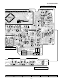
CD-C449W/K449W
SERVICE MANUAL
No.S8875CDC449W/
CD-C449W
CD-K449W
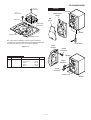
CD-C449W mini component system consisting of
CD-C449W mini component system and
CP-C449 speaker system.
CD-K449W mini component system consisting of
CD-K449W mini component system and
CP-C449 speaker system.
● SRS, the SRS Logo (●) and the Sound Retrieval System
are registered trademarks of SRS Labs, Inc. in the United
States.
• In the interests of user-safety the set should be restored to its
original condition and only parts identical to those specified be
used.
CONTENTS
Page
SAFETY PRECAUTION FOR SERVICE MANUAL ........................................................................................................... 2
SPECIFICATIONS ............................................................................................................................................................. 3
VOLTAGE SELECTION ...................................................................................................................................................... 3
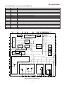
NAMES OF PARTS ........................................................................................................................................................... 4
OPERATION MANUAL ...................................................................................................................................................... 7
DISASSEMBLY .................................................................................................................................................................. 9
REMOVING AND REINSTALLING THE MAIN PARTS ................................................................................................... 12
ADJUSTMENT ................................................................................................................................................................. 13
NOTES ON SCHEMATIC DIAGRAM .............................................................................................................................. 17
TYPES OF TRANSISTOR AND LED ................................................................................................................................ 17
WAVEFORMS OF CD CIRCUIT ...................................................................................................................................... 18
BLOCK DIAGRAM ........................................................................................................................................................... 19
SCHEMATIC DIAGRAM / WIRING SIDE OF P.W.BOARD ............................................................................................. 22
TROUBLESHOOTING ..................................................................................................................................................... 46
FUNCTION TABLE OF IC ................................................................................................................................................ 50
FL DISPLAY ..................................................................................................................................................................... 57
REPLACEMENT PARTS LIST/EXPLODED VIEW
SECTION
CD-C449W
CD-K449W
KARAOKE CIRCUIT
SHARP CORPORATION
–1–
This document has been published to be used
for after sales service only.
The contents are subject to change without notice.
CD-C449W/K449W
SAFETY PRECAUTION FOR SERVICE MANUAL
WARNINGS
THE AEL (ACCESSIBLE EMISSION LEVEL) OF THE LASER POWER OUTPUT IS LESS THAN CLASS 1 BUT THE LASER
COMPONENT IS CAPABLE OF EMITTING RADIATION EXCEEDING THE LIMIT FOR CLASS 1. THEREFORE IT IS
IMPORTANT THAT THE FOLLOWING PRECAUTIONS ARE OBSERVED DURING SERVICING TO PROTECT YOUR EYES
AGAINST EXPOSURE TO THE LASER BEAM.
1-WHEN THE CABINET IS REMOVED, THE POWER IS TURNED ON WITDOUT A COMPACT DISC IN POSITION AND THE
PICK-UP IS ON THE OUTER EDGE THE LASER WILL LIGHT FOR SEVERAL SECONDS TO DETECT A DISC. DO NOT
LOOK INTO THE PICK-UP LENS.
2-THE LASER POWER OUTPUT OF THE PICK-UP UNIT AND REPLACEMENT SERVICE PARTS ARE ALL FACTORY
PRE-SET BEFORE SHIPMENT.
DO NOT ATTEMPT TO RE-ADJUST THE LASER PICK-UP UNIT DURING REPLACEMENT OR SERVICING.
3-UNDER NO CIRCUMSTANCES STARE INTO THE PICK-UP LENS AT ANY TIME.
4-CAUTION-USE OF CONTROLS OR ADJUSTMENTS, OR PERFORMANCE OF PROCEDURES OTHER THAN THOSE
SPECIFIED HEREIN MAY RESULT IN HAZARDOUS RADIATION EXPOSURE.
CAUTION
Laser Diode Properties
Material: GaAIAs
Wavelength: 780 nm
Emission Duration: continuous
Laser Output: max. 0.6 mW
● This Mini Component System is classified as a CLASS
1 LASER product.
● The CLASS 1 LASER PRODUCT label is located on the
rear cover.
● Use of controls, adjustments or performance of procedures other than those specified herein may result in
hazardous radiation exposure.
As the laser beam used in this compact disc player is
harmful to the eyes, do not attempt to disassemble the
cabinet. Refer servicing to qualified personnel only.
CAUTION-INVISIBLE LASER RADIATION WHEN OPEN. DO NOT STARE INTO
BEAM OR VIEW DIRECTLY WITH OPTICAL INSTRUMENTS.
VARNING-OSYNLIG LASERSTRALNING NAR DENNA DEL AR OPPNAD. STIRRA
EJ IN I STRALEN OCH BETRAKTA EJ STRALEN MED OPTISKA INSTRUMENT.
ADVERSEL-USYNLIG LASERSTRALING VED ABNING. SE IKKE IND I
STRALEN-HELLER IKKE MED OPTISKE INSTRUMENTER.
VARO! AVATTAESSA OLET ALTTIINA NAKYMATON LASERSATEILYLLE.
ALA TUIJOTA SATEESEEN ALAKA KATSO SITA OPTISEN LAITTEEN LAPI.
VARNING-OSYNLIG LASERSTRALNING NAR DENNA DEL AR OPPNAD.
STIRRA EJ IN I STRALEN OCH BETRAKTA EJ STRALEN GENOM OPTISKT
INSTRUMENT.
ADVERSEL-USYNLIG LASERSTRALING NAR DEKSEL APNES. STIRR IKKE
INN I STRALEN ELLER SE DIREKTE MED OPTISKE INSTRUMENTER.
VARO !
VARNING!
Avattaessa ja suojalukitus ohitettaessa olet alttiina näkymättömälle lasersäteilylle. Älä katso säteeseen.
Osynlig laserstralning när denna del är öppnad och spärren är urkopplad. Betrakta ej strälen.
–2–
CD-C449W/K449W
SPECIFICATIONS
CD-C449W/K449W
● General
Power source:
Power consumption:
Dimensions:
Weight:
● Cassette deck section
Frequency response:
Signal/noise ratio:
AC 110/127/220/230-240 V,
50/60 Hz
120 W
Width; 270 mm (10-5/8")
Height; 316 mm (12-1/2")
Depth; 343 mm (13-1/2")
9.2 kg (20.3 lbs.)
Wow and flutter:
50-14,000 Hz (Normal tape)
55 dB (TAPE 1, playback)
50 dB (TAPE 2, recording/
playback)
0.15 % (WRMS)
● Compact disc player section
Type:
● Amplifier section
Output power:
Output terminals:
Input terminals:
PMPO; 1200 W
MPO; 240 W (120 W + 120 W)
(10 % T.H.D.)
RMS; 150 W (75 W + 75 W)
(10 % T.H.D.)
Speakers; 8 ohms
Headphones; 16-50 ohms
(recommended; 32 ohms)
CD digital output (optical)
Video/Auxiliary (audio signal)
1/2; 500 mV/47 kohms
Microphone 1/2; 1 mV/4.7 kohms
(CD-K449W only)
● Tuner section
Frequency range:
FM; 88 - 108 MHz
SW2; 9.5 - 21.85 MHz
SW1; 3.2 - 7.3 MHz
MW; 531 - 1,602 kHz
Signal readout:
D/A converter:
Frequency response:
Dynamic range:
3-disc multi-play compact disc
player
Non-contact, 3-beam semiconductor laser pickup
1-bit D/A converter
20 - 20,000 Hz
90 dB (1 kHz)
CP-C449
● Speaker section
Type:
Maximum input
power:
Impedance:
Dimensions:
Weight:
3-way type [130 mm (5-1/8")
woofer, 50 mm (2") tweeter and
super tweeter]
150 W
8 ohms
Width; 220 mm (8-11/16")
Height; 316 mm (12-1/2")
Depth; 284 mm (11-3/16")
3.6 kg (7.9 lbs.)/each
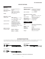
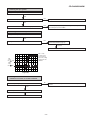
VOLTAGE SELECTION
The voltage selector is located on the AC voltage selector box. If adjustment is necessary, use a screwdriver in order to turn the
selector in either direction until the correct voltage figure is displayed in the window next to the adjustment screw.
AQCCJ0003AW00
QACCA0001AW00
QACCE0008AW00
Figure 2 AC POWER SUPPLY CORD AND AC PLUG ADAPTOR
–3–
CD-C449W/K449W
SPECIFICATIONS
CD-C449W/K449W
● General
Power source:
Power consumption:
Dimensions:
Weight:
● Cassette deck section
Frequency response:
Signal/noise ratio:
AC 110/127/220/230-240 V,
50/60 Hz
120 W
Width; 270 mm (10-5/8")
Height; 316 mm (12-1/2")
Depth; 343 mm (13-1/2")
9.2 kg (20.3 lbs.)
Wow and flutter:
50-14,000 Hz (Normal tape)
55 dB (TAPE 1, playback)
50 dB (TAPE 2, recording/
playback)
0.15 % (WRMS)
● Compact disc player section
Type:
● Amplifier section
Output power:
Output terminals:
Input terminals:
PMPO; 1200 W
MPO; 240 W (120 W + 120 W)
(10 % T.H.D.)
RMS; 150 W (75 W + 75 W)
(10 % T.H.D.)
Speakers; 8 ohms
Headphones; 16-50 ohms
(recommended; 32 ohms)
CD digital output (optical)
Video/Auxiliary (audio signal)
1/2; 500 mV/47 kohms
Microphone 1/2; 1 mV/4.7 kohms
(CD-K449W only)
● Tuner section
Frequency range:
FM; 88 - 108 MHz
SW2; 9.5 - 21.85 MHz
SW1; 3.2 - 7.3 MHz
MW; 531 - 1,602 kHz
Signal readout:
D/A converter:
Frequency response:
Dynamic range:
3-disc multi-play compact disc
player
Non-contact, 3-beam semiconductor laser pickup
1-bit D/A converter
20 - 20,000 Hz
90 dB (1 kHz)
CP-C449
● Speaker section
Type:
Maximum input
power:
Impedance:
Dimensions:
Weight:
3-way type [130 mm (5-1/8")
woofer, 50 mm (2") tweeter and
super tweeter]
150 W
8 ohms
Width; 220 mm (8-11/16")
Height; 316 mm (12-1/2")
Depth; 284 mm (11-3/16")
3.6 kg (7.9 lbs.)/each
VOLTAGE SELECTION
The voltage selector is located on the AC voltage selector box. If adjustment is necessary, use a screwdriver in order to turn the
selector in either direction until the correct voltage figure is displayed in the window next to the adjustment screw.
AQCCJ0003AW00
QACCA0001AW00
QACCE0008AW00
Figure 2 AC POWER SUPPLY CORD AND AC PLUG ADAPTOR
–3–
CD-C449W/K449W
CD-C449W/K449W
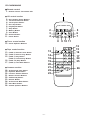
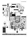
NAMES OF PARTS
■ Front panel
11.
12.
13.
14.
(CD)
(CD)
(CD)
(CD)
15.
16.
17.
18.
19.
10.
11.
12.
13.
14.
15.
16.
17.
18.
19.
20.
21.
22.
(CD) Disc Number Indicators
SRS Indicator
(TAPE 2) Direction Indicators
(TAPE 2) Reverse Mode Indicator
(CD) Play Indicator
(CD) Repeat Play Indicator
(CD) Pause Indicator
(TAPE 2) Record Indicator
Timer Record Indicator
Timer Play Indicator
Sleep Indicator
Extra Bass Indicator
(CD) Random Play Indicator
(CD/TUNER) Memory Indicator
(TUNER) FM Stereo Indicator
(TUNER) FM Stereo Mode Indicator
Karaoke Indicator (CD-K449W Only)
Spectrum Analyzer
23.
24.
25.
26.
27.
28.
29.
30.
31.
32.
33.
Function Selector Buttons
Equalizer Mode Selector Buttons
Extra Bass Button
Volume Control
On/Stand-by Button
Headphone Socket
Karaoke Maker Switch (CD-K449W Only)
Microphone Sockets (CD-K449W Only)
Microphone Level Controls (CD-K449W Only)
Digital Echo Control (CD-K449W Only)
3D Surround/Demo Mode Button
34.
35.
36.
37.
38.
39.
40.
41.
42.
43.
44.
45.
3
3
46.
47.
3
3
48.
3
3
49.
Clock Button
Sleep Button
(TAPE 2) Reverse Mode Button
(CD) Pause Button
Jog Dial
(CD/TAPE) Stop Button
(TAPE) Record Pause Button
Balance Control Buttons
Timer Button
Memory Button
(CD) Clear Button
(CD) Track Down/Review Button
(TAPE 2) Fast Wind Button
(TUNER) Tuning Down Button
(TAPE 2) Reverse Play Button
(CD) Play/Repeat Button
(TAPE 1) Play Button
(TAPE 2) Forward Play Button
(CD) Track Up/Cue Button
(TAPE 2) Fast Wind Button
(TUNER) Tuning Up Button
Editing Speed Selector Buttons
2
1
Disc Tray
Disc Number Select Buttons
Disc Skip Button
Open/Close Button
5
3
4
6 7 8
9 10 11 12
13 1415
16
17
18
19 20 21 22
23
24
27 28 29
25 26
30
31
32
34 35 36 37 38 39 40 41
42 43 44 45 46 47 48 49
–4–
33
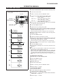
CD-C449W/K449W
11.
12.
1
(TAPE 1) Cassette Compartment
(TAPE 2) Cassette Compartment
1
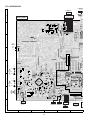
■ Rear panel
11.
12.
13.
14.
15.
16.
17.
18.
19.
2
2
3
CD Digital Output Socket
Video/Auxiliary (Audio Signal) Input Sockets
Span Selector Switch
FM 75 Ohms Aerial Terminal
Aerial Earth Terminal
SW1/SW2/MW Aerial Terminal
AC Voltage Selector
AC Power Lead
Speaker Terminals
4
5
6
7
8
9
CP-C449
■ Speaker section
1
11.
12.
13.
14.
15.
2
3
Super Tweeter
Tweeter
Woofer
Bass Reflex Ducts
Speaker Terminals
4
–5–
5
CD-C449W/K449W
■ Remote control
11.
Remote Control Transmitter LED
1
● CD control section
12.
13.
14.
15.
16.
17.
18.
19.
10.
11.
Disc Number Select Buttons
Track Down/Review Button
Track Up/Cue Button
Disc Skip Button
Play/Repeat Button
Stop Button
Memory Button
Clear Button
Random Button
Pause Button
2
3
4
8 9 10 11
● Tuner control section
12.
Preset Up/Down Buttons
● Tape control section
13.
14.
15.
3
16.
17.
(TAPE
(TAPE
(TAPE
(TAPE
(TAPE
(TAPE
13
14
18
19
20
21
22
23
2) Record Pause Button
2) Reverse Play Button
1) Play Button
2) Forward Play Button
1/2) Stop Button
2) Fast Wind Buttons
● Common section
18.
19.
20.
21.
22.
23.
24.
25.
26.
5
6
7
3D Surround Pass Button
Equalizer Mode Button
Function Selector Buttons
Balance Control Buttons
On/Stand-by Button
Dimmer Button
3D Surround Mode Button
Extra Bass Button
Volume Up/Down Buttons
–6–
12
15
16
17
24
25
26
CD-C449W/K449W
OPERATION MANUAL
SETTING THE CLOCK
In this example, the clock is set for the 24-hour
(0:00) system.
Jog dial
1
2
3
4
Press the ON/STAND-BY button to enter the stand-by mode.
Press the CLOCK button.
Within 5 seconds, press the MEMORY button.
Turn the jog dial to select the time display mode.
"0:00"
→ The 24-hour display will appear.
(0:00 - 23:59)
"AM 12:00" → The 12-hour display will appear.
(AM or PM 12:00 - 11:59)
"AM 0:00" → The 12-hour display will appear.
(AM or PM 0:00 - 11:59)
● Note that this can only be set when the unit is first installed
or it has been reset (see page 28).
CLOCK
ON/STAND-BY
MEMORY
TUNING
(
)
5
6
Press the MEMORY button.
Adjust the hour by turning the jog dial.
● When the jog dial is turned
increase by 1 hour. When it
the time will decrease by 1
Keep turning the jog dial to
2
one click clockwise, the time will
is turned one click anti-clockwise,
hour.
change the time continuously.
● When the 12-hour display is selected, "AM" will change automatically to "PM".
3
7
8
4
● When the jog dial is turned one click clockwise, the time will
increase by 1 minute. When it is turned one click anti-clockwise, the time will decrease by 1 minute.
Keep turning the jog dial to change the time continuously.
● The hour setting will not advance even if minutes advance
from "59" to "00".
0:00
AM 12:00
AM 0:00
9
5
6
7
8
Press the MEMORY button.
Adjust the minutes by turning the jog dial.
Press the MEMORY button.
● The clock starts operating from "0" seconds. (Seconds are not
displayed.)
Note:
● In the event of a power failure or when the AC power lead is
disconnected, the clock display will go out.
When the AC power supply is restored, the clock display will
flash on and off to indicate the time when the power failure
occurred or when the AC power lead was disconnected.
If this happens, follow the procedure below to change the clock
time.
To change the clock time:
When the unit is in the stand-by mode:
① Press the MEMORY button.
② Perform steps 6 - 9 above.
When the unit is on:
9
① Press the CLOCK button.
② Within 5 seconds, press the MEMORY button.
③ Perform steps 6 - 9 above.
To see the time display:
Press the CLOCK button.
● The time display will appear for about 5 seconds.
To change the time display mode:
① Perform steps 1 - 2 in the section "RESETTING THE MICROCOMPUTER", on page 28.
② Perform steps 1 - 9 above.
–7–
–8–
ON/STAND-BY
FLAT
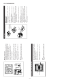
RESETTING THE MICROCOMPUTER
50/9 100/10
FM/MW
(kHz)
SPAN
SELECTOR
Press the ON/STAND-BY button whilst holding down the
button and the FLAT button.
Set the SPAN SELECTOR switch to "50/9" for 9 kHz MW
interval (50 kHz FM interval), and "100/10" for 10 kHz MW
interval (100 kHz FM interval).
Press the ON/STAND-BY button to enter the stand-by mode.
Press the ON/STAND-BY button whilst holding down the
button and the FLAT button.
Press the ON/STAND-BY button to enter the stand-by mode.
Caution:
● The operation explained above will erase all data stored in
memory including clock and timer settings, and tuner and CD
presets.
1
2
Reset the microcomputer under the following conditions:
● To erase all of the stored memory contents (clock and timer
settings, and tuner and CD presets).
● If the display is not correct.
● If the operation is not correct.
Caution:
● The operation explained above will erase all data stored in
memory including clock and timer settings, and tuner and CD
presets.
3
1
2
To change the tuning zone:
Before using the unit, set the SPAN SELECTOR switch (on the
rear panel) to MW tuning interval (span) of your area.
The International Telecommunication Union (ITU) has established that member countries should maintain either a 10 kHz or
a 9 kHz interval between broadcasting frequencies of any MW
station. The illustration shows the 9 kHz interval zones (regions
1 and 3), and the 10 kHz interval zone (region 2).
■ FM/MW interval (span)
(Continued)
+
-
15
0.2 m - 6 m
(8" - 20')
+
15
● 2 "AA" size batteries (UM/SUM3, R6, HP-7 or
similar)
● Keep the remote control away from moisture, excessive heat,
shock, and vibrations.
● Periodically clean the transmitter LED on the remote control
and the sensor on the main unit with a soft cloth.
● Exposing the sensor on the main unit to strong light may interfere with operation. Change the lighting or the direction of
the unit.
Notes concerning use:
● Replace the batteries if the operating distance is reduced or if
the operation becomes erratic.
Caution:
Do not use rechargeable batteries (nickel-cadmium battery, etc.).
● Insert the batteries according to the direction indicated in the
battery compartment.
● Replace all old batteries with new ones at the same time.
● Do not mix old and new batteries.
● Remove the batteries if they are weak or if the unit will not be
used for long periods of time. This will prevent potential damage due to battery leakage.
Precautions for battery use:
● When inserting or removing the batteries, push them towards
the
battery terminal.
● Installing the batteries incorrectly may cause the unit to malfunction.
■ Remote control
CD-C449W/K449W
CD-C449W/K449W
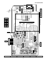
DISASSEMBLY
Caution on Disassembly
Follow the below-mentioned notes when disassembling
the unit and reassembling it, to keep it safe and ensure
excellent performance:
1. Take cassette tape and compact disc out of the unit.
2. Be sure to remove the power supply plug from the wall
outlet before starting to disassemble the unit.
3. Take off nylon bands or wire holders where they need to
be removed when disassembling the unit. After servicing
the unit, be sure to rearrange the leads where they were
before disassembling.
4. Take suffcient care on static electricity of integrated
circuits and other circuits when servicing.
CD-C477W/K449W
( A1 ) x2
ø3 x12mm
Top Cabinet
( A1 ) x2
ø3 x12mm
( B1 ) x2
ø3 x8mm
Side Panel
(Left)
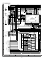
CD-C449W/K449W
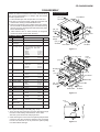
STEP
REMOVAL
PROCEDURE
FIGURE
1
Top Cabinet
1. Screw ..................... (A1) x4
9-1
2
Side Panel
(Left/right)
1. Screw ..................... (B1) x8
9-1
CD Player Unit/
CD Tray Cover
1. Turn on the power supply,
open the disc tray, take out
the CD cover, and close.
(Note 1)
2. Hook ....................... (C1) x3
3. Hook ....................... (C2) x2
4. Screw ..................... (C3) x1
5. Socket .................... (C4) x3
9-2
1. Socket .................... (D1) x1
2. Screw ..................... (D2) x5
10-1
3
4
Tuner PWB
( B1 ) x4
ø3 x8mm
( B1 ) x2
ø3 x8mm
Rear Panel
Figure 9-1
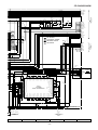
5
Rear Panel
1. Screw ..................... (E1) x11
...................................
9-2
10-1
6
Main PWB
1. Flat cable ............... (F1) x2
2. Flat wire ................. (F2) x3
3. Socket ...................... (F3) x3
4. Screw ....................... (F4) x3
10-1
7
Side Panel
(Right)
(C2) x1
( C4 ) x2
Pull
CD Tray Cover
Hook
( C1) x3
1
1
CD Player
Unit
Karaoke PWB
1. Screw ..................... (G1) x2
(CD-K449W only)
10-2
8
Front Panel
10-2
9
Power Amp. PWB 1. Socket .................... (J1) x2
2. Screw ..................... (J2) x6
10-2
Front Panel
10
Power Supply PWB 1. Screw ..................... (K1) x6
10-3
Main PWB
11
Display PWB
1. Knob ....................... (L1) x2
2. Nut .......................... (L2) x1
3. Screw ..................... (L3)x12
10-4
12
CD Switch PWB 1. Screw ..................... (M1) x3
10-4
13
Headphones PWB 1. Screw ..................... (N1) x1
10-4
14
Tape Mechanism 1. Screw ..................... (P1) x6
10-4
15
Turntable
1. Screw ..................... (Q1) x1
2. Cover ..................... (Q2) x1
10-5
16
Disc Tlay
1. Screw ..................... (R1) x2
2. Guide ..................... (R2) x2
10-5
17
CD Servo PWB
(Note2)
1. Screw ..................... (S1) x1
2. Socket .................... (S2) x4
10-6
18
CD Changer
Mechanism
1. Screw ..................... (T1) x4
11-1
19
CD Mechanism
1. Screw ..................... (U1) x1
11-1
1. Flat wire ................. (H1) x1
2. Screw...................... (H2) x2
2
( C2 ) x1
( C4 ) x1
Tuner PWB
( E1 ) x10
ø3 x8mm
Rear Panel
Figure 9-2
LOCK
LEVER
Note 1:
How to open the changer manually. (Fig. 10-3)
1. Then, turn fully the lock lever in the arrow direction through
the hole on the loading chassis bottom in this state.
After that, push forward the CD player base.
2. After removing the connector for the optical pickup fromthe
connector wrap the conductive aluminium foil around the
front end of connector so as to protect the optical pickup
from electrostatic damage.
Figure 9-3
–9–
( C3 ) x1
ø3 x8mm
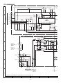
CD-C449W/K449W
(L1)x2
CD Switch PWB
(E1) x1
ø3 x10mm
(F2) x1
(F3) x2
CD-K449W
Only
Front Panel
(F4) x2
ø3x10mm
Front Panel
(L2)x1
(M1)x3
ø3x10mm
(F3) x2
(F2) x2
(F1) x1
Display
PWB
(L3)x12
ø3x10mm
(F4) x1
ø3x10mm
Rear
Panel
Washer
Headphones
PWB
(D1) x1
Open
Main PWB
(D2) x1
ø3x10mm
Tuner PWB
(D2) x4
ø3 x10mm
(N1)x1
ø3x10mm
Tape Mechanism
(P1)x6
ø3x10mm
Figure 10-1
Cassette
Lug Wire Holder (Left/Right)
Figure 10-4
( Q1 ) x1
ø3 x10mm
(G1)x2
ø3x10mm
( Q2 ) x1
Front Panel
CD-K449W
Only
Karaoke
PWB
(G1)x1
ø3x10mm
Turntable
( J1 ) x2
( H1 ) x1
(J2)x5
ø3x10mm
Disc Tray
( R1 ) x1
ø3 x10mm
( R2 ) x1
( J2 ) x1
( H2 ) x1
ø3x10mm
ø3x10mm
Power Amp. PWB
( R1 ) x1
ø3 x10mm
Figure 10-2
CD Player Unit
(K1)x4
ø4x8mm
( R2 ) x1
Figure 10-5
(K1)x1
ø3x10mm
( S1 ) x1
ø3 x10mm
Power Supply PWB
CD Servo PWB
( S2 ) x2
(K1)x1
ø3x8mm
( S2 ) x2
CD Player Unit
Figure 10-3
Figure 10-6
– 10 –
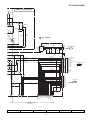
CD-C449W/K449W
( U1 ) x4
ø3 x12mm
CP-C449
Tweeter
( V1 ) x1
ø2.6 x10mm
Baffle Board
(A2)x1
Net
(A1)x1
Shift Lever
CD Changer
Mechanism
Woofer
CD Player Base
CD Mechanism
Be careful when installing the CD changer mechanism.
Install the CD changer mechanism on the CD player base after
the shift lever has been set in the highest position.
Screw driver
Super
Tweeter
Figure 11-1
(A5)x2
ø3x10mm
Tweeter
CP-C449
STEP
1
REMOVAL
PROCEDURE
Front Speaker
1. Net ..........................
2. Front Panel ............
3. Screw .....................
4. Screw .....................
5. Screw .....................
FIGURE
(A1) x1
(A2) x1
(A3) x2
(A4) x4
(A5) x2
11-2
(A3)x2
ø3x10mm
(A4)x4
ø4x16mm
Figure 11-2
– 11 –
Woofer
CD-C449W/K449W
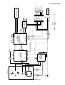
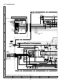
REMOVING AND REINSTALLING THE MAIN PARTS
CD MECHANISM SECTION
Perform steps 1, 2, 3,15,16,17 and 19 of the disassembly
method to remove the CD mechanism.
Loading / Up
/ Down Motor
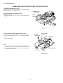
How to remove the loading motor
(See Fig. 12-1)
Motor
PWB
1. Remove the screws (A1) x 2 pcs., to remove the loading
motor.
( A1 ) x2
ø2.6 x5mm
Figure 12-1
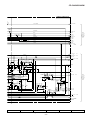
How to remove the pickup (See Fig. 12-2)
Stop Washer
( B1 ) x2
( B3 ) x1
ø2.6 x6mm
1. Remove the screws (B1) x 2 pcs., to remove the shaft (B2).
2. Remove the stop washer (B3) x 1 pc., to remove the gear
(B4).
3. Remove the pickup.
Pickup
Note
After removing the connector for the optical pickup fromthe
connector wrap the conductive aluminium foil around the
front end of connector so as to protect the optical pickup
from electrostatic damage.
Shaft
( B2 ) x1
CD Mechanism
Gear
( B4 ) x1
Figure 12-2
– 12 –
CD-C449W/K449W
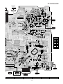
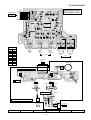
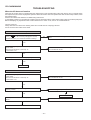
ADJUSTMENT
MECHANISM SECTION
TUNER SECTION
• Driving Force Check
fL: Low-range frequency
fH: High-renge frequency
• AM IF/RF
Signal generator: 400 Hz, 30%, AM modulated
Torque Meter
Specified Value
Play: TW-2412
Tape 1: Over 80 g
Tape 2: Over 80 g
Test Stage Frequency
• Torque Check
Torque Meter
Specified Value
Tape 1
450 kHz
1,602 kHz
MW Band
Coverage
—
531 kHz
(fL): T306
1.1 ± 0.1 V
*2
SW1 Band —
Coverage
3.2 MHz
(fL): T307
2.0 ± 0.1V
*2
SW1 Band —
Coverage
7.3 MHz
(fH): TC305
7.7 ± 0.2 V
*2
Instrument
Connection
SW2 Band —
Coverage
9.5 MHz
(fL): T308
2.1 ± 0.1V
*2
Speaker
terminal
(Load
resistance:
8 ohms)
SW2 Band —
Coverage
21.85 MHz
(fH): TC304
7.7 ± 0.2V
*2
MW
Tracking
990 kHz
990 kHz
T302
*1
SW1
Tracking
3.9 MHz
3.9 MHz
(fL): T303
*1
SW1
Tracking
7.1 MHz
7.1 MHz
(fH): TC303
*1
SW2
Tracking
11.65 MHz
11.65 MHz
(fL): T304
*1
SW2
Tracking
21.45 MHz
21.45 MHz
(fH): TC302
*1
Play: TW-2111
30 to 60 g. cm
30 to 100 g.cm
Fast forward: TW-2231
—
50 to 100 g.cm
Rewind: TW-2231
—
50 to 100 g.cm
• Tape Speed
Normal
speed
Adjusting
Point
Specified
Value
MTT-111
VRM01
3,000 ±
30 Hz
*1. Input: Antenna,
*2. Input: Anetnna,
TAPE MECHANISM PWB
VRM01
FAS
SW
Setting/
Instrument
Adjusting Connection
Parts
T351
*1
IF
Tape 2
Test Tape
Frequency
Display
TAPE
SPEED
Figure 13
– 13 –
Output: TP302
Output: TP301
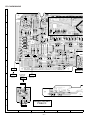
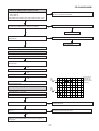
CD-C449W/K449W
• FM RF
Signal generator: 1 kHz, 40 kHz dev, FM modulated
Test Stage Frequency Frequency
Display
Setting/
Adjusting
Parts
Band
Coverage
—
87.5 kHz
(fL): LT02
3.7 ± 0.1 V
*1
RF
98 MHz
10 - 30 dB
98 MHz
LT01
*2
*1. Input: Antenna,
*2. Input: Anetnna,
• FM Detection
Signal generator: 10.7 MHz, FM sweep
Instrument
Connection
Test Stage Frequency Frequency
Display
IF
10.7 MHz
98 MHz
Output: TP301
Output: Speaker Terminal
*1. Input: Antenna,
*2. Input: Anetnna,
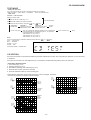
• Setting the Test Mode
Keeping the PAUSE button and TUNER button pressed, turn
on POWER. Then, the frequency is initially set in the memory
as shown in Table. Call it with the PRESET button to use it for
adjustment and check of tuner circuit.
Preset
No.
FM
Preset
No.
MW
Preset
No.
SW1
Preset
No.
SW2
1
2
3
4
5
87.50 MHz
108.00 MHz
90.00 MHz
106.00 MHz
98.00 MHz
6
7
8
9
10
531 kHz
1,602 kHz
603 kHz
1,404 kHz
990 kHz
11
12
13
14
15
3.2 MHz
7.3 MHz
3.9 MHz
7.1 MHz
5.06 MHz
16
17
18
19
20
9.5 MHz
21.85MHz
11.65 MHz
21.45 MHz
15.1 MHz
Setting/
Adjusting
Parts
Instrument
Connection
TT01
*1
(Turn the
core of transformer TT01
fully counterclock wise)
Output: TP301
Output: Speaker Terminal
• FM Mute Level
Signal generator: 1kHz, 40 kHz dev., FM modulated
Frequency
Frequency
Display
98.00 MHz
(25 dBµV)
98.00 MHz
Adjusting
Parts
VR351 *1
Instrument
Connection
Input: Antenna
Output: Speaker
Terminal
*1. Adjust so that an output signal appears.
21 ~ 40
TUNER PWB
SW1 Band
Coverage
fL
fH
T351
FM Band
Coverage
FM IF
LT02
TT01
TP301
VR351
T307 TC305
AM IF
FM Mute
Level
T308 TC304
FM RF
LT01
SW2 Tracking
fH
fL
TC302 T304
TC303 T303
IC303
T306
TP302
R357
fL
fH
SW2
Coverage
MW Band
Coverage
T302
MW
Tracking
Figure 14 ADJUSTMENT POINTS
– 14 –
fH
fL
SW1
Tracking
SO301
ANTENNA
TERMINAL
CD-C449W/K449W
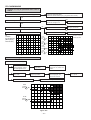
TEST MODE
• Setting the test mode
Any one of test mode can be set by pressing several keys as follows.
<REC. PAUSE> + <DISC. SKIP> + <POWER>
TEST: CD operation test
• TEST mode
Function — CD test mode
Setting of TEST mode
Indication of CD TST mode (Fig. 15-1)
IL is not performed.
OPEN/CLOSE operation is manual operation.
The pickup can be moved by using the (
<MEMORY>
LASER ON
<MEMORY>
Tracking on the spot.
SERVO OFF PLAY
<PLAY> key input
) or (
) key.
<MEMORY>
Tracking on the spot.
SERVO ON PLAY
<STOP>
STOP
TOC. IL is performed, and the ordinary PLAY is performed.
If the following key is pressed during PLAY, it is possible
to specify directly any Track No.
<Disc Number 1> key: Track 4
<Disc Number 2> key: Track 9
<Disc Number 3> key: Track 15
Note:
Only in STOP state it is possible to slide the pickup with the (
VOL. --- Last memory
BAL. --- CENTER
R.GEQ. --- FLAT
X-BAS --- OFF
) or (
Press <STOP> key.
Stop
) key.
Canceling method - POWER OFF
Figure 15-1
CD SECTION
Since this CD system incorporates the following automatic adjustment function, when the pickup is replaced, it is not necessary
to readjust it.
Since this CD unit does not need adjustment, the combination of PWB and laser pickup unit is not restricted.
• Automatic adjustment item
1. Focus offset (Fig. 15-2)
2. Tracking offset (Fig. 15-3)
3. E/F balance (tracking error balance) (Fig. 15-4)
4. RF level AGC function (HF level: constant)
5. RF level automatic follow-up of the tracking gain
This automatic adjustment is performed each time a disc is changed. Therefore,
each disc is played back using the optimal settings.
Enlarged
View
10ms
0.50 V
IC1 20 FE
0.1s
0.50 V
IC1 20 FE
FOCUS
OFF-SET
ADJUST
10ms
0.50 V
IC1 7 TE
0.1s
0.50 V
IC1 7 TE
TRACKING
OFF-SET
1 ADJUST
TRACKING
OFF-SET
1 ADJUST
2
2
Figure 15-3
Figure 15-2
TRACKING/
ERROR
BARANCE
1 ADJUST
200 ms
1V/diV
IC 1 15
TO
200 ms
1V/diV
IC 1 7
TE
2
Figure 15-4
– 15 –
CD-C449W/K449W
(Continued)
■ SRS (●) 3D SURROUND
About SRS (●) 3D surround:
SRS
MODE
PASS
SRS is a breakthrough technology that creates 3-dimensional
sound by processing sound signals based on the human auditory
system. It produces real depth and localization of the sound
image which cannot be accomplished by ordinary stereo.
SRS only requires two speakers.
SRS (●) 3D surround effects:
Ordinary stereo sound
● Live performance atmosphere
(Simulates a live concert atmosphere)
● The localization of various musical sources is quite clear.
(The positions of the musical instruments and singers are very
clear.)
● Reproduction of depth
(Sounds from the front and back of an orchestra can be identified easily.)
● Expansion of the sound field
(The sound image is spread out over a wide area.)
Selecting the 3D surround mode:
When the sound source is in stereo, you can select from any of
5 different 3D surround effect.
Listening area
(Listening range with good stereo fidelity)
3D SURROUND
1
2
Select any desired audio source and begin playback.
To hear the 3D surround effect, press the SRS MODE button.
● "SRS (●)" will appear.
When the SRS MODE button is pressed, the current mode setting
will be displayed. To change to a different mode, press the SRS
MODE button repeatedly.
● "PASS" will not be displayed in remote control operation.
MODE-1
Wide listening area
(Stereo music can be heard anywhere in the room.)
SURROUND
MODE
MODE-1
MODE-2
MODE-2
MODE-3
MODE-4
MODE-5
PASS
Notes:
● The 3D SURROUND effect will not work on a monaural sound
source.
● When the 3D surround mode is being used, the equalizer will
be set to FLAT.
To cancel the 3D surround effect:
Effect from each mode
You will enjoy a sound image that produces an intimate sound field. (as in
a medium-size hall)
(Main unit operation)
Press the SRS MODE button repeatedly to select "PASS".
(Remote control operation)
Press the PASS button.
This setting gives you a maximum
sound field as music comes out beyond the speakers. (as in a large,
domed arena)
MODE-3
This setting is great for live recording
and vocal music.
MODE-4
You will hear more vocals in an intimate sound field. (as at a live music
performance)
MODE-5
This setting greatly increases the
amount of vocals or centre sounds in
a recording. (as in a small club)
– 16 –
CD-C449W/K449W
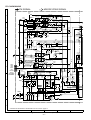
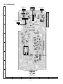
NOTES ON SCHEMATIC DIAGRAM
• Resistor:
To differentiate the units of resistors, such symbol as K and
M are used: the symbol K means 1000 ohm and the symbol
M means 1000 kohm and the resistor without any symbol is
ohm-type resistor. Besides, the one with “Fusible” is a fuse
type.
• Capacitor:
To indicate the unit of capacitor, a symbol P is used: this
symbol P means micro-micro-farad and the unit of the
capacitor without such a symbol is microfarad. As to
electrolytic capacitor, the expression “capacitance/withstand
voltage” is used.
(CH), (TH), (RH), (UJ): Temperature compensation
(ML): Mylar type
(P.P.): Polypropylene type
• Schematic diagram and Wiring Side of P.W.Board for this
model are subject to change for improvement without prior
notice.
REF. NO
SW1
DESCRIPTION
OPEN/CLOSE
• The indicated voltage in each section is the one measured
by Digital Multimeter between such a section and the chassis with no signal given.
1. In the tuner section,
( ) indicates AM
< > indicates FM stereo
2. In the main section, a tape is being played back.
3. In the deck section, a tape is being played back.
( ) indicates the record state.
4. In the power section, a tape is being played back.
5. In the CD section, the CD is stopped.
• Parts marked with “
”(
) are important for
maintaining the safety of the set. Be sure to replace these
parts with specified ones for maintaining the safety and
performance of the set.
POSITION
REF. NO
ON—OFF
SWD32
REVERSE MODE
DESCRIPTION
POSITION
ON—OFF
R-PLAY
ON—OFF
SW2
MECHA UP
ON—OFF
SWD33
SW3
DISC NUMBER
ON—OFF
SWD34
CLOCK
ON—OFF
SW4
PICKUP IN
ON—OFF
SWD35
MEMORY
ON—OFF
SW991
VOLTAGE SELECTOR
230-240V
SWD36
TIMER
ON—OFF
ON—OFF
SWD37
SLEEP
ON—OFF
SWD1
VOLUME JOG
SWD2
JOG
ON—OFF
SWD38
CLEAR
ON—OFF
SWD3
X-BASS
ON—OFF
SWD39
VIDEO/AUX 1
ON—OFF
SWD7
SOFT
ON—OFF
SWD40
VIDEO/AUX 2
ON—OFF
SWD8
VOCAL
ON—OFF
SWD41
TAPE 1/2
ON—OFF
SWD9
HAVY-2
ON—OFF
SWD42
TUNER/BAND
ON—OFF
SWD10
HAVY-1
ON—OFF
SWD43
CD
ON—OFF
SWD11
FLAT
ON—OFF
SWD48
POWER
ON—OFF
SWD12
TUNING UP/CUE
ON—OFF
SWD49
KARAOKE (CD-K449W Only)
ON—OFF
DISC 1
ON—OFF
SWD13
STOP
ON—OFF
SWD50
SWD14
NORMAL EDIT
ON—OFF
SWD51
DISC 2
ON—OFF
SWD15
HIGH EDIT
ON—OFF
SWD52
DISC 3
ON—OFF
SWD16
REC/PAUSE
ON—OFF
SWD53
DISC SKIP
ON—OFF
ON—OFF
SWD54
OPEN/CLOS
ON—OFF
SPAN SELECTOR
50/9
SWD17
F-PLAY
SWD18
SRS/DEMO
ON—OFF
SWF2
SWD21
BAL RIGHT
ON—OFF
SWM3
REC FWD
ON—OFF
SWD22
BAL LEFT
ON—OFF
SWM4
REC RVS
ON—OFF
SWD30
TUNING DOWN/REWIND
ON—OFF
SWM5
F.A.S
ON—OFF
ON—OFF
SWM6
CAM
ON—OFF
SWD31
CD PAUSE
FRONT VIEW
FRONT
VIEW
FRONT
VIEW
FRONT
VIEW
E C B
(S) (G) (D)
(1) (2) (3)
KTA1266 GR
KTA1270Y
KTA1271 Y
KTA1273 Y
KTA1268 GR
KTC3199 GR
KTC3203 Y
KRA107 M
KRA102 M
KRC102 M
KRC104 M
KRC107 M
2SC535 C
2SC1845 F
B C E
(D) (G) (S)
(3) (2) (1)
2SC2878 A
2SC2878 B
2SC2236 Y
2SD468 C
2SK246 GR
KTC3200 GR
2SD2012
2SB1375
Figure 17 TYPES OF TRANSISTOR AND LED
– 17 –
SLR325MG
SLR325VR
KL052UL
SLR505MC
LMKD515B
KV1236Z23
CD-C449W/K449W
WAVEFORMS OF CD CIRCUIT
STOP
FOCUS
1
2
PLAY
SERCH
5ms
0.50 V
IC1 20 F.E
5ms
5.0 V
IC1 54 DRF
0.5ms
10.0 V
JP+
7
0.5ms
10.0 V
JP-
8
0.5ms
0.50 V
JP
9
0.5ms
1.00 V
TE
3
1
3
6
PLAY
CUE
0.5ms
1.00 V
HF
NORMAL DISC
TN0=01
4
0.5ms
5.0 V
HFL
1
5
0.5ms
5.0 V
TES
3
3
0.5ms
1.00 V
HF
10
20ms
1.00 V
SPO
11
20ms
2.00 V
CLV+
2
REVIEW
PLAY
TCD-712 (140mm)
TN0=01
4
5
0.5ms
5.0 V
HFL
1
0.5ms
5.0 V
TES
3
6
50ms
10.0 V
JP+
7
50ms
10.0 V
JP-
8
50ms
0.50 V
JP
9
50ms
1.00 V
TE
6
0.5ms
10.0 V
JP+
7
0.5ms
10.0 V
JP-
8
0.5ms
0.50 V
JP
9
0.5ms
1.00 V
TE
6
50ms
10.0 V
JP+
7
50ms
10.0 V
JP-
8
50ms
0.50 V
JP
9
50ms
1.00 V
TE
2
10
50ms
1.00 V
SPO
11
50ms
2.00 V
CLV+
CUE
PLAY
TCD-712
12
5s
100mV
SLD
1
12
0.5s
100mV
SLD
REVIEW
1
– 18 –
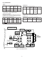
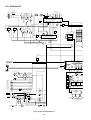
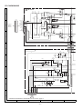
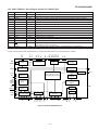
Figure 19 BLOCK DIAGRAM (1/3)
– 19 –
M
M
PICKUP IN
SW4
M1
DISC
MOTOR
M2
SLIDE
MOTOR
TRACKING COIL
24
25
30
31
12
13
6
7
22 32
8 9
10 11
IC3
M56748FP
DRIVER
5
26
27
28
29
34
35
36
20
30 31 54
IC1
LA9241M
SERVO AMP.
15 16 27 23 29
FIN2
FIN1
E
F
64
VCC1
TO
FD
SPO
NC
SLD
FOCUS COIL
1
2
3
4
LD0
62
Q1
SL–
SL+
DRF
JP– 32
Q52
CV+ 40
SLC 43
SL1 44
~
+5V
+B1
PU-IN SW
+B1
SL+. SL–. DRF
23 36 41 43
20 JP–
53 ~ 58
Q91
Q93
26
RES. CQCK. COIN
SQOUT. RWC. WRQ
10 EFMIN
12 CLV+
9
6
+5V
37
40
9
CONT2 25
+4.3V
+12V(+B5)
1
Q91
LCHO
RCHO
CONT1 24
CONT4 27
IC2
LC78622K DOUT 31
SERVO/SIGNAL
EFMO CONTROL
44
XOUT
45
XL1
XIN
CL, DAT, SELIAL CONTROL/CE
51 52 53
CL
DAT
CE
~
VVDD
VDD
LVDD
RVDD
XVDD
PICKUP UNIT
7
Q81
9
8
7
6
5
4
3
2
1
+B1
CNS10
9
8
7
6
5
4
3
2
1
10
+7.3V (+B9)
MECHA UP
GND (D)
DISK NO.
OPEN/CLOSE
GND (D)
M–
M+
GND (M)
10 GND (D)
5
6
CNP10
REGULATOR
3
IC81
TA7291S
LORDING MOTOR
DRIVER
8
SOLM1
M3
LOADING
TO MAIN
SECTION
M
SW1
OPEN/CLOSE
SW3
DISC No.
SW2
MECHA UP
TO MAIN SECTION
CD-C449W/K449W
ICT01
TA7358AP
FM FRONT END
1
6
FM IF
FM IF
TT01
CF302
8
1
LT02
LT01
+B7
CF352
FM IF IN
7
FM
OSC
3
5
FM
RF
SW1
SW2
MW
AM IF
AM IF
T351
9
AMP
2
OUT
5
8
IC303 IN GND
LA1832
FM IF DET./FM MPX./AM IF
VR351
FM MUTE LEVEL
QT01
4
3
REG
AM OSC
9 17
VCC
18
16
OUT
22
FMOSC
7
21
13
IN
SD
IF OUT
23
IN
OUT
24
STEREO
3
10
12
6
14 15
L
MONO/ST
2
GND
AM RF IN
1
FM
+B7
BFT01
X351
456KHz
FM BAND
PASS FILTER
AFC
SO301
ANTENNA
TERMINAL
FM IF
CF351
CD-C449W/K449W
R
MUTING
Q361
TUNER
Q353
Q354
TUNER SD
SW1/SW2
ANT.
SW1/SW2
OSC.
AM IN
VOLTAGE
REGURATER
+B7
Q308
Q309
Q306
Q307
X352
4.5MHz
+B7
1
FM +B
Q360
Q361
FM
20
+B7
15
16
11
10
12
IC302
LC72131
PLL CONTROLLER
9
3 4 5 6
13
Q362
SW1 +B
+B7
T1 RUN
T2 RUN
T2 A FP
T2 B FP
T1 CrO 2
T2 CrO 2
CAM-SW
TAPE SOL
TA MOT
HIGH SP
FR SP
BIAS
BEAT–CUT
TA R/P
ICH11(1/2)
+12V
+B7
8
17
7
6
8
-B6
4
21
1
CE
DI
CL
DO
MW +B
22
OSC
7
IF IN
T307
T308
FM MONO/ST
T303
T304
FM IN
T306
MW OSC.
AM IN
T302
MW ANT.
29
30
31
32
33
34
35
36
37
38
39
40
41
42
2
REC MUT
T1/T2
PB MUTE
+B7
44
45
46
Q363
SW2 +B
Q364
TA–PB–EQ
QG05
43
DO
7
CD MUTE
DI
QU02
QU01
14
CD
FROM CD UNIT
+B6
JR11
VCR/AUX1
L
L
TUNER
R
TAPE
+B2
JR12
VCR/AUX2
MOTOR
MM1
MOTOR
DRIVER
QL14
M
DRIVER
QL17
QL11
HI SPEED
51
61
52
60
IN
45 10
Vref
LVref
22
27
19
1 MIC
IN
TA MOT H/L
T2_RUN
QL16
31
T2_A_FP
SWM3
REC FWD
J602
MIC1
CAM SW
SWM6
CAM SW
T1/T2 CrO 2
SWM5
F.A.S.
L R
L R
+B7
VOLTAGE
REGULATOR
18
GND
IC601
M65845FP
MIC AMP.
MIC SW
MIC1
VOL IN
5
VR602
MIC2
VOLUME
T1/T2 PLAY
SWM4
REC RVS
47 12
44 9
41 6
38 3
VCC
6 MIC2 IN
+B6
46 11
43 8
40 5
37 2
Q631
J602
MIC2
HI SPEED
PHM1
MIC2
VOL IN
AUD
ECHO
VOL IN
10
25
VR601
MIC2
VOLUME
VR6
DIGITAL
VOLU
T2 F-REC
SWM1
T1 CrO2
T2 R-REC
SWM2
T2 CrO2
SOLENOID
PB MUTE
ICK01
AN7345K
PLAYBACK AND RECORD AMP
MUTING
DRIVER
PB HEAD
TAPE 1 L-CH
R-CH
REC/PB
HEAD
L-CH
R-CH
L(T1) 1
R(T1) 24
L(T2) 2
R(T2) 23
L NF 3
R NF 4
P.B
REC/PB
REC
P.B
QK03 QK05
QK04 QK06
AC BIAS
POP REDUCE 6
QK09 QK07
QK08
P.B.
12
T1/T2
H/N
REC MUTE
5
20
MUTING
L REC
R
L NF
R NF
10 ALC
7
18
8
17
HIGH T1/T2
15
QK10 QK11
P.B
L
R
4
21
L REC 9 REC
R REC 16
REF 14
13
+B7
NOR/
QK17
QK18
QK21
QK22
SWITCHING
QK19
19
T1/T2
REC/PB
ERASE
HEAD
QK28
LK04
SWITCHING
SWITCHING
BAIS
QK24
QK26
Figure 20 BLOCK DIAGRAM (2/3)
– 20 –
28
27
26
1
11 10
25 24
QS11
QS16
QS17
QS18
VOLTAGE
REGULATOR
+B7
QK15
QK16
SWITCHING
ICS01
SRS5250AS
SRS
R 17
L 18
BAIS
QL15
QL19
SOLM1
SOLENOID
TAPE 2
RVref 42 7
39 4
21
14
SWITCHING
QL13
QL12
GRAPHIC EQUALIZER
TA MOT SW
QL18
DRIVER
2
ICU01
LC75396N
AUDIO PROCESSOR
L 54
R 58
AUX1 L
R
AUX2 L
R
R
34
L 55
R 57
SWITCHING
R
L
PA
SW
CD-C449W/K449W
F2
1
2
3
VF1 (AC)
F1
62
63
64
VF2 (AC)
FD01 FL DISPLAY
+B6
5 ~ 43
RXD01
REMOTE
CONTROL
SENSOR
1
33
~ 45 47 ~ 50 51 ~ 71 73 ~ 75
29
ICD01
IX0243AW
FL DRIVER &
CONTROLLER
DATA1 95
COM1 96
SCK1 97
STB 1
VSS
15
89
KEY MATRIX
26
VDD
18
46
72
90
SWD01~SWD03
SWD07~SWD18
SWD21~SWD22
SWD30~SWD43
SWD48
SWD50~SWD54
SWD49(CD-K449W ONLY)
21
~
LEDD23~LEDD28
LEDD01~LEDD21
14
KEY IN
27
TUNER MUTE
+B2
9
7
10
9
8
7
29
5
30
3
31
4
32
11
33
100
34
2
35
1
36
14
13
37
38
41
42
REC MUT
T1/T2
PB MUTE
44
45
46
VSS
90
15
57
89
12
16
17
27
91
92
TO CD UNIT
SQ OUT
WRQ
RWC
CD SL+
CD SLCD-PUIN
CD-DRF
+B3
+B4 (5V BACK UP)
VDD 56
93
TA–PB–EQ
RES
CQCK
COIN
18
ICF01
IX0235AW
SYSTEM CONTROL
MICROCOMPUTER
39
40
SWD02 JOG DIAL
DAT
SCK
STB
DS RES
COM
6
STB
SCK
8
SWD01
JOG DIAL
99
T1 RUN
T2 RUN
T2 A FP
T2 B FP
T1 CrO 2
T2 CrO 2
CAM-SW
TAPE SOL
TA MOT
HIGH SP
FR SP
BIAS
BEAT–CUT
TA R/P
+B4
RESET
RESET IN QG01
OSC
XF0201
4.19MHz
SYSTEM STOP
CD O/C
CD U/D
CD DNO
+5V
UNSWITCH
+B2
MEMORY
QG02
QG03
ZDF01
+B3
P.FAIL DET
43
64 63 65 62 82 24
FAN
PROT
S-MUTE
POWER
AMP
FAN CONT
FRNT RLY
45 27 75 79 47 49 50
H/P SW
POSISTOR
VOICE CAN
MIC_DET
DO
DI
CL
CE
CD MUTE
61 81
SRS A
SRS B
SRS IN H
SRS PASS
72 71 69 68 87
+B6
FAN MOTOR
CONTROL
QV20
QN21
23 25
ICP11
NJM4565M
BUFFER AMP.
ICU01
LC75396N
UDIO PROCESSOR
GRAPHIC EQUALIZER
VOLUME
OUT
31 L
17 R
L 5
R 3
8
OUT
7 L
1 R
L-IN
QP11
QP12
R-IN
L R
L R
55
GND
SW
MIC1
VOL IN
MIC2
VOL IN
CD-K449W
ONLY
26
IN 27
AUD SW
ECHO
VOL IN
10
33
34
29
OUT 28
L-CH
–
–
GND TMV01
SPEAKER
GND TERMINALS
+
R-CH
VOLTAGE
REGULATER
+B2
+4.6V
UN-SWITCHED
Q903
L
T991
POWER
TRANSFORMER
R
25
+B6
VR603
DIGITAL ECHO
VOLUME
+B7
+12V(MOTOR)
VOLTAGE
REGULATOR
+12V(ANALOG)
230~240V
F992
T1.6A L 250V
VR601
MIC2
VOLUME
+
R-OUT
Q914
VOLTAGE
REGULATOR
02
C2
ME
7
6
VOLTAGE
REGULATER
+B7
IC601
M65845FP
MIC AMP.
RLYV11
RELAY
–15V
18
VCC
IN
L-OUT
QV19
1 2
L R
Q631
+B7
VOLTAGE
REGULATOR
J901
HEADPHONES
QV18
VH+
VH3 9
–B6
–B6
19
ICV01
STK40709
POWER AMP.
AMP
VDD
OUT
48 63
14
10
–B1
21
5
15
QV16
QV17
QV13
QV14
+B1
RVref
47 12
44 9
41 6
38 3
PROTECTION
PROT
QV22
4
46 11
43 8
40 5
37 2
RELAY DRIVER
RELAY
PROTECTION
Vss 26
45 10
42 7
39 4
M
FAN CONT
Q907
+B7
IN
FAN
MOTOR
H/P SW
S-MUTE
24
POWER ON/STB
SWITCHING
POSISTOR
CL
CE
DI
34
POWER
FAN
Q902
Q901
Q906
Q905
D991
220V
F991
T1.6A L 250V
B6
23 ~ 19
70
58
DATA
TUNER SD
SW991
VOLTAGE
SELECTOR
127V
110V
Q904
ICS01
SRS5250AS
SRS
11 10
28
27
26
25 24
L
SWITCHING
QS14
QS16
QS17
QS18
VOLTAGE
REGULATOR
PASS/SRS STEREO/SRS MONO
SRS PASS/3D
+B9
TO CD UNIT
+7.3V(CD)
Q908
Q908
F990
T3.15A L 250V
F997
T2A L 250V
SWITCHING
R
D992~D995
F999
T5mA L 250V
Q951
VOLTAGE
REGULATOR
SRS A/SRS B
SWITCHING
SRS IN H
VF1 VP VF2
(AC)
(AC)
SWITCHING
Figure 21 BLOCK DIAGRAM (3/3)
– 21 –
T.F
AC POWER
SUPPLY CORD
AC 110/127/220
230–240V
50/60HZ
CD-C449W/K449W
R2
1K
C2
0.01
C3
1/50
C30 0.1/50
Q1
KTA1266
C32 0.01
R1
10
5V
C34 0.33/50
0V
C31 220/6.3
+B
C1
47/16
C33 0.47/50
A
C15
0.01
+
4V
4V
0V
THLD
CLK
DEF
CL
SLOF
SLOF
R24
47K
TO
R40
5.6K
41
2.5V
C24
2.2P
1.6V
GND
C35
1/50
D1
1SS133
VR
LD
6
7
8
6
7
8
CH4
TSD
–
–
+
+
–
+
0V
35
0V
34
2.5V
33
2.5V
32
31 1.8V
30 1.8V
0V
29
0V
28
0V
27
0V
26
2V
25
2V
24
2.5V
23
2.5V
22
2.5V
21
20 4.7V
SW4
PICKUP UNIT
6
5
4
3
2
1
6
5
4
3
2
1
6
5
4
3
2
1
CNP3
CNS3A
M
+
–
CNS3B
M
CNP3A
19
+
–
C36
100/16
0V
0V
R48
10K
0.7V
PD
+
-
CH3
3
FO– 4
GND 5
1
2
3
4
5
1CH
FO+
1 TR–
2 TR+
3 FO+
4 FO–
5 GND
PD
6
7
VR
8 LD
36
STAND
BY
CH2
1
2
CNP2
CNS2B
TR+
TR–
2
0V 3
2.5V 4
2.5V
5
2V
6
2V
7
0V
8
0V
9
0V
10
0V
11
2V
12
2V
13
2.5V
14
2.5V
15
0V 16
4.7V 17
+–
CNS2A
2.5V
1
2.5V
+–
E
M2
SLED
MOTOR
D2
RL104A
IC3 M56748FP
FOCUS/TRACKING
/SPIN/SLIDE DRIVER
6
5 SP+
4 SP–
SL+
3
SL–
2
1 PU-IN
CD MOTOR PWB-K
G
H
• NOTES ON SCHEMATIC DIAGRAM can be found on page 17.
1
R39
1K
R38 C23
HF 470 0.0027
R37
82K
M1
SPINDLE
MOTOR
R43
56K
SL+
JP–
SL–
2.5V
2.5V
2.5V
2.5V
C20
47/16
PICKUP UNIT
F
R42
47K
C25
27P
–+
REF
SLD
SLEO
SPO
SP–
C12
0.1
10K 2.5V
2.5V
10K
R28
56K 2.5V
REF
SPG
SPOF
2.5V
0V
2.5V
R30
6.8K
R31
1.2K
C18
0.47/50
R25 C14
1.5K 0.01
42
R41
47K
2.5V
30 31 32
R36
220K
VREF
C17
0.001
29
28
R35
R22
22K
LD
27
1.2K
VR
C27
0.001
43
C22
220P
R33
PD
SPI
SP
AGND
FE
FE–
C13
330P
R26
82K
26
R29
GND
R23
10K
R19
1K
25
24
39K
C16
0.0047
R20
1K
FO–
2.5V
2.5V
C11
0.1
R18 15K
FO+
21 22 23
2.5V
OR
SLOF
C26
0.033
10
R32
C19 1/50
ACTUATOR
TR+
19 20
R27
FO–
TR–
R17 33K
R21
22K
FO+
FOF
18
17
1M
TR+
FD
F
FA–
B
+–
+–
REF
FA
2.5V
16
REF
REF
GEN
2.5V
TR–
A
2200P
D
REF
FD–
1
2
3
4
5
6
7
8
+–
2.5V
TO
15
E
+–
REF
+–
K
R44
33K
2.5V
CV+ 40 0V
0V
CV– 39
SLOF 38 5V
HFL 37 0V
0V
TES 36
5V
TOFF 35
5V
TGL 34
JP+ 33 0V
CV–
+–
GEN
RFS–
RFSM
CV+
REF
TO FSC
+–
F
5
4
3
2
1
RF
JP+
REF
REF
REF
GEN
+–
GND
A
1M
PSTR
THD
+–
B
C
GL
+–
JP–
+
WCOMP
LD
LT0H30M1
JP
TD
JP
2.5V
14
44
+–
P-ON RES
REF
REF
JP
R16
3.3K
2200P
SLOF
SLC
+
REF -
TGL1
THDL
MON
K
E
0V
0V
SHOCK;WCOMP
TA
–+
45
-
TH
TD–
SLI
REF
–+
13
DAT
8/12CM
C21
220K 0.0033
2.5V
FSTA
VCC
REF
C10
180P
LD
DGND
CL
+
S.Q.R
R9
100K
R15
12K
2.5V 11
2.5V 12
FSC 46 2.5V
–
R14
10
REF
HIST.COMP
+–
C
C9
27K 0.047
BAL
+–
2.5V
R13 1K
REF
IC1
LA9241M
SERVO AMP.
+–
9
R11 C6
SCI
6.8K 0.033
C7
0.1/50
R12
100
C8 0.068
2FREQ
LASER
VCR
VCR
0V
TBC 47
CLK
CE
TOSTA
LATCH
8
TESI
2.5V
DAT
HFL
DRF
+–
–+
R10 C5
2.2K 0.033
REF
C28
0.1
FOSTA
VCR
–+
2.5V
C54
0.001
REF
–+
TE
TB
R8 2.5V
5
15K 2.5V
6 TE–
TE
2.5V 7
C29
4.7/50
FEBAL
DEF
REF
VCR
C4 0.1/50
2.4V
0V
FSS
VCC2
REFI
VR
–+
NC 48
REF
FE1
0V
0V
5V
2.5V
1V
LF2
PHI
BHI
LDO
2.5V
1V
2.2V
0V
LDS
+–
VCC1
VCC
22K
F 5
REF
R45
4.7K
56 55 54 53 52 51 50 49
57
–+
3 E
4 F
2.5V
58
–
2.5V
E 4
59
60
RF
–+
B 3
REF
61
R34
A 2
FIN2
1
2 FIN1
62
DRF
CE
2.5V
–+
B
2.5V
K 1
–+
CNS1A
1
2
3
4
5
5
4
A 3
B 2
F 1
E
63
64
CNP1
CNS1B
K
5V
C85
0.001
4.2V
R46
560
2
3
4
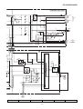
Figure 22 SCHEMATIC DIAGRAM (1/15)
– 22 –
5
6
D3
RL104A
D4
RL104
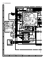
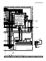
CD-C449W/K449W
CD SIGNAL
+B
R38
R39
1K
R531V
1.2K 0V
2.5V
100P
100P
C48
C49
FR
8 VSS
EFMO
9
EFMIN SLICE LEVEL
4FS
DIGITAL
FILTER
SYNC-DETECT
EFM DEMODULATE
42
MUTER
41
RVDD
40
RCHO
39
RVSS
1BIT
DAC LVSS 38
LCHO
CLV+
12
CLV
CLV–
DIGITAL SERVO
13
5V
14 V/P
15
SERVO
HFL
COMMAND
16
TES
37
DOUT
24 25 26 27 28 29 30 31
R74
560
C74
0.001
R73
560
C73
0.001
CNP11
1
2
3
4
5
6
C71
10/50
+B
+B
R88
R89
R90
R54
330
+B
CNSF11
FROM MAIN PWB
P24 1-B
1
1
2
3
2
3
DOUT
+4.3V
GND
Q52
KTC3203 Y
Q51
KRC107 M
3
CD R-CH
GND(AU)
CD L-CH
GND(CD)
+7.3V
12V(M)
32
1K
1K
1K
17 18 19 20 21 22 23
TEST3
C2F
DIGITAL
OUT
EMPH
CONT5
CONT3
CONT2
CONT4
VDD
CONT1
EXTERNAL
OUTPUT
PCK
JP–
C72 R72
10/50 2.7K
C43
R71
330/6.3 2.7K
TEST4 33
FSEQ
TOFF
JP+
C57
0.001
TGL
0V
C22
220P
D81
1SS133
LVDD 36
MUTEL
35
PCCL 34
0V
XL1
16.934MHz
PW
SBCK
FSX
WRQ
SQOUT
RWC
/RES
/CQCK
COIN
ERROR CORRECT
FLAG CONTROL
2.5V
CONTROL
10
0V
11 TEST2
C23
HF 470 0.0027
C53
0.022
RAM
VCO CLOCK
OSC CONTROL
6 VVDD
7
R93 @220
D82
1SS133
44
XOUT
XVDD 43
CNP99
R43
56K
X-TAL
GENERATOR
C42
15P
45
BI99
C25
27P
XIN
C83
0.022
5V
C56
0.022
R40
5.6K
R42
47K
C41
12P
48
150
R41
47K
EFLG
47
SBSY
XVSS 46
SUB-CODE
IC2
LC78622K
SERVO/SIGNAL
CONTROL 2K x8BIT
R51 3.3M
4 VVSS
C40 0V
0.047
5
ISET
R52 2.2V
27K
R44
33K
4M
µ-COM
INTERFACE
0V PDO
C26
0.033
51 50 49
R55
C39
0.047
1
2 TA1
0V
R50
680
3
16M
TST11
64 63 62 61 60 59 58 57 56 55 54 53 52
TEST1
DEFI
0V
SFSY
C38
0.01
100P
100P
100P
100P
C28
0.1
/CS
TEST5
29
/50
1K
1K
1K
1K
1K
1K
1K
C44
C45
C46
C47
+B
R57
R58
R59
R60
R61
R62
R63
CNPR11
TO MAIN PWB
P27 12-D
C50
3.3/16
C51
100/16
R66
R64 330
22
ZD61
MTZJ4.7B
L61
0.82µH
1
C52 100/16
2
+B
+B
D1
1SS133
R47
10K
C37
0.022
R81
3.9K
IC81
TA7291S
LOADING
MOTOR DRIVER
R80
6.8K
+B
Q91
KTA1271 Y
1
R86
2.2K
D91
1SS133
1 SOL
GND(D)
1
2
3
4
5
6
7
8
9 MECHA UP
9
2
3
4
5
6
7
8
R85
56
GND(M)
M–
M+
GND(D)
OPEN
/CLOSE
DISC NO.
10 GND(D)
BIM05
2
3
R82
6.8K
CNS10
LOCK
CNP10
9
0V
2.9V
6.5V
6.5V
0V
6.5V
R83
3.9K
C82
47/16
C81
47/16
+B
D4
RL104A
1V
0V
D3
RL104A
6.4V
1 2 3 4 5 6 7 8
SOLENOID2
R87
Q93
KRC102 M 10K
1
2
3
4
5
6
–
+
M3 T/T
UP/DOWN
LOADING
MOTOR
SW1
OPEN
CLOSE
M
SENSOR PWB-J
SW2
MECHA UP
10
GND(D)
1
2
1
2
SW3
DISC NUMBER
CNS5
DISC NO.
MECHA UP
SL–
OPEN/CLOSE
SL+
9 10 11 12 13 14
PIUN
RES (DSP)
DRF
GND(D)
CQCK (DSP)
SQ_OUT (DSP)
WRQ (DSP)
5 6 7 8
COIN (DSP)
1 2 3 4
RWC (DSP)
CD SERVO PWB-B
CNP12
CNSF12
FROM MAIN PWB
P24 1-D
• The numbers 1 to 12 are waveform numbers shown in page 18.
7
8
9
10
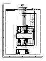
Figure 23 SCHEMATIC DIAGRAM (2/15)
– 23 –
11
12
CNPF01
CD-C449W/K449W
GND(D)
GND(D)
+B
+B
GND(µ
RG11
10K
+B
E
+12V(A)
GND(A)
TUN MUTE
L-CH
R-CH 10
CNP303
TO TUNER PWB
P33 11-H
+B
+12V(A)
GND(A)
11
RG01
220K
RH12
RH13
12.5V
1K 0V
820K
6 –
8
0V
(2/2)
1
7
(1/2)
CH10
0V
+
4
+
5
47P
-11.9V
0V
0V
2 –
ICH11
NJM4558M
MOTOR 0V3
DRIVER
RH14
560K
DH11
1SS133
RH15
33K
CH15
0.22/50
CH17
0.047
RH21
560K
DH12
1SS133
CH16
1/50
RH22
33K
CH18
0.22/50
CH20
0.015
RH26
560K
DH13
1SS133
CH19
0.47/50
RH27
33K
CH21
0.22/50
CH23
0.0047
RH31
560K
DH14
1SS133
CH22
0.1
RH32
33K
CH13
330P
CH30
0.0056
F
RH16
470K
P29 12-C
MECHA SECTION
+B
M +12V
M_GND
TA_FR SPEED
TA_MOT_SW
TA_SOL
T2_A_FP
TA_CAM_SW
T1_RUN
T2_RUN
T2_B_FP
T1_CRO2
T2_CRO2
+B
1
2
3
4
5
6
7
8
9
RH20
1.5K
+B
10
11
12
P29 12-D
DECK SECTION
G
HIGH_SP
TA_R/P
REC_MUT
TA_PB-EQ
16
17
18
RH35
1.5K
19
L-CH
R-CH
L-CH
R-CH
+B
DH19
1SS133
1KHz
SPE-4
RH34
470K
RH36
560K
DH15
1SS133
CH25
0.027
RH37
33K
CH27
0.22/50
DH20
1SS133
4KHz
SPE-5
RH39
470K
GND(A)
REC L-CH
REC R-CH
PRE L-CH
PRE R-CH
23
24
25
26
H
• NOTES ON SCHEMATIC DIAGRAM can be found on page 17.
1
2
3
1K
RF53
47K
RH29
470K
CH24
0.22/50
CH26
0.0012
TUN R
DH18
1SS133
250Hz
SPE-3
+B
GND(BIAS) 20
+12V(A) 21
GND(A) 22
REC
REC
PRE
PRE
63Hz
SPE-2
RH24
470K
+B
RH30
1.5K
TA_T1/T2 13
PB_MUT 14
TA_BIAS 15
TUN L
DH17
1SS133
+B
RH25
1.5K
CH12
10/16
DH16
1SS133
16KHz
SPE-1
+B
RH17
1.5K
(4.0V) PC5
PA0 (4.0V)
INT3 (0V)
INT2 (4.0V)
TUN_SM
SP LEVEL
SP PROT
SYS_STOP
T1_RUN
T2_RUN
1K
1K
1K
1K
1K
RF25
RF26
RF27
RF28
RF29
RG04
10K
VSS
CG05
XF01
15P
CF1
CF2
CG06
15P
RF17 820 VDD
RF19 1K SP_4KHz
RF20 1K SP_1KHz
RF21 1K SP_250Hz
RF22 1K SP_63Hz
RF23 1K SP_16K
RF24 10K POSISTOR
RH11
22K
CH29
0.022
PC6
PD1
4SP2A/NA PD0
(8.0V)
PC7
AN7 (0V)
AN6 (0V)
AN5 (0V)
AN4 (0.4V)
AN3 (0.4V)
AN2 (0.4V)
INT1 (4.0V)
PD2
(8.0V) VDD2
(DO) PD3
(0V) VSS2
PD4
(DI) PD5
(0V) PD7
(3.6V) PD6
PE0
PE1
(0V) PE4
(4.0V) PE3
PE2
(0V) PE6
(4.0V) PE5
(0V) PF0
(4.0V) PE7
PF2
(3.8V) PF1
(3.8V) PF3
+B
CH28
0.022
BIF13
–B
+B
10
11
CNSF13
+12V(A)
–15V
CG08
0.001
4
Figure 24 SCHEMATIC DIAGRAM (3/15)
– 24 –
5
RF30
1K
RG16
47K
RG19
47K
RG26
10K
GND(A)
0V
1
2
3
4
5
6
7
8
9
AMP
PB5 43
TA_R/P
(4.0V) PB4 42
BEAT_CU
(0V) PB3 41
TA_BIAS
(0V) PB2 40
FR SPEED(
(4.0V) PB1 39
HIGH_SP
PB0 38
TA MOTO
(4.0V) PA7 37
TAPE_SOL
(0V) PA6 36
CAM_SW
(4.0V) PA5 35
T2_CRO S
(4.0V) PA4 34
T1_CRO S
33
T2_B-FP S
32
31 T2_A-FP S
RG25
10K
1
2
3
4
5
6
7
8
9
48
(4.0V) PC1 47
PB_MUT
(4.0V) PC0 46
TA_T1/T2
PB7 45
REC_MUT
(3.8V) PB6 44
RG38
100K
GND(D)
CL(µCON SIDE DI)
DO
CE(CE1)(µCON SIDE DO)
DI
FRNT_RLY
50
49 FAN CONT
1 2 3 4 5 6 7 8 9 10 11 12 13 14 15 16 17 18 19 20 21 22 23 24 25 26 27 28 29 30
D
QG04
KTA1266 GR
4.1V
3.8V
CENT/REAR RLY RF52
VDD
VSS
PASS
1K
1K
1K
1K
RF65
RF64
RF63
RF62
B
ENA
CE
CL
SD
100
1K
1K
1K
1K
1K
1K
RF73
RF72
RF71
RF70
RF69
RF68
RF67
DI
DO
RF75 1K
TUN_MUTE
VDD1 (4.0V)
98
99
100
AN0 (0.4V)
97 P02 (8.8V)
AN1 (0.4V)
CD MUTE
33 PA3 (4.0V)
32 PA2 (4.0V)
31 PA1 (4.0V)
CF2 (2.0V)
1K
98 P03 (4.0V)
99 P04
100 P05 (0V)
95 P00
96 P01
VSS1 (0V)
94 P35
RF97
(4.0V) PF4
(3.8V) PF6
(4.0V) PF5
(4.0V) PL6
(4.0V) PF7
91 P32
92 P33 (4.0V)
93 P34
CF1 (1.7V)
CD OP/CL SW
P75 (0.4V)
CD DISC No.SW
P74 (0V)
CD UP/DOWN SW
INT0 (0V)
RF94 1K
RF95 1K
RF96 1K
48 PC2
ICF01
IX0235AW
SYSTEM CONTROL
MICROCOMPUTER
89 VSS3
90 VDD3
RES(MAIN) (4.0V)
10K
10K
10K
88 P31
P17 (4.0V)
RG57
RG58
RG59
SYS MUTE
REAR MUTE RF76 1K
RF79 1K
CENT MUTE RF77 22K
POWER
9K/10K
VDD
50 PC4 (4.0V)
49 PC3
83 PL0 (0V)
87 P30
VSS
P16 (0.6V)
+B
SCK1 (4.0V)
14
+B
SI1 (0V)
13
14
81 PL5 (0V)
82 PL4 (0V)
SCK (4.0V)
12
13
83
84 PL1 (0V)
85 PL2 (4.0V)
S.W_ANA
86 PL3 (4.0V)
SO1 (0V)
12
DOL_A/NA
Si0 (4.0V)
11
SRS_A/NA
10K
SO0 (0V)
11
RG08
RF61
22K
80 79 78 77 76 7 5 74 73 72 71 70 69 68 67 66 65 64 63 62 61 60 59 58 57 56 55 54 53 52 51
P06 (0V)
10
S/N
P07 (0V)
10
1K MIC_DET
81
1K H/P SW 82
RWC
5
6
7
8
9
RF81
RF82
10K
1K
5
6
7
8
9
CG61
0.022
RF01 1K SLD–
RF02 1K SLD+
RF03 1K COIN
RF04 1K SQOUT
RF05 1K CQCK
RF06
1K COM
RF07
1K DAT
RF08
1K SCK
RF09
1K STB
RF10
1K DS_RES
RF11
1K WRQ
RF12 1K RES
RF13 1K DRF
RF14 1K PUIN
1
2
3
4
RG24
RF80
1K
RG56
1
2
3
4
CD-C449W
ONLY
0V
RF92
47K
3
4
5
6
9/50
RF87
47K
3
4
5
6
RU96
2.2K
QU01
KTC3199 GR
BIF11
1
2
0V
SWF02
SPAN
SELECTOR
BIF12
CNP12
TO CD SERVO PWB
P23 8-H
1
2
CNSF12
RWC
WRQ
COIN
SQOUT
CQCK
RES
DRF
D2GND
SLD+
SLD–
PUIN
OP/CL
DISC2NO
UP/DOWN
0V
0V
CNSF11
GND(Au)
CD L-CH
GND(CD)
+7.3V(CD)
+12V(M)
C
0V
QU02
KTC3199 GR
0V
CD R-CH
10/100 RG05
10K
RG10
47K
RU95
2.2K
CD-K449W
ONLY
CD-K449W
ONLY
DG06
RG23
1SS133
10K
CG07
22/25
CNP11
TO CD SERVO PWB
P23 11-C
+4V(µ-C
+B
STB
2
1 SCK1
CNSD01
TO DISPLAY PWB
P30 1-D
B
+B
+B
+B
1K CD RES
A
+4.6V(D)
+12V(M)
COM1
RESET
DATA1
RF98
9
8
7
6
5
4
3
RF91
47K
10
GND(CD2)
GND(CD1)
GND(D)
+7.3V(CD)
+12V(M)
+4.6V(D)
6
CD-C449W/K449W
CD GND(D2)
CD GND(D1)
GND(D)
+7.3V(CD)
+12V(M)
36 CD GND(D2)
37 CD GND(D1)
38 GND(D)
39 +7.3V(CD)
+B
+B
40 +12V(M)
41 +4.6V(D)
+B
+4V(µ-CON)
+4.6V(D)
RG35
1K
0V
4.0V
DG04
1SS133
CG02
0.01
1 0V
RG36
3.3K
RG33
10K
4.0V RG32
RG34
100
10K
0V
0.4V
0V
0V
DG02
1SS133
2
CG04
0.01
CG03
3.3/50
3
4.0V
DG05
1SS133
DG03
1SS133
QG02
KTC3199 GR
QG01
KRC102 M
RG37
1K
ZDF01
MTZJ3.3A
+4V
PRE SECTION
P27 8-H
GND(µ-CON)
42 AMP
43 S-MUTE
44 SP PROT
RG31
1K
QG03
RG39
82
KTC3199 GR
RESET
POINT
45 POSISTOR
RG30 RG29 CG01
150
150 470/10
46 H/P SW
47 SP LEVEL
48 FAN CONT
49 FRNT RLY(1)
+4V
LG01
2.2µH
50 POWER
51 CL
AN CONT
52 DI
RF50 1K
RF49 1K
53 CE
54 GND(M)
+B
MP
B_MUT
A_T1/T2
REC_MUT
RF47 1K
RF46 1K
RG55 1K
RF44 1K
RF42
EAT_CUT RF41
RF40
A_BIAS
R SPEED(M) RF39
RF38
IGH_SP
A MOTOR RF37
RF36
APE_SOL
RF35
CAM_SW
RF34
2_CRO S
RF33
1_CRO S
RF32
2_B-FP S
RF31
2_A-FP S
A_R/P
1K
1K
1K
1K
1K
1K
1K
1K
1K
1K
1K
1K
+B
–B
–B
QG05
KRC104 M
FM SIGNAL
PLAYBACK SIGNAL
RECORD SIGNAL
CD SIGNAL
4.1V
0V
0V
RF99
10K
RG17
RG20
RG21
RG22
55 +12V(A)
56 –12V
57 GND(BIAS)
58 GND(A)
59 GND(D3)
CD-C449W
ONLY
60 OUT(L)
61 OUT(R)
62 IN(L)
10K
10K
10K
10K
63 IN(R)
64 GND(A)
65 +12V(A)
66 PASS
67 SRS A
RG15
10K
68 SRS B
PRE SECTION
P26 1-B
RNT_RLY
69 SRS INH
0
CG57
47/25
CG56
0.022
6
K
9
26
K
+12V(A)
–15V
+B
–B
CD-K449W
ONLY
REC L-CH
RU21
RU26
RU25
RU23
4
44
43
42
41
40
39
38
37
36
35
34
33
(5.0V) LF2C2
(4.8V) LF2C3
(5.0V) LF3C1
(5.0V) LF3C2
(4.8V) LF3C3
(5.0V) LF4C1
(5.0V) LF4C2
(4.8V) LF4C3
LF5
(5.0V) LTOUT
(5.0V)
LFIN
RU93 CU01
1K
(5.0V)
51 L4
(5.0V)
CU42
10/50
(5.0V)
LFCOM 32
(5.0V)
LFOUT 31
CU61
(5.0V) LRIN 30
10/50
(5.0V) LRCOM 29
(5.0V) LVref 27
ICU01
LC75396N
AUDIO PROCESSOR
L1
(0.1V)
VSS 26
(0V)
CE 25
CU02
2.2/50
CU04
2.2/50
CU06
2.2/50
58 R3 (5.0V)
(5.0V) Vref 22
CU08
2.2/50
59 R4 (5.0V)
(0V) RVref 21
CU36
2.2/50 60
R5 (5.0V)
(5.0V)RROUT 20
57 R2 (5.0V)
RF2C2 (0V)
RF2C3 (0V)
RF3C1 (5.0V)
RF3C2 (5.0V)
RF3C3 (4.8V)
RF4C1 (5.0V)
RF4C2 (5.0V)
RF4C3 (4.8V)
(5.0V)
RF5
RTOUT(5.0V)
RFIN (5.0V)
RFCOM(5.0V)
1
2
3
4
5
6
7
8
9
10
11
12
13
14
15
16
CU16
0.47/50
CU18 CU22 CU24
0.18 0.22/50 0.15
(ML)
(ML)
CU64
0.022
CU26
0.22/50
RU06
2.7K
CU10
10/50
RF2C1 (0V)
100P
RU04 15K
CU28
0.027
CU30 CU32
0.015 0.0022
CU40
10/50
CU43
47/16
CU51
RRCOM 19
10/50
(5.0V)
RRIN 18
(0V)
17
RFOUT
(5.0V)
CU62
RF1C3 (4.8V)
RINVIN1
61 (5.0V)
62 RSERO
(5.0V)
63 RTIN
(5.0V)
64
RU09 1K
RU10 1K
(CON SIDE DO) DI 24
RU11 1K
(0V)
(0V) CL 23
RF1C2 (5.0V)
CU12
56 R1 (5.0V)
RF1C1
(5.0V)
CU46
1/50
CU55
47/16
CU52
(5.0V) LROUT 28
10/50
55 VDD (10.1V)
RU94
1K
CNPU02
RU01
470K
50 L5
OUT(R)
IN(R)
GND
MIC
CU56
47/16
2.2/50 52
L3 (5.0V)
2.2/50
53 L2 (5.0V)
2.2/50 54
(5.0V)
9
CU39
10/50
10/50
CU41
10/50
RU14
1K
2.2/50
CU05
6
V, CAN
OUT(L)
IN(L)
GND(A)
+12V(A)
RU13
1K
2.2/50
CU07
(5.0V)
45
CU35
CU03
CU33
0.0047
CU31
0.0022
46
(5.0V) LF2C1
AUX 2
47
(4.8V) LF1C3
49 LSELO
(5.0V)
48
(5.0V) LF1C2
CU11
100P
1K
8
LTIN
(5.0V)
CU58
2.2/50
RU24
5
7
(5.0V) LF1C1
RU03
15K
RU05
2.7K
1K
RU22
CU17
CU23
CU15 0.18 CU21 0.15 CU25 CU27 CU29
0.47/50 (ML) 0.22/50 (ML) 0.22/50 0.027 0.015
CU57
2.2/50
2
3
REC R-CH
CU45
1/50
CU09
10/50
1
1K
1K
1K
1K
CU34
0.0047
DU01
CU63 DU02
100/16 1SS133 1SS133
+B
RU02
470K
MAIN PWB-A(1/ 4 )
27 28 29
L-CH OUT
GND(A)
R-CH OUT
R-CH OUT
GND(A)
L-CH OUT
L-CH OUT
GND(A)
R-CH OUT
VIDEO1 IN
33 34 35
30 31 32
VIDEO2 IN
VOLUME
OUT
TO PRE SECTION
P28 2 H
7
TO PRE SECTION
P28 6-H
8
9
10
Figure 25 SCHEMATIC DIAGRAM (4/15)
– 25 –
11
12
FROM
KARAOKE PWB
P36 3-A
CNSU02
CD-C449W/K449W
M
0V
3.7V
3
QS14 1
KRC107 M
RS34
100K
RS33
100K
2
0V
CS12
2.2/50
CS11
2.2/50
A
CS13
100/16
CS14
100/16
15
C_IN
CL4
CL3
CL2
CL1
Vref
L_OUT
R_OUT
CR1
GND
ICS01
SRS5250AS
SRS
C4
C5
C6
S_IN
S_OUT
CR4
CR3
CR2
4
5
6
7
8
9
10
11
12
13
14
C
5.9V
5.9V
C3
3
RS24
22K
CS16
0.047
(ML)
QS
2SK24
2
RS29
33K
CS15
100/16
0V
16
1
RS18
10K
QS11
1
KRC107 M 0V
5.9V
17
C2
11.9V
1
1.9V
RS15
1K
18
C1
RS23
2.2K
5.9V
5.9V
19
C_OUT
11.9V
0V
5.9V
5.9V
20
PN_OUT
0V
21
5.9V
3
22
VCC
2
0V
SRS INH 69
23
PN_IN
QS12
KRC107 M 0V
3
SRS B 68
RS22
10K
24
5.9V
SRS A 67
RS20
10K
QS13
KRC107 M
12.5V
3
0V
2
1 0V
12.5V
2
SRS PASS 66
25
MODE
12.6V
26
L_IN
+B
RS16
1K
27
R_IN
GND(A) 64
+12V(A) 65
RS12
1K 28
CS22
4.7/50
QS15
KTC3203 Y
12.5V
TO MAIN SECTION
P25 12-C
B
+B
OUT(R) 63
5.9V
RS11
1K
RS13
4.7K
CS21
4.7/50
OUT(L) 62
5.9V
IN(R) 61
RS14
100K
IN(L) 60
CS19
0.33/50
RS28
100K
RS32
1.5K
RS26
1.5K
QS16
2SK246 GR
G
0V
5.9V
RS27
3.9K
CS17
0.47/50
(ML)
5.9V
D
RS30
4.7K
CS18
0.0047
RS25
47K
S
DS03
1SS133
RS31
4.7K
+B
L CH
CP15 CP19
0.082 0.082
(ML) (ML)
0V
RP15
100K
WTP01
VF1
1
–38(VP)
2
VF2
3
RP16
100K
TO DISPLAY PWB
P30 1-B
FWD02
VF2
–38(VP)
3
VF1
1
2
JR12
CR14
390P
JR11
0.7V
CP07
100P
CP08
100P
RP20
2.2K
RP18
8.2K
0V
0V
CP16 CP20
0.082 0.082
(ML) (ML)
RP28
8.2K
RP22
100
2 –
ICP11
(2/2)
3 +
1
0V
CP24
10/16
0V
RP29
5.6K
RP30
5.6K
0.7V
0V
QP12
KTC3199 GR
RP26
1K
4
CP28
0.022
–11.2V
–B
RR18
2.7K
RP09
100K
R-CH
0V
RP73
22K
RP10
100K
INPUT
VIDEO/AUX-2
RP25
1K
RP27
8.2K
QP11
KTC3199 GR
RR17
2.7K
RR15
27K
RR16
27K
CP57
22/25
CR11
390P
L-CH
INPUT
VIDEO/AUX-1
RR11
27K
RR13
1.8K
RR12
27K
RR14
1.8K
R-CH
DR12
1SS133
VIDEO-1
35
34
43
33
R-CH IN
L-CH
L-CH
R-CH
GND(A)
R-CH
GND(A)
29 28 27 32 31 30
GND(A)
CR10
0.001
G
DR11
1SS133
CR12
390P
L-CH IN
F
RP21
100
CR13
390P
L-CH
0V
S-MUTE
R CH
0V
RP19
2.2K
RP12
100
WTP02
CP27
0.022
CP23
10/16
7
0V
CP18
47P
E
8
5 +
ICP11
(1/2)
6 –
S-MUTE
TO POWER PWB
P35 8-H
FW901
CP17
47P
RP17
8.2K
+B
11.8V
CP26
0.001
RP11
100
ICP11
NJM4565M
BUFFER AMP.
CP25
0.001
MAIN PWB-A(3/4)
D
VIDEO-2
TO MAIN SECTION
P25 7-H
TO MAIN
SECTION
P25 10-H
H
• NOTES ON SCHEMATIC DIAGRAM can be found on page 17.
1
2
3
4
Figure 26 SCHEMATIC DIAGRAM (5/15)
– 26 –
5
6
CD-C449W/K449W
MAIN PWB-A(2/4)
R_OUT
RS36
1K
RS35
4.7K
0V
16
15
5.9V
QS18
2SK246 GR
D
G
GND
5.9V
RS16
1K
17
CR1
5.9V
CS12
2.2/50
0V
CR4
CR3
CR2
13
14
S
0V
G
5.9V
12
5.9V
D
5.9V
QS17
2SK246 GR
S
CS19
0.33/50
DS01
1SS133
DS02
1SS133
RS32
1.5K
5.9V
D
FM SIGNAL
QS16
2SK246 GR
G
0V
5.9V
S
DS03
1SS133
DIGITAL-OUTPUT
+B
LR0
2.2µH 1
(DH)
1
ICR11
GP1F38T
CNPR11
2
RR01
100
ZDR01
MTZJ3.3B
3
CR02
100/10
CR01
0.022
3
DOUT
2
+4.3V
1
GND
FROM CD SERVO PWB
P23 11-C
CNS99
CR03
0.001
CP27
0.022
CP09
100/16
RELAY2
OUT1(L-CH)
OUT1(Lch)
QP11
KTC3199 GR
GND(A)
CP25
0.001
0.7V
FAN CONT
OUT2(R-CH)
OUT2(Rch)
RP29
5.6K
SP LEVEL
H/P SW
+B
RP30
5.6K
FWP01
1
OUT1(FRONT L-CH)
2
FRNT RLY(1)
3
GND(A)
4
FAN CONT
5
OUT2(FRONT R-CH)
6
SP LEVEL
7
GND(M)
8
H/P SW
9
+12V(M)
FAN SW
+B 10
0.7V
11
PROT
P12
TC3199 GR
POSISTOR
AMP
CP10
100/16
RP31
150
(1/4)
S-MUTE
RP32
150
(1/4)
–12V
–B
+B
–B
+12V(A)
+B
+4.6V(D)
RP73
22K
12
PROT
13
POSISTOR
14
AMP
+12V(M)
CP28
0.022
TO SPEAKER AMP.PWB
P34 1-B
CFWV11
+B
GND(D)
+B
CP57
22/25
CNPP01
1
–12V(A)
2
GND(A)
3
+12V(A)
4
+12V(M)
5
GND(M)
TO POWER PWB
P34 3-H
6
+4.6V(D)
CNS901
7
GND(D)
8
+7.3V(CD)
9
10
+B
CD GND(D1)
POWER
11 GND(D3)
0V
3.7V
3
1
2
0V
POWER
+7.3V(CD)
CD GND(D1)
GND(M)
+4.6V(D)
GND(BIAS)
AMP
+12V(M)
PROT
POSISTOR
H/P SW
SP LEVEL
GND(A)
FAN CONT
GND(D)
49 48 47 46 44 45 42 40 54 41 57 39 37 50 59
FRNT RLY(1)
56 58 55
–12V
38
+12V(A)
43
S-MUTE
QP17
KRC107 M
GND(D3)
CP26
0.001
CFWP01
RELAY1
GND(A)
TO PRE SECTION
P25 12-A
7
8
9
10
Figure 27 SCHEMATIC DIAGRAM (6/15)
– 27 –
11
12
CD-C449W/K449W
A
PLAYBACK SIGNAL
RECORD SIGNAL
QL11
KTA1266 GR
0.26V
0.26V
H
+
2
M
VRM1
3.3K(B)
RM1
2.7K
L
SWM3
REC FWD
1
2
3
4
5
6
H
MOT+B
REC FWD
CAM SW
M2GND
F.A.S
RUN PULSE
+B
SOL
REC RVS
SWM6
CAM SW
SWM5
F.A.S
PHM1
C
SOLM1
SOL
FWM1
1
MOT L
MOT H
MOT +B
T2 A-FP
CUM SW
M2GND
T1 RUN-SW
T2 PH-OUT
+B
SOL
T2 B-FP
7
8
9
10
11
12
13
1
2
3
4
5
6
0V
12.6V
7
8
9
QL18
KRC104 M
RL16
2.2K
2
3
0V
12.5V
1 0V
RL19
2.2K
RL18
10K
RL20
1.2K
10
11
12
13
13
SWM4
REC RVS
0.26V
RL15
12.6V 10K
CL12
47/16
QL15
RL17
KTA1271 Y 10(1/2W)
12.6V
WTL11
3.8V
1 0V
12.6V
DL12
1SS133
MOTOR
MM1
QL13
KRC104 M
3
2
0V
QL14
KTA1273 Y
QL12
KTA1266 GR
L
4V
1 0V
RL14
33K
0V
TAPE MICHANISM PWB–H
FWM2
0V
RL12
2.2K
RL13
6.8K 0.26V 0.26V
TAPE MECHANISM ASSEMBLY
B
QL17
KRC104 M
2
3
RL11
33K
0V
DL14
1SS133
DL13
1SS133
DGND
D
RK33
22K
TAPE1
PLAYBACK HEAD
L-CH
R-CH
RK19
56
CK02
680P
QK03
2SC1845 F
0.7V
TAPE2 HEAD
PWB-G
CNPK02
ERASE
HEAD
RK09 0V
0V
4.7K
RK07
47K
RK11
15K
CK05
330P
RK89
1K
CK25
0.0082
RK37
6.8K
CK21
1/50
RK29
10K
RK12
CK06
15K
330P
0V
0.7V
RK90
1K
QK06
RK06
2SC1845 F 0V
3.3K
RK08
47K
0V
RK10 0V
4.7K
0V
5
24
0V
23
0V
112K
21
3.0V
22
0.6V
CK12
330P
REC
1.3V
CK26
0.0082
CK16
47/16
CK18
0.033
CK20
560P
RK20
56
RK22
100K
RK24
3.9K
CK27
0.022
CK32
470P
RK36
3.3K
CK30
470P
CK24
0.1
QK14
KRC104 M
3
8.2K
RK32
33K
2
0V
G
REC
9.2V
RK13
10K
0V
REC
CK09
0.022
10K
RK15
4.7K
0V 1
1 0V
2
RK14 0V
3.9V
QK10
KRC104M
CK60
100/16
RK69
220
2
3
3
0V
QK11
KRC104M
H
• NOTES ON SCHEMATIC DIAGRAM can be found on page 17.
1
2
3
4
Figure 28 SCHEMATIC DIAGRAM (7/15)
– 28 –
5
CK34
22/25
RK38
6.8K
CK28
3.3/25
RK26
5.6K
0V 1 RK28
0V
18
0V
RK30
10K
CK14
330P
PB EQ CrO2
6
20
0V
CK22
1/50
RK18
1K
RK04
2.2K
QK09
KTA1266GR
7
112K
HIGH=CHROM
+
-
QK08
KTC3199 GR
9.1V
0V
HIGH=T1
CK08
0.001
CK31
470P
CK33
22/25
0.8V
19
0V
4
–
+
CK07
0.001
0.7V
QK04
2SC1845 F 0V
3.2V
CK13 0.5V
2 330P 3
1
QK07
KTC3199 GR 0V
RK05
3.3K
0V
CK17
0.033
0V
0V
0.7V
QK05
2SC1845 F
CNSK02
BI102
R-CH L-CH
F
1
2
3
4
5
6
CK19
560P
RK25
5.6K
CK11
330P
RK17
1K
0V
7
6
5
4
3
2
1
RK31
33K
RK23
3.9K
CK23
0.1
RK03
2.2K
0V
TAPE2
RECORD/
PLAYBACK HEAD
RK21
100K
RK02
1K
CK15
47/16
7
6
5
4
3
2
1
RK47
10K
RK34
68K
RK27
0V 1 8.2K
CNPK01
CNSK01
QK13
KRC104 M
2 0V
3
CK29
470P
E
3
2
1
0V
RK35
3.3K
3
2
1
RK01
1K
CK01
680P
6
CD-C449W/K449W
MAIN PWB-A(4/4)
17
04 M
3
TA2F/R SPEED
3 TA_F/R SPEED
4V
0V
2
TA2MOT2SW
3
0V
1 0V
M212V
TA2SOL
3 0V
QL19
KRC104 M
2
12.5V
1
T22A2FP
TA2CAM2SW
M2GND
T12RUN
0V
DL11
1SS133
RL24
3.3K
0V
TA_MOT_SW
1
M_12V
5
TA_SOL
6
7
2
8
T2_A_FP
TA_CAM_SW
M_GND
T1_RUN
9
T2_RUN
10
11
T2_B_FP
T1 Cro2
1
T22RUN
2 4.1V
QL16
KRC107 M
0V
3
CL13
3.3/50
4
MAIN SECTION
P24 1-G
QL18
KRC104 M
12.5V
T22B2FP
T12CRO2
12 T2 Cro2 H:Cro2
L: NORM
PB.MUTE
7
K
CK31
470P
CK33
22/25
RK41
82
0.6V
3.1V
8
9
–
+
HIGH=CHROME
56K
CK34
22/25
RK50
10K
CK45
22/25
ALC
16
3.0V
RK40
560
CK36
0.022
CK30
470P
CK40
0.0033
10
3.0V
HI. SP H:LOW
26
PRE R-CH
22
GND(A)
L:HIGH
RK57
4.7K
RK58
470
12.5V
3
0V
RK64 2
4.7K
1 0V
KTA1266 GR
0.3V
0.26V
1
RK61
RK63
0V
270
10K 2
0V
0.27V
3
RK65 0.3
10K V QK27
LK03
KRC104 M
1mH
QK24
KTA1266 GR
RK60
270
ALC GND
11 12
0V 0V
QK26
KRC104 M
RK62
47K
12.5V
CK62
0.047
RK66 RK67
27K
47K
RK52
1K
15
BIAS
HI.SP
CK51
0.027(ML)
LK04
330µH
0V
L:OFF
QK40
KRC107 M
5.4V 3
1
0V
2
0V
QK30
0V
3 KRC104 M
1
0V
RK81
2 5.4V 6.8K
0.3V
0.3V
CK50
0.0082(P.P) RK68
4.7
BIAS H:ON
0.3V QK25
CK42
47/25
RK46
10K
1
16
21 12V(A)
CK47
6.3V 0.022
13
RK42 QK16
82 KRC104 M
2
3
CK38
0.018
PRE L-CH
CK46
220/10
0V
3.8V
14
15
NOR/CrO 2
56K
17
0.6V
LK02
1.8mH
CK32
470P
QK19
KRC104 M
ICK01
PLAYBACK AND RECORD/PLAYBACK AMP.
+
AN7345K
–
38
K
3.8V
0V
RIPPLE
7
18
0V
CK41
47/25
CK39
0.0033
LK01
1.8mH
V
6
K
3.8V
3
QK15
KRC104 M
L:OFF
25
MAIN SECTION
P24 1-G
2
CK37
0.018
RK39
560
HI.SP
3
L:T2
PB.MUTEH:ON
CK55
0.022
1 0V
2
12.6V
0V
0V 1
TA T1/T2H:T1
14
0V
CK44
0.022
VCC
CK35
0.022
QK18
2SC2878 A
RK48
0V
10K 0.7V
CK43
0.022
0V
RK45 10K
CK10
47/25
RK49 10K
CK29
470P
RK47
10K
HI.SP
QK17
2SC2878 A
0V
RK43
0.7V 10K
13
QK28
2SC2236 Y
CK52
47/16
RK55
33K
QK22
KTC3199 GR
RK75
82K
RK73
27K
RK56
33K
0V
0V
0.7V
0V
RK74
82K
3 5.4V
1 0V
QK29
2 KRC107 M
0V
RK54
10K
0.7V
RK53
10K
QK21
KTC3199 GR
23 REC L-CH
24 REC R-CH
RK72
27K
0V
17 TA R/P
18
@H:PB
L:REC
REC MUTE
19 TA BE EQ L:NORM
H:Cro2
20 GND(BIAS)
7
8
9
10
Figure 29 SCHEMATIC DIAGRAM (8/15)
– 29 –
11
12
CD-C449W/K449W
RD53
1K
CD30
1/50
LEDD08
SLR325MG
1
QD05 KRC107 M
3 QD06
KRC107 M
1
CD29
1/50
LEDD11
SLR325MG
RD05 1K
RD06 1K
LEDD12
SLR325MG
S1
S2
S2
S1
94 P07 STEREO-R (0.4V)
DATA1
RD15 1K
RD17 1K
1
95 SO0 (0V)
COM1 96
SI0 (0V)
SCK1
RD16 1K
100 SCK1
97 SCK0 (4.0V)
3
4
5
6
7
99 SI1 (0V)
LEDD14
SLR325MG
100
LEDD15
SLR325MG
LEDD16
SLR325VR
1
STROBE
2
LEDD17
SLR325VR
QD07
KRC107 M
3 R-PLAY
2
LEDD20
KL052UL
RD54
1.2K
LEDD18
SLR325MG
RD19
1K
LEDD19
SLR325MG
1
+B
LEDD21
SLR505MC
RD21
1K
RD2
1K
RD22
1K
3 REW
2
RD55
820
DISK 1
P34 (0V)
98 SO1 (0V)
+B
D
93 P06 STEREO-G (9.0V)
RD14 1K
P33 (0V)
2
92 P05 NORMAL-R (10.8V)
RD13 560
P32 (0V)
STB
CD20 150P
3
89 VSS2 (0V)
91 P04 NORMAL-G (0.6V)
RD12 1K
CD21 150P
4
DATA1
FROM MAIN PWB
P24 1-B
+B
+B
5
RESET
SCK1
RD11 560
+B
CD19 150P
6
CNPF01
88 P03 VIRTUAL-R (10.8V)
VDD 90
VDD2 (4.1V)
CD18 150P
+12V(M)
COM1
87 P02 VIRTUAL-G (–6V)
8
7
82 PG1
(0V)
83 PG2 SRS-G
(4.0V)
81 PG0 (0
84 PG3 SRS-R (0V)
86 P01 PHANT-R (10.8V)
RD10 1K
9
+4.6V(D)
81
85 P00 PHANT-G (0.6V)
RD08 1K
RD09 560
LEDD13
SLR325VR
VSS
CNSD01
C
FF
PAUSE
RD07 560
10
GND(D)
80 79 78 77 76 75 74
RD03
1K
RD04 1K
LEDD10
LEDD09
SLR325VR SLR325MG
CD28
1/50
RD01
1K
1
QD08
KRC107 M
DD01
1N4004S
+B
RD57
39
CD11
0.022
DD02
1SS133
2
CD10
220/6.3
E
1
3
RXD01
REMOTE
CONTROL
SENSOR
RD58
100K
RD59
100K
CD05
0.001
CD09
150P
+B
RE09
27K
F
SWD11
FLAT
SWD10
HEAVY-1
SWD18
SRS/DEMO
SWD17
F-PLAY
RE17
5.6K
RE08
12K
RE07
5.6K
RE16
3.9K
RE06
3.9K
SWD08
VOCAL
SWD09
HEAVY-2
RE15
2.2K
RE02
2.2K
KEY1
SWD03
X-BASS
RE14
1.8K
SWD15
HIGH EDIT
SWD16
REC/PAUSE
RE04
3.9K
SWD07
SOFT
RE01
8.2K
RE12
1K
SWD14
NORMAL EDIT
RE13
1.2K SWD13
STOP
KEY2
RE11
8.2K
SWD12
TUNING UP/CUE
RE21
8.2K
RE22
1K
KEY3
G
SWD22
BALANCE LEFT
RE39
RE38
27K
RE37
12K
RE36
5.6K
RE35
3.9K
RE34
2.2K
1.8K
SWD21
BALANCE RIGHT
RE33
RE32
1.2K
1K
SWD38
SWD37
SWD36
SWD35
SWD34
SWD33
SWD32
SWD31
CLEAR
SLEEP
TIMER
MEMORY
CLOCK
R-PLAY
REVERSE
MODE
CD
PAUSE
RE31
8.2K
KEY4
SWD30
TUNING DOWN
/REWIND
H
• NOTES ON SCHEMATIC DIAGRAM can be found on page 17.
1
(–30V) S41
1
RD02
1K
REW
FWD02
RD52
560
2
LEDD07
SLR325VR
VF1
WTP01
TO MAIN PWB
P26 1-E
6
(–28V) S42
–38(VP)
1
5
(0V) S43
LEDD05
SLR325MG
3 VF2
QD01
KRC107 M
QD02
KRC107 M
QD03
KRC107 M
QD04
KRC107 M
STOP
(YELLOW)
PAUSE
3
4
F-PLAY
RD48
LEDD01
1.2K 2
KL052UL
3
LEDD02 RD49
1.2K
1
KL052UL
2
LEDD03
3
2
1
SLR505MC
3
RD50
1
LEDD04 820
2
KL052UL
3
RD51
LEDD06
1
SLR325MG 1.2K
3
2
(YELLOW)
F-PLAY
(YELLOW)
STOP
(GREEN)
FF
HEADPHONES PWB-C3
B
3
CV92
100
LV91
2.2µH(XH)
1
1 2
S47
(0V)
S46
(0V)
S45
(0V)
(0V) S44
1
FWV91
F1
RV92 CV91
220 100
P16
(0.6V)
P17
(0V)
P30
(0V)
P31 (0V)
WTV11
TO SPEAKER
AMP.2 PWB
P35 12-C
JV91
HEADPHONE
R-PLAY
HP-LCH
GND(A)
HP-RCH
GND(M)
H/P SW
X2
5
5
NC
RV91
220
F1
A
NC
FM SIGNAL
2
3
4
Figure 30 SCHEMATIC DIAGRAM (9/15)
– 30 –
5
6
CD-C449W/K449W
F2
F2
12G
NC
NC
11G
9G
8G
10G
7G
6G
5G
4G
30 31 32
3G
29
2G
28
1G
9 10 11 12 13 14 15 16 17 18 19 20 21 22 23 24 25 26 27
S27
8
S26
7
S25
6
S24
S23
S22
S21
S20
S19
S18
S17
S16
S15
S14
S13
S5
S12
S4
S11
S3
5
S9
S2
4
S8
S1
3
S7
NC
2
S6
F1
NC
S10
FLD01
FL DISPLAY
33 34 35 36 37 38 39 40 41 42 43 44 45 46 47
D01
1K
S23
S22
S21
S20
S19
S18
S17
S16
S15
S14
S13
S12
S11
S10
S9
S8
S7
S6
S5
S4
VDD
S3
S2
S1
+B
–29(VP)
81 PG0 (0V)
S24
(–28V)
S23
(0V)
S22
(–23V)
S21
(–28V)
S20
(–26V)
VP
(–30V)
(0V) S25
(0V) S26
(0V) S27
(–28V) S28
(–26V) S29
(–30V) S30
(–21V) S31
(–30V) S32
(–30V) S33
(–30V) S34
(–30V) S35
(–30V) S36
(–30V) S37
(–28V) S38
(–30V) S39
(4.1V) VDD4
(–28V) S40
(–30V) S41
-G
(–28V) S42
(0V) S43
S45
(0V)
(0V) S44
78 77 76 75 74 73 72 71 70 69 68 67 66 65 64 63 62 61 60 59 58 57 56 55 54 53 52 51
50
(–21V) S18 49
(–30V) S17 48
50 S19 (–30V)
(–26V) S16 47
-R (0V)
(4.0V) VDD3 46
NT-G (0.6V)
NT-R (10.8V)
(–29V) S15 45
UAL-G (–6V)
(–29V) S14 44
UAL-R (10.8V)
(–29V) S13 43
V)
(–29V) S12 42
ICD01
IX0234AW
LF DRIVER AND
CONTROLLER
1V)
RMAL-G (0.6V)
RMAL-R (10.8V)
REO-G (9.0V)
(–29V) S11 41
(–29V) S10 40
(–29V) S9 39
(–29V) S8 38
(–29V) S7 37
REO-R (0.4V)
(–29V) S6 36
INT3
(3.5V)
S0
(0V)
INT2(4V)
INT1(4V)
AN7 (4V)
AN6 (4V)
AN5 (4V)
AN4 (4V)
AN3 (4V)
AN2 (0V)
AN1 (0.4V)
AN0 (0V)
CF2 (1.9V)
VDD1(4V)
S27
VDD
G1
G2
G3
G4
G5
G6
G7
G8
G9
G10
G11
G12
G12
+B
31
RD45
1K
+B
RD44
1K
RD42
1K
CD01
0.022
RD40
1K
RD38
1K
RD36
1K
RD33
1K
RD31
1K
XD01
RD28
1K
S26
REMOCON
JOG DOWN
JOG UP
RD43
1K
KEY6
KEY5
RD41
1K
KEY4
KEY3
RD39
1K
KEY2
KEY1
RD37
1K
AUD-SET
TUN-SET
RD35
1K
RD34 820 VDD
RESET
RD30
47K
RD27
1K
(–29V) S3 33
S2
(–29V) 32
S25
16 17 18 19 20 21 22 23 24 25 26 27 28 29 30
0V
XCOUT
10 11 12 13 14 15
RD26
1K
CF1 (1.7V)
9
XCIN
VSS1 (0V)
8
VSS
P37 (0V)
P75 (4V)
P36 (0V)
P74 (4V)
P35 (0V)
7
RD32 VOL JOG UP
1K
VOL JOG DOWN
P34 (0V)
6
DISK 3
P33 (0V)
5
DISK 2
P32 (0V)
4
DISK 1
P30
(0V)
P31 (0V)
3
REW
/RES (4V)
(–29V) S4 34
R PLAY
0V)
(–29V) S5 35
31 S1 (0V)
INT0 FL-SET (0V)
100 SCK1 (0V)
S24
LD01
2.2µH
CD02
100/10
QD10
KRC107 M
DISC 3
3
2
RD70
820
2
RD71
820
DISC 3
RD66
8.2K
RD61
10K
RD64
10K
CD05
0.001
SWD01
VOL JOG
DISC 2
RD65
10K
3
DISC 1
CD07
0.001
CD06
0.001
CD08
0.001
DISC 2
QD11
KRC107 M
1
RD67
2.2K
RD60
10K
RD62
8.2K
1
3
2
DISC 1
RD72
820
QD12
KRC107 M
1
SWD02
JOG
JOG PWB-C4
+B
RE42
1K
KEY5
KEY1
RE41
8.2K
RE01
8.2K
SWD39
VIDEO/AUX1
RE44
1.8K
RE43
1.2K
SWD41
TAPE
1/2
SWD40
VIDEO/AUX2
RE45
2.2K
SWD42
TUNER/BAND
SWD43
CD
RE52
1K
KEY6
KEY2
RE11
8.2K
SWD48
POWER
RE51
8.2K
RE21
8.2K
RE53
1.2K
SWD49
KARAOKE
CD-K449W
ONLY
+B
KEY3
6
1
FWD01
7
8
SWITCH PWB-C2
9
10
Figure 31 SCHEMATIC DIAGRAM (10/15)
– 31 –
11
12
1
LEDD23~LEDD28
LMKD515B
LEDD24
LEDD23
SWD50
DISC1
LEDD28
SWD51
DISC2
LEDD26
RE54
1.8K
RE55
2.2K
SWD52
DISC3
DISC1
DISPLAY PWB-C1
SWD53
DISC
SKIP
DISC3
SWD54
OPEN/CLOSE
LEDD27
RE56
3.9K
RE57
5.6K
KEY4
DISC2
6
LEDD25
RE31
8.2K
CD-C449W/K449W
FM SIGNAL
MW/SW1/SW2 SIGNAL
R310
22K
VD302-B
KV1236Z23F
Q309
R311
D305
2SC2878 B R312
C303
100K
1SS135
0V
0.022
0V 33K
D309
0V
C309
1SS135
330P
TC302
SW2
fL
C308 (UJ) 0V
C304 TRACKING fH
R314
0.022
3.3K
8.2P
D306
0V
1SS135
D310 C310
Q308
0V
2SC2878 B 1SS133 0.001
TC303
T303
fL SW1 ANT
SW1
R316
D311
TRACKING fH
22K
1SS135
C305
VD301-1
0.047
D307 1SS135 T302
C311
KV1236Z23F
0.022
R319
100K
C330
D308
8.2P
C331
1SS135 MW TRACKING
(UJ)
0.047
MW
ANT
R317
L311
10K
560µH
C306
10P (UJ)
R313
22K
T304
SW2 ANT
C307
0.047
A
C312
0.022
R315
22K
C313
0.022
1
C342
0.022
VR351
10K(B)
FM MUTE
LEVEL
R318
1.5K
B
Q
3
MW OSC T306
BFT01
FM BAND PASS
FILTER
C334
18P
(UJ)
C336
470P
MIX
CT11
15P
(CH)
CT03
4.7P
FMRF
8
7
VCC
9
RT06
10
LT02
FM BAND
COVERAGE
CT12
33P
FM
OSC
FMIF
TT01
CT05
6.8P
(UJ)
CT16
10/16
2
2
CT14
22P(CH)
3
CT10
0.022
CT09
0.0047
CT08 0.0047
CT07 0.001
C301
0.001
CT06 0.022
D304
1SS133
RT03
22
0V
2
1
3
+B
RT08
10K
D303
1SS133
G
R341
47K
1
1
3
CT13
3.9P(UJ)
RT04
47
R340
220
5 6
CT15
0.022
4
VDT02
KDV147B
CT01
18P(CH) CT02
0.01
CT04
0.001
RT02
33K
RT01
100K
1 2 3
1DT01
SS133
1 2 3
OSC
+B
R343
47K
C349
1/50
ICT01A TA7358AP
FM FRONTEND
RF
2
R342
47K
B.A
SO301
ANTENNA
TERMINAL
F
R323
68K
MW BAND
COVERAGE
LT01
FM
75ohms
D302
1SS133
VDT01
KDV147B
E
SW1
SW2
MW
GND
RT10
4.7K
RT05
47K
C390
100P
RT07
680
QT01
2SC535 C
AMP
+B
RT09
820
H
• NOTES ON SCHEMATIC DIAGRAM can be found on page 17.
1
2
3
3
12.18V
SW1 BAND fL
COVERAGE fH
1
MW+B
SW1 OSC
T307
D301
1SS133
Q307
2SC2878 B
0V
0V
Q306
0V
R330
2SC2878 B 1K
VD301-2
R324
KV1236Z23F
100K
Q362
KRA107 M
TC305
CF302
10.7MHz
FM1F
R326
1K
R338
470
0V
fH
SW1
TRACKING fL
C335
18P (CH)
D
C321
0.0039
SW1+B
C338
0.001
C320
0.0018
R329
100K
R327
0V 5.6K
0V
Q363
KRA107 M
SW2 OSC
T308
TC304
R325
56K
VD302-A
KV1236Z23F
SW2+B
D316
1SS135
C319
0.022
D317
1SS135
C315
0.1
D313
1SS133
D314
1SS133
R322
5.6K
R328
C318 10K
0.022
Q364
KRA107 M
R339
470
C316
0.1
D315
1SS135
C314
0.022
R320
10K
L356
1mH
R302
82
R321
D312
5.6K 1SS133
C
4
Figure 32 SCHEMATIC DIAGRAM (11/15)
– 32 –
5
6
CD-C449W/K449W
TUNER PWB-E
Q365
KRC107 M
2
R364
1.5K
C373
0.022
R362
5.6K
3.95V
MUTING
Q353
0V KTC3199 GR
0.65V
R367
1K
R368
33K
0V
R366
10K
0.65V
3.85V
0V Q354
KTC3199 GR
MUTING
R355
3.3K
R354
4.7K
C356
0.001
C370
1/50
C355
22P
C399
0.022
C398
100/10
C354
0.022
CF351
FMIF
AMIF
C358 12
1/50
10K C375
R365 3.3/50
0V
D353
1SS133
C368 R356
1.19V 1/50 1K
C372
1/50
R-CH
OUT
L-CH
OUT
PHASE
(FM/AM) MO/ST
MPX VCO
IF OUT
PHASE
5.01V
5.09V
0V
CF352
AM IF
C353
0.022
C350
0.022
C357
2.2/50
3
2
R361
5.6K
15 14 13
3.68V
3.85V
VCC
10 11
1
1.18V
C374
0.022
R357
470K
2.05V
2.29V X351
456kHz
FM DET
9
R353
270
STEREO
8
5.09V
7
2.84V
SD
FM/AM OUT
GND
6
2.06V
5
R352
1K
C371
1/50
R363
1.5K
IC303
LA1832
FM IF DET./FM MPX./AM IF
AM IF IN
VSM
MPX IN
C365 0.022
C366 0.001
2.52V
0V
0.46V
AM RF IN
2.2V
AM LOW CUT
L358
560mH
C364 10/16
C360
0.022
C361
0.022
FM AFC
17 16
REG
18
AM MIX OUT
AM OSC IN
19
4
T351
2
20
FM IF IN
AM OSC OUT
21
C367
1/50
3
C352
10/16
3
22
R350
2.7K
2
C351
0.022
1
23
5.01V
CF302
10.7MHz
FM1F
24
TP 302
1
2.06V
R351
5.6K
L356
mH
5.01V
3.48V
L353
1mH
2.2V
VR351
10K(B)
M MUTE
EVEL
C362
3.3/50
R358
8.2K
L357
4.7mH
C342
0.022
C363 0.022
C343
15P (CH)
1
2.07V
3
R393 1K
L351
100µH
R380
1.5K
C385
0.01
4
5
6
8
7
R397
1K
NC
9
10
11
R390
82K
R360
4.7K
R398 1K
R385
5.6K
R384
5.6K
3
R359
1.8K
D352 1SS133
2
3.95V
1
R391
390
R392
390
12.18V
R383
11.37V 5.6K
11.6V
19 18 17 16 15 14 13 12
IC302
LC72131
PLL CONTROLLER
SW1
C382
15P (CH)
+B
22 21 20
C396
100/10
Q360
KTA1266 GR
R395
47K
R376
1K
X352
4.5MHz
C381
12P (CH)
R396
1K
MO/ST SW2
IF IN
STEREO
5.1V
C386
330P
C393
2.2/50
C395
0.022
+B
0V
0V
2.38V
R381
10K
ZD351
MTZJ4.7B
C391
47/16
1
3
2
ZD352
MTZJ3.9B
Q361 R387
KRC107 M 22K
D351
1SS133
R373 1K
R374 1K
R371 1K
R372 1K
C383
0.0022
+B
+B
CL
DO
CE
GND(D)
CNP303
DI
+12V(A)
GND(A)
TUNER MUTE
L-CH
R-CH
SD
2.52V
2.52V
X IN X OUT
0V
NC VSS
0V
2.1V
AOUT
0V
CE
0V
DI
4.82V
0.9V
CL
AIN
0.9V
5.1V
PD
DO
R379
0.16V
5.11V 2.2K
FM VDD
C380
2.48V
FM IN
1/50
0V
MW AM IN
12.1V
R382
150
C392
0.001
C394
47/16
L352
100µH
R377
47K
3.85V
C397
0.022
+B
C387
0.022
FMIF
1 2 3 4 5 6 7 8 9 10 11
FROM MAIN PWB
P24 1-E CNSF13
7
8
9
10
Figure 33 SCHEMATIC DIAGRAM (12/15)
– 33 –
11
12
CD-C449W/K449W
QV13
KTC3200 GR
3.9V
DV13
1SS133
0V
FM SIGNAL
RV27
10K
CV25
0.022
13
41.1V
RV29
0.2(1W)
0V
7
3
42.1V
DV15
1SS133
QV18
KTC3199 GR
RV69
0.2(1W)
9
13
AMP
14
RV33
10K
RV24
1K
CV22
15P
0V
15
0V
CV12
2.2/50
CV18
47P
RV18
1K
0V
42.1V
12
8
11
2
1
ICV01
POWER AMP.
10
CV14
2.2/50
RV70
0.2(1W)
–42V
0V
6
RV30
0.2(1W)
CV26
0.022
5
4
0.2V
0V
RV28
10K
C
CV30
3300/63
0V
3.9V
0V
QV14
KTC3200 GR
CNPV12
CNS903
D
BI903
POWER PWB-D
–11.9V
–41.4V
–12.4V
R918
100
C902
47/25
C901
0.022
C920
47/25
12.5V
Q903
2SD468 C
+4.6V(D)
+B
4.8V
C906
0.022
2
3
4
5
6
7
1
2
3
4
5
6
7
1
2
3
4
5
6
7
R901
68(3W)
–12.47V
1
Q914
KRC107 M
2
3
ZD901
MTZJ130A
–12.45V
Q902
2SD2012
+12V(M)
+B
E
1
R917
4.7K
Q913
2SB1375
–B
CV29
3300/63
DV14
1SS133
R905
11.8V
22
Fusible
5.46V
R906
100
GND(D)
18.8V
13.2V
Q901
KTC3199 GR
R903
47(1/6)
13.8V
C904
47/25
ZD902
MTZJ5.6A
18.8V
13.2V
R904
1.5K
R902
1K
C903
47/25
GND
C905
47/25
(1/4W)
Q906
2SD2012
12.5V
13.8V
R909
1K
C908
47/25
–0.62V
1
1.35V
2
3
R908
33K
ZD903
MTZJ130C
18.8V
C907
220/25
C909
0.022
D901
1SS133
R907
560(1/4)
13.2V
Q904
KRA107 M
F
Q905
KTC3199 GR
R910
150
13.8V
13.1V
18.8V
13.8V
+12V(A)
+B
2
1
1.35V
3 Q907
0V KRA102 M
+7.3V(CD)
Q909
2SD2012
8V
C911
0.022
D905
1SS133
G
18.1V
C919
4700/25
8.4V
R911
560(1/6)
GND(D3)
+B
R912
47
+B
POWER
CD GND(D1)
+7.3V(CD)
GND(D)
+B
+4.6V(D)
+12V(M)
GND(M)
–B
+B
+12V(A)
GND(A)
–12V(A)
H
F999
T500mA L 250V
8V
ZD904
MTZJ8.2C
GND(M)
BI901
D903
1N4004S
Q908
KTC3199 GR
C910
47/25
CD GND(D)
D904
1N4004S
18.1V
7.8V
1
2
3
4
5
6
7 8
9 10 11
CNS901 1
2
3
4
5
6
7 8
9 10 11
TO MAIN PWB
P27 12-F
CNPP01
• NOTES ON SCHEMATIC DIAGRAM can be found on page 17.
1
2
3
4
Figure 34 SCHEMATIC DIAGRAM (13/15)
– 34 –
5
+VCC
12
CV27
1000/6.3
RV63
120K
+VCC
11
Fusible
RV22
56K
GND
NC
PROT
POSISTOR
RV26
100(1/2W)
6
+VCC
9
10
CV24
47/63
RV71
820
+VCC
+12V(M)
FAN SW
RV38
10K
CV20
100/50
GND
8
CV16
470P
GND
H/P SW
RV37
47K
RV20
270
GND
7
CV2
47/5
100(1/2W)
CV23
47/63
0V
3
0V
Fusible
–VCC
GND(M)
0.67V
RV25
RV32
1K
SP LEVEL
5
6
42V
4
QV17
KTA1268 GR
FAN CONT
OUT2(R-CH)
RV19
270
CV19
100/50
FR
0
QV19
KTC3199 GR
–40.6V
2
DV21
1SS133
TO MAIN PWB
P27 12-E
CFWP01
1
RELAY1
GND(A)
3.9V
–39.5V
B
OUT1(L-CH)
RV14
56K
FWP01
CV15
470P
3.9V
0V
0V
RV35
2.2K
RV36
22K
RV21
56K QV16
41.4V
KTC3199 GR 0V
RV13
56K
CFWV11
CV21 RV23
15P
1K
GND
0V
–VCC
A
ICV01
POWER AMP.
STK407-09
14
GND
0V
CV17
47P
–VCC
RV17
1K
–VCC
CV13
2.2/50
RV31
1K
CV11
2.2/50
0V
CD-C449W/K449W
SPEAKER AMP.PWB-F
3
33
TMV01
RLYV11
+
DV15
1SS133
3.9V
RV41
56K
0V
SPEAKER
L-CH
CV31
0.1(ML)
0V
QV18
KTC3199 GR
–
8OHMS
CV33
0.1(ML)
DV17
1SS133
RV43
4.7(1/2W)
SPEAKER
R-CH
–
CNPV11
RV40
56K
DV24
1SS133
CV28
47/50
RV53
22K
0V
DV23
1SS133
+
RV54
22K
0V
RV44
4.7(1/2W)
RV42
56K
RV55
47
CV34
0.1(ML)
0V
CV30
3300/63
CV29
3300/63
FAN SW
SP LEVEL
4
133
FAN CONT
0V
ZDV11
MTZJ5.1B
8V
WTV11
5
HP-L-CH
4
GND(A)
3
HP-R-CH
2
GND(M)
1
H/P SW
FROM
HEADPHONES PWB
P30 1-B
FW901
7
1
2
3
4
5
6
7
1
2
3
4
5
6
7
+VCC
6
+VCC
QV20
KTA1270
+VCC
+VCC
GND
GND
GND
5
GND
–VCC
4
GND
–VCC
3
GND
2
–VCC
1
–VCC
BI903
0V
RV51
330
H/P SW
NS903
M
RV72
22K
RV52
330
NPV12
FAN MOTOR
M901
2
1
7.2V
QV21
KTC3199 GR
0V
CV49
100/50
RV61
47K
RV59
100K
RV62
3.3K
RV57
4.7K
2
1
DV20
1SS133
RV60
27K
RELAY1
DV22 CV48
1SS133 10/50
0.8V
CV32
0.1(ML)
DV25
1SS133
DV19
1SS133
RV58
10K
0.13V
QV22
KTC3199 GR
CV47
47/25
ZDV12
MTZJ6.2B
RV56
3.9K
8V
CNSV11
3.9V
QV19
KTC3199 GR
4.7K
T991
POWER TRANSFORMER
Q914
KRC107 M
3
D991
KBU1003
C954
0.047(ML)
F991
T1.6A L 250V
C956
0.047(ML)
SW991
VOLTAGE
SELECT
F992
T1.6A L 250V
D
230-240V
D992-D995
2A02
ZD952
MTZJ6.8C
–31.4
R953
220
(1/4)
VF1
VF2
3
–VP
R954
220
(1/4)
C919
700/25
2
1
–36.1V
Q951
KTA1266
F997
T2A L 250V
D952
1N4004S
C962
47/63
C965
100/35
R957
2.2K
R955
12K
R956
100
-38V
–32.1V
C963
47/50
C964
47/50
ZD951
MTZJ330C
C961
220/50
F990
T3.15A L 250V
(285)
(285)
T.F.
AC POWER
SUPPLY CORD
AC110/127/220
/230-240V
50/60Hz
(242)
C959
220/50
C958
0.047
(ML)
D951
1N4004S
D994
220V
127V
110V
C960
220/50
D993
D953
1N4004S
D995
ZD903
MTZJ130C
R907
560(1/4)
D992
C957
0.047
(ML)
D954
1N4004S
FW901
TO MAIN PWB
P26 1-E
WTP02
7
8
9
10
Figure 35 SCHEMATIC DIAGRAM (14/15)
– 35 –
11
12
1
2
3
C601
0.47/50
R601
5.6K
C634
0.082
(ML)
R606 15K
R605
150K
C610 C611
2.2/50 0.1/50
R636
1K
2.3V
2.3V 11
Figure 36 SCHEMATIC DIAGRAM (15/15)
– 36 –
4
C616
0.15/50
R619
22K
0V
DA CONT 20
VCC 19
18 GND
DA INT IN 21
4.7V
0.6V
2.3V
+B
C629
0.068
(ML)
C630
0.22(ML)
R616
15K
C628
0.082(ML)
C627
0.022(ML)
+B
DIGITL
ECHO
17 REF
AD CONT
2.3V
R617
10K
R618
15K
R615
3.3K
C626
0.1/50
+B
R-in
L-in
R-out
L-out
V.CAN
B
2.3V
LPF2 IN
AD INT IN
DA INT OUT 22
LPF2 OUT 24
C621
2.2/50
C620
2.2/50
C623
2.2/50
C622
2.2/50
C624
0.1/50
D601
1SS133
R614
30K
C619
100P
C618
0.01(ML)
R612
56K
C
AD INT OUT
2.3V
2.3V
2.3V
2.3V
2.3V
2.3V
C625
0.0082
23
2.3V
ECHO VOL IN 25
R LINE IN 26
L LINE IN 27
R LINE OUT 28
L LINE OUT 29
MIC ECHO OUT 30 2.3V
MIC SW
R610
1K
C617
0.15/50
MIC
IN(R)
OUT(R)
+12V(A)
GND(A)
IN(L)
OUT(L)
V.CAN
9
8
7
6
5
4
3
2
1
BI601
9
8
7
6
5
4
3
2
1
CNSU02
A
C615
220/10
AUD SW1 33
CLOCK
0V
4.7V
2.3V
0V
R611
1K
32
1.6V
0.5V
31
AUD SW2 34
VALC 35
VCFIL 36
LPF1 OUT
LPF1 IN
MIC OUT
10 MIC2 VOL IN
MIC OUT
MIC2 NF IN
ALC2
7
0V
2.3V 8
C609
270P 9
2.3V
MIC2 IN
MIC1 VOL IN
6
5
MIC1 OUT
MIC1 NF IN
3
4
ALC1
2
2.3V 12
C612
R608 15K
0.0082
13
2.3V
C613 0.068(ML)
14
2.3V
2.3V 15
C614
R609 33
0.22
16
(ML)
0.6V
R607 10K
VR601
20K(B)
MIC1
VOLUME
C608
2.2/50
MIC2 VOLUME
C633
2.2/50
R604
150K
F
VR602
20K(B)
R603
1K
0V
2.3V
C605
270P
2.3V
2.3V
C606
0.1/50
2.3V
MIC IN
1
D
R602
5.6K
C604
2.2/50
2.3V
KARAOKE PWB-L CD-K449W ONLY
J601
MIC1
J602
MIC2
G
C602
0.47/50
E
MIC AMP.
IC601
M65845FP
CD-C449W/K449W
TO MAIN PWB
P25 12 - E
CNPU02
FM SIGNAL
GND(D)
+B
+B
R669
220
R670
220
C677
47/25
ZD631
MTZJ5.6B
R668
1.2K
R667
VOLTAGE
100
REGULATOR 6.4V
5.4V
Q631
KTC3203 Y
C674
4.7V
47/25
C673
0.022
C672
47/25
VR603
20K(B)
C632
100/10
5
C631
0.022
H
• NOTES ON SCHEMATIC DIAGRAM can be found on page 17.
6
CD-C449W/K449W
SOLENOID
SOLM2
CD MOTOR PWB-K
M2
SLED MOTOR
+
SENSOR PWB-J
M3
T/T UP/
DOWN LOADING
1
2
3
4
5
6
CNS3A
SW4
PICK UP IN
CNP3A
1
2
3
4
5
6
CNS3B
+
M1
SPINDLE MOTOR
+
SW3
DISC NUMBER
-
RD
WH
GY
WH
GY
WH
1
2
3
4
5
6
2 1
-
PICKUP UNIT(306)
BIM5
6
CNS1A
RD
WH
GY
WH
GY
WH
GY
WH
1
2
3
4
5
6
7
8
19
16
17
R18
YL
YELLOW
GREEN
BL
BLUE
VL
VIOLET
GY
GRAY
WH(W)
WHITE
BK
BLACK
PK
PINK
R26
C21
C17 R33
1
R34
R89
R90
D3
D2
R87
Q91
R81
R80
C81
B
R64
Q93
R83
C82
9
IC81
CNP10
2
Q51
C52
2
R51
C40
C39
R41
1 2 3
1
25
C48
50
49
48
45
XL1
40
C42
30 35
C41
32 33
C50
R55
L61
R72 C72
C43
C53
D81
C83
R54
R74
D82
BI99
CNP11
6 5 4 3 2 1
14 13 12 11 10 9 8
7 6 5 4 3 2
3
1
RD WH
BK
CNSF11
TO MAIN PWB
P38 5-H
11
RD WH
1 2 3
1
CNP12
CNSF12
TO MAIN PWB
P39 9-H
BK
CNS99
CNPR11
TO MAIN PWB
P38 2-H
• The numbers 1 to 12 are waveform numbers shown in page 18.
7
8
9
C47
C38
R52
R53
55
IC2
20
R73
C74
C51
3
4
7
10
15
16
17
C71
C73
6
5
60
R93
B C E
R66
C
D91
8
3
R58
C49
Q52
E
1
C26
C27
R38
R36
C18
R82
R59
R62
R57
C44
R35
R31
R63
R61
1 64
R32
R88
C19
R30
R47
C37
C45
C20
ZD61
IC3
32 33
C46
R60
R50
5
C16
C36
GR
C13
R29
R28
36
ORANGE
40
30 35
C12
R27
5
OR
49
48
10
35
RED
50
45
25
R23
C14
30
RD(R)
55
12
20
R25
15
CNPV11
TO SPEAKER
AMP.2 PWB
P44 2-A
15
C11
60
IC1
R24
18
20
1
2
3
4
5
6
7
8
9
10
10
C33
R40
5
R22
CNSV11
C57
R17
R21
R19
RD 2
BR
1
R46
1 64
R15
C10
R16
C34
C2
C1
CNP1
R10
R48
25
R1
C15
R14
C9
R13
C30
C56
C6
C3
D1
C32
R43
C5
R20
M901
FAN MOTOR
C85
C31
B C E
C24
R9
CD SERVO PWB-B
C23
1
2
3
4
5
5
R42
R2
D4
CNP3
8
7
6
5
4
3
2
1
3
R44
R8
9
6
C22
C7
R37
C4
4
Q1
C54
R12
R11
CNP2
1
2
3
4
5
6
BROWN
2
7 10 8
C35
BR
1
CNS2B
R39
CNS2A
10 9 8 7 6 5 4 3 2 1
C8
COLOR TABLE
1
2
3
4
5
C28
OR
BR
WH
GY
WH
GY
WH
GY
WH
RD
CNS10
GY
1
2
3
4
5
6
7
8
SW2
MECHA UP
BL
PK
WH
YL
BK
C25
2 1
CNS1B
BK
WH
PK
YL
BL
C29
1
2
3
4
5
R86
CNS5
SW1
OPEN/CLOSE
R45
1
10
Figure 37 WIRING SIDE OF P.W.BOARD (1/9)
– 37 –
11
12
CD-C449W/K449W
FROM SPEAK
AMP PWB
P44 3-A
TO TUNER PWB
P42 1-B
CNWV1
CNP303
A
1
1 2 3 4 5 6 7 8 9 10 11
CP24
E
C
RP26
RP19
RP30
CP09
E
C
B
QP11
QG04
RP31
CP10
CP19
CP17
5
8
RP17
CP27
ICP11
RP21
RP25
CP07
RP11
CP28
RP12
RP15
CP15
B
B
CP23
1 RP22
4
RP29
CP25
RP16
CP08
RP27
RP20
QP12
CP26
RP18
RP28
CP20
CP16
CP18
RD
BK
BK
BK
BK
BK
BK
BK
BK
BK
BK
MAIN PWB-A
1
11
BIF13
E
C
RG01
RU94
RU93
RP32
B
RP10
RP09
C
SWF02
SPAN
SELECTOR
SWF02
10/100
FM/MW
9/50
CD-K449W
ONLY
RU23
D
1
2
CNPU02
3
4
5
6
7
RU24
8
E
9
RU02
RS33
RS16
CU04
CU02
RS24
RS26
CS17
CS16
RS36
RS12
C
RU21
CU03
CU05
WTP02
CNPP01
BIF11
3 2 1
1
1
2
3
4
5
6
7 8
9 10 11
6
RU96
FWD02
FW901
RD
BK
BK
BK
BK
BK
RU95
3 2 1
WTP01
B C E
CNS99
1 2 3 4 5 6 CNSF11
FROM
FROM
DISPLAY PWB POWER PWB
P40 1-F
P54 7-E
CNS901
CNP11
FROM POWER
PWB
P45 7-F
TO CD SERVO PWB
P37 10-H
2
RS28
RS27
CS18
RS14
RS13
E C
RS34
DU02
1 2
CS15
CU06
B C E
FROM CD
SERVO PWB
P37 10-H
1
RS25
RS30
QS16
RS18
DS03
CU57
CU58
RU06
RS15
CS13
CU12
RU04
CU08
DU01
CU07
CU09
RR18
CR14
RR14
28
CS11
QU01
CR12
CR03
25
RS11
CU36
QU02
H
20
RU22
CS21
RR01
CNPR11 3 2 1
ICS01
CS12
49
CU15
CU23
CU25
CU27
ZDR01
RR13
DIGITAL
OUT PUT
5
10
CU01
RU05
CR11
G
50
RU03
CU17
CR13
RR17
3
ICR11 2
1
CR02
LR01
CR01
DR12
1
14
CS22
CU10
CU46
CU11
CU21
RR12
DR11
CR10
48
CU29
CU63
CU31
64
55
45
CU39
R-CH
1
ICU01 60
40
RS29
15
CU64
JR11
CU22
CU41
RU11
33
CU33
INPUT
VIDEO/AUX-1
CU16
D
RU25
10
5
30
35
S
G
RU26
CU18
15
25
32
CU42
CU34
16
CU35
RR11
CU55
RU01
L-CH
20
CU26
CU24
CU40
CU45
JR11
F
17
CU52
CU61
RU09
CU43
RU10
RR16
CU51
CU62
R-CH
RS31
RS32
QS11
1 2 3
CS19
CU30
CU28
CU32
RU14
RR15
INPUT
VIDEO/AUX2
CU56
RU13
JR12
L-CH
3
4
Figure 38 WIRING SIDE OF P.W.BOARD (2/9)
– 38 –
5
6
FR
CD-C449W/K449W
LK04
CK50
QK28
QK04
RK15
CNPK02
CNSK02
E C B
3
2
1
CK01
RK08
CNPK01
1 2 3
FROM TAPE
MECHANISM
TAPE2 HEAD
P43 11-H
RK10
QK11
CK07
QK08
RK09
RK17
RK19
RK90
QK06
CK06
RK89
7 6 5 4 3 2 1
RK07
CK02
CK11
RK18
CK08
RK02
E
C
B
RK14
CK05
QK07
RK20
CK12
RK30
CK22
C
E
E
RK06
RK11
CK21
CK28
CH19
RH26
RH27
DH13
CH20
RH25
CH21
DH14
RH34
CH24
RH32
RH31
CH23
RH39
RH30
RH29
CH22
RH37
CH27
CNSK01
FROM TAPE
MECHANISM
TAPE1 HEAD
P43 9-H
DH19
DH20
DH16
DH17
COLOR TABLE
BR
RG21
RG17
RG20
RG26
RG25
2
1
RF99
CH18
QG05
1
2
3
QK10
CK15
CK17
RK01
RK21
CK19
DH15
CH16
RH20
RK23
RK25
CK25
CH25
RH36
CH17
RH21
RH22
RK66
LK03 RK67
RK05
CK18
QK05
RK13
CK09
CK24
RK36
RK32
CK26
RK26
B
C
E
E
RK12
RK38
CK32
CK41
RK45
CH26
RH35
9W
B
3
CH15
RK27
CK23
RH13
RH24
4
DH12
1
B
C
B
C
CK16
CH29
RH12
CK40
CK45
RK40
RK37
CK29
CH28
RH14
RH15 RH16
ICH11
RH11
CK47
2
3
5
8
CH12
CK33
CK31
1
DH11
LK01
QK13
RH17
CH30
QK30
RK81
2
1
RK55
QK29
RK73
RK53
QK21
RK72
3
RK22
CK13
CK27 RK29
CK39
CK62
B
RK03 RK04
13 14 15 16 17 18 19 20 21 22 23 24
CH10
CK35
E
1
2
3
RK75
JP57
CK55
C
RK24
E
C
DH18
CK43
C
E
RK74
B
B
12 11 10 9 8 7 6 5 4 3 2 1
RK35
1 2 3
QK40
E
C
C
B
RK34
RK33
RK31
RK41
RU94
RU93
B
CK37
QK09
ICK01
QK17
RK56
E
CK46
CH13
C
B
RG01
1 2 3
QK15
RK50
RK39
CG08
E
RK49
RK58
RK47
CK10
RK43
RK54
QG04
11
BIF13
QK19
RK57
CK44
CFWP01
3 2 1
C
B
RK52
QK18
E
RK48
3 5 7 9 11 13
2 4 6 8 10 12 14
RK46 LK02
B
CK34
CK30
QK16
CK42
CK38
3 2 1
1
2
1
RK61
QK25
QK26 QK14
CK36 RK42
E
C
CFWP02
1
B C E
RK60
RK28
RK63
QK27
QK22
RK69
BK
BK
BK
BK
7 8 9 10 11
QK24
3
3
2
1
3
2
CK14 CK20
RK65
CK60
14
1
RK62
RK64
FWP01
RK68
CK52
303
QK03
CNWV11
CK51
FROM SPEAKER
AMP PWB
P44 3-A
R PWB
-B
RF39
RF36
RF40
RF47
RG55
RF50
RF53
RF33
RF34
RF35
RF37
RF41
RF38
RF42
RF44
RF46
RF49
RF52
GRAY
WHITE
BK
BLACK
PK
PINK
RF23
CG06
RF14
RF13
RF05
QL13
3
2
3
2
1
1
RL14
B
C
9
RL15
2
4
6
8
10
RL11
B
B
C
E
C
E
CNSD1
FROM DISPLAY PWB
P40 2-F
BK
BK
BK
BK
BK
BK
BK
BK
BK
BK
BK
BK
BK
RD
QL12
RL24
3
2
1
RL13
DL14
5
RL12
C
E
E
RL20
1
3
CNPF01
QL18
2
1
1
RL16
3
2
RL19
QL16
CL13
QL19
DL11
RF04
RF03
RG16
RG04
RG15
3
QL11
RF11
RF12
RF02
RF01
RG56
RF97
RG22
CG07
RF06
B
13 12 11 10 9 8 7 6 5 4 3 2 1
1
RF07
3
DL13
BIF12
RF10
RF09
7
WTL11
14
RF19
RF08
RG58
RG59
RF20
QL17
1
RF98
RF95
RF96
RF94
RG10
RG08
E
RG57
9 10 11
CG05
RF17
100
CG56
RF21
QL14
7 8
GY
WH(W)
RF22
XF01
RL18
6
10
RL17
5
VIOLET
RF30
QL15
4
BLUE
VL
RF29
DL12
3
GREEN
BL
RF31
RF25
CL12
CG04
CNPP01
2
YELLOW
RF24
RF92
B
C
30
5
RG19
DG05
DG02
1
YL
GR
RF32
RF26
25
15
90
DG03
QG01
CG01
QP17
ICF01
95
QG03
RG29
LG01
RG33
RG35
RG31
E
RG30
CS14
RG32
3
2
1
1 2 3
ORANGE
RF27
20
RF82
RG34
B
C
31
35
85
RF81
ZDF01
CG02
CG03
QG02
QS15
RG39
RG36
CS15
CS13
QS14
RS23
75
CG57
RG37
RS13
E C B
80
81
RF91
QS12
DS01
RS22
QS13
D
D
1 2 3
CS12
RS14
S
G
70
RF80
RG23
RS35
RS11
S
G
RF78
RF79
RG05
RG24
40
65
RF77
DG06
RF28
45
60
RF76
DG04
28
RS15
RP73
CP57
25
RS36
20
15
RS12
ICS01
55
RF73
RS20
QS17
DS02
5
10
2
1
50
51
RF70
RG38
RED
OR
RF72
QS18
RS24
CS17
RS26
RS28
RS27
CS18
RS25
RS30
RS31
1
14
3
1
CS16
D
3
2
RS29
QS16
S
G
CS19
RS32
RF69
RF71
RF62
RF63
RG11
RF67
RF68
3
RF61
RF65
RF64
CG61
14 13 12 11 10 9 8 7 6 5 4 3 2 1
CNSF11
CNS901
CNSU02
FROM POWER
PWB
P45 7-F
FROM KARAOKE PWB
P43 7-A
B
7
CD-K449W ONLY
8
BROWN
RD(R)
CNP12
TO CD SERVO PWB
P37 11-H
9
CNSF12
FWM1
FROM TAPE
MECHANISM PWB
P43 9-D
10
Figure 39 WIRING SIDE OF P.W.BOARD (3/9)
– 39 –
11
12
CD-C449W/K449W
FLD0
CD11
CD09
A
CD06
CD05
CD10
1 2
3 4 5 6 7 8 9 10 11 12 13 14 15 16 17 18 19 20 21 22 23 24
SWD01
VOLUME JOG
1
3
2
RD39
RD57
FLHLD
60
RXD01
REMOTE
CONTROL
65
70
80
81
LD01
B
90
95
RD08
RD09
RD10
RD07
RD04
RD05
RD06
RD03
SWD21
BAL,RIGHT
CD18
CD21
SWD22
BAL,LEFT
5 3
1
6 4
1
2
RE14
RE22
10 8
RD59
9 7
RE15
CNSD01
3
SWD13
STOP
LEDD03
FF
RE16
CD30
RE13
E
WTP02
TO SPEAKER
AMP. PWB
P44 2-A
WTV11
SWD17
F-PLAY
SWD14
NORMAL
EDIT
SWD15
HIGH-EDIT
SWD0
JOG
RE12
RE17
TO MAIN PWB
P38 5-H
RD13
RD11
SWD16
REC/PAUSE
CD20
CD19
SWD09
HAVY-
LEDD01
F-PLAY
RD58
RD49
D
FWD02
SWD08
VOCAL
RE07
RD48
CD28
LEDD
LEDD02
STOP
CD29
LEDD09
LEDD11
LEDD13
SWD07
SOFT
RE06
3 2 1
RD19
RD31
QD01
LEDD07
SWD18
SRS/DEMO
RD17
3 2 1
RD15
RD16
QD02
RD02
RD01
RD52
RD50
LEDD05
3 2 1
LEDD12
LEDD06
QD05
RE04
3 2 1
RE21
3 2 1
RE02
QD03
RD61
RD60
RE22
RD32
RD33
DD02
DD01
3 2 1
100
RD53
QD06
RD51
SWD12
TUNING
UP/CUE
JOG PW
CNPF01
FROM MAIN PWB
P39 12-G
F
5
FWV91
1
LV91
CV91
G
RE57
SWD54
RV92
OPEN/
CLOSE
CV92
RE56
SWD53
DISC
SKIP
RV91
HEADPHONES
PWB-C3
H
1
2
ICD
85
SWD03
X-BASS
QD04
C
75
3
4
Figure 40 WIRING SIDE OF P.W.BOARD (4/9)
– 40 –
5
6
CD-C449W/K449W
DISPLAY PWB-C1
FLD01
SWD43
CD
RD42
30
RD34
LEDD15
LEDD14
LEDD19
RD12
RD40
SWD40
VIDEO
AUX2
QD12
1
2
3
1
2
3
SWD34
CLOCK
SWD37
SLEEP
LEDD21
REW
SWD48
POWER
RE37
RE36
RE39
QD07
6
RE52
RE35
RE38
SWD33
R-PLAY
3
2
1
QD08
RD54
RD55
1
RE53
SWD36
TIMER
3
2
1
RD70
RD45
RD28
RD26
RD27
RD21
RD22
SWD31 SWD32
CD REVERSE
PAUSE MODE
RE33
CD08
CD07
RE34
RE32
LEDD04
PAUSE
QD10
RD71
RD67
RD62
RE09
LEDD20
R-PLAY
1
2
3
RD66
RE08
SWD35
MEMORY
SWD38
CLEAR
C449
SWD30
TUNING
DOWN/RERWIND
JOG PWB-C4
QD11
SWD11
FLAT
RD72
RD36
SWD10
HAVY-1
SWD09
HAVY-2
SWD02
JOG
RD37
LEDD17
LEDD16
RD14
RD30
RE11
RD65
RD35
LEDD10
LEDD18
RE01
RD38
CD-C449W
CD-K449W
K449
RD13
LEDD08
RE49
CD02
XD01
1
LEDD09
++
RE48
5
100
+
CD01
10
SWD39
VIDEO
AUX1
15
90
95
RD64
WHD01
25
20
85
RE31
RE43
ICD01
31
SWD41
TAPE1/2
75
35
RE45
40
65
RE44
45
RE51
RE41
RD41
RE42
55
60
SWD42
TUNER
50
51
70
RD44
RD43
46 47
8 19 20 21 22 23 24 25 26 27 28 29 30 31 32 33 34 35 36 37 38 39 40 41 42 43 44 45
SWD49
KARAOKE
CD-K449W ONLY
SWD51
D1SC2
LEDD24
LEDD23
RE54
FWD01
SWD52
DISC3
LEDD26
1
RE55
LEDD25
LEDD27
LEDD28
SWD50
DISC1
6
SWITCH PWB-C2
7
8
9
10
Figure 41 WIRING SIDE OF P.W.BOARD (5/9)
– 41 –
11
12
SW1
SW2
MW
GND
FM
75Ohms
SO301
ANTENNA
TERMINAL
D305
1 2 3
D304
D301
D302
D306
CT06
R310
RT02
CT15
D303 D307
D311
T303
D309
L311
C312
E
C
B
Q308
R318
T302
TC303
C308
TC302
B
C
E
VDT02
D312
R320
D308
CT13
R321
C315
C331
TT01
R312 Q309
R319
T304
R316
DT01
1 2 3 4 5 6 7 8 9
CT16
ICT01
CT09
RT07 RT05
CT01
CT03
RT03
RT06
CT08
VDT01
C304
CT05
RT01
BFT01
CT07
CT11
C309
C303
LT01
CT04
RT08
C306
RT04
R313
TC305
3
2
1
C334
Q362
3
2
1
R325
T307
VD302-A
T308
T306 C336
C335
Q307 TC304
E
C
B
E
C
B
Q364
3
2
1
R397
R398
Q363
QT01
RT09
BCE
LT02
C321
CT02
C314
C305
C338
VD301-1
R343
R314
VD302-B
R315
R322 D310
C307 R311
D314
R342
C311
RT10
C310
CT10
CT14
CT12
D315
R327 D313
Q306
R328
C318
D316
C316
R317
C313
R326
R330
D317
R302
R340
C386
C301
VD301-2
R339
C320
R329
C319
R338
R324
C380
C385
R396
Q365
3
2
1
L356
1 2 3
C397
C398
X352
C381
L357
C383
R353
Q360
ECB
R383
R391
D351
D352
IC303
24 23 22 21 20 19 18 17 16 15 14 13
L358
C366
CNSF13
X351
R354
R359
R392
C357
R355
C358
C391
D353
R368
C370
E
C
B
E
C
B
R393
C375
R390
R363
R364
ZD351
C396
C395
3 2 1
ZD352 Q361
R382
R373
CNP303
1 2 3 4 5 6 7 8 9 10 11
R372
CF351
C351 C399
1 2 3 4 5 6 7 8 9 10 11 12
C352
CF302
FM MUTE
LEVEL
T351 CF352
1
2
C342 3
R360
L353
VR351
C349
R376
11 10 9 8 7 6 5 4 3 2 1
12 13 14 15 16 17 18 19 20 21 22
C387
IC302
C382
R380
C393
C361
R385
TUNER PWB-E
R323
R351
L351
R341
C394
C365
R379
C360
R358
C343
R381
C364
C390
C350
C362
C354
C367
L352
C392
R352
R395
R357
C355
C356
C353
R356
5
R350
4
C363
R371
R387
R374
R384
C373
3
C368
Figure 42 WIRING SIDE OF P.W.BOARD (6/9)
– 42 –
C372
2
R361
1
C371
H
R362
G
C374
F
Q353
E
Q354
D
R367
C
R365
A
R366
B
P38 5-A
FROM MAIN PWB
CD-C449W/K449W
033C
6
R377
CD-C449W/K449W
C628
C630
C629
C618
R614
C619
C617
25 20
IC601
5
10
C601
15
1
C615
C616
R609
C610
C611
C613
R608
C612
C609
C608
C606
C633
R619
C614
18
R636
R605
R603
30
C634
C605
C674
C602
35
C604
R612
R604
R667
R668
R618
R615
C631
36
E
C C672
B C673
D601
19
R606
R607
R670
R669
C627
C677
C632
C625
C621
C626
Q631
R616
R617
C620
1
ZD631
C624
C623
R610
P39 8-H
R611
CNPU02
C622
BI601
TO MAIN PWB
KARAOKE PWB-L
CD-K449W ONLY
9
CNSU02
GY
9
WH
8
GY
7
6 WH
5 GY
4 WH
3 GY
2 WH
1 RD
R601
R602
COLOR TABLE
BR
BROWN
RD(R)
RED
OR
ORANGE
YL
YELLOW
GR
GREEN
VR603
DIGITAL
ECHO
VR602
MIC2
VOLUME
VR601
MIC1
VOLUME
J602
MIC2
MIC LEVEL
J601
MIC1
MIC
BL
BLUE
VL
VIOLET
GY
GRAY
WH(W)
WHITE
TO MAIN PWB
P39 10-H
BK
BLACK
WTL11
PK
PINK
FWM1
MM1
TAPE MOTOR
13 12 11 10 9 8 7 6 5 4 3 2 1
L
H
TAPE MECHANISM PWB-H
FWM2
SWM4
REC RVS
SWM3
REC FWD
FWM1
1
13
VRM1
4
TAPE
SPEED
1
RM1
1
CNPM2
SWM5
F. A. S
SWM6
CAM
PHM1
2
4
3
SOLENOID
SOLM1
TAPE 1
TAPE 2
PLAYBACK HEAD
RECORD/PLAYBACK/ERASE HEAD
PK
BK
WH
TAPE MECHANISM ASSEMBLY
BI 102
6
1
WH
YL
BL
PK
BK
WH
3 2 1
FLEXIBLE PWB
HEAD PWB-G
CNSK01
WH
BK
PK
GY
CNSK02
TO MAIN PWB
P39 12-C
CNPK01
7
8
9
WH
BK
PK
BL
BK
YL
WH
GY
GY
1
2
3
4
5
6
7
10
Figure 43 WIRING SIDE OF P.W.BOARD (7/9)
– 43 –
TO MAIN PWB
P39 12-B
CNPK02
11
12
CD-C449W/K449W
TO MAIN PWB
P39 7-A
FROM
HEADPHONES PWB
P40 2-F
CFWP01
FROM FAN MOTOR
P37 8-G
FWP01
FWV91
CNSV11
14
1
A
B
C
E
5
4
3
2
1
1 2
QV22
CNPV11
E C B
RV55
CV
30
RV56
RV72
RV57
DV25
DV22
CV11
ZDV12
CV49
DV20
CV47
QV20
RV58
RV60
FROM POWER PWB
P45 12-G
CNS903
E C B
B
RV62
RV59
CNPV12
ZDV11
RV38
DV19
RY22
QV18
B C E
E C B
7 6 5 4 3 2 1
RY21
CFWV11
1 3 5 7 9 11 13
2 4 6 8 10 12 14
QV19
CV48
RV61
QV21
CV12
DV15
SPEAKER AMP. PWB-F
WTV11
C
CV13
CV29
CV28
RV40
CV31
CV15
RV13
RV43
RV23
CV34
RV21
RV18
CV22
ICV01
RV71
CV27
E
CV17
CV18
RV22
RV24
DV17
RV14
CV16
RV63
DV21
RV42
RV20
RV51
CV23
CV24
RLYV11
RV69
RV26
RV25
RV29
15 14 13 12 11 10 9 8 7 6 5 4 3 2 1
RV33
CV32
CV20
RV52
RV17
RV44
RV41
RV19
CV33
CV19
CV14
CV21
D
RV70
RV32
DV23
DV24
RV53
RV30
QV13
RV28
CV26
CV25
DV14
RV27
DV13
E
C
B
RV37
QV16
RV54
E
C
B
F
QV14
E
C
B
RV31
RV36
RV35
B C E
QV17
G
SPEAKER SPEAKER
L-CH
R-CH
TMV01
SPEAKER TERMINAL
H
1
2
3
4
Figure 44 WIRING SIDE OF P.W.BOARD (8/9)
– 44 –
5
6
F992
T1.6A L 250V
127V
110V
220V
POWER PWB-D
AC POWER
SUPPLY
AC 110/127/220/230-240V
50/60Hz
(242)
SW991
VOLTAGE SELECT
F991
T1.6A L 250V
(285)
F990
T3.15A L 250V
230–240V
CD-C449W/K449W
(285)
COLOR TABLE
T.F.
D953
R953
Q951
R954
D954
ZD952
C960
D993
C965
C961
D992
11
C954
C962
C956
+
C919
RD
WH
WH
WH
WH
WH
WH
1
BI901
CNPP01
1
D903
TO MAIN PWB
WH
WH
WH
WH
WH
WH
WH
WH
WH
WH
RD
C958
C964
R955
11
10
9
8
7
6
5
4
3
2
1
C959
R957
R956
D991
WTP02
TO MAIN PWB
D951
D952
BI903
PINK
7
BLACK
PK
–
BK
~
GRAY
WHITE
~
GY
WH(W)
F997
T2A L 250V
VIOLET
C957
BLUE
VL
D995
GREEN
BL
F999
T500mA L 250V
YELLOW
D994
YL
GR
ZD951
ORANGE
C963
RED
OR
123
FW901
RD(R)
T991
POWER TRANSFORMER
BROWN
E C B
CNS903
1
2
3
4
5
6
7
D904
Q907
3 2 1
9
Figure 45 WIRING SIDE OF P.W.BOARD (9/9)
– 45 –
11
3 2 1
C902
Q914
R917
R901
C901
E
C
B
10
C908
3 2 1
R908
Q904
C903
R902
R909
E
C
B
C920
R910
R918
R903
ZD901
E C B
D901
Q906
E C B
E
C
B
Q901 R907
C904
R911
ZD903
E
C
B
C907
C910
Q903
ZD904
Q908
C906
8
E
C
B
D905
ZD902
R905
B
C
E
R906
R904
C905
7
R912
Q902
Q905
Q913
C909
Q909
C911
BR
12
CD-C449W/K449W
TROUBLESHOOTING
When the CD does not function
When the CD section does not operate When the objective lens of the optical pickup is dirty,this section may not operate.Clean
the objective lens,and check the playback operation.When this section does not operate even after the above step is taken,check
the following items.
Remove the cabinet and follow the troubleshooting instructions.
"Track skipping and/or no TOC(Table Of Contents) may be caused by build up of dust other foreign matter on the laser pickup lens.
Before attempting any adjustment make certain that the lens is clean. If not, clean it as mentioned below."
Turn the power off.
Gently clean the lens with a lens cleaning tissue and a small amount of isopropyl alcohol.
Do not touch the lens with the bare hand.
• When the turntable fails to stop.
5V
Is from 2.5V
5 V till 2.5V down pulse (approx. 300 ms)
0V
No
input into the ICF01 pin 91 when the turntable is rotating?
Check the SW3 and the wiring from the ICF01 pin 91 to the
SW3.
Yes
Is there following voltage input on the ICF01 pin 91 in the
specific state?
When the CD mechanism is moved up: 0V
In other states: 4.3V
No
Check the MECHA UP SW and the wiring from the ICF01 pin
91 to the MECHA UP SW.
Yes
Check IC2 pin26 Q91 and Q93 and the periphery.
Yes
ICF01 defective.
• When turntable fails to move.
Is there following voltage input on the ICF01 pin 91 in the
specific state?
When the CD mechanism is moved up: 0V
In other states: 4.3V
No
Check the MECHA UP SW and the wiring from the ICF01 pin
91 to the MECHA UP SW.
Yes
Is L output from the IC2 pin 26 during SEC when the disc skip
switch is pressed?
Check the wiring of IC2 pin 26 and Q93 pin 2.
No
OK
Yes
IC2 defective.
Is 4V output from the Q91 emitter during operation stated
above?
No
Yes
Check turntable motor and turntable mechanism.
– 46 –
Check Q91, Q93 and the periphery.
CD-C449W/K449W
• When the CD tray fails to open or close.
Is there following voltage input in specific state of ICF01 pin 93?
Open state: 0V
Close state: 0V
Intermediate state between open state and close state: 4.3V
Check the OPEN CLOSE SW and the wiring from the ICF01
pin 93 to the OPEN CLOSE SW.
No
Yes
Is H output to IC2 pin 24 or 25 for 7 seconds when the OPEN/
CLOSE key is pressed?IC81 is defective. Replace it.
Check the wiring of the IC2 pins 24 and 25, IC81 pins 1 and 3.
No
OK
IC2 defective.
Yes
Is 4V output between IC81 pins 3 and 7 during operation
stated above?
Check the periphery of IC81.
No
OK
Yes
IC81 defective.
Check the loading motor (M1) and the loading mechanism.
• The CD function will not work.
The CD operating keys don't work.
Yes
Check the CD, DSP, power supply, and 16.93 MHz clock, and
reset terminal.
Yes
Check the waveform of SCK, SO (DATA) and SI (COMM).
Yes
See if the pick-up is the in PICKUP IN SW position.
Yes
If the items mentioned above are OK, check the main
microcomputer ICF01.
• The CD operating keys work.
Focus search is
performed two
times when play
operation is done
without disc.
0.5s
0.50 V
IC1 16 FD
0.5s
0.50 V
IC1 7 TE
Check the Focus - HF system.
1
Playback can be performed without a disc.
2
Figure 47
Yes
Does the pick-up move up and down twice?
Yes
Focus search OK
No
Does the output waveform of IC1(16)(FD) match that shown in
Fig. 47?
Check the area around IC3-CNP2.
Yes
No
Check the IC1(50)(CLK) line, 4MHz.
Check the microcomputer data on pins (51)(CL), (52)(DAT)
and (53)CE.
– 47 –
CD-C449W/K449W
• Playback can only be performed when a disc is
loaded.
Is the Focus servo active? (Can you hear it working?)
No
Check the laser diode driver.
Check the area around IC1(16) - (21) (focus servo circuit).
No
If the disc is not turning, the DRF
should not change to "H".
Yes
Yes
Does the DRF signal change from "L" to "H"?
Check the spin system.
Yes
Yes
No
Is HF waveform normal (see the Fig.48-1, 2)?
Check the periphery of
IC1 pins 41 and 42.
Level is abnormal.
Yes
Yes
Check the spin system.
Waveform is unstable.
Check the tracking system.
HF
1.0V/DIV
0.5µsec/DIV(DC)
(When playing
back the disc)
Waveform in case of
normal play-back
0.5s
1.00 V
IC1 16 FD
0.5s
10.0 V
IC2 13 CLV+
2
1
3
0.5s
10.0 V
IC1 54 DRF
4
0.5s
2.00 V
IC1 7 TE
Figure 48-1
Figure 48-2
• Check the tracking system.
Check waveform of IC1 pin 7 (TE).
The waveform shown in
Fig.48-3 appears, and nodisc state appears soon.
Play is possible in
TEST mode.
Yes
Yes
Data cannot be read.
Tracking servo is
inoperative.
Yes
Although IL is possible,
play is impossible.
Yes
Yes
Check the periphery of IC 1
pin 8 to pin 15, and IC 3 to
CNP2.
Normal jump is impeded,
and the program top
cannot be reached.
Check the VCO-PLL system.
5ms
1.00 V
IC1 7 TE
4
5 ms
5.0 V
IC1 54 DRF
3
Figure 48-3
– 48 –
Yes
Check the periphery
of IC 1 pin 14.
CD-C449W/K449W
• Checking the spin system.
Play operation is performed without disc.
Yes
Yes
The turntable rotates a little.
The spin driver circuit is normal.
No
Yes
The turntable fails to rotate or rotates at high speed.
Check the periphery of IC1 pins 23 to 27, pin 39, and pin 40, IC2
pin 12 and pin 13, IC5 to CNP3.
• Checking the VCO-PLL system
Play operation is performed when disc exits.
Yes
Although HF waveform is normal, TOC data cannot be read.
Yes
Check PDO waveform (Fig. 49).
Abnormal
Check the IC1 pins 43 and 44, IC2 pins 3, 5, 7, 10, and 11.
Stop --> Play
As VCO frequency is locked at
4.32 M Hz, voltage
of PDO rises and
stabilizes.
0.5s
1.00 V
IC2 3 PDO
2
0.5s
1.00 V
IC2 16 FD
3
Figure 49
• Although HF waveform is normal and the time
indication is normal, no sound is emitted.
No
Check IC 2 pin 48 (EFLG).
Yes
Check IC2 pins 37, 40.
Abnomal
Check IC 401 and POWER AMP ICV01 and ICX01.
– 49 –
Usually, the number of pulses of flawless disc is 100 pulses/sec
or less.
CD-C449W/K449W
FUNCTION TABLE OF IC
IC2 VHiLC78622K-1: Servo/Signal Control (LC78622K) (1/2)
Pin No.
Terminal Name Input/Output
1
DEFI
Input
Input terminal of defect detection signal (DEF). (Connected to OV when not used.)
2
TAI
Input
For PLL
3
PDO
4
VVSS
—
5
ISET
Input
6
VVDD
—
7
FR
8
VSS
9
EFMO
Output
10
EFMIN
Input
11
TEST2
Input
12
CLV+
Outout
Output for disk motor control. 3 values can be output with the commands.
13
CLV-
Output
Output for disk motor control. 3 values can be output with the commands.
14
V/P
Output
Monitor output terminal for automatic switch of rough servo/phase control.
"H" for rough servo, and "L" for phase servo.
15
HLF
Intput
Input terminal of track detection signal. Schmit input.
16
TES
Input
Input terminal of tracking error signal. Schmit input.
17
TOFF
18
19
Output
Input
—
Function
Input terminal for test. Pull-down resistor is integrated. Surely connected to 0V.
Output terminal of phase comparison for external VCO control.
Ground terminal for integrated VCO. Surely connected to 0V.
Resistance connection terminal for current adjustment of PDO output.
Power terminal for integrated VCO.
VCO frequency range adjustment.
Ground terminal of digital system. Surely connected to 0V.
For slice level control
EFM signal output terminal.
EFM signal input terminal.
Input terminal for test. Pull-down resistor is integrated. Surely connected to 0V.
Output
Tracking OFF output terminal.
TGL
Output
Output terminal for switch of tracking gain "L" increases the gain.
JP+
Output
Output for track jump control. 3 values can be output with the commands.
20
JP-
Output
Output for track jump control. 3 values can be output with the commands.
21*
PCK
Output
Clock monitor terminal for EFM data replay. 4,3218MHz as the phase clock.
22*
FSEQ
Output
Output terminal synchronous signal detection. "H" is output when synchronous signal detected
by EFM signal matches synchronous signal internally generated.
23
VDD
24
CONT1
Input/Output
General purpose input/output terminal 1
25
CONT2
Input/Output
General purpose input/output terminal 2
26
CONT3
Input/Output
General purpose input/output terminal 3
27
CONT4
Input/Output
General purpose input/output terminal 4
28*
CONT5
Input/Output
General purpose input/output terminal 5
29*
EMPH
Output
—
Power terminal of digital system.
Controlled with serial data command
from micro computer.
When not used, set it as the input terminal and
open it by connecting to 0V, or set it as the output
terminal and open it.
Difference monitor terminal At "H", deemphasis disk is being replayed.
30*
C2F
Output
C2 flag output terminal.
31
DOUT
Output
Output terminal of digital OUTPUT. (EIAJ format)
32*
TEST3
Input
33
TEST4
Input
34
N.C.
35*
MUTEL
36
LVDD
—
37
LCHO
Output
38
LVSS
—
39
RVSS
—
40
RCH0
Output
41
RVDD
—
—
Output
Output
Input terminal for test. Pull-down resistor is integrated. Surely connected to 0V.
Input terminal for test. Pull-down resistor is integrated. Surely connected to 0V.
Terminal not used. Open during operation.
L channel 1 bit DAC
Mute output terminal for L channel.
Power terminal for L channel.
L channel output terminal.
Ground terminal for L channel Surely connected to 0V.
R channel 1 bit DAC
Ground terminal for R channel Surely connected to 0V.
R channel output terminal.
Power terminal for R channel.
42*
MUTER
43
XVDD
—
Mute output terminal for R channel.
44
XOUT
Output
Ground terminal of 16.9344 MHz quartz oscillator.
45
XIN
Input
Ground terminal of 16.9344 MHz quartz oscillator.
46
XVSS
—
47*
SBSY
Output
Output terminal of synchronous signal of subcode block.
48*
EFLG
Output
Correction monitor terminal of C1, C2, single and double.
Power terminal for quartz oscillation.
Ground terminal for quartz oscillation. Surely connected to 0V.
In this unit, the terminal with asterisk mark (*) is (open) terminal which is not connected to the outside.
– 50 –
CD-C449W/K449W
IC2 VHiLC78622K-1: Servo/Signal Control (LC78622K) (2/2)
Pin No.
Terminal Name Input/Output
49*
PW
Output
50*
SFSY
Output
51
SBCK
Input
52*
FSX
Output
53
WRQ
Output
54
RWC
Input
55
SQOUT
56
COIN
Input
Command input terminal from microcomputer.
57
CQCK
Input
Clock input terminal to fetch command input, or pick up subcode from SQOUT. Schmit input
58
RES
Input
Reset input terminal of LC78622. When turning on power, set it at "L".
59*
TEST11
Output
60*
16M
Output
Output terminal of 16.9344Hz.
61
4.2M
Output
Output terminal of 4.2336MHz.
62
TEST5
Input
Input terminal for test Pull-down resistor is integrated. Surely connected to 0V.
63
CS
Input
Chip selection input terminal. Pull-down resistor is integrated.
Connected to 0when not controlled.
64
TEST1
Input
Input terminal for test Pull-down resistor is integrated. Surely connected to 0V.
Output
Function
Output terminal of subcodes P, A, R, S, T, U and W.
Output terminal of synchronous signal of subcode frame. It drops when subcode stands by.
Clock input terminal to read subcode. Schmit input (Connected to 0V when not used.)
Output terminal of synchronous signal of 7.35kHz divided from quartz oscillation.
Output terminal to stand by output of subcode Q.
Input terminal of read/write. Schmit input.
Output terminal of subcode Q.
Output terminal for test. Used in the open state ("L" output as ordinary).
Note: The same potential must be supplied to the power terminals (VDD, VVDD, LVDD, RVDD, XVDD).
DEFI
EFMIN
FSEQ
Slice level
control
Vss
VDD
TAI
TSTI1
TEST1
TEST2
TEST3
TEST4
TEST5
PCK
FR
I SET
PDO
VVDD
VVss
EFMO
In this unit, the terminal with asterisk mark (*) is (open) terminal which is not connected to the outside.
RAM address
generator
2K x 8bit
RAM
VCO colck oscillation
clock control
Sync detection
EFM demodulation
Interpolation mute
C2F
Bilingual
Digital OUT
CLV+
CLV-
CLV
Digital servo
Flag processing of C1/C2
error detection and correction
DOUT
Digital
attenuator
V/P
PW
SBCK
SBSY
SFSY
CS
WRQ
SQOUT
Subcode division
QCRC
X4 oversampling
digital filter
(NC)
µCOM
Interface
1bitDAC
CQCK
Figure 51 BLOCK DIAGRAM OF IC
– 51 –
LCHO
MUTEL
LVss
LVDD
RCHO
RVss
RVDD
MUTER
EFLG
EMPH
CONT1
CONT2
CONT3
CONT4
CONT5
TGL
JPJP+
RES
RWC
HFL
TES
TOFF
L.P.F
XTAL system timing
generator
General-use port
Servo commander
16M
4.2M
XVss
FSX
XIN
XOUT
XVDD
COIN
CD-C449W/K449W
IC1 VHiLA9241M/-1: Servo Amp. (LA9241M) (1/2)
Pin No.
Function
Port Name
1
FIN2
Connection pin for photodiode of pickup.
RF signal is generated through addition with FIN pin, and FE signal is generated through subtraction.
2
FIN1
Connection pin for photodiode of pickup.
3
E
Connection pin for photodiode of pickup. TE signal is generated through subtraction with F pin.
4
F
Connection pin for photodiode of pickup.
5
TB
Pin for input of DC component of TE signal.
6
TE-
Pin to connect gain setting resistor of TE signal to TE signal.
7
TE
TE signal output pin.
8
TESI
TES (Track error sense) comparator input pin. TE signal is band-passed and input.
9
SCI
Input pin for shock detection.
10
TH
Pin to set time constant of tracking gain.
11*
TA
TA amplifier output pin.
12
TD-
Pin to compose tracking phase compensation constant between TD and VR pins.
13
TD
Pin to set tracking phase compensation.
14
JP
Pin to set amplitude of tracking jump signal (kick pulse).
15
TO
Tracking control signal output pin.
16
FD
Focusing control signal output pin.
17
FD-
Pin to compose focusing phase compensation constant between FD and FA pins.
18
FA
Pin to compose focusing phase compensation constant between FD-/FA-pins.
19
FA-
Pin to compose focusing phase compensation constant between FA and FE pins.
20
FE
Output pin of FE signal.
21
FE-
Pin to connect gain setting resistor of FE signal across TE pin.
22
AGND
GND for analog signal.
23
NC
No connect.
24
SPI
Spindle amplifier input.
25
SPG
Pin to connect gain setting resistor in the 12cm mode of spindle.
26
SP-
Pin to connect spindle phase compensation constant together with SPD pin.
27
SPD
Spindle control signal output pin.
28
SLEQ
Pin to connect thread phase compensation constant.
29
SLD
Thread control signal output pin.
30
SL-
Input pin of thread feed signal from micro computer.
31
SL+
Input pin of thread feed signal from micro computer.
32
JP-
Input pin of tracking jump signal from DSP.
33
JP+
Input pin of tracking jump signal from DSP.
34
TGL
Input pin of tracking gain control signal from DSP. TGL = Gain low at "H"
35
TOFF
Input pin of tracking off control signal from DSP. TOFF = Off at "H"
36
TES
Output pin of TES signal to DSP.
37
HFL
(HIGH FREQUENCY LEVEL) is used to judge whether main beam is positioned on the bit or on the mirror.
38
SLOF
Thread servo off control input pin.
39
CV-
Pin to input CLV error signal from DSP.
40
CV+
Pin to input CLV error signal from DSP.
41
RFSM
RF output pin.
42
RFS-
Pin to set gain of RF and set 3T compensation constant together with RFSM pin.
43
SLC
(SLICE LEVEL CONTROL) is the output pin to control of the level of the data slice with RF waveform DSP.
44
SLI
Input pin to control the level of data slice with DSP.
45
DGND
GND pin in the digital system.
46
FSC
Output pin for focus search smoothening capacitor.
47
TBC
(Tracking Balance Control) Pin to set EF balance variable range.
48*
NC
No connect.
49
DEF
Defect detection output pin of disk.
50
CLK
Reference clock input pin. 4.23MHz of DSP is input.
In this unit, the terminal with asterisk mark (*) is (open) terminal which is not connected to the outside.
– 52 –
CD-C449W/K449W
IC1 VHiLA9241M/-1: Servo Amp. (LA9241M) (2/2)
Function
Port Name
Pin No.
51
CL
Micro computer command clock input pin.
52
DAT
Micro computer command data input pin.
53
CE
Micro computer command chip enable input pin.
54
DRF
(DETECT RF) RF level detection output.
55
FSS
(Focus Serch Select) Pin to switch focus search mode. (± search/+ search for reference voltage)
56
VCC2
VCC pin for servo system and digital system.
57
REFI
Pin to connect pass control for reference voltage.
58
VR
Reference voltage output pin.
59
LF2
Pin to set defect detection time constant of disk.
60
PH1
Pin to connect capacitor for peak hold of RF signal.
61
BH1
Pin to connect capacitor for bottom hold of RF signal.
62
LDD
APC circuit output pin.
63
LDS
APC circuit output pin.
64
VCC1
RF system VCC pin.
LDS
63
VCC1
64
LDD
62
BH1
61
PH1
60
APC
FIN2
1
FIN1
2
3
F
4
TB
5
TE-
6
TE
7
TESI
8
SCI
9
VR
58
REFI
57
VCC2
56
FSS DRF CE DAT CL CLK
55 54 53 52 51 50
DEF
49
REF
RF DET
48 NC
47 TBC
VCA
I/V
E
LP2
59
46 FSC
BAL
45 DGND
SLC
µ-COM
VCA
INTER FACE
44 SLI
43 SLC
42 RFS-
TE
41 RFSM
RF AMP
40 CV+
39 CV-
T.SERVO & T.LOGIC
38 SLOF
TH 10
37 HFL
36 TES
TA 11
35 TOFF
34 TGL
TD- 12
F.SERVO & F.LOGIC
SPINDLE SERVO
33 JP+
SLED SERVO
TD 13
JP 14
TO 15
FD 16
17
FD-
18
FA
19
FA-
20
FE
21
22 23
NC
FE- AGND SP
24
SPI
25
SPG
Figure 53 BLOCK DIAGRAM OF IC
– 53 –
26
SP-
27
SPD
28
SLEQ
29
SLD
30 31
SL- SL+
32
JP-
CD-C449W/K449W
ICF01 RH-iX0235AWZZ:System Microcomputer (IX0235AW)
Pin No.
Port Name
Input/Output
1,2
P00-P01
Input/Output
8-Bit input/output port. Input/output can be specified in 4-bit units
HOLD release input. Port 0 interrupt input
3-10
P10-P17
Input/Output
8-Bit input/output port. Input/output can be specified in 1-bit units
Dual-purpose function
P10: SIO0 data output
P11: SIO0 data input input/bus input/output
P12: SIO0 clock input/output
P13: SIO1 data output
P14: SIO1 data input input/bus input/output
P15: SIO1 clock input/output
P16: BUZ output
P17: Timer 1 output (PWM output)
11
P70
Input/Output
6-Bit input port. Dual-purpose function
P70: INT0 input/HOLD release input/Nch-Tr. Output for watchdog timer
12
RES
Input
Reset terminal
13
XT1/P74
Input
Input terminal for 32.768 KHz crystal oscillator
Connected to VDD when not used
Dual-purpose function
General-purpose input port P74
14
XT2/P75
Output
15
VSS1
16
CF1
Input
17
CF2
Output
18
VDD1
19-26
P80-P87
Input
8-Bit input port. Dual-purpose function
AD input port (8 pcs.)
27-29
P71-73
Input
6-Bit input port. Dual-purpose function
P71: INT1 input/HOLD release input
P72: INT2 input/timer 0 event input
P73: INT3 input (input with noise filter)/ timer 0 event input
30-37
S0/PA0S7/PA7
Input/Output
Segment output terminal for LCD display
Usable as general-purpose input/output port (PA)
38-45
S8/PB0S15PB7
Input/OUtput
Segment output terminal for LCD display
Usable as general-purpose input/output port (PB)
46-53
S16/PC0(48*,51*,53*)
S23/PC7
Input/Output
Segment output terminal for LCD display
Usable as general-purpose input/output port (PC)
54,55
(55*)
Input/Output
Segment output terminal for LCD display
Usable as general-purpose input/output port (PD)
S24/PD0S25/PD1
—
—
Function
Output terminal for 32.768 KHz crystal oscillator
Open when not use
Dual-purpose function
General-purpose input port P75
Negative power terninal
Intput terminal for ceramic oscillator
Output terminal for ceramic oscillator
Positive power terninal
56
VDD2
—
Positive power terninal
57
VSS2
—
Negative power terninal
58-63
(58*-60*)
S26/PD2S31/PD7
Input/Output
Segment output terminal for LCD display
Usable as general-purpose input/output port (PD)
64-71
(66*)
S32/PE0S39/PE7
Input/Output
Segment output terminal for LCD display
Usable as general-purpose input/output port (PE)
72-79
(74*,78*)
S40/PF0S47/PF7
Input/Output
Segment output terminal for LCD display
Usable as general-purpose input/output port (PF)
80-82
V1/PL4V3/PL6
Input
Bias power terminal for LCD drive
Usable as general-purpose input/output port (PL)
83-86
COM0/PL0COM3/PL3
Input/Output
Common output terminal for LCD display
Usable as general-purpose input/output port (PL)
87*,88*
P30-P31
Input/Output
89
VSS3
—
Negative power terninal
90
VDD3
—
Positive power terninal
91-94
(94*)
P32-P35
Input/Output
6-Bit input/output port. Input/output can be specified in 1-bit units
95-100
P02-P07
Input/Output
8-Bit input/output port. Input/output can be specified in 4-bit units
HOLD release input. Port 0 interrupt input
(95*,96*,99*)
6-Bit input/output port. Input/output can be specified in 1-bit units
In this unit, the terminal with asterisk mark (*) is (open) terminal which is not connected to the outside.
– 54 –
CD-C449W/K449W
ICD01 RH-iX0234AWZZ:System Microcomputer (IX0234AW) (1/2)
Pin No.
Port Name
Input/Output
1-2
(1*,2)
P16-P17
Input/Output
8-Bit input/output port. Input/output can be specified in 1-bit units
Dual-purpose function
P16: BUZ output
P17: Timer 1 output (PWM output)
3-10
(5*-7*)
P30-37
Input/Output
8-Bit input/output port. Input/output can be specified in 1-bit units
Dual-purpose function
Nchannel open output: 15V withstand rating
11
P70
Input/Output
4-Bit input/output port. Input/output can be specified in 1-bit units.
2-Bit input port. Dual-purpose functio
P70: INT0 input/HOLD release input/Nch-Tr. Output for watchdog timer
12
RES
Input
Reset terminal
13
XT1/P74
Input
Input terminal for 32.768 KHz crystal oscillator
Connected to VDD when not used
Dual-purrpose function
General-purpose input port P74
14
XT2/P75
Output
15
VSS1
16
CF1
Input
17
CF2
Output
18
VDD1
19-22
P80-P83
Input
4-Bit input/output port. Input/output can be specified in 1-bit units.
4-Bit input port. Dual-purrpose function
AD input port (8 pcs.)
23-27
P84-P87
Input
4-Bit input/output port. Input/output can be specified in 1-bit units.
4-Bit input port. Dual-purrpose function
AD input port (8 pcs.)
27-29
P71-73
Input
4-Bit input/output port. Input/output can be specified in 1-bit units.
4-Bit input port. Dual-purrpose function
P71: INT1 input/HOLD release input
P72: INT2 input/timer 0 event input
P73: INT3 input (input with noise filter)/ timer 0 event input
30-36
(30*-32*)
S0/T0S6/T6
37-45
S7/T7S15/T15
46
VDD3
47-50
S16-S20
51
VP
52-63
S21-S31
—
—
Function
Output terminal for 32.768 KHz crystal oscillator
Dual-purrpose function
General-purpose input port P75
When not use. (Oscillatication specification) Open. (Port specification) Connect to VDD1.
Negative power terninal
Intput terminal for ceramic oscillator
Output terminal for ceramic oscillator
Positive power terninal
Output
Fluorescent charcater display tube (VFD)display controller
Segment/timing shared output
Input/OUtput
Fluorescent charcater display tube (VFD)display controller
Segment/timing shared output
Pull-down resistance built-in output
—
Input/Output
—
Input/Output
Positive power terninal
Fluorescent charcater display tube (VFD)display controller
Segment output
Dual-purrpose function
S16: High voltage withstand input port PC0
S17: High voltage withstand input port PC1
S18: High voltage withstand input port PC2
S19: High voltage withstand input port PC3
S20: High voltage withstand input port PC4
Negative power terminal (Independent power supply only for fluorescent character display tube
drive output)
(Power supply for pull-dowen resistores)
Fluorescent charcater display tube (VFD)display controller
Segment output
Dual-purrpose function
S21: High voltage withstand input port PC5
S22: High voltage withstand input port PC6
S23: High voltage withstand input port PC7
S24: High voltage withstand input port PD0
S25: High voltage withstand input port PD1
S26: High voltage withstand input port PD2
S27: High voltage withstand input port PD3
S28: High voltage withstand input port PD4
S29: High voltage withstand input port PD5
S30: High voltage withstand input port PD6
S31: High voltage withstand input port PD7
In this unit, the terminal with asterisk mark (*) is (open) terminal which is not connected to the outside.
– 55 –
CD-C449W/K449W
ICD01 RH-iX0234AWZZ:System Microcomputer (IX0234AW) (2/2)
Pin No.
Port Name
Input/Output
64-71
S32-S39
Input/Output
72
VDD4
73-80
(76*-78*)
S40-S47
Input/Output
Fluorescent charcater display tube (VFD)display controller
Segment output
Dual-purrpose function
S40: High voltage withstand input port PF0
S41: High voltage withstand input port PF1
S42: High voltage withstand input port PF2
S43: High voltage withstand input port PF3
S44: High voltage withstand input port PF4
S45: High voltage withstand input port PF5
S46: High voltage withstand input port PF6
S47: High voltage withstand input port PF7
81-84
S48-S51
Input/Output
Fluorescent charcater display tube (VFD)display controller
Segment output
Dual-purrpose function
S48: High voltage withstand input port PG0
S49: High voltage withstand input port PG1
S50: High voltage withstand input port PG2
S51: High voltage withstand input port PG3
85-88
P00-P03
Input/Output
8-Bit input/output port. Input/output can be specified in 4-bit units.
HOLD release input. Port 0 interrupt input
N channel open output: 15V withstand rating
89
VSS2
—
Function
Fluorescent charcater display tube (VFD)display controller
Segment output
Dual-purrpose function
S32: High voltage withstand input port PE0
S33: High voltage withstand input port PE1
S34: High voltage withstand input port PE2
S35: High voltage withstand input port PE3
S36: High voltage withstand input port PE4
S37: High voltage withstand input port PE5
S38: High voltage withstand input port PE6
S39: High voltage withstand input port PE7
Positive power terninal
—
Negative power terninal
—
Positive power terninal
90
VDD2
91-94
P04-P07
Input/Output
8-Bit input/output port. Input/output can be specified in 4-bit units.
HOLD release input. Port 0 interrupt input
N channel open output: 15V withstand rating
95-100
P10-P17
(98*-100*)
Input/Output
8-Bit input/output port. Input/output can be specified in 1-bit units
Dual-purpose function
P10: SIO0 data output
P11: SIO0 data input input/bus input/output
P12: SIO0 clock input/output
P13: SIO1 data output
P14: SIO1 data input input/bus input/output
P15: SIO1 clock input/output
P16: BUZ output
P17: Timer 1 output (PWM output)
In this unit, the terminal with asterisk mark (*) is (open) terminal which is not connected to the outside.
– 56 –
CD-C449W/K449W
FLD01 : VVKBJ614GK/-1
FL Display
12G
8G
7G
6G
5G
3G
2G
1G
CO
11G
10G
9G
4G
S4
S3
B7
B14
B21
B7
B14
B1
B8
B15
B1
B8
S6
S5
a
j
h
f
k b
g
m
e
n
r
p
c
S1
S2
d
12G
(2G)
DP
11G
10G
9G
P1
–
–
–
–
P2
–
–
–
–
P3
–
–
–
P4
–
–
–
–
P5
–
–
–
–
P6
–
–
–
–
P7
–
–
–
–
P8
–
S6
S6
P9
–
S4
P10
–
P11
–
P12
8G
7G
6G
5G
4G
(1G)
3G
2G
1G
–
–
–
–
–
–
–
–
–
–
–
–
–
–
–
–
–
B7
B7
B14
B14
S6
S6
S6
S6
S6
S6
B21
–
S4
S4
S4
S4
S4
S4
S4
B6
B6
S5
S5
S5
S5
S5
S5
S5
S5
B13
B13
S3
S3
S3
S3
S3
S3
S3
S3
B20
–
–
a
a
a
a
a
a
a
a
B5
B5
P13
–
h
h
h
h
h
h
h
h
B12
B12
P14
–
j
j
j
j
j
j
j
j
B19
–
P15
–
k
k
k
k
k
k
k
k
B4
B4
P16
–
b
b
b
b
b
b
b
b
–
B11
B11
P17
–
f
f
f
f
f
f
f
f
–
B18
–
P18
–
m
m
m
m
m
m
m
m
–
B3B
B3
P19
–
g
g
g
g
g
g
g
g
–
B10
B10
P20
–
c
c
c
c
c
c
c
c
–
B17
–
P21
–
e
e
e
e
e
e
e
e
–
B2
B2
P22
–
r
r
r
r
r
r
r
r
–
B9
B9
P23
–
p
p
p
p
p
p
p
p
–
B16
–
P24
–
n
n
n
n
n
n
n
n
–
B1
B1
P25
–
d
d
d
d
d
d
d
d
–
B8
B8
P26
–
DP
DP
DP
DP
DP
DP
DP
DP
–
B15
–
P27
–
–
–
–
–
–
–
–
–
S2
S1
PIN No.
47
46
45
44
40
39
38
37
36
35
34
33
32
CONNECTION
F2
F2
NP
NP 12G 11G 10G 9G
8G
7G
6G
5G
4G
3G
2G
1G P27 P26 P25 P24 P23 P22 P21 P20
23
22
21
20
15
14
13
12
11
10
9
8
7
6
5
4
3
2
1
P19 P18 P17 P16 P15 P14 P13 P12 P11 P10 P9
P8
P7
P6
P5
P4
P3
P2
P1
NP
NP
F1
F1
PIN No.
CONNECTION
43
19
42
18
41
CO
17
16
Figure 57 FL DISPLAY
– 57 –
31
30
29
28
27
26
25
24