1
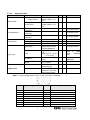
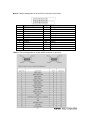
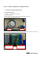
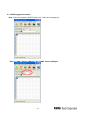
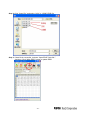
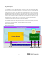
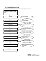
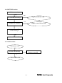
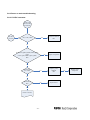
Product Service Manual – Level II Service Manual for BenQ: G2420HD P/N: 9H.L3ALB.QBx Applicable for All Regions Version: 001 Date:2009/05/26 Notice: - For RO to input specific “Legal Requirement” in specific NS regarding to responsibility and liability statements. - Please check BenQ’s eSupport web site, http://esupport.benq.com, to ensure that you have the most recent version of this manual. First Edition (May, 2009) © Copyright BenQ Corporation 2009. All Right Reserved. -1- Content Index Abbreviations & Acronyms .............................................................................. 3 1 About This Manual......................................................................................... 3 1.1. Trademark ............................................................................................................ 3 2 Introduction .................................................................................................... 4 2.1. 2.2. 2.3. 2.4. 2.5. RoHS (2002/95/EC) Requirements ...................................................................... 4 Safety Notice........................................................................................................ 4 Compliance Statement ......................................................................................... 4 General Descriptions ........................................................................................... 4 Related Service Information ................................................................................. 4 3 Product Overview .......................................................................................... 5 3.1. Specification ......................................................................................................... 5 3.2. Customer Acceptance ........................................................................................ 19 4 Level 1 Cosmetic / Appearance / Alignment Service ................................ 25 4.1. Software / Firmware Upgrade Process .............................................................. 25 4.2. Alignment procedure (for function adjustment) ................................................... 31 5 Level 2 Disassembly /Assembly Circuit Board and Standard Parts Replacement ................................................................................................... 39 5.1. Exploded View ................................................................................................... 39 5.2. Disassembly /Assembly ..................................................................................... 41 5.3. Main-Shielding Position...................................................................................... 50 5.4. Packing .............................................................................................................. 51 5.5. Block diagram .................................................................................................... 52 5.6. Trouble Shooting Guide ..................................................................................... 53 5.7. Circuit Operation Theory .................................................................................... 58 Appendix 1 – Screw List / Torque .................................................................. 69 Appendix 2-Physical Dimension Front View and Side view ....................... 72 -2- Abbreviations & Acronyms 1 About This Manual This manual contains information about maintenance and service of BenQ products. Use this manual to perform diagnostics tests, troubleshoot problems, and align the BenQ product. 1.1. Trademark The following terms are trademarks of BenQ Corporation: BenQ Importance Only trained service personnel who are familiar with this BenQ Product shall perform service or maintenance to it. Before performing any maintenance or service, the engineer MUST read the “Safety Note”. -3- 2 Introduction This section contains general service information, please read through carefully. It should be stored for easy access place for quick reference. 2.1. RoHS (2002/95/EC) Requirements – Applied to all countries require RoHS. The RoHS (Restriction of Hazardous Substance in Electrical and Electronic Equipment Directive) is a legal requirement by EU (European Union) for the global electronics industry which sold in EU and some counties also require this requirement. Any electrical and electronics products launched in the market after June 2006 should meet this RoHS requirements. Products launched in the market before June 2006 are not required to compliant with RoHS parts. If the original parts are not RoHS complaints, the replacement parts can be non ROHS complaints, but if the original parts are RoHS compliant, the replacement parts MUST be RoHS complaints. If the product service or maintenance require replacing any parts, please confirming the RoHS requirement before replace them. 2.2. Safety Notice 1. Make sure your working environment is dry and clean, and meets all government safety requirements. 2. Ensure that other persons are safe while you are servicing the product. DO NOT perform any action that may cause a hazard to the customer or make the product unsafe. 3. Use proper safety devices to ensure your personal safety. 4. Always use approved tools and test equipment for servicing. 5. Never assume the product’s power is disconnected from the mains power supply. Check that it is disconnected before opening the product’s cabinet. 6. Modules containing electrical components are sensitive to electrostatic discharge (ESD). Follow ESD safety procedures while handling these parts. 7. Some products contain more than one battery. Do not disassemble any battery, or expose it to high temperatures such as throwing into fire, or it may explode. 8. Refer to government requirements for battery recycling or disposal. 2.3. Compliance Statement Caution: This Optical Storage Product contains a Laser device. Refer to the product specifications and your local Laser Safety Compliance Requirements. 2.4. General Descriptions This Service Manual contains general information. There are 3 levels of service: Level 1: Cosmetic / Appearance / Alignment Service Level 2: Circuit Board or Standard Parts Replacement Level 3: Component Repair to Circuit Boards 2.5. Related Service Information BenQ Global Service Website: http://www.benq.com/support/ eSupport Website: http://esupport.benq.com/v2 -4- 3 Product Overview 3.1. Specification 3.1.1 Introduction G2420HD is defined 24’W LCD Monitor supports WXGA (1920x1080) resolution with DPMS (Display Power Management System) and Senseye function. There are three different input types, D-sub, DVI and HDMI, of models. G2420HD adopts AUO panel, M240HW01 V2. The features summary is shown as below, *All panel spec. in service manual definition depends on the variance of panel source. *All spec. of monitor need to warm up at least 1hr. * To test the “Contrast Ratio” and “Luminance” functions, the color status must be “User preset” mode. 1. “Contrast Ratio”: Set “brightness” at 100, and “contrast” at 50. 2. “Luminance”: Set “brightness” at 100, and “contrast” at 100. Feature items Panel supplier & module name Screen diagonal Display Format Pixel Pitch Specifications AUO M240HW01 V2 24W” 531.36(H) x 298.89(V) 0.276 mm x 0.276 mm R/L:85/85 degrees (typ) Viewing Angle (@ Contrast Ratio >= 10) and U/D: 80/80 degrees (typ) Remark TN, Normally white 609.7mm Panel Display information per one triad With 15-pin D-sub Yes connector Yes Yes 1920 (H) x 1080(V)@60Hz 16.7 Millions RGB 6-bit + FRC Test Condition: Set Contrast at 50, Brightness Contrast Ratio 1000:1 (typ.),600:1(min) at 100, Color at User preset Test Condition: Set 300 cd/m2 (typ.),240 cd/m2 contrast at 100, brightness Luminance (min) at 100 , color at User preset. AC power input Yes 90-264 Volts, 47-63 Hz. DC power input (with AC power adapter) No Off mode<1W DPMS supported(G2420HD) Yes Sleep Mode <1W LED indicator for power status showed Yes Green/Amber/None OSD for control & information supported Yes Multi-language supported for OSD Yes 17 languages. Buttons control supported Yes Flywheel control supported No Scaling function supported Yes Analog interface with Scaling supported DVI interface with Scaling supported HDMI interface with Scaling supported Max resolution mode supported Number of Display Colors supported -5- Auto adjustment function supported DDC function supported (EDID ver. 1.3) DDC-CI support version 1.1 or later Audio speakers supported Audio Jack (input connector) supported Earphone Jack (input connector) supported Microphone function supported Mechanical Tilt base design VESA wall mounting design Mechanical Rotate design Mechanical Lift base design Kensington compatible lock design 3.1.2 3.1.2.1 Item Yes Yes Yes No No “I-Key” function DDC2B DDC-CI Yes No Yes Yes No No Yes For HDMI Audio only From -5 to +23 degree Operational Specification Power supply Input Voltage range Input Current range Power Consumption DPMS(G2420HD) Inrush Current Earth Leakage Current Hi-Pot Power Line Transient Condition Universal input full range 90 ~ 264VAC Normal “On” operation DPMS “Off” state DPMS “Sleep” state 110 VAC 220 VAC 264 VAC/50Hz 1. 1500VAC, 1 sec 2. Ground test: 30A, 1sec IEC1000-4-4 Spec OK N.A Remark 90~264VAC /47~63Hz < 2.0 Arms <49 W <1W <1W < 30 A (peak) < 60A (peak) < 3.5 mA Without damage < 0.1 ohm 1KV Common: 2KV, IEC1000-4-5 (Surge) Differential: 1KV (on-line test) (in-lab test) 90 ~ 264VAC 3~8mA CCFL Frequency 90 ~ 264VAC 40KHz ~ 80KHz Color: Black Length: 1500 +/- 50 mm -6- Cold-start CCFL operation range Power cord LED: Green LED: Off LED: Amber Depends on panel source Depends on panel source 3.1.2.2 Item Signal interface Condition 15-pin D-Sub Signal Cable 24-pin DVI-D 15-pin D-sub connector 24-pin DVI-D connector 19-pin HDMI connector Signal type Level Impedance Pin assignment Analog input Impedance Sync Pulse Width (SPW) Level Impedance Digital input For 15-pin D-sub For 24-pin DVI-D For 19-pin HDMI Separate analog R/G/B 700 mV (peak to peak) 75 Ohms +/- 1.5 Ohms Separate H/V-sync Composite H/V-sync (Positive/Negative) Logic High: 2.4V ~ 5.5V Logic Low: 0V ~ 0.5V (TTL level) Minimum 2.2KΩ(pull down) 0.7μs < H-SPW 1H < V-SPW 600mV for each differential line 50 Ohm TDR Scan needed for DVI cable and interface board For 15-pin D-sub See Note-3 Level OK N.A Remark See Note-2 Signal type Sync input Spec Color: Black Length: 1500 +/- 30 mm Color: Black Length: 2000 +/- 50 mm See Note-1 Note-1: The pin assignment of 15-pin D-sub connector is as below, 1 2 3 4 5 6 7 8 PSignal Assignment Pin Signal Assignment Red video Green video Blue video Ground Cable Detected Red Ground Green Ground Blue Ground 9 10 11 12 13 14 15 PC5V (+5 volt power) Sync Ground Ground SDA H-Sync (or H+V) V-sync SCL -7- For 15-pin D-sub Refer VSIS V1R1 to VESA Standard 10KΩ application for Note-2: The pin assignment of 24-pin DVI-D connector is as below, 1 2 3 4 5 6 7 8 9 10 11 12 PSignal Assignment TMDS RX2TMDS RX2+ TMDS Ground Floating Floating DDC Clock DDC Data Floating TMDS RX1TMDS RX1+ TMDS Ground Floating Pin 13 14 15 16 17 18 19 20 21 22 23 24 Signal Assignment Floating +5V Power Ground Hot Plug Detect TMDS RX0TMDS RX0+ TMDS Ground Floating Floating TMDS Ground TMDS Clock+ TMDS Clock- Note-3: The pin assignment of 19-pin HDMI connector is as below, -8- 3.1.2.3 Item Video performance Condition Spec OK N.A Remark Both for analog and 170 MHz digital inputs Both for analog and 1920x1080@60 digital inputs 1920 x 1080 @ <5.89 ns 60Hz (50% of minimum pixel (max. support clock period) timing) Refer to VESA < 5% final full-scale VSIS Standard value V1R1 Refer to VESA < 12% of step function voltage level over the VSIS Standard full voltage range V1R1 Max. support Pixel rate Max. Resolution Rise time + Fall time Settling Time after overshoot /undershoot Overshoot/Undershoot 3.1.2.4 Scan range Item Horizontal Vertical Condition Spec 24-83 KHz 50-76 Hz 3.1.2.5 Plug & Play DDC2B DDC-CI Support Item Condition Spec DDC channel type EDID DDC2B Version 1.3 DDC-CI Version 1.1 or Later -9- OK N.A Remark OK N.A Remark Refer to BenQ LS EDID definition. Refer to BenQ DDCCI requirement definition. 3.1.2.6 Support Timings - 10 - HDMI video support timing 3.1.3 Operational & Functional Specification 3.1.3.1 Video performance *All spec. of monitor need to warm up at least 1hr. Item Condition Spec Any input resolution Resolution modes which are under 1920 x 1080 1920x1080 Contrast ratio 600(min),1000(typ) Brightness At R/G/B saturated condition Response time Gray to Gray Viewing angle At Contrast ratio = 10 CIE coordinate of White Display colors Average response time Response time with AMA of gray level to gray level - 11 - Test Condition: Set Contrast at 50, Brightness at 100, Color at User preset. Test Condition : Set contrast at 100 , brightness at 100 , color at User preset. Test Equipment: Westar TRD 100 or equal level equipment ; 240 cd/m2 (typ.),300(min) 2 ms (typ.) At Contrast ratio = 10 OK NA Remark R/L: 85/85 degrees (typ.) 75/75 degrees (min) U/D: 80/80 degrees (typ.) 70/70 degress(min) (0.31, 0.33) +/- (0.03, 0.03) 16.7 Millions colors 2ms(typ.), 2.9ms(max) 6 bit+FRC Test Condition: Set Contrast at 50, Brightness at 90, Color at User preset. 3.1.3.2 Item Brightness Adjustable Range Condition Spec OK NA Remark At default contrast level (Max. brightness value – Brightness adjustable (saturate point) & FullMin. brightness value) range white color pattern ≧ 100 cd/㎡ 3.1.3.3 Acoustical Noise Item Condition At 4 cm distance Acoustical Noise 3.1.3.4 Item Spec ≦ 28 dB/A OK NA Remark Refer to C326 Condition Operating Non-operating Spec 0 ~ +40 ℃ -20 ~ +60 ℃ Operating 10 ~ 90% Non-operating 10 ~ 90% OK NA Remark Non condensing Non condensing Without packing With packing Environment Temperature Humidity Operating Altitude 0~3048m (10,000ft) Non-operating 3.1.3.5 Item 0~12,192m (40,000ft) Transportation Condition (1) Vibration Spec OK NA Remark (1) Sine wave 5~200Hz 1.5G, 1 octave/min, 15 min dwell on each resonant frequency, all primary axis, one sweep (30 min minimum) per orientation, total of 90+ min. Package, Non-Operating (2) Random 5 ~100 Hz, 0 dB/Oct. 0.015 g2/Hz 100 ~200 Hz, -6 dB/Oct. 200 Hz, 0.0038 g2/Hz Equivalent to 1.47 Grms, All primary axis, 20 min per- orientation, total is 60 min. - 12 - (3) Procedure: Confirmed sample with appearance and function ready before testing then compare with after test record as brightness, uniformity and contrast ratio. Perform random vibration after sine-wave vibration test. Test Spectrum: 20 Hz 0.0185(g2/Hz) 200Hz 0.0185(g2/Hz) Unpackaged, Non(2) Unpackaged Vibration Duration : 5 Minutes Operating Axis : 3 axis ( Horizontal and Vertical axis ,Z axis) 91 cm Height (MP stage) (3) Drop Package, Non-Operating (1 corner, 3 edges, 6 faces) Waveform: half sine Faces: 6 sides/ per Wooden package, Nonorientation (4) Shock Operating 3 shocks. Duration: <3ms Velocity accelerate: 75g 3.1.3.6 Item Electrostatic Discharge Requirements Condition Spec Contact: 8KV Electrostatic Discharge IEC801-2 standard Air: 15KV 3.1.3.7 Item EMC Condition Electric TCO03 Magnetic FCC part 15J class B EMI EN55022 class B 3.1.3.8 Item OK NA Remark Spec OK NA Remark Band 1 < 10 V/m Band 2 < 1 V/m Band 1 < 200nT Band 2 < 25nT After Mass production under 1dBuv for constant measure. Besides DNSF and VCCI class-2 are optional. Reliability MTBF Prediction CCFL Life time Condition Spec Refer to MIL-217F At 25±2℃, under 7.0mA > 60,000 Hours 40,000 Hours (min) OK NA Remark Excluding CCFL See Note-4 Note-4: CCFL lifetime is determined as the time at which brightness of lamp is 50%. The typical lifetime of CCFL is on the condition at 7.0mA lamp current. - 13 - 3.1.3.9 Audio performance (Ear-Jack, For HDMI audio only) Item Condition Spec OK NA Remark Preamp + Power amp (1)Output power 1 Wrms/CH @ 1KHz (2)THD (@ 1W) <1% (3)S/N ratio >40dB Speaker Driver (1)Nominal impedance 4 ohm (2)Rated input power 1 W/CH (3)Frequency response 180~20KHz SPL-10dB (4)Output sound pressure 84 ± 3 dB (1W 0.5M) level 2 (5)Dimension of box 284x60x27mm Audio Control (1)Volume range 0 ~100 levels (2)Mute On/Off 3.1.4 LCD Characteristics 3.1.4.1 The Physical definition & Technology summary of LCD panel Item Condition Spec LCD Panel Supplier AUO Panel type of Supplier M240HW01 V2 Display area Unit=mm 531.36(H) x 298.89(V) Physical Size Unit=mm 556(H) x323.2(V) x 16.65(D) Weight Unit=gram 2860(typ.) Technology TN type Pixel pitch Unit=mm 0.276(H) x 0.276(W) (Typ.) Pixel arrangement R/G/B vertical stripe Display mode Normally White Support color 16.7Millions colors 3.1.4.2 Optical characteristics of LCD panel Item Unit Conditions Min. [degree] Horizontal 75 [degree] (Right) 75 CR = 10 (Left) Viewing Angle [degree] Vertical (Up) 70 [degree] CR = 10 70 (Down) Contrast ratio Normal Direction 600 [msec] Rising Time Response Time [msec] Falling Time [msec] Rising + Falling Gray to Gray Red x 0.619 Red y 0.308 Color / Chromaticity Green x 0.259 Coordinates (CIE) Green y 0.579 Blue x 0.116 - 14 - OK N.A Remark Per one triad 6 bit + HiFRC Typ. Max. 85 85 - 80 80 - 1000 3.4 1.6 5 2 0.649 0.338 0.289 0.609 0.146 7.4 2.6 10 0.679 0.368 0.319 0.639 0.176 Remark Color White Coordinates Luminance Uniformity Blue y White x White y 9 points measurement (CIE) [%] 0.04 0.283 0.299 0.07 0.313 0.329 75 80 0.10 0.343 0.359 White Luminance @ CCFL [cd/m2] 240 300 6.0mA (center) Crosstalk (in 75Hz) [%] 1.5 * The test methods for the above items definition, please refer to the relative panel specification. 3.1.5 User Controls 3.1.5.1 User’s hardware control definition Item Condition Power button Enter button Right/Inc. button Left/Dec. button Menu button(Exit buttom) Mode button Input Select button iKey button Mute button 3.1.5.2 OSD control function definition Item Condition Auto Adjust Brightness Contrast Horizontal Position Vertical Position Pixel Clock Phase Spec OK NA Remark Spec Auto-Geometry OK NA Remark Bluish Reddish Normal User: Separate R/G/B adjustment Reset Color OSD Horizontal position OSD Vertical position From 5 sec to 30 sec 17 languages Recall All Standard / Dynamics / Movie / Photo/sRGB D-sub DVI HDMI Color OSD Position OSD Time OSD Lock Language Recall Mode Input Select - 15 - Sharpness Display Information For input timing Volume For HDMI Audio only Mute For HDMI Audio only Hot key for Brightness Hot key for Contrast Hot key for Volume Hot key for Input Select Hot key for Mode The detailed firmware functions’ specification, please refer to C212 S/W spec. document. 3.1.6 Mechanical Characteristics 3.1.6.1 Dimension Item Bezel opening Monitor without Stand Monitor with Stand Carton Box (outside) Condition W x H x D mm W x H x D mm L x W x H mm Tilt and Swivel range 3.1.6.2 Weight Item Monitor (Net) Monitor with (Gross) Spec 533.2*300.7 mm 570*348.42*63.26mm 570*412.6*183.94mm 636*133*482 mm Tilt: -3.5 ~ +21.5 degree Swivel: 0 degree Condition packing 3.1.6.3 Plastic Item Flammability Heat deflection To UV stability Condition ABS ABS Resin Texture Color 3.1.6.4 Carton Item Color Material Compression strength Burst Strength Stacked quantity Condition Remark Spec 4.91Kg OK N.A Remark 6.5Kg Spec >ABS<,94-HB 65 ℃ Delta E < 8.0 MPRII: ABS (SD0150/GP35/D150/PA 757/HP-126/T0103) MT-11010 BCS-7015A OK N.A Remark Spec Kraft A Flute 250 KGF 19.2 KGF/cm2 5 Layers - 16 - OK N.A OK N.A Remark 3.1.7 Pallet & Shipment 3.1.7.1 Container Specification Quantity of products Stowing Type Container (sets) (Every container) 624 20' With pallet 1296 40' 20' Without pallet 40' Quantity of Products (sets) (Every Pallet) Pallet A: 76 Pallet B: 68 Pallet C: 24 Pallet A: 76 Pallet B: 68 X Quantity of pallet (sets) (Every Container) Pallet A: 4 Pallet B: 4 Pallet C: 2 Pallet A: 9 Pallet B: 9 X X X X X X X 3.1.7.2 Carton Specification Product: Net Weight (Kg) Gross Weight (Kg) 4.9Kg 6.5Kg Package: Carton Interior Dimension (mm) L*W*H 570*412.6*183.94mm 636*133*482 mm Certification Item Environment PC-Monitor Safety Dimension w/ Base W*H*D (mm) Carton External Dimension (mm) L*W*H 624*121*456 mm 3.1.8 Dimension w/o Base W*H*D (mm) 570*412.6*87.7mm Condition Spec Green design API Doc. 715-C49 Blue Angel German Standard E-2000 EPA TCO’99 TCO’03 Green Mark Microsoft Windows DPMS DDC 2B USB UL (USA) CSA (Canada) Nordic / D.N.S.F - 17 - Switzerland USA Standard OK N.A Remark ISO14000 Requirement PC98/99 VESA Version 1.3 External UL60950 3rd edition CAN/CSA-C22.2 No. 60950 EN60950 FIMKO CE Mark CB CB TUV/GS EMC X- Ray Requirement CCC (China) GOST SASO CE Mark FCC (USA) EN55022 CISPR 22 VCCI (Japan) BSMI (Taiwan) C-Tick (Australia) DHHS (21 CFR) DNHW German X- Ray standard PTB Ergonomics EN60950 73/23/EEC IEC60950 EN60950 EN60950 / EK1-ITB 2000:2003 CB4943 EN60950 IEC60950 89/336/EEC FCC Part 15 B Class B Class B VCCI Class B CNS 13438 AS/ NZS CISPR22 USA X- Ray Standard TUV / Ergo ISO 13406-2 prEN50279 - 18 - 3.2. Customer Acceptance 3.2.1. SCOPE This document establishes the general workmanship standards and functional Acceptance criteria for LCD color monitor model G2420HD Produced by BenQ Corporation. 3.2.2. PURPOSE The purpose of this publication is to define a procedure for inspection of the LCD monitor by means of a customer acceptance test, the method of evaluation of defects and rules for specifying acceptance levels. 3.2.3. APPLICATION The "Customer Acceptance Criteria" is applicable to the inspection of the LCD monitor, completely packed and ready for dispatch to customers. Unless otherwise specified, the customer acceptance inspection should be conducted at manufacturer's site. 3.2.4. DEFINITION The "Customer Acceptance Criteria" is the document defining the process of examining, testing or otherwise comparing the product with a given set of specified technical, esthetic and workmanship requirements leading to an evaluation of the "degree of fitness for use", including possible personal injury or property damage for the user of the product. 3.2.5. CLASSIFICATION OF DEFECTS The defects are grouped into the following classes: Critical defect A critical defect is a defect that judgment and experience indicate is likely to result in hazardous or unsafe conditions for individuals using, maintaining or depending upon the product. Major defect A major defect is a defect, other than critical, that is likely to result in failure, or to reduce materially the usability of the product for its intended purpose. Minor defect A minor defect is a defect that is not likely to reduce materially the usability of the product for its intended purpose, or is a departure from established standards having little bearing on the effective use of operation of the product. - 19 - 3.2.6. CLASSIFICATION OF DEFECTIVES A defective is a product which contains one or more defects. The defective will be classified into following classes. Critical defective A critical defective contains one or more critical and may also contain major and/or minor defects. Major defective A major defective contains one or more defects and may also contain minor defects but contains no critical defect. Minor defective A minor defective contains one or more minor defects but contains no critical and major defects. 3.2.7. EXPRESSION OF DEFECTIVES Number of defects Percent of defects = ------------------------------------------ X 100% Number of products inspected 3.2.8. INSPECTION STANDARD Unless otherwise specified, the inspection standard will be defined by MIL- STD105E(ISO-2859), SINGLE SAMPLING PLAN. level II is in use all the time , inspection levels are normal ,reduce and tighten . Acceptance Quality Level When a critical defect is found, this must be reported immediately upon detection, the lot or batch shall be rejected and further shipments shall be held up pending instructions from the responsible person in relevant organization. Major Defective: 0.4 AQL Minor Defective: 1.50 AQL 3.2.9. GENERAL RULES The inspection must be carried out by trained inspectors having good knowledge of the meaning of "fitness for use". The inspection must be based upon the documents concerning the completely assembled and packed product when more defects appear with the same cause only the most serious defect must be taken into account. Defects found in accessories packed with the product as connecting cables, plugs, adapters and the like, and being inspected as a part of the complete product, must be included in the evaluation. The evaluation must be within the limits of the product specification and, for not specified characteristics, be related to the design model, limit samples or judgment of a jury of experts. Faults must be demonstrable. - 20 - 3.2.10. TEST CONDITIONS Unless otherwise prescribed, the test conditions are as follows: . Nominal mains voltage Temperature: +5~+35℃ . Warm up time : 30minutes minimum . . Visual inspection shall be down with the distance from eyes to the sample 35-50 cm . . Display mode: Primary mode 1920 x 1080 3.2.11. TEST EQUIPMENTS 1. PC with display adapter or other specific display adapter which is agreed upon by both parties 2. Test program by BenQ 3. Ruler 4. Power saving test tool 5. Minolta color analyzer ( CA-110 or BM – 7 ) 3.2.12. VISUAL INSPECTION CRITERIA 1. PACKING 2. ACCESSORIES 3. APPEARANCE 4. AC POWER AND SIGNAL CABLE 5. INTERIOR OF THE PRODUCT No Description 1 Packing 1.1 Wrong packing material 1.2 Carton damaged(over 6cm dia).wet, badly taped or stapled, product will not arrive in good condition at customer 1.3 Carton damaged(3cm to 6cm dia), badly taped or stapled , product will arrive in good condition at customer 1.4 Wrong marking of trade mark 1.5 Wrong marking of model number 1.6 Wrong serial # marking on carton 1.7 Product wrongly placed in box ( upside down ) 1.8 Broken polyfoam or PU foam 1.9 Broken packing bag 1.10 Wrong size or poor printing for artwork/character 1.11 Bar-code wrong, missing, or damaged 1.12 Label on box missing or damaged 1.13 Strange object in the box 1.14 Unit not corresponding to model stated on external label 1.15 Superficial breaking 5 ~ 10 cm dia 2 Accessories 2.1 Missing accessory parts 2.2 Wrong Accessory parts 3 Appearance of product 3.1 Incorrect color of cabinet 3.2 Incorrect color of tilt/swivel base 3.3 Wrong logo or name plate - 21 - Class Major Minor Minor Major Major Major Major Major Major Major Major Major Major Major Minor Major Major Major Major Major No 3.4 3.5 3.6 3.7 3.8 3.9 3.10 3.11 3.12 3.13 3.14 3.15 3.16 3.17 3.18 3.19 3.20 3.21 3.22 3.20 3.21 3.23 3.24 3.25 3.26 3.27 3.28 3.29 4 4.1 4.2 4.3 4.4 4.5 4.6 4.7 4.8 5 5.1 5.2 5.3 5.4 5.5 5.6 5.7 5.8 5.9 5.10 Description Poor print of logo or name plate Label on product Wrong or missing Scratched or dirty but legible spec. label GAP between LCD and front bezel is over 2.0 mm Dot/area discolor over 1mm dia. in front or over 2mm dia. in other areas Cabinet warped, sagged or bulging >0.5% of surface length Cabinet warped, sagged or bulging noticeable but <0.5% of surface length Sharp stud or edge, which can cause damage not safe Finishing of piece parts will not arrived in good condition at the customer Cabinet step ( between housing and bezel ) >1.0mm , < 1.5mm Cabinet step ( between housing and bezel ) >1.5mm Wiring or fixing cord comes out of cabinet or jammed Auxiliary material used during production not removed Cabinet parts come loose during normal handling, not safe Cabinet parts come loose during normal handling, but safe Tilt/swivel too flexible/not working Tilt/swivel stiff Dirty front bezel and housing can’t remove Dirty front bezel and housing removable easily Sticker or loose user control switch which will not function correctly Missing knob or switch, not safe Missing knob or switch, but safe Poor functional user controls in mechanical Unreadable printing of user controls label Rubber foot missing LED wrong material or missing LED sagged >1.0mm or bulging>0.5mm Wrong S/N between spec. label and monitor display AC power and signal cable AC power or connector not correct or damaged, not safe AC power or connector not correct or damaged, but safe Signal cable contact pin dirty Signal cable plug dirty or surface damaged, but safe Cable crack Cable scratch ( wire not exposed ), or dirty AC-DC adapter no function Signal cable contact pin dirty Interior of the product Use Non-QVL ( Qualify vendor list )component Wrong parts, broken component, but safe Foreign material Conductive (Has potential to short circuit) Non-conductive (Moveable) Missing hardware, component or screw, stripped screw Loose hardware/screw or insufficient torque Poor wire routing, which is no concerned on EMI Cold soldering/loose connections (Electrical) Wires and mechanical structure do not meet UL/CSA or TUV Wrong parts, broken component, not safe Component burn - 22 - Class Major Major Minor Major Major Major Minor Major Major Minor Major Major Major Critical Major Major Minor Major Minor Major Critical Major Major Major Major Major Minor Major Critical Major Minor Minor Major Major Minor Major Major Major Major Minor Major Major Minor Major Critical Critical Critical 3.2.13. OPERATIONAL INSPECTION CRITERIA 1. TEST PATTERN 2. SPECIFICATIONS 3. OPERATIONAL INSPECTION CRITERIA 3.2.13.1. List of test pattern KEY A E PATTERN FULL WHITE DARK TEST ITEM H - Size , V – Size .Viewing Angle Light Output Impurity, Spot check Contrast Ratio Brightness adjust Range Background, Spot check F FULL W , R , G , B Impurity, Spot check .CIE Coordinate check G 256 COLORS Color Check H 16 GREY Gray Check H Electric characteristics Black/White stripe pattern - 23 - 3.2.13.2. Video performance Item Spec Max. support Pixel rate Max. Resolution OK 170 MHz 1920x1080@60 Rise time + Fall time <5.89 ns (50% of minimum pixel clock period) N.A Remark Both for analog and digital inputs Both for analog and digital inputs Settling Time after < 5% final full-scale value overshoot /undershoot < 12% of step function Overshoot/Undershoot voltage level over the full voltage range 1920 x 1080 @ 60Hz (max. support timing) Refer to VESA VSIS Standard V1R1 Refer to VESA VSIS Standard V1R1 3.2.14. PANEL INSPECTION CRITERIA Inspection Item Specification Line defect Can’t be seen Bright Dot <=2 dots Green bright dots <=2 dots Dark dots <=4 dots Total dots defect <=5 dots Continuous Defect Two continuous bright dots(vertical ,horizontal, oblique):<=1 pair Exclude continuous green-green bright dots Three or more continuous bright dots (vertical, horizontal ,oblique):Not allowed Two continuous dark dots(vertical ,horizontal, oblique):<=2 pairs Three or more continuous dark dots(vertical, horizontal, oblique):Not allowed Distance between 2B dots:>=15mm Distance between 2Ddots:>=15mm Distance between B and D dot :>=10mm Note: This Panel Specification is subject to change. Please check it on eSupport system for latest update. - 24 - 4 Level 1 Cosmetic / Appearance / Alignment Service 4.1. Software / Firmware Upgrade Process 4.1.1 Hardware Requirement: 1. I2C board x 1 (a.Print Board b. I2C Board) 2. DSUB VGA cables x 2 3. Printer cable (with one male connector and another female connector) x 1. 4. PC or Notebook with parallel (printer) port x1. Print Cord I2C Board Check the Jumpers on the I2C circuit board (make sure J5/J6/J7/J8 are set at Pin 1 & Pin 2 short) Connected to print cord and PC Connected to Display Signal Cable - 25 - Link “I2C BD, Power cable and Signal cable 4.1.2 Software prepare 1. Realtek.exe Step 1: Press RTD Tool Step 2: Choose “ IIC”, “Serial Flash” and “0x94”. Then, press “ISP” 1. 2. - 26 - Step 3: Click the “Bank” and Find the F/W 1. xxx.H00 2. xxx.H01 3. xxx.H02 4. xxxEXT.Hex Step4: Choose “P-Flash” and “Auto” Step5: Press to run the program Step6: Check result, If the words showed in red, need to run the program again 3. 6. 4. 5. - 27 - 4.1.3 EDID Upgrade Procedure Step 1: Run the program “Q-EDID-V016.exe”, when the UI popped up Note: If “VGA” choose 128bytes, and “HDMI” choose 256bytes - 28 - Step 2: Click “Open File” and select “VGA” or “HDMI” EDID file Step 3: If load file is successful, it shows “Open EDID Table OK.” And then, Click “Write EDID” button to update EDID - 29 - Step 4: If write EDID is successful, it shows ”Write EDID OK …” And then, click “Read EDID” button to check if successful or not. Step 5: If read EDID is successful, it shows” Read EDID OK …” - 30 - 4.2. Alignment procedure (for function adjustment) A. Preparation: 1. Setup input timing ICL-605( 1280x1024@75Hz ), Pattern:5-Mosaic. 2. Setup unit and keep it warm up at least 30 minutes. B. Timing adjustment: 1. Enter factory setting area (press “ENTER”, “MENU” and then press “SOFTPOWER”). 2. Check the settings to following values: Contrast = 50 Brightness = 90 Color = User Mode Senseye mode = Standard Language = English Burn In =ON Then, turn off the monitor power. 3. Turn on power enter user area. C. Color balance adjustment: 1. Enter factory setting area (press “ENTER”, “MENU” and then press “SOFTPOWER”). 2. Setup input timings WS7(1280x1024@75Hz), Pattern:5-Mosaic. 3. Setup Color mode “User Mode”. 4. Press “I-KEY”( or Left key directly), and then OSD will show “White Balance” item and then press “ENTER” button to do auto color. - 31 - D. Color adjustment: 1. Setup input timing ICL-605, white pattern. 2. Confirm auto color adjustment had already done. 3. Measure color temperature by Minolta CA-110 (or equivalent equipment). 4. Check the color temperature Bluish, Reddish & Normal. The color temperature specification as follows: White Balance X+0.283+(-) 0.015 (Bluish, 9300K set on OSD) Y+0.297+(-) 0.015 White Balance X+0. 326+(-) 0.015 (Reddish, 5800K set on OSD) Y+0. 342+(-) 0.015 White Balance X+0.313+(-) 0.015 (sRGB, 6500K set on OSD) Y+0. 329 +(-) 0.015 5. Setup input timing, 32 -Gray pattern. To check if there are any abnormal display problems of preset timing modes Check the following preset timings with General pattern: No. Mode H V 1 720×400 @ 70Hz 31.468 70.8 2 640×480 @ 60Hz 31.469 59.940 3 640×480 @ 75Hz 37.500 75.000 4 800×600 @ 60Hz 37.879 60.317 5 800×600 @ 75Hz 46.875 75.000 6 1024×768 @ 60Hz 48.363 60.004 7 1024×768 @ 75Hz 60.023 75.029 8 1152x864 @ 75Hz 67.500 75.000 1280×1024 @ 9 63.981 60.020 60Hz 1280×1024 @ 10 79.976 75.025 75Hz 6. Checking if the picture is no good, reject this monitor. 7. To check the power consumption by disabling “burn-in mode” setting 8. To clear user data and program complete DDC data to monitor by IIC bus communication. E. Writing EDID file: 1. Setup a PC with DDC card. 2. Connect PC to monitor with a D-sub(DVI) signal cable. 3. Please refer to the C212 for the correct EDID file. 4. Runs the writing program to write the EDID file into EEPROM . 5. Read EEPROM data and confirm it to match with the C212 document definition. - 32 - F. Command definition : PC Host will send 0x7C IIC slave address and then following 4 bytes command Byte Byte I2C Send Command Byte1 2 3 Byte4 OK N.A. Remark cksu Write Contrast to MCU RAM CA 55 Data m cksu Write Brightness to MCU RAM CA 56 Data m cksu Write data to MCU RAM Write Red Gain to MCU RAM CA 57 Data m and update the related cksu register to refresh the Write Green Gain to MCU RAM CA 58 Data m screen immediately. Don’t store data to cksu EEPROM. Write Blue Gain to MCU RAM CA 59 Data m cksu Read Contrast from MCU RAM C3 55 XX m cksu Read Brightness from MCU RAM C3 56 XX m Read Red Gain from MCU RAM by cksu color index C3 57 XX m Read Green Gain from MCU RAM by cksu color index C3 58 XX m Base on current color index to read back the Read Blue Gain from MCU RAM by cksu right gain value. color index C3 59 XX m Write C1 (Bluish) R-Gain Data to cksu EEPROM AA 3C Data m Write C1 (Bluish) G-Gain Data to cksu EEPROM AA 3D Data m Write C1 (Bluish) B-Gain Data to cksu EEPROM AA 3E Data m Write C2 (sRGB) R-Gain Data to cksu EEPROM AA 4C Data m Write C2 (sRGB) G-Gain Data to cksu EEPROM AA 4D Data m Write C2 (sRGB) B-Gain Data to cksu EEPROM AA 4E Data m Write C3 (Reddish) R-Gain Data to cksu EEPROM AA 5C Data m Write C3 (Reddish) G-Gain Data to cksu EEPROM AA 5D Data m Write C3 (Reddish) B-Gain Data to cksu EEPROM AA 5E Data m cksu Write User R-Gain Data to EEPROM AA 6C Data m cksu Write User G-Gain Data to EEPROM AA 6D Data m cksu Write User B-Gain Data to EEPROM AA 6E Data m - 33 - Write Cx R-Gain Data to EEPROM AA 7C Write Cx G-Gain Data to EEPROM AA 7D Write Cx B-Gain Data to EEPROM AA 7E Write Contrast to EEPROM AA 92 Write Brightness to EEPROM AA 93 Write C/T index to EEPROM AA Write OSD-Hpos to EEPROM AA Write OSD-Vpos to EEPROM AA cksu Data m cksu Data m cksu Data m cksu Data m cksu Data m Reserved for some model have extra color temperature 1=C1/9300/Bluish, 2=C2/6500/sRGB/, 3=C3/5800/Reddish, 4=User, 5=Cx cksu 1~4 m cksu 95 Data m cksu 96 Data m 94 (Also Update MCU RAM) Write Language to EEPROM AA Write EEPROM OSD Timer AA Write EEPROM Volume AA Write EEPROM Gamma index AA Write OSD Transparency to EEPROM AA Write OSD Rotation to EEPROM Read C1 (Bluish) R-Gain data from EEPROM Read C1 (Bluish) G-Gain data from EEPROM Read C1 (Bluish) B-Gain data from EEPROM Read C2 (sRGB) R-Gain data from EEPROM Read C2 (sRGB) G-Gain data from EEPROM AA A3 A3 A3 A3 A3 - 34 - cksu 97 0~17 m cksu 98 Data m cksu 99 Data m cksu 9A Data m cksu 9E Data m cksu 9F Data m cksu 3C XX m cksu 3D XX m cksu 3E XX m cksu 4C XX m cksu 4D XX m 1=English, 3=French, 0=Deutsch, 4=Italian, 2=Spanish, 5=JAPAN, 6=繁中, 7=簡中 8=Hungarian, 9=Serbian, 0A=Russian, 0B=Dutch, 0C=Polish, 0D=Czech, 0E=Swedish, 0F=Portugese, 10=Romanian For model with Gamma curve selection function Read C2 (sRGB) B-Gain data from EEPROM Read C3 (Reddish) R-Gain data from EEPROM Read C3 (Reddish) G-Gain data from EEPROM Read C3 (Reddish) B-Gain data from EEPROM A3 4E XX A3 5C XX A3 5D XX A3 5E XX Read User R-Gain data from EEPROM A3 6C XX Read User G-Gain data from EEPROM A3 6D XX Read User B-Gain data from EEPROM A3 6E XX Read Cx R-Gain data from EEPROM A3 7C XX Read Cx G-Gain data from EEPROM A3 7D XX Read Cx B-Gain data from EEPROM A3 7E XX Read Contrast from EEPROM A3 92 XX Read Brightness from EEPROM A3 93 XX Read C/T index from EEPROM A3 94 Read OSD-Hpos EEPROM A3 95 Read OSD-Vpos from EEPROM A3 96 Read Language from EEPROM A3 97 Read OSD Timer from EEPROM A3 98 Read Volume from EEPROM A3 99 Read Gamma index from EEPROM Read OSD Transparency from EEPROM A3 9A A3 9E - 35 - cksu m cksu m cksu m cksu m cksu m cksu m cksu m cksu m cksu m cksu m cksu m cksu m Reserved for some model have extra color temperature 1=C1/9300/Bluish, 2=C2/6500/sRGB/, 3=C3/5800/Reddish, 4=User, 5=Cx cksu XX m cksu XX m cksu XX m cksu XX m cksu XX m cksu XX m cksu XX m cksu XX m 1=English, 3=French, 0=Deutsch, 4=Italian, 2=Spanish, 5=JAPAN, 6=繁中, 7=簡中 8=Hungarian, 9=Serbian, 0A=Russian, 0B=Dutch, 0C=Polish, 0D=Czech, 0E=Swedish, 0F=Portugese, 10=Romanian For model with Gamma curve selection function Read OSD Rotation from EEPROM Change Color Temp. to C1/9300K/Bluish Change Color Temp. to C2/6500K/sRGB Change Color Temp. to C3/5800K/Reddish A3 9F CC 01 CC 02 CC 03 Change Color Temp. to User CC 04 Change Color Temp. to Cx CC 05 Change Input Source to D-Sub CD 01 Change Input Source to DVI CD 02 On burn in mode CE 01 Off burn in mode CE XX* Monitor is forced power saving CF 01 Monitor wake up from power saving CF XX* Change Sense-Eye mode to Standard C0 00 Change Sense-Eye mode to Movie1 C0 01 Change Sense-Eye mode to Movie2 C0 02 Change Sense-Eye mode to Photo C0 03 Set luminance sensor mode to Off C1 00 Set luminance sensor mode to Bright Set luminance sensor mode to Moderate C1 01 C1 02 Set luminance sensor mode to Dim C1 03 Increase ADC R-Offset2 AC 23 Increase ADC G-Offset2 AC 24 Increase ADC B-Offset2 AC 25 Increase ADC R-Gain AC 33 Increase ADC G-Gain AC 34 - 36 - cksu XX m cksu XX m cksu XX m cksu XX m cksu XX m cksu XX m cksu XX m cksu XX m cksu XX m cksu XX m cksu XX m cksu XX m cksu XX m cksu XX m cksu XX m cksu XX m cksu XX m cksu XX m cksu XX m cksu XX m cksu Data m cksu Data m cksu Data m cksu Data m cksu Data m Change C/T immediately. And store C/T index to EEPROM. Reserved Store data to EEPROM XX* = Non “1” value Store data to EEPROM XX* = Non “1” value Change Sense-Eye mode immediately. And store the index to EEPROM. Change luminance sensor mode immediately. And store the index to EEPROM. cksu Data m cksu Data m cksu Data m cksu Data m cksu Data m cksu Data m cksu Data m cksu XX m cksu XX m cksu XX m cksu XX m cksu XX m cksu XX m cksu XX m cksu XX m cksu XX m cksu XX m cksu XX m NA NA NA NA Increase ADC B-Gain AC 35 Decrease ADC R-Offset2 AD 23 Decrease ADC G-Offset2 AD 24 Decrease ADC B-Offset2 AD 25 Decrease ADC R-Gain AD 33 Decrease ADC G-Gain AD 34 Decrease ADC B-Gain AD 35 Read ADC R-Offset2 AE 23 Read ADC G-Offset2 AE 24 Read ADC B-Offset2 AE 25 Read ADC R-Gain AE 33 Read ADC G-Gain AE 34 Read ADC B-Gain AE 35 User mode to factory mode 1A 5A Auto Color (Offset1, Offset2, Gain) 1B 5A Copy EDID Serial number to EEPROM 1C 5A Factory mode to User mode 1E 5A Clear user mode and factory recall Write EDID data to MCU DDC RAM Copy DDC RAM data to EEPROM Drive WP pin to low to enable write DDC IC Drive WP pin to high to disenable write function 1F 55 BB 5A NA NA 55 NA NA NA For stand alone DDC IC BB NA NA NA Switch DDC bus to DVI-A DDC IC 44 NA NA NA Switch DDC bus to DVI-D DDC IC 33 NA NA Change Senseye Mode C0 0~3 NA cksu XX m For stand alone DDC IC For input signal with multi-input source For input signal with multi-input source - 37 - For specified “Industry Customer” model. Store data to EEPROM For MTV312 MCU type For MTV312 MCU type Change Power Status cksu D0 Data XX m Change Language Type ckssu D1 Data XX m PowerOFF: Data=AA PowerON: Data=Other Value Asia: Data=AA European: Data=Other Value EEPROM Bank R/W (For Debug using only, not for Production Line Write EEPROM directly) Addr cksu Read EEPROM Bank 0 B0 ess XX m Addr cksu Read EEPROM Bank 1 B1 ess XX m Addr cksu Read EEPROM Bank 2 B2 ess XX m (For 24C08 type) Addr cksu Read EEPROM Bank 3 B3 ess XX m (For 24C08 type) Addr cksu Write EEPROM Bank 0 B8 ess Data m Addr cksu Write EEPROM Bank 1 B9 ess Data m Addr cksu Write EEPROM Bank 2 BA ess Data m (For 24C08 type) Addr cksu Write EEPROM Bank 3 BB ess Data m (For 24C08 type) Note A: Byte4 (cksum) = Byte1 + Byte2 + Byte3 Note B: Data = The value write to MCU or EEPROM Note C: XX = don't care, any value (<=0xFF). When PC Host sends 0x7D command to MCU, MCU must return as following (2 bytes) Return Code Checksum error code Normal return code If normal return code is exact FCh - 38 - R-Byte1 FC R-Byte2 AA the above Byte3 (/data) FC FC CF 5 Level 2 Disassembly /Assembly Circuit Board and Standard Parts Replacement 5.1. Exploded View 5 1 2 3 13 9 14 15 16 17 21 20 8 7 12 6 5 4 10 11 18 22 19 23 - 39 - 5E.0BJ06.001 5E.0RM03.001 5E.0RM02.001 5E.0RM01.011 5F.LUDB0.051 * This Service BOM is subject to change. Please check it on eSupport and SPO system before service parts order release. - 40 - 5.2. Disassembly /Assembly 5.2.1 Disassembly SOP Preparation before disassemble 1. Clean the room for disassemble 2. Identify the area for monitor 3. Check the position that the monitors be placed and the quantity of the monitor; prepare the area for material flow; according to the actual condition plan the disassemble layout 4. Prepare the implement, equipments, material as bellow: 1) Press-fixture 2) working table 3) Screw-driver 4) knife*1 5) glove 6) cleaning cloth 7) ESD protection ite m 1 2 picture Operation Disassemble the stand 2 screws disassembly the bezel from the monitor, notice the disassembly order : 1.Left (1) parts of bezel 2.Top (2) parts of bezel 3.Bottom (3) parts of bezel 4. Right (4) parts of bezel Don’t draw the BZL - 41 - Tool Notes Screw-driver When disassembly the bezel ,notice don’t bend the C/B .man must wear glove The purpose is loose the BZL 3 Turn over the monitor ,dismantle the Rear cover from the monitor(if it have earphone function, pull the earphone wire out of the connector) 4 Pull the c/b wire out of the c/b connector. Tear off the C/B wire from panel ,move away C/B and button 5 Tear off the big aluminum foil. - 42 - 6 Tear off the two acetic tapes (if it have that ) Pull out the light wires from connector . 7 Disassemble the SHD 8 Tear off all the tapes sticked on the BKT (including aluminum foils and acetic tapes ) - 43 - 9 Tear off the yellow tape on the LVDS FFC ,and pull LVDS FFC out off the panel . 10 Disassemble the hexangular screws ( four or two ) 10 Turn over the BKT , and disassemble the power board and I/F board .----7 screws 11 Pull out the connector - 44 - Screw-driver 5.2.2 Assembly SOP Preparation before assemble 1. Clean the room for work 2. Identify the area for material 3. Prepare the implement, equipments, materials as bellow: 1) Press-fixture 2) working table 3) Screw-driver 4) knife*1 5) glove 6) cleaning cloth 7) ESD protection ite m picture Operation Put panel on the cushion carefully, 1 2 Fetch I/F board and LVDS FFC ,insert FFC into I/F . 3 Fetch power board and put it into BKT, and put the connector wire into I/F connector ,then put I/F into BKT (like the pic. Showed ) - 45 - Tool Notes 4 Lock PCBA screw .-five or six PCBA screw ,one earth screw . 5 Turn over the bkt, and lock the hexangular screws ( four or two ) Screw driver:5+0.6kg Lock one HDMI screw (if it have that ) Screw driver: Side mount: 3±0.6 Other: 4±0.6 6 Lock SHD on the BKT ,to fixup the P/B 7 Insert LVDS FFC in the panel - 46 - Screw driver : 7±1kg 8 Fetch yellow tape, and stick it on the LVDS FFC 9 Use location tool ,location the bkt on panel 10 Stick tapes follow standard: One tape stick on angel side ,one on right side ,one on ground side . Stick acetic tapes on left 11 Insert light wires, and make sure it connect well . Use two acetic tapes fix the light wires . - 47 - location tool: G24101 12 Stick big aluminum foil on the side (like left PIC) 13 Fetch bezel ,and put panel into bezel (don’t touch the LCD screen. 14 Put c/b in the button, and put button in bezel. Tear the tapes on the back of c/b wire , insert c/b connector in I/F ,stick c/b on panel . 15 Fetch cover ,cover the monitor .( if it have ear phone function ,assay earphone board on cover first, and insert the wire into I/F ) First cover bottom ,then cover two sides ,last cover the angel side . - 48 - Screw driver(if it need) : 3+0.5KG Φ1.75±0.05 #1 16 Assay stand .(follow picture on left .) put hinge in front cover ,and lock four screws, then cover the back cover ,last put the clip in front cover. Screw driver : 7.5+0.5kg 17 Put stand in monitor, and lock two screws . Screw driver : 9.0+1.0kg 18 Fetch base ,and assay base on monitor . - 49 - 5.3. Main-Shielding Position 機種名稱 BenQ G900HD BenQ G2220HD BenQ G2020HD BenQ G2410HD AUO BenQ G2410HD CMO BenQ T2200 BenQ G2420HD/G2420HDB 測點A尺寸 56.69mm 84mm 69mm 78.65mm 72.65mm 56.69mm 78.65mm 測點B尺寸 40mm 44.5mm 42mm 57.2mm 55.85mm 40mm 57.2mm 測點C尺寸 40mm 44.5mm 42mm 57.2mm 55.85mm 40mm 57.2mm AL-Tape AL-Tape L Shape Tooling - 50 - 5.4. Packing - 51 - 5.5. Block diagram The G2420HD is a 24” (1920x1080) Model, LCD type is TN+ Film and Normally White, 16.7M colors(R, G, B 6-bit data+ FRC data) TFT LCD monitor. There are D-SUB, DVI and HDMI interface LCD monitor. It’s compliant with VESA specification to offer a smart power management and power saving function. It also offers OSD menu for users to control the adjustable items and get some information about this monitor. The best function is to offer users an easy method to do DDC/CI Enable and Auto Adjustment items well done just by pressing hot key, we called it “DDC/CI” and “Auto” which can manual controlled items. G2420HD also offer DDC2/CI function to meet VESA standard. The G2420HD consists of a LCD module with 4 lamps, a power board including an inverter, a control board, a Interface board. The block diagram is shown as below. Monitor internal structure Monitor internal structure - 52 - 5.6. Trouble Shooting Guide 5.6.1 No Display or display is unstable on analog, digital or video port: No picture or picture unstable on Analog port or DVI port or HDMI port Power off Y Turn on power N Does cable plugs in connector? N Plug the cable then turn on power again. Y Is 5V from power board normal ? N Check Power BD 5V output Y Is Power LED light Green or amber? Y N Check Key BD and Key BD cable N Is Power LED status normal? Replace Power Key BD Y Does crystal work correctly? N Check crystal CKT or replace it (Y1) Y Is interface BD normally? N Replace interface BD Y N Plug LVDS cable again or replace it Is LVDS cable connect OK? Y Replace panel - 53 - 5.6.2 BUTTON Function: OSD is not working Yes No Plug control BD then retry Is control BD connecting? Yes Yes Is bottom key normally? Replace control BD then retry No Replace Control BD Is OSD working?? No Check Interface BD 5.6.3 OSD Function: OSD doesn’t work Is control BD working? N Replace control BD Y Check interface BD - 54 - 5.6.4 Power no work troubleshooting 5.6.4.1 DC/DC converter Panel or I/F BD or Audio no function DC/DC converter +5V(+5.4V) valid? Check wire and I/F BD Yes No Check L852, Q852, FD852, FD853, Q855, Q856 (L851, Q851, FD851, Q853, Q854) OK? No Replace components IC Check IC851 Vcc valid? Yes Check IC851 pin1 frequency, DTC, feedback OK? No Check F851 OK? No Yes AC/DC converter - 55 - Replace F851 No Replace IC851 components 5.6.4.2 AC/DC converter - 56 - 5.6.4.3 Inverter Panel lamp no work Check V-INVERTER OK? No AC/DC converter Yes Check IC801 VDDA OK? No DC/DC converter Yes Check BL_ON, BRT_ADJ OK? No Check wires, I/F BD No Replace IC801 components Yes Check IC801 frequency, output OK? Yes Check T801, T802, Q801~Q804 Replace components - 57 - 5.7. Circuit Operation Theory A-1.) Interface board diagram: A-2.) Circuit operation theory: (a) Monitor Diagram: - 58 - (b) Circuit operation theory A basic operation theory for this interface board is to convert analog signals of Red, Green and Blue to digital signals of Red, Green and Blue. The scaling IC has internal A/D converter, internal OSD, built in RSDS transmitter and auto-detect input timing functions. A/D converter is convert analog signal to digital data. OSD is offering adjustable functions to end-user. Detect timing is for detect change mode. RSDS transmitter is used to compress the digital RGB data, the Hsync, Vsync and pixel clock generated by Scaling then output to LCD module. Flash-rom stores source code and MCU (embedded in Scalar) offers H/W DDC2Bi function & controls system processing. EEPROM is stored DDC data, OSD common data and user mode data. (c) IC introduction: 1.) DDC (Display Data Channel) function: We use DDC IC to support DDC2Bi function. DDC data is store in 24C02 (EEPROM). Those data related to LCD monitor specification. PC can read them by “SDA” and “SCL” serial communication for I²C communication for DDC2Bi. 2.) Scalar IC: There are A/D, TMDS receiver, Scaling, OSD and LVDS transmitter functions built-in the RTD2482D IC. Scaling IC is revolutionary scaling and color engine, capable of expanding any source resolution to a highly uniform and sharp image or down scaling from 1920x1080, combined with the critically proven integrated 8 bit triple-ADC and patented Rapid-lock digital clock recovery system. It also support detect mode and DPMS control. 3.) MCU embedded in Scalar: Control unit, it controls all the functions of this interface board, just like the OSD display setting, the adjustable items, adjusted data storage, the external IIC communication, support DDC2Bi. . 4.) EEPROM: We use 24C16 to store all the adjustable data, user settings and uses two 24C02 to store D-SUB, DVI and HDMI data. 5.) Flash-rom stores source code. A-2.) Control board introduction There are 6 keys for user's control which includes “Power”, “Menu”, “Right/Plus”, “Left/Minus”, “Auto”, and “Enter”. The following descriptions are the introduction of these keys. (1) Power key: to turn/off power of monitor (2) “Menu” key: to enter sub-menus or select items. (3) “Right/Plus key: to select previous and to increase adjustment and Brightness /Contrast Popup submenu hotkey (4) “Left/Minus” key: to select next and to decrease adjustment and Senseye Mode Popup submenu hotkey - 59 - (5) “Auto” key: to perform auto adjustment (6) LED: It indicates the DPMS status of this LCD monitor; blue light means DPMS on (Normal operating condition). Amber light means DPMS off (Power Saving). A-3.) Power board diagram: EMI Filter Rectifier and filter PWM controller Isolation power transformer Rectifier and filter Switching element Rectifier and filter Inverter circuit SW regulator Feedback Isolation Fig.1 #1 EMI Filter This circuit (fig. 2) is designed to inhibit electrical and magnetic interference for meeting FCC, VDE, VCCI standard requirements. 2 t TR601 NTC 5 1 L4 1 L602 2 4 C601 0.22U M 3 C604 2200PF 19MH C602 0.22U M C603 2200PF N3 Fig. 2 - 60 - #2 Rectifier and filter AC Voltage (90-264V) is rectified and filtered by BD601, C605 (See Fig 3) and the DC Output voltage is 1.4*(AC input). (See Fig.3) E1 3 L6 GSIB4A60-LF BD601 + + 1 2 4 - 1 ~ C605 150U 450V <Spec> 2 ~ Fig. 3 #3 Switching element and Isolation power transformer When the Q601 turns on, energy is stored in the transformer. During Q601 turn-off period, the stored energy is delivered to the secondary of transformer. C614, R607, C607 and D601 are snubber circuits. R615 is current sense resistor to control output power. (See Fig.4) L605 E2 Z45/100MHZ C607 0.001U J R607 68K E3 K 1 T601 12 A D601 UF4007-LF 2 E4 L604 Z45/100MHZ E5 3 10 11 L603 5 Q601 D Z45/100MHZ C614 100P K 4 S G R615 0.22 6 Fig. 4 - 61 - 8 #4 Rectifier and filter D701, D702, C701, C702, C703 are used to produce DC output. (See Fig.5) A1 J A2 + R702 100 3 C704 1000P K C705 1000P K 10 11 5 4 6 8 Fig. 5 - 62 - 2 2 C701 470U 35V RC1820 1 + C702 470U 35V RC1820 + 2 D702 Y G862C15RSC 1 R701 100 2 12 V-INVERTER 1 1 T601 D701 Y G862C15RSC A1 J A2 C703 470U 35V RC1820 #5 PWM Controller The TEA1530(A)T can be used in Fixed Frequency converter designs for low voltage, high current applications. At low power (standby) levels, the system operates in cycle skipping mode which minimizes the switching losses during standby. The proprietary high voltage BCD800 process makes direct start-up possible from the rectified universal mains voltage in an effective and green way. A second low voltage BICMOS IC is used for accurate, high speed protection functions and control. The TEA1530(A)T enables highly efficient and reliable supplies to be designed easily. L605 E1 1 E3 1 K 2 Z45/100MHZ C607 0.001U J R607 68K C605 150U 450V <Spec> + E2 T601 12 A D601 UF4007-LF 2 E4 R605 10K L604 Z45/100MHZ E5 R606 1 K C612 1U K 2 3 R620 100K F 4 Gnd HVS Protect Driv er Ctrl R617 10K F Sense 8 7 5 Z45/100MHZ C608 1000P K Q601 STP7NK80ZFP R612 10 J 6 R614 1K F C611 100PF 50V J C614 100P K G R613 68K F 5 D K C613 1U 25V A ZD601 TZMC20 Drain 4 R622 10K F C616 1U K R615 0.22 6 90V ?W Protection 264V ?W Protection C610 3300P J 11 L603 D602 EGP10D-LF 10 J C606 47U 50V 10 2 NXP1530 1 ‧ Vcc + E6 3 S IC601 A R611 27 R618 4.7K A K ZD602 TZMC6V2 Fig. 6 - 63 - K R616 68K A D605 LL4148 8 #6 Feedback circuit PC123 is a photo-coupler and KA431 is a shunt regulation. They are used to detect the output voltage change and be the primary and secondary isolation. When output voltage changes, the feedback voltage will be compared and duty cycle will be decided to control the correct output voltage. (See Fig.7) R708 2K 1 R711 22K F C709 0.1U K 2 R709 10K F K IC602 PC123FY 1J00F 3 4 R707 10K A R IC702 R712 3.32K F KA431AZT A_NL Fig. 7 #7 DC-DC circuit IC851(PWM IC TL1451) is used to convert V-INVERTER to other voltage needed. F851 32V 2A R864 3.3K R865 22K Q853 PMBS3904 R876 2.05K F IC851-10 FD851 SB360-LF Q854 2N3906S C863 470P K A + C865 220U 25V R877 1.2K F C B R866 22 R853 10K F C864 0.1U 1 B 2 Q853-B K 2 C860 0.1U MCU_3.3V G + C862 220U 25V R863 330 R860 22K C AUDIO_CTRL R861 2.7K J R856 330K L851 D E C853 1U K S 47U E C E R852 Q857-B 2.7K B Q857 2N3906S Q851 2SJ598 Q853-C 1 V-INVERTER C855 0.01U K R855 47K 9 VCC Q852 2SJ598 Q855-C C859 1U K S C857 220P K K A FD853 ERB83-004 C868 470P K R874 3.09K F C869 0.1U 1 FD852 ERB83-004 + C871 220U 25V 2 E E Q856 2N3906S B C R862 2.7K J C858 0.01U K 1U K R858 330K Q855 PMBS3904 Q855-E A B IC851-7 R873 47K R857 C85610K F G R872 22K R871 3.3K C + C867 220U 25V 2 R851 10K F PANEL_5V 47U 8 7 6 5 4 3 2 1 C851 470P K L852 D 1 GND 1OUT 1DTC 1FBK 1IN- RT CT 1IN+ IC851 TL1451ACN C852 0.1U K K 2OUT 11 2FBK 2DTC 10 IC851-14 12 13 C854 220P K 2IN- 14 15 SCP 2IN+ RFF 16 R854 10K F R859 10K F IC851-3 - 64 - R882 22 L853 Z45/100MHZ R875 1K F IC851(TL1451) is a 2-way PWM control IC. C851/R851 determine the frequency of PWM. Pin 1IN+/1IN- and 2IN+/2IN- are the inputs of the error amplifiers. 1IN+/2IN+ are used as the feedback pins for DC-DC circuit. 1DTC/2DTC are used for determining the threshold states of dead time control. C854, C855, C857, C858, R855 and R873 are used for gain/phase compensation. P11 V-INVERTER C853 1U M R856 330K F851 32V 2A R853 10K F C855 0.01U K R863 330 R854 10K F R855 47K R851 10K F R858 330K 10 9 VCC 11 2DTC C858 0.01U K R859 10K F The timing diagram of TL1451 is shown as following: - 65 - GND 8 P13 R873 47K R857 10K F 1OUT 1DTC C857 220P K 7 6 1IN- 1FBK 5 4 RT 3 CT 2 1 C851 470P K 1IN+ IC851 TL1451ACN C852 0.1U K C856 1U M 2OUT 12 13 2IN- 2FBK 15 14 SCP 2IN+ RFF 16 C854 220P K C859 1U M P-MOSFET Q852 is used for switching of step-down converter. And FD852/FD853 are the flywheel diodes. R874/R875 determine the feedback to IC851 to set up the output to +5V or +3.3V. V-INVERTER 9 Q852 2SJ598 VCC 11 10 2OUT S D A R874 3.09K F FD853 ERB83-004 C869 1200P K 1 C Q856 2N3906S B FD852 ERB83-004 + C871 220U 25V C868 470P K R882 22 C R862 2.7K J Q855 PMBS3904 P10 E E B K K R872 22K R871 3.3K A 2 + C867 220U 25V G 1 GND 8 1OUT 7 1DTC 1FBK 1IN- PANEL_+5V L852 47U 6 5 4 RT 1IN+ 3 2 1 CT IC851 TL1451ACN L853 Z45/100MHZ 2 2FBK 2DTC 12 13 2IN- 14 2IN+ 15 SCP RFF 16 F851 32V 2A R875 1K F #8 Inverter Circuit Operation Theory LCDM Inverter Controller --- OZ9933 OZ9933 is a high performance, cost-effective CCFL controller designed for driving large-size LCD applications requiring 2 to 6 CCFLs. The controller converts unregulated DC voltages into a nearly sinusoidal lamp voltage and current waveforms. The OZ9933 supports full-bridge power conversion topologies while maintaining highefficiency operation, current and voltage regulation, over-voltage and over-current protection, high drive capability. The control logic provides s regulated ignition voltage and appropriate protection features for over-voltage or over-current conditions. Pin Assignment of OZ9933 - 66 - K Full-Bridge Configuration ZD801 TZMC6V2 Q801 P_A 3 A R801 5.1K 4 5 6 8 7 N_B C827 4.7U M R811 10K Q802 K 3 P_C C829 4.7U M T 801 . 5 1 2 6 4 A FD801 ERB83-004 . 3 4 7 . 5 6 8 7 N_D . 2 2 1 1 R812 10K 8 Fig. 1 Fig. 1: Q801, Q802 and T801 form a full-bridge configuration. The full-bridge switch is configured such that Q801 N-MOS and Q8026 P-MOS are ON while Q801 P-MOS and Q802 N-MOS are OFF in a half-cycle. During the next half cycle, Q801 NMOS and Q802 P-MOS are OFF while Q801 P-MOS and Q802 N-MOS are ON. This develops an alternating current through the transformer primary. The result in T801 primary coil has an AC square waveform. Certainly, the secondary of T801 will produce high voltage AC sinusoidal waveform. - 67 - Feed-back Circuit C815 100P J F1 TP801 TP802 C819 5PF D 6 . C820 470P J . 3 4 7 . 10 11 12 13 14 15 NDR2 PDR1 GNDP VDDA TIMER PWM ISEN OVPT ENA PDR2 GNDA RT1 CT SST/CMP VSEN 8 7 C816 100P J 8 C821-2 . 2 1 6 5 A K 2 2K62272102 A R831 D801 511 F BAV99 TP803 TP804 C821 5PF D 1 2 CN802 1 2 2K62272102 R821 100K R816 2.2K C822 470P J R822 20K F 4 3 2 1 K C814 0.033U K R834 1M D809 LL4148 1 R820 20K F J 16 NDR1 OZ9933 9 K C831 0.22U K F3 IC801 R815 2.2K R819 100K 5 2 CN801 J T 801 1 D805 BAV99 A R827 365 F Fig. 2 Fig. 2 shows the feedback circuit consists of a lamp, R816, D805, R827 and C814. With the lamp current through D805, a half sine-waveform voltage signal is produced. We may get the Maximum value through R827/C814. After OZ9933 gets the feedback voltage signal from PIN14, the duty of the full-bridge driver outputs is decided. - 68 - Appendix 1 – Screw List / Torque STANDARD SCREW TORQUE SPEC. ITEM P/N 1 8F.205B4.019 2 8F.5A224.6R0 8F.EA324.6R0 3 4 5 8F.5A356.8R0 6K.L8810.001 6 8F.00273.6R0 7 8F.VZ524.6R0 8 8F.00518.100 9 8F.00003.143 DESCRIPTION MOUNTING MATERIAL HOLE TORQUE SIZE (KG-CM) (MM) Metal; D-SUB;DVI 5.0±0.6 Connector Metal Side mount: SCRW MACH Metal to metal 3±0.6 Plastic to Other: FLATM3*0.5P*6L ZN metal 4±0.6 None tread: 8~ SCRW TAP FH M3*6L ZN Metal 10 Have tread: 6~8 Metal SCRW MACH FH M4*8L B- Metal to metal 9.0±1.0 ZN NYL Plastic to metal ASSY SCREW M4*8L Metal FP726A NLK ISU Metal to metal 9.0±1.0 (8F.5A456.8R0+4B.L7212.0 Plastic to 01) metal None tread: 8~ Metal Metal to metal 10 SCRW TAP PH F/10WSH Plastic to Have tread: M3*6L C-ZN metal 6~8 PCB to metal Aluminum: 4~5 None tread: 8~ 10 SCRW TAP FLAT+EXT Metal Have tread: M3*6L C-ZN Metal to metal 6~8 Aluminum: 4~5 None Metal tread: 8~ Metal to metal 10 SCRW TAP W/FL Plastic to Have tread: M3*10L(S3.8)ZN metal 6~8 SPEAKER to Aluminum: metal 4~5 Aluminum SCRW TAP PAN #4-40*3/8 (Heatsink) 3.3±0.3 SCRW MACH HEX #440*0.3" N - 69 - Screw Head 5.0±0.6 #4-40 M3*0.5 #2 Φ2.68±0.0 3 #2 M4*0.7 #2 M4*0.7 #2 Æ2.68±0.0 3 Æ2.68±0.0 3 #2 #2 Æ2.68±0.0 3 #2 Φ2.6±0.03 #2 10 8F.VG234.6R0 SCRW TAP PH W/F M3*6 TP-S ZN Aluminum (Heatsink) Metal Metal to metal Metal SCRW TAP Metal to metal 8F.HA334.8R0 FPHM3*6(6/1)TP-S B-ZN Plastic to metal Metal SCRW MACH FLAT M4*8L Metal to metal 8F.5A456.8R0 C-ZN NYLO Plastic to metal Metal SCRW TAP CAP Metal to metal 8F.WA324.6R0 M3*1.34P*6L B-NI Plastic to metal Metal 8F.XA324.5R0 SCRW TAP M3*5L B-ZB Metal to Plastic Metal SCRW MACH PAN M4*5L Metal to metal 8F.1A526.5R0 NI Plastic to metal 11 8F.VZ526.6R0 SCRW TAP FLAT+EXT M4*6L ZN-W None tread: 8~ 10 Φ2.68±0.0 Have tread: 3 6~8 Aluminum: 4~5 #2 M4*0.7 #2 6~8 Φ2.68±0.0 3 #2 9.0±1.0 M4*0.7 #2 5.0±1.0 Φ2.35±0.0 5 #2 6~8 2.85~2.95 #2 8~10 M4*0.7P #2 17 Metal SCRW MACH PAN W/SPG Metal to metal 8F.1B524.3R0 M3*3L NI Plastic to metal 6~8 M3*0.5P #2 18 Metal SCRW MACH FLAT M3*4L Metal to metal 8F.5A524.4R0 NI(W2407 lift Plastic to metal 6~8 M3*0.5P #2 19 8F.00573.5R0 6~8 M3*0.5P #1 Metal SCRW MACH FLAT M4*7L Metal to Metal 20 8F.5A456.7R0 B-ZN NYL Plastic to Metal 8~10 M4*0.7P #2 Metal Metal to metal Plastic to metal 8~10 M4*0.7P #2 12 13 14 15 16 21 SCRW TAP FPHM3*5 BZN SCRW TAP FLAT M4*15L 8F.XA326.150 B-ZN - 70 - Metal Metal to Plastic 10±1.0 22 23 8F.00608.6R0 8F.XA313.8R0 24 8F.WA314.8R0 SCRW TAP PH F/10WSH M3*6L B-ZN SCRW TAP FLAT/PT M2.5*8L B-ZN SCRW TAP CAP M3*1.34P*8L B-ZN 25 8F.XA224.6R0 SCRW TAP FH M3*6L ZN 26 SCRW TAP FLAT 8F.XA314.8R0 M3*1.34P*8L B-ZN 27 8F.00607.8R0 SCRW TAP FPH M3*8L(5/0.8) B-ZN 28 8F.5A322.2R4 SCRW MACH FLAT-P M2*2.4L B-ZN 29 8F.00551.3R0 SCRW M FPH M2*3L (6/1.4) NI 30 8F.MA324.5R5 SCRW TAP FPH M3*5.5L B-ZN 31 SCRW TAP FLAT M4*10L B-ZN 8F.XA326.100 - 71 - PLASTIC Plastic Metal to plastic Plastic to plastic PCB to plastic Plastic Metal to plastic Plastic to plastic PLASTIC Plastic Metal to plastic Plastic to plastic Plastic Metal to plastic Plastic to plastic PCB to plastic Plastic Metal to plastic Plastic to plastic PCB to plastic Plastic Metal to plastic Plastic to plastic PCB to plastic Metal Metal to metal Plastic to metal Plastic Metal to plastic Plastic to plastic 4.5±0.5 Φ2.35±0.0 5 #2 4.0±0.5 Φ2.0±0.05 #1 5.0±1.0 Φ2.35±0.0 5 #2 4.5±0.5 Φ2.35±0.0 5 #2 4.5±0.5 Φ2.35±0.0 5 #2 4.0±0.5 Φ2.68±0.0 3 #2 2.0±0.5 Φ1.75±0.0 5 #1 2.0±0.5 Φ1.75±0.0 5 #1 6~8 M3*0.5P #2 8~10 Φ3.45±0.0 5 #2 Appendix 2-Physical Dimension Front View and Side view Fig. 1 Physical Dimension Front View and Side view - 72 - Fig. 2 Appearance Description - 73 -