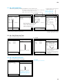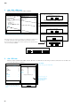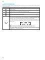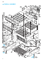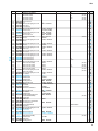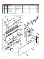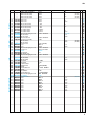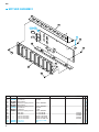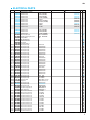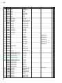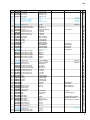
1
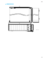
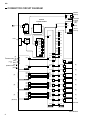
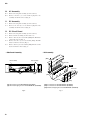
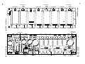
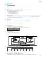
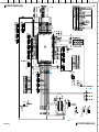
YDP-123C
ANALOG INPUT BOX
SERVICE MANUAL
MODEL
AI8-ML8
AI8-AD8
AI8-ML4AD4
AI8-ML8AB
AI8-ML8F
REFERENCE SERVICE MANUAL
LMY2-ML
LMY4-AD
LMY4-AD
LMY2-ML
LMY2-MLAB
LMY4-MLF
PA011502
PA011503
PA011503
PA011502
PA011736
PA011737
CONTENTS
REVISED PAGE LIST ............................................................ 2-1
SPECIFICATIONS .................................................................. 3-1
PANEL LAYOUT ..................................................................... 3-2
DIMENSIONS ......................................................................... 3-3
CONNECTOR CIRCUIT DIAGRAM .......................................... 4
BLOCK DIAGRAM ..................................................................... 6
DISASSEMBLY PROCEDURE ................................................. 7
LSI PIN DESCRIPTION ........................................................... 11
IC BLOCK DIAGRAM .............................................................. 14
CIRCUIT BOARDS .................................................................. 16
INSPECTION ...................................................................... 21/23
TEST PROGRAM ............................................................... 26/31
ERROR MESSAGES ............................................................... 42
PARTS LIST
CIRCUIT DIAGRAM
PA
011505
HAMAMATSU, JAPAN
Copyright (c) Yamaha Corporation. All rights reserved. PDF-K-
****
K
’01.03
1
AI8
REVISED PAGE LIST
ITEM
PAGE
SPECIFICATIONS
3-1
PANEL LAYOUT
3-2
DIMENSIONS
3-3
BLOCK DIAGRAM
6
DISASSEMBLY PROCEDURE
7,9
IC BLOCK DIAGRAM
14
CIRCUIT BOARDS
16~20
AC, IPC3, DR, PSB, LED1
16
DC, MB1
19
IFC2
20
INSPECTION
21~22
TEST PROGRAM
23~27
ERROR MESSAGES
42
<PARTS LIST>
ITEM
PAGE
OVERALL ASSEMBLY
2, 3, 4
SIDE PANEL ASSEMBLY
4, 5
MOTHER ASSEMBLY
6
ELECTRICAL PARTS
7~12
<CIRCUIT DIAGRAM>
ITEM
UNC CIRCUIT DIAGRAM
IFC2 CIRCUIT DIAGRAM
PAGE
002
3
003
4
002
9
003
10
004
11
005
12
006
13
007
14
008
15
IPC1 CIRCUIT DIAGRAM
16
IPC3 CIRCUIT DIAGRAM
17
AICOM CIRCUIT DIAGRAM 002
18
2-1
AI8
IMPORTANT NOTICE
This manual has been provided for the use of authorized Yamaha Retailers and their service personnel. It has been assumed that
basic service procedures inherent to the industry, and more specifically Yamaha Products, are already known and understood by
the users, and have therefore not been restated.
WARNING:
Failure to follow appropriate service and safety procedures when servicing this product may result in personal
injury, destruction of expensive components and failure of the product to perform as specified. For these
reasons, we advise all Yamaha product owners that all service required should be performed by an authorized
Yamaha Retailer or the appointed service representative.
IMPORTANT:
This presentation or sale of this manual to any individual or firm does not constitute authorization, certification,
recognition of any applicable technical capabilities, or establish a principal-agent relationship of any form.
The data provided is belived to be accurate and applicable to the unit(s) indicated on the cover. The research engineering, and
service departments of Yamaha are continually striving to improve Yamaha products. Modifications are, therefore, inevitable and
changes in specification are subject to change without notice or obligation to retrofit. Should any discrepancy appear to exist,
please contact the distributor's Service Division.
WARNING:
Static discharges can destroy expensive components. Discharge any static electricity your body may have
accumulated by grounding yourself to the ground bus in the unit (heavy gauge black wires connect to this bus).
IMPORTANT:
Turn the unit OFF during disassembly and parts replacement. Recheck all work before you apply power to the
unit.
WARNING: CHEMICAL CONTENT NOTICE!
The solder used in the production of this product contains LEAD. In addition, other electrical/electronic and/or plastic (where
applicable) components may also contain traces of chemicals found by the California Health and Welfare Agency (and possibly
other entities) to cause cancer and/or birth defects or other reproductive harm.
DO NOT PLACE SOLDER, ELECTRICAL/ELECTRONIC OR PLASTIC COMPONENTS IN YOUR MOUTH FOR ANY REASON
WHAT SO EVER!
Avoid prolonged, unprotected contact between solder and your skin! When soldering, do not inhale solder fumes or expose eyes
to solder/flux vapor!
If you come in contact with solder or components located inside the enclosure of this product, wash your hands before handling
food.
IMPORTANT NOTICE FOR THE UNITED KINGDOM
Connecting the Plug and Cord
IMPORTANT.
The wires in this main lead are coloured in
accordance with the following code:
BLUE:
NEUTRAL
BROWN: LIVE
As the colours of the wires in the main lead of this apparatus may not
correspond with the coloured markings identifying the terminals in
your plug, proceed as follows:
The BLUE wire must be connected to the terminal that is marked with
the letter N (or coloured BLACK).
The BROWN wire must be connected to the terminal that is marked
with the letter L (or coloured RED).
Be certain that neither core is connected to the earth terminal of the
three pin plug.
WARNING
Components having special characteristics are marked
originally installed.
2-2
and must be replaced with parts having specification equal to those
AI8
SPECIFICATIONS
Sampling frequency (external sync)
39.69 kHz – 50.88 kHz
USA and Canada: 120 V, 60 Hz
Power supply
Others: 230 V, 50 Hz
Power consumption
120 W
Dimensions (W x H x D)
480 mm x 141.5 mm x 466.8 mm
Weight
15.4 kg
Operating temperature
10 – 35 ˚C
Power cable length
2.1 m
Cooling fan speed
always fixed
Accessories
Connection cable (68-pin, D-sub, half-pitch) x 1, Length: 3 m
Digital I/Os
I/O connectors
Level
Type
OUTPUT A, B, C
RS-422
D-sub, half-pitch, 68-pin connector (female)
WORD CLOCK IN
TTL/75 Ω (ON/OFF)
BNC Connector
WORD CLOCK OUT
TTL/75 Ω
BNC Connector
Slots
Card
Input
LMY2-ML
Channel 1A or 1B, 2A or 2B
LMY4-AD
Channel 1 – 4
3-1
AI8
PANEL LAYOUT
Front Panel
INPUT UNIT ID
1
PHANTOM MASTER
1
2
3
4
5
6
7
8
ON
UNIT NO.
+48V
OFF
PHANTOM MASTER
2
ON
+48V
OFF
POWER
ON/ OFF
POWER
ON/ OFF
ANALOG INPUT BOX
* The illustration shows the AI8 analog input box.
3
ANALOG INPUT BOX
1 INPUT UNIT ID indicator
2 PHANTOM MASTER switch, indicator
3 POWER ON/OFF
Rear Panel
5
CONTROL
PORT
4
CONTROL
PORT
A
B
C
B
A
WORD
CLOCK
IN
OFF
ON
75
OUT
6
IN
OFF
ON
75
7
OUT
4 CONTROL PORT switch
5 OUTPUT connectors A, B, C
6 WORD CLOCK IN jack, ON/OFF switch
7 WORD CLOCK OUT jack
3-2
OUTPUT
C
WORD
CLOCK
OUTPUT
C
A
B
C
B
A
AI8
DIMENSIONS
466.8
455
430
480
4
5
6
7
8
UNIT NO.
PHANTOM MASTER
ON
+48V
OFF
POWER
ON/ OFF
141.5
3
Unit: mm
ANALOG INPUT BOX
9.5
2
132 (3U)
1
3-3
AI8
CONNECTOR CIRCUIT DIAGRAM
[POWER
ON/OFF]
3P CN600
**
PSB
POWER
TRANSFORMER
AC
8P CN101
2P CN700
[OFF]
14P CN100
**
FG
[INPUT
UNIT ID]
CN702 CN701
3P
4P
DR
CN802
3P
CN800
2P
LED1
5P CN127
6P CN103
FAN
[PHANTOM
MASTER]
[+48V]
[ON]
4P CN126
4P CN125
CN100 14P
CN002
5P
CN101 4P
CN300 2P
CN001
4P
CN301 4P
CN302 2P
6P CN124
4P CN123
CN303 4P
6P CN122
CN200 12P
4P CN121
CN400 4P
DC
[8]
CN507 8P
8P CN116
CN107
100P
[7]
CN506 8P
8P CN115
CN106
100P
[6]
CN505 8P
8P CN114
CN105
100P
[5]
CN504 8P
8P CN113
CN104
100P
[4]
CN503 8P
8P CN112
CN103
100P
[3]
CN502 8P
8P CN111
CN102
100P
[2]
CN501 8P
8P CN110
CN101
100P
[1]
CN512 6P
8P CN118
5P CN511
IPC3
CN101 13P
13P CN709
CN102 13P
13P CN710
CN103 10P
10P CN711
10P CN712
CN101 13P
13P CN705
CN102 13P
13P CN706
CN103 10P
10P CN707
10P CN708
CN104 10P
IPC1
CN101 13P
13P CN701
CN102 13P
13P CN702
CN103 10P
10P CN703
10P CN704
CN104 10P
[OUTPUT]
8P CN117
100P
CN300 5P
IPC1
[A]
CN508 8P
CN509 14P
CN104 10P
[B]
30P CN119
CN108
[C]
CN101 30P
5P CN510
100P
[IN]
[WORD CLOCK]
[OUT]
CN200 5P
20P CN120
CN109
[A]
[CONTROL PORT] [B]
[C]
[ON]
[75 ]
[OFF]
CN102 20P
IPC1
UNC
SLOT NO.
IFC2
MB1
KEC-92522-2
4
AI8
Circuit Board
CN No.
Pin No.
Circuit Board
CN No.
Pin No.
DC
CN100
1
2
3
4
5
6
7
8
9
10
11
12
13
14
1
2
3
1
2
3
4
5
6
7
8
9
1
2
1
2
1
2
1
2
1
2
3
4
1
2
3
4
5
6
7
8
9
10
11
12
13
14
1
3
4
MB1
CN122
MB1
CN124
MB1
IFC2
CN127
CN103
MB1
CN122
MB1
CN124
MB1
IFC2
CN127
CN103
MB1
IFC2
CN127
CN103
MB1
CN121
MB1
CN123
MB1
CN125
MB1
MB1
MB1
DR
CN121
CN123
CN125
CN800
MB1
MB1
MB1
CN122
CN124
CN127
MB1
MB1
LED1
CN122
CN124
CN101
LED1
CN100
LED1
LED1
CN101
CN101
4
3
4
3
5
1
2
2
1
2
1
3
3
4
4
5
6
4
3
4
3
4
3
1
1
1
1
2
6
6
2
1
5
2
1
2
3
4
1
2
3
4
5
6
7
8
9
10
11
12
13
14
7
6
5
PSB
CN600
DC
CN101
DC
CN200
DC
CN300
DC
CN301
DC
CN302
DC
CN303
DC
CN400
IFC2
CN509
MB1
CN126
AC
CN701
1
4
1
3
KEC-92522-3
5
AI8
6
BLOCK DIAGRAM
SLOT NO.
/CS1
IC601
I11
[1]
/CON1
I12
DOA
DSP5
/CS2
DIR2
I21
[2]
/CON2
I22
IC307
44.1K
48K
/CS3
[3]
DIR2
WCO
LOCK
WC SEL & SYNC DETECTOR
I41
[4]
WC
I51
[5]
WCIB
WCO
Decoder
I52
Register
/CS6
I61
[6]
FPGA
DIR2 2
I71
[7]
IC301
IC302
I72
/CS8
[8]
IPC1
WCIC
ID I/O
WCO
MASTER
CLOCK
/CON8
I81
IC405
I82
DIR2
Driver
Receiver
48V
WCID
[IN]
WCO
[WORD CLOCK]
[OUT]
[OFF]
[A]
IFC2
[C]
IPC1
[ON]
MB1
[B]
IC404
I62
/CS7
Driver
Receiver
DOC
IC202
DIR2
/CON7
IPC1
DOB
DIR2
I42
/CS5
/CON6
[A]
IC402
ID I/O
/CON5
Driver
Receiver
I32
/CS4
/CON4
WCIA
ID I/O
I31
/CON3
[OUTPUT]
IC401
[75 ]
[B]
[C]
[CONTROL PORT]
IPC3
[ON] 48V
Register
Data Bus
Decoder
Address Bus
CPU
[INPUT UNIT ID]
IC101
UNC
[PHANTOM MASTER]
[+48V]
RAM
FLASH
IC203
IC201
[OFF]
LED1
KEC-92520
1
AI8
DISASSEMBLY PROCEDURE
1.
UNC Card Assembly
1-1
Remove the four (4) screws marked [470]. The UNC card
assembly can them be removed. (Fig. 1)
2.
Front Panel Assembly
2-1
2-2
Remove the UNC card assembly. (See Procedure 1.)
Remove the thirty-two (32) screws marked [500]. The
blank panel can then be removed. (Fig. 1)
Remove the eight (8) screws marked [450] and the two (2) screws
marked [452]. Each mount bracket can then be removed. (Fig. 1)
Remove the six (6) screws marked [400]. The front panel
assembly can then be removed. (Fig. 1)
2-3
2-4
1
2
Blank panel
[400]
Front panel assembly
3
4
5
6
7
[470]
UNC card assembly
<Right Side View>
8
[450]
[400]
[452]
Mount bracket
Mount bracket
[400]
[500] x 32
[470]
Mount bracket
<Left Side View>
[450]
[452]
Mount bracket
[450]: Oval Head Screw 4.0x8 MFZN2BL (VS153600)
[452]: Oval Head Screw B4.0x8 MFZN2BL (V6221000)
[500]: Bonding Screw 3.0x6 MFZN2BL (VS863000)
[470]: Bonding Screw 3.0x6 MFZN2BL (VS863000)
[400]: Flat Head Screw 4.0x8 MFZN2BL (VA221200)
Fig. 1
3.
LED1 Circuit Board
3-1
3-2
Remove the front panel assembly. (See Procedure 2.)
Remove the two (2) screws marked [80]. The LED1
circuit board can then be removed. (Fig. 2)
4.
PSB Circuit Board
4-1
4-2
4-3
Remove the UNC card assembly. (See Procedure 1.)
Remove the front panel assembly. (See Procedure 2.)
Remove the seventeen (17) screws marked [430]. The top
panel can then be removed. (Fig. 2)
Remove the two (2) screws marked [100]. The PSB circuit
board can then be removed. (Fig. 2)
4-4
7
AI8
[170]
<Top View>
[430] x 17
LED1
[80]
[100]
PSB
Top panel
[80]: Bind Head Tapping Screw-B 3.0x6 MFZN2BL (EP600230)
[100]: Bind Head Screw 3.0x8 MFZN2BL (VB659000)
[170]: Bind Head Tapping Screw-B A4.0x8 MFZN2BL (VC688800)
[430]: Bind Head Tapping Screw-B A4.0x8 MFZN2BL (VC688800)
Fig. 2
5.
Circuit Boards and Units
Remove the top panel, each circuit board and unit can
then be removed. (Fig. 3)
Circuit Board and Unit
Ref. No.
A
310
320
380
240
IPC1
IPC3
DR
Power Transformer
Screw
Screw
Bonding Screw 3.0x6 MFZN2BL (VS863000)
Bind Head Screw A4.0x6 MFZN2BL (EG340290)
Bonding Tapping Screw-B (VN413300)
Bonding Tapping Screw-B (VC688800)
6.
Mother Assembly
6-1
6-2
6-3
6-4
Remove the UNC card assembly. (See Procedure 1.)
Remove the front panel assembly. (See Procedure 2.)
Remove the top panel. (See Procedure 4-3.)
Remove the seven (7) screws marked [280]. The mother
assembly can then be removed. (Fig. 3)
<Top View>
IPC1
IPC3
QTY
2
2
2
2
4
<Rear View>
[240]
DR
Power transformer
[380]
[320]
[A]
[280]
[310]
[320]
[A]
Mother assembly
[180]
[180]: Bind Head Tapping Screw-B A3.0x6 MFZN2BL (VP157900)
[280]: Bind Head Tapping Screw-B A4.0x8 MFZN2BL (VC688800)
[280]
Upper chassis
Fig. 3
8
AI8
7.
MB1 Circuit Board
7-1
7-2
Remove the mother assembly. (See Procedure 6.)
Remove the nine (9) screws marked [30] and the five (5)
screws marked [50]. The MB1 circuit board can then be
removed. (Fig. 4)
8.
IFC2 Circuit Board
8-1
8-2
Remove the mother assembly. (See Procedure 6.)
Remove the six (6) screws marked [70]. The IFC2 circuit
board can then be removed. (Fig. 4)
9.
Side Panel Assembly
9-1
9-2
9-3
9-4
9-5
Remove the UNC card assembly. (See Procedure 1.)
Remove the front panel assembly. (See Procedure 2.)
Remove the top panel. (See Procedure 4-3.)
Remove the mother assembly. (See Procedure 6.)
Remove the eight (8) screws marked [450] and the two (2) screws
marked [452]. Each mount bracket can then be removed. (Fig. 5)
Remove the seven (7) screws marked [200]. The side
panel (L) can then be removed. (Fig. 5)
Remove the three (3) screws marked [170] and the five (5)
screws marked [180]. The upper chassis can then be
removed. (Fig. 2, Fig. 3)
Remove the seven (7) screws marked [260]. The side
panel assembly can then be removed. (Fig. 5)
9-6
9-7
9-8
• Mother Assembly
<Left Side View>
Side panel L
[200]
Mount bracket
[450]
IFC2
[200]
[452]
<Right Side View>
[30]
[70]
Mount bracket
Side panel assembly
[450]
[452]
<Rear View>
[260]
[260]
[50]
MB1
[30]: Bind Head Tapping Screw-B 3.0x6 MFZN2BL (EP600230)
[50]: Bind Head Tapping Screw-B 3.0x6 MFZN2BL (EP600230)
[70]: Bind Head Tapping Screw-B 3.0x6 MFZN2BL (EP600230)
Fig. 4
[200]: Bind Head Tapping Screw-B A4.0x8 MFZN2BL (VC688800)
[260]: Bind Head Tapping Screw-B A4.0x8 MFZN2BL (VC688800)
[450]: Oval Head Screw 4.0x8 MFZN2BL (VS153600)
[452]: Oval Head Screw B4.0x10 MFZN2BL (V6221000)
Fig. 5
9
AI8
10.
AC Assembly
10-1
10-2
Remove the side panel assembly. (See Procedure 9.)
Remove the three (3) screws marked [90]. The AC
assembly can then be removed. (Fig. 6)
11.
DC Assembly
11-1
11-2
Remove the side panel assembly. (See Procedure 9.)
Remove the four (4) screws marked [60]. The DC
assembly can then be removed. (Fig. 6)
12.
DC Circuit Board
12-1
12-2
12-3
Remove the side panel assembly. (See Procedure 9.)
Remove the DC assembly. (See Procedure 11.)
Remove the four (4) screws marked [D60]. The TR holder
can then be removed. (Fig. 7)
Remove the three (3) screws marked [D80]. The BR
holder can then be removed. (Fig. 7)
Remove the five (5) screws marked [D90]. The DC cricuit
board can then be removed. (Fig. 7)
12-4
12-5
• Side Panel Assembly
• DC Assembly
[D60]
DC assembly
AC assembly
TR holder
DC
BR holder
[60]
[90]
[D90]
[D80]
[60]: Bind Head Screw A4.0x6 MFZN2BL (EG340290)
[90]: Bind Head Tapping Screw-B A4.0x8 MFZN2BL (VC688800)
Fig. 6
10
[D60]: Pan Head Screw SP4.0x8 MFZN2Y (EL200020)
[D80]: Pan Head Screw SP4.0x8 MFZN2Y (EL200020)
[D90]: Bind Head Tapping Screw-B 3.0x6 MFZN2BL (EP600230)
Fig. 7
AI8
LSI PIN DESCRIPTION
YSS904-F (XV989A00) DSP5 (Digital Signal Processor)
PIN
NO.
1
2
3
4
5
6
7
8
9
10
11
12
13
14
15
16
17
18
19
20
21
22
23
24
25
26
27
28
29
30
31
32
33
34
35
36
37
38
39
40
41
42
43
44
45
46
47
48
49
50
51
52
53
54
55
56
57
58
59
60
61
62
63
64
65
66
67
68
69
70
71
72
73
74
75
76
77
78
79
80
81
82
83
84
85
86
87
88
89
90
91
92
93
94
95
96
97
98
99
100
101
102
103
104
NAME
NC
NC
NC
NC
Vdd
Vss
XI
XO
Vdd
/SYNCI
/SYNCO
Vdd
CKI
CKO
CKSEL
Vss
MCKD
/SSYNC
/IC
/TEST
NC
NC
NC
Vdd
Vss
/CS
/WR
/RD
CA7
CA6
CA5
CA4
CA3
CA2
CA1
Vss
Vdd
CD15
CD14
CD13
CD12
CD11
CD10
CD09
CD08
CD07
CD06
Vss
NC
NC
NC
NC
NC
NC
NC
NC
Vdd
Vdd
CD05
CD04
CD03
CD02
CD01
CD00
/WAIT
Vss
SIO00
SIO01
SIO02
SIO03
SIO04
SIO05
SIO06
SIO07
Vss
Vdd
SIO08
SIO09
SIO10
SIO11
SIO12
SIO13
SIO14
SIO15
Vss
Vdd
SIO16
SIO17
SIO18
SIO19
SIO20
SIO21
SIO22
SIO23
Vss
Vdd
SIO24
SIO25
SIO26
SIO27
NC
NC
NC
NC
I/O
FUNCTION
Not used
I
O
O
I
O
I
O
I
I
I
I
I
Ground
Power supply
System master clock input (60 MHz or 30 MHz)
System master clock output (High or 30 MHz)
Ground
Sync. signal input
Sync. signal output
Ground
System clock input (30 MHz)
System clock output (30 MHz)
System master clock select
Power supply
Serial clock input (256 fs)
Serial. signal input
Initial clear
Test mode setting (0: TEST, 1: Normal)
Not used
I
I
I
I
I
I
I
I
I
I
Ground
Power supply
Chip select
Write enable input
Read enable input
CPU address bus
Power supply
Ground
I/O
I/O
I/O
I/O
I/O
I/O
I/O
I/O
I/O
I/O
CPU data bus
Power supply
Not used
Ground
I/O
I/O
I/O
I/O
I/O
I/O
O
I/O
I/O
I/O
I/O
I/O
I/O
I/O
I/O
CPU data bus
Wait output
Power supply
Serial data bus
Power supply
Ground
I/O
I/O
I/O
I/O
I/O
I/O
I/O
I/O
Serial data bus
Power supply
Ground
I/O
I/O
I/O
I/O
I/O
I/O
I/O
I/O
Serial data bus
Power supply
Ground
I/O
I/O
I/O
I/O
Serial data bus
Not used
PIN
NO.
105
106
107
108
109
110
111
112
113
114
115
116
117
118
119
120
121
122
123
124
125
126
127
128
129
130
131
132
133
134
135
136
137
138
139
140
141
142
143
144
145
146
147
148
149
150
151
152
153
154
155
156
157
158
159
160
161
162
163
164
165
166
167
168
169
170
171
172
173
174
175
176
177
178
179
180
181
182
183
184
185
186
187
188
189
190
191
192
193
194
195
196
197
198
199
200
201
202
203
204
205
206
207
208
NAME
NC
NC
NC
NC
SIO28
SIO29
SIO30
SIO31
Vss
Vdd
SIO32
SIO33
SIO34
SIO35
SIO36
SIO37
SIO38
SIO39
Vss
Vdd
SIO40
SIO41
SIO42
SIO43
SIO44
SIO45
SIO46
SIO47
Vss
SIO48
SIO49
SIO50
SIO51
SIO52
SIO53
SIO54
SIO55
Vss
Vdd
Vdd
SIO56
SIO57
SIO58
SIO59
SIO60
SIO61
SIO62
SIO63
NC
NC
NC
NC
NC
NC
NC
NC
Vss
/POE
Vss
PIO00
PIO01
PIO02
PIO03
PIO04
PIO05
PIO06
PIO07
Vss
Vdd
Vdd
PIO08
PIO09
PIO10
PIO11
PIO12
PIO13
PIO14
PIO15
Vss
NC
PIO16
PIO17
PIO18
PIO19
PIO20
PIO21
PIO22
PIO23
Vss
Vdd
Vdd
PIO24
PIO25
PIO26
PIO27
PIO28
PIO29
PIO30
PIO31
Vss
NC
NC
NC
NC
IFC2: IC601
I/O
FUNCTION
Not used
I/O
I/O
I/O
I/O
Serial data bus
Power supply
Ground
I/O
I/O
I/O
I/O
I/O
I/O
I/O
I/O
Serial data bus
Power supply
Ground
I/O
I/O
I/O
I/O
I/O
I/O
I/O
I/O
Serial data bus
Power supply
I/O
I/O
I/O
I/O
I/O
I/O
I/O
I/O
Serial data bus
Power supply
Ground
I/O
I/O
I/O
I/O
I/O
I/O
I/O
I/O
Serial data bus
Not used
I
I/O
I/O
I/O
I/O
I/O
I/O
I/O
I/O
Power supply
Parallel data bus controll signal
Power supply
Parallel data bus
Power supply
Ground
I/O
I/O
I/O
I/O
I/O
I/O
I/O
I/O
Parallel data bus
Power supply
Not used
I/O
I/O
I/O
I/O
I/O
I/O
I/O
I/O
Parallel data bus
Power supply
Ground
I/O
I/O
I/O
I/O
I/O
I/O
I/O
I/O
Parallel data bus
Power supply
Not used
11
AI8
HD6477042AF28 (XY715A00) CPU
PIN
NO.
1
2
3
4
5
6
7
8
9
10
11
12
13
14
15
16
17
18
19
20
21
22
23
24
25
26
27
28
29
30
31
32
33
34
35
36
37
38
39
40
41
42
43
44
45
46
47
48
49
50
51
52
53
54
55
56
12
NAME
I/O
PE14
PE15
VSS
A0
A1
A2
A3
A4
A5
A6
A7
A8
A9
A10
A11
A12
A13
A14
A15
A16
VCC
A17
VSS
/RAS
/CASL
/CASH
VSS
RDWR / PB5
A18
A19
A20
PB9 /A21
VSS
/RD
/WDTOVF
/WRH
VCC
/WRL
VSS
/CS1
/CS0
O
O
I
O
O
O
O
O
O
O
O
O
O
O
O
O
O
O
O
O
I
O
I
O
O
O
O
O
O
O
O
O
I
O
O
O
I
O
I
O
O
O
I
O
O
I
O
I
I
O
I
I/O
I/O
I/O
I
I/O
PA9 / TCLKD
/IRQ2 / TCLKC
/CS3
/CS2
/IRQ1
TXD
RXD
/IRQ0
PA1 / TXD0
PA0 / RXD0
D15
D14
D13
VSS
D12
FUNCTION
Port E
Port E
Ground
Address bus
Power supply
Address bus
Ground
Row address strobe
Column address strobe (low)
Column address strobe (high)
Ground
DRAM read/write / Port B
Address bus
Port B / Address bus
Ground
Read
Watch dog timer overflow
High write
Power supply
Low write
Ground
Chip select
Chip select
Port A / Timer clock
Interrupt request / Timer clock
Chip select
Chip select
Interrupt request
Data transmission
Data reception
Interrupt request
Port A / Data transmission
Port A / Data reception
Data bus
Ground
Data bus
UNC: IC101
PIN
NO.
57
58
59
60
61
62
63
64
65
66
67
68
69
70
71
72
73
74
75
76
77
78
79
80
81
82
83
84
85
86
87
88
89
90
91
92
93
94
95
96
97
98
99
100
101
102
103
104
105
106
107
108
109
110
111
112
NAME
I/O
D11
D10
D9
D8
VSS
D7
D6
D5
VCC
D4
D3
D2
D1
D0
VSS
XTAL
MD3
EXTAL
MD2
NMI
VCC
MD1
MD0
PLLVCC
PLLCAP
PLLVSS
PA15 / CK
/RES
PE0
PE1
PE2
PE3
PE4
VSS
AN0 / PF0
AN1 / PF1
AN2 / PF2
AN3 / PF3
AN4 / PF4
AN5 / PF5
AVSS
AN6 / PF6
AN7 / PF7
AVCC
VSS
PE5
VCC
PE6
PE7
PE8
PE9
PE10
VSS
PE11
PE12
PE13
I/O
I/O
I/O
I/O
I
I/O
I/O
I/O
I
I/O
I/O
I/O
I/O
I/O
I
I
I
I
I
I
I
I
I
I
I
I
O
I
I
I
I
I
I
I
I
I
I
I
I
I
I
I
I
I
I
O
I
O
O
O
O
O
I
O
O
O
FUNCTION
Data bus
Ground
Data bus
Power supply
Data bus
Ground
Crystal oscillator
Mode control
Crystal oscillator
Mode control
Non-maskable interrupt request
Power supply
Mode control
Mode control
PLL Power supply
PLL capacitor
PLL Ground
Port A / Clock
Reset
Port E
Ground
Analog input / Port F
Analog ground
Analog input / Port F
Analog input / Port F
Power supply
Ground
Port E
Power supply
Port E
Ground
Port E
AI8
YM3436DK (XG948E0) DIR2 (Digital Format Interface Receiver)
PIN
NO.
1
2
3
4
5
6
7
8
9
10
11
FUNCTION
PIN
NO.
23
24
25
26
27
28
29
30
31
32
33
NAME
I/O
NAME
I/O
DAUX
HDLT
DOUT
VFL
OPT
SYNC
MCC
WC
MCB
MCA
SKSY
I
O
O
O
O
O
O
O
O
O
I
Auxiliary input for audio data
Asynchronous buffer operation flag
Audio data output
Parity flag output
Fs x 1 Synchronous output signal for DAC
Fs x 1 Synchronous output signal for DSP
Fs x 64 Bit clock output
FS x 1 Word clock output
Fs x 128 Bit clock output
Fs x 256 Bit clock output
Clock synchronization control input
RSTN
Vdda
CTLN
PCO
(NC)
CTLP
Vssa
TSTN
KM2
KM0
FS1
I
12
XI
I
34
FS0
O
13
14
XO
P256
O
O
Crystal oscillator connection or external
clock input
Crystal oscillator connection
VCO oscillating clock connection
35
36
CSM
EXTW
I
I
15
16
17
18
19
LOCK
Vss
TC
DIM1
DIM0
O
37
38
39
40
41
DDIN
LR
Vdd
ERR
EMP
I
O
O
I
I
PLL lock flag
Logic section power (GND)
PLL time constant switching output
Data input mode selection
Data input mode selection
20
DOM1
I
Data output mode selection
42
CD0
O
21
DOM0
I
Data output mode selection
43
CCK
I
22
KM1
I
Clock mode switching input 1
44
CLD
I
I
O
I
I
I
I
O
O
O
IFC2: IC301, 302, 307, 401,
402, 404, 405
FUNCTION
System reset input
VCO section power (+5V)
VCO control input N
PLL phase comparison output
VCO control input P
VCO section power (GND)
Test terminal. Open for normal use
Clock mode switching input 2
Clock mode switching input 0
Channel status sampling frequency
display output 1
Channel status sampling frequency
display output 0
Channel status output method selection
External synchronous auxiliary input
word clock
EIAJ (AES/EBU) data input
PLL word clock output
Logic section power (+5 V)
Data error flag output
Channel status emphasis control code
output
3-wire type microcomputer interface data
output
3-wire type microcomputer interface clock
input
3-wire type microcomputer interface load
input
13
AI8
IC BLOCK DIAGRAM
HD74LVU04AFPEL (XY102A00)
Hex Inverter
HD74LV04AFPEL (IS000400)
Hex Inverter
HD74LV08AFPEL (IS000800)
Quad 2 Input AND
IFC2: IC106
IFC2: IC309, 411, 412
UNC: IC105
IFC2: IC107, 108, 410
UNC: IC104, 213
1
1A
14
2
1Y
13
1A
VDD
1Y
6A
1
14
2
13
3
12
6Y
2A
3
12
6Y
2Y
4
11
5A
2Y
4
11
5A
3A
5
10
3A
5
10
3Y
6
3Y
6
9
7
Vss
8
4A
Vss
4Y
9
7
8
4A
4Y
IFC2: IC602
UNC: IC211, 212
2
1CK
3
1PR
4
1Q
5
1Q
6
GND
7
D
CK
CLR
1
1D
CLR
SN74LV138ANSR (IS013810)
3 to 8 Demultiplexer
PR
PR
H
L
L
H
H
H
D
14
VCC
13
2CLR
12
2D
CK
11
2CK
Q
PR
10
2PR
Q
Q
9
2Q
Q
8
2Q
INPUTS
CLR CLK
L
H
L
H
H
H
X
X
X
f
f
L
A
Select
Enable
D
OUTPUTS
Q
Q
X
X
X
H
L
X
H
L
H
H
L
QO
14
VDD
2
13
4B
1Y
3
12
4A
2A
4
11
4Y
2B
5
10
3B
2Y
6
9
3A
VSS
7
8
3Y
TC74VHCT245AF (XV242A00)
TC74VHC245F (XT487A00)
Octal 3-State Bus Transceiver
IPC1: IC106
IFC2: IC101-105, 501-504, 701-712
UNC: IC102, 204-210
Output
1
16
Vcc
D1R
A
1
20
2
19
Vcc
B
2
B
Y0
15
YO
A1
C
3
C
Y1
14
Y1
A2
3
G2A
4
G2A Y2
13
Y2
A3
4
17
G2B
5
G2B Y3
12
Y3
A4
5
16
G1
6
G1
Y4
11
Y4
A5
6
15
B4
Y7
7
Y7
Y5
Y6
10
Y5
A6
7
14
B5
GND
8
9
Y6
A7
8
13
B6
A8
9
12
B7
10
11
B8
18
Output
L
H
H
L
H
QO
GND
G
B1
B2
B3
HD74LV273AFPEL (IS027300)
Octal D-Type Flir Flop
AM26LS31CNSR (XU996A00)
Quad Line Driver
DS26C32ATMX (XU815A00)
Quad Differential Line Receiver
IFC2: IC603, 604
IPC1: IC100, 102-105
IPC1: IC101
4A
1Z
3
14
4Y
8Q
ENABLE G
4
13
4Z
8D
2Z
5
12
7D
2Y
6
CLEAR
1
20
1Q
2
Q
1D
3
CL
D CK
Q
CL
CK D
19
2D
4
D CK
CL
2Q
5
Q
CK D
CL
Q
17
16
7Q
2A
7
10
3Y
3Q
6
Q
Q
15
6Q
GND
8
9
3A
3D
7
CL
D CK
CL
CK D
14
6D
4D
8
5D
9
CK D
CL
Q
13
4Q
D CK
CL
Q
12
5Q
GND
10
11
CLOCK
18
VCC
INPUT
A
H
L
H
L
X
11
ENABLES
G
G
H
X
H
X
X
L
X
L
L
H
ENABLE G
3Z
OUTPUTS
Y
Z
H
L
L
H
H
L
L
H
Z
Z
X= irrelevant
Z= high impedance (off)
INPUT A
1
-
16
Vcc
INPUT A
2
+
15
INPUT B
OUTPUT A
3
14
INPUT B
ENABLE
4
13
OUTPUT B
OUTPUT C
5
12
ENABLE
INPUT C
6
11
OUTPUT D
INPUT C
7
GND
8
+
-
-
Vcc
15
+
16
2
-
1
1Y
+
1A
H= high level
L= low level
14
5Y
TC74VHCT74AF(EL) (XZ226A00)
Dual D-Type Flip-Flop
1CLR
1
6A
2A
5Y
1A
1B
VDD
10
INPUT D
9
INPUT D
AI8
SN75124N (XE737A00)
Triple Line Receiver
SN75121 (XE638A00)
Dual Line Driver
IPC3: IC300
IPC3: IC301
1A
1
16
Vcc
1A
1
16
Vcc
1B
2
15
1S
1B
2
15
2F
2R
3
14
1R
1C
3
14
2E
2S
4
13
1Y
1D
4
13
2D
2A
5
12
3A
1E
5
12
2C
3S
1F
6
11
2B
2B
6
11
2Y
7
10
3R
1Y
7
10
2A
GND
8
9
3Y
GND
8
9
2Y
CIRCUIT BOARDS CONTENTS
AC Circuit Board (XW293B0)····················································································· 16
DC Circuit Board (XW293B0)····················································································· 19
DR Circuit Board (XW293B0)····················································································· 16
IFC2 Circuit Board (XW283B0) ·················································································· 20
IPC1 Circuit Board (XW285A0) ·················································································· 17
IPC3 Circuit Board (XW286B0) ·················································································· 16
LED1 Circuit Board (XW286B0)················································································· 16
MB1 Circuit Board (XW282A0) ·················································································· 19
PSB Circuit Board (XW293B0) ·················································································· 16
UNC Circuit Board (XW281B0) ·················································································· 18
Note: See parts list for details of circuit board component parts.
15
AI8
CIRCUIT BOARDS
DR Circuit Board
to FAN
AC Circuit Board
to DC-CN300
AC Cord
Component side
PSB Circuit Board
POWER ON/OFF
to PSB-CN600
Power transformer
toAC-CN701
Component side
IPC3 Circuit Board
A
CONTROL
INPUT PORT
B
to IFC2-CN510
Component side
LED1 Circuit Board
C
IN
to IFC2-CN511
to IFC2-CN509
75
OFF
to DC-CN400
WORD
CLOCK
ON
OUT
PANTOM MASTER ON/OFF
Component side
Component side
16
AC, DR, PSB: 3NA-V412850 3
IPC3, LED1: 3NA-V488230 1
AI8
IPC1 1/3 Circuit Board
OUTPUT A
IFC2-CN702 IFC2-CN701
IFC2-CN703
IFC2-CN704
Component side
Pattern side
IPC1 2/3 Circuit Board
OUTPUT B
IFC2-CN706 IFC2-CN705
IFC2-CN707
IFC2-CN708
Component side
Pattern side
IPC1 3/3 Circuit Board
OUTPUT C
IFC2-CN710 IFC2-CN709
3NA-V488220
IFC2-CN711
IFC2-CN712
Component side
Pattern side
17
AI8
UNC Circuit Board
Component side
18
Pattern side
3NA-V412870 2
19
to DC-CN200
to LED-CN101
to DC-CN100
CN101
CN302
to IFC2-CN101
to IFC2-CN102
MB1 Circuit Board
to IFC2-CN512
to DC-CN200
to DC-CN100
CN301
CN303
Component side
AI8
to DC-CN200
to DC-CN100
CN301
CN303
to IFC2-CN501
to IFC2-CN502
to IFC2-CN503
to IFC2-CN504
to IFC2-CN505
to IFC2-CN506
to IFC2-CN507
to IFC2-CN508
to MB1-CN127
IFC2-CN103
Power transformer
to MB1-CN122
CN124
to MB1-CN127
to DR-CN800
Power transformer
to MB1-CN121
CN123
CN125
to MB1-CN122, CN124,
CN127
IFC2-CN103
DC: 3NA-V412850
MB1: 3NA-V412880
3
DC Circuit Board
Component side
to LED-CN101
Pattern side
3NA-V412890 3
to IPC1 2/3-CN101
to IPC1 1/3-CN102
to MB1-CN120
to MB1-CN116
to MB1-CN115
to MB1-CN114
to IPC1 1/3-CN103
IFC2 Circuit Board
AI8
to MB1-CN117
to IPC1 2/3
to MB1
to MB1-CN112 to IPC1 3/3
to MB1-CN110
-CN103
-CN104
-CN113
to IPC3
to IPC3
to IPC1 3/3 to MB1-CN111
to IPC1 2/3 to IPC1 1/3-CN104
-CN200
-CN300
-CN104
-CN103
20
to IPC1 2/3-CN102
to MB1-CN118
to IPC1 3/3-CN102
to IPC1 1/3-CN101
to LED1-CN100
to DC-CN100
CN101
Component side
to IPC1 3/3-CN101
to MB1-CN119
AI8
INSPECTION
1.
Range of Applicability
These specifications apply to the AI8, AI8-ML8, AI8-AD8, and AI8-ML4AD4.
2.
Preparations
2-1.
Conditions
For details on the connection method, refer to the Test Program Specifications KES-92652.
Unless otherwise specified, the conditions are as follows.
· Set the PHANTOM MASTER switch to On.
· Set WORD CLOCK IN 75 Ω to ON.
· Set the CONTROL INPUT PORT to A.
2-2
Loading the Firmware
The firmware used must be the “AI8/AO8 Firmware” (managed with the already drawn CD-R assembly drawing (3JL-XY714A0))
of the PM1D System Software with a version later than the version shown on the cover. For details on the firmware writing
method, refer to theTest Program Specifications KES-92652.
2-3.
Test Program
For details on the starting method etc., refer to the Test Program Specifications KES-92652.
3.
Inspection
3-1.
Inspection with Test Program
· Inspect based on the Test Program Specifications KES-92652.
3-2.
Jitter Measurement
· Connect the LMY-slot inspection jig Canon terminal to DSA1.
· Set Fs to 48 kHz and 44.1 kHz with the test program and measure the jitter at DSA1.
48 kHz
44.1 kHz
Range of tolerance
5 nsec max.
5 nsec max.
3-3.
Fan Operation Check
· Check that the fan rotates while the power is on.
3-4.
Sound
· The connections are as in the diagram below.
Connection diagram
LMY2-ML
or
LMY4-AD
AI8
AO8
68-pin cable
OUTPUT A
INPUT A
x8
x8
LMY2-ML
or
LMY4-AD
LMY4-DA
BNC
LMY4-DA
Function Generator
OMNI OUT
01V
INPUT
Power speaker
ST OUT
· Set the AI8 and AO8 sheet UNC DIP switch as below. DIP Switch 8 is not used.
AI8
AO8
1
OFF
OFF
2
ON
OFF
3
OFF
OFF
DIP SW
4
OFF
ON
5
ON
OFF
6
ON
OFF
7
ON
OFF
· For 01V, OSC1kHz is output from OMNI OUT and the signal input to INPUT is assigned to ST OUT.
· For AI8, insert the inspection LMY4-AD cards in Slot 1-8.
· For AI8-ML8, insert the shipping LMY2-ML cards in Slot 1-8.
· For AI8-AD8, insert the shipping LMY4-AD cards in Slot 1-8.
· For AI8-ML4AD4, insert the shipping LMY2-ML cards in Slot 1-4 and the shipping LMY4-AD cards in Slot 5-8.
21
AI8
(1) Fs = 51.12 kHz (48 kHz + 6.5 %)
· Set the function generator to 51.12 kHz.
· Test listen for 30 seconds at all the input terminals and verify that there is no noise.
However, for the LMY2-ML, only the A terminal needs to be checked.
(2) Fs = 39.69 kHz (44.1 kHz -10 %)
· Set the function generator to 39.69 kHz.
· Test listen for 30 seconds at all the input terminals and verify that there is no noise.
However, for the LMY2-ML, only the A terminal needs to be checked.
3-5.
4.
Firmware Load Test
Check that it is possible to load the firmware as in 2-2. using the Output C terminal.
Factory Settings
· Switch all the sheet UNC DIP switch settings On.
· Front panel
PHANTOM MASTER:
OFF
· Rear panel
WORD CLOCK IN 75 Ω:
On
CONTROL INPUT PORT:
A
22
AI8
TEST PROGRAM
A. Preparations for Inspection
• Writing the firmware
This equipment requires firmware. When there are changes to the program for this equipment and during manufacturing processes,
it is necessary to download the new firmware to FlashRom from a PC. (If there is no firmware loaded or its checksum does not
match the correct value, when the power is first switched on, the LED on UNC flashes at one second intervals.)
The only sheet for which the firmware must be downloaded is UNC. There are two methods for writing this firmware: to write it
indirectly using the CS1D or DSP1D RS232C port or to write it directly to the AI8 UNC sheet. The detailed methods are given
below.
• Method for writing firmware using the DSP1D RS232C port
* It is possible to write the AI8 (UNC) firmware from the PC via the CS1D or DSP1D RS232C port. This is the method
normally used except for production processes for this equipment.
Software used: PM1DLOAD within PM1D system software
Firmware used: AI8/AO8 firmware in PM1D system software
Version used:
PM1DLOAD and the AI8/AO8 firmware are files composed using a PM1D SYSTEM SOFTWARE
with a version later than the version shown on the cover.
(Managed with the already drawn CD-R assembly drawing (3JL-XY714A0).)
* For the installation and setting methods, refer to the CS1D Test Program Specifications.
DSP1D
RS232C
Serial connection
D-sub 9-pin
cross-cable
AI8
OUTPUT A
INTPUT 1
PC
(Windows 95 or later)
1. Install and set the above reference destination files.
2. At the very least, connect as shown in the figure above (when AI8). If it is not possible to avoid making signal connections other
than these, turn off the power supply for all components other than those relevant to the write object and turn off the control
power supply for the volume of other components such as speakers and amplifiers. Please note that at that time, if other
AI8/A08 are connected they may be written and because of this, there is no guaranteed that the writing has been properly
performed even if the writing shows a successful completion.
3. Use the methods shown in the CS1D Test Program Specifications to write the firmware to the necessary units.
After the firmware has been written, check that the versions for all the units are the desired versions.
• Method for writing firmware directly to the AI8 UNC
* When there is some kind of problem or the DSP1D is unavailable due to this equipment's production processes and
the firmware can not be written with the method on the previous page, use the method below.
AI8
1 2 3 4 5 6 7 8
UNC sheet
Connect the 5-pin PH connectors
with a straight-wired cable.
Serial
communications jig
Serial connection
PC
(Windows 95 or later)
D-sub 9-pin cross-cable
For the connection diagram, refer to the
LMY-slot inspection jig specifications.
Only COM1 can be used.
1. Connect the D-sub 9-pin serial cables (cross) and DSP-CHECK board between the 5-pin connector for the target board and the
PC. At this time, do not connect other signal lines.
2. After PM1DLOAD starts up, select CardDirect with MODE SELECT, then press OK.
3. Use the setup menu to properly set the serial port to be used and then select AI8/A08 from the pull-down menu.
4. Check on the items for INPUT 1 on the list and click the write button.
5. After writing ends, end PM1DLOAD.
6. Switch off the power for AI8 and remove the PH connector, then switch the power for AI8. DSP1D on again and check that it
starts up normally. (Operation is normal if an " " is displayed in 7-segment display for AI8.)
• PM1D inspection PC software preparation
Inspection with this device uses special PC software for inspection.
The software used, version and installation methods as follows
23
AI8
Software used:
Version used:
Method of preparation:
PM1D inspection PC software in PM1D system software
PM1D system software component files with the version number listed on the cover sheet.
(Managed with the already drawn CD-R assembly drawing (3JL-XY714A0).)
Follow the instructions in the CS1D test program specifications (Drawing No: KES-92654) titled
"Procedure for extracting software groups for production and customer service applications".
Once the files have been extracted, refer to the Readme.txt in the FactoryDiag directory.
Before starting inspection, refer to version.txt in the same directory as the firmware shown on the previous page and input the
version character string as instructed. (Please refer to page 24, 25)
B. Inspection Method
The inspection configuration is shown in the diagram below.
Install the inspection jig to the AI8 to be inspected as in the figure above. Send the inspection commands from the PC via the AI8 to the
LMY-slot inspection jig and take in at the PC the results returned from the LMY-slot inspection jig. Always switch on the Phantom
switch before starting the inspection. (The pop-up box is displayed on the PM1D inspection PC software when the checks start.)
LMY-slot
inspection jig
x8
AI8
BNC
LMY-slot
inspection jig
68-pin
ID
change jig
PC
AO8
Oscilloscope
OUT
IN
LMY-slot
inspection jig
SLOT1
A
68-pin
port connection
change
W.CLK I/O
This connection
is changed.
OUT
SERIAL
IN
Serial
communications jig
UNC
Jitter meter
DSA-1
W.CLK I/O
For jitter measurement, use either according
to the Overall Inspection Specifications.
AI8 inspection jig
* Turn on the power supply for AO8 before making the connection between the AO8 on the jig side and the jig for serial
communication. Warning: Do not connect until " " is displayed on the AO8 7-segment display.
* Use the LMY-slot inspection jigs inserted into the LMY-slots. For details, see the LMY-slot inspection jig
specifications.
* Serial communications jigs are boards that convert the serial interface from the PC. For details, see the LMY-slot
inspection jig specifications.
* Set the DIP switches on the ID change jig for AI8 inspection as shown below. For details on the IC change jig, see
the LMY-slot inspection jig specifications.
SW 101
SW 102
SW 200
1 2 3 4 5 6 7 8
1 2 3 4 5 6 7 8
1 2 3 4 5 6 7 8
ID change jig
DIP switch settings
PM1D inspection PC software summary
The AI8 is inspected using PC inspection software. This inspection software is common for AI8/AI8/DSP1D/CS1D. For the basic
operation methods, menu screen specifications, etc., see the CS1D Test Program Specifications.
Below is the menu for AI8 inspection.
Input the latest version of AI8 UNC before starting the inspection. (This is necessary for the version check.) For the character string
to input, refer to version.txt in the same directory as the AI8/AI8 firmware. Details of each check item and the corresponding PC
software are shown on the following pages.
Version character string input example
Latest Version
xxxxxxxx
Auto Test Start
Only items whose checkboxes are
checked are automatically checked.
ALL checks all the items.
CLEAR removes all the checks.
1.
AI8-UNC Test
OK
2.
AI8-IFC2 Test
OK
3.
AI8-SLOT Test
OK
4.
AI8-IPC3, LED1 Test
OK
5.
AI8-IPC1 Test
OK
ALL
CLR
Input the character string for the latest
firmware version. When the version is
checked, this character string and the
version actually written in the firmware
are compared. The value entered here
can be retained in memory.
Pressing this button starts the automatic checks of the checked items.
The check item and the check results
are displayed. Just one item can be
inspected by pressing its button.
24
AI8
C. Inspection Items
The inspection items are as below. Details of the inspection items are shown on the following pages.
* However, 128 Fs Sync must be normal for the DSP to operate, so there is no special check item.
No.
1
2
3
4
5
1.
Item
AI8 - UNC test
AI8 - IFC2 test
AI8 - SLOT test
AI8 - IPC3, LED1 test
AI8 - IPC1 test
AI8 - UNC Test
This test checks around the AI8-UNC.
OK/NG display for the page as a whole
Displayed when all the checks have been completed.
1. AI8-UNC Test
Received ID displayed as
board name and hexadecimal
OK
* ID
UNC [1Eh]
* RAM
Sub-item
DataBus
AddressBus
* Flash
* Version
Main item
OK
OK
OK
OK
1. AI8-UNC Test
If OK, sub-items are
not displayed.
ID:
unc[1Eh]
OK
OK
RAM:
OK
DBus[38-35,32-29,16-13,10-7 pin]
00000000 00000000
OK
ABus[18-21,24-27,42-44,1-5 pin]
0 00000000 0000000OK
Flash:
Version:
OK/NG display for individual itemsOK
If there is no response from the
firmware, NO is displayed.
The NG is displayed the moment the
item is found to be NG, even if the
test is still underway.
Checked in order from top to bottom.
Completed main items have marks
next to them.
NG example
Using the terminal status display and
the corresponding pin numbers in the
example below, it is possible to
determine that the fifth one from left on
the terminal status display is for pin 32.
1. AI8-UNC Test
* ID
* RAM
DataBus
AddressBus
* Flash
* Version
xxx [xxh]
NG
NG
NG
NG
1. AI8-UNC Test
ID:
xxx [xxh]
NG
RAM:
NG
DBus[38-35,32-29,16-13,10-7 pin]
NG
11111111 11111111
ABus[18-21,24-27,42-44,1-5 pin]
NG
1 11111111 1111111Flash:
NG
CheckSum = xxxx[xxxx]
Version:
NG
Current = x.xx , Latest = x.xx
Abnormal port name
Previously read value.
[ ] gives the correct value.
4-digit hexadecimal notation
Now Checking …
Version
Current status display
Displays all the detailed results so
far. This display can be scrolled.
(
2.
SRAM
OK:
NG:
OK:
NG:
Flash
)
AI8 - IFC2 Test
2. AI8-IFC2 Test
* SICKB
* FPGA
* DIR2
* DSP5
DataBus
AddressBus
NG sample
Please refer to the AI8-UNC Test for NG charts.
OK
OK
OK
OK
OK
2. AI8-IFC2 Test
SICKB:
FPGA:
DIR2:
DSP5:
OK
OK
OK
OK
Please refer to the AI8-UNC Test
for charts showing the same detailed
result as those up until now.
25
Gives the current version
and the latest version
LED lit up
LED flashes on (0.2 s) - Off (0.2 s) - On (0.2 s) - Off (0.1 s)
LED lit up
LED flashes on (0.1 s) - Off (0.1 s) - On (0.1 s) - Off (0.1 s)
This test checks around the AI8-IFC2.
Stopped the moment an
actual ID NG appears;
stopped at the end of the
page for any other NG.
Terminal status display
Delimited in units of 8
digits right justified in the
order upper then lower.
0: Normal 1: Abnormal
-: Ignored
AI8
3-1. AI8 - Slot [Initial] Test
Stopped the moment an actual Addr.BusTest
or DataBusTest NG appears.
Checks slot operation by checking the minimum necessary number of pins.
The results for each slot are displayed in order from the left. A mark is made
for each check to show the progress of the checks.
(Blank: Not yet checked; 0: Normal; 1: Abnormal; N: No response)
NG example
3-1. AI8-SLOT [Initial] Test
* Address Bus Test
* Data Bus Test
* Voltage Check
00000000
+48V
00000000
+15V
00000000
-15V
00000000
+5V
* /CON Line Test
OK
Displays which pin
number is NG. The main
part of the address bus is
displayed. (1: NG; 0: OK)
3-1. AI8-SLOT [Initial] Test
00000000 OK
00000000 OK
00000000 OK
3-1. AI8-SLOT [Initial] Test
Address Bus Test:
Data Bus Test:
Voltage Check:
/CON Line Test:
* Address Bus Test
* Data Bus Test
* Voltage Check
00010000
+48V
00010000
+15V
00000000
-15V
00000100
+5V
* /CON Line Test
OK
OK
OK
OK
00000000 OK
00000100 NG
00010100 NG
00010100 NG
00010100 NG
First, all the voltages for one slot are
checked, then this is repeated for the
next slot. (The notation is each
voltage [x 8 slots], but the check
order is each slot [x all voltages].)
3-1. AI8-SLOT [Initial] Test
Address Bus Test:
SLOT6
111 1111111Data Bus Test:
SLOT4 11111111 11111111
SLOT6 11111111 11111111
Voltage Check:
SLOT4
+48V => +xx.xxV (-xx.x%)
+15V => +xx.xxV (+xx.x%)
SLOT6
+5V
=> +xx.xxV (-xx.x%)
/CON Line Test:
00010100
NG
NG
NG
NG
NG
NG
NG
NG
NG
Now Checking …
/CON Line Test
The detected voltage is displayed and the
percentage deviation from the ideal state
is displayed. This is shown for each slot.
The +48V check assumes that the PHANTOM switch is On.
It must be switched on at the start of the AI8 inspection.
3-2. AI8 - Slot [Clock Line] Test
This test checks around the slot clock.
NG example
3-2. AI8-SLOT [Clock Line] Test OK
* FS Line Check
Fs
64Fs
256Fs
3-2. AI8-SLOT [Clock Line] Test
OK
00000000
00000000
00000000
3-2. AI8-SLOT [Clock Line] Test
FS Line Check:
OK
* FS Line Check
Fs
64Fs
256Fs
NG
00010000
00010000
00010100
Basically, the same as up till here
Now Checking …
FS Check 256Fs
3-2. AI8-SLOT [Clock Line] Test
FS Line Check:
SLOT4
Fs
-> xx.xxx
64Fs -> xx.xxx
256Fs -> xx.xxx
SLOT6
256Fs -> xx.xxx
NG
NG
kHz
(-xx.x%)
kHzX64 (+xx.x%)
kHzX256 (-xx.x%)
NG
kHzX256 (-xx.x%)
The detected FS frequency is displayed
and the percentage deviation from the
ideal state is displayed.
The values for 64 Fs and 256 Fs are
displayed in such a way that they can be
easily grasped.
3-3. AI8 - Slot [Data Line] Test
This test checks around the serial signals.
3-3. AI8-SLOT [Data Line] Test
* Digital Signal line Test
SO
00000000
NG sample
Please refer to page 25 for NG charts.
OK
OK
3-3. AI8-SLOT [Data Line] Test
Digital Signal Line Test:
OK
Basically, the same as up till here
The switching of Digital Line by
the LMY-SLOT inspection jig
and ID conversion jig will be
inspected automatically.
26
AI8
4.
AI8 - IPC3, LED1 test
This test checks around the AI8 - IPC3 and LED1.
4. AI8-IPC3, LED1 Test
For the 75 switch item, the pop-up box is displayed below and the inspector
judges visually on the oscilloscope.
OK
* Control Input Port SW
* W.CLK 75ohm SW
* Phantom Master SW
* 7segments LED
* W.CLK
In 48 kHz + 6%
In 44.1kHz - 10%
Jitter 48 kHz
Jitter 44.1kHz
DIR2
In/Out
OK
OK
OK
OK
OK
4. AI8-IPC3, LED1 Test
Please check [WordClock 75ohm SW].
Control Input Port SW:
WordClock 75ohm SW:
Phantom Master SW:
7segments LED:
W.CLK:
OK
OK
OK
OK
OK
OK
NG
Normal behavior on the
oscilloscope for 75 switch.
ON
OFF
For the LED lighting order, see *1. If the LEDs light this way, they are OK.
For the jitter ** kHz item, the pop-up box is displayed with the system in the
48/44.1 kHz output state to ask the user to measure the jitter. The inspector
judges the jitter.
Please check [Jitter (48kHz)].
OK
NG
When moving from the jitter measurement to the In/Out check, the the pop-up
box is displayed to ask the user to change the connections.
Detects PLL for valid detection (IC301 of IFC3 sheet).
Connect [AI8 BNC Out] to [AO8 BNC In].
OK
When other checks are necessary, the pop-up dialog box is displayed to ask the inspector
to select OK or NG and the system stands by until the inspector makes a selection.
Please check [Control Input Port SW].
The current switch status is displayed in real time and the inspector looks at the behavior
of the system and judges it OK/NG.
Control Input Port SW= xxx
OK
NG
(*1) 7-segment LED lighting order
0.0. 1.1 .2.2. · · · 9.9.
5.
AI8 - IPC1 test
This test checks around the AI8 - IPC1. Ports A, B, and C are all checked, so the same procedure is carried out in 5-1 for Port A, in
5-2 for Port B, and in 5-3 for Port C.
5-1. AI8-IPC1 [PortA] Test
* SO
* RQ
* AK
* W.CLK
* CONTROL
* ID
In
Out
* MSB/LSB
* 2CH/4CH
00000000
OK
OK
OK
OK
OK
OK
OK
Please refer to page 25 for NG charts.
5-1. AI8-IPC1 [PortA] Test
SO:
RQ:
AK:
W.CLK:
CONTROL:
ID:
MSB/LSB:
2CH/4CH:
OK
OK
OK
OK
OK
OK
OK
OK
Displays the current port.
OK
When changing to the next port, a pop-up
box like that on the right is displayed.
Change the connections and click the OK
button.
27
NG sample
OK
Please refer to page 25
for charts showing the
same detailed result as
those up until now.
Change to [B port] and push OK button.
OK
AI8
ERROR MESSAGES
If an error occurs in the connection to the DSP1D, or if the unit does not lock to the wordclock signal, one of the following
error indications appears.
ERROR MESSAGE
DESCRIPTION
The AI8 is connected to the OUTPUT connector of the DSP1D/DSP1D-EX. Connect the AI8 to the
INPUT connector.
A cable is disconnected from the OUTPUT A, B, or C connector on the rear panel, or the connection
is made incorrectly. If the connection is proper, replace the cable.
The unit does not lock to the wordclock signal.
The control signal is not being received correctly.
(two dots and the ID number of the OUTPUT connector on the DSP1D/DSP1D-EX)
Illuminating or flashing dots mean that the AI8 is connected in Mirror mode from the DSP1D/DSP1D-EX.
If “.x .” lights up continuously during Mirror mode operation, the CONTROL PORT switch setting
matches the setting controlled from the CS1D and the system is operating normally.
If the control signal from the CS1D has changed the setting during Mirror mode operation and it
does not match the CONTROL INPUT PORT switch setting any more, this indicator changes in the
following order.
“. .”
“.x.”
“. .”
“
”( or “
”)
“
” means that the control signal from the CS1D has changed the setting to “A.”
“
” means that the control signal from the CS1D has changed the setting to “B.”
During this time period, you can connect or disconnect the cable from the unselected output connector.
If you set the CONTROL PORT switch so that it matches the setting made via the control signal
from the CS1D, “.x .” lights up continuously.
28
ANALOG INPUT BOX
PARTS LIST
CONTENTS
OVERALL ASSEMBLY······························································································································ 2
SIDE PANEL ASSEMBLY ························································································································· 4
MOTHER ASSEMBLY······························································································································· 6
ELECTRICAL PARTS ························································································································· 7~12
Notes : DESTINATION ABBREVIATIONS
A:
B:
C:
D:
E:
F:
H:
I :
J:
Australian model
British model
Canadian model
German model
European model
French model
North European model
Indonesian model
Japanese model
M: South African model
O: Chinese model
Q: South-east Asia model
T: Taiwan model
U: U.S.A. model
V: General export model (110 V)
W: General export model (220 V)
N,X: General export model
Y: Export model
WARNING
Components having special characteristics are marked
specification equal to those originally installed.
•
•
•
•
•
and must be replaced with parts having
The numbers in “ QTY ” show quantities for each unit.
The parts with “ - - ” in “ PART NO. ” are not available as spare parts.
The mark “
” in the remarks column indicates that these parts are interchangeable.
The second letter of the shaded (
) part number is O, not zero.
The second letter of the shaded (
) part number is I, not one.
AI8
OVERALL ASSEMBLY
290
221
310
320
220
380
360
350
355
300
170
475
210
370
430
365
260
330
420
50
280
160
390
340
130
90
180
70
110
80 100
410
390b
390a
120
400
150
390c
500
480
460
140
280
470
240
270
460a
460b
280
190
40
460c
200
560
230
530
540
285
452
550
520
450
440
445
10
260
200
60
20
250
30
2
445
440
AI8
REF NO.
*
*
*
*
*
*
*
*
*
*
*
*
*
*
*
*
*
*
*
*
*
*
*
*
*
*
10
20
30
40
50
60
70
80
90
100
110
120
130
140
150
160
170
180
190
200
210
220
221
230
230
230
240
250
250
250
250
260
270
280
285
288
290
300
310
320
330
340
350
355
360
365
370
380
390
390a
390b
390c
400
410
420
430
440
445
450
452
460
460a
460b
460c
470
PART NO. DESCRIPTION
OVERALL ASSEMBLY
Overall Assembly
-Overall Assembly
-Overall Assembly
-Overall Assembly
-V4277100 Bottom Chassis
CB806590 Leg
VR138400 Bind Head Tapping Screw-B
V4278900 PET Sheet
V4277800 Front Shassis
VC688800 Bind Head Tapping Screw-B
V41295S0 Circuit Board
EP600230 Bind Head Tapping Screw-B
V41294S0 Circuit Board
VB659000 Bind Head Screw
Connector Assembly
-V4277900 Chassis
VC688800 Bind Head Tapping Screw-B
V4914400 Shield
VP157900 Bind Head Tapping Screw-B
V4278000 Chassis
VC688800 Bind Head Tapping Screw-B
VP157900 Bind Head Tapping Screw-B
V4277200 Side Panel
VC688800 Bind Head Tapping Screw-B
V4277400 Rear Panel
VC688800 Bind Head Tapping Screw-B
VC688800 Bind Head Tapping Screw-B
XW258B00 Power Transformer
XW259B00 Power Transformer
XW260B00 Power Transformer
VC688800 Bind Head Tapping Screw-B
Side Panel Assembly
-Side Panel Assembly
-Side Panel Assembly
-Side Panel Assembly
-VC688800 Bind Head Tapping Screw-B
Mother Assembly
-VC688800 Bind Head Tapping Screw-B
CB817510 Cord Binder
CB069250 Cord Holder
V41291S0 Circuit Board
V41292S0 Circuit Board
VS863000 Bonding Screw
EG340290 Bind Head Screw
V5789100 Motor
V6444900 Fan Guide
VK949100 Fan Guard
ET800070 Toothed Lock Washer
EG340110 Bind Head Screw
CB817510 Cord Binder
V46485S0 Circuit Board
VN413300 Bonding Tapping Screw-B
Front Panel Assembly
-V4277700 Front Panel
V4278800 LED Cover
VL813000 Escutcheon, Power Switch
VA221200 Flat Head Screw
VL812900 Power Switch Knob
V4278200 Top Panel
VC688800 Bind Head Tapping Screw-B
V7447100 Mount Bracket
V6676700 Soft Gasket
VS153600 Oval Head Screw
V6221000 Oval Head Screw
UNC Card Assembly
-V41287S0 Circuit Board
V4278600 UNC Plate
VS154500 Bonding Screw
VS863000 Bonding Screw
*: New Parts
REMARKS
AI8
J
U,V
H,W
B
QTY
RANK
(V479510)
(V479520)
(V479530)
(V479540)
BL
4.0X12 MFZN2BL
4
4
3
A4.0X8 MFZN2BL
AI8 LED1 (IPCOM)
3.0X6 MFZN2BL
AI8 PSB (AICOM)
3.0X8 MFZN2BL
VH4P-VH3P #18
LOWER
A4.0X8 MFZN2BL
4
15
03
01
02
08
01
2
01
2
01
(V508720)
4
11
01
06
01
08
01
01
09
01
10
01
01
17
18
17
01
7
01
8
01
03
01
4
MFZN2BL
2
MFZN2BL
MFZN2BL
3
5
MFZN2BL
7
A4.0X8 MFZN2BL
A4.0X8 MFZN2BL
6
A3.0X6
UPPER
A4.0X8
A3.0X6
LEFT
A4.0X8
J
U,V
H,B,W
A4.0X8 MFZN2BL
RIGHT
RIGHT
RIGHT
RIGHT
A4.0X8 MFZN2BL
J
U,V
H,W
B
(V479320)
(V479330)
(V479340)
(V479350)
(V479270)
A4.0X8 MFZN2BL
S-14B
BK-1
AI8 IPC1
AI8 IPC3 (IPCOM)
3.0X6 MFZN2BL
A4.0X6 MFZN2BL
DC KDE1208PTS3-6
2
3
2
2
4
4
2
01
01
09
02
06
01
01
03
2
01
Fan
FG-08UL
A4.0 MFZN2BL
4.0X16 MFZN2BL
S-14B
AI8 DR (AICOM)
3.0X8 MFZN2BL
(V479180)
7 SEG.
6
4.0X8 MFZN2BL
POWER ON/OFF
17
2
2
6
2
A4.0X8 MFZN2BL
3U
4.0X8 MFZN2BL
B4.0X10 MFZN2BL
16
05
03
01
03
13
01
09
01
01
(V479500)
AI8 UNC
4.0X8 MFZN2BL
3.0X6 MFZN2BL
2
4
04
01
01
RANK: Japan only
3
AI8
475
* 480
500
520
530
540
550
560
PART NO.
-V4278500
VS863000
CB835590
CB069250
VC362700
-VP156800
*
ACCESSORIES
V4789400 Cable, SCSI
REF NO.
DESCRIPTION
Label, Caution
Blank Panel
Bonding Screw
Holder
Cord Holder
Ferrite Core
Connector Assembly
Bind Head Screw
REMARKS
U
QTY
RANK
8
32
2
2
2
07
01
01
01
04
(V533510)
3.0X6 MFZN2BL
TMS-20
BK-1
FR25/15/12-1400L
Earth #18
A4.0X8 MFZN2BL
(V572480)
01
DHK-HA2-3000
27
SIDE PANEL ASSEMBLY
50
D60
70
D20
D30
D100
D50
130
120
40
30
D40
20
100 105
110
FZ400
D90
90
80b
FZ301
FZ300
FZ200
D90
80a
D30
D70
FZ100
D75
D10
D80
10
60
4
80
AI8
REF NO.
*
*
*
*
*
*
*
*
*
*
*
*
*
*
*
10
10
10
20
20
20
20
30
30
30
40
50
50
60
70
80
80
80a
80b
80b
90
100
105
110
120
130
D10
D20
D30
D40
D50
D60
* D70
D75
D80
D90
D100
D110
FZ100
FZ100
FZ200
FZ200
FZ300
FZ300
FZ301
FZ301
FZ400
FZ400
PART NO. DESCRIPTION
SIDE PANEL ASSEMBLY
Side Panel Assembly
-Side Panel Assembly
-Side Panel Assembly
-Side Panel Assembly
-V5074900 Side Panel
V5075000 Side Panel
V5075100 Side Panel
VS228900 AC Cord Assembly
VS229000 AC Cord Assembly
VS229100 AC Cord Assembly
VS229200 AC Cord Assembly
CB806850 Cord Strain Relief
CB811230 Cord Strain Relief
CB032840 Cord Strain Relief
VP156800 Bind Head Tapping Screw-B
V47941S0 DC Aaaembly
V47942S0 DC Assembly
EG340290 Bind Head Screw
V5099100 Connector Assembly
AC Assembly
-AC Assembly
-V46482S0 Circuit Board
KB003620 Fuse
KB003090 Fuse
VC688800 Bind Head Tapping Screw-B
VC362700 Ferrite Core
CB835590 Holder
CB069250 Cord Holder
V4914300 AC Shield cover
VC688800 Bind Head Tapping Screw-B
V47941S0
V47942S0
V4914800
V4914900
V4276400
V46483S0
V4276500
EL200020
V4914500
CB817510
EL200020
EP600230
CB817510
-KB003630
KB003100
KB003630
KB003100
KB003590
KB003090
KB003590
KB003090
KB003530
KB003040
*: New Parts
DC Aaaembly
DC Assembly
Heat Sink
Heat Sink
Isolation Sheet
Circuit Board
Holder
Pan Head Screw
Holder
Cord Binder
Pan Head Screw
Bind Head Tapping Screw-B
Cord Binder
Insulation Sheet
Fuse
Fuse
Fuse
Fuse
Fuse
Fuse
Fuse
Fuse
Fuse
Fuse
REMARKS
RIGHT
RIGHT
RIGHT
RIGHT
RIGHT
RIGHT
RIGHT
RIGHT
2P 15A
3P 10A
3P 6A
3P 10A
SR-6N3-4
SR-6N-4
SR-5N-4
A4.0X8 MFZN2BL
AI8
J
U,V
H,W
B
J
U,V
H,B,W
J
U,V
H,W
B
J
U,V
H,B,W
U,H,B,V,W
J,U,V
H,B,W
QTY
(V479320)
(V479330)
(V479340)
(V479350)
12
12
12
09
10
10
11
02
02
03
01
4
A4.0X6 MFZN2BL
PH-DC
J,U,V
H,B,W
AI8 AC (AICOM)
4.00A JU
3.15A S
A4.0X8 MFZN2BL
FR25/15/12-1400L
TMS-20
BK-1
RANK
01
17
(V479450)
(V479460)
J,U,V
H,B,W
3
A4.0X8 MFZN2BL
01
01
01
04
01
01
03
01
J,U,V
H,B,W
DC LOW
DC UP
DC
AI8 DC (AICOM)
TR
SP 4.0X8 MFZN2Y
BR
S-14B
SP 4.0X8 MFZN2Y
3.0X6 MFZN2BL
S-14B
2
4
3
3
4
07
07
05
08
01
03
03
01
01
03
(V558710)
5.00A JU
4.00A S
5.00A JU
4.00A S
3.00A JU
3.15A S
3.00A JU
3.15A S
1.00A JU
1.00A S
J,U,V
H,B,W
J,U,V
H,B,W
J,U,V
H,B,W
J,U,V
H,B,W
J,U,V
H,B,W
01
01
01
01
01
01
01
01
01
01
RANK: Japan only
5
AI8
MOTHER ASSEMBLY
20
130 140
100
110
65
70
40
60
70
120
30
80
10
90
50
REF NO.
10
20
30
* 40
50
* 60
65
70
80
90
100
110
120
130
140
*
*
PART NO.
-V41288S0
V4278300
EP600230
V4278100
EP600230
V41289S0
CB817510
EP600230
-----VC362700
CB069250
*: New Parts
6
DESCRIPTION
MOTHER ASSEMBLY
Circuit Board
Support Metal
Bind Head Tapping Screw-B
Support Metal
Bind Head Tapping Screw-B
Circuit Board
Cord Binder
Bind Head Tapping Screw-B
Cable, FFC
Cable, FFC
Connector Assembly
Connector Assembly
Connector Assembly
Ferrite Core
Cord Holder
REMARKS
AI8
AI8 MB1
1
3.0X6 MFZN2BL
2
3.0X6 MFZN2BL
AI8 IFC2
S-14B
3.0X6 MFZN2BL
P=1.25-K-20-80
P=1.25-K-30-80
PH&PH 13P 80 #28
PH&PH 10P 80 #28
PH&PH 5P 200L #28
FR25/15/12-1400L
BK-1
QTY
RANK
(V479270)
5
09
01
07
01
2
6
03
01
9
(V508550)
(V508560)
(V508800)
(V508810)
(VN38360)
6
6
2
04
01
RANK: Japan only
AI8
ELECTRICAL PARTS
REF NO.
*
*
*
*
*
*
*
*
*
*
*
*
*
*
*
*
*
* C104
* C105
C107
* C108
C110
* C111
C113
C115
* C204
* C205
C207
* C208
C210
* C211
C213
C304
C305
C308
C309
C312
C313
* C404
C406
C408
C600
* C700
C800
C801
C803
CN001
CN002
CN100
CN101
CN200
CN300
CN301
CN302
CN303
CN400
CN600
CN700
CN701
CN702
CN800
PART NO. DESCRIPTION
ELECTRICAL PARTS
V46482S0 Circuit Board
V46483S0 Circuit Board
V46485S0 Circuit Board
V41294S0 Circuit Board
V41291S0 Circuit Board
V41292S0 Circuit Board
V41295S0 Circuit Board
V41289S0 Circuit Board
V41288S0 Circuit Board
V41287S0 Circuit Board
V46482S0
V46483S0
V46485S0
V41294S0
VH610100
VR144900
VA078900
V4276300
V4797200
VN057300
V5101700
V4908300
UR868470
UR848470
UR868470
UR848470
UR868470
UR848470
UR838100
V4908300
UR868470
UR848470
UR868470
UR848470
UR868470
UR848470
VJ802900
VJ802900
UR848100
UR848100
UR848100
UR848100
V4871200
UR897100
UR897470
V3311600
V5170300
UR838100
UR868100
UR838100
VS589000
FG644100
UA355100
LB932040
LB932050
VE352600
VB390000
VB390800
VB389800
VB390000
VB389800
VB390000
VB390000
LB933030
VG879900
LB933040
LB933030
VB858100
*: New Parts
Circuit Board
Circuit Board
Circuit Board
Circuit Board
Bind Head Screw
Bonding Tapping Screw-B
Jumper Wire
AC Shield Metal
Transistor Holder
Heat Sink
Insulation Sheet
Electrolytic Cap.
Electrolytic Cap.
Electrolytic Cap.
Electrolytic Cap.
Electrolytic Cap.
Electrolytic Cap.
Electrolytic Cap.
Electrolytic Cap.
Electrolytic Cap.
Electrolytic Cap.
Electrolytic Cap.
Electrolytic Cap.
Electrolytic Cap.
Electrolytic Cap.
Electrolytic Cap.
Electrolytic Cap.
Electrolytic Cap.
Electrolytic Cap.
Electrolytic Cap.
Electrolytic Cap.
Electrolytic Cap.
Electrolytic Cap.
Electrolytic Cap.
Electrolytic Cap.
Capacitor-KH
Capacitor
Electrolytic Cap.
Electrolytic Cap.
Electrolytic Cap.
Ceramic Capacitor-E
Ceramic Capacitor-F
Mylar Capacitor
Base Post Connector
Base Post Connector
Connector Base Post
Connector Base Post
Connector Base Post
Connector Base Post
Connector Base Post
Connector Base Post
Connector Base Post
Connector Base Post
Base Post Connector
Base Post Connector
Base Post Connector
Base Post Connector
Connector Base Post
REMARKS
QTY
RANK
AI8
AI8 AC (AICOM)
AI8 DC (AICOM)
AI8 DR (AICOM)
AI8 PSB (AICOM)
AI8 IPC1
AI8 IPC3 (IPCOM)
AI8 LED1 (IPCOM)
AI8 IFC2
AI8 MB1
AI8 UNC
(XW293C0)
(XW293C0)
(XW293C0)
(XW293C0)
(XW285A0)
(XW286B0)
(XW286B0)
(XW283C0)
(XW282A0)
(XW281B0)
AI8 AC (AICOM)
AI8 DC (AICOM)
AI8 DR (AICOM)
AI8 PSB (AICOM)
3.0X14 MFZN2BL
3.0X6 MFZN2BL
0.55
(XW293C0)
(XW293C0)
(XW293C0)
(XW293C0)
6800 63.0
470.00 50.0V
470.00 25.0V
470.00 50.0V
470.00 25.0V
470.00 50.0V
470.00 25.0V
100.00 16.0V
6800 63.0
470.00 50.0V
470.00 25.0V
470.00 50.0V
470.00 25.0V
470.00 50.0V
470.00 25.0V
3300 35.0V
3300 35.0V
100.00 25.0V
100.00 25.0V
100.00 25.0V
100.00 25.0V
1000 100
10.0 100.0V
47.0 100.0V
0.010 250V J.U.C.S
0.220 275V U.C.S
100.00 16.0V
100.00 50.0V
100.00 16.0V
4700P 500V M
0.0100 50V Z
0.1000 50V J
VH 4P TE
VH 5P TE
PH-14P TE
PH 4P TE
PH 12P TE
PH 2P TE
PH 4P TE
PH 2P TE
PH 4P TE
PH 4P TE
VH 3P SE
VA 2P TE
VH 4P SE
VH 3P SE
PH 2P SE
01
2
04
07
08
01
05
01
01
01
01
01
01
01
05
01
01
01
01
01
01
04
04
01
01
01
01
04
01
01
01
01
01
01
01
01
01
01
01
01
01
01
01
01
01
01
01
01
01
01
01
01
01
RANK: Japan only
7
AI8
REF NO.
*
*
*
*
*
*
*
CN802
D100
-102
D103
D104
D200
-202
D300
-307
D400
DB100
DB200
DB300
DB400
EM100
-103
EM200
-202
EM300
-303
FZ100
FZ200
FZ300
FZ301
FZ400
FZ700
FZ800
IC100
-102
IC103
IC200
-202
IC300
IC301
IC302
IC303
IC500
K001
-004
L100
-102
L200
-202
L700
R400
R404
R405
R408
R410
R411
R510
R511
R802
R804
SW600
TR400
TR401
TR402
TR403
TR404
TR510
TR800
TR801
TR802
PART NO.
VB858200
VP974300
VP974300
VB481900
VB481900
VP974300
VP974300
VB481900
VB481900
VB481900
VM621400
VM621400
VT682400
VB845300
FZ006970
FZ006970
FZ006970
FZ006970
FZ006920
FZ006920
VP206500
VP206500
VP206500
VP206500
VP206500
VP206500
VG297000
XT442A00
XT442A00
XW196A00
XT442A00
XT442A00
XR608A00
XD854A00
XR608A00
XD854A00
XD631A00
BB069510
BB069510
V2379700
V2379700
V2379700
V2379700
V4122100
VC749400
VC757100
VC757100
VC750200
VC330400
VC328600
VC327700
VC327200
VC757100
VC740100
HF756220
HF756330
HF756560
HF757100
HF757220
HF758100
V3127000
VS150800
VM923000
VS150800
VS150800
VM923000
IC1815M0
IB059600
IC1815M0
IC1815M0
*: New Parts
8
DESCRIPTION
Connector Base Post
Diode
Diode
Diode
Diode
Diode
Diode
Diode
Diode
Diode
Diode Stack
Diode Stack
Diode Stack
Diode Stack
LC Filter
LC Filter
LC Filter
LC Filter
LC Filter
LC Filter
Fuse Holder
Fuse Holder
Fuse Holder
Fuse Holder
Fuse Holder
Fuse Holder
IC Protector
IC
IC
IC
IC
IC
IC
IC
IC
IC
IC
Land Terminal
Land Terminal
Coil
Coil
Coil
Coil
Line Filter
Metal Oxide Film Resistor
Metal Oxide Film Resistor
Metal Oxide Film Resistor
Metal Oxide Film Resistor
Metal Film Resistor
Metal Film Resistor
Metal Film Resistor
Metal Film Resistor
Metal Oxide Film Resistor
Metal Oxide Film Resistor
Carbon Resistor
Carbon Resistor
Carbon Resistor
Carbon Resistor
Carbon Resistor
Carbon Resistor
Push Switch
Transistor
Transistor
Transistor
Transistor
Transistor
Transistor
Transistor
Transistor
Transistor
REMARKS
PH 3P SE
D3S6M-4002
D3S6M-4002
11ES4
11ES4
D3S6M-4002
D3S6M-4002
11ES4
11ES4
11ES4
RBV-1506
RBV-1506
D6SB60L 6.0A 600V
S1WB(A)60 1.0A 60
LS MT Y223NB
LS MT Y223NB
LS MT Y223NB
LS MT Y223NB
LS MT B271KB
LS MT B271KB
EYF-52BC
EYF-52BC
EYF-52BC
EYF-52BC
EYF-52BC
EYF-52BC
ICP-F20
SI-8050S
SI-8050S
UPC2933HF
SI-8050S
SI-8050S
UPC2415AHF
NJM7915FA
UPC2415AHF
NJM7915FA
PST518B-TP
A-8
A-8
HP-033JY 150
HP-033JY 150
HP-033JY 150
HP-033JY 150
PLH10A7003R6P02
5.6K 1W J
22.0 2W J
22.0 2W J
12.0K 1W J
47.0K 1/4 F
8.2K 1/4 F
3.6K 1/4 F
2.2K 1/4 F
22.0 2W J
1.0 1W J
2.2K 1/4 J
3.3K 1/4 J
5.6K 1/4 J
10.0K 1/4 J
22.0K 1/4 J
100.0K 1/4 J
ESB92S23B J.U.C.S
2SC2SC3200 GR
2SD2015
2SC2SC3200 GR
2SC2SC3200 GR
2SD2015
2SC1815 Y-GR
2SB596LBB O,Y
2SC1815 Y,GR
2SC1815 Y,GR
REGULATOR +5V
REGULATOR +5V
REGULATOR +3.3V
REGULATOR +5V
REGULATOR +5V
REGULATOR +15V
REGULATOR -15V
REGULATOR +15V
REGULATOR -15V
SYSTEM RESET
POWER ON/OFF
QTY
RANK
01
03
03
01
01
03
03
01
01
01
05
05
04
02
02
02
02
02
01
01
01
01
01
01
01
01
02
05
05
03
05
05
04
03
04
03
02
01
01
06
06
06
06
02
01
01
01
01
01
01
01
01
01
01
01
01
01
01
01
02
01
03
01
01
03
01
04
01
01
RANK: Japan only
AI8
DESCRIPTION
Zener Diode
Zener Diode
Zener Diode
Zener Diode
GND Wire
Connector Assembly
Connector Assembly
Connector Assembly
MTZJ7.5A 7.5V
MTZJ33B 33.0V
MTZJ27B 27.0V
MTZJ7.5A 7.5V
L=180
L=90
L=210
SAN&PH2P 690
V41291S0
C100 UF038100
UB245100
* CN100 V4158600
CN101 VF283100
CN102 VF283100
CN103 VB390600
CN104 VB390600
DA100 VV556300
-154 VV556300
EM100 FZ006970
EM101 VL534100
-106 VL534100
IC100 XU996A00
IC101 XU815A00
IC102 XU996A00
-105 XU996A00
IC106 XT487A00
RD254100
RD255150
RD256100
RD257220
RD257100
RD257470
Circuit Board
Electrolytic Cap. (chip)
Monolithic Ceramic Cap.
Connector
Connector Base Post
Connector Base Post
Connector Base Post
Connector Base Post
Diode Array
Diode Array
LC Filter
LC Filter
LC Filter
IC
IC
IC
IC
IC
Carbon Resistor (chip)
Carbon Resistor (chip)
Carbon Resistor (chip)
Carbon Resistor (chip)
Carbon Resistor (chip)
Carbon Resistor (chip)
AI8 IPC1
100 16V
F 0.100 25V Z
230R (SCSI) 68P SE
PH 13P TE
PH 13P TE
PH 10P TE
PH 10P TE
DAN217 0.3A X2
DAN217 0.3A X2
LS MT Y223NB
NFA81R00C101
NFA81R00C101
AM26LS31CNSR
DS26C32ATMX
AM26LS31CNSR
AM26LS31CNSR
TC74VHC245F
10.0 0.1 J
150.0 0.1 J
1.0K 0.1 J
22.0K 0.1 J
10.0K 0.1 J
47.0K 0.1 J
V41292S0
V41295S0
UR838100
FG651330
FG652100
VT439600
VE352600
VB390400
VB390100
VB390100
VB941200
VB941200
FZ006920
FZ006920
FZ006970
XE737A00
XE683A00
VI552200
VI552200
VI474400
VI474400
V4078200
VR080200
V4411600
VB397800
VG837400
VI575400
VQ907900
HF753470
HF754470
HF754750
HF756220
Circuit Board
Circuit Board
Electrolytic Cap.
Ceramic Capacitor-SL
Ceramic Capacitor-SL
Monolithic Ceramic Cap.
Connector Base Post
Connector Base Post
Connector Base Post
Connector Base Post
Diode
Diode
LC Filter
LC Filter
LC Filter
IC
IC
BNC Connector
BNC Connector
Terminal Plate
Terminal Plate
LED Display
LED
Spacer
LED Spacer
Slide Switch
Slide Switch
Slide Switch
Carbon Resistor
Carbon Resistor
Carbon Resistor
Carbon Resistor
AI8 IPC3 (IPCOM)
AI8 LED1 (IPCOM)
100.00 16.0V
33P 50V J
100P 50V J
0.100 50V Z
PH-14P TE
PH 8P TE
PH 5P TE
PH 5P TE
1SS133,1SS176
1SS133,1SS176
LS MT B271KB
LS MT B271KB
LS MT Y223NB
SN75124N
SN75121
YKS11-0
YKS11-0
REF NO.
* ZD400
ZD401
ZD402
* ZD800
W0013
W0023
W0033
W0043
PART NO.
VQ554100
VQ558500
VQ557800
VQ554100
-----
*
*
*
C304
CN100
CN101
CN200
CN300
D300
-303
EM300
EM301
EM302
IC300
IC301
JK300
JK301
K300
K301
* LD100
LD101
* SP100
SP101
SW1
SW200
SW300
*
V41289S0 Circuit Board
C106 UF128470 Electrolytic Cap. (chip)
C107 UF038100 Electrolytic Cap. (chip)
*: New Parts
REMARKS
QTY
01
01
01
01
(V744560)
(V746250)
(V746260)
(V744550)
(XW285A0)
01
01
06
01
01
01
01
01
01
02
05
05
05
06
05
05
03
01
01
01
01
01
01
OUTPUT A/B/C
LINE DRIVER
LINE RECEIVER
LINE DRIVER
LINE DRIVER
TRANSCEIVER
(XW286B0)
(XW286B0)
LINE RECEIVER
LINE DRIVER
WORD CLOCK IN
WORD CLOCK OUT
LNM423AS01
SLR-342VR3F
7 SEG. 2S
UNIT NO.
PHANTOM MASTER
SSSB04
SSSU12 2/3
SSSU112-S06N-1
4.7 1/4 J
47.0 1/4 J
75.0 1/4 J
2.2K 1/4 J
PHANTOM MASTER ON/OFF
CONTROL INPUT PORT
WORD CLOCK 75ohm OFF/ON
AI8 IFC2
470 10V
100 16V
RANK
01
01
01
01
01
01
01
01
01
01
01
01
02
05
05
05
05
01
01
06
01
01
01
03
02
01
01
01
01
01
(XW283C0)
02
01
RANK: Japan only
9
AI8
REF NO.
C115
C303
C304
C329
C403
C404
C412
C413
*
*
*
*
*
*
*
*
*
*
*
*
*
*
*
*
*
CN101
CN102
CN103
CN201
CN501
-508
CN509
CN510
CN511
CN512
CN701
CN702
CN703
CN704
CN705
CN706
CN707
CN708
CN709
CN710
CN711
CN712
EM101
EM102
IC101
-104
IC105
IC106
IC107
IC108
IC109
IC201
IC202
IC301
IC302
IC307
IC308
IC309
IC401
IC402
IC404
IC405
IC406
-409
IC410
IC411
IC412
IC501
-504
IC601
IC602
IC603
IC604
IC701
-711
IC712
L101
PART NO.
UF017220
UF128470
UF128470
UF037470
UF037470
UF037470
UF037470
UF037470
UB051220
UB245100
UB445330
UA354820
VR327300
VQ045900
VQ045000
VB390200
VB390600
VK025200
VK025200
VE352600
VB390100
VB390100
VF728300
VF283100
VF283100
VB390600
VB390600
VF283100
VF283100
VB390600
VB390600
VF283100
VF283100
VB390600
VB390600
FZ006970
FZ006970
XT487A00
XT487A00
XV242A00
XY102A00
IS000800
IS000800
XY094A00
XW239A00
XY217A00
XG948E00
XG948E00
XG948E00
XW422A00
IS000400
XG948E00
XG948E00
XG948E00
XG948E00
XW422A00
XW422A00
IS000800
IS000400
IS000400
XT487A00
XT487A00
XV989A00
XZ226A00
XY772A00
XY772A00
XT487A00
XT487A00
XV242A00
VS740100
*: New Parts
10
DESCRIPTION
Electrolytic Cap. (chip)
Electrolytic Cap. (chip)
Electrolytic Cap. (chip)
Electrolytic Cap. (chip)
Electrolytic Cap. (chip)
Electrolytic Cap. (chip)
Electrolytic Cap. (chip)
Electrolytic Cap. (chip)
Monolithic Ceramic Cap.
Monolithic Ceramic Cap.
Monolithic Ceramic Cap.
Mylar Capacitor
Mylar Capacitor (chip)
Connector, FFC
Connector, FFC
Connector Base Post
Connector Base Post
Wire Trap
Wire Trap
Connector Base Post
Connector Base Post
Connector Base Post
Wire Trap
Connector Base Post
Connector Base Post
Connector Base Post
Connector Base Post
Connector Base Post
Connector Base Post
Connector Base Post
Connector Base Post
Connector Base Post
Connector Base Post
Connector Base Post
Connector Base Post
LC Filter
LC Filter
IC
IC
IC
IC
IC
IC
IC
IC
IC
IC
IC
IC
IC
IC
IC
IC
IC
IC
IC
IC
IC
IC
IC
IC
IC
IC
IC
IC
IC
IC
IC
IC
Chip Inductance
REMARKS
22 6.3V
470 10V
470 10V
47 16V
47 16V
47 16V
47 16V
47 16V
SL 22P 50V J
F 0.100 25V Z
F 0.330 16V Z
0.0820 50V J
0.0820 16V J
52044 30P SE
52044 20P SE
PH 6P TE
PH 10P TE
52147 8P TE
52147 8P TE
PH-14P TE
PH 5P TE
PH 5P TE
52147 6P TE
PH 13P TE
PH 13P TE
PH 10P TE
PH 10P TE
PH 13P TE
PH 13P TE
PH 10P TE
PH 10P TE
PH 13P TE
PH 13P TE
PH 10P TE
PH 10P TE
LS MT Y223NB
LS MT Y223NB
TC74VHC245F
TC74VHC245F
TC74VHCT245AF
HD74LVU04AFPEL
HD74LV08AFPEL
HD74LV08AFPEL
LT1118CST-2.5
EPC1PC8
EPF10K50EQC208
YM3436DK
YM3436DK
YM3436DK
M51953AFP
HD74LV04AFPEL
YM3436DK
YM3436DK
YM3436DK
YM3436DK
M51953AFP
M51953AFP
HD74LV08AFPEL
HD74LV04AFPEL
HD74LV04AFPEL
TC74VHC245F
TC74VHC245F
YSS904-F
TC74VHCT74AF(EL)
TC74HC273AFEL
TC74HC273AFEL
TC74VHC245F
TC74VHC245F
TC74VHCT245AF
BLM21B751S 2125
TRANSCEIVER
TRANSCEIVER
TRANSCEIVER
INVERTER
AND
AND
REGULATOR
EPROM 1M
FPGA
DIR2
DIR2
DIR2
SYSTEM RESET
INVERTER
DIR2
DIR2
DIR2
DIR2
SYSTEM RESET
SYSTEM RESET
AND
INVERTER
INVERTER
TRANSCEIVER
TRANSCEIVER
DSP5
D-FF
D-FF
D-FF
TRANSCEIVER
TRANSCEIVER
TRANSCEIVER
QTY
RANK
01
02
02
01
01
01
01
01
01
01
01
01
01
02
01
01
01
01
01
01
01
01
01
01
01
01
01
01
01
01
01
01
01
01
01
02
02
03
03
03
01
01
01
08
09
25
11
11
11
01
01
11
11
11
11
01
01
01
01
01
03
03
11
03
03
03
03
RANK: Japan only
AI8
REF NO.
-137
L301
-303
L401
-404
RA101
-103
RA104
-111
RA112
RA113
RA501
-506
RA701
-706
* SC201
TA501
TA502
X103
X104
X105
X601
*
*
*
*
CN101
-109
CN110
-117
CN118
CN119
CN120
CN121
CN122
CN123
CN124
CN125
CN126
CN127
W110
-117
W118
PART NO.
VS740100
GE300610
GE300610
GE300610
GE300610
RE047100
RE047100
RE048100
RE048100
RE047100
RE047100
RE047100
RE047100
RE047100
RE047100
VV047100
VQ248400
VQ248500
VI927300
VT641400
VQ248800
VZ156100
RD250000
RD154270
RD254470
RD254750
RD255100
RD255130
RD155330
RD255470
VV375100
RD256100
RD256330
VV333200
RD257100
RD259100
DESCRIPTION
Chip Inductance
Ferrite Bead
Ferrite Bead
Ferrite Bead
Ferrite Bead
Resistor Array
Resistor Array
Resistor Array
Resistor Array
Resistor Array
Resistor Array
Resistor Array
Resistor Array
Resistor Array
Resistor Array
IC Socket
Transistor Array
Transistor Array
Quartz Crystal Unit
Quartz Crystal Unit
Quartz Crystal Unit
Quartz Crystal Unit
Carbon Resistor (chip)
Carbon Resistor (chip)
Carbon Resistor (chip)
Carbon Resistor (chip)
Carbon Resistor (chip)
Carbon Resistor (chip)
Carbon Resistor (chip)
Carbon Resistor (chip)
Carbon Resistor (chip)
Carbon Resistor (chip)
Carbon Resistor (chip)
Carbon Resistor (chip)
Carbon Resistor (chip)
Carbon Resistor (chip)
BLM21B751S 2125
BL02RN1-R62T4
BL02RN1-R62T4
BL02RN1-R62T4
BL02RN1-R62T4
10KX4
10KX4
100KX4
100KX4
10KX4
10KX4
10KX4
10KX4
10KX4
10KX4
DICF-8CS-E
TD62783AF
TD62381F
20.0000MHz AT-49
3119A-AQA8022.5792
3119A-AQA8024.576
60MHz DSO751S
0.0 0.0 J
27.0 1/4 J
47.0 0.1 J
75.0 0.1 J
100.0 0.1 J
130.0 0.1 J
330.0 1/4 J
470.0 0.1 J
750.0 0.1 D
1.0K 0.1 J
3.3K 0.1 J
3.3K 0.1 D
10.0K 0.1 J
1.0M 0.1 J
V41288S0
VU328200
VU328200
VI878600
VI878600
VI878400
VQ045900
VQ045000
VB858300
VB858500
VB858300
VB858500
VB858300
VB858300
VB858400
----
Circuit Board
Plug
Plug
Cable Holder
Cable Holder
Cable Holder
Connector, FFC
Connector, FFC
Connector Base Post
Connector Base Post
Connector Base Post
Connector Base Post
Connector Base Post
Connector Base Post
Connector Base Post
Ribbon Cable
Ribbon Cable
Ribbon Cable
AI8 MB1
PHEC 100P TE
PHEC 100P TE
51048 8P TE
51048 8P TE
51048 6P TE
52044 30P SE
52044 20P SE
PH 4P SE
PH 6P SE
PH 4P SE
PH 6P SE
PH 4P SE
PH 4P SE
PH 5P SE
P=2.0 #26 8P 140L
P=2.0 #26 8P 140L
P=2.0 #26 6P 140L
Circuit Board
Electrolytic Cap. (chip)
Ceramic Capacitor
Ceramic Capacitor
Monolithic Ceramic Cap.
Monolithic Ceramic Cap.
Connector Base Post
Receptacle
LC Filter
IC
IC
IC
IC
IC
AI8 UNC
100 16V
120P 50V K
560P 50V K
B 470P 50V K
F 0.100 25V Z
PH 5P TE
PHEC 100P SE
LS MT Y223NB
PM1D42 V1.01
TC74VHC245F
IC-PST591DMT
HD74LV08AFPEL
HD74LV04AFPEL
V4128S00
C218 UF038100
FG652120
FG612560
UB012470
UB245100
CN101 VB390100
CN202 VT640300
EM201 FZ006970
* IC101 XY715A00
IC102 XT487A00
IC103 XP226A00
* IC104 IS000800
* IC105 IS000400
*: New Parts
*
REMARKS
QTY
RANK
03
01
01
01
01
01
01
01
01
01
01
01
01
01
01
01
04
04
03
08
10
06
01
01
01
01
01
01
01
01
01
01
01
01
01
(XW282A0)
SLOT 1-8,UNC Card
05
05
01
01
01
02
01
01
01
01
01
01
01
01
(V507960)
(V507960)
(V510880)
(XW281B0)
MASK CPU
TRANSCEIVER
SYSTEM RESET
AND
INVERTER
01
01
01
01
01
01
04
02
10
03
03
01
01
RANK: Japan only
11
AI8
REF NO.
* IC201
IC203
IC204
-210
* IC211
* IC212
* IC213
K201
K202
* LD101
RA101
-120
RA202
-212
SW102
* X101
PART NO.
XV685A00
XV729A00
XT487A00
XT487A00
IS013810
IS013810
IS000800
VI474400
VI474400
V3990300
RE047100
RE047100
RE048100
RE048100
VQ949900
V3990700
RD250000
RD255220
RD256300
RD257100
DESCRIPTION
IC
IC
IC
IC
IC
IC
IC
Terminal Plate
Terminal Plate
LED (chip)
Resistor Array
Resistor Array
Resistor Array
Resistor Array
Switch
Ceramic Resonator
Carbon Resistor (chip)
Carbon Resistor (chip)
Carbon Resistor (chip)
Carbon Resistor (chip)
*
*
*
XW258B00 Power Transformer
XW259B00 Power Transformer
XW260B00 Power Transformer
*
V5789100 Motor
* FZ400
FZ400
FZ100
FZ100
FZ200
FZ200
FZ300
FZ300
FZ301
FZ301
FZ400
FZ400
FZ700
FZ700
FLASH ROM 4M
SRAM 1M
TRANSCEIVER
TRANSCEIVER
DECODER
DECODER
AND
TLSU1008 RE
10KX4
10KX4
100KX4
100KX4
SSGM18151A
CSTCC7.16MG0H6-TC
0.0 0.0 J
220.0 0.1 J
3.0K 0.1 J
10.0K 0.1 J
FOR TEST
FUNCTION
QTY
RANK
11
09
03
03
01
01
01
01
01
01
01
01
01
01
03
01
01
01
01
01
J
U,V
H,B,W
17
18
17
DC KDE1208PTS3-6
Fan
09
VS228900
VS229000
VS229100
VS229200
AC Cord Assembly
AC Cord Assembly
AC Cord Assembly
AC Cord Assembly
2P 15A
3P 10A
3P 6A
3P 10A
J
U,V
H,W
B
09
10
10
11
KB003730
KB003250
KB003630
KB003100
KB003630
KB003100
KB003590
KB003090
KB003590
KB003090
KB003530
KB003040
KB003620
KB003090
Fuse
Fuse
Fuse
Fuse
Fuse
Fuse
Fuse
Fuse
Fuse
Fuse
Fuse
Fuse
Fuse
Fuse
8.00A JU
6.30A S
5.00A JU
4.00A S
5.00A JU
4.00A S
3.00A JU
3.15A S
3.00A JU
3.15A S
1.00A JU
1.00A S
4.00A JU
3.15A S
J,U,V
H,B,W
J,U,V
H,B,W
J,U,V
H,B,W
J,U,V
H,B,W
J,U,V
H,B,W
J,U,V
H,B,W
J,U,V
H,B,W
01
01
01
01
01
01
01
01
01
01
01
01
01
01
*: New Parts
12
REMARKS
MBM29F400BC-70PFTN
IDT71016S15Y-TR
TC74VHC245F
TC74VHC245F
SN74LV138ANSR
SN74LV138ANSR
HD74LV08AFPEL
RANK: Japan only
ANALOG INPUT BOX
CIRCUIT DIAGRAM
CONTENTS
UNC ···································································· 3
MB1····································································· 5
IFC2 ···································································· 9
IPC1 ·································································· 16
IPC3 ·································································· 17
AICOM ······························································ 18
LED1 ································································· 20
WARNING
Components having special characteristics are marked
specification equal to those originally installed.
and must be replaced with parts having
P
O
N
M
L
K
J
I
H
G
F
E
D
C
B
UNC CIRCUIT DIAGRAM 002 (AI8)
A
AI8
1
2
3
4
5
CPU
6
7
SYSTEM RESET
8
AND
AND
9
TRANSCEIVER
AND
INVERTER
10
11
INVERTER
: Ceramic Capacitor
KEC-92504-2
5
UNC CIRCUIT DIAGRAM 002 (AI8)
12
3
W
1
V
U
T
S
R
Q
P
O
N
M
L
K
J
I
H
G
F
E
D
C
UNC CIRCUIT DIAGRAM 003 (AI8)
B
A
AI8
TRANSCEIVER
2
3
AND
4
5
6
FLASH MEMORY 4M
SRAM 1M
7
8
9
10
11
AND
AND
12
DECODER
13
14
15
AND
DECODER
16
TRANSCEIVER
KEC-92504-3 5
17
4
: Ceramic Capacitor
UNC CIRCUIT DIAGRAM 003 (AI8)
P
O
N
MB1 CIRCUIT DIAGRAM 002 (AI8)
M
L
K
J
I
H
G
F
E
D
C
B
A
AI8
1
2
3
4
5
6
7
8
9
10
11
KEC-92505-2
1
MB1 CIRCUIT DIAGRAM 002 (AI8)
12
5
P
O
N
M
MB1 CIRCUIT DIAGRAM 003 (AI8)
1
L
K
J
I
H
G
F
E
D
C
B
A
AI8
2
3
4
5
6
7
8
9
10
11
KEC-92504-3
12
6
1
MB1 CIRCUIT DIAGRAM 003 (AI8)
P
O
N
MB1 CIRCUIT DIAGRAM 004 (AI8)
M
L
K
J
I
H
G
F
E
D
C
B
A
AI8
1
2
3
4
5
6
7
8
9
10
11
KEC-92505-4
1
MB1 CIRCUIT DIAGRAM 004 (AI8)
12
7
P
O
N
M
L
K
J
I
H
G
F
E
MB1 CIRCUIT DIAGRAM 005 (AI8)
1
C
B
A
AI8
to IFC2-CN512
2
D
to IFC2-CN505
to IFC2-CN501
from DC-CN200-1,2,7p
3
from DC-CN100-1,2,8,9p
-CN301-1p
to IFC2-CN101
to IFC2-CN506
to IFC2-CN502
4
from DC-CN200-3,4,8p
to IFC2-CN503
5
to IFC2-CN507
from DC-CN100-3,4,10,11p
-CN301-2p
6
from DC-CN200-5,6,9p
to IFC2-CN102
to IFC2-CN508
to IFC2-CN504
7
from LED1
8
from DC-CN100-5,12p
-CN101-1p
-CN302
9
10
11
KEC-92505-5
12
8
1
MB1 CIRCUIT DIAGRAM 005 (AI8)
P
O
N
M
L
K
J
I
H
G
F
E
D
C
B
A
IFC2 CIRCUIT DIAGRAM 002 (AI8)
AI8
1
INVERTER
2
from MB1-CN119
TRANSCEIVER
3
4
5
6
TRANSCEIVER
7
from DC-CN100-6,7,13,14p
-CN101-2,3p
REGULATOR
8
from MB1-CN120
AND
9
TRANSCEIVER
AND
10
AND
AND
INVERTER
11
KEC-92506-2
14
IFC2 CIRCUIT DIAGRAM 002 (AI8)
12
9
P
O
N
M
L
K
J
I
H
IFC2 CIRCUIT DIAGRAM 003 (AI8)
1
G
F
E
D
C
B
A
AI8
2
3
4
5
6
FPGA
7
8
9
10
11
ERROM 1M
KEC-92506-3
12
10
14
IFC2 CIRCUIT DIAGRAM 003 (AI8)
P
O
N
M
L
K
J
I
H
G
F
E
D
IFC2 CIRCUIT DIAGRAM 004 (AI8)
C
B
A
AI8
1
2
3
4
DIR2
DIR2
5
6
INVERTER
7
AND
8
DIR2
SYSTEM RESET
INVERTER
9
INVERTER
10
11
: Metal Film Resistor
: Mylar Capacitor
KEC-92506-4
14
IFC2 CIRCUIT DIAGRAM 004 (AI8)
12
11
P
O
N
M
L
K
J
I
H
G
F
E
D
C
B
IFC2 CIRCUIT DIAGRAM 005 (AI8)
1
A
AI8
2
3
INVERTER
INVERTER
4
DIR2
DIR2
SYSTEM RESET
SYSTEM RESET
5
INVERTER
AND
INVERTER
AND
6
7
INVERTER
INVERTER
8
DIR2
DIR2
SYSTEM RESET
SYSTEM RESET
9
INVERTER
AND
AND
10
AND
11
INVERTER
INVERTER
: Mylar Capacitor
KEC-92506-5
12
12
9
IFC2 CIRCUIT DIAGRAM 005 (AI8)
P
O
N
M
L
K
J
I
H
G
F
E
IFC2 CIRCUIT DIAGRAM 006 (AI8)
D
C
B
A
AI8
1
2
from MB1-CN110
TRANSCEIVER
3
from MB1-CN111
to LED1-CN100
4
from MB1-CN112
TRANSISTOR ARRAY
TRANSCEIVER
5
from MB1-CN113
6
from MB1-CN114
TRANSCEIVER
7
TRANSCEIVER
from MB1-CN115
8
from IPC3-CN200
from MB1-CN116
to MB1-CN118
from IPC3-CN300
9
from MB1-CN117
10
11
KEC-92506-6
14
IFC2 CIRCUIT DIAGRAM 006 (AI8)
12
13
P
O
N
M
L
K
J
I
H
G
F
E
D
C
IFC2 CIRCUIT DIAGRAM 007 (AI8)
1
B
A
AI8
2
3
D-FF
4
5
DSP5
6
D-FF
7
8
D-FF
9
10
11
KEC-92506-7
12
14
14
IFC2 CIRCUIT DIAGRAM 007 (AI8)
P
O
N
M
L
K
J
I
H
G
F
E
D
C
IFC2 CIRCUIT DIAGRAM 008 (AI8)
B
A
AI8
TRANSCEIVER
TRANSCEIVER
1
TRANSCEIVER
2
to IPC1-CN101
to IPC1-CN101
to IPC1-CN101
3
4
TRANSCEIVER
TRANSCEIVER
TRANSCEIVER
5
to IPC1-CN102
to IPC1-CN102
to IPC1-CN102
6
TRANSCEIVER
TRANSCEIVER
TRANSCEIVER
7
to IPC1-CN103
to IPC1-CN103
to IPC1-CN103
8
TRANSCEIVER
from IPC1-CN104
9
TRANSCEIVER
TRANSCEIVER
from IPC1-CN104
from IPC1-CN104
10
11
KEC-92506-8
14
IFC2 CIRCUIT DIAGRAM 008 (AI8)
12
15
W
1
3
4
U
T
S
R
Q
P
O
N
M
L
K
J
I
H
G
F
E
D
C
IPC1 CIRCUIT DIAGRAM (AI8)
B
A
AI8
LINE DRIVER
from IFC2-CN701,705,709
2
V
LINE DRIVER
5
6
LINE DRIVER
7
8
LINE DRIVER
9
10
LINE RECEIVER
14
15
from IFC2
-CN703,707,711
13
LINE DRIVER
from IFC2
-CN704,708,712
12
from IFC2
-CN702,706,710
11
TRANSCEIVER
: Not Installed
16
KEC-92507-1
17
16
2
IPC1 CIRCUIT DIAGRAM (AI8)
H
G
F
E
D
C
B
A
IPC3 CIRCUIT DIAGRAM (AI8)
AI8
to IFC2-CN510
1
2
3
LINE RECEIVER
to IFC2-CN511
4
5
LINE DRIVER
KEC-92508-2
1
IPC3 CIRCUIT DIAGRAM (AI8)
17
6
W
V
1
U
T
S
R
Q
P
O
N
M
L
K
J
I
H
G
F
E
D
C
B
A
AICOM CIRCUIT DIAGRAM 002 (AI8)
AI8
DC
2
3
REGULATOR +5V
REGULATOR +5V
REGULATOR +5V
4
REGULATOR +3.3V
to MB1-CN122-1,2,3,4p
-CN124
-CN127
IFC2-CN103
to MB1-CN127-4p
IFC2-CN103-5,6p
5
6
PSB
REGULATOR +5V
REGULATOR +5V
7
to MB1-CN121-1p
CN123-1,3,4p
CN125-1,3,4p
REGULATOR +5V
8
9
AC
REGULATOR +15V
10
to DR-CN800
REGULATOR +15V
SYSTEM RESET
to MB1-CN122-6p
-CN124-6p
11
to MB1-CN127
TO SERVICE PERSONNEL
12
Critical Components Information
Components having special characteristics are marked
and must be replaced with parts having specifications
equel to those originally installed.
!
to MB1-CN122-5
-CN124-5
REGULATOR -15V
13
REGULATOR -15V
to LED1-CN101
14
15
: Mylar Capacitor
: Metal Film Resistor
16
KEC-92509-2
17
18
7
AICOM CIRCUIT DIAGRAM 002 (AI8)
H
G
F
E
D
C
B
AICOM CIRCUIT DIAGRAM 003 (AI8)
A
AI8
1
2
DR
3
from DC-CN300
not installed
to FAN
4
5
KEC-92509-3
6
AICOM CIRCUIT DIAGRAM 003 (AI8)
19
6
H
G
F
E
D
C
B
A
LED1 CIRCUIT DIAGRAM (AI8)
AI8
1
2
from IFC2-CN509
3
4
µPC2933HF (XW196A00)
REGULATOR +3.3V
SI-8050S(XT442A00)
REGULATOR +5V
to MB1-CN126-1,3,4p
DC-CN400
µPC2415HF (XR608A00)
REGULATOR +15V
NJM7915FA(XD854A00)
REGULATOR -15V
1
3
2
5
5
4
1: V in
2: SW out
3: GND
4: V os
5: S.S
32
1
2
3
1: INPUT
2: COMMON
3: OUTPUT
LT1118CST-2.5 (XY094A00) RBV-1506 (VM621400)
REGULATOR +2.5V
DIODE STACK
1
2
3
1: INPUT
2: COMMON
3: OUTPUT
D6SB60L (VT682400)
DIODE STACK 6.0A 600V
1
1: OUTPUT
2: INPUT
3: COMMON
S1WB (A) 60 (VB845300)
DIODE STACK
TAB IS
GND
1
2
3
KEC-92512-2
6
20
1
1: OUT
2: GND
3: IN
LED1 CIRCUIT DIAGRAM (AI8)