1
Preface, Contents
Part 1: Working with the
Ladder Editor
Part 2: Language Description
SIMATIC
Appendix
Ladder Logic (LAD)
for S7-300 and S7-400
Programming
Manual
C79000-G7076-C504-02
Glossary, Index
ii
Safety Guidelines
!
!
!
This manual contains notices which you should observe to ensure your own personal safety, as well as to
protect the product and connected equipment. These notices are highlighted in the manual by a warning
triangle and are marked as follows according to the level of danger:
Danger
indicates that death, severe personal injury or substantial property damage will result if proper precautions are
not taken.
Warning
indicates that death, severe personal injury or substantial property damage can result if proper precautions are
not taken.
Caution
indicates that minor personal injury or property damage can result if proper precautions are not taken.
Note
draws your attention to particularly important information on the product, handling the product, or to a particular
part of the documentation.
Qualified Personnel
The device/system may only be set up and operated in conjunction with this manual.
Only qualified personnel should be allowed to install and work on this equipment. Qualified persons are
defined as persons who are authorized to commission, to ground, and to tag circuits, equipment, and systems in accordance with established safety practices and standards.
Correct Usage
!
Note the following:
Warning
This device and its components may only be used for the applications described in the catalog or the technical
description, and only in connection with devices or components from other manufacturers which have been
approved or recommended by Siemens.
This product can only function correctly and safely if it is transported, stored, set up, and installed correctly, and
operated and maintained as recommended.
Trademarks
SIMATICR and SINECR are registered trademarks of SIEMENS AG.
Third parties using for their own purposes any other names in this document which refer to trademarks might
infringe upon the rights of the trademark owners.
Copyright E Siemens AG 1996 All rights reserved
Disclaimer of Liability
The reproduction, transmission or use of this document or its contents is
not permitted without express written authority. Offenders will be liable for
damages. All rights, including rights created by patent grant or registration
of a utility model or design, are reserved.
We have checked the contents of this manual for agreement with the
hardware and software described. Since deviations cannot be precluded
entirely, we cannot guarantee full agreement. However, the data in this
manual are reviewed regularly and any necessary corrections included in
subsequent editions. Suggestions for improvement are welcomed.
Siemens AG
Automation Group
Industrial Automation Systems
Postfach 4848, D-90327 Nürnberg
Siemens Aktiengesellschaft
E Siemens AG 1996
Technical data subject to change.
C79000-G7076-C504
Ladder Logic (LAD) for S7-300 and S7-400
C79000 G7076 C504 02
Preface
Purpose
This manual is your guide to creating user programs in the Ladder Logic
(LAD) programming language. The manual explains the basic procedures for
creating programs. The online help contains more detailed information about
operating procedures.
This manual also includes a reference section that describes the syntax and
functions of the language elements of Ladder Diagram.
Audience
The manual is intended for S7 programmers, operators, and
maintenance/service personnel. A working knowledge of automation
procedures is essential.
Scope of the
Manual
This manual is valid for release 3.0 of the STEP 7 programming software
package.
Compliance with
Standards
LAD corresponds to the “Ladder Logic” language defined in the
International Electrotechnical Commission’s standard IEC 1131-3. For
further details, refer to the table of standards in the STEP 7 file
NORM_TBL.WRI.
Ladder Logic (LAD) for S7-300 and S7-400
C79000-G7076-C504-02
iii
Preface
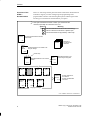
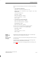
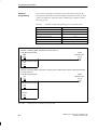
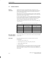
Overview of the
STEP 7
Documentation
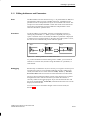
There is a wide range of both general and task-oriented user documentation
available to support you when configuring and programming an S7
programmable controller. The following descriptions and the figure below
will help you to find the user documentation you require.
This symbol indicates the order in which you should read the
manuals, especially as a first-time user of S7.
Meaning
Symbol
This documentation introduces the methodology.
This is a reference manual on a specific topic.
The documentation is supported by online help.
S7-300 Programmable Controller
Quick Start
Primer
/30/
Manual
Progr.
Manual
Manuals on
S7-300/S7-400
Hardware
System Software for S7-300/S7-400
Program Design
/234/
Online Help
User
Manual
Standard Software for S7 and M7
STEP 7
/232/
Standard Software for S7
Converting S5 Programs
/230/
/231/
STL
User
Manual
LAD
/233/
FBD
/236/
SCL
/250/
Reference
Manual
GRAPH
for S7
/251/
HiGraph
/252/
CFCs for
S7
/235/
System Software for
S7-300/400
System and Standard
Functions
/254/
Language Packages
/xxx/: Number in the list of references
iv
Ladder Logic (LAD) for S7-300 and S7-400
C79000-G7076-C504-02
Preface
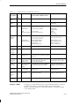
Table 1-1
Summary of the Documentation
Subject
Title
S7-300 Programmable
Controller
Quick Start, Primer
The primer provides you with a very simple introduction to the methods of configuring
and programming an S7-300/400. It is particularly suitable for first-time users of an S7
programmable logic controller.
S7-300/400 Program
Design
Programming Manual
The “S7-300/400 Program Design” programming manual provides you with the basic
information you require about the structure of the operating system and a user program
for an S7 CPU. First-time users of an S7-300/400 should use this manual to get a basic
overview of programming methods on which to base the design of a user program.
S7-300/400 System and
Standard Functions
Reference Manual
The S7 CPUs have system functions and organization blocks integrated in the operating
system that can be used when programming. The manual provides you with an
overview of the system functions, organization blocks and loadable standard functions
available with an S7 programmable controller and contains detailed interface
descriptions explaining how to use the functions and blocks in your user program.
STEP 7
User Manual
The “STEP 7” User Manual explains the basic use and functions of the STEP 7
automation software. Whether you are a first-time user of STEP 7 or an experienced
STEP 5 user, the manual will provide you with an overview of the procedures for
configuring, programming and getting started with an S7-300/400 programmable
controller. When working with the software, you can call up the online help which
supports you with information about specific details of the program.
Converting S5 Programs
User Manual
You require the “Converting S5 Programs” User Manual if you want to convert
existing S5 programs and to run them on S7 CPUs. The manual explains how to use the
converter. The online help system provides more detailed information about using the
specific converter functions. The online help system also includes an interface
description of the available converted S7 functions.
STL, LAD, FBD, SCL1
Manuals
The manuals for the language packages STL, LAD, FBD, and SCL contain both
instructions for the user and a description of the language. To program an S7-300/400,
you only require one of the languages, but you can, if required, mix the languages
within a project. When using one of the languages for the first time, it is advisable to
familiarize yourself with the methods of creating a program as explained in the manual.
When working with the software, you can use the online help system which provides
you with detailed information about using the editors and compilers.
GRAPH1 , HiGraph1,
CFC1
Manuals
1
The GRAPH, HiGraph, and CFC languages provide you with optional methods for
implementing sequential control systems, status control systems, or graphical
interconnection of blocks. The manuals contain both the user instructions and the
description of the language. When using one of these languages for the first time, it is
advisable to familiarize yourself with the methods of creating a program based on the
“S7-300 and S7-400 Program Design” manual. When working with the software, you
can also use the online help system (with the exception of HiGraph) that provides you
with detailed information about using the editors and compilers.
Optional package for system software for S7-300/S7-400
Ladder Logic (LAD) for S7-300 and S7-400
C79000-G7076-C504-02
v
Preface
How to Use This
Manual
To use the LAD effectively, you should already be familiar with the theory
behind S7 programs. This is explained in the Programming Manual /234/.
The language packages also use the standard software for S7, so you you
should also be familiar with the standard software as described in the User
Manual /231/.
The manual is divided into the following parts:
S Part 1 introduces you to the use of the Editor.
S Part 2 explains all LAD operations and is intendede for reference
purposes.
S The glossary includes definitions of the basic terms.
S The index helps you find the relevant page on a subject of your choice.
Conventions
References to other manuals and documentation are indicated by numbers in
slashes /.../. These numbers refer to the titles of manuals listed in Appendix
KEIN MERKER.
Additional
Assistance
If you have any questions regarding the software described in this manual
and cannot find an answer here or in the online help, please contact the
Siemens representative in your area. You will find a list of addresses in the
Appendix of /70/ or /100/, or in catalogs, and in Compuserve (go
autforum). You can also contact our Hotline under the following phone or
fax number:
Tel. (+49) (911) 895-7000 (Fax 7001)
If you have any questions or comments on this manual, please fill out the
remarks form at the end of the manual and return it to the address shown on
the form. We would be grateful if you could also take the time to answer the
questions giving your personal opinion of the manual.
Siemens also offers a number of training courses to introduce you to the
SIMATIC S7 automation system. Please contact your regional training center
or the central training center in Nuremberg, Germany for details:
D-90327 Nuremberg, Tel. (+49) (911) 895-3154.
Notes on Using the
Manual
vi
The user’s guide sections in this manual do not describe procedures in
step-by-step detail, but simply outline basic procedures. You will find more
detailed information on the individual dialogs in the software and how to use
them in the online help.
Ladder Logic (LAD) for S7-300 and S7-400
C79000-G7076-C504-02
Contents
Preface . . . . . . . . . . . . . . . . . . . . . . . . . . . . . . . . . . . . . . . . . . . . . . . . . . . . . . . . . . . . . . . . .
iii
Part 1: Working with the Ladder Editor
1
Product Overview . . . . . . . . . . . . . . . . . . . . . . . . . . . . . . . . . . . . . . . . . . . . . . . . . . . . . . .
1-1
2
Introduction . . . . . . . . . . . . . . . . . . . . . . . . . . . . . . . . . . . . . . . . . . . . . . . . . . . . . . . . . . . . .
2-1
2.1
Structure of User Programs . . . . . . . . . . . . . . . . . . . . . . . . . . . . . . . . . . . . . . .
2-2
2.2
Creating User Programs – Overview . . . . . . . . . . . . . . . . . . . . . . . . . . . . . . . .
2-4
2.3
Rules to Observe . . . . . . . . . . . . . . . . . . . . . . . . . . . . . . . . . . . . . . . . . . . . . . . .
2-7
Creating Logic Blocks . . . . . . . . . . . . . . . . . . . . . . . . . . . . . . . . . . . . . . . . . . . . . . . . . . .
3-1
3.1
Creating Logic Blocks – Overview . . . . . . . . . . . . . . . . . . . . . . . . . . . . . . . . . .
3-2
3.2
Logic Blocks in the Editor . . . . . . . . . . . . . . . . . . . . . . . . . . . . . . . . . . . . . . . . .
3-3
3.3
Structure of the Variable Declaration Table . . . . . . . . . . . . . . . . . . . . . . . . . .
3-6
3.4
Editing Variable Declaration Tables – Overview . . . . . . . . . . . . . . . . . . . . . .
3-8
3.5
Declaring Multiple Instances . . . . . . . . . . . . . . . . . . . . . . . . . . . . . . . . . . . . . . .
3-10
3.6
Assigning System Attributes for Parameters . . . . . . . . . . . . . . . . . . . . . . . . .
3-11
3.7
Editing the Code Section – Overview . . . . . . . . . . . . . . . . . . . . . . . . . . . . . . .
Editable Parts of the Code Section . . . . . . . . . . . . . . . . . . . . . . . . . . . . . . . . .
3-13
3-13
3.8
Basic Guidelines for Entering Ladder Logic Instructions . . . . . . . . . . . . . . .
3-15
3.9
Entering Ladder Elements . . . . . . . . . . . . . . . . . . . . . . . . . . . . . . . . . . . . . . . . .
3-18
3.10
Creating Parallel Branches . . . . . . . . . . . . . . . . . . . . . . . . . . . . . . . . . . . . . . . .
3-21
3.11
Editing Addresses and Parameters . . . . . . . . . . . . . . . . . . . . . . . . . . . . . . . . .
3-23
3.12
Symbolic Addressing . . . . . . . . . . . . . . . . . . . . . . . . . . . . . . . . . . . . . . . . . . . . .
3-24
3.13
Editing in the Overwrite Mode . . . . . . . . . . . . . . . . . . . . . . . . . . . . . . . . . . . . . .
3-26
3.14
Entering Titles and Comments . . . . . . . . . . . . . . . . . . . . . . . . . . . . . . . . . . . . .
3-28
3
Ladder Logic (LAD) for S7-300 and S7-400
C79000-G7076-C504-02
vii
Contents
4
5
Creating Data Blocks and User-Defined Data Types . . . . . . . . . . . . . . . . . . . . . . . .
4-1
4.1
Creating Data Blocks – Overview . . . . . . . . . . . . . . . . . . . . . . . . . . . . . . . . . .
4-2
4.2
Selecting a Method . . . . . . . . . . . . . . . . . . . . . . . . . . . . . . . . . . . . . . . . . . . . . . .
4-4
4.3
Editing the Declaration Table . . . . . . . . . . . . . . . . . . . . . . . . . . . . . . . . . . . . . .
4-5
4.4
Editing Actual Data Values . . . . . . . . . . . . . . . . . . . . . . . . . . . . . . . . . . . . . . . .
4-6
4.5
Creating User-Defined Data Types (UDTs) . . . . . . . . . . . . . . . . . . . . . . . . . .
4-8
Editing the Block Properties and Testing the Program . . . . . . . . . . . . . . . . . . . . .
5-1
5.1
Editing the Block Properties . . . . . . . . . . . . . . . . . . . . . . . . . . . . . . . . . . . . . . .
5-2
5.2
Testing your Ladder Program - Overview . . . . . . . . . . . . . . . . . . . . . . . . . . . .
5-5
5.3
Setting the Program Status . . . . . . . . . . . . . . . . . . . . . . . . . . . . . . . . . . . . . . . .
5-6
5.4
Setting the Trigger Conditions . . . . . . . . . . . . . . . . . . . . . . . . . . . . . . . . . . . . .
5-7
5.5
Choosing a Test Environment and Starting/Stopping the Program Status
5-8
Part 2: Language Description
6
7
8
viii
Configuration and Elements of Ladder Logic . . . . . . . . . . . . . . . . . . . . . . . . . . . . . .
6-1
6.1
Elements and Boxes . . . . . . . . . . . . . . . . . . . . . . . . . . . . . . . . . . . . . . . . . . . . .
6-2
6.2
Boolean Logic and Truth Tables . . . . . . . . . . . . . . . . . . . . . . . . . . . . . . . . . . . .
6-6
6.3
Significance of the CPU Registers in Instructions . . . . . . . . . . . . . . . . . . . . .
6-12
Addressing . . . . . . . . . . . . . . . . . . . . . . . . . . . . . . . . . . . . . . . . . . . . . . . . . . . . . . . . . . . . .
7-1
7.1
Overview . . . . . . . . . . . . . . . . . . . . . . . . . . . . . . . . . . . . . . . . . . . . . . . . . . . . . . .
7-2
7.2
Types of Addresses . . . . . . . . . . . . . . . . . . . . . . . . . . . . . . . . . . . . . . . . . . . . . .
7-4
Bit Logic Instructions . . . . . . . . . . . . . . . . . . . . . . . . . . . . . . . . . . . . . . . . . . . . . . . . . . . .
8-1
8.1
Overview . . . . . . . . . . . . . . . . . . . . . . . . . . . . . . . . . . . . . . . . . . . . . . . . . . . . . . .
8-2
8.2
Normally Open Contact . . . . . . . . . . . . . . . . . . . . . . . . . . . . . . . . . . . . . . . . . . .
8-3
8.3
Normally Closed Contact . . . . . . . . . . . . . . . . . . . . . . . . . . . . . . . . . . . . . . . . . .
8-4
8.4
Output Coil . . . . . . . . . . . . . . . . . . . . . . . . . . . . . . . . . . . . . . . . . . . . . . . . . . . . . .
8-5
8.5
Midline Output . . . . . . . . . . . . . . . . . . . . . . . . . . . . . . . . . . . . . . . . . . . . . . . . . . .
8-6
8.6
Invert Power Flow . . . . . . . . . . . . . . . . . . . . . . . . . . . . . . . . . . . . . . . . . . . . . . . .
8-7
8.7
Save RLO to BR Memory . . . . . . . . . . . . . . . . . . . . . . . . . . . . . . . . . . . . . . . . .
8-8
8.8
Set Coil . . . . . . . . . . . . . . . . . . . . . . . . . . . . . . . . . . . . . . . . . . . . . . . . . . . . . . . . .
8-9
8.9
Reset Coil . . . . . . . . . . . . . . . . . . . . . . . . . . . . . . . . . . . . . . . . . . . . . . . . . . . . . . .
8-10
8.10
Set Counter Value . . . . . . . . . . . . . . . . . . . . . . . . . . . . . . . . . . . . . . . . . . . . . . . .
8-11
8.11
Up Counter Coil . . . . . . . . . . . . . . . . . . . . . . . . . . . . . . . . . . . . . . . . . . . . . . . . . .
8-12
8.12
Down Counter Coil . . . . . . . . . . . . . . . . . . . . . . . . . . . . . . . . . . . . . . . . . . . . . . .
8-13
8.13
Pulse Timer Coil . . . . . . . . . . . . . . . . . . . . . . . . . . . . . . . . . . . . . . . . . . . . . . . . .
8-14
8.14
Extended Pulse Timer Coil . . . . . . . . . . . . . . . . . . . . . . . . . . . . . . . . . . . . . . . .
8-15
Ladder Logic (LAD) for S7-300 and S7-400
C79000-G7076-C504-02
Contents
9
10
11
8.15
On-Delay Timer Coil . . . . . . . . . . . . . . . . . . . . . . . . . . . . . . . . . . . . . . . . . . . . . .
8-16
8.16
Retentive On-Delay Timer Coil . . . . . . . . . . . . . . . . . . . . . . . . . . . . . . . . . . . . .
8-17
8.17
Off-Delay Timer Coil . . . . . . . . . . . . . . . . . . . . . . . . . . . . . . . . . . . . . . . . . . . . . .
8-18
8.18
Positive RLO Edge Detection . . . . . . . . . . . . . . . . . . . . . . . . . . . . . . . . . . . . . .
8-19
8.19
Negative RLO Edge Detection . . . . . . . . . . . . . . . . . . . . . . . . . . . . . . . . . . . . .
8-20
8.20
Address Positive Edge Detection . . . . . . . . . . . . . . . . . . . . . . . . . . . . . . . . . . .
8-21
8.21
Address Negative Edge Detection . . . . . . . . . . . . . . . . . . . . . . . . . . . . . . . . . .
8-22
8.22
Set Reset Flipflop . . . . . . . . . . . . . . . . . . . . . . . . . . . . . . . . . . . . . . . . . . . . . . . .
8-23
8.23
Reset Set Flipflop . . . . . . . . . . . . . . . . . . . . . . . . . . . . . . . . . . . . . . . . . . . . . . . .
8-24
Timer Instructions . . . . . . . . . . . . . . . . . . . . . . . . . . . . . . . . . . . . . . . . . . . . . . . . . . . . . . .
9-1
9.1
Location of a Timer in Memory and Components of a Timer . . . . . . . . . . .
9-2
9.2
Choosing the Right Timer . . . . . . . . . . . . . . . . . . . . . . . . . . . . . . . . . . . . . . . . .
9-4
9.3
Pulse S5 Timer . . . . . . . . . . . . . . . . . . . . . . . . . . . . . . . . . . . . . . . . . . . . . . . . . .
9-5
9.4
Extended Pulse S5 Timer . . . . . . . . . . . . . . . . . . . . . . . . . . . . . . . . . . . . . . . . .
9-7
9.5
On-Delay S5 Timer . . . . . . . . . . . . . . . . . . . . . . . . . . . . . . . . . . . . . . . . . . . . . . .
9-9
9.6
Retentive On-Delay S5 Timer . . . . . . . . . . . . . . . . . . . . . . . . . . . . . . . . . . . . . .
9-11
9.7
Off-Delay S5 Timer . . . . . . . . . . . . . . . . . . . . . . . . . . . . . . . . . . . . . . . . . . . . . . .
9-13
Counter Instructions . . . . . . . . . . . . . . . . . . . . . . . . . . . . . . . . . . . . . . . . . . . . . . . . . . . . .
10-1
10.1
Location of a Counter in Memory and Components of a Counter . . . . . . .
10-2
10.2
Up-Down Counter . . . . . . . . . . . . . . . . . . . . . . . . . . . . . . . . . . . . . . . . . . . . . . . .
10-3
10.3
Up Counter . . . . . . . . . . . . . . . . . . . . . . . . . . . . . . . . . . . . . . . . . . . . . . . . . . . . . .
10-5
10.4
Down Counter . . . . . . . . . . . . . . . . . . . . . . . . . . . . . . . . . . . . . . . . . . . . . . . . . . .
10-7
Integer Math Instructions . . . . . . . . . . . . . . . . . . . . . . . . . . . . . . . . . . . . . . . . . . . . . . . .
11-1
11.1
Add Integer . . . . . . . . . . . . . . . . . . . . . . . . . . . . . . . . . . . . . . . . . . . . . . . . . . . . .
11-2
11.2
Add Double Integer . . . . . . . . . . . . . . . . . . . . . . . . . . . . . . . . . . . . . . . . . . . . . . .
11-3
11.3
Subtract Integer . . . . . . . . . . . . . . . . . . . . . . . . . . . . . . . . . . . . . . . . . . . . . . . . . .
11-4
11.4
Subtract Double Integer . . . . . . . . . . . . . . . . . . . . . . . . . . . . . . . . . . . . . . . . . . .
11-5
11.5
Multiply Integer . . . . . . . . . . . . . . . . . . . . . . . . . . . . . . . . . . . . . . . . . . . . . . . . . .
11-6
11.6
Multiply Double Integer . . . . . . . . . . . . . . . . . . . . . . . . . . . . . . . . . . . . . . . . . . .
11-7
11.7
Divide Integer . . . . . . . . . . . . . . . . . . . . . . . . . . . . . . . . . . . . . . . . . . . . . . . . . . .
11-8
11.8
Divide Double Integer . . . . . . . . . . . . . . . . . . . . . . . . . . . . . . . . . . . . . . . . . . . . .
11-9
11.9
Return Fraction Double Integer . . . . . . . . . . . . . . . . . . . . . . . . . . . . . . . . . . . . 11-10
11.10
Evaluating the Bits of the Status Word After Integer Math Instructions . . . 11-11
Ladder Logic (LAD) for S7-300 and S7-400
C79000-G7076-C504-02
ix
Contents
12
13
14
x
Floating-Point Math Instructions . . . . . . . . . . . . . . . . . . . . . . . . . . . . . . . . . . . . . . . . . .
12-1
12.1
Overview . . . . . . . . . . . . . . . . . . . . . . . . . . . . . . . . . . . . . . . . . . . . . . . . . . . . . . .
12-2
12.2
Add Floating-Point Numbers . . . . . . . . . . . . . . . . . . . . . . . . . . . . . . . . . . . . . . .
12-3
12.3
Subtract Floating-Point Numbers . . . . . . . . . . . . . . . . . . . . . . . . . . . . . . . . . . .
12-4
12.4
Multiply Floating-Point Numbers . . . . . . . . . . . . . . . . . . . . . . . . . . . . . . . . . . .
12-5
12.5
Divide Floating-Point Numbers . . . . . . . . . . . . . . . . . . . . . . . . . . . . . . . . . . . . .
12-6
12.6
Evaluating the Bits of the Status Word After Floating-Point Instructions . .
12-7
12.7
Establishing the Absolute Value of a Floating-Point Number . . . . . . . . . . .
12-8
12.8
Establishing the Square and/or the Square Root of a
Floating-Point Number . . . . . . . . . . . . . . . . . . . . . . . . . . . . . . . . . . . . . . . . . . . .
12-9
12.9
Establishing the Natural Logarithm of a Floating-Point Number . . . . . . . . . 12-11
12.10
Establishing the Exponential Value of a Floating-Point Number . . . . . . . . . 12-12
12.11
Establishing the Trigonometrical Functions of Angles as Floating-Point
Numbers . . . . . . . . . . . . . . . . . . . . . . . . . . . . . . . . . . . . . . . . . . . . . . . . . . . . . . . . 12-13
Comparison Instructions . . . . . . . . . . . . . . . . . . . . . . . . . . . . . . . . . . . . . . . . . . . . . . . . .
13-1
13.1
Compare Integer . . . . . . . . . . . . . . . . . . . . . . . . . . . . . . . . . . . . . . . . . . . . . . . . .
13-2
13.2
Compare Double Integer . . . . . . . . . . . . . . . . . . . . . . . . . . . . . . . . . . . . . . . . . .
13-3
13.3
Compare Floating-Point Numbers . . . . . . . . . . . . . . . . . . . . . . . . . . . . . . . . . .
13-5
Move and Conversion Instructions . . . . . . . . . . . . . . . . . . . . . . . . . . . . . . . . . . . . . . .
14-1
14.1
Assign a Value . . . . . . . . . . . . . . . . . . . . . . . . . . . . . . . . . . . . . . . . . . . . . . . . . . .
14-2
14.2
BCD to Integer . . . . . . . . . . . . . . . . . . . . . . . . . . . . . . . . . . . . . . . . . . . . . . . . . . .
14-4
14.3
Integer to BCD . . . . . . . . . . . . . . . . . . . . . . . . . . . . . . . . . . . . . . . . . . . . . . . . . . .
14-5
14.4
Integer to Double Integer . . . . . . . . . . . . . . . . . . . . . . . . . . . . . . . . . . . . . . . . . .
14-6
14.5
BCD to Double Integer . . . . . . . . . . . . . . . . . . . . . . . . . . . . . . . . . . . . . . . . . . . .
14-7
14.6
Double Integer to BCD . . . . . . . . . . . . . . . . . . . . . . . . . . . . . . . . . . . . . . . . . . . .
14-8
14.7
Double Integer to Floating-Point Number . . . . . . . . . . . . . . . . . . . . . . . . . . . .
14-9
14.8
Ones Complement Integer . . . . . . . . . . . . . . . . . . . . . . . . . . . . . . . . . . . . . . . . 14-10
14.9
Ones Complement Double Integer . . . . . . . . . . . . . . . . . . . . . . . . . . . . . . . . . 14-11
14.10
Twos Complement Integer . . . . . . . . . . . . . . . . . . . . . . . . . . . . . . . . . . . . . . . . 14-12
14.11
Twos Complement Double Integer . . . . . . . . . . . . . . . . . . . . . . . . . . . . . . . . . . 14-13
14.12
Negate Floating-Point Number . . . . . . . . . . . . . . . . . . . . . . . . . . . . . . . . . . . . . 14-14
14.13
Round to Double Integer . . . . . . . . . . . . . . . . . . . . . . . . . . . . . . . . . . . . . . . . . . 14-15
14.14
Truncate Double Integer Part . . . . . . . . . . . . . . . . . . . . . . . . . . . . . . . . . . . . . . 14-16
14.15
Ceiling . . . . . . . . . . . . . . . . . . . . . . . . . . . . . . . . . . . . . . . . . . . . . . . . . . . . . . . . . . 14-17
14.16
Floor . . . . . . . . . . . . . . . . . . . . . . . . . . . . . . . . . . . . . . . . . . . . . . . . . . . . . . . . . . . 14-18
Ladder Logic (LAD) for S7-300 and S7-400
C79000-G7076-C504-02
Contents
15
16
17
18
19
20
Word Logic Instructions . . . . . . . . . . . . . . . . . . . . . . . . . . . . . . . . . . . . . . . . . . . . . . . . .
15-1
15.1
Overview . . . . . . . . . . . . . . . . . . . . . . . . . . . . . . . . . . . . . . . . . . . . . . . . . . . . . . .
15-2
15.2
WAnd Word . . . . . . . . . . . . . . . . . . . . . . . . . . . . . . . . . . . . . . . . . . . . . . . . . . . . .
15-3
15.3
WAnd Double Word . . . . . . . . . . . . . . . . . . . . . . . . . . . . . . . . . . . . . . . . . . . . . .
15-4
15.4
WOr Word . . . . . . . . . . . . . . . . . . . . . . . . . . . . . . . . . . . . . . . . . . . . . . . . . . . . . .
15-5
15.5
WOr Double Word . . . . . . . . . . . . . . . . . . . . . . . . . . . . . . . . . . . . . . . . . . . . . . .
15-6
15.6
WXOr Word . . . . . . . . . . . . . . . . . . . . . . . . . . . . . . . . . . . . . . . . . . . . . . . . . . . . .
15-7
15.7
WXOr Double Word . . . . . . . . . . . . . . . . . . . . . . . . . . . . . . . . . . . . . . . . . . . . . .
15-8
Shift and Rotate Instructions . . . . . . . . . . . . . . . . . . . . . . . . . . . . . . . . . . . . . . . . . . . . .
16-1
16.1
Shift Instructions . . . . . . . . . . . . . . . . . . . . . . . . . . . . . . . . . . . . . . . . . . . . . . . . .
16-2
16.2
Rotate Instructions . . . . . . . . . . . . . . . . . . . . . . . . . . . . . . . . . . . . . . . . . . . . . . . 16-10
Data Block Instructions . . . . . . . . . . . . . . . . . . . . . . . . . . . . . . . . . . . . . . . . . . . . . . . . . .
17-1
17.1
Open Data Block: DB or DI . . . . . . . . . . . . . . . . . . . . . . . . . . . . . . . . . . . . . . . .
17-2
Jump Instructions . . . . . . . . . . . . . . . . . . . . . . . . . . . . . . . . . . . . . . . . . . . . . . . . . . . . . . .
18-1
18.1
Overview . . . . . . . . . . . . . . . . . . . . . . . . . . . . . . . . . . . . . . . . . . . . . . . . . . . . . . .
18-2
18.2
Jump in the Block If RLO = 1 (Unconditional Jump) . . . . . . . . . . . . . . . . . . .
18-3
18.3
Jump in the Block If RLO = 1 (Conditional Jump) . . . . . . . . . . . . . . . . . . . . .
18-4
18.4
Jump in the Block If RLO = 0 (Jump-If-Not) . . . . . . . . . . . . . . . . . . . . . . . . . .
18-5
18.5
Label . . . . . . . . . . . . . . . . . . . . . . . . . . . . . . . . . . . . . . . . . . . . . . . . . . . . . . . . . . .
18-6
Status Bit Instructions . . . . . . . . . . . . . . . . . . . . . . . . . . . . . . . . . . . . . . . . . . . . . . . . . . .
19-1
19.1
Overview . . . . . . . . . . . . . . . . . . . . . . . . . . . . . . . . . . . . . . . . . . . . . . . . . . . . . . .
19-2
19.2
Exception Bit BR Memory . . . . . . . . . . . . . . . . . . . . . . . . . . . . . . . . . . . . . . . . .
19-3
19.3
Result Bits . . . . . . . . . . . . . . . . . . . . . . . . . . . . . . . . . . . . . . . . . . . . . . . . . . . . . .
19-4
19.4
Exception Bits Unordered . . . . . . . . . . . . . . . . . . . . . . . . . . . . . . . . . . . . . . . . .
19-6
19.5
Exception Bit Overflow . . . . . . . . . . . . . . . . . . . . . . . . . . . . . . . . . . . . . . . . . . . .
19-7
19.6
Exception Bit Overflow Stored . . . . . . . . . . . . . . . . . . . . . . . . . . . . . . . . . . . . .
19-9
Program Control Instructions . . . . . . . . . . . . . . . . . . . . . . . . . . . . . . . . . . . . . . . . . . . .
20-1
20.1
Calling FCs/SFCs from Coil . . . . . . . . . . . . . . . . . . . . . . . . . . . . . . . . . . . . . . .
20-2
20.2
Calling FBs, FCs, SFBs, SFCs, and Multiple Instances . . . . . . . . . . . . . . . .
20-4
20.3
Return . . . . . . . . . . . . . . . . . . . . . . . . . . . . . . . . . . . . . . . . . . . . . . . . . . . . . . . . . .
20-7
20.4
Master Control Relay Instructions . . . . . . . . . . . . . . . . . . . . . . . . . . . . . . . . . .
20-8
20.5
Master Control Relay Activate/Deactivate . . . . . . . . . . . . . . . . . . . . . . . . . . .
20-9
20.6
Master Control Relay On/Off . . . . . . . . . . . . . . . . . . . . . . . . . . . . . . . . . . . . . . . 20-12
Ladder Logic (LAD) for S7-300 and S7-400
C79000-G7076-C504-02
xi
Contents
Appendix
A
B
C
21
xii
Alphabetical Listing of Instructions . . . . . . . . . . . . . . . . . . . . . . . . . . . . . . . . . . . . . . .
A-1
A.1
Listing with International Names . . . . . . . . . . . . . . . . . . . . . . . . . . . . . . . . . . .
A-2
A.2
Listing with International Names and SIMATIC Equivalents . . . . . . . . . . . .
A-5
A.3
Listing with SIMATIC Names . . . . . . . . . . . . . . . . . . . . . . . . . . . . . . . . . . . . . .
A-9
A.4
Listing with SIMATIC Names and International Equivalents . . . . . . . . . . . .
A-12
A.5
Listing with International Short Names and SIMATIC Short Names . . . . .
A-16
Programming Examples . . . . . . . . . . . . . . . . . . . . . . . . . . . . . . . . . . . . . . . . . . . . . . . . .
B-1
B.1
Overview . . . . . . . . . . . . . . . . . . . . . . . . . . . . . . . . . . . . . . . . . . . . . . . . . . . . . . .
B-2
B.2
Bit Logic Instructions . . . . . . . . . . . . . . . . . . . . . . . . . . . . . . . . . . . . . . . . . . . . .
B-3
B.3
Timer Instructions . . . . . . . . . . . . . . . . . . . . . . . . . . . . . . . . . . . . . . . . . . . . . . . .
B-7
B.4
Counter and Comparison Instructions . . . . . . . . . . . . . . . . . . . . . . . . . . . . . . .
B-11
B.5
Integer Math Instructions . . . . . . . . . . . . . . . . . . . . . . . . . . . . . . . . . . . . . . . . . .
B-13
B.6
Word Logic Instructions . . . . . . . . . . . . . . . . . . . . . . . . . . . . . . . . . . . . . . . . . . .
B-14
Number Notation . . . . . . . . . . . . . . . . . . . . . . . . . . . . . . . . . . . . . . . . . . . . . . . . . . . . . . . .
C-1
C.1
Number Notation . . . . . . . . . . . . . . . . . . . . . . . . . . . . . . . . . . . . . . . . . . . . . . . . .
C-2
References . . . . . . . . . . . . . . . . . . . . . . . . . . . . . . . . . . . . . . . . . . . . . . . . . . . . . . . . . . . . . .
D-1
Glossary . . . . . . . . . . . . . . . . . . . . . . . . . . . . . . . . . . . . . . . . . . . . . . . . . . . . . . . . . .
Glossary-1
Index . . . . . . . . . . . . . . . . . . . . . . . . . . . . . . . . . . . . . . . . . . . . . . . . . . . . . . . . . . . . .
Index-1
Ladder Logic (LAD) for S7-300 and S7-400
C79000-G7076-C504-02
Part 1:
Working with the
Ladder Editor
Product Overview
1
Introduction
2
Creating Logic Blocks
3
Creating Data Blocks and
User Data Types
4
Editing the Block Properties
and Testing the Program
5
1-2
Ladder Logic (LAD) for S7-300 and S7-400
C79000-G7076-C504-02
Product Overview
1
What is LAD?
LAD stands for Ladder Logic. LAD is a graphic programming language. The
syntax of the instructions is similar to a circuit diagram. With Ladder Logic,
you can follow the signal flow between power rails via inputs, outputs, and
instructions.
The Programming
Language Ladder
Logic
The programming language Ladder Logic has all the necessary elements for
creating a complete user program. It contains the complete range of basic
instructions and a wide range of addresses are available. Functions and
function blocks allow you to structure your LAD program clearly.
The Programming
Package
The LAD Programming Package is an integral part of the STEP 7 Standard
Software. This means that following the installation of your STEP 7 software,
all the editor functions, compiler functions, and test/debug functions for LAD
are available to you.
Using LAD, you can create your own user program with the Incremental
Editor. The input of the local block data structure is made easier with the
help of table editors.
There are three programming languages in the standard software, STL, FBD,
and LAD. You can switch from one language to the other almost without
restriction and choose the most suitable language for the particular block you
are programming.
If you write programs in LAD or FBD, you can always switch over to the
STL representation. If you convert LAD programs into FBD programs and
vice versa, program elements that cannot be represented in the destination
language are displayed in STL.
Ladder Logic (LAD) for S7-300 and S7-400
C79000-G7076-C504-02
1-1
1-2
Ladder Logic (LAD) for S7-300 and S7-400
C79000-G7076-C504-02
2
Introduction
In This Chapter
This chapter is a brief description of the structure of a user program
consisting of blocks.
The LAD Editor runs on the platform of the SIMATIC Manager which
underlies all STEP 7 applications. This chapter explains how to change from
the SIMATIC Manager to the LAD Editor and how the created blocks fit into
the project structure.
Chapter Overview
Section
Description
Page
2.1
Structure of User Programs
2-2
2.2
Creating User Programs - Overview
2-4
2.3
Rules to Observe
2-7
Ladder Logic (LAD) for S7-300 and S7-400
C79000-G7076-C504-02
2-1
Introduction
2.1
Structure of User Programs
Logic Blocks and
Data Blocks
A user program consists of logic blocks and data blocks. Logic blocks are
blocks with a code section such as organization blocks, function blocks, or
functions.
Organization
Blocks
Organization blocks (OBs) form the interface between the operating system
and the user program. Different organization blocks have different functions.
To create the LAD user program for your S7 CPU, you select the
organization blocks necessary for your specific automation task. For the most
basic task you will require the following:
S Startup (OB100, OB101)
S Scan cycle (OB1)
S Error handling (OB80 to OB87, OB121, OB122), if you do not want your
CPU to switch to STOP when an error occurs.
There are also organization blocks available to handle interrupts in the CPU
or other interrupts from the process.
For detailed information about the functions of each organization block and
the startup information provided by the CPU operating system, refer to the
Reference Manual /235/.
Functions/
Function Blocks
You can program every organization block as a structured program by
creating functions (FCs) and function blocks (FBs) and calling them in the
code section. When the blocks are called, you supply the data required for
the declared parameters.
S A function block (FB) is a logic block with “memory”. This memory
takes the form of instance data blocks assigned to the FB. The instance
DBs store all the actual parameters and static data relating to the function
block.
S A function (FC) is a logic block without “memory”, in other words
without associated instance DBs. After an FC has been processed, the
output parameters contain the calculated function values. Once the
function has been called, the user decides how the actual parameters are
used and stored.
Data
The operating system makes the following data available:
S Peripheral I/Os
S Process image input/output
S Bit memory
S Timers
S Counters
2-2
Ladder Logic (LAD) for S7-300 and S7-400
C79000-G7076-C504-02
Introduction
You can also define your own data:
S You can define shared data in data blocks. This data is accessible to the
entire user program.
S You can define static variables. These are only valid in the function block
within which they are defined. Every time an FB is called, an instance
data block is specified which includes all parameters and the static data.
In the case of multiple instances, the instance and static data are
incorporated in the instance data block.
S You can define temporary data when you create logic blocks. This data
only requires stack memory during the actual processing of the block.
Data Blocks
Data blocks store the data of the user program. There are two types of data
blocks: shared data blocks and instance data blocks.
S Shared DBs can be accessed by all the blocks in the program.
S Instance data blocks are assigned to a function block and contain not only
the data of the function block but also the data of any defined multiple
instances. For this reason, you should only access an instance data block
in connection with its own specific function block.
Additional
Information
The Programming Manual /234/ contains an introduction to programming
methods.
Ladder Logic (LAD) for S7-300 and S7-400
C79000-G7076-C504-02
2-3
Introduction
2.2
Creating User Programs – Overview
User Program
A user program that runs on an S7 CPU is essentially made up of blocks. It
also contains information such as data about the system configuration and
about system networking. Depending on your application, the user program
will include the following elements:
S Organization blocks (OBs)
S Function blocks (FBs)
S Functions (FCs)
S Data blocks (DBs)
To simplify your work, you can create your own user-defined data types
(UDTs), which can be used either as data types in their own right or as a
template for creating data blocks.
Some of the frequently used blocks such as the system function blocks
(SFBs) and the system functions (SFCs) are integrated on the CPU. Other
blocks (for example blocks for IEC functions or closed-loop controller
blocks) are available as separate packages. You do not need to program these
blocks but simply load them into your user program.
Note
You can check which SFBs and SFCs are integrated on your CPU online by
clicking PLC " Module Information... in the menu bar.
LAD Incremental
Editor
The STEP 7 standard software includes an editor for programming blocks.
The editor can be set to the LAD programming language to allow you to
program logic blocks (OBs, FBs, FCs). The LAD Editor works incrementally,
which means that the syntax of each entry you make is checked. Syntax
errors are reported and illegal arrangements of LAD elements or addresses
are rejected immediately.
Starting from the
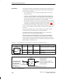
SIMATIC Manager
The LAD Editor is started from the SIMATIC Manager. You must first create
a project containing an S7 program in the SIMATIC Manager before you can
call the editor. The program you create can be either dependent or
independent of the hardware. You either add the S7 program directly into the
project or edit the S7 program assigned to the programmable module. The
program itself can contain the user program (blocks), source files, or charts.
With the LAD Editor, you can only edit blocks stored in the folder of the user
program.
2-4
Ladder Logic (LAD) for S7-300 and S7-400
C79000-G7076-C504-02
Introduction
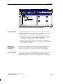
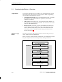
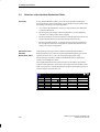
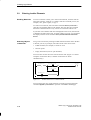
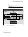
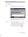
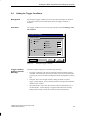
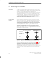
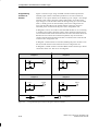
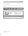
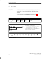
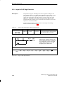
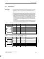
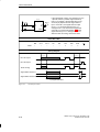
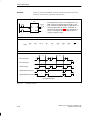
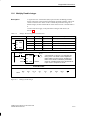
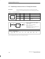
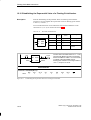
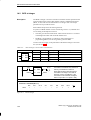
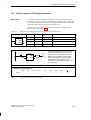
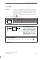
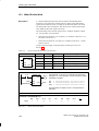
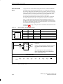
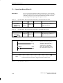
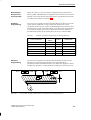
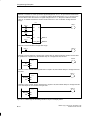
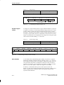
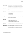
SIMATIC Manager – TRAFFIC
File
Edit
Insert
PLC
View
ON
Options Window
Help
OFF
TRAFFIC - <Offline> (Project)
TRAFFIC
S7 Program (1)
Source Files
OB1
FB6
DB5
DB6
Blocks
SIMATIC 300 Station1
Press F1 for help
NUM
Figure 2-1 Starting the LAD Editor from the SIMATIC Manager
Creating a Block
To create a block for the first time, you first create an empty block in the
SIMATIC Manager with which you can then open the Editor. Once you have
opened the LAD Editor you can then create further blocks.
S In the SIMATIC Manager you can select the “Blocks” folder and insert
the block type you want by selecting Insert " S7 Block " .... The new
block appears on the right hand side of the project window.
S Once you are in the editor, you can create a block by selecting File "
New. In the dialog box that follows you are prompted to specify the block
type and number you require.
Choosing a
Programming
Language
When you create a block, you also select the programming language you
want to use. The corresponding editor is then activated based on this
selection. To program in LAD, select “LAD” as the working language.
Opening a Block
You can open a block in the SIMATIC Manager by double-clicking the block.
Alternatively, you can open it by either selecting the menu command
Edit " Open Object or by clicking the corresponding button in the toolbar.
Ladder Logic (LAD) for S7-300 and S7-400
C79000-G7076-C504-02
2-5
Introduction
Saving and
Downloading
Blocks
When you save a block in the Editor, remember the following points:
S File " Save always saves the block in the “Blocks” folder on the hard disk
of your programming device/PC.
S PLC " Download downloads the opened block to the CPU.
After creating the blocks for your user program, download them to the S7
CPU in your SIMATIC Manager. For further information about downloading
user programs, refer to the User Manual /231/.
Note
It is not always sufficient to download the created blocks individually to the
CPU because data from the system configuration may sometimes be
required. You should therefore download the complete program in the
SIMATIC Manager.
Calling Supporting
Functions
The LAD Editor has the following functions which you will find useful when
creating programs and starting up.
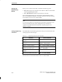
Table 2-1
Supporting Functions in the LAD Editor
Function
Menu Command
Call reference data of the active user
programs
Options " Reference Data
Edit the symbol table / individual
symbols
Options " Symbol Table /
Options " Edit Symbols
Monitor / modify variables
PLC " Monitor/Modify Variables
Display / modify operating mode or
memory reset on the CPU
PLC " Operating Mode or
PLC " Clear/Reset
Display the status of the selected
module
PLC " Module Information
Set the time and date on the CPU
PLC " Set Time and Date
These functions are described in detail in the User Manual /231/.
2-6
Ladder Logic (LAD) for S7-300 and S7-400
C79000-G7076-C504-02
Introduction
2.3
Rules to Observe
Order of Creating
Blocks
The order in which you create logic blocks and data blocks in a user program
is important. As a rule: if blocks are called within other blocks, the called
blocks must already exist before you program their calls. Entering a
non-existent block as a Ladder element (box) is not possible. If you program
a call for a non-existent block using CALL, an error is reported when you
save the program because the called block cannot be found.
Editing during
Program
Execution
With STEP 7 you can edit a user program stored on the CPU online while the
CPU is in the RUN mode.
!
Warning
If you make online modifications to a program while it is running, this can
lead to malfunctions and unforeseen reactions in your plant or process that
could cause injury to persons or damage to equipment.
If the CPU is switched online and is in the RUN mode, modifying the user
program stored on the CPU can cause situations in which machines and
devices are suddenly turned on or off, potentially causing injury to persons
or damage to equipment.
Always plan the sequence of events in your process in accordance with the
pertinent safety regulations. Never attempt to make online modifications to a
program while it is running without having first considered the consequences
and taking appropriate action to prevent accidents.
Note
For information about working online and offline, refer to the User Manual
/231/.
Ladder Logic (LAD) for S7-300 and S7-400
C79000-G7076-C504-02
2-7
Introduction
2-8
Ladder Logic (LAD) for S7-300 and S7-400
C79000-G7076-C504-02
3
Creating Logic Blocks
In This Chapter
Chapter Overview
A user program cannot exist without logic blocks. In many situations, you
can use the blocks integrated on the CPU or the available standard function
blocks. You will, however, always have to create a number of logic blocks
yourself. This chapter describes how to create blocks using the LAD Editor.
Section
Description
Page
3.1
Creating Logic Blocks – Overview
3-2
3.2
Logic Blocks in the Editor
3-3
3.3
Structure of the Variable Declaration Table
3-6
3.4
Editing Variable Declaration Tables – Overview
3-8
3.5
Declaring Multiple Instances
3-10
3.6
Assigning System Attributes for Parameters
3-11
3.7
Editing the Code Section – Overview
3-13
3.8
Basic Guidelines for Entering Ladder Logic Instructions
3-15
3.9
Entering Ladder Elements
3-18
3.10
Creating Parallel Branches
3-21
3.11
Editing Addresses and Parameters
3-23
3.12
Symbolic Addressing
3-24
3.13
Editing in Overwrite Mode
3-26
3.14
Entering Titles and Comments
3-28
Ladder Logic (LAD) for S7-300 and S7-400
C79000-G7076-C504-02
3-1
Creating Logic Blocks
3.1
Creating Logic Blocks – Overview
Logic Blocks
Logic blocks (OBs, FBs, FCs) are made up of a variable declaration section
and a code section. They also have certain properties. When programming,
you must edit the following three sections:
S Variable declaration table: In the variable declaration table, you declare
the parameters, the system attributes for parameters, and the local
variables of your block.
S Code section: In the code section, you program the block code that is to
be executed by the programmable controller. This consists of one or more
networks with Ladder elements.
S Block properties: The block properties include additional information,
such as a time stamp and a path name, which is entered by the system
itself. In addition to these items you can enter further details about the
name, family, release and author and can assign system attributes for
blocks (see Chapter 5).
Editing a Logic
Block
The order in which you edit the three sections is irrelevant and you can, of
course, make corrections and additions.
When you refer to symbols from the symbol table, you should make sure that
they are complete and, when necessary, add any missing information.
Create a logic block (FB, FC or OB)
in the SIMATIC Manager.
LAD Editor
Make the settings for the editor
Edit the variable declaration table
for the block
Edit the code section
Enter the block properties
Save the block
Figure 3-1
3-2
Procedure for Creating Logic Blocks in LAD
Ladder Logic (LAD) for S7-300 and S7-400
C79000-G7076-C504-02
Creating Logic Blocks
3.2
Logic Blocks in the Editor
Overview
Before you start programming in the LAD Editor, you should familiarize
yourself with the various ways in which you can customize the editor to suit
your preferences and method of working.
Settings in the
Editor
With the menu command Options " Customize, you can open a tabbed page
dialog box. In the “Editor” tabbed page, you can make the following basic
settings for block programming:
S Font (type style, size) used in text and tables
S The programming language of your choice (FBD, LAD, or STL). A new
block will be opened in FBD, LAD, or STL depending on the
programming language you select. Bearing in mind certain restrictions,
you can switch to one of the other languages later on and still view the
block.
S Display of symbols and comment in the new block (on or off)
The settings for language, comment and symbols can be altered at any time
during editing by using the commands in the View ” ... menu.
Settings for LAD
In the “LAD/FBD” tabbed page, which you also display with Options "
Customize, you can make the following basic settings:
S Ladder Layout: determines the display size of your networks. The
selected size decides how many LAD elements you can position next to
each other in one network. This setting also has effects when printing out
the block.
S Width of Address Field: determines the width of text fields for addresses.
If the width is exceeded, a line break is made. A large address field is
more practical for symbolic addressing, a small field is sufficient for
absolute addressing.
S Line/Color for: the selected element, contact, status fulfilled, status not
fulfilled
Ladder Logic (LAD) for S7-300 and S7-400
C79000-G7076-C504-02
3-3
Creating Logic Blocks
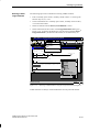
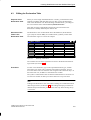
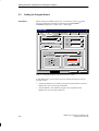
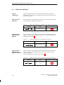
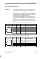
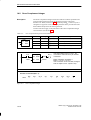
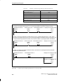
Main Window of
the LAD Editor
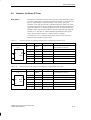
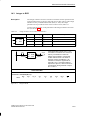
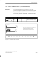
When you open a logic block, a window appears displaying the following:
S The variable declaration table of the block in the upper part
S The code section in the lower part, in which you edit the actual block
code
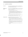
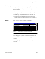
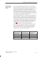
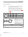
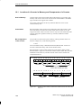
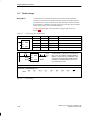
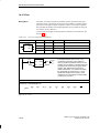
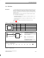
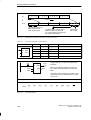
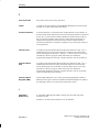
FB6-<Offline>-LAD/STL/FBD: Programming S7 Blocks
File
Edit
Insert
PLC
Debug
View
Options
Window
Help
FB6-<Offline>
Address Decl. Symbol
Data Type Initial Value
0.0
in
dur_g_p
S5TIME
S5T#0MS
2.0
in
del_r_p
S5TIME
S5T#0MS
4.0
in
starter
BOOL
FALSE
6.0
in
t_dur_y_car
TIMER
8.0
in
t_dur_g_ped
TIMER
Comment
Network 1 : Red for road traffic
#starter
#t_next_red_car
#t_dur_r_car
#condition
#condition
Network 2 : Green for road traffic
#condition
#g car
Network 3 : Start permanent amber for cars
#condition
Figure 3-2
#g car
SE
S5T#3S
Variable Declaration Table and Code Section in LAD
The block properties are edited in their own dialog (see Chapter 5).
The editor allows you enables you to open and work on several blocks
simultaneously.
Relationship
between the
Variable
Declaration and
Code Section
3-4
The variable declaration table and the code section are closely linked as the
names from the variable declaration table are used in the code section. This
means that changes in the variable declaration table also affect the code
section and therefore the entire block.
Ladder Logic (LAD) for S7-300 and S7-400
C79000-G7076-C504-02
Creating Logic Blocks
Table 3-1
Relationship between Variable Declaration and Code Section
Action in the Variable Declaration
Reaction in the Code Section
New correct entry
If invalid code exists, previously
undeclared variable becomes valid
Correct name change without type change
Symbol is immediately shown
everywhere with new name
Correct name is changed to an invalid name
Code is not changed
Invalid name is changed to a correct name
If invalid code exists, it becomes
valid
Type change
If invalid code exists, it becomes
valid and if valid code exists, it
becomes invalid
Symbol deleted that is being used in the code
Valid code becomes invalid
Comment change
None
Incorrect entry of a new variable
None
Deleting an unused variable
None
Initial value change
None
Ladder Logic (LAD) for S7-300 and S7-400
C79000-G7076-C504-02
3-5
Creating Logic Blocks
3.3
Structure of the Variable Declaration Table
Overview
In the variable declaration table, you set the local variables including the
formal parameters of the block and the system attributes for parameters. This
has (among other things) the following effects:
S As a result of the declaration, memory is reserved in the local data stack
or instance data block.
S By setting the input, output, and in/out parameters you also define the
“interface” for calling a block in the program.
S Declaring variables in a function block provides the data structure for any
instance data block that you associate with the function block.
S By setting system attributes, you assign special properties to parameters
for message and connection configuration, operator interface functions
and process control configuration.
Structure of the
Variable
Declaration Table
After opening a new logic block, a default variable declaration table is
displayed on the screen. This lists all the permitted declaration types for the
specific block (in, out, in_out, stat, temp) in the appropriate order.
When creating a new OB, a standard variable declaration is displayed in
which you can change the values.
The variable declaration table contains entries for the address, declaration,
symbolic name, data type, initial value, and comment for the variables. Each
table row represents a variable declaration. Variables of the data type array or
structure require more than one row.
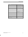
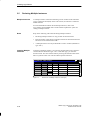
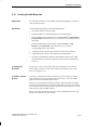
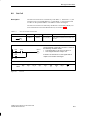
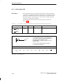
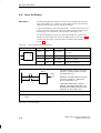
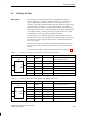
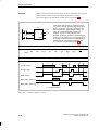
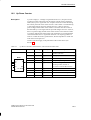
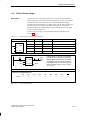
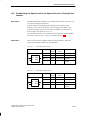
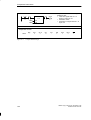
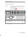
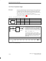
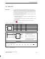
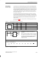
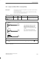
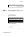
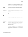
TRAFFIC\...\FB40 - <Offline>
Address
Decl.
Symbol
Data Type
Initial Value Comment
0.0
in
ein
BOOL
FALSE
Light on
0.1
in
start
BOOL
FALSE
Switch
2.0
out
Motor
BOOL
FALSE
Motor
2.1
out
Message
BOOL
FALSE
Motor
4.0
in_out
in_outp1
INT
0
6.0
in_out
in_outp2
INT
0
Figure 3-3 Example of a Variable Declaration Table
3-6
Ladder Logic (LAD) for S7-300 and S7-400
C79000-G7076-C504-02
Creating Logic Blocks
Meaning of the
Columns
Table 3-2
The columns in the variable declaration table are interpreted as follows:
Columns of the Variable Declaration Table
Column
Meaning
Remarks
Editing
Address
Address in format BYTE.BIT
In the case of data types which require more
than one byte, the address indicates this with
a jump to the next byte address.
Key:
* : Size of an array element in bytes
+ : Initial address, ref. to the structure start
= : Total memory requirement of a structure
System entry:
the address is
assigned and
displayed by
the system after
you have
finished
entering your
declaration.
Decl.
Declaration type “Purpose” of the
variables
The following are possible depending on
block type:
Input parameters “in”
Output parameters “out”
In/out parameters “in_out”
Static variables “stat”
Temporary variables “temp”
Default settings
according to
block type
Symbol
Symbolic name of variables
The name must begin with a letter. Reserved Mandatory
keywords are not permitted.
Data Type
Data type of the variable
(BOOL, INT, WORD, ARRAY
etc.)
Basic data types can be selected in the menu Mandatory
with the right mouse button.
Initial Value
Initial value, when the software
should not assume a default value
Must be compatible with the data type.
Unless a specific actual value has been
selected, the initial value is used as the
actual value of the variable when editing a
DB for the first time.
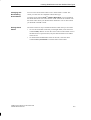
Comment
Comment on documentation
Optional
Optional
Meaning of the
“Golf Flag”
If you have assigned system attributes to a variable, a symbol resembling a
golf flag appears in the “Symbol” column (see Figure 3-3). Double-click the
flag to open the “System Attributes” dialog box.
Altering the
Column Width
You can vary the width of the columns. Position the mouse pointer between
two columns and holding the left mouse button pressed move the mouse
horizontally. As an alternative, you can alter the width of the column using
the menu command View " Column Width... having previously selected the
table. This allows you to minimize the optional comment and initial value
columns and focus solely on the remaining columns.
Ladder Logic (LAD) for S7-300 and S7-400
C79000-G7076-C504-02
3-7
Creating Logic Blocks
3.4
Editing Variable Declaration Tables – Overview
Procedure
After you have entered the required declaration type of a new declaration,
enter the name of the variables, the data type, the initial value (optional) and
the comment (optional). You can move the cursor to the next field with the
TAB key. At the end of a row an address will be assigned to the variable
automatically.
After each table field has been edited, its syntax is checked and any errors
are displayed in red. At this point, you can continue editing the table and
postpone the correction of errors to a later stage.
Editing Functions
All the usual functions in the Edit menu are available to you when editing a
table. Using the context-sensitive right mouse button makes editing easier.
The menu displayed with the right mouse button also helps you to enter the
data type. The “Data Type” menu includes all elementary data types.
You can select single rows by clicking the write-protected address cell. You
can also select several rows of the same declaration type by holding down the
SHIFT key. The selected rows appear on a black background.
Changing the
Declaration Type
The “Decl.” column is read-only. The declaration type is determined by the
position of the declaration within the table. This ensures that variables can
only be entered in the correct order of their declaration types. If you want to
change the declaration type of a declaration, cut the declaration first and then
paste it under the new declaration type.
Entering
Structures
If you want to enter a structure as a variable, enter the name in the “Symbol”
column and the keyword STRUCT in the data type column. Press either the
TAB or the RETURN key to insert an empty row plus a final row
(END_STRUCT) for the structure. In the empty row, enter the elements of
the structure by entering its name, data type and its initial value (optional).
You can create more rows and insert further elements using either the menu
commands or by pressing RETURN.
If you want to select a structure, click the address or declaration cell of the
first or last row of the structure (containing the keyword STRUCT or
END_STRUCT). You can select individual declarations within a structure by
clicking the address cell in the relevant row.
If you want to enter a structure within another structure, the hierarchy is
indicated by the indented variable names.
3-8
Ladder Logic (LAD) for S7-300 and S7-400
C79000-G7076-C504-02
Creating Logic Blocks
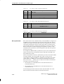
Entering Arrays
To enter an array as a data type, enter the name in the “Symbol” column and
the keyword ARRAY in the cell for the data type together with the array size,
for example array [1..20, 3..24] for a two-dimensional array. Press the TAB
key (if necessary, more than once) to insert a row in which you can enter the
data type of the array.
If you want to select an array, click the address cell in the relevant row.
Initial values for each array element can be entered singly or with a repetition
factor (see Figure 3-4):
S Individual entry: You assign each element its own initial value. The
values are separated by commas.
S Repetition factor: The same initial value can be assigned to several
elements. The value itself is shown in parentheses and is preceded by the
repetition factor which defines the number of elements.
Example
Figure 3-4 shows an example of a variable declaration table:
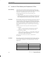
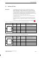
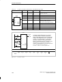
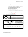
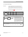
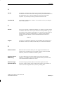
TRAFFIC\...\FB50 - <Offline>
Address
Decl. Symbol
Data Type
0.0
in
STRUCT
+0.0
in
var1
BOOL
FALSE
+2.0
in
var2
INT
0
+4.0
=6.0
in
in
var3
WORD
END_STRUCT
W#16#0
6.0
in
array1
ARRAY[1..20,1..40]
TRUE
*2.0
in
Figure 3-4
structur1
Initial Value
Comment
BOOL
Structures and Arrays in a Variable Declaration Table
Note
If you make changes to the variable declaration of blocks whose calls you
have already programmed, time stamp conflicts may occur. You should
therefore first program all blocks to be called, and then program the blocks
that call them. In the case of function blocks, instance DBs should also be
re-created.
When making changes to a UDT which was entered as a data type in a
variable declaration, check the variable declaration of the block and then
save it again.
Ladder Logic (LAD) for S7-300 and S7-400
C79000-G7076-C504-02
3-9
Creating Logic Blocks
3.5
Declaring Multiple Instances
Multiple Instances
A multiple instance results from declaring a static variable of the same data
type as a function block (FB). In the code section, the instance is called as a
Ladder element.
For more detailed information about multiple instances, refer to the
Programming Manual /234/. Part 2 of this manual explains the syntax for
calling a multiple instance.
Rules
Keep to the following rules when declaring multiple instances:
S Declaring multiple instances is only possible in function blocks
S Function blocks within which a multiple instance has been declared must
also have an associated instance DB.
S A multiple instance can only be declared as a static variable (declaration
type “stat”).
Inputting Multiple
Instances
To declare a multiple instance, you enter the variable name in the “Symbol”
column after the declaration type “stat”. Under data type, you enter the
function block. This can be done either by entering the absolute name of the
FB or a symbolic name. You can also add an optional comment.
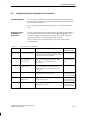
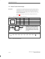
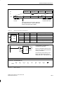
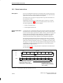
TRAFFIC\...\FB60-<Offline>
Address
Symbol
Data TypeInitial Value Comment
0.0
in
varin
BYTE
B#16#0
2.0
out
varout
BYTE
B#16#0
4.0
in_out
varinout BYTE
B#16#0
stat
locinst
FB6
temp
tempo
REAL
0.0
Figure 3-5
3-10
Decl.
local instance
Declaration of Multiple Instances (Example)
Ladder Logic (LAD) for S7-300 and S7-400
C79000-G7076-C504-02
Creating Logic Blocks
3.6
Assigning System Attributes for Parameters
System Attributes
You can assign system attributes to blocks and parameters. These influence
the message and connection configuration, operator interface functions, and
process control configuration.
You can assign system attributes for parameters in the variable declaration
table.
Entering System
Attributes for
Parameters
To enter system attributes for parameters, select the name of the parameter in
the variable declaration table and select Edit " Object Properties in the
menu bar to display the Properties dialog. Select the “System Attributes”
tabbed page and enter the required attribute and its value.
Table 3-3 shows which system attributes you can enter in the variable
declaration table.
Table 3-3
Attribute
System Attributes for Parameters
Value
When to Assign the Attribute
Permitted
Declaration type
S7_server
connection, alarm_archiv When the parameter is relevant to connection or
message configuration. This parameter contains
the connection or message number.
IN
S7_a_type
alarm, alarm_8,
alarm_8p, alarm_s,
notify, ar_send
IN, only with blocks
of the type FB and
SFB
S7_co
pbkl, pbk, ptpl, obkl, fdl, When the parameter will specify the connection
iso, pbks, obkv
type in the connection configuration (only
possible when the S7_server attribute is set to
connection).
IN
S7_m_c
true, false
When the parameter will be modified or
monitored from an operator panel.
IN/OUT / IN_OUT,
only with blocks of
the type FB and SFB
S7_shortcut
Any 2 characters, for
example, W, Y
When the parameter is assigned a shortcut to
evaluate analog values.
IN/OUT / IN_OUT,
only with blocks of
the type FB and SFB
S7_unit
Unit, for example, liters
When the parameter is assigned a unit for
evaluating analog values.
IN/OUT / IN_OUT,
only with blocks of
the type FB and SFB
Ladder Logic (LAD) for S7-300 and S7-400
C79000-G7076-C504-02
When the parameter will define the message
block type in a message block (only possible
when the S7_server attribute is set to
alarm_archiv).
3-11
Creating Logic Blocks
Table 3-3
Attribute
System Attributes for Parameters, continued
Value
When to Assign the Attribute
Permitted
Declaration type
S7_string_0
Any 16 characters, , for
example, OPEN
When the parameter is assigned text for
evaluating binary values
IN/OUT / IN_OUT,
only with blocks of
the type FB, SFB,
FC, and SFC
S7_string_1
Any 16 characters, , for
example, CLOSE
When the parameter is assigned text for
evaluating binary values
IN/OUT / IN_OUT,
only with blocks of
the type FB, SFB,
FC, and SFC
S7_visible
true, false
When you do not want the parameter to be
displayed in CFC.
IN/OUT / IN_OUT,
only with blocks of
the type FB, SFB,
FC, and SFC
S7_link
true, false
When you do not want the parameter to be
linked in CFC.
IN/OUT / IN_OUT,
only with blocks of
the type FB, SFB,
FC, and SFC
S7_dynamic
true, false
When you want the parameter to have dynamic
capability when testing in CFC.
IN/OUT / IN_OUT,
only with blocks of
the type FB, SFB,
FC, and SFC
S7_param
true, false
When you want the parameter to be protected
from incorrect value assignment in CFC.
IN/OUT / IN_OUT,
only with blocks of
the type FB, SFB,
FC, and SFC
3-12
Ladder Logic (LAD) for S7-300 and S7-400
C79000-G7076-C504-02
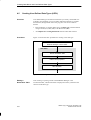
Creating Logic Blocks
3.7
Editing the Code Section – Overview
Code Section
In the code section you describe the program sequence of your logic block.
To do this, you form networks from Ladder elements. In most cases, the code
section of a logic block is made up of several networks. After you have
entered a Ladder element, the editor runs a check and shows you if any
entries were incorrect (errors are shown in red). Elements placed incorrectly
are rejected with an error message.
Editable Parts of
the Code Section
In a code section, you can edit the block title, network titles, block
comments, network comments, and, of course, the statements within the
networks.
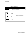
TRAFFIC\...\FB6 - <Offline>
Block title
FB6 : Traffic Light
Block
comment
Controlling a set of traffic lights for a pedestran crossing on a main street.
Network 1 : Red request for road traffic
Network
comment
The red request from road traffic is activated by a start input when the time between two
red phases for road traffic is running.
#starter
Ladder
elements
Network
title
#t_next_red_car
#t_dur_r_car
#condition
#condition
Network 2 : Green for road traffic
The traffic lights turn green when there is no request for red.
#condition
Figure 3-6
Ladder Logic (LAD) for S7-300 and S7-400
C79000-G7076-C504-02
#g_car
Structure of the Code Section
3-13
Creating Logic Blocks
Entering New
Blocks
The order in which you perform each of the following steps is not fixed.
When programming the code section of a new block, we recommend you
proceed as follows:
Enter block title (optional)
Enter block comment (optional)
Edit networks
Enter network title (optional)
Enter network comment (optional)
Enter Ladder elements
Figure 3-7
Editing the Code Section
You can make changes either in the insert or the overwrite mode. Toggle
between the insert and overwrite mode using the INSERT key.
3-14
Ladder Logic (LAD) for S7-300 and S7-400
C79000-G7076-C504-02
Creating Logic Blocks
3.8
Basic Guidelines for Entering Ladder Logic Instructions
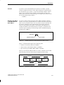
Overview
A Ladder network can contain several elements in different branches. All
elements and branches must be connected together; however, the power rail
on the left does not count as a connection (IEC 1131-3).
When you program in Ladder, you must observe certain guidelines.
Any errors are reported with an error message in the Program Editor.
Ending a Ladder
Network
Every Ladder network must end with a coil or a box. You cannot use the
following elements to close a network:
S Comparison boxes
S Midline outputs (#)
S Positive (P) or Negative (N) RLO edge detection
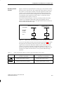
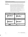
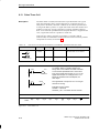
Power Flow
Branches that cause reverse power flow (from right to left) cannot be edited.
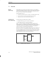
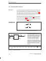
Figure 3-8 shows an example. With signal state “0” at I 1.4, a power flow
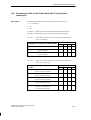
from right to left would be possible at I 6.8. This is not allowed.
I 1.0
I 1.2
Q 2.6
I 6.8
✗
I 1.4
Ladder Logic (LAD) for S7-300 and S7-400
C79000-G7076-C504-02
Q 6.0
Illegal Power Flow
Q 4.4
Figure 3-8
I 4.2
I 2.8
Power Flow in Reverse Direction (Illegal)
3-15
Creating Logic Blocks
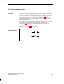
Short Circuit
You cannot create branches that cause a short circuit. Figure 3-9 shows an
example:
I 1.0
I 1.2
I 1.4
Q 6.0
✗
Illegal Short Circuit
Figure 3-9
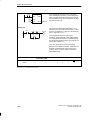
Placing Boxes
Short Circuit in a Ladder Network (Illegal)
The starting point of a branch for a box connection must always be the left
power rail. Logic or other boxes can, however, exist in the branch before the
box.
Boxes must not be placed within a T-branch. Exceptions to this are compare
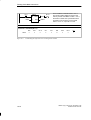
boxes. Figure 3-10 shows an example:
I 1.0
I 1.2
I 1.4
T branch
Box
✗
Figure 3-10
Placing Coils
Q 6.0
Box illegal at this
position
Box in a T-Branch (Illegal)
Coils are automatically placed at the right end of a network where they form
the branch end.
Exceptions: Coils for Midline Outputs (#) and Positive (P) or
Negative (N) RLO Edge Detection cannot be placed on the extreme left
or the extreme right of a branch. Nor are they permitted in parallel branches.
3-16
Ladder Logic (LAD) for S7-300 and S7-400
C79000-G7076-C504-02
Creating Logic Blocks
Some coils require preceding logic and some coils cannot accept preceding
logic.
S Coils requiring preceding logic:
Output Coil ( ), Set Coil (S), Reset Coil (R)
Midline Outputs (#) and Positive (P) or Negative (N) RLO
Edge Detection.
All Counter and Timer Coils
Jump-If-Not (JMPN)
Master Control Relay On (MCR<)
Save RLO to BR Memory (SAVE)
Return (RET)
S Coils that do not accept preceding logic:
Master Control Relay Activate (MCRA)
Master Control Relay Deactivate (MCRD)
Open Data Block (OPN)
Master Control Relay Off (MCR>)
All other coils can accept preceding logic but do not require it.
The following coils must not be used as parallel outputs:
Jump-If-Not (JMPN)
Jump (JMP)
Call FC SFC from Coil (CALL)
Return (RET)
Enable
Input/Enable
Output
Passing power to (activating) the enable input “EN” or the enable output
“ENO” of a logic box is possible but not necessary.
Removing and
Changing
If a branch only consists of one instruction, deleting this instruction removes
the whole branch.
If you remove a box, all branches connected to the box with logic inputs,
with the exception of the main branch, are removed.
The overwrite mode is ideal for exchanging elements of the same type (see
Section 3.13).
Ladder Logic (LAD) for S7-300 and S7-400
C79000-G7076-C504-02
3-17
Creating Logic Blocks
3.9
Entering Ladder Elements
Handling Networks
To select a network to allow you to enter LAD elements, click the network
name (for example, “Network 1”). When a network is selected you can, for
example, cut it, paste it again, or copy it.
To create a new network, select the menu command Insert " Network or
click the corresponding button in the toolbar. The new network is inserted
below the selected network. It only consists of one branch and one coil.
If you enter more elements than can be displayed on the screen, the network
is shifted to the left of the screen. To obtain a better overview, you can adjust
the display with the menu command View " Zoom In/Zoom Out/Zoom
Factor.
Selecting Objects
in Networks
You go into a network by clicking a Ladder element with the mouse. Within
a network you can, in principle, select three areas with a mouse click:
S Ladder elements, for example, a contact or a box
S Junction points
S Empty instructions (lines or open branches)
You can select one area at a time with one mouse click. (Figure 3-11 shows
examples of selections. Here, a number of selections are shown
simultaneously.)
#condition
#t_dur_y_car
#r_ped
#t_dur_g_ped
#condition
Figure 3-11
Possible Selections in a Ladder Network
You can choose the color of the selections yourself by selecting the menu
command Options " Customize to open the “LAD/FBD” tabbed page.
3-18
Ladder Logic (LAD) for S7-300 and S7-400
C79000-G7076-C504-02
Creating Logic Blocks
Entering Ladder
Logic Elements
The following options are available for inserting Ladder elements:
S Enter a normally open contact, normally closed contact, or coil using the
function keys F2, F3, or F4.
S Click on the button for a normally open contact, normally closed contact,
or coil from the toolbar.
S Select an element from the Insert " LAD Element... menu.
S Select elements from the list box in the Program Elements dialog (see
Figure 3-12). To display this dialog box, use the menu command Insert "
Program Element..., the button in the toolbar, or the function key F11.
FB6-<Offline> - LAD/STL/FBD Programming S7 Blocks
File
Edit
Insert
PLC
Debug View
Object
Block Template
Data Type
Declaration Row
Network
FB6-<Offline>
Program Elements
LAD Element
FB6 : Traffic light
Network 1 : Red request for road traffic
#starter #t_next_red_car #t_dur_r_car
Options
&
Window
>1
Help
=
#condition
#condition
Network 2 : Green for cars
#condition
Program Elements
Bit logic #g car
Compare
Convert
Network 2 : Start permanent amber for road traffic
Counters
S_CD
#condition
S_CU
SE
S_CUD
DB Call
Real Number Fct.
Floating Point Number
<
Press F1 for help.
Figure 3-12
Insert
Inserting a Ladder Element Using the Program Elements Dialog Box
Ladder elements are always inserted behind the currently selected element.
Ladder Logic (LAD) for S7-300 and S7-400
C79000-G7076-C504-02
3-19
Creating Logic Blocks
Note
If you select the group “FB Blocks”or “FC Blocks” in the “Program
Elements” list box, all the corresponding blocks in the S7 program are listed
below. If you select the group “SFC Blocks” or “SFB Blocks”, all the system
function blocks or system functions available on the CPU will be listed.
If you select the group “Libraries” in the “Program Elements” list box, the
STEP 7 standard libraries and any libraries you have created will be listed.
In this way you can include whole blocks in your network and program calls
for other blocks very quickly.
Calling Multiple
Instances
3-20
You can also call multiple instances as Ladder elements if you have defined
them in the variable declaration table. To do this, select the menu command
Insert "Program Element. In the list box of the Ladder elements, you will
find the group “Multiple Instances” under which all declared multiple
instances are listed.
Ladder Logic (LAD) for S7-300 and S7-400
C79000-G7076-C504-02
Creating Logic Blocks
3.10 Creating Parallel Branches
Application
To create OR instructions in the Ladder programming language, you need to
create parallel branches.
Guidelines
Use the following guidelines to edit parallel branches:
S Draw OR branches from left to right
S Parallel branches are opened downwards and closed upwards
S Open a parallel branch with the menu command Insert " LAD Element...
"
Open Branch, with function key F8 or with the corresponding button in
the toolbar.
S Close a parallel branch with the menu command Insert " LAD
Element... " Close Branch, with function key F9 or with the
corresponding button in the toolbar.
S A parallel branch is always opened in front of the selected element
S A parallel branch is always closed after the selected element
S To delete a parallel branch, delete all the elements in the branch. When
the last element in the branch is deleted, the OR branch is automatically
removed.
Creating New
Branches
If you want to open a new branch, select the starting point of the branch
below which you want to insert a new branch. You create the new branch
with F8 (see Figure 3-13).
Creating a Closed
Branch
To create a closed branch, select the element in front of which you want to
open a parallel branch. Open the parallel branch with F8, insert the Ladder
elements and close the branch again with F9.
When you close parallel branches, the necessary empty elements are added.
If necessary, the branches are arranged so that branch crossovers are avoided.
If you close the branch directly from the parallel branch, the branch is closed
after the next possible Ladder element.
Figure 3-13 shows an example of how to create a parallel branch using only
function keys and buttons in the toolbar.
Ladder Logic (LAD) for S7-300 and S7-400
C79000-G7076-C504-02
3-21
Creating Logic Blocks
Step 1.
Step 2.
M2.0
I1.0
M2.0
I1.0
M2.0
I1.0
or <F8>
Step 3.
??.?
or <F2>
Step 4.
M2.0
I1.0
??.?
or <F9>
Figure 3-13
Separating Closed
Parallel Branches
3-22
Creating Parallel Branches in a Ladder Network
You can separate a closed parallel branch by cutting out the intersection point
where the parallel branch rejoins the main branch.
Ladder Logic (LAD) for S7-300 and S7-400
C79000-G7076-C504-02
Creating Logic Blocks
3.11 Editing Addresses and Parameters
Uses
The Block Editor uses the character string ??:? as placeholders for addresses
and parameters when you insert a Ladder instruction. All addresses and
parameters must be completed correctly for an executable code section. The
exceptions to this are FBs and SFBs or timer and counter boxes that do not
need to have all parameters assigned. Addresses and parameters can be
entered in absolute or symbolic form.
Procedure
To edit an address or a parameter, open the corresponding text box by
clicking the placeholders ??.?. When you have completed your entry its
syntax is checked. If errors are found, the address or parameter is displayed
in red and an error message appears in the status bar. If the syntax is correct,
the next text box which has not yet been edited is opened.
Step 1.
??.?
Figure 3-14
Step 2.
Step 3.
m1.6
M1.6
Entering Addresses for Ladder Instructions
As you become familiar with the editing tools in Ladder, you can enter all
elements in a network first, and later assign the address or a parameter, to
each element.
Debugging
Because they are marked in red, errors are easy to recognize. To allow you to
navigate more easily to errors located outside the currently visible screen
section, the Editor has two search functions: Edit " Go To... " Previous
Error/Next Error which can also be activated from buttons in the toolbar.
The error search extends beyond the network. This means errors are found
throughout the entire code section and not just within the network or
currently visible section of the program. If you activate the status bar with
the menu command View " Status Bar, information about the errors will be
displayed in the status bar.
You can correct errors and make changes in the overwrite mode (see
Section 3.13).
Ladder Logic (LAD) for S7-300 and S7-400
C79000-G7076-C504-02
3-23
Creating Logic Blocks
3.12 Symbolic Addressing
Using Symbolic
Addressing
In the Ladder programming language you can either enter absolute addresses,
parameters and block names, or use symbols. Using the menu command
View " Symbolic Representation, you can switch between symbolic and
absolute addressing.
Specifying
Symbols
To use shared symbols, you must enter them in the symbol table as follows:
S Open the symbol table with the menu command Options " Symbol
Table.
S Using the menu command Options " Edit Symbols open a dialog box in
which you can define and modify individual symbols.
For further information about editing symbols, refer to the User Manual
/231/.
Representation
In most cases it is not necessary to define whether a symbol is local or
shared. However, in cases where confusion might arise, for example if the
same symbol is being used in both the symbol table and the variable
declaration table, you can distinguish between the symbols as follows:
S Symbols from the symbol table are shown between inverted commas “..”.
S Symbols from the variable declaration table of the block are preceded by
the hash character “#”.
You do not enter the ID with “..” or “#” yourself. If the symbolic address is
contained in the variable declaration table or in the symbol table, the ID is
completed after the syntax check.
Symbol
Information
Made Easy
3-24
To make programming with symbolic addressing easier, you can display the
absolute address and symbol comment for a symbol. You display this
information with the menu command View " Symbol Information. If you
choose this option, a text box is displayed after each network. You cannot
edit in this view. Any modifications you require must be made in the symbol
table or the variable declaration table.
Ladder Logic (LAD) for S7-300 and S7-400
C79000-G7076-C504-02
Creating Logic Blocks
PROJ1\...\FB53-<Offline>
Network 1 : Output alarm
An alarm is output when the temperature limit is exceeded and the
message is not acknowledged
”sensor1”
”button2”
”lampon”
Symbol Information:
I0.0
I1.2
Q4.0
Figure 3-15
sensor1
button2
lampon
Temperature exceeded
Acknowledge button
Alarm signal
Symbol Information in Ladder
When you print the block, the printout is the same as the current screen
followed by the corresponding instruction and symbol comments.
Note
When you download a program to the CPU, the symbol table is not
downloaded. This means that when you are editing a user program whose
original is not on the programming device or PC, the original symbols are no
longer available.
Ladder Logic (LAD) for S7-300 and S7-400
C79000-G7076-C504-02
3-25
Creating Logic Blocks
3.13 Editing in the Overwrite Mode
Overwriting
Addresses and
Parameters
In the Block Editor you can change addresses or parameters conveniently
using the overwrite mode. You toggle between insert and overwrite mode
using the INSERT key. You then overwrite your entries in the text boxes for
addresses or parameters.
Overwriting
Ladder Elements
The overwrite mode allows you to overwrite Ladder elements of the same
type. All boolean logic connections and parameters are retained.
This has the advantage that you do not have to enter the addresses and
parameters again. The Ladder element you want to overwrite can only be
replaced by a Ladder element of the same type. For example, you can
exchange a normally open contact for a normally closed contact, an R/S
flipflop for an S/R flipflop or exchange one timer for another.
To overwrite an existing Ladder element, select it and switch to the overwrite
mode with the INSERT key. The Ladder element is overwritten as soon as you
insert another Ladder element of the same type.
T1
I 0.0
I 1.1
I 0.1
S5T#10s
I 1.2
Q 1.0
S_ODT
S
Q
TV
R
BI
MW 2
BCD
MW 4
I 0.2
Overwrite
T1
I 0.0
I 1.1
S
I 0.1
S5T#10s
I 1.2
Q 1.0
S_PULSE
TV
R
Q
BI
MW 2
BCD
MW 4
I 0.2
Figure 3-16
3-26
Overwriting Boxes
Ladder Logic (LAD) for S7-300 and S7-400
C79000-G7076-C504-02
Creating Logic Blocks
Special Case:
Splitting a
Junction
If at one point in a branch one parallel branch closes and another one opens,
this is called a junction. You can split a junction by selecting it at the lower
or upper junction point and inserting a Ladder element. The junction is split
and the Ladder element inserted.
M4.0
I6.0
I8.0
M4.6
Q2.4
Overwrite
M4.0
??.?
I8.0
Figure 3-17
I6.0
Q2.4
M4.6
Splitting a Junction
Note
You can correct comments and titles in overwrite mode.
Ladder Logic (LAD) for S7-300 and S7-400
C79000-G7076-C504-02
3-27
Creating Logic Blocks
3.14 Entering Titles and Comments
Overview
In the code section of a logic block, you can enter information such as block
and network titles, and block and network comments. These entries are
optional and not essential to the program execution.
Entering Block
Titles and Network
Titles
To enter a block title or network title, position the cursor on the three
question marks to the right of the block name or network name (for example,
network 1 : ???). A text box is then opened in which you enter the title. This
can be up to 64 characters long.
1.
Network 2: ???
Mouse click
2.
Network 2:
Figure 3-18
Entering
Comments
Network title
Entering Block Titles
Using the View " Comment menu command, you can display or hide the
gray comment field. When you double-click the comment field, a text box
appears which you can use to enter comments. You have 64 Kbytes per block
available for block comments and network comments.
1.
???
2.
Figure 3-19
Mouse click
Comment for network or block
Entering Comments
Note
When you download a block to the CPU, the comments are not downloaded.
If you then upload a block from the CPU, whose original is not on your
programming device or PC, you cannot view or edit the original comments.
3-28
Ladder Logic (LAD) for S7-300 and S7-400
C79000-G7076-C504-02
Creating Data Blocks and User-Defined
Data Types
In This Chapter
4
Data blocks are an important part of your user program since they contain all
its data. This chapter explains how to create data blocks.
User-defined data types (UDTs) are not essential for programming. However,
they can be real time-savers in situations where you have to write programs
for similar tasks.
Chapter Overview
Section
Description
Page
4.1
Creating Data Blocks - Overview
4-2
4.2
Selecting a Method
4-4
4.3
Editing the Declaration Table
4-5
4.4
Editing Actual Data Values
4-6
4.5
Creating User-Defined Data Types (UDTs)
4-8
Ladder Logic (LAD) for S7-300 and S7-400
C79000-G7076-C504-02
4-1
Creating Data Blocks and User-Defined Data Types
4.1
Creating Data Blocks – Overview
Data Blocks
Data blocks (DBs) are used to handle data which is why they do not have a
code section. Programming data blocks involves the following :
S Declaration table: The declaration table is where you specify the data
structure of the data block.
S Block properties: These include extra information such as time stamp,
programming language and path name, which is all entered by the system
itself. You can also add information about the name, family, version and
author and you can assign system attributes for blocks (see Chapter 5).
Types of Data
Blocks
A user program can have the following data blocks:
S Shared DBs can be accessed by all logic blocks in the program. The data
remains stored in the data block even when it has been closed.
If you require several shared DBs of the same data structure, you can
create them with the help of a UDT. These are data blocks with an
associated user-defined data type.
S Instance DBs are associated with specific function blocks and are
structured according to the declaration table of the FB. You can only
create an instance DB if the corresponding function block exists. They are
data blocks with an associated function block.
Methods of
Creating Data
Blocks
Depending on the type of data block you want to create, different methods
are used.
Shared data blocks can be created as follows:
S Define the structure for a single data block. For this you must define the
variables and data types in the desired order. This structure only applies to
this DB.
S Define the structure for the data block with the help of a user-defined data
type. In this case the UDT structure defines the data structure of the DB.
A user data type can be assigned to a number of data blocks.
Create an instance data block and then:
S Assign an existing function block to the data block. In this case the
declaration section of the function block defines the structure of the data
block. A number of instance data blocks can be assigned to one function
block.
4-2
Ladder Logic (LAD) for S7-300 and S7-400
C79000-G7076-C504-02
Creating Data Blocks and User-Defined Data Types
Note
When you change the declaration section of an FB, you have to recreate all
the instance data blocks associated with it in order to ensure their
compatibility. The same applies to data blocks which have been created on
the basis of a UDT.
Create a data block (DB) in the SIMATIC Manager or in the Editor
LAD Editor
Select the desired method ...
... Declaration for a single
data block.
... Assign to a UDT.
... Assign the
DB to an FB.
Edit the declaration table.
Shared DB
Instance DB
Edit the block properties.
Save the block.
Figure 4-1
Programming Procedure for Creating Data Blocks
Ladder Logic (LAD) for S7-300 and S7-400
C79000-G7076-C504-02
4-3
Creating Data Blocks and User-Defined Data Types
4.2
Selecting a Method
Procedure
When you create a DB in the SIMATIC Manager or in the LAD Editor, you
must select the method you want to use. You are prompted to select the
method in a dialog box.
New Data Block
Block:
DB7
Programming Tool:
DB Editor
Create
Data Block
Data Block Referencing a User-Defined Data Type
Data Block Referencing a Function Block
Reference:
FB6
FB88
FB101
OK
Figure 4-2
Cancel
Help
Selecting a Method and Assigning an FB/UDT
When creating a DB based on either a UDT or as an instance data block of an
FB, you make your selection in the list box that displays all existing UDTs
and FBs. The UDT or FB must already exist.
How to Proceed
How you proceed from here depends on whether you are creating the DB by
assigning it or by creating a single declaration.
S Since the assigned UDT or FB defines the structure of the data block, you
have actually already created the new data block. The declaration table is
displayed on your screen, but no further changes can be made to it.
S If you are defining the structure of a shared data block, you must now edit
the declaration table, declaring the variable names and data type and, if
you require, the initial value and comment (see Section 4.3).
4-4
Ladder Logic (LAD) for S7-300 and S7-400
C79000-G7076-C504-02
Creating Data Blocks and User-Defined Data Types
4.3
Editing the Declaration Table
Purpose of the
Declaration View
When you create single shared data blocks or UDTs, you must declare their
elements (variables) and their data types. For this you use the declaration
table in the declaration view. When working with data blocks, you change to
this view with the menu command View " Declaration View.
This does not apply to data blocks assigned to a UDT or FB since the
declaration is already defined by the UDT or FB.
Structure of the
Table in the
Declaration View
The declaration view of a data block shows the addresses, the declaration
types (only for instance DBs), the variable names (symbols), initial values
and comments. Figure 4-3 shows an example:
DB15 - <Offline>
Address
Symbol
0.0
Data Type
Initial Value
Comment
Maximum RPM
STRUCT
+0.0
speed
INT
100
+2.0
runtime
DINT
L#0
+6.0
+10.0
history
motor_on
REAL
BOOL
0.000000e+000
+10.1
motor_off
BOOL
FALSE
=12.0
Figure 4-3
FALSE
END_STRUCT
Declaring a Data Block
The columns have the same significance as those in the declaration table for
logic blocks (see Section 3.3).
Procedure
To enter a new declaration, type in the required declaration type, variable
name, data type, initial value (optional) and comment (optional). You can
move the cursor from one cell to the next using the TAB or RETURN keys. At
the end of each row, an address is allocated to the variable.
The syntax is checked after each cell has been edited and errors are shown in
red. You can continue to make your entries and correct any errors later.
Note
Editing in the declaration view is the same as editing the variable declaration
table of logic blocks (see Section 3.4). The editing and input procedures are
identical and you should also proceed in the same way when entering arrays
or structures.
Ladder Logic (LAD) for S7-300 and S7-400
C79000-G7076-C504-02
4-5
Creating Data Blocks and User-Defined Data Types
4.4
Editing Actual Data Values
Initial Value –
Actual Value
When you create and save a data block for the first time, the declared
(optional) initial value is automatically assumed as the actual value of the
variable. When it accesses the data block, the user program continues to use
this as the actual value, unless you explicitly specify a new actual value for
the variable in the user program.
The actual values of the variables are changed by the logic blocks writing to
them while the CPU program is being executed. You can display and change
the actual values of variables yourself.
Data View of Data
Blocks
You must switch to the data view to display and edit actual data values in
data blocks. Open a data block and use the menu command View " Data
View to switch to the data view.
The only difference between the data view and the declaration view of a data
block is the additional column “Actual Value”. In the data view, the elements
of variables with a complex data type are displayed individually and with
their complete symbolic name, so that each of their actual values can be
displayed and edited (see Figure 4-4).
DB17 - <Offline>
Address Symbol
INT
2.0 motor.runtime
DINT L#0
6.0 motor.history
100
89
Maximum RPM
L#0
REAL 0.000000e+000 0.000000e+000
10.0 motor.motor_on
BOOL FALSE
TRUE
10.1 motor.motor_off
BOOL FALSE
FALSE
12.0 field[1]
INT
0
7
14.0 field[2]
INT
0
4
16.0 field[3]
INT
0
8
Figure 4-4
Displayed Actual
Value
Type Initial Value Actual Value Comment
0.0 motor.speed
Data Block in the Data View
The displayed actual value is either the value that the variable had when you
opened the data block or the most recently modified and saved value.
Note
If you open data blocks online, the actual value is not updated cyclically.
4-6
Ladder Logic (LAD) for S7-300 and S7-400
C79000-G7076-C504-02
Creating Data Blocks and User-Defined Data Types
Changing and
Reinitializing
Actual Values
You can overwrite the actual values in the “Actual Value” column. The
values you enter must be compatible with the data type.
Saving Actual
Values
The actual values are only activated and become valid when you save them.
Using the menu command Edit " Initialize Data Block you can reinitialize
the whole data block. This overwrites the actual values of the variables with
the initial values which you declared in the declaration view or those which
you declared in the FB or UDT.
S To save the actual data values that you changed offline, select the menu
command File " Save or click on the “Save” button in the toolbar. Even if
the data block was opened online, only the data block that exists offline
will be saved.
S To download the modified data values to the CPU, select the menu
command PLC " Download or click the button in the toolbar.
Ladder Logic (LAD) for S7-300 and S7-400
C79000-G7076-C504-02
4-7
Creating Data Blocks and User-Defined Data Types
4.5
Creating User-Defined Data Types (UDTs)
Overview
User-defined data types are data structures that you create yourself and save
as blocks. Once defined, you can use them under their absolute or symbolic
block names, throughout the entire user program. You can use UDTs as
follows:
S Like elementary or complex data types as the data type in the declaration
of logic blocks (FCs, FBs, OBs) or in data blocks (DBs).
S As templates for creating data blocks with the same data structure.
Procedure
Figure 4-5 shows the basic procedure for creating a user data type:
Create a block for a UDT in the
SIMATIC Manager or in the Editor
LAD Editor
Edit the declaration table
Edit the block properties
Save the block
Figure 4-5
Editing a
Declaration Table
4-8
Creating a User Data Type
After creating or opening a UDT in the SIMATIC Manager or the
incremental editor, a declaration table is displayed in which you declare the
structure of the data type.
Ladder Logic (LAD) for S7-300 and S7-400
C79000-G7076-C504-02
Creating Data Blocks and User-Defined Data Types
UDT56 - <Offline>
Address
Symbol
0.0
Data Type
Initial Value
Comment
Maximum RPM
STRUCT
+0.0
speed
INT
100
+2.0
runtime
DINT
L#0
+6.0
+10.0
history
motor_on
REAL
BOOL
0.000000e+000
+10.1
motor_off
BOOL
FALSE
=12.0
Figure 4-6
FALSE
END_STRUCT
Declaring a UDT
The first and the final row of the declaration view of a UDT are already
allocated and display the key words STRUCT and END_STRUCT, which
define the beginning and end of a UDT. These rows cannot be edited.
Initially, two empty rows are displayed to allow you to declare your
variables. You must enter the variable name and data type. Initial value or
comments are optional. You can create more empty rows using the menu
command Insert " Declaration Row " Before Selection / After Selection.
Note
Editing this declaration table is similar to editing the declaration table of
logic and data blocks.
Ladder Logic (LAD) for S7-300 and S7-400
C79000-G7076-C504-02
4-9
Creating Data Blocks and User-Defined Data Types
4-10
Ladder Logic (LAD) for S7-300 and S7-400
C79000-G7076-C504-02
Editing the Block Properties and Testing
the Program
In This Chapter
5
After you have created and edited the data blocks and logic blocks, you
should check and edit the block properties. They contain information that
identifies the block and indicates how and when it was created. This
information can be useful when debugging a program.
The Ladder Editor allows you to test a single block while it is being executed
in a user program on the CPU. You can follow the signal flow within
networks on the screen. This program test, known as Program Status, helps
you check various processes and eliminate errors.
Chapter Overview
Section
Description
Page
5.1
Editing the Block Properties
5-2
5.2
Testing your Ladder Program - Overview
5-5
5.3
Setting the Program Status
5-6
5.4
Setting the Trigger Conditions
5-7
5.5
Choosing a Test Environment and Starting/Stopping the
Program Status
5-8
Ladder Logic (LAD) for S7-300 and S7-400
C79000-G7076-C504-02
5-1
Editing the Block Properties and Testing the Program
5.1
Editing the Block Properties
Overview
The block properties contain additional information about the block.
Optional data such as name, family, version and author of the block can be
entered here. The properties also include other statistical data and further
information, automatically entered by the system, which cannot be edited by
the user (see Figure 5-1). You can also assign system attributes to the block.
The block properties provide you with important information about the block
type, memory requirements and time of the last modification. This can be
useful when trying to track down errors, such as insufficient memory and
time stamp conflicts.
Procedure
The block properties can be edited using a dialog box.
S In the SIMATIC Manager, select the block and select the menu command
Edit " Object Properties.
S Select File " Properties when opening a block in the Ladder Editor.
Properties - Block
General–Part1 General–Part2 System Attributes
Internal ID:
FB6
Type:
Function Block (FB)
Language: LAD
Symbol:
Symbol from traffic light
Symbol Comment:
Traffic light on Main Street
Project Path:
Traffic\Traffic light\User Program\FB6
Name (Header):
Traffic
Version:
01.00
Family:
Traffic
Block Version:
3.000
Author:
Meier
Multiple Instance DB
Last Modified:
Code:
Interface:
OK
25.10.96 15:23:41.190
25.10.96 15:23:41.190
Cancel
Help
Figure 5-1 Setting the Display of the Program Status in Ladder
In the tabbed pages “General – Part 1”, “General Part – 2”, and “System
Attributes”, you can make a number of entries including the following:
5-2
Ladder Logic (LAD) for S7-300 and S7-400
C79000-G7076-C504-02
Editing the Block Properties and Testing the Program
Block Name and
Family
Blocks with a name and family are easier to classify. For example you could
allocate some blocks to the “Closed-Loop Controller” family, showing that
they are all used for programming closed-loop controllers.
When the block is called later in the code section of another Ladder block,
the benefits of this information become apparent: the family and name of the
block are displayed in the “Program Elements” list box when this block is
selected, so that you can identify the purpose of the block more easily.
Block Release
This information shows you which STEP 7 version was used to create a
block. Version 1 blocks must be converted before they can be incorporated in
a program of version 3. You can achieve this in the SIMATIC Manager by
using the menu command File " Open Old Version 1 Project
Blocks created with version 1 cannot be used in conjunction with multiple
instances. They must be decompiled into source files and then be compiled
into version 3 blocks. For further information, refer to the User Manual
/231/.
Block Attributes
Block attributes in the “General – Part 2” tabbed page include entries such as
the following:
S The attribute “DB write-protected in PLC” means that the block is
write-protected. This is useful for data blocks containing constant values
that must not be changed. The DB must exist as an STL source file.
S The attribute “Know How Protect” indicates a protected block and has
the following effects:
– The code section cannot be viewed.
– The variable declaration table does not display the temporary and
static variables.
– STL source files cannot be generated from the block.
– Block properties cannot be edited.
S The attribute “Standard block” means a protected standard Siemens
block. It appears on the bottom left of the page.
S The attribute “Unlinked” only occurs with to data blocks. It indicates that
the data block cannot be downloaded from the load memory to the work
memory of the CPU. Data blocks in the load memory can only be
accessed using SFCs which copy the content of the data blocks to the
work memory. A more effective use of the work memory is achieved as it
only contains relevant data during the run time.
Ladder Logic (LAD) for S7-300 and S7-400
C79000-G7076-C504-02
5-3
Editing the Block Properties and Testing the Program
Note
Attributes such as block protection, write protection and unlinked can only
be added to the block if it is being programmed as a source file in STL. If
you have created your block in Ladder, you must change to the programming
language STL using the menu command View " STL. You must then convert
the block into a source file before entering these attributes. Once the source
files are compiled into blocks the blocks are protected according to the
attributes you have selected.
Further information can be found in the STL Reference Manual /232/.
System Attributes
for Blocks
Table 5-1
Attribute
To configure the process control and process diagnostics, you can assign the
following system attributes in the “System Attributes” tabbed page.
System Attributes for Process Control Configuration
Value
When to Assign the Attribute
Permitted Block
Type
S7_m_c
true, false
When the block will be manipulated or
monitored from an operator panel.
FB, SFB
S7_tasklist
’taskname1’,
’taskname2’, etc.
When the block will be called in organization
blocks other than in cyclic OBs (for example in
error or startup OBs).
FB, SFB, FC, SFC
S7_blockview
big, small
To specify whether the block is displayed in large FB, SFB, FC, SFC
or small format.
Table 5-2
Attribute
System Attributes for Process Diagnostics
Value
When to Assign the Attribute
Permitted Block
Type
S7_pdiag
true, false
When the block will generate information
relevant to process diagnostics.
FB, FC, OB, DB
S7_pdiag_
unit
true, false
When the block will generate information
relevant to process diagnostics and a unit of
measurement will be monitored.
UDT
S7_pdiag_
motion
true, false
When the block will generate information
UDT
relevant to process diagnostics and a motion will
be monitored.
5-4
Ladder Logic (LAD) for S7-300 and S7-400
C79000-G7076-C504-02
Editing the Block Properties and Testing the Program
5.2
Testing your Ladder Program - Overview
Test Method
You can test your Ladder program by visually displaying the signal flow
within the network of a block. The display of the program is updated
cyclically.
Prior Conditions
You can only display the program status when the following conditions are
met:
S The block was saved and downloaded to the CPU without any errors.
S The CPU is in operation and the user program is running.
S You have opened the block online.
Basic Procedure
Figure 5-2 shows the basic procedure for monitoring the program status:
Open block online
Make settings for test display
Set trigger conditions (optional)
Select test environment
Start/stop test
Figure 5-2
Ladder Logic (LAD) for S7-300 and S7-400
C79000-G7076-C504-02
Procedure for Testing Logic Blocks in Ladder
5-5
Editing the Block Properties and Testing the Program
5.3
Setting the Program Status
Procedure
Before starting the Ladder program test, you select the criteria you would
like to see displayed. To do this use the menu command Options "
Customize and open the “Ladder Logic” tabbed page.
LAD/STL/FBD
Editor
STL
LAD/FBD
Create Block
Layout
Source Files
Element Representation
DIN A4 Landscape
Width of Address Field
18
LAD:
Deep (2D)
FBD:
Deep (3D)
(10-24)
Line/Color
For:
Status fulfilled
Line Thickness
Color
Thin
Medium
Thick
Select
OK
Cancel
Help
Figure 5-3 Setting the Display for the Program Status in Ladder
In this tabbed page, you now select the color and line thickness for the two
possible results:
S “Status not fulfilled”: the conditions along the current path have not been
fulfilled. No current is flowing (dotted line).
S “Status fulfilled”: the conditions along the current path have been
fulfilled. Current is flowing (solid line).
5-6
Ladder Logic (LAD) for S7-300 and S7-400
C79000-G7076-C504-02
Editing the Block Properties and Testing the Program
5.4
Setting the Trigger Conditions
Background
By setting the trigger condition you select the call environment of the block
to be tested. The test will not take place unless the trigger condition is
fulfilled.
Procedure
The trigger conditions can be set by using the menu command Debug " Call
Environment.
Block Call Environment
Trigger Condition
No Condition
Call Path
1st Block:
2nd Block:
3rd Block:
Block Status:
FB6
Global DB Number:
DB6
Open Data Blocks
Instance DB Number:
OK
Figure 5-4
Trigger Condition
Settings and their
Meanings
Cancel
Help
Setting the Trigger Conditions
The three possible settings have the following meanings:
S No trigger conditions: The call environment of the block being tested is
irrelevant. This means that if a block is called at various points during the
program, you will not be able to distinguish which status applied to which
call.
S Call path: This is the call path used for calling the block in order to
trigger a status display. You can enter three block nesting levels before the
tested block is reached.
S Open data blocks: In this case the call environment is defined by one or
two data blocks. A status display is triggered when the block currently
being tested is called in association with one of these data blocks.
Ladder Logic (LAD) for S7-300 and S7-400
C79000-G7076-C504-02
5-7
Editing the Block Properties and Testing the Program
5.5
Choosing a Test Environment and Starting/Stopping the Program
Status
Selecting a Test
Environment
There are two ways of testing your program online.
S The “process” test environment tests your program online, in a working
process. The status of the statements in programmed loops that are run
through more than once in the scan cycle is stopped at the return jump to
the start of the loop and is no longer updated while the loop is visible.
This mode causes the least load on the cycle.
S In the test environment “laboratory” your program is also tested online
under laboratory conditions. In this case, however, the status of
statements in programmed loops that are run through more than once in
the scan cycle is shown after the end of each loop. This mode can take up
considerable scan time depending on the number of loop iterations and
the number of tested statements.
You can select the test environment using the menu command Debug " Test
Environment " Laboratory/Process.
Starting and
Stopping the
Program Status
The program status is started and stopped by using the command Debug "
Monitor. The program status is only displayed for the area currently visible
in the editor.
FB6-<Online>
Address
Decl.
Symbol
Data Type
Initial Value
0.0
in
dur_g_p
S5TIME
S5T#0MS
2.0
in
del_r_p
S5TIME
S5T#0MS
4.0
in
starter
BOOL
FALSE
Comment
FB6 : Traffic Light
Network 1
#starter
#t_next_red_car
#t_dur_r_car
#condition
#condition
Network 2: Green for road traffic
#condition
#g car
Network 3: Start duration of yellow for road traffic
#t_dur_y_car
#condition
SD
S5T#3S
S5T#3S
Figure 5-5
5-8
Program Status in Ladder (Example)
Ladder Logic (LAD) for S7-300 and S7-400
C79000-G7076-C504-02
Editing the Block Properties and Testing the Program
Checking the
Scan Time
Activating the test mode increases the scan time. If the set scan time is
exceeded, the CPU switches to STOP unless you have programmed OB80.
You can display and check the currently set scan time using the menu
command PLC " Module Information. If necessary, you can change the
maximum scan time in the CPU properties for test purposes when assigning
hardware parameters.
Ladder Logic (LAD) for S7-300 and S7-400
C79000-G7076-C504-02
5-9
Editing the Block Properties and Testing the Program
5-10
Ladder Logic (LAD) for S7-300 and S7-400
C79000-G7076-C504-02
Part 2:
Language Description
Configuration and
Elements of Ladder Logic
6
Addressing
7
Bit Logic Instructions
8
Timer Instructions
9
Counter Instructions
10
Integer Math Instructions
11
Floating-Point Math Instructions
12
Comparison Instructions
13
Transfer and
Conversion Instructions
14
Word Logic Instructions
15
Shift and Rotate Instructions
16
Data Block Instructions
17
Jump Instructions
18
Status Bit Instructions
19
Program Control Instructions
20
5-2
Ladder Logic (LAD) for S7-300 and S7-400
C79000-G7076-C504-02
Configuration and Elements of Ladder
Logic
6
Chapter Overview
Page
Section
Description
6.1
Elements and Box Structure
6-2
6.2
Boolean Logic and Truth Tables
6-6
6.3
Significance of the CPU Registers in Instructions
Ladder Logic (LAD) for S7-300 and S7-400
C79000-G7076-C504-02
6-12
6-1
Configuration and Elements of Ladder Logic
6.1
Elements and Boxes
Ladder
Instructions
Ladder instructions consist of elements and boxes which are connected
graphically to form networks. The elements and boxes can be classified into
the following groups:
Instructions as
Elements
STEP 7 represents some ladder logic instructions as individual elements that
need no address or parameters (see Table 6-1).
Table 6-1
Ladder Logic Instruction as Elements without Addresses or Parameters
Element
NOT
Instructions as
Elements with
Address
Section in This Manual
Invert Power Flow
8.6
STEP 7 represents some ladder logic instructions as individual elements for
which you need to enter an address (see Table 6-2). For more information on
addressing, see Chapter 7.
Table 6-2
Ladder Logic Instruction as an Element with an Addres
Element
<Address>
Instructions as
Elements with
Address and Value
Name
Name
Section in This Manual
Normally Open Contact
8.2
STEP 7 represents some ladder logic instructions as individual elements for
which you need to enter an address and a value (such as a time or count
value, see Table 6-3).
For more information on addressing, see Chapter 7.
Table 6-3
Ladder Logic Instruction as an Element with an Address and Value
Element
<Address>
SS
Name
Section in This Manual
Retentive On-Delay Timer
Coil
8.16
Value
6-2
Ladder Logic (LAD) for S7-300 and S7-400
C79000-G7076-C504-02
Configuration and Elements of Ladder Logic
Instructions as
Boxes with
Parameters
STEP 7 represents some ladder logic instructions as boxes with lines
indicating inputs and outputs (see Table 6-4). The inputs are on the left side
of the box; the outputs are on the right side of the box. You fill in the input
parameters. For the output parameters, you fill in locations where the STEP 7
software can place output information for you. You must use the specific
notation of the individual data types for the parameters.
The principle of the enable in (EN) and enable out (ENO) parameters is
explained below. For more information on input and output parameters, see
the description of each instruction in this manual.
Table 6-4
Ladder Logic Instruction as Box with Inputs and Outputs
Box
Name
Section in This Manual
Divide Real
12.5
DIV_R
EN ENO
IN1
IN2
Enable In and
Enable Out
Parameters
OUT
Passing power to (activating) the enable input (EN) of a ladder logic box
causes the box to carry out a specific function. If the box is able to execute
its function without error, the enable output (ENO) passes power along the
circuit. The ladder logic box parameters EN and ENO are of data type BOOL
and can be in memory area I, Q, M, D, or L (see Tables 6-5 and 6-6).
EN and ENO function according to the following principles:
S If EN is not activated (that is, if it has a signal state of 0), the box does
not carry out its function and ENO is not activated (that is, it also has a
signal state of 0).
S If EN is activated (that is, if it has a signal state of 1) and the box to
which EN belongs executes its function without error, ENO is also
activated (that is, it also has a signal state of 1).
S If EN is activated (that is, if it has a signal state of 1) and an error occurs
while the box to which EN belongs is executing its function, ENO is not
activated (that is, its signal state is 0).
Restrictions for
Boxes and Inline
Coils
You cannot place a box or an inline coil in a ladder logic rung which does not
start at the left power rail. The Compare instructions are an exception.
Memory Areas and
Their Functions
Most of the addresses in LAD relate to memory areas. The following table
shows the types and their functions.
Ladder Logic (LAD) for S7-300 and S7-400
C79000-G7076-C504-02
6-3
Configuration and Elements of Ladder Logic
Table 6-5
Memory Areas and Their Functions
Access to Area
Name of Area
Function of Area
Process-image
input
At the beginning of the scan cycle, the operating
system reads the inputs from the process and
records the values in this area. The program can
use these values in its cyclic processing.
Input bit
Input byte
Input word
Input double word
I
IB
IW
ID
Process-image
output
During the scan cycle, the program calculates
output values and places them in this area. At
the end of the scan cycle, the operating system
reads the calculated output values from this area
and sends them to the process outputs.
Output bit
Output byte
Output word
Output double word
Q
QB
QW
QD
Bit memory
This area provides storage for interim results
calculated in the program.
Memory bit
Memory byte
Memory word
Memory double word
M
MB
MW
MD
I/O:
external input
This area enables your program to have direct
access to input and output modules (that is,
peripheral inputs and outputs).
Peripheral input byte
Peripheral input word
Peripheral input double word
PIB
PIW
PID
Peripheral output byte
Peripheral output word
Peripheral output double word
PQB
PQW
PQD
Timer (T)
T
I/O:
external output
via Units of the following size:
Abbrev.
Timer
Timers are function elements of Ladder
programming. This area provides storage for
timer cells. In this area, clock timing accesses
time cells to update them by decrementing the
time value. Timer instructions access time cells
here.
Counter
Counters are function elements of Ladder
Counter (C)
programming. This area provides storage for
counters. Counter instructions access them here.
Data block
This area contains data that can be accessed
from any block. If you need to have two
different data blocks open at the same time, you
can open one with the statement “OPN DB”
and one with the statement “OPN DI”. The
notation of the addresses, e.g. L DBWi and
L DIWi, determines the data block to be
accessed.
Whil you can use the
While
h “OPN DI” statement to
open any data block, the principal use of this
statement is to open instance data blocks that are
associated with function blocks (FBs) and
system function blocks (SFBs). For more
information on FBs and SFBs, see the STEP 7
Program Design Manual /234/ and the STEP 7
User Manual /231/.
Data block opened with the statement
“OPN DB”:
Data bit
Data byte
Data word
Data double word
DIX
DIB
DIW
DID
This area contains temporary data that is used
within a logic block (FB, or FC). These data are
also called dynamic local data. They serve as an
intermediate buffer. When the logic block is
finished, these data are lost. The data are
contained in the local data stack (L stack).
Temporary local data bit
Temporary local data byte
Temporary local data word
Temporary local data double word
L
LB
LW
LD
Local data
6-4
Data bit
Data byte
Data word
Data double word
C
DBX
DBB
DBW
DBD
Data block opened with the statement
“OPN DI”:
Ladder Logic (LAD) for S7-300 and S7-400
C79000-G7076-C504-02
Configuration and Elements of Ladder Logic
Table 6-6 lists the maximum address ranges for various memory areas. For
the address range possible with your CPU, refer to the appropriate S7-300
CPU manual.
Table 6-6
Memory Areas and Their Address Ranges
Access to Area
Name of Area
via Units of the Following Size:
Abbrev.
Maximum Address Range
Process-image input Input bit
Input byte
Input word
Input double word
I
IB
IW
ID
0.0 to 65,535.7
0 to 65,535
0 to 65,534
0 to 65,532
Process-image
output
Output bit
Output byte
Output word
Output double word
Q
QB
QW
QD
0.0 to 65,535.7
0 to 65,535
0 to 65,534
0 to 65,532
Bit memory
Memory bit
Memory byte
Memory word
Memory double word
M
MB
MW
MD
0.0 to 255.7
0 to 255
0 to 254
0 to 252
Peripheral I/O:
External input
Peripheral input byte
Peripheral input word
Peripheral input double word
PIB
PIW
PID
0 to 65,535
0 to 65,534
0 to 65,532
Peripheral I/O:
External output
Peripheral output byte
Peripheral output word
Peripheral output double word
PQB
PQW
PQD
0 to 65,535
0 to 65,534
0 to 65,532
Timer
Timer (T)
T
0 to 255
Counter
Counter (C)
C
0 to 255
Data block
Data block opened with the statement DB
––(OPN)
DBX
DBB
DBW
DBD
0.0 to 65,535.7
0 to 65,535
0 to 65, 534
0 to 65,532
Data bit
Data byte
Data word
Data double word
DIX
DIB
DIW
DID
0.0 to 65,535.7
0 to 65,535
0 to 65, 534
0 to 65,532
Temporary local data bit
Temporary local data byte
Temporary local data word
Temporary local data double word
L
LB
LW
LD
0.0 to 65,535.7
0 to 65,535
0 to 65, 534
0 to 65,532
Data bit
Data byte
Data word
Data double word
Data block opened with the statement DI
––(OPN)
Local data
Ladder Logic (LAD) for S7-300 and S7-400
C79000-G7076-C504-02
6-5
Configuration and Elements of Ladder Logic
6.2
Boolean Logic and Truth Tables
Power Flow
A ladder logic program tracks power flow between power rails as it passes
through various inputs, outputs, and other elements and boxes. Many Ladder
instructions work according to the principles of Boolean logic.
Each of the Boolean logic instructions checks the signal state of an electrical
contact for 0 (not activated, off) or 1 (activated, on) and produces a result
based on the findings. The instruction then either stores this result or uses it
to perform a Boolean logic operation. The result of the logic operation is
called the RLO. The principles of Boolean logic are demonstrated here on
the basis of normally open and normally closed contacts.
Normally Open
Contact
Figure 6-1 shows two conditions of a relay logic circuit with one contact
between a power rail and a coil. The normal state of this contact is open. If
the contact is not activated, it remains open. The signal state of the open
contact is 0 (not activated). If the contact remains open, the power from the
power rail cannot energize the coil at the end of the circuit. If the contact is
activated (signal state of the contact is 1), power will flow to the coil.
The circuit on the left in Figure 6-1 shows a normally open control relay
contact as it is sometimes represented in relay logic diagrams. For the
purpose of this example, the circuit on the right indicates that the contact has
been activated and is therefore closed.
Standard Representation
Power Rail
Normally Open
Contact
Representation Indicating
Activated Contact
Í
Í
Coil
Figure 6-1
Relay Logic Circuit with Normally Open Control Relay Contact
You can use a Normally Open Contact instruction (see Section 8.2) to check
the signal state of a normally open control relay contact. By checking the
signal state, the instruction determines whether power can flow across the
contact or not. If power can flow, the instruction produces a result of 1; if
power cannot flow, the instruction produces a result of 0 (see Table 6-7). The
instruction can either store this result or use it to perform a Boolean logic
operation.
6-6
Ladder Logic (LAD) for S7-300 and S7-400
C79000-G7076-C504-02
Configuration and Elements of Ladder Logic
Normally Closed
Contact
Figure 6-2 shows two representations of a relay logic circuit with one contact
between a power rail and a coil. The normal state of this contact is closed. If
the contact is not activated, it remains closed. The signal state of the closed
contact is 0 (not activated). If the contact remains closed, power from the
power rail can cross the contact to energize the coil at the end of the circuit.
Activating the contact (signal state of the contact is 1) opens the contact,
interrupting the flow of power to the coil.
The circuit on the left in Figure 6-2 shows a normally closed control relay
contact as it is sometimes represented in relay logic diagrams. For the
purpose of this example, the circuit on the right indicates that the contact has
been activated and is therefore open.
Standard Representation
Representation Indicating
Activated Contact
Power Rail
Normally
Closed
Contact
Coil
Figure 6-2
Relay Logic Circuit with Normally Closed Control Relay Contact
You can use a Normally Closed Contact instruction (see Section 8.3) to check
the signal state of a normally closed control relay contact. By checking the
signal state, the instruction determines whether power can flow across the
contact or not. If power can flow, the instruction produces a result of 1; if
power cannot flow, the instruction produces a result of 0 (see Table 6-7). The
instruction can either store this result or use it to perform a Boolean logic
operation.
Table 6-7
Result of Signal State Check by Normally Open and Normally Closed Contact
Result if Signal State of Contact is 1
(Contact Is Activated)
Instruction
Result if Signal State of Contact Is 0
(Contact Is Not Activated)
1
(Available power can flow because the
normally open contact is closed.)
0
(Available power cannot flow because the
normally open contact is open.)
0
(Available power cannot flow because the
normally closed contact is opened.)
1
(Available power can flow because the
normally closed contact is closed.)
Ladder Logic (LAD) for S7-300 and S7-400
C79000-G7076-C504-02
6-7
Configuration and Elements of Ladder Logic
Programming
Contacts in Series
Figure 6-3 shows a logic string of Ladder instructions that represents two
normally open contacts connected in series to a coil. The contacts are
labelled “I” for “input” and the coil is labelled “Q” for “output.” Activating a
normally open contact closes the contact. When both contacts in the logic
string are activated (that is, closed), power can flow from the power rail
across each contact to energize the coil at the end of the circuit. That is,
when both contact I 1.0 and I 1.1 are activated, power can flow to the coil.
In Diagram 1, both contacts are activated. Activating a normally open
contact closes the contact. Power can flow from the power rail across each
closed contact to energize the coil at the end of the circuit.
In Diagrams 2 and 3, because one of the two contacts is not activated, power
cannot flow all the way to the coil. The coil is not energized.
In Diagram 4, neither contact is activated. Both contacts remain open. Power
cannot flow to the coil. The coil is not energized.
Diagram 1
I 1.0
I 1.1
Diagram 2
Q 4.0
Diagram 3
I 1.0
I 1.1
6-8
I 1.1
Q 4.0
Diagram 4
Q 4.0
= activated
Figure 6-3
I 1.0
I 1.0
I 1.1
Q 4.0
= energized
Using Normally Open Contact to Program Contacts in a Series
Ladder Logic (LAD) for S7-300 and S7-400
C79000-G7076-C504-02
Configuration and Elements of Ladder Logic
Using Normally
Open Contact in
Series
Figure 6-3 shows a ladder logic diagram that you can use to program two
normally open contacts connected in series to a coil. The first Normally Open
Contact instruction in the logic string checks the signal state of the first
contact in the series (input I 1.0) and produces a result based on the findings
(see Table 6-7). This result can be 1 or 0. A result of 1 means that the contact
is closed and any available power could flow across the contact; a result of 0
means that the contact is open, interrupting the flow of any power available
at the contact. The first Normally Open Contact instruction copies this 1 or 0
to a memory bit in the status word of the programmable logic controller. This
bit is called the “result of logic operation” (RLO) bit.
The second Normally Open Contact instruction in the logic string checks the
signal state of the second contact in the series (I 1.1) and produces a result
based on the findings (see Table 6-7). This result can be 1 or 0, depending on
whether the contact is closed or open. At this point, the second Normally
Open Contact instruction performs a Boolean logic combination. The
instruction takes the result it produced upon checking the signal state of the
second contact and combines this result with the value stored in the RLO bit.
The result of this combination (either 1 or 0) is stored in the RLO bit of the
status word, replacing the old value stored there. The Output Coil instruction
(see Section 8.4) assigns this new value to the coil (output Q 4.0).
The possible results of such a logic combination can be shown in a “truth
table.” In such a logic combination, 1 represents “true” and 0 represents
“false.” The possible Boolean logic combinations and their results are
summed up in Table 6-8, where “contact is closed” and “power can flow”
correspond to “true” and “contact is open” and “power cannot flow”
correspond to “false” (see Figure 6-3 for the contacts).
Table 6-8
Truth Table: And
If the result produced by
checking the signal state
of contact I 1.0 is
and the result produced
by checking the signal
state of contact I 1.1 is
1 (contact is closed)
1 (contact is closed)
1 (power can flow)
0 (contact is open)
1 (contact is closed)
0 (power cannot flow)
1 (contact is closed)
0 (contact is open)
0 (power cannot flow)
0 (contact is open)
0 (contact is open)
0 (power cannot flow)
Ladder Logic (LAD) for S7-300 and S7-400
C79000-G7076-C504-02
the result of the logic
operation shown in
Figure 6-3 is
6-9
Configuration and Elements of Ladder Logic
Programming
Contacts in
Parallel
Figure 6-4 shows a logic string of Ladder instructions that represent two
normally open contacts connected in parallel to a coil. The contacts are
labelled “I” for “input” and the coil is labelled “Q” for “output.” Activating a
normally open contact closes the contact. When either one contact in the
logic string (I 1.1) or the other contact in the logic string (I 1.0) is activated
(that is, closed), power can flow from the power rail to energize the coil
(Q 4.0) at the end of the circuit. If both contacts in the logic string are
activated, power can flow from the power rail to energize the coil.
In Diagrams 1 and 2, one contact is activated and the other is not. Activating
a normally open contact closes the contact. Power can flow from the power
rail across the closed contact and continue to the coil at the end of the circuit.
Because the two contacts are connected in parallel, only one of the two
contacts need be closed for the power flow to continue to the coil at the end
of the circuit to energize the coil.
In Diagram 3, both contacts are activated, enabling the power to flow across
the two closed contacts to the end of the circuit to energize the coil.
In Diagram 4, neither contact is activated. Both contacts remain open. Power
cannot flow to the coil. The coil is not energized.
Diagram 1
I 1.0
Diagram 2
Q 4.0
I 1.1
Diagram 4
Q 4.0
= activated
6-10
I 1.0
Q 4.0
I 1.1
I 1.1
Figure 6-4
Q 4.0
I 1.1
Diagram 3
I 1.0
I 1.0
= energized
Using Normally Open Contact to Program Contacts in Parallel
Ladder Logic (LAD) for S7-300 and S7-400
C79000-G7076-C504-02
Configuration and Elements of Ladder Logic
Using Normally
Open Contact in
Parallel
Figure 6-4 shows a ladder logic diagram that you can use to program two
normally open contacts connected in parallel to a coil. The first Normally
Open Contact instruction in the logic string checks the signal state of the first
contact (input I 1.0) and produces a result based on the findings (see
Table 6-7). This result can be 1 or 0. A result of 1 means that the contact is
closed and any available power could flow across the contact; a result of 0
means that the contact is open, interrupting the flow of any power available
at the contact. The first Normally Open Contact instruction copies this 1 or 0
to a memory bit in the status word of the programmable logic controller. This
bit is called the “result of logic operation” (RLO) bit.
The second Normally Open Contact instruction in the logic string checks the
signal state of the second contact (I 1.1) and produces a result based on the
findings (see Table 6-7). This result can be 1 or 0, depending on whether the
contact is closed or open. At this point, the second Normally Open Contact
instruction performs a Boolean logic combination. The instruction takes the
result it produced upon checking the signal state of the second contact and
combines this result with the value stored in the RLO bit. The result of this
combination (either 1 or 0) is stored in the RLO bit of the status word,
replacing the old value stored there. The Output Coil instruction (see
Section 8.4) assigns this new value to the coil (output Q 4.0).
The possible results of such a logic combination can be shown in a “truth
table.” In such a logic combination, 1 represents “true” and 0 represents
“false.” The possible Boolean logic combinations and their results are
summed up in Table 6-9, where “contact is closed” and “power can flow”
correspond to “true” and “contact is open” and “power cannot flow”
correspond to “false” (see Figure 6-4 for the contacts).
Table 6-9
Truth Table: Or
If the result produced by
checking the signal state
of contact I 1.0 is
and the result produced
by checking the signal
state of contact I 1.1 is
1 (contact is closed)
0 (contact is open)
1 (power can flow)
0 (contact is open)
1 (contact is closed)
1 (power can flow)
1 (contact is closed)
1 (contact is closed)
1 (power can flow)
0 (contact is open)
0 (contact is open)
0 (power cannot flow)
Ladder Logic (LAD) for S7-300 and S7-400
C79000-G7076-C504-02
the result of the logic
operation shown in
Figure 6-4 is
6-11
Configuration and Elements of Ladder Logic
6.3
Significance of the CPU Registers in Instructions
Explanation
Registers help the CPU perform logic, math, shift, or conversion operations.
These registers are described below.
Accumulators
The two 32-bit accumulators are general purpose registers that you use to
process bytes, words, and double-words.
31
24
23
High byte
16
High byte
0
Low byte
Low word
Accumulator (1 or 2)
Areas of an Accumulator
Status Word
The status word contains bits that you can reference in the address of bit
logic instructions. The sections that follow the figure explain the significance
of bits 0 through 8.
215...
Figure 6-6
Changing of the
Bits in the Status
Word
6-12
8 7
Low byte
High word
Figure 6-5
15
...29
28
27
26
25
BR
CC 1 CC 0
OV
24
OS
23
22
21
20
OR
STA
RLO FC
Structure of the Status Word
Value
Meaning
0
Sets the signal state to 0
1
Sets the signal state to 1
x
Changes the state
–
State remains unchanged
Ladder Logic (LAD) for S7-300 and S7-400
C79000-G7076-C504-02
Configuration and Elements of Ladder Logic
First Check
Bit 0 of the status word is called the first-check bit (FC bit, see Figure 6-6).
At the start of a ladder logic network, the signal state of the FC bit is always
0, unless the previous network ended with –––(SAVE). (The bar over the FC
indicates that it is negated, that is, always 0 at the beginning of a ladder logic
network.)
Each logic instruction checks the signal state of the FC bit as well as the
signal state of the contact that the instruction addresses. The signal state of
the FC bit determines the sequence of a logic string. If the FC bit is 0 (at the
start of a ladder logic network), the instruction stores the result in the result
of logic operation bit of the status word and sets the FC bit to 1. The
checking process is called a first check. The 1 or 0 that is stored in the RLO
bit after the first check is then referred to as the result of first check.
If the signal state of the FC bit is 1, an operation then links the result of its
signal state check with the RLO formed at the addressed contact since the
first check, and stores the result in the RLO bit.
A rung of ladder logic instructions (logic string) always ends with an output
instruction (Set Coil, Reset Coil, or Output Coil) or a jump instruction related
to the result of logic operation. Such an output instruction resets the FC bit
to 0.
Result of Logic
Operation
Bit 1 of the status word is called the result of logic operation bit (RLO bit,
see Figure 6-6). This bit stores the result of a string of bit logic instructions or
math comparisons. The signal state changes of the RLO bit can provide
information related to power flow.
For example, the first instruction in a network of ladder logic checks the
signal state of a contact and produces a result of 1 or 0. The instruction stores
the result of this signal state check in the RLO bit. The second instruction in
a rung of bit logic instructions also checks the signal state of a contact and
produces a result. Then the instruction combines this result with the value
stored in the RLO bit of the status word according to the principles of
Boolean logic (see First Check above and Chapter 8). The result of this logic
operation is stored in the RLO bit of the status word, replacing the former
value in the RLO bit. Each subsequent instruction in the rung performs a
logic operation on two values: the result produced when the instruction
checks the contact, and the current RLO.
You can, for example, use a Boolean bit logic instruction on a first check to
assign the state of the contents of a Boolean bit memory location to the RLO
or trigger a jump.
Ladder Logic (LAD) for S7-300 and S7-400
C79000-G7076-C504-02
6-13
Configuration and Elements of Ladder Logic
Status Bit
Bit 2 of the status word is called the status bit (STA bit, see Figure 6-6). The
status bit stores the value of a bit that is referenced. The status of a bit
instruction that has read access to the memory (Normally Open Contact,
Normally Closed Contact) is always the same as the value of the bit that this
instruction checks (the bit on which it performs its logic operation). The
status of a bit instruction that has write access to the memory (Set Coil, Reset
Coil, or Output Coil) is the same as the value of the bit to which the
instruction writes or, if no writing takes place, the same as the value of the bit
that the instruction references. The status bit has no significance for bit
instructions that do not access the memory. Such instructions set the status bit
to 1 (STA=1). The status bit is not checked by an instruction. It is interpreted
during program test (program status) only.
OR Bit
Bit 3 of the status word is called the OR bit (see Figure 6-6). The OR bit is
needed if you use Contact instructions to perform logical Or operations with
an And function. Logical Or operations correspond to arranging contacts in
parallel. The And function corresponds to arranging contacts in series (see
Section 6.2). An And function may contain the following instructions:
Normally Open Contact and Normally Closed Contact. The OR bit shows
these instructions that a previously executed And function has supplied the
value 1 and thus forestalls the result of the logical Or operation. Any other
bit-processing command resets the OR bit.
Overflow Bit
Bit 5 of the status word is called the overflow bit (OV bit, see Figure 6-6).
The OV bit indicates a fault. It is set by a math instruction or a floating-point
compare instruction after a fault occurs (overflow, illegal operation, illegal
number). The bit is set or reset in accordance with the result of the math or
comparison operation (fault).
Stored Overflow
Bit
Bit 4 of the status word is called the stored overflow bit (OS bit, see
Figure 6-6). The OS bit is set together with the OV bit if an error occurs.
Because the OS bit remains set after the error has been eliminated (unlike the
OV bit), it indicates whether or not a error occurred in one of the previously
executed instructions. The following commands reset the OS bit: JOS (jump
after stored overflow, STL programming), the block call commands, and the
block end commands.
Condition Code 1
and Condition
Code 0
Bits 7 and 6 of the status word are called condition code 1 and condition
code 0 (CC 1 and CC 0, see Figure 6-6). CC 1 and CC 0 provide information
on the following results or bits:
S Result of a math operation
S Result of a comparison
S Result of a digital operation
S Bits that have been shifted out by a shift or rotate command
6-14
Ladder Logic (LAD) for S7-300 and S7-400
C79000-G7076-C504-02
Configuration and Elements of Ladder Logic
Tables 6-10 through 6-15 list the significance of CC 1 and CC 0 after your
program executes certain instructions.
Table 6-10
CC 1 and CC 0 after Math Instructions, without Overflow
CC 1
CC 0
Explanation
0
0
Result = 0
0
1
Result < 0
1
0
Result > 0
Table 6-11
CC 1 and CC 0 after Integer Math Instructions, with Overflow
CC 1
CC 0
Explanation
0
0
Negative range overflow in Add Integer and Add Double Integer
1
Negative range overflow in Multiply Integer and Multiply
Double Integer
Positive range overflow in Add Integer, Subtract Integer, Add
Double Integer, Subtract Double Integer, Twos Complement
Integer, and Twos Complement Double Integer
1
0
Positive range overflow in Multiply Integer and Multiply Double
Integer, Divide Integer, and Divide Double Integer
Negative range overflow in Add Integer, Subtract Integer, Add
Double Integer, and Subtract Double Integer
1
1
Division by 0 in Divide Integer, Divide Double Integer, and
Return Fraction Double Integer
0
Table 6-12
CC 1 and CC 0 after Floating-Point Math Instructions, with Overflow
CC 1
CC 0
0
0
Gradual underflow
0
1
Negative range overflow
1
0
Positive range overflow
1
1
Illegal operation
Ladder Logic (LAD) for S7-300 and S7-400
C79000-G7076-C504-02
Explanation
6-15
Configuration and Elements of Ladder Logic
Table 6-13
CC 1 and CC 0 after Comparison Instructions
CC 1
CC 0
0
0
IN2 = IN1
0
1
IN2 < IN1
1
0
IN2 > IN1
1
1
IN1 or IN2 is an illegal floating-point number
Table 6-14
CC 1 and CC 0 after Shift and Rotate Instructions
CC 1
CC 0
0
0
Bit shifted out last = 0
1
0
Bit shifted out last = 1
Table 6-15
Binary Result Bit
Explanation
Explanation
CC 1 and CC 0 after Word Logic Instructions
CC 1
CC 0
0
0
Explanation
Result = 0
1
0
Result <> 0
Bit 8 of the status word is called the binary result bit (BR bit, see Figure 6-6).
The BR bit forms a link between the processing of bits and words. This bit
enables your program to interpret the result of a word operation as a binary
result and to integrate this result in a binary logic chain. Viewed from this
angle, the BR represents a machine-internal memory marker into which the
RLO is saved prior to an RLO-changing word operation, so that it is still
available for the continuation of the interrupted bit chain after the operation
has been carried out.
For example, the BR bit makes it possible for you to write a function block
(FB) or a function (FC) in statement list (STL) and then call the FB or FC
from ladder logic (LAD).
When writing a function block or function that you want to call from Ladder,
no matter whether you write the FB or FC in STL or LAD, you are
responsible for managing the BR bit. The BR bit corresponds to the enable
output (ENO) of a Ladder box. You should use the SAVE instruction (in
STL) or the or the –––(SAVE) coil (in LAD) to store an RLO in the BR bit
according to the following criteria:
S Store an RLO of 1 in the BR bit for a case where the FB or FC is
executed without error.
S Store an RLO of 0 in the BR bit for a case where the FB or FC is
executed with error
You should program these instructions at the end of the FB or FC so that
these are the last instructions that are executed in the block.
6-16
Ladder Logic (LAD) for S7-300 and S7-400
C79000-G7076-C504-02
Configuration and Elements of Ladder Logic
!
Warning
Possible unintentional resetting of the BR bit to 0.
When writing FBs and FCs in Ladder, if you fail to manage the BR bit as
described above, one FB or FC may overwrite the BR bit of another FB
or FC.
To avoid this problem, store the RLO at the end of each FB or FC as
described above.
Meaning of
EN/ENO
The enable input (EN) and enable output (ENO) parameters of a ladder logic
box function according to the following principles:
S If EN is not activated (that is, if it has a signal state of 0), the box does
not carry out its function and ENO is not activated (that is, it also has a
signal state of 0).
S If EN is activated (that is, if it has a signal state of 1) and the box to
which EN belongs executes its function without error, ENO is also
activated (that is, it also has a signal state of 1).
S If EN is activated (that is, if it has a signal state of 1) and an error occurs
while the box to which EN belongs is executing its function, ENO is not
activated (that is, its signal state is 0).
When you call a system function block (SFB) or a system function (SFC) in
your program, the SFB or SFC indicates whether the CPU was able to
execute the function with or without errors by providing the following
information in the binary result bit:
S If an error occurred during execution, the BR bit is 0.
S If the function was executed with no error, the BR bit is 1.
Ladder Logic (LAD) for S7-300 and S7-400
C79000-G7076-C504-02
6-17
Configuration and Elements of Ladder Logic
6-18
Ladder Logic (LAD) for S7-300 and S7-400
C79000-G7076-C504-02
7
Addressing
Chapter Overview
Section
Description
Page
7.1
Overview
7-2
7.2
Types of Addresses
7-4
Ladder Logic (LAD) for S7-300 and S7-400
C79000-G7076-C504-02
7-1
Addressing
7.1
Overview
What Is
Addressing?
Many ladder logic instructions work together with one or more addresses
(operands). This address indicates a constant or a place where the instruction
finds a variable on which to perform a logic operation. This place can be a
bit, a byte, a word or a double word of the address.
Possible addresses are, e.g.:
S A constant, the value of a timer or counter, or an ASCII character string
S A bit in the status word of the programmable logic controller
S A data block and a location within the data block area
Immediate and
Direct Addressing
The following types of addressing are available:
S Immediate addressing (enter a constant as the address)
S Direct addressing (enter a variable as the address)
Figure 7-1 shows an example of immediate and direct addressing. The
function of the box is to compare two input parameters (in this case, two
16-bit integers) to see if the first input is less than or equal to the second. The
constant 50 is entered as input parameter IN1 Memory word MW200, a
location in memory, is entered as input parameter IN2.
Because the constant 50 in the example is the actual value with which IN1 of
the box is to work, 50 is considered an immediate address of the instruction
box. Because MW200 points to a location in memory where there is another
value with which IN2 of the box is to work, MW200 is considered a direct
address. MW200 is a location, not the actual value itself.
CMP_I
<=
50
MW200
Figure 7-1
7-2
IN1
IN2
Immediate and Direct Addressing
Ladder Logic (LAD) for S7-300 and S7-400
C79000-G7076-C504-02
Addressing
Table 7-1
Type and
Description
Constant Formats for Immediate Addressing Using Addresses of Elementary Data Types
Size in Format Options
Bits
Range and Number Notation
(Lowest Value to Highest Value)
Example
BOOL
(Bit)
1
Boolean Text
TRUE/FALSE
TRUE
BYTE
(Byte)
8
Hexadecimal
B#16#0 to B#16#FF
B#16#10
byte#16#10
WORD
(Word)
16
Binary
2#0 to
2#1111_1111_1111_1111
W#16#0 to W#16#FFFF
2#0001_0000_0000_0000
Hexadecimal
BCD
C#0 to C#999
Unsigned decimal B#(0,0) to B#(255,255)
DWORD
(Double
word)
32
Binary
W#16#1000
word16#1000
C#998
B#(10,20)
byte#(10,20)
2#0 to
2#1111_1111_1111_1111_
1111_1111_1111_1111
Hexadecimal
DW#16#0000_0000 to
Unsigned decimal DW#16#FFFF_FFFF
B#(0,0,0,0) to
B#(255,255,255,255)
2#1000_0001_0001_1000_
1011_1011_0111_1111
DW#16#00A2_1234
dword#16#00A2_1234
B#(1,14,100,120)
byte#(1,14,100,120)
INT
(Integer)
16
Signed decimal
-32768 to 32767
1
DINT
(Double
integer)
32
Signed decimal
L#-2147483648 to L#2147483647
L#1
REAL
(Floating
point)
32
IEEE
floating point
Upper limit: ±3.402823e+38
Lower limit: ±1.175495e-38
(see also Table C-5)
1.234567e+13
S5TIME
(SIMATIC
time)
16
S5 Time in
10-ms units (as
default value)
S5T#0H_0M_0S_10MS to
S5T#2H_46M_30S_0MS and
S5T#0H_0M_0S_0MS
S5T#0H_1M_0S_0MS
S5TIME#0H_1M_0S_0MS
TIME
(IEC time)
32
IEC time in 1-ms
units, signed
integer
T#-24D_20H_31M_23S_648MS
to
T#24D_20H_31M_23S_647MS
T#0D_1H_1M_0S_0MS
TIME#0D_1H_1M_0S_0MS
DATE
(IEC date)
16
IEC date
in 1-day units
D#1990-1-1 to
D#2168-12-31
D#1994-3-15
DATE#1994-3-15
TIME_OF_
DAY
(Time of
day)
32
Time of day in
1-ms units
TOD#0:0:0.0 to
TOD#23:59:59.999
TOD#1:10:3.3
TIME_OF_DAY#1:10:3.3
CHAR
(Character)
8
Character
’A’,’B’, and so on
’E’
Ladder Logic (LAD) for S7-300 and S7-400
C79000-G7076-C504-02
7-3
Addressing
7.2
Types of Addresses
Possible
Addresses
An address of a ladder logic instruction can indicate any of the following
items:
S A bit whose signal state is to be checked
S A bit to which the signal state of the logic string is assigned
S A bit to which the result of logic operation (RLO) is assigned
S A bit that is to be set or reset
S A number that indicates a counter that is to be incremented or
decremented
S A number that indicates a timer to be used
S An edge memory bit that stores the previous result of logic operation
(RLO)
S An edge memory bit that stores the previous signal state of another
address
S A byte, word, or double word that contains a value with which the ladder
element or box is to work.
S The number of a data block (DB or DI) that is to be opened or created
S The number of a function (FC), system function (SFC), function block
(FB), or system function block (SFB) that is to be called
S A label that is to be jumped to
Address Identifiers
Variables as addresses include an address identifier and a location within the
memory area indicated by the address identifier. An address identifier can be
one of the following two basic types:
S An address identifier that indicates both of the following:
– The memory area in which an instruction finds a value (data object)
on which to perform an operation (for example, I for the
process-image input area of memory, see Table 6-5)
– The size of the value (data object) on which the instruction is to
perform its operation (for example, B for byte, W for word, and D for
double word, see Table 6-5)
S An address identifier that indicates a memory area but no size of a data
object in that area (for example, an identifier that indicates the area T for
timer, C for counter, or DB or DI for data block, plus the number of that
timer, counter, or data block, see Table 6-5.
7-4
Ladder Logic (LAD) for S7-300 and S7-400
C79000-G7076-C504-02
Addressing
Pointers
A pointer is a device that identifies the location of a variable. A pointer
contains an address instead of a value. When assigning an actual parameter
for the parameter type “pointer,” you provide the memory address. STEP 7
allows you to enter the pointer in either a pointer format or simply as an
address (such as M 50.0). The following is an example of the pointer format
for accessing data starting at M 50.0:
P#M50.0
Working with Word
or Double Word as
Data Object
If you are working with an instruction whose address identifier indicates a
memory area of your programmable logic controller and a data object that is
either a word or a double word in size, you need to be aware of the fact that
the memory location is always referenced as a byte location. This byte
location is the smallest byte number or the number of the high byte. For
example, the address in the statement shown in Figure 7-2 references four
successive bytes in memory area M, starting at byte 10 (MB10) and going
through byte 13 (MB13).
Statement: L MD10
Address identifier
Figure 7-2
Byte location
Example of Memory Location Referenced as Byte Location
Figure 7-3 illustrates data objects of the following sizes:
S Double word: memory double word MD10
S Word: memory words MW10, MW11, and MW12
S Byte: memory bytes MB10, MB11, MB12, and MB13
When you use absolute addresses that are a word or a double word in width,
make sure that you do not create any byte assignments that overlap.
MW10
MB10
MW12
MB11
MB12
MB13
MW11
MD10
Figure 7-3
Ladder Logic (LAD) for S7-300 and S7-400
C79000-G7076-C504-02
Referencing a Memory Location as a Byte Location
7-5
Addressing
7-6
Ladder Logic (LAD) for S7-300 and S7-400
C79000-G7076-C504-02
8
Bit Logic Instructions
Chapter Overview
Section
Description
Page
8.1
Overview
8-2
8.2
Normally Open Contact
8-3
8.3
Normally Closed Contact
8-4
8.4
Output Coil
8-5
8.5
Midline Output
8-6
8.6
Invert Power Flow
8-7
8.7
Save RLO to BR Memory
8-8
8.8
Set Coil
8-9
8.9
Reset Coil
8-10
8.10
Set Counter Value
8-11
8.11
Up Counter Coil
8-12
8.12
Down Counter Coil
8-13
8.13
Pulse Timer Coil
8-14
8.14
Extended Pulse Timer Coil
8-15
8.15
On-Delay Timer Coil
8-16
8.16
Retentive On-Delay Timer Coil
8-17
8.17
Off-Delay Timer Coil
8-18
8.18
Positive RLO Edge Detection
8-19
8.19
Negative RLO Edge Detection
8-20
8.20
Address Positive Edge Detection
8-21
8.21
Address Negative Edge Detection
8-22
8.22
Set Reset Flipflop
8-23
8.23
Reset Set Flipflop
8-24
Ladder Logic (LAD) for S7-300 and S7-400
C79000-G7076-C504-02
8-1
Bit Logic Instructions
8.1
Overview
Explanation
Bit logic instructions work with two digits, 1 and 0. These two digits form
the base of a number system called the binary system. The two digits 1 and 0
are called binary digits or bits. In the world of contacts and coils, a 1
indicates activated or energized, and a 0 indicates not activated or not
energized.
The bit logic instructions interpret signal states of 1 and 0 and combine them
according to Boolean logic. These combinations produce a result of 1 or 0
that is called the “result of logic operation” (RLO, see Section 6.3). The logic
operations that are triggered by the bit logic instructions perform a variety of
functions.
Functions
There are bit logic instructions to perform the following functions:
S Normally Open Contact and Normally Closed Contact each check the
signal state of a contact and produce a result that is either copied to the
result of logic operation (RLO) bit or is combined with the RLO. If these
contacts are connected in series, they combine the result of their signal
state check according to the And truth table (see Table 6-8); if they are
connected in parallel, they combine their result according to the Or truth
table (see Table 6-9).
S Output Coil and Midline Output assign the RLO or store it temporarily.
S The following instructions react to an RLO of 1:
– Set Coil and Reset Coil
– Set Reset and Reset Set Flipflops
S Other instructions react to a positive or negative edge transition to
perform the following functions:
– Increment or decrement the value of a counter
– Start a timer
– Produce an output of 1
S The remaining instructions affect the RLO directly in the following ways:
– Negate (invert) the RLO
– Save the RLO to the binary result bit of the status word
In this chapter, the counter and timer coils are shown in their international
and SIMATIC forms.
8-2
Ladder Logic (LAD) for S7-300 and S7-400
C79000-G7076-C504-02
Bit Logic Instructions
8.2
Normally Open Contact
Description
You can use the Normally Open Contact (Address) instruction to check the
signal state of a contact at a specified address. If the signal state at the
specified address is 1, the contact is closed and the instruction produces a
result of 1. If the signal state at the specified address is 0, the contact is open
and the instruction produces a result of 0.
When Normally Open Contact (Address) is the first instruction in a logic
string, this instruction stores the result of its signal check in the result of logic
operation (RLO) bit.
Any Normally Open Contact (Address) instruction that is not the first
instruction in a logic string combines the result of its signal state check with
the value that is stored in the RLO bit. The instruction makes the
combination in one of the two following ways:
S If the instruction is used in series, it combines the result of its signal state
check according to the And truth table.
S If the instruction is used in parallel, it combines the result of its signal
state check according to the Or truth table.
Table 8-1
Normally Open Contact (Address) Element and Parameter
LAD Element
<address>
I 0.0
Parameter
Data Type
Memory Area
<address>
BOOL
TIMER
COUNTER
I, Q, M, T, C,
D, L
Description
The address indicates the bit whose
signal state is checked.
I 0.1
Power flows if one of the following conditions exists:
S The signal state is 1 at inputs I 0.0 and I 0.1
S Or the signal state is 1 at input I 0.2
I 0.2
Status Word Bits
Write
Figure 8-1
BR
–
CC 1
–
CC 0
–
OV
–
OS
–
OR
x
STA
x
RLO
x
FC
1
Normally Open Contact (Address)
Ladder Logic (LAD) for S7-300 and S7-400
C79000-G7076-C504-02
8-3
Bit Logic Instructions
8.3
Normally Closed Contact
Description
You can use the Normally Closed Contact (Address) instruction to check the
signal state of a contact at a specified address. If the signal state at the
specified address is 0, the contact is closed and the instruction produces a
result of 1. If the signal state at the specified address is 1, the contact is open
and the instruction produces a result of 0.
When Normally Closed Contact (Address) is the first instruction in a logic
string, this instruction stores the result of its signal check in the result of logic
operation (RLO) bit.
Any Normally Closed Contact (Address) instruction that is not the first
instruction in a logic string combines the result of its signal state check with
the value that is stored in the RLO bit. The instruction makes the
combination in one of the two following ways:
S If the instruction is used in series, it combines the result of its signal state
check according to the And truth table.
S If the instruction is used in parallel, it combines the result of its signal
state check according to the Or truth table.
Table 8-2
Normally Closed Contact (Address) Element and Parameter
LAD Element
<address>
I 0.0
Parameter
Data Type
Memory Area
<address>
BOOL
TIMER
COUNTER
I, Q, M, T, C,
D, L
Description
The address indicates the bit whose
signal state is checked.
I 0.1
Power flows if one of the following conditions exists:
S The signal state is 1 at inputs I 0.0 and I 0.1
S Or the signal state is 0 at input I 0.2
I 0.2
Status Word Bits
Write
Figure 8-2
8-4
BR
–
CC 1
–
CC 0
–
OV
–
OS
–
OR
x
STA
x
RLO
x
FC
1
Normally Closed Contact (Address)
Ladder Logic (LAD) for S7-300 and S7-400
C79000-G7076-C504-02
Bit Logic Instructions
8.4
Output Coil
Description
The Output Coil instruction works like a coil in a relay logic diagram. The
coil at the end of the circuit is either energized or not energized depending on
the following criteria:
S If power can flow across the circuit to reach the coil (that is, the signal
state of the circuit is 1), the power energizes the coil.
S If power cannot flow across the entire circuit to reach the coil (that is, the
signal state of the circuit is 0), the power cannot energize the coil.
The ladder logic string represents the circuit. The Output Coil instruction
assigns the signal state of the ladder logic string to the coil that the
instruction addresses (this is the same as assigning the signal state of the
RLO bit to the address). If there is power flow across the logic string, the
signal state of the logic string is 1; otherwise the signal state is 0.
The Output Coil instruction is affected by the Master Control Relay (MCR).
For more information on how the MCR functions, see Section 20.5.
You can place an Output Coil only at the right end of a logic string. Multiple
Output Coils are possible. You cannot place an output coil alone in an
otherwise empty network. The coil must have a preceding link.
You can create a negated output by using the Invert Power Flow instruction.
Table 8-3
Output Coil Element and Parameter
LAD Element
Parameter
Data Type
Memory Area
Description
<address>
BOOL
I, Q, M, D, L
The address indicates the bit to which
the signal state of the logic string is
assigned.
<address>
I 0.0
I 0.1
The signal state of output Q 4.0 is 1 if one of the
following conditions exists:
S The signal state is 1 at inputs I 0.0 and I 0.1
and I 0.3.
S Or the signal state is 0 at input I 0.2
Q 4.0
I 0.2
I 0.3
Q 4.1
The signal state of output Q4.1 is 1 if one of the
following conditions exists:
S The signal state is 1 at inputs I 0.0 and I 0.1
and I 0.3.
S Or the signal state is 0 at input I 0.2
and 1 at input I 0.3
Status Word Bits
Write
Figure 8-3
BR
–
CC 1
–
CC 0
–
OV
–
OS
–
OR
0
STA
x
RLO
–
FC
0
Output Coil
Ladder Logic (LAD) for S7-300 and S7-400
C79000-G7076-C504-02
8-5
Bit Logic Instructions
8.5
Midline Output
Description
The Midline Output instruction is an intermediate assigning element that
stores the RLO. This intermediate assigning element saves the bit logic
combination of the last open branch until the assigning element is reached. In
a series with other contacts, the Midline Output functions as a normal
contact.
The Midline Output instruction is affected by the Master Control Relay
(MCR). For more information on how the MCR functions, see Section 20.5.
Certain restrictions apply to the placement of a Midline Output. For example,
a Midline Output element can never be located at the end of a network or at
the end of an open branch. See also Section 6.1.
You can create a negated output by using the Invert Power Flow instruction.
Table 8-4
Midline Output Element and Parameter
LAD Element
<address>
#
1
Parameter
Data Type
Memory Area
Description
<address>
BOOL
I, Q, M, D, L1
The address indicates the bit to which
the RLO is assigned.
For the Midline Output instruction, you can only use an address in the L memory area if you declare it in VAR_TEMP.
You cannot use the L memory area for an absolute address with this instruction.
I 1.0 I 1.1
M 0.0
#
I 1.2
I 1.3
NOT
M 1.1
#
NOT
M 2.2
#
Q 4.0
The following Midline Outputs have the following RLOs:
M 0.0 has the RLO of
M 1.1 has the RLO of
I 1.0
I 1.1
I 1.0 I 1.1
M 0.0
#
I 1.2
I 1.3
NOT
M 2.2 has the RLO of the complete bit logic combination.
Status Word Bits
Write
Figure 8-4
8-6
BR
–
CC 1
–
CC 0
–
OV
–
OS
–
OR
0
STA
x
RLO
–
FC
Midline Output
Ladder Logic (LAD) for S7-300 and S7-400
C79000-G7076-C504-02
Bit Logic Instructions
8.6
Invert Power Flow
Description
The Invert Power Flow instruction negates the RLO.
Table 8-5
Invert Power Flow Element
LAD Element
Parameter
Data Type
Memory Area
Description
NOT
None
–
–
–
I 0.0
Q 4.0
NOT
I 0.1
I 0.2
Output Q 4.0 is 1 if one of the following
conditions exists:
S The signal state at input I 0.0 is NOT 1
S Or the signal state is NOT 1 at either
input I 0.1 or input I 0.2 or both.
Status Word Bits
Write
Figure 8-5
BR
–
CC 1
–
CC 0
–
OV
–
OS
–
OR
–
STA
1
RLO
*
FC
–
Invert Power Flow
Ladder Logic (LAD) for S7-300 and S7-400
C79000-G7076-C504-02
8-7
Bit Logic Instructions
8.7
Save RLO to BR Memory
Description
The Save RLO to BR Memory instruction saves the RLO to the BR bit of the
status word.
Table 8-6
Save RLO to BR Memory
LAD Element
Parameter
Data Type
Memory Area
Description
None
–
–
–
SAVE
I 0.0
The status of the rung (= RLO)
is saved to the BR bit before
FC10 is called.
SAVE
Status Word Bits
Write
Figure 8-6
8-8
BR
x
CC 1
–
CC 0
–
OV
–
OS
–
OR
–
STA
–
RLO
–
FC
–
Save RLO to BR Memory
Ladder Logic (LAD) for S7-300 and S7-400
C79000-G7076-C504-02
Bit Logic Instructions
8.8
Set Coil
Description
The Set Coil instruction is executed only if the RLO = 1. If the RLO = 1, this
instruction sets its specified address to 1. If the RLO = 0, the instruction has
no effect on the specified address. The address remains unchanged.
The Set Coil instruction is affected by the Master Control Relay (MCR). For
more information on how the MCR functions, see Section 20.5.
Table 8-7
Set Coil Element and Parameter
LAD Element
Parameter
Data Type
Memory Area
Description
<address>
S
<address>
BOOL
I, Q, M, D, L
The address indicates the bit that is to
be set.
I 0.0
I 0.1
Q 4.0
S
I 0.2
The signal state of output Q 4.0 is set to 1 if one of
the following conditions exists:
S The signal state is 1 at input I 0.0 And I 0.1
S Or the signal state is 0 at input I 0.2.
If the RLO of the branch is 0, the signal state of
output Q 4.0 remains unchanged.
Status Word Bits
Write
Figure 8-7
BR
–
CC 1
–
CC 0
–
OV
–
OS
–
OR
0
STA
x
RLO
–
FC
0
Set Coil
Ladder Logic (LAD) for S7-300 and S7-400
C79000-G7076-C504-02
8-9
Bit Logic Instructions
8.9
Reset Coil
Description
The Reset Coil instruction is executed only if the RLO = 1. If the RLO = 1,
this instruction resets its specified address to 0. If the RLO = 0, the
instruction has no effect on its specified address. The address remains
unchanged.
The Reset Coil instruction is affected by the Master Control Relay (MCR).
For more information on how the MCR functions, see Section 20.5.
Table 8-8
Reset Coil Element and Parameter
LAD Element
<address>
R
I 0.0
Parameter
Data Type
Memory Area
<address>
BOOL
TIMER
COUNTER
I, Q, M, T, C,
D, L
I 0.1
Q 4.0
R
I 0.2
Description
The address indicates the bit that is to
be reset.
The signal state of output Q 4.0 is reset to 0 if one
of the following conditions exists:
S The signal state is 1 at inputs I 0.0 and I 0.1
S Or the signal state is 0 at input I 0.2
If the RLO of the branch is 0, the signal state of
output Q 4.0 remains unchanged.
Status Word Bits
Write
Figure 8-8
8-10
BR
–
CC 1
–
CC 0
–
OV
–
OS
–
OR
0
STA
x
RLO
–
FC
0
Reset Coil
Ladder Logic (LAD) for S7-300 and S7-400
C79000-G7076-C504-02
Bit Logic Instructions
8.10 Set Counter Value
Description
You can use the Set Counter Value (SC) instruction to place a preset value
into the counter that you specify. The instruction is executed only if the RLO
has a positive edge (that is, a transition from 0 to 1 takes place in the RLO).
Table 8-9
Set Counter Value Element and Parameters, with SIMATIC and International Short Name
LAD Element
<address>
SZ
SC
<Preset value>
Parameter
Data Type
Memory Area
Description
Counter
number
COUNTER
C
The address indicates the number of the
counter that is to be preset with a value.
Preset
value
–
I, Q, M, D, L
The value for presetting can be in the
range of 0 to 999. C# should precede the
value to indicate binary coded decimal
(BCD) format, for example C#100.
I 0.0
C5
SC
C#100
If the signal state of input I 0.0 changes from 0 to 1
(that is, if there is a positive edge in the RLO),
counter C 5 is preset with the value of 100. The C#
indicates that you are entering a value in BCD
format. When you save the rung, this value will be
represented as w#16#100 on your screen.
If there is not a positive edge, the value of counter
C 5 remains unchanged.
Status Word Bits
Write
Figure 8-9
BR
–
CC 1
–
CC 0
–
OV
–
OS
–
OR
0
STA
x
RLO
–
FC
0
Set Counter Value
Ladder Logic (LAD) for S7-300 and S7-400
C79000-G7076-C504-02
8-11
Bit Logic Instructions
8.11 Up Counter Coil
Description
The Up Counter Coil (CU) instruction increments the value of a specified
counter by one if the RLO has a positive edge (that is, a transition from 0 to 1
takes place in the RLO) and the value of the counter is less than 999. If the
RLO does not have a positive edge, or if the counter is already at 999, the
value of the counter does not change.
The Set Counter Value instruction sets the value of the counter (see
Section 8.10).
Table 8-10
Up Counter Coil Element and Parameter, with SIMATIC and International Short Name
LAD Element
Parameter
Data Type
Memory Area
<address>
ZV
Counter
number
COUNTER
C
Description
The address indicates the number of
the counter that is to be incremented.
CU
I 0.0
If the signal state of input I 0.0 changes from
0 to 1 (that is, if there is a positive edge in the
RLO), the value of counter C 10 is
incremented by 1 (unless the value of C 10 is
equal to 999).
C 10
CU
If there is not a positive edge, the value of
C 10 remains unchanged.
Status Word Bits
Write
Figure 8-10
8-12
BR
–
CC 1
–
CC 0
–
OV
–
OS
–
OR
0
STA
–
RLO
–
FC
0
Up Counter Coil
Ladder Logic (LAD) for S7-300 and S7-400
C79000-G7076-C504-02
Bit Logic Instructions
8.12 Down Counter Coil
Description
The Down Counter Coil (CD) instruction decrements the value of a specified
counter by one if the RLO has a positive edge (that is, a transition from 0 to 1
takes place in the RLO) and the value of the counter is more than 0. If the
RLO does not have a positive edge, or if the counter is already at 0, the value
of the counter does not change.
The Set Counter Value instruction sets the value of the counter (see
Section 8.10).
Table 8-11
Down Counter Coil Element and Parameter, with SIMATIC and International Short Name
LAD Element
Parameter
Data Type
Memory Area
<address>
ZR
Counter
number
COUNTER
C
Description
The address indicates the number of
the counter that is to be
decremented.
CD
I 0.0
If the signal state of input I 0.0 changes from
0 to 1 (that is, if there is a positive edge in
the RLO), the value of counter C 10 is
decremented by 1 (unless the value of C 10
is equal to 0).
C 10
CD
If there is not a positive edge, the value of
C 10 remains unchanged.
Status Word Bits
Write
Figure 8-11
BR
–
CC 1
–
CC 0
–
OV
–
OS
–
OR
0
STA
–
RLO
–
FC
0
Down Counter Coil
Ladder Logic (LAD) for S7-300 and S7-400
C79000-G7076-C504-02
8-13
Bit Logic Instructions
8.13 Pulse Timer Coil
Description
The Pulse Timer Coil (SP) instruction starts a specified timer with a given
time value if the RLO has a positive edge (that is, a transition from 0 to 1
takes place in the RLO). The timer continues to run with the specified time
as long as the RLO is positive. A signal state check of the timer number for 1
produces a result of 1 as long as the timer is running. If the RLO changes
from 1 to 0 before the specified time has elapsed, the timer is stopped. In this
case, a signal state check for 1 produces a result of 0.
Time units are d (days), h (hours), m (minutes), s (seconds), and ms
(milliseconds). For information on the location of a timer in memory and the
components of a timer, see Section 9.1.
Table 8-12
Pulse Timer Coil Element and Parameters, with SIMATIC and International Short Name
LAD Element
<address>
SI
SP
Parameter
Data Type
Memory Area
Timer
number
TIMER
T
Time value
S5TIME
I, Q, M, D, L
Description
The address indicates the number of
the timer that is to be started.
Time value (S5TIME format)
<Time value>
I 0.0
If the signal state of input I 0.0 changes from 0
to 1 (that is, there is a positive edge in the
RLO), timer T 5 is started. The timer continues
to run with the specified time of 2 seconds as
long as the signal state of input I 0.0 is 1. If the
signal state of input I 0.0 changes from 1 to 0
before the specified time has elapsed, the
timer stops.
T5
SP
S5T# 2s
T5
Q 4.0
The signal state of output Q 4.0 is 1 as long as
the timer is running.
Examples of timer values:
S5T#2s = 2 seconds
S5T#12m_18s = 12 minutes and 18 seconds
Status Word Bits
Write
Figure 8-12
8-14
BR
–
CC 1
–
CC 0
–
OV
–
OS
–
OR
0
STA
–
RLO
–
FC
0
Pulse Timer Coil
Ladder Logic (LAD) for S7-300 and S7-400
C79000-G7076-C504-02
Bit Logic Instructions
8.14 Extended Pulse Timer Coil
Description
The Extended Pulse Timer Coil (SE) instruction starts a specified timer with
a given time value if the RLO has a positive edge (that is, a transition from
0 to 1 takes place in the RLO). The timer continues to run with the specified
time even if the RLO changes to 0 before the time has elapsed. A signal state
check of the timer number for 1 produces a result of 1 as long as the timer is
running. The timer is restarted (retriggered) with the specified time if the
RLO changes from 0 to 1 while the timer is running. For information on the
location of a timer in memory and the components of a timer, see
Section 9.1.
Table 8-13
Extended Pulse Timer Coil Element and Parameters, with SIMATIC and International Short Name
LAD Element
Parameter
Data Type
Memory Area
<address>
SV
Timer
number
TIMER
T
Time value
S5TIME
I, Q, M, D, L
SE
Description
The address indicates the number of
the timer that is to be started.
Time value (S5TIME format)
Time value
I 0.0
T5
SE
S5T#2s
T5
If the signal state of I 0.0 changes from 0 to 1 (that
is, there is a positive edge in the RLO), timer T 5 is
started. The timer continues to run without regard to
a negative edge in the RLO. If the signal state of
I 0.0 changes from 0 to 1 before the specified time
has elapsed, the timer is retriggered.
Q 4.0
The signal state of output Q 4.0 is 1 as long as the
timer is running.
Status Word Bits
Write
Figure 8-13
BR
–
CC 1
–
CC 0
–
OV
–
OS
–
OR
0
STA
–
RLO
–
FC
0
Extended Pulse Timer Coil
Ladder Logic (LAD) for S7-300 and S7-400
C79000-G7076-C504-02
8-15
Bit Logic Instructions
8.15 On-Delay Timer Coil
Description
The On-Delay Timer Coil (SD) instruction starts a specified timer if the RLO
has a positive edge (that is, a transition from 0 to 1 takes place in the RLO).
A signal state check of the timer for 1 produces a result of 1 when the
specified time has elapsed without error and the RLO is still 1. When the
RLO changes from 1 to 0 while the timer is running, the timer is stopped. In
this case, a signal state check for 1 always produces the result 0. For
information on the location of a timer in memory and the components of a
timer, see Section 9.1.
Table 8-14
On-Delay Timer Coil Element and Parameters, with SIMATIC and International Short Name
LAD Element
Parameter
Data Type
Memory Area
<address>
SE
Timer
number
TIMER
T
Time value
S5TIME
I, Q, M, D, L
SD
Description
The address indicates the number of
the timer that is to be started.
Time value (S5TIME format)
Time value
I 0.0
T5
If the signal state of input I 0.0 changes from
0 to 1 (that is, there is a positive edge in the
RLO), timer T 5 is started. If the time elapses
and the signal state of input I 0.0 is still 1,
output Q 4.0 is 1. If the signal state of input
I 0.0 changes from1 to 0, the timer is stopped,
and output Q 4.0 is 0.
SD
S5T# 2s
T5
Q 4.0
Status Word Bits
Write
Figure 8-14
8-16
BR
–
CC 1
–
CC 0
–
OV
–
OS
–
OR
0
STA
–
RLO
–
FC
0
On-Delay Timer Coil
Ladder Logic (LAD) for S7-300 and S7-400
C79000-G7076-C504-02
Bit Logic Instructions
8.16 Retentive On-Delay Timer Coil
Description
The Retentive On-Delay Timer Coil (SS) instruction starts a specified timer
if the RLO has a positive edge (that is, a transition from 0 to 1 takes place in
the RLO). The timer continues to run with the specified time even if the RLO
changes to 0 before the time elapses. A signal state check of the timer
number for 1 produces a result of 1 when the time has elapsed, without
regard to the RLO. The timer is restarted (retriggered) with the specified time
if the RLO changes from 0 to 1 while the timer is running. For information
on the location of a timer in memory and the components of a timer, see
Section 9.1.
Table 8-15
Retentive On-Delay Timer Coil Element and Parameters, with SIMATIC and International Short Name
LAD Element
Parameter
Data Type
Memory Area
Description
<address>
Timer
number
TIMER
T
The address indicates the number
of the timer that is to be started.
Time value
S5TIME
I, Q, M, D, L
SS
Time value
I 0.0
Time value (S5TIME format)
T5
If the signal state of input I 0.0 changes from 1
to 0, the timer is started.
SF
S5T# 2s
T5
The signal state of output Q 4.0 is 1 when the
signal state of input I 0.0 is 1, or when the
timer is running.
Q 4.0
Status Word Bits
Write
Figure 8-15
BR
–
CC 1
–
CC 0
–
OV
–
OS
–
OR
0
STA
–
RLO
–
FC
0
Off-Delay Timer Coil
Ladder Logic (LAD) for S7-300 and S7-400
C79000-G7076-C504-02
8-17
Bit Logic Instructions
8.17 Off-Delay Timer Coil
Description
The Off-Delay Timer Coil (SF) instruction starts a specified timer if the RLO
has a negative edge (that is, a transition from 1 to 0 takes place in the RLO).
The result of a signal state check of the timer number for 1 is 1 when the
RLO is 1, or when the timer is running. The timer is reset when the RLO
goes from 0 to 1 while the timer is running. The timer is not restarted until
the RLO changes from 1 to 0.
Parameters
For information on the location of a timer in memory and the components of
a timer, see Section 9.1.
Table 8-16
Off-Delay Timer Coil Element and Parameters, with SIMATIC and International Short Name
LAD Element
Parameter
Data Type
Memory Area
Description
<address>
SA
Timer
number
TIMER
T
The address indicates the number
of the timer that is to be started.
Time value
S5TIME
I, Q, M, D, L
SF
Time value (S5TIME format)
Time value
I 0.0
T5
If the signal state of input I 0.0 changes from 1
to 0, the timer is started.
If the signal state of I 0.0 changes from 0 to 1,
the timer is reset.
The signal state of output Q 4.0 is 1 when the
signal state of input I 0.0 is 1, or when the
timer is running.
SF
S5T# 2s
T5
Q 4.0
Status Word Bits
Write
Figure 8-16
8-18
BR
–
CC 1
–
CC 0
–
OV
–
OS
–
OR
0
STA
–
RLO
–
FC
0
Off-Delay Timer Coil
Ladder Logic (LAD) for S7-300 and S7-400
C79000-G7076-C504-02
Bit Logic Instructions
8.18 Positive RLO Edge Detection
Description
The operation Positive RLO Edge Detection recognizes a change in the
entered address from 0 to 1 (rising edge) and displays this as RLO = 1 after
the operation. The current signal state in the RLO is compared with the
signal state of the address, the edge memory bit. If the signal state of the
address is 0 and the RLO was 1 before the operation, the RLO will be 1
(impulse) after the operation, and 0 in all other cases. The RLO prior to the
operation is stored in the address.
Certain restrictions apply to the placement of the Positive RLO Edge
Detection element (see Section 6.1).
Table 8-17
Positive RLO Edge Detection Element and Parameter
LAD Element
Parameter
Data Type
Memory Area
Description
<address1>
BOOL
Q, M, D
The address indicates the edge memory
bit that stores the previous RLO.
<address1>
P
I 0.0
I 0.1
M 0.0
CAS1
P
JMP
Edge memory bit M 0.0 saves the old
state of the RLO from the complete bit
logic combination. If there is a signal
change at the RLO from 0 to 1, the
program jumps to label CAS1.
I 0.2
Status Word Bits
Write
Figure 8-17
BR
–
CC 1
–
CC 0
–
OV
–
OS
–
OR
x
STA
x
RLO
x
FC
1
Positive RLO Edge Detection
Ladder Logic (LAD) for S7-300 and S7-400
C79000-G7076-C504-02
8-19
Bit Logic Instructions
8.19 Negative RLO Edge Detection
Description
The operation Negative RLO Edge Detection recognizes a change in the
entered address from 1 to 0 (falling edge) and displays this as RLO = 1 after
the operation. The current signal state in the RLO is compared with the
signal state of the address, the edge memory bit. If the signal state of the
address is 1 and the RLO was 0 before the operation, the RLO will be 0
(impulse) after the operation, and 1 in all other cases. The RLO prior to the
operation is stored in the address.
Certain restrictions apply to the placement of the Negative RLO Edge
Detection element (see Section 6.1).
Table 8-18
Negative RLO Edge Detection Element and Parameter
LAD Element
Parameter
Data Type
Memory Area
Description
<address1>
BOOL
Q, M, D
The address indicates the edge memory
bit that stores the previous RLO.
<address1>
N
I 0.0
I 0.1
M 0.0
CAS1
N
JMP
Edge memory bit M 0.0 saves the old
state of the RLO from the complete bit
logic combination. If there is a signal
change at the RLO from 1 to 0, the
program jumps to label CAS1.
I 0.2
Status Word Bits
Write
Figure 8-18
8-20
BR
–
CC 1
–
CC 0
–
OV
–
OS
–
OR
x
STA
x
RLO
x
FC
1
Negative RLO Edge Detection
Ladder Logic (LAD) for S7-300 and S7-400
C79000-G7076-C504-02
Bit Logic Instructions
8.20 Address Positive Edge Detection
Description
The Address Positive Edge Detection instruction compares the signal state of
<address1> with the signal state from the previous signal state check stored
in <address2>. If there is a change from 0 to 1, output Q is 1. Otherwise, it
is 0.
Certain restrictions apply to the placement of the Address Positive Edge
Detection box (see Section 6.1).
Table 8-19
Address Positive Edge Detection Box and Parameters
LAD Element
Parameter
<address1>
Data Type
BOOL
Memory Area
I, Q, M, D, L
Signal to be checked for a
positive edge transition.
dd
1
<address1>
POS
Q
M_BIT
BOOL
Q, M, D
The address M_BIT indicates
the edge memory bit that stores
the previous signal state of POS.
Use the process-image input (I)
memory area for the M_BIT
only if no input module already
occupies this address.
Q
BOOL
I, Q, M, D, L
One-shot output
M_BIT
<address2>
I 0.3
I 0.0 I 0.1 I 0.2
I 0.4
POS
Q 4.0
Q
M 0.0
Description
M_BIT
Output Q 4.0 is 1 if the following
conditions exist:
S The signal state is 1 at inputs I 0.0
And I 0.1 And I 0.2
S And there is a positive edge at
input I 0.3
S And the signal state is 1 at
input I 0.4
Status Word Bits
Write
Figure 8-19
BR
x
CC 1
–
CC 0
–
OV
–
OS
–
OR
x
STA
1
RLO
x
FC
1
Address Positive Edge Detection
Ladder Logic (LAD) for S7-300 and S7-400
C79000-G7076-C504-02
8-21
Bit Logic Instructions
8.21 Address Negative Edge Detection
Description
The Address Negative Edge Detection instruction compares the signal state
of <address1> with the signal state from the previous signal state check
stored in <address2>. If there is a change from 1 to 0, output Q is 1.
Otherwise it is 0.
Certain restrictions apply to the placement of the Address Negative Edge
Detection box (see Section 6.1).
Table 8-20
Address Negative Edge Detection Box and Parameters
LAD Box
Parameter
Data Type
Memory Area
<address1>
BOOL
I, Q, M, D, L
Signal to be checked for a
negative edge transition
<address1>
NEG
Q
<address2>
M_BIT
BOOL
Q, M, D
The address M_BIT indicates
the edge memory bit that stores
the previous signal state of NEG.
Use the process-image input (I)
memory area for the M_BIT only
if no input module already
occupies this address.
Q
BOOL
I, Q, M, D, L
One-shot output
M_BIT
I 0.3
I 0.0 I 0.1 I 0.2
NEG
M 0.0
Description
I 0.4
Q 4.0
Q
M_BIT
Output Q 4.0 is 1 if the following
conditions exist:
S The signal state is 1 at inputs I 0.0
And I 0.1 And I 0.2
S And there is a negative edge
at input I 0.3
S And the signal state is 1 at
input I 0.4
Status Word Bits
Write
Figure 8-20
8-22
BR
x
CC 1
–
CC 0
–
OV
–
OS
–
OR
x
STA
1
RLO
x
FC
1
Address Negative Edge Detection
Ladder Logic (LAD) for S7-300 and S7-400
C79000-G7076-C504-02
Bit Logic Instructions
8.22 Set Reset Flipflop
Description
The Set Reset Flipflop instruction executes Set (S) and Reset (R) operations
only when the RLO is 1. An RLO of 0 has no effect on these operations; the
address specified in the operation remains unchanged.
A Set Reset Flipflop is set if the signal state is 1 at the S input and 0 at the
R input. Otherwise, if the signal state is 0 at the S input and 1 at the R input,
the Flipflop is reset. If the RLO is 1 at both inputs, the Flipflop is reset.
The Set Reset Flipflop instruction is affected by the Master Control Relay
(MCR). For more information on how the MCR functions, see Section 20.5.
Certain restrictions apply to the placement of the Set Reset Flipflop box (see
Section 6.1).
Table 8-21
Set Reset Flipflop Box and Parameters
LAD Box
Parameter
<address>
SR
S
Q
<address>
R
Data Type
Memory Area
Description
BOOL
I, Q, M, D, L
The address indicates the bit that is to be
set or reset.
S
BOOL
I, Q, M, D, L
Enabled set operation
R
BOOL
I, Q, M, D, L
Enabled reset operation
Q
BOOL
I, Q, M, D, L
Signal state of <address>
M 0.0
SR
I 0.0
S
If the signal state is 1 at input I 0.0 and 0
at input I 0.1, memory bit M 0.0 is set and
output Q 4.0 is 1.
Q 4.0
Q
If the signal state is 0 at input I 0.0 and 1
at input I 0.1, memory bit M 0.0 is reset
and Q 4.0 is 0.
I 0.1
R
If both signal states are 0, nothing is
changed. If both signal states are 1, the
Reset operation dominates because of
the order, M 0.0 is reset, and Q 4.0 is 0.
Status Word Bits
Write
Figure 8-21
BR
–
CC 1
–
CC 0
–
OV
–
OS
–
OR
x
STA
x
RLO
x
FC
1
Set Reset Flipflop
Ladder Logic (LAD) for S7-300 and S7-400
C79000-G7076-C504-02
8-23
Bit Logic Instructions
8.23 Reset Set Flipflop
Description
The Reset Set Flipflop instruction executes Set (S) and Reset (R) operations
only when the RLO is 1. An RLO of 0 has no effect on these operations; the
address specified in the operation remains unchanged.
A Reset Set Flipflop is reset if the signal state is 1 at the R input and 0 on the
S input. Otherwise, if the signal state is 0 at the R input and 1 at the S input,
the Flipflop is set. If the RLO is 1 at both inputs, the Flipflop is set.
The Reset Set Flipflop instruction is affected by the Master Control Relay
(MCR). For more information on how the MCR functions, see Section 20.5.
Certain restrictions apply to the placement of the Reset Set Flipflop box (see
Section 6.1).
Table 8-22
Reset Set Flipflop Box and Parameters
LAD Box
Parameter
<address>
RS
R
Q
S
Data Type
Memory Area
Description
<address>
BOOL
I, Q, M, D, L
The address indicates the bit that is to be
set or reset.
R
BOOL
I, Q, M, D, L
Enabled reset operation
S
BOOL
I, Q, M, D, L
Enabled set operation
Q
BOOL
I, Q, M, D, L
Signal state of <address>
M 0.0
RS
I 0.0
R
If the signal state is 1 at input I 0.0 and 0
at input I 0.1, memory bit M 0.0 is reset,
and output Q 4.0 is 0.
Q 4.0
Q
Otherwise, if the signal state is 0 at input
I 0.0 and 1 at input I 0.1, memory bit
M 0.0 is set and Q 4.0 is 1.
I 0.1
S
If both signal states are 0, nothing is
changed. If both signal states are 1, the
Set operation dominates because of the
order, M 0.0 is set, and Q 4.0 is 1.
Status Word Bits
Write
Figure 8-22
8-24
BR
–
CC 1
–
CC 0
–
OV
–
OS
–
OR
x
STA
x
RLO
x
FC
1
Reset Set Flipflop
Ladder Logic (LAD) for S7-300 and S7-400
C79000-G7076-C504-02
9
Timer Instructions
Chapter Overview
Section
Description
Page
9.1
Location of a Timer in Memory and Components of a Timer
9-2
9.2
Choosing the Right Timer
9-4
9.3
Pulse S5 Timer
9-5
9.4
Extended Pulse S5 Timer
9-7
9.5
On-Delay S5 Timer
9-9
9.6
Retentive On-Delay S5 Timer
9-11
9.7
Off-Delay S5 Timer
9-13
Ladder Logic (LAD) for S7-300 and S7-400
C79000-G7076-C504-02
9-1
Timer Instructions
9.1
Location of a Timer in Memory and Components of a Timer
Area in Memory
Timers have an area reserved for them in the memory of your CPU. This
memory area reserves one 16-bit word for each timer address. The ladder
logic instruction set supports 256 timers. Please refer to your CPU’s technical
information to establish the number of timer words available.
The following functions have access to the timer memory area:
S Timer instructions
S Updating of timer words by means of clock timing. This function of your
CPU in the RUN mode decrements a given time value by one unit at the
interval designated by the time base until the time value is equal to zero.
Time Value
Bits 0 through 9 of the timer word contain the time value in binary code. The
time value specifies a number of units. Time updating decrements the time
value by one unit at an interval designated by the time base. Decrementing
continues until the time value is equal to zero. You can load a time value into
the low word of accumulator 1 in binary, hexadecimal, or binary coded
decimal (BCD) format (see Figure 9-1). The time range is from 0 to 9,990
seconds.
You can pre-load a time value using either of the following formats:
S W#16#wxyz
– Where w = the time base (that is, the time interval or resolution)
– Where xyz = the time value in binary coded decimal format
S S5T# aH_bbM_ccS_ddMS
– Where a = hours, bb = minutes, cc = seconds, and dd = milliseconds
– The time base is selected automatically, and the value is rounded to
the next lower number with that time base.
The maximum time value that you can enter is 9,990 seconds, or
2H_46M_30S.
Time Base
Bits 12 and 13 of the timer word contain the time base in binary code. The
time base defines the interval at which the time value is decremented by one
unit (see Table 9-1 and Figure 9-1). The smallest time base is 10 ms; the
largest is 10 s.
Table 9-1
9-2
Time Base and Its Binary Code
Time Base
Binary Code for the Time Base
10 ms
00
100 ms
01
1 s
10
10 s
11
Ladder Logic (LAD) for S7-300 and S7-400
C79000-G7076-C504-02
Timer Instructions
Because time values are stored with only one time interval, values that are
not exact multiples of a time interval are truncated. Values whose resolution
is too high for the required range are rounded down to achieve the desired
range but not the desired resolution. Table 9-2 shows the possible resolutions
and their corresponding ranges.
Table 9-2
Time Base Resolutions and Ranges
Range
Resolution
0.01 second
10MS to 9S_990MS
0.1 second
100MS to 1M_39S_900MS
1 second
1S to 16M_39S
10 seconds
Bit Configuration
in the Timer Cell
10S to 2HR_46M_30S
When a timer is started, the contents of the timer cell are used as the time
value. Bits 0 through 11 of the timer cell hold the time value in binary coded
decimal format (BCD format: each set of four bits contains the binary code
for one decimal value). Bits 12 and 13 hold the time base in binary code (see
Table 9-1). Figure 9-1 shows the contents of the timer cell loaded with timer
value 127 and a time base of 1 second.
15...
x
...8
x
1
0
0
0
0
1
Time base
1 second
1
7...
0
...0
0
1
0
0
1
2
1
1
7
Time value in BCD (0 to 999)
Irrelevant: These bits are ignored when the timer is started.
Figure 9-1
Reading the Time
and the Time Base
Contents of the Timer Cell for Timer Value 127, Time Base 1 Second
Each timer box provides two outputs, BI and BCD, for which you can
indicate a word location. The BI output provides the time value in binary
format. The BCD output provides the time base and the time value in binary
coded decimal (BCD) format.
Ladder Logic (LAD) for S7-300 and S7-400
C79000-G7076-C504-02
9-3
Timer Instructions
9.2
Choosing the Right Timer
Figure 9-2 provides an overview of the five types of timers described in this
chapter. This overview is intended to help you choose the right timer for your
timing job.
Input signal
I 0.0
Output signal
(Pulse timer)
Q 4.0 S_PULSE
t
The maximum time that the output signal remains at 1 is the
same as the programmed time value t. The output signal
stays at 1 for a shorter period if the input signal changes to 0.
Output signal
(Extended pulse
timer)
Q 4.0 S_PEXT
Output signal
(On-delay timer)
Q 4.0 S_ODT
t
The output signal remains at 1 for the programmed length of
time, regardless of how long the input signal stays at 1.
t
The output signal changes to 1 only when the programmed
time has elapsed and the input signal is still 1.
Output signal
(Retentive
on-delay timer)
Q 4.0 S_ODTS
Output signal
(Off-delay timer)
Q 4.0 S_OFFDT
t
The output signal changes from 0 to 1 only when the
programmed time has elapsed, regardless of how long the
input signal stays at 1.
t
The output signal changes to 1 when the input signal changes
to 1 or while the timer is running. The time is started when the
input signal changes from 1 to 0.
Figure 9-2
9-4
Choosing the Right Timer
Ladder Logic (LAD) for S7-300 and S7-400
C79000-G7076-C504-02
Timer Instructions
9.3
Pulse S5 Timer
Description
The Pulse S5 Timer instruction starts a specified timer if there is a positive
edge (that is, a change in signal state from 0 to 1) at the Start (S) input. A
signal change is always necessary to start a timer. The timer continues to run
with the specified time at the Time Value (TV) input until the programmed
time elapses, as long as the signal state at input TV is 1. While the timer is
running, a signal state check for 1 at output Q produces a result of 1. If there
is a change from 1 to 0 at the S input before the time has elapsed, the timer is
stopped. Then a signal state check for 1 at output Q produces a result of 0.
While the timer is running, a change from 0 to 1 at the Reset (R) input of the
timer resets the timer. This change also resets the time and the time base to
zero. A signal state of 1 at the R input of the timer has no effect if the timer
is not running.
The actual time value can be scanned at outputs BI and BCD. The time value
at BI is in binary coded format; at BCD it is in binary coded decimal format.
Table 9-3
Pulse S5 Timer Box and Parameters, with International Short Name
LAD Box
T no.
S PULSE
S_PULSE
S
TV
Q
BI
BCD
R
Table 9-4
T no.
S IMPULS
S_IMPULS
R
Data Type
Memory Area
Description
no.
TIMER
T
Timer identification number. The
range depends on the CPU.
S
BOOL
I, Q, M, D, L, T, C
Start input
TV
S5TIME
I, Q, M, D, L
Preset time value (range 0 to 9999)
R
BOOL
I, Q, M, D, L, T, C
Reset input
Q
BOOL
I, Q, M, D, L
Status of the timer
BI
WORD
I, Q, M, D, L
Remaining time value (integer format)
BCD
WORD
I, Q, M, D, L
Remaining time value (BCD format)
Pulse S5 Timer Box and Parameters, with SIMATIC Short Name
LAD Box
S
TW
Parameter
Q
DUAL
DEZ
Parameter
Data Type
no.
TIMER
T
Timer identification number. The
range depends on the CPU.
S
BOOL
I, Q, M, D, L, T, C
Start input
TW
S5TIME
I, Q, M, D, L
Preset time value (range 0 to 9999)
R
BOOL
I, Q, M, D, L, T, C
Reset input
Q
BOOL
I, Q, M, D, L
Status of the timer
DUAL
WORD
I, Q, M, D, L
Remaining time value (integer format)
DEZ
WORD
I, Q, M, D, L
Remaining time value (BCD format)
Ladder Logic (LAD) for S7-300 and S7-400
C79000-G7076-C504-02
Memory Area
Description
9-5
Timer Instructions
Example
Figure 9-3 shows the Pulse S5 Timer instruction, describes the status word
bits, and shows the pulse timer characteristics. Certain restrictions apply to
the placement of timer boxes (see Section 6.1).
If the signal state of input I 0.0 changes from 0 to 1
(that is, if there is a positive edge in the RLO), timer
T 5 is started. The timer continues to run with the
specified time of two seconds (2s) as long as input
I 0.0 is 1. If the signal state of input I 0.0 changes
from1 to 0 before the time elapses, the timer is
stopped. If the signal state of input I 0.1 changes
from 0 to 1 while the timer is running, the timer is
reset. The signal state of output Q 4.0 is 1 as long as
the timer is running.
T5
I 0.0
S5T# 2s
I 0.1
S_PULSE
Q
S
TV
BI
Q 4.0
BCD
R
Examples for other preset Time Values:
Available units: h (hours), m (minutes), s (seconds),
ms (milliseconds)
S5T#4s ––> 4 seconds
S5T#1h_15m ––> 1 hour and 15 minutes
S5T#2h_46m_30s––>2 hours, 46 minutes, and
30 seconds
Status Word Bits
Write
BR
–
CC 1
–
CC 0
–
OV
–
OS
–
OR
x
STA
x
RLO
x
FC
1
Timing Diagram
–– t ––
RLO at S input
RLO at R input
Timer running
Signal state check for 1
Signal state check for 0
t = programmed time
Figure 9-3
9-6
S5 Pulse Timer
Ladder Logic (LAD) for S7-300 and S7-400
C79000-G7076-C504-02
Timer Instructions
9.4
Extended Pulse S5 Timer
Description
The Extended Pulse S5 Timer instruction starts a specified timer if there is a
positive edge (that is, a change in signal state from 0 to 1) at the Start (S)
input. A signal change is always necessary to start a timer. The timer
continues to run with the specified time at the Time Value (TV) input, even if
the signal state at the S input changes to 0 before the time has elapsed. A
signal state check for 1 at output Q produces a result of 1 as long as the timer
is running. The timer is restarted with the specified time if the signal state at
input S changes from 0 to 1 while the timer is running.
A change from 0 to 1 at the Reset (R) input of the timer while the timer is
running resets the timer. This change also resets the time and the time base to
zero.
The actual time value can be scanned at the outputs BI and BCD. The time
value at BI is in binary coded format; at BCD it is in binary coded decimal
format.
Table 9-5
Extended Pulse S5 Timer Box and Parameters, with International Short Name
LAD Box
T no.
S_PEXT
S
TV
Q
BI
BCD
R
Table 9-6
Data Type
Memory Area
Description
no.
TIMER
T
Timer identification number. The
range depends on the CPU.
S
BOOL
I, Q, M, D, L, T, C
Start input
TV
S5TIME
I, Q, M, D, L
Preset time value (range 0 to 9999)
R
BOOL
I, Q, M, D, L, T, C
Reset input
Q
BOOL
I, Q, M, D, L
Status of the timer
BI
WORD
I, Q, M, D, L
Remaining time value (integer format)
BCD
WORD
I, Q, M, D, L
Remaining time value (BCD format)
Extended Pulse S5 Timer Box and Parameters, with SIMATIC Short Name
LAD Box
T no.
S_VIMP
S
TW
R
Parameter
Q
DUAL
DEZ
Parameter
Data Type
no.
TIMER
T
Timer identification number. The
range depends on the CPU.
S
BOOL
I, Q, M, D, L, T, C
Start input
TW
S5TIME
I, Q, M, D, L
Preset time value (range 0 to 9999)
R
BOOL
I, Q, M, D, L, T, C
Reset input
Q
BOOL
I, Q, M, D, L
Status of the timer
DUAL
WORD
I, Q, M, D, L
Remaining time value (integer format)
DEZ
WORD
I, Q, M, D, L
Remaining time value (BCD format)
Ladder Logic (LAD) for S7-300 and S7-400
C79000-G7076-C504-02
Memory Area
Description
9-7
Timer Instructions
Example
Figure 9-4 shows the Extended Pulse S5 Timer instruction, describes the
status word bits, and shows the pulse timer characteristics. Certain
restrictions apply to the placement of timer boxes (see Section 6.1).
T5
S_PEXT
I 0.0
S
TV
S5T# 2s
I 0.1
R
Q 4.0
Q
BI
BCD
If the signal state of input I 0.0 changes from 0 to 1
(that is, there is a positive edge in the RLO), timer T 5
is started. The timer continues to run with the
specified time of two seconds (2s) without regard to a
negative edge at input S. If the signal state of
input I 0.0 changes from 0 to 1 before the time has
elapsed, the timer is restarted. If the signal state of
input I 0.1 changes from 0 to 1 while the timer is
running, the timer is reset. The signal state of output
Q 4.0 is 1 as long as the timer is running (see also
Section 9.3).
Status Word Bits
Write
BR
–
CC 1
–
CC 0
–
OV
–
OS
–
OR
x
STA
x
RLO
x
FC
1
Timing Diagram
–– t ––
–– t ––
–– t ––
RLO at S input
RLO at R input
Timer running
Signal state check for 1
Signal state check for 0
t = programmed time
Figure 9-4
9-8
Extended Pulse S5 Timer
Ladder Logic (LAD) for S7-300 and S7-400
C79000-G7076-C504-02
Timer Instructions
9.5
On-Delay S5 Timer
Description
The On-Delay S5 Timer instruction starts a specified timer if there is a
positive edge (that is, a change in signal state from 0 to 1) at the Start (S)
input. A signal change is always necessary to start a timer. The timer
continues to run with the specified time at the Time Value (TV) input as long
as the signal state at input S is 1. A signal state check for 1 at output Q
produces a result of 1 when the time has elapsed without error and when the
signal state at input S is still 1. When the signal state at input S changes from
1 to 0 while the timer is running, the timer is stopped. In this case, a signal
state check for 1 at output Q always produces the result 0.
A change from 0 to 1 at the Reset (R) input of the timer while the timer is
running resets the timer. This change also resets the time and the time base to
zero. The timer is also reset if the signal state is 1 at the R input while the
timer is not running.
The actual time value can be scanned at the outputs BI and BCD. The time
value at BI is in binary coded format; at BCD it is in binary coded decimal
format.
Certain restrictions apply to the placement of timer boxes (see Section 6.1).
Table 9-7
On-Delay S5 Timer Box and Parameters, with International Short Name
LAD Box
Parameter
Data Type
Memory Area
no.
TIMER
T
Timer identification number. The
range depends on the CPU.
S
BOOL
I, Q, M, D, L, T, C
Start input
TV
S5TIME
I, Q, M, D, L
Preset time value (range 0 to 9999)
R
BOOL
I, Q, M, D, L, T, C
Reset input
Q
BOOL
I, Q, M, D, L
Status of the timer
BI
WORD
I, Q, M, D, L
Remaining time value (integer format)
BCD
WORD
I, Q, M, D, L
Remaining time value (BCD format)
T no.
S_ODT
_
S
TV
Q
BI
BCD
R
Table 9-8
On-Delay S5 Timer Box and Parameters, with SIMATIC Short Name
LAD Box
Parameter
Data Type
Memory Area
no.
TIMER
T
Timer identification number. The
range depends on the CPU.
S
BOOL
I, Q, M, D, L, T, C
Start input
TW
S5TIME
I, Q, M, D, L
Preset time value (range 0 to 9999)
R
BOOL
I, Q, M, D, L, T, C
Reset input
Q
BOOL
I, Q, M, D, L
Status of the timer
DUAL
WORD
I, Q, M, D, L
Remaining time value (integer format)
DEZ
WORD
I, Q, M, D, L
Remaining time value (BCD format)
T no.
S_EVERZ
_
S
TW
R
Description
Q
DUAL
DEZ
Ladder Logic (LAD) for S7-300 and S7-400
C79000-G7076-C504-02
Description
9-9
Timer Instructions
T5
S_ODT
I 0.0
S5T# 2s
I 0.1
S
TV
R
Q 4.0
Q
BI
BCD
If the signal state of input I 0.0 changes from 0 to
1 (that is, there is a positive edge in the RLO),
timer T 5 is started. If the specified time of two
seconds (2s) elapses and the signal state of
input I 0.0 is still 1, the signal state of output
Q 4.0 is 1. If the signal state of input I 0.0
changes from 1 to 0, the timer is stopped and
output Q 4.0 is 0 (see also Section 9.3). If the
signal state of input I 0.1 changes from 0 to 1
while the timer is running, the timer is reset.
Status Word Bits
Write
BR
–
CC 1
–
CC 0
–
OV
–
OS
–
OR
x
STA
x
RLO
x
FC
1
Timing Diagram
–– t ––
–– t ––
RLO at S input
RLO at R input
Timer running
Signal state check for 1
Signal state check for 0
t = programmed time
Figure 9-5
9-10
On-Delay S5 Timer
Ladder Logic (LAD) for S7-300 and S7-400
C79000-G7076-C504-02
Timer Instructions
9.6
Retentive On-Delay S5 Timer
Description
The Retentive On-Delay S5 Timer instruction starts a specified timer if there
is a positive edge (that is, a change in signal state from 0 to 1) at the Start (S)
input. A signal change is always necessary to start a timer. The timer
continues to run with the time that is specified at the Time Value (TV) input,
even if the signal state at input S changes to 0 before the timer has expired. A
signal state check for 1 at output Q produces a result of 1 when the time has
elapsed, without regard to the signal state at input S when the reset input (R)
remains at “0”. The timer is restarted with the specified time if the signal
state at input S changes from 0 to 1 while the timer is running.
A change from 0 to 1 at the Reset (R) input of the timer resets the timer
without regard to the RLO at the S input.
Table 9-9
Retentive On-Delay S5 Timer Box and Parameters, with International Short Name
LAD Box
T no.
S_ODTS
S
TV
Q
BI
BCD
R
Table 9-10
T no.
S_SEVERZ
R
Data Type
Memory Area
Description
no.
TIMER
T
Timer identification number. The
range depends on the CPU.
S
BOOL
I, Q, M, D, L, T, C
Start input
TV
S5TIME
I, Q, M, D, L
Preset time value (range 0 to 9999)
R
BOOL
I, Q, M, D, L, T, C
Reset input
Q
BOOL
I, Q, M, D, L
Status of the timer
BI
WORD
I, Q, M, D, L
Remaining time value (integer format)
BCD
WORD
I, Q, M, D, L
Remaining time value (BCD format)
Retentive On-Delay S5 Timer Box and Parameters, with SIMATIC Short Name
LAD Box
S
TW
Parameter
Q
DUAL
DEZ
Parameter
Data Type
no.
TIMER
T
Timer identification number. The
range depends on the CPU.
S
BOOL
I, Q, M, D, L, T, C
Start input
TW
S5TIME
I, Q, M, D, L
Preset time value (range 0 to 9999)
R
BOOL
I, Q, M, D, L, T, C
Reset input
Q
BOOL
I, Q, M, D, L
Status of the timer
DUAL
WORD
I, Q, M, D, L
Remaining time value (integer format)
DEZ
WORD
I, Q, M, D, L
Remaining time value (BCD format)
Ladder Logic (LAD) for S7-300 and S7-400
C79000-G7076-C504-02
Memory Area
Description
9-11
Timer Instructions
Example
Figure 9-6 shows the Retentive On-Delay S5 Timer instruction, describes the
status word bits, and shows the pulse timer characteristics. Certain
restrictions apply to the placement of timer boxes (see Section 6.1).
If the signal state of input I 0.0 changes from 0
to 1 (that is, there is a positive edge in the RLO),
timer T 5 is started. The timer continues to run
without regard to a signal change of input I 0.0
from1 to 0. If the signal state of input I 0.0
changes from 0 to 1 before the time has
elapsed, the timer is restarted. If the signal state
of input I 0.1 changes from 0 to 1 while the timer
is running, the timer is reset. The signal state of
output Q 4.0 is 1 if the time has elapsed and
I 0.1 remains on 0 (see also Section 9.3).
T5
S_ODTS
I 0.0
S5T# 2s
I 0.1
Q
BI
S
TV
R
Q 4.0
BCD
Status Word Bits
Write
BR
–
CC 1
–
CC 0
–
OV
–
OS
–
OR
x
STA
x
RLO
x
FC
1
Timing Diagram
–– t ––
–– t ––
–– t ––
RLO at S input
RLO at R input
Timer running
Signal state check for 1
Signal state check for 0
t = programmed time
Figure 9-6
9-12
Retentive On-Delay S5 Timer
Ladder Logic (LAD) for S7-300 and S7-400
C79000-G7076-C504-02
Timer Instructions
9.7
Off-Delay S5 Timer
Description
The Off-Delay S5 Timer instruction starts a specified timer if there is a
negative edge (that is, a change in signal state from 1 to 0) at the Start (S)
input. A signal change is always necessary to start a timer. The result of a
signal state check for 1 at output Q is 1 when the signal state at the S input is
1 or when the timer is running. The timer is reset when the signal state at
input S goes from 0 to 1 while the timer is running. The timer is not restarted
until the signal state at input S changes again from 1 to 0.
A change from 0 to 1 at the Reset (R) input of the timer while the timer is
running resets the timer.
The actual time value can be scanned at the outputs BI and BCD. The time
value at BI is in binary coded format; at BCD it is in binary coded decimal
format.
Certain restrictions apply to the placement of timer boxes (see Section 6.1).
Table 9-11
Off-Delay S5 Timer Box and Parameters, with International Short Name
LAD Box
Parameter
Data Type
Memory Area
no.
TIMER
T
Timer identification number. The
range depends on the CPU.
S
BOOL
I, Q, M, D, L, T, C
Start input
TV
S5TIME
I, Q, M, D, L
Preset time value (range 0 to 9999)
R
BOOL
I, Q, M, D, L, T, C
Reset input
Q
BOOL
I, Q, M, D, L
Status of the timer
BI
WORD
I, Q, M, D, L
Remaining time value (integer format)
BCD
WORD
I, Q, M, D, L
Remaining time value (BCD format)
T no.
S_OFFDT
S
TV
Q
BI
BCD
R
Table 9-12
Off-Delay S5 Timer Box and Parameters, with SIMATIC Short Name
LAD Box
Parameter
Data Type
Memory Area
no.
TIMER
T
Timer identification number. The
range depends on the CPU.
S
BOOL
I, Q, M, D, L, T, C
Start input
TW
S5TIME
I, Q, M, D, L
Preset time value (range 0 to 9999)
R
BOOL
I, Q, M, D, L, T, C
Reset input
Q
BOOL
I, Q, M, D, L
Status of the timer
DUAL
WORD
I, Q, M, D, L
Remaining time value (integer format)
DEZ
WORD
I, Q, M, D, L
Remaining time value (BCD format)
T no.
S_AVERZ
S
TW
R
Description
Q
DUAL
DEZ
Ladder Logic (LAD) for S7-300 and S7-400
C79000-G7076-C504-02
Description
9-13
Timer Instructions
Example
Figure 9-7 shows the Off-Delay S5 Timer instruction, describes the status
word bits, and shows the pulse timer characteristics.
T5
S_OFFDT
I 0.0
S5T# 2s
I 0.1
Q
BI
S
TV
R
Q 4.0
BCD
If the signal state of input I 0.0 changes from 1 to 0
(that is, there is a negative edge in the RLO), the
timer is started. The signal state of output Q 4.0 is 1
when the signal state of I 0.0 is 1 or the timer is
running (see also Section 9.3). If the signal state of
input I 0.1 changes from 0 to 1 while the timer is
running, the timer is reset.
Status Word Bits
Write
BR
–
CC 1
–
CC 0
–
OV
–
OS
–
OR
x
STA
x
RLO
x
FC
1
Timing Diagram
–– t ––
–– t ––
RLO at S input
RLO at R input
Timer running
Signal state check for 1
Signal state check for 0
t = programmed time
Figure 9-7
9-14
Off-Delay S5 Timer
Ladder Logic (LAD) for S7-300 and S7-400
C79000-G7076-C504-02
10
Counter Instructions
Chapter Overview
Section
Description
Page
10.1
Location of a Counter in Memory and Components of a
Counter
10-2
10.2
Up-Down Counter
10-3
10.3
Up Counter
10-5
10.4
Down Counter
10-7
Ladder Logic (LAD) for S7-300 and S7-400
C79000-G7076-C504-02
10-1
Counter Instructions
10.1 Location of a Counter in Memory and Components of a Counter
Area in Memory
Counters have an area reserved for them in the memory of your CPU. This
memory area reserves one 16-bit word for each counter address. The ladder
logic instruction set supports 256 counters.
The counter instructions are the only functions that have access to the
counter memory area.
Count Value
Bits 0 through 9 of the counter word contain the count value in binary code.
The count value is moved to the counter word when a counter is set. The
range of the count value is 0 to 999. You can vary the count value within this
range by using the Up-Down Counter, Up Counter, and Down Counter
instructions.
Bit Configuration
in the Counter
You provide a counter with a preset value by entering a number from 0 to
999, for example 127, in the following format:
C#127
The C# stands for binary coded decimal format (BCD format: each set of
four bits contains the binary code for one decimal value).
Bits 0 through 11 of the counter contain the count value in binary coded
decimal format . Figure 10-1 shows the contents of the counter after you have
loaded the count value 127, and the contents of the counter cell after the
counter has been set.
15 14 13 12
11 10 9
8
7
6
5
4
3
2
1
0
0
1
0
0
1
0
0
1
1
1
0
0
1
Irrelevant
2
7
Count value in BCD (0 to 999)
15 14 13 12
11 10 9
8
7
6
5
4
3
2
1
0
0
0
0
1
1
1
1
1
1
1
irrelevant
Figure 10-1
10-2
Binary count value
Contents of the Counter Cell after the Counter has been set with Count
Value 127
Ladder Logic (LAD) for S7-300 and S7-400
C79000-G7076-C504-02
Counter Instructions
10.2 Up-Down Counter
Description
A positive edge (i.e. a change in signal state from 0 to 1) at input S of the
Up-Down Counter instruction sets the counter with the value at the Preset
Value (PV) input. A signal state of 1 at input R resets the counter. Resetting
the counter places the value of the count at 0. The counter is incremented by
1 if the signal state at input CU changes from 0 to 1 (that is, there is a
positive edge) and the value of the counter is less than 999. The counter is
decremented by 1 if the signal state at input CD changes from 0 to 1 (that is,
there is a positive edge) and the value of the counter is more than 0. If there
is a positive edge at both count inputs, both operations are executed and the
count remains the same. A signal state check for 1 at output Q produces a
result of 1 when the count is greater than 0; the check produces a result of 0
when the count is equal to 0.
Certain restrictions apply to the placement of the counter boxes (see
Section 6.1).
Table 10-1
Up-Down Counter Box and Parameters, with International Short Name
LAD Box
Parameter
C no
no.
S CUD
S_CUD
CU
CD
S
PV
R
Q
Data Type
Memory Area
no.
COUNTER
C
Counter identification number. The range
depends on the CPU.
CU
BOOL
I, Q, M, D, L
Count up input CU
CD
BOOL
I, Q, M, D, L
Count down input CD
S
BOOL
I, Q, M, D, L
Set input for presetting counter
PV
WORD
I, Q, M, D, L
Value in the range of 0 to 999 for
presetting counter (entered as
C#<value> to indicate BCD format)
R
BOOL
I, Q, M, D, L
Reset input
Q
BOOL
I, Q, M, D, L
Status of the counter
CV
WORD
I, Q, M, D, L
Current counter value (integer format)
CV_BCD
WORD
I, Q, M, D, L
Current counter value (BCD format)
CV
CV_BCD
Description
Ladder Logic (LAD) for S7-300 and S7-400
C79000-G7076-C504-02
10-3
Counter Instructions
Table 10-2
Up-Down Counter Box and Parameters, with SIMATIC Short Name
Parameter
LAD Box
Z no.
no
ZAEHLER
ZV
Q
ZR
S
DUAL
ZW
DEZ
R
Data Type
Memory Area
Description
no.
COUNTER
C
Counter identification number. The range
depends on the CPU.
ZV
BOOL
I, Q, M, D, L
Count up input ZV
ZR
BOOL
I, Q, M, D, L
Count down input ZR
S
BOOL
I, Q, M, D, L
Set input for presetting counter
ZW
WORD
I, Q, M, D, L
Value in the range of 0 to 999 for
presetting counter (entered as
C#<value> to indicate BCD format)
R
BOOL
I, Q, M, D, L
Reset input
Q
BOOL
I, Q, M, D, L
Status of the counter
DUAL
WORD
I, Q, M, D, L
Current counter value (integer format)
DEZ
WORD
I, Q, M, D, L
Current counter value (BCD format)
C 10
S_CUD
I 0.0
CU
Q 4.0
Q
I 0.1
CD
I 0.2
S
C#55
CV
PV
I 0.3
CV_BCD
R
A change in signal state from 0 to 1 at input
I 0.2 sets counter C 10 with the value 55 in
binary coded decimal format. If the signal state
of input I 0.0 changes from 0 to 1, the value of
counter C 10 is increased by 1, except when
the value of counter C 10 is equal to 999. If
input I 0.1 changes from 0 to 1, counter C 10 is
decreased by 1, except when the value of
counter C 10 is equal to 0. If I 0.3 changes from
0 to 1, the value of C 10 is set to 0.
Q 4.0 is 1, when C 10 is not equal to “0”.
Status Word Bits
Write
Figure 10-2
10-4
BR
–
CC 1
–
CC 0
–
OV
–
OS
–
OR
x
STA
x
RLO
x
FC
1
Up-Down Counter
Ladder Logic (LAD) for S7-300 and S7-400
C79000-G7076-C504-02
Counter Instructions
10.3 Up Counter
Description
A positive edge (i.e. a change in signal state from 0 to 1) at input S of the Up
Counter instruction sets the counter with the value at the Preset Value (PV)
input. With a positive edge, the counter is reset at input R. The resetting of
the counter sets the count value to 0. With a positive edge, the value of the
counter at input CU is increased by 1 when the count value is less than 999.
A signal state check for 1 at output Q produces a result of 1 when the count is
greater than 0; the check produces a result of 0 when the count is equal to 0.
Certain restrictions apply to the placement of the counter boxes (see
Section 6.1).
Table 10-3
Up Counter Box and Parameters, with International Short Name
LAD Box
Parameter
C no.
S_CU
CU
S
PV
Q
Memory Area
Description
no.
COUNTER
C
Counter identification number. The range
depends on the CPU.
CU
BOOL
I, Q, M, D, L
Count up input CU
S
BOOL
I, Q, M, D, L
Set input for presetting counter
PV
WORD
I, Q, M, D, L
Value in the range of 0 to 999 for
presetting counter (entered as
C#<value> to indicate BCD format)
R
BOOL
I, Q, M, D, L
Reset input
Q
BOOL
I, Q, M, D, L
Status of the counter
CV
WORD
I, Q, M, D, L
Current counter value (integer format)
CV_BCD
WORD
I, Q, M, D, L
Current counter value (BCD format)
CV
CV_BCD
R
Data Type
Ladder Logic (LAD) for S7-300 and S7-400
C79000-G7076-C504-02
10-5
Counter Instructions
Table 10-4
Up Counter Box and Parameters, with SIMATIC Short Name
Parameter
LAD Box
Z no.
Z_VORW
ZV
Q
S
ZW
Data Type
Memory Area
no.
COUNTER
C
Counter identification number. The range
depends on the CPU.
ZV
BOOL
I, Q, M, D, L
Count up input ZV
S
BOOL
I, Q, M, D, L
Set input for presetting counter
ZW
WORD
I, Q, M, D, L
Value in the range of 0 to 999 for
presetting counter (entered as
C#<value> to indicate BCD format)
R
BOOL
I, Q, M, D, L
Reset input
Q
BOOL
I, Q, M, D, L
Status of the counter
DUAL
WORD
I, Q, M, D, L
Current counter value (integer format)
DEZ
WORD
I, Q, M, D, L
Current counter value (BCD format)
DUAL
DEZ
R
Description
C 10
S_CU
I 0.0
CU
Q 4.0
Q
A change in signal state from 0 to 1 at
input I 0.2 sets counter C 10 with the
value 901 in binary coded decimal
format. If the signal state of I 0.0 changes
from 0 to 1, the value of counter C 10 is
increased by 1, unless the value of C 10
is equal to 999. If I 0.3 changes from 0
to 1, the value of C 10 is set to 0. The
signal state of output Q 4.0 is 1 if C 10 is
not equal to 0.
I 0.2
S
PV
C#901
I 0.3
CV
CV_BCD
R
Status Word Bits
Write
Figure 10-3
10-6
BR
–
CC 1
–
CC 0
–
OV
–
OS
–
OR
x
STA
x
RLO
x
FC
1
Up Counter
Ladder Logic (LAD) for S7-300 and S7-400
C79000-G7076-C504-02
Counter Instructions
10.4 Down Counter
Description
A positive edge (that is, a change in signal state from 0 to 1) at input S of the
Down Counter instruction sets the counter with the value at the Preset Value
(PV) input. With a positive edge, the counter is reset at input R. The resetting
of the counter sets the count value to 0. With a positive edge, the value of the
counter at the input is reduced by 1 when the count value is greater than 0. A
signal state check for 1 at output Q produces a result of 1 when the count is
greater than 0; the check produces a result of 0 when the count is equal to 0.
Certain restrictions apply to the placement of the counter boxes (see
Section 6.1).
Table 10-5
Down Counter Box and Parameters, with International Short Name
LAD Box
Parameter
C no.
S_CD
S
CD
CD
S
PV
R
Q
CV
CV_BCD
Data Type
Memory Area
Description
no.
COUNTER
C
Counter identification number. The range
depends on the CPU.
CD
BOOL
I, Q, M, D, L
Count down input CD
S
BOOL
I, Q, M, D, L
Set input for presetting counter
PV
WORD
I, Q, M, D, L
Value in the range of 0 to 999 for
presetting counter (entered as
C#<value> to indicate BCD format)
R
BOOL
I, Q, M, D, L
Reset input
Q
BOOL
I, Q, M, D, L
Status of the counter
CV
WORD
I, Q, M, D, L
Current counter value (integer format)
CV_BCD
WORD
I, Q, M, D, L
Current counter value (BCD format)
Ladder Logic (LAD) for S7-300 and S7-400
C79000-G7076-C504-02
10-7
Counter Instructions
Table 10-6
Down Counter Box and Parameters, with SIMATIC Short Name
Parameter
LAD Box
Z no.
Z RUECK
Z_RUECK
ZR
Q
S
ZW
DUAL
DEZ
R
Data Type
Memory Area
Description
no.
COUNTER
C
Counter identification number. The range
depends on the CPU.
ZR
BOOL
I, Q, M, D, L
Count down input ZR
S
BOOL
I, Q, M, D, L
Set input for presetting counter
ZW
WORD
I, Q, M, D, L
Value in the range of 0 to 999 for
presetting counter (entered as
C#<value> to indicate BCD format)
R
BOOL
I, Q, M, D, L
Reset input
Q
BOOL
I, Q, M, D, L
Status of the counter
DUAL
WORD
I, Q, M, D, L
Current counter value (integer format)
DEZ
WORD
I, Q, M, D, L
Current counter value (BCD format)
C 10
S_CD
I 0.0
Q 4.0
CD
Q
A change in signal state from 0 to 1 at input I 0.2
sets counter C 10 with the value 89 in binary
coded decimal format. If the signal state of input
I 0.0 changes from 0 to 1, the value of counter
C 10 is decreased by 1, unless the value of
counter C 10 is equal to 0. The signal state of
output Q 4.0 is 1 if counter C 10 is not equal to 0.
If I 0.3 changes from 0 to 1, the value of C 10 is
set to 0.
I 0.2
S
PV
C#89
I 0.3
CV
CV_BCD
R
Status Word Bits
Write
Figure 10-4
10-8
BR
–
CC 1
–
CC 0
–
OV
–
OS
–
OR
x
STA
x
RLO
x
FC
1
Down Counter
Ladder Logic (LAD) for S7-300 and S7-400
C79000-G7076-C504-02
11
Integer Math Instructions
Chapter Overview
Section
Description
Page
11.1
Add Integer
11-2
11.2
Add Double Integer
11-3
11.3
Subtract Integer
11-4
11.4
Subtract Double Integer
11-5
11.5
Multiply Integer
11-6
11.6
Multiply Double Integer
11-7
11.7
Divide Integer
11-8
11.8
Divide Double Integer
11-9
11.9
Return Fraction Double Integer
11-10
11.10
Evaluating the Bits of the Status Word After Integer Math
Instructions
11-11
Ladder Logic (LAD) for S7-300 and S7-400
C79000-G7076-C504-02
11-1
Integer Math Instructions
11.1 Add Integer
Description
A signal state of 1 at the Enable (EN) input activates the Add Integer
instruction. This instruction adds inputs IN1 and IN2. The result can be
scanned at OUT. If the result is outside the permissible range for an integer,
the OV and OS bit of the status word are 1 and the ENO is 0.
Certain restrictions apply to the placement of integer math boxes (see
Section 6.1).
Table 11-1
Add Integer Box and Parameters
Parameter
LAD Box
ADD_II
ADD
EN ENO
IN1
IN2
OUT
Data Type
Memory Area
Description
EN
BOOL
I, Q, M, D, L
Enable input
ENO
BOOL
I, Q, M, D, L
Enable output
IN1
INT
I, Q, M, D, L
First value for addition
IN2
INT
I, Q, M, D, L
Second value for addition
OUT
INT
I, Q, M, D, L
Result of addition
I 0.0
ADD_I
EN ENO
MW0
IN1
MW2
IN2 OUT
Q 4.0
S
NOT
MW10
A signal state of 1 at input I 0.0 activates
the ADD_I box. The result of the addition
MW0 + MW2 is put into memory word
MW10. If the result is outside the
permissible range for an integer or the
signal state of input I 0.0 is 0, output Q 4.0
is set.
Status Word Bits
Function is executed (EN = 1):
BR
CC 1
CC 0
Write
x
x
x
Figure 11-1
11-2
OV
x
OS
x
OR
x
STA
1
RLO
x
FC
x
Add Integer
Ladder Logic (LAD) for S7-300 and S7-400
C79000-G7076-C504-02
Integer Math Instructions
11.2 Add Double Integer
Description
A signal state of 1 at the Enable (EN) input activates the Add Double Integer
instruction. This instruction adds inputs IN1 and IN2. The result can be
scanned at OUT. If the result is outside the permissible range for a double
integer, the OV and the OS bit of the status word are 1 and the ENO is 0.
Certain restrictions apply to the placement of integer math boxes (see
Section 6.1).
Table 11-2
Add Double Integer Box and Parameters
LAD Box
Parameter
ADD_DI
ADD
DI
EN ENO
IN1
IN2
OUT
Data Type
Memory Area
Description
EN
BOOL
I, Q, M, D, L
Enable input
ENO
BOOL
I, Q, M, D, L
Enable output
IN1
DINT
I, Q, M, D, L
First value for addition
IN2
DINT
I, Q, M, D, L
Second value for addition
OUT
DINT
I, Q, M, D, L
Result of addition
I 0.0
ADD_DI
EN ENO
MD0
IN1
MD4
IN2
OUT
NOT
Q 4.0
S
MD10
A signal state of 1 at input I 0.0 activates
the ADD_DI box. The result of the addition
MD0 + MD4 is put into memory double
word MD10. If the result is outside the
permissible range for a double integer or
the signal state of input I 0.0 is 0, output
Q 4.0 is set.
Status Word Bits
Function is executed (EN = 1):
Write
Figure 11-2
BR
x
CC 1
x
CC 0
x
OV
x
OS
x
OR
x
STA
1
RLO
x
FC
x
Add Double Integer
Ladder Logic (LAD) for S7-300 and S7-400
C79000-G7076-C504-02
11-3
Integer Math Instructions
11.3 Subtract Integer
Description
A signal state of 1 at the Enable (EN) input activates the Subtract Integer
instruction. This instruction subtracts input IN2 from IN1. The result can be
scanned at OUT. If the result is outside the permissible range for an integer,
the OV and the OS bit of the status word are 1 and the ENO is 0.
Certain restrictions apply to the placement of integer math boxes (see
Section 6.1).
Table 11-3
Subtract Integer Box and Parameters
LAD Box
SUB_II
SUB
EN ENO
IN1
IN2
OUT
I 0.0
Parameter
Data Type
Memory Area
Description
EN
BOOL
I, Q, M, D, L
Enable input
ENO
BOOL
I, Q, M, D, L
Enable output
IN1
INT
I, Q, M, D, L
First value (from which to subtract)
IN2
INT
I, Q, M, D, L
Value to subtract from first value
OUT
INT
I, Q, M, D, L
Result of subtraction
SUB_I
EN ENO
MW0
IN1
MW2
IN2 OUT
Q 4.0
S
NOT
MW10
A signal state of 1 at input I 0.0 activates the
SUB_I box. The result of the subtraction
MW0 – MW2 is put into memory word MW10.
If the result is outside the permissible range
for an integer or the signal state of input I 0.0
is 0, output Q 4.0 is set.
Status Word Bits
Function is executed (EN = 1):
BR
CC 1
CC 0
Write
x
x
x
Figure 11-3
11-4
OV
x
OS
x
OR
x
STA
1
RLO
x
FC
x
Subtract Integer
Ladder Logic (LAD) for S7-300 and S7-400
C79000-G7076-C504-02
Integer Math Instructions
11.4 Subtract Double Integer
Description
A signal state of 1 at the Enable (EN) input activates the Subtract Double
Integer instruction. This instruction subtracts input IN2 from IN1. The result
can be scanned at OUT. If the result is outside the permissible range for a
double integer, the OV and the OS bit of the status word are 1 and the ENO
is 0.
Certain restrictions apply to the placement of integer math boxes (see
Section 6.1).
Table 11-4
Subtract Double Integer Box and Parameters
LAD Box
Parameter
SUB_DI
SUB
DI
EN ENO
IN1
IN2
OUT
I 0.0
Data Type
Memory Area
Description
EN
BOOL
I, Q, M, D, L
Enable input
ENO
BOOL
I, Q, M, D, L
Enable output
IN1
DINT
I, Q, M, D, L
First value (from which to subtract)
IN2
DINT
I, Q, M, D, L
Value to subtract from first value
OUT
DINT
I, Q, M, D, L
Result of subtraction
SUB_DI
EN ENO
MD0
IN1
MD4
IN2 OUT
NOT
Q 4.0
S
MD10
A signal state of 1 at input I 0.0 activates the
SUB_DI box. The result of the subtraction
MD0 – MD4 is put into memory double word
MD10. If the result is outside the permissible
range for a double integer or the signal state
of input I 0.0 is 0, output Q 4.0 is set.
Status Word Bits
Function is executed (EN = 1):
Write
Figure 11-4
BR
x
CC 1
x
CC 0
x
OV
x
OS
x
OR
x
STA
1
RLO
x
FC
x
Subtract Double Integer
Ladder Logic (LAD) for S7-300 and S7-400
C79000-G7076-C504-02
11-5
Integer Math Instructions
11.5 Multiply Integer
Description
A signal state of 1 at the Enable (EN) input activates the Multiply Integer
instruction. This instruction multiplies inputs IN1 and IN2. The result is a
32-bit integer that can be scanned at OUT. If the result is outside the
permissible range for a 16-bit integer, the OV and the OS bit of the status
word are 1 and the ENO is 0.
Certain restrictions apply to the placement of integer math boxes (see
Section 6.1).
Table 11-5
Multiply Integer Box and Parameters
LAD Box
Parameter
MUL_II
MUL
EN ENO
IN1
IN2
OUT
I 0.0
Data Type
Memory Area
Description
EN
BOOL
I, Q, M, D, L
Enable input
ENO
BOOL
I, Q, M, D, L
Enable output
IN1
INT
I, Q, M, D, L
First value for multiplication
IN2
INT
I, Q, M, D, L
Second value for multiplication
OUT
DINT
I, Q, M, D, L
Result of multiplication
MUL_I
EN ENO
MW0
IN1
MW2
IN2 OUT
NOT
Q 4.0
S
A signal state of 1 at input I 0.0 activates the
MUL_I box. The result of the multiplication
MW0 x MW2 is put into memory double word
MD10. If the result is outside the permissible
range for a 16-bit integer or the signal state
of input I 0.0 is 0, output Q 4.0 is set.
MD10
Status Word Bits
Function is executed (EN = 1):
Write
Figure 11-5
11-6
BR
x
CC 1
x
CC 0
x
OV
x
OS
x
OR
x
STA
1
RLO
x
FC
x
Multiply Integer
Ladder Logic (LAD) for S7-300 and S7-400
C79000-G7076-C504-02
Integer Math Instructions
11.6 Multiply Double Integer
Description
A signal state of 1 at the Enable (EN) input activates the Multiply Double
Integer instruction. This instruction multiplies inputs IN1 and IN2. The result
can be scanned at OUT. If the result is outside the permissible range for a
double integer, the OV and the OS bit of the status word are 1 and the ENO is
0.
Certain restrictions apply to the placement of integer math boxes (see
Section 6.1).
Table 11-6
Multiply Double Integer Box and Parameters
LAD Box
Parameter
MUL_DI
MUL
DI
EN ENO
IN1
IN2
OUT
I 0.0
Data Type
Memory Area
Description
EN
BOOL
I, Q, M, D, L
Enable input
ENO
BOOL
I, Q, M, D, L
Enable output
IN1
DINT
I, Q, M, D, L
First value for multiplication
IN2
DINT
I, Q, M, D, L
Second value for multiplication
OUT
DINT
I, Q, M, D, L
Result of multiplication
MUL_DI
EN ENO
MD0
IN1
MD4
IN2
Q 4.0
S
NOT
MD10
OUT
A signal state of 1 at input I 0.0 activates the
MUL_DI box. The result of the multiplication
MD0 x MD4 is put into memory double word
MD10. If the result is outside the permissible
range for a double integer or the signal state of
input I 0.0 is 0, output Q 4.0 is set.
Status Word Bits
Function is executed (EN = 1):
Write
Figure 11-6
BR
x
CC 1
x
CC 0
x
OV
x
OS
x
OR
x
STA
1
RLO
x
FC
x
Multiply Double Integer
Ladder Logic (LAD) for S7-300 and S7-400
C79000-G7076-C504-02
11-7
Integer Math Instructions
11.7 Divide Integer
Description
A signal state of 1 at the Enable (EN) input activates the Divide Integer
instruction. This instruction divides input IN1 by IN2. The integer quotient
(truncated result) can be scanned at OUT. The remainder cannot be scanned.
If the quotient is outside the permissible range for an integer, the OV and the
OS bit of the status word are 1 and the ENO is 0.
Certain restrictions apply to the placement of integer math boxes (see
Section 6.1).
Table 11-7
Divide Integer Box and Parameters
LAD Box
DIV_II
DIV
EN ENO
IN1
IN2
OUT
I 0.0
Parameter
Data Type
Memory Area
Description
EN
BOOL
I, Q, M, D, L
Enable input
ENO
BOOL
I, Q, M, D, L
Enable output
IN1
INT
I, Q, M, D, L
Dividend
IN2
INT
I, Q, M, D, L
Divisor
OUT
INT
I, Q, M, D, L
Result of division
DIV_I
EN ENO
MW0
IN1
MW2
IN2 OUT
NOT
Q 4.0
S
MW10
A signal state of 1 at input I 0.0 activates the
DIV_I box. The quotient of dividing MW0 by
MW2 is put into memory word MW10. If the
quotient is outside the permissible range for
an integer or the signal state of input I 0.0
is 0, output Q 4.0 is set.
Status Word Bits
Function is executed (EN = 1):
BR
CC 1
CC 0
Write
x
x
x
Figure 11-7
11-8
OV
x
OS
x
OR
x
STA
1
RLO
x
FC
x
Divide Integer
Ladder Logic (LAD) for S7-300 and S7-400
C79000-G7076-C504-02
Integer Math Instructions
11.8 Divide Double Integer
Description
A signal state of 1 at the Enable (EN) input activates the Divide Double
Integer instruction. This instruction divides input IN1 by IN2. The quotient
(truncated result) can be scanned at OUT. The Divide Double Integer
instruction stores the quotient as a single 32-bit value in DINT format. This
instruction does not produce a remainder. If the quotient is outside the
permissible range for a double integer, the OV and the OS bit of the status
word are 1 and the ENO is 0.
Certain restrictions apply to the placement of integer math boxes (see
Section 6.1).
Table 11-8
Divide Double Integer Box and Parameters
LAD Box
Parameter
DIV_DI
DIV
DI
EN ENO
IN1
IN2
OUT
I 0.0
Data Type
Memory Area
Description
EN
BOOL
I, Q, M, D, L
Enable input
ENO
BOOL
I, Q, M, D, L
Enable output
IN1
DINT
I, Q, M, D, L
Dividend
IN2
DINT
I, Q, M, D, L
Divisor
OUT
DINT
I, Q, M, D, L
Result of division
DIV_DI
EN ENO
MD0
IN1
MD4
IN2 OUT
NOT
A signal state of 1 at input I 0.0 activates
the DIV_DI box. The quotient of dividing
MD0 by MD4 is put into memory double
word MD10. If the quotient is outside the
permissible range for a double integer or
the signal state of input I 0.0 is 0, output
Q 4.0 is set.
Q 4.0
S
MD10
Status Word Bits
Function is executed (EN = 1):
Write
Figure 11-8
BR
x
CC 1
x
CC 0
x
OV
x
OS
x
OR
x
STA
1
RLO
x
FC
x
Divide Double Integer
Ladder Logic (LAD) for S7-300 and S7-400
C79000-G7076-C504-02
11-9
Integer Math Instructions
11.9 Return Fraction Double Integer
Description
A signal state of 1 at the Enable (EN) input activates the Return Fraction
Double Integer instruction. This instruction divides input IN1 by IN2. The
remainder (fraction) can be scanned at OUT. If the result is outside the
permissible range for a double integer, the OV and the OS bit of the status
word are 1 and the ENO is 0.
Certain restrictions apply to the placement of integer math boxes (see
Section 6.1).
Table 11-9
Return Fraction Double Integer Box and Parameters
LAD Box
MOD
EN ENO
IN1
IN2
OUT
I 0.0
Parameter
Data Type
Memory Area
Description
EN
BOOL
I, Q, M, D, L
Enable input
ENO
BOOL
I, Q, M, D, L
Enable output
IN1
DINT
I, Q, M, D, L
Dividend
IN2
DINT
I, Q, M, D, L
Divisor
OUT
DINT
I, Q, M, D, L
Remainder
MOD
EN ENO
NOT
MD0
IN1
MD4
IN2 OUT
Q 4.0
S
MD10
A signal state of 1 at input I 0.0 activates
the MOD box. The remainder (fraction) of
dividing MD0 by MD4 is stored in memory
double word MD10. If the result is outside
the permissible range for a double integer
or the signal state of input I 0.0 is 0, output
Q 4.0 is set.
Status Word Bits
Function is executed (EN = 1):
Write
Figure 11-9
11-10
BR
x
CC 1
x
CC 0
x
OV
x
OS
x
OR
x
STA
1
RLO
x
FC
x
Return Fraction Double Integer
Ladder Logic (LAD) for S7-300 and S7-400
C79000-G7076-C504-02
Integer Math Instructions
11.10 Evaluating the Bits of the Status Word After Integer Math
Instructions
The basic math instructions affect the following bits in the status word:
S CC 1 and CC 0
S OV
S OS
A dash (-) in the table means that the bit is not affected by the result of the
instruction.
Table 11-10
Signal State of the Status Word Bits: Result in Valid Range
Valid Range
g for the Result with Integers
g
(16 and 32 bits)
Status Word Bits
CC 1
CC 0
OV
OS
0 (zero)
0
0
0
-
16 bits: -32 768 v result t 0 (negative number)
32 bits: -2 147 483 648 v result t 0 (negative
number)
0
1
0
-
16 bits: 32 767 w result u0 (positive number)
32 bits: 2 147 483 647 w result u0 (positive
number)
1
0
0
-
Table 11-11
Signal State of the Status Word Bits: Result not in Valid Range
Invalid Range
g for the Result with Integers
g
(16 and 32 bits)
Status Word Bits
CC 1
CC 0
OV
OS
32 767 (positive number)
2 147 483 647 (positive number)
1
0
1
1
16 bits: result t -32 768 (negative number)
32 bits: result t -2 147 483 648 (negative number)
0
1
1
1
16 bits: result u
32 bits: result u
Table 11-12
Signal State of the Status Word Bits: Integer Math Instructions
(32 Bits) +D, /D and MOD
Instruction
Status Word Bits
CC 1
CC 0
OV
OS
+D: result = -4 294 967 296
0
0
1
1
/D or MOD: division by 0
1
1
1
1
Ladder Logic (LAD) for S7-300 and S7-400
C79000-G7076-C504-02
11-11
Integer Math Instructions
11-12
Ladder Logic (LAD) for S7-300 and S7-400
C79000-G7076-C504-02
Floating-Point Math Instructions
Chapter Overview
Section
12
Description
Page
12.1
Overview
12-2
12.2
Add Floating-Point Numbers
12-3
12.3
Subtract Floating-Point Numbers
12-4
12.4
Multiply Floating-Point Numbers
12-5
12.5
Divide Floating-Point Numbers
12-6
12.6
Evaluating the Bits of the Status Word After Floating-Point
Instructions
12-7
12.7
Establishing the Absolute Value of a Floating-Point Number
12-8
12.8
Establishing the Square and/or the Square Root of a
Floating-Point Number
12-9
12.9
Establishing the Natural Logarithm of a Floating-Point
Number
12-11
12.10
Establishing the Exponential Value of a Floating-Point
Number
12-12
12.11
Establishing the Trigonometrical Functions of Angles as
Floating-Point Numbers
12-13
Ladder Logic (LAD) for S7-300 and S7-400
C79000-G7076-C504-02
12-1
Floating-Point Math Instructions
12.1 Overview
You can use the floating-point math instructions to perform the following
math instructions using two 32-bit IEEE floating-point numbers:
S Add
S Subtract
S Multiply
S Divide
The IEEE 32-bit floating-point numbers belong to the data type called
REAL. For information on the format of floating-point (real) numbers, see
Appendix C.
Using floating-point math, you can carry out the following operations with
one 32-bit IEEE floating-point number:
S Establish the square (SQR) and the square root (SQRT) of a floating-point
number
S Establish the natural logarithm (LN) of a floating-point number
S Establish the exponential value (EXP) of a floating-point number to base
e (= 2.71828...)
S Establish the following trigonometrical functions of an angle represented
as a 32-bit IEEE floating-point number:
– Establish the sine of a floating-point number (SIN) and establish the
arc sine of a floating-point number (ASIN)
– Establish the cosine of a floating-point number (COS) and establish
the arc cosine of a floating-point number (ACOS)
– Establish the tangent of a floating-point number (TAN) and establish
the arc tangent of a floating-point number (ATAN)
12-2
Ladder Logic (LAD) for S7-300 and S7-400
C79000-G7076-C504-02
Floating-Point Math Instructions
12.2 Add Floating-Point Numbers
Description
A signal state of 1 at the Enable (EN) input activates the Add Floating-Point
Numbers instruction. This instruction adds inputs IN1 and IN2. The result
can be scanned at OUT. If the result is outside the permissible range for a
floating-point number (overflow or underflow), the OV and the OS bit of the
status word are 1 and ENO is 0. You will find information on evaluating the
displays in the status word in Section 12.6.
Certain restrictions apply to the placement of floating-point math boxes (see
Section 6.1).
Table 12-1
Add Real Box and Parameters
LAD Box
ADD_R
ADD
R
EN ENO
IN1
IN2
OUT
I 0.0
Parameter
Data Type
Memory Area
Description
EN
BOOL
I, Q, M, D, L
Enable input
ENO
BOOL
I, Q, M, D, L
Enable output
IN1
REAL
I, Q, M, D, L
First value for addition
IN2
REAL
I, Q, M, D, L
Second value for addition
OUT
REAL
I, Q, M, D, L
Result of addition
ADD_R
EN ENO
MD0
IN1
MD4
IN2
NOT
Q 4.0
S
A signal state of 1 at input I 0.0 activates
the ADD_R box. The result of the addition
MD0 + MD4 is put into memory double
word MD10. If the result is outside the
permissible range for a real number or the
signal state of input I 0.0 is 0, output Q 4.0
is set.
MD10
OUT
Status Word Bits
Function is executed (EN = 1):
BR
CC 1
CC 0
Write
x
x
x
Figure 12-1
OV
x
OS
x
OR
x
STA
1
RLO
x
FC
x
Add Real
Ladder Logic (LAD) for S7-300 and S7-400
C79000-G7076-C504-02
12-3
Floating-Point Math Instructions
12.3 Subtract Floating-Point Numbers
Description
A signal state of 1 at the Enable (EN) input activates the Subtract
Floating-Point Numbers instruction. This instruction subtracts input IN2 from
IN1. The result can be scanned at OUT. If the result is outside the permissible
range for a floating-point number (overflow or underflow), the OV and the
OS bit of the status word is 1 and ENO is 0. You will find information on
evaluating the displays in the status word in Section 12.6.
Certain restrictions apply to the placement of floating-point math boxes (see
Section 6.1).
Table 12-2
Subtract Real Box and Parameters
LAD Box
SUB_R
SUB
R
EN ENO
IN1
IN2
OUT
I 0.0
Parameter
Data Type
Memory Area
Description
EN
BOOL
I, Q, M, D, L
Enable input
ENO
BOOL
I, Q, M, D, L
Enable output
IN1
REAL
I, Q, M, D, L
First value (from which to subtract)
IN2
REAL
I, Q, M, D, L
Value to subtract from first value
OUT
REAL
I, Q, M, D, L
Result of subtraction
SUB_R
EN
ENO
NOT
MD0
IN1
MD4
IN2 OUT
MD10
Q 4.0
S
A signal state of 1 at input I 0.0 activates the
SUB_R box. The result of the subtraction
MD0 – MD4 is put into memory double word
MD10. If the result is outside the permissible
range for a real number or the signal state of
input I 0.0 is 0, output Q 4.0 is set.
Status Word Bits
Function is executed (EN = 1):
BR
CC 1
CC 0
Write
x
x
x
Figure 12-2
12-4
OV
x
OS
x
OR
x
STA
1
RLO
x
FC
x
Subtract Real
Ladder Logic (LAD) for S7-300 and S7-400
C79000-G7076-C504-02
Floating-Point Math Instructions
12.4 Multiply Floating-Point Numbers
Description
A signal state of 1 at the Enable (EN) input activates the Multiply
Floating-Point Numbers instruction. This instruction multiplies inputs IN1
and IN2. The result can be scanned at OUT. If the result is outside the
permissible range for a floating-point number (overflow or underflow), the
OV and the OS bit of the status word are 1 and ENO is 0. You will find
information on evaluating the displays in the status word in Section 12.6.
Certain restrictions apply to the placement of floating-point math boxes (see
Section 6.1).
Table 12-3
Multiply Real Box and Parameters
LAD Box
MUL_R
MUL
R
EN ENO
IN1
IN2
OUT
I 0.0
Parameter
Data Type
Memory Area
Description
EN
BOOL
I, Q, M, D, L
Enable input
ENO
BOOL
I, Q, M, D, L
Enable output
IN1
REAL
I, Q, M, D, L
First value for multiplication
IN2
REAL
I, Q, M, D, L
Second value for multiplication
OUT
REAL
I, Q, M, D, L
Result of multiplication
MUL_R
EN ENO
MD0
IN1
MD4
IN2 OUT
Q 4.0
S
NOT
A signal state of 1 at input I 0.0 activates the
MUL_R box. The result of the multiplication
MD0 x MD4 is put into memory double word
MD10. If the result is outside the permissible
range for a real number or the signal state of
input I 0.0 is 0, output Q 4.0 is set.
MD10
Status Word Bits
Function is executed (EN = 1):
BR
CC 1
CC 0
Read
*
–
–
Write
x
x
x
Figure 12-3
OV
*
x
OS
–
x
OR
*
x
STA
–
1
RLO
*
x
FC
*
x
Multiply Real
Ladder Logic (LAD) for S7-300 and S7-400
C79000-G7076-C504-02
12-5
Floating-Point Math Instructions
12.5 Divide Floating-Point Numbers
Description
A signal state of 1 at the Enable (EN) input activates the Divide
Floating-Point Numbers instruction. This instruction divides input IN1 by
IN2. The result can be scanned at O. If the result is outside the permissible
range for a floating-point number (overflow or underflow), the OV and the
OS bit of the status word are 1 and ENO is 0. You will find information on
evaluating the displays in the status word in Section 12.6.
Certain restrictions apply to the placement of floating-point math boxes (see
Section 6.1).
Table 12-4
Divide Real Box and Parameters
LAD Box
Parameter
DIV_R
DIV
R
EN ENO
IN1
IN2
O
I 0.0
Data Type
Memory Area
Description
EN
BOOL
I, Q, M, D, L
Enable input
ENO
BOOL
I, Q, M, D, L
Enable output
IN1
REAL
I, Q, M, D, L
Dividend
IN2
REAL
I, Q, M, D, L
Divisor
O
REAL
I, Q, M, D, L
Result of division
DIV_R
EN ENO
MD0
IN1
MD4
IN2
O
NOT
Q 4.0
S
MD10
A signal state of 1 at input I 0.0 activates the
DIV_R box. The result of dividing MD0 by
MD4 is put into memory double word MD10.
If the result is outside the permissible range
for a real number or the signal state of input
I 0.0 is 0, output Q 4.0 is set.
Status Word Bits
Function is executed (EN = 1):
BR
CC 1
CC 0
Write
x
x
x
Figure 12-4
12-6
OV
x
OS
x
OR
x
STA
1
RLO
x
FC
x
Divide Real
Ladder Logic (LAD) for S7-300 and S7-400
C79000-G7076-C504-02
Floating-Point Math Instructions
12.6 Evaluating the Bits of the Status Word After Floating-Point
Instructions
Description
The math instructions affect the following bits in the status word:
S CC 1 and CC 0
S OV
S OS
A hyphen (–) entered in a bit column of the table means that the bit in
question is not affected by the result of the integer math instruction.
Table 12-5
Signal State of Status Word Bits for Floating-Point Math Result
that is in Valid Range
Bits of Status Word
Valid Range for a Floating-Point Result (32 Bits)
CC 1 CC 0
OV
OS
+0, -0 (zero)
0
0
0
–
-3.402823E+38 t Result t -1.175494E-38
(negative number)
0
1
0
–
+1.175494E–38 t Result t 3.402823E+38
(positive number)
1
0
0
–
Table 12-6
Signal State of Status Word Bits for Floating-Point Math Result
that is not in Valid Range
Range
Result
g Not Valid for a Floating-Point
g
(32 Bits)
Bits of Status Word
CC 1 CC 0
OV
OS
-1.175494E-38 t Result t -1.401298E-45
(negative number) Underflow
0
0
1
1
+1.401298E-45 t Result t +1.175494E-38
(positive number) Underflow
0
0
1
1
Result t -3.402823E+38
(negative number) Overflow
0
1
1
1
Result u -3.402823E+38
(positive number) Overflow
1
0
1
1
Result < -3.402823E+38
or Result > +3.402823E+38
no floating-point number
1
1
1
1
Ladder Logic (LAD) for S7-300 and S7-400
C79000-G7076-C504-02
12-7
Floating-Point Math Instructions
12.7 Establishing the Absolute Value of a Floating-Point Number
Description
Table 12-7
With the Establishing the Absolute Value of a Floating-Point Number
instruction you can establish the absolute value of a floating-point number.
Box ABS and Parameters
Parameter
LAD Box
ABS
EN ENO
IN
OUT
I 0.0
MD8
Data Type
Memory Area
Description
EN
BOOL
I, Q, M, D, L
Enable input
ENO
BOOL
I, Q, M, D, L
Enable output
IN
REAL
I, Q, M, D, L
Input value: real
OUT
REAL
I, Q, M, D, L
Output value: absolute value of the
real number
Q 4.0
ABS
EN ENO
NOT
IN
MD12
OUT
If I 0.0 = 1, the absolute value of MD8 is
output at MD12.
MD8 = +6.234 x 10⁻³ results in
MD12 = 6.234 x 10⁻³.
Output Q 4.0 is “1” if the conversion is not
executed (ENO = EN = 0).
Status Word Bits
Function is executed (EN = 1):
Write
BR
X
CC 1
–
CC 0
–
OV
–
OS
–
OR
0
STA
X
RLO
X
/FC
1
Figure 12-5Establishing the Absolute Value of a Floating-Point Number
12-8
Ladder Logic (LAD) for S7-300 and S7-400
C79000-G7076-C504-02
Floating-Point Math Instructions
12.8 Establishing the Square and/or the Square Root of a Floating-Point
Number
Description
With the Establishing the Square of a Floating-Point Number instruction, you
can square a floating-point number.
With the instruction Establishing the Square Root of a Floating-Point
Number, you can extract the square root of a floating-point number. This
instruction produces a positive result when the address is greater than “0”.
Sole exception: the square root of -0 is -0.
You can find information on the effects that the instructions SQR and SQRT
have on the status bits CC 1, CC 0, OV and OS in Section 12.6.
Parameters
Table 12-8 shows the box SQR and describes the parameters. Table 12-9
shows the box SQRT and describes the parameters.
Table 12-8
Box SQR and Parameters
LAD Box
SQR
EN ENO
IN
Table 12-9
OUT
SQ
SQRT
EN ENO
Ladder Logic (LAD) for S7-300 and S7-400
C79000-G7076-C504-02
Data
Type
Memory
Area
Description
EN
BOOL
I, Q, M, D, L
Enable input
ENO
BOOL
I, Q, M, D, L
Enable output
IN
REAL
I, Q, M, D, L
Number
OUT
REAL
I, Q, M, D, L
Square of the
number
Box SQRT and Parameters
LAD Box
IN
Parameter
OUT
Parameter
Data
Type
Memory
Area
Description
EN
BOOL
I, Q, M, D, L
Enable input
ENO
BOOL
I, Q, M, D, L
Enable output
IN
REAL
I, Q, M, D, L
Number
OUT
REAL
I, Q, M, D, L
Square root of the
number
12-9
Floating-Point Math Instructions
I 0.0
SQRT
EN ENO
MD0
IN
OUT
NOT
The box SQRT is activated when I 0.0 = 1.
The result of SQRT (MD0) is stored in the
memory double word MD10. If MD0 < 0 or if
the result is outside of the permissible area
for floating-point numbers or if the signal
state of I 0.0 = 0, output Q 4.0 is set.
Q 4.0
S
MD10
Status Word Bits
Function is executed (EN = 1):
Write
Figure 12-6
12-10
BR
x
CC 1
x
CC 0
x
OV
x
OS
x
OR
0
STA
x
RLO
x
FC
1
Establishing the Square Root of a Floating-Point Number
Ladder Logic (LAD) for S7-300 and S7-400
C79000-G7076-C504-02
Floating-Point Math Instructions
12.9 Establishing the Natural Logarithm of a Floating-Point Number
Description
With the Establishing the Natural Logarithm of a Floating-Point Number
instruction you can determine the natural logarithm of a floating-point
number.
You can find information on the effects that the instruction LN has on the
status bits CC 1, CC 0, OV and OS in Section 12.6.
Table 12-10
Box LN and Parameters
Parameter
Data
Type
Memory
Area
EN
BOOL
I, Q, M, D, L
Enable input
ENO
BOOL
I, Q, M, D, L
Enable output
IN
REAL
I, Q, M, D, L
Number
OUT
REAL
I, Q, M, D, L
Natural logarithm
of the number
LAD Box
LN
EN ENO
IN
I 0.0
MD0
LN
EN ENO
IN
OUT
OUT
The box LN is activated when I 0.0 = 1. The
result of LN (MD0) is stored in the memory
double word MD10. If MD0 < 0 or if the result
is outside of the permissible area for
floating-point numbers or if the signal state of
I 0.0 = 0, output Q 4.0 is set.
Q 4.0
S
NOT
Description
MD10
Status Word Bits
Function is executed (EN = 1):
BR
CC 1
CC 0
Write
x
x
x
Figure 12-7
OV
x
OS
x
OR
0
STA
x
RLO
x
FC
1
Establishing the Natural Logarithm of a Floating-Point Number
Ladder Logic (LAD) for S7-300 and S7-400
C79000-G7076-C504-02
12-11
Floating-Point Math Instructions
12.10 Establishing the Exponential Value of a Floating-Point Number
Description
With the Establishing the Exponential Value of a Floating-Point Number
instruction you can establish the exponential value of a floating-point number
to base e (= 2.71828...).
You can find information on the effects that the instruction EXP has on the
status bits CC 1, CC 0, OV and OS in Section 12.6.
Table 12-11
Box EXP and Parameters
Parameter
Data
Type
Memory
Area
EN
BOOL
I, Q, M, D, L
Enable input
ENO
BOOL
I, Q, M, D, L
Enable output
IN
REAL
I, Q, M, D, L
Number
OUT
REAL
I, Q, M, D, L
Exponent of the
number
LAD Box
EXP
EN ENO
IN
I 0.0
MD0
EXP
EN ENO
IN
OUT
OUT
The box EXP is activated when I 0.0 = 1. The
result of EXP (MD0) is stored in the memory
double word MD10. If MD0 < 0 or if the result
is outside of the permissible area for
floating-point numbers or if the signal state of
I 0.0 = 0, output Q 4.0 is set.
Q 4.0
S
NOT
Description
MD10
Status Word Bits
Function is executed (EN = 1):
BR
CC 1
CC 0
Write
x
x
x
Figure 12-8
12-12
OV
x
OS
x
OR
0
STA
x
RLO
x
FC
1
Establishing the Exponential Value of a Floating-Point Number
Ladder Logic (LAD) for S7-300 and S7-400
C79000-G7076-C504-02
Floating-Point Math Instructions
12.11 Establishing the Trigonometrical Functions of Angles as
Floating-Point Numbers
Description
With the following instructions, you can establish the trigonometrical
functions of angles represented as 32-bit IEEE floating-point numbers.
Instruction
Explanation
SIN
Establish the sine of an angle given in the radian measure.
ASIN
Establish the arc sine of a floating-point number. The result is an angle
that is given in the radian measure. The value lies within the following
range:
/ 2 v arc sine v + / 2, where = 3.14.
COS
Establish the cosine of a floating-point number from an angle given in
the radian measure.
ACOS
Establish the arc cosine of a floating-point number. The result is an
angle that is given in the radian measure. The value lies within the
following range:
0 v arc cosinev + , where = 3.14...
TAN
Establish the tangent of a floating-point number from an angle given in
the radian measure.
ATAN
Establish the arc tangent of a floating-point number. The result is an
angle that is given in the radian measure. The value lies within the
following range:
/ 2 v arc tangent v + / 2, where = 3.14...
You can find information on the effects that the instructions SIN, ASIN,
COS, ACOS, TAN and ATAN have on the status bits CC 1, CC 0, OV and
OS in Section 12.6.
Parameters
Tables 12-12 to 12-17 show the boxes SIN, ASIN, COS, ACOS, TAN and
ATAN and describe the parameters.
Table 12-12
Box SIN and Parameters
LAD Box
SIN
EN ENO
IN
Ladder Logic (LAD) for S7-300 and S7-400
C79000-G7076-C504-02
OUT
Parameter
Data
Type
Memory
Area
Description
EN
BOOL
I, Q, M, D, L
Enable input
ENO
BOOL
I, Q, M, D, L
Enable output
IN
REAL
I, Q, M, D, L
Number
OUT
REAL
I, Q, M, D, L
Sine of the
number
12-13
Floating-Point Math Instructions
Table 12-13
Box ASIN and Parameters
LAD Box
ASIN
EN ENO
IN
Table 12-14
OUT
COS
EN ENO
Table 12-15
OUT
ACOS
EN ENO
12-14
Memory
Area
Description
EN
BOOL
I, Q, M, D, L
Enable input
ENO
BOOL
I, Q, M, D, L
Enable output
IN
REAL
I, Q, M, D, L
Number
OUT
REAL
I, Q, M, D, L
Arc sine of the
number
Data
Type
Memory
Area
EN
BOOL
I, Q, M, D, L
Enable input
ENO
BOOL
I, Q, M, D, L
Enable output
IN
REAL
I, Q, M, D, L
Number
OUT
REAL
I, Q, M, D, L
Cosine of the
number
Parameter
Description
Box ACOS and Parameters
LAD Box
IN
Data
Type
Box COS and Parameters
LAD Box
IN
Parameter
OUT
Parameter
Data
Type
Memory
Area
Description
EN
BOOL
I, Q, M, D, L
Enable input
ENO
BOOL
I, Q, M, D, L
Enable output
IN
REAL
I, Q, M, D, L
Number
OUT
REAL
I, Q, M, D, L
Arc cosine of the
number
Ladder Logic (LAD) for S7-300 and S7-400
C79000-G7076-C504-02
Floating-Point Math Instructions
Table 12-16
Box TAN and Parameters
Parameter
Data
Type
Memory
Area
EN
BOOL
I, Q, M, D, L
Enable input
ENO
BOOL
I, Q, M, D, L
Enable output
IN
REAL
I, Q, M, D, L
Number
OUT
REAL
I, Q, M, D, L
Tangent of the
number
LAD Box
TAN
EN ENO
IN
OUT
Table 12-17
Box ATAN and Parameters
LAD Box
Parameter
ATAN
EN ENO
IN
I 0.0
MD0
SIN
EN ENO
IN
OUT
NOT
OUT
Description
Data
Type
Memory
Area
EN
BOOL
I, Q, M, D, L
Enable input
ENO
BOOL
I, Q, M, D, L
Enable output
IN
REAL
I, Q, M, D, L
Number
OUT
REAL
I, Q, M, D, L
Arc tangent of the
number
Q 4.0
S
MD10
Description
The box SIN is activated when I 0.0 = 1.
The result of SIN (MD0) is stored in the
memory double word MD10. If the result
is outside of the permissible area for
floating-point numbers or if the signal
state of I 0.0 = 0, output Q 4.0 is set.
Status Word Bits
Function is executed (EN = 1):
BR
CC 1
CC 0
Write
x
x
x
Figure 12-9
OV
x
OS
x
OR
0
STA
x
RLO
x
FC
1
Establishing the Sine of a Floating-Point Number
Ladder Logic (LAD) for S7-300 and S7-400
C79000-G7076-C504-02
12-15
Floating-Point Math Instructions
12-16
Ladder Logic (LAD) for S7-300 and S7-400
C79000-G7076-C504-02
13
Comparison Instructions
Chapter Overview
Section
Description
Page
13.1
Compare Integer
13-2
13.2
Compare Double Integer
13-3
13.3
Compare Floating-Point Numbers
13-5
Ladder Logic (LAD) for S7-300 and S7-400
C79000-G7076-C504-02
13-1
Comparison Instructions
13.1 Compare Integer
Description
The Compare Integer instruction carries out a compare operation on the basis
of 16-bit floating-point numbers. You can use this instruction like a normal
contact. This instruction compares inputs IN1 and IN2 according to the type
of comparison you select from the browser. Table 13-1 lists the valid
comparisons.
If the comparison is true, the result of logic operation (RLO) of the
comparison is 1. Otherwise, it is 0. There is no negation of the compare
output because this logic can also be handled by the inverse compare
function.
Table 13-1
Types of Comparisons for Integers
Symbols in Name at Top of Box
Type of Comparison
Table 13-2
IN1 is equal to IN2.
==
IN1 is not equal to IN2.
<>
IN1 is greater than IN2.
>
IN1 is less than IN2.
<
IN1 is greater than or equal to IN2.
>=
IN1 is less than or equal to IN2.
<=
Compare Integer Box and Parameters
Parameter
LAD Box
CMP
== I
Data Type
Memory Area
Description
IN1
INT
I, Q, M, D, L
First value to compare
IN2
INT
I Q
I,
Q, M
M, D
D, L
Second value to compare
IN1
IN2
I 0.0
I 0.1
MW0
CMP
== I
IN1
MW2
IN2
I 0.2
Q 4.0
S
Output Q 4.0 is set if the following
conditions exist:
S There is a signal state of 1 at
inputs I 0.0 and I 0.1
S And MW0 = MW2
S And there is a signal state of 1 at
input I 0.2
Status Word Bits
Comparison is true:
Write
Figure 13-1
13-2
BR
–
CC 1
x
CC 0
x
OV
0
OS
–
OR
x
STA
1
RLO
x
FC
1
Compare Integer
Ladder Logic (LAD) for S7-300 and S7-400
C79000-G7076-C504-02
Comparison Instructions
13.2 Compare Double Integer
Description
The Compare Double Integer instruction carries out a compare operation on
the basis of 32-bit floating-point numbers. You can use this instruction like a
normal contact. This instruction compares inputs IN1 and IN2 according to
the type of comparison you select from the browser. Table 13-3 lists the valid
comparisons.
If the comparison is true, the result of logic operation (RLO) of the function
is 1. Otherwise it is 0. There is no negation of the compare output, because
this logic can also be handled by the inverse compare function.
Table 13-3
Types of Comparisons for Double Integers
Type of Comparison
Table 13-4
Symbols in Name at Top of Box
IN1 is equal to IN2.
==
IN1 is not equal to IN2.
<>
IN1 is greater than IN2.
>
IN1 is less than IN2.
<
IN1 is greater than or equal to IN2.
>=
IN1 is less than or equal to IN2.
<=
Compare Double Integer Box and Parameters (Example: not equal)
LAD Box
CMP
<> D
Parameter
Data Type
Memory Area
Description
IN1
DINT
I, Q, M, D, L
First value to compare
IN2
DINT
I Q
I,
Q, M
M, D
D, L
Second value to compare
IN1
IN2
Ladder Logic (LAD) for S7-300 and S7-400
C79000-G7076-C504-02
13-3
Comparison Instructions
I 0.0
I 0.1
MD0
CMP
== D
IN1
MD4
IN2
I 0.2
Q 4.0
S
Output Q 4.0 is set if the following
conditions exist:
S There is a signal state of 1 at
inputs I 0.0 and at I 0.1
S And MD0 = MD4
S And there is a signal state of 1 at
input I 0.2
Status Word Bits
Comparison is true:
Write
Figure 13-2
13-4
BR
–
CC 1
x
CC 0
x
OV
0
OS
–
OR
x
STA
1
RLO
x
FC
1
Compare Double Integer
Ladder Logic (LAD) for S7-300 and S7-400
C79000-G7076-C504-02
Comparison Instructions
13.3 Compare Floating-Point Numbers
Description
The Compare Floating-Point Numbers instruction triggers a comparison
operation. You can use this instruction like a normal contact. This instruction
compares inputs IN1 and IN2 according to the type of comparison you select
from the browser. Table 13-5 lists the valid comparisons.
If the comparison is true, the result of logic operation (RLO) of the function
is 1. Otherwise it is 0. There is no negation of the compare output, because
this logic can also be handled by the inverse compare function.
Table 13-5
Types of Comparisons for Floating-Point Numbers
Symbols in Name at Top of Box
Type of Comparison
Table 13-6
IN1 is equal to IN2.
==
IN1 is not equal to IN2.
<>
IN1 is greater than IN2.
>
IN1 is less than IN2.
<
IN1 is greater than or equal to IN2.
>=
IN1 is less than or equal to IN2.
<=
Compare Floating-Point Numbers: Box and Parameters (Example: less than)
LAD Box
Parameter
CMP
<R
Data Type
Memory Area
Description
IN1
REAL
I, Q, M, D, L
First value to compare
IN2
REAL
I Q
I,
Q, M
M, D
D, L
Second value to compare
IN1
IN2
I 0.0
I 0.1
CMP
== R
MD0
IN1
MD4
IN2
I 0.2
Q 4.0
S
Output Q 4.0 is set if the following
conditions exist:
S There is a signal state of 1 at
inputs I 0.0 and I 0.1
S And MD0 = MD4
S And there is a signal state of 1 at
input I 0.2
Status Word Bits
Comparison is true:
Write
Figure 13-3
BR
–
CC 1
x
CC 0
x
OV
x
OS
x
OR
x
STA
1
RLO
x
FC
1
Compare Floating-Point Numbers
Ladder Logic (LAD) for S7-300 and S7-400
C79000-G7076-C504-02
13-5
Comparison Instructions
13-6
Ladder Logic (LAD) for S7-300 and S7-400
C79000-G7076-C504-02
Move and Conversion Instructions
Chapter Overview
Section
Description
14
Page
14.1
Assign a Value
14-2
14.2
BCD to Integer
14-4
14.3
Integer to BCD
14-5
14.4
Integer to Double Integer
14-6
14.5
BCD to Double Integer
14-7
14.6
Double Integer to BCD
14-8
14.7
Double Integer to Floating-Point Number
14-9
14.8
Ones Complement Integer
14-10
14.9
Ones Complement Double Integer
14-11
14.10
Twos Complement Integer
14-12
14.11
Twos Complement Double Integer
14-13
14.12
Negate Floating-Point Number
14-14
14.13
Round to Double Integer
14-15
14.14
Truncate Double Integer Part
14-16
14.15
Ceiling
14-17
14.16
Floor
14-18
Ladder Logic (LAD) for S7-300 and S7-400
C79000-G7076-C504-02
14-1
Move and Conversion Instructions
14.1 Assign a Value
Description
The Assign a Value instruction enables you to pre-assign a variable with a
specific value.
The value specified at the IN input is copied to the address specified at the
OUT output. ENO has the same signal state as EN.
With the MOVE box, the Assign a Value instruction can copy all data types
that are 8, 16, or 32 bits in length. User-defined data types such as arrays or
structures have to be copied with the Direct Word Move integrated system
function (see the Programming Manual /234/).
The Assign a Value instruction is affected by the Master Control Relay
(MCR). For more information on how the MCR functions, see Section 20.5.
Certain restrictions apply to the placement of the Assign a Value box (see
Section 6.1).
Table 14-1
Assign a Value Box and Parameters
LAD Box
Parameter
MOVE
EN ENO
IN
Description
BOOL
I, Q, M, D, L
Enable input
ENO
BOOL
I, Q, M, D, L
Enable output
IN
All data types that
are 8, 16, and 32
bits in length
I, Q, M, D, L
Source value
OUT
All data types that
are 8, 16, and 32
bits in length
I, Q, M, D, L
Destination address
MOVE
EN
ENO
MW10
Memory Area
EN
OUT
I 0.0
Data Type
IN
The instruction is executed if the signal
state of input I 0.0 is 1. The content of
memory word MW10 is copied to data
word 12 of the open DB.
Q 4.0
OUT
DBW12
Output Q 4.0 is 1 if the operation is
executed.
Status Word Bits
Function is executed (EN = 1):
Write
Figure 14-1
14-2
BR
1
CC 1
–
CC 0
–
OV
–
OS
–
OR
–
STA
1
RLO
1
FC
x
Assign a Value
Ladder Logic (LAD) for S7-300 and S7-400
C79000-G7076-C504-02
Move and Conversion Instructions
Pre-Assigning a
Specific Value to a
Variable
For information on integrated system functions that act as move instructions
which can pre-assign a specific value to a variable or which can copy
variables of varying types, see the Programming Manual /234/.
Ladder Logic (LAD) for S7-300 and S7-400
C79000-G7076-C504-02
14-3
Move and Conversion Instructions
14.2 BCD to Integer
Description
The BCD to Integer conversion instruction reads the contents specified in the
input parameter IN as a three-digit number in binary coded decimal format
(BCD, " 999) and converts this number to an integer value. The output
parameter OUT provides the result.
ENO and EN always have the same signal state.
If a place of a BCD number is in the invalid range of 10 to 15, a BCDF error
occurs during an attempted conversion.
S The CPU goes into the STOP mode. “BCD Conversion Error” is entered
in the diagnostic buffer with event ID number 2521.
S If OB121 is programmed, it is called. For more information on
programming OB121, see the Programming Manual /234/.
Certain restrictions apply to the placement of the BCD to Integer conversion
box (see Section 6.1).
Table 14-2
BCD to Integer Conversion Box and Parameters
Parameter
LAD Box
Data Type
Memory Area
Description
EN
BOOL
I, Q, M, D, L
Enable input
BCD_II
BCD
EN ENO
ENO
BOOL
I, Q, M, D, L
Enable output
IN
IN
WORD
I, Q, M, D, L
Number in BCD format
OUT
INT
I, Q, M, D, L
Integer value of BCD number
OUT
I 0.0
MW10
BCD_I
EN ENO
IN
OUT
Q 4.0
NOT
MW12
If the signal state of input I 0.0 is 1, the
conversion is executed. The contents of
memory word MW10 is read as a
three-digit number in BCD format and
converted to an integer. The result is
stored in memory word MW12. If the
conversion is not executed, the signal
state of output Q 4.0 is 1 (ENO = EN).
Status Word Bits
Function is executed (EN = 1):
Write
Figure 14-2
14-4
BR
1
CC 1
–
CC 0
–
OV
–
OS
–
OR
0
STA
1
RLO
1
FC
x
BCD to Integer
Ladder Logic (LAD) for S7-300 and S7-400
C79000-G7076-C504-02
Move and Conversion Instructions
14.3 Integer to BCD
Description
The Integer to BCD conversion instruction reads the contents specified in the
input parameter IN as an integer value and converts this value to a three-digit
number in binary coded decimal format (BCD, " 999). The output
parameter OUT provides the result. If an overflow occurs, ENO is 0.
Certain restrictions apply to the placement of the Integer to BCD conversion
box (see Section 6.1).
Table 14-3
Integer to BCD Conversion Box and Parameters
LAD Box
Parameter
II_BCD
BCD
EN ENO
IN
OUT
I 0.0
MW10
Data Type
Memory Area
Description
EN
BOOL
I, Q, M, D, L
Enable input
ENO
BOOL
I, Q, M, D, L
Enable output
IN
INT
I, Q, M, D, L
Integer number
OUT
WORD
I, Q, M, D, L
Result in BCD format
I_BCD
EN ENO
IN
OUT
Q 4.0
NOT
MW12
If the signal state of input I 0.0 is 1, the
conversion is executed. The contents of
memory word MW10 is read as an
integer and converted to a three-digit
number in BCD format. The result is
stored in memory word MW12. If an
overflow occurred, the signal state of
output Q 4.0 is 1. If the signal state at
input EN is 0 (that is, if the conversion is
not executed), the signal state of output
Q 4.0 is also 1.
Status Word Bits
Function is executed (EN = 1):
Write
Figure 14-3
BR
1
CC 1
–
CC 0
–
OV
x
OS
x
OR
0
STA
1
RLO
x
FC
x
Integer to BCD
Ladder Logic (LAD) for S7-300 and S7-400
C79000-G7076-C504-02
14-5
Move and Conversion Instructions
14.4 Integer to Double Integer
Description
The Integer to Double Integer conversion instruction reads the contents
specified in the input parameter IN as an integer and converts the integer to a
double integer. The output parameter OUT provides the result. ENO and EN
always have the same signal state.
Certain restrictions apply to the placement of the Integer to Double Integer
conversion box (see Section 6.1).
Table 14-4
Integer to Double Integer Conversion Box and Parameters
LAD Box
Parameter
II_DI
DI
EN ENO
IN
OUT
I 0.0
MW10
Data Type
Memory Area
Description
EN
BOOL
I, Q, M, D, L
Enable input
ENO
BOOL
I, Q, M, D, L
Enable output
IN
INT
I, Q, M, D, L
Value to convert
OUT
DINT
I, Q, M, D, L
Result
I_DI
EN ENO
NOT
IN
MD12
Q 4.0
OUT
If the signal state of input I 0.0 is 1, the
conversion is executed. The contents of
memory word MW10 is read as an integer
and converted to a double integer. The result
is stored in memory double word MD12. If
the conversion is not executed, the signal
state of output Q 4.0 is 1 (ENO = EN).
Status Word Bits
Function is executed (EN = 1):
Write
Figure 14-4
14-6
BR
1
CC 1
–
CC 0
–
OV
–
OS
–
OR
0
STA
1
RLO
1
FC
x
Integer To Double Integer
Ladder Logic (LAD) for S7-300 and S7-400
C79000-G7076-C504-02
Move and Conversion Instructions
14.5 BCD to Double Integer
Description
The BCD to Double Integer conversion instruction reads the contents
specified in the input parameter IN as a seven-digit number in binary coded
decimal format (BCD, " 9,999,999) and converts this number to a double
integer value. The output parameter OUT provides the result.
ENO and EN always have the same signal state.
If a place of a BCD number is in the invalid range of 10 to 15, a BCDF error
occurs during an attempted conversion.
S The CPU goes into the STOP mode. “BCD Conversion Error” is entered
in the diagnostic buffer with event ID number 2521.
S If OB121 is programmed, it is called. For more information on
programming OB121, see the Programming Manual /234/.
Certain restrictions apply to the placement of the BCD to Double Integer
conversion box (see Section 6.1).
Table 14-5
BCD to Double Integer Conversion Box and Parameters
Parameter
LAD Box
BCD_DI
BCD
DI
EN ENO
IN
OUT
I 0.0
MD8
Data Type
Memory Area
Description
EN
BOOL
I, Q, M, D, L
Enable input
ENO
BOOL
I, Q, M, D, L
Enable output
IN
DWORD
I, Q, M, D, L
Number in BCD format
OUT
DINT
I, Q, M, D, L
Double integer value of BCD number
BCD_DI
EN ENO
NOT
IN
MD12
OUT
Q 4.0
If the signal state of input I 0.0 is 1, the
conversion is executed. The contents of
memory double word MD8 is read as a
seven-digit number in BCD format and
converted to a double integer. The result is
stored in memory double word MD12. If the
conversion is not executed, the signal state
of output Q 4.0 is 1 (ENO = EN).
Status Word Bits
Function is executed (EN = 1):
Write
Figure 14-5
BR
1
CC 1
–
CC 0
–
OV
–
OS
–
OR
0
STA
1
RLO
1
FC
x
BCD to Double Integer
Ladder Logic (LAD) for S7-300 and S7-400
C79000-G7076-C504-02
14-7
Move and Conversion Instructions
14.6 Double Integer to BCD
Description
The Double Integer to BCD conversion instruction reads the contents
specified in the input parameter IN as a double integer value and converts
this value to a seven-digit number in BCD format (" 9,999,999). The output
parameter OUT provides the result. If an overflow occurs, ENO is 0.
Certain restrictions apply to the placement of the Double Integer to BCD
conversion box (see Section 6.1).
Table 14-6
Double Integer to BCD Conversion Box and Parameters
LAD Box
Parameter
DI_BCD
DI
BCD
EN ENO
IN
OUT
I 0.0
MD8
Data Type
Memory Area
Description
EN
BOOL
I, Q, M, D, L
Enable input
ENO
BOOL
I, Q, M, D, L
Enable output
IN
DINT
I, Q, M, D, L
Double integer number
OUT
DWORD
I, Q, M, D, L
Result in BCD format
Q 4.0
DI_BCD
EN ENO
NOT
IN
MD12
OUT
If the signal state of input I 0.0 is 1, the
conversion is executed. The contents of
memory double word MD8 is read as a
double integer and converted to a
seven-digit number in BCD format. The
result is stored in memory double word
MD12. If an overflow occurred, the signal
state of output Q 4.0 is 1. If the signal state
at input EN is 0 (that is, if the conversion is
not executed), the signal state of output
Q 4.0 is also 1.
Status Word Bits
Function is executed (EN = 1):
Write
Figure 14-6
14-8
BR
x
CC 1
–
CC 0
–
OV
x
OS
x
OR
x
STA
1
RLO
x
FC
x
Double Integer to BCD
Ladder Logic (LAD) for S7-300 and S7-400
C79000-G7076-C504-02
Move and Conversion Instructions
14.7 Double Integer to Floating-Point Number
Description
The Double Integer to Floating-Point Number conversion instruction reads
the contents specified in the input parameter IN as a double integer value and
converts this value to a real number. The output parameter OUT provides the
result. ENO and EN always have the same signal state.
Certain restrictions apply to the placement of the Double Integer to Real
conversion box (see Section 6.1).
Table 14-7
Double Integer to Floating-Point Number Conversion Box and Parameters
LAD Box
Parameter
DI_R
DI
R
EN ENO
IN
OUT
I 0.0
MD8
Data Type
Memory Area
Description
EN
BOOL
I, Q, M, D, L
Enable input
ENO
BOOL
I, Q, M, D, L
Enable output
IN
DINT
I, Q, M, D, L
Value to convert
OUT
REAL
I, Q, M, D, L
Result
Q 4.0
DI_R
EN ENO
NOT
IN
MD12
OUT
If the signal state of input I 0.0 is 1, the
conversion is executed. The contents of
memory double word MD8 is read as an
integer and converted to a real number.
The result is stored in memory double
word MD12. If the conversion is not
executed, the signal state of output Q 4.0
is 1 (ENO=EN).
Status Word Bits
Function is executed (EN = 1):
Write
Figure 14-7
BR
1
CC 1
–
CC 0
–
OV
–
OS
–
OR
0
STA
1
RLO
1
FC
x
Double Integer to Floating-Point Number
Ladder Logic (LAD) for S7-300 and S7-400
C79000-G7076-C504-02
14-9
Move and Conversion Instructions
14.8 Ones Complement Integer
Description
The Ones Complement Integer instruction reads the contents specified in the
input parameter IN and performs the Boolean word logic instruction
Exclusive Or Word (see Section 15.6) masked by FFFFH, so that every bit is
changed to its opposite value. The output parameter OUT provides the result.
ENO and EN always have the same signal state.
Certain restrictions apply to the placement of the Ones Complement Integer
conversion box (see Section 6.1).
Table 14-8
Ones Complement Integer Box and Parameters
LAD Box
Parameter
INV_II
INV
EN ENO
IN
OUT
I 0.0
MW8
Data Type
Memory Area
Description
EN
BOOL
I, Q, M, D, L
Enable input
ENO
BOOL
I, Q, M, D, L
Enable output
IN
INT
I, Q, M, D, L
Input value
OUT
INT
I, Q, M, D, L
Ones complement integer
INV_I
EN ENO
IN
OUT
Q 4.0
NOT
If the signal state of input I 0.0 is 1, the
conversion is executed. Every bit in MW8
is reversed.
MW8 = 00000000 00000000 →
MW10 = 11111111 11111111
If the conversion is not executed, the signal
state of output Q 4.0 is 1 (ENO = EN).
MW10
Status Word Bits
Function is executed (EN = 1):
Write
Figure 14-8
14-10
BR
x
CC 1
–
CC 0
–
OV
–
OS
–
OR
x
STA
1
RLO
x
FC
x
Ones Complement Integer
Ladder Logic (LAD) for S7-300 and S7-400
C79000-G7076-C504-02
Move and Conversion Instructions
14.9 Ones Complement Double Integer
Description
The Ones Complement Double Integer instruction reads the contents
specified in the input parameter IN and performs the Boolean word logic
operation Exclusive Or Word (see Section 15.6) masked by FFFF FFFFH, so
that every bit is changed to the opposite value. The output parameter OUT
provides the result. ENO and EN always have the same signal state.
Certain restrictions apply to the placement of the Ones Complement Double
Integer conversion box (see Section 6.1).
Table 14-9
Ones Complement Double Integer Box and Parameters
LAD Box
Parameter
INV_DI
INV
DI
EN ENO
IN
OUT
I 0.0
MD8
Data Type
Memory Area
Description
EN
BOOL
I, Q, M, D, L
Enable input
ENO
BOOL
I, Q, M, D, L
Enable output
IN
DINT
I, Q, M, D, L
Input value
OUT
DINT
I, Q, M, D, L
Ones complement double integer
INV_DI
EN ENO
NOT
If the signal state of input I 0.0 is 1, the
conversion is executed. Each bit of memory
double word MD8 is changed:
IN
MD10
MD8 =FFFF FFFF → MD12 = 0000 0000
Q 4.0
OUT
If the conversion is not executed, the signal
state of output Q 4.0 is 1 (ENO = EN).
Status Word Bits
Function is executed (EN = 1):
Write
Figure 14-9
BR
x
CC 1
–
CC 0
–
OV
–
OS
–
OR
x
STA
1
RLO
x
FC
x
Ones Complement Double Integer
Ladder Logic (LAD) for S7-300 and S7-400
C79000-G7076-C504-02
14-11
Move and Conversion Instructions
14.10 Twos Complement Integer
Description
The Twos Complement Integer instruction reads the contents specified in the
input parameter IN and changes the sign (for example, from a positive value
to a negative value). The output parameter OUT provides the result. If the
signal state of EN is 0, then the signal state of ENO is 0. If the signal state of
EN is 1 and an overflow occurs, the signal state of ENO is 0.
Certain restrictions apply to the placement of the Twos Complement Integer
conversion box (see Section 6.1).
Table 14-10
Twos Complement Integer Box and Parameters
LAD Box
Parameter
Description
BOOL
I, Q, M, D, L
Enable input
ENO
BOOL
I, Q, M, D, L
Enable output
IN
INT
I, Q, M, D, L
Input value
OUT
INT
I, Q, M, D, L
Twos complement integer
NEG_I
EN ENO
NOT
OUT
I 0.0
Memory Area
EN
NEG_II
NEG
EN ENO
IN
Data Type
MW8
IN
Q 4.0
OUT
MW10
If the signal state of input I 0.0 is 1, the conversion
is executed. The value of memory word MW8 is
provided at OUT in memory word MW10 with the
opposite sign, as shown in the following example:
MW8 = +10 → MW10 = – 10
If the signal state of EN is 1 and an overflow
occurs, the signal state of ENO is 0 and the signal
state of output Q 4.0 is 1. If the conversion is not
executed, the signal state of output Q 4.0 is 1
(ENO = EN).
Status Word Bits
Function is executed (EN = 1):
Write
Figure 14-10
14-12
BR
x
CC 1
x
CC 0
x
OV
x
OS
x
OR
x
STA
1
RLO
x
FC
x
Twos Complement Integer
Ladder Logic (LAD) for S7-300 and S7-400
C79000-G7076-C504-02
Move and Conversion Instructions
14.11 Twos Complement Double Integer
Description
The Twos Complement Double Integer instruction reads the contents
specified in the input parameter IN and changes the sign (for example, from a
positive value to a negative value). The output parameter OUT provides the
result. If the signal state of EN is 0, then the signal state of ENO is 0. If the
signal state of EN is 1 and an overflow occurs, the signal state of ENO is 0.
Certain restrictions apply to the placement of the Twos Complement Double
Integer conversion box (see Section 6.1).
Table 14-11
Twos Complement Double Integer Box and Parameters
LAD Box
Parameter
NEG_DI
NEG
DI
EN ENO
IN
OUT
I 0.0
MD8
Memory Area
Description
EN
BOOL
I, Q, M, D, L
Enable input
ENO
BOOL
I, Q, M, D, L
Enable output
IN
DINT
I, Q, M, D, L
Input value
OUT
DINT
I, Q, M, D, L
Twos complement double integer
NEG_DI
EN ENO
IN
Data Type
Q 4.0
NOT
OUT
MD12
If the signal state of input I 0.0 is 1, the conversion
is executed. The value of memory double word
MD8 is provided at OUT in memory double word
MD10 with the opposite sign, as shown in the
following example:
MD8 = +60.000 → MD10 = – 60.000.
If the signal state of EN is 1 and an overflow
occurs, the signal state of ENO is 0 and the signal
state of output Q 4.0 is 1. If the conversion is not
executed, the signal state of output Q 4.0 is 1
(ENO = EN).
Status Word Bits
Function is executed (EN = 1):
BR
CC 1
CC 0
Write
x
x
x
Figure 14-11
OV
x
OS
x
OR
x
STA
1
RLO
x
FC
x
Twos Complement Double Integer
Ladder Logic (LAD) for S7-300 and S7-400
C79000-G7076-C504-02
14-13
Move and Conversion Instructions
14.12 Negate Floating-Point Number
The Negate Floating-Point Number instruction reads the contents specified in
the input parameter IN and inverts the sign bit, that is, the instruction
changes the sign of the number (for example from 0 for plus to 1 for minus).
The bits of the exponent and mantissa remain the same. The output
parameter OUT provides the result. ENO and EN always have the same
signal state.
Certain restrictions apply to the placement of the Negate Floating-Point
Number conversion box (see Section 6.1).
Table 14-12
Negate Floating-Point Number Box and Parameters
Parameter
LAD Box
NEG_R
NEG
R
EN ENO
IN
OUT
I 0.0
MD8
Data Type
Memory Area
Description
EN
BOOL
I, Q, M, D, L
Enable input
ENO
BOOL
I, Q, M, D, L
Enable output
IN
REAL
I, Q, M, D, L
Input value
OUT
REAL
I, Q, M, D, L
The result is the negated form of the
input value.
Q 4.0
NEG_R
EN ENO
NOT
IN
MD12
OUT
If the signal state of input I 0.0 is 1, the conversion
is executed. The value of memory double word
MD8 is provided at OUT in memory double word
MD12 with the opposite sign, as shown in the
following example:
MD8 = +6.234 x 10 –3 → MD12 = –6.234 x 10 –3
If the conversion is not executed, the signal state
of output Q 4.0 is 1 (ENO = EN).
Status Word Bits
Function is executed (EN = 1):
Write
Figure 14-12
14-14
BR
x
CC 1
–
CC 0
–
OV
–
OS
–
OR
0
STA
x
RLO
x
FC
1
Negate Floating-Point Number
Ladder Logic (LAD) for S7-300 and S7-400
C79000-G7076-C504-02
Move and Conversion Instructions
14.13 Round to Double Integer
Description
The Round to Double Integer conversion instruction reads the contents
specified in the input parameter IN as a real number and converts this
number to a double integer, by rounding it to the nearest whole number. The
result is the nearest integer component (that is, the nearest whole number).
The output parameter OUT provides the result. If an overflow occurs, ENO
is 0.
Certain restrictions apply to the placement of the Round to Double Integer
conversion box (see Section 6.1).
Table 14-13
Round to Double Integer Box and Parameters
LAD Box
Parameter
ROUND
EN
ENO
IN
OUT
Data Type
MD8
Description
EN
BOOL
I, Q, M, D, L
Enable input
ENO
BOOL
I, Q, M, D, L
Enable output
IN
REAL
I, Q, M, D, L
Value to round
OUT
DINT
I, Q, M, D, L
IN rounded to nearest whole number
ROUND
I 0.0
Memory Area
Q 4.0
EN
ENO
NOT
IN
OUT
MD12
If the signal state of input I 0.0 is 1, the
conversion is executed. The contents of
memory double word MD8 is read as a real
number and converted to a double integer.
The result of this round-to-nearest function is
stored in memory double word MD12. If an
overflow occurred, the signal state of output
Q 4.0 is 1. If the signal state at input EN is 0
(that is, if the conversion is not executed), the
signal state of output Q 4.0 is also 1.
Status Word Bits
Function is executed (EN = 1):
Write
Figure 14-13
BR
x
CC 1
–
CC 0
–
OV
x
OS
x
OR
x
STA
1
RLO
x
FC
x
Round to Double Integer
Ladder Logic (LAD) for S7-300 and S7-400
C79000-G7076-C504-02
14-15
Move and Conversion Instructions
14.14 Truncate Double Integer Part
Description
The Truncate Double Integer Part conversion instruction reads the contents
specified in the input parameter IN as a real number and converts this
number to a double integer, by rounding it to the nearest lower or equal
whole number. The result is the integer component of the specified real
number (that is, the whole number part of the real number). The output
parameter OUT provides the result. If an overflow occurs, ENO is 0.
Certain restrictions apply to the placement of the Truncate Double Integer
Part conversion box (see Section 6.1).
Table 14-14
Truncate Double Integer Part Box and Parameters
LAD Box
Parameter
TRUNC
EN
ENO
IN
OUT
I 0.0
MD8
Data Type
Memory Area
Description
EN
BOOL
I, Q, M, D, L
Enable input
ENO
BOOL
I, Q, M, D, L
Enable output
IN
REAL
I, Q, M, D, L
Value to round
OUT
DINT
I, Q, M, D, L
Whole number part of IN value
If the signal state of input I 0.0 is 1, the
conversion is executed. The contents of
memory double word MD8 is read as a real
number and converted to a double integer.
The integer component is the result and is
stored in memory double word MD12. If an
overflow occurred, the signal state of output
Q 4.0 is 1. If the signal state at input EN is 0
(that is, if the conversion is not executed),
the signal state of output Q 4.0 is also 1.
Q 4.0
TRUNC
EN
ENO
NOT
IN
OUT
MD12
Status Word Bits
Function is executed (EN = 1):
Write
Figure 14-14
14-16
BR
x
CC 1
–
CC 0
–
OV
x
OS
x
OR
x
STA
1
RLO
x
FC
x
Truncate Double Integer Part
Ladder Logic (LAD) for S7-300 and S7-400
C79000-G7076-C504-02
Move and Conversion Instructions
14.15 Ceiling
Description
The Ceiling conversion instruction reads the contents specified in the input
parameter IN as a real number and converts this number to a double integer.
The result is the lowest integer component which is greater than or equal to
the specified real number. The output parameter OUT provides the result. If
an overflow occurs, ENO is 0.
Certain restrictions apply to the placement of the Ceiling conversion box (see
Section 6.1).
Table 14-15
Ceiling Conversion Box and Parameters
LAD Box
Parameter
CEIL
EN
ENO
IN
OUT
Data Type
Description
EN
BOOL
I, Q, M, D, L
Enable input
ENO
BOOL
I, Q, M, D, L
Enable output
IN
REAL
I, Q, M, D, L
Value to convert
OUT
DINT
I, Q, M, D, L
Result
CEIL
I 0.0
MD8
Memory Area
If the signal state of input I 0.0 is 1, the
conversion is executed. The contents of
memory double word MD8 is read as a real
number and converted to a double integer by
rounding to the next higher (or equal) whole
number. The result is stored in memory
double word MD12. If an overflow occurred,
the signal state of output Q 4.0 is 1. If the
signal state at input EN is 0 (that is, if the
conversion is not executed), the signal state
of output Q 4.0 is also 1.
Q 4.0
EN
ENO
NOT
IN
OUT
MD12
Status Word Bits
Function is executed (EN = 1):
Write
Figure 14-15
BR
x
CC 1
–
CC 0
–
OV
x
OS
x
OR
x
STA
1
RLO
x
FC
x
Ceiling
Ladder Logic (LAD) for S7-300 and S7-400
C79000-G7076-C504-02
14-17
Move and Conversion Instructions
14.16 Floor
Description
The Floor conversion instruction reads the contents specified in the input
parameter IN as a real number and converts this number to a double integer.
The result is the highest integer component which is lower than or equal to
the specified real number. The output parameter OUT provides the result. If
an overflow occurs, ENO is 0.
Certain restrictions apply to the placement of the Floor conversion box (see
Section 6.1).
Table 14-16
Floor Conversion Box and Parameters
LAD Box
Parameter
FLOOR
EN
ENO
IN
OUT
Data Type
MD8
Description
EN
BOOL
I, Q, M, D, L
Enable input
ENO
BOOL
I, Q, M, D, L
Enable output
IN
REAL
I, Q, M, D, L
Value to convert
OUT
DINT
I, Q, M, D, L
Result
FLOOR
I 0.0
Memory Area
If the signal state of input I 0.0 is 1, the
conversion is executed. The contents of
memory double word MD8 is read as a real
number and converted to a double integer by
rounding to the next lower (or equal) whole
number. The result is stored in memory
double word MD12. If an overflow occurred,
the signal state of output Q 4.0 is 1. If the
signal state at input EN is 0 (that is, if the
conversion is not executed), the signal state
of output Q 4.0 is also 1.
Q 4.0
EN
ENO
NOT
IN
OUT
MD12
Status Word Bits
Function is executed (EN = 1):
Write
Figure 14-16
14-18
BR
x
CC 1
–
CC 0
–
OV
x
OS
x
OR
x
STA
1
RLO
x
FC
x
Floor
Ladder Logic (LAD) for S7-300 and S7-400
C79000-G7076-C504-02
15
Word Logic Instructions
Chapter Overview
Section
Description
Page
15.1
Overview
15-2
15.2
WAnd Word
15-3
15.3
WAnd Double Word
15-4
15.4
WOr Word
15-5
15.5
WOr Double Word
15-6
15.6
WXOr Word
15-7
15.7
WXOr Double Word
15-8
Ladder Logic (LAD) for S7-300 and S7-400
C79000-G7076-C504-02
15-1
Word Logic Instructions
15.1 Overview
What Are
Word Logic
Instructions?
Word logic instructions compare pairs of words (16 bits) and double words
(32 bits) bit by bit, according to Boolean logic. The following instructions
are available for performing word logic operations:
S (Word) And Word: Combines two words bit by bit, according to the And
truth table.
S (Word) And Double Word: Combines two double words bit by bit,
according to the And truth table.
S (Word) Or Word: Combines two words bit by bit, according to the Or
truth table.
S (Word) Or Double Word: Combines two double words bit by bit,
according to the Or truth table.
S (Word) Exclusive Or Word: Combines two words bit by bit, according to
the Exclusive Or truth table.
S (Word) Exclusive Or Double Word: Combines two double words bit by
bit, according to the Exclusive Or truth table.
15-2
Ladder Logic (LAD) for S7-300 and S7-400
C79000-G7076-C504-02
Word Logic Instructions
15.2 WAnd Word
Description
A 1 at the Enable (EN) input activates the (Word) And Word instruction. This
instruction combines the two digital values indicated in inputs IN1 and IN2
bit by bit, according to the And truth table. The values are interpreted as pure
bit patterns. The result can be scanned at the output OUT. ENO has the same
signal state as EN.
The relationship of the result at output OUT to 0 affects condition code bit
CC 1 of the status word as follows:
S If the result at output OUT is not equal to 0, condition code bit CC 1 of
the status word is set to 1.
S If the result at output OUT is equal to 0, condition code bit CC 1 of the
status word is 0.
Certain restrictions apply to the placement of word logic boxes (see
Section 6.1).
Table 15-1
(Word) And Word Box and Parameters
LAD Box
Parameter
WAND_W
WAND
W
EN ENO
IN1
IN2
OUT
Data Type
Memory Area
Description
EN
BOOL
I, Q, M, D, L
Enable input
ENO
BOOL
I, Q, M, D, L
Enable output
IN1
WORD
I, Q, M, D, L
First value for logic operation
IN2
WORD
I, Q, M, D, L
Second value for logic operation
OUT
WORD
I, Q, M, D, L
Result of logic operation
I 0.0
WAND_W
EN ENO
MW0
IN1
2#0000000000001111
IN2
OUT
Q 4.0
MW2
A signal state of 1 at input I 0.0
activates the instruction. Only bits 0 to
3 are important; the rest of memory
word MW0 is masked:
IN1
IN2
OUT
=
=
=
0101010101010101
0000000000001111
0000000000000101
The signal state of output Q 4.0 is 1 if
the operation is executed.
Status Word Bits
Function is executed (EN = 1):
Write
Figure 15-1
BR
1
CC 1
x
CC 0
0
OV
0
OS
–
OR
x
STA
1
RLO
1
FC
1
(Word) And Word
Ladder Logic (LAD) for S7-300 and S7-400
C79000-G7076-C504-02
15-3
Word Logic Instructions
15.3 WAnd Double Word
Description
A 1 at the Enable (EN) input activates the (Word) And Double Word
instruction. This instruction combines the two digital values indicated in
inputs IN1 and IN2 bit by bit, according to the And truth table. The values
are interpreted as pure bit patterns. The result can be scanned at the output
OUT. ENO has the same signal state as EN.
The relationship of the result at output OUT to 0 affects condition code bit
CC 1 of the status word as follows:
S If the result at output OUT is not equal to 0, condition code bit CC 1 of
the status word is set to 1.
S If the result at output OUT is equal to 0, condition code bit CC 1 of the
status word is 0.
Certain restrictions apply to the placement of word logic boxes (see
Section 6.1).
Table 15-2
(Word) And Double Word Box and Parameters
LAD Box
Parameter
WAND_DW
WAND
DW
EN ENO
IN1
IN2
OUT
I 0.0
Data Type
MD0
IN1
DW#16#FF0
IN2
Description
EN
BOOL
I, Q, M, D, L
Enable input
ENO
BOOL
I, Q, M, D, L
Enable output
IN1
DWORD
I, Q, M, D, L
First value for logic operation
IN2
DWORD
I, Q, M, D, L
Second value for logic operation
OUT
DWORD
I, Q, M, D, L
Result of logic operation
WAND_DW
EN
Memory Area
Q 4.0
ENO
OUT
MD4
A signal state of 1 at input I 0.0 activates the instruction.
Only bits 4 to 11 are important; the rest of memory double
word MD4 is masked:
IN1
IN2
OUT
= 0101010101010101 0101010101010101
= 0000000000000000 0000111111111111
= 0000000000000000 0000010101010000
The signal state of output Q 4.0 is 1 if the operation is
executed.
Status Word Bits
Function is executed (EN = 1):
Write
Figure 15-2
15-4
BR
1
CC 1
x
CC 0
0
OV
0
OS
–
OR
x
STA
1
RLO
1
FC
1
(Word) And Double Word
Ladder Logic (LAD) for S7-300 and S7-400
C79000-G7076-C504-02
Word Logic Instructions
15.4 WOr Word
Description
A 1 at the Enable (EN) input activates the (Word) Or Word instruction. This
instruction combines the two digital values indicated in inputs IN1 and IN2
bit by bit, according to the Or truth table. The values are interpreted as pure
bit patterns. The result can be scanned at the output OUT. ENO has the same
signal state as EN.
The relationship of the result at output OUT to 0 affects condition code bit
CC 1 of the status word as follows:
S If the result at output OUT is not equal to 0, condition code bit CC 1 of
the status word is set to 1.
S If the result at output OUT is equal to 0, condition code bit CC 1 of the
status word is 0.
Certain restrictions apply to the placement of word logic boxes (see
Section 6.1).
Table 15-3
(Word) Or Word Box and Parameters
LAD Box
Parameter
WOR_W
WOR
W
EN ENO
IN1
IN2
OUT
Data Type
Memory Area
Description
EN
BOOL
I, Q, M, D, L
Enable input
ENO
BOOL
I, Q, M, D, L
Enable output
IN1
WORD
I, Q, M, D, L
First value for logic operation
IN2
WORD
I, Q, M, D, L
Second value for logic operation
OUT
WORD
I, Q, M, D, L
Result of logic operation
I 0.0
WOR_W
EN ENO
MW0
IN1
2#0000000000001111
IN2
OUT
Q 4.0
MW2
A signal state of 1 at input I 0.0
activates the instruction. Bits 0 to 3 are
set to 1; the rest of memory word MW0
remains unchanged:
IN1
IN2
OUT
= 0101010101010101
= 0000000000001111
= 0101010101011111
The signal state of output Q 4.0 is 1 if
the operation is executed.
Status Word Bits
Function is executed (EN = 1):
Write
Figure 15-3
BR
1
CC 1
x
CC 0
0
OV
0
OS
–
OR
x
STA
1
RLO
1
FC
1
(Word) Or Word
Ladder Logic (LAD) for S7-300 and S7-400
C79000-G7076-C504-02
15-5
Word Logic Instructions
15.5 WOr Double Word
Description
A 1 at the Enable (EN) input activates the (Word) Or Double Word
instruction. This instruction combines the two digital values indicated in
inputs IN1 and IN2 bit by bit, according to the Or truth table. The values are
interpreted as pure bit patterns. The result can be scanned at the output OUT.
ENO has the same signal state as EN.
The relationship of the result at output OUT to 0 affects condition code bit
CC 1 of the status word as follows:
S If the result at output OUT is not equal to 0, condition code bit CC 1 of
the status word is set to 1.
S If the result at output OUT is equal to 0, condition code bit CC 1 of the
status word is 0.
Certain restrictions apply to the placement of word logic boxes (see
Section 6.1).
Table 15-4
(Word) Or Double Word Box and Parameters
LAD Box
Parameter
WOR_DW
WOR
DW
EN ENO
IN1
IN2
OUT
I 0.0
IN1
DW#16#FFF
IN2
Memory Area
Description
EN
BOOL
I, Q, M, D, L
Enable input
ENO
BOOL
I, Q, M, D, L
Enable output
IN1
DWORD
I, Q, M, D, L
First value for logic operation
IN2
DWORD
I, Q, M, D, L
Second value for logic operation
OUT
DWORD
I, Q, M, D, L
Result of logic operation
A signal state of 1 at input I 0.0 activates the instruction.
Q 4.0 Bits 0 to 11 are set to 1; the rest of memory double word
MD4 remains unchanged:
WOR_DW
EN ENO
MD0
Data Type
OUT
MD4
IN1
IN2
OUT
= 0101010101010101 0101010101010101
= 0000000000000000 0000111111111111
= 0101010101010101 0101111111111111
The signal state of output Q 4.0 is 1 if the operation is
executed.
Status Word Bits
Function is executed (EN = 1):
Read
Write
Figure 15-4
15-6
BR
*
1
CC 1
–
x
CC 0
–
0
OV
–
0
OS
–
–
OR
*
x
STA
–
1
RLO
*
1
FC
*
1
(Word) Or Double Word
Ladder Logic (LAD) for S7-300 and S7-400
C79000-G7076-C504-02
Word Logic Instructions
15.6 WXOr Word
Description
A 1 at the Enable (EN) input activates the (Word) Exclusive Or Word
instruction. This instruction combines the two digital values indicated in
inputs IN1 and IN2 bit by bit, according to the XOr truth table. The values
are interpreted as pure bit patterns. The result can be scanned at the output
OUT. ENO has the same signal state as EN.
The relationship of the result at output OUT to 0 affects condition code bit
CC 1 of the status word as follows:
S If the result at output OUT is not equal to 0, condition code bit CC 1 of
the status word is set to 1.
S If the result at output OUT is equal to 0, condition code bit CC 1 of the
status word is 0.
Certain restrictions apply to the placement of word logic boxes (see
Section 6.1).
Table 15-5
(Word) Exclusive Or Word Box and Parameters
LAD Box
Parameter
WXOR_W
WXOR
W
EN ENO
IN1
IN2
OUT
Data Type
Memory Area
Description
EN
BOOL
I, Q, M, D, L
Enable input
ENO
BOOL
I, Q, M, D, L
Enable output
IN1
WORD
I, Q, M, D, L
First value for logic operation
IN2
WORD
I, Q, M, D, L
Second value for logic operation
O
WORD
I, Q, M, D, L
Result of logic operation
I 0.0
WXOR_W
EN ENO
MW0
IN1
2#0000000000001111
IN2
OUT
Q 4.0
MW2
A signal state of 1 at input I 0.0
activates the instruction.
IN1
IN2
OUT
= 0101010101010101
= 0000000000001111
= 0101010101011010
The signal state of output Q 4.0 is 1
if the operation is executed.
Status Word Bits
Function is executed (EN = 1):
Write
Figure 15-5
BR
1
CC 1
x
CC 0
0
OV
0
OS
–
OR
x
STA
1
RLO
1
FC
1
(Word) XOr Word
Ladder Logic (LAD) for S7-300 and S7-400
C79000-G7076-C504-02
15-7
Word Logic Instructions
15.7 WXOr Double Word
Description
A 1 at the Enable (EN) input activates the (Word) Exclusive Or Double Word
instruction. This instruction combines the two digital values indicated in
inputs IN1 and IN2 bit by bit, according to the XOr truth table. The values
are interpreted as pure bit patterns. The result can be scanned at the output
OUT. ENO has the same signal state as EN.
The relationship of the result at output OUT to 0 affects condition code bit
CC 1 of the status word as follows:
S If the result at output OUT is not equal to 0, condition code bit CC 1 of
the status word is set to 1.
S If the result at output OUT is equal to 0, condition code bit CC 1 of the
status word is 0.
Certain restrictions apply to the placement of word logic boxes (see
Section 6.1).
Table 15-6
(Word) Exclusive Or Double Word Box and Parameters
LAD Box
Parameter
WXOR_DW
WXOR
DW
EN
ENO
IN1
IN2
OUT
I 0.0
MD0
IN1
IN2
Memory Area
Description
EN
BOOL
I, Q, M, D, L
Enable input
ENO
BOOL
I, Q, M, D, L
Enable output
IN1
DWORD
I, Q, M, D, L
First value for logic operation
IN2
DWORD
I, Q, M, D, L
Second value for logic operation
O
DWORD
I, Q, M, D, L
Result of logic operation
WXOR_DW
EN
ENO
DW#16#FFF
Data Type
Q 4.0
OUT
MD4
A signal state of 1 at input I 0.0 activates the instruction.
IN1
IN2
OUT
= 0101010101010101 0101010101010101
= 0000000000000000 0000111111111111
= 0101010101010101 0101010101010101
The signal state of output Q 4.0 is 1 if the operation is
executed.
Status Word Bits
Function is executed (EN = 1):
Write
Figure 15-6
15-8
BR
1
CC 1
x
CC 0
0
OV
0
OS
–
OR
x
STA
1
RLO
1
FC
1
WXOr Double Word
Ladder Logic (LAD) for S7-300 and S7-400
C79000-G7076-C504-02
16
Shift and Rotate Instructions
Chapter Overview
Section
Description
16.1
Shift Instructions
16.2
Rotate Instructions
Ladder Logic (LAD) for S7-300 and S7-400
C79000-G7076-C504-02
Page
16-2
16-10
16-1
Shift and Rotate Instructions
16.1 Shift Instructions
Shift Instructions
You can use the Shift instructions to move the contents of input IN bit by bit
to the left or the right. Shifting to the left multiplies the contents of input IN
by 2 to the power n (2n); shifting to the right divides the contents of input IN
by 2 to the power n (2n). For example, if you shift the binary equivalent of
the decimal value 3 to the left by 3 bits, you obtain the binary equivalent of
the decimal value 24 in the accumulator. If you shift the binary equivalent of
the decimal value 16 to the right by 2 bits, you obtain the binary equivalent
of the decimal value 4 in the accumulator.
The number that you supply for input parameter N indicates the number of
bits by which to shift. The bit places that are vacated by the Shift instruction
are either filled with zeros or with the signal state of the sign bit (a 0 stands
for positive and a 1 stands for negative). The signal state of the bit that is
shifted last is loaded into the CC 1 bit of the status word (see Section 6.3).
The CC 0 and OV bits of the status word are reset to 0. You can use jump
instructions to evaluate the CC 1 bit.
The following Shift instructions are available:
S Shift Left Word, Shift Left Double Word
S Shift Right Word, Shift Right Double Word
S Shift Right Integer, Shift Right Double Integer
Shift Left Word
A signal state of 1 at the Enable (EN) input activates the Shift Left Word
instruction. This instruction shifts bits 0 to 15 of input IN bit by bit to the
left. There is no carry to bit 16.
Input N specifies the number of bits by which to shift. If N is larger than 16,
the command writes a 0 into the low word of accumulator 1 and resets the
CC 0 and OV bits of the status word to 0. The bit positions at the right are
padded with zeros. The result of the shift operation can be scanned at
output OUT.
The operation triggered by this instruction always resets the CC 0 and OV
bits of the status word to 0. If the box is executed (EN = 1), ENO shows the
signal state of the bit shifted last (same as CC 1 and RLO in the status word).
The result is that other functions following this box that are connected by the
ENO (cascade arrangement) are not executed if the bit shifted last had a
signal state of 0.
Certain restrictions apply to the placement of the Shift Left Word box (see
Section 6.1).
16-2
Ladder Logic (LAD) for S7-300 and S7-400
C79000-G7076-C504-02
Shift and Rotate Instructions
Parameters:
15...
IN
...8
1 1 1 1
0 0 0 0
N
7...
...0
0 1 0 1
0 1 0 1
0 1 0 0
0 0 0 0
6 places
OUT
0 0 0 0 1
1
0 1 0 1
1 1 0 1
These five bits
are lost.
The vacated places
are filled with zeros.
The signal state of the bit that is shifted out
last is stored in bit CC 1 of the status word
(same as the signal state of ENO).
Table 16-1
Shift Left Word Box and Parameters
Parameter
LAD Box
SHL_W
SHL
W
EN ENO
IN
OUT
N
Data Type
Memory Area
Description
EN
BOOL
I, Q, M, D, L
Enable input
ENO
BOOL
I, Q, M, D, L
Enable output
IN
WORD
I, Q, M, D, L
Value to shift
N
WORD
I, Q, M, D, L
Number of bit positions by which to shift
OUT
WORD
I, Q, M, D, L
Result of shift operation
I 0.0
Q 4.0
S
SHL_W
EN
ENO
MW0
IN
MW2
N
OUT
MW4
A signal state of 1 at input I 0.0
activates the instruction.
Memory word MW0 is shifted to the
left by the number of bits specified in
memory word MW2.
The result is put into memory word
MW4. If the signal state of the bit
shifted last was 1, output Q4.0 is set.
Status Word Bits
Function is executed (EN = 1):
Write
Figure 16-1
BR
x
CC 1
x
CC 0
x
OV
0
OS
–
OR
x
STA
1
RLO
x
FC
x
Shift Left Word
Ladder Logic (LAD) for S7-300 and S7-400
C79000-G7076-C504-02
16-3
Shift and Rotate Instructions
Shift Left Double
Word
A signal state of 1 at the Enable (EN) input activates the Shift Left Double
Word instruction. This instruction shifts bits 0 to 31 of input IN bit by bit to
the left. Input N specifies the number of bits by which to shift. If N is larger
than 32, the command writes a 0 in output 0 and resets the CC 0 and OV bits
of the status word to 0. The bit positions at the right are padded with zeros.
The result of the shift operation can be scanned at output OUT.
The operation triggered by this instruction always resets the CC 0 and OV
bits of the status word to 0 if N is not equal to 0. If the box is executed
(EN = 1), ENO shows the signal state of the bit shifted last (same as CC 1
and RLO in the status word). The result is that other functions following this
box that are connected by the ENO (cascade arrangement) are not executed if
the bit shifted last had a signal state of 0.
Certain restrictions apply to the placement of the Shift Left Double Word box
(see Section 6.1).
Table 16-2
Shift Left Double Word Box and Parameters
Parameter
LAD Box
SHL_DW
SHL
DW
EN ENO
IN
N
OUT
I 0.0
Data Type
Memory Area
Description
EN
BOOL
I, Q, M, D, L
Enable input
ENO
BOOL
I, Q, M, D, L
Enable output
IN
DWORD
I, Q, M, D, L
Value to shift
N
WORD
I, Q, M, D, L
Number of bit positions by which to shift
OUT
DWORD
I, Q, M, D, L
Result of shift operation
SHL_DW
EN
ENO
MD0
IN
MW4
N
OUT
Q 4.0
S
MD10
A signal state of 1 at input I 0.0 activates the
instruction.
Memory double word MD0 is shifted to the left by
the number of bits specified in memory word
MW4.
The result is put into memory double word
MD10. If the signal state of the bit shifted last
was 1, output Q 4.0 is set.
Status Word Bits
Function is executed (EN = 1):
Write
Figure 16-2
16-4
BR
x
CC 1
x
CC 0
x
OV
x
OS
–
OR
x
STA
x
RLO
x
FC
1
Shift Left Double Word
Ladder Logic (LAD) for S7-300 and S7-400
C79000-G7076-C504-02
Shift and Rotate Instructions
Shift Right Word
A signal state of 1 at the Enable (EN) input activates the Shift Right Word
instruction. This instruction shifts bits 0 to 15 of input IN bit by bit to the
right. Bits 16 to 31 are not affected. Input N specifies the number of bits by
which to shift. If N is larger than 16, the command writes a 0 in output 0 and
resets the CC 0 and OV bits of the status word to 0. The bit positions at the
left are padded with zeros. The result of the shift operation can be scanned at
output OUT.
The operation triggered by this instruction always resets the OV bit of the
status word to 0. If the box is executed (EN = 1), ENO shows the signal state
of the bit shifted last (same as CC 1 and RLO in the status word). The result
is that other functions following this box that are connected by the ENO
(cascade arrangement) are not executed if the bit shifted last had a signal
state of 0.
Certain restrictions apply to the placement of the Shift Right Word box (see
Section 6.1).
Table 16-3
Shift Right Word Box and Parameters
LAD Box
Parameter
SHR_W
SHR
W
EN ENO
IN
OUT
N
I 0.0
Data Type
Memory Area
Description
EN
BOOL
I, Q, M, D, L
Enable input
ENO
BOOL
I, Q, M, D, L
Enable output
IN
WORD
I, Q, M, D, L
Value to shift
N
WORD
I, Q, M, D, L
Number of bit positions by which to shift
O
WORD
I, Q, M, D, L
Result of shift operation
SHR_W
EN ENO
MW0
IN
MW2
N
OUT
Q 4.0
S
MW4
A signal state of 1 at input I 0.0 activates the
instruction.
Memory word MW0 is shifted to the right by the
number of bits specified in memory word MW2.
The result is put into memory word MW4. If the
signal state of the bit shifted last was 1, output
Q 4.0 is set.
Status Word Bits
Function is executed (EN = 1):
Write
Figure 16-3
BR
x
CC 1
x
CC 0
x
OV
x
OS
–
OR
x
STA
x
RLO
x
FC
1
Shift Right Word
Ladder Logic (LAD) for S7-300 and S7-400
C79000-G7076-C504-02
16-5
Shift and Rotate Instructions
Shift Right Double
Word
A signal state of 1 at the Enable (EN) input activates the Shift Right Double
Word instruction. This instruction shifts bits 0 to 31 of input IN bit by bit to
the right. Input N specifies the number of bits by which to shift. If N is larger
than 32, the command writes a 0 in output 0 and resets the CC 0 and OV bits
of the status word to 0. The bit positions at the left are padded with zeros.
The result of the shift operation can be scanned at output OUT.
The operation triggered by this instruction always resets the OV bit of the
status word to 0. If the box is executed (EN = 1), ENO shows the signal state
of the bit shifted last (same as CC 1 and RLO in the status word). The result
is that other functions following this box that are connected by the ENO
(cascade arrangement) are not executed if the bit shifted last had a signal
state of 0.
Certain restrictions apply to the placement of the Shift Right Double Word
box (see Section 6.1).
Parameters:
31...
...16 15...
1111 1111 0101 0101 1010 1010 1111 1111
IN
N
3 places
OUT
0001 1111 1110 1010 1011 0101 0101 1111 111
The vacated places
are filled with zeros.
The signal state of the bit that is
shifted out last is stored in bit
CC 1 of the status word (same
as the signal state of ENO).
Figure 16-4
Shifting Bits of Input IN Three Bits to the Right
Table 16-4
Shift Right Double Word Box and Parameters
LAD Box
SHR DW
SHR_DW
EN ENO
IN
N
16-6
...0
OUT
Parameter
Data Type
Memory Area
These two
bits are lost.
Description
EN
BOOL
I, Q, M, D, L
Enable input
ENO
BOOL
I, Q, M, D, L
Enable output
IN
DWORD
I, Q, M, D, L
Value to shift
N
WORD
I, Q, M, D, L
Number of bit positions by which to shift
OUT
DWORD
I, Q, M, D, L
Result of shift operation
Ladder Logic (LAD) for S7-300 and S7-400
C79000-G7076-C504-02
Shift and Rotate Instructions
I 0.0
SHR_DW
EN ENO
MD0
IN
MW4
N
OUT
Q 4.0
S
MD10
A signal state of 1 at input I 0.0 activates the
instruction.
Memory double word MD0 is shifted to the right
by the number of bits specified in memory word
MW4.
The result is put into MD10. If the signal state of
the bit shifted last was 1, output Q 4.0 is set.
Status Word Bits
Function is executed (EN = 1):
Write
Figure 16-5
BR
x
CC 1
x
CC 0
x
OV
x
OS
–
OR
x
STA
x
RLO
x
FC
1
Shift Right Double Word
Shift Right Integer
A signal state of 1 at the Enable (EN) input activates the Shift Right Integer
instruction. This instruction shifts bits 0 to 15 of input IN bit by bit to the
right. Input N specifies the number of bits by which to shift. If N is larger
than 16, the command behaves as if N were 16. The bit positions at the left
are padded according to the signal state of bit 15 (which is the sign of an
integer number), that is, they are filled with zeros if the number is positive,
and with ones if it is negative. The result of the shift operation can be
scanned at output OUT.
The operation triggered by this instruction always resets the CC 0 and OV
bits of the status word to 0. If the box is executed (EN = 1), ENO shows the
signal state of the bit shifted last (same as CC 1 and RLO in the status word).
The result is that other functions following this box that are connected by the
ENO (cascade arrangement) are not executed if the bit shifted last had a
signal state of 0.
Certain restrictions apply to the placement of the Shift Right Integer box (see
Section 6.1).
Ladder Logic (LAD) for S7-300 and S7-400
C79000-G7076-C504-02
16-7
Shift and Rotate Instructions
Parameters:
15...
IN
1
N
Sign bit
1
OUT
0
1 0
1
1
1
...8
7...
1
0
...0
0
0
0
1
0
1
0
1
1
1
0
0
0
0
4 places
1
1
1
1
0
1
0
The vacated places are
filled with the signal
state of the sign bit.
1
The signal state of the bit that is
shifted out last is stored in bit
CC 1 of the status word (same as
the signal state of ENO).
Figure 16-6
Shifting Bits of Input IN Four Bits to the Right with Sign
Table 16-5
Shift Right Integer Box and Parameters
Parameter
LAD Box
SHR_II
SHR
EN ENO
IN
OUT
N
I 0.0
Data Type
Memory Area
1
0
1
0
These three
bits are lost.
Description
EN
BOOL
I, Q, M, D, L
Enable input
ENO
BOOL
I, Q, M, D, L
Enable output
IN
INT
I, Q, M, D, L
Value to shift
N
WORD
I, Q, M, D, L
Number of bit positions by which to shift
OUT
INT
I, Q, M, D, L
Result of shift operation
SHR_I
EN ENO
MW0
IN
MW2
N
OUT
Q 4.0
S
MW4
A signal state of 1 at input I 0.0 activates the
instruction.
Memory word MW0 is shifted to the right by
the number of bits specified in memory word
MW2.
The result is put into memory word MW4. If the
signal state of the bit shifted last was 1, output
Q 4.0 is set.
Status Word Bits
Function is executed (EN = 1):
Write
Figure 16-7
16-8
BR
x
CC 1
x
CC 0
x
OV
x
OS
–
OR
x
STA
x
RLO
x
FC
1
Shift Right Integer
Ladder Logic (LAD) for S7-300 and S7-400
C79000-G7076-C504-02
Shift and Rotate Instructions
Shifting Right
Double Integer
A signal state of 1 at the Enable (EN) input activates the Shift Right Double
Integer instruction. This instruction shifts the entire contents of input IN bit
by bit to the right. Input N specifies the number of bits by which to shift. If N
is larger than 32, the command behaves as if N were 32. The bit positions at
the left are padded according to the signal state of bit 31 (which is the sign of
a double integer number), that is, they are filled with zeros if the number is
positive, and with ones if it is negative. The result of the shift operation can
be scanned at output OUT.
The operation triggered by this instruction always resets the CC 0 and OV
bits of the status word to 0. If the box is executed (EN = 1), ENO shows the
signal state of the bit shifted last (same as CC 1 and RLO in the status word).
The result is that other functions following this box that are connected by the
ENO (cascade arrangement) are not executed if the bit shifted last had a
signal state of 0.
Certain restrictions apply to the placement of the Shift Right Double Integer
box (see Section 6.1).
Table 16-6
Shift Right Double Integer Box and Parameters
Parameter
LAD Box
SHR_DI
SHR
DI
EN ENO
IN
OUT
N
I 0.0
Data Type
Memory Area
Description
EN
BOOL
I, Q, M, D, L
Enable input
ENO
BOOL
I, Q, M, D, L
Enable output
IN
DINT
I, Q, M, D, L
Value to shift
N
WORD
I, Q, M, D, L
Number of bit positions by which to shift
OUT
DINT
I, Q, M, D, L
Result of shift operation
Q 4.0
S
SHR_DI
EN ENO
MD0
IN
MW4
N
OUT
MD10
A signal state of 1 at input I 0.0 activates the
instruction.
Memory double word MD0 is shifted to the right by
the number of bits specified in memory word MW4.
The result is put into memory double word MD10.
If the signal state of the bit shifted last was 1,
output Q 4.0 is set.
Status Word Bits
Function is executed (EN = 1):
Write
Figure 16-8
BR
x
CC 1
x
CC 0
x
OV
x
OS
–
OR
x
STA
x
RLO
x
FC
1
Shift Right Double Integer
Ladder Logic (LAD) for S7-300 and S7-400
C79000-G7076-C504-02
16-9
Shift and Rotate Instructions
16.2 Rotate Instructions
Description
You can use the Rotate instructions to rotate the entire contents of input IN
bit by bit to the left or to the right. The vacated bit places are filled with the
signal states of the bits that are shifted out of input IN.
The number that you supply for input parameter N specifies the number of
bits by which to rotate.
Depending on the instruction, rotation takes place via the CC 1 bit of the
status word (see Section 6.3). The CC 0 bit of the status word is reset to 0.
The following Rotate instructions are available:
S Rotate Left Double Word
S Rotate Right Double Word
Rotate Left Double
Word
A signal state of 1 at the Enable (EN) input activates the Rotate Left Double
Word instruction. This instruction rotates the entire contents of input IN bit
by bit to the left. Input N specifies the number of bits by which to rotate. If N
is larger than 32, the double word is rotated ((N–1) modulo 32) +1) places.
The bit positions at the right are filled with the signal states of the bits
rotated. The result of the rotate operation can be scanned at output OUT.
The operation triggered by this instruction always resets the CC 0 and OV
bits of the status word to 0. If the box is executed (EN = 1), ENO shows the
signal state of the bit shifted last (same as CC 1 and RLO in the status word,
see Figure 16-9). The result is that other functions following this box that are
connected by the ENO (cascade arrangement) are not executed if the bit
shifted last had a signal state of 0.
Certain restrictions apply to the placement of the Rotate Left Double Word
box (see Section 6.1).
31...
Parameters:
...16 15...
1111 0000 1010 1010 0000 1111 0000 1111
IN
3 places
N
OUT
111
1000 0101 0101 0000 0111 1000 0111 1111
The signal states of the three
bits that are shifted out are
inserted in the vacated places.
Figure 16-9
16-10
...0
The signal state of the last
bit shifted is also stored in
bit CC 1 (same as the signal
state of ENO).
Rotating Bits of Input IN Three Bits to the Left
Ladder Logic (LAD) for S7-300 and S7-400
C79000-G7076-C504-02
Shift and Rotate Instructions
Table 16-7
Rotate Left Double Word Box and Parameters
Parameter
LAD Box
ROL_DW
EN ENO
IN
Data Type
Memory Area
EN
BOOL
I, Q, M, D, L
Enable input
ENO
BOOL
I, Q, M, D, L
Enable output
IN
DWORD
I, Q, M, D, L
Value to rotate
N
WORD
I, Q, M, D, L
Number of bit positions by which to
rotate
OUT
DWORD
I, Q, M, D, L
Result of rotate operation
OUT
N
I 0.0
Description
Q 4.0
S
ROL_DW
EN
ENO
MD0
IN
MW4
N
OUT
A signal state of 1 at input I 0.0 activates the
instruction.
Memory double word MD0 is rotated to the left
by the number of bits specified in memory word
MW4.
MD10
The result is put into memory double word
MD10. If the signal state of the bit shifted last
was 1, output Q 4.0 is set.
Status Word Bits
Function is executed (EN = 1):
Write
Figure 16-10
BR
x
CC 1
x
CC 0
x
OV
x
OS
–
OR
x
STA
x
RLO
x
FC
1
Rotate Left Double Word
Rotate Right
Double Word
A signal state of 1 at the Enable (EN) input activates the Rotate Right Double
Word instruction. This instruction rotates the entire contents of input IN bit
by bit to the right. Input N specifies the number of bits by which to rotate.
The value of N can be between 0 and 31. If N is larger than 32, the double
word is rotated ((N–1) modulo 32) +1) places. The bit positions at the left are
filled with the signal states of the bits rotated. The result of the rotate
operation can be scanned at output OUT.
The operation triggered by this instruction always resets the CC 0 and OV
bits of the status word to 0. If the box is executed (EN = 1), ENO shows the
signal state of the bit shifted last (same as CC 1 and RLO in the status word).
The result is that other functions following this box that are connected by the
ENO (cascade arrangement) are not executed if the bit shifted last had a
signal state of 0.
Certain restrictions apply to the placement of the Rotate Right Double Word
box (see Section 6.1).
Ladder Logic (LAD) for S7-300 and S7-400
C79000-G7076-C504-02
16-11
Shift and Rotate Instructions
31...
Parameters:
...16 15...
...0
1010 1010 0000 1111 0000 1111 0101 0101
IN
3 places
N
1011 0101 0100 0001 1110 0001 1110 1010 101
OUT
The signal states of
the three bits that are
shifted out are inserted
in the vacated places.
The signal state of the last bit shifted
is also stored in bit CC 1 (same as
the signal state of ENO).
Figure 16-11
Rotating Bits of Input IN Three Bits to the Right
Table 16-8
Rotate Right Double Word Box and Parameters
Parameter
LAD Box
ROR_DW
EN ENO
IN
Data Type
Memory Area
EN
BOOL
I, Q, M, D, L
Enable input
ENO
BOOL
I, Q, M, D, L
Enable output
IN
DWORD
I, Q, M, D, L
Value to rotate
N
WORD
I, Q, M, D, L
Number of bit positions by which to
rotate
OUT
DWORD
I, Q, M, D, L
Result of rotate operation
OUT
N
I 0.0
Description
ROR_DW
EN ENO
MD0
IN
MW4
N
OUT
Q 4.0
S
MD10
A signal state of 1 at input I 0.0 activates the
instruction.
Memory double word MD0 is rotated to the right
by the number of bits specified in memory word
MW4.
The result is put into memory double word
MD10. If the signal state of the bit shifted last
was 1, output Q 4.0 is set.
Status Word Bits
Function is executed (EN = 1):
Write
Figure 16-12
16-12
BR
x
CC 1
x
CC 0
x
OV
x
OS
–
OR
x
STA
x
RLO
x
FC
1
Rotate Right Double Word
Ladder Logic (LAD) for S7-300 and S7-400
C79000-G7076-C504-02
17
Data Block Instructions
Chapter Overview
Section
17.1
Ladder Logic (LAD) for S7-300 and S7-400
C79000-G7076-C504-02
Description
Open Data Block: DB or DI
Page
17-2
17-1
Data Block Instructions
17.1 Open Data Block: DB or DI
Description
You can use the Open Data Block: DB or DI instruction to open an already
existing data block as DB or DI. The number of the data block is transferred
in the DB or DI register. The subsequent DB and DI commands access the
corresponding blocks depending on the register contents.
Table 17-1
Open Data Block: DB or DI Element and Parameters, with International Short Name
LAD Element
<DB number> or
<DI number>
OPN
Table 17-2
Parameter
Data Type
Number of
DB or DI
BLOCK_DB
Memory Area
Description
The number range of DB or DI
depends on your CPU.
–
Open Data Block: DB or DI Element and Parameters, with SIMATIC Short Name
LAD Element
<DB number> or
<DI number>
AUF
Parameter
Data Type
Number of
DB or DI
BLOCK_DB
Memory Area
The number range of DB or DI
depends on your CPU.
–
DB10
DB10 is the currently opened
data block. That is why the
scan at DBX0.0 refers to bit 0
of data byte 0 of data block
DB10. The signal state of this
bit is assigned to output Q 4.0.
OPN
DBX0.0
Description
Q 4.0
Status Word Bits
Write
BR
–
CC 1
–
CC 0
–
OV
–
OS
–
OR
–
STA
–
RLO
–
FC
–
This instruction does not read or change the bits of the status word.
Figure 17-1
17-2
Open Data Block: DB or DI
Ladder Logic (LAD) for S7-300 and S7-400
C79000-G7076-C504-02
18
Jump Instructions
Chapter Overview
Section
Description
Page
18.1
Overview
18-2
18.2
Jump in the Block If RLO = 1 (Unconditional Jump)
18-3
18.3
Jump in the Block If RLO = 1 (Conditional Jump)
18-4
18.4
Jump in the Block If RLO = 0 (Jump-If-Not)
18-5
18.5
Label
18-6
Ladder Logic (LAD) for S7-300 and S7-400
C79000-G7076-C504-02
18-1
Jump Instructions
18.1 Overview
Label as Address
The address of a Jump instruction is a label. A label consists of a maximum
of four characters. The first character must be a letter of the alphabet; the
other characters can be letters or numbers (for example, SEG3). The jump
label indicates the destination to which you want the program to jump.
You enter the label above the jump coil (see Figure 18-1).
Label as
Destination
The destination label must be at the beginning of a network. You enter the
destination label at the beginning of the network by selecting LABEL from
the ladder logic browser. An empty box appears. In the box, you type the
name of the label (see Figure 18-1).
Network 1
SEG3
JMP
Network 2
I 0.1
Q 4.0
.
.
.
Network X
SEG3
I 0.4
Q 4.1
R
Figure 18-1
18-2
Label as Address and Destination
Ladder Logic (LAD) for S7-300 and S7-400
C79000-G7076-C504-02
Jump Instructions
18.2 Jump in the Block If RLO = 1 (Unconditional Jump)
Description
The Unconditional Jump instruction corresponds to a “go to label”
instruction. No additional LAD element may be positioned between the left
power rail and the operation. None of the instructions between the jump
operation and the label is executed.
You can use this instruction in all logic blocks: organization blocks (OBs),
function blocks (FBs), and functions (FCs).
Table 18-1
Unconditional Jump Element and Parameters
LAD Element
<address>
Parameter
Data Type
Memory Area
–
–
Name of a
label
Description
The address determines the mark to
which the absolute jump is made.
JMP
Network 1
CAS1
JMP
Network X
CAS1 I 0.4
The jump is executed every time. None of
the instructions between the jump
operation and the label is executed.
Q 4.1
R
Status Word Bits
Write
Figure 18-2
BR
–
CC 1
–
CC 0
–
OV
–
OS
–
OR
–
STA
–
RLO
–
FC
–
Unconditional Jump: Go to Label
Ladder Logic (LAD) for S7-300 and S7-400
C79000-G7076-C504-02
18-3
Jump Instructions
18.3 Jump in the Block If RLO = 1 (Conditional Jump)
Description
The Conditional Jump instruction corresponds to a “go to label” instruction if
RLO = 1. Use the Ladder element “Jump unconditional” for this operation
but only with an advance logic operation. The conditional jump is only
executed when the result of this logic operation is RLO = 1. None of the
instructions between the jump operation and the label is executed.
You can use this instruction in all logic blocks: organization blocks (OBs),
function blocks (FBs), and functions (FCs).
Table 18-2
Conditional Jump Element and Parameters
LAD Element
<address>
JMP
Parameter
Data Type
Memory Area
–
–
Name of a
label
Description
The address determines the mark to
which the jump is made when the
RLO = 1.
Network 1
I 0.0
CAS1
JMP
If the signal state of input I 0.0 is 1, the
jump to label CAS1 is executed. The
instruction to reset output Q 4.0 is not
executed, even if the signal state of input
I 0.3 is 1.
Network 2
Q 4.0
R
I 0.3
Network 3
Q 4.1
I 0.4
CAS1
R
Status Word Bits
Write
Figure 18-3
18-4
BR
–
CC 1
–
CC 0
–
OV
–
OS
–
OR
0
STA
1
RLO
1
FC
0
Conditional Jump: Go to Label
Ladder Logic (LAD) for S7-300 and S7-400
C79000-G7076-C504-02
Jump Instructions
18.4 Jump in the Block If RLO = 0 (Jump-If-Not)
Description
The Jump-If-Not instruction corresponds to a “go to label” instruction that is
executed if the RLO is 0.
You can use this instruction in all logic blocks: organization blocks (OBs),
function blocks (FBs), and functions (FCs).
Table 18-3
Jump-If-Not Element and Parameters
LAD Element
<address>
JMP N
Parameter
Data Type
Memory Area
–
–
Name of a
label
Description
The address determines the mark to
which the jump is made when the
RLO = 0.
Network 1
CAS1
I 0.0
JMPN
If the signal state of input I 0.0 is 0, the
jump to label CAS1 is executed. The
instruction to reset output Q 4.0 is not
executed, even if the signal state of input
I 0.3 is 1.
Network 2
I 0.3
Q 4.0
None of the instructions between the
jump operation and the label is executed.
R
Network 3
CAS1 I 0.4
Q 4.1
R
Status Word Bits
Write
Figure 18-4
BR
–
CC 1
–
CC 0
–
OV
–
OS
–
OR
0
STA
1
RLO
1
FC
0
Jump-If-Not
Ladder Logic (LAD) for S7-300 and S7-400
C79000-G7076-C504-02
18-5
Jump Instructions
18.5 Label
Description
LABEL is the identifier for the destination of a jump instruction. For every
–––(JMP) or –––(JMPN) a label must exist.
LAD Element
LABEL
Network 1
I 0.0
Description
4 characters:
First character: letter
remaining characters: letter or alphanumeric
CAS1
JMP
Network 2
I 0.3
Q 4.0
If I 0.0 = 1, the jump to label CAS1 is
executed.
Due to the jump, the operation “Reset
output” at Q 4.0 is not executed even if
I 0.3 = 1.
R
Network 3
CAS1
I 0.4
Q 4.1
R
Figure 18-5Label
18-6
Ladder Logic (LAD) for S7-300 and S7-400
C79000-G7076-C504-02
19
Status Bit Instructions
Chapter Overview
Section
Description
Page
19.1
Overview
19-2
19.2
Exception Bit BR Memory
19-3
19.3
Result Bits
19-4
19.4
Result Bit Unordered
19-6
19.5
Exception Bit Overflow
19-7
19.6
Exception Bit Overflow Stored
19-9
Ladder Logic (LAD) for S7-300 and S7-400
C79000-G7076-C504-02
19-1
Status Bit Instructions
19.1 Overview
Description
The status bit instructions are bit logic instructions (see Section 8.1) that
work with the bits of the status word (see Section 6.3). Each of these
instructions reacts to one of the following conditions that is indicated by one
or more bits of the status word:
S The binary result bit is set (that is, has a signal state of 1).
S The result of a math function is related to 0 in one of the following ways:
– Greater than 0 (>0)
– Less than 0 (<0)
– Greater than or equal to 0 (>=0)
– Less than or equal to 0 (<=0)
– Equal to 0 (==0)
– Not equal to 0 (<>0)
S The result of a math function is unordered.
S A math function had an overflow.
When a status bit instruction is connected in series, it combines the result of
its signal state check with the previous result of logic operation according to
the And truth table (see Section 6.2 and Table 6-8). When a status bit
instruction is connected in parallel, it combines its result with the previous
RLO according to the Or truth table (see Section 6.2 and Table 6-9).
In this chapter, the Exception Bit BR Memory element, which checks the
signal state of the BR (Binary Result) bit of the status word, is shown in its
international and SIMATIC form.
Status Word
The status word is a register in the memory of your CPU that contains bits
that you can reference in the address of bit and word logic instructions.
Figure 19-1 shows the structure of the status word. For more information on
the individual bits of the status word, see Section 6.3.
215...
Figure 19-1
Parameters
19-2
...29
28
27
26
25
BR
CC 1 CC 0
OV
24
OS
23
22
21
20
OR
STA
RLO FC
Structure of the Status Word
The following LAD elements do not have any enterable parameters.
Ladder Logic (LAD) for S7-300 and S7-400
C79000-G7076-C504-02
Status Bit Instructions
19.2 Exception Bit BR Memory
Description
You can use the Exception Bit BR Memory instruction to check the signal
state of the BR (Binary Result) bit of the status word (see Section 6.3). When
used in series, this instruction combines the result of its check with the
previous result of logic operation (RLO) according to the And truth table
(see Section 6.2 and Table 6-8). When used in parallel, this instruction
combines the result of its check with the previous RLO according to the Or
truth table (see Section 6.2 and Table 6-9).
The Element and
Its Negated Form
Figure 19-2 shows the Exception Bit BR Memory element and its negated
form. The elements are pictured with their international and SIMATIC short
names.
International element
SIMATIC element
BR
BIE
BR
BIE
Figure 19-2
I 0.0
BR
Exception Bit BR Memory Element and Its Negated Form
Q 4.0
S
I 0.2
Output Q 4.0 is set if the signal state at input
I 0.0 is 1 or the signal state at input I 0.2 is 0,
and, in addition to this RLO, the signal state
of the BR bit is 1.
Status Word Bits
Write
Figure 19-3
BR
–
CC 1
–
CC 0
–
OV
–
OS
–
OR
x
STA
x
RLO
x
FC
1
Exception Bit BR Memory
Ladder Logic (LAD) for S7-300 and S7-400
C79000-G7076-C504-02
19-3
Status Bit Instructions
19.3 Result Bits
Description
You can use the Result Bit instructions to determine the relationship of the
result of a math function to zero, that is, if the result is >0, <0, >=0, <=0,
==0, or <>0. This instruction uses a comparison to zero as its address (see
Table 19-1). Internally, the CPU goes to the condition code bits of the status
word (CC 1 and CC 0, see Section 6.3) and checks the combination of signal
states in these locations. The combination tells the CPU the relationship of
the result to 0. If the comparison condition indicated in the address is
fulfilled, the result of this signal state check is 1.
When used in series, this instruction combines the result of its check with the
previous result of logic operation (RLO) according to the And truth table
(see Section 6.2 and Table 6-8). When used in parallel, this instruction
combines the result of its check with the previous RLO according to the Or
truth table (see Section 6.2 and Table 6-9).
Table 19-1
Result Bit Elements and Their Negated Forms
LAD Element
Description
>0
>0
The Result Bit Greater Than 0 instruction determines whether or not the result of a math
function is greater than 0. This instruction checks the combination in the CC 1 and CC 0
(condition code) bits of the status word to determine the relationship of a result to 0.
<0
<0
>=0
>=0
<=0
<=0
The Result Bit Less Than 0 instruction determines whether or not the result of a math
function is less than 0. This instruction checks the combination in the CC 1 and CC 0
(condition code) bits of the status word to determine the relationship of a result to 0.
The Result Bit Greater Equal 0 instruction determines whether or not the result of a math
function is greater than or equal to 0. This instruction checks the combination in the CC 1
and CC 0 (condition code) bits of the status word to determine the relationship of a result
to 0.
The Result Bit Less Equal 0 instruction determines whether or not the result of a math
function is less than or equal to 0. This instruction checks the combination in the CC 1
and CC 0 (condition code) bits of the status word to determine the relationship of a result
to 0.
== 0
== 0
The Result Bit Equal 0 instruction determines whether or not the result of a math
function is equal to 0. This instruction checks the combination in the CC 1 and CC 0
(condition code) bits of the status word to determine the relationship of a result to 0.
<>0
<>0
19-4
The Result Bit Not Equal 0 instruction determines whether or not the result of a math
function is not equal to 0. This instruction checks the combination in the CC 1 and CC 0
(condition code) bits of the status word to determine the relationship of a result to 0.
Ladder Logic (LAD) for S7-300 and S7-400
C79000-G7076-C504-02
Status Bit Instructions
I 0.0
SUB_I
EN
ENO
IW0
IN2
IW2
IN2
I 0.0
OUT
SUB_I
EN
ENO
IW0
IN2
IW2
IN2
OUT
>0
If the signal state at input I 0.0 is 1, the
SUB_I box is activated. If the value of
input word IW0 is higher than the value of
input word IW2, the result of the math
function IW0 – IW2 is greater than 0.
If the signal state of EN is 1 (activated)
and an error occurs while the instruction
is being executed, the signal state of ENO
is 0.
Q 4.0
S
MW10
>0
Output Q 4.0 is set if the function is
executed properly and the result is
greater than 0. If the signal state of input
I 0.0 is 0 (not activated), the signal state
of both EN and ENO is 0.
Q 4.0
S
Output Q 4.0 is set if the function is
executed properly and the result is less
than or equal to 0. If the signal state of
input I 0.0 is 0 (not activated), the signal
state of both EN and ENO is 0. If the
signal state of EN is 1 (activated) and an
error occurs while the instruction is being
executed, the signal state of ENO is 0.
MW10
Status Word Bits
Write
Figure 19-4
BR
–
CC 1
–
CC 0
–
OV
–
OS
–
OR
x
STA
x
RLO
x
FC
1
Result Bit Greater Than 0 and Negated Result Bit Greater Than 0
Ladder Logic (LAD) for S7-300 and S7-400
C79000-G7076-C504-02
19-5
Status Bit Instructions
19.4 Exception Bits Unordered
Description
You can use the Exception Bit Unordered instruction to check whether or not
the result of a floating-point math function is unordered (that is, if one of the
values in the math function is not a valid floating-point number). Therefore,
the condition code bits of the status word (CC 1 and CC 0, see Section 6.3)
are evaluated. If the result of the math function is unordered (UO) the signal
state check produces a result of 1. If the combination in CC 1 and CC 0 does
not indicate unordered, the result of the signal state check is 0.
When used in series, this instruction combines the result of its check with the
previous result of logic operation (RLO, see Section 6.3) according to the
And truth table (see Section 6.2 and Table 6-8). When used in parallel, this
instruction combines the result of its check with the previous RLO according
to the Or truth table (see Section 6.2 and Table 6-9).
The Element and
Its Negated Form
UO
UO
Figure 19-5
I 0.0
UO
DIV_R
EN
ENO
ID0
IN1
ID4
IN2
OUT
Exception Bit Unordered Element and Its Negated Form
Q 4.0
S
MD10
If the signal state at input I 0.0 is 1, the
DIV_R box is activated. If the value of either
input double word ID0 or ID4 is not a valid
floating-point number, the floating-point
math function is unordered. If the signal
state of EN is 1 (activated) and an error
occurs while the instruction is being
executed, the signal state of ENO is 0.
Output Q 4.0 is set if the function DIR_V is
executed, but one of the values in the math
function is not a valid floating-point number.
If the signal state of input I 0.0 is 0 (not
activated), the signal state of both EN and
ENO is 0.
Status Word Bits
Write
Figure 19-6
19-6
BR
–
CC 1
–
CC 0
–
OV
–
OS
–
OR
x
STA
x
RLO
x
FC
1
Exception Bit Unordered
Ladder Logic (LAD) for S7-300 and S7-400
C79000-G7076-C504-02
Status Bit Instructions
19.5 Exception Bit Overflow
Description
You can use the Exception Bit Overflow instruction to recognize an overflow
(OV) in the last math function. If, after the system executes a math function,
the result is outside the permissible negative range or outside the permissible
positive range, the OV bit in the status word (see Section 6.3) is set. The
instruction checks the signal state of this bit. This bit is reset by error-free
running math functions.
When used in series, this instruction combines the result of its check with the
previous result of logic operation according to the And truth table
(see Section 6.2 and Table 6-8). When used in parallel, this instruction
combines the result of its check with the previous RLO according to the Or
truth table (see Section 6.2 and Table 6-9).
The Element and
Its Negated Form
OV
OV
Figure 19-7
Ladder Logic (LAD) for S7-300 and S7-400
C79000-G7076-C504-02
Exception Bit Overflow Element and Its Negated Form
19-7
Status Bit Instructions
Network 1:
I 0.0
SUB_I
EN
ENO
IW0
IN2
IW2
IN2
OUT
MW10
Network 2:
OV
I 0.1 I 0.2
Q 4.0
S
If the signal state at input I 0.0 is 1, the SUB_I
box is activated. If the result of the math function
input word IW0 minus input word IW2 is outside
the permissible range for an integer, the OV bit in
the status word is set.
The result of a signal state check with OV is 1.
Output Q 4.0 is set if the check with OV is 1 and
the RLO of network 2 is 1 (that is, if the RLO just
prior to output Q 4.0 is 1).
If the signal state of input I 0.0 is 0 (not
activated), the signal state of both EN and ENO
is 0. If the signal state of EN is 1 (activated) and
the result of the math function is out of range, the
signal state of ENO is 0.
I 0.2
Note: The check with OV is only necessary
because of the different networks. Otherwise, it is
possible to take the ENO output of the math
function, which is 0 if the result is outside the
permissible range.
Status Word Bits
Write
Figure 19-8
19-8
BR
–
CC 1
–
CC 0
–
OV
–
OS
–
OR
x
STA
x
RLO
x
FC
1
Exception Bit Overflow
Ladder Logic (LAD) for S7-300 and S7-400
C79000-G7076-C504-02
Status Bit Instructions
19.6 Exception Bit Overflow Stored
Description
You can use the Exception Bit Overflow Stored instruction to recognize a
latching overflow (overflow stored, OS) in a math function. If, after the
system executes a math function, the result is outside the permissible
negative range or outside the permissible positive range, the OS bit in the
status word (see Section 6.3) is set. The instruction checks the signal state of
this bit. Unlike the OV (overflow) bit, the OS bit remains set by error-free
running math functions (see Section 19.5).
When used in series, this instruction combines the result of its check with the
previous result of logic operation (RLO) according to the And truth table
(see Section 6.2 and Table 6-8). When used in parallel, this instruction
combines the result of its check with the previous RLO according to the Or
truth table (see Section 6.2 and Table 6-9).
The Element and
Its Negated Form
OS
OS
Figure 19-9
Ladder Logic (LAD) for S7-300 and S7-400
C79000-G7076-C504-02
Exception Bit Overflow Stored Element and Its Negated Form
19-9
Status Bit Instructions
Network 1:
I 0.0
MUL_I
EN
ENO
IW0
IN1
IW2
IN2
OUT
MD8
If the signal state at input I 0.0 is 1, the
MUL_I box is activated. If the signal state
at input I 0.1 is 1, the ADD_I box is
activated. If the result of one of the math
functions is outside the permissible range
for an integer, the OS bit in the status
word is set.
Network 2:
I 0.1
Network 3:
The result of a signal state check with OS
is 1. Output Q 4.0 is set if the check with
OS is 1.
ADD_I
EN
ENO
IW0
IN1
IW2
IN2
OUT
MW12
OS
Q 4.0
S
In network 1, if the signal state of input
I 0.0 is 0 (not activated), the signal state
of both EN and ENO is 0. If the signal
state of EN is 1 (activated) and the result
of the math function is out of range, the
signal state of ENO is 0.
In network 2, if the signal state of input
I 0.1 is 0 (not activated), the signal state
of both EN and ENO is 0. If the signal
state of EN is 1 (activated) and the result
of the math function is out of range, the
signal state of ENO is 0.
Note: The check with OS is only
necessary because of the different
networks. Otherwise it is possible to take
the ENO output of the first math function
and connect it with the EN input of the
second (cascade arrangement).
Status Word Bits
Write
Figure 19-10
19-10
BR
–
CC 1
–
CC 0
–
OV
–
OS
–
OR
x
STA
x
RLO
x
FC
1
Exception Bit Overflow Stored
Ladder Logic (LAD) for S7-300 and S7-400
C79000-G7076-C504-02
Program Control Instructions
Chapter Overview
Section
Description
20
Page
20.1
Calling FCs/SFCs from Coil
20-2
20.2
Calling FBs, FCs, SFBs, SFCs, and Multiple Instances
20-4
20.3
Return
20-7
20.4
Master Control Relay Instructions
20-8
20.5
Master Control Relay Activate/Deactivate
20-9
20.6
Master Control Relay On/Off
Ladder Logic (LAD) for S7-300 and S7-400
C79000-G7076-C504-02
20-12
20-1
Program Control Instructions
20.1 Calling FCs/SFCs from Coil
Description
You can use the Call FC/SFC from Coil instruction to call a function (FC) or
a system function (SFC) that has no parameters. Depending on the preceding
link, the call is conditional or unconditional (see the example in Figure 20-1).
In the case of a conditional call, you cannot enter parameters of data type
BLOCK_FC in the code section of a function (FC). Within a function block
(FB), however, you can enter BLOCK_FC as a parameter type.
A conditional call is executed only if the RLO is 1. If a conditional call is not
executed, the RLO after the call instruction is 0. If the instruction is
executed, it performs the following functions:
S Saves the address that it needs to return to the calling block
S Saves the selectors of both current data blocks (DB and DI)
S Changes the current local data range to the previous local data range
S Pushes the MA bit (MCR Active bit) to the block stack (BSTACK)
S Creates the new local data range for the called FC or SFC
After all this, program processing continues in the called block. For
information on the passing of parameters, see the Programming Manual
/120/.
Table 20-1
Call FC/SFC from Coil Element and Parameter
LAD Element
Parameter
Data Type
Memory Area
Description
Number of the FC or SFC (for example,
FC10 or SFC59). The SFCs that are
available depend on your CPU.
Number
CALL
20-2
Number
BLOCK_FC
–
In the case of a conditional call, you
cannot enter parameters of data type
BLOCK_FC within a function (FC).
Within a function block, however, you
can enter BLOCK_FC as a parameter
type.
Ladder Logic (LAD) for S7-300 and S7-400
C79000-G7076-C504-02
Program Control Instructions
.
.
.
.
.
.
.
.
DB10
OPN
MCRA
.
.
.
.
FC10
CALL
Q 4.0
I 0.0
.
.
.
.
.
.
.
.
MCRD
FC11
CALL
I 0.1
If the unconditional call of FC10 is executed, the CALL instruction performs the following
functions:
S Saves the address that it needs to return to the current FB
S Saves the selectors for DB10 and for the instance data block of the FB
S Pushes the MA bit, set to 1 in the MCRA instruction, to the block stack (BSTACK) and
resets this bit to 0 for the called FC10
Program processing continues in FC10. If you want to use the MCR function in FC10, you must
reactivate it there. When FC10 is finished, program processing returns to the calling FB. The
MA bit is restored, and DB10 and the instance data block of the user-defined FB are the current
DBs again, regardless of which DBs FC10 used.
After jumping back from FC10 the signal state of input I 0.0 is assigned to output Q 4.0. The call
of FC11 is a conditional call. It is executed only if the signal state of input I 0.1 is 1. If the call is
executed, the function is the same as for calling FC10.
Status Word Bits
Unconditional Call
Write
BR
–
CC 1
–
CC 0
–
OV
–
OS
0
OR
0
STA
1
RLO
–
FC
0
BR
–
CC 1
–
CC 0
–
OV
–
OS
0
OR
0
STA
1
RLO
1
FC
0
Conditional Call
Write
Figure 20-1
Call FC/SFC from Coil
Ladder Logic (LAD) for S7-300 and S7-400
C79000-G7076-C504-02
20-3
Program Control Instructions
20.2 Calling FBs, FCs, SFBs, SFCs, and Multiple Instances
Description
You can call function blocks (FBs), functions (FCs), system function blocks
(SFBs), and system functions (SFCs), and multiple instances by selecting
them from the “Program Elements” list box. They are at the end of the list of
instruction families under the following names:
S FB Blocks
S FC Blocks
S SFB Blocks
S SFC Blocks
S Multiple Instances
S Libraries
When you select one of these blocks, a box appears on your screen with the
number or symbolic name of the function or function block and the
parameters that belong to it.
The block that you call must have been compiled and must already exist in
your program file, in the library, or on the CPU.
If the call FB, FC, SFB, SFC, and multiple instances instruction is executed,
it performs the following functions:
S Saves the address that it needs to return to the calling block
S Saves the selectors of both current data blocks (DB and DI)
S Changes the previous local data range to the current local data range
S Pushes the MA bit (MCR Active bit) to the block stack (BSTACK)
S Creates the new local data range for the called FC or SFC
Note
When the DB and DI registers are saved, they may not point to the data
blocks that you opened. Because of the copy-in and copy-out mechanism for
passing parameters, especially where function blocks are concerned, the
compiler sometimes overwrites the DB register. See the Programming
Manual /234/ for more details.
After this, program processing continues in the called block.
20-4
Ladder Logic (LAD) for S7-300 and S7-400
C79000-G7076-C504-02
Program Control Instructions
Enable Output
The enable output (ENO) of a Ladder box corresponds to the BR bit of the
status word (see Section 6.3). When writing a function block or function that
you want to call from Ladder, no matter whether you write the FB or FC in
STL or Ladder, you are responsible for managing the BR bit. You should use
the SAVE instruction (in STL) or the –––(SAVE) coil (in Ladder) to store an
RLO in the BR bit according to the following criteria:
S Store an RLO of 1 in the BR bit for a case where the FB or FC is
executed without error.
S Store an RLO of 0 in the BR bit for a case where the FB or FC is
executed with error
You should program these instructions at the end of the FB or FC so that
these are the last instructions that are executed in the block.
!
Warning
Possible unintentional resetting of the BR bit to 0.
When writing FBs and FCs in LAD, if you fail to manage the BR bit as
described above, one FB or FC may overwrite the BR bit of another FB
or FC.
To avoid this problem, store the RLO at the end of each FB or FC as
described above.
Effect of the Call
on the Bits of the
Status Word
Conditional:
Write
Unconditional: Write
Figure 20-2
Figure 20-2 shows the effects of a conditional and an unconditional call of a
block on the bits of the status word (see Section 6.3).
BR
x
–
CC 1
–
–
CC 0
–
–
OV
–
–
OS
0
0
OR
0
0
STA
1
1
RLO
1
–
FC
x
x
Effect of a Block Call on the Bits of the Status Word
Ladder Logic (LAD) for S7-300 and S7-400
C79000-G7076-C504-02
20-5
Program Control Instructions
Parameters
The parameters that have been defined in the VAR section of the block will
be displayed in the ladder box. Supplying parameters differs depending on
the type of block as follows:
S For a function (FC), you must supply actual parameters for all of the
formal parameters.
S The entry of actual parameters is optional with function blocks (FBs).
You must, however, attach an instance data block (instance DB) to the
FB. If an actual parameter has not been attached to a formal parameter,
the FB works with the values that exist in its instance DB.
S With multiple instances, you do not need to specify the instance DB since
the box that is called has already been assigned the DB number (for more
information about declaring multiple instances, refer to Section 3.5).
For structured IN/OUT parameters and parameters of the types “Pointer” and
“Array”, you must make an actual parameter available (at least during the
first call).
Every actual parameter that you make available when calling a function
block must have the same data type as its formal parameter.
For information on how to program a function or how to work with its
parameters, see the Programming Manual /234/.
Table 20-2 shows a box for calling FBs, FCs, SFBs, SFCs, and multiple
instances and describes the parameters common to the box for all these
blocks. When you call your block from the Instruction Browser, the block
number appears automatically at the top of the block (number of the FB, FC,
SFB, or SFC, for example, FC10).
Table 20-2
Box and Parameters for Calling FBs, FCs, SFBs, SFCs, and Multiple Instances
LAD Box
Parameter
Data Type
Memory Area
Description
DB No.
BLOCK_DB
–
Instance data block number. You need to
supply this information for calling FBs
only.
EN
BOOL
I, Q, M, D, L
Enable input
ENO
BOOL
I, Q, M, D, L
Enable output
DB No.
Block no.
EN
ENO
OUT
IN
IN/OUT
DB13
Actual addresses,
the values of which
are copied into
instance data block
DB13 before
processing FB10.
Figure 20-3
20-6
I 1.0
I 1.1
FB10
ENO
EN
Start Run
Stop
MW20
Length
Calls FB10 (using
instance DB13)
M2.1
The value of this parameter is
copied from DB13 into M 2.1 after
processing FB10.
Formal parameters of the FB
Call FB from Box
Ladder Logic (LAD) for S7-300 and S7-400
C79000-G7076-C504-02
Program Control Instructions
20.3 Return
Description
You can use the Return instruction to abandon blocks. You can abandon a
block conditionally. Return saves the RLO to the BR bit of the status word.
If a block is abandoned because of a conditional return, the signal state of the
RLO and the BR bit in the block to which program control returns is 1.
Table 20-3
Return Element
LAD Element
Parameter
Data Type
Memory Area
Description
RET
None
–
–
–
I 0.0
RET
If the signal state of input I 0.0 is 1, the block is
abandoned. The BR bit of the status word then has the
same signal state as input I 0.0 (= 1)
Status Word Bits
Conditional Return (Return if RLO = 1)
Write
Figure 20-4
BR
x
CC 1
–
CC 0
–
OV
–
OS
x
OR
0
STA
1
RLO
1
FC
0
Return
Ladder Logic (LAD) for S7-300 and S7-400
C79000-G7076-C504-02
20-7
Program Control Instructions
20.4 Master Control Relay Instructions
Definition of
Master Control
Relay
The Master Control Relay (MCR, see also Section 20.5) is an American relay
ladder logic master switch for energizing and de-energizing power flow
(current path). A de-energized current path corresponds to an instruction
sequence that writes a zero value instead of the calculated value, or, to an
instruction sequence that leaves the existing memory value unchanged.
Operations triggered by the instructions shown in Table 20-4 are dependent
on the MCR.
The Output Coil and Midline Output instructions write a 0 to the memory if
the MCR is 0. The Set Coil and Reset Coil instructions leave the existing
value unchanged (see Table 20-5).
Table 20-4
Instructions Influenced by an MCR Zone
Element or Name in Box
Instruction Name
Midline Output
8.5
Output Coil
8.4
Set Coil
8.8
Reset Coil
8.9
SR
Set_Reset Flipflop
8.22
RS
Reset_Set Flipflop
8.23
Assign a Value
14.1
#
S
R
MOVE
Table 20-5
Section in This
Manual
Operations Dependent on MCR and How They React to Its Signal State
Signal State of
MCR
Output Coil or
Midline Output
Sector Set or Reset
Assign a Value
MOVE
#
Writes 0
20-8
S
SR
R
RS
Does not write
Writes 0
0
(Imitates a relay that falls to its (Imitates a latching relay that
quiet state when voltage is
remains in its current state
removed)
when voltage is removed)
(Imitates a component that, on
loss of voltage, produces a
value of 0)
1
Normal execution
Normal execution
Normal execution
Ladder Logic (LAD) for S7-300 and S7-400
C79000-G7076-C504-02
Program Control Instructions
20.5 Master Control Relay Activate/Deactivate
MCR Activate
Table 20-6
Master Control Relay Activate Element
LAD Element
MCRA
MCR Deactivate
Table 20-7
With the instruction Activate Master Control Relay, you switch on the
MCR-dependency of subsequent commands. After entering this command,
you can program the MCR zones with these instructions (see Section 20.6).
When your program activates an MCR area, all MCR actions depend on the
content of the MCR stack (see Figure B-4).
Parameter
Data Type
Memory Area
Description
None
–
–
Activates the MCR function
With the instruction Deactivate Master Control Relay, you switch off the
MCR-dependency of subsequent commands. After this instruction, you
cannot program any more MCR zones. When your program deactivates an
MCR area, the MCR is always energized irrespective of the entries in the
MCR stack.
Master Control Relay Deactivate Element
LAD Element
Parameter
Data Type
Memory Area
Description
MCRD
None
–
–
Deactivates the MCR function
The MCR stack and the bit that controls its dependency (the MA bit) relate to
each level and have to be saved and fetched every time you switch to the
sequence level. They are preset at the beginning of every sequence level
(MCR entry bits 1 to 8 are set to 1, the MCR stack pointer is set to 0 and the
MA bit is set to 0).
The MCR stack is passed on from block to block and the MA bit is saved and
set to 0 every time a block is called. It is fetched back at the end of the block.
The MCR can be implemented in such a way that it optimizes the run time of
code-generating CPUs. The reason for this is that the dependency of the
MCR is not passed on by the block; it must be explicitly activated by an
MCR instruction. A code-generating CPU recognizes this instruction and
generates the additional code necessary for the evaluation of the MCR stack
until it recognizes an MCR instruction or reaches the end of the block. With
instructions outside the MCRA/MCRD range, there is no increase of the
runtime.
The instructions MCRA and MCRD must always be used in pairs within your
program.
Ladder Logic (LAD) for S7-300 and S7-400
C79000-G7076-C504-02
20-9
Program Control Instructions
ÀÀÀÀÀÀ
ÀÀÀÀÀÀ
ÀÀÀÀÀÀ
ÀÀÀÀÀÀ
ÀÀÀÀÀÀ
ÀÀÀÀÀÀ
OB1
MCRA
ÀÀÀÀÀÀ
ÀÀÀÀÀÀ
ÀÀÀÀÀÀ
ÀÀÀÀÀÀ
ÀÀÀÀÀÀ
ÀÀÀÀÀÀ
FBx
ÀÀÀÀÀÀÀ
ÀÀÀÀÀÀÀ
ÀÀÀÀÀÀÀ
ÀÀÀÀÀÀÀ
ÀÀÀÀÀÀÀ
FCy
MCRA
MCRA
ÀÀÀÀÀÀ
ÀÀÀÀÀÀ
ÀÀÀÀÀÀ
ÀÀÀÀÀÀ
ÀÀÀÀÀÀ
MCRD
Call FBx
MCRA
Call FCy
ÀÀÀÀÀÀ
ÀÀÀÀÀÀ
ÀÀÀÀÀÀ
MCRD
BEU
BEU
Operations not dependent on the MCR bit
Operations dependent on the MCR bit
BEU
Figure 20-5
BEU is an STL instruction.
You will find more details in the Reference Manual /102/
Activating and Deactivating an MCR Area
The operations programmed between MCRA and MCRD depend on the
signal state of the MCR bit. Operations programmed outside an
MCRA-MCRD sequence do not depend on the signal state of the MCR bit. If
an MCRD instruction is missing, the operations programmed between the
instructions MCRA and BEU depend on the MCR bit. (BEU is an STL
instruction. You will find more information in Manual /232/.)
20-10
Ladder Logic (LAD) for S7-300 and S7-400
C79000-G7076-C504-02
Program Control Instructions
MCRA
I 0.0
MCR<
Q 4.0
I 0.3
S
.
.
.
Q 4.1
I 0.4
MCR>
MCRD
The instruction ––(MCRA) activates the function MCR up to the next MCRD. The instructions
between ––(MCR<) and ––(MCR>) are processed dependent on the MA bit (here I 0.0):
S If the signal state of input I 0.0 = 1, the following conditions can exist:
– Output Q 4.0 is set to 1 if the signal state of input I 0.3 is 1.
– Output Q 4.0 remains unchanged if the signal state of input I 0.3 is 0.
– The signal state of input I 0.4 is assigned to output Q 4.1.
S If the signal state of input I 0.0 = 0, the following conditions exist:
– Output Q 4.0 remains unchanged regardless of the signal state of input I 0.3.
– Output Q 4.1 is 0 regardless of the signal state of input I 0.4.
Status Word Bits
BR
–
Write
Figure 20-6
CC 1
–
CC 0
–
OV
–
OS
–
OR
–
STA
–
RLO
–
FC
–
Master Control Relay (Activate and Deactivate)
You must program the dependency of the functions (FCs) and function blocks
(FBs) in the blocks by yourself. If this function or function block is called
from an MCRA/MCRD sequence, not all instructions within this sequence
are automatically dependent on the MCR bit. To achieve this, use the
instruction MCRA of the block called.
!
Warning
Risk of personal injury and danger to equipment:
Never use the instruction MCR as an EMERGENCY OFF or safety device
for personnel.
MCR is not a substitute for a hardwired master control relay.
Ladder Logic (LAD) for S7-300 and S7-400
C79000-G7076-C504-02
20-11
Program Control Instructions
20.6 Master Control Relay On/Off
MCR On
Table 20-8
The Master Control Relay On (MCR<) instruction triggers an operation that
pushes the RLO to the MCR stack and opens an MCR zone. The instructions
shown in Table 20-4 are influenced by the RLO that is pushed to the RLO
stack when the MCR zone is opened. The MCR stack works like a LIFO
(Last In, First Out) buffer. Only eight entries are possible. If the stack is
already full, the Master Control Relay On instruction produces an MCR stack
fault (MCRF).
Master Control Relay On Element
LAD Element
Parameter
Data Type
Memory Area
Description
MCR<
None
–
–
Opens an MCR zone
MCR Off
Table 20-9
The Master Control Relay Off (MCR>) instruction closes the MCR zone that
was opened last. The instruction does this by removing the RLO entry from
the MCR stack. The RLO was pushed there by the Master Control Relay On
instruction. The entry released at the other end of the LIFO (Last In, First
Out) MCR stack is set to 1. If the stack is already empty, the Master Control
Relay Off instruction produces an MCR stack fault (MCRF).
Master Control Relay Off Element
LAD Element
MCR>
Parameter
Data Type
Memory Area
None
–
–
Description
Closes the MCR zone that was
opened last
The MCR is controlled by a stack which is one bit wide and eight entries
deep (see Figure 20-7). The MCR is activated until all eight entries in the
stack are equal to 1. The instruction ––(MCR<) copies the RLO to the MCR
stack. The instruction ––(MCR>) removes the last entry from the stack and
sets the released stack address to 1. If an error occurs – e.g. if more than
eight ––(MCR>) instructions follow one another, or you attempt to execute
the instruction ––(MCR>) when the stack is empty – this error activates the
MCRF error message. The monitoring of the MCR stack follows the stack
pointer (MSP: 0 = empty, 1 = one entry, 2 = two entries, ..., 8 = eight entries).
20-12
Ladder Logic (LAD) for S7-300 and S7-400
C79000-G7076-C504-02
Program Control Instructions
RLO
#
MSP !
Pushed bit
"
RLO
RLO
1
RLO
3
2
4
5
6
7
#
Pushed bit
"
8
1
MA
"
"
MCRA 1
0
MCRD
MSP = MCR stack pointer
MA = Bit for controlling MCR-dependency
Figure 20-7
Master Control Relay Stack
The instructions ––(MCR<) and ––(MCR>) must always be used in pairs
within your program.
The instruction ––(MCR<) takes over the signal state of the RLO and copies
it to the MCR bit.
The instruction ––(MCR>) sets the MCR bit absolutely to 1. Because of this
characteristic, every other instruction between the instructions ––(MCRA)
and ––(MCRD) operates independent of the MCR bit (for information on
––(MCRA) and ––(MCRD), see above).
Nesting the
Instructions
(MCR<) and
(MCR>)
You can nest the instructions ––(MCR<) and ––(MCR>). The maximum
nesting depth is eight, i.e. you can write a maximum of eight ––(MCR<)
instructions one after the other before inserting an ––(MCR>) instruction.
You must program an equal number of ––(MCR<) and ––(MCR>)
instructions.
If the ––(MCR<) instructions are nested, the MCR bit of the lower nesting
level is formed. The ––(MCR<) instruction then links the current RLO with
the current MCR bit in accordance with the AND truth table.
When an ––(MCR>) instruction finishes a nesting level, it fetches the MCR
bit from the next higher level.
Ladder Logic (LAD) for S7-300 and S7-400
C79000-G7076-C504-02
20-13
Program Control Instructions
MCRA
I 0.0
MCR <
I 0.1
MCR <
Q 4.0
S
I 0.3
MCR>
Q 4.1
I 0.4
MCR>
MCRD
When the MCRA instruction activates the MCR function, you can create up to eight nested MCR
zones. In the example, there are two MCR zones. The first MCR> instruction works together with the
second MCR< instruction. All instructions between the second set of MCR brackets (MCR<MCR>)
belong to the second MCR zone. The operations are executed as follows:
S If the signal state of input I 0.0 = 1, the signal state of input I 0.4 is assigned to output Q 4.1.
S If the signal state of input I 0.0 = 0, the signal state of output Q 4.1 is 0 regardless of
S
S
the signal state of input I 0.4. Output Q 4.0 remains unchanged regardless of the signal state
of input I 0.3.
If the signal state of input I 0.0 and I 0.1 = 1, output Q 4.0 is set to 1 if the signal state
of input I 0.3 is 1 and output Q 4.1 = input I 0.4.
If the signal state of input I 0.1 = 0, output Q 4.0 remains unchanged regardless of
the signal state of input I 0.3 and input I 0.0.
Status Word Bits
Write
Figure 20-8
20-14
BR
–
CC 1
–
CC 0
–
OV
–
OS
–
OR
0
STA
1
RLO
–
FC
0
Master Control Relay Off
Ladder Logic (LAD) for S7-300 and S7-400
C79000-G7076-C504-02
Appendix
Alphabetical Listing of
Instructions
A
Programming Examples
B
Number Representation
C
References
D
T-16
Ladder Logic (LAD) for S7-300 and S7-400
C79000-G7076-C504-02
Alphabetical Listing of Instructions
Chapter Overview
Section
Description
A
Page
A.1
Listing with International Names
A-2
A.2
Listing with International Names and SIMATIC Equivalents
A-5
A.3
Listing with SIMATIC Names
A.4
Listing with SIMATIC Names and International Equivalents
A-12
A.5
Listing with International Short Names and SIMATIC Short
Names
A-16
Ladder Logic (LAD) for S7-300 and S7-400
C79000-G7076-C504-02
A-9
A-1
Alphabetical Listing of Instructions
A.1
Listing with International Names
Table A-1 provides an alphabetical listing of instructions with international
full names. Next to each full name is its international short name and a
reference to the page on which the instruction is explained in this manual.
Table A-1
Ladder Logic Instructions Arranged Alphabetically by International Name, with Short Names
Full Name
Short Name
Page No.
Add Double Integer
ADD_DI
11-3
Add Integer
ADD_I
11-2
Add Real
ADD_R
12-3
Address Negative Edge Detection
NEG
8-22
Address Positive Edge Detection
POS
8-21
Assign a Value
MOVE
14-2
BCD to Double Integer
BCD_DI
14-7
BCD to Integer
BCD_I
14-4
Call FB from Box
CALL_FB
20-4
Call FC from Box
CALL_FC
20-4
Call FC SFC from Coil (without parameters)
––––(CALL)
20-2
Call System FB from Box
CALL_SFB
20-4
Call System FC from Box
CALL_SFC
20-4
Ceiling
CEIL
14-17
Compare Double Integer (>, <, ==, <>, <=, >=)
CMP>=D
13-3
Compare Integer (>, <, ==, <>, <=, >=)
CMP>=I
13-2
Compare Real (>, <, ==, <>, <=, >=)
CMP>=R
13-5
Divide Double Integer
DIV_DI
11-9
Divide Integer
DIV_I
11-8
Divide Real
DIV_R
12-6
Double Integer to BCD
DI_BCD
14-8
Double Integer to Real
DI_R
14-9
Down Counter
S_CD
10-7
Down Counter Coil
––––( CD )
8-13
Exception Bit BR Memory
BR –––| |–––
19-3
Exception Bit Overflow
OV –––| |–––
19-7
Exception Bit Overflow Stored
OS –––| |–––
19-9
Exception Bit Unordered
UO –––| |–––
19-6
Extended Pulse S5 Timer
S_PEXT
9-7
Extended Pulse Timer Coil
–––( SE )
8-15
Floor
FLOOR
14-18
Integer to BCD
I_BCD
14-5
Integer to Double Integer
I_DI
14-6
Invert Power Flow
–––| NOT |–––
8-7
A-2
Ladder Logic (LAD) for S7-300 and S7-400
C79000-G7076-C504-02
Alphabetical Listing of Instructions
Table A-1
Ladder Logic Instructions Arranged Alphabetically by International Name, with Short Names, cont.
Full Name
Short Name
Page No.
Jump-If-Not
–––(JMPN)
18-5
Jump
–––(JMP)
18-3
Master Control Relay Activate
–––(MCRA)
20-9
Master Control Relay Deactivate
–––(MCRD)
20-9
Master Control Relay Off
–––(MCR>)
20-12
Master Control Relay On
–––(MCR<)
20-12
Midline Output
–––(#)–––
8-6
Multiply Double Integer
MUL_DI
11-7
Multiply Integer
MUL_I
11-6
Multiply Real
MUL_R
12-5
Negate Real Number
NEG_R
14-14
Negated Exception Bit BR Memory
BR –––|/|–––
19-3
Negated Exception Bit Overflow
OV –––|/|–––
19-7
Negated Exception Bit Overflow Stored
OS –––|/|–––
19-9
Negated Exception Bit Unordered
UO –––|/|–––
19-6
Negated Result Bit Equal 0
==0 –––|/|–––
19-4
Negated Result Bit Greater Equal 0
>=0 –––|/|–––
19-4
Negated Result Bit Greater Than 0
>0 –––|/|–––
19-4
Negated Result Bit Less Equal 0
<=0 –––|/|–––
19-4
Negated Result Bit Less Than 0
<0 –––|/|–––
19-4
Negated Result Bit Not Equal 0
<>0 –––|/|–––
19-4
Negative RLO Edge Detection
–––( N )–––
8-20
Normally Closed Contact (Address)
–––|/|–––
8-4
Normally Open Contact (Address)
–––| |–––
8-3
Off-Delay S5 Timer
S_OFFDT
9-13
Off-Delay Timer Coil
–––( SF )
8-18
On-Delay S5 Timer
S_ODT
9-9
On-Delay Timer Coil
–––( SD )
8-16
ONEs Complement Double Integer
INV_DI
14-11
ONEs Complement Integer
INV_I
14-10
Open Data Block: DB or DI
–––( OPN )
17-2
Output Coil
–––( )
8-5
Positive RLO Edge Detection
–––( P )–––
8-19
Pulse S5 Timer
S_PULSE
9-5
Pulse Timer Coil
–––( SP )
8-14
Reset Coil
–––( R )
8-10
Reset-Set Flipflop
RS
8-24
Result Bit Equal 0
==0 –––| |–––
19-4
Result Bit Greater Equal 0
>=0 –––| |–––
19-4
Result Bit Greater Than 0
>0 –––| |–––
19-4
Ladder Logic (LAD) for S7-300 and S7-400
C79000-G7076-C504-02
A-3
Alphabetical Listing of Instructions
Table A-1
Ladder Logic Instructions Arranged Alphabetically by International Name, with Short Names, cont.
Full Name
Short Name
Page No.
Result Bit Less Equal 0
<=0 –––| |–––
19-4
Result Bit Less Than 0
<0 –––| |–––
19-4
Result Bit Not Equal 0
<>0 –––| |–––
19-4
Retentive On-Delay S5 Timer
S_ODTS
9-11
Retentive On-Delay Timer Coil
–––( SS )
8-17
Return
–––(RET)
20-7
Return Fraction Double Integer
MOD
11-10
Rotate Left Double Word
ROL_DW
16-10
Rotate Right Double Word
ROR_DW
16-12
Round to Double Integer
ROUND
14-15
Save RLO to BR Memory
–––( SAVE )
Set Coil
–––( S )
8-9
Set Counter Value
–––( SC )
8-11
Set-Reset Flipflop
SR
8-23
Shift Left Double Word
SHL_DW
16-4
Shift Left Word
SHL_W
16-2
Shift Right Double Integer
SHR_DI
16-9
Shift Right Double Word
SHR_DW
16-6
Shift Right Integer
SHR_I
16-7
Shift Right Word
SHR_W
16-5
Subtract Double Integer
SUB_DI
11-5
Subtract Integer
SUB_I
11-4
Subtract Real
SUB_R
12-4
Truncate Double Integer Part
TRUNC
14-16
TWOs Complement Double Integer
NEG_DI
14-13
TWOs Complement Integer
NEG_I
14-12
Up Counter
S_CU
10-5
Up Counter Coil
–––( CU )
8-12
Up-Down Counter
S_CUD
10-3
(Word) And Double Word
WAND_DW
15-4
(Word) And Word
WAND_W
15-3
(Word) Exclusive Or Double Word
WXOR_DW
15-8
(Word) Exclusive Or Word
WXOR_W
15-7
(Word) Or Double Word
WOR_DW
15-6
(Word) Or Word
WOR_W
15-5
A-4
8-8
Ladder Logic (LAD) for S7-300 and S7-400
C79000-G7076-C504-02
Alphabetical Listing of Instructions
A.2
Listing with International Names and SIMATIC Equivalents
Table A-2 provides an alphabetical listing of instructions with international
full names. Next to each full name is its SIMATIC equivalent and a reference
to the page on which the instruction is explained in this manual.
Table A-2
Ladder Logic Instructions Arranged Alphabetically by International Name,
with SIMATIC Equivalents
International Name
SIMATIC Name
Page No.
Add Double Integer
Ganze Zahlen addieren (32 Bit)
11-3
Add Integer
Ganze Zahlen addieren (16 Bit)
11-2
Add Real
Realzahlen addieren
12-3
Address Negative Edge Detection
Signalflanke 1→0 abfragen
8-22
Address Positive Edge Detection
Signalflanke 0→1 abfragen
8-21
Assign a Value
Wert übertragen
14-2
BCD to Double Integer
BCD-Zahl in Ganzzahl (32 Bit) wandeln
14-7
BCD to Integer
BCD-Zahl in Ganzzahl (16 Bit) wandeln
14-4
Call FB from Box
FB als Box aufrufen
20-4
Call FC from Box
FC als Box aufrufen
20-4
Call FC SFC from Coil (without parameters)
FC/SFC aufrufen ohne Parameter
20-2
Call System FB from Box
System FB als Box aufrufen
20-4
Call System FC from Box
System FC als Box aufrufen
20-4
Ceiling
Aus Realzahl nächsthöhere Ganzzahl erzeugen
14-17
Compare Double Integer
(>, <, ==, <>, <=, >=)
Ganze Zahlen vergleichen (32 Bit)
Compare Integer (>, <, ==, <>, <=, >=)
Ganze Zahlen vergleichen (16 Bit)
13-2
Compare Real (>, <, ==, <>, <=, >=)
Realzahlen vergleichen
13-5
Divide Double Integer
Ganze Zahlen dividieren (32 Bit)
11-9
Divide Integer
Ganze Zahlen dividieren (16 Bit)
11-8
Divide Real
Realzahlen dividieren
12-6
Double Integer to BCD
Ganzzahl (32 Bit) in BCD-Zahl wandeln
14-8
Double Integer to Real
Ganzzahl (32 Bit) in Realzahl wandeln
14-9
Down Counter
Abwärts zählen
10-7
Down Counter Coil
Abwärtszählen
8-13
Exception Bit BR Memory
Störungsbit BR-Register
19-3
Exception Bit Overflow
Störungsbit Überlauf
19-7
Exception Bit Overflow Stored
Störungsbit Überlauf gespeichert
19-9
Exception Bit Unordered
Störungsbit Ungültige Operation
19-6
Extended Pulse S5 Timer
Zeit als verlängerten Impuls starten (SV)
9-7
Extended Pulse Timer Coil
Zeit als verlängerten Impuls starten (SV)
8-15
Ladder Logic (LAD) for S7-300 and S7-400
C79000-G7076-C504-02
13-3
A-5
Alphabetical Listing of Instructions
Table A-2
Ladder Logic Instructions Arranged Alphabetically by International Name,
with SIMATIC Equivalents, cont.
International Name
SIMATIC Name
Page No.
Floor
Aus Realzahl nächstniedere Ganzzahl
erzeugen
14-18
Integer to BCD
Ganzzahl (16 Bit) in BCD-Zahl wandeln
14-5
Integer to Double Integer
16-bit-Ganzzahl in 32-bit-Ganzzahl wandeln
14-6
Invert Power Flow
Verknüpfungsergebnis invertieren
8-7
Jump-If-Not
Springen wenn 0
18-5
Jump
Springen wenn 1
18-3
Master Control Relay Activate
Master Control Relais Anfang
20-9
Master Control Relay Deactivate
Master Control Relais Ende
20-9
Master Control Relay Off
Master Control Relais ausschalten
20-12
Master Control Relay On
Master Control Relais einschalten
20-12
Midline Output
Konnektor
8-6
Multiply Double Integer
Ganze Zahlen multiplizieren (32 Bit)
11-7
Multiply Integer
Ganze Zahlen multiplizieren (16 Bit)
11-6
Multiply Real
Realzahlen multiplizieren
12-5
Negate Real Number
Vorzeichen einer Realzahl wechseln
14-14
Negated Exception Bit BR Memory
Negiertes Störungsbit BR-Register
19-3
Negated Exception Bit Overflow
Negiertes Störungsbit Überlauf
19-7
Negated Exception Bit Overflow Stored
Negiertes Störungsbit Überlauf gespeichert
19-9
Negated Exception Bit Unordered
Negiertes Störungsbit Ungültige Operation
19-6
Negated Result Bit Equal 0
Negiertes Ergebnisbit bei gleich 0
19-4
Negated Result Bit Greater Equal 0
Negiertes Ergebnisbit bei größer gleich 0
19-4
Negated Result Bit Greater Than 0
Negiertes Ergebnisbit bei größer als 0
19-4
Negated Result Bit Less Equal 0
Negiertes Ergebnisbit bei kleiner gleich 0
19-4
Negated Result Bit Less Than 0
Negiertes Ergebnisbit bei kleiner 0
19-4
Negated Result Bit Not Equal 0
Negiertes Ergebnisbit bei ungleich 0
19-4
Negative RLO Edge Detection
Flanke 1→0 abfragen
8-20
Normally Closed Contact (Address)
Öffnerkontakt
8-4
Normally Open Contact (Address)
Schließerkontakt
8-3
Off-Delay S5 Timer
Zeit als Ausschaltverzögerung starten (SA)
9-13
Off-Delay Timer Coil
Zeit als Ausschaltverzögerung starten (SA)
8-18
On-Delay S5 Timer
Zeit als Einschaltverzögerung starten (SE)
9-9
On-Delay Timer Coil
Zeit als Einschaltverzögerung starten (SE)
8-16
ONEs Complement Double Integer
1er Komplement zu Ganzzahl (32 Bit)
erzeugen
14-11
ONEs Complement Integer
1er Komplement zu Ganzzahl (16 Bit)
erzeugen
14-10
A-6
Ladder Logic (LAD) for S7-300 and S7-400
C79000-G7076-C504-02
Alphabetical Listing of Instructions
Table A-2
Ladder Logic Instructions Arranged Alphabetically by International Name,
with SIMATIC Equivalents, cont.
International Name
SIMATIC Name
Page No.
Open Data Block: DB or DI
Datenbaustein öffnen
17-2
Output Coil
Relaisspule, Ausgang
8-5
Positive RLO Edge Detection
Flanke 0→1 abfragen
8-19
Pulse S5 Timer
Zeit als Impuls starten (SI)
9-5
Pulse Timer Coil
Zeit als Impuls starten (SI)
8-14
Reset Coil
Ausgang rücksetzen
8-10
Reset-Set Flipflop
Flipflop rücksetzen setzen
8-24
Result Bit Equal 0
Ergebnisbit bei gleich 0
19-4
Result Bit Greater Equal 0
Ergebnisbit bei größer gleich 0
19-4
Result Bit Greater Than 0
Ergebnisbit bei größer als 0
19-4
Result Bit Less Equal 0
Ergebnisbit bei kleiner gleich 0
19-4
Result Bit Less Than 0
Ergebnisbit bei kleiner 0
19-4
Result Bit Not Equal 0
Ergebnisbit bei ungleich 0
19-4
Retentive On-Delay S5 Timer
Zeit als speich. Einschaltverzögerung starten
(SS)
9-11
Retentive On-Delay Timer Coil
Zeit als speich. Einschaltverzögerung starten
(SS)
8-17
Return
Springe zurück
20-7
Return Fraction Double Integer
Divisionsrest gewinnen (32 Bit)
11-10
Rotate Left Double Word
32 Bit linksrotieren
16-10
Rotate Right Double Word
32 Bit rechtsrotieren
16-12
Round to Double Integer
Zahl runden
14-15
Save RLO to BR Memory
Verknüpfungsergebnis ins BR-Register laden
8-8
Set Coil
Ausgang setzen
8-9
Set Counter Value
Zähleranfangswert setzen
8-11
Set-Reset Flipflop
Flipflop setzen rücksetzen
8-23
Shift Left Double Word
32 Bit links schieben
16-4
Shift Left Word
16 Bit links schieben
16-2
Shift Right Double Integer
Ganzzahl (32 Bit) rechtsschieben
16-9
Shift Right Double Word
32 Bit rechts schieben
16-6
Shift Right Integer
Ganzzahl (16 Bit) rechtsschieben
16-7
Shift Right Word
16 Bit rechts schieben
16-5
Subtract Double Integer
Ganze Zahlen subtrahieren (32 Bit)
11-5
Subtract Integer
Ganze Zahlen subtrahieren (16 Bit)
11-4
Subtract Real
Realzahlen subtrahieren
12-4
Truncate Double Integer Part
Ganze Zahl erzeugen
14-16
Ladder Logic (LAD) for S7-300 and S7-400
C79000-G7076-C504-02
A-7
Alphabetical Listing of Instructions
Table A-2
Ladder Logic Instructions Arranged Alphabetically by International Name,
with SIMATIC Equivalents, cont.
International Name
SIMATIC Name
Page No.
TWOs Complement Double Integer
2er Komplement zu Ganzzahl (32 Bit)
erzeugen
14-13
TWOs Complement Integer
2er Komplement zu Ganzzahl (16 Bit)
erzeugen
14-12
Up Counter
Aufwärts zählen
10-5
Up Counter Coil
Aufwärtszählen
8-12
Up-Down Counter
Aufwärts/abwärts zählen
10-3
(Word) And Double Word
32 Bit UND verknüpfen
15-4
(Word) And Word
16 Bit UND verknüpfen
15-3
(Word) Exclusive Or Double Word
32 Bit Exclusiv ODER verknüpfen
15-8
(Word) Exclusive Or Word
16 Bit Exclusiv ODER verknüpfen
15-7
(Word) Or Double Word
32 Bit ODER verknüpfen
15-6
(Word) Or Word
16 Bit ODER verknüpfen
15-5
A-8
Ladder Logic (LAD) for S7-300 and S7-400
C79000-G7076-C504-02
Alphabetical Listing of Instructions
A.3
Listing with SIMATIC Names
Table A-3 provides an alphabetical listing of instructions with SIMATIC full
names. Next to each full name is its international short name and a reference
to the page on which the instruction is explained in this manual.
Table A-3
Ladder Logic Instructions Arranged Alphabetically by SIMATIC Name, with Short Names
SIMATIC Name
Short Name
Page No.
1er Komplement zu Ganzzahl (16 Bit) erzeugen
INV_I
14-10
1er Komplement zu Ganzzahl (32 Bit) erzeugen
INV_DI
14-11
2er Komplement zu Ganzzahl (16 Bit) erzeugen
NEG_I
14-12
2er Komplement zu Ganzzahl (32 Bit) erzeugen
NEG_DI
14-13
16 Bit Exclusiv ODER verknüpfen
WXOR_W
15-7
16-bit-Ganzzahl in 32-bit-Ganzzahl wandeln
I_DI
14-6
Ganzzahl (16 Bit) in BCD-Zahl wandeln
I_BCD
14-5
Ganzzahl (16 Bit) rechtsschieben
SHR_I
16-7
16 Bit links schieben
SHL_W
16-2
16 Bit ODER verknüpfen
WOR_W
15-5
16 Bit rechts schieben
SHR_W
16-5
16 Bit UND verknüpfen
WAND_W
15-3
32 Bit Exclusiv ODER verknüpfen
WXOR_DW
15-8
Ganzzahl (32 Bit) in BCD-Zahl wandeln
DI_BCD
14-8
Ganzzahl (32 Bit) in Realzahl wandeln
DI_R
14-9
Ganzzahl (32 Bit) rechtsschieben
SHR_DI
16-9
32 Bit linksrotieren
ROL_DW
16-10
32 Bit links schieben
SHL_DW
16-4
32 Bit ODER verknüpfen
WOR_DW
15-6
32 Bit rechtsrotieren
ROR_DW
16-12
32 Bit rechts schieben
SHR_DW
16-4
32 Bit UND verknüpfen
WAND_DW
15-4
Abwärts zählen
S_CD
10-7
Abwärtszählen
––––(CD)
8-13
Aufwärts/abwärts zählen
S_CUD
10-3
Aufwärts zählen
S_CU
10-5
Aufwärtszählen
–––( CU )
8-12
Ausgang rücksetzen
–––( R )
8-10
Ausgang setzen
–––( S )
Aus Realzahl nächsthöhere Ganzzahl erzeugen
CEIL
14-17
Aus Realzahl nächstniedere Ganzzahl erzeugen
FLOOR
14-18
BCD-Zahl in Ganzzahl (16 Bit) wandeln
BCD_I
14-4
BCD-Zahl in Ganzzahl (32 Bit) wandeln
BCD_DI
14-7
Datenbaustein öffnen
–––( OPN )
17-2
Ladder Logic (LAD) for S7-300 and S7-400
C79000-G7076-C504-02
8-9
A-9
Alphabetical Listing of Instructions
Table A-3
Ladder Logic Instructions Arranged Alphabetically by SIMATIC Name, with Short Names, cont.
SIMATIC Name
Short Name
Page No.
Divisionsrest gewinnen (32 Bit)
MOD
11-10
Ergebnisbit bei gleich 0
==0 –––| |–––
19-4
Ergebnisbit bei größer als 0
>0 –––| |–––
19-4
Ergebnisbit bei größer gleich 0
>=0 –––| |–––
19-4
Ergebnisbit bei kleiner 0
<0 –––| |–––
19-4
Ergebnisbit bei kleiner gleich 0
<=0 –––| |–––
19-4
Ergebnisbit bei ungleich 0
<>0 –––| |–––
19-4
FB als Box aufrufen
CALL_FB
20-4
FC als Box aufrufen
CALL_FC
20-4
FC/SFC aufrufen ohne Parameter
––––(CALL)
20-2
Flanke 0→1 abfragen
–––( P )–––
8-19
Flanke 1→0 abfragen
–––( N )–––
8-20
Flipflop rücksetzen setzen
RS
8-24
Flipflop setzen rücksetzen
SR
8-23
Ganze Zahlen addieren (16 Bit)
ADD_I
11-2
Ganze Zahlen addieren (32 Bit)
ADD_DI
11-3
Ganze Zahlen dividieren (16 Bit)
DIV_I
11-8
Ganze Zahlen dividieren (32 Bit)
DIV_DI
11-9
Ganze Zahlen multiplizieren (16 Bit)
MUL_I
11-6
Ganze Zahlen multiplizieren (32 Bit)
MUL_DI
11-7
Ganze Zahlen subtrahieren (16 Bit)
SUB_I
11-4
Ganze Zahlen subtrahieren (32 Bit)
SUB_DI
11-5
Ganze Zahlen vergleichen (16 Bit)
CMP_I_>=
13-2
Ganze Zahlen vergleichen (32 Bit)
CMP_D_>=
13-3
Ganze Zahl erzeugen
TRUNC
14-16
Konnektor
–––(#)–––
Master Control Relais Anfang
–––(MCRA)
20-9
Master Control Relais ausschalten
–––(MCR>)
20-12
Master Control Relais einschalten
–––(MCR<)
20-12
Master Control Relais Ende
–––(MCRD)
20-9
Negiertes Ergebnisbit bei gleich 0
==0 –––|/|–––
19-4
Negiertes Ergebnisbit bei größer als 0
>0 –––|/|–––
19-4
Negiertes Ergebnisbit bei größer gleich 0
>=0 –––|/|–––
19-4
Negiertes Ergebnisbit bei kleiner gleich 0
<=0 –––|/|–––
19-4
Negiertes Ergebnisbit bei kleiner 0
<0 –––|/|–––
19-4
Negiertes Ergebnisbit bei ungleich 0
<>0 –––|/|–––
19-4
Negiertes Störungsbit BR-Register
BR –––|/|–––
19-3
Negiertes Störungsbit Überlauf
OV –––|/|–––
19-7
Negiertes Störungsbit Überlauf gespeichert
OS –––|/|–––
19-9
Negiertes Störungsbit Ungültige Operation
UO –––|/|–––
19-6
A-10
8-6
Ladder Logic (LAD) for S7-300 and S7-400
C79000-G7076-C504-02
Alphabetical Listing of Instructions
Table A-3
Ladder Logic Instructions Arranged Alphabetically by SIMATIC Name, with Short Names, cont.
SIMATIC Name
Short Name
Page No.
Öffnerkontakt
–––|/|–––
8-4
Realzahlen addieren
ADD_R
12-3
Realzahlen dividieren
DIV_R
12-6
Realzahlen multiplizieren
MUL_R
12-5
Realzahlen subtrahieren
SUB_R
12-4
Realzahlen vergleichen
CMP_R_>=
13-5
Relaisspule, Ausgang
–––( )
8-5
Schließerkontakt
–––| |–––
8-3
Signalflanke 0→1 abfragen
POS
8-21
Signalflanke 1→0 abfragen
NEG
8-22
Springen wenn 0
–––(JMPN)
18-5
Springen wenn 1
–––(JMP)
18-3
Springe zurück
–––(RET)
20-7
Störungsbit BR-Register
BR –––| |–––
19-3
Störungsbit Überlauf
OV –––| |–––
19-7
Störungsbit Überlauf gespeichert
OS –––| |–––
19-9
Störungsbit Ungültige Operation
UO –––| |–––
19-6
System FB als Box aufrufen
CALL_SFB
20-4
System FC als Box aufrufen
CALL_SFC
20-4
Verknüpfungsergebnis ins BR-Register laden
–––( SAVE )
8-8
Verknüpfungsergebnis invertieren
–––| NOT |–––
8-7
Vorzeichen einer Realzahl wechseln
NEG_R
14-14
Wert übertragen
MOVE
14-2
Zahl runden
ROUND
14-15
Zähleranfangswert setzen
–––( SC )
8-11
Zeit als Ausschaltverzögerung starten (SA)
S_OFFDT
9-13
Zeit als Ausschaltverzögerung starten (SA)
–––( SF )
8-18
Zeit als Einschaltverzögerung starten (SE)
S_ODT
9-9
Zeit als Einschaltverzögerung starten (SE)
–––( SD )
8-16
Zeit als Impuls starten (SI)
S_PULSE
9-5
Zeit als Impuls starten (SI)
–––( SP )
8-14
Zeit als speich. Einschaltverzögerung starten (SS)
S_ODTS
9-11
Zeit als speich. Einschaltverzögerung starten (SS)
–––( SS )
8-17
Zeit als verlängerten Impuls starten (SV)
S_PEXT
9-7
Zeit als verlängerten Impuls starten (SV)
–––( SE )
8-15
Ladder Logic (LAD) for S7-300 and S7-400
C79000-G7076-C504-02
A-11
Alphabetical Listing of Instructions
A.4
Listing with SIMATIC Names and International Equivalents
Table A-4 provides an alphabetical listing of instructions with SIMATIC full
names. Next to each full name is its international equivalent and a reference
to the page on which the instruction is explained in this manual.
Table A-4
Ladder Logic Instructions Arranged Alphabetically by SIMATIC Name, with International
Equivalents
International Name
SIMATIC Name
Page No.
1er Komplement zu Ganzzahl (16 Bit)
erzeugen
ONEs Complement Integer
1er Komplement zu Ganzzahl (32 Bit)
erzeugen
ONEs Complement Double Integer
2er Komplement zu Ganzzahl (16 Bit)
erzeugen
TWOs Complement Integer
2er Komplement zu Ganzzahl (32 Bit)
erzeugen
TWOs Complement Double Integer
16 Bit Exclusiv ODER verknüpfen
(Word) Exclusive Or Word
15-7
16-bit-Ganzzahl in 32-bit-Ganzzahl wandeln
Integer to Double Integer
14-6
Ganzzahl (16 Bit) in BCD-Zahl wandeln
Integer to BCD
14-5
Ganzzahl (16 Bit) rechtsschieben
Shift Right Integer
16-7
16 Bit links schieben
Shift Left Word
16-2
16 Bit ODER verknüpfen
(Word) Or Word
15-5
16 Bit rechts schieben
Shift Right Word
16-5
16 Bit UND verknüpfen
(Word) And Word
15-3
32 Bit Exclusiv ODER verknüpfen
(Word) Exclusive Or Double Word
15-8
Ganzzahl (32 Bit) in BCD-Zahl wandeln
Double Integer to BCD
14-8
Ganzzahl (32 Bit) in Realzahl wandeln
Double Integer to Real
14-9
Ganzzahl (32 Bit) rechtsschieben
Shift Right Double Integer
16-9
32 Bit linksrotieren
Rotate Left Double Word
16-10
32 Bit links schieben
Shift Left Double Word
16-4
32 Bit ODER verknüpfen
(Word) Or Double Word
15-6
32 Bit rechtsrotieren
Rotate Right Double Word
16-12
32 Bit rechts schieben
Shift Right Double Word
16-4
32 Bit UND verknüpfen
(Word) And Double Word
15-4
Abwärts zählen
Down Counter
10-7
Abwärtszählen
Down Counter Coil
8-13
Aufwärts/abwärts zählen
Up-Down Counter
10-3
Aufwärts zählen
Up Counter
10-5
Aufwärtszählen
Up Counter Coil
8-12
Ausgang rücksetzen
Reset Coil
8-10
Ausgang setzen
Set Coil
8-9
A-12
14-10
14-11
14-12
14-13
Ladder Logic (LAD) for S7-300 and S7-400
C79000-G7076-C504-02
Alphabetical Listing of Instructions
Table A-4
Ladder Logic Instructions Arranged Alphabetically by SIMATIC Name, with International
Equivalents, cont.
SIMATIC Name
International Name
Page No.
Aus Realzahl nächsthöhere Ganzzahl erzeugen
Ceiling
Aus Realzahl nächstniedere Ganzzahl
erzeugen
Floor
BCD-Zahl in Ganzzahl (16 Bit) wandeln
BCD to Integer
14-4
BCD-Zahl in Ganzzahl (32 Bit) wandeln
BCD to Double Integer
14-7
Datenbaustein öffnen
Open Data Block: DB or DI
17-2
Divisionsrest gewinnen (32 Bit)
Return Fraction Double Integer
11-10
Ergebnisbit bei gleich 0
Result Bit Equal 0
19-4
Ergebnisbit bei größer als 0
Result Bit Greater Than 0
19-4
Ergebnisbit bei größer gleich 0
Result Bit Greater Equal 0
19-4
Ergebnisbit bei kleiner 0
Result Bit Less Than 0
19-4
Ergebnisbit bei kleiner gleich 0
Result Bit Less Equal 0
19-4
Ergebnisbit bei ungleich 0
Result Bit Not Equal 0
19-4
FB als Box aufrufen
Call FB from Box
20-4
FC als Box aufrufen
Call FC from Box
20-4
FC/SFC aufrufen ohne Parameter
Call FC SFC from Coil (without parameters)
20-2
Flanke 0→1 abfragen
Positive RLO Edge Detection
8-19
Flanke 1→0 abfragen
Negative RLO Edge Detection
8-20
Flipflop rücksetzen setzen
Reset-Set Flipflop
8-24
Flipflop setzen rücksetzen
Set-Reset Flipflop
8-23
Ganze Zahlen addieren (16 Bit)
Add Integer
11-2
Ganze Zahlen addieren (32 Bit)
Add Double Integer
11-3
Ganze Zahlen dividieren (16 Bit)
Divide Integer
11-8
Ganze Zahlen dividieren (32 Bit)
Divide Double Integer
11-9
Ganze Zahlen multiplizieren (16 Bit)
Multiply Integer
11-6
Ganze Zahlen multiplizieren (32 Bit)
Multiply Double Integer
11-7
Ganze Zahlen subtrahieren (16 Bit)
Subtract Integer
11-4
Ganze Zahlen subtrahieren (32 Bit)
Subtract Double Integer
11-5
Ganze Zahlen vergleichen (16 Bit)
Compare Integer (>, <, ==, <>, <=, >=)
13-2
Ganze Zahlen vergleichen (32 Bit)
Compare Double Integer
(>, <, ==, <>, <=, >=)
13-3
Ganze Zahl erzeugen
Truncate Double Integer Part
14-16
Konnektor
Midline Output
8-6
Master Control Relais Anfang
Master Control Relay Activate
20-9
Master Control Relais ausschalten
Master Control Relay Off
20-12
Master Control Relais einschalten
Master Control Relay On
20-12
Master Control Relais Ende
Master Control Relay Deactivate
20-9
Ladder Logic (LAD) for S7-300 and S7-400
C79000-G7076-C504-02
14-17
14-18
A-13
Alphabetical Listing of Instructions
Table A-4
Ladder Logic Instructions Arranged Alphabetically by SIMATIC Name, with International
Equivalents, cont.
SIMATIC Name
International Name
Page No.
Negiertes Ergebnisbit bei gleich 0
Negated Result Bit Equal 0
19-4
Negiertes Ergebnisbit bei größer als 0
Negated Result Bit Greater Than 0
19-4
Negiertes Ergebnisbit bei größer gleich 0
Negated Result Bit Greater Eqaul 0
19-4
Negiertes Ergebnisbit bei kleiner gleich 0
Negated Result Bit Less Equal 0
19-4
Negiertes Ergebnisbit bei kleiner 0
Negated Result Bit Less Than 0
19-4
Negiertes Ergebnisbit bei ungleich 0
Negated Result Bit Not Equal 0
19-4
Negiertes Störungsbit BR-Register
Negated Exception Bit BR Memory
19-3
Negiertes Störungsbit Überlauf
Negated Exception Bit Overflow
19-7
Negiertes Störungsbit Überlauf gespeichert
Negated Exception Bit Overflow Stored
19-9
Negiertes Störungsbit Ungültige Operation
Negated Exception Bit Unordered
19-6
Öffnerkontakt
Normally Closed Contact (Address)
8-4
Realzahlen addieren
Add Real
12-3
Realzahlen dividieren
Divide Real
12-6
Realzahlen multiplizieren
Multiply Real
12-5
Realzahlen subtrahieren
Subtract Real
12-4
Realzahlen vergleichen
Compare Real (>, <, ==, <>, <=, >=)
13-5
Relaisspule, Ausgang
Output Coil
8-5
Schließerkontakt
Normally Open Contact (Address)
8-3
Signalflanke 0→1 abfragen
Address Positive Edge Detection
8-21
Signalflanke 1→0 abfragen
Address Negative Edge Detection
8-22
Springe wenn 0
Jump-If-Not
18-5
Springen wenn 1
Jump
18-3
Springe zurück
Return
20-7
Störungsbit BR-Register
Exception Bit BR Memory
19-3
Störungsbit Überlauf
Exception Bit Overflow
19-7
Störungsbit Überlauf gespeichert
Exception Bit Overflow Stored
19-9
Störungsbit Ungültige Operation
Exception Bit Unordered
19-6
System FB als Box aufrufen
Call System FB from Box
20-4
System FC als Box aufrufen
Call System FC from Box
20-4
Verknüpfungsergebnis ins BR-Register laden
Save RLO to BR Memory
8-8
Verknüpfungsergebnis invertieren
Invert Power Flow
8-7
Vorzeichen einer Realzahl wechseln
Negate Real Number
14-14
Wert übertragen
Assign a Value
14-2
Zahl runden
Round to Double Integer
14-15
Zähleranfangswert setzen
Set Counter Value
8-11
Zeit als Ausschaltverzögerung starten (SA)
Off-Delay S5 Timer
9-13
A-14
Ladder Logic (LAD) for S7-300 and S7-400
C79000-G7076-C504-02
Alphabetical Listing of Instructions
Table A-4
Ladder Logic Instructions Arranged Alphabetically by SIMATIC Name, with International
Equivalents, cont.
SIMATIC Name
International Name
Page No.
Zeit als Ausschaltverzögerung starten (SA)
Off-Delay Timer Coil
8-18
Zeit als Einschaltverzögerung starten (SE)
On-Delay S5 Timer
9-9
Zeit als Einschaltverzögerung starten (SE)
On-Delay Timer Coil
8-16
Zeit als Impuls starten (SI)
Pulse S5 Timer
9-5
Zeit als Impuls starten (SI)
Pulse Timer Coil
8-14
Zeit als speich. Einschaltverzögerung starten
(SS)
Retentive On-Delay S5 Timer
Zeit als speich. Einschaltverzögerung starten
(SS)
Retentive On-Delay Timer Coil
Zeit als verlängerten Impuls starten (SV)
Extended Pulse S5 Timer
9-7
Zeit als verlängerten Impuls starten (SV)
Extended Pulse Timer Coil
8-15
Ladder Logic (LAD) for S7-300 and S7-400
C79000-G7076-C504-02
9-11
8-17
A-15
Alphabetical Listing of Instructions
A.5
Listing with International Short Names and SIMATIC Short Names
Table A-5 provides a list of instructions which have both international and
SIMATIC short names. The table lists these instructions alphabetically
according to their international full names.
Table A-5
Ladder Logic Instructions Listed in This Manual with International Short Names and SIMATIC Short
Names
International Name
International Short Name
SIMATIC Short Name
Page No.
Down Counter
S_CD
Z_RUECK
10-7
Down Counter Coil
––––( CD )
––––( ZR )
8-13
Exception Bit BR Memory
BR –––| |–––
BIE –––| |–––
19-3
Extended Pulse S5 Timer
S_PEXT
S_VIMP
9-7
Extended Pulse Timer Coil
–––( SE )
–––( SV )
8-15
Off-Delay S5 Timer
S_OFFDT
S_AVERZ
9-13
Off-Delay Timer Coil
–––( SF )
–––( SA )
8-18
On-Delay S5 Timer
S_ODT
S_EVERZ
9-9
On-Delay Timer Coil
–––( SD )
–––( SE )
8-16
Open Data Block: DB or DI
–––( OPN )
–––( AUF )
17-2
Pulse S5 Timer
S_PULSE
S_IMPULS
9-5
Pulse Timer Coil
–––( SP )
–––( SI )
8-14
Retentive On-Delay S5 Timer
S_ODTS
S_SEVERZ
9-11
Retentive On-Delay Timer Coil
–––( SS )
–––( SS )
8-17
Set Counter Value
–––( SC )
–––( SZ )
8-11
Up Counter
S_CU
Z_VORW
10-5
Up Counter Coil
–––( CU )
–––( ZV )
8-12
Up-Down Counter
S_CUD
ZAEHLER
10-3
A-16
Ladder Logic (LAD) for S7-300 and S7-400
C79000-G7076-C504-02
B
Programming Examples
Chapter Overview
Section
Description
Page
B.1
Overview
B-2
B.2
Bit Logic Instructions
B-3
B.3
Timer Instructions
B.4
Counter and Comparison Instructions
B-11
B.5
Integer Math Instructions
B-13
B.6
Word Logic Instructions
B-14
Ladder Logic (LAD) for S7-300 and S7-400
C79000-G7076-C504-02
B-7
B-1
Programming Examples
B.1
Overview
Practical
Applications
Each ladder logic instruction described in this manual triggers a specific
operation. When you combine these instructions into a program, you can
accomplish a wide variety of automation tasks. This chapter provides the
following examples of practical applications of the ladder logic instructions:
S Controlling a conveyor belt using bit logic instructions
S Detecting direction of movement on a conveyor belt using bit logic
instructions
S Generating a clock pulse using timer instructions
S Keeping track of storage space using counter and comparison instructions
S Solving a problem using integer math instructions
S Setting the length of time for heating an oven
Instructions Used
The examples in this chapter use the following instructions:
S Add Integer (ADD_I)
S Assign a Value (MOVE)
S Compare Integer (CMP_I>=)
S Compare Integer (CMP_I<=)
S Divide Integer (DIV_I)
S Down Counter Coil ––( CD )
S Extended Pulse Timer Coil ––( SE )––
S Jump-If-Not ––( JMPN )––
S Multiply Integer (MUL_I)
S Normally Closed Contact ––| / |––
S Normally Open Contact ––| |––
S Output Coil ––( )
S Positive RLO Edge Detection ––( P )––
S Reset Coil ––( R )
S Return ––( RET )
S Set Coil ––( S )
S Up Counter Coil ––( CU )
S (Word) And Word (WAND_W)
S (Word) Or Word (WOR_W)
B-2
Ladder Logic (LAD) for S7-300 and S7-400
C79000-G7076-C504-02
Programming Examples
B.2
Bit Logic Instructions
Controlling a
Conveyor Belt
Figure B-1 shows a conveyor belt that can be activated electrically. There are
two push button switches at the beginning of the belt: S1 for START and S2
for STOP. There are also two push button switches at the end of the belt: S3
for START and S4 for STOP. It it possible to start or stop the belt from either
end. Also, sensor S5 stops the belt when an item on the belt reaches the end.
Symbolic
Programming
You can write a program to control the conveyor belt shown in Figure B-1
using symbols that represent the various components of the conveyor system.
If you choose this method, you need to make a symbol table to correlate the
symbols you choose with absolute values (see Table B-1). You define the
symbols in the symbol table (see /231/ User Manual).
Table B-1
Elements of Symbolic Programming for Conveyor Belt System
System Component
Absolute
Address
Push Button Start Switch
I 1.1
S1
I 1.1
S1
Push Button Stop Switch
I 1.2
S2
I 1.2
S2
Push Button Start Switch
I 1.3
S3
I 1.3
S3
Push Button Stop Switch
I 1.4
S4
I 1.4
S4
Sensor
I 1.5
S5
I 1.5
S5
Motor
Q 4.0
MOTOR_ON
Q 4.0
MOTOR_ON
Symbol
Symbol Table
Sensor S5
MOTOR_ON
Figure B-1
S1
S2
` Start
` Stop
S3
S4
` Start
` Stop
Conveyor Belt System
Ladder Logic (LAD) for S7-300 and S7-400
C79000-G7076-C504-02
B-3
Programming Examples
Absolute
Programming
You can write a program to control the conveyor belt shown in Figure B-1
using absolute values that represent the different components of the conveyor
system (see Table B-2). Figure B-2 shows a ladder logic program to control
the conveyor belt.
Table B-2
Elements of Absolute Programming for Conveyor Belt System
System Component
Absolute Address
Push Button Start Switch
I 1.1
Push Button Stop Switch
I 1.2
Push Button Start Switch
I 1.3
Push Button Stop Switch
I 1.4
Sensor
I 1.5
Motor
Q 4.0
Network 1: Pressing either start switch turns the motor on.
Push Button Start Switch
“S1”
I 1.1
Motor
“MOTOR_ON”
Q 4.0
S
Push Button Start Switch
“S3”
I 1.3
Network 2: Pressing either stop switch or opening the normally closed contact at the end of the belt
turns the motor off.
Push Button Stop Switch
“S2”
I 1.2
Motor
“MOTOR_ON”
Q 4.0
R
Push Button Stop Switch
“S4”
I 1.4
Sensor
“S5”
I 1.5
Figure B-2
B-4
Ladder Logic for Controlling a Conveyor Belt
Ladder Logic (LAD) for S7-300 and S7-400
C79000-G7076-C504-02
Programming Examples
Detecting the
Direction of a
Conveyor Belt
Figure B-3 shows a conveyor belt that is equipped with two photoelectric
barriers (PEB1 and PEB2) that are designed to detect the direction in which a
package is moving on the belt. Each photoelectric light barrier functions like
a normally open contact (see Section 8.2).
Symbolic
Programming
You can write a program to activate a direction display for the conveyor belt
system shown in Figure B-3 using symbols that represent the various
components of the conveyor system, including the photoelectric barriers that
detect direction. If you choose this method, you need to make a symbol table
to correlate the symbols you choose with absolute values (see Table B-3).
You define the symbols in the symbol table (see the User Manual /231/).
Table B-3
Elements of Symbolic Programming for Detecting Direction
System Component
Photo electric barrier 1
Absolute
Programming
Q 4.0
Figure B-3
Absolute
Address
Symbol
Symbol Table
I 0.0
PEB1
I 0.0
PEB1
Photo electric barrier 2
I 0.1
PEB2
I 0.1
PEB2
Display for movement to right
Q 4.0
RIGHT
Q 4.0
RIGHT
Display for movement to left
Q 4.1
LEFT
Q 4.1
LEFT
Pulse memory bit 1
M 0.0
PMB1
M 0.0
PMB1
Pulse memory bit 2
M 0.1
PMB2
M 0.1
PMB2
You can write a program to activate the direction display for the conveyor
belt shown in Figure B-3 using absolute values that represent the
photoelectric barriers that detect direction (see Table B-4). Figure B-4 shows
a ladder logic program to control the direction display for the conveyor belt.
PEB2
PEB1
Q 4.1
Conveyor Belt System with Photoelectric Light Barriers for Detecting Direction
Ladder Logic (LAD) for S7-300 and S7-400
C79000-G7076-C504-02
B-5
Programming Examples
Table B-4
Elements of Absolute Programming for Detecting Direction
Absolute Address
System Component
Photo electric barrier 1
I 0.0
Photo electric barrier 2
I 0.1
Display for movement to right
Q 4.0
Display for movement to left
Q 4.1
Pulse memory bit 1
M 0.0
Pulse memory bit 2
M 0.1
Network 1: If there is a transition in signal state from 0 to 1 (positive edge) at input I 0.0 and, at the
same time, the signal state at input I 0.1 is 0, then the package on the belt is moving to the left.
Photoelectric barrier 1
“PEB1”
I 0.0
Pulse memory bit 1
“PMB1”
M 0.0
Photoelectric barrier 2
“PEB2”
I 0.1
P
Display for movement to left
“LEFT”
Q 4.1
S
Network 2: If there is a transition in signal state from 0 to 1 (positive edge) at input I 0.1 and, at the
same time, the signal state at input I 0.0 is 0, then the package on the belt is moving to the right. If one
of the photoelectric light barriers is broken, this means that there is a package between the barriers.
Photoelectric barrier 2
“PEB2”
I 0.1
Pulse memory bit 2 Photoelectric barrier 1
“PMB2”
“PEB1”
M 0.1
I 0.0
P
Display for movement to right
“RIGHT”
Q 4.0
S
Network 3: If neither photoelectric barrier is broken, then there is no package between the barriers.
The direction pointer shuts off.
Photoelectric barrier 1
“PEB1”
I 0.0
Photoelectric barrier 2
“PEB2”
I 0.1
Display for movement to right
“RIGHT”
Q 4.0
R
Display for movement to left
“LEFT”
Q 4.1
R
Figure B-4
B-6
Ladder Logic for Detecting the Direction of a Conveyor Belt
Ladder Logic (LAD) for S7-300 and S7-400
C79000-G7076-C504-02
Programming Examples
B.3
Timer Instructions
Clock Pulse
Generator
You can use a clock pulse generator or flasher relay when you need to
produce a signal that repeats periodically. A clock pulse generator is common
in a signalling system that controls the flashing of indicator lamps.
When you use the S7-300, you can implement the clock pulse generator
function by using time-driven processing in special organization blocks. The
example shown in the following ladder logic program, however, illustrates
the use of timer functions to generate a clock pulse.
The sample program in Figure B-5 shows how to implement a freewheeling
clock pulse generator by using a timer (pulse duty factor 1:1). The frequency
is divided into the values listed in Table B-5.
Ladder Logic (LAD) for S7-300 and S7-400
C79000-G7076-C504-02
B-7
Programming Examples
Network 1: If the signal state of timer T 1 is 0, load the time value 250 ms into T 1 and start T 1 as
an extended-pulse timer.
M0.2
T1
SE
S5T#250MS
Network 2:
The state of the timer is saved temporarily in an auxiliary memory marker.
M0.2
T1
Network 3: If the signal state of timer T is “1”, jump to jump label N001.
N001
JMP
M0.2
Network 4: When the timer T1 expires, the memory word 100 is incremented by “1”.
ADD_I
EN ENO
MW100
IN1
1
IN2
OUT
MW100
Network 5: The MOVE instruction allows you to output the different clock frequencies at
outputs Q12.0 through Q 13.7.
M001
MOVE
EN ENO
MW100
IN
OUT
AW12
Figure B-5 Ladder Logic to Generate a Clock Pulse
B-8
Ladder Logic (LAD) for S7-300 and S7-400
C79000-G7076-C504-02
Programming Examples
A signal check of timer T 1 produces the result of logic operation (RLO, see
Section 6.2) shown in Figure B-6.
1
0
250 ms
Figure B-6
RLO for Negated T 1 Contact in the Clock Pulse Timer Example
As soon as the time runs out, the timer is restarted. Because of this, the signal
check made by ––| / |–– T 1 produces a signal state of 1 only briefly.
Figure B-7 shows what the negated (inverted) RLO bit looks like.
1
0
250 ms
Figure B-7
Negated RLO Bit of Timer T 1 in the Clock Pulse Timer Example
Every 250 ms the RLO bit is 0. The jump is ignored and the contents of
memory word MW100 is incremented by 1.
Achieving a
Specific
Frequency
Table B-5 lists the frequencies that you can achieve from the individual bits
of memory bytes MB101 and MB100. Network 5 in the ladder logic diagram
shown in Figure B-5 illustrates how the MOVE instruction allows you to see
the different clock frequencies on outputs Q12.0 through Q13.7.
Table B-5
Frequencies for Clock Pulse Timer Example
Bits of
MB101/MB100
Frequency in Hz
Duration
M 101.0
2.0
0.5 s (250 ms on/250 ms off)
M 101.1
1.0
1 s (0.5 s on/0.5 s off)
M 101.2
0.5
2 s (1 s on/1 s off
M 101.3
0.25
4 s (2 s on/2 s off)
M 101.4
0.125
8 s (4 s on/4 s off)
M 101.5
0.0625
16 s (8 s on/8 s off)
M 101.6
0.03125
32 s (16 s on/16 s off)
M 101.7
0.015625
64 s (32 s on/32 s off)
M 100.0
0.0078125
128 s (64 s on/64 s off)
M 100.1
0.0039062
256 s (128 s on/128 s off)
M 100.2
0.0019531
512 s (256 s on/256 s off)
Ladder Logic (LAD) for S7-300 and S7-400
C79000-G7076-C504-02
B-9
Programming Examples
Table B-5
Frequencies for Clock Pulse Timer Example
Bits of
MB101/MB100
Frequency in Hz
Duration
M 100.3
0.0009765
1024 s (512 s on/512 s off)
M 100.4
0.0004882
2048 s (1024 s on/1024 s off)
M 100.5
0.0002441
4096 s (2048 s on/2048 s off)
M 100.6
0.000122
8192 s (4096 s on/4096 s off)
M 100.7
0.000061
16384 s (8192 s on/8192 s off)
Table B-6 lists the signal states of the bits of memory byte MB101.
Figure B-8 shows the signal state of memory bit M101.1.
Table B-6
Signal States of the Bits of Memory Byte MB101
Scan
Cycle
7
6
5
4
3
2
1
0
Time
Value
in ms
0
0
0
0
0
0
0
0
0
250
1
0
0
0
0
0
0
0
1
250
2
0
0
0
0
0
0
1
0
250
3
0
0
0
0
0
0
1
1
250
4
0
0
0
0
0
1
0
0
250
5
0
0
0
0
0
1
0
1
250
6
0
0
0
0
0
1
1
0
250
7
0
0
0
0
0
1
1
1
250
8
0
0
0
0
1
0
0
0
250
9
0
0
0
0
1
0
0
1
250
10
0
0
0
0
1
0
1
0
250
11
0
0
0
0
1
0
1
1
250
12
0
0
0
0
1
1
0
0
250
Signal State of Bits of Memory Byte MB101
T
M 101.1
1
0
Time
0
250 ms 0.5 s 0.75 s 1 s 1.25 s 1.5 s
Frequency + 1 + 1 + 1Hz
1 s
T
Figure B-8
B-10
Signal State of Bit 1 of MB101 (M 101.1)
Ladder Logic (LAD) for S7-300 and S7-400
C79000-G7076-C504-02
Programming Examples
B.4
Counter and Comparison Instructions
Storage Area with
Counter and
Comparator
Figure B-9 shows a system with two conveyor belts and a temporary storage
area in between them. Conveyor belt 1 delivers packages to the storage area.
A photoelectric barrier at the end of conveyor belt 1 near the storage area
determines how many packages are delivered to the storage area. Conveyor
belt 2 transports packages from the temporary storage area to a loading dock
where trucks take the packages away for delivery to customers. A
photoelectric barrier at the end of conveyor belt 2 near the storage area
determines how many packages leave the storage area to go to the loading
dock.
A display panel with five lamps indicates the fill level of the temporary
storage area. Figure B-10 show the ladder logic program that activates the
indicator lamps on the display panel.
Display Panel
Storage area
empty
(Q 12.0)
Storage area
not empty
(Q 12.1)
I 0.0
Packages in
Storage area
50% full
(Q 15.2)
Temporary
storage for 100
packages
Conveyor belt 1
(Q 15.3)
Storage area
filled to capacity
(Q 15.4)
I 0.1
Packages out
Conveyor belt 2
Photoelectric barrier 1
Figure B-9
Storage area
90% full
Photoelectric barrier 2
Storage Area with Counter and Comparator
Ladder Logic (LAD) for S7-300 and S7-400
C79000-G7076-C504-02
B-11
Programming Examples
Network 1: Counter C1 counts up at each signal change from “0” to “1” at input CU and counts down
at each signal change from “0” to “1” at input CD. With a signal change from “0” to ”1” at input S, the
counter value is set to the value PV. A signal change from “0” to “1” at input R resets the counter
value to “0”. MW200 contains the current counter value of C1. Q12.1 indicates “storage area not
empty”.
C1
S_CUD
Q12.1
I12.0
CU
Q
I12.1
CD
I12.2
S
PV
C#10
CV
MW210
R CV_BCD
MW200
I12.3
Network 2: Q12.0 indicates ”storage area empty”.
Q12.0
Q12.1
Network 3: If 50 is less than or equal to the counter value (in other words if the current counter value
is greater than or equal to 50), the indicator lamp for “storage area 50% full” is lit.
Q15.2
CMP
<= I
50
IN1
MW200
IN2
Network 4: If the counter value is greater than or equal to 90, the indicator lamp for “storage area 90%
full” is lit.
Q15.3
CMP
>= I
MW200
90
IN1
IN2
Network 5: If the counter value is greater than or equal to 100, the indicator lamp for “storage area full”
is lit. Use output Q4.4 to interlock conveyor belt 1.
Q15.4
CMP
>= I
MW200
100
IN1
IN2
Figure B-10 Ladder Logic for Activating Indicator Lamps on a Display Panel
B-12
Ladder Logic (LAD) for S7-300 and S7-400
C79000-G7076-C504-02
Programming Examples
B.5
Integer Math Instructions
Solving a Math
Problem
The sample program in Figure B-11 shows you how to use three integer math
instructions to produce the same result as the following equation:
MD4 +
Network 1:
(IW0 ) DBW3)
MW0
15
Open Data Block DB1
DB1
OPN
Network 2: Input word IW0 is added to shared data word DBW3 (data block must be defined and
opened) and the sum is loaded into memory word MW100. MW100 is then multiplied by 15 and the
answer stored in memory word MW102. MW102 is divided by MW0 with the result stored in MW4. As
long as all results are in the permissible range of each instruction, the ENO passes a signal state of 1
to the next box.
ADD_I
EN ENO
IW0
IN1
DBW3
IN2
Figure B-11
MUL_I
EN ENO
MW100
OUT
MW100
15
IN1
IN2
OUT
DIV_I
EN ENO
MW102
IN1
MW102 MW0
IN2
OUT
MD4
Ladder Logic for Integer Math Instructions
Ladder Logic (LAD) for S7-300 and S7-400
C79000-G7076-C504-02
B-13
Programming Examples
B.6
Word Logic Instructions
Heating an Oven
The operator of the oven shown in Figure B-12 starts the oven heating by
pushing the start push button. The operator can set the length of time for
heating by using the thumbwheel switches shown in the figure. The value
that the operator sets indicates seconds in binary coded decimal (BCD)
format. Table B-7 lists the components of the heating system and their
corresponding absolute addresses used in the sample program shown in
Figure B-13.
Table B-7
Heating System Components and Corresponding Absolute Addresses
Absolute Address in STL Program
System Component
Start push button
I 0.7
Thumbwheel for ones
I 1.0 to I 1.3
Thumbwheel for tens
I 1.4 to I 1.7
Thumbwheel for hundreds
I 0.0 to I 0.3
Heating starts
Q 4.0
Thumbwheels for setting BCD digits
ÎÎÎÎÎ
ÎÎÎÎÎ
ÎÎÎÎÎ
Oven
4
Heat
Q 4.0
7....
...0
XXXX
0001
4
7...
1001
IB0
IB1
4
...0
Bits
0001
IW0
Bytes
Start push button I 0.7
Figure B-12
B-14
Using the Inputs and Outputs for a Time-Limited Heating Process
Ladder Logic (LAD) for S7-300 and S7-400
C79000-G7076-C504-02
Programming Examples
Network 1: If the timer is running, then turn on the heater. If the timer is running, the Return
instruction ends the processing here.
“Heating starts”
Q 4.0
T1
Network 2:
If the timer is running, the Return instruction ends the processing here.
T1
RET
Network 3: Mask input bits I 0.4 through I 0.7 (that is, reset them to 0). These bits of the thumbwheel
inputs are not used. The 16 bits of the thumbwheel inputs are combined with W#16#0FFF according
to the (Word) And Word instruction. The result is loaded into memory word MW1. In order to set the
time base of seconds, the preset value is combined with W#16#2000 according to the (Word) Or
Word instruction, setting bit 13 to 1 and resetting bit 12 to 0.
WAND_W
EN ENO
IW0
IN1
W#16#FFF
IN2
OUT
WOR_W
EN ENO
MW1
MW1
IN1
W#16#2000
IN2
OUT
MW2
Network 4: Start timer T 1 as an extended pulse timer if the start push button is pressed, loading as
a preset value memory word MW2 (derived from the logic above).
“Start”
I 0.7
T1
SE
MW2
Figure B-13
Ladder Logic for Heating an Oven
Ladder Logic (LAD) for S7-300 and S7-400
C79000-G7076-C504-02
B-15
Programming Examples
B-16
Ladder Logic (LAD) for S7-300 and S7-400
C79000-G7076-C504-02
C
Number Notation
Chapter Overview
Section
C.1
Ladder Logic (LAD) for S7-300 and S7-400
C79000-G7076-C504-02
Description
Number Notation
Page
C-2
C-1
Number Notation
C.1
Number Notation
General
Information
Ladder logic instructions work with data objects of specific sizes (see
Table C-2). For example, the Bit Logic instructions perform their operations
on binary digits (bits); the Move instructions perform their operations on
bytes, words, and double words.
Math instructions also perform their operations on bytes, words, and double
words. In these byte, word, and double word addresses, you can code various
number formats such as integer and real.
If you use symbolic addressing, you define symbols and indicate a data type
for each of these symbols (see Table C-2). Different data types have different
format options and number notation. The information in the following
sections will help you understand formats and number notation.
This chapter of the manual describes only some of the possible number and
constant notations.
Table C-1
Number and Constant Formats Not Covered in this Chapter
Size in Bits
Number Notation
Hexadecimal
8, 16, and 32
B#16#, W#16#, and DW#16#
Binary
8, 16, and 32
2#
IEC date
16
D#
IEC time
32
T#
Time of day
32
TOD#
Character
8
’A’
Format
Bits, Bytes, Words,
and Double Words
A bit is a binary digit (0 or 1), a byte is 8 bits, a word is 16 bits, and a double
word is 32 bits.
Data Types
Every input and output parameter of a LAD box can have one of the
following types:
S Elementary types (see Table C-2)
S Structured types (Array, Struct, String, Date_and_Time)
S Timer, counter and block types
S Pointer und array
More detailed information on data structures and arrays which you can define
yourself, and on data types with a different structure, such as STRING and
DATE_AND_TIME, is available in the Programming Manual /120/ and User
Manual /231/.
C-2
Ladder Logic (LAD) for S7-300 and S7-400
C79000-G7076-C504-02
Number Notation
Table C-2
Constant Formats for Elementary Data Types
Size
Type and
Description in
Bits
Format Options
Range and Number Notation
(Lowest Value to Highest Value)
Example
BOOL
(Bit)
1
Boolean text
TRUE/FALSE
TRUE
BYTE
(Byte)
8
Hexadecimal
B#16#0 to B#16#FF
B#16#10
byte#16#10
WORD
(Word)
16
Binary
2#0001_0000_0000_0000
Hexadecimal
2#0 to
2#1111_1111_1111_1111
W#16#0 to W#16#FFFF
BCD
Unsigned decimal
C#0 to C#999
B#(0,0) to B#(255,255)
Binary
2#0 to
2#1111_1111_1111_1111_
1111_1111_1111_1111
DW#16#0000_0000 to
DW#16#FFFF_FFFF
B#(0,0,0,0) to
B#(255,255,255,255)
2#1000_0001_0001_1000_
1011_1011_0111_1111
DWORD
(Double
word)
32
Hexadecimal
Unsigned decimal
W#16#1000
word16#1000
C#998
B#(10,20)
byte#(10,20)
DW#16#00A2_1234
dword#16#00A2_1234
B#(1,14,100,120)
byte#(1,14,100,120)
INT
(Integer)
16
Signed decimal
-32768 to 32767
1
DINT
(Double
integer)
32
Signed decimal
L#-2147483648 to L#2147483647
L#1
REAL
(Floating
point)
32
IEEE
floating point
Upper limit: ±3.402823e+38
1.234567e+13
Lower limit: ±1.175 495e-38 (see also
Table C-5)
S5TIME
(SIMATIC
time)
16
S5 Time in
10-ms units (as
default value)
S5T#0H_0M_0S_10MS to
S5T#2H_46M_30S_0MS and
S5T#0H_0M_0S_0MS
S5T#0H_1M_0S_0MS
S5TIME#0H_1M_0S_0MS
TIME
(IEC time)
32
IEC time in 1-ms
units, signed
integer
T#-24D_20H_31M_23S_648MS to
T#24D_20H_31M_23S_647MS
T#0D_1H_1M_0S_0MS
TIME#0D_1H_1M_0S_0MS
DATE
(IEC date)
16
IEC date
in 1-day units
D#1990-1-1 to
D#2168-12-31
D#1994-3-15
DATE#1994-3-15
TIME_OF_
DAY
(Time of
day)
32
Time of day in
1-ms units
TOD#0:0:0.0 to
TOD#23:59:59.999
TOD#1:10:3.3
TIME_OF_DAY#1:10:3.3
CHAR
(Character)
8
Character
’A’,’B’, and so on
’E’
Integers: 16 Bits
An integer is a whole number that has a sign to indicate whether it is positive
or negative. In memory, a 16-bit integer takes up one word of space.
Table C-3 shows the range of a 16-bit integer. Figure C-1 shows the integer
+ 44 in binary format.
Ladder Logic (LAD) for S7-300 and S7-400
C79000-G7076-C504-02
C-3
Number Notation
Table C-3
Integer Range
Format
Range
16-bit integer
-32,768 to +32,767
Bits 15
0 0
0
12 11
0 0 0
Sign
Figure C-1
Double Integers:
32 Bits
1
4
0
Decimal Values: 32
+
0
8
0
7
0
0
3
1
1
0
0
0
8 + 4 = 44
A 16-Bit Integer in Binary Format: +44
An integer is a whole number that has a sign to indicate whether it is positive
or negative. In memory, a 32-bit integer (double integer) takes up two words
of space. Table C-4 shows the range of a double integer. Figure C-2 shows
the integer - 500,000 in binary format. In binary format, the negative form of
an integer is represented as the twos complement of the positive form of that
integer. You obtain the twos complement of an integer by inverting the signal
states of all bits and then adding + 1 to the result.
Table C-4
Double Integer Range
Format
Range
32-bit integer
-2,147,483,648 to +2,147,483,647
Bits
31
28 27
24 23
20 19
16 15
12 11
8 7
4
1 1 1 1 1 1 1 1 1 1 1 1 1 0 0 0 0 1 0 1 1 1 1 0 1 1 1 0
3
0
0 0 0 0
Sign
Figure C-2
A 32-Bit Integer in Binary Format: -500,000
Real Numbers
A real number (also called floating-point number) is a positive or negative
number that includes a decimal value, for example, 0.339 or - 11.1. You can
also include an exponent with a real number to indicate the integer power of
10 by which the real number is multiplied to obtain the value you want to
represent. For example, you can represent 1,234,000 as 1.234E6 or 1.234e6
(that is, 1.234 106). Table C-5 shows the range of a real number.
In memory, a real number takes up two words of space (32 bits, see
Figure C-3). The most significant bit indicates the sign of the number (bit 31,
where 0 indicates plus, 1 indicates minus). The other bits represent the
exponent and the mantissa.
C-4
Ladder Logic (LAD) for S7-300 and S7-400
C79000-G7076-C504-02
Number Notation
Table C-5
1
Format for Real
Numbers
Real Number Ranges
Format
Range1
Real numbers
-3.402823E+38 to -1.175495E-38
and " 0 and
+1.175495E-38 to +3.402823E+38
If the result of a floating-point operation falls into the ranges of -1.175495E-38 to
-1.401298E-45 or +1.401298E-45 to +1.175495E-38, then an underflow is
generated (see Table 12-6). This is the range of denormalized numbers.
Real numbers (also called floating-point numbers) in ladder logic conform to
the basic format, single width, described in ANSI/IEEE Std 754-1985, IEEE
Standard for Binary Floating-Point Arithmetic. In this format, you can
represent only those values that are specified by the following three integer
parameters:
S p = the number of significant bits (precision)
S Emax = the maximum exponent
S Emin = the minimum exponent
Table C-6 shows the format parameters.
Table C-6
Format Parameters for Real Numbers
Parameter Name
p
Parameter Value
24
Emax
+127
Emin
-126
Exponent bias
+127
Exponent width in bits
Format width in bits
8
32
The format includes the following entities:
S Numbers of the form (-1)s 2E (b0 . b1 b2...bp-1), where
– s = 0 or 1
– E = any integer between Emin and Emax, inclusive
– bi = 0 or 1
S Two infinities, +R and -R
S At least one signaling NaN (NaN means “not a floating-point number”)
S At least one quiet NaN (NaN means “not a floating-point number”)
Ladder Logic (LAD) for S7-300 and S7-400
C79000-G7076-C504-02
C-5
Number Notation
Component Fields
of a Real Number
Real numbers (also called floating-point numbers) of the basic format, single
width, are composed of the following fields (see Figure C-3):
S A one-bit sign: s
S A biased exponent: e = E + bias
S A fraction: f = . b1 b2...bp-1
The range of the unbiased exponent E is every integer between Emin and
Emax (that is, -126 to +127), inclusive, and two other reserved values Emin-1
to encode "0 and denormalized numbers, and Emax + 1 to encode "R and
NaNs.
Figure C-3 shows the three fields (s, e, and f) of a 32-bit floating-point
number. In the figure, a 32-bit floating-point number X has a value v that you
derive from the fields in the following manner:
S If e = 255 and if f 00, then v is NaN regardless of s.
S If e = 255 and if f = 0, then v = (-1)s R.
S If 0 < e < 255, then v = (-1)s 2e-127 (1 . f).
(In this case, you are dealing with a normalized number.)
S If e = 0 and f 00, then v = (-1)s 2e-126 (0 . f).
(In this case, you are dealing with a denormalized number.)
S If e = 0 and f = 0, then v = (-1)s 0 (zero).
Bits
31
28 27
s
Sign of
Mantissa: s
(1 bit)
Figure C-3
C-6
24 23
20 19
e
Exponent: e
(8 bits)
16 15
12 11
8 7
4 3
0
f
Mantissa or fraction: f
(23 bits)
Format of a Real Number
Ladder Logic (LAD) for S7-300 and S7-400
C79000-G7076-C504-02
Number Notation
Examples of Real
Number Format
Figure C-4 shows the real number format for the following decimal values:
S 10.0
S (3.141593)
S Square root of 2 (p2 = 1.414214)
The hexadecimal value for the real number is shown in the row above the bit
numbers.
Decimal value 10.0
Hexadecimal
4
value
Bits
31
1
28 27
2
24 23
0
20 19
0
16 15
0
12 11
0
8 7
0
4 3
0
0 1 0 0 0 0 0 1 0 0 1 0 0 0 0 0 0 0 0 0 0 0 0 0 0 0 0 0 0 0 0 0
Sign of
Mantissa: s
(1 bit)
Exponent: e
(8 bits)
e = 27 + 21 = 130
1.f 2e-bias = 1.25 23 = 10.0
[1.25 2(130-127) = 1.25 23 = 10.0]
Decimal value 3.141593
Hexadecimal
4
0
value
Bits
31
28 27
4
24 23
9
20 19
Mantissa or fraction: f
(23 bits)
f = 2-2 = 0.25
0
16 15
F
12 11
D
8 7
C
4 3
0
0 1 0 0 0 0 0 0 0 1 0 0 1 0 0 1 0 0 0 0 1 1 1 1 1 1 0 1 1 1 0 0
Sign of
Mantissa: s
(1 bit)
Exponent: e
(8 bits)
Mantissa or fraction: f
(23 bits)
Decimal value 1.414214
Hexadecimal
3
value
Bits
31
F
28 27
B
24 23
5
20 19
0
16 15
4
12 11
F
8 7
7
4 3
0
0 0 1 1 1 1 1 1 1 0 1 1 0 1 0 1 0 0 0 0 0 1 0 0 1 1 1 1 0 1 1 1
Sign of
Mantissa: s
(1 bit)
Figure C-4
Exponent: e
(8 bits)
Mantissa or fraction: f
(23 bits)
Example of a Floating-Point Number Format for Decimal Value 10.0
Ladder Logic (LAD) for S7-300 and S7-400
C79000-G7076-C504-02
C-7
Number Notation
Binary Coded
Decimal Numbers
The binary coded decimal (BCD) format represents a decimal number by
using groups of binary digits (bits). One group of 4 bits represents one digit
of a signed decimal number or the sign of the decimal number. The groups of
4 bits are combined to form a word (16 bits) or double word (32 bits). The
four most significant bits indicate the sign of the number (1111 indicates
minus and 0000 indicates plus). Commands with BCD-coded addresses only
evaluate the highest-value bit (15 in word, 31 in double word format).
Table C-7 shows the format and range for the two types of BCD numbers.
Figure C-5 and Figure C-6 provide an example of a binary coded decimal
number in word format and double word format, respectively.
Table C-7
Binary Coded Decimal Numbers with 16 and 32 Bits
Range
Format
Word (16 bits, three-digit BCD number
with sign)
-999 to +999
Double word (32 bits, seven-digit BCD
number with sign)
-9,999,999 to +9,999,999
+310 (Decimal format)
Bits 15
0 0
Sign
Figure C-5
0
12 11
8
0 0 0 1 1
Hundreds
(102)
Figure C-6
C-8
0 0
Tens
(101)
4
1
3
0
0 0
Ones
(100)
0
0
Binary Coded Decimal Number in Word Format
-9,999,999
Bits
31
28 27
24 23
20
1 1 1 1 1 0 0 1 1 0 0 1
Millions
Hundreds of
Sign
(106)
Thousands
(105)
7
0
(Decimal format)
19
16 15
12 11
8 7
4
1 0 0 1 1 0 0 1 1 0 0 1 1 0 0 1
Tens of
Thousands Hundreds
Tens
Thousands
(103)
(102)
(101)
(104)
3
0
1 0 0 1
Ones
(100)
Binary Coded Decimal Number in Double Word Format
Ladder Logic (LAD) for S7-300 and S7-400
C79000-G7076-C504-02
Number Notation
Entering Duration
of Time
When you enter time duration using the S5TIME data type, your entries are
stored in binary coded decimal format (BCD, see Figure C-7 and Table C-8).
When working with S5TIME, you enter a time value in the range of 0 to 999
and you indicate a time base (see Table C-8). The time base indicates the
interval at which a timer decrements the time value by one unit until it
reaches 0.
15...
x
...8
x
1
0
0
0
0
1
1
Time base
1 second
7...
0
...0
0
1
0
0
1
2
1
1
7
Time value in BCD (0 to 999)
Irrelevant: These bits are ignored when the timer is started.
Figure C-7
Contents of Timer Address: Timer Value 127, Time Base 1 Second
Table C-8
Time Base for S5TIME
Time Base
Binary Code for the Time Base
10 ms
00
100 ms
01
1s
10
10 s
11
You can pre-load a time value using either of the following syntax formats:
S W#16#wxyz
– Where w = the time base (that is, the time interval or resolution)
– Where xyz = the time value in binary coded decimal format
S S5T# aH_bbM_ccS_ddMS
– Where a = hours, bb = minutes, cc = seconds, and dd = milliseconds
– The time base is selected automatically and the value is rounded to the
next lower number with that time base.
The maximum time value that you can enter is 9,990 seconds, or
2H_46M_30S.
Entering Date and
Time
When you enter date and time using the DATE_AND_TIME data type, your
entries are stored in binary coded decimal format (see Table C-9). The
DATE_AND_TIME data type has the following range:
DT#1990-1-1-0:0:0.0 to DT#2089-12-31-23:59:59.999
Ladder Logic (LAD) for S7-300 and S7-400
C79000-G7076-C504-02
C-9
Number Notation
The following examples show the syntax for the date and time for Thursday,
December 25, 1993, at 8:01 and 1.23 seconds in the morning. The following
two formats are possible:
S DATE_AND_TIME#1993-12-25-8:01:1.23
S DT#1993-12-25-8:01:1.23
The following special IEC (International Electrotechnical Commission)
standard functions are available for working with the DATE_AND_TIME
data type (for more information, see the Programming Manual /234/:
S Convert date and time of day to the DATE_AND_TIME (DT) format
FC3: D_TOD_DT
S Extract the date from the DATE_AND_TIME format
FC6: DT_DATE
S Extract the day of the week from the DATE_AND_TIME format
FC7: DT_DAY
S Extract the time of day from the DATE_AND_TIME format
FC8: DT_TOD
Table C-9 shows the contents of the bytes that contain the date and time
information for Thursday, December 25, 1993, at 8:01 and 1.23 seconds in
the morning.
Table C-9
Contents of the Date and Time Bytes
Byte
C-10
Contents
Example
0
Year
B#16#93
1
Month
B#16#12
2
Day
B#16#25
3
Hour
B#16#08
4
Minute
B#16#01
5
Second
B#16#01
6
Two most significant digits of MSEC
B#16#23
7
(4MSB)
Least significant digit of MSEC
B#16#6
7
(4LSB)
Day of week
1 = Sunday
2 = Monday
...
7 = Saturday
B#16#5
Ladder Logic (LAD) for S7-300 and S7-400
C79000-G7076-C504-02
D
References
/30/
Primer: S7-300 Programmable Controller,
Quick Start
/70/
Manual: S7-300 Programmable Controller,
Hardware and Installation
/71/
Reference Manual: S7-300, M7-300 Programmable Controllers
Module Specifications
/72/
Instruction List: S7-300 Programmable Controller
/100/ Manual: S7-400/M7-400 Programmable Controllers,
Hardware and Installation
/101/ Reference Manual: S7-400/M7-400 Programmable Controllers
Module Specifications
/102/ Instruction List: S7-400 Programmable Controller
/231/ User Manual: Standard Software for S7 and M7,
STEP 7
/232/ Manual: Statement List (STL) for S7-300 and S7-400
Programming
/234/ Programming Manual: System Software for S7-300 and S7-400
Program Design
/235/ Reference Manual: System Software for S7-300 and S7-400
System and Standard Functions
/236/ Manual: FBD for S7-300 and 400,
Programming
/237/ Master Index, STEP 7
/250/ Manual: Structured Control Language (SCL) for S7-300/S7-400,
Programming
/251/ Manual: GRAPH for S7-300 and S7-400,
Programming Sequential Control Systems
/252/ Manual: HiGraph for S7-300 and S7-400,
Programming State Graphs
/253/ Manual: C Programming for S7-300 and S7-400,
Writing C Programs
/254/ Manual: Continuous Function Charts (CFC) for S7 and M7,
Programming Continuous Function Charts
Ladder Logic (LAD) for S7-300 and S7-400
C79000-G7076-C504-02
D-1
References
/270/ Manual: S7-PDIAG for S7-300 and S7-400
“Configuring Process Diagnostics for LAD, STL, and FBD”
/271/ Manual: NETPRO,
“Configuring Networks”
/800/ DOCPRO
Creating Wiring Diagrams (CD only)
/801/ TeleService for S7, C7 and M7
Remote Maintenance for Automation Systems (CD only)
/802/ PLC Simulation for S7-300 and S7-400 (CD only)
/803/ Reference Manual: Standard Software for S7-300 and S7-400,
STEP 7 Standard Functions, Part 2
D-2
Ladder Logic (LAD) for S7-300 and S7-400
C79000-G7076-C504-02
Glossary
A
Absolute
Addressing
Absolute addressing specifies the location of the address which is currently
being processed.
Accumulator
Accumulators are registers in the CPU which act as intermediate buffers for
load, transfer, comparison, math, and conversion operations.
Actual Parameter
Actual parameters replace the formal parameters when function blocks (FB)
and functions (FC) are called.
Example: The formal parameter “Start” is replaced by the actual parameter
“I 3.6”.
Address
An address is part of a STEP 7 statement instruction which determines the
medium the processor should use to do something. It can be addressed with
either an absolute or a symbolic name.
Address Identifier
An address identifier is the part of the address which contains various data.
The data can include elements such as a value itself (data object) or the size
of a value with which the instruction can, for example, perform a logic
operation. In the instruction statement “L IB10” IB is the address identifier
(“I” indicates the memory input area and “B” indicates a byte in that area).
Address Register
The address register is part of the registers in the communication part of the
CPU. They act as pointers for register indirect addressing (possible in STL).
Array
An array is a complex data type which consists of data elements of the same
type. These elements can be elementary or complex.
Ladder Logic (LAD) for S7-300 and S7-400
C79000-G7076-C504-02
Glossary-1
Glossary
B
Bit Result (BR)
The bit result is the link between bit and word-oriented processing. This is an
efficient method to allow the binary interpretation of the result of a word
instruction and to include it in a series of logic operations.
C
Call Hierarchy
All blocks must be called first before they can be processed. The sequence
and nesting of these calls within an organized block is called the call
hierarchy.
Chart
Specific graphic source file created with the programming language CFC
(Continuous Function Chart).
Condition Codes
CC 1 and CC 0
The CC 1 and CC 0 bits (condition codes) provide information on the
following results or bits:
S Result of a math operation
S Result of a comparison
S Result of a digital operation
S Bits that have been shifted out by a shift or rotate command
Container
Folder of the user interface of the SIMATIC Manager which can be opened
and can hold other folders and objects.
CPU
A CPU (central processing unit) is the central module in a programmable
controller in which the user program is stored and processed. It consists of an
operating system, processing unit, and communication interfaces.
Current Path
Characteristics of the Ladder Logic representation type. Current paths
contain contacts and coils. Complex elements (e.g. math functions) can also
be inserted into current paths in the form of “boxes”. Current paths are
connected to power rails.
Glossary-2
Ladder Logic (LAD) for S7-300 and S7-400
C79000-G7076-C504-02
Glossary
D
Data Block (DB)
Data blocks are areas in a user program which store user data. There are
shared data blocks which can be accessed by all logic blocks and there are
instance data blocks which are associated with a certain function block (FB)
calls. In contrast to all other blocks, data blocks do not contain instructions.
Data, Static
Static data are local data of a function block which are stored in the instance
data block and, therefore, remain intact until the function block is processed
again.
Data Type
A data type defines how the value of a variable or a constant should be used
in the user program.
In SIMATIC STEP 7 two data types are available to the user (IEC 1131–3):
S Elementary data types
S Complex data types
Data Type,
Complex
Complex data types are created by the user with the data type declaration.
They do not have their own name and cannot, therefore, be used again. They
can either be arrays or structures. The data types STRING and DATE AND
TIME are classed as complex data types.
Data Type,
Elementary
Elementary data types are preset data types according to IEC 1131–3.
Examples:
S “BOOL” defines a binary variable (“Bit”)
S Data type “INT” defines a 16-bit fixed-point variable.
Declaration
The declaration section is used for the declaration of the local data of a logic
block when programming in the Text Editor.
Direct Addressing
In direct addressing the address contains the memory location of a value
which is to be used by the instruction.
Example:
The location Q4.0 defines bit 0 in byte 4 of the process-image output table.
Ladder Logic (LAD) for S7-300 and S7-400
C79000-G7076-C504-02
Glossary-3
Glossary
F
First Check Bit
First check of the result of logic operation.
Folder
A folder on the user interface of the SIMATIC Manager that can be opened
and that can contain other folders and objects.
Formal Parameter
A formal parameter is a stand-in for the actual parameter in logic blocks. In
function blocks (FBs) and functions (FCs) the formal parameters are declared
by the user, in system function blocks (SFBs) and system functions (SFCs)
they are already available. When a block is called, formal parameters are
assigned actual parameters; the block works with the actual parameters.
The formal parameters are classed as local data. They can be input, output, or
in/out parameters.
Function (FC)
According to the International Electrotechnical Commission’s IEC 1131–3
standard, functions are logic blocks that do not reference an instance data
block, meaning they do not have a ’memory’. A function allows you to pass
parameters in the user program, which means they are suitable for
programming frequently recurring, complex functions, such as calculations.
Function Block
(FB)
According to the International Electrotechnical Commission’s IEC 1131–3
standard, function blocks are logic blocks that reference an instance data
block, meaning they have static data. A function block allows you to pass
parameters in the user program, which means they are suitable for
programming frequently recurring, complex functions, such as closed-loop
control and operating mode selection.
Function Block
Diagram (FBD)
Function Block Diagram is one of the programming languages in STEP 7.
FBD represents logic in the boxes familiar from Boolean algebra. In STEP 5,
this language is known as Control System Flowchart (CSF).
I
Immediate
Addressing
In immediate addressing the address contains the value with which the
instruction works.
Example: L.27 means load constant 27 into accumulator.
Glossary-4
Ladder Logic (LAD) for S7-300 and S7-400
C79000-G7076-C504-02
Glossary
Input, Incremental
When a block is input incrementally, each line or element is checked
immediately for errors (for example syntax errors). If an error is detected, it
is marked and must be corrected before programming is completed.
Incremental input is possible in STL (Statement List), LAD (Ladder Logic),
and FBD (Function Block Diagram).
Instance
An “instance” is the call of a function block. If, for example, a function is
called five times in a STEP 7, then there are five instances. Each call is
assigned to an instance data block.
Instance Data
Block (DB)
An instance data block stores the formal parameters and the static local data
of function blocks. An instance data block can be assigned to one or more
function blocks.
Instruction
An instruction is part of a statement; it specifies what the processor should
do.
K
Key Word
Key words are used when programming with source files to identify the start
and end of a block and to select sections in the declaration section of blocks,
the start of block comments and the start of titles.
L
Ladder Logic
(LAD)
Ladder Logic is a graphic programming language in STEP 5 and STEP 7. Its
representation is standardized in compliance with DIN 19239 (international
standard IEC 1131-1). Ladder Logic representation corresponds to the
representation of relay ladder logic diagrams. In contrast to Statement List
(STL), LAD has a restricted set of instructions. In STEP 5, this language is
known as Ladder Diagram.
Logic Block
Logic blocks are the blocks within STEP 7 that contain the program for the
control logic. In contrast, data blocks (DBs) only contain data. There are the
following types of logic blocks: organization blocks (OBs), functions (FCs),
function blocks (FBs), system functions (SFCs), and system function blocks
(SFBs).
Ladder Logic (LAD) for S7-300 and S7-400
C79000-G7076-C504-02
Glossary-5
Glossary
Logic String
A logic string is that portion of a user program which begins with an FC bit
that has a signal state of 0 and which ends when an instruction or event resets
the FC bit to 0. When the CPU executes the first instruction in a logic string,
the FC bit is set to 1. Certain instructions such as output instructions (for
example, Set, Reset, or Assign) reset the FC bit to 0. See First Check Bit
above.
M
Master Control
Relay
The Master Control Relay (MCR) is an American relay ladder logic master
switch for energizing and de-energizing power flow (current path). A
de-energized current path corresponds to an instruction sequence that writes a
zero value instead of the calculated value, or, to an instruction sequence that
leaves the existing memory value unchanged.
Memory Area
A CPU in the SIMATIC Manager has three memory areas:
S Load memory
S Work memory
S System memory
Memory Indirect
Addressing
A type of addressing in which the address of an instruction indicates the
location of the value with which the instruction is to work.
Mnemonic
Representation
Mnemonic representation is an abbreviated form for displaying the names of
addresses and programming instructions in the program (for example, “I”
stands for “input”). STEP 7 supports the international representation (based
on the English language), and the SIMATIC representation (based on the
German abbreviations of the instruction set and the SIMATIC addressing
conventions).
N
Nesting Stack
The nesting stack is a storage byte used by the nesting instructions A(, O(,
X(, AN(, ON(, XN(. A total of eight bit logic instructions can be stacked.
Network
Networks subdivide LAD blocks into complete current paths.
Glossary-6
Ladder Logic (LAD) for S7-300 and S7-400
C79000-G7076-C504-02
Glossary
O
OR Bit
The OR bit is needed if you perform a logical AND before OR operation.
The OR bit shows these instructions that a previously executed AND function
has supplied the value 1, thus forestalling the result of the logical OR
operation. Any other bit-processing command resets the OR bit.
Overflow Bit
The status bit OS stands for overflow. An overflow can occur, for example,
after a math operation.
P
Pointer
You can use a pointer to identify the address of a variable. A pointer contains
an identifier instead of a value. If you allocate an actual parameter type, you
provide the memory address. With STEP 7 you can either enter the pointer in
pointer format or simply as an identifier (e.g. M 50.0). In the following
example, the pointer format is shown with which data from M 50.0 is
accessed:
P#M50.0
Project
A project is a container for all objects in an automation task, irrespective of
the number of stations, modules, and how they are connected in networks.
R
Reference Data
Reference data are used to check your CPU program and include cross
reference lists, assignment list, user program structure, the list of unused
addresses, and the list of addresses without symbols.
Register Indirect
Addressing
A type of addressing in which the address of an instruction indicates
indirectly via an address register and an offset the memory location of the
value with which the instruction is to work.
Result of Logic
Operation (RLO)
The result of logic operation (RLO) is the current signal state in the
processor, which is used to process other binary signals. The execution of
certain instructions depends entirely on their preceding RLO.
Ladder Logic (LAD) for S7-300 and S7-400
C79000-G7076-C504-02
Glossary-7
Glossary
S
S7 Program
A container for user programs, source files, and charts for S7 programmable
controllers. The S7 program also includes the symbol table.
Shared Data Block
(DB)
A shared data block is a DB whose address is loaded in the DB address
register when it is opened. It provides storage and data for all logic blocks
(FC, FB, or OB) that are being executed.
In contrast, an instance DB is designed to be used as specific storage and data
for the FB with which it has been associated.
SIMATIC Manager
The SIMATIC Manager is the graphical user interface for SIMATIC users
under Windows 95.
Source File
A source file (text file) is part of a program created either with a graphic or a
textual Editor and is compiled into an executable S7 user program or the
machine code for M7.
An S7 source file is stored un the “Sources” folder in the S7 program.
Statement
A statement is the smallest independent part of a user program created in a
textual language. The statement represents a command for the processor.
Statement List
(STL)
Statement List is a textual representation of the STEP 7 programming
language, similar to machine code. STL is the assembler language of STEP 5
and STEP 7. If you program in STL, the individual statements represent the
actual steps in which the CPU executes the program.
Station
A station is a device which can be connected to one or more subnets, for
example the programmable controller, programming device, operator station.
Status Bit
The status bit stores the value of a bit that is referenced. The status of a bit
instruction that has read access to the memory (A, AN, O, ON, X, XN) is
always the same as the value of the bit that this instruction checks (the bit on
which it performs its logic operation). The status of a bit instruction that has
write access to the memory (S, R, =) is the same as the value of the bit to
which the instruction writes or, if no writing takes place, the same as the
value of the bit that the instruction references. The status bit has no
significance for bit instructions that do not access the memory. Such
instructions set the status bit to 1 (STA=1). The status bit is not checked by
an instruction. It is interpreted during program test (program status) only.
Glossary-8
Ladder Logic (LAD) for S7-300 and S7-400
C79000-G7076-C504-02
Glossary
Status Word
The status word is part of the register of the CPU. It contains status
information and error information which is displayed when specific STEP 7
commands are executed. The status bits can be read and written on by the
user, the error bits can only be read.
STL Source File
A source file programmed in Statement List.
Stored Overflow
Bit
The status bit OS stands for “stored overflow bit of the status word”. An
overflow can take place, for example, after a math operation.
Symbolic
Addressing
In symbolic addressing the address being processed is designated with a
symbol (as opposed to an absolute address).
System Function
(SFC)
A system function is integrated in the CPU and can, if necessary, be called
from the STEP 7 user program.
System Function
Block (SFB)
A system function block is a function block that is integrated in the S7
operating system that you can call from your program if necessary.
Symbol
A symbol is a name which can be defined by the user subject to syntax
guidelines. After it has been declared (for example, as a variable, data type,
jump label, block etc) the symbol can be used for programming and for
operator interface functions. Example: Address: I 5.0, data type: Bool,
Symbol: momentary contact switch / emergency stop.
Symbol Table
A table in which the symbols of addresses for shared data and blocks are
allocated. Examples: Emergency Stop (symbol) -I 1.7 (address) or
closed-loop control (symbol) - SFB24 (block).
U
User Data Types
(UDTs)
User data types are special data structures which you can create yourself and
use in the entire CPU program after they have been defined. They can be
used like elementary or complex data types in the variable declaration of
logic blocks (FCs, FBs, OBs) or as a template for creating data blocks with
the same data structure.
Ladder Logic (LAD) for S7-300 and S7-400
C79000-G7076-C504-02
Glossary-9
Glossary
User Program
The user program contains all the statements and declarations and all the data
for signal processing which can be used to control a device or a process. It is
part of a programmable module (CPU, FM) and can be structured with
smaller units (blocks).
User Program
(SW Object)
A container for blocks loaded into a programmable S7 module (e.g. CPU,
FM) where they are capable of running to control a unit or process.
User Program
Structure
The user program structure describes the call hierarchy of the blocks within a
CPU program and provides an overview of the blocks used and their
dependency.
V
Variable
Declaration
The variable declaration includes a symbolic name, a data type and,
optionally, an initial value, an address, and a comment.
Variable
Declaration Table
The variable declaration table is used for declaring the local data of a logic
block, when programming takes place in the Incremental Editor.
Variable Table
The variable table is used for compiling all the variables that are to be
observed and controlled along with their corresponding formats.
Glossary-10
Ladder Logic (LAD) for S7-300 and S7-400
C79000-G7076-C504-02
Index
Symbols
(Word) And Double Word (WAND_DW)
instruction, 15-4–15-5
(Word) And Word (WAND_W) instruction,
15-3–15-4
(Word) Exclusive Or Double Word
(WXOR_DW) instruction, 15-8–15-9
(Word) Exclusive Or Word (WXOR_W)
instruction, 15-7–15-8
(Word) Or Double Word (WOR_DW)
instruction, 15-6–15-7
(Word) Or Word (WOR_W) instruction,
15-5–15-6
––( ). See Output Coil instruction
––(#)––. See Midline Output instruction
––(CALL). See Call FC/SFC from Coil
instruction
––(CD). See Down Counter Coil instruction
––(CU). See Up Counter Coil instruction
––(JMP). See Jump instruction
––(JMPN). See Jump–If–Not instruction
––(MCR<). See Master Control Relay On
instruction
––(MCR>). See Master Control Relay Off
instruction
––(N)––. See Negative RLO Edge Detection
instruction
––(P)––. See Positive RLO Edge Detection
instruction
––(R). See Reset Coil instruction
––(RET). See Return instruction
––(S). See Set Coil instruction
––(SAVE). See Save RLO to BR Memory
instruction
––(SC). See Set Counter Value instruction
––(SD). See On-Delay Timer Coil instruction
––(SE). See Extended Pulse Timer Coil
instruction
––(SF). See Off-Delay Timer Coil instruction
––(SP). See Pulse Timer Coil instruction
––(SS). See Retentive On-Delay Timer Coil
instruction
Ladder Logic (LAD) for S7-300 and S7-400
C79000-G7076-C504-02
––(ZR). See Down Counter Coil instruction,
SIMATIC short name
––(ZV). See Up Counter Coil instruction,
SIMATIC short name
––| |––. See Normally Open Contact (Address)
instruction
––| BIE |––. See Exception Bit BR Memory
instruction, SIMATIC short name
––| BR |––. See Exception Bit BR Memory
instruction
––| OV |––. See Exception Bit Overflow
instruction
––| OVS|––. See Exception Bit Overflow Stored
instruction
––| UO |––. See Exception Bit Unordered
instruction
––|/|––. See Normally Closed Contact (Address)
instruction
––|NOT|––. See Invert Power Flow instruction
A
Absolute addressing, practical application, B-4
Absolute value, floating-point number, 12-8
Accumulators
count value in, 10-2
time value in, 9-3
ACOS. See Arc cosine
Actual value
data view of, 4-6
reinitializing, 4-7
Actual values
changing, 4-7
saving, 4-7
Add Double Integer (ADD_DI) math
instruction, 11-3–11-4
Add Integer (ADD_I) math instruction,
11-2–11-3
Add Real (ADD_R) floating-point math
instruction, 12-3–12-4
ADD_DI. See Add Double Integer math
instruction
Index-1
Index
ADD_I. See Add Integer math instruction
ADD_R. See Add Real floating-point math
instruction
Address, 3-7
description of, 7-4
entering in Ladder, 3-23
label for a jump instruction, 18-2
types, 7-4
Address Negative Edge Detection (NEG)
instruction, 8-22–8-23
Address Positive Edge Detection (POS)
instruction, 8-21–8-22
Addressing
absolute, B-4
definition of, 7-2
symbolic, 3-24, B-3
Arc cosine (ACOS), 12-13–12-15
Arc sine (ASIN), 12-13–12-14
Arc tangent (ATAN), 12-13
Arrays, in the variable declaration table, 3-9
ASIN. See Arc sine
Assign a Value (MOVE) instruction, 14-2–14-3
Assignment
DBs to FBs, 4-4
DBs to UDTs, 4-4
ATAN. See Arc tangent
B
BCD. See Binary coded decimal format
BCD to Double Integer (BCD_DI) conversion
instruction, 14-7–14-8
BCD to Integer (BCD_I) conversion instruction,
14-4–14-5
BCD_DI. See BCD to Double Integer
conversion instruction
BCD_I. See BCD to Integer conversion
instruction
BCDF. See Errors, binary coded decimal
conversion
Binary coded decimal (BCD) format, C-8
Binary result (BR)
Exception Bit BR Memory ––| BR |––
instruction, 19-3
saving the RLO to the binary result bit, 8-8
Bit, as data type, C-2
Bit logic, practical applications, B-3–B-6
Index-2
Bit logic instructions, 8-2–8-33
See also Status bit instructions
Address Negative Edge Detection,
8-22–8-23
Address Positive Edge Detection, 8-21–8-22
Down Counter Coil ––(CD), 8-13
Extended Pulse Timer Coil ––(SE), 8-15
Invert Power Flow ––|NOT|––, 8-7
Midline Output ––(#)––, 8-6–8-7
Negative RLO Edge Detection ––(N)––,
8-20
Normally Closed Contact (Address) ––|/|––,
8-4–8-5
Normally Open Contact (Address) ––| |––,
8-3–8-4
Off-Delay Timer Coil ––(SF), 8-18
On-Delay Timer Coil ––(SD), 8-16
Output Coil ––( )––, 8-5–8-6
Positive RLO Edge Detection ––(P)––, 8-19
practical applications, B-3–B-6
Pulse Timer Coil ––(SP), 8-14–8-15
Reset Coil ––(R), 8-10
Reset Set Flipflop, 8-24–8-25
Retentive On-Delay Timer Coil ––(SS), 8-17
Save RLO to BR Memory, 8-8
Set Coil ––(S), 8-9
Set Counter Value ––(SC), 8-11
Set Reset Flipflop, 8-23–8-24
Up Counter Coil ––(CU), 8-12
Block attributes, in the Incremental Editor, 5-3
Block properties, 3-2, 4-2
processing of, 5-2
Block protection, 5-3
Blocks
abandoning, 20-7
calling, 20-2–20-6
from libraries, 3-20
creating, 2-5
downloading, 2-6
entering in STL, 3-14
opening, 2-5
order of creating, 2-7
properties, 3-2, 4-2
saving, 2-6
Boolean (BOOL)
as data type, C-2
range, 7-3, C-3
Ladder Logic (LAD) for S7-300 and S7-400
C79000-G7076-C504-02
Index
Branch, creating, 3-21
Byte
as data type, C-2
range, 7-3, C-3
C
Call environment, 5-7
See also Trigger conditions
Call FC/SFC from Coil ––(CALL) instruction,
20-2–20-3
Calling function blocks
effect of the call on the bits of the status
word, 20-4
from a box, 20-4–20-6
supplying parameters, 20-6
Calling functions
effect of the call on the bits of the status
word, 20-4
from a box, 20-4–20-6
supplying parameters, 20-6
with the Call FC/SFC from Coil instruction,
20-2–20-3
Calling system function blocks
effect of the call on the bits of the status
word, 20-4
from a box, 20-4–20-6
supplying parameters, 20-6
Calling system functions
effect of the call on the bits of the status
word, 20-4
supplying parameters, 20-6
with the Call FC/SFC from Coil instruction,
20-2–20-3
CEIL. See Ceiling conversion instruction
Ceiling (CEIL) conversion instruction,
14-17–14-18
Character (CHAR), range, 7-3, C-3
Checking the scan time, 5-9
CMP_D. See Compare Double Integer
instruction
CMP_I. See Compare Integer instruction
CMP_R. See Compare Real instruction
Code section, 3-2
editable parts, 3-13
editing, 3-13
Ladder, 3-4
Color, of selections, 3-18
Column width, in the variable declaration table,
3-7
Ladder Logic (LAD) for S7-300 and S7-400
C79000-G7076-C504-02
Comment
block comment, 3-28
in the declaration table, 3-7
network comment, 3-28
Compare Double Integer (CMP_D) instruction,
13-3–13-4
Compare Integer (CMP_I) instruction,
13-2–13-3
Compare Real (CMP_R) instruction, 13-5–13-6
Comparing the result of a math function to 0,
19-4–19-5
Comparison instructions
Compare Double Integer, 13-3–13-4
Compare Integer, 13-2–13-3
Compare Real, 13-5–13-6
practical applications, B-11–B-12
Condition codes (CC 1 and CC 0)
as affected by floating-point math
instructions, 12-7
as related to the Exception Bit Unordered
instruction, 19-6–19-7
as related to the Result Bits instructions,
19-4–19-5
Conversion instructions
BCD to Double Integer (BCD_DI),
14-7–14-8
BCD to Integer (BCD_I), 14-4–14-5
Ceiling (CEIL), 14-17–14-18
Double Integer to BCD (DI_BCD),
14-8–14-9
Double Integer to Real (DI_REAL),
14-9–14-10
Floor (FLOOR), 14-18–14-19
Integer to BCD (I_BCD), 14-5–14-6
Integer to Double Integer (I_DINT),
14-6–14-7
Negate Real Number (NEG_R),
14-14–14-15
Ones Complement Double Integer
(INV_DI), 14-11–14-12
Ones Complement Integer (INV_I),
14-10–14-11
Round to Double Integer (ROUND),
14-15–14-16
Truncate Double Integer Part (TRUNC),
14-16–14-17
Twos Complement Double Integer
(NEG_DI), 14-13–14-14
Twos Complement Integer (NEG_I),
14-12–14-13
Index-3
Index
Count value
format, 10-2
range, 10-2
Counters
area in memory, 10-2
count value
format, 10-2
range, 10-2
instructions used with counters
Down Counter Coil ––(CD), 8-13
practical applications, B-11–B-12
Set Counter Value ––(SC), 8-11
Up Counter Coil ––(CU), 8-12
Up-Down Counter (S_CUD), 10-3–10-4
number supported, 10-2
Counting
down, 8-13, 10-7–10-8
up, 8-12, 10-5–10-6
up and down, 10-3–10-4
CPU registers, accumulators
count value in accumulator 1, 10-2
time value in accumulator 1, 9-3
Create
data block, 4-4
user program, 3-2
D
Data block (DB)
changing actual values, 4-7
instance, 20-6
methods of creating, 4-2
Data blocks, 2-3
data view of, 4-6
declaration view, 4-5
with associated FB, 4-2
with associated UDT, 4-2
Data format. See Number notation
Data type, in the declaration table, 3-7
Data types, 7-3, C-2
Boolean (BOOL), 7-3, C-2, C-3
BYTE, 7-3, C-3
byte, C-2
character (CHAR), 7-3, C-3
date (D), 7-3, C-3
DATE AND TIME (DT), C-10
double integer (DINT), 7-3, C-3, C-4
double word (DWORD), 7-3, C-2, C-3
integer (INT), 7-3, C-3
REAL, 7-3, C-3
real (REAL), C-4–C-6
Index-4
S5 TIME, 7-3, C-3, C-9
time (T), 7-3, C-3
time of day (TOD), 7-3, C-3
user defined, 2-4
WORD, 7-3, C-3
word, C-2
Data view, 4-6
Date and time (DT)
format, C-10
range, C-9
Debugging, 3-23
Declaration table
for data blocks, 4-2
structure when creating a DB, 4-5
syntax check, 4-5
Declaration type
changing, 3-8
meaning, 3-7
Declaration view, 4-5
DI_BCD. See Double Integer to BCD
conversion instruction
DI_REAL. See Double Integer to Real
conversion instruction
DIV_DI. See Divide Double Integer math
instruction
DIV_I. See Divide Integer math instruction
DIV_R. See Divide Real floating-point math
instruction
Divide Double Integer (DIV_DI) math
instruction, 11-9–11-10
Divide Integer (DIV_I) math instruction,
11-8–11-9
Divide Real (DIV_R) floating-point math
instruction, 12-6–12-7
Double integer (DINT), range, 7-3, C-3
Double Integer to BCD (DI_BCD) conversion
instruction, 14-8–14-9
Double Integer to Real (DI_REAL) conversion
instruction, 14-9–14-10
Double integers
comparing two, 13-3–13-4
format, C-4
range, C-4
Double word (DWORD)
data type, C-2
range, 7-3, C-3
Down Counter (S_CD) instruction, 10-7–10-8
Down Counter Coil ––(CD) instruction, 8-13
Downloading blocks, 2-6
Ladder Logic (LAD) for S7-300 and S7-400
C79000-G7076-C504-02
Index
E
Edge detection, 8-19–8-25
Edit, the variable declaration table, 4-5
Editing, variable declaration tables, 3-8
Editing during program execution, 2-7
Editor, settings for LAD, 3-3
Enable output (ENO). See Binary result
Enter Ladder logic elements, 3-19
Errors, binary coded decimal conversion
(BCDF), 14-4, 14-7
Examples, practical applications of instructions,
B-2–B-16
Exception Bit BR Memory ––| BR |––
instruction, 19-3
Exception Bit Overflow ––| OV |–– instruction,
19-7–19-8
Exception Bit Overflow Stored ––| OS |––
instruction, 19-9–19-10
Exception Bit Unordered ––| UO |–– instruction,
19-6–19-7
as related to floating-point math, 19-6–19-7
Exponential value, floating-point number, 12-12
Extended Pulse S5 Timer (S_PEXT), 9-7–9-8
Extended Pulse Timer Coil ––(SE) instruction,
8-15
F
Flipflop, 8-23–8-26
Floating-point math
Arc cosine (ACOS), 12-13–12-15
Arc sine (ASIN), 12-13–12-14
Arc tangent (ATAN), 12-13
as related to the Exception Bit Unordered ––|
UO |–– instruction, 19-6–19-7
Floating-point math instructions, 12-2–12-11
Add Real (ADD_R), 12-3–12-4
Divide Real (DIV_R), 12-6–12-7
Multiply Real (MUL_R), 12-5–12-6
Subtract Real (SUB_R), 12-4–12-5
valid ranges of results, 12-7
Floating–point numbers, data type for. See Real
number, data type
FLOOR. See Floor conversion instruction
Floor (FLOOR) conversion instruction,
14-18–14-19
Format
count value, 10-2
time value, 9-3
Ladder Logic (LAD) for S7-300 and S7-400
C79000-G7076-C504-02
Function blocks (FBs), 2-2
calling FBs from a box, 20-4–20-6
supplying parameters, 20-6
Functions (FCs), 2-2
calling FCs from a box, 20-4–20-6
calling FCs with the Call FC/SFC from Coil
instruction, 20-2–20-3
supplying parameters, 20-6
I
I_BCD. See Integer to BCD conversion
instruction
I_DINT. See Integer to Double Integer
conversion instruction
Identification of symbols, 3-24
Information overview, iv
Initial value, with data blocks, 4-6
Initial values, 3-7
Instance data block (DI), 20-6
Instance data blocks, 4-2
creating, 4-4
Instruction browser, 3-19
Instructions
See also Operations
alphabetical listing, A-2–A-16
international full names with
international short names, A-2–A-4
international names with SIMATIC
equivalents, A-5–A-8
international short names and SIMATIC
short names, A-16
SIMATIC names with international
equivalents, A-12–A-15
SIMATIC names with international short
names, A-9–A-11
bit logic, 8-2–8-33
practical applications, B-3–B-6
comparison, practical applications,
B-11–B-12
counter, practical applications, B-11–B-12
dependent on the Master control Relay
(MCR), 20-8
floating-point math, 12-2–12-11
valid ranges of results, 12-7
integer math
practical applications, B-13–B-14
valid range for results, 11-11
practical applications, B-2–B-16
rotate, 16-10–16-13
Index-5
Index
shift, 16-2–16-13
shift and rotate, 16-2–16-18
status bit, 19-2–19-12
that evaluate the condition codes (CC 1 and
CC 0), 12-7
that evaluate the overflow bit (OV) of the
status word, 12-7
that evaluate the stored overflow bit (OS) of
the status word, 12-7
timer, practical applications, B-7–B-10
word logic, 15-2–15-14
practical applications, B-14–B-15
Integer (INT), range, 7-3, C-3
Integer math, valid range for results, 11-11
Integer math instructions
Add Double Integer (ADD_DI), 11-3–11-4
Add Integer (ADD_I), 11-2–11-3
Divide Double Integer (DIV_DI),
11-9–11-10
Divide Integer (DIV_I), 11-8–11-9
Multiply Double Integer (MUL_DI),
11-7–11-8
Multiply Integer (MUL_I), 11-6–11-7
practical applications, B-13–B-14
Return Fraction Double Integer (MOD_DI),
11-10–11-11
Subtract Double Integer (SUB_DI),
11-5–11-6
Subtract Integer (SUB_I), 11-4–11-5
Integer to BCD (I_BCD) conversion instruction,
14-5–14-6
Integer to Double Integer (I_DINT) conversion
instruction, 14-6–14-7
Integers
comparing two, 13-2–13-3
format, C-3
International full names for instructions,
alphabetical listing, with international short
names, A-2–A-4
International names of instructions, alphabetical
listing, with SIMATIC equivalents, A-5–A-8
INV_DI. See Ones Complement Double Integer
conversion instruction
INV_I. See Ones Complement Integer
conversion instruction
Invert Power Flow ––|NOT|–– instruction, 8-7
J
Jump ––(JMP) instruction, 18-3–18-4
Jump–If–Not ––(JMPN) instruction, 18-5
Index-6
K
Know-how-protection, 5-3
L
Label, 18-6
as address of a jump (logic control)
instruction, 18-2
LAD. See Ladder Logic
Ladder, rules, 3-15
Ladder Logic (LAD), definition of, 1-1
Ladder program
status, possible settings, 5-6
testing, 5-5
Libraries, 3-20
Loading a count value
format, 10-2
range, 7-3, C-3
Loading a time value
format, 9-2
range, 7-3, C-3
Logarithm, natural, 12-11
Logic blocks
creating, 3-2
in the Incremental Editor, 3-2
structure, 3-2
Logic control instructions
Jump ––(JMP), 18-3–18-4
Jump–If–Not ––(JMPN), 18-5
label as address, 18-2
M
Master Control Relay (MCR)
dependency on, 20-8
effect on Set Coil ––(S) and Reset Coil
––(R) instructions, 20-8
Master Control Relay (MCR) instructions,
20-8–20-16
Master Control Relay Off ––(MCR>),
20-12–20-13
Master Control Relay On ––(MCR<),
20-12–20-13
nesting operations, 20-13
Master Control Relay Off ––(MCR>)
instruction, 20-12–20-13
Master Control Relay On ––(MCR<)
instruction, 20-12–20-13
Memory areas, counter, 10-2
Method of creating a DB, selecting, 4-4
Ladder Logic (LAD) for S7-300 and S7-400
C79000-G7076-C504-02
Index
Midline Output ––(#)–– instruction, 8-6–8-7
MOD_DI. See Return Fraction Double Integer
math instruction
MOVE. See Assign a Value instruction
Move instructions, Assign a Value (MOVE),
14-2–14-3
MUL_DI. See Multiply Double Integer math
instruction
MUL_I. See Multiply Integer math instruction
MUL_R. See Multiply Real floating-point math
instruction
Multiple instances
calling, 3-10, 3-20
declaring, 3-10
rules for declaring, 3-10
Multiply Double Integer (MUL_DI) math
instruction, 11-7–11-8
Multiply Integer (MUL_I) math instruction,
11-6–11-7
Multiply Real (MUL_R) floating-point math
instruction, 12-5–12-6
N
Natural logarithm, floating-point number, 12-11
NEG. See Address Negative Edge Detection
instruction
NEG_DI. See Twos Complement Double
Integer conversion instruction
NEG_I. See Twos Complement Integer
conversion instruction
NEG_R. See Negate Real Number conversion
instruction
Negate Real Number (NEG_R) conversion
instruction, 14-14–14-15
Negative RLO Edge Detection ––(N)––
instruction, 8-20
Nesting operations, Master Control Relay
(MCR), 20-13
Network
inserting, 3-18
selecting, 3-18
Normally Closed Contact (Address) ––|/|––
instruction, 8-4–8-5
Normally Open Contact (Address) ––| |––
instruction, 8-3–8-4
Number format. See Number notation
Ladder Logic (LAD) for S7-300 and S7-400
C79000-G7076-C504-02
Number notation, C-2–C-9
binary coded decimal (BCD), C-8
bit, C-2
byte, C-2
DATE AND TIME (DT), C-10
double integer, C-4
double word, C-2
floating-point, C-4–C-6
integer, C-3
real, C-4–C-6
S5 TIME, C-9
word, C-2
O
Off-Delay S5 Timer (S_OFFDT), 9-13–9-14
Off-Delay Timer Coil ––(SF) instruction, 8-18
On-Delay S5 Timer (S_ODT), 9-9–9-11
On-Delay Timer Coil ––(SD) instruction, 8-16
Ones Complement Double Integer (INV_DI)
conversion instruction, 14-11–14-12
Ones Complement Integer (INV_I) conversion
instruction, 14-10–14-11
Open, a block, 2-5
Operations. See Instructions
OR instruction, Ladder, 3-21
Order, blocks, 2-7
Organization blocks, 2-2
Output Coil ––( ) instruction, 8-5–8-6
Overflow (OV)
as affected by floating-point math
instructions, 12-7
Exception Bit Overflow ––| OV |––
instruction, 19-7–19-8
Overwrite mode, 3-26
Overwriting
addresses/parameters, 3-26
junctions in Ladder, 3-27
Ladder elements, 3-26
P
Parallel branch, 3-21
opening, 3-22
Parameter, entering in Ladder, 3-23
Index-7
Index
POS. See Address Positive Edge Detection
instruction
Positive RLO Edge Detection ––(P)––
instruction, 8-19
Power flow, inverting, 8-7
Program control instructions
Call FC/SFC from Coil ––(CALL),
20-2–20-3
Master Control Relay Off ––(MCR>),
20-12–20-13
Master Control Relay On ––(MCR<),
20-12–20-13
Return ––(RET), 20-7
Program status, 5-5
See also Test
selecting the call environment, 5-7
settings, 5-6
starting and stopping, 5-8
Programming, practical applications, B-2–B-16
Programming language, selection, 2-5
Pulse S5 Timer (S_PULSE), 9-5–9-6
Pulse Timer Coil ––(SP) instruction, 8-14–8-15
R
Real number
comparing two real numbers, 13-5–13-6
data type, 7-3, C-3
format, C-4–C-6
range, 7-3, C-3
Reinitialize, an actual value, 4-7
Reinitializing, 4-7
Repetition factor, 3-9
Reset Coil ––(R) instruction, 8-10
Reset Set Flipflop (RS) instruction, 8-24–8-25
Result Bit instructions, 19-4–19-5
Result of logic operation (RLO)
inverting, 8-7
negating, 8-7
Retentive On-Delay S5 Timer (S_ODTS),
9-11–9-12
Retentive On-Delay Timer Coil ––(SS)
instruction, 8-17
Return ––(RET) instruction, 20-7
Return Fraction Double Integer (MOD_DI)
math instruction, 11-10–11-11
ROL_DW. See Rotate Left Double Word
instruction
ROR_DW. See Rotate Right Double Word
instruction
Index-8
Rotate instructions, 16-10–16-13
Rotate Left Double Word (ROL_DW),
16-10–16-11
Rotate Right Double Word (ROR_DW),
16-11–16-12
Rotate Left Double Word (ROL_DW)
instruction, 16-10–16-11
Rotate Right Double Word (ROR_DW)
instruction, 16-11–16-12
ROUND. See Round to Double Integer
conversion instruction
Round to Double Integer (ROUND) conversion
instruction, 14-15–14-16
RS. See Reset Set Flipflop instruction
Rules, Ladder, 3-15
S
S_AVERZ. See Off–Delay S5 Timer instruction,
SIMATIC short name
S_CD. See see Down Counter instruction
S_CU. See see Up Counter instruction
S_CUD. See Up-Down Counter instruction
S_EVERZ. See On–Delay S5 Timer instruction,
SIMATIC short name
S_IMPULS. See Pulse S5 Timer instruction,
SIMATIC short name
S_ODT. See On-Delay S5 Timer instruction
S_ODTS. See Retentive On-Delay S5 Timer
instruction
S_OFFDT. See Off-Delay S5 Timer instruction
S_PEXT. See Extended Pulse S5 Timer
instruction
S_PULSE. See Pulse S5 Timer instruction
S_SEVERZ. See Retentive On-Delay S5 Timer
instruction, SIMATIC short name
S_VIMP. See Extended Pulse S5 Timer
instruction, SIMATIC short name
S5 TIME
format, C-9
range, 7-3, C-3
time base, 9-2–9-3, C-9
time value, 9-2
Save RLO to BR Memory ––(SAVE)
instruction, 8-8
Saving blocks, 2-6
Scan time, 5-9
Selecting
in networks, 3-18
Ladder instructions, 3-18
Ladder Logic (LAD) for S7-300 and S7-400
C79000-G7076-C504-02
Index
Set Coil ––(S) instruction, 8-9
Set Counter Value ––(SC) instruction, 8-11
Set Reset Flipflop (SR) instruction, 8-23–8-24
Setting
the Editor in LAD, 3-3
the Ladder program status, 5-6
Setting a counter value, 8-11
SFB, 2-4
SFC, 2-4
Shift and rotate instructions, 16-2–16-18
Shift instructions, 16-2–16-13
Shift Left Double Word (SHL_DW),
16-4–16-5
Shift Left Word (SHL_W), 16-2–16-3
Shift Right Double Integer (SHR_DI),
16-9–16-10
Shift Right Double Word (SHR_DW),
16-6–16-7
Shift Right Integer (SHR_I), 16-7–16-8
Shift Right Word (SHR_W), 16-5–16-6
Shift Left Double Word (SHL_DW) instruction,
16-4–16-5
Shift Left Word (SHL_W) instruction,
16-2–16-3
Shift Right Double Integer (SHR_DI)
instruction, 16-9–16-10
Shift Right Double Word (SHR_DW)
instruction, 16-6–16-7
Shift Right Integer (SHR_I) instruction,
16-7–16-8
Shift Right Word (SHR_W) instruction,
16-5–16-6
SHL_DW. See Shift Left Double Word
instruction
SHL_W. See Shift Left Word instruction
SHR_DI. See Shift Right Double Integer
instruction
SHR_DW. See Shift Right Double Word
instruction
SHR_I. See Shift Right Integer instruction
SHR_W. See Shift Right Word instruction
SIMATIC Manager, 2-4
SIMATIC names of instructions, alphabetical
listing
with international equivalents, A-12–A-15
with international short names, A-9–A-11
Splitting junctions, Ladder, 3-27
Square, floating-point number, 12-9–12-10
Square root, floating-point number, 12-9–12-10
SR. See Set Reset Flipflop instruction
Standard block, 5-3
Ladder Logic (LAD) for S7-300 and S7-400
C79000-G7076-C504-02
Status bit instructions, 19-2–19-12
Exception Bit BR Memory ––| BR |––, 19-3
Exception Bit Overflow ––| OV |––,
19-7–19-8
Exception Bit Overflow Stored ––| OS |––,
19-9–19-10
Exception Bit Unordered ––| UO |––,
19-6–19-7
Result Bits, 19-4–19-5
Status word
binary result (BR) bit, 19-3
condition codes (CC 1 and CC 0) as related
to the Exception Bit Unordered
instruction, 19-6–19-7
condition codes (CC 1 and CC 0) as related
to the Result Bits instructions, 19-4–19-5
effect of calling an FB, FC, SFB, or SFC on
the bits of the status word, 20-4
invalid range for the result of integer math,
11-11
overflow bit, 19-7–19-8
status bit instructions, 19-2–19-12
stored overflow (OS) bit, 19-9–19-10
structure, 19-2
valid range for the result of integer math,
11-11
STL
Incremental Editor, 2-4
starting the Editor, 2-4
Stored overflow (OS)
as affected by floating-point math
instructions, 12-7
Exception Bit Overflow Stored ––| OS |––
instruction, 19-9–19-10
Structures, in the variable declaration table, 3-8
SUB_DI. See Subtract Double Integer math
instruction
SUB_I. See Subtract Integer math instruction
SUB_R. See Subtract Real floating-point math
instruction
Subtract Double Integer (SUB_DI) math
instruction, 11-5–11-6
Subtract Integer (SUB_I) math instruction,
11-4–11-5
Subtract Real (SUB_R) floating-point math
instruction, 12-4–12-5
Symbol information, 3-24
Symbol table, 3-24
Symbolic addressing, 3-24
practical example, B-3
Syntax check, 4-5
Index-9
Index
System function blocks. See SFB
System function blocks (SFBs)
calling SFBs from a box, 20-4–20-6
supplying parameters, 20-6
System functions. See SFC
System functions (SFCs)
calling SFCs from a box, 20-4–20-6
calling SFCs with the Call FC/SFC from
Coil instruction, 20-2–20-3
supplying parameters, 20-6
T
Test environment
laboratory, 5-8
process, 5-8
selecting, 5-8
Testing a Ladder program, 5-5
Time base, reading, 9-3
Time base for S5 TIME, 9-2–9-3, C-9
Time of day (TOD), range, 7-3, C-3
Time resolution. See Time base for S5 TIME
Time stamp conflict, 3-9
Time value
format in accumulator 1, 9-3
range, 9-2–9-3
reading, 9-3
syntax, 9-2
Timers
components, 9-2–9-3
instructions used with timers
Extended Pulse S5 Timer (S_PEXT),
9-7–9-8
Extended Pulse Timer Coil ––(SE), 8-15
Off-Delay S5 Timer (S_OFFDT),
9-13–9-14
Off-Delay Timer Coil ––(SF), 8-18
On-Delay S5 Timer (S_ODT), 9-9–9-11
On-Delay Timer Coil ––(SD), 8-16
practical applications, B-7–B-10
Pulse S5 Timer (S_PULSE), 9-5–9-6
Pulse Timer Coil ––(SP), 8-14–8-15
Retentive On-Delay S5 Timer
(S_ODTS), 9-11–9-12
Retentive On-Delay Timer Coil ––(SS),
8-17
location in memory, 9-2
number supported, 9-2
reading the time and the time base, 9-3
resolution. See Time base for S5 TIME
time base for S5 TIME, 9-2–9-3
Index-10
time value, 9-2
range, 9-2–9-3
syntax, 9-2
types, overview, 9-4
Title
block title, 3-28
network title, 3-28
Trigger conditions, 5-7
Trigonometrical functions, angles, 12-13
TRUNC. See Truncate Double Integer Part
conversion instruction
Truncate Double Integer Part (TRUNC)
conversion instruction, 14-16–14-17
Twos Complement Double Integer (NEG_DI)
conversion instruction, 14-13–14-14
Twos Complement Integer (NEG_I) conversion
instruction, 14-12–14-13
U
UDT, 2-4
See also User defined data types
creating, 4-8
definition, 4-2
function, 4-8
Unlinked, 5-3
Up Counter (S_CU) instruction, 10-5–10-6
Up Counter Coil ––(CU) instruction, 8-12
Up-Down Counter (S_CUD) instruction,
10-3–10-4
User data type, 4-8
definition, 4-2
User program
creating, 2-4
structure, 2-2
User-defined data types. See UDT
User-defined data types (UDT), 2-4
V
Variable, 3-7
Variable declaration table, 3-2, 3-4, 3-6
editing, 3-8, 4-5
purpose, 3-6
structure, 3-6
W
WAND_DW. See (Word) And Double Word
instruction
WAND_W. See (Word) And Word instruction
Ladder Logic (LAD) for S7-300 and S7-400
C79000-G7076-C504-02
Index
WOR_DW. See (Word) Or Double Word
instruction
WOR_W. See (Word) Or Word instruction
WORD, range, 7-3, C-3
Word, data type, C-2
Word logic instructions, 15-2–15-14
(Word) And Double Word (WAND_DW),
15-4–15-5
(Word) And Word (WAND_W), 15-3–15-4
(Word) Exclusive Or Double Word
(WXOR_DW), 15-8–15-9
(Word) Exclusive Or Word (WXOR_W),
15-7–15-8
(Word) Or Double Word (WOR_DW),
15-6–15-7
(Word) Or Word (WOR_W), 15-5–15-6
practical applications, B-14–B-15
Ladder Logic (LAD) for S7-300 and S7-400
C79000-G7076-C504-02
WXOR_DW. See (Word) Exclusive Or Double
Word instruction
WXOR_W. See (Word) Exclusive Or Word
instruction
Z
Z_RUECK. See Down Counter instruction,
SIMATIC short name
Z_VORW. See Up Counter instruction,
SIMATIC short name
ZAEHLER. See Up–Down Counter instruction,
SIMATIC short name
Index-11
Index
Index-12
Ladder Logic (LAD) for S7-300 and S7-400
C79000-G7076-C504-02
Siemens AG
AUT E 146
Östliche Rheinbrückenstr. 50
D–76181 Karlsruhe
Federal Republic of Germany
From:
Your Name: _ _ _ _
Your Title: _ _ _ _
Company Name:
_
Street:
_
City, Zip Code_
Country:
_
Phone:
_
_
_
_
_
_
_
_
_
_
_
_
_
_
_
_
_
_
_
_
_
_
_
_
_
_
_
_
_
_
_
_
_
_
_
_
_
_
_
_
_
_
_
_
_
_
_
_
_
_
_
_
_
_
_
_
_
_
_
_
_
_
_
_
_
_
_
_
_
_
_
_
_
_
_
_
_
_
_
_
_
_
_
_
_
_
_
_
_
_
_
_
_
_
_
_
_
_
_
_
_
_
_
_
_
_
_
_
_
_
_
_
_
_
_
_
_
_
_
_
_
_
_
_
_
_
_
_
_
_
_
_
_
_
_
_
_
_
_
_
_
_
_
_
_
_
_
_
_
_
_
_
_
_
_
_
_
_
_
_
_
_
_
_
_
_
_
_
_
_
_
_
_
_
_
_
✄
Please check any industry that applies to you:
❒
Automotive
❒
Pharmaceutical
❒
Chemical
❒
Plastic
❒
Electrical Machinery
❒
Pulp and Paper
❒
Food
❒
Textiles
❒
Instrument and Control
❒
Transportation
❒
Nonelectrical Machinery
❒
Other _ _ _ _ _ _ _ _ _ _ _
❒
Petrochemical
Ladder Logic (LAD) for S7-300 and S7-400
C79000-G7076-C504-02
1
Remarks Form
Your comments and recommendations will help us to improve the quality and usefulness
of our publications. Please take the first available opportunity to fill out this questionnaire
and return it to Siemens.
Please give each of the following questions your own personal mark within the range
from 1 (very good) to 5 (poor).
1.
Do the contents meet your requirements?
2.
Is the information you need easy to find?
3.
Is the text easy to understand?
4.
Does the level of technical detail meet your requirements?
5.
Please rate the quality of the graphics/tables:
Additional comments:
_ _ _ _ _ _ _ _ _ _
_ _ _ _ _ _ _ _ _ _
_ _ _ _ _ _ _ _ _ _
_ _ _ _ _ _ _ _ _ _
_ _ _ _ _ _ _ _ _ _
_ _ _ _ _ _ _ _ _ _
_ _ _ _ _ _ _ _ _ _
_ _ _ _ _ _ _ _ _ _
_ _ _ _ _ _ _ _ _ _
_ _ _ _ _ _ _ _ _ _
_ _ _ _ _ _ _ _ _ _
_ _ _ _ _ _ _ _ _ _
2
_
_
_
_
_
_
_
_
_
_
_
_
_
_
_
_
_
_
_
_
_
_
_
_
_
_
_
_
_
_
_
_
_
_
_
_
_
_
_
_
_
_
_
_
_
_
_
_
_
_
_
_
_
_
_
_
_
_
_
_
_
_
_
_
_
_
_
_
_
_
_
_
_
_
_
_
_
_
_
_
_
_
_
_
_
_
_
_
_
_
_
_
_
_
_
_
_
_
_
_
_
_
_
_
_
_
_
_
_
_
_
_
_
_
_
_
_
_
_
_
_
_
_
_
_
_
_
_
_
_
_
_
_
_
_
_
_
_
_
_
_
_
_
_
_
_
_
_
_
_
_
_
_
_
_
_
_
_
_
_
_
_
_
_
_
_
_
_
_
_
_
_
_
_
_
_
_
_
_
_
_
_
_
_
_
_
_
_
_
_
_
_
_
_
_
_
_
_
_
_
_
_
_
_
_
_
_
_
_
_
_
_
_
_
_
_
_
_
_
_
_
_
_
_
_
_
_
_
_
_
_
_
_
_
_
_
_
_
_
_
_
_
_
_
_
_
_
_
_
_
_
_
_
_
_
_
_
_
_
_
_
_
_
_
_
_
_
_
_
_
_
_
_
_
_
_
_
_
_
_
_
_
_
_
_
_
_
_
_
_
_
_
_
_
_
_
_
_
_
_
Ladder Logic (LAD) for S7-300 and S7-400
C79000-G7076-C504-02