1
PLASMA DISPLAY TV
Chassis : D71C(N_HD_PODless_HDMI)_Strauss
Model : PL50P5HDX/XAX (PL-42P5HD)
SERVICE
PLASMA DISPLAY TV
Manual
FEATURES
■ NTSC/ATSC Tuner Built-In
■ 12-Bit Processing (68.7 Billion Colors)
■ Split Screen & Picture-In-Picture
■ Samsung DNIe™
™
(Digital Natural Image engine)
■ SRS TruSurround XT™
™
■ 1 HDMI Input
■ Energy Saving
PL-50P5HD
■ Anynet™
™ System Control Solution
■ SAMSUNG EPG System
ELECTRONICS
This Service Manual is a property of Samsung Electronics Co.,Ltd.
Any unauthorized use of Manual can be punished under applicable
International and/or domestic law.
© Samsung Electronics Co., Ltd. Nov. 2005
Printed in Korea
AA82-03150A
Table of Contents
Chapter 1 Precaution
■ 1-1 Safety Precautions . . . . . . . . . . . . . . . . . . . . . . . . . . . . . . . . . . . . . . . . . . . . . . . . . . . . . . . . . . . 1-1
■ 1-2 Servicing Precautions . . . . . . . . . . . . . . . . . . . . . . . . . . . . . . . . . . . . . . . . . . . . . . . . . . . . . . . . 1-3
■ 1-3 Static Electricity Precautions . . . . . . . . . . . . . . . . . . . . . . . . . . . . . . . . . . . . . . . . . . . . . . . . . . . 1-4
■ 1-4 Installation Precautions . . . . . . . . . . . . . . . . . . . . . . . . . . . . . . . . . . . . . . . . . . . . . . . . . . . . . . . 1-5
Chapter 2 Product Specification
■ 2-1 Product Features . . . . . . . . . . . . . . . . . . . . . . . . . . . . . . . . . . . . . . . . . . . . . . . . . . . . . . . . . . . . 2-1
■ 2-2 Key Features . . . . . . . . . . . . . . . . . . . . . . . . . . . . . . . . . . . . . . . . . . . . . . . . . . . . . . . . . . . . . . . 2-2
■ 2-3 Specifications Analysis . . . . . . . . . . . . . . . . . . . . . . . . . . . . . . . . . . . . . . . . . . . . . . . . . . . . . . . . 2-5
■ 2-4 Accessories . . . . . . . . . . . . . . . . . . . . . . . . . . . . . . . . . . . . . . . . . . . . . . . . . . . . . . . . . . . . . . . . 2-6
Chapter 3 Alignment & Adjustment
■ 3-1 Service Instruction . . . . . . . . . . . . . . . . . . . . . . . . . . . . . . . . . . . . . . . . . . . . . . . . . . . . . . . . . . . 3-1
■ 3-2 How to Access Service Mode . . . . . . . . . . . . . . . . . . . . . . . . . . . . . . . . . . . . . . . . . . . . . . . . . . . 3-2
■ 3-3 Factory Data . . . . . . . . . . . . . . . . . . . . . . . . . . . . . . . . . . . . . . . . . . . . . . . . . . . . . . . . . . . . . . . . 3-3
■ 3-4 Service Adjustment . . . . . . . . . . . . . . . . . . . . . . . . . . . . . . . . . . . . . . . . . . . . . . . . . . . . . . . . . . 3-11
■ 3-5 Software Upgrade . . . . . . . . . . . . . . . . . . . . . . . . . . . . . . . . . . . . . . . . . . . . . . . . . . . . . . . . . . . 3-16
■ 3-6 Replacements & Calibration . . . . . . . . . . . . . . . . . . . . . . . . . . . . . . . . . . . . . . . . . . . . . . . . . . . . 3-18
Chapter 4 Exploded View & Part List
■ 4-1 PL50P5HDX/XAX . . . . . . . . . . . . . . . . . . . . . . . . . . . . . . . . . . . . . . . . . . . . . . . . . . . . . . . . . . . . 4-1
Chapter 5 Electrical Part List
■ 5-1 PL50P5HDX/XAX Service Item . . . . . . . . . . . . . . . . . . . . . . . . . . . . . . . . . . . . . . . . . . . . . . . . . 5-1
Chapter 6 Troubleshooting
■ 6-1 First Checklist for Troubleshooting . . . . . . . . . . . . . . . . . . . . . . . . . . . . . . . . . . . . . . . . . . . . . . . 6-1
■ 6-2 Checkpoints by Error Mode . . . . . . . . . . . . . . . . . . . . . . . . . . . . . . . . . . . . . . . . . . . . . . . . . . . . 6-2
■ 6-3 Troubleshooting Procedures by ASS'Y . . . . . . . . . . . . . . . . . . . . . . . . . . . . . . . . . . . . . . . . . . . 6-7
Chapter 7 Block Diagram
■ 7-1 Overall Block Diagram . . . . . . . . . . . . . . . . . . . . . . . . . . . . . . . . . . . . . . . . . . . . . . . . . . . . . . . . 7-1
■ 7-2 Partial Block Diagram . . . . . . . . . . . . . . . . . . . . . . . . . . . . . . . . . . . . . . . . . . . . . . . . . . . . . . . . . 7-2
Chapter 8 Wiring Diagram
■ 8-1 Overall Wiring . . . . . . . . . . . . . . . . . . . . . . . . . . . . . . . . . . . . . . . . . . . . . . . . . . . . . . . . . . . . . . . 8-1
Chapter 9 PCB Diagram
■ 9-1 Overall PCB Diagram . . . . . . . . . . . . . . . . . . . . . . . . . . . . . . . . . . . . . . . . . . . . . . . . . . . . . . . . . 9-1
Chapter 10 Schematic Diagram
■ 10-1 POWER & TUNER . . . . . . . . . . . . . . . . . . . . . . . . . . . . . . . . . . . . . . . . . . . . . . . . . . . . . . . . . . 10-1
■ 10-2 SOUND-PROCESS . . . . . . . . . . . . . . . . . . . . . . . . . . . . . . . . . . . . . . . . . . . . . . . . . . . . . . . . . 10-2
■ 10-3 MICOM & IO-EX & AV IN/OUT . . . . . . . . . . . . . . . . . . . . . . . . . . . . . . . . . . . . . . . . . . . . . . . . 10-3
■ 10-4 HDMI & PC . . . . . . . . . . . . . . . . . . . . . . . . . . . . . . . . . . . . . . . . . . . . . . . . . . . . . . . . . . . . . . . . 10-4
■ 10-5 SVP-EX52 . . . . . . . . . . . . . . . . . . . . . . . . . . . . . . . . . . . . . . . . . . . . . . . . . . . . . . . . . . . . . . . . 10-5
■ 10-6 S3C2800 . . . . . . . . . . . . . . . . . . . . . . . . . . . . . . . . . . . . . . . . . . . . . . . . . . . . . . . . . . . . . . . . . 10-6
■ 10-7 EAGLE+ . . . . . . . . . . . . . . . . . . . . . . . . . . . . . . . . . . . . . . . . . . . . . . . . . . . . . . . . . . . . . . . . . . 10-7
■ 10-8 POD . . . . . . . . . . . . . . . . . . . . . . . . . . . . . . . . . . . . . . . . . . . . . . . . . . . . . . . . . . . . . . . . . . . . . 10-8
■ 10-9 DNIe Lite & LVDS . . . . . . . . . . . . . . . . . . . . . . . . . . . . . . . . . . . . . . . . . . . . . . . . . . . . . . . . . . . 10-9
■ 10-10 Side-AV . . . . . . . . . . . . . . . . . . . . . . . . . . . . . . . . . . . . . . . . . . . . . . . . . . . . . . . . . . . . . . . . . 10-10
■ 10-11 Function A'ssy Board . . . . . . . . . . . . . . . . . . . . . . . . . . . . . . . . . . . . . . . . . . . . . . . . . . . . . . . 10-11
■ 10-12 Power & IR A'ssy Board . . . . . . . . . . . . . . . . . . . . . . . . . . . . . . . . . . . . . . . . . . . . . . . . . . . . . 10-12
■ 10-13 Assy Side-AV . . . . . . . . . . . . . . . . . . . . . . . . . . . . . . . . . . . . . . . . . . . . . . . . . . . . . . . . . . . . . 10-13
Chapter 11 Operation Instruction & Installation
■ 11-1 Product Features and Functions . . . . . . . . . . . . . . . . . . . . . . . . . . . . . . . . . . . . . . . . . . . . . . . 11-1
■ 11-2 New Features . . . . . . . . . . . . . . . . . . . . . . . . . . . . . . . . . . . . . . . . . . . . . . . . . . . . . . . . . . . . . . 11-6
■ 11-3 Installation Notes and Precautions . . . . . . . . . . . . . . . . . . . . . . . . . . . . . . . . . . . . . . . . . . . . . . 11-8
Chapter 12 Disassembly & Reassembly
■ 12-1 Overhaul Disassembly & Reassembly . . . . . . . . . . . . . . . . . . . . . . . . . . . . . . . . . . . . . . . . . . . 12-1
Chapter 13 Circuit Description
■ 13-1 Power ON/OFF Signal Timing Sequence . . . . . . . . . . . . . . . . . . . . . . . . . . . . . . . . . . . . . . . . . 13-1
■ 13-2 Partial Block Description . . . . . . . . . . . . . . . . . . . . . . . . . . . . . . . . . . . . . . . . . . . . . . . . . . . . . 13-2
■ 13-3 New Circuit Description . . . . . . . . . . . . . . . . . . . . . . . . . . . . . . . . . . . . . . . . . . . . . . . . . . . . . . 13-26
Chapter 14 Reference Information
■ 14-1 Other issues related to other products . . . . . . . . . . . . . . . . . . . . . . . . . . . . . . . . . . . . . . . . . . . 14-1
■ 14-2 Technical Terms . . . . . . . . . . . . . . . . . . . . . . . . . . . . . . . . . . . . . . . . . . . . . . . . . . . . . . . . . . . . 14-3
Precaution
1. Precaution
To avoid possible damages or electric shocks or exposure to radiation, follow the instructions below with regard to safety,
installation, service and ESD.
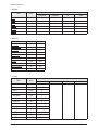
1-1 Safety Precautions
1.
Make sure all protective devices are properly installed
including non-metallic handles and compartment covers
when installing or re-installing the chassis or chassis
assemblies.
2.
Make sure that no gaps exist between the cabinets for
children to insert their fingers in to prevent children from
receiving electric shocks. Gaps mentioned above include
ventilation holes of a too great magnitude between the
PDP module and the cabinet mask, and the improper
installation of the rear cabinet.
5.
Warning for Engineering Changes:
Never make any changes or additions to the circuit
design or the internal part for this product.
Ex: Do not add any audio or video accessory
connectors. This might cause physical damage.
Furthermore, any changes or additions to the original
design/engineering will invalidate the warranty.
6.
Warning - Hot Chassis:
Some TV chassis are directly connected to one end of
the AC power cord for electrical reasons.
Without insulated transformers, the product can only be
repaired safely when the chassis is connected to the
earthed end of the AC power source.
Errors may occur when the resistance is below 1.0 ㏁ or
over 5.2 ㏁.
In these cases, make sure that the device is repaired
before sending it back to the customer.
3.
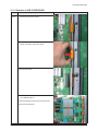
Check for Electricity Leakage (Figure 1-1)
Warning: Do not use an insulated transformer for checking the leakage. Use only those current leakage testers
or mirroring systems that comply with ANSIC 101.1 and
the Underwriter Laboratory's specifications (UL1410,
59.7).
LEAKAGE
CURRENT
TESTER
DEVICE
UNDER
TEST
2-WIRE CORD
EARTH
GROUND
Fig. 1-1 AC Leakage Test
4.
A high voltage is maintained within the specified limits
using safety parts, calibration and tolerances. When
voltage exceeds the specified limits, check each special
part.
Samsung Electronics
7.
Some TV chassis are shipped with an additional
secondary grounding system. The secondary system is
adjacent to the AC power line. These two grounding
systems are separated in the circuit using an
unbreakable/unchangeable insulation material.
8.
When any parts, material or wiring appear overheated or
damaged, replace them with new regular ones
immediately. When any damage or overheating is
detected, correct this immediately and make a regular
check of possible errors.
(READING SHOULD
NOT BE ABOVE
0.5mA)
TEST ALL
EXPOSED METAL
SURFACES
ALSO TEST WITH
PLUG REVERSED
(USING AC ADAPTER
PLUG AS REQUIRED)
To make sure the AC power cord is properly connected,
follow the instructions below. Use the voltmeter to
measure the voltage between the chassis and the
earthed ground. If the measurement is over 1.0V, unplug
the AC power cord and change the polarity before reinserting it. Measure the voltage between the chassis
and the ground again.
9. Check for the original shape of the lead, especially that
of the antenna wiring, any sharp edges, the AC power
and the high voltage power. Carefully check if the wiring
is too tight, incorrectly placed or loose. Never change the
space between the part and the printed circuit board.
Check the AC power cord for possible damages. Keep
the part or the lead away from any heat-emitting
materials.
1-1
Precaution
10. Safety Indication:
Some electrical circuits or device related materials
require special attention to their safety features, which
cannot be viewed by the naked eye. If an original part is
replaced with another irregular one, the safety or
protective features will be lost even if the new one has a
higher voltage or more watts.
Critical safety parts should be bracketed with (
! ).
Use only regular parts for replacements (in particular,
flame resistance and dielectric strength specifications).
Irregular parts or materials may cause electric shock or
fire.
1-2
Samsung Electronics
Precaution
1-2 Servicing Precautions
Warning 1: First carefully read the "Safety Instruction" in this service manual.
When there is a conflict between the service and the safety instructions, follow the safety instruction at all times.
Warning 2: Any electrolytic capacitor with the wrong polarity will explode.
1.
The service instructions are printed on the cabinet, and
should be followed by any service personnel.
2.
Make sure to unplug the AC power cord from the power
source before starting any repairs.
(a) Remove or re-install parts or assemblies.
(b) Disconnect the electric plug or connector, if any.
(c) Connect the test part in parallel with the electrolytic
capacitor.
3.
Some parts are placed at a higher position than the
printed board. Insulated tubes or tapes are used for this
purpose. The internal wiring is clamped using buckles to
avoid contact with heat emitting parts. These parts are
installed back to their original position.
4.
After the repair, make sure to check if the screws, parts
or cables are properly installed. Make sure no damage is
caused to the repaired part and its surroundings.
5.
Check for insulation between the blade of the AC plug
and that of any conductive materials (i.e. the metal
panel, input terminal, earphone jack, etc).
6.
Insulation Check Process: Unplug the power cord from
the AC source and turn the switch on. Connect the insulating resistance meter (500v) to the AC plug blade.
7.
Any B+ interlock should not be damaged.
If the metal heat sink is not properly installed, no
connection to the AC power should be made.
8.
Make sure the grounding lead of the tester is connected
to the chassis ground before connecting to the positive
lead. The ground lead of the tester should be removed
last.
9.
Beware of risks of any current leakage coming into
contact with the high-capacity capacitor.
10. The sharp edges of the metal material may cause
physical damage, so ensure wearing protective gloves
during the repair.
11. Due to the nature of plasma display panels, partial afterimages may appear if a still picture is displayed on the
screen for a long period of time.
This is caused by brightness deterioration due to the
storage effect of the panel, and to prevent this from
happening, we recommend that the brightness and contrast are reduced.
(e.g.) Contrast: 25, Brightness: 50
The insulating resistance between the blade of the AC
plug and that of the conductive material should be more
than 1 ㏁.
Samsung Electronics
1-3
Precaution
1-3 Static Electricity Precautions
1.
Some semi-conductive ("solid state") devices are
vulnerable to static electricity. These devices are known
as ESD. ESD includes the integrated circuit and the field
effect transistor. To avoid any materials damage from
electrostatic shock, follow the instructions described
below.
2.
Remove any static electricity from your body by
connecting the earth ground before handling any
semi-conductive parts or ass'ys. Alternatively, wear a
dischargeable wrist-belt.
(Make sure to remove any static electricity before
connecting the power source - this is a safety instruction
for avoiding electric shock)
3.
Remove the ESD ass'y and place it on a conductive
surface such as aluminum foil to prevent accumulating
static electricity.
4.
Do not use any Freon-based chemicals.
Such chemicals will generate static electricity that
causes damage to the ESD.
5.
Use only grounded-tip irons for soldering purposes.
6.
Use only anti-static solder removal devices.
Most solder removal devices do not support an
anti-static feature. A solder removal device without an
anti-static feature can store enough static electricity to
cause damage to the ESD.
7.
Do not remove the ESD from the protective box until the
replacement is ready. Most ESD replacements are
covered with lead, which will cause a short to the entire
unit due to the conductive foam, aluminum foil or other
conductive materials.
8.
Remove the protective material from the ESD
replacement lead immediately after connecting it to the
chassis or circuit ass'y.
9.
Take extreme caution in handling any uncovered ESD
replacements. Actions such as brushing clothes or lifting
your leg from the carpet floor can generate enough static
electricity to damage the ESD.
CAUTION
These servicing instructions are for use by
qualified service personnel only.
To reduce the risk of electric shock do not
perform any servicing other than that contained in the
operating instructions unless you are qualified to do so.
1-4
Samsung Electronics
Precaution
1-4 Installation Precautions
1.
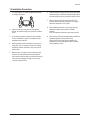
For safety reasons, more than two people are required
for carrying the product.
2.
Keep the power cord away from any heat emitting
devices, as a melted covering may cause fire or electric
shock.
3.
Do not place the product in areas with poor ventilation
such as a bookshelf or closet. The increased internal
temperature may cause fire.
4.
Bend the external antenna cable when connecting it to
the product. This is a measure to protect it from being
exposed to moisture. Otherwise, it may cause a fire or
electric shock.
5.
Make sure to turn the power off and unplug the power
cord from the outlet before repositioning the product.
Also check the antenna cable or the external connectors
if they are fully unplugged. Damage to the cord may
cause fire or electric shock.
Samsung Electronics
6.
Keep the antenna far away from any high-voltage cables
and install it firmly. Contact with the high-voltage cable or
the antenna falling over may cause fire or electric shock.
7.
When connecting the RF antenna, check for a DTV
receiving system and install a separate DTV reception
antenna for areas with no DTV signal.
8.
When installing the product, leave enough space (4")
between the product and the wall for ventilation
purposes.
A rise in temperature within the product may cause fire.
9.
When moving a PDP with attached speakers, detach the
speakers first before moving the main body.
Moving the PDP main body without separating the
speakers may cause the speakers to detach, possibly
causing damage or injury.
1-5
MEMO
1-6
Samsung Electronics
Product Specification
2. Product Specification
2-1 Product Features
Block
Specfication
Major IC
Remark
Digital/Analog (DTV Built In)
VSB NIM Tuner
S5H2010A01 (Eagle+)
Samsung SDI V4 Module
50" HD
New Module
Power
Samsung electro mechanics SMPS
50" HD SMPS
New SMPS
Video
NTSC 3.58, ATSC
HDMI
DNIe Lite
Component, PC
STP22 (Scaler)
SDP43 (DNIe Lite)
MST9883 (PC A/D)
SiI9993 (HDMI)
Sound
Speaker : 15W + 15W
SRS TruSurrond XT, Dolby Digital
MSP4440K, NSP-6241
TAS5122
Cabinet
P5 Design
RF
PDP Module
Optical, Coaxial
Output
New Cabinet
■ Chip Description
- DNVS303EH261A Tuner : ATSC/NTSC VSB NIM Tuner
- STP22 : Component, CVBS, Y/C, HDMI, PC input Video signal processor
- SDP43 : The DNIe IC for visual quality improvement. (DNIe Lite)
- Sii9993 : Converts the TMDS signal on the HDMI input into 8 bit digital R, G, B signals.
- MSP4440K : Sound Processing IC
- MST9883 : A/D converts the R, G, B input signal from 15 Pin PC video to 8 bit digital R, G, B signals.
- NSP6241A: Sound PWM IC
- TAS5122 : Sound AMP IC
- S5H2010A01 : MPEG Decoder IC (EAGLE+)
- S3C2800X01 : CPU IC
- 3F8668 : Generates various control signals required for operating the circuit.
The software is downloaded through PC D-SUB Jack. (Sub Micom)
Samsung Electronics
2-1
Product Specification
2-2 Key Features
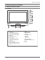
Model
PL-50P5HD
Dimensions Display
Weight
Display
1230.1 (W) x 826.0 (H) x 94.5 (D) mm (Without Stand)
1230.1 (W) x 875.5 (H) x 334.8 (D) mm (With Stand)
46.8Kg (Without Stand)
53.5Kg (With Stand)
Voltage
AC 110 V~, 60 Hz
Number of Pixels
1366 (H) x 768 (V)
Screen Size
50 inches
ANT 1 - CABLE IN
ANT 2 - AIR IN
※ 75Ω unbalanced
ANTENNA input
VIDEO input
AV 1, AV2
S-VIDEO 1, S-VIDEO 2
COMPONENT1 - 480i/480p/720p/1080i
COMPONENT2 - 480i/480p/720p/1080i
PC
HDMI (DVI Compatible)
AUDIO input
AV 1, AV2
S-VIDEO 1, S-VIDEO 2
COMPONENT1 - 480i/480p/720p/1080i
COMPONENT2 - 480i/480p/720p/1080i
PC
DVI
AV Output
AUDIO (L/R)
Speaker Output
Audio Output
ETC
New Function
15W + 15W (8Ω )
OPTICAL(DIGITALOUT)
COAXIAL(DIGITALOUT)
DNIe Lite, Anynet, Color Weakness, My Color Control, SRS TruSurround XT, Dolby Digital,
Built-in Speaker/Stand
Energy Saving, Screen Burn Protection
■ H/W Configuration
- DTV Module : S5H2010A01 (MPEG Decoder IC, Eagle+)
- Video : STP-22, MST9883, SiI9993, DNIe Lite
- Sound : MSP4440K, NSP-6241, TAS5122
- Tuner : UMX-NT-043 (RF-Splitter), DNVS303EH261A (VSB NIM Tuner)
- CPU : S3C2800X01, S3F866B, P_PCFM_012
■ S/W Configuration
- Main Program : TE28F640 (Flash memory)
- Sub-Micom : S3F866B
- DDC : 24C02 x2 (Analog DDC Data, Digital DDC Data)
- EEPROM : 24C256 (White balance data and Factory initial data)
2-2
Samsung Electronics
Product Specification
■ Picture
- System : Video → ATSC / NTSC
- Progressive
- Output resolution : 1366 x 768 p
- OSD : Smart user Interface Grade 1
- Picture Enhancement : DNIe Lite
- Still picture, Noise reduction
- Comb Filter : 3D comb filter
- PIP : Large, Double 1, Double 2
- Picture Size : 16:9, Panorama, Zoom1, Zoom2, 4:3 (AV, S-Video, Component 480i/480p)
16:9, 4:3 (Component 720p/1080i, PC, HDMI)
■ Sound
- System : Stereo
- Dolby Digital, TruSurround XT
- Output : 15W + 15W
- Speaker : Built-in
- Optical/Coaxial Sound Output : Dolby Digital, PCM (DTV), PCM (HDMI)
■ Feature
- Component Interface(480i/480p/720p/1080i, Y/Pb/Pr)
- Digital Interface : HDMI (480p/720p/1080i)
- Auto Program
- Sleep Timer : 180 Minutes
- Anynet Interface
- My Color Control
- Color Weakness
- Energy Saving
- Screen Burn Protection
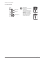
■ In/Out Terminals
- 1 Monitor audio Output
- 2 Component Inputs
- 15 Pin PC D-sub Input
- 1 HDMI Input
- 2 SPDIF Outputs (Optical, Coaxial)
- 2 RF Input : Cable/Air
- 2 CVBS Input
- 2 S-Video Input
■ Remocon
- TM76
■ Power Supply
- 110 V~, 60Hz
■ HDMI input mode : 480p, 720p, 1080i
■ Note
- You can input the DVI signal using the DVI ↔ HDMI conversion cable.
- When connecting HDMI input using the DVI ↔ HDMI conversion cable, connect the sound signal to the DVI Audio IN port
using a separate connection cable.
Samsung Electronics
2-3
Product Specification
■ PC(D-Sub 15Pin Jack) Input mode
The table below shows all of the display modes that are supported. (N : Negative, P : Positive)
Video Signal
Resolution
(Dot X Line)
Vertical
Frequency (Hz)
Horizontal
Frequency (KHz)
Vertical
Polarity
Horizontal
Polarity
640 X 350
70.086
31.469
P
N
720 X 400
70.087
31.469
N
P
59.940
31.469
N
N
70.000
35.000
N/P
N/P
72.809
37.861
N
N
75.000
37.500
N
N
56.250
35.156
N/P
N/P
60.317
37.879
P
P
70.000
43.75
N/P
N/P
72.188
48.077
P
P
75.000
46.875
P
P
60.004
48.363
N
N
70.069
56.476
N
N
72.000
57.672
N/P
N/P
75.029
60.023
P
P
1280 X 720
59.855
44.772
P
N
1360 X 768
60.015
47.712
P
P
640 X 480
IBM PC / AT
Compatible
800 X 600
1024 X 768
2-4
Samsung Electronics
Product Specification
2-3 Specifications Analysis
Model
PL-50D4H
PL-50P5HD
Display Type
PDP TV
PDP TV
Built-In Tuner
×
○
Design
Basic
Picture
Audio
Features
Connections
ETC
Resolution
1366 × 768
1366 × 768
PDP Module
Samsung SDI V3
Samsung SDI V4
Screen Size
50"
50"
Picture ratio
16 : 9
16 : 9
Dimensions
1205(W) x 724 (H) x 79 (D) mm
1230 (W) x 826 (H) x 95 (D) mm
Weight
43 Kg (Without Stand)
46.8 Kg (Without Stand)
Brightness
1,000 Cd/m2
1,300 Cd/m2
Contrast Ratio
3,000 : 1
10,000 : 1
Picture Enhacer
DNIe 2
DNIe Lite
Comb Filter
○
○
Equalizer
5 Band
5 Band
Auto Volume Control
○
○
Surround Sound
SRS TruSurround XT
SRS TruSurround XT Dolby Digital
Speaker Output
15W + 15W
15W + 15W
PIP
○
○
Double Window
○
○
Caption
○
○
Still Image
○
○
EPG
×
○
My Color Control
○
○
Color Weakness
○
○
Energy Saving
×
○
Anynet
×
○
Antenna
1
2 (Cable/Air)
AV Input
2
2
S-Video
1
2
Component
2
2
PC(D-SUB)
1
1
DVI
1
×
HDMI
×
1
POD Cable Card
×
×
Sub Woofer
×
×
Optical
×
1
Coaxial
×
1
Speaker/Stand
Built-in Speaker/Stand
Built-in Speaker/Stand
FCC Class
Class B
Class B
Samsung Electronics
2-5
Product Specification
2-4 Accessories
Accessories that can be purchased
additionally
Supplied Accessories
Accessories
2-6
Item
Item code
Owner's Instructions
BN68-00825Q
Remote Control
AAA Batteries
BN59-00462A
4301-000103
Remark
Samsung Service center
Power Cord
3903-000144
Anynet Cable
BN39-00518A
S-VIDEO Cable
-
HDMI Cable
-
HDMI/DVI cable
-
Component Cables (RCA)
-
PC Cable
-
PC Audio Cable
-
Optical Cable
-
Coaxial Cable
-
Antenna Cable
-
Internal shopping mall
Samsung Electronics
Alignment & Adjustment
3. Alignment & Adjustment
3-1 Service Instruction
* Check items listed after changing each
Replaced Items
Item Code
Check Items
ASSY PCB MISC-MAIN
1) Auto Program
BN94-00860A 2) Let the user go through subscription process after contacting
user's cable service provider.
ASSY PCB P-SMPS(MAIN)
BN96-01801B Voltage Adjustment
ASSY PCB P-SMPS(DC DC)
BN96-01856A Voltage Adjustment
ASSY PDP P-LOGIC BOARD
BN96-03097A
-
ASSY PDP P-X MAIN BOARD
BN96-03090A
-
ASSY PDP P-Y MAIN BOARD
BN96-03091A
-
ASSY PDP P-Y UPPER BUFFER BOARD
BN96-03092A
-
ASSY PDP P-Y LOWER BUFFER BOARD
BN96-03093A
-
ASSY PDP P-ADDRESS E BUFF BOARD
BN96-03094A
-
ASSY PDP P-ADDRESS F BUFF BOARD
BN96-03095A
-
ASSY PDP P-ADDRESS G BUFF BOARD
BN96-03096A
-
※ When replacing the SMPS or PDP panel, you have to check the voltage printed on the panel sticker and adjust it.
Samsung Electronics
3-1
Alignment & Adjustment
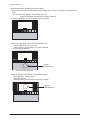
3-2 How to Access Service Mode
■ Using the Customer Remote
1. Turn the power off and set to stand-by mode.
2. Press the remote buttons in this order; MUTE-1-8-2- POWER ON to turn the set on.
3. The set turns on and enters service mode.
4. Press the Power button to exit and store data in memory.
※ If you fail to enter service mode, repeat steps 1 and 2 above.
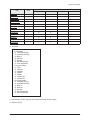
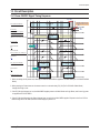
5. Initial SERVICE MODE DISPLAY State
HDMI/DTV HD
Calibration
Adjust
Option Byte
Test Pattern
White Balance
Chip Debugger
SVP-EX
Checksum
MST9883
Option PDP
MSP34XX
RESET
YC Delay
DNIe Lite
T-STRANUS0S-0036 Jan 12 2005
T-STRANUS5-0117 [Sec : 29]
※ "T-STRANUS0S-0036" and "T-STRANUS5-0117" are firmware version.
The firmware version is subject to change without notice.
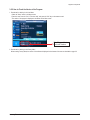
6. Buttons operations within Service Mode
MENU
Direction keys ▲ / ▼
Item Selection by Moving the Cursor
Direction keys ◀ / ▶
Data Increase/Decrease for the Selected Item
Source
3-2
Full Menu Display / Move to Parent Menu
Cycles through the active input source that are connected to the unit
Samsung Electronics
Alignment & Adjustment
3-3 Factory Data
★ The underlined are items applied during the service adjustment. None of the others should be adjusted.
1. Calibration
ITEM
AV Calibration
Off
Comp Calibration
Off
PC Calibration
Off
2. Option Byte
ITEM
Caption Level
16
V-Chip Enable
1
Watchdog Enable
1
Spread Enable PC
1
Clock Adjust
4
MST3385 USED
0
STA323 USED
0
Nim Version
T310
MSP Version
K
New_WB_CbCr
1
3. White Balance
ITEM
Range
Sub Bright(SVP)
Initial Values of Input Modes
TV/AV/S-video
Component
PC
HDMI
0~1204
495
513
480
492
R-Offset
0~1204
516
512
512
515
G-Offset
0~1204
512
512
512
512
B-offset
0~1204
512
512
512
511
Sub Contrast(DNIe)
0~255
130
131
128
131
R-Gain
0~255
132
132
128
132
G-Gain
0~255
125
125
128
125
B-Gain
0~255
140
140
128
140
256
256
256
256
Comb Filter
0
0
0
0
Peaking
0
0
0
0
NR
0
0
0
0
Deinterlace
0
0
0
0
Sub Contrast(SVP)
Samsung Electronics
3-3
Alignment & Adjustment
4. SVP-EX
Initial Values of Input Modes
ITEM
Range
TV
AV/S-Video
Component
480i/P
720/1080
PC
HDMI
00.Comb Filter
01.Y-Filter
01.Peaking
01.V-PosGain
0~15
4
3
2
2
0
3
02.V-NegGain
0~15
4
4
4
2
0
4
03.V-BpGain
0~32
16
16
16
16
16
16
04.V-HfGain
0~32
20
20
20
20
20
20
05.V-Peaking-TH 1
0~256
16
16
16
16
16
16
06.V-Peaking-TH 3
0~256
128
128
128
128
128
128
01.TCD3 Contrast
0~255
120
120
120
120
120
02.TCD3 Brightness
0~255
49
49
49
49
49
03.TCD3 YC Delay
0~15
1
1
1
1
1
04.Analog Y Offset
0~1023
61
61
61
61
61
05.Analog PB Offset
0~1023
512
512
512
512
512
06.Analog PR Offset
0~1023
512
512
512
512
512
07.Analog Y Gain
0~255
217
217
217
217
217
08.Analog PB Gain
0~255
225
225
225
225
225
09.Analog PR Gain
0~255
225
225
225
225
225
10.Black Level Setting
0~255
16
16
16
0
16
11.Brightness
0~255
128
128
125
128
128
12.UserColor(MAX)
0~127
127
127
127
127
127
01.MP R-Offset2
0~1023
512
512
512
512
512
02.MP G-Offset2
0~1023
512
512
512
512
512
03.MP B-Offset2
0~1023
512
512
512
512
512
04.PP R-Offset2
0~1023
512
512
512
512
512
05.PP G-Offset2
0~1023
512
512
512
512
512
06.PP B-Offset2
0~1023
512
512
512
512
512
02.NR
01.Y-NR-Off
02.C-NR-Off
03.Y-NR-On
04.C-NR-On
03.Deinterlace
01.Motion
04.Picture Gain Adjust
06.WB Control
3-4
Samsung Electronics
Alignment & Adjustment
Initial Values of Input Modes
ITEM
Sub
Address 'h
Range
Component
TV
AV/
S-Video
480i
HDMI
480p 720p 1080i 480P 720P 1080i
PC
07. Chroma
01.LtiPeakGain
P1 Luma/Croma 0x0F [4:0]
0~31
31
31
31
31
31
31
31
31
31
15
02.LtiStep
P1 Luma/Croma 0x0F [6:5]
0~3
2
2
2
2
2
2
2
2
2
2
03.LtiTh
P1 Luma/Croma 0x10 [7:0]
0~255
16
16
16
16
16
16
16
16
16
16
04.LtiGain
P1 Luma/Croma 0x11 [4:0]
0~31
8
10
10
10
10
10
10
10
10
8
05.LowPassGain
P1 Luma/Croma 0x12 [4:0]
0~31
8
24
17
15
15
20
10
10
10
2
06.BandPassGain
P1 Luma/Croma 0x13 [4:0]
0~31
18
25
24
20
25
28
25
25
25
12
07.HighPassGain
P1 Luma/Croma 0x14 [4:0]
0~31
20
28
18
18
24
24
24
24
24
4
08.PeakStep
P1 Luma/Croma 0x12 [6:5]
0~3
1
1
1
0
0
0
1
0
0
1
09.PeakTh1
P1 Luma/Croma 0x15 [7:0]
0~255
7
7
7
7
7
10
7
7
7
7
10.PeakTh2
P1 Luma/Croma 0x16 [7:0]
0~255
2
2
2
2
0
3
2
2
2
0
11.PeakTh3
P1 Luma/Croma 0x19 [7:0]
0~255
32
32
32
32
32
34
32
32
32
32
12.PeakN1Factor2
P1 Luma/Croma 0x14 [7:5]
P1 Luma/Croma 0x13 [7:5]
0~63
56
8
8
8
0
8
0
0
0
0
13.PeakN1Factor1
P1 Luma/Croma 0x1A [5:0]
0~63
40
48
48
40
48
40
40
40
40
48
14.CoringTh
P1 Luma/Croma 0x17 [7:0]
0~255
2
2
2
2
2
2
2
2
2
0
15.CoringGain
P1 Luma/Croma 0x18 [4:0]
0~31
8
0
8
8
8
12
8
8
8
24
16.PeakPosGain
P1 Luma/Croma 0x49 [7:4]
0~15
1
1
2
2
2
2
1
2
2
3
17.PeakNegGain
P1 Luma/Croma 0x49 [3:0]
0~15
1
1
2
2
1
1
1
2
2
3
18.BypassHsharp
P1 Luma/Croma 0x1A [6]
0~1
0
0
0
0
0
0
0
0
0
1
19.DctiGain
P1 Luma/Croma 0x28 [3:0]
0~15
4
4
10
10
10
10
4
4
4
12
20.DctiStep
P1 Luma/Croma 0x29 [6:4]
0~7
1
1
7
1
1
1
1
1
1
3
21.DctiEnable
P1 Luma/Croma 0x29 [7]
0~1
1
1
1
1
1
1
1
1
1
0
22.DctiThres
P1 Luma/Croma 0x2A [7:0]
0~255
12
12
12
12
12
12
12
12
12
12
08.CLK_A
P5. DSS 0x0A[15:0]
16~17
16
16
16
16
09.CLK_B
P5. DSS 0x0B[15:0]
0~255
32
32
48
32
1
1
1
0
10.GAMMA
Samsung Electronics
3-5
Alignment & Adjustment
5. MST9883
ITEM
Range
Initial Values of Input Modes
TV/AV/SVHS
Component
PC
HDMI
R_Gain
0~255
112
112
112
112
G_Gain
0~255
112
112
112
112
B_Gain
0~255
113
113
113
113
R_Offset
0~255
122
122
122
122
G_Offset
0~255
121
121
121
121
B_Offset
0~255
122
122
122
122
6. MSP34XX
ITEM
Range
Initial
FM-Prescale
0~255
0x20
NICAM-Prescale
0~255
0x20
AV-Prescale
0~255
0x1C
I2S_1 Prescale
0~255
0x10
I2S_3 Prescale
0~255
0x11
Carrier Mute
0~255
On
Pilot High
0~255
0x0D
Pilot Low
0~255
0x07
Scart1 Out Volume
0~255
0x6D
Scart2 Out Volume
0~255
0x73
7. YC Delay
ITEM
Range
Initial Values of Input Modes
TV/AV/SVHS
RF PAL-B/G
0~255
0
RF PAL-D/K
0~255
0
RF PAL- I
0~255
0
RF SECAM-B/G
0~255
0
RF SECAM-D/K
0~255
0
RF SECAM-L/L'
0~255
0
RF NTSC3.58
0~255
0
RF NTSC4.43
0~255
0
AV PAL
0~255
0
AV SECAM
0~255
0
AV NTSC 3.58
0~255
0
AV NTSC4.43
0~255
0
AV PAL60
0~255
0
3-6
Component
PC
HDMI
-
-
-
Samsung Electronics
Alignment & Adjustment
8. DNIe Lite
ITEM
Range
Initial Values of Input Modes
TV/AV/SVHS
Component
PC
HDMI
01.PATT_SEL
0~63
0
0
0
0
02.BLACK_TILT
0~255
110
125
80
110
03.BLACK_GAINMAX
0~1023
380
390
370
380
04.TEST_MCC
0~255
0
0
0
0
05.OVERLAP_MCM
0~255
0
0
0
0
06.AREA_EN_MCC
0~255
31
31
31
31
07.I2C Offset Mean
0~63
16
10
10
10
0
0
0
0
08.I2C Ana Check
09.White Balance(Post)
1.R-Offset(Post)
-512~511
0
0
0
0
2.G-Offset(Post)
-512~511
0
0
0
0
3.B-Offset(Post)
-512~511
0
0
0
0
4.R-Gain(Post)
0~255
0
128
128
128
5.G-Gain(Post)
0~255
0
128
128
128
6.B-Gain(Post)
0~255
0
128
128
128
7.Com_Offset_Sel
0,1
1
0
0
0
8.Com_Gain_Sel
0,1
1
0
0
0
10.ColorTone Cool2
11.ColorTone Cool1
12.ColorTone Normal
Refer to Table 3
13.ColorTone Warm1
14.ColorTone Warm2
15.MCM_EN
0,1
1
1
1
1
16.TEMP_DEST
0~255
150
150
150
150
17.CB5_HIGH
0~255
139
140
156
141
18.CR5_HIGH
0~255
125
126
126
124
19.CB5_LOW
0~255
128
127
126
128
20.CR5_LOW
0~255
129
130
129
129
Samsung Electronics
3-7
Alignment & Adjustment
9. Adjust
ITEM
Range
Initial Values of Input Modes
TV/AV/SVHS
Component
PC
HDMI
01.Video Mute Time
0~63
5
-
-
5
02.Melody Volume
0~63
10
-
-
20
03.Dynamic Contrast
0
0
0
0
04.Dynamic Bright
0
0
0
0
05.Dynamic Color
0
0
0
0
06.Dynamic Sharpness
0
0
0
0
07.Standard Contrast
0
0
0
0
08.Standard Bright
0
0
0
0
09.Standard Color
0
0
0
0
10.Standard Sharpness
0
0
0
0
Rf
AV
11.Movie Contrast
12.Movie Bright
13.Movie Color
14.Movie Sharpness
15.RF_dB_1
-.Noise Thres1
0~255
20
20
-.LowPassGain1
0~31
7
14
-.BandPassGain1
0~31
12
19
-.HighPassGain1
0~31
6
16
-.PeakStep1
1
1
-.CoringTh1
2
2
-.CoringGain1
8
2
-.PosGain1
1
1
-.NegGain1
1
1
-.V-PosGain1
3
3
-.V-NegGain1
2
2
-.Noise Thres2
30
40
-.LowPassGain2
5
10
-.BandPassGain2
8
15
-.HighPassGain2
0
8
-.PeakStep2
0
0
-.CoringTh2
12
8
-.CoringGain2
8
10
-.PosGain2
1
1
-.NegGain2
1
1
-.V-PosGain2
2
2
-.V-NegGain2
1
1
16.RF_dB_2
3-8
Samsung Electronics
Alignment & Adjustment
ITEM
Range
Initial Values of Input Modes
TV/AV/SVHS
Component
-.Noise Thres3
40
60
-.LowPassGain3
0
5
-.BandPassGain3
0
12
-.HighPassGain3
0
4
-.PeakStep3
0
0
-.CoringTh3
26
14
-.CoringGain3
15
16
-.PosGain3
0
0
-.NegGain3
0
0
-.V-PosGain3
0
0
-.V-NegGain3
0
0
PC
HDMI
17.RF_dB_3
10. Test Pattern
01. OSD Pattern
01. Luma Ramp(32 Step)
02. Luma Ramp(128 Step)
03. White 16
04. White 240
05. Color Bar
06. RGB Ramp(32 Step)
07. Cross Hatch(20X20)
02. 1 Channel Pattern
01. Y-Filter
02. V-PosGain
03. V-NegGain
04. V-BpGain
05. V-HfGain
06. V-Peaking-Th1
07. V-Peaking-Th3
03. 2 Channel Pattern
01. Luma Ramp(32 Step)
02. Luma Ramp(128 Step)
03. White 16
04. White 240
05. Color Bar
06. RGB Ramp(32 Step)
07. Cross Hatch(20X20)
11. Chip Debugger : ON/OFF (Select this menu before downloading sub-micom image)
12. Checksum [XXXX]
Samsung Electronics
3-9
Alignment & Adjustment
13. Option PDP : ON/OFF
ITEM
Range
01.Pixel Shift
Initial
0
-.Pixel Shift Test
0~1
0
-.Number Range
0~1
1
-.Line Range
0~1
1
02.Sound SD delay
0~2
1
03.Sound HD delay
0~2
1
04.Sound DTV delay
0~1
0
05.DDC Write
0~1
0
06.Auto Voltage Adj
5
-.Auto Voltage On
Off
-.AVC Set Mode
0
-.Manual Control_Vs
180
-.Manual Control_Va
55
-.Vs Reference
0
-.Vs Average
0
-.Va Reference
0
-.Va Average
0
07.Image Sticking
0
08.Error Mode Check
1
09.Error Code Table
4
10.Patt Sel
0
11.Control Key Lock
0
12.FCRL Con
1
14. KS1406
ITEM
Range
01.AGC_REF[AIR]
Initial
0x50
02.CR_F_GAIN[AIR]
0~2
0xD0B
03.CR_L_GAIN[AIR]
0~2
0x24
04.EQ_STEP[AIR]
0~1
0x0B
05.AGC_REF[CABLE]
0~1
0x60
06.CR_F_GAIN[CABLE]
0xC0B
07.CR_L_GAIN[CABLE]
0x50
08.EQ_STEP[CABLE]
0x03
15. Reset : Factory reset (User settings in OSD is initialized.)
3-10
Samsung Electronics
Alignment & Adjustment
3-4 Service Adjustment
3-4-1 White Balance Adjustment
1. W/B Adjustment is required for the following sequence.
Color Calibration (CVBS,Component,PC) → W/B Adjustment (HDMI,Component,CVBS)
2. Adjustment Method (Signal equipment : MSPG-925LTH, Measurement equipment : CA210)
3. You can adjust the white ratio in factory mode (Calibration, White Balance menu).
4. Since the adjustment value and the data value vary depending on the input source, you have to adjust these in HDMI,
Component and AV modes.
5. The optimal values for each mode are configured by default. (Refer to Table 2 and 3)
Equipment: CA-210 & Master MSPG925 Generator
Calibration Pattern: Master MSPG925 #24 "Lattice pattern"
W/B adjustment Pattern: Master MSPG925 #16 "ABL pattern"
Use other equipment only after comparing the result with that of the Master equipment.
Set Aging Time: Longer than 30 min.
Pattern Resolution: Given below.
Calibration Available/None and Pattern used for Calibration.
Input mode
Calibration
Pattern
CVBS IN (Model_#1)
Perform in NTSC B&W Pattern #24
Lattice
Component IN (Model_#6)
Perform in 720p B&W Pattern #24
Lattice
PC Analog IN (Model_#21)
Perform in VESA XGA (1024x768)
B&W Pattern #24
Lattice
HDMI IN
None
-
<Table 1>
White Balance coordinates configuration result. (On the basis of the ABL pattern. The resolutions are given below)
Input mode
x
y
Y(fL)
T(K)/MPCD
CVBS IN
(NTSC)
H/L
265
265
Do not adjust
15000K/-5
L/L
280
285
0.8
10000K/-5
Component IN
(720p, 60Hz)
H/L
265
265
Do not adjust
15000K/-5
L/L
280
285
0.8
10000K/-5
PC Analog IN
HDMI IN
(720p, 60Hz)
None
H/L
265
265
Do not adjust
15000K/-5
L/L
280
285
0.8
10000K/-5
<Table 2>
For PC Mode, perform only calibration and do not perform additional W/B adjustments.
Samsung Electronics
3-11
Alignment & Adjustment
Item
AV
Component
HDMI
PC
Warm 2
Warm 1
Normal
Cool1
Cool2
R Cutoff
128
128
128
128
128
G Cutoff
128
128
128
128
128
B Cutoff
128
128
128
128
128
R Gain
128
128
128
128
128
G Gain
128
128
128
128
128
B Gain
128
128
128
128
128
R Cutoff
128
128
128
128
128
G Cutoff
128
128
128
128
128
B Cutoff
128
128
128
128
128
R Gain
128
128
128
128
128
G Gain
128
128
128
128
128
B Gain
128
128
128
128
128
<Table 3>
3-12
Samsung Electronics
Alignment & Adjustment
3-4-2 Conditions for Measurement
1. On the basis of toshiba ABL pattern : High Light level (57 IRE)
■ INPUT SIGNAL GENERATOR : MSPG-925LTH
* Mode NO 1 : 744X484@60 Hz
NO 6 : 1280X720@60 Hz
NO 21 : 1024X768@60 Hz
* Pattern NO 24 : B&W Lattice Pattern
NO 16 : Toshiba ABL Pattern
2. Optical measuring device : CA210 (FL)
Please use the MSPG-925 LTH generator for model PL-50P5HD
3-4-3 Method of Adjustment
1. Adjust the basic level of Component,PC and CVBS input signals.
a) Enter factory Calibration, confirm the ADC data (Component, PC, AV Modes).
* ADC default value : Table 1
Picture 2-1 B&W Lattice Pattern
* You must perform Calibration in the Lattice pattern before adjusting the White Balance.
* If you perform Calibration in a pattern other than the Lattice pattern, it causes a malfunction and the operation will not finish.
In this case, press the "EXIT" button on the remote control to terminate the operation.
1) Enter Service mode.
2) Apply the NTSC Lattice (No 1) pattern signal to the VIDEO IN port.
3) Press the Source key to switch to "AV/S-VIDEO" mode.
4) After confirming that the Lattice pattern appears, select the "Calibration" menu.
5) Select the "AV Calibration" menu.
6) In "AV Calibration Off" status, press the "▶" key to perform Calibration.
7) When Calibration is complete, it returns to the high-level menu.
8) Apply the 720p Lattice (No 6) pattern signal to the COMPONENT IN (Y/Pb/Pr) port.
9) Press the Source key to switch to "COMPONENT" mode.
10) After confirming that the Lattice pattern appears, select the "Calibration" menu.
11) Select the "COMP Calibration" menu.
12) In "COMP Calibration Off" status, press the "▶" key to perform Calibration.
13) When Calibration is complete, it returns to the high-level menu.
14) Apply the 1024x768 Lattice (No 21) pattern signal to the PC IN port.
15) Press the Source key to switch to "PC" mode.
16) After confirming that the Lattice pattern appears, select the "Calibration" menu.
17) Select the "PC Calibration" menu.
18) In "PC Calibration Off" status, press the "▶" key to perform Calibration.
19) When Calibration is complete, it returns to the high-level menu.
20) All Calibration operations are complete.
Samsung Electronics
3-13
Alignment & Adjustment
2. Adjust the white balance of HDMI,Component and AV Modes.
a) Set the input to the mode in which the adjustment will be made (HDMI, Component, AV adjustment. Do not adjust in PC
Mode.)
* Input signal - AV Mode : Model #1 (744*484 Mode), Pattern #16
- Component/HDMI Mode : Model #6 (1280*720 Mode), Pattern #16
b) Enter the White Balance menu of service mode and confirm the data.
Picture 2-2 Toshiba ABL Pattern
c) Adjust the low light. (Refer to Picture 2-3 for measurement point.)
- Adjust Sub-Bright(SVP) to set the 'Y' value.
- Adjust red offset ('x') and blue offset ('y') to the color coordinates.
* Do not adjust green offset data.
Low light
Measurement point
Picture 2-3 Toshiba ABL Pattern
d) Adjust the high light. (Refer to Picture 2-4 for measurement point.)
- Do not adjust the 'Y' value of high light.
- Select DNIe Lite menu.
- Adjust CB5 HIGH('y') and CR5 HIGH('x') to the color coordinates
High light
Measurement point
Picture 2-4 Toshiba ABL Pattern
3-14
Samsung Electronics
Alignment & Adjustment
3-4-4 How to adjust White Balance with 10 steps gray pattern
1. If you don't have Toshiba ABL pattern, you can adjust white balance with 10 steps gray scale pattern of Picture 2-5.
2. When you measure Low Light, use 20 IRE portions.
And When you measure High Light, use 70 IRE portion. But if color noise is less in 60 IRE than in 70 IRE, 60 IRE is allowed as
a measure point.
Picture 2-5
3. Perform adjustments 2-b through 2-d from previous page using the 10 step gray scale pattern.
Samsung Electronics
3-15
Alignment & Adjustment
3-5 Software Upgrade
3-5-1 Source Program Download & Generals
1. Downloading boot code
(1) Turn off PDP-TV.
(2) Connect the RS-232 serial cable to the service jack of PDP-TV.
(3) Enter the DOS Mode and move to the directory including "bootdn.bat" and Excute the file.
(4) Turn on PDP-TV.
2. Downloading application code
(1) Turn off PDP-TV.
(2) Connect the RS-232 serial cable to the service jack of PDP-TV.
(3) Enter the DOS Mode and move to the directory including "appdn.bat" and Excute the file.
(4) Power on PDP-TV.
■ Changing RS-232 serial port and downloaded file
If you want to change serial port, you must edit "bootdn.bat" and "appdn.bat".
"bootdn.bat" → sdn 1 0xdeadbbbb rom
execution file
port number
file to be downloaded
downloading type : boot image
"appdn.bat" → sdn 1 0xdeadaaaa ram.z
execution file
port number
file to be downloaded
downloading type : application image
1. Don' t turn off during downloading.
2. sdn.exe, download file and Batch file should be in the same directory.
3. During Downloading, Hyper Terminal should be turned off.
(2) Enter a new name.
(3) Select a modem port.(com 1 and direct connection.)
(4) Set the bit/second to 115200.
(5) Set the data bit to 8
(6) No parity bit.
(7) Set stop bit to 1.
(8) No flow control.
(9) Save in memory.
(10) At this point, the new hyper terminal is ready.
3-16
Samsung Electronics
Alignment & Adjustment
3-5-2 How to Check the Version of the Program
1. Procedures for checking in the User Menu
- Select the "Setup" menu in the Menu screen
- Place the cursor over the "On" of "Function Help", and press the "Info" key on the remote control
- The version of the program is displayed at the bottom of the Menu screen
Main Program Version
Boot-code Version
2. Procedures for checking in the Factory Menu
When entering Factory Mode, the version of the software is displayed at the bottom of the menu as described on page 3-2.
Samsung Electronics
3-17
Alignment & Adjustment
3-6 Replacements & Calibration
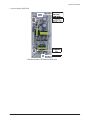
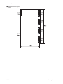
3-6-1 Voltage Adjustment
1. SMPS Panel voltages must be adjusted after changing SMPS-PCB or PDP module.
Range
Vs
190~220V
Va
60~80V
Vset
180~210V
Ve
80~120V
Vscan
-160~210V
Voltage
Label
Board Adjustment
SMPS-MAIN
SMPS-DC/DC
SMPS-MAIN
SMPS-DC/DC
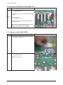
2. A point of adjusting SMPS-MAIN voltage.
TP : Vs (TOP)
Va (BOT)
Va Adjustment Point
3-18
Vs Adjustment Point
Samsung Electronics
Alignment & Adjustment
3. A point of adjusting SMPS-DC/DC.
* Use base chassis of PDP panel as GND point.
Samsung Electronics
3-19
MEMO
3-20
Samsung Electronics
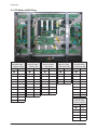
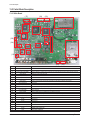
Exploded View & Part List
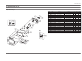
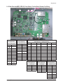
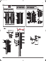
4. Exploded View & Part List
4-1 PL50P5HDX/XAX
You can search for the updated part code through ITSELF web site.
URL:http://itself.sec.samsung.co.kr
M0013
T0555
T0074
T0268
M0006
T0079
M0006
T0275
T0044
T0446
T0003
T0091
M0013
T0010
T0175
M0145
Loc. No.
Code No.
Description
Specification
Q'ty
SA/SNA
CIS7
AA61-60003B
SPRING ETC-CS
-,SUS304,-,-,OD11.2,N7,OD1
1
S.N.A
M0006
BN63-01688A
COVER-REAR
50P5,PCM,T0.5,COLOR STILL
1
S.N.A
M0006
BN63-01634B
COVER-REAR SUB
SP-R4232,SECC,T1.0
1
S.N.A
M0013
BN96-01939E
ASSY STAND P-BASE
50P5,XAC,HIPS HB,BK07,
1
S.A
M0013
BN96-01790D
ASSY COVER P-REAR
50P5,PCM,T0.5
1
S.A
M0111
BN63-01834G
COVER-STAND
50P5H,XAC,HIPS,T3.5,HB,BK07,
1
S.N.A
M0145
BN96-02549A
ASSY BOARD P-FUNCTION
SCHUBERT,CT5000-37
1
S.A
M0146
BN96-02050E
ASSY BOARD P-POWER & IR
SCHUBERT,CT5000-
1
S.A
T0003
BN96-02686E
ASSY COVER P-FRONT
50P5,XAX,HIPS HB,BKN-
1
S.A
T0010
BN61-01533A
HOLDER-AV
SPD-50P5HD,ABS
1
S.N.A
T0023
BN64-00336A
KNOB POWER
42P5,PC,VIOLET
1
S.N.A
T0044
BN96-03082A
ASSY PDP MODULE P
M1,PL50HW005B,V5.0,136
1
S.A
T0061
BN64-00338A
WINDOW-REMOCON
42P5,ACRYL,5%
1
S.N.A
T0073
AA63-01127A
GASKET-EMI
50P5,AL FOIL,T1.5,7mm,1177mm
2
S.N.A
T0073
AA63-01128A
GASKET-EMI
50P5,AL FOIL,T1.5,7mm,702mm
2
S.N.A
T0074
BN59-00462A
REMOCON
STRAUSS,TM76A,200*54*30,ZILOG,54
1
S.A
T0079
BN94-00860A
ASSY PCB MISC-MAIN
HP-R5072CF,D71C,V5
1
S.A
T0091
BN94-00647A
ASSY PCB MISC-SIDE A/V
SPD-42P5HD,D71A,4
1
S.A
T0175
BN96-01738B
ASSY SPEAKER P
8ohm,P5,50,15W,Urethan co
1
S.A
T0175
BN63-01015B
SHIELD-AV JACK
50P5,SECC,T0.5
1
S.N.A
T0268
3903-000144
CBF-POWER CORD
DT,US,BP3/Y,U(IEC C13-RA)
1
S.A
T0275
BN96-02369A
ASSY MISC P-INLET
HP-R4252,STRAUSS,DOCUM
1
S.N.A
T0446
BN96-02703K
ASSY BRACKET P-FRONT
50P5(NEW),XAX,MRT G
1
S.A
T0456
BN67-00156A
GLASS-FILTER EMI
50 P5,Mesh,NTR,40%,1224
1
S.N.A
T0555
BN96-02877C
ASSY MISC P-BRKT TERMINAL
42P5,50P5,XAA,
1
S.N.A
Remark
M0111
T0073
T0456
T0175
M0146
T0061
CIS7
T0073
Samsung Electronics
T0023
4-1
Electrical Part List
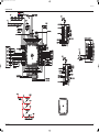
5. Electrical Part List
5-1 PL50P5HDX/XAX Service Item
You can search for the updated part code through ITSELF web site.
URL:http://itself.sec.samsung.co.kr
Loc. No.
Code No.
Description
Specification
Q'ty
SA/SNA
M0013
BN96-01790D
M0013
BN96-01939E
ASSY COVER P-REAR
50P5,PCM,T0.5
1
S.A
ASSY STAND P-BASE
50P5,XAC,HIPS HB,BK07,
1
S.A
M2893
BN39-00454D
M2893
BN39-00632A
LEAD CONNECTOR
Schubert,UL1185/2547#26,U
1
S.A
LEAD CONNECTOR
HPR4252,UL1617#22,UL/CSA,
1
M2893
S.A
BN39-00667A
LEAD CONNECTOR-LVDS
SCHUBERT,UL20276#30,
1
S.A
M2893
BP39-00053A
LEAD CONNECTOR
P57A/SVP-55WHT,UL1007#26,
1
S.A
M2893
MD39-00074B
LEAD CONNECTOR
P57A/SVP-55W9HT,UL1007#26
1
S.A
T0003
BN96-02686E
ASSY COVER P-FRONT
50P5,XAX,HIPS HB,BKN-
1
S.A
T0044
BN96-03082A
ASSY PDP MODULE P
M1,PL50HW005B,V5.0,136
1
S.A
T0074
BN59-00462A
REMOCON
STRAUSS,TM76A,200*54*30,ZILOG,54
1
S.A
T0079
BN94-00860A
ASSY PCB MISC-MAIN
HP-R5072CF,D71C,V5
1
S.A
T0128
BN39-00518A
CBF SIGNAL-STEREO
NA32KO,1P,UL2464#26,20
1
S.A
T0159
BN96-01801B
ASSY PCB P-SMPS
SPD-50P5HDM,100~240V,395
1
S.A
T0159
BN96-01856A
ASSY PCB P-SMPS
SPD-50P5HD(DC_DC),200Vin
1
S.A
T0175
BN96-01738B
ASSY SPEAKER P
8ohm,P5,50,15W,Urethan co
1
S.A
T0446
BN96-02703K
ASSY BRACKET P-FRONT
50P5(NEW),XAX,MRT G
1
S.A
T0568
BN39-00602B
CBF IF
SPR4232,1P,1365#26,200mm,BLK,DIN(
1
S.A
T1910
BN96-03090A
ASSY PDP MODULE P-X-MAIN BOARD
M1,PL50HW
1
S.A
T1911
BN96-03091A
ASSY PDP MODULE P-Y-MAIN BOARD
M1,PL50HW
1
S.A
T1912
BN96-03092A
ASSY PDP MODULE P-Y-UPPER SCAN
M1,Y-UPPE
1
S.A
T1913
BN96-03093A ASSY PDP MODULE P-Y-LOWWER SCA
M1,Y-LOWW
1
S.A
T1914
BN96-03094A
ASSY PDP MODULE P-ADDRESS E-BU
M1,addres
1
S.A
T1915
BN96-03095A
ASSY PDP MODULE P-ADDRESS F-BU
M1,addres
1
S.A
T1916
BN96-03096A
ASSY PDP MODULE P-ADDRESS G-BU
M1,addres
1
S.A
T1917
BN96-03097A
ASSY PDP MODULE P-LOGIC BOARD
M1,logic b
1
S.A
Samsung Electronics
Remark
5-1
MEMO
5-2
Samsung Electronics
Troubleshooting
6. Troubleshooting
6-1 First Checklist for Troubleshooting
1. Check the various cable connections first.
- Check to see if there is a burnt or damaged cable.
- Check to see if there is a disconnected cable connection or a connection is too loose.
- Check to see if the cables are connected according to the connection diagram.
2. Check the power input to the Main Board.
3. Check the voltage in and out between the SMPS ↔ Main Board, between the SMPS ↔ X, Y Drive Board, and between the
Logic Boards.
Samsung Electronics
6-1
Troubleshooting
6-2 Checkpoints by Error Mode
6-2-1 No Power
Symptom
- The LEDs on the front panel do not work when connecting the power cord.
- The SMPS relay does not work when connecting the power cord.
- The power of the unit seems to be out of order.
The SMPS relay or the LEDs on the front panel do not work when connecting the power cord if the cables are improperly
connected or the Main Board or SMPS is out of order. In this case, check the following:
- Check the internal cable connection status inside the unit.
Major Checklist
- Check the fuses of each part.
- Check the output voltage of SMPS.
- Replace the Main Board.
Troubleshooting
Procedures
Are the AC IN socket connector
and the Main SMPS CN800 connected?
Connect The AC IN socket connector
and the Main SMPS CN800
Is the Fuse (F101) of the Main SMPS
Power Input Part blown?
Replace the Main SMPS
Check Main SMPS CN804-2
Pin 3: STB 5V = 5V
Pin 5 PS-ON = 0V
Replace the Main SMPS
Replace the Main Board
6-2
Samsung Electronics
Troubleshooting
6-2-2 When the unit is repeatedly turned on and off
Symptom
- The SMPS relay is repeatedly turned on and off.
In general, the SMPS relay repeatedly turns on and off by the protection function due to a defect on a board connected to the
SMPS.
- Disconnect all cables from the SMPS, operate the SMPS alone and check if the SMPS works properly and if each voltage
Major Checklist output is correct.
- If the symptom continues even when SMPS is operated alone, replace the SMPS.
- If the symptom is not observed when operating the SMPS alone, find any defective ASSYs by connecting the cables one by
one.
Troubleshooting
Procedures
Does the symptom continue
after connecting the power and
removing CN809 cable from
the Main SMPS?
Does the symptom continue
when separating the CN804-2
and CN803 cables from the
Main SMPS and shorting pins
4 and 5 of the CN804-2
Connector?
Replace the Main SMPS
Does the symptom continue when
connecting the power after
connecting the CN809 cable and
removing the CN1, CN2, CN4 and
CN5 cables from the DC-DC
SMPS?
Replace the DC-DC SMPS
Reconnect all cables.
Does the symptom continue when
connecting the power after the CN4
cable to the DC-DC SMPS?
Replace the X Drive Board
Does the symptom continue when
connecting the power after CN2
to the DC-DC SMPS?
Replace the Y Drive Board
Does the symptom continue when
connecting the power after
removing CN810 from the
Main SMPS?
Replace the Logic Drive
Board
Replace the Main Board
Caution
When separating and connecting the cables such as CN809 of the Main SMPS, CN1, CN2, CN3, CN4 and CN5 of DC-DC
SMPS, CN of the X Drive Board, and CN of the Y Drive Board, a spark may be generated by the electric charge of the high
capacity capacitor. Therefore, wait some time after separating the power cord from the unit.
Samsung Electronics
6-3
Troubleshooting
6-2-3 No Picture (When audio is normal)
Symptom
- Audio is normal but no picture is displayed on the screen.
- This may happen when the Video Board is normal but the X, Y Drive Board, Logic Board, or Y Buffer Boards are out of
order.
Major Checklist
- The output voltage of the Main SMPS or the DC-DC SMPS is out of order.
- This may happen when the LVDS cable connecting the Main Board and the Logic Board is disconnected.
Troubleshooting
Procedures
Are the Vs and Va voltages
normal after removing the
CN809 cable from the
Main SMPS?
Is the output voltage of the
DC-DC SMPS normal when
reconnecting the CN809 cable
and removing the CN1, CN2,
CN4 and CN5 cables from the
DC-DC SMPS?
Replace the Main SMPS
Replace the DC-DC SMPS
Replace the Y Drive Board
Replace the X Drive Board
Replace the Logic Drive Board
Replace the Y Buffer Drive Board
Caution
6-4
When separating and connecting the cables such as CN809 of the Main SMPS, CN1, CN2, CN3, CN4 and CN5 of the DC-DC
SMPS, CN of the X Drive Board, and CN of the Y Drive Board, a spark may be generated by the electric charge of the high
capacity capacitor. Therefore, wait some time after separ ating the power cord from the unit.
Samsung Electronics
Troubleshooting
6-2-4 No Sound
Symptom
- Video is normal but there is no sound.
- When the speaker connectors are disconnected or damaged.
Major Checklist - When the sound processing part of the Video Board is out of order.
- Speaker defect.
Troubleshooting
Procedures
Is the cable connection between
the main Board and the speaker
properly connected?
Connect the cable properly or
replace the cable, if necessary.
Is the output voltage of SMPS
normal? (CN803 #6)
Replace the main SMPS
Is the speaker output terminal
of the Main Board normal?
Replace the Main Board
Replace the Speaker
Samsung Electronics
6-5
Troubleshooting
6-2-5 No Video
Symptom
- A normal/cable network analog broadcast screen is blank or abnormal.
- Check the antenna connection settings (Antenna 1 - Normal/Cable/DTV, Antenna 2 - Only for DTV)
Major Checklist - Check the tuner output signal (CVBS).
- Check the power input of the Main board.
Troubleshooting
Procedures
Is the antenna connection setting
properly configured?
Check CN1001 pin 2 for +33V
Configure properly
Replace the Main SMPS
Replace the Main Board
6-6
Samsung Electronics
Troubleshooting
6-3 Troubleshooting Procedures by ASS'Y
No
Code No.
Description
1
ASSY PCB P-SMPS
Assy
BN96-01801B
Main SMPS
2
ASSY PCB P-SMPS
BN96-01856A
DC-DC SMPS
Blank screen, the Relay repeats On and Off.
3
ASSY PDP P-X MAIN BOARD
BN96-03090A
X Drive Board
Blank screen.
4
ASSY PDP P-Y MAIN BOARD
BN96-03091A
Y Drive Board
Blank screen.
5
ASSY PDP P-LOGIC BOARD
BN96-03097A
Logic Board
6
ASSY PDP P-Y BUFF UPPER BOARD
BN96-03092A
Y Buffer Upper Board
Upper screen is blank.
7
ASSY PDP P-Y BUFF LOWER BOARD
BN96-03093A
Y Buffer Lower Board
Lower screen is blank.
8
ASSY PDP P-ADDRESS E-BUFF BOARD
BN96-03094A
Address E Buffer Board
Corresponding Buffer Board block screen is blank.
9
ASSY PDP P-ADDRESS F-BUFF BOARD
BN96-03095A
Address F Buffer Board
Corresponding Buffer Board block screen is blank.
10 ASSY PDP P-ADDRESS G-BUFF BOARD
BN96-03096A
Address G Buffer Board
Corresponding Buffer Board block screen is blank.
11 ASSY PCB MISC-MAIN
BN94-00860A
Main Board
12 ASSY FUNCTION
BN96-02549A
Function Key Board
The side function key does not work properly.
13 ASSY POWER
BN96-02050E
Power Button Board
The remote control does not work properly, the LED does not work properly.
14 ASSY PCB MISC-SIDE AV
BN94-00647A
Side AV Board
Samsung Electronics
Major Symptoms
No power, Blank screen, the Relay repeats On and Off.
Blank screen, Screen noise.
No Power, Abnormal screen for each input source, PIP screen trouble, Sound trouble.
The AV2 and S-VIDEO2 modes do not work properly.
6-7
MEMO
6-8
Samsung Electronics
Block Diagram
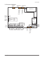
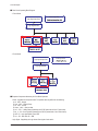
7. Block Diagram
7-1 Overall Block Diagram
Y Main Board
X Main Board
1366x768 Pixels
1366x768x3 Cells (R,G,B)
Deinterlacer
Image
Scaler
(110V)
CPU
Decoder
Micom
Samsung Electronics
7-1
Block Diagram
7-2 Partial Block Diagram
7-2-1 Main SMPS Block Diagram
HOT
COL D
VS(+200V)
AC Input
90V ~ 132V
VS_Sw i t c h i n g
EMI
Vo l t ag e Do u b l er
St ag e
FIL T ER
Return
INPUT
PWM c o n t r o l
St ag e
VA(+70V)
VA _Sw i t c h i n g
R et u r n
St ag e
A u x i l i ar y
VT (+33V)
Vcc
St ag e
D12V (+12V)
REG
PWM Co n t r o l
St ag e
A12V(+12V)
STD_5V
D5.3V(+5.3V)
PS-ON / Relay Signal
Re t ur n
Mu l t i Ou t p u t
Sw i t c h i n g
VS-ON Signal
St ag e
VG (+15V)
REG
PWM c o n t r o l
C HOPPE R REG
18VAMP(+18V)
CHOP P ER RE G
6.5V(+6.5V)
St ag e
COL D
HOT
COL D
7-2-2 DC-DC SMPS Block Diagram
Vs Input Part
Transformer
Control
and
Switching Block
Feedback
Block
7-2
Rectification
Block
Vset Output
(175~210)
Auxiliary
Power
Feedback
Block
Transformer
Control
and
Switching Block
Vscan Output
Auxiliary
Power
Transformer
Control
and
Switching Block
Rectification
Block
Rectification
Block
Ve Output
Auxiliary
Power
Feedback
Block
Samsung Electronics
Block Diagram
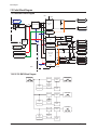
7-2-3 Module Driver Board Block Diagram
1. Y Main Board
Logic Signal Input Part
Power Input Part
Logic Signal Buffer
2. X Main Board
Logic Signal Input Part
Power Input Part
Logic Signal Buffer
Samsung Electronics
7-3
Block Diagram
7-2-4 Logic Board Block Diagram
31Pin LVDS
10Pin(Power)
RELAY_EINT
AC-OFF-EINT
Vs-ON
LVDS
SIGNAL
SDA, SCL
4pin (I2C)
60MHz
TX, RX
DATA : 32bit
ADDR : 12bit
DQS, CLK, nCLK
DDR
(MB)
X-MAIN
CONTROL
SIGNAL
ADC 4bit
74MHz
CONTROL
SIGNAL
MICOM
R,G,B : 16bit
CLK A, B
BLK, POL, STB
ADC 1bit
ASIC
nRESET
30pin Connector
50pin Connector
Y-MAIN
CONTROL
SIGNAL
SPS-NIRB
(ASIC 816P)
DDR
(FA)
DDR
(MA)
DRIVE
RESET
ADC 3bit
R,G,B : 16bit
CLK A, B
BLK, POL, STB
30MHz
60pin Connector
60pin Connector
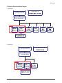
7-2-5 Main Board Block Diagram
28F640
Main
VSB NIM Tuner
Display Panel
50" 1366 x 768
SVP-EX62
DNIe
Lite
VIDEO1
S-VIDEO1
Video SW
Audio Process
MSP4440K
NSP
Audio AMP
TAS5122
Optical Out
VIDEO2
S-VIDEO2
(SIDE-AV)
7-4
Coaxial Out
Samsung Electronics
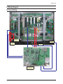
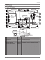
Wiring Diagram
8. Wiring Diagram
8-1 Overall Wiring
ASSY SIDE-AV
BN94-00647A
ASSY SPEAKER
BN96-01738B
ASSY FUNCTION
ASSY POWER
BN96-02549A
BN96-02050E
ASSY PCB MISC-MAIN
BN94-00860A
Samsung Electronics
8-1
Wiring Diagram
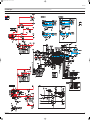
8-1-1 PDP Module ↔ SMPS Wiring
①
CN809(Main SMPS)
↔ CN3(DC-DC SMPS)
②,
CN2(DC-DC SMPS)
↔ CN5007(Y B'D)
③
CN4(DC-DC SMPS)
↔ CN4000(X B'D)
④
CN5(DC-DC SMPS)
↔ CN2710(BOT G-Buf)
⑤
CN810(Main SMPS)
↔ CN2013(Logic B'D)
Pin No
Signal
Pin No
Signal
Pin No
Signal
Pin No
Signal
Pin No
Signal
1■
5.3V
1■
Vs
1■
Vs
1■
RTN
1■
5.3V
2
Vg
2
Vs
2
Vs
2
N.C
2
5.3V
3
RTN
3
RTN
3
RTN
3
5.3V
3
RTN
4
RTN
4
RTN
4
RTN
4
N.C
4
RTN
5
RTN
5
Vset
5
Ve
5
Va
5
5.3V
6
RTN
6
RTN
6
RTN
6
RTN
7
RTN
7
Vscan
7
RTN
7
PS-ON
8
Va
8
RTN
8
Vg
8
N.C
9
Va
9
Vg
9
5.3V
9
VS-ON
10
N.C
10
5.3V
10
STB 5V
11
Vs
12
Vs
8-2
⑥
CN1(DC-DC SMPS)
↔ CN2501(TOP E-Buf)
Pin No
Signal
1■
RTN
2
N.C
3
5.3V
4
N.C
5
Va
Samsung Electronics
Wiring Diagram
8-1-2 Main Board ↔ SMPS, SIDE-AV, Power Button, Function Board, Speaker Out Wiring
①
CN1002(MAIN B'D)
↔
CN804-1(MAIN SMPS)
Pin No
Signal
1■
FAN-D
2
FAN-ON
3
STB5V
4
RTN
5
PS-ON
6
12V
7
RTN
8
RTN
9
VCA
10
VCS
11
RTN
12
5.3V
Samsung Electronics
②
CN1001(MAIN B'D)
↔ CN803(MAIN SMPS)
③
JA9001(MAIN B'D) ↔ CN2020(LOGIC B'D)
Pin No
Signal
Pin No
Signal
Pin No
Signal
12
TXOUT3+
23
TXOUT1B-
13
TXOUT3-
24
TXOUT1+
14
TXCLKOUTB+
25
TXOUT1-
GND
15
TXCLKOUTB-
26
GND
PW_SCL0
16
TXCLKOUT+
27
GND
17
TXCLKOUT-
28
TXOUT0+
18
GND
29
TXOUT0-
19
GND
30
GND
20
TXCLKOUT2+
31
GND
I2C_READY
21
TXCLKOUT-
32
GND
GND
22
TXOUT1B+
33
GND
Pin No
Signal
1■
RTN
2
GND
2
VT(33V)
3
PW_SDA0
3
RTN_AMP
4
4
RTN_AMP
5
5
18V_AMP
6
GND
6
18V_AMP
7
7
RTN
8
TXOUT0B+
8
12V
9
TXOUT0B-
9
RTN
10
10
6V
11
1■
④
CN1004(MAIN B'D)
↔ FUNCTION
⑤
CN2001(MAIN B'D)
↔ SPEAKER
⑥
CN1003(MAIN B'D)
↔ POWER BUTTON
Pin No
Signal
Pin No
Signal
Pin No
1■
KEY1
1■
SPK_R+
1■
GND
2
KEY2
2
SPK_R-
2
LED_RED
3
GND
3
SPK_L+
3
5V
4
SPK_L-
4
GND
Signal
5
-
6
SDA
7
SCL
8
IR
8-3
Wiring Diagram
⑦
CN101(MAIN B'D)
↔ SIDE-AV
Pin No
Signal
1■
VIDEO2_CVBS
2
GND
3
VIDEO2_IDENT
4
SVHS2_IDENT
5
VIDEO2_SL_IN
6
GND
7
VIDEO2_SR_IN
8
GND
9
SVHS2_Y
8-4
10
GND
11
SVHS2_C
12
GND
Samsung Electronics
PCB Diagram
9. PCB Diagram
9-1 Overall PCB Diagram
10 G-BUFFER
9
F-BUFFER
CN2710
CN5401
5
E-BUFFER
8
CN2608
CN2510
SMPS
-DC
Y-BUFFER(UP)
CN5402
2
CN809
4
CN5009
CN5403
1
CN5007
Y-DRIVE
CN3
CN1
CN4004
CN4000
CN2
SMPS-MAIN
3
X-DRIVE
CN4
CN4003
CN800
CN5501
CN2501
CN5010
CN804-1
CN2020 CN2013
CN2005
CN5008
CN5502
CN5
CN803 CN810
CN4002
CN2010
CN2009
7
CN2004
LOGIC BOARD
CN2006
CN2007
CN4005
CN2008
CN4001
15
6
CN5503
Y-BUFFER(LOW)
AC-INLET
CN2501
CN2510
8
CN2608
E-BUFFER
FUNCTION
9 F-BUFFER
10 G-BUFFER
JA9001 CN1002 CN1001
CN1
CN1004
12
11
MAIN BOARD
16
CN102
SIDE AV
No
-
Assy
ASSY PDP MODULE P
CN2710
CN2709
CN101
CN001
CN2001 CN1003
13
POWER SW
14 SPEAKER
Code No.
Description
BN96-03082A
M1,PL50HW005B,V5.0,1366*768,NTSC/PAL,50 inch,with logic
① ASSY PCB P-SMPS
BN96-01801B
SPD-50P5HDM,100~240V,395*245mm
② ASSY PCB P-SMPS
BN96-01856A
SPD-50P5HD(DC_DC),200Vin(DC_DC)
③ ASSY PDP P-X MAIN BOARD
BN96-03090A
M1,PL50HW005A,V5.0,1184×700,1366×768,NTSC/PAL,50",LJ92-01045A
④ ASSY PDP P-Y MAIN BOARD
BN96-03091A
M1,PL50HW005A,V5.0,1184×700,1366×768,NTSC/PAL,50",LJ92-01046A
⑤ ASSY PDP P-Y BUFF UPPER BOARD
BN96-03092A
M1,PL50HW005A,V5.0,1184×700,1366×768,NTSC/PAL,50",LJ92-01047A
⑥ ASSY PDP P-Y BUFF LOWER BOARD
BN96-03093A
M1,PL50HW005A,V5.0,1184×700,1366×768,NTSC/PAL,50",LJ92-01048A
⑦ ASSY PDP P-LOGIC BOARD
BN96-03097A
V4 50 HD,B'd with Harness,V4,1366*768,With Harness,Logic Packing
⑧ ASSY PDP P-ADDRESS E BUFF BOARD
BN96-03094A
M1,PL50HW005A,V5.0,1184×700,1366×768,NTSC/PAL,50",LJ92-01103A
⑨ ASSY PDP P-ADDRESS F BUFF BOARD
BN96-03095A
M1,PL50HW005A,V5.0,1184×700,1366×768,NTSC/PAL,50",LJ92-01104A
⑩ ASSY PDP P-ADDRESS G BUFF BOARD
BN96-03096A
M1,PL50HW005A,V5.0,1184×700,1366×768,NTSC/PAL,50",LJ92-01105A
⑪ ASSY PCB MISC-MAIN
BN94-00860A
HP-R5072CF,D71C,V5
⑫ ASSY BOARD P-FUNCTION
BN96-02549A
SCHUBERT,CT5000-3700,FUNCTION,BLACK KNOB,600mm,SHIELD
⑬ ASSY BOARD P-POWER & IR
BN96-02050E
SCHUBERT,CT5000-3540B,POWER&IR
⑭ ASSY SPEAKER P
BN96-01738B
8ohm,P5,50,15W,Urethan coating
⑮ ASSY MISC P-INLET
BN96-02369A
HP-R4252,STRAUSS,DOCUMENT,INLET.CORE
Samsung Electronics
9-1
MEMO
9-2
Samsung Electronics
Schematic Diagram
10. Schematic Diagram
10-1 POWER & TUNER
This Document can not be used without Samsung’s authorization.
B5V_VCC
Power
FT1003
KIA78D05F
1
O
I
COMPONENT 2
COMPONENT 1
3
G
Signal
2
C1073
100uF
C1074
100nF
JA1001
PGND
PGND
+6V
B5V_BA7657
FT1001
KIA78D05F
1
C1004
C1005
220uF
100nF
I
3
O
G
2
C1006
C1007
220uF
100nF
TP1003
R1002
1
jack9p_2
1
3
2
4
6
5
7
9
8
1
jack9p_2
JA1002
100oXhRm
EF
TP1T0P017008
TP1009
R1004
10ohm
TP1011
R1006
10ohXmREF
1 1
1
1
D1005
RLZ8.2
D1004
RLZ8.2
TP1014
1
D1006
RLZ8.2
R1011
XREF
10ohm
XREF
COMP2_IDENT
COMP2_Y
COMP2_PB
TP1002
R1001 100ohXRm
EF
TP1T0P014005
TP1006
1
3
2
4
6
5
7
9
8
1 1
XREF
TP1010
XREF
D1001
RLZ8.2
TP1012
1
D1003
RLZ8.2
D1002
RLZ8.2
BD1001
BLM41P600S
A
B
C1012
100nF
16V
XREF
TUNERGND
10
9
8
7
6
5
4
3
2
1
TP1026
TP1027
TP1028
TP1029
D1008
RLZ8.2
BD1003
HH-1H4532-121JT
R1008
75ohm
D1009
RLZ8.2
D1014
RLZ8.2
D1010
RLZ8.2
PGND
FT1002
3BA178M09FP
D1011
RLZ8.2
AGND_IN
AGND_IN
JA1003
jack6p_3
2
TP1020
1 1
L1002
1
TP1023
D1018
RLZ8.2
1
D1019
RLZ8.2
R1016
L1004
R1018
470ohm
XREF
470ohm
XREF
TP1T0P115016
1
3
2
4
6
5
TP1T0P118019
1
3
2
4
6
5
+18V_A
COMP2_SL_IN
TP1017
1 1
L1001
1
TP1022
D1016
RLZ8.2
1
D1017
RLZ8.2
L1003
C1018
100nF
AGND_IN
PGND
D1023
RLZ8.2
D1022
RLZ8.2
B33V
SOUND_AMP
C1015
330pF
BD1004
HH-1H4532-121JT
CN1001
470ohm
XREF
R1017
470ohm
XREF
COMP1_SL_IN
COMP1_SR_IN
C1014
330pF
C1013
330pF
D1021
RLZ8.2
D1020
RLZ8.2
C1016
330pF
AGND_IN
AGND_IN
SOUND_AMP
SMW250-10 WHT
R1015
COMP2_SR_IN
AGND_IN
C1017
100uF
25V
D1007
RLZ8.2
C1001 R1009 C1002 R1010 C1003
33pF 75ohm 33pF 75ohm 33pF
AGND_IN
jack6p_3
B9V
TP1024
D1013
RLZ8.2
C1008 R1013 C1009 R1014 C1010
33pF 75ohm 33pF 75ohm 33pF
JA1004
O
G
PGND
COMP1_PR
COMP2_PR
AGND_IN
BD1002
HH-1H4532-121JT
TP1025
R1012
75ohm
D1012
RLZ8.2
2
1
B8V
D1015
PMLL4148
C1011
47uF
16V
I
COMP1_PB
R1007 10ohm
AGND_IN
PGND
1
COMP1_Y
R1005 10ohm
1
AGND_IN
PGND
COMP1_IDENT
R1003 10ohm
1
C1019
C1020
10uF
100nF
AGND_IN
AGND_IN
C1021
100nF
16V
PGND
PGND
B3.3V_1
DELETE OPTION
BD1005
BLM41P600S
USA OPTION
PGND
PGND
MGND8
NEAR NIM TUNER
TUNERGNDTUNERGND
R1041
EXT POD NIM OPTION
(DELETE OPTION)
0ohm
1/10W
+6V
B3.3V_2
R1042
R1043
SDA6_DTVCH
SCL6_DTVCH
100ohm
100ohm
R1044
R1045
R1047
DELETE OPTION
nNXT2004_RST
R1069
USA OPTION
USA OPTION
0o hm
nRESETO
0ohm
1/10W
R1046
0ohm
100ohm
0ohm
B12V
KOREA OPTION
L1008
22uH
2
A
1
B
BD1012
BLM41P600S
OS_CON
C1056
100nF
16V
C1058
10nF
B3.3V_2
BS
SS
IN
EN
SW
GND
COMP
FB
1
1
2
2
3
3
4
4
DATA7
DATA6
DATA5
DATA4
DATA3
DATA2
DATA1
DATA0
MPEG_CLK
SDA
5
6
7
8
B6_+1.2V
MPEG_PKT_SYNC
MPEG_DATA_EN
MPEG_DATA7
MPEG_DATA6
MPEG_DATA5
MPEG_DATA4
MPEG_DATA3
MPEG_DATA2
MPEG_DATA1
MPEG_DATA0
MPEG_DATA_CLK
SDA
R1050
0ohm
1/10W
R1052
10Kohm
8
7
6
5
OS_CON
C1057
TUNERGND
C1060
100nF
25V
47uF
10V
MGND3
MGND3
MGND4
MGND4
2
B
A
1
1
2
3
4
C1064
100uF
25V
C1063
100uF
16V
C1065
100nF
16V
BS
SS
IN
EN
SW
GND
COMP
FB
1
IC1008
MP1583DN
BLM41P600S
BD1013
8
7
6
5
R1053
10Kohm
B
BD1014
BLM41P600S
1
A
PGND
2
L1009
3A Current
C1066
47uF
10V
OS_CON
R1051
6.2Kohm
1/10W
C1061
120uF
6.3V
C1062
100nF
16V
KOREA option
C1067
100nF
16V
C1068
100pF
C1071
100nF
16V
R1054
10Kohm
1/10W
D1025
S S24
C1069
10nF
R1055
C1070
180pF 100Kohm
B3.3V_2
TUNERGND
0ohm
C1046
100nF
25V
C1045
100uF
16V
KOREA OPTION
R1030,R1032,R1036
R1038,R1040,R1078,R1079
B
TUNERGND
KOREA OPTION
B3.3V_2
BD1011
CIB32P600NE
IC1006
TP1057 AP1117D-18A
B1.8V_TUNER
C1055
100nF
25V
C1054
47uF
16V
1 2
VOUT
VIN
3
B
ADJ
TUNERGND
B3.3V_2 S_3.3V_TUNER
DELETE OPTION
TUNERGND
BD1017
C1088
10uF
16V
BD1018
C1089
100nF
IC1011
KOREA OPTION
74LCX245MTCX
20
19
18
17
16
15
14
13
12
11
VCC
DIR
/OE
A1
B1
A2
B2
A3
B3
B4
A4
A5
B5
A6
B6
A7
B7
A8
B8
GND
R1056
3.6Kohm
1/10W
D1026
SS24
BD1010
CIB32P600NE
FROM NEWPORT
R1040
KOREA : 0x28
USA : 0x14
PGND
ALPS_XTAL_OFF
XREF
TUNERGND
TUNERGND
TUNER
R1057
10Kohm
0ohm
R1033
100Kohm
1/10W
TUNERGND
TP1067
C1059
10nF
R1034
0ohm
0ohm
R1036
R1038
SCL
SCL
22uH
IC1007
MP1583DN
1
2
3
4
VALID/EN
GND
B5_+2.5V
MGND3
MGND4
USA option
1.1V
FSTART/SYNC
SIF_OUT
B4_+3.3V
B
PGND
MGND7
C1053
22uF
16V
1.8V
VIDEO_OUT
X_TAL_OFF_SW
SIF_MAIN
XREF
100ohm
1/10W
1
0ohm
1/10W
GND
R1031
0ohm
1/10W
B
C1052
100nF
16V
C1051
47uF
16V
MGND6
XREF
TUNERGND
R1079
DELETE OPTION
MPEG_ERROR
2
PGND
TUNER_CVBS_MAIN
R1028
1Kohm
1/10W
A
ADJ
R1039
2
R1027
10Kohm
1/10W
nRSTO
XREF
DELETE OPTION
1
VOUT
N. C
3.3V
TUNERGND
POWER_RESET
ERROR
SIF_OUT
R1023
0ohm
1/10W
Q1001
KSC1623-G
E
TUNERGND
0ohm
R1032
GND
GND
POWER_RESET
VIDEO_OUT
C
B
TUNERGND
2
C1050
100nF
16V
C1049
47uF
16V
2
VIN
1
C1048
100nF
16V
C1047
47uF
16V
PGND
AP1117D-18A
3
3
O
G
B3__+32V
R1048
R1049
I
MGND5
33V
A
IC1005
IC1004
BA033FP
1
C1044
47uF
10V
OS_CON
C1043
100nF
16V
KOREA OPTION
AFT_OUT
TUNERGNDTUNERGND
R1030
0ohm
B2_+5V
5V(B+)
1
S_3.3V_TUNER
0ohm
1/10W
RFAGC
RF_AGC
AFT_OUT
R1078
S_5V
C1042
100nF
16V
C1041
47uF
10V
OS_CON
PGND
L1007
SCL1_DTVCH
XREF
SDA1_DTVCH
PGND
USA OPTION
PGND
9
G
2
PGND
R1029
3
28 27 26 25 24 23 22 21 20 19 18 17 16 15 14 13 12 11 10
O
1/10W
0ohm
I
100ohm
100ohm
1
5
IC1003
BA033FP
C1040
100nF
16V
C1039
47uF
10V
OS_CON
2
R1022
100ohm
R1026
100ohm
C1035
100nF
25V
N_C
N.C
6
G
C1038
100nF
16 V
C1037
220uF
16V
C1036
3.3nF
50V
100nF
MGND2
B
C1034
47uF
50V
C1030
TUNERGND
MGND2
B33V
BD1009
CIB32P600NE
R1021
0ohm
1/10W
MGND1
MGND1
7
3
O
B
TUNERGND
8
I
C1026
47uF
16V
TU1003
TU1002
9
IC1002
KIA78D05F
1
C1033
47uF
10V
OS_CON
0ohm
R1024
C1031
180pF 100Kohm
C1032
100nF
1 6V
TP_CLK
TP_DATA
TP_EN
TP_PD
TP1032
TP1033
TP1034
TP1036
TP1037
TP1038
TP1039
TP1040
TP1041
TP1042
TP1043
TP1044
TP1047
TP1048
TP1049
TP1050
TP1051
TP1052
TP1053
TP1054
TP1055
TP1056
TP1058
TP1059
TP1060
TP1061
TP1062
TP1063
TP1064
TP_TS_ERR
TP1065
TP1066
TP_ETX USA OPTION
TP_CTX
TP_ITX
TP_QTX
0ohm
S_6.5V
R1025
3.6Kohm
1/10W
D1024
SS24
MGND2
28 27 26 25 24 23 22 21 20 19 18 17 16 15 14 13 12 11 10
MGND1
L1006
3A Current
C1025
100nF
25V
SEC NIM ALPS NIM
DELETE OPTION
DNVS303EH261A
C1024
100nF
16V
C1023
120uF
6.3V
R1037
R1019
6.2Kohm
1/10W
B5V_BA7657
BD1008
CIB32P600NE
NEAR NIM TUNER
POD NIM
R1035
FB
GND
L1011
OS_CON
R1020
10Kohm
8
7
6
5
SS
EN
COMP
SW
RF_AGC
XREF
KOREA OPTION
DRX
C1029
100nF
16V
C1028
100uF
25V
BS
IN
USA OPTION
1
CRX
1
2
3
4
L1 0 0 5
1 1 1 1 1 1 1 1 1 1 1 1 1 1 1 1 1 1 1 1 1 1 1 1 1 1 1 1 1 1 1 1 1 1 1 1 1 1 1 1
B
B
BLM41P600S
OFF : LOW
22uH
IC1001
MP1583DN
C1027
100uF
16V
AFT_MAIN
XREF
TP1030
ON : HIGH
2
1
A
BD1007
B3.3V_1_1
NC : Auto
PGND
C1022
10nF
2
1
A
D6V
1
2
3
4
5
6
7
8
9
10
1
3
5
7
1
3
5
7
2
4
6
8
2
4
6
8
1
3
5
7
2
4 RA1003
6 33ohm
8 1/16W
SAM_TS(7)
RA1001
33ohm
1/16W
SAM_TS(6)
SAM_TS(0:7)
XREF
SAM_TS(5)
SAM_TS(4)
SAM_TS(3)
RA1002
33ohm
1/16W
SAM_TS(2)
SAM_TS(1)
SAM_TS(0)
SAM_TSSYNC
SAM_TSVLD
SAM_TSCLK
XREF
XREF
XREF
C1072
3.3nF
PGND
POD_NIM_OPTION
(USA OPTION)
D6V
A5V
A3.3V
BD1015
A5V
A3.3V
GND
R1077
Q1003
KSC1623-G
1KohXmREF
A1.8V_CPU
1/10W
SW_POWER
GND
IC1009
STD_5V
SMW250-12 WHT
CN1002
SI-3006KWM-TL
1
BD1016
PGND
THER_D
XREF
PGND
2
FAN_ON_OFF
FT1006
LFA30-2A1E223MT
C1079
220uF
IR
TP1081
VOUT2
VOUT1
VIN
GND
R1063
1Kohm
5
FT1005
LFA30-2A1E223MT
4
3
C1078
47uF
6.3V
C1080
100nF
C1081
100nF
16V
C1082
10nF
50V
C1083
100nF
16V
LED_RED
R1065
10Kohm
XREF
FAN_DET
PGND
PGND
PGND
PGND
PGND
PGND
KEY1
SDA5_TV_5V
SCL5_TV_5V
R1062
100ohm
1/10W
R1074
PODIN(2)
PODIN(0)
PODIN(1)
PODIN_SYNC
PODIN_VLD
PODIN_CLK
RA1006
XREF
33ohm
1/16W
XREF
XREF
TP1072
TP1074
TP1076
TP1077
TP1094
TP1080
TP1082
0ohm
1/10W
R1064
22Kohm
FT1009
LFA30-2A1E223MT
KEY2
SMW250-03
KEY1
XREF
A3.3V
TP1089
B3.3V_1
PODIN(3)
RA1005
33ohm
1/16W
D1032 D1033 D1034
8T
4C
5Z
VX
6L
1 5V6LT1
BZX84CB
5Z
VX
6L
1B
8T
4C
Q1002
KSC1623-G
FT1007
LFA30-2A1E223MT
XREF
1nF
50V
PODIN(0:7)
XREF
PODIN(4)
CN1004
PGND
FT1008
LFA30-2A1E223MT
C1077
XREF
1
GND
VC
FT1004
LFA30-2A1E223MT
PODIN(5)
3
PGND
3
SW_POWER
D12V
PS_ON
1
2
3
4
5
6
7
8
R1061
100ohm
1/10W
2
1/10W
PODIN(6)
33ohm
1/16W
CN1003
DELETE_OPTION
0ohXmREF
PODIN(7)
RA1004
SMAW250-08 WHT
1
R1076
GND
C1076
100nF
C1075
100uF
1
VCS
VCA
2
R1060
100ohXm
REF
1/10W
100ohXm
REF
1/10W
MGND1
TP1083
TP1084
TP1085
R1058
D3.3V
1/10W
2.7Kohm
3
12
11
10
9
8
7
6
5
4
3
2
1
R1059
D1029
SDS7000
2
D3.3V
TP1068
TP1069
TP1070
TP1071
TP1073
TP1075
TP1078
TP1079
D1028
SDS7000
2
4
6
8
2
4
6
8
2
4
6
8
POWER
DELETE_OPTION
D1027
SDS7000
1
D6V
1
3
5
7
1
3
5
7
1
3
5
7
KEY2
1
2
3
TP1086
TP1087
TP1092
XREF
1
PGND
CONTROL
L1010
C1084
100uF
16V
CIC21J601NE
IC1010
AD5337ARM
XREF
C1086
10uF
16V
C1087
100nF
25V
PGND
Samsung Electronics
VCXRSEF
VCA
R1068
1
2
3
0ohm 4
1/10W
VDD
A0
VOUTA SCL
VOUTB SDA
REFIN GND
8
7
6
5
R1066
R1067
100ohm XREF
100ohm XREF
C1085
100nF
16V
SCL4_TV_3.3V
SDA4_TV_3.3V
PGND
PGND
PGND
10-1
Schematic Diagram
10-2 SOUND-PROCESS
This Document can not be used without Samsung’s authorization.
BD2007,BD2009 : DELETE OPTION
Power
B8V
C2001 C2002
100nF 22uF
16V
Signal
B5V_VCC
L2001
B5V_VCC B3.3V_1_1
R2001 R2002 R2003 R2004 R2005 R2006 R2007 R2008
47Kohm 47Kohm 47Kohm 47Kohm 47Kohm 47Kohm 47Kohm 47Kohm
B3.3V_1_1
OPTION
B5V_VCC
[ Del et e]
R2009 R2015 R2018 R2030
R2010 R2019 R2031
BD2002
VIDEO1_SL_IN
XREF
16V 10uF
C2003
COMP1_SL_IN
XREF
16V 10uF
C2004
COMP2_SL_IN
XREF
16V 10uF
C2005
16V 10uF
C2011
16V 10uF
XREF
VIDEO1_SR_IN
16V 10uF
XREF
COMP1_SR_IN
XREF
COMP2_SR_IN
C2020
C2022
C2006
C2007
C2008
C2009
100nF
47uF
6.3V
100nF
47uF
6.3V
0Y
2Y
1X
3Y
X-COM
1Y
0X
/EN
3X
VEE
VSS
A
B
R2011
R2012
1/10W
2Kohm
1/10W
2Kohm
R2014
4.7ohm
1/10W
1
0ohm
2
FT2001
M1
FILT+
14
VL
0ohm
REF_GND
4
2.2nF
50V
R2021
C2018
2.2nF
50V
100Kohm 100Kohm
1/10W
1/10W
13
SDOUT
VA
5
R2022
1/10W
100ohm
6
11
VQ
10
SCLK
AINL
LRCK
/RST
8
9
C2023
100nF
25V
R2032
R2033
100Kohm
1/10W
100Kohm
1/10W
15
2
100ohm
1/10W
4
5
7
C2021
100nF
25V
D0
D1
D2
D3
Q0
Q1
Q2
Q3
8
14
16V
10uF
16V
10uF
SOUND_SEL2
C2027
R2042
R2043
100ohm
C2028
6
C2029
100nF
25V
7
Q0
Q1
Q2
Q3
8
11
10
1M SRAM
IC2007
K6X1008C2D-TF55
1
2
3
4
5
6
7
8
9
10
11
12
13
14
15
16
14
13
12
11
10
9
1
16
2
15
3
100ohm
1/10W
C2033
XREF
DVI_SR_IN
XREF
PC_SL_IN
XREF
PC_SR_IN
XREF
C2035
4.7uF35V
C2036
4.7uF35V
C2037
4.7uF35V
B8V
C2038
4.7uF
35V
10uF
C2041100nF
R2122
64
63
62
61
60
59
58
57
56
55
54
53
52
51
50
49
48
47
46
45
44
43
42
41
C2049 56pF
XREF
C2052
47uF
16V
SIF_MAIN
56pF
2
C2057
SGND
C2058
3pF
HC-49/SM5H_18R432
X2001
1
SGND
R2062 100ohm
XREF
M_CLK
C2061
3pF
R2063
R2066
100ohm
100ohm
B5V_VCC
AVSUP
AVSUP
ANA_IN1+
ANA_INANA_IN2+
TESTEN
XTAL_IN
XTAL_OUT
TP
AUD_CL_OUT
NC
NC
D_CTR_I/O_1
D_CTR_I/O_0
ADR_SEL
STANDBYQ
65
66
67
68
69
70
71
72
73
74
75
76
77
78
79
80
R2068
1Kohm
IC2012
MSP4440G_QA_C12_500
0X80
CAPL_M
AHVSUP
CAPL_A
SC1_OUT_L
SC1_OUT_R
VREF1
SC2_OUT_L
SC2_OUT_R
NC
NC
DACM_SUB
NC
DACM_L
DACM_R
VREF2
DACA_L
NC
I2C_CL
I2C_DA
I2S_CL
I2S_WS
I2S_DA_OUT
I2S_DA_IN1
ADR_DA
ADR_WS
ADR_CL
DVSUP
DVSUP
DVSUP
DVSS
DVSS
DVSS
I2S_DA_IN2
NC
I2S_CL3
I2S_WS3
RESETQ
I2S_DA_IN3
NC
DACA_R
56pF
D0
D1
D2
D3
Q0
Q1
Q2
Q3
8
SGND
100ohm
1/10W
D2001
BZT52-C15 DELETE OPTION
C2046
10uF
16V
NC
NC
AVSS
AVSS
MONO_IN
NC
VREFTOP
SC1_IN_R
SC1_IN_L
ASG
SC2_IN_R
SC2_IN_L
ASG
SC3_IN_R
SC3_IN_L
ASG
SC4_IN_R
SC4_IN_L
NC
AGNDC
AHVSS
AHVSS
NC
NC
SGND
C2056
470pF
C2048
7
R2046
C2045L2002
C2043 C2044100uF
3.3uH
470pF 1.5nF 16V
SGND
100Kohm
1/10W
100Kohm
1/10W
R2123
SGND
R2049
C2050
10uF
16V
40
39
38
37
36
35
34
33
32
31
30
29
28
27
26
25
R2050
100ohm C2047
14
5D
12
LATCH
R2044
IC2006
1
20
8Q
3
XREF
18
10
2D
17
7D
7Q
6
C2051
R2054
R2057
3
14
4D
13
9
6
7
Q0
Q1
Q2
Q3
8
XREF
MONITOR_SL_OUT
XREF
MONITOR_SR_OUT
SDA5_TV_5V
XREF
ANY_SC2_SL_OUT
100ohm
DELAY1
IC2010
N74F125D
1
IN
3
IN
DELAY2
ANY_SC2_SR_OUT
4
IN
5
IN
R2061
1Kohm
Del et e
6
IN
7
RESET_MSP
IN
N
M
L
K
J
I
H
5VC
IC2011
MC74F14D
R2053
1Kohm
14
C2059
100nF
25V
11
10
R2056
150ohm
9
14
1
XREF
S_CLK
13
12
VCC
IO
R2055
0ohm
XREF
S_CLK_1
13
2
O_O
I5
3
12
I1
R2059
1Kohm
R2065
4.7Kohm
Del et e
R2058
1Kohm
O_5
O_1
I4
5
10
I2
O_4
6
9
I3
0ohm O_2
7
R2069
20Kohm
8
GND
O_3
OPTION
[ Del et e]
R2047 R2048 R2051 R2052
R2059 R2060 R2061 R2067
R2071
20Kohm
C2065
1uF
HP_R
C2060
100nF
25V
11
4
8
R2067
C2062
1uF
100ohm
SGND
R2074
C2067
4.7nF
C2066
4.7nF
XREF
100ohm
C2068
1nF
C2070
3.3nF
C2069
1nF
B3.3V_1_1
SEL_I2S HIGH
OUTPUT EAGLE
XREF
DELETE OPTION
S_DATA_IN
LATCH
Del et e
R2075
100ohm
R2077
100ohm
1Kohm
R2076
S_DATA_OUT
11
XREF
R2073
LR_CLK
A
B
C
D
E
F
G
IN
2
XREF
R2064
4.7Kohm
100ohm
XREF
S_CLK
5Q
10
XREF
R2060
1Kohm
0ohm
SGND
R2072
12
GND
R2047
150ohm
R2048
150ohm
R2052 Del et e
1Kohm
R2051
1Kohm
10uF
XREF
C2064SGND
100nF
100ohm
R2070
5D
4Q
11
10
HP_L
XREF
13
8
5VC
10uF
100ohm
L2004 3.3uH
C2063
10uF SCL5_TV_5V
16V
14
6D
3D
Del et e
12
9
6Q
7
15
D0
D1
D2
D3
15
3Q
16
C2031
100nF
25V
16
5
9
C2032
10uF
16V
8D
1D
4
5VC
100ohm
1/10W
19
IQ
S_DATA_OUT
S_DATA_IN
VCC
2
11
S_CLK_1
XREF
OUTPUT
2
5
XREF
C2026
47pF
50V
11
MM74HC373MTCX
12
100ohm
5Q
GND
13
R2031
14
13
9
1
4
C2042
100nF
25V
100ohm
SGND
1
2
3
4
5
6
7
8
9
10
11
12
13
14
15
16
17
18
19
20
21
22
23
24
C2055
1.5nF
C2054
22uF
C2053
47nF
6
100ohm
100ohm
6D
10
IC2009
74F163AD(REEL)
C2040
100nF
L2003
3.3uH
5
4D
4Q
32
31
30
29
28
27
26
25
24
23
22
21
20
19
18
17
OE_
A10
CS_1
I/O8
I/O7
I/O6
I/O5
I/O4
VSS
I/O3
I/O2
I/O1
A0
A1
A2
A3
A11
A9
A8
A13
WE_
CS2
A15
VCC
NC
A16
A14
A12
A7
A6
A5
A4
R2030
100ohm
R2016
R2019
6Q
2Q
C2039
B5V_BA7657
4
C2034
100nF
25V
SGND
DVI_SL_IN
4.7uF35V
15
7
IC2008
74F163AD(REEL)
R2045
16
7Q
3Q
8
16
17
7D
6
C2013
10uF
16V
C2012
100nF
25V
8D
5
XREF
S_CLK_1
9
D0
D1
D2
D3
2Q
3D
15
5
100ohm
12
2
4
100ohm
R2018
13
1
3
100ohm
1/10W
RESET_MSP
R2015
R2025 100ohm
IC2005
74F163AD(REEL)
SOUND_SEL1
R2034 R2035 R2036 R2037 R2038 R2039 R2040 R2041
47Kohm 47Kohm 47Kohm 47Kohm 47Kohm 47Kohm 47Kohm 47Kohm
16
1
R2024
2D
100ohm
8Q
18
4
C2017
100nF
25V
R2010
19
1D
6
C2024 C2025
1uF
1uF
50V
50V
VCC
2
3
IC2004
74F163AD(REEL)
5VC
DELETE OPTION
20
OUTPUT
100ohm
IQ
C2014
100uF
16V
3
R2023
AINR
VD
7
2
XREF
S_CLK_1
12
GND
0ohm
0ohm
0ohm
0ohm
C2015
15
MCLK
R2020
100nF
25V
R2009
1
C2010
16
M0
3
R2026
R2027
R2028
R2029
3
IC2002
CS5340-CZZ
R2013
SAM_SCLK_IN
SAM_SCLK_OUT
SAM_LRCLK_OUT
SAM_LRCLK_IN
IC2001
MM74HC373MTCX
DELETE OPTION
5VC
1
SAM_SDO_IN
16
15
14
13
12
11
10
9
VDD
2X
Y-COM
B5V_VCC
47Kohm
1/10W
MM74HC4052M
1
2
3
4
5
6
7
8
AUDIO DELAY
BD2009
BD2008
SAM_ODCLK_OUT
IC2003
C2019
16V 10uF
BD2001
R2017
C2016
16V 10uF
BD2007
R2079
R2080
1Kohm
1/10W
SGND
B3.3V_1_1
C
Q2001
B
SEL_I2S
KSC1623-G
XREF
R2078
100ohm
LOW
HDMI
E
XREF
L2005
MSP_SCLK_IN
MSP_LRCLK_IN
MSP_SDO_IN
XREF
XREF
IC2013
XREF
MC74VHC244DTR2
1
20
C2071
10uF
16V
C2072
100nF
VCC
IN
19
OE2
SAM_SDO_OUT
R2082
0ohm
IN
17
I4
R2084
SAM_LRCLK_OUT
+3.3V_6241
R2087
SAM_SCLK_OUT
10
IN
GND
MSP_SDO_IN
100nF
R2111 100ohm
+3.3V_6241
PVDD_A
GND
PVDD_A
DGND
OUT_A
GND
OUT_A
GND
GND
/RESET_AB
OUT_B
PWM_BM
OUT_B
PWM_BP
PVDD_B
DREG
PVDD_B
M1
BST_B
M2
BST_C
M3
PVDD_C
REG_RTN
PVDD_C
PWM_CP
OUT_C
PWM_CM
OUT_C
/RESET_CD
GND
PWM_DM
GND
PWM_DP
OUT_D
/SD_AB
OUT_D
/SD_CD
PVDD_D
/OTW
PVDD_D
GREG
BST_D
GND
GVDD
GND
GND
L2007
33nF
C2092
100nF
R2097
1
C2096
100nF
100nF
C2093
R2098
C2094
100nF
10Kohm
10nF
SOUND_AMP
R2103
R2101
1
C2098
SPK_L+
2
1
C2095
1
SOUND_AMP
R2104
1
C2102
C2101
R2107
R2108
100nF
10Kohm
1
SOUND_AMP
C2099
63V
330nF
SOUND_AMP
33nF
SPEAKER_OUT_L
D2002
RLZTE-1130B
D2003
RLZTE-1130B
C2103
BD2004
L2008
3
2
4
1
10KohmC2106
1uF
BD2005
10nF
L2009
R2112
C2105
33nF
C2104
1
SPK_L-
SOUND_AMP
1
2
SOUND_AMP
L2010
100nF
3
4
3
2
1
L+
LR+
R-
BD2006
TP2002
TP2003
TP2004
TP2005
SOUND_AMP
2
1
R2110
100ohm
DVDD
C2088
33nF
1
4.7Kohm
AGSPLL
LPPLL
AVDPLL
DVDPLL
AVSPLL
R2106
GVDD
BST_A
1
DVSPLL
10ohm
56
55
54
53
52
51
50
49
48
47
46
45
44
43
42
41
40
39
38
37
36
35
34
33
32
31
30
29
B
VDDc
GNDc
PROTECT1)
TESTEN
GNDIO
WCK_A1)
BCK_A1)
OUT6B
NSP6241A
0xCC
VDDIO
SCL/VH
SDA/VL
VDDc
OUT6A
100nF
C2100
100nF
25V
SOUND_AMP
A
VDDIO
GNDc
GNDIO
NSP6241
GNDIO
SOUND_AMP
A
SDATA561)
C2097
GND
GND
PWM_AM
3.3
R2095
GREG
PWM_AP
R2093
B 2
VDDIO
GND
R2092
3.3
A
SDATA341)
+3.3V_6241
SGND
SGND
AGND_IN
SMAW250-04 WHT
C2109
C2110
100nF
33uF
25V
DELETE OPTION
L2011
1
SPK_R+
4
1
CN2001
2
C2111
R2121
100nF
10Kohm
C2112
SPEAKER_OUT_R
10nF
0ohm
M_CLK
SOUND_AMP
R2115
SOUND_AMP
1
100ohm
10uH
10uH
L2013
10uH
10uH
L2012
RESET_MSP
O7
B 2
OUT5B
IC2016
22nF
R2116
HDMI_SDO
IN
C2082
R2114
R2120
R2088
9
2
SDATA12/SPDIF_M1)
C2108
XREF
1000uF
25V
1
OUT5A
BCK_M1)
R2113
0ohm
XREF
1000uF
25V
1
OUT3B
OUT3A
VDDIO
GNDIO
OUT2B
OUT2A
OUT1B
AD
VDDIO
GNDIO
OUT1A
VDDc
GNDc
GNDIO
WCK_M1)
48
47
46
45
44
43
42
41
40
39
38
37
36
35
34
33
17
18
19
20
21
22
23
24
25
26
27
28
29
30
31
32
C2107
100nF
25V
VDDIO
GNDc
SDA5_TV_3.3V
OUT4B
VDDc
RF2109
XRE
100ohm
100ohm
OUT4A
CKOUT
SCL5_TV_3.3V
RF2105
XRE
VCC_HP_R
HPOUT_R
64
63
62
61
60
59
58
57
56
55
54
53
52
51
50
49
0ohm
0ohm
0ohm
1
2
3
4
5
6
7
8
9
10
11
12
13
14
15
16
17
18
19
20
21
22
23
24
25
26
27
28
1uF
100ohm
GND_HP_L
CKIN
R2099
R2100
R2102
10nF
C2081
SOUND_AMP
TAS5122IDCA
C2086
R2096
HPOUT_L
M/S
XREF
SOUND_AMP
100nF
IC2015
RESET1)
S_CLK
S_DATA_IN
VCC_HP_L
SDATA_O12/SPDIF_01)
LR_CLK
C2084
R2094
10Kohm
10uF
16V
1
2
3
4
5
6
7
8
9
10
11
12
13
14
15
16
8
I3
C2078
C2079
100nF
C2087
100nF
25V
C2091
100nF
25V
O6
IN
C2083
C2090
100nF
0ohm
HDMI_LRCLK
7
MSP_LRCLK_IN
6241_OUT1A
6241_OUT1B
6241_OUT2A
6241_OUT2B
C2085
100nF
25V
C2089
R2085
I2
MSP_SCLK_IN
C2077
R2091
0ohm
1/10W
10uH
10uH
L2006
0ohm
HDMI_SCLK
MSP_MCLK_IN
100nF
B3.3V_1_1
+2.5V_S
IN
11
I7
C2080
10nF
PGND
0ohm
1
1
C2075
SAM_ODCLK_OUT
1
ADJ
C2076
22uF
16V
R2090
+18V_A
O3
R2089
10Kohm
R2086
10Kohm
3
GND_HP_R
VIN
VOUT
BCK_O1)
2
SDATA78/SPDIF_A1)
WCK_O1)
1
+18V_A
10uF
16V
100nF
IC2014
AP1117D-25A
12
O5
IN
13
I6
C2074
C2073
TP2001
O2
0ohm
R2083
I1
6
15
I5
0ohm
HDMI_MCLK
5
IN
14
BD2003
MPZ2012S300A
B5V_VCC
0ohm
B3.3V_1_1
R2081
O4
4
IN
16
O1
0ohm
I0
3
18
O0
OE1
2
IN
AMP_MUTE1
C2118
C2119
C2120
100nF
100nF
100nF
10uF
16V
R2117
R2118
100nF
10Kohm
1
C2113
63V
330nF
D2005
RLZTE-1130B
SOUND_AMP
R2119
10Kohm
C2116
C2114
D2004
RLZTE-1130B
C
Q2002
B
C2115
KSC1623-G
XREF
10nF
L2014
E
1
SPK_R-
SOUND_AMP
2
C2117
10uF
16V
10-2
Samsung Electronics
Schematic Diagram
10-3 MICOM & IO-EX & AV IN/OUT
PC_VS_MICOM
Power
PC_HS_MICOM
This Document can not be used without Samsung’s authorization.
Signal
XREF
B3.3V_1
A3.3V
A3.3V
24.0MHz
D3003
KDS184
XOUT
P2.2
P2.1
TEST
P2.0
P1.3/AD3
2.7Kohm
Q3001
KSC1623-G
E
A5V
C3042
22uF
16V
TP3002
XREF
XXRREEFF
TP3003
XREF
XREF
1
2
B
HC-49/S-SMD(12MHz,30ppm)
C3003
10uF
16V
3
3
FAN_ON_OFF
RESET_MSP
SW_POWER
I2C_READY
SW_DTV_OUT
SW_HDMI_ADC_OUT
SW_SPDIF_OUT
RESET_DNIE
SEL_COMP
SEL_COMP_PC
SEL_I2S
RF_AGC
AFT_MAIN
Q3009
KSC1623-G
R3086
10Kohm
E
XREF
XREF
XREF
XREF
XREF
XREF
100ohm
100ohm
XREF
KEY1
KEY2
R3090
R3091
R3094
100ohm
XREF
XREF
XREF
R3076
1Kohm
P0_1_SO
P0_0_SCK
RESET
P3_0
P3_2
P2_0_AD0
P2_1_AD1
P2_2_AD2
P2_3_AD3
P2_4_AD4
P2_5_AD5
AVSS
R3078
1Kohm
R3077
1Kohm
TEST_VPP
VDD
P0_2_SI
P0_3_CLO
R3045
R3048
R3051
R3054
470ohm
470ohm
XREF
100ohm
100ohm
XREF
R3057
R3059
R3062
R3064
R3066
470ohm
470ohm
XREF
XREF
XREF
XREF
100ohm
100ohm
100ohm
XREF
470ohm
XREF
R3068
R3071
R3073
R3075
R3079
100ohm
100ohm
100ohm
100ohm
R3080
1Kohm
XREF
XREF
XREF
XREF
XREF
XREF
EN1
EN0
DELAY1
DELAY2
OOB_SEL
POD_SW
LNA_ON
SW_RF1
SW_RF2
OOB_EN
IRQ2SYS
FAN_STATUS
SCL5_TV_5V
SDA5_TV_5V
100ohm
100ohm
8
7
6
5
VCC
/WC
NC
NC
SCL
NC
SDA
VSS
1
2
3
4
3
DELETE OPTION
SCL2_24C256
SDA2_24C256
R3095
100ohm
1
2
1
100ohm
32
31
30
29
P0_4_AD8
28
P0_5_AD9
27
P0_6_AD10
P0_7_AD11_PWM0 26
P3_1 25
P3_3 24
23
P1_0_T0_ZCD
22
P1_1_BUZ
P1_2_INT0 21
20
P1_3_INT1_PWM1
P2_7_AD7_SCLK 19
P2_6_AD6_SDAT 18
17
AVREF
0x62
ZD3007
BZX84C5V6LT1
2
3
ZD3006
BZX84C5V6LT1
470ohm
100ohm
100ohm
100ohm
100ohm
XIN
XOUT
LED_RED
LED_GRN
XREF
DELETE OPTION
C3014
100nF
470ohm
100ohm
C3012
IC3004
XREF
A5V A3.3V
C3013
22uF
16V
R3056
R3061
R3063
R3065
R3067
R3070
R3072
R3074
VSS
AT24C16AN-10SI-2.7
100ohm
100ohm
100ohm
R3092
R3093
470ohm
XREF
XREF
10Kohm
1
2
3
4
5
6
7
8
9
10
11
12
13
14
15
16
Q0
R3053
XREF
R3073,R3141 : USA OPTION
IC3003
R3081
R3082
R3083
R3084
R3085
R3087
R3088
R3089
B
Q3002
KSC1623-Y
C3009
20pF
Q1
XREF
C
C3008
S3C9428X35-S0T8
POWER_INFO
RESET_SVP
LVDS_EN
RESET_HDMI
FAN_DET
A3.3V
100nF
X3001
2
C3002
100nF
25V
R3139
6X
BZX84C5B
VZ
LT
81
4C5V6LT1
ZD3008 ZD3009
A
10Kohm
1
R3141
XREF
XREF
DELETE OPTION
FT3001
10Kohm
10Kohm
10Kohm
10Kohm
10Kohm
10Kohm
10Kohm
10Kohm
R3020
TP3001
1
XREF
100ohm
100ohm
100ohm
100ohm
100ohm
100ohm
100ohm
100ohm
XREF
R3069
4.7Kohm
DDC_WP
10Kohm
10Kohm
10Kohm
10Kohm
10Kohm
10Kohm
10Kohm
10Kohm
10Kohm
10Kohm
10Kohm
10Kohm
10Kohm
10Kohm
10Kohm
R3042
R3044
R3047
R3050
R3052
R3055
R3058
R3060
1
P3.2/PWM2/SCL1(2)
P3.3/PWM3/SDA1(2)
NC
P3.4/PWM4(2)
P3.6/PWM6(2)
P1.4/VSYNC-O
P3.5/PWM5(2)
P2.3
P0.2/TM2CAP
22pF
50V
22pF
50V
P2.4
XIN
C3011
C3010
P2.5
3
5
7
12
13
14
15
16
17
18
19
20
21
22
3
VSS1
P0.3(2)
3
P2.7
IC3002
S3F866B
VDD1
I/O EXPANDER
B
10Kohm
1Kohm
1Kohm
1Kohm
1Kohm
1Kohm
1
P3.0/PWM0
33
32
31
30
29
28
27
26
25
24
23
1
2
P3.1/PWM1
P2.6
SCLK(1)/SCL0(2)
CPU_nRESET
1
1
2
D3002
KDS184
P0.1/INT1
HP_IDENT
PC_IDENT
COMP2_IDENT
COMP1_IDENT
SVHS1_IDENT
HDMI_IDENT
VIDEO1_IDENT
0ohm
1/10W
C
R3029
XREF
2
HDMI_5V
DDC_VCC
P0.0/INT0
XREF
2 100ohm
4 1/16W
6
8
RA30021
VSS2
XREF
XREF
SDAT(1)/SDA0(2)
VDD2
R3046
100ohm
R3049
100ohm
X3002
4C-49/SM5H,24MHZ,16PF
XREF
PC_5V
VSYNC-I(2)
P1.2/AD2
XREF
1
2
3
4
5
6
7
8
9
10
11
P1.1/AD1
XREF
SDA3_SMICOM
SCL3_SMICOM
100ohm
100ohm
100ohm
100ohm
P1.0/AD0
XREF
IR
A5V
R3031
R3040
R3041
R3043
P1.5/HSYNC-O
1nF
50V
NC
22-28-4023
XREF
R3025
MUTE_HP
AMP_MUTE1
AMP_MUTE2
R3032
R3033
R3034
R3035
R3036
R3037
R3038
R3039
R3134
C3041
1
2
P0.6(2)
CN3002
XREF
XREF
XREF
P0.5(2)
GND
XREF
44
43
42
41
40
39
38
37
36
35
34
2B
XREF
XREF
2 100ohm
4 1/16W
6
8
3
5
7
HSYNC-I(2)
2A
SDA_EMU
SCL_EMU
P1.6/CLAMP-O
1B
100ohm
100ohm
100ohm
RA30011
1
2
3
4
P1.7/CSYNC-I(SOG)
1A
P0.4(2)
/OE1
/OE2
4.7Kohm
EMU_SDA
EMU_SCL
VCC
NRESET
8
7
6
5
R3024
R3027
R3028
B3.3V_1
R3023
10Kohm
R3138
NC7WBD3125K8X
A3.3V
4.7Kohm
IC3001
C3005
100nF
R3015
R3016
R3017
R3018
R3019
R3021
R3022
R3026
0o h m
R3007
R3008
R3009
R3010
R3011
R3013
R3014
R3012
10uF
16V
XREF
A5V
C3001
R3001
R3002
R3003
R3004
R3005
R3006
SW_IC3010
2.7Kohm
2.7Kohm
10Kohm
10Kohm
10Kohm
10Kohm
PC_VS_MICOM
DELETE OPTION
A5V
R3097
2.2Kohm
1/10W TP3004
R3099
0ohm
1/10W
SUB MICOM RESET
C3015
R3100
0ohm
1/10W
10nF
50V
0ohm
1/10W
100nF
SLAVE_INT
1
3
100nF
4
5
10ohm 11
R3102
TXD_ANYNET
AV INPUT 1
SIG_2
SIG_1
GND_2
SIG_4
SIG_3
GND_3
SIG_6
SIG_5
1
3
2
4
6
5
7
9
8
TXD_DEBUG
RXD_ANYNET
TP3009
1
R3108
1
TP3012
1
L3002 3.3uH
1
1
R3109
L3004
1
D3007
RLZ8.2
D3008
RLZ8.2
10ohm 12
R3107
10ohm 9
XREF
2
C3019
100nF
C3020
100nF
6
C2+
TPT
3P
0035006
TP3007
ANYNET I/F
C2-
1 1
1
T1IN
T1OUT
T2IN
T2OUT
R1IN
R1OUT
R2OUT
R2IN
14 R3103
100ohm
TP3008
7
1
13 R3106
100ohm
8
D3004
D3005
CDS3C30GTH
CDS3C30GTH
C3024
330pF
AGND_IN
VIDEO1_SL_IN
F
100oXRhEm
JA3001
SUPLVAL
4
9
10
5
6
8
7
SEL_I2S HIGH
OUTPUT EAGLE
15
VIDEO1_CVBS
XR
F
100o
hEm
R3111
C3022
100pF
R3112
75ohm
10ohm 10
V-
AGND_IN
AGND_IN
TPT
3P
0133014
1 1
L3003
TP3017
R3104
RR3E1F05
X
XREF
V+
C1-
VIDEO1_IDENT
XREF
TP3015
D3006
RLZ8.2
RXD_DEBUG
F
100oXRhEm
XREF
C1+
VCC
C3018
R3140
C3021
GND_1
100nF
IC3006
MAX232ECWE 16
0ohm
1/10W
jack9p_bTP3T0P130011
C3017
10uF
16V
C3016
R3101
JA3002
ANYNET & SERVICE I/F
L3001
R3110
100ohm
VIDEO1_SR_IN
TP3016
SERVICE I/F
1
TP3018
R3113
100ohm
1
D3009
RLZ8.2
AGND_IN
D3024
D3010
CDS3C30GTH
CDS3C30GTH
JA3003
SUPLVAL
OP3001
CT5000-2870
D3011
RLZ8.2
D3012
RLZ8.2
R2125
L3005
4.7Kohm
1/10W
IC3007
DM74LS157M
1
2
3
4
5
6
7
8
DELETE OPTION
1
TP3022
TP3T0P230021
AGND_IN
AGND_IN
0ohm
1/10W
TP3019
1 1
D3013
RLZ8.2
AGND_IN
1
3
1
AGND_IN
C3027
100nF
AGND_IN
B5V_VCC
SEL_I2S
SW_SPDIF_OUT
R2124
B5V_VCC
C3023
330pF AGND_IN
LOW
HDMI
SAM_SPDIF_OUT
HDMI_SPDIF
OPTICAL SPDIF OUT
4
9
10
5
6
8
7
1
/PBRST
1
2
GND
8
7
6
5
3
3.3VIN
4
5VIN
/5V_RST
/3.3V_RST
5V_TOL
3.3V_TOL
5
1
2
3
4
6
10Kohm
1/10W
GND
R3096
R3098
100ohm
7
IC3005
DS1834AS/T.R
C3036
10uF
16V
2
FT3002
SGM32F1E104-2A
S
VCC
A1
B1
Y1
G
A4
B4
A2
Y4
B2
A3
Y2
B3
GND
Y3
16
15
14
13
12
11
10
C3026
10uF
16V
C3025
100nF
9
AGND_IN
AGND_IN
B5V_VCC
10uH
L3006
MONITOR_OUT
SPDIF_COAX_OUT
B5V_BA7657
SVHS INPUT 1
C3028
100nF
3
1
JA3004
T0P237028
1 T1P3
D3015
RLZ8.2
D3016
RLZ8.2
100ohm
100ohm
XREF
L3008 3.3uH
R3117
100ohm
XREF
R3120
75ohm
5
6
1 TP3030
C3030
100pF
R3121
75ohm
C3031
330pF
TP3033
4
2
R3114
R3116
XREF
1 TP3029
SVHS1_IDENT
SVHS1_C
SVHS1_Y
JA3006
jack9p_b
GND_1
JA3007
jack6p_3
1
D3014
RLZ8.2
D3019
RLZ8.2
3
SIG_1
2
GND_2
4
SIG_4
6
SIG_3
5
4
GND_3
7
6
SIG_6
5
D3018
RLZ8.2
SIG_2
2
3
1
TPT
3P
0234025
1
SIG_5
Q3008
KSC1623-G
TP3026
1 1
1
R3136
100ohm
C3037
10uF
C3029
XREF
B
MONITOR_OUT
E
R3119
470ohm
ZD3001
100nF
R3137
22Kohm
B
C
Q3004
2SA1611-M6-T1
2
UJK-SW-16D
TP3023
R3115
4
100ohm
E
1
1
3
R3118
75ohm
2
1
D3017
RLZ8.2
CDS3C30GTH
A3.3V
9
8
AGND_IN
AGND_IN AGND_IN AGND_IN AGND_IN
AGND_IN
AGND_IN
USA OPTION
TP3034
KSA1182
1
Q3005
ZD3002
RLZ8.2
AGND_IN
XREF
R3124
R3122
E
MUTE_HP
B
XREF
C
4.7Kohm
C3038
10uF
AGND_IN
AGND_IN
3
KSC1623-G
R3135
C 22Kohm
1 1
KOREA OPTION
CN3001
L3007
Q3003
ANY_SC2_SL_OUT
Q3006
KSC1623-G
R3123
1Kohm
0ohm
C3039
4.7nF
ZD3003
RLZ8.2
R3126
100Kohm
TP3035
1
AGND_IN
ZD3004
RLZ8.2
ZD3005
RLZ8.2
Q3007
KSC1623-G
AGND_IN
1Kohm
C3040
10uF
XREF
AGND_IN
R3129
R3128
ANY_SC2_SR_OUT
0ohm
C3034
4.7nF
R3130
100Kohm
AGND_IN
Samsung Electronics
10-3
Schematic Diagram
10-4 HDMI & PC
This Document can not be used without Samsung’s authorization.
B3.3V_1
B3.3V_1
Power
L4001
L4002
PC_IN
A5V
Signal
2
1
2
1
2
C4010
100nF
1
AGND_IN
C4011
100uF
C4015 C4016
100nF 100nF
C4012 C4013 C4014
100nF 100nF 100nF
C4017 C4018
100nF 220pF
C4001 C4002
100nF 100uF
C4019 C4020
220pF 220pF
C4004 C4005 C4006
100nF 100nF 100nF
C4003
100nF
D40013 D4002 3 D40033
1XREF
R4005
10Kohm
R4011
R4013
47ohm
47ohm
BD4004
B
1
1
TP4035
DELETE OPTION
AGND_IN
IN
D4007
C4032
100pF
RLZ8.2
D4004 D4005 D4006
RLZ8.2 RLZ8.2 RLZ8.2
R4023
D4008
RLZ8.2
100ohm
R4026
PC_S_IN
JA4002
XREF
XREF
R4024100ohm
AGND_IN
AGND_IN
AGND_IN
AGND_IN
XREF
100ohm
XREF
C4037
33pF
50V
XREF
EMU_SDA
EMU_SCL
XREF
C4031
47nF
R4019
41
42
43
44
45
46
47
48
49
50
51
52
53
54
55
56
57
58
59
60
100ohm
8
74LCX14MX R4021100ohm
C4033
100pF
XREF
PC_BLUE
9
PC_HS_7657
PC_VS_7657
PC_HS_MICOM
PC_VS_MICOM
XREF
PC_GREEN
R4022
C4034
47nF
100ohm
C4035
1nF
R4027
1F00ohm
XRE
PC_RED
C4038
33pF
50V
C4036
47nF
R4028
1F00ohm
XRE
XREF
SCL4_TV_3.3V
SDA4_TV_3.3V
TP1 4T0P049010
R4030
100ohm
1
TP4011
1 TP4012
10uH
R4031
470ohmXREF
10uH
R4032
470ohmXREF
PC_SR_IN
PC_SL_IN
VDD
VDD
GND
GND
GND
GND
PVDD
PVDD
COAST
FILT
GND
B/Cb[3]
AVDD
B/Cb[4]
IC4003
GND
GIN/Y
B/Cb[5]
B/Cb[6]
B/Cb[7]
SOGIN
GND
VDD
MST9883CR-110
AVDD
GND
G/Y[0]
AVDD
GND
RIN/Pr
G/Y[2]
G/Y[3]
0x98
A0
G/Y[1]
SCL
G/Y[4]
SDA
G/Y[5]
VREF
G/Y[6]
AVDD
GND
G/Y[7]
GND
C4039
100nF
1
3
5
7
1
3
5
7
20
19
18
17
16
15
14
13
12
11
10
9
8
7
6
5
4
3
2
1
1
3
5
7
1
3
5
7
R4020
R4025
2
4
6
8
2
4
6
8
SVP_B(0)
SVP_B(1)
SVP_B(2)
SVP_B(3)
SVP_B(4)
SVP_B(5)
SVP_B(6)
SVP_B(7)
2
4
6
8
2
4
6
8
SVP_G(0)
SVP_G(1)
SVP_G(2)
SVP_G(3)
SVP_G(4)
SVP_G(5)
SVP_G(6)
SVP_G(7)
22 ohm
22 ohm
22 ohm
22 ohm
R4029
XREF
SVP_G(0:7)
D4010
D4009
RLZ8.2
RLZ8.2
C4040
330pF
D4011
D4012
RLZ8.2
RLZ8.2
C4041
330pF
AGND_IN
R4033
R4034
22
22
R4035
SVP_R(7)
SVP_R(6)
SVP_R(5)
SVP_R(4)
SVP_R(3)
SVP_R(2)
SVP_R(1)
SVP_R(0)
1
3
5
7
1
3
5
7
3722-001061
L4003
L4004
AVDD
100ohm
1
B/Cb[2]
GND
4
9
10
5
6
8
7
B/Cb[0]
B/Cb[1]
GND
61
62
63
64
65
66
67
68
69
70
71
72
73
74
75
76
77
78
79
80
SUPLVAL
AVDD
BIN/Pb
2
4
6
8
2
4
6
8
AGND_IN
10
R4018
GND
7
MGND1
C4030
100nF
11
VDD
IN
VDD
IN
R/Cr[1]
R/Cr[0]
IN
6
SVP_B(0:7)
GND
R/Cr[2]
4
5
GND
R/Cr[3]
22ohm
12
R/Cr[4]
IN
XREF
13
R/Cr[5]
3
14
VSYNC
HSYNC
N
M
L
K
J
I
H
IN
R/Cr[7]
R/Cr[6]
PC_IDENT
R4017
A
B
C
D
E
F
G
IN
2
PVDD
1
XREF
VDD
R4015
75ohm
R4016 100ohm
TP4007
IC4002
PC_5V
TP4008
A3.3V
AT24C02N-10SC
AGND_IN
TP4036
XREF
1
C4029
100nF
PVDD
75ohm
C4025
220pF
C4023 C4024
220pF 100nF
50V
1
R4014
1TP4006
C4022
10nF
50 V
C4027
8.2nF
C4079
33pF
R4010
0ohm
1
2
3
4
8
7
6
5
GND
1TP4005
100ohm
DCK
22ohm AGND_IN
R4009
IC4001
B3.3V_1
B
DDC_WP
HSOUT
R4012
100ohm
C4009
220pF
40
39
38
37
36
35
34
33
32
31
30
29
28
27
26
25
24
23
22
21
B
100ohm
F 4003
XRER
MIDSCV
GND
BD4003
TP4004
1
XRER
F 4002
VSOUT
SOGOUT
B
PC_VS_7657
GND
R4004
10Kohm
BD4002
1TP4003
PC_HS_7657
TP4034
AVDD
ACB1608H-060-T
6
1
11
7
2
12
8
3
13
9
4
14
10
5
15
C4028
100nF
C4026
10uF
R4006 R4007 R4008
75ohm 75ohm 75ohm
1
CLAMP
TP14T0P041002
MGND2
C4021
82nF
R4001
2.7Kohm
DDC_VCC
GND
XREF
105-15202N330
AVDD
XREF
JA4001
BD4001
MPZ2012S300A
PC_RED
PC_GREEN
PC_BLUE
XREF
C4007 C4008
100nF 220pF
AGND_IN
XREF
SVP_R(0:7)
D2_RX2D2_RX2+
D2_RX1D2_RX1+
D2_RX0D2_RX0+
D2_RXCLK+
D2_RXCLK-
96
97
R4054
R4055
10ohm
10ohm
91
92
R4056
R4057
10ohm
10ohm
86
87
R4058
R4059
10ohm
10ohm
84
83
BD4005
HDMI_INPUT
D4018
RLZ6.2B
C4055
10uF
16V
DGND_IN
1XREF
C4056
100nF
47ohm
1
R4065
DGND_IN
TP4032
TP4033
1
1/10W
3.9Kohm
R4070
TP4031
DGND_IN
D4019
R4066
D4020
D4021
RLZ8.2
MMBD4148SE MMBD4148SE
R4071 10Kohm
0ohm
33ohm
33ohm
R4072
R4073
R4074
HDMI_IDENT
D2_DDC_SDA
D2_DDC_SCL
XREF
XREF
XREF
FT4001
FT4003
FT4004
23
24
MGND1
3
D4024
3
D4025 3 D4026 3 D4027 3 D4028 3 D4029 3 D4030 3 D4031
P/N:3701-001298
MMBD4148SE
1
D4032
RLZ5.6B-TE-11
DGND_INDGND_IN
10-4
2
1
2
1
2
1
2
1
2
1
2
1
2
1
56
67
C4057
22uF
16V
C4058
100nF
C4059
1nF
D4033
RLZ5.6B-TE-11
R4046
R4048
R4050
HDMI_DE
HDMI_AD_VS
HDMI_AD_HS
HDMI_AD_CLK
0ohm
0ohm
0ohm
Q16
Q 17
Q1 8
Q19
Q20
Q21
Q22
Q23
AGND
AGND
AGND
AGND
AGND
PVCC
MCLKIN
PGND
SCK
WS
SD0
OVCC
OVCC
OVCC
OVCC
SPDIF
ANGY
ANBPB
ANRPR
OGND
OGND
OGND
OGND
OGND
COMP
VCC
VCC
VCC
VCC
DACVCC
DACVCCR
DACVCCG
DACVCCB
G ND
G ND
65
GND
99
GND
DACGND
DACGNDR
DACGNDG
DACGNDB
70
69
68
63
62
61
60
59
1
3
5
7
1
3
5
7
2
4
6
8
2
4
6
8
SVP_B(0)
SVP_B(1)
SVP_B(2)
SVP_B(3)
SVP_B(4)
SVP_B(5)
SVP_B(6)
SVP_B(7)
58
55
54
53
52
51
50
49
1
3
5
7
1
3
5
7
2
4
6
8
2
4
6
8
SVP_G(0)
SVP_G(1)
SVP_G(2)
SVP_G(3)
SVP_G(4)
SVP_G(5)
SVP_G(6)
SVP_G(7)
48
44
43
42
39
38
37
36
1
3
5
7
1
3
5
7
2
4
6
8
2
4
6
8
SVP_R(0)
SVP_R(1)
SVP_R(2)
SVP_R(3)
SVP_R(4)
SVP_R(5)
SVP_R(6)
SVP_R(7)
26
R4060
33ohm
27
R4063
33ohm
22 ohm
RA4002
22 ohm
SVP_G(0:7)
RA4003
22 ohm
RA4004
22 ohm
SVP_R(0:7)
RA4005
22 ohm
RA4006
22 oh m
DELETE OPTION
R4064
32
31
30
1
3
5
7
29
R4067
R4068
R4069
12
15
7
SVP_B(0:7)
RA4001
33ohm
C4054
100pF
HDMI_MCLK
HDMI_SCLK
2
4
6
8
HDMI_LRCLK
HDMI_SDO
HDMI_SPDIF
RA4007
0ohm
0ohm
0ohm
1
1
1
C4066
1nF
C4065
1nF
BD4010
ACB1608H-060-T
16
41
23
B
22
C4073 C4074C4075
10uF 100nF 1nF
16V
PLLVCC
PLLGND
C4076
10uF
RSET
10.5mm
6
11
14
C4061
10nF
C4060
10uF
16V
2
5
10
13
C4067
1nF
C4068
1nF
DACVREFO
DACVREFI
9
4
3
ANALOG_Y/Pb/Pr
B3.3V_1
BD4009
ACB1608H-060-T
C4069
100nF
C4071 C4072
22uF 100nF
16V
C4070
100nF
D4022
RLZ5.6B-TE-11
ANALOG
R4076
NC 100ohm
A5V
B3.3V_1
NC
R4077
4.7Kohm
NC
C4077
47nF
TP4017
TP4018
TP4019
ANALOG
8
B
C4062 C4063 C4064
22uF 100nF 100nF
16V
R4080
3.9Kohm
2
28
45
57
66
78
17
40
64
100
BLM41P600S
A3.3V
21
0.5m4m7
BD4008
D2_RXCLKD2_RXCLK+
D2_RX0D2_RX0+
D2_RX1D2_RX1+
D2_RX2D2_RX2+
FT4002
3301-001594 => 2901-001302
BLM41P600S
47ohm
R4075 0ohm
DGND_IN
BD4007
DGND_IN
NC
CEC
1
2
3
4
8
7
6
5
IC4004
AT24C02N-10SC
RXC+
RXC-
MCLKOUT
79
C4052 C4053
100nF 1nF
DDC_WP
Q8
Q9
Q10
Q11
Q 12
Q13
Q14
Q15
24
25
R4062
10Kohm
0x60
RX0RX0+
AVCC
80
C4051
10uF
16V
IC4005
SII9993CT100
RX1RX1+
82
AVCC
89
AVCC
93
AVCC
90
5 .5mm
85
88
90
94
98
B
R4061
10Kohm
MGND2
C4050
1nF
BD4006
ACB1608H-060-T
HDMI_5V
19
18
17
16
15
14
13
12
11
10
9
8
7
6
5
4
3
2
1
C4049
100nF
RLZ5.6B-TE-11
XREF
MGND3
C4048
100nF
Q0
Q1
Q2
Q3
Q4
Q5
Q6
Q7
DSDA
DSCL
DDC_VCC
C4047
22uF
16V
C4046
100nF
RX2RX2+
CONFIG_I2C
C4045
100uF
16V
BLM41P600S
EXT_RES
76
77
D4017
22ohm
22ohm
22ohm
R4039
R4040
R4041
10ohm
10ohm
CSDA
CSCL
B3.3V_1
81
R4052
R4053
ODCK
R4051
390ohm
AGND_IN
22ohm
22ohm
22ohm
22oh m
46
B3.3V_1
AGND_IN
JA4004
DC1R019WDA
R40 4 4
R4045
R4047
R4049
72
D4016
RLZ8.2
D4015
RLZ8.2
C4044
100nF
25V
HDMI
C4043
330pF
C4042
330pF
100ohm
DVI_SR_IN
L4006
10uH
AGND_IN
0ohm
R4042
75
74
XREF
R4037
DE
VSYNC
HSYNC
470ohm
R4043
RESET_HDMI
35
34
33
D4014
RLZ8.2
IRQ2SYS
DVI_SL_IN
R4079
R4082
4.7Kohm
D4013
RLZ8.2
1
XREF
71
TP4016
470ohm
INT
R4038
1
RSVD
RSVD
RSVD
RSVD
L4005
10uH
TP4015
73
20
19
18
1
R4081
4.7Kohm
1
RESET#
TP4T0P143014
1
3
2
4
6
5
PLLIN
PLLOUT
jack6p_3
R4036
4.7Kohm
DVI_S_IN
JA4003
HDMI_VS
HDMI_HS
B3.3V_1
R4083
47ohm
47ohm
R4084
100ohm
R4085
100ohm
R4078
4.7Kohm
AGND_IN
C4078
25V
100nF
IC4006
NC7WBD3125K8X
8
7
6
5
VCC
/OE1
/OE2
1A
1B
2A
2B
GND
1
2
3
4
D2_DDC_SCL
D2_DDC_SDA
AGND_IN
DGND_IN
SCL4_TV_3.3V
SDA4_TV_3.3V
DGND_IN
Samsung Electronics
Schematic Diagram
10-5 SVP-EX52
This Document can not be used without Samsung’s authorization.
B3.3V_1_1
B5V_VCC
IC5001
SMW250-03
AP1117D-25A
C5016
SDA4_TV_3.3V
SCL4_TV_3.3V
BD5004
F11
E12
E11
E2
E1
F2
F1
DPIO_RT4
AD5
VDDC
AD2
VDDC
AD1
PAVSS1
MLF1
PAVDD1
XTLO
MD29
B7
B10
DDR_MD(17)
B12
B11
B13
B14
DDR_CAS#
DDR_CS0#
XREF
B15
XREF
B16
B17
VSS
NC
MD25
NC
VSS
NC
MD20
DPIO_RT5
VSS
VDDC
MD17
VDDC
VSS
PDVSS
VSSR
PAVDD
CAS#
PAVSS
IC5004
CS0#
VSS
B18
VDDM
B19
DDR_MA(0)
B20
DDR_MD(15)
SVP_CD(6)
C1
SVP_CD(7)
C2
SVP_AD(0)
C3
SVP_AD(1)
C4
C6
C7
DDR_MD(26)
C8
MD1
NC
VSS
VDDC
STP22 (SVP-EX62)
AD7
ADDR0
DDR_MD(30)
MD0
MD15
ADDR1
DDR_MD(27)
XTL1
AD6
C5
VDDC
VDDC
VSS
VSS
VSS
MD30
VSS
MD27
VDDC
MD26
VDDC
C9
DDR_MD(23)
C10
DDR_MD(21)
MD23
PDVDD
MD21
AIN_N3
MD19
Y_G2
MD18
AIN_N2
C11
DDR_MD(19)
C12
DDR_MD(18)
DDR_BA0
DDR_WE#
DDR_RAS#
MA0
XREF
C13
XREF
C14
XREF
C15
MD2
BA0
C16
0ohm
WE#
VSS
RAS#
MD3
CS1#
VDDM
C17
R5065
VDDM
VSS
MA1
VSS
MD13
VSS
C18
DDR_MA(1)
C19
DDR_MD(13)
C20
DDR_MD(14)
SVP_AD(5)
SVP_AD(4)
SVP_AD(3)
SVP_AD(2)
D1
MD14
VSS
ADDR5
VSS
D2
ADDR4
VSS
ADDR3
CVBS2
ADDR2
CVBS3
VDDC
AIN_N1
D3
D4
D5
D6
DDR_MD(28)
D7
MPUGPIO2
Y_G1
MD28
DQS0
VSS
DQM0
D8
D9
VDDM
MD4
VDDM
VDDM
D10
D11
VSS
VDDM
D12
D13
DDR_CLKE
VDDM
VSS
VSS
VSS
D14
XREF
VSS
VSS
VDDM
VSS
CVBS1
VDDM
MA2
VREFP_1
VSS
VREFN_1
J8
J7
VSS22
VSS23
VSS24
A10
K4
A3
C3
C4
K9
VSS25
VSSQ0
VSSQ1
VSSQ2
VSSQ3
VSSQ4
C10
C5
C9
D5
D8
F4
C8
VSSQ5
VSSQ6
VSSQ7
VSSQ8
VSSQ9
VSSQ10
F9
E4
G4
E9
VSSQ11
VDD7
D11
D2
B1 1
B9
B7
B6
VDDQ1
VDDQ0
VDD6
E10
E3
B4
B2
K10
K7
VDD5
K6
VDD3
VDD2
VDD1
VDD0
VDD4
K3
D3
D10
C7
C6
WE_
CAS_
VREF
RAS_
L1
K1
K2
M12
CKE
CS_
M1
M11
C12
D12
H10
F1 0
F3
RA5007
1/16W
22ohm
RA5006
1/16W
22ohm
7
5
3
1
7
5
3
1
C5045
0.1UF
50V
T6
T5
R5048
T4
0ohm
100pF
50V
T3
T2
C5087
PAVSS2
PAVDD2
XREF
T1
R20
R19
100nF
25V
C5046
100nF
25V
C5049
XREF
R5045
1Kohm
1/10W
R18
R17
R16
R5
R4
100pF
50V
R3
R2
C5082
X5001
R1
XREF
PAVSS1
XREF
PAVDD1
C5126
20pF
P19
P18
D6V
P17
C5050
P16
14.31818MHz
P5
PDVSS
PAVDD
PAVSS
XREF
P3
XREF
P2
DDR_MD(0)
N19
DDR_MD(1)
C5052
100nF
25V
P1
N20
XREF
C5051
100n F
16V
BD5007
BLM41P600S
20pF
P4
N18
1
2
3
4
N13
C5056
100u F
16V
N11
C5059
C5057
100uF
25V
BS
SS
IN
EN
SW
GND
C5058
100nF
16V
R5063
XREF
0ohm
1/10W
0ohm
1/10W
R5064
N1
M20
FB
C5061
1uF
R5061
10Kohm
C5060
100pF
XREF
COMP2_Y
C5063
M18
C5055
100nF
16 V
10Kohm
R5062
10Kohm
1/10W
C5064
10uF
16V
100nF
DELETE OPTION
DDR_MD(3)
FT5001
C5065
100nF
20
50V
1uF
C5066
M13
M12
M11
IC5006
MC74VHC244DTR2
M17
R5067
1
IN
VCC
0ohm
M8
C5067
C5068
M4
M3
R5069
M2
0ohm
1/10W
M1
L19
XREF
C5127
DDR_DQS(0)
L1 8
100nF
100nF
XREF
XREF
100nF
C5070
DELETE OPTION
50V
1uF
C5071
DDR_MD(4)
L17
L13
L1 2
L 11
XREF
50V
1uF
C5069
COMP1_Y
IN
100ohm
1/10W
VIDEO1_CVBS
XREF
R5071
22ohm
HD_VS
O6
13
8
IN
I6
HD_HS
I3
9
IN
O7
10
11
HDMI_AD_CLK
22ohm
7
IN
O2
HDMI_DE
R5070
I2
14
12
R5072
O5
6
15
I5
O3
L9
I1
5
IN
O1
HDMI_AD_VS
DDR_DQM(0)
4
IN
I4
16
50V
1uF
HD_CLK
O4
17
HDMI_AD_HS
0ohm
3
IN
O0
TUNER_CVBS_MAIN
SVHS1_Y
R5068
SW_DTV_OUT
I0
18
DELETE OPTION
0ohm
2
IN
OE2
M9
R5066
OE1
19
SW_HDMI_ADC_OUT
M10
L20
R5060
Q5001
KSC1623-G
C5062
10nF
DDR_MD(2)
M19
C 5054
120uF
6.3V
BB3.3V_1_1
PDVDD
N4
N2
100nF
C5075
IN
I7
GND
SVP_CLK
SVP_DE
SVP_VS
SVP_HS
AVSS_ADC1
100nF
MD5
K20
VSS
K19
MA11
K18
VSS
VSS
VDDM
K17
K13
K12
VSS
VSS
VSS
VSS
K9
K8
K11
100nXF
REF
C5074
100nF
C5072
L2
AVSS_ADC1
K10
AVSS3_BG
CVBS_OUTP
CVBS_OUTN
C5073
L4
L3
VD1.8
B1.8VD_SVP
DELETE OPTION
SVP_AD(7)
B1.8VL_SVP
C5080
100nF
C5076
22uF
16V
DDR_MD(5)
DDR_MD(7)
DDR_MD(6)
B1.8VA_SVP
C5077
100nF
C5079
100nF
BD5008
DDR_DQM(1)
C5085
BD5010
XREF
nWR_SVP
nRD_SVP
VDDH_CPU
25V
100nF
XREF
XREF
R5076
0ohm
XREF
XREF
XREF
100nF
25V
XREF
C5096
AVSS_ADC1
AVDD_ADC1
10uF
16V
XREF
AVSS_ADC1
XREF
AVDD_ADC2
C5094
100nF
XREF
AVSS_ADC2
XREF
AVDD_ADC3
AVSS3_BG_ASS
AVDD3_AVSP2
XREF
XREF
AVSS_ADC3
AVDD_ADC3
SVP_INT
C5099
100nF
25V
VDDH_B3.3V
3.3Kohm
R5079
C5107
C5129
C5104
1uF
50V
100nF
C5128
1uF
50V
100nF
C5130
100nF
C5132
100nF
XREF
C5113
C5116
100nF
XREF
C5124
C5133
1uF
50V
100nF
C5123
1uF
50V
100nF
XREF
XREF
COMP2_PB
C5105
R5080
1.2Kohm
XREF
0ohm
B1.8VA_SVP
COMP1_PB
30pF
C5110
1uF
C5112
100nF
AP1117D-18A TP5006
MONITOR_OUT
3
C5111
22uF
16 V
R5081
75ohm
PAVDD2
XREF
PAVSS2
C5097
47uF
1 0V
XREF
PDVDD
C5098
100nF
XREF
PDVSS
XREF
PAVDD
BD5014
C5101
F
100n
XREF
C5102
AVSS_ADC3
OS_CON
47uF
1 0V
C5103
100nF
XREF
PAVSS
1
ADJ
C5108
100uF
16V
C5109
16V
100nF
R5084
XREF
C5118
100nF
25V
C5117
1uF
10V L5005
B3.3V_1_1
2.2uH
B1.8VL_SVP
IC5008
TP5007
FAN1117AD-1.8
3
C 51 22
22uF
16V
XREF
C5106
2
XREF
47uF
10V
1.5Kohm
SVHS1_C
COMP2_PR
COMP1_PR
VOUT
VIN
PAVSS1
A3.3V
AVSS_ADC3
XREF
R5078
AVSS_ADC2
C5114
100nF
VDDH_CPU
C5119
10uF
16V
B3.3V_1_1
VD1.8
XREF
100nF
C5115
100nF
C5100
IC5007
C5131
100nF
OS_CON
OS_CON
BD5013
XREF
XREF
C5089
100nF
BD5009
BD5012
C5136
25V
100nF
PAVDD1
C5088
C5093
VSSL
XREF
1
0ohm
0ohm
XREF
0ohm
1/10W
C5095
25V
100nF
AVDD_ADC1
C5086
100nF
BD5011
C5090
VDDH_CPU
R5074 R5075
0ohm
1/10W
DDR_DQS(1)
XREF
0ohm
1/10W
25V
100nF
C5092
100nF
C5134
VOUT
VIN
2
1
C5121
ADJ
C5120
1
XREF
C5135
R5073
C5091
10uF
16V
AVSS_ADC2
AVDD_ADC2
10uF
16V
VDDL
XREF
47uF
1 0V
C5081
100nF
XREF
R5082
R5083
C5084
100nF
C5083
OS_CON
DDR_MA(11)
DDR_MA(10)
DDR_MA(9)
DDR_MA(8)
DDR_MD(8)
DDR_MD(10)
DDR_MD(9)
DDR_MA(6)
DDR_MA(7)
DDR_MA(5)
DDR_MA(3)
DDR_MA(4)
DDR_MD(11)
SVP_AD(6)
C5078
100nF
L5004
BD5015
XREF
DDR_MCLK0
B3.3V_1_1
1
R5058
5.6Kohm
1/10W
D5001
SS24
N5
N3
COMP
R5059
10Kohm
8
7
6
5
25V
100nF
CLOSE TO SVP_EX
N8
C5047
10nF
50V
R5057
N16
N9
DDR_MCLK0#
1Kohm
1/10W
IC5005
MP1583DN
C5053
10nF
N12
B1.8VD_SVP
U1
L5003
N17
N10
R5054
51ohm
1/10W
XREF
HC-49/S-SMD(14.31818MHZ)
P20
XREF
R5049
C5123,C5127,C5128,C5133
XREF
MVREF
R5047
1Kohm
1/10W
51ohm
1/10W
XREF
1/10W
1Kohm
J3
H3
T7
C5061,C5066,C5069,C5071,C5104
R5077
J10
XREF
L1
K4
K3
K2
AVDD_ADC1
MD6
K1
J20
MD7
J19
VDDM
VSS
MA10
J18
J17
J13
VSS
J12
VSS
VSS
VSS
VSS
J9
J11
J10
J8
PB_B2
PB_B1
C
AVDD3_AVSP2
J4
J3
J2
J1
VSS
MD8
H20
H19
MA9
VDDC
VDDC
MA8
H18
H17
H16
H13
VSS
H12
VSS
VSS
VSS
H9
H11
H10
VDDC
H8
VDDH_CPU
H5
AVSS_ADC2
VREFN_2
AVDD_ADC2
H4
H3
H2
VREFP_2
H1
MD10
MA7
MA6
MD9
G20
G18
G19
VDDC
PR_R2
VDDH_CPU
G5
G4
G17
G16
PR_R1
G3
G2
VREFP_3
VREFN_3
VSS
MD11
G1
F20
F19
F18
VSS
F17
F16
VDDC
AVSS_ADC3
INTN
MPUCSON
AVDD_ADC3
F5
F4
F3
F2
F1
ALE
DQS1
MA3
MA4
DQM1
E20
E19
E18
VDDM
E17
VDDC
VDDC
VDDM
E16
E15
E14
E13
E8
MPUGPIO3
VDDC
E7
VDDC
E6
WR_
E5
E4
ADDR7
RD_
E3
E2
E1
ADDR6
MD12
MPUGPIO4
D20
MA5
D19
Samsung Electronics
D7
D6
D4
L8
D17
DDR_MD(12)
E5
D9
T8
L10
CLKE
VDDM
D15
D18
E6
T13
D16
DDR_MA(2)
F5
E7
A
NC
VSSL
B6
DDR_MD(20)
F6
E8
T14
2
VDDL
VSS
B9
F7
1
NC
VDDM
MPUGPIO0
B8
F8
XREF
NC
MCK0
B5
DDR_MD(29)
G7
G5
T15
XREF
MCK0#
B4
DDR_MD(25)
G8
G6
C5044
0.1UF
50V
XREF
B3
H5
T16
XREF
PAVSS2
PAVDD2
T17
XREF
VDDR
T18
XREF
PLF2
T19
XREF
SVP_CD(1)
1Kohm
1/10W
H6
DDR_CLKE
DDR_CS0#
DDR_RAS#
DDR_CAS#
DDR_WE#
RF5056
XRE
B2
VSSQ12
VDDQ2
DDR_BA0
DDR_BA1
pSVP_CS
B1
SVP_CD(2)
G9
DQ23
J5
H7
DDR_DQM(2)
VDDC
A20
SVP_CD(5)
VSSQ13
VDDQ3
CK
J2
DDR_DQM(0)
VDDH
AIN_HS
A19
100nF
25V
VSSQ14
VDDQ4
DDR_DQM(3)
C5048
VSSQ15
VDDQ5
XREF
A18
J4
VDDQ6
DQ22
DDR_DQM(1)
A17
VSSQ16
DQ19
DQ20
DQ21
XREF
XREF
J9
VDDQ7
J6
H8
1/10W
1/10W
1/10W
1/10W
VDDH
DQS2
MD16
BA1
A15
A16
C5019 C5021
10nF
100nF
16 V
22ohm
22ohm
22ohm
22ohm
MD22
VDDH
MVREF
XREF
H4
VDDQ8
R5050
R5051
R5052
R5053
A14
H9
VDDQ9
DQ18
XREF
VDDH
A13
XREF
VSSQ17
DQ16
DQ17
XREF
A12
VSSQ18
VDDQ10
DDR_MD(16)
A11
DDR_MD(16)
VDDM
8
6
4
2
8
6
4
2
VDDH
VDDH
DQM2
XREF
XREF
U1
AIN_VS
U3
U4
U5
U6
U2
TESTMODE
RESET
SCL
DPIN4
DPIN5
DPIN13
U7
U8
U9
DPIN21
DPIN_FLD
DPIN20
U10
U12
U13
U11
VDDH
VDDH
DPIO17
U14
U15
DPIO9
DPIO10
U17
U18
U16
DPIO3
U19
NC
DPIO_RT1
DPIO_RT2
U20
NC
V1
V3
V2
SDA
PWM
V5SF
DPIN12
DPIN14
V4
V5
V7
V8
V6
DPIN3
DPIN6
DPIN19
DPIN22
DPIN_DE
V9
V10
DPIO23
V11
V13
V14
V12
DPIO18
DPIO11
DPIO16
V15
DPIO8
V16
V17
V18
NC
DPIO4
DPIO_RT0
V19
NC
W1
W2
W3
V20
NC
H
DPIN8
DPIN11
MPUCS_FLD
DPIN15
W4
W5
W7
W6
DPIN2
DPIN7
DPIN18
W8
W10
W11
W9
DPIN23
DPIO22
DPIN_V
W13
W12
DPIO19
DPIO12
DPIO15
W14
W15
W17
W16
DPIO5
DPIO0
DPIO_CLK
W19
W18
NC
NC
Y2
Y1
W20
V
DE
DPIN9
NC
Y3
DPIN10
Y6
Y7
Y4
Y5
DPIN0
DPIN1
DPIN17
DPIN16
Y8
DPIN_CLK
Y9
Y10
Y12
Y11
DPIO21
Y13
Y14
DPIO7
Y15
Y17
Y18
Y19
Y16
DPIO6
DPIO1
NC
DQM3
DQS3
MD24
A10
XREF
B10
VDDQ11
DQ15
DDR_MD(17)
A9
B3
DQ14
DDR_MD(23)
A8
VSSQ19
VDDQ12
XREF
XREF
DPIO2
A7
DDR_MD(24)
G3
VDDQ13
DDR_DQS(1)
DDR_DQS(3)
DDR_DQS(0)
DDR_DQS(2)
DDR_DQM[0:3]
XREF
VSSL
DPIO_RT3
MD31
DDR_MD(22)
NC0
VDDQ14
T20
B
VDDL
NC
A
DDR_MCLK0#
DDR_MCLK0
NC
A6
XREF
VDDMQ
C 5005
4.7nF
2
DDR_MD(31)
DDR_DQM(2)
DDR_BA1
MVREF
NC
AD0
MPUGPIO1
A5
DDR_DQM(3)
DDR_DQS(2)
AD4
AD3
A4
0ohm
DDR_DQS(3)
DPIO20
A3
DPIN_H
A2
SVP_CD(0)
DPIO14
A1
SVP_CD(3)
DPIO13
SVP_CD(4)
NC1
VDDQ15
H1
0ohm
1
R5046
NC
NC
Y20
R5044
NC2
DQ10
DQ12
DQ13
J1
H2
RA5005
VSS1
DQ11
BA1
RA5004
VSS2
VSS0
BA0
1/16W
22ohm
VSS4
VSS3
DQ9
DQ24
DDR_MD(0)
H11
F12
DQ8
CK_
DDR_MD(2
2)2ohm
J11
H12
L4
DDR_MD(3)
DDR_MD(1
1)/16W
RA5003
1/16W
22ohm
M3
DDR_MD(4)
25V
100nF
7
5
3
1
7
5
3
2
1
4
6
8
2
4
6
8
L11
C5042 C5043
25V
100nF
DQ7
VSS5
4M X 32 DDR
1105-001533
DQ5
DQ6
J12
8
6
4
2
8
6
4
1
2
3
5
7
1
3
5
7
DQ4
C1
D1
L10
2 5V
100nF
C2
VSS7
VSS6
DM3
C5040 C5041
25V
100nF
B1
VSS8
IC5003
SUPLECODE
DM2
25V
100nF
DQ2
DQ3
DM1
25V
100nF
A5
A4
G2
25V
100nF
VSS9
A11
C5038 C5039
C5036 C5037
25V
100nF
VSS10
DQ1
G11
SVP_R(4)
SVP_R(5)
SVP_R(3)
SVP_R(6)
SVP_R(2)
SVP_R(7)
4.7Kohm
1/10W
VSS11
A11
DQ0
B5
DM0
C5035
25V
100nF
R5043
A10
L6
A6
A2
2
4 RA5001
6
8
2
4 RA5002
6
8
VSS12
DQS2
DDR_MD(5
1)/16W
NC3
DDR_MA(10)
K5
A9
DQS1
SVP_B(5)
SVP_B(4)
SVP_B(6)
SVP_B(0)
SVP_B(3)
SVP_B(7)
DDR_MD(2
6)2ohm
G10
L7
VSS13
DQS0
IC5002
DDR_MD(24)
NC4
DDR_MA(9)
A8_AP
DQS3
DDR_MD(25)
L2
M10
G1
VDDMQ
K11
DDR_MA(8)
A12
DDR_MD(28)
DDR_MD(27)
K12
VSS14
G12
25V
100nF
K8
VSS15
A7
DQ31
25V
100nF
NC5
VSS16
A6
M9
A1
25V
100nF
NC6
VSS17
A5
M8
DQ30
R5039
R5040
R5041
R5042
R5038
R5012
C5033 C5034
C5031 C5032
25V
100nF
DDR_MD(26)
XREF
XREF
25V
100nF
SVP_G(4)
SVP_G(5)
R5034
R5035
R5036
R5037
R5033
R5011
SVP_G(3)
SVP_G(6)
R5026
R5027
R5028
R5029
R5030
R5031
R5032
R5009
R5010
SVP_G(2)
SVP_G(7)
C5029 C5030
25V
100nF
NC7
A4
L8
DDR_MD(18)
SVP_R(0:7)
R5020
R5021
R5008
R5022
R5023
R5024
R5025
R5006
R5007
SVP_G(0)
SVP_B(2)
XREF
C5028
25V
100nF
DDR_MD(29)
DDR_MD(7)
XREF
SVP_B(1)
SVP_G(1)
XREF
SVP_B(0:7)
XREF
SVP_R(0)
DDR_MD(0:31)
DDR_MA(0:11)
DDR_DQM(0:3)
XREF
SVP_R(1)
SVP_CD(0:7)
SVP_AD(0:7)
R5013
R5014
R5015
R5016
R5017
R5018
R5019
XREF
DDR_MD(30)
VSS18
DQ29
VD1.8
A3
DQ28
25V
100nF
VSS19
DDR_MA(7)
1
3
DDR_MD(1
13/)16W 5
7
DDR_MD(12)
1
DDR_MD(11)
DDR_MD(2
10
2)ohm 3
DDR_MD(9
1)/16W 5
7
DDR_MD(8)
C5027
VSS21
VSS20
A2
DDR_MA(4)
DDR_MA(11)
33ohm
33ohm
33ohm
33ohm
100ohm
33ohm
33ohm
33ohm
33ohm
33ohm
33ohm
33ohm
33ohm
33ohm
33ohm
33ohm
33ohm
33ohm
33ohm
33ohm
33ohm
33ohm
33ohm
33ohm
33ohm
33ohm
33ohm
33ohm
XREF
A0
A1
DDR_MA(5)
DDR_MD(31)
SVP_G(0:7)
C5018
100nF
16 V
DDR_MA(6)
DDR_MD(2
14
2)ohm
25V
100nF
C5020
47uF
16V
M7
DDR_MD(15)
C5026
33ohm
33ohm
DDR_MD[0:31]
DNIE_BIN(0)
DNIE_BIN(4)
DNIE_BIN(3)
DNIE_BIN(1)
DNIE_BIN(5)
DNIE_BIN(2)
DNIE_BIN(9)
DNIE_BIN(6)
DNIE_BIN(8)
DNIE_BIN(7)
VDDH
DNIE_BIN(0:9)
XREF
DDR_MA(3)
M6
A7
VSSH
M5
L5
B8
DNIE_GIN(1)
DNIE_GIN(0)
DNIE_GIN(4)
DNIE_GIN(5)
DNIE_GIN(6)
DDR_MD[0:31]
33ohm
33ohm
33ohm
33ohm
33ohm
33ohm
33ohm
M4
DDR_MA(1)
DDR_MA(2)
A8
DNIE_RIN(3)
DNIE_RIN(0)
DNIE_RIN(9)
DNIE_RIN(4)
DNIE_RIN(2)
DNIE_RIN(1)
DNIE_RIN(8)
DNIE_RIN(5)
DNIE_GIN(7)
DNIE_GIN(2)
DNIE_GIN(9)
DNIE_GIN(8)
C5025
100nF
XREF
DNIE_GIN(0:9)
XREF
DNIE_GIN(3)
C5024
10uF
16V
XREF
DDR_MA(0)
VDDH
XREF
DDR_MA[0:11]
DDR_MD(19)
BD5006
DNIE_RIN(7)
DNIE_RIN(6)
BD5005
DDR_MA[0:11]
DNIE_RIN(0:9)
XREF
A9
XREF
XREF
XREF
DELETE OPTION
XREF
AVSS3_BG_ASS
XREF
A3.3V
L12
RESET_SVP
C5013 C5015
10nF 10nF
C5011
10nF
C5003
C5023
1 00n F
L3
XREF
C5014
10nF
C 5006
4.7nF
C5010
47uF
16V
C5007
100nF
16V
Near to DDR
AVDD3_AVSP2
XREF
C5022
10uF
16V
L9
XREF
C5125
47uF
16V
C5012
10nF
C5004
BD5003
DDR_MD(20)
B3.3V_1_1
100ohm
HSOUT_EX
22ohm
22ohm
VSOUT_EX
R5004
R5005
CLKOUT_EX
R5003
XREF
XREF
BD5002
1
VSSH_B3.3V
XREF
NC8
XREF
1
DQ27
1
TP5005
TP5001
2
VOUT
ADJ
B12
100ohm
100nF
16V
M2
TP5004
R5002
C5017
100nF
10uF
16V
VIN
C5002
NC9
1
1
C5009
22uF
16V
NC11
2.2uH
3
VDDH_B3.3V
XREF
1
BD5001
TP5T0P052003
NC10
FOR DEBUG I2C CONTROL
DELETE OPTION
DQ26
2.2uH
L5002
SVP_VS
SVP_HS
B2.5V_SVP
TEST5001
DQ25
22ohm
B5V_VCC
C11
SVP_DE
A5V
C5001
1uF
10V L5001
DDR_MD(21)
XREF
0ohm
Signal
C5008
100nF
25V
DDR_MD(22)
R5001
R5085
SVP_CLK
3
2
1
Power
XREF
100uF
16V
16V
100nF
10-5
Schematic Diagram
10-6 S3C2800
This Document can not be Aused
3.3Vwithout Samsung’s authorization.
B3.3V_2
RA6002
4.7Kohm
CD(14)
AD(14)
CD(15)
AD(15)
nSCS0
nSCS1
nSCS2
nSCS3
100ohm
R6078
1
XREF
2
4
6
8
1
3
5
7
nOE
nWE
3
R6011
R6010
4.7Kohm
R6009
SW6002
KSA-2441
R6028
nRD_SVP
R6035
0ohm
1/10W
A0
VCC
/Y0
A1
A5
/Y5
/Y1
A4
A2
/Y4
/Y2
A3
GND
/Y3
R6030
14
13
12
11
10
9
8
R6031
0ohm
1/10W
R6034
R6036
R6039
0ohm
1
0/o1h0m
W
0
1/o1h0m
W
1/10W
0ohm
1/10W
nCIMAX_CS
nWE
nWR_SVP
nSVP_CS
pSVP_CS
2
Q1
Q0
A5V
TP6004
R6052
SCL5_TV_5V
SDA5_TV_5V
3
GND
OUT
IN
TP6002 TP6003
A5V
1
MGND1
Q6001
2N7002L
MGND2
4.7Kohm
EEPROM WRITE JIG Connector
GND
Q6002
2N7002L
2
A3.3V
A5V
IC6004
KIA7027F
C6038
10nF
50V
R6058R6059
10Koh1m0Kohm
TP6005
TP6006
TP6007
TP6008
R6107
4.7Kohm
R6109
0ohm
SCL5_TV_3.3V
SDA5_TV_3.3V
A5V
Q6004
KSC1623-Y
1: DATA
12507WR-06L
2: CLOCK
CN6001
A3.3V
R6081
4.7Kohm
D6001
IC6012
SCL2_24C256
XREF
SDA2_24C256
VCC /OE1
1A
/OE2
DELETE OPTION
2A
2B
GND
WP_24C2X5R6EF
R6066
R6067
R6069
A3.3V
C6039
100nF
16V
IC6005
M24256-WMN6T
8
7
6
5
22ohm
22ohm
22ohm
VCC
A0
/WC
SCL
A1
NC
SDA
VSS
1
2
3
4
1
1B
1
2
3
4
4: WRITE PROTECTION
5: GROUND
6: 5V
R6110
100ohm
NC7WBD3125K8X
8
7
6
5
3: BUS_STOP (LOW ACTIVE)
R6108
10Kohm
RLZ8.2
C6066
100nF
10Kohm
R6084
nRSTO
R6086
1Kohm
C6040
100nF
16V
WP_24C256
nNXT2004_RST
pRST
R6094
4.7Kohm
A3.3V
O3
B3.3V_2
X6003
HC-49/SM5H 6MHz C6037
15pF
CPU_nRESET
4.7Kohm
A3
B3
GND
C6036
15pF
XREF
R6090
R6091
R6092
R6093
100ohm
100ohm
100ohm
100ohm
CD(29)
CD(30)
CD(31)
CD(25)
CD(26)
CD(27)
CD(28)
CD(24)
AD(24)
CD(23)
AD(23)
CD(22)
AD(22)
AD(21)
CD(21)
CD(20)
AD(20)
DQM(0:3)
CD(19)
0ohm
DELETE OPTION
AD(19)
0ohm
0ohm
0ohm
47ohm
0ohm
1/10W
A3.3V
CD(18)
R6085
R6087
R6088
R6089
O2
O1
Q1
Q2
4
Q3
Q0
1
53
4.7Kohm
4.7Kohm
R6027
0ohm
4.7Kohm
R6018
DELETE OPTION
R6017
R6019
R6020
R6021
R6022
R6023
R6024
R6025
R6026
4.7Kohm
4.7Kohm
4.7Kohm
4.7Kohm
4.7Kohm
4.7Kohm
4.7Kohm
4.7Kohm
4.7Kohm
R6016
4.7Kohm
R6012
P_AD(24)
P_AD(25)
P_AD(26)
P_AD(27)
P_AD(22)
P_AD(23)
P_AD(28)
P_AD(29)
P_AD(30)
P_AD(31)
R6077
TXD_ANYNET
RXD_ANYNET
nRESETO
POWER_INFO
ALPS_XTAL_OFF
TXD_DEBUG
RXD_DEBUG
SCL3_SMICOM
SDA3_SMICOM
SCL6_DTVCH
SDA6_DTVCH
IR
A1
B1
14
13
12
11
10
9
8
C6034
33pF
XREF
R6116
nVPEN
nSDCAS
nSDRAS
SDCKE
SDCLK
10Kohm
10Kohm
10Kohm
A3.3V_CPU
AD(18)
100ohm
AD(17)
Q6003
KSC1623-G
R6082
4.7Kohm
100ohm
100ohm
100ohm
100ohm
100ohm
100ohm
100ohm
100ohm
1Kohm
R6070
R6071
R6072
GND
HIGH: ENABLE
LOW: DISABLE
R6083
DQM(0)
DQM(1)
DQM(2)
DQM(3)
CD(16)
AD(16)
CD(17)
SW_IC3010
R6060
R6061
R6062
R6063
R6064
R6065
R6105
R6106
R6068
1
2
3
4
5
6
7
8
9
10
11
12
13
14
15
16
17
18
19
20
21
22
23
24
25
26
27
28
29
30
31
32
33
34
35
36
37
38
39
40
41
42
43
44
45
46
47
48
49
50
51
52
R6079
4.7Kohm
DELETE OPTION
100ohm
100ohm
100ohm
100ohm
A2
B2
TP6009
1
TP6010
1
TP6011
nSDCS0
CPU_GPIO6001
R6054
R6055
R6056
R6057
SCL1_DTVCH
SDA1_DTVCH
100ohm
VCC
X6002
DMX-26S(32.768KHz,20ppm) C6035
33pF
32.768Hz
nCIMAX_INT
SVP_INT
SLAVE_INT
pLAN_INT
SCL4_TV_3.3V
SDA4_TV_3.3V
nVPEN
TU_DATA
TU_CLK
TU_EN
nOE
R6032
R6115
CD(13)
AD(13)
100ohm
100ohm
100ohm
100ohm
100ohm
100ohm
100ohm
100ohm
100ohm
0ohm
100ohm
100ohm
R6117
TP6017
R6114
CD(12)
AD(12)
R6041
R6042
R6043
R6044
R6045
R6046
R6047
R6048
R6049
R6050
R6051
R6053
BR-SF
SF-MF
CPU_nRESET
C6017
100nF
16V
10uH
IC6003
1
2
3
4
5
6
7
MGND4 MGND2
R6038 1Kohm
R6037
R6040
C6016
10uF
4.7Kohm
1/10W
74LVX04MX
4.7Kohm
1/10W
4.7Kohm
AD(11)
4.7Kohm
4.7Kohm
MF-SF
nSCS1
nSF_CS
A0
B0
O0
L6002
C6030
100nF
16V
TP6016
TP6018
C6033
MF-NC
0ohm
CD(11)
560pF
6
7
8
9
10
2
3
4
5
nBR_CS
R6033
0ohm
MGND3 MGND1
R6113
CD(10)
AD(10)
1
TP6015
P_NGNT1
PCLK_CPU
nRSTO
A3.3V
C6031
10uF
TP6014
DELETE OPTION
nSCS0
C6032
100nF
16V
nSCS3
TP6T0P163012
nMF_CS
1
2
3
4
5
6
7
AD(24)
1
2
3
4
5
6
AD(9)
C6029
10uF
16V
C6028
100nF
16V
nSVP_CS
SW_SVPBUS
IC6001
0ohm
0ohm
CD(9)
2
R6006
0ohm
1/10W
74LCX32MX
R6111
R6112
CD(8)
AD(8)
C6027
10uF
16V
D
AD(7)
OPTION
D
CD(7)
GND
C6026
1uF
10V
S
AD(6)
S3C2800X
2
1
G
CD(6)
4
GND
IN
OUT
4.7Kohm
1/10W
0ohm
1/10W
0ohm
1/10W
R6007
IC6002
KIA7027F
3
R6004
DELETE OPTION
R6005
DELETE OPTION
PCI_nGNTx3
104
PCI_nGNTx2
103
PCI_nGNT1
102
PCI_CLK
101
PCI_nRST
100
AVSS
99
PLLCAP
98
AVDD
97
OM1
96
OM0
95
EXTAL1
94
XTAL1
93
nRESET
92
TEST
91
EXTAL0
90
XTAL0
89
VSS3OP_4
88
VDD3OP_4
87
GPF7
86
GPF6
85
GPF5
84
GPF4
83
GPF3
82
GPF2
81
GPF1
80
GPF0
79
GPE7
78
GPE6
77
GPE5
76
GPE4
75
VS S_ 2
74
VDD_2
73
GPE3
72
GPE2
71
GPE1
70
GPE0
69
nRESET_OUT
68
GPD7
67
GPD6
66
GPD5
65
GPD4
64
GPD3
63
GPD2
62
GPD1
61
GPD0
60
IRIN
59
TDO
58
TDI
57
TMS
56
TCK
55
nTRST
54
ENDIAN
IC6006
1
S
C D(5)
AD(5)
L6001
DELETE OPTION
3
G
CD(4)
AD(4)
PCI_AD5
VSS3OP_9
PCI_AD4
PCI_AD3
PCI_AD2
PCI_AD1
PCI_AD0
PCI_nINTA
DATA0
ADDR0
DATA1
ADDR1
DATA2
ADDR2
DATA3
ADDR3
VDD3OP_8
VSS3OP_10
DATA4
ADDR4
DATA5
ADDR5
DATA6
ADDR6
DATA7
ADDR7
DATA8
ADDR8
DATA9
ADDR9
VDD4
VSS_4
DATA10
ADDR10
DATA11
ADDR11
VDD3OP_9
VSS3OP_11
DATA12
ADDR12
DATA13
ADDR13
DATA14
ADDR14
DATA15
ADDR15
nSCS0
nSCS1
nSCS2
nSCS3
nSDCS0
nSDCS1
4.7Kohm
AD(3)
A3.3V
SW6001
4.7Kohm
CD(3)
PCLK_SAM
PCLK_CPU
R6002
47ohm
R6076
AD(2)
3
KPS-1105PYN
R6075
CD(1)
CD(2)
OUT
A3.3V
4.7Kohm
AD(0)
AD(1)
GND
R6008
68Kohm
1/10W
R6074
AD(0:24)
2
A3.3V
R6001
47ohm
C6015
4.7Kohm
CD(0)
4
100nF
16V
R6073
157
158
159
160
161
162
163
164
165
166
167
168
169
170
171
172
173
174
175
176
177
178
179
180
181
182
183
184
185
186
187
188
189
190
191
192
193
194
195
196
197
198
199
200
201
202
203
204
205
206
207
208
P_AD(4)
P_AD(3)
P_AD(2)
P_AD(1)
P_AD(0)
P_NINTA
A5V
P_AD(16)
P_AD(17)
P_AD(18)
P_AD(19)
P_AD(20)
P_AD(21)
P_AD(6)
P_AD(7)
P_AD(0:31)
P_AD(5)
VCC
K3750HCE(33MHz,100ppm)
C6013
100uF
16V
P_NREQ1
C6022
100nF
16V
R6029
4.7Kohm
INH-
P_NBE(3)
4.7Kohm
C6025
100nF
16V
1
X6001
BD6002
MPZ2012S300A
156
C6024
100nF
16V
4.7Kohm
PCI_AD6
155
PCI_AD7
154
PCI_C0_nBE0
153
VDD3OP_7
152
PCI_AD8
151
PCI_AD9
150
PCI_AD10
149
PCI_AD11
148
PCI_AD12
147
PCI_AD13
146
PCI_AD14
145
VSS3OP_8
144
PCI_AD15
143
PCI_C1_nBE1
142
PCI_PAR
141
PCI_nSERR
140
PCI_nPERR
139
PCI-NLOCK
138
PCI_nSTOP
137
PCI_nDEVSEL
136
PCI_nTRDY
135
VDD3OP_6
134
PCI_nIRDY
133
PCI_nFRAME
132
PCI_C2_nBE2
131
VSS3OP_7
130
PCI_AD16
129
PCI_AD17
128
PCI_AD18
127
PCI_AD19
126
PCI_AD20
125
PCI_AD21
124
VSS_3
123
VDD_3
122
PCI_AD22
121
PCI_AD23
120
PCI_IDSEL
119
PCI_C3_nBE3
118
VSS3OP_6
117
PCI_AD24
116
PCI_AD25
115
PCI_AD26
114
PCI_AD27
113
VDD3OP_5
112
PCI_AD28
111
PCI_AD29
110
PCI_AD30
109
PCI_AD31
108
PCI_nREQx3
107
PCI-nREQx2
106
VSS3OP_5
105
PCI_nREQ1
C6023
100nF
16V
P_NDEV
P_NTRDY
P_NIRDY
P_NFRAME
P_NBE(2)
nSDCS2
nSDCS3
VDD3OP
VSS3OP
nDCAS0
nDCAS1
nSDCAS
nSDRAS
SDCKE
SDCLK
DQM0
DQM1
DQM2
DQM3
DATA16
ADDR16
DATA17
ADDR17
DATA18
ADDR18
VDD3OP_2
VSS3OP_2
DATA19
ADDR19
DATA20
ADDR20
VDD_1
VSS_1
DATA21
ADDR21
DATA22
ADDR22
DATA23
ADDR23
DATA24
ADDR24
DATA25
DATA26
DATA27
DATA28
VDD30P_3
VSS30P_3
DATA29
DATA30
DATA31
nOE
nWE
GPB6_nWAIT
GPB7_CLKOUT
GPC0
GPC1
GPC2
47uF
6.3V
C6021
10nF
50V
C6020
100nF
16V
R6003
C6012
100nF
16V
C6002
100uF
16V
R6013
R6014
R6015
B3.3V_2
C6019
10nF
50V
RA6003
4.7Kohm
4.7Kohm
4.7Kohm
4.7Kohm
FOR PCI POWER OF CPU
C6018
100nF
16V
C6011
100nF
16V
C6010
10nF
50V
P_NSTOP
P_NLOCK
P_NPERR
P_NSERR
P_NPAR
P_NBE(1)
P_NBE(0)
A1.8V_CPU
C6014
C6009
100nF
16V
C6008
10nF
50V
1
3
5
7
C6007
100nF
16V
C6006
10nF
50V
1
3
5
7
C6005
100nF
16V
P_AD(15)
C6004
10nF
50V
P_AD(8)
P_AD(9)
P_AD(10)
P_AD(11)
P_AD(12)
P_AD(13)
P_AD(14)
C6003
100nF
16V
C6001
100uF
16V
BD6001
MPZ2012S300A
2
4
6
8
2
4
6
8
RA6001
4.7Kohm
A3.3V
nCIMAX_WAIT
XREF
R6096
R6098
R6097
4.7Kohm
4.7Kohm
R6100
SCL2_24C256
SDA2_24C256
R6095
4.7Kohm
4.7Kohm
L6003
C6041 C6042
100nF 10uF
R6099
4.7Kohm
1/10W
4.7Kohm
XREF
IC6007
XREF
SW_SVPBUS
nRD_SVP
74LCX245MTCX
SVP_CD(0:7)
X RE F
SVP_CD(0)
SVP_CD(1)
SVP_CD(2)
SVP_CD(3)
SVP_CD(4)
SVP_CD(5)
SVP_CD(6)
SVP_CD(7)
A3.3V
20
19
18
17
16
15
14
13
12
11
VCC
/OE
DIR
A1
B1
A2
B2
A3
B3
A4
B4
A5
B5
B6
A6
A7
B7
A8
B8
GND
1
2
3
4
5
6
7
8
9
10
CD(0:7)
XREF
CD(0)
CD(1)
CD(2)
CD(3)
CD(4)
CD(5)
DIR H : A -> B
CD(6)
CD(7)
DIR L : B -> A
A3.3V
2402-001210 => 2402-001086
2402-001210 => 2402-001086
2402-001210 => 2402-001086
L6004
C6043
100uF
16V
C60 46
100nF
16V
C6048
100nF
16V
C6047
10nF
50V
C6049
10nF
50V
C6044
100uF
16V
C6050
100nF
16V
C6051
10nF
50V
C6052
100nF
16V
C6053
10nF
50V
C6054
100nF
16V
C6055
10nF
50V
C6045
100uF
16V
C6056
100nF
16V
C6057
10nF
50V
C6058
100nF
16V
C6059
10nF
50V
C6060
100nF
16V
C6062 C6063
100nF 10uF
C6061
10nF
50V
A5V
DELETE OPTION
R6101
4.7Kohm
1/10W
A3.3V
XREF
SW_SVPBUS
IC6008
74LCX245MTCX
C6064
100nF
16V
CD(0:31)
AD(0:24)
C6065
100nF
16V
SVP_AD(0:7)
XREF
SVP_AD(0)
AD(22)
AD(21)
AD(20)
AD(19)
AD(18)
AD(17)
AD(16)
AD(15)
AD(14)
AD(13)
AD(12)
nMF_CS
nVPEN
nRESETO
4.7Kohm
R6080
AD(11)
AD(10)
AD(9)
AD(8)
AD(7)
AD(6)
AD(5)
AD(4)
AD(3)
AD(2)
AD(1)
1
2
3
4
5
6
7
8
9
10
11
12
13
14
15
16
17
18
19
20
21
22
23
24
25
26
27
28
/WP,A24
/WE
A21,NC
/OE
A20
STS
A19
DQ15
A18
A17
DQ7
DQ14
A16
DQ6
VCC
GND
A15
DQ13
A14
DQ5
A13
A12
DQ12
DQ4
CE0
VCC,VCCQ
VPEN,VPP
/RP
IC6010
R6102
A22,NC
CE1
GND
DQ11
A11
DQ3
A10
A9
DQ10
DQ2
A8
VCC
GND
DQ9
A7
DQ1
A6
A5
DQ8
DQ0
A4
A0
A3
/BYTE
A2
A23
A1
NC,CE2
56
55
54
53
52
51
50
49
48
47
46
45
44
43
42
41
40
39
38
37
36
35
34
33
32
31
30
29
0ohm
CD(16)
CD(17)
CD(18)
CD(15)
CD(7)
CD(14)
CD(6)
CD(19)
CD(20)
CD(13)
CD(5)
CD(12)
CD(4)
CD(11)
CD(3)
CD(10)
CD(2)
CD(9)
CD(1)
CD(8)
CD(0)
AD(23)
R6104
CD(21)
CD(22)
CD(23)
DQM(2)
nWE
nSDCAS
nSDRAS
nSDCS0
AD(23)
AD(24)
AD(12)
AD(2)
AD(3)
AD(4)
A D(5 )
R6103
4.7Kohm
1/10W
10Kohm
1/10W
10-6
1 VDD1
2 DQ0
3 VDDQ1
4 DQ1
5 DQ2
6 VSSQ1
7 DQ3
8 DQ4
9 VDDQ2
10 DQ5
11 DQ6
12 VSSQ2
13 DQ7
14 VDD2
15 LDQM
16 WE_
17 CAS_
18 RAS_
19 CS
20 BA0
21 BA1
22 A10
23 A0
24 A1
25 A2
26 A3
27 VDD3
VSS3
DQ15
VSSQ4
DQ14
DQ13
VDDQ4
DQ12
DQ11
VSSQ3
DQ10
DQ9
VDDQ3
DQ8
VSS2
N_C2
UDQM
CLK
CKE
N_C1
A11
A9
A8
A7
A6
A5
A4
VSS1
54
53
52
51
50
49
48
47
46
45
44
43
42
41
40
39
38
37
36
35
34
33
32
31
30
29
28
K4S281632B-TL1H000
CD(31)
CD(0)
CD(30)
CD(29)
CD(1)
CD(2)
CD(28)
CD(27)
CD(3)
CD(4)
CD(26)
CD(25)
CD(5)
CD(6)
CD(24)
CD(7)
DQM(0)
DQM(3)
SDCLK
SDCKE
AD(13)
AD(11)
AD(10)
AD(9)
AD(8)
AD(7)
AD(6)
nWE
nSDCAS
nSDRAS
nSDCS0
AD(23)
AD(24)
AD(12)
AD(2)
AD(3)
AD(4)
AD(5)
1 VDD1
2 DQ0
3 VDDQ1
4 DQ1
5 DQ2
6 VSSQ1
7 DQ3
8 DQ4
9 VDDQ2
10 DQ5
11 DQ6
12 VSSQ2
13 DQ7
14 VDD2
15 LDQM
16 WE_
17 CAS_
18 RAS_
19 CS
20 BA0
21 BA1
22 A10
23 A0
24 A1
25 A2
26 A3
27 VDD3
VSS3
DQ15
VSSQ4
DQ14
DQ13
VDDQ4
DQ12
DQ11
VSSQ3
DQ10
DQ9
VDDQ3
DQ8
VSS2
N_C2
UDQM
CLK
CKE
N_C1
A11
A9
A8
A7
A6
A5
A4
VSS1
54
53
52
51
50
49
48
47
46
45
44
43
42
41
40
39
38
37
36
35
34
33
32
31
30
29
28
CD(15)
CD(14)
CD(13)
CD(12)
CD(11)
CD(10)
CD(9)
CD(8)
DQM(1)
SDCLK
SDCKE
AD(13)
AD(11)
AD(10)
AD(9)
AD(8)
AD(7)
AD(6)
pRST
pLAN_INT
nWE
nOE
nSCS2
nBR_CS
nSF_CS
CD(0)
CD(1)
CD(2)
CD(3)
CD(4)
CD(5)
CD(6)
CD(7)
CD(8)
CD(9)
CD(10)
CD(11)
CD(12)
CD(13)
CD(14)
CD(15)
NC6001
A6002
NC6002
AD6001
AD6002
AD6003
AD6004
AD6005
AD6006
AD6007
AD6008
GND6002
AD6009
AD6010
AD6011
AD6012
AD6013
AD6014
AD6015
AD6016
AD6017
NC6004
AD6018
AD6019
AD6020
AD6021
AD6022
AD6023
GND6004
AD6024
SVP_AD(2)
SVP_AD(3)
AD(1)
AD(2)
AD(3)
AD(4)
AD(5)
AD(6)
AD(7)
AD(8)
AD(0:24)
SVP_AD(4)
SVP_AD(5)
SVP_AD(6)
SVP_AD(7)
VCC
DIR
/OE
A1
B1
B2
A2
A3
B3
A4
B4
A5
B5
A6
B6
A7
B7
B8
A8
GND
1
2
3
4
5
6
7
8
9
10
XREF
AD(0)
AD(0:7)
AD(1)
AD(2)
AD(3)
AD(4)
AD(5)
AD(6)
AD(7)
AD(9)
AD(10)
AD(11)
AD(12)
AD(13)
AD(14)
AD(15)
AD(16)
AD(17)
AD(18)
AD(19)
AD(20)
AD(21)
AD(22)
AD(23)
AD(24)
CD(0:31)
DQM(0:3)
OPTION
KOREA : 1107-001228(8M)
USA : 1107-001229(16M)
IC6011
K4S281632B-TL1H000
nWE
nOE
nRESETO
nVPEN
1 1 1 1 1 1 1 1 1 1 1 1 1 1 1 1 1 1 1 1 1 1 1 1 1 1 1 1 1 1
E28F640J3A-120
A6001
CPU_NRESET
NVPEN
NC6003
PRST
PLAN_INT
NWE
NOE
NSCS6001
NBR_CS
NSF_CS
GND6001
CD6001
CD6002
CD6003
CD6004
CD6005
CD6006
CD6007
CD6008
CD6009
CD6010
GND6003
CD6011
CD6012
CD6013
CD6014
CD6015
CD6016
NC6005
1 1 1 1 1 1 1 1 1 1 1 1 1 1 1 1 1 1 1 1 1 1 1 1 1 1 1 1 1 1
SVP_AD(1)
IC6009
20
19
18
17
16
15
14
13
12
11
TP_POINT_CHECK
PITCH:2.54mm
Samsung Electronics
Schematic Diagram
10-7 EAGLE+
This Document can not be used without Samsung’s authorization.
Power
Signal
C7005
100nF
16V
C7004
10nF
50V
C7007
100nF
16V
C7006
10nF
50V
C7002
100uF
16V
C7008
10nF
50V
C7009
100nF
16V
C7011
100nF
16V
C7010
10nF
50V
C7013
100nF
16V
C7012
10n F
50V
L7001
C7014
10nF
50V
A
C7003
100nF
16V
B3.3V_2
B
1
C7001
100uF
16V
EAGLE+ Digiatl/Analog Output
2
EAGLE+ MEMORY INTERFACE
B3.3V_2
C7016C7017C7018C7019
10nF 10nF 10nF 10nF
50V 50V 50V 50V
C7015
10uF
16V
XREF
MD(3)
MD(4)
MD(5)
MD(6)
MD(7)
MDQ(0)
NMWE
NMCAS
NMRAS
NMCS0
MBA0
MBA1
MA(10)
MA(0)
MA(1)
MA(2)
MDQ(2)
MD(16)
MD(17)
MD(18)
MD(19)
MD(20)
MD(21)
MD(22)
MD(23)
VSS
DQ15
VDDQ
VSSQ
DQ1
DQ2
DQ14
DQ13
VSSQ
VDDQ
DQ3
DQ12
DQ4
DQ11
VDDQ
VSSQ
DQ5
DQ6
DQ10
DQ9
VSSQ
VDDQ
DQ7
DQ8
NC
NC
VDD
DQM0
VSS
DQM1
NC
/WE
NC
/CAS
/RAS
CLK
/CS
CKE
NC
BA0
A9
A8
BA1
A7
A10,AP
A6
A0
A5
A4
A1
A2
DQM2
A3
DQM3
VSS
VDD
NC
NC
DQ16
DQ31
VSSQ
DQ17
VDDQ
DQ30
DQ18
DQ29
VDDQ
VSSQ
DQ19
DQ28
DQ20
DQ27
VSSQ
DQ21
VDDQ
DQ26
DQ22
DQ25
VDDQ
VSSQ
DQ23
DQ24
VDD
VSS
MA(0:10)
K4S643232E-TC60
86
85
84
83
82
81
80
79
78
77
76
75
74
73
72
71
70
69
68
67
66
65
64
63
62
61
60
59
58
57
56
55
54
53
52
51
50
49
48
47
46
45
44
MD(15)
MD(32)
MD(14)
MD(13)
MD(33)
MD(34)
MD(12)
MD(11)
MD(35)
MD(36)
MD(10)
MD(9)
MD(37)
MD(38)
MD(8)
MD(39)
MDQ(1)
MCLK
MCKE
MA(9)
MA(8)
MA(7)
MA(6)
MA(5)
MA(4)
MA(3)
MDQ(3)
MDQ(4)
NMWE
NMCAS
NMRAS
NMCS0
MBA0
MBA1
MA(10)
MA(0)
MA(1)
MA(2)
MDQ(6)
MD(31)
MD(48)
MD(30)
MD(29)
MD(49)
MD(50)
MD(28)
MD(27)
MD(51)
MD(52)
MD(26)
MD(25)
MD(53)
MD(54)
MD(24)
MD(55)
1
2
3
4
5
6
7
8
9
10
11
12
13
14
15
16
17
18
19
20
21
22
23
24
25
26
27
28
29
30
31
32
33
34
35
36
37
38
39
40
41
42
43
VDD
VSS
DQ0
DQ15
VDDQ
VSSQ
DQ1
DQ2
DQ14
DQ13
VSSQ
VDDQ
DQ3
DQ12
DQ4
DQ11
VDDQ
VSSQ
DQ5
DQ6
DQ10
DQ9
VSSQ
VDDQ
DQ7
DQ8
NC
NC
VDD
DQM0
VSS
DQM1
/WE
NC
/CAS
NC
/RAS
CLK
/CS
CKE
NC
BA0
A9
A8
BA1
A7
A10,AP
A6
A0
A5
A4
A1
A3
DQM3
A2
DQM2
VSS
VDD
NC
NC
DQ16
DQ31
VSSQ
DQ17
VDDQ
DQ30
DQ18
DQ29
VDDQ
VSSQ
DQ19
DQ28
DQ20
DQ27
VSSQ
DQ21
VDDQ
DQ26
DQ22
DQ25
VDDQ
VSSQ
DQ23
DQ24
VDD
VSS
86
85
84
83
82
81
80
79
78
77
76
75
74
73
72
71
70
69
68
67
66
65
64
63
62
61
60
59
58
57
56
55
54
53
52
51
50
49
48
47
46
45
44
MD(47)
MD(46)
MD(45)
MD(44)
MD(43)
MD(42)
MD(41)
MDQ(0:7)
MD(40)
MDQ(5)
MD(63)
MD(62)
MD(61)
MD(60)
MD(59)
MD(58)
MD(57)
MD(56)
MD(55)
MD(54)
MD(53)
MD(52)
MD(51)
MD(50)
MD(49)
MD(48)
MD(47)
MD(46)
MD(0:63)
MD(63)
MD(62)
MD(61)
MD(60)
MD(59)
MD(58)
MD(57)
MD(56)
MDATA0
MADDR1
MDATA1
Y26
W25
AE18
MADDR2
MDATA2
MADDR3
MDATA3
MADDR4
MDATA4
AF19
Y25
W24
AD16
AA26
AE17
AF18
MADDR5
MDATA5
MADDR6
MDATA6
MADDR7
MDATA7
MADDR8
MDATA8
AF17
AC26
AD14
AB25
MADDR9
MDATA9
AA24
AE15
MADDR10
MDATA10
MDQM0
MDATA11
MDQM1
MDATA12
MDQM2
MDATA13
Y23
U24
Y24
AA23
AC25
MDQM3
MDATA14
MDQM4
MDATA15
AF16
AB24
AA22
AE12
MDATA16
MDQM5
MDQM6
MDATA17
MDQM7
MDATA18
AD7
AB23
MBA0
MDATA19
AE24
AD18
47ohm
MBA1
MDATA20
MCLK
MDATA21
AC22
AC15
AF21
AD23
MCKE
AE20
MDATA22
nMCS0
MDATA23
nMCS1
MDATA24
AF22
AE23
nMWE
MDATA25
nMCAS
MDATA26
AF24
AD20
AB20
AE21
nMRAS
MDATA27
MDATA63
MDATA28
AE4
AF3
AC20
MDATA62
MDATA29
MDATA61
MDATA30
AF23
AC7
MDATA31
MDATA60
AF15
AD6
MDATA59
MDATA32
MDATA58
MDATA33
MDATA57
MDATA34
MDATA56
MDATA35
AE5
AE14
AF14
AF13
AC8
AE6
AE13
MDATA55
MDATA36
MDATA54
MDATA37
AF5
AD13
AF12
AD8
MDATA53
MDATA38
MDATA52
MDATA39
MDATA51
MDATA40
AF11
AE7
AF6
AD21
AE22
AB7
AF4
AB21
AD22
AD19
NMWE
NMCAS
NMRAS
AD25
AC24
AF20
R7011
Y22
AD26
AC21
AD10
AB26
AA25
AE16
MBA0
MBA1
MCLK
MCKE
NMCS0
MCLK
MCKE
MA(9)
MA(8)
MA(7)
MA(6)
MA(5)
MA(4)
MA(3)
MDQ(7)
MADDR0
AD17
AF7
AD12
AF10
MDATA50
MDATA41
MDATA49
MDATA42
MDATA48
MDATA43
MDATA47
MDATA44
MDATA46
MDATA45
AD9
AE11
AF9
AE8
AE9
AE10
AF8
AD11
MD(0)
MD(1)
MD(2)
MD(3)
MD(4)
MD(5)
MD(6)
MD(7)
MD(8)
MD(9)
MD(10)
MD(11)
MD(12)
MD(13)
MD(14)
MD(15)
MD(16)
MD(17)
MD(18)
MD(19)
MD(20)
MD(21)
MD(22)
MD(23)
MD(24)
MD(25)
MD(26)
MD(27)
MD(28)
MD(29)
MD(30)
MD(31)
MD(32)
MD(33)
MD(34)
MD(35)
MD(36)
MD(37)
MD(38)
MD(39)
MD(40)
MD(41)
MD(42)
MD(43)
MD(44)
MD(45)
MD(0:63)
RA7002
1Kohm
IC7010-3
S5H2010A
2
4
6
8
C7
JTDI
A4
RA7004
4.7Kohm
1
3
5
7
aRPR
B5
K23
JTCK
aGY
C6
K22
aBPB
nJTRST
N23
RA7009
4.7Kohm
1
3
5
7
N24
D5
aC
TEST_EN
E6
aCVBS
SCAN_EN
FT24
HVIDCLK
FT135
OHDCLK
2
4
6
8
aPLL1
HOVSYNC
aPLL2
HOHSYNC
aPLL3
HOR0
E13
RX
HOR1
TX
HOR2
C5
CLK27M
HOR3
nRESET
HOR4
B20
A11
A21
PWM
HOR5
SC_CLK
HOR6
SC_CMDVCC
HOR7
B19
SC_RSTIN
HOG0
SC_IOUC
HOG1
SC_OFF
HOG2
E2
C17
D1
16V
R7012
1Kohm
B18
A19
G5
HOG3
SC_F_SEL1
C1
SC_F_SEL0
HOG4
I2CCLK
HOG5
I2CDATA
HOG6
AV_DIN
HOG7
B4
A18
B16
F5
B3.3V_2
C7030
100nF
C7031
100nF
16V
E3
C7025
100nF
C7027
100nF
C7028
100nF
C7029
100nF
A17
AV_DOUT
HOB0
AV_VLDI
HOB1
C2
16V
F4
C15
AV_VLDO
HOB2
AV_CLK27
HOB3
16V
D3
M26
A15
AV_nRST
HOB4
aHCOMP
HOB5
aSCOMP
HOB6
C14
J26
K26
16V
B14
aHSIN
HOB7
aSSIN
OADATA
L26
R7021
1Kohm
1/10W
1Kohm
1/10W
A5
R7020
390ohm
R7022
390ohm
R7015
R7016
R7017
R7018
A10
J25
aHVREF
OBCLK
aSVREF
OLRCLK
A9
K25
B11
aHIRSET
ODCLK
aSIRSET
OSPDIF
2
4
6
8
2
4
6
8
2
4
6
8
2
4
6
8
2
4
6
8
2
4
6
8
ADATA_MT
ADATA_CL
ADATA_NTSC
ADATA_SR
22ohm
22ohm
22ohm
22ohm
HD_G(2)
HD_G(3)
HD_G(4)
HD_G(5)
HD_R(0:7)
HD_G(6)
HD_G(7)
HD_G(0:7)
1Y 1
1Y 2
GND
GND
1Y 3
1A3
1A4
1Y4
VCC
2A1
VCC
2Y 1
2A2
2Y 2
GND
GND
2A3
2Y 3
2A4
2Y 4
3A1
3A2
3Y1
3Y 2
GND
GND
3A3
3Y 3
3A4
3Y4
VCC
VCC
4A1
4A2
4Y 1
4Y 2
GND
GND
4A3
4Y3
4A4
4Y 4
/3OE
/4OE
1
2
3
4
5
6
7
8
9
10
11
12
13
14
15
16
17
18
19
20
21
22
23
24
RA7001
1
3
5
7
2
4
6
8
SVP_R(0)
SVP_R(1)
SVP_R(2)
SVP_R(3)
SVP_R(0:7)
47ohm
1/16W
RA7003
1
3
5
7
2
4
6
8
1
3
5
7
2
4
6
8
RA7005
1
3
5
7
2
4
6
8
RA7007
SVP_R(4)
SVP_R(5)
SVP_R(6)
SVP_R(7)
SVP_G(0)
SVP_G(1)
SVP_G(2)
SVP_G(3)
SVP_G(4)
SVP_G(5)
SVP_G(6)
SVP_G(7)
47ohm
1/16W
SVP_G(0:7)
47ohm
1/16W
47ohm
1/16W
B3.3V_2
L7002
HD_B(0:7)
C7024
10uF
16V
SW_DTV_OUT
SAM_SDO_OUT
SAM_SCLK_OUT
SAM_LRCLK_OUT
SAM_ODCLK_OUT
SAM_SPDIF_OUT
C8
B7
B6
HD_G(0:7)
47ohm
HD_R(0)
HD_R(1)
HD_R(2)
HD_R(3)
HD_R(4)
HD_R(5)
HD_R(6)
HD_R(7)
HD_G(0)
HD_G(1)
HD_G(2)
HD_G(3)
HD_G(4)
HD_G(5)
HD_G(6)
HD_G(7)
HD_B(0)
HD_B(1)
HD_B(2)
HD_B(3)
HD_B(4)
HD_B(5)
HD_B(6)
HD_B(7)
C11
L 25
R7019
A14
B10
M25
16V
B15
A16
E4
16V
C16
B17
A3
FSEL0
A20
C18
F3
C7023
100nF
HD_CLK
HD_HS
B21
A22
G4
R7013
4.7Kohm
R7014
4.7Kohm
47ohm
R7010
1
RA70063
22 5
7
1
RA70083
22 5
7
1
RA70103
22 5
7
RA7011
1
22 3
5
7
1
RA70123
22 5
7
RA70131
22 3
5
7
C19
C12
D2
47ohm
R7009
B13
C20
B12
27M_MPEG
NRSTO_SAM
PWM
R7007
HD_R(6)
HD_R(7)
HD_G(0)
HD_G(1)
HD_VS
C13
E14
E12
D6
47ohm
47ohm
47ohm
47ohm
47ohm
47ohm
A13
C4
TP7002
TP7003
N22
HD_R(4)
HD_R(5)
A12
B3
C7020
1uF
C7021
1uF
C7022
1uF
B3.3V_2
aY
JTMS
2
4
6
8
R7002
R7003
R7004
R7005
R7006
R7008
K24
JTDO
HD_R(2)
HD_R(3)
DTV_CVBS
D7
B1.8V_EA
R7021
4 Kohm
nRSTO
1
3
5
7
/1OE
B
MD(1)
MD(2)
VDD
DQ0
V24
/2OE
1A1
1A2
2
K4S643232E-TC60
1
2
3
4
5
6
7
8
9
10
11
12
13
14
15
16
17
18
19
20
21
22
23
24
25
26
27
28
29
30
31
32
33
34
35
36
37
38
39
40
41
42
43
MD(0)
AE19
MA(0)
MA(1)
MA(2)
MA(3)
MA(4)
MA(5)
MA(6)
MA(7)
MA(8)
MA(9)
MA(10)
MDQ(0)
MDQ(1)
MDQ(2)
MDQ(3)
MDQ(4)
MDQ(5)
MDQ(6)
MDQ(7)
48
47
46
45
44
43
42
41
40
39
38
37
36
35
34
33
32
31
30
29
28
27
26
25
HD_R(0)
HD_R(1)
HD_R(0:7)
A
IC7005
IC7004
EA_PR
EA_Y
EA_PB
EA_SY
EA_SC
1
IC7010-2
S5H2010A
MDQ(0:7)
1 1
MA(0:10)
R7001
10Kohm
74LCX16244AFT(EL)
1 1 1 1 1
B3.3V_2
MD(0:63)
SW_DTV_OUT
IC7001
HVIDCLK
R7023
47Kohm
HD_B(0:7)
C7026
100nF
IC7006
74LCX245MTCX
XREF
HD_B(0)
HD_B(1)
HD_B(2)
HD_B(3)
HD_B(4)
HD_B(5)
HD_B(6)
HD_B(7)
20
19
18
17
16
15
14
13
12
11
VCC
DIR
/OE
A1
B1
A2
B2
A3
B3
B4
A4
A5
B5
B6
A6
A7
B7
A8
B8
GND
1
2
3
4
5
6
7
8
9
10
RA7014
1
3
5
7
1
3
5
7
2
4
6
8
2
4
6
8
SVP_B(0)
SVP_B(1)
SVP_B(2)
SVP_B(3)
SVP_B(4)
SVP_B(5)
SVP_B(6)
SVP_B(7)
SVP_B(0:7)
47ohm
1/16W
47ohm
1/16W
RA7015
B3.3V_2
NRSTO_SAM
IC7007
AP1117D-18A
2
C_V
VCC
IC7010-4
S5H2010A
E10
C3
VDDI
VDDOP
VDDI
VDDOP
VDDI
VDDOP
VDDI
VDDOP
VDDI
VDDOP
VDDI
VDDOP
E19
D9
D11
L5
IC7009
CY24204-1
B1.8V_EA
1
2
3
4
5
6
7
8
XOUT
XIN
VDD
OE
AVDD
FS1
VCXO
VSS
AVSS
CLK1
VSSL
VDDL
NC
FS0
REFCLK1
CLK2
16
15
14
13
12
11
10
9
C7048
100nF
16V
R7027
0ohm DELETE OPTION
C7049
10nF
50V
C7050
100nF
16V
C7051
10nF
50V
VDDOP
VDDI
VDDOP
VDDI
VDDOP
VDDI
VDDOP
VDDI
VDDOP
U22
47ohm
R7028
HVIDCLK
C7059
10nF
50V
VDDOP
VDDI
VDDOP
VDDI
VDDOP
F17
VSSI
VDDOP
F18
VSSI
VDDOP
VSSI
VDDOP
VSSI
VDDOP
VSSI
VDDOP
E18
VDDOP
G21
VSSI
VDDOP
VSSI
VDDOP
VSSI
VDDOP
H5
AB1
TSDATA10
PCLK
AA2
TSDATA11
nPRST
V4
G3
F2
TSDATA12
nPGNT
TSDATA13
nPREQ
AD5
E1
TSDATA14
nPCBE0
TSDATA15
nPCBE1
TSDATA16
nPCBE2
H3
W1
R1
F1
TSDATA17
nPCBE3
W3
J3
G1
TSCLK_1
TSVLD_1
nPISEL
V3
TSDATA20
nPIRDY
TSDATA21
nPTRDY
TSDATA22
nPDSEL
TSDATA23
nPSTOP
W2
K3
J2
AA1
Y1
H1
L3
K2
AC1
TSDATA24
nPLOCK
TSDATA25
nPPERR
TSDATA26
nPSERR
TSDATA27
PPAR
V2
L2
W5
M3
TSCLK_2
nPINT
TSVLD_2
PDATA0
SIDATA0
PDATA1
SIDATA1
PDATA2
AC6
K1
T25
AD4
SIDATA2
PDATA3
SIDATA3
PDATA4
T26
AC5
R24
AB4
SIDATA4
PDATA5
SIDATA5
PDATA6
SIDATA6
PDATA7
R25
AC3
P26
PDATA8
AB3
SICLK
PDATA9
AC2
SIVSYNC
PDATA10
W26
AD1
SIHSYNC
PDATA11
SIFLD
PDATA12
IBCLK
PDATA13
T24
R7033
R7034
R7035
R7036
R7037
R7038
R7039
0ohm
0ohm
0ohm
0ohm
0ohm
0ohm
0ohm
B9
Y5
A8
ILRCLK
PDATA14
AB2
IPCM
PDATA15
ESBCLK
PDATA16
T3
C9
U2
B8
ESDATA
PDATA17
ESLRCK
PDATA18
ESDCLK
PDATA19
HIR0
PDATA20
U1
G26
R3
F26
HIR1
PDATA21
HIR2
PDATA22
R2
G25
T1
G24
HIR3
PDATA23
HIR4
PDATA24
HIR5
PDATA25
F25
P1
HIR6
PDATA26
HIR7
PDATA27
N1
N2
F24
HIG0
PDATA28
HIG1
PDATA29
HIG2
PDATA30
HIG3
PDATA31
G23
N3
M1
L1
C26
M2
D25
HIG4
HIG5
HIVSYNC
HIG6
HIHSYNC
HIG7
HICLK
F23
D24
HIB0
HIB7
HIB1
HIB6
HIB2
HIB5
HIB3
HIB4
E23
D22
P_NFRAME
P_NIRDY
P_NTRDY
P_NDEV
P_NSTOP
P_NLOCK
P_NPERR
P_NSERR
P_NPAR
P_NINTA
P_NBE(0:3)
B3.3V_2
D14
VDDOP
VSSI
VDDOP
VSSI
VDDOP
VSSI
VDDOP
M4
P4
PVDDT_PLL
VDDOP
PVSSI_PLL
VDDOP
VDDOP
PVBB_PLL
VDDOP
AVDD3_HD1
VDDOP
VDDOP
AVDD3_HD3
VDDOP
AVDD3_HD4
VDDOP
VDDOP
VDDOP
AVSS_HD2
VDDOP
AVSS_HD3
VDDOP
Y6
H26
AA6
J24
AA7
AVBB_HD
VDDOP
AVDD3_SD1
VDDOP
AVDD3_SD2
VDDOP
AVDD3_SD3
VDDOP
P25
C7080
100nF
16V
AVDD3_SD4
VDDOP
AVDD3_SD5
VDDOP
VDDOP
VDDOP
AVSS_SD3
VDDOP
AVSS_SD
VDDOP
VDDOP
VSSOP
VDDOP
VDDOP
VSSOP
VDDOP
VSSOP
VDDOP
VSSOP
VDDOP
VSSOP
VDDOP
VSSOP
VDDOP
VSSOP
VDDOP
VSSOP
VDDOP
VSSOP
VDDOP
C7077
1nF
50V
R7032
1Kohm
1/10W
Q7002
KSC1623-G
E
AA19
AC4
AC23
AD3
AD15
AD24
D19
T16
VSSOP
VSSOP
VSSOP
VSSOP
VSSOP
VSSOP
VSSOP
VSSOP
F22
T15
T14
H22
T13
T12
J4
VSSOP
VSSOP
VSSOP
VSSOP
L4
T11
N4
R16
VSSOP
VSSOP
VSSOP
VSSOP
VSSOP
VSSOP
R23
R15
R14
R13
U4
VSSOP
VSSOP
VSSOP
VSSOP
VSSOP
VSSOP
VSSOP
VSSOP
VSSOP
VSSOP
VSSOP
VSSOP
U23
R12
W23
R11
P16
AB9
AC12
P15
P14
P13
AC14
VSSOP
VSSOP
VSSOP
VSSOP
VSSOP
VSSOP
P12
P11
VSSOP
VSSOP
VSSOP
VSSOP
VSSOP
VSSOP
VSSOP
VSSOP
VSSOP
VSSOP
VSSOP
VSSOP
VSSOP
VSSOP
N16
N15
N14
N13
AE26
N12
AF1
N11
AF2
M16
M15
AF26
VSSOP
VSSOP
L11
M14
VSSOP
VSSOP
VSSOP
VSSOP
VSSOP
VSSOP
L12
M13
L13
M12
M11
L14
Samsung Electronics
XREF
AC19
D17
L15
C
B
SW_RF1
AC17
D15
AF25
C7074
10nF
50V
AC13
B26
AE1
C7073
100nF
16V
AC11
B25
AE2
C7072
10nF
50V
AC9
VSSOP
D10
AE25
AA8
C7071
100nF
16V
AB22
B2
A24
XREF
AB8
VDDOP
B1
B23
C7067
1nF
50V
AB5
VSSOP
VSSOP
A26
AC16
SW_RF2
R7031
1Kohm
1/10W
AA20
A2
AC10
B
E
AA21
A1
R4
C
Q7001
KSC1623-G
AA18
AVSS_SD1
AVSS_SD2
P24
D21
C7066
100nF
25V
AA9
N25
D8
100uF
16V
AA17
N26
A25
C7060
AA10
M22
C7079
10nF
50V
FOR NIM TUNER
KOREA OPTION
W6
Y21
M23
C7078
100nF
16V
C7065
10nF
50V
0ohm
XREF
2
T23
W21
AVDD3_HD5
AVSS_HD1
M24
P_AD(0:31)
UMX-NT-041
5
V23
P23
P_AD(0)
P_AD(1)
P_AD(2)
P_AD(3)
P_AD(4)
P_AD(5)
P_AD(6)
P_AD(7)
P_AD(8)
P_AD(9)
P_AD(10)
P_AD(11)
P_AD(12)
P_AD(13)
P_AD(14)
P_AD(15)
P_AD(16)
P_AD(17)
P_AD(18)
P_AD(19)
P_AD(20)
P_AD(21)
P_AD(22)
P_AD(23)
P_AD(24)
P_AD(25)
P_AD(26)
P_AD(27)
P_AD(28)
P_AD(29)
P_AD(30)
P_AD(31)
4
V6
AVDD3_HD2
H25
P22
3
V21
L22
C7076
10nF
50V
2
U21
H24
C7075
100nF
16V
CN7001
LNA_ON
1uH
U6
PVSST_PLL
L24
C7070
100uF
16V
C7063
10nF
50V
C7064
100nF
16V
T4
E11
L23
C7062
100nF
16V
VDDOP
J22
BD7002
MPZ2012S300A
K21
R22
D13
AC18
B24
VSSI
J23
P_AD(0:31)
XREF
1
K6
PVDDI_PLL
C7069
10nF
50V
1
R7030
L7005
K4
D12
C7068
100nF
16V
USA : BN59-00459A
KOR : BN59-00458A
TPT
7P
0078009
J21
E15
B22
C22
C23
VDDOP
AB19
C21
A23
VDDOP
AB17
PCISEL
E24
C25
P3
P2
E26
E25
D26
V1
T2
A6
H23
Y4
AA3
C10
A7
AD2
AA4
SIDATA7
V25
V26
SAM_SCLK_IN
SAM_LRCLK_IN
SAM_SDO_IN
AB6
AE3
U26
R26
Y3
W4
J1
U25
U3
nPFRM
H2
VDDOP
VSSI
AB13
BD7001
MPZ2012S300A
P_NBE(0)
P_NBE(1)
P_NBE(2)
P_NBE(3)
P_AD(23)
AA5
G2
SAM_TSCLK
SAM_TSVLD
Y2
VSSI
VSSI
V22
PCLK_SAM
NRSTO_SAM
P_NGNT1
P_NREQ1
2
NEW
J6
V5
H4
1uH
FOR POD
VDDOP
AB11
AB15
1
H6
H21
VSSI
B1.8V_EA
L7004
G22
T22
C7061
100nF
16V
USA OPTION
G6
P5
T5
OPTION
B9V S_9V
F21
M5
27M_MPEG
F19
F20
E20
VSSI
47ohm
RF_SPLITTER
F8
F9
F10
K5
R7029
C7055
10nF
50V
F7
VDDOP
VDDI
E9
E16
C7054
100nF
16V
F6
VDDI
E7
C7058
100nF
16V
C7053
10nF
50V
E5
AB18
C7057
10nF
50V
C7052
100nF
16V
D20
E22
W22
AB16
C7056
100nF
16V
C7047
10nF
50V
D23
AB12
FSEL0
C7046
100nF
1 6V
D18
VDDOP
VDDI
AB10
AB14
C7045
10nF
50V
D16
VDDI
U5
R7026
4.7Kohm
C7044
100nF
16V
TP7007
R5
C24
D4
E21
MGND4
E17
MGND3
C7043
100nF
16V
S/W2
C7042
10nF
50V
C7041
100nF
16V
TP7005
TP7006
C7040
10nF
50V
47uF
6.3V
GND
C7036
TP7004
C7039
10nF
50V
S/W1
3
MGND2
OUT
LNA
GND
MGND1
2
B+
C7038
100nF
16V
C7037
N5
SAM_TS(0)
SAM_TS(1)
SAM_TS(2)
SAM_TS(3)
SAM_TS(4)
SAM_TS(5)
SAM_TS(6)
SAM_TS(7)
C7033
100uF
16V
VDDI
J5
SAM_TS(0:7)
C7035
100nF
16V
E8
330nF
IC7010-1
S5H2010A
3
ADJ
4
R7025
10Kohm
VIN
VOUT
L7003
X7001
3DH-52S 27MHz
1
C7032
100uF
16V
1
B3.3V_2
S5H2010A MPEG & DISPLAY CLOCK GEN.
PWM
C7034
100nF
16V
VSSOP
VSSOP
VSSOP
VSSOP
L16
10-7
Schematic Diagram
10-8 POD
* This page is not reguired for PODless model.
This Document can not be used without Samsung’s authorization.
Power
Signal
S_3.3V_POD
U SA O NLY
S_3.3V_POD
C8002
100nF
16V
C8001
10uF
POWER INPUT FOR POD STAND-BY
C8004
100nF
16V
IC8002
C8003
10uF
IC8001
1
2
3
4
5
6
7
8
CAS_MA(0:14)
XREF
PCMCIA FAN CONNECTOR
S_9V
1
3
C8015
10nF
50 V
C8016
100nF
50V
OUT
C8010
100uF
16 V
IN
C8006
100nF
16V
C8007
100nF
16 V
C8008
100nF
16V
C8009
100uF
16V
C8011
100nF
16V
C8012
100nF
16V
C8013
100nF
16V
S_12V
IC8003
BA178M09FP
TP8001
C8005
100uF
16V
74HC02PW
74HC257PW
S_5V
SEL
VCC
1D0
/OE
1D1
/1Q
4D0
4D1
2D0
/4Q
2D1
3D0
/2Q
3D1
GND
/3Q
16
15
14
13
12
11
10
9
1
2
3
4
5
6
7
OOB_SEL
XREF
/O0
VCC
A0
/O2
B0
/O1
B2
A2
A1
/O3
B1
B3
GND
A3
14
13
12
11
10
9
8
R8001
4.7Kohm
XREF
OOB_EN
CAS_MA(9)
POD_SW
1
2
IC8004
R8002
0ohm
S_12V
C8017
100nF
50V
GND
MIC39102BM
CN8001
TP8003 1
TP8004
1
TP8006
1
2
3
4
3
2
1
1
C8019
10uF
16V
C8020
100nF
50V
C8021
100nF
50V
C8023
33uF
25V
R8004
GND
IN
GND
OUT
GND
ADJ
GND
8
7
6
5
8V Output Setting
TP8002
TP8005
TP8007
TP8008
TP8009
1
1
1
1
1
TP8010
1
TP8011
XREF
TP8012
1
Normal : Low
Abnormal : High
S_3.3V_POD
C8018
100nF
16V
C8014
10uF
12
11
10
9
8
7
6
5
4
3
2
1
1
S_3.3V_POD
S_6.5V
HH-1H4532-121JT
20Kohm
1/10W
R8006
3.6Kohm
1/10W
FAN_STATUS
EN
BD8001
BD8002
R8003
10Kohm
IXTRX
EF
HH-1H4532-121JT
C8022
100uF
16V
BD8003
HH-1H4532-121JT
C8025
100nF
16V
C8024
100nF
16V
C8026
100nF
16V
IC8005
MC74VHC244DTR2
S_12V
OE1
CAS_MA(5)
BD8004
VCC
19
IN
OE2
18
3
O4
CN8002
IN
2
I0
HH-1H4532-121JT
SMW250-12 WHT
20
1
BD8005
C8027
HH-1H4532-121JT
100uF
25V
C8028
100nF
C8029
100nF
C8030
100nF
50V
50V
50V
CAS_MA(6)
IN
CAS_MA(7)
0ohm
I5
14
O2
13
8
IN
I6
9
POD_SW
O7
S_3.3V_POD
15
IN
O6
R8008
10Kohm
O1
IN
I3
RA8002
I4
IN
7
CAS_MA(14)
10Kohm
16
6
I2
RA8001
17
IN
5
O5
2
4
6
8
2
4
6
8
O0
4
I1
1
3
5
7
1
3
5
7
R8005
4.7Kohm
R8007 0ohm
12
IN
C8032
100nF
16V
O3
10
11
IN
C8031
10uF
I7
GND
IC8006
74HC257PW
16
15
14
13
12
11
10
9
QTX_A7
XREF
QTX
XREF
VCC
SEL
/OE
1D0
4D0
1D1
4D1
/4Q
/1Q
2D0
3D0
2D1
3D1
/2Q
/3Q
GND
1
2
3
4
5
6
7
8
OOB_SEL
ITX_A5
XREF
XREF
ITX
ETX_A6
XREF
XREF
ETX
XREF
DELETE OPTION
XREF
RSTA
WAITA#
REG#
MOVAL
MOSTAT
R8009
S_3.3V_POD
100Kohm
R8010
4.7Kohm
S_3.3V_POD
GND
OUT
MDIA3
MDIB4
MIVALB
MDIA4
MIVALA
MICLKB
VCC_DVB1
MDIA5
MDIB5
MDIB6
MICLKA
MDIA6
MDIB7
MDIA7
RSTB
MOCLKB
RSTA
MOCLKA
IOWR
INT
IORD
WAIT/ACK
OE
IC8008
CIMAX-SP2
WR/STR
RD/DIR
CS
A15
A16
OE2A
GND_DVB2
CE2B
MDOA7
MDOB7
0x84
A17
CE1A
A18
CE1B
A19
MDOA6
A20
MDOB6
A21
MDOA5
A22
MDOB5
A23
MDOA4
A24
MDOB4
A25
MDOA3
SDA
MDOB3
SCL
CD1A
SA0
CD1B
SA1
VCCEN
RESET
DATOE
CLK
DATDIR
VCC_TSO
MOCLK
MOSTRT
MOVAL
MDO7
MDO6
MDO5
MDO4
MDO3
MDO2
ADOE
ADLE
VCC_DVB2
MDO1
VCC_CORE
GND_CORE
VCC_PROC
GND
C8037
100nF
16V
2
IN
1
C8038
100nF
16V
S_3.3V_POD
C8039
100nF
16V
C8041
100nF
16V
C8040
10uF
MDIA2
IC8009
74LCX245MTCX
WE#
MDIA1
20
19
18
17
16
15
14
13
12
11
NDATOE
XREF
MDIA0
CD(0)
CD(1)
CD(2)
CD(3)
CD(4)
CD(5)
CD(6)
CD(7)
CD(0:31)
XREF
MISTAT
IOWR#
IORD#
OE#
CE2#
3
MDDA3
CD1#
NDATOE
DATDIR
XREF
NADOE
XREF
ADLE
CAS_MD(0:7)
XREF
CAS_MD(3)
CAS_MD(4)
CAS_MD(5)
CAS_MD(6)
CAS_MD(7)
CE1#
XREF
XREF
CAS_MA(0:14)
CAS_MA(10)
CAS_MA(11)
W E#
IREQ#
MIVAL
MICLK
SAM_TSCLK
SAM_TSVLD
SAM_TS(0:7)
XREF
RA8003
RA8004
22
22
XREF
A4
A5
A6
B6
A7
B7
A8
B8
GND
S_3.3V_POD
C8047
100nF
16V
C8046
10uF
IORD#
IOWR#
MISTAT
MDIA0
MDIA1
MDIA2
MDIA3
C8050
100nF
16V
C8049
100nF
16V
C8048
10uF
NADOE
XREF
ADLE
QTX_A7
XREF
ETX_A6
XREF
ITX_A5
XREF
CTX_A4
EFA(3)
CASX_RM
CAS_MA(2)
CAS_MA(1)
CAS_MA(0)
CAS_MD(0)
CAS_MD(1)
CAS_MD(2)
MDIA4
MDIA5
MDIA6
MDIA7
C8051
1uF
EN0 EN1 OUT
==================
0 0 HI-Z
R8020
10Kohm
0
RSTA
WAITA#
REG#
MOVAL
MOSTAT
MDDA0
MDDA1
MDDA2
CD2#
1
AD(0:24)
XREF
IC8010
SN74LVTH16373
1
0
5V
1
1
HI-Z
AD(2)
AD(3)
AD(4)
AD(5)
BD8006
MPZ2012S300A
AD(6)
AD(7)
AD(8)
AD(9)
IC8011
LTC1470CS8
C8054
100nF
16V
1
2
3
4
OUT
OUT
5VIN
3VIN
EN1
3VIN
EN0
GND
AD(0)
AD(1)
3.3V
S_3.3V_POD
S_5V
C8053
100nF
16V
8
7
6
5
AD(10)
AD(11)
C8055
100nF
16V
C8056
100nF
16V
AD(12)
AD(13)
AD(14)
EN1
XREF
EN0
XREF
10-8
A3
B4
B5
CAS_MD(0:7)
XREF
S_3.3V_POD
CD1#
MDDA3
MDDA4
MDDA5
MDDA6
MDDA7
CE2#
OE#
XREF
XREF
XREF
A2
B2
B3
DATDIR
XREF
CAS_MD(0)
CAS_MD(1)
CAS_MD(2)
CAS_MD(3)
CAS_MD(4)
CAS_MD(5)
CAS_MD(6)
CAS_MD(7)
CN8003
T53BR00041
MOCLK
R8022
R8021
8
6
4
2
8
6
4
2
R8023
0ohm
B1
1
2
3
4
5
6
7
8
9
10
MDDA5
MDDA4
CAS_MA(12)
SAM_TS(0)
SAM_TS(1)
SAM_TS(2)
SAM_TS(3)
SAM_TS(4)
SAM_TS(5)
SAM_TS(6)
SAM_TS(7)
PODIN_SYNC
PODIN_CLK
A1
CE1#
DRX_A9
XREF
CRX_A8
EF
CASX_RM
A(13)
PODIN(0:7)
PODIN_VLD
DIR
/OE
MDDA6
XREF
C8052
100nF
16V
VCC
MDDA7
4
R8019
2
REG
EXTCS
IREQ#
GND
OUT
S_5V
IC8007
MIC39100-3.3BS
22ohm
VCC
WAITB
MISTRTB
22ohm
C_V
WAITA
MISTRTA
EXTINT
PODIN(0)
PODIN(1)
PODIN(2)
PODIN(3)
PODIN(4)
PODIN(5)
PODIN(6)
PODIN(7)
1
MOVALB
NC
102
101
100
99
98
97
96
95
94
93
92
91
90
89
88
87
86
85
84
83
82
81
80
79
78
77
76
75
74
73
72
71
70
69
68
67
66
65
C8036
100nF
16V
R8011
4.7Kohm
39
40
41
42
43
44
45
46
47
48
49
50
51
52
53
54
55
56
57
58
59
60
61
62
63
64
X8001
3DH-52S 27MHz
MOVALA
MDOB0
MDIB0
7
5
3
1
7
5
3
1
4.7Kohm
1/10W
MOSTRTB
MDIA0
MDO0
R8018
5.6Kohm
1/10W
GND_PRO0
NC
GND_TSI
R8017
R8016
4.7Kohm
22ohm
MDIB1
GND_TSO
S_3.3V_POD
XREF
MDIA1
VCC_TSI
pRST
CD2A
GND_DVB1
MICLK
XREF
0ohm
100ohm
100ohm
0ohm
WE
MISTRT
SDA6_DTVCH
XREF
SCL6_DTVCH
AD(15)
AD(16)
AD(17)
AD(18)
AD(19)
AD(20)
AD(21)
AD(22)
AD(23)
AD(24)
R8012
R8013
R8014
R8015
MDIB2
MIVAL
XREF
MDOA2
CD2B
MDI7
XREF
AD(0:24)
MDIA2
MDI6
nCIMAX_INT
XREF
nCIMAX_WAIT
XREF
nWE
XREF
nOE
XREF
nCIMAX_CS
MDOB2
MDI5
CD2#
RDY/IRQB
MDI4
C8045
100nF
16V
RDY/IRQA
MDOA1
MDI3
C8044
100nF
16V
C8043
100nF
16V
MDIB3
MDOB1
MDI2
C8042
10 0n F
16V
MDOA0
MDI1
MDDA2
1
2
3
4
5
6
7
8
9
10
11
12
13
14
15
16
17
18
19
20
21
22
23
24
25
26
27
28
29
30
31
32
33
34
35
36
37
38
MDI0
MDDA0
MDDA1
MOSTRTA
128
127
126
125
124
123
122
121
120
119
118
117
116
115
114
113
112
111
110
109
108
107
106
105
104
103
3
C8035
100nF
1 6V
C8034
100nF
16V
C8033
10uF
MGND1
MDIA7
MDIA6
MDIA5
MICLK
MDIA4
MIVAL
MDIA3
MOCLK
48
47
46
45
44
43
42
41
40
39
38
37
36
35
34
33
32
31
30
29
28
27
26
25
1LE
/1OE
1D1
1Q1
1D2
1Q2
GND
GND
1D3
1D4
1Q3
1Q4
VCC
VCC
1D5
1Q5
1D6
1Q6
GND
GND
1D7
1D8
1Q7
1Q8
2D1
2Q1
2D2
2Q2
GND
GND
2D3
2Q3
2D4
VCC
2Q4
VCC
2D5
2Q5
2D6
2Q6
GND
GND
2D7
2D8
2Q7
2Q8
2LE
/2OE
1
2
3
4
5
6
7
8
9
10
11
12
13
14
15
16
17
18
19
20
21
22
23
24
CAS_MA(0)
CAS_MA(1)
CAS_MA(0:14)
XREF
CAS_MA(2)
CAS_MA(3)
CAS_MA(4)
CAS_MA(5)
CAS_MA(6)
CAS_MA(7)
CAS_MA(8)
CAS_MA(9)
CAS_MA(10)
CAS_MA(11)
CAS_MA(12)
CAS_MA(13)
CAS_MA(14)
0802-001041
Samsung Electronics
Schematic Diagram
10-9 DNIe Lite & LVDS
This Document can not be used without Samsung’s authorization.
Power
Signal
B1.8V_DN
R9002
R9003
XREF
RESET_DNIE
C9025
100nF
16V
C9024
100nF
16V
C9026
10 0 n F
16V
C9028
100nF
16V
C9027
100nF
16V
XREF
SCL4_TV_3.3V
SDA4_TV_3.3V
XREF
B3.3V_1
C9031
100nF
16V
C9030
100nF
16V
C9029
100nF
16V
100ohm
100ohm
C9001
100nF
16V
R9001
100ohm
1/10W
C9002
47uF
16V
BD9001
CIB32P600NE
B
B3.3V_DN
B3.3V_DLVTX
C9037
100nF
16V
C9039
100nF
16V
C9038
100nF
16V
C9041
100nF
16V
C9040
100nF
16V
C9042
100nF
16V
C9043
100nF
16V
C9045
100nF
16V
C9044
100nF
16V
C9003
100nF
B3.3V_DLVTX
R9004
R9005
4.7Kohm
1/10W
4.7Kohm
1/10W
XREF
DNIE_ROUT(0:11)
IC9001
DTC34LM85A
DELETE OPTION
B3.3V_DLVRX
R9006
0ohm
1/10W
C9049
100nF
16V
C9050
100nF
16V
R9007
0ohm
1/10 W
C9048
100nF
16V
1
2
3
4
5
6
7
8
9
10
11
12
13
14
15
16
17
18
19
20
21
22
23
24
25
26
27
28
DNIE_ROUT(11)
DNIE_ROUT(9)
XREF
DNIE_GOUT(0:11)
DNIE_GOUT(4)
DNIE_GOUT(5)
DNIE_GOUT(6)
C9051
100nF
16 V
C9053
100nF
16V
C9052
100nF
16V
DNIE_GOUT(10)
DNIE_GOUT(11)
DNIE_BOUT(4)
DNIE_BOUT(5)
DNIE_BOUT(6)
DNIE_BOUT(7)
DNIE_BOUT(8)
DNIE_BOUT(9)
DNIE_BOUT(10)
DNIE_BOUT(11)
0ohm
0ohm
0ohm
0ohm
0ohm
0ohm
0ohm
DNIE_GOUT(7)
DNIE_GOUT(8)
DNIE_GOUT(9)
XREF
DNIE_BOUT(0:11)
DNIE_BOUT(4)
DNIE_BOUT(10)
DNIE_BOUT(11)
7
5
3
1
DNIE_BOUT(5)
RA9001
RA9002
22ohm
22ohm
DNIE_BOUT(6)
DNIE_BOUT(7)
8
6
4
2
8
6
4
2
R9012
R9013
R9014
R9015
R9016
R9008
R9009
7
5
3
1
DNIE_RIN(9)
DNIE_RIN(8)
DNIE_RIN(7)
DNIE_RIN(6)
DNIE_RIN(5)
XR EF
R9010
R9011
DNIE_RIN(0:9)
0ohm
0ohm
DNIE_BOUT(0:11)
DNIE_BOUT(8)
DNIE_BOUT(9)
XREF
DNIE_HSOUT
XREF
DNIE_VSOUT
R9018
R9019
22ohm
22ohm
RS
56
55
54
53
52
51
50
49
48
47
46
45
44
43
42
41
40
39
38
37
36
35
34
33
32
31
30
29
D4
D5
D3
D6
D2
D7
GND
GND
D8
D1
D0
D27
D9
D10
LVDSGND
VCC
TXIN0M
D11
D12
TXIN0P
TXIN1M
D13
TXIN1P
GND
LVDSVCC
D14
LVDSGND
D15
TXIN2M
D16
R/F
TXIN2P
TXCLKM
D17
TXCLKP
TXIN3M
D18
D19
TXIN3P
LVDSGND
GND
D20
D21
PLLGND
PLLVCC
D22
PLLGND
D23
PDN
VCC
CLKIN
D24
D25
D26
GND
DNIE_ROUT(8)
DNIE_ROUT(7)
DNIE_ROUT(6)
DNIE_ROUT(5)
DNIE_ROUT(4)
DNIE_ROUT(10)
12BIT_Tx_012BIT_Tx_0+
12BIT_Tx_112BIT_Tx_1+
12BIT_Tx_212BIT_Tx_2+
12BIT_Tx_CLK12BIT_Tx_CLK+
12BIT_Tx_312BIT_Tx_3+
R9017
100ohmXREF
FROM DNIe Lite (12BIT)
LVDS_EN
slcon33p
JA9001
TP9002
XREF
DNIE_DEOUT
DNIE_GIN(9)
DNIE_GIN(8)
DNIE_GIN(7)
DELETE OPTION
GND11
O_DATA_B_OUT04
O_DATA_B_OUT05
O_DATA_B_OUT06
O_DATA_B_OUT07
O_DATA_B_OUT08
O_DATA_B_OUT09
VDD32
GND43
O_DATA_B_OUT10
O_DATA_B_OUT11
VDD14
VDD13
O_ANA_DIMING
O_PWM_DIMING
GND16
I_NAND_ENABLE
I_SCAN_MODE
I_SCAN_ENABLE
GND13
I_BCLK
I_BIST_MODE
I_TM2
I_TM1
B_I2C_SDA
I_I2C_SCL
I_nRESET
I_I2C_ADDR01
GND39
I_I2C_ADDR00
I_CLK_SEL_PIN01
I_R_DIN09
I_R_DIN08
I_CLK_SEL_PIN00
VDD30
VDD31
I_R_DIN07
GND38
I_R_DIN06
VDD29
GND18
GND3
GND35
O_DATA_G_OUT11
VDD8
O_DATA_G_OUT10
I_VSYNC_IN
O_DATA_G_OUT09
GND33
I_HSYNC_IN
VDD19
O_DATA_G_OUT08
I_G_DIN09
I_G_DIN08
O_DATA_G_OUT07
O_DATA_G_OUT06
I_G_DIN07
I_G_DIN06
22ohm
22ohm
33
32
31
O_DATA_G_OUT05
VDD23
120
119
118
117
116
115
114
113
112
111
110
109
108
107
106
105
104
103
102
101
100
99
98
97
96
95
94
93
92
91
90
89
88
87
86
85
84
83
82
81
1
3
5
7
22ohm
2
4
6
8
DNIE_BOUT(3)
C9004 C9005
C9006
15pF
50V
15pF
50V
15pF
50V
DNIE_BOUT(2)
DELETE OPTION
DNIE_BOUT(1)
12BIT_Tx_112BIT_Tx_1+
12BIT_Tx_1b12BIT_Tx_1b+
12BIT_Tx_212BIT_Tx_2+
DNIE_BOUT(0)
DNIE_VSOUT
DNIE_HSOUT
DNIE_DEOUT
DNIE_TXOUT0DNIE_TXOUT0+
DNIE_TXOUT1DNIE_TXOUT1+
R9024
1Kohm
DNIE_TXOUT2DNIE_TXOUT2+
DNIE_TXCLKOUTDNIE_TXCLKOUT+
DNIE_TXOUT3DNIE_TXOUT3+
1
3
5
7
22ohm
2
4
6
8
1
3
5
7
2
4
6
8
RA9005
22ohm
BL-B5141
B3.3V_1
OP9001
28
TP9003
TP9004
XREF
26
XREF
25
XREF
24
XREF
23
XREF
22
XREF
21
20
TP9005
TP9006
TP9007
TP9008
TP9009
TP9010
R9026
100ohm
XREF
18
XREF
17
XREF
16
XREF
15
XREF
14
XREF
13
12
XREF
11
XREF
10
XREF
9
8
7
SCL4_TV_3.3V
SDA4_TV_3.3V
R9027
100ohm
6
100ohm
4
5
XREF
R9029
XREF
3
2
R9030
100ohm
1
TP9011
TP9012
TP9013
TP9014
TP9015
TP9016
TP9017
TP9018
TP9019
TP9020
TP9021
TP9022
TP9023
U4
TP9024
DNIE_GOUT(9)
DNIE_GOUT(8)
DNIE_GOUT(7)
C9013
82uF
6.3V
C9014
82uF
6.3V
C9015
100nF
16V
DNIE_GOUT(6)
DNIE_GOUT(5)
C9016
100nF
16V
SOUND_SEL1
DELETE OPTION
IC9003
DTC34LM85A
DNIE_GOUT(4)
close to pin 102
1
2
3
4
5
6
7
8
9
10
11
12
13
14
15
16
17
18
19
20
21
22
23
24
25
26
27
28
DNIE_BOUT(3)
XREF
DNIE_ROUT(0)
DNIE_ROUT(1)
XREF
DNIE_GOUT(0)
DNIE_GOUT(1)
XREF
DNIE_BOUT(0:11)
DNIE_GOUT(3)
DNIE_GOUT(2)
DNIE_GOUT(1)
29
DNIE_GOUT(10)
DNIE_BOUT(0)
DNIE_BOUT(1)
7
5
3
1
DNIE_GOUT(0)
DNIE_ROUT(11)
DNIE_ROUT(10)
DNIE_ROUT(9)
DNIE_ROUT(8)
DNIE_ROUT(7)
DNIE_ROUT(6)
DNIE_ROUT(5)
DNIE_ROUT(4)
DNIE_ROUT(3)
DNIE_ROUT(2)
DNIE_ROUT(1)
DNIE_ROUT(0)
30
XREF
C9008
100nF
DNIE_GOUT(11)
DNIE_HSOUT
XREF
I2C_READY
12BIT_Tx_0b12BIT_Tx_0b+
DELETE OPTION
8
6
4
2
8
6
4
2
8
6
4
2
8
6
4
2
DNIE_BIN(0)
DNIE_BIN(1)
DNIE_BIN(2)
DNIE_BIN(3)
DNIE_BIN(4)
DNIE_BIN(5)
DNIE_BIN(6)
DNIE_BIN(7)
DNIE_BIN(8)
DNIE_GIN(0)
DNIE_BIN(9)
DNIE_GIN(1)
DNIE_GIN(2)
DNIE_GIN(3)
DNIE_GIN(4)
DNIE_GIN(5)
DNIE_GIN(0:9)
DNIE_BIN(0:9)
XREF
7
5
3
1
22ohm
7
5
3
1
RA9009
22ohm
7
5
3
1
RA9008
22ohm
Q9001
KSC1623-G
B
L9002
10uH
DNIE_GOUT(0:11)
RA9007
C9007
47uF
16V
BD9002
CIB32P600NE
DNIE_ROUT(0:11)
22ohm
12BIT_Tx_CLK12BIT_Tx_CLK+
12BIT_Tx_CLKb12BIT_Tx_CLKb+
12BIT_Tx_312BIT_Tx_3+
N.C
RA9004
XREF
19
A5V
DNIE_CLKOUT
close to pin 29
RA9006
12BIT_Tx_012BIT_Tx_0+
27
41
42
43
44
45
46
47
48
49
50
51
52
53
54
55
56
57
58
59
60
61
62
63
64
65
66
67
68
69
70
71
72
73
74
75
76
77
78
79
80
DNIE_GIN(6)
GND14
ANA_GND
O_DATA_G_OUT03
O_DATA_G_OUT04
1/10W
0ohm
R9033
TXAVDD33IO
ANA_VDD
O_DATA_G_OUT02
XREF
0xC8
LVSS_00_2
O_DATA_G_OUT01
VSOUT_EX
HSOUT_EX
TXAVSS33IO
GND17
C9012
100nF
16V
RCLKN
TDN
TDP
O_DATA_G_OUT00
C9011
100nF
16V
RDN
RCLKP
TCLKP
O_DATA_R_OUT10
O_DATA_R_OUT11
C9010
82uF
6.3V
TCP
TCLKN
DNIe_LITE
RDP
O_DATA_R_OUT09
XREF
DNIE_RXIN3+
C9009
82uF
6.3V
LVSS_00_1
LVDD_33_2
TXAVSS33A
TCN
VDD5
R9034
100ohm
1/10W
RCP
RCN
TXAVDD33A
O_DATA_R_OUT08
XREF
DNIE_RXIN3-
IC9002
DNIE-LCD
RBN
O_DATA_R_OUT07
XR EF
TBP
O_DATA_R_OUT05
O_DATA_R_OUT06
1/1 0W
0ohm
R9032
XREF
RBP
GND31
DNIE_RXCLK+
L9001
10uH
TBN
O_DATA_R_OUT04
R9031
100ohm
1/10W
TAP
RAN
O_DATA_R_OUT03
DNIE_RXCLK-
TXAVSS33D
TAN
RAP
O_DATA_R_OUT01
O_DATA_R_OUT02
XREF
DIG_VDD
LVDD_33_1
O_DATA_R_OUT00
DNIE_RXIN2+
XREF
TXAVDD33D
VDD21
R9028
100ohm
1/10W
DIG_GND
I_B_DIN00
DNIE_RXIN2-
XREF
GND34
I_B_DIN01
DNIE_RXIN1+
GND9
I_B_DIN03
I_B_DIN02
XREF
VDD26
I_B_DIN04
R9025
100ohm
1/10W
VDD9
GND4
DNIE_RXIN1-
O_OUT_CLK
I_B_DIN05
XREF
GND28
I_B_DIN07
I_B_DIN06
DNIE_RXIN0+
O_V_SYNC_POSTOUT
O_DATA_EN_POSTOUT
GND36
VDD24
I_INPUT_CLK
I_B_DIN08
XREF
O_DATA_B_OUT01
O_DATA_B_OUT00
O_H_SYNC_POSTOUT
I_R_DIN00
I_B_DIN09
1/10W
0ohm
R9022
I_R_DIN01
VDD4
CLKOUT_EX
O_DATA_B_OUT02
VDD11
I_G_DIN00
XREF
R9020
R9021
RA9003
O_DATA_B_OUT03
GND2
I_G_DIN02
I_G_DIN01
DNIE_RIN(0)
R9023
100ohm
1/10W
I_R_DIN03
I_R_DIN02
I_G_DIN03
DNIE_RIN(1)
XREF
DNIE_RXIN0-
I_R_DIN04
I_G_DIN04
DNIE_RIN(2)
GND26
DNIE_RIN(4)
DNIE_RIN(3)
VDD2
I_G_DIN05
1
2
3
4
5
6
7
8
9
10
11
12
13
14
15
16
17
18
19
20
21
22
23
24
25
26
27
28
29
30
31
32
33
34
35
36
37
38
39
40
I_R_DIN05
160
159
158
157
156
155
154
153
152
151
150
149
148
147
146
145
144
143
142
141
140
139
138
137
136
135
134
133
132
131
130
129
128
127
126
125
124
123
122
121
XREF
DNIE_CLKOUT
DNIE_VSOUT
DNIE_DEOUT
XREF
R9035
22ohm
XREF
R9036
R9037
22ohm
22ohm
XREF
DNIE_GOUT(0:11)
RS
D5
D4
D3
D6
D2
D7
GND
GND
D1
D8
D0
D9
D10
56
55
54
53
52
51
50
49
48
47
46
45
44
43
42
41
40
39
38
37
36
35
34
33
32
31
30
29
D27
LVDSGND
VCC
TXIN0M
D11
TXIN0P
D12
TXIN1M
D13
TXIN1P
LVDSVCC
LVDSGND
GND
D14
TXIN2M
D15
D16
TXIN2P
R/F
TXCLKM
D17
D18
TXCLKP
TXIN3M
D19
TXIN3P
GND
LVDSGND
D20
PLLGND
D21
PLLVCC
D22
D23
PLLGND
PDN
VCC
CLKIN
D24
D26
D25
GND
DNIE_BOUT(2)
XREF
DNIE_GOUT(3)
DNIE_GOUT(2)
XREF
DNIE_ROUT(3)
XREF
DNIE_ROUT(2)
DNIE_BOUT(0:11)
DNIE_GOUT(0:11)
DNIE_ROUT(0:11)
12BIT_Tx_0b12BIT_Tx_0b+
12BIT_Tx_1b12BIT_Tx_1b+
12BIT_Tx_CLKb12BIT_Tx_CLKb+
R9038
100ohmXREF
LVDS_EN
DNIE_ROUT(0:11)
XREF
DNIE_CLKOUT
R9039
22ohm
C9017
C9018
C9019
15pF
50V
15pF
50V
15pF
50V
DELETE OPTION
B3.3V_1
IC9005
B
VOUT
C9055
100nF
16V
ADJ
1
C9054
100uF
16V
Samsung Electronics
VIN
R26
R25
R24
R23
R21
R22
VCC
GND
B16
B17
B15
R20
B14
B13
B12
B10
B11
G17
G16
G15
VCC
G14
CLKIN
G27
IC9004
PLLVCC
B20
DS90C387VJD
GND
B21
PRE
PLLSEL
B22
B23
PLLGND
B24
PLLGND
B25
PLLVCC
B26
PLLGND
R_FB
B27
DE
R_FDE
VSYNC
/PD
HSYNC
DUAL
VCC
A0M
LVDSGND
A0P
LVDSVCC
A1M
A2M
A1P
A2P
LVDSGND
CLK1M
LVDSVCC
CLK1P
A3M
A3P
A4M
GND
A4P
LVDSGND
A5M
LVDSGND
BAL
TP9001
AP1117D-18A
3
G26
26
27
28
29
30
31
32
33
34
35
36
37
38
39
40
41
42
43
44
45
46
47
48
49
50
B1.8V_DN
R10
75
74
73
72
71
70
69
68
67
66
65
64
63
62
61
60
59
58
57
56
55
54
53
52
51
2
2
1
A
BLM41P600S
FT9005
25
G25
GND
VCC
A5P
23
24
G24
R13
R12
R11
A6M
C9047
100nF
16V
G22
G23
R14
A6P
C9046
100uF
16V
R16
R15
A7M
LVDSVCC
2
1
B
A
BLM41P600S
FT9004
B3.3V_DN
G13
100
99
98
97
96
95
94
93
92
91
90
89
88
87
86
85
84
83
82
81
80
79
78
77
76
10
11
12
13
14
15
16
17
18
19
20
21
22
GND
G12
C9033
100nF
16V
R27
G20
G21
A7P
B
2
1
C9032
100uF
16V
G11
G10
R17
CLK2M,NC
1
2
3
4
5
6
7
8
9
B3.3V_DLVTX
CLK2P,NC
1
2
C9023
100nF
16 V
C9022
100uF
16V
C9020
A
BLM41P600S
FT9002
C9021
100uF
B
A
BLM41P600S
FT9001
B3.3V_DLVRX
C9056
100uF
16V
C9057
100nF
16V
10-9
Schematic Diagram
10-10 Side-AV
This Document can not be used without Samsung’s authorization.
C101 C102
100nF 22uF
16V
B5V_VCC
R101
L102 3.3uH
XREF
R114
100ohm
1/10W
16V10uF
C107
SUPLVAL
SUPLVAL
SUPLVAL
SUPLVAL
SUPLVAL
SUPLVAL
SUPLVAL
L104
D101
RLZ8.2
D102
RLZ8.2
D103
RLZ8.2
1 1 1 1 1 1 1
CN101
XREF
L103
TP101
TP102
TP103
TP104
TP105
TP106
TP107
SIDE AV ASSY
SVHS2_C
100XoRhEFm
L101
R106
R110
R108
R107
R109
R103
R104
R105
33Kohm 33Kohm 33Kohm 33Kohm 33Kohm 33Kohm 33Kohm 33Kohm
C104
100pF
R113
75ohm
C106
330pF
R102
100XoRhEFm
R111
100XoRhEFm
VIDEO2_IDENT
VIDEO2_CVBS
VIDEO2_SL_IN
VIDEO2_SR_IN
D104
RLZ8.2
SMW250-12 WHT
SVHS1_C
XREF
R116
100ohm
1/10W
16V10uF
C109
100ohm
1/10W
100ohm
1/10W
16V10uF
C110
16V10uF
C111
XREF
VIDEO2_CVBS
SVHS2_Y
SVHS1_Y
XREF
R117
XREF
R119
XREF
R123
100ohm
1/10W
16V10uF
SELECT_Y
IC101
MM74HC4052M
1
2
3
4
5
6
7
8
C114
R128
R131
R130
R126
R132
R127
R129
R133
33Kohm 33Kohm 33Kohm 33Kohm 33Kohm 33Kohm 33Kohm 33Kohm
R134
0ohm
1/10W
R135
0ohm
1/10W
0Y
VDD
2Y
2X
Y-COM 1X
3Y X-COM
1Y
0X
/EN
3X
VEE
A
VSS
B
16
15
14
13
12
11
10
9
XREF
XREF
AV_SEL0
XREF
AV_SEL1
C105
330pF
1
2
3
4
5
6
7
8
9
10
11
12
D105
RLZ8.2
D106
RLZ8.2
D107
RLZ8.2
R118
100ohm
XREF
D109
RLZ8.2
SELECT_C
D110
RLZ8.2
100ohm
R122
100ohm
XREF
L105 3.3uH
XREF
R124
75ohm
D111
RLZ8.2
R120
C113
100pF
R125
75ohm
C115
330pF
SVHS2_IDENT
SVHS2_C
SVHS2_Y
D108
RLZ8.2
D112
RLZ8.2
STRAUSS OPTION
Samsung Electronics
10-10
Schematic Diagram
10-11 Function A'ssy Board
This Document can not be used without Samsung’s authorization.
10-11
Samsung Electronics
Schematic Diagram
10-12 Power & IR A'ssy Board
This Document can not be used without Samsung’s authorization.
Power
5V_ST
Signal
10
9
CN001
5V_ST
1
2
3
4
5
6
7
8
LED
Q001
R006
POWER OUT LED
SDA
SCL
IR
SST3904
1K
R002
R01
C02
JTP-1164 EBEM
1608 0.1uF
C006
1608 5pF
47uF/16V
CDS3C30GTH
1608 10K
1
1
346HF10A
POWER
CD003
BZX84C6V2
1608 200
C01
R004
LED002
LTL-353TBK
1
L001
R005
1
22uF/16V
2
C001
100nF
ZD5
1
2
VDD SMBDATA
GND SMBCLK
R007 1608 100
R008 1608 100
4
3
SDA
SCL
1608 200
TSL2550
CD002
CD001
CDS3C30GTH
CDS3C30GTH
1
1
5.5
25
24
23
5.5
1
C007
BZX84C6V2
3
OP001
1.8
1
1.8
LTL-353TBK
LED004
LTL-353TBK
GT
26
1
LED003
BZX84C5V1
3
ZD003
2
1608 200
5V_ST
BZX84C5V1
2
3
ZD004
CD02
CDS3C30GTH
IR
3225 10uH
Samsung Electronics
LTL-353TBK
BZX84C5V1
C005
1608 5pF
POWER OUT
R003
LED001
BZX84C5V1
3
CD01
3
2
1
ZD01
3
ZD002
C004
1608 5pF
1
C003
1608 100nF
SW001
5V_ST
2
2
1608 200
R009
1608 47
2
3
ZD001
C002
CDS3C30GTH
RM01
1608 100nF
12507WR-08L
1
G/T PIN
10-12
Schematic Diagram
10-13 Assy Side-AV
This Document can not be used without Samsung’s authorization.
10-13
Samsung Electronics
Operation Instruction & Installation
11. Operation Instruction & Installation
11-1 Product Features and Functions
11-1-1 Front Panel
1
2
3
4
5
8
1
7
SOURCE button
Press to display all of the available video
sources (TV, AV1, AV2, S-Video1, S-Video2,
Component1, Component2, PC, and HDMI).
2
6
5
6
4
MENU button
Power indicator
- Power Off : Blue
- Power On : Off
VOL +, - buttons
Press to increase or decrease the volume.
Also used to select or adjust items on the
on-screen menu.
7
CH(
8
,
) buttons
Press CH
or CH
to change channels.
Also used to move up or down in the on-screen
menu.
Samsung Electronics
Power button
Press to turn the TV on and off.
Displays the main on-screen menu.
3
(Enter) button
Press to confirm a selection.
Remote Control Sensor
Aim the remote control towards this spot on
the TV.
Speakers
11-1
Operation Instruction & Installation
11-1-2 Side of the TV
COMPONENT
Ferrite Cores
S-Video Input
Video Input
Audio Input (L, R)
11-2
The ferrite cores are used to attenuate
undesired signals.
When connecting cables, attach one
of these ferrite cores to the cable near
the connector.
When you connect COMPONENT
(VIDEO, AUDIO), or Side AV(VIDEO,
AUDIO) first bind the ferrite core
around each cable to secure it.
Side AV
Samsung Electronics
Operation Instruction & Installation
11-1-3 Rear Panel
1 POWER IN
Connect the supplied power cord.
2 SERVICE ONLY
Connector for service only.
3 HDMI/DVI IN
Connect to the HDMI jack of a device with
HDMI output.
These inputs can also be used as a DVI
connection with separate analog audio inputs.
An optional HDMI/DVI cable will be
necessary to make this connection.
When using the optional HDMI/DVI adapter,
the DVI analog audio inputs on your TV allow
you to receive left and right audio from your
DVI device. (Not compatible with PC)
4 DVI AUDIO IN (AUDIO-L/R)
Connect to the DVI audio output jack of an
external device.
5 PC IN
Connect to the video output jack on your PC.
6 PC AUDIO IN
Connect to the audio output jack on your PC.
7 OPTICAL DIGITAL AUDIO OUT
Connect to a Digital Audio component.
8 COAXIAL DIGITAL AUDIO OUT
Connect to a Digital Audio component.
9 Anynet
Please refer to the Anynet Owner’s
Instruction. This jack is for connecting to
other Samsung Anynet-enabled devices.
10 COMPONENT IN 1, 2
Video (Y/PB/PR) and audio (L-AUDIO-R)
component inputs.
11 ANT (75Ω)
75 Ω Coaxial connector for Antenna/Cable
Network.
12 AV IN (AUDIO-L/R)
Audio inputs for external devices, such as
a camcorder or VCR.
13 S-VIDEO
Video input for external devices with an
S-Video output, such as a camcorder or VCR.
14 AUDIO OUT
Audio outputs for external devices.
15 VIDEO
Video input for external devices, such as
a camcorder or VCR.
Note
•
Please be sure to match the color coded input terminals and cable jacks.
Samsung Electronics
11-3
Operation Instruction & Installation
11-1-4 Remote Control
1 POWER button
Turns the TV on and off.
2 GUIDE button
Press to display the on-screen Electronic Program Guide (EPG).
3 ANTENNA button
Press to select “Air” or “Cable”.
4 Number buttons
5 - button
Press to select additional channels (digital and analog)
being broadcast by the same station. For example, to select channel
“54-3”, press “54”, then press “ - ” and “3”.
6 MUTE button
Press to mute the TV sound.
7 VOL (Volume) buttons
Use it to adjust volume.
8 Anynet button
Runs the Anynet view functions and sets up Anynet devices.
9 MENU button
Displays the main on-screen menu.
10 ENTER button
Confirms a selection.
11 FAV.CH button
Press to switch to your favorite channels.
12 CH LIST button
Displays the channel list.
13 MODE button
Selects a target device to be controlled by the Samsung remote control
(i.e., TV, STB, VCR, CABLE, or DVD).
14 PRE-CH button
Tunes to the previous channel.
15 SOURCE button
Press to display all of the available video sources (TV, AV, S-Video,
Component1, Component2, PC, and HDMI).
16 CH (Channel) buttons
Use it to switch channels.
17 INFO button
Press to display information on the TV screen.
18 EXIT button
Press to exit the menu.
19 Up/Down/Left/Right buttons
Control the cursor in the menu.
11-4
Samsung Electronics
Operation Instruction & Installation
20 P.MODE button
Adjust the TV picture by selecting one of the preset factory settings (or
select your personal, customized picture settings).
21 S.MODE button
Select Sound effect.
22 E.SAVING button
Press to adjust screen brightness according to surrounding environment.
(Refer to page 111)
23 P.SIZE button
Select Picture size.
24 DNIe button
Activates DNIe (Digital Natural Image engine).
25 MTS button
Press to choose stereo, mono or Separate Audio Program
(SAP broadcast).
26 SET button
Used during set up of this Samsung remote control, so that it will work
compatibly with other devices (VCR, Cable Box and DVD).
27 PIP button
Activates picture in picture.
28 PIP control buttons
CH
,
: Displays the available channels in sequence.
(These buttons change channels in the PIP window only.)
29 CAPTION button
Controls the caption decoder.
30 VCR, DVD control buttons
Controls VCR tape or DVD disc functions: Stop, Rewind, Play/Pause,
and Fast Forward.
31 RESET button
If your remote control is not functioning properly, take out the batteries
and press the reset button for about 2~3 seconds.
Re-insert the batteries and try using the remote control again.
Samsung Electronics
11-5
Operation Instruction & Installation
11-2 New Features
11-2-1 Energy Saving Mode (Applies to the "Setup" of the User Menu)
- Location of the Ambient Light Sensor
The sensor is attached to the Power Assy., which is on the front of the PDP. The location of the sensor on the Power Assy is
displayed in the figure below. External light reaches the sensor through the guide of the Power Assy.
The screen brightness is adjusted according to the brightness measured by the Ambient Light Sensor, using the Multi APC
function (controls the number of sustain pulses according to the average signal levels) of the PDP panel, thus reducing power
consumption.
- Procedures for entering the menu: Select Menu → Setup → Energy Saving Mode
When pressing the "Energy Saving Mode" button on the remote control:
The Energy saving mode changes in the sequence of "Standard" → "Auto Saving" → "Super Saving".
- Description of each power saving mode
Standard: The screen brightness and the power consumption are not changed regardless of the ambient brightness measured
by the Ambient Light Sensor.
Auto Saving: The screen brightness and the power consumption are changed depending on the ambient brightness.
If the ambient brightness is low, it automatically turns the TV brightness down and reduces the power consumption.
Super Saving: This mode controls the screen brightness so that the power consumption is always reduced regardless of the
ambient brightness.
.
11-6
Samsung Electronics
Operation Instruction & Installation
11-2-2 PIP Settings (A : Analog, D : Digital, X : PIP doesn't operate, ○: PIP and swap operate)
TV
Main screen
PIP screen
TV
Analog
Analog
Digital (ATSC)
X
Digital (ATSC)
AV(A)
S-Video(A)
Component(A)
PC
HDMI(D)
○
X
X
X
○
○
○
○
X
X
AV(A)
X
○
X
X
X
○
○
S-Video(A)
X
○
X
X
X
○
○
Component(A)
X
○
X
X
X
○
○
PC
X
X
X
X
X
X
X
○
X
○
X
X
HDMI(D)
○
○
Note : This TV has only one tuner and does not allow you to watch one TV channel in the main screen and another channel in the
PIP screen.
Samsung Electronics
11-7
Operation Instruction & Installation
11-3 Installation Notes and Precautions
11-3-1 Installation Notes
1. Contact a technician for installing the wall bracket.
2. Samsung Electronics is not responsible for any damage to the product or injury to yourself or others if you elect to perform the
wall installation.
3. This product is for installing on cement walls. The product may not stay in place when installed on plaster or wood.
11-3-2 Parts (Wall attachment panel is sold separately)
Only use the components and accessories shipped with the panel.
Wall Bracket
Hinge
Accessories
Plastic Hanger : 4
1
11-8
Left : 1
Right : 1
Screw
:4
Screw
: 11
Anchor : 11
Samsung Electronics
Operation Instruction & Installation
11-3-3 How to assemble the Wall Mount Bracket
1
Insert and tighten the Captive Screw in the direction of the arrow.
When done, mount the wall bracket on the wall.
Captive Screws
Wall Bracket
Hinge (Left)
Hinge (Right)
There are two hinges
(left and right). Use the
correct one.
2
Before drilling into the wall, check if the
length between the two locking holes at
the back of the product is correct.
If the length is too short or long, loosen
all or some of the 4 screws on the wall
bracket to adjust the length.
3
Check the installation diagram and mark
the drill points on the wall.
Use the 5.0 mm bit to drill holes deeper
than 35 mm. Fix each anchor in the
corresponding hole.
Match each of the brackets and hinge
holes to the corresponding anchor holes
and insert and tighten the 11 screws .
Length between the
two locking holes
Samsung Electronics
11-9
Operation Instruction & Installation
11-3-4 Fixing the TV panel to the wall attachment panel bracket
1
Remove the 4 screws on the back of the product.
2
Insert the screw
into the plastic hanger. (See the figure below)
• Mount the product on the wall bracket and make sure it is properly fixed to the left and
right plastic hangers.
• Be careful when installing the product on the bracket as fingers can be caught in the holes.
• Make sure the wall bracket is securely fixed to the wall, or the product may not stay in
place after installation.
3
Tighten the 4 screws in step 2 (plastic
hanger + screw ) to the rear holes of
the product.
4
Remove safety pin ( ) and insert the 4
product holders into the corresponding
bracket holes ( ). Then place the
product ( ) so that it is firmly fixed to
the bracket. Make sure to reinsert and
tighten the safety pin ( ) to securely
hold the product to the bracket.
PDP
Wall Bracket Wall
11-10
Samsung Electronics
Operation Instruction & Installation
11-3-5 How to Adjust Mounting Angle
o
Note : Adjust the bracket angle to -2 before installing it on the wall.
Change Angle
1
2
Fix the product to the wall bracket.
3
You can adjust the bracket angle between -2°
and 15°.
Hold the product at the top in the center and
pull it forward (direction of the arrow) to
adjust the angle. (See the figure to the right)
How to Adjust Mounting Angle
Make sure to use the top center, and not the
left or the right side of the product to adjust
the angle.
Notes
•
•
•
•
•
Contact an authorized technician when installing the wall attachment panel.
After hanging the TV panel on the wall attachment panel, make sure that the Insulation holders are
completely secured.
Be careful not to get your fingers caught during installation.
Make sure the wall attachment panel brackets are tightened. Otherwise, the TV panel may
fall down.
Please secure the mounting bracket on the wall surface after setting its angle at 0°.
Samsung Electronics
11-11
Operation Instruction & Installation
11-3-6 How to assemble the Stand-Base
1
Using the 4 screws for securing the stand pegs and the monitor, firmly attach the monitor
to the stand pegs. (The exterior of the set may be different than the picture.)
Warning
Firmly secure the stand to
the TV before moving it, as
the stand may fall and
could cause serious injury.
Two or more people should carry the TV. Never lay the TV on the floor because of possible damage to the screen.
Always store the TV upright.
11-12
Samsung Electronics
Disassembly & Reassembly
12. Disassembly & Reassembly
12-1 Overall Disassembly & Reassembly
Notice
- Be sure to separate the power cord before disassembling the unit.
- Discharge the capacitors first when separating PCB's with high capacity capacitors such as SMPS, X Drive Board, Y Drive
Board, etc. (A spark may be generated by the electric charge, and there is danger of electronic shock.)
- Check that the cables are properly connected referring to the circuit diagram when disassembling or assembling the unit taking
care not to damage the cables.
- Take care not to cause a flaw in the Glass Filter in the front.
- Assemble the boards in the reverse order of the disassembly.
- The plasma must be layed down on a flat padded surface for disassembly and reassembly.
12-1-1 Separation of Stand
Part Name
Stand
Description
Description Photo
① Remove 4 screws.
: PH,+,WSP,S,M4,L35,ZPC(BLK)
② Pull the stand down to remove it from the unit.
: Please lay the PDP unit face down on a soft surface when
removing the stand.
12-1-2 Separation of ASSY COVER-STAND CABLE
Part Name
Cover
Stand
Description
Description Photo
① Remove 6 screws on the SPEAKER-COVER
: BH,+,B,M4,L12,ZPC(BLK)
② Remove the SPEAKER-COVER.
Samsung Electronics
12-1
Disassembly & Reassembly
12-1-3 Separation of ASSY COVER P-REAR TOP
Part Name
Rear Top
Description
Description Photo
① Remove the 9 screws on the cover rear.
: BH,+,-,S,M4,L8,ZPC(BLK)
② Remove the 2 Hex nuts for the PC input.
: M3,L6,NI PLT,SUM24L,#4-40
③ Remove the cover rear.
12-1-4 Separation of ASSY COVER P-REAR
Part Name
Rear
Description
Description Photo
① Remove 24 screws.
: BH,+,-,S,M4,L8,ZPC(BLK)
② Remove 4 screws.
: M8,L16,ZPC(BLK)
③ Remove the Back Cover.
12-1-5 Separation of ASSY PCB MISC-MAIN
Part Name
Main
Board
Description
Description Photo
① Remove 5 screws
: PH,+,WWP,M3,L8,NI PLT
② Remove all connectors from the board.
③ Remove the Main Board.
12-2
Samsung Electronics
Disassembly & Reassembly
12-1-6 Separation of ASSY COVER P-REAR SUB
Part Name
Rear Sub
Description
Description Photo
① Remove 4 screws.
: BH,+,-,S,M4,L8,ZPC(BLK)
② Remove 2 screws.
: BH,+,B,M4,L8,ZPC(BLK)
③ Remove the sub cover.
12-1-7 Separation of ASSY SPEAKER
Part Name
Speaker
Description
Description Photo
① Remove 1 screw.
: BH,+,-,S,M4,L8,ZPC(BLK)
② Remove the Speaker Assy.
12-1-8 Separation of ASSY SIDE AV
Part Name
Side AV
Description
Description Photo
① Remove 2 screw.
: BH,+,-,S,M4,L8,ZPC(BLK)
② Remove the Side AV assy.
Samsung Electronics
12-3
Disassembly & Reassembly
12-1-9 Separation of ASSY SMPS and ASSY SMPS DC-DC
Part Name
SMPS
Description
Description Photo
① Remove 8 screws.
: PH,+,WWP,M3,L8,NI PLT
② Detach all connectors from the ASSY SMPS then remove the
boards.
SMPS DC- ③ Remove 4 screws.
DC
: PH,+,WWP,M3,L8,NI PLT
④ Detach all connectors from the ASSY SMPS DC DC then
remove the board.
: Wear gloves when handling the power board as there may
be some remaining electrical charge in the capacitor.
Specifically, avoid touching any part of the capacitor.
12-1-10 Separation of ASSY LOGIC BOARD
Part Name
Flat Cable
Description
Description Photo
① Take care when separating the Logic Board not to damage
the Flat-Cable Connector Cover.
Logic Board ① Remove 4 screws.
: PH,+,WWP,M3,L8,NI PLT
② Remove the Logic Board.
12-4
Samsung Electronics
Disassembly & Reassembly
12-1-11 Separation of ASSY X DRIVE BOARD
Part Name
X-Drive
Board
Description
Description Photo
① To separate the Flat Cable of the X-Board, press the upper
and the lower sides of the connector.
① While pressing the connector, apply slight force toward the
direction of the cable to release the connector.
① Remove the Flat cable.
① Remove 6 screws.
: PH,+,WWP,M3,L8,NI PLT
② Detach all reamining connectors from the X-Drive Board.
③ Remove the X-Drive Board.
Samsung Electronics
12-5
Disassembly & Reassembly
12-1-12 Separation of ASSY Y DRIVE BOARD
Part Name
Description
Flat Cable
① Detech the 6 Scan Board connectors from the Panel Assy by
pulling the holder from both the top and bottom ends.
Y-Scan
Description Photo
① Remove 5 screws.
: PH,+,WWP,M3,L8,NI PLT
Connectors ① Separate the Scan Boards from the Y-Main Board by
detaching the 2 connectors and remove the Scan Boards.
Y Drive
① Remove 8 screws.
: PH,+,WWP,M3,L8,NI PLT
② Detach all connectors from the Y-Main Board and remove the
Y-Main Board.
12-6
Samsung Electronics
Disassembly & Reassembly
12-1-13 Separation of ASSY BUFFER BOARD
Part Name
Wall
Bracket
Description
Description Photo
① Remove 8 screws.
: BH,+,-,S,M4,L8,ZPC(BLK)
② Separate PDP module from Front cover.
: Please lay the PDP panel face down on a soft surface when
separating front cover.
③ Remove 16 screws.
: BH,+,S,M4,L10,ZPC(BLK)
TCP Cover ① Remove 8 screws.
: PH,+,WWP,M3,L8,NI PLT
② Remove TCP covers.
Buffer
(TOP)
① Remove 12 screws.
: PH,+,WWP,M3,L8,NI PLT
② Remove the E-Board, F-Board and G-Board.
Buffer
(BOT)
① Remove 12 screws.
: PH,+,WWP,M3,L8,NI PLT
② Remove the E-Board, F-Board and G-Board.
Samsung Electronics
12-7
MEMO
12-8
Samsung Electronics
Circuit Description
13. Circuit Description
13-1 Power ON/OFF Signal Timing Sequence
70 m Sec .
SSttaannddbbyy sstteepp ttuurrnn--ooffff
ffoorr µµ--pprroocceessssoorr rreesseett
A C POWER ON
A C P O W E R O N /O F F
5V
3.4 V
S t a n d -B y ,
(P O P O p t i o n o u t p u t s )
P S _ O N (A c t i v e L o w )
f r o m PS Ex t e r n a l
( Re m o t e c o n t r o l l e r O N / O F F)
Rem o t e Co n t r o l l er ON
OFF
Rem o t e Co n t r o l l er ON
PFC o u tp u t
D C O U T PU T S
Va
VVccaa
D C O U T PU T S
D 5 .3 V ,A 6 .5 V ,1 2 V ,V a m p ,V t
O U T PU T S
Vg
V S _ O N (A c t i v e h i g h )
f r o m P/ S Ex t e r n a l
D C O U T PU T
Vs
D IS P L A Y O N / O F F
VS_ON
VS_ON
VVccss
DISPL A Y ON
DISPL A Y ON
1. When connecting the AC power cord, Stand-By 5V from the Main SMPS is supplied to the Main Board (Pin 3 of CN1002 of Main
Board).
2. When pressing the Power button on the remote control or on the main body, PS_ON (Pin 5 of CN1002 of Main Board)
changes from High to Low.
3. If the PS_ON signal changes to Low, the Main SMPS supplies power to the Main Board and Logic Board, and Va and Vg power
is supplied to the DC-DC SMPS.
4. If the VS_ON signal from the Logic Board changes from Low to High, the Main SMPS supplies VS power to the X and Y Drive
Board through the DC-DC SMPS, and the screen displays a picture on it.
Samsung Electronics
13-1
Circuit Description
13-2 Partial Block Description
13-2-1 Main Board
(18)
(17)
(19)
(3)
(1)
(4)
(5)
(7)
(6)
(8)
(20)
(9)
(24)
(10)
(11)
(13)
(12)
(2)
(14)
(15)
(21)
(16)
(22)
No
Loc. No.
(1)
TU1002 (DNVS303EH261A)
(23)
Description
The Main Tuner.
(2)
CN7001 (UMX-NT-043)
(3)
IC9001,IC9003 (DTC34LM85AL)
(4)
IC9002 (SDP43)
(5)
IC7010 (S5H2010A01)
MPEG Decoder IC.
(6)
IC6006 (S3C2800X01)
CPU IC.
(7)
IC5003 (K4D263238E)
SDRAM for STP22.
(8)
IC5004 (STP22)
(9)
IC2016 (NSP-6241A)
Sound PWM IC
(10)
IC2015 (TAS5122)
Sound AMP IC
(11)
IC3002 (3F866B)
Generates various control signals required for operating the circuit. The software is downloaded through PC D-SUB Jack.
(12)
IC3003 (P_PCFM_012)
(13)
IC2012 (MSP4440K)
(14)
IC4005 (SIL9993)
Converts the TMDS signal on the HDMI input into 8 bit digital R, G, B signals.
(15)
IC4003 (MST9883)
A/D converts the R, G, B input signal from 15 Pin PC video to 8 bit digital R, G, B signals.
(16)
IC3006 (MAX232)
RS-232 receiver IC
(17)
JA9001
LVDS Logic Connector
(18)
CN1002
SMPS Connector
(19)
CN1001
SMPS Connector
(20)
CN1004
Function key board Connector
(21)
60P CONNECTOR for Debug (Option)
(22)
CN2001
SPEAKER CONNECTOR
(23)
CN1003
POWER&IR BOARD CONNECTOR
(24)
CN101
SIDE AV BOARD CONNECTOR
13-2
The RF Splitter for selecting Antenna IN 1 or Antenna IN 2.
Converts the digital R, G, B signals from the main board into an LVDS signal and transmits the signal to the PDP Logic board.
The DNIe IC for visual quality improvement.
A Scaler IC that generates the output resolution appropriate to the PDP panel and generates the PIP screen.
The Micom that inputs and outputs various control signals.
Sound Processing IC
Samsung Electronics
Circuit Description
13-2-2 Connectors of Main Board
LVDS out
JA9001
Digital Power
Analog Power
CN1002
CN1001
1
1
1. FAN_D
2. THER_D
3. STD_5V
4. GND
5. PS_ON
6. D12V
7. GND
8. D3.3V
9. D3.3V
10. GND
11. D6V
Funcion
Connector
1
CN1004
Side-AV
Connector
CN101
1
MAIN
1. GND
2. VT(B33V)
3. GND
4. GND
5. 18V_A
6. 18V_A
7. GND
8. A12V
9. GND
10. +6V
VSB NIM Tuner
1. KEY1
2. KEY2
3. GND
1. VIDEO2_CVBS
2. GND
3. VIDEO2_IDENT
4. SVHS2_IDENT
5. VIDEO2_SL_IN
6. GND
MAIN SUB
7. VIDEO2_SR_IN
9. GND
9. SVHS2_Y
10. GND
11. SVHS2_C
12. GND
Splitter
Cable
HDMI
Digital Out
DVI L/R PC In - Audio Optical/Coaxial
Video In
SVC In
Anynet In
1
Component 2
R-L-Pr-Pb-Y
Samsung Electronics
Air
Component 1
R-L-Pr-Pb-Y
S-Video
1
SPK.out Power-IR Monitor Out
CN2001
1. R(-)
2. R(+)
3. L(-)
4. L(+)
CN1003
1. GND
2. LED_RED
3. A5V
4. GND
5. KEY2
6. SDA
7. SCL
8. IR
13-3
Circuit Description
13-2-3 Power Button Board
(1)
No
(2)
Loc. No.
Description
(1)
RM01
Remote Control Sensor
(2)
SW001
Power Button
(3)
OP001
The Illumination sensor that senses the quantity of
light. It senses the illumination and automatically
adjusts the screen brightness according to the surrounding brightness when the Power Saving Mode
of the User menu is set to Auto.
No
Loc. No.
(1)
CN101
S-VIDEO2 Input Jack
(2)
SK101
AV2 Input Jack
(3)
CN102
Side AV Connector
(3)
13-2-4 Function Key Board
Function Key. Located on the side of the unit.
13-2-5 Side AV Board
(1)
Description
(3)
(2)
13-4
Samsung Electronics
Circuit Description
13-2-6 Main SMPS
(1) CN800: AC IN (90 ~ 264V)
(2)
CN804-1
MAIN SMPS
↔
CN1002(Main B'D)
(3)
CN803(MAIN SMPS)
↔
CN1001(Main B'D)
(4)
CN810(Main SMPS)
↔
CN2013(Logic B'D)
(5)
CN809(Main SMPS)
↔
CN3(DC-DC SMPS)
Pin No
Signal
Pin No
Signal
Pin No
Signal
1■
RTN
1■
5.3V
1■
5.3V
Pin No
Signal
1■
FAN-D
2
VT(33V)
2
5.3V
2
Vg
2
FAN-ON
3
RTN_AMP
3
RTN
3
RTN
3
STB5V
4
RTN_AMP
4
RTN
4
RTN
4
RTN
5
18V_AMP
5
5.3V
5
RTN
5
PS-ON
6
18V_AMP
6
RTN
6
RTN
6
12V
7
RTN
7
PS-ON
7
RTN
7
RTN
8
12V
8
N.C
8
Va
8
RTN
9
RTN
9
VS-ON
9
Va
9
VCA
10
6V
10
STB 5V
10
N.C
10
VCS
11
Vs
11
RTN
12
Vs
12
5.3V
※ CN811, CN806, CN807 and CN808 are not used.
Samsung Electronics
13-5
Circuit Description
1. Outline (PDP 42inch/50inch SMPS)
Considering various related conditions, the switching regulator with good efficiency and allowing for its small size and light weight
was used as the power supply for PDP 42inch(Schubert)/50inch(Strauss), VS requiring high power consumption Asymmetrical Half
Bridge converter and flyback converter. To comply with the international harmonics standards and improve the power factor, active
PFC(Power Factor Correction) was used to rectify AC input into +400V DC output, which in turns used as input to the switching
regulator.
2. Input
The power supply shall be capable of supplying full rated output power over free voltage ranges that are rated 100 VAC - 240 VAC
RMS nominal. Operating voltage : 90 VAC - 264 VAC
The power supply must be able to start up under peak loading at 90V AC. The power supply shall automatically recover from AC
power loss. (Note that nominal voltages for test purposes are considered to be within +/- 1.0V of nominal).
STD_5V & Vpr2(3.3V) is a SELV standby voltage that is always present when AC mains voltage present.
3. Output
Output Name
Output Voltage
Output Current(Max.)
Using in PDP Driving
VS
+190V ~ 220V (210V)
2.0A
Sustain Voltage of Drive Board
VA
+60V ~ 80V (70V)
3.0A
Address Voltage of Drive Board
D5.3V
+5.3V
5.0A
A6.5V
+6.5V
3.0A
FAN_9V
+9V
0.2A
VG
+15V
1.0A
D12V
+12V
1.5A
A12V
+5.3V
0.5A
18VAMP
+18V
2.5A
VT
+33V
0.006A
STD_5V
+5V
1.0A
Amp Voltage of Audio Board
Standby for Remote Control
4. Over Voltage Protection
The over voltage sense circuitry and reference shall reside in package that are separate and distinct from the regulator control
circuitry and reference. No single point fault shall be able to cause a sustained over voltage condition on any or all outputs.
The supply shall provide latch-mode Over Voltage Protection as defined below.
Parameter
Min
Unit
VS(210V)
250 ~
V
VA(70V)
100 ~
V
VCC(+5.3V)
6.8 ~
V
5. Short Circuit and Over current Protection
An output short circuit is defined as output impedance of less than 300mohms. The power supply shall shutdown and latch off for
shorting VS DC rails to return. Shorts between main output rails and STD_5V shall not cause any damages to the power supply.
The power supply shall either shutdown and latch off until the short condition is removed, at which point the P/S shall recover.
The power supply shall be capable of withstanding a continuous short-circuit to the output without damage or over stress to the
unit (components, PCB traces,connectors,etc.) under the input conditions specified in Section 3 above. Current Protection as
defined below.
Output
Over Current Limit
Unit
VS(210V)
20A, Constant Current.(TBD)
A
VA(70V)
10A, Constant Current.(TBD)
A
Output except Vs,Va
No damage (Auto Recovery or Shut down.)
A
13-6
Samsung Electronics
Circuit Description
13-2-7 DC-DC SMPS
(1)
CN809(Main SMPS)
↔
CN3(DC-DC SMPS)
Pin No
Signal
1■
5.3V
2
Vg
3
RTN
4
RTN
5
RTN
6
RTN
7
RTN
8
Va
9
Va
10
N.C
11
Vs
12
Vs
(4), (5)
CN1, CN5
(DC-DC SMPS)
↔
CN2501(E-Buffer),
CN2710(G-Buffer)
(2)
CN2(DC-DC SMPS)
↔ CN5007(Y B'D)
(3)
CN4(DC-DC SMPS)
↔ CN4000(X B'D)
Pin No
Signal
Pin No
Signal
1■
Vs
1■
Vs
Vs
2
Vs
Pin No
Signal
2
1■
RTN
3
RTN
3
RTN
2
N.C
4
RTN
4
RTN
3
5.3V
5
Vset
5
Ve
4
N.C
6
RTN
6
RTN
5
Va
7
Vscan
7
RTN
8
RTN
8
Vg
9
Vg
9
5.3V
10
5.3V
(6) D5.3V, Vg, Ve Test Point
(7) Va, Vset, Vscan Test Point
Samsung Electronics
13-7
Circuit Description
1. Block Diagram
Vs Input Part
Transformer
Control
and
Switching Block
Feedback
Block
Rectification
Block
Vset Output
(175~210)
Auxiliary
Power
Feedback
Block
Transformer
Control
and
Switching Block
Vscan Output
Auxiliary
Power
Transformer
Control
and
Switching Block
Rectification
Block
Rectification
Block
Ve Output
Auxiliary
Power
Feedback
Block
DC DC SMPS receives Vs input (195~215V) from the Main SMPS and the necessary Vscan, Vset and Ve voltages are output to
operate the PDP Module as shown in the block diagram above.
13-8
Samsung Electronics
Circuit Description
13-2-8 PDP Module
No
Assy Name
(1)
ASSY PDP P-LOGIC BOARD (BN96-02031A)
Logic Main Board
(2)
ASSY PDP P-X MAIN BOARD (BN96-02024A)
X Drive Board
(3)
ASSY PDP P-Y MAIN BOARD (BN96-02025A)
Y Drive Board
(4)
ASSY PDP P-ADDRESS E BUFFER BOARD (BN96-02028A)
Buffer Board
(5)
ASSY PDP P-ADDRESS F BUFFER BOARD (BN96-02029A)
Buffer Board
(6)
ASSY PDP P-ADDRESS G BUFFER BOARD (BN96-02030A)
Buffer Board
(7)
ASSY PDP P-Y BUFF UPPER BOARD (BN96-02026A)
Y Buffer Upper Board
(8)
ASSY PDP P-Y BUFF LOWER BOARD (BN96-02027A)
Y Buffer Upper Board
Samsung Electronics
Description
13-9
Circuit Description
1. Logic Block
■ Logic Block Diagram
31Pin LVDS
10Pin(Power)
RELAY_EINT
AC-OFF-EINT
Vs-ON
LVDS
SIGNAL
SDA, SCL
4pin (I2C)
60MHz
TX, RX
SPS-NIRB
(ASIC 816P)
DDR
(MB)
X-MAIN
CONTROL
SIGNAL
ADC 4bit
74MHz
CONTROL
SIGNAL
MICOM
R,G,B : 16bit
CLK A, B
BLK, POL, STB
ADC 1bit
60pin Connector
13-10
DATA : 32bit
ADDR : 12bit
DQS, CLK, nCLK
30MHz
ASIC
nRESET
30pin Connector
50pin Connector
Y-MAIN
CONTROL
SIGNAL
DDR
(FA)
DDR
(MA)
DRIVE
RESET
ADC 3bit
R,G,B : 16bit
CLK A, B
BLK, POL, STB
60pin Connector
Samsung Electronics
Circuit Description
■ A name of main part of Logic Board and vocabulary.
Item
Name
Description
①
LVDS Connector
The connector to receive the RGB, H, V, DATAEN and DCLK signals that have been LVDS encoded through the
main board.
②
Operating Status LED (LED2001)
The LED that shows whether the Sync and Clock signal is properly supplied to the logic board (Normal
Status:Blinks at 0.8 second intervals)
③
I2C Connector (Debug only)
The connector for the Key Scan board that checks and controls the 512K data.
④
V-TOGG
TP for V Sync Check
⑤
Y Connector
The connector to output the control signal for the Y drive board.
⑥
X Connector
The connector to output the control signal for the X drive board.
⑦
CN2006, CN2007, CN2008
The connector to output the address data and the control signal to the E,F and G-buffer board of BOTTOM.
⑧
CN2009, CN2010, CN2011
The connector to output the address data and the control signal to the E,F and G-buffer board of TOP.
⑨
ARM-PROCESSOR
512K including the Gamma Table, APC Table, drive waveform timing and other options is saved to internal
flashmemory.
⑩
Power Connector
The connector to receive power (5V, 3.3V) for the Logic board.
⑪
ASIC CHIP
The main processor that generates and outputs the logic drive signal and the address data.
⑫
MICOM LOADING 5PIN CONNECTOR
(Debug only)
The connector to load the Micom drive program. The program is loaded by connecting to the GA-WRITER.
■ About Logic Board
The Logic Board consists of a Logic Main board, which processes the main signal input through LVDS and creates the address
driver output and X,Y drive signals, and a Buffer board, which buffers the output signal and outputs the signal to the Address Driver
IC (TCP IC).
Logic Board
Logic Main
Buffer Board
Samsung Electronics
Function
Remark
- Video Signal Processing (W/L, error diffusion, APC)
- Outputs the Address Driver Control and Data Signals to the Buffer board.
- Outputs the XY Drive Board Control Signal
Lower E Buffer board
Outputs data and control signals to the bottom left TCP IC.
Lower F Buffer board
Outputs data and control signals to the bottom center TCP IC.
Lower G Buffer board
Outputs data and control signals to the bottom right TCP IC.
Upper E Buffer board
Outputs data and control signals to the Top right TCP IC.
Upper F Buffer board
Outputs data and control signals to the top center TCP IC.
Upper G Buffer board
Outputs data and control signals to the top left TCP IC.
Top and bottom
Symmetry design
13-11
Circuit Description
■ Major Check Points and Waveforms
- The waveform during a Normal Operation
When the PDP set and the Logic Board are properly operating, the Operation Status LED blinks at approximately 0.8 second
interval as shown in Figure 1.
If the set is out of order, check the Operation Status LED first, and check that the output waveform is normal using an
oscilloscope.
Check if the waveform is the same as shown in Figure 2 by connecting the oscilloscope to the No. 12 TP in Figure 1. Check if
the waveform is the same as in Figure 3 by connecting the oscilloscope to the connector that is connected to the Buffer board.
If the measured waveform is different from the following waveforms, the board must be replaced.
To check the waveforms, refer to the following waveform patterns.
Figure 2. Normal V-SYNC Output Waveform
13-12
Figure 3. Normal Address Data Output Waveform
Samsung Electronics
Circuit Description
1. X, Y Control Block
■ Drive Circuit Definition
The Drive Circuit is a circuit that generates a waveform (high-voltage pulse) for the X and Y electrode group of the panel's external
port so as to control the panel. The high-voltage switching pulse is generated through the combination of the IC HYBRID (Drive
block + IGBT) and FET.
■ Drive Circuit Mechanism
A picture is displayed on the PDP by applying voltage to the X, Y and ADDRESS electrodes of each pixel according to the appropriate condition. The drive waveform applied to 42HD V4 is of the ISSS (ISSS: Interweaving Scan and Selective Sustain with Scan
IC) type and has IDS (InDependent Sustain) in the Scan section unlike the existing ADS. Discharges within a PDP pixel can be
classified into 3 types:
① Address Discharge: To form a wall voltage within the pixel by giving information (applying DATA voltage) to the pixel to be lit.
② Sustain Discharge: Sustain Discharge is a display section that voluntarily maintains the discharge of the pixels whose wall
voltage has been formed by the Address Discharge. (Optical output for displaying a picture is generated).
③ Erase Discharge: To selectively perform Address Discharge for each pixel, all pixels on the panel should be in the same status
(the wall electric charge status and space electric charge status must be the same). Therefore, the Erase
Discharge section is an important component for guaranteeing the drive margin, and is implemented by
various methods such as applying a log waveform. However, the current 42HD V4 has adopted a wall voltage
control through an RA (Repeated Auto-quenching) reset that separates the discharge area and performs
switching to perform an efficient erase operation, while the gradient was the same in the RAMP section in the
existing approach.
1) Address Discharge
A discharge that is caused by the difference between the plus electric potential (Va apply voltage of 65~70V + Positive Wall
Charge) of the electrode and the negative electric potential (Applied GND Level + Negative Wall Charge) of the Y electrode. The
Address discharge forms a wall voltage within the pixel to display color (to be discharged) before the Sustain Discharge period.
That is, the pixel whose wall charge has been formed by the Address Discharge forms a Sustain Discharge vis the following
Sustain pulse.
2) Sustain Discharge
A Sustain Discharge is a Self-Sustaining Discharge formed by the accumulation of the electric potential of the Sustain pulse (generally 200 ~ 210 Volt) alternating over the X and Y electrodes during the sustain period, and the wall charge depending on whether
the pixel has previously been discharged or not. That is, it is controlled by the memory characteristics, one of the basic characteristics of the AC PDP (in that the past operating conditions determine the current status). That is, if a wall voltage exists on the pixel
(if the pixel is on), a discharge is formed again because the applied voltage, which is the sum of the following applied Sustain voltage and the wall voltage, is higher than the discharge threshold voltage. If no wall voltage exists on the pixel (if the pixel is off), a
discharge will not occur because the Sustain voltage is not higher than the discharge threshold voltage. The Sustain Discharge
period is the period for generating actual optical output so as to display a picture on the PDP screen.
3) Erase Discharge
The purpose of a Reset (Erase) Discharge is to create uniformity of the wall voltage within all panel pixels. It evens the wall voltages regardless of the Sustain Discharge in the previous stage. The Erase Discharge has to remove the wall voltage introduced by
the Sustain Discharge by supplying ions or electrons by a discharge. When the wall voltage is removed through a discharge, the
time when the reverse polarity is applied to the wall voltage (fine width erasing) is to be limited or ions or electrons are to be supplied by a weak discharge (low voltage erasing) so as to prevent a wall charge in reverse polarity.
There are 2 known weak discharge (low-voltage) erase methods. 1) A log waveform adopted by F company and 2) a weak erase
discharge via a ramp waveform adopted by Matsushita and other companies. Both methods control the externally applied voltage
by the difference of the wall voltage of the pixel by applying the rising gradient of the erasing waveform slowly, because the discharge begins when the sum of the existing remaining wall voltage and the rising waveform voltage exceeds the drive threshold
voltage. In addition, a weak discharge is introduced, because the applied voltage is low.
Samsung Electronics
13-13
Circuit Description
■ Drive Circuit Operating Block Diagram
- Y Drive Board
Logic Signal Input Part
Power Input Part
Logic Signal Buffer
- X Drive Board
Logic Signal Input Part
Power Input Part
Logic Signal Buffer
■ Requisite Components Necessary for Drive Board Operation
- Power : Supplied from the power board. The optimal value may differ from the following:
a) Vs : 205V - Sustain
b) Vset : 195V - Y Rising Ramp
c) Ve : 100V - Ve bias
d) Vscan : -190V - Scan low bias
e) Vnf : -175V - Y falling Ramp (Created by the DC-DC power block of the Y Drive board)
f) Vsc_h : -70V - Scan high bias (Created by the DC-DC power block of the Y Drive board)
g) Vdd : 5V - Logic signal buffer IC and IPM
h) Vcc : 15V - Gate drive IC ¹× IPM
- Logic Signal : Supplied by the Logic board. Gate signal of each switch
13-14
Samsung Electronics
Circuit Description
■ Drive Circuit Architecture and Function Description
- Description of the function of each board
1) X Drive Board
This is connected to the X port part of the panel. 1) Sustain voltage waveform (including ERC) is output, and 2) Ve bias in the Scan
section is maintained.
2) Y Drive Board
This is connected to the Y port part of the panel. It outputs 1) Sustain voltage wave form (including ERC), and 2) Y Rising, Falling
Ramp waveform, and maintains 3) Vscan bias.
3) Y Buffer Board (Upper, Lower)
This board supplies the Scan waveform to the Y port and consists of Upper and Lower boards. For an HD grade unit, 6 scan
driver ICs (TEXAS INSTRUMENT SN755867APZP: 64 outputs) are mounted on the board.
Samsung Electronics
13-15
Circuit Description
■ Drive Waveform Specifications
- Drive Waveform
- Description of the function of each pulse
1) Y Preset RA Pulse
This is supplied to the first sub-field and erases the discharge status of the previous subfield.
2) Y Main RA Pulse
During the Y Rising Ramp section, approximately 300V~350V (Vscan-h + Vset) of external voltage is supplied to the Y electrode,
and a weak discharge is started when each gap voltage is equal to the discharge start voltage. While maintaining the weak discharge, as a whole, negative wall charges are accumulated on the Y electrode and positive wall charges on the X electrode and
the address electrode.
During the Y Falling Ramp section, the negative wall charges accumulated on the Y electrode by the approximately 105V of X bias
are used to erase the positive wall charges on the X electrode, and the address electrode maintains most of the positive wall
charges accumulated during the (0V) Rising Ramp section preparing for the next address discharge.
3) Y Scan Pulse (Odd/Even)
A scan pulse classifies the Y electrode into Odd and Even lines and selects FPC output electrodes sequentially (one line-at-atime). At this time, Vscan is called the Scan Bias Voltage.
A Vscan voltage of approximately -175 Volt (Vsc_1) is supplied to the electrode lines. For the other lines, -56 volt (Vsc_h is higher
than Vscan-l by 120V) is supplied. However, negative wall charges are accumulated on the Y electrode by the Ramp pulse, and
positive wall charges are accumulated on the address electrode, and the voltage applied to the cells, to which the Address pulse
(70V~75V) has been applied, becomes higher than the discharge voltage. An address Discharge occurs as a result. Since the
Scan and Data pulse is applied one line at a time as above, the address time of PDP is very long.
4) IDS Pulse (InDependent Sustain Pulse)
Since an Odd Scan is performed first, the Odd line output sustains optical twice during the IDS section. At this time, a Sustain
Discharge does not occur for the Even line because the Even line is not scanned.
5) CPS Pulse (ComPare Sustain Pulse)
By floating the Odd line that caused the Sustain Discharge in the IDS section to the Vscan-h level, and introducing the Sustain
Discharge only for Even lines, it compensates for the optical output difference between the Even and Odd lines.
6) CMS Pulse (ComMon Sustain Pulse)
Actual optical is output during the common Sustain Discharge section.
13-16
Samsung Electronics
Circuit Description
■ Mechanism of the FET Operation and High-Voltage Switching
Mechanism of the FET Operation
1) When the signal is output to the gate, (positive electric
potential) FET short circuits
(i.e. Conductor of resistance 0)
2) When no signal is output to the gate (GND), FET changes
to an open circuit (i.e. an insulator of resistance ∞).
High-Voltage Switching of the FET Operation
1) When no signal is applied to G1, FET1 is
opened and when the signal is applied to G2,
FET2 short circuits, GND is output via the output
terminal.
2) When a signal is applied to G1, FET1 short cir
cuits and when no signal is applied to G2, FET2
is opened, and 180V is output via the output
terminal.
Samsung Electronics
13-17
Circuit Description
■ Drive Board Connector Layout
1) X-Main
13-18
Samsung Electronics
Circuit Description
2) Y-Main
CN5401
- Panel
CN5007
- Power
CN5402
- Panel
CN5403
- Panel
CN5407
CN5009
320mm
CN5507
CN5010
CN5501
- Panel
CN5502
- Panel
CN5503
CN5008
- Signal
265mm
- Panel
Samsung Electronics
13-19
Circuit Description
■ Troubleshooting the Drive Board
1) Y Buffer
- To check whether the Y Main board is properly working, check the operation of the Y Buffer first.
- Separate the connector of the Y Buffer from the Y Main board.
- Check OUTL and OUTH and confirm that the forward voltage reduction is between 0.4V ~ 0.5V.
UP - CN5407 1~10pin - OUTH / 11~33pin - OUTL
LOW - CN5507 50~41pin - OUTH / 40~17pin - OUTL
OUTL
OUTH
- In addition, the resistance between the points must be higher than a few kΩ .
OUTL
OUTL
OUTH
OUTH
<Y buffer U P>
13-20
<Y buffer LOW>
Samsung Electronics
Circuit Description
2) Y Main
- Connect the Y Main and Y Buffer, and confirm that the output from TP(CN5410, CN5411) of the Y Buffer UP is the same as
#Attachment 1 when the power is supplied.
CN5410
CN5411
Samsung Electronics
13-21
Circuit Description
▶ Adjust the drive waveform so that the main reset (Rising: 100 usec, Falling: 40 usec) are the same as those in the figure.
Rising Ramp
100us
100us
...
Falling Ramp
40us
40us
Rising Ramp Variable resistor
IPM
Falling Ramp Variable resistor
DC-DC
Y Main Board
<Voltage Adjustment Specifications>
Vset
Vs
Vsc_l
Vsc_h
Ve
Va
200V
205V
-175V
-56V
105V
70V
※ The Vsc_h and Vnf voltages are controlled by the DC-DC power part of the Y Main board.
DC-DC
Vsc_h TP
Y Main Board
13-22
Samsung Electronics
Circuit Description
3) X
- Check that the output of X-Out of the X board follows the waveform of #Attachment 2 when the power is supplied.
XOUT
Samsung Electronics
13-23
Circuit Description
※ Attachment 1
■ Y Output Waveform
The Scan Waveform Must Be Observed
Y Output Waveform (200us/div, 100V/div)
1us/div, 100V/div (Sustain Waveform)
13-24
Samsung Electronics
Circuit Description
※ Attachment 2
■ X Output Waveform
X Output Waveform (200us/div, 100V/div)
2us/div, 100V/div (Sustain Waveform)
Samsung Electronics
13-25
Circuit Description
13-3 New Circuit Description
13-3-1 Power Saving Modes (Standard, Automatic, Super Power Saving)
1. Objective
To enhance a sensible visual quality by maintaining an appropriate screen brightness according to the ambient brightness and to
reduce power consumption.
2. Circuit Architecture
S3C2800
Ambient Light Sensor
(TSL2550 Lux Calculation IC)
The CPU S3C2800 of the Video Board monitors the current ambient brightness (in Lux units), stored in the Ambient Light Sensor
of Power Assy., which is attached at the front of the PDP, at given intervals through SMBUS communication (identical to I2C) and
controls the PDP module to operate at the appropriate luminance level.
3. Descriptions of Each Mode
1) Standard Mode
Standard Mode is set as standard visual quality.
2) Auto Power Saving Mode (Ambient Light Sensor)
This uses the TAOS 4 pin TSL2550 and is currently being used in
LCD TVs. It also uses SMBUS, which is the same type as I2C, for
communication. The Ambient Light Sensor can detect up to 1846
Lux in normal mode. The data of the sensor can be measured for
Lux operations once every 800ms.
Control is implemented by using R_ASL_GAIN. The number of
sustain pulses moves left or right as shown in the figure on the right.
For a low gradation condition, the change by R_ASL_GAIN has
been minimized considering the degradation of the visual quality.
That is, the Auto Power Saving mode screen controlled by the
ambient light sensor aims at normal video of medium gradation.
Number of Sustain Pulses
※ The following values are for a normal air signal with 80 Watt attenuation at maximum
13-26
Detected Lux
R_ASL_GAIN (Address 0xE9)
0~8
250
9 ~ 22
210
23 ~ 35
170
Else
128 (default)
Remarks
- Read the Lux value once per second and change it the target
R_ASL_GAIN value by 5 per second according to the changed Lux
value.
- If more than 3 communication errors or saturation (count1>count0) is
detected, the default value is set (R_ASL_GAIN=128).
Samsung Electronics
Circuit Description
3) Super Power Saving Mode
This uses the Multi APC function of the PDP module, and aims at reducing power consumption more than 100 W for the white
pattern, which is similar to the power consumption reduction of other manufacturers.
- Concept of Multi APC
: Controls the number of sustain pulses according to the ASL (Average Signal Level) by R_P_Lower_Gain value.
In the PDP Logic, R_Multi_APC is set to 0X01, Multi_APC operates, and R_P_CM_Gain_SW is set to 0X01 so that the
upper and lower limits of the APC Table can be shifted by adjusting the R_P_Lower_Gain value only.
Therefore, the sustain pulse is controllable for the white pattern, even though it was formerly not controllable.
Number of Sustain Pulses
※ Caution: The Super Power Saving Mode screen is darker than that of Standard Mode.
Samsung Electronics
13-27
MEMO
13-28
Samsung Electronics
Reference Information
14. Reference Information
14-1 Other issues related to other products
Problem
Descriptions
A fixed screen can cause
permanent damage to the TV
Braun tube.
Braun, PDP and LCD TVs can all be damaged. When a still image is displayed in a sequence,
this can leave stains or after-images due to the characteristics of the panel.
However, the DLP TV has the advantage that no stains or after-images are left on the screen.
The DLP TV has mirror pixels on the DMD panel that project the beam onto the screen, in
which the mirror is a digital representation of 0s and 1s, leaving no trace of light.
The mirror returns to a blank state so that no stains or after-images are left.
Confusion between the
ANYNET Port and the
SERVICE Jack Port
The SAMSUNG SKY500N model has both an ANYNET port and a SERVICE jack port.
Because the shape of the ANYNET port on the DLP TV is the same as that of the SERVICE
jack port of the SKY500N, it fails to turn the TV off after a connection has been reported.
The ANYNET port uses an RS232 port called Phone Jack, and the SERVICE jack port also
uses the RS232 port. However, you must not connect the SERVICE port and the ANYNET port.
Check if the port is the ANYNET port or the SERVICE port before connecting the port.
Even if the TV cannot be turned on after connecting, the TV will turn on if you disconnect the
connection.
Length of DVI Cable / PC RGB
Cable
- A too long DVI cable may cause a malfunction or degradation of the visual quality due to an
attenuation of the signal. There is no recommendation for the cable length at present.
In general, although a cable length of up to 5 meters should work, please check if video is
properly displayed on the screen after connecting. If you think the length of the cable is longer
than for normal use, check the visual quality of the video on the screen and shorten the
length, if necessary.
- This also applies to the PC RGB (D-Sub) cable. When the length of the cable is longer than
for normal use, video may not be displayed on the screen. In this case, shorten the cable
length.
When a digitally distributed TV
user receives HD-rated
broadcasts:
The digital distributed TV (Ready Technique) can render HD sources as HD-rated.
However, you need to install a set-top box for this purpose. The digital TV alone cannot render
HD broadcasting as HD-rated. Install the formal set-top box for HD broadcasts.
When a digital distributed TV
The digitally distributed TV (Ready Technique) renders any broadcasting service as SD-rated.
user selects normal size (4:3) to
However, when connected to a set-top box, the digital TV renders HD broadcasts as HD-rated
receive SD-rated digita
and renders SD as SD-rated. The screen size is scaled to 4:3.
broadcasts:
The digitally integrated TV ("built-in" type) renders SD broadcasting as SD-rated.
This can be understood easily.
When a digitally built-in TV user
Even a high-resolution TV cannot improve a low resolution picture into high quality.
receives SD (air) broadcasting:
In contrast, an SD-rated TV cannot represent HD broadcasting as HD because the resolution of
the TV is lower than the original.
The representation capability of SD or HD-rated depend entirely on the TV set. The HD TV can
render HD broadcasting as HD-rated only when it receives HD sources.
When selecting a picture size of
In the meantime, the HD TV renders SD as SD-rated when it receives SD sources.
4:3 in connection with a
The picture size has nothing to do with the resolution; TV models like SVP-XXL3HD or
computer or a multimedia
SVP-XXL6HD have a size adjustment feature to 16:9, 4:3, Panorama, Zoom1, Zoom2 and Auto
device:
Wide. This is about the aspect ratio of the top and bottom boundaries to the overall screen and
users can select their preference.
Samsung Electronics
14-1
Reference Information
■ SD/HD broadcasts and the TV's display capability are related
1. A digital broadcast should be transmitted in wide screen (an aspect ratio of 16:9) HD. If the broadcasting station converts a
conventional program created in normal screen (aspect ratio of 4:3) into a digital signal and broadcasts the signal, the left and
right of the picture will not be displayed.
This symptom also appears in other manufacturer's TV's. The three appliance companies are trying to resolve the problem
through the Ministry of Information and Communication.
* When watching an SD (normal) broadcast through a Digital (Wide) TV (480P normal broadcast)
* When watching an SD (normal) broadcast through a Digital Ready (Wide) TV (Using a set-top-box)
* When watching an analog (normal) broadcast through a wide TV
(When watching a broadcast after changing the aspect ratio of the TV from 16:9 (wide screen) to 4:3)
2. When watching a DVD title or video tape in wide screen (21:9) through a wide (16:9) TV, watching video from a computer or
game console by selecting the aspect ratio to 4:3, or watching video from a DVD, VCR, computer or game console through a
wide TV by selecting the aspect ratio to normal (4:3) or wide (21:9), the left and right, or top and bottom of the picture will not be
displayed.
This symptom appears in other manufacturer's TV's. The three appliance companies are trying to resolve the problem through
the Ministry of Information and Communication.
■ Changing the Order of the Picture Size for 16:9 Display Devices
■ Changing the Order of the Picture Size for DTV 1080i/720p Sources
■ Restrictions
1. When you want to change the picture size in PIP 'ON', you must turn the PIP off before changing the size.
However, you can change the main picture size even in PIP ON for products with no restrictions.
2. When the picture size is not Normal (4:3 for 4:3 display devices, 16:9 for 16:9 display devices) and you turn PIP on, the picture
size is changed to Normal.
However, you can turn PIP on without changing the picture size for products with no restrictions.
3. In the OSD notation for the picture size, 16:9 is represented as "Wide" instead of "16:9" for devices other than with 16:9 dis
plays.
Ex: For LCD 15:9 devices, "Wide" is displayed on the OSD instead of "16:9".
4. The picture size can be changed even in the blue screen.
However, the picture size should be controlled by the product specifications if the change is impossible due to hardware
restrictions.
14-2
Samsung Electronics
Reference Information
14-2 Technical Terms
Virtual Channel
In digital channels, a virtual channel is used. A virtual channel
is a function that enables users to watch a channel by selecting
a virtual channel number regardless of the region of the user.
Run Auto Channel Scan for digital broadcasts, tune in to a UHF
channel number according to the region for terrestrial broadcasts, or tune into a channel number allocated by the cable
broadcasting station for a cable TV network, and then select a
displayed virtual channel.
For example, even if you tune into channels UHF 14(MBC),
15(KBS1), 16(SBS), 17(KBS2) and 18(EBS) broadcast from
Kwanak mountain in Seoul, you can watch the channels using
virtual channels such as 11-1(MBC), 9-1(KBS1), 6-1(SBS), 71(KBS2) and 10-1(EBS) regardless of your region and the
actual local channel number. The virtual channel numbers may
be used nationwide, but the virtual channel numbers may vary
depending on the local broadcasting stations.
(Since the digital channel numbers may vary depending on
your region and can be changed by the broadcasting policy,
ask your local broadcasting station or regional cable TV network company about the channel numbers.) If the virtual channel numbers are saved and the TV set can receive digital
broadcasting, you can watch a digital channel by pressing the
DTV+ button and pressing the first two digits of the corresponding virtual channel number.
Custom Color Adjustment
Using this function, a user can adjust the color according to
personal preferences (Red, Grass-Color, Sky-Color, GoldColor, Skin-Color, White, Standard, Custom) without affecting
other colors using automatic selection mode or fine adjustment
mode.
Simultaneous Screen
Using this function, a user can view two video signals from
separate video sources on a single screen at the same time.
For example, you can watch TV and video simultaneously.
Dolby Digital
This is the digital sound standard developed by the Dolby
Laboratory. You can select your preferred digital surround
mode after connecting external speakers.
Digital Broadcasting
Digital Broadcasting is a television broadcasting signal digitized
and transmitted according to the United States' terrestrial digital
broadcast standard, or ATSC.
Mono
A type of audio interface that transmits the audio signal through
a single channel only.
Through a mono interface, it is hard to experience stereophonic
sound and the sound is played using only one speaker.
Samsung Electronics
Reception Sensitivity Amplification (LNA)
A signal amplification technique that amplifies a weak broadcasting signal by applying satellite technology to provide better
visual quality even for users in regions where only a weak
broadcasting signal is available. (LNA: Low Noise Amplifier)
Sub Woofer
A Sub Woofer is a speaker for ultra bass sound output only
whose frequency is as low as 150Hz. There are two types: an
active type which includes an amplifier, and a passive type,
which requires an additional amplifier.
Stereo
A type of audio interface that transmits audio signal through 2
channels.
Stereo transmits audio signals for right and left sound so that
you can experience stereophonic sound, and the sound is
played through 2 speakers.
Partial Color Blind Person Mode
Using this function, a user can adjust the red, green or blue
colors according to the preferences of the partially color-blind
person so that he or she can view the clearest possible picture
on the screen.
Analog Broadcasting
Analog Broadcasting is a television broadcasting signal transmitted according to the NTSC standard.
ANTENNA IN Port
The port connecting the TV aerial via a coaxial cable. It is generally used for watching public broadcast programs.
English Caption
A function that displays English captions or text information
included in the broadcast signal or video tape. You can use this
function for your English studies by watching AFKN or CC
marked video tapes.
Video/Audio Ports
You may experience poor visual and audio quality when watching a video tape on channel 3 or 4 through the antenna cable.
You can experience better visual and audio quality by connecting the TV and VCR through the Video/Audio ports. The video
port is in yellow, and the audio ports are in white and red.
Wide Screen
Wide Screen refers to a screen that is horizontally longer than
a conventional TV screen.
While the aspect ratio of a normal TV is 4:3, that of a wide
screen is 16:9.
14-3
Reference Information
External Input
External Input is a connected video device such as a VCR,
camcorder, DTV receiver, DVD, etc. as a video source.
Satellite Broadcasting
Satellite Broadcasting transmits programs via satellite so that a
program can be viable in all areas at a high visual and sound
quality. Approximately 100 channels including public broadcast
channels are provided. To view a satellite broadcast, you have
to install an additional receiver.
Wire Broadcasting
Wire Broadcasting refers to movie, entertainment and educational programs transmitted by a broadcasting station within a
hotel or school.
Audio Multimix
Audio Multimix provides 2 audio languages when foreign
movie, drama, news, etc. are broadcast. You can select and listen to one of the supported languages or you can select and
listen to both languages simultaneously.
After-Image Protection
Using this function, a user can configure the options necessary
for protecting the PDP TV screen.
Power Saving Mode
This function adjusts the screen brightness according to the
ambient brightness so as to conserve power.
Component Port
The Component Port transmits a separate luminance signal as
well as the green, blue, and red color signal and provides the
best quality of all video connection types.
Cable Broadcasting
Cable Broadcasting transmits programs via cable instead of via
the air. To view cable broadcasting, you have to subscribe to
your local cable broadcast service provider and install an additional receiver.
Tuner
A device that enables the selecting of specific channel frequencies for TV or radio.
Anynet
Anynet is an AV network system that enables an easy-to-use
AV interface for users by controlling all connected AV devices
through the Anynet menu when the AV devices of Samsung
Electronics are connected.
DVD (Digital Versatile Disc)
DVD is a large capacity storage media that can store multimedia content such as video, games, audio applications, etc.
using MPEG-2 video compression technology on a CD sized
disc
DRC
This is a sound quality enhancement function that automatically
controls audio output so as to prevent sound quality distortion
even at loud volumes and correct the sound to the speakers so
that you can listen to the sound at the original sound quality.
DVI (Digital Visual Interface) Port
A DVI interface is a standard for high definition television connectivity. It provides a clear picture on the screen using TMDS
which minimizes video signal loss.
DVI-D Cable
A type of DVI connector. Using this cable you can only transmit
digital signals.
DVI-I Cable
A type of DVI connector. Using this cable you can transmit
either digital or analog signals.
HDMI
HDMI (High-Definition Multimedia Interface) is the first industrysupported, uncompressed, all-digital audio/video interface.
HDMI provides an interface between any audio/video source,
such as a set-top box, DVD player, and A/V receiver and an
audio and/or video monitor, such as a digital television (DTV).
HDMI supports standard, enhanced, or high-definition video,
plus multi-channel digital audio on a single cable. It transmits
all ATSC HDTV standards and supports 8-channel digital audio,
with bandwidth to spare to accommodate future enhancements
and requirements.
Panorama Screen
This refers to a screen that corrects the picture distortion due
to a screen size mismatch on the TV.
PCM
PCM (Pulse Coded Modulation): This refers to an uncompressed digital signal. Use this for an AV amplifier that does not
support 5.1 channels when connecting the audio output via
optical or coaxial cable.
Progressive Scan
Progressive scan displays the entire frame in a single sweep
so as to provide clearer and sharper visual quality.
SRS TruSurround XT
This function provides 5.1 channel surround sound using 2
channel speakers when inputting a stereo audio signal.
14-4
Samsung Electronics
Reference Information
VESA Plug & Play
This function enables the automatic recognition of devices
when connecting the TV to the computer without additional settings.
VHF/UHF
VHF refers to TV channels 2 to 13, and UHF refers to TV channels 14 to 69.
S-VIDEO IN Port
This is called super video. S-Video is a type of video signal
which has the video luminance and the color signal separated
in order to provide better visual quality.
Pixels, Resolution
The pixels are the number of small dots that make up the TV screen. The resolution represents the number of pixels on a screen.
For example, if the resolution of a TV is 852x480, it means the width of the screen consists of 852 pixel columns and the height of
the screen consists of 480 pixel rows. In this case, the total number of pixels on the screen is 408,960. The more pixels there are,
the higher the visual quality that can be achieved because the picture on the screen is displayed with more pixels and therefore
with more detail.
852
480
42SD = 409K Pixels
Gradation, Color Depth
Gradation describes the number of gradual brightness levels. Since all information is represented by binary numbers in a digital
system, the Gradation is determined by the number of bits used to represent the brightness levels of a pixel on the TV screen. For
example, if a pixel is represented by 8 bits, the Gradation is 28 or 256. Since a TV uses the three primary colors of light, R, G and
B, the number of possible colors for a pixel is 256 x 256 x 256, 16,777,216, or 16.7 million colors. If 12 bits are used for a pixel, the
gradation is 212 or 4096 for a color. Since three colors R, G and B are used, 4096 x 4096 x 4096 or 68.7 billion colors are supported per pixel. Since 68.7 billion colors are far more than 16.7 million colors, the picture will be displayed by far more abundant and
natural colors using a 12 bit pixel. That is, since Gradation means the number of brightness levels, color represented by 4096 levels appears more natural than color represented by 256 levels.
Contrast
The contrast is the ratio of brightness of the brightest color to the darkest color. The contrast is calculated by dividing the brightness of the brightest color by the brightness of the darkest color. For example, if the brightness of the darkest color is 1 and the
brightness of the brightest color is 3000, then the Contrast is 3000/1 or 3000. A higher contrast means that a dark color is displayed darker and bright color is displayed brighter so that the screen contrast can be easily distinguished. The contrast differs
from the Gradient which means the number of brightness levels.
Therefore, if someone says that a 5000:1 contrast displays a color by 5000 levels, he is confusing Contrast with Gradation.
Brightness
Brightness is the brightness per unit screen area, the unit for brightness is candela (cd). For example, 1000cd/m2 means the
brightness that is measured when 1000 candles are lit within 1 square meters area.
Samsung Electronics
14-5
Reference Information
Color Reproductivity
Each color displayed on the TV screen is implemented by a pixel on color coordinates which have an X and Y axis.
For example, when a pixel on the X coordinate 0.65 and the Y coordinate 0.74 is displayed as a
color and it becomes visible on the TV screen. While the possible color coordinate area is very
wide, the color coordinate area of the signal broadcast from a broadcast station is smaller than
that of possible color coordinates. Moreover, a TV provides a smaller color coordinate area than
that of the signal from the broadcasting station even though the size of the color coordinate area
varies depending on the TV model. In general, Color Reproductivity is used as follows:
The Color reproductivity of a TV is a certain % of NTSC. This means the TV displays that
particular % of the color coordinate area of the NTSC signal broadcast by the broadcasting
station. In general, a CRT TV provides the highest functional color reproductivity.
14-6
Samsung Electronics