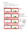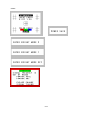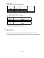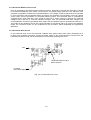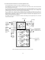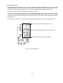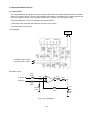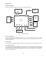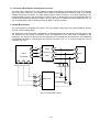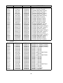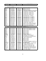
1
PART NO. 599910598
SERVICE MANUAL
COLOR MONITOR
MODEL
Diamond Plus 93SB
DPlus 93SB (B)
NEC-MITSUBISHI ELECTRIC VISUAL SYSTEMS CORPORATION
JUNE 2002
200207
08109716
WARNING
The SERVICE PERSONNEL should have the appropriate technical training, knowledge and
experience necessary to:
• Be familiar with specialized test equipment, and
• Be careful to follow all safety procedures associated with high voltage CRT circuit designs to
minimize danger to themselves and their coworkers.
To avoid electrical shocks, this equipment should be used with an appropriate power code and be
connected only to a properly grounded AC outlet.
This equipment utilized a micro-gap power switch. Turn off the set by first pushing the front panel
power switch. Next, remove the power cord from the AC outlet.
To prevent fire or shock hazards, do not expose this unit to rain or moisture.
This symbol warns the personnel that un-insulated voltage within the unit may have
sufficient magnitude to cause electric shock.
This symbol alerts the personnel that important literature concerning the operation and
maintenance of this unit has been included.
Therefore, it should be read carefully in order to avoid any problems.
PRODUCT SAFETY CAUTION
1. When parts replacement is required for servicing, always use the manufacturer's specified replacement.
2. Comply with all caution and safety-related notes on the product display chassis and picture tube.
3. When replacing the component, always be certain that all the components are put back in the place.
4. When servicing display monitor unit, it is required that the provided lead dress is used in the high voltage
circuit area.
5. It is also recommended that shatter proof goggles are worn, when removing installing and handling the
picture tube. People not equipped with the proper precautionary measures mentioned should keep the
picture tube away from body while handling.
6. As for a connector, pick and extract housing with fingers properly since a disconnection and improper
contacts may occur, when wires of the connector are led.
7. Use a proper screwdriver. If you use screwdriver that does not fit, you may damage the screws.
8. X-radiation precaution
This product contains critical electrical and mechanical parts essential for X-ray protection.
Normal anode voltage is 26.0 kV at zero beam picture tube current under AC 100-120V/220-240V input,
and anode voltage must not exceed the voltages shown below under any operation condition.
To measure anode voltage set brightness for very dim picture, and use a high impedance volt meter
between chassis and anode lead and measure high voltage.
If high voltage exceeds the specifications on the chassis schematic diagram, take the necessary
corrective action.
Table MAXIMUM ANODE VOLTAGE
beam current
A/B Ver.
at 0 mA
31.0 kV
at 0.6 mA
30.5 kV
at 1.2 mA
30.5 kV
9. When you degauss the set with an external degaussing coil, you must keep strictly item “ * Notes about
degaussing method “ of ADJUSTMENT Procedures.
CONTENTS
Page No.
USER'S MANUAL
..................................................................................................
SERIAL NUMBER INFORMATION
DISASSEMBLY
.......................................................................
2-1
......................................................................................................
3-1
ADJUSTMENT PROCEDURES
INSPECTION
1-1
............................................................................
4-1
.........................................................................................................
5-1
TROUBLE SHOOTING
..........................................................................................
6-1
.......................................................................................
7-1
CIRCUIT DESCRIPTION
REPLACEMENT PARTS LIST
BLOCK DIAGRAMS
..............................................................................
8-1
..............................................................................................
9-1
SCHEMATIC DIAGRAMS
....................................................................................
10-1
User's Manual
1. B Version
User’s Manual
1-1
Declaration of the Manufacturer
We hereby certify that the colour monitor
Diamond Pro 750SB / Diamond Plus 93SB
is in compliance with
Council Directive 73/23/EEC:
– EN 60950
Council Directive 89/336/EEC:
EN 55022
– EN 61000-3-2
– EN 61000-3-3
– EN 55024
and marked with
NEC-Mitsubishi Electric Visual
Systems Corporation
686-1, Nishioi Oi-Machi
Ashigarakami-gun
Kanagawa 258-8533, Japan
ENERGYSTAR Product
As an ENERGYSTAR Partner, NEC-Mitsubishi Electronics Display of America, Inc. has determined that this
product meets the ENERGYSTAR guidelines for energy efficiency. The ENERGYSTAR emblem does not represent
EPA endorsement of any product or service.
IBM is registered trademark of International Business Machines Corporation.
Apple and Macintosh are registered trademarks of Apple Computer Inc.
Microsoft and Windows are registered trademarks of the Microsoft Corporation.
ENERGYSTAR is a U.S. registered trademark.
NEC is a registered trademark of NEC Corporation.
All other trademarks or registered trademarks are property of their respective owners.
2 User’s Manual
1-2
WARNING
TO PREVENT FIRE OR SHOCK HAZARDS, DO NOT EXPOSE THIS UNIT TO RAIN OR MOISTURE. ALSO, DO NOT USE
THIS UNIT'S POLARIZED PLUG WITH AN EXTENSION CORD RECEPTACLE OR OTHER OUTLETS UNLESS THE
PRONGS CAN BE FULLY INSERTED.
EFRAIN FROM OPENING THE CABINET AS THERE ARE HIGH VOLTAGE COMPONENTS INSIDE. REFER SERVICING
TO QUALIFIED SERVICE PERSONNEL.
CAUTION
RISK OF ELECTRIC SHOCK • DO NOT OPEN
CAUTION: TO REDUCE THE RISK OF ELECTRIC SHOCK, DO NOT REMOVE COVER (OR BACK). NO USER SERVICEABLE PARTS INSIDE. REFER SERVICING TO QUALIFIED SERVICE PERSONNEL.
This symbol warns user that uninsulated voltage within the unit may have sufficient magnitude to cause
electric shock. Therefore, it is dangerous to make any kind of contact with any part inside this unit.
This symbol alerts the user that important literature concerning the operation and maintenance of this unit
has been included. Therefore, it should be read carefully in order to avoid any problems.
Canadian Department of Communications Compliance Statement
DOC: This Class B digital apparatus meets all requirements of the Canadian Interference-Causing
Equipment Regulations.
C-UL: Bears the C-UL Mark and is in compliance with Canadian Safety Regulations
according to C.S.A. C22.2 No. 950.
FCC Information
1. Use the attached specified cables with the Diamond Pro 750SB / Diamond Plus 93SB colour monitor so as
not to interfere with radio and television reception.
(1) Please use the supplied power cord or equivalent to ensure FCC compliance.
(2) Shielded captive type signal cable.
Use of other cables and adapters may cause intereference with radio and television reception.
2. This equipment has been tested and found to comply with the limits for a Class B digital device, pursuant to
part 15 of the FCC Rules. These limits are designed to provide reasonable protection against harmful
interference in a residential installation. This equipment generates, uses, and can radiate radio frequency
energy, and, if not installed and used in accordance with the instructions, may cause harmful interference
to radio communications. However, there is no guarantee that interference will not occur in a particular
installation. If this equipment does cause harmful interference to radio or television reception, which can be
determined by turning the equipment off and on, the user is encouraged to try to correct the interference by
one or more of the following measures:
• Reorient or relocate the receiving antenna.
• Increase the separation between the equipment and receiver.
• Connect the equipment into an outlet on a circuit different from that to which the receiver is connected.
• Consult your dealer or an experienced radio/TV technician for help.
Changes or modifications not expressly approved by the party responsible for compliance could void the
user’s authority to operate the equipment.
If necessary, the user should contact the dealer or an experienced radio/television technician for additional
suggestions. The user may find the following booklet, prepared by the Federal Communications Commission,
helpful: ”How to Identify and Resolve Radio-TV Interference Problems.“ This booklet is available from the U.S.
Government Printing Office, Washington, D.C., 20402, Stock No. 004-000-00345-4.
Diamond Pro 750SB / Diamond Plus 93SB 3
1-3
Contents
Your new Diamond Pro 750SB / Diamond Plus 93SB monitor box* should contain the following:
SB
• Diamond Pro 750 / Diamond Plus 93SB Monitor with tilt/swivel base
• Power Cord
• Captive Signal Cable
• User’s Manual
• CD ROM with Setup Software, complete User’s Manual and other helpful files.
To see the User’s Manual, Acrobat Reader 4.0 must be installed on your PC.
Captive Signal Cable
User’s Manual
Power Cord
CD-ROM
* Remember to save your original box and packing material to transport or ship the monitor.
4 User’s Manual
1-4
Quick Start
To attach the Diamond Pro 750SB / Diamond Plus 93SB monitor to your system, follow these instructions:
1. Turn off the power to your computer.
2. If necessary, install the display card into your system. For more information, refer to the display card
manual.
3. For the PC: Connect the 15-pin mini D-SUB of the captive signal cable to the connector of the display card
in your system (Figure A.1). Tighten all screws.
For the Mac: Connect the Diamond Pro 750SB / Diamond Plus 93SB Macintosh cable adapter (not included)
to the monitor connector on the Macintosh (Figure B.1). Attach the 15-pin mini D-SUB end of the captive
signal cable to the Diamond Pro 750SB / Diamond Plus 93SB Macintosh cable adapter on the computer
(Figure B.1). Tighten all screws.
4. Connect one end of the power cord to the Diamond Pro 750SB / Diamond Plus 93SB monitor and the other
end to the power outlet (Figure C.1).
5. Turn on the monitor (Figure D.1) and the computer.
NOTE: If you have any problems, please refer to the Troubleshooting section of this User’s Manual.
Figure B.1
Figure A.1
15-pin
mini
D-SUB
Mac Adapter
(Not Included)
Captive Signal Cable
Captive Signal Cable
Diamond Pro 750SB / Diamond Plus 93SB 5
1-5
Quick Start – continued
Power Outlet
Power
Cord
Figure C.1
Power Button
Figure D.1
6 User’s Manual
1-6
Controls
OSM (On-Screen Manager) control buttons on the front of the monitor function as follows:
Main Menu
Sub-Menu
EXIT
Exits the OSM menu.
Exits to the OSM controls
main menu.
CONTROL
Moves the highlighted
area left/right to select
one of the sub-menus.
Moves the highlighted area
left/right to select one of the
controls.
CONTROL
–/+
Has no function.
Moves the bar in the – or +
direction to decrease or
increase the adjustment.
S E LE C T/
SBMODE
Without OSD, switches
SuperBright Mode ON/OFF
With OSD, enters sub menu
Has no function.
R ESET
Resets all the controls within
the highlighted menu
to the factory setting.
Resets the highlighted control
to the factory setting.
Y
/
Y
NOTE: When RESET is pressed in the main and sub-menu, a warning window will appear
allowing you to cancel the reset function.
NOTE: When the OSM is off, it will act as the SuperBright (SB) function key. User can select
between SB MODE OFF, SB MODE1, and SB MODE2. The first time this key is
pressed, the current SB Mode is indicated. Within a 3 second window, if this key is
selected again, the SB MODE will change to the next SB MODE. For example, the
current mode is SB MODE OFF, the key is pressed twice within a 3 second time frame,
the SB MODE will change to SB MODE1 and so on. The color temperature at each SB
Mode is adjusted by appropriate color control except for the sRGB mode whose color
setting cannot be adjusted. When the unit is turned off, it will reset to SB off mode.
Brightness/Contrast Controls
Brightness: Adjusts the overall image and background screen brightness.
Contrast: Adjusts the image brightness in relation to the background.
Degauss: Eliminates the buildup of stray magnetic fields which alter the correct scan of the electron beams
and affect the purity of the screen colours, focus and convergence. When activated, your screen image will
jump and waver a bit as the screen is demagnetized.
Caution: Please allow a minimum of 20 minutes to elapse between uses of the Degauss Control.
Size and Position Controls
Left/Right: Moves the image horizontally (left or right).
Down/Up: Moves the image vertically (up or down).
Narrow/Wide: Decreases or increases the horizontal size of the image.
Short/Tall: Decreases or increases the vertical size of the image.
Diamond Pro 750SB / Diamond Plus 93SB 7
1-7
Controls – continued
Color Control System
Colour presets selects the desired colour setting. The bar is replaced by the colour setting choice. Each
colour setting is adjusted at the factory to the stated Kelvin. If a setting is adjusted, the name of the setting
will change from Kelvin to Custom except sRGB mode.
Red, Green, Blue: Color Control System decreases or increases the monitor's red, green or blue colour guns
depending upon which is selected. The change in colour will appear on screen and the direction (decrease or
increase) will be shown by the bars.
sRGB mode: sRGB mode provides the suitable colour managed picture image. You can not change Red,
Green and Blue colours, brightness and contrast individually.
Colour Temperature Adjustment: Adjusts the colour temperature of the screen image.
Geometry Controls
Geometry Controls Menu
The Geometry controls allow you to adjust the curvature or angle of the sides of your display.
Sides In/Out (pincushion): Decreases or increases the curvature of the sides either inward or outward.
Sides Left/Right (pincushion balance): Decreases or increases the curvature of the sides either to the left
or right.
Sides Tilt (parallelogram): Decreases or increases the tilt of the sides either to the left or right.
Sides Align (trapezoidal): Decreases or increases the bottom of the screen to be the same as the top.
Rotate (raster rotation): Rotates the entire display clockwise or counterclockwise.
Corner Correction: Allows you to adjust the geometry of the corners of your display – Top or Bottom.
Tools 1
Moiré Canceler: Moiré is a wavy pattern which can sometimes appear on the screen. The pattern is repetitive
and superimposed as rippled images. When running certain applications, the wavy pattern is more evident
than in others. To reduce moiré, adjust the level by using –/+ CONTROL buttons.
Linearity: This selection allows you to adjust the spacing of the area on the screen. The purpose of this
control is to ensure that a one-inch circle is a true one-inch circle wherever it is on the screen. The best way to
determine the vertical linearity is as follows:
• Draw equally spaced horizontal lines using a drawing application that has a ruler.
• Use the Vertical Balance control to adjust the lines near the top and bottom of your screen.
• Use the LINEARITY (VER.) control to adjust the spacing between the lines near the center and top of your
screen.
Convergence (Diamond Plus 93SB only): Aligns all three colors (R,G,B) to form a single color (white). The
purpose of this control is to ensure that a white line drawn on the screen is as crisp and clear as possible.
• Use the CONVERGENCE (HOR.) control to adjust the alignment of the lines in the up/down direction.
• Use the CONVERGENCE (VER.) control to adjust the alignment of the lines in the left/right direction.
8 User’s Manual
1-8
Controls – continued
Tools 2
Language: OSM controls menus are available in 6 languages.
OSM Position: You can choose where you would like the OSM controls menu to appear on your screen.
Selecting OSM Position allows you to manually adjust the OSM controls menu position from among Center,
Top left, Top right, Bottom left and Bottom right.
OSM Turn Off: The OSM controls menu will stay on as long as it is in use. In the OSM Turn Off sub-menu,
you can select how long the monitor waits after the last touch of a button for the OSM controls menu to
disappear. The preset choices are 5 thru 120 seconds.
OSM Lock Out: This control completely locks out access to all OSM controls functions except Brightness
and Contrast. When attempting to activate OSM controls while in the lock out mode, a screen will appear
indicating that OSM controls are locked out. To activate the OSM Lock Out function, press SELECT and
hold + down simultaneously. To deactivate the OSM Lock Out, press SELECT and hold + down simultaneously.
IPM System Off Mode:
Enable:
The IPM System works
normally and all stages of
energy savings are utilized.
Disable:
The Off Mode of the IPM System
is not used.
NOTE: For standard systems and graphics boards, keep the factory setting at ENABLE.
EdgeLock Control: Operating your monitor at a nonstandard timing may cause images to appear darker than
normal or have color distortion. Use of the EdgeLock control will adjust images to their normal state.
Hot Key: This selection allows you to use / as brightness control and –/+ as contrast control.
Factory Preset: Selecting Factory Preset allows you a reset most OSM control settings back to the factory
settings. A warning statement will appear to confirm that you do want to reset ALL settings. Individual settings
can be reset by highlighting the control to be reset and pressing the RESET button.
Y
Y
Information
Display Mode: Indicates the current mode and frequency setting of the monitor.
Monitor Info: Indicates the model and serial numbers of your monitor.
Refresh Notifier: A message will advise you if the refresh rate of the signal being applied to the monitor by
the computer is too low. For further information, please refer to your display card or system manual.
Diamond Pro 750SB / Diamond Plus 93SB 9
1-9
Recommended Use
Safety Precautions and Maintenance
FOR OPTIMUM PERFORMANCE, PLEASE NOTE
THE FOLLOWING WHEN SETTING UP AND USING THE
DIAMOND PRO 750SB / DIAMOND PLUS 93SB COLOUR MONITOR:
• DO NOT OPEN THE MONITOR. There are no user serviceable parts inside and opening or removing covers
may expose you to dangerous shock hazards or other risks. Refer all servicing to qualified service personnel.
• Do not spill any liquids into the cabinet or use your monitor near water.
• Do not insert objects of any kind into the cabinet slots, as they may touch dangerous voltage points, which
can be harmful or fatal or may cause electric shock, fire or equipment failure.
• Do not place any heavy objects on the power cord. Damage to the cord may cause shock or fire.
• Do not place this product on a sloping or unstable cart, stand or table, as the monitor may fall, causing
serious damage to the monitor.
• Keep the monitor away from high capacity transformers, electric motors and other devices such as external
speakers or fans, which may create strong magnetic fields.
• If possible, position the monitor so that it is facing the east to minimize the effects of the earth’s magnetic
field.
• Changing the direction of the monitor while it is powered on may cause image discolouration. To correct this,
turn the monitor off for 20 minutes before powering it back on.
• When operating the Diamond Pro 750SB / Diamond Plus 93SB with its AC 220 - 240 V worldwide power
supply, use a power supply cord that matches the power supply voltage of the AC power outlet being used.
The power supply cord you use must have been approved by and comply with the safety standards of your
country. (Type H05VV-F should be used except in UK)
• In UK, use a BS-approved power cord with molded plug having a black (5A) fuse installed for use with this
monitor. If a power cord is not supplied with this monitor, please contact your supplier.
Cleaning Your Monitor
A special coating is provided on the glass (CRT) surface of this monitor to reduce a reflection and static
electricity on the glass surface. Due to the delicate coating on the glass surface, use a lint-free, non-abrasive
cloth (cotton or equivalent) and a non-alcohol, neutral, non-abrasive cleaning solution to minimize dust. If the
screen requires more than a light cleaning, apply a soft neutral detergent and water directly to a soft cloth and
use it upon wringing water, to clean the glass surface. Clean your monitor regularly.
CAUTION: The following agents will cause damage to the CRT when cleaning the glass surface:
Benzene, thinner, acid/alkaline detergent, alcohol detergent, detergent with abrasive powder, detergent with
anti-static agent, detergent for cleaning.
Immediately unplug your monitor from the wall outlet and refer servicing to qualified service personnel under
the following conditions:
•
•
•
•
•
When the power supply cord or plug is damaged.
If liquid has been spilled, or objects have fallen into the monitor.
If the monitor has been exposed to rain or water.
If the monitor has been dropped or the cabinet damaged.
If the monitor does not operate normally by following operating instructions.
• Allow adequate ventilation around the monitor so that heat can properly
dissipate. Do not block ventilated openings or place the monitor near a radiator
or other heat sources. Do not put anything on top of monitor.
• The power cable connector is the primary means of detaching the system from
the power supply. The monitor should be installed close to a power outlet which
CAUTION
is easily accessible.
• Handle with care when transporting. Save packaging for transporting.
10 User’s Manual
1-10
Recommended Use – continued
CORRECT PLACEMENT AND ADJUSTMENT OF THE MONITOR
CAN REDUCE EYE, SHOULDER AND NECK FATIGUE. CHECK THE
FOLLOWING WHEN YOU POSITION THE MONITOR:
• Adjust the monitor height so that the top of the screen is at or slightly
below eye level. Your eyes should look slightly downward when viewing the
middle of the screen.
• Position your monitor no closer than 40 cm and no further away than
60 cm from your eyes. The optimal distance is 50 cm.
• Rest your eyes periodically by focusing on an object at least 6 meter away.
Blink often.
• Position the monitor at a 90° angle to windows and other light sources to
minimize glare and reflections. Adjust the monitor tilt so that ceiling lights
do not reflect on your screen.
• If reflected light makes it hard for you to see your screen, use an anti-glare
filter.
• Clean your monitor regularly. Use a lint-free, non-abrasive cloth and a non-alcohol, neutral, non-abrasive
cleaning solution or glass cleaner to minimize dust.
• Adjust the monitor’s brightness and contrast controls to enhance readability.
• Use a document holder placed close to the screen.
• Position whatever you are looking at most of the time (the screen or reference material) directly in front of
you to minimize turning your head while you are typing.
• Get regular eye checkups.
Ergonomics
To realize the maximum ergonomics benefits, we recommend the following:
•
•
•
•
•
•
Adjust the Brightness until the background raster disappears
Do not position the Contrast control to its maximum setting
Use the preset Size and Position controls with standard signals
Use the preset Colour Setting and Sides Left/Right controls
Use non-interlaced signals with a vertical refresh rate between 75 - 120 Hz
Do not use primary colour blue on a dark background, as it is difficult to see and may produce eye fatigue
due to insufficient contrast
Diamond Pro 750SB / Diamond Plus 93SB 11
1-11
Specifications
Diamond Pro 750SB
Monitor
Monitor
Specifications
Picture Tube
Diagonal: 43 cm/17 inch
Viewable Image Size: 406 mm/16 inch
Input Signal
Notes
90° deflection, 0.25 mm grille pitch,
medium short persistence phosphor,
aperture grille CRT, multi-layered, antistatic screen coating, dark-tint screen
and OptiClear screen.
Video: ANALOG 0.7 Vp-p/75 Ohms
Sync: Separate sync. TTL Level
Horizontal sync. Positive/Negative
Vertical sync. Positive/Negative
Composite sync. (Positive/Negative) (TTL Level)
Display Colours
Synchronization
Analog input: Unlimited number of Colours
Depends on display card used.
Horizontal: 30 kHz to 96 kHz
Automatically
Vertical: 50 Hz to 160 Hz
Automatically
Range
Resolutions Supported
Resolution based on horizontal and
vertical frequencies only
640 x 480 @ 60 to 160 Hz
Some systems may not support all
800 x 600 @ 50 to 146 Hz
modes listed.
832 x 624 @ 50 to 141 Hz
1024 x 768 @ 50 to 116 Hz ............... NEC-Mitsubishi Electronics Display
1152 x 870 @ 50 to 103 Hz
cites recommended resolution at
1280 x 1024 @ 50 to 89 Hz
85 Hz for optimal display performance
1600 x 1200 @ 50 to 76 Hz
Active Display Area
(Factory Setting)
Horizontal: 315 mm/12.4 inches
Vertical: 236 mm/9.3 inches
Dependent upon signal timing used,
and does not include
border area.
Active Display Area
(Full Scan)
325 mm/12.8 inches
244 mm/9.6 inches
Dependent upon signal timing used,
and does not include
border area.
Power Supply
AC 100 - 240 V, 50 - 60 Hz
Current Rating
1.9 A @ 100 - 240 V
Dimensions
397 mm (W) x 392 mm (H) x 415.5 mm (D)
15.6 inches (W) x 15.4 inches (H) x 16.4 inches (D)
Weight
17.2 kg
37.9 lbs
Environmental Considerations
Operating Temperature:
Humidity:
Altitude:
Storage Temperature:
Humidity:
Altitude:
+5 °C to +35 °C
10 % to 90 %
0 to 3,000 m
-20 °C to +60 °C
10 % to 90 %
0 to 15,000 m
NOTE: Technical specifications are subject to change without notice.
12 User’s Manual
1-12
Specifications – continued
Diamond Plus 93SB
Monitor
Monitor
Specifications
Picture Tube
Notes
Diagonal: 50 cm/19 inch
90° deflection, 0.25/0.27 mm grille
pitch, medium short persistence
phosphor, aperture grille CRT, multilayered, anti-static screen coating,
dark-tint screen and OptiClear screen.
Viewable Image Size: 457 mm/18 inch
Input Signal
Video: ANALOG 0.7 Vp-p/75 Ohms
Sync: Separate sync. TTL Level
Horizontal sync. Positive/Negative
Vertical sync. Positive/Negative
Composite sync. (Positive/Negative) (TTL Level)
Display Colours
Synchronization
Analog input: Unlimited number of Colours
Depends on display card used.
Horizontal: 30 kHz to 96 kHz
Range
Automatically
Vertical: 50 Hz to 160 Hz
Resolutions Supported
Resolution based on horizontal and
vertical frequencies only
Automatically
640 x 480 @ 60 to 160 Hz
Some systems may not support all
800 x 600 @ 50 to 146 Hz
modes listed.
832 x 624 @ 50 to 141 Hz
1024 x 768 @ 50 to 116 Hz
NEC-Mitsubishi Electronics Display
cites recommended resolution at
1152 x 870 @ 50 to 103 Hz
1280 x 1024 @ 50 to 89 Hz .............. 85 Hz for optimal display performance
1600 x 1200 @ 50 to 76 Hz
1792 x 1344 @ 50 to 68 Hz
Active Display Area
(Factory Setting)
Horizontal: 356 mm/14.0 inches
Vertical: 266 mm/10.5 inches
Dependent upon signal timing used,
and does not include
border area.
Active Display Area
(Full Scan)
366 mm/14.4 inches
266 mm/10.5 inches
Dependent upon signal timing used,
and does not include
border area.
Power Supply
AC 100 - 240 V, 50 - 60 Hz
Current Rating
2.2 A @ 100 - 240 V
Dimensions
442 mm (W) x 443 mm (H) x 447.5 mm (D)
17.4 inches (W) x 17.4 inches (H) x 17.6 inches (D)
Weight
22.7 kg
50.0 lbs
Environmental Considerations
Operating Temperature:
Humidity:
Altitude:
Storage Temperature:
Humidity:
Altitude:
+5 °C to +35 °C
10 % to 90 %
0 to 3,000 m
-20 °C to +60 °C
10 % to 90 %
0 to 15,000 m
NOTE: Technical specifications are subject to change without notice.
Diamond Pro 750SB / Diamond Plus 93SB 13
1-13
Features
SuperBright Diamondtron CRT: This patented flat aperture grille CRT delivers an exceptional viewing experience with unprecedented brightness and contrast and a virtually flat image that reduces distortion and glare so
that what you see on-screen is what you get on your printed output. The state-of-the-art Mitsubishi PX-DBF
electron gun and tight 0.25 mm grille pitch delivers precise focus for crisp, clear text and images.
SuperBright Mode : With the simple touch of a button, the brightness level of the Diamondtron CRT doubles.
This function enhances the crispness of images for clarity-conscious applications such as graphics, animation
and video.
Super Bright Mode OFF: for text based images (normal use)
Super Bright Mode-1 ON: for images
Super bright Mode-2 ON: for moving image such as DVD movies
OptiClear Screen Surface: Further reduces reflection and glare and increases contrast without sacrificing focus
level, clarity or brightness.
Dual Dynamic Beam Focus: Provides precise, continuous focus adjustments of the electron beams and optimum image quality, even to the far edges of the screen.
Color Control System with sRGB: Allows you to change between five colour settings on your display to match
your personal preference. The sRGB-enabled colour matching setting found within Color Control helps achieve a
consistent colour environment with other sRGB-enabled hardware and software applications.
On Screen Manager (OSM) Controls: Allows you to quickly and easily adjust all elements of your screen image
via simple to use on-screen menus.
ErgoDesign Features: Enhances human ergonomics to improve the working environment, protect the health of
the user and save money. Examples include OSM controls for quick and easy image adjustments, tilt/swivel base
for preferred angle of vision, space-conscious cabinet design and compliance with MPRII guidelines for lower
emissions.
Plug and Play: The Microsoft solution with the Windows 95/98/Me/2000/XP operating system facilitates setup
and installation by allowing the monitor to send its capabilities (such as screen size and resolutions supported)
directly to your computer, automatically optimizing display performance.
Intelligent Power Manager (IPM) System: Provides innovative power-saving methods that allow the monitor to
shift to a lower power consumption level when on but not in use, saving two-thirds of your monitor energy costs,
reducing emissions and lowering the air conditioning costs of the workplace.
Reduced Magnetic Field Technology: Reduces magnetic and alternating electric field emissions and static
electricity, addressing ergonomic concerns regarding potential risks from extended computer monitor use.
Multiple Frequency Technology: Automatically adjusts monitor to the display card’s scanning frequency, thus
displaying the resolution required.
FullScan Capability: Allows you to use the entire screen area in most resolutions, significantly expanding image
size.
14 User’s Manual
1-14
Troubleshooting
No picture
•
•
•
•
Display card should be completely seated in its slot.
Power Button and computer power switch should be in the ON position.
Signal cable should be completely connected to display card/computer.
Check connector for bent or pushed-in pins.
Image is scrolling or unstable
• Signal cable should be completely attached to the computer.
• Check pin assignments and signal timings of the monitor and your display card with respect to
recommended timings and pin assignments.
• If the Macintosh cable adapter is used, check for proper connection or make sure the display card is
Macintosh compatible and that the card is properly seated in the computer.
LED on monitor is not lit (no green, orange colour can be seen)
• Power Switch should be in the ON position and power cord should be connected.
Picture is fuzzy or colour looks blotchy
• Adjust Brightness and Contrast Controls or adjust the Moiré Canceler control.
• Access the Degauss Control through OSM controls. Activate the Degauss Control.
CAUTION: A minimum interval of 20 minutes should elapse before the Deguass Control is used a second
time when not switching between modes.
Picture bounces or a wavy pattern is present in the picture
• Move electrical devices that may be causing electrical interference away from the monitor.
• See inside cover of User’s Manual for FCC information.
Edges of the display image are not square
• Use the OSM Geometry Controls to straighten the edges.
• If possible, position the front of the monitor facing east.
Display image is not centered, too small, or too large
• Use the OSM Size and Position Controls to adjust the image.
Thin lines appear on your screen
• Thin lines are normal for an aperture grille CRT and are not a malfunction.
These are shadows from the damper wires used to stabilize the aperture grille and are most noticeable when
the screen’s background is light (usually white).
Black vertical lines are visible on the screen
• Thin vertical black lines on one or both sides of the screen. This minor condition is caused by grille element
overlap which can occur during shipping.
• Position an open white window over the affected area of the screen and maximize the brightness and
contrast controls. This will cause localized heating of the overlap which will clear in a few minutes. Be sure
to readjust the brightness and contrast controls back to the normal viewing level after this procedure.
Diamond Pro 750SB / Diamond Plus 93SB 15
1-15
TCO’99
Diamond Pro 750SB / Diamond Plus 93SB
Congratulations! You have just purchased a TCO’99 approved and labeled product! Your
choice has provided you with a product developed for professional use. Your purchase has
also contributed to reducing the burden on the environment and also to the further development of environmentally adapted electronics products.
Why do we have environmentally labelled computers?
In many countries, environmental labelling has become an established method for encouraging the adaptation of
goods and services to the environment. The main problem, as far as computers and other electronics equipment
are concerned, is that environmentally harmful substances are used both in the products and during the manufacturing. Since it has not been possible for the majority of electronics equipment to be recycled in a satisfactory
way, most of these potentially damaging substances sooner or later enter Nature.
There are also other characteristics of a computer, such as energy consumption levels, that are important from the
viewpoints of both the work (Internal) and natural (external) environments. Since all methods of conventional
electricity generation have a negative effect on the environment (acidic and climate-influencing emissions, radioactive waste, etc.), it is vital to conserve energy. Electronics equipment in offices consume an enormous amount of
energy since they are often left running continuously.
What does labelling involve?
This product meets the requirements for the TCO’99 scheme which provides for international and environmental
labelling of personal computers. The labelling scheme was developed as a joint effort by the TCO (The Swedish
Confederation of Professional Employees), Svenska Naturskyddsforeningen (The Swedish Society for Nature
Conservation) and Statens Energimyndighet (The Swedish National Energy Administration).
The requirements cover a wide range of issues: environment, ergonomics, usability, emission of electrical and
magnetic fields, energy consumption and electrical and fire safety.
The environmental demands concern restrictions on the presence and use of heavy metals, brominated and
chlorinated flame retardants, CFCs (freons) and chlorinated solvents, among other things. The product must be
prepared for recycling and the manufacturer is obliged to have an environmental plan which must be adhered to in
each country where the company implements its operational policy. The energy requirements include a demand
that the computer and/or display, after a certain period of inactivity, shall reduce its power consumption to a lower
level in one or more stages. The length of time to reactivate the computer shall be reasonable for the user.
Labelled products must meet strict environmental demands, for example, in respect of the reduction of electric
and magnetic fields, physical and visual ergonomics and good usability.
Environmental Requirements
Flame retardants
Flame retardants are present in printed circuit boards, cables, wires, casings and housings. In turn, they delay the
spread of fire. Up to thirty percent of the plastic in a computer casing can consist of flame retardant substances.
Most flame retardants contain bromine or chloride and these are related to another group of environmental toxins,
PCBs, which are suspected to give rise to severe health effects, including reproductive damage in fisheating birds
and mammals, due to the bioaccumulative* processes. Flame retardants have been found in human blood and
researchers fear that disturbances in foetus development may occur.
16 User’s Manual
1-16
TCO’99 – continued
TCO’99 demand requires that plastic components weighing more than 25 grams must not contain flame retardants with organically bound chlorine and bromine. Flame retardants are allowed in the printed circuit boards
since no substitutes are available.
Lead**
Lead can be found in picture tubes, display screens, solders and capacitors. Lead damages the nervous system
and in higher doses, causes lead poisoning.
TCO’99 requirement permits the inclusion of lead since no replacement has yet been developed.
Cadmium**
Cadmium is present in rechargeable batteries and in the colourgenerating layers of certain computer displays.
Cadmium damages the nervous system and is toxic in high doses.
TCO’99 requirement states that batteries, the colourgenerating layers of display screens and the electrical or
electronics components must not contain any cadmium.
Mercury**
Mercury is sometimes found in batteries, relays and switches, Mercury damages the nervous system and is toxic
in high doses.
TCO’99 requirement states that batteries may not contain any Mercury. It also demands that no mercury is
present in any of the electrical or electronics components associated with the display unit.
CFCs (freons)
CFCs (freons) are sometimes used for washing printed circuit boards. CFCs break down ozone and thereby
damage the ozone layer in the stratosphere, causing increased reception on Earth of ultraviolet light with consequent increased risks of skin cancer (malignant melanoma).
The relevant TCO’99 requirement; Neither CFCs nor HCFCs may be used during the manufacturing and assembly
of the product or its packaging.
* Bio-accumulative is defined as substances which accumulate within living organisms.
** Lead, Cadmium and Mercury are heavy metals which are Bio-accumulative.
To obtain complete information on the environmental criteria document, order from:
TCO Development Unit
SE-114 94 Stockholm
SWEDEN
FAX Number: +46 8 782 92 07
E-mail (Internet): [email protected]
You may also obtain current information on TCO’99 approved and labelled products by visiting their website at:
http://www.tco-info.com/
Diamond Pro 750SB / Diamond Plus 93SB 17
1-17
Serial Number Information
Refer to the serial number information shown below.
EX.) SERIAL NUMBER LABEL
Model
: DPlus93SB
SERIAL NO. :
g g g g g g g g g
Manufactured Year :
( Last digit )
Manufactured Month :
January to September
1 to 9
October
X
November
Y
December
Z
Serial number(5 digits)
Factory Code :
NPG China Factory (A/B/R ver.)
:“Y”
Destination Code :
USA
: “A”
Europe : “B”
Australia : “R”
2-1
DISASSEMBLY
• Before you disassemble the set, turn off power and pull out the power plug.
• Use the appropriate screwdriver that fits the screw. If you use screwdriver that does not fit, you may break
the screws.
• Assembly is the opposite process of Disassembly.
• Carefully discharge the CRT anode by shorting it to ground before removing anode cap.
Revolving Stand ASSY
1. Turn the monitor CRT face down on a clean static free surface to prevent scratching CRT face.
2. Remove the screw (PL-CPTS*3*10*15BF) and remove by pulling up the Hooks and lifting the Revolving
stand Assy up to the side.
Screw (PL-CPTS*3*10*15BF)
HOOK
Revolving Stand Assy
Cabinet Back
1. Remove the two screws (PL-CPTS*4*16*15BF) and unlock the two hooks.
Hook
Screws (PL-CPTS*4*16*15BF)
3-1
CRT BOARD
1. Remove the nine terminals and desolder the five points as shown.
Terminals
Solder
2. Disconnect the connectors “S201”, “S202”, “S203” and “GND”.
3. Desoldor the wires: “White wire”, “Red wire” and “G2”.
S202
S201
Red wire
S203
White wire
GND
G2
3-2
MAIN BOARD
1. Disconnect the connectors “S601”, “S602”, ”S101” and “GND”.
2. Remove the screw (P-#2CRBITS*4*8*15BF) and two screws (PL-CPIMS*4*10*15BF).
S602
S601
S101
Screw
(P-#2CRBITS*4*8*15BF)
GND
Screw
(PL-CPIMS*4*10*15BF)
3. Disconnect the connectors “GND” and “S301”.
4. Remove the screw (P-#2CRBITS*4*8*15BF) .
5. Remove the Anode cap from CRT.
NOTE: Carefully discharge the CRT anode by shorting it to ground before removing anode cap.
Screw (P-#2CRBITS*4*8*15BF)
GND
S301
3-3
6. Remove the four screws (PL-CPTS*4*16*15BF) and remove the Chassis Base from Cabinet Front ASSY.
Screws (PL-CPTS*4*16*15BF)
7. Remove the seven screws (PL-CPTS*3*8*15BF) and two screws (PL-CPIMS*3*10*15BF).
8. Remove the Main Board from Chassis Base.
Screw (PL-CPTS*3*8*15BF)
Screw (PL-CPIMS*3*10*15BF)
3-4
ADJUSTMENT PROCEDURES
TABLE OF CONTENTS
Page
1. Adjustment & Inspection Tools............................................................................................ 4-2
2. Timing Table ..................................................................................................................... 4-2
3. Normal Condition Definition .............................................................................................. 4-2
4. Hot Key Operation ............................................................................................................. 4-3
5. B+ Check ........................................................................................................................... 4-5
6. X-RAY Test ........................................................................................................................ 4-5
7. H. V. Adjustment ............................................................................................................... 4-5
8. H-Raster Center Adjustment ............................................................................................. 4-5
9. Preset Adjustment ............................................................................................................. 4-5
10. G2 Voltage Adjustment ................................................................................................... 4-5
11. White Balance Adjustment .............................................................................................. 4-6
12. Focus Adjustment ........................................................................................................... 4-8
13. Purity Adjustment ............................................................................................................ 4-8
14. Convergence Adjustment ............................................................................................... 4-9
15. Power Saving Function Inspection .................................................................................. 4-9
16. Distortion Adjustment .................................................................................................... 4-10
17. Setting Before Shipment ............................................................................................... 4-12
18. Adjustment Magnetic Field ........................................................................................... 4-13
19. TIMING SHEET ............................................................................................................. 4-14
4-1
1. Adjustment & Inspection Tools
(A) Color Analyzer
(B) Signal Generator CHROMA 2235 or compatible
(C) Multi Meter
(D) Hi-Voltage Probe
(E) Convergence Meter
(F) Degaussing Probe
(G) Power Meter
2. Timing Table (Factory Mode –18 Modes)
MODE
RESOLUTION
H-SYNC EREQ. V-SYNC FREQ H . POLARITY
V . POLARITY
1
VGA400
31.4KHz
70Hz
-
+
2
VGA640*480
31.4KHz
60Hz
-
-
3
640*480(75)
37.5KHz
75Hz
-
-
4
640*480(85)
43.2KHz
85Hz
-
-
5
800*600(75)
46.8KHz
75Hz
+
+
6
MACII 49K
49.7KHz
75Hz
-
-
7
800*600(85)
53.6KHz
85Hz
+
+
8
1024*768(75)
60.0KHz
75Hz
+
+
9
1280*1024(60)
64.0KHz
60Hz
+
+
10
1024*768(85)
68.6KHz
85Hz
+
+
11
1280*1024(75)
79.9KHz
75Hz
+
+
12
1280*1024(85)
91.1KHz
85Hz
+
+
13
1600*1200(75)
93.7KHz
75Hz
+
+
14
1024*768(60)
48.3KHz
60Hz
-
-
15
800*600(60)
37.8KHz
60Hz
+
+
16
MACII 35K
35.0KHz
67Hz
-
+
17
MAC 1152*870
68.7KHz
75Hz
-
-
18
VGA720*400(70)
31.5KHz
70Hz
-
+
3. Normal Condition Definition
(A) Input AC Voltage 110V/60Hz.
(B) Warm up time minimum 30 minutes.
(C) Full White Pattern.
(D) All VR’s adjust to Center Position.
(F) Color temp 9300K
4-2
4. Hot Key Operation
(A) Factory Mode: power on + ‘+’ key + ‘−‘ key.
*To hide the Factory menu temporary in Factory mode:
Push "RESET" key once while Menu is displayed, then Menu disappears.
Push "RESET" key once more, then Menu reappears.
(B) Factory Menu
TAB 1) BRIGHTNESS / CONTRAST
: Brightness
: Contrast
TAB 2) POSITION / SIZE
: Left / Right (H.Position)
: Down / Up (V.Position)
: Narrow / Wide (H.Size)
: Short / Tall (V.Size)
VG: Vertical GAIN(Vertical Sub Size)
TAB 3) COLOR ADJUST
1: 9300K
2: 8200K
3: 7500K
sRGB: sRGB
5: 5000K
: N/A
: Red Gain
: Green Gain
: Blue Gain
: Red Bias
: Green Bias
: Blue Bias
: Brightness
: Contrast
TAB 4) DISTORTION
: In / Out (Side Pincushion)
: Left / Right (Pin Balance)
: Tilt (Parallelogram)
: Align (Trapezoid)
: Rotate
: Top Corner
: Bottom Corner
VF : Vertical Focus
4-3
TAB 5) TOOLS 1
:Moire canceller
:Linearity(VER.)
:Linearity balance
:Convergence(HOR.)
:Convergence(VER.)
TAB 6) TOOLS 2
TOOL 2 is as same as user mode
TAB 7) INFORMATION
DS :Destination
4-4
5. B+ Check
(A) Mode: No.12.
(B) Pattern: Full White. (Brightness set to cut off)
(C) Check other power sources are: 83.9V ±1V, 7.05V ±0.3V, 26.5V ±1V, -14.3V ±1V, 14.2V ±0.3V.
6. X-RAY Test
(A) Mode: No.12
(B) Pattern: Normal Crosshatch (Brightness just cut off)
(C) Test
Apply a resistor (4.7K, 1/4W, 1%) between TP1 and TP2 then power on, Monitor should be active in x-ray
protector.
7. H. V. Adjustment
(A) Mode: No.12
(B) Pattern: Full Black (Brightness just cut off)
(C) Adjust VR301 to make the high voltage has 26kV ±0.1kV.
8. H-Raster Center Adjustment
(A) Mode: No.13
(B) Pattern: Crosshatch Reverse
(C) Adjust the Brightness Control so that the background is visible.
(D) Adjust VR501 to make the raster mostly near center background position.
9. Preset Adjustment
(A) Mode No.12
(B) Pattern: Cross hatch
(C) Enter to Factory mode. Adjust H-phase, V-center, H-size, V-size, Pincushion, Trapezoid, Bow,
Parallelogram Top-corner, Bottom-corner, and rotation to make Picture Position Center and Picture Size
356*267mm.
10. G2 Voltage Adjustment
(A) Mode No. 12
(B) Pattern: Full Black
(C) Adjust: Monitor should be warm up more than 30 minutes.
(D) Adjust screen VR to make G2 voltage 680V±10V.
4-5
11. White Balance adjustment
(A) Setting
Enter Factory Mode,
Mode: No.12, Pattern: Full White.
Warm up 60 min.
Make External Degauss.
(B) Cut Off Adjustment
1. Select the color Mode 9300K.
2. Cut Off Adjustment : Video Signal Off(0.Vp-p),Bright Control set to Max., Adjust G. Bias at the
Brightness 3.4 ±0.7cd/m2 (1FL ±0.2FL).
3. 9300K (Select color Mode 9300)
Adjust R. Bias, B. Bias to make X=0.283, Y=0.297, with readjusting G. Bias to keep the brightness
between 3.4 ±0.7cd/m2 (1FL ±0.2FL).
(C) “9300K, 5000K MODE” White Balance Adjustment
1. 9300K (Select color Mode 9300K)
1) Video Signal off (0.Vp-p), Contrast set to Max, Adjust Brightness to 0.1cd/m2.
2) 50*50mm Green block Pattern, Adjust G Gain to Y=86cd/m2 .
3) 50*50mm White block Pattern, Adjust R, B Gain to x=0.283, y=0.297.
4) Adjust R, G, B gain again to meet following spec.
9300K
x=0.283 ±0.010cd/m2
y=0.297 ±0.010cd/m2
Y=130 ±2cd/m2
4-6
2. 5000K (Select color Mode 5000K)
1) Video Signal off (0.Vp-p), Contrast set to Max, Adjust Brightness to 0.1cd/m2.
2) 50*50mm Green block Pattern, Adjust G Gain to Y=70cd/m2 .
3) 50*50mm White block Pattern, Adjust R, B Gain to x=0.345, y=0.359.
4) Adjust R, G, B gain again to meet following spec.
5000K
x=0.345 ±0.010cd/m2
y=0.359 ±0.010cd/m2
Y>100cd/m2
(D) “sRGB MODE” White Balance Adjustment (Select color Mode sRGB)
1) Video Signal off (0.Vp-p), Contrast set to Max, Adjust Brightness to 0.1cd/m2.
2) 50*50mm Green block Pattern, Adjust G Gain to Y=75cd/m2 .
3) Change Pattern to Full white. Adjust R, B Gain to x=0.313, y=0.329.
4) Adjust contrast to meet following spec.
sRGB
x=313 ±0.010cd/m2
y=329 ±0.010cd/m2
Y=93 ±2cd/m2(27FL)
(E) “SB1, 2 MODE” White Balance Adjustment (Select the color Mode SB1, 2 MODE)
1) Select the color mode “SB1 Mode” by “Select” key when OSM is off.
2) Video signal off (0Vp-p), Adjust brightness to Y=0.1cd/m2.
3) Change pattern to 50*50mm white block, Adjust contrast control to Y=215 ±2cd/m2.
4) Change pattern to 32/255 gray. Adjust brightness to make 0.8cd/m2.
5) Select the color mode “SB2 MODE”.
6) Video signal off(0Vp-p), Adjust brightness to Y=0.1cd/m2.
7) Change pattern to 50*50mm white block, Adjust contrast control to Y=255 ±2cd/m2.
(F) ABL Adjustment and Brightness Preset
1) SB mode off, Color set to 9300K.Full White Pattern.
2) Brightness, contrast control to max., Adjust VR302 to Y=105 ±2cd/m2 (30.5FL).
3) Brightness preset: set to Y=0.1 ±2cd/m2.
4-7
12. Focus Adjustment
(A) Mode: No.12, 9300K
(B) Pattern: Green Crosshatch, Brightness just cut off, Contrast maximum.
(C) Adjust V- Parabola Vp-p by OSM V-Focus control in Factory Mode. V focus: 73% of control bar.
(D) Check T303 output voltage of the video range.
H-para=300V ±30V
V-para=150V ±10V
Horizontal
Vertical
(E) Adjust F1 VR of FBT (lower side VR) for the vertical line to become fine line.
(F) Adjust F2 VR of FBT (higher side VR) for the horizontal line to become fine line.
(G) Receive Focus adjustment pattern.
(H) Adjust F1 VR if vertical black line is not falling out.
(I) Adjust F2 VR if horizontal black line is not falling out.
(J) Use the video card “Matrox G550”, and receive Microsoft Excel “Work sheet” (1280*1024(85)).
Make sure that there is no double line for horizontal at the center.
*Note: Focus adjustment must be finished at F1 VR.
Black dot is fall out
F1 VR
F2 VR
The shape of black dot (1 dot) fall out.
G2 VR
The shape of black dot (2dots) fall out .
Focus VR
FOCUS ADJUSTMENT PATTERN
13. Purity Adjustment
(1) Receive signal 12 (Cross hatch pattern).
(2) The CRT face should be facing east and degauss the entire unit by external degaussing coil.
(3) Make sure the single color purity.
If not, readjust CPC magnet and touch up using correction magnets.
4-8
14. Convergence Adjustment
CH
CH : Convergence error of horizontal direction
CV : Convergence error of vertical direction
Cv
(1) Receive signal 12 (Cross hatch pattern).
(2) Measure convergence error. If it is out of spec, adjust convergence by 4-pole magnets and 6-pole
magnets.
A
266mm
B
356mm
A Zone (A circle 236mm in the center of the CRT face center)
CH, CV : Within 0.25mm
B Zone (Areas outside of zone A within the rectangle of 356mmx266mm)
CH, CV : Within 0.30mm
15. Power Saving Function Inspection
(A) Mode: No.13
(B) Pattern: Full white
(C) Input: Maximum rating voltage
(D) Inspection
1. It should be into power off Mode when the both horizontal sync and vertical sync are disable after
8 seconds. Check the LED color “Orange” and the power consumption must be less than 5W.
2. It should be recovered the normal Mode when the both horizontal sync and vertical sync are enable.
Check the picture is normal and LED color “Green”.
4-9
16. Distortion Adjustment
Factory mode setting
* After completion of adjustment exit the factory mode and data will be saved.
Signal: All signals
Cross hatch
Perform the adjust for signal No.13 in step 1 ~ 3.
Perform the adjust for above all signal in step 4 ~ 5.
1. Rotation Adjustment
(1) Receive signal 13 (Cross hatch)
(2) Select the “
“ icon in OSM TAB 4.
(3) Make sure that the picture tilt meets the following standards.
+x
X ≤ 1.0mm
-x
2. Pincushion Balance Adjustment
(1) Select the “
“ icon in OSM TAB 4.
(2) Make sure that the Pincushion Balance meets the following standards.
A – B ≤ 0.5mm
A B
4-10
3. Parallelogram distortion Adjustment
(1) Select the “
“ icon in OSM TAB 4.
(2) Adjust “+”, “-“ SW so that the vertical line and horizontal line at the screen’s center fall at right angles.
(less than 90 ±0.5 degree)
4. Side Pincushion Adjustment
(1) Select the “
“ icon in OSM TAB 4.
(2) Make sure that the side pincushion distortion meets the following standards.
0.5mm
0.5mm
0.5mm
0.5mm
5. Trapezoid Distortion Adjustment
(1) Select the “
“ icon in OSM TAB 4.
(2) Make sure that the trapezoid distortion meets the following standards.
A
B
C
D
|(AB – CD)| ≤ 1.0mm
|(AC – BD)| ≤ 1.0mm
4-11
17. Setting Before Shipment
(A) Color Temp: 9300K(SB mode off).
(B) OSM position: Center of the screen
(C) Brightness: Preset
(D) H moire: Minimum
(E) Refresh Notifier: OFF
(F) OSM turn off time: 45 sec
(G) IPM off mode: Enable
(H) Language: English for A,B,C,R Version, Japanese for J Version.
(I)
OSM Lock: OFF
(J)
Edge Lock: Back
(K) Hot Key: “OFF” for A,J Version and “ON” for B,R Version.
4-12
18. Adjustment Magnetic Field
Vertical: +40uT, Horizontal: ±0uT(Neutral)
* Notes About Degaussing Method
Follow the degaussing procedure as below. (To prevent intertwinement of aperture grille.)
1) Use stick type degaussing probe at demagnetizing CRT.
Do not use ring type degaussing probe.
2) In order to remove a magnetization from front, top, bottom and side of CRT, and bottom chassis.
Do not switch off the degaussing probe abruptly. Move the degaussing probe slowly when degaussing.
Note: If switch off the degaussing probe near the set, the set will be magnetized.
3) Degaussing method
When switch on the degaussing probe, keep distance between panel surface and degaussing probe
more than 50cm. Move the degaussing probe vertically facing to the panel surface.
Keep distance of panel surface and degaussing probe to more than 15mm.
Starting from edge of CRT, move the degaussing probe toward CRT center in circular motion, spending
6 to 7 seconds. (Rounding about 4 or 5 times.)
Horizontal
Vertical
4) After sufficiently degaussing the CRT, move the degaussing probe slowly away from the panel surface
while rotating from corner to center, taking more than 3 seconds. Turn off SW more than 1m away from
the CRT. Degauss again if the unit is magnetized.
Over 1m
SW OFF
Magnetized Pattern Example
4-13
19. TIMING SHEET
Preset Mode No.
Signal Name
1
2
3
4
5
6
VGA
VGA
VESA
VESA
VESA
(MAC)
640*400
640*480
640*480
640*480
800*600
832*624
(75)
(85)
(75)
(75)
640*480
640*480
800*600
832*624
640*400
Resolution
640*480
Dot Clock
(MHz
25.175
25.175
31.500
36.000
49.500
57.283
fh
(kHz)
31.47
31.469
37.50
43.269
46.875
49.725
fv
(Hz)
70.09
59.940
75.00
85.008
75.00
74.550
Total
(dot)
(uS)
800
31.78
800
31.778
840
26.667
832
23.111
1056
21.333
1152
20.111
Disp
(dot)
640
640
640
640
800
832
(uS)
25.42
25.422
20.317
17.778
16.162
14.523
Front
(dot)
(uS)
16
0.64
16
0.636
16
0.508
56
1.556
16
0.323
32
0.559
Sync Pulse
(dot)
96
96
64
56
80
64
(uS)
3.18
3.813
2.032
1.556
1.616
1.117
(dot)
48
48
120
80
160
224
(uS)
1.91
1.907
3.810
2.222
3.232
3.910
Total
(H)
(mS)
449
14.268
525
16.683
500
13.333
509
11.764
625
13.333
667
13.414
Disp
(H)
400
480
480
480
600
624
12.711
15.253
12.800
11.093
12.800
12.549
Back
(mS)
Front
(mS)
Sync Pulse
1
1
1
1
0.027
0.023
0.021
0.020
2
2
3
3
3
3
0.064
0.064
0.080
0.069
0.064
0.060
35
33
16
25
21
39
1.112
1.049
0.427
0.578
0.448
0.784
(H)
(mS)
NON
Interlace
Polarity
10
0.318
(H)
(mS)
Back
12
0.381
(H)
(H/V) NEG/POS
NON
NON
NON
NON
NON
NEG/NEG
NEG/NEG
NEG/NEG
POS/POS
NEG/NEG
Composite Sync
Composite Video
Character Font
7*9
7*9
7*9
7*9
7*9
7*9
Serration
OFF
OFF
OFF
OFF
OFF
OFF
EQP
OFF
OFF
OFF
OFF
OFF
OFF
4-14
Preset Mode No.
Signal Name
Resolution
7
8
9
10
11
12
VESA
VESA
VESA
VESA
VESA
VESA
800*600
1024*768
1280*1024
1024*768
(85)
(75)
(60)
(85)
800*600
1024*768
1280*1024
1024*768
1280*1024 1280*1024
(75)
(85)
1280*1024 1280*1024
Dot Clock
(MHz)
56.250
78.750
108.000
94.5
135.0
157.5
fh
(kHz)
53.674
60.023
63.981
68.677
79.976
91.146
fv
(Hz)
85.061
75.029
60.020
85
75.025
85.024
Total
(dot)
(uS)
1048
18.631
1312
16.660
1688
15.630
1376
14.561
1688
12.504
1728
10.971
Disp
(dot)
800
1024
1280
1024
1280
1280
(uS)
14.222
13.003
11.852
10.836
9.481
8.127
(dot)
32
16
48
48
16
64
(uS)
0.569
0.203
0.444
0.508
0.119
0.406
(dot)
64
96
112
96
144
160
(uS)
1.138
1.219
1.037
1.016
1.067
1.016
(dot)
152
176
248
208
248
224
(uS)
2.702
2.235
2.296
2.201
1.873
1.422
Total
(H)
(mS)
631
11.756
800
13.328
1066
16.661
808
11.765
1066
13.329
1072
11.761
Disp
(H)
600
768
1024
768
1024
1024
11.179
12.795
16.005
11.183
12.804
11.235
1
1
1
1
1
1
0.019
0.017
0.016
0.015
0.013
0.011
3
3
3
3
3
3
0.056
0.050
0.047
0.044
0.038
0.033
27
28
38
36
38
44
0.503
0.466
0.594
0.524
0.475
0.483
Front
Sync Pulse
Back
(mS)
Front
(H)
(mS)
Sync Pulse
(H)
(mS)
Back
(H)
(mS)
NON
NON
NON
NON
NON
NON
POS/POS
POS/POS
POS/POS
POS/POS
POS/POS
POS/POS
Character Font
7*9
7*9
7*9
7*9
7*9
7*9
Serration
OFF
OFF
OFF
OFF
OFF
OFF
EQP
OFF
OFF
OFF
OFF
OFF
OFF
Interlace
Polarity
(H/V)
Composite Sync
Composite Video
4-15
Preset Mode No.
Signal Name
Resolution
13
14
15
16
17
18
VESA
VESA
VESA
MAC
MAC
VGA
1600*1200
1024*768
800*600
640*480
1152*870
720*400
(75)
(60)
(60)
(67)
(75)
(70)
1600*1200
1024*768
800*600
640*480
1152*870
720*400
Dot Clock
(MHz)
202.5
65.0
40.0
30.24
100
28.322
Fh
(kHz)
93.75
48.36
37.8
35.0
68.681
31.469
Fv
(Hz)
75
60
60
66.67
75.062
70.087
Total
(dot)
(uS)
2160
10.667
1344
20.68
1056
26.40
864
28.57
1456
14.560
900
31.777
Disp
(dot)
1600
1024
800
640
1152
720
(uS)
7.901
15.75
10.0
21.16
11.52
25.422
(dot)
64
24
40
64
32
18
(uS)
0.316
0.37
1.00
2.12
0.320
0.636
(dot)
192
136
128
64
128
108
(uS)
0.948
2.09
3.20
2.12
1.280
3.813
(dot)
304
160
188
96
144
54
(uS)
1.501
2.46
2.20
3.17
1.440
1.907
Total
(H)
(mS)
1250
13.333
806
16.667
628
16.579
525
15.000
915
13.322
449
14.268
Disp
(H)
1200
768
600
480
870
400
12.800
15.880
15.840
13.714
12.667
12.711
1
3
1
3
3
12
0.011
0.062
0.026
0.086
0.044
0.381
3
6
4
3
3
2
0.032
0.124
0.106
0.086
0.044
0.064
46
29
23
39
39
35
0.491
0.600
0.607
1.114
0.568
1.112
Front
Sync Pulse
Back
(mS)
Front
(H)
(mS)
Sync Pulse
(H)
(mS)
Back
(H)
(mS)
Interlace
Polarity
(H/V)
NON
NON
NON
NON
NON
NON
POS/POS
NEG/NEG
POS/POS
NEG/NEG
NEG/NEG
NEG/POS
YES
YES
Composite Sync
Composite Video
Character Font
7*9
7*9
7*9
7*9
7*9
7*9
Serration
OFF
OFF
OFF
ON
ON
ON
EQP
OFF
OFF
OFF
OFF
OFF
OFF
4-16
INSPECTION
TABLE OF CONTENTS
Page
1.Scope --------------------------------------------------------------------------------------------------------------- 5-2
1.1 Introduction --------------------------------------------------------------------------------------------------1.2 General Description ---------------------------------------------------------------------------------------1.3 Regulations -------------------------------------------------------------------------------------------------1.4 Regulation Information & Marking Location ----------------------------------------------------------
5-2
5-3
5-4
5-5
2. CRT Specifications ---------------------------------------------------------------------------------------------- 5-6
3. Electric Specifications ------------------------------------------------------------------------------------------ 5-7
3.1 Deflections --------------------------------------------------------------------------------------------------3.2 Signal Input --------------------------------------------------------------------------------------------------3.3 Video Performance ----------------------------------------------------------------------------------------3.4 Power Supply -----------------------------------------------------------------------------------------------3.5 Power Saving -----------------------------------------------------------------------------------------------3.6 Degaussing --------------------------------------------------------------------------------------------------
5-7
5-7
5-7
5-8
5-8
5-9
4. Functions ---------------------------------------------------------------------------------------------------------- 5-9
4.1 Display Part -------------------------------------------------------------------------------------------------- 5-9
5. Display Quality --------------------------------------------------------------------------------------------------- 5-19
5.1 Basic Test Conditions ------------------------------------------------------------------------------------5.2 Picture Size and Position --------------------------------------------------------------------------------5.3 Luminance (Brightness) ----------------------------------------------------------------------------------5.4 Color ----------------------------------------------------------------------------------------------------------5.5 Geometric Distortion --------------------------------------------------------------------------------------5.6 Linearity ------------------------------------------------------------------------------------------------------5.7 Misconvergence --------------------------------------------------------------------------------------------5.8 Focus ---------------------------------------------------------------------------------------------------------5.9 Halo -----------------------------------------------------------------------------------------------------------5.10 Raster Regulation -----------------------------------------------------------------------------------------
5-19
5-19
5-20
5-21
5-22
5-23
5-24
5-24
5-25
5-25
6. CRT Limits of Screen and Faceplate Blemish ------------------------------------------------------------ 5-26
6.1 CRT Face plate defect ------------------------------------------------------------------------------------ 5-26
6.2 AR-film Blemishes ------------------------------------------------------------------------------------------ 5-27
7. Inspection of PLUG & PLAY Communication and OSM "MONITOR INFORMATION" for
Model Name/ Serial Number ---------------------------------------------------------------------------------- 5-30
7.1 A System Construction ----------------------------------------------------------------------------------7.2 Input Signal --------------------------------------------------------------------------------------------------7.3 Programs Required ---------------------------------------------------------------------------------------7.4 Inspection Procedures ------------------------------------------------------------------------------------7.5 Error Messages --------------------------------------------------------------------------------------------7.6 EDID Data File ----------------------------------------------------------------------------------------------
5-30
5-30
5-30
5-30
5-32
5-32
Appendix 1 Preset Timing Chart ------------------------------------------------------------------------------- 5-33
5-1
1.Scope
1.1 Introduction
This document defines the design and performance requirements for a 19 inch (18inch Viewable), color
display monitor. This monitor uses a 19 inch Flat AG Trio (Aperture Grille) type CRT. This monitor is capable
of maximum resolution of 1600 x 1200 pixels at 76 Hz non-interlaced mode, and is capable of horizontal
frequencies between 30kHz and 96kHz.
The manufacture assumes the responsibilities for the design and assembly of the power supply and deflection
circuits and the integration of these components with the CRT/yoke assembly and all mechanical parts, to
meet the requirements of this specification.
The following list shows the model name, Cabinet color, Audio function and market.
MODEL NAME
Dplus93SB
Dplus93SB
Dplus93SB
Cabinet
color
DAS/LG
AS/LG
AS/LG
Audio
Base
No
No
No
MARKET
Ver.
Europe
Australia
China
Bver.
Rver.
Cver.
* “AS” : Aluminum Silver
“LG” : Light Gray
“DAS” : Dark Aluminum Silver
5-2
1.2 General Description
NO
Item
Vendor / Model No.
Type
Size
1 CRT
2 SCANNING
3 SIGNAL INPUT
4 SCREEN
CHARACTERISTICS
Grill Speacing
(Phosphor Spacing)
Phosphor Type
Face-plate
Electron Gun Type
Face-plate Transmission
Horizontal Freq
Vertical Freq
Video
Sync
Termination
Video
(Impedance)
Sync.
Display Resolution(Maximum)
Display Size
5 CONTROL
Preset
Full Scan
Misconvergence
Brightness (Full White)
Front
Spec.
Mitsubishi / M46LXH51X31
Diamondtron M2+ (Aperture Grille)
48cm / 45.7cm Diagnonal Viewable Image
(19" / 18" Diagnonal Viewable Image)
Approx. 0.25mm (center) / 0.27mm (edge)
(Approx. 0.26mm(center) / 0.28mm (edge)
B22
Anti-Refection / Anti-Static Film
PX-DBF
approx.43.8% (Includidng face-plate coating)
30.0k - 96.0kHz
50 - 160Hz
Analog
Composite Sync
Separate Sync
75 ohm to GND
2.2K ohm to GND or more
1792×1344 68Hz (Maximum)
1280x1024 85Hz (recommend)
356 mm(H) * 266 mm(V)
366 mm(H) * 274 mm(V)
Center: 0.25 mm , Corner : 0.3 mm
2
100cd/m at 9300K (Cont:MAX Bri:Preset)
Power SW
REMARKS
Aperture Grille
0.7Vp-p
TTL Pos / Neg
TTL Pos / Neg
Exit, Left, Right, -, +, Select, Reset
(User Controls)
Note: User can change Super Bright Mode by pressing a Select key.
Brightness , Contrast , Degauss
OSM
H.Size, V.Size, H.Position, V.Position
Color Control (9300K, 8200K, 7500K, sRGB, 5000K)
Color Temperature Adjust, Color Gain Adjust
Geometry : 7ways (Side Pin In/Out , Side Pin Left/Right , Parallelogram,
Trapezoid, Rotation, TopPin In/Out, BottomPin In/Out)
Moire Canceler (Horizontal), Linearrity(Vertical), Vertical Balance
Convergence Adjust(H), Convergence Adjust(V)
Language select (6:E/G/F/SP/IT/JA), OSM position, OSM turn off,
OSM lock out, IPM System, Clamp Pulse Position, Hot Key, Factory Preset
Display mode, Monitor info., Refresh notifire, URL indication
Diagnosis indication
6 CONNECTOR
7 POWER SUPPLY
8 ENVIRONMENTAL
CONDITION
9 WEIGHT
10 DIMENSIONS
11 REGULATION
Power Input
Signal Input
Operating Range
Power Consumption (Max.)
Operating temperature
Relative humidity
Cabinet with Tilt / Swivel stand
Carton
Safety
EMC
X-Ray
VLF / ELF
Power Management
Ergonomics
12 OTHERS
13 FEATURE
Miscellaneous
Others
Plug & Play
Power Cord (Length:1.8m, Color: Haze Gray)
Mini 15pin D-sub (Length:1.8m, Color:Haze Gray)
AC100-120 / 220-240VAC
100W 2.2A@100-120V / 220-240VAC
Power save < 5W
o
5- 35 C
10 - 90 % (without condensation)
Net : 22.7kg / 50.0lbs, Gross : 26.7kg / 58.9lds
Net : W 442mm(17.4"), H 443mm(17.4"), D 447.55mm(17.6")
Gross: W 550mm(21.7"), H 580mm(22.8"), D 585mm(23.0")
UL1950(UL), CSA C22.2 No.950(C-UL),
EN60950(TUV-GS), CCIB, PCBC, GOST, PSB
FCC-B, DOC-B, EN55022-B, EN61000-3-2,-3-3,
EN55024(IEC61000-4-2,-4-3,-4-4,-4-5,-4-6,-4-8,-4-11),
C-tick, CCIB, VCCI-B, JPHG
DHHS, Red Act, PTB
pr EN50279(MPR-lll), TCO'99, TCO95(for Aver. Black)
JEIDA-G15-1996
International Energy Star Office Equipment Program
TUV-GS (ISO9241-3, ISO9241-7, ISO9241-8),
TCO'99, TCO95(for Aver. Black)
TCO'99, TCO95(for Aver. Black), CE marking, JEIDA-G11-1996
WHQL (Win ME, Win 2000, Win XP)
DDC2B,DDC/CI (Support 9pin-5V)
Self Diagnosis
5-3
7 control buttons
1.3 Regulations
GEOGRAPHICAL
REGULATIONS
REGION
SAFETY
EMC
X-RAY
ELF/VLF*
Power
Ergonomics
Management*
Miscellaneo
us
And others
DPlus73SB(B)
UL
EN55022-B
DPlus73SB (C)
C-UL
EN55024
DPlus73SB (R)
TUV-GS
PTB
MPR-III
Energy Star
TUV-GS
WHQL
TCO’99
TCO’99
(IS9241-3
(Win ME,
EN61000-3-2
IS9241-7
Win 2000,
PCBC
EN61000-3-3
IS9241-8)
Win XP)
Gost
C-tick
TCO’99
PSB
CCIB
CCEE
*: This model is applied these regulations in case of including the audio base.
5-4
1.4 Regulation Information & Marking Location
Marking
Location
Regulation
Information
(1)
UL
UL1950 3rd Edition (or UL60950 3rd edition)
(1)
C-UL
CAN/CSA-C22.2 NO.950:1995 (or CAN/CSA-C22.2 No.60950:2000)
TUV-GS
EN60950 : 1992 & AD1/AD2/AD3/AD4/AD11(or EN60950:2000),
EK1-ITB 2000, ISO9241-3: 1992, ISO9241-7: 1998, ISO9241-8: 1997
(1),(2)
(1)
PSB
Singapore Safety
(1)
CCIB
Chinese Safety & EMI
(1),(2)
FCC
47 CFR Chapter I Part15 Subpart B, Class B
-
DOC
Interference-Causing Equipment Standard ICES-003 Issue 3,Class B
-
DHHS
21CFR Chapter I Subchapter J
-
Red Act
Radiation Emitting Devices Act
-
PTB
German X-ray
-
MPR-III
prEN50297
-
TCO’95
Requirements for environmental labeling of personal computers
(1),(2),(3)
TCO’99
Requirements and test methods for environmental labeling of
display(CRT) and Ecology
(1),(2),(3)
CE-Marking
EN60950: 1992 & AD1/AD2/AD3/AD4/AD11(or EN60950 : 2000)
EN55022: 1998 Class B,
EN55024: 1998(IEC61000-4-2,-4-3,-4-4,-4-5,-4-6,-4-8,-4-11)
EN61000-3-2 : 1995 & AD1/AD2, EN61000-3-3 : 1995
(1),(2),(3)
Energy Star
International Energy Star office Equipment Program
PCBC
Poland Safety
(1),(2),(3)
Gost
Russian Safety
(1),(2),(3)
C-tick
(1),(2)
JPHG
-
JEIDA
-
WHQL
AS/NZS3548:1995+A1/A2:1997
(Japan Power Harmonics Guidelines)
Guidelines for the suppression of Harmonics in Household and General –
Use Equipment
JEIDA-G-15-1996: Guide Line for Low Frequency electromagnetic field
JEIDA-G11-1996: Guide Line for Electrostatic Field Emission.
Microsoft Windows® Hardware Quality Labs
(2)
Note:
(1) This mark is printed on the “ Rating Label ”.
(2) This mark is printed on the “ Carton Box ”.
(3) This mark is printed on the “ User’s Manual ”.
5-5
2. CRT Specifications
Vendor
Mitsubishi
CRT Model No.
M46LXH51X31
Type
Dot pitch
Diamondtron NF (Aperture Grille)
46cm/43cm Diagonal View able Image
(19”/18” Diagonal Viewable Image)
0.25mm / 0.27mm
Phosphor Spacing
0.26mm
Deflection Angle
90 degree
Phosphor Type
Electron Gun Type
B22
PX-DBF type
Light Transmission at
Center (Approx.)
Face-plate
Approx.43.5% (Include Face-plate coating)
Size
Useful Screen dimensions
AR-film
(Anti-reflection and Anti-static)
366x 274 mm
Face-plate Curvature
H: R=50000 mm , V: R=80000 mm
Phosphor Color
Coordinate
R: X=0.626 , Y=0.338
G: X=0.278 , Y=0.601 (Typical)
B: X=0.150 , Y=0.068
5-6
3. Electric Specifications
3.1 Deflections
Horizontal
Vertical
Scanning Frequency
30 – 96 kHz
Back Porch
Blanking
H-sync Width
Scanning frequency
> 1.1 µsec
> 2.3 µsec
> 0.9 µsec
50 – 160 Hz
V-sync + V-back Porch
V-sync Width
> 420 µsec
2H < Vs < 8H or 100 µsec
V-Total Line
> 256H+ V-sync Width
3.2 Signal Input
Video Input Signal
Sync. Input Signal
Video Input Impedance
R.G.B analog
External composite sync. TTL(P or N)
External HD/VD separate sync. TTL(P or N)
75 ohm to ground
Sync. Input Impedance
2.2k ohm to grand or more.
Signal Level
Video signal : 0.70V p-p ±5%
Composite sync. :TTL level(>2.5V)
Separate H/V-sync. :TTL level(>2.5V)
3.3 Video Performance
Video Clock Frequency
Pulse Rise and Fall time
235MHz (Input signal)
6.0nsec (typ.) 10 to 90% at 40Vp-p
The rise and fall time of the input video signal is 2.0nsec or less.
The pulse rise or fall time is determined using the formula :
Ta = Tm 2 − (Ts 2 + Tp 2 + Tsc 2 )
Where
: Ta = Amplifier rise / fall time
Tm = Measured rise / fall time
Ts = Input signal rise / fall time
Tp = Probe effect on rise / fall time = 2.2 x Rl x Cp
Rl = Amplifier output resistance (ohm)
Cp = Total probe capacitance (F)
Tsc= Scope rise / fall time = 0.35 / Scope bandwidth (MHz)
5-7
3.4 Power Supply
Input Voltage
100 - 240 VAC ± 10%
Frequency
50/60Hz ± 3Hz
Power Consumption (Max.)
100W 100 - 240VAC, 2.2A
Condition (Monitor):
Input voltage:100-240VAC
Signal: No.13 (1600x1200 (75Hz), (All white))
Contrast: Max, Brightness: Max,
SB Mode: ON
H/V size: full scan
Others: default position
(Typical) 92W
Condition (Monitor):
Input voltage: 100 - 240VAC
Signal: No.12 (1280x1024 (85Hz), (All white))
Contrast: Max, Brightness: Cut off
SB Mode: OFF
H/V size: Preset
Distortion/color: default position
AC leakage current
Except Japan ≤ 3.5mA(259V), Japan ≤ 0.25mA(105V)
Inrush current
≤ 42A 0-peak at 240VAC on cold starting
≤ 100A 0-peak at 240VAC on hot starting
3.5 Power Saving
H-sync
V-sync
Video
ON Mode
On
On
Active
Off
Off
On
Blank
Mode
On
Off
Blank
Off
Off
Blank
Power
Recovery
LED
Consumption
Time
Indicator
100W (Max.)
-
Green
≤ 5W
3 - 5 sec
Orange
5-8
3.6 Degaussing
Auto Degaussing
The monitor has an automatic degaussing function
which activates when the unit is turned on.
Manual Degaussing
This activates degaussing at the user’s discretion after
the unit is operating
The Monitor requires minimum of 15 minutes between manual degaussing operations.
4. Functions
4.1 Display Part
4.1.1 Front Controls
a : POWER SWITCH
b : POWER INDICATOR
c : EXIT BUTTON
d : ITEM SELECT BUTTONS
SB MODE
e : FUNCTION ADJUST BUTTONS
a
f : SELECT BUTTON
b
EXIT
c
<
+
>
d
e
SELECT
f
g : RESET BUTTON
RESET
g
5-9
4.1.2 OSM (On-Screen Manager) Function
4.1.2.1 OSM Menu
Tab 1
Tab 2
Tab 3
Tab 4
5-10
Tab 5
Tab 6
Tab 6 (Language)
Tab 6 (OSM Position)
Tab 6 (OSM Turn off)
Tab 6 (OSM Lock)
Tab 6 (IPM OFF Mode)
5-11
Tag6 (Edge Lock)
Tag6 (Hot Key)
Tab 6 Factory Preset
Tab 7 (URL indication)
Tab 7 (Display Mode)
Tab 7 (Monitor info.)
5-12
Tab 7 (Refresh Notifier)
Refresh Notifier
Item Reset
Tab Reset
Factory Preset
5-13
Others
5-14
4.1.2.2 OSM Item variability & Default position.
Tab
1
2
Item
Default
Push"-"
Up
Down
Yes
Up
Down
Yes
Operate
Right
Left
0-100%
Contrast
0-100%
Degauss
Left/Right (H.Posi)
0-100%
50%
(Normal, SB
mode2)
Adjusted
(SB mode1)
100%
(A, J)
85%
(B, C, R)
Adjusted
Down/Up (V.Posi)
0-100%
Adjusted
Yes
Up
Down
Narrow/Wide (H.Size)
0-100%
Adjusted
Yes
Big
Small
0-100%
Adjusted
Yes
Big
Small
Yes
-
-
Short/Tall(V.Size)
1(9300K)
2(8200K)
Color Number
3(7500K)
1(9300K)
4(sRGB)
5(5000K)
5
Push"+"
Brightness
3
4
Item
Reset
Yes
Yes
-
-
Yes
-
-
Yes
-
-
Yes
-
-
Yes
High
Low
0-100%
0-100%
1:9300K
2:8200K
3:7500K
5:5000K
Adjusted
Adjusted
Yes
Yes
Up
Down
Left/Right(SidePinBalance)
0-100%
Adjusted
Yes
Tilt (Parallelogram)
0-100%
Adjusted
Yes
Color Temperature
5000K-9300K
R/G/B gain control
In/Out (Side_Pin)
Align (Trapezoidal)
0-100%
Adjusted
Yes
Rotate
0-100%
Adjusted
Yes
Top(Top comer)
Bottom(Bottom comer)
Moire Canceler (Hor)
Moire Canceler (Ver)
(SM-CRT model only)
Linearity
Linearity Balance
Convergence(Hor.)
Convergence(Ver.)
0-100%
0-100%
0-100%
0-100%
Adjusted
Adjusted
0%
0%
Yes
Yes
Yes
Yes
Big
Big
Increase
Increase
Small
Small
Decrease
Decrease
0-100%
0-100%
0-100%
0-100%
English /
German /
French /
Spanish / Italian
/ Japanese
5 position
5-120 sec.
Adjusted
Adjusted
Adjusted
Adjusted
English
(A,B,C,R)
Yes
Yes
Yes
Yes
Right(Red)
Up(Red)
Left(Red)
Down(Red)
No
-
-
6
Language
OSM Position
OSM Turn off
OSM Lock
IPM OFF Mode
EDGE LOCK
HOT KEY
Factory Preset
OFF/ON
Enable/
Disable
Front/Back
OFF/ON
-
Japanese
(J)
Center
45sec
OFF
1
(Enable)
Back
OFF(A,J)
ON(B,R)
-
5-15
Yes
Yes
No
No
Cursor move to +/Turn off
Turn off
Time shorter
Time longer
Lock on: "Select" + "+"key
Cursor move to +/-
Yes
No
Cursor move to +/Cursor move to +/-
-
All Reset
7
URL indication
Display Mode
Monitor Info.
Refresh Notifier
Type “W” : WWW.NECMITSUBISHI.COM
Type “J” : WWW.NMV.CO.JP
FH : Horizontal Frequency & Polarity
FV : Vertical Frequency & Polarity
Model Name & Serial Number
OFF/ON
OFF
-
Cursor move to +/-
Default show factory shipping condition.
5-16
4.1.3 Back Panel
a: AC POWER CONNECTOR (3P IEC Plug)
b: SIGNAL INPUT CONNECTOR pig-tail type (D-SUB 15P)
Signal Cable: Length:1800 ±50mm, Color: Hazegray (NEC#8508)
a
b
4.1.4 Connector Pin Assignment
1) Signal Input Connector (mini D-sub 15P pig-tail cable)
Pin
1
2
3
4
5
6
7
8
9
10
11
12
13
14
15
Signal
Red-video
Green-video
Blue-video
Gnd
DDC Gnd
Red Gnd
Green Gnd
Blue Gnd
DDC +5V
Sync Gnd
Gnd
Serial data
H-sync or Composite sync
V-sync(v-clock)
Serial clock
1
5
6
10
11
15
Signal Cable Connector
5-17
4.1.5 DDC (Display Data Channel) Functions
VESA DDC 2B (EDID data only) , (Support 9pin-5V)
VESA DDC/CI
4.1.6 Preset Timing
Factory-presets : 14 signals (See 19. Timing sheet of ADJUSTMENT PROCEDURES for detail timing
parameters.)
(Signal No. 2 to No.8, No.10 to No.13, No.16 to No.18 are adjustment Signals.)
User-presets : 10 (F.I.F.O)
Preset Timing Discrimination
Horizontal Frequency
≥ 1kHz
Vertical Frequency
≥ 1Hz
* The monitor is able to discriminate input signals by at least one of above parameters.
5-18
5. Display Quality
5.1 Basic Test Conditions
AC Voltage
120VAC 60Hz or 230VAC 50Hz
Video Signal
Picture
No.12, 1280 x 1024 (85Hz) (fH=91.1kHz fV=85Hz)
Video signal 0.70 ±0.01Vp-p
Reverse cross hatch pattern
Warm Up
More than 30 min. with full white picture
Temperature
20 – 25 degree C
Relative Humidity
Magnetic Field
40 - 80 %
BH=0.000mT, BV=0.040mT (Northern Hemisphere)
BH=0.000mT, BV=-0.040mT (Southern Hemisphere)
Contrast maximum and
Brightness default position (Cut off)
356 x 266 mm for 4:3 aspect ratio
200 ± 50 lx
Minolta CA100 or Equivalent
Contrast & Brightness
Display Size
Ambient light
Luminance Meter
If no description, the test below are applied under the Basic Test Condition.
Unless specified, the monitor is set at the factory default setting.
5.2 Picture Size and Position
Adjustment Signal:
Signal No.1 to 14
Size
Horizontal : 356mm ± 4.0 mm
Vertical
: 266mm ± 4.0 mm
Position
Horizontal : | XLef t – Xright | ≤ 4.0mm
Vertical
: | XTop - XBottom | ≤ 4.0mm
The picture should adjust underscan.
XTop
Figure
Bezel
Video
XLeft
XRight
236 mm
XBottom
315 mm
5.2.1 Size and Position Control Ranges
Signal No.1 to 14
The horizontal and vertical size control should be
Size Control Ranges controllable to “FullScan” at the maximum position.
Signal No.1 to 14
Image position can be controlled to the center
Position Control Ranges position of the bezel opening.
5-19
5.3 Luminance (Brightness)
Signal No.13 (VESA1280*1024@85Hz)
5.3.1 Luminance
at CRT center
(Full white pattern)
Contrast : Max.
Brightness : default position (Cut off)
95cd/m2 ≤ Full White ≤ 110 cd/m2
(at 9300K + 8 M.P.C.D.)
5.3.2 Luminance
SB Mode : OFF
at CRT center
Contrast : Max.
(Window pattern) Brightness : default position (Cut off)
(H:33%,V:33%)
120 cd/m2 ≤ Window pattern ≤ 150 cd/m2
(at 9300K + 8 M.P.C.D.)
SB Mode 1
Contrast : Max.
Brightness : default position
(Adjust to 0.8 cd/m2 at 2/15 gray(32/255 gray)*1)
Window pattern = 200 cd/m2 -0, +30 cd/m2
(at 9300K + 8 M.P.C.D.)
SB Mode 2
Contrast : Max.
Brightness : default position (Cut off)
Window pattern = 240 cd/m2 -0, +30 cd/m2
(at 9300K + 8 M.P.C.D.)
*1
Gray scale
15/15
(255/255)
0/15
(0/255) 2/15
(32/255)
5.3.3
Luminance Variation
(Full white pattern)
B1
120% ≥
Contrast : MAX
Brightness :
Adjust to 100cd/m2
Bi
×100 ≥ 80%
A
B4
A
B2
B3
5.3.4
Brightness : default position (Cut off)
Back Raster
Raster ≤ 0.20 cd/m2
Luminance
Raster must not visible at minimum Brightness control.
(Full black pattern) Brightness : MAX position
2.0 cd/m2 ≤ Raster ≤ 6.0 cd/m2
5-20
5.4 Color
Signal No.13 (VESA1280*1024@85Hz)
Color-1: 9300K + 8 M.P.C.D.
5.4.1Color Temperature
(Window pattern)
Xref=0.283 ± 0.015
(H:33%,V:33%)
Yref=0.297 ± 0.015
Color-2:
8200K
Contrast : 100cd/m2
X=0.290 ± 0.015
Brightness : Cut off
Y=0.313 ± 0.015
Color-3: 7500K
X=0.300 ± 0.015
Y=0.315 ± 0.015
Color-4: sRGB (Luminance: 80 +20/-10 cd/m2)
X=0.313 ± 0.015
Y=0.329 ± 0.015
Color-5: 5000K
X=0.345 ± 0.015
Y=0.359 ± 0.015
5.4.2 White Uniformity
White color temperature (x, y) at B1,B2,B3,B4 is as follows.
(Full white pattern)
B1
B4
A(x ref, y ref)
Contrast : 100cd/m2
x < x ref + 0.015
A
Brightness : Cut off
y < y ref + 0.015
B2
B3
5.4.3 Color Tracking of
X = Xref + 0.015
Contrast control
Y = Yref + 0.015
(Window pattern) Color setting : 9300K
(H:33%,V:33%)
Contrast Control: from 20cd/m2 to MAX
Brightness : Cut off
5.4.4 Color Tracking of
X = Xref ± 0.015
brightness control
Y = Yref ± 0.015
(Window pattern) Color setting : 9300K
(H:33%,V:33%) Contrast Control: 20cd/m2
Brightness : from Man. to Mix.
5.4.5 sRGB color quality
RED :
x=0.640 +0.020/-0.035
(Full white pattern)
Y=0.330 +0.030/-0.020
Green: x=0.300 +0.020/-0.035
Y=0.600 +0.020/-0.020
Blue:
x=0.150 +0.015/-0.015
Y=0.060 +0.030/-0.015
White:
x(sRGB)=0.3127 ± 0.020
y(sRGB)=0.3290 ± 0.020
|x(sRGB)-y(sRGB)|< 0.020
Brightness:Y=80 +20/-10 cd/m2
Gamma: S-g=2.2 ± 0.2
5-21
5.5 Geometric Distortion
5.5.1 Partial Distortion
The number of pole point each side
All Preset Signals
Pole point
Top and Bottom side: Less than 3 point
Left and right side: Less than 2point
5.5.2 Inner Distortion
All Preset Signals With Crosshatch
fh ≥ 38kHz: x ≤ 0.5 mm
fh < 38kHz: x ≤ 1.0 mm
X
5.5.3 Raster Rotation/Tilt
All Preset Signals
b
a
| a - b | ≤ 1.0 mm
or -0.5 degree ≤ θ ≤ ± 0.5 degree
θ
Bezel
5.5.4 Pincushion
All Preset Signals
d1
: d1 ≤ 1.5 mm
: b1 ≤ 1.5 mm
|d1-b1| ≤ 1.5 mm
Left side : a1 ≤ 1.5 mm
Right side : c1 ≤ 1.5 mm
|a1-c1| ≤ 1.5 mm
Top
Bottom
a1
c1
b1
5.5.5 Barrel
All Preset Signals
Top
Bottom
Left side
Right side
d2
: d2 ≤ 1.5mm
: b2 ≤ 1.5 mm
: a2 ≤ 1.5 mm
: c2 ≤ 1.5 mm
c2
a2
b2
5.5.6 Trapezoid
y1
∆y ≤ 1.5 mm
∆x ≤ 1.5 mm
y2
x1
x1’
∆x = | x1 - x2 |
∆y = | y1 - y2 |
Bezel
x2’
x2
y1’
5-22
y2’
a
5.5.7. Parallelogram
All Preset Signals
α
-0.8mm ≤ a ≤ +0.8mm
or -0.2 degree ≤ α ≤ +0.2 degree
5.5.8 Overall Distortion
All Preset Signals
Top
: d ≤ 1.5mm
Bottom
: b ≤ 1.5mm
Left side : a ≤ 1.5mm
Right side : c ≤ 1.5mm
d
b
c
a
5.5.9 Video Boundary Geometry
All Preset Signals
S ≤ 50mm : b-a ≤ 0.5 mm
S > 50mm : b-a ≤ 0.01 x S mm
5.6 Linearity
Linearity
H: ≤ 15%(31-43k) , ≤ 12%(43-55k) , ≤ 10%(55k-) , adjacent: ≤ 6%
V: ≤ 10% , adjacent: ≤ 5%
* at preset timings
* With Green-Crosshatch (17 lines horizontally by 13 lines vertically ) applied.
* The formula used to calculate linearity is:
Xmax – Xmin
Ymax - Ymin
x 100%
(Xmax + Xmin)/2
x 100%
(Ymax + Ymin)/2
X1 X2 X3 X4 X5 X6 X7 X8 X9 X10 X11 X12 X13 X14 X15 X16
Y1
Y2
X1=X2=X3=…=X16
Y3
Y1=Y2=Y2=…=Y12
Y4
Y5
Y6
Y7
Y8
Y9
Y10
X11
Y12
5-23
5.7 Misconvergence
Zone A: X, Y ≤ 0.25 mm within the 236 mm diameter circle
Misconvergence
Zone B: X, Y ≤ 0.3 mm within 315 mm x 236 mm
* With White Crosshatch (17 lines horizontally by 13 lines vertically ) applied.
* Zone A is a circular area with 236mm diameter at the center.
* Zone B is a rectangular area (315mm x 236mm) outside of the Zone A.
* Use worst case horizontal/vertical misconvergence between any two primary colors.
Zone B
Y
Zone A
X
5.8 Focus
Focus
Signal No.13
Resolution: 1600 x 1280 (75Hz)
Character: 7 x 9 pixel ”∃”
Color : White
Contrast : Max.
Brightness: Cut off
Judgment:
“∃” character are readable with clearly at the whole screen.
9 lines
The gap between lines
should be crisp.
7 dots
Use the video card “Matrox G550” and receive Microsoft
Excel “Work sheet” (1280*1024(85)).
Make sure that there is no double line for horizontal.
5-24
5.9 Halo
Halo
Signal No.13
Contrast : Max.
Brightness: Preset
Character:
Color: Crosshatch
Judgment:
Each color (Red, Blue) line do not form halos.
Vertical lines : halos + core are less than 7 grills(R), 7 grills(B)
Horizontal lines : core : halos = 1 : less than 1.5
Vertical
Horizontal
Core
Grills
5.10 Raster Regulation
Raster Size
Judgment:
Regulation
1.The total horizontal and vertical size of the picture shall not
change more than 1.0mm, when displaying a flat field, and
adjusting the brightness from 30 to 110 cd/m2.
All Preset Signals
(Full White pattern)
2. The picture size should not vary 1% in the horizontal and
vertical direction by Input voltage change in 90-132VAC
and 198-264VAC.
Size Change Spec.
| H1− H 2 |
≤ 1%
H2
H1
| V1 −V 2 |
≤ 1%
V2
H2
V1
V2
Dynamic Raster
Regulation
Pattern
A
All preset signal
B
Judgment
fh ≥ 46kHz: |A-B| ≤ 0.5mm
fh < 46kHz: |A-B| ≤ 1.0mm
5-25
White window
V: 33%
H: 100%
6. CRT Limits of Screen and Faceplate Blemish
6.1 CRT Face plate defect
6.1.1 Inspection condition
1) Adjust each gun to provide approximately 34cd/m2 of 9300K+27M.P.C.D. (or 6550K+727M.P.C.D.) light at
the center of the screen. Ambient light level at the tube face should be approximately 10 luxes.
2) When the tube is not operating, the screen should be viewed under high-level source incandescent light of
approximately 200 luxes measured at he faceplate surface.
3) The screen should be viewed distance of 60 cm for both cases.
4) View white and R, G, B individual color, and faceplate appearances.
6.1.2 Quality zone
The screen quality area is divided into the following two quality zones.
Zone A : Inside of the central rectangle of horizontal 360mm by vertical 270mm on the screen.
Zone B : Outside of this rectangle on the screen.
6.1.3 Screen and Faceplate Blemish Acceptance Criteria
1) Screen blemish
d
a. Minimum separation of defects : d
a
b. Average diameter of defects :
Turn of (a + b) / 2
(a: length, b: width)
b
c. Acceptance criteria for screen blemishes
Black spot, missing aperture
Average diameter (mm)
A
B
A+B
Minimum distance
0.51 ~
0
0
0
-
0.31 ~ 0.50
0
0
0
-
0.15 ~ 0.30
6 (note 1)
6 (note 1)
10 (note 1)
10mm
Discoloration, stain, Missing phosphor, etc.
Average diameter (mm)
A
B
A+B
Minimum distance
0.51 ~ 0.75
0
1
-
20mm
00.15 ~ 0.50
2
3
-
20mm
Note 1: Applied for each color independently.
5-26
2) Face plate defect
a. Blisters, opaque spots and elongated closed blisters
Average diameter (*1)
(mm)
Allowable number (pcs)
Zone A
Zone B
Total
0.76
0
0
0
0.51 ~ 0.75
0
1
1
0.26 ~ 0.50
2
3
5
0.11 ~ 0.25
-
-
-
Minimum Separation
(mm)
30
(*2)
Note (*1) Mean diameter shall be either one of the following values, which is smaller.
(a+b)/2 or a/20+2b (a: length, b: width)
Note (*2) Less than 5pcs. In area of 10mm diameter.
b. Flaw
Flaw Width (mm)
Specification Length
0.16 ~
Rejected
0.11 ~ 0.15
Less than 13mm
0.06 ~ 0.10
Less than 26mm
~ 0.05
Unlimited
c. Other glass defect
Flaw, crack and chip must be visually noticeable.
See the limitation sample regarding iron rust and striae, etc.
6.2 AR-film Blemishes
6.2.1 Inspection conditions
1) Plate a CRT on the test table and illuminate the CRT screen surface by a fluorescent lamp.
2) The luminance on the CRT surface shall be set between 1000 and 1500 luxes.
3) Those not recognized with the naked eye at the viewing distance of 40cm from the CRT surface are not
considered to be defects.
5-27
6.2.2 Quality zone
The screen is divided into following 3 zones.
Zone A: Inside of the central rectangle of horizontal 360mm by 270mm on the screen.
Zone B: The area between outside the rectangle and the edge of the phosphor screen.
Zone C: The area outside the edge of the phosphor screen.
Fluorescent surface edge
zone B
zone A
H
zone C
V
6.2.3 Acceptance Criteria for K Coating Blemishes
a. Scratch (Glass and coating)
Width (mm)
0.16 ~
0.11 ~ 0.15
0.06 ~ 0.10
~ 0.05
Specification Length (Zone A + Zone B)
Rejected
Maximum length 13mm
Maximum length 26mm
Unlimited
Note 1: Even though width of scratch is more than 0.16mm, regard scratch whose contrast is weak
extremely as stain and apply standard of 6.2.3 a.
Note 2: Do not recognize flaws which injures goods prices though it is not especially stipulated as for
zone C.
b. Opaque flaws ( ex. Stain ) and coating peeling
Do not apply the following standard to zone C.
Classify flaws by contrast and judge it by size every the contrast.
Definition of contrast
High contrast :
The foreign substance which shuts off light from fluorescence surface.
Middle contrast : A semitransparent foreign substance and stain.
( ex. coating material which has been changed )
Low contrast :
Stain and dust which do not reflect light from fluorescence surface and can be
distinguished by its appearance.
Note : Ignore the light spot with no interference color.
(However, Non of them with its size in excess of 3.75 mm is acceptable, that damages
the product quality.)
5-28
Standards
Average diameter classified by a contrast (Note 1) (mm)
High contrast
Middle contrast
Low contrast
~ 0.10
~ 0.20
~ 0.50
0.11 ~ 0.25
0.21 ~ 0.50
0.51 ~ 1.25
0.26 ~ 0.50
0.51 ~ 1.00
1.26 ~ 2.50
0.51 ~ 0.75
1.01 ~ 1.50
2.51 ~ 3.75
Allowable number
Zone A
Zone B
Ignore
Ignore
2 [4]
4 [5]
1 [4]
2 [4]
0 [4]
1 [4]
Allowable
Length (mm)
20
40
80
Values inside [ ] represent acceptable number in low contrast.
See the table in the next page for total defect number, which is acceptable in low contrast.
Note 1: Convert (a+b)/2 or a/20 + 2b small value into average diameter. (a: length, b: width)
total number of a low contrast flaws
Standard classified by zones
Total ( zone A + zone B )
Zone A
6
Zone B
8
10
Note 1: Acceptable interval shall be larger one in the case that defects have different interval.
Note 2: There is no standard regarding zone C. Therefore, no defect is accepted that may deteriorate the
value of products. Defect level by consultation. Discuss is necessary.
Note 3: Tolerance of defect size is approx. 10%.
6.2.4 Irregularity of reflected color
Irregularity of reflected color that is easily visible should not be recognized. (K coat)
Irregularity of reflected color that influences Raster easily should not be recognized. (AR Film)
6.2.5 Dirt, cloudiness, no uniformity and other defects
The defects shall not be recognized when the green raster is produced over the screen. If necessary, the
limit sample is provided.
5-29
7. Inspection of PLUG & PLAY Communication and OSM "MONITOR INFORMATION" for
Model Name/ Serial Number
7.1 A System Construction
This system should be connected as shown below.
Program Disk
Part No.599910508
Part No. 599910593
DESKTOP/NOTE
PC
Signal Cable
Printer Cable
EDID JIG
(NPG)
Signal Generator
Signal Cable
Monitor
7.2 Input Signal
Horizontal sync frequency: Not specified.
Vertical sync frequency: Not specified.
7.3 Programs Required
NPGV233.EXE
DP93SB.BAT
DP93SB.TXT
7.4 Inspection Procedures
a. Factory Mode: power on + ‘+’ key + ‘−‘ key.
b. Copy the above-mentioned programs in an adequate directory.
c. Set up the MO-DOS mode. (DOS Prompt of Windows95/98 is also acceptable.)
d. Execute the DP93SB.BAT from the command line.
e. "MONITOR INFO." of the OSM is indicated, and a model name and a serial number are confirmed.
When the model name and the serial number are not written in or it differs, h or later is performed.
f. Press the F2 key to start the inspection of DDC2B.
As a result of inspection, when EDID data is not written in or it differs, h or later is performed.
5-30
g. Check the serial number of the set and enter an input of the following code from the keyboard.
08109710 Serial Number (Model Code + 1 Space + Serial No.)
Example: 08109716 2450001YB
h. Press the Enter key. Then, the EDID data, OSM model name, and the serial number begin to be
written in.
i. Display “MONITOR INFO.” of the OSM, and confirm that the model name and serial number have been
correctly written.
j. Press the F2 key to start the inspection of DDC2B.
After the completion of inspection, the contents of EDID are displayed. If an error should occur, the related
error message will be displayed in the bottom area of the screen. Refer to Paragraph 7.5 in regard to the
meaning of this error message.
5-31
7.5 Error Messages
• IIC Communication Error
Communication disabled
• EDID Check Sum Error
Entry of false EDID
• DDC2 Does Not Find Head Data
DDC2 Communication disabled
7.6 EDID Data File
The EDID data file text is shown below. When you write or inspect EDID for this monitor, the following table
can be used.
File name : DP93SB.TXT
0
1
2
3
4
5
6
7
8
9
A
B
C
D
E
F
00
00
FF
FF
FF
FF
FF
FF
00
34
AC
25
46
01
01
01
01
10
04
*1
0C
*2
01
03
0C
25
1B
78
EB 7A
68
A0
56
47
99
26
20
12
48
4C
FF
FF
80
31
59
45
59
61
59
71
4F
81
59
30
81
99
A9
4F
C1
45
86
3D
00
C0
51
00
30
40
40
A0
40
13
00
64
0A
11
00
00
1E
00
00
00
FD
00
32
A0
1E
50
60
17
00
0A
20
20
20
20
20
20
00
00
00
FC
00
44
60
50
4C
55
53
39
33
53
42
0A
20
20
20
00
00
00
FF
70
00
32
*3
32
*3
30
*3
30
*3
30
*3
30
*3
31
*3
59
*3
41
*3
0A
*3
20
*3
20
*3
20
*3
00
15
*4
Table 7.6 Data list
*1 : address 10h
*2 : address 11h
Manufactured month x 4
Manufactured year - 1990
*3 : address 71h ~ 7Dh
Input serial number (ASCII code)
Add 0Ah after serial number.
Add 20th remaining address.
*4 : address 7Fh
Checksum. The sum of entire 128byte shall be equal to 00h.
5-32
Appendix 1 Preset Timing Chart
[ H-SYNC ]
Th
Tdh
Tsh
Tfh
Tbh
[ VIDEO ]
[ V-SYNC ]
Tv
Tsv
Tdv
Tbv
Tfv
[ VIDEO ]
Preset Signal
No
Signal Name
1
VGA
720*400(70)
2
VGA
640*480(60)
3
4
Mac640*480
VESA
640*480(75)
5
VESA
800*600(75)
6
VESA
640*480(85)
7
8
MAC832*624
VESA
800*600(85)
9
VESA
1024*768(75)
10
Mac1152*870
11 VESA
1024*768(85)
12 VESA
1280*1024(75)
13 VESA
1280*1024(85)
14
VESA
1600*1200(75)
Clock
Fh
Fv
(MHz)
(kHz)
(Hz)
28.322 31.469 70.087
25.175 31.469 59.940
30.240 35.000 66.667
31.500 37.500 75.000
49.500 46.875 75.000
36.000 43.269 85.008
57.283 49.725 74.550
56.250 53.674 85.061
78.750 60.023 75.029
100.00 68.681 75.062
94.500 68.677 84.997
135.00 79.976 75.025
157.50 91.146 85.024
202.50 93.750 75.000
Th
Tsh
Tfh
Tbh
Tdh
Tv
Tsv
Tfv
Tbv
Tdv
(uSec) (uSec) (uSec) (uSec) (uSec) (mSec) (mSec) (mSec) (mSec) (mSec)
(dot)
(dot)
(dot)
(dot)
(line)
(line)
(line)
31.777 3.813
0.636
1.907 25.422 14.268 0.064
0.381
1.112 12.711
(900)
(108)
31.778 3.813
(800)
(96)
28.571 2.116
(864)
(64)
26.667 2.032
(840)
(64)
21.333 1.616
(1056)
(80)
23.111 1.556
(832)
(56)
20.111 1.117
(1152)
(64)
18.631 1.138
(1048)
(64)
16.660 1.219
(1312)
(96)
14.560 1.280
(1456)
(128)
14.561 1.016
(1376)
(96)
12.504 1.067
(1688)
(144)
10.970 1.016
(1728)
(160)
10.667 0.948
(2160)
(192)
(18)
0.636
(16)
2.116
(64)
0.508
(16)
0.323
(16)
1.556
(56)
0.559
(32)
0.569
(32)
0.203
(16)
0.320
(32)
0.508
(54)
(dot)
(720)
(line)
(449)
(2)
1.907 25.422 16.683 0.064
(48)
(640)
(525)
(2)
3.175 21.164 15.000 0.086
(96)
(640)
(525)
(3)
3.810 20.317 13.333 0.080
(120)
(640)
(500)
(3)
3.232 16.162 13.333 0.064
(160)
(800)
(625)
(3)
2.222 17.778 11.764 0.069
(80)
(640)
(509)
(3)
3.910 14.524 13.414 0.060
(224)
(832)
(667)
(3)
2.702 14.222 11.756 0.056
(152)
(800)
(631)
(3)
2.235 13.003 13.328 0.050
(176)
(1024)
(800)
(3)
1.440 11.520 13.322 0.044
(144)
(1152)
(915)
(3)
2.201 10.836 11.765 0.044
(48)
(208)
0.119
1.837
9.481 13.329 0.038
(16)
(248)
(1280) (1066)
0.406
1.420
8.130 11.761 0.033
(64)
(224)
(1280) (1072)
0.306
1.501
7.901 13.330 0.032
(64)
(304)
(1600) (1250)
5-33
(1024)
(808)
(3)
(3)
(3)
(3)
(12)
0.318
(10)
0.086
(3)
0.027
(1)
0.021
(1)
0.023
(1)
0.020
(1)
0.019
(1)
0.017
(1)
0.044
(3)
0.015
(1)
0.013
(1)
0.011
(1)
0.011
(1)
(35)
(line)
(400)
1.049 15.253
(33)
(480)
1.114 13.714
(39)
(480)
0.427 12.800
(16)
(480)
0.448 12.800
(21)
(600)
0.578 11.093
(25)
(480)
0.784 12.549
(39)
(624)
0.503 11.179
(27)
(600)
0.466 12.795
(28)
(768)
0.568 12.667
(39)
(870)
0.524 11.183
(36)
(768)
0.475 12.804
(38)
(1024)
0.483 11.761
(44)
(1024)
0.491 12.800
(46)
(1200)
Hs
Vs
-
+
-
-
-
-
-
-
+
+
-
-
-
-
+
+
+
+
-
-
+
+
+
+
+
+
+
+
TROUBLE SHOOTING
TABLE OF CONTENTS
Refer to User’s Manual trouble shooting section before using this chart.
Page
1. NO OPERATION, POWER LED FLASH ....................................................................... 6-2
2. NO OPERATION, POWER LED OFF ........................................................................... 6-3
3. VIDEO NOISE, NO SYNCHRONOUS .......................................................................... 6-4
4. NO VIDEO ..................................................................................................................... 6-5
5. NO RASTER ................................................................................................................. 6-6
6. H. V. SYNC TROUBLE .................................................................................................. 6-8
7. POOR FOCUS .............................................................................................................. 6-9
8. POOR HORIZONTAL LINEARITY .............................................................................. 6-10
6-1
1.
NO OPERATION, POWER LED FLASH
POWER LED FLASH
POWER SW
TURN OFF
MULTIMETER TEST
Q314, Q504, D505, D151,
D152, D153, D154, D155
1. DC P/S O/P VOLTAGE SET AT 12V,CURRENT
SET AT 600MA. POSITIVE CONNECT TO
C330”+”. NEGATIVE CONNECT TO U501-pin 7.
CHECK
U501
U501 PIN6
PULSE O/P
POWER SW
TURN OFF
2. SCOPE SET AT 10V/DIV, 10US/DIV, PROBE
CONNECT TO Q319-GATE AND U501-pin 6.
NO
CHECK
U501 PIN 10 VCC
PIN 4 SAWTOOTH
PIN 8 = 5V
FAILURE
U501, Q504
6-2
2.
NO OPERATION, POWER LED OFF
POWER SW
TURN OFF
CHECK
F101
CHECK
Q101, Q102, r121
1. DC P/S O/P VOLTAGE SET AT 17V,CURRENT SET
AT 200MA. POSITIVE CONNECT TO C111”+”.
NEGATIVE CONNECT TO C107”-“.
CHECK
U101
U101 PIN6
PULSE O/P
POWER SW
TURN ON
2.
NO
SCOPE SET AT 10V/DIV, 10US/DIV,
CONNECT TO Q101-GATE AND C107”-“.
CHECK
U101 PIN 7 VCC
PIN 4 SAWTOOTH
PIN 8, 5V
FAILURE
R119, R120, R109, ZD101
6-3
PROBE
3.
VIDEO NOISE, NO SYNCHRONOUS
CHECK
Q101 G-S FREQUENCY
YES
CHECK D116, D115
R108, R118
NO
SYNCRONIZE
WITH H-SYNC
NO
CHECK HORIZONTAL
FREQUENCY l501 SYNC “+”
TO GND, D116 TO GND
NO
CHECK HORIZONTAL
FREQUENCY C359 TO GND
YES
CHECK
Q319 G-S FREQUENCY
CHECK U501
NO
SYNCRONIZE
WITH H-SYNC
NORMAL OPERATION
6-4
4.
NO VIDEO
NO VIDEO
YES
CHECK
SCREEN CONTROL
CLOCKWISE
NO
REFER TO
“NO RASTER”
ON PAGE
NO
TROUBLE IN
R/G/B SIGNAL,
SIGNAL CABLE
NO
PROBLEM IN U201
CLAMP (PIN 23)
U201 12V VOLTAGE
YES
CHECK
U201 PIN 5, 6, 7
SIGNAL LEVEL
YES
CHECK
U201 PIN 18, 19, 20
SIGNAL LEVEL
YES
CHECK
U201 PIN 6, 7, 9
SIGNAL LEVEL
PROBLEM IN U204
NO
12V, 80V VOLTAGE
YES
CHECK
CATHODE VIDEO
LEVEL
PROBLEM IN
NO
R255, R235, R215
YES
PROBLEM IN CRT
6-5
5. NO RASTER
NO RASTER
YES
CHECK
B+
POWER SUPPLY
NO
CHECK
YES
CHECK
U501 PIN 14, 15
H/V SYNC
PROBLEM IN
NO
MCU U701
YES
CHECK
U701 PIN 35, PIN 2 IS
LOW
NO
YES
CHECK
U501 PIN 6, 8
BDRY, HDRY
TROUBLE
NO
CHECK ISCL, ISDC
YES
IN U501
YES
CHECK
Q504 DRAIN ABOUT
180Vp-p fH=93KHz
TROUBLE IN
D505, T501, Q504,
R525, Q502, Q503
NO
YES
CHECK
Q314 COLLECT PULSE
1000Vp-p
TROUBLE IN
NO
Q314, Q313, D317, T304
YES
Next page
6-6
Continue
CHECK
B301 EMITTER H-BLKD
PULSE 40Vp-p
TROUBLE IN
NO
C331, D316, C332
YES
CHECK
Q305 DRAIN PULSE
280Vp-p
CHECK
FBT 2PIN
80V
NO
YES
TROUBLE IN
NO
Q309, R301, D151
YES
TROUBLE IN
U301, Q303, Q305
CHECK
G1 VOLTAGE ABOUT
-20 ~ -5V
TROUBLE IN
NO
Q307, ZD303, T301, D309
YES
TROUBLE IN
G2 VOLTAGE T301
6-7
6. H. V. SYNC TROUBLE
TROUBLE IN
HOR OR VER SYNC
YES
CHECK
CONNECTOR S701
(PIN1, 2), SIGNAL
NO
TROUBLE IN
SIGNAL CABLE
NO
TROUBLE IN
H/V SYNC LINE &
Q701, Q702
YES
CHECK
U701 (PIN 39,40)
H/V SYNC
SIGNAL
YES
CHECK
U701 (PIN 32,33)
H/V SYNC
SIGNAL
NO
NO
TROUBLE IN
5V LINE
NO
TROUBLE IN
X701, U701
YES
YES
YES
CHECK
U502 PIN 14, 15
CHECK
U701 (PIN 5)
VOLTAGE
5V?
NO
CHECK
U701 (PIN 7, 8)
FREQ12MHz
TROUBLE IN
H. V. SIGNAL LINE
R507, R508, C521, C522
YES
TROUBLE IN
U501
6-8
7.
POOR FOCUS
POOR FOCUS
YES
CHECK
T302 3PIN H-DYNAMIC
PARBOLA WAVEFORM 500Vp-p
V-DYNAMIC PARABOLA
WAVEFORM 150Vp-p
ADJUST
T301 STATIC FOCUS VR AND
DYNAMIC FOCUS VR
YES
NO
NO
1. CHECK STATIC FOCUS AND DYNAMIC
FOCUS VR LINE TO CRT SOCKET.
2. CRT SOCKET OR CRT POOR.
CHECK
T302 H AND V
PARABOLA
WAVEFORM
NO
H-PARABOLA
TROUBLE IN
T302, C325, R341, T301
YES
TROUBLE IN
Q312, C343, R356, R330
NO
ADJUST V-FOUCS
OUTPUT 50 ~ 60%.
NO
H-PARABOLA
CHECK
U501 32 PIN
V-PARABOLA WAVE
0.47Vp-p
NO
CHECK
U501 32 PIN
V-PARABOLA WAVE
0.47Vp-p
YES
6-9
8.
POOR HORIZONTAL LINEARITY
POOR HORIZONTAL
LINEARITY
NO
TROUBLE
T303, Q310
6-10
CIRCUIT DESCRIPTION
TABLE OF CONTENTS
Page
1. Power Circuit ........................................................................................................................ 7-3
1.1 General Description ........................................................................................................... 7-3
1.2 EMI Circuit ......................................................................................................................... 7-3
1.3 AC Rectification and Smoothing Capacitor ........................................................................ 7-3
1.4 Degaussing Circuit ............................................................................................................. 7-3
1.5 Transformer and Energy .................................................................................................... 7-3
1.6 Overcurrent Protection ....................................................................................................... 7-3
1.7 Starter Circuit ..................................................................................................................... 7-4
1.8 Sync Circuit ........................................................................................................................ 7-4
1.9 Feedback Circuit ................................................................................................................ 7-4
1.10 Snubber Circuit ................................................................................................................ 7-4
1.11 Power Management Function .......................................................................................... 7-4
1.12 Harmonic Coil Changeover Circuit .................................................................................. 7-4
2. MCU ..................................................................................................................................... 7-5
2.1 Frequency Specifications ................................................................................................... 7-5
2.2 System Architecture ........................................................................................................... 7-5
2.3 Inputs ................................................................................................................................. 7-5
2.4 Outputs ............................................................................................................................... 7-5
2.5 Pin Assignments ................................................................................................................ 7-6
2.6 CS Table ............................................................................................................................. 7-6
2.7 Model Changeover Table ................................................................................................... 7-6
3. Deflection Circuit .................................................................................................................. 7-7
3.1 Deflection Control IC (IC501) ............................................................................................. 7-7
3.2 Horizontal Deflection Circuit ............................................................................................... 7-8
3.2.1 Horizontal Oscillator Circuit ............................................................................................ 7-8
3.2.2 Step-up Horizontal Deflection Source (+B) ..................................................................... 7-8
7-1
3.2.3 Horizontal Width Control Circuit ...................................................................................... 7-9
3.2.4 Horizontal Drive Circuit ................................................................................................... 7-9
3.2.5 Horizontal Output Circuit and Horizontal Feedback Circuit .......................................... 7-10
3.2.6 Linear Correction Circuit and Character S Correction Circuit ....................................... 7-11
3.2.7 Centering Circuit ........................................................................................................... 7-12
3.3 Vertical Deflection Circuit ................................................................................................. 7-13
3.3.1 Introduction ................................................................................................................... 7-13
3.3.2 Saw-tooth Wave Signals and Waveform Correction Circuit (U501) ............................. 7-14
3.3.3 Vertical Output Amplifier Circuit (U401) ........................................................................ 7-14
4. High Voltage Circuit ........................................................................................................... 7-14
5. Dynamic Focus Circuit ....................................................................................................... 7-14
6. Safety Protection Circuit and X-ray Protection Circuit ....................................................... 7-15
6.1 X-ray Protection Circuit .................................................................................................... 7-15
6.2 Beam Current Protection Circuit ...................................................................................... 7-15
6.3 Primary Leakage Current Protection Circuit .................................................................... 7-15
7. Video Circuit ....................................................................................................................... 7-16
7.1 Video Pre-amplifier .......................................................................................................... 7-16
7.1.1 Video signal mixing ....................................................................................................... 7-16
7.1.2 Video Clamp ................................................................................................................. 7-16
7.1.3 Horizontal Blanking ....................................................................................................... 7-16
7.1.4 Contrast, White Balance, and Brightness Control ........................................................ 7-17
7.2 Video Bias Control ........................................................................................................... 7-17
7.3 Vertical Flyback Blanking Circuit ...................................................................................... 7-18
7.4 Blanking Operations: Signal Mode Changeover,
Power ON/OFF and Unstable Sync signals ..................................................................... 7-18
7.5 ABL Circuit ....................................................................................................................... 7-19
7.6 SB MODE (Super Bright Mode) ....................................................................................... 7-19
7-2
1. Power Circuit
1.1 General Description
This power unit uses a switching power supply. The switching frequency is synchronized within the range of
the horizontal frequencies (31kHz to 96kHz).
1.2 EMI Circuit
The EMI circuit comes in a two-stage configuration. The first stage is composed of the choke coil in the
common mode and the capacitor X. The second stage is composed of the four capacitors Y. R101 is a
discharge resistor for the capacitor X. When the power switch is OFF, this resistor is used to discharge the
electric charge accumulated in the capacitor C101.
The EMI circuit is the circuit that is used to prevent the outflow of monitor’s switching noise toward the
outside. Its function is effective in minimizing the adverse influence of switching noise to other electronic
devices.
1.3 AC Rectifier and Smoothing Capacitor
The AC input power is rectified by the full bridge type rectifier. This rectifier is composed of the diodes D101
to D104. The AC voltage is converted into a DC voltage by the smoothing capacitor C107.
TH101 is an NTC thermistor intended to reduce the inrush current that is generated when the power switch is
turned ON.
1.4 Degaussing Circuit
The degaussing circuit is composed of the PTC thermistor TH102, the degaussing coil and the relay RL181.
The relay is controlled by the control signal from the MCU.
1.5 Transformer and Energy
1) When a drive pulse is fed from U101 pin 6 (IC KA3842A) to the gate of Q101, a current flows from the
positive side to the negative side of C107 through the primary winding of transformer T101 (Pin 6 and Pin
4) and Q101 D-S. By this operation, energy is stored in T101. When the supply of the driving pulse to the
gate of Q101 is suspended, Q101 is turned OFF and all the diodes connected to the secondary winding is
reversed biased so that the energy stored in T101 is discharged to the secondary side. Q101 is turned ON
and OFF by U101 and this operation is then repeated.
2) The MOS FET Q101 is turned ON and OFF by U101 (KA3842A). KA3842A is a PWM (Pulse Width
Modulation) IC with an operation start voltage of 16V and an operation stop voltage of 10V.
The pin assignment of the KA3842A pulse width modulation IC chip is shown below.
Pin 1: Feedback
Pin 5: Ground (GND)
Pin 2: Correction
Pin 6: Pulse output
Pin 3: Current sensor
Pin 7: VCC
Pin 4: Oscillator
Pin 8: VREF (5.1V)
1.6 Overcurrent Protection
If a certain fault occurs and the output power on secondary side becomes too excessive, the peak voltage at
U101 Pin 3 raised. When this voltage reaches 1V, U101 operates so that the ON period of Q101 is shortened.
As a result, the output voltage on secondary side and the voltage in the auxiliary winding (Pin 1 and Pin 2) on
T101’s primary side is lowered. When the voltage in the auxiliary winding becomes less than 10V, the
oscillation of the U101 is stopped. However, a charging current flows into C111 through R102, R103, Q102,
and D105. When the voltage at U101 Pin 7 reaches 16V, U101 begins to oscillate again. As a result, U101
repeats the intermittent oscillation (repetition of oscillation and suspension).
7-3
1.7 Starter Circuit
When the power switch is turned ON, Q102 is turned ON and a charging current flows into C111 through
R102, R103, Q102, and D105. When the voltage at U101 Pin 7 reaches 16V, the U101 begins to oscillate.
When the U101 begins to oscillate, the currents consumed in U101 and Q101 increased. Therefore, current
is fed from the auxiliary winding (Pin 1 and Pin 2) on primary side of T101.
1.8 Sync Circuit
When the pulses synchronized with the horizontal frequencies (31kHz to 96kHz), are supplied from the
centering choke coil L501 to the sync circuit that is composed of D115, D116, R125, R108, R118, and C119,
the oscillation frequency of the U101 is synchronized with the input horizontal frequency.
1.9 Feedback Circuit
The output of the auxiliary winding on the primary side of T101 Pin 1 is converted into a DC voltage by D110
and C112. This DC voltage is divided by R114 and R115, and is then compared with the reference voltage at
U101 Pin 8. The error from the reference voltage is input in U101 Pin 2 and the output voltage is controlled
until it becomes identical with the reference voltage.
1.10 Snubber Circuit
The snubber circuit consisting of D116, C109, and R122 is intended to reduce the surge voltage that is
generated when Q101 is turned OFF.
1.11 Power Management Function
This is the power saving mode: The power of the 14V line is turned OFF by the MPU (U701), in order to stop
the operation of the deflection circuit and the video circuit. At that time,
LED101 changes its color from green to orange.
1) When the power switch is kept in the ON position, the MPU detects both the horizontal and vertical sync
signals. If the either the vertical and horizontal sync signals from the PC main unit is no present from the
signal cable, the voltage level at the MPU Pin 29 (PS1) turns HI to cause Q152 to turn ON and Q151 is
turned OFF. This causes the power of the 14V line to be turn OFF and this causes Q503 to turn OFF. In
addition, the -12V power supply fed by U601 from the 14V line is also turns OFF. As a result, operation of
the deflection and the video circuits is suspended.
At that time, the potential at MPU Pin 28 (PS2) turns LOW with a 50% duty, thus making Q155 to turn
ON/OFF. As a result, the heater voltage is lowered and the power consumption is reduced.
2) When the user touches the keyboard of the PC in the OFF mode, the MPU detects the horizontal and
vertical sync signals to reset the monitor.
1.12 Harmonic Coil Changeover Circuit
In order to suppress harmonics generated from equipment, this coil is connected in series with the live side
of the power line. To comply with the world wide specifications for power supplies, the power voltage is
divided by the resistors of R131, R132, and R133 and the resulting voltage is used to cause Q131 and Q132
to turn ON/OFF with the threshold value of ZD131 to drive the coil of RL131. In this fashion, changeover is
conducted to choose a series connection when the source voltage is high or a parallel connection when the
source voltage is low. The source voltage change over is about 170V AC.
7-4
2. MCU
2.1 Frequency Specifications
Horizontal Frequency
: 29.5kHz to 96kHz
Vertical Frequency
: 43Hz to 160Hz
Support of composite sync signals
2.2 System Architecture
1) MCU - Myson MTV212NM32, 32k-byte ROM size.
2) E2PROM - 24C08 Series, 8k-bits (initialize enabled by microcomputer).
3) OSD - Myson MTV030N16.
2.3 Inputs
1) Sync input - Two pins for reversal inputs of horizontal sync and vertical sync.
2) Key input - Two pins for A/D key input (EXIT, <, >, -, +, SELECT, RESET).
3) One pin for signaling cable connection sensing (for factory).
4) Reset input - High pulses for MCU reset.
5) Crystal oscillator input - Two pins for using a 12MHz crystal oscillator.
6) Detection of oscillation IC operation - One pin.
7) Detection of protector operation - Three pins for beam current, high voltage, and X rays protector detection.
8) External 5V detection input - One pin.
2.4 Outputs
1) Degaussing - Made to be active for a predetermined time period during degaussing. The MCU executes
degaussing even when the power supply is turned ON.
2) CS output - Four pins for CS control (CS4, CS2, CS1, CS0)
CS3 not used.
3) MUTE - When the sync signal is unstable, this output becomes active to protect the relevant circuits. The two
circuits of MUTE1 and MUTE2 are available.
4) Convergence - Two PWM outputs for horizontal and vertical (19” only).
5) POWER save - Two circuit control pins for power saving.
6) Sync signal output - Two pins for horizontal sync and vertical sync.
7) Rotation - One PWM output pin for rotation circuit control.
8) DDC communication - Communication port of DDC-DDC2B or DDC/CI. Two circuits of HSCL and HSDA.
9) ISDA/ISCL - Two pins for EEPROM, OSD IC, OSC IC, and PRE-AMP IC.
7-5
2.5 Pin Assignments
Pin #
Function
Circuit
symbols
Pin #
Function
Circuit
symbols
1
DEFL-IN
21
Signaling cable detection input
#5(PC)
2
3
4
5
6
UNLOCK supervisory input
of OSC IC
MUTE output
Protector input
RESET input
Power input
GND
MUTE1
7
Crystal oscillator input
X2
27
8
9
10
11
12
13
14
15
16
17
18
19
20
Crystal oscillator input
I2C communication port
I2C communication port
CS control output
Not used
Protector input
Protector input
Model changeover input
CS control output
CS control output
Not used
CS control output
External 5V detection input
X1
28
29
30
31
32
33
34
35
36
37
38
39
40
Key input
Key input
DDC communication port
DDC communication port
Vertical convergence control
output
Horizontal convergence control
output
POWER SAVE control output
POWER SAVE control output
Degaussing control output
Not used
Vertical sync output
Horizontal sync output
Not used
MUTE output
Rotation control output
Model changeover input
Model changeover input
Horizontal sync input
Vertical sync input
AD1
VSS
22
23
24
25
26
X/YRAY-IN
RESET
VDD
ISDA
ISCL
CS0
AD-DRIFT
MEAN-IN
HVOLT-IN
OPTION1
CS1
CS2
CS3
CS4
PC97
AD0
HSDA
HSCL
CG-V
CG-H
PS2
PS1
DEG
TL
V-OUT
H-OUT
TR
MUTE
ROT
BL
BR
H-IN
V-IN
2.6 CS Table
Horizontal
frequencies
<34K
<36.5K
<40K
<44K
<49K
<52K
<58K
<62.5K
<67K
<74K
<83K
83K<98K
98K<
RDF193H/FE991SB/DPlus93SB
CS0
CS1
CS2
CS3
CS4
Pin 11 Pin 16 Pin 17 Pin 18 Pin 19
L
L
L
L
H
H
H
L
L
H
L
H
H
L
L
L
H
H
H
H
H
H
H
H
H
H
L
H
H
L
L
L
L
H
H
H
H
H
H
H
H
H
H
H
H
H
H
H
H
H
H
H
L
H
H
L
L
H
H
L
L
L
H
H
H
RDF173H/FE791SB/Dpro750SB
CS0
CS1
CS2
CS3
CS4
Pin 11 Pin 16 Pin 17 Pin 18 Pin 19
L
H
L
L
L
L
H
L
H
H
L
H
H
2.7 Model Changeover Table
Model
RDF193H/FE991SB/DPlus93SB
RDF173H/FE791SB/Dpro750SB
Pin 15
H
H
Pin 37
L
H
7-6
Pin 38
H
L
L
L
L
H
H
H
H
H
H
H
H
H
H
L
H
H
L
L
L
L
H
H
H
H
H
H
H
H
H
H
H
H
H
H
H
H
H
H
H
L
L
H
L
H
H
H
L
L
L
H
H
H
3. Deflection Circuit
3.1 Deflection Control IC (IC501)
IC501 is in charge of the horizontal width control and the generation of vertical pre-amplifier output. This IC
follows the frequency and generates a proper output of horizontal drive pulses. For the screen size control,
this IC also generates the B+ output drive pulses.
In addition, using the control signals from the microcomputer IC701, this IC is used to control the trapezoidal
distortion, the pin balance, and the horizontal position. There are also outputs of horizontal and vertical
parabolic waveforms for focusing.
The pre-amplifier functions are available for the vertical screen width, the position, and the vertical linearity.
To H_DRIVE Circuit
B_SENCE
To B_DRIVE Circuit
AFC feedback
(From H_OUT Circuit)
(Fig. 3.1)Deflection Control IC (IC501)
7-7
3.2 Horizontal Deflection Circuit
3.2.1 Horizontal Oscillator Circuit
The outputs of the horizontal oscillator drive pulses (Pin 8 H_DRV) and the Power B drive pulses (Pin 6
B_DRIV) are generated from the U501 (TDA4856).
The horizontal drive pulses of about 10Vp-p are output from Pin 8 (H_DRV) in the open collector mode. The
duty cycle is about 50% and its frequency is dependent on the input horizontal sync frequency. Even though
the input frequency varies, the duty cycle is kept almost constant (about 50%).
The AFC feedback signal from the horizontal deflection output circuit is input to Pin 5 (B_IN) and an error
amplifier of R515, R516, C510, and C511 is established between Pin 5 (B_IN) and Pin 3 (B_OUT).
Based on the error-guaranteed voltage at Pin 3 (B_OUT), a voltage B drive pulse output is generated in the
open collector mode from Pin 6 (B_DRIV) with the use of the IC’s internal comparator and the flip-flop circuit.
These pulses are output in synchronization with the horizontal drive pulses.
3.2.2 Step-up Horizontal Deflection source (+B)
This is a step-up type chopper circuit consisting of Q504, T601, D505, etc.
Based on the input power supply of 26V, an output of about 30 to 40V (horizontal size MIN to MAX) is
generated when fh = 31kHz and another output of about 110 to 130V is generated when fh = 93kHz.
To produce this circuit input, the drive pulse output from U501 (TDA4856) Pin 6 (B_DRIV) and the 26V power
is stepped up to obtain a B power source according to this pulse duty.
The deflection source B is obtained from the input pulse duty when the power input is assumed to be Vi,
using the formula given below.
D = 1 - (Vi/B)
B = Vi/(1 - D)
For horizontal size and distortion adjustment, a signal is output from U501 Pin 11 (EW_DRV) to Pin 5 (B_IN)
which is superposed on the drive pulses output from Pin 6 (B_DRIV).
[B_SENS operation waveform]
When the current of R525 reaches about 3.5A peak (B_SENS voltage at U501 pin 4 = 0.27Ω * 3.5A =
0.945V; TYP 1.0V for IC specifications), the B_DRV signal at U501 Pin 6 turns OFF and the FET Q504 is
turned OFF. At that time, the drain voltage of Q504 is raised by the counter electromotive force and the
resultant voltage is used as a B power supply for the deflection circuit. The duration of the counter
electromotive force pulse for the B power supply is dependent on the load that is required by the deflection
circuit. When the required amount of current is flows through D505, the drain voltage of Q504 settles down to
the source voltage (approx. 26V) through the inductance of T501.
26V
H_OUT Circuit
B_DRIVE
(From U501 6pin)
B_SENS
(From U501 4pin)
(Fig. 3.2.2) Step-up Horizontal Deflection Source (+B)
7-8
3.2.3 Horizontal Width Control Circuit
Q314 is controlled by the horizontal drive pulses from IC501. While Q314 is turned ON, the energy is stored
in the horizontal deflection yoke. When it is turned OFF, the stored energy flows into C331 and C332. This
operation is repeated to maintain the horizontal deflection. The voltage of collector pulses at Q314 is divided
by C331 and C332, and the resultant pulses are used for the switching synchronization of the high voltage
control IC301 and the generation of horizontal blanking pulses. The horizontal width is controlled by
changing the B+ drive pulse duty of the output at IC501 Pin 6. When the duty is changes, the rectifying
voltage of D317 and the “S” correction capacitor changes. Then, the horizontal width also changes. The
vertical parabolic waveform is generated within IC501 and the resultant output is generated at IC501 pin 5.
This output is then applied to the B+ drive pulse generator circuit through R512. By virtue of this parabolic
output, the correction control can be conducted for the pincushion, barrel trapezoidal and upper/lower
distortions.
3.2.4 Horizontal Drive Circuit
In the horizontal drive circuit, the horizontal oscillation drive pulses output from IC501 (TDA4856) pin 8
H_DRV of the oscillator are used to convert the power supply of 26V to the base drive current fed to the
horizontal transistor through the drive transformer T304 and the switching FET Q313.
26V
Horizontal transistor Q314
Base current Ib
H_DRIVE
(From U501 8pin)
(Fig. 3.2.4) Horizontal Drive Circuit
7-9
3.2.5 Horizontal Output Circuit and Horizontal Feedback Circuit
The horizontal output circuit is composed of the horizontal transistor Q314, the damper diode D317, the
resonance capacitor C332 and the deflection yoke (H_DY).
When the base current fed from the drive circuit is turned ON, a deflection current flows into the horizontal
transistor Q314 for the specified time period. By virtue of the base current drain feature (Ib2), a collector
pulse of about 1000V is generated at the collector of Q314 by the resonance circuit consisting of the
resonance capacitor C332 and H_DY, the linear coil and the “S” capacitor. The pulse width of this resonance
pulse is mainly dependent on the inductance value of the deflection yoke H_DY and the capacitance value of
the resonance capacitor.
Using the collector pulse of this output circuit, the presence of an AFC pulse is detected according to the
capacitance ratio of the resonance capacitor C332 vs. C331 in the AFC feedback circuit. The AFC feedback
circuit is composed of D315, D316, C330, C331, R349, and R350. The detected AFC pulse is DC-rectified by
D315 and C330, and fed back to the +B voltage input circuit (U501: Pin 5 of B_IN) of the oscillator circuit.
(Fig. 3.2.5) Horizontal Output Circuit and Horizontal Feedback Circuit
7-10
3.2.6 Linear Correction Circuit and “S” Correction capacitor Circuit
The horizontal linearity correction circuit uses a variable linear coil (T303).
The variable linear coil T303 is used to control the current with the aid of Q310, R339, C322, and C323 which
flows on the primary side of the coil.
The control signal input is entered from the drive pulse circuit of the horizontal deflection source (+B power
supply) circuit. It is dependent on the variation (input frequency and horizontal size) in the +B voltage of the
horizontal deflection circuit, and is used to control the horizontal linearity.
The “S” capacitor C517 correction circuit is enabled when all the signals are received. For the other “S”
capacitors C334, C336, C338 and C340 are turned ON and OFF at each frequency by the FETs Q315, Q317,
Q319 and Q321, respectively, in order to control the increase or decrease in the capacitance of the “S”
capacitors according to the input frequency.
The ON/OFF control of the “S” capacitors is carried out according to the CS signals (CS0, CS1, CS2 and
CS4) sent from the MPU.
From H_DY
+B voltage
From the
horizontal
deflection
source (+B)
circuit
+B drive
pulse input
of the
horizontal
deflection
source (+B)
circuit
Horizontal linearity
correction circuit
(variable linear coil)
“S” correction
circuit
“S” changeover
circuit
(Fig. 3.2.6) Linear Correction Circuit and “S” Correction Circuit
7-11
3.2.7 Centering Circuit
The horizontal raster centering circuit is inserted between the horizontal deflection source circuit and the
horizontal deflection output circuit (H_DY). This circuit is used to assure a current flow of the DC current bias
component in order to shift the deflection current waveform toward the horizontal deflection circuit.
The inflow current is controlled through the adjustment of VR501.
The raster centering circuit uses about 5VDC generated by the rectifier circuit of D507 and C518, using the
power from the secondary winding of T501 in the horizontal deflection source circuit. As a result, a raster
centering correction current is fed from the current circuit that is composed of Q505, R529, R530, VR501,
C519 and L501.
The correction current value is determined by the synthetic impedance (approx. 10Ω) of R530 and L501.
To H_DY of the horizontal deflection circuit
Horizontal deflection raster centering circuit
Horizontal deflection source +B voltage
(Fig. 3.2.7) Centering Circuit
7-12
3.3 Vertical Deflection Circuit
3.3.1 Introduction
The vertical deflection circuit gains an input of vertical saw-tooth wave signals generated from the oscillator
IC501 Pin 13 Vout1 and Pin 12 Vout2. The resultant output signal is converted into a current that drives the
DY (V) through the use of the U401 (TDA8172) driven by +14V and -12V of the power supply.
The vertical deflection circuit is composed of the following blocks:
1) Saw-tooth wave generator and waveform correction circuit (U501)
2) Vertical output circuit (U401)
Circuit diagram
V_DY
Vout2(From U501 12pin)
Vout1(From U501 13pin)
Equivalent circuit
R405
6.8kΩ
Vref1
Vi1(Vout2)
Vref2
Vi2(Vout1)
1
7
-
5
V_DY
r(DY)
+
R409
6.8kΩ
Vout
R410
3.0kΩ
R406
3.0kΩ
(Fig. 3.3.1) Introduction
7-13
R407
1.2Ω
1W
3.3.2 Saw-tooth Wave Signal and Waveform Correction Circuit (U501)
1) Vertical oscillator
When a vertical sync signal input is entered into U501 Pin 14, the saw-tooth wave signals are output from
U501 Pin 12 and 13. The frequencies of these waveforms are identical with those of the vertical input sync
signal. If there is no vertical sync signal input, the frequency of the output waveform is equal to the
free-run frequency. This free-run frequency is maintained at approximately 75Hz.
2) Vertical size control circuit
The saw-tooth wave signal output generated from U501 Pin 12 and Pin 13 is input to U401 of the vertical
output amplifier. The vertical screen size is controlled by changing the amplitude of this saw-tooth wave
signal.
3) Vertical raster position
The saw-tooth wave signal output generated from U501 Pin 12 and 13 is input to U401 of the vertical
output amplifier. At the same time, the DC component of the waveform applied to U401 Pin 7 changes to
control the vertical raster position.
3.3.3 Vertical Output Amplifier Circuit (U401)
The saw-tooth wave signal output generated from U302 Pin 12 is input to U401 Pin 1 of the vertical output
amplifier. The amplified current waveform is output from U401 Pin 5. With this current, the vertical deflection
coil is operated.
4. High Voltage Circuit
The high voltage circuit uses the PWM control system to regulate the ON/OFF time of the high voltage
generator FET. U301 is the IC that performs the PWM control. The pulse voltage generated in Q305 is
stepped up at T301 (F.B.T.) to obtain a 26kV potential. The feedback voltage from T301 Pin 11 is divided by
a combination of R316 and VR301, and the obtained voltage is then fed back to IC701 Pin 1. A constant high
voltage is maintained by controlling the pulse width of the PWM output at Pin 10. For the adjustment of a high
voltage the VR301 is adjusted, which is used as a shunt resistor of the feedback voltage. The PWM output is
synchronized with the horizontal sync frequency. The trigger pulse signal for synchronization is output from
the shunt voltage of the collector pulse obtained from the horizontal deflection output circuit Q314. This
output is applied to IC301 Pin 5.
5. Dynamic Focus Circuit
The primary winding of T302 is driven by the parabolic voltage generated by the horizontal source +B circuit.
As a result, a step-up horizontal parabolic waveform is generated in the secondary winding of T302. On the
other hand, the vertical parabolic waveform output is generated from IC501 Pin 32 and it is then amplified at
Q312. The vertical parabolic waveform signal is superposed on the horizontal parabolic waveform signal
available on the secondary side of T302. The power supply for Q312 is obtained by using the output voltage
at T301 Pin 6 Which is rectified by D307 and C311.
7-14
6. Safety Protection Circuit and X-ray Protection Circuit
6.1 X-ray Protection Circuit
This is a protection circuit intended to prevent the radiation of X-ray from exceeding the dangerous level,
possibly caused by an unusual high voltage rise.
Please do not modify either the high voltage circuit or the safety protection circuit.
The high voltage upper limit value and the beam current value are defined by the upper limit curves of X-ray
radiation in the CRT.
The X-ray protection circuit operates at 27.5kV. The detection and protection circuit comes in the two circuits.
In Circuit 1, the rise of the pulse voltage at T301 Pin 7 is controlled by comparing the reference voltage with
the voltage rectified at D308 and C312 in the U302. In an error mode, a high level output from U302 is
applied to U701 Pin 3 (X/XRAY-IN). When an error is sensed, U701 suspends the high voltage deflection for
protection in the completely stopped mode.
In Circuit 2, the rise of the pulse voltage T301 Pin 7 is controlled by inputing the voltage which is rectified at
D308 and C312, at U501 Pin 2 (XRAY). When an error is sensed, U501 suspends the oscillation. At the
same time, the HUNLOCK is turned HIGH to send the information of abnormal oscillation to the
microcomputer. Q301 is simultaneously turned ON to stop the driving U301 for protection.
Operation of this circuit is maintained until the AC power supply is turned OFF.
6.2 Beam Current protection Circuit
The protection circuit operates when the current flowing in the high voltage generator winding of the FBT
exceeds the specified level. The detection of the beam current is conducted in terms of the voltage drop
measured by the circuit elements of VR302, R321, and R320, connected in between T301 Pin 8 and 12V.
When the inrush current flowing in Pin 8 exceeds the specified level, the voltage is lowered at T301 Pin 8.
This voltage input to U302 via R236 and is compared with the reference voltage. In any error mode, the
output is turned LOW and this output is input to U701 Pin 13 (MEAN-IN). At this stage, high voltage
deflection is suspended in the completely stopped mode.
6.3 Primary Leakage Current Protection Circuit
The protection circuit operates when the current flowing into the primary winding of the FBT exceeds the
specified level. The detection of the primary leakage current is conducted in terms of the voltage drop
measured at R301 that is connected in between the 83V power supply and T301 Pin 2. When the inrush
current flowing into Pin 2 exceeds the specified level, the voltage of R301 is lowered at T301 Pin 2. Q309 is
then turned ON and the potential at U501 Pin 2 is turned HIGH via R318. When an error is sensed, U501
suspends oscillation. At the same time, the HUNLOCK is turned HIGH to send the information of abnormal
oscillation to the microcomputer. Q301 is simultaneously turned ON to stop driving U301 for protection.
7-15
7. Video Circuit
7.1 Video Pre-amplifier
The U201 is a video pre-amplifier. It is used to control the following functions.
CLAMP
U701
U501
16
OSC IC
MPU
D-SUB
R
G
B
5
9
10
11
12
23
SDA
SCL
CLAMP
6
U201
7
Pre-Amp
18
19
G
20
R
3
2
DAC
DAC
DAC
B-Bias G-Bias R-Bias
14
15
ABL H-BLK
22
16
B
24
1
B
G
R
7
6
U204
OUTPUTAmp
9
13
U202
14
OSD
15
H-BLK
3
2
1
ABL
BIAS circuit
(Fig. 7.1) Video Pre-amplifier
7.1.1 Video Signal Mixing
In U201, the video signal is mixed with the OSD signal (3, 2, 1 for B, G, R respectively). Then, the resultant
signal is mixed with the horizontal blanking waveform signal. Outputs for B, G, R are generated from Pins 18,
19, and 20, respectively.
7.1.2 Video Clamp
The clamp waveform signal with a polarity is output from the oscillator IC (U501) and is input to U201 Pin 23.
7.1.3 Horizontal Blanking
The collector pulses of Q314 are divided by the combination of C331 and C332. The obtained pulses are
used as the horizontal blanking pulses and is input to U201 pin 24 with a positive polarity. The potential at
Pin 24 is HIGH during the horizontal flyback period and the video output voltage of U201 is dropped to
perform the blanking operation.
7-16
7.1.4 Contrast, White Balance, and Brightness Control
The MPU (U701) sends an 8-bit control data of contrast, white balance, and brightness to the U201 through
the I2C bus (SCL, SDA line). The contrast data is used for the simultaneous control of the R, G, B cathode
voltages for the three channels. The white balance data is used to control R, G, B, gains respectively. The
brightness data is used for the simultaneous control of the R, G, B bias levels. Then, the brightness data are
converted from digital to analog (DC voltage 0 to 5V) in the U201. The data from the D/A output pins (14, 15,
16) are respectively output to the bias circuits (B_BIAS, G_BIAS, R_BIAS).
7.2 Video Bias Control
The video signals are amplified at the U204. The bias voltages output from U201 are amplified in the bias
circuit to control the Brightness.
The brightness of the back raster is adjusted by controlling the black level of the CRT cathode, which is the
DC clamp level of the output for the bias circuit. The brightness of this back raster is adjusted by the
brightness. The output from the bias circuit is dependent on the R/G/B bias and brightness. The R/G/B bias
is individually adjusted by controlling the D/A outputs from U201 Pins 14, 15, and 16 through the I2C bus
extended from U701.
18
U201
Pre-Amp
14
B-Bias
15
B
19
G
20
R
7
U204
6
OUTPUT-
9
Amp
16
3
B
BK
2 G
GK CRT
1 R
RK
83V Line
G-Bias R-Bias
R256
R236 R216
D254
R217
1
BIAS circuit
R237
D234
2
D214
R257
3
(Fig. 7.2) Video Bias Control
7-17
7.3 Vertical Flyback Blanking Circuit
The V-OUT output from the MPU U701 Pin 32 is synthesized with the vertical deflection output that has been
shaped by the circuit of C409, D402, R415, R414, and C408. The synthesized output is used for the blanking
operation of the vertical flyback period, by switching Q401 that is connected to G1.
G1
vertical deflection output
U701
32pin
(Fig. 7.3)Vertical Flyback Blanking Circuit
7.4 Blanking Operation: Signal Mode Changeover, Power ON/OFF and Unstate Sync signals
The image blanking operation at the time of signal mode changeover and power ON/OFF is carried out by
controlling the G1 voltage. This voltage control is actually effected by Q307 that makes the switching of the
blanking pulse output sent from the MUTE1 circuit of the U701 Pin 2 through D310.
When the sync signals become unstable, the blanking operation is carried out by controlling the G1 voltage,
whose operation is actually effected by Q307 that makes the switching of the blanking pulse output sent from
the HUNLOCK circuit of the U501 through D311.
T301
5pin
G1
12V
U701
2pin
U501
17Pin
(Fig. 7.4) Blanking Operation: Signal Mode Changeover, Power ON/OFF and Unstable Sync signals
7-18
7.5 ABL Circuit
The ABL circuit performs the adjustment of the ABL level with the use of VR302.
7.6 SB MODE (Super Bright Mode)
The Super Bright Mode (SB MODE hereafter) is a function to achieve the effective display of images by
emphasizing their intonation. This feature is enabled by controlling the brightness level and the contrast.
The SB MODE makes the best use of the features of the high brightness CRT. In this mode, the video
amplitude is increased so that the maximum brightness is raised higher than that in the normal mode.
In the case of this model two kinds of the SB MODE are available, chosen by changing the setting according
to the application.
In the SB MODE1 that is intended to achieve a sharp display of photos or the like, the black level is lowered
than usual to strain the black tone so that the brightness can be raised by increasing the video amplitude.
In the SB MODE2 that is intended to achieve the reproduction of motion pictures like DVD, etc., the black
level is cut off and the maximum brightness is raised higher than that in the SB MODE1. This mode is
effective in attaining the maximum brightness almost equivalent to the brightness of a TV screen, useful for
the expression of details in a dark scene. As a matter of course, the maximum brightness of the SB MODE1
is lower than that of the SB MODE2.
In the SB MODE, U201 is controlled by the microcomputer through the I2C bus to realize this mode. At that
time, the video amplitude (maximum brightness) and the image bias point (black level) are controlled.
7-19
REPLACEMENT PARTS LIST
The components specified for Model DPlus 93SB(B)
SYMBOL
Part No for NPG Part No for NMV
*** ICS ***
U201
U202
U203
U204
U301
U302
U401
U501
U601
U701
U702
DESCRIPTION
80016621
80016761
80010891
80016611
80016141
80010251
80001041
80007131
80010641
80016951
80009941
79PQ2544
79PQ2546
79PQ1731
79PQ2543
79PQ2534
79PQ2205
79PQ0793
79PQ2525
79PQ2527
79PQ2550
79PQ2277
IC LM1267
OSD IC MTV030N-046 FOR P7
IC LM2480
IC LM2465
IC TL494
IC LM358N/KIA358P
IC TDA8172 (N.S,SGS)
IC TDA4856
IC KA7812 CT(TO-220)
FLASH MCU MTV212MN32 N170
IC ATMEL EEPROM AT24C08B
*** TRANSISTORS ***
Q101
EF100113
Q102
80005251
Q103
80014321
Q104
EAA09456
Q105
EAA09456
Q131
EAA09456
Q132
EAA09456
Q151
EB307720
Q152
80014321
Q153
EA306691
Q155
EB307720
Q156
80014321
Q157
80016661
Q181
EAA09456
Q201
EAA18157
Q271
EBA07336
Q301
80014321
Q302
EAA09456
Q303
EBA07336
Q304
EAA09456
Q305
80008081
Q306
EF206300
Q307
EBA04230
Q309
EBA04230
Q310
EA306691
Q312
80005251
Q313
EF206300
Q315
EF206301
79PQ2812
79PQ2524
79PQ2529
79PQ0056
79PQ0056
79PQ0056
79PQ0056
79PQ1246
79PQ2529
79PQ1522
79PQ1246
79PQ2529
79PQ2545
79PQ0056
79PQ0734
79PQ0062
79PQ2529
79PQ0056
79PQ0062
79PQ0056
79PQ2526
79PQ1525
79PQ0061
79PQ0061
79PQ1522
79PQ2524
79PQ1525
79PQ0064
FET N 2SK2843(SC) 600V/10
TR NPN KSP44 TO-92(T)
TR NPN KRC102M TO-92(T)
TR NPN 2SC945 TO-92(T)
TR NPN 2SC945 TO-92(T)
TR NPN 2SC945 TO-92(T)
TR NPN 2SC945 TO-92(T)
TR PNP KSB772 TO-126
TR NPN KRC102M TO-92(T)
TR NPN HSD669AC TO-126
TR PNP KSB772 TO-126
TR NPN KRC102M TO-92(T)
TR 2SD882
TR NPN 2SC945 TO-92(T)
TR NPN 2SC1815GR TO-92(T)
TR PNP 2SA733P TO-92(T)
TR NPN KRC102M TO-92(T)
TR NPN 2SC945 TO-92(T)
TR PNP 2SA733P TO-92(T)
TR NPN 2SC945 TO-92(T)
TR N 2SK2996
FET N IRF630 TO-220 3P
TR PNP BF423 TO-92(T)
TR PNP BF423 TO-92(T)
TR NPN HSD669AC TO-126
TR NPN KSP44 TO-92(T)
FET N IRF630 TO-220 3P
FET N YTAF630 TO-220F
8-1
SYMBOL
Part No for NPG Part No for NMV
DESCRIPTION
Q316
Q317
Q318
Q319
Q320
Q321
Q322
Q401
Q501
Q502
Q503
Q504
Q505
Q601
Q602
Q603
Q613
Q614
Q615
Q616
Q617
Q618
Q701
Q702
Q703
80014321
EF206301
80014321
80003311
80014321
EF206301
80014321
EAA04220
EAA09456
EAA09456
EAA09456
80003311
EA306691
EAA09456
EAA12133
EBA06733
EAA09456
EAA12133
EBA06733
EAA09456
EAA12133
EBA06733
EAA23690
EAA09456
EBA07336
79PQ2529
79PQ0064
79PQ2529
79PQ1168
79PQ2529
79PQ0064
79PQ2529
79PQ0811
79PQ0056
79PQ0056
79PQ0056
79PQ1168
79PQ1522
79PQ0056
79PQ0057
79PQ1524
79PQ0056
79PQ0057
79PQ1524
79PQ0056
79PQ0057
79PQ1524
79PQ0059
79PQ0056
79PQ0062
TR NPN KRC102M TO-92(T)
FET N YTAF630 TO-220F
TR NPN KRC102M TO-92(T)
FET N YTAF640 TO-220F
TR NPN KRC102M TO-92(T)
FET N YTAF630 TO-220F
TR NPN KRC102M TO-92(T)
TR NPN BF422 TO-92(T)
TR NPN 2SC945 TO-92(T)
TR NPN 2SC945 TO-92(T)
TR NPN 2SC945 TO-92(T)
FET N YTAF640 TO-220F
TR NPN HSD669AC TO-126
TR NPN 2SC945 TO-92(T)
TR NPN 2SC1213AC TO-92(T)
TR PNP 2SA673AC TO-92(T)
TR NPN 2SC945 TO-92(T)
TR NPN 2SC1213AC TO-92(T)
TR PNP 2SA673AC TO-92(T)
TR NPN 2SC945 TO-92(T)
TR NPN 2SC1213AC TO-92(T)
TR PNP 2SA673AC TO-92(T)
TR NPN PH2369 TO-92(T)
TR NPN 2SC945 TO-92(T)
TR PNP 2SA733P TO-92(T)
*** DIODES
D101
D102
D103
D104
D105
D106
D107
D108
D109
D110
D111
D112
D113
D115
D116
D117
D118
D119
D120
D131
D132
***
EJB20001
EJB20001
EJB20001
EJB20001
EJ044148
EJ044148
EJ044148
80003841
EJ044148
80003841
EJ044148
EJ044148
EJ044148
EJ044148
EJ044148
EJ044148
80003821
EJ044148
EJ044148
EJAC0010
EJ044148
79PQ0318
79PQ0318
79PQ0318
79PQ0318
79PQ0065
79PQ0065
79PQ0065
79PQ1489
79PQ0065
79PQ1489
79PQ0065
79PQ0065
79PQ0065
79PQ0065
79PQ0065
79PQ0065
79PQ1487
79PQ0065
79PQ0065
79PQ2552
79PQ0065
DIODE/A 3A 1N5406 (FAGOR)
DIODE/A 3A 1N5406 (FAGOR)
DIODE/A 3A 1N5406 (FAGOR)
DIODE/A 3A 1N5406 (FAGOR)
DIODE T" 1N4148"
DIODE T" 1N4148"
DIODE T" 1N4148"
DIODE 1A/20V UF4003 DG41
DIODE T" 1N4148"
DIODE 1A/20V UF4003 DG41
DIODE T" 1N4148"
DIODE T" 1N4148"
DIODE T" 1N4148"
DIODE T" 1N4148"
DIODE T" 1N4148"
DIODE T" 1N4148"
DIODE 1A/1KV UF4007 D041
DIODE T" 1N4148"
DIODE T" 1N4148"
DIODE/T 1A 1N4007
DIODE T" 1N4148"
8-2
SYMBOL
D150
D151
D152
D153
D154
D155
D181
D203
D210
D211
D212
D213
D214
D230
D231
D232
D233
D234
D250
D251
D252
D253
D254
D271
D301
D302
D303
D304
D305
D306
D307
D308
D309
D310
D311
D312
D313
D314
D315
D316
D317
D318
D319
D401
D402
D501
D502
D503
Part No for NPG Part No for NMV
EJA05819
80016531
80016961
80012371
80003571
80010341
EJ044148
EJAC0018
EJ044148
EJ044148
80000451
80000451
80000451
EJ044148
EJ044148
80000451
80000451
80000451
EJ044148
EJ044148
80000451
80000451
80000451
EJ044148
EJ044148
EJ044148
EJ044148
EJ044148
80011421
80001121
80009741
80003841
80009761
EJ044148
EJ044148
80003841
EJ044148
EJ044148
80003841
80003841
EJB00004
EJ044148
EJA00018
EJAC0005
EJ044148
EJ044148
EJ044148
EJ044148
79PQ1644
79PQ2541
79PQ2551
79PQ2528
79PQ2522
79PQ2063
79PQ0065
79PQ1251
79PQ0065
79PQ0065
79PQ0043
79PQ0043
79PQ0043
79PQ0065
79PQ0065
79PQ0043
79PQ0043
79PQ0043
79PQ0065
79PQ0065
79PQ0043
79PQ0043
79PQ0043
79PQ0065
79PQ0065
79PQ0065
79PQ0065
79PQ0065
79PQ2809
79PQ2521
79PQ1784
79PQ1489
79PQ1786
79PQ0065
79PQ0065
79PQ1489
79PQ0065
79PQ0065
79PQ1489
79PQ1489
79PQ0070
79PQ0065
79PQ1526
79PQ0067
79PQ0065
79PQ0065
79PQ0065
79PQ0065
DESCRIPTION
DIODE STKY/T 1A/40V 1N581
DIODE 3A/600V RL4A (SANKE
DIODE/A 3.5A/200V RL4Z(SA
DIODE 3A/200V SF33(CHENMK
DIODE 200V/2A UF003 (CHEN
DIODE SR260 2A/60V(CHENMK
DIODE T" 1N4148"
DIODE/T 1A 1N4937
DIODE T" 1N4148"
DIODE T" 1N4148"
DIODE/T 1/2W 1SS83
DIODE/T 1/2W 1SS83
DIODE/T 1/2W 1SS83
DIODE T" 1N4148"
DIODE T" 1N4148"
DIODE/T 1/2W 1SS83
DIODE/T 1/2W 1SS83
DIODE/T 1/2W 1SS83
DIODE T" 1N4148"
DIODE T" 1N4148"
DIODE/T 1/2W 1SS83
DIODE/T 1/2W 1SS83
DIODE/T 1/2W 1SS83
DIODE T" 1N4148"
DIODE T" 1N4148"
DIODE T" 1N4148"
DIODE T" 1N4148"
DIODE T" 1N4148"
DIODE 2A/600V RK36(SANKEN
DIODE 3A/400V HER305G
DIODE/T UF4005
DIODE 1A/20V UF4003 DG41
DIODE/T UF4004
DIODE T" 1N4148"
DIODE T" 1N4148"
DIODE 1A/20V UF4003 DG41
DIODE T" 1N4148"
DIODE T" 1N4148"
DIODE 1A/20V UF4003 DG41
DIODE 1A/20V UF4003 DG41
DIODE/A 5TUZ47
DIODE T" 1N4148"
DIODE/T 1A UF4006
DIODE/T 1A 1N4002
DIODE T" 1N4148"
DIODE T" 1N4148"
DIODE T" 1N4148"
DIODE T" 1N4148"
8-3
SYMBOL
D504
D505
D507
D601
D602
D605
D606
D704
D709
LED101
ZD101
ZD102
ZD131
ZD151
ZD303
ZD701
ZD702
ZD703
ZD704
ZD705
ZD706
ZD712
ZD713
Part No for NPG Part No for NMV
EJ044148
80001121
80003841
EJ044148
EJ044148
EJ044148
EJ044148
EJ044148
EJ044148
80000131
EKA0200B
EKA0180B
EKA01201
EKA00604
EKA00906
EKA00607
EKA00607
EKA00607
EKA00607
EKA00607
EKA00607
EKA0150B
EKA0150B
*** TRANSFORMERS ***
T101
HE100031
T301
HH910011
T302
80016811
T304
80012261
DESCRIPTION
79PQ0065
79PQ2521
79PQ1489
79PQ0065
79PQ0065
79PQ0065
79PQ0065
79PQ0065
79PQ0065
79PQ0021
79PQ1252
79PQ0078
79PQ0077
79PQ1441
79PQ0076
79PQ0292
79PQ0292
79PQ0292
79PQ0292
79PQ0292
79PQ0292
79PQ2553
79PQ2553
DIODE T" 1N4148"
DIODE 3A/400V HER305G
DIODE 1A/20V UF4003 DG41
DIODE T" 1N4148"
DIODE T" 1N4148"
DIODE T" 1N4148"
DIODE T" 1N4148"
DIODE T" 1N4148"
DIODE T" 1N4148"
LED L-59GH/1GYC
ZEN DIODE 1/2W(T) HZS20.2
ZEN DIODE 1/2W(T) 18V
ZEN DIODE 1/2W(T) 12A2
ZEN DIODE 1/2W(T) HZS6B2
ZEN DIODE 1/2W(T) 9C1
ZEN DIODE 1/2W(T) 6C2
ZEN DIODE 1/2W(T) 6C2
ZEN DIODE 1/2W(T) 6C2
ZEN DIODE 1/2W(T) 6C2
ZEN DIODE 1/2W(T) 6C2
ZEN DIODE 1/2W(T) 6C2
ZEN DIODE 1/2W(T) 15-2
ZEN DIODE 1/2W(T) 15-2
79PQ2815
79PQ2816
79PQ2549
79PQ2817
POWER XFMR ERL35 200UH E9
FBT E95 (MERITRON)
DF X'FM N1901
DRIVE X'FM 6MH(EI-19) HR1
*** VARIABLE RESISTORS ***
VR301
FF310223
79PQ2573
VR302
FF310223
79PQ2573
VR501
FF310501
79PQ2231
VR CARBON 6MM 22K
VR CARBON 6MM 22K
VR CARBON 6MM 500H
*** RELAYS & SWITCHES ***
SW101
JC800121
79PQ2453
SW701
80000251
79PQ0028
SW702
80000251
79PQ0028
SW703
80000251
79PQ0028
SW704
80000251
79PQ0028
SW705
80000251
79PQ0028
SW706
80000251
79PQ0028
SW707
80000251
79PQ0028
SW POWER DC 30V 0.1A SPUN
TACT SW 1P 100G+-50
TACT SW 1P 100G+-50
TACT SW 1P 100G+-50
TACT SW 1P 100G+-50
TACT SW 1P 100G+-50
TACT SW 1P 100G+-50
TACT SW 1P 100G+-50
*** PWB ASSYS ***
CRTBD
AC0M22MM
MAINBD
AM0M22MM
CRT INSERT ASSY
MAIN INSERT ASSY(FE991SB)
79PQ2788
79PQ2596
8-4
SYMBOL
Part No for NPG Part No for NMV
*** COILS & FILTERS ***
B201
HC006002
B203
80000561
B204
80000561
L101
HA100041
L131
HA200031
L151
HB000008
L201
HB000008
L202
HB000008
L203
HB013100
L210
HB013278
L211
HB013338
L230
HB013278
L231
HB013338
L250
HB013278
L251
HB013338
L301
80016071
L501
80016081
RL181
80003761
T501
80016801
79PQ1104
79PQ1232
79PQ1232
79PQ2810
79PQ2811
79PQ0276
79PQ0276
79PQ0276
79PQ1277
79PQ1752
79PQ2590
79PQ1752
79PQ2590
79PQ1752
79PQ2590
79PQ2531
79PQ2532
79PQ2523
79PQ2548
DESCRIPTION
BEAD 3.5X4.7/T
BEAD 3.5*6*0.8/T
BEAD 3.5*6*0.8/T
CORE EMI COMMON CHOKE25MH
HARMONIC CHOKE EE42 60MH
CHOKE COIL 100UH 8X10
CHOKE COIL 100UH 8X10
CHOKE COIL 100UH 8X10
PACKING COIL T 10UH K
PACKING COIL /T 0.27UH K
PACKING COIL /T 0.33UH K(
PACKING COIL /T 0.27UH K
PACKING COIL /T 0.33UH K(
PACKING COIL /T 0.27UH K
PACKING COIL /T 0.33UH K(
CHOCK COIL 14UH P75
CHOCK COIL 8.0MH (DRWW16*
REPLY 12V 6P OSA-SS-212DM
CHOKE COIL 45UH N1901
*** ELECTRICAL PARTS & MISCELLANEOUS PARTS ***
B101
HC006003
79PQ1595
BEAD 3.5X8/T
B102
HC005003
79PQ1594
BEAD 3.5X8/T(WBRH-2.5X8X0
B103
HC005003
79PQ1594
BEAD 3.5X8/T(WBRH-2.5X8X0
B301
HC006003
79PQ1595
BEAD 3.5X8/T
B302
HC006003
79PQ1595
BEAD 3.5X8/T
B303
HC006003
79PQ1595
BEAD 3.5X8/T
B304
HC006003
79PQ1595
BEAD 3.5X8/T
CABLE
80016301
79PQ2536
SIGNAL CABLE P75
CRTS
80005711
79PQ1363
ISDW02S41 CRT SOCKET
DEG
HA690011
79PQ2785
DEGAUSSING COIL E95 UN-PU
F101
80001521
79PQ0799
FUSE 3.15A/250V 50T
J70
HC006003
79PQ1595
BEAD 3.5X8/T
J79
HC006003
79PQ1595
BEAD 3.5X8/T
J80
HC006003
79PQ1595
BEAD 3.5X8/T
L102
HA100051
79PQ2737
CORE EMI COMMON CHOKE UU1
P101
JD512001
79PQ0290
AC SOCKET 3P
P-CORD
80001651
79PQ0869
POWER CORD 3P 1.8M EUROPE
Q314
80008151
79PQ2739
TR NPN 2SC5587 TO-3P
R102
FA360333
79PQ2710
CARBON 1/2W M(T) 5% 33K
RL131
80005831
79PQ1722
RELAY 12V 8 P MI-SS-212D
TH101
80004371
79PQ1499
THERMISTOR NTCR N15SP006L
TH102
80015731
79PQ2530
THERMISTOR PTCR 4.5H(9H13
X701
EM012004
79PQ1735
X'TAL 49U 12MHZ
8-5
SYMBOL
Part No for NPG Part No for NMV
DESCRIPTION
*** APPEARANCE PARTS ***
CABB
10102221
79PQ2672
CABF
10102031
79PQ2513
CHASS
12000631
79PQ2515
PANEL
11700431
79PQ2676
REVS
11000991
79PQ2466
SPONGE
17000301
79PQ1359
CABINET BACK
CABINET FRONT ASSY
CHASSIS BASE
PANEL(DP93SB)
REVOLVING STAND ASSY
CUSHION PIECE(BACK)
*** PRINTED & PACKING MATERIALS ***
BAGP1
13700031
79PQ2252
BAGP2
13700021
79PQ0958
CART
13201821
79PQ2680
CDROM
19700082
79PQ2797
LABELC
15201621
79PQ2486
LA-WA1
15201541
79PQ2632
LA-WA2
15201561
79PQ2670
MANU
15501241
79PQ2687
NAV
15900251
79PQ2790
NP
15001551
79PQ2683
PEBAG
13700231
79PQ2792
POLB
13400771
79PQ2518
POLT
13400761
79PQ2517
BAG POLYETHYLENE(150*370)
BAG POLYETHYLENE
CARTON BOX DP93 SB(B)
INSTRUCTION CO-ROM DPLUS/
LABEL CARTON (NE)
LABEL WARNING(28KV)
LABEL WARNING(28KV,1100UA
OWNERS MANUAL DP93SB(B)
NAVISET CARTON BOX FLYER
NAME PLATE DP93SB(B)
PE BAG(500*480*850+WARNIN
POLYLON(B)
POLYLON(T)
*** RESISTORS ***
R101
FA330684
R103
FA330333
R104
FA240564
R105
FA240564
R106
FB244708
R107
FB910010
R108
FA040390
R109
FA240470
R110
FA240103
R111
FA240103
R112
FA240563
R113
FA240242
R114
FB242702
R115
FA240222
R116
FB244531
R117
FA240203
R118
FA330330
R119
FA330102
R120
FC240158
R121
FB560338
R122
FB570683
R123
FA240104
R124
FA240222
R125
FA330102
CARBON 1/2W(T) 5% 680K
CARBON 1/2W(T) 5% 33K
CARBON 1/4W(T) 5% 560K
CARBON 1/4W(T) 5% 560K
METAL 1/4W(T) 1% 4.7H
METAL 1/4W(T) 5% 1OHM
CARBON 1/8W(T) 5% 39OHM
CARBON 1/4W 5% 47OHM
CARBON 1/4W(T) 5% 10K
CARBON 1/4W(T) 5% 10K
CARBON 1/4W(T) 5% 56K
CARBON 1/4W(T) 5% 2.4K
METAL 1/4W(T) 1% 27K
CARBON 1/4W(T) 5% 2.2K
METAL 1/4W(T) 1% 4.53K
CARBON 1/4W(T) 5% 20K
CARBON 1/2W(T) 5% 33H
CARBON 1/2W(T) 5% 1K
WOUND RES 3W/M(A)5% 0.15H
MOF 2W/M(A) 5% 0.33H
MOF 2W/M(B) 5% 68K
CARBON 1/4W(T) 5% 100K
CARBON 1/4W(T) 5% 2.2K
CARBON 1/2W(T) 5% 1K
79PQ0156
79PQ1039
79PQ0328
79PQ0328
79PQ2561
79PQ0345
79PQ0108
79PQ0136
79PQ0126
79PQ0126
79PQ1646
79PQ1032
79PQ1052
79PQ0129
79PQ2560
79PQ0128
79PQ2556
79PQ0146
79PQ2572
79PQ1183
79PQ2570
79PQ0822
79PQ0129
79PQ0146
8-6
SYMBOL
R126
R127
R128
R129
R131
R132
R133
R135
R137
R138
R139
R148
R151
R153
R154
R155
R156
R157
R158
R161
R162
R164
R165
R181
R182
R201
R202
R203
R204
R205
R206
R207
R208
R209
R210
R211
R213
R215
R216
R217
R218
R230
R231
R233
R235
R236
R237
R238
Part No for NPG Part No for NMV
FA040472
FA330470
FA330564
FA330564
FA330434
FA330434
FA330513
FA330433
FA040103
FA240681
FA040103
FA040162
FA330224
FA330104
FA240103
FA330751
FA240103
FA240103
FA330751
FA240102
FA240122
FA330109
FA330102
FA240103
FA240473
FA040562
FA040105
FA040222
FA040562
FA040221
FA040102
FA040101
FA040101
FA040101
FA040101
FA040330
FB247509
FA240330
FA040105
FA040102
FA240750
FA040101
FA040330
FB247509
FA240330
FA040105
FA040102
FA240750
79PQ0114
79PQ2266
79PQ1544
79PQ1544
79PQ2558
79PQ2558
79PQ2559
79PQ2557
79PQ0083
79PQ0140
79PQ0083
79PQ2211
79PQ0828
79PQ0826
79PQ0126
79PQ2215
79PQ0126
79PQ0126
79PQ2215
79PQ0125
79PQ1030
79PQ0147
79PQ0146
79PQ0126
79PQ0138
79PQ0739
79PQ0085
79PQ0095
79PQ0739
79PQ1255
79PQ0082
79PQ0081
79PQ0081
79PQ0081
79PQ0081
79PQ0105
79PQ0168
79PQ1645
79PQ0085
79PQ0082
79PQ0141
79PQ0081
79PQ0105
79PQ0168
79PQ1645
79PQ0085
79PQ0082
79PQ0141
DESCRIPTION
CARBON 1/8W(T) 5% 4.7K
CARBON 1/2W(T) 5% 47H
CARBON 1/2(T) 5% 560K
CARBON 1/2(T) 5% 560K
CARBON 1/2W(T) 5% 430K
CARBON 1/2W(T) 5% 430K
CARBON 1/2W(T) 5% 51K
CARBON 1/2W(T) 5% 43K
CARBON 1/8W(T) 5% 10K
CARBON 1/4W(T) 5% 680OHM
CARBON 1/8W(T) 5% 10K
CARBON 1/8W(T) 5% 1.6K
CARBON 1/2W (T) 5% 220K
CARBON 1/2W(T)5%100K
CARBON 1/4W(T) 5% 10K
CARBON 1/2W(T) 5% 750H
CARBON 1/4W(T) 5% 10K
CARBON 1/4W(T) 5% 10K
CARBON 1/2W(T) 5% 750H
CARBON 1/4W 5% 1KOHM
CARBON 1/4W(T) 5% 1.2KH
CARBON 1/2W (T) 5% 1OHM
CARBON 1/2W(T) 5% 1K
CARBON 1/4W(T) 5% 10K
CARBON 1/4W 5% 47KOHM
CARBON 1/8W(T) 5% 5.6K
CARBON 1/8W(T) 5% 1M
CARBON 1/8W(T) 5% 2.2K
CARBON 1/8W(T) 5% 5.6K
R,CARBON 1/8W(T) 5% 220H
CARBON 1/8W(T) 5% 1K
CARBON 1/8W(T) 5% 100OHM
CARBON 1/8W(T) 5% 100OHM
CARBON 1/8W(T) 5% 100OHM
CARBON 1/8W(T) 5% 100OHM
CARBON 1/8W(T) 5% 33OHM
METAL 1/4W(T) 1% 75OHM
CARBON 1/4W(T) 5% 33H
CARBON 1/8W(T) 5% 1M
CARBON 1/8W(T) 5% 1K
CARBON 1/4W(T) 5% 75OHM
CARBON 1/8W(T) 5% 100OHM
CARBON 1/8W(T) 5% 33OHM
METAL 1/4W(T) 1% 75OHM
CARBON 1/4W(T) 5% 33H
CARBON 1/8W(T) 5% 1M
CARBON 1/8W(T) 5% 1K
CARBON 1/4W(T) 5% 75OHM
8-7
SYMBOL
R250
R251
R253
R255
R256
R257
R258
R270
R271
R272
R273
R274
R275
R276
R277
R278
R279
R280
R282
R283
R284
R285
R286
R287
R289
R301
R302
R303
R304
R305
R306
R307
R308
R309
R310
R311
R312
R313
R314
R315
R316
R317
R318
R319
R320
R321
R322
R323
Part No for NPG Part No for NMV
FA040101
FA040330
FB247509
FA240330
FA040105
FA040102
FA240750
FA240472
FA040103
FA040472
FA040681
FA040681
FA040102
FA330101
FA240334
FA040102
FB241002
FB470229
FA040101
FA040472
FA040101
FA040103
FA040123
FA040102
FA040102
FB470338
FA040102
FA040103
FA040563
FA040102
FA040102
FA040472
FA040222
FA040102
FA040220
FA040103
FA040102
FA040511
FA040103
FA330100
FA040753
FA040512
FA040104
FA040103
FA330102
FA330103
FA040103
FA330274
79PQ0081
79PQ0105
79PQ0168
79PQ1645
79PQ0085
79PQ0082
79PQ0141
79PQ0137
79PQ0083
79PQ0114
79PQ0120
79PQ0120
79PQ0082
79PQ0145
79PQ1034
79PQ0082
79PQ0161
79PQ1471
79PQ0081
79PQ0114
79PQ0081
79PQ0083
79PQ0087
79PQ0082
79PQ0082
79PQ1712
79PQ0082
79PQ0083
79PQ0820
79PQ0082
79PQ0082
79PQ0114
79PQ0095
79PQ0082
79PQ1528
79PQ0083
79PQ0082
79PQ0117
79PQ0083
79PQ0144
79PQ1619
79PQ1531
79PQ0084
79PQ0083
79PQ0146
79PQ0825
79PQ0083
79PQ1038
DESCRIPTION
CARBON 1/8W(T) 5% 100OHM
CARBON 1/8W(T) 5% 33OHM
METAL 1/4W(T) 1% 75OHM
CARBON 1/4W(T) 5% 33H
CARBON 1/8W(T) 5% 1M
CARBON 1/8W(T) 5% 1K
CARBON 1/4W(T) 5% 75OHM
CARBON 1/4W(T) 5% 4.7K
CARBON 1/8W(T) 5% 10K
CARBON 1/8W(T) 5% 4.7K
CARBON 1/8W(T) 5% 680OHM
CARBON 1/8W(T) 5% 680OHM
CARBON 1/8W(T) 5% 1K
CARBON 1/2W(T) 5% 100OHM
CARBON 1/4W(T) 5% 330K
CARBON 1/8W(T) 5% 1K
METAL 1/4W(T) 1% 10K
MOF 1W/M(A) 5% 2.2OHM
CARBON 1/8W(T) 5% 100OHM
CARBON 1/8W(T) 5% 4.7K
CARBON 1/8W(T) 5% 100OHM
CARBON 1/8W(T) 5% 10K
CARBON 1/8W(T) 5% 12K
CARBON 1/8W(T) 5% 1K
CARBON 1/8W(T) 5% 1K
MOF 1W/M(A) 5% 0.33H
CARBON 1/8W(T) 5% 1K
CARBON 1/8W(T) 5% 10K
CARBON 1/8W(T) 5% 56K
CARBON 1/8W(T) 5% 1K
CARBON 1/8W(T) 5% 1K
CARBON 1/8W(T) 5% 4.7K
CARBON 1/8W(T) 5% 2.2K
CARBON 1/8W(T) 5% 1K
CARBON 1/8W(T) 5% 22H
CARBON 1/8W(T) 5% 10K
CARBON 1/8W(T) 5% 1K
CARBON 1/8W(T) 5% 510OHM
CARBON 1/8W(T) 5% 10K
CARBON 1/2W(T) 5% 10OHM
CARBON 1/8W(T) 5% 75K
CARBON 1/8W(T) 5% 5.1K
CARBON 1/8W(T) 5% 100K
CARBON 1/8W(T) 5% 10K
CARBON 1/2W(T) 5% 1K
CARBON 1/2W(T) 5% 10K
CARBON 1/8W(T) 5% 10K
CARBON 1/2W(T) 5% 270KH
8-8
SYMBOL
R324
R325
R326
R327
R328
R329
R330
R331
R333
R334
R335
R336
R337
R338
R339
R340
R341
R342
R343
R344
R345
R347
R348
R349
R350
R351
R352
R353
R354
R355
R356
R357
R358
R359
R360
R361
R362
R363
R364
R365
R401
R403
R404
R405
R406
R407
R408
R409
Part No for NPG Part No for NMV
FA330223
FA040821
FA040103
FA040333
FA040103
FA330104
FA330102
FB560104
FA040105
FA040103
FB470101
FA040103
FB470100
FA040103
FA040562
FB470331
FA330330
FA040103
FA040220
FA040103
FB710121
FA330270
FB710518
FB241003
FB245601
FA040472
FA040103
FA040472
FA040472
FA040103
FA040222
FA040513
FA040103
FA040103
FA040101
FA040101
FA040472
FA040101
FA040101
FB710161
FB560339
FB470109
FA240229
FA040682
FA040302
FB470139
FA330122
FA040682
79PQ2554
79PQ1025
79PQ0083
79PQ0106
79PQ0083
79PQ0826
79PQ0146
79PQ2568
79PQ0085
79PQ0083
79PQ0169
79PQ0083
79PQ0340
79PQ0083
79PQ0739
79PQ0743
79PQ2556
79PQ0083
79PQ1528
79PQ0083
79PQ1555
79PQ2555
79PQ2571
79PQ1047
79PQ1058
79PQ0114
79PQ0083
79PQ0114
79PQ0114
79PQ0083
79PQ0095
79PQ0118
79PQ0083
79PQ0083
79PQ0081
79PQ0081
79PQ0114
79PQ0081
79PQ0081
79PQ2805
79PQ0180
79PQ0742
79PQ1031
79PQ0121
79PQ1529
79PQ1648
79PQ1539
79PQ0121
DESCRIPTION
CARBON 1/2W(T) 5% 22K
CARBON 1/8W(T) 5% 820
CARBON 1/8W(T) 5% 10K
CARBON 1/8W(T) 5% 33K
CARBON 1/8W(T) 5% 10K
CARBON 1/2W(T)5%100K
CARBON 1/2W(T) 5% 1K
MOF 2W/M(A) 5% 100K
CARBON 1/8W(T) 5% 1M
CARBON 1/8W(T) 5% 10K
MOF 1W/M(A) 5% 100OHM
CARBON 1/8W(T) 5% 10K
MOF 1W/M(A) 5% 10OHM
CARBON 1/8W(T) 5% 10K
CARBON 1/8W(T) 5% 5.6K
RES MOF 1W/M(A) 5% 330H
CARBON 1/2W(T) 5% 33H
CARBON 1/8W(T) 5% 10K
CARBON 1/8W(T) 5% 22H
CARBON 1/8W(T) 5% 10K
MOF 2W/M(A) 5% 120H
CARBON 1/2W(T) 5% 27H
MOF 3W/M(A) 5% 0.51H
METAL 1/4W(T) 1% 100K
METAL 1/4W(T) 1% 5.6K
CARBON 1/8W(T) 5% 4.7K
CARBON 1/8W(T) 5% 10K
CARBON 1/8W(T) 5% 4.7K
CARBON 1/8W(T) 5% 4.7K
CARBON 1/8W(T) 5% 10K
CARBON 1/8W(T) 5% 2.2K
CARBON 1/8W(T) 5% 51K
CARBON 1/8W(T) 5% 10K
CARBON 1/8W(T) 5% 10K
CARBON 1/8W(T) 5% 100OHM
CARBON 1/8W(T) 5% 100OHM
CARBON 1/8W(T) 5% 4.7K
CARBON 1/8W(T) 5% 100OHM
CARBON 1/8W(T) 5% 100OHM
MOF 3W/M(A) 5% 160 OHM
MOF 2W/M(A) 5% 3.3OHM
RES MOF 1W/M(A) 5% 1H
CARBON 1/4W(T) 5% 2.2H
CARBON 1/8W(T) 5% 6.8K
CARBON 1/8W(T) 5% 3K
MOF 1W/M(A) 5% 1.3H
CARBON 1/2W (T) 5% 1.2K
CARBON 1/8W(T) 5% 6.8K
8-9
SYMBOL
R410
R411
R412
R413
R414
R415
R501
R502
R503
R504
R505
R506
R507
R508
R509
R510
R511
R512
R513
R514
R515
R516
R517
R518
R519
R520
R521
R522
R523
R524
R525
R526
R527
R528
R529
R530
R531
R533
R601
R602
R603
R604
R614
R615
R616
R617
R618
R619
Part No for NPG Part No for NMV
FA040302
FA040222
FA040103
FA040472
FA040332
FA040104
FA040101
FA040101
FA040223
FA040222
FB242611
FB247250
FA040101
FA040101
FA040103
FA040103
FB245102
FA040153
FA040102
FA040103
FA040223
FA040333
FA040512
FA040222
FA040103
FA040472
FA040102
FA040563
FA040220
FA040103
FC2D0278
FA040222
FA040103
FB710561
FA040103
FB440010
FB274702
FB271742
FA040333
FA040103
FA040184
FA040220
FB470242
FA040472
FA040102
FB470242
FA040472
FA040102
79PQ1529
79PQ0095
79PQ0083
79PQ0114
79PQ0321
79PQ0084
79PQ0081
79PQ0081
79PQ0096
79PQ0095
79PQ0165
79PQ2562
79PQ0081
79PQ0081
79PQ0083
79PQ0083
79PQ2268
79PQ0090
79PQ0082
79PQ0083
79PQ0096
79PQ0106
79PQ1531
79PQ0095
79PQ0083
79PQ0114
79PQ0082
79PQ0820
79PQ1528
79PQ0083
79PQ2813
79PQ0095
79PQ0083
79PQ2814
79PQ0083
79PQ2566
79PQ1872
79PQ2563
79PQ0106
79PQ0083
79PQ0092
79PQ1528
79PQ2567
79PQ0114
79PQ0082
79PQ2567
79PQ0114
79PQ0082
DESCRIPTION
CARBON 1/8W(T) 5% 3K
CARBON 1/8W(T) 5% 2.2K
CARBON 1/8W(T) 5% 10K
CARBON 1/8W(T) 5% 4.7K
CARBON 1/8W(T) 5% 3.3K
CARBON 1/8W(T) 5% 100K
CARBON 1/8W(T) 5% 100OHM
CARBON 1/8W(T) 5% 100OHM
CARBON 1/8W(T) 5% 22K
CARBON 1/8W(T) 5% 2.2K
METAL 1/4W(T) 1% 2.61K
METAL 1/4W(T) 1% 725H
CARBON 1/8W(T) 5% 100OHM
CARBON 1/8W(T) 5% 100OHM
CARBON 1/8W(T) 5% 10K
CARBON 1/8W(T) 5% 10K
METAL 1/4W(T) 1% 51K
CARBON 1/8W(T) 5% 15K
CARBON 1/8W(T) 5% 1K
CARBON 1/8W(T) 5% 10K
CARBON 1/8W(T) 5% 22K
CARBON 1/8W(T) 5% 33K
CARBON 1/8W(T) 5% 5.1K
CARBON 1/8W(T) 5% 2.2K
CARBON 1/8W(T) 5% 10K
CARBON 1/8W(T) 5% 4.7K
CARBON 1/8W(T) 5% 1K
CARBON 1/8W(T) 5% 56K
CARBON 1/8W(T) 5% 22H
CARBON 1/8W(T) 5% 10K
R WOUND 3W/M(A) 5% 0.27K
CARBON 1/8W(T) 5% 2.2K
CARBON 1/8W(T) 5% 10K
MOF 3W/M(A) 5% 560OHM
CARBON 1/8W(T) 5% 10K
MOF 1W/M(A) 5% 1H
METAL 1/4W/M(T) 1% 47K
METAL 1/4W/M(T) 1% 17.4K
CARBON 1/8W(T) 5% 33K
CARBON 1/8W(T) 5% 10K
CARBON 1/8W(T) 5% 180K
CARBON 1/8W(T) 5% 22H
MOF 1W/M(A) 5% 2.4K
CARBON 1/8W(T) 5% 4.7K
CARBON 1/8W(T) 5% 1K
MOF 1W/M(A) 5% 2.4K
CARBON 1/8W(T) 5% 4.7K
CARBON 1/8W(T) 5% 1K
8-10
SYMBOL
R627
R628
R629
R630
R635
R701
R702
R703
R704
R705
R706
R707
R708
R710
R711
R713
R714
R715
R716
R717
R719
R721
R722
R723
R724
R725
R726
R727
R728
R729
R730
R731
R732
R733
R734
R735
R736
R737
R738
R739
R746
R747
R748
R749
R751
R752
R754
R756
Part No for NPG Part No for NMV
FA040103
FA040103
FB560201
FB560201
FA040102
FA040472
FA040472
FA040101
FA040101
FA040472
FA040472
FA040105
FA040472
FA040472
FB277500
FA040103
FA040102
FB272701
FA040472
FA040472
FB275601
FA040101
FA040472
FA040101
FB271002
FB277500
FA040472
FA040472
FB272701
FA040472
FA040472
FA040472
FA040101
FA040101
FA040472
FA040471
FA040222
FA040472
FA040103
FB275601
FA040472
FA040472
FA040472
FA040472
FA040103
FA040472
FA040472
FA040103
79PQ0083
79PQ0083
79PQ1474
79PQ1474
79PQ0082
79PQ0114
79PQ0114
79PQ0081
79PQ0081
79PQ0114
79PQ0114
79PQ0085
79PQ0114
79PQ0114
79PQ2565
79PQ0083
79PQ0082
79PQ2564
79PQ0114
79PQ0114
79PQ1967
79PQ0081
79PQ0114
79PQ0081
79PQ1862
79PQ2565
79PQ0114
79PQ0114
79PQ2564
79PQ0114
79PQ0114
79PQ0114
79PQ0081
79PQ0081
79PQ0114
79PQ0113
79PQ0095
79PQ0114
79PQ0083
79PQ1967
79PQ0114
79PQ0114
79PQ0114
79PQ0114
79PQ0083
79PQ0114
79PQ0114
79PQ0083
DESCRIPTION
CARBON 1/8W(T) 5% 10K
CARBON 1/8W(T) 5% 10K
MOF 2W/M(A) 5% 200OHM
MOF 2W/M(A) 5% 200OHM
CARBON 1/8W(T) 5% 1K
CARBON 1/8W(T) 5% 4.7K
CARBON 1/8W(T) 5% 4.7K
CARBON 1/8W(T) 5% 100OHM
CARBON 1/8W(T) 5% 100OHM
CARBON 1/8W(T) 5% 4.7K
CARBON 1/8W(T) 5% 4.7K
CARBON 1/8W(T) 5% 1M
CARBON 1/8W(T) 5% 4.7K
CARBON 1/8W(T) 5% 4.7K
METAL 1/4W/M(T) 1% 750H
CARBON 1/8W(T) 5% 10K
CARBON 1/8W(T) 5% 1K
METAL 1/4W/M(T) 1%2.7K
CARBON 1/8W(T) 5% 4.7K
CARBON 1/8W(T) 5% 4.7K
METAL 1/4W/M(T) 1% 5.6K
CARBON 1/8W(T) 5% 100OHM
CARBON 1/8W(T) 5% 4.7K
CARBON 1/8W(T) 5% 100OHM
METAL 1/4W/M(T) 1% 10K
METAL 1/4W/M(T) 1% 750H
CARBON 1/8W(T) 5% 4.7K
CARBON 1/8W(T) 5% 4.7K
METAL 1/4W/M(T) 1%2.7K
CARBON 1/8W(T) 5% 4.7K
CARBON 1/8W(T) 5% 4.7K
CARBON 1/8W(T) 5% 4.7K
CARBON 1/8W(T) 5% 100OHM
CARBON 1/8W(T) 5% 100OHM
CARBON 1/8W(T) 5% 4.7K
CARBON 1/8W(T) 5% 470OHM
CARBON 1/8W(T) 5% 2.2K
CARBON 1/8W(T) 5% 4.7K
CARBON 1/8W(T) 5% 10K
METAL 1/4W/M(T) 1% 5.6K
CARBON 1/8W(T) 5% 4.7K
CARBON 1/8W(T) 5% 4.7K
CARBON 1/8W(T) 5% 4.7K
CARBON 1/8W(T) 5% 4.7K
CARBON 1/8W(T) 5% 10K
CARBON 1/8W(T) 5% 4.7K
CARBON 1/8W(T) 5% 4.7K
CARBON 1/8W(T) 5% 10K
8-11
SYMBOL
R757
R760
R762
Part No for NPG Part No for NMV
DESCRIPTION
FA040472
FA040392
FA040272
79PQ0114
79PQ0110
79PQ0100
CARBON 1/8W(T) 5% 4.7K
CARBON 1/8W(T) 5% 3.9K
CARBON 1/8W(T) 5% 2.7K
*** CAPACITORS ***
C101
GJ047400
C102
GJH102E5
C103
GJH102E5
C105
GJH102E5
C106
GJH102E5
C107
GKA337E5
C108
GA347625
C109
GB7103H3
C110
GA310655
C111
GA322745
C112
GA310655
C113
GA310655
C114
GA310655
C115
GF222252
C116
GB210458
C117
GB715153
C118
GB747153
C119
GF233262
C120
GA347755
C121
GF210452
C131
GA3105E5
C132
GA310555
C135
GJC222E5
C151
GAI10775
C152
GAH47755
C153
GAB10835
C154
GAH22735
C155
GAA10825
C157
GAA10775
C158
GAA47735
C159
GA322635
C160
GA322735
C161
GA347625
C162
GA315725
C181
GA310655
C182
GA310655
C202
GE210352
C203
GE210352
C205
GB910358
C206
GA310655
C207
GB910358
C209
GA310655
C210
GB210458
79PQ0272
79PQ0274
79PQ0274
79PQ0274
79PQ0274
79PQ0382
79PQ0210
79PQ1746
79PQ0198
79PQ1082
79PQ0198
79PQ0198
79PQ0198
79PQ0754
79PQ0228
79PQ2582
79PQ0238
79PQ0256
79PQ2578
79PQ0752
79PQ2576
79PQ0196
79PQ0273
79PQ1984
79PQ2806
79PQ0223
79PQ2807
79PQ0218
79PQ1576
79PQ1577
79PQ1743
79PQ1266
79PQ0210
79PQ2577
79PQ0198
79PQ0198
79PQ0245
79PQ0245
79PQ0242
79PQ0198
79PQ0242
79PQ0198
79PQ0228
SAFETY X-CAP 0.47U/275V M
SAFE Y-CAP/S 1000P/400V M
SAFE Y-CAP/S 1000P/400V M
SAFE Y-CAP/S 1000P/400V M
SAFE Y-CAP/S 1000P/400V M
POWER ELECT 85C 330U/400V
ELECT 85°C/T 47U/16V M
CERAMIC Y5P(B)/T0.01U/1KV
ELECT 85°C/T 10U/50V M
ELECT 85°C/T 220U/35V M
ELECT 85°C/T 10U/50V M
ELECT 85°C/T 10U/50V M
ELECT 85°C/T 10U/50V M
MEF CAP BOX 0.0022U/50V J
CERAMIC Y5V/T 0.1U/50V Z
CERAMIC Y5P(B)/T 150P/50V
CC Y5P(B)/T 470P/50V K
MEF CAP BOX 0.0033U/63VJ
ELECT 85OC/T 470U/50V M
MEF CAP BOX 0.1U/50V J
ELECT 85OC/T 1U/400V M
ELECT 85°C/T 1U/50V M
SAFE Y-CAP/D 2200P/400V M
ELECT 105 C/T 100U/100V M
ELECT 105OC/A 470U/50V M
ELECT 105°C/A1000U/25V M
ELECT 105OC/A 220U/25V M
ELECT 85°C/A 1000U/16V M
ELECT 85C/ A 100U/100V M
ELECT 85C/A 470U/25V M
ELECT 85C/T 22U/25V M
C,ELEC 220UF 25V M
ELECT 85°C/T 47U/16V M
ELECT 85OC/T 150U/16V M
ELECT 85°C/T 10U/50V M
ELECT 85°C/T 10U/50V M
CQ PEI/T 0.01U/50V J
CQ PEI/T 0.01U/50V J
CC Z5V(F)/T 0.01U/50V Z
ELECT 85°C/T 10U/50V M
CC Z5V(F)/T 0.01U/50V Z
ELECT 85°C/T 10U/50V M
CERAMIC Y5V/T 0.1U/50V Z
8-12
SYMBOL
C211
C212
C213
C230
C231
C232
C233
C250
C251
C252
C253
C270
C272
C273
C274
C275
C276
C277
C278
C279
C27A
C27E
C280
C282
C283
C284
C285
C286
C287
C288
C289
C290
C293
C294
C295
C296
C301
C302
C303
C304
C305
C306
C307
C308
C309
C310
C311
C312
Part No for NPG Part No for NMV
GB910358
GA410575
GA210575
GB210458
GB910358
GA410575
GA210575
GB210458
GB910358
GA410575
GA310575
GB656052
GA347625
GB910358
GB7102F3
GB7222F3
GA222675
GAA10575
GB7102F3
GB910358
GB618152
GB618152
GB7102F3
GA310555
GB210458
GB7102F3
GB9332H3
GB9472H3
GB910358
GF210462
GA347625
GB910358
GA322555
GB647152
GA210675
GA210675
GA347625
GA310725
GB768153
GF210452
GB768153
GF222352
GB710153
GFE102H2
GF233452
GA310555
GA2105D5
GA347655
79PQ0242
79PQ0213
79PQ1265
79PQ0228
79PQ0242
79PQ0213
79PQ1265
79PQ0228
79PQ0242
79PQ0213
79PQ0197
79PQ1087
79PQ0210
79PQ0242
79PQ0234
79PQ1717
79PQ1078
79PQ1744
79PQ0234
79PQ0242
79PQ2233
79PQ2233
79PQ0234
79PQ0196
79PQ0228
79PQ0234
79PQ0243
79PQ2235
79PQ0242
79PQ0253
79PQ0210
79PQ0242
79PQ0202
79PQ1930
79PQ2574
79PQ2574
79PQ0210
79PQ0199
79PQ1582
79PQ0752
79PQ1582
79PQ0857
79PQ2580
79PQ2589
79PQ0760
79PQ0196
79PQ2808
79PQ1267
DESCRIPTION
CC Z5V(F)/T 0.01U/50V Z
ELECT NP/T 1U/100V M
C,ELEC 1UF 100V M
CERAMIC Y5V/T 0.1U/50V Z
CC Z5V(F)/T 0.01U/50V Z
ELECT NP/T 1U/100V M
C,ELEC 1UF 100V M
CERAMIC Y5V/T 0.1U/50V Z
CC Z5V(F)/T 0.01U/50V Z
ELECT NP/T 1U/100V M
ELECT 85°C/T 1U/100VM
CERAMIC SL/T 56P/50V
ELECT 85°C/T 47U/16V M
CC Z5V(F)/T 0.01U/50V Z
CC Y5P(B)/T 1000P/500V K
CERAMIC Y5P(B) 2200P/500V
ELECT 105°C/T 22U/100V M
ELECT 85C/A 1U/100V M
CC Y5P(B)/T 1000P/500V K
CC Z5V(F)/T 0.01U/50V Z
CERAMIC SL/T 180P/50V J
CERAMIC SL/T 180P/50V J
CC Y5P(B)/T 1000P/500V K
ELECT 85°C/T 1U/50V M
CERAMIC Y5V/T 0.1U/50V Z
CC Y5P(B)/T 1000P/500V K
CC Z5V(F)/T 3300P/1KV Z
CERAMIC Z5V(F)/T 4700P/1K
CC Z5V(F)/T 0.01U/50V Z
MEF CAP BOX 0.1U/63V J
ELECT 85°C/T 47U/16V M
CC Z5V(F)/T 0.01U/50V Z
ELECT 85°C/T 2.2U/50V M
CERAMIC SL/T 470P/50V J
ELECT 105OC/T 10U/100V M
ELECT 105OC/T 10U/100V M
ELECT 85°C/T 47U/16V M
ELECT 85°C/T 100U/16V M
CERAMIC Y5P(B)/T 680P/50V
MEF CAP BOX 0.1U/50V J
CERAMIC Y5P(B)/T 680P/50V
MEF CAP BOX 0.022U/50V J
CERAMIC Y5P(B)/T 100P/50V
PLASTIC PMS/A 1000P/1KV J
MEF CAP BOX 0.33U/50V J
ELECT 85°C/T 1U/50V M
ELECT 105OC/T 1U/350V M
C,ELEC 47UF 50V M
8-13
SYMBOL
C313
C314
C315
C316
C317
C318
C320
C321
C322
C323
C325
C326
C327
C328
C330
C331
C332
C333
C334
C335
C336
C337
C338
C339
C340
C343
C401
C403
C404
C406
C407
C408
C409
C410
C411
C501
C502
C503
C504
C505
C506
C507
C508
C509
C510
C511
C512
C513
Part No for NPG Part No for NMV
GA310685
GA322555
GA347625
GB910358
GBE332F5
GA310555
GAA22775
GA347625
GB768153
GA322725
GB7101H3
GB910358
GF210452
GA322585
GF210272
GFB10482
GFE622J2
GB210458
GFB22482
GB210458
GFB56482
GA347555
GFB15582
GB210458
GFB10482
GA310655
GA347725
GA347725
GF222452
GF222252
GB710253
GF215352
GA310555
GF210482
GA310745
GA310725
GA310655
GB639052
GF215452
GF210452
GF282252
GF282352
GE410351
GF268252
GF210352
GB768153
GF210352
GA322655
79PQ1081
79PQ0202
79PQ0210
79PQ0242
79PQ2583
79PQ0196
79PQ2579
79PQ0210
79PQ1582
79PQ0204
79PQ1089
79PQ0242
79PQ0752
79PQ0203
79PQ0750
79PQ1209
79PQ1749
79PQ0228
79PQ0889
79PQ0228
79PQ0380
79PQ0208
79PQ2588
79PQ0228
79PQ1209
79PQ0198
79PQ0851
79PQ0851
79PQ0756
79PQ0754
79PQ0233
79PQ2585
79PQ0196
79PQ1586
79PQ0848
79PQ0199
79PQ0198
79PQ1928
79PQ1098
79PQ0752
79PQ2312
79PQ2587
79PQ2584
79PQ2586
79PQ0751
79PQ1582
79PQ0751
79PQ1122
DESCRIPTION
ELECT 85°C/T 10U/250V M
ELECT 85°C/T 2.2U/50V M
ELECT 85°C/T 47U/16V M
CC Z5V(F)/T 0.01U/50V Z
CC Z5U(E)/A 3300P/500V M
ELECT 85°C/T 1U/50V M
ELECT 85OC/A 220U/100V M
ELECT 85°C/T 47U/16V M
CERAMIC Y5P(B)/T 680P/50V
ELECT 85°C/T 220U/16V M
CERAMIC 100P/1KV
CC Z5V(F)/T 0.01U/50V Z
MEF CAP BOX 0.1U/50V J
ELECT 85°C/T 2.2U/250V M
MEF CAP BOX 0.001U/100V J
PLASTIC MPP/A 0.10U/250VJ
PLASTIC PMS/A 6200P/2KV J
CERAMIC Y5V/T 0.1U/50V Z
PLASTIC MPP/A 0.22U/250V
CERAMIC Y5V/T 0.1U/50V Z
PLASTIC MPP/A 0.56U/250V
ELECT 85°C/T 4.7U/50V M
PLASTIC MPP/A 1.5U/250V J
CERAMIC Y5V/T 0.1U/50V Z
PLASTIC MPP/A 0.10U/250VJ
ELECT 85°C/T 10U/50V M
ELECT 85C/T 470U/16VM
ELECT 85C/T 470U/16VM
MEF CAP BOX 0.22U/50V J
MEF CAP BOX 0.0022U/50V J
CC Y5P(B)/T 1000P/50V K
MEF CAP BOX 0.015U/50V J
ELECT 85°C/T 1U/50V M
MEF CAP BOX 0.1U/250V J
ELECT 85C/T 100U/35VM
ELECT 85°C/T 100U/16V M
ELECT 85°C/T 10U/50V M
CERAMIC SL/T 39P/50V J
MEF CAP BOX 0.15U/50V J
MEF CAP BOX 0.1U/50V J
MEF CAP BOX 0.0082U/50V J
MEF CAP BOX 0.082U/50V J
PLASTIC PPN/T 0.01UF/50V
MEF CAP BOX 0.0068U/50V J
MEF CAP BOX 0.01U/50V J
CERAMIC Y5P(B)/T 680P/50V
MEF CAP BOX 0.01U/50V J
ELECT 85°C/T 22U/50V M
8-14
SYMBOL
C514
C515
C516
C517
C518
C519
C520
C521
C522
C523
C524
C601
C602
C603
C611
C612
C613
C614
C615
C616
C701
C702
C703
C704
C705
C706
C709
C710
C716
C717
C718
C719
C720
Part No for NPG Part No for NMV
GF210252
GA347755
GB7471H3
GFD304E2
GA310725
GA310725
GB910358
GB610153
GB610153
GB639052
GB639052
GA322725
GA322725
GA322555
GB733153
GA310655
GB733153
GA310655
GB210458
GB210458
GE210352
GB210458
GA310715
GB633052
GB633052
GB710153
GB710153
GB710153
GB710253
GB210458
GB210458
GB910358
GB910358
79PQ0748
79PQ2578
79PQ0239
79PQ1624
79PQ0199
79PQ0199
79PQ0242
79PQ1578
79PQ1578
79PQ1928
79PQ1928
79PQ0204
79PQ0204
79PQ0202
79PQ1580
79PQ0198
79PQ1580
79PQ0198
79PQ0228
79PQ0228
79PQ0245
79PQ0228
79PQ1570
79PQ0231
79PQ0231
79PQ2580
79PQ2580
79PQ2580
79PQ0233
79PQ0228
79PQ0228
79PQ0242
79PQ0242
DESCRIPTION
MEF CAP BOX 0.001U/50V J
ELECT 85OC/T 470U/50V M
CC Y5P(B)/T 470P/1KV K
PLASTIC PMM/T 0.3U/400V J
ELECT 85°C/T 100U/16V M
ELECT 85°C/T 100U/16V M
CC Z5V(F)/T 0.01U/50V Z
CERAMIC SL/T 100P/50V K
CERAMIC SL/T 100P/50V K
CERAMIC SL/T 39P/50V J
CERAMIC SL/T 39P/50V J
ELECT 85°C/T 220U/16V M
ELECT 85°C/T 220U/16V M
ELECT 85°C/T 2.2U/50V M
CERAMIC Y5P(B)/T 330P/50V
ELECT 85°C/T 10U/50V M
CERAMIC Y5P(B)/T 330P/50V
ELECT 85°C/T 10U/50V M
CERAMIC Y5V/T 0.1U/50V Z
CERAMIC Y5V/T 0.1U/50V Z
CQ PEI/T 0.01U/50V J
CERAMIC Y5V/T 0.1U/50V Z
ELECT 85O C/T 100U/10V M
CERAMIC SL/T 33P/50V J
CERAMIC SL/T 33P/50V J
CERAMIC Y5P(B)/T 100P/50V
CERAMIC Y5P(B)/T 100P/50V
CERAMIC Y5P(B)/T 100P/50V
CC Y5P(B)/T 1000P/50V K
CERAMIC Y5V/T 0.1U/50V Z
CERAMIC Y5V/T 0.1U/50V Z
CC Z5V(F)/T 0.01U/50V Z
CC Z5V(F)/T 0.01U/50V Z
8-15
9. BLOCK DIAGRAM
HORIZONTAL AND VERTICAL
KA3842
SYNC PROCESSOR
SMPS
TDA 4856
H/HV
D.F
EH.T.
H
V
EW-OUT & HOUT / V.GEOMETRY
SYSTEM ARCHITECTURE
V
Hi-VOLTAGE
STAGE
MCU/E²PROM/DDC
VERT OUT
TDA 8172
DYNAMIC
FOCUSING
RGB OUT
MTV212+24C08
LM2465
DC-DC
B+
MOTHER BOARD
HOR
DEFLECT-STAGE
I²C
CUT-OFF
R G B
R
OSD
MTV-030
G
B
FBLK
KEY-BOARD
9-1
RGB PREAMP
LM2480
CUT-OFF
LM1267
10. SCHEMATIC DIAGRAM MAIN PWB ASSY (FE991SB/DPlus93SB)
33
32
7
8
30
34
31
29
37,38
9
6
10
5
11
28
2,3
4
1
12,13
25
26
36
27
19
18
35
20
21
14
15
16
17
22
23
24
10-1
10. SCHEMATIC DIAGRAM CRT PWB ASSY (FE991SB/DPlus93SB)
10-2
WAVE FORM
MAIN PWB ASSY (FE991SB/DPlus93SB)
1
2
3
2Vp-p
4Vp-p
35us
H
H
PMS MODE
ON MODE
4
5
6
10Vp-p
V
15Vp-p
H
7
t
8
9
84V
27V
10
14V
11
12
5V
7V
-14V
ON MODE
13
47kHz
14
15
12MHz
5V0-p
5V0-p
12MHz
5V0-p
PMS MODE
16
17
5V0-p
18
5V0-p
5V0-p
H
19
H
V
20
21
6V0-p
5V0-p
5V0-p
V
V
V
10-3
22
23
24
15Vp-p
11V0-p
1V0-p
40V0-p
H
H
25
26
50V0-p
27
50V0-p
890V0-p
24V0-p
H
H
28
29
30
3Vp-p
2V0-p
-50V0-p
V
V
31
V
32
33
11V0-p
55Vp-p
H
V
34
11V0-p
36
35
350Vp-p
H
220V0-p
7V0-p
V
V
37
38
160Vp-p
540Vp-p
H
10-4