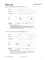
1
Acorn Archimedes 500 series
Acorn R200 series
Service Manual
Copyright © Acorn Computers Limited 1991
Neither the whole nor any part of the information contained in, nor the product described in this manual may be
adapted or reproduced in any material form except with the prior written approval of Acorn Computers Limited.
The products described in this manual, and products for use with it are subject to continuous development and
improvement. All information of a technical nature and particulars of the products and their use (including the
information and particulars in this manual) are given by Acorn Computers Limited in good faith. However, Acorn
Computers Limited cannot accept any liability for any loss or damage arising from the use of any information or
particulars in this manual, or any incorrect .use of the products. All maintenance and service on the products must be
carried out by Acorn Computers' authorised dealers or Approved Service Centres. Acorn Computers Limited can
accept no liability whatsoever for any loss or damage caused by service, maintenance or repair by unauthorised
personnel.
All correspondence should be addressed to:
The Customer Service department
Acorn Computers Limited
Fulbourn Road
Cherry Hinton
Cambridge CB1 4JN
United Kingdom
ACORN, ARCHIMEDES, ARM and ECONET are trademarks of Acorn Computers Limited.
Epson is a trademark of Epson Corporation
Ethernet is a trademark of Xerox Corporation
Keytronic is a trademark of Keytronic Corporation
Olivetti is a trademark of Ing. C. Olivetti & Co.
Panasonic is a trademark of Panasonic U.K.Ltd
IBM is a trademark of International Business Machines Corporation.
Published by Acorn Computers Limited
ISBN 1 85250 093 X
Part number 0486,056
Issue 2, June 1991
Service Manual
Contents
About this manual
vi
Part 1 - System description
1-1
Introduction
General
System timing
1-1
1-1
1-2
The I/O system
The sound system
The keyboard and mouse
Floppy disc drive
Power supply
Hard disc drive
Main PCB Links
Plugs
1-3
1-9
1-10
1-14
1-15
1-15
1-17
1-18
Sockets
Internal expansion
1-18
1-19
Part 2 - Interface cards
2-1
Ethernet interface
Overview
Ethernet I expansion card
Ethernet II expansion card
SCSI interface
2-1
2-1
2-1
2-13
2-18
Part 3 - Disassembly and assembly
Contents
3-1
Introduction
Removing the top cover
Removing the SCSI podule
Removing cables
Removing the backplane
Removing the RAM and ARM cards
Removing the main PCB
Removing the front moulding assembly
Removing the floppy disc drive
3-1
3-1
3-1
3-2
3-2
3-2
3-2
3-2
3-2
Removing the hard disc drive
Removing the power supply unit
Main unit assembly
Keyboard
Mouse
3-2
3-2
3-3
3-3
3-3
Issue 2, June 1991
lll
Service Manual
Part 4 - Fault diagnosis
4-1
Test equipment required
Checking a 'dead' computer
Functional testing
General test procedure
Preparing to run the tests
Creating a CMOS test data file
Completing the tests
Main PCB functional test suite
Individual tests
4-1
4-2
4-4
4-4
4-5
4-6
4-6
4-7
4-15
Part 5 - Main PCB fault diagnosis
5-1
Test equipment you will need
5-1
Integral test software overview
Power-on self-test (POST)
Using the test link
Using the display adapter
Using the external diagnostic interface
Probe SWIs
Repairing a 'dead' computer
5-1
5-1
5-3
5-4
5-9
5-17
5-23
Test ROMs
Repairs following functional testing
5-23
5-27
Keyboard and mouse
Expansion cards
5-28
5-28
Part 6 - Parts lists
iv
6-1
Main PCB assembly parts list
4MB RAM card (optional upgrade)
Backplane adaptor
ARM3 (PGA) Daughter card
Keyboard adaptor PCB (membrane keyboard)
Keyboard adaptor PCB (cont.) (membrane keyboard)
Keyboard assembly (keyswitch keyboard)
Ethernet I
6-1
6-6
6-6
6-7
6-7
6-8
6-8
6-8
Ethernet II
SCSI interface card (issue 2+)
6-9
6-10
Issue 2, June 1991
Contents
Service Manual
Appendix A - Mouse test jig template
A-1
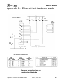
Appendix B - Ethernet test feedback leads
B-1
Appendix C - Serial port Ioopback plug
C-1
Appendix D - Earth continuity testing
D-1
Appendix E - DC insulation testing - class 1
E-1
Drawings
•
•
•
•
•
•
•
•
•
•
Contents
Final assembly drawings
SCSI interface card circuit diagram
Ethernet I expansion card circuit diagram
Ethernet II expansion card circuit diagram
Main PCB circuit diagram
Main PCB assembly drawing
4MB RAM upgrade circuit diagram
Backplane circuit diagram
ARMS (PGA) daughter card circuit diagram
Keyboard adaptor PCB circuit diagram
Issue 2, June 1991
Service Manual
About this manual
This manual is intended as a service manual for the
following models:
• Archimedes 540
• Acorn R260
• Acorn R225
Throughout the remainder of this manual, the generic
term workstation will be used to refer to the above, unless a
reference to a specific model is required.
This manual supplements the basic information given on
system hardware in the installation Guide and Technical
Reference Manual (available for separate purchase).
The operating systems, RISC OS and RISC iX, are
covered at the user level in the RISC OS User Guide and
the RISC iX User Guide, supplied with certain models (
also available for separate purchase). Programmers and
users requiring a greater depth of information about RISC
OS and RISC iX will also need the following manuals:
•
RISC OS Programmer's Reference Manual
(4 volume set)
• RISC iX Programmer's Reference Manual
(2 volume set).
They are available from Acorn authorised dealers. Full
details on the Acorn ARM chip set used in the workstation
are given in the Acorn RISC Machine (ARM) Family Data
Manual, ISBN 0-13-781618-9, available from:
VLSI Technology, Inc.
Application Specific Logic Products Division
8375 South River Parkway
Tempe, AZ 85284
USA
602-752-8574
or from the VLSI national distributor.
Note: This manual describes various PCB assemblies.
The issue of each PCB is as defined by the relevant
schematic.
vi
Issue 2, June 1991
Contents
Service Manual
Part 1 - System description
Introduction
General
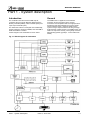
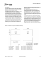
The workstation is built around the ARM chip set,
comprising the Acorn"RISC Machine (ARM) itself, the
Memory Controller (MEMC), Video Controller (VIDC) and
Input Output Controller (IOC).
The ARM3 CPU is a pipelined, 32-bit reduced
instruction set microprocessor which accepts
instructions and manipulates data via a high speed 32bit data bus and 26-bit address bus, giving a 64 MB
uniform address space. it supports virtual memory
systems using a simple instruction set with good highlevel language compiler support. The ARM3 version has
4KB of on-chip cache memory, which greatly increases
data handling speeds (typically 2 - 3 times faster than
ARM2).
The ARM CPU is fitted on a daughter card. Additionally,
memory expansion cards are available, each with 4MB of
RAM and a MEMC controller.
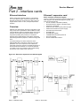
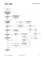
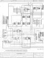
A block diagram of the workstation is shown below:
Fig 1-1: Block diagram of workstation
Part 1 - System description
Issue 2, June 1991
1-1
Service Manual
MEMC acts as the interface between the ARM, VIDC,
IOC, ROM (Read-Only Memory) and DRAM (Dynamic
RAM) devices, providing all the critical system timing
signals, including processor clocks.
Up to 4 MB of DRAM is connected to the 'Master'
MEMC which provides all signals and refresh
operations. A Logical to Physical Translator maps the
Physical Memory into a 32 MB Logical address space (
with three levels of protection) allowing Virtual Memory
and Multi-Tasking operations to be implemented. Fast
page mode DRAM accesses are used to maximise
memory bandwidth. VIDC requests data from the RAM
when required and buffers it in one of three FIFOs
before using it. Data is requested in blocks of four 32-bit
words, allowing efficient use of paged-mode DRAM
without locking the system data bus for long periods.
MEMC supports Direct Memory Access (DMA)
operations with a set of programmable DMA Address
Generators which provide a circular buffer for Video
data, a linear buffer for Cursor data and a double buffer
for Sound data.
IOC controls the I/O bus and expansion cards, and
provides basic functions such as the keyboard interface,
system timers, interrupt masks and control registers. It
supports a number of different peripheral cycles and all
I/O accesses are memory mapped.
VIDC takes video data from memory under DMA
control, serialises it and passes it through a colour lookup palette and converts it to analogue signals for driving
the CRT guns. VIDC also controls all the display timing
parameters and controls the position and pattern of the
cursor sprite. In addition, it incorporates an exponential
Digital to Analogue Converter (DAC) and stereo image
table for the generation of high-quality sound from data
in the DRAM.
VIDC is a highly programmable device, offering a very
wide choice of display formats. The colour look-up
palette which drives the three on-chip DACs is 13 bits
wide, offering a choice from 4096 colours or an external
video source.
The cursor sprite is 32 pixels wide and any number of
rasters high. Three simultaneous colours (again from a
choice of 4096) are supported and any pixel can be
defined as transparent, making possible cursors of
many shapes. It can be positioned anywhere on the
screen. The sound system implemented on the device
can support up to eight channels, each with a separate
stereo position.
Additional memory is provided on daughter cards, in
4MB blocks. Each 4MB block is controlled by a separate
MEMC.
NOTE: MEMCs must be Acorn Part Number 2201,393,
to ensure correct timing parameters.
System timing
Fig 1-2: System timing shows how the various clock
signals are derived for the system.
Fig 1-2: System timing
1-2
Issue 2, June 1991
Part 1 - System description
Service Manual
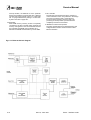
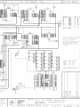
The I/O system
System architecture
The I/O system is controlled by IOC, MEMC and two
PALs. The I/O bus supports all the internal peripherals
and the expansion cards.
The I/O system (which includes expansion card devices)
consists of a 16-bit data bus (BD[0:15]), a buffered
address bus (LA[2:21]), and various control and timing
signals. The I/O data bus is independent of the main 32bit system data bus, being separated from it by
bidirectional latches and buffers. In this way the I/O data
bus can run at much slower speeds than the main
system bus to cater for slower peripheral devices. The
latches between the two buses, and hence the I/O bus
timing, are controlled by the I/O controller, IOC. IOC
caters for four different cycle speeds (slow, medium,
fast and synchronous).
This section is intended to give the reader a general
understanding of the I/O system and should not be used
to program the I/O system directly. The implementation
details are liable to change at any time and only the
published software interfaces should be used to
manipulate the
system. Future systems may have a
different implementation of the I/O system, and in
particular the addresses (and number) of expansion
card locations may move. For this reason, and to ensure
that any device may be plugged into any slot, all driver
code for expansion cards must be relocatable.
References to the direct expansion card addresses
should never be used. It is up to the machine operating
system, in conjunction with the expansion card ID, to
determine the address at which an expansion card
should be accessed. To this extent, some of the
following sections are for background information only.
A typical I/O system is shown in Fig 1-3: The I/O
system. For clarity, the data and address buses are
omitted from this diagram.
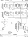
System memory map
The system memory map is defined by master MEMC
and the master PAL, and is shown in Fig 1-4: System
memory map. Note that all system components,
including I/O devices, are memory mapped.
I/O space memory map
This IOC-controlled space has allocation for simple
expansion cards and MEMC expansion cards.
Part 1 - System description
Issue 2, June 1991
1-3
Service Manual
Data bus mapping
Expansion card identification
The mapping of the BD[0:15] bus onto the D[0:31] bus is
as follows:
During a WRITE (ie ARM to peripheral) D[16:31] is
mapped toBD[0:15].
I/O address memory mapping
The I/O data bus is 16 bits wide. Bytewide accesses are
used for 8-bit peripherals. The I/O data bus (BD[0:15])
connects to the main system data bus (D[0:31]) via a set
of bidirectional data latches.
It is important that the system is able to identify what
expansion cards (if any) are present, and where they
are. This is done by reading the Podule (expansion
card) Identification (PI) byte, or bytes, from the Podule
Identification Field.
All I/O accesses are memory mapped. IOC is connected
as detailed in this table:
During a READ (ie peripheral to ARM) BD[0:15] is
mapped to D[0:15].
Byte accesses
Byte instructions are used to access bytewide
expansion cards. A byte store instruction places the
written byte on all four bytes of the word, and so
correctly places the desired value on the lowest byte of
the I/O bus. A byte or word load may be used to read a
bytewide expansion card into the lowest byte of an ARM
register.
Half-word accesses
IOC
ARM
OE
T[1]
T[0]
B[2]
B[1]
B[0]
LA[21]
LA[20]
LA[19]
LA[18]
LA[17]
LA[16]
To access a 16-bit wide expansion card, half-word
instructions are used. When storing, the half-word is
placed on the upper 16 bits, D[16:31]. To maintain
upwards compatibility with future machines, half-word
stores replicate the written data on the lower half-word,
D[0:15]. When reading, the upper 16 bits are undefined.
Fig 1-4: System memory map
1-4
Issue 2, June 1991
Part 1 - System description
Service Manual
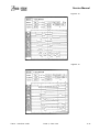
Internal register memory map
Address
Read
Write
3200000H
3200004H
Control
Control
Serial Rx Data
3200008H
-
320000CH
-
-
3200010H
IRQ status A
-
3200014H
IRQ request A
IRQ clear
3200018H
IRQ mask A
IRQ mask A
320001CH
-
-
3200020H
IRO status B
-
3200024H
IRQ request B
-
3200028H
IRQ mask B
IRQ mask B
320002CH
-
-
3200030H
FIQ status
-
3200034H
FIQ request
-
3200038H
FIQ mask
FIQ mask
320003CH
-
-
3200040H
T0 count Low
T0 latch Low
3200044H
T0 count High
T0 latch High
3200048H
-
T0 go command
320004CH
-
T0 latch command
3200050H
T1 count Low
T1 latch Low
3200054H
T1 count High
T1 latch High
3200058H
-
T1 go command
320005CH
-
T1 latch command
3200060H
T2 count Low
T2 latch Low
3200064H
T2 count High
T2 latch High
3200068H
-
T2 go command
320006CH
-
T2 latch command
3200070H
T3 count Low
T3 latch Low
3200074H
T3 count High
T3 latch High
3200078H
320007CH
-
T3 go command
T 3 latch command
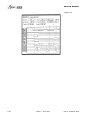
Peripheral address
Cycle
Base
type
Bk address
IC
Use
Serial Tx Data
Fast
1
&3310000
1772
Floppy disc controller
-
Sync
Sync
2
3
&33A0000
&33B0000
6854
6551
Econet controller'
Serial line controller
Slow
Med
4
4
&3240000
&32C0000
Podule 0
Podule 0
Expansion slot
Expansion slot
Fast
Sync
4
4
&3340000
&33C0000
Podule 0
Podule 0
Expansion slot
Expansion slot
Slow
Med
4
4
&3244000
&32C4000
Podule 1
Podule 1
Expansion slot
Expansion slot
Fast
Sync
4
4
&3344000
&33C4000
Podule 1
Podule 1
Expansion slot
Expansion slot
Slow
Med
4
4
&3248000
&32C8000
Podule 2
Podule 2
Expansion slot
Expansion slot
Fast
Sync
4
4
&3348000
&33C8000
Podule 2
Podule 2
Expansion slot
Expansion slot
Slow
Med
4
4
&324C000
&32CC000
Podule 3
Podule 3
Expansion slot
Expansion slot
Fast
Sync
4
4
&334C000
&33CC000
Podule 3
Podule 3
Expansion slot
Expansion slot
Fast
Fast
5
5
&335000
&3350018
LS374
HC574
Printer Data
Latch B (See next
page for details)
Fast
5
&3350040
HC574
Latch A (See next
page for details)
Fast
5
&3350048
HC175
Latch C (See next
page for details)
Fast
6
&3360000
16L8
Podule interrupt
request register
Fast
6
&3360004
16L8
Podule interrupt
mask register
Slow
7
&3270000
Extended external
podule space
*if fitted
Part 1 - System description
Issue 2, June 1991
1-5
Service Manual
I/O programming details
External latch B
External latch A
External Latch B is a write only register shared
between several users who must maintain a
consistent RAM copy. Updates must be made with
IRQ disabled.
External latch A is a write only latch used to control
parts of the floppy disc sub-system:
Bit
0-3
4
Bit
Name
Function
Floppy disc sel.
These bits select the floppy disc
drive 0 through 3 when written
LOW. Only one bit should be LOW
at any one time.
Side select
This controls the side select line of
the floppy disc interface
0 = Side 1 (upper)
Name
0-2
CD[0:2] should be programmed
CD[0.2] LOW for future compatibility.
CD[1] controls the floppy disc data
separator format.
CD[1] = 0 Double Density
CD[1] =1 Single Density
3
FDCR
4
Printer Strobe
1 = Side 0 (lower)
5
Floppy motor
This bit controls the floppy disc
on/off control motor line. Its exact
use depends on the type of drive.
6
In Use
This bit controls the IN USE line of
the floppy disc. Its exact use
depends on the type of drive.
7
Function
This controls the floppy disc
controller reset line. When
programmed LOW, the controller is
RESET.
This is used to indicate valid data on
the printer outputs. It should be set
HIGH when valid data has been
written to the printer port and LOW
after about 5
Not used.
[5:6]
AUX [1:2]
7
HS3
Not used.
Not used.
External latch C
External latch C is a write only register that is used to
control video sync polarity and clock speed.
1-6
Issue 2, June 1991
Part 1 - System description
Service Manual
IRQ status A
Interrupts
The I/O system generates two independent interrupt
requests, IRO and FIQ. Interrupt requests can be caused
by events internal to IOC or by external events on the
interrupt or control port input pins.
The interrupts are controlled by four types of register:
• status
• mask
• request
• clear
The status registers reflect the current state of the various
interrupt sources. The mask registers determine which
sources may generate an interrupt. The request registers
are the logical AND of the status and mask registers and
indicate which sources are generating interrupt requests
to the processor. The clear register allows clearing of
interrupt requests where appropriate. The mask registers
are undefined after power up.
The IRQ events are split into two sets of registers, A and
B. There is no priority encoding of the sources.
Internal Interrupt Events
• Timer interrupts TM[0:1]
• Power-on reset POR
• Keyboard Rx data available SRx
• Keyboard Tx data register empty STx
• Force interrupts 1.
External Interrupt Events
• IRQ active low inputs IL[0:7] wired as (0-7
respectively) PFIQ, SIRQ, SLC1, not used, DCIRQ,
PIRQ, PBSY and RII.
• IRQ falling-edge input IF wired as PACK
• IRQ rising-edge input IR wired as VFLY
• FIQ active high inputs FII[0:1] wired as FFDQ and
FFIQ
• FIQ active low input FL wired as EFIQ
• Control port inputs C[3:5].
Bit
Name
0
PBSY
Function
1
RI
2
Printer Ack
3
Vert Flyback
4
Power-on reset
[5:6]
Timer 0 and
These bits indicate that events have
Timer 1 events
occurred. Note: latched interrupt.
Force
This bit is used to force an IRQ request.
It is usually owned by the FIQ owner
This bit indicates that the printer is
busy.
This bit indicates that a Ringing
Indication has been detected by the
serial line interface.
This bit indicates that a printer
acknowledgement bit has been
received.
This bit indicates that a vertical flyback
has commenced.
7
This bit indicates that a power-on reset
has occurred.
Podule interrupt mask
Podule IRQ can be masked by writing a 0 to the Podule
IRQ mask register at &3360004. This will disable the
interrupt.
The request register at &3360000 is a logical AND of
Podule IRO and the mask register, ie it is1 if Podule IRO
is not masked.
Part 1 - System description
Issue 2, June 1991
1-7
Service Manual
Control port
IRQ status B
Bit
Name
0
Podule FIQ req
Function
This bit indicates that a Podule FIQ
request has been received. It should
usually be masked OFF.
The control register allows the external control pins C[0:5]
to be read and written and the status of the PACK and
VFLY inputs to be inspected. The C[0:5] bits manipulate
the C[0:5] I/O port. When read, they reflect the current
state of these pins. When written LOW the output pin is
driven LOW. These outputs are open-drain, and if
programmed HIGH the pin is undriven and may be
treated as an input.
1
Snd buffr swap
This bit indicates that the MEMC sound
buffer pointer has been relocated.
2
Serial line ctrlr
This bit indicates that 65C51 serial line
controller interrupt has occurred.
On reset all bits in the control register are set to 1.
3
H disc interrupt
This bit indicates that a hard disc
interrupt has occurred.
Bit
Name
Function
4
Disc changed
This bit indicates that the floppy disc
interrupt has been removed.
C[7]
VFLYBK
5
Pod. interr req
This bit indicates that a Podule IRQ
request has occurred.
6
Keyb Tx event
Allows the state of the (VFLYBK)
and Test Mode signal to be inspected.
This bit will be read HIGH during
vertical flyback and LOW during
display. See VIDC datasheet for
details. This bit MUST be
programmed HIGH to select normal
operation of the chip.
7
Keybd Rx event
C[6]
PACK 8 Test
Mode
Allows the state of the parallel printer
acknowledge input to be inspected.
This bit MUST be programmed HIGH
to select normal operation of the chip.
C[5]
SMUTE
This controls the muting of the internal
speaker. It is programmed HIGH to
mute the speaker and LOW to enable
it. The speaker is muted on reset.
This bit indicates that the keyboard
transmit register is empty and may be
reloaded.
This bit indicates that the keyboard
reception register is full and may be
read.
Interrupt status FIQ
Bit
Name
Function
C[4]
0
Floppy disc
This bit indicates that a floppy disc
data request
Data Request has occurred.
C[3]
1
Floppy disc
interrupt request
This bit indicates that a floppy disc
Interrupt Request has occurred.
2
Econet Interrupt
request
This bit indicates that an Econet
Interrupt Request has occurred.
3-5
C[3:5]
See IOC data sheet for details.
6
Podule FIQ req
This bit indicates that a podule
FIQ Request has occurred.
7
Force
This bit allows an FIQ Interrupt
Request to be generated.
1-8
Available on the Auxiliary I/O
connector.
Programmed HIGH, unless Reset
Mask is required.
C[2]
C[1:0]
Issue 2, June 1991
READY
Used as the floppy disc (READY)
input and must be programmed HIGH.
SDA, SCL
The C[0:1] pins are used to implement
the I2C bus the bi-directional serial
I2C bus to which the Real Time Clock
and battery-backed RAM are
connected.
Part 1 - System description
Service Manual
The sound system
MEMC sound system hardware
The sound system is based on the VIDC stereo sound
hardware. External analogue anti-alias filters are used
which are optimised for a 20 kHz sample rate. The high
quality sound output is available from a 3.5mm stereo
jack socket at the rear of the machine which will directly
drive personal stereo headphones or alternatively an
amplifier and speakers. One internal speaker is fitted, to
provide mono audio.
The registers allow the physical addresses for the
START, PNTR (incremental) and END buffer pointers to a
block of data in the lowest half Megabyte of physical RAM
to be accessed.
VIDC sound system hardware
VIDC contains an independent sound channel consisting
of the following components: A four-word FIFO buffers 16
8-bit sound samples with a DMA request issued
whenever the last byte is consumed from the FIFO. The
sample bytes are read out at a constant sample rate
programmed into the 8-bit Audio Frequency Register.
This may be programmed to allow samples to be output
synchronously at any integer value between 3 and 255
microsecond intervals.
The sample data bytes are treated as sign plus 7-bit
logarithmic magnitude and, after exponential digital to
analogue conversion, de-glitching and sign-bit steering,
are output as a current at one of the audio output pins to
be integrated and filtered externally.
VIDC also contains a bank of eight stereo image position
registers each of three bits. These eight registers are
sequenced through at the sample rate with the first
register synchronised to the first byte clocked out of the
FIFO. Every sample time is divided into eight time slots
and the 3-bit image value programmed for each register
is used to pulse width modulate the output amplitude
between the LEFT and RIGHT audio current outputs in
multiples of time slot subdivisions. This allows the signal
to be spatially positioned in one of seven stereo image
positions.
MEMC provides three internal DMA address registers to
support Sound buffer output; these control the DMA
operations performed following Sound DMA ,requests
from VIDC.
These operate as follows: programming a 19-bit address
into the PNTR register sets the physical address from
which sequential DMA reads will occur (in multiples of
four words), and programming the END pointer sets the
last physical address of the buffer. Whenever the PNTR
register increments up to this END value the address
programmed into the START register is automatically
written into the PNTR register for the DMA to continue
with a new sample buffer in memory.
A Sound Buffer Interrupt (SIRQ) signal is generated when
the reload operation occurs which is processed by IOC as a
maskable interrupt (IRQ) source.
MEMC also includes a sound channel enable/disable
signal. Because this enable/disable control signal is not
synchronised to the sound sampling, requests will
normally be disabled after the waveforms which are being
synthesised have been programmed to decay to zero
amplitude; the last value loaded into the Audio data latch
in the VIDC will be output to each of the Stereo image
positions at the current Audio Sample rate.
IOC sound system hardware
IOC provides a programmed output control signal which
is used to turn the internal speaker on or off, as well as an
interrupt enable/status/reset register interface for the
Sound Start Buffer reload signal generated by MEMC.
The internal speaker may be muted by the control line
SMUTE which is driven from the IOC output C5. On reset
this signal will be taken high and the internal speaker will
be muted.
The stereo output to the headphone socket is not muted
by SMUTE and will always reflect the current output of
the DAC channels.
Part 1 - System description
Issue 2, June 1991
1-9
Service Manual
The keyboard and mouse
The keyboard assembly comprises a membrane
keyswitch panel connected to an adaptor PCB, which
serialises the keyboard and mouse data; connection to
the ARM is made via a serial link to the IOC. The ARM
reads and writes to the KART registers in the IOC. The
protocol is essentially half duplex, so in normal operation
the keyboard will not send a second byte until it has
received an Ack. The only exception to this is during the
reset protocol used to synchronise the handshaking,
where each side is expecting specific responses from the
other, and will not respond further until it has these.
In addition to this simple handshaking system, the
keyboard will not send mouse data unless specifically
allowed to, as indicated by Ack Mouse, which allows the
transmission of one set of accumulated mouse
coordinate changes, or the next move made by the
mouse. While it is not allowed to send mouse changes,
the keyboard will buffer mouse changes.
A similar handshake exists on key changes, transmitted
as key up and key down, and enabled by Ack Scan. At the
end of a keyboard packet (two bytes) the operating
system will perform an Ack Scan as there is no protocol
for re-enabling later. Mouse data may be requested later
by means of Request Mouse Position (ROMP).
Key codes
The keyboard identifies each key by its row and column
address in the keyboard matrix. Row and column codes
are appended to the key up or down prefix to form the
complete key code.
For example, 0 key down — the complete row code is
11000010 (&C2) and the column code is 11000111 (
&C7).
Note: Eight keys have N key roll over. The operating
system is responsible for implementing two-key rollover,
therefore the keyboard controller transmits all key
changes (when enabled). The keyboard does not operate
any auto-repeat; only one down code is sent, at the start
of the key down period.
Data protocol
Data transmissions from the keyboard are either one or
two bytes in length. Each byte sent by the keyboard is
individually acknowledged. The keyboard will not
transmit a byte until the previous byte has been
acknowledged, unless it is the HRST (HardReSeT) code
indicating that a power on or user reset occurred or that a
protocol error occurred; see paragraph below.
Reset protocol
The keyboard restarts when it receives an HRST code
from the ARM. To initiate a restart the keyboard sends an
HRST code to the ARM, which will then send back HRST
to command a restart.
The keyboard sends HRST to the ARM if:
• A power-on reset occurs
• A user reset occurs
• A protocol error is detected.
After sending HRST, the keyboard waits for an HRST
code. Any non-HRST code received causes the keyboard
to resend HRST. The pseudo program below illustrates
the reset sequence or protocol.
Note, the on/off state of the LEDs does not change
across a reset event, hence the LED state is not defined
at power on. The ARM is always responsible for selecting
START reset
ONerror Send HRST code to ARM then wait for code from ARM.
IF code = HRST THEN restart ELSE error
ONrestart
clear mouse position counters
set mouse mode to data only in response to an RMPS request.
stop key matrix scanning and set key flags to up send
HRST code to ARM
Wait for next code
IF code = RAK1 THEN send RAK1 to ARM
ELSE
error
Wait for next code
IF code = RAK2 THEN send RAK2 to ARM
ELSE error
Wait for next code
IF code = SMAK THEN mouse mode to send if not zero and enable key scan
ELSE IF code = SACK THEN enable key scanning ELSE IF code = MACK
THEN set mouse mode to send when not zero ELSE IF code = NACK THEN
do nothing
ELSE
error END reset
Reset sequencing
Direction
Code
Expected
reply
Action on
Action on
wrong reply timeout
(Sender)
(Sender)
ARM -> Kb Hard reset Hard reset Resend
Resend
Kb -> ARM Hard reset Reset Ack 1 Resend
Nothing
ARM -> Kb
Reset Ack 1 Reset Ack 1 Hard reset Hard reset
Kb -> ARM Reset Ack 1 Reset Ack 2 Nothing
Nothing
ARM -> Kb
Reset Ack 2 Reset Ack 2 Hard reset Hard reset
1-10
Reset protocol illustration
Action if
unexpected
(Receiver)
Hard
Hard
Hard
Hard
Hard
reset
reset
reset
reset
reset
Issue 2, June 1991
Part 1 - System description
Service Manual
the LED status. After the reset sequence, key scanning
will only be enabled if a scan enable acknowledged (
SACK or SMAK) was received from the ARM.
Data transmission
When enabled for scanning, the keyboard controller
informs the ARM of any new key down or new key up by
sending a two byte code incorporating the key row and
column addresses. The first byte gives the row and is
acknowledged by a byte acknowledge (BACK) code from
the ARM. If BACK was not the acknowledge code then
the error process (ON error) is entered. If the BACK
code was received, the keyboard controller sends the
column information and waits for an acknowledge. If
either a NACK, SACK, MACK or SMAK acknowledge
code is received, the keyboard controller continues by
processing the ACK type and selecting the mouse and
scan modes implied. If the character received as the
second byte acknowledge was not one of
NACK/MACK/SACK/SMAK then the error process is
entered.
Mouse data
Mouse data is sent by the keyboard controller if
requested by a RQMP request from the ARM or if a
SMAK or MACK has enabled transmission of non-zero
values. Two bytes are used for mouse position data.
Byte one encodes the accumulated movement along the
X axis while byte two gives Y axis movement.
Both X and Y counts must be transferred to temporary
registers when data transmission is triggered, so that
accumulation of further mouse movement can occur. The
X and Y counters are cleared upon each transfer to the
transmit holding registers. Therefore, the count values are
relative to the last values sent. The ARM acknowledges
the first byte (Xcount) with a BACK code and the second
byte (Ycount) with any of NACK/MACK/SACK/SMAK. A
protocol failure causes the keyboard controller to enter
the error process (ON error).
When transmission of non-zero mouse data is enabled,
the keyboard controller gives key data transmission
priority over mouse data except when the mouse counter
over/underflows.
Acknowledge codes
There are seven acknowledge codes which may be sent
by the ARM. RAK1 and RAK2 are used during the reset
sequence. BACK is the acknowledge to the first byte of a
2-byte keyboard data set. The four remaining types,
NACK/MACK/SACK and SMAK, acknowledge the final
byte of a data set. NACK disables key scanning and
therefore key up/down data transmission as well as
setting the mouse mode to send data only on RQMP
request. SACK enables key scanning and key data
transmission but disables unsolicited mouse data. MACK
disables key scanning and key data transmission and
enables the transmission of mouse count values if either
X or Y counts are non-zero. SMAK enables key scanning
and both key and mouse data transmission. It combines
the enable function of SACK and MACK.
While key scanning is suspended (after NACK or MACK)
any new key depression is ignored and will not result in a
key down transmission unless the key remains down after
scanning resumes following a SACK or SMAK.
Code values
Mnemonic
msb
Isb
Comments
HRST
RAK1
1111
1111
1111
1110
1-byte command, keyboard reset.
RAK2
1111
1101
1-byte response in reset protocol.
RQPD
0100
xxxx
1-byte from ARM, encodes four bits of data.
PDAT
1110
xxxx
1-byte from keyboard, echoes four data bits of RQPD.
RQID
KBID
KDDA
KUDA
RQMP
0010
10xx
1100
1101
0010
0000
xxxx
xxxx
xxxx
0010
1-byte ARM request for keyboard ID.
1-byte from keyboard encoding keyboard ID.
New key down data. Encoded Row (first byte) and column (second byte) numbers.
Encoded Row (first byte) and column (second byte) numbers for a new key up.
1-byte ARM request for mouse data.
MDAT
Oxxx
xxxx
Encoded mouse count, X (byte1) then Y (byte2). Only from ARM to keyboard.
BACK
0011
1111
Ack for first keyboard data byte pair.
NACK
0011
0000
Last data byte Ack, selects scan/mouse mode.
SACK
0011
0001
Last data byte Ack.
MACK
0011
0010
Last data byte Ack.
SMAK
0011
0011
Last data byte Ack.
LEDS
PRST
0000
0010
0xxx
0001
bit flag to turn LED(s) on/off.
From ARM, 1-byte command, does nothing.
1-byte response in reset protocol.
x is a data bit in the Code; e.g. xxxx is a four bit data field
Part 1 - System description
Issue 2, June 1991
1-11
Service Manual
Similarly, a key release is ignored while scanning is off.
Commands may be received at any time. Therefore,
commands can be interleaved with acknowledge replies
from the ARM, eg keyboard sends KDDA (first byte),
keyboard receives command, keyboard receives BACK,
keyboard sends KDDA (second byte), keyboard receives
command, keyboard receives SMACK. If the HRST
command is received the keyboard immediately enters
the restart sequence. The LEDS and PRST commands
may be acted on immediately. Commands which require
a response are held pending until the current data
protocol is complete. Repeated commands only require a
single response from the keyboard.
ARM commands
Mnemonic
Function
HRST
Reset keyboard.
LEDS
Turns key cap LEDs on/off. A three bit field
indicates which state the LEDs should be in.
Mouse interface
The mouse interface has three switch sense inputs and
two quadrature encoded movement signals for each of
the X axis and Y axis directions. Mouse key operations
are debounced and then reported to the ARM using the
Acorn key up / key down protocol. The mouse keys are
allocated unused row and column codes within the main
key matrix.
Switch 1 (left)
Switch 2 (middle)
Switch 3 (right)
Row code - 7
Row code - 7
Row code - 7
Column code - 0
Column code - 1
Column code - 2
For example, switch 1 release would give 11010111 (&D7)
as the complete row code, followed by 11010000 (&D0)
for the column code.
Note: Mouse keys are disabled by NACK and MACK
acknowledge codes, and are only enabled by SACK and
SMAK codes, ie they behave in the same way as the
keyboard keys.
Logic 1 is ON, logic 0 (zero) OFF
The mouse is powered from the computer 5V supply and
may consume up to 100mA.
DO controls CAPS LOCK
D1 controls NUM LOCK
D2 controls SCROLL LOCK
Movement signals
RQM
RQID
Request mouse position (X,Y counts).
PRST
Reserved for future use, the keyboard
controller currently ignores this command.
Each axis of movement is independently encoded in two
quadrature signals. The two signals are labelled
REFerence and DIRection (eg X REF and X DIR). The
table below defines the absolute direction of movement.
Circuitry in the keyboard decodes the quadrature signals
and maintains a signed 7-bit count for each axis of mouse
movement.
RQPD
For future use. The keyboard controller will
encode the four data bits into the PDAT code
data field and then send PDAT to the ARM.
Request keyboard identification code. The
computer is manufactured with a 6-bit code to
identify the keyboard type to the ARM. Upon
receipt of RQID the keyboard controller
transmits KBID to the ARM.
Initial
state
REF
DIR
Next
state
REF DIR
1
1
0
0
1
0
0
1
1
0
0
1
0
0
1
1
Increase count by one
for each change of state.
1
0
0
1
1
1
0
0
0
0
1
1
1
0
0
1
Decrease count by one
for each change of state.
When count overflow or underflow occurs on either axis
both X and Y axis counts lock and ignore further mouse
movement until the current data has been sent to the
ARM.
Overflow occurs when a counter holds its maximum
positive count (0111111 binary). Underflow occurs when
a counter holds its maximum negative count (1000000
binary).
1-12
issue 2, June 1991
Part 1 - System description
Service Manual
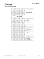
Base Keyswitch mapping (UK 103 key
keyboard)
name
Row
code
Col.
code
1.5
1
Tab
Q
2
2
6
7
1
W
2
8
1
E
2
9
1
R
2
A
Key
size
Key
Notes
Key
Key
size
name
Row
code
Col.
code
Notes
1
1
Esc
F1
0
0
0
1
1
2
1
F2
0
2
2
1
F3
0
3
2
1
F4
0
4
2
1
T
2
B
1
F5
0
5
2
1
Y
2
C
1
F6
0
6
2
1
U
2
D
1
F7
0
7
2
1
I
2
E
1
F8
0
8
2
1
0
2
F
1
F9
0
9
2
1
P
3
0
2
1
[{
3
1
1
]}
3
2
1.5
\
3
3
1
Delete
3
4
1
1
Copy
3
5
1
1
Pgdwn
3
6
1
1
7
3
7
1
8
3
8
1
1
9
-
3
3
9
A
1
1.75
1
Ctrl
A
3
3
B
1,3
1
S
3
D
1
D
3
E
1
F
3
F
1
G
4
0
1
H
4
1
1
J
4
2
1
F10
0
A
1
F11
0
B
2
1
F12
0
C
2
1
Print
0
D
1,3
1
1
Scroll
Break
0
0
E
F
1
1
1
1
1
1
1
0
1
1
2
1
2
1
3
1
3
C
1
4
1
4
1
5
1
5
1
6
1
6
1
7
1
7
1
8
1
8
1
9
1
9
1
0
1
A
1
K
4
3
1
-_
1
B
1
L
4
4
1
=+
1
C
4
5
1
£a
1
D
1
;:
,"
4
6
E
1
2.25
Return
4
7
4
4
8
1
Backspc
1
1
Insert
1
F
1
1
1
Home
2
0
1,3
1
5
4
9
1
Pgup
2
1
1
1
Numlock
2
2
1,4
1
1
6
+
4
4
A
B
1
/
2
3
1
1
*
2
4
1
1
#
2
5
1
Part 1 - System description
1
1
1
Row and column codes are in hexadecimal.
Key colour - dark grey.
Notes:
1
2
Key colour - dark grey.
3
Key position with N key rollover.
4
Green LED under key cap.
Issue 2, June 1991
1-13
Service Manual
Floppy disc drive
Keyswitch mapping (cont.)
Key
Name
Row
code
Col.
code
Notes
Size
2.25
1
1
1
1
1
1
1
1
1
1
2.75
1
1
1
1
shift
Z
X
C
V
B
N
M
,<
.>
/
shift
crsrUp
1
2
3
4
4
4
5
5
5
5
5
5
5
5
5
5
5
5
5
C
E
F
0
1
2
3
4
5
6
7
8
9
A
B
C
1,3
1.5
1.5
7.0
1.5
1.5
1
1
1
2.0
1
Caps
Alt
Space
Alt
Ctrl
crsrLt
crsrDn
crsrRt
0
.
Enter
5
5
5
6
6
6
6
6
6
6
6
D
E
F
0
1
2
3
4
5
6
7
1,4
1,3
Key
2.0
The floppy disc drive used on the workstations (except
discless) is a one-inch high drive, taking 3.5 inch doublesided double-density floppy discs.
Performance
Capacity
1 MB (unformatted)
Track to track step rate
3ms
15ms
1200µs
Seek settle time
Write to read timing
Power-on to drive ready
+5Vdc (+/– 5%)
Maximum power
2 Watts (continuous)
1,3
1
Power connector
The power connector is a 4-pin, 2.5mm pitch type.
1,3
1,3
1
1
1
Pin
Signal
1
2
+5V
0V
3
4
0V
+12V
Interface connector
1
The interface connector is a 34-way, 2 row, 0.1 inch pitch
type, with pinouts as shown below:
Pin
Row and column codes are in hexadecimal.
1
Key colour - dark grey.
Notes:
2
Key colour - dark grey.
3
Key position with N key rollover.
4
Green LED under key cap.
Retn
1
3
5*
7*
9*
11*
13
15
17
19
21
23
25
27
29
31
33
Issue 2, June 1991
Dir
Signal
main (PCB)
Signal
2
4
6
8
10
12
14
16
18
20
22
24
26
28
30
32
34
*Optionally +5V
1-14
1000ms
Power supply
Disc change
In use
Drive select 3
Index
Drive select 0
Drive select 1
Drive select 2
Motor ON
Direction
Step/Disc chg rst
Write data
Write gate
Track 0
Write protect
Read data
Side 1 select
Ready
I = Input
I
I
0
I
0
0
0
0
0
0
0
0
I
I
I
0
I
0 = Output
Part 1 - System description
Service Manual
Power supply
Hard disc drive
Performance characteristics
Performance
Min
Nom
Max
Units
Input voltage (47-53 Hz)
198
220/
240
264
Vac
*Input voltage (57-63 Hz)
98
110
132
Vac
Output voltage VO1
4.9
5
5.1
Vdc
Output current 101
1.5
-
12.2
Amps dc
50
mV pk-pk
Output ripple and noise VO1
BW 0-20MHz
Overshoot VO1
0.1
Vdc
7.0
Vdc
14.5
Amps dc
1.0
Sec
11.4 12
12.6
Vdc
0
3.2
Amps dc
Output ripple and noise V02
100
mV pk-pk
Overshoot VO2
0.2
Vdc
-
4
Amps dc
Overvoltage prot VO1 (thrshld)
5.8
Surge output current 101
-
Surge output current duration
-
Output voltage VO2
Output current 102
-
The hard disc drive used on the workstations (except
discless) is an internally-fitted SCSI device. For more
information on the types of SCSI drive usable, see the
SCSI Expansion Card User Guide.
Case colour specification
The colour of the cream plastic mouldings, the main case
and the back panels which are painted, is Pearl White
RAL 1013C.
The colour of the light grey front sub-moulding and the
light grey keyboard keycaps is Pantone warm grey 3.
The colour of the darker grey keytops is Pantone warm
grey 6.
BW 0-20 MHz
Surge output current 102
Surge output current duration
-
-
10.0
Sec
Output voltage VO3
-4.5
-5
-5.5
Vdc
Output current 103
0
-
0.3
Amps dc
Output ripple and noise V03
50
mV pk-pk
Overshoot VO3
Efficiency
Vdc
63
0.1
-
Total output power
-
100
122
Watts cont.
Watts srge
BW 0-20MHz
-
%@max Id,
nominal I/P volt
'Manufacturing option
DANGER
THE POWER SUPPLY IS A SEPARATE
REPLACEABLE MODULE, AND CONTAINS NO USER
SERVICEABLE PARTS.
ALL ACORN POWER SUPPLIES CONTAIN
HAZARDOUS VOLTAGES AND MUST NOT BE
MODIFIED OR REPAIRED.
POWER SUPPLY UNITS MAY ONLY BE FITTED BY
AN AUTHORISED ACORN SERVICE CENTRE.
SAFETY EARTH CONTINUITY TESTING MUST BE
CARRIED OUT WHEN ANY POWER SUPPLY IS
FITTED.
Part 1 - System description
Issue 2, June 1991
1-15
Service Manual
1-16
Issue 2, June 1991
Part 1 - System description
Service Manual
Main PCB Links
Part 1 - System description
Issue 2, June 1991
1-17
Service Manual
Plugs
1-18
Sockets
Issue 2, June 1991
Part 1 - System description
Service Manual
Internal expansion
Sockets (cont.)
Skt
Fitted
SK11 Yes
SK12 Yes
SK13 Yes
Interface
Function/Specification
6-way mini-DIN socket providing the
connection point for the keyboard. If required,
a standard Archimedes keyboard may be
plugged into this socket.
High resolution mono video output.
Provides a 0.7V mono video signal (into 75
Ohm) at a dot rate of 96MHz. This requires a
High resolution monitor to be connected.
High resolution mono vertical sync.
Provides composite/vertical synchronisation
pulses for the high resolution mono output.
SK14 Yes
High resolution mono horizontal sync.
Provides horizontal synchronisation pulses for
the high resolution mono output.
Introduction
The computer supports an expansion card (podule)
interface. The maximum power available per slot can be
calculated from the following:
• The +5V supply rail is rated at a maximum of 1A
• The +12V supply rail is rated at a maximum of 250mA
• The -5V supply rail is rated at a maximum of 50mA
Refer to the application note 'A Series Podules' for a full
podule interface specification, available on request from
Acorn Computers.
Pin a
c
Description
1
2
3
4
5
6
0V
LA[15]
LA[14]
LA[13]
LA[12]
LA[11]
0V
—5V
0V
0V
reserved
MS[0]*
Ground
7
8
9
10
11
12
13
14
15
16
17
18
19
20
21
LA[10]
LA[9]
LA[8]
LA[7]
LA[6]
LA[5]
LA[4]
LA[3]
LA[2]
BD[15]
BD[14]
BD[13]
BD[12]
BD[11]
BD[10]
reserved
reserved
reserved
reserved
reserved
RST*
PR/W*
PWE*
PRE*
PIRQ*
PFIQ*
S[6]*
C1
C0
S[7]*
22
23
24
BD[9]
BD[8]
BD[7]
PS[0]*
IOGT*
IORQ*
Simple Podule select
MEMC Podule handshake
MEMC Podule request
25
BD[6]
BL*
I/O data latch control
26
27
28
BD[5]
BD[4]
BD[3]
0V
CLK2
CLK8
Supply
2MHz Synchronous clock
8MHz Synchronous clock
29
BD[2]
REF8M
8MHz Reference clock
30
31
BD[1]
BD[0]
Supply
32
+5V
+5V
reserved
+12V
Ground
Ground
MEMC Podule select
Reset (see note below)
Read/not write
Write strobe
Read strobe
Normal interrupt
Fast interrupt
12C serial bus clock
12C serial bus data
External Podule select
Note: The RST* signal is the system reset signal, driven by
IOC on power up or by the keyboard reset switch. It is an
open-collector signal, and expansion cards may drive it also
if this is desirable. The pulse width should be at least 50ms.
Part 1 - System description
Issue 2, June 1991
1-19
Service Manual
1-20
Issue 2, June 1991
Part 1 - System description
Service Manual
Part 2 - Interface cards
Ethernet interface
Ethernet I expansion card
Where an Ethernet interface is fitted, it is provided by
one of two different types of Ethernet expansion card,
identified as Ethernet I and Ethernet II. Both cards can
support either a Thick' or 'thin' (Cheapernet) Ethernet
interface.
Figure 2-1: Ethernet I expansion card block diagram is a
block diagram of the Ethernet/Cheapernet podule. The
main functional blocks are:
•
the net controller: Intel 82586 (LANCE)
•
the serial interface adaptor: Intel 82501 (SIA)
•
transceiver: Intel 82502
•
attachment unit interface (AUI) socket (D-type)
•
isolation transformers and power supply
•
bus buffers and transceivers
Overview
Ethernet was developed by the Xerox Corporation in the
early 1970s and a specification made available in 1980.
This specification known as the 'Blue Book' was used as
the basis for the IEEE and ECMA standards. All new
equipment (including this product) is or should be
designed to the IEEE standard. This allows networking
with existing Ethernet equipment, at least at the physical
level.
Basic operation and block diagram
•
•
•
•
•
the RAM buffer
the RAM page register
a PROM based 'extended' podule ID
the control register
the PAL based state machine.
An understanding of the basic architecture of the
Ethernet/IEEE 802.3 standard is assumed. The Intel
publication The LAN Components User's Manual is
particularly useful and contains a suitable introduction to
local area network standards. It is recommended that
you obtain a copy if you require a wider understanding,
as reference to it is made in this document.
Figure 2-1: Ethernet I expansion card block diagram
Part 2 - Interface cards
Issue 2, June 1991
2-1
Service Manual
The Intel chip set
As the Xerox and IEEE standards have become widely
accepted, a number of systems companies have produced
VLSI devices that considerably reduce the design effort
required to implement a connection. The most notable of
these are by Advanced Micro Devices (AMD) and Intel.
The Intel chip set comprising the 82586 local area network
coprocessor, the 82501 Ethernet serial interface, and the
82502 Ethernet transceiver chip has been used in this
design.
The 82586 and other similar local area network controllers
are generally referred to by the acronym LANCE, even
though this is a trademark of AMD.
The 82586 LANCE performs media access control,
framing, pre/postamble generation and stripping, source
address generation, CRC checking, and short packet
detection. In addition diagnostic functions such as Time
Domain Reflectometry (TDR) can be performed.
The 82501 serial interface adapter (SIA) performs
Manchester encoding/decoding, receives clock recovery
and directly drives the attachment unit interface (AU I) to
the cable mounted Ethernet transceiver. In addition the
82501 operates a watchdog to prevent continuous
transmission (a fault condition), and provides a loop-back
test facility. A second source for this device is SEEQ who
manufacturer a similar part, the DQ8023A. This part
however is not identical and will not perform TDR
correctly.
The 82502 transceiver applies transmit data to, and
removes receive data from the Cheapernet cable
interface. This devices performs a similar function to the
cable mounted Ethernet transceiver.
The dual port memory
The control register
The control register contains four bits:
Reset (RST) Bit 0.
This bit controls the RESET pin on the LANCE. This bit
is set (LANCE reset) on system power-up/hard reset or
writing to the control register with this bit logic 1. This bit
is cleared (and the LANCE released from the reset state)
by writing to the control register with this bit logic 0.
Loop-Back (LB) Bit 1
This bit selects the loop-back mode of 82501 SAI chip.
This bit is set and the SIA chip put into loop-back mode
by the ARM writing to the control register with this bit
logic 1. This bit is cleared (SIA taken out of loop-back
mode) on system power-up/hard reset or writing to the
control register with this bit logic 0.
Channel Attention (CA) Bit 2
This bit generates a correctly timed CA pulse when the
ARM writes to the control register with this bit logic 1. No
CA pulse is generated if the ARM writes to the control
register with this bit logic 0.
Clear Interrupt (CLI) Bit 3
This bit clears the podule interrupt flag and removes the
podule interrupt when the ARM writes to the control
register with this bit logic 1. The podule interrupt and flag
are unaffected if the ARM writes to the control register
with this bit logic 0.
Each bit in the control register is not independent and
when writing to a particular bit, the remaining three must
be valid. The remaining 12 bits are ignored by the
hardware (zero is recommended).
Podule identification PROM
The podule identification PROM contains the following
information:
The LANCE is a true coprocessor and is designed to
perform scatter-gather DMA. In common with other
LANCE chips the 82586 will utilise a significant bus
bandwidth when operating on a net running at 10 Mbps (
note: this is not simply the serial data rate divided by the
parallel bus width). This bandwidth cannot be provided by
the ARM processor over the podule bus and so a dual-port
memory system has been implemented.
•
•
•
All communication between the ARM and the LANCE is
carried out through command blocks in the dual-port RAM
(there are no visible registers in the 82586 LANCE). These
command blocks and associated data structures are
defined and described in Intel's data sheet.
Detailed description
To issue a command to the LANCE the ARM appends the
command to the command block list (CBL) in the dual-port
RAM. It then raises the channel attention (CA) signal to
the LANCE signalling the presence of the new command.
The LANCE responds to CA by reading the command
from the CBL and executing as required.
the Acorn podule identity number (03)
the interrupt (IRQ) flag bit
the PCB revision number
• the six byte IEEE globally assigned address block
•
a CRC to allow the PROM to be validated. The
contents and operation of the interrupt flag are
described in Interrupts in Detailed description below.
Address map
The Ethernet I expansion card address map (offset
relative to slot base) is shown in Table 2-1: Ethernet I
expansion card address map. The RAM buffer occupies
the upper half of the podule address space. The ID
PROM, page register and control register occupy the
lower half.
The LAN Components User's Manual contains a
considerably more detailed and comprehensive
description of the operation of the LANCE.
2-2
Issue 2, June 1991
Part 2 - Interface cards
Service Manual
The LANCE
The 82586 LANCE is a 'scatter-gather' DMA controller
type device and is designed to interface to 80186 type
processors using a HOLD/HOLDA protocol to resolve
arbitration for access to shared memory.
The ARM podule bus cannot easily support a
HOLD/HOLDA type interface. This is because the ARM
is a dynamic device and cannot be stopped for the
required time. (This can be longer than 10µs during the
interframe/interpacket spacing time.) The ARM cannot
be given priority and HOLDA de-asserted because this
will result in the net controller failing to meet the timing
requirements of the net protocol due to the increased
bus latency. For example, this could result in the failure
of the net controller to take part in the back-off and retry
sequence following a collision on a heavily loaded net.
In this design HOLD and HOLDA are wired together and
ARM cycles cause wait-states to be inserted into the
LANCE bus cycle. This is achieved by removing the
READY signal to the LANCE while the ARM is active.
Adopting this scheme avoids the problems outlined
above. The ARM is never stopped and the LANCE sees
minimal bus latency.
The LANCE ARDY/SRDY input used can be
programmed to be either asynchronous/ ARDY and
internally synchronised, or synchronous/SRDY and
externally synchronised. In this case it is SRDY mode
that must be selected. This is achieved by issuing a
configure command with the ARDY/SRDY bit set to logic
1. This is important as the LANCE powers-up in ARDY
mode.
In certain circumstances the LANCE needs to perform
read-modify-write bus cycles with lockout. Using READY
to insert wait-states does not allow this. However lockout
is only required when the LANCE updates error counts (
statistics) and even then a problem only arises when a
count overflows and the ARM resets it to zero while the
LANCE is in the modify phase of a read-modify-write
cycle. This is solved by the ARM reading back the count
after it sets it to zero. If the count is still indicting an
overflow then a read modify-write cycle was in progress
Table 2-1: Ethernet I expansion card address map
ID PROM (Base)
= Slot base
(Type 3 access) + 0x0000 (Read only)
Page Register
= Slot base
(Type 2 access) + 0x0000 (Write only)
Control Register
Dual-Port RAM
= Slot base
= Slot base
(Type 2 access) + 0x0004 (Write only)
(Type 2 access) + 0x2000 (Read/write)
Part 2 - Interface cards
Issue 2, June 1991
2-3
Service Manual
and the ARM has to correct the count. Error counts this
high indicate a major problem that will require correction
so should be a rare event.
The memory bus of the LANCE is operated in 'minimum
mode' as the timing parameters for LANCE outputs in
this mode are subject to less spread between devices.
The pull-up resistors on WR*, RD*, and BHE are
required to prevent RAM cycles when the LANCE is
inactive.
The LANCE communicates directly with the SIA (IC24)
via a serial channel comprising seven signals: TXC,
TXD, RXC, RXD, RTS, CRS and CDT. The function of
each of these is described in the LANCE data sheet. The
Clearto-Send (CTS*) input is not supported by the SIA
and is connected to 0V (enabled).
Dual port RAM
The podule bus provides only a limited space in the
address map (8 KB) for each podule. This is insufficient
and so a paged scheme has been implemented.
Viewed from the ARM side the RAMs are paged into the
top half of podule space by a 'page register'. The four bit
page register is split across two PALs (see the section
entitled The PALs). Sixteen pages each of 4 KB provide
64 KB in total. This is organised as 32 k x 16 bits (two 32
k x 8 static RAMs). An alternative RAM size of 8 k x 16
bits (two 8 k x 8 static RAMs) can be supported (see the
section entitled Links on page 2-12).
The podule address bus (LA2-13) is buffered by two
HCT244 (IC66 and IC58) and the podule data bus (BD0BD15) is buffered by and two HCT245 transceivers (
IC15 and IC54). The direction of the data bus
transceivers is determined by the podule R/W signal,
while both output enables (AAOE and BDOE) are
generated by the bus control PAL (IC36).
Viewed from the net controller side, the RAM will be
contiguous from location 0x0000 to 0xFFFF. The
initialisation root for the controller is 0x0FFFFF6 which is
mapped into the RAM at 0xFFF6. The high order
address bits are not decoded.
The LANCE address/data bus (AD0-AD15) is
demultiplexed by two HCT245 (IC17 and IC22) which
use the LANCE ALE signal to latch the address bus. The
data bus only requires buffers and two HCT573
transceivers (IC10 and IC32) are used. The direction of
the data bus transceivers is determined by the LANCE
DT/R signal, while the output enables are generated by
the bus control PAL (IC36).
The LANCE is capable of operating on an eight bit bus
and is reset to this mode. The LANCE initialisation root (
read when released from reset) contains a bit that
defines the bus width and this must be set to 0 (=16 bit
bus). Until the LANCE reads this it deasserts Byte High
Enable (BHE*) and outputs address bits on AD8-AD15
for the entire cycle. To avoid a bus clash BHE* is used to
disable the high order data bus transceiver via the bus
control PAL (IC36).
2-4
Once initialised to a byte wide bus the LANCE only
operates on half words (never bytes) so it not necessary
to decode the least significant address bit (ADO) to
produce separate write strobes for each byte.
Podule Identification PROM
The device used is a 32 byte PROM 27LS19 (IC14).
Typical content of an ID PROM is shown in Table 2
overleaf.
The ID PROM shares address and data bus buffers with
the RAM. Viewed from the ARM side the ID PROM is
byte wide and word aligned.
The podule specification defines two bits in the ID byte to
be interrupt flags. This design requires only IRQ
interrupts so the FIQ flag is always zero. The IRQ flag is
generated by connecting the podule interrupt signal to
the most significant address pin. The content of the
upper half is similar to the lower half but has the IRQ flag
bit set, in this way the interrupt flag is multiplexed 'into'
the ID byte.
Bytes 09 - 0E are the six byte Ethernet address unique
across all Ethernet equipment from manufacturers
worldwide.
The CRC (Bytes 1C - 1F) is calculated on the rest of the
PROM (Bytes 00 - 1B) using a 32 bit Autodin - II CRC
polynomial. This is the same algorithm as the LANCE
uses to perform multicast address filtering (see the
section entitled PROM CRC calculation on page 2-12).
Since each PROM is unique the CRC is used to perform
verification.
The output enable is generated by the bus control PAL (
IC36).
The PALs
Three PALs are used in this design:
•
the main state PAL (IC29)
•
the interrupt and channel attention PAL (IC78)
•
the device enable control PAL (IC36).
The main state PAL (IC29)
This PAL implements a state machine which provides
timing information for the other two PALS in the design.
In addition it produces the two least significant bits of
both the page register (PRO and PR1) and control
register (RSTO and LOOP).
The interrupt and channel attention PAL (IC78)
This PAL implements the two most significant bits of
both the page register (PR2 and PR3) and control
register (CLI and CA).
The device enable control PAL (IC36).
This device decodes the address map to provide various
device output enables.
Issue 2, June 1991
Part 2 - Interface cards
Service Manual
Table 2-2: Podule identity PROM
Part 2 - Interface cards
Issue 2, June 1991
2-5
Service Manual
The state machine and operation
The state machine has four states; IDLE, SA1, SA2, and
SA3 and is clocked from state to state on the falling edge
of CLK8, the 8 MHz podule bus clock. See Figure 2-2:
State diagram.
The idle state
The state machine enters this state on power-up, hard
reset (RST* low), or from the SA3 state. In this state the
bus buffers on the ARM side of the dual-ported RAM are
disabled and those on the LANCE side enabled. Other
outputs such as the page and control register bits remain
unchanged. The state machine remains in the idle state
until the ARM starts an access (podule select - PS
active).
The SA1 state
This state is entered from the idle state only. In this state
the LANCE READY signal is disabled, forcing the
LANCE to insert wait states if it is active on the bus. The
RAM write strobe (RAMWE*) is disabled to prevent
writes while the LANCE side of the dual-port RAM is
disabled and the ARM side enabled. The state machine
exits to the SA2 state unless a reset occurs.
The SA2 state
This state is entered from the SA1 state only. In this
state the ARM access is performed and the
corresponding device enables are active eg, if a RAM
write is performed then the RAM write strobe (RAMWE*)
is active. Similarly if a RAM or ID read is required than
the RAM or IDOE is active. Writes to the page register or
control bits are also
performed during this state. READY is still inactive. The
state machine exits to the SA3 state unless a reset
occurs.
The SA3 state
This state is entered from the SA2 state only. The RAM
write strobe (RAMWE*) is disabled to prevent writes
while the LANCE side of the dual-port RAM is enabled
and the ARM side disabled. The state machine exits to
the idle state where any LANCE access that was in
progress is completed.
Podule bus cycles
The podule specification requires all ID PROM access to
be made using type 3 (sync) IOC bus cycles. All other
accesses to the Ethernet podule must be made using
type 2 (fast) IOC cycles.
Figure 2-3: Typical podule bus cycle illustrates a
read/write to RAM while the net controller is active. The
cycle starts with podule select (PS) active and puts the
state machine into the SA1 state on the next clock edge.
A description of each state that follows is given above.
It should be noted that Ready is always deasserted for
three cycles, even if the LANCE is idle. A podule bus
access can 'collide' with a LANCE access in five different
ways, depending on what state the LANCE is in when
the podule bus access starts. These are: PS* while the
lance is in states T1 to T4 or idle. The actual number of
wait states that the LANCE will insert depends on which
of these cases apply. Figures 2-4, 2-5, 2-6 and 2-7
illustrate the possible cases.
Figure 2-2: State diagram
2-6
Issue 2, June 1991
Part 2 - Interface cards
Service Manual
Figure 2-3: Typical podule bus cycle
Part 2 - Interface cards
Issue 2, June 1991
2-7
Service Manual
Figure 2-4: Access collision cases PS* while LANCE is in T1
PS* while the LANCE is in T1
The LANCE samples READY deasserted at the end of T2 (SA2), and then
again at the end of TW1 (SA3), so in this case two wait states are inserted.
Figure 2-5: Access collision cases PS* while LANCE is in T2
PS* while the LANCE is in T2
The LANCE samples READY deasserted at the end of T2 (SA1), TW1 (SA2),
TW2 (SA3), so the maximum of three wait states are inserted.
2-8
Issue 2, June 1991
Part 2 - Interface cards
Service Manual
Figure 2-6: Access collision cases PS* while LANCE is in T3
PS* while the LANCE is in T3
In this case READY is still active when the LANCE samples it at the end of T3 (
idle). This is the last time that the LANCE does this for the current cycle so the
LANCE cycle completes before the podule bus cycle starts. Note that the
LANCE is not active on the RAM bus during T4.
Figure 2-7: Access collision cases PS* while LANCE is in T4
PS* while the LANCE is in T4
Since the LANCE does not require the bus during T4 no further wait states are
inserted in the current cycle. However T1 of the next cycle could follow T4 and
one wait state will be inserted into this LANCE access.
Part 2 - Interface cards
Issue 2, June 1991
2-9
Service Manual
PS* while the LANCE is idle
If the LANCE remains idle while the podule bus cycle
occurs then there is no collision and the LANCE ignores
the READY signal. This case is not illustrated.
A read from the podule ID PROM or write to the control
or page register is similar to a RAM cycle. To simplify
the bus design the LANCE is removed from the RAM
buses during cycles to these devices.
Bus design note
The cycle stealing scheme should guarantee that the
LANCE never has insufficient bus bandwidth or sees
excessive bus latency to the extent that it cannot service
the net or fails to meet the IEEE timings. Even when the
ARM continuously accesses the RAM. The following
gives the reasoning behind this statement: Assumptions:
Net Clock
Bus Clock
LANCE FIFO size
HOLDA is wired to HOLD so:
Bus Latency
IEEE Interframe Space Time = 9.6 µS
Criteria:
10 MHz
8 MHz
16 bytes
0 cycles
1 FIFO must not over/underrun.
FIFO fill/empty time from serial side:
= 8 (bits)* 16 (bytes) " 100E-9 (bit time) =
12.8 µs
FIFO empty/fill time from parallel side:
= 8 (Word transfers)
* (4 (standard 8 MHz cycles) + Nwait (wait
cycles))
* 125E-9
= 4 µs (if Nwait = 0)
= 7 µs (if Nwait = 3)
= 8 µs (if Nwait = 4)
2 The LANCE must be in a position to transmit by the
end of the interframe spacing time.
With a Fp/Fs ratio of 8 MHz/10 MHz (0.8):
16*Nwait + Nlatency must be less than or equal
to 80.
If HOLDA = HOLD then Nlatency 0
and
Nwait <= 5
So this strategy works if we can keep the number of wait
states (Nwait) less than or equal to five per access. In
the current design three are used and this is unlikely to
change.
Interrupts
The podule interrupt (PIRQ) is level triggered. However,
the interrupt signal (INT) from the LANCE is designed
for use with edge triggered interrupt controllers. If the
net controller detects a second interrupting condition just
after the first is raised, it will drop and reassert INT. The
situation could arise where the podule manager (
software) may scan the slots and find no IRQ flag set.
The above problem is prevented by latching INT in the
interrupt and channel attention PAL (IC78) and using the
latched signal INTO to generate the flag. The clear
interrupt (CLI) bit in the control register is used to clear
the latch.
Latching INT introduces another problem, which is
eliminated by a feature of the 82586 LANCE. If a second
interrupt occurs after the processor has read the status
word in the SCB, but before the first is cleared, then the
second interrupt would be missed. However, if the
interrupt is cleared at the same time as the channel
attention (signalling the acknowledge command) is
issued, the LANCE will respond by deasserting INT and
reasserting if the second interrupt was not
acknowledged because it was missed. It is
recommended to set CA whenever CLI is set.
Figure 2-8: Example interrupt cycles
2-10
Issue 2, June 1991
Part 2 - Interface cards
Service Manual
Figure 2-9: State diagram for INTO/PIRQ*
Figure 2-10: State diagram for INTEN*
Part 2 - Interface cards
Issue 2, June 1991
2-11
Service Manual
Links
The Ethernet I PCB should be viewed from the
component side with the 96 way podule bus connector on
the left and the rear panel on the right. When viewed like
this, west is to the left, east the right, north the top and
south the bottom.
LK1 and LK2 select the RAM size
If 32 KB devices are fitted (normally) the links should both
be south. 8 KB devices will not normally be fitted but in
this case LK1 and LK2 should be north.
LK3 to LK8 select Ethernet or Cheapernet.
For Ethernet operation the links should be west (link pin a
to pin b). For Cheapernet operation the links should be
east (link pin b to pin c).
LK9 is tracked south and not fitted on production
units.
See data sheets for the 82502 for use.
PROM CRC calculation
The following is a code fragment in the C programming
language that calculates and validates the Ethernet
PROM checksum.
/* To calculate and check the PROM checksum */
int ROM_chk(vector)
/* array 0..32 bytes*/
u_char vector[32];
{ register int i,j;
register unsigned chk = -1;
/* Set the CRC register*/
/* to FFFFFFFF*/
r e g i s t e r u n s i g n e d b y t e ; /* temp
for (i = 0; i < 28; i++) {
/* CRC on bytes 0..28*/
byte = vector[i];
for (j = 0; j < 8; j++) {
if (((byte & 1) ^ (chk » 31)) != 0)
/* IF feedback = 1*/
/*
chk = (chk << 1) ^ (0x04C11DB7);
else
shift and FOR taps*/
/* ELSE
chk = (chk << 1);
/*
just shift*/
b y t e = b y t e > > 1 ; /* next bit*/
/* chk is now the calculated CRC */
/* Now get CRC from PROM */
byte = (vector[31] << 24) | (vector[30] << 16) | (vector[29] << 8) |
(vector[28] << 0);
/* Test to see if the same */
if (byte != chk) return (FALSE); /* checksum error*/
else return (TRUE);
2-12
Issue 2, June 1991
Part 2 - Interface cards
Service Manual
Ethernet II expansion card
The IEEE 803.2 standard supports two different
versions for the media:
• 10BASE5 (commonly known as Ethernet)
• 10BASE2 (thin-wire Ethernet, or 'Cheapernet'). These
can be used-separately, or together in a hybrid form.
Both versions have similar electrical specifications and
can be implemented using the same transceiver chip.
Thin-wire Ethernet is the lower cost version and is userinstallable. Main differences are in the segment length,
network span and nodes per segment, with thin-wire
Ethernet having only one-third of the performance. The
capacitance per node and the cable cost are however
much less.
The Ethernet expansion card has been designed to
provide the physical and media access control layer
functions of the local area network as specified in IEEE
802.3 standard. This standard is based on the access
method known as Carrier-Sense Multiple Access with
Collision Detection (CSMA/CD). In this scheme, if a
network station wants to transmit, it first 'listens' to the
medium; if someone else is transmitting, the station
defers until the medium is clear before it begins to
transmit. However, two or more stations could still begin
transmitting at the same time and give rise to a collision.
When this happens, the two nodes detect this condition
and back off for a random amount of time before making
another attempt.
System considerations
Bus Latency is the maximum time between the NIC (
Network Interface Controller) assertion of BREQ and the
system granting BACK. This is of importance because
of the finite size of the NIC's FIFO. If the bus latency
becomes too great, the FIFO overflows during
reception, and becomes empty during transmission. The
Bus Utilization is a fraction of the time the NIC is the
master of the Ethernet podule internal bus, and this
should be minimised. The lowest bus utilization occurs
when the bursts of data across the podule interface are
as long as possible. This requires the threshold as high
as possible, and Empty/Fill mode is used. The
determination of the threshold is related to the maximum
bus latency the system can guarantee.
A DMA set up and recovery time is associated with each
burst, hence when longer bursts are used, less bus
bandwidth is required to complete the same packet.
Hardware overview
The Ethernet II expansion card has been designed
around the National Semiconductor Chip Set. This
provides all the functions necessary to implement an
IEEE 802.3 (Ethernet/thin-wire Ethernet) interface on a
host computer or a peripheral device. As there is no
direct DMA memory path across the podule bus, data is
Part 2 - Interface cards
transferred via a static RAM local buffer. Since both the
ARM and the DMAC will have access to the Ethernet II
expansion card internal bus, some arbitration is
required.
Dual-port memory equivalent
This configuration makes use of the NIC's remote DMA
capabilities, and requires only a local buffer memory
and a bi-directional I/O port. The high priority network
bandwidth is decoupled from the system bus, and the
system interacts with the local buffer memory using a
lower-priority bi-directional I/O port. When a packet is
received, the local DMA channel transfers it into the
buffer memory, part of which has been configured as
the receive buffer ring. The remote DMA channel
transfers the packet on a byte by byte basis to the I/O
port. At this point the data is transferred through an
asynchronous protocol into main memory.
Remote DMA
The remote DMA channels work in both directions;
pending transmission packets are transferred into the
local buffer memory, and received packets are
transferred out of the local buffer memory. Transfers
into the network memory are known as remote write
operations, and transfers out of the local buffer memory
are known as remote read operations. A special remote
read operation, Send Packet, automatically removes the
next packet from the receive buffer ring. Both the
starting address and the length are set before initiating
the remote DMA operation. The remote DMA operation
begins by setting the appropriate bits in the Command
Register. When the remote DMA operation is complete,
the RDC bit in the Interrupt Status Register (ISR) is set
and the processor receives an interrupt. When the Send
Packet command is used, the controller automatically
loads the starting address and byte count from the
receive buffer ring for the remote read operation. Upon
completion it updates the boundary pointer for the
receive buffer ring. Only one remote DMA operation can
be active at any time.
Hardware components
The Ethernet II expansion card can be divided into five
major blocks (see Fig 2-11: Ethernet II block diagram).
The five major blocks are as follows:
1 Decode and cycle access control:
Carrying out address and register decoding, control
of the local buffer (latched or transparent mode) and
all the required read/write signals. The type of
access cycle required may be extended if bus
arbitration is needed.
2 Podule and Ethernet identification:
A PROM containing the ID of the type of podule (
expansion card) that is fitted, with the address of the
Issue 2, June 1991
2-13
Service Manual
interrupt location, the Ethernet ID of the particular
board (each PROM is programmed with a different
number) and required driver code to run under RISC
OS. It is page addressed by writing to 'mode' latch.
System reset sets to page zero.
3 Data Buffer:
Static RAM memory. Memory access is completely
controlled by the NIC controller which performs the
memory management. Data is transferred between
the controller and SRAM using local DMA, and
between the SRAM and the PORT by remote DMA.
4 NIC controller:
Provides the required data rate with a minimum of
control overhead. This is a key element in the design.
Once set up it performs many of the Ethernet
functions without requiring processor help, only
producing an interrupt when a packet has been
completely received or transmitted.
5 IEEE802.3 Interface Components:
Providing the Manchester encoding/decoding, high
voltage isolation and line drivers for the thin-wire
Ethernet interface.
Fig 2-11: Ethernet II block diagram
2-14
Issue 2, June 1991
Part 2 - Interface cards
Service Manual
Circuit component details
transferred automatically between the Port and Network
via the NIC and SRAM.
Decode and cycle access control
The Ethernet II expansion card has hardware in both
podule space and Module space. The podule section
consists of the ID/RISC OS driver EPROM, the interrupt
status register and the EPROM page register. The podule
hardware is kept isolated from the Module hardware so
that accesses to the Interrupt Status Register and Page
Register do not affect any DMA transfers in progress on
the Ethernet podule internal bus.
The Module memory map address is shown below:
Address PO
LA13
LA12
use
03003000
1
1
MC controller
using LA5—LA2
03002000
1
0
Data transfer I/O Port
The podule memory map is shown below:
Podule and Ethernet identification
Address PO
03343000
LA13
1
LAl2
use
1
WRITE Page Register
READ not defined
03342000
1
0
03341000
0
1
WRITE not defined
READ Interrupt status
SRAM test
03340000
0
0
EPROM (Paged)
The ID/RISC OS driver PROM has been laid out to give
from 8kB to 512kB of code space. The host cannot directly
address the full PROM and therefore is operated in a page
mode by writing the required page to the page register.
The page register is set for page zero by power on reset.
The top two bits of the page register being used for 'Lr_w' (
access to the I/O Port is set for reading or writing a
packet) and 'Srst' (software internal reset). The page
register is not cleared by the 'software internal reset'.
The page register is as follows:
The Interrupt Status register is as follows:
bit7
bit6
bit5
bit4
bit3
bit2
bit1
bit0
=
=
=
=
=
=
=
=
X
X
X
X
X
X
X
Not used
Not used
Not used
Not used
Not used
Not used
Not used
interrupt pending
When the Ethernet II expansion card generates an
interrupt, the 'podule manager' will interrogate the status
register (as defined by the podule ID) to check for bit 0 set
active low.
bit15
bit14
bit13
bit12
bit11
bit10
bit9
bit8
=
=
=
=
=
=
=
=
Srst (active low)
Lr_w (active high — read)
bit7
bit6
bit5
bit4
bit3
bit2
bit1
bit0
=
=
=
=
=
=
=
=
EPROM page address bit7
EPROM page address bit 6
EPROM page address bit 5
EPROM page address bit 4
EPROM page address bit 3
EPROM page address bit 2
EPROM page address bit 1
EPROM page address bit 0
EPROM page address bit 8
In Module space the ARM has access to the Ethernet
controller and the data transfer I/O Port. When a local
DMA transfer between NIC and SRAM is in progress, the
ARM may still access the NIC or I/O Port in the normal
manner, simply by reading and writing to them. All
arbitration required to gain access to the Ethernet II
expansion card internal bus (when accessing the NIC) or
waiting for data to be ready at the port, is carried out
transparently by stretching the MEMC cycle.
The NIC has 46 registers (normally accessed using
address bits RAO through RA3 of the host processors
data bus. RAO through RA3 on the NIC are connected to
LA2 through LA5) which provide the flexibility and
programmability to handle both the Ethernet interface and
also the interface to the local memory and controlling
processor.
The I/O Port is used to transfer packets of data to and
from the Ethernet/thin-wire Ethernet via the podule
interface, by simply writing or reading the required data
file length in 16 bit wide words. The individual bytes being
Part 2 - Interface cards
Issue 2, June 1991
2-15
Service Manual
Local Buffer Memory
The buffer memory consists of two 8k x 8 (up to 512k x 8
for SRAM source flexibility) static RAMs which give a 16
bit data transfer across the podule interface, hence
maximizing the podule bandwidth. The data buffer is
completely controlled by the NIC controller, which
performs all the memory management in a ring buffer
format. Pointers to the memory are updated as required (
but can be accessed via the NIC registers if necessary).
The data buffer is transparent as far as data transfers
across the podule interface are concerned.
NIC Controller
The National Semiconductor Network Interface Controller
provides all the functions necessary to implement all
Media Access Control (MAC) layer functions for
transmission and reception of packets in accordance with
the IEEE 802.3 standard. All bus arbitration and memory
support logic and two DMA channels are integrated into
the NIC. The local DMA channel transfers data between
the internal controller FIFO and local memory. On
transmission, the packet is transferred from local memory
to the FIFO in bursts. Should a collision occur, the packet
is re-transmitted with no processor intervention. On
reception, packets are transferred from the FIFO to the
receive buffer ring. A remote DMA channel is provided to
transfer between local buffer memory and system
memory. Full details for operating the NIC are contained
in the data book (see the section entitled Bibliography on
page 2-17).
IEEE802.3 Interface Components
These are the components concerned with the
Ethernet/Thin-wire Ethernet interface. They include the
20MHz oscillator (providing the required transmit and
receive clock), the Manchester encoder/decoder, DP8391
(to produce the required signals), the transceiver/line
drivers,DP8392 (required to provide thin-wire Ethernet
signals) and components to provide isolation such as the
DC to DC convertor, line transformers, termination
resistors, capacitors and a diode as required.
PALs
There are four PALs used:
• Decode
• Intbuf
• Memcpal
• Natfix.
Intbuf (0273,272)
The 'intbuf' PAL, in conjunction with the 'memcpal' PAL,
form the core to the Ethernet podule bus arbitration
logic. Intbuf produces the interrupt control and all the
functions required to control the I/O Port (HCT646s,
which are used in both latched and transparent mode,
depending on the type of access active).
Memcpal (0273,273)
The 'memcpal' PAL, working in conjunction with the '
intbuf' PAL, produces all the podule interface (MEMC)
required read and write pulses. The Ethernet controller
has two main modes of operation – Bus Master (while
performing DMA) and Bus Slave (while its internal
registers are being accessed. These two modes require
two different types of access cycle (a different bus
arbitration is used). Within these two modes a read or a
write cycle may be in operation. The PAL's function is
shown by the state diagram overleaf
The internal reset will set this PAL to the 'Idle' state. It
remains in this state until a MEMC cycle is decoded.
From the 'Idle' state it may enter one of four states:
• Slave Read
• Slave Write
• Master Read
• Master Write.
On entry to one of these states, a complete cycle will
follow. Whichever state it has entered, it will remain in
that state while the bus arbitration function is completed.
Once access has been granted, the cycle continues,
producing read or write pulses and MEMC signals (
including waiting during interrupts) as required.
Natfix (0273,274)
The National Semiconductor NIC Ethernet controller
requires care to be taken when trying to access its
internal registers via the control signal Chip Select. The
PAL Natfix is used to monitor the controller's use of the
bus and then hold back any access to the registers while
the controller is using the bus. It similarly holds back the
controller during a register access, and has the effect of
making sure that Chip Select doesn't become active on
a rising edge of the 20MHz clock.
Decode (0273,271)
As its name suggests, this PAL decodes podule and
module addresses to produce chip select signals. It
enables reading of the EPROM, writing to the page
register, reading interrupt status, and read/write
operations to the NIC controller main podule interface
functions. It also defines whether podule or DMAC have
control of the bus. The PAL's function is shown by the
state flow diagram below.
2-16
Issue 2, June 1991
Part 2 - Interface cards
Service Manual
Bibliography
Summary
The Ethernet II expansion card hardware design tries to
be as transparent, in terms of data transfer, as possible.
Where design requirements have allowed, flexibility has
been given to the way the software can use this
hardware platform, at the same time trying to maintain
minimum
system overhead. Much of the flexibility of the design is
achieved by the use of the DP8390 (NIC), which is a
complicated device containing several internal registers
allowing software to dictate operation. Therefore access
to the Ethernet/Cheapernet LAN is achieved by software
drivers that firstly prime the device by direct access and
then leave the expansion card to run free, requiring only
burst data transfers across the podule interface, an
interrupt being used when intervention is required.
The following publications will be of interest to
technicians and users wanting to find out more about
Ethernet and the Acorn Ethernet II card:
• ANSI/IEEE Std 802.3 – 1985 ISO draft International
Standard 8802/3 ISBN 0-471-82749-5, Carrier Sense
Multiple Access with Collision Detection (CSMA/CD)
access method and physical layer specifications.
• National Semiconductor data sheet for the DP8390C
NIC. In the National Semiconductor Data
Communications, Local Area Networks and UARTs
Advanced Peripherals Handbook, available from
National Semiconductor (UK) Ltd, 301 Harpur Centre,
Home Lane, Bedford MK40 1TR.
• 'A-series Podules', specification issue 2.0, available as
an application note from Acorn Computers Limited (
address at the front of this manual).
Fig 2-12: Ethernet/Cheapernet links
Part 2 - Interface cards
Issue 2, June 1991
2-17
Service Manual
SCSI interface
Circuit description of the SCSI
expansion card (Issue 2+)
Overview
Maximum performance is achieved from the Acorn
expansion bus by the use of the STM (STore Multiple)
and LDM (LoaD Multiple) ARM assembler instructions to
transfer data to and from a peripheral device. These
instructions, coupled with the full use of the 16 bit I/O
data bus, will provide a maximum data transfer rate of 8
MB per second. Unfortunately these commands cannot
be used to transfer data to and from the SCSI controller
chip directly, because it cannot be predicted whether or
not the WD33C93A (the device used in this design) can
accept or provide the mandatory number of bytes for the
relevant instruction.
Workstation models which provide a SCSI interface do
so by means of a SCSI expansion card (Podule) plugged
into an expansion slot in the backplane.
The Small Computer System Interface (SCSI) is a highspeed interface for use mainly with mass storage
devices such as hard discs, tape drives or CDs. It is an
asynchronous bus capable of data transfer rates up to
4MB per second. The bus cable is a 50 way cable
consisting of:
•
•
•
•
•
•
30 Ground wires
9 Control signals
8 Data signals
1 Data parity signal
1 Terminator power line
1 Not Connected.
Furthermore, the WD33C93A is an 8 bit device, hence
some kind of funnel hardware is required to couple the 8
bit bus to the 16 bit I/O bus.
The pin allocation for the two standard SCSI bus
connectors can been seen on the schematic.
Communication on the bus is between two devices, an
initiator and a target. In the most common case the
initiator will be the host computer and the target will be a
hard disc drive. The first task for the initiator is to select
the required target. There can be up to eight devices on
a single SCSI bus, each having its own unique select
code.
This select code is simply a different single bit of the
data bus allocated to each device on the SCSI bus.
Generally the host computer uses select code seven (
data bit 7) and the first target will use select code zero (
data bit 0).
Having selected its target, the host then transfers a small
group of bytes known as the Command Descriptor Block
(CDB) to the target. The CDB defines the action to be
taken by the target. In the case of a disc drive this will
usually be to send some data to the host, or to receive
some data from the host and write it onto disc.
The SCSI bus will go through many 'Phases' during the
execution of such a command and the target may even
release the bus (or 'Disconnect') during the execution of
a command (for example if a 'Seek' is required by a hard
disc drive), thus allowing the host (or initiator) to initiate
commands on other targets.
The complexities of SCSI Bus Phases, handling target
disconnections etc, can be all taken care of by single
chip SCSI controllers.
For further details of the functions of the SCSI bus, refer
to the ANSI Standard X3.131-1986 and the data sheet
for the SCSI controller used in the Acorn SCSI
expansion card (see the section entitled Bibliography on
page 2-23).
2-18
The solution to these problems is to have buffer memory
on the expansion card, accessible by both the
WD33C93A and the ARM processor. This dual porting of
the buffer memory is the most complex aspect of the
circuit and is therefore dealt with separately.
The main elements of the SCSI Expansion card are:• Western Digital WD33C93A SCSI Bus Controller
• NEC 71071 DMA Controller
• two 32K by 8 bit Static RAMs
• EPROM containing the driver software
• five PAL devices controlling ARM access to the card
• SCSI bus connector, termination resistor packs, and
filters
• data and address bus buffers and latches.
The SCSI Expansion Card (SEC) has hardware in both
Podule (expansion card) I/O space and Module I/O
space. The podule section consists of the ID/RISC_OS
driver EPROM, the interrupt status register and the
EPROM page register. This page register is also used for
the SRAM (Static RAM buffer memory) page. The podule
hardware is kept isolated from the Module hardware to
allow accesses to the Interrupt Status Register (ISR) and
the Memory Page Register (MPR) not to interfere with
any DMA process that may be taking place between the
SCSI Bus Interface Controller (SBIC) and the SRAM.
The EPROM circuit permits from 8 KB up to 128 KB of
code space, the top two bits of the MPR being used for
interrupt enable (IE) and user reset (UR). The IE is 0 by
default and has to be set to 1 before any interrupts can
be generated by the SEC. The UR bit is also 0 by default
and if set to 1 will cause the internal reset line (IRST) in
the SEC to become active. The DMAC has a minimum
reset period of 2tCYK (250ns) and the SBIC has a
minimum reset period of 1µs. The MPR is not cleared by
the IRST signal. A link option does allow the SCSI bus
reset to control the IRST, should the card be required to
act as a target. The SBIC will inform the host processor
that a reset has occurred.
Issue 2, June 1991
Part 2 - Interface cards
Service Manual
The final section of the podule hardware is the interrupt
control logic. There are two sources of interrupts within
the SEC, the DMAC and the SBIC. The DMAC will issue
a terminal count (TC) pulse at the end of a data transfer
which will be latched by the ISR, and may be
subsequently read at any time by the ARM processor.
SBIC interrupts are latched within the SBIC, but can be
monitored in the ISR. DMAC interrupts remain latched
until the Clear Interrupt (CLRINT) address is written to.
SBIC interrupts remain latched until appropriate action is
taken by the host. The two interrupt sources are
combined in a PAL to form a common PIRO.
The address map for podule slot 0 fast access is given
below:
and 16 bit data buses, the DMAC addressing has had to
be mapped rather unusually. Al through A7 on the DMAC
are connected to LA2 through LA8, and AO on the DMAC
is connected to LA9.
Thus the mapping becomes:
Normal Offset
SEC Offset
Register
0000
0001
0002
0003
0004
0005
0006
0007
0008
0009
000A
0008
000C
0000
000E
000F
0000
0200
0004
0204
0008
0208
000C
Initialise
Select Channel to Program
Transfer Count Low
Transfer Count High
Transfer Address Low
Transfer Address Mid
Transfer Address High
Unused
Device Control Register 1
Device Control Register 2
Mode Control Register
Status Register
Temporary Register Low
Temporary Register High
Request Register
0010
0210
0014
0214
0018
0218
001C
021C
Mask Register
The SBIC is used in the indirect addressing mode where
LA2 is used as AO to select between control registers
and the address register (see data sheet).
When a DMA transfer between SBIC and SRAM is in
progress, the ARM may still access the DMAC, SBIC or
SRAM in the normal manner simply by reading or writing
to the appropriate address. All arbitration required to gain
access to the SEC internal buses is carried out
transparently by stretching the MEMC I/O cycle (see the
podule bus specification). In the case of an STM and
LDM instruction only the first access is stretched to gain
control of the SEC buses. The ARM will normally retain
control of the SEC buses during video DMA interruptions.
Bit
MPR Bit Allocation
7
6
5
4
3
2
1
1 = User Reset
1 = Interrupts Enabled
EPROM Pa9e Address
EPROM/SRAM Page Address
EPROM/SRAM Page Address
EPROM/SRAM Page Address
EPROM/SRAM Page Address
0
EPROM/SRAM Page Address
ISR Bit Allocation
Module Address Map:
X Not used
X Not used
X Not used
X Not used
1 = SBIC Interrupt
X Not Used
1 = DMAC Terminal
Count Interrupt
1 = SEC Requesting IRQ
In Module address space the ARM has access to the
SRAM via a 16 bit data bus and addresses it as 16 4KB
pages (8K addresses 16 bits wide, every 4th address),
using the MPR located in podule address space.
LA2 of the podule bus is connected to A0 of the SRAM,
so that the lower 16 bits of the ARM registers will be
stored in consecutive addresses when an STM
instruction is used.
The DMAC and the SBIC are also memory mapped but
only have 8 bit data buses. The DMAC has many
registers which are normally accessed using address bits
AO through A7 of the host processor address bus. Due to
the funnelling required to exchange data between 8 bit
Part 2 - Interface cards
SRAM paging is exactly the same as EPROM paging.
Component identification on the SEC
EPROM address lines from the ARM podule bus are
unbuffered. This allows them to operate during DMA. The
extra address lines are provided by the MPR (IC1
Issue 2, June 1991
2-19
Service Manual
HCT273), which are directly connected to the EPROM,
but isolated from the SRAMs by IC3 (HCT541). The
EPROM (IC5) and the ISR (IC15, PAL 0273,215) also
have an 8 bit data bus buffer (IC2 HC245) separate from
that used for the SRAMs, DMAC and SBIC. Again, this
allows ARM access independent of DMA activity. IC4 (
HC245) and 106 (HC245) provide 16 bits of data bus
buffering for the SRAMs (IC13 and IC11), as well as the
DMAC and SBIC. IC7 (HCT573) is used to hold the
upper 8 address bits for the DMAC during DMA transfers,
and IC8 (HC245) routes the data to the correct SRAM,
depending on the state of A0. The DMAC 'sees' the
SRAM as 64K by 8 bits, whereas the ARM 'sees' the
SRAM as 32K by 16 bits. IC17 (uPD71071) is the DMAC
and 1016 (WD33C93A) is the SBIC.
provided via diode D1, to allow target devices on the SCSI
bus to power them should the initiator be switched off. The
initiator may also power the terminators at the far end of the
SCSI bus cable. Fuse FS1 limits the current to a maximum
of 1 Amp. TR1 provides an open-collector drive to the
SCSI reset signal when the SEC is used in initiator mode.
All address decoding is taken care of by IC9 (PAL 0273,
216). The task of arbitration for access to the SRAM is
shared by IC15 (PAL 0273,215) and IC14 (PAL 0273,
217), 1018 (PAL 0273,219), and IC12 (PAL 0273,218).
IC14 also generates the IOGT and BL signals required by
the podule Bus, while IC12 handles the I/O and memory
read and write lines (IORD, IOWR, MEMR, MEMW).
There are various link options on the SEC and they are
listed below:
When the ARM system memory clock is run at a different
speed from that of the I/O clock, a period of
synchronization (minimum 1 I/O clock cycle) is required at
the beginning and end of each I/O cycle. These extra
clock cycles cause the earlier SEC design to relinquish
and re-arbitrate for SRAM access on every register
transfer of an STM or LDM command, degrading
potential performance. The solution to this was to cause
the Issue 2+ state machine to hold access to the SRAM
for the ARM for a number of clock cycles after the
completion of the I/O cycle. This allows for
synchronisation clock cycles and will, conveniently, span
video DMA interruptions too. This is achieved by the use of
a three bit counter built in to the PAL 0273,218 and count
decode logic in the new PAL 0273,219. Figure 2-13 shows
two accesses to the SBIC. The first access is a write to
the address register in order to pre-select a register. The
second is a register read. Note that because LA13 is high
the second access is an E-cycle, even though the ARM
has control. Figure 2-14 shows an LDM from SRAM. Note
that LA13 is low throughout this command. When the
extended cycle is complete the RW_DN signal is
activated and the counter starts to count from zero
again. However, each time an IORQ is received, it is reset
to zero. Hence we see the counter oscillating between
zero and one until the end of the LDM, when it counts
out to seven, and the bus control is relinquished. Figure 215 shows an STM split up by video DMA accesses and the
counter reaching a higher count before being reset to
zero.
Issue 2+ expansion card:
EPROM size select
EPROM
27128
27256
27512
27C101
LK1
C
0
0
0
LK2
0
0
C
C
0- Open
C - Closed
LK3
0
0
0
C
LK4
0
C
C
C
LK5
C
C
0
0
LK7
C
C
C
0
Factory fitted links set the size of the Issue 2+ PCB to
27256.
LK8 and LK9 allow for larger SRAM devices, but these
could not be fully addressed by the ARM processor.
LK10 and LK6 switch the reset line for initiator or target
mode:
Mode
LK10
LK11
Initiator
target
O
C
C
O
The SCSI expansion card state machine
This section describes the difference between a SCSI 1
state machine and a SCSI 2+ state machine. For a full
description of the SCSI 1 state machine, see the SCSI
Expansion Card Service Manual.
The PCB is factory configured for initiator mode.
The SCSI bus signals are connected from the SCSI bus
connector to the SBIC, via filter capacitors clearly visible
on the circuit board. The SCSI bus requires termination at
each end of the bus cable on all signal lines. These are
220R to +5 volts and 330R to 0 volts. Where no internal
drive is fitted, termination is provided internally by a plugon terminator PCB assembly, which is mechanically
polarised. Power to these termination resistors is
2-20
Issue 2, June 1991
Part 2 - Interface cards
Service Manual
Figure 2-13
Figure 2-14
Part 2 - Interface cards
Issue 2, June 1991
2-21
Service Manual
Figure 2-15
2-22
Issue 2, June 1991
Part 2 - Interface cards
Service Manual
Glossary of terms for PAL signal names
SCSI
SBIC
DMAC
SRAM
Small computer systems interface
SCSI bus interface controller
Direct memory access controller
Static random access memory
PCLK8M
CLRINT
INTE
TC
INTRQ
ARMA
MS
URST
RST
ABE
IRST
IRQ
DINT
FIQ
SINT
SRST
PIRQ
PRE
PWE
LA12
LA13
PS
DACK
A0
A23
EPRM
SRLO
SRHI
PAGE
INTRD
AEN
IORQ
HLDRQ
STAGE
PNRW
BL
LBL
LIOGT
REL
EXTRW
HLDAK
IOGT
RA7
8MHz clock
Clear interrupt
Interrupt enable
Terminal count
Interrupt request
ARM processor access
Module select
User reset
Reset
ARM bus enable
Internal reset
Interrupt request
DMA interrupt
Fast interrupt
SCSI interrupt
SCSI reset
Podule interrupt
Podule read enable
Podule write enable
Latched address 12
Latched address 13
Podule select
DMA acknowledge
Address line 0
Address line 23
EPROM
Static RAM low
Static RAM high
Page register
Interrupt read
Address enable
Input/output request
Hold request
Move to next stage
Podule not read, write
Buffer latch
Latched buffer latch
Latched IOGT
Release
Extended read write
Hold acknowledge
Input output grant
SRAM address 7
Part 2 - Interface cards
REF8M
MEMW
C2
C1
C0
IOWR
IORD
I/O
MEMR
CNTR0
CNTR1
CNTR2
RWD
B***
UDE
NC
Reference 8MHz clock
Memory write
Counter bit 2
Counter bit 1
Counter bit 0
I/O device write
I/O device read
Input/Output
Memory read
Counter bit 0
Counter bit 1
Counter bit 2
Read write done
Buffered 'signal'
Upper data enable
Not connected
Bibliography
• WD33C93A SCSI Bus Interface Controller Data Book
(document no. 79-000199). Available from Western
Digital (UK) Ltd, The Old Manor House, 17 West
Street, Epsom, Surrey KT18 7RL.
• NEC Microprocessor and Peripheral Data Book,
covering the uPD71071 DMA controller. Available
from NEC Electronics (UK) Ltd, Cygnus House,
Linford Wood Business Centre, Sunrise Parkway,
Linford Wood, Milton Keynes MK14 6NP.
• 'A Series Podules' - a specification of the Acorn
podule bus, available as an Application Note from
Customer Services (address as at the front of this
manual).
• Acorn SCSI Expansion Card User Guide, supplied
with the SCSI expansion card.
• Acorn SCSI Expansion Card Service Manual.
Issue 2, June 1991
2-23
Service Manual
2-24
Issue 2, June 1991
Part 2 - Interface cards
Service Manual
Part 3 - Disassembly and assembly
DANGER:
BEFORE REMOVING THE TOP COVER, ENSURE
THAT THE COMPUTER SYSTEM HAS BEEN
SWITCHED OFF AND THE MAINS PLUG REMOVED
FROM THE SUPPLY.
REMOVING THE TOP COVER GIVES ACCESS TO
THE POWER SUPPLY. ALTHOUGH THE POWER
SUPPLY IS DESIGNED TO COMPLY WITH
BS7002/EN60950 CLASS 1, YOU MUST STILL TAKE
CARE TO ENSURE THAT NO METAL OBJECTS FALL
(OR ARE PUT) INTO THE POWER SUPPLY UNIT
THROUGH THE VENTILATION HOLES.
Removing the top cover
1 Switch off and disconnect the computer from the mains
supply and disconnect all peripherals, including the
keyboard.
2 Place the main unit, with the rear panel facing you, on
a work surface with a clean, soft covering.
3 Remove the top cover:
NOTE:
STRINGENT ANTI-STATIC PRECAUTIONS MUST BE
TAKEN ONCE YOU HAVE REMOVED THE TOP
COVER.
Introduction
This chapter tells you how to break down a standard A540
or R260 computer into its serviceable modules, in order to
carry out basic checks and replace modules found to be
faulty.
It is recommended that you remove modules in the order
given in this chapter, to ensure, for instance, that no
cables are left connected to the particular item you wish to
remove.
The main unit houses the following:
• SCSI podule (and the Econet podule, in some cases)
• Backplane
• RAM and ARM cards
• Main PCB
• 3.5" floppy disc drive
• Hard disc drive
• PSU.
The keyboard, mouse and monitor are separate units. See
the appropriate third-party service information for the
monitor. The mouse is a service replacement only item.
This chapter makes reference (when it gives item
numbers) to the final assembly drawings (part number
0086,000/A sheets 1 and 2) which you will find at the back
of this manual.
Note on R225 model
Disassembly for the R225 is mostly the same as for the
A540/R260 models. Where there are physical differences (
ie not just different item numbers) these will be noted in
the relevant sections in this chapter.
• Remove the two screws in the sides of the top cover,
immediately behind the front moulding.
• Remove the three screws along the top of the rear
panel and remove the top cover by sliding it off from
the rear of the unit. You may need to spring the sides
apart slightly to make this easier.
Removing the SCSI podule
1 Remove the SCSI data cable (item 44) from the SCSI
PCB (item 4).
2 Remove the SCSI PCB and the blanking panel (item
15) by removing two screws and washers (items 52
and 62).
3 Disconnect the SCSI PCB from the backplane.
4 Remove the double-width blanking panel (item 13) by
removing two screws and washers (items 52 and 62).
5 Remove the SCSI podule from the T piece (item 16).
Notel : Some models may also be fitted with an Econet
podule as standard. You can remove this at the same
time as the SCSI podule.
Note2: R225 models are not fitted with a SCSI podule.
However, they are fitted with a ROM podule and an
Ethernet podule. To remove these, follow steps 2 to 5
above.
Note 3: Carefully store any PCBs, ensuring that all antistatic precautions are taken.
Part 3 - Disassembly and assembly
Issue 2, June 1991
3-1
Service Manual
Removing cables
Note: On an R225, ignore references to cables attached
to hard or floppy drives
1 Disconnect the cables from the following plugs on the
main board:
• PL4 (floppy drive controller cable)
• PL2 (floppy drive power cable)
• PL5 (PSU power cable)
2 Remove the hard disc power cable from the rear of the
hard disc drive.
3 Disconnect the twisted pair leads for the speaker and
the green power-on LED by removing the connectors
from LK13 and LK14 on the main board.
4 Unbolt the PCB earth strap (item 42) from the drive
saddle (item 25) by removing a nut and washer (items
59 and 65). Lift the earth strap clear.
Removing the backplane
1 Remove two screws and washers (items 53 and 61)
from the backplane support bar (item 37).
2 Stand the unit on one side and remove from the
underside the three screws (item 56) securing the front
moulding assembly to the base metalwork (item 10).
3 Stand the unit back on its feet, grasp the front
moulding assembly at each end and use a straight,
steady pull to withdraw it half way from the front of the
unit.
4 Disconnect the amber LED cable (item 45) from the
front of the hard disc drive (item 80).
5 Completely remove the front moulding assembly.
6 For access to the indicator LEDs, locate and remove the
two self-tapping screws (item 56) at each end inside the
main front moulding and slide the sub-moulding (item
21) away from the main moulding.
Removing the floppy disc drive
1 Remove the floppy disc drive (item 22) complete with
the floppy drive bracket (item 24) by unscrewing two
screws (item 57) and plain washers (item 61) securing
the drive bracket to the drive saddle (item 25).
2 Remove the backplane from the main board connector
SK9.
2 Lift the drive and bracket clear from the case.
Note: There is no floppy drive fitted to R225 models, but
the drive bracket is still present (to add rigidity to the
structure).
Removing the RAM and ARM
cards
Removing the hard disc drive
1 Remove any RAM cards from the sockets SK5, 6 and
7 on the main board. (Not fitted to R225 or A540
models).
2 Remove the ARMS (PGA) PCB (item 49) from PL3 on
the main board, and remove the backplane insulation
sheet (item 40).
Note: carefully store the PCBs, ensuring that all antistatic precautions are taken.
Removing the main PCB
1 Remove the two PCB backplate retaining screws and
washers (items 52 and 62) from the rear of the unit.
2 Carefully slide the main PCB out from the rear of the
unit.
Note: carefully store the main PCB, ensuring that all
antistatic precautions are taken.
Removing the front moulding
assembly
1 Remove the two screws (item 55) securing the front
moulding assembly (item 7) at each side.
3-2
1 Remove the SCSI hard disc drive (item 80) complete
with the hard disc bracket (item 39) by unscrewing the
two securing screws (item 57).
2 Lift the drive and bracket clear from the case.
Note: There is no hard disc fitted to R225 models
Removing the power supply unit
CAUTION: DOUBLE POLE/NEUTRAL FUSING
The PSU is fitted with a double-pole switch and
both the Live and Neutral lines are fused.
1 Turn the unit on its side and remove the four fixing
screws and washers (items 53 and 63) from the
underside of the base metalwork.
2 Stand the unit back on its feet, and slide the PSU (item
31) forward to clear the rear moulding, then lift it clear.
Note 1: When installing a PSU, the system should be
tested for satisfactory earth continuity in accordance with
BS7002/EN60950.
Issue 2, June 1991
Part 3 - Disassembly and assembly
Service Manual
Note 2: The PSU is a service replacement only item.
DANGER:
WHEN REFITTING OR FITTING A
REPLACEMENT ASSEMBLY, CHECKS
SHOULD BE MADE FOR EARTH CONTINUITY
AS DESCRIBED-IN Appendix D - Earth continuity
testing.
Assembly
Keyboard assembly is generally in reverse order, with the
following notes:
Slot the PCB support tray under the two fixing screws at
the end furthest from the keyboard cable, then insert the
remaining screws. Check that all keys clear the cutouts in
the top moulding before finally tightening all PCB fixing
screws.
Mouse
The mouse is a service replacement only item.
Main unit assembly
Assembly is generally the reverse of the disassembly
procedures, but take care with the routing of cables and
ensure that leads are not trapped when refitting
assemblies to the main unit.
Keyboard
The computer may be fitted with either one of two
keyboards:
• Panasonic (fitted on most models)
• Keytronic (on some early models). Both keyboards
are identical on the exterior; they only differ internally,
in that they have different PCBs.
Disassembly
1 Invert the keyboard and place it on a soft, level
surface.
2 Remove the eight cross-headed screws securing the
two halves of the case and carefully lift the base
moulding away.
3 The PCB in the Keytronic keyboard is fixed to the top
moulding by six No. 6 x 0.25" screws.
The PCB in the Panasonic keyboard is fixed to the top
moulding directly by four screws, and also by means of
two metal brackets (with four screws and washers).
For the Panasonic keyboard, first remove the two
screws and washers fixing the brackets to the top
moulding, then remove the remaining screws fixing the
PCB directly to the moulding (you can leave the
brackets attached to the PCB).
For the Keytronic keyboard, remove the six screws
fixing the PCB to the top moulding.
4 Note that the reset switch cap must be removed from
the original keyboard and fitted to the replacement.
Part 3 - Disassembly and assembly
Issue 2, June 1991
3-3
Service Manual
3-4
Issue 2, June 1991
Part 3 - Disassembly and assembly
Service Manual
Part 4 - Fault diagnosis
This chapter is a guide to the diagnosis and repair of
basic faults in the Archimedes 500 series and R200
series computer systems.
Additional test equipment required
when testing expansion cards
It consists of algorithms to enable you to trace and
remedy faults in a 'dead' computer, followed by
instructions for running the Archimedes functional test
software, which is designed to isolate faults in a computer
which is working.
You will need the following additional equipment when
testing expansion cards:
Part 5 - Main PCB fault diagnosis is designed to help
repair centres to diagnose and repair faults at component
level on the main PCB.
Note 1: It is a good idea to familiarise yourself with the
tests by performing them on a known working computer.
Note 2: Throughout this chapter the acronym UUT is
used to mean Unit Under Test.
Test equipment required
• 100 MHz Oscilloscope
• DC Voltmeter
• test discs:
• dealer test disc (Acorn part number 0286,832)
• hard disc initialiser test disc (0286,822)
• test SCSI hard disc (see the section entitled Creating
a test SCSI hard disc on page 4-5)
• serial port loopback plug – see Appendix C - Serial
port loopback plug
• headphones (32 ohm impedance)
• analogue multisync colour monitor (suitable for super
VGA)
• hi-resolution monochrome monitor
• Epson FX80 compatible printer (Olivetti JP101 or
Epson FX80)
• 3 x blank BOOK ADFS E format write-enabled, 3.5 inch
floppy discs:
• data disc– for storing customer CMOS RAM
configuration data
• CMOS RAM test data disc– for storing the
manufacturer's default CMOS RAM settings (see
the section entitled Creating a CMOS test data file
on page 4-6)
• scratch disc– used in the disc interface test
• working keyboard (0086,900/A)
• working backplane (0186,001)
• working SCSI card (0173,010 Issue 2+)
• mouse test jig template (see Appendix A - Mouse test
jig template)
• chip extraction tool (68/84 pin)
• standard hand tools, such as screwdrivers and pliers
• earth testers (see Appendix D - Earth continuity
testing)
ROM expansion card test:
• ROM Podule Guide (0476,220)
• EPROM (0276,230-01)
• EPROM FS (0276,221) required if not fitted.
10 expansion card + MIDI expansion card test:
• a known working MIDI expansion card (0176,280)
• 10 port tester assembly (0233,020) from which only
the following parts are needed:
•
•
•
•
port tester main PCB
34way IDC skt to 34way IDC skt cable assembly
20way IDC skt to 20way IDC skt cable assembly
15way IDC D type plug to 15way IDC D type plug
assembly
• Acorn Econet cable – 2 off.
MIDI expansion card test:
• a second, known good, MIDI expansion card
• 2 Acorn Econet cables (which have been labelled IN
and 0/P)
Ethernet I and II expansion card tests:
•
Ethernet I and II test feedback leads – see Appendix
B - Ethernet test feedback leads (you will need to
make these)
• Ethernet T-piece
• Ethernet terminators – 2 off.
Anti-static precautions must be used at all levels of
servicing, ie antistatic matting and wrist-straps. Refer
to Part 3 - Disassembly and assembly for information
on how to gain access to the components mentioned.
DANGER:
WHEN REFITTING OR FITTING A REPLACEMENT
ASSEMBLY, CHECKS SHOULD BE MADE FOR EARTH
CONTINUITY BETWEEN THE EARTH PIN OF THE MAINS
PLUG AND THE FOLLOWING:
• THE BASE METALWORK
• THE REAR PANELS (INCLUDING BLANKING PANELS
AND CONNECTING PLATE)
• THE TOP COVER
USE AN EARTH CONTINUITY TESTER SET TO 25 AMPS.
REFER TO Appendix D - Earth continuity testing.
• isolation tester (see Appendix E - DC Insulation testing
- class 1).
Part 4 - Fault diagnosis
Issue 2, June 1991
4-1
Service Manual
Checking a 'dead' computer
This section covers the initial tests that you should
perform on an apparently 'dead' computer to discover
which module or upgrade is faulty. If the computer is
partially working (ie any faults occur after a successful
power-up) go straight to the section entitled Functional
testing on page 4-4.
Follow the instructions shown in the flow chart opposite.
Notes:
1 You may need to reconfigure the CMOS RAM to its
original (factory) default. Make sure that the customer
is made aware of this.
DANGER:
BEFORE ATTEMPTING TO OPEN THE COMPUTER,
OR EXCHANGE EITHER THE PSU OR PCB, ENSURE
THAT YOU HAVE READ AND FULLY UNDERSTOOD
ALL THE INSTRUCTIONS IN Part 3 - Disassembly and
assembly. UNDER NO CIRCUMSTANCES SHOULD
ANY ATTEMPT BE MADE TO REPAIR OR MODIFY
THE PSU. ANY ATTEMPT TO DO SO WILL
INVALIDATE THE ORIGINAL SAFETY TESTS
APPLIED AT MANUFACTURE AND MAY CREATE A
SAFETY HAZARD.
2 Before replacing any of the units as described below,
switch off and unplug both the monitor and computer.
What to do next
In most cases you can now use the test software
described in the section entitled Functional testing on
page 4-4 to check for and correct any other faults. The
two main exceptions to this are:
•
when a fault within the keyboard prevents the dealer
test disc from auto-booting – in which case exchange
the keyboard
•
when there is a floppy disc drive fault, and the test
software will not load from a known working dealer
test disc – in this case, exchange the disc drive.
If, after all the above tests, the computer still fails to
power-up and provide a screen display, return the entire
computer (with all original modules fitted) to an Acorn
central service facility for repair.
4-2
Issue 2, June 1991
Part 4 - Fault diagnosis
Service Manual
Part 4 - Fault diagnosis
Issue 2, June 1991
4-3
Service Manual
Functional testing
Notes:
The following information gives details of how to isolate
faults to individual modules, using the dealer test disc (
0286,832) on machines which are running, but exhibiting
faults. The tests included on the disc can be divided into
two groups as follows:
2 You must switch off the equipment and disconnect
from the mains supply BEFORE removing any other
connections.
• Test suite — includes everything needed for testing a
standard configuration machine. The tests run
automatically, in sequence — see the section entitled
Main PCB functional test suite on page 4-7.
• Individual tests — for testing an individual module,
expansion card, or upgrade (ie only the memory) — see
the section entitled Individual tests on page 4-15.
Note 1: Please read the section entitled The dealer test
disc before you carry out any of the tests.
Note 2: For details of how to repair the main PCB, see
Part 5 - Main PCB fault diagnosis.
The dealer test disc
This test disc (0286,832) contains various menu-driven
tests. The menus are generated from a set of text files.
You can generate new text files if you wish. The menu
option you select determines the test to be executed. To
select an option, type the corresponding letter. Some
options lead to further menus, other options run tests
immediately.
There are two types of test:
• subjective — you must judge whether the equipment
passes or fails these tests. For this reason it is a good
idea for you to familiarise yourself with the correct
results given by a known good computer. In this way
you will be in a better position to judge faulty results.
1 You must only connect the power AFTER you have
made all the other connections.
You will find instructions for removing the top cover in
Part 3 - Disassembly and assembly
Before you start
Before carrying out any of the tests in this chapter,
validate the test equipment using a known good unit. If
the test equipment fails, you should repair the test
equipment and retest on a known good unit.
Ensure that you
• adjust the colour monitor to produce adequate contrast
• inspect all the mechanical parts of the test equipment
and replace any parts as necessary.
Also, if required:
• ensure that the printer has sufficient paper
• connect the printer and monitor to the mains supply.
Do NOT turn on.
Error messages
If a message is expected and has not appeared within 30
seconds, you must record the fault, switch off the
machine and repair before retesting.
If a test fails, then you should record the fault and attempt
to continue with the tests. You should also note any other
failures, but bear in mind the possibility that these failures
could be caused by the first recorded failure.
• non-subjective — the test program passes or fails the
equipment.
Performing soak tests
General test procedure
At the end of each test, you should carry out a soak test.
To do this, leave the unit under test powered up for eight
hours, or alternatively, overnight. After carrying out the
soak test, it is advisable to retest the unit.
IMPORTANT
Before you start testing, make a backup copy of the test
discs (0286,832 and 0286,822).
All items should be complete with the correct cables so
that you can connect them to the Archimedes computer.
Safety
Some of these tests require that you remove the top
cover of the Archimedes computer. Although the power
supply unit is designed to comply with BS7002/EN60950
Class 1, you must still take care to ensure that no metal
objects fall (or are put) into the power supply unit
through the ventilation holes.
4-4
Repairing faults
When repairing a computer, you should repair the faults
in the order in which they occurred during the test (ie
repair the first recorded failure FIRST).
For further information on checking for component level
faults on the main PCB and carrying out repairs, refer to
Part 5 - Main PCB fault diagnosis.
Issue 2, June 1991
Part 4 - Fault diagnosis
Service Manual
Creating a test SCSI hard disc
To avoid overwriting the customer's hard disc during
testing, prepare a test hard disc as follows:
Equipment required
• SCSI Hard disc to be initialised(UUT)
• A500 series test station (do not use a customer's
computer for this test)
• 3.5" Winchester initialiser test disc (0286,822) (write
protected)
• Standard RGB colour monitor (Analogue RGB) and
cable.
NOTE: The A500 series test station comprises an A500
series computer with the hard disc drive removed and a
keyboard attached. Plug the unit under test into the
SCSI port of the test station.
7 Type Y. This will destroy all data on the hard disc
while formatting it. The UUT will then be formatted, a
disc shape check performed, verified and sectioned.
8 A test is then performed to check the formatted capacity
against the expected capacity. The disc capacity check
verifies that the capacity is within 10% of the expected
capacity.
If the UUT passes all these tests the PASSED
message will be displayed prior to the TEST
COMPLETE message.
A successful test display should look something like the
following:
SCSI Initialiser V x.xx PRO 0
Device identifies itself as a Connor
CP3100-100mb-3.50A15
Setup procedure
1 Connect the test station and the monitor to the mains
supply. Do NOT turn on.
2 Insert the test disc into the floppy disc drive.
Test procedure
Notes:
1 Throughout the test procedure the power shall be the
last connection made before a test commences, and
the first connection removed when a test is complete.
2 The mains supply voltage must be within the rated
voltage range as indicated on the PSU input label.
3 If a message is expected and has not appeared within
30 seconds record the fault, the machine needs
repairing. If a failed message appears, record the fault,
and continue the test (as far as possible), then repair.
4 If the test equipment fails 3 consecutive UUT's for the
same fault it shall be subject to a validation test using
a known good UUT and repaired as necessary before
testing continues.
Power-up procedure
1 Insert the UUT into the test station, taking care to plug
the two cables in correctly. Replace the A500's top
cover.
2 Turn on the monitor.
3 Turn on the test station whilst holding down the Delete
key (until the appearance of a red border area on the
screen).
The test station should display the desktop.
4 Press the Break key whilst holding down the Shift key,
and then release the Shift key.
The screen should now display the following:
SCSI Initialiser V x.xx PRO 0
Device identifies itself as a
5 The hard disc manufacturer's name, model number,
and firmware version number will then be displayed.
6 You will then get the following prompt:
Do you want to format device 0?
Part 4 - Fault diagnosis
WARNING
Formatting will destroy all data on
this device
Do you want to format drive 0? YES
Formatting Complete
Reading new disc shape....done
Verifyied O.K.
Writing RISC OS partition....done
Formatted Capacity is 104Mbytes
Drive Size Passed
TEST COMPLETE
Switch off the test station.
After the test
1 Turn all the mains supplies to the equipment off.
2 Disconnect the UUT, from all associated equipment, in
reverse order to that detailed earlier in the Power up
procedure section.
If any fail messages have occurred, the UUT must be
sent for repair and retested.
The hard disc is now ready to be inserted in the customer'
s computer for testing of the computer system.
Maintenance
Inspect and replace all mechanical parts whenever
necessary.
Preparing to run the tests
The start-up menus are used to select a test data file.
These test data files contain strings that represent tests
that can be performed on a system. When you select a
data file, the strings are interpreted, and the CMOS RAM
is set up to contain this test information. Each test
program then reads the CMOS RAM to determine the test
type and which of its tests are to be executed. The test
program then writes its results to the CMOS RAM. At the
end of the test sequence, a program (reports) will
read the CMOS RAM and display the test results.
Issue 2, June 1991
4-5
Service Manual
You need to save the contents of the CMOS RAM before
any of the tests you run, and restore them when the last
test is over:
1 Insert the dealer test disc (0286,832) into the floppy
disc drive.
2 Hold down the Shift key and switch the computer on (
do NOT touch the Delete key). Keep the Shift key held
down while the computer powers up.
The following menu will be displayed:
Menu Vx.xx UN-DEF
(A) Test Suite
(B) Individual Tests
(C) Load / Save CMOS
(D) Quit
Select the test type of your choice
3 Select option (C) Load / Save CMOS by pressing the
C key.
4 The Load / Save CMOS selection will be confirmed
and then the screen will display the following menu:
Creating a CMOS test data file
Before you run the tests described later in the chapter,
you may need to create a CMOS test data file. This is
used in the CMOS RAM test (see the section entitled
Battery backed RAM on page 4-8).
To do this, proceed as follows:
1 Follow steps 10, 11, 12 and 13 in the previous section
entitled Preparing to run the tests.
2 Select the Load / Save CMOS option from the menu.
3 Select the Save CMOS to disc option.
4 When prompted, enter the path and file name where
you want the default CMOS RAM settings saved.
5 Store this test data file on a separate disc (the CMOS
RAM test data disc).
You have now created a new CMOS RAM test data file.
LOAD / SAVE CMOS RAM V x.xx UN-DEF
1. Save CMOS RAM to disc.
2. Load CMOS RAM from disc.
3. Exit Program.
Completing the tests
Please select the required option ?
5 Select option 1, and then replace the test floppy disc
with the data disc.
6 When prompted, enter the filename (including the full
directory path if necessary) that you want the CMOS
RAM saved to.
7 Remove the data disc and put it in a safe place.
8 Press the space bar to continue.
9 Type 3 to exit the program.
10 Switch off the computer (leave the monitor on).
11 Insert the test disc (0286,832) into the floppy disc
drive.
12 Switch on the computer, whilst holding down the
Delete key (NOT the backspace key), the Shift key and
the key on the numeric keypad. Keep holding down
these keys for several seconds, until a momentary red
border around the screen confirms that a power-on
Delete is taking place. (This action clears the CMOS
RAM and resets the configuration defaults to the
manufacturer's original specification).
13A boot file will now execute resulting in the following
menu being displayed:
Menu Vx.xx UN-DEF
(A) Test Suite
(B) Individual Tests
(C) Load / Save CMOS
(D) Quit
Select the test type of your choice
4-6
In order to run any of the tests described later in this
chapter, you must first have saved the CMOS RAM
settings, as described above.
When you have finished testing, you need to restore the
customer's original CMOS RAM settings:
1 Press the Shift and Break keys simultaneously. This
will produce the top level menu:
Menu Vx.xx UN-DEF
(A) Test Suite
(B) Individual Tests
(C) Load / Save CMOS
(D) Quit
Select the test type of your choice
2 Select option (C) Load / Save CMOS. This will produce
the following menu:
LOAD / SAVE CMOS RAM V x.xx UN-DEF
1. Save CMOS RAM to disc.
2. Load CMOS RAM from disc.
3. Exit Program.
Please select the required option ?
3 Select option 2, and then replace the test disc with the
data disc.
4 When prompted, enter the filename (including the full
directory path if necessary) that contains the customer'
s CMOS RAM configuration settings. Press Return.
5 Remove the data disc when prompted.
6 Press the space bar to continue.
7 Type 3 to exit the program.
8 Switch off the power to the computer (at the mains
switch on the rear of the machine).
Issue 2, June 1991
Part 4 - Fault diagnosis
Service Manual
9 Switch off the power to the rest of the equipment.
10 Replace the test hard disc if fitted, with the original.
11 Check the refitted hard disc starts up properly –
power up the equipment, click the mouse over the hard
disc icon and ensure a directory viewer appears.
12 Shutdown the unit under test:
• press F12 and type SHUTDOWN (then press Return)
Or
• select Shutdown from the task manager menu.
13 Switch off the power to the computer (at the mains
switch on the rear of the machine).
14 Switch off the mains power to the rest of the
equipment.
Disconnecting the equipment
IMPORTANT
If you have completed service or tests on the system and
are about to move the computer and/or return it to the
user, you MUST do the following BEFORE switching off:
1 Park the hard disc heads (if a hard disc drive is fitted).
2 Load the contents of the CMOS RAM back into the
machine.
Then you can
3 switch off the power to the Archimedes computer (at
the mains switch on the rear of the machine)
4 switch off the power to the rest of the equipment.
It is important to disconnect the equipment from the
computer in the correct order:
1 Disconnect the Archimedes computer from the mains
supply.
2 Disconnect all monitors from the mains supply.
3 Disconnect all other equipment from the mains supply.
4 Disconnect all monitors from the Archimedes
computer.
5 Disconnect the headphones from the headphones
socket.
6 Disconnect the printer from the Parallel Printer port.
7 Disconnect the serial port loopback plug from the
RS423 socket.
8 Disconnect the keyboard from the front panel
connector.
9 Disconnect all other test equipment from the
computer.
Packing
After servicing, repack the computer in its box. To avoid
damage, do NOT send the computer through the post or
by courier unless it is in its original packaging.
Main PCB functional test suite
WARNING: Running the hard disc tests can
destroy data held on the hard disc. Ensure that
customers are aware of this and that they give you
their consent before you start.
Alternatively replace the hard disc with a test hard
disc.
The following is an example of how to test a standard
computer.
Note: Both the replacement of the hard disc and the
check on memory size require the top cover to be
removed from the computer. See the section entitled
Removing the top cover on page 3-1.
Replace the user's hard disc
Ensure the user's hard disc is not overwritten during the
test. Disconnect the fitted hard disc and place it in a safe
place. Connect and secure the test SCSI hard disc into
the computer (see the section entitled Creating a test
SCSI hard disc on page 4-5 for details of creating a test
SCSI hard disc).
Check memory size
You should check the amount of memory that is fitted to
the computer and log the size. Each computer will have
4Mbytes on the main PCB plus another 4 MB on each
memory expansion card, if any are fitted. Reference will
be made to the memory size later.
Connect up the equipment
Connect the equipment in the following order:
1 keyboard to front panel connector
2 serial port loopback plug to the RS232 port
3 printer to the Parallel Printer port
4 headphones to the Headphones 32 Ohm socket
5 high resolution monochrome monitor to the Comp
Sync & Mono Video socket
6 multi-sync analogue RGB monitor to the Analogue
RGB socket
7 monitors to the mains supply (do not switch on yet)
8 computer to the mains supply (do not switch on yet).
Run the tests
1 Make sure you have followed the instructions in the
section entitled Preparing to run the tests on page 4-5.
2 Select option A from the resulting menu to initialise the
CMOS RAM.
Part 4 - Fault diagnosis
Issue 2, June 1991
4-7
Service Manual
3 Select the A500 option from the next menu which will
configure the CMOS RAM for the selected computer. If
only one option exists in the A500 series then the
software will automatically select that option. If there is
more than one option then a second menu will be
displayed. Select the required option (eg A54 0
Dealer Acceptance Test). If the test type is not
found in the test data file then a test type menu will be
displayed.
4 A list of settings will then appear on the screen. These
are the test configuration modules read from the test
data file and then set up in the CMOS.
Note the following at this stage:
• memory size
• printer type
• mouse type.
The test continues by testing battery backed RAM. The
following is displayed on the screen:
CMOS RAM test Vx.xx DEALER
CMOS
CMOS
Read
CMOS
CMOS
The screen will clear and the following menu will be
displayed:
Memory Test Vx.xx DEALER
Amount of Memory 4 Mbytes
Running four phase memory test.
Lower memory limit &00008934
Upper memory limit &00332790
Phase one : incrementing pattern....
Phase two : Cycling bits..............
Phase three : TRUE Hierarchy..........
Phase four : FALSE Hierarchy..........
Battery backed RAM
Copied
Passed
Passed
Copied
Passed
Memory test
PASSED......
PRESS <SPACE BAR> to continue
You should check that the amount of memory displayed
is the same as that you made a note of at the end of the
section entitled Run the tests on page 4-7.
Press the space bar when prompted at the end of the
test. The data file for the A540 test can be modified to
only execute a two phase test.
RAM into main memory.
RAM Configuration.
- Write function.
RAM from main memory.
RAM Verification Test
THIS SUB TEST HAS PASSED
PRESS <SPACE BAR> TO CONTINUE
Press the space bar to continue the test.
During the Read - Write function test of the CMOS RAM
you will be requested to enter the file name for the CMOS
data file that should be used for this test. This file
contains some of the CMOS data, and will change with
different configurations of unit (ie SCSI fitted etc). You
should press Return to use the default data file. If you
need to use a specific file, not the default, then enter the
path and filename of the data file to be used (this is the
one you created in the section entitled Creating a CMOS
test data file on page 4-6).
Action if the test fails: Check batteries, battery holders
and connections. Re-run the test. Check the CMOS test
data file is correct (see the section entitled Creating a
CMOS test data file on page 4-6). If the test still fails,
either change the main PCB, or see Part 5 - Main PCB
fault diagnosis.
Note: If this test fails you can not rely on the results of the
remaining tests. This is because the CMOS RAM is used
to control the test sequence and store the results.
Note: The Upper and Lower memory limit can vary
slightly between releases of the test software, hence
approximate values are given.
Real Time test
The screen will clear and the following menu will be
displayed:
TIME TEST Vx.xx DEALER
1) CHECK THE DATE AND TIME
2) SET THE DATE AND TIME
3) CHECK THEN SET THE DATE AND TIME
Please select the required option ?
The normal procedure is to select option 1. If you want to
reset the time or date you would select 2 or 3. For
example, you can:
• type 1 to check the date and time
• check that the time is correct and the seconds are
incrementing correctly.
Then either press F5 (if correct) or F8 (if not correct), and
then press the space bar to continue.
Com ptype
The test continues by running a comparison check
between the test data file and what is fitted to the
computer. The screen will clear and the following will be
displayed:
COMPUTER TYPE TEST V x.xx DEALER
PASSED
PASSED
PASSED
PASSED
4-8
Issue 2, June 1991
CPU version matches
MEMC version matches
OS version matches
Memory size matches
Part 4 - Fault diagnosis
Service Manual
PASSED
PASSED
PASSED
PASSED
PASSED
PASSED
PASSED
PASSED
PASSED
Press F5 if correct, or F8 if not correct, to continue. You
cannot press a function key until at least one cycle of
each sound channel is complete.
ST506 int. correct setup
ST506 ext. correct setup
FDC correct setup
Serial correct setup
Ethernet I correct setup
Ethernet II correct setup
SCSI Podule correct setup
ROM Podule correct setup
UPM correct setup
Action if test falls: If no sound, check speaker
connections. Substitute a known good speaker and
retest. If OK, replace speaker. If test fails, change the
main PCB, or see Part 5 - Main PCB fault diagnosis.
Headphone tests
PRESS <SPACE BAR> TO CONTINUE
Press the space bar.
The following will be displayed:
COMPUTER TYPE TEST V x.xx DEALER
PASSED IO correct setup
PASSED IO MIDI correct setup
PASSED MIDI correct setup
The screen will then clear and the sound test results will
be displayed.
PRESS <SPACE BAR> TO CONTINUE
Action if test fails: Check that the system matches the
data file selected. A guide to the test data file can be to
read the system variables that start
Action if test fails: If no sound or poor/faulty sound on
known good headphones, change the main PCB, or see
Part 5 - Main PCB fault diagnosis.
Press the space bar to continue.
This is a subjective test – note any failures.
Screen tests
Test_xxxx :y.
Test_Serial_port : 1 serial port
fitted.
You should be familiar with the correct screen displays
before running this test.
If a module is fitted, the related test system variable
should exist, Comptype verifies this. If it is a version
number check, then comptype compares the version
number with the version fitted. The value attached to the
string is only used in this test when checking version
numbers or memory size. If the value is non-zero, it
means the test is to be executed.
Test_MEMC_Version : 101 MEMC version
la fitted
Speaker tests
You should be familiar with the correct sounds before
running these tests.
The screen will clear and the following will be displayed:
SOUND TEST Vx.xx DEALER
The screen will clear and the following will be displayed:
RUNNING Standard Colour Tests. DEALER
PRESS <SPACE BAR> to continue.
These tests consist of a series of screen displays. You
proceed through the tests at your own pace.
When you press the space bar the screen test will
commence.
Standard monitor screen test
You will see a screen display in mode 0, consisting of a
series of white lines radiating from the top left hand
corner across which a three-coloured bird will travel from
bottom left to top right, where it will rest.
Check the accuracy of the lines, and the movement and
integrity of the bird/cursor.
Running Loudspeaker Test
Listen and check sound quality
Stereo Output Channel
Flashing arrow heads (««) will then point alternately
left and right depending on the stereo channel being
used.
The test consists of a repeating sequence of 8 musical
notes.
1 Listen to the sequence of notes.
2 Check for any deviation from the known good sound,
and ensure that a clean sound is being emitted from
both channels.
3 Listen for any interference or background hissing from
the speaker.
Part 4 - Fault diagnosis
The headphone test is similar to the speaker test except
that the sound is sent through the headphones. The
same checks that are used for the loudspeaker test
should be undertaken. The first four notes are played in
one headphone and the next four notes in the other
headphone.
Press F5 if correct, or F8 if incorrect, to continue.
This is a subjective test – note any failures.
Following this display are four test cards, each
surrounded by a contrasting border and consisting of 16
concentric circles beneath a horizontal band. The band is
divided into 16 sections with a pale border highlighting
the leftmost 8 sections. The object of the cards is to
display 16 shades, the border should be mid-range.
The four test cards are:
• Red
• Green
• Blue
• Grey scale
Issue 2, June 1991
4-9
Service Manual
Check the following:
• the 16 shades displayed
• the mid-coloured border
• the quality of the 'grey scale' display
• the integrity of each test card.
Press F5 if the display is correct, or F8 if not correct, to
continue.
These are subjective tests — note any failures.
If the test fails due to the colours being incorrect or
missing, proceed as follows:
With a full white screen, VIDC IC 54 pins 39,40 and 41
should all have the same signal on them. If not, either
change the main PCB, or see Part 5 - Main PCB fault
diagnosis.
High resolution monochrome display
Before running this test you should ensure that the hiresolution monochrome monitor is at least 500mm away
from any other monitor.
The screen of the high resolution monochrome monitor
will display a number of vertical lines, and after you
press either F5 (pass) or F8 (fail) when prompted, a set
of horizontal lines will be added. Check for
• clarity and linearity of lines
• electronic noise affecting the display
• any signs of distortion at the edge of the display. This
is best seen at approximately a metre back from the
screen.
Press the space bar when prompted. This will produce
an inverse video of the display. Make the same checks
again.
Press F5 if correct, or F8 if not, to continue.
This is a subjective test — note any failures.
Action if fails: See Part 5 - Main PCB fault diagnosis.
Standard VGA display
A screen display in mode 27 will appear, consisting of a
series of white lines radiating from the top left hand
corner across which a three-coloured bird will travel from
bottom left to top right, where it will rest. Check
• the accuracy of the lines
• the movement and integrity of the bird/cursor.
Press F5 if correct, or F8 if not correct, to continue.
This is a subjective test — note any failures.
Following this display are four test cards each consisting
of 16 concentric circles beneath a horizontal band. The
band is divided into 16 sections with a pale border
highlighting the leftmost 8 sections (see Note). The
object of the cards is to display 16 shades, the border
should be mid-range.
Check
• the 16 shades displayed
• the quality of the grey scale display
• the integrity of each test card.
Press F5 if the display is correct, or F8 if not correct, to
continue.
These are subjective tests — note any failures.
Note: The border is removed in the Standard VGA tests,
and the 8 sections of the 16 section bar are only
highlighted below and to the left, NOT above the bar.
Action if fails: See Part 5 - Main PCB fault diagnosis.
Super VGA display
A screen display in mode 31 will appear, consisting of a
series of white lines radiating from the top left hand
corner across which a three-coloured bird will travel from
bottom left to top right, where it will rest. Check
• the accuracy of the lines
• the movement and integrity of the bird/cursor.
Press F5 if correct, or F8 if not correct, to continue.
This is a subjective test — note any failures.
Following this display are four test cards each consisting
of 16 concentric circles beneath a horizontal band. The
band is divided into 16 sections with a pale border
highlighting the leftmost 8 sections (see Note). The object
of the cards is to display 16 shades, the border should be
mid-range. The four test cards are:
• Red
• Green
• Blue
• Grey scale
Check
• the 16 shades displayed
• the quality of the grey scale display
• the integrity of each test card.
Press F5 if the display is correct, or F8 if not correct, to
continue.
These are subjective tests — note any failures.
NOTE: The border is removed in Super VGA tests.
Check how the band is highlighted.
Action if fails: See Part 5 - Main PCB fault diagnosis.
The four test cards are:
• Red
• Green
• Blue
• Grey scale
4-10
Issue 2, June 1991
Part 4 - Fault diagnosis
Service Manual
External port tests
You should be familiar with the correct print-out pattern
before running this test. It should resemble Figure 4-3:
Printer test output.
While each test is being run the word Running will
appear next to the test and-then, when the test is
complete, the pass/fail message will overwrite it. The
Printer test sends a test pattern to the printer. The
pattern comprises a repeated series of stepped lines,
each representing bits 0 to 7. You should look for
missing or corrupted pattern. As this is a subjective test
make a note of any faults that you detect.
The RS423 port test is carried out automatically and
gives a PASSED/FAILED message.
The screen will clear and the following will be displayed:
External Ports Tests Vx.xx DEALER
Passed PRINTER Test Epson FX
Passed Printer Graphic Test.
Passed Printer Text Test.
Passed RS423 Serial Port Tests.
Passed RS423 Control Line Tests.
Passed RS423 Data Line Tests.
Passed RS423 Baud Rate Test.
Passed RS423 Communistate Test.
NOT DOING Econet TEST
THIS SUB-TEST HAS PASSED
PRESS <SPACE BAR> TO CONTINUE
Check the printout.
Figure 4-3: Printer test output
Part 4 - Fault diagnosis
Issue 2, June 1991
4-11
Service Manual
Action if printer test fails
• Check that the configuration settings for PRINTER
and IGNORE are correct.
• Check that the correct type of printer is called in the
test data file, or check your notes when running the
configuration program earlier in the test.
• Check that the printer is on line and that the printer
lead is connected correctly and functions correctly.
• If the fault still persists then either change the main
PCB, or see Part 5 - Main PCB fault diagnosis.
Action if the RS423 tests fail
• Ensure that the configuration items BAUD and DATA
are set to sensible values (see the RISC OS User
Guide or the RISC iX User Guide).
• If the test still fails, check that the correct loopback
plug is fitted and that it functions correctly (this can be
done by trying it on another unit).
• If the unit still fails, either change the main PCB, or
see Part 5 - Main PCB fault diagnosis.
NOTE: During the soak tests neither the printer nor the
RS423 tests are executed.
Disc interface test
The screen will clear and the following will be displayed:
Floppy Disc Test Vx.xx DEALER
Passed Write Protect Test.
Passed Verification Test.
Running Write Track Test 0, Drive 0
Remove the test disc from drive :0
Replace the BLANK DISC in drive :0
During this test the mouse is viewed with the cable
coming out of the top of the mouse.
1 The test starts by clearing the screen and asking you to
position the mouse in the bottom left hand corner of
the mouse test jig.
2 With the mouse in this position, press the middle key.
3 The screen is then cleared, and a rectangle is drawn in
the bottom left hand corner with the word Left
printed inside it. Do not move the mouse at this stage.
4 Press the left hand mouse key.
5 The screen will then clear, and you should move the
mouse to the bottom right hand position on the test jig.
Ensure the mouse does not skid on the jig as you
move it.
6 As the mouse moves across the jig, a box will appear in
the bottom right hand corner of the screen. When the
mouse reaches the bottom right hand position on the
jig, the pointer on the screen should be in the centre of
the displayed box.
7 Press the right mouse button, when requested. A new
box now appears in the top right hand corner.
8 Move the mouse to the top right hand position on the
test jig. Again the screen pointer should appear in the
centre of the displayed box when the mouse is in the
top right hand position on the test jig.
9 Press the requested key.
10 Repeat this exercise for the two remaining positions.
• If the pointer does not finish in the displayed box
when the mouse is in the relevant test jig box, the
test is a FAIL.
Insert the scratch disc, and the Write track test
continues, displaying the following on the screen:
•
Working Track 76 Sector 04 Head 00
Disc Address used &000BF000
•
The read track and erase track tests are now complete.
When you are requested, put the test disc back in drive :
0. Press the space bar to continue.
If the write protect test fails it will corrupt the test disc.
You will then have to replace it with a new copy. A sign
of this corruption is that a file called !DISC_NAFF will
appear on the disc, and the disc will not boot.
If errors occur during the read test, a maximum of 12
read errors may occur per sector before the next sector
is read. A total of 6 sectors are tested.
Note: During the soak tests only the write protect and
verification tests are executed.
Mouse tests
This tests the three buttons on the mouse and the
movement of the mouse to the left, right, up and down.
Each of the mouse buttons (ie left, middle, right) are
displayed on the screen in turn, together with a pointer.
You need a mouse test jig template to perform this test.
See Appendix A - Mouse test jig template.
4-12
•
If you press the wrong mouse button and the pointe
r
is not in the rectangle, then nothing will happen.
If you accidentally press two buttons together, you
will see both buttons displayed on the screen. The
screen display is put into inverse video and
depressed keys are displayed on the screen. Press
the Break key to continue the test.
If you cannot make a button disappear then it will
be impossible to continue the test.
•
You should repeat the test with the known good
mouse to isolate the fault to either the keyboard or
the mouse. Replace faulty components then retest.
If everything is normal the program moves on to the next
test.
Action if test fails
-
Check the correct mouse type is being tested by reading
the data file, or by referring to your notes made when
running the configuration program earlier in the test.
Ensure the configuration setting for MouseStep (0) is
correct. If, when you pressed the requested mouse
button, nothing happens or the program repeatedly
claims that two keys were pressed then try using a known
good mouse of the same type.
Issue 2, June 1991
Part 4 - Fault diagnosis
Service Manual
Break and Escape key stuck sub-test
If the Break or Escape keys are stuck down, the
following message will be displayed on to the screen:
THE ESCAPE OR BREAK KEYS ARE STUCK
DOWN. REPLACE THE KEYBOARD
The keyboard is faulty and should be rejected.
If everything is normal and no keys are stuck then
nothing is displayed on the screen and the program
passes straight on to the next sub-test automatically.
Reset button sub-test
During the tests you will be asked to press the reset
button. This will test the operation of the switch. If
everything is normal then the program will move to the
next sub-test automatically.
Stuck key sub-test
During this test, any keys or mouse buttons which are in
a permanently closed position (ie stuck down) are
displayed on the screen. The screen display will clear,
and the following will be displayed:
SOME KEYS ARE STUCK
Note the keys that are stuck, reject the
keyboard or the mouse.
Press the Break key to continue and wait.
Press the Break key; the program will now exit to the
Keyboard/Mouse report screen.
If everything is normal and no keys are stuck, then there
will be no screen display from this sub-test and the next
sub-test will start automatically.
Keyboard LED sub-test
This test checks that the LEDs on Caps Lock, Scroll
Lock and Num Lock are working.
The screen will clear and the following will be displayed:
CHECK <caps lock> LED is ON
1 Check that the caps lock keyboard LED is the only
LED on, the other two are extinguished.
As you move across the keyboard pressing the keys in
the correct order, the key that is pressed should
disappear from the display. The test continues in this way
until all the keys up to the function key F12 have been
tested.
If the wrong key is pressed nothing will happen. If two
keys (the correct key and one other) are pressed this is
highlighted in the same way as in the mouse test. If a key
fails to disappear after three attempts, the program will
display a failure message at the top of the screen, and
then prompt you to press the Break key.
The program will now exit to the Keyboard/ Mouse report
screen.
Numeric keypad sub-test
The display is cleared and the cursor and numeric key
matrixes are displayed. The two key matrixes are tested
separately: first the cursor keys, then the text editing
keys, and then the Print, Scroll Lock and Break keys.
Finally the numeric matrix is tested, starting with the 0
key and working along the matrix in the same pattern as
before, finishing with the # key.
If you press the wrong key, nothing will happen. If you
press, two keys this is highlighted in the same way as in
the mouse test. If a key fails to disappear then after three
attempts, the program will display a failure message at
the top of the screen, and then prompt you to press the
Break key.
Press the Break key to continue.
If everything is normal the program will automatically
move to the keyboard/mouse report screen display.
Keyboard/mouse report screen
At the end of a successful test the following will be
displayed:
REPORTSCREEN
DIGIMOUSE SUB TEST RESET BUTTON SUB-TEST KEYS STUCK SUB-TEST KEYBOARD LED SUB-TEST
MAIN KEYBOARD SUB_TEST NUMERIC KEY PAD SUB-TEST THE MOUSE TEST HAS
THE KEYBOARD TEST HAS
2 Press the Break key and then check the caps lock is
extinguished, hence all keyboard LEDs are off.
3 This test is repeated for the remaining two keyboard
LEDs, the display giving you suitable prompts. Note
any LED failures before continuing on to the next test.
This is a subjective test.
Main keyboard sub-test
Press 'A' or 'a' to test another
keyboard or
space bar to continue test suite
software.
The display is cleared and the main keyboard matrix is
displayed with the words Main Keyboard Test at the
top of the screen.
Press each key in turn, starting at the bottom left (Caps
lock) moving across to the bottom right (Ctrl) key, then
up a line to the left hand Shift key.
Part 4 - Fault diagnosis
PASSED
PASSED
PASSED
- DONE
PASSED
PASSED
PASSED
PASSED
This indicates the end of the test.
Note: The indication that the keyboard has passed is
referring to the non-subjective test elements and should
not be interpreted as an overall PASS, since you may
wish to fail the UUT on the subjective test element.
Note: During the soak test neither the keyboard nor the
mouse tests are executed.
Issue 2, June 1991
4-13
Service Manual
SCSI card test
WARNING: This test will write to the SCSI hard disc.
You should fit a test hard disc, or alternatively ensure
that the customer is aware that their hard disc will be
overwritten, and has given their consent before you
start.
The screen will clear and the following will be displayed
SCSI PODULE Vx.xx DEALER
SCSI podule fitted in slot 1
Passed EPROM checksum is 65A8
Passed SRAM (00 to FF) Passed
SRAM (FF to 00) Passed SBIC
register test Passed Data
Transfer test
SCSI podule test passed
PRESS <SPACE BAR> TO CONTINUE
Press the space bar to continue.
Note: The checksum can vary between releases of the
test software, so the value given is an example.
Reports
This test will display a report screen showing the status of
the tests.
REPORTS Vx.xx DEALER
PASSED
PASSED
PASSED
PASSED
PASSED
PASSED
PASSED
PASSED
PASSED
PASSED
PASSED
Configuration
Floppy Disc
Keyboard
CMOS Ram
Clock/Calendar
Mouse
Parallel Port
Serial Port
Sound
SCSI Podule
Winchester Disc
TESTS PASSED
PRESS <SPACE BAR> TO CONTINUE
4-14
Additional test executed under Soak
conditions
Hard disc exerciser
This program will exercise the hard disc by creating 20
random data files on the disc. It will then perform various
operations on these files. A pass completion screen
display will be of the following form:
SCSI Winchester Exerciser
Operations 2048
Pass
File 1
54
File 2
55
File 3
33
File 4
73
File 5
3
File 6
64
File 7
60
File 8
44
File 9
22
File A
40
Disc Op. : 0
Fail
File B
File C
File D
File E
File F
File 10
File 11
File 12
File 14
File 15
Pass
39
19
40
33
43
25
24
38
9
42
Fail
Commands : 0
The values given to Disc Op. and Commands are 8 bit
patterns decoded to be the following:
Disc Op.
Bit 7,6,5 Not used
Bit 4
Read Failure
Bit 3
Write Failure
Bit 2
Failed trying to close file
Commands
Bit 7
Bit 6
Bit 5
Bit 4
Bit 3
Bit 2
Bit 1
Fail try to load dummy file
Compact Failed
Verify Failed
Free Failed
Map Failed
CAT Failed
not used Bit 0 not used
You have now reached the end of the automatically-run
tests in the test suite. If you have finished testing, follow
the instructions in the section entitled Completing the tests
on page 4-6.
Issue 2, June 1991
Part 4 - Fault diagnosis
Service Manual
ROM expansion card test
Individual tests
You can choose which tests you run from this section —
they are not all run automatically in sequence. They are
for testing an individual module or expansion card. So
you have two options:
• You can run any one of the tests described in the
section entitled Main PCB functional test suite on
page 4-7 by itself.
See that section for a description of each module test.
• You can run any one or more of the individual
expansion card tests described in the remainder of
this chapter.
Run the relevant expansion card test detailed below; if it
fails, substitute a known good expansion card. If the test
still fails, substitute a known good backplane. If the test
fails again, either replace the main PCB, or repair it. For
expansion card details, see the relevant user guide
supplied with the card.
Note: Expansion cards were previously known as
Podules.
Additional equipment required
Refer to the section entitled Additional test equipment
required when testing expansion cards on page 4-1. It
lists the extra equipment you need for each test.
Carry out this test whenever you install, repair or replace
a ROM expansion card.
Note: These instructions assume that both the expansion
card and the backplane have already been correctly
installed.
Connect up the equipment
It is important to connect the equipment to the computer
in the correct order:
• Ensure the ROM Expansion card test ROM (
0276,230-01) is fitted to socket IC6, and set the
following links:
• LK1-6 to position C
• LK2-6 to position A.
• Ensure the EPROM FS (0276,221) is fitted to IC
socket 1, and set the following links:
• LK1-1 to position A
• LK2-1 to position C.
• Connect the keyboard to the front panel connector
• Connect the monochrome monitor to the Mono Video
socket, or analogue RGB monitor to the Analogue
RGB socket
•
•
Connect the monitor to the mains supply (don't switch
on yet)
Connect the computer to the mains supply (don't
switch on yet).
Run the test
Preparing to run the individual
expansion card tests
1 Follow the instructions in the section entitled Preparing
to run the individual expansion card tests on page 415.
The tests alter the contents of the battery backed RAM
that holds the computer's configuration data.
1 Make sure you have followed the instructions in the
section entitled Preparing to run the tests on page 4-5.
2 Select the Individual tests option.
Another menu is then displayed.
3 Select the Exp.-Cards option.
(The other option — Pcb-Module — is for when you want
to test just one particular main PCB module at a time.)
You will now see part of a list of test options. To see the
rest of the options, press the space bar.
2 Press the relevant key to select the ROM expansion
card test.
The display will then clear and the selection will be
displayed.
The test will then run. When the test is finished a
message is displayed to tell you whether the ROM
expansion card has passed or failed.
You have now completed the ROM expansion card tests.
Follow the instructions in the section entitled Completing
the tests on page 4-6.
Remove the test ROM and reset links LK1-6 and LK2-6.
Part 4 - Fault diagnosis
Issue 2, June 1991
4-15
Service Manual
I/O expansion card test & Midi upgrade
test
The I/O expansion card test should be carried out
whenever you install, repair or replace an I/O expansion
card.
The MIDI Upgrade test should be carried out whenever
you install, repair or replace the MIDI Upgrade for the I/O
expansion card.
Note: These instructions assume that the I/O expansion
card, the MIDI upgrade to the expansion card (if fitted)
and the backplane have already been correctly installed.
Connecting up the equipment
It is important to connect the equipment to the computer
in the correct order. Connect the
• keyboard to the front panel connector
• hi-res monochrome monitor to the Mono and Sync
sockets, or analogue RGB monitor to the Analogue
RGB socket
• Port Tester 1 MHz Bus socket to the computer's 1
MHz Bus socket, using the 34way IDC cable
• Port Tester User Port socket to the User Port socket,
using the 20way IDC cable
• Port Tester A/D Port socket to the Analogue Port
socket, using the 15way IDC D type cable
• MIDI IN socket to the MIDI OUT socket, using the
Econet cable
• monitor to the mains supply (don't switch on yet)
• computer to the mains supply (don't switch on yet).
Run the test
1 Follow the instructions in the section entitled Preparing
to run the individual expansion card tests on page 415.
2 Select the I/O Exp. Card Test option, or the 10 Exp.
Card + Midi Test option.
The display will then clear and the selection will be
displayed.
The test will then run automatically. When the test is
finished, a message is displayed to tell you whether the
expansion card has passed or failed.
You have now completed the I/O expansion card or the
I/O expansion card + MIDI upgrade tests. Follow the
instructions in the section entitled Completing the tests
on page 4-6.
I/O expansion card test
The I/O expansion card test should be carried out
whenever you install, repair or replace an I/O expansion
card.
Note: These instructions assume that the I/O expansion
card and the backplane have already been correctly
installed.
4-16
Connect up the equipment
See the section entitled I/O expansion card test & Midi
upgrade test.
Run the test
1 Follow the instructions in the section entitled Preparing
to run the individual expansion card tests on page 415.
2 Select the I/O Exp. Card Test option.
The display will clear and the selection will be displayed.
The test will then run. When the test is finished a
message is displayed to tell you whether the expansion
card has passed or failed.
You have now completed the I/O expansion card tests.
Follow the instructions in the section entitled Completing
the tests on page 4-6.
MIDI expansion card test
The MIDI expansion card test should be carried out
whenever you install, repair or replace a MIDI expansion
card.
Set up the MIDI expansion cards
For this test to function correctly, the MIDI expansion
cards MUST be installed in these positions:
• The MIDI expansion card under test must be in the
upper socket of the backplane, labelled Podule 0.
• The known good MIDI expansion card must be in the
lower socket of the backplane, labelled Podule 2.
It will therefore be necessary to rearrange the expansion
cards in the computer.
Note: Make a record of the positions of any expansion
cards already fitted, so you can replace them in their
correct sockets after you have run the test.
Proceed as follows:
1 Remove the top cover of the computer.
2 Ensure that the backplane and its support bar are fitted
correctly.
3 Remove any expansion card already in the backplane
sockets labelled Podule 0 and Podule 2.
4 Install the known good MIDI expansion card in the
backplane socket labelled Podule 2.
5 Install the MIDI expansion card under test in the
backplane socket labelled Podule 0.
Connect up the equipment
It is important to connect the equipment to the computer
in the correct order. Connect the
• keyboard to the front panel connector
• hi-res monochrome monitor to the Mono and Sync
sockets
Or
analogue RGB monitor to the Analogue RGB socket
Issue 2, June 1991
Part 4 - Fault diagnosis
Service Manual
• one end of the Econet cable marked IN to the IN
socket of the (uppermost) MIDI expansion card under
test
• the other end of this cable to the OUT1 socket of the
(lower) known good MIDI expansion card
• one end of the Econet cable marked 0/P to the IN
socket of the (lower) known good MIDI expansion
card
• monitor to the mains supply (don't switch on yet)
• computer to the mains supply (don't switch on yet).
Note: At this stage the cable marked 0/P is only
connected at one end. You will be prompted to
connect the other end as necessary.
Remove the backplane
You must remove the backplane for testing. Note the
following:
• Make a record of the positions of any expansion cards
already fitted, so you can replace them in their correct
sockets after the test.
• Full instructions for the installation or removal of
expansion cards and of the backplane are given in
Part 3 - Disassembly and assembly.
Proceed as follows:
1 Remove the top cover of the computer.
2 Ensure that the backplane and its support bar are fitted
correctly.
Run the test
3 Ensure that all expansion cards are fitted correctly.
4 If no fault was visible, remove all expansion cards from
the backplane.
5 Remove the backplane from the computer.
2 Press the space bar to see the rest of the menu.
3 Select the MIDI Expansion option.
4 Once the test program is loaded and the first part of
the test has been run, the screen displays the
following:
Test the backplane
1 Follow the instructions in the section entitled Preparing
to run the individual expansion card tests on page 415.
MIDI Podule Test Vx.xx DEALER
PASSED
PASSED
Rom test
IN socket test
Set Test Switch to THRU or move cable
PRESS <SPACE BAR> TO CONTINUE
Note that during this test you can use a test box to
switch leads between sockets. If you're not using a test
box, ignore any comments about the test switch.
5 Plug the free end of the cable marked 0/P into the
THRU socket of the (uppermost) MIDI expansion card
under test.
Test the backplane PCB electrically using a suitable
continuity/isolation analyser and wire harness to suit.
Note: Due to the presence of an active device no pin on
any connector may be subjected to a voltage greater than
300mV with respect to any other pin on any other
connector.
Replace the backplane
1 Replace the backplane in the computer.
2 Replace the expansion cards removed at the start of
the test in their original sockets.
3 Replace the top cover of the computer, as described in
Part 3 - Disassembly and assembly.
Ethernet I Expansion Card
6 Press the space bar to start the test.
A PASSED or FAILED message appears.
7 When prompted, move the cable from the THRU
socket to the OUT1 socket, then press the space bar.
A PASSED or FAILED message again appears.
The Ethernet I expansion card test should be carried out
whenever you install, repair or replace an Ethernet I card.
Note: These instructions assume that both the expansion
card and the backplane have been correctly installed
(with the Ethernet I expansion card installed in skt 1
podule slot 0). See Part 3 - Disassembly and assembly.
8 When prompted, move the cable from the OUT1
socket to the OUT2 socket, then press the space bar.
A PASSED or FAILED message again appears.
Connect up the equipment
9 A final message appears telling you whether the MIDI
expansion card has passed or failed.
You have now completed the MIDI expansion card test.
Follow the instructions in the section entitled Completing
the tests on page 4-6.
It is important to connect the equipment to the computer
in the correct order. Connect the
1 keyboard to the front panel connector
2 monochrome monitor to the Mono Video socket or the
analogue RGB monitor to the Analogue RGB socket
3 monitor to the mains supply (don't switch on yet)
4 computer to the mains supply (don't switch on yet).
Run the test
Backplane tests
The backplane should be tested if you suspect it is
faulty. Likely symptoms of this are
• all installed expansion cards fail their tests
• expansion cards fail their test only if installed in a
specific slot
1 Ensure that the Ethernet links are set for Ethernet (
towards the front of the unit), with the Ethernet I test
feedback lead connected between the Ethernet port and
the free side of the Ethernet/Cheapernet links.
• a known good expansion card fails a test, but then
passes the same test on another computer.
Part 4 - Fault diagnosis
Issue 2, June 1991
4-17
Service Manual
2 Follow the instructions in the section entitled Preparing
to run the individual expansion card tests on page 415.
3 Select the Ethernet I option.
The test program is then loaded and executed. This test
is only a partial test of the Ethernet card. The partial test
tests the RAM, ROM and the transmit and receive
circuitry when in loopback mode.
When the test has finished, a board passed/failed
message is produced.
Check that all the LEDs on the Ethernet I test feedback
lead are lit:
• The single red LED lit proves that 0 & 12 volts are
present.
Check that all LEDs on the test feedback lead are lit:
• the single red LED lit proves that 0 & 12 volts are
present
• the 5 green LEDs detect the signal returns are in tact.
If the green LEDs are not lit check that there is continuity
along the computers back panel.
You have now completed the Ethernet II expansion card
tests. Follow the instructions in the section entitled
Completing the tests on page 4-6.
• The 5 green LEDs detect the signal returns are in tact.
If the green LEDs are not lit check that there is continuity
along the computers back panel.
You have now completed the Ethernet I expansion card
tests. Follow the instructions in the section entitled
Completing the tests on page 4-6.
Ethernet II Expansion Card
The Ethernet II expansion card test should be carried out
whenever you install, repair or replace an Ethernet II
card.
Note: These instructions assume that both the
expansion card and the backplane have been correctly
installed (with the Ethernet II expansion card installed in
skt 1 podule slot 0).
Connect up the equipment
It is important to connect the equipment to the computer
in the correct order. Connect the
1 keyboard to the front panel connector
2 monochrome monitor to the Mono Video socket or the
analogue RGB monitor to the Analogue RGB socket.
3 monitor to the mains supply (don't switch on yet)
4 computer to the mains supply (don't switch on yet).
Run the test
1 Before running the test ensure that the links on the
Ethernet card are set to the Cheapernet position (
towards the crystal).
The Ethernet test feedback lead should be connected
between the Ethernet socket and the free side of the
link positions.
2 Follow the instructions in the section entitled Preparing
to run the individual expansion card tests on page 415.
3 Select the Ethernet II option.
The test program is then loaded and executed. This test
is only a partial test of the Ethernet card. The partial test
tests the RAM, ROM and the transmit and receive
circuitry when in loopback mode.
When the test has finished a board passed/ failed
message is produced.
4-18
Issue 2, June 1991
Part 4 - Fault diagnosis
Service Manual
Part 5 - Main PCB fault diagnosis
This chapter deals with fault diagnosis and repair of the
main PCB at component level.
The larger part of this chapter describes how to use the
integral test software which is incorporated in the
computer's ROMs, and includes details of the power-on
self-test (POST), the fault display and the diagnostic
interface.
The remainder of the chapter gives details of how to
repair a 'dead' computer (see the section entitled
Repairing a 'dead' computer on page 5-23).
Test equipment you will need
You will need
• an Acorn Probe test kit (part number 0386,804) which
contains the following:
• display adaptor
• interface cable
• interface cable with grabber connectors (for
attaching to machines without a diagnostic
connector)
• test disc (for use in a host machine)
• probe test ROMs (4) (0286,834 to 0286,837)
• host machine fitted with a user port (if you are using
the external diagnostic interface)
• frequency counter
• 100 MHz oscilloscope
• DC voltmeter
• earth continuity tester
• serial port loopback plug – see Appendix C - Serial
port loopback plug
• headphones (32 Ohm impedance)
• chip extraction tools (68/84 pin)
• standard items such as soldering/desoldering
workstation, screwdrivers, pliers, etc.
IMPORTANT: Use anti-static precautions (ie antistatic
matting and wrist-straps) at all levels of servicing.
Integral test software overview
The integral test software is invoked through the ARM
reset vector, and will automatically select a test mode
defined by the type of reset conditions and the presence
or absence of external diagnostic equipment.
When no external equipment is connected, a standard
user start up is performed. The test software will
examine a status register in IOC to determine whether
the reset was a soft reset or a power-on reset:
• If a soft reset occurred (Reset key operated or reexecution of the reset vector) then no further test
operations take place and RISC OS is immediately
Part 5 - Main PCB fault diagnosis
started. This ensures that the most common type of
reset operation is not delayed by operation of the
POST.
• If the reset appeared to have been caused by a poweron operation, a short test sequence (the POST) is
started. This is accompanied by changes of the screen
colour to indicate test progress. If faults are detected,
these are indicated by a blinking LED on the floppy
disc drive (if fitted). If no faults are found, this test
sequence will last between 2 and 12 seconds (
dependant on memory configuration).
You can use three types of test interface to modify this
standard operation. These are:
• the test link
If you have fitted the test link, the POST will be
performed regardless of whether the IOC power-on bit
is set. This is useful to force repeated test operations
on reset without power cycling, and to force a test
sequence if the power-on circuitry is faulty.
• the display adapter
If you have fitted the display adapter, the POST
sequence is forced and the test execution is
accompanied by a series of status messages on the
attached display which indicate test progress and
results. These results may be used to suggest which
areas of the system are malfunctioning, although they
will rarely identify an actual faulty component.
• the external diagnostic interface
If you are using the external diagnostic interface, the
integral test software will perform no further automatic
operations, but will await commands from a second (
host) computer to perform further tests, enter
exercising loops etc. You can request the POST
sequence. The status messages that are normally sent
to the display adapter will instead appear on the host
machine's screen.
Power-on self-test (POST)
Note 1: During the POST, the screen mode is set to suit
a simple 15kHz monitor (Monitor 0, Sync 0). This will
produce a signal unsuitable for VGA or High Resolution
monitors, resulting in an unsynchronised screen display.
If a stable display is not shown on a type 0 monitor, this
may indicate either a video system fault, or some more
fundamental fault which stops the test software itself from
running.
Note 2: The various power-on key combinations should
be held until the message in stage 5 (or the red screen
border resulting from a power-on delete operation)
appear – the keys will be ignored if released before the
self-test sequence has completed.
Issue 2, June 1991
5-1
Service Manual
4 The screen colour reverts to purple and a test is
performed for an ARM 3 processor. This test relies on
good RAM, and will not be performed if a failure has
already been detected.
The following is a normal POST sequence:
1 The screen colour is first set to purple to indicate
testing has started. The first part of the test:
•
•
•
performs a brief ROM and RAM test
initialises the 10 controller
initialises the Video controller.
This part of the test lasts less than a second and is not
easily visible. However, certain system failures may
cause the machine to crash or halt during this phase:
no further activity will occur and this may be read as a
major failure, probably of the 10 system.
2 The screen colour changes to blue if the simple
memory test above is passed, indicating that a more
extensive test has started. This phase can take up to
12 seconds on a 16MB machine.
3 Tests are now performed on the video and sound
controller, VIDC. These are again very brief.
Fig 5-1: The test link
5-2
5 The screen now turns black, with a memory size
message displayed, indicating that the self-test is now
complete. The system will normally start RISC OS.
However, an unexpected failure could leave a purple
screen displayed, indicating a major system fault. If a
fault has been detected, RISC OS will not start
immediately. Instead, the entire screen will change to red,
and the LED on the disc drive will flash. The flashing
sequence indicates the fault detected in accordance with
the fault codes described in the section entitled Result
reporting on page 5-9 — an 8 digit hexadecimal number
is displayed as 8 groups of 4 flashes, where a long flash
indicates binary 1 and a short flash indicates binary 0.
Fig 5-2: Link positions on main PCB
Issue 2, June 1991
Part 5 - Main PCB fault diagnosis
Service Manual
Thus a ROM failure (fault code 00000219 on an ARM 3
machine) will be displayed as:
short short short short
short short short short
short short short short
short short short short
short short short short
short short long short
short short short long
long short short long
0
0
0
0
0
2
1
9
The external test connector is the 6 pin link LK4 on the
main PCB. It is situated near the four RAM upgrade
sockets, as shown in Fig 5-2: Link positions on main
PCB.
Fitting this link causes the tests to be run regardless of
the state of the IOC power-on interrupt bit. This may be
useful where it is not convenient to use the full test
adapters, and you require some positive indication of a
completed test sequence.
Using the test link
The POST is normally only run after a power-up. If the
machine is reset after RISC OS has started, the POST
will be skipped. The action taken is dependant on the
value of the power-on interrupt bit in IOC.
If the test link is fitted, the test result code is always
displayed (even if no fault is found). You can then read
the status bits in the least significant part of the result
word: currently, the only useful part of these status bits is
to indicate that an ARM 3 has been detected.
The screen will be set to green while the result code is
displayed: you can take this as a test pass if it occurs
after a proper sequence of purple and blue screens.
You can force the self-test to occur (with no IOC read
performed) by making and fitting a test link (consisting
simply of a diode - IN4148 or similar) to the external test
connector. This is shown in Fig 5-1: The test link.
Fig 5-3: The display adaptor
Part 5 - Main PCB fault diagnosis
Issue 2, June 1991
5-3
Service Manual
Cycling reset
You can find certain faults (such as address, data bus,
or ROM faults) more easily by constantly cycling the
reset line to the processor. This causes it to execute the
first few instructions in the ROM repetitively. One way to
do this is described in the section entitled Using the
external diagnostic interface on page 5-9. However, you
can instead use a fixed-rate oscillator that is built into the
reset circuitry. This oscillator will operate if you fit a
shorting link to LK5 on the main board, and will permit
the processor to run for about 500µS before being reset
for about 200µs.
Using the display adapter
The display adapter (Acorn part number 0086,804)
consists of a single-line 16 character liquid crystal
display with a few support components. See Fig 5-3: The
display adaptor. The integral test software uses this to
display textual progress and status messages. This has
the advantage that very little of the target machine's
circuitry need be running in order to display these
diagnostic messages – this is in contrast to the use of
the video display, which requires a great deal of the
machine to be working.
The display adapter has the following features:
• Reset button
causes the POST sequence to
start (you can use this to interrupt
a POST that is running, and start
again)
• Pause button
pressing this suspends the
operation of the POST, and
allows you time to note down the
displayed results of a particular
test
• 9-way D-type
connector for the interface cable
socket
• 20-pin IDC socket used to connect the adapter to the
user port on the host machine.
You will find this connector, and
its cable, in a compartment on
the rear of the adapter.
To use the test adapter, proceed as follows:
1 Take the top cover off the machine, as described in the
section entitled Removing the top cover on page 3-1.
2 Plug the 9-pin DIN plug on the end of the interface
cable into the 9-pin DIN socket on the display adapter.
3 Plug the 6-pin connector on the other end of the
interface cable onto the external test connector LK4.
Note that the brown wire of the interface cable
corresponds to pin 1 on LK4.
4 Switch on the computer and press the Reset button on
the display adaptor to start the POST.
5-4
The computer will now cycle through the POST, and you
can follow the progress of the test on the LCD. If you
need to make a note of any results as the tests are
progressing, press the Pause button. This will temporarily
suspend the POST, and retain the current message on
the display.
If you want to run the POST again, press the Reset
button on the adapter.
Each test is preceded by a display of the form
ROM:
where the colon indicates that the test has been started.
If the test is passed, no further message relating to that
test is displayed. If a test fails, then a message of the
form
ROM bad 124AF007
is displayed, where the message indicates the nature of
the fault in a context-dependant manner.
Some tests complete by displaying a status message
which is neither a pass nor a fail, but for information only (
or for the operator to determine the result). These are of
the form
M Size
4000.20
where the information is again dependant on the context.
A short delay occurs after every message to give you
time to read it: you can extend this by operating the
Pause button, which suspends further output until you
release it. The test then proceeds normally.
Messages with a numerical content (except for the
display of the software release number) are always
displayed as one or more hexadecimal fields.
Note that these tests are the same as those performed by
the POST. The only difference between the test
sequences are that the POST skips the message display
when it is found not to exist, and the use of the display
adapter avoids the test of an 10C register to determine
the necessity for a test sequence. Hence, IOC faults
which cause the test sequence to hang in a very early
phase are not a problem.
The messages shown on the display adapter are
explained below.
Sign on
The first message displayed occurs immediately after the
display interface is detected. It consists of a sign-on
message indicating the release level of the test software
in ROM:
SELFTEST R1.13
After this, VIDC is initialised for a mode 0, sync 0 monitor
and the purple screen colour is set, as in the POST.
ROM checksum
The ROM checksum test is preceded by the message
ROM:
and consists of a simple 32-bit wide additive checksum of
every word in ROM except the last 2 (ie from &3800000
to &387FFF8 for 1 MBit ROMs). The last two words are
Issue 2, June 1991
Part 5 - Main PCB fault diagnosis
Service Manual
reserved for data used to force the CRC of individual
ROMs to be zero. This checksum should always total
zero - if it doesn't, the message
ROM bad xxxxxxxx
(where xxxxxxxx is the calculated checksum in
hexadecimal) is displayed. If a faulty checksum is
detected, an additional test is performed to search for a
possible ROM address line fault. This compares the
words at the start of the ROM (&3800000) with data at a
series of walking-one addresses (&3804000, &3808000,
&3810000 etc). If an image of the initial ROM data is
found before the expected end address of the ROM, this
may indicate an address line shorted or not connected to
the ROM. The results of this test are indicated as
ROM size xxxxxx
where xxxxxx is the measured size of the ROM in bytes
of address space used (080000 for 1 Mbit ROMs,
200000 for 4 MBit ROMs) displayed in hexadecimal.
Memory size determination
and cycles these patterns through to
&80000000 to memory at offset 248 from the test
address
&7FFFFFFF to memory at offset 252 from the test
address.
A second loop then validates the patterns, recording as
a bit pattern any data bits which failed to hold the proper
values. If any bits failed, the memory sizing algorithm is
likely to have set the wrong MEMC page size. This can
generate misleading faults, since the highest DRAM
multiplexed address line (RA9) is not driven. In order to
obtain consistent data bit fault diagnosis, the memory
configuration is forced to 32K pagesize. This will cause
address errors, but if data errors area present the
address tests will be meaningless in any case.
A pair of error messages indicating the first address at
which failure occurred and a bitmap of all the failing data
bits is displayed. The messages
Data @ 2000000
Data 00004001
The algorithm used by RISC OS to determine memory
size and page configuration is also used by the test
software. This algorithm will only operate on working
memory, since it is not possible to distinguish between
faulty memory and not-fitted memory. Use of the same
algorithm ensures that memory faults which cause an
incorrect determination of memory size to be made will
test the memory in the same configuration.
would then indicate that bits DO and D14 showed a fault
at the lowest memory address. Note that this is a
physical memory address, since all memory tests are
performed in the physical address space.
Memory size tests are announced by the message
M Size:
and the result is indicated by the message
M Size xxxx.yy
where xxxx is the measured memory size in KBytes, and
yy is the MEMC page size, also in KBytes. Thus a 4MB
machine (32K pagesize) should indicate
The test consists of a loop which writes unique data
patterns to pairs of word addresses at memory locations
between the bottom and (previously calculated) top of
physical memory. These locations are again chosen by
walking a one and a zero leftwards through the address
space: thus the test addresses for 1 MB memory will be
M Size
1000.20
Note that complete memory failure will result in selection
of the smallest permitted memory configuration, 0100.08
(256 Kbyte, 4K page size).
Memory line tests
These tests attempt to exercise address, data and
control lines into the memory array. They are performed
only on the size of memory indicated in the previous
section.
The data line tests are announced by the message
Data:
and perform walking-one and walking-zero tests of the
data lines in attempt to detect stuck-at-one, stuck-at-zero
or tied-together lines. The test is repeated at 1 MB
intervals to exercise all arrays of memory devices, and
consists of a loop which writes
&00000001 to memory at offset 0 from the test
address
&FFFFFFFE to memory at offset 4 from the test
address
Part 5 - Main PCB fault diagnosis
If the data line tests passed an address line test will then
be performed, announced by the message
Addrs:
2000000 write A5A5A5A5 (test endpoints)
20FFFFC write A5A55A5A
2000004 write 00000004 (bit A2)
20FFFF8 write FFFFFFFB
2000008 write 00000008 (bit A3)
20FFFF4 write FFFFFFF7
... through to ...
2080000 write 00080000 (bit A19)
207FFFC write FFF7FFFF
The patterns are then checked, and the address bits
which appear to have no effect (ie the same data is read
regardless of whether the address bit tested is one or
zero) are marked in result bitmap. If any such bits are
found, the error message
Addrs
xxxxxxx
will be displayed, where xxxxxxx is the resulting fault
bitmap (hence an ineffective bit A8 will result in a fault
display of 000100).
Issue 2, June 1991
5-5
Service Manual
Note that the memory sizing algorithm uses address
aliasing to determine the MEMC page size to be used.
This may cause address line faults to result in an
incorrect memory size detection rather than an address
line error.
The ARM memory interface is capable of both word and
byte accesses to memory. These are indistinguishable
when data is read (the whole word is read and the
unused data discarded), but byte write operations must
write only the proper byte without affecting the other
bytes in the same word. This is achieved by using four
byte CAS strobes to indicate which byte is to be written.
All four strobes occur simultaneously for a word write:
thus two strobes shorted together will not be detected by
the word-access memory tests.
The byte strobe lines test is announced by the message
Byte:
and consists of a test (repeated at 4 MB intervals within
the physical memory address space) which, for each of
the four bytes in a word:
• writes a pattern (&AABBCCDD) to the test word
• writes the byte number to the test byte (0 to 3)
• reads back and verifies the modified test word.
If this test fails for any byte strobes at each of four
possible 4 MB address areas, a failure message of the
form
Byte
xxxxxxx
will be displayed, where xxxxxxx is the address at
which failure occurred, and the lowest digit is a bitmap of
the failing byte strobes. Thus a failure of the lowest two
byte strobes (CASO, CAS) at the second 4MB memory
region will be indicated by the fault code 2400003.
Finally, if the line tests all pass and there is less than the
(maximum) 16 MB of physical memory fitted, the data
line test is repeated just above where memory ends.
This produces some diagnostic information about data
line faults on expansion memory cards, if such faults
have resulted in a failure of the memory-sizing algorithm
to detect the presence of the expansion card.
This test is announced by the message
Exp?:
and always results in the two displays which indicate
where the memory was tested (this should be just above
the reported memory size) and a bitmap of faulty lines
Exp? @ xxxxxxx Exp? yyyyyyyy
Note that some systems have high-order memory
address lines undecoded. This will result in an image of
good memory 4 MB above the start of real physical
memory. This will have no failing bits, so an expansion
bitmap of 00000000 is displayed rather than the
expected FFFFFFFF.
5-6
IOC test
The functions of IOC are not tested in the current release
of the integral test software. However, this stage indicates
the first access to IOC and hence if the announcement
message
IOC:
remains stuck on the display, an IOC addressing problem
is likely to exist. The test does read the IOC interrupt
status registers and display them on the LCD: this may
be used to indicate, for instance, a stuck FIQ line causing
permanent FIQs. No attempt is made to clear pending
IOC interrupts before displaying the status registers. The
status registers are displayed in the form
IOC
ccaabbff
where cc is the control register, as is IRQ status register
A, bb is IRQ status register B and ff is the FIQ status
register. The detailed content of these registers is
described in the VL86C010 RISC family data manual.
10 Initialisation
There are a number of 10 registers on Archimedes main
boards in IOC address space. These are initialized to
fixed values to ensure that floppy disc drives, etc are
disabled during the POST.
Register initialization is performed after the
announcement
IOinit:
is displayed. At the current time, the registers are written
as follows:
Address
&3350010
&3350018
&3350040
&3350048
Data
&00
&00
&FF
&00
Register usage
Printer port data
FDC control & printer strobes
FDD select lines
VIDC clock speed selection
Speed test
MEMC has certain configuration possibilities for various
ROM speeds. In order to obtain maximum speed from the
system, the system memory clock speed is measured
and the ROM speed set to ensure the shortest allowed
cycle time. Timing the memory speed is dependant on
proper operation of IOC and a failure will result in a wildly
inaccurate estimate of the system speed. The result of
this timing test is therefore displayed for comparison with
known standards for given machine types.
The test is announced by the message
Speed:
and the results are displayed in the format
Speed
xxxx.y.z
where
xxxx
is the processor speed (in KHz)
y
is 0 for MEMC, 1 for MEMC1a
z
is the chosen EPROM speed as written to
the MEMC control register.
Issue 2, June 1991
Part 5 - Main PCB fault diagnosis
Service Manual
These values will vary between machine types, and the
bus cycle speed will improve when MEMC1 a is fitted.
Note that ARM3 uses an additional clock for cached and
internal operations which is not enabled when this test is
performed.
Large memory test
The earlier memory tests performed brief checks on the
memory control and data lines to ensure that the
memory components were present and to assist in
finding short or open circuits in the interconnections.
Ideally, a large
number of pattern tests should be run to detect possible
pattern sensitivity or obscure bit-failure faults. However,
these take a considerable time to run and are not
suitable for a POST.
The minimum test required is to exercise each RAM
location through zero and one values. The large RAM
test does this, using an odd-repeat-length data pattern to
reduce the possibility that an address/data line short will
be concealed by the test method.
The test code is loaded into RAM for greater speed. For
this reason, the test is not run if a previous test has
detected any fault, since the test code might not then
remain valid for the execution of the test. It is still
possible that an addressing fault undetected by the
address line tests could cause the test code to be
overwritten by the memory test patterns. In this case, the
RAM test announcement
RAM:
would remain on the display without a subsequent
message. If the RAM test is not run due to previously
detected faults, the message
RAM: skipped
will be displayed.
The screen colour changes from purple to blue after the
RAM: message is displayed and before the test
commences.
If the test fails, the failing location is displayed in a
message of the form
RAM Bad xxxxxxx
where xxxxxxx is near the failed location. In the
current version of the software, the value displayed may
be up to 13 words PAST the actual location.
CAM test
The content-addressable-memory used by MEMC to
perform logical to physical address mapping is tested by
this sequence. The test, announced by the message
CAMs:
relies on proper functioning of some memory in order to
store an exception vector. This test is, therefore, not run
unless both the memory control lines and the main
memory test have passed. In this case, the message
CAMs skipped
will be displayed.
Part 5 - Main PCB fault diagnosis
Any failure reported by this test (provided that the
memory configuration has been correctly determined:
check the result of the 'M Size' test) probably points to a
failure in MEMC, although a poor connection to MEMC
from the ARM is also possible.
First, the memory is initialised by writing a copy of the
vectors and a unique identifying value to each physical
page (in descending memory address order). The extent
and size of physical pages is determined by the memory
sizing algorithm executed earlier. The highest expected
page is then checked to ensure it hasn't been overwritten
by an address fault when a lower addressed page was
initialized. This check is made at descending addresses
until a correct identifier is found: this is the highest valid
physical memory page and is compared against the
expected number of pages for this memory configuration.
This part of the test may result in an error message of the
form
CAM ## xxx.yyy
meaning that an unexpected number of CAM entries
were found, where xxx is the number expected for the
calculated memory configuration, and yyy is the number
actually found.
The vector in the current page 0 is then checked to
ensure it's still there (in physical memory). The test will
crash if memory is unable to record the vector. Use of the
vector also depends on the proper mapping of logical
page zero to a physical page containing the vectors: this
cannot be checked, since any attempt to test logical page
zero will be forced to use the vector if the memory
mapping has failed, crashing the system.
Failure of the vector data to be retained in physical
memory is indicated by the message
CAM vec xxxxxxxx
where xxxxxxxx is a bitmap indicating which of the data
bits appear to have been lost (1 in a given position
indicates that bit failed to retain the expected data).
Each physical page is then mapped at a series of logical
addresses. To save time, not all logical addresses are
checked — only a short sequence intended to exercise all
the comparators in the CAM array with each bit value.
Mapping is checked by placing the physical page at each
logical address in turn and checking the expected data at
that logical page. It is possible for no page to be mapped
there (causing an abort error), for the wrong page to be
mapped there (causing a data mismatch) and for the
page under test to be simultaneously mapped elsewhere.
This last possibility cannot be exhaustively tested in a
short time, so again a test is made with each of the bits in
the logical page number flipped in turn to test for an
address comparator that always finds a match.
The failures indicated by these tests will almost always
imply a faulty MEMC: the physical page number in the
displayed results may be used to indicate which MEMC in
a multiple-MEMC system is at fault. The physical page
number (in hexadecimal) should be divided by &80 to
indicate the faulty MEMC.
Issue 2, June 1991
5-7
Service Manual
CAM map xxx.yyyy The identifier at physical
page xxx was not equal
to that at logical page yyyy
when they should be
mapped together.
CAM pmk xxx.yyyy The data found at logical
page yyyy was the same
as that at physical page
xxx, but was not the
expected value (ie the data
had become corrupt)
CAM als xxx.yyyy Physical page xxx was
mapped at logical page
yyyy as well as in it's
proper place.
CAM abo xxx.yyyy
When physical page xxx
was mapped at logical
page yyyy, MEMC failed to
map anything at that logical
page at all, so a data
transfer abort occurred.
In addition to these reported errors, unexpected
processor traps may occur – either the wrong trap when a
data abort was expected, or a trap occurring at an
unexpected time. These are indicated by one of the
following messages:
RST @ xxxxxxx Reset
UDF @ xxxxxxx Undefined
instruction
SWI @ xxxxxxx Software interrupt
PAB @ xxxxxxx Instruction fetch
abort
DAB @ xxxxxxx Data transfer abort
ADX @ xxxxxxx Address exception
IRQ @ xxxxxxx Interrupt
FIQ @ xxxxxxx Fast Interrupt
with xxxxxxx indicating the address at which the
trap occurred.
These are extremely unlikely to occur, and although they
may be caused by a processor fault are most likely to be
due to an earlier failure (eg a RAM failure causing a
misread data abort vector) causing the processor to
execute code from arbitrary addresses, with
unpredictable results.
PPL test
This is an additional MEMO test which exercises the
memory protection features. Like the CAM test, it relies
on page zero memory to store vectors. It is announced as
PPLs:
which may be displayed as
PPLs: skipped
if previous RAM tests failed.
5-8
The test sets the various page protection levels (0 to 3)
and performs reads and writes with MEMC in both
Supervisor and user mode. All code actually executes in
ARM mode 0 (Supervisor), using the Translate flag to
indicate to MEMC that user mode access is required.
Operating system mode is not currently tested. Faults
may be displayed using a message of the form
PPL bad x.y.zzzz
where x is the page protection level tested (0 to 3), zzzz
is the physical page tested and y is the protection found
to be present displayed as a bitmap:
1000
user mode read permitted
0100
user mode write permitted
0010
supervisor mode read permitted
0001
supervisor mode write permitted
The unexpected trap messages indicated in the previous
(CAM test) section may also appear.
VIDC test
It is not possible to monitor the video or sound outputs of
VIDC from within the integral test software. However,
some timing tests are performed on VIDC to check the
proper clock speed (relative to the IOC clock) and to
check the basic operation of the timing generators. The
VIDC tests are announced by the message
VIDC:
The vertical timing interval (should be 20mS) is then
compared with the IOC timer by examining the IOC timer
at two consecutive Virq (VIDC interrupt request) edges. If
the timed value is outside 19.8 - 20.2 ms, a failure will be
indicated with the message
Virq bad xxxxxx
where xxxxxx may be
000001
Failed to find the first Virq, to start timing
00000o Failed to find second Virq within IOC timeout
or either Virq or IOC timeout within
200ms.
other
Measured time in microseconds
Failures may be indicated due to either IOC or VIDC
failure or a failure of the Virq interrupt line. An IOC failure
will usually also result in an unusual value of the
measured processor speed.
Similar tests are performed on the sound section of VIDC:
here the 10C timers are set to 10.14 and 10.34 ms. A
sound DMA is then started, with a clock rate and length
which result in completion in 10.24 ms. The Sirq bit in
IOC is tested to ensure that it appears after the expiry of
the first timer and before the expiry of the second.
Failures are indicated by the message
Sirq bad xxxxxx
where xxxxx may be
000001
Timers stuck as though TO done, T1 not
done.
Issue 2, June 1991
Part 5 - Main PCB fault diagnosis
Service Manual
000000
other
Timers failed to get to TO done, T1 not
done. Either indicate 10C cannot time
properly
Number of wait loops expired before
failure.
Since in this test the clock signals for IOC and VIDC are
both derived from the same clock (see Fig 1-2: System
timing on page 1-2) errors in the speed of this clock will
result in the ratio remaining correct. A fault will not be
indicated, but the measured processor speed may be
abnormal.
The screen colour is restored to purple at the end of this
test.
ARM type test
The final test attempts to read the ARM 3 identification
register. If an ARM 2 is fitted, an undefined instruction
trap should be taken. This test will not be performed if
memory is faulty, since it relies on the operation of
memory for vector storage.
The test is announced with the message
ARM ID:
or
ARM ID: skipped
and the results are indicated with a message of the form
ARM ID xxxxxxxx
where xxxxxxxx may be
00000000 ARM 2 fitted
91560300 ARM 3.0 ID register content
FFFFFFFF Fault: exception not taken, no ID read.
Result reporting
At the close of the test sequence, the screen colour is
set to red if a failure has been recorded in the tests,
green if not. The test result is transmitted to the operator
by flashing the disc selection light in accordance with the
scheme described earlier.
An overall PASS/FAIL message is also displayed with
the same result code - this will be either
Fault bits
ROM failed checksum test
MEMO CAM mapping failed
MEMC protection failed
VIDC (Virq interrupt) timing failed
Sound (Sirq interrupt) timing failed
Ram control line failure
Long RAM test failure
Only bits 8 to 31 indicate faults: any of the bits 0 to 7 may
be set with a green screen and the PASS message
displayed. Bit patterns not defined above may be
assigned to future versions of the test software.
00000200
00000900
00000800
00004000
00008000
00020000
00040000
Using the external diagnostic
interface
When this interface is attached, the target machine will
accept a small number of commands and associated
parameters which you can use to exercise memory and
peripherals, examine memory or peripheral registers, or
even load test code into the target machine for remote
execution.
In order to be able to test the target machine using this
interface, you need the following:
• a host computer (ie an Archimedes computer fitted with
a standard Acorn User Port podule) that boots up from
the floppy disc drive by default. You can configure this
with the *Command *Configure drive 0
• a display adaptor
• a test disc
• an interface cable.
To use the external diagnostic interface, proceed as
follows:
1 Open the compartment on the rear of the display
adaptor to reveal the 20-pin IDC connector and cable.
PASS: xxxxxxxx
2 Plug the IDC connector into the user port on the host
machine.
FAIL: xxxxxxxx
3 Connect the interface cable to the 9-way D-type socket
on the display adaptor.
Or
where xxxxxxxx is a bitmap summarising the test results
and other flags. The meaning assigned to these bits is
as follows:
Status bits
00000001
00000002
00000004
00000008
00000010
Self-test due to power-on
Self-test due to interface hardware
Self-test due to test link
Long memory test performed
ARM 3 fitted
Part 5 - Main PCB fault diagnosis
4 Connect the other end of the interface cable to the test
link LK4 on the target machine
5 Place the test disc in the floppy drive on the host
machine.
6 Switch on the host machine, so that it boots up using
the test disc.
7 Switch on the target machine.
You are now ready to test the target machine. Software
support for the external test interface is currently provided
by a RISC OS relocatable module called Probe, which
provides a set of SWIs corresponding to the low-level
interface commands and a set of *Commands modelled
on the RISC OS *Debug commands. The following pages
contain information on these *Commands.
Issue 2, June 1991
5-9
Service Manual
You can select the standard POST sequence: in fact,
the display interface is hard-wired to generate this
command then passively display the resulting text
output. It is therefore also possible to display the POST
results on the host's display.
Note: if you attempt to access logical memory without
first setting up MEMC, the target will trap with an
exception error, jump to a vector which cannot be set
up, and crash. It is safe to access ROM (&3800000 to
&3FFFFFF) and physical memory space (&2000000 to
&2FFFFFF). You can address 10 space with careful
reference to the 10 address map.
The command syntax has been chosen to reflect the
similarity with the commands in the RISC OS *Debug
module. This results in rather untypeable commands:
the use of command aliases is recommended.
You can use the RISC OS Help command to provide
reminders of the Probe *Commands and their syntax.
For a detailed description of how the diagnostic
interface works, see the section entitled Display/debug
interface on page 5-14.
*PMemory
Display values in target system memory
Syntax
*PMemory [-BRQ] <addr1>
*PMemory [-BRQ] <addrl> [+l-]<addr2>
*PMemory [-BRQ] <addrl> [+l-]<addr2>
+<addr3>
Parameters
B Optionally read and display as bytes
R Read repetitively
Q Suppress output (and speed-up loop)
<addr1> Address for start of display
<addr2> offset from <addr1>
<addr3> offset from <addr1 + addr2>
Use
*PMemory is used to list areas of memory in the
target system, with syntax similar to that used by
*Memory (PRM IV).
The single-address form displays a 256 byte block of
memory starting from <addr1>.
The two-address form displays memory starting at
<addr1> and ending at <addr1 + addr2>.
The three-address form displays memory starting at
<addr1 offset by addr2> and ending at <addr1 offset
by <addr2 + addr3>>.
The repetitive functions may be used to exercise the
target's bus for hardware debugging - the R
command will start a repeated read operation on a
given address (single-address command) or range of
addresses
(multiple address command).
Note that use of the R option alters the default
address range of the single-address command from
256 bytes to a single (byte or word) operation and
also limits reporting of the data value read to loops on
which the value changes.
The Q option suppresses all output to greatly
increase the loop iteration rate.
Example
*PMemory 3800000
Displays the first 256 bytes of the MOS ROM, in
wordwide format.
Related commands
*Memory, *PMemoryA
5-10
Issue 2, June 1991
Part 5 - Main PCB fault diagnosis
Service Manual
*PMemoryA
Display and alter target system memory
Syntax
*PMemoryA [-B] <addrl> [<data>]
*PMemoryA [-BR] <addrl> <data>
Parameters
B
Alter memory addressed as bytes
R
Perform the write operation repetitively
Use
*PMemoryA displays and modifies the contents of the
target system memory, either interactively or using
the new value given. This may also be used to
program peripheral devices or initialise MEMO.
The interactive mode is entered at the given address
if no data is given, and operates with a similar syntax
to the *MemoryA (PRM IV) command, as follows.
Return
+
!
<hex digits>
=<addr>
@
[
]
~<opt ions>
.
Go to the next location moving in the
current direction
Change the current direction to step
backwards in memory
Change the current direction to step
forwards in memory
Disable address stepping - always
use the same address
Alter a location and proceed to the
next address
Move to a given location
Display a 256 byte area of memory
starting at the current address
Make the next address the word just
read from memory (pointer indirection)
Restore the address used before the
most recent [
*PLoad
Load the contents of a file to target memory
Syntax
*PLoad [-BF] <filename> <hex load addr>
Parameters
<filename>
a valid pathname specifying
a file
<hex load addr>
target memory address
B
Load memory address as
bytes
F
Load all data to the same
address
Use
*PLoad performs in a similar manner to *Load (
although the files will rarely be compatible). The file
specified is loaded either at the load address for the
file or (if specified) at <hex load address>.
If the file is executable, *PGo may be used to begin
execution.
Example
*PLoad $.mmtsts.basemem 2200000
Loads the contents of a file mint st s . ba semem to
target memory, 2MB from the start of physical RAM.
Related commands
*PMemoryA, *PGo
Toggle the R and B options
To exit
In non-interactive mode, the given data value may
optionally be written repetitively until the Esc key is
pressed.
Example
PMemoryA -b 2000000 89
Writes &89 to the first byte location in physical
memory space.
Related commands
*MemoryA, *PMemory, *PLoad
Part 5 - Main PCB fault diagnosis
Issue 2, June 1991
5-11
Service Manual
*PGo
*PReset
Execute code on the target machine
Syntax
*PGo
<exec addr>
*PGo -V
<vector number>
Perform a hardware reset on the target machine
Syntax
*PReset
*PReset nn
*Preset -P
Parameters
<exec addr>
Address to begin execution
<vector number>
Index into ROM vector table
The following vectors are currently defined:
0
Restart the test code at the beginning
1
Restart test code, ignoring test adapter
2
Restart test code, simulating power-on reset
3
Restart test code, expecting display adapter
4
Restart test code, simulating test link
5
Wait to receive command
6
Exit test code as though from soft reset
7
Exit test code as though from power-on reset
Note that RISC OS does not currently distinguish
between the effects of 6 and 7, and the test code will
behave similarly for vectors 1,2,3 and 4.
Use
Used to execute parts of the ROM test code or code
loaded onto the target machine with *PLoad. ROMresident code is normally executed through a vector
table providing protection against address changes in
later ROM versions.
Example
*PGo -v 7
Start RISC OS on the target machine.
Related commands
•PLoad
Parameters
Hold Reset permanently active
nn
Cycle Reset with reset time nn microseconds
Use
Reset the target machine when some operation has
caused a crash or hang-up.
Generate cycling reset to make the first few execution
cycles visible. If about 25 microseconds of executions
is allowed, the first few bus cycles will be clearly
visible on an oscilloscope due to the high repetition
rate. This may be used to debug a system which
crashes before running the test code, by examining
the system signals for evidence of shorted address or
data lines, missing control signals etc.
Force a permanent Reset condition. This will cause
the ARM to generate a constantly-incrementing
address, which will therefore cycle round the entire
address space of the processor. The resulting
patterns may be used to check for address line
Integrity, address decode operation etc.
The *Reset command with no parameters may be
used to stop periodic resets or remove the permanent
reset condition. Note that *Reset -p and *Reset nn
return to the command prompt after setting the
operation up: it is not necessary to Esc from these
operations.
Example
*PReset 25
Generates a square wave on the processor reset
line with reset asserted for 25 microseconds and
execution enabled for 25 microseconds.
Related Commands
None
5-12
Issue 2, June 1991
Part 5 - Main PCB fault diagnosis
Service Manual
*PAddex
*PDatex
Exercise a specified memory location
Syntax
*PAddex [-BM] <addr>
*PAddex [-BM] <addr> <addr>
*PAddex [-BCM] -W <addr> <addr> <data>
*PAddex [-BM] -W <addr> <addr> <data>
<data>
Exercise the data bus at a given address
Syntax
*PDatex [-BCM]
*PDatex [-BCM] <address>
*PDatex [-BCM] <address> <data>
*PDatex [-BM] <address> <data> <data>
Use
This command is intended to generate various
cycling patterns to assist in debugging address
decodes, memory failures etc.
The single-address form generates repeated reads of
memory at the given location. If the M option is given,
the LDMIA instruction is used to read two consecutive
word locations. If the B option is given, byte reads are
performed. If two addresses are given, pairs of read
cycles alternating between the two addresses are
performed.
The W option causes data to be written to the
location before reading back: the data written to the
address or pair of addresses will be <data> unless
the C option is used to write <data> and it's
complement or unless a second <data> argument is
given. The M option
will cause STMIA and LDMIA to be used for the
operation.
The repetitive operation may be halted with the Esc
key.
Use
This command is very similar to PAddex, and is
intended to generate various cycling data values to
assist in finding data bus open and short circuits.
The command with no arguments performs repetitive
writes (of the value &55555555) and reads at address
&200000. The B option causes a byte to be written,
the M option uses the STMIA / LDMIA to perform
consecutive memory cycles at adjacent addresses
and the C option causes alternate true and
complemented data to be written.
An address may be given to generate the bus cycles
at an alternate address and data arguments may be
given to specify the data written there.
The repetitive operation may be halted with the Esc
key.
Example
*PDatex -b 2400000 32
Repetitively write (and read back) the byte value 32
to the lowest address used by a second MEMC in a
multiple MEMC system.
Related Commands
`PMemory, *PMemoryA, *PAddex
Example
*PAddex -m 2000000
Repetitively read address &2000000 and &2000004
using sequential memory accesses.
Related Commands
`PMemory, *PMemoryA, *PDatex
Part 5 - Main PCB fault diagnosis
Issue 2, June 1991
5-13
Service Manual
Display/debug interface
*PMonitor
The display/debug interface connects to machines with
an external test connector through a 0.025 in sq 0.1 inch
pitch 6-way plug. This has connections as follows:
Display the text normally written to the LCD.
Syntax
*PMonitor
Use
This command may be used to simulate a display
adapter using the external test interface. If no output
appears from the target within a short time, and the
target is not ready to receive a command from the
test interface, it is reset. If the target is ready to
receive a command, it is sent the command normally
generated by the display adapter. This should start
the self-test.
When the self-test sequence is completed, the target
will display the test result on screen and disc LED as
described in the display adapter section above. The
target will not accept further commands until it is
reset.
The Monitor operation will continue indefinitely unless
halted with the Esc key.
Example
*PMonitor
Related commands
*PReset
1 +5v
2 D<0>
2K2 pull-up to +5v on interface
3 LA<21>
Output pulse to interface
4 ROMCS*
Response connection from interface
5 RST*
Open-collector drive to Reset
6 0v
You can use the interface with earlier Archimedes
systems by making appropriate temporary connections.
Do this using a 0.025 in sq 0.1 inch pitch 3-way plug to
connect +5v, 0v and RST to pins 17, 16 and 15
respectively of the Econet interface connector. Use
miniature test clips (E-Z hooks) or an IC clip to pick up
ROMCS and D<0> from one of the ROM sites (D<0>
need not be used – any data line will do) and LA<21>
from the address latches (IC30 pin 19 on an A3000).
300-series and early 400 series machines drive ROMCS
directly from a PAL and this signal cannot be safely
overdriven. To overcome this, place a 330R resistor in
the signal from the PAL, as follows:
1 Stack two 20-pin sockets on top of one another,
bending pin 18 out so that the connection is not
carried right through the stack.
2 Solder a 330R resistor in line, so that when the
adapter is used to hold the PAL, pin 18 is connected
through the resistor rather than directly.
3
Remove the PAL from its socket near MEMC, insert
the adapter in the PAL socket and fit the PAL in
adapter socket.
The display/debug interface is primarily a serial-toparallel interface with some additional features for
synchronization and bidirectional data transfer. A shift
register is used to perform the serial to parallel
conversion, with a 22V10 PAL to perform control and
decoding functions. The serial protocol is encoded using
groups of pulses closer together than 4µS or spaced
apart by more than 164. Discrimination is performed by
a retriggerable monostable with a period near 104.
The pulses are transmitted by the target using the LA21
address line. This line is a 'don't care' in ROM address
space, and accesses to a ROM address with this line
asserted will normally return data from an aliased ROM
address. The interface may respond to the LA21 pulse
by forcing ROMCS inactive for the duration of the data
fetch: the integral test software will then read the bus
with no ROM driving it, obtaining a result different from
that read from the aliased ROM address. A pull-up on
one bit of the data bus ensures that the value read when
nothing drives the bus is non-zero. The integral test
software actually asserts both A22 and A21 for the test
operation: this allows for expansion to 4MB of ROM.
A number of pulse sequences are recognised by the
interface hardware:
5-14
Issue 2, June 1991
Part 5 - Main PCB fault diagnosis
Service Manual
Input
Four pulses are sent: the fourth pulse is repeated until
ROMCS is asserted in response. The following eight
pulses then clock in eight data bits, most significant bit
first. ROMCS asserted (overdriven to disable the ROM)
is interpreted as a logical '1'. If pulses continue without a
break, they should be interpreted as further polling for
input and more data may be transferred without returning
to the initial four-pulse start-up.
PB2 (MSTR): Host output - asserted low by the host
to obtain control of the shift
register.
PB3 (RDS): Host output - strobed low to indicate
data has been read from the
interface.
PB4 (TXRDY): Host input - set high to indicate
interface has data ready to send
to host.
Output
Three pulses are sent: if ROMCS is asserted (
overdriven, disabling ROM) in response to the third
pulse, the interface is ready for data. A break then
occurs, and either another attempt is made or data is
sent. Data is transmitted as an eight-group sequence of
either one or two pulses, where one pulse is interpreted
as a logical '1'. Each sequence of eight bits is preceded
by a sequence of three-pulse poll operations to ensure
the interface is ready for data. A dummy three-pulse
sequence is sent at the end of a series of bytes to
ensure that the last byte is recognised.
The interface is forced to drive only the LCD module
when a pin on the 20-way IDC host connector is NOT
grounded. The target will then always read zero from the
interface (causing POSTs to execute) and will not write
data to the LCD faster than 1 byte / 5ms, to ensure the
LCD module always has sufficient time to process
commands. The LCD module requires a maximum of 1.
6ms to process the slowest command.
The shift register drives the LM020L LCD directly in 4-bit
mode to permit control of both data and the RS control
line with only 8 bits of I/O. The LCD is never read by the
integral test software, even to poll the display's BUSY bit.
Instead, another monostable is used to generate the 5ms
pause time required to ensure every command has
sufficient completion time.
When in host control mode (the connection of the host
cable to a user port will short to ground the DEN input)
the interface may be controlled by user port bits as
follows:
CB1 (COUT):
Host output - clock pulse when
writing data to the interface (must
be input when PB1 is clock).
CB2 (WRD):
Host output - data from host when
writing data to the interface (must
be input if MSTR is not asserted).
PB0 (RDD):
Host input - data from interface
when reading data.
Part 5 - Main PCB fault diagnosis
PB1 (CIN): Host output - clock pulse when reading
data from the interface (must be
input if CB1 is clock).
PB5 (WRS): Host output - strobed low to indicate
data has been written to interface
by host.
PB6 (RXRDY): Host input - set high to indicate
interface is read to receive data
from host.
PB7 (RST):
Host output - set low to assert
RESET on target.
External debug protocol
The integral test software initially performs a four-pulse
sequence followed by a gap to ensure the interface state
machine is properly reset. A byte '&90' is then
transmitted to indicate readiness for a command. This
value may change in later issues of the software to
indicate changes in the command protocol. The target
then waits for a single byte command. The following
values are currently acceptable:
0
Go to LCD driving mode
&08 - &OF
&10 - &17
&18
&20 - &27
&FF
Write data
Read data
Execute (jump to address)
Perform bus cycles
Perform self test
If the input operation to read this command never sees
ROMCS overdriven, no interface hardware is recognised
and the IOC power-on-reset bit is tested to determine
whether a soft or hard reset sequence should be
performed.
Note that the interface hardware in LCD mode will
always return 0, causing the POST to be performed. A
diode connected between LA21 and ROMCS will appear
always to return &FF, forcing a self-test regardless of the
state of the IOC power-on reset flag.
In each case (except for Execute), the lower three bits of
the command byte provide for options on the command
execution.
Issue 2, June 1991
5-15
Service Manual
Write command
Options:
Byte operation
Word operation
00001xx1
00001xx0
Increment address at each operation 00001x1x
Repeat operation at same address
00001X0X
Accept new data for each operation
000011XX
Use same data for each operation
000010XX
Data transfer (all 32-bit words):
Operation count (bytes or words to write)
Initial address
Data
Additional data if option bit 2 is set
Checksum fixup
Note that byte data is sent as words, with only the lower
8 bits significant. A fixup value is appended to arrange
that the 32-bit additive checksum of the entire command
data transfer (ie all except the initial command byte) is
zero. If this is not correct, the target will respond with
&FF: if it is correct, the target will respond with a copy of
the command byte. If more than one word was to be
written, it is done at the time of reception: a transfer error
will indicate that incorrect data has already been written.
Read Command
Options:
Byte operation
Word operation
00010XX1
00010XX0
Increment address at each operation
Repeat operation at same address
00010X0X
00010X0X
Report every value read
000101XX
Report only last value read
000100XX
Data transfer, host to target (all 32-bit words):
Operation count (bytes or words to read)
Initial address
Checksum fixup
Command acknowledgement:
Target replies with &FF or echo of command byte
Data transfer, target to host (all 32-bit words):
Data from target to host (one or more words)
Checksum fixup
Checksums for each transfer block are arranged to be
zero, as described in the Write Command, above. Byte
data is sent in the lowest 8 bits of a word, one byte per
transmitted word.
Execute command
The Execute command has only a single word of data
and a checksum. There are no options. The data word
is loaded into R15 exactly as transmitted, so take care
to ensure that processor and interrupt mode flags are
correctly set. The vector execution operations permitted
5-16
by the *Go user command are performed by using Read
to read the appropriate value from the vector table and
Go to start execution.
Bus Exercise command
Although you can use the read and write commands to
generate continuous bus cycles with which to exercise
particular peripheral and memory locations, it is not
possible to produce cycles which toggle address or data
bits. The bus exercise command provides a set of small
loops which are reproduced below. The code loop
executed is defined by the option bits in the command
byte. The command is acknowledged (by returning the
command byte to the host) before execution starts. Data
transfer (all 32 bit words)
Operation count
(R8)
First address
(R9)
Second address
(R10)
First data
(R11)
Second data
(R13)
Checksum fixup
Option 000
loop
LDR r11,[r9]
;read-only separate
LDR r12,[r10]
;words
ADDS
r8, r8, r7
BCS loop
Option 001
loop
LDRB r11,[r9] ;read-only separate bytes
LDRB r12,[r10]
ADDS r8, r8, r7
BCS
loop
Option 010
loop
STR
r11,[r9]
;write and read separate
STR
r12,[r10] ;words
LDR
r1,[r9]
LDR
r2,[r10]
ADDS r8, r8, r7
BCS
loop
Option 011
loop
STRB r11,[r9] ;write and read separate
STRB r12,[r10] ;bytes
LDRB r1,[r9]
LDRB r2,[r10]
ADDS r8, r8, r7
BCS
loop
Option 100
loop
LDMIA r9,{r1,r2} ;read-only multiple
LDMIA r10,{r1,r2] ;words
ADDS r8, r8, r7
BCS
loop
Option 101
loop
LDMIA r9,{r1,r2} ;read-only multiple
LDRB r1,[r10] ;words then single bytes
LDR
r1,[r9]
;and single words
ADDS r8, r8, r7
BCS
loop
Issue 2, June 1991
Part 5 - Main PCB fault diagnosis
Service Manual
Option 110
loop
STMIA
LDMIA
STMIA
LDMIA
ADDS
BCS
Option 111
loop
STMIA
STRB
STR
LDMIA
LDRB
LDR
ADDS
BCS
r9,{r11,r12};write and read multiple
r9,{r1,r2 ;words
r10{r11,r12
r10,{r1,r2}
r8, r8, r7
loop
r9,{r11,r1 2} ;store multiple words
r11,[r10] ;write byte
r12,[r9] ;write words
r9,{r1,r2}
r1,[r10]
r1,[r9]
;read single and
r8, r8, r7 ;multiple words
loop
Note that R7 holds the value -1, and is used to
decrement the loop counter in R8. The pattern of using
bit zero to define a word or byte operation is broken on
options 101 and 111, since there is no load multiple byte
instruction. These options instead contain a mixture of
byte, word and multiple word operations. The second
address (R10) is used only for byte operations, and so
need not be a word-aligned value.
Probe_Reset
(SWI &C8000)
Reset the target machine
On entry
R0 = Reset repetition period in microseconds
00000000 for single-shot reset
FFFFFFFF for permanent reset
On exit
R0 =
result status
0 if the SWI succeeded
pointer to error block if the SWI failed
Interrupts
Unchanged
Processor mode
SVC mode
Re-entrancy
Not re-entrant (to safeguard hardware state)
Use
This is used to force the target system Reset line
active cyclically, permanently or transiently.
Related SWIs
Probe_Write, Probe_Read, Probe_Run
Related vectors
None
Probe SWIs
The *commands documented above are built around the
simple operations described in the debug protocol. The
low-level operations used to write commands to the
target system are made available by the Probe module
as a set of SWIs, described on the following pages.
Part 5 - Main PCB fault diagnosis
Issue 2, June 1991
5-17
Service Manual
Probe_Write
Probe_Read
(SWI &C8001)
(SWI &C8002)
Write memory locations in the target machine
On entry
R0 = target address
R1 = block size, in bytes
R2 = source address (local machine)
R4 = options
Read memory locations in the target machine
On entry
R0 = target address
R1 = block size (in bytes)
R2 = destination address (local machine)
R4 = options
On exit
R0 = result status
Interrupts
Interrupts may be enabled
Processor mode
SVC mode
Re-entrancy
Not re-entrant
On exit
R0 = result status
Interrupts
May be enabled
Processor mode
SVC mode
Re-entrancy
Not re-entrant
Use
May be used to load target memory before a
subsequent Probe_Run, for memory verification with
a subsequent Probe_Read, for bus exercising or for
10 programming.
Use
To verify memory after a previous Probe_Write
operation and for reading peripheral status or ROM
content.
Related SWIs
Probe_Reset, Probe_Read, Probe_Run
Related vectors
Related SWIs
Probe_Reset, Probe_Write, Probe_Run
Related vectors
None
None
5-18
Issue 2, June 1991
Part 5 - Main PCB fault diagnosis
Service Manual
Probe_Run
Probe_Busex
(SWI &C8003)
(SWI &C8004)
Execute code in the target machine
Generate repetitive bus cycles
On entry
R0 = options
R1 = repetition cycles
R2 = first address
R3 second address
R4 = first data
R5 = second data
On entry
R0 = target address
On exit
R0 = result status
Interrupts
May be enabled
Processor mode
SVC mode
Re-entrancy
Not re-entrant
Use
To execute built-in ROM self-test function or code
previously downloaded using Probe_Write.
Related SWIs
Probe_Reset, Probe_Write, Probe_Read
Related vectors
None
Part 5 - Main PCB fault diagnosis
On exit
R0 = result status
Interrupts
May be enabled
Processor mode
SVC mode
Re-entrancy
Not re-entrant
Use
To repetitively read and write given locations with
given data to assist in hardware debugging.
Related SW's
Probe_Reset, Probe_Write, Probe_Read
Related vectors
None
Issue 2, June 1991
5-19
Service Manual
Probe_Poll
Probe_GetWord
(SWI &C8005)
(SWI &C8006)
Read status of interface hardware
On entry
N/A
Read a 32-bit word from the interface hardware
On entry
R0 = target address
On exit
R0 = result status
R1 = word read
Interrupts
May be enabled
Processor mode
SVC mode
Re-entrancy
Not re-entrant
On exit
R0 = result status
R1 = interface status
Flags ST_TXRDY (&10) and ST_RXRDY (&40) in R1
indicate data available from the target and target
ready to receive data respectively.
Interrupts
May be enabled
Processor mode
SVC mode
Re-entrancy
Not re-entrant
Use
To poll interface hardware and determine readiness to
accept or complete commands.
Related SWI
Probe_GetByte, Probe_PutByte, Probe_GetSlow
Probe_GetWord, Probe_PutWord
Use
To perform low-level operations required to transfer
data for the SWIs &C8000 to &C8004.
Related SWIs
Probe_Poll, Probe_PutWord, Probe_GetWord
Probe_PutByte, Probe_GetByt, Probe_GetSlow
Related vectors
None
Related vectors
None
5-20
Issue 2, June 1991
Part 5 - Main PCB fault diagnosis
Service Manual
Probe_PutWord
Probe_GetByte
(SWI &C8007)
(SWI &C8008)
Write a 32-bit word to the interface hardware
On entry
R1 = word to write
Read a 8-bit byte from the interface hardware
On exit
R0 = result status
Interrupts
May be enabled
Processor mode
SVC mode
Re-entrancy
Not re-entrant
Use
To perform low-level operations required to transfer
data for the SWIs &C8000 to &C8004.
Related SWIs
Probe_Poll, Probe_PutWord, Probe_GetWord
Probe_PutByte, Probe_GetByt, Probe_GetSlow
Related vectors
None
Part 5 - Main PCB fault diagnosis
On entry
R0 = target address
On exit
R0 = result status
R1 = byte read
Interrupts
May be enabled
Processor mode
SVC mode
Re-entrancy
Not re-entrant
Use
To perform low-level operations required to transfer
data for the SWIs &C8000 to &C8004.
Related SWIs
Probe_Poll, Probe_PutWord, Probe GetWord
Probe_PutByte, Probe_GetByte, Probe_GetSlow
Related vectors
None
Issue 2, June 1991
5-21
Service Manual
Probe_PutByte
Probe_GetSlow
(SWI &C8009)
(SWI &C800A)
Read a byte slowly from the interface hardware
On entry
R0 target address
On exit
R0 = result status
R1 = byte read
Interrupts
May be enabled
Processor mode
SVC mode
Re-entrancy
Not re-entrant
Use
To read data normally intended for the LCD module.
This SWI is similar to Probe_GetByte, but ensures
that the data remains latched on the interface
sufficiently long to permit the LCD module to accept
the data.
Related SWIs
Probe_Poll, Probe_PutWord, Probe_GetWord
Probe_PutByte, Probe_GetByte, Probe_GetSlow
Related vectors
None
Write a 8-bit byte to the interface hardware
On entry
R1 = byte to write
On exit
R0 = result status
Interrupts
May be enabled
Processor mode
SVC mode
Re-entrancy
Not re-entrant
Use
To perform low-level operations required to transfer
data for the SWIs &C8000 to &C8004.
Related SWIs
Probe_Poll, Probe_PutWord, Probe GetWord
Probe_PutByte, Probe_GetByt, Probe_GetSlow
Related vectors
None
5-22
Issue 2, June 1991
Part 5 - Main PCB fault diagnosis
Service Manual
Repairing a 'dead' computer
See the section entitled Checking a 'dead' computer on
page 4-2 for initial tests.
These notes are a guide to diagnosing and repairing
faults on the main PCB, resulting from the initial tests.
Video failure
1 Check for +5 Von both ends of L1; if open circuit then
check C9 for short circuit. Also check for 3.5 Volts (
approx.) on IC 54 pin 43. Should this not be present
then check R10, D4 and C31.
2 Check for a 24 MHz clock on IC54 pin 19. If missing
then check continuity to and through LK17 and its
shunt.
3 Check for video data on IC 54 pins 39, 40 and 41. If
not present, check power supply to IC 54; if present,
before finally changing IC 54.
4 Check for short circuits on signals VIDRQ and VIDAK.
Check connection of all data lines to VIDC.
System Failure
In order to eliminate the major devices first, change in
turn the ARM processor module, MEMC IC 60, IOC IC
58 and VIDC IC 54. Re-try the system after each device
change. If the system still appears to be dead, proceed
as follows:
to move between logic states. None of these lines
should be stuck permanently high, low or in a midrail
state. Also check for short or open circuits on the
BDATA bus, IC 9 pins 12 to 19 and IC 58 pins 12 to 19.
A fault here may well cause a false interrupt.
6 Check for shorts on DRAM address bus, either on the
DRAMs themselves or on IC 60 pins 28 to 37.
7 Check for Data and Address signals on all four of the
ROMs. This is especially important if the ROMs have
been disturbed, as mis-use of a screwdriver during
ROM removal may have damaged or broken PCB
tracks or pins on the socket.
8 Check for all address lines on MC, again with RESET
held down.
9 Check the processor interrupt lines FIQ and IRQ pins 8
and 7 on ARM IC 3. Neither of these should be stuck
low. IRQ can be expected to pulse low, FIQ should be
high. These interrupts should also be checked at their
source on IOC IC 58 pins 50 and 51. Should these also
be low, the interrupt source can be traced by
examining all interrupt inputs to IOC IC 58 on pins 30
to 42 (note that pins 30, 31 and 42 are active high
logic).
10 Check corner pins of IOC IC58 for short circuits.
11 Check for a RAS signal on pin 9 of all the DRAMS.
Test ROMs
1 Check for main system clock of 24 MHz on LK11
centre position. If absent, check again on IC 57 pin 8; if
still absent, check for 96 MHz (this will look like a sine
wave of small amplitude if a high quality oscilloscope is
not used), on IC57 Pin 11. Change IC57 if 96 MHz is
present and accurate. If not, try changing IC51, 01 and
X1.
The test ROMs are designed to assist in the repair of all
Archimedes systems where 'Failure to Initialise' faults
are present - ie the machine appears to be 'dead' on
power-up.
2 Check for clocks on MEMC IC 60 pin 67 and V IDC IC
54 pin 19.
3 Check that the signal RST driving MEMC IC 60 pin 44
and IOC IC 58 pin 9 is not stuck high.
4 Check for the presence and validity of the processor
addresses and ¢1 clock. This can be done by
examining the signals on IC 69 pins 12 to 19, IC 68
pins 12 to 19 and IC 67 pins 12 to 15, whilst holding
down the RESET button on the keyboard. In this
situation the processor continuously increments its
address bus. Should any of the signals not toggle,
suspect either a short or open circuit on that line.
Should none of the signals toggle, check for the ¢1
clock on the appropriate IC and on MEMCIC 60 pin 66.
Also check to see that addresses are being presented
to the inputs of the above devices. Change ICs 67, 68
or 69 as appropriate, or if no addresses are present,
change the ARM module.
The ROMs contain software which can be categorised in
two sections:
Note: This section is included for compatibility - it is
recommended that you use the test interface described
earlier in this chapter.
1 Main memory test routines.
2 Test routines for use under repetitive reset.
To install the test ROMs, carefully remove the RISC OS
ROM set, ICs 47, 48, 49 and 50 and replace them with
the test ROMs, 0, 1, 2 and 3 respectively - see the
diagram on following page.
5 The data bus can be inspected by probing on SK5 pins
b1 to b32. By their nature, it is difficult to interpret the
signals seen, so just check for the ability of the signals
Part 5 - Main PCB fault diagnosis
Issue 2, June 1991
5-23
Service Manual
Note the correct position of the ROMs in their sockets;
ROM pin 1 is two rows down from the 'top' of the socket.
Fitting the test ROMs in place of the RISC OS
ROMs
Providing that the ARM, memory controller and video
controller are functioning, the test ROMs will auto-boot
into the menu-driven display shown in Fig 5-4 Test ROM
display menu. At any point in the operation of the test
ROMs, pressing the BREAK key or re-powering the
machine will re-start the program and re-display the
menu.
Main memory test
The memory test checks memory according to memory
size selected.
It is possible that faulty memory may lie in the region
designated as screen memory. If this occurs, the video
display may become unreadable. For this reason, the
Fig 5-4 Test ROM display menu
5-24
Issue 2, June 1991
Part 5 - Main PCB fault diagnosis
Service Manual
sequence 0123456789 is repeated across the top line of
the display. Every 4 digits represents a 32 bit word.
Watch for missing or corrupted display.
After setting the border colour to white, the signals should
be observable in the following order.
As the start of the screen memory is known to be at
physical address &2000000, it should be possible to
determine the exact device that is faulty by examining
the corruption pattern on the display.
The default 'memory size' is &100000 bytes (1 Mb),
however this may be cycled through 0.5, 1, 2 and 4Mb
memory sizes by pressing the 'M' key.
When using the ROMs on a machine having memory
content other than 1Mb, the video display may at first
appear out of line or incorrect. In this instance press the '
M' key repeatedly until the required memory size has
been selected.
The memory test is cyclic and on completion of each full
memory test a full stop ('.') will be displayed. The 4Mb
test takes about 29 seconds.
If for some reason the video display is completely blank
or unreadable (eg because of a video fault), a printed
output may be obtained by selecting option 1, the output
being produced at the printer port as well as on the VDU.
If an error is found in the memory, the display will show:
AT ADDRESS &nnnnnnnn WROTE &pppppppp READ
xxxxxxxxxxxxxxxxxxxxxxxxxxxxxxxx
where nnnn is the faulty address, pppp is the data
written to that address and xxxxxxxx is the data read
back from that address in binary form.
Return to start for three executions.
The memory tests do not terminate unless an error is
found, in which case after reporting 8 or 9 errors, the test
will terminate.
An additional check is now made on the state of CMOS
RAM control lines C0 and C1. If either of these lines are
short-circuit to 0 Volts, the test ROMs will indicate this on
power-up.
Repetitive reset test
This section of test code is intended for use when the
main memory test menu fails to initialise.
To make use of this section of the ROMs the following
test equipment is required:
• Oscilloscope
• Signal or pulse generator
The purpose of the code is to produce certain signals
around specific areas of the PCB. These signals may
then be monitored using the oscilloscope to assess the
operation of that area of the circuit.
The code is written in a loop which should execute three
times before proceeding to the main memory test. For
this reason the machine must be reset repeatedly.
A suitable square wave or, preferably, a negative-going
pulse generator output at 10 KHz should be connected to
the reset line via a component connected to IOC IC58 pin
29.
Part 5 - Main PCB fault diagnosis
Issue 2, June 1991
5-25
Service Manual
After execution of this code, the border colour is reset to black. The assembler listing for this section of code is shown
below:
Start1
5-26
LDRT
r0,
[r5]
;SVPMD pin low)
LDRT
r0,
[r5]
;
)continual toggle of:-
LDRT
r0,
[r5]
;
)
LDR
r1,
iocmof
;re-load ioc base addr. -offset
LDR
r0,
[r1,r6]!
;SVPMD pin high
LDR
r0,
[r1, r6]!
;IOC CS pin high
;S1 ioc hi
LDR
r0,
[r1, r6]!
;IOC CS pin high
;S2 ioc hi
LDR
r0,
[r1, r6]!
;IOC CS pin high
;S3 ioc hi
LDR
r0,
[r1, r6]!
;IOC CS pin high
;S4 ioc hi
LDR
r0,
[r1, r6]!
;IOC CS pin high
;S5 ioc hi
LDR
r0,
[r1, r6]!
;IOC CS pin high
;S6 ioc hi
LDR
r0,
[r1, r6]!
;IOC CS pin high
;S7 ioc hi
LDRB
r0,
[r5]
;nB/W pin high
)
LDRB
r0,
[r5]
;nB/W pin high
)
LDRB
r0,
[r5]
;nB/W pin high
)
MOV
r1
#&FE0000
,
STR
r1,
[r7]
;
MOV
r1
#&FD0000
)
STR
r1,
[r7]
MOV
r1
#&FB0000
STR
r1,
MOV
r1
STR
set C0
)
;
set C1
)
;
)
[r7]
;
set C2
#&F70000
;
r1,
[r7]
;
set C3
MOV
r1
#&EF0000
;
)
STR
r1,
[r7]
;
set C4
MOV
r1
#&DF0000
;
)
STR
r1,
[r7]
;
set C5
MOV
r1
#&FF0000
;
STR
r1,
[r7]
;
LDR
r1,
&55555555
; write to printer port
STR
r1,[r8]
;
SUBS
r9, r9, #1
BNE
start1
B
main
)
) I.O.C.
Issue 2, June 1991
)
)
)
reset all
Part 5 - Main PCB fault diagnosis
Service Manual
Repairs following functional
testing
Monitor Screen
The following notes refer to the functional test
procedures described in the previous chapter, and give
component level diagnosis and repair information
following a test failure.
Unless otherwise stated, always perform the simple
checks given in Part 4 - Fault diagnosis first, then refer
to the relevant component level information below.
If the display breaks up around its edges and spurious
characters appear then investigate the system oscillator.
Check IC 51 and X1.
Check DRAM using the test ROMs (see the section
entitled Test ROMs on page 5-23).
With a full white screen, VIDC IC 54 pins 39, 40 and 41
should all have the same signal on them. If not, change
the VIDC IC 54.
Trace each signal through the periphery circuitry and out
to SK2 until the fault is found.
Unstable or scrolling display
Type/Model
Memory area fault— run the Memory Test (see the
section entitled Test ROMs on page 5-23) and repair as
necessary.
The computer may have lost its configuration value for
SYNC. Type at the keyboard:
*CON. SYNC 1
Repair as above.
press RESET and see if any change occurs. Check for
CSYNC signal on SK2 pin 4. If not present, trace back
through LK6, R96 and IC 63, finally changing VIDC IC
54.
Battery-backed RAM
Floppy disc drive
Memory
If the NVM suffers data retention problems and the RTC
fails, then, with the computer power off, check for about
2.8 V on IC22 pin 8. If this voltage is not present, check
the charge state of the battery BT1 (1.2V).
If the NVM IC22 consistently fails on the same data bits,
change the device.
If the clock fails to run or runs inaccurately, check and if
necessary replace X3. LK8 allows access to the clock
signal.
Audio (Loudspeaker test and
Headphones test)
Test the audio with both headphones and internal
speaker. Do not forget to issue *SPEAKER ON and
*VOLUME 127 commands.
If only the speaker fails, check connections to the main
PCB via LK13 and check IC80 pin 5 for a signal of 3 V
amplitude. If no signal is present on pin 5 but can be
found on pin 3, change IC80.
If there is no audio at all, first check for +5 Von both
ends of L18. If this is open circuit, check the condition of
C2 before replacement. Check for -5 V on IC78 pin 11
and R49 and R43. Check for about 3 V on VIDC IC 54
pin 12.
A low-amplitude signal should be found on VIDC IC 54
pins 13, 14, 15 and 16. If not, change VIDC. These
signals can be traced through the peripheral circuitry and
out to 012 and 013. The signal amplitude at these points
should be about 1.5 V peak to peak.
Make sure that the configuration items STEP and
FLOPPIES are correctly set. Check that the disc drive ID
selection switch is in the required position (usually 0).
Swap the disc drive for a known good drive and cable. If
this also fails, check the power supply connection for
+12V, +5V and 0V.
Serial port
If a fault is reported but the test is passed, see the Serial
Port Application Note in the Archimedes 440 Service
Manual for possible explanations, noting that the A500
and R200 series serial port is now based on the RS232
standard, and the patch (RS423 Drive version 1.24) is
no longer required.
Check for -5 V on IC 6 pin. Check for the clock on IC 2
pins 6 and 7; change X2 if faulty. If OK, change ICs 5
and 6.
Printer
If the printer fails completely, check for a STROBE signal
on SK 3 pin 1, trace back through R 122, 0 4 and R 29 to
IC 77. Also check for shorts or open circuits on PACK
and PBSY.
If the data printed is incorrect, check the continuity of the
data lines into and out of IC 79, though R 104, R83,
R203, R196, R186, R172, R157, R140 and onto SK 3.
If both the printer and the floppy disc drive fail, change
IC 43.
Check for short or open circuit on signals SNDAK and
SNDRQ on VIDC IC 54 pins 9 and 24.
Part 5 - Main PCB fault diagnosis
Issue 2, June 1991
5-27
Service Manual
Keyboard and mouse
Check computer interface by swapping to a known good
keyboard and mouse. If failure still present, check
continuity of keyboard connector SK 11 and ensure that
+5 V can be found on pin 4 and 0 V on pin 3.
Check functionality of inverting buffers in IC 3, check
continuity through R 62 and R 101.
Check REF8M clock at IC58 pin 8 with a digital frequency
meter. Replace IOC IC 58.
Expansion cards
Check through the section entitled System Failure on
page 5-23, tracing all signals through to the expansion
card backplane. If necessary, replace the expansion card
backplane.
5-28
Issue 2, June 1991
Part 5 - Main PCB fault diagnosis
Service Manual
Part 6 - Parts lists
The parts lists in this chapter detail the components
used in the manufacture of workstations and upgrades.
The parts lists are given under the following headings:
• Main PCB
• 4MB RAM upgrade card
• Backplane
• ARMS daughter card (PGA)
• Keyboard and adaptor card (membrane keyboard) or
Keyboard assembly (keyswitch keyboard)
• Ethernet I card or
Ethernet II card
• SCSI interface card.
There is a circuit diagram for each of the above items.
All the circuit diagrams are included at the back of this
manual.
Contact the Spares Department of Acorn Computers
Limited (account holders only), or its authorised dealers
and Approved Service Centres, for information as to
which parts are available as spares.
Part 6 - Parts lists
Main PCB assembly parts list
1
2
3
7
12
13
14
15
16
21
22
23
24
25
26
27
28
29
30
31
BT1
C1
C2
C3
C4
C5
C6
C7
C8
C9
C10
C11
C12
C13
C14
C15
C16
C17
C18
C19
C20
C21
C22
C23
C24
C25
C26
C27
C28
C29
C30
C31
C32
C33
C34
C35
C36
C37
C38
C39
C40
C41
C42
C43
C44
C45
C46
C47
C48
C49
C50
C51
C52
C53
C54
C55
Issue 2, June 1991
BARE PCB
PCB ASSEMBLY DWG (1 per batch)
PCB CIRCUIT DIAGRAM (1 per batch)
MAIN PCB REAR PANEL
CONR 2W SHUNT 0.1"
fitted to LK2, 3, 6, 15(x2), 23 - 27
WIRE 22SWG CPR TIN A/R (X1, X2, X3)
WIRE 25SWG CPR TIN (X3)
LABEL SERIAL PCB
FOAM PAD (11x24mm) (BT1)
SKT IC 20/0.3" SUPA (1C21)
SKT IC 20/0.3" SUPA (IC39)
SKT IC 32/0.6" SUPA (1C47)
SKT IC 32/0.6" SUPA (IC48)
SKT IC 32/0.6" SUPA (IC49)
SKT IC 32/0.6" SUPA (IC50)
SKT IC 68P PLCC (IC58)
SKT IC 68P PLCC (IC60)
SKT IC 68P PLCC (IC64)
SKT IC 20/0.3" SUPA (IC66)
SKT IC 20/0.3" SUPA (IC71)
BAT NI-CAD 1 V2 280MAH PCB
CPCTR 10U TANT 10V 20% 5P
CPCTR 10U TANT 10V 20% 5P
CPCTR 10U TANT 10V 20% 5P
CPCTR 10U TANT 10V 20% 5P
CPCTR 220U ALEC 16V RAD
CPCTR 220U ALEC 16V RAD
CPCTR 47U ALEC 16V RAD
CPCTR 4U7 ALEC 16V RAD
CPCTR 47U ALEC 16V RAD
CPCTR 1000 ALEC 25V RAD
CPCTR 10U ALEC 16V RAD
CPCTR 10U ALEC 16V RAD
CPCTR 220U ALEC 16V RAD
CPCTR 4U7 ALEC 16V RAD
CPCTR 1000 ALEC 25V RAD
CPCTR 47U ALEC 16V RAD
CPCTR 100U ALEC 25V RAD
CPCTR 10U ALEC 16V RAD
CPCTR 220U ALEC 16V RAD
CPCTR 220U ALEC 16V RAD
CPCTR 220U ALEC 16V RAD
CPCTR 47N CER 30V 80%
CPCTR 47U ALEC 16V RAD
CPCTR 220U ALEC 16V RAD
CPCTR 47N CER 30V 80%
CPCTR 47U ALEC 16V RAD
CPCTR 220U ALEC 16V RAD
CPCTR 47N CER 30V 80%
CPCTR 47U ALEC 16V RAD
CPCTR 220U ALEC 16V RAD
CPCTR 10U ALEC 16V RAD
CPCTR 47N CER 30V 80%
CPCTR 47U ALEC 16V RAD
CPCTR 10U ALEC 16V RAD
CPCTR 220U ALEC 16V RAD
CPCTR 10U ALEC 16V RAD
CPCTR 220U ALEC 16V RAD
CPCTR 33/47N DCPLR 0.2"
CPCTR 22N MPSTR 50V 10%
CPCTR 22N MPSTR 50V 10%
CPCTR 100N MPSTR 50V 10%
CPCTR 100N MPSTR 50V 10%
CPCTR 100N DCPLR SMD1210
CPCTR 100P CPLT 30V 2%
CPCTR 470P CPLT 30V 10%
CPCTR 100N DCPLR SMD1210
CPCTR 470P CPLT 30V 10%
CPCTR 18P CPLT 30V 2%
CPCTR 100P CPLT 30V 2%
CPCTR 2N2 CPLT 30V 10% SP
CPCTR 2N2 CPLT 30V 10% 5P
CPCTR 33N DCPLR SMD1210
CPCTR 2N2 CPLT 30V 10% 5P
CPCTR 2N2 CPLT 30V 10% 5P
CPCTR 100P CPLT 30V 2%
1
1
1
1
10
1
1
1
1
1
1
1
1
1
1
1
1
1
1
1
1
1
1
1
1
1
1
1
1
1
1
1
1
1
1
1
1
1
1
1
1
1
1
1
1
1
1
1
1
1
1
1
1
1
1
1
1
1
1
1
1
1
1
1
1
1
1
1
1
1
1
1
1
1
6-1
Service Manual
Item
C56
C57
C58
C59
C60
C61
C62
C63
C64
C65
C66
C67
C68
C69
C70
C71
C72
C73
C74
C75
C76
C77
C78
C79
C80
C81
C82
C83
C84
C85
C86
C87
C88
C89
C90
C91
C92
C93
C94
C95
C96
C97
C98
C99
C100
C101
C102
C103
C104
C105
C106
C107
C108
C109
C110
C111
C112
C113
C114
C115
C116
C117
C118
C119
C120
C121
C122
C123
0124
C125
C126
C127
C128
C129
C130
C131
C132
C133
C134
C135
C136
C137
6-2
Description
CPCTR 2N2 CPLT 30V 10% 5P
CPCTR 33P CPLT 30V 2%
CPCTR 470P CPLT 30V 10%
CPCTR 100P CPLT 30V 2%
CPCTR 100P CPLT 30V 2%
CPCTR 100P CPLT 30V 2%
CPCTR 470P CPLT 30V 10%
CPCTR 1N CPLT 30V 10%
CPCTR 100P CPLT 30V 2%
CPCTR 100P CPLT 30V 2%
CPCTR 27P CPLT 30V 2%
CPCTR 2N2 CPLT 30V 10% 5P
CPCTR 1 N CPLT 30V 10%
CPCTR 15P CPLT 30V 2%
CPCTR 100P CPLT 30V 2%
CPCTR 18P CPLT 30V 2%
CPCTR 1N CPLT 30V 10%
CPCTR 47P CPLT 30V 2%
CPCTR 1N CPLT 30V 10%
CPCTR 100P CPLT 30V 2%
CPCTR 1N CPLT 30V 10%
CPCTR 47P CPLT 30V 2%
CPCTR 1N CPLT 30V 10%
CPCTR 100P CPLT 30V 2%
CPCTR 1N CPLT 30V 10%
CPCTR 47P CPLT 30V 2%
CPCTR 1N CPLT 30V 10%
CPCTR 1N CPLT 30V 10%
CPCTR 1N CPLT 30V 10%
CPCTR 1N CPLT 30V 10%
CPCTR 100P CPLT 30V 2%
CPCTR 1N CPLT 30V 10%
CPCTR 100P CPLT 30V 2%
CPCTR 1N CPLT 30V 10%
CPCTR 100P CPLT 30V 2%
CPCTR 100P CPLT 30V 2%
CPCTR 100P CPLT 30V 2%
CPCTR 33N DCPLR SMD1210
CPCTR 33N DCPLR SMD1210
CPCTR 33N DCPLR SMD1210
CPCTR 33N DCPLR SMD1210
CPCTR 33N DCPLR SMD1210
CPCTR 33N DCPLR SMD1210
CPCTR 33N DCPLR SMD1210
CPCTR 33N DCPLR SMD1210
CPCTR 33N DCPLR SMD1210
CPCTR 33N DCPLR SMD1210
CPCTR 33N DCPLR SMD1210
CPCTR 33N DCPLR SMD1210
CPCTR 33N DCPLR SMD1210
CPCTR 33N DCPLR SMD1210
CPCTR 33N DCPLR SMD1210
CPCTR 33N DCPLR SMD1210
CPCTR 33N DCPLR SMD1210
CPCTR 33N DCPLR SMD1210
CPCTR 33N DCPLR SMD1210
CPCTR 33N DCPLR SMD1210
CPCTR 33N DCPLR SMD1210
CPCTR 33N DCPLR SMD1210
CPCTR 33N DCPLR SMD1210
CPCTR 33N DCPLR SMD1210
CPCTR 33N DCPLR SMD1210
CPCTR 33N DCPLR SMD1210
CPCTR 33N DCPLR SMD1210
CPCTR 33N DCPLR SMD1210
CPCTR 33N DCPLR SMD1210
CPCTR 33N DCPLR SMD1210
CPCTR 33N DCPLR SMD1210
CPCTR 33N DCPLR SMD1210
CPCTR 33N DCPLR SMD1210
CPCTR 33N DCPLR SMD1210
CPCTR 33N DCPLR SMD1210
CPCTR 33N DCPLR SMD1210
Qty
Item
1
1
1
NF
1
1
1
1
NF
1
1
NF
1
1
1
1
1
NF
1
1
NF
1
1
1
1
NF
1
1
1
1
1
1
1
1
1
1
1
1
NF
1
1
NF
1
NF
1
1
1
1
1
1
1
1
1
1
1
1
1
1
1
1
1
1
1
1
1
1
1
1
1
1
1
1
1
1
1
1
1
1
1
1
1
1
C138
C139
C140
C141
C142
C143
C144
C145
0146
C147
C148
C149
C150
C151
C152
C153
C154
C155
C156
C157
C158
C159
C160
C161
C162
C163
C164
C165
C166
C167
C168
C169
C170
C171
C172
C173
C174
C175
C176
C177
C178
C179
C180
C181
C182
C183
0184
C185
0186
0187
C188
C189
C190
C191
C192
C193
C194
C195
C196
C197
C198
D1
D2
D3
D4
D5
D6
D7
D8
D9
D10
D11
D12
D13
D14
D15
FS1
IC1
IC2
IC3
IC4
IC5
IC6
Issue 2, June 1991
Description
CPCTR 33N DCPLR SMD1210
CPCTR 33N DCPLR SMD1210
CPCTR 33N DCPLR SMD1210
CPCTR 33N DCPLR SMD1210
CPCTR 33N DCPLR SMD1210
CPCTR 33N DCPLR SMD1210
CPCTR 33N DCPLR SMD1210
CPCTR 33N DCPLR SMD1210
CPCTR 33N DCPLR SMD1210
CPCTR 33N DCPLR SMD1210
CPCTR 33N DCPLR SMD1210
CPCTR 33N DCPLR SMD1210
CPCTR 100N DCPLR SMD1210
CPCTR 100N DCPLR SMD1210
CPCTR 100N DCPLR SMD1210
CPCTR 100N DCPLR SMD1210
CPCTR 100N DCPLR SMD1210
CPCTR 100N DCPLR SMD1210
CPCTR 100N DCPLR SMD1210
CPCTR 100N DCPLR SMD1210
CPCTR 100N DCPLR SMD1210
CPCTR 33N DCPLR SMD1210
CPCTR 100N DCPLR SMD1210
CPCTR 100N DCPLR SMD1210
CPCTR 100N DCPLR SMD1210
CPCTR 33N DCPLR SMD1210
CPCTR 100N DCPLR SMD1210
CPCTR 100N DCPLR SMD1210
CPCTR 100N DCPLR SMD1210
CPCTR 33N DCPLR SMD1210
CPCTR 100N DCPLR SMD1210
CPCTR 100N DCPLR SMD1210
CPCTR 100N DCPLR SMD1210
CPCTR 33N DCPLR SMD1210
CPCTR 100N DCPLR SMD1210
CPCTR 100N DCPLR SMD1210
CPCTR 100N DCPLR SMD1210
CPCTR 100N DCPLR SMD1210
CPCTR 100N DCPLR SMD1210
CPCTR 100N DCPLR SMD1210
CPCTR 100N DCPLR SMD1210
CPCTR 100N DCPLR SMD1210
CPCTR 100N DCPLR SMD1210
CPCTR 100N DCPLR SMD1210
CPCTR 100N DCPLR SMD1210
CPCTR 100N DCPLR SMD1210
CPCTR 33N DCPLR SMD1210
CPCTR 33N DCPLR SMD1210
CPCTR 10U TANT 10V 20% 5P
CPCTR 10U TANT 10V 20% 5P
CPCTR 10U TANT 10V 20% 5P
CPCTR 10U TANT 10V 20% SP
CPCTR 10U TANT 10V 20% 5P
CPCTR 10U TANT 10V 20% 5P
CPCTR 10U TANT 10V 20% 5P
CPCTR 10U TANT 10V 20% 5P
CPCTR 10U TANT 10V 20% 5P
CPCTR 10U TANT 10V 20% 5P
CPCTR 33N DCPLR SMD1210
DIODE
SI 1N4005 600V 1 A
DIODE
SI 1N4148
DIODE
SI 1N4148
DIODE
SI 1N4148
DIODE
SI 1N4148
DIODE
SI 1N4148
DIODE
SI 1N4148
DIODE
SI 1N4148
DIODE
BAT85 SBL
BAT85
DIODE
SI 1N418
DIODE
SI 1N418
DIODE
SI 1N418
DIODE
SI 1N418
DIODE
SI 1N418
DIODE
SI 1N418
FUSE 2AO F AX LEAD LBC
C 74HCT14 CMOS 14/0.3"
C 65C51 ACIA CMOS 2MHZ
C 74HCT14 CMOS 14/0.3"
C 74ACT174 CMOS 16/0.3"
C 75189 RS232 RCVR
C 75189 RS232 RCVR
Qty
1
1
1
1
1
1
1
1
1
1
1
1
1
1
1
1
1
1
1
1
1
1
1
1
1
1
1
1
1
1
1
1
1
1
1
1
1
1
1
1
1
1
1
1
1
1
1
1
1
1
1
1
1
1
1
1
1
1
NF
NF
1
1
1
1
1
1
1
1
1
1
1
1
1
1
1
1
1
1
1
1
1
1
1
Part 6 - Parts lists
Service Manual
Item
IC7
IC8
IC9
IC10
IC11
IC12
IC13
IC14
IC15
IC16
IC17
IC18
IC19
IC20
IC21
IC22
IC23
IC24
IC25
IC26
IC27
IC28
IC29
IC30
IC31
IC32
IC33
IC34
IC35
IC36
IC37
IC38
IC39
IC40
IC41
IC42
IC43
IC44
IC45
IC46
IC47
IC48
IC49
IC50
IC51
IC52
IC53
IC54
IC55
IC56
IC57
IC58
IC59
IC60
IC61
IC62
IC63
IC64
IC65
IC66
IC67
IC68
IC69
IC70
IC71
IC72
IC73
IC74
IC75
IC76
IC77
IC78
IC79
IC80
L1
L2
L3
L4
L5
L6
L7
L8
L9
Description
IC 74ACT245 CMOS 20/0.3"
IC 74ACT153 CMOS 16/0.3"
IC 74HCT573 CMOS 20/0.3"
IC 74HCT573 CMOS 20/0.3"
IC DRAM 1 MX1 20ZIP 80NS
IC DRAM 1 MX1 20ZIP 80NS
IC DRAM 1 MX1 20ZIP 80NS
IC DRAM 1 MX1 20ZIP 80NS
IC DRAM 1 MX1 20ZIP 80NS
IC DRAM 1 MX1 20ZIP 80NS
IC 26LS30 RS422/423 DRVR
IC DRAM 1 MX1 20ZIP 80NS
IC DRAM 1 MX1 20ZIP 80NS
IC DRAM 1 MX1 20ZIP 80NS
IO SLOW PAL (0760,203)
IC 8583 RTC RAM 8/0.3"
IC DRAM 1 MX1 20ZIP 80NS
IC DRAM 1 MX1 20ZIP 80NS
IC DRAM 1 MX1 20ZIP 80NS
IC DRAM 1 MX1 20ZIP 80NS
IC DRAM 1 MX1 20ZIP 80NS
IC DRAM 1 MX1 20ZIP 80NS
IC DRAM 1 MX1 20ZIP 80NS
IC DRAM 1 MX1 20ZIP 80NS
IC DRAM 1 MX1 20ZIP 80NS
IC DRAM 1 MX1 20ZIP 80NS
IC DRAM 1 MX1 20ZIP 80NS
IC DRAM 1 MX1 20ZIP 80NS
IC DRAM 1 MX1 20ZIP 80NS
IC DRAM 1 MX1 20ZIP 80NS
IC DRAM 1 MX1 20ZIP 80NS
IC DRAM 1 MX1 20ZIP 80NS
MMEMC ADD PAL (0760,203)
IC DRAM 1 MX1 20ZIP 80NS
IC DRAM 1 MX1 20ZIP 80NS
IC DRAM 1 MX1 20ZIP 80NS
IC DRAM 1 MX1 20ZIP 80NS
IC DRAM 1 MX1 20ZIP 80NS
IC DRAM 1 MX1 20ZIP 80NS
IC DRAM 1 MX1 20ZIP 80NS
RISC OS 2.01 ROM1
RISC OS 2.01 ROM2
RISC OS 2.01 ROM3
RISC OS 2.01 ROM4
IC 74AC04 CMOS 14/0.3
IC 74AC04 CMOS 14/0.3
IC 74AC11 CMOS 14/0.3
IC 74S00 TTL 14/0.3
IC 7406 TTL 14/0.3"
IC 74AS21 TTL 14/0.3"
IC 74AS74 TTL 14/0.3
IC IOC PLSTC
IC 74AC32 CMOS 14/0.3"
IC MEMC1A 12MHZ PLSTC
IC 74F166 FAST 16/0.3
IC 74HC00 CMOS 14/0.3"
IC 74AC86 CMOS 14/0.3
IC VIDC 1A PLSTC
IC 74HC175 CMOS 16/0.3"
MEMC FAST PAL (0760,203)
IC 74HC573 CMOS 20/0.3"
IC 74HC573 CMOS 20/0.3"
IC 74HC573 CMOS 20/0.3"
IC 1772 FDC 28/0.
MEMC SYNC PAL (0760,203)
IC 74ACT74 CMOS 14/0.3
IC 74AC574 CMOS 20/0.3
IC 74HCT573 CMOS 20/0.3"
IC 74HC138 CMOS 16/0.3"
IC 74HCT573 CMOS 20/0.3"
IC 74HC574 CMOS 20/0.3"
IC LM324 QUAD OP AMP
IC 74LS374 TTL 20/0.3"
IC LM386 AUDIO AMP
CHOKE RF 2U2H AX Q=30
CHOKE 80OHM/100MHZ
CHOKE 80OHM/100MHZ
CHOKE 80OHM/100MHZ
CHOKE 80OHM/100MHZ
CHOKE 80OHM/100MHZ
CHOKE 80OHM/100MHZ
CHOKE 80OHM/100MHZ
CHOKE 80OHM/100MHZ
Part 6 - Parts lists
0286,022
0286,023
0286,021
0286,020
Qty
Item
1
1
1
1
1
1
1
1
1
1
1
1
1
1
1
1
1
1
1
1
1
1
1
1
1
1
1
1
1
1
1
1
1
1
1
1
1
1
1
1
1
1
1
1
1
1
1
1
1
1
1
1
1
1
1
1
1
1
1
1
1
1
1
1
1
1
1
1
1
1
1
1
1
1
1
1
1
1
1
1
1
1
1
L10
L11
L12
L13
L14
L15
L16
L17
L18
LK1
LK2
LK3
LK4
LK5
LK6
LK7
LK8
LK9
LK10
LK11
LK12
LK13
LK14
LK15
LK23
LK24
LK25
LK26
LK27
LK29
PL1
PL2
PL3
PL4
PL5
PL6
PL7
PL8
PL9
PL10
PL11
O1
O2
03
O4
O5
Q6
O7
Q8
010
Q12
Q13
O14
R1
R2
R3
R4
R5
R6
R7
R8
R9
R10
R11
R12
R13
R14
R15
R16
R17
R18
R19
R20
R21
R22
R23
R24
R25
R26
R27
R28
R29
R30
Issue 2, June 1991
Description
CHOKE 80OHM/100MHZ
CHOKE 80OHM/100MHZ
CHOKE 80OHM/100MHZ
CHOKE 80OHM/100MHZ
CHOKE 80OHM/100MHZ
CHOKE 80OHM/100MHZ
CHOKE 80OHM/100MHZ
CHOKE RF U22H AX Q=35 7X3
CHOKE RF 33UH AX Q=45
CONR 6W WAFR 0.1" ST PCB
CONR 3W WAFR 0.1" ST PCB
CONR 3W WAFR 0.1" ST PCB
CONR 6W WAFR 0.1" ST PCB
CONR 2W WAFR 0.1" ST PCB
CONR 3W WAFR 0.1" ST PCB
CONR 10W WAFR 2ROW 0.1"
CONR 2W WAFR 0.1" ST LK
CONR 2W WAFR 0.1" ST LK
CONR 16W WAFR 2ROW 0.1"
CONR 3W WAFR 0.1" ST PCB
CONR 3W WAFR 0.1" ST PCB
CONR 2W WAFR 0.1" ST PCB
CONR 3W WAFR 0.1" ST PCB
CONR 2W WAFR 0.1" ST PCB
CONR 6W WAFR 0.1" ST PCB
CONRD 9WPLG RA PCB+RFI+L
CONR 4W PLG PCB ST DISC P
CONR 96W PLG ST PCB REV
CONR 34W BOX IDC LP ST
CONR 6W PLG PCB DCPWR
FSTN TAB 6,3MMX0,8 ST PCB
FSTN TAB 6,3MMX0,8 ST PCB
TRANS BF689K NPN TO92 .1"
TRANS 2N3904 NPN TO92 .2"
TRANS 2N3906 PNP TO92 .2"
TRANS BC239C NPN TO92 .2"
TRANS 2N3906 PNP TO92 .2"
TRANS 2N3906 PNP TO92 .2"
TRANS 2N3906 PNP TO92 .2"
TRANS 2N3906 PNP TO92 .2"
TRANS 2N3906 PNP TO92 .2"
TRANS BC239C NPN TO92 .2"
TRANS BC239C NPN TO92 .2"
TRANS BC239C NPN TO92 .2"
RES 4K7 SMD 5% 0W25 1206
RES 4K7 SMD 5% 0W25 1206
RES 4K7 SMD 5% 0W25 1206
RES 4K7 SMD 5% 0W25 1206
RES 4K7 SMD 5% 0W25 1206
RES 4K7 SMD 5% 0W25 1206
RES 4K7 SMD 5% 0W25 1206
RES 33K SMD 5% 0W25 1206
RES 1K2 SMD 5% 0W25 1206
RES 10K SMD 5% 0W25 1206
RES 10R SMD 5% 0W25 1206
RES 22R SMD 5% 0W25 1206
RES 1K2 SMD 5% 0W25 1206
RES 10K SMD 5% 0W25 1206
RES 220R SMD 5% 0W25 1206
RES 4K7 SMD 5% 0W25 1206
RES 1K0 SMD 5% 0W25 1206
RES 2K2 SMD 5% 0W25 1206
RES 4K7 SMD 5% 0W25 1206
RES 330R SMD 5% 0W25 1206
RES 6K8 SMD 5% 0W25 1206
RES 68R SMD 5% 0W25 1206
RES 1K0 SMD 5% 0W25 1206
RES 180R SMD 5% 0W25 1206
RES 100K SMD 5% 0W25 1206
RES 1K0 SMD 5% 0W25 1206
RES 1K0 SMD 5% 0W25 1206
RES 220R SMD 5% 0W25 1206
RES 1K0 SMD 5% 0W25 1206
RES 68R SMD 5% 0W25 1206
Qty
1
1
1
1
1
1
1
1
1
1
1
1
1
1
1
NF
NF
1
NF
NF
NF
1
1
1
1
1
1
1
1
1
1
1
1
1
1
NF
NF
NF
NF
1
1
1
1
1
1
1
1
1
1
1
1
1
1
1
1
1
1
1
1
1
1
1
1
1
1
1
1
1
1
1
1
1
1
1
1
1
1
1
1
1
1
1
1
6-3
Service Manual
Item
R31
R32
R33
R34
R35
R36
R37
R38
R39
R40
R41
R42
R43
R44
R45
R46
R47
R48
R49
R50
R51
R52
R53
R54
R55
R56
R57
R58
R59
R60
R61
R62
R63
R64
R65
R66
R67
R68
R69
R70
R71
R72
R73
R74
R75
R76
R77
R78
R79
R80
R81
R82
R83
R84
R85
R86
R87
R88
R89
R90
R91
R92
R93
R94
R95
R96
R97
R98
R99
R100
R101
R102
R103
R104
R105
R106
R107
R108
R109
R110
R111
R112
R113
6-4
Description
RES 33R SMD 5% 0W25 1206
RES 1K0 SMD 5% 0W25 1206
RES 180R SMD 5% 0W25 1206
RES 100K SMD 5% 0W25 1206
RES 100R SMD 5% 0W25 1206
RES 1K0 SMD 5% 0W25 1206
RES 10K SMD 5% 0W25 1206
RES 10K SMD 5% 0W25 1206
RES 56R SMD 5% 0W25 1206
RES 100K SMD 5% 0W25 1206
RES 68R SMD 5% 0W25 1206
RES 100K SMD 5% 0W25 1206
RES 4K7 SMD 5% 0W25 1206
RES 1K0 SMD 5% 0W25 1206
RES 47K SMD 5% 0W25 1206
RES 100K SMD 5% 0W25 1206
RES 33R SMD 5% 0W25 1206
RES 68R SMD 5% 0W25 1206
RES 68R SMD 5% 0W25 1206
RES 33R SMD 5% 0W25 1206
RES 1K0 SMD 5% 0W25 1206
RES 10K SMD 5% 0W25 1206
RES 10K SMD 5% 0W25 1206
RES 33R SMD 5% 0W25 1206
RES 3K3 SMD 5% 0W25 1206
RES 68R SMD 5% 0W25 1206
RES 33R SMD 5% 0W25 1206
RES 68R SMD 5% 0W25 1206
RES 1K0 SMD 5% 0W25 1206
RES 100K SMD 5% 0W25 1206
RES 100K SMD 5% 0W25 1206
RES 2K2 SMD 5% 0W25 1206
RES 68R SMD 5%0W25 1206
RES 68R SMD 5% 0W25 1206
RES 68R SMD 5% 0W25 1206
RES 68R SMD 5% 0W25 1206
RES 33R SMD 5% 0W25 1206
RES 68R SMD 5% 0W25 1206
RES 1K0 SMD 5% 0W25 1206
RES 10K SMD 5% 0W25 1206
RES 2K2 SMD 5% 0W25 1206
RES 56R SMD 5% 0W25 1206
RES 3K3 SMD 5% 0W25 1206
RES 68R SMD 5% 0W25 1206
RES 10K SMD 5% 0W25 1206
RES 680R SMD 5% 0W25 1206
RES 1K0 SMD 5% 0W25 1206
RES 10K SMD 5% 0W25 1206
RES 100K SMD 5% 0W25 1206
RES 330R SMD 5% 0W25 1206
RES 68R SMD 5% 0W25 1206
RES 1K0 SMD 5% 0W25 1206
RES 22R SMD 5% 0W25 1206
RES 68R SMD 5% 0W25 1206
RES 68R SMD 5%0W25 1206
RES 68R SMD 5% 0W25 1206
RES 33R SMD 5% 0W25 1206
RES 33R SMD 5% 0W25 1206
RES 33R SMD 5% 0W25 1206
RES 1K0 SMD 5% 0W25 1206
RES 1K0 SMD 5% 0W25 1206
RES 56R SMD 5% 0W25 1206
RES 33R SMD 5% 0W25 1206
RES 3K3 SMD 5% 0W25 1206
RES 68R SMD 5% 0W25 1206
RES 68R SMD 5% 0W25 1206
RES 330R SMD 5% 0W25 1206
RES 1K0 SMD 5% 0W25 1206
RES 100K SMD 5%0W25 1206
RES 100K SMD 5% 0W25 1206
RES 220R SMD 5% 0W25 1206
RES 68R SMD 5% 0W25 1206
RES 1K0 SMD 5% 0W25 1206
RES 22R SMD 5% 0W25 1206
RES 68R SMD 5% 0W25 1206
RES 68R SMD 5% 0W25 1206
RES 68R SMD 5% 0W25 1206
RES 33R SMD 5% 0W25 1206
RES 33R SMD 5% 0W25 1206
RES 33R SMD 5%0W25 1206
RES 330R SMD 5%0W25 1206
RES 33R SMD 5% 0W25 1206
RES 33K SMD 5%0W25 1206
Qty
1
1
1
1
1
1
1
1
1
1
1
1
1
1
1
1
1
1
1
1
1
1
1
1
1
1
1
1
1
1
1
1
1
1
1
1
1
1
1
1
1
1
1
1
1
1
1
1
1
1
1
1
1
1
1
1
1
1
1
1
1
1
1
1
1
1
1
1
1
1
1
1
1
1
1
1
1
1
1
1
1
1
1
Item
R114
R115
R116
R117
R118
R119
R120
R121
R122
R123
R124
R125
R126
R127
R128
R129
R130
R131
R132
R133
R134
R135
R136
R137
R138
R139
R140
R141
R142
R143
R144
R145
R146
R147
R148
R149
R150
R151
R152
R153
R154
R155
R156
R157
R158
R159
R160
R161
R162
R163
R164
R165
R166
R167
R168
R169
R170
R171
R172
R173
R174
R175
R176
R177
R178
R179
R180
R181
R182
R183
R184
R185
R186
R187
R188
R189
R190
R191
R192
R193
R194
R195
R196
Issue 2, June 1991
Description
RES 3K3 SMD 5% 0W25 1206
RES 3R3 SMD 5%0W25 1206
RES 68R SMD 5%0W25 1206
RES 4K7 SMD 5% 0W25 1206
RES 100K SMD 5% 0W25 1206
RES 100K SMD 5% 0W25 1206
RES 68R SMD 5% 0W25 1206
RES 68R SMD 5%0W25 1206
RES 22R SMD 5%0W25 1206
RES 4K7 SMD 5% 0W25 1206
RES 68R SMD 5% 0W25 1206
RES 68R SMD 5% 0W25 1206
RES 68R SMD 5% 0W25 1206
RES 33R SMD 5% 0W25 1206
RES 33R SMD 5% 0W25 1206
RES 68R SMD 5% 0W25 1206
RES 1K0 SMD 5% 0W25 1206
RES 10K SMD 5% 0W25 1206
RES 3K3 SMD 5%0W25 1206
RES 3R3 SMD 5% 0W25 1206
RES 68R SMD 5% 0W25 1206
RES 4K7 SMD 5% 0W25 1206
RES 100K SMD 5% 0W25 1206
RES 100K SMD 5% 0W25 1206
RES 68R SMD 5%0W25 1206
RES 68R SMD 5%0W25 1206
RES 22R SMD 5%0W25 1206
RES 4K7 SMD 5% 0W25 1206
RES 68R SMD 5% 0W25 1206
RES 68R SMD 5% 0W25 1206
RES 68R SMD 5% 0W25 1206
RES 68R SMD 5% 0W25 1206
RES 33R SMD 5%0W25 1206
RES 33R SMD 5% 0W25 1206
RES 68R SMD 5% 0W25 1206
RES 10K SMD 5%0W25 1206
RES 3K3 SMD 5% 0W25 1206
RES 330R SMD 5% 0W25 1206
RES 68R SMD 5% 0W25 1206
RES 100K SMD 5% 0W25 1206
RES 100K SMD 5% OW25 1206
RES 68R SMD 5%0W25 1206
RES 68R SMD 5% 0W25 1206
RES 22R SMD 5%0W25 1206
RES 47K SMD 5% 0W25 1206
RES 68R SMD 5% 0W25 1206
RES 68R SMD 5% 0W25 1206
RES 68R SMD 5% 0W25 1206
RES 68R SMD 5%0W25 1206
RES 33R SMD 5% 0W25 1206
RES 33R SMD 5% 0W25 1206
RES 4K7 SMD 5% 0W25 1206
RES 10K SMD 5% 0W25 1206
RES 4K7 SMD 5% 0W25 1206
RES 68R SMD 5%0W25 1206
RES 100K SMD 5% 0W25 1206
RES 68R SMD 5% 0W25 1206
RES 68R SMD 5% 0W25 1206
RES 22R SMD 5% 0W25 1206
RES 4K7 SMD 5% 0W25 1206
RES 68R SMD 5%0W25 1206
RES 68R SMD 5%0W25 1206
RES 68R SMD 5% 0W25 1206
RES 68R SMD 5% 0W25 1206
RES 33R SMD 5% 0W25 1206
RES 33R SMD 5% 0W25 1206
RES 33R SMD 5% 0W25 1206
RES 33R SMD 5% OW25 1206
RES 10K SMD 5% 0W25 1206
RES 4K7 SMD 5% 0W25 1206
RES 68R SMD 5%0W25 1206
RES 68R SMD 5%0W25 1206
RES 22R SMD 5%0W25 1206
RES 4K7 SMD 5% OW25 1206
RES 68R SMD 5% 0W25 1206
RES 68R SMD 5% 0W25 1206
RES 68R SMD 5% 0W25 1206
RES 68R SMD 5% 0W25 1206
RES 33R SMD 5% 0W25 1206
RES 68R SMD 5% 0W25 1206
RES 33R SMD 5% OW25 1206
RES 68R SMD 5% 0W25 1206
RES 22R SMD 5% 0W25 1206
Qty
1
1
1
1
1
1
1
1
1
1
1
1
1
1
1
1
1
1
1
1
1
1
1
1
1
1
1
1
1
1
1
1
1
1
1
1
1
1
1
1
1
1
1
1
1
1
1
1
1
1
1
1
1
1
1
1
1
1
1
1
1
1
1
1
1
1
1
1
1
1
1
1
1
1
1
1
1
1
1
1
1
1
1
Part 6 - Parts lists
Service Manual
Item
R197
R198
R199
R200
R201
R202
R203
R204
R205
R206
R207
R208
R209
R210
R211
R212
R213
R214
R215
R216
R217
R218
R219
R220
R221
R222
R223
R224
R225
R226
R227
R228
R229
R230
R231
R232
R233
R234
R235
R236
R237
R238
R239
R240
R241
R242
R243
R244
R245
R246
R247
R248
R249
R250
R251
R252
R253
R254
R255
R256
R257
R258
R259
R260
R261
R262
R263
R264
R265
R266
R267
R268
R269
R270
R271
R272
R273
R274
R275
R276
R277
R278
R279
Description
RES 4K7 SMD 5% 0W25 1206
RES 68R SMD 5% 0W25 1206
RES 68R SMD 5% 0W25 1206
RES 68R SMD 5% 0W25 1206
RES 68R SMD 5% 0W25 1206
RES 33R SMD 5% 0W25 1206
RES 22R SMD 5% 0W25 1206
RES 4K7 SMD 5% 0W25 1206
RES 68R SMD 5% 0W25 1206
RES 33R SMD 5% 0W25 1206
RES 1K2 SMD 5% 0W25 1206
RES 10K SMD 5% 0W25 1206
RES 1K0 SMD 5% 0W25 1206
RES 1K0 SMD 5% 0W25 1206
RES 1K0 SMD 5% 0W25 1206
RES 43R2 MF 1% 0W25 E96
RES 43R2 MF 1% 0W25 E96
RES 22K1 MF 1% 0W25 E96
RES22K1 MF 1% 0W25 E96
RES22K1 MF 1% 0W25 E96
RES 220R SMD 5% 0W25 1206
RES 43R2 MF 1% 0W25 E96
RES 22K1 MF 1% 0W25 E96
RES 220R SMD 5% 0W25 1206
RES 100K SMD 5% 0W25 1206
RES 22K1 MF 1% 0W25 E96
RES 22K1 MF 1% 0W25 E96
RES 150R SMD 5% 0W25 1206
RES 100K SMD 5% 0W25 1206
RES 1K00 MF 1% 0W25 E96
RES 22K1 MF 1% 0W25 E96
RES 330R SMD 5% 0W25 1206
RES 100K SMD 5%0W25 1206
RES 332R MF 1%0W25 E96
RES 1K00 MF 1% 0W25 E96
RES 330R SMD 5% 0W25 1206
RES 100K SMD 5% 0W25 1206
RES 332R MF 1%0W25 E96
RES 1K00 MF 1%0W25 E96
RES 150R SMD 5% 0W25 1206
RES 33K SMD 5% 0W25 1206
RES 332R MF 1%0W25 E96
RES 1K00 MF 1% 0W25 E96
RES 150R SMD 5% 0W25 1206
RES 33K SMD 5% 0W25 1206
RES 22K1 MF 1% 0W25 E96
RES 1K8 SMD 5% 0W25 1206
RES 560R SMD 5% 0W25 1206
RES 10K SMD 5% 0W25 1206
RES 100K SMD 5% 0W25 1206
RES 100K SMD 5% 0W25 1206
RES 100K SMD 5% 0W25 1206
RES 100K SMD 5%0W25 1206
RES 10R SMD 5%0W25 1206
RES 1K0 SMD 5% 0W25 1206
RES 1K0 SMD 5% 0W25 1206
RES 1K0 SMD 5% 0W25 1206
RES I K0 SMD 5% 0W25 1206
RES 22R SMD 5% 0W25 1206
RES 33R SMD 5% 0W25 1206
RES 22R SMD 5% 0W25 1206
RES 22R SMD 5% 0W25 1206
RES 22R SMD 5% 0W25 1206
RES 22R SMD 5% 0W25 1206
RES 33R SMD 5% 0W25 1206
RES 33R SMD 5% 0W25 1206
RES 33R SMD 5% 0W25 1206
RES 33R SMD 5% 0W25 1206
RES 33R SMD 5% 0W25 1206
RES 33R SMD 5% 0W25 1206
RES 33R SMD 5% 0W25 1206
RES 33R SMD 5% 0W25 1206
RES 33R SMD 5% 0W25 1206
RES 33R SMD 5% 0W25 1206
RES 33R SMD 5% 0W25 1206
RES 33R SMD 5% 0W25 1206
RES 33R SMD 5% 0W25 1206
RES 33R SMD 5% 0W25 1206
RES 68R SMD 5% 0W25 1206
RES 33R SMD 5% 0W25 1206
RES 33R SMD 5% 0W25 1206
RES 33R SMD 5% 0W25 1206
RES 22R SMD 5% 0W25 1206
Part 6 - Parts lists
Qty
1
1
1
1
1
1
1
1
1
1
1
1
1
1
1
1
1
1
1
1
1
1
1
1
1
1
1
1
1
1
1
1
1
1
1
1
1
1
1
1
1
1
1
1
1
1
1
1
1
1
1
1
1
1
1
1
1
1
1
1
1
1
1
1
1
1
1
1
1
1
1
1
1
1
1
1
1
1
1
1
1
1
1
Item
R280
R281
R282
R283
R284
R285
R286
R287
R288
R289
R290
SKI
SK2
SK3
SK4
SK5
SK6
SK7
SK8
SK9
SK10
SK11
SK12
SK13
SK14
X1
X2
X3
X4
X5
X6
X7
Issue 2, June 1991
Description
RES 33R SMD 5% 0W25 1206
RES 33R SMD 5% 0W25 1206
RES 33R SMD 5% 0W25 1206 00
RES 33R SMD 5% 0W25 1206
RES 33R SMD 5% 0W25 1206
RES 33R SMD 5% 0W25 1206
RES 33R SMD 5% 0W25 1206
RES 68R SMD 5% 0W25 1206
RES 1K0 SMD 5% 0W25 1206
RES 1 K0 SMD 5% 0W25 1206
RES 33R SMD 5% 0W25 1206
CONR JKSKT 3W 3,5MM RAPCB
CONRD 9WSKT RA PCB+RFI+L
CONRD 25W SKT RAPCB+RFI+L
CONR 5W SKT DIN SCRN PCB
CONR 96W SKT ST ABC PCB
CONR 96W SKT ST ABC PCB
CONR 96W SKT ST ABC PCB
CONR 5W SKT HSNG 0.1" PCB
CONR 96W SKT ST ABC PCB
CONR 17W SKT HSNG .1" PCB
SKT 6W MINDIN RA PCB RFI
CONR BNC SKT RAPCB METAL
CONR BNC SKT RAPCB METAL
CONR BNC SKT RAPCB METAL
XTAL 96MHZ HC18 5TH O/T
XTAL 1.8432MHZ HC18
XTAL 32.768KHZ CC 0.05P
XTAL OSC 72.00MHZ 14/0.3"
XTAL OSC 36.00MHZ 14/03"
XTAL OSC 25.175MHZ 14/0.3
Qty
1
1
1
1
1
1
1
1
1
1
1
1
1
1
1
1
1
1
1
1
1
1
1
1
1
1
1
1
1
NF
1
1
6-5
Service Manual
4MB RAM card (optional upgrade)
Item
1
2
3
15
C1
C2
C3
C4
C5
C6
C7
C8
C9
C10
C11
C12
C13
C14
ICI
IC2
IC3
IC4
IC5
IC6
IC7
IC8
IC9
IC10
L1
L2
L3
PL1
R1
R2
R3
R4
R5
R6
R7
R8
R9
R10
R11
R12
R13
R14
R15
R16
R17
R18
R19
R20
R21
R22
R23
R24
R25
R26
R27
R28
R29
R30
R31
R32
R33
R34
R35
R36
R37
R38
R39
R40
6-6
Description
BARE PCB
PCB ASSEMBLY DRG
PCB CIRCUIT DIAGRAM
LABEL SERIAL PCB
CPCTR 47U TANT SMD
CPCTR 47U TANT SMD
CPCTR 47U TANT SMD
CPCTR 47U TANT SMD
CPCTR 33N DCPLR SMD1210
CPCTR 33N DCPLR SMD1210
CPCTR 33N DCPLR SMD1210
CPCTR 33N DCPLR SMD1210
CPCTR 33N DCPLR SMD1210
CPCTR 33N DCPLR SMD1210
CPCTR 33N DCPLR SMD1210
CPCTR 33N DCPLR SMD1210
CPCTR 33N DCPLR SMD1210
CPCTR 33N DCPLR SMD1210
IC 1MX4 DRAM 80NS SOJ
IC 1 MX4 DRAM B0NS SOJ
IC 1 MX4 DRAM 80NS SOJ
IC 1 MX4 DRAM 80NS SOJ
IC 1 MX4 DRAM 80NS SOJ
IC 1 MX4 DRAM 80NS SOJ
IC 1 MX4 DRAM B0NS SOJ
IC 1 MX4 DRAM 80NS SOJ
IC 74AC04 CMOS 14P SMD
IC MEMC1A 1 2MHZ PLSTC
CHOKE 80R/100MHZ SMD
CHOKE 80R/100MHZ SMD
CHOKE 80R/100MHZ SMD
CONR 96W PLG RA ABC PCB
RES 68R SMD 5% 0W25 1206
RES 68R SMD 5% 0W25 1206
RES 68R SMD 5% 0W25 1206
RES 68R SMD 5% 0W25 1206
RES 68R SMD 5% 0W25 1206
RES 68R SMD 5% 0W25 1206
RES 68R SMD 5% 0W25 1206
RES 68R SMD 5% 0W25 1206
RES 68R SMD 5% 0W25 1206
RES 68R SMD 5% 0W25 1206
RES 68R SMD 5% 0W25 1206
RES 68R SMD 5% 0W25 1206
RES 68R SMD 5% 0W25 1206
RES 68R SMD 5% 0W25 1206
RES 68R SMD 5% 0W25 1206
RES 68R SMD 5% 0W25 1206
RES 68R SMD 5% 0W25 1206
RES 68R SMD 5% 0W25 1206
RES 68R SMD 5%0W25 1206
RES 68R SMD 5% 0W25 1206
RES 68R SMD 5% 0W25 1206
RES 68R SMD 5% 0W25 1206
RES 68R SMD 5% 0W25 1206
RES 68R SMD 5% 0W25 1206
RES 68R SMD 5% 0W25 1206
RES 68R SMD 5% 0W25 1206
RES 68R SMD 5% 0W25 1206
RES 68R SMD 5% 0W25 1206
RES 68R SMD 5% 0W25 1206
RES 68R SMD 5% 0W25 1206
RES 68R SMD 5% 0W25 1206
RES 68R SMD 5% 0W25 1206
RES 33R SMD 5% 0W25 1206
RES 33R SMD 5% 0W25 1206
RES 33R SMD 5% 0W25 1206
RES 33R SMD 5% 0W25 1206
RES 33R SMD 5% 0W25 1206
RES 33R SMD 5% 0W25 1206
RES 33R SMD 5% 0W25 1206
RES 33R SMD 5% 0W25 1206
Oty
1
1
1
1
1
1
1
1
1
1
1
1
1
1
1
1
1
1
1
1
1
1
1
1
1
1
1
1
1
1
1
1
1
1
1
1
1
1
1
1
1
1
1
1
1
1
1
1
1
1
1
1
1
1
1
1
1
1
1
1
1
1
1
1
1
1
1
1
1
1
1
1
Notes on MEMC:
MEMCs MUST be Acorn Part Number 2201,393, to
ensure correct timing parameters.
To allow for future expansion, PL1 pins A25,16 and 8
should be left open circuit, not connected to +5V. This
change will be carried out on any future issue of the PCB.
Backplane adaptor
Item
1
2
3
15
C1
C2
C3
C4
C5
C6
IC1
IC2
IC3
PL1
R1
R2
R3
R4
SKI
SK2
SK3
SK4
Issue 2, June 1991
Description
Oty
BARE PCB
PCB ASSEMBLY DRG (1 PER BATCH)
PCB CIRCUIT DIAGRAM (1 PER BATCH)
LABEL SERIAL PCB 15x50mm
CPCTR 33/47N DCPLR 0.2"
CPCTR 33/47N DCPLR 0.2"
CPCTR 33/47N DCPLR 0.2"
CPCTR 47U ALEC 16V AX
CPCTR 47U ALEC 16V AX
CPCTR 47U ALEC 16V AX
IC 74HC139 CMOS 16/0.3"
BP INT MASK PAL(0760003)
BP INT MASK PAL(0760003)
CONR 96W PLG RA ABC PCB
RES 10K C/MF 5% 0W25
RES 10K C/MF 5% 0W25
RES 10K C/MF 5% 0W25
RES 10K C/MF 5% 0W25
CONR 64W SKT ST AC PCB SH
CONR 64W SKT ST AC PCB SH
CONR 64W SKT ST AC PCB SH
CONR 64W SKT ST AC PCB SH
1
1
1
1
1
1
1
1
1
1
1
1
1
1
1
1
1
1
1
1
1
1
Part 6 - Parts lists
Service Manual
Keyboard adaptor PCB (
membrane keyboard)
ARMS (PGA) Daughter card
Item
Description
Qty
Item
1
2
3
15
C1
C2
C3
C4
C5
C6
C7
IC1
IC2
R1
R2
R4
R5
R6
R7
R8
R9
R10
R11
R12
R13
R14
R15
R16
R17
R18
R19
R20
R21
R22
R23
R24
R25
R26
R27
R28
R29
R30
R31
R32
R33
R34
R35
R36
R37
R38
R39
R40
R41
R42
R43
R44
R45
R46
R47
R48
R49
R50
R51
R52
R53
R54
R55
R56
R57
R58
R59
R60
R61
R62
R63
R64
R65
R66
R67
R68
SK1
BARE PCB
PCB ASSEMBLY DRG
PCB CIRCUIT DIAGRAM
LABEL SERIAL PCB
CPCTR 47U ALEC 10V AX
CPCTR 47U AL-EC 10V AX
CPCTR 22P CPLT 30V 2%
CPCTR 33N DCPLR SMD1210
CPCTR 33N DCPLR SMD1210
CPCTR 33N DCPLR SMD1210
CPCTR 33N DCPLR SMD1210
ARM3 CPU [PGA]
IC 74ACT74 CMOS 14/0.3
RES 10K SMD 5% 0W25 1206
RES 68R SMD 5%0W25 1206
RES 100R SMD 5% 0W25 1206
RES 22R SMD 5% 0W25 1206
RES 22R SMD 5% 0W25 1206
RES 22R SMD 5% 0W25 1206
RES 22R SMD 5% 0W25 1206
RES 22R SMD 5% 0W25 1206
RES 22R SMD 5% 0W25 1206
RES 22R SMD 5% 0W25 1206
RES 22R SMD 5% 0W25 1206
RES 22R SMD 5% 0W25 1206
RES 22R SMD 5% 0W25 1206
RES 22R SMD 5% 0W25 1206
RES 22R SMD 5% 0W25 1206
RES 22R SMD 5% 0W25 1206
RES 22R SMD 5% 0W25 1206
RES 22R SMD 5% 0W25 1206
RES 22R SMD 5% 0W25 1206
RES 22R SMD 5% 0W25 1206
RES 22R SMD 5% 0W25 1206
RES 22R SMD 5% 0W25 1206
RES 22R SMD 5% 0W25 1206
RES 22R SMD 5% 0W25 1206
RES 22R SMD 5% 0W25 1206
RES 22R SMD 5% 0W25 1206
RES 22R SMD 5% 0W25 1206
RES 22R SMD 5% 0W25 1206
RES 22R SMD 5% 0W25 1206
RES 22R SMD 5% 0W25 1206
RES 22R SMD 5% 0W25 1206
RES 22R SMD 5% 0W25 1206
RES 22R SMD 5% 0W25 1206
RES 22R SMD 5% 0W25 1206
RES 22R SMD 5% 0W25 1206
RES 22R SMD 5% 0W25 1206
RES 22R SMD 5% 0W25 1206
RES 22R SMD 5% 0W25 1206
RES 22R SMD 5%0W25 1206
RES 22R SMD 5% 0W25 1206
RES 22R SMD 5% 0W25 1206
RES 22R SMD 5% 0W25 1206
RES 22R SMD 5% 0W25 1206
RES 22R SMD 5%0W25 1206
RES 22R SMD 5% 0W25 1206
RES 22R SMD 5% 0W25 1206
RES 22R SMD 5% 0W25 1206
RES 22R SMD 5% 0W25 1206
RES 22R SMD 5% 0W25 1206
RES 22R SMD 5% 0W25 1206
RES 22R SMD 5% 0W25 1206
RES 22R SMD 5% 0W25 1206
RES 22R SMD 5% 0W25 1206
RES 22R SMD 5% 0W25 1206
RES 22R SMD 5% 0W25 1206
RES 22R SMD 5% 0W25 1206
RES 22R SMD 5%0W25 1206
RES 22R SMD 5% 0W25 1206
RES 22R SMD 5% 0W25 1206
RES 22R SMD 5% 0W25 1206
RES 22R SMD 5% 0W25 1206
RES 22R SMD 5% 0W25 1206
RES 22R SMD 5% 0W25 1206
RES 22R SMD 5%0W25 1206
RES 22R SMD 5% 0W25 1206
RES 22R SMD 5% 0W25 1206
RES 22R SMD 5%0W25 1206
CONR 96W SKT RA PCB REV
X1
XTAL OSC 14/0.3"
Part 6 - Parts lists
1
1
1
1
1
1
1
1
1
1
1
1
1
1
1
1
1
1
1
1
1
1
1
1
1
1
1
1
1
1
1
1
1
1
1
1
1
1
1
1
1
1
1
1
1
1
1
1
1
1
1
1
1
1
1
1
1
1
1
1
1
1
1
1
1
1
1
1
1
1
1
1
1
1
1
1
1
1
1
1
1
1
1
2
3
9
16
19
21
C1
C2
C3
C4
C5
C6
C7
C8
C9
C10
C11
C12
C13
C14
C15
C16
C17
C18
C19
C20
C21
C22
C23
IC1
IC2
IC3
IC4
IC5
IC6
L1
LK 1
LK2
LK3
LK4
LK5
LK6
LK7
R1
R2
R3
R4
R5
R6
R7
R8
R9
R10
R11
R12
R13
R14
R15
R16
R17
R18
R19
R20
R21
R22
R23
R24
R25
R26
R27
R28
R29
R30
R31
R32
R33
R34
R35
SK1
Issue 2, June 1991
Description
BARE PCB
PCB ASSEMBLY DWG (1 PER BATCH)
PCB CIRCUIT DIAGRAM (1 PER BATCH)
KEYBOARD CABLE ASSEMBLY
LABEL SERIAL PCB
WIRE 25SWG CPR TIN (A/R X1)
SKT IC 40/0.6" SUPA (IC3)
CPCTR 1N CPLT 30V 10%
CPCTR 1N CPLT 30V 10%
CPCTR 1N CPLT 30V 10%
CPCTR 1N CPLT 30V 10%
CPCTR 47U ALEC 10V AX
CPCTR 33/47N DCPLR 0.2"
CPCTR 33/47N DCPLR 0.2"
CPCTR 27P CPLT 30V 2%
CPCTR 33/47N DCPLR 0.2"
CPCTR 27P CPLT 30V 2%
CPCTR 33/47N DCPLR 0.2"
CPCTR 33/47N DCPLR 0.2"
CPCTR 33/47N DCPLR 0.2"
CPCTR 4U7 ALEC 10V AX
CPCTR 47U ALEC 10V AX
CPCTR 1N CPLT 30V 10%
CPCTR 1N CPLT 30V 10%
CPCTR 1N CPLT 30V 10%
CPCTR 1N CPLT 30V 10%
CPCTR 1N CPLT 30V 10%
CPCTR 1N CPLT 30V 10%
CPCTR 1N CPLT 30V 10%
CPCTR 1N CPLT 30V 10%
IC 74HCT4051 CMOS 16/0.3"
IC 74HCT4051 CMOS 16/0.3"
IC KBD CTRLR {0708,051}
IC 74HC14 CMOS 14/0.3"
IC 74HCT4051 CMOS 16/0.3"
IC 74HCT14 CMOS 14/0.3"
CHOKE 80OHM/100MHZ
RES 220R C/MF 5% 0W25
RES 330R C/MF 5% 0W25
RES 47K C/MF 5% 0W25
RES 47K C/MF 5% 0W25
RES 47K C/MF 5% 0W25
RES 47K C/MF 5% 0W25
RES 47K C/MF 5% 0W25
RES 47K C/MF 5% 0W25
RES 47K C/MF 5% 0W25
RES 47K C/MF 5% 0W25
RES 47K C/MF 5% 0W25
RES 47K C/MF 5% 0W25
RES 47K C/MF 5% 0W25
RES 47K C/MF 5%0W25
RES 47K C/MF 5% 0W25
RES 270R C/MF 5%0W25
RES 47K C/MF 5% 0W25
RES 47K C/MF 5% 0W25
RES 47K C/MF 5% 0W25
RES 4K7 C/MF 5% 0W25
RES 10K C/MF 5% 0W25
RES 330R C/MF 5% 0W25
RES 330R C/MF 5% 0W25
RES 10K C/MF 5% 0W25
RES 330R C/MF 5% 0W25
RES 10K C/MF 5% 0W25
RES 220R C/MF 5% 0W25
RES 270R C/MF 5% 0W25
RES 10K C/MF 5% 0W25
RES 10K C/MF 5% 0W25
RES 10K C/MF 5% 0W25
RES 10K C/MF 5% 0W25
RES 22K C/MF 5% 0W25
RES 100R C/MF 5% 0W25
RES 100R C/MF 5% 0W25
CONR 20W FLEX PCB
Qty
1
1
1
1
1
1
1
1
1
1
1
1
1
1
1
1
1
1
1
1
1
1
1
1
1
1
1
1
1
1
1
1
1
1
1
1
NF
NF
NF
NF
NF
NF
NF
1
1
1
1
1
1
1
1
1
1
1
1
1
1
1
1
1
1
1
1
1
1
1
1
1
1
1
1
1
1
1
1
1
1
1
1
6-7
Service Manual
Ethernet I
Keyboard adaptor PCB (cont)
(membrane keyboard)
Item
SK2
SK3
SW1
X1
Description
Qty
CONR 20W FLEX PCB
CONR 9W SKT M/DIN RA RFI
SW 2P MOM CO P/B RA PCB
XTAL 12.00MHZ HC18
1
1
1
1
Keyboard assembly (keyswitch
keyboard)
This is a service replacement item. Part numbers:
0186,012 (keyboard subassembly)
0086,900/A (complete keyboard unit).
Item
IC13
IC14
IC15
IC12
R18
R12-15
R7-10
R6
R2,3,1E
R11
RP1
C1,2
C4,5,9,
10,15
C8
C18,19
C13
C3
"A",C6,
7,14,
6,17
IC10,11
IC16
IC17
IC1
IC2,3
IC6,7,
8,9
IC4,5
IC18
DC1
Q1
D1,2
LK10
LK3-8,
10
SKT
SKT
SKT
SK1
PL1
LK3-8
PL3
X1
T1
WIRE
SCW
SCW
NUT
NUT
WSHR
WSHR
Description
Qty
BARE PCB
ASSEMBLY DRAWING
CIRCUIT DIAGRAM
IC GAL 1 {0760,200 TBP}
IC GAL 2 {0760,200 TBP}
IC GAL 3 {0760,200 TBP}
IC PROM {0702,719 TB P}
ETHER/CHEAPERNET REAR PNL
PCB SUPPORT MOUNTING BRKT
RES 4K7 C/MF 5% 0W25
RES 39R2 MF 1% 0W25 E96
RES 43R2 MF 1% 0W25 E96
RES 78R7 MF 1% 0W25 E96
RES 243R MF 0%5 0W25
RES 1M0 HIVOLT 5% 0W25
RES 10Kx5 NET SIL 6P 5%
CPCTR CPLT 33p 30V 2%
CPCTR ALEC 47uF 16V RAD
1
1*
1'
1
1
1
1
1
1
1
4
4
1
3
1
1
2
5
CPCTR CML 220n 25V 80%
CPCTR CER 10n 100V 20%
CPCTR MPSTR 22n 50V 10%
CPCTR CLASY 10n 250V 20%
CPCTR DCPLR 33/47n 0.2"
1
2
1
1
12
IC 62256 SRAM 100nS 32Kx8
IC 82501 SIA NMOS 20/0/3"
IC 82502 TRAN MOS 16/0.3"
IC 82586 LAN NMOS 48/0.6"
IC 74HCT244 CMOS 20/0.3"
IC 74HCT245 CMOS 20/0.3"
2
1
1
1
2
4
IC 74HCT573 CMOS 20/0.3"
IC 74ACT240 CMOS 20/0.3"
was DC)DC/DC CONV 12V TO 5V,10V
was TR1)TRANS BC239 NPN TO92 EBC
DIODE IN4150 SI 50V DO35
CONR WAFR 3W 0.1" ST PCB
CONR 2W SHUNT 0.1"
2
1
1
1
2
1
7
IC 16/03" SUPA
USE ON IC17
IC 20/0.3" SUPA
USE ON IC16
IC 48/0.6" SUPA
USE ON IC1
(was PL2)CONR 15W SKT RA PCB+RFI
CONR 64W PLG RA AC PCB
CONR WAFR 6W 0.1" ST PCB
CONR BNC SKT PNL 50R INSU
15W D SLIDE LOCK ASSY
USE ON SK1
XTAL 20MHZ HC18 20PF P/L
ISO TRANS 16PIN DIL 0.3"
22SWG CPR TIN
USE ON X1,PL3
M2.5x6 PAN HD POSI
USE ON 1,16,17
M3x10 PAN HD POSI
USE ON 1,17,89
M2.5 STL FULL Z/PAS
USE ON 108
M3 STL FULL Z/PAS
USE ON 96,109
M2.5 SPRF IT STL
USE ON 108
M3 SPRF IT STL
USE ON 96,109
1
1
1
1
1
3
1
1
1
1
A/R
4
2
2
2
2
2
*1 PER BATCH
6-8
Issue 2, June 1991
Part 6 - Parts lists
Service Manual
Ethernet II
Item
1
2
3
7
8
11
13
14
15
16
18
19
20
22
23
25
26
28
29
R1
R2
R3
R4
R5
R6
R7
R8
R9
R10
R11
R12
R13
R14
R15
RP1
RP2
C1
C2
C3
C4
C5
C6
C7
C8
C9
C10
C11
C12
C13
C14
C15
C16
C17
C18
C19
C20
C21
C22
C23
C24
C25
C26
C27
C28
C29
IC1
Description
Qty
BARE PCB
ASSEMBLY DRAWING
CIRCUIT DIAGRAM
ETHERNET II REAR PANEL
PCB SUPPORT MOUNTING BRKT
CONR 2W SHUNT 0.1"
LK3 to 8
SKT IC 20/0.3" SUPA
IC10,14,18,19
SKT IC 32/0.6" SUPA
IC6
SKT IC 68W PLCC
IC3
SKT IC 28W PLCC
IC1
15W D SLIDE LOCK ASSY
SK 1
1
1*
1*
1
1
6
WIRE 22SWG CPR TIN
X1,SK2
SCW M2,5x6 PAN HD POSI
USE WITH ITEMS 1,7 & 8
SCW M3x10 PAN HD POSI
USE WITH ITEMS 1,8 & SK1
NUT M2,5 STL FULL Z/PAS
USED WITH ITEM 22
NUT M3 STL FULL Z/PAS
USED WITH ITEM 23
WSHR M2,5 SPRF IT STL
USED WITH ITEM 22
WSHR M3 SPRF IT STL
USED WITH ITEM 23
RES 39R2 MF 1% 0W25 E96
RES 39R2 MF 1% 0W25 E96
RES 68R C/MF 5% 0W25
RES 39R2 MF 1% 0W25 E96
RES 100K C/MF 5% 0W25
RES 39R2 MF 1% 0W25 E96
RES 1K00 MF 1% 0W25 E96
RES 1 K5 C/MF 5% 0W25
RES 274R MF 1% 0W25 E96
RES 220R C/MF 5% 0W25
RES 1K5 C/MF 5% 0W25
RES 274R MF 1% 0W25 E96
RES 1K5 C/MF 5% 0W25
RES 1M0 HIVOLT 5% 0W25
RES 56R C/MF 5% 0W25
RESNET 1K5x7 SIL 8P 2%
RESNET 1K5x7 SIL 8P 2%
CPCTR 100U ALEC 25V RAD
CPCTR ALEC 47uF 16V RAD
CPCTR ALEC 47uF 16V RAD
CPCTR DCPLR 33/47n 0.2"
CPCTR DCPLR 33/47n 0.2"
CPCTR DCPLR 33/47n 0.2"
CPCTR DCPLR 33/47n 0.2"
CPCTR DCPLR 33/47n 0.2"
CPCTR DCPLR 33/47n 0.2"
CPCTR DCPLR 33/47n 0.2"
CPCTR DCPLR 33/47n 0.2"
CPCTR DCPLR 33/47n 0.2"
CPCTR DCPLR 33/47n 0.2"
CPCTR DCPLR 33/47n 0.2"
CPCTR DCPLR 33/47n 0.2"
CPCTR DCPLR 33/47n 0.2"
CPCTR DCPLR 33/47n 0.2"
CPCTR DCPLR 33/47n 0.2"
CPCTR DCPLR 33/47n 0.7
CPCTR DCPLR 33/47n 0.2"
CPCTR DCPLR 33/47n 0.2"
CPCTR CLASY 10n 250V 20%
CPCTR 10N CPLT 30V 80%
CPCTR 10N CPLT 30V 80%
CPCTR CPLT 33p 30V 2%
CPCTR CPLT 10p 30V 2%
CPCTR 10N CPLT 30V 80%
CPCTR 10N CPLT 30V 80%
CPCTR 10U TANT 16V 20%
IC 8391A MCC 28 PLCC
A/R
Part 6 - Parts lists
4
1
1
1
1
4
2
2
2
4
2
1
1
1
1
1
1
1
1
1
1
1
1
1
1
1
1
1
1
1
1
1
1
1
1
1
1
1
1
1
1
1
1
1
1
1
1
1
1
1
1
1
1
1
1
1
1
1
Item
IC2
IC3
IC4
IC5
IC6
IC7
IC8
IC9
IC10
IC11
IC12
IC13
IC14
IC15
IC16
IC17
IC18
IC19
IC20
IC21
D1
FS1
TF1
LK1
LK2
LK3}
LK4}
LK5}
LK6}
LK7}
LK8}
LK9
LK10
LK11
LK12
LK13
LK14
LK15
LK16
SK1
SK2
PL1
X1
Issue 2, June 1991
Description
Qty
IC 8392A TRNSCVR 16/0.3"
IC 83900 NIC 68 PLCC
IC 74HC245 CMOS 20/0.3"
IC 74HC245 CMOS 20/0.3"
IC ROM {0727,128 TBP}
IC 74HCT273 CMOS 20/0.3"
IC 74HCT273 CMOS 20/0.3"
IC 74HCT573 CMOS 20/0.3"
IC PAL 1 (0760,200 TBP}
IC 74ACT646 CMOS 20/0.3"
IC 74HCT573 CMOS 20/0.3"
IC 74ACT646 CMOS 20/0.3"
IC PAL 2 {0760,200 TBP}
IC SRAM 32Kx8 100nS 28/.6
IC SRAM 32Kx8 100nS 28/.6
IC DC/DC CONV 5V TO -9V
IC PAL 3 (0760,200 TBP}
IC PAL 4 {0760,200 TBP}
IC 74HC04 CMOS 14/0.3"
IC 74HC04 CMOS 14/0.3"
DIODE IN4150 SI 50V DO35
FUSE 500MA FF AX LEAD LBC
TXF ISO LAN 16/0.3"
NOT FITTED
NOT FITTED
1
1
1
1
1
1
1
1
1
1
1
1
1
1
1
1
1
1
1
1
1
1
1
CONR 6W WAFR 0.1" ST PCB
3
NOT FITTED
NOT FITTED
NOT FITTED
NOT FITTED
NOT FITTED
NOT FITTED
NOT FITTED
NOT FITTED
CONR 15W SKT RA PCB +RFI
CONR BNC SKT RAPCB INSU
CONR 64W PLG RA AC PCB
XTAL 20MHZ HC18 20PF P/L
1
1
1
1
*1 PER BATCH
6-9
Service Manual
SCSI interface card (issue 2+)
Item
1
2
3
6
8
10
13
15
16
17
18
21
22
24
25
26
28
R1
R2
R3
R4
R5
R10
R17
R19
R21
R22
R25
Description
BARE SCSI PCB {Iss 2+}
ASSEMBLY DRAWING
CIRCUIT DIAGRAM
SCSI PCB BACKPANEL
PODULE PCB BRACKET {STD}
CONRDL 50W PLG SCSI TERM
SK1
CONR 2W SHUNT 0.1"
LK4,5,6,7
SKT IC 20/0.3" SUPA
IC9,12,14,15,18
SKT IC 32/0.6" SUPA
IC5
SKT IC 44W PLCC
IC16
SKT IC 52W PLCC
IC17
SCW M2,5x6 PAN HD POSI
USE ON ITEM 6
SCW M3x8 PAN HD POSI Z&P
USE ON ITEM 1 AND SK1
NUT M3 STL FULL Z/PAS
USE ON ITEM 22
WSHR M3 PLN STL Z/PAS
USE ON ITEM 22
WSHR M2,5 PLN STL Z/PASS
USE ON ITEM 21
RIVET POP DOME 3,2D & THK
USE ON ITEMS 1 AND 8
RES 270R C/MF 5% 0W25
RES 68R C/MF 5% 0W25
RES 10K C/MF 5% 0W25
RES 10R C/MF 5% 0W25
RES 10K C/MF 5% 0W25
RES 4K7 C/MF 5% 0W25
RES 1K5 C/MF 5% 0W25
RES 470R C/MF 5% 0W25
RES 10K C/MF 5% 0W25
RES 10K C/MF 5% 0W25
RES 10K C/MF 5% 0W25
Qty
1
1'
1'
1
2
1
4
5
1
1
1
2
2
2
2
2
2
1
1
1
1
1
1
1
1
1
1
1
Item
C1
C2
TO
TO
TO
IC1
IC2
IC3
IC4
IC5
IC6
IC7
IC8
IC9
IC10
IC11
IC12
IC13
IC14
IC15
IC16
IC17
IC18
TR1
D1
LK1
LK2
LK3
LK4
LK5
LK6
LK7
LK8
LK9
LK10
SK1
PL1
PL2
FS1
Description
CPCTR 33/47n DCPLR 0.2"
CPCTR 100u ALEC 25V 20%
CPCTR 33/47n DCPLR 0.2"
CPCTR 100P CPLT 30V 2%
CPCTR 100P CPLT 30V 2%
IC 74HCT273 CMOS 20/0.3"
IC 74HC245 CMOS 20/0.3"
IC 74HCT541 CMOS 20/0.3"
IC 74HC245 CMOS 20/0.3"
IC SCSI EPROM {0727,256}
IC 74HC245 CMOS 20/0.3"
IC 74HCT573 CMOS 20/0.3"
IC 74HC245 CMOS 20/0.3"
IC GAL 2+ {0760,200 TBP}
IC 74HCT541 CMOS 20/0.3"
IC SRAM 32Kx8 100nS 28/0.6
IC GAL 4+ {0760,200 TBP}
IC SRAM 32Kx8 100nS 28/0.6
IC GAL 3+ {0760,200 TBP}
IC GAL 1+ {0760,200 TBP}
IC 33C93A SCSI 44PLCC
IC 71071 DMAC 52PLCC
IC GAL 5+ {0760,200 TBP}
TRANS BC239C NPN TO92 .2"
DIODE BYV10-40 SCHOTTKY
CONR 2W WAFR 0.1" ST PCB
CONR 2W WAFR 0.1" ST PCB
CONR 2W WAFR 0.1" ST PCB
CONR 2W WAFR 0.1" ST PCB
CONR 2W WAFR 0.1" ST PCB
CONR 2W WAFR 0.1" ST PCB
CONR 2W WAFR 0.1" ST PCB
NOT FITTED
NOT FITTED
CONR 2W WAFR 0.1" ST PCB
CONRDL 50W SKT RA PCB M3
CONR 64W PLG RA AC PCB
CONR 50W BOX IDC LP ST
FUSE 1A0 F 8.7x2.54mm LBC
Qty
1
1
17
12
5
1
1
1
1
1
1
1
1
1
1
1
1
1
1
1
1
1
1
1
1
1
1
1
1
1
1
1
1
1
1
1
1
'1 PER BATCH
6-10
Issue 2, June 1991
Part 6 - Parts lists
Service Manual
Appendix A - Mouse test jig template
You can use the template above as a test jig, but take care
that the mouse does not slip on the paper. You can
construct a better jig as follows:
1 Using wood or metal strips, construct a test jig with the
dimensions shown in the template (plan view) above.
2 Secure the test jig to a firm, flat, horizontal, non-slip
surface.
3 Mark out the three button boxes shown on the template.
Appendix A - Mouse test jig template
Notes:
• The }NS}DE dimensions of the jig are important.
• The sides of the jig should be LESS than 5mm high.
• The Middle and Right button boxes overlap.
Issue 2, June 1991
A-1
Service Manual
A-2
Issue 2, June 1991
Appendix A - Mouse test jig template
Service Manual
Appendix B - Ethernet test feedback leads
Pin mappings for Ethernet II
and Ethernet I test feedback leads
Parts list
See over for instructions on
constructing the leads.
Appendix B - Ethernet test feedback leads
Issue 2, June 1991
B-1
Service Manual
Constructing the test feedback
leads
One solution is to incorporate the LEDs in the cover of the
15-way D-type plug. This involves modifying the plug's
cover, but makes for a neat, compact test lead with no
unnecessary trailing wires.
The finished lead should look like that shown in the figure
below.
B-2
Issue 2, June 1991
Appendix B - Ethernet test feedback leads
Service Manual
Appendix C - Serial port loopback plug*
Item
Part no.
Description
Qty
Assembly notes
Assemble the components onto Veroboard, and fit item
5 (the shell) to protect the assembly
1
3
0276,081
0800,288
CIRCUIT & ASSEMBLY DRAWING
CONR 9W SCKT 'D' ST MS SB
1*
1
1
5
0800,991
CONR 9W SHELL 'D' + SCREWS
R1
R2
R3
R4
R5
R6
R7
0502,122
0502,122
0502,122
0502,122
0502,472
RES 1K2 C/MF 5% 0W25
RES 1K2 C/MF 5% 0W25
RES 1K2 C/MF 5% 0W25
RES 1K2 C/MF 5% 0W25
RES 4K7 C/MF 5% 0W25
0502,472
RES 4K7 C/MF 5% 0W25
R8
0502,472
RES 4K7 C/MF 5% 0W25
1
1
1
1
1
N/F
1
1
D1
D1
0790,085
0790,085
DIODE BAT85 SBL
DIODE BAT85 SBL
1
1
per batch
Appendix C - Serial port loopback plug
Issue 2, June 1991
C-1
Service Manual
C-2
Issue 2, June 1991
Appendix C - Serial port loopback plug
Service Manual
Appendix D - Earth continuity testing
Equipment required
DANGER
THE FOLLOWING TESTS INVOLVE HIGH
CURRENTS BUT LOW VOLTAGES. ALL
NECESSARY PRECAUTIONS MUST BE TAKEN TO
ENSURE OPERATOR SAFETY DURING TESTING.
An earth continuity tester capable of sourcing 25A
derived from an AC source with a no-load voltage not
exceeding 12V.
It is recommended that the calibration and operation of
the instrument be checked frequently enough to ensure
its accuracy.
Test Procedure
The test should be performed on a fully assembled
computer.
Using the earth continuity tester, check the continuity
between the power supply cord plug earth/ground pin and
the following points:1 the rear panel internal expansion card fixing screws
2 fixing bolts for
• printer/parallel port (D-type)
• Analogue RGB port (D-type)
• any other expansion cards (eg SCSI).
DANGER
SWITCH OFF THE COMPUTER, DISCONNECT IT
FROM THE MAINS SUPPLY, AND DISCONNECT
ANY PERIPHERALS BEFORE CARRYING OUT THIS
TEST.
The resistance measured between the earth pin and each
of the above test points shall not exceed 0.15 CI This
value includes an allowance for the resistance of the
mains cable. The duration of each test shall not exceed
10 seconds. No waiting period between tests is
necessary.
Earth continuity test points
WARNING
YOU MUST NOT ALLOW THE
TEST PROBE TO TOUCH
ANY OF THE CONNECTORS'
SIGNAL PINS AS THIS WILL
DAMAGE THE EQUIPMENT.
Appendix D - Earth continuity testing
Issue 2, June 1991
D-1
Service Manual
D-2
Issue 2, June 1991
Appendix D - Earth continuity testing
Service Manual
Appendix E - DC insulation testing - class 1
UK information only
Before testing
Equipment required
Check the mains lead and plug for any physical damage
and replace if necessary.
A portable appliance tester or an insulation tester that
provides 500V DC ONLY.
Note that the computer contains RFI capacitors on the
PSU input.
It is recommended that the calibration and operation of
the instrument be checked frequently enough to ensure
its accuracy.
Test Procedure
Consult the instructions supplied with the test equipment.
The test should be performed on a fully assembled
computer.
1 Insert the mains lead of the computer either into a
portable appliance tester, or into an adaptor, as shown
below.
2 Move the computer's power switch to the ON position.
3 Apply the test voltage for 1 (ONE) MINUTE and then
measure the resistance.
DANGER
THE FOLLOWING TEST INVOLVES HIGH
VOLTAGES. ALL NECESSARY PRECAUTIONS
MUST BE TAKEN TO ENSURE OPERATOR SAFETY
DURING TESTING. NOTE THAT THE OPERATOR
MUST BE TRAINED AND COMPETENT.
4 Pass level: GREATER than 2 (TWO) MOhm
5 Move the computer's power switch to the OFF position
and remove the mains lead from the portable
appliance tester.
WARNING
SWITCH OFF THE COMPUTER, DISCONNECT IT
FROM THE MAINS SUPPLY, AND DISCONNECT
ANY EXTERNAL PERIPHERALS AND EXTERNAL
CONNECTIONS BEFORE CARRYING OUT THIS
TEST.
Testing with an insulation tester
Mains lead
Modified mains
socket - fully
enclosed and
securely mounted
Appendix E - DC insulation testing - class 1
Issue 2, June 1991
E-1
Service Manual
E-2
Issue 2, June 1991
Appendix E - DC insulation testing - class 1