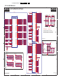
1
Color Television
Chassis
L04.6HU
CA
G_16430_000.eps
260406
Contents
Page
1. Technical Specifications, Connections, and Chassis
Overview
2
2. Safety Instructions, Warnings, and Notes
4
3. Directions for Use
6
4. Mechanical Instructions
7
5. Service Modes, Error Codes, and Fault Finding 10
6. Block Diagrams, Test Point Overviews, and
Waveforms
Wiring Diagram
19
Block Diagram Supply and Deflection
20
Testpoint Overview Mono Carrier
21
Block Diagram Video
22
Testpoint Overview CRT Panel
23
Block Diagram Audio/Control
24
I2C and Supply Voltage Overview
25
7. Circuit Diagrams and PWB Layouts
Diagram
Mono Carrier: Power Supply
(A1) 26
Mono Carrier: Diversity Table for [A1]
27
Mono Carrier: Deflection
(A2) 28
Mono Carrier: Diversity Table for [A2]
29
Mono Carrier: Tuner IF
(A3) 30
Mono Carrier: Hercules
(A4) 31
Mono Carrier: Features & Connectivity
(A5) 32
Mono Carrier: Class D - Audio Amplifier
(A6) 33
Mono Carrier: Audio Amplifier
(A7) 34
Mono Carrier: Rear I/O Cinch
(A8) 35
Mono Carrier: Front Control
(A9) 36
Mono Carrier: DVD PSU (optional)
(A10) 37
ATSC Panel: Power
(ATSC2) 44
ATSC Panel: Reset, Pads, Spade Lug, I2C
EEPROM
(ATSC3) 45
ATSC Panel: DDR SDRAM Interface (ATSC4) 46
ATSC Panel: Guest Bus & Flash
(ATSC5) 47
ATSC Panel: Tuner
(ATSC6) 48
Contents
8.
9.
PWB
38-43
38-43
38-43
38-43
38-43
38-43
38-43
38-43
38-43
38-43
38-43
38-43
54-54
10.
11.
Page
ATSC Panel: Connectors
(ATSC7) 49
ATSC Panel: Video Out
(ATSC8) 50
ATSC Panel: Audio Output
(ATSC9) 51
ATSC Panel: Power & Gnd
(ATSC10) 52
ATSC Panel: YUV Converter
(ATSC11) 53
CRT Panel
(B1) 55
CRT Panel: Eco Scavem
(B2) 56
Side AV + Headphone Panel
(D) 58
External Supply
(EPS1B) 60
SP/LS Module (NA-LA)
(I1) 61
Interface Module
(J1) 63
Main Switch Panel (For SL5 Styling)
(M) 65
Alignments
67
Circuit Descriptions, List of Abbreviations, and IC
Data Sheets
74
Abbreviation List
77
IC Data Sheets
78
Spare Parts List
79
Revision List
80
54-54
54-54
54-54
54-54
54-54
57-57
57-57
59-59
60
n.a.
n.a.
66-66
54-54
54-54
54-54
54-54
©
Copyright 2006 Philips Consumer Electronics B.V. Eindhoven, The Netherlands.
All rights reserved. No part of this publication may be reproduced, stored in a
retrieval system or transmitted, in any form or by any means, electronic,
mechanical, photocopying, or otherwise without the prior permission of Philips.
Published by WS 0665 BG CD Customer Service
Printed in the Netherlands
Subject to modification
EN 3122 785 16430
EN 2
1.
Technical Specifications, Connections, and Chassis Overview
L04.6HU CA
1. Technical Specifications, Connections, and Chassis Overview
1.2
Index of this chapter:
1.1 Technical Specifications
1.2 Connections
1.3 Chassis Overview
Note: The following connector color abbreviations are used
(acc. to DIN/IEC 757): Bk= Black, Bu= Blue, Gn= Green, Gy=
Grey, Rd= Red, Wh= White, Ye= Yellow.
Notes:
• Figures can deviate due to the different set executions.
• Specifications are indicative (subject to change).
1.1
Technical Specifications
1.1.1
Vision
Display type
Screen size
Tuning system
TV Color systems
:
:
:
:
:
:
:
IF picture carrier
Video playback
1.1.2
CRT, DV, RF
27”, 4:3
PLL
ATSC (QAM, 8VSB)
NTSC
45.75 MHz
NTSC
Sound
Sound systems
Maximum power (WRMS)
1.1.3
: BTSC
: 2 x 10
G_16430_001.eps
210406
Miscellaneous
Power supply:
- Mains voltage (VAC)
- Mains frequency (Hz)
: 90 - 140
: 60
Ambient conditions:
- Temperature range (°C)
- Maximum humidity
: +5 to +40
: 90% R.H.
Figure 1-1 Connections overview (27HT7210D/27, see also DFU)
Power consumption (values are indicative)
- Normal operation (W)
: ≈ 120
- Stand-by (W)
: <1
1.1.4
Connections
Mechanical Styling
Model Number
Styling Name
27HT4000D/27
SL3
27HT7210D/27
SL5
In above table the link is shown between the model number and
the (internal) Philips styling number. In this manual, sometimes
a refernce is made to this styling number. For a mechanical
drawing of the model, please check the quarterly published
Product Survey.
1.2.1
Rear Connections
Cinch: S/PDIF - Out
Bk - Coaxial
0.4 - 0.6VPP / 75 ohm
Cable/Antenna - In
- - F-type (US)
Coax, 75 ohm
Service Connector (ComPair)
1 - SDA-S
I2C Data (0 - 5 V)
2 - SCL-S
I2C Clock (0 - 5 V)
3 - Ground
Gnd
kq
D
jk
j
H
Mini Jack: Ext. Bathroom speaker- Out
- External speaker
stereo jack, pins 1-3
RJ11: SmartplugTM
1 - CLOCK
2 - DATA IN
3 -+ 5 V
4 - DATA OUT
5 - GND
6 - IR DATA
Monitor Out - Cinch: Video CVBS - Out, Audio - Out
Ye - Video CVBS
1 VPP / 75 ohm
kq
Wh - Audio L
0.5 VRMS /10 kohm
kq
Rd - Audio R
0.5 VRMS / 10 kohm
kq
AV1 - Cinch: Video YPbPr - In
Gn - Video Y
1 VPP / 75 ohm
Bu - Video Pb
0.7 VPP / 75 ohm
Rd - Video Pr
0.7 VPP / 75 ohm
jq
jq
jq
AV1 - Cinch: Video CVBS - In, Audio - In
Ye - Video CVBS
1 VPP / 75 ohm
Wh - Audio L
0.5 VRMS / 10 kohm
jq
jq
Technical Specifications, Connections, and Chassis Overview
0.5 VRMS / 10 kohm
jq
AV2 - Cinch: Video CVBS - In, Audio - In
Ye - Video CVBS
1 VPP / 75 ohm
Wh - Audio L
0.5 VRMS / 10 kohm
Rd - Audio R
0.5 VRMS / 10 kohm
jq
jq
jq
Rd - Audio R
AV2 - SVHS (Hosiden): Video Y/C - In
1 - Ground Y
Gnd
2 - Ground C
Gnd
1.3
H
H
3
4
1.2.2
L04.6HU CA
- Video Y
- Video C
1.
EN 3
j
j
1 VPP / 75 ohm
0.3 VPPP / 75 ohm
Side Connections
Cinch: Video CVBS - In, Audio - In
Ye - Video CVBS
1 VPP / 75 ohm
Wh - Audio L
0.5 VRMS / 10 kohm
Rd - Audio R
0.5 VRMS / 10 kohm
Bk - Head phone
32 - 600 ohm / 10 mW
jq
jq
jq
ot
Chassis Overview
B1
CRT
B2
ECO
SCAVEM
D
CRT PANEL
E
MAINS SWITCH PANEL (OPTIONAL)
M
FRONT INTERFACE PANEL
(OPTIONAL)
SIDE AV PANEL +
HEADPHONE
ATSC
TOP CONTROL PANEL (OPTIONAL)
ATSC PANEL
MONO
CARRIER
J
POWER SUPPLY
A1
LINE DEFLECTION
A2
TUNER IF
A3
HERCULES
A4
FEATURES & CONNECTIVITIES
A5
CLASS D AUDIO AMPLIFIER
A6
AUDIO AMPLIFIER
A7
REAR I/O CINCH
A8
FRONT CONTROL
A9
DVD POWER SUPPLY
A10
G_16430_002.eps
210406
Figure 1-2 PWB location
EN 4
2.
L04.6HU CA
Safety Instructions, Warnings, and Notes
2. Safety Instructions, Warnings, and Notes
1. Perform the 'general repair instruction' noted above.
2. Clean the power supply and deflection circuitry on the
chassis.
3. Clean the picture tube panel and the neck of the picture
tube.
Index of this chapter:
2.1 Safety Instructions
2.2 Maintenance Instructions
2.3 Warnings
2.4 Notes
2.1
Safety Instructions
2.3
Safety regulations require that during a repair:
• Due to the chassis concept, a very large part of the circuitry
(incl. deflection) is 'hot'. Therefore, connect the set to the
mains via an isolation transformer.
• Replace safety components, indicated by the symbol h,
only by components identical to the original ones. Any
other component substitution (other than original type) may
increase risk of fire or electrical shock hazard.
• Wear safety goggles when you replace the CRT.
Safety regulations require that after a repair, you must return
the set in its original condition. Pay, in particular, attention to
the following points:
• General repair instruction: as a strict precaution, we advise
you to re-solder the solder connections through which the
horizontal deflection current is flowing. In particular this is
valid for the:
1. Pins of the line output transformer (LOT).
2. Fly-back capacitor(s).
3. S-correction capacitor(s).
4. Line output transistor.
5. Pins of the connector with wires to the deflection coil.
6. Other components through which the deflection current
flows.
Note: This re-soldering is advised to prevent bad connections
due to metal fatigue in solder connections, and is therefore only
necessary for television sets more than two years old.
• Route the wire trees and EHT cable correctly and secure
them with the mounted cable clamps.
• Check the insulation of the mains cord for external
damage.
• Check the strain relief of the mains cord for proper function,
to prevent the cord from touching the CRT, hot
components, or heat sinks.
• Check the electrical DC resistance between the mains plug
and the secondary side (only for sets that have an isolated
power supply). Do this as follows:
1. Unplug the mains cord and connect a wire between the
two pins of the mains plug.
2. Turn on the main power switch (keep the mains cord
unplugged!).
3. Measure the resistance value between the pins of the
mains plug and the metal shielding of the tuner or the
aerial connection of the set. The reading should be
between 4.5 MΩ and 12 MΩ.
4. Switch the TV 'off' and remove the wire between the
two pins of the mains plug.
• Check the cabinet for defects, to prevent the possibility of
the customer touching any internal parts.
2.2
Maintenance Instructions
We recommend a maintenance inspection carried out by
qualified service personnel. The interval depends on the usage
conditions:
• When a customer uses the set under normal
circumstances, for example in a living room, the
recommended interval is three to five years.
• When a customer uses the set in an environment with
higher dust, grease, or moisture levels, for example in a
kitchen, the recommended interval is one year.
• The maintenance inspection includes the following actions:
Warnings
•
In order to prevent damage to ICs and transistors, avoid all
high voltage flashovers. In order to prevent damage to the
picture tube, use the method shown in Fig. 2-1, to
discharge the picture tube. Use a high voltage probe and a
multi-meter (position V_dc). Discharge until the meter
reading is 0 V (after approx. 30 s).
V
E_06532_007.eps
250304
Figure 2-1 Discharge picture tube
•
•
•
•
•
All ICs and many other semiconductors are susceptible to
electrostatic discharges (ESD, w). Careless handling
during repair can reduce life drastically. Make sure that,
during repair, you are connected with the same potential as
the mass of the set by a wristband with resistance. Keep
components and tools also at this potential. Available ESD
protection equipment:
– Complete kit ESD3 (small tablemat, wristband,
connection box, extension cable and ground cable)
4822 310 10671.
– Wristband tester 4822 344 13999.
Together with the deflection unit and any multi-pole unit,
flat square picture tubes form an integrated unit. The
deflection and the multi-pole units are set optimally at the
factory. We do not recommend adjusting this unit during
repair.
Be careful during measurements in the high voltage
section and on the picture tube.
Never replace modules or other components while the unit
is 'on’.
When you align the set, use plastic rather than metal tools.
This will prevent any short circuits and the danger of a
circuit becoming unstable.
2.4
Notes
2.4.1
General
•
•
Measure the voltages and waveforms with regard to the
chassis (= tuner) ground (H), or hot ground (I), depending
on the tested area of circuitry.
The voltages and waveforms shown in the diagrams are
indicative. Measure them in the Service Default Mode (see
chapter 5) with a color bar signal and stereo sound (L: 3
kHz, R: 1 kHz unless stated otherwise) and picture carrier
at 475.25 MHz for PAL, or 61.25 MHz for NTSC (channel
3).
Safety Instructions, Warnings, and Notes
•
•
•
2.4.2
Where necessary, measure the waveforms and voltages
with (D) and without (E) aerial signal. Measure the
voltages in the power supply section both in normal
operation (G) and in standby (F). These values are
indicated by means of the appropriate symbols.
The picture tube panel has printed spark gaps. Each spark
gap is connected between an electrode of the picture tube
and the Aquadag coating.
The semiconductors indicated in the circuit diagram and in
the parts lists, are interchangeable per position with the
semiconductors in the unit, irrespective of the type
indication on these semiconductors.
•
•
Schematic Notes
•
•
•
•
•
•
•
2.4.3
All resistor values are in ohms and the value multiplier is
often used to indicate the decimal point location (e.g. 2K2
indicates 2.2 kohm).
Resistor values with no multiplier may be indicated with
either an "E" or an "R" (e.g. 220E or 220R indicates 220
ohm).
All capacitor values are expressed in micro-farads (µ= x
10^-6), nano-farads (n= x 10^-9), or pico-farads (p= x 10^12).
Capacitor values may also use the value multiplier as the
decimal point indication (e.g. 2p2 indicates 2.2 pF).
An "asterisk" (*) indicates component usage varies. Refer
to the diversity tables for the correct values.
The correct component values are listed in the Electrical
Replacement Parts List. Therefore, always check this list
when there is any doubt.
•
•
L04.6HU CA
2.
EN 5
workshops should be avoided because paste is not easy to
store and to handle.
Use only adequate solder tools applicable for lead-free
soldering tin. The solder tool must be able:
– To reach a solder-tip temperature of at least 400°C.
– To stabilise the adjusted temperature at the solder-tip.
– To exchange solder-tips for different applications.
Adjust your solder tool so that a temperature of around
360°C - 380°C is reached and stabilised at the solder joint.
Heating time of the solder-joint should not exceed ~ 4 sec.
Avoid temperatures above 400°C, otherwise wear-out of
tips will increase drastically and flux-fluid will be destroyed.
To avoid wear-out of tips, switch “off” unused equipment or
reduce heat.
Mix of lead-free soldering tin/parts with leaded soldering
tin/parts is possible but PHILIPS recommends strongly to
avoid mixed regimes. If this cannot be avoided, carefully
clear the solder-joint from old tin and re-solder with new tin.
Use only original spare-parts listed in the Service-Manuals.
Not listed standard material (commodities) has to be
purchased at external companies.
For sets produced before 1.1.2005, containing leaded
soldering tin and components, all needed spare parts will
be available till the end of the service period. For the repair
of such sets nothing changes.
In case of doubt whether the board is lead-free or not (or with
mixed technologies), you can use the following method:
• Always use the highest temperature to solder, when using
SAC305 (see also instructions below).
• De-solder thoroughly (clean solder joints to avoid mix of
two alloys).
Lead-free Solder
2.4.4
Philips CE is producing lead-free sets (PBF) from 1.1.2005
onwards.
In September 2003, Philips CE introduced a change in the way
the serial number (or production number, see Figure 2-2) is
composed. From this date on, the third digit in the serial
number (example: AG2B0335000001) indicates the number of
the alternative BOM (Bill of Materials used for producing the
specific model of TV set). It is possible that the same TV model
on the market is produced with e.g. two different types of
displays, coming from two different O.E.M.s.
By looking at the third digit of the serial number, the service
technician can see if there is more than one type of B.O.M.
used in the production of the TV set he is working with. He can
then consult the At Your Service Web site, where he can type
in the Commercial Type Version Number of the TV set (e.g.
28PW9515/12), after which a screen will appear that gives
information about the number of alternative B.O.M.s used.
If the third digit of the serial number contains the number 1
(example: AG1B033500001), then there is only one B.O.M.
version of the TV set on the market. If the third digit is a 2
(example: AG2B0335000001), then there are two different
B.O.M.s. Information about this is important for ordering
the correct spare parts!
For the third digit, the numbers 1...9 and the characters A...Z
can be used, so in total: 9 plus 26 = 35 different B.O.M.s can
be indicated by the third digit of the serial number.
Identification: The bottom line of a type plate gives a 14-digit
serial number. Digits 5 and 6 refer to the production year, digits
7 and 8 refer to production week (in example below it is 1991
week 18).
E_06532_024.eps
230205
Figure 2-2 Serial number example
Regardless of the special lead-free logo (which is not always
indicated), one must treat all sets from this date onwards
according to the rules as described below.
P
2.4.5
b
Figure 2-3 Lead-free logo
Due to lead-free technology some rules have to be respected
by the workshop during a repair:
• Use only lead-free soldering tin Philips SAC305 with order
code 0622 149 00106. If lead-free solder paste is required,
please contact the manufacturer of your soldering
equipment. In general, use of solder paste within
Alternative BOM identification
Practical Service Precautions
•
•
It makes sense to avoid exposure to electrical shock.
While some sources are expected to have a possible
dangerous impact, others of quite high potential are of
limited current and are sometimes held in less regard.
Always respect voltages. While some may not be
dangerous in themselves, they can cause unexpected
reactions that are best avoided. Before reaching into a
powered TV set, it is best to test the high voltage insulation.
It is easy to do, and is a good service precaution.
EN 6
3.
L04.6HU CA
Directions for Use
3. Directions for Use
You can download this information from the following websites:
http://www.philips.com/support
http://www.p4c.philips.com
Mechanical Instructions
L04.6HU CA
4.
EN 7
4. Mechanical Instructions
1. Disconnect the degaussing coil [1].
2. Release the two fixation clamps (at the mid left and mid
right side of the bracket), and remove the bracket from the
bottom tray, by pulling it backwards [2].
3. Turn the chassis tray 90 degrees counter clockwise.
4. Move the panel bracket somewhat to the left and flip it 90
degrees [3], with the components towards the CRT.
5. Turn the panel bracket with the rear I/O toward the CRT.
6. Place the hook of the tray in the fixation hole of the cabinet
bottom [4] and secure it.
Index of this chapter:
4.1 Set Disassembly
4.2 Service Position
4.3 Assy/Panel Removal
4.4 Set Re-assembly
Notes:
• Figures below can deviate slightly from the actual situation,
due to different set executions.
4.1
Set Disassembly
Warning: Be sure to disconnect the AC power from the set
before opening it.
4.1.1
4.3
Assy/Panel Removal
4.3.1
Front Interface Assy/Panel Removal
Rear Cover
1. Remove all fixation screws of the rear cover (do not forget
the screws that hold the rear connection panel, and the
screws on the small black cover with the text “not to be
removed”).
2. Pull the rear cover backwards to remove it.
1
1
4.2
Service Position
2
Before placing the Mono Carrier in its service position, remove
the Front Interface assy/panel (see paragraph “Front Interface
Assy/Panel removal”) and the Side AV assy/panel (see
paragraph “Side AV Assy/Panel removal”).
3
3
E_14480_049.eps
110204
Figure 4-2 Front interface assy/panel removal
1. Remove the complete module from the bottom plate, by
pulling the two fixation clamps upward [1], while sliding the
module away from the CRT [2].
Note: these clamps are difficult to access.
2. Release the two fixation clamps [3] at the side of the
bracket, and lift the panel out of the bracket (it hinges at
one side).
1
4.3.2
Side AV Assy/Panel Removal
2
A
3
E_14480_050.eps
170204
4
Figure 4-3 Side AV assy/panel removal
B
E_14480_048.eps
110204
Figure 4-1 Service position Mono Carrier
1. Remove the two fixation screws, and remove the complete
Side AV assembly.
2. Release the two fixation clamps, and lift the panel out of the
bracket.
EN 8
4.3.3
4.
Mechanical Instructions
L04.6HU CA
4.3.5
ATSC Module/Panel Removal
Interface Module/Panel Removal
3
3
2
1
2
F_15760_009.eps
151105
1
Figure 4-4 ATSC bracket
G_16430_004.eps
210406
1. Disconnect all cables that lead to the module.
2. Unlock the clip [1] at the left side of the bracket and pull out
the ATSC module [2].
3. Release the fixation clips that hold the panel [3] and take
out the panel (it hinges at the bottom).
4.3.4
Figure 4-6 Bracket with Interface Module
EPS1B Module/Panel Removal
1
2
G_16430_005.eps
210406
Figure 4-7 Interface Module
1
G_16430_003.eps
210406
Figure 4-5 EPS1B Module
1. Disconnect all cables that lead to the module.
2. Unlock the clip [1] at the lower side of the bracket and pull
out the EPS1B bracket.
3. Release the fixation clips that hold the panel [2] and take
out the panel.
1. Loosen the screw [1] that fixes the bracket with the
Interface module [2] to the TV chassis, and reverse the
bracket to get access to the Interface Module (see Figure
“Bracket with Interface Module”).
2. Loosen the screw [1] in the middle of the Interface Module,
release the fixation clips (or shift the Interface Module
aside), and take it out of its bracket (see Figure “Interface
Module”).
3. Disconnect all cables that lead to the Interface Module.
Mechanical Instructions
4.3.6
SP/LS Module/Panel Removal
1
G_16430_006.eps
210406
Figure 4-8 SP/LS Module
1. Loosen the screw [1] that fixes the bracket with the
Interface module to the TV chassis, and position the
bracket in such a way that it no longer blocks access to the
SP/LS module (see Figure “Bracket with Interface
Module”).
2. Unlock the connector [1] that fixes the SP/LS module to the
chassis, and take out the SP/LS module (see Figure “SP/
LS Module”).
3. Disconnect all cables that lead to the module.
4.4
Set Re-assembly
To re-assemble the whole set, do all processes in reverse
order.
Note: before you mount the rear cover, perform the following
checks:
• Check whether the AC power cord is mounted correctly in
its guiding brackets.
• Check whether all cables are replaced in their original
position
L04.6HU CA
4.
EN 9
EN 10
5.
L04.6HU CA
Service Modes, Error Codes, and Fault Finding
5. Service Modes, Error Codes, and Fault Finding
Index of this chapter:
5.1 Test Points
5.2 Service Modes
5.3 ComPair
5.4 Error Codes
5.5 The Blinking LED Procedure
5.6 Protections
5.7 Fault Finding and Repair Tips
5.1
5.2
Software version.
Option settings.
Error buffer reading and erasing.
Software alignments.
This chassis is equipped with test points in the service printing.
In the schematics test points are identified with a rectangle box
around Fxxx or Ixxx. These test points are specifically
mentioned in the “Test Point Overview” as “half moons” with a
dot in the center.
How to Enter SDAM
To enter SDAM, use one of the following methods:
• Switch the optional RC2573GR remote controll to Setup
mode, and press the following key sequence on the remote
control transmitter: “062596" directly followed by the
M(enu) button (do not allow the display to time out between
entries while keying the sequence).
• Or via ComPair.
• Or Short circuit the SDAM jumper on the mono carrier (see
Chapter 7: Layout Mono Carrier: Top side, item 9252 in cel
C5) and apply AC power. Then press the power button
(remove the short circuit after start-up).
Perform measurements under the following conditions:
• Television set in Service Default Alignment Mode.
• Video input: Color bar signal.
• Audio input: 3 kHz left channel, 1 kHz right channel.
Caution: Entering SDAM by short-circuiting the SDAM jumper
will override the +8V-protection. Do this only for a short period.
When doing this, the service-technician must know exactly
what he is doing, as it could lead to damaging the set.
Service Modes
After entering SDAM, the following screen is visible, with “S” in
the upper right corner of the screen to indicate that the
television is in Service Default Alignment Mode.
Test Points
Service Default Alignment Mode (SDAM) offers several
features for the service technician, while the Customer Service
Mode (CSM) is used for communication between the call
center and the customer. For the TV setup main menu, please
refer to the DFU.
This chassis also offers the option of using ComPair, a
hardware interface between a computer and the TV chassis. It
offers the abilities of structured troubleshooting, error code
reading, and software version readout for all chassis.
Minimum requirements for ComPair: a Pentium processor, a
Windows OS, and a CD-ROM drive (see also paragraph
"ComPair").
5.2.1
•
•
•
•
Service Default Alignment Mode (SDAM)
Purpose
• To change option settings.
• To create a predefined setting to get the same
measurement results as given in this manual.
• To display / clear the error code buffer when leaving SDAM
with “standby” key on remote control.
• To override SW protections.
• To perform alignments.
• To start the blinking LED procedure.
Specifications
• Tuning frequency:
– 61.25 MHz (channel 3)
• Colour system:
– NTSC
• All picture settings at 50 % (brightness, color contrast,
hue).
• Bass, treble and balance at 50 %; volume at 25 %.
• All service-unfriendly modes (if present) are disabled, like:
– (sleep) timer,
– child/parental lock,
– blue mute,
– hotel/hospitality mode
– auto switch-off (when no IDENT video signal is
received for 15 minutes),
– skip / blank of non-favourite presets / channels,
– auto store of personal presets,
– auto user menu time-out.
• Operation hours counter.
00058
L06HU I 0.5D
S
ERR 0 0 0 0 0
OP 034 004 161 009 060 117 000
HRM SW H3.03B
. CLEAR
CLEARED
. ISP MODE
OFF
. OPTIONS
. DEFLECTION
. TUNER
. WHITE TONE
. GEOMETRY
. 60Hz OFFSET
G_16430_008.eps
040506
Figure 5-1 SAM menu (example)
1. LLLL
This is the operation hours counter. It counts the normal
operation hours, not the standby hours.
2. AAAABC-X.Y
This is the software identification of the main micro
controller:
– A = the project name (L04H).
– B = the region: E= Europe, A= Asia Pacific, U= NAFTA,
L= LATAM.
– C = the feature and language
– X = the main software version number.
– Y = the sub software version number.
3. S
Indication of the actual mode. S= SDAM= Service Default
Alignment mode.
4. Error buffer
Five errors possible.
Service Modes, Error Codes, and Fault Finding
5. Option bytes
Shows the actual settings of the options; seven codes
possible.
6. Clear
Erases the contents of the error buffer. Select the CLEAR
menu item and press the MENU RIGHT key. The content
of the error buffer is cleared
7. ISP Mode
Can be used to switch on the television to ISP mode (for
uploading software)
8. Options
To set the Option Bytes. See chapter 8 for a detailed
description.
9. Deflection
To align the Deflection. See chapter 8 for a detailed
description.
10. Tuner
To align the Tuner. See chapter 8 for a detailed description.
11. White Tone
To align the White Tone. See chapter 8 for a detailed
description.
12. Geometry
To align the Geometry. See chapter 8 for a detailed
description.
13. 60Hz offset
To align the horizontal and vertical screen positions and
vertical amplitude at 60 Hz. See chapter 8 for a detailed
description.
Customer Service Mode (CSM)
Purpose
The Customer Service Mode shows error codes and
information on the TV’s operation settings. The call center can
instruct the customer (by telephone) to enter CSM in order to
identify the status of the set. This helps the call center to
diagnose problems and failures in the TV set before making a
service call.
The CSM is a read-only mode; therefore, modifications are not
possible in this mode.
How to Enter
To enter CSM, switch the optional RC2573GR remote controll
to Setup mode, and press its RECALL button.
Upon entering the Customer Service Mode, the following
screen will appear:
EN 11
CSM
2 CODES 0 0 0 0 0
3 CODES 0 0 0 0 0
4 OP 034 004 161 009 060 117 000
5 AUTO AUTO STEREO
6
7
8 CO 31 CL 31 BR 31 SH 31
9 VL 13 BL 0
10 BS 31 TR 31
11 COMMERCIAL SMARTPORT OFF
12 CHANNEL TV2
G_16430_009.eps
210406
Figure 5-2 CSM menu (example)
Menu Explanation
1. Indication of the operation hours counter, the chassis
firmware version, and the service mode (CSM= Customer
Service Mode).
2. Displays the software version used.
3. Displays the last five errors detected in the error code
buffer.
4. Displays the option bytes (decimal values).
5. Displays sound info of the set.
6. Indicates if the television is receiving an "IDENT" signal on
the selected source. If no "IDENT" signal is detected, the
display will read "NOT TUNED"
7. Reserved.
8. Displays various picture settings.
9. Displays various picture settings.
10. Displays various picture settings.
11. Displays if the TV set is in CONSUMER or COMMERCIAL
mode, and if it is on-line with e.g. a SmartPort DCM.
12. Displays the sound setting information.
How to Store Settings
To store settings first go back to the main menu (fig. 5-1) with
“MENU” button on the remote control and leave the SDAM with
the “STANDBY” button on the remote control.
5.2.2
5.
1 00058 L06HU I 0.5D
How to Navigate
Use one of the following methods:
• In SDAM, select menu items with the CURSOR UP/DOWN
key on the remote control transmitter. The selected item
will be highlighted. When not all menu items fit on the
screen, move the CURSOR UP/DOWN key to display the
next / previous menu items.
• With the CURSOR LEFT/RIGHT keys, it is possible to:
– Activate the selected menu item.
– Change the value of the selected menu item.
– Activate the selected submenu.
• When you press the MENU key in a submenu, you will
return to the previous menu.
How to Exit
Switch the set to STANDBY by pressing the power button on
the remote control transmitter. The error buffer is cleared. (If
you switch the set 'off' by removing the AC power, the set will
return in SDAM when AC power is re-applied and the error
buffer will not be cleared.)
L04.6HU CA
How to Exit
To exit CSM, use one of the following methods:
• Press the MENU, STATUS/EXIT, or POWER button on the
remote control transmitter.
• Press the POWER button on the television set.
5.3
ComPair
5.3.1
Introduction
ComPair (Computer Aided Repair) is a service tool for Philips
Consumer Electronics products. ComPair is a further
development on the European DST (service remote control),
which allows faster and more accurate diagnostics. ComPair
has three big advantages:
• ComPair helps you to quickly get an understanding on how
to repair the chassis in a short time by guiding you
systematically through the repair procedures.
• ComPair allows very detailed diagnostics (on I2C level) and
is therefore capable of accurately indicating problem areas.
You do not have to know anything about I2C commands
yourself because ComPair takes care of this.
• ComPair speeds up the repair time since it can
automatically communicate with the chassis (when the
microprocessor is working) and all repair information is
directly available. When ComPair is installed together with
EN 12
5.
Service Modes, Error Codes, and Fault Finding
L04.6HU CA
the Force/SearchMan electronic manual of the defective
chassis, schematics and PWBs are only a mouse click
away.
5.3.2
The ComPair fault finding program is able to determine the
problem of the defective television. ComPair can gather
diagnostic information in two ways:
• Automatically (by communicating with the television):
ComPair can automatically read out the contents of the
entire error buffer. Diagnosis is done on I2C/UART level.
ComPair can access the I2C/UART bus of the television.
ComPair can send and receive I2C/UART commands to
the microcontroller of the television. In this way, it is
possible for ComPair to communicate (read and write) to
devices on the I2C/UART buses of the TV-set.
• Manually (by asking questions to you): Automatic
diagnosis is only possible if the microcontroller of the
television is working correctly and only to a certain extent.
When this is not the case, ComPair will guide you through
the fault finding tree by asking you questions (e.g. Does the
screen give a picture? Click on the correct answer: YES /
NO) and showing you examples (e.g. Measure test-point I7
and click on the correct oscillogram you see on the
oscilloscope). You can answer by clicking on a link (e.g.
text or a waveform picture) that will bring you to the next
step in the fault finding process.
By a combination of automatic diagnostics and an interactive
question / answer procedure, ComPair will enable you to find
most problems in a fast and effective way.
5.4.1
How To Read The Error Buffer
You can read the error buffer in 3 ways:
• On screen via the SAM (if you have a picture). Examples:
– ERROR: 0 0 0 0 0: No errors detected
– ERROR: 6 0 0 0 0: Error code 6 is the last and only
detected error
– ERROR: 9 6 0 0 0: Error code 6 was detected first and
error code 9 is the last detected (newest) error
• Via the blinking LED procedure (when you have no
picture). See “The Blinking LED Procedure”.
• Via ComPair.
5.4.2
How to Clear the Error Buffer
The error code buffer is cleared in the following cases:
• By using the CLEAR command in the SAM menu:
– To enter SAM, press the following key sequence on the
remote control transmitter: “062596” directly followed
by the OSD/STATUS button (do not allow the display
to time out between entries while keying the
sequence).
– Make sure the menu item CLEAR is highlighted. Use
the MENU UP/DOWN buttons, if necessary.
– Press the MENU RIGHT button to clear the error
buffer. The text on the right side of the “CLEAR” line will
change from “CLEAR?” to “CLEARED”
• If the contents of the error buffer have not changed for 50
hours, the error buffer resets automatically.
Note: If you exit SAM by disconnecting the AC power from the
television set, the error buffer is not reset.
How to Connect
This is described in the chassis fault finding database in
ComPair.
TO
UART SERVICE
CONNECTOR
PC
TO
I2C SERVICE
CONNECTOR
VCR
Power
9V DC
I2C
E_06532_021.eps
180804
Figure 5-3 ComPair interface connection
5.3.4
Error Codes
The error code buffer contains all errors detected since the last
time the buffer was erased. The buffer is written from left to
right. When an error occurs that is not yet in the error code
buffer, it is displayed at the left side and all other errors shift one
position to the right.
Specifications
ComPair consists of a Windows based fault finding program
and an interface box between PC and the (defective) product.
The ComPair interface box is connected to the PC via a serial
(or RS-232) cable.
For this chassis, the ComPair interface box and the TV
communicate via a bi-directional service cable via the service
connector(s).
5.3.3
5.4
How to Order
ComPair order codes (US):
• ComPair Software: ST4191.
• ComPair Interface Box: 4822 727 21631.
• AC Adapter: T405-ND.
• ComPair Quick Start Guide: ST4190.
• ComPair interface extension cable: 3139 131 03791.
• ComPair UART interface cable: 3122 785 90630.
Note: If you encounter any problems, contact your local
support desk.
5.4.3
Error Codes
In case of non-intermittent faults, write down the errors present
in the error buffer and clear the error buffer before you begin
the repair. This ensures that old error codes are no longer
present.
If possible, check the entire contents of the error buffer. In
some situations, an error code is only the result of another error
and not the actual cause of the problem (for example, a fault in
the protection detection circuitry can also lead to a protection).
Service Modes, Error Codes, and Fault Finding
L04.6HU CA
5.
EN 13
Table 5-1 Error code overview
Error Device
Error description
0
Not applicable
No Error
Check item
Diagram
1
Not applicable
X-Ray/Over-voltage protection (US only)
2411, 2412, 2413, 6404, 6411,
6412
A2
2
3
Not applicable
High beam (BCI) protection
3404, 7405
A2
Not applicable
Vertical guard protection
3466, 7451, 7452, 7453, 7454
A2
4
Tuner
I2C error while communicating with 2nd tuner
1000, 5010, (PIP Module)
F2
5
Not applicable
+5v protection
7604, 7605
A5
6
I2C bus
General I2C error
7200, 3207, 3214
A4
7
Not applicable
Power down (over current) protection
-
-
8
Not applicable
EW protection (only for sets with EW circuitry)
-
-
9
24C16
I2C error while communicating with the EEPROM
7601, 3604, 3605
A5
10
Tuner
I2C error while communicating with the PLL tuner
1000, 5001
A3
11
TDA6107/A
Black current loop instability protection
7330, 3351, CRT
B1
12
SDA9488X
I2C error while communicating with the PIP processor
7242 (PIP Module)
F1
13
Not applicable
I2C error while communicating with the Voice Ctrl processor
-
-
14
DVD Loader
I2C error while communicating with the DVD Interface module
DVD Interface module
DVD Loader
15
TDA9178T/N1
I2C error while communicating with the LTI module
7610
H
16
TDA9887
I2C error while communicating with the PIP Demodulator
7201
F2
17
ATSC module
I2C error while communicating with the IBO module
-
ATSC
18
ATSC module
I2C error while communicating with other I2C IBO module
-
ATSC
Note: For all error codes the following applies: error codes are
only valid when the module or device they refer to is used in the
TV set.
5.6
Notes:
• It is assumed that the components are mounted correctly
with correct values and no bad solder joints.
• Before any fault finding actions, check if the correct options
are set.
The Blinking LED Procedure
Using this procedure, you can make the contents of the error
buffer visible via the front LED. This is especially useful when
there is no picture.
Fault Finding and Repair Tips
5.7.1
NVM Editor
When the SDM is entered, the front LED will blink the contents
of the error-buffer:
• When all the error-codes are displayed, the sequence
finishes with a LED blink of 1.5 seconds,
• The sequence starts again.
In some cases, it can be handy if one directly can change the
NVM contents. This can be done with the “NVM Editor” in SAM
mode. In the next table, some default NVM values are given.
Example of error buffer: 12 9 6 0 0
After entering SDM, the following occurs:
• 1 long blink of 5 seconds to start the sequence,
• 12 short blinks followed by a pause of 1.5 seconds,
• 9 short blinks followed by a pause of 1.5 seconds,
• 6 short blinks followed by a pause of 1.5 seconds,
• 1 long blink of 1.5 seconds to finish the sequence,
• The sequence starts again at 12 short blinks.
Bit
Protections
If a fault situation is detected, an error code will be generated;
and, if necessary, the television set will go into protection
mode. Blinking of the red LED at a frequency of 3 Hz indicates
the protection mode. In some error cases, the microprocessor
does not put the set in protection mode. The error codes of the
error buffer and the blinking LED procedure can be read via the
Service Default Menu (SDM), or via ComPair.
To get a quick diagnosis the chassis has three service modes
implemented:
• The (Digital) Customer Service Mode ((D)CSM).
• The Service Default Mode (SDM).
• The Service Alignment Mode (SAM).
For a detailed mode description, see the relevant sections.
27HT7210D/27 (HEX)
27HT4000D/27 (HEX)
Table 5-2 Default NVM values
Addr. (DEC)
5.5
5.7
EW (EW width)
58
28
2D
PW (EW parabola width)
59
13
14
HS (Horizontal shift)
53
2D 2B
HP (Horizontal Parallelogram)
54
2A
21
HB (Horizontal Bow)
55
20
1F
UCP(EW Upper Corner Parab.) 60
2A
29
LCP(EW Lower Corner Parab.) 61
30
33
TC (EW Trapezium)
62
12
14
VS (Vertical Slope)
63
1C 1F
VA (Vertical Amplitude)
64
15
SC (S-Correction)
65
1E 1E
VSH (Vertical Shift)
66
1E
21
VX (Vertical Zoom)
67
19
19
VSC (Vertical scroll)
68
20
20
VL (Vertical linearity)
56
20
20
BLOR (Black Level Offset Red) 71
24
24
BLOG (Black Level Offset Grn) 72
1F
1F
AGC (AGC Take over)
14
14
69
1F
Service Modes, Error Codes, and Fault Finding
L04.6HU CA
Addr. (DEC)
Bit
27HT7210D/27 (HEX)
5.
27HT4000D/27 (HEX)
EN 14
OIF (IF-PLL Offset)
68
26
26
H60 (60 Hz Horizontal Shift)
150 00
00
PWL (Peak White Limit)
74
60 Hz Vertical amplitude
152 00
NVM_CVI_BLOR
71
24
24
NVM_CVI_BLOG
72
1F
1F
TXT Brightness
128 20
20
V60 offset (60Hz Vert. Ampl.)
151 00
00
NVM_CRYSTALALIGN
284 3F
3F
White-D Cool Red
134 20
20
White-D Cool Green
135 1B 1B
White-D Cool Blue
136 1A 1A
White-D Normal Red
137 00
00
White-D Normal Green
138 01
01
5.7.3
Power Supply
Set Not Working
Check Power
Supply Mains
Switch
Bridge Rectifier
circuit 6500
Check fusible
resistor 3510 &
circuit before it
Not Ok
0A 0A
Ok
00
White-D Normal Blue
139 07
07
White-D Warm Red
140 00
00
White-D Warm Green
141 FB FB
White-D Warm Blue
142 EF EF
Check DC
voltage at
2505/2507
Not Ok
Ok
Check
fusible
resistor 3532
Check
7512
Check IC7511 &
IC7531
Ok
Set able to
start-up
Check other
fusible resistor
and capacitor in
the circuit
No
Yes
End
5.7.2
E_14480_057.eps
190204
ATSC Module
Figure 5-5 Fault finding tree “Set not working”
ATSC Module check
Set Does Not Start Up
Check 10 V supply
from Main Chassis
Set Unable
to Start
OK?
No
Check Auxillary
Power Supply
Software
loaded?
No
Fuse Blown?
Yes
Change
Fuse
Yes
Yes
Check UART Signal
(P1206)
Load
Software
Check
voltage
across 2552
OK?
No
Check Hercules
UART o/p
Yes
Check Video &
Audio signal o/p
from ATSC Module
Is Vbatt
approximately
140V
No
Check Power
Supply circuit
Yes
Check
voltage 2562
&2563
No
OK?
No
Replace ATSC
Module
16V
Yes
Yes
Check wiring and
connections of ATSC
Module
Check 3V
across 2535
F_15760_010.eps
161105
Figure 5-4 Fault finding tree “ATSC Module check”
Yes
Check 6V
across 2535
Yes
Set able to
Start
No
Check Line
Transistor 7405
Yes
End
E_14480_058.eps
170204
Figure 5-6 Fault finding tree “Set does not start up”
Service Modes, Error Codes, and Fault Finding
5.7.4
L04.6HU CA
EN 15
Blank Screen
Deflection
One Thin Vertical Line
Quick check:
• Set in protection mode.
• LED blinking with error “3”.
Blank Screen
Check Vg2
(fine tune)
One Thin Vertical Line
LED Blinking
Ok
Not Ok
Check all
connection and
peripheral at
Deflection Circuit in
place
Picture
appears?
Picture not appearing
Check Beam Current Limit
(voltage is 1.8V-2V when
brightness and contrast is
set to the maximum
Not Ok
Check deflection
circuit
Ok
Check
Line Transistor
7405
Check heater voltage
(measure pin 9&10
at the CRT socket)
Is VBE between
200mV to 30mV & VCB
approximately 500mV
5.
Yes
Check Horizontal
Deflection
Circuitry
Ok
Picture not appearing
Not Ok
Check video supply
(2457) is approximately
180V
Ok
Replace transistor
Picture
appears?
E_14480_059.eps
170204
Figure 5-7 Fault finding tree “One thin vertical line”
Ok
End
One Thin Horizontal Line
Quick check:
• Set in protection mode.
• LED blinking with error “2”.
E_14480_061.eps
170204
Figure 5-9 Fault finding tree “Blank screen”
One Horizontal
Thin Line
LED Blinking
5.7.5
Set is not able to go into AV or any missing AV is
encountered
E.g. AV1 is available but not able to enter to AV1: Check if the
option setting is correct.
Check all connection
and peripheral at
Deflection Circuit
in place
Check transistor
(7451, 7523, 7543) at
Vertical Deflection Circuitry
Source Selection
Set is able to go to AV, but no Audio is heard.
1. Check that continuity of signal is there from the SCART/
Cinch input to the input of the Hercules.
2. If continuity is there and still no audio, check that option
settings are correct.
3. If logic setting is correct and still no audio, proceed to Audio
Decoder/Processor troubleshooting section.
Set is able to go into AV but no Video is available:
1. Check continuity from AV input to Hercules depending on
the input.
2. If continuity is available and yet no video, proceed to Video
Processor troubleshooting section.
Replace transistor
5.7.6
Check Vertical
Deflection Circuit
E_14480_060.eps
170204
Figure 5-8 Fault finding tree “One thin horizontal line”
Tuner and IF
No Picture
1. Check that the Option settings are correct.
2. If correct, check that supply voltages are there.
3. If supply voltages are present, check whether picture is
present in AV.
4. If picture is present in AV, check with the scope the Tuner
IF output signal by manual storage to a known channel.
5. If IF output is present, Tuner is working fine. If no IF output,
I2C data lines may be open, check continuity of I2C lines.
If I2C lines are ok, Tuner may be defect, replaced Tuner.
EN 16
5.
Service Modes, Error Codes, and Fault Finding
L04.6HU CA
6. If Tuner IF is present and yet still no picture in RF mode, go
to Video Processing troubleshooting section.
Unable To Perform Tuning
Unable to
perform tuning
No Picture, No Sound
Check tuning
supply voltage,
pin 9 of tuner
No Picture,
No Sound,
Raster Ok
Check AGC
Voltage, pin 1
of tuner
>30V & <35V
Enter SDM
check optionbyte 1
No
Yes
Check
VT Supply
Section
Correct
Check if tuner
Supply Voltage
pin 7
Check supply
voltage, pin 7 of
tuner
AGC voltage
changes with
different signal
strength
Enter SDM and change
to the appropriate byte
Incorrect
5V
No
Check Power
Supply
Yes
Check I2C
circuit
No
Check Tuner
Supply Voltage
33V
Yes
5V
No
No
Check Power
Supply
Replace
Tuner
Not Ok
Check I2C at pin
4 & 5 and tuner
Not Ok
Yes
Not Ok
Check AGC
circuit section
Ok
Check Tuner
pin 4 & 5
I2C Bus
I2C
Check other
functional area
Tuner
Not Ok
E_14480_064.eps
170204
Ok
No
Check other
functional area
Yes
Replace Tuner
E_14480_062.eps
170204
Figure 5-10 Fault finding tree “No picture, no sound”
Picture Ok, No Sound
Picture Ok,
No Sound
Check IF output of
tuner, pin 11
CVBS
present?
No
Refer to fig.
"Power Supply:
Set not working"
No
Replace SAW
filter
Yes
Check SAW filter output
(pin 4&5)
EU/AP/CH (QSS)- 1001
NA/LA/AP INT - 1002
Output Ok?
Yes
Check other
functional area
E_14480_063.eps
170204
Figure 5-11 Fault finding tree “Picture ok, no sound”
Figure 5-12 Fault finding tree “Unable to perform tuning”
Service Modes, Error Codes, and Fault Finding
5.7.7
Controller
Below are some guidelines for troubleshooting of the Micro
Controller function. Normally Micro Controller should be
checked when there is a problem of startup.
1. Check that both +3.3 V_dc and +1.8 V_dc are present.
2. Check that crystal oscillator is working.
3. Check that Power Good signal is at “high” logic, normal
operation.
4. Check that Hercules is not in standby mode. Pin 15 of
Hercules should be 0 V_dc.
5. Make sure H-drive pulse is there. This can be checked at
resistor R3239. If H-drive does not exist, remove resistor
R3239 to check if there is loading.
Note: When the set shuts down after a few second after power
“on”, the main cause is that Vg2 not aligned properly, try
adjusting Vg2 during the few seconds of power “on”.
5.7.9
L04.6HU CA
5.
EN 17
Audio Processing
No Sound
Picture Ok,
No Sound
Tuner IF Ok
Not Ok
Check Tuner/IF
Ok
Check AUDOUTLSL &
AUDOUTLSR pin at
UOCIII
Not Ok
Check UOCIII IC
Ok
5.7.8
Video Processing
No Picture
When “no picture in RF”, first check if the microprocessor is
functioning ok in section “Controller”. If that is ok, follow the
next steps.
When “no picture in AV”, first check if the video source
selection is functioning ok in section “Source Selection”. If that
is ok, follow the next steps.
1. Check that normal operating conditions are met.
2. Check that there is video signal at pin 81. If no video,
demodulator part of the Hercules is faulty, replace with new
Hercules.
3. If video signal is available at pin 81, check pin 56, 57, and
58 for the RGB signal.
4. If signal is not available, try checking the BRIGHTNESS
and/or CONTRAST control, and make sure it is not at zero.
5. If still with the correct settings and no video is available,
proceed to the CRT/RGB amplifier diagram.
For sets with Scavem, and Scavem does not work, follow steps
below:
1. Check Scavem coil connector (position is 1361) if
connected; if not, connect it.
2. If connected, check NVM “bit storage” byte 1 bit 7; if it is not
“1”, set it to “1”.
3. If it is “1”, then check the data of the NVM addresses as in
table “Default NVM values“ (addresses 140, 141, and 142).
If the data is not correct, then set these addresses to the
table values.
4. If it still not works, track Scavem output from pin64 of
Hercules to CRT panel.
Check Audio
Amplifier
Not Ok
Check Audio
Power Supply
Check Power
Supply
Ok
Check Audio
Amplifier Circuit
and loud speaker
Not Ok
Replace Audio
Amplifier
Ok
Check NVM
E_14480_065.eps
201005
Figure 5-13 Fault finding tree “No sound”
No RF Audio for QSS/Inter-Carrier Stereo Sets.
1. Check pin 99 and 100 for SIF signal (for QSS) or pin 104
and 105 for video with SIF (for Inter-Carrier)
2. If signal is not present, check for the QSS/FMI bit settings.
Check also the NVM data.
3. If signals are present and still no audio, check the audio
supply voltage +8V are present.
4. If still no audio signal at Hercules output, Hercules is faulty.
No AV Audio.
1. Check troubleshooting methods in section “Source
Selection”.
2. Check the output of the Hercules to see if there is signal
available. If no, check the normal operating condition and
also the NVM data.
3. If still no audio signal at Hercules output, Hercules is faulty.
Note: If there is audio signal at Hercules output and no audio
at loudspeaker, proceed to Audio Amplifier troubleshooting
methods.
5.7.10 Audio Amplifier
No RF as well as AV Audio at the Loudspeaker:
1. Check that the normal operation condition of the amplifier
is met.
2. If normal operation conditions are met, check the continuity
from Hercules output to input of the amplifier.
3. If continuity is there and still no audio, check speaker wire
connections. If still no audio, amplifier IC might be faulty.
EN 18
5.
L04.6HU CA
Service Modes, Error Codes, and Fault Finding
Block Diagrams, Test Point Overviews, and Waveforms
L04.6HU CA
6.
19
6. Block Diagrams, Test Point Overviews, and Waveforms
Wiring Diagram
WIRING DIAGRAM
M
MAIN SWITCH PANEL
DEGAUSSING COIL
1693
6P
AQUADAG
CRT
EHT
CRT
FRAME
ROTATION
COIL
(component view)
YELLOW
B
CRT PANEL
RIGHT
SPEAKER
GREEN
BLUE
1361
3P
5P
1351
SCAVEM
COIL
1332
1331
LEFT
SPEAKER
RED
7P
1352
B
CRT
SOCKET
CRT PANEL
1381
3P
SIDE
A/V PANEL +
HEADPHONE
1693
1692
7
7P
6P
D
(optional)
1
1252
1507
7P
2P
CVBS (YELLOW)
LEFT (WHITE)
1504
1505
2P
2P
1254
5P
RIGHT (RED)
1278
4P
3P
1279
5P
5 1280 1
A
1582
4P
HEADPHONE
MAINS
CORD
MONO
CARRIER
6P
1220
6
0228
3P
1213
7
7P
1
1
1206
7P
EPS1B
1404
EXTERNAL
POWER SUPPLY
0213
2P
2P
7P
1204
(SMART PLUG +
BATH ROOM SPEAKER)
1265
1267
3P
TUNER
1259
SPDIF
TUNER
3P
1005
3P
COMPAIR
CONNECTOR
I1
SP/LS
MODULE
1227
6P
6
1800
32P
LOT
9
1264
1
1451
2P
1263
1236
U1
U2
1229
3P
5P
7P
3P
0262
3P
3P
1219
1
1266
1262
1251
1212
6P
1401
1245
1207
EXTERNAL
POWER SUPPLY
1246
J1 INTERFACE MODULE
7P
I1
9P
4P
P1582
3P
4P
P1206
9P
ATSC
5P
P1219
3P
5P
P1212
5401
1212
1
SP/LS
MODULE
0228
5P 5
1
1534
3P
1213
7P
1227
1219
4P
1229
1259
9P
1692
5P
G_16430_012.eps
260406
Block Diagrams, Test Point Overviews, and Waveforms
L04.6HU CA
6.
20
Block Diagram Supply and Deflection
SUPPLY AND DEFLECTION
DEFLECTION
t
4
3
1
ENERGIZING
CIRCUIT
(optional)
V_DG
7200-H
(SYNC)
112
EHTinfo
2
3507
1
A2
7541
2240
Degaussing
Coil
1503
113
A2 LINE + FRAME DEFLECTION
A2
Vguard
A4 HERCULES
1504
2
3232
A1 POWER SUPPLY
Vbatt
+6VA
LINE
116
7408
1505
5500 :
5501
1500
VERTICAL
GUARD
DETECTOR
VIDEO
IDENT
6500
AC
F508
T4E
R.G.B.
BLANKING
TO RGB
PROC.
6401
2505
5402
5512
9
17
8
18
7512
11
I511
3514
I519
2511
6
SENSE
Vcc
9
DEMAG
G
5
5562 6563
3
7514
10
-Vaudio
63
6571
5561 6562
INTF_Y GREEN_IN
56
+6VA
3517
7571
1
E/W
+
GEOMETRY
1532
1A
HOR.
DEFL.
COIL
3410
1454
6
6452
5
A4
6483
6484
6453
3458
3484
3485
6456
8
1452
+9V
3457
2456
2564
5
10
2534
CONTROL
IC
7561
6566
POWER-DOWN
A4 2x
X-RAY
PROTECTION
EHTo
FRAME
1
3538
8
+3V
+6VA
+6VA
6576
2535
6536
6
AUX
+6V
2536
2
VERTICAL
SYNC
SEPARATOR
VERTICAL
DIVIDER
VERTICAL
SAWTHOOTH
VERTICAL
OUTPUT
+
GEOMETRY
106
107
VDRA
3474
F461
7455
7456
7453
Vaux
Filament
F458
3466
D
4
Vguard
A4
3465
7454
6537
1401
5
EHTb
7451
VDRB
VideoSupply
1451
1
3
TO 1351
2
CRT
1
Vbatt
7452
7535
2
G
I548
7536
3531
6459
3462
F460
F537
S
3534
3455
3565
F536
6532
97
+9V
6535
9
12
I531
A2
6454
6455
F564
I533
VideoSupply
F455
Filament
7
EHTinfo
14
F453
7411
I573
6565
F452
-12V
7484
Stdby_Con
BCL
A4
7406
I417
A4
2403
3440
Vbatt
7573
STANDBY
CIRCUIT
6564
6533
11
7410
EHTb
EHTb
+
EHTinfo
+
EHTinfo
BCL
PROC.
6481 3481
9
4
SOURCE
EW_DRIVE
3451
3442
10
2
3532
5531
7531
TEA1623
REG
108
1404
1
3576
+3V3
2
+8V
3420
3575
6512
6
A5
SANDCASTLE
GENERATOR
REFERENCE
CIRCUIT
7515
TCET1103
STANDBY
SUPPLY
MAIN
SYNC
SEPARATOR
LINE
OUTPUT
CIRCUIT
+
E/W
3497
CORR.
E/W
SANDCASTLE
+8V
3571
11
6573
3530
+Vbatt
FOCUS VG2
7207
F561
A5
3
DRAIN
HDRIVE
62
1543
14
3518
Vcc
HORIZONTAL
OUTPUT
+Vaudio
S
3532
13
I516
D
4
3
PHI 2
DETECTOR
F418
6511
3519
HORIZONTAL
OSC.
Frame_FB
HD
3516
7
PHI 1
DETECTOR
Vbatt
2
CONTROL
IC
CTRL
5552
A1
B1
3498
DRIVER
2
4
3513
14
DRAIN
F552
7401 : 7403
3411 7480 : 7483 POWER-DOWN
TO
CRT
1
F563
I513
7511
TEA1506T
5551 6551
EHT
3
7405
BU4508DX
7404
MAIN
SUPPLY
I433
5450
6486
-9V
F414
DC
7532
F402
F412
HD
VER.
DEFL.
COIL
3463
B
A4
3401
VT_SUPPLY
F459
-12V
F401
3461
A4
FRAME_FB
3471
For IDTV only
HOT GROUND
COLD GROUND
F_15760_034.eps
240406
B1
Block Diagrams, Test Point Overviews, and Waveforms
L04.6HU CA
6.
21
Testpoint Overview Mono Carrier
F001
F002
F003
F004
F005
F006
F007
F008
F009
E1
E1
E2
E2
E1
E2
E1
E1
D4
F010
F011
F101
F102
F103
F104
F105
F106
F107
E2
E1
D1
D1
D1
D1
D1
D1
D1
F108
F109
F110
F111
F112
F113
F115
F116
F117
D1
D1
C1
D1
C1
C1
C1
C2
C1
F119
F120
F121
F122
F123
F138
F200
F201
F202
E1
E1
E1
D1
D1
D2
D5
C4
D4
F203
F204
F205
F206
F207
F208
F209
F210
F211
D4
C4
C3
C3
D4
D2
E4
E4
E5
F212
F213
F214
F215
F216
F217
F218
F219
F220
E4
E4
D4
D3
C3
C2
C2
D2
D2
F221
F222
F223
F224
F225
F226
F227
F228
F229
D2
C2
D2
C3
C3
D2
E4
C4
C4
F230
F232
F233
F237
F238
F239
F240
F241
F242
D4
D4
D4
D4
D4
D4
C3
C3
C3
F243
F244
F245
F247
F248
F249
F250
F251
F270
C3
D4
C3
E2
E2
E2
C3
D4
D4
F401
F402
F404
F407
F412
F414
F415
F416
F417
C5
B2
B2
B3
C3
A2
A3
A3
A3
F418
F419
F420
F451
F452
F453
F454
F455
F456
B3
B3
B2
C1
C2
B2
C2
B1
A2
F457
F458
F459
F460
F461
F462
F463
F464
F465
A2
C1
C2
C2
C2
A1
B1
A3
A3
F466
F500
F501
F502
F503
F504
F505
F506
F507
A1
C7
B6
B7
A7
A7
A7
A7
A7
F508
F509
F510
F535
F536
F537
F541
F542
F551
A5
A5
B4
C5
C4
C5
C6
C5
C4
F552
F561
F562
F563
F564
F573
F581
F582
F583
B4
C5
B5
C5
C4
C4
D5
D5
C5
F682
F683
F685
F691
F692
F693
F694
F695
F696
D7
D7
D7
C7
B7
A7
C7
C7
B7
F697
F698
F699
F901
F903
F904
F905
F910
F911
A7
C7
B7
D6
D7
D7
D7
D6
D6
F950
F951
F952
F953
F955
F956
I001
I002
I003
D6
D6
E6
E5
E6
E5
E1
E1
E2
I004
I005
I006
I007
I008
I009
I010
I011
I012
E2
E4
E3
E1
E3
E3
E3
E1
E2
I013
I014
I015
I016
I017
I104
I105
I106
I107
E2
E1
E1
E1
D4
D1
D1
D1
D1
I108
I109
I110
I111
I112
I113
I114
I115
I116
D1
D2
D1
D1
D1
C1
D1
C1
D2
I117
I118
I119
I120
I201
I203
I204
I205
I206
D1
E1
E1
D1
E4
E3
E4
E4
E4
I207
I208
I209
I210
I211
I212
I213
I214
I215
D2
C3
D3
D3
C3
D3
E4
E4
E3
I216
I217
I218
I219
I222
I223
I224
I225
I226
D3
D2
D2
D2
D4
D4
D4
D4
C3
I227
I228
I229
I230
I231
I232
I233
I234
I235
E4
D4
C4
D4
D4
E2
D2
E5
D4
I236
I240
I241
I401
I402
I403
I404
I405
I406
D4
E5
E5
A2
A3
A2
A2
A2
A2
I407
I409
I410
I412
I413
I414
I415
I416
I417
A2
A1
A3
A3
C3
B3
C3
C4
B4
I418
I419
I421
I422
I423
I424
I425
I426
I427
B3
C3
B2
B2
B3
A1
C3
B2
B4
I428
I429
I430
I431
I432
I433
I434
I443
I444
B3
A1
A3
C2
B2
A3
C3
A2
A1
I445
I446
I448
I449
I451
I452
I453
I455
I456
A2
C4
A1
B1
B2
A1
B2
B2
B1
I457
I458
I459
I460
I461
I462
I463
I464
I465
B2
B2
B1
C1
C1
C1
B1
C1
A1
I466
I467
I468
I469
I470
I471
I472
I473
I474
SERVICE TESTPOINT
3139 123 5673.4
F_15760_043.eps
151105
B2
A1
B1
A1
B1
C1
C1
A3
A3
I475
I501
I502
I503
I504
I505
I506
I507
I511
I513
I514
I515
I516
I517
I518
I519
I520
I521
I523
I524
I527
I529
I531
I532
I533
I535
I536
I537
I538
I539
I540
I541
I542
I543
I544
I545
I546
I547
I548
I551
I552
I553
I554
I555
I556
I557
I561
I562
I565
I571
I572
I573
I574
I575
I576
I577
I578
I579
I582
I583
I584
I585
I587
I588
I681
I682
I683
I686
I687
I688
I689
I691
I693
I909
I910
I911
I913
I914
I915
I916
I918
I919
I920
I921
I922
I924
I925
I926
I927
I928
I930
I934
I935
I936
I937
I938
I939
I940
B1
A6
A6
A7
A7
B7
A6
B6
A4
A4
B4
A4
A4
A4
A4
A4
A4
A4
A4
A4
A4
B6
B5
B6
B6
B6
B5
C5
C5
B6
B5
B5
C6
C6
B6
C6
C6
C6
C6
B4
B4
B6
B5
B5
B5
B5
B5
B5
C5
B4
C4
B4
B4
B4
B4
B4
B4
B4
D5
D5
D5
D5
C5
D5
A7
D7
D7
C7
B7
C7
B7
A7
B7
D6
C6
C6
C6
C6
C6
C7
C6
C6
D6
C6
C6
D6
D6
D7
C6
D7
C7
D7
D7
D7
C7
D6
D7
D6
I941
I942
I943
I944
I945
I946
I948
I951
I952
I953
I954
I955
I956
I957
I958
I959
C6
C6
D7
C6
C7
D6
D6
E5
E5
E6
E6
D5
E6
E6
D5
D5
Block Diagrams, Test Point Overviews, and Waveforms
L04.6HU CA
6.
22
Block Diagram Video
VIDEO
J1
A5
INTERFACE MODULE (VIDEO PART)
- for “SYSTEM” version only -
1219
1219
VIDEO INTERFACE
1
6
N.C.
2
7
N.C.
HD
3
8
HD_PIP
CVBS0
4
9
ITV_V1OUT
17
B_IN
19
R_IN
1212
7708
20
12
31
32
FBL_IN
VSYNC_OUT
Y_VIDEO_IN
C_VIDEO_IN
1212
G
1
1
B
3
3
R
5
5
FBL
6
6
SC1_FBL
1266
SC
7
7
SANDCASTLE
1245
A5
A8
7720
PULSE
FORMER
1212
1
2
3
4
5
6
7
8
9
10
11
12
1229
1
Y/CVBS
2
Cin
3
ATSC
Y
GND
U
GND
V
-
A5
4
INTF_Y/GREE_IN
ATSC
6
INTF_Pb/BLUE_IN
ATSC PANEL
8
INTF_Pr/RED_IN
TO P1212
TO
See block
AUDIO diagram
PART AUDIO
(optionel)
SSIF
A4 HERCULES
FEATURES & CONNECTIVITIES
1212
(RGB/YPrPb/YUV
7200-C INPUT SWITCHING)
(YUV-SIGNAL)
51 50 49
53
54
INTF_Pr/RED_IN
G_IN
See block
diagram
DEFLECTION
INTF_Pb/BLUE_IN
CVBS_OUT
18
A4
INTF_Y/GREE_IN
DCM
MODULE
7716
HSYNC_OUT
22
SC1_RED_IN
11
SC1_GREEN_IN
PULSE
FORMER
SC1_BLUE_IN
7705,7706
57 58 59
55
7200-B (CVBS I/O + FILTERS + COLOUR DECODING)
7200-A (IF)
DIGITAL SIGNAL PROC.
- 4:3 LINEAR/NON-LINEAR SCALING
- DOUBLE WINDOW PROC.
A3 TUNER IF
7003
1000
6, 7
9
VT
FM
TV TUNER
FROM TUNER
ATSC
1002
1003
10
F004
VIF_2
5
3001
4
VIDEO
IF
VIDEO
DEMOD
SW_SC2_CVBS 81
A5
24
25
INTF_CVBS_OUT
N.C.
RGB2/
RGB3
SELECTION
ADC
SC1_CVBS_IN 74
SOUND
TRAP
A8
Yint
SIDE_Y/CVBS_IN 78
RGB
TO
DVD
DVD
TO
DVD
SC2_Y/CVBS_IN 71
A8
DAC
Yint
YUV
TO
DVD
DVD
TO
YUV
A5
AGC
1
INPUT
SWITCH
CVBS1
I002
RF
SDA
3000
VCO
65
PLL
VIF_1
IF 11
TV
ATSC PANEL
PHASE
DISC
F002
OUTPUT
SWITCH
31
I001
SIF2
SOUND
MIXER
29
30
COMB
FILTER
&TRAP
SWITCH
SC2_CHROMA_IN 70
A4 SCL
SIF1
CVBS/Y
PLL
TUNER IF
AGC
AUDIO IF
QSS/AM
AM
SOUND
DET.
A8
FM/QSS
Uint
CHROMA/CVBS
C
A5
TO
AUDIO
PART
AM
SIDE_CHROMA_IN 77
PAL, NTSC
SECAM
DECODER
Y
Uint
Pr
Vint
Pb
Vint
SC1_FBL
See block
diagram
AUDIO
Yint
52 INSSW3
SELECTION
LOGIC
VIDEO
IDENT
YUV
RGB
DVD
DINT
5001
86
SWITCH
YUV
9003
+5VS
YPrPb2/
YPrPb3
SELECTION
SSIF
6001
BZX79-C33
RGB
A2 VT_SUPPLY
DVD
9002
+5V
SC1_FBL
F205
A8 REAR I/O CINCH
1229
1
SC2_Y/CVBS_IN
F201
F203
F206
F240
F241
F242
F331
F332
F333
B1 CRT
2V / div DC
2V / div DC
B2 SCAVEM
FILAMENT
Y/CVBS_IN
2
2
500mV / div DC
10ms / div
3
SC2_CHROMA_IN
SVHS
1
3
4
Cin
1V / div DC
20µs / div
500mV / div DC
20µs / div
500mV / div DC
20µs / div
500mV / div DC
20µs / div
500mV / div DC
20µs / div
500mV / div DC
20µs / div
500mV / div DC
20µs / div
F224
F225
F226
F338
F339
F341
500mV / div DC
20us / div
500mV / div DC
20us / div
500mV / div DC
20us / div
ROT
F216
AV1
F217
F218
1381
1
ROTATION
OUTPUT
5
2
ROTATION
COIL
(OPTIONAL)
SC1_CVBS_IN
V
FILAMENT VSVM
1V / div DC
20us / div
1263
YUV INPUT
SC1_GREEN_IN
Y
A4
1264
1V / div DC
20us / div
1V / div DC
20us / div
50V / div DC
20us / div
50V / div DC
20us / div
50V / div DC
20us / div
SVM
A5
HERCULES
1361
1
SCAVEM
OUTPUT
2
SCAVEM
COIL
(OPTIONAL)
SC1_BLUE_IN
U
1265
7200-E (RGB PROCESSING + CATHODE CALIBRATION)
7200-D (YUV PROCESSING)
SC1_RED_IN
V
FROM µP PART
F240
CONNECTION
WHITE/BLACK
STRETCH
GAMMA COR.
Y
Y
B
PEAKING
OSD
INSERTION
BRIGHTNESS
+
PEAK WHITE
LIM.
CATHODE
CALIBRATION
OUTPUT
STAGE
43
44
3227
3228
1
C
5
VIDEO
IN
1 B
2
2 G
ROUT
3
3 R
7330
F341
3
7 B 3332
1
9 G 3334
2
8 R
F332
4
4
5
5
6
6
SVM
7
7
ROT
3336
F338
F339
1332
AQUADAG
11
6
B
8
G
45
SVM
5
SIDE_Y/CVBS_IN
TINT CONTROL
SKINTONE
SCAVEM
PROC.
SATURATION
MATRIX
G_Y
VSVM FILAMENT
F353
B_Y
5352
64
5 7 1
5
25kV
BEAM
CURRENT
LIM.
R_Y
6
F333
BC_INFO
CRT
R
10 9
SIDE_CHROMA_IN
7
4
5
F331
1331
GOUT
IBLACK
1207
3
1
Pb
7
G
BLUE
STRETCH
&
CONTRAST
BOUT
6
SVHS
2
Pr
1252
SIDE AV
RGB
ADDER
CLAMP
+
MUTE
3226
+200V
46
F354
7308
BCL
A2
ROT
D
1204
42
A4
EHT-b
3351
EHT
V
+200VA
F242
R
VG2
FOCUS
DEFLECTION
SW_SC2_CVBS
SC2_CVBS_OUT
FBL
MONITOR
OUTPUT
B_OSD
7606
7607
G_OSD
F241
R_OSD
A5
A2 FROM DEFLECTION
+200VA
2351
1351
1 1351
2
3
4
to 1401
A2 DEFLECTION
5
G_16430_013.eps
090506
Block Diagrams, Test Point Overviews, and Waveforms
L04.6HU CA
6.
23
Testpoint Overview CRT Panel
SERVICE TEST POINT
3139 123 5674.3
F_15760_039.eps
151105
Block Diagrams, Test Point Overviews, and Waveforms
L04.6HU CA
6.
24
Block Diagram Audio/Control
AUDIO
A3 TUNER IF
A4 HERCULES
A8 REAR I/O CINCH
SUBWOOFER
(optional)
7200-A (IF)
7003
9002
A2 VT_SUPPLY
+5V
9003
1000
6, 7
PHASE
DISC
ATSC
F004
5
VIF_1
24
VIF_2
25
IF 11
TV
ATSC PANEL
VIDEO
IF
To VIDEO PART
see block diagram
VIDEO
VIDEO
DEMOD
RF
A4 SDA
31
I001
3000
SCART
CINCH
OUTPUT
AUDIO
SELECT
DAC
92
SC1_R_OUT
93
SC1_L_OUT
1004
7001
FILTER
SELECTION
SIF1
29
SIF2
30
AUDIO IF
QSS/AM
1228
1
3161
N.C.
2
3
SOUND
MIXER
FM/QSS
AM
SOUND
DET.
AM
DIGITAL
STEREO
SOUND
DECODER
AUDIO
SELECT
HP
OUTPUT
66
SC2_R_OUT
67
SC2_L_OUT
MONITOR
OUT
75
INTF_L_IN
76
SC2_R_IN
72
SC2_L_IN
73
SIDE_R_IN
79
SIDE_L_IN
80
1236
SC1_R_IN
94
1
SC1_L_IN
95
2
PLL
TUNER IF
AGC
A4 SCL
A4 SEL-LLPIM
DIGITAL
SOUND
PROCESSING
ADC
INTF_R_IN
I002
3001
AUDIO
SOURCE
SELECTION
(optional)
7103
AM
AGC
1
4
AMPLI
+
MUTE
FM
DEM.
96
PLL
1002
1003
10
FM/QSS
SSIF
VCO
F002
FM
TV TUNER
FROM TUNER
3164
9
VT
SPDIF
DIGITAL PART
SSIF
6001
BZX79-C33
5001
+5VS
7200-F (AUDIO)
L
ERR
19
LS
OUTPUT
68
MAIN_OUTR
69
MAIN_OUTL
R
7140
MUTING
3
A8 REAR I/O CINCH
AV1
F952
J1
SC1_L_IN
L
AMPLIFIER
A7 AUDIO
I951
1227
SC1_R_IN
R
INTERFACE MODULE
(AUDIO PART)
AV2
1
1800
32 P CONN.
2
26
3
27
F_R_AUDIO_OUT
1
28
F_L_AUDIO_OUT
2
1227
SC2_L_IN
L
DCM
MODULE
SC2_R_IN
R
MAIN_OUTL
7
A4 Stby_Con
I951
4
1
MUTING
1280
5
L 8 Ohm/15W
4
I952
MAIN_OUTR
MUTE
A4 POWER_DOWN
500mV / div AC
2ms / div
F952
50mV / div AC
2ms / div
A5
7993, 7994
V AUDIO+1
7990
TDA2616Q
F955
9
OR
2
6
I952
3
A5 CONNECTIVITIES
SIDE AV
1252
L
R
29
4
30
L_AUDIO_IN
5
2
50mV / div AC
2ms / div
1207
3
3
SIDE_L_IN
1
1
SIDE_R_IN
ATSC
ATSC PANEL
INTF_L_IN
1
INTF_R_IN
6004
TSOP1836
RC5_SWITCH
A5 FEATURES
7200-G (Control)
TDA12001H1
22
A9
6001
5V-STANDBY
1693
3
9
KEY_PROTN
FRONT CONTROL
1693
3
IR
4
4
LED
5
5
KEYBOARD
6
6
LIGHT_SENSOR
IR
32
LED
30
LIGHT-SENSOR
14
ITV_SCL
+3.3V
IIC BUS
TRANSCEIVER
20
OR
A1
POWER_DOWN 31
21
PWM
OUTPUTS
+
6693
LIGHT_SENSOR
17
9252
CPU
3690 6694
-5V1
1692
1
IR_IN
2
LED_SUPPLY
OR
ROM
RAM
OR
LOCAL
KEYBOARD
+
IR OUT
ON/OFF
(USA only)
5
+
LED
3691
4691
3
4
TELETEXT
(close caption)
F692
6691
+6V
DATA_IN
SCL
SMART PLUG
LOADER U1
3
CLOCK
4
Q1
9
2
1
Q6,Q7
+5V
IR_OUT
DATA_IN
SMART
LOADER
CLOCK
+5V
IR_DATA
5 GND
+5V
DCM_CLK
3
DATA_OUT
6
R33
8
see
IIC
DIAGRAM
ROT
J1
B2
SEL_LLPIM
A3
1213
27
26
23
ITV_DATA_OUT/SDA
ITV_DATA_IN
ITV_CLOCK
3
ITV/SCL
ITV_POR1
STDBY_CON
SDM
+
IR
2
6
3604
SDA
3214
4x
1
1
DATA_OUT
Bath Room
Speaker
Q8
0262
1
2
3
Q9
J5
N.C.
OR
1205
24MHz
ERR
20
118
1
2
3
4
5
6
7
1800
1
DATA_OUT/SDA
2
DATA_IN
3
CLOCK
4
IR
5
6
STDBY N.C.
DATA_OUT 9
CLOCK
ENABLE
DATA_IN
8
CLK
7
IR_DATA 5
SDA 15
DCM
MODULE
7
8
15
Stdby_Con
18
VOL_MUTE
23
I2SD/1
24
Reset__5V
A1
A7
A7
A5
G
A5
9
25
SEL_SC2_INTF
10
ITV_MSG
A5
SCL 14
+5V
CLOCK_ENABLE
A8 REAR IO CINCH
ITV_MSG
1262
1
2
3
1
ITV_DATA_OUT/SDA
2
ITV_DATA_IN
3
ITV_CLOCK
4
ITV_SCL
5
ITV_POR1
6
LED OUT
6
POR
1213
119
KEYBOARD
INTERFACE MODULE (CONTROL PARTS)(ONLY FOR SYSTEM SETS)
1259
16
SERVICE JUMPER
9275
6692
TSOP1836
SP/LS MODULE (SP, SMART PLUG PART)
4
3605
3204
16 Ohm
RT1
+
ON/OFF
A9
I1
7
3207
U2
3
5
+
3202
SP/LS
(LS, Loudspeaker part)
1
7205
USA only
C+/-_V+/-
1278
1259
EEPROM 8
(NVM)
7
6
ERR
5
9
WRITE_PROTECT
I/O PORTS
ON_OFF_LED
KEYBOARD
1246
1254
-V AUDIO
500mV / div AC
2ms / div
1682
2
MAINS SWITCH PANEL
I1
HP
F955
7991
+3.3V
3
5
SIDE I/O
2
1207
TO P1219
M
A4
D
6
A4 HERCULES (CONTROL)
CONTROL
VOLUME
+
MUTE
VOL_MUTE
R 8 Ohm/15W
OR
1
7991
7992
32P CONN.
D
R_AUDIO_IN
7
1230
N.C.
1692
IR
1
2
N.C.
3
4
5
N.C.
N.C.
G_16430_014.eps
260406
Block Diagrams, Test Point Overviews, and Waveforms
L04.6HU CA
6.
25
I2C and Supply Voltage Overview
SUPPLY LINES DIAGRAM
A2 LINE + FRAME DEFLECTION
A1 POWER SUPPLY
3
4
2
1
1503
7541
B1 CRT
ENERGIZING
CIRCUIT
(optional)
V_DG
Vbatt
5445
5402
SUPPLY
PRIMARY
SIDE
7405
EHT
17
8
18
4
14
5
13
3
5551 6551
5552
A4
Vbatt
A7 AUDIO_AMPLIFIER
5562 6563
1543
-Vaudio
+Vaudio
7
AUDIO
OUTPUT
A4
LINE
OUTPUT
CIRCUIT
+
E/W
CORR.
EW_DRIVE
VIDEO SUPPLY
FILAMENT
+5V
VSVM
2
2
+200V
3
3
FILAMENT
4
4
5
5
To 3405, 3463,
3475
on
10
HOR.
DEFL.
COIL
A2
BCL
1454
5001
9002
+5V
To TUNER
Pin 6.7
A5
+200V
FILAMENT
3351
VT_SUPPLY
+200A
To TUNER
Pin 9
A2
6001
-/C33
FOCUS VG2
2
6
2
6484
B1
1404
1
6571
5561 6562
10
5
Vaudio+1
Vbatt
6483
FILAMENT
1351
1
1401
1
HDRIVE
7990
TDA2616Q
-Vaudio
TO
CRT
1
7404
5512
A3 TUNER IF
VSVM
V_DG
3
9
B2 SCAVEM
+Vbatt
A5 FEATURES & CONNECTIVITIES
A8 REAR I/O CINCH
6452
-12V
Vbutter
Vbutter
A5
+6VA
1221
3571
12
7571
A6 CLASS D
3575
AUDIO AMP
REFERENCE
CIRCUIT
3
1
1903
+Vaudio
7573
VT_SUPPLY
1212
To 6403, 3480,
3420, b-7401,
c-7403
on
3485
Vaudio+1
6456
1452
A2
+9V
9910
3457
9
2456
V_DG
3455
4
6565
2564
5
+9VA_1
6459
To
VERTICAL
DEFLECTION
6676
+8V
+8V
+3V
A1
+3V
+3V (N.C.)
A1
+6V
+6V
3210
+6V
4604
6201
D
7200
G
7536
HERCULES
A4
PWM1
115
1
DECDIG
3
3206
only used in sets with IDTV
A1
A1
Stdby_Con
15
POWER_DOWN
31
+3.3V
+5V
A5
0228
C
CR1
L5
+12V
C23
DC
3
2
1
+5V
1220
A2
+5V
N.C.
6207
A5
+3.3V
S
5
A5
4
7209
D
G
+3.3V
VT_SUPPLY 3606
7604
RESET +5V
D
N.C.
3607
A4
G
A3,
A9
A4
3608
7210
2
CONTROL
7605
7201-1
C7
IC1
+5V
7203
3208
3295
1
AC
1
A4
EXTERNAL POWER SUPPLY
T1
1582
+3.3V
7201-2
+1.8V_B
BR1
Vaux
A1
16
3209
EPS1B
DVD POWER SUPPLY
7603
L78L33ACZ
A10
7535
0213
A10
+6VS
Vaux
B
+5V-STANDBY
Vaux
7204
3211
6537
COLD GROUND
MAIN SWITCH PANEL
1693
+1.8V_A
2536
HOT GROUND
M
A4
Vbuffer
A4
A1
A4
A5
S
1507
1
6610
9605
+3V
A4
A5
+6VA
5537
2
6
3610
A4 HERCULES
6536
8
1693
3639
3565
2535
To 3-6692
(IR_REC)
6694
-/C5V1
+9VA
A5, A3
+3V
To LED
3693
Vbuffer A8
6535
10
1
A4
6566
3690
+6V
A5
VT_SUPPLY
POWER-DOWN
A9 FRONT CONTROL
12
+9V
6454
+6VA (To 3445)
6564
+9V
6455
3532
7561
+9V
4611
* see diversity table
6573
5531
+9V
9911 *
A4
1
+9V
FILAMENT
7
8
STDBY_CON
STANDBY
CIRCUIT
2
4
3401
3576
VIDEO SUPPLY
3484
(RESERVED)
+3V3
7515
TCET1103
3458
6453
5
To 6407
on A2
I1
INTERFACE MODULE (SUPPLY PART)
SMART PLUG
LOADER U1
U4
LE50CZ
1251
1
1
2
2
3
3
DATA_OUT
R1
IR_DATA
+5V
MAIN_AUX
R5 +5V
SMART
LOADER
CLOCK
3 +5V
DATA_IN
N.C.
5
3609
GND
S
2204
+Vbutter
+Vbutter
D2
+6V
A1
J1
3217
7202
HOT GROUND
HOT
COLD
A5
COLD GROUND
+8V
INTERFACE MODULE (SUPPLY PART)
1800
32P CONN.
+6V
C21
+8V
0228
1
+12V
3
+12V
2
3
I2C BUS INTERCONNECTION DIAGRAM
A4 HERCULES
+3.3V
+5V
A5 FEATURES & CONNECTIONS
+3.3V
A3 TUNER IF
A5
I1
FEATURES &
CONNECTIONS
SP/LS MODULE (CONTROL PART)
+5V
ERR
6
3202
7200
20
SET
PROCESSOR
21
PART OF
VIDEOPROCESSER
(HERCULES)
R11
R2
SDA
2
DATA_IN
SCL
3
CLOCK
6210
4
6
R6
1
3
R3
3605
6211
3604
3001
R7
Q1
3000
10
2703
SMART PLUG
LOADER U1
R12
R9
+3.3V
+5V
+5V
DATA_OUT
3214
R4
3601
DATA_OUT
IR_DATA
SMART
LOADER
CLOCK
+5V
2
DATA_IN
5 GND
WRITE_PROTECT
14
ITV_SCL
ITV_POR1
J1
3264
ERR
9
1005
1259
1
1
2
ERR
10
For
COMPAIR
only
INTERFACE MODULE (CONTROL PART)
DATA_OUT_SDA
2
DATA_IN
3
CLOCK
3
1213
ITV_DATA_OUT 3626
ITV_DATA_IN
3625
ITV_CLOCK
3628
ITV_SCL
ITV_POR1
+5V +5V
1213
1
1
DATA_OUT_SDA
3743
2
2
DATA_IN
3715
3
3
CLOCK
3710
5
5
SCL
3744
6
POR
9023
6
1800
+5V +5V
SDA
15
DATA_OUT 9
DATA_IN
CLOCK
ENABLE
32P CONN.
ITV_CLOCK
4
1000
TUNER
3729
23
5
3717
ITV_DATA_IN
6
7601
PCF8511
EEPROM
(NVM)
3716
ITV_DATA_OUT_SDA
26
5
7
3745
27
3281
+3V3
3
1259
1
3207
22
ERR
19,20
3204
6703
+5V
DCM
MODULE
3740
8
CLOCK
7
SCL
14
POR
6
DCM
MODULE
G_16430_015.eps
260406
Circuit Diagrams and PWB Layouts
L04.6HU CA
7.
26
7. Circuit Diagrams and PWB Layouts
Mono Carrier: Power Supply
1
2
3
5
6
POWER SUPPLY
3
RES
2507
2505
2n2
6572
I575
3563
6564
220R
BAS316
POWER-UP
RESET
+
10X
+
100p
2K2
2549
3537
4n7
2533
1
1u0
4535
*
8V2
10n
2572
+6VA
+6V
1m0 6.3V
2536
2548
9537
RES
Vaux
I539
6537
STPS10L60D
2540
HOT
1n
COLD
I547
Vaux_GND
7535
SI2307DS
3536
I548
I546
*
A4
I545
7536
PDTC143ZT
1K0
L06 ATSC/ITV
B
3535
Vaux_GND
I
Vaux_GND
4
SGND
1545
Provision For
Lightning Protection
8
NC
1 2 7 9 10 13 15 16
I513
F508
F511
F531
F537
*
268V / div DC
15V5 / div DC
2V7 / div DC
0V (N.A.)
F552
F561
F564
F573
I516
I519
I533
130V / div DC
15V9 / div DC
9V4 / div DC
0V (N.A.)
Cell 11NC
: 8239_125_0925
Function 11NC : 8239_125_0932
J
100V / div DC
5µs / div
100V / div DC
5µs / div
2V / div DC
5µs / div
100V / div DC
5µs / div
F_15760_011.eps
181105
3139 123 5673.4
1
H
1u0
Vaux_GND F537
4536
10
For IDTV Only
*
6576
470P
SS22220-03
2n2
+3V
F536
RES
2539
G
Vaux_GND
5537
SB180
RES
5536
BAS316
1532
3532
I540 2
6536
I538
100n
1u0
Vaux_GND
RES
2535
8
Vaux_GND
9
5535
SB160
2566
2547
9536
+
11 AUX
100K
3531
10n
2544
3
-
GND
HOT GROUND
10n
9512
Vaux_GND
7
4
I537
1u0
2543
0V3
COLD GROUND
2545
470p
SOURCE 0V
2.5V
REG
12
I532
2546
6
BAS316
4537
5534
5531
POWER_DOWN
-17V7
3565
I565
6535
F535
6566
6565
RES
2m2 16V
68p
F
U
3542
I529
3539
6
BLANK
3538
8K2
PROT
LOGIC
1.8
I536
J
I544
68K
LOW FREQ
2V7
FOR MAINS 120V AC 170V (177V)
220V AC 309V (317V)
..V.. Normal Operation
(..V..) Standy Mode
6540
2534
OSC
I535
*
*
Vaux_GND
2537
5532
THERMAL
SHTDWN
STOP
RC
T315MA
BZX384-B6V8
5
1V
I531
"$"
33P
9532
PWM
470p
3533
3530
2550
-8V3
+
*
82K
F
7561
PDTC143ZT 3V3 F564
470P
4534 RES
5
DRAIN 14
VALLEY
LOGIC
*
0V3
I533
3
VCC
2531
6531
BZX384-C15
I556
I557
6534
BAV21WS
100R
TEA1620 (Basic)
7531 TEA1623 (IDTV)
SUPPLY
BZX384-B3V9
6533
I
33u
3534
*
3V8
7532
5533
I554
330p
6532
10u
2530
2532
13V
*
220R
2512
100n
1K2
3512
3527
*
*
I555
*
6538
3528
2528
*
For IDTV
Only
BAT54 COL
I541
I553
H
3K3
3575
*
3518
15K
3519
6512
G
3572
2562
BZX384-B6V2
BZX79-C9V1
1K5
2538
I527
2
3
4
E
4K7
470p
2515
1n5
10n
A4
9589
I578
2564
1u0
Stdby_Con
6V2
7513
TCET1103(G)
2518
I520
3577
I577
9V3
2 8V2
5V 3
I523
5513
1
2573
OVER
POWER
PROTECTION
*
4
6573
I519 100n
15V6
I571
220n
I518
11
2V2
6V8
2570
470P
3589
F573
100R
7571
7V6
BC547B
I561
3511 4R7 F510
Driver
I521
1K0
47K
2516
1N5062
3520
0V
CURRENT
SENSING
3515
3522
9
7573
PDTC114ET
I576
+6VA
15n
3576
10
AUDIO_GND2
470R
100n
11
AUDIO_GND1
15K
3K3
BAS316
3521
5511
I573
3578
A2
I574
3579
2K2
2571
D
K
I572
3571
2m2 10V
3510
4R7
I507 9511
RES
3524
*
12
9
3516 0R1
CIRCUIT
MAXIMUM
ON-TIME
PROTECTION
BURST
DETECTOR
1n0
RGP10D
2517
Sense
OUTPUT
DRIVER
0V
6511
14
LOGIC
CONTROL
POWER-ON
RESET
INPUT
CONTROL
CIRCUIT
Ctrl
5
*
A1
AUDIO_GND2
13
100p
*
6
15
8
2514
CURRENT SOURCE
7
0V
2519
F
Demag
START-UP
OVER
TEMPERATURE
PROTECTIOM
3529
4
6571
BAV70
*
1n
9513
RES
I515
I516
D 295V
S
0V
470p
FREQUENCY
CONTROL
16
I524
HVS
VOLTAGE
CONTRLLED
OSCILLATOR
C
F561
3574
Gnd
TO 1013 OF
(For
Lightning
Protection)
-T
VALLEY
-16V
+16V
2561
17
7512
2V3
G
*
+Vaudio
2K2
*
14
297V
3514
1510
Drain
CURRENT SOURCE
330K
2513
3
START-UP
SUPPLY
MANAGEMENT
-Vaudio
AUDIO_GND1
*
18
0V
2V3
I513
*
9514
F562
6562
3
1507
For 70W Subwoofer
Vcc
I562
2
I514
*
2511
E
2
15V5
22u 50V
3M3
3501
1n5
I511
2565
5512
7514
BC847B
For DVD
F563
*
1542
For Heatsink
*
3513
DSP
140V
1R
1n
3503
7511
TEA1506T/N1
6563
2542
5561
I517
I505
3M3
2509
3506
3M3
3500
For
Lightning
Protection
*
F504
9504
3517
D
3502
9508
*
F551
B
Vbatt
1535
3
2
1
1543
I579
5562
F509
6575
*
I504
1509
3
*
5552
I502
47K
6514
MAINS SWITCH
*
*
RES
V
F507
1508
2
2
3
DMF-2405
9503
RES
100n
3
4
1n
Vaux_GND
3
9505
RES
2502
1
F505
5500
2
1
4
1M5
2
*
2
1
*
*
9502
2508
1
9500
For ITV only
3504
1505
9501
RES
5501 4
1
1506
6
5
470n
3505
C
F506
2500
*
*
T4E.250V
F503
9507
2504
*
Vaux_GND
AUDIO_GND1
27u
2552
F542
"$"
F508
AUDIO_GND2
100u 160V
1
A
9509
F552
Vaux_GND
6500
4
3
*
2551
2563
2503
5503
1
4
DMF-2810
1500
I503
A1
6551
I551
3573
2
2
2541
2506
47u 25V
7541
BC857B
I552
5551
F541
I501
33n
+t
RES
Audio_Gnd
16V4
3509
470R
9510
BZX384-C12
9506
47K
6541
3541
1
*
I542
16V4
2n2
*
I506
3508
1502
PFC5000
5502
2
1
4
*
3507
+t
1501
PFC5000
13
2553
I543
8
5
RES
2501
F501
B
12
4
1
2
F500
Rp
1504
1
11
10
180P
+t
Rs
DEGAUSSING COIL
2
9
1503
LKS1AF
F502
3
A1
8
7
V_DG
3523
A
4
5
6
7
8
9
10
11
12
13
1500 B3
1501 B3
1502 B3
1503 A8
1504 A2
1505 C2
1506 C2
1507 D5
1508 C1
1509 C1
1510 D1
1532 F7
1535 B11
1542 B8
1543 B10
1545 G7
2500 C3
2501 A4
2502 C5
2503 B6
2504 B6
2505 B7
2506 B6
2507 B7
2508 C5
2509 D2
2511 D2
2512 F3
2513 E5
2514 D6
2515 D7
2516 E6
2517 E2
2518 E6
2519 E6
2528 G1
2530 F3
2531 G4
2532 F2
2533 H3
2534 G6
2535 F9
2536 F9
2537 G9
2538 E9
2539 F9
2540 G9
2541 B8
2542 B8
2543 G7
2544 H3
2545 G7
2546 G7
2547 F11
2548 F11
2549 H4
2550 F7
2551 B9
2552 B9
2553 A11
2561 C9
2562 C9
2563 B9
2564 E10
2565 C9
2566 E11
2570 D8
2571 D9
2572 D10
2573 E8
3500 C2
3501 D2
3502 C4
3503 C5
3504 C4
3505 C4
3506 D1
3507 B4
3508 B6
3509 B4
3510 C5
3511 E7
3512 F2
3513 C6
3514 D5
3515 D6
3516 E6
3517 E5
3518 F5
3519 F2
3520 E6
3521 D7
3522 D6
3523 A4
3524 D6
3527 F2
3528 G2
3529 D2
3530 G3
3531 H3
3532 F7
3533 G4
3534 G3
3535 G10
3536 G10
3537 H3
3538 G6
3539 G6
3541 A8
3542 F7
3563 E9
3565 E10
3571 D9
3572 C11
3573 D9
3574 E9
3575 D10
3576 E10
3577 D9
3578 D9
3579 D9
3589 D11
4534 F8
4535 F8
4536 F10
4537 F10
5500 C5
5501 C4
5502 A6
5503 B6
5511 D7
5512 C7
5513 E6
5531 F8
5532 F6
5533 G3
5534 F8
5535 F8
5536 F10
5537 F10
5551 B9
5552 B10
5561 C9
5562 B9
6500 B7
6511 E2
6512 F2
6514 D6
6531 F3
6532 F3
6533 F3
6534 F3
6535 F9
6536 F9
6537 G9
6538 G2
6540 F7
6541 A8
6551 B9
6562 C9
6563 B9
6564 E9
6565 E10
6566 E10
6571 C10
6572 E9
6573 E8
6575 E6
6576 F9
7511 D3
7512 D6
7513 E8
7514 C6
7531 F4
7532 G2
7535 G10
7536 G11
7541 B8
7561 E11
7571 D9
7573 D10
9500 C3
9501 B4
9502 B5
9503 C4
9504 C5
9505 C6
9506 B6
9507 B2
9508 C2
9509 A11
9510 A10
9511 C6
9512 G7
9513 C9
9514 B10
9532 F6
9536 F10
9537 F10
9589 D11
F500 A2
F501 A2
F502 A5
F503 B2
F504 C3
F505 C3
F506 B3
F507 C3
F508 B7
F509 C7
F510 D7
F535 E11
F536 F11
F537 F11
F541 B8
F542 B8
F551 B10
F552 B10
F561 C11
F562 C9
F563 B11
F564 E11
F573 D11
I501 B7
I502 C7
I503 B2
I504 C2
I505 D2
I506 B6
I507 C6
I511 D2
I513 D5
I514 C7
I515 D7
I516 D7
I517 C5
I518 E6
I519 E5
I520 E5
I521 D6
I523 E7
I524 C7
I527 F3
I529 G6
I531 G4
I532 G6
I533 F6
I535 F7
I536 G3
I537 F9
I538 F9
I539 G8
I540 F7
I541 F2
I542 A8
I543 A8
I544 F7
I545 G10
I546 G11
I547 G10
I548 G11
I551 B8
I552 B9
I553 F2
I554 G2
I555 G2
I556 F3
I557 G3
I561 D8
I562 C9
I565 F9
I571 D8
I572 D9
I573 D9
I574 D10
I575 E8
I576 D9
I577 E9
I578 D10
I579 B9
Circuit Diagrams and PWB Layouts
L04.6HU CA
7.
27
Mono Carrier: Diversity Table for [A1]
1
2
3
4
5
6
8
7
9
10
11
12
13
DIVERSITY TABLE FOR A1 POWER SUPPLY
A
B
C
D
E
REGION
NAFTA
MAIN RANGE
LR
32RF
26WSRF
30WSRF
32FSQ
21RF
VBATT
AUDIO
OUTPUT
1508
130V
2X5W
2X10W
---
130V
2X5W
2X10W
---
143V
2X5W
2X10W
---
2X10W
1510
---
---
2505
2506
2508
2509
2528
2542
2570
3505
3506
3507
3508
3514
3520
3527
3528
3529
3523
3565
3574
5500
5502
5512
6500
6538
6551
6565
7512
7532
9502
9504
9506
200V 470U 200V 470U
----------------250V 1N5
250V 1N5
----1MA/423V 1MA/423V
------144V 3R
----100R
100R
0R18
0R18
--------------145V 1R5
15K
15K
150K
150K
--------SS40310-01 SS40310-01
GBU6JL
GBU4JL
----STTH8L06D BYV29X-500
UDZS9.1B UDZS9.1B
FQPF9N50 FQPF9N50
----JMP
JMP
JMP
JMP
JMP
JMP
H
I
J
130V
WIRE SIN
180 SIN
18ST BK
--WIRE SIN
400 SIN
18ST BK
200V 470U 400V 330U
------275V 100N
--250V 1N5
--470N
250V 1N5
250V 1N
--250V 470P
1MA/423V 1MA/612V
--3M3
--144V 3R
----100R
47R
0R18
0R33
--47K
--1M
--2M2
--276V 4R5
18K
15K
150K
33K
--10MH 2A
----SS40312-01 SS42315-01
GBU4JL
GBU6JL
BAS316
--BYV29X-500 STTH8L06D
UDZS9.1B UDZS7.5B
FQPF9N50 FQPF7N80
--BC857B
--JMP
--JMP
JMP
JMP
ATSC
MAIN RANGE
SET
G
FR
27RF
27FSQ
REGION
F
LATAM / AP
LR
L06
27RF
L06
27FSQ
L06
32FS
L06
32RF
VBATT
130V
130V
143V
130V
AUDIO
OUTPUT
1545
2505
2537
2544
2545
2546
2570
3532
3533
3535
3536
3538
3539
3542
3574
5500
5512
5531
5532
5533
6500
6536
6537
6540
6551
6565
7531
7535
7536
9502
9504
9578
9579
9591
9592
2X5W
2X5W
2X5W
2X5W
SIN 560
SIN 560
SIN 560
SIN 560
200V 680U 200V 680U 200V 680U 200V 680U
25V 2200U 25V 2200U 25V 2200U 25V 2200U
50V 1NF
50V 1NF
50V 1NF
50V 1NF
400V 4N7
400V 4N7
400V 4N7
400V 4N7
1KV 470P 1KV 470P 1KV 470P 1KV 470P
250V 470P 250V 470P 250V 470P 250V 470P
1R5
1R5
1R5
1R5
5K6
5K6
5K6
5K6
1K
1K
1K
1K
1K
1K
1K
1K
1R2
1R2
1R2
1R2
1R2
1R2
1R2
1R2
150K
150K
150K
150K
150K
33K
150K
150K
DMF2810
DMF2810
DMF2810
DMF2810
SS40511-00 SS40511-00 SS40512-00 SS40511-00
SS22508-01 SS22508-01 SS22508-01 SS22508-01
50R 100MHz 50R 100MHz 50R 100MHz 50R 100MHz
1U0
1U0
1U0
1U0
GBU4J
GBU6J
GBU6J
GBU4J
SB240
SB240
SB240
SB240
STPS10LD60STPS10LD60STPS10LD60STPS10LD60
RGP15J
RGP15J
RGP15J
RGP15J
STTH8L06D STTH8L06D BYV29X-500 BYV29X-500
PDZ2.7B
PDZ2.7B
PDZ2.7B
PDZ2.7B
TEA1623PH TEA1623PH TEA1623PH TEA1623PH
Si2307DS Si2307DS Si2307DS Si2307DS
PDTC143ZT PDTC143ZT PDTC143ZT PDTC143ZT
----------------JMP
JMP
JMP
JMP
JMP
JMP
JMP
JMP
JMP
JMP
JMP
JMP
JMP
JMP
JMP
JMP
25RF
29FSQ
29RF
29RF
28WSRF
32WSRF
28WSSF
130V
130V
130V
143V
143V
2X5W
2X10W
2X5W
2X10W
2X5W
2X10W
WIRE SIN
WIRE SIN
WIRE SIN
WIRE SIN
WIRE SIN
180 SIN
180 SIN
180 SIN
180 SIN
180 SIN
18ST BK
18ST BK
18ST BK
18ST BK
18ST BK
WIRE SIN
WIRE SIN
WIRE SIN
WIRE SIN
WIRE SIN
400 SIN
400 SIN
400 SIN
400 SIN
400 SIN
18ST BK
18ST BK
18ST BK
18ST BK
18ST BK
400V 330U
400V 330U
400V 330U
400V 330U
400V 330U
----------275V 100N
275V 100N
275V 100N
275V 100N
275V 100N
250V 1N5
250V 1N5
250V 1N5
250V 1N5
250V 1N5
470N
470N
470N
470N
470N
250V 1N
250V 1N
250V 1N
250V 1N
250V 1N
250V 470P
250V 470P
250V 470P
250V 470P
250V 470P
1MA/612V
1MA/612V
1MA/612V
1MA/612V
1MA/612V
3M3
3M3
3M3
3M3
3M3
--------------------47R
47R
47R
47R
47R
0R33
0R22
0R33
0R33
0R22
47K
47K
47K
47K
47K
1M
1M
1M
1M
1M
2M2
2M2
2M2
2M2
2M2
276V 4R5
276V 4R5
276V 4R5
276V4R5
276V 4R5
18K
18K
18K
18K
18K
150K
150K
150K
33K
33K
10MH 2A
10MH 2A
10MH 2A
10MH 2A
10MH 2A
----------SS49308-01
SS42315-01
SS42315-01
SS49309-01
SS42316-01
GBU6JL
GBU4JL
GBU6JL
GBU6JL
GBU6JL
BAS316
BAS316
BAS316
BAS316
BAS316
STTH8L06D
BYV29X-500
STTH8L06D
STTH8L06D
STTH8L06D
UDZS7.5B
UDZS7.5B
UDZS7.5B
UDZS7.5B
UDZS7.5B
STP10NK8OZFP STP10NK8OZFP STP10NK8OZFP STP10NK8OZFP STP10NK8OZFP
BC857B
BC857B
BC857B
BC857B
BC857B
--------------------JMP
JMP
JMP
JMP
JMP
21/25RF
130V
2X10W
WIRE SIN
180 SIN
18ST BK
WIRE SIN
400 SIN
18ST BK
450V 220U
--275V 100N
250V 1N5
470N
250V 1N
250V 470P
1MA/612V
3M3
----47R
0R33
47K
1M
2M2
276V 4R5
15K
150K
20MH 1A5
--SS42315-01
GBU4JL
BAS316
STTH8L06D
UDZS10B
FQPF7N80
BC857B
----JMP
CHINA
INDIA
EUROPE
HR
HR
HR
29RF
34RF
130V
130V
2X10W
2X5W
2X10W
WIRE SIN
WIRE SIN
180 SIN
180 SIN
18ST BK
18ST BK
WIRE SIN
WIRE SIN
400 SIN
400 SIN
18ST BK
18ST BK
450V 220U 450V 220U
400V 33N
400V 33N
275V 100N 275V 100N
250V 1N5
250V 1N5
470N
470N
250V 1N
250V 1N
250V 470P 250V 470P
1MA/612V 1MA/612V
3M3
3M3
----470R
470R
47R
47R
0R33
0R33
47K
47K
1M
1M
2M2
2M2
276V 4R5
276V 4R5
15K
15K
150K
150K
20MH 1A5 20MH 1A5
65MH
65MH
SS42315-01 SS42315-01
GBU4JL BYV29X-500
BAS316
BAS316
STTH8L06D GBU4JL
UDZS10B UDZS10B
FQPF7N80 FQPF7N80
BC857B
BC857B
-------------
21/29RF
130V
2X5W
2X10+20W
WIRE SIN
180 SIN
18ST BK
WIRE SIN
400 SIN
18ST BK
450V 220U
----250V 1N5
470N
250V 1N
250V 470P
1MA/612V
3M3
----47R
0R33
47K
1M
2M2
276V 4R5
15K
150K
----SS42315-01
GBU4JL
BAS316
STTH8L06D
UDZS10B
FQPF7N80
BC857B
JMP
JMP
JMP
21/29RF
29FSQ
130V
2X15W
WIRE SIN
180 SIN
18ST BK
WIRE SIN
400 SIN
18ST BK
450V 220U
----250V 1N5
470N
250V 1N
250V 470P
1MA/612V
3M3
----47R
0R33
47K
1M
2M2
276V 4R5
15K
150K
----SS42317-01
GBU4JL
BAS316
STTH8L06D
UDZS10B
FQPF7N80
BC857B
JMP
JMP
JMP
21RF
130V
2X5W
2X10W
WIRE SIN
180 SIN
18ST BK
WIRE SIN
400 SIN
18ST BK
400V 220U
--275V 100N
250V 1N5
470N
250V 1N
250V 470P
1MA/612V
3M3
----47R
0R33
47K
1M
2M2
276V 4R5
15K
150K
20MH 1A5
--SS42315-01
GBU4JL
BAS316
STTH8L06D
UDZS10B
FQPF7N80
BC857B
----JMP
29RF
28WSSF
29RF
130V
130V
2X5W
2X10W
WIRE SIN
180 SIN
18ST BK
WIRE SIN
400 SIN
18ST BK
400V 220U
400V 33N
275V 100N
250V 1N5
470N
250V 1N
250V 470P
1MA/612V
3M3
--470R
47R
0R33
47K
1M
2M2
276V 4R5
15K
150K
20MH 1A5
65MH
SS42315-01
GBU4JL
BAS316
STTH8L06D
UDZS10B
FQPF7N80
BC857B
-------
WIRE SIN
180 SIN
18ST BK
WIRE SIN
400 SIN
18ST BK
400V 220U
--275V 100N
250V 1N5
470N
250V 1N
250V 470P
1MA/612V
3M3
----47R
0R33
47K
1M
2M2
276V 4R5
15K
150K
20MH 1A5
--SS42315-01
GBU4JL
BAS316
STTH8L06D
UDZS10B
FQPF7N80
BC857B
----JMP
A
24WR
25/28BLD
143V
2X5W
2X10W
WIRE SIN
180 SIN
18ST BK
WIRE SIN
400 SIN
18ST BK
400V 220U
--275V 100N
250V 1N5
470N
250V 1N
250V 470P
1MA/612V
3M3
----47R
0R33
47K
1M
2M2
276V 4R5
15K
33K
20MH 1A5
--SS42316-01
GBU4JL
BAS316
STTH8L06D
UDZS10B
FQPF7N80
BC857B
----JMP
28WSRF
32WSRF
143V
143V
2X5W
2X5W
2X10W
2X10W
WIRE SIN
WIRE SIN
180 SIN
180 SIN
18ST BK
18ST BK
WIRE SIN
WIRE SIN
400 SIN
400 SIN
18ST BK
18ST BK
400V 220U 400V 220U
400V 33N
400V 33N
275V 100N
275V 100N
250V 1N5
250V 1N5
470N
470N
250V 1N
250V 1N
250V 470P 250V 470P
1MA/612V
1MA/612V
3M3
3M3
----470R
470R
47R
47R
0R33
0R33
47K
47K
1M
1M
2M2
2M2
276V 4R5
276V 4R5
15K
15K
33K
33K
20MH 1A5
20MH 1A5
65MH
38MH
SS42316-01 SS42316-01
GBU4JL
GBU4JL
BAS316
BAS316
STTH8L06D BYV29X-500
UDZS10B
UDZS10B
FQPF7N80 FQPF7N80
BC857B
BC857B
-------------
C
E
2X5W
2X10W
2X10+20W
2X15W
AUDIO
OUTPUT
----2A 250V
1543
2A250V
25V 1000uF 25V 2200uF 25V 2200uF 25V 2200uF
2562
2563
25V 1000uF 25V 2200uF 25V 2200uF 25V 2200uF
220R
3571
220R
680R
220R
220R
220R
220R
470R
3572
SB360
SB360
6562
SB360
SB380
SB360
6563
SB360
SB360
SB380
----JMP
9514
JMP
F
G
ROW
REGION NAFTA
1506
Main Switch
----9507
JMP
--JMP
9508
H
I
J
F_15760_011d.eps
151105
3139 123 5673.4
1
B
2
3
4
5
6
7
8
9
10
11
12
13
Circuit Diagrams and PWB Layouts
4
5
6
F402
I445
I432
22R
F414
F415
3452
*
*
22K
I424
4492
3492
RES
VDRA
A4
I415
+9V
100R
3493
3V3
4K7
3498
J
56n
2428
7484
BC847B
I434 0V2
1453
RES
RES
2425
1V3
10K
RES
3483
3K3
3494
3482
BAV21WS
*6483
100n
3481
RGP10D
*
6454
*
15K
3474
1u0
3437
-0V8
2K0
6458
7454
BC847B
I471
2464
-11V8
G
4437
7453
BD136
3470
-1V9
22R
2469
7452
BF422
-1V1
F458
I472
-1V6
1451
1
2
-12V4
220n
VERTICAL
DEFLECTION COIL
H
F459
3461
Frame_FB
A2
2K2
3471
I
6488
BAS316
1K5
A4
FRAME DEFLECTION
3427
I425 I417
3V6
Cell 11NC
: 8239_125_0925
Function 11NC : 8239_125_0933
I421
I431
RES
2480
3n3
2484
-0V6
I464
F461
Vguard
22u 100V
2470
F457
7451
BD135
F
8K2
0V5
470p
-12V
I426
F412
F414
F418
F455
F458
F459
F460
F461
500mV / div DC
5ms / div
500mV / div DC
5ms / div
F401 130V / div DC
F402 32V8 / div DC
F452 -13V4 / div DC
F453 190V8 / div DC
4493
6489
BZX384-C33
820K
470R
3440
3420
3495
2V8
1V7
1u0 16V
2451
BAS316
6457
1K0
+9V
-12V
330R
2463 50V 100u
I463
RGP10D
I462
7411
BC857B
7410
BC857B
E
9451
3475
I422
I
5451
F456
1R
3467
1n
2462
2K2
3462
1n
3463
-12V4
I468
0V8
7456
BC857B
3469
*
47n
I461
-12V4
VDRB
A4
Vbatt
3R3
3418
3428 2R2
3446
470R
10n
2482
EW_DRIVE
7406
KTC2800
2K2
F460
3460
100K
0V6
A4
2461
9407
CI-15
0V8
7455
BC857B
-12V4
1K0
1n0
3436
100K
27V6
330R
3464
1V4
*
I416
3431
100p
H
*
I470
3425
820K
2488
2452
3468
2419
5406
1
1R0
G
3499
3 SC21329
I460
35m
BAV21WS
3497
BAV21WS
*
I423
2490
RGP10D
1R
MRT
6455
2456 47n I456
1452
I467
3465
2
F466
F455
4R7
6456
1
Vbatt
3457
470p
*
2
5405
6408
2487
I427
*
2459
4
6484
BAV21WS
6459
RGP15G
5403
VideoSupply
200V
F454
1N4148
1R0
8
I459
*
2457
2418
9402
9401
6491
BY228-1500
3455
I475
9
2492
*
D
F453
Filament
12
I428
*
6481
3485
I458
2455
4R7
*
7
I412
F452
16V 470u
16V 470u
3484
5408
6407
I466
2454
11
*
I473
2416
*
6410 RGP10D
BYV29X-500
2412
6412
6411
A
*
BYV29X-500
2413
1n
*
*
AK
6404
2411
F407
2408
F
1
0V7
2
I413
HDRIVE
A4
3
7404
SI2306DS
1u0
4V5
K
DMV1500M
100n
2410
RES
2414
100n
2421
3 PSD10-204B 6
*
6453
I457
6452
RGP10D
3458
24V
F419
A2
F463
2465
0V
EHTb
2460
10n
I414
*
I449 BZX79-B5V1
6K8
-12V
1R
MRT
4R7
I430
C
6480
3443
I453 6K8
RGP10D
0V
5
15K
F418
5402
1
1K0
100n
I455
5
3417
I418
33R
2409
2489
47R
7405
126V
BU4508DX
3416
1V
2420
2415
6
6K8
3486
3466
6442
17V1
9443
3442
6K8
1454
A4
A4
3478
4u7
2458
I410
10
BCL
7481
BC857B
18V1
BAS316
220p
33n
2403
33n
F464
I465
2u2 100V
680K
3414
RGP10D
1404
3404
68V
of CRT PANEL
F465
6486
I419
3R3
6406
6441
To
9442
RGP10D
3441
680K
3415
VG2
1
3410
3430
-2V2
3489
1
2486 100p
BZX384-C12
FOCUS
4
2K2
6450
I452
F417
9417
6V
I406
7408
BC847B
A4
I409
3409
2402
6443
3K3
F412
1470
I448
3
2468
68R
3406
2401
4u7 50V
I405
1K8
-12V
D
COIL
OR
To 1404 of
3405
+6VA
TO 1382 of
TO PICTURE TUBE
F416
BAS316
I404
1K0
3445
EHT
8K2
*
I401
3407
A2
*
*
RES
3403
390R
Frame_FB
EHTinfo
F462
3476
470u 16V
DEFLECTION
I407
3453
BC847B
1401
LOT
* 5450
6451
680p
HORIZONTAL
I469
BZX384-C4V7
2453
A2
7403
I403
7402
BC847B
5
56K
F451
680K
3454
5401
2405
1n 2KV
F404 4
I474
B
RES
2406
BYD33V
L.LIN
680K
47n
I429
0V
2491
3477
2V / div DC
20µs / div
I416
I417
I423
200V / div DC
20µs / div
I433
5V / div DC
20µs / div
I462
5V / div DC
20µs / div
20 V / div DC
5ms / div
1V / div DC
5ms / div
J
I468
EW DRIVE
20V / div DC
20µs / div
3139 123 5673.4
1
2
3
4
5
A
2483
6V2
56K
4477
I451
220R
1K0
3412
I402
3
EHTb
BAV21
6403
10u 50V
3491
3473
Filament
E
15n
6401
220R
3434
3432
33R
0V5
POWER_DOWN
15n
I433
A2
6482
1V7
7483
2V6
BC857B
3472
3411
2427
3451
2481
I444
0V
3433
9410
7401
BUH2M20AP
13
220R
2
VideoSupply
+9V
7480
BC857B
220R
2467
68K
VT_Supply
+9V
47u
3401
CRT PANEL
1
12
7V9 BZX384-C6V8
3R3
+9V
2404
F401
HD
10K
F420
RES
To 1351 of
11
I446
3490
2K2
I443
3488
3487
Vbatt
C
10
9
+9V
From LOT 5450
(For A80ERF042X14
Tube Only)
1402
5410
B
8
7
7482
PDTA114ET
LINE + FRAME DEFLECTION
A2
28
2417
A
3
7.
3480
Mono Carrier: Deflection
1
2
L04.6HU CA
6
7
500mV / div DC
20µs / div
8
10V / div DC
20µs / div
10V / div DC
20µs / div
9
10V / div DC
5ms / div
10
5V / div DC
5ms / div
F_15760_012.eps
161105
11
12
13
1401 B3
1402 A4
1404 C6
1451 F10
1452 E9
1453 H3
1454 C8
1470 B9
2401 C3
2402 C4
2403 C5
2404 A5
2405 B5
2406 B6
2408 E3
2409 D3
2410 D3
2411 E4
2412 D5
2413 E5
2414 D2
2415 C6
2416 E5
2417 D6
2418 D7
2419 E6
2420 D2
2421 D3
2425 G4
2427 A6
2428 G5
2451 B8
2452 E9
2453 B9
2454 C9
2455 C10
2456 D9
2457 D9
2458 D9
2459 D8
2460 E9
2461 E7
2462 E8
2463 E8
2464 F8
2465 E10
2467 F10
2468 F9
2469 F9
2470 E10
2480 D10
2481 A9
2482 F3
2483 A10
2484 D10
2486 C3
2487 F5
2488 F4
2489 D3
2490 D10
2491 B9
2492 E6
3401 B3
3403 B3
3404 C6
3405 C3
3406 C4
3407 C4
3409 C5
3410 C5
3411 B4
3412 B6
3414 D2
3415 D3
3416 D4
3417 D6
3418 G2
3420 G3
3425 F4
3427 G6
3428 G6
3430 C4
3431 F5
3432 A6
3433 A6
3434 B6
3436 F5
3437 E10
3440 G3
3441 C3
3442 C8
3443 C9
3445 C2
3446 F4
3451 A7
3452 A8
3453 B8
3454 B9
3455 D8
3457 D9
3458 C9
3460 F7
3461 G8
3462 E7
3463 F7
3464 E8
3465 E8
3466 F9
3467 F10
3468 F10
3469 F8
3470 F9
3471 G10
3472 G10
3473 B9
3474 E10
3475 E11
3476 B9
3477 B9
3478 B9
3480 A8
3481 D10
3482 B10
3483 B10
3484 D8
3485 D8
3486 C9
3487 A9
3488 A7
3489 C2
3490 A9
3491 A9
3492 B10
3493 C9
3494 B10
3495 G2
3497 F4
3498 H3
3499 F2
4437 F10
4477 A9
4492 B10
4493 G6
5401 B6
5402 D4
5403 E5
5405 E5
5406 E6
5408 E6
5410 A6
5450 B7
5451 D10
6401 B5
6403 D2
6404 E5
6406 D6
6407 E3
6408 E4
6410 D5
6411 E5
6412 D5
6441 C4
6442 C4
6443 C3
6450 B9
6451 B9
6452 C9
6453 C8
6454 E10
6455 D10
6456 E8
6457 E8
6458 F8
6459 D9
6480 C10
6481 D9
6482 A10
6483 D10
6484 D11
6486 D2
6488 G6
6489 H6
6491 D5
7401 B4
7402 B4
7403 B4
7404 D3
7405 C5
7406 F4
7408 C2
7410 G3
7411 G4
7451 E9
7452 F9
7453 F9
7454 F9
7455 F7
7456 F8
7480 A8
7481 B10
7482 A10
7483 A9
7484 H3
9401 D6
9402 D6
9407 E7
9410 A6
9417 D6
9442 C8
9443 C9
9451 D10
F401 B2
F402 A2
F404 B3
F407 E3
F412 C2
F414 B5
F415 B6
F416 B7
F417 B7
F418 D4
F419 D5
F420 A6
F451 B10
F452 C10
F453 C10
F454 D9
F455 D10
F456 E10
F457 E9
F458 F10
F459 F10
F460 F7
F461 G7
F462 B10
F463 C10
F464 C7
F465 C7
F466 D10
I401 B3
I402 B4
I403 B4
I404 C4
I405 C4
I406 C4
I407 B5
I409 C5
I410 C6
I412 D6
I413 E3
I414 D4
I415 G4
I416 F4
I417 G3
I418 D4
I419 D2
I421 G5
I422 G6
I423 E5
I424 A9
I425 G3
I426 G6
I427 E3
I428 D6
I429 A10
I430 D6
I431 G4
I432 B6
I433 B5
I434 H3
I443 A8
I444 A8
I445 A9
I446 A10
I448 B8
I449 C10
I451 A8
I452 B9
I453 C9
I455 C8
I456 D10
I457 C8
I458 D8
I459 E8
I460 E8
I461 E9
I462 E10
I463 F8
I464 F9
I465 C8
I466 C9
I467 E8
I468 F8
I469 B9
I470 F7
I471 F8
I472 F10
I473 E5
I474 B6
I475 D8
Circuit Diagrams and PWB Layouts
Mono Carrier: Diversity Table for [A2]
1
2
3
4
L04.6HU CA
5
7.
29
6
8
7
9
11
10
12
13
DIVERSITY TABLE FOR A2 DEFLECTION
A
A
Region
B
C
D
E
LATAM
NAFTA
AP
CHINA
INDIA
Tube
LPD
LPD
LPD
LPD
LPD
LPD
SMGK
LPD
LPD
LPD
LPD
LPD
SMGK
CPT
LPD
LPD
LPD
LPD
LPD
LPD
LPD
LPD
CPD
LPD
SMGK
Size
27 V
28 WR
29 RF
32 V
32 V RF
32 WR
25 RF
25 RF
27V
28WS
28WR
32WR
29RF
21RF
25RF
29RF
32WR
34RF
25RF
21RF
29RF
34RF
21RF
29RF
29FSQ
2411
2412
2413
2416
2418
2419
2425
2451
2457
2487
2490
3224
3295
3414
3431
3451
3452
3453
3467
3468
3471
3472
3473
3474
3481
3482
3483
3491
3494
3499
5401
5408
5450
5451
6404
6411
6412
7405
9407
9417
1.2nF
330pF
470pF
2.2nF
1.2nF
1.5nF
680pF
12nF
15nF
13nF
15nF
13nF
12nF
15nF
120nF
15nF
33nF
18nF
33nF
39nF
33nF
3n3
4n7
390nF
470nF
390nF
270nF
330nF
2u2
390nF
2u2
430nF
2u2
2u2
33nF
33nF
33nF
33nF
10nF
33nF
150nF
150nF
100nF
180nF
150nF
180nF
180nF
4u7
4u7
4u7
4u7
4u7
4u7
4u7
1n5
1n5
1n5
2n2
1n5
1n5
47n
47n
680K 5%
680K 5%
680K 5%
680K 5%
560K 5%
680K 5%
680K 5%
8K2 5%
10K 5%
8K2 5%
8K2 5%
8K2 5%
8K2 5%
8K2 5%
1R 1W 5%
3R3 1W 5%
2R2 1W 5%
6R8 1W 5%
1R 1W 5%
0R33 1W 5%
1R 1W 5%
82K 1%
82K 1%
82K 1%
10K 1%
82K 1%
82K 1%
82K 1%
68K 1%
68K 1%
82K 1%
82K 1%
68K 1%
68K 1%
75K 1%
15K 5%
18K 5%
15K 5%
6K8 5%
6K8 5%
18K 5%
15K 5%
33K 5%
33K 5%
22K 5%
33K 5%
33K 5%
22K 5%
22K 5%
220R 5%
150R 5%
120R 5%
120R 5%
120R 5%
120R 5%
220R 5%
150R 5%
150R 5%
220R 5%
220R 5%
150R 5%
150R 5%
150R 5%
2R4 1%
2R7 1%
2R2 1%
1R8 1%
2R2 1%
2R4 1%
3R3 1%
2R4 1%
3R3 1%
2R4 1%
2R2 1%
2R 1%
2R7 1%
390K 5%
680K 5%
820K 5%
820K 5%
820K 5%
680K 5%
820K 5%
15K 5%
12K 5%
15K 5%
15K 5%
15K 5%
15K 5%
15K 5%
5R6 5%
4R7 5%
10R 5%
5R6 5%
2R7 5%
5R6 5%
22K 1%
22K 1%
2K4 1%
22K 1%
22K 1%
22K 1%
56K 1%
56K 1%
5K6 1%
56K 1%
56K 1%
56K 1%
100K 5%
82K 5%
68K 5%
100K 5%
100K 5%
100K 5%
82K 5%
680K 5%
680K 5%
150K 5%
180K 5%
100K 5%
680K- 5%
680K- 5%
680K- 5%
680K- 5%
680K- 5%
680K- 5%
330K- 5%
42uH
33uH
50uH
33uH
25uH
42uH
33uH
SC2132 9-00B
CU15
CU15
CU15
SC2132 9-00B
CU15
JF0501-21835B JF0501-85021B JF0501-21836B JF0501-21140B JF0101-85020B JF0101-85021B JF0501-21835B
33uH 10%
JMP
JMP
27uH 10%
JMP
27uH 10%
33uH 10%
DVM1500M
DVM1500M
DVM1500M
DVM1500M
DVM1500M
BY229X-800
BY229X-800
BY359X-1500
BY359X-1500
BU4508DX
BU2725DX
BU2725DX
BU4508DX
BU2725DX
BU4508DX
BU4508DX
JMP
JMP
JMP
JMP
JMP
JMP
-
Region
EUROPE
680nF
15nF
33nF
360nF
2u2
33nF
100nF
4u7
1n5
680K 5%
8K2 5%
1R 1W 5%
82K 1%
68K 1%
18K 5%
33K 5%
120R 5%
150R 5%
2R4 1%
2R4 1%
820K 5%
15K 5%
100K 5%
680K- 5%
37uH
CU15
JF0501-2153B
27uH 10%
DVM1500M
BU4508DX
JMP
-
1.5nF
220pF
680nF
1.2nF
330pF
330pF
470pF
1.2nF
1.2nF
12nF
15nF
13nF
13nF
15nF
15nF
13nF
8n2
15nF
18nF
39nF
120nF
18nF
15nF
68nF
33nF
33nF
18nF
2n2
3n3
3n3
220nF
360nF
330nF
390nF
330nF
430nF
470nF
390nF
430nF
2u2
2u2
2u2
33nF
33nF
33nF
33nF
33nF
33nF
33nF
120nF
120nF
220nF
180nF
150nF
120nF
150nF
180nF
100nF
4u7
4u7
4u7
4u7
4u7
4u7
4u7
4u7
4u7
1nF
1n5
1nF
1n5
3n3
1n5
1n5
1n5
47n
1M 5%
680K 5%
680K 5%
680K 5%
680K 5%
680K 5%
560K 5%
680K 5%
680K 5%
8K2 5%
10K 5%
8K2 5%
2K7 5%
10K 5%
8K2 5%
8K2 5%
8K2 5%
8K2 5%
1R 1W 5%
1R 1W 5%
6R8 1W 5%
1R 1W 5%
4R7 1W 5%
2R2 1W 5%
6R8 1W 5%
0R33 1W 5%
10R 1W 5%
82K 1%
82K 1%
82K 1%
82K 1%
82K 1%
82K 1%
82K 1%
82K 1%
82K 1%
82K 1%
68K 1%
68K 1%
68K 1%
120K 1%
82K 1%
82K 1%
68K 1%
82K 1%
18K 5%
18K 5%
15K 5%
6K8 5%
18K 5%
27K 5%
15K 5%
6K8 5%
15K 5%
33K 5%
33K 5%
22K 5%
22K 5%
33K 5%
33K 5%
33K 5%
22K 5%
33K 5%
220R 5%
120R 5%
120R 5%
220R 5%
120R 5%
220R 5%
120R 5%
220R 5%
120R 5%
220R 5%
150R 5%
150R 5%
220R 5%
220R 5%
220R 5%
150R 5%
220R 5%
150R 5%
1R8 1%
1R8 1%
2R2 1%
2R4 1%
2R4 1%
1R8 1%
2R2 1%
2R7 1%
3R3 1%
3R3 1%
2R4 1%
3R9 1%
2R4 1%
2R4 1%
3R3 1%
3R3 1%
2R2 1%
680K 5%
820K 5%
1M 5%
390K 5%
820K 5%
680K 5%
820K 5%
390K 5%
1M 5%
15K 5%
15K 5%
15K 5%
15K 5%
15K 5%
15K 5%
12K 5%
15K 5%
15K 5%
4R7 5%
5R6 5%
5R6 5%
4R7 5%
22K 1%
22K 1%
22K 1%
22K 1%
56K 1%
56K 1%
56K 1%
56K 1%
100K 5%
82K 5%
82K 5%
82K 5%
100K 5%
82K 5%
82K 5%
100K 5%
82K 5%
180K 5%
680K 5%
680K 1%
680K- 5%
680K- 5%
680K- 5%
680K 5%
680K 5%
680K 5%
680K 5%
680K- 5%
680K- 5%
50uH
16uH
42uH
42uH
25uH
82uH
37uH
33uH
42uH
SC2132 9-00B SC2132 9-00B SC2132 9-00B
CU15
CU15
CU15
SC2132 9-00B
JF0501-21835B JF0501-21133B JF0501-85021B JF0101-85021B JF0501-2136B JF0501-2135B JF0501-2135B JF0501-2136B JF0101-85021B
27uH 10%
39uH 10%
JMP
JMP
27uH 10%
27uH 10%
27uH 10%
0.58mm COL
68uH 5%
DVM1500M
DMV1500M
DVM1500M
DVM1500M
DVM1500M
BY229X-800
BY229X-80
BY229X-80
BY229X-800
BY359X-1500
BY359X-1500
BY359X-1500
BY359X-1500
BU4508DX
BU4508DX
BU2725DX
BU2725DX
BU4508DX
BU4508DX
BU4508DX
BU4508DX
BU2725DX
JMP
JMP
JMP
JMP
JMP
JMP
JMP
1.2nF
680pF
1nF
680nF
220pF
1.2nF
1nF
220pF
12nF
15nF
8n2
15nF
12nF
8n2
15nF
13nF
33nF
33nF
68nF
33nF
39nF
33nF
33nF
68nF
3n3
3n3
300nF
360nF
270nF
330nF
300nF
220nF
330nF
390nF
2u2
2u2
2u2
2u2
2u2
2u2
10nF
33nF
33nF
10nF
33nF
33nF
270nF
120nF
220nF
220nF
270nF
120nF
220nF
220nF
4u7
4u7
4u7
4u7
4u7
4u7
4u7
4u7
3n3
1n5
1nF
1nF
3n3
1nF
1nF
1nF
1M 5%
680K 5%
1M 5%
680K 5%
1M 5%
1M 5%
680K 5%
1M 5%
7K5 1%
8K2 5%
8K2 5%
10K 5%
7K5 1%
2K7 5%
10K 5%
8K2 5%
6R8 1W 5%
1R 1W 5%
4R7 1W 5%
1R 1W 5%
6R8 1W 5%
10R 1W 5%
1R 1W 5%
4R7 1W 5%
82K 1%
82K 1%
10K 1%
82K 1%
82K 1%
82K 1%
10K 1%
82K 1%
68K 1%
68K 1%
68K 1%
68K 1%
68K 1%
82K 1%
68K 1%
56K 1%
18K 5%
18K 5%
18K 5%
15K 5%
18K 5%
18K 5%
15K 5%
18K 5%
33K 5%
33K 5%
33K 5%
33K 5%
33K 5%
33K 5%
33K 5%
33K 5%
150R 5%
120R 5%
220R 5%
120R 5%
150R 5%
220R 5%
120R 5%
220R 5%
150R 5%
220R 5%
150R 5%
220R 5%
150R 5%
150R 5%
220R 5%
150R 5%
2R2 1%
2R4 1%
3R9 1%
2R4 1%
2R2 1%
2R4 1%
2R2 1%
2R2 1%
2R2 1%
2R4 1%
4R7 1%
2R4 1%
2R2 1%
3R9 1%
2R4 1%
2R2 1%
680K 5%
680K 5%
430K 5%
820K 5%
680K 5%
680K 5%
430K 5%
390K 5%
15K 5%
15K 5%
15K 5%
15K 5%
15K 5%
15K 5%
15K 5%
15K 5%
82K 5%
100K- 5%
56K 5%
82K 5%
82K 5%
82K 5%
82K 5%
56K 5%
56K 5%
56K 5%
680K 5%
680K 5%
680K 5%
56K 5%
56K 5%
56K 5%
42uH
82uH
33uH
42uH
82uH
33uH
33uH
CU15
CU15
CU15
CU15
CU15
CU15
JF0501-2601B JF0501-2135B
JF0501-2135B JF0501-2136B JF0501-2601B JF0501-2135B JF0501-2136B JF0501-2133B
37uH
22uH
27uH 10%
68uH 5%
27uH 10%
22uH
68uH 5%
27uH 10%
22uH 10%
DVM1500M
DVM1500M
DVM1500M
DVM1500M
DVM1500M
DVM1500M
DVM1500M
DVM1500M
BU4508DX
BU4508DX
BU4508DX
BU4508DX
BU4508DX
BU4508DX
BU4508DX
BU4508DX
JMP
JMP
JMP
JMP
JMP
JMP
-
H
I
J
C
D
E
F
F
G
B
Tube
LPD
LPD
Size
21RF
24 WR
2411
2412
2413
2416
2418
2419
2425
2451
2457
2487
2490
3224
3295
3414
3431
3451
3452
3453
3467
3468
3471
3472
3473
3474
3481
3482
3483
3491
3494
3499
5401
5408
5450
5451
6404
6411
6412
7405
9407
9417
470pF
8n2
33nF
470nF
2u2
33nF
220nF
4u7
1nF
47n
1M 5%
8K2 5%
4R7 1W
82K 1%
68K 1%
18K 5%
22K 5%
220R 5%
220R 5%
3R3 1%
3R3 1%
470K 5%
15K 5%
56K 5%
56K 5%
680K- 5%
82uH
CU15
1342.0033CY
22uH 10%
DVM1500M
BU4508DX
JMP
-
1n2
13nF
15nF
2n2
470nF
33nF
220nF
4u7
1nF
1M 5%
8K2 5%
4R7 1W
82K 1%
56K 1%
18K 5%
22K 5%
220R 5%
220R 5%
3R3 5%
3R3 1%
470K 5%
15K 5%
56K 5%
56K 5%
680K- 5%
37uH
SC21329-00B
1342.0048B
22uH 10%
BY229X-800
BY359X-1500
BU2725DX
JMP
LPD
LPD
LPD
LPD
LPD
25 I
28 I
29 RF
28 WR
28 WS
32 WR
470pF
9n1
18nF
390nF
470nF
33nF
220nF
4u7
1nF
1M 5%
8K2 5%
10R 1W 5%
82K 1%
120K 5%
18K 5%
33K 5%
220R 5%
220R 5%
1R5 1%
2R2 1%
680K 5%
15K 5%
56K 5%
56K 5%
680K- 5%
50uH
SC21329-00B
1342.0048B
27uH 10%
BY229X-800
BY359X-1500
BU2725DX
-
470pF
9n1
18nF
390nF
470nF
33nF
220nF
4u7
1nF
1M 5%
8K2 5%
10R 1W 5%
82K 1%
120K 5%
18K 5%
33K 5%
220R 5%
220R 5%
1R5 1%
2R2 1%
680K 5%
15K 5%
56K 5%
56K 5%
680K- 5%
50uH
SC21329-00B
1342.0048B
27uH 10%
BY229X-800
BY359X-1500
BU2725DX
-
1nF
13nF
33nF
360nF
2u2
33nF
220nF
4u7
1nF
1M 5%
8K2 5%
2R2 1W
82K 1%
68K 1%
18K 5%
33K 5%
220R 5%
220R 5%
2R2 1%
2R2 1%
680K 5%
15K 5%
56K 5%
56K 5%
680K- 5%
25uH
CU15
1362.0016AB
39uH 10%
DVM1500M
BU4508DX
JMP
-
680pF
11nF
15nF
4n7
430nF
33nF
220nF
4u7
1nF
1M 5%
8K2 5%
3R3 1W
82K 1%
68K 1%
18K 5%
22K 5%
220R 5%
220R 5%
1R5 1%
6R8 1%
470K 5%
15K 5%
56K 5%
56K 5%
680K- 5%
50uH
SC21329-00B
1362-0015AB
0.588 COL
BY229X-800
BY359X-1500
BU2725DX
JMP
680pF
11nF
15nF
2n2
470nF
33nF
220nF
4u7
1nF
1M 5%
8K2 5%
4R7 1W
82K 1%
68K 1%
18K 5%
22K 5%
220R 5%
220R 5%
3R3 1%
3R3 1%
470K 5%
15K 5%
56K 5%
56K 5%
680K- 5%
25uH
SC21329-00B
1342.0042CY
22uH 10%
BY229X-800
BY359X-1500
BU4508DX
JMP
680pF
11nF
15nF
4n7
430nF
33nF
220nF
4u7
1nF
1M 5%
8K2 5%
3R3 1W
68K 1%
18K 5%
220R 5%
220R 5%
1R5 1%
6R8 1%
470K 5%
15K 5%
56K 5%
56K 5%
680K 5%
680K 5%
25uH
SC21329-00B
1362-0015AB
33uH 10%
BY229X-800
BY359X-1500
BU2725DX
JMP
LPD
G
H
I
J
F_15760_012d.eps
151105
3139 123 5673.4
1
2
3
4
5
6
7
8
9
10
11
12
13
Circuit Diagrams and PWB Layouts
Mono Carrier: Tuner IF
1
2
4
3
7.
30
6
5
8
7
10
9
I016
15
AS
POWER SUPPLY
+5
5
7
ADC
8
6006
1K5
100n
3003
470u
A4
2016
3014
2009
*
I007
SSIF
3019
*
*1002
1
I008
I005
A4
*
1V1
*
D
I012
0V3
*
*
7003
2013
2014
3018
*
I006
5V
I003
*
*
F010
*
4
VIF1
0V
*
0V
I009 2
*
E
A4
5004
3006
1012
*
VIF2
5
A4
3
IFGND
GND_28
IFGND
TO 1510 OF
1013
* 1003
10
SWI
F
1
2
4002
* 4004
CH LNA
NA/LA/AP NTSC
AP LNA
EU Normal EU FM Radio EU Splitter
AP Splitter
UV1316E/A I-4 UR1316/A I-3 TEDE9-703A TEDH9-305A
UV1356A/A I G-3 TEDE9-703A UV1356A/A I G-3
50V 22P
50V 22P
50V 22P
50V 22P
50V 22P
50V 22P
--68u
68u
100u
68u
100u
68u
100u
--16V 100N
----------------------25V 1N
--25V 1N
------------25V 1N
----------------330R
--------820R
------------------100K
------------560R
------150K
----------0U47
0U47
0U39
0U47
0U47
0U39
0U39
----------BFS20
---
O1
4
F
(For Lightning Protection)
IN
ING GND
GND_28
3
O2
for EMC
5
4013
GND_28
8
GND_28
* *1001
IFGND
1
SIF2
4
G
I010
* 4011
2
SIF1
5
4012
A4
*
H
5003
A4
1u8
F009
*
5V
4010
RES
3010
3008
3009
I017
*
I004
+5V
F011
C
for ATSC
3016
* *
RF_AGC
RES
*
*
F006
100R
3007
SEL_LLP|M
B
3005
I011
*
1
2
3
6004
A4
4003
5002
2003
RES
2002
2001
1005
7001
PDTC124ET
E
*
*
4006
RES
For Compair only
D
I002
3001
A4
*
2008
I015 F008
FOR DVD
ONLY
6002
3002
4001
SDA
220R
BAS316
6003
RES
C
4005
RES
1
2
3
I013
I001
3000
A4
SDA
4
3004
I014 F007
SCL
3
4000
SCL
F004
11
4.9V
1011
F003
2007
10
3020
VT_Supply
F002
34V5
2005
MT
9
2004
14
FOR EMC ONLY
4.3V
TO 0282
OF
4.3V
B
NC
47n
TV TUNER
13
3
GND_28
H
IFGND
ITEM
EU-QSS
K9656M
1001
K3953M
1002
1003
--50V 10N
2003
3002
10K
10K
3006
3007
2K2
3008
6K8
3009
2K2
4002
JMP
4003
--4004
--4006
--4011
JMP
--4012
BAS316
6002
6004
1SS356
7001 PDTC124ET
CH QSS
NA/LA/AP INT
AP QSS
K9362M
--K9352M
K7257M
M1971M
------K6274M
--50V 10N
50V 10N
--------10K
10K
2K2
--2K2
--6K8
6K8
--2K2
2K2
--JMP
JMP
----JMP
--JMP
--JMP
JMP
JMP
--------JMP
JMP
------1SS356
--1SS356
--PDTC124ET PDTC124ET
F004
F003
I001
I002
0V (N.A.)
I
200mV / div AC
10ms / div
1V / div DC
20µs / div
1V / div DC
20µs / div
J
Cell 11NC
: 8239_125_0926
Function 11NC : 8239_125_0934
F_15760_013.eps
161105
3139 123 5673.4
1
2
A
1004
5001
2006
6
BZX79-C33
12
1010
J
A3
9002
2
F005
I
13
F001
1
BZX79-B8V2
* 1000
ITEM
1000
2002
2008
2009
2013
2014
2016
3010
3014
3016
3018
3019
5002
7003
12
+5V +5VS Vbuffer
FOR ITV ONLY
G
11
TUNER IF
6001 10u 50V
A
A3
L04.6HU CA
3
4
5
6
7
8
9
10
11
12
13
1000 A5
1001 E9
1002 D9
1003 E9
1004 A11
1005 C3
1010 A3
1011 B3
1012 C11
1013 E10
2001 C5
2002 C5
2003 C6
2004 B7
2005 B7
2006 B7
2007 B8
2008 C7
2009 C9
2013 D10
2014 C9
2016 C10
3000 B4
3001 C4
3002 B8
3003 B8
3004 C8
3005 B8
3006 D5
3007 D8
3008 D8
3009 C6
3010 C9
3014 C10
3016 C10
3018 D10
3019 D10
3020 A10
4000 B4
4001 C4
4002 E9
4003 C6
4004 E9
4005 B9
4006 C8
4010 C9
4011 F9
4012 F9
4013 E10
5001 A9
5002 C6
5003 F10
5004 D10
6001 B7
6002 B8
6003 B8
6004 D6
6006 B10
7001 D5
7003 C10
9002 A9
F001 A6
F002 B6
F003 B6
F004 B6
F005 A5
F006 B10
F007 B4
F008 C4
F009 D4
F010 C11
F011 C4
I001 B5
I002 C5
I003 C9
I004 C10
I005 D5
I006 D6
I007 C9
I008 D8
I009 D9
I010 F9
I011 B8
I012 C10
I013 A10
I014 B4
I015 C4
I016 A6
I017 D4
4K7 3282
F270
3283 4K7
I235
4K7 3279
GND121
4K7
3262
0V0
A5
100R 3264
C
A5
3265 100R
D
A5
E
A5
100u 10V
2V
7209
BSH103
GND_1
I204
4
2V
2V6
1R0
27K
3210
F200
1R0
7203
2V9
GND_1 I201
BC327-25
7201-2
7201-1
IMX1
3
IMX1
2V
2
5
2V
2V6
for ITV only
6201
7202
22n
3203 150K
F
7204
BC327-25 2V8
6
2V
G
2V
12V
I224
+1.8V_A
I225 F209
5K6
3296
+1.8V_B
4u7 10V
2V6
2227
220n
2290
2226
GND12
4u7
5K6
GND12
INTF_Y_OUT
GND_1
3209
5214
100n
2217
5219
2214
2269 39p
39p
2268
3225
100R
3206
+3.3V
*
-1V
27K
6207
GND_28
BAS316
GND_1
+3.3V
+3V
BAS316
5V
1K0
3285
15K
3211
*
GND12
E
1u0
2277
+5V
3205
GND92
GND3
GND2
GND1
D
100R
HC49U
24MHZ576
2258
100n 100n
INTF_Y|GREEN_IN 100n 2243
INTF_Pr|RED_IN 2247
100n
2246
INTF_Pb|BLUE_IN
A5
B_1
100R 3266
GND95
101 0V0
1u0
150n 2278
A
3263 100R
3208
0V0
1205
GND1
KEY_protn
I222
3217
117 0V0
C
+3.3V
3280 4K7
1n0
2282
0V3
1V2
1V2
5V0
1V7
2V0
2V5
90
64
54
106
107
53
55
0V5
13 0V0
10 0V0
9 3V3
14
220n
5213
2229
VIF1
VIF2
A9
A5
3281
I236
2204
I203
GND89
2251
100n
47u 25V
2223
I212
2218
100R
6208 BAS316
100R
INTF_U_OUT
100R INTF_V_OUT
BAS316 3234
6202
+3.3V
H
7210
BSH103
SERVICE JUMPER
SDM
9252
GND12
GND_1
GND_1
A5
A5
A5
A5
A3
A3
A5
A2
A3
A3
10n
+3.3V
F201
F203
c208
c207
B
1K0
105
0V0 104
0V0 121
0V0 123
3V3 120
3V3 124
3V3 122
1V6 38
0V0 40
3V3 39
4V0 103
1V6 119
1V6 118
1V5 58
1V5 59
1V5 57
2V0 56
116
39K
0V5
2V0
0V3 100
0V3
99
3241
GND1
1M0
SIF1
SIF2
VD c200 F204
3230
Vguard
GND1
GND2
2263
12K
GNDIF
F206
F205
c211
c204
c203
9203
To 1010
1
2
3
TOP CONTROL PANEL
3201
37
0V0
GNDA
48
0V0
GND3
89
0V0
GND2
111 0V0
GND1
2V / div DC
2V / div DC
ITEM NO
NAFTA
LATAM
EU
AP
3217
---
---
10K
10K
3293
39K
39K
22K
39K
4213
---
---
JUMP
---
7200
500mV / div DC
10ms / div
4210
1682
3233
SVM
*4211
3290
*4214
BZX384-C27
3245
220R
6205
220n
100R
ROT
22K
3246
I208
22K
2259
3259
100R
5n6
I216
3287
2242
GND89
2236
I206
GND1
1u5 3224
3232
2240
I214
A
I209
GND1
15K
10K
3295
A2
3247
100n
390R
2239 220n
2266
2u2
GND2
I213
100R
6n8
2235
GND1
100n
100R
3244
33K
EHTinfo
3251
SIDE_Y|CVBS_IN
+8V
A5
A5
A5
INTF_FBL
A5
A2
A2
*
VDRB
4213
VDRA
100R
3235
3237
1n0
10n
2252
2248
2222
3271220R
GND2
3n3
for ITV only SC2_STATUS|ITV_MSG
1230
2257
GND1
A5,A9
A8
A8
10K
3212
100R
1234
for ITV only
100R
3298
3V2
17 0V0
16 3V4
15 0V0
7 0V0
6 0V0
30
3
22
2
1
21
20
31
18
3V3
3V9
0V0
3V3
3V3
3V3
2V1
2V2
24
25
26
27
32
23
I215
3231
10u 50V
2275
2u2
2241
22n
2244
GND1
3243
33K
GND2
*
3274
100R
9262
SC2_Y|CVBS_IN
A8
A8
3297
I205
c210
9202
LIGHT_SENSOR
SC1_STATUS
BAS316 6209
SEL_LLP|M
Stdby_Con
3284
4K7
3252
BZX384-C5V6
6210
10R
BZX384-C5V6
3207
10R
6211
GND121
SDA
VOL_MUTE
3219 100R
*4219
A3
A1,A7
+3.3V
A6,A7
POWER_DOWN
A3,A5
3204
3214
100R
3216
A3,A5
POWER_DOWN
LED
WRITE_PROTECT
SCL
3K3
3202
3K3
3215
1u0
100p
2280
2279
100R
0V0
0V0
0V0
0V0
5V5
0V0
62 1V3
81 1V4
63 0V8
108 3V5
+3.3V
A9
A5
A9
+3.3V
IR
4K7
I2SCLK
I2SWS
4K7
3261
100R
3269
3260
5K6
GND_1 3223
9204
100R
3218 10R
2221
33n
GND1
SW_SC2_CVBS
I2SD|1
Reset_+5V
SEL_SC2_INTF
F205
4u7
5217
100R
3236
3267
86 3V8
2285
GND2
100R
* 9215
3275
SC1_CVBS_IN
+5V
100p
100p 2256
100n
2261
2287
2283
GND2
10n
2255
A5
INTF_L_IN
INTF_R_IN
SC2_L_IN
SC2_R_IN
SIDE_L_IN
SIDE_R_IN
SC1_L_IN
SC1_R_IN
SIDE_CHROMA_IN
*
100R
9257
3270
*
A8
A5
A5
A5
A5
A5
A5
A8
A2
EW_DRIVE
SC1_CVBS_OUT
ITV_V1OUT
100R
for ITV only 3268
100R
9201
3289
2V3
2V4
2V4
0V0
42
43
44
65
2230
3139 123 5673.4
1
1n0
5218
c201
9205
GND2
2254
A4
KEY_protn
1K0
100n
13
GND1
3242
100R
GND92
requested by Hock Aun
requested by Rama Rao
Vaux_GND
100p
100p
10n 2284
GND2
2262 100p
2237
2286 100n
*
3278
100R
9265
A8
Cell 11NC
: 8239_125_0926
Function 11NC : 8239_125_0935
c202
220n
A5
A5
A2
4212
A8
requested by Gozali
SC2_CHROMA_IN
A8
+3V
100R
9261
GND2
100n
100n
2232
100R
* 9266
3277
SC1_BLUE_IN
CRT INTERFACE
PANEL
+6V
C
Iblack
BCL
4209
220n
2208
85 4V4
4V5
3V8
3V6
3V3
3V3
3V6
3V6
0V0
560p
3276
100u 16V
100R
OR
requested by Leong From 1410(pin2) of
SC1_RED_IN
1683
2231
2264
TO 1282 OF
GND3
3288
220n
2203
10u
10V
2206
GND121
2207
98
67
66
69
68
93
92
96
GND2
2274
220n
POWER_DOWN
IFGND
83
76
75
73
72
80
79
95
94
49
1K0
Vguard
2281
5295
1V9
2V2
2V2
2V2
2V2
2V2
2V2
2V2
2V2
1V3
BAS316
I211
2u2
+1.8V_B
5201
GND3
2213
GND3
3221
390R
To 1729 Of
2267
3229
7205 1V
BC847B
2245 1n0
VSSA1
100n
180R
3220
I226
GND92
6203
*
VSSADC 34
SC1_FBL
VCC8V
220n
220n
3293 56K
13V
1V7
12
I228
A8
VDDA_1.8
220n
GND95 2225
2211
GND89
SC1_GREEN_IN
100n
100u 10V
2272
2273
+3.3V
F203
J
VDDA1
5216
GND2
I
7V0
3294
F202
VSSP2 128
0V0
61
VSSCOMB
0V0
GND68
127
VSSC4
0V0 GND125
VSSC3 4
0V0
VSSC2 28
0V0
VSSC1|P 8
GND121
1V4 78
2V3
109
2V8 115
2V3 91
2V0 11
1V7 97
0V0 52
2V0 102
2V3 112
4V0 113
2V0 88
2V3 110
1V5 87
84
2216
VDDADC_1.8
1V5 71
2V0
220n
Rear I/O Scart
1684
36
I217
100R
3292
7200
* TDA12001H1
2260 100n
F
41
5206 3V3
+1.8V_A
2212
VDDC4
VDDC3
VDDC2
VDDC1
A5
+3.3V
120R
3254
220n
5215
I207
+5V
VDDCOMB
125
VDDA3_3.3
35
VDDA2_3.3
3V3
2215
3V3
220n
GND92
1V4
11
+3.3V
VDDP_3.3
A5
A5
A8
A8
A5
A5
A8
A8
SS14
6204
5211
5205
2210
GND125
H
2205
F207
+1.8V_B
2V0 126
5
2V0
2V0 29
12
2V0
2V0 33
220n
+3.3V
100n
5203
GND68
5207
F201
60
c205
100u 25V
2249
5V0
4u7 50V
+1.8V_A
(+8V)
Vbuffer
2250
19
GND1
220n
100u 10V
3V4 46
3V2 45
1V6 70
1V6
77
1V4 74
2224
5210
+5V
GND68
2238
1V3 51
5209
1V3 50
+5V
GND1
3V3
47
5V1
VP3
82
5V1
VP2
5V1 114
VP1
100n
VIDEO
SIGNAL
PROCESSOR
100u 10V
D
220n
100u 25V
2233
GND3
GND2
+3.3V
GND121
13V
AGCOUT
AUDOUTHPL
AUDOUTHPR
AUDOUTLSL
AUDOUTLSR
AUDOUTSL
AUDOUTSR
AVL
SWO
SSIF
REFO
REFIN
BO
GO
RO
CVBSO
PIP
DVBO
FMRO
DVBO
IFVO
FMRO
EWD
AVL
FBISO
CSY
HOUT
IFVO
SVO
CVBSI
I2SDI1
O
I2SDO1
I2SDO2
I2SCLK
I2SWS
INT0
P0<0:5>
INT1
T0
INT2
T1
RX
TX
SCL
SDA
P1<0:7>
TPWM
PWM0
PWM1
PWM2
PWM3
PWM4
P2<0:5>
ADC0
ADC1
ADC2
ADC3
P3<0:3>
QSSO
AMOUT
AUDEEM
SVM
UOUT
VDRA
VDRB
VOUT
YOUT
100n
2265
2209
* 7208
10
AGC2SIF
AUDIOIN2L
AUDIOIN2R
AUDIOIN3L
AUDIOIN3R
AUDIOIN4L
AUDIOIN4R
AUDIOIN5L
AUDIOIN5R
B
PBIN3
G
YIN3
R
PRIN3
BCLIN
BLKIN
C2
C3
C4
CVBS2
Y2
CVBS3
Y3
CVBS4
Y4
DECBG
DECDIG
DECSDEM
DECV1V8
EHTO
INSSW3
IREF
PH1LF
PH2LF
PLLIF
SECPLL
SIFAGC
DVBAGC
SIFIN1
DVBIN1
SIFIN2
DVBIN2
VGUARD
SWIO
VIFIN1
VIFIN2
VREF_NEG_HPL+HPR
VREF_NEG_LSL+HPL
VREF_POS_HPR
VREF_POS_LSL
VREF_POS_LSR+HPR
VREFAD
VREFAD_NEG
VREFAD_POS
VSC
XTALIN
XTALOUT
UIN
VIN
YIN
YSYNC
2234
+5V
9
100R
5202
I210
+5V
2276
Vguard
8
7
c206
5208
3253
+5V
100R
3228
100R
100n
3227
GND2
10n
*9260
Bout
Gout
Rout
INTF_CVBS_OUT
INTCO
3226
100R
3222
680R
2271
2253
+5V
A5
A5
A5
A5
A5
A5
A8
A8
A3
100R
100R
2289
1n0
3248
100R
3256 100R
3255
1
2
3
5212
G
6
SSIF
SC1_R_OUT
A3
RF_AGC
RT-01T-1.0B
SC1_L_OUT
A8
A8
MAIN_OUTR
SC2_R_OUT
3249
3257 100R
1208
2270
GND2 100n
3238 2K2
100R
3258
22K
10K
9212
3299
100R
22K
3239
MAIN_OUTL
MAIN_OUTL_A
3200
3286 22K
F206
1K0
A8
A8
SC2_L_OUT
A2
MAIN_OUTR_A
A2
HD
9211
I218
GND68
1
1235
for ITV only
3272
820R
3250
I219
1n0
10K
1
1K0
3240
1K0
4207
0v7
2288
3213
4215
2
3
7207
BC847B
3291
+5V
3273
C
F208
HDRIVE
HD_PIP
SANDCASTLE
A5
A5
A
0v6
5
31
HERCULES
A4
B
4
3
7.
1V / div DC
20µs / div
c209
Mono Carrier: Hercules
1
2
L04.6HU CA
GND121
Circuit Diagrams and PWB Layouts
I
TDA12001H1/N1B50 TDA12001H1/N1B50 TDA12020H1/N1B11 TDA12060H1/N1B11
TDA12001H1/N1B51 TDA12021H1/N1B10 TDA12021H1/N1B11 TDA12020H1/N1B11
TDA12021H1/N1B11
TDA12020H1/N1B10
TDA12021H1/N1B10
7202
---
---
PDTC114ET
PDTC114ET
7208
BC847B
BC847B
---
BC847B
for EMC
Vaux_GND
2
GND_1
3
GND95
GND2
4
F_15760_014.eps
161105
GND1 GND2 GND3 GND12 GND_28 GND68 GND89 GND92 GND95 GND121
5
6
7
8
9
10
11
12
13
J
1205 E9
1208 B3
1230 B8
1234 B8
1235 A4
1682 B11
1683 G2
1684 F1
2203 F2
2204 E10
2205 D3
2206 F2
2207 H2
2208 H2
2209 C3
2210 D2
2211 E2
2212 E2
2213 E3
2214 E9
2215 D3
2216 E3
2217 E10
2218 F7
2221 A6
2222 B8
2223 F7
2224 D2
2225 E3
2226 F9
2227 F10
2229 G7
2230 F5
2231 F3
2232 F3
2233 C3
2234 C3
2235 F6
2236 G6
2237 F3
2238 C3
2239 F6
2240 G6
2241 F6
2242 F8
2243 F8
2244 F5
2245 B9
2246 F8
2247 F8
2248 B8
2249 D2
2250 D2
2251 F8
2252 B8
2253 B4
2254 F6
2255 G4
2256 F5
2257 B8
2258 F9
2259 B9
2260 G5
2261 F5
2262 F3
2263 F6
2264 F3
2265 C2
2266 F7
2267 E4
2268 F9
2269 F9
2270 B4
2271 B5
2272 E2
2273 E1
2274 F6
2275 F6
2276 C2
2277 D11
2278 F8
2279 B6
2280 B6
2281 F2
2282 C9
2283 G5
2284 F4
2285 G5
2286 F3
2287 G5
2288 A3
2289 B4
2290 F9
3200 B3
3201 B10
3202 B7
3203 E10
3204 B7
3205 D10
3206 F10
3207 B7
3208 E11
3209 E11
3210 E12
3211 E11
3212 B8
3213 B3
3214 B7
3215 B6
3216 B6
3217 D10
3218 B7
3219 B7
3220 E2
3221 F2
3222 A4
3223 B6
3224 G6
3225 F9
3226 B5
3227 C5
3228 B5
3229 E3
3230 F7
3231 F6
3232 F6
3233 B10
3234 A10
3235 A9
3236 B5
3237 A8
3238 B2
3239 B2
3240 B2
3241 F7
3242 B9
3243 G6
3244 G6
3245 B9
3246 A9
3247 F6
3248 B4
3249 B3
3250 B2
3251 G6
3252 B8
3253 C6
3254 E2
3255 A4
3256 B4
3257 B4
3258 B3
3259 B9
3260 B6
3261 B6
3262 C10
3263 C10
3264 C10
3265 D10
3266 D10
3267 B5
3268 B5
3269 B6
3270 G3
3271 A8
3272 B2
3273 B1
3274 G5
3275 G5
3276 G3
3277 G3
3278 G3
3279 C10
3280 C10
3281 B10
3282 C10
3283 C10
3284 B7
3285 D10
3286 B3
3287 B9
3288 G2
3289 C5
3290 A10
3291 B2 I211 E5
3292 A8 I212 F7
3293 A8 I213 F6
3294 A9 I214 F6
3295 G6 I215 E6
3296 F10 I216 B8
3297 G6 I217 A10
3298 B8 I218 C1
3299 B3 I219 B2
4207 B1 I222 C10
4209 G2 I224 F12
4210 H4 I225 F12
4211 B10 I226 F2
4212 H1 I228 B10
4213 A8 I235 C10
4214 A10 I236 C10
4215 B2 c200 F7
4219 B7 c201 H5
5201 F2 c202 H5
5202 C3 c203 H6
5203 D2 c204 H6
5205 D3 c205 H5
5206 E3 c206 H6
5207 D3 c207 H6
5208 C3 c208 H7
5209 C3 c209 H7
5210 D2 c210 H5
5211 E1 c211 H6
5212 C2
5213 G8
5214 E10
5215 E2
5216 E2
5217 B5
5218 H4
5219 E9
5295 F2
6201 E11
6202 B10
6203 E2
6204 D1
6205 B10
6207 E10
6208 G7
6209 A7
6210 B7
6211 B7
7200 D6
7201-1 E10
7201-2 E11
7202 D10
7203 E11
7204 E11
7205 B9
7207 B1
7208 A8
7209 F10
7210 F11
9201 B5
9202 H3
9203 H4
9204 B6
9205 H3
9211 A3
9212 B3
9215 G5
9257 G4
9260 B5
9261 G3
9262 G5
9265 G3
9266 G3
F200 E11
F201 D3
F202 C9
F203 F2
F204 F7
F205 B6
F206 B2
F207 D3
F208 B2
F209 F12
F270 C10
I201 E11
I203 E8
I204 F10
I205 G6
I206 G6
I207 A8
I208 A9
I209 B10
I210 C3
Circuit Diagrams and PWB Layouts
Mono Carrier: Features & Connectivity
2
1
3
A
L04.6HU CA
4
7.
5
32
6
8
7
9
10
12
11
FEATURES & CONNECTIVITIES
A5
13
A5
A
1212
INTF_U_OUT
F225
INTF_Y_OUT
F226
A4
3616
INTF_Pb|BLUE_IN
100R 3617
A4
3618 100R
INTF_Pr|RED_IN
47u 16V
A4
GND_1
F216
F250
3619
+3.3V
WRITE_PROTECT
3V3
A4
F214
2601
22R
7
4
3
2
EEPROM
+9VA
+9VA_1
+9V
3604
6
100R
5
SCL
3605
A4
SDA
A4
I240
4612
A4
100u 10V
BAS316
9605
I232
+6V
F241
Rout
F242
Iblack
F243
A4
A4
VD
A4
HD_PIP
C
1204
1
2
3
4
5
6
7
F244
1
2
3
4
5
6
7
8
9
9633
9642
F221
3642
To 1331 of
CRT PANEL
F245
SVM
D
A4
ROT
A4
4605
RES
F222
75R
E
Gout
1219
RES
3611
GND_1 GND_1
F240
A4
A2 INTF_CVBS_IN
A4
VT_Supply
F219
120R
4603
SW_SC2_CVBS
Bout
A4
3633
INTF_R_IN
A4
INTF_L_IN
5605
Vbuffer
F237
A4
+8V
100n
2621
100R
9273
100n
RES
F212
6610
2620
4610
RES
3610
B
F238
2613
for EMC
F215
D
6273
BAV21
A4 SEL_SC2_INTF
14
16
GND3
A4 INTF_FBL
A4 SANDCASTLE
100R
1
B
A
A1
A4
For ITV
Only
1245
100R
4602
F233
A4 C
A4 B_1
9604
RES
3603
8
1n0
9639
RES
3639
7601
PCF85116
4K7
3601
4611
+9V
F218
100R
GND_1
C
F217
27p
2611
COM
GND
2
INTF_Y|GREEN_IN
A4
+3.3V
27p
2629
I230
3
OUT
27p
2628
OUT
27p
2627
1
IN
IN
1
2
3
4
5
6
7
F239
D
A4
2626
4604
1206
A4
To P1219 of
ATSC PANEL
F211
+6V
75R
B
A4
75R 3621
7603
L78L33ACZ
3620 75R
F210
+6VS
F230
E
1
2
3
4
5
6
7
8
9
10
11
12
13
15
To P1206 of
ATSC PANEL
F224
To P1212 of
ATSC PANEL
INTF_V_OUT
A4
E
47R
3637
For ITV
1242
Only
2622
GND_1
Reset_+5V
A4
9603
MUTING
1240
A7
5601
2630
TO 1138
OF
/
(FOR CINCH)
TO 1763 & 1764
OF
A4
A4
F249
3626
A4
I2SCLK F251
3625 10R
F229
A4
I2SD|1 I231
10R 3628
F232
1241
for ITV only
F228
10R
1221
9280
1213
I2SWS I229
A4
1
2
3
F
F248
SIDE_CHROMA_IN
4601
4607
+3.3V
+3V
+5V
For ITV
Only 1243
I2SD|1
(FOR SCART)
A4
+6V
+9V
1n0
H
F227
AV PANEL
SIDE_Y|CVBS_IN
1
2
3
4
5
6
3623 100K
GND_1
GND_1 GND_1
3622
100K
1K0
A4
G
GND_1
+9VA_1
3V3
3634
I234
3609
7606
BC847B
9612
F247
To 1252 of
1220
+6VS
A4 Stdby_Con
4u7
SC2_CVBS_OUT
GND_1 GND_1
SIDE_L_IN
1
2
3
4
5
6
7
G
RES
100R
ITV_V1OUT
7V
I233
1
2
3
4
5
6
7
A4
F220
RES
4u7
A4
9607
4606
RES
3614
470R
K
9235
RES
5602
4614
22u 50V
2615
SIDE_R_IN
A4
100n
INTF_CVBS_OUT
2617
2631
100u 10V
2623
+5V
A4
47K
5V
F213
AK
27K
2u2
3607
2625
6602
BAV99
A
A4 INTF_CVBS_OUT
3635
5V4
F223
4609
3636
33K
7604
BC847B
0V5
F
6V
33p
27K
3608
5V
7605
BC327-25
100n
2624
I241
I227
3606
150K
1207
Vbuffer
LIGHT_SENSOR
A4
C
A4
Stdby_Con
A4
H
4630
I
1213
1
2
3
4
5
6
7
MTV
1206
ITV
A
B
C
D
E
I2SWS
ITV DATA OUT/SDA
ITV DATAIN
I2SCLK
ITV CLOCK
I2SDI1
GND
GND
Light sensor
ITV SCL
ITV POR 1
C
Stdby-con
Stdby-con
DVD
PCMCIA
ATSC
USB
iDTV
Power On
Power On
Power On Power On
Power On
Bus Request Bus Request Bus Request Bus Request Reset #
Rx
Rx
Rx
Rx
Tx
Tx
Tx
Tx
1212
ATSC
1
2
3
4
5
6
7
8
9
10
11
12
Y
GND
U
GND
V
-
F240
F241
F242
500mV / div DC
20µs / div
500mV / div DC
20µs / div
500mV / div DC
20µs / div
I
J
J
Cell 11NC
: 8239_125_0926
Function 11NC : 8239_125_0935
3139 123 5673.4
1
2
3
4
5
6
7
F_15760_015.eps
080206
8
9
10
11
12
13
1204 C10
1206 A10
1207 D10
1212 A9
1213 E11
1219 C9
1220 E9
1221 F9
1240 F5
1241 F8
1242 E7
1243 F8
1245 C9
2601 C5
2611 B3
2613 B10
2615 E5
2617 E7
2620 D3
2621 D3
2622 E6
2623 E3
2624 E4
2625 E2
2626 D9
2627 D10
2628 D10
2629 D10
2630 F3
2631 E5
3601 C5
3603 B8
3604 C6
3605 C6
3606 D2
3607 E2
3608 D3
3609 E3
3610 C3
3611 D6
3614 E6
3616 B7
3617 B7
3618 B7
3619 B7
3620 B7
3621 B7
3622 E8
3623 E8
3625 E10
3626 E10
3628 F10
3633 C8
3634 E6
3635 E6
3636 D6
3637 E7
3639 C3
3642 D8
4601 E8
4602 C8
4603 D6
4604 B2
4605 D8
4606 D8
4607 F8
4609 D10
4610 C3
4611 B2
4612 C3
4614 E6
4630 F3
5601 F3
5602 E6
5605 D6
6273 B9
6602 E3
6610 C3
7601 B6
7603 B3
7604 E3
7605 D3
7606 E6
9235 E6
9273 B10
9280 F8
9603 F2
9604 B8
9605 D4
9607 D8
9612 E8
9633 C8
9639 C3
9642 C8
F210 B2
F211 B2
F212 C3
F213 E3
F214 C5
F215 C5
F216 B7
F217 B7
F218 B7
F219 C8
F220 D8
F221 C8
F222 D8
F223 D8
F224 A7
F225 A7
F226 B7
F227 E8
F228 E10
F229 E10
F230 A10
F232 F10
F233 B10
F237 B10
F238 B10
F239 B10
F240 B10
F241 C10
F242 C10
F243 C10
F244 C10
F245 C10
F247 E10
F248 E10
F249 E10
F250 B8
F251 E9
I227 D3
I229 E9
I230 B4
I231 F9
I232 C4
I233 E6
I234 E3
I240 C3
I241 E2
Circuit Diagrams and PWB Layouts
L04.6HU CA
7.
33
Mono Carrier: Class D - Audio Amplifier
2
1
8
7
9
12
11
10
CLASS D - AUDIO AMP
13
A6
3975
+9VB
2951
Vaudio47n
2950
1 -9V1
I911
220p
I913
100K
470u 35V
2948
6905
Audio_Gnd
22u
2947
-V
3935
1
-Vaudio
2
3
P0102DA
I926
RES
9914
5910
Vaudio-
100K
+Vaudio
Vaudio+
VSS1
VSS2
11
15n
3956
220n
2982
10K
E
39K
2970
4R7
Vaudio+
Audio_Gnd
Vaudio+
680p
5912
I939
5902
I940
Audio_Gnd
BZX384-C27
I946
5908
3957
F
Vaudio+
33u
33u
2981
150K
Vaudio680p
4912
6904
-V
F903
F905
5
4
3
2
1
I943
47n
560p
3937
Audio_Gnd
2971
Vaudio-
F
Audio_Gnd
I938
3971
2945
35V 470u
2946
Vaudio+
680p
39K
10K
OUT2
-Vaudio
2936
1902
2954
3945
I918
680p
4R7
2953
10K
I945
-15V6
Vaudio-
10V5 I937
1u0
SW2
REL2
EN2
33u
2955
I936
15n
3972
BOOT2
12
3953
-2V8
-2V8
POWERUP
10
-2V8
17
16
14
3
D
F904
220n
2983
DIAG
I935
Audio_Gnd
220n
2957
STAB
5901
33u
3955
8
7903
BC847B
-9V1
I934
5911
Audio_Gnd
220n
5907
220n
2974
15
4911
1u0
7
Audio_Gnd
220n
2980
2952
10V7
2958
-8V8
6
2973
BOOT1
220n
4K7
2K2
3974
3943
3961
-15V6
47K
3946
BAS316
SW1
REL1
EN1
OUT1
I922
47K
9
-V
4910
Audio_Gnd
I919
39K
3948
-2V8
I921
3947
Audio_Gnd
-2V7
1
2
4
-9V1
100n
1V5
4K7
6901
C
2984
39K
I915
470R
I920
3962
1V6
22K
7904
BC857B
E
Vaudio-
Audio_Gnd
Vaux_GND
VDD2
CLASS-D
AMPLIFIER
22u
2942
3949
D
3K9
3959
VDD1
3952
5
7902
TDA8925J
2960
VOL_MUTE
A4
Vaux_GND
13
Vaudio-
B
VT_Supply
9915
Audio_Gnd
F901
6903
BAS316
I927
RES
4913
47n
I914
2K7
120p
4
47K
1u0
3933
3934
2932
4K7
2933
3960
220n
2972
C
3932
7901-1
LM393N
3965
I944
10K
5914
2
I942
I930
2978
10K
2934
V_DG
7906
BC327-25
25V 47u
47n
2949
I916
9910
+Vaudio
2961
10p
100n
3
Vaudio+
Vaudio+1
RES
VALUE MRT
BAV99
I924
Audio_Gnd
8
I910
2K2
1n0
3930
I909
3942
2930
MAIN_OUTL
A4
5913
A
22K
1u0
B
1903
3964
2977
9913
47n
I941
Audio_Gnd 2928
*
Vaudio-
2963
10K
3973
150K
6906
I928
Vaudio+
2K2
560p
3931
9911
*
Vaudio+
50V 22u
2979
2931
3958
A
A6
6
5
4
3
Audio_Gnd
2929
2935
MAIN_OUTR
A4
G
I925
100n
2939
1n0
3936
7
10K
1
-Vaudio
2
3
F910
4
5 VOL_CTRL
6
F911
7
For SUB Woofer
H
For ITV
1222
120p
Audio_Gnd
2K7
G
-9V1
4
7901-2
LM393N
47K
1u0
3939
3940
2937
4K7
2938
Audio_Gnd
6
220p
3938
Audio_Gnd
Audio_Gnd
8
5
3941
I948
-V
100K
H
Vaudio+
Audio_Gnd
I
J
3975
Europe
ROW
100R, 2W 150R, 2W
1903
9911
AMP-ST-5W-GL
AMP-ST-10W+20W-GL
JMP
----FUSE RAD LT 2A 250V IEC
AMP-ST-15W/20W-GL
--FUSE RAD LT 2A 250V IEC
AMP-ST-5W-NO.SAV-EU AMP-ST-10W-GL AMP-ST-5W-NO.SAV-ITV-EU AMP-ST-5W-ITV-GL AMP-ST-5W-EU AMP-ST-10W-EU AMP-ST-5W-ITV-EU
JMP
JMP
JMP
JMP
JMP
JMP
JMP
---------------
4914
4916
4915
4917
I
Audio_Gnd
J
Cell 11NC
: 8239_125_0929
Function 11NC : 8239_125_0938
F_15760_016.eps
151105
3139 123 5673.4
1
2
3
4
5
6
7
8
9
10
11
12
13
1222 F2
1902 D10
1903 A8
2928 B3
2929 E3
2930 B3
2931 A3
2932 B3
2933 B3
2934 B3
2935 E3
2936 E3
2937 F3
2938 F3
2939 F3
2942 C5
2945 D6
2946 E6
2947 B6
2948 B6
2949 B6
2950 B6
2951 A6
2952 C7
2953 D7
2954 D8
2955 D8
2957 D9
2958 D9
2960 C5
2961 B6
2963 B7
2970 D8
2971 D8
2972 E8
2973 E9
2974 E9
2977 B5
2978 B8
2979 B9
2980 C8
2981 E8
2982 D9
2983 E9
2984 C8
3930 B3
3931 A3
3932 B3
3933 B3
3934 B3
3935 B4
3936 E3
3937 E3
3938 F3
3939 F3
3940 F3
3941 F4
3942 B5
3943 D5
3945 E10
3946 D3
3947 D4
3948 D3
3949 C4
3952 C7
3953 D7
3955 D7
3956 D9
3957 E10
3958 B6
3959 C4
3960 B6
3961 D4
3962 C3
3964 B9
3965 B9
3971 D7
3972 E9
3973 A4
3974 D5
3975 A8
4910 C9
4911 C7
4912 E7
4913 B8
4914 G9
4915 G9
4916 G9
4917 G9
5901 C8
5902 E8
5907 C8
5908 E9
5910 B8
5911 C7
5912 E7
5913 A9
5914 B8
6901 D2
6903 B10
6904 E4
6905 B6
6906 A7
7901-1 B4
7901-2 F4
7902 C6
7903 D4
7904 C3
7906 B9
9910 B8
9911 A8
9913 A9
9914 B8
9915 C8
F901 C2
F903 D10
F904 C10
F905 D10
F910 F2
F911 F2
I909 B3
I910 B3
I911 B3
I913 B3
I914 C4
I915 C4
I916 B5
I918 D3
I919 D4
I920 C3
I921 D5
I922 D5
I924 B6
I925 E3
I926 B9
I927 B9
I928 A6
I930 B7
I934 C7
I935 C8
I936 D8
I937 D7
I938 D7
I939 E8
I940 E8
I941 B4
I942 B9
I943 D8
I944 B9
I945 D5
I946 E10
I948 F4
Circuit Diagrams and PWB Layouts
L04.6HU CA
7.
34
Mono Carrier: Audio Amplifier
1
3
4
5
6
7
8
AUDIO AMPLIFIER
9
A7
100n
100n
2986
Vaudio+1
2987
A7
2
A
A
2985
I951
2989
2995
3996
3997
TO 1683 OF
100K
27K
3986
56K
Vaudio+1
10R
2997
47K
100n
C
Audio_Gnd
0V7
3984
A4
2988
I958
B
2u2
3982
-Vaudio
4u7
4984
VOL_MUTE
8 ohm / 15W
2998
Audio_Gnd
3993
-16V 5
7992
BC847B
8 ohm / 15W
F956
16V
2916
68K
1281
5
4
3
2
1
680K
C
I957
22n
VP-
47K
2993
4K7
3992
Vaudio+1
AmpOutR
6
INV12
I955
7991
BC847B
3994
F953
F955
5
4
3
2
1
Audio_Gnd
220n
8
10R
INV2OUT2
1K0
F952
3K9
9
22n
1280
3989
3983
I952
2992
I956
47n
I954
3995
F951
RES
3991
1n0
MAIN_OUTR
2994
2 MUTE
+16V
3 V|GND
2991
A4
AmpOutL
4
INV1-
47n
OUT1
1
2996
4K7
2990
220n
3988
B
VP+
I953
1K0
1n0
F950
MAIN_OUTL
A4
7990
TDA2616Q +16V 7
RES
3985
7993
BC847B
I959
6990
3999
2917
BAS316
4991
D
6991
BAS316
100u 6.3V
1282
D
*
E
4992
7994
BC847B
10K
BZX384-C5V1
3998
2918
Stdby_Con
4u7
6992
VOL_CTRL
I951
I952
F952
F955
50mV / div AC
2ms / div
50mV / div AC
2ms / div
500mV / div AC
2ms / div
500mV / div AC
2ms / div
E
MUTING
A5
F_15760_017.eps
181105
3139 123 5673.4
1
2
3
4
5
6
7
8
9
1280 B9
1281 B9
1282 D2
2916 C5
2917 D3
2918 E4
2985 A3
2986 A7
2987 A6
2988 C6
2989 A4
2990 B5
2991 B3
2992 B4
2993 B5
2994 B7
2995 B7
2996 B8
2997 C8
2998 B9
3982 B9
3983 C9
3984 C2
3985 A3
3986 C2
3988 B4
3989 B8
3991 B3
3992 B4
3993 B8
3994 C4
3995 B5
3996 C5
3997 D4
3998 E2
3999 D4
4984 C2
4991 D1
4992 E5
6990 D2
6991 D1
6992 E4
7990 A6
7991 C5
7992 C4
7993 D4
7994 E2
F950 A3
F951 B3
F952 B8
F953 B9
F955 B8
F956 C9
I951 A5
I952 B5
I953 A4
I954 B4
I955 C5
I956 B8
I957 B8
I958 C3
I959 D3
Circuit Diagrams and PWB Layouts
Mono Carrier: Rear I/O Cinch
2
3
1
4
5
7.
35
6
REAR I/O CINCH
8
7
9
13
1236
1
2
3
1101
6
7104-2
IMX1
7104-1
IMX1
1138
From 1240 OF
1227
3
2
1
1229
1
2
3
F115
6
1
2
3
4
5
D
4116
75R
3135
4136
1137
1113
F112
RES
75R
*9112
3136
I115
A4
A4
RES
For ITV
1264
RES
9138
1110
6132
75R
RES
*
3130
3129
75R
75R
4130
R
13
V
16
F
2137
4144
390p
1112
F111
150R
330p
14
390p
1111
2136
4104 RES
330p
2131
3132
47K
2133
I120 50V 2u2
150R
F110
3133
47K
75R
4113
9101
L
3131
I114
3134
75R
3121
A4
*
A4
I109
SC1_R_IN
47p
1K0
2163
G
F138
1
2
3
4
5
Sub Woofer
2
100n
2157
47K
1153
2159
F120
1237
1
H
4117
SC1_FBL
I118
2K2
2158
1262
A4
3166
10K
for ITV only
1266
I117
10K
3164
47n
3161
SC2_L_OUT
A4
A4
A4
For ITV
SPDIF
7103
BC847B
SC2_R_OUT
ITEM CN-R1 I/1 O/YUV-GL CN-R2 I/1 O/YUV-GL CN-R2 I/1 O-GL CN-R1 I/1 O-GL CN-R1 I/1 O/YUV-SY-ITV-GL CN-R1 I-ITV-LA
--JMP
4101
----JMP
----4102
--JMP
JMP
JMP
--4103
----JMP
JMP
JMP
--4109
----JMP
------4110
----JMP
----------4111
----JMP
----4130
------JMP
--JMP
9112
JMP
----JMP
--9113
JMP
JMP
JMP
JMP
--JMP
9114
JMP
--JMP
--JMP
--9116
JMP
JMP
----JMP
---
F119
22R
47n
3126
330p
390p
2125
2u2 50V
3157
4115
1228
1
2
3
3162
Vbuffer
I112
F121
I119
SC1_L_IN
3156
2u2 50V
47K
3124
330p
2122
2123
9157
I111
3125
150R
2127
1109
2134
SC2_R_IN
A4
I110
330R
9113
4110
BZX284-C6V8
*
F109
SC1_CVBS_IN
3123
2124
F123
50V 2u2
I113
4111
9
2132
I116
SC2_L_IN
A4
1224
9162
*
150R
2126
1108
R
4105 RES
F108
390p
6106
1107
L
10
3168
3115
1106
*9116
3122
11
SC1_RED_IN
A4
RES
F107
AV1
I106
3116
4108
E
AV2
15
1265
F
12
F113
3138
A4
1267
F106
1223-3
3167
RES
F122
For ITV
47K
8
*9114
SC2_Y|CVBS_IN
A4
RES
RES
Y
3113
5
1105
F105
I105 SC1_BLUE_IN
3114
4107
V
V
I104 SC1_GREEN_IN
3169
3111
1104
7
6
G
SC2_CHROMA_IN
1263
4106
U
E
SC2_R_OUT A4
for ITV
F116
10u
3112
4109
1223-2
C
for ITV
For ITV
F104
YUV INPUT
SC2_L_OUT A4
4112
330p
3104
220K
220K
390p
2108
1103
I107
* * *
D
F117
10u
2106
150R
4102
4101
4103
I108
3105
F103
330p
3106
4
390p
2107
1
V
2103
150R
1102
R
2105
3103
F102
2
2104
3
L
C
B
4
1
MONITOR OUTPUT
3
5
2
1223-1
A
SC2_CVBS_OUT A5
68R
B
I
12
A8
3101
F101
H
11
10
ITV RES
RES
A
A8
L04.6HU CA
6
7
SC2_STATUS|ITV_MSG
I
CELL 11NC
: 8239_125_0928
FUNCTION 11NC : 8239_125_0937
J
J
F_15760_018.eps
161105
3139 123 5673.4
1
2
3
4
5
6
7
8
9
10
11
12
13
3
1101 A4
1102 B4
1103 C4
1104 C4
1105 D4
1106 D4
1107 E4
1108 F4
1109 F4
1110 D9
1111 E9
1112 E9
1113 C9
1137 C11
1138 B5
1153 F10
1223-1 B3
1223-2 D3
1223-3 E3
1227 C7
1228 E11
1229 C9
1236 A5
1237 F11
1262 F8
1263 C6
1264 D6
1265 D6
1266 G6
1267 D6
2103 B5
2104 C5
2105 B6
2106 C6
2107 B4
2108 C4
2122 F5
2123 E6
2124 F5
2125 F6
2126 F4
2127 F4
2131 E8
2132 D8
2133 E8
2134 E8
2136 E9
2137 E9
2157 F10
2158 F8
2159 F9
2163 F10
3101 A4
3103 B5
3104 B5
3105 C5
3106 C5
3111 C5
3112 C5
3113 D5
3114 D5
3115 D5
3116 D5
3121 E5
3122 E5
3123 E5
3124 F6
3125 F5
3126 F6
3129 D10
3130 D10
3131 D9
3132 E8
3133 E9
3134 E8
3135 C8
3136 C8
3138 D8
3156 F9
3157 F9
3161 F8
3162 E10
3164 F8
3166 F8
3167 D6
3168 D6
3169 C6
4101 C3
4102 C4
4103 C3
4104 E9
4105 F4
4106 C4
4107 D4
4108 D4
4109 D4
4110 E4
4111 F4
4112 B6
4113 E7
4115 F7
4116 D10
4117 F11
4130 D10
4136 C8
4144 E7
6106 E4
6132 D9
7103 F9
7104-1 A5
7104-2 A5
9101 E7
9112 D5
9113 E5
9114 D5
9116 E5
9138 D8
9157 F9
9162 E10
F101 A4
F102 B4
F103 C4
F104 C3
F105 D3
F106 D3
F107 E3
F108 E3
F109 F3
F110 D9
F111 E9
F112 C9
F113 D9
F115 C8
F116 C6
F117 B6
F119 F11
F120 F10
F121 E11
F122 D3
F123 F3
F138 G7
I104 C6
I105 D6
I106 D6
I107 C5
I108 B6
I109 E6
I110 E6
I111 E6
I112 F6
I113 D8
I114 E8
I115 C8
I116 D7
I117 F8
I118 F9
I119 E9
I120 E8
Circuit Diagrams and PWB Layouts
L04.6HU CA
7.
36
Mono Carrier: Front Control
1
3
Personal Notes:
FRONT CONTROL
KEY_PROTN
A9
3681
I686
A
volume-
1602
820R
1K8
3687
3686
1603
volume+
USA
F683
I683
channel-
TS
1604
channel+
DVD Eject
POWER
A
1606
390R
I682
I688
I681
150R
3685
1K2
3684
9683
RES
RES
3689
F682
3683
A9
A4,A9
2
1601
1600
F685
F692
3691
*
330R
3693
3692
F696
*
3694
I693
C
F691
IR
A4
4691
F692
6692
TSOP1836
3
1
IR_OUT
F699 2
IR
LED_OUT
BPW46
F695
GND
1692
1
2
3
4
5
6
7
7691
BC847B
*4693
3698
3697
10K
F697
1693
1
2
3
4
5
6
To 1693 of
M
or 1693 of
J
100R
680K
2692
47n
3696
I687
D
C
OUT
for ITV only
6693
4694
VS
IR RECEIVER
For Engg Purpose Only
F694
B
I689
BZX384-C5V1
4692
220R
LED
A4
4695
RES
100u
6694
RES
3690
STANDBY LED
6691
F693
2
1
2691
B
I691
3695
4K7
2V / div DC
2ms / div
220R
+6V
F698
LIGHT_SENSOR
A4
KEY_PROTN
A9
ITEM NO.
6691
NAFTA
LATAM
EU
AP
4693
D
1600 A3
1601 A3
1602 A3
1603 A2
1604 A2
1606 A2
1692 D3
1693 D3
2691 C3
2692 D1
3681 A3
3683 A1
3684 A2
3685 A2
3686 A3
3687 A3
3689 A1
3690 B3
3691 B2
3692 B1
3693 B3
3694 C2
3695 B1
3696 D2
3697 D2
3698 D3
4691 C2
4692 B1
4693 D2
4694 D1
4695 B2
6691 B2
6692 C3
6693 D1
6694 C3
7691 D2
9683 A2
F682 A1
F683 A3
F685 A3
F691 C2
F692 C2
F693 B2
F694 D1
F695 D1
F696 B1
F697 D3
F698 D2
F699 C3
I681 A2
I682 A2
I683 A3
I686 A3
I687 D1
I688 A2
I689 B3
I691 B2
I693 C3
SETS WITH LIGHT_SENSOR
JMP
LTL-10234WHCR LTL-10234WHCR LTL-10224WHCR LTL-10224WHCR
(RED)
(GREEN)
(GREEN)
(RED)
F_15760_019.eps
161105
3139 123 5673.4
1
2
3
E_06532_012.eps
131004
Circuit Diagrams and PWB Layouts
L04.6HU CA
7.
37
Mono Carrier: DVD PSU (optional)
1
2
3
4
5
6
7
DVD POWER SUPPLY (OPTIONAL)
A10
A10
Vaux
1582
1583
3593
ITV only
F582
7581
L4978
9593
22K
VCC
FB
I587
8
3584
3
I582
OSC
OUT
1
2
3
4
5
6
47u
I583
8K2
3582
100n
2584
2n2
4K7
3583
6
1n0
1
I584
2587
B
6581
GND BOOT
7
100n
COMP
SB340
2 SS_INH
Vaux_GND
2583
F583
Vaux_GND
+5V
5581
4
2586
Vaux_GND
I588
Vaux_GND
F581
2K7
1m0 16V
220n
3581
2582
25V
100u
2581
3585
100R
5
1581
2588
Vaux
A
DVD/IDTV
A
ITV only
4
3
2
1
B
Vaux_GND
Vaux_GND
Vaux_GND
Vaux_GND
4581
Vaux_GND
22n
Vaux_GND
+9VA
2585
I585
7582
L78L08ACZ
OUT
COM
2
3
C
Vaux_GND
2u2
2u2
IN
2590
1
+9VB
2589
C
MainSupplyGnd MainSupplyGnd MainSupplyGnd
F_15760_020.eps
161105
3139 123 5673.4
1
2
3
4
5
6
7
1581 A7
1582 A7
1583 A1
2581 A2
2582 A2
2583 B2
2584 B3
2585 C3
2586 B4
2587 B4
2588 B5
2589 C1
2590 C2
3581 A2
3582 B3
3583 B5
3584 A6
3585 A1
3593 A2
4581 C2
5581 B5
6581 B4
7581 A3
7582 C2
9593 A2
F581 A6
F582 A3
F583 A6
I582 B2
I583 B3
I584 B3
I585 B3
I587 A4
I588 B4
Circuit Diagrams and PWB Layouts
L04.6HU CA
7.
38
Layout Mono Carrier: (Top Side)
1000
1001
1002
1003
1004
1005
1010
1011
1012
1013
1137
E7
E5
E5
E5
E7
E7
E7
E7
E6
E7
C7
1138
1204
1205
1206
1207
1208
1212
1213
1219
1220
1221
E7
C5
D5
D4
E6
D6
C6
D5
C7
E4
C5
1222
1223
1227
1228
1229
1230
1234
1236
1237
1240
1241
3139 123 5673.4
D3
D7
C7
E7
C7
D4
D5
D7
E7
D4
D5
1242
1243
1245
1262
1263
1264
1265
1266
1267
1280
1281
E4
C6
D6
D7
C7
D7
D7
E7
D7
E3
E3
1282
1401
1402
1404
1451
1452
1453
1454
1470
1500
1501
D3
C6
A6
A5
C7
A7
B5
B7
A7
A2
A2
1502
1503
1504
1505
1506
1507
1508
1509
1510
1532
1535
B2
C2
C2
A2
A2
C2
A2
C1
B1
B3
C4
1542
1543
1545
1581
1582
1583
1600
1601
1602
1603
1604
C4
C4
C4
D3
C3
D3
C1
C1
D1
D1
C1
1606
1682
1683
1684
1692
1693
1902
1903
2005
2006
2008
A1
D4
C4
D6
C1
C1
D1
D3
E5
E7
E7
2105
2106
2123
2125
2132
2134
2203
2217
2218
2224
2230
D7
D7
D7
D7
C7
C7
D5
E5
D6
E5
D6
2234
2240
2250
2251
2265
2273
2275
2401
2404
2405
2406
D6
E5
D6
E5
E6
E6
E6
A7
B6
A6
A6
2411
2412
2413
2415
2416
2417
2418
2419
2427
2451
2452
B6
A6
B6
A5
B6
A5
A5
B5
B6
A7
B7
2454
2455
2457
2458
2459
2460
2463
2465
2467
2481
2484
A7
A7
C7
C6
A7
A7
C7
C7
C7
A7
A7
2486
2492
2500
2501
2502
2503
2504
2505
2506
2507
2508
B6
B6
A2
C2
C2
A3
A4
A3
A3
A3
C2
2509
2511
2514
2528
2534
2535
2536
2537
2539
2540
2541
C1
A5
A4
B3
B3
C3
C3
C3
C3
C3
C2
2542
2543
2545
2546
2551
2552
2561
2562
2563
2565
2570
B4
B3
B3
B3
B4
C5
C4
B4
C4
C4
B4
2581
2588
2611
2621
2624
2631
2691
2945
2948
2949
2960
C4
C3
E4
E5
E5
D7
B1
D2
D2
D2
D2
2961
2978
3020
3101
3103
3105
3112
3114
3116
3122
3123
D1
C2
E6
D7
D7
D7
D7
D7
D7
D7
D7
3125
3131
3133
3138
3157
3167
3200
3201
3213
3215
3224
D7
C7
D7
D7
E7
D7
E7
D5
E7
D5
E5
3230
3231
3234
3239
3241
3246
3249
3252
3258
3260
3270
D4
D6
C6
C6
E5
D5
D6
D5
D6
D5
D7
3274
3275
3276
3277
3278
3291
3401
3403
3406
3407
3410
D7
E7
C7
C7
D7
D6
C6
A7
A7
A7
A7
3411
3412
3414
3415
3417
3418
3425
3430
3431
3432
3433
A6
A5
C6
B6
A5
C5
C5
B6
C5
B6
B6
3434
3440
3441
3442
3443
3451
3454
3455
3457
3458
3460
B6
C5
B6
A7
A7
B6
A7
B7
B7
B7
B7
3461
3466
3467
3468
3470
3471
3472
3482
3483
3484
3485
C7
C7
C7
C7
C7
C7
C7
B7
B7
B7
B7
3497
3500
3501
3502
3503
3504
3505
3506
3507
3508
3509
C5
B1
B1
A1
B1
B2
A1
B1
B2
A3
B2
3510
3511
3513
3514
3515
3516
3519
3520
3521
3523
3529
B2
B5
A4
A4
A4
A4
B4
A4
A5
B2
B3
3531
3532
3534
3542
3563
3571
3574
3575
3577
3584
3585
B3
B3
B3
B3
C3
B5
B5
B5
B5
C4
D4
3589
3593
3603
3606
3616
3617
3618
3633
3639
3642
3683
C5
C4
C6
E4
C6
C6
C6
C6
E4
D6
B1
3943
3945
3961
3962
3975
5201
5208
5216
5217
5295
5401
C2
D2
C3
D3
D3
D5
D6
D6
D7
C5
A6
5402
5403
5405
5406
5408
5410
5450
5451
5500
5501
5502
B6
B5
B5
B5
B5
B6
B7
B7
B2
B2
A3
5503
5511
5512
5512C
5512D
5531
5532
5536
5537
5551
5552
F_15760_021.eps
151105
A3
A4
B4
B4
B4
B3
B3
C3
C4
B4
B5
5561
5562
5581
5602
5901
5902
5907
5908
5913
5914
6001
6006
6273
6401
6403
6404
6406
6410
6411
6412
6452
6453
6454
6455
6456
6459
6480
6481
6486
6491
6500
6511
6535
6536
6537
6540
6551
6562
6563
6573
6575
6581
6691
6692
6693
6905
7203
7204
7401
7405
7406
7451
7452
7453
7512
7513
7531
7571
7581
7582
7601
7603
7605
7902
7906
7990
9002
9101
9112
9113
9114
9116
9120
9121
9122
9123
9124
9125
9126
9128
9129
9138
9157
9162
9201
9202
9203
9204
9205
9206
9207
9208
9209
9210
9211
9212
9213
9214
9215
B4
B4
D3
D7
D1
D2
D1
D2
D3
D3
E7
E7
D4
A6
C6
A6
A5
A6
A6
A6
C7
B6
B7
B7
A7
B7
B7
B7
C6
A6
A3
A5
C3
C3
C3
B3
C4
B4
C4
B5
A4
D3
A1
B1
B1
D1
E4
E4
A6
B6
C5
C7
C7
C7
A4
B5
B3
B5
D4
D4
D5
E4
E4
C2
C3
E3
E6
D7
D7
D7
D7
D7
C7
D7
D7
D7
D7
D7
D7
D7
D7
D7
E7
E7
E6
E4
E6
E6
D4
D4
D4
D4
C5
E7
E7
E7
D7
D4
E7
9216
9217
9218
9219
9220
9221
9222
9223
9224
9225
9226
9227
9228
9229
9230
9231
9232
9233
9234
9235
9236
9237
9238
9239
9240
9241
9242
9243
9244
9245
9246
9247
9248
9249
9250
9251
9252
9253
9254
9255
9257
9258
9259
9260
9261
9262
9263
9264
9265
9266
9267
9268
9269
9271
9272
9273
9274
9275
9276
9277
9278
9279
9280
9290
9294
9296
9297
9298
9299
9401
9402
9407
9410
9417
9442
9443
9451
9460
9466
9467
9469
9470
9473
9474
9475
9476
9477
9478
9479
9480
9481
9482
9483
9484
9485
9486
9487
9488
9489
D4
D6
E6
D6
D5
D5
E5
E6
D5
D4
D4
D5
D4
D5
D5
E6
E5
E6
E7
D7
C5
D6
D7
E6
E4
C6
D4
C4
E5
E4
E5
E4
E6
D4
E6
E5
C5
D4
C6
C6
D7
C7
D7
D7
D7
D7
E6
C6
C7
C7
D7
D7
C4
E5
D4
D4
D4
C5
D4
C6
D4
D4
D5
E6
C6
C4
C4
C4
C5
B5
B5
B6
B6
A5
A7
A7
B7
B6
B5
B6
C5
C6
C5
C5
C5
C5
C5
C6
C6
C6
C6
C6
C7
C7
C7
B7
B7
A7
B7
9490
9491
9492
9500
9501
9502
9503
9504
9505
9506
9507
9508
9509
9510
9511
9512
9513
9514
9532
9536
9537
9570
9573
9574
9575
9576
9577
9578
9579
9582
9583
9584
9585
9586
9587
9589
9590
9591
9592
9593
9603
9604
9605
9607
9612
9631
9633
9637
9639
9642
9643
9653
9660
9661
9662
9663
9664
9665
9666
9683
9688
9689
9690
9694
9695
9696
9910
9911
9913
9914
9915
9920
9921
9924
9926
9927
9933
9935
9936
9937
9939
9940
9941
9942
9943
9944
9946
A7
A6
C6
A2
B2
B2
B1
B2
B2
A3
A2
A2
C4
C4
B2
B3
B5
C4
B3
C3
C4
A3
C2
B4
C3
A4
B5
B3
C3
C3
C4
B4
A4
C4
B4
C5
C5
C3
C3
C4
C7
C6
E6
D6
E4
C5
C6
E7
E4
D6
D4
D4
C1
C1
B1
C1
C1
B1
C1
B1
E4
E4
E4
E6
E4
D4
C3
D3
D3
D3
C3
D3
D3
D2
D3
D2
D3
D2
C3
C3
D3
C3
D3
D3
D3
D3
C1
Circuit Diagrams and PWB Layouts
L04.6HU CA
7.
39
Layout Mono Carrier (Overview Bottom Side)
2001
2002
2003
2004
2007
2009
2013
2014
2016
2103
2104
E1
E1
E2
E1
E1
E1
E1
E2
E2
D2
E1
2107
2108
2122
2124
2126
2127
2131
2133
2136
2137
2157
D1
D1
D1
D1
D1
D1
C1
C1
C1
D1
E1
2158
2159
2163
2204
2205
2206
2207
2208
2209
2210
2211
E1
E1
E1
E4
D4
D4
E5
E5
D3
D4
D3
2212
2213
2214
2215
2216
2221
2222
2223
2225
2226
2227
D4
D3
E4
D3
D3
E4
E3
D3
D3
E4
E4
2229
2231
2232
2233
2235
2236
2237
2238
2239
2241
2242
D3
D3
D3
D3
E4
E4
D3
E4
E4
E3
D3
2243
2244
2245
2246
2247
2248
2249
2252
2253
2254
2255
D3
E4
E4
D3
D2
E4
D3
D3
E3
E3
E2
2256
2257
2258
2259
2260
2261
2262
2263
2264
2266
2267
D3
E3
D3
D4
E2
E3
D2
E3
D3
E3
E3
2268
2269
2270
2271
2272
2274
2276
2277
2278
2279
2280
E4
E4
E3
E3
E3
E3
E3
D4
E4
D3
D3
2281
2282
2283
2284
2285
2286
2287
2288
2289
2290
2402
D4
D4
E3
E3
E3
D3
D3
D5
D5
E4
A1
Part 1
F_15769_022a.eps
2403
2408
2409
2410
2414
2420
2421
2425
2428
2453
2456
A1
C3
B3
C3
C3
C3
B3
C3
B2
A1
B1
2461
2462
2464
2468
2469
2470
2480
2482
2483
2487
2488
B1
B1
C1
C1
B1
C1
A1
B4
A1
B3
C4
2489
2490
2491
2512
2513
2515
2516
2517
2518
2519
2530
B3
B1
A1
A4
A4
B4
A4
A4
A4
A4
B5
2531
2532
2533
2538
2544
2547
2548
2549
2550
2553
2564
B5
B5
B5
C5
B5
C5
C5
B5
B5
B5
C5
2566
2571
2572
2573
2582
2583
2584
2585
2586
2587
2589
C5
B4
C4
B4
C5
D5
D5
D5
D5
D5
D5
2590
2601
2613
2614
2615
2617
2620
2622
2623
2625
2626
D5
D4
D4
D2
D2
D2
E4
D2
E4
E5
C3
2627
2628
2629
2630
2692
2916
2917
2918
2928
2929
2930
D3
D3
D3
C2
B7
D5
E5
D5
C6
D6
D6
2931
2932
2933
2934
2935
2936
2937
2938
2939
2942
2946
C6
C6
C6
C6
D6
D6
D6
D6
D6
C7
D7
2947
2950
2951
2952
2953
2954
2955
2957
2958
2963
2970
C7
D7
C7
C7
C7
D7
D7
D7
D7
D7
D7
2971
2972
2973
2974
2977
2979
2980
2981
2982
2983
2984
D7
D7
D7
D7
C6
C6
D7
D7
D7
D7
D7
2985
2986
2987
2988
2989
2990
2991
2992
2993
2994
2995
D6
E5
E5
E5
D6
E6
E6
E6
E6
E6
E6
2996
2997
2998
3000
3001
3002
3003
3004
3005
3006
3007
E6
E6
E5
E1
E1
E1
E1
E1
E1
E4
E4
3008
3009
3010
3014
3016
3018
3019
3104
3106
3111
3113
E2
E3
E2
E1
E1
E1
E2
D2
E1
D1
D1
3115
3121
3124
3126
3129
3130
3132
3134
3135
3136
3156
D1
D1
D1
D1
C1
C1
C1
C1
C1
C1
E1
3161
3162
3164
3166
3168
3169
3202
3203
3204
3205
3206
D1
E1
D1
E1
D2
D2
D4
E4
D4
E4
E4
3207
3208
3209
3210
3211
3212
3214
3216
3217
3218
3219
D4
E4
E4
E4
E4
D4
D4
D3
E4
D3
D4
3220
3221
3222
3223
3225
3226
3227
3228
3229
3232
3233
D3
D3
E3
E5
D3
D3
D3
D3
D3
E4
C3
3235
3236
3237
3238
3240
3242
3243
3244
3245
3247
3248
E4
E4
E4
D2
D2
D3
E4
E3
C3
E3
D2
3250
3251
3253
3254
3255
3256
3257
3259
3261
3262
3263
D2
E3
E3
E3
E2
E2
D2
D4
D4
D4
D4
3264
3265
3266
3267
3268
3269
3271
3272
3273
3279
3280
D4
D4
D4
E3
D2
D4
D2
D2
D3
D4
D4
3281
3282
3283
3284
3285
3286
3287
3288
3289
3290
3292
Part 2
F_15769_022b.eps
Part 4
F_15769_022d.eps
Part 3
F_15769_022c.eps
3139 123 5673.4
F_15760_022.eps
151105
D4
D4
D4
D4
E4
E2
D4
D4
D3
C3
D2
3293
3294
3295
3296
3297
3298
3299
3404
3405
3409
3416
3420
3427
3428
3436
3437
3445
3446
3452
3453
3462
3463
3464
3465
3469
3473
3474
3475
3476
3477
3478
3480
3481
3486
3487
3488
3489
3490
3491
3492
3493
3494
3495
3498
3499
3512
3517
3518
3522
3524
3527
3528
3530
3533
3535
3536
3537
3538
3539
3541
3565
3572
3573
3576
3578
3579
3581
3582
3583
3601
3604
3605
3607
3608
3609
3610
3614
3619
3620
3621
3622
3623
3625
3626
3628
3631
3634
3635
3636
3637
3681
3684
3685
3686
3687
3689
3690
3691
3692
3693
D2
C3
E4
E4
E3
D4
E2
A3
A2
A1
B3
C3
B2
B2
B3
C2
C4
C4
B2
A1
B1
B1
C1
C1
C1
A1
C2
C2
A1
A1
B1
A2
B1
B1
A2
A2
C3
A1
A1
A1
A1
A1
C3
C3
C3
A4
A4
A4
A4
A4
B5
B5
B5
B5
C6
C6
B5
B6
B6
C6
C5
C4
B4
B4
B4
B4
D5
D5
D5
D4
D4
D4
E5
E4
E5
E5
D2
C3
C3
C3
E5
E5
D4
D4
D4
D2
D2
D2
D2
D2
C7
C7
D7
D7
C7
C7
C7
A7
A7
B7
3694
3695
3696
3697
3698
3930
3931
3932
3933
3934
3935
3936
3937
3938
3939
3940
3941
3942
3946
3947
3948
3949
3952
3953
3955
3956
3957
3958
3959
3960
3964
3965
3971
3972
3973
3974
3982
3983
3984
3985
3986
3988
3989
3991
3992
3993
3994
3995
3996
3997
3998
3999
4000
4001
4002
4003
4004
4005
4006
4010
4011
4012
4013
4015
4101
4102
4103
4104
4105
4106
4107
4108
4109
4110
4111
4112
4113
4115
4116
4117
4130
4136
4144
4207
4209
4210
4211
4212
4213
4214
4215
4219
4221
4222
4223
4224
4226
4227
4240
4241
A7
B7
B7
B7
C7
C6
C6
C6
C6
C6
C7
D6
D6
D6
D6
D6
D6
C7
D6
C6
C6
C6
C7
C7
D7
D7
D6
D7
C6
D7
C6
C6
D7
D7
D6
C6
E6
E6
D5
D6
D5
E6
E6
E6
E6
E6
D5
E5
D5
D5
E5
E5
E1
E1
E4
E2
E4
E2
E1
E2
E3
E3
E3
E1
D1
D1
D1
C1
D1
D1
D1
D1
D1
D1
D1
C1
C1
D1
C1
E1
C1
C1
D2
D2
E3
D3
D3
D3
D2
C3
D2
D4
D3
E4
E3
E3
E3
E3
C5
C5
4437
4470
4474
4477
4492
4493
4533
4534
4535
4536
4537
4581
4601
4602
4604
4605
4606
4607
4609
4610
4611
4612
4620
4630
4631
4635
4637
4642
4644
4645
4646
4648
4649
4650
4651
4691
4692
4693
4694
4695
4696
4910
4911
4912
4913
4914
4915
4916
4917
4921
4984
4991
4992
5001
5002
5003
5004
5202
5203
5205
5206
5207
5209
5210
5211
5212
5213
5214
5215
5218
5219
5513
5533
5534
5535
5601
5910
5911
5912
6002
6003
6004
6106
6132
6201
6202
6203
6204
6205
6207
6208
6209
6210
6211
6407
6408
6441
6442
6443
6450
C2
A1
C3
A1
A1
C2
A4
C5
C5
C6
C5
D5
E5
C2
E5
C2
C2
E5
E2
E5
D5
E4
C2
C2
D4
C2
D2
E2
E2
D2
D4
D2
E5
D5
D5
C7
B7
B7
C7
A7
C7
D6
D7
D7
C6
E5
E5
E5
E5
C7
D5
D6
D5
E2
E2
E3
E3
D4
D4
D3
D3
D4
E4
D3
E3
E3
D3
E4
D4
D3
E4
B4
B5
C5
C5
C2
C6
D7
D7
E1
E1
E3
D1
C1
E5
D3
D3
E3
C3
E4
C4
C5
D4
D4
B4
B4
B3
B3
C3
A1
6451
6457
6458
6482
6483
6484
6488
6489
6512
6514
6531
6532
6533
6534
6538
6541
6564
6565
6566
6571
6572
6576
6602
6610
6694
6901
6903
6904
6906
6990
6991
6992
7001
7003
7103
7104
7200
7201
7202
7205
7207
7208
7209
7210
7402
7403
7404
7408
7410
7411
7454
7455
7456
7480
7481
7482
7483
7484
7511
7514
7532
7535
7536
7541
7561
7573
7602
7604
7606
7607
7691
7901
7903
7904
7991
7992
7993
7994
A1
C1
C1
C4
B2
B2
B2
B2
B4
A4
B5
B5
B5
B5
B5
C6
C5
C5
C5
C4
B4
C5
E4
E4
C7
D6
C6
C6
D7
D5
D6
D5
E4
E2
E1
D1
D3
E4
E4
C3
D2
D2
E4
E4
A2
A2
C3
C3
C3
C3
C1
B1
B1
A2
B1
C4
A1
C4
A4
A4
B5
C6
C6
C6
C5
C4
D2
E4
D2
D2
B7
C6
C6
C6
D5
D5
E5
E5
Circuit Diagrams and PWB Layouts
L04.6HU CA
7.
40
Layout Mono Carrier (Part 1 Bottom Side)
Part 1
F_15760_022a.eps
151105
Circuit Diagrams and PWB Layouts
L04.6HU CA
7.
41
Layout Mono Carrier (Part 2 Bottom Side)
Part 2
F_15760_022b.eps
151105
Circuit Diagrams and PWB Layouts
L04.6HU CA
7.
42
Layout Mono Carrier (Part 3 Bottom Side)
Part 3
F_15760_022c.eps
151105
Circuit Diagrams and PWB Layouts
L04.6HU CA
7.
43
Layout Mono Carrier (Part 4 Bottom Side)
Part 4
F_15760_022d.eps
151105
Circuit Diagrams and PWB Layouts
L04.6HU CA
7.
44
ATSC Panel: Power
5
ATSC2
4
3
2
1
POWER
ATSC2
10VDC
E-L5973D
DC-DC CONVERTOR,2.5A
U200
8
VCC
2
SYNC
4
+ CE200
+ CE201
CB200
470UF_16V
10UF_50V
0.1uF
ELEC_DIP 8X11.5 ELEC_DIP 5x11
0603
20% 5mm pitch
20% 2.5mm pitch X7R,K
1C-YXA-470-M-TA-8x11.5
EKM-106-M-1H-5-11-TU
C200
220pF
0603
NPO,J
5VDC
VREF
OUT
1
FB
5
L200
33UH
12x12 20%, 2.1A, 0.057Rdc
MSCDRI-125-330-M
L203
4.7uH
SQC575047T-4R7 M5750M
D
COMP
GND
D
6
R201
0603
SO8
C201
22nF
0603
X7R,K
3.3K R202
1% 0603
11K
1%
D200
20V,1A,DIODE
SOD-123FL
MBR120LSFT1G
7
4.7K
5%
INH
R209
0603
3
FB200
MLB-201209-0120P-N2
+ CE202
100UF_10V
ELEC_DIP 5x11
20% 2.5mm pitch
1A-YXA-100-M-T1-5x11
10VDC
+ CE203
470UF_10V
ELEC_DIP 8X11.5
20% 5mm pitch
EGC-477-M-1A-8-11.5-TC
P1582
CB207
0.1uF
0603
X7R,K
R200
4.7K
0603
5%
CB206
0.1uF
0603
X7R,K
1
2
3
4
+ CE212
470UF_25V
ELEC_DIP 10x12.5
20% 5mm pitch
EKM-477-M-1E-10-12.5-TC
CB203
0.1uF
0603
X7R,K
4 X 1 CONNECTOR
4P_2.50_THRUHOLE_Black
B4B-EH-A-K(LF)SN
5VDC
FB201
MLB-201209-0120P-N2
C202
220pF
0603
NPO,J
5
C203
22nF
0603
X7R,K
GND
VFB
GND
COMP
GND
1
L201
33UH
12x12 20%, 2.1A, 0.057Rdc
MSCDRI-125-330-M
R204
0603
3K R205
1% 0603
3.3K
1%
7
D201
20V,1A,DIODE
SOD-123FL
MBR120LSFT1G
R203
4.7K
0603
5%
3
CE213
+ 10UF_50V
CB204
0.1uF
ELEC_DIP 5x11
0603
20% 2.5mm pitch
EKM-106-M-1H-5-11-TU X7R,K
SO8
3
+ CE204
+ CE205
CB201
10UF_50V
470UF_16V
0.1uF
ELEC_DIP 8X11.5 ELEC_DIP 5x11
0603
20% 2.5mm pitch X7R,K
20% 5mm pitch
1C-YXA-470-M-TA-8x11.5
EKM-106-M-1H-5-11-TU
Vout
GND
4
U203
2V5DC
VIN
2
8
6
C
3V3DC
5VDC
E-L5972D
DC-DC CONVERTOR,2A
U201
+ CE206
100UF_10V
ELEC_DIP 5x11
20% 2.5mm pitch
1A-YXA-100-M-T1-5x11
1
TAB
4
VOUT
2
VIN
GND
+ CE214
100UF_10V
ELEC_DIP 5x11
20% 2.5mm pitch
1A-YXA-100-M-T1-5x11
RT9164A-33PG
SOT-223
CB205
0.1uF
0603
X7R,K
C
+ CE207
470UF_10V
ELEC_DIP 8X11.5
20% 5mm pitch
EGC-477-M-1A-8-11.5-TC
Power and Ground Test Points
5VDC
10VDC
C204
220pF
0603
NPO,J
TP3
1V8DC
TP4
1
D202
20V/3A,DIODE
AXIAL DIP
MBR340
TP20
1
B
1
+ CE210
100UF_10V
ELEC_DIP 5x11
20% 2.5mm pitch
1A-YXA-100-M-T1-5x11
+ CE211
470UF_10V
ELEC_DIP 8X11.5
20% 5mm pitch
EGC-477-M-1A-8-11.5-TC
TP6
TP7
TP8
TP9
1
1.5K
1%
1
3.3K R208
1% 0603
1
TP5
R207
0603
7
2V5DC
L202
33UH
12x12 20%, 2.1A, 0.057Rdc
MSCDRI-125-330-M
SO8
3
C205
22nF
0603
X7R,K
1
1
5
3V3DC
TP2
1
1
VFB
GND
COMP
GND
4
GND
1
GND
Vout
2
+ CE208
+ CE209
CB202
0.1uF
470UF_16V
10UF_50V
0603
ELEC_DIP 8X11.5 ELEC_DIP 5x11
20% 5mm pitch
20% 2.5mm pitch X7R,K
1C-YXA-470-M-TA-8x11.5
1H-YXA-10-M-T1-5x11
VIN
5VDC
TP1
1V8DC
8
6
B
E-L5972D
DC-DC CONVERTOR,2A
U202
FB202
MLB-201209-0120P-N2
R206
4.7K
0603
5%
A
A
G_16430_026.eps
100506
3139 267 2819.1
5
4
3
2
1
Circuit Diagrams and PWB Layouts
L04.6HU CA
7.
45
ATSC Panel: Reset, Pads, Spade Lug, I2C EEPROM
5
ATSC3
4
3
2
RESET, PADS, SPADE LUG, I2C EEP-ROM
ATSC3
Reset Cir
D
1
cuit
D
I2C EEP-ROM
3V3DC
3V3DC
3V3DC
U300
CAT811TTBI-T
CB300
0.1uF
0603
X7R,K
U301
R306
0603
10K
5%
1
2
3
4
A0
A1
A2
VSS
SDA
SCL
WP
VCC
5
6
7
8
4
R307
0603
33
5%
I2C1DATA
6,7
R308
0603
33
5%
I2C1CLK
6,7
1
VCC
GND
R304
1K
0603
5%
RST
2
MR
3
RESETN
5,7
RST_MAIN
7
C300
10nF
0603
X7R,K
CAT24WC04W
8P_SOIC
7
7
JTAG_RSTN
UPDATE_RST
C
JTAG_RSTN
R301
0603
R303
0603
don`t stuf
0
5%
0
5%
C
f
Grounded Mounting Holes, PCB
PAD1
Gnd_Mount_Pad
4
5
6
9
7
8
3
2
1
9
7
8
3
2
1
4
5
6
PAD2
Gnd_Mount_Pad
P1545
1
2
3
PAD5
Gnd_Mount_Pad
B
4
5
6
9
7
8
B
3
2
1
4
5
6
1 X 1 CONNECTOR
SL_THRUHOLE
0-10645-1
SPADE LUG
AMP
A
A
G_16430_027.eps
100506
3139 267 2819.1
5
4
3
2
1
Circuit Diagrams and PWB Layouts
L04.6HU CA
7.
46
ATSC Panel: DDR SDRAM Interface
5
4
3
ATSC4
DDRA[0:12]
DDRA0
DDRA1
DDRA2
DDRA3
DDRA4
DDRA5
DDRA6
DDRA7
DDRA8
DDRA9
DDRA10
DDRA11
DDR SDRAM CTLR
DDRA8
DDRA9
DDRA10
DDRA11
DDRA12
C
22 X 8
RA5D
22 X 8
RA1D
22 X 8
RA5H
22 X 8
RA5G
22 X 8
RA8B
22 X 8
RA4A
22 X 8
RA8E
22 X 8
RA4B
22 X 8
RA8D
22 X 8
RA5E
22 X 8
RA4D
22 X 8
RA4C
22 X 8
1
TP40
DDRBS0
DDRBS1
DDRDQS0
DDRDQS1
DDRDQS2
DDRDQS3
DDRDM0
DDRDM1
DDRDM2
DDRDM3
RA1C
RA5A
22 X 8
RA1F
22 X 8
R415
R416
R417
R418
DDRRASN
DDRCASN
DDRWEN
DDRCK R419
DDRCKN R420
DDRCKE
39
39
39
39
RA2C
RA3F
RA6H
RA6A
RA1E
22 X 8
RA8H
22 X 8
RA1B
22 X 8
RA8A
E1
A10
E2
B9
A9
E15
A8
E16
SADR0
SADR1
SADR2
SADR3
SADR4
SADR5
SADR6
SADR7
SDATA0
SDATA1
SDATA2
SDATA3
SDATA4
SDATA5
SDATA6
SDATA7
B1
C4
B2
C3
C5
C2
A1
C1
B8
D16
B10
A7
C8
E3
A11
D3
SADR8
SADR9
SADR10
SADR11
SADR12
SADR13
SBS0
SBS1
SDATA8
SDATA9
SDATA10
SDATA11
SDATA12
SDATA13
SDATA14
SDATA15
B7
A3
A6
B5
A5
A4
B6
C7
0603 B3
0603 C6
0603 A15
0603 A16
22 X 8
A2
22 X 8
B4
22 X 8
C12
22 X 8
B14
D2
E17
D1
39CK 0603 C17
39CKN 0603 D17
22 X 8
D15
VREF
C9
SDQS0
SDQS1
SDQS2
SDQS3
SDQM0
SDQM1
SDQM2
SDQM3
SRASN
SCASN
SWEN
SCK
SCKN
SCKE
B
SDATA16
SDATA17
SDATA18
SDATA19
SDATA20
SDATA21
SDATA22
SDATA23
B12
A13
C11
A12
A14
B11
B13
C10
SDATA24
SDATA25
SDATA26
SDATA27
SDATA28
SDATA29
SDATA30
SDATA31
C16
A17
C15
B15
C14
C13
B17
B16
22 X 8
RA2G
22 X 8
RA3G
22 X 8
22 X 8
22 X 8
RA2D
RA2B
RA3D
22 X 8
RA2E
22 X 8
RA2F
22 X 8
22 X 8
22 X 8
22 X 8
RA2H
RA4E
RA3H
RA4G
22 X 8
RA3C
22 X 8
RA3B
22 X 8
22 X 8
22 X 8
22 X 8
22 X 8
22 X 8
22 X 8
22 X 8
22 X 8
22 X 8
22 X 8
RA3E
RA4H
RA4F
RA6G
RA6C
RA5C
RA6F
RA7H
RA5B
RA6D
RA5F
22 X 8
RA8C
22 X 8
RA7A
22 X 8
22 X 8
22 X 8
RA7G
RA7F
RA6B
22 X 8
RA6E
22 X 8
RA7B
22 X 8
RA7D
DDRDQ0
DDRDQ1
DDRDQ2
DDRDQ3
DDRDQ4
DDRDQ5
DDRDQ6
DDRDQ7
DDRDQ8
DDRDQ9
DDRDQ10
DDRDQ11
DDRDQ12
DDRDQ13
DDRDQ14
DDRDQ15
DDRDQ16
DDRDQ17
DDRDQ18
DDRDQ19
DDRDQ20
DDRDQ21
DDRDQ22
DDRDQ23
DDRDQ24
DDRDQ25
DDRDQ26
DDRDQ27
DDRDQ28
DDRDQ29
DDRDQ30
DDRDQ31
A0
A1
U400
A2
A3
A4
A5
A6
A7
A8
A9
A10/AP
A11
DDRRASN
DDRCASN
DDRWEN
24
23
22
21
CS
RAS
CAS
WE
DDRDQS0
DDRDQS1
16
51
LDQS
UDQS
DDRDM0
DDRDM1
20
47
LDM
UDM
DDRBS0
DDRBS1
26
27
BA0
BA1
VREF
VREF
49
29
30
31
32
35
36
37
38
39
40
28
41
VREF
A0
U401
A1
A2
A3
A4
A5
A6
A7
A8
A9
A10/AP
A11
VCC2_6_DDR
CB401
0.1uF
0603
X7R,K
CB402
0.1uF
0603
X7R,K
CB403
0.1uF
0603
X7R,K
CB404
0.1uF
0603
X7R,K
CB405
0.1uF
0603
X7R,K
CB406
0.1uF
0603
X7R,K
CB407
0.1uF
0603
X7R,K
CB408
0.1uF
0603
X7R,K
CB409
0.1uF
0603
X7R,K
VCC2_6_DDR
CB411
0.1uF
0603
X7R,K
CB412
0.1uF
0603
X7R,K
CB413
0.1uF
0603
X7R,K
CB414
0.1uF
0603
X7R,K
CB415
0.1uF
0603
X7R,K
CB416
0.1uF
0603
X7R,K
CB417
0.1uF
0603
X7R,K
CB418
0.1uF
0603
X7R,K
CB419
0.1uF
0603
X7R,K
DDRCK
DDRCKN
DDRCKE
45
46
44
CK
CK
CKE
DDRRASN
DDRCASN
DDRWEN
24
23
22
21
CS
RAS
CAS
WE
DDRDQS2
DDRDQS3
16
51
LDQS
UDQS
20
47
LDM
UDM
DDRDM2
DDRDM3
A
DDRBS0
DDRBS1
5
26
27
4
2
4
5
7
8
10
11
13
54
56
57
59
60
62
63
65
NC
NC
NC
NC
NC
NC
NC
NC
14
17
19
25
42
43
50
53
VDD
VDD
VDD
VDDQ
VDDQ
VDDQ
VDDQ
VDDQ
1
18
33
3
9
15
55
61
VSS
VSS
VSS
VSSQ
VSSQ
VSSQ
VSSQ
VSSQ
34
48
66
6
12
52
58
64
DDRDQ0
DDRDQ1
DDRDQ2
DDRDQ3
DDRDQ4
DDRDQ5
DDRDQ6
DDRDQ7
DDRDQ8
DDRDQ9
DDRDQ10
DDRDQ11
DDRDQ12
DDRDQ13
DDRDQ14
DDRDQ15
BA0
BA1
VCC2_6_DDR
R411
100
0603
1%
R407
100
0603
1%
R403
100
0603
1%
2
4
5
7
8
10
11
13
54
56
57
59
60
62
63
65
NC
NC
NC
NC
NC
NC
NC
NC
14
17
19
25
42
43
50
53
VDD
VDD
VDD
VDDQ
VDDQ
VDDQ
VDDQ
VDDQ
1
18
33
3
9
15
55
61
VSS
VSS
VSS
VSSQ
VSSQ
VSSQ
VSSQ
VSSQ
34
48
66
6
12
52
58
64
R405
100
0603
1%
3
R409
100
0603
1%
R413
100
0603
1%
DDRCK
R412
100
0603
1%
R408
100
0603
1%
R404
100
0603
1%
R406
100
0603
1%
Don`t stuff
DDRA12
D
DDRCKN
R410
100
0603
1%
R414
100
0603
1%
Don`t stuff
VCC2_6_DDR
PCB Location
comment
R403 R404 R405 R406 place close by R419,R42
0
R407 R408 R409 R410 place close by U400 pin45,pi
n46
R411 R412 R413 R414 place close by U401 pin45,pi
n46
C
VREF Generatio
n
2V5DC
DQ0
DQ1
DQ2
DQ3
DQ4
DQ5
DQ6
DQ7
DQ8
DQ9
DQ10
DQ11
DQ12
DQ13
DQ14
DQ15
VCC2_6_DDR
2V5DC
DDRDQ16
DDRDQ17
DDRDQ18
DDRDQ19
DDRDQ20
DDRDQ21
DDRDQ22
DDRDQ23
DDRDQ24
DDRDQ25
DDRDQ26
DDRDQ27
DDRDQ28
DDRDQ29
DDRDQ30
DDRDQ31
VCC2_6_DDR
FB400
BLM31PG391SN1D
1206(3216)
+ CE400
470UF_16V
ELEC_DIP 8X11.5
20% 5mm pitch
1C-YXA-470-M-TA-8x11.5
CB423
0.1uF
0603
X7R,K
Don`t stuff
CB422
0.1uF
0603
X7R,K
R400
2K
1%
0603
VREF
R401
2K
1%
0603
CB420
0.1uF
X7R,K
0603
VREF
CB424
0.1uF
0603
X7R,K
B
place close by pin49(DDR)
DDRA12
VCC2_6_DDR
A
K4DU551638F-LC50
66P_TSOPII
DDRDQ[0:31]
3139 267 2819.1
DQ0
DQ1
DQ2
DQ3
DQ4
DQ5
DQ6
DQ7
DQ8
DQ9
DQ10
DQ11
DQ12
DQ13
DQ14
DQ15
K4DU551638F-LC50
66P_TSOPII
DDRA0
DDRA1
DDRA2
DDRA3
DDRA4
DDRA5
DDRA6
DDRA7
DDRA8
DDRA9
DDRA10
DDRA11
VCC2_6_DDR
CB410
0.1uF
0603
X7R,K
29
30
31
32
35
36
37
38
39
40
28
41
CK
CK
CKE
DDR Bypass Cap s
CB400
0.1uF
0603
X7R,K
VREF
45
46
44
ZR39640BGCC
VCC2_6_DDR
49
DDRCK
DDRCKN
DDRCKE
SVREF
CB421
0.1uF
0603
X7R,K
VREF
VREF
U69B
DDRA0
DDRA1
DDRA2
DDRA3
DDRA4
DDRA5
DDRA6
DDRA7
1
DDR SDRAM INTERFACE
ATSC4
D
2
G_16430_028.eps
100506
2
1
Circuit Diagrams and PWB Layouts
L04.6HU CA
7.
47
ATSC Panel: Guest Bus & Flash
5
3
2
1
GUEST BUS & FLASH
ATSC5
U69A
GDAT[0:13]
TP502
Guest Bus
D
C
GDAT[0:13]
TP501
GADR15
GADR14
GADR13
GADR12
GADR11
GADR10
GADR9
GADR8
GADR7
GADR6
GADR5
GADR4
GADR3
GADR2
GADR1
GADR0
T8
R8
U6
R9
R7
U3
T7
U4
U8
T9
U9
U10
R10
T10
T12
T11
GALE
GIORD_N
GIOWR_N
U16
T5
U5
GOE_N
GWE_N
T6
U7
GCS_N0
GCS_N1
GCS_N2
GCS_N3
GCS_N4
GCS_N5
P17
T15
L17
N17
U17
U14
GADR[0:15]
1
R15
K17
U12
U11
T13
R13
M17
R11
U13
M16
T14
R12
T16
L16
U15
R14
1
GADR[0:15]
GDAT15
GDAT14
GDAT13
GDAT12
GDAT11
GDAT10
GDAT9
GDAT8
GDAT7
GDAT6
GDAT5
GDAT4
GDAT3
GDAT2
GDAT1
GDAT0
GDAT13
GDAT12
GDAT11
GDAT10
GDAT9
GDAT8
GDAT7
GDAT6
GDAT5
GDAT4
GDAT3
GDAT2
GDAT1
GDAT0
27
0603
R500
1%
0603
27
27
0603
1%
R501
R502
1%
D
U501
GADR15
GADR14
GADR13
GADR12
GADR11
GADR10
GADR9
GADR8
GADR7
GADR6
GADR5
GADR4
GADR3
GADR2
GADR1
GADR0
TP503
NOR_WPN
GDAT8
GDAT9
GDAT10
GDAT11
GDAT12
GDAT13
3,7
GCS_N0
GADR1
GADR2
GADR3
GADR4
GADR5
GADR6
GADR7
GADR8
GADR9
GADR10
GADR11
GADR12
GADR13
GADR14
GADR15
R518
0
R519
0
R520
0
R521
0
R522
0
R523
0
25
24
23
22
21
20
19
18
8
7
6
5
4
3
2
1
48
17
16
9
10
A0
A1
A2
A3
A4
A5
A6
A7
A8
A9
A10
A11
A12
A13
A14
A15
A16
A17
A18
A19
A20
RESETN
12
RESETN
GOE_N
GWE_N
26
28
11
CEN
OEN
WEN
RESETN
R516
5%
0
0603
DON`T STUFF
DQ0
DQ1
DQ2
DQ3
DQ4
DQ5
DQ6
DQ7
DQ8
DQ9
DQ10
DQ11
DQ12
DQ13
DQ14
DQ15
NOR_WPN
GOE_N
GWE_N
7
GPIO5
GDAT12
GCS_N0
GCS_N1
GCS_N2
GCS_N3
GCS_N4
GCS_N5
R517
5%
R550
0
0603
0
29
31
33
35
38
40
42
44
30
32
34
36
39
41
43
45
GDAT0
GDAT1
GDAT2
GDAT3
GDAT4
GDAT5
GDAT6
GDAT7
GADR0
3V3DC
R551
NC1
13
BYTEN
VDD
47
37
0
C
BYTEn
R552
0
3V3DC
OPTION
1
ATSC5
4
14
VPP/WPN
15
RBN
VSS
VSS
27
46
R524
4.7K
S29GL032M-90TFIR4
OPTION
FLASH MEMORY OPTION
S29GL032M-90TFIR 4
B
ZR39640BGCC
R517
DON`T STUFF
R522
STUFF
R550
DON`T STUFF
R551
DON`T STUFF
R552
DON`T STUFF
B
DEFAULT S29GL032M-90TFIR4
3V3DC
GCS_N0
GCS_N1
GCS_N2
GCS_N3
GCS_N4
GCS_N5
R503
R504
R505
R506
R507
R508
4.7K
4.7K
4.7K
4.7K
4.7K
4.7K
3V3DC
GWE_N
GOE_N
NOR_WPN
R509
0603
R530
0603
R512
0603
pin37
4.7K
5%
4.7K
5%
4.7K
5%
pin47
pin13
3V3DC
CB501
0.1uF
0603
X7R,K
TP500
CB502
0.1uF
0603
X7R,K
CB503
0.1uF
0603
X7R,K
CB504
0.1uF
0603
X7R,K
GADR0
A
1
A
3V3DC
GPIO5
R531
0603
4.7K
5%
G_16430_029.eps
100506
3139 267 2819.1
5
4
3
2
1
Circuit Diagrams and PWB Layouts
L04.6HU CA
7.
48
ATSC Panel: Tuner
5
4
3
2
1
TUNER & OREN CASCADE DEMODULATOR
ATSC6
ATSC6
+5VT1
don`t stuff
TU601
C650
X7R,K
FB608
MLB-201209-012 0P-N2
CB600
0.1uF
0603
X7R,K
0
C603
22pF
0603
NPO,K
IF_AGC
TD1336OZ/FGHP
C600
10nF
0603
X7R,K
R617
75
0603
FB603
0603
FB604
0603
+
C601
47UF_16V
100pF
ELEC_DIP 5X11
0603
20% 2.5mm pitch
NPO,5%
1C-YXA-47-M-T1-5x11
+
CE600
10UF_50V
ELEC_DIP 5X11
20% 2.5mm pitch
EKM-106-M-1H-5- 11-TU
MLB-160808-0120 A-N2
T_SCL
MLB-160808-0120 A-N2
T_SDA
C630
X7R,K
1.0uF
0603
+5VT2
CB606
X7R,K
0.1uF
0603
C604
22pF
0603
NPO,K
CB601
0.1uF
0603
X7R,K
C605
10nF
0603
X7R,K
+
C606
47UF_16V
100pF
ELEC_DIP 5X11
0603
20% 2.5mm pitch
NPO,5%
1C-YXA-47-M-T1-5x11
C607
10nF
X7R,K
0603
FB607
MLB-201209-0120 P-N2
R612
5%
C608
X7R,K
C
C631
1.0uF
0603
X7R,K
3V3DC
CB603
0.1uF
0603
X7R,K
L600
220nH
2012
MLI-201208-R2 2K
47
0603
C632
1.0uF
0603
X7R,K
C620
1.0uF
0603
X7R,K
FB606
MLB-201209-0120P-N2
C619
1nF
0603
NPO,5%
C621
1.0uF
0603
X7R,K
CB613
0.1uF
0603
X7R,K
C623
1nF
0603
NPO,5%
CB614
0.1uF
0603
X7R,K
C624
1nF
0603
NPO,5%
CB615
0.1uF
0603
X7R,K
CB616
0.1uF
0603
X7R,K
CB617
0.1uF
0603
X7R,K
C625
1.0uF
0603
X7R,K
B
IF_AGC
R603
1%
CB610
0.1uF
0603
X7R,K
3,7
3,7
IF_PWM
T_SDA
R604
R605
I2C1CLK
I2C1DATA
2K
0603
T_SCL
H_SCL
0
H_SDA
0
don`t stuff
C615
1nF
0603
NPO,5%
D
C616
1nF
0603
NPO,5%
R620
0603
220
5%
1
LD600
RED_LED
R621
0603
220
5%
1
2
LD601
C1632VGC
GREEN_LED 1206
TS ERRO
R
C609
47pF
0603
NPO,J
CB620
0.1uF
0603
X7R,K
C611
NPO,5%
XTI_IN
XT0
GND
3_3V
1_8V
LOCK
R614
1M
0603
3V3DC
1
2
3
4
5
6
7
8
9
10
11
12
13
14
15
16
17
18
19
20
21
22
23
24
25
PRM_1
SCAN_EN
TEST_MODE
DIN_0
VDD_COR_ADC
VSS_COR_ADC
VSS_COR1
SCAN_MODE
VDD_COR1
DIN_1
IF_AGC
RF_AGC
IIC_ADDR
DIN_2
VSS_PER1
TUNER_SDA
VDD_PER1
TUNER_SCL
HOST_SCL
HOST_SDA
DIN_3
VDD_COR2
VSS_COR2
STAT0/SCLK
DIN_4
R609
1%
CAS-220/C
VD_CLO
VD_PLO
VS_PLO
LO_OUTN
LO_OUTP
VSS_COR5
VDD_COR5
DRX_A9
CRX_A8_DSTR
AU_SCK_DSTR
AU_SD
AU_TEST
AU_WS
VDD_PER4
RESET_N
VSS_PER4
OOB_AGC/PRM_3
PRM_2
SDAT/STAT7
SCLK/STAT6
VSS_COR4
STAT5
VDD_COR4
STAT4
STAT3
26
27
28
29
30
31
32
33
34
35
36
37
38
39
40
41
42
43
44
45
46
47
48
49
50
2
C1632SRC
1206
3V3DC
75
74
73
72
71
70
69
68
67
66
65
64
63
62
61
60
59
58
57
56
55
54
53
52
51
18pF
0603
C
Y600
25 MHz
100
0603
C612
NPO,5%
18pF
0603
TP600
CB609
0603
0.1uF
X7R,K
B
ZR39640BGCC
U69C
TRANSPORT/POD I/F
R3
R5
R4
T2
2 RP600B 7 22x4
1 RP600A 8 22x4
3 RP600C 6 22x4
TSDATA
TSDVALID
TSFRAME
TSCLK
4 RP600D 5 22x4
STAT1/SDAT
DIN_5
MPG_CLK
MPG_VALID
VDD_PER2
DIN_6
MPG_FAIL
VSS_PER2
MPG_SOP
VSS_COR3
MPG_DO0
VDD_COR3
DIN_7
MPG_DO1
MPG_DO2
MPG_DO3
DIN_8
MPG_DO4
MPG_DO5
VSS_PER3
VDD_PER3
DIN_9
MPG_DO6
MPG_DO7
STAT2/LOCK
TP_ERR
LOCK
R613
5%
U601
1V8DC
C622
1nF
0603
NPO,5%
10nF
0603
1V8DC
C618
1nF
0603
NPO,5%
CB608
0.1uF
0603
X7R,K
47
0603
IF_P
CB612
0.1uF
0603
X7R,K
+5VT2
CE611
IF_N
C617
1nF
0603
NPO,5%
MLB-201209-0120 P-N2
C614
560pF
FB609
0603
CB607
NPO,5%
0.1uF
0603
X7R,K
C613
1nF
0603
NPO,5%
1
R601
0603
I2C Addre s: C2
CB611
0.1uF
0603
X7R,K
+5VT1
CE610
VPLA
OD_25V
+5V
OOB
NC
AGC
NC1
A_SEL
SCL
SDA
NC2
+5V
AN_IF
IF_GC
IF_OUT1
IF_OUT2
5VDC
100
99
98
97
96
95
94
93
92
91
90
89
88
87
86
85
84
83
82
81
80
79
78
77
76
GND
GND
GND
GND
GND
GND
GND
GND
GND
GND
GND
GND
1
2
3
4
5
6
7
8
9
10
11
12
13
14
15
R616
47K
5%
0603
PRM_0
AVDD_COR_ADC
AVSS_COR_ADC
AIN1_P
AIN1_N
AVSS_COR_ADC
AIN2_P
AIN2_N
AVSS_COR_ADC
AVSS_COR_ADC
AIN_OB_N
AIN_OB_P
AVSS_COR_ADC
AVDD_COR_ADC
VDD_COR_PLL
VSS_COR_PLL
AVDD_PER_PLL
AVSS_PER_PLL
VDD_PER_OSC
VSS_PER_OSC
CLK0
XTO
VD_COSC
VS_COSC
VS_CLO
D
G1
G2
G3
G4
G5
G6
G7
G8
G9
G10
G11
G12
R615
10K
5%
0603
10nF
0603
TU_RST
7
LQFP100
A
A
1V8DC
3V3DC
GND
TP_ERR
LOCK
G_16430_030.eps
100506
3139 267 2819.1
5
4
3
2
1
Circuit Diagrams and PWB Layouts
L04.6HU CA
7.
49
ATSC Panel: Connectors
5
ATSC7
4
3
2
1
CONNECTORS
Super I/O
ATSC7
TP700
U69D
1
U700
R732
5%
3V3DC
0
0603
UART_SW
4
7
9
12
1A
2A
3A
4A
1
S
16
R733
5%
5VDC
CB710
0.1uF
0603
X7R,K
0
0603
don`t stuf
f
Vcc
8
15
don`t stuff
1B1
1B2
2
3
DEBUG_TX
COM_TX
2B1
2B2
5
6
DEBUG_RX
COM_RX
3B1
3B2
11
10
4B1
4B2
14
13
UART0TX
UART0RX
R750
5%
R751
5%
COM_TX
0
0603
0
0603
D
COM_RX
P701
R736
0603
R737
0603
GND
OE
33
5%
33
5%
SN74CBTLV3257DR
C712
5pF
0603
NPO,J
3V3DC
B
TRSTN
TDI
TDO
TMS
TCK
TAPSEL
GPIO0
GPIO1
GPIO2
GPIO3
T3
T4
R6
U2
GPIO0
GPIO1
GPIO2
GPIO3
RESETN
N1
RESETN
CLKIN
M2
CLKOUT
M1
1%
R730
1%
R731
GIRQ1
GIRQ3
XC_BUF_EN_N
XC_VCC5EN_N
TP707
M15
N16
L15
K15
1%
R700
S3B-PH-K-S
3P_2_THRUHOLE
RV701
CT0402S14AHSG
0402
GPIO[3:0]
Changed P701 from 4P_2.54mm Pitch
to 3P_2mmPitch (2005/06
/13)
P703
1
2
3
4
3,6
3,6
8bit-NOR
3
1
2
1
1
1
0
0
JTAG/EJ TAG
4 X 1 CONNECTOR
4P_2.50_THRUHOLE
HEADER
C
P700
0603
30
PU1
PU2
3V3DC
1
3
5
7
9
11
13
2
4
6
8
10
12
14
TP703
3V3DC
R716
4.7K
0603
5%
3V3DC
GPIO3
TP704
3V3DC
R717
4.7K
0603
5%
1
H1
J3
G1
H2
J2
G2
I2C1CLK
I2C1DATA
C713
5pF
0603
NPO,J
RV700
CT0402S14AHSG
0402
1
TRSTN
TDI
TDO
TMS
TCLK
TAPSEL
1
I2C0CLK
I2C0DAT
I2C1CLK
I2C1DAT
1
C
I2C0CLK
I2C0DATA
I2C1CLK
I2C1DATA
L2
L1
K2
J1
TP702
1
TP701
Tx
GND
Rx
1
2
3
GPIO2
TP705
3V3DC
R718
4.7K
0603
5%
TP706
R719
4.7K
0603
5%
1
UART0TX
UART0RX
D
UART0TX
UART0RX
K1
L3
1
IRR
IRR
K3
GPIO1
GPIO0
don`t stuff
CON14A
* Key Pin 12
JTAG_RSTN
RESETN
3,5
0603
30
0603
30
UART_SW
R720
4.7K
0603
5%
3
don`t stuff
Y700
24.576MHz
GPIO5
C700
10pF
0603
NPO,J
R722
4.7K
0603
5%
don`t stuff
don`t stuf
R723
4.7K
0603
5%
f
3V3DC
5
UPDATE_RST 3
TU_RST
6
R721
4.7K
0603
5%
C701
10pF
0603
NPO,J
ZR39640BGCC
TAPSEL
B
DON`T STUFF R721,R719,R720,R722
R715
4.7K
0603
5%
P702
1
2
3
CON3
HDR-3P-2.54
3V3DC
3V3DC
PU1
PU2
R702
R703
1K
1K
I2C0CLK
R709
I2C0DATA R710
4.7K
4.7K
P1206
COM_TX
A
TDI
TDO
TMS
TCK
R704
R705
R706
R707
1K
4.7K
1K
1K
TRSTN
R708
1K
R711
I2C1CLK
I2C1DATA R712
COM_RX
4.7K
4.7K
3
3V3DC
UART0RX R734
COM_TX
R724
DEBUG_TX R725
4.7K
4.7K
4.7K
UART_SW R726
4.7K
RST_MAIN
FB700
0603
MLB-160808-0120A-N2
FB701
0603
MLB-160808-0120A-N2
1
2
3
4
4 X 1 CONNECTOR
4P_2.50_THRUHOLE_White
B4B-EH-A(LF)SN
FB704
0603
MLB-160808-0120A-N2
A
C710
5pF
0603
NPO,J
C711
5pF
0603
NPO,J
C714
5pF
0603
NPO,J
G_16430_031.eps
100506
3139 267 2819.1
5
4
3
2
1
Circuit Diagrams and PWB Layouts
L04.6HU CA
7.
50
ATSC Panel: Video Out
5
4
3
2
1
VIDEO OUT
ATSC8
ATSC8
U69G
Component Video
AVID_PR
D
PR / RED
G17
R801
75
0603
1%
AVID_Y
D
Don`t stuff
Y / GREEN
H17
R802
75
0603
1%
DAC Gain
PR / RED
R821
5%
0
0603
PR
Y / GREEN
R822
5%
0
0603
Y
PB / BLUE
R823
5%
0
0603
PB
Don`t stuff
Don`t stuff
AVID_PB
J17
TP802
OSDP
K16
R803
75
0603
1%
5VDC
FB800
MLB-201209-0120P-N2
Don`t stuff
C
HSYNC
VSYNC
R807
R808
27
27
TP801
CB826
0.1uF
0603
X7R,K
C
R811
1
J15
J16
1
TP800
CB825
0.1uF
0603
X7R,K
U800
ZR39640BGCC
PR / RED
CE819
10UF_50V
ELEC_DIP 5X11 20% 2.5mm pitch
EKM-106-M-1H-5-11-TU
CE821
10UF_50V
ELEC_DIP 5X11 20% 2.5mm pitch
EKM-106-M-1H-5-11-TU
CE823
10UF_50V
ELEC_DIP 5X11
R820
R812 20% 2.5mm pitch
75
75
EKM-106-M-1H-5-11-TU
0603
0603
1%
1%
+
RSET
1
H16
R800
360_1%
0603
1%
PB / BLUE
Don`t stuff
+
Y / GREEN
VCC
Rin Rout
Gin Gout
Bin Bout
GND
8
7
6
5
R814
FMS6143
narrow SOIC8P
R817
+
PB / BLUE
4
1
2
3
R810
75
0603
1%
75
0603
1%
75
0603
1%
75
0603
1%
PR 11
Y
11
PB 11
B
B
A
A
G_16430_032.eps
100506
3139 267 2819.1
5
4
3
2
1
Circuit Diagrams and PWB Layouts
L04.6HU CA
7.
51
ATSC Panel: Audio Output
5
4
3
2
1
AUDIO OUTPUT
ATSC9
ATSC9
AUDP
10VDC
R960
5%
+ CE917
470UF_16V
ELEC_DIP 8X11.5
20% 5mm pitch Low ESR
NXC 470uF16V
AUDP
(DDX Audio Out Left)
S/PDIF
T1
4.75K
0603
1%
1
2
C907
150pF
0603
NPO,J
4.75K
0603
1%
R916
AUDP
4.75K
0603
1%
R928
1%
C911
7.5K
0603
150pF
0603
NPO,J
don`t stuf
(DDX Audio Out Right)
1
C910
150pF
0603
NPO,J
IEC958
DDXRA
R922
4.75K
0603
1%
R924
4.75K
0603
1%
R926
R929
15K
0603
5%
R930
15K
0603
5%
4.75K
0603
1%
5
U901B
LM833MX
8P_MSOP
7
6
AUDP
DDXRB
R923
4.75K
0603
1%
R925
C908
150pF
0603
NPO,J
4.75K
0603
1%
R927
8
C906
470pF
0603
NPO,J
4.75K
0603
1%
1
2
3
4
5
C917
100pF
0603
NPO,5%
5X1 CONNECTER
5P_2.50_THRUHOLE_White
B5B-EH-A(LF)SN
f
AUDP
CB920
0.1uF
0603
X7R,K
AUDP
ZR39640BGCC
P1219
CE915
FB900
220UF_16V
MLB-160808-0120A-N2
ELEC_DIP 6.3X11
20% 2.5mm pitch
EKM-227-M-1C-E11-TU R920
10K
0603
5%
+
3
DDXLB
DDXRA
DDXRB
TP900
C
R914
4.75K
0603
1%
4
U1
R912
R915
R932
1%
C912
C
CE916
FB901
MLB-160808-0120A-N2
-
ADATA1[0]
4.75K
0603
1%
D
+
DDXLB
R2
P2
R1
R913
C905
470pF
0603
NPO,J
DDXLA
P1
ADATA0[0]_DDXLB
ADATAO[1]_DDXRA
ADATAO[2]_DDXRB
4.75K
0603
1%
+
ADATAI[2]_DDXLA
R911
CB921
0.1uF
0603
X7R,K
U901A
LM833MX
8P_MSOP
8
DDXLA
R918
15K
0603
5%
-
Audio
R917
15K
0603
5%
4
C909
150pF
0603
NPO,J
D
+
U69E
CB919
0.1uF
0603
X7R,K
47
0805
220UF_16V
ELEC_DIP 6.3X11
20% 2.5mm pitch
EKM-227-M-1C-E11-TU
R933
10K
0603
5%
C918
100pF
0603
NPO,5%
don`t stuff
7.5K
0603
150pF
0603
NPO,J
don`t stuff
U931
2
5VDC
NC
VCC
GND
5
3
INA
OUTY
4
B
SN74LVC1G04
5P_DCK
CB930
0.1uF
0603
X7R,K
CB931
0.1uF
0603
X7R,K
U930
1
2
3
4
IEC958
5VDC
CB922
0.1uF
0603
X7R,K
VDD
RO
DI
GND
RI+
RICO+
CO-
8
7
6
5
D2
4
D1
1
R950
1%
270
0603
FB905
MLB-160808-0120A-N2
R951
110
0603
1%
SN75179B
8P_SOIC
P900
RCA JACK
SCP621-X-N-S-80000 0
3
C1
C2
C920
47pF
0603
NPO,J
RV1014
CT0402S14AHSG
0402
A1
1
A2
B
A
A
G_16430_033.eps
100506
3139 267 2819.1
5
4
3
2
1
Circuit Diagrams and PWB Layouts
L04.6HU CA
7.
52
ATSC Panel: Power & Gnd
5
4
ATSC10
3
1
POWER AND GROUND (ATV & DDR)
POWER & GROUND
F15
H13
J13
L13
N11
N7
G5
J5
L5
D
IVDD
IVDD
IVDD
IVDD
IVDD
IVDD
IVDD
IVDD
IVDD
2V5DC
F12
E13
E12
E11
E10
E9
E8
F6
E7
E6
E5
MVDD
MVDD
MVDD
MVDD
MVDD
MVDD
MVDD
MVDD
MVDD
MVDD
MVDD
F13
G13
G12
K13
M13
M12
L12
N13
N12
N10
N9
N8
G6
M6
L6
N6
F5
H5
K5
M5
N5
CVDD
CVDD
CVDD
CVDD
CVDD
CVDD
CVDD
CVDD
CVDD
CVDD
CVDD
CVDD
CVDD
CVDD
CVDD
CVDD
CVDD
CVDD
CVDD
CVDD
CVDD
1V8DC
C
3V3DC
FB1002
MLB-201209-0120P-N2
0805
CB1035
0.1uF
0603
X7R,K
ATSC10
U69F
3V3DC
B
2
CB1036
0.1uF
0603
X7R,K
GND
GND
GND
GND
GND
GND
GND
GND
GND
GND
GND
GND
GND
GND
GND
GND
GND
GND
GND
GND
GND
GND
GND
GND
GND
GND
GND
GND
GND
GND
GND
GND
GND
GND
GND
GND
GND
GND
GND
GND
GND
H12
K12
J12
F11
F10
H11
H10
G11
G10
K11
K10
J11
J10
M11
M10
L11
L10
F9
F8
H9
H8
G9
G8
K9
K8
J9
J8
M9
M8
L9
L8
F7
H7
H6
G7
K7
K6
J7
J6
M7
L7
NC
F16
NC
NC
NC
NC
NC
NC
NC
NC
NC
NC
NC
NC
NC
NC
P16
N16
T17
R17
R16
K15
M15
L15
P15
N15
F3
F2
H3
G3
NC
NC
F1
U1
NC
NC
T1
F17
GNDDAC_P
GNDDAC_BS
G16
G15
2V5DC
CB1004
0.1uF
0603
X7R,K
CB1005
0.1uF
0603
X7R,K
CB1006
0.1uF
0603
X7R,K
+ CE1009
CB1007 + CE1008
0.1uF
10UF_50V
10UF_50V
0603
ELEC_DIP 5X11
ELEC_DIP 5X11
X7R,K
20% 2.5mm pitch
20% 2.5mm pitch
EKM-106-M-1H-5-11-TU EKM-106-M-1H-5-11-TU
CB1011
0.1uF
0603
X7R,K
CB1012
0.1uF
0603
X7R,K
CB1013
0.1uF
0603
X7R,K
D
3V3DC
CB1010
0.1uF
0603
X7R,K
CB1014
0.1uF
0603
X7R,K
CB1015
0.1uF
0603
X7R,K
+ CE1016
10UF_50V
ELEC_DIP 5X11
20% 2.5mm pitch
+ CE1017
10UF_50V
ELEC_DIP 5X11
20% 2.5mm pitch
+ CE1018
10UF_50V
ELEC_DIP 5X11
20% 2.5mm pitch
EKM-106-M-1H-5-11-TU
EKM-106-M-1H-5-11-TU
EKM-106-M-1H-5-11-TU
1V8DC
CB1019
0.1uF
0603
X7R,K
CB1020
0.1uF
0603
X7R,K
CB1021
0.1uF
0603
X7R,K
CB1022
0.1uF
0603
X7R,K
CB1023
0.1uF
0603
X7R,K
CB1024
0.1uF
0603
X7R,K
+ CE1025
10UF_50V
ELEC_DIP 5X11
20% 2.5mm pitch
+ CE1026
10UF_50V
ELEC_DIP 5X11
20% 2.5mm pitch
EKM-106-M-1H-5-11-TU
C
EKM-106-M-1H-5-11-TU
1V8DC
CB1027
0.1uF
0603
X7R,K
CB1028
0.1uF
0603
X7R,K
CB1029
0.1uF
0603
X7R,K
CB1030
0.1uF
0603
X7R,K
CB1031
0.1uF
0603
X7R,K
CB1032
0.1uF
0603
X7R,K
+ CE1033
10UF_50V
ELEC_DIP 5X11
20% 2.5mm pitch
+ CE1034
10UF_50V
ELEC_DIP 5X11
20% 2.5mm pitch
EKM-106-M-1H-5-11-TU
EKM-106-M-1H-5-11-TU
B
3V3DC
FB1000
MLB-201209-0120P-N2
0805
ADAC_VDD
CB1000
0.1uF
0603
X7R,K
CB1001
0.1uF
0603
X7R,K
H15
N3
1V8DC
DAC_VDD
ADAC_VDD
ADAC_VSS
FB1001
MLB-201209-0120P-N2
0805
P3
PLL_VDD
CB1002
0.1uF
0603
X7R,K
A
C1003
1nF
0603
NPO,5%
A
FB1003
MLB-201209-0120P-N2
M3
PLL_AVDD
PLL_AGND
N2
0805
ZR39640BGCC
G_16430_034.eps
100506
3139 267 2819.1
5
4
3
2
1
Circuit Diagrams and PWB Layouts
L04.6HU CA
7.
53
ATSC Panel: YUV Converter
3
2
YUV CONVERTER
R1103
100K
0603
1%
R1100
75
0603
1%
CE1100
C1103
22pF
0603
NPO,K
CB1102
0.1uF
0603
X7R,K
10VDC
ATSC11
MLB-201209-0120P-N2
CE1101
+ 220UF_16V
ELEC_DIP 6.3X11
20% 5mm pitch
EKM-227-M-1C-E11-TU
D
TR1101
BC857B
3
1
FB1100
0603
MLB-160808-0120A-N2
C1102
390pF
0603
NPO,5%
FB1103
R1105
820
0603
1%
1
TR1100
BC847B
1
P1212
R1101
1uF50V
75
0603 ELEC_DIP 5X11
1%
20% 2.5mm pitch
EKM-105-M-1H-5-11-TU
120
1%
R1106
0603
2
Y
D1100
BAS16HT1G
SOD323
+
8
C1100
22pF
0603
NPO,K
L1100
2.2uH
0603
MLI-160808-2R2K
C1101
390pF
0603
NPO,5%
C1104
220nF
0603
Y5V,Z
R1104
1K
0603
1%
2
R1102
33K
0603
1%
D
1
12V_YUV
2
ATSC11
4
3
5
R1107
150
0603
1%
R1130
5%
0
0603
1
2
3
4
5
R1108
1K
0603
1%
C1120
5pF
0603
NPO,K
DON`T STUFF
Y
U
V
5X1 CONNECTER
B5B-EH-A-K(LF)SN
5P_2.50_THRUHOLE_Black
DON`T STUFF
R1109
0
5%
0603
DON`T STUFF
VIDEO OUT
12V_YUV
CB1100
0.1uF
0603
X7R,K
C
R1110
75
0603
1%
4
FB1101
0603
MLB-160808-0120A-N2
C1107
390pF
0603
NPO,5%
0
0603
CE1102
C1108
22pF
0603
NPO,K
1.8K
1%
R1111
0603
22uF50V
ELEC_DIP 5X11
20% 2.5mm pitch
R1112
75
0603
1%
TR1102-1
BC847BS
2
R1131
5%
0
0603
R1114
0603
C1121
5pF
0603
NPO,K
4.7K
1%
R1115
1K
0603
1%
R1116
0
5%
0603
DON`T STUFF
B
12V_YUV
R1117
75
0603
1%
FB1102
0603
MLB-160808-0120A-N2
C1111
390pF
0603
NPO,5%
CE1103
C1112
22pF
0603
NPO,K
22uF50V
ELEC_DIP 5X11
20% 2.5mm pitch
R1118
0603
2.4K
1%
CB1101
0.1uF
0603
X7R,K
C1131
1nF
0603
NPO,5%
6
TR1103-2
BC847BS
TR1103-1
BC847BS
2
R1132
5%
0
0603
DON`T STUFF
R1119
75
0603
1%
1
PR
0
0603
+
8
R1136
5%
R1134
82K
0603
1%
R1120
8.2K
0603
1%
5
3
DON`T STUFF
DON`T STUFF
DON`T STUFF
4
B
C1109
22pF
0603
NPO,K
L1102
2.2uH
0603
MLI-160808-2R2K
C1110
390pF
0603
NPO,5%
C
TR1102-2
BC847BS
1
PB
R1135
5%
+
8
C1105
22pF
0603
NPO,K
L1101
2.2uH
0603
MLI-160808-2R2K
C1106
390pF
0603
NPO,5%
R1133
82K
0603
1%
C1130
1nF
0603
NPO,5%
6
DON`T STUFF
DON`T STUFF
3
R1113
8.2K
0603
1%
5
R1121
0603
4.7K
1%
C1122
5pF
0603
NPO,K
R1122
1K
0603
1%
A
A
R1123
0
5%
0603
DON`T STUFF
G_16430_035.eps
100506
3139 267 2819.1
5
4
3
2
1
Circuit Diagrams and PWB Layouts
L04.6HU CA
7.
54
Layout ATSC Panel (Top Side)
3139 267 2819.1
Layout ATSC Panel (Bottom Side)
G_16430_024.eps
100506
3139 267 2819.1
G_16430_025.eps
100506
Circuit Diagrams and PWB Layouts
CRT Panel
1
3
4
7.
55
6
5
8
7
CRT PANEL
B1
ITEM
3328
3329
3330
3337
4328
4329
4330
4337
5351
9351
9
I357
3356
B1
12
13
ROW
THE REST
RGB+DISPL-29FS_IN
100R
100R
100R
100R
100R
100R
------------------JMP
IND FXD LAL04A 22U PM10
--JMP
JMP
B
EHTb
11
10
B1
A
B
AQUADAG
WIRE
1332
10R
+200VA
0330
MECHPART
100R
140V
I333
OUT2 8
BC2
3335
140V
I334
100R
Vref
2.5V
OUT3 7
BC3
140V
THERMAL
F341
1n5
B
6
5
7
7
8
8
9
9
10
10
11
11
12
12
CG
CG
CRT
7
G2
G2
CR
8
H1
9
H2
10
CB
11
GND
12
PROTECTION
7V
D
Green
CR
H1
H2
CB
GND
I335
Red
E
6V
GND_CRT
4
5356
RES
9352
1 F331
I355
5355
F
1331
Blue
G1
6
BCI 5
GND
I337
100R
2332
5
6
V
A3
Vref
R
F340
1K
3331
2333
*
3330 100R
4330
4328
3328 100R
*
3k75
I332
F339
1K
3332
Vdd
I336
5
1n
3k77
G
10n
3357
A2
Vref
I331
F338
1K
3336
Vdd
2V5
G1
G3
T0 CRT SOCKET
BAV21
3334
3333
188k7
3 IN3
1
5
RES
3k77
3k75
G3
2331
2 IN2
2V5
E
BAV21
6332
6333
BC1
I330
188k7
*
1
C
1254-A
1256-A
3355
3329
OUT1 9
Vref
100R
4329
6331
Vdd
A1
3k75
D
10n
188k7
3k77
2V5
1255
1
4
6
Vdd
1 IN1
BAV21
7330
TDA6107
100n
C
2334
2330
CRT Sockets
1
7
NOT USED
A
2
L04.6HU CA
F
2 F332
T0 CRT SOCKET
4337
3337
H
3n3
2353
680p
3354
9351
*
SVM_ROT
2352
F356
27u
ROT
B2
G
5352
*
1K5
BZX384-C5V6
7
BZX384-C5V6
6337
F336
BZX384-C5V6
6336
6
BC_INFO
F335
6334
Features &
Connectivities
5
BZX384-C5V6
6335
4 F334
G
*
5351
3 F333
From 1204 of
*
H
I353
B2
1352
+200V
VG2
10n
2336
1351
10n
2335
VSVM
B2
FOCUS
EHT
1
F351
2 I351
3351
3
100R
F354
+200VA
From 1401 of
F353
5
LINE + FRAME DEFLECTION
5330
10u
Line + Frame
Deflection
FROM LOT, MAIN CHASSIS
Filament
4 F352
2351
I
F331
F332
F333
500mV / div DC
20µs / div
500mV / div DC
20µs / div
500mV / div DC
20µs / div
I
EHTb
B1
J
3139 123 5674.3
1
2
3
4
FAMILY BOARD 11 NC : 3139_123_5672
CRT BOARD 11 NC : 3139_123_5674
7
6
5
J
F_15760_023.eps
171105
8
9
10
11
12
13
0330 B2
1254-A B7
1255 B6
1256-A B7
1331 E2
1332 B8
1351 G2
1352 G9
2330 B3
2331 E7
2332 D6
2333 D4
2334 B4
2335 G3
2336 G3
2351 G4
2352 F7
2353 F7
3328 D2
3329 C3
3330 D3
3331 D4
3332 D5
3333 C4
3334 C5
3335 C4
3336 C5
3337 F4
3351 G3
3354 F6
3355 E7
3356 B7
3357 E7
4328 D2
4329 C2
4330 D3
4337 E4
5330 G6
5351 F4
5352 F5
5355 E7
5356 E6
6331 C5
6332 C5
6333 C5
6334 F3
6335 F3
6336 F3
6337 F4
7330 C3
9351 F4
9352 E7
F331 E2
F332 E2
F333 E2
F334 F2
F335 F2
F336 F2
F338 C5
F339 C5
F340 C6
F341 D5
F351 G3
F352 G3
F353 G4
F354 G4
F356 F5
I330 C4
I331 C4
I332 D4
I333 C5
I334 D5
I335 D5
I336 C6
I337 D3
I351 G3
I353 F6
I355 E7
I357 B7
Circuit Diagrams and PWB Layouts
L04.6HU CA
7.
56
CRT Panel: Eco Scavem
1
3
4
5
6
7
8
ECO SCAVEM
B2
3364
3363
2363
22u 100V
1K8
1K8
I360
3373
0316
22u 100V
220p
83V
I366 3365 I367
10R
35V
2364
2365
33R
4n7
I365
35V
3369
B
470R
7364
2SC3421
0V3
10R
2385
58V
I372
3370
I363
1R8
220p
3368
47p
I371
560R
2387
1K0
6383
3390
C
2367
68K
3367
K
3389
7362
BC857B
13V
C
7331
BC847B
D
1K2
2381
RGP10D
3383
I381
100u 25V
I386
3371
3366
10R
I369
3
2
1
TO
SCAVEM COIL
1361
9361
RES
F362
14V
5331
Filament
F361
400 V
I364
B1SVM_ROT
5361
68K
4n7
BAS316
3362
AK
BAV99
22n
6361
B
6362
A
33R
I375
F360
7363
2SA1358
83V
I362
A
2376
I368
To 1470 of
13V6
AK
BAV99
6376
2368
1n0
2362
250
1K8
1K5
14V4
A
2384
1382
3388
K
MECHPART
7361
BC847B
I361
68K
3376
I374
47n
I373
20V
26V
2361
7376
BC857B
3387
20V
3361
3375
A
180K
I370
10u 100V
B1 VSVM
560R
B2
2
17V7
8V7
I383
7381
BC337-40
D
9V4
2382
100n
2383
1u0
F382
3386
8V7
82K
I385
1K0
3385
RES
0V6
10K
I384
E
7382
BC337-40
3374
3384
4374
E
F_15760_024.eps
171105
3139 123 5674.3
1
1381
3
2
1
TO
ROTATION COIL
BAS316
6381
7366
BC857B
F381
100n
2386
100R
7332
BC857B
B1 ROT
3381
I387
2
3
4
5
6
7
8
0316 A6
1361 B7
1381 D7
1382 A5
2361 A4
2362 A4
2363 A4
2364 A4
2365 B4
2367 B6
2368 A4
2376 B2
2381 D3
2382 E6
2383 E6
2384 A5
2385 C5
2386 E3
2387 C3
3361 A3
3362 B3
3363 A5
3364 A5
3365 A5
3366 B5
3367 B5
3368 C5
3369 B5
3370 C5
3371 B6
3373 A2
3374 E5
3375 A3
3376 A3
3381 D4
3383 D4
3384 E4
3385 E5
3386 E5
3387 A3
3388 A4
3389 B4
3390 D3
4374 E5
5331 C2
5361 A6
6361 B3
6362 B3
6376 B2
6381 D5
6383 C3
7331 D3
7332 D3
7361 A3
7362 C3
7363 A6
7364 C6
7366 D6
7376 A2
7381 D5
7382 E5
9361 B6
F360 C2
F361 A6
F362 B6
F381 E7
F382 E7
I360 A5
I361 A3
I362 B3
I363 C4
I364 C3
I365 B5
I366 A5
I367 A5
I368 A6
I369 B5
I370 A4
I371 B5
I372 C6
I373 A3
I374 A2
I375 B2
I381 C3
I383 D4
I384 E4
I385 E5
I386 C2
I387 D3
Circuit Diagrams and PWB Layouts
L04.6HU CA
7.
57
Layout CRT Panel (Top Side)
3139 123 5674.3
F_15760_025.eps
151105
0316
0330
1254
1255
1256
1331
1332
1351
1352
1361
1381
1382
2330
2351
2352
2353
2361
2363
2364
2367
2368
2381
3331
3332
3333
3334
3335
3336
3351
3354
3355
3356
3362
3364
3367
3371
3373
3381
5330
5331
5351
5352
5355
5361
6331
6332
6333
6383
7330
7363
7364
7381
7382
9351
9352
9361
9373
9390
A2
A1
A2
A2
A2
A1
A1
A1
A1
A2
A2
A2
A1
A1
A1
A2
A2
A2
A2
A2
A2
A2
A1
A2
A1
A1
A1
A1
A1
A2
A1
A1
A2
A2
A2
A2
A1
A2
A1
A2
A1
A2
A1
A2
A1
A1
A1
A2
A1
A2
A2
A2
A2
A1
A1
A2
A1
A2
Layout CRT Panel (Bottom Side)
3139 123 5674.3
F_15760_026.eps
151105
2331
2332
2333
2334
2335
2336
2362
2365
2376
2382
2383
2384
2385
2386
2387
3328
3329
3330
3337
3357
3361
3363
3365
3366
3368
3369
3370
3374
3375
3376
3383
3384
3385
3386
3387
3388
3389
3390
4328
4329
4330
4337
4370
4371
4374
6334
6335
6336
6337
6361
6376
6381
7331
7332
7361
7362
7366
7376
A2
A1
A2
A2
A2
A2
A1
A1
A1
A1
A1
A1
A1
A1
A1
A2
A2
A2
A2
A2
A1
A1
A1
A1
A1
A1
A1
A1
A1
A1
A1
A1
A1
A1
A1
A1
A1
A1
A2
A2
A2
A2
A1
A2
A1
A2
A2
A2
A2
A1
A1
A1
A1
A1
A1
A1
A1
A1
Circuit Diagrams and PWB Layouts
Side AV + Headphone Panel
3
1
2
4
5
7.
58
6
6
1
2
3
4
5
13
12
HEADPHONE
75R
1
Video_Gnd
I155
4
1277-B
2178
470pF
470pF
I171
TO
ECO SUB
8
I163
*
9
I169
*
* 1250-B
2u2 50
330p
2180
2171
3151
150R
47K
RES
2174
SG03
5
6
7
D
E
I152
LEFT
F
*
2172
RES
2173
SG04
7
*
3150
E
1250-A
9152
*
3157
I162
RES
9
C
1279
3
2
1
3153
8
3152
RIGHT
4
3
2176
for 2X5W from 1280
SG11
2u2
9175
TO
SPEAKER
2
1u
1250-C
F152
5
39K
*
2175
*
F154
I168
3161
1277-A
SG10
SG09
Video_Gnd Video_Gnd
1
3156
4
3
2
1
I170
6
2181
3
5
4
3
2
1
1278
1232
I166
1254
from Main Chassis
2
Video_Gnd
7
6
5
4
3
2
1
F153
SG08
VIDEO IN
6161
SG02
C
BZX79-C6V8
100R
from Main Chassis 1207
75R
3154
1252
3160
for 2X10W from 1280
SG01
75R
9181
3155
B
I157
Video_Gnd
A
3159
Video_Gnd
*
11
100R
4180
B
D
10
D
Video_Gnd
1251
LAP5100-1411F
*
9
8
7
SIDE AV PANEL + HP PANEL
D
3158
A
L04.6HU CA
F150
F
9180
F151
G
G
H
H
I
SIDE CINCH
ITEM Mono Set Stereo Set
0250
--YES
0277
YES
--2172
--330p
3152
--47K
--3153
150R
I
SIDE HEADPHONE
ITEM HP NA/LA/AP HP EU
3156
120R
270R
3157
120R
270R
J
J
3139 123 5718.1
1
F_15760_027.eps
161105
C
2
3
4
5
6
7
8
9
10
11
12
13
1232 B10
1250-A D2
1250-B E2
1250-C C2
1251 B3
1252 B6
1254 B7
1277-A C2
1277-B E2
1278 B11
1279 C11
2171 E5
2172 D5
2173 D4
2174 E4
2175 C5
2176 C9
2178 B9
2180 E5
2181 D9
3150 E4
3151 E4
3152 D4
3153 C4
3154 B3
3155 B3
3156 B9
3157 C9
3158 B4
3159 A5
3160 B5
3161 C9
4180 B3
6161 C4
9152 D4
9175 C5
9180 E5
9181 B4
F150 E5
F151 E5
F152 C5
F153 B5
F154 B8
I152 E4
I155 C4
I157 B4
I162 C8
I163 C9
I166 B8
I168 B9
I169 C9
I170 B11
I171 C11
SG01 B4
SG02 C4
SG03 E4
SG04 D4
SG08 C5
SG09 C5
SG10 C5
SG11 C5
Circuit Diagrams and PWB Layouts
L04.6HU CA
7.
59
Layout Side AV + Headphone Panel (Top Side)
1232 A4
1250 A3
1251 A2
1252 A1
1254 A3
1277 A2
1278 A4
1279 A4
2171 A1
2172 A2
2173 A3
2174 A2
2175 A2
2180 A1
3150 A2
3151 A2
3152 A3
3153 A3
3154 A1
3155 A1
3156 A4
3157 A4
3158 A1
3159 A1
3160 A1
6161 A1
9152 A3
Personal Notes:
9175 A2
9180 A1
9181 A1
F_15760_028.eps
161105
3139 123 5718.1
Layout Side AV + Headphone Panel (Bottom Side)
2176 A1
3139 123 5718.1
2178 A1
2181 A2
3161 A2
4180 A3
F_15760_029.eps
161105
E_06532_012.eps
131004
Circuit Diagrams and PWB Layouts
L04.6HU CA
7.
60
External Supply
EPS1B
Personal Notes:
EXTERNAL SUPPLY
0228
1
2
C
to Chassis
CON 0213
0213
1
Live
A1
Power
Supply
T1
SA10-12 81-09034-0
CR1
BC3
L5
C7 12uH
220uF
SB360 31DQ06
BR1
D4106
C22
330uF
C36
100n
R24
1K0
3
+5V
Gnd
+12V
CON 0 2 2 8
J1
Interface
module
1
2
Neutral
C38
220pF
ZD1
C5
33uF 100k
A
D1
UF4005G
2
3
R12
D2
22R
1N4148
4
1
Control
IC1
TOP222P MIP222P
8
2
7
3
6
4
5
Source
Drain
C21
100n
ZD2
MTZJ108
C4
47p
R11
0R
L6
C20
100n
C6
47uF
3139 137 2296.1
3139 137 2296.1
E_14820_028.eps
150904
E_06532_012.eps
131004
Circuit Diagrams and PWB Layouts
L04.6HU CA
7.
61
SP/LS Module (NA-LA)
I1 SP/LS MODULE (NA-LA)
+5V
R6
100R
R7
100R
R2
10K
+5V
R5
100R
R3
U1
1
Data_in
2
+5V
3
Data_out
4
Gnd
5
IR_data
6
+5V
D6
C6V8
R11
10K
R13
10K
1259
D4
C6V8
100R
D5
C6V8
2
2
1
2
2
1
R20
1
1
Q9
BC857B
R33
0R
47R
D9
C6V8
Q6
BC847B
R21
1K0
R23
Q7
BC847B
100K
1
Data_out
2
Data_i n
3
Cl ock
4
Gnd
5
IR_out
6
+3.3V
7
Gnd
8
+5V
9
DCM_clk
9-P_(WHI TE)_VE R_CONN
1
3
+5V
R22
10K
22R 1W
2
R12
10K
+5V
+5V
R19
0262
D3
C6V8
+5V
R18
5.6K
+5V
D7
C6V8
R9
+5V
R17
1
2
4.7K
Q1
BC847B
R4
10K
Cl ock
RJ11
1
10K
2
1
D10
J5
F-pin_conn_fo r_ chassis_pl ug_in
Fishhood
R24
100K
LL 4148
Q8
BC847B
C5
100n
U4
LE50CZ
1
OUT
IN
3
GND
2
+
C7
1uF
1246
U2
C6
2n2 RT1
PHONE_JACK
1
Spk-
2
Spk+
RXE 030 3
D2
+5V
3-P_(WHI TE)_VE R_CONN
D11
C22V
3139 123 6155.1
D12
C22V
1N4148
+
3139 188 61511_ SP/LS( EU ) Module
3139 188 61501_ SP/LS ( NA-LA ) Module
3139 267 19341_ L05 ATSC SP/LS Module NA
1251
R1
C1
100uF
D1
C5V6
270R
1
Main _aux
2
Gnd
3
Stdby
3-P_(BLACK)_VE R_CONN
G_16430_019.eps
040506
Circuit Diagrams and PWB Layouts
L04.6HU CA
7.
62
Layout SP/LS Module (NA-LA) (Top Side)
3139 123 6155.1
Layout SP/LS Module (NA-LA) (Bottom Side)
G_16430_020.eps
050506
3139 123 6155.1
G_16430_021.eps
050506
Circuit Diagrams and PWB Layouts
L04.6HU CA
7.
63
Interface Module
J1 INTERFACE MODULE
+3V3
+5V
+12V
N
N
Y
4012
Y
N
N
+5V
3700
4K7
+5V
1
1K
3748
150K
3
PRLL5817
+5V
4013
0R0
6708
PRLL5817
3760
10K
3749
2
AGND
1
10K
3758
10K
100n
7718
BC847B3
3761
2704
1u
2
+3V3
2717
4u7
3747
10K
6707
PRLL5 817
2
7717
BC847B
3759
1K
2718
6.8u, E-Cap
6702
1
3738
6K8
AGND
7710
DS1813R-5
AGND
3706
47K
3
2702
1u
Reset
2701
3
+5V
1775
1
BAS216
7719
BC327-25
AGND
AGND
2
AP ONLY
AGND
2700
1u
5705
56u
1
6709
TO CHASSIS
CON 1220 1220
+6Vs
1
GND
2
+9V(Status)
3
4
+6V
5
+3.3V
6
+5V
EH-B(6)
White
4011
VCC
AGND
EU
GND
AGND
EUROPE &
+
2703
220R
+5V
NAFTA
3
USA ONLY
3740
BZX79-C5V1
6703
TO CHASSIS 1582
CON 1582
EH-B(4)
V_aux
1
V_aux
2
3
GND
4
GND
(W hite)
AP
100u
To EPS 0228 0228 +5V
EH-B(5)
+5Veps
1
GND
2
+12Veps
3
4
GND
5
+3.3Veps
(Red)
2
3705
47K
7711
BC847B
AGND
9020
0R0
AGND
AGND
AGND
1
2
+5V
4011
3
4012
0R0
+5V
+5V
3716
10K
AGND
3708
47K
3745
10K
AGND
2
9.1K, 1%
8
3719
3.9K, 1%
+5V +5V
AGND
3729
4K7
3720
2.2K, 1%
3743
100R
3744
6
+
7
4
3717
10K
5
100R
GND
Y/CVBS
Cin
3139 123 6164.1
3
7720B
LM393
2714
2n2,Pol Cap
AGND
2
+
7720A
LM393
3752 4K7
2K2, 5%
10K
1
2
EGND
7705
B C847
16
2
17
AGND
1
-
18
2721
220pF
19
20
AGND
AGND
21
AGND
EGND
24
100p 100p
2705
22pF
+5V
2706
22pF
EGND
+5V
2707
22pF
7708
BC847B
25
3
1
820R
EGND
1K8 (USA)
2
1212
EH-B(7)
3753
100R
1229
EH-B(3)
2716
4u7
2726
4u7
5706
4.7u
3755
27K
7716
BC847B3
1
3732
1K
EGND
2723
33p
3756
10K
3741
EGND
1K
26
3731
+12V
1
2
3
4
5
6
7
22
23
2711 2712
AGND
14
15
AGND
2719 100nF
AGND
(White)
3762
100R, 5%
AGND
7706
BC847
1
12
3
3
3721
3751
16K, 1%
11
13
3724
+5V
2720
100nF
3725
2K2
2715
82pF
+5V
+5V
9
10
3722
4K7
3718
0237
(W hite) EH-B(4)
To Clock
SDA
1
Panel C on
2
SCL
0237
3
+5V
4
GND
G
GND
B
TO CHASSIS
GND
R
CON 1212 & 1229/1729 FBL
SC
+5V
+5V
+5V
1
2
3
4
8
AGND
7701
BC847B
+5V
1219
EH-B(4)
3746
10K
100R
AGND
(Black)
7700
B C847B
AGND
HYSNC
3715
1213
EH-B(7)
(BLACK)
2
1
47K
BZX284-C8V2
6706
BZX284-C8V2
6704
AGND
1
2
3
4
5
6
7
6
7
3
GND
VD
HD
CVBSO
+5V
1
3710
Data Out/SDA
Data In
Clock
TO CHASSIS
GND
C ON 1213
SCL
(W hite)
POR
Stdby_con
5
3
2725 47n
To SP/UIR
Connector 1259
1259 & 1240EH-B(9)
Data Out/SDA
1
Data In
2
C lock
3
GND
4
(White)
IR
5
6
STDBY
7
GND
8
5Vs
Clock Disable 9
4
3707
10K
0R0
4
5
+12V
8
+5V
4
TO CHASSIS1692
CON 1692 EH-B(5)
IR
1
(Black) +5V
2
GND
3
2
3750
220R
2724
100n EGND
3754
75R
1215
EH-B(3)
Audio_R_out 1
Audio_L_out 2
3
GND
(Black) DGND
1227
2722 4u7
3764 100R
Audio_R_out
1
Audio_L_out 2
3
3765 100R 2733 4u7
GND
L2-in/mono 4
5
R2-in
6
GND
To Chassis
1227 & 1236
EP-B(6) DGND
(Black)
1727 & 1736
DGND
27
28
29
2710
100n
3733
47K
30
31
32
DGND
2709
100n
3734
47K
3735
75R
EGND
LV
1800
32 PIN CONN
3.3Ve ps
GND_POWER
+12Veps
GND II C
IR_da ta
POR
CLK
DATA_IN
DATA_OUT
5Veps
HSYNC_OUT
VSYNC_OUT
GND_CVBS_in
SCL
SDA
Reserved
B_in
G_in
R_in
FBL_in
GND_CVBS_out
CVBS_Out
NC
Reserved
NC
GND_Audio_in
F_R_aud_out
F_L_aud_out
R_audio_in
L_audio_in
Y_vi deo_in
C_vi deo_in
3736
75R
EGND
DGND
1
2
3
EGND
G_16430_018.eps
040506
Circuit Diagrams and PWB Layouts
L04.6HU CA
7.
64
Layout Interface Module (Top Side)
3139 123 6164.1
Layout Interface Module (Bottom Side)
G_16430_022.eps
050506
3139 123 6164.1
G_16430_023.eps
050506
Circuit Diagrams and PWB Layouts
L04.6HU CA
7.
65
Main Switch Panel (For SL5 Styling)
4
5
0202
1
2
3
4
2
1
F013
F010
F012
3M3
3031
6
MAINS 0201 2
AC
1
IN
F011
5
270R
1031
SDDF
BLUE LED
3023
2
I031
LTL-10224WHCR
BAS316
I030
4n7
*
1
8V6
B
6007
4005
F008
7003
PDTC114ET
2004
*
F009
I029
3003
100R
6002-2
TLUV5300
GREEN
2
3
0V5
4004
I020
9031
4K7
3022
A
I028
6009
0V
F007
330R
F005
9
HOT MAINS SWITCH
7002
PDTA114ET
I027
BZX384-C3V3
3021
ORANGE-RED
6002-1
TLUV5300
0V
*
5V-STANDBY
8
5V-STANDBY
6008
1
F004
4003
BACKLIGHT_TOP 1
ON/OFF LED 2
RC5 3
5V-STANDBY 4
GND 5
GND KEYBOARD 6
KEYBOARD 7
LIGHT SENSOR 8
+8V6 9
*4002
I004
2
5V3
*
3002
F003
0241
100R
4001
7
M
I012
3V
ON_OFF_LED
*
560R
F002
3004
LTL-10224WHCR
0V
3001
F001
6
5V-STANDBY
6001
0V
8V6
330R
MAINS SWITCH PANEL(SL5)
4007
A
3
1
M
2
2
1
B
9032
I006
FRONT
CONTROL
3019
560R
390R
560R
270R
3K3
1004
3016
3M3
2030
3030
3032
3M3
4006
3017
390R
I008
1032
3015
3014
COLD
I023
C
V+
I026
I019
I018
6003
I024
1005
C-
1K5
C+
3018
1002
GND
1003
BAT85
OUT
V-
D
9019
2001
100u 10V
6005
2
USA ONLY
I013
3020
560R
* 9020
I011
1006
POWER
LTR-301
6006
5V-STANDBY
7001
RES
*9017
3013
10n
2003
330R
I015 1
RES
I009
I005
*
I025
9015
3011
VS
BZX384-C3V3
A9
3006
3007
*
I021
9013
6004
TSOP1836
3
1693
1
2
3
4
5
6
5V-STANDBY
RES
3010
*
KEYBOARD
I010
150R
LIGHT_SENSOR
RC5_SWITCH
9010
C
From 1693 of
*
I003
* 9011
I017
S5B-EH
D
1K0
3005
0242
5
4
3
2
1
1n5
I007
I002
E
47n
3009
*4008
680K
2002
I016
E
3008
10K
F_15760_030.eps
161105
3139 123 6015.3
1
2
3
4
5
6
7
8
9
0201 B7
0202 B9
0241 A1
0242 B2
1002 D5
1003 D5
1004 C6
1005 D6
1006 D5
1031 A8
1032 C9
1693 D2
2001 D3
2002 E3
2003 C4
2004 B6
2030 B8
3001 A4
3002 A5
3003 A5
3004 A4
3005 B4
3006 C3
3007 D3
3008 E3
3009 E3
3010 C2
3011 C4
3013 C5
3014 C5
3015 C5
3016 C5
3017 C5
3018 D6
3019 C6
3020 D4
3021 A5
3022 A5
3023 A6
3030 B8
3031 B7
3032 C7
4001 A4
4002 A4
4003 A4
4004 B4
4005 B4
4006 B5
4007 A3
4008 E3
6001 A4
6002-1 B5
6002-2 B4
6003 C6
6004 C3
6005 D3
6006 E3
6007 B6
6008 A5
6009 A6
7001 E3
7002 A6
7003 B6
9010 C2
9011 C4
9013 C5
9015 C5
9017 C5
9019 D4
9020 E4
9031 A8
9032 B8
F001 A2
F002 A2
F003 A2
F004 A2
F005 A2
F007 B2
F008 B2
F009 B2
F010 B7
F011 B7
F012 B9
F013 B9
I002 B7
I003 C7
I004 A4
I005 D2
I006 B5
I007 B9
I008 C9
I009 D3
I010 C4
I011 D4
I012 A5
I013 D2
I015 D3
I016 E3
I017 C4
I018 D5
I019 D5
I020 B4
I021 C5
I023 C6
I024 D6
I025 C5
I026 D6
I027 A5
I028 A6
I029 A6
I030 B6
I031 B6
Circuit Diagrams and PWB Layouts
L04.6HU CA
7.
Layout Main Switch Panel (For SL5 Styling) (Top Side)
Layout Main Switch Panel (For SL5 Styling) (Bottom Side)
0201
0202
0241
0242
1002
1003
1004
1005
1006
1031
1032
1693
2001
2003
2030
3001
3007
3010
3011
3013
3014
3015
3016
3017
3018
3019
3020
3030
3031
3032
6001
6002
6003
6004
6006
6007
9010
9011
9013
9015
9017
9019
9020
9031
9032
9040
9041
9043
9044
9045
9046
9047
9048
3139 123 6015.3
F_15760_031.eps
161105
66
2002
2004
3002
3003
3004
3005
3006
3008
3009
3021
3022
3023
4001
4002
4003
4004
4005
4006
4007
4008
4040
6005
6008
6009
7001
7002
7003
A2
A2
C2
D2
E1
E1
D1
D1
A1
A2
B2
B2
B1
D1
B2
B1
B1
D2
D2
E1
E1
E1
E1
D1
E1
D1
A1
B2
A2
B2
B1
B1
D1
B1
B1
A1
D1
D2
D1
E2
E1
C2
A1
A2
A2
B2
C1
C2
C1
C1
C1
C1
C2
3139 123 6015.3
F_15760_032.eps
161105
B2
B2
B2
B2
B2
B2
B2
B2
B2
B2
B2
B2
B2
B2
B2
B2
B2
B2
C1
B2
D1
B2
B2
B2
B2
B2
B2
Alignments
L04.6HU CA
8.
EN 67
8. Alignments
8.2.1
Index of this chapter:
8.1 General Alignment Conditions
8.2 Hardware Alignments
8.3 Software Alignments and Settings
1. Activate the SAM.
2. Go to the WHITE TONE sub menu.
3. Set the values of NORMAL RED, GREEN, and BLUE to
“32”.
4. Go, via the MENU key, to the normal user menu and set
5. SATURATION/COLOR to “0”.
6. CONTRAST to “0”.
7. BRIGHTNESS to minimum (OSD just visible).
8. Return to the SAM via the MENU key.
9. Connect the RF output of a pattern generator to the
antenna input. Test pattern is a 'black' picture (blank
screen on CRT without any OSD info) with a signal
strength of 1 V_pp.
10. Connect the 10:1 probe to the positive side of the vertical
deflection (positive flyback pulse). Ground the scope at the
CRT-panel. Trigger the scope on the vertical pulse.
11. Measure with a 100:1 probe (Ri > 10 Mohm, Ci < 3.5 pF) at
the cathodes of the picture tube socket (pin 8 - RED, pin 6
- GREEN and pin 11 - BLUE). Measure the level of the
black current measuring pulses. These are the 2nd line
(Red), 3rd line (Green), and 4th line (Blue) directly after the
frame blanking.
Remark: This chassis is using a TDA110xx (Hercules)
series. There are two different measuring pulses at each of
the R, G, and B cathodes. The above-mentioned level
applies to the lower pulse (which is the nearer one to the
ground) of the gun with highest cut-off voltage.
12. Select the cathode with the highest V_dc value for the
alignment. Adjust the V_cutoff of this gun with the
SCREEN potentiometer (see figure “Top view family
board”) on the LOT to the 160V.
13. Restore BRIGHTNESS and CONTRAST to normal (= 31).
Notes:
• The Service Default Mode (SDM) and Service Alignment
Mode (SAM) are described in chapter 5. Menu navigation
is done with the CURSOR UP, DOWN, LEFT or RIGHT
keys of the remote control transmitter.
• Figures below can deviate slightly from the actual situation,
due to different set executions.
8.1
General Alignment Conditions
8.1.1
Start Conditions
Perform all electrical adjustments under the following
conditions:
• Power supply voltage (depends on region):
– AP-NTSC: 120 VAC or 230 VAC / 50 Hz (± 10%).
– AP-PAL-multi: 120 - 230 VAC / 50 Hz (± 10%).
– EU: 230 VAC / 50 Hz (± 10%).
– LATAM-NTSC: 120 - 230 VAC / 50 Hz (± 10%).
– US: 120 VAC / 60 Hz (± 10%).
• Connect the set to the AC Power via an isolation
transformer with low internal resistance.
• Allow the set to warm up for approximately 15 minutes.
• Measure voltages and waveforms in relation to chassis
ground (with the exception of the voltages on the primary
side of the power supply).
Caution: It is not allowed to use heatsinks as ground.
• Test probe: Ri > 10 Mohm, Ci < 20 pF.
• Use an isolated trimmer/screwdriver to perform
alignments.
8.2
Vg2 Adjustment
Hardware Alignments
max.
VCUTOFF [VDC]
0V Ref.
C
1506
1504
Figure 8-2 V_cutoff waveform
8.2.2
5512
7601
9275
A
9252
1221
1204
B
1000 (TUNER)
LOT
Focus
Screen
VG2
D
1005
ComPair
E_14480_030.eps
130204
Figure 8-1 Top view family board
Focusing
1. Tune the set to a circle or crosshatch test pattern (use an
external video pattern generator).
2. Choose picture mode NATURAL (or MOVIES) with the
SMART PICTURE button on the remote control
transmitter.
3. Adjust the FOCUS potentiometer (see figure “Top view
family board”) until the vertical lines at 2/3 from east and
west, at the height of the center line, are of minimum width
without visible haze. Also the vertical lines may not be too
wide compared to the central lines in the picture. Check
this for both cross-hatch and circle pattern.
7990
SDM
E_06532_011.eps
110204
EN 68
8.3
8.
Alignments
L04.6HU CA
Software Alignments and Settings
S
Options
. OP1
34
. OP2
4
. OP3
161
. OP4
9
. OP5
117
. OP6
Remarks:
0
. LOAD DEFAULT
type 062596 M to
to enter
>
press standby to
exit
80
L06HU1 0.5D
S
ERR 0 0 0 0 0
OP 34 4 161 9 60 117 0
S
DEFLECTION
HRM SW H3.03B
. CLEAR
. ISP MODE
. AKB
CLEARED
. BRIGHTNESS
OFF
. CONTRAST
ON
||||||----- 31
||||||----- 31
. OPTIONS
. DEFLECTION
. TUNER
. WHITE TONE
. GEOMETRY
. 60HZ OFFSET
S
TUNER
. IFPLL
38
. AGC
35
. SL
0
. CFA0
OFF
. CL
8
. YD
0
S
WHITE
TONE
. NORMAL RED
32
. NORMAL GREEN
25
. NORMAL BLUE
29
. DELTA COOL RED
0
. DELTA COOL GREEN
1
. DELTA COOL BLUE
7
. DELTA WARM RED
0
. DELTA WARM GREEN
-5
. DELTA WARM BLUE
-17
S
GEOMETRY
. SC
30
. SBL
OFF
. VS
26
. VSH
33
. VA
39
. HS
43
. EW
46
. PW
17
S
60HZ
OFFSET
.HS60
0
.VSH60
0
.VA60
0
G_16430_017.eps
260406
Figure 8-3 Service Mode overview (Analog TV mode)
Alignments
Enter the Service Alignment Mode (see also chapter 5 “Service
Modes, ....”). The SAM menu will now appear on the screen.
Select one of the following alignments:
• Options
• Tuner
• White Tone
• Geometry
• Audio
8.3.1
Options
Options are used to control the presence/absence of certain
features and hardware.
How to change an Option Byte
An Option Byte represents a number of different options.
Changing these bytes directly, makes it possible to set all
options very fast. All options are controlled via seven option
bytes. Select the option byte (OP1.. OP7) with the MENU UP/
DOWN keys, and enter the new value.
Leaving the OPTION submenu saves the changes in the
Option Byte settings. Some changes will only take effect after
the set has been switched “off” and “on” with the AC power
switch (cold start).
How to calculate the value of an Option Byte
Calculate an Option Byte value (OP1 .. OP7) in the following
way:
• Check the status of the single option bits (OB): are they
enabled (1) or disabled (0).
• When an option bit is enabled (1) it represents a certain
value (see column “Bit value” in table below). When an
option bit is disabled, its value is 0.
• The total value of an Option Byte (decimal) is formed by the
sum of its eight option bits. The factory values are printed
on a sticker on the CRT.
Table 8-1 Option Byte calculation
Bit (value)
OP1
OP2
OP3
OP4
OP5
OP6
OP7
0 (1)
OB10
OB20
OB30
OB40
OB50
OB60
OB70
1 (2)
OB11
OB21
OB31
OB41
OB51
OB61
OB71
2 (4)
OB12
OB22
OB32
OB42
OB52
OB62
OB72
3 (8)
OB13
OB23
OB33
OB43
OB53
OB63
OB73
4 (16)
OB14
OB24
OB34
OB44
OB54
OB64
OB74
5 (32)
OB15
OB25
OB35
OB45
OB55
OB65
OB75
6 (64)
OB16
OB26
OB36
OB46
OB56
OB66
OB76
7 (128)
OB17
OB27
OB37
OB47
OB57
OB67
OB77
Total:
Sum
Sum
Sum
Sum
Sum
Sum
Sum
L04.6HU CA
8.
EN 69
EN 70
8.
Alignments
L04.6HU CA
Option Bit Assignment
Table 8-2 Option code overview per model
Byte
Bit
Option
Model
Byte_0 (TV System)
7
Not Used
0
27HT4000D/27 27HT7210D/27
6
0
0
0
5
Default sound
1
1
4
BG (orWEST EU)-001,I(or UK)-010
0
0
3
DK (or EAST EU)-011,M-100,LL (or FRANCE)-101
0
0
2
Sound Board
0
0
1
Mono-000,Multi Stereo-001
1
1
0
BTSC Stereo-010, AVStereo-011
0
0
Decimal (visible in Options menu)
34
34
Hex
22
22
Byte_1 (Pin Usage)
7
Not Used
0
0
6
WideScreen
0
0
5
Rotation
0
0
4
QSS
0
0
3
Uir Msg
0
0
2
SPI I2C
0
1
1
Not Used
0
0
0
0
Decimal (visible in Options menu)
0
0
4
Hex
00
04
Byte_2 (Devices)
7
SCAVEM
1
1
6
Comb Filter
0
0
5
EW
0
1
4
OSD FRONT
0
0
3
Radio
0
0
2
LNA
0
0
1
Tuner
0
0
0
None-00,Philips-01,Alps-10
1
1
Decimal (visible in Options menu)
129
161
Hex
81
A1
0
Byte_3 (Devices)
7
Not Used
0
6
Soft Clipper
0
0
5
Not Used
0
0
0
0
3
SmartPort
0
1
2
Active-Off LED
0
0
1
WSL
0
0
0
None-00, 4136-01, 34836-10
1
1
Decimal (visible in Options menu)
1
9
Hex
01
09
0
4
Byte_4 (AV, Tuning)
7
Not Used
0
6
AV3YC
0
0
5
CVI
1
1
4
AV2YC
1
1
3
AV3
1
1
2
AV2
1
1
1
AV1
1
0
0
RGB
0
0
Decimal (visible in Options menu)
62
60
Hex
3E
3C
Alignments
L04.6HU CA
8.
Byte
Bit
Option
Byte_5 (Feature)
7
ITV Ring
0
0
6
Protection
1
1
5
WatchDog
1
1
4
No Ident Standby
1
1
3
Buzzer Type
0
0
2
None=00, Internal=01, External=10
1
1
1
Clock Type
0
0
0
None-00,OSD-01,LED-10
1
1
Decimal (visible in Options menu)
117
117
Hex
75
75
Byte_6 (Power)
7
0
0
6
0
0
5
0
0
4
0
0
3
0
0
2
0
0
0
0
1
0
Not Used
Model
Card POR
0
0
Decimal (visible in Options menu)
0
0
Hex
00
00
EN 71
EN 72
8.3.2
8.
L04.6HU CA
Alignments
Tuner
Note: Described alignments are only necessary when the NVM
(item 7601) is replaced.
IF PLL
This adjustment is auto-aligned. Therefore, no action is
required.
AGC (AGC take over point)
1. Set the external pattern generator to a color bar video
signal and connect the RF output to aerial input. Set
amplitude to 10 mV and set frequency to 61.25 MHz
(channel 3).
2. Connect a DC multimeter to pin 1 of the tuner (item 1000
on the main panel).
3. Activate the SAM.
4. Go to the TUNER sub menu.
5. Select AGC with the UP/DOWN cursor keys.
6. Adjust the AGC-value (default value is 27) with the LEFT/
RIGHT cursor keys until the voltage at pin 1 of the tuner lies
between 3.8 and 2.3 V (default value is “20”).
7. Switch the set to STANDBY, in order to store the
alignments.
CL (Cathode drive level)
Always set to “5”.
8.3.3
White Tone
In the WHITE TONE sub menu, the values of the black cut off
level can be adjusted. Normally, no alignment is needed, and
you can use the given default values.
The color temperature mode (NORMAL, COOL and WARM)
and the color (R, G, and B) can be selected with the UP/DOWN
RIGHT/LEFT cursor keys. The value can be changed with the
LEFT/RIGHT cursor keys. First, select the values for the
NORMAL color temperature. Then select the values for the
COOL and WARM mode. After alignment, switch the set to
STANDBY, in order to store the alignments.
8.3.4
Geometry
The geometry alignments menu contains several items to align
the set, in order to obtain correct picture geometry.
1
VERT. SLOPE
2
VERT. SHIFT
3
VERT. AMPLITUDE
4
V.S-CORRECTION
5
HOR. SHIFT
6
HOR. AMPLITUDE
7
E/W PARABOLE
8
UPPER E/W CORNER
9
LOWER E/W CORNER
10
E/W TRAPEZIUM
11
HOR. PARALLELOGRAM
12
HOR. BOW
E_06532_010.eps
110204
Default settings: See table “NVM Default values” in chapter 5
“Service Modes, ....”.
Figure 8-4 Geometry alignments
1. Connect an external video pattern generator to the aerial
input of the TV-set and input a crosshatch test pattern. Set
the generator amplitude to at least 1 mV and set frequency
to 61.25 MHz (channel 3).
2. Set 'Smart Picture' to NATURAL (or MOVIES).
3. Activate the SAM menu (see chapter 5 “Service Modes,
...”).
4. Go to the GEOMETRY sub menu.
5. Choose HORIZONTAL or VERTICAL alignment
Now the following alignments can be performed:
Alignments
Horizontal
• Horizontal Parallelogram (HP). Align straight vertical
lines in the top and the bottom; vertical rotation around the
center.
• Horizontal Bow (HB). Align straight horizontal lines in the
top and the bottom; horizontal rotation around the center.
• Horizontal Shift (HS). Align the horizontal center of the
picture to the horizontal center of the CRT.
• East West Width (EW). Align the picture width until the
complete test pattern is visible.
• East West Parabola (PW). Align straight vertical lines at
the sides of the screen.
• Upper Corner Parabola (UCP). Align straight vertical lines
in the upper corners of the screen.
• Lower Corner Parabola (LCP). Align straight vertical lines
in the lower corners of the screen.
• East West Trapezium (TC). Align straight vertical lines in
the middle of the screen.
• H60 (Delta HSH for 60Hz, if present). Align straight
horizontal lines if NTSC system is used (60 Hz) i.s.o. PAL
(50 Hz). Default value is “9”.
Vertical
• Service blanking (SBL). Switch the blanking of the lower
half of the screen “on” or “off” (to be used in combination
with the vertical slope alignment).
• Vertical Shift (VSH). Align the vertical centering so that
the test pattern is located vertically in the middle. Repeat
the 'vertical amplitude' alignment if necessary.
• Vertical slope (VS). Align the vertical center of the picture
to the vertical center of the CRT. This is the first of the
vertical alignments to perform. For an easy alignment, set
SBL to “on”.
• Vertical Amplitude (VA). Align the vertical amplitude so
that the complete test pattern is visible.
• Vertical S-Correction (SC). Align the vertical linearity,
meaning that vertical intervals of a grid pattern must be
equal over the entire screen height.
• Vertical Zoom (VX, if present). The vertical zoom is
added in for the purpose of development. It helps the
designer to set proper values for the movie expand or
movie(16x9) compress. Default value is “25”.
• V60 (Delta VAM for 60Hz, if present). Align straight
vertical lines if NTSC system (60 Hz) is used i.s.o. PAL (50
Hz). Default value is “-2”.
In the table “NVM Default values” in chapter 5 “Service Modes,
....”, you will find the GEOMETRY default values for the
different sets.
8.3.5
L04.6HU CA
8.
EN 73
Audio
No alignments are needed for the audio sub menu. Use the
given default values.
QSS (Quasi Split Sound)
• For NICAM/2CS sound system (EU/AP, except for APNTSC), set to “On”.
• For AV-Stereo sound system (sets without NICAM), set to
“On”.
• For all other sets (NAFTA/LATAM/AP-NTSC), set to “Off”.
FMI (Freq. Modulation Intercarrier)
• For NICAM/2CS sound system (EU/AP, except for APNTSC), set to “On”.
• For AV-Stereo sound system (sets without NICAM), set to
“Off”.
• For dBx/non-dBx sound systems, set to “On”,
EN 74
9.
Circuit Descriptions, List of Abbreviations, and IC Data Sheets
L04.6HU CA
9. Circuit Descriptions, List of Abbreviations, and IC Data Sheets
Notes:
• Only new circuits compared to the L04 chassis are
described in this chapter. For the other circuit descriptions,
see the L04 manual.
• Figures can deviate slightly from the actual situation, due
to different set executions.
• For a good understanding of the following circuit
descriptions, please use the diagrams in sections “Block
Diagrams, ...”, and/or “Electrical Diagrams”. Where
necessary, you will find a separate drawing for clarification.
Index of this chapter:
9.1 Introduction
9.2 ATSC Module
9.3 Supply Architecture
9.4 Power Modes
9.5 Abbreviation List
9.6 IC Data Sheets
Master IIC Bus1
Introduction
TUNER
Sound
Amp
SEL_LL/
H_Reset
SCART_1
Status
SCART_
2 Status
Light
Sensor
15
18
24
P2.3
P2.0
P0.1
NVM
WP
Vol_
mute
NVM
Reset_+
5V
Stdby_
Con
9.1
22
UART COMM
P1.3
ATSC
panel
SDA 20
16 P2.2
SCL21
TV_IRQ
INT2 3
10 ADC2
Power_Down
INT1 31
13 ADC1
HERCULES
ADC3 9
14 ADC0
INT0
32
Key Board
IR
P1.5/TX 1
P2.1
P2.4
P2.5
17
7
6
P1.4/TX 2
B, C
A
ROT_Coil
F_15760_040.eps
161105
Figure 9-1 Chassis block diagram
The “L04.6 ATSC” platform is derived from the L04 chassis. It
is designed to be a Standard Definition (SD) 60 Hz set for the
NAFTA market segments. Screen sizes of standard TV models
are 27- and 32-inch, but the iTV/Hotel TV version (L04.6HU
CA) uses 27 inch screens only.
The "L04" chassis, developed by Philips Singapore BCT MTV,
was a global “50/60Hz” chassis for the BASIC and BASIC+
market segment.
The fundamental electrical properties and key components of
L04.6 ATSC are:
• Hercules = TDA12000 with integrated Video processing,
Sound processing and Microprocessor.
• Audio Amplifier = TDA2616Q with the capability to drive up
to 2X10W stereo sets.
• Zoran ZR39640: ATSC decoder + Scalar.
• The L04.6HU CA (iTV/Hotel TV), contains some additional
modules: the EPS1B (power supply for extra functions), the
SP/LS (Smart Plug and bathroom speaker), and an
Interface module (not used in standard models).
The standard architecture consists of a Main panel (called
"family board"), a Picture Tube panel, a Side I/O panel, a Top
Control panel, and an ATSC panel. The Main panel carries the
small and large signals on the same board, and uses primarily
conventional components, with some surface mounted devices
in the audio and video processing part.
The ATSC digital module is a TV bolt on module with a
terrestrial RF Digital ATSC 8VSB (Free to Air) front end and
Cable RF Digital ATSC, QAM (Cable in-the-clear) front end.
For Service, this is a black box. When defective, this module
must be replaced, and the defective module must be send to
the centralized repair workshop.
The functions for video/audio processing, microprocessor (uP),
and CC/Teletext (TXT) decoding are all combined in one IC
(TDA120xxH, item 7200), the so-called third generation
Ultimate One Chip (UOC-III) or “Hercules”. This chip is
mounted on the “solder” side of the main panel, and has the
following features:
• Control, small signal, mono/stereo, and extensive Audio/
Video switching in one IC.
• Upgrade with digital sound & video processing.
• Alignment free IF.
• FM sound 4.5/5.5/6.0/6.5, no traps/bandpass filters.
• Full multi-standard color decoder.
• One Xtal reference for all functions (microprocessor, RCP,
TXT/CC, RDS, color decoder, and stereo sound
processor).
The tuning system features 181 channels with on-screen
display. The main tuning system uses a tuner, a
microcomputer, and a memory IC mounted on the main panel.
The microcomputer communicates with the memory IC, the
customer keyboard, remote receiver, tuner, signal processor IC
and the audio output IC via the I2C bus. The memory IC retains
Circuit Descriptions, List of Abbreviations, and IC Data Sheets
9.
EN 75
the secondary side of the power supply and the rest of the
chassis.
the settings for favorite stations, customer-preferred settings,
and service / factory data.
The on-screen graphics and closed caption decoding are done
within the microprocessor where they are added to the main
signal.
The chassis uses a Switching Mode Power Supply (SMPS) for
the main voltage source. The chassis has a 'hot' ground
reference on the primary side and a cold ground reference on
RF
L04.6HU CA
9.2
ATSC Module
9.2.1
Block Diagram
RF Loop-through to Analogue Tuner
Tuner
DDR
32MB
IF
IF section
Flash
4MB
EEPROM
512B
(SAW & Amp)
I2C
Power On, Reset
ATSC/QAM
(CAS-2)
TS
MPEG
Decoder
ZR39640
L/R
Y
U
V
S/PDIF Out
RS-232 (SW download)
DTV board
TV
chassis
UART
Power 10V
5V, 3.3V, 2.5V, 1.8V
F_15760_007.eps
141105
Figure 9-2 Block diagram ATSC module
The module functionality includes digital cable and terrestrial
reception and processing, digital terrestrial (8VSB ATSC) and
digital cable (QAM & 8VSB ATSC) free to air reception and
processing, and S/PDIF audio output possibility (coaxial). The
ATSC module provides its own OSD (On Screen Display)
capsulated in the main video output and handles EPG (digital,
based on PSIP information), CC (digital) and V-Chip (digital).
The module can be controlled via RS-232C by a host controller.
The ATSC module has one physical RF input for cable or
terrestrial. The CAS-2 IC sends the serial Transport Stream to
the MPEG-2 decoder after demodulation of the digital 8-VSB
ATSC RF (Terrestrial or Cable) and 64-256 QAM (Cable in-theclear). The MPEG2 Transport Stream is routed to the ZR39640
IC where it is parsed into video, audio, and data streams. After
the video stream decoding, processing, and conversion, the
video is coming out of the module on the main video output
(480i, analogue YUV). The audio stream is decoded,
processed, and DA converted, and is coming out of the module
on the audio output (analogue L/R, standard or DolbyProLogic down-mixed – and S/PDIF).
Table 9-1 ATSC module connector pinning overview
Pin No Signal Name
Name Explanation
Connector P1206
1
Rx
2
GND
RS-232 Rx
GND
3
Tx
RS-232 Tx
4
RESET#
Module Reset Signal
Connector P1212
1
Y
2
GND
Video Y signal out to TV chassis
GND
3
U
Video U signal Out to TV chassis
4
GND
GND
5
V
Video V signal Out to TV chassis
Connector P1219
1
R_OUT
2
GND
Audio Right signal out to TV chassis
GND
3
L_OUT
Audio Left signal out to TV chassis
4
GND
GND
5
Reserved
Reserved
Connector P1582
1
10V
2
10V
Supply
Supply
3
GND
GND
4
GND
GND
EN 76
9.
Circuit Descriptions, List of Abbreviations, and IC Data Sheets
L04.6HU CA
Connector P701
1
Tx
3.3V TTL (RS232 Tx for Service port)
2
GND
GND
3
Rx
3.3V TTL (RS232 Rx for Service port)
9.3
Supply Architecture
9.3.1
Block Diagram
SWITCH
FILTER
&
MH COIL
Vbatt ( To def lection )
RECTIF IER
-Vaudio
MAINS SMPS
+Vaud io
Stdby_Con (From Hercules)
+3.3V ( To Hercules)
AUX SMPS
+12V (To ATSC panel)
DEGAUSS
RELAY
F_15760_041.eps
161105
Figure 9-3 Block diagram Power Supply
The L04.6 power management consists of two Switched Mode
Power Supplies (SMPS).
and disable it during Stand-by. Figure above gives the block
diagram of the complete chassis power supply.
The Main SMPS delivers Vbat and Vaudio. The Aux SMPS
delivers 3.3V, 12V to derive Hercules and Tuner on the main
chassis, and also to provide the 3.3V, 6V and 10V supply to the
ATSC Module The Aux SMPS also gives out the
POWER_DOWN signal to the Hercules. This is an early
warning signal on power failure used to mute the sound and
EHT discharge.
STBY_CON
This signal is generated by the Hercules. It is logic “Low” (0V)
under normal operation and in Semi Stand-by of the TV, and
High (3.3V) during Stand-by.
The Hercules gives out STDBY_CON signal to the Main
SMPS. This is to enable the Main SMPS in normal operation,
POWER_DOWN
This signal is generated by the Aux SMPS. It is logic “High”
(3V3) under normal operation of the TV and goes “Low” (0V)
when the AC Power input voltage of the supply goes below 70
VAC.
Circuit Descriptions, List of Abbreviations, and IC Data Sheets
B (Hercules Port)
This port is used to switch “on” the +12V of the ATSC panel. It
is logic “High” (3.3V) under normal operation and in Semi
Stand-by of the TV, and “Low” (0V) during Standby.
9.4
9.5
2CS
ACI
ADC
AFC
“STANDBY”
Keypad,
Remote Controller,
Timer, I2C.
Plug out AC Power cable
Protection circuit
Plug in/out AC Power cable
“OFF”
“PROTECTION”
“ON”
F_15760_042.eps
161105
Figure 9-4 Power modes transition diagram
AFT
AGC
AM
AP
AR
ATS
AV
AVL
BCL
B/G
BTSC
The chassis has four power supply modes for efficient power
management and protection management. They are: “ON”,
“OFF”, “STANDBY”, and “PROTECTION”. Transitions
between any power modes are shown in figure above.
9.4.1
OFF Mode
The set is completely switched “off” from the AC Power. This is
done with the AC. For NAFTA it means disconnecting the TV
from the mains by pulling out the AC Power cable. When the
mains is connected, this mode transits to “STANDBY”. The
transition timing for a “cold” start from “OFF” state to “ON” is
such that from the instance the Hercules gets a hard reset, in
12 s or less, the audio and video must be present.
9.4.2
ON Mode
This is the normal operating mode. All the power supply lines
in the chassis are available. All the circuits in the set are active.
From this mode, it is possible to transit to “STANDBY,
“PROTECTION”, or “OFF” mode.
9.4.3
STANDBY Mode
The total power consumption of the TV set in this mode shall
be equal or less than 1 W (“GREEN” requirement).The Standby
State will be indicated by the LED (LED “off”). In this state, only
the Hercules uP and NVM are powered. Rest of the chassis
sub-systems are disconnected. Control ports STDBY_CON
and AUX_ON are defined to control this status. In this mode,
the Hercules and peripherals are set to the lowest power
consumption mode (SLEEP MODE) by software. From this
mode it shall be possible to transit to “ON” or “OFF” mode.
9.4.4
CC
CCC
ComPair
CRT
CSM
CTI
CVBS
CVI
DAC
DBX
D/K
DFU
DNR
DSP
DST
DVD
EEPROM
EHT
EHT-INFO
EPG
EU
EW
PROTECTION Mode
EXT
The power profile for the PROTECTION mode is as low as
required to allow “soft” diagnostics, error detection, and to
indicate LED flashes to flag the type of fault. The horizontal
deflection is “off” in this mode. From the protection mode the
only possible transition is to “OFF” mode and “ON” mode.
Special cases to disable
9.
EN 77
Abbreviation List
Power Modes
Pull out AC
mains cable
L04.6HU CA
FBL
FILAMENT
FM
H
HP
I
I2C
IF
2 Carrier (or Channel) Stereo
Automatic Channel Installation:
algorithm that installs TV sets directly
from cable network by means of a
predefined TXT page
Analogue to Digital Converter
Automatic Frequency Control: control
signal used to tune to the correct
frequency
Automatic Fine Tuning
Automatic Gain Control: algorithm that
controls the video input of the feature
box
Amplitude Modulation
Asia Pacific region
Aspect Ratio: 4 by 3 or 16 by 9
Automatic Tuning System
External Audio Video
Automatic Volume Leveler
Beam Current Limitation
Monochrome TV system. Sound
carrier distance is 5.5 MHz
Broadcast Television Standard
Committee. Multiplex FM stereo sound
system, originating from the USA and
used e.g. in LATAM and AP-NTSC
countries
Closed Caption
Continuous Cathode Calibration
Computer aided rePair
Cathode Ray Tube or picture tube
Customer Service Mode
Color Transient Improvement:
manipulates steepness of chroma
transients
Composite Video Blanking and
Synchronization
Component Video Input
Digital to Analogue Converter
Dynamic Bass Expander or noise
reduction system in BTSC
Monochrome TV system. Sound
carrier distance is 6.5 MHz
Direction For Use: description for the
end user
Dynamic Noise Reduction
Digital Signal Processing
Dealer Service Tool: special remote
control designed for dealers to enter
e.g. service mode
Digital Versatile Disc
Electrically Erasable and
Programmable Read Only Memory
Extra High Tension
Extra High Tension information
Electronic Programming Guide
Europe
East West, related to horizontal
deflection of the set
External (source), entering the set via
SCART or Cinch
Fast Blanking: DC signal
accompanying RGB signals
Filament of CRT
Field Memory or Frequency
Modulation
Horizontal sync signal
Headphone
Monochrome TV system. Sound
carrier distance is 6.0 MHz
Integrated IC bus
Intermediate Frequency
EN 78
9.
IIC
ITV
LATAM
LED
L/L'
LS
M/N
NC
NICAM
NTSC
NVM
OB
OC
OP
OSD
PAL
PCB
PLL
9.6
IC Data Sheets
Not applicable
L04.6HU CA
Circuit Descriptions, List of Abbreviations, and IC Data Sheets
Integrated IC bus
Institutional TV
Latin American countries like Brazil,
Argentina, etc.
Light Emitting Diode
Monochrome TV system. Sound
carrier distance is 6.5 MHz. L' is Band
I, L is all bands except for Band I
Large Screen or Loudspeaker
Monochrome TV system. Sound
carrier distance is 4.5 MHz
Not Connected
Near Instantaneous Compounded
Audio Multiplexing. This is a digital
sound system, mainly used in Europe.
National Television Standard
Committee. Color system mainly used
in North America and Japan. Color
carrier NTSC M/N = 3.579545 MHz,
NTSC 4.43 = 4.433619 MHz (this is a
VCR norm, it is not transmitted off-air)
Non Volatile Memory: IC containing
TV related data e.g. alignments
Option Bit
Open Circuit
Option Byte
On Screen Display
Phase Alternating Line. Color system
mainly used in West Europe (color
carrier = 4.433619 MHz) and South
America (color carrier PAL M =
3.575612 MHz and PAL N = 3.582056
MHz)
Printed Circuit board
Phase Locked Loop. Used for e.g.
FST tuning systems. The customer
can give directly the desired frequency
POR
PTP
RAM
RC
RGB
ROM
SDAM
SAP
SC
S/C
SCL
SDA
SECAM
SIF
SS
STBY
SVHS
SW
THD
TXT
uP
UOC
V
V_BAT
V-chip
VCR
WYSIWYR
XTAL
YC
Power-On Reset
Picture Tube Panel (or CRT-panel)
Random Access Memory
Remote Control handset
Red, Green, and Blue video signals
Read Only Memory
Service Default / Alignment Mode
Second Audio Program
Sandcastle: pulse derived from sync
signals
Short Circuit
Serial Clock
Serial Data
SEequence Couleur Avec Memoire.
Color system mainly used in France
and East Europe. Color carriers =
4.406250 MHz and 4.250000 MHz
Sound Intermediate Frequency
Small Screen
Standby
Super Video Home System
Software
Total Harmonic Distortion
Teletext
Microprocessor
Ultimate One Chip
Vertical sync signal
Main supply voltage for the deflection
stage (mostly 141 V)
Violence Chip
Video Cassette Recorder
What You See Is What You Record:
record selection that follows main
picture and sound
Quartz crystal
Luminance (Y) and Chrominance (C)
signal
Spare Parts List
10. Spare Parts List
Not available at the time of publishing
L04.6HU CA
10.
EN 79
EN 80
11.
L04.6HU CA
11. Revision List
Manual xxxx xxx xxxx.0
• First release.
Revision List