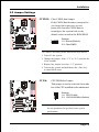
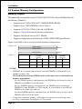
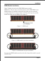
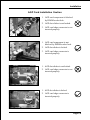
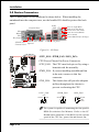
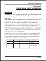
1
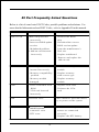
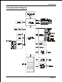
User’s Manual nVIDIA nForce 2 Ultra 400 mainboard nForce2 for AMD Socket A processor TRADEMARK All products and company names are trademarks or registered trademarks of their respective holders. These specifications are subject to change without notice. 60000028PRO10 Manual Revision 1.0 May 24, 2004 DISCLAIMER OF WARRANTIES: THERE ARE NO WARRANTIES WHICH EXTEND BEYOND THE DESCRIPTION ON THE FACE OF THE MANUFACTURER LIMITED WARRANTY. THE MANUFACTURER EXPRESSLY EXCLUDES ALL OTHER WARRANTIES, EXPRESS OR IMPLIED, REGARDING ITS PRODUCTS; INCLUDING ANY IMPLIED WARRANTIES OF MERCHANTABILITY, FITNESS FOR A PARTICULAR PURPOSE OR NONINFRINGEMENT. THIS DISCLAIMER OF WARRANTIES SHALL APPLY TO THE EXTENT ALLOWED UNDER LOCAL LAWS IN THE COUNTRY PURCHASED IN WHICH LOCAL LAWS DO NOT ALLOW OR LIMIT THE EXCLUSION OF THE IMPLIED WARRANTIES. ii 80 Port Frequently Asked Questions Below is a list of some basic POST Codes, possible problems and solutions. For more detailed information about POST Codes, refer to Appendix D in this manual. P O ST C O D E P r o bl e m So l uti o n FFh o r CFh 1 .B IO S c hip inse rte d 1 . Re inse rt the B IO S inc o rre c tly c hip 2 . Inc o rre c t BIO S update ve rsio n 3 . M ainbo ard pro ble m 4 . Add-o n c ard inse rte d inc o rre c tly. 2 . D o wnlo ad the c o rre c t BIO S ve rsio n update fro m the m anufac ture r's We b site . 3 . Re plac e m ainbo ard 4 . Re m o ve and re plac e the add-o n c ard C1 h - C5 h 1 . M e m o ry m o dule 1 . Re inse rt m e m o ry inse rte d inc o rre c tly 2 . M e m o ry c o m patibility m o dule 2 . Re plac e m e m o ry pro ble m 2Dh with c o rre c t type 3 . M e m o ry m o dule dam age d 3 . Re plac e m e m o ry m o dule 1 . Erro r o c c ure d in VG A 1 . Re plac e VG A c ard BIO S 2 . VG A c ard inse rte d 2 . Re inse rt the VG A c ard inc o rre c tly 26h O ve rc lo c k e rro r Cle ar CM O S o r pre ss the inse rt ke y to po we r o n the syste m 07h - 12h 1 . Initial Init keKeyboard ybo ard c o ntro lle r e rro r 1 . Ensure that the ke ybo ard and 2 . RTC e rro r c o rre c tly. 2 . Re plac e the RTC batte ry. m o use are c o nne c te d iii Table of Contents Page Section 1 Introduction Package Contents ...................................................... 1- 1 Mainboard Features ................................................... 1- 2 System Block Diagram ............................................... 1- 5 Section 2 Specification Mainboard Specification ............................................ 2- 1 Section 3 Installation Mainboard Layout ..................................................... 3- 2 Easy Installation Procedure ....................................... 3- 3 CPU Insertion ............................................................. 3- 3 Jumper Settings .......................................................... 3- 5 System Memory Configuration .................................. 3- 6 Expansion Slots .......................................................... 3- 8 Device Connectors..................................................... 3- 10 Power-On/Off (Remote) .............................................. 3- 17 External Modem Ring-in Power ON and Keyboard Power ON Function (KBPO) ..................... 3- 17 STR (Suspend To RAM) Function ............................ 3- 18 CPU Overheating Protection ...................................... 3- 19 Section 4 BIOS Setup Main Menu ................................................................ 4- 1 Standard CMOS Setup ............................................... 4- 2 Advanced BIOS Features .......................................... 4- 3 Advanced Chipset Features ...................................... 4- 4 Integrated Peripherals ................................................ 4- 8 Power Management Setup ......................................... 4- 14 iv PNP/PCI Configuration .............................................. 4- 16 PC Health Status ........................................................ 4- 18 Power BIOS Features ................................................. 4- 19 Defaults Menu ........................................................... 4- 20 Supervisor/User Password Setting ............................ 4- 21 Exit Selecting .............................................................. 4- 22 Section 5 S-ATA RAID Configuration Introduction ............................................................... 5- 1 NVidia SATA RAID Features ....................................... 5- 3 Silicon Image SiI3114 SATA RAID Features (Optional) . 5- 4 Enable RAID Function ............................................... 5- 5 Section 6 Driver Installation Easy Driver Installation .............................................. 6- 1 Realtek Sound Manager Quick User guide ................ 6- 2 Appendix Appendix A Realtek Media Player User’s Guide ............................ A-1 Appendix B Update Your System BIOS ......................................... B- 1 Appendix C NVidia RAID BIOS Utility ............................................ C- 1 Silicon Image SiI3114 RAID BIOS Utility (Optional) ... C- 4 Appendix D POST Codes ............................................................... D- 1 v Page Left Blank vi Introduction Section 1 INTRODUCTION 1-1 Package Contents Contents Powerpack items A. Mainboard I. Mini heatsink B. User’s manual J. Tool Pen K. Extra USB2.0 port cable C. Floppy drive cable Optional Items D. HDD drive cable L. S/PDIF Module E. CD (drivers and utilities) If you need the optional item, please contact your dealer for assistance. F. I/O Shield G. Game & COM bracket cable H. S-ATA data and power cable E USER’S MANUAL C G D F B A H I J K L Page 1-1 Introduction 1-2 Mainboard Features Brief Introduction 2 AthlonTM Processor The AMD AthlonTM is a seventh-generation micro architecture with an integrated L2 cache, which is powerful enough to support the bandwidth requirements of a large range of applications, hardware, graphics, and memory technologies. For more information about all the new features AthlonTM Processor deliver, check out the AMD website at http://www.amd.com 2 Chipset This board is designed with nVidia chipset, nForce2TM Ultra 400 as North Bridge and nForce2TM Gigabit MCP as South Bridge, The nForce2 Ultra 400 delivers twice the bandwidth by implementing the new NVIDIA DualDDR™ Memory Architecture speed to DDR 400 memories. This generation System Platform Processor also implements the AGP 8X interface, HyperTransport Link, and is fully compliant with industry standard power management specifications such as ACPI 2.0 and PCI Power Management Interface (PMI) Spec 1.1. For more details about the NVIDIA nForce2 MCPs, please visit the NVIDIA Web site at http://www.nvidia.com. 2 Accelerated Graphics Port (AGP) The AGP slot on the board is compliant with the new AGP 3.0 specification. This new specification enhances the functionality of the original AGP specification by allowing 8X data transfers ( 8 data samples per clock) resulting in maximum bandwidth of 2.1GB/s. Only 1.5V AGP cards are supported. 2 Ultra ATA100/133 The mainboard provides an Ultra ATA100/133 Bus Master IDE controller. This controller supports Ultra ATA100/133 protocols which are ideal to support demanding applications such as real-time video, multimedia, and a high performance operating system. A new IDE cable is required for Ultra ATA100/133. 2 Hardware Monitoring Hardware monitoring enables you to monitor various aspects of the system operation and status. This includes CPU temperature, voltage and fan speed in RPMs. Page 1-2 Introduction 2 GbE LAN This mainboard is optionally mounted with a Gigabit ethernet LAN chipset. The new Gigabit Ethernet LAN allows data transmission at 1,000 megabits per second (Mbps), which runs 10 times faster than conventional 10/100BASE-T Ethernet LANs. 2 Serial ATA Support Serial ATA, an evolutionary replacement for Parallel ATA IDE storage interface .Increases the peak data transfer speed up to 150MB/sec and allows future enhancements to the computing platform. 2 More S-ATA (Optional) Extra Silicon Image SiI3114 S-ATA controller onboard for 4 additional S-ATA ports with 150MB/sec supporting RAID 0, 1 , 10, 5. 2 IEEE 1394 IEEE 1394 provides transfer rates up to 400Mbits/sec. IEEE 1394 provides enhanced PC connectivity for consumer electronics audio/video appliances, storage peripherals, portable devices such as digital cameras, and inter-PC communications. 2 USB2.0 A popular USB standard for plugging in peripherals with up to 480Mbps transfer speed while maintaining backward compatibility with older USB1.1 device. 2 8ch Delivers 8 channel audio to bring you the latest in audio realism from DVD movies and games. Perfect for your home theatre system. Page 1-3 Introduction Special Features & 80 Port An onboard LED-display trouble-shooting device, facilitating user to detect boot-up problems. & NVIDIA Firewall The NVIDIA Firewall is a high performance, “hardware-optimized” firewall offering enhanced reliability and protection at the end-point. & QuickSPDIF On board SPDIF-out connector for quick connection to multi-channel speakers. Not only removes cable cluttering but also delivers loss-free digital audio to let you enjoy DVD movies and games with crystal clear sound. & Magic Health Reports your system hardware status for every boot-up to help detect faults early. Monitor hardware status including CPU temperature, CPU/Memory/AGP voltage, fan RPM speed for chassis fan, CPU fan & Power supply fan. & EZ-Boot Simply press “ESC” to select your bootable device. No more hassle to search the BIOS menu, change and re-start. & PowerBIOS Supporting a full range of overclocking setting via BIOS. Various adjustable feature include FSB/AGP/Memory voltage tweaking. Page 1-4 Introduction 1-3 System Block Diagram Page 1-5 Introduction Page 1-6 Specification Section 2 SPECIFICATION Mainboard Specification Processor Supports 462-pin SocketA for AMD Athlon XP and Barton processors with 266/333/400MHz Front Side Bus - Athlon XP (1500+ to 3000+) with 266/333MHz Front Side Bus, - Barton (2500+ to 3200+) with 333/400MHz Front Side Bus Chipset nVidia AGPset : nForce2 Ultra 400 + Gigabit MCP Main Memory Three 184-pin DDR DIMM sockets for 64-bit, Unbuffered, Single/Doubleside and DDR-266/333/400 DIMMs Supports 128-bit dual channel memory architecture Supports up to 3GB memory size BIOS Flash EEPROM with Award BIOS - ACPI v2.0 compliant - S3 (Suspend to DRAM) sleep-state support - SMBIOS (System Management BIOS) v2.2 compliant - Supports Power failure recovery - Able to wake the computer from specific states by LAN, Power switch, PME#, RTC alarm, USB, PS2 K/B, PS2 Mouse, Modem Ring-in COM#1… Onboard PCI Devices 1394 --> Integrated VIA VT6307 1394 controller with 2 ports solution - IEEE-1394a compliant with up to 400Mbps bandwidth LAN --> 1Gbps Fast Ethernet with onboard Cicada CIS8201 LAN PHY Page 2-1 Specification S-ATA --> Integrated Serial ATA controller from Silicon Image SiI3114 (Optional) for 4 ports solution with RAID 0, 1 ,10, 5 and support up to 150MB/sec transfer rate For more detailed information about SiI3114, refer to user’s manual in the bundled CD. Legacy IO Controller Winbond W83627THF LPC IO controller with floppy, printer, game, serial and SIR interface Supports Hardware Monitoring function Audio Eight channel audio with analog and digital output using Realtek ALC850 AC’97 CODEC (for high-end model only) - AC’97 v2.3 compliant - Supports CD-In, AUX-IN and S/PDIF-in interface - Supports Line-out and Mic-In for front panel - Supports automatic “Jack-sensing” - Rear panel audio jacks configuration: Phone Jack Color 2 ch an n el 6 ch an n el Light Blue Line-in Rear stereo-out Line-in Lime Line-out Front stereo-out Front stereo-out Pink Mic-in Center&Subwoofer Gray Mic-in Side stereo-out Black Rear stereo-out Orange Center&Subwoofer Supports S/PDIF-out from nForce2 MCP south bridge Peripheral Interfaces ) At Rear Panel PS/2 keyboard and mouse ports One Parallel (printer) port One S/PDIF-Out Coaxial jack Page 2-2 8 ch an n el Specification One S/PDIF-Out Optical One Serial port One RJ45 LAN connector Four USB2.0 ports Six Audio jacks ) Onboard connector and pin-header One floppy drive connector Two ATA-133 IDE connectors Four extra USB2.0 ports Two CD-IN connectors One Front Panel Audio connector One S/PDIF in/out connector One IR connector One Game port connector One Serial Port (COM2) connector Two 1394 connectors Six S-ATA connectors ( 4 optional from Silicon Image SiI3114 chip) Three Fan connectors Front Panel Controller Supports Reset & Soft-Off switches Supports HDD & Power LEDs Supports PC speaker Expansion Slots One AGP slot supporting 1.5v 4X/8X AGP card - AGP v3.0 compliant Six PCI slots with Bus Master support - PCI v2.2 compliant Page 2-3 Specification Other Features Magic Health – A quick “dashboard” display at POST to show hardware status. Helps to detect faults early. EZ Boot – An easy way let end-user can choose to boot from hard drive, CD-ROM, floppy, … KBPO – Keyboard power on, turn on the computer from keyboard Supports NVIDIA Personal Firwall Function under Windows 2000/XP For more detailed information about NVIDIA Firewall, refer to user’s manual in the bundled CD. PowerBIOS for excellent Overclocking capabilities through - subtle voltage tuning for CPU, Memory, AGP - subtle frequency tuning on FSB with 1MHz increment - Supports complete Asynchronous FSB/Memory and Asynchronous FSB/ AGP, PCI scheme for overclocking CPU Overheating Protection P80P for system debugging Form Factor 305mm x 245 mm ATX size Page 2-4 Installation Section 3 INSTALLATION Note: Depending on the model you purchased, some components are optional and may not be available. Page 3-1 Installation Mainboard Layout <Figure 1> Note: Depending on the model you purchased, some components are optional and may not be available. Page 3-2 Installation Easy Installation Procedure The following must be completed before powering on your new system: 3-1. CPU Installation 3-2. Jumper Settings 3-3. System Memory Configuration 3-4. Expansion Slots 3-5. Device Connectors 3-1 CPU Installation CPU Insertion: (use AMD AthlonTM as reference) Step 1 Open the socket by raising the actuation lever. <Figure 2> Step 2 Insert the processor. <Figure 3> Ensure proper pin 1 orientation by aligning the FC-PGA corner marking with the socket corner closest to the actuation arm tip. The pin field is keyed to prevent misoriented insertion. Don’t force processor into socket. If it does not go in easily, check for mis-orientation and debris. Make sure the processor is fully inserted into the socket on all sides. Page 3-3 Installation Step 3 Close the socket by lowering and locking the actuation lever. <Figure 4> Step 4 Thermal compound and qualified heatsink recommended by AMD are a must to avoid CPU overheat damage. For more information about installing your CPU, please refer to the AMD website article “Socket A AMD processor and Heatsink Installation Guide” http://www.amd.com/products/cpg/athlon/pdf/23986.pdf. <Figure 5> Page 3-4 Installation 3-2 Jumper Settings JCMOS: Clear CMOS data Jumper If the CMOS data becomes corrupted or you forgot the supervisor or user password, clear the CMOS data to reconfigure the system back to the default values stored in the ROM BIOS. 1 Settings: 1-2: Normal (Default) 2-3: Clear CMOS To CMOS Clear data, please follow the steps below. 1. Turn off the system. 2. Change the jumper from “1-2” to “2-3” position for a few seconds. 3. Replace the jumper on to the “1-2” position. 4. Turn on the system and hold down the <Del> key to enter BIOS setup. JCLK: CPU FSB Select Jumper This jumper is used to select the front side bus of the CPU installed on the mainboard. 1 Settings: 1-2: 100/133 MHz 2-3: 133/166/200 MHz (Default) Note: Overclocking may cause system instability and are not guaranteed to provide better system performance. Page 3-5 Installation 3-3 System Memory Configuration Memory Layout The mainboard accommodates three PC1600/2100/2700/3200 184-pin DIMMs (Dual Inline Memory Modules): • Supports up to 3.0GB of 200/266/333/400MHz DDR SDRAM • Supports up to 3 DDR DIMMs (refer to Table 1) • Supports 64/128/256/512Mb, 1Gb x8 & x16 DRAMs • Supports 128-bit dual channel memory architecture • Supports unbuffered and non-ECC DIMMs • Supports configurations defined in the JEDEC DDR DIMM specification Figure 6 and Table 1 show several possible memory configurations. <Figure 6> DDR DIMM 2 Bank 1 DDR DIMM 3 Bank 0 DDR DIMM 1 <Table 1> 1 DIMM (64-bit) DIMM#1 DIMM#2 DIMM#3 2 DIMMs (64-bit) SS/DS SS/DS SS/DS SS/DS SS/DS 2 DIMMs (128-bit) SS/DS SS/DS SS/DS SS/DS NOTES: • DIMM#2 & #3 shared same memory bus and DIMM#1 is dedicated for 2nd channel memory bus. We recommend you to use DIMM socket of the same color to obtain the best memory performance. - For one DIMM memory configuration, the DIMM can be located on any of DIMM#1 to DIMM#3 in 64-bit mode - For two DIMMs memory configuration, the DIMMs can be located on DIMM#2/#3 and DIMM#1 in 128-bit mode. It is preferable to use DRAM DIMM of the same type and size. - For three DIMMs memory configuration, the DIMMs can be located on all DIMM sockets in 128-bit mode. • Using non-compliant memory with higher bus speeds (overclocking) may severely compromise the integrity of the system. Page 3-6 Installation DIMM Module Installation Figure 7 displays the notch on the DDR DIMM memory module. DIMMs have 184 pins and one notch that matches with the DDR DIMM socket. DIMM modules are installed by placing the chip firmly into the socket and pressing straight down as shown in figure 8 until the white clips close and the module fits tightly into the DIMM socket (figure 9). CENTER KEY ZONE (2.5 V DRAM) <Figure 7> DIMM notch <Figure 8> DIMM module clips before installation <Figure 9> DIMM module clip after installation To remove the DIMM module press down the white clips and the module is ejected from the socket. Page 3-7 Installation 3-4 Expansion Slots AGP Slot The mainboard is equipped with an AGP slot. Make sure you install a card that supports the 1.5V specification. AGP Slot PCI Slots PCI Slots The mainboard is equipped with 6 PCI slots. Installing an Expansion Card The steps below assume that the mainboard is already installed in the system chassis. 1. Make sure the PC and all other peripheral devices connected to its has been powered down. 2. Disconnect all power cords and cables. 3. Remove the system unit cover. 4. Remove the bracket of the slot that you intend to use. (You need to remove the screw in order to remove the bracket.) 5. Align the card above the slot then press it down firmly until it is completely seated in the slot. 6. Secure the card to the chassis with the screw you removed in step 4. 7. Replace the system unit cover. 8. Power on the PC. 9. Enter the BIOS step program to make the necessary settings. 10. Save the settings and restart the PC. 11. Install the software drivers of the expansion cards, if necessary. Page 3-8 Installation AGP Card Installation Caution 1. AGP card component is blocked by DIMM socket lock. 2. AGP slot clicker is not locked. 3. AGP card edge connector is not inserted properly. 1. AGP card component is not blocked by DIMM socket lock. 2. AGP slot clicker is locked. 3. AGP card edge connector is inserted properly. 1. AGP slot clicker is not locked. 2. AGP card edge connector is not inserted properly. 1. AGP slot clicker is locked. 2. AGP card edge connector is inserted properly. Page 3-9 Installation 3-5 Device Connectors The I/O back panel for this mainboard is shown below. When installing the mainboard into the computer case, use the bundled I/O shield to protect this back panel. RJ45 LAN Parallel Port Line-in (Light Blue) Side stereo-out (Gray) Front stereo-out (Lime) Rear stereo-out (Black) Mic-in (Pink) Center&Subwoofer (Orange) PS/2 Mouse PS/2 Keyboard S/PDIF-out S/PDIF-out COM1 Coaxial Jack Optical USB2.0 x 4 ports Figure 10 - I/O Ports JPWR_FAN JCPU_FAN JCPU_FAN / JPWR_FAN / JSYS_FAN: CPU/Power/Chassis Fan Power Connectors JCPU_FAN: The CPU must be kept cool by using a heatsink with fan assembly. JSYS_FAN JPWR_FAN: If you are installing an additional fan in the unit, connect to this fan connector. JSYS_FAN: The chassis fan will provide adequate airflow throughout the chassis to prevent overheating the CPU. JCPU_FAN +12V Ground Sense 1 JPWR_FAN +12V Ground NC 1 JSYS_FAN 1 Ground +12V Sence The system is capable of monitoring the fan speed in RPM (Revolutions Per Minute). Refer to the PC Health Status submenu of the BIOS for the current speed of the CPU fan , power fan and chassis fan. Page 3-10 Installation FDD: Floppy Controller Connector This mainboard connects floppy disk drive. IDE1/IDE2:Ultra DMA-100/133 Primary/Secondary IDE Connector IDE1IDE2 This mainboard is equipped with 2 IDE connectors to support up to 4 ATA-133 IDE drives. It supports PIO and DMA mode operations for maximum data transfer rate of 133MB/sec per channel. FDD 34 33 40 When using two IDE drives, one must be set to 39 Master mode and the other to Slave mode. Refer to your disk drive user’s manual for information about selecting the proper drive switch settings. 1 2 FDD 2 1 IDE1/IDE2 PW1: 20-pin ATX Power Connector PW12: 4-pin ATX12V Power Connector The mainboard is equipped with a standard 20-pin ATX main power connector and a 4-pin +12V power connector for connecting an ATX12V power supply. The plugs of the power cables are designed to fit in only one orientation. Insert the plugs into the connectors until they fit in place. PW1 PW12 Caution: The PW1 and PW12 Power Connector must be used simultaneously for the system to work safely. 10 20 +12V +5V 5VSB 3 +12V -5V Ground Ground Ground Ground Ground +5V PS-ON Ground 3.3V Ground -12V 4 +12V Ground +5V PW-OK Ground +5V 1 2 PW12 3.3V 3.3V 1 11 The board requires a minimum of 250 Watt power supply to operate. Your system configuration (amount of memory, add-in cards, peripherals, etc.) may exceed this minimum power requirement. To ensure that adequate power, use a 300 Watt or greater power supply. PW1 Page 3-11 Installation CFPA: Front Panel Audio Connector When the jumpers are removed this connector can be used for front panel audio. The front panel phone jack should have “normal close” switch. Without phone plug inserted, the rear panel audio is enabled. With phone plug inserted, the rear panel audio will be disabled. MIC_In 1 2 GND +5V NC Front Line-out-R Rear Line-out-FR Key Rear Line-out-FL Front Line-out-L 9 10 Settings: Pins (5-6) & (9-10) Short (default): Only the onboard rear panel audio jack can be used. Pins (5-6) & (9-10) Open: Only front panel audio jack can be used. In 2-Channel audio mode, Mic-In is shared for both front panel and rear panel. In 6-Channel audio mode, the Mic-In is dedicated for front panel use, and rear panel Mic-In function will switch to Center and Subwoofer support. CD_IN1/AUX_IN1: CD Audio_IN Connector These connectors are used to receive audio form a CD-ROM drive, TV tuner or MPEG card. AUX_IN1 CD_IN1 CD_IN_Right AUX_IN1 CD_IN1 AUX_IN_Right CD_Reference 1 Page 3-12 CD_IN_Left GND 1 AUX_IN_Left Installation SPDIF: Sony/Philips Digital InterFace connector This connector links digital audio between the mainboard and your audio devices, such as CD player, sampler or DAT recorder. It allows the digital transmission of audio data in S/PDIF format. SPDIF_IN VCC 5 1 6 2 NC GND SPDIF_OUT GAME1: Game/MIDI connector This port works well with any application that is compatible with the standard PC joystick. J1CY J1CX J1B1 J1B2 GND +5V +5V 1 15 2 16 J2CX +5V MIDI_In J2B2 J2B1 J2CY MIDI_Out COM2: Serial Port Connector The serial port can be used with modems, serial printers, remote display terminals, and other serial device. RTS RI DSR CTS NC 2 1 10 9 DCD TXD Ground RXD DTR Page 3-13 Installation SATA1 / SATA2: Serial ATA Connectors SATA3 / SATA4 / SATA5 / SATA6 (Optional): Serial ATA Connectors from Silicon Image SiI3114 chip. These connectors enable you to connect Serial ATA devices that conform to the Serial ATA specification. SATA2 1 SATA5 SATA6 SATA3 SATA4 GND B+ BA- A+ GND GND C1394-1 / C1394-2 : 400Mbps 1394a (FireWire) Connectors C1394-1 and C1394-2 enable you to connect two IEEE 1394 ports for use with external devices that conform to the IEEE 1394 specification. TPB+ +12V (Fused) GND TPA+ Key 9 1 10 C1394-1 C1394-2 2 GND TPA+12V (Fused) GND TPB- LED1: 80 Port Debug LED Provides two-digit POST code to show why the system fail to boot. Allows quick and easy optimization. 80 Port Debug 7-segment LED display (Refer to Appendix E for POST codes) Page 3-14 Installation CUSB3/CUSB4: USB 2.0 ports USB2.0 allows data transfer speed up to 480Mbps. This mainboard includes 4 additional USB2.0 ports, identified by two 10-pin connector. If you wish to use the additional USB ports, install the card-edge bracket to the system chassis then insert its cables to this 10-pin connector. CUSB3 CUSB4 CAUTION ! Please make sure the USB cable has the same pin assignment. A different pin assignment may cause damage to the system. If you need the USB cable, please contact our retailer. Page 3-15 Installation CFP: Front Panel Connector HD_LED This LED will light up whenever the hard drive is being accessed. PWR_LED This connects to the power button of the system chassis CFP CIR RST This switch allows you to reboot without having to power off the system thus prolonging the life of the power supply or system. PW_ON This is connected to the power button on the case. To use the Soft-Off by PWR-BTTN feature, refer to the Power Management Setup in the BIOS setup section of this manual. CIR: IR connector Connect the IrDA cable (if available) to this IR connector. CSPK Page 3-16 CSPK: Speaker Connect to the case speaker. Installation 3-6 Power-On/Off (Remote) This board has a 20-pin ATX and a 4-pin ATX12V power supply connector to support power supplies with Remote On/Off feature. The 4-pin ATX12V connector must be plugged in for the system to operate safely. The chassis power button should be connected to the mainboard front panel PW_ON header (Figure 15). You can turn off the system in two ways: by pressing the front panel power On/Off button or using the "Soft Off" function that can be controlled by an operating system such as Windows®XP/ME/2000/98. Note: For maintaining the DDR SDRAM power during STR (ACPI S3) function, it is strongly recommended to use power supplies that have a +5VSB current of (>=) 2A. Please check the 5VSB’s specification printed on the power supply’s outer case. Note: The board requires a minimum of 250 Watt power supply to operate. Your system configuration (amount of memory, add-in cards, peripherals, etc.) may exceed this minimum power requirement. To ensure that adequate power, use a 300 Watt (or higher) power supply. 12V 4-pin 20-pin PW-ON Case (chassis) Power ON/OFF button (PW-ON) Figure 15: Simple ATX power ON/OFF controller 3-7 External Modem Ring-in Power ON and Keyboard Power ON Functions (KBPO) Modem-Ring Power ON Function The mainboard supports External Modem Ring-in Power ON function. Once you connect an external modem to COM1 or COM2, you can turn on the system through remote and host dial-up control. Keyboard Power ON Function The mainboard features a keyboard power on function to turn on the power supply using a keypress. Refer to the Power Management Setup in the BIOS setup section for details. To enable this feature, the BIOS default setting is Keyboard Hot Key (<Ctrl> + <F1>). To power off the system, use the Soft-OFF function under Windows XP/ME/2000/98. (refer to Windows online help). Page 3-17 Installation 3-8 ACPI S3 (Suspend To RAM) Function This mainboard supports the STR (Suspend To RAM) power management scheme by maintaining the appropriate power states in the DDR SDRAM interface signals. The power source to the DDR SDRAM is kept active during STR (ACPI S3). Advanced Configuration Power Interface (ACPI) provides many Energy Saving Features for operating systems that support Instant ON and QuickStartTM function. 1. To enable STR functionality to save system power : a. Install ACPI certified add-on cards (such as AGP, LAN, and modem cards). b. In BIOS, under Power Management Setup (refer to Section 4), select “ACPI Suspend Type: S3(STR)”. If you have a USB mouse or keyboard, set “USB Wake-Up from S3” to “Enabled”. c. Install Windows® XP/2000/ME/98SE. d. Restart the system. e. When in Windows, open the Control Panel Power Management application, and click the Advanced tab. In the Power buttons section, select “Stand By” from the drop-down lists. 2. To activate the STR function: a. Click the START button and choose Shut Down. b. In the Shut Down Windows dialog box, select the Stand By option to enter STR mode. The following are the differences between STR power saving mode and Suspend (Power On Suspend) mode: a. STR is the most advanced Power Management mode. b. STR cuts all the power supplied to peripherals except to memory - max. power saving. c. STR saves and keeps all on-screen data including any executed applications to DDR SDRAM. d. In STR mode, you must push the power button (connected to the onboard PWOn of CFP pin), click your USB mouse buttons, or press your USB keyboard keys to wake up your system to the last display. Page 3-18 Installation 3-9 CPU Overheating Protection This mainboard is equipped with CPU Overheating Protection. It will automatically shutdown the system when CPU temperature reaches approximately 110°C to prevent long term damage to the CPU. When this happens, the speaker produces a sustained beep sound and the system will not be able to power on. This protection is designed through hardware and no BIOS setup is required. To power on your system again, Step 1: Unplug the ATX power cord (or turn off the ATX power supply switch) Step 2: Wait a few minutes for the CPU to cool. Step 3: Check that the CPU heatsink and cooling fan assembly is properly installed. Be careful when touching the heatsink as it may be hot. Step 4: Plug back the ATX power cord (or turn on the ATX power supply switch) and power -on the system. If the beeping sound persists, repeat Step 1 to remove the power source. Page 3-19 Installation Page 3-20 BIOS Section 4 BIOS SETUP Main Menu The ROM BIOS contains a built-in Setup program which allows user to modify the basic system configuration and hardware parameters. The modified data is stored in a battery-backed CMOS, so that data will be retained even when the power is turned off. In general, the information saved in the CMOS RAM will stay unchanged unless there is a configuration change in the system, such as hard drive replacement or a device is added. It is possible for the CMOS battery to fail causing CMOS data loss. If this happens you will need install a new CMOS battery and reconfigure your BIOS settings. The BIOS setup screen and description are for reference only, and may not exactly match what you see on your screen. The contents of BIOS are subject to change without notice. Please visit our website for updates. To enter the Setup Program : Power on the computer and press the <Del> key during the POST (Power On Self Test). The BIOS CMOS SETUP UTILITY opens. (Figure 1) Figure 1: CMOS Setup Utility Page 4-1 BIOS The main menu displays all the major selection items. Select the item you need to reconfigure. The selection is made by moving the cursor (press any direction (arrow key ) to the item and pressing the ‘Enter’ key. An on-line help message is displayed at the bottom of the screen as the cursor is moved to various items which provides a better understanding of each function. When a selection is made, the menu of the selected item will appear so that the user can modify associated configuration parameters. 4-1 Standard CMOS Setup Choose “STANDARD CMOS FEATURES” in the CMOS SETUP UTILITY Menu (Figure 2). Standard CMOS Features Setup allows the user to configure system settings such as the current date and time, type of hard disk drive installed, floppy drive type, and display type. Memory size is auto-detected by the BIOS and displayed for your reference. When a field is highlighted (use direction keys to move the cursor and the <Enter> key to select), the entries in the field can be changed by pressing the <PgDn> or the <PgUp> key. Figure 2: Standard CMOS Setup Notes: • If the hard disk Primary Master/Slave and Secondary Master/Slave are set to Auto, the hard disk size and model will be auto-detected. • The “Halt On:” field is used to determine when the BIOS will halt the system if an error occurs. Page 4-2 BIOS 4-2 Advanced BIOS Features Selecting the “ADVANCED BIOS FEATURES” option in the CMOS SETUP UTILITY menu allows users to change system related parameters in the displayed menu. This menu shows all of the manufacturer’s default values for the board. Pressing the [F1] key displays a help message for the selected item. Figure 3: BIOS Features Setup Removable Device / Hard Disk / CD-ROM / Network Boot Priority This item allows you to select the removable device/hard disk/CD-ROM/network boot priority. First /Second/Third Boot Device The BIOS attempts to load the operating system from the devices in the sequence selected in these items. Options: Floppy, LS120, Hard Disk, CDROM, ZIP100, USB-FDD, USB-ZIP, LAN, Disabled. Boot Other Device When enabled, the system searches all other possible locations for an operating system if it fails to find one in the devices specified under the first, second, and third boot devices. Options: Enabled, Disabled. Page 4-3 BIOS Boot Up Floppy Seek If this item is enabled, it checks the size of the floppy disk drives at start-up time. You don’t need to enable this item unless you have a legacy diskette drive with 360K capacity. Options: Enabled, Disabled. Security Option This category allows you to limit access to the System and Setup, or just to Setup. The default is Setup. System: The system will not boot and access to Setup will be denied unless the correct password is entered at the prompt. Setup: The system will boot, but access to Setup will be denied unless the correct password is entered at the prompt. Full Screen LOGO Show This item allows you determine Full Screen LOGO display during POST. Options: Enabled, Disabled. 4-3 Advanced Chipset Features Choose the “ADVANCED CHIPSET FEATURES” option in the CMOS SETUP UTILITY menu to display following menu. Figure 4: Chipset Features Setup Page 4-4 BIOS System Performance This item will help you to configure your system performance, selecting higher performance may cause instability. Options: Optimal, Aggressive, Turbo, Expert. CPU Clock Ratio Use this item to select a multiplier to set the CPU frequency. See FSB Frequency item below for explanation. FSB Frequency Enables you to increment the CPU’s clock generator at 1 MHz step. This works together with CPU Clock Ratio (above) to set the CPU operating frequency. CPU Clock Generator x CPU Clock Ratio = CPU Frequency For example, if you have a processor that is rated at 2.4GHz and the clock generator is 200MHz, then 200MHz x 12 = 2.4GHz Note: Overclocking failure will cause no display on the monitor. To overcome this switch off the power supply and switch on again. Restart the system, press and hold <Insert> key. This will revert the BIOS to default or initial setting. CPU Interface Allows you to set CPU/FSB parameters for CPU most stable or overclocked. Options: Optimal, Aggressive. Memory Frequency Enables you to select the memory frequency. Options: By SPD, 50%, 60%, 66%, 75%, 80%, 83%, 100%, 120%, 125%, 133%, 150%, 166%, 200%, Auto. Below is a list of Auto mode table for reference. Note: Auto mode ensures the FS B SPD/Memory Sync/Async and Speed set 200 266 Sync 200 200 333 Sync 200 200 400 Sync 200 266 266 Sync 266 266 333 Sync 266 266 400 Sync 266 333 266 Async 333/266 333 333 Sync 333 333 400 Sync 333 400 266 Async 400/266 400 333 Async 400/333 400 400 Sync 400 memory init module initializes the memory controller for the best performance based on the FSB and DDR SPD capabilities. Page 4-5 BIOS Memory Timings For setting DRAM Timing. Options: Optimal, Aggressive, Turbo, Expert. T (RAS) This item specifies the number of clock cycles needed after a bank active command before a precharge can occur (sets the minimum RAS pulse width.). Options: 1 ~ 15. T (RCD) This item sets the timing parameters for the system memory such as the CAS (Column Address Strobe) and RAS (Row Address Strobe). Options: 1 ~ 7. T (RP) This item refers to the number of cycles required to return data to its original location to close the bank or the number of cycles required to page memory before the next bank activate command can be issued. Options: 1 ~ 7. CAS Latency This item specifies the number of clock cycles needed after a Column Address Strobe (CAS) signal before data can be read. The default is by DRAM SPD. Options: 2.0, 2.5, 3.0. Memory Auto Precharge Enables Memory Auto Precharge function. Options: Enabled, Disabled. FSB Spread Spectrum This item can significantly reduce the EMI (ElectroMagnetic Interference) generated by the CPU. Options: Disabled, 0.50%, 1.00%. AGP Spread Spectrum This item can significantly reduce the EMI (ElectroMagnetic Interference) generated by the AGP. Options: Disabled, 0.50%, 1.00%. Page 4-6 BIOS AGP Aperture Size (MB) This item defines the size of the aperture if you use an AGP graphics adapter. It refers to a section of the PCI memory address range used for graphics memory. Options: 32, 64, 128, 256, 512 MB. AGP Frequency This item allows you to select the AGP frequency. Options: Auto, 90MHz, 93MHz, 95MHz, 97MHz, 100MHz, 50MHz ~87MHz in 1MHz increments. AGP 8X Support Enables AGP 8X supports. Options: Disabled, Enabled. AGP Fast Write Capability This item allows you to use Fast Write transfer for CPU write to graphics adapter’s memory. Options: Disabled, Enabled. System BIOS Cacheable This item allows the system BIOS to be cached in memory for faster execution. Options: Disabled, Enabled. Video RAM Cacheable This option allows the CPU to cache read/writes of the video RAM. Options: Disabled, Enabled. Page 4-7 BIOS 4-4 Integrated Peripherals Figure 5: Integrated Peripherals Init Display First This item is used to select whether to initialize the AGP or PCI first when the system boots. Options: PCI Slot, Onboard/AGP. IDE Function Setup Scroll to IDE Function Setup and press <Enter>. The following screen appears: Page 4-8 BIOS OnChip IDE Channel 0/1, OnChip Serial-ATA The mainboard supports two channel of ordinary IDE interface and one channel of serial ATA interface. Select “Enabled” to activate each channel separately. Note: If you do not use the onboard IDE connector, then set the Onboard Primary (Secondary) PCI IDE to “Disabled”. Primary/Secondary Master/Slave UDMA Select the mode of operation for the IDE drive. Ultra DMA-100/133 implementation is possible only if your IDE hard drive supports it and the operating environment includes a DMA driver. If your hard drive and your system software both support Ultra DMA-100/133, select Auto to enable UDMA mode by BIOS. Options: Auto, Disabled. IDE Prefetch Mode Selecting “Enabled” reduces latency between each drive read/write cycle, but may cause instability in IDE subsystems that cannot support such fast performance. If you are getting disk drive errors, try setting this value to Disabled. This field does not appear when the Internal PCI/IDE field, above, is Disabled. Options: Enabled, Disabled. IDE RAID This item allows you to enable RAID mode for IDE and SATA ports. When set to “Enabled” the following six fields become available. Options: Enabled, Disabled. IDE DMA transfer access Automatic data transfer between system memory and IDE device with minimum CPU intervention. This improves data throughput and frees CPU to perform other tasks. Options: Enabled, Disabled. IDE HDD Block Mode IDE Block Mode allows the controller to access blocks of sectors rather than a single sector at a time. The default is Enabled. Options: Enabled, Disabled. Page 4-9 BIOS Onboard Device Scroll to Onboard Device and press <Enter>. The following screen appears: Onchip USB Enables the USB controller. Options: Disabled, V1.1+V2.0, V1.1. USB KB/Storage Support Enable/Disable support for USB keyboard/Storage under DOS. Options: Enabled, Disabled. USB Mouse Support Enable/Disable support for USB mouse under DOS. Options: Enabled, Disabled. AC97 Audio This item allows you disable the chipset on-chip AC97 Audio. Options: Auto, Disabled. NV Lan Enables the onboard Gigabit LAN feature. Options: Auto, Disabled. NV Lan MAC Address Machine MAC (NV) address selection. Options: Enabled, Disabled. NV Lan Address Input Allows you to input the MAC (NV) address. Current NV Lan MAC Address Display the current MAC (NV) address. Page 4-10 BIOS Onboard Debug LED Enables the onboard Debug LED feature. Options: Enabled, Disabled. Onboard I/O Chip Setup Scroll to Onboard I/O Chip Setup and press <Enter>. The following screen appears: POWER ON Function Enables computer power on by keyboard, mouse, or hotkey activity. Password: Requires you to enter a password when using the keyboard to power on. Set the password in the next field “KB Power ON Password.” Hot KEY: (default) Enables you to use a hot key combination to power on the computer. Set the hot key combination in the “Hot Key Power ON” field. Enables you to set any keyboard activity to power on the computer. AnyKEY: Button Only: Requires you to push the computer power button to power on the system. Keyboard 98: Enables you to set the Windows 98 key to power on the system. KB Power ON Password Press “Enter” to create a password that is required when you use the keyboard to power on the system. You must set the POWER ON Function to “Password” to be prompted for a password at power on. Page 4-11 BIOS Hot Key Power ON Enables you to set a hot key combination to be used for powering on the system. The default is Ctrl-F1. Options: Ctrl+F1 ~ Ctrl+F12. Onboard FDC Controller Select “Enabled” if you wish to use onboard floppy disk controller (FDC). If you install an external FDC or the system has no floppy drive, select “Disabled “in this field. Options: Enabled, Disabled. Onboard Serial Port 1/2 Select an address and corresponding interrupt for the first and second serial ports. Options: 3F8/IRQ4, 2E8/IRQ3, 3E8/IRQ4, 2F8/IRQ3, Disabled, Auto. UART Mode Select This field configures the 2nd serial port for IR application. Select the required IR protocol or select “Normal” to disable IR mode. Options: Normal, IrDA and ASKIR. RxD, TxD Active When the above UART Mode Select is in IR mode, this field configures the receive and transmit signals generated from the IR port. Options: Hi-Hi, Hi-Lo, Lo-Hi, and Lo-Lo. IR Transmission delay This item allows you to enabled/disable IR transmission delay. Options: Enabled, Disabled. UR2 Duplex Mode This item allows you to select IR half/full duplex function. Options: Half, Full. Use IR Pins This item allows you to select IR transmission routes, one is RxD2, TxD2 (COM Port) and the other is IR-Rx2Tx2. Options: IR-Rx2Tx2; RxD2, TxD2. Onboard Parallel Port This field allows the user to configure the LPT port. Options: 378/IRQ7, 278/IRQ5, 3BC/IRQ7, Disabled. Page 4-12 BIOS Parallel Port Mode This field allows the user to select the parallel port mode. Options: SPP, EPP, ECP, ECP+EPP. EPP Mode Select This field allows the user to select the EPP mode for parallel port mode. Options: EPP1.9, EPP1.7. ECP Mode USE DMA This field allows the user to select DMA1 or DMA3 for the ECP mode. Options: DMA1, DMA3. Game Port Address Select an address for the Game port. Options: 201, 209, Disabled. Midi Port Address Select an address for the Midi port. Options: 290, 300, 330, Disabled. Midi Port IRQ Select an interrupt for the Midi port. Options: 5, 10. Page 4-13 BIOS 4-5 Power Management Setup Choose the “POWER MANAGEMENT SETUP” in the CMOS SETUP UTILITY to display the following screen. This menu allows the user to modify the power management parameters and IRQ signals. In general, these parameters should not be changed unless it’s absolutely necessary. Figure 6: Power Management ACPI Function Enables the ACPI Function. Options: Enabled, Disabled. ACPI Suspend Type This item allows you to select S1(Power-On-Suspend) or S3(Suspend-To-RAM) function. When set to “S3(STR)” or “S1&S3” the following two fields become available. Options: S1(POS), S3(STR), S1&S3. Power Management Use this to select your Power Management selection. The default is User define. Max. saving: Maximum power savings. Inactivity period is 1 minute in each mode. Min. saving: Minimum power savings. Inactivity period is 1 hour in each mode. User define: Allows user to define PM Timers parameters to control power saving mode. Page 4-14 BIOS Video Off Method This option allows you to select how the video will be disabled by the power management. The default is V/H Sync + Blank V/H Sync + Blank: System turns off vertical and horizontal synchronization ports and writes blanks to the video buffer. DPMS Support: Select this option if your monitor supports the Display Power Management Signaling (DPMS) standard of the Video Electronics Standards Association (VESA). Use the software supplied for your video subsystem to select video power management values. Blank Screen: System only writes blanks to the video buffer. HDD Power Down Powers down the hard disk drive after a preset period of system inactivity. Options: Disabled, 1min ~ 15min. HDD Down In Suspend Lets you enable the HDD to power off in suspend mode. Options: Enabled, Disabled. Soft-Off by PBTN Use this to select your soft-off function. The default is Instant Off. Instant Off: Turns off the system instantly. Delay 4 Second : Turns off the system after a 4 second delay. If momentary press of button, the system will go into Suspend Mode. Press the power button again to make system back to work. WOL (PME#) From Soft-Off An input signal from PME on the PCI card awakens the system from soft-off state. Options: Enabled, Disabled. WOR (RI#) From Soft-Off An input signal form RI on the PCI card awakens the system from a soft-off state. Options: Enabled, Disabled. Power-On by Alarm When set to Enable alarm resume, you can set the date (of month) and time (hh:mm: ss), that will awaken a system which has been powered down. Options: Enabled, Disabled. Page 4-15 BIOS PwerOn After Pwr-Fail This item enables your computer to automatically restart or return to its last operating status after power returns from a power failure. Off: The system stays off after a power failure. Former-Sts: The system returns to the state it was in just prior to the power failure. 4-6 PNP/PCI Configuration This page lets the user to modify the PCI IRQ signals when various PCI cards are inserted. WARNING: Conflicting IRQ’s may cause system unable to locate certain devices. Figure 7: PNP/PCI Configuration Setup Resources Controlled By Determines what controls system PNP/PCI resources. The default is Auto (ESCD). Manual: PNP Card’s resources are controlled manually. The “IRQ Resources” field becomes available and you can set which IRQ-X and DMA-X are assigned to PCI and onboard devices. Auto: BIOS assigns the interrupt resource automatically. Page 4-16 BIOS PCI/VGA Palette Snoop This item is designed to overcome problems that may be caused by some nonstandard VGA cards. Options: Enabled, Disabled. Interrupt requests are shared as shown below: INT A AGP Slot INT B INT C AC97 V Slot 2 V V Slot 4 V Slot 5 V Onboard 1394 V Onboard LAN Onboard SiI3114 Onboard USB V V V Onboard USB V USB 2.0 SM BUS INT E V Slot 1 Slot 3 INT D V V V IMPORTANT! When using PCI cards on shared IRQ slots, make sure its drivers support “Shared IRQ”, or that the cards do not need IRQ assignments. IRQ conflicts between the two PCI groups will make the system unstable or cards inoperable. Page 4-17 BIOS 4-7 PC Health Status Figure 8: PC Health Status Show PC Health in POST When this function is enabled the PC Health information is displayed during the POST (Power On Self Test). Options: Enabled, Disabled. Shutdown Temperature This is the temperature that the computer will turn off the power to combat the effects of an overheating system. (requires ACPI to be enabled in Power Management BIOS and ACPI compliant operating system.) The default is Disabled. Options available are 60oC/140oF to 75oC/167oF in increments of 5oC. Current System/CPU Temperature Displays the current system /CPU temperature. Current CPU/Chassis/Power FAN Speed Displays the current speed of the CPU, chassis, and power fan speed in RPMs. CPU Vcore Voltage The voltage level of the CPU(Vcore). AGP Voltage The voltage level of power supplied to AGP card. Page 4-18 BIOS Chipset Voltage The voltage level of the Chipset. Dimm Voltage The voltage level of the DRAM. Battery Voltage The voltage level of the battery. Power Supply + 5V, 5V Standby The voltage level of the switching power supply. 4-8 POWER BIOS Features This page lets you adjust various parameters to obtain improved performance for overclocking. Warning: Overclocking requires expert knowledge and risks permanent damage to system components. We recommend you leave these parameters at their default values for proper operation. Figure 9: Power BIOS Features Page 4-19 BIOS CPU Voltage Regulator This item allows you to set the CPU Vcore voltage. Options: 1.400V to 2.200V in 0.025V increments. AGP Voltage Regulator This item allows you to set the AGP slot voltage. Options: 1.5V to +1.8V in 1V increments. DIMM Voltage Regulator This item allows you to set the DIMM slot voltage. Options: 2.50V, 2.63V, 2.77V, 2.90V. Chipset Voltage Regulator This item allows you to set the chipset slot voltage. Options: 1.6V, 1.8V, 2.0V. Warning: Default chipset voltage is 1.6V. Setting higher voltage may cause damage to chipset. Please ensure proper cooling for Northbridge and Southbridge. 4-9 Defaults Menu Selecting “Defaults” from the main menu shows you two options which are described below Load Fail-Safe Defaults When you press <Enter> on this item you get a confirmation dialog box: Load Fail-Safe Defaults (Y/N) ? N Pressing ‘Y’ loads the BIOS default values for the most stable, minimal-performance system operations. Load Optimized Defaults When you press <Enter> on this item you get a confirmation dialog box: Load Optimized Defaults (Y/N) ? N Pressing ‘Y’ loads the default values that are factory settings for optimal performance system operations. Page 4-20 BIOS 4-10 Supervisor/User Password Setting This function lets you set either Supervisor or User Password, or both, to prevent unauthorized changes to BIOS menus. supervisor password: full rights to enter and change options of the setup menus. user password: only enter but no rights to change options of the setup menus. When you select this function, the following message will appear at the center of the screen to assist you in creating a password. ENTER PASSWORD: Type the password, up to eight characters in length, and press <Enter>. The password typed now will clear any previously entered password from CMOS memory. You will be asked to confirm the password. Type the password again and press <Enter>. You may also press <Esc> to abort the selection and not enter a password. To disable a password, just press <Enter> when you are prompted to enter the password. A message will confirm the password will be disabled. Once the password is disabled, the system will boot and you can enter Setup freely. PASSWORD DISABLED. When a password has been enabled, you will be prompted to key in each time you enter Setup. This prevents an unauthorized person from changing any part of your system configuration. Additionally, when a password is enabled, you can also require the BIOS to request a password every time your system is rebooted. This would prevent unauthorized use of your computer. You can determine when the password is required within the Advanced BIOS Features Menu and its Security option. If the Security option is set to “System”, the password will be required both at boot and at entry to Setup. If set to “Setup”, prompting only occurs when trying to enter Setup. Page 4-21 BIOS 4-11 Exiting BIOS Save & Exit Setup Pressing <Enter> on this item asks for confirmation: Save to CMOS and EXIT (Y/N)? Y Pressing “Y” stores the selections made in the menus in CMOS – a special section of memory that stays on after you turn your system off. The next time you boot your computer, the BIOS configures your system according to the Setup selections stored in CMOS. After saving the values the system is restarted again. Exit Without Saving Pressing <Enter> on this item asks for confirmation: Quit without saving (Y/N)? Y This allows you to exit Setup without storing in CMOS any change. The previous selections remain in effect. This exits the Setup utility and restarts your computer. Page 4-22 S-ATA RAID Configuration Section 5 S-ATA RAID CONFIGURATION Introduction This section gives a brief introduction on the RAID-related background knowledge and a brief introduction on S-ATA RAID Host Controller. RAID Basics RAID (Redundant Array of Independent Disks) is a method of combining two hard disk drives into one logical unit. The advantage of an Array is to provide better performance or data fault tolerance. Fault tolerance is achieved through data redundant operation, where if one drives fails, a mirrored copy of the data can be found on another drive. This can prevent data loss if the operating system fails or hangs. The individual disk drives in an array are called “members”. The configuration information of each member is recorded in the “reserved sector” that identifies the drive as a member. All disk members in a formed disk array are recognized as a single physical drive to the operating system. Hard disk drives can be combined together through a few different methods. The different methods are referred to as different RAID levels. Different RAID levels represent different performance levels, security levels and implementation costs. The table below briefly introduced these RAID levels. RAID Le ve l No. of Drive s Capacity Be ne fits RAID 0 (Striping) 2 Number drivers *Smallest size Highest performance without data protection RAID 1 (Mirroring) 2 Smallest size Data protection JBOD (Spanning) 2 Sum of All drivers No data protection and performance improving, but disk capacity fully used. Page 5-1 S-ATA RAID Configuration RAID 0 (Striping) RAID 0 reads and writes sectors of data interleaved between multiple drives. If any disk member fails, it affects the entire array. The disk array data capacity is equal to the number of drive members times the capacity of the smallest member. The striping block size can be set from 4KB to 64KB. RAID 0 does not support fault tolerance. RAID 1 (Mirroring) RAID 1 writes duplicate data onto a pair of drives and reads both sets of data in parallel. If one of the mirrored drives suffers a mechanical failure or does not respond, the remaining drive will continue to function. Due to redundancy, the drive capacity of the array is the capacity of the smallest drive. Under a RAID 1 setup, an extra drive called the “spare drive” can be attached. Such a drive will be activated to replace a failed drive that is part of a mirrored array. Due to the fault tolerance, if any RAID 1 drive fails, data access will not be affected as long as there are other working drives in the array. JBOD (Spanning) A spanning disk array is equal to the sum of the all drives when the drives used are having different capacities. Spanning stores data onto a drive until it is full, then proceeds to store files onto the next drive in the array. When any disk member fails, the failure affects the entire array. JBOD is not really a RAID and does not support fault tolerance. Others Other RAID derivatives are RAID 10 and RAID 5. These RAID levels require more than 2 drives to operate, combining the benefits of RAID 0 and RAID 1. Page 5-2 S-ATA RAID Configuration This mainboard is equipped with the following SATA RAID controllers: 1. Nvidia SATA from nForce2 Gigabit MCP chip (SATA1/ SATA2) 2. (Optional) Silicon Image SiI3114 controller (SATA3/ SATA4/SATA5/SATA6) Each of these controllers have their own unique RAID setup BIOS and software. Note: Before you proceed, identify which SATA controller your HDD drives are connected to in order to ensure a successful installation. nVidia S-ATA RAID Features The nVidia S-ATA RAID solution uses the nForce2 Gigabit MCP chip as a RAID controller, which is a 2-channel S-ATA and 1-channel ATA133 solution. Listed below are the main features and benefits of nVidia S-ATA RAID: • Support two S-ATA hard disk drives. • Supports hard disk drive larger than 137 GB (48-bits LBA). • Supports RAID 0, 1 and JBOD. • Free Disk and Dedicated Spare Disk A Free Disk or Dedicated Disk can be automatically used in case one drive of a mirrored array fails. A free disk can be used by any available mirrored array, while a dedicated disk can be used only by the array to which it is assigned. • RAID Across PATA and SATA NVRAID can span across both Parallel ATA as well as Serial ATA controllers. RAID operations can be performed on Parallel ATA hard drives, Serial ATA hard drives, or both Parallel and Serial ATA hard drives. • Bootable RAID NVRAID can be configured in a way to make it bootable. For example, two hard drives can be configured as a bootable mirrored RAID array. • RAID on Multiple Disk Controllers Unlike other RAID solutions that limits the user to a dedicated RAID controller, NVRAID software can use a drive on one RAID controller and another drive on a second RAID controller. Page 5-3 S-ATA RAID Configuration Optional - Silicon Image Sil3114 S-ATA RAID Features • RAID 0, 1, 5, 10 • Hot Spare and On-line Mirror Rebuilding • System GUI Monitoring Utility: - Displays/Logs/Alerts Users to Vital RAID Set Information - Manages RAID Set Functions (configures, rebuilds, etc.) • RAID Set Accommodates Multiple Size HDDs • HDDs function normally when not in RAID Sets • Adjustable Stripe Size for RAID 0 • Automatically Selects Highest Available Transfer Speed for All ATA and ATAPI Devices • Supports: - UDMA up to 150MB/Sec. - All UDMA and PIO Modes - Up to 4 SATA devices - ACPI and ATA/ATAPI6 Page 5-4 S-ATA RAID Configuration Enable RAID Function For any RAID controller, the general procedure to enable RAID function are shown below: Note: If you are not installing O/S into the RAID disks, you may skip Step 2 & Step3. Step 1: Create RAID Array RAID arrays are created using the RAID controller’s BIOS utility. NVIDIA nForce2 MCP Power-on the system and wait for the following screen to appear. Press the ”F10” key to enter its BIOS configuration utility. Refer to Appendix C-1 for details about creating RAID array using this utility. After the RAID array is created, press “F10” to exit. Page 5-5 S-ATA RAID Configuration (Optional) Silicon Image Sil3114 Wait for the following message to appear during boot-up: Press <CTRL-S> or F4 to enter RAID utility. An easy-to-use screen will appear with the following choices in the top left: Create RAID Set Delete RAID Set Rebuild RAID Set Resolve Conflicts Low Level Format Logical Drive Info Refer to Appendix C-2 for details about creating RAID array using this utility. Step 2: Prepare driver floppy When installing Windows XP/2000/NT4.0 into any RAID disk, the O/S setup will require a floppy disk containing the RAID driver. This step will show you how to prepare this driver floppy. There are 2 methods to prepare this floppy: Method 1 1. Insert the bundled CD into the CD-ROM drive 2. Boot the system from the CD-ROM 3. A menu of driver for various RAID controllers will appear 4. Insert a blank floppy into the A:drive 5. Select the appropriate RAID controller to begin copy into the floppy Method 2 1. Locate another computer and insert the bundled CD into its CD-ROM drive. 2. A main menu screen will appear (Autorun feature) 3. Select the page “RAID floppy” Page 5-6 S-ATA RAID Configuration 4. Insert a blank floppy into the A:drive 5. Click on the required driver to begin copy into the floppy Step 3: Install O/S into RAID disk Continue to install Windows XP/2000/NT4.0 as normal. When requested by Windows Setup for RAID driver, insert the floppy created earlier in Step 2. Step 4: Install Software utility for Windows After the O/S has been installed, you may install the RAID driver and software. The RAID software is a Windows-based utility with graphical user interface that provides an easy operating tool to configure and manage RAID arrays. 1)Insert the bundled CD into the CD-ROM drive. 2)When the main menu appears, click on the SATA RAID driver corresponding to the SATA controller you have configured in Step 1. See driver installation in section 6 for more details. Note: For information on using the software utility, refer to the user guide in the bundled CD. Page 5-7 S-ATA RAID Configuration Page 5-8 Drivers Installation Section 6 DRIVER INSTALLATION Easy Driver Installation (Optional) Insert the bundled CD-disk, the main menu screen will appear. The main menu displays buttons that link you to the supported drivers, utilities and software. Step 1 : Click “NVIDIA NFORCE Driver” to install chipset driver. Step 2 : Click “AC’97 AUDIO Driver” to install audio driver. Step 3 : Click “USB 2.0 Driver” to install USB 2.0 driver. Step 4 : (Optional) Step 5 : (Optional) Click “SILICON IMAGE SATA RAID Driver” to install Serial ATA driver. Make sure to follow the instructions to install “JAVA 2 RUNTIME ENVIRONMENT installation” and then the “SILICON IMAGE SATA RAID GUI installation” item for Raid Administrator. Page 6-1 Drivers Installation Realtek Sound Manager Quick Guide Introduction To obtain the best performance from your audio system, run the "Sound Manager" utility to adjust the settings to suit your needs. This section of the manual is intended to provide a quick user-guide to setup "Sound Manager". For more detailed information, refer to "Sound Manager manual" in the CD. <Figure 1> 1. Right-click “Sound Effect” button on the task bar and select “Sound Manager”. Sound Effect : <Figure 2> 2. Select "Sound Effect" page to set the desired audio environment from the pull-down menu. Page 6-2 Drivers Installation Speaker Configuration: <Figure 3> 3. This page displays the mainboards's phone jack function when a corresponding audio mode is selected. Figure 3 above shows the phone jack setup for 8 channel mode. HRTF Demo: <Figure 4> 4. This page lets you test the HRTF 3D Positional Audio features. Page 6-3 Drivers Installation General: <Figure 5> 5. This page displays information regarding the audio hardware and software. To remove "Sound Manager" icon from Windows Task bar, uncheck "Show icon in system tray". SPDIF: <Figure 6> 6. This page shows S/PDIF-In and S/PDIF-Out function on your system. S/PDIF-In: a. Click "Auto Lock" to detect S/PDIF input and display its information. b.Check "Real-time S/PDIF-In monitor" to listen to the S/PDIF In signal through Line-out connector. S/PDIF-Out: Choose the type of audio source that will appear on the S/PDIFout connector. Page 6-4 Drivers Installation This board is equipped with Jack Sensing capability. If an audio device is plugged into the wrong connector, a warning message will appear to remind users to check the connection. Connector Sensing: <Figure 7> 7. Push "Start" button to start the sensing. Please remember to terminate all audio applications before starting the sensing. Connector Sensing: <Figure 8> 8. EZ-Connection shows the result of the detection. “Audio Connector” column reflects the settings used in the "Speaker Configuration" page. “Current Connection” column shows the type of device detected. If the results do not match, an exclamation mark will appear on the right side. Page 6-5 Drivers Installation Connector Sensing: <Figure 9> 9. After closing EZ-Connector, this page will show the latest connector status as above. Page 6-6 Appendix Appendix A A-1 Realtek Media Player User’s Guide Realtek Media Player Platform H 4 A 5 D 6 06 - Reo Speedwagon 1 I 1 2 5 6 2 K 3 C H J 8 4 7 3 B 06-Reo Speedwagon - K 03:31 E G F Functional Descriptions A. Playback Windows Display Playback windows displays the following mode information: 1. Playback Time Display 2. Voice Cancellation Mode Display 3. Pitch Mode Display 4. Surround Sound Mode Display A-1 Appendix B. Playback Function Controls There are 8 selectable functions for the playback: 1. Volume control High/Low Adjustment Bar. 2. Pitch control 4-step High/Low Adjustment Bar. 3. Repeat mode Choice of Repeat, All Repeat, Random or No Repeat Mode. 4. Mute Mute On/Off Mode select. 5. Voice cancellation Voice Cancellation On/Off Mode select for Karaoke. 6. Surround mode A total of 26 Surround Sound mode select as shown in the table below. Surround mode Surround mode Generic Stone corridor Padded Alley Room Forrest Bathroom City Living room Mountain Stone Quarry Auditorium Plain Concert Parking lot Cave Sewer pipe Arena Under water Hangar Drug Carpet Dizzy Hallway Psychological 7. Skin change Media Player Skin Type select. 8. Open Open file formats including MP3, CDA, MDI, WAV & WMA support. C. Playback Controls The playback controls include “Play”, “Pause”, “Stop”, “Previous”, “Backward”, “Forward”, & “Next”. A-2 Appendix D. Seeking bar Display Animated Playback Status E. Title/Play List Windows Display Currently Selected Title(s) F. Title/Play List Edit Controls There title/play list controls include “Add”, “Del”, “Clear”, “Load”, & “Store”. 1. Add Add to the Title/Play List. 2. Del Remove form the Title/Play List. 3. Clear Clear the Title/Play List. 4. Load Load Title/Play List. 5. Store Save Title/Play List. G. Title/Play List Scroll bar Scroll Up/Down the Title/Play List. H. Recording Function Controls The recording function controls include “Input”, “Save, “New”, “Rec”, “Stop”, & “Play”. 1. Input Input soruce select. 2. Save Save to file. 3. New Open new file & select format includes Sampling Rate, Sampling bit, Mono or Stereo. 4. Rec Start Rec. 5. Stop Stop Rec. 6. Play Playback Rec file. I. REC/Playback Time Display Displays REC/Playback Time. A-3 Appendix J. Platform Display Panel Controls The platform display panel control include “Minimize” & “Close”. 1. Minimize Minimize Platform Display Panel. 2. Close Close/Exit Platform Display Panel. K. Equalizer Control Panel The Equalizer Control Panel include “On/Off” & “Preset”. 1. On/Off Enable/Disable Equalizer. 2. Preset Clear Equalizer setting to default value. A-4 Appendix Appendix B B-1 Update Your System BIOS Download the xxxxx.EXE file corresponding to your model from our website to an empty directory on your hard disk or floppy. Run the downloaded xxxxx.EXE file and it will self extract. Copy these extracted files to a bootable floppy disk. Note: The floppy disk should contain NO device drivers or other programs. 1. Type “A:\AWDFLASH and press <Enter> Key. 2. You will see the following setup screen. 3. Please key in the xxxxx.bin BIOS file name. XXXX 4. If you want to save the previous BIOS data to the diskette, please key in [Y], otherwise please key in [N]. XXXX XXXXX xxxxx.bin B-1 Appendix 5. Key in File Name to save previous BIOS to file. XXXX XXXXX xxxxx.bin xxxxx.bin 6. To confirm and proceed, please key in [Y] to start the programming. XXXX XXXXX xxxxx.bin xxxxx.bin 7. The BIOS update is finished. XXXX XXXXX xxxxx.bin F1 : Reset B-2 F10 : Exit Appendix Appendix C C-1 NVIDIA RAID BIOS Utility Power-on the system and wait for the following screen to appear. Press the ”F10” key to enter its BIOS configuration utility. Using the Define a New Array Window If necessary, press the tab key to move from field to field until the appropriate field is highlighted. • Selecting the RAID Mode By default, this is set to Mirroring. To change to a different RAID mode, press the down arrow key until the mode that you want appears in the RAID Mode box—either Mirroring, Striping, Spanning, or Stripe Mirroring. • Selecting the Striping Block Size Striping block size is given in kilobytes, and affects how data is arranged on the disk. It is recommended to leave this value at the default Optimal, which is 32KB, but the values can be between 4 KB and 128 KB. • Assigning the Disks The disks that you enabled from the RAID Config BIOS setup page appear in the Free Disks block. These are the drives that are available for use as RAID array disks. C-1 Appendix To designate a free disk to be used as a RAID array disk, 1) Tab to the Free Disks section. The first disk in the list is selected 2) Move it from the Free Disks block to the Array Disks block by pressing the rightarrow key (-> ). The first disk in the list is moved, and the next disk in the list is selected and ready to be moved. 3) Continue pressing the right-arrow key (-> ) until all the disks that you want to use as RAID array disks appear in the Array Disks block. Completing the RAID BIOS Setup After assigning your RAID array disks, press F7. The Clear disk data prompt appears. Press Y if you want to wipe out all the data from the RAID array, otherwise press N. You must choose Yes if the drives were previously used as RAID drives. The Array List window appears, where you can review the RAID arrays that you have set up. C-2 Appendix Use the arrow keys to select the array that you want to set up, then press Enter. The Array Detail window appears. The Array Detail window shows information about the array that you selected, such as Striping Block used, RAID Mode, Striping Width, Disk Model Name, and disk capacity. If you want to mark this disk as empty and wipe out all its contents then press C. At the prompt, press Y to wipe out all the data, otherwise press N. Press Enter again to go back to the previous window and then press F10 to exit the RAID setup. C-3 Appendix C-2 Optional - Silicon Image Sil3114 RAID BIOS Utility To enter this BIOS utility, power on and wait for the following message to appear during boot-up: Press <CTRL-S> or F4 to enter RAID utility. An easy-to-use screen will appear with the following choices in the top left: Create RAID Set Delete RAID Set Rebuild RAID Set Resolve Conflicts Low Level Format Logical Drive Info Below this will be listed the drives currently installed on the system. The top right half of the screen displays directions and comments for the user. The bottom right half lists the command keys: Arrows up and down are Select Keys ESC takes the user to the previous menu Enter selects the user’s choice Ctrl-E exits the utility Creating RAID Sets This creates RAID Sets. 1. Select “Create RAID Set” 2. Choose either a “Striped” or “Mirrored” RAID Set. 3. Select if you want the utility to Auto Configure the RAID Set or if you want to manually configure the RAID Set. For Striped Sets, you can change the chunk size. For Mirrored Sets, you assign which is the Source and Target drives, as well as if you want Disk Copy. What is Disk Copy? If the disk assigned as the source disk already has been partitioned and has data stored on it, and then a second disk is added for redundancy, the data on the source drive can be copied to the destination drive, so the disks are identical, and all subsequent data will be written C-4 Appendix to both drives as a Mirrored set. If, however, the source disk does not have data already stored on it, there is no need for Disk Copy. 4. The utility will ask “Are You Sure?” before completing the configuration. Rebuild RAID Sets This is used to initiate the copying of data a from an existing drive to a replacement drive that has been installed in a RAID set after the failure of the members. Deleting RAID Sets 1. To remove one or more RAID sets, select “Delete RAID Set.” 2. Select desired set and press Y when asked “Are You Sure?” Resolving Conflict When a RAID set is created, the metadata written to the disk includes drive connection information (Primary Channel, Secondary Channel). If, after a disk failure, the replacement disk was previously part of a RAID set (or used in another system), it may have conflicting metadata, specifically in reference to the drive connection information. If so, this will prohibit the RAID set from being either created or rebuilt, In order for the RAID set to function properly, this old metadata must be first overwritten with the new metadata. To resolve this, select “Resolve Conflict” and the correct metadata, including the correct drive connection information, will be written to the replacement disk. Low Level Format This selection allows you to do “Low Level Format” for a single disk at a time. Logical Drive Info This selection shows the hard disk information of the RAID setup. C-5 Appendix C-6 Appendix Appendix D D-1 POST CODES POST (hex) DESCRIPTION CFh C0h Test CMOS R/W functionality. Early chipset initialization: - Disable shadow RAM - Disable L2 cache (socket 7 or below) - Program basic chipset registers Detect memory - Auto-detection of DRAM size, type and ECC. - Auto-detection of L2 cache (socket 7 or below) Expand compressed BIOS code to DRAM Call chipset hook to copy BIOS back to E000 & F000 shadow RAM. Expand the Xgroup codes locating in physical address 1000:0 Reserved Initial Superio_Early_Init switch. Reserved 1. Blank out screen 2. Clear CMOS error flag Reserved 1. Clear 8042 interface 2. Initialize 8042 self-test 1. Test special keyboard controller for Winbond 977 series Super I/O chips. 2. Enable keyboard interface. Reserved 1. Disable PS/2 mouse interface (optional). 2. Auto detect ports for keyboard & mouse followed by a port & interface swap (optional). 3. Reset keyboard for Winbond 977 series Super I/O chips. Reserved Test F000h segment shadow to see whether it is R/W-able or not. If test fails, keep beeping the speaker. Reserved Auto detect flash type to load appropriate flash R/W codes into the run time area in F000 for ESCD & DMI support. Reserved Use walking 1’s algorithm to check out interface in CMOS circuitry. Also set real-time clock power status, and then check for override. Reserved Program chipset default values into chipset. Chipset default values are MODBINable by OEM customers. Reserved Initial Early_Init_Onboard_Generator switch. Reserved C1h C3h C5h 01h 02h 03h 04h 05h 06h 07h 08h 09h 0Ah 0B-0Dh 0Eh 0Fh 10h 11h 12h 13h 14h 15h 16h 17h D-1 Appendix 18h 19-1Ah 1Bh 1Ch 1Dh 1Eh 1Fh 20h 21h 22h 23h 24-26h 27h 28h 29h 2A-2Ch 2Dh 2E-32h 33h 34-3Bh 3Ch 3Dh 3Eh 3Fh 40h 41h 42h D-2 Detect CPU information including brand, SMI type (Cyrix or Intel) and CPU level (586 or 686). Reserved Initial interrupts vector table. If no special specified, all H/W interrupts are directed to SPURIOUS_INT_HDLR & S/W interrupts to SPURIOUS_soft_HDLR. Reserved Initial EARLY_PM_INIT switch. Reserved Load keyboard matrix (notebook platform) Reserved HPM initialization (notebook platform) Reserved 1. Check validity of RTC value: e.g. a value of 5Ah is an invalid value for RTC minute. 2. Load CMOS settings into BIOS stack. If CMOS checksum fails, use default value instead. 3. Prepare BIOS resource map for PCI & PnP use. If ESCD is valid, take into consideration of the ESCD’s legacy information. 4. Onboard clock generator initialization. Disable respective clock resource to empty PCI & DIMM slots. 5. Early PCI initialization: -Enumerate PCI bus number -Assign memory & I/O resource -Search for a valid VGA device & VGA BIOS, and put it into C000:0. Reserved Initialize INT 09 buffer Reserved 1. Program CPU internal MTRR (P6 & PII) for 0-640K memory address. 2. Initialize the APIC for Pentium class CPU. 3. Program early chipset according to CMOS setup. Example: onboard IDE controller. 4. Measure CPU speed. 5. Invoke video BIOS. Reserved 1. Initialize multi-language 2. Put information on screen display, including Award title, CPU type, CPU speed …. Reserved Reset keyboard except Winbond 977 series Super I/O chips. Reserved Test 8254 Reserved Test 8259 interrupt mask bits for channel 1. Reserved Test 8259 interrupt mask bits for channel 2. Reserved Reserved Appendix 43h 44h 45-46h 47h 48h 49h 4A-4Dh 4Eh 4Fh 50h 51h 52h 53-54h 55h 56h 57h 58h 59h 5Ah 5Bh 5Ch 5Dh 5E-5Fh 60h 61-64h 65h 66h 67h 68h 69h 6Ah 6Bh 6Ch 6Dh Test 8259 functionality. Reserved Reserved Initialize EISA slot Reserved 1. Calculate total memory by testing the last double word of each 64K page. 2. Program writes allocation for AMD K5 CPU. Reserved 1. Program MTRR of M1 CPU 2. Initialize L2 cache for P6 class CPU & program CPU with proper cacheable range. 3. Initialize the APIC for P6 class CPU. 4. On MP platform, adjust the cacheable range to smaller one in case the cacheable ranges between each CPU are not identical. Reserved Initialize USB Reserved Test all memory (clear all extended memory to 0) Reserved Display number of processors (multi-processor platform) Reserved 1. Display PnP logo 2. Early ISA PnP initialization -Assign CSN to every ISA PnP device. Reserved Initialize the combined Trend Anti-Virus code. Reserved (Optional Feature) Show message for entering AWDFLASH.EXE from FDD (optional) Reserved 1. Initialize Init_Onboard_Super_IO switch. 2. Initialize Init_Onbaord_AUDIO switch. Reserved Okay to enter Setup utility; i.e. not until this POST stage can users enter the CMOS setup utility. Reserved Initialize PS/2 Mouse Reserved Prepare memory size information for function call: INT 15h ax=E820h Reserved Turn on L2 cache Reserved Program chipset registers according to items described in Setup & Autoconfiguration table. Reserved 1. Assign resources to all ISA PnP devices. 2. Auto assign ports to onboard COM ports if the corresponding item in Setup is set to “AUTO”. D-3 Appendix 6Eh 6Fh 70-72h 73h 74h 75h 76h 77h 78h-79h 7Ah 7B-7Eh 7Fh 80h-81h 82h 83h 84h 85h 86-92h 93h 94h 95h 96h FFh D-4 Reserved 1. Initialize floppy controller 2. Set up floppy related fields in 40:hardware. Reserved (Optional Feature) Enter AWDFLASH.EXE if : -AWDFLASH is found in floppy drive. -ALT+F2 is pressed Reserved Detect & install all IDE devices: HDD, LS120, ZIP, CDROM….. Reserved Detect serial ports & parallel ports. Reserved Detect & install co-processor Reserved 1. Switch back to text mode if full screen logo is supported. -If errors occur, report errors & wait for keys -If no errors occur or F1 key is pressed to continue: Clear EPA or customization logo. Reserved 1. Call chipset power management hook. 2. Recover the text fond used by EPA logo (not for full screen logo) 3. If password is set, ask for password. Save all data in stack back to CMOS Initialize ISA PnP boot devices 1. USB final Initialization 2. NET PC: Build SYSID structure 3. Switch screen back to text mode 4. Set up ACPI table at top of memory. 5. Invoke ISA adapter ROMs 6. Assign IRQs to PCI devices 7. Initialize APM 8. Clear noise of IRQs. Reserved Read HDD boot sector information for Trend Anti-Virus code 1. Enable L2 cache 2. Program boot up speed 3. Chipset final initialization. 4. Power management final initialization 5. Clear screen & display summary table 6. Program K6 write allocation 7. Program P6 class write combining 1. Program daylight saving 2. Update keyboard LED & typematic rate 1. Build MP table 2. Build & update ESCD 3. Set CMOS century to 20h or 19h 4. Load CMOS time into DOS timer tick 5. Build MSIRQ routing table. Boot attempt (INT 19h)