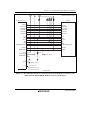
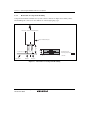
1
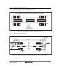
To our customers,
Old Company Name in Catalogs and Other Documents
On April 1st, 2010, NEC Electronics Corporation merged with Renesas Technology
Corporation, and Renesas Electronics Corporation took over all the business of both
companies. Therefore, although the old company name remains in this document, it is a valid
Renesas Electronics document. We appreciate your understanding.
Renesas Electronics website: http://www.renesas.com
April 1st, 2010
Renesas Electronics Corporation
Issued by: Renesas Electronics Corporation (http://www.renesas.com)
Send any inquiries to http://www.renesas.com/inquiry.
Notice
1.
2.
3.
4.
5.
6.
7.
All information included in this document is current as of the date this document is issued. Such information, however, is
subject to change without any prior notice. Before purchasing or using any Renesas Electronics products listed herein, please
confirm the latest product information with a Renesas Electronics sales office. Also, please pay regular and careful attention to
additional and different information to be disclosed by Renesas Electronics such as that disclosed through our website.
Renesas Electronics does not assume any liability for infringement of patents, copyrights, or other intellectual property rights
of third parties by or arising from the use of Renesas Electronics products or technical information described in this document.
No license, express, implied or otherwise, is granted hereby under any patents, copyrights or other intellectual property rights
of Renesas Electronics or others.
You should not alter, modify, copy, or otherwise misappropriate any Renesas Electronics product, whether in whole or in part.
Descriptions of circuits, software and other related information in this document are provided only to illustrate the operation of
semiconductor products and application examples. You are fully responsible for the incorporation of these circuits, software,
and information in the design of your equipment. Renesas Electronics assumes no responsibility for any losses incurred by
you or third parties arising from the use of these circuits, software, or information.
When exporting the products or technology described in this document, you should comply with the applicable export control
laws and regulations and follow the procedures required by such laws and regulations. You should not use Renesas
Electronics products or the technology described in this document for any purpose relating to military applications or use by
the military, including but not limited to the development of weapons of mass destruction. Renesas Electronics products and
technology may not be used for or incorporated into any products or systems whose manufacture, use, or sale is prohibited
under any applicable domestic or foreign laws or regulations.
Renesas Electronics has used reasonable care in preparing the information included in this document, but Renesas Electronics
does not warrant that such information is error free. Renesas Electronics assumes no liability whatsoever for any damages
incurred by you resulting from errors in or omissions from the information included herein.
Renesas Electronics products are classified according to the following three quality grades: “Standard”, “High Quality”, and
“Specific”. The recommended applications for each Renesas Electronics product depends on the product’s quality grade, as
indicated below. You must check the quality grade of each Renesas Electronics product before using it in a particular
application. You may not use any Renesas Electronics product for any application categorized as “Specific” without the prior
written consent of Renesas Electronics. Further, you may not use any Renesas Electronics product for any application for
which it is not intended without the prior written consent of Renesas Electronics. Renesas Electronics shall not be in any way
liable for any damages or losses incurred by you or third parties arising from the use of any Renesas Electronics product for an
application categorized as “Specific” or for which the product is not intended where you have failed to obtain the prior written
consent of Renesas Electronics. The quality grade of each Renesas Electronics product is “Standard” unless otherwise
expressly specified in a Renesas Electronics data sheets or data books, etc.
“Standard”:
8.
9.
10.
11.
12.
Computers; office equipment; communications equipment; test and measurement equipment; audio and visual
equipment; home electronic appliances; machine tools; personal electronic equipment; and industrial robots.
“High Quality”: Transportation equipment (automobiles, trains, ships, etc.); traffic control systems; anti-disaster systems; anticrime systems; safety equipment; and medical equipment not specifically designed for life support.
“Specific”:
Aircraft; aerospace equipment; submersible repeaters; nuclear reactor control systems; medical equipment or
systems for life support (e.g. artificial life support devices or systems), surgical implantations, or healthcare
intervention (e.g. excision, etc.), and any other applications or purposes that pose a direct threat to human life.
You should use the Renesas Electronics products described in this document within the range specified by Renesas Electronics,
especially with respect to the maximum rating, operating supply voltage range, movement power voltage range, heat radiation
characteristics, installation and other product characteristics. Renesas Electronics shall have no liability for malfunctions or
damages arising out of the use of Renesas Electronics products beyond such specified ranges.
Although Renesas Electronics endeavors to improve the quality and reliability of its products, semiconductor products have
specific characteristics such as the occurrence of failure at a certain rate and malfunctions under certain use conditions. Further,
Renesas Electronics products are not subject to radiation resistance design. Please be sure to implement safety measures to
guard them against the possibility of physical injury, and injury or damage caused by fire in the event of the failure of a
Renesas Electronics product, such as safety design for hardware and software including but not limited to redundancy, fire
control and malfunction prevention, appropriate treatment for aging degradation or any other appropriate measures. Because
the evaluation of microcomputer software alone is very difficult, please evaluate the safety of the final products or system
manufactured by you.
Please contact a Renesas Electronics sales office for details as to environmental matters such as the environmental
compatibility of each Renesas Electronics product. Please use Renesas Electronics products in compliance with all applicable
laws and regulations that regulate the inclusion or use of controlled substances, including without limitation, the EU RoHS
Directive. Renesas Electronics assumes no liability for damages or losses occurring as a result of your noncompliance with
applicable laws and regulations.
This document may not be reproduced or duplicated, in any form, in whole or in part, without prior written consent of Renesas
Electronics.
Please contact a Renesas Electronics sales office if you have any questions regarding the information contained in this
document or Renesas Electronics products, or if you have any other inquiries.
(Note 1) “Renesas Electronics” as used in this document means Renesas Electronics Corporation and also includes its majorityowned subsidiaries.
(Note 2) “Renesas Electronics product(s)” means any product developed or manufactured by or for Renesas Electronics.
User’s Manual
SH-4A, SH4AL-DSP E200F
Emulator
Additional Document for User’s Manual
Supplementary Information on Using
the SH7781
Renesas Microcomputer Development
Environment System
SuperH™ Family
E200F for SH7781 R0E877810EMU00E
Rev.2.00 2008.01
Rev. 2.00 Jan. 28, 2008 Page ii of vi
REJ10J1422-0200
Notes regarding these materials
1. This document is provided for reference purposes only so that Renesas customers may select the appropriate
Renesas products for their use. Renesas neither makes warranties or representations with respect to the
accuracy or completeness of the information contained in this document nor grants any license to any
intellectual property rights or any other rights of Renesas or any third party with respect to the information in
this document.
2. Renesas shall have no liability for damages or infringement of any intellectual property or other rights arising
out of the use of any information in this document, including, but not limited to, product data, diagrams, charts,
programs, algorithms, and application circuit examples.
3. You should not use the products or the technology described in this document for the purpose of military
applications such as the development of weapons of mass destruction or for the purpose of any other military
use. When exporting the products or technology described herein, you should follow the applicable export
control laws and regulations, and procedures required by such laws and regulations.
4. All information included in this document such as product data, diagrams, charts, programs, algorithms, and
application circuit examples, is current as of the date this document is issued. Such information, however, is
subject to change without any prior notice. Before purchasing or using any Renesas products listed in this
document, please confirm the latest product information with a Renesas sales office. Also, please pay regular
and careful attention to additional and different information to be disclosed by Renesas such as that disclosed
through our website. (http://www.renesas.com )
5. Renesas has used reasonable care in compiling the information included in this document, but Renesas
assumes no liability whatsoever for any damages incurred as a result of errors or omissions in the information
included in this document.
6. When using or otherwise relying on the information in this document, you should evaluate the information in
light of the total system before deciding about the applicability of such information to the intended application.
Renesas makes no representations, warranties or guaranties regarding the suitability of its products for any
particular application and specifically disclaims any liability arising out of the application and use of the
information in this document or Renesas products.
7. With the exception of products specified by Renesas as suitable for automobile applications, Renesas
products are not designed, manufactured or tested for applications or otherwise in systems the failure or
malfunction of which may cause a direct threat to human life or create a risk of human injury or which require
especially high quality and reliability such as safety systems, or equipment or systems for transportation and
traffic, healthcare, combustion control, aerospace and aeronautics, nuclear power, or undersea communication
transmission. If you are considering the use of our products for such purposes, please contact a Renesas
sales office beforehand. Renesas shall have no liability for damages arising out of the uses set forth above.
8. Notwithstanding the preceding paragraph, you should not use Renesas products for the purposes listed below:
(1) artificial life support devices or systems
(2) surgical implantations
(3) healthcare intervention (e.g., excision, administration of medication, etc.)
(4) any other purposes that pose a direct threat to human life
Renesas shall have no liability for damages arising out of the uses set forth in the above and purchasers who
elect to use Renesas products in any of the foregoing applications shall indemnify and hold harmless Renesas
Technology Corp., its affiliated companies and their officers, directors, and employees against any and all
damages arising out of such applications.
9. You should use the products described herein within the range specified by Renesas, especially with respect
to the maximum rating, operating supply voltage range, movement power voltage range, heat radiation
characteristics, installation and other product characteristics. Renesas shall have no liability for malfunctions or
damages arising out of the use of Renesas products beyond such specified ranges.
10. Although Renesas endeavors to improve the quality and reliability of its products, IC products have specific
characteristics such as the occurrence of failure at a certain rate and malfunctions under certain use
conditions. Please be sure to implement safety measures to guard against the possibility of physical injury, and
injury or damage caused by fire in the event of the failure of a Renesas product, such as safety design for
hardware and software including but not limited to redundancy, fire control and malfunction prevention,
appropriate treatment for aging degradation or any other applicable measures. Among others, since the
evaluation of microcomputer software alone is very difficult, please evaluate the safety of the final products or
system manufactured by you.
11. In case Renesas products listed in this document are detached from the products to which the Renesas
products are attached or affixed, the risk of accident such as swallowing by infants and small children is very
high. You should implement safety measures so that Renesas products may not be easily detached from your
products. Renesas shall have no liability for damages arising out of such detachment.
12. This document may not be reproduced or duplicated, in any form, in whole or in part, without prior written
approval from Renesas.
13. Please contact a Renesas sales office if you have any questions regarding the information contained in this
document, Renesas semiconductor products, or if you have any other inquiries.
Rev. 2.00 Jan. 28, 2008 Page iii of vi
REJ10J1422-0200
Rev. 2.00 Jan. 28, 2008 Page iv of vi
REJ10J1422-0200
Contents
Section 1 Connecting the Emulator with the User System ................................1
1.1
1.2
1.3
1.4
1.5
Components of the Emulator ............................................................................................ 1
Connecting the Emulator with the User System ............................................................... 3
Installing the H-UDI Port Connector on the User System ................................................ 4
Pin Assignments of the H-UDI Port Connector ................................................................ 4
Recommended Circuit between the H-UDI Port Connector and the MPU....................... 6
1.5.1 Recommended Circuit (38-Pin Type) .................................................................. 6
1.5.2 Restriction on Component Mounting................................................................... 8
Section 2 Software Specifications when Using the SH7781 .............................9
2.1
2.2
Differences between the SH7781 and the Emulator ......................................................... 9
Specific Functions for the Emulator when Using the SH7781.......................................... 14
2.2.1 Notes on Using the Trace Functions .................................................................... 14
2.2.2 Notes on Using the JTAG (H-UDI) Clock (TCK) and AUD Clock (AUDCK)... 15
2.2.3 Notes on Setting the [Breakpoint] Dialog Box .................................................... 16
2.2.4 Notes on Setting the [Event Condition] Dialog Box and
the BREAKCONDITION_ SET Command ........................................................ 17
2.2.5 Note on Setting the UBC_MODE Command ...................................................... 17
2.2.6 Note on Setting the PPC_MODE Command ....................................................... 18
Section 3 Preparing to Connect the Trace Unit .................................................19
3.1
3.2
Connecting the E200F Trace Unit with the User System.................................................. 19
Installing the Trace Unit Connector .................................................................................. 19
3.2.1 Trace Unit Connector Installed on the User System ............................................ 19
3.2.2 Pin Assignments of the User System Connector.................................................. 20
3.2.3 Recommended Foot Pattern ................................................................................. 20
3.2.4 Restrictions on Component Installation ............................................................... 21
3.2.5 Pin Assignments of the Trace Unit Connector..................................................... 21
3.2.6 Layout of the Trace Unit Connector .................................................................... 30
3.2.7 Restrictions on Using the Trace Unit ................................................................... 31
3.2.8 Description of Emulation Memory Control Signal .............................................. 32
Rev. 2.00 Jan. 28, 2008 Page v of vi
REJ10J1422-0200
Rev. 2.00 Jan. 28, 2008 Page vi of vi
REJ10J1422-0200
Section 1 Connecting the Emulator with the User System
Section 1 Connecting the Emulator with the User System
1.1
Components of the Emulator
The E200F emulator supports the SH7781. Table 1.1 lists the components of the emulator.
Table 1.1 Components of the Emulator
Classification Component
Hardware
Appearance
Quantity
Remarks
Emulator main unit
1
R0E0200F2EMU00:
Depth: 185.0 mm, Width: 130.0 mm,
Height: 45.0 mm, Mass: 321.0 g
AC adapter
1
Input: 100 to 240 V
Output: 12 V 4.0 A
Depth: 120.0 mm, Width: 72.0 mm,
Height: 27.0 mm, Mass: 400.0 g
AC cable
1
Length: 200 mm
USB cable
1
Length: 1500 mm, Mass: 50.6 g
External probe
1
Length: 500 mm,
Pins 1 to 4: probe input pins,
T: trigger output pin,
G: GND pin
Rev. 2.00 Jan. 28, 2008 Page 1 of 32
REJ10J1422-0200
Section 1 Connecting the Emulator with the User System
Table 1.1 Components of the Emulator (cont)
Classification Component
Software
E200F emulator setup
program,
Appearance
Quantity
Remarks
1
R0E0200F0EMU00S,
SH-4A, SH4AL-DSP
E200F Emulator User’s
Manual,
R0E0200F0EMU00J,
R0E0200F0EMU00E,
Supplementary
Information on Using the
SH7781*
R0E877810EMU00J,
R0E877810EMU00E
(provided on a CD-R)
Note: Additional document for the MPUs supported by the emulator is included. Check the target
MPU and refer to its additional document.
Rev. 2.00 Jan. 28, 2008 Page 2 of 32
REJ10J1422-0200
Section 1 Connecting the Emulator with the User System
1.2
Connecting the Emulator with the User System
To connect the E200F emulator (hereinafter referred to as the emulator), the H-UDI port connector
must be installed on the user system to connect the user system interface cable. When designing
the user system, refer to the recommended circuit between the H-UDI port connector and the
MPU.
It is impossible to connect this emulator to the 14-pin and 36-pin connectors that are
recommended for the E10A-USB emulator. The 38-pin connector has the same specification as
the optional 38-pin connector for the E10A-USB emulator. When designing the user system, read
the E200F emulator user's manual and the hardware manual for the relevant device.
H-UDI port connectors are of the 38-pin, 36-pin, and 14-pin types described below. Use the 38pin type with the SH7781 E200F emulator.
1. 38-pin type (with AUD function, and supporting high-density mounting and high-speed
operation)
This connector supports high-density mounting and high-speed operation. A large amount of
trace information can be acquired in realtime by the AUD trace function. This connector also
supports window tracing for the acquisition of memory data in a specified range (accessed
addresses and data in memory access).
2. 36-pin type (with AUD function)
The AUD trace function is supported. A large amount of trace information can be acquired in
realtime. This connector also supports window tracing for the acquisition of memory data in a
specified range (accessed addresses and data in memory access). The 36-pin connector cannot
be used for connection of the SH7781 E200F emulator. Instead, this connector is for use with
the E10A-USB emulator (with AUD function).
3. 14-pin type (without AUD function)
The AUD trace function cannot be used because only the H-UDI function is supported. This
connector cannot be used for connection of the SH7781 E200F emulator. Instead, this
connector is for use with the E10A-USB emulator.
Rev. 2.00 Jan. 28, 2008 Page 3 of 32
REJ10J1422-0200
Section 1 Connecting the Emulator with the User System
1.3
Installing the H-UDI Port Connector on the User System
Table 1.2 shows the recommended H-UDI port connectors for the SH7781 E200F emulator.
Table 1.2 Recommended H-UDI Port Connector
Connector
Type Number
Manufacturer
Specifications
38-pin connector
2-5767004-2
Tyco Electronics AMP K.K.
Mictor type
Note: When designing the 38-pin connector layout on the user board, do not place any other
signals under the H-UDI connector to reduce cross-talk noises, etc.
1.4
Pin Assignments of the H-UDI Port Connector
Figure 1.1 shows the pin assignments of the 38-pin H-UDI port connector.
Rev. 2.00 Jan. 28, 2008 Page 4 of 32
REJ10J1422-0200
Section 1 Connecting the Emulator with the User System
Pin No.
Input/
Output *1
Signal
1
N.C.
2
N.C.
SH7781 Pin No.
Port 1
Port 2
Note
(GND)*4
Input/
Output *1
Pin No.
Signal
20
N.C.
21
_TRST *2
22
N.C.
3
MPMD
4
N.C.
23
N.C.
5
_UCON (GND)*3
24
AUDATA3
6
AUDCK
25
N.C.
7
N.C.
26
AUDATA2
8
_ASEBRK/
27
N.C.
28
AUDATA1
29
N.C.
30
AUDATA0
31
N.C.
32
AUDSYNC
33
N.C.
34
N.C.
35
N.C.
36
N.C.
37
N.C.
38
N.C.
Output
B18
B13
BRKACK *2
Input/
output
C17
←
9
_RESET *2
Output
A12
←
10
N.C.
11
TDO
Output
12
UVCC_AUD
Output
13
N.C.
14
UVCC
Output
15
TCK
Input
16
N.C.
17
TMS
18
N.C.
19
TDI
Input
Input
B17
C16
D16
A17
User reset
←
←
←
←
SH7781Pin No.
Port 1 Port 2
D17
←
C18
B16
D18
A16
A19
A15
B19
C14
A18
C13
Note
Notes: 1. The input or output is based on the target system.
2. The symbol (_) means that the signal is active-low.
3. The emulator monitors the GND signal of the user system and detects whether or not the user system is connected.
4. When the user system interface cable is connected to this pin and the MPMD pin is set to 0, do not connect to GND
but to the MPMD pin directly.
5. The GND bus leads, which are allocated on the center of the H-UDI port connector, must be connected to GND.
37
1
38-pin Mictor connector 2-5767004-2
manufactured by Tyco Electronics AMP K.K.
38
2
Figure 1.1 Pin Assignments of the H-UDI Port Connector (38 Pins)
Rev. 2.00 Jan. 28, 2008 Page 5 of 32
REJ10J1422-0200
Section 1 Connecting the Emulator with the User System
1.5
Recommended Circuit between the H-UDI Port Connector and the
MPU
1.5.1
Recommended Circuit (38-Pin Type)
Figure 1.2 shows a recommended circuit for connection between the H-UDI port connector (38
pins) and the MPU when the emulator is in use.
Notes: 1. Do not connect anything to the N.C. pins of the H-UDI port connector.
2.
The MPMD pin must be 0 when the emulator is connected and 1 when the emulator is
not connected, respectively.
(1) When the emulator is used: MPMD = 0
(2) When the emulator is not used: MPMD = 1
Figure 1.2 shows an example of circuits that allow the MPMD pin to be GND (0)
whenever the emulator is connected by using the user system interface cable.
3.
When a network resistance is used for pull-up, it may be affected by a noise. Separate
TCK from other resistances.
4.
The /TRST pin must be at the low level for a certain period when the power is
supplied regardless of whether the H-UDI is used or not.
5.
The pattern between the H-UDI port connector and the MPU must be as short as
possible. Do not connect the signal lines to any other components on the board.
6.
Since the H-UDI and AUD of the MPU operates with the VDDQ (3.3 V) voltage,
supply only the VDDQ (3.3 V) voltage to the UVCC pin.
7.
The resistance value shown in figure 1.2 is for reference.
8.
For the pin processing in cases where the emulator is not used, refer to the hardware
manual of the related MPU.
9.
For the AUDCK pin, guard the pattern between the H-UDI port connector and the
MPU at GND level.
Rev. 2.00 Jan. 28, 2008 Page 6 of 32
REJ10J1422-0200
Section 1 Connecting the Emulator with the User System
VDDQ
3.3V
VDDQ
VDDQ
All pulled-up at 4.7 kΩ or more
H-UDI port connector
AUDCK
AUDSYNC
AUDATA0
AUDATA1
AUDATA2
AUDATA3
SH7781
6
15
TDI
19
TDO
_ASEBRK/BRKAC K
11
8
UVC C
UVCC _AUD
UCON(GND)
GND
N.C
AUDCK
AUDSYNC
AUDATA0
AUDATA1
AUDATA2
AUDATA3
32
30
28
26
24
TCK
TMS
_TRST
RESET
MPMD(G ND)
VDDQ = I/O power supply
TCK
TMS
_TRST
TDI
TDO
_ASEBRK/BRKAC K
17
21
9
PRESET
MPMD
3
14
12
1 kΩ
Reset signal
5
GND bus leads
1,2,4,7,10,13,16,
18,20,22,23,25,27,29,
31,33,34,35,36,37,38
Target system
Figure 1.2 Recommended Circuit for Connection between the H-UDI Port Connector and
MPU when the SH7781 E200F Emulator is in Use (38-Pin Type)
Rev. 2.00 Jan. 28, 2008 Page 7 of 32
REJ10J1422-0200
Section 1 Connecting the Emulator with the User System
1.5.2
Restriction on Component Mounting
Components mounted around the user system connector must be no higher than a limit (5 mm).
The H-UDI probe connector on the emulator is of the straight (plug) type.
Direction to draw the H-UDI/AUD probe
E200F H-UDI/AUD probe
5
37
20
2-5767004-2
1
2- 5767 004- 2
2
38
50
Target system
Odd pins
Even pins
Figure 1.3 Restriction on Component Mounting
Rev. 2.00 Jan. 28, 2008 Page 8 of 32
REJ10J1422-0200
Restricted area for
mounting components:
Unit: mm
Section 2 Software Specifications when Using the SH7781
Section 2 Software Specifications when Using the SH7781
2.1
Differences between the SH7781 and the Emulator
1. When the emulator system is initiated, it initializes the general registers and part of the control
registers as shown in table 2.1. The initial values of the actual SH7781 registers are undefined.
When the emulator is initiated from the workspace, a value to be entered is saved in a session.
Table 2.1 Register Initial Values at Emulator Link Up
Register
Emulator at Link Up
R0 to R14
H'00000000
R15 (SP)
H'A0000000
R0_BANK to R7_BANK
H'00000000
PC
H'A0000000
SR
H'700000F0
GBR
H'00000000
VBR
H'00000000
MACH
H'00000000
MACL
H'00000000
PR
H'00000000
DBR
H'00000000
SGR
H'00000000
SPC
H'00000000
SSR
H'000000F0
FPUL
H'00000000
FPSCR
H'00040001
FR0 to FR15
H'00000000
XF0 to XF15
H'00000000
2. The emulator uses the H-UDI; do not access the H-UDI.
Rev. 2.00 Jan. 28, 2008 Page 9 of 32
REJ10J1422-0200
Section 2 Software Specifications when Using the SH7781
3. Low-Power States (Sleep and Module Standby)
For low-power consumption, the SH7781 has sleep and module standby states.
The sleep and module standby states are switched using the SLEEP instruction. When the
emulator is used, the sleep state can be cleared with either the normal clearing function or with
the [STOP] button, and a break will occur.
Note: The memory must not be accessed or modified in sleep state.
4. Reset Signals
The SH7781 reset signals are only valid during emulation started with clicking the GO or
STEP-type button. If these signals are enabled on the user system in command input wait
state, they are not sent to the SH7781.
Note: Do not break the user program when the _PRESET or _BREQ signal is being low and the
WAIT control signal is being active. A TIMEOUT error will occur. If the WAIT control
signal and the _BREQ signal are fixed to active and low during break, respectively, a
TIMEOUT error will occur at memory access.
5. Direct Memory Access Controller (DMAC)
The DMAC operates even when the emulator is used. When a data transfer request is
generated, the DMAC executes DMA transfer.
6. Memory Access during User Program Execution
When a memory is accessed from the memory window, etc. during user program execution,
the user program is resumed after it has stopped in the emulator to access the memory.
Therefore, realtime emulation cannot be performed.
The stopping time of the user program is as follows:
Environment:
®
Host computer: 800 MHz (Pentium III)
JTAG clock: 30 MHz (TCK clock)
When a one-byte memory is read from the command-line window, the stopping time will be
about 45 ms.
7. Memory Access during User Program Break
The emulator can download the program for the flash memory area (for details, refer to section
6.22, Download Function to the Flash Memory Area, in the SH-4A, SH4AL-DSP E200F
Emulator User’s Manual). Other memory write operations are enabled for the RAM area.
Therefore, an operation such as memory write or BREAKPOINT should be set only for the
RAM area.
Rev. 2.00 Jan. 28, 2008 Page 10 of 32
REJ10J1422-0200
Section 2 Software Specifications when Using the SH7781
8. Cache Operation during User Program Break
When cache is enabled, the emulator accesses the memory by the following methods:
⎯ At memory write: Writes through the cache, then issues a single write to outside. The LRU
is not updated.
⎯ At memory read: Reads memory from the cache. The LRU is not updated.
Therefore, when memory read or write is performed during user program break, the cache state
does not change.
⎯ At breakpoint set: Disables the instruction cache.
9. Port
The AUD pin is multiplexed as shown in table 2.2.
Table 2.2 Multiplexed Functions
Port 1
Port 2
Function 1
Function 2
FALE
AUDCK
_FCE
AUDSYNC
FD0
AUDATA0
FD1
AUDATA1
FD2
AUDATA2
FD3
AUDATA3
_DRAK2/_CE2A
AUDCK
_DRAK3/_CE2B
AUDSYNC
_DREQ2/_INTB
AUDATA0
_DREQ3/_INTC
AUDATA1
_DACK2/_MRESETOUT
AUDATA2
_DACK3/_IRQOUT
AUDATA3
Note: Function 1 can be used when the AUD pins of the device are not connected to the
emulator. When the AUD trace is enabled, the emulator changes settings so that function 2
is forcibly used.
10. UBC
When [User] is specified in the [UBC mode] list box in the [Configuration] dialog box, the
UBC can be used in the user program.
Do not use the UBC in the user program as it is used by the emulator when [EML] is specified
in the [UBC mode] list box in the [Configuration] dialog box.
Rev. 2.00 Jan. 28, 2008 Page 11 of 32
REJ10J1422-0200
Section 2 Software Specifications when Using the SH7781
11. Memory Access during Break
In the enabled MMU, when a memory is accessed and a TLB error occurs during break, it can
be selected whether the TLB exception is controlled or the program jumps to the user
exception handler in [TLB Mode] in the [Configuration] dialog box. When [TLB miss
exception is enable] is selected, a “Communication Timeout error” will occur if the TLB
exception handler does not operate correctly. When [TLB miss exception is disable] is
selected, the program does not jump to the TLB exception handler even if a TLB exception
occurs. Therefore, if the TLB exception handler does not operate correctly, a “Communication
Timeout error” will not occur but the memory contents may not be correctly displayed.
12. Loading Sessions
Information in [JTAG clock] of the [Configuration] dialog box cannot be recovered by loading
sessions. Thus the TCK value will be 5 MHz.
13. [IO] window
⎯ Display and modification
Do not change values of the User Break Controller because it is used by the emulator.
For each watchdog timer register, there are two registers to be separately used for write and
read operations.
Table 2.3 Watchdog Timer Register
Register Name
Usage
Register
WTCSR(W)
Write
Watchdog timer control/status register
WTCNT(W)
Write
Watchdog timer counter
WTCSR(R)
Read
Watchdog timer control/status register
WTCNT(R)
Read
Watchdog timer counter
⎯ The watchdog timer operates only when the user program is executed. Do not change the
value of the frequency change register in the [IO] window or [Memory] window.
⎯ The internal I/O registers can be accessed from the [IO] window. However, note the
following when accessing the SDMR register of the bus-state controller. Before accessing
the SDMR register, specify addresses to be accessed in the I/O-register definition file
(SH7781.IO) and then activate the HEW. After the I/O-register definition file is created,
the MPU’s specifications may be changed. If each I/O register in the I/O-register
definition file differs from addresses described in the hardware manual, change the I/Oregister definition file according to the description in the hardware manual. The I/Oregister definition file can be customized depending on its format. Note that, however, the
E200F emulator does not support the bit-field function.
Rev. 2.00 Jan. 28, 2008 Page 12 of 32
REJ10J1422-0200
Section 2 Software Specifications when Using the SH7781
⎯ Verify
In the [IO] window, the verify function of the input value is disabled.
14. Illegal Instructions
If illegal instructions are executed by STEP-type commands, the emulator cannot go to the
next program counter.
15. [Reset CPU] and [Reset Go] in the [Debug] Menu
When a reset is issued from [Reset CPU] or [Reset Go] in the [Debug] menu, the clock pulse
generator or system controller is not initialized.
Rev. 2.00 Jan. 28, 2008 Page 13 of 32
REJ10J1422-0200
Section 2 Software Specifications when Using the SH7781
2.2
Specific Functions for the Emulator when Using the SH7781
In the SH7781, a reset must be input when the emulator is activated.
2.2.1
Notes on Using the Trace Functions
The emulator supports the trace functions listed in table 2.4.
Table 2.4 Trace Functions
Function
Internal Trace
AUD Trace
Memory Output
Trace
Branch trace
Supported (eight branches)
Supported
Supported
Range memory access trace
Supported (eight events)
Supported
Supported
Software trace
Supported (eight events)
Supported
Supported
Internal Trace Function: This function is activated by selecting the [Internal trace] radio button
in the [Trace type] group box of the [Trace mode] page. Set the trace condition to be used.
Notes: 1. If an interrupt is generated at the program execution start or end, including a step
operation, the emulator address may be acquired. In such a case, the following
message will be displayed. Ignore this address because it is not a user program
address.
*** EML ***
2. If a completion-type exception occurs during exception branch acquisition, the next
address to the address in which an exception occurs is acquired.
3. Trace information cannot be acquired for the following branch instructions:
• The BF and BT instructions whose displacement value is 0
• Branch to H'A0000000 by reset
AUD Trace Function: This function is operational when the AUD pin of the device is connected
to the emulator. It is activated by selecting the [AUD trace] radio button in the [Trace type] group
box of the [Trace mode] page.
Notes: 1. When the trace display is performed during user program execution, the mnemonics,
operands, or source is not displayed.
2. The AUD branch trace function outputs the differences between newly output branch
source addresses and previously output branch source addresses. The window trace
function outputs the differences between newly output addresses and previously output
Rev. 2.00 Jan. 28, 2008 Page 14 of 32
REJ10J1422-0200
Section 2 Software Specifications when Using the SH7781
addresses. If the previously output address is the same as the upper 16 bits, the lower
16 bits are output. If it matches the upper 24 bits, the lower 8 bits are output. If it
matches the upper 28 bits, the lower 4 bits are output.
The emulator regenerates the 32-bit address from these differences and displays it in
the [Trace] window. If the emulator cannot display the 32-bit address, it displays the
difference from the previously displayed 32-bit address.
3. If the 32-bit address cannot be displayed, the source line is not displayed.
4. In the emulator, when multiple loops are performed to reduce the number of AUD trace
displays, only the IP counts up.
5. In the emulator, the maximum number of trace displays is 524288 lines. However, the
maximum number of trace displays differs according to the AUD trace information to
be output. Therefore, the above pointers cannot be always acquired.
6. The AUD trace acquisition is not available when [User] is selected in the [UBC mode]
list box of the [Configuration] dialog box. In this case, close the [Trace] window.
7. If a completion-type exception occurs during exception branch acquisition, the next
address to the address in which an exception occurs is acquired.
Memory Output Trace Functions: This function is activated by selecting the [Use Memory
trace] radio button in the [Trace type] group box of the [Trace mode] page.
In this function, write the trace data in the specified user memory range.
Specify the start address to output a trace for the [Start] edit box in the [User memory area] group
box, and the end address for the [End Address] edit box.
Notes: 1. The memory range for which trace is output is the address on the system bus and not
supported for the MMU or cache.
2. In the memory range for output, do not specify the ranges that the user program has
been downloaded or the user program accesses.
3. The range for trace output must be 1 MB or less.
2.2.2
Notes on Using the JTAG (H-UDI) Clock (TCK) and AUD Clock (AUDCK)
1. Set the JTAG clock (TCK) frequency to lower than the frequency of the SH7781 peripheral
module clock (CKP).
2. Set the AUD clock (AUDCK) frequency to 100 MHz or lower. If the frequency is higher than
100 MHz, the emulator will not operate normally.
3. The set value of the JTAG clock (TCK) is initialized by executing [Reset CPU] or [Reset Go].
Rev. 2.00 Jan. 28, 2008 Page 15 of 32
REJ10J1422-0200
Section 2 Software Specifications when Using the SH7781
2.2.3
Notes on Setting the [Breakpoint] Dialog Box
1. When an odd address is set, the next lowest even address is used.
2. A BREAKPOINT is accomplished by replacing instructions of the specified address.
Accordingly, it can be set only to the internal RAM area. However, a BREAKPOINT cannot
be set to the following addresses:
⎯ ROM areas in CS0 to CS6
⎯ Areas other than CS0 to CS6
⎯ Areas other than the internal RAM
⎯ A slot instruction of a delayed branch instruction
⎯ An area that can be only read by MMU
3. During step operation, BREAKPOINTs are disabled.
4. When execution resumes from the address where a BREAKPOINT is specified, single-step
operation is performed at the address and execution is continued from the next PC value.
Therefore, realtime operation cannot be performed.
5. When a BREAKPOINT is set to the slot instruction of a delayed branch instruction, the PC
value becomes an illegal value. Accordingly, do not set a BREAKPOINT to the slot
instruction of a delayed branch instruction.
6. Note on DSP repeat loop:
A BREAKPOINT is equal to a branch instruction. In some DSP repeat loops, branch
instructions cannot be set. For these cases, do not set BREAKPOINTs. Refer to the hardware
manual for details.
7. When the [Normal] option is selected in the [Memory area] group box in the [General] page of
the [Configuration] dialog box, a BREAKPOINT is set to a physical address or a virtual
address according to the SH7781 MMU status during command input when the VPMAP_SET
command setting is disabled. The ASID value of the SH7781 PTEH register during command
input is used. When VPMAP_SET command setting is enabled, a BREAKPOINT is set to a
physical address into which address translation is made according to the VP_MAP table.
However, for addresses out of the range of the VP_MAP table, the address to which a
BREAKPOINT is set depends on the SH7781 MMU status during command input. Even
when the VP_MAP table is modified after BREAKPOINT setting, the address translated when
the BREAKPOINT is set valid.
8. When the [Physical] option is selected in the [Memory area] group box in the [General] page
of the [Configuration] dialog box, a BREAKPOINT is set to a physical address. A
BREAKPOINT is set after disabling the SH7781 MMU upon program execution. After
setting, the MMU is returned to the original state. When a break occurs at the corresponding
virtual address, the cause of termination displayed in the status bar and the [Output] window is
ILLEGAL INSTRUCTION, not BREAKPOINT.
Rev. 2.00 Jan. 28, 2008 Page 16 of 32
REJ10J1422-0200
Section 2 Software Specifications when Using the SH7781
9. When the [Virtual] option is selected in the [Memory area] group box in the [General] page of
the [Configuration] dialog box, a BREAKPOINT is set to a virtual address. A BREAKPOINT
is set after enabling the SH7781 MMU upon program execution. After setting, the MMU is
returned to the original state. When an ASID value is specified, the BREAKPOINT is set to
the virtual address corresponding to the ASID value. The emulator sets the BREAKPOINT
after rewriting the ASID value to the specified value, and returns the ASID value to its original
value after setting. When no ASID value is specified, the BREAKPOINT is set to a virtual
address corresponding to the ASID value at command input.
10. An address (physical address) to which a BREAKPOINT is set is determined when the
BREAKPOINT is set. Accordingly, even if the VP_MAP table is modified after
BREAKPOINT setting, the BREAKPOINT address remains unchanged. When a
BREAKPOINT is satisfied with the modified address in the VP_MAP table, the cause of
termination displayed in the status bar and the [Output] window is ILLEGAL INSTRUCTION,
not BREAKPOINT.
11. If an address of a BREAKPOINT cannot be correctly set in the ROM or flash memory area, a
mark z will be displayed in the [BP] area of the address on the [Source] or [Disassembly]
window by refreshing the [Memory] window, etc. after Go execution. However, no break will
occur at this address. When the program halts with the event condition, the mark z
disappears.
2.2.4
Notes on Setting the [Event Condition] Dialog Box and the BREAKCONDITION_
SET Command
1. When [Go to cursor], [Step In], [Step Over], or [Step Out] is selected, the settings of Event
Condition 3 are disabled.
2. When an Event Condition is satisfied, emulation may stop after two or more instructions have
been executed.
3. If a PC break address condition is set to the slot instruction after a delayed branch instruction,
user program execution cannot be terminated before the slot instruction execution; execution
stops before the branch destination instruction.
2.2.5
Note on Setting the UBC_MODE Command
In the [Configuration] dialog box, if [User] is set while the [UBC mode] list box has been set,
Ch10 (IA_OA_R) and Ch11 (OA_OA_CT_R) of Event Condition cannot be used.
Rev. 2.00 Jan. 28, 2008 Page 17 of 32
REJ10J1422-0200
Section 2 Software Specifications when Using the SH7781
2.2.6
Note on Setting the PPC_MODE Command
In the [Configuration] dialog box, if [User] is set while the [PPC mode] list box has been set, Ch1
and Ch2 of the performance analysis function and options 1 and 2 of the profile function cannot be
used.
Rev. 2.00 Jan. 28, 2008 Page 18 of 32
REJ10J1422-0200
Section 3 Preparing to Connect the Trace Unit
Section 3 Preparing to Connect the Trace Unit
3.1
Connecting the E200F Trace Unit with the User System
To use the external bus trace function in the emulator, the emulator and the user system must be
connected via the external bus trace unit (R0E0200F0ETU00). Install the trace unit connector on
the user system for connection of the trace unit, referring to section 3.2, Installing the Trace Unit
Connector, in this manual. When designing the user system, read the SH-4A, SH4AL-DSP E200F
Emulator User's Manual and hardware manual for the related MPU.
3.2
3.2.1
Installing the Trace Unit Connector
Trace Unit Connector Installed on the User System
Table 3.1 shows the recommended trace unit connector.
Table 3.1 Recommended Connector
Type Number
Manufacturer
Specification
QTH-090-04-L-D-A
Samtec, Inc.
QTH series, 0.5-mm pitch, 180 pins
Note: To connect the connector on the trace unit, do not place any components within 6 mm of
the trace unit connector.
Rev. 2.00 Jan. 28, 2008 Page 19 of 32
REJ10J1422-0200
Section 3 Preparing to Connect the Trace Unit
3.2.2
Pin Assignments of the User System Connector
Pin assignment on the user system (connector is installed)
179
1
180
2
Probe direction
Figure 3.1 Pin Assignments of the User System Connector
3.2.3
Recommended Foot Pattern
2-φ1.05NTH
4.76
Pin 1
Pin 179
2-φ2.2NTH
0.64
Screw hole
1.45
3.09
7.62
1.05
4.76
58.48
Pin 2
0.31
0.50
Pin 180
Unit: mm
Figure 3.2 Recommended Foot Pattern (on which the Connector is Installed)
Rev. 2.00 Jan. 28, 2008 Page 20 of 32
REJ10J1422-0200
Section 3 Preparing to Connect the Trace Unit
3.2.4
Restrictions on Component Installation
Fastens the trace unit board and
the user system
E200F trace unit board
16 mm
User system
Connector (QTH-090-04-L-D-A)
13 mm
Screw
Figure 3.3 Restrictions on Component Installation
3.2.5
Pin Assignments of the Trace Unit Connector
Table 3.2 shows the pin assignments of the trace unit connector.
Rev. 2.00 Jan. 28, 2008 Page 21 of 32
REJ10J1422-0200
Section 3 Preparing to Connect the Trace Unit
Table 3.2 Pin Assignments of the Trace Unit Connector
Connector in the user
system: QTH-090-04-L-D-A;
Samtec (180 pins)
Pin
No.
I/O
Connector
Pin Name
SH7781
Signal Name
Meaning of
Signal
1
I
UA-P0
A0
Address bus A0
2
I
UA-P1
A1
Address bus A1
3
I
UA-P2
A2
Address bus A2
4
I
UA-P3
A3
Address bus A3
5
I
UA-P4
A4
Address bus A4
6
I
UA-P5
A5
Address bus A5
7
I
UA-P6
A6
Address bus A6
8
I
UA-P7
A7
Address bus A7
9
I
GND
GND
GND
10
I
GND
GND
GND
11
I
UA-P8
A8
Address bus A8
12
I
UA-P9
A9
Address bus A9
13
I
UA-P10
A10
Address bus A10
14
I
UA-P11
A11
Address bus A11
15
I
UA-P12
A12
Address bus A12
16
I
UA-P13
A13
Address bus A13
17
I
UA-P14
A14
Address bus A14
18
I
UA-P15
A15
Address bus A15
19
I
GND
GND
GND
20
I
GND
GND
GND
21
I
UA-P16
A16
Address bus A16
22
I
UA-P17
A17
Address bus A17
23
I
UA-P18
A18
Address bus A18
24
I
UA-P19
A19
Address bus A19
25
I
UA-P20
A20
Address bus A20
26
I
UA-P21
A21
Address bus A21
27
I
UA-P22
A22
Address bus A22
Rev. 2.00 Jan. 28, 2008 Page 22 of 32
REJ10J1422-0200
Note
Section 3 Preparing to Connect the Trace Unit
Table 3.2 Pin Assignments of the Trace Unit Connector (cont)
Connector in the user
system: QTH-090-04-L-D-A;
Samtec (180 pins)
Pin
No.
I/O
Connector
Pin Name
SH7781
Signal Name
Meaning of
Signal
28
I
UA-P23
A23
Address bus A23
29
I
GND
GND
GND
30
I
GND
GND
GND
31
I
UA-P24
A24
Address bus A24
32
I
UA-P25
A25
Address bus A25
33
I
UA-P26
GND
GND
34
I
UA-P27
GND
GND
35
I
UA-P28
GND
GND
36
I
UA-P29
GND
GND
37
I
UA-P30
GND
GND
38
I
UA-P31
GND
GND
39
I
GND
GND
GND
40
I
GND
GND
GND
41
IO
UD-P0
D0
Data bus D0
42
IO
UD-P1
D1
Data bus D1
43
IO
UD-P2
D2
Data bus D2
44
IO
UD-P3
D3
Data bus D3
45
IO
UD-P4
D4
Data bus D4
46
IO
UD-P5
D5
Data bus D5
47
IO
UD-P6
D6
Data bus D6
48
IO
UD-P7
D7
Data bus D7
49
I
GND
GND
GND
50
I
GND
GND
GND
51
IO
UD-P8
D8
Data bus D8
52
IO
UD-P9
D9
Data bus D9
53
IO
UD-P10
D10
Data bus D10
54
IO
UD-P11
D11
Data bus D11
Note
Rev. 2.00 Jan. 28, 2008 Page 23 of 32
REJ10J1422-0200
Section 3 Preparing to Connect the Trace Unit
Table 3.2 Pin Assignments of the Trace Unit Connector (cont)
Connector in the user
system: QTH-090-04-L-D-A;
Samtec (180 pins)
Pin
No.
I/O
Connector
Pin Name
SH7781
Signal Name
Meaning of
Signal
55
IO
UD-P12
D12
Data bus D12
56
IO
UD-P13
D13
Data bus D13
57
IO
UD-P14
D14
Data bus D14
58
IO
UD-P15
D15
Data bus D15
59
I
GND
GND
GND
60
I
GND
GND
GND
61
IO
UD-P16
D16
Data bus D16
62
IO
UD-P17
D17
Data bus D17
63
IO
UD-P18
D18
Data bus D18
64
IO
UD-P19
D19
Data bus D19
65
IO
UD-P20
D20
Data bus D20
66
IO
UD-P21
D21
Data bus D21
67
IO
UD-P22
D22
Data bus D22
68
IO
UD-P23
D23
Data bus D23
69
I
GND
GND
GND
70
I
GND
GND
GND
71
IO
UD-P24
D24
Data bus D24
72
IO
UD-P25
D25
Data bus D25
73
IO
UD-P26
D26
Data bus D26
74
IO
UD-P27
D27
Data bus D27
75
IO
UD-P28
D28
Data bus D28
76
IO
UD-P29
D29
Data bus D29
77
IO
UD-P30
D30
Data bus D30
78
IO
UD-P31
D31
Data bus D31
79
I
GND
GND
GND
80
I
GND
GND
GND
81
IO
UD-P32
N.C.
Rev. 2.00 Jan. 28, 2008 Page 24 of 32
REJ10J1422-0200
*1
Not connected
Note
Section 3 Preparing to Connect the Trace Unit
Table 3.2 Pin Assignments of the Trace Unit Connector (cont)
Connector in the user
system: QTH-090-04-L-D-A;
Samtec (180 pins)
Pin
No.
I/O
Connector
Pin Name
SH7781
Signal Name
Meaning of
Signal
Note
82
IO
UD-P33
N.C.
*1
83
IO
UD-P34
N.C.
*1
Not connected
N.C.
*1
Not connected
N.C.
*1
Not connected
N.C.
*1
Not connected
N.C.
*1
Not connected
*1
Not connected
84
85
86
87
IO
IO
IO
IO
UD-P35
UD-P36
UD-P37
UD-P38
Not connected
88
IO
UD-P39
N.C.
89
I
GND
GND
90
I
GND
GND
91
IO
UD-P40
N.C.
*1
Not connected
92
IO
UD-P41
N.C.
*1
Not connected
N.C.
*1
Not connected
N.C.
*1
Not connected
N.C.
*1
Not connected
N.C.
*1
Not connected
N.C.
*1
Not connected
*1
Not connected
93
94
95
96
97
IO
IO
IO
IO
IO
UD-P42
UD-P43
UD-P44
UD-P45
UD-P46
GND
GND
98
IO
UD-P47
N.C.
99
I
GND
GND
GND
100
I
GND
GND
GND
101
102
103
104
105
IO
IO
IO
IO
IO
UD-P48
UD-P49
UD-P50
UD-P51
UD-P52
N.C.
*1
Not connected
N.C.
*1
Not connected
N.C.
*1
Not connected
N.C.
*1
Not connected
N.C.
*1
Not connected
Not connected
106
IO
UD-P53
N.C.
*1
107
IO
UD-P54
N.C.
*1
Not connected
N.C.
*1
Not connected
108
IO
UD-P55
Rev. 2.00 Jan. 28, 2008 Page 25 of 32
REJ10J1422-0200
Section 3 Preparing to Connect the Trace Unit
Table 3.2 Pin Assignments of the Trace Unit Connector (cont)
Connector in the user
system: QTH-090-04-L-D-A;
Samtec (180 pins)
Pin
No.
I/O
Connector
Pin Name
SH7781
Signal Name
Meaning of
Signal
109
I
GND
GND
GND
110
I
GND
GND
GND
111
112
113
114
115
116
IO
IO
IO
IO
IO
IO
UD-P56
UD-P57
UD-P58
UD-P59
UD-P60
UD-P61
N.C.
*1
Not connected
N.C.
*1
Not connected
N.C.
*1
Not connected
N.C.
*1
Not connected
N.C.
*1
Not connected
N.C.
*1
Not connected
Not connected
Not connected
117
IO
UD-P62
N.C.
*1
118
IO
UD-P63
N.C.
*1
119
I
GND
GND
GND
120
I
GND
GND
GND
121
I
UCONT-P0
_WE0/_REG
Write enable 0/
PCMCIA REG
122
I
UCONT-P1
_WE1
Write enable 1
123
I
UCONT-P2
_WE2/_IORD
Write enable 2/
PCMCIA IORD
124
I
UCONT-P3
_WE3/_IOWR
Write enable 3/
PCMCIA IOWR
125
I
UCONT-P4
R/_W
Read/write
126
I
UCONT-P5
_RD/_FRAME
Read
127
I
UCONT-P6
_BS
Bus start
128
I
UCONT-P7
_PRESET
Power-on reset
129
I
UCONT-P8
STATUS0/
CMT_CTR0
Status/CMT_CTR0
130
I
UCONT-P9
STATUS1/
CMT_CTR1
Status/CMT_CTR1
131
I
UCONTP10
_BREQ
Bus mastership
request
Rev. 2.00 Jan. 28, 2008 Page 26 of 32
REJ10J1422-0200
Note
Section 3 Preparing to Connect the Trace Unit
Table 3.2 Pin Assignments of the Trace Unit Connector (cont)
Connector in the user
system: QTH-090-04-L-D-A;
Samtec (180 pins)
Pin
No.
I/O
Connector
Pin Name
SH7781
Signal Name
Meaning of
Signal
132
I
UCONTP11
_BACK
Bus mastership
recognition
133
I
UCONTP12
_RDY
Bus ready
134
I
UCONTP13
TCLK/_IOIS16
TMU/PCMCIA
IOIS
135
I
UCONTP14
_DRAK2/
_CE2A/
AUDCK
DMAC/PCMCIA
136
I
UCONTP15
_DRAK3/
_CE2B/
AUDSYNC
DMAC/PCMCIA
137
I
UCONTP16
SCIF1_TXD/
MCCLK/
MODE5
SCIF1_TXD/
MCCLK/MODE5
138
I
UCONTP17
GND
GND
139
I
UCONTP18
GND
GND
140
I
UCONTP19
NMI
NMI
141
I
UCONTP20
IRQ/_IRL0
IRQ/_IRL0
142
I
UCONTP21
IRQ/_IRL1
IRQ/_IRL1
143
I
UCONTP22
IRQ/_IRL2
IRQ/_IRL2
144
I
UCONTP23
IRQ/_IRL3
IRQ/_IRL3
145
I
UCONTP24
IRQ/_IRL4/
FD4/MODE3
IRQ/_IRL4/FD4/
MODE3
Note
Rev. 2.00 Jan. 28, 2008 Page 27 of 32
REJ10J1422-0200
Section 3 Preparing to Connect the Trace Unit
Table 3.2 Pin Assignments of the Trace Unit Connector (cont)
Connector in the user
system: QTH-090-04-L-D-A;
Samtec (180 pins)
Pin
No.
I/O
Connector
Pin Name
SH7781
Signal Name
Meaning of
Signal
146
I
UCONTP25
IRQ/_IRL5/
FD5/MODE4
IRQ/_IRL5/FD5/
MODE4
147
I
UCONTP26
IRQ/_IRL6/
FD6/MODE6
IRQ/_IRL6/FD6/
MODE6
148
I
UCONTP27
IRQ/_IRL7/
FD7
IRQ/_IRL7/FD7
149
I
UCONTP28
N.C.
*1
Not connected
150
I
UCONTP29
N.C.
*1
Not connected
151
I
UCONTP30
N.C.
*1
Not connected
152
I
UCONTP31
N.C.
*1
Not connected
153
I
GND
GND
GND
154
I
GND
GND
GND
155
I
MPUCLK
CLKOUT
Clock output
156
I
GND
GND
GND
157
I
GND
GND
GND
158
I
DDRCLK-P/
ASECK-P
GND
GND
159
I
GND
GND
GND
160
I
DDRCLK-N/
ASETS-N
GND
GND
161
I
GND
GND
GND
162
I
GND
GND
GND
163
I
CS0IN-N
_CS0
Area selection 0
Connect _CS of SH7781.
Fix unused _CS to high level.
164
I
CS1IN-N
_CS1
Area selection 1
Connect _CS of SH7781.
Fix unused _CS to high level.
Rev. 2.00 Jan. 28, 2008 Page 28 of 32
REJ10J1422-0200
Note
Connect CLKOUT of
SH7781.
Section 3 Preparing to Connect the Trace Unit
Table 3.2 Pin Assignments of the Trace Unit Connector (cont)
Connector in the user
system: QTH-090-04-L-D-A;
Samtec (180 pins)
Pin
No.
I/O
Connector
Pin Name
SH7781
Signal Name
Meaning of
Signal
165
I
CS2IN-N
_CS2
Area selection 2
Connect _CS of SH7781.
Fix unused _CS to high level.
166
I
CS3IN-N
_CS3
Area selection 3
Connect _CS of SH7781.
Fix unused _CS to high level.
167
I
CS4IN-N
_CS4
Area selection 4
Connect _CS of SH7781.
Fix unused _CS to high level.
168
I
CS5IN-N
_CS5
Area selection 5
Connect _CS of SH7781.
Fix unused _CS to high level.
169
I
CS6IN-N
_CS6
Area selection 6
Connect _CS of SH7781.
Fix unused _CS to high level.
170
I
CS7IN-N
N.C.
*1
Not connected
Not connected
Not connected
Note
171
I
CS8IN-N
N.C.
*1
172
I
CS9IN-N
N.C.
*1
173
O
EM0OUT-N
EM0OUT-N
174
O
EM1OUT-N
N.C.
*1
Not connected
Not connected
Not connected
Emulation-memory
select output
Connect this signal instead
of CS of the MPU when an
*2
emulation memory is used.
175
O
EM2OUT-N
N.C.
*1
176
O
EMEN-P
N.C.
*1
177
I
UVCC1
I/O power
supply
3.3-V power
supply
Connect the 3.3-V power
supply.
178
I
UVCC2
I/O power
supply
3.3-V power
supply
Connect the 3.3-V power
supply.
179
I
UVCC3
I/O power
supply
3.3-V power
supply
Connect the 3.3-V power
supply.
180
I
UCNN-N
Connected to
user connector
GND (for detecting
connection of the
user system)
Connect this signal to GND
on the user system.
Notes: 1. Do not connect anything to this pin.
2. Refer to section 3.2.8, Description of Emulation Memory Control Signal.
Rev. 2.00 Jan. 28, 2008 Page 29 of 32
REJ10J1422-0200
Section 3 Preparing to Connect the Trace Unit
3.2.6
Layout of the Trace Unit Connector
When designing the user system, there are restrictions on the position to install the trace unit
connector. Figure 3.4 shows the external dimensions of the trace unit.
The size of the printed-circuit board of the E200F trace unit is 90 mm × 125 mm. The size of
components around the user system connector must not exceed the limit on component installation
(the height must be 10 mm or less).
10
1
2
Trace bus interface connector
(SAMTEC QSH-090-01-L-D-A: 180 pins)
45
90
179
180
125
Unit: mm
Figure 3.4 External Dimensions of the Trace Unit (on which the Connector is Installed)
Rev. 2.00 Jan. 28, 2008 Page 30 of 32
REJ10J1422-0200
Section 3 Preparing to Connect the Trace Unit
Notes: 1. The external bus trace interface connector installed on the user system must be as close
to the MPU as possible.
2. Wiring pattern of clock lines (CLKOUT)
The followings are notes on wiring of clock lines for the E200F trace interface signals.
Take them into consideration when designing the user system to embed suitable clock
lines.
3.2.7
(a)
Clock lines must be as short as possible.
(b)
Clock lines must be surrounded by the GND pattern for protection so that the
signals will be of low-impedance.
(c)
Other layers next to the layer with clock line wiring should have solid patterns
of GND/VCC so that the signals will be of low-impedance.
(d)
To prevent affect by the crosstalk noise, other signal patterns must not be
embedded along with the clock lines.
Restrictions on Using the Trace Unit
(1) This trace unit supports the external bus memory interfaces of SH7781; SRAM interface and
byte-selection SRAM interface (except for SRAM page mode). For other memory interfaces
(burst ROM, MPX, DDR-SDRAM, PCI, and PCMCIA), bus trace acquisition and bus event
detection are not supported.
(2) When the sequential trace stop condition or delay-count trace stop condition is specified, trace
acquisition will stop after several cycles have been passed from the stop condition match cycle.
(3) During break mode, a timestamp value of the external bus trace information that has been
acquired by a trace is not counted up.
(4) When an emulation memory is used, it is not possible to access the memory on the user system
which is in the same area as an area where the emulation memory has been set.
(5) When an emulation memory is accessed, at least six wait cycles are required. Set the number
of wait cycles by using bits WR3 to WR0 in the CS0 area wait control register (CS0WCR).
(6) When an emulation memory is used, set the same bus width (8 bits, 16 bits, or 32 bits) as that
of the CS0 area on the user system. If the different bus width is set, the emulation memory will
be illegally accessed.
(7) The emulator occupies the CS0 area where the emulation memory has been set. Accordingly, it
is not possible to access the memory in the user system side of that area.
(8) This trace unit is available for the external 8-, 16-, or 32-bit data bus width. When the data bus
width is 8 or 16 bits, unused data bus pins D31 to D8 (for 8-bit bus width) or D31 to D16 (for
16-bit bus width) of the trace unit connector must be fixed to high or low level. In addition,
when area 0 is used with the emulation memory, the bus width of the emulation memory needs
Rev. 2.00 Jan. 28, 2008 Page 31 of 32
REJ10J1422-0200
Section 3 Preparing to Connect the Trace Unit
to be set. For details, refer to section 5.1.8, Changing the Memory Map Setting, in the SH-4A,
SH4AL-DSP E200F Emulator User's Manual.
3.2.8
Description of Emulation Memory Control Signal
When the CS signal of the MPU is connected directly to the memory or used to generate the CS
signal of the memory, connect the EM0OUT-N signal (pin 173) of the external bus connector
instead of the CS signal of the MPU.
Even if the emulator is not used, prepare the jumper pins as shown in figure 3.5 so that connection
of the CS signal can be easily changed.
User system
External
memory
CS
User
circuit
Emulator trace unit
EM0OUT-N
Jumper
pin
MPU
/CS
Figure 3.5 EM0OUT-N Signal (Pin 173)
Rev. 2.00 Jan. 28, 2008 Page 32 of 32
REJ10J1422-0200
/CS mask signal
SH-4A, SH4AL-DSP E200F Emulator
Additional Document for User's Manual
Supplementary Information on Using the SH7781
Publication Date: Rev.1.00, April 4, 2005
Rev.2.00, January 28, 2008
Published by:
Sales Strategic Planning Div.
Renesas Technology Corp.
Edited by:
Customer Support Department
Global Strategic Communication Div.
Renesas Solutions Corp.
©2008. Renesas Technology Corp., All rights reserved. Printed in Japan.
Sales Strategic Planning Div.
Nippon Bldg., 2-6-2, Ohte-machi, Chiyoda-ku, Tokyo 100-0004, Japan
RENESAS SALES OFFICES
http://www.renesas.com
Refer to "http://www.renesas.com/en/network" for the latest and detailed information.
Renesas Technology America, Inc.
450 Holger Way, San Jose, CA 95134-1368, U.S.A
Tel: <1> (408) 382-7500, Fax: <1> (408) 382-7501
Renesas Technology Europe Limited
Dukes Meadow, Millboard Road, Bourne End, Buckinghamshire, SL8 5FH, U.K.
Tel: <44> (1628) 585-100, Fax: <44> (1628) 585-900
Renesas Technology (Shanghai) Co., Ltd.
Unit 204, 205, AZIACenter, No.1233 Lujiazui Ring Rd, Pudong District, Shanghai, China 200120
Tel: <86> (21) 5877-1818, Fax: <86> (21) 6887-7858/7898
Renesas Technology Hong Kong Ltd.
7th Floor, North Tower, World Finance Centre, Harbour City, Canton Road, Tsimshatsui, Kowloon, Hong Kong
Tel: <852> 2265-6688, Fax: <852> 2377-3473
Renesas Technology Taiwan Co., Ltd.
10th Floor, No.99, Fushing North Road, Taipei, Taiwan
Tel: <886> (2) 2715-2888, Fax: <886> (2) 3518-3399
Renesas Technology Singapore Pte. Ltd.
1 Harbour Front Avenue, #06-10, Keppel Bay Tower, Singapore 098632
Tel: <65> 6213-0200, Fax: <65> 6278-8001
Renesas Technology Korea Co., Ltd.
Kukje Center Bldg. 18th Fl., 191, 2-ka, Hangang-ro, Yongsan-ku, Seoul 140-702, Korea
Tel: <82> (2) 796-3115, Fax: <82> (2) 796-2145
Renesas Technology Malaysia Sdn. Bhd
Unit 906, Block B, Menara Amcorp, Amcorp Trade Centre, No.18, Jln Persiaran Barat, 46050 Petaling Jaya, Selangor Darul Ehsan, Malaysia
Tel: <603> 7955-9390, Fax: <603> 7955-9510
Colophon 6.2
SH-4A, SH4AL-DSP E200F Emulator
Additional Document for User’s Manual
Supplementary Information on Using the
SH7781
1753, Shimonumabe, Nakahara-ku, Kawasaki-shi, Kanagawa 211-8668 Japan
REJ10J1422-0200