1
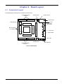
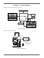
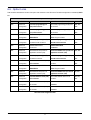
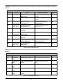
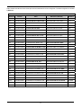
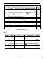
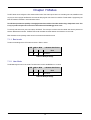
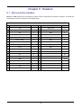
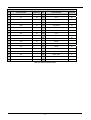
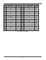
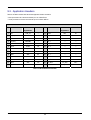
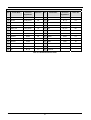
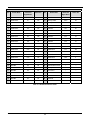
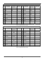
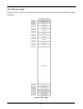
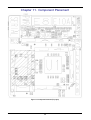
REG10J0125-0100
Renesas Starter Kit
for SH7211 User's Manual
RENESAS SINGLE-CHIP MICROCOMPUTER
SuperHTM RISC engine
Rev.1.00
Revision date:17.Jan.2008
Renesas Technology Europe Ltd.
www.renesas.com
Table of Contents
Chapter 1. Preface ..................................................................................................................................................1
Chapter 2. Purpose .................................................................................................................................................2
Chapter 3. Power Supply ........................................................................................................................................3
3.1. Requirements ...............................................................................................................................................3
3.2. Power – Up Behaviour .................................................................................................................................3
Chapter 4. Board Layout .........................................................................................................................................4
4.1. Component Layout .......................................................................................................................................4
4.2. Board Dimensions ........................................................................................................................................5
Chapter 5. Block Diagram .......................................................................................................................................6
Chapter 6. User Circuitry.........................................................................................................................................7
6.1. Switches .......................................................................................................................................................7
6.2. LEDs.............................................................................................................................................................7
6.3. Potentiometer ...............................................................................................................................................7
6.4. Serial port .....................................................................................................................................................7
6.5. LCD Module..................................................................................................................................................8
6.6. Option Links..................................................................................................................................................9
6.7. Oscillator Sources ......................................................................................................................................13
6.8. Reset Circuit ...............................................................................................................................................13
Chapter 7. Modes..................................................................................................................................................14
7.1.1. Boot mode............................................................................................................................................14
7.1.2. User Mode ...........................................................................................................................................14
Chapter 8. Programming Methods........................................................................................................................15
Chapter 9. Headers...............................................................................................................................................16
9.1. Microcontroller Headers .............................................................................................................................16
9.2. Application Headers ...................................................................................................................................20
Chapter 10. Code Development ...........................................................................................................................24
10.1. Overview...................................................................................................................................................24
10.2. Compiler Restrictions ...............................................................................................................................24
10.3. Breakpoint Support...................................................................................................................................24
10.4. Memory Map.............................................................................................................................................25
Chapter 11. Component Placement ......................................................................................................................26
Chapter 12. Additional Information........................................................................................................................27
ii
Chapter 1. Preface
Cautions
This document may be, wholly or partially, subject to change without notice.
All rights reserved. No one is permitted to reproduce or duplicate, in any form, a part or this entire document without the written
permission of Renesas Technology Europe Limited.
Trademarks
All brand or product names used in this manual are trademarks or registered trademarks of their respective companies or
organisations.
Copyright
© Renesas Technology Europe Ltd. 2008. All rights reserved.
© Renesas Technology Corporation. 2008. All rights reserved.
© Renesas Solutions Corporation. 2008. All rights reserved.
Website:
http://www.renesas.com/
Glossary
ADC
Analog to Digital Converter
USB
Universal Serial Bus
CPU
Central Processing Unit
DAC
Digital to Analog Converter
DMA
Direct Memory Access
E10A
“E10A for Starter Kit” debugger
FDT
Flash Development Tool
RSK
Renesas Starter Kit
LED
Light Emitting Diode
LCD
Liquid Crystal Display
1
Chapter 2. Purpose
This RSK is an evaluation tool for Renesas microcontrollers.
Features include:
•
Renesas Microcontroller Programming.
•
User Code Debugging.
•
User Circuitry such as switches, LEDs and potentiometer(s).
•
Sample Application.
•
Sample peripheral device initialisation code.
The CPU board contains all the circuitry required for microcontroller operation.
This manual describes the technical details of the RSK hardware. The Quick Start Guide and Tutorial Manual provide details of the
software installation and debugging environment.
2
Chapter 3. Power Supply
3.1. Requirements
This CPU board operates from a 5V power supply.
A diode provides reverse polarity protection only if a current limiting power supply is used.
The kit is supplied with an E10A debug module and a PSU. When the CPU board is connected to another system that system should
supply power to the CPU board.
All CPU boards have an optional centre positive supply connector using a 2.0mm barrel power jack which is compatible with the supplied
PSU.
Warning
The CPU board is neither under not over voltage protected. Use a centre positive supply for this board.
3.2. Power – Up Behaviour
When the RSK is purchased the CPU board has the ‘Release’ or stand alone code from the example tutorial code pre-programmed into the
Renesas microcontroller. On powering up the board the user LEDs will start to flash. Pressing any switch will cause the LEDs to flash at a
rate controlled by the potentiometer.
3
Chapter 4. Board Layout
4.1. Component Layout
The following diagram shows top layer component layout of the board.
Application Board
Interface
JA5
Reset Switch
RS232 Serial
JA1
LCD Display
Power
Power LED
J1
Microcontroller
Pin Headers
BUS Interface
E8 Header
J2
J4
J
A
3
User LEDs
E10A Header
J3
JA6
JA2
Boot LED
Potentiometer
User Switches
Application Board
Interface
Figure 4-1: Board Layout
4
4.2. Board Dimensions
The following diagram gives the board dimensions and connector positions. All through hole connectors are on a common 0.1” grid for easy
interfacing.
120.00mm
115.00mm
86.36mm
Short Board = 85 mm
Corners x4
3mm radius
50.80 mm
43.18 mm
35.56 mm
27.00mm
SW
1
SW
2
SW
3
POT
JA2
E10A
JA6
J3 - Applies to connector
with micriocontroller pin1
J4
MCU
J2
E8
J1
Serial D9
SKT
R
E
S
JA5
JA1
45.00mm
Figure 4-2 : Board Dimensions
5
Chapter 5. Block Diagram
Figure 5-1 shows the CPU board components and their connectivity.
Figure 5-1: Block Diagram
Figure -5-2 shows the connections to the RSK.
Figure -5-2 : RSK Connections
6
Chapter 6. User Circuitry
6.1. Switches
There are four switches located on the CPU board. The function of each switch and its connection are shown in Table 6-1.
Switch
Function
RES
SW1/BOOT*
Microcontroller
When pressed; the CPU board microcontroller is reset.
RESn, Pin 22
Connects to an IRQ input for user controls.
IRQ0, Pin 92
(Port B, bit 21)
SW2*
Connects to an IRQ line for user controls.
IRQ4, Pin 87
(Port B, bit 18)
SW3*
Connects to an IRQ line for user controls. Same pin functions as ADC
IRQ6, Pin 88
trigger input.
(Port B, bit 19)
Table 6-1: Switch Functions
*Refer to schematic for detailed connectivity information.
6.2. LEDs
There are six LEDs on the CPU board. The green ‘POWER’ LED lights when the board is powered. The orange BOOT LED indicates the
device is in BOOT mode when lit. The four user LEDs are connected to an IO port and will light when their corresponding port pin is set low.
Table 6-2, below, shows the LED pin references and their corresponding microcontroller port pin connections.
LED Reference (As
Microcontroller Port Pin
Microcontroller Pin
Polarity
shown on silkscreen)
function
Number
LED0
Port B bit 10
75
Active Low
LED1
Port B bit 11
76
Active Low
LED2
Port B bit 12
79
Active Low
LED3
Port B bit 13
80
Active Low
Table 6-2: LED Port
6.3. Potentiometer
A single turn potentiometer is connected to pin ‘AN0’ of the microcontroller. This may be used to vary the input analog voltage value to this
pin between AVCC and Ground.
6.4. Serial port
The microcontroller programming serial port (SCI1) is connected to the E8 connector. SCI2 is connected to the RS232 connector SERIAL.
SCI1 can optionally be connected to the RS232 transceiver by fitting option resistors. The connections to be fitted are listed in Table 6-3
7
Description
Function
Fit for RS232
Remove for
Fit for E8a
Remove for E8a
RS232
TxD1
Programming Serial Port
R47
R21, R56
R21
R47,R56
RxD1
Programming Serial Port
R38
R20,R48
R20
R38,R48
Table 6-3: Serial Option Links
The board is designed to accept a straight through RS232 cable.
6.5. LCD Module
The LCD module supplied with the RSK can be connected to the connector ‘LCD’ for use with the tutorial code. Any module that conforms
to the pin connections and has a KS0066u compatible controller can be used. The LCD module uses a 4 bit interface to reduce the pin
allocation. No contrast control is provided; this must be set on the display module.
Table 6-4 shows the pin allocation and signal names used on this connector.
The module supplied with the CPU board only supports 5V operation.
LCD
Pin
Circuit Net Name
Device
Pin
Circuit Net Name
Device
Pin
Pin
1
Ground
-
2
5V Only
-
3
No Connection
-
4
DLCDRS
112
5
R/W (Wired to Write only)
-
6
DLCDE
111
7
No Connection
-
8
No connection
-
9
No Connection
-
10
No connection
-
11
DLCD4
63
12
DLCD5
65
13
DLCD6
66
14
DLCD7
67
Table 6-4: LCD Module Connections
8
6.6. Option Links
Table 6-5 below describes the function of the option links contained on this CPU board. The default configuration is indicated by BOLD
text.
Option Link Settings
Reference
R20
R21
R32
R38
R40
R42
R47
R48
R52
R55
R56
R58
R59
Function
Fitted
Alternative ( Removed )
Related To
Serial Port
Connects programming port
Disconnects programming port (Rx) from
R38, R42,
Configuration
(Rx) to E8 connector.
E8 connector.
R48
Serial Port
Connects programming port
Disconnects programming port (Tx) from
R47, R55,
Configuration
(Tx) to E8 connector.
E8 connector.
R56
Serial Port
Connects serial port RXD0 to
Disconnects serial port RXD0 from
R52
Configuration
RS232 Buffer.
SERIAL D-type connector.
Serial Port
Connects programming port (Rx)
Disconnects programming port (Rx) to
R20, R42,
Configuration
to external serial connectors.
external serial connectors.
R48
Serial Port
Disables RS232 Serial
Enables RS232 Serial
-
Configuration
Transceiver
Transceiver
Serial Port
Routes RS232 serial port Rx to
Disconnects RS232 serial port Rx from
Configuration
application connector (JA6).
application connector (JA6).
Serial Port
Connects programming port (Tx)
Disconnects programming port (Tx) to
R34, R20,
Configuration
to external connectors.
external serial connectors.
R22
Serial Port
Connects Alternate serial (CH2)
Disconnects Alternate serial from D
R20, R38,
Configuration
to D connector
connector.
R42
Serial Port
Connects serial port TXD0 to
Disconnects serial port TXD0 from
R32
Configuration
RS232 Buffer.
SERIAL D-type connector.
Serial Port
Routes RS232 serial port Tx to
Disconnects RS232 serial port Tx from
Configuration
application connector (JA6).
application connector (JA6).
Serial Port
Connects Alternate serial (CH2)
Disconnects Alternate serial from D
R21,R47,
Configuration
to D connector
connector.
R57
Serial Port
Connects Alternate serial (CH0) to
Disconnects Alternate serial from D
R59
Configuration
D connector
connector.
Serial Port
Connects Alternate serial (CH0) to
Disconnects Alternate serial from D
Configuration
D connector
connector.
Table 6-5: Serial configuration links
9
R48, R38
R4, R56
R58
Table 6-6 below describes the function of the option links associated with Power configuration. The default configuration is indicated by
BOLD text.
Option Link Settings
Reference
R4
R11
Function
Power Source
Power Source
Fitted
Alternative ( Removed )
Board can be powered from
Disconnects the supply from PWR
PWR connector.
connector.
Board can be powered by E8a
Disconnects the supply from E8
Related To
R11, R28
R4, R8
connector.
R22
R27
R28
Microcontroller
E8A_VCC2 can drive
E8A_VCC2 disconnected from
Power Supply
microcontroller core
microcontroller core.
Microcontroller
Regulated 1V5 can drive
Regulated 1V5 disconnected from
Power Supply
microcontroller core
microcontroller core.
Power
Board input power connected
Disconnects the supply from Con_5V
R4, R11
Fit Low ohm resistor to measure current.
R53
Disconnect Board_VCC from CON_3V3
R49
Connects regulated 3V3 voltage
Disconnects regulated 3V3 voltage
R45
source to Board_VCC.
source from Board_VCC.
Microcontroller
Core Supply power to
Fit Low ohm resistor to measure current.
Power Supply
Microcontroller.
R27
R22
to CON_5V
R44
R45
Microcontroller
I/O Supply power to
Power Supply
Microcontroller.
Power
Connects Board_VCC to
CON_3V3.
R49
R53
Power Source
R44
Table 6-6: Power configuration links
Table 6-7 below describes the function of the option links associated with Analog configuration. The default configuration is indicated by
BOLD text.
Option Link Settings
Reference
R60
Function
Fitted
Alternative ( Removed )
Related To
Connects AVCC to Board_5V
Disconnects AVCC from CON_VREF.
Analog Voltage
Links analog ground to digital
Isolates analog ground from digital
Source
ground.
ground.
Analog Voltage
Connects AVCC to CON_VREF
Disconnects AVCC from CON_VREF.
R60
Connects Board_5V to VREF
Disconnects Board_5V from VREF.
R77
Voltage Reference
Connects CON_VREF
Disconnects CON_VREF from VREF
R73
Source
to VREF
Analog Voltage
R71
Source
R70
R71
Source
R73
Voltage Reference
Source
R77
Table 6-7: Analog configuration links
10
Table 6-8 below describes the function of the option links associated with Pin function configuration. The default configuration is indicated
by BOLD text.
Option Link Settings
Reference
Function
Fitted
Alternative ( Removed )
Related To
R61
Pin function select
Connects PIN 109 to RxD2 on JA6.
Disconnects PIN 109 from RxD2.
R126
R62
Pin function select
Connects PIN 110 to TxD2 on JA6.
Disconnects PIN 110 from TxD2.
R119
R63
Pin function select
Connects PIN 80 to LED3.
Disconnects PIN 80 from LED3.
R105
R64
Pin function select
Connects PIN 115 to M1_Vn on JA2.
Disconnects PIN 115 from M1_Vn.
R93
R65
Pin function select
Connects PIN 79 to LED2.
Disconnects PIN 79 from LED2.
R108
R66
Pin function select
Connects PIN 76 to LED1.
Disconnects PIN 76 from LED1.
R116
R67
Pin function select
Connects PIN 75 to LED0.
Disconnects PIN 75 from LED0.
R118
R68
Pin function select
Connects PIN 82 to CS5n on JA3.
Disconnects PIN 82 from CS5n.
R78
R69
Pin function select
Connects PIN 72 to WE1n on JA3.
Disconnects PIN 72 from WE1n.
R125
R72
Pin function select
Connects PIN 60 to TxD0 on JA2.
Disconnects PIN 60 from TxD0.
R122
R74
Pin function select
Connects PIN 59 to RxD0 on JA2.
Disconnects PIN 59 from RxD0.
R123
R75
Pin function select
Connects PIN 6 to TIOC0B on JA5.
Disconnects PIN 6 from TIOC0B.
R124
R76
Pin function select
Connects PIN 81 to ADTRGn on JA1.
Disconnects PIN 81 from ADTRGn.
R117
R79
Pin function select
Connects PIN 97 to AN0 on JA1.
Disconnects PIN 97 from AN0.
R84
R80
Pin function select
Connects PIN 8 to TIOC0D on JA5.
Disconnects PIN 8 from TIOC0D.
R120
R81
Pin function select
Connects PIN 7 to TIOC0C on JA5.
Disconnects PIN 7 from TIOC0C.
R127
R82
Pin function select
Connects PIN 117 to M1_Up on JA2.
Disconnects PIN 117 from M1_Up.
R88, R103
R83
Pin function select
Connects PIN 120 to M1_Un on JA2.
Disconnects PIN 120 from M1_Un.
R91, R111
R84
Pin function select
Connects PIN 97 to AD_POT.
Disconnects PIN 97 from AD_POT.
R79
R86
Pin function select
Connects PIN 116 to M1_Vp on JA2.
Disconnects PIN 116 from M1_Vp.
R96, R113
R87
Pin function select
Connects PIN 70 to M1_Wp on JA2.
Disconnects PIN 70 from M1_Wp.
R95
R88
Pin function select
Connects PIN 117 to TMR0 on JA2.
Disconnects PIN 117 from TMR0.
R82, R103
R91
Pin function select
Connects PIN 120 to TMR1 on JA2.
Disconnects PIN 120 from TMR1.
R83, R111
R93
Pin function select
Connects PIN 115 to TRIGa on JA2.
Disconnects PIN 115 from JA2.
R64
R95
Pin function select
Connects PIN 70 to IRQ7 on JA1.
Disconnects PIN 70 from IRQ7.
R87
R96
Pin function select
Connects PIN 116 to TRIGb on JA2.
Disconnects PIN 116 from TRIGb.
R86, R113
R103
Pin function select
Connects PIN 117 to DACK0 on JA6.
Disconnects PIN 117 from DACK0.
R82, R88
R105
Pin function select
Connects PIN 80 to M2_Up on .
Disconnects PIN 80 from M2_Up.
R63
R108
Pin function select
Disconnects PIN 79 from M2_Un.
R65
Connects PIN 79 to M2_Un on JA5.
11
Option Link Settings
Reference
Function
Fitted
Alternative ( Removed )
Related To
R111
Pin function select
Connects PIN 120 to DREQ0 on JA6.
Disconnects PIN 120 from DREQ0.
R83, R91
R113
Pin function select
Connects PIN 116 to DTEND0 on JA6.
Disconnects PIN 116 from DTEND0.
R86, R96
R116
Pin function select
Connects PIN 76 to M2_Vp on JA5.
Disconnects PIN 76 from M2_Vp.
R66
R117
Pin function select
Connects PIN 81 to M2_TRISTn on
Disconnects
R76
PIN
81
from
M2_TRISTn.
JA5.
R118
Pin function select
Connects PIN 75 to M2_Vn on JA5.
Disconnects PIN 75 from M2_Vn.
R67
R119
Pin function select
Connects PIN 110 to TCLKC on JA5.
Disconnects PIN 110 from TCLKC.
R62
R120
Pin function select
Connects PIN 8 to PTTX on JA6.
Disconnects PIN 8 from PTTX.
R80
R122
Pin function select
Connects PIN 60 to WRn on JA3.
Disconnects PIN 60 from WRn.
R72
R123
Pin function select
Connects PIN 59 to RDn on JA3.
Disconnects PIN 59 from RDn.
R74
R124
Pin function select
Connects PIN 6 to SCK1 on JA6.
Disconnects PIN 6 from SCK1.
R75
R125
Pin function select
Connects PIN 72 to M2_Wp on JA5.
Disconnects PIN 72 from M2_Wp.
R69
R126
Pin function select
Connects PIN 109 to TCLKD on JA5.
Disconnects PIN 109 from TCLKD.
R61
R127
Pin function select
Connects PIN 7 to PTRX on JA6.
Disconnects PIN 7 from PTRX.
R81
R128
Pin function select
Connects PIN 71 to WE0n on JA3.
Disconnects PIN 71 from WE0n.
R132
R132
Pin function select
Connects PIN 71 to M2_Wn on JA5.
Disconnects PIN 71 from M2_Wn.
R128
Table 6-8: Pin function select links
Table 6-9 below describes the function of the option links associated with Clock configuration. The default configuration is indicated by
BOLD text.
Option Link Settings
Reference
Function
Fitted
Alternative ( Removed )
Related To
R75
Clock Oscillator
Parallel resistor for crystal
Not fitted
-
R76
Clock Oscillator
Connects on board clock to MCU
External Clock Source can be connected.
R74, R77,
R108
R108
Clock Oscillator
Connects on board clock to MCU
External Clock Source can be connected.
R74, R77,
R76
R74
Clock Oscillator
Connects external clock to MCU
Disconnects external clock connection
R77, R76
to MCU
R77
Clock Oscillator
Connects external clock to MCU
Disconnects external clock connection
to MCU
Table 6-9: Clock configuration links
12
R74, R76
6.7.Oscillator Sources
A crystal oscillator is fitted on the CPU board and used to supply the main clock input to the Renesas microcontroller.
Table 6-10: Oscillators / Resonators details the oscillators that are fitted and alternative footprints provided on this CPU board:
Component
Crystal (X1)
Fitted
10MHz (HC49/4H package)
Table 6-10: Oscillators / Resonators
Warning: When replacing the default oscillator with that of another frequency, the debugging monitor will not function unless the following
are corrected:
•
FDT programming kernels supplied are rebuilt for the new frequency
6.8.Reset Circuit
The CPU Board includes a simple latch circuit that links the mode selection and reset circuit. This provides an easy method for swapping
the device between Boot Mode and User mode. This circuit is not required on customers’ boards as it is intended for providing easy
evaluation of the operating modes of the device on the RSK. Please refer to the hardware manual for more information on the requirements
of the reset circuit.
The reset circuit operates by latching the state of the boot switch (SW1) on pressing the reset button. This control is subsequently used to
modify a port pin state to select which code is executed.
The reset is held in the active state for a fixed period by a pair of resistors and a capacitor. Please check the reset requirements carefully to
ensure the reset circuit on the user’s board meets all the reset timing requirements.
13
Chapter 7.Modes
The CPU board can be configured in User mode and Boot mode. User mode may be used to run and debug user code, while Boot mode
may only be used to program the Renesas microcontroller with program code via the SCI1 interface. Further details of programming the
flash are available in the SH7211 device hardware manual.
The CPU board provides the capability of changing between User and Boot / User Boot modes using a simple latch circuit. This
is only to provide a simple mode control on this board when the E10A debugger is not in use.
To manually enter boot mode, press and hold the SW1/BOOT. The mode pins are held in their boot states while reset is pressed and
released. Release the boot button. The BOOT LED will be illuminated to indicate that the microcontroller is in boot mode.
More information on the operating modes can be found in the device hardware manual.
7.1.1. Boot mode
The boot mode settings for this CPU board are shown in Table 7-1 below:
FWE
MD1
MD0
LSI State after Reset
End
1
0
0
Boot Mode
Table 7-1: Mode pin settings
7.1.2. User Mode
The SH7086 supports various user modes. The default user mode for the RSKSH7211 is mode 6.
FWE
MD1
MD0
LSI State after Reset
End
1
1
0
User Mode
Table 7-2: Mode pin settings
14
Chapter 8. Programming Methods
The board is intended for use with HEW and the supplied E10A debugger only. Please refer to SH7211 Group Hardware Manual for details
of the programming methods using on-chip serial port SCI1 and without using E10A debugger.
15
Chapter 9. Headers
9.1. Microcontroller Headers
Table 9-1 to Table 9-4 show the microcontroller pin headers and their corresponding microcontroller connections. The header pins
connect directly to the microcontroller pin unless otherwise stated.
J1
Pin
Circuit Net Name
Device Pin
Pin
Circuit Net Name
Device Pin
1
A18
1
19
WDT_OVFn
19
2
A19
2
20
VCC
20
3
A20
3
21
GND
21
4
A21
4
22
RESn
22
5
A22
5
23
FWE
23
6
SCK1_TIOC0B
6
24
GND
24
7
PTRX_TIOC0C
7
25
CON_XTAL
25
8
PTTX_TIOC0D
8
26
CON_EXTAL
26
9
VCCQ
9
27
GND
27
10
GND
10
28
VCCQ
28
11
NMI
11
29
ASEMDn
29
12
TDI
12
30
ASEBRKn
30
MD_CLK0
31
32
13
VCC
13
31
14
GND
14
32
MD_CLK2
15
TDO
15
33
MD0
33
MD1
34
16
TCK
16
34
17
TMS
17
35
VCC
35
18
TRSTn
18
36
GND
36
Table 9-1: J1 microcontroller header
16
J2
Pin
Circuit Net Name
Device Pin
Pin
Circuit Net Name
Device Pin
1
D0
37
19
GND
55
2
D1
38
20
D13
56
3
D2
39
21
D14
57
4
D3
40
22
D15
58
5
GND
41
23
RDn_RxD0
59
6
VCCQ
42
24
WRn_TxD0
60
7
D4
43
25
GND
61
8
D5
44
26
VCC
62
9
D6
45
27
DLCD4
63
10
D7
46
28
DLCD5
64
11
VCC
47
29
DLCD6
65
12
GND
48
30
DLCD7
66
13
D8
49
31
VCCQ
67
14
D9
50
32
GND
68
15
D10
51
33
M1_Wn
69
16
D11
52
34
M1Wp_IRQ7
70
17
D12
53
35
WE0n_M2Wn
71
18
VCCQ
54
36
WE1n_M2Wp
72
Table 9-2: J2 microcontroller header
17
J3
Pin
Circuit Net Name
Device Pin
Pin
Circuit Net Name
Device Pin
1
VCC
73
19
M1_TRISTn
91
2
GND
74
20
IRQ0
92
3
LED0_M2Vn
75
21
AVSS
93
4
LED1_M2Vp
76
22
AVCC
94
5
GND
77
23
DA1
95
6
VCCQ
78
24
DA0
96
7
LED2_M2Un
79
25
ADPOT_AN0
97
8
LED3_M2Up
80
26
AN1
98
9
ADTRGn_M2TRISTn
81
27
AN2
99
10
CS5n_UD
82
28
AN3
100
11
CS1n
83
29
AN4
101
12
CS3n
84
30
AN5
102
13
VCC
85
31
AN6
103
104
14
GND
86
32
AN7
15
IRQ4
87
33
AN8
105
16
IRQ6
88
34
AVSS
106
17
GND
89
35
PIN107
107
18
VCCQ
90
36
PIN108
108
Table 9-3: J3 microcontroller header
18
J4
Pin
Circuit Net Name
Device Pin
Pin
Circuit Net Name
Device Pin
1
RXD2_TCLKD
109
19
A4
127
2
TXD2_TCLKC
110
20
A5
128
3
DLCDE
111
21
A6
129
4
DLCDRS
112
22
A7
130
5
GND
113
23
GND
131
6
VCCQ
114
24
VCC
132
7
M1Vn_TRIGa
115
25
A8
133
8
M1Vp_DTEND0_TRIGb
116
26
A9
134
9
M1Up_DACK0_TMR0
117
27
A10
135
10
GND
118
28
A11
136
11
VCC
119
29
A12
137
12
M1Un_DREQ0_TMR1
120
30
A13
138
13
A0
121
31
VCCQ
139
14
A1
122
32
GND
140
15
A2
123
33
A14
141
16
VCCQ
124
34
A15
142
17
GND
125
35
A16
143
18
A3
126
36
A17
144
Table 9-4: J4 microcontroller header
19
9.2. Application Headers
Table 9-5 to Table 9-9 below show the standard application header connections.
* marks pins where a link to the microcontroller pin is via a fitted 0R link
** marks pins where a link to the microcontroller pin is via a fitted 100R link
JA1
Pin
Header Name
CPU board
Device Pin
Pin
Header Name
Signal Name
CPU board
Device Pin
Signal Name
1
5V
CON_5V
---
14
DAC1
DA1
95
2
0V(5V)
GROUND
---
15
IO_0
---
---
3
3V3
CON_3V3
---
16
IO_1
---
---
4
0V(3V3)
GROUND
---
17
IO_2
---
---
5
AVcc
CON_AVCC
94
18
IO_3
---
---
6
AVss
AVSS
93
19
IO_4
---
---
7
AVref
CON_VREF
105
20
IO_5
---
---
8
ADTRG
ADTRGn
81*
21
IO_6
---
---
9
AD0
AN0
97*
22
IO_7
---
---
10
AD1
AN1
98
23
IRQ3
IRQ7
70*
11
AD2
AN2
99
24
IIC_EX
---
---
12
AD3
AN3
100
25
IIC_SDA
IIC_SDA
108**
13
DAC0
DA0
96
26
IIC_SCL
IIC_SCL
107**
Table 9-5 JA1 Standard Generic Header
20
JA2
Pin
Header Name
CPU board
Device Pin
Pin
Header Name
Signal Name
CPU board
Device Pin
Signal Name
1
RESn
RESn
22
14
Un
M1_Un
120*
2
EXTAL
CON_EXTAL
26*
15
Vp
M1_Vp
116*
3
NMIn
NMI
11
16
Vn
M1_Vn
115*
4
Vss1
GROUND
14
17
Wp
M1_Wp
70*
5
WDT_OVF
WDT_OVFn
19
18
Wn
M1_Wn
69*
6
SCIaTX
TxD0
60*
19
TMR0
TMR0
117*
7
IRQ0
IRQ0
92
20
TMR1
TMR1
120*
8
SCIaRX
RXD0
59*
21
TRIGa
TRIGa
115*
9
IRQ1
IRQ1n
87
22
TRIGb
TRIGb
116*
10
SCIaCK
SCK0
---
23
IRQ2
IRQ6
88
11
UD
UD
82*
24
TRISTn
M1_TRISTn
91
12
CTSRTS
---
---
25
Reserved
13
Up
M1_Up
117*
26
Reserved
Table 9-6: JA2 Standard Generic Header
21
JA3
Pin
Header Name
CPU board
Device Pin
Pin
Header Name
Signal Name
CPU board
Device Pin
Signal Name
1
Address Bus
A0
121
26
Read/Write Control
WRn
60*
2
Address Bus
A1
122
27
Memory Select
CS1n
83
3
Address Bus
A2
123
28
Memory Select
CS3n
84
4
Address Bus
A3
126
29
Data Bus
D8
49
5
Address Bus
A4
127
30
Data Bus
D9
50
6
Address Bus
A5
128
31
Data Bus
D10
51
7
Address Bus
A6
129
32
Data Bus
D11
52
8
Address Bus
A7
130
33
Data Bus
D12
53
9
Address Bus
A8
133
34
Data Bus
D13
56
10
Address Bus
A9
134
35
Data Bus
D14
57
11
Address Bus
A10
135
36
Data Bus
D15
58
12
Address Bus
A11
136
37
Address Bus
A16
143
13
Address Bus
A12
137
38
Address Bus
A17
144
14
Address Bus
A13
138
39
Address Bus
A18
1
15
Address Bus
A14
141
40
Address Bus
A19
2
16
Address Bus
A15
142
41
Address Bus
A20
3
17
Data Bus
D0
37
42
Address Bus
A21
4
18
Data Bus
D1
38
43
Address Bus
A22
5
19
Data Bus
D2
39
44
External Device Clock
---
---
20
Data Bus
D3
40
45
Memory Select
CS5n
82*
21
Data Bus
D4
43
46
Bus Control
---
---
22
Data Bus
D5
44
47
Data Bus Strobe
WE1n
72*
23
Data Bus
D6
45
48
Data Bus Strobe
WE0n
71*
24
Data Bus
D7
46
49
Reserved
25
Read/Write Control
RDn
59*
50
Reserved
Table 9-7: JA3 Standard Generic Header
22
JA5
Pin
Header Name
CPU board
Device Pin
Pin
Header Name
Signal Name
CPU board
Device Pin
Signal Name
1
AD4
AN4
101
13
TIOC0A
TIOC0B
6
2
AD5
AN5
102
14
TIOC0B
TIOC0C
7
3
AD6
AN6
103
15
TIOC0C
TIOC0D
8
4
AD7
AN7
104
16
M2_TRISTn
M2_TRISTn
81
5
CAN1TX
---
---
17
TCLKC
TCLKC
110
6
CAN1RX
---
---
18
TCLKD
TCLKD
109
7
CAN2TX
---
---
19
M2_Up
M2_Up
80
8
CAN2TX
---
---
20
M2_Un
M2_Un
79
9
AD8
---
---
21
M2_Vp
M2_Vp
76
10
AD9
---
---
22
M2_Vn
M2_Vn
75
11
AD10
---
---
23
M2_Wp
M2_Wp
72
12
AD11
---
---
24
M2_Wn
M2_Wn
71
Table 9-8: JA5 Standard Generic Header
JA6
Pin
Header Name
CPU board
Device Pin
Pin
Header Name
Signal Name
CPU board
Signal Name
1
DREQ
DREQ0
120
13
Reserved
2
DACK
DACK0
117
14
Reserved
3
TEND
DTEND0
116
15
Reserved
4
STBYn
---
---
16
Reserved
5
RS232TX
RS232TX
---
17
Reserved
6
RS232RX
RS232RX
---
18
Reserved
7
SCIbRX
RxD2
109*
19
Reserved
8
SCIbTX
TxD2
110*
20
Reserved
9
SCIcTX
PTTX
8
21
Reserved
10
SCIbCX
---
---
22
Reserved
11
SCIcCK
SCK1
6
23
Reserved
12
SCIcRX
PTRX
7
24
Reserved
Table 9-9: JA6 Standard Generic Header
23
Device Pin
Chapter 10. Code Development
10.1. Overview
Note: For all code debugging using Renesas software tools, the CPU board must either be connected to a PC serial port via a serial cable
or a PC USB port via an E10A. An E10A is supplied with the RSK product.
Due to the continuous process of improvements undertaken by Renesas the user is recommended to review the information provided on
the Renesas website at www.renesas.com to check for the latest updates to the Compiler and Debugger manuals.
10.2. Compiler Restrictions
The compiler supplied with this RSK is fully functional for a period of 60 days from first use. After the first 60 days of use have expired, the
compiler will default to a maximum of 256k code and data. To use the compiler with programs greater than this size you will need to
purchase the full tools from your distributor.
Warning: The protection software for the compiler will detect changes to the system clock. Changes to the system clock back in
time may cause the trial period to expire prematurely.
10.3.Breakpoint Support
This RSK is supplied with E10A emulator which supports breakpoints in ROM. For more details on breakpoints & E10A functions please
refer to ‘SuperH Family E10A-USB Emulator User’s Manual’.
24
10.4.Memory Map
The memory map shown in this section visually describes the locations of the each memory areas when operating the RSK in the default
mode (Mode 6).
Figure 10-1: Memory Map
25
Chapter 11. Component Placement
Figure 11-1: Component Placement (Top Layer)
26
Chapter 12. Additional Information
For details on how to use High-performance Embedded Workshop (HEW), refer to the HEW manual available on the CD or installed in the
Manual Navigator.
For information about the SH7211 microcontrollers refer to the SH7211 Group Hardware Manual.
For information about the SH7211 assembly language, refer to the SH-2A, SH2A-FPU Software Manual.
For information about the E10A Emulator, please refer to the SH Family E10A-USB Emulator User’s Manual.
Online technical support and information is available at: http://www.renesas.com/renesas_starter_kits
Technical Contact Details
America:
[email protected]
Europe:
[email protected]
Japan:
[email protected]
General information on Renesas Microcontrollers can be found on the Renesas website at: http://www.renesas.com/
27
Renesas Starter Kit for SH7211
User's Manual
Publication Date
Rev.1.00 17.Jan.2008
Published by:
Renesas Technology Europe Ltd.
Duke’s Meadow, Millboard Road, Bourne End
Buckinghamshire SL8 5FH, United Kingdom
©2008 Renesas Technology Europe and Renesas Solutions Corp., All Rights Reserved.
Renesas Starter Kit for SH7211
User's Manual
Renesas Technology Europe Ltd.
Dukes Meadow, Millboard Road, Bourne End Buckinghamshire SL8 5FH, United Kingdom