1
Application Note
32
Intelligent Stepper Motor (ISM) Function
V850E2/Dx4
32-bit Microcontroller
All information contained in these materials, including products and product specifications,
represents information on the product at the time of publication and is subject to change by
Renesas Electronics Corp. without notice. Please review the latest information published by
Renesas Electronics Corp. through various means, including the Renesas Electronics Corp.
website (http://www.renesas.com).
www.renesas.com
R01AN0168ED0101, Rev. 01.01
February 13, 2012
Notice
1. All information included in this document is current as of the date this
document is issued. Such information, however, is subject to change
without any prior notice. Before purchasing or using any Renesas
Electronics products listed herein, please confirm the latest product
information with a Renesas Electronics sales office. Also, please pay
regular and careful attention to additional and different information to be
disclosed by Renesas Electronics such as that disclosed through our
website.
2. Renesas Electronics does not assume any liability for infringement of
patents, copyrights, or other intellectual property rights of third parties by or
arising from the use of Renesas Electronics products or technical
information described in this document. No license, express, implied or
otherwise, is granted hereby under any patents, copyrights or other
intellectual property rights of Renesas Electronics or others.
3. You should not alter, modify, copy, or otherwise misappropriate any
Renesas Electronics product, whether in whole or in part.
4. Descriptions of circuits, software and other related information in this
document are provided only to illustrate the operation of semiconductor
products and application examples. You are fully responsible for the
incorporation of these circuits, software, and information in the design of
your equipment. Renesas Electronics assumes no responsibility for any
losses incurred by you or third parties arising from the use of these circuits,
software, or information.
5. When exporting the products or technology described in this document,
you should comply with the applicable export control laws and regulations
and follow the procedures required by such laws and regulations. You
should not use Renesas Electronics products or the technology described
in this document for any purpose relating to military applications or use by
the military, including but not limited to the development of weapons of
mass destruction. Renesas Electronics products and technology may not
be used for or incorporated into any products or systems whose
manufacture, use, or sale is prohibited under any applicable domestic or
foreign laws or regulations.
6. Renesas Electronics has used reasonable care in preparing the
information included in this document, but Renesas Electronics does not
warrant that such information is error free. Renesas Electronics assumes
no liability whatsoever for any damages incurred by you resulting from
errors in or omissions from the information included herein.
7. Renesas Electronics products are classified according to the following
three quality grades: “Standard”, “High Quality”, and “Specific”. The
recommended applications for each Renesas Electronics product depends
on the product’s quality grade, as indicated below. You must check the
quality grade of each Renesas Electronics product before using it in a
particular application. You may not use any Renesas Electronics product
for any application categorized as “Specific” without the prior written
consent of Renesas Electronics. Further, you may not use any Renesas
Electronics product for any application for which it is not intended without
the prior written consent of Renesas Electronics. Renesas Electronics
shall not be in any way liable for any damages or losses incurred by you or
third parties arising from the use of any Renesas Electronics product for an
application categorized as “Specific” or for which the product is not
intended where you have failed to obtain the prior written consent of
Renesas Electronics.
R01AN0168ED0101
Application Note
2
The quality grade of each Renesas Electronics product is “Standard”
unless otherwise expressly specified in a Renesas Electronics data sheets
or data books, etc.
“Standard”:
Computers; office equipment; communications
equipment; test and measurement equipment; audio
and visual equipment; home electronic appliances;
machine tools; personal electronic equipment; and
industrial robots.
“High Quality”: Transportation equipment (automobiles, trains, ships,
etc.); traffic control systems; anti-disaster systems; anticrime systems; safety equipment; and medical
equipment not specifically designed for life support.
“Specific”:
Aircraft; aerospace equipment; submersible repeaters;
nuclear reactor control systems; medical equipment or
systems for life support (e.g. artificial life support
devices or systems), surgical implantations, or
healthcare intervention (e.g. excision, etc.), and any
other applications or purposes that pose a direct threat
to human life.
8. You should use the Renesas Electronics products described in this
document within the range specified by Renesas Electronics, especially
with respect to the maximum rating, operating supply voltage range,
movement power voltage range, heat radiation characteristics, installation
and other product characteristics. Renesas Electronics shall have no
liability for malfunctions or damages arising out of the use of Renesas
Electronics products beyond such specified ranges.
9. Although Renesas Electronics endeavors to improve the quality and
reliability of its products, semiconductor products have specific
characteristics such as the occurrence of failure at a certain rate and
malfunctions under certain use conditions. Further, Renesas Electronics
products are not subject to radiation resistance design. Please be sure to
implement safety measures to guard them against the possibility of
physical injury, and injury or damage caused by fire in the event of the
failure of a Renesas Electronics product, such as safety design for
hardware and software including but not limited to redundancy, fire control
and malfunction prevention, appropriate treatment for aging degradation or
any other appropriate measures. Because the evaluation of
microcomputer software alone is very difficult, please evaluate the safety
of the final products or system manufactured by you.
10. Please contact a Renesas Electronics sales office for details as to
environmental matters such as the environmental compatibility of each
Renesas Electronics product. Please use Renesas Electronics products in
compliance with all applicable laws and regulations that regulate the
inclusion or use of controlled substances, including without limitation, the
EU RoHS Directive. Renesas Electronics assumes no liability for
damages or losses occurring as a result of your noncompliance with
applicable laws and regulations.
11. This document may not be reproduced or duplicated, in any form, in whole
or in part, without prior written consent of Renesas Electronics.
R01AN0168ED0101
Application Note
3
12. This document may not be reproduced or duplicated, in any form, in whole
or in part, without prior written consent of Renesas Electronics.
13. Please contact a Renesas Electronics sales office if you have any
questions regarding the information contained in this document or
Renesas Electronics products, or if you have any other inquiries.
Notes
1. “Renesas Electronics” as used in this document means Renesas
Electronics Corporation and also includes its majority-owned subsidiaries.
2. “Renesas Electronics product(s)” means any product developed or
manufactured by or for Renesas Electronics.
R01AN0168ED0101
Application Note
4
General Precautions in the Handling of MPU/MCU Products
The following usage notes are applicable to all MPU/MCU products from Renesas. For detailed usage
notes on the products covered by this manual, refer to the relevant sections of the manual. If the
descriptions under General Precautions in the Handling of MPU/MCU Products and in the body of the
manual differ from each other, the description in the body of the manual takes precedence.
1. Handling of unused Pins
Handle unused pins in accord with the directions given under Handling of Unused Pins in the
manual.
– The input pins of CMOS products are generally in the high-impedance state. In operation with an
unused pin in the open-circuit state, extra electromagnetic noise is induced in the vicinity of LSI,
an associated shoot-through current flows internally, and malfunctions occur due to the false
recognition of the pin state as an input signal become possible. Unused pins should be handled
as described under Handling of Unused Pins in the manual.
2. Processing at power-on
The state of the product is undefined at the moment when power is supplied.
– The states of internal circuits in the LSI are indeterminate and the states of register settings and
pins are undefined at the moment when power is supplied.
In a finished product where the reset signal is applied to the external reset pin, the states of pins
are not guaranteed from the moment when power is supplied until the reset process is
completed.
In a similar way, the states of pins in a product that is reset by an on-chip power-on reset
function are not guaranteed from the moment when power is supplied until the power reaches
the level at which resetting has been specified.
3. Prohibition of access to reserved addresses
Access to reserved addresses is prohibited.
– The reserved addresses are provided for the possible future expansion of functions. Do not
access these addresses; the correct operation of LSI is not guaranteed if they are accessed.
4. Clock signals
After applying a reset, only release the reset line after the operating clock signal has become
stable. When switching the clock signal during program execution, wait until the target clock signal
has stabilized.
– When the clock signal is generated with an external resonator (or from an external oscillator)
during a reset, ensure that the reset line is only released after full stabilization of the clock signal.
Moreover, when switching to a clock signal produced with an external resonator (or by an
external oscillator) while program execution is in progress, wait until the target clock signal is
stable.
5. Differences between products
Before changing from one product to another, i.e. to one with a different part number, confirm that
the change will not lead to problems.
– The characteristics of MPU/MCU in the same group but having different part numbers may differ
because of the differences in internal memory capacity and layout pattern. When changing to
products of different part numbers, implement a system-evaluation test for each of the products.
R01AN0168ED0101 Rev. 01.01
Application Note
5
Table of Contents
General Precautions in the Handling of MPU/MCU Products
...... 5
Table of Contents . . . . . . . . . . . . . . . . . . . . . . . . . . . . . . . . . . . . . . . . . . . . . . . . . . . . . . . .
6
Chapter 1
Overview of ISM in the Dx4-H Series . . . . . . . . . . . . . . . . .
8
Chapter 2
General Notices . . . . . . . . . . . . . . . . . . . . . . . . . . . . . . . . . . . . . . . . .
9
2.1
2.2
Abbreviations in this Application Note . . . . . . . . . . . . . . . . . . . . . . . . . . . . 9
The Initial State . . . . . . . . . . . . . . . . . . . . . . . . . . . . . . . . . . . . . . . . . . . . . . . . . . . . 9
2.2.1
2.2.2
2.2.3
2.3
How to generate a first PWM Output . . . . . . . . . . . . . . . . . . . . . . . . . . . . . . 10
Chapter 3
3.1
. . . . . . . . . . . . . . . . . . . . . . . . . 17
Looking into the PWM and ZPD Tables. . . . . . . . . . . . . .
22
Channels and Precision . . . . . . . . . . . . . . . . . . . . . . . . . . . . . . . . . . . . . . . . 23
PWM Values . . . . . . . . . . . . . . . . . . . . . . . . . . . . . . . . . . . . . . . . . . . . . . . . . 24
Values for ZPD Operation . . . . . . . . . . . . . . . . . . . . . . . . . . . . . . . . . . . . . . . . 28
5.3.1
Chapter 6
6.1
Automated Motor Movement
Virtual Channels. . . . . . . . . . . . . . . . . . . . . . . . . . . . . . . . . . . . . . . . . . . . . . . . . . 22
Values for PWM Operation. . . . . . . . . . . . . . . . . . . . . . . . . . . . . . . . . . . . . . . . 23
5.2.1
5.2.2
5.3
ISM Clocking . . . . . . . . . . . . . . . . . . . . . . . . . . . . . . . . . . . . . . . . . . . . . . . . . 14
PWM Output Generation. . . . . . . . . . . . . . . . . . . . . . . . . . . . . . . . . . . . . . . . 14
Processing of PWM (non-ZPD) Channels . . . . . . . . . . . . . . . . . . . . . . . . . 18
Processing of ZPD Channels (ZPD Mode) . . . . . . . . . . . . . . . . . . . . . . . . 18
Channel Management Processing Overview . . . . . . . . . . . . . . . . . . . . . . 21
Chapter 5
5.1
5.2
Microsteps: Moving the Motor . . . . . . . . . . . . . . . . . . . . . . . . . . . . . . . . . . . . 12
Macrosteps: Performing several Turns . . . . . . . . . . . . . . . . . . . . . . . . . . . . . 12
Recirculation of Inductance . . . . . . . . . . . . . . . . . . . . . . . . . . . . . . . . . . . . . . 15
The ISM Channel Circuitry . . . . . . . . . . . . . . . . . . . . . . . . . . . . . . . . . . . . . . . . 16
Chapter 4
4.1
4.2
4.3
11
The PWM Generation of ISM . . . . . . . . . . . . . . . . . . . . . . . . . . . . . . . . . . . . . . 13
3.2.1
3.2.2
3.3
3.4
About Stepper Motor Movement . . . . . . . . . . . . . . . . . . . . .
The Physics of a Stepper Motor . . . . . . . . . . . . . . . . . . . . . . . . . . . . . . . . . . 11
3.1.1
3.1.2
3.2
Functionality of GCE (Channel Management Enable) . . . . . . . . . . . . . . . . . . 9
Analogue Part Linkage (GZL) . . . . . . . . . . . . . . . . . . . . . . . . . . . . . . . . . . . . . 9
Functionality of GEN (Soft Reset) . . . . . . . . . . . . . . . . . . . . . . . . . . . . . . . . . 10
Addressing in ZPD Mode . . . . . . . . . . . . . . . . . . . . . . . . . . . . . . . . . . . . . . . 28
Performing Movements
. . . . . . . . . . . . . . . . . . . . . . . . . . . . . . . 29
Parameters and Variables . . . . . . . . . . . . . . . . . . . . . . . . . . . . . . . . . . . . . . . . 29
6.1.1
6.1.2
6.1.3
6.1.4
Common 25-bit Number Format . . . . . . . . . . . . . . . . . . . . . . . . . . . . . . . . . .
Parameter Description . . . . . . . . . . . . . . . . . . . . . . . . . . . . . . . . . . . . . . . . .
Variable Description . . . . . . . . . . . . . . . . . . . . . . . . . . . . . . . . . . . . . . . . . . .
Algorithm Code . . . . . . . . . . . . . . . . . . . . . . . . . . . . . . . . . . . . . . . . . . . . . . .
R01AN0168ED0101 Rev. 01.01
Application Note
30
31
33
33
6
Table of Contents
6.2
Moving the Motors . . . . . . . . . . . . . . . . . . . . . . . . . . . . . . . . . . . . . . . . . . . . . . . 36
Chapter 7
7.1
The ZPD Measurement Principle . . . . . . . . . . . . . . . . . . . . . . . . . . . . . . . . . 38
The ZPD Function Settings . . . . . . . . . . . . . . . . . . . . . . . . . . . . . . . . . . . . . . . 42
7.2.1
7.2.2
7.3
37
Zero Point Detection (ZPD) Theory . . . . . . . . . . . . . . . . . . . . . . . . . . . . . . . 37
7.1.1
7.2
Performing Zero Point Detection . . . . . . . . . . . . . . . . . . . . .
Analogue Hardware of ZPD . . . . . . . . . . . . . . . . . . . . . . . . . . . . . . . . . . . . . 42
ZPD Measurement Cycles . . . . . . . . . . . . . . . . . . . . . . . . . . . . . . . . . . . . . . 43
ZPD Operation . . . . . . . . . . . . . . . . . . . . . . . . . . . . . . . . . . . . . . . . . . . . . . . . . . . 45
7.3.1
7.3.2
Using Direct I/O Control . . . . . . . . . . . . . . . . . . . . . . . . . . . . . . . . . . . . . . . . 46
Executing a ZPD Table . . . . . . . . . . . . . . . . . . . . . . . . . . . . . . . . . . . . . . . . . 47
Revision History
. . . . . . . . . . . . . . . . . . . . . . . . . . . . . . . . . . . . . . . . . . . . . . . . . . . . . . . . 49
R01AN0168ED0101 Rev. 01.01
Application Note
7
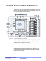
Chapter 1 Overview of ISM in the Dx4-H Series
PWM Value RAM
RAM_D
RAM_C
RAM_A
THOUT1n, THEN1n,
THOUT2n, THEN2n,
TVOUT1n, TVEN1n,
TVOUT2n, TVEN2n
Prescaler
TB_CLK
PWM Value RAM Interface
Table Entry
Channel
Timebase
ADR
MACRO_CLK
ASSIGN_RAM
32 bits RAM Data
20 bits
6
APB
Interface
Channel
Management
(CM)
CM
Values
Addr./Data
CLEAR_
ZIPn GCB ZIPn
ZMTn
6
6
6
20 bits
PWM_Hn
V
PWM_Vn
I
n
f
o
B
u
s
STORE_
CHANNELn
6
5
Current
ZPD Delay
CZDn
IRQ_ZPDAD
Channel
D
Channel
D
Channel
D
Channel
D
V
CHP2
20 bits
H
V
CVP2
CHP3
20 bits
H
ZIPn, ZDRn
6
2*6
ZISn
Input
Selection
Bus
20 bits
H
V
CVP4
6*34 bits
CHP5
20 bits
H
V
CVP5
ZPD Blanking
(ZBTn Counters)
fm
6
ZPD
ZTRn Unit
I/O
Control
V
CHP4
Channel Access Selection &
Value Storage
InfoZMTn
Static
Settings
D
CVP3
6*2
Info-Bus Values
H
Channel
CVP1
IRQ_ZPD
Configuration
Registers
H
D
CHP1
APB Bus
IRQ_ZPD
Channel
CVP0
IRQ_DONE
Channels: n = 0...5
IRQ_DONE
I/O
Control
I...
6*12
CHP0
IRQ_REACHn
IRQ_REACHED
ZERO
(10-bit)
ZERO
Soft Reset
TH1n, TH2n,
TH3n, TH4n,
TV1n, TV2n,
TV3n, TV4n
Port Signals
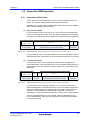
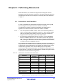
Within the Dx4-H series, the Intelligent Stepper Motor (ISM) function supports
6 channels; this means, that 6 stepper motors can be attached and driven, with
two coils (horizontal and vertical) for each motor.
Anal. Measurement
Input Signals
6*2 bits Quadrant Information CQIn
ZPD_SHORTn
6
6*2*2
ZERO
CQIn
COSPFBn, COSMFBn, SINPFBn, SINMFPn
Figure 1-1
Overview of ISM within Dx4-H Series
When looking at the overview, it is obvious that the ISM contains a “standard”
stepper motor function with 6 channels (seen on the right hand side), and in
addition a “Channel Management” function, which will allow automated
operation by feeding in values into the channels.
In fact, the Channel Management function can be disabled, so that pure PWM
output control is possible by software.
In addition, functionality is included within the Channel Management, which
allows automated Zero Point Detection (ZPD), too. From the view of the
Channel Management, the regular PWM Mode and the ZPD Mode are simply
two different operation modes, how to serve a channel with values for the
output (PWM or direct port settings), and when to read and analyze values
from the ports (coil inductions).
R01AN0168ED0101 Rev. 01.01
Application Note
8
Chapter 2 General Notices
2.1 Abbreviations in this Application Note
Typically, all variables and register settings are written by 3- or 4-letterabbreviations. These abbreviations can be identified within the User’s Manual
by looking at the register and bit names of ISM, and skipping some common
letters like “ISMxG” (for global settings), “ISMxC” (for channel related settings),
“ISMxS/I/F” (for sign, integer and fraction of parameters and variables).
Note
The letter “n” is used to distinguish between channels, i.e., it is a channel
index.
2.2 The Initial State
After the Hardware RESET, the ISM function is set to a passive default state.
• Channel Management is disabled (GCE is cleared).
• All PWM output channels have a 0% duty cycle (PWM off) setting.
• The Quadrant of all channels is set to 0.
• The central Time Base counter is running at its slowest speed.
• The Channel Management update speed is set to its slowest speed.
• All Interrupts are disabled.
• The linkage of ISM and the analogue ZPD hardware is disabled.
2.2.1 Functionality of GCE (Channel Management Enable)
By clearing GCE, the Channel Management (CM) is stopped. Stopping is
performed synchronously, i.e., when GCE is cleared, the current processing of
all channels is completed. After GCB is cleared, the CM is effectively stopped.
PWM and all other output settings remain active as set on the last CM pass. In
this state, all parameters and variables can be redefined arbitrarily.
2.2.2 Analogue Part Linkage (GZL)
Whenever Zero Point Detection (ZPD) is used within your application, always
set the GZL flag. This activates the linkage between the digital and analogue
components of port and ISM.
Note
If GZL is not activated, all settings of GCS, GZF, GRV, GFD, GFL, GZO, GZP
and GZE are blocked, so that ZPD operations cannot be performed.
R01AN0168ED0101 Rev. 01.01
Application Note
9
Chapter 2
General Notices
2.2.3 Functionality of GEN (Soft Reset)
GEN is always set on Hardware RESET.
By clearing the GEN flag by software, the ISM macro is forcibly reset by software. On this synchronous soft-reset, all internal state machines, processing
(GCE is automatically cleared) and also PWM is stopped and forced to reset
conditions. RAM contents, variables and parameters remain untouched, however. These can still be modified by software. Registers are keeping their values, except the following: GCE, GCB, CZCn, CZDn, ZIPn and ZAFn are
cleared on soft-reset.
Cautions
1. As the soft-reset functionality is allowed in any state of the ISM macro,
inconsistencies of status flags with the internal state machines of ISM may
occur. For example, an interrupt pending flag may indicate an interrupt, but
the interrupt could no more be generated due to the soft-reset. For this
reason, after a soft-reset, it is the responsibility of the application software,
to clear status flags accordingly.
2. When Soft Reset is activated and deactivated, distortion on the PWM
outputs will occur, because the Soft Reset happens asynchronously. While
the distortion on activation of Soft Reset is unavoidable (PWM immediately
goes to recirculation via power), the distortion on restart after Soft Reset can
be avoided by software (disabling of port output while synchronously reactivating the ISM).
3. As PWM value settings are not touched by the Soft Reset, PWM output will
continue immediately after Soft Reset is released, unless the corresponding
registers are cleared by software in advance.
2.3 How to generate a first PWM Output
ISM is almost ready-to-use after a Hardware RESET. Therefore, only few steps
are required to see an appropriate PWM output.
• Enable the associated ports of the device for the corresponding peripheral
mode and input mode.
• Set the Central Time Base speed by GTB.
• Set the PWM duty cycle values by CHPn and CVPn.
• Set the PWM quadrant by CQIn.
• If there is no resistive load on the outputs, enable the Recirculation to VSS
by IHRn and IVRn, so that push-pull operation is activated on the ports.
Notes
1. The usage of input mode must be combined with the associated port
setting to enable port control by the peripheral, i.e., the ISM.
In this way, ISM will select input or output direction depending on its
internal processing.
2. The Quadrant selects which of the 4 signals per channel will be applied the
PWM.
3. If Recirculation is not enabled, each port will only drive or not drive one
voltage level; i.e., the PWM toggles from and to high-impedance.
R01AN0168ED0101 Rev. 01.01
Application Note
10
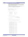
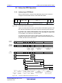
Chapter 3 About Stepper Motor Movement
3.1 The Physics of a Stepper Motor
The Stepper Motor consists of a permanent magnet, which rotates within the
magnetic fields of two coils.
Figure 3-1
Stepper Motor Coil Connection
By using two driver bridges (one for the horizontal coil, one for the vertical coil),
both coils can be driven currents in both directions. Depending on the device
hardware (port structures), either half-bridges or full-bridges are used.
Half-bridges are two push-pull drivers with high-impedance function, while fullbridges are 4 discrete power transistors, which are forming a H-bridge, with the
motor coil in its middle.
Like this, when adding the forces of the magnetic fields of both coils, the motor
anchor can be rotated by changing the amplitude and direction of the fields.
Figure 3-2
Forces and Angle of the Stepper Motor
R01AN0168ED0101 Rev. 01.01
Application Note
11
Chapter 3
About Stepper Motor Movement
The average amplitude of the magnetic field is determined by the PWM duty
cycle, which is represented by the integration of the PWM along its period.
Doing this for both coils, their forces are adding up (red and green
components) to an angle .
Now, the four Quadrants are defined in the mathematical way, where quadrant
0 is where both vertical and horizontal currents are positive (angles 0 to /2),
and quadrant 3 is where vertical current is negative and horizontal current is
positive (angles 32 to 2).
3.1.1 Microsteps: Moving the Motor
When moving the motor anchor, a certain amount of Microsteps can be
applied. In hardware, this is related to the resolution of the PWM, which is
applied to the coils. ISM supports a resolution of 4*[210 -1] microsteps in PWM
granularity (if directly applied by software), or a subset of 512 or 128
microsteps from those, which can be chosen by the Channel Management.
Each microstep corresponds to one combination of PWM for the horizontal and
vertical coil, where the vectorized addition of the vertical and horizontal PWM
duty cycles must be a constant, so that the resulting magnetic force is a
constant, too. This is valid for an ideal motor. For realistic motors, the
combinations of PWM duty cycles may cause variable magnetic forces, in
order to compensate mechanical issues like misalignments etc.
When numbering the microsteps, starting off at angle zero in the positive
mathematical way (“left” turning), the resulting angle of the anchor is
proportional to the microstep number.
Rotation of the motor anchor now is achieved by applying the microsteps in an
incremental sequence. The delay between the microsteps appliance will then
determine the velocity (rotation speed) of the anchor.
An alternative way to rotate the motor is to apply microsteps in constant time
intervals, but to change the velocity (rotation speed), some microsteps are
missed out from the sequence, causing a “jump” of the anchor. This is the
way how the Channel Management of ISM is performing the motor
rotation.
The direction of rotation is determined by reversing the microstep order.
3.1.2 Macrosteps: Performing several Turns
One Macrostep is defined to be one full turn of the motor’s anchor.
The Channel Management of ISM defines either 128 or 512 Microsteps for one
Macrostep. This means, that for one turn, it will apply either 128 or 512 PWM
combinations at maximum to the motor coils. It will miss out microsteps, the
faster the turning shall be.
The Motor Position now is a number of Macrosteps plus Microsteps, because
typically, a stepper motor contains a gear.
In this way, the motor position is formed to a binary number, with the upper
binary part being the macrosteps, and the lower binary part being the
microsteps.
While the microstep number is determining the PWM combination to be
applied to the motor coils, the macrosteps and microsteps are used for the
motor movement in general (acceleration, velocity etc).
R01AN0168ED0101 Rev. 01.01
Application Note
12
Chapter 3
About Stepper Motor Movement
3.2 The PWM Generation of ISM
Following a Prescaler (GTB), the central Time Base determines the PWM
output of ISM; this means that all PWM outputs of ISM are having the same
frequency and are all synchronous.
In order to avoid that too many edges are occurring at the same time on
several ports, each PWM output can be assigned to a delay, which is set in
clocks of the central time base (CDVn and CDHn).
The level of the PWM is in the range 0 ... 210- 1, where 0 means no PWM
output (0%), and 210-1 sets the output level to full 100%. The zero level (0%)
output is important to allow to switch off the output completely. 100% level is
achieved, because the PWM compare value can be set one count more than
the range of counting of the timebase.
The duty cycle of the PWM is set by defining the values CHPn and CVPn, for
each channel, for the horizontal and vertical PWM, respectively. As the
maximum count c of the Channel Timebase is 210- 2, and the duty cycle is
given by a/(c+1), the following formula is given for the duty cycle P:
CHP
P% = ----------------10
2 –1
CVP
P% = ----------------10
2 –1
&KDQQHO7LPHEDVH&RXQW9DOXH
F
F
D
&RPSDUH
0DWFK
3:0 DF
D D &RPSDUHPDWFKKDVSULRULW\
RYHU7LPHEDVH=HUR(YHQW
D F 0DWFKQHYHURFFXUVRQO\
7LPHEDVH=HUR(YHQWV
Figure 3-3
D 3:0 F
D D F
3:0 FF
D F
D 3:0 F 3:0 D F PWM Generation of ISM
R01AN0168ED0101 Rev. 01.01
Application Note
13
Chapter 3
About Stepper Motor Movement
3.2.1 ISM Clocking
The clock of the central time base is selected by the prescaler, and it depends
on the ISM Macro Clock (System Clock), which is set in the Clock Controller of
the device.
f macro
f PWM = ---------------------------------------------------------------10
GTB Factor 2
– 1
3.2.2 PWM Output Generation
Every Channel of ISM consists of two PWM output pairs; one pair for the
horizontal (cosine, COS) and another pair for the vertical (sine, SIN) coil of the
attached stepper motor. PWM duty cycle settings are double-buffered in
registers, so that a change of the PWM duty cycle is not causing distortion on
the PWM signals.
Depending on the Quadrant, the vertical and horizontal PWM output is directed
to the output ports of ISM. Horizontal PWM is output to the COSx ports, while
vertical PWM is output to the SINx ports.
Table 3-1
Quadrant Assignments
Quadrant Selection
Notes
Output Generation
Quadrant
Angle
CQIn
COSP
COSM
SINP
SINM
0
0° - 90°
00B
PWM_H
0
PWM_V
0
1
90° - 180°
01B
0
PWM_H
PWM_V
0
2
180° - 270°
10B
0
PWM_H
0
PWM_V
3
270° - 360°
11B
PWM_H
0
0
PWM_V
1. In this table, PWM_H refers to the horizontal PWM, and PWM_V refers to
the vertical PWM.
2. The port assignments for channel n of the Dx4 devices are as follows:
SMn1
• SINM SMn2
• COSP SMn3
• COSM SMn4
• SINP
R01AN0168ED0101 Rev. 01.01
Application Note
14
Chapter 3
About Stepper Motor Movement
3.3 Recirculation of Inductance
Recirculation means performing a short-circuit on a stepper motor coil, during
the low-phase of the attached PWM. During the high-phase of the PWM the
output voltage drives a current through the coil, and during the low-phase, this
current of the coil, which represents an amount of energy, can be discharged
through the short-cut.
If recirculation is enabled, the PWM output of ISM performs a driving of the
output FET stages, which looks like this for a certain quadrant:
Figure 3-4
Inductive Output driving with Recirculation enabled
Obviously, the generated short-circuit by “~PWM(t)” avoids voltage peaks,
because the current i(t) can continuously discharge. If recirculation is switched
off, the disadvantage of the inductive voltage peak becomes obvious:
Figure 3-5
Inductive Output driving with Recirculation disabled
R01AN0168ED0101 Rev. 01.01
Application Note
15
Chapter 3
About Stepper Motor Movement
3.4 The ISM Channel Circuitry
As a summary of the previous chapters, a full detailed drawing of the circuitry
of one stepper motor channel is shown below.
,600$&52
3RUWLQWHJUDWHG
7R
&263)%
7+287
7+
7+
7+(1
+DOI
EULGJH
2XWSXW
&LUFXLW
0
7+(1
7+287
=(52
,+' 'LUHFW&RQWURO
,
,+( 'LUHFW&RQWURO(QDEOH
,+5 5HFLUFXODWLRQ(QDEOH
'LUHFW
&RQWURO
6WRUHV
7+
,56 5HFLUFXODWLRQ6LGH
&RPSDUH
+RUL]RQWDO
&+3
6WRUDJH
'HOD\
6WDJH'
7+
7
7+
¶¶7+
¶¶
%UHDN
%HIRUH
0DNH
&LUFXLW
7+
3:0
3:0
4XDGUDQW,QIRUPDWLRQ
&4,
+RUL]RQWDO
4XDGUDQW
(QFRGHU
=3'+RUL]RQWDO
$QDORJXH
0HDVXUHPHQW
,QSXW6LJQDOV
7979
=(52
,9' 'LUHFW&RQWURO
,
,9( 'LUHFW&RQWURO(QDEOH
,95 5HFLUFXODWLRQ(QDEOH
'LUHFW
&RQWURO
6WRUHV
,56 5HFLUFXODWLRQ6LGH
5HFLUFX
ODWLRQ
7,0(%$6(
&2817
&RPSDUH
9HUWLFDO
&93
6WRUDJH
79
¶¶79
¶¶
3RUW
7
%UHDN
%HIRUH
0DNH
&LUFXLW
&260
9&&RI60
DOWHUQDWLYHO\
DWWDFKHGWR
GLVFUHWHSRUW
9HUWLFDO
+)(7%ULGJH
7
7
7
3:0B9
79
&4,
&263
79
7%B&/.
=(52
'HOD\6HWWLQJ&'9
LQ7%B&/.&ORFNV
&4,
3:0
9HUWLFDO
4XDGUDQW
(QFRGHU
=3'9HUWLFDO
$QDORJXH
0HDVXUHPHQW
,QSXW6LJQDOV
6WRUDJH
4XDGUDQW,QIRUPDWLRQ
0
&260)%
79
3:0
7
79
79
9HUWLFDO
5HFLUFXODWLRQ
DQG'LUHFW
&RQWURO
(QFRGHU
3ULRULW\RQ
6HW
0$7&+
'HOD\
6WDJH'
0$7&+
7
966RI60
&263)%
79
9(57,&$/
3:09
DOWHUQDWLYHO\
DWWDFKHGWR
GLVFUHWHSRUW
+RUL]RQWDO
+)(7%ULGJH
7
7+
'HOD\6HWWLQJ&'+
LQ7%B&/.&ORFNV
DWWDFKHGWR
LQWHJUDWHGSRUW
3:0B+
7%B&/.
=(52
9&&RI60
7+
7+
+RUL]RQWDO
5HFLUFXODWLRQ
DQG'LUHFW
&RQWURO
(QFRGHU
3ULRULW\RQ
6HW
0$7&+
0$7&+
3RUWGLVFUHWH
6WHSSHU0RWRU
+RUL]RQWDO&RLO
5HFLUFX
ODWLRQ
7,0(%$6(
&2817
+25,=217$/
3:0+
7R
&260)%
7+7+
6,13)%
6WHSSHU0RWRU
9HUWLFDO&RLO
0
966RI60
6,13
6,10
6,10)%
&KDQQHO
3RUWLQWHJUDWHG
DWWDFKHGWR
LQWHJUDWHGSRUW
7R
6,13)%
79287
+DOI
EULGJH
2XWSXW
&LUFXLW
=3'B6+257
79(1
79(1
0
79287
79
79
,2&RQWURO
Figure 3-6
7R
6,10)%
Circuitry of one ISM Channel
R01AN0168ED0101 Rev. 01.01
Application Note
16
Chapter 4 Automated Motor Movement
Within this chapter, more deep functional description about the processing of
the Channel Management (CM) is given. In an overview, the functional blocks
of the CM are looking like this:
START
Channel Enable
Update
Timebase
Prescaler
ZERO
GUD
IRQ_DONE
Sequencer
Soft Reset
IRQ_REACHn
6
ZPD Counter
CZC
GEN_
ZPD_
CALC_
START
INFO
START
Ch. Number n Ch. Number n
CZCn
ZPD Pointer
Mode/Count.
Set
Pointer Set
Pointer Set
Pointer Set
APB
Interface
Clear ZIPn
ASSIGN_RAM
ZIPn,
ZMTn
UPDATE
PWM
Value
RAM
Interface
32-bit access address specification
Ch. Type/Prec.
Pointer SetSet
Pointer Set
Pointer Set
Pointer Set
Address
Generation
6
2*6
Current ZPD
Delay CZDn
5
Position Load Set
6
MICRO
STEP
Parameter Set
Figure 4-1
GCB
Speed Direction
CALC_
DONE
Movement
Calculator
Ch. Acc.
Selection
STORE_
CHANNELn
Actual Position Set
APB
Interface
Variable Set
Channel Management Details
When globally enabled by GCE, the Sequencer is triggered by its implicit
Update Timebase (Speed defined by GUD, triggers START). This starts the
processing of all enabled channels (CENn). If a channel is not enabled (which
can be individually set), its processing is skipped, thus leaving all its
parameters, calculations etc. untouched.
R01AN0168ED0101 Rev. 01.01
Application Note
17
Chapter 4
Automated Motor Movement
4.1 Processing of PWM (non-ZPD) Channels
This is performed for all channels, which are enabled, and CZPn is cleared.
On processing of a channel, first the Movement Calculator is started
(CALC_START). This block calculates a new microstep value for horizontal
and vertical PWM, and evaluates the current speed level and motor direction.
Further, the macrostep value is calculated. This is done by using an implicit
algorithm, which considers external parameters, the current absolute position
of the motor and static variables (digital processing results of previous and
current calls per channel). The Movement Calculator indicates to the
Sequencer, when the calculation is finished. If the Movement Calculator
detects that the given target end position is reached by comparing the actual
position set with the internal position variable, and the actual movement speed
VAS is zero, it generates the per-channel signal IRQ_REACHn.
The Movement Calculator delivers its result, which are the current microstep
values for the PWMs per channel, the associated speed levels and the motor
directions.
Using these microstep values, the Address Generation block creates an
access address to the PWM Value RAM. Like this, the microstep values are
translated into PWM duty cycle and quadrant settings. The Sequencer fetches
the values CVPn, CHPn, CQIn, IHRn and IVRn from the RAM and writes them
into the appropriate register settings of the ISM channels, where the result
becomes visible as changed PWM settings.
In summary, for each time-event of the Update Timebase (GUD), new motor
positions are calculated for each activated channel, and by a look-up table in
the PWM Value RAM, they are translated into PWM values for the channels.
With the next ZERO event, the new values for the PWM settings (CVPn,
CHPn, CQIn) and I/O control (IHRn, IVRn) will become active at the outputs.
The ZERO event is the synchronous start of a new PWM cycle. The
Sequencer is designed such, that it is capable to complete all processing of all
channels within one PWM cycle.
After completion, the Sequencer stops in an idle state and waits on the next
START event.
4.2 Processing of ZPD Channels (ZPD Mode)
This is performed for all channels, which are enabled, and CZPn is set, and the
zero point is not yet detected.
In ZPD Mode, the Movement Calculator is neither used, nor started. Instead of
the microstep result of the Movement Calculator, the value of CZC is used for
the addressing of the PWM Value RAM.
When entering the ZPD mode for a channel n (CZPn was not set in the
previous pass), ZIPn, ZAFn, CZCn and CZDn are initialized to zero, as the
ZPD mode for this channel now begins.
A local copy of the ZPD table index delay CZDn for this channel is
decremented, if it is above zero.
If the current CZDn delay has passed (CZDn has reached zero during this
START event cycle), the next ZPD table index has to be applied by
incrementing ZPD table index counter CZCn of this channel. If the count of
R01AN0168ED0101 Rev. 01.01
Application Note
18
Chapter 4
Automated Motor Movement
CZCn has reached the end of the table marked by ZPD table index limit CTLn,
the counter CZCn is reset to zero again.
Like this, each entry of the PWM Value RAM ZPD table may have an execution
time of CZDn, which is a 5-bit value in counts of the frequency of START (the
Update Timebase). Subsequent equal entries can be put into the table, in
order to get longer delay times.
On ZMTn is set, the ZPD Blanking activates ZTRn after its delay of ZBTn
cycles of the ZPD measurement frequency fm. Then, on ZTRn, the ZPD
measurement is activated, using ZISn as parameter.
The ZPD Unit now will perform ZPD measurements for this channel
(concurrently with other channels), until ZTRn is cancelled again, caused by
the Sequencer, which cancels ZMTn according to a ZPD table entry. On
cancelling, ZTRn immediately follows ZMTn. In case that the ZPD does not
detect the zero position (level was at least once above the threshold), it
activates the corresponding flag ZIPn for this channel.
If the ZPD measurement process is stopped, because ZMTn of the current
channel is cleared (ZMTn of the corresponding ZPD table entry is cleared), but
zero position was not detected meanwhile (ZIPn is set), the ZPD mode
continues by processing the ZPD table from the PWM Value RAM.
If the signal ZIPn is not set for a channel, at the time point when ZMTn is
cancelled, the ZPD mode for this channel is left automatically by clearing
CZPn, and disabling the channel by clearing CENn. This will cause, that the
channel is not processed any more, unless it is reactivated.
The value of CZCn is forwarded to the Address Generation Block.
Using CZCn, the Address Generation block creates an access address to the
PWM Value RAM. Like this, the ZPD table index values are translated into
PWM and output control settings. The Sequencer fetches the values CVPn,
CHPn, CQIn, IHRn, IVRn, IHEn, IVEn, IHDn, IVDn, IHRn, IVRn, ZMTn and
CZDn from the RAM and writes them into the appropriate register settings of
the ISM channels, where the result becomes visible as changed PWM and/or
output settings.
In summary, for each time-event of the Update Timebase (GUD), a new ZPD
table index is calculated for each activated channel, and by a look-up table in
the PWM Value RAM, this is translated into PWM and output control values for
the channels.
With the next ZERO event, the new values for the PWM settings (CVPn,
CHPn, CQIn) and I/O control (IHRn, IVRn, IHEn, IVEn, IHDn, IVDn) will
become active at the outputs. The ZERO event is the synchronous start of a
new PWM cycle. The Sequencer is designed such, that it is capable to
complete all processing of all channels within one PWM cycle.
After completion, the Sequencer stops in an idle state and waits on the next
START event.
The ZPD mode operation is shown graphically in the following flowchart.
R01AN0168ED0101 Rev. 01.01
Application Note
19
Chapter 4
Automated Motor Movement
=3'3URFHVVLQJ
RI&KDQQHOQ
'HOD\
&='Q!
"
'HFUHPHQW&='Q
<(6
(1'
12
=07Q
=3'0HDVXUH
)ODJ6HW"
<(6
=$)Q
=3'$FWLYH
)ODJ6HW"
12
12
<(6
=$)Q
=3'$FWLYH
)ODJ6HW"
12
6HW=3'$FWLYH)ODJ=$)Q
&OHDU=3'$FWLYH)ODJ=$)Q
<(6
12
=,3Q
=3''HWHFWLRQ
)ODJ6HW"
<(6
&OHDU=3'0RGH&=3Q
&KDQQHOQ8SGDWH
&OHDU=3'&RXQWHU&=&Q
DQG'HOD\&='Q
,QFUHPHQW&=&Q
=07Q
=3'0HDVXUH
)ODJ6HW"
&OHDU&KDQQHO(QDEOH&(1Q
12
,54B5($&+Q
<(6
<(6
=$)Q
=3'$FWLYH
)ODJ6HW"
=3'&RXQWHU
&=&QDERYH
/LPLW&7/Q"
12
<(6
&OHDU=3'&RXQWHU&=&Q
12
(1'
Figure 4-2
&OHDU=3''HWHFWLRQ)ODJ=,3Q
ZPD Processing Flow of ISM
R01AN0168ED0101 Rev. 01.01
Application Note
20
Chapter 4
Automated Motor Movement
4.3 Channel Management Processing Overview
Summarized from the chapters above, the processing of the Channel
Management looks like this:
Amount of
START
ZERO
events
reached
Update
Timebase
On every
event for all
channels
Info Bus
Values
Enabled in
Non-ZPD
Mode:
New
Calculation
Movement
Calculator
Addressing
by
Microstep,
Speed,
Direction
Regular
Data
Format
CHP,
CVP,
CQI,
IHR,
IVR
Enabled
Channels
Address
Generation
ZERO
Enabled
in ZPD
Mode:
One
Delay
Step
Disabled
Delay
passed
ZPD
Table
Counter
Delay
CZD
New
Delay
Disabled
Channels
ZPD
Table
Counter
CZC
PWM
Value RAM
Info Bus
Values
Addressing
by ZPD
Table Index
ZPD
Table
Limit
CTL
ZPD
Data
Format
IHE, IVE,
IHD, IVD,
ZMT, ZIS
Info Bus
Value
CZD
Variable ZPD Step Delay
No Processing
Figure 4-3
Sequential Processing: Next Channel
Channel Management Processing Overview
The Info Bus represents all registers, which are accessed by the Channel
Managment during its processing.
R01AN0168ED0101 Rev. 01.01
Application Note
21
Chapter 5 Looking into the PWM and ZPD Tables
5.1 Virtual Channels
As the PWM Value RAM is a lookup-table, it can also perform an abstraction of
a physical channel (where the motor is attached to a port) into a logical or
“virtual” channel.
3FFFH
unused
1 kBytes
One Entry
3C00H
Data of Info Bus, dedicated Format
Ch. Type 5 ZPD
32 Bits
High
Precision
Per
Channel
Type,
2 kBytes
Ch. Type 4 ZPD
Standard
Precision
Ch. Type 3 ZPD
128 Entries
MICROSTEP,
Direction 1,
Speed 1
128 Entries
MICROSTEP,
Direction 0,
Speed 1
128 Entries
MICROSTEP,
Direction 1,
Speed 0
512 Entries
128 Entries
MICROSTEP,
Direction 0,
Speed 0
Ch. Type 2 ZPD
Ch. Type 1 ZPD
Ch. Type 0 ZPD
Channel Type 5
Regular
Channel Type 4
Regular
Channel Type 3
Regular
Channel Type 2
Regular
32 Bits
32 Bits
Channel Type 1
Regular
Channel Type 0
Regular
Figure 5-1
3BFFH
3A00H
39FFH
3800H
37FFH
3600H
35FFH
3400H
33FFH
3200H
31FFH
3000H
2FFFH
PWM Value
RAM Tables
2800H
27FFH
2000H
1FFFH
1800H
17FFH
1000H
0FFFH
0800H
07FFH
0000H
PWM Value RAM Layout
The application can define a virtual channel number CCTn for each physical
channel n. This means, when addressing the content of channel n, not n, but
CCTn instead is used for the addressing of the RAM. Like this, it is possible to
have the same table for several channels, so that only a part of the RAM needs
to be defined.
This virtual channel definition is valid for either “regular” PWM operation or
ZPD mode of a channel.
Note
If several motors are having the same characteristics, it is recommendable to
use the same virtual channel number for them. Like this, the uploading of data
phase into the RAM during startup can be drastically reduced.
R01AN0168ED0101 Rev. 01.01
Application Note
22
Chapter 5
Looking into the PWM and ZPD Tables
5.2 Values for PWM Operation
5.2.1 Channels and Precision
As can be seen from the RAM layout, for each virtual channel there are two
tables: The “regular” PWM operation table and the ZPD table.
Regarding the “regular” PWM operation table, there are two formats available,
which can be selected by the CCPn flag.
(1)
High Precision Mode
In high precision mode (CCPn set), for one turn of the motor the whole table
section is used with 512 entries. Thus, the RAM is addressed in the following
way, which also defines the layout of data to be copied there by the application:
CCTn
(000B ... 101B)
Bits 10 ... 2
Channel Settings
Figure 5-2
MICROSTEP[8:0] from Movement Calculator
A1
A0
Always zero
PWM Table Addressing Layout for High Precision Channels
In high precision mode, 512 angle positions can be stored, but there will be no
distinguishing of the characteristic for current speed and direction of the motor.
(2)
Low Precision Mode
In low precision mode (CCPn cleared), the table section is divided into 4
equally sized parts, with 128 entries each. Thus, the RAM is addressed in the
following way, which also defines the layout of data to be copied there by the
application:
CCTn
(000B ... 101B)
Channel Settings
Figure 5-3
VSPn
VDRn
Speed,
Direction
Bits 8 ... 2
MICROSTEP[6:0] from Movement Calculator
A1
A0
Always zero
PWM Table Addressing Layout for Low Precision Channels
In low precision mode, 128 angle positions can be stored, but there are 4
tables to distinguish for speed and direction of the motor. Speed and direction
flags are corresponding to the variables VSPn and VDRn of the Movement
Calculator. These variables are automatically calculated, and they are
depending on some parameters (speed limits, current position, target position).
Like this, optimized table sets can be stored, which are depending on the
motor characteristics, and which are dynamically switched during operation
and motor movement.
R01AN0168ED0101 Rev. 01.01
Application Note
23
Chapter 5
Looking into the PWM and ZPD Tables
5.2.2 PWM Values
In the ideal case, one would expect that the values of the PWM duty cycles are
sine and cosine waveforms, if they are related to the microstep or the angle of
the motor anchor.
This assumes, that the force relations inside of the motor are ideal, that the
forces can be added and that the forces of the horizontal and vertical coils are
rectangular to each other. This is what is explained in the theory, as shown in
3.1 “The Physics of a Stepper Motor” on page 11 .
However, the mechanical physics of a stepper motor are not ideal, typically.
Therefore, the values of the PWM duty cycles along with the motor anchor
angle or microstep may showing waveforms like this:
Vertical PWM
Left Turning
Horizontal PWM
1,5
1
PWM %
0,5
0
0
16
32
48
64
80
96
112
-0,5
-1
-1,5
Microstep
Figure 5-4
Non-ideal PWM Settings of a typical Stepper Motor
In this figure, the value “1” of the PWM refers to a duty cycle of 100%, meaning
a value of “0x3FF” for the registers CVPn or CHPn.
Even more, when changing the rotation direction or when running faster or
slower, the characteristics of a motor may vary. To support this, the ISM PWM
tables in low precision mode are supporting the rotation direction and one level
of speed hysteresis, which are changing the tables dynamically.
Note
It is up to the user, to find out the best fitting PWM table sets of the used
motors. If no background data is available, it is recommended to start off with
ideal sine and cosine sequences for the PWM tables.
R01AN0168ED0101 Rev. 01.01
Application Note
24
Chapter 5
Looking into the PWM and ZPD Tables
(1)
Example of a Sine - Cosine Sequence PWM Table
When writing PWM tables into the PWM Value RAM, a standard table for a
quick start could look like the following table. For different speed levels and
directions, the same table can be used.
This table is “right turning”, because the sequence of quadrants is 4, 3, 2, 1.
The used access type is shown in advance of the table.
/*............... ISM PWM RAM access structures ..................*/
#define EE_ISM_SPEEDS
( 2 )
#define EE_ISM_DIRECTIONS
( 2 )
#define EE_ISM_TABLESIZE_STD ( 128 )
typedef struct eeism_pwmcell_t {
volatile
volatile
volatile
volatile
volatile
volatile
u32_t
u32_t
u32_t
u32_t
u32_t
u32_t
cvp
chp
cqi
ivr
ihr
UNUSED
:
:
:
:
:
:
10;
10;
2;
1;
1;
8;
} eeism_pwmcell_t;
typedef struct eeism_pwmstd_t {
struct eeism_pwmcell_t std[ EE_ISM_SPEEDS ]
[ EE_ISM_DIRECTIONS ]
[ EE_ISM_TABLESIZE_STD ];
} eeism_pwmstd_t;
/* Default PWM Table: SINE on CVP, COSINE on CHP */
const struct eeism_pwmstd_t EE_ISM_A_STDPWMTABLE1 = {
/* CVP
{
{{{ 0x000L,
{ 0x032L,
{ 0x064L,
{ 0x096L,
{ 0x0C7L,
{ 0x0F8L,
{ 0x128L,
{ 0x158L,
{ 0x187L,
{ 0x1B5L,
{ 0x1E2L,
{ 0x20DL,
{ 0x238L,
{ 0x261L,
{ 0x288L,
{ 0x2AFL,
{ 0x2D3L,
{ 0x2F5L,
{ 0x316L,
{ 0x335L,
{ 0x352L,
{ 0x36DL,
{ 0x386L,
{ 0x39CL,
{ 0x3B1L,
{ 0x3C3L,
{ 0x3D2L,
R01AN0168ED0101 Rev. 01.01
Application Note
CHP
0x3FFL,
0x3FDL,
0x3FAL,
0x3F3L,
0x3EBL,
0x3E0L,
0x3D2L,
0x3C3L,
0x3B1L,
0x39CL,
0x386L,
0x36DL,
0x352L,
0x335L,
0x316L,
0x2F5L,
0x2D3L,
0x2AFL,
0x288L,
0x261L,
0x238L,
0x20DL,
0x1E2L,
0x1B5L,
0x187L,
0x158L,
0x128L,
CQI
IVR IHR */
0x3L,
0x3L,
0x3L,
0x3L,
0x3L,
0x3L,
0x3L,
0x3L,
0x3L,
0x3L,
0x3L,
0x3L,
0x3L,
0x3L,
0x3L,
0x3L,
0x3L,
0x3L,
0x3L,
0x3L,
0x3L,
0x3L,
0x3L,
0x3L,
0x3L,
0x3L,
0x3L,
1L,
1L,
1L,
1L,
1L,
1L,
1L,
1L,
1L,
1L,
1L,
1L,
1L,
1L,
1L,
1L,
1L,
1L,
1L,
1L,
1L,
1L,
1L,
1L,
1L,
1L,
1L,
1L,
1L,
1L,
1L,
1L,
1L,
1L,
1L,
1L,
1L,
1L,
1L,
1L,
1L,
1L,
1L,
1L,
1L,
1L,
1L,
1L,
1L,
1L,
1L,
1L,
1L,
1L,
0L
0L
0L
0L
0L
0L
0L
0L
0L
0L
0L
0L
0L
0L
0L
0L
0L
0L
0L
0L
0L
0L
0L
0L
0L
0L
0L
}, /* 4th quadrant */
},
},
},
},
},
},
},
},
},
},
},
},
},
},
},
},
},
},
},
},
},
},
},
},
},
},
25
Chapter 5
Looking into the PWM and ZPD Tables
{
{
{
{
{
0x3E0L,
0x3EBL,
0x3F3L,
0x3FAL,
0x3FDL,
0x0F8L,
0x0C7L,
0x096L,
0x064L,
0x032L,
0x3L,
0x3L,
0x3L,
0x3L,
0x3L,
1L,
1L,
1L,
1L,
1L,
1L,
1L,
1L,
1L,
1L,
0L
0L
0L
0L
0L
},
},
},
},
},
{
{
{
{
{
{
{
{
{
{
{
{
{
{
{
{
{
{
{
{
{
{
{
{
{
{
{
{
{
{
{
{
0x3FFL,
0x3FDL,
0x3FAL,
0x3F3L,
0x3EBL,
0x3E0L,
0x3D2L,
0x3C3L,
0x3B1L,
0x39CL,
0x386L,
0x36DL,
0x352L,
0x335L,
0x316L,
0x2F5L,
0x2D3L,
0x2AFL,
0x288L,
0x261L,
0x238L,
0x20DL,
0x1E2L,
0x1B5L,
0x187L,
0x158L,
0x128L,
0x0F8L,
0x0C7L,
0x096L,
0x064L,
0x032L,
0x000L,
0x032L,
0x064L,
0x096L,
0x0C7L,
0x0F8L,
0x128L,
0x158L,
0x187L,
0x1B5L,
0x1E2L,
0x20DL,
0x238L,
0x261L,
0x288L,
0x2AFL,
0x2D3L,
0x2F5L,
0x316L,
0x335L,
0x352L,
0x36DL,
0x386L,
0x39CL,
0x3B1L,
0x3C3L,
0x3D2L,
0x3E0L,
0x3EBL,
0x3F3L,
0x3FAL,
0x3FDL,
0x2L,
0x2L,
0x2L,
0x2L,
0x2L,
0x2L,
0x2L,
0x2L,
0x2L,
0x2L,
0x2L,
0x2L,
0x2L,
0x2L,
0x2L,
0x2L,
0x2L,
0x2L,
0x2L,
0x2L,
0x2L,
0x2L,
0x2L,
0x2L,
0x2L,
0x2L,
0x2L,
0x2L,
0x2L,
0x2L,
0x2L,
0x2L,
1L,
1L,
1L,
1L,
1L,
1L,
1L,
1L,
1L,
1L,
1L,
1L,
1L,
1L,
1L,
1L,
1L,
1L,
1L,
1L,
1L,
1L,
1L,
1L,
1L,
1L,
1L,
1L,
1L,
1L,
1L,
1L,
1L,
1L,
1L,
1L,
1L,
1L,
1L,
1L,
1L,
1L,
1L,
1L,
1L,
1L,
1L,
1L,
1L,
1L,
1L,
1L,
1L,
1L,
1L,
1L,
1L,
1L,
1L,
1L,
1L,
1L,
1L,
1L,
0L
0L
0L
0L
0L
0L
0L
0L
0L
0L
0L
0L
0L
0L
0L
0L
0L
0L
0L
0L
0L
0L
0L
0L
0L
0L
0L
0L
0L
0L
0L
0L
},
},
},
},
},
},
},
},
},
},
},
},
},
},
},
},
},
},
},
},
},
},
},
},
},
},
},
},
},
},
},
},
/* 3rd quadrant */
{
{
{
{
{
{
{
{
{
{
{
{
{
{
{
{
{
{
{
{
{
{
{
{
{
{
{
{
{
{
{
0x000L,
0x032L,
0x064L,
0x096L,
0x0C7L,
0x0F8L,
0x128L,
0x158L,
0x187L,
0x1B5L,
0x1E2L,
0x20DL,
0x238L,
0x261L,
0x288L,
0x2AFL,
0x2D3L,
0x2F5L,
0x316L,
0x335L,
0x352L,
0x36DL,
0x386L,
0x39CL,
0x3B1L,
0x3C3L,
0x3D2L,
0x3E0L,
0x3EBL,
0x3F3L,
0x3FAL,
0x3FFL,
0x3FDL,
0x3FAL,
0x3F3L,
0x3EBL,
0x3E0L,
0x3D2L,
0x3C3L,
0x3B1L,
0x39CL,
0x386L,
0x36DL,
0x352L,
0x335L,
0x316L,
0x2F5L,
0x2D3L,
0x2AFL,
0x288L,
0x261L,
0x238L,
0x20DL,
0x1E2L,
0x1B5L,
0x187L,
0x158L,
0x128L,
0x0F8L,
0x0C7L,
0x096L,
0x064L,
0x1L,
0x1L,
0x1L,
0x1L,
0x1L,
0x1L,
0x1L,
0x1L,
0x1L,
0x1L,
0x1L,
0x1L,
0x1L,
0x1L,
0x1L,
0x1L,
0x1L,
0x1L,
0x1L,
0x1L,
0x1L,
0x1L,
0x1L,
0x1L,
0x1L,
0x1L,
0x1L,
0x1L,
0x1L,
0x1L,
0x1L,
1L,
1L,
1L,
1L,
1L,
1L,
1L,
1L,
1L,
1L,
1L,
1L,
1L,
1L,
1L,
1L,
1L,
1L,
1L,
1L,
1L,
1L,
1L,
1L,
1L,
1L,
1L,
1L,
1L,
1L,
1L,
1L,
1L,
1L,
1L,
1L,
1L,
1L,
1L,
1L,
1L,
1L,
1L,
1L,
1L,
1L,
1L,
1L,
1L,
1L,
1L,
1L,
1L,
1L,
1L,
1L,
1L,
1L,
1L,
1L,
1L,
1L,
0L
0L
0L
0L
0L
0L
0L
0L
0L
0L
0L
0L
0L
0L
0L
0L
0L
0L
0L
0L
0L
0L
0L
0L
0L
0L
0L
0L
0L
0L
0L
},
},
},
},
},
},
},
},
},
},
},
},
},
},
},
},
},
},
},
},
},
},
},
},
},
},
},
},
},
},
},
/* 2nd quadrant */
R01AN0168ED0101 Rev. 01.01
Application Note
26
Chapter 5
Looking into the PWM and ZPD Tables
{ 0x3FDL, 0x032L, 0x1L, 1L, 1L, 0L },
{
{
{
{
{
{
{
{
{
{
{
{
{
{
{
{
{
{
{
{
{
{
{
{
{
{
{
{
{
{
{
{
...
0x3FFL,
0x3FDL,
0x3FAL,
0x3F3L,
0x3EBL,
0x3E0L,
0x3D2L,
0x3C3L,
0x3B1L,
0x39CL,
0x386L,
0x36DL,
0x352L,
0x335L,
0x316L,
0x2F5L,
0x2D3L,
0x2AFL,
0x288L,
0x261L,
0x238L,
0x20DL,
0x1E2L,
0x1B5L,
0x187L,
0x158L,
0x128L,
0x0F8L,
0x0C7L,
0x096L,
0x064L,
0x032L,
0x000L,
0x032L,
0x064L,
0x096L,
0x0C7L,
0x0F8L,
0x128L,
0x158L,
0x187L,
0x1B5L,
0x1E2L,
0x20DL,
0x238L,
0x261L,
0x288L,
0x2AFL,
0x2D3L,
0x2F5L,
0x316L,
0x335L,
0x352L,
0x36DL,
0x386L,
0x39CL,
0x3B1L,
0x3C3L,
0x3D2L,
0x3E0L,
0x3EBL,
0x3F3L,
0x3FAL,
0x3FDL,
0x0L,
0x0L,
0x0L,
0x0L,
0x0L,
0x0L,
0x0L,
0x0L,
0x0L,
0x0L,
0x0L,
0x0L,
0x0L,
0x0L,
0x0L,
0x0L,
0x0L,
0x0L,
0x0L,
0x0L,
0x0L,
0x0L,
0x0L,
0x0L,
0x0L,
0x0L,
0x0L,
0x0L,
0x0L,
0x0L,
0x0L,
0x0L,
1L,
1L,
1L,
1L,
1L,
1L,
1L,
1L,
1L,
1L,
1L,
1L,
1L,
1L,
1L,
1L,
1L,
1L,
1L,
1L,
1L,
1L,
1L,
1L,
1L,
1L,
1L,
1L,
1L,
1L,
1L,
1L,
1L,
1L,
1L,
1L,
1L,
1L,
1L,
1L,
1L,
1L,
1L,
1L,
1L,
1L,
1L,
1L,
1L,
1L,
1L,
1L,
1L,
1L,
1L,
1L,
1L,
1L,
1L,
1L,
1L,
1L,
1L,
1L,
0L
0L
0L
0L
0L
0L
0L
0L
0L
0L
0L
0L
0L
0L
0L
0L
0L
0L
0L
0L
0L
0L
0L
0L
0L
0L
0L
0L
0L
0L
0L
0L
},
},
},
},
},
},
},
},
},
},
},
},
},
},
},
},
},
},
},
},
},
},
},
},
},
},
},
},
},
},
},
} },
/* 1st quadrant */
} };
R01AN0168ED0101 Rev. 01.01
Application Note
27
Chapter 5
Looking into the PWM and ZPD Tables
5.3 Values for ZPD Operation
5.3.1 Addressing in ZPD Mode
When in ZPD mode for a channel, the addressing range for this channel is
changed to the ZPD table sections of the PWM Value RAM.
1
CCTn
(000B ... 101B)
1
ZPD Table
Range Code
Figure 5-5
Bits 8 ... 2
Channel Settings
A1
CZCn[6:0] from Sequencer
A0
Always zero
ZPD Table Addressing Layout
Again, the virtual channel number is used to select a ZPD table in general. Like
this, the same ZPD table can be used to serve for several physical channels.
In contrary to the “regular” PWM operation mode, now simply the current ZPD
table index CZCn is used for the addressing. Here, the RAM is no longer used
as a “translator”, but used as an instruction table.
The instructions are derived from the data contents of the RAM, which are
triggering measurements, causing delays, setting outputs and selecting inputs.
In detail, the data format looks like this:
31
Common
Format
Regular
(non-ZPD)
Operation
30
26
25
24
23
22
21
20
CQI1
ZIS1
CQI0
ZIS0
ZMT
CZD
IHE
IVE
IHR
IVR
X
XXXXXB
X
X
IHR
IVR
ZMT
CZD
IHE
IVE
IHR
IVR
10 9
CQI1
ZIS1
CQI0
ZIS0
0
CQI
1
ZIS
0
CHP / IHD
CVP / IVD
CHP
CVP
PWM Value CHP
10-bit H (cos)
PWM Value CVP
10-bit V (sin)
CHP / IHD
CVP / IVD
CQI
Recirculation Quadrant
Enable for Information
CQI
H+V
ZPD
Operation
19
13
0
10
CHP
1
IHD
3
0
CVP
1
ZPD
Measurement
Trigger
Figure 5-6
Delay Count
Setting CZD
for this step
Port Direct Recirculation ZPD Input
Control Enable Enable for Selection or
H+V
H+V
Quadrant
0
IVD
PWM Value
10-bit H (cos) or Horizontal
Direct Control Setting
PWM Value
10-bit V (sin) or Vertical
Direct Control Setting
Common PWM Value RAM Data Format
R01AN0168ED0101 Rev. 01.01
Application Note
28
Chapter 6 Performing Movements
Within this section, the movement of stepper motors using the Channel
Management and the Movement Calculator is discussed. Operation with Zero
Point Detection can be found in Chapter 7 “Performing Zero Point Detection”
on page 37 .
6.1 Parameters and Variables
In order to understand the automated movement of a stepper motor by ISM,
the knowledge about its parameters and variables is essential.
The Movement Calculator is using the parameters as constants for its
algorithm, and it stores temporary values and results in variables.
Notes
1. The most important variable is VAPn, which shows the actual position in
macro- and microsteps of a (physical) channel n. If VAPn matches PMPn
(which is the target motor position to move to), the motor movement is
stopped and the interrupt IRQ_REACHED is generated.
2. Be careful when thinking about the term “channel”. For the PWM tables,
there are “virtual” channels CCTn. This means, that for each physical
channel n, a set of PWM values can be chosen. However, all other parts of
ISM, including the Movement Calculator and its parameters and variables,
are always referring to physical channels.
For parameters and variables there is no software reset (only by hardware), so
that parameters and variables shall be initialized by software before starting or
re-starting the Channel Management. Parameters and variables must not be
changed during operation of the Channel Management, except PMPn.
As an overview, the following parameters and variables are existing for each
physical channel n, and they are all accessible by software via registers. Most
of them have a common format using 25 bits.
Table 6-1
Parameters of the Movement Calculator
Abbreviation /
Bit Name
Width / Bits
Register Name
Target Motor Positiona
PMP
25
ISMxPAR0CFGn
Damping Factor
PDF
3
ISMxPAR1CFGn
Acceleration Limit
PAL
25
ISMxPAR2CFGn
Deceleration Limit
PDL
25
ISMxPAR3CFGn
Maximum Speed
PMS
25
ISMxPAR4CFGn
Hysteresis Correction
PHC
25
ISMxPAR5CFGn
Speed Threshold 1
PS1
25
ISMxPAR6CFGn
Speed Threshold 2
PS2
25
ISMxPAR7CFGn
Speed Threshold 3
PS3
25
ISMxPAR8CFGn
Speed Threshold 4
PS4
25
ISMxPAR9CFGn
Parameter
a)
This parameter is double-buffered. Change by software is possible at any time
without disturbances. On each START event, the buffered value is updated.
R01AN0168ED0101 Rev. 01.01
Application Note
29
Chapter 6
Performing Movements
Table 6-2
Variables of the Movement Calculator
Abbreviation /
Bit Name
Width /
Bits
Register Name
Actual Acceleration / Deceleration
VAX
25
ISMxVAR0CFGn
Actual Speed
VAS
25
ISMxVAR1CFGn
Previous Iteration Speed
VPS
25
ISMxVAR2CFGn
Temporary Calculator Register PT1
VPT
25
ISMxVAR3CFGn
Actual Position, Current Result
VAP
25
ISMxVAR4CFGn
Virtually Displayed Position
VVP
25
ISMxVAR5CFGn
Direction Flag
VDR
1
ISMxVAR6CFGn
Speed Flag
VSP
1
ISMxVAR7CFGn
Variable
6.1.1 Common 25-bit Number Format
For all parameters and variables which are 25 bits wide, a common number
format is given.
;XQGHILQHG
6LJQ
9DOXH
9DOXH,QWHJHU
6LJQ)ODJ([WHQVLRQ
9DOXH%LQDU\)UDFWLRQ
0DFURVWHS
0,&5267(3>@2XWSXWIRU9$3
Figure 6-1
Common 25-bit Number Format
The number format consists of a sign flag, the macrosteps and the microsteps
values. The storage format is a binary fixed-point format, with bits [23:8] being
the integer and [7:0] the fraction part. Bit 24 is the sign (positive/negative),
which can be extended by software to 32 bits by copying bit 24. Negative
values are stored in 2’s complement.
(1)
Sign Flag
All numbers within the Movement Calculator are signed numbers. This means,
that the position of zero is a relative one. In fact, movements are always
calculated by relative distances. If by software the variable VAP is set to a
certain value p, before the Channel Management is started, this position now is
assumed to be the actual position. To move towards zero by more steps than
p, a negative value for the target position PMP would be entered.
Negative numbers have the sign flag set (1).
Note
It makes sense to clear PMPn and VAPn after having reached the mechanical
zero point of an instrument (i.e., by Zero Point Detection). Like this, all position
values would be positive, and other values would have a positive sign, if their
direction would point away from the mechanical stop, or have a negative sign,
if their direction would point towards the mechanical stop.
R01AN0168ED0101 Rev. 01.01
Application Note
30
Chapter 6
Performing Movements
(2)
Value Integer
For position values, the value integer consists of the macrosteps and the
microsteps. Depending on the precision setting of a channel (CCPn), either 9
or 7 bits are reserved for the microsteps, and the remaining bits up to bit 23 are
used for the macrosteps.
(3)
Value Binary Fraction
This part represents the fractional part of the value. Its binary step is 1/256 of
the value integer.
The binary fraction is used for internal calculations only. For user software, the
following rules are important:
1. When setting the parameter PMPn,
all bits of the binary fraction have to be set.
2. When setting all other parameters or variables by software,
all bits of the binary fraction have to be cleared.
Caution
If rule (1) is not followed, it may happen that because of permanent deviation
of the algorithm, a target position can never be reached.
• The deviation of the algorithm of the Movement Calculator is less than 1
microstep.
• When moving “upwards”, the algorithm may stop less than 1 microstep
below the target position, which however results in one count too less for
the microstep, but an added fractional value. Like this, the position
reached interrupt (IRQ_REACHEDn) can never be generated, because
this interrupt is based on a comparison on Value Integer level.
• When moving “downwards”, the algorithm has no deviation. Therefore
the target position can be reached in any case, independently of any
settings of the binary fraction.
6.1.2 Parameter Description
(1)
Target Position PMPn
Represents the requested target position of the motor, given in macrosteps
(full turns) and microsteps (angle). The target position can be a negative
number.
(2)
• Unit:
Absolute Position
• Example Setting:
(for low precision setting, sine/cosine table)
0x001234FF
+36 turns, 146°
Damping Factor PDFn
Represents the inertia of the algorithm. The value given here is not a 25-bit
number, but only a 3-bit number. It is the exponent 2PDF, which divides the
theoretical maximum speed required to reach the target position within only
one algorithm pass.
• Unit:
Factor
• Example Setting:
(chosen speed on every algorithm pass)
0x6
1
/64 of maximum speed
R01AN0168ED0101 Rev. 01.01
Application Note
31
Chapter 6
Performing Movements
(3)
Acceleration Limit, Deceleration Limit PALn, PDLn
If acceleration or deceleration of the motor would become larger than these
limits, acceleration or deceleration is set to these values. After a new speed
has been calculated, the algorithm determines the corresponding acceleration/
decelerations and by case, it limits the speed, so that the acceleration and
deceleration limits cannot be crossed.
(4)
• Unit:
(from the physics: distance / time2)
Acceleration: Microsteps *
(CM Update Frequency)2
• Example settings:
(using an update period GUD of 10 ms)
(for low precision setting)
0x00000020
1250 microsteps / second2
9.77 turns / s2
Maximum Speed PMSn
If the speed of a motor would becomer larger than this limit, either positive or
negative, the speed is limited to this value. The speed limit works
independently of the acceleration limit.
(5)
• Unit:
(from the physics: distance / time)
Speed: Microsteps *
(CM Update Frequency)
• Example setting:
(using an update period GUD of 10 ms)
(for low precision setting)
0x000009C0
975 microsteps / second
7.62 turns / second
Hysteresis Correction PHCn
Position values of VAPn, which are less than the given hysteresis by PHCn will
be indicated to software as “zero” position, when software reads the current
position via the VVPn variable. Also, VVPn always indicates a position which is
by PHCn less than VAPn. Like this, the variable VVPn can be used by software
as a dynamically compressed readout of the actual position.
(6)
• Unit:
Distance
• Example setting:
(indicated as still at zero)
+/-
0x00000700
7 turns of the motor
Speed Thresholds PS1n, PS2n, PS3n, PS4n
Speed marks for switching of the VSPn flag, which dynamically switches the
PWM tables for low-speed and high-speed operation of the motor. While PS3n
and PS4n are marking a speed range for the high-speed operation, the values
of PS1n and PS2n are marking the outside ranges for the low-speed
operation. See 6.1.4 “Algorithm Code” for details on these thresholds.
• Unit:
(from the physics: distance / time)
Speed: Microsteps *
(CM Update Frequency)
PS1 = 0x0000010E
PS2 = 0x00000620
PS3 = 0x000001C3
PS4 = 0x0000056B
(calculate speed in the same way as for 4 “Maximum Speed PMSn”).
• Example settings:
R01AN0168ED0101 Rev. 01.01
Application Note
32
Chapter 6
Performing Movements
6.1.3 Variable Description
(1)
Actual Algorithm Values VAXn, VASn, VAPn
These values are representing the current Movement Calculator results for the
physical channel n. Acceleration, speed and position values have to be
interpreted like their associated parameter values.
Checking the values is possible anytime to monitor the movements by
software.
(2)
Temporary Storages VPSn, VPTn
These are internal values of the Movement Calculator, to resume the
calculation after the next processing start. Previously calculated values and
intermediate results are stored there.
Software access to these values is not senseful, but nevertheless possible.
(3)
Virtual Position VVPn
A position value, which was submitted a hysteresis can be derived from the
VVPn variable. Its generation is explained in 5 “Hysteresis Correction PHCn”.
(4)
Flags of PWM Table Selection on Low-Precision Operation VDRn, VSPn
These flags are representing the PWM sub-table selection within a physical
channel ‘s assigned virtual table set, if low-precision operation is chosen
(CCPn is cleared).
In case of high-precision operation, these flags have no meaning, and the
associated parameters PS1n, PS2n, PS3n and PS4n are not considered.
6.1.4 Algorithm Code
/* Calculation of new acceleration and speed */
VPT
VAS
VAX
=
=
=
VPT + ( ( PMP - VPT) >> PDF )
( VPT - VAP ) >> PDF
VAS - VPS
/* Limitation of the acceleration and speed */
if ( VPS > 0 )
{
if ( VAX > PAL )
{
VAS = VPS + PAL
}
if ( VAX < ( - PDL ) )
{
VAS = VPS - PDL
}
}
else
{
if ( VAX < ( - PAL ) )
{
VAS = VPS - PAL
}
if ( VAX > PDL )
{
VAS = VPS + PDL
R01AN0168ED0101 Rev. 01.01
Application Note
33
Chapter 6
Performing Movements
}
}
if ( VAS >= 0 )
{
if ( VAS > PMS )
{
VAS = PMS
}
}
else
{
if ( ( -VAS ) > PMS )
{
VAS = ( - PMS )
}
}
/* Result output for Microstep & store old speed */
VAP
VPS
=
=
VAP + VAS
VAS
/* Calculate SW displayed position */
if ( ( VAP - VVP ) > PHC )
{
VVP = VAP - PHC
}
if ( ( VAP - VVP ) < ( - PHC ) )
{
VVP = VAP + PHC
}
/* Select Table according to speed and direction */
if ( VAS > 0 )
{
VDR = 0
if ( ( VAS <= PS1 ) or ( VAS >= PS2 ) )
{
VSP = 0
}
else
{
VSP = VSP
}
if( ( VAS >= PS3 ) and( VAS <= PS4 ) )
{
VSP = 1
}
else
{
VSP = VSP
}
}
else
{
if ( VAS < 0 )
{
VDR = 1
if ( ( ( -VAS ) <= PS1 ) or ( ( -VAS ) >= PS2 ) )
{
R01AN0168ED0101 Rev. 01.01
Application Note
34
Chapter 6
Performing Movements
VSP = 0
}
else
{
VSP = VSP
}
if ( ( ( -VAS ) >= PS3 ) and( ( -VAS ) <= PS4 ) )
{
VSP = 1
}
else
{
VSP = VSP
}
}
}
if ( VAS == 0 )
{
VSP = 0
}
/* Negative Position suppression */
if ( VAP < 0 )
{
VAP = 0
}
R01AN0168ED0101 Rev. 01.01
Application Note
35
Chapter 6
Performing Movements
6.2 Moving the Motors
Having all parameters set, the timebases defined and the RAM PWM tables
set up, the motor movement can be started by activating the Channel
Management for the selected channels.
Caution
When using stepper motor hardware, always enable Recirculation.
Otherwise, caused by the inductive load, damage to the output drivers may
happen.
The following diagram shows a movement graphically, by reading out the
variables by software.
Upw ards Movem ent
12000
1400000
11000
1200000
10000
9000
VAP
1000000
VAX
VAS
8000
7000
800000
6000
5000
600000
4000
3000
400000
Acceleration (VAX), Speed (VAS)
Set Position (PMP), Actual Position (VAP)
PMP
2000
1000
200000
0
-1000
0
10
0
20
0
30
0
40
0
50
0
60
0
70
0
80
0
90
0
10
00
11
00
12
00
13
00
14
00
15
00
16
00
17
00
18
00
19
00
20
00
0
CM Update Cycle
Figure 6-2
Graphical Movement Illustration
R01AN0168ED0101 Rev. 01.01
Application Note
36
Chapter 7 Performing Zero Point Detection
7.1 Zero Point Detection (ZPD) Theory
In order to define the ZPD table entries, base knowledge about zero point
detection is required. Let’s have a look into a simplified stepper motor. In the
following figure, four steps of movement are shown, one for each quadrant of
the motor’s anchor.
Within each quadrant, it is possible to detect, whether the motor could move,
or whether it had hit its mechanical stop, and therefore, it could not move.
The detection of the mechanical stop is performed by measuring inductive
pulses one one coil set, while the other coil set is powered for a movement of
the anchor.
Powered,
for Measure
Figure 7-1
Powered,
for Measure
Powered,
for Measure
Powered,
for Measure
Four Quadrant Zero Point Detection1
Surely, it is not required to perform the measurement for all four quadrants.
Alternatively, it’s also possible to move the motor a full turn, and perform a
measurement only in one of the four steps above.
Regarding the ZPD algorithms, there is some trade-off between quality
(smoothness of movement, noise on hitting the stop) and the capabilities of the
motor and the stepper motor driver hardware. From 1 to 4, the quality of ZPD
increases:
1. Single-Quadrant ZPD
One full turn of the motor in 90° steps, one measurement at 0°.
2. Single-Quadrant ZPD with PWM movement
One full turn of the motor in fine PWM microsteps, accelerating sequence,
one measurement at 0°.
3. Four-Quadrant ZPD
Quarter-turn of the motor, measurement after each quarter-turn.
4. Four-Quadrant ZPD with PWM movement
Quarter-turn of the motor by fine PWM microsteps, accelerating sequence,
measurement after each quarter-turn.
ISM supports all four approaches.
1)
Figure by “Lessons In Electric Circuits copyright (C) 2000-2012 Tony R. Kuphaldt”
R01AN0168ED0101 Rev. 01.01
Application Note
37
Chapter 7
Performing Zero Point Detection
7.1.1 The ZPD Measurement Principle
For all 4 cases, the same measurement principle is applied:
An analogue measurement of induced voltage is performed, while the other
coil moves the anchor. If the anchor is still able to move, it will cause a small
voltage induction in the measurement coil. If the motor has hit the mechanical
stop, the anchor will almost not move any longer, and the induced voltage will
decrease or disappear.
(1)
Finding the Measurement Time Window
Typically, the measurement waveforms could look like this:
Self-Induction of measured coil
(must be skipped from measurement)
Induction time: about 500 µs
This is our
measurement target
Figure 7-2
ZPD Measurement Waveform
Caused by the previous movement, the coil also creates a self-induction, when
its current is switched off and it is attached to the measurement input. This selfinduction is not relevant for the ZPD status, and therefore it must be reduced
(also to protect our measurement circuitry) and blanked out from the
measurement window.
Reduction of the self-induction can be performed by creating a short-circuit on
the coil for a limited amount of time.
The measurement window has to be chosen by delaying the measurement
start and limitation of the measurement time.
(2)
Determining the Measurement Voltage Level
As a target, a voltage detector (comparator) has to be set up such, that it
shows an indication above its level, if the zero point (ZP) has not yet been
reached (induction was found), and that it shows an indication below its level, if
the ZP has been reached (no induction was found). Like this, the ZP status is
digitized into a single binary state flag.
As shown in the following figure, the difference in the voltage level between a
reached ZP and a still turning motor is quite small.
R01AN0168ED0101 Rev. 01.01
Application Note
38
Chapter 7
Performing Zero Point Detection
Zero Point not
yet reached
Zero Point
reached
Reference
Level
Figure 7-3
Reaching the Zero Point
In the best case, the induced voltage is slightly below the selected analogue
reference level, when the ZP is reached.
If this is not the case, the reference level should be selected such, that it is by
one selection step lower than the induced voltage, even if the ZP is reached.
The remaining detection of the level in detail then has to be perfomed by using
the digital filtering features of ISM.
(3)
Definition of the Measurement Window using the Blanking Time
In general, ISM provides two options (which can also be combined), to set the
timing of the measurement window: The Blanking Time and the ZPD table
itself.
The Blanking Time is an additional delay, which can be applied optionally after
a measurement start trigger (ZMTn set in the ZPD table).
Using the Blanking Time allows a delayed measurement start in a certain
range, so that the self-induction phase of the coil and other undesired noisy
phases can be skipped (blanked out).
The Blanking Time can be defined by the setting ZBTn for each physical
channel individually. The value of ZBTn represents the number of
Measurement Cycles1 to wait, until the measurement phase is started.
The measurement phase then is shortened in its beginning by the Blanking
Time.
The following figure shows the waveform of the induced voltage, while the ZP
is not yet reached, and how the electrical parameters and delays can be set to
define the measurement window.
1)
See 7.2.2 “ZPD Measurement Cycles” for details.
R01AN0168ED0101 Rev. 01.01
Application Note
39
Chapter 7
Performing Zero Point Detection
Detect this
with the
Digital Filter
Reference
Level:
450 mV
Blanking Time:
800 µs
Measurement Time: 14 ms
Figure 7-4
(4)
Using the Blanking Time
Definition of the Measurement Window using the ZPD Table
As the ZPD table itself is a timed execution list, all timing can be derived from
it, as long as the timing requirement is within the precision of the ZPD table
execution (this depends on the GUD setting).
As an example, the measurement window also can be defined like this (we are
assuming a cycle frequency of the Channel Management (GUD) of 500 Hz):
Detect this
with the
Digital Filter
Measurement
Delay: 4 ms
(2 CM Cycles)
Figure 7-5
Reference
Level:
450 mV
Measurement Time: 10 ms
(5 CM Cycles @ 500 Hz)
Using the Timing of the ZPD Table
R01AN0168ED0101 Rev. 01.01
Application Note
40
Chapter 7
Performing Zero Point Detection
(5)
Setting up the Digital Filter of ZPD
The digital filter of the ZPD function of ISM has a maximum depth of 16
measurements. After each measurement phase, the digital filter compares the
amount of measurement results, which have been above the reference level,
against its filter level. If the level is less than this amount, the digital filter
indicates a “one”, which is equal to a filtered signal above the reference level.
Like this, the digital filter works like an adjustable integration function.
To achieve the best effectiveness of the filter with maximum adjustability, it is
recommendable to have at least so many sampling points of the filter during
the measurement window, that it is enough to use the full depth of the filter, if at
least one Measurement Cycle is performed. Then, the variable integration can
be adjusted in the full range of the filter depth.
Thus, in our example, we are using a Measurement Cycle, that allows us to
repeat 15 times within the measurement window. Like this, it is a remaining
option for us, either to use one Measurement Cycle with 15 sampling points, or
to use more Measurement Cycles with less sampling points of the filter.
Indicator
Raster:
144 µs
Reference
Level:
450 mV
Figure 7-6
Setting up the Digital Filter of ZPD
Every green bar is representing a measurement, where the voltage of the
signal was clearly above the reference level. Red bars are indicating
measurements, where the voltage of the signal was clearly below the
reference level. And the yellow bars are indicating measurements, where
some uncertainty exists.
If we now set the digital filter depth to 15, level to a value between 1 and 3, the
result of this single Measurement Cycle would be “one”, thus indicating that the
ZP is not yet reached. A digital filter level of 6 or higher would cause a result of
“zero” of the filter, because the amount of measurements above the level is not
enough. In this case, the filter would indicate that the ZP was reached.
Now, depending on the condition when this measurement was taken (ZP or not
ZP), the digital filter level can be set accordingly.
R01AN0168ED0101 Rev. 01.01
Application Note
41
Chapter 7
Performing Zero Point Detection
In most cases, the reference level on its own is enough to detect the ZP
clearly. Then, the digital filter can be generally disabled by setting depth and
level to 1. The digital filter is an additonal aid for detection in difficult cases.
Note
7.2 The ZPD Function Settings
7.2.1 Analogue Hardware of ZPD
Attached to ISM, there is a quite sophisticated set of analogue hardware
beside it. This hardware is activated by the flag GZE, powered by the flag GZP,
and linked to ISM by the flag GZL.
ISM is capable to switch the direction of its ports dynamically during its
operation. This feature is essential for the ZPD measurements. Therefore, take
care that the appropriate port setting is activated, to let ISM have control on the
port direction.
Note
3
GCS
GZE
ZPD Measurement
Sequencer
ZTRn
6*1
GZF
3
ZPD
Prescaler
MACRO
CLOCK
Next Measure
GFD, GFL
Sequence
Start
Next Measure
6*2
fm
GFD, GFL
ZDR current 5
ZISn
6 Comparators
COSPFB0
COSMFB0
SINPFB0
4:1
Mux
ZDR current 0
+
SYNC
GZP
SINMFB0
DIGITAL
NOISE FILTER
-
ZDR0
ZDR1
COSPFB5
COSMFB5
SINPFB5
ZDR2
4:1
Mux
ZDR3
+
SYNC
GZP
SINMFB5
DIGITAL
NOISE FILTER
-
ZDRn
ZDR4
ZDR5
6 Sync Stages Digital Filters
Ref.
Switch
Ref.
Switch
ZDR
ZRSn
ZPD_ADCOUT0
ADC Output Enable
GRV
ZPD_ADCOUT5
GZO
ZPD_INTREF
GZP
Reference
Voltage
Selection 1
Reference
Voltage Cutoff
Reference
Voltage
Divider
8
Reference
Voltage
Selection 2
SMVSS
Analogue Circuitry
Figure 7-7
ZPD Analogue Circuitry
R01AN0168ED0101 Rev. 01.01
Application Note
42
Chapter 7
Performing Zero Point Detection
For each channel, one of its four ports can be assigned by ZISn for the
measurement input of its individual analogue comparator. Common to all
comparators are two selectable and adjustable reference sources GRV, which
are defining the two different reference levels that can be assigned by ZRSn.
Behind this analogue stuff, the digital filters are attached, one for each channel
with common settings GFLn and GFDn.
7.2.2 ZPD Measurement Cycles
The ZPD units within ISM have their own clocking scheme. Therefore, the
clocking of ZPD is set independently from other ISM functionality by using the
settings of GZF, GCS and GFD.
With these parameters, the Measurement Cycle of ZPD is defined as a
frequency fm.
f(MACRO_CLK)
fm = ------------------------------------------------------------------------------ GZF Factor GCS + GFD
In detail, the Measurement Cycle of ZPD looks like this:
System Clock
GZF prescaled clock (here set to 0)
Measurement
sequence
Delay GCS (here set to 6)
Filter depth GFD (here set to 3)
Measurement Cycle = 1/fm
Figure 7-8
The ZPD Measurement Cycle
Whenever the ZPD measurement is active (ZMTn is set for a channel), the
Measurement Cycles are continuously repeated. If at least one cycle detects
that the ZP is not reached, this flag is kept stored and will cause that after
stopping the measurement, the status of ZPD is “ZP not yet reached”.
During the time of GCS, no measurements are taken, because this is the
analogue hardware settling time, where voltage jumps by possible port
switchings before the measurement start are skipped.
(1)
Example how to set up the Measurement Cycle
In the previous examples of ZPD measurement, certain settings have been
assumed. Within this paragraph, the way to define these settings is described.
The example is defining a Measurement Cycle of 144 µs with 16
measurements.
1. Having one Measurement Cycle in the measurement window
– We select to use a GCS delay of 1, and a filter depth GFD of 15.
This yields an amount of 16 prescaled clocks of ZPD.
– To fit the 16 clocks into 144 µs, a ZPD prescaled clock of 111 kHz is
required.
– If we assume a system clock of 80 MHz, a divider of 720 would be
R01AN0168ED0101 Rev. 01.01
Application Note
43
Chapter 7
Performing Zero Point Detection
required. So, we choose GZF to be 14 (factor 1/512), and we are running
a little bit faster.
2. Having four Measurement Cycles in the measurement window
– We select to use a GCS delay of 1, and a filter depth GFD of 3.
This yields an amount of 4 prescaled clocks of ZPD for each
Measurement Cycle.
– For GZF, the settings will be the same as above.
(2)
Further Strategy Recommendations for the ZPD Measurements
1. The more depth (GFD) the digital filter has, the more flexibility in its
adjustment is given.
2. Several Measurement Cycles are accumulating during the measurement
phase, where ZMTn is set. This means, if at least one Measurement Cycle
is indicating that ZP was not reached, this becomes valid for the whole
measurement phase.
3. When adjusting the digital filter, it is recommendable to start off with a filter
setting of GFL=0 (level of 1).
– Use this setting when the ZP is reached (motor hits the mechanical
stop).
– Adjust the reference level such, that it is one step below of the level,
where the ZP would be recognized.
– Now the ZP is no longer recognized. Increase the filter level, until it is
recognized again.
– This approach can be performed for several settings for the amount of
Measurement Cycles. Then, choose the most reliable setting.
4. When setting up the ZPD table, be sure that the table always contains one
or more full rotations of the motor. The table restarts continously from the
beginning, if a ZPD measurement does not yield the ZP detection, or if no
measurement is contained at all.
5. If the ZPD motor movement is creating too much jitter, it is possible to
activate the ZPD Vibration Damping feature of ISM (ZSSn). If activated,
the open end of the measured coil (measure input) will be short-cut with
the other end of the coil, if this is connected to a power or ground side via
Direct I/O Control, after the first setting of ZIPn during a measurement
phase (ZMTn set).
This short-cut works like an additional breaking or damping, because now,
after the measurement can be aborted (ZP not found), the measured coil
induces and kills the remaining movement energy of the anchor.
R01AN0168ED0101 Rev. 01.01
Application Note
44
Chapter 7
Performing Zero Point Detection
7.3 ZPD Operation
The ZPD operation for a channel can be individually started, if the following
prerequisites are fulfilled:
1. Channel Management is activated for this physical channel (GEN, CENn).
2. The virtual channel for the physical channel n is selected (CCTn).
3. The ZPD table is defined for the used virtual channel (CTLn).
4. The analogue hardware is initialized and linked to ISM (GZE, GZP, GZL).
5. The ZPD operation mode is selected for the physical channel (CZPn).
The ZPD operation for a channel can be stopped by software, either bei
clearing CZPn, or by disabling the channel (CENn, GEN).
The ZPD operation for a channel ends automatically, if during a measurement
cycle (ZMTn set), no ZPD interrupt IRQZPD was generated (if enabled at all),
and if the flag ZIPn is not set.
After the ZPD operation has ended automatically, the channel remains
disabled (CENn cleared), until reactivated by software.
R01AN0168ED0101 Rev. 01.01
Application Note
45
Chapter 7
Performing Zero Point Detection
7.3.1 Using Direct I/O Control
When performing ZPD, it is often mandatory to perform special settings on the
port outputs to the stepper motors, like creating short-cuts, keeping the
measured end of a coil open, or driving current through the motor permanently.
To allow to do these kind of things, the Direct I/O Control function is available.
It is activated by the flags IHEn and IVEn.
If these are set, any PWM output to the motor n is disabled for these coils, and
instead, the motor ports are driven by the codes of IHDn and IVDn directly.
Also, recirculation is disabled, if Direct I/O Control is active.
Note
However, even if Direct I/O Control is active, the break-before-make safety
system of ISM still remains active. Therefore, it is not possible to destroy
outputs by wrong codes, i.e., by trying to create power shortcuts.
VCC of SM
H-FET Bridge
T1
T3
P
M
T2
M
T4
VSS of SM
Figure 7-9
Virtual Transistors for Direct I/O Control
The control codes for Direct I/O Control are referring to “virtual transistors”,
which are forming a H-FET bridge, where the motor coil is connected to.
Every code of IHDn and IVDn is a bit-field of the activation of the transistors T1
to T4, where “1” means an activated transistor.
Examples:
– IHD = 0110B:
Full powered coil from M to P (reverse current),
(SMn2 to SMn1, or SMn4 to SMn3).
– IHD = 0101B:
Coil is short-cut via ground level.
– IHD = 0011B:
This is an illegal code. The safety system of ISM will
refuse to activate neither T3, nor T4.
R01AN0168ED0101 Rev. 01.01
Application Note
46
Chapter 7
Performing Zero Point Detection
7.3.2 Executing a ZPD Table
The following illustration shows, how a ZPD table is executed and how this
propagates to the virtual transistors and motor outputs.
7+
=3'5$07DEOH(QWULHV
)LUVW6WHSV
0RYLQJ%DFNZDUGV4XDGUDQWVĺĺĺ
W
7+
W
='5QDQG=,3Q
VHW
=66QDFWLYDWHG
7+
W
7+
W
ǻW%
*59
=56Q
&263)%±
&260)%
ǻW
1RQ=3'
2SHUDWLRQ
6,13)%±
6,10)%
ǻW
&='
ǻW
ǻW
ǻW
D
ǻW
D
ǻW
%
,+'
%
,9'
ǻW
&+3
&93
3KDVH
1RQ=HUR'HWHFWLRQ
ǻW=
ǻW
ǻW
'HOD\
=3'0HDVXUHPHQW+RU
ǻW
+RUL]RQWDO&RLO5HFLUFXODWLRQ,56 ,QLWLDO=3'0RYHPHQW
2SWLRQDO'HOD\3KDVH
1H[W0HDVXUHPHQW9HUW
9HUWLFDO&RLO5HFLUFXODWLRQ,56 =(52
I3:0
=
0
7
ǻWD
ǻWD
, , , , &4,
+ 9 + 9 =,6
( ( 5 5 &+3
,+'
&93
,9'
>7777@
>7777@
&+3
&93
&+3
&93
%
,+'
%
,9'
&4,
=,6
2SWLRQDOVWHSVLIǻWLVQRW
VXIILFLHQW
%
,+'
%
,9'
2SWLRQDOVWHSVLIǻWLVQRW
VXIILFLHQW
WREHFRQWLQXHG
ǻWQ &='SKDVH*8'*7%±IPDFUR
>WLPHYDOXHVDUHJLYHQLQ&='VWHSVRI67$57HYHQWV@
79
ǻW=3HULRGRI=3'8QLW6DPSOLQJGHSHQGLQJ
RQ*=)ZKLOHHQDEOHGGXULQJ3KDVH
W
79
ǻW= IP
ǻW%=3'8QLWPHDVXUHPHQW%ODQNLQJ7LPHGHSHQGLQJ
RQ*=)VWDUWHGZLWK=07WULJJHURI3KDVH
W
ǻW% =%7IP
79
ǻW=ǻW%7LPLQJGHSHQGV
RQVHWWLQJVRIWKH=3'8QLW*=)*&6*)'
IP IPDFUR*=)*&6*)'
W
*59=56Q=3''HWHFWLRQ/HYHORI&KDQQHOQ
79
=(52HYHQWVDUHDVVXPHGWREHDWDKLJK
IUHTXHQF\UHODWHGWRWKHGUDZQVLJQDOV
W
Figure 7-10
Executing a ZPD Table
R01AN0168ED0101 Rev. 01.01
Application Note
47
Chapter 7
Performing Zero Point Detection
The following chapters are referring to the steps indicated within Figure 7-10
“Executing a ZPD Table” on page 47 .
(1)
Rotating the Anchor to 0°
Assuming that we are in Quadrant 0, the anchor is set to a horizontal direction
by applying 100% PWM for horizontal and 0% PWM for vertical.
(2)
Rotating the Anchor to 270° (approaching the Measurement Position)
A right turn of -90° is performed by applying 100% vertical PWM and 0%
horizontal PWM in Quadrant 3. By applying 0% PWM, the energy of the
horizontal coil is recirculated, so that its self-induction pulse is reduced.
(3)
Preparing the ZPD Measurement
Using Direct I/O Control, the vertical coil is kept full powered, while the
horizontal coil is disconnected. This phase is used as a delay, to approach the
time-window of the ZPD induction within the horizontal coil. During this phase,
the anchor is still moving towards the 270° position.
(a)
Optional additional Delay
Depending on the clocking of ISM and the setting of GUD, additional delay
steps can be required to wait on the correct time-window position. This can be
realized by simply repeating the phase 3 “Preparing the ZPD Measurement”.
(4)
ZPD Measurement Phase
By activating ZMT, the ZPD measurement is started. At the same time, the
horizontal coil is pulled to ground on one side, while its other side is attached to
the analogue measurement input, which is selected by the ZIS setting. The
vertical coil remains powered, in order to complete the anchor rotation.
Blanking Delay can be used to add further delay with higher precision to the
time-window.
The ZPD measurement is performed using the defined Measurement Cycles.
In our example, the level is reached that indicates that the zero point was not
yet reached.
As a consequence, as ZSS is set, the horizontal coil is recirculated, as soon as
the detection of non-zero-point has happened.
(a)
Optional additional Delay within Measurement
By adding identical steps of phase 4 “ZPD Measurement Phase”, the
measurement phase can be extended. If the measurement phase ends by a
step with ZMT cleared, the decision of stopping the execution is taken.
(5)
Delay of ZPD Measurement Completion
This optional delay phase shall achieve that the anchor has finally reached the
270° position.
(6)
Rotating the Anchor to 180°
By using PWM, the anchor is now rotated to the 180° position, which is in
Quadrant 2. At this point, alternatively, a new measurement can already be
prepared by continuing with an adjusted phase 3 “Preparing the ZPD
Measurement”.
Note
Following further steps must achieve, that the anchor completes at least one
full turn within one pass of the ZPD table. Like this, the motor keeps on turning,
until the ZPD table execution is aborted in case the ZP is reached.
R01AN0168ED0101 Rev. 01.01
Application Note
48
Revision History
The table below gives an overview about the revision history of this document.
Rev.
Date
Summary
01.00
Aug 30, 2010
first edition.
01.01
Feb 13, 2012
updated figure external references.
R01AN0168ED0101 Rev. 01.01
Application Note
49
V850E2/Dx4 Application Note
Publication Date:
Rev. 01.01 February 13, 2012
Published by:
Renesas Electronics Corporation
http://www.renesas.com
SALES OFFICES
Refer to "http://www.renesas.com/" for the latest and detailed information.
Renesas Electronics America Inc.
2880 Scott Boulevard Santa Clara, CA 95050-2554, U.S.A.
Tel: +1-408-588-6000, Fax: +1-408-588-6130
Renesas Electronics Canada Limited
1101 Nicholson Road, Newmarket, Ontario L3Y 9C3, Canada
Tel: +1-905-898-5441, Fax: +1-905-898-3220
Renesas Electronics Europe Limited
Dukes Meadow, Millboard Road, Bourne End, Buckinghamshire, SL8 5FH, U.K
Tel: +44-1628-585-100, Fax: +44-1628-585-900
Renesas Electronics Europe GmbH
Arcadiastrasse 10, 40472 Düsseldorf, Germany
Tel: +49-211-65030, Fax: +49-211-6503-1327
Renesas Electronics (China) Co., Ltd.
7th Floor, Quantum Plaza, No.27 ZhiChunLu Haidian District, Beijing 100083, P.R.China
Tel: +86-10-8235-1155, Fax: +86-10-8235-7679
Renesas Electronics (Shanghai) Co., Ltd.
Unit 204, 205, AZIA Center, No.1233 Lujiazui Ring Rd., Pudong District, Shanghai 200120, China
Tel: +86-21-5877-1818, Fax: +86-21-6887-7858 / -7898
Renesas Electronics Hong Kong Limited
Unit 1601-1613, 16/F., Tower 2, Grand Century Place, 193 Prince Edward Road West, Mongkok, Kowloon, Hong Kong
Tel: +852-2886-9318, Fax: +852 2886-9022/9044
Renesas Electronics Taiwan Co., Ltd.
7F, No. 363 Fu Shing North Road Taipei, Taiwan
Tel: +886-2-8175-9600, Fax: +886 2-8175-9670
Renesas Electronics Singapore Pte. Ltd.
1 harbourFront Avenue, #06-10, keppel Bay Tower, Singapore 098632
Tel: +65-6213-0200, Fax: +65-6278-8001
Renesas Electronics Malaysia Sdn.Bhd.
Unit 906, Block B, Menara Amcorp, Amcorp Trade Centre, No. 18, Jln Persiaran Barat, 46050 Petaling Jaya, Selangor Darul Ehsan, Malaysia
Tel: +60-3-7955-9390, Fax: +60-3-7955-9510
Renesas Electronics Korea Co., Ltd.
11F., Samik Lavied' or Bldg., 720-2 Yeoksam-Dong, Kangnam-Ku, Seoul 135-080, Korea
Tel: +82-2-558-3737, Fax: +82-2-558-5141
© 2010 Renesas Electronics Corporation. All rights reserved.
Colophon 1.0
V850E2/Dx4
R01AN0168ED0101